US10418092B2 - Apparatuses and methods to reverse data stored in memory - Google Patents
Apparatuses and methods to reverse data stored in memoryDownload PDFInfo
- Publication number
- US10418092B2 US10418092B2US15/961,374US201815961374AUS10418092B2US 10418092 B2US10418092 B2US 10418092B2US 201815961374 AUS201815961374 AUS 201815961374AUS 10418092 B2US10418092 B2US 10418092B2
- Authority
- US
- United States
- Prior art keywords
- array
- sensing components
- sio
- data
- lines
- Prior art date
- Legal status (The legal status is an assumption and is not a legal conclusion. Google has not performed a legal analysis and makes no representation as to the accuracy of the status listed.)
- Active
Links
- 238000000034methodMethods0.000titleclaimsabstractdescription14
- 230000002441reversible effectEffects0.000titledescription8
- 238000012546transferMethods0.000claimsabstractdescription26
- 238000012545processingMethods0.000claimsdescription20
- 230000000295complement effectEffects0.000claimsdescription18
- 238000010586diagramMethods0.000description11
- 238000011067equilibrationMethods0.000description10
- 230000003213activating effectEffects0.000description9
- 239000003990capacitorSubstances0.000description8
- 230000008878couplingEffects0.000description8
- 238000010168coupling processMethods0.000description8
- 238000005859coupling reactionMethods0.000description8
- 238000013459approachMethods0.000description6
- 230000004913activationEffects0.000description5
- 238000003491arrayMethods0.000description5
- 230000006870functionEffects0.000description5
- 241000625836OchrolechiaSpecies0.000description4
- 230000002093peripheral effectEffects0.000description4
- 238000010304firingMethods0.000description3
- 230000008901benefitEffects0.000description2
- 230000008569processEffects0.000description2
- 239000004065semiconductorSubstances0.000description2
- 239000013598vectorSubstances0.000description2
- 230000006978adaptationEffects0.000description1
- 230000008859changeEffects0.000description1
- 238000004891communicationMethods0.000description1
- 230000001066destructive effectEffects0.000description1
- 238000007667floatingMethods0.000description1
- 230000002085persistent effectEffects0.000description1
- 230000003068static effectEffects0.000description1
- 230000001360synchronised effectEffects0.000description1
Images


Classifications
- G—PHYSICS
- G11—INFORMATION STORAGE
- G11C—STATIC STORES
- G11C11/00—Digital stores characterised by the use of particular electric or magnetic storage elements; Storage elements therefor
- G11C11/21—Digital stores characterised by the use of particular electric or magnetic storage elements; Storage elements therefor using electric elements
- G11C11/34—Digital stores characterised by the use of particular electric or magnetic storage elements; Storage elements therefor using electric elements using semiconductor devices
- G11C11/40—Digital stores characterised by the use of particular electric or magnetic storage elements; Storage elements therefor using electric elements using semiconductor devices using transistors
- G11C11/401—Digital stores characterised by the use of particular electric or magnetic storage elements; Storage elements therefor using electric elements using semiconductor devices using transistors forming cells needing refreshing or charge regeneration, i.e. dynamic cells
- G11C11/4063—Auxiliary circuits, e.g. for addressing, decoding, driving, writing, sensing or timing
- G11C11/407—Auxiliary circuits, e.g. for addressing, decoding, driving, writing, sensing or timing for memory cells of the field-effect type
- G11C11/409—Read-write [R-W] circuits
- G11C11/4091—Sense or sense/refresh amplifiers, or associated sense circuitry, e.g. for coupled bit-line precharging, equalising or isolating
- G—PHYSICS
- G11—INFORMATION STORAGE
- G11C—STATIC STORES
- G11C11/00—Digital stores characterised by the use of particular electric or magnetic storage elements; Storage elements therefor
- G11C11/21—Digital stores characterised by the use of particular electric or magnetic storage elements; Storage elements therefor using electric elements
- G11C11/34—Digital stores characterised by the use of particular electric or magnetic storage elements; Storage elements therefor using electric elements using semiconductor devices
- G11C11/40—Digital stores characterised by the use of particular electric or magnetic storage elements; Storage elements therefor using electric elements using semiconductor devices using transistors
- G11C11/401—Digital stores characterised by the use of particular electric or magnetic storage elements; Storage elements therefor using electric elements using semiconductor devices using transistors forming cells needing refreshing or charge regeneration, i.e. dynamic cells
- G11C11/4063—Auxiliary circuits, e.g. for addressing, decoding, driving, writing, sensing or timing
- G11C11/407—Auxiliary circuits, e.g. for addressing, decoding, driving, writing, sensing or timing for memory cells of the field-effect type
- G11C11/408—Address circuits
- G—PHYSICS
- G11—INFORMATION STORAGE
- G11C—STATIC STORES
- G11C11/00—Digital stores characterised by the use of particular electric or magnetic storage elements; Storage elements therefor
- G11C11/21—Digital stores characterised by the use of particular electric or magnetic storage elements; Storage elements therefor using electric elements
- G11C11/34—Digital stores characterised by the use of particular electric or magnetic storage elements; Storage elements therefor using electric elements using semiconductor devices
- G11C11/40—Digital stores characterised by the use of particular electric or magnetic storage elements; Storage elements therefor using electric elements using semiconductor devices using transistors
- G11C11/401—Digital stores characterised by the use of particular electric or magnetic storage elements; Storage elements therefor using electric elements using semiconductor devices using transistors forming cells needing refreshing or charge regeneration, i.e. dynamic cells
- G11C11/4063—Auxiliary circuits, e.g. for addressing, decoding, driving, writing, sensing or timing
- G11C11/407—Auxiliary circuits, e.g. for addressing, decoding, driving, writing, sensing or timing for memory cells of the field-effect type
- G11C11/409—Read-write [R-W] circuits
- G11C11/4097—Bit-line organisation, e.g. bit-line layout, folded bit lines
- G—PHYSICS
- G11—INFORMATION STORAGE
- G11C—STATIC STORES
- G11C16/00—Erasable programmable read-only memories
- G11C16/02—Erasable programmable read-only memories electrically programmable
- G11C16/06—Auxiliary circuits, e.g. for writing into memory
- G11C16/26—Sensing or reading circuits; Data output circuits
- G11C16/28—Sensing or reading circuits; Data output circuits using differential sensing or reference cells, e.g. dummy cells
- G—PHYSICS
- G11—INFORMATION STORAGE
- G11C—STATIC STORES
- G11C11/00—Digital stores characterised by the use of particular electric or magnetic storage elements; Storage elements therefor
- G11C11/21—Digital stores characterised by the use of particular electric or magnetic storage elements; Storage elements therefor using electric elements
- G11C11/34—Digital stores characterised by the use of particular electric or magnetic storage elements; Storage elements therefor using electric elements using semiconductor devices
- G11C11/40—Digital stores characterised by the use of particular electric or magnetic storage elements; Storage elements therefor using electric elements using semiconductor devices using transistors
- G11C11/401—Digital stores characterised by the use of particular electric or magnetic storage elements; Storage elements therefor using electric elements using semiconductor devices using transistors forming cells needing refreshing or charge regeneration, i.e. dynamic cells
- G11C11/4063—Auxiliary circuits, e.g. for addressing, decoding, driving, writing, sensing or timing
- G11C11/407—Auxiliary circuits, e.g. for addressing, decoding, driving, writing, sensing or timing for memory cells of the field-effect type
- G11C11/409—Read-write [R-W] circuits
- G11C11/4096—Input/output [I/O] data management or control circuits, e.g. reading or writing circuits, I/O drivers or bit-line switches
- G—PHYSICS
- G11—INFORMATION STORAGE
- G11C—STATIC STORES
- G11C2211/00—Indexing scheme relating to digital stores characterized by the use of particular electric or magnetic storage elements; Storage elements therefor
- G11C2211/401—Indexing scheme relating to cells needing refreshing or charge regeneration, i.e. dynamic cells
- G11C2211/4013—Memory devices with multiple cells per bit, e.g. twin-cells
- G—PHYSICS
- G11—INFORMATION STORAGE
- G11C—STATIC STORES
- G11C7/00—Arrangements for writing information into, or reading information out from, a digital store
- G11C7/10—Input/output [I/O] data interface arrangements, e.g. I/O data control circuits, I/O data buffers
- G11C7/1006—Data managing, e.g. manipulating data before writing or reading out, data bus switches or control circuits therefor
Definitions
- the present disclosurerelates generally to semiconductor memory and methods, and more particularly, to apparatuses and methods related to reversing an order of bits in a memory array or subarray.
- Memory devicesare typically provided as internal, semiconductor, integrated circuits in computers or other electronic systems. There are many different types of memory including volatile and non-volatile memory. Volatile memory can require power to maintain its data (e.g., host data, error data, etc.) and includes random access memory (RAM), dynamic random access memory (DRAM), static random access memory (SRAM), synchronous dynamic random access memory (SDRAM), and thyristor random access memory (TRAM), among others.
- RAMrandom access memory
- DRAMdynamic random access memory
- SRAMstatic random access memory
- SDRAMsynchronous dynamic random access memory
- TAMthyristor random access memory
- Non-volatile memorycan provide persistent data by retaining stored data when not powered and can include NAND flash memory, NOR flash memory, and resistance variable memory such as phase change random access memory (PCRAM), resistive random access memory (RRAIVI), and magnetoresistive random access memory (MRAM), such as spin torque transfer random access memory (STT RAM), among others.
- NAND flash memoryNOR flash memory
- resistance variable memorysuch as phase change random access memory (PCRAM), resistive random access memory (RRAIVI), and magnetoresistive random access memory (MRAM), such as spin torque transfer random access memory (STT RAM), among others.
- PCRAMphase change random access memory
- RRAIVIresistive random access memory
- MRAMmagnetoresistive random access memory
- STT RAMspin torque transfer random access memory
- a processorcan comprise a number of functional units such as arithmetic logic unit (ALU) circuitry, floating point unit (FPU) circuitry, and a combinatorial logic block, for example, which can be used to execute instructions by performing logical operations such as AND, OR, NOT, NAND, NOR, and XOR, and invert (e.g., inversion) logical operations on data (e.g., one or more operands).
- ALUarithmetic logic unit
- FPUfloating point unit
- combinatorial logic blockfor example, which can be used to execute instructions by performing logical operations such as AND, OR, NOT, NAND, NOR, and XOR, and invert (e.g., inversion) logical operations on data (e.g., one or more operands).
- functional unit circuitrymay be used to perform arithmetic operations such as addition, subtraction, multiplication, and division on operands via a number of logical operations.
- a number of components in an electronic systemmay be involved in providing instructions to the functional unit circuitry for execution.
- the instructionsmay be executed, for instance, by a processing resource such as a controller and host processor.
- Datae.g., the operands on which the instructions will be executed
- the instructions and datamay be retrieved from the memory array and sequenced and/or buffered before the functional unit circuitry begins to execute instructions on the data.
- intermediate results of the instructions and datamay also be sequenced and/or buffered.
- the processing resourcesmay be external to the memory array, and data is accessed via a bus between the processing resources and the memory array to execute a set of instructions.
- Processing performancemay be improved in a processor-in-memory device, in which a processor may be implemented internal and/or near to a memory (e.g., directly on a same chip as the memory array), which may reduce time in processing and may also conserve power.
- Data movement between and within arrays and/or subarrays of various memory devices, such as processing-in-memory devices,can affect processing time and/or power consumption.
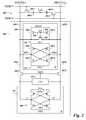
- FIG. 1is a block diagram of an apparatus in the form of an electronic system including a memory device in accordance with a number of embodiments of the present disclosure.
- FIG. 2is a schematic diagram illustrating a portion of a memory array including sensing circuitry in accordance with a number of embodiments of the present disclosure.
- FIG. 3is a schematic diagram illustrating a portion of a memory array including sensing circuitry that can be operated to reverse data stored in memory accordance with a number of embodiments of the present disclosure.
- FIG. 4A / 4 Bis a schematic diagram illustrating an example data path in an apparatus in accordance with a number of embodiments of the present disclosure.
- FIG. 5provides tables illustrating logical indices of data stored in an array before and after reversing data stored in memory in accordance with a number of embodiments of the present disclosure.
- FIG. 6is a timing diagram associated with reversing data stored in memory in accordance with a number of embodiments of the present disclosure.
- the present disclosureincludes apparatuses and methods related to reversing data stored in memory.
- a number of embodimentsinclude an apparatus comprising an array of memory cells, a first plurality of sensing components corresponding to a respective first plurality of columns of the array, a second plurality of sensing components corresponding to a respective second plurality of columns of the array, and a plurality of shared input/output (I/O) lines (which may be referred to as SIO lines).
- I/Oinput/output
- Each one of the plurality of SIO linescan be selectively coupled to a respective subset of the first plurality of sensing components and to a respective subset of the second plurality of sensing components.
- the apparatuscan include a controller configured to control reversing a logical sequence of data stored in a group of memory cells coupled to a first access line of the array by performing a plurality of transfer operations via the plurality of SIO lines.
- reversing datarefers reversing a logical sequence (e.g., order) of a stored data pattern.
- Reversing a stored data patterncan include writing the (reversed) data pattern back to a same group of memory cells in which the (nonreversed) data pattern was initially stored (e.g., a group of cells coupled to a same access line, which may be referred to herein as a “word line” or a “row”); however, embodiments are not so limited.
- reversing a stored data patterncan include writing the reversed data pattern to a group of cells other than the group of cells in which the nonreversed data pattern was initially stored (e.g., the reversed data pattern can be written to a group of cells coupled to a different word line).
- reversing dataincludes storing data in a manner such that a data unit (e.g., bit) corresponding to a first logical index (e.g., logical index “0” if a zero-based numbering convention is used) is stored so as to correspond to a last logical index (e.g., logical index “N ⁇ 1” if N represents the total number of bits in a sequence), a data unit corresponding to the last logical index (e.g., logical index “N ⁇ 1”) is stored so as to correspond to the first logical index (e.g., logical index “0”), the data unit corresponding to the second logical index (e.g., logical index “1”) is stored so as to correspond to the next to last logical index (e.g., logical index “N ⁇ 2”), and so on.
- a “logical index”refers to a logical address associated with a particular data unit.
- a number of embodimentscan include reversing the data corresponding to an entire row of a memory array in a faster and/or more efficient manner as compared to prior approaches. For example, consider a memory array comprising 16K (e.g., 16,000) columns (e.g., 16K sense lines or complementary sense line pairs, which may be referred to herein as “digit lines”) such that each row stores 16K data units (e.g., bits).
- a number of shared input/output (I/O) linescan be utilized to reverse the entire 16K bits corresponding to a particular row via a number of transfer operations.
- the transfer operationscan include swapping data values between subsets of sensing components selectively coupled to respective SIO lines.
- the number of transfer operationscan depend on the number of SIO lines corresponding to the array.
- the number of SIO linescorrelates to the number of sensing components selectively coupled to each of the respective SIO lines (with each one of the number of sensing components corresponding to a respective one of the columns). For instance, in this example, if the number of array columns is N (e.g., 16K) and each SIO line is selectively coupled to eight sensing components, then the number of SIO lines is 2K (e.g., 16K columns divided by 8 sensing components per SIO line). Similarly, if the number of SIO lines is “M”, then the number of sensing components per SIO line is “N/M”.
- the number of sensing components per SIO linewould be 4 (e.g., 16K columns divided by 4K SIO lines).
- the quantity “16K”can refer 16,384 (e.g., 2 14 )
- “4K”can refer to 4,096 (e.g., 2 12 )
- “2K”can refer 2,048 (e.g., 2 11 ), etc.
- “K”can represent the binary multiplier 2 10 (e.g., 1024).
- Previous approaches to reversing data stored in memoryoften involve moving subsets of the data to be reversed (e.g., bytes, words, etc.) out of the array to an external processing resource (e.g., a scalar processor).
- the external processing resource(s)can reverse the data and then the reversed data can be further operated on by the external processing resource and/or can be written back to the array.
- itcan be cumbersome to perform data reversal processes on large data sets (e.g., data of an entire row) in accordance with previous approaches.
- a number of embodiments of the present disclosurecan provide improved parallelism and/or reduced power consumption in association with reversing data stored in memory as compared to previous systems such as previous PIM systems and systems having an external processor (e.g., a processing resource located external from a memory array, such as on a separate integrated circuit chip).
- an external processore.g., a processing resource located external from a memory array, such as on a separate integrated circuit chip.
- a number of a particular thingcan refer to one or more of such things (e.g., a number of memory arrays can refer to one or more memory arrays).
- a “plurality of”is intended to refer to more than one of such things.
- FIG. 1is a block diagram of an apparatus in the form of an electronic system 100 including a memory device 120 in accordance with a number of embodiments of the present disclosure.
- a memory device 120 , memory controller 140 , channel controller 143 , memory array 130 , sensing circuitry 150 , including sensing components, and peripheral logic 170might each also be separately considered an “apparatus.”
- the system 100includes a host 110 coupled (e.g., connected) to memory device 120 , which includes the memory array 130 .
- Host 110can be a host system such as a personal laptop computer, a desktop computer, a tablet computer, a digital camera, a smart phone, or a memory card reader, among various other types of hosts.
- Host 110can include a system motherboard and/or backplane and can include a number of processing resources (e.g., one or more processors, microprocessors, or some other type of controlling circuitry).
- the system 100can include separate integrated circuits or both the host 110 and the memory device 120 can be on the same integrated circuit.
- the system 100can be, for instance, a server system and a high performance computing (HPC) system and/or a portion thereof.
- HPChigh performance computing
- FIG. 1illustrates a system having a Von Neumann architecture
- embodiments of the present disclosurecan be implemented in non-Von Neumann architectures, which may not include one or more components (e.g., CPU, ALU, etc.) often associated with a Von Neumann architecture.
- the memory array 130can be a DRAM array, SRAM array, STT RAM array, PCRAM array, TRAM array, RRAM array, NAND flash array, and NOR flash array, for instance.
- the memory array 130can include memory cells arranged in rows coupled by access lines (which may be referred to herein as word lines or select lines) and columns coupled by sense lines (which may be referred to herein as data lines or digit lines).
- access lineswhich may be referred to herein as word lines or select lines
- sense lineswhich may be referred to herein as data lines or digit lines.
- memory device 120may include a number of memory arrays 130 (e.g., a number of banks of DRAM cells, NAND flash cells, etc.).
- the memory device 120includes address circuitry 142 to latch address signals provided over an address/control bus 154 (e.g., an address/control bus from the host 110 ). Address signals are received by address circuitry 142 and decoded by row decode circuitry 146 and column decode circuitry 152 to access the memory array 130 .
- address/control bus 154is shown as a single bus, the bus 154 can comprise separate address and control busses.
- the column decode circuitry 152can comprise logic (e.g., multiplexor circuitry) to selectively couple shared I/O lines (e.g., SIO line 355 shown in FIG. 3 ) to subsets of sensing components in association with reversing data stored in memory in accordance with embodiments described herein.
- the shared I/O (SIO) linescan provide an increased data path size (e.g., width) as compared to previous data paths used to move data from the array 130 (e.g., via a data bus such as data bus 475 shown in FIG. 4A / 4 B) to DQ pads, for instance, among other benefits.
- the SIO linesmay serve as both local I/O lines and global I/O lines corresponding to array 130 , which can facilitate moving data between subarrays (e.g., portions of a memory array being coupled to separate sensing circuitry stripes).
- Datacan be sensed (read) from memory array 130 by sensing voltage and/or current changes on digit lines using a number of sensing components (e.g., sense amplifiers) of the sensing circuitry 150 .
- a sense amplifiercan read and latch a page (e.g., a row) of data from the memory array 130 .
- the sensing components of the sensing circuitry 150can comprise respective sense amplifiers and corresponding compute components coupled thereto that can be used to sense, store (e.g., cache and/or buffer), and move data, for instance.
- the I/O circuitry 144can be used for bi-directional data communication with host 110 over the data bus 156 (e.g., DQ connections).
- the write circuitry 148can be used to write data to the memory array 130 .
- Memory controller 140which can serve as a sequencer, can decode control signals (e.g., commands) provided by address/control bus 154 from the host 110 . These signals can include chip enable signals, write enable signals, and address latch signals that can be used to control operations performed on the memory array 130 , including data sense, data store, data move, data write, and data erase operations, among other operations.
- the memory controller 140can be responsible for executing instructions from the host 110 and/or accessing the memory array 130 .
- the memory controller 140can be a state machine, a sequencer, or some other type of controller and can be implemented in hardware, software, firmware, and/or combinations thereof.
- system 100includes a bus 157 which can provide, for example, status and exception information from the memory controller 140 to a channel controller 143 .
- the sensing circuitry 150can include a number of sense amplifiers and corresponding compute components, which may serve as an accumulator and can be used to perform logical operations (e.g., on data associated with complementary sense lines).
- the sensing circuitry 150can be used to reverse data stored in memory (e.g., in array 130 ) in accordance with embodiments described herein.
- the sensing circuitry 150can also be used to perform logical operations (e.g., logical functions such as AND, OR, NOT, NOR, NAND, XOR, etc.) using data stored in memory array 130 as inputs and participate in movement of the data for writing and storage operations back to a different location in the memory array 130 without transferring the data via a sense line address access (e.g., without firing a column decode signal).
- logical operationse.g., logical functions such as AND, OR, NOT, NOR, NAND, XOR, etc.
- various compute functionscan be performed using, and within, sensing circuitry 150 rather than (or in association with) being performed by processing resources external to the sensing circuitry 150 (e.g., by a processor associated with host 110 and other processing circuitry, such as ALU circuitry, located on device 120 , such as on memory controller 140 or elsewhere).
- processing resources external to the sensing circuitry 150e.g., by a processor associated with host 110 and other processing circuitry, such as ALU circuitry, located on device 120 , such as on memory controller 140 or elsewhere.
- sensing circuitry 150is configured to perform logical operations on data stored in memory array 130 and store the result back to the memory array 130 without enabling a local I/O line and global I/O line coupled to the sensing circuitry 150 .
- the sensing circuitry 150can be formed on pitch with the memory cells of the array.
- Additional peripheral logic 170which can include an additional number of sense amplifiers, can be coupled to the sensing circuitry 150 .
- the sensing circuitry 150 and the peripheral logic 170can cooperate in performing logical operations and/or in reversing data stored in memory, according to a number of embodiments described herein.
- circuitry external to memory array 130 and sensing circuitry 150is not needed to reverse data stored in memory array 130 and/or to perform compute functions as the sensing circuitry 150 can perform the appropriate operations in order to perform such data reversal and/or compute functions without the use of an external processing resource. Therefore, the sensing circuitry 150 may be used to complement and to replace, at least to some extent, such an external processing resource (or at least the bandwidth consumption of such an external processing resource).
- FIG. 2is a schematic diagram illustrating a portion of a memory array 230 including sensing circuitry in accordance with a number of embodiments of the present disclosure.
- the sensing component 250represents one of a number of sensing components that can correspond to sensing circuitry 150 shown in FIG. 1 .
- the memory array 230is a DRAM array of 1T1C (one transistor one capacitor) memory cells in which a transistor serves as the access device and a capacitor serves as the storage element; although other embodiments of configurations can be used (e.g., 2T2C with two transistors and two capacitors per memory cell).
- a first memory cellcomprises transistor 202 - 1 and capacitor 203 - 1
- a second memory cellcomprises transistor 202 - 2 and capacitor 203 - 2 , etc.
- the memory cellsmay be destructive read memory cells (e.g., reading the data stored in the cell destroys the data such that the data originally stored in the cell is refreshed after being read).
- the cells of the memory array 230can be arranged in rows coupled by access lines 204 -X (Row X), 204 -Y (Row Y), etc., and columns coupled by pairs of complementary sense lines (e.g., digit lines 205 - 1 labelled DIGIT(n) and 205 - 2 labelled DIGIT(n)_in FIG. 2 and digit lines 305 - 0 labelled DIGIT_ 0 and 305 - 0 * labelled DIGIT_ 0 * in FIG. 3 ). Although only one pair of complementary digit lines are shown in FIG. 2 , embodiments of the present disclosure are not so limited, and an array of memory cells can include additional columns of memory cells and digit lines (e.g., 4,096, 8,192, 16,384, etc.).
- Memory cellscan be coupled to different digit lines and word lines. For instance, in this example, a first source/drain region of transistor 202 - 1 is coupled to digit line 205 - 1 , a second source/drain region of transistor 202 - 1 is coupled to capacitor 203 - 1 , and a gate of transistor 202 - 1 is coupled to word line 204 -Y.
- a first source/drain region of transistor 202 - 2is coupled to digit line 205 - 2
- a second source/drain region of transistor 202 - 2is coupled to capacitor 203 - 2
- a gate of transistor 202 - 2is coupled to word line 204 -X.
- a cell plateas shown in FIG. 2 , can be coupled to each of capacitors 203 - 1 and 203 - 2 .
- the cell platecan be a common node to which a reference voltage (e.g., ground) can be applied in various memory array configurations.
- the digit lines 205 - 1 and 205 - 2 of memory array 230are coupled to sensing component 250 in accordance with a number of embodiments of the present disclosure.
- the sensing component 250comprises a sense amplifier 206 and a compute component 231 corresponding to a respective column of memory cells (e.g., coupled to a respective pair of complementary digit lines).
- the sense amplifier 206is coupled to the pair of complementary digit lines 205 - 1 and 205 - 2 .
- the compute component 231is coupled to the sense amplifier 206 via pass gates 207 - 1 and 207 - 2 .
- the gates of the pass gates 207 - 1 and 207 - 2can be coupled to selection logic 213 .
- the selection logic 213can include pass gate logic for controlling pass gates that couple the pair of complementary digit lines un-transposed between the sense amplifier 206 and the compute component 231 and swap gate logic for controlling swap gates that couple the pair of complementary digit lines transposed between the sense amplifier 206 and the compute component 231 .
- the selection logic 213can be coupled to the pair of complementary digit lines 205 - 1 and 205 - 2 and configured to perform logical operations on data stored in array 230 .
- the selection logic 213can be configured to control continuity of (e.g., turn on/turn off) pass gates 207 - 1 and 207 - 2 based on a selected logical operation that is being performed.
- the sense amplifier 206can be operated to determine a data value (e.g., logic state) stored in a selected memory cell.
- the sense amplifier 206can comprise a cross coupled latch 215 (e.g., gates of a pair of transistors, such as n-channel transistors 227 - 1 and 227 - 2 are cross coupled with the gates of another pair of transistors, such as p-channel transistors 229 - 1 and 229 - 2 ), which can be referred to herein as a primary latch.
- a cross coupled latch 215e.g., gates of a pair of transistors, such as n-channel transistors 227 - 1 and 227 - 2 are cross coupled with the gates of another pair of transistors, such as p-channel transistors 229 - 1 and 229 - 2
- a primary latche.g., embodiments are not limited to this example.
- the voltage on one of the digit lines 205 - 1 or 205 - 2will be slightly greater than the voltage on the other one of digit lines 205 - 1 or 205 - 2 .
- An ACT signal and an RNL* signalcan be driven low to enable (e.g., fire) the sense amplifier 206 .
- the digit line 205 - 1 or 205 - 2 having the lower voltagewill turn on one of the transistors 229 - 1 or 229 - 2 to a greater extent than the other of transistors 229 - 1 or 229 - 2 , thereby driving high the digit line 205 - 1 or 205 - 2 having the higher voltage to a greater extent than the other digit line 205 - 1 or 205 - 2 is driven high.
- the digit line 205 - 1 or 205 - 2 having the higher voltagewill turn on one of the transistors 227 - 1 or 227 - 2 to a greater extent than the other of the transistors 227 - 1 or 227 - 2 , thereby driving low the digit line 205 - 1 or 205 - 2 having the lower voltage to a greater extent than the other digit line 205 - 1 or 205 - 2 is driven low.
- the digit line 205 - 1 or 205 - 2 having the slightly greater voltageis driven to the voltage of the supply voltage Vcc through a source transistor, and the other digit line 205 - 1 or 205 - 2 is driven to the voltage of the reference voltage (e.g., ground) through a sink transistor. Therefore, the cross coupled transistors 227 - 1 and 227 - 2 and transistors 229 - 1 and 229 - 2 serve as a sense amplifier pair, which amplify the differential voltage on the digit lines 205 - 1 and 205 - 2 and operate to latch a data value sensed from the selected memory cell.
- Embodimentsare not limited to the sensing component configuration illustrated in FIG. 2 .
- the sense amplifier 206can be a current-mode sense amplifier and/or a single-ended sense amplifier (e.g., sense amplifier coupled to one digit line).
- embodiments of the present disclosureare not limited to a folded digit line architecture such as that shown in FIG. 2 .
- the sensing component 250can be one of a plurality of sensing components selectively coupled to a shared I/O line (e.g., SIO line 355 shown in FIG. 3 ). As such, the sensing component 250 can be used in association with reversing data stored in memory in accordance with a number of embodiments of the present disclosure.
- the sense amplifier 206includes equilibration circuitry 214 , which can be configured to equilibrate the digit lines 205 - 1 and 205 - 2 .
- the equilibration circuitry 214comprises a transistor 224 coupled between digit lines 205 - 1 and 205 - 2 .
- the equilibration circuitry 214also comprises transistors 225 - 1 and 225 - 2 each having a first source/drain region coupled to an equilibration voltage (e.g., VDD/2), where VDD is a supply voltage associated with the array.
- VDD/2equilibration voltage
- a second source/drain region of transistor 225 - 1is coupled to digit line 205 - 1
- a second source/drain region of transistor 225 - 2is coupled to digit line 205 - 2
- Gates of transistors 224 , 225 - 1 , and 225 - 2can be coupled together and to an equilibration (EQ) control signal line 226 .
- EQequilibration
- activating EQenables the transistors 224 , 225 - 1 , and 225 - 2 , which effectively shorts digit lines 205 - 1 and 205 - 2 together and to the equilibration voltage (e.g., VDD/2).
- sense amplifier 206comprising the equilibration circuitry 214
- embodimentsare not so limited, and the equilibration circuitry 214 may be implemented discretely from the sense amplifier 206 , implemented in a different configuration than that shown in FIG. 2 , or not implemented at all.
- the compute component 231can also comprise a latch, which can be referred to herein as a secondary latch 264 .
- the secondary latch 264can be configured and operated in a manner similar to that described above with respect to the primary latch 215 , with the exception that the pair of cross coupled p-channel transistors (e.g., PMOS transistors) included in the secondary latch can have their respective sources coupled to a supply voltage (e.g., VDD), and the pair of cross coupled n-channel transistors (e.g., NMOS transistors) of the secondary latch can have their respective sources selectively coupled to a reference voltage (e.g., ground), such that the secondary latch is continuously enabled.
- the configuration of the compute component 231is not limited to that shown in FIG. 2 , and various other embodiments are feasible.
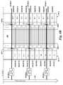
- FIG. 3is a schematic diagram illustrating a portion of a memory array 330 including sensing circuitry that can be operated to reverse data stored in memory accordance with a number of embodiments of the present disclosure.
- the array 330is a subarray of DRAM memory cells; however, embodiments are not so limited.
- a subarraycan refer to a portion of a memory array coupled to a respective “stripe” of sensing components.
- a memory array “bank”may comprise a plurality of subarrays, with each subarray corresponding to a one of a respective plurality of sensing stripes.
- the example shown in FIG. 3includes eight sensing components 350 - 0 , 350 - 1 , . . . , 350 - 7 of a sensing component stripe.
- Each of the sensing components 350 - 0 to 350 - 7is coupled to a pair of complementary sense lines (e.g., 305 - 0 (DIGIT_ 0 and 305 - 1 (DIGIT_ 0 *) and corresponds to a respective column 322 - 0 to 322 - 7 of the array.
- the sensing components 350 - 0 to 350 - 7can be sensing components such as those shown in FIG. 2 .
- the array 330has a folded digit line architecture and the sensing components 350 - 0 to 350 - 7 (which may be referred to generally as sensing components 350 ) are interleaved such that sensing components corresponding to physically adjacent columns are located on opposite sides of the array 330 .
- the sensing componentsare interleaved such that sensing components corresponding to even numbered columns (e.g., 322 - 0 , 322 - 2 , 322 - 4 , and 322 - 6 ) are arranged on one side of the array 330 (e.g., on the bottom as shown in FIG.
- sensing components corresponding to odd numbered columnsare arranged on the opposite side of the array 330 (e.g., on the top as shown in FIG. 3 ).
- the sensing components 350 - 0 to 350 - 7are selectively coupled to an SIO line, which is referred to generally as an SIO line 355 .
- the SIO line 355is selectively coupled to eight sensing components 350 .
- the SIO line 355comprises a pair of complementary SIO lines 355 - 0 (e.g., SHARED I/O LINE) and 355 - 0 * (e.g., SHARED I/O LINE*).
- the sensing components 350 - 0 to 350 - 7are selectively coupled to the SIO line 355 via column decode circuitry (e.g., column decode circuitry 152 shown in FIG. 1 ). As such, the column decode circuitry can be used to select which one of the eight sensing components is coupled to the SIO line 355 at a particular time.
- the column decode circuitrycomprises pairs of select devices (e.g., transistors) 359 - 0 / 359 - 0 * to 359 - 7 / 359 - 7 * whose gates are coupled to corresponding respective column select lines 358 - 0 to 358 - 7 .
- column select line 358 - 0e.g., column select line 0
- each of the select devicesis coupled between a sense line corresponding to a particular column 322 and the shared I/O line 355 .
- select device 359 - 0is coupled between sense line 305 - 0 corresponding to column 322 - 0 and SIO line 355 - 0
- select device 359 - 0 *is coupled between complementary sense line 305 - 0 * and complementary SIO line 355 - 0 *.
- an activation signale.g., voltage
- a data value stored in a memory cell coupled to a particular column 322 of the array 330can be sensed via a corresponding sensing component 350 , can be transferred to the SIO line 355 (e.g., via activation of the column select line 358 corresponding to the particular column 322 ), can be transferred from the SIO line 355 to a sensing component 350 corresponding to a different column 322 (e.g., via activation of the column select line 358 corresponding to the different column 322 ), and can be stored in a memory cell coupled to the different column.
- a number of transfer operations via SIO lines(e.g., 355 ) can be performed in association with reversing data stored in memory in accordance with a number of embodiments of the present disclosure.
- Embodimentsare not limited to the example shown in FIG. 3 .
- embodimentscan include arrays comprising many more columns 322 and SIO lines 355 , and the SIO lines 355 can be selectively coupled to more or fewer than 8 sensing components 350 .
- each of the plurality of SIO lineswould be selectively coupled to a particular sensing component of a different subset of sensing components 350 via the same column select lines 358 - 0 to 358 - 7 .
- a second SIO line 355e.g., SIO line pair 355 - 1 / 355 - 1 * not shown in FIG.
- the decode circuitrycould be configured such that activation of column select line 358 - 0 couples sensing component 350 - 0 of column 322 - 0 to SIO line pair 355 - 0 / 355 - 0 * and also couples sensing component 350 - 8 of column 322 - 8 to SIO line pair 355 - 1 / 355 - 1 *.
- activating column select line 358 - 0could correspond to coupling columns 0 , 8 , 16 , 24 , etc., to respective SIO lines
- activating column select line 358 - 1could correspond to coupling columns 1 , 9 , 17 , 25 , etc., to respective SIO lines
- activating column select line 358 - 2could correspond to coupling columns 2 , 10 , 18 , 26 , etc., to respective SIO lines
- activating column select line 358 - 3could correspond to coupling columns 3 , 11 , 19 , 27 , etc., to respective SIO lines
- activating column select line 358 - 4could correspond to coupling columns 4 , 12 , 20 , 28 , etc., to respective SIO lines
- activating column select line 358 - 5could correspond to coupling columns 5 , 13 , 21 , 29 , etc., to respective SIO lines, activating
- FIG. 4A / 4 B(which may be referred to as FIG. 4 ) is a schematic diagram illustrating an example data path in an apparatus in accordance with a number of embodiments of the present disclosure.
- the data path shown in FIG. 4comprises a plurality of shared I/O (SIO) lines 455 - 0 , 455 - 1 , . . . , 455 -(M ⁇ 1) (referred to generally as SIO lines 455 ).
- SIO lines 455shared I/O lines 455
- each of the plurality of SIO lines 455 - 0 to 455 -(M ⁇ 1)is coupled to one of a respective plurality of sense amplifiers 470 - 0 to 470 -(M ⁇ 1).
- the sense amplifiers 470 - 0 to 470 -(M ⁇ 1)which can be referred to generally as sense amplifiers 470 , can correspond to logic 170 shown in FIG. 1 .
- data valuescan be transferred out of array 430 to data I/O pads (e.g., DQs not shown in FIG. 4 ) via a bus 475 , which is coupled to the sense amplifiers 470 .
- the datacan then be transferred to an external processing resource, for example.
- the array 430comprises a plurality of columns 422 - 0 to 422 -(N ⁇ 1) (referred to generally as columns 422 ). In the example shown in FIG. 4 , the array 430 comprises 16K (e.g., 16,000) columns 422 . Each of the columns 422 comprises a pair of complementary sense lines (e.g., 405 - 0 and 405 - 0 *); however, embodiments are not limited to complementary sense line pairs.
- the array 430comprises a plurality of sensing components corresponding to the respective plurality of columns 422 and coupled to the respective sense line pairs.
- the array 430is arranged in a folded and interleaved sense line architecture in which a first plurality of sensing components (referred to generally as sensing component stripe 451 - 0 ) correspond to respective even numbered columns 422 (e.g., 422 - 0 , 422 - 2 , 422 - 4 , . . . , 422 -(N ⁇ 2)), and in which a second plurality of sensing components (referred to generally as sensing component stripe 451 - 1 ) correspond to respective odd numbered columns 422 (e.g., 422 - 1 , 422 - 3 , 422 - 5 , . . . , 422 -(N ⁇ 1)).
- a first plurality of sensing componentsreferred to generally as sensing component stripe 451 - 0
- sensing component stripe 451 - 1correspond to respective even numbered columns 422 (e.g., 422 - 0 , 422 - 2 ,
- the sensing component stripe 451 - 0is located on one side of array 430 (e.g., the right side as shown in FIG. 4 ), and the sensing component stripe 451 - 1 is located on the opposite side of array 430 (e.g., the left side as shown in FIG. 4 ).
- each of the SIO lines 455is selectively coupled to a subset of the sensing components of stripe 451 - 0 and to a subset of the sensing components of stripe 451 - 1 .
- each of the SIO lines 455is selectively coupled to eight sensing components (e.g., four sensing components of stripe 451 - 0 and four sensing components of stripe 451 - 1 ).
- each of the SIO lines 455corresponds to eight physically sequential columns 422 of the array (e.g., SIO line 455 - 0 corresponds to columns 422 - 0 to 422 - 7 , SIO line 455 - 1 corresponds to columns 422 - 8 to 422 - 15 , SIO line 455 -(M ⁇ 1) corresponds to columns 422 -(N ⁇ 8) to 455 -(N ⁇ 1), etc.). That is, each one of the SIO lines 455 is selectively coupled to a respective subset of sensing components of stripe 451 - 0 and a respective subset of sensing components of stripe 451 - 1 .
- the stripes 451 - 0 and 451 - 1can comprise sensing components such as sensing components 350 described in association with FIG. 3 , for example.
- the SIO lines 455are selectively coupled to the corresponding respective subsets of sensing components of stripes 451 - 0 / 451 - 1 via column select circuitry, which is represented by elements 460 - 0 to 460 - 7 in FIG. 4 .
- the column select circuitrywhich can be referred to generally as column select circuitry 460 , can represent at least a portion of column decode circuitry 152 shown in FIG. 1 and/or column decode circuitry 358 / 359 shown in FIG. 3 .
- the column select circuitry 460can comprise multiplexer circuitry (e.g., an 8 to 1 multiplexer) configured to selectively couple a particular SIO line 455 to one of a subset of eight sensing components corresponding to the particular SIO line 455 .
- multiplexer circuitrye.g., an 8 to 1 multiplexer
- each of the plurality of SIO lines 455is selectively coupled to the sensing components corresponding to a respective eight columns 422
- the column select circuitry 460can be configured to selectively couple one sensing component from each of the “M” subsets of sensing components to the corresponding respective “M” SIO lines 455 in parallel.
- column select circuitry 460 - 0can be configured to selectively couple, in parallel, the sensing component corresponding to column 422 - 0 to SIO line 455 - 0 , the sensing component corresponding to column 422 - 8 to SIO line 455 - 1 , . . . , and the sensing component corresponding to column 422 -(N ⁇ 8) to SIO line 455 -(M ⁇ 1).
- the column select circuitry 460 - 1can be configured to selectively couple, in parallel, the sensing component corresponding to column 422 - 1 to SIO line 455 - 0 , the sensing component corresponding to column 422 - 9 to SIO line 455 - 1 , . . .
- the column select circuitry 460 - 2can be configured to selectively couple, in parallel, the sensing component corresponding to column 422 - 2 to SIO line 455 - 0 , the sensing component corresponding to column 422 - 10 to SIO line 455 - 1 , . . . , and the sensing component corresponding to column 422 -(N ⁇ 6) to SIO line 455 -(M ⁇ 1).
- the column select circuitry 460 - 3can be configured to selectively couple, in parallel, the sensing component corresponding to column 422 - 3 to SIO line 455 - 0 , the sensing component corresponding to column 422 - 11 to SIO line 455 - 1 , . . . , and the sensing component corresponding to column 422 -(N ⁇ 5) to SIO line 455 -(M ⁇ 1).
- the column select circuitry 460 - 4can be configured to selectively couple, in parallel, the sensing component corresponding to column 422 - 4 to SIO line 455 - 0 , the sensing component corresponding to column 422 - 12 to SIO line 455 - 1 , . . .
- the column select circuitry 460 - 5can be configured to selectively couple, in parallel, the sensing component corresponding to column 422 - 5 to SIO line 455 - 0 , the sensing component corresponding to column 422 - 13 to SIO line 455 - 1 , . . . , and the sensing component corresponding to column 422 -(N ⁇ 3) to SIO line 455 -(M ⁇ 1).
- the column select circuitry 460 - 6can be configured to selectively couple, in parallel, the sensing component corresponding to column 422 - 6 to SIO line 455 - 0 , the sensing component corresponding to column 422 - 14 to SIO line 455 - 1 , . . . , and the sensing component corresponding to column 422 -(N ⁇ 2) to SIO line 455 -(M ⁇ 1).
- the column select circuitry 460 - 7can be configured to selectively couple, in parallel, the sensing component corresponding to column 422 - 7 to SIO line 455 - 0 , the sensing component corresponding to column 422 - 15 to SIO line 455 - 1 , . . . , and the sensing component corresponding to column 422 -(N ⁇ 1) to SIO line 455 -(M ⁇ 1).
- datacan be transferred from the sensing components corresponding to columns selected via the column select circuitry 460 to the respective SIO lines 455 (e.g., the sensed data stored in the sensing components can be driven onto the respective SIO lines 455 ).
- the datacan then be transferred from the SIO lines 455 to a different storage location.
- the data driven onto each one of the respective SIO lines 455can be transferred to a sensing component corresponding to a different selected column (e.g., via the appropriate column select circuitry 460 corresponding to the different selected respective columns 422 ).
- the datacan then be stored to a memory cell coupled to a selected access line (e.g., 425 - 1 , 425 - 2 ) of the array 430 via the corresponding sense lines 405 .
- the different storage locationcan be external from the array 430 .
- the sense amplifiers 470can serve as the different storage location; however, embodiments are not so limited.
- References 471 - 0 and 471 - 1 shown in FIG. 4indicate the logical indices corresponding to respective columns 422 .
- the example shown in FIG. 4includes 16K logical indices (e.g., numbered “0” to “16K ⁇ 1”) corresponding to the respective 16K columns 422 . That is, each of the “N” physical columns 422 , with N being 16K in this example, is assigned a logical index which corresponds to the logical index of data stored in the cells coupled to a particular row (e.g., 425 - 1 , 425 - 2 ) of the array 430 .
- the references 471 - 0 and 471 - 1indicate the logical indices of data units (e.g., bits) stored in a row (e.g., 425 - 1 , 425 - 2 ) of array 430 .
- the data stored in one of eight different memory cellscan be driven onto each respective SIO line 455 (e.g., via the corresponding sensing components and circuitry 460 ).
- data on each respective SIO line 455can be transferred to one of the eight different memory cells (e.g., via the corresponding sensing components and circuitry 460 ).
- the logical indices of the M particular subsets of the 16K columns 422 assigned to the respective M SIO lines 455are assigned as follows:
- the eight physical columns 422 selectively coupled to the first SIO line 455 - 0are assigned respective logical indices “0,” “16K ⁇ 1,” “4K,” “12K ⁇ 1,” “8K,” “8K ⁇ 1,” “12K,” and “4K ⁇ 1” (as indicated at references 470 - 0 and 470 - 1 ).
- the eight physical columns 422 selectively coupled to the last SIO line 455 -(M ⁇ 1)are assigned respective logical indices “2K ⁇ 1,” “14K,” “6K ⁇ 1,” “10K,” “10K ⁇ 1,” “6K,” “14K ⁇ 1,” and “2K.”
- Embodimentsare not limited to logical index assignments shown in FIG. 4 .
- a number of embodiments of the present disclosurecan include reversing a data pattern stored in an array (e.g., a data pattern stored in a particular row 425 - 1 of array 430 ) by performing a plurality of transfer operations via the SIO lines 455 .
- performing the transfer operationscan include transferring data between subsets of the sensing components of stripe 451 - 0 and respective subsets of the sensing components of stripe 451 - 1 . Transferring data between subsets of sensing components of stripe 451 - 0 and subsets of sensing components of stripe 451 - 1 can be referred to as “swapping” data.
- a 16K bit data pattern(e.g., bit-vector) stored in the memory cells commonly coupled to a particular row (e.g., access line 425 - 1 ).
- the 16K data pattern stored in the particular rowcan be reversed and the reversed data pattern can be stored back to array 430 (e.g., the reversed data pattern can be written to the particular row such that the data previously stored in the particular row is replaced and/or the reversed data pattern can be written to a row other than the particular row).
- Reversing the stored data patterncan include sensing a first subset of the cells coupled to a particular row (e.g., access line 425 - 1 in this example).
- the first subset of cellscan comprise those cells of the columns 422 coupled to respective SIO lines 455 in parallel via column select circuitry 460 - 0 (e.g., cells corresponding to columns 422 - 0 , 422 - 8 , . . . , 422 -(N ⁇ 8)).
- Sensing the first subset of cellscan include storing the data values of the first subset of cells in respective latches (e.g., sense amplifier latch and/or compute component latch) of the sensing components 451 - 0 corresponding to the respective 2K columns 422 .
- the sensed data of the first subset of cellscan be stored in a number of temporary storage locations. For instance, the sensed data corresponding to the first subset of cells can be written (e.g., at least temporarily) to memory cells corresponding to the same respective 2K columns but commonly coupled to a different access line (e.g., cells corresponding to columns 422 - 0 , 422 - 8 , . . .
- Embodimentsare not limited to a particular temporary storage location.
- the temporary storage locationscould include sense amplifiers 470 , among other temporary storage locations suitable for storing sensed data corresponding to the first subset of cells.
- Reversing the stored data patterncan include subsequently sensing a second subset of the cells (e.g., an additional 2K cells corresponding to 2K bits) coupled to the access line 425 - 1 .
- the second subset of cellscan comprise those cells of the columns 422 coupled to respective SIO lines 455 in parallel via column select circuitry 460 - 1 (e.g., cells corresponding to the 2K columns 422 - 1 , 422 - 9 , . . . , 422 -(N ⁇ 7)).
- Sensing the second subset of cellscan include storing the data values of the second subset of cells in respective latches (e.g., sense amplifier latch and/or compute component latch) of the sensing components 451 - 1 corresponding to the respective columns 422 .
- the data of the second subset of cellscan be transferred, via the 2K SIO lines 455 - 0 to 455 -(M ⁇ 1), from the respective sensing components 451 - 1 (e.g., the sensing components corresponding to columns 422 - 1 , 422 - 9 , . . .
- the respective sensing components 451 - 0corresponding to the first subset of cells (e.g., the sensing components 451 - 0 corresponding to columns 422 - 0 , 422 - 8 , . . . , 422 -(N ⁇ 8)).
- the data of the second subset of cellscan then be written, from the respective sensing components 451 - 0 , to the memory cells of a target row (e.g., to row 425 - 1 and/or to a different row of array 430 to which the reversed data pattern is to be stored).
- the 2K bits corresponding to the first subset of cells, which was stored in the temporary storage locationscan be sensed by the sensing components of stripe 451 - 0 corresponding to the first subset of columns 422 (e.g., 422 - 0 , 422 - 8 , . . . , 422 -(N ⁇ 8), and can be transferred, via the 2K SIO lines 455 - 0 to 455 -(M ⁇ 1), from the respective sensing components 451 - 0 to the respective sensing components 451 - 1 corresponding to the second subset of cells (e.g., the sensing components 451 - 1 corresponding to columns 422 - 1 , 422 - 9 , . . .
- the data of the first subset of cellscan then be written, from the respective sensing components 451 - 1 , to the memory cells of the target row.
- the 2K bits of data stored in cells corresponding to the first subset of columns 422e.g., 2K even numbered columns corresponding to stripe 451 - 0
- 2K bits of data stored in cells corresponding to the second subset of columns 422e.g., 2K odd numbered columns corresponding to stripe 451 - 1 ).
- the logical indices corresponding to the data values stored in the target roware reversed as compared to the logical indices of the data in the particular row (e.g., 425 - 1 ).
- the data value previously stored in a cell corresponding to logical column “0”e.g., physical column 422 - 0
- the data value previously stored in a cell corresponding to logical column “16K ⁇ 1”e.g., physical column 422 - 1
- the data value previously stored in a cell corresponding to logical column “16K ⁇ 1”e.g., physical column 422 - 1
- the data value previously stored in a cell corresponding to logical column “16K ⁇ 1”e.g., physical column 422 - 1
- the data value previously stored in a cell corresponding to logical column “0”e.g., physical column 422 - 0 .
- the data valuecan be held temporarily by sense amplifiers 470 - 0 to 470 -(M ⁇ 1) to transfer the data value.
- the data value formerly corresponding to the first logical index(e.g., “0”) corresponds to the last logical index (e.g., “16K ⁇ 1”) and vice versa.
- the data value previously stored in a cell corresponding to logical column “1”is stored in a cell coupled to the target row and corresponding to logical index “16K ⁇ 2” (e.g., physical column 422 - 9 )
- the data value previously stored in a cell corresponding to logical column “16K ⁇ 2”is stored in a cell coupled to the target row and corresponding to logical column “1” (e.g., physical column 422 - 8 ).
- the data value formerly corresponding to the second logical index(e.g., “1”) corresponds to the next to last logical index (e.g., “16K ⁇ 2”) and vice versa.
- transfer operations described above and involving swapping the data stored in the first and second subsets of cellscan be repeated for the remaining 12K cells of the row such that the entire row (e.g., 425 - 1 ) is reversed.
- transfer operationscan be performed to swap the data stored in a subset of cells of columns coupled to respective SIO lines 455 in parallel via column select circuitry 460 - 2 (e.g., even numbered columns 422 - 2 , 422 - 10 , . . .
- the number of swaps performed in order to reverse the entire row of datacan be N/2M (e.g., the number of columns 422 divided by two times the number of SIO lines 455 ).
- reversing the entire rowinvolves 4 swaps.
- the reversed data patterncan be read out of the array (e.g., to external processing circuitry) via peripheral sense amps 470 - 0 to 470 -(M ⁇ 1).
- the column select circuitry 460can be operated to drive 2K bits onto the 2K SIO lines 455 - 0 to 455 -(M ⁇ 1), the data can be latched by the respective sense amplifiers 470 - 0 to 470 -(M ⁇ 1), and can be moved to DQ pads via data bus 475 .
- embodiments of the present disclosurecan facilitate reversal of relatively large data sets (e.g., bit-vectors) in a more efficient manner than various previous approaches, which may require bit, byte, and word actions within a host processor, for example, in order to perform data reversals.
- relatively large data setse.g., bit-vectors
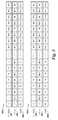
- FIG. 5provides tables illustrating logical indices of data stored in an array before and after reversing data stored in memory in accordance with a number of embodiments of the present disclosure.
- Row 596 - 1 of Table 590 - 1indicates the indices of a number of data units (e.g., bits) D 0 to D N-1 prior to being reversed
- Row 596 - 2 of Table 590 - 2indicates the indices of the number of data units D 0 to D N-1 after being reversed in accordance with a number of embodiments of the present disclosure.
- Row 592 of tables 590 - 1 and 590 - 2indicate the physical column numbers 0 , 1 , . . . , (N ⁇ 1) corresponding to an array (e.g., array 430 shown in FIG. 4 ).
- Row 594 of tables 590 - 1 and 590 - 2indicate the logical indices assigned to the respective physical columns (e.g., columns 422 shown in FIG. 4 ).
- each assigned one of a respective 16K logical indicese.g., 0, 1, . . . , (16K ⁇ 1)).
- the logical indices assigned to the columnsremain the same before and after reversing the data of a particular row.
- bit D 0is stored in a cell corresponding to physical column “ 0 ,” which is assigned logical index “0” (e.g., a first logical index in the 16K sequence)
- bit D 1is stored in a cell corresponding to physical column “ 1 ,” which is assigned logical index “16K ⁇ 1” (e.g., the last logical index in a 16K sequence)
- bit D 2is stored in a cell corresponding to physical column “ 2 ,” which is assigned logical index “4K,” . . .
- bit D N-1is stored in a cell corresponding to physical column “N ⁇ 1,” which is assigned logical index “2K.”
- Row 596 - 2 of table 590 - 2illustrates the logical indices of bits Do to D N-1 after being reversed in accordance with embodiments described herein.
- bit Dois stored in a cell corresponding to physical column “ 1 ,” which is assigned logical index “16K ⁇ 1”
- bit D 1is stored in a cell corresponding to physical column “ 0 ,” which is assigned logical index “0”.
- bit D 0goes from being the first bit in the data pattern (e.g., logical index “0” prior to reversal to being the last bit in the data pattern (e.g., logical index “16K ⁇ 1” after reversal.
- the logical indicesare assigned to the physical columns such that swapping the data values stored in adjacent physical columns (e.g., physical columns 0 / 1 , physical columns 2 / 3 , . . . , physical columns (N ⁇ 2)/(N ⁇ 1)) results in reversing the stored data pattern.
- adjacent physical columnse.g., physical columns 0 / 1 , physical columns 2 / 3 , . . . , physical columns (N ⁇ 2)/(N ⁇ 1)
- the even numbered physical columnse.g., 0 , 2 , . . . , (N ⁇ 2)
- the odd numbered physical columnse.g., 1 , 3 , . . .
- (N ⁇ 1))can correspond to columns coupled to sensing components of a stripe on an opposite side of the array (e.g., with each of a plurality of shared I/O lines being coupled to sensing components of a respective subset of the even numbered columns and to sensing components of a corresponding respective subset of the odd numbered columns).
- FIG. 6is a timing diagram 672 associated with reversing data stored in memory in accordance with a number of embodiments of the present disclosure.
- the timing diagram 672provides an example of a sequence of signals to perform transfer operations as described herein.
- the signalse.g., 676 , 677 , 678 , 679 , 680 , 681 , 682 , 683 , 684 , and 685 ) illustrated in FIG. 6 can be provided to the corresponding components (e.g., access lines, sense lines, sense amplifiers, compute components, etc.) via a controller such as controller 140 shown in FIG. 1 , for example.
- a time scale 675provides a number of times t 0 , t 1 , t 2 , . . . , t 13 associated with transferring data in accordance with this example.
- FIG. 6illustrates signals associated with transferring data between subarrays (e.g., between a subarray 630 - 0 and a subarray 630 - 1 ).
- subarrayse.g., between a subarray 630 - 0 and a subarray 630 - 1 .
- embodimentsare not limited to this example.
- a number of embodimentscan include transferring data to different sensing components within a particular subarray (e.g., subarray 630 - 0 and 630 - 1 can be the same subarray).
- the subarrays 630 - 0 and 630 - 1can be a subarray such as array 430 shown in FIG. 4 .
- t 1 signal 676goes low to enable a pre-charge of the source sense amplifier stripe (e.g., stripe 451 - 0 , 451 - 1 shown in FIG. 4 ) of the source subarray 630 - 0 in association with sensing (e.g., reading) stored data.
- t 2 signal 677which is provided to a selected source row (e.g., access line) goes high to enable a read to be performed on the memory cells of the selected row.
- the sensing componentse.g., sensing components 350 shown in FIG. 3
- those cells of the source row being readare activated (e.g., fired), as indicated by signal 678 going high.
- Firing the sensing components via signal 678latches the data values in the corresponding sensing components.
- a signal 679goes high to drive the latched data onto the shared I/O lines (e.g., SIO lines 355 shown in FIG. 3 , SIO lines 455 shown in FIG. 4 ).
- Signal 679corresponds to a selected one of multiple column select signals (e.g., column select signals corresponding to column select circuitries 460 - 0 to 460 - 7 shown in FIG. 4 ).
- the voltages on the shared I/O lineschanges (e.g., as a voltage corresponding to a particular data value is driven from the sensing components onto the respective SIO lines via the column select circuitry) as indicated by signal 680 between times t 4 and t 5 .
- the data value on each SIO linecan then be transferred to a sensing component corresponding to a particular column in the destination subarray 630 - 1 .
- the signal 685goes high, which couples the SIO lines to the selected destination columns via the corresponding column select circuitry.
- the sensing components coupled to the corresponding selected destination columnsare fired as indicated by signal 684 going high. Firing the sensing components results in latching the data on the SIO lines in the corresponding sensing components.
- the destination rowcan be activated (e.g., opened), as indicated by signal 683 going high, to transfer the latched data from the sensing components to the corresponding cells of the destination row.
- a signal 681which corresponds to pre-charging the shared I/O lines
- signal 682which corresponds to pre-charging the destination sensing component stripe.
- the source rowcan be a same row as the destination row.
Landscapes
- Engineering & Computer Science (AREA)
- Microelectronics & Electronic Packaging (AREA)
- Computer Hardware Design (AREA)
- Theoretical Computer Science (AREA)
- Dram (AREA)
- Human Computer Interaction (AREA)
- Physics & Mathematics (AREA)
- General Engineering & Computer Science (AREA)
- General Physics & Mathematics (AREA)
Abstract
Description
- M;
- (3N/4)−M−1;
- (N/2)−M−1;
- (N/4)−M−1;
- (N/4)+M;
- (N/2)+M;
- (3N/4)+M; and
- N−M−1;
Claims (20)
Priority Applications (2)
| Application Number | Priority Date | Filing Date | Title |
|---|---|---|---|
| US15/961,374US10418092B2 (en) | 2015-04-16 | 2018-04-24 | Apparatuses and methods to reverse data stored in memory |
| US16/550,609US10878884B2 (en) | 2015-04-16 | 2019-08-26 | Apparatuses and methods to reverse data stored in memory |
Applications Claiming Priority (3)
| Application Number | Priority Date | Filing Date | Title |
|---|---|---|---|
| US201562148503P | 2015-04-16 | 2015-04-16 | |
| US15/098,707US9959923B2 (en) | 2015-04-16 | 2016-04-14 | Apparatuses and methods to reverse data stored in memory |
| US15/961,374US10418092B2 (en) | 2015-04-16 | 2018-04-24 | Apparatuses and methods to reverse data stored in memory |
Related Parent Applications (1)
| Application Number | Title | Priority Date | Filing Date |
|---|---|---|---|
| US15/098,707ContinuationUS9959923B2 (en) | 2015-04-16 | 2016-04-14 | Apparatuses and methods to reverse data stored in memory |
Related Child Applications (1)
| Application Number | Title | Priority Date | Filing Date |
|---|---|---|---|
| US16/550,609ContinuationUS10878884B2 (en) | 2015-04-16 | 2019-08-26 | Apparatuses and methods to reverse data stored in memory |
Publications (2)
| Publication Number | Publication Date |
|---|---|
| US20180240509A1 US20180240509A1 (en) | 2018-08-23 |
| US10418092B2true US10418092B2 (en) | 2019-09-17 |
Family
ID=57129169
Family Applications (3)
| Application Number | Title | Priority Date | Filing Date |
|---|---|---|---|
| US15/098,707Active2036-05-13US9959923B2 (en) | 2015-04-16 | 2016-04-14 | Apparatuses and methods to reverse data stored in memory |
| US15/961,374ActiveUS10418092B2 (en) | 2015-04-16 | 2018-04-24 | Apparatuses and methods to reverse data stored in memory |
| US16/550,609ActiveUS10878884B2 (en) | 2015-04-16 | 2019-08-26 | Apparatuses and methods to reverse data stored in memory |
Family Applications Before (1)
| Application Number | Title | Priority Date | Filing Date |
|---|---|---|---|
| US15/098,707Active2036-05-13US9959923B2 (en) | 2015-04-16 | 2016-04-14 | Apparatuses and methods to reverse data stored in memory |
Family Applications After (1)
| Application Number | Title | Priority Date | Filing Date |
|---|---|---|---|
| US16/550,609ActiveUS10878884B2 (en) | 2015-04-16 | 2019-08-26 | Apparatuses and methods to reverse data stored in memory |
Country Status (1)
| Country | Link |
|---|---|
| US (3) | US9959923B2 (en) |
Cited By (1)
| Publication number | Priority date | Publication date | Assignee | Title |
|---|---|---|---|---|
| US20200201649A1 (en)* | 2018-12-21 | 2020-06-25 | Micron Technology, Inc. | Apparatuses and methods for ordering bits in a memory device |
Families Citing this family (52)
| Publication number | Priority date | Publication date | Assignee | Title |
|---|---|---|---|---|
| US9959923B2 (en)* | 2015-04-16 | 2018-05-01 | Micron Technology, Inc. | Apparatuses and methods to reverse data stored in memory |
| US9805772B1 (en) | 2016-10-20 | 2017-10-31 | Micron Technology, Inc. | Apparatuses and methods to selectively perform logical operations |
| CN207637499U (en) | 2016-11-08 | 2018-07-20 | 美光科技公司 | The equipment for being used to form the computation module above memory cell array |
| US10423353B2 (en) | 2016-11-11 | 2019-09-24 | Micron Technology, Inc. | Apparatuses and methods for memory alignment |
| US9761300B1 (en) | 2016-11-22 | 2017-09-12 | Micron Technology, Inc. | Data shift apparatuses and methods |
| US10402340B2 (en) | 2017-02-21 | 2019-09-03 | Micron Technology, Inc. | Memory array page table walk |
| US10268389B2 (en) | 2017-02-22 | 2019-04-23 | Micron Technology, Inc. | Apparatuses and methods for in-memory operations |
| US10403352B2 (en) | 2017-02-22 | 2019-09-03 | Micron Technology, Inc. | Apparatuses and methods for compute in data path |
| US10838899B2 (en) | 2017-03-21 | 2020-11-17 | Micron Technology, Inc. | Apparatuses and methods for in-memory data switching networks |
| US11222260B2 (en) | 2017-03-22 | 2022-01-11 | Micron Technology, Inc. | Apparatuses and methods for operating neural networks |
| US10185674B2 (en) | 2017-03-22 | 2019-01-22 | Micron Technology, Inc. | Apparatus and methods for in data path compute operations |
| US10049721B1 (en) | 2017-03-27 | 2018-08-14 | Micron Technology, Inc. | Apparatuses and methods for in-memory operations |
| US10043570B1 (en) | 2017-04-17 | 2018-08-07 | Micron Technology, Inc. | Signed element compare in memory |
| US10147467B2 (en) | 2017-04-17 | 2018-12-04 | Micron Technology, Inc. | Element value comparison in memory |
| US9997212B1 (en) | 2017-04-24 | 2018-06-12 | Micron Technology, Inc. | Accessing data in memory |
| US10942843B2 (en) | 2017-04-25 | 2021-03-09 | Micron Technology, Inc. | Storing data elements of different lengths in respective adjacent rows or columns according to memory shapes |
| TWI631508B (en)* | 2017-04-28 | 2018-08-01 | 慧榮科技股份有限公司 | Storage device, control method and access system |
| US10236038B2 (en) | 2017-05-15 | 2019-03-19 | Micron Technology, Inc. | Bank to bank data transfer |
| US10068664B1 (en) | 2017-05-19 | 2018-09-04 | Micron Technology, Inc. | Column repair in memory |
| US10013197B1 (en) | 2017-06-01 | 2018-07-03 | Micron Technology, Inc. | Shift skip |
| US10152271B1 (en) | 2017-06-07 | 2018-12-11 | Micron Technology, Inc. | Data replication |
| US10262701B2 (en) | 2017-06-07 | 2019-04-16 | Micron Technology, Inc. | Data transfer between subarrays in memory |
| US10318168B2 (en) | 2017-06-19 | 2019-06-11 | Micron Technology, Inc. | Apparatuses and methods for simultaneous in data path compute operations |
| US10162005B1 (en) | 2017-08-09 | 2018-12-25 | Micron Technology, Inc. | Scan chain operations |
| US10534553B2 (en) | 2017-08-30 | 2020-01-14 | Micron Technology, Inc. | Memory array accessibility |
| US10416927B2 (en) | 2017-08-31 | 2019-09-17 | Micron Technology, Inc. | Processing in memory |
| US10741239B2 (en) | 2017-08-31 | 2020-08-11 | Micron Technology, Inc. | Processing in memory device including a row address strobe manager |
| US10346092B2 (en) | 2017-08-31 | 2019-07-09 | Micron Technology, Inc. | Apparatuses and methods for in-memory operations using timing circuitry |
| US10409739B2 (en) | 2017-10-24 | 2019-09-10 | Micron Technology, Inc. | Command selection policy |
| US10936221B2 (en)* | 2017-10-24 | 2021-03-02 | Micron Technology, Inc. | Reconfigurable memory architectures |
| US11281608B2 (en) | 2017-12-11 | 2022-03-22 | Micron Technology, Inc. | Translation system for finer grain memory architectures |
| US10522210B2 (en) | 2017-12-14 | 2019-12-31 | Micron Technology, Inc. | Apparatuses and methods for subarray addressing |
| US10332586B1 (en) | 2017-12-19 | 2019-06-25 | Micron Technology, Inc. | Apparatuses and methods for subrow addressing |
| US10614875B2 (en) | 2018-01-30 | 2020-04-07 | Micron Technology, Inc. | Logical operations using memory cells |
| US10437557B2 (en) | 2018-01-31 | 2019-10-08 | Micron Technology, Inc. | Determination of a match between data values stored by several arrays |
| US11194477B2 (en) | 2018-01-31 | 2021-12-07 | Micron Technology, Inc. | Determination of a match between data values stored by three or more arrays |
| US10725696B2 (en) | 2018-04-12 | 2020-07-28 | Micron Technology, Inc. | Command selection policy with read priority |
| US10440341B1 (en) | 2018-06-07 | 2019-10-08 | Micron Technology, Inc. | Image processor formed in an array of memory cells |
| US11175915B2 (en) | 2018-10-10 | 2021-11-16 | Micron Technology, Inc. | Vector registers implemented in memory |
| US10769071B2 (en) | 2018-10-10 | 2020-09-08 | Micron Technology, Inc. | Coherent memory access |
| US10483978B1 (en) | 2018-10-16 | 2019-11-19 | Micron Technology, Inc. | Memory device processing |
| US11184446B2 (en) | 2018-12-05 | 2021-11-23 | Micron Technology, Inc. | Methods and apparatus for incentivizing participation in fog networks |
| US12118056B2 (en) | 2019-05-03 | 2024-10-15 | Micron Technology, Inc. | Methods and apparatus for performing matrix transformations within a memory array |
| US10867655B1 (en) | 2019-07-08 | 2020-12-15 | Micron Technology, Inc. | Methods and apparatus for dynamically adjusting performance of partitioned memory |
| US11217291B2 (en)* | 2019-07-11 | 2022-01-04 | Micron Technology, Inc. | Circuitry borrowing for memory arrays |
| US11360768B2 (en) | 2019-08-14 | 2022-06-14 | Micron Technolgy, Inc. | Bit string operations in memory |
| US11449577B2 (en) | 2019-11-20 | 2022-09-20 | Micron Technology, Inc. | Methods and apparatus for performing video processing matrix operations within a memory array |
| US11853385B2 (en) | 2019-12-05 | 2023-12-26 | Micron Technology, Inc. | Methods and apparatus for performing diversity matrix operations within a memory array |
| US11227641B1 (en) | 2020-07-21 | 2022-01-18 | Micron Technology, Inc. | Arithmetic operations in memory |
| US12217785B2 (en)* | 2022-09-23 | 2025-02-04 | Taiwan Semiconductor Manufacturing Company, Ltd. | Method of and apparatus for refreshing memory devices |
| CN116052741B (en)* | 2023-01-17 | 2025-09-05 | 安徽大学 | A non-volatile 3T1R1C storage circuit, correction circuit, DRAM and storage-computing circuit |
| CN116755641B (en)* | 2023-08-22 | 2023-10-24 | 山东凌远机电科技有限公司 | Distribution box operation data optimization acquisition and storage method |
Citations (264)
| Publication number | Priority date | Publication date | Assignee | Title |
|---|---|---|---|---|
| US4380046A (en) | 1979-05-21 | 1983-04-12 | Nasa | Massively parallel processor computer |
| US4435793A (en) | 1979-07-26 | 1984-03-06 | Tokyo Shibaura Denki Kabushiki Kaisha | Semiconductor memory device with dummy word line/sense amplifier activation |
| US4435792A (en) | 1982-06-30 | 1984-03-06 | Sun Microsystems, Inc. | Raster memory manipulation apparatus |
| EP0214718A2 (en) | 1985-07-22 | 1987-03-18 | Alliant Computer Systems Corporation | Digital computer |
| US4727474A (en) | 1983-02-18 | 1988-02-23 | Loral Corporation | Staging memory for massively parallel processor |
| US4843264A (en) | 1987-11-25 | 1989-06-27 | Visic, Inc. | Dynamic sense amplifier for CMOS static RAM |
| US4958378A (en) | 1989-04-26 | 1990-09-18 | Sun Microsystems, Inc. | Method and apparatus for detecting changes in raster data |
| US4977542A (en) | 1988-08-30 | 1990-12-11 | Mitsubishi Denki Kabushiki Kaisha | Dynamic semiconductor memory device of a twisted bit line system having improved reliability of readout |
| US5023838A (en) | 1988-12-02 | 1991-06-11 | Ncr Corporation | Random access memory device with integral logic capability |
| US5034636A (en) | 1990-06-04 | 1991-07-23 | Motorola, Inc. | Sense amplifier with an integral logic function |
| US5201039A (en) | 1987-09-30 | 1993-04-06 | Mitsubishi Denki Kabushiki Kaisha | Multiple address-space data processor with addressable register and context switching |
| US5210850A (en) | 1990-06-15 | 1993-05-11 | Compaq Computer Corporation | Memory address space determination using programmable limit registers with single-ended comparators |
| US5253308A (en) | 1989-06-21 | 1993-10-12 | Amber Engineering, Inc. | Massively parallel digital image data processor using pixel-mapped input/output and relative indexed addressing |
| US5276643A (en) | 1988-08-11 | 1994-01-04 | Siemens Aktiengesellschaft | Integrated semiconductor circuit |
| US5325519A (en) | 1991-10-18 | 1994-06-28 | Texas Microsystems, Inc. | Fault tolerant computer with archival rollback capabilities |
| US5367488A (en) | 1992-03-18 | 1994-11-22 | Goldstar Electron Co., Ltd. | DRAM having bidirectional global bit lines |
| US5379257A (en) | 1990-11-16 | 1995-01-03 | Mitsubishi Denki Kabushiki Kaisha | Semiconductor integrated circuit device having a memory and an operational unit integrated therein |
| US5386379A (en) | 1992-01-03 | 1995-01-31 | France Telecom, Establissement Autonome De Droit Public | Memory cell for associative memory |
| US5398213A (en) | 1992-10-08 | 1995-03-14 | Samsung Electronics Co., Ltd. | Access time speed-up circuit for a semiconductor memory device |
| US5440482A (en) | 1993-03-25 | 1995-08-08 | Taligent, Inc. | Forward and reverse Boyer-Moore string searching of multilingual text having a defined collation order |
| US5446690A (en) | 1993-08-10 | 1995-08-29 | Hitachi, Ltd. | Semiconductor nonvolatile memory device |
| US5473576A (en) | 1993-07-27 | 1995-12-05 | Nec Corporation | Dynamic random access memory device with low-power consumption column selector |
| US5481500A (en) | 1994-07-22 | 1996-01-02 | International Business Machines Corporation | Precharged bit decoder and sense amplifier with integrated latch usable in pipelined memories |
| US5485373A (en) | 1993-03-25 | 1996-01-16 | Taligent, Inc. | Language-sensitive text searching system with modified Boyer-Moore process |
| JPH0831168A (en) | 1994-07-13 | 1996-02-02 | Hitachi Ltd | Semiconductor memory device |
| US5506811A (en) | 1993-04-20 | 1996-04-09 | Micron Technology Inc. | Dynamic memory with isolated digit lines |
| US5615404A (en) | 1994-10-31 | 1997-03-25 | Intel Corporation | System having independently addressable bus interfaces coupled to serially connected multi-ported signal distributors generating and maintaining frame based polling schedule favoring isochronous peripherals |
| US5638317A (en) | 1990-08-22 | 1997-06-10 | Texas Instruments Incorporated | Hierarchical DRAM array with grouped I/O lines and high speed sensing circuit |
| US5638128A (en) | 1994-11-08 | 1997-06-10 | General Instrument Corporation Of Delaware | Pixel interpolation filters for video decompression processor |
| US5654936A (en) | 1995-05-25 | 1997-08-05 | Samsung Electronics Co., Ltd. | Control circuit and method for controlling a data line switching circuit in a semiconductor memory device |
| US5678021A (en) | 1992-08-25 | 1997-10-14 | Texas Instruments Incorporated | Apparatus and method for a memory unit with a processor integrated therein |
| US5724366A (en) | 1995-05-16 | 1998-03-03 | Mitsubishi Denki Kabushiki Kaisha | Semiconductor memory device |
| US5724291A (en) | 1995-11-30 | 1998-03-03 | Nec Corporation | Semiconductor memory device with reduced chip area |
| US5751987A (en) | 1990-03-16 | 1998-05-12 | Texas Instruments Incorporated | Distributed processing memory chip with embedded logic having both data memory and broadcast memory |
| US5787458A (en) | 1995-08-31 | 1998-07-28 | Nec Corporation | Content addressable memory of a simple construction capable of retrieving a variable word length data |
| US5854636A (en) | 1994-04-11 | 1998-12-29 | Hitachi, Ltd. | Semiconductor IC with a plurality of processing circuits which receive parallel data via a parallel data transfer circuit |
| US5867429A (en) | 1997-11-19 | 1999-02-02 | Sandisk Corporation | High density non-volatile flash memory without adverse effects of electric field coupling between adjacent floating gates |
| US5870504A (en) | 1996-02-29 | 1999-02-09 | International Business Machines Corporation | High speed outline smoothing method and apparatus including the operation of shifting bits of the current, preceding, and succeeding lines left and right |
| US5915084A (en) | 1996-09-30 | 1999-06-22 | Advanced Micro Devices, Inc. | Scannable sense amplifier circuit |
| US5935263A (en) | 1997-07-01 | 1999-08-10 | Micron Technology, Inc. | Method and apparatus for memory array compressed data testing |
| US5986942A (en) | 1998-01-20 | 1999-11-16 | Nec Corporation | Semiconductor memory device |
| US5991209A (en) | 1997-04-11 | 1999-11-23 | Raytheon Company | Split sense amplifier and staging buffer for wide memory architecture |
| US5991785A (en) | 1997-11-13 | 1999-11-23 | Lucent Technologies Inc. | Determining an extremum value and its index in an array using a dual-accumulation processor |
| US6005799A (en) | 1998-08-06 | 1999-12-21 | Silicon Aquarius | Methods and circuits for single-memory dynamic cell multivalue data storage |
| US6009020A (en) | 1998-03-13 | 1999-12-28 | Nec Corporation | Semiconductor memory device having dynamic data amplifier circuit capable of reducing power dissipation |
| US6092186A (en) | 1996-05-07 | 2000-07-18 | Lucent Technologies Inc. | Apparatus and method for aborting un-needed instruction fetches in a digital microprocessor device |
| US6122211A (en) | 1993-04-20 | 2000-09-19 | Micron Technology, Inc. | Fast, low power, write scheme for memory circuits using pulsed off isolation device |
| US6125071A (en) | 1998-04-22 | 2000-09-26 | Kabushiki Kaisha Toshiba | Semiconductor memory device with high data read rate |
| US6134164A (en) | 1999-04-22 | 2000-10-17 | International Business Machines Corp. | Sensing circuit for a memory cell array |
| US6147514A (en) | 1997-12-11 | 2000-11-14 | Kabushiki Kaisha Toshiba | Sense amplifier circuit |
| US6151244A (en) | 1998-03-17 | 2000-11-21 | Mitsubishi Denki Kabushiki Kaisha | Dynamic semiconductor memory device |
| US6157578A (en) | 1999-07-15 | 2000-12-05 | Stmicroelectronics, Inc. | Method and apparatus for accessing a memory device |
| US6163862A (en) | 1997-12-01 | 2000-12-19 | International Business Machines Corporation | On-chip test circuit for evaluating an on-chip signal using an external test signal |
| US6166942A (en) | 1998-08-21 | 2000-12-26 | Micron Technology, Inc. | Embedded DRAM architecture with local data drivers and programmable number of data read and data write lines |
| US6172918B1 (en) | 1998-12-08 | 2001-01-09 | Mitsubishi Denki Kabushiki Kaisha | Semiconductor memory device allowing high-speed operation of internal data buses |
| US6175514B1 (en) | 1999-01-15 | 2001-01-16 | Fast-Chip, Inc. | Content addressable memory device |
| US6181698B1 (en) | 1997-07-09 | 2001-01-30 | Yoichi Hariguchi | Network routing table using content addressable memory |
| US6208544B1 (en) | 1999-09-09 | 2001-03-27 | Harris Corporation | Content addressable memory cell providing simultaneous read and compare capability |
| US6226215B1 (en) | 1998-12-30 | 2001-05-01 | Hyundai Electronics Industries Co., Ltd. | Semiconductor memory device having reduced data access time and improve speed |
| US20010007112A1 (en) | 1997-07-02 | 2001-07-05 | Porterfield A. Kent | System for implementing a graphic address remapping table as a virtual register file in system memory |
| US20010008492A1 (en) | 2000-01-18 | 2001-07-19 | Fujitsu Limited | Semiconductor memory and method for controlling the same |
| US20010010057A1 (en) | 1997-06-24 | 2001-07-26 | Matsushita Electronics Corporation | Semiconductor integrated circuit, computer system, data processor and data processing method |
| WO2001065359A2 (en) | 2000-02-29 | 2001-09-07 | Peter Petrov | Method and apparatus for building a memory image |
| US6301164B1 (en) | 2000-08-25 | 2001-10-09 | Micron Technology, Inc. | Antifuse method to repair columns in a prefetched output memory architecture |
| US6301153B1 (en) | 1997-04-30 | 2001-10-09 | Kabushiki Kaisha Toshiba | Nonvolatile semiconductor memory device |
| US20010028584A1 (en) | 2000-03-28 | 2001-10-11 | Kabushiki Kaisha Toshiba | Semiconductor memory device having replacing defective columns with redundant columns |
| US6304477B1 (en) | 2001-01-31 | 2001-10-16 | Motorola, Inc. | Content addressable magnetic random access memory |
| US20010043089A1 (en) | 1999-05-26 | 2001-11-22 | Leonard Forbes | Dram sense amplifier for low voltages |
| US6389507B1 (en) | 1999-01-15 | 2002-05-14 | Gigabus, Inc. | Memory device search system and method |
| US20020059355A1 (en) | 1995-08-31 | 2002-05-16 | Intel Corporation | Method and apparatus for performing multiply-add operations on packed data |
| US6418498B1 (en) | 1999-12-30 | 2002-07-09 | Intel Corporation | Integrated system management memory for system management interrupt handler independent of BIOS and operating system |
| US6466499B1 (en) | 2000-07-11 | 2002-10-15 | Micron Technology, Inc. | DRAM sense amplifier having pre-charged transistor body nodes |
| US6510098B1 (en) | 1997-05-28 | 2003-01-21 | Cirrus Logic, Inc. | Method and apparatus for transferring data in a dual port memory |
| US6563754B1 (en) | 2001-02-08 | 2003-05-13 | Integrated Device Technology, Inc. | DRAM circuit with separate refresh memory |
| US6578058B1 (en) | 1999-10-06 | 2003-06-10 | Agilent Technologies, Inc. | System and method for comparing values from target systems |
| US20030167426A1 (en) | 2001-12-20 | 2003-09-04 | Richard Slobodnik | Method and apparatus for memory self testing |
| US20030222879A1 (en) | 2002-04-09 | 2003-12-04 | University Of Rochester | Multiplier-based processor-in-memory architectures for image and graphics processing |
| US20040073592A1 (en) | 2002-06-10 | 2004-04-15 | International Business Machines Corporation | Sense-amp based adder with source follower evaluation tree |
| US20040073773A1 (en) | 2002-02-06 | 2004-04-15 | Victor Demjanenko | Vector processor architecture and methods performed therein |
| US6731542B1 (en) | 2002-12-05 | 2004-05-04 | Advanced Micro Devices, Inc. | Circuit for accurate memory read operations |
| US20040085840A1 (en) | 2001-08-29 | 2004-05-06 | Micron Technology, Inc. | High voltage low power sensing device for flash memory |
| US20040095826A1 (en) | 2002-11-19 | 2004-05-20 | Frederick Perner | System and method for sensing memory cells of an array of memory cells |
| US6754746B1 (en) | 1994-07-05 | 2004-06-22 | Monolithic System Technology, Inc. | Memory array with read/write methods |
| US6768679B1 (en) | 2003-02-10 | 2004-07-27 | Advanced Micro Devices, Inc. | Selection circuit for accurate memory read operations |
| US20040154002A1 (en) | 2003-02-04 | 2004-08-05 | Ball Michael S. | System & method of linking separately compiled simulations |
| US20040205289A1 (en) | 2003-04-11 | 2004-10-14 | Sujaya Srinivasan | Reclaiming blocks in a block-alterable memory |
| US6807614B2 (en) | 2001-07-19 | 2004-10-19 | Shine C. Chung | Method and apparatus for using smart memories in computing |
| US6816422B2 (en) | 2002-05-13 | 2004-11-09 | Renesas Technology Corp. | Semiconductor memory device having multi-bit testing function |
| US6819612B1 (en) | 2003-03-13 | 2004-11-16 | Advanced Micro Devices, Inc. | Apparatus and method for a sense amplifier circuit that samples and holds a reference voltage |
| US20040240251A1 (en) | 2003-05-27 | 2004-12-02 | Rohm Co., Ltd. | Memory device with function to perform operation, and method of performing operation and storage |
| US20050015557A1 (en) | 2002-12-27 | 2005-01-20 | Chih-Hung Wang | Nonvolatile memory unit with specific cache |
| US20050078514A1 (en) | 2003-09-30 | 2005-04-14 | Scheuerlein Roy E. | Multiple twin cell non-volatile memory array and logic block structure and method therefor |
| US20050097417A1 (en) | 2003-11-04 | 2005-05-05 | Agrawal Ghasi R. | Novel bisr mode to test the redundant elements and regular functional memory to avoid test escapes |
| US6894549B2 (en) | 2001-02-21 | 2005-05-17 | Ramtron International Corporation | Ferroelectric non-volatile logic elements |
| US6943579B1 (en) | 2002-12-20 | 2005-09-13 | Altera Corporation | Variable fixed multipliers using memory blocks |
| US6948056B1 (en) | 2000-09-28 | 2005-09-20 | Intel Corporation | Maintaining even and odd array pointers to extreme values by searching and comparing multiple elements concurrently where a pointer is adjusted after processing to account for a number of pipeline stages |
| US6950898B2 (en) | 2000-08-31 | 2005-09-27 | Micron Technology, Inc. | Data amplifier having reduced data lines and/or higher data rates |
| US6950771B1 (en) | 2003-12-09 | 2005-09-27 | Xilinx, Inc. | Correlation of electrical test data with physical defect data |
| US6956770B2 (en) | 2003-09-17 | 2005-10-18 | Sandisk Corporation | Non-volatile memory and method with bit line compensation dependent on neighboring operating modes |
| US6961272B2 (en) | 2002-02-15 | 2005-11-01 | Micron Technology, Inc. | Physically alternating sense amplifier activation |
| US6965648B1 (en) | 2000-05-04 | 2005-11-15 | Sun Microsystems, Inc. | Source synchronous link integrity validation |
| US6985394B2 (en) | 2002-12-05 | 2006-01-10 | Samsung Electronics Co., Ltd | Integrated circuit devices including input/output line pairs and precharge circuits and related memory devices |
| US6987693B2 (en) | 2002-09-24 | 2006-01-17 | Sandisk Corporation | Non-volatile memory and method with reduced neighboring field errors |
| US20060047937A1 (en) | 2004-08-30 | 2006-03-02 | Ati Technologies Inc. | SIMD processor and addressing method |
| US7020017B2 (en) | 2004-04-06 | 2006-03-28 | Sandisk Corporation | Variable programming of non-volatile memory |
| US20060069849A1 (en) | 2004-09-30 | 2006-03-30 | Rudelic John C | Methods and apparatus to update information in a memory |
| US7028170B2 (en) | 2000-03-08 | 2006-04-11 | Sun Microsystems, Inc. | Processing architecture having a compare capability |
| US7045834B2 (en) | 1997-08-22 | 2006-05-16 | Micron Technology, Inc. | Memory cell arrays |
| US7054178B1 (en) | 2002-09-06 | 2006-05-30 | Etron Technology, Inc. | Datapath architecture for high area efficiency |
| US7061817B2 (en) | 2004-06-30 | 2006-06-13 | Micron Technology, Inc. | Data path having grounded precharge operation and test compression capability |
| US20060149804A1 (en) | 2004-11-30 | 2006-07-06 | International Business Machines Corporation | Multiply-sum dot product instruction with mask and splat |
| US20060146623A1 (en) | 2000-02-04 | 2006-07-06 | Renesas Technology Corp. | Semiconductor device |
| US7079407B1 (en) | 2002-10-18 | 2006-07-18 | Netlogic Microsystems, Inc. | Content addressable memory (CAM) device including match line sensing |
| US20060181917A1 (en) | 2005-01-28 | 2006-08-17 | Kang Hee-Bok | Semiconductor memory device for low voltage |
| US20060215432A1 (en) | 2005-03-28 | 2006-09-28 | Wickeraad John A | TCAM BIST with redundancy |
| US20060225072A1 (en) | 2004-05-18 | 2006-10-05 | Oracle International Corporation | Packaging multiple groups of read-only files of an application's components into multiple shared libraries |
| US20060291282A1 (en) | 2004-05-07 | 2006-12-28 | Zhizheng Liu | Flash memory cell and methods for programming and erasing |
| US7173857B2 (en) | 2002-05-23 | 2007-02-06 | Renesas Technology Corp. | Nonvolatile semiconductor memory device capable of uniformly inputting/outputting data |
| US7187585B2 (en) | 2005-04-05 | 2007-03-06 | Sandisk Corporation | Read operation for non-volatile storage that includes compensation for coupling |
| US7196928B2 (en) | 2005-04-05 | 2007-03-27 | Sandisk Corporation | Compensating for coupling during read operations of non-volatile memory |
| US20070171747A1 (en) | 2006-01-23 | 2007-07-26 | Freescale Semiconductor, Inc. | Memory and method for sensing data in a memory using complementary sensing scheme |
| US20070180006A1 (en) | 2006-01-31 | 2007-08-02 | Renesas Technology Corp. | Parallel operational processing device |
| US20070180184A1 (en) | 2005-12-13 | 2007-08-02 | Mototada Sakashita | Semiconductor device and control method therefor |
| US7260565B2 (en) | 2000-03-09 | 2007-08-21 | Broadcom Corporation | Method and apparatus for high speed table search |
| US7260672B2 (en) | 2001-09-07 | 2007-08-21 | Intel Corporation | Using data stored in a destructive-read memory |
| US20070195602A1 (en) | 2004-12-23 | 2007-08-23 | Yupin Fong | Reducing floating gate to floating gate coupling effect |
| US20070285979A1 (en) | 2004-03-10 | 2007-12-13 | Altera Corporation | Dynamic ram storage techniques |
| US20070285131A1 (en) | 2006-04-28 | 2007-12-13 | Young-Soo Sohn | Sense amplifier circuit and sense amplifier-based flip-flop having the same |
| US20070291532A1 (en) | 2004-02-23 | 2007-12-20 | Renesas Technology Corp. | Semiconductor integrated circuit device and magnetic memory device capable of maintaining data integrity |
| US20080025073A1 (en) | 2006-07-14 | 2008-01-31 | Igor Arsovski | Self-Referenced Match-Line Sense Amplifier For Content Addressable Memories |
| US20080037333A1 (en) | 2006-04-17 | 2008-02-14 | Kyoung Ho Kim | Memory device with separate read and write gate voltage controls |
| US20080052711A1 (en) | 1998-09-09 | 2008-02-28 | Microsoft Corporation | Highly componentized system architecture with loadable virtual memory manager |
| US7372715B2 (en) | 2006-06-14 | 2008-05-13 | Micron Technology, Inc. | Architecture and method for NAND flash memory |
| US20080137388A1 (en) | 2006-12-08 | 2008-06-12 | Krishnan Rengarajan S | Novel match mismatch emulation scheme for an addressed location in a cam |
| US20080165601A1 (en) | 2007-01-05 | 2008-07-10 | International Business Machines Corporation | eDRAM HIERARCHICAL DIFFERENTIAL SENSE AMP |
| US7400532B2 (en) | 2006-02-16 | 2008-07-15 | Micron Technology, Inc. | Programming method to reduce gate coupling interference for non-volatile memory |
| US20080178053A1 (en) | 2004-01-29 | 2008-07-24 | Gorman Kevin W | Hybrid built-in self test (bist) architecture for embedded memory arrays and an associated method |
| US7406494B2 (en) | 2002-05-14 | 2008-07-29 | Texas Instruments Incorporated | Method of generating a cycle-efficient bit-reverse index array for a wireless communication system |
| US20080215937A1 (en) | 2004-01-29 | 2008-09-04 | International Business Machines Corporation | Remote bist for high speed test and redundancy calculation |
| US7447720B2 (en) | 2003-04-23 | 2008-11-04 | Micron Technology, Inc. | Method for finding global extrema of a set of bytes distributed across an array of parallel processing elements |
| US7454451B2 (en) | 2003-04-23 | 2008-11-18 | Micron Technology, Inc. | Method for finding local extrema of a set of values for a parallel processing element |
| US7457181B2 (en) | 2005-11-17 | 2008-11-25 | Samsung Electronics Co., Ltd. | Memory device and method of operating the same |
| EP2026209A2 (en) | 2007-08-14 | 2009-02-18 | Dell Products, L.P. | System and method for using a memory mapping function to map memory defects |
| US20090067218A1 (en) | 2007-09-06 | 2009-03-12 | Philippe Graber | Sense amplifier circuitry for integrated circuit having memory cell array, and method of operating same |
| US7535769B2 (en) | 2005-06-20 | 2009-05-19 | Sandisk Corporation | Time-dependent compensation currents in non-volatile memory read operations |
| US7546438B2 (en) | 2001-07-19 | 2009-06-09 | Chung Shine C | Algorithm mapping, specialized instructions and architecture features for smart memory computing |
| US20090154238A1 (en) | 2007-07-25 | 2009-06-18 | Micron Technology, Inc. | Programming multilevel cell memory arrays |
| US20090154273A1 (en) | 2007-12-17 | 2009-06-18 | Stmicroelectronics Sa | Memory including a performance test circuit |
| US7562198B2 (en) | 2004-06-09 | 2009-07-14 | Renesas Technology Corp. | Semiconductor device and semiconductor signal processing apparatus |
| US7574466B2 (en) | 2003-04-23 | 2009-08-11 | Micron Technology, Inc. | Method for finding global extrema of a set of shorts distributed across an array of parallel processing elements |
| US20090254697A1 (en) | 2008-04-02 | 2009-10-08 | Zikbit Ltd. | Memory with embedded associative section for computations |
| US7602647B2 (en) | 2006-07-20 | 2009-10-13 | Sandisk Corporation | System that compensates for coupling based on sensing a neighbor using coupling |
| JP2009259193A (en) | 2008-02-20 | 2009-11-05 | Renesas Technology Corp | Semiconductor signal processor |
| US7663928B2 (en) | 2007-10-09 | 2010-02-16 | Ememory Technology Inc. | Sense amplifier circuit having current mirror architecture |
| US20100067296A1 (en) | 2006-07-20 | 2010-03-18 | Yan Li | Compensating for coupling during programming |
| US7685365B2 (en) | 2004-09-30 | 2010-03-23 | Intel Corporation | Transactional memory execution utilizing virtual memory |
| US7692466B2 (en) | 2006-08-18 | 2010-04-06 | Ati Technologies Ulc | Sense amplifier based flip-flop |
| US20100091582A1 (en) | 2008-10-09 | 2010-04-15 | Micron Technology, Inc. | Architecture and method for memory programming |
| US7752417B2 (en) | 2006-06-05 | 2010-07-06 | Oracle America, Inc. | Dynamic selection of memory virtualization techniques |
| US20100172190A1 (en) | 2007-09-18 | 2010-07-08 | Zikbit, Inc. | Processor Arrays Made of Standard Memory Cells |
| WO2010079451A1 (en) | 2009-01-08 | 2010-07-15 | Zikbit Ltd. | Memory with smaller, faster, and/or less complex storage cells |
| US20100210076A1 (en) | 2003-04-29 | 2010-08-19 | Infineon Technologies Ag | Memory circuit arrangement and method for the production thereof |
| US20100226183A1 (en) | 2007-03-07 | 2010-09-09 | Mosaid Technologies Incorporated | Partial block erase architecture for flash memory |
| US7796453B2 (en) | 2007-06-29 | 2010-09-14 | Elpida Memory, Inc. | Semiconductor device |
| US7805587B1 (en) | 2006-11-01 | 2010-09-28 | Nvidia Corporation | Memory addressing controlled by PTE fields |
| US7808854B2 (en) | 2008-02-19 | 2010-10-05 | Kabushiki Kaisha Toshiba | Systems and methods for data transfers between memory cells |
| US7827372B2 (en) | 2003-09-04 | 2010-11-02 | Nxp B.V. | Intergrated circuit and a method of cache remapping |
| KR20100134235A (en) | 2009-06-15 | 2010-12-23 | 삼성전자주식회사 | Semiconductor memory device |
| US20100332895A1 (en) | 2009-06-30 | 2010-12-30 | Gurkirat Billing | Non-volatile memory to store memory remap information |
| US7869273B2 (en) | 2007-09-04 | 2011-01-11 | Sandisk Corporation | Reducing the impact of interference during programming |
| US7898864B2 (en) | 2009-06-24 | 2011-03-01 | Sandisk Corporation | Read operation for memory with compensation for coupling based on write-erase cycles |
| US20110051523A1 (en) | 2009-09-02 | 2011-03-03 | Micron Technology, Inc. | Small unit internal verify read in a memory device |
| US20110063919A1 (en) | 2009-09-14 | 2011-03-17 | Micron Technology, Inc. | Memory kink checking |
| US7924628B2 (en) | 2007-11-14 | 2011-04-12 | Spansion Israel Ltd | Operation of a non-volatile memory array |
| US20110093662A1 (en) | 2009-10-21 | 2011-04-21 | Micron Technology, Inc. | Memory having internal processors and data communication methods in memory |
| US7937535B2 (en) | 2007-02-22 | 2011-05-03 | Arm Limited | Managing cache coherency in a data processing apparatus |
| US20110103151A1 (en) | 2009-11-03 | 2011-05-05 | Samsung Electronics Co., Ltd. | Methods of Programming Semiconductor Memory Devices |
| US20110119467A1 (en) | 2009-11-13 | 2011-05-19 | Nec Laboratories America, Inc. | Massively parallel, smart memory based accelerator |
| US20110122695A1 (en) | 2009-11-24 | 2011-05-26 | Yan Li | Programming memory with bit line floating to reduce channel-to-floating gate coupling |
| US7957206B2 (en) | 2008-04-04 | 2011-06-07 | Micron Technology, Inc. | Read circuitry for an integrated circuit having memory cells and/or a memory cell array, and method of operating same |
| US20110140741A1 (en) | 1999-10-19 | 2011-06-16 | Zerbe Jared L | Integrating receiver with precharge circuitry |
| US7979667B2 (en) | 2007-12-10 | 2011-07-12 | Spansion Llc | Memory array search engine |
| CN102141905A (en) | 2010-01-29 | 2011-08-03 | 上海芯豪微电子有限公司 | Processor system structure |
| US7996749B2 (en) | 2007-07-03 | 2011-08-09 | Altera Corporation | Signal loss detector for high-speed serial interface of a programmable logic device |
| US20110219260A1 (en) | 2007-01-22 | 2011-09-08 | Micron Technology, Inc. | Defective memory block remapping method and system, and memory device and processor-based system using same |
| US8042082B2 (en) | 2007-09-12 | 2011-10-18 | Neal Solomon | Three dimensional memory in a system on a chip |
| US8045391B2 (en) | 2007-06-07 | 2011-10-25 | Sandisk Technologies Inc. | Non-volatile memory and method with improved sensing having bit-line lockout control |
| US20110267883A1 (en) | 2010-05-03 | 2011-11-03 | Peter Wung Lee | Dram-like nvm memory array and sense amplifier design for high temperature and high endurance operation |
| US8059438B2 (en) | 2009-08-28 | 2011-11-15 | International Business Machines Corporation | Content addressable memory array programmed to perform logic operations |
| US20110317496A1 (en) | 2010-06-23 | 2011-12-29 | International Business Machines Corporation | Jam latch for latching memory array output data |
| US20120005397A1 (en) | 2010-07-02 | 2012-01-05 | Hynix Semiconductor Inc. | Sense amplifier and semiconductor apparatus including the same |
| US8095825B2 (en) | 2006-01-16 | 2012-01-10 | Renesas Electronics Corporation | Error correction method with instruction level rollback |
| US20120017039A1 (en) | 2010-07-16 | 2012-01-19 | Plx Technology, Inc. | Caching using virtual memory |
| US20120023281A1 (en) | 1993-09-17 | 2012-01-26 | Shumpei Kawasaki | Single-chip microcomputer |
| US8117462B2 (en) | 2000-08-21 | 2012-02-14 | United States Postal Service | Delivery point validation system |
| US8164942B2 (en) | 2010-02-01 | 2012-04-24 | International Business Machines Corporation | High performance eDRAM sense amplifier |
| US20120120705A1 (en) | 2010-11-11 | 2012-05-17 | Elpida Memory, Inc. | Semiconductor device having bit lines and local i/o lines |
| US20120134226A1 (en) | 2010-11-29 | 2012-05-31 | Chow Daniel C | Sense amplifier and sense amplifier latch having common control |
| US20120134216A1 (en) | 2006-06-26 | 2012-05-31 | Micron Technology, Inc. | Integrated circuit having memory array including ecc and column redundancy, and method of operating same |
| US20120140540A1 (en) | 2009-07-16 | 2012-06-07 | Agam Oren | Charge sharing in a tcam array |
| US8213248B2 (en) | 2009-03-06 | 2012-07-03 | Samsung Electronics Co., Ltd. | Semiconductor memory device having improved local input/output line precharge scheme |
| US8223568B2 (en) | 2008-12-19 | 2012-07-17 | Samsung Electronics Co., Ltd. | Semiconductor memory device adopting improved local input/output line precharging scheme |
| US20120182798A1 (en) | 2000-03-08 | 2012-07-19 | Kabushiki Kaisha Toshiba | Non-Volatile Semiconductor Memory |
| US20120198310A1 (en) | 2010-09-28 | 2012-08-02 | Texas Instruments Incorporated | Configurable source based/requestor based error detection and correction for soft errors in multi-level cache memory to minimize cpu interrupt service routines |
| US20120195146A1 (en) | 2011-02-01 | 2012-08-02 | Jun In-Woo | Local sense amplifier circuit and semiconductor memory device including the same |
| US8238173B2 (en) | 2009-07-16 | 2012-08-07 | Zikbit Ltd | Using storage cells to perform computation |
| US20120246380A1 (en) | 2009-10-21 | 2012-09-27 | Avidan Akerib | Neighborhood operations for parallel processing |
| US8279683B2 (en) | 2004-07-15 | 2012-10-02 | Micron Technology, Inc. | Digit line comparison circuits |
| US20120265964A1 (en) | 2011-02-22 | 2012-10-18 | Renesas Electronics Corporation | Data processing device and data processing method thereof |
| US20120281486A1 (en) | 2008-08-18 | 2012-11-08 | Elpida Memory, Inc | Semiconductor memory device and method with auxiliary i/o line assist circuit and functionality |
| US8310884B2 (en) | 2009-08-06 | 2012-11-13 | Kabushiki Kaisha Toshiba | Semiconductor memory device |
| US20120303627A1 (en) | 2011-05-23 | 2012-11-29 | Kimberly Keeton | Responding to a query in a data processing system |
| US8332367B2 (en) | 2010-10-20 | 2012-12-11 | International Business Machines Corporation | Parallel data redundancy removal |
| US8339824B2 (en) | 2008-07-02 | 2012-12-25 | Cooke Laurence H | Nearest neighbor serial content addressable memory |
| US8339883B2 (en) | 2009-11-18 | 2012-12-25 | Samsung Electronics Co., Ltd. | Semiconductor memory device |
| US8347154B2 (en) | 2010-09-21 | 2013-01-01 | International Business Machines Corporation | Use of hashing function to distinguish random and repeat errors in a memory system |
| US8351292B2 (en) | 2010-01-15 | 2013-01-08 | Elpida Memory, Inc. | Semiconductor device and data processing system |
| US8356144B2 (en) | 2005-02-10 | 2013-01-15 | Richard Hessel | Vector processor system |
| US20130061006A1 (en) | 2011-09-01 | 2013-03-07 | Elpida Memory, Inc. | Data mask encoding in data bit inversion scheme |
| US8417921B2 (en) | 2008-08-15 | 2013-04-09 | Apple Inc. | Running-min and running-max instructions for processing vectors using a base value from a key element of an input vector |
| WO2013062596A1 (en) | 2011-10-28 | 2013-05-02 | Hewlett-Packard Development Company, L.P. | Row shifting shiftable memory |
| US20130107623A1 (en) | 2011-11-01 | 2013-05-02 | Micron Technology, Inc. | Memory cell sensing |
| US20130117541A1 (en) | 2011-11-04 | 2013-05-09 | Jack Hilaire Choquette | Speculative execution and rollback |
| KR20130049421A (en) | 2011-11-04 | 2013-05-14 | 에스케이하이닉스 주식회사 | Semiconductor memory apparatus and test circuit therefor |
| US20130124783A1 (en) | 2011-11-14 | 2013-05-16 | Samsung Electronics Co., Ltd. | Method of operating nonvolatile memory devices storing randomized data generated by copyback operation |
| US20130132702A1 (en) | 2011-11-22 | 2013-05-23 | Mips Technologies, Inc. | Processor with Kernel Mode Access to User Space Virtual Addresses |
| US20130138646A1 (en) | 2010-04-27 | 2013-05-30 | Emin Gun Sirer | System and methods for mapping and searching objects in multidimensional space |
| WO2013081588A1 (en) | 2011-11-30 | 2013-06-06 | Intel Corporation | Instruction and logic to provide vector horizontal compare functionality |
| US8462532B1 (en) | 2010-08-31 | 2013-06-11 | Netlogic Microsystems, Inc. | Fast quaternary content addressable memory cell |
| US20130163362A1 (en) | 2011-12-22 | 2013-06-27 | SK Hynix Inc. | Precharge circuit and non-volatile memory device |
| WO2013095592A1 (en) | 2011-12-22 | 2013-06-27 | Intel Corporation | Apparatus and method for vector compute and accumulate |
| US20130173888A1 (en) | 1998-08-24 | 2013-07-04 | Microunity Systems Engineering, Inc. | Processor for Executing Wide Operand Operations Using a Control Register and a Results Register |
| US8484276B2 (en) | 2009-03-18 | 2013-07-09 | International Business Machines Corporation | Processing array data on SIMD multi-core processor architectures |
| US8495438B2 (en) | 2007-12-28 | 2013-07-23 | Texas Instruments Incorporated | Technique for memory imprint reliability improvement |
| US8503250B2 (en) | 2000-07-07 | 2013-08-06 | Mosaid Technologies Incorporated | High speed DRAM architecture with uniform access latency |
| US20130205114A1 (en) | 2006-12-06 | 2013-08-08 | Fusion-Io | Object-based memory storage |
| US20130219112A1 (en) | 2007-10-19 | 2013-08-22 | Virident Systems Inc. | Managing memory systems containing components with asymmetric characteristics |
| US20130227361A1 (en) | 2009-06-30 | 2013-08-29 | Micro Technology, Inc. | Hardwired remapped memory |
| US8526239B2 (en) | 2010-04-29 | 2013-09-03 | Hynix Semiconductor Inc. | Semiconductor memory device and method of operating the same |
| US8533245B1 (en) | 2010-03-03 | 2013-09-10 | Altera Corporation | Multipliers with a reduced number of memory blocks |
| US8555037B2 (en) | 2008-08-15 | 2013-10-08 | Apple Inc. | Processing vectors using wrapping minima and maxima instructions in the macroscalar architecture |
| US20130283122A1 (en) | 2009-10-15 | 2013-10-24 | Apple Inc. | Error Correction Coding Over Multiple Memory Pages |
| US20130286705A1 (en) | 2012-04-26 | 2013-10-31 | David B. Grover | Low power content addressable memory hitline precharge and sensing circuit |
| US8599613B2 (en) | 2011-03-29 | 2013-12-03 | Kabushiki Kaisha Toshiba | Nonvolatile semiconductor memory |
| US20130326154A1 (en) | 2012-05-31 | 2013-12-05 | Samsung Electronics Co., Ltd. | Cache system optimized for cache miss detection |
| US8605015B2 (en) | 2009-12-23 | 2013-12-10 | Syndiant, Inc. | Spatial light modulator with masking-comparators |
| US20130332707A1 (en) | 2012-06-07 | 2013-12-12 | Intel Corporation | Speed up big-number multiplication using single instruction multiple data (simd) architectures |
| US8625376B2 (en) | 2010-11-02 | 2014-01-07 | Hynix Semiconductor Inc. | Semiconductor memory device and method of operation the same |
| US8650232B2 (en) | 2009-10-26 | 2014-02-11 | Via Technologies, Inc. | System and method for determination of a horizontal minimum of digital values |
| US20140185395A1 (en) | 2013-01-03 | 2014-07-03 | Seong-young Seo | Methods of copying a page in a memory device and methods of managing pages in a memory system |
| US20140215185A1 (en) | 2013-01-29 | 2014-07-31 | Atmel Norway | Fetching instructions of a loop routine |
| US20140250279A1 (en) | 2013-03-04 | 2014-09-04 | Micron Technology, Inc. | Apparatuses and methods for performing logical operations using sensing circuitry |
| US20140344934A1 (en) | 2013-05-17 | 2014-11-20 | Hewlett-Packard Development Company, L.P. | Bloom filter with memory element |
| US20150029798A1 (en) | 2013-07-26 | 2015-01-29 | Micron Technology, Inc. | Apparatuses and methods for performing compare operations using sensing circuitry |
| US20150042380A1 (en) | 2013-08-08 | 2015-02-12 | Micron Technology, Inc. | Apparatuses and methods for performing logical operations using sensing circuitry |
| US20150063052A1 (en) | 2013-08-30 | 2015-03-05 | Micron Technology, Inc. | Independently addressable memory array address spaces |
| US20150078108A1 (en) | 2013-09-19 | 2015-03-19 | Micron Technology, Inc. | Data shifting via a number of isolation devices |
| US9015390B2 (en) | 2003-04-25 | 2015-04-21 | Micron Technology, Inc. | Active memory data compression system and method |
| US20150134713A1 (en) | 2013-11-08 | 2015-05-14 | Micron Technology, Inc. | Divsion operations for memory |
| US9165023B2 (en) | 2011-01-31 | 2015-10-20 | Freescale Semiconductor, Inc. | Integrated circuit device and method for determining an index of an extreme value within an array of values |
| US20150324290A1 (en) | 2014-05-08 | 2015-11-12 | John Leidel | Hybrid memory cube system interconnect directory-based cache coherence methodology |
| US20150325272A1 (en) | 2014-05-08 | 2015-11-12 | Richard C. Murphy | In-memory lightweight coherency |
| US9257173B2 (en) | 2013-10-18 | 2016-02-09 | Semiconductor Energy Laboratory Co., Ltd. | Arithmetic processing unit and driving method thereof |
| US9959923B2 (en)* | 2015-04-16 | 2018-05-01 | Micron Technology, Inc. | Apparatuses and methods to reverse data stored in memory |
Family Cites Families (25)
| Publication number | Priority date | Publication date | Assignee | Title |
|---|---|---|---|---|
| US5875470A (en)* | 1995-09-28 | 1999-02-23 | International Business Machines Corporation | Multi-port multiple-simultaneous-access DRAM chip |
| US20120135225A1 (en) | 2009-08-18 | 2012-05-31 | Andre Colas | Multi-layer Transdermal Patch |
| US9449675B2 (en) | 2013-10-31 | 2016-09-20 | Micron Technology, Inc. | Apparatuses and methods for identifying an extremum value stored in an array of memory cells |
| US20150270015A1 (en) | 2014-03-19 | 2015-09-24 | Micron Technology, Inc. | Memory mapping |
| US9934856B2 (en) | 2014-03-31 | 2018-04-03 | Micron Technology, Inc. | Apparatuses and methods for comparing data patterns in memory |
| US9830999B2 (en) | 2014-06-05 | 2017-11-28 | Micron Technology, Inc. | Comparison operations in memory |
| US9786335B2 (en) | 2014-06-05 | 2017-10-10 | Micron Technology, Inc. | Apparatuses and methods for performing logical operations using sensing circuitry |
| US9711206B2 (en) | 2014-06-05 | 2017-07-18 | Micron Technology, Inc. | Performing logical operations using sensing circuitry |
| US9449674B2 (en) | 2014-06-05 | 2016-09-20 | Micron Technology, Inc. | Performing logical operations using sensing circuitry |
| US9779019B2 (en) | 2014-06-05 | 2017-10-03 | Micron Technology, Inc. | Data storage layout |
| US9496023B2 (en) | 2014-06-05 | 2016-11-15 | Micron Technology, Inc. | Comparison operations on logical representations of values in memory |
| US10074407B2 (en) | 2014-06-05 | 2018-09-11 | Micron Technology, Inc. | Apparatuses and methods for performing invert operations using sensing circuitry |
| US9455020B2 (en) | 2014-06-05 | 2016-09-27 | Micron Technology, Inc. | Apparatuses and methods for performing an exclusive or operation using sensing circuitry |
| US9704540B2 (en) | 2014-06-05 | 2017-07-11 | Micron Technology, Inc. | Apparatuses and methods for parity determination using sensing circuitry |
| US9910787B2 (en) | 2014-06-05 | 2018-03-06 | Micron Technology, Inc. | Virtual address table |
| US9711207B2 (en) | 2014-06-05 | 2017-07-18 | Micron Technology, Inc. | Performing logical operations using sensing circuitry |
| US9589602B2 (en) | 2014-09-03 | 2017-03-07 | Micron Technology, Inc. | Comparison operations in memory |
| US9740607B2 (en) | 2014-09-03 | 2017-08-22 | Micron Technology, Inc. | Swap operations in memory |
| US9747961B2 (en) | 2014-09-03 | 2017-08-29 | Micron Technology, Inc. | Division operations in memory |
| US10068652B2 (en) | 2014-09-03 | 2018-09-04 | Micron Technology, Inc. | Apparatuses and methods for determining population count |
| US9904515B2 (en) | 2014-09-03 | 2018-02-27 | Micron Technology, Inc. | Multiplication operations in memory |
| US9898252B2 (en) | 2014-09-03 | 2018-02-20 | Micron Technology, Inc. | Multiplication operations in memory |
| US9847110B2 (en) | 2014-09-03 | 2017-12-19 | Micron Technology, Inc. | Apparatuses and methods for storing a data value in multiple columns of an array corresponding to digits of a vector |
| US9836218B2 (en) | 2014-10-03 | 2017-12-05 | Micron Technology, Inc. | Computing reduction and prefix sum operations in memory |
| US9940026B2 (en) | 2014-10-03 | 2018-04-10 | Micron Technology, Inc. | Multidimensional contiguous memory allocation |
- 2016
- 2016-04-14USUS15/098,707patent/US9959923B2/enactiveActive
- 2018
- 2018-04-24USUS15/961,374patent/US10418092B2/enactiveActive
- 2019
- 2019-08-26USUS16/550,609patent/US10878884B2/enactiveActive
Patent Citations (277)
| Publication number | Priority date | Publication date | Assignee | Title |
|---|---|---|---|---|
| US4380046A (en) | 1979-05-21 | 1983-04-12 | Nasa | Massively parallel processor computer |
| US4435793A (en) | 1979-07-26 | 1984-03-06 | Tokyo Shibaura Denki Kabushiki Kaisha | Semiconductor memory device with dummy word line/sense amplifier activation |
| US4435792A (en) | 1982-06-30 | 1984-03-06 | Sun Microsystems, Inc. | Raster memory manipulation apparatus |
| US4727474A (en) | 1983-02-18 | 1988-02-23 | Loral Corporation | Staging memory for massively parallel processor |
| EP0214718A2 (en) | 1985-07-22 | 1987-03-18 | Alliant Computer Systems Corporation | Digital computer |
| US5201039A (en) | 1987-09-30 | 1993-04-06 | Mitsubishi Denki Kabushiki Kaisha | Multiple address-space data processor with addressable register and context switching |
| US4843264A (en) | 1987-11-25 | 1989-06-27 | Visic, Inc. | Dynamic sense amplifier for CMOS static RAM |
| US5276643A (en) | 1988-08-11 | 1994-01-04 | Siemens Aktiengesellschaft | Integrated semiconductor circuit |
| US4977542A (en) | 1988-08-30 | 1990-12-11 | Mitsubishi Denki Kabushiki Kaisha | Dynamic semiconductor memory device of a twisted bit line system having improved reliability of readout |
| US5023838A (en) | 1988-12-02 | 1991-06-11 | Ncr Corporation | Random access memory device with integral logic capability |
| US4958378A (en) | 1989-04-26 | 1990-09-18 | Sun Microsystems, Inc. | Method and apparatus for detecting changes in raster data |
| US5253308A (en) | 1989-06-21 | 1993-10-12 | Amber Engineering, Inc. | Massively parallel digital image data processor using pixel-mapped input/output and relative indexed addressing |
| US5751987A (en) | 1990-03-16 | 1998-05-12 | Texas Instruments Incorporated | Distributed processing memory chip with embedded logic having both data memory and broadcast memory |
| US5034636A (en) | 1990-06-04 | 1991-07-23 | Motorola, Inc. | Sense amplifier with an integral logic function |
| US5210850A (en) | 1990-06-15 | 1993-05-11 | Compaq Computer Corporation | Memory address space determination using programmable limit registers with single-ended comparators |
| US5638317A (en) | 1990-08-22 | 1997-06-10 | Texas Instruments Incorporated | Hierarchical DRAM array with grouped I/O lines and high speed sensing circuit |
| US5379257A (en) | 1990-11-16 | 1995-01-03 | Mitsubishi Denki Kabushiki Kaisha | Semiconductor integrated circuit device having a memory and an operational unit integrated therein |
| US5325519A (en) | 1991-10-18 | 1994-06-28 | Texas Microsystems, Inc. | Fault tolerant computer with archival rollback capabilities |
| US5386379A (en) | 1992-01-03 | 1995-01-31 | France Telecom, Establissement Autonome De Droit Public | Memory cell for associative memory |
| US5367488A (en) | 1992-03-18 | 1994-11-22 | Goldstar Electron Co., Ltd. | DRAM having bidirectional global bit lines |
| US5678021A (en) | 1992-08-25 | 1997-10-14 | Texas Instruments Incorporated | Apparatus and method for a memory unit with a processor integrated therein |
| US5398213A (en) | 1992-10-08 | 1995-03-14 | Samsung Electronics Co., Ltd. | Access time speed-up circuit for a semiconductor memory device |
| US5440482A (en) | 1993-03-25 | 1995-08-08 | Taligent, Inc. | Forward and reverse Boyer-Moore string searching of multilingual text having a defined collation order |
| US5485373A (en) | 1993-03-25 | 1996-01-16 | Taligent, Inc. | Language-sensitive text searching system with modified Boyer-Moore process |
| US5506811A (en) | 1993-04-20 | 1996-04-09 | Micron Technology Inc. | Dynamic memory with isolated digit lines |
| US6122211A (en) | 1993-04-20 | 2000-09-19 | Micron Technology, Inc. | Fast, low power, write scheme for memory circuits using pulsed off isolation device |
| US5473576A (en) | 1993-07-27 | 1995-12-05 | Nec Corporation | Dynamic random access memory device with low-power consumption column selector |
| US5446690A (en) | 1993-08-10 | 1995-08-29 | Hitachi, Ltd. | Semiconductor nonvolatile memory device |
| US20120023281A1 (en) | 1993-09-17 | 2012-01-26 | Shumpei Kawasaki | Single-chip microcomputer |
| US5854636A (en) | 1994-04-11 | 1998-12-29 | Hitachi, Ltd. | Semiconductor IC with a plurality of processing circuits which receive parallel data via a parallel data transfer circuit |
| US6754746B1 (en) | 1994-07-05 | 2004-06-22 | Monolithic System Technology, Inc. | Memory array with read/write methods |
| JPH0831168A (en) | 1994-07-13 | 1996-02-02 | Hitachi Ltd | Semiconductor memory device |
| US5481500A (en) | 1994-07-22 | 1996-01-02 | International Business Machines Corporation | Precharged bit decoder and sense amplifier with integrated latch usable in pipelined memories |
| US5615404A (en) | 1994-10-31 | 1997-03-25 | Intel Corporation | System having independently addressable bus interfaces coupled to serially connected multi-ported signal distributors generating and maintaining frame based polling schedule favoring isochronous peripherals |
| US5638128A (en) | 1994-11-08 | 1997-06-10 | General Instrument Corporation Of Delaware | Pixel interpolation filters for video decompression processor |
| US5724366A (en) | 1995-05-16 | 1998-03-03 | Mitsubishi Denki Kabushiki Kaisha | Semiconductor memory device |
| US5654936A (en) | 1995-05-25 | 1997-08-05 | Samsung Electronics Co., Ltd. | Control circuit and method for controlling a data line switching circuit in a semiconductor memory device |
| US5787458A (en) | 1995-08-31 | 1998-07-28 | Nec Corporation | Content addressable memory of a simple construction capable of retrieving a variable word length data |
| US20020059355A1 (en) | 1995-08-31 | 2002-05-16 | Intel Corporation | Method and apparatus for performing multiply-add operations on packed data |
| US5724291A (en) | 1995-11-30 | 1998-03-03 | Nec Corporation | Semiconductor memory device with reduced chip area |
| KR100211482B1 (en) | 1995-11-30 | 1999-08-02 | 가네꼬 히사시 | Semiconductor memory device with reduced chip area |
| US5870504A (en) | 1996-02-29 | 1999-02-09 | International Business Machines Corporation | High speed outline smoothing method and apparatus including the operation of shifting bits of the current, preceding, and succeeding lines left and right |
| US6092186A (en) | 1996-05-07 | 2000-07-18 | Lucent Technologies Inc. | Apparatus and method for aborting un-needed instruction fetches in a digital microprocessor device |
| US5915084A (en) | 1996-09-30 | 1999-06-22 | Advanced Micro Devices, Inc. | Scannable sense amplifier circuit |
| US5991209A (en) | 1997-04-11 | 1999-11-23 | Raytheon Company | Split sense amplifier and staging buffer for wide memory architecture |
| US6301153B1 (en) | 1997-04-30 | 2001-10-09 | Kabushiki Kaisha Toshiba | Nonvolatile semiconductor memory device |
| US6510098B1 (en) | 1997-05-28 | 2003-01-21 | Cirrus Logic, Inc. | Method and apparatus for transferring data in a dual port memory |
| US20010010057A1 (en) | 1997-06-24 | 2001-07-26 | Matsushita Electronics Corporation | Semiconductor integrated circuit, computer system, data processor and data processing method |
| US5935263A (en) | 1997-07-01 | 1999-08-10 | Micron Technology, Inc. | Method and apparatus for memory array compressed data testing |
| US20010007112A1 (en) | 1997-07-02 | 2001-07-05 | Porterfield A. Kent | System for implementing a graphic address remapping table as a virtual register file in system memory |
| US6181698B1 (en) | 1997-07-09 | 2001-01-30 | Yoichi Hariguchi | Network routing table using content addressable memory |
| US7045834B2 (en) | 1997-08-22 | 2006-05-16 | Micron Technology, Inc. | Memory cell arrays |
| US5991785A (en) | 1997-11-13 | 1999-11-23 | Lucent Technologies Inc. | Determining an extremum value and its index in an array using a dual-accumulation processor |
| US5867429A (en) | 1997-11-19 | 1999-02-02 | Sandisk Corporation | High density non-volatile flash memory without adverse effects of electric field coupling between adjacent floating gates |
| US6163862A (en) | 1997-12-01 | 2000-12-19 | International Business Machines Corporation | On-chip test circuit for evaluating an on-chip signal using an external test signal |
| US6147514A (en) | 1997-12-11 | 2000-11-14 | Kabushiki Kaisha Toshiba | Sense amplifier circuit |
| US5986942A (en) | 1998-01-20 | 1999-11-16 | Nec Corporation | Semiconductor memory device |
| US6009020A (en) | 1998-03-13 | 1999-12-28 | Nec Corporation | Semiconductor memory device having dynamic data amplifier circuit capable of reducing power dissipation |
| US6151244A (en) | 1998-03-17 | 2000-11-21 | Mitsubishi Denki Kabushiki Kaisha | Dynamic semiconductor memory device |
| US6125071A (en) | 1998-04-22 | 2000-09-26 | Kabushiki Kaisha Toshiba | Semiconductor memory device with high data read rate |
| US6005799A (en) | 1998-08-06 | 1999-12-21 | Silicon Aquarius | Methods and circuits for single-memory dynamic cell multivalue data storage |
| US6166942A (en) | 1998-08-21 | 2000-12-26 | Micron Technology, Inc. | Embedded DRAM architecture with local data drivers and programmable number of data read and data write lines |
| US20130173888A1 (en) | 1998-08-24 | 2013-07-04 | Microunity Systems Engineering, Inc. | Processor for Executing Wide Operand Operations Using a Control Register and a Results Register |
| US20080052711A1 (en) | 1998-09-09 | 2008-02-28 | Microsoft Corporation | Highly componentized system architecture with loadable virtual memory manager |
| US6172918B1 (en) | 1998-12-08 | 2001-01-09 | Mitsubishi Denki Kabushiki Kaisha | Semiconductor memory device allowing high-speed operation of internal data buses |
| US6226215B1 (en) | 1998-12-30 | 2001-05-01 | Hyundai Electronics Industries Co., Ltd. | Semiconductor memory device having reduced data access time and improve speed |
| US6389507B1 (en) | 1999-01-15 | 2002-05-14 | Gigabus, Inc. | Memory device search system and method |
| US6175514B1 (en) | 1999-01-15 | 2001-01-16 | Fast-Chip, Inc. | Content addressable memory device |
| US6134164A (en) | 1999-04-22 | 2000-10-17 | International Business Machines Corp. | Sensing circuit for a memory cell array |
| US20010043089A1 (en) | 1999-05-26 | 2001-11-22 | Leonard Forbes | Dram sense amplifier for low voltages |
| US6157578A (en) | 1999-07-15 | 2000-12-05 | Stmicroelectronics, Inc. | Method and apparatus for accessing a memory device |
| US6208544B1 (en) | 1999-09-09 | 2001-03-27 | Harris Corporation | Content addressable memory cell providing simultaneous read and compare capability |
| US6578058B1 (en) | 1999-10-06 | 2003-06-10 | Agilent Technologies, Inc. | System and method for comparing values from target systems |
| US20110140741A1 (en) | 1999-10-19 | 2011-06-16 | Zerbe Jared L | Integrating receiver with precharge circuitry |
| US6418498B1 (en) | 1999-12-30 | 2002-07-09 | Intel Corporation | Integrated system management memory for system management interrupt handler independent of BIOS and operating system |
| US20010008492A1 (en) | 2000-01-18 | 2001-07-19 | Fujitsu Limited | Semiconductor memory and method for controlling the same |
| US20060146623A1 (en) | 2000-02-04 | 2006-07-06 | Renesas Technology Corp. | Semiconductor device |
| WO2001065359A2 (en) | 2000-02-29 | 2001-09-07 | Peter Petrov | Method and apparatus for building a memory image |
| US7028170B2 (en) | 2000-03-08 | 2006-04-11 | Sun Microsystems, Inc. | Processing architecture having a compare capability |
| US20120182798A1 (en) | 2000-03-08 | 2012-07-19 | Kabushiki Kaisha Toshiba | Non-Volatile Semiconductor Memory |
| US7260565B2 (en) | 2000-03-09 | 2007-08-21 | Broadcom Corporation | Method and apparatus for high speed table search |
| US20010028584A1 (en) | 2000-03-28 | 2001-10-11 | Kabushiki Kaisha Toshiba | Semiconductor memory device having replacing defective columns with redundant columns |
| US6965648B1 (en) | 2000-05-04 | 2005-11-15 | Sun Microsystems, Inc. | Source synchronous link integrity validation |
| US8503250B2 (en) | 2000-07-07 | 2013-08-06 | Mosaid Technologies Incorporated | High speed DRAM architecture with uniform access latency |
| US6466499B1 (en) | 2000-07-11 | 2002-10-15 | Micron Technology, Inc. | DRAM sense amplifier having pre-charged transistor body nodes |
| US8117462B2 (en) | 2000-08-21 | 2012-02-14 | United States Postal Service | Delivery point validation system |
| US6301164B1 (en) | 2000-08-25 | 2001-10-09 | Micron Technology, Inc. | Antifuse method to repair columns in a prefetched output memory architecture |
| US6950898B2 (en) | 2000-08-31 | 2005-09-27 | Micron Technology, Inc. | Data amplifier having reduced data lines and/or higher data rates |
| US6948056B1 (en) | 2000-09-28 | 2005-09-20 | Intel Corporation | Maintaining even and odd array pointers to extreme values by searching and comparing multiple elements concurrently where a pointer is adjusted after processing to account for a number of pipeline stages |
| US6304477B1 (en) | 2001-01-31 | 2001-10-16 | Motorola, Inc. | Content addressable magnetic random access memory |
| US6563754B1 (en) | 2001-02-08 | 2003-05-13 | Integrated Device Technology, Inc. | DRAM circuit with separate refresh memory |
| US6894549B2 (en) | 2001-02-21 | 2005-05-17 | Ramtron International Corporation | Ferroelectric non-volatile logic elements |
| US6807614B2 (en) | 2001-07-19 | 2004-10-19 | Shine C. Chung | Method and apparatus for using smart memories in computing |
| US7546438B2 (en) | 2001-07-19 | 2009-06-09 | Chung Shine C | Algorithm mapping, specialized instructions and architecture features for smart memory computing |
| US20040085840A1 (en) | 2001-08-29 | 2004-05-06 | Micron Technology, Inc. | High voltage low power sensing device for flash memory |
| US7260672B2 (en) | 2001-09-07 | 2007-08-21 | Intel Corporation | Using data stored in a destructive-read memory |
| US20030167426A1 (en) | 2001-12-20 | 2003-09-04 | Richard Slobodnik | Method and apparatus for memory self testing |
| US20040073773A1 (en) | 2002-02-06 | 2004-04-15 | Victor Demjanenko | Vector processor architecture and methods performed therein |
| US6961272B2 (en) | 2002-02-15 | 2005-11-01 | Micron Technology, Inc. | Physically alternating sense amplifier activation |
| US20030222879A1 (en) | 2002-04-09 | 2003-12-04 | University Of Rochester | Multiplier-based processor-in-memory architectures for image and graphics processing |
| US6816422B2 (en) | 2002-05-13 | 2004-11-09 | Renesas Technology Corp. | Semiconductor memory device having multi-bit testing function |
| US7406494B2 (en) | 2002-05-14 | 2008-07-29 | Texas Instruments Incorporated | Method of generating a cycle-efficient bit-reverse index array for a wireless communication system |
| US7173857B2 (en) | 2002-05-23 | 2007-02-06 | Renesas Technology Corp. | Nonvolatile semiconductor memory device capable of uniformly inputting/outputting data |
| US20040073592A1 (en) | 2002-06-10 | 2004-04-15 | International Business Machines Corporation | Sense-amp based adder with source follower evaluation tree |
| US7054178B1 (en) | 2002-09-06 | 2006-05-30 | Etron Technology, Inc. | Datapath architecture for high area efficiency |
| US6987693B2 (en) | 2002-09-24 | 2006-01-17 | Sandisk Corporation | Non-volatile memory and method with reduced neighboring field errors |
| US7079407B1 (en) | 2002-10-18 | 2006-07-18 | Netlogic Microsystems, Inc. | Content addressable memory (CAM) device including match line sensing |
| US20040095826A1 (en) | 2002-11-19 | 2004-05-20 | Frederick Perner | System and method for sensing memory cells of an array of memory cells |
| US6731542B1 (en) | 2002-12-05 | 2004-05-04 | Advanced Micro Devices, Inc. | Circuit for accurate memory read operations |
| US6985394B2 (en) | 2002-12-05 | 2006-01-10 | Samsung Electronics Co., Ltd | Integrated circuit devices including input/output line pairs and precharge circuits and related memory devices |
| US6943579B1 (en) | 2002-12-20 | 2005-09-13 | Altera Corporation | Variable fixed multipliers using memory blocks |
| US20050015557A1 (en) | 2002-12-27 | 2005-01-20 | Chih-Hung Wang | Nonvolatile memory unit with specific cache |
| US20040154002A1 (en) | 2003-02-04 | 2004-08-05 | Ball Michael S. | System & method of linking separately compiled simulations |
| US6768679B1 (en) | 2003-02-10 | 2004-07-27 | Advanced Micro Devices, Inc. | Selection circuit for accurate memory read operations |
| US6819612B1 (en) | 2003-03-13 | 2004-11-16 | Advanced Micro Devices, Inc. | Apparatus and method for a sense amplifier circuit that samples and holds a reference voltage |
| US20040205289A1 (en) | 2003-04-11 | 2004-10-14 | Sujaya Srinivasan | Reclaiming blocks in a block-alterable memory |
| US7447720B2 (en) | 2003-04-23 | 2008-11-04 | Micron Technology, Inc. | Method for finding global extrema of a set of bytes distributed across an array of parallel processing elements |
| US7574466B2 (en) | 2003-04-23 | 2009-08-11 | Micron Technology, Inc. | Method for finding global extrema of a set of shorts distributed across an array of parallel processing elements |
| US7454451B2 (en) | 2003-04-23 | 2008-11-18 | Micron Technology, Inc. | Method for finding local extrema of a set of values for a parallel processing element |
| US9015390B2 (en) | 2003-04-25 | 2015-04-21 | Micron Technology, Inc. | Active memory data compression system and method |
| US20100210076A1 (en) | 2003-04-29 | 2010-08-19 | Infineon Technologies Ag | Memory circuit arrangement and method for the production thereof |
| US20040240251A1 (en) | 2003-05-27 | 2004-12-02 | Rohm Co., Ltd. | Memory device with function to perform operation, and method of performing operation and storage |
| US7827372B2 (en) | 2003-09-04 | 2010-11-02 | Nxp B.V. | Intergrated circuit and a method of cache remapping |
| US6956770B2 (en) | 2003-09-17 | 2005-10-18 | Sandisk Corporation | Non-volatile memory and method with bit line compensation dependent on neighboring operating modes |
| US20050078514A1 (en) | 2003-09-30 | 2005-04-14 | Scheuerlein Roy E. | Multiple twin cell non-volatile memory array and logic block structure and method therefor |
| US20050097417A1 (en) | 2003-11-04 | 2005-05-05 | Agrawal Ghasi R. | Novel bisr mode to test the redundant elements and regular functional memory to avoid test escapes |
| US6950771B1 (en) | 2003-12-09 | 2005-09-27 | Xilinx, Inc. | Correlation of electrical test data with physical defect data |
| US20080178053A1 (en) | 2004-01-29 | 2008-07-24 | Gorman Kevin W | Hybrid built-in self test (bist) architecture for embedded memory arrays and an associated method |
| US20080215937A1 (en) | 2004-01-29 | 2008-09-04 | International Business Machines Corporation | Remote bist for high speed test and redundancy calculation |
| US20070291532A1 (en) | 2004-02-23 | 2007-12-20 | Renesas Technology Corp. | Semiconductor integrated circuit device and magnetic memory device capable of maintaining data integrity |
| US20070285979A1 (en) | 2004-03-10 | 2007-12-13 | Altera Corporation | Dynamic ram storage techniques |
| US7020017B2 (en) | 2004-04-06 | 2006-03-28 | Sandisk Corporation | Variable programming of non-volatile memory |
| US20060291282A1 (en) | 2004-05-07 | 2006-12-28 | Zhizheng Liu | Flash memory cell and methods for programming and erasing |
| US20060225072A1 (en) | 2004-05-18 | 2006-10-05 | Oracle International Corporation | Packaging multiple groups of read-only files of an application's components into multiple shared libraries |
| US20100308858A1 (en) | 2004-06-09 | 2010-12-09 | Renesas Technology Corp. | Semiconductor device and semiconductor signal processing apparatus |
| US7791962B2 (en) | 2004-06-09 | 2010-09-07 | Renesas Technology Corp. | Semiconductor device and semiconductor signal processing apparatus |
| US7562198B2 (en) | 2004-06-09 | 2009-07-14 | Renesas Technology Corp. | Semiconductor device and semiconductor signal processing apparatus |
| US7061817B2 (en) | 2004-06-30 | 2006-06-13 | Micron Technology, Inc. | Data path having grounded precharge operation and test compression capability |
| US20130003467A1 (en) | 2004-07-15 | 2013-01-03 | Micron Technology, Inc. | Digit line comparison circuits |
| US8279683B2 (en) | 2004-07-15 | 2012-10-02 | Micron Technology, Inc. | Digit line comparison circuits |
| US20060047937A1 (en) | 2004-08-30 | 2006-03-02 | Ati Technologies Inc. | SIMD processor and addressing method |
| US20060069849A1 (en) | 2004-09-30 | 2006-03-30 | Rudelic John C | Methods and apparatus to update information in a memory |
| US7685365B2 (en) | 2004-09-30 | 2010-03-23 | Intel Corporation | Transactional memory execution utilizing virtual memory |
| US20060149804A1 (en) | 2004-11-30 | 2006-07-06 | International Business Machines Corporation | Multiply-sum dot product instruction with mask and splat |
| US20070195602A1 (en) | 2004-12-23 | 2007-08-23 | Yupin Fong | Reducing floating gate to floating gate coupling effect |
| US20060181917A1 (en) | 2005-01-28 | 2006-08-17 | Kang Hee-Bok | Semiconductor memory device for low voltage |
| US8356144B2 (en) | 2005-02-10 | 2013-01-15 | Richard Hessel | Vector processor system |
| US20060215432A1 (en) | 2005-03-28 | 2006-09-28 | Wickeraad John A | TCAM BIST with redundancy |
| US20070103986A1 (en) | 2005-04-05 | 2007-05-10 | Jian Chen | Compensating for coupling during read operations of non-volatile memory |
| US7187585B2 (en) | 2005-04-05 | 2007-03-06 | Sandisk Corporation | Read operation for non-volatile storage that includes compensation for coupling |
| US7196928B2 (en) | 2005-04-05 | 2007-03-27 | Sandisk Corporation | Compensating for coupling during read operations of non-volatile memory |
| US7535769B2 (en) | 2005-06-20 | 2009-05-19 | Sandisk Corporation | Time-dependent compensation currents in non-volatile memory read operations |
| US7457181B2 (en) | 2005-11-17 | 2008-11-25 | Samsung Electronics Co., Ltd. | Memory device and method of operating the same |
| US20070180184A1 (en) | 2005-12-13 | 2007-08-02 | Mototada Sakashita | Semiconductor device and control method therefor |
| US8095825B2 (en) | 2006-01-16 | 2012-01-10 | Renesas Electronics Corporation | Error correction method with instruction level rollback |
| US20070171747A1 (en) | 2006-01-23 | 2007-07-26 | Freescale Semiconductor, Inc. | Memory and method for sensing data in a memory using complementary sensing scheme |
| US20070180006A1 (en) | 2006-01-31 | 2007-08-02 | Renesas Technology Corp. | Parallel operational processing device |
| US7400532B2 (en) | 2006-02-16 | 2008-07-15 | Micron Technology, Inc. | Programming method to reduce gate coupling interference for non-volatile memory |
| US20080037333A1 (en) | 2006-04-17 | 2008-02-14 | Kyoung Ho Kim | Memory device with separate read and write gate voltage controls |
| US20070285131A1 (en) | 2006-04-28 | 2007-12-13 | Young-Soo Sohn | Sense amplifier circuit and sense amplifier-based flip-flop having the same |
| US7752417B2 (en) | 2006-06-05 | 2010-07-06 | Oracle America, Inc. | Dynamic selection of memory virtualization techniques |
| US7372715B2 (en) | 2006-06-14 | 2008-05-13 | Micron Technology, Inc. | Architecture and method for NAND flash memory |
| US20120134216A1 (en) | 2006-06-26 | 2012-05-31 | Micron Technology, Inc. | Integrated circuit having memory array including ecc and column redundancy, and method of operating same |
| US20080025073A1 (en) | 2006-07-14 | 2008-01-31 | Igor Arsovski | Self-Referenced Match-Line Sense Amplifier For Content Addressable Memories |
| US20100067296A1 (en) | 2006-07-20 | 2010-03-18 | Yan Li | Compensating for coupling during programming |
| US7602647B2 (en) | 2006-07-20 | 2009-10-13 | Sandisk Corporation | System that compensates for coupling based on sensing a neighbor using coupling |
| US7692466B2 (en) | 2006-08-18 | 2010-04-06 | Ati Technologies Ulc | Sense amplifier based flip-flop |
| US7805587B1 (en) | 2006-11-01 | 2010-09-28 | Nvidia Corporation | Memory addressing controlled by PTE fields |
| US20130205114A1 (en) | 2006-12-06 | 2013-08-08 | Fusion-Io | Object-based memory storage |
| US20080137388A1 (en) | 2006-12-08 | 2008-06-12 | Krishnan Rengarajan S | Novel match mismatch emulation scheme for an addressed location in a cam |
| US20080165601A1 (en) | 2007-01-05 | 2008-07-10 | International Business Machines Corporation | eDRAM HIERARCHICAL DIFFERENTIAL SENSE AMP |
| US20110219260A1 (en) | 2007-01-22 | 2011-09-08 | Micron Technology, Inc. | Defective memory block remapping method and system, and memory device and processor-based system using same |
| US7937535B2 (en) | 2007-02-22 | 2011-05-03 | Arm Limited | Managing cache coherency in a data processing apparatus |
| US20100226183A1 (en) | 2007-03-07 | 2010-09-09 | Mosaid Technologies Incorporated | Partial block erase architecture for flash memory |
| US8045391B2 (en) | 2007-06-07 | 2011-10-25 | Sandisk Technologies Inc. | Non-volatile memory and method with improved sensing having bit-line lockout control |
| US7796453B2 (en) | 2007-06-29 | 2010-09-14 | Elpida Memory, Inc. | Semiconductor device |
| US7996749B2 (en) | 2007-07-03 | 2011-08-09 | Altera Corporation | Signal loss detector for high-speed serial interface of a programmable logic device |
| US20090154238A1 (en) | 2007-07-25 | 2009-06-18 | Micron Technology, Inc. | Programming multilevel cell memory arrays |
| EP2026209A2 (en) | 2007-08-14 | 2009-02-18 | Dell Products, L.P. | System and method for using a memory mapping function to map memory defects |
| US7869273B2 (en) | 2007-09-04 | 2011-01-11 | Sandisk Corporation | Reducing the impact of interference during programming |
| US20090067218A1 (en) | 2007-09-06 | 2009-03-12 | Philippe Graber | Sense amplifier circuitry for integrated circuit having memory cell array, and method of operating same |
| US8042082B2 (en) | 2007-09-12 | 2011-10-18 | Neal Solomon | Three dimensional memory in a system on a chip |
| US20100172190A1 (en) | 2007-09-18 | 2010-07-08 | Zikbit, Inc. | Processor Arrays Made of Standard Memory Cells |
| US7663928B2 (en) | 2007-10-09 | 2010-02-16 | Ememory Technology Inc. | Sense amplifier circuit having current mirror architecture |
| US20130219112A1 (en) | 2007-10-19 | 2013-08-22 | Virident Systems Inc. | Managing memory systems containing components with asymmetric characteristics |
| US7924628B2 (en) | 2007-11-14 | 2011-04-12 | Spansion Israel Ltd | Operation of a non-volatile memory array |
| US7979667B2 (en) | 2007-12-10 | 2011-07-12 | Spansion Llc | Memory array search engine |
| US20090154273A1 (en) | 2007-12-17 | 2009-06-18 | Stmicroelectronics Sa | Memory including a performance test circuit |
| US8495438B2 (en) | 2007-12-28 | 2013-07-23 | Texas Instruments Incorporated | Technique for memory imprint reliability improvement |
| US7808854B2 (en) | 2008-02-19 | 2010-10-05 | Kabushiki Kaisha Toshiba | Systems and methods for data transfers between memory cells |
| US8274841B2 (en) | 2008-02-20 | 2012-09-25 | Renesas Electronics Corporation | Semiconductor signal processing device |
| JP2009259193A (en) | 2008-02-20 | 2009-11-05 | Renesas Technology Corp | Semiconductor signal processor |
| US20090254697A1 (en) | 2008-04-02 | 2009-10-08 | Zikbit Ltd. | Memory with embedded associative section for computations |
| US7957206B2 (en) | 2008-04-04 | 2011-06-07 | Micron Technology, Inc. | Read circuitry for an integrated circuit having memory cells and/or a memory cell array, and method of operating same |
| US8339824B2 (en) | 2008-07-02 | 2012-12-25 | Cooke Laurence H | Nearest neighbor serial content addressable memory |
| US8417921B2 (en) | 2008-08-15 | 2013-04-09 | Apple Inc. | Running-min and running-max instructions for processing vectors using a base value from a key element of an input vector |
| US8555037B2 (en) | 2008-08-15 | 2013-10-08 | Apple Inc. | Processing vectors using wrapping minima and maxima instructions in the macroscalar architecture |
| US20120281486A1 (en) | 2008-08-18 | 2012-11-08 | Elpida Memory, Inc | Semiconductor memory device and method with auxiliary i/o line assist circuit and functionality |
| US20100091582A1 (en) | 2008-10-09 | 2010-04-15 | Micron Technology, Inc. | Architecture and method for memory programming |
| US8223568B2 (en) | 2008-12-19 | 2012-07-17 | Samsung Electronics Co., Ltd. | Semiconductor memory device adopting improved local input/output line precharging scheme |
| WO2010079451A1 (en) | 2009-01-08 | 2010-07-15 | Zikbit Ltd. | Memory with smaller, faster, and/or less complex storage cells |
| US8213248B2 (en) | 2009-03-06 | 2012-07-03 | Samsung Electronics Co., Ltd. | Semiconductor memory device having improved local input/output line precharge scheme |
| US8484276B2 (en) | 2009-03-18 | 2013-07-09 | International Business Machines Corporation | Processing array data on SIMD multi-core processor architectures |
| US8208328B2 (en) | 2009-06-15 | 2012-06-26 | Samsung Electronics Co., Ltd. | Semiconductor memory device |
| KR20100134235A (en) | 2009-06-15 | 2010-12-23 | 삼성전자주식회사 | Semiconductor memory device |
| US7898864B2 (en) | 2009-06-24 | 2011-03-01 | Sandisk Corporation | Read operation for memory with compensation for coupling based on write-erase cycles |
| US20100332895A1 (en) | 2009-06-30 | 2010-12-30 | Gurkirat Billing | Non-volatile memory to store memory remap information |
| US20130227361A1 (en) | 2009-06-30 | 2013-08-29 | Micro Technology, Inc. | Hardwired remapped memory |
| US20120140540A1 (en) | 2009-07-16 | 2012-06-07 | Agam Oren | Charge sharing in a tcam array |
| US8238173B2 (en) | 2009-07-16 | 2012-08-07 | Zikbit Ltd | Using storage cells to perform computation |
| US8310884B2 (en) | 2009-08-06 | 2012-11-13 | Kabushiki Kaisha Toshiba | Semiconductor memory device |
| US8059438B2 (en) | 2009-08-28 | 2011-11-15 | International Business Machines Corporation | Content addressable memory array programmed to perform logic operations |
| US20110051523A1 (en) | 2009-09-02 | 2011-03-03 | Micron Technology, Inc. | Small unit internal verify read in a memory device |
| US20110063919A1 (en) | 2009-09-14 | 2011-03-17 | Micron Technology, Inc. | Memory kink checking |
| US20130283122A1 (en) | 2009-10-15 | 2013-10-24 | Apple Inc. | Error Correction Coding Over Multiple Memory Pages |
| US20120246380A1 (en) | 2009-10-21 | 2012-09-27 | Avidan Akerib | Neighborhood operations for parallel processing |
| US20110093662A1 (en) | 2009-10-21 | 2011-04-21 | Micron Technology, Inc. | Memory having internal processors and data communication methods in memory |
| US8650232B2 (en) | 2009-10-26 | 2014-02-11 | Via Technologies, Inc. | System and method for determination of a horizontal minimum of digital values |
| US20110103151A1 (en) | 2009-11-03 | 2011-05-05 | Samsung Electronics Co., Ltd. | Methods of Programming Semiconductor Memory Devices |
| US20110119467A1 (en) | 2009-11-13 | 2011-05-19 | Nec Laboratories America, Inc. | Massively parallel, smart memory based accelerator |
| US8339883B2 (en) | 2009-11-18 | 2012-12-25 | Samsung Electronics Co., Ltd. | Semiconductor memory device |
| US20110122695A1 (en) | 2009-11-24 | 2011-05-26 | Yan Li | Programming memory with bit line floating to reduce channel-to-floating gate coupling |
| US8605015B2 (en) | 2009-12-23 | 2013-12-10 | Syndiant, Inc. | Spatial light modulator with masking-comparators |
| US8351292B2 (en) | 2010-01-15 | 2013-01-08 | Elpida Memory, Inc. | Semiconductor device and data processing system |
| CN102141905A (en) | 2010-01-29 | 2011-08-03 | 上海芯豪微电子有限公司 | Processor system structure |
| US9047193B2 (en) | 2010-01-29 | 2015-06-02 | Shanghai Xin Hao Micro Electronics Co. Ltd. | Processor-cache system and method |
| US8164942B2 (en) | 2010-02-01 | 2012-04-24 | International Business Machines Corporation | High performance eDRAM sense amplifier |
| US8533245B1 (en) | 2010-03-03 | 2013-09-10 | Altera Corporation | Multipliers with a reduced number of memory blocks |
| US20130138646A1 (en) | 2010-04-27 | 2013-05-30 | Emin Gun Sirer | System and methods for mapping and searching objects in multidimensional space |
| US8526239B2 (en) | 2010-04-29 | 2013-09-03 | Hynix Semiconductor Inc. | Semiconductor memory device and method of operating the same |
| US20110267883A1 (en) | 2010-05-03 | 2011-11-03 | Peter Wung Lee | Dram-like nvm memory array and sense amplifier design for high temperature and high endurance operation |
| US20110317496A1 (en) | 2010-06-23 | 2011-12-29 | International Business Machines Corporation | Jam latch for latching memory array output data |
| US20120005397A1 (en) | 2010-07-02 | 2012-01-05 | Hynix Semiconductor Inc. | Sense amplifier and semiconductor apparatus including the same |
| US20120017039A1 (en) | 2010-07-16 | 2012-01-19 | Plx Technology, Inc. | Caching using virtual memory |
| US8462532B1 (en) | 2010-08-31 | 2013-06-11 | Netlogic Microsystems, Inc. | Fast quaternary content addressable memory cell |
| US8347154B2 (en) | 2010-09-21 | 2013-01-01 | International Business Machines Corporation | Use of hashing function to distinguish random and repeat errors in a memory system |
| US20120198310A1 (en) | 2010-09-28 | 2012-08-02 | Texas Instruments Incorporated | Configurable source based/requestor based error detection and correction for soft errors in multi-level cache memory to minimize cpu interrupt service routines |
| US8332367B2 (en) | 2010-10-20 | 2012-12-11 | International Business Machines Corporation | Parallel data redundancy removal |
| US8625376B2 (en) | 2010-11-02 | 2014-01-07 | Hynix Semiconductor Inc. | Semiconductor memory device and method of operation the same |
| US20120120705A1 (en) | 2010-11-11 | 2012-05-17 | Elpida Memory, Inc. | Semiconductor device having bit lines and local i/o lines |
| US20120134226A1 (en) | 2010-11-29 | 2012-05-31 | Chow Daniel C | Sense amplifier and sense amplifier latch having common control |
| US20120134225A1 (en) | 2010-11-29 | 2012-05-31 | Chow Daniel C | Sense amplifier latch with integrated test data multiplexer |
| US9165023B2 (en) | 2011-01-31 | 2015-10-20 | Freescale Semiconductor, Inc. | Integrated circuit device and method for determining an index of an extreme value within an array of values |
| US8644101B2 (en) | 2011-02-01 | 2014-02-04 | Samsung Electronics Co., Ltd. | Local sense amplifier circuit and semiconductor memory device including the same |
| US20120195146A1 (en) | 2011-02-01 | 2012-08-02 | Jun In-Woo | Local sense amplifier circuit and semiconductor memory device including the same |
| US20120265964A1 (en) | 2011-02-22 | 2012-10-18 | Renesas Electronics Corporation | Data processing device and data processing method thereof |
| US8599613B2 (en) | 2011-03-29 | 2013-12-03 | Kabushiki Kaisha Toshiba | Nonvolatile semiconductor memory |
| US20120303627A1 (en) | 2011-05-23 | 2012-11-29 | Kimberly Keeton | Responding to a query in a data processing system |
| US20130061006A1 (en) | 2011-09-01 | 2013-03-07 | Elpida Memory, Inc. | Data mask encoding in data bit inversion scheme |
| WO2013062596A1 (en) | 2011-10-28 | 2013-05-02 | Hewlett-Packard Development Company, L.P. | Row shifting shiftable memory |
| US20130107623A1 (en) | 2011-11-01 | 2013-05-02 | Micron Technology, Inc. | Memory cell sensing |
| US20130117541A1 (en) | 2011-11-04 | 2013-05-09 | Jack Hilaire Choquette | Speculative execution and rollback |
| US8873272B2 (en) | 2011-11-04 | 2014-10-28 | SK Hynix Inc. | Semiconductor memory apparatus and test circuit therefor |
| KR20130049421A (en) | 2011-11-04 | 2013-05-14 | 에스케이하이닉스 주식회사 | Semiconductor memory apparatus and test circuit therefor |
| US20130124783A1 (en) | 2011-11-14 | 2013-05-16 | Samsung Electronics Co., Ltd. | Method of operating nonvolatile memory devices storing randomized data generated by copyback operation |
| US20130132702A1 (en) | 2011-11-22 | 2013-05-23 | Mips Technologies, Inc. | Processor with Kernel Mode Access to User Space Virtual Addresses |
| WO2013081588A1 (en) | 2011-11-30 | 2013-06-06 | Intel Corporation | Instruction and logic to provide vector horizontal compare functionality |
| US20130163362A1 (en) | 2011-12-22 | 2013-06-27 | SK Hynix Inc. | Precharge circuit and non-volatile memory device |
| WO2013095592A1 (en) | 2011-12-22 | 2013-06-27 | Intel Corporation | Apparatus and method for vector compute and accumulate |
| US20130286705A1 (en) | 2012-04-26 | 2013-10-31 | David B. Grover | Low power content addressable memory hitline precharge and sensing circuit |
| US20130326154A1 (en) | 2012-05-31 | 2013-12-05 | Samsung Electronics Co., Ltd. | Cache system optimized for cache miss detection |
| US20130332707A1 (en) | 2012-06-07 | 2013-12-12 | Intel Corporation | Speed up big-number multiplication using single instruction multiple data (simd) architectures |
| US20140185395A1 (en) | 2013-01-03 | 2014-07-03 | Seong-young Seo | Methods of copying a page in a memory device and methods of managing pages in a memory system |
| US20140215185A1 (en) | 2013-01-29 | 2014-07-31 | Atmel Norway | Fetching instructions of a loop routine |
| US20140250279A1 (en) | 2013-03-04 | 2014-09-04 | Micron Technology, Inc. | Apparatuses and methods for performing logical operations using sensing circuitry |
| US20140344934A1 (en) | 2013-05-17 | 2014-11-20 | Hewlett-Packard Development Company, L.P. | Bloom filter with memory element |
| US20150029798A1 (en) | 2013-07-26 | 2015-01-29 | Micron Technology, Inc. | Apparatuses and methods for performing compare operations using sensing circuitry |
| US8964496B2 (en) | 2013-07-26 | 2015-02-24 | Micron Technology, Inc. | Apparatuses and methods for performing compare operations using sensing circuitry |
| US20150042380A1 (en) | 2013-08-08 | 2015-02-12 | Micron Technology, Inc. | Apparatuses and methods for performing logical operations using sensing circuitry |
| US8971124B1 (en) | 2013-08-08 | 2015-03-03 | Micron Technology, Inc. | Apparatuses and methods for performing logical operations using sensing circuitry |
| US20150063052A1 (en) | 2013-08-30 | 2015-03-05 | Micron Technology, Inc. | Independently addressable memory array address spaces |
| US20150078108A1 (en) | 2013-09-19 | 2015-03-19 | Micron Technology, Inc. | Data shifting via a number of isolation devices |
| US9257173B2 (en) | 2013-10-18 | 2016-02-09 | Semiconductor Energy Laboratory Co., Ltd. | Arithmetic processing unit and driving method thereof |
| US20150134713A1 (en) | 2013-11-08 | 2015-05-14 | Micron Technology, Inc. | Divsion operations for memory |
| US20150324290A1 (en) | 2014-05-08 | 2015-11-12 | John Leidel | Hybrid memory cube system interconnect directory-based cache coherence methodology |
| US20150325272A1 (en) | 2014-05-08 | 2015-11-12 | Richard C. Murphy | In-memory lightweight coherency |
| US9959923B2 (en)* | 2015-04-16 | 2018-05-01 | Micron Technology, Inc. | Apparatuses and methods to reverse data stored in memory |
Non-Patent Citations (18)
| Title |
|---|
| "4.9.3 MINLOC and MAXLOC", Jun. 12, 1995, (5pgs.), Message Passing Interface Forum 1.1, retrieved from http://www.mpi-forum.org/docs/mpi-1.1/mpi-11-html/node79.html. |
| Adibi, et al., "Processing-In-Memory Technology for Knowledge Discovery Algorithms," Jun. 25, 2006, (10 pgs.), Proceeding of the Second International Workshop on Data Management on New Hardware, retrieved from: http://www.cs.cmu.edu/˜damon2006/pdf/adibi06inmemory.pdf. |
| Boyd et al., "On the General Applicability of Instruction-Set Randomization", Jul.-Sep. 2010, (14 pgs.), vol. 7, Issue 3, IEEE Transactions on Dependable and Secure Computing. |
| Debnath, Biplob, Bloomflash: Bloom Filter on Flash-Based Storage, 2011 31st Annual Conference on Distributed Computing Systems, Jun. 20-24, 2011, 10 pgs. |
| Derby, et al., "A High-Performance Embedded DSP Core with Novel SIMD Features", Apr. 6-10, 2003, (4 pgs), vol. 2, pp. 301-304, 2003 IEEE International Conference on Accoustics, Speech, and Signal Processing. |
| Draper, et al., "The Architecture of the DIVA Processing-In-Memory Chip," Jun. 22-26, 2002, (12 pgs.), ICS '02, retrieved from: http://www.isi.edu/˜draper/papers/ics02.pdf. |
| Dybdahl, et al., "Destructive-Read in Embedded DRAM, Impact on Power Consumption," Apr. 2006, (10 pgs.), vol. 2, Issue 2, Journal of Embedded Computing-Issues in embedded single-chip multicore architectures. |
| Elliot, et al., "Computational RAM: Implementing Processors in Memory", Jan.-Mar. 1999, (10 pgs.), vol. 16, Issue 1, IEEE Design and Test of Computers Magazine. |
| International Search Report and Written Opinion for PCT Application No. PCT/US2013/043702, dated Sep. 26, 2013, (11 pgs.). |
| Kogge, et al., "Processing in Memory: Chips to Petaflops," May 23, 1997, (8 pgs.), retrieved from: http://www.cs.ucf.edu/courses/cda5106/summer02/papers/kogge97PIM.pdf. |
| Pagiamtzis, et al., "Content-Addressable Memory (CAM) Circuits and Architectures: A Tutorial and Survey", Mar. 2006, (16 pgs.), vol. 41, No. 3, IEEE Journal of Solid-State Circuits. |
| Pagiamtzis, Kostas, "Content-Addressable Memory Introduction", Jun. 25, 2007, (6 pgs.), retrieved from: http://www.pagiamtzis.com/cam/camintro. |
| Stojmenovic, "Multiplicative Circulant Networks Topological Properties and Communication Algorithms", (25 pgs.), Discrete Applied Mathematics 77 (1997) 281-305. |
| U.S. Appl. No. 13/449,082, entitled, "Methods and Apparatus for Pattern Matching," filed Apr. 17, 2012, (37 pgs.). |
| U.S. Appl. No. 13/743,686, entitled, "Weighted Search and Compare in a Memory Device," filed Jan. 17, 2013, (25 pgs.). |
| U.S. Appl. No. 13/774,553, entitled, "Neural Network in a Memory Device," filed Feb. 22, 2013, (63 pgs.). |
| U.S. Appl. No. 13/774,636, entitled, "Memory As a Programmable Logic Device," filed Feb. 22, 2013, (30 pgs.). |
| U.S. Appl. No. 13/796,189, entitled, "Performing Complex Arithmetic Functions in a Memory Device," filed Mar. 12, 2013, (23 pgs.). |
Cited By (6)
| Publication number | Priority date | Publication date | Assignee | Title |
|---|---|---|---|---|
| US20200201649A1 (en)* | 2018-12-21 | 2020-06-25 | Micron Technology, Inc. | Apparatuses and methods for ordering bits in a memory device |
| US10838732B2 (en)* | 2018-12-21 | 2020-11-17 | Micron Technology, Inc. | Apparatuses and methods for ordering bits in a memory device |
| US11269648B2 (en)* | 2018-12-21 | 2022-03-08 | Micron Technology, Inc. | Apparatuses and methods for ordering bits in a memory device |
| US20220236995A1 (en)* | 2018-12-21 | 2022-07-28 | Micron Technology, Inc. | Apparatuses and methods for ordering bits in a memory device |
| US11782721B2 (en)* | 2018-12-21 | 2023-10-10 | Micron Technology, Inc. | Apparatuses and methods for ordering bits in a memory device |
| US12314723B2 (en) | 2018-12-21 | 2025-05-27 | Lodestar Licensing Group Llc | Apparatuses and methods for ordering bits in a memory device |
Also Published As
| Publication number | Publication date |
|---|---|
| US20160306584A1 (en) | 2016-10-20 |
| US10878884B2 (en) | 2020-12-29 |
| US20180240509A1 (en) | 2018-08-23 |
| US20190378558A1 (en) | 2019-12-12 |
| US9959923B2 (en) | 2018-05-01 |
Similar Documents
| Publication | Publication Date | Title |
|---|---|---|
| US10878884B2 (en) | Apparatuses and methods to reverse data stored in memory | |
| US12393341B2 (en) | Bank to bank data transfer | |
| US11557326B2 (en) | Memory power coordination | |
| US11513945B2 (en) | Apparatuses and methods for transferring data using a cache | |
| US11468944B2 (en) | Utilization of data stored in an edge section of an array | |
| US10482948B2 (en) | Apparatuses and methods for data movement | |
| US10529387B2 (en) | Apparatuses and methods for performing logical operations using sensing circuitry | |
| US10971214B2 (en) | Apparatuses and methods to perform logical operations using sensing circuitry | |
| US20190347031A1 (en) | Apparatuses and methods for data movement | |
| US10878856B2 (en) | Data transfer between subarrays in memory | |
| US9966116B2 (en) | Apparatuses and methods for storing a data value in a sensing circuitry element | |
| US10614875B2 (en) | Logical operations using memory cells |
Legal Events
| Date | Code | Title | Description |
|---|---|---|---|
| AS | Assignment | Owner name:MICRON TECHNOLOGY, INC., IDAHO Free format text:ASSIGNMENT OF ASSIGNORS INTEREST;ASSIGNORS:ZAWODNY, JASON T.;HUSH, GLEN E.;SIGNING DATES FROM 20160405 TO 20160408;REEL/FRAME:045625/0110 | |
| FEPP | Fee payment procedure | Free format text:ENTITY STATUS SET TO UNDISCOUNTED (ORIGINAL EVENT CODE: BIG.); ENTITY STATUS OF PATENT OWNER: LARGE ENTITY | |
| AS | Assignment | Owner name:JPMORGAN CHASE BANK, N.A., AS COLLATERAL AGENT, ILLINOIS Free format text:SECURITY INTEREST;ASSIGNORS:MICRON TECHNOLOGY, INC.;MICRON SEMICONDUCTOR PRODUCTS, INC.;REEL/FRAME:047540/0001 Effective date:20180703 Owner name:JPMORGAN CHASE BANK, N.A., AS COLLATERAL AGENT, IL Free format text:SECURITY INTEREST;ASSIGNORS:MICRON TECHNOLOGY, INC.;MICRON SEMICONDUCTOR PRODUCTS, INC.;REEL/FRAME:047540/0001 Effective date:20180703 | |
| AS | Assignment | Owner name:MORGAN STANLEY SENIOR FUNDING, INC., AS COLLATERAL AGENT, MARYLAND Free format text:SUPPLEMENT NO. 9 TO PATENT SECURITY AGREEMENT;ASSIGNOR:MICRON TECHNOLOGY, INC.;REEL/FRAME:047282/0463 Effective date:20180731 Owner name:MORGAN STANLEY SENIOR FUNDING, INC., AS COLLATERAL Free format text:SUPPLEMENT NO. 9 TO PATENT SECURITY AGREEMENT;ASSIGNOR:MICRON TECHNOLOGY, INC.;REEL/FRAME:047282/0463 Effective date:20180731 | |
| STPP | Information on status: patent application and granting procedure in general | Free format text:RESPONSE TO NON-FINAL OFFICE ACTION ENTERED AND FORWARDED TO EXAMINER | |
| STPP | Information on status: patent application and granting procedure in general | Free format text:NOTICE OF ALLOWANCE MAILED -- APPLICATION RECEIVED IN OFFICE OF PUBLICATIONS | |
| STPP | Information on status: patent application and granting procedure in general | Free format text:PUBLICATIONS -- ISSUE FEE PAYMENT RECEIVED | |
| STPP | Information on status: patent application and granting procedure in general | Free format text:PUBLICATIONS -- ISSUE FEE PAYMENT VERIFIED | |
| STCF | Information on status: patent grant | Free format text:PATENTED CASE | |
| AS | Assignment | Owner name:MICRON TECHNOLOGY, INC., IDAHO Free format text:RELEASE BY SECURED PARTY;ASSIGNOR:MORGAN STANLEY SENIOR FUNDING, INC., AS COLLATERAL AGENT;REEL/FRAME:050713/0001 Effective date:20190731 | |
| AS | Assignment | Owner name:MICRON SEMICONDUCTOR PRODUCTS, INC., IDAHO Free format text:RELEASE BY SECURED PARTY;ASSIGNOR:JPMORGAN CHASE BANK, N.A., AS COLLATERAL AGENT;REEL/FRAME:051028/0001 Effective date:20190731 Owner name:MICRON TECHNOLOGY, INC., IDAHO Free format text:RELEASE BY SECURED PARTY;ASSIGNOR:JPMORGAN CHASE BANK, N.A., AS COLLATERAL AGENT;REEL/FRAME:051028/0001 Effective date:20190731 | |
| MAFP | Maintenance fee payment | Free format text:PAYMENT OF MAINTENANCE FEE, 4TH YEAR, LARGE ENTITY (ORIGINAL EVENT CODE: M1551); ENTITY STATUS OF PATENT OWNER: LARGE ENTITY Year of fee payment:4 |