US10418091B2 - Memory cell and memory cell array having an electrically floating body transistor, and methods of operating same - Google Patents
Memory cell and memory cell array having an electrically floating body transistor, and methods of operating sameDownload PDFInfo
- Publication number
- US10418091B2 US10418091B2US14/518,670US201414518670AUS10418091B2US 10418091 B2US10418091 B2US 10418091B2US 201414518670 AUS201414518670 AUS 201414518670AUS 10418091 B2US10418091 B2US 10418091B2
- Authority
- US
- United States
- Prior art keywords
- memory cell
- electrically floating
- floating body
- transistor
- gate
- Prior art date
- Legal status (The legal status is an assumption and is not a legal conclusion. Google has not performed a legal analysis and makes no representation as to the accuracy of the status listed.)
- Expired - Fee Related, expires
Links
Images


Classifications
- G—PHYSICS
- G11—INFORMATION STORAGE
- G11C—STATIC STORES
- G11C11/00—Digital stores characterised by the use of particular electric or magnetic storage elements; Storage elements therefor
- G11C11/21—Digital stores characterised by the use of particular electric or magnetic storage elements; Storage elements therefor using electric elements
- G11C11/34—Digital stores characterised by the use of particular electric or magnetic storage elements; Storage elements therefor using electric elements using semiconductor devices
- G11C11/40—Digital stores characterised by the use of particular electric or magnetic storage elements; Storage elements therefor using electric elements using semiconductor devices using transistors
- G11C11/401—Digital stores characterised by the use of particular electric or magnetic storage elements; Storage elements therefor using electric elements using semiconductor devices using transistors forming cells needing refreshing or charge regeneration, i.e. dynamic cells
- G11C11/4063—Auxiliary circuits, e.g. for addressing, decoding, driving, writing, sensing or timing
- G11C11/407—Auxiliary circuits, e.g. for addressing, decoding, driving, writing, sensing or timing for memory cells of the field-effect type
- G11C11/409—Read-write [R-W] circuits
- G—PHYSICS
- G11—INFORMATION STORAGE
- G11C—STATIC STORES
- G11C11/00—Digital stores characterised by the use of particular electric or magnetic storage elements; Storage elements therefor
- G11C11/21—Digital stores characterised by the use of particular electric or magnetic storage elements; Storage elements therefor using electric elements
- G11C11/34—Digital stores characterised by the use of particular electric or magnetic storage elements; Storage elements therefor using electric elements using semiconductor devices
- G11C11/40—Digital stores characterised by the use of particular electric or magnetic storage elements; Storage elements therefor using electric elements using semiconductor devices using transistors
- G11C11/401—Digital stores characterised by the use of particular electric or magnetic storage elements; Storage elements therefor using electric elements using semiconductor devices using transistors forming cells needing refreshing or charge regeneration, i.e. dynamic cells
- G11C11/403—Digital stores characterised by the use of particular electric or magnetic storage elements; Storage elements therefor using electric elements using semiconductor devices using transistors forming cells needing refreshing or charge regeneration, i.e. dynamic cells with charge regeneration common to a multiplicity of memory cells, i.e. external refresh
- G11C11/404—Digital stores characterised by the use of particular electric or magnetic storage elements; Storage elements therefor using electric elements using semiconductor devices using transistors forming cells needing refreshing or charge regeneration, i.e. dynamic cells with charge regeneration common to a multiplicity of memory cells, i.e. external refresh with one charge-transfer gate, e.g. MOS transistor, per cell
- G—PHYSICS
- G11—INFORMATION STORAGE
- G11C—STATIC STORES
- G11C11/00—Digital stores characterised by the use of particular electric or magnetic storage elements; Storage elements therefor
- G11C11/21—Digital stores characterised by the use of particular electric or magnetic storage elements; Storage elements therefor using electric elements
- G11C11/34—Digital stores characterised by the use of particular electric or magnetic storage elements; Storage elements therefor using electric elements using semiconductor devices
- G11C11/40—Digital stores characterised by the use of particular electric or magnetic storage elements; Storage elements therefor using electric elements using semiconductor devices using transistors
- G11C11/401—Digital stores characterised by the use of particular electric or magnetic storage elements; Storage elements therefor using electric elements using semiconductor devices using transistors forming cells needing refreshing or charge regeneration, i.e. dynamic cells
- G11C11/4063—Auxiliary circuits, e.g. for addressing, decoding, driving, writing, sensing or timing
- G11C11/4067—Auxiliary circuits, e.g. for addressing, decoding, driving, writing, sensing or timing for memory cells of the bipolar type
- G—PHYSICS
- G11—INFORMATION STORAGE
- G11C—STATIC STORES
- G11C11/00—Digital stores characterised by the use of particular electric or magnetic storage elements; Storage elements therefor
- G11C11/21—Digital stores characterised by the use of particular electric or magnetic storage elements; Storage elements therefor using electric elements
- G11C11/34—Digital stores characterised by the use of particular electric or magnetic storage elements; Storage elements therefor using electric elements using semiconductor devices
- G11C11/40—Digital stores characterised by the use of particular electric or magnetic storage elements; Storage elements therefor using electric elements using semiconductor devices using transistors
- G11C11/401—Digital stores characterised by the use of particular electric or magnetic storage elements; Storage elements therefor using electric elements using semiconductor devices using transistors forming cells needing refreshing or charge regeneration, i.e. dynamic cells
- G11C11/4063—Auxiliary circuits, e.g. for addressing, decoding, driving, writing, sensing or timing
- G11C11/407—Auxiliary circuits, e.g. for addressing, decoding, driving, writing, sensing or timing for memory cells of the field-effect type
- G11C11/4076—Timing circuits
- H01L27/108—
- H01L27/10802—
- H01L27/1203—
- H01L29/7841—
- H—ELECTRICITY
- H10—SEMICONDUCTOR DEVICES; ELECTRIC SOLID-STATE DEVICES NOT OTHERWISE PROVIDED FOR
- H10B—ELECTRONIC MEMORY DEVICES
- H10B12/00—Dynamic random access memory [DRAM] devices
- H—ELECTRICITY
- H10—SEMICONDUCTOR DEVICES; ELECTRIC SOLID-STATE DEVICES NOT OTHERWISE PROVIDED FOR
- H10B—ELECTRONIC MEMORY DEVICES
- H10B12/00—Dynamic random access memory [DRAM] devices
- H10B12/20—DRAM devices comprising floating-body transistors, e.g. floating-body cells
- H—ELECTRICITY
- H10—SEMICONDUCTOR DEVICES; ELECTRIC SOLID-STATE DEVICES NOT OTHERWISE PROVIDED FOR
- H10D—INORGANIC ELECTRIC SEMICONDUCTOR DEVICES
- H10D30/00—Field-effect transistors [FET]
- H10D30/60—Insulated-gate field-effect transistors [IGFET]
- H10D30/711—Insulated-gate field-effect transistors [IGFET] having floating bodies
- H—ELECTRICITY
- H10—SEMICONDUCTOR DEVICES; ELECTRIC SOLID-STATE DEVICES NOT OTHERWISE PROVIDED FOR
- H10D—INORGANIC ELECTRIC SEMICONDUCTOR DEVICES
- H10D86/00—Integrated devices formed in or on insulating or conducting substrates, e.g. formed in silicon-on-insulator [SOI] substrates or on stainless steel or glass substrates
- H10D86/201—Integrated devices formed in or on insulating or conducting substrates, e.g. formed in silicon-on-insulator [SOI] substrates or on stainless steel or glass substrates the substrates comprising an insulating layer on a semiconductor body, e.g. SOI
Definitions
- the inventionsrelate to a semiconductor memory cell, array, architecture and device, and techniques for controlling and/or operating such cell, array and device; and more particularly, in one aspect, to a dynamic random access memory (“DRAM”) cell, array, architecture and device, wherein the memory cell includes an electrically floating body wherein an electrical charge is stored therein.
- DRAMdynamic random access memory
- SOISemiconductor-on-Insulator
- PDpartially depleted
- FDfully depleted
- Fin-FETFin-FET
- the dynamic random access memory cellis based on, among other things, the electrically floating body effect of SOI transistors.
- the dynamic random access memory cellmay consist of a PD or a FD SOI transistor (or transistor formed in bulk material/substrate) on having a channel, which is disposed adjacent to the body and separated therefrom by a gate dielectric.
- the body region of the transistoris electrically floating in view of the insulation layer (or non-conductive region, for example, in a bulk-type material/substrate) disposed beneath the body region.
- the state of memory cellis determined by the concentration of charge within the body region of the SOI transistor.
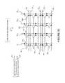
- semiconductor DRAM array 10includes a plurality of memory cells 12 each consisting of transistor 14 having gate 16 , body region 18 , which is electrically floating, source region 20 and drain region 22 .
- the body region 18is disposed between source region 20 and drain region 22 .
- body region 18is disposed on or above region 24 , which may be an insulation region (for example, in an SOI material/substrate) or non-conductive region (for example, in a bulk-type material/substrate).
- the insulation or non-conductive region 24may be disposed on substrate 26 .
- Datais written into or read from a selected memory cell by applying suitable control signals to a selected word line(s) 28 , a selected source line(s) 30 and/or a selected bit line(s) 32 .
- charge carriersare accumulated in or emitted and/or ejected from electrically floating body region 18 wherein the data states are defined by the amount of carriers within electrically floating body region 18 .
- the entire contents of the '662 patentincluding, for example, the features, attributes, architectures, configurations, materials, techniques and advantages described and illustrated therein, are incorporated by reference herein.
- the memory cell 12 of DRAM array 10operates by accumulating in or emitting/ejecting majority carriers (electrons or holes) 34 from body region 18 .
- majority carriersin this example, “holes”
- conventional write techniquesmay accumulate majority carriers (in this example, “holes”) 34 in body region 18 of memory cells 12 by, for example, impact ionization near source region 20 and/or drain region 22 .
- the majority carriers 30may be emitted or ejected from body region 18 by, for example, forward biasing the source/body junction and/or the drain/body junction. (See, FIG. 2B ).
- logic high or logic “1”corresponds to, for example, an increased concentration of majority carries in the body region relative to an unprogrammed device and/or a device that is programmed with logic low or logic “0”.
- logic low or logic “0”corresponds to, for example, a reduced concentration of majority carries in the body region relative to an unprogrammed device and/or a device that is programmed with logic high or logic “1”.
- the memory cellis read by applying a small bias to the drain of the transistor as well as a gate bias which is above the threshold voltage of the transistor.
- a positive voltageis applied to one or more word lines 28 to enable the reading of the memory cells associated with such word lines.
- the amount of drain currentis determined/affected by the charge stored in the electrically floating body region of the transistor.
- a floating body memory cellmay have two or more different current states corresponding to two or more different logical states (for example, two different current conditions/states corresponding to the two different logical states: “1” and “0”).
- conventional writing programming techniques for memory cells having an N-channel type transistoroften provide an excess of majority carriers by channel impact ionization (see, FIG. 3A ) or by band-to-band tunneling (gate-induced drain leakage “GIDL”) (see, FIG. 3B ).
- the majority carriermay be removed via drain side hole removal (see, FIG. 4A ), source side hole removal (see, FIG. 4B ), or drain and source hole removal, for example, using the back gate pulsing (see, FIG. 4C ).
- the present inventionsare directed to a combination of the programming/reading methods which allows relatively low power memory programming and provides a relatively larger memory programming window (e.g., both relative to at least the conventional programming techniques).
- This new approachmay also provide a floating body memory cell that may be less sensitive to the technology variations and may include improved retention characteristics.
- the present inventionsare directed to an integrated circuit device (for example, a logic or discrete memory device) including a memory cell including an electrically floating body transistor (for example, an N-channel type transistor or a P-channel type transistor).
- the electrically floating body transistorincludes a source region, a drain region, a body region disposed between the source region and the drain region, wherein the body region is electrically floating, and a gate disposed over the body region.
- the memory cellincludes (i) a first data state which is representative of a first charge in the body region of the electrically floating body transistor, and (ii) a second data state which is representative of a second charge in the body region of the electrically floating body transistor.
- the integrated circuit devicefurther includes data write circuitry, coupled to the memory cell, to apply (i) first write control signals to the memory cell to write the first data state therein and (ii) second write control signals to the memory cell to write the second data state therein, wherein, in response to first write control signals applied to the memory cell, the electrically floating body transistor generates a first bipolar transistor current which substantially provides the first charge in the body region of the electrically floating body transistor.
- the first write control signalscause, provide, produce and/or induce the first bipolar transistor current.
- the first write control signalsinclude a signal applied to the gate and a signal applied to the source region wherein the signal applied to the source region includes a first voltage having a first amplitude and a second voltage having a second amplitude.
- the first write control signalsinclude a signal applied to the gate and a signal applied to the drain region wherein the signal applied to the drain region includes a first voltage having a first amplitude and a second voltage having a second amplitude.
- the first write control signalsinclude a signal applied to the gate and a signal applied to the source region to cause, provide, produce and/or induce the first bipolar transistor current.
- the signal applied to the source regionincludes a first voltage having a first amplitude and a second voltage having a second amplitude and the signal applied to the gate includes a third voltage having a third amplitude and a fourth voltage having a fourth amplitude.
- the first write control signalsinclude a signal applied to the gate and a signal applied to the drain region, wherein (i) the signal applied to the drain region includes a first voltage having a first amplitude and a second voltage having a second amplitude and (ii) the signal applied to the gate includes a third voltage having a third amplitude and a fourth voltage having a fourth amplitude.
- the first write control signalsinclude a signal applied to the gate and a signal applied to the drain region wherein, in response to the first bipolar transistor current, majority carriers are generated in the electrically floating body region.
- signal applied to the gatemay temporally change relative to the signal applied to the drain region to cause, provide, produce and/or induce the majority carriers to accumulate in a portion of the electrically floating body region that is juxtaposed or near a gate dielectric which is disposed between the gate and the electrically floating body region.
- the signal applied to the gatemay change or terminate before the signal applied to the drain region.
- the second write control signalsinclude a signal applied to the gate, a signal applied to the source region, and a signal applied to the drain region.
- the signal applied to the drain regionmay include a blocking voltage to prevent the first data state from being written into the electrically floating body transistor.
- the integrated circuit devicemay further include data sense circuitry, coupled to the memory cell, to sense the data state of the memory cell.
- the electrically floating body transistormay generate a second bipolar transistor current which is representative of the data state of the memory cell and wherein the data sense circuitry determines the data state of the memory cell at least substantially based on the second bipolar transistor current.
- the second bipolar transistor currentis representative of the first data state.
- the read control signalsmay include a signal applied to the gate, source region, and drain region to cause, force and/or induce the bipolar transistor current which is representative of the data state of the memory cell.
- the signal applied to the drain regionmay include a positive voltage pulse or a negative voltage pulse.
- one or more of the read control signalsmay include a constant or unchanging voltage amplitude (for example, ground).
- the present inventionsare directed to an integrated circuit device (for example, a logic or discrete memory device) comprising a memory cell array including a plurality of word lines, plurality of source lines, plurality of bit lines, and plurality of memory cells arranged in a matrix of rows and columns.
- Each memory cellincludes an electrically floating body transistor (for example, an N-channel type transistor or a P-channel type transistor), wherein the electrically floating body transistor includes a source region coupled to an associated source line, a drain region, a body region disposed between the source region and the drain region coupled to an associated bit line, wherein the body region is electrically floating, and a gate disposed over the body region and coupled to an associated word line.
- the memory cellincludes (i) a first data state which is representative of a first charge in the body region of the electrically floating body transistor, and (ii) a second data state which is representative of a second charge in the body region of the electrically floating body transistor.
- the source region of the electrically floating body transistor of each memory cell of a first row of memory cellsis connected to a first source line.
- the integrated circuit device of this aspect of the inventionsfurther includes data write circuitry, coupled to the first row of memory cells, to apply (i) first write control signals to the memory cells to write the first data state therein and (ii) second write control signals to the memory cells to write the second data state therein.
- data write circuitrycoupled to the first row of memory cells, to apply (i) first write control signals to the memory cells to write the first data state therein and (ii) second write control signals to the memory cells to write the second data state therein.
- first write control signals applied to at least a portion of the memory cells of the first row of memory cellsthe electrically floating body transistor of each such memory cell of the first row generates a first bipolar transistor current which at least substantially provides the first charge in the body region of the electrically floating body transistor of the each such memory cells.
- the source region of the electrically floating body transistor of each memory cell of a second row of memory cellsis connected to the first source line.
- the source region of the electrically floating body transistor of each memory cell of a second row of memory cellsis connected to a second source line
- the source region of the electrically floating body transistor of each memory cell of a third row of memory cellsis connected to a second source line.
- the second and third rows of memory cellsare adjacent to the first row of memory cells.
- the first write control signalscause, provide, produce and/or induce the first bipolar transistor current.
- the first write control signalsmay include a signal applied to the gate which includes a first voltage having a first amplitude and a second voltage having a second amplitude.
- the write control signalsmay include a signal applied to the source region which includes a first voltage having a first amplitude and a second voltage having a second amplitude.
- the first write control signalincludes a signal applied to the drain region which includes a first voltage having a first amplitude and a second voltage having a second amplitude.
- the data write circuitryprior to applying the first write control signals, applies the second write control signals to all of all of the memory cells of the first row of memory cells to write the second data state therein. In certain other embodiments, the data write circuitry at least substantially simultaneously applies (i) the first write control signals to the portion of the memory cells of the first row of memory cells to write the first data state therein, and (ii) the second write control signals to the other portion of the memory cells of the first row of memory cells to write the second data state therein.
- the first write control signalsmay include a signal applied to the gate and a signal applied to the source region of the electrically floating body transistors of a one or more memory cells of the first row of memory cells to cause, provide, produce and/or induce the first bipolar transistor current, wherein (i) the signal applied to the source region includes a first voltage having a first amplitude and a second voltage having a second amplitude, and (ii) the signal applied to the gate includes a third voltage having a third amplitude and a fourth voltage having a fourth amplitude.
- the first write control signalsinclude a signal applied to the gate and a signal applied to the drain region of the electrically floating body transistors of a one or more memory cells of the first row of memory cells to cause, provide, produce and/or induce the first bipolar transistor current, wherein (i) the signal applied to the drain region includes a first voltage having a first amplitude and a second voltage having a second amplitude, and (ii) the signal applied to the gate includes a third voltage having a third amplitude and a fourth voltage having a fourth amplitude.
- the signal having the fourth voltageis applied to the gate before the signal having the second voltage is applied to the drain.
- the integrated circuit device of this aspect of the present inventionsmay further include data sense circuitry, coupled to each memory cell of the plurality of memory cells, to sense the data state of the memory cell.
- the electrically floating body transistor of each memory cellIn response to read control signals applied to the memory cells, the electrically floating body transistor of each memory cell generates a second bipolar transistor current which is representative of the data state of the memory cell.
- the data sense circuitrydetermines the data state of the memory cell substantially based on the second bipolar transistor current. In one embodiment, the second bipolar transistor current is representative of the first data state.
- the read control signalsmay include a signal applied to the gate, source region, and drain region to cause, force and/or induce the bipolar transistor current which is representative of the data state of the memory cell.
- the signal applied to the drain regionmay include a positive voltage pulse or a negative voltage pulse.
- one or more of the read control signalsmay include a constant or unchanging voltage amplitude (for example, ground).
- the present inventionsare directed to an integrated circuit device (for example, a logic or discrete memory device) including a memory cell consisting essentially of an electrically floating body transistor (for example, an N-channel type transistor or a P-channel type transistor).
- the electrically floating body transistorincludes a source region, a drain region, a body region disposed between the source region and the drain region, wherein the body region is electrically floating, and a gate disposed over the body region.
- the memory cellincludes (i) a first data state which is representative of a first charge in the body region of the electrically floating body transistor, and (ii) a second data state which is representative of a second charge in the body region of the electrically floating body transistor.
- the integrated circuit devicefurther includes data write circuitry, coupled to the memory cell, to apply (i) first write control signals to the memory cell to write the first data state therein and (ii) second write control signals to the memory cell to write the second data state therein, wherein, in response to first write control signals applied to the memory cell, the electrically floating body transistor generates a first bipolar transistor current which substantially provides the first charge in the body region of the electrically floating body transistor.
- the first write control signalscause, provide, produce and/or induce the first bipolar transistor current.
- the first write control signalsmay include a signal applied to the gate and a signal applied to the source region wherein the signal applied to the source region includes a first voltage having a first amplitude and a second voltage having a second amplitude.
- the first write control signalsinclude a signal applied to the gate and a signal applied to the drain region wherein the signal applied to the drain region includes a first voltage having a first amplitude and a second voltage having a second amplitude.
- the first write control signalsmay include a signal applied to the gate and a signal applied to the source region to cause, provide, produce and/or induce the first bipolar transistor current.
- the signal applied to the source regionincludes a first voltage having a first amplitude and a second voltage having a second amplitude.
- the signal applied to the gateincludes a third voltage having a third amplitude and a fourth voltage having a fourth amplitude.
- the first write control signalsinclude a signal applied to the gate and a signal applied to the drain region, wherein (i) the signal applied to the drain region includes a first voltage having a first amplitude and a second voltage having a second amplitude and (ii) the signal applied to the gate includes a third voltage having a third amplitude and a fourth voltage having a fourth amplitude.
- the first write control signalsinclude a signal applied to the gate and a signal applied to the drain region wherein, in response to the first bipolar transistor current, majority carriers are generated in the electrically floating body region.
- signal applied to the gatemay temporally change relative to the signal applied to the drain region to cause, provide, produce and/or induce the majority carriers to accumulate in a portion of the electrically floating body region that is juxtaposed or near a gate dielectric which is disposed between the gate and the electrically floating body region.
- the signal applied to the gatemay change or terminate before the signal applied to the drain region.
- the second write control signalsinclude a signal applied to the gate, a signal applied to the source region, and a signal applied to the drain region.
- the signal applied to the drain regionmay include a blocking voltage to prevent the first data state from being written into the electrically floating body transistor.
- the integrated circuit devicemay further include data sense circuitry, coupled to the memory cell, to sense the data state of the memory cell.
- the electrically floating body transistormay generate a second bipolar transistor current which is representative of the data state of the memory cell and wherein the data sense circuitry determines the data state of the memory cell at least substantially based on the second bipolar transistor current.
- the second bipolar transistor currentis representative of the first data state.
- the read control signalsmay include a signal applied to the gate, source region, and drain region to cause, force and/or induce the bipolar transistor current which is representative of the data state of the memory cell.
- the signal applied to the drain regionmay include a positive voltage pulse or a negative voltage pulse.
- one or more of the read control signalsmay include a constant or unchanging voltage amplitude (for example, ground).
- FIG. 1Ais a schematic representation of a prior art DRAM array including a plurality of memory cells comprised of one electrically floating body transistor;
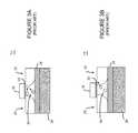
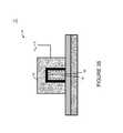
- FIG. 1Bis a three-dimensional view of an exemplary prior art memory cell comprised of one electrically floating body partially depleted transistor (PD-SOI NMOS);
- PD-SOI NMOSelectrically floating body partially depleted transistor
- FIG. 1Cis a cross-sectional view of the prior art memory cell of FIG. 1B , cross-sectioned along line C-C;
- FIGS. 2A and 2Bare exemplary schematic illustrations of the charge relationship, for a given data state, of the floating body, source and drain regions of a prior art memory cell comprised of one electrically floating body transistor (PD-SOI NMOS);
- PD-SOI NMOSelectrically floating body transistor
- FIGS. 3A and 3Bare exemplary schematic and general illustrations of conventional methods to program a memory cell to logic state “1” (i.e., generate or provide an excess of majority carrier in the electrically floating body of the transistor (an N-type channel transistor in this exemplary embodiment) of the memory cell of FIG. 1B ; majority carriers in these exemplary embodiments are generated or provided by the channel electron impact ionization ( FIG. 3A ) and by GIDL or band to band tunneling ( FIG. 3B );
- FIGS. 4A-4Care exemplary schematics and general illustrations of conventional methods to program a memory cell to logic state “0” (i.e., provide relatively fewer majority carrier by removing majority carriers from the electrically floating body of the transistor of the memory cell of FIG. 1B ; majority carriers may be removed through the drain region/terminal of the transistor ( FIG. 4A ), the source region/terminal of the transistor ( FIG. 4B ), and through both drain and source regions/terminals of the transistor via using the back gate pulses applied to the substrate/backside terminal of the transistor of the memory cell ( FIG. 4C );
- FIG. 5illustrates an exemplary schematic (and control signal) of a conventional reading technique
- the state of the memory cellmay be determined by sensing the amount of the channel current provided/generated by the transistor of the memory cell in response to the application of a predetermined voltage on the gate of the transistor;
- FIG. 6Ais a schematic representation of an equivalent electrically floating body memory cell (N-channel type) including an intrinsic bipolar transistor in addition to the MOS transistor;
- FIG. 6Bis a schematic representation (and control signal voltage relationship) of an exemplary embodiment of an aspect of the present inventions of programming a memory cell to logic state “1” by generating, storing and/or providing an excess of majority carriers in the electrically floating body of the transistor of the memory cell in accordance with certain aspects and/or embodiments of the present inventions;
- FIG. 6Cillustrates three exemplary relationships of selected control signals to program or write logic state “1” into a memory cell in accordance with certain aspects and/or embodiments of the present inventions; notably, in this illustration the gate and drain control signal sequences are illustrated whereby the control signal applied to the drain region may be applied before the signal is applied to the gate of the transistor (Case A), simultaneously (Case B), or after the control signal is applied to the gate (Case C);
- FIG. 7illustrates an exemplary schematic (and control signal) of an exemplary embodiment of an aspect of the present inventions of programming a memory cell to logic state “0” by generating, storing and/or providing relatively fewer majority carriers (as compared to the number of majority carriers in the electrically floating body of the memory cell that is programmed to logic state “1”) in the electrically floating body region of the transistor of the memory cell, wherein the majority carrier are removed (write “0”) through both drain and source regions/terminals by applying a control signal (for example, a programming pulse) to the gate of the transistor of the memory cell;
- a control signalfor example, a programming pulse
- FIG. 8illustrates an exemplary schematic (and control signal) of an exemplary embodiment of an aspect of the present inventions of holding or maintaining the data state of a memory cell when programming, for example, a neighboring memory cell to a predetermined data state (for example, logic state “1” and/or logic state “0”);
- a predetermined data statefor example, logic state “1” and/or logic state “0”
- FIG. 9is a graphical representation of the exemplary retention time distribution of a memory cell implementing one or more aspect of the present inventions.
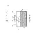
- FIG. 10illustrates an exemplary schematic (and control signal) of an exemplary embodiment of an aspect of the present inventions of reading the data state of a memory cell by sensing the amount of the current provided/generated in response to the application of a predetermined voltage on the gate of the transistor of the memory cell;
- FIG. 11illustrates an exemplary distribution of logic state “1” and state “0” of a memory cell implementing one or more aspect of the present inventions
- FIGS. 12A and 12Bare schematic block diagrams of embodiments of an integrated circuit device including, among other things, a memory cell array, data sense and write circuitry, memory cell selection and control circuitry, according certain aspects of the present inventions;
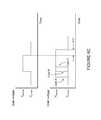
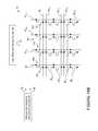
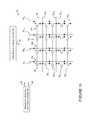
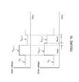
- FIGS. 13, 14A, 14B, and 15illustrate an embodiment of an exemplary memory array having a plurality of memory cells and employing a separate source line configuration for each row of memory cells, according to certain aspects of the present inventions
- FIG. 16illustrates exemplary relationships of selected write control signals to implement a program or write operation for logic high or logic “1” into a memory cell according to one embodiment of the present inventions
- FIG. 17illustrates exemplary relationships of selected write control signals to implement a program or write operation for logic low or logic “0” into a memory cell according to one embodiment of the present inventions
- FIG. 18illustrates exemplary relationships of selected control signals to implement a read operation of a memory cell according to one embodiment of the present inventions
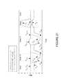
- FIGS. 19, 21, 22, 23, 24, 25 and 26illustrate exemplary relationships of selected control signals to control or implement certain operations of the memory cells of associated memory array configurations or layouts illustrated herein, according to certain aspects of the present inventions;
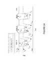
- FIGS. 20 and 27illustrate exemplary embodiments of memory arrays having a plurality of memory cells and employing separate or common source line configurations for each row of memory cells, according to certain aspects of the present inventions.
- FIG. 28illustrates a quasi non-destructive reading technique according to one embodiment of the present inventions
- FIG. 29illustrates exemplary timing relationships of selected write control signals to (i) program or write logic “0” into one or more N-channel type memory cells, (ii) program or write logic “1” into one or more N-channel type memory cells, and (iii) read one or more N-channel type memory cells according to one embodiment of the present inventions;
- FIG. 30illustrates an exemplary embodiment of a memory array having a plurality of memory cells (including N-channel type transistors) and employing a common source line configuration for each row of memory cells, according to certain aspects of the present inventions;
- FIG. 31illustrates an exemplary embodiment of a memory array having a plurality of memory cells (including P-channel type transistors) and employing a common source line configuration for each row of memory cells, according to certain aspects of the present inventions;
- FIG. 32illustrates exemplary timing relationships of selected write control signals to (i) program or write logic “0” into one or more P-channel type memory cells, (ii) program or write logic “1” into one or more P-channel type memory cells, and (iii) read one or more P-channel type memory cells according to one embodiment of the present inventions;
- FIG. 33illustrates an exemplary schematic (and control signals) of an FD transistor employed as a floating body memory cell, according to an aspect of the present inventions; notably, back gate bias is not required (although it may be employed);
- FIGS. 34 and 35illustrate exemplary schematic (and control signals) of a double-gate and triple-gate transistor, respectively, employed as a floating body memory cell, according to aspects of the present inventions.
- FIG. 36illustrates an exemplary semiconductor cell (and control signals) that may be used as a floating memory cell according to the present inventions; as before, a back gate bias is not required (although it may be employed) and additional technology/fabrication processes are also not required (although such processing may be implemented); and
- FIG. 37illustrates exemplary relationships of selected control signals to control or implement certain operations of the memory cells of associated memory array configurations or layouts illustrated herein, according to certain aspects of the present inventions.
- the present inventionsare directed to techniques to control and/or operate a semiconductor memory cell (and memory cell array having a plurality of such memory cells as well as an integrated circuit device including a memory cell array) having one or more electrically floating body transistors in which an electrical charge is stored in the body region of the electrically floating body transistor.
- the techniques of the present inventionsmay employ intrinsic bipolar transistor currents to control, write and/or read a data state in such a memory cell.
- the present inventionsmay employ the intrinsic bipolar transistor current to control, write and/or read a data state in/of the electrically floating body transistor of the memory cell.
- the present inventionsmay employ band-to-band tunneling to write a data state in the electrically floating body memory cell and an intrinsic bipolar transistor current generated by the electrically floating body transistor to read and/or determine the data state of the memory cell.
- the data stateis determined primarily by, sensed substantially using and/or based substantially on the bipolar transistor current that is responsive to the read control signals and significantly less by the interface channel current component, which is less significant and/or negligible relatively to the bipolar component.
- the present inventionsare also directed to semiconductor memory cell, array, circuitry and device to implement such control and operation techniques.
- the memory cell and/or memory cell arraymay comprise a portion of an integrated circuit device, for example, logic device (such as, a microcontroller or microprocessor) or a portion of a memory device (such as, a discrete memory).
- electrically floating body transistor 14may be schematically illustrated as including a MOS transistor “component” and an intrinsic bipolar transistor “component”.
- the present inventionsemploy the intrinsic bipolar transistor “component” to program/write as well as read memory cell 12 .
- the intrinsic bipolar transistorgenerates and/or produces a bipolar transistor current which is employed to program/write the data state in memory cell 12 and read the data state of memory cell 12 .
- electrically floating body transistor 14is an N-channel device. As such, majority carriers 34 are “holes”.
- Such control signalsgenerate or provide a bipolar current in electrically floating body region 18 of transistor 14 .
- the bipolar currentcauses or produces impact ionization and/or the avalanche multiplication phenomenon in electrically floating body region 18 . In this way, an excess of majority carriers is produced, provided and/or generated in electrically floating body region 18 of transistor 14 of memory cell 12 .
- the predetermined voltages of the control signalsprogram or write logic “1” in memory cell 12 via impact ionization and/or avalanche multiplication in electrically floating body region 18 , caused or produced by a bipolar current in body region 18 of transistor 14 of memory cell 12 .
- the bipolar transistor current responsible for impact ionization and/or avalanche multiplication in electrically floating body region 18is initiated or induced by the control signal applied to gate 16 of transistor 14 .
- Such a control signalmay induce channel impact ionization which raises or increases the potential of body region 18 and “turns on”, produces, causes and/or induces a bipolar current in transistor 14 .
- One advantage of the proposed writing/programming techniqueis that a large amount of the excess majority carriers may be generated and stored in electrically floating body region 18 of transistor 14 .
- control signal applied to drain region 22 of transistor 14may be applied before the control signal is applied to the gate, simultaneously thereto, or after the control signal is applied to the gate (Cases A, B, C, respectively). From a relative timing perspective, it is preferred that the control signal applied to drain region 22 temporally extends beyond or continues after the control signal which is applied to gate 16 ceases. (See, for example, Case C of FIG. 6C ).
- majority carriers 34are generated in electrically floating body region 18 via the bipolar current, and majority carriers 34 may accumulate (and be stored) in a portion of electrically floating body region 18 of the transistor of memory cell(s) 12 that is juxtaposed or near gate dielectric 32 (which is disposed between gate 16 and electrically floating body region 18 ).
- control signals having predetermined voltagesare applied to gate 16 and source region 20 and drain region 22 (respectively) to initiate or induce band-to-band tunneling. In this way, an excess of majority carriers are generated and stored in electrically floating body region 18 of transistor 14 .
- majority carriersmay be removed from electrically floating body region 18 of transistor 14 .
- the majority carriersare removed, eliminated or ejected from body region 18 through source region 20 and drain region 22 . (See, FIG. 7 ).
- the majority carriersmay be removed, eliminated or ejected from body region 18 substantially through source region 20 or drain region 22 .
- control signalshaving predetermined voltages
- the gate-to-source voltageis below the threshold voltage of transistor 14 . In this way, the power consumption during “0” writing may be even further reduced.
- control signal applied to gate 16 to write or program logic “0”is different from and, in at least one embodiment, higher than a holding voltage (discussed below) that may be applied to the gates of transistors 14 of other memory cells 12 (for example, other memory cells in a memory cell array). In this way, the impact of the write operation on the other memory cells is minimized and/or reduced.
- the illustrated/exemplary voltage levels to implement the write operationsare merely exemplary.
- the control signalsincrease the potential of electrically floating body region 18 which “turns on”, produces, causes and/or induces a bipolar current in the transistor of the memory cell.
- the bipolar currentIn the context of a write operation, the bipolar current generates majority carriers in the electrically floating body region which are then stored. In the context of a write operation, the bipolar current generates majority carriers in the electrically floating body region which are then stored.
- the data statemay be determined primarily by, sensed substantially using and/or based substantially on the bipolar transistor current that is responsive to the read control signals and significantly less by the interface channel current component, which is less significant and/or negligible relatively to the bipolar component.
- the voltage levels to implement the write operationsare merely exemplary.
- the indicated voltage levelsmay be relative or absolute.
- the voltages indicatedmay be relative in that each voltage level, for example, may be increased or decreased by a given voltage amount (for example, each voltage may be increased or decreased by 0.5, 1.0 and 2.0 volts) whether one or more of the voltages (for example, the source, drain or gate voltages) become or are positive and negative.
- inventive programming techniquemay consume less power relative to conventional techniques of FIGS. 4A and 4B .
- the current for writing or programming to logic “0”is smaller when compared to such conventional techniques.
- the programming techniques of the present inventionsmay be implemented without employing a back gate terminal (Compare, FIG. 4C ).
- the memory cell 12may be implemented in a memory cell array.
- a memory cellWhen a memory cell is implemented in a memory cell array configuration, it may be advantageous to implement a “holding” operation or condition to certain memory cells when programming one or more other memory cells of the array in order to improve or enhance the retention characteristics of such certain memory cells.
- the transistor of the memory cellmay be placed in a “holding” state via application of control signals (having predetermined voltages) which are applied to the gate and the source and drain regions of the transistor of the memory cells which are not involved in the write or read operations.
- control signalsprovide, cause and/or induce majority carrier accumulation in an area that is close to the interface between gate dielectric 32 and electrically floating body 18 .
- the proposed holding conditionmay provide enhanced retention characteristics (See, for example, FIG. 9 ).
- Such control signalsinduce and/or cause a bipolar transistor current in memory cells 12 that are programmed to logic “1”.
- the bipolar transistor currentmay be considerably larger than a channel current.
- sensing circuitryfor example, a cross-coupled sense amplifier
- transistor 14for example, drain region 22
- control signalsinduce, cause and/or produce little to no bipolar transistor current (for example, a considerable, substantial or sufficiently measurable bipolar transistor current).
- the proposed reading techniquemay provide a larger signal (see, FIG. 11 ) compared to the conventional method (see, FIG. 5 ). Moreover, the reading technique may simplify the sensing of the signal read from transistor 14 of memory cell 12 .
- a read operationmay be performed by applying 0 volts to source region 20 and gate 16 and a positive voltage (for example, +3.5 volts) to drain region 22 .
- a bipolar transistor currentis produced between source region 20 and drain region 22 .
- the bipolar transistor currentmay be larger than a channel current.
- sensing circuitryfor example, a cross-coupled sense amplifier
- transistor 14for example, drain region 22
- electrically floating body transistor 14in response to read control signals, electrically floating body transistor 14 generates a bipolar transistor current which is representative of the data state of memory cell 12 . Where the data state is logic high or logic “1”, electrically floating body transistor 14 provides a substantially greater bipolar transistor current than where the data state is logic low or logic “0”. Indeed, electrically floating body transistor 14 may provide little to no bipolar transistor current when the data state is logic low or logic “0”. As discussed in more detail below, data sensing circuitry determines the data state of the memory cell based substantially on the bipolar transistor current induced, caused and/or produced in response to the read control signals.
- electrically floating body transistor 14is an P-channel type transistor
- 0 voltsmay be applied to source region 20 and gate 16 and a negative voltage (for example, ⁇ 4 volts) may be applied to drain region 22 .
- Such control signalsinduce and/or cause a bipolar transistor current which may be considerably larger than a channel current.
- electrically floating body transistor 14generates a bipolar transistor current which is representative of the data state of the memory cell. In this embodiment, where the data state is logic high or logic “1”, electrically floating body transistor 14 provides a substantially greater bipolar transistor current than where the data state is logic low or logic “0”.
- electrically floating body transistor 14may provide little to no bipolar transistor current when the data state is logic low or logic “0”.
- the sensing circuitry(for example, a cross-coupled sense amplifier), which is coupled to transistor 14 (for example, drain region 22 ) of memory cell 12 , senses the data state using primarily and/or based substantially on the bipolar transistor current.
- the illustrated/exemplary voltage levels to implement the read operationsare merely exemplary.
- the indicated voltage levelsmay be relative or absolute.
- the voltages indicatedmay be relative in that each voltage level, for example, may be increased or decreased by a given voltage amount (for example, each voltage may be increased or decreased by 0.5, 1.0 and 2.0 volts) whether one or more of the voltages (for example, the source, drain or gate voltages) become or are positive and negative.
- the present inventionsmay be implemented in an integrated circuit device (for example, a discrete memory device or a device having embedded memory) including a memory array having a plurality of memory cells arranged in a plurality of rows and columns wherein each memory cell includes an electrically floating body transistor.
- the memory arraysmay be comprised of N-channel, P-channel and/or both types of transistors.
- circuitry that is peripheral to the memory arrayfor example, data sense circuitry (for example, sense amplifiers or comparators), memory cell selection and control circuitry (for example, word line and/or source line drivers), as well as row and column address decoders) may include P-channel and/or N-channel type transistors.
- the integrated circuit devicemay include array 10 , having a plurality of memory cells 12 , data write and sense circuitry 36 , and memory cell selection and control circuitry 38 .
- the data write and sense circuitry 36reads data from and writes data to selected memory cells 12 .
- data write and sense circuitry 36includes a plurality of data sense amplifiers. Each data sense amplifier receives at least one bit line 32 and an output of reference generator circuitry (for example, a current or voltage reference signal).
- the data sense amplifiermay be a cross-coupled type sense amplifier as described and illustrated in the Non-Provisional U.S. patent application Ser. No. 11/299,590 (U.S.
- Patent Application Publication US 2006/0126374filed by Waller and Carman, on Dec. 12, 2005, and entitled “Sense Amplifier Circuitry and Architecture to Write Data into and/or Read Data from Memory Cells”, the application being incorporated herein by reference in its entirety) to sense the data state stored in memory cell 12 and/or write-back data into memory cell 12 .
- the data sense amplifiermay employ voltage and/or current sensing circuitry and/or techniques.
- a current sense amplifiermay compare the current from the selected memory cell to a reference current, for example, the current of one or more reference cells. From that comparison, it may be determined whether memory cell 12 contained logic high (relatively more majority carries 34 contained within body region 18 ) or logic low data state (relatively less majority carries 28 contained within body region 18 ).
- the present inventionsmay employ any type or form of data write and sense circuitry 36 (including one or more sense amplifiers, using voltage or current sensing techniques, to sense the data state stored in memory cell 12 ) to read the data stored in memory cells 12 and/or write data in memory cells 12 .
- memory cell selection and control circuitry 38selects and/or enables one or more predetermined memory cells 12 to facilitate reading data therefrom and/or writing data thereto by applying a control signal on one or more word lines 28 .
- the memory cell selection and control circuitry 38may generate such control signals using address data, for example, row address data.
- memory cell selection and control circuitry 38may include a conventional word line decoder and/or driver.
- control/selection techniquesand circuitry therefor to implement the memory cell selection technique. Such techniques, and circuitry therefor, are well known to those skilled in the art. Notably, all such control/selection techniques, and circuitry therefor, whether now known or later developed, are intended to fall within the scope of the present inventions.
- the present inventionsmay be implemented in any architecture, layout, and/or configuration comprising memory cells having electrically floating body transistors.
- memory array 10including a plurality of memory cells 12 having a separate source line for each row of memory cells (a row of memory cells includes a common word line connected to the gates of each memory cell of the row). (See, for example, FIGS. 13 - 15 ).
- the memory array 10may employ one or more of the exemplary programming, reading and/or holding techniques described above.
- the present inventionsare implemented in conjunction with a two step write operation whereby all the memory cells of a given row are written to a predetermined data state by first executing a “clear” operation, whereby all of the memory cells of the given row are written or programmed to logic “0”, and thereafter selective memory cells of the row are selectively write operation to the predetermined data state (here logic “1”).
- the present inventionsmay also be implemented in conjunction with a one step write operation whereby selective memory cells of the selected row are selectively written or programmed to either logic “1” or logic “0” without first implementing a “clear” operation.
- memory cells 12may be programmed using the two step operation wherein a given row of memory cells are written to a first predetermined data state by first executing a “clear” operation (which, in this exemplary embodiment, all of the memory cells of the given row are written or programmed to logic “0”) and thereafter selected memory cells are written to a second predetermined data state (i.e., a selective write operation to the second predetermined data state).
- the “clear” operationmay be performed by writing or programming each memory cell of the given row to a first predetermined data state (in this exemplary embodiment the first predetermined data state is logic “0”) using the inventive technique described above. (See, FIG. 7 ).
- transistor of each memory cell 12 of a given rowis controlled to store a majority carrier concentration in the electrically floating body region of the transistor which corresponds to logic “0”.
- control signals to implement a clear operationare applied to the gate, the source region and the drain region of the transistor of memory cells 12 a - 12 d .
- a clear operationincludes applying (i) 1.5 v to the gate, (ii) 0 v to the source region, and (iii) 0 v to the drain region of the transistor.
- the same logic state(for example, logic low or logic “0”) is stored in memory cells 12 a - 12 d and the state of memory cells 12 a - 12 d are “cleared”.
- memory cells 12 b and 12 care programmed to logic high or logic “1”, via impact ionization and/or avalanche multiplication, by applying (i) ⁇ 2 v to the gate (via word line 28 i ), (ii) ⁇ 2 v to the source region (via source line 30 ), and (iii) 1.5 v to the drain region (via bit line 32 j+1 and 32 j+2 ).
- control signalsgenerate or provide a bipolar current in the electrically floating body region of the transistor of memory cell 12 .
- the bipolar currentcauses or produces impact ionization and/or the avalanche multiplication phenomenon in the electrically floating body region of the transistors of memory cells 12 b and 12 c .
- an excess of majority carriersare provided and stored in the electrically floating body region of the transistor of memory cells 12 b and 12 c which corresponds to logic high or logic “1”.
- the bipolar transistor current responsible for impact ionization and/or avalanche multiplication in the floating bodyis initiated or induced by the control signal (control pulse) applied to the gate of the transistor.
- a signal/pulsemay induce the channel impact ionization which raises or increases the potential of the electrically floating body region of the transistor of memory cells 12 b and 12 c and “turns-on” and/or produces a bipolar current in transistor 14 .
- One advantage of the proposed methodis that a large amount of the excess majority carriers may be generated and stored in the electrically floating body region of the transistor of memory cells 12 b and 12 c.
- memory cells 12 a and 12 dare maintained at logic low (or logic “0”) by applying an inhibit control signal to the drain region of each memory cell 12 a and 12 d .
- an inhibit control signalfor example, applying 0 v to the drain regions of memory cells 12 a and 12 d (via bit lines 32 j and 32 j+4 ) inhibits writing logic high or logic “1” into memory cells 12 a and 12 d during the selective write operation for memory cells 12 b and 12 c.
- a holding voltageis applied to the gates of the transistors of other memory cells of memory cell array 10 (for example, each memory cell connected to word lines 28 i+1 , 28 i+2 , 28 i+3 , and 28 i+4 ).
- a holding voltage of ⁇ 1.2 vis applied to the gate of each transistor of the memory cells connected to word lines 28 i+1 , 28 i+2 , 28 i+3 , and 28 i+4 .
- memory cellsare selectively written to logic high (logic “1”) using the band-to-band tunneling (GIDL) method.
- GIDLband-to-band tunneling
- the band-to-band tunnelingprovides, produces and/or generates an excess of majority carriers in the electrically floating body of the transistors of each selected memory cell (in this exemplary embodiment, memory cells 12 b and 12 c ).
- memory cells 12 b and 12 care programmed to logic high or logic “1”, via band-to-band tunneling, by applying (i) ⁇ 3 v to the gate (via word line 28 i ), (ii) ⁇ 0.5 v to the source region (via source line 30 ), and (iii) 1 v to the drain region (via bit line 32 j+1 and 32 j+2 ).
- the other memory cells connected to word line 28 imay be maintained at logic low via application of a write “inhibit” control signal to the bits lines associated with such other memory cells (bit lines 32 j and 32 j+4 , respectively).
- the other memory cells of memory cell array 10 which are not connected to word line 28 imay be maintained at a given data state via application of “holding” operation or condition.
- a holding voltageis applied to the gate of the transistor of each memory cell connected to word lines 28 i+1 , 28 i+2 , 28 i+3 , and 28 i+4 .
- ⁇ 1.2 vis applied to the gate of each transistor of the memory cells connected to word lines 28 i+1 , 28 i+2 , 28 i+3 , and 28 i+4 . In this way, the impact of the write operation for memory cells 12 a - 12 d (which are connected to word line 28 i ) on the other memory cells of memory cell array 10 is minimized and/or reduced.
- a selected row of memory cellsmay be read by applying a read control signals to the associated word line 28 and associated source lines 30 and sensing a signal (voltage and/or current) on associated bit lines 32 .
- memory cells 12 a - 12 dare read by applying (i) ⁇ 0.5 v to the gate (via word line 28 i ) and (ii) 3 v to the source region (via source line 30 ).
- the data write and sense circuitry 36reads the data state of the memory cells 12 a - 12 d by sensing the response to the read control signals applied to word line 28 i and source line 30 i .
- memory cells 12 a - 12 dIn response to the read control signals, memory cells 12 a - 12 d generate a bipolar transistor current which is representative of the data state of memory cells 12 a - 12 d .
- memory cells 12 b and 12 c(which were earlier programmed to logic “1”), in response to the read control signals, generate a bipolar transistor current which is considerably larger than any channel current.
- memory cells 12 a and 12 d(which were earlier programmed to logic “0”), in response to such control signals, induce, cause and/or produce little to no bipolar transistor current (for example, a considerable, substantial or sufficiently measurable bipolar transistor current).
- the circuitry in data write and sense circuitry 36which senses the data state of the memory cell (for example, a cross-coupled sense amplifier) senses the data state using and/or based substantially on the bipolar transistor current.
- the electrically floating body transistor of each memory cell 12 a - 12 din response to read control signals, the electrically floating body transistor of each memory cell 12 a - 12 d generates a bipolar transistor current which is representative of the data state stored therein.
- the data sensing circuitry in data write and sense circuitry 36determines the data state of memory cells 12 a - 12 d based substantially on the bipolar transistor current induced, caused and/or produced in response to the read control signals.
- a read operationmay be performed by applying other control signaling techniques.
- a holding voltageis applied to the gates of the transistors of other memory cells of memory cell array 10 (for example, each memory cell connected to word lines 28 i+1 , 28 i+2 , 28 i+3 , and 28 i+4 ).
- a holding voltage of ⁇ 1.2 vis applied to the gate of each transistor of the memory cells connected to word lines 28 i+1 , 28 i+2 , 28 i+3 , and 28 i+4 .
- control signals to implement a write operationmay be configured to provide a lower power consumption as well as a one step write whereby selective memory cells of a selected row of memory cells are selectively written or programmed to either logic “1” or logic “0” without first implementing a “clear” operation.
- the temporally varying control signals to implement the write logic “1” operationinclude the voltage applied to the gate (V gw′′1′′ ) and the voltage applied to the drain region (V dw′′1′′ ).
- the logic states “1” and “0”are written to one or more selected cells by applying appropriate bit line voltages.
- the drain pulse (V dw′′1′′1 )may be applied to the drain region (via, for example, the associated bit line) of the electrically floating body transistor of the memory cell before the gate pulse (V gw′′1′′1 ) is applied to the gate (via, for example, the associated word line), simultaneously thereto, or after the gate pulse (V gw′′1′′1 ) is applied to gate. It is preferred that the drain pulse (V dw′′1′′1 ) include an amplitude which is sufficient to maintain a bipolar current that is suitable for programming the memory cell to logic “1”.
- the drain pulse (V dw′′1′′1 )extend beyond/after or continue beyond the conclusion of the gate pulse (V gw′′1′′1 ), or extend beyond/after or continue beyond the time the gate pulse (V gw′′1′′1 ) is reduced, as illustrated in FIG. 16 (see, ⁇ t>0).
- majority carriersare generated in the electrically floating body region via a bipolar current and majority carriers may accumulate (and be stored) in a portion of the electrically floating body region of the transistor of the memory cell 12 that is juxtaposed or near the gate dielectric (which is disposed between the gate and the electrically floating body region).
- the gate voltage (V gw′′1′′2 )may be equal to (or substantially equal to) the voltage applied to the gate to implement a hold operation (V gh ) and the drain bias (V dw′′1′′2 ) may be equal to (or substantially equal to) the voltage applied to the drain region to implement a hold operation (V dh ).
- the temporally varying control signals to implement the write logic “0” operationincluding the voltage applied to the gate (V gw′′0′′ ) and the voltage applied to the drain region (V dw′′0′′ ).
- the control signal applied to the drain region (V dw′′0′′1 )may be applied before the control signal is applied to the gate (V gw′′0′′1 ), or simultaneously thereto, or after the control signal is applied to the gate.
- the drain pulse (V dw′′0′′1 )include an amplitude which is insufficient to maintain a bipolar current that is suitable for programming the memory cell to logic “1”.
- the drain pulse (V dw′′0′′1 )extend beyond/after or continue beyond the conclusion of the gate pulse (V gw′′0′′1 ), or extend beyond/after or continue beyond the time the gate pulse (V gw′′0′′1 ) is reduced, as illustrated in FIG. 17 (see, ⁇ t>0).
- majority carriersare generated in the electrically floating body region via a bipolar current and majority carriers may accumulate (and be stored) in a portion of the electrically floating body region of the transistor of the memory cell 12 that is juxtaposed or near the gate dielectric (which is disposed between the gate and the electrically floating body region).
- the gate voltage (V gw′′0′′2 )may be equal to (or substantially equal to) the voltage applied to the gate to implement a hold operation (V gh ) and the drain bias (V dw′′0′′2 ) may be equal to (or substantially equal to) the voltage applied to the drain region to implement a hold operation (V dh ).
- the memory cellmay be read using read control signals illustrated in FIG. 18 .
- a read control signalis applied to the drain region and the gate.
- the voltage applied to the drain region (V dr )may be applied to drain region before application of the voltage applied to the gate (V gr ), simultaneously thereto, or after the voltage is applied to the gate. Further, the drain pulse (V dr ) may cease or terminate before the gate pulse (V gr ), simultaneously thereto (as illustrated in FIG. 18 ), or after the gate pulse (V gr ) concludes or ceases.
- a bipolar currentis generated in those memory cells storing logic “1” and little to no bipolar current is generated in those memory cells storing logic “0”.
- the data stateis determined primarily by, sensed substantially using and/or based substantially on the bipolar transistor current that is responsive to the read control signals and significantly less by the interface channel current component, which is less significant and/or negligible relatively to the bipolar component.
- the programming and reading techniques described hereinmay be employed in conjunction with a plurality of memory cells arranged in an array of memory cells.
- a memory array implementing the structure and techniques of the present inventionsmay be controlled and configured including a plurality of memory cells having a separate source line for each row of memory cells (a row of memory cells includes a common word line).
- the exemplary layouts or configurations(including exemplary control signal voltage values), according to certain aspects of the present inventions are shown, each consisting of the control signal waveforms and exemplary array voltages during one-step writing phase 1, phase 2, and reading.
- FIG. 19provides exemplary control signal information (temporal and amplitude) in connection with the exemplary layout or configuration illustrated in FIG. 20 .
- the temporally varying control signals to implement the write operationinclude (i) a voltage applied to the gate (V gw ) via the associated word line, (ii) a voltage applied to the source (V sw ) via the source line, and (iii) a voltage applied to the drain region (V dw ) via the associated bit line.
- the logic states “1” and “0”are written to one or more selected cells by applying appropriate bit line voltages.
- logic “1”is written into a memory cell by applying drain pulse (V dw′′1′′ ) having an amplitude of 0.5V
- logic “0”is written into a memory cell by applying the drain pulse (V dw′′0′′ ) having an amplitude of 0V
- the source pulse (V sw1 )includes an amplitude of ⁇ 2.5V
- the gate pulse (V gw1 )includes an amplitude of ⁇ 2.5V
- the source pulse (V sw2 )includes an amplitude of ⁇ 2.2V
- the gate pulse (V gw2 )includes an amplitude of ⁇ 3.3V.
- the reference to a first phase and a second phase of a write operationwas used for explanation purposes to highlight changes in voltage conditions of control signals in the exemplary embodiments. It may be advantageous, when writing logic “1” and “0”, to apply constant or non-changing voltages to gate, drain region and/or source region during or through what has been labeled as write phases 1 and 2. Although the “one-step” programming technique may consume more power than the “two-step” programming technique, the “one-step” programming technique may present a less complex control signaling regime and circuitry therefor.
- a row of memory cellsmay be read in parallel.
- memory cells 12are read by applying the following read control signals: (i) a voltage applied to the gate (V gr ) via the associated word line and (ii) a voltage applied to the source (V sr ) via the source line.
- the logic state of each memory cell(for example, 12 a - 12 d ) is sensed, determined and/or sampled on the associated bit line ( 32 j - 32 j+3 , respectively).
- the gate pulse (V gr )includes an amplitude of ⁇ 0.5V
- the source pulse (V sr )includes an amplitude of 3V.
- a bipolar currentis generated in those memory cells storing logic “1” and little to no bipolar current is generated in those memory cells storing logic “0”.
- the data stateis determined primarily by, sensed substantially using and/or based substantially on the bipolar transistor current that is responsive to the read control signals and significantly less by the interface channel current component, which is less significant and/or negligible relatively to the bipolar component.
- FIG. 21provides exemplary control signal information (temporal and amplitude) in connection with the exemplary layout illustrated in FIG. 20 .
- the temporally varying control signals to implement the write operationinclude (i) a voltage applied to the gate (V gw ) via the associated word line, (ii) a voltage applied to the source (V sw ) via the source line, and (iii) a voltage applied to the drain region (V dw ) via the associated bit line.
- the logic states “1” and “0”are written to one or more selected cells by applying appropriate bit line voltages.
- logic “1”is written into a memory cell by applying drain pulse (V dw′′1′′ ) having (i) an amplitude of 0.5V during phase 1 and (ii) an amplitude of 0V during phase 2, and logic “0” is written into a memory cell by applying the drain pulse (V dw′′0′′ ) having an amplitude of 0V.
- the source pulse (V sw1 )includes an amplitude of ⁇ 2.5V
- the gate pulse (V gw1 )includes an amplitude of ⁇ 2.5V.
- the source pulse (V sw2 )includes an amplitude of ⁇ 2.5V
- the gate pulse (V gw2 )includes an amplitude of ⁇ 3.3V.
- a row of memory cellsmay be read in parallel.
- the memory cellsare read by applying the following read control signals: (i) a voltage applied to the gate (V gr ) via the associated word line and (ii) a voltage applied to the source (V sr ) via the source line.
- the logic state of each memory cell(for example, 12 a - 12 d ) is sensed, determined and/or sampled on the associated bit line ( 32 j - 32 j+3 , respectively).
- the gate pulse (V gr )includes an amplitude of ⁇ 0.5V
- the source pulse (V sr )includes an amplitude of 3V.
- a bipolar currentis generated in those memory cells storing logic “1” and little to no bipolar current is generated in those memory cells storing logic “0”.
- the data stateis determined primarily by, sensed substantially using and/or based substantially on the bipolar transistor current that is responsive to the read control signals and significantly less by the interface channel current component, which is less significant and/or negligible relatively to the bipolar component.
- FIG. 22provides exemplary control signal information (temporal and amplitude) in connection with the exemplary layout illustrated in FIG. 20 .
- the temporally varying control signals to implement the write operationinclude (i) a voltage applied to the gate (V gw ) via the associated word line, (ii) a voltage applied to the source (V sw ) via the source line, and (iii) a voltage applied to the drain region (V dw ) via the associated bit line.
- the logic states “1” and “0”are written to one or more selected cells by applying appropriate bit line voltages.
- logic “1”is written into a memory cell by applying drain pulse (V dw′′1′′ ) having an amplitude of 0.5V
- logic “0”is written into a memory cell by applying the drain pulse (V dw′′0′′ ) having an amplitude of 0V
- the source pulse (V sw′′1′′1 )includes an amplitude of ⁇ 2.5V
- the gate pulse (V gw′′1′′1 )includes an amplitude of ⁇ 2.5V.
- the source pulse (V sw′′1′′2 )includes an amplitude of ⁇ 2.2V
- the gate pulse (V gw′′1′′2 )includes an amplitude of ⁇ 3.3V.
- a row of memory cellsmay be read in parallel.
- the memory cellsare read by applying the following read control signals: (i) a voltage applied to the gate (V gr ) via the associated word line and (ii) a voltage applied to the source (V sr ) via the source line.
- the logic state of each memory cell(for example, 12 a - 12 d ) is sensed, determined and/or sampled on the associated bit line ( 32 j - 32 j+3 , respectively).
- the gate pulse (V gr )includes an amplitude of ⁇ 3V
- the source pulse (V sr )includes an amplitude of ⁇ 3.5V.
- a bipolar currentis generated in those memory cells storing logic “1” and little to no bipolar current is generated in those memory cells storing logic “0”.
- the data stateis determined primarily by, sensed substantially using and/or based substantially on the bipolar transistor current that is responsive to the read control signals and significantly less by the interface channel current component, which is less significant and/or negligible relatively to the bipolar component.
- FIG. 23provides exemplary control signal information (temporal and amplitude) in connection with the exemplary layout illustrated in FIG. 20 .
- the temporally varying control signals to implement the write operationinclude (i) a voltage applied to the gate (V gw ) via the associated word line, (ii) a voltage applied to the source (V sw ) via the source line, and (iii) a voltage applied to the drain region (V dw ) via the associated bit line.
- the logic states “1” and “0”are written to one or more selected cells by applying appropriate bit line voltages.
- logic “1”is written into a memory cell by applying drain pulse (V dw′′1′′ ) having (i) an amplitude of 0.5V during phase 1 and (ii) an amplitude of 0V during phase 2, and logic “0” is written into a memory cell by applying the drain pulse (V dw′′0′′ ) having an amplitude of 0V.
- the source pulse (V sw1 )includes an amplitude of ⁇ 2.5V
- the gate pulse (V gw1 )includes an amplitude of ⁇ 2.5V.
- the source pulse (V sw2 )includes an amplitude of ⁇ 2.5V
- the gate pulse (V gw2 )includes an amplitude of ⁇ 3.3V.
- a row of memory cellsmay be read in parallel.
- the memory cellsare read by applying the following read control signals: (i) a voltage applied to the gate (V gr ) via the associated word line and (ii) a voltage applied to the source (V sr ) via the source line.
- the logic state of each memory cell(for example, 12 a - 12 d ) is sensed, determined and/or sampled on the associated bit line ( 32 j - 32 j+3 , respectively).
- the gate pulse (V gr )includes an amplitude of ⁇ 3V
- the source pulse (V sr )includes an amplitude of ⁇ 3.5V.
- a bipolar currentis generated in those memory cells storing logic “1” and little to no bipolar current is generated in those memory cells storing logic “0”.
- the data stateis determined primarily by, sensed substantially using and/or based substantially on the bipolar transistor current that is responsive to the read control signals and significantly less by the interface channel current component, which is less significant and/or negligible relatively to the bipolar component.
- FIG. 24provides exemplary control signal information (temporal and amplitude) in connection with the exemplary layout illustrated in FIG. 20 .
- the temporally varying control signals to implement the write operationinclude (i) a voltage applied to the gate (V gw ) via the associated word line, (ii) a voltage applied to the source (V sw ) via the source line, and (iii) a voltage applied to the drain region (V dw ) via the associated bit line.
- the logic states “1” and “0”are written to one or more selected cells by applying appropriate bit line voltages.
- logic “1”is written into a memory cell by applying drain pulse (V dw′′1′′ ) having an amplitude of 0.5V
- logic “0”is written into a memory cell by applying the drain pulse (V dw′′0′′ ) having an amplitude of 0V
- the source pulse (V sw1 )includes an amplitude of ⁇ 2.5V
- the gate pulse (V gw1 )includes an amplitude of ⁇ 2.5V
- the source pulse (V sw2 )includes an amplitude of ⁇ 2.2V
- the gate pulse (V gw2 )includes an amplitude of ⁇ 3.3V.
- a row of memory cellsmay be read in parallel.
- the memory cellsare read by applying the following read control signals: (i) a voltage applied to the gate (V gr ) via the associated word line and (ii) a voltage applied to the source (V sr ) via the source line.
- the logic state of each memory cell(for example, 12 a - 12 d ) is sensed, determined and/or sampled on the associated bit line ( 32 j - 32 j+3 , respectively).
- the gate pulse (V gr )includes an amplitude of ⁇ 2.5V
- the source pulse (V sr )includes an amplitude of ⁇ 3V.
- a bipolar currentis generated in those memory cells storing logic “1” and little to no bipolar current is generated in those memory cells storing logic “0”.
- the data stateis determined primarily by, sensed substantially using and/or based substantially on the bipolar transistor current that is responsive to the read control signals and significantly less by the interface channel current component, which is less significant and/or negligible relatively to the bipolar component.
- FIG. 25provides exemplary control signal information (temporal and amplitude) in connection with the exemplary layout illustrated in FIG. 20 .
- the temporally varying control signals to implement the write operationinclude (i) a voltage applied to the gate (V gw ) via the associated word line, (ii) a voltage applied to the source (V sw ) via the source line, and (iii) a voltage applied to the drain region (V dw ) via the associated bit line.
- the logic states “1” and “0”are written to one or more selected cells by applying appropriate bit line voltages.
- logic “1”is written into a memory cell by applying drain pulse (V dw′′1′′ ) having (i) an amplitude of 0.5V during phase 1 and (ii) an amplitude of 0V during phase 2, and logic “0” is written into a memory cell by applying the drain pulse (V dw′′0′′ ) having an amplitude of 0V.
- the source pulse (V sw1 )includes an amplitude of ⁇ 2.5V
- the gate pulse (V gw1 )includes an amplitude of ⁇ 2.5V.
- the source pulse (V sw2 )includes an amplitude of ⁇ 2.5V
- the drain pulse (V dw2 )includes an amplitude of 0V
- the gate pulse (V gw2 )includes an amplitude of ⁇ 3.3V.
- a row of memory cellsmay be read in parallel.
- the memory cellsare read by applying the following read control signals: (i) a voltage applied to the gate (V gr ) via the associated word line, (ii) a voltage applied to the source (V sr ) via the source line, and (iii) a voltage applied to the drain (V dr ) via the associated bit line.
- the logic state of each memory cell(for example, 12 a - 12 d ) is sensed, determined and/or sampled on the associated bit line ( 32 j - 32 j+3 , respectively).
- the gate pulse (V gw )includes an amplitude of ⁇ 3V
- the source pulse (V sr )includes an amplitude of ⁇ 2.5V
- the drain pulse (V dr )includes an amplitude of 0.5V.
- a bipolar currentis generated in those memory cells storing logic “1” and little to no bipolar current is generated in those memory cells storing logic “0”.
- the data stateis determined primarily by, sensed substantially using and/or based substantially on the bipolar transistor current that is responsive to the read control signals and significantly less by the interface channel current component, which is less significant and/or negligible relatively to the bipolar component.
- a holding voltageis applied to the gates of the transistors of other memory cells of memory cell array 10 (for example, each memory cell connected to word lines 28 i+1 , 28 i+2 , 28 i+3 , and 28 i+4 ).
- a holding voltage of ⁇ 1.2 vis applied to the gate of each transistor of the memory cells connected to word lines 28 i+1 , 28 i+2 , 28 i+3 , and 28 i+4 . In this way, the impact of the write operation of memory cells 12 a - 12 d (which are connected to word line 28 i ) on the other memory cells of memory cell array 10 is minimized and/or reduced.
- the illustrated/exemplary voltage levels discussed above to implement the write and read operations of the embodiments of FIGS. 19-25are merely exemplary.
- the control signalsincrease the potential of electrically floating body region which “turns on” or produces a bipolar current in the transistor of the memory cell.
- the bipolar currentgenerates majority carriers in the electrically floating body region which are then stored.
- the data statemay be determined primarily by, sensed substantially using and/or based substantially on the bipolar transistor current that is responsive to the read control signals and significantly less by the interface channel current component, which is less significant and/or negligible relatively to the bipolar component.
- each voltage levelmay be increased or decreased by a given voltage amount (for example, each voltage may be increased or decreased by 0.5, 1.0 and 2.0 volts) whether one or more of the voltages (for example, the source, drain or gate voltages) become or are positive and negative.
- the present inventionsmay be implemented in any memory array architecture having a plurality of memory cells that employ electrically floating body transistors.
- a memory array implementing the structure and techniques of the present inventionsmay be controlled and configured having a common source line for every two rows of memory cells (a row of memory cells includes a common word line).
- An example (including exemplary control signal voltage values), according to certain aspects of the present inventionsis also shown that consists of the control signal waveforms and exemplary array voltages during one-step writing phase 1, phase 2, and reading.
- the temporally varying control signals to implement the write operationinclude (i) a voltage applied to the gate (V gw ) via the associated word line and (ii) a voltage applied to the drain region (V dw ) via the associated bit line.
- the logic states “1” and “0”are written to one or more selected cells by applying appropriate bit line voltages.
- logic “1”is written into a memory cell by applying drain pulse (V dw′′1′′ ) having (i) an amplitude of 3V during phase 1 and (ii) an amplitude of 2.7V during phase 2.
- logic “0”is written into a memory cell by applying the drain pulse (V dw′′0′′ ) having (i) an amplitude of 2.5V during phase 1 and (ii) an amplitude of 2.2V during phase 2.
- the gate pulse (V gw1 )includes an amplitude of 0V.
- the gate pulse (V gw2 )includes an amplitude of ⁇ 1.5V.
- the voltage applied to the source lines (and, as such, the source regions of the transistors of the row of memory cells)is 0V. Under these conditions, a bipolar current that is suitable for programming the memory cell to logic “1” is provided. Moreover, little to no bipolar current is generated for programming the memory cell to logic “0”.
- a row of memory cellsmay be read in parallel.
- the memory cellsare read by applying the following read control signals: (i) a voltage applied to the gate (V gr ) via the associated word line and (ii) a voltage applied to the drain (V dr ) via the associated bit line.
- the logic state of each memory cell(for example, 12 a - 12 d ) is sensed, determined and/or sampled on the associated bit line ( 32 j - 32 j+3 , respectively).
- the gate pulse (V gr )includes an amplitude of ⁇ 0.5V
- the drain pulse (V dr )includes an amplitude of 3V.
- the voltage applied to the source linesis 0V.
- a bipolar currentis generated in those memory cells storing logic “1” and little to no bipolar current is generated in those memory cells storing logic “0”.
- the data stateis determined primarily by, sensed substantially using and/or based substantially on the bipolar transistor current that is responsive to the read control signals and significantly less by the interface channel current component, which is less significant and/or negligible relatively to the bipolar component.
- a holding voltageis applied to the gates of the transistors of other memory cells of memory cell array 10 (for example, each memory cell connected to word lines 28 i+1 , 28 i+2 , 28 i+3 , and 28 i+4 ).
- a holding voltage of ⁇ 1.2 vis applied to the gate of each transistor of the memory cells connected to word lines 28 i+1 , 28 i+2 , 28 i+3 , and 28 i+4 .
- the reading technique described hereinmay reduce the degradation of the floating body charge caused by charge-pumping (charge-pumping disturb) thus allowing the quasi non-disturbing reading (see, for example, FIG. 28 ).
- charge-pumping disturbcharge-pumping disturb
- the memory arraymay employ any of the exemplary programming, holding and/or reading techniques described herein. Moreover, exemplary voltage values for each of the control signals for a given operation (for example, programming, holding or reading), according to exemplary embodiments of the present inventions, is also provided.
- the present inventionsmay be implemented in any electrically floating body memory cell and memory cell array.
- the present inventionsare a memory array, having a plurality of memory cells each including an electrically floating body transistor, and/or technique of writing or programming data into one or more memory cells of such a memory array.
- the data states of adjacent memory cells and/or memory cells that share a word linemay be individually programmed.
- the memory arraysmay be comprised of N-channel, P-channel and/or both types of transistors. Indeed, circuitry that is peripheral to the memory array (for example, sense amplifiers or comparators, row and column address decoders, as well as line drivers (not illustrated herein)) may include P-channel and/or N-channel type transistors. Where P-channel type transistors are employed as memory cells 12 in the memory array(s), suitable write and read voltages (for example, negative voltages) are well known to those skilled in the art in light of this disclosure. Accordingly, for sake of brevity, these discussions will not be repeated.
- control signals having a predetermined amplitudemay be selectively applied to a row of memory cells (for example, memory cells 12 a - d ) to write logic “1” into selected memory cells 12 a and 12 d , and logic “0” into selected memory cells 12 b and 12 c .
- the logic “1” and “0”are written to one or more selected cells by applying appropriate bit line voltages.
- logic “1”is written into a memory cell by applying drain pulse (V dw′′1′′ ) having an amplitude of 0V
- logic “0”is written into a memory cell by applying the drain pulse (V dw′′0′′ ) having an amplitude of 0.5V
- logic “1”may be programmed or written in memory cells 12 a and 12 d by applying a voltage pulse of 0V to bit lines 32 j and 32 j+3 , respectively.
- Logic “0”is programmed in memory cells 12 b and 12 c by applying a voltage pulse of 0.5V to bit lines 32 j+1 and 32 j+2 , respectively.
- a voltage of 3Vis applied to source region of the transistors of memory cells 12 a - 12 d (via source line 30 i - 30 i+4 ) and a voltage pulse of 0.5V to gate of the transistors of memory cells 12 a - 12 d (via word line 28 i ).
- the source pulsemay be applied before the gate pulse, simultaneously thereto, or after the gate pulse is applied to gate 16 of memory cells 12 a and 12 d . It is preferred that the source pulse be applied to source region of the transistors of memory cells 12 a and 12 d with a sufficient amplitude to maintain a sufficient bipolar current to program logic “1” into memory cells 12 a and 12 d .
- the source pulseextend beyond when the gate pulse reduces or ceases, as illustrated in FIG. 29 .
- majority carriersare generated in the electrically floating body region and majority carriers may accumulate (and be stored) in a portion of the electrically floating body region of the transistor of the memory cell 12 that is juxtaposed or near the gate dielectric (which is disposed between the gate and the electrically floating body region).
- a drain pulse(0.5V amplitude in this example) is applied to drain regions of the transistors of memory cells 12 b and 12 c to prevent, prohibit, limit and/or retard a bipolar current (if any) from causing or generating a sufficient charge in the floating body region of transistors to program or write logic state “1” into the transistors of memory cells 12 b and 12 c .
- the drain pulsemay be characterized as a “blocking” pulse.
- the drain pulsebe applied to drain regions of the transistors of memory cells 12 b and 12 c for a temporal period that extends beyond or is applied before, during and after the source and gate pulses (for example, initiates, starts, ramps, declines and/or terminates) as illustrated in FIG. 29 .
- a holding conditionmay be applied or established to prevent, minimize or avoid disturbance of the data state of, or charge stored in the unselected memory cells.
- a voltagefor example, ⁇ 1.2V
- a voltagefor example, 0V
- the data state of the unselected memory cellsis unaffected (or substantially unaffected) by the programming of or writing to selected memory cells 12 a - d.
- the memory cellsmay be read by applying the following read control signals: (i) a voltage applied to the gate (V gr ) via the associated word line and (ii) a voltage applied to the source (V sr ) via the source line.
- the logic state of each memory cell(for example, 12 a - 12 d ) is sensed, determined and/or sampled on the associated bit line ( 32 j - 32 j+3 , respectively).
- the gate pulse (V gr )includes an amplitude of ⁇ 0.5V
- the source pulse (V sr )includes an amplitude of 3V.
- the source pulse(V sr ) may be applied to source line 30 (and, for example, the source regions of the transistors of memory cells 12 a - 12 d ) before application of the gate pulse to word line 28 (and, for example, the gates of the transistors of memory cells 12 a - 12 d ), simultaneously thereto, or after the gate pulse is applied to word line 28 . Further, the source pulse may cease or terminate before the gate pulse, simultaneously thereto (as illustrated in FIG. 29 ), or after the gate pulse concludes or ceases.
- a holding conditionmay be applied or established to prevent, minimize or avoid disturbance of the data state in the unselected memory cells.
- a voltagefor example, ⁇ 1.2V
- a voltagefor example, 0V
- the state of the unselected memory cellsis unaffected (or it is substantially unaffected) during the reading of, for example, selected memory cells 12 a - d.
- each voltage levelmay be increased or decreased by a given voltage amount (for example, each voltage may be increased or decreased by 0.25, 0.5, 1.0 and 2.0 volts) whether one or more of the voltages (for example, the source, drain or gate voltages) become or are positive and negative.
- a bipolar currentis generated in those memory cells storing logic “1” and little to no bipolar current is generated in those memory cells storing logic “0”.
- the data stateis determined primarily by, sensed substantially using and/or based substantially on the bipolar transistor current that is responsive to the read control signals and significantly less by the interface channel current component, which is less significant and/or negligible relatively to the bipolar component.
- the reading technique described hereinmay reduce the degradation of the floating body charge caused by charge-pumping (charge-pumping disturb) thus allowing the quasi non-disturbing reading.
- charge-pumping disturbcharge-pumping disturb
- memory array 10may be comprised of N-channel, P-channel and/or both types of transistors.
- circuitry that is peripheral to the memory arraymay include P-channel and/or N-channel type transistors.
- P-channel type transistorsare employed as memory cells 12 in the memory array(s)
- suitable write and read voltagesfor example, negative voltages
- FIG. 31where P-channel type transistors are employed as memory cells 12 , the exemplary control voltages and timing relationships of FIG.
- 32may be employed to (i) program or write logic state “1” into one or more P-channel type memory cells, (ii) program or write logic state “0” into one or more P-channel type memory cells, and (iii) read one or more P-channel type memory cells.
- logic “1” and “0”are written to one or more selected memory cells, having P-channel type transistors, by applying appropriate bit line voltages.
- logic “1”is written into a memory cell by applying drain pulse (V dw′′1′′ ) having an amplitude of 0V
- logic “0”is written into a memory cell by applying the drain pulse (V dw′′0′′ ) having an amplitude of ⁇ 0.5V.
- logic “1”may be programmed or written in memory cells 12 a and 12 d by applying a voltage pulse of 0V to bit lines 32 j and 32 j+3 , respectively.
- Logic “0”is programmed in memory cells 12 b and 12 c by applying a voltage pulse of ⁇ 0.5V to bit lines 32 j+1 and 32 j+2 , respectively.
- a voltage of ⁇ 3Vis applied to source region of the transistors of memory cells 12 a - 12 d (via source line 30 i - 30 i+4 ) and a voltage pulse of ⁇ 0.5V to gate of the transistors of memory cells 12 a - 12 d (via word line 28 i ).
- the source pulsemay be applied before the gate pulse, simultaneously thereto, or after the gate pulse is applied to the gate of the memory cells. It is preferred that the source pulse be applied to source region of the memory cells with a sufficient amplitude to maintain a sufficient bipolar current to program logic state “1” into the memory cells.
- the source pulseextends beyond when the gate pulse reduces or ceases (See, FIG. 32 ). In this way, majority carriers are generated in the electrically floating body region and majority carriers may accumulate (and be stored) in a portion of the electrically floating body region of the transistor of the memory cell 12 that is juxtaposed or near the gate dielectric (which is disposed between the gate and the electrically floating body region).
- a drain pulse( ⁇ 0.5V amplitude in this example) is applied to drain regions of the transistors of memory cells 12 b and 12 c to prevent, prohibit, limit and/or retard a bipolar current (if any) from causing or generating a sufficient charge in the floating body region of transistors to program or write logic state “1” into the transistors of memory cells 12 b and 12 c .
- the drain pulsemay be characterized as a “blocking” pulse.
- the drain pulsebe applied to drain regions of the transistors of memory cells 12 b and 12 c for a temporal period that extends beyond or is applied before, during and after the source and gate pulses (for example, initiates, starts, ramps, declines and/or terminates) as illustrated in FIG. 32 .
- the drain pulsebe applied to the drain region of the memory cells programmed to logic state “0” for a temporal period that extends or is applied before, during and after the source and gate pulses (for example, initiates, starts, ramps, declines and/or terminates). (See, FIG. 32 ).
- a holding conditionmay be applied or established to prevent, minimize or avoid disturbance of the data state of, or charge stored in the unselected memory cells.
- a voltagefor example, 1.2V
- a voltagefor example, 0V
- the data state of the unselected memory cellsis unaffected (or substantially unaffected) by the programming of or writing to selected memory cells.
- the datamay be read from P-channel type memory cells applying the following read control signals: (i) a voltage applied to the gate (V gr ) via the associated word line and (ii) a voltage applied to the source (V sr ) via the source line.
- the logic state of each memory cell(for example, 12 a - 12 d ) is sensed, determined and/or sampled on the associated bit line ( 32 j - 32 j+3 , respectively).
- the gate pulse (V gr )includes an amplitude of 0.5V
- the source pulse (V sr )includes an amplitude of ⁇ 3V.
- the source pulse(V sr ) may be applied to source line 30 (and, for example, the source regions of the transistors of memory cells 12 a - 12 d ) before application of the gate pulse to word line 28 (and, for example, the gates of the transistors of memory cells 12 a - 12 d ), simultaneously thereto, or after the gate pulse is applied to word line 28 . Further, the source pulse may cease or terminate before the gate pulse, simultaneously thereto (as illustrated in FIG. 32 ), or after the gate pulse concludes or ceases.
- a bipolar currentis generated in those memory cells storing logic “1” and little to no bipolar current is generated in those memory cells storing logic “0”.
- the data stateis determined primarily by, sensed substantially using and/or based substantially on the bipolar transistor current that is responsive to the read control signals and significantly less by the interface channel current component, which is less significant and/or negligible relatively to the bipolar component.
- a holding conditionmay be applied or established to prevent, minimize or avoid disturbance of the data state in the unselected memory cells.
- a voltagefor example, 1.2V
- a voltagefor example, 0V
- the states of the unselected memory cellsare unaffected (or it is substantially unaffected) during the reading of selected memory cells.
- the voltage amplitudes illustrated in FIG. 32 to perform certain operationsare merely exemplary.
- the indicated voltage levelsmay be relative or absolute.
- the voltages indicatedmay be relative in that each voltage level, for example, may be increased or decreased by a given voltage amount (for example, each voltage may be increased or decreased by ⁇ 0.1, ⁇ 0.25, ⁇ 0.5, ⁇ 1.0 and ⁇ 2.0 volts) whether one or more of the voltages (for example, the source, drain or gate voltages) become or are positive and negative.
- the present inventionsmay be implemented in any electrically floating body memory cell and memory cell array.
- the present inventionsare directed to a memory array, having a plurality of memory cells each including an electrically floating body transistor, and/or technique of programming data into one or more memory cells of such a memory cell array.
- the data states of adjacent memory cells and/or memory cells that share a word linemay or may not be individually programmed.
- memory array 10may be comprised of a plurality of memory cells 12 of N-channel type, P-channel type and/or both types of electrically floating body transistors.
- the memory array 10includes a plurality of rows and columns (for example, in a matrix form) of memory cells 12 .
- the circuitry which is peripheral to memory array 10may include P-channel type and/or N-channel type transistors. Where N-channel type transistors or P-channel type transistors are employed as memory cells 12 in memory array(s) 10 , suitable write voltages are known to those skilled in the art. Accordingly, for sake of brevity, these discussions will not be repeated here.
- memory cells 12 (having electrically floating body transistor 14 ) and memory cell array 10 of the present inventionsmay be implemented in an integrated circuit device having a memory portion and a logic portion (see, for example, FIG. 12A ), or an integrated circuit device that is primarily a memory device (see, for example, FIG. 12B ).
- the present inventionsmay be implemented in any device having one or more memory cells 12 (having electrically floating body transistors) and/or memory cell arrays 10 .
- an integrated circuit devicemay include array 10 , having a plurality of memory cells 12 (having electrically floating body transistors), data write and sense circuitry, and memory cell selection and control circuitry (not illustrated in detail).
- the data write and sense circuitrywrites data into and senses the data state of one or more memory cells.
- the memory cell selection and control circuitryselects and/or enables one or more predetermined memory cells 12 to be read by data sense circuitry during a read operation.
- the electrically floating body transistorwhich programmed (written to), controlled and/or read using the techniques of the present inventions, may be employed in any electrically floating body memory cell, and/or memory cell array architecture, layout, structure and/or configuration employing such electrically floating body memory cells.
- an electrically floating body transistorwhich state is read by using the techniques of the present inventions, may be implemented in the memory cell, architecture, layout, structure and/or configuration described and illustrated in the following non-provisional U.S. patent applications:
- the memory cellsmay be controlled (for example, programmed or read) using any of the control circuitry described and illustrated in the above-referenced five (5) U.S. patent applications. For the sake of brevity, those discussions will not be repeated; such control circuitry is incorporated herein by reference. Indeed, all memory cell selection and control circuitry for programming, reading, controlling and/or operating memory cells including electrically floating body transistors, whether now known or later developed, are intended to fall within the scope of the present inventions.
- the data write and data sense circuitrymay include a sense amplifier (not illustrated in detail herein) to read the data stored in memory cells 12 .
- the sense amplifiermay sense the data state stored in memory cell 12 using voltage or current sensing circuitry and/or techniques.
- the current sense amplifiermay compare the cell current to a reference current, for example, the current of a reference cell (not illustrated). From that comparison, it may be determined whether memory cell 12 contained logic high (relatively more majority carriers 34 contained within body region 18 ) or logic low data state (relatively less majority carriers 34 contained within body region 18 ).
- Such circuitry and configurations thereofare well known in the art.
- the present inventionsmay employ the reference generation techniques (used in conjunction with the data sense circuitry for the read operation) described and illustrated in U.S. Provisional Patent Application Ser. No. 60/718,417, which was filed by Bauser on Sep. 19, 2005, and entitled “Method and Circuitry to Generate a Reference Current for Reading a Memory Cell Having an Electrically Floating Body Transistor, and Device Implementing Same”.
- the entire contents of the U.S. Provisional Patent Application Ser. No. 60/718,417are incorporated herein by reference.
- the present inventionsmay also employ the read circuitry and techniques described and illustrated in U.S. patent application Ser. No. 10/840,902, which was filed by Portmann et al.
- each memory cell 12 in the exemplary embodimentsincludes one transistor 14
- memory cell 12may include two transistors, as described and illustrated in application Ser. No. 10/829,877, which was filed by Ferrant et al. on Apr. 22, 2004 and entitled “Semiconductor Memory Cell, Array, Architecture and Device, and Method of Operating Same” (U.S. Patent Application Publication No. 2005/0013163). The contents of U.S. Patent Application Publication No. 2005/0013163 are hereby incorporated by reference herein.
- the electrically floating memory cells, transistors and/or memory array(s)may be fabricated using well known techniques and/or materials. Indeed, any fabrication technique and/or material, whether now known or later developed, may be employed to fabricate the electrically floating memory cells, transistors and/or memory array(s).
- the present inventionsmay employ silicon, germanium, silicon/germanium, gallium arsenide or any other semiconductor material (whether bulk-type or SOI) in which transistors may be formed.
- the electrically floating memory cellsmay be disposed on or in (collectively “on”) SOI-type substrate or a bulk-type substrate.
- the electrically floating transistors, memory cells, and/or memory array(s)may employ the techniques described and illustrated in non-provisional patent application entitled “Integrated Circuit Device, and Method of Fabricating Same”, which was filed on Jul. 2, 2004, by Fazan, Ser. No. 10/884,481 (U.S. Patent Application Publication No. 2005/0017240), provisional patent application entitled “One Transistor Memory Cell having Mechanically Strained Electrically Floating Body Region, and Method of Operating Same”, which was filed on Oct. 19, 2005, Ser. No. 60/728,060, by Bassin, and/or provisional patent application entitled “Memory Cell, Array and Device, and Method of Operating Same”, which was filed on Oct. 19, 2005, Ser. No. 60/728,061, by Okhonin et al. (hereinafter collectively “Integrated Circuit Device Patent Applications”). The contents of the Integrated Circuit Device Patent Applications are hereby incorporated by reference herein.
- the present inventionsare directed to techniques for programming, reading, controlling and/or operating a semiconductor memory cell, array, architecture and device including electrically floating body transistors, having, for example, fully depleted (FD), surrounding-gate, double-gate, triple-gate and/or FinFET characteristics, in which electrical charge is stored in the body of the transistor.
- the present inventionsare also directed to semiconductor memory cell, array, architecture and device that implement circuitry to implement such reading, controlling and/or operating techniques.
- the programming/reading techniquemay employ any of the techniques described and/or illustrated herein.
- FIG. 33illustrates the FD transistor (N-channel type) in a holding condition in accordance with the present inventions.
- the accumulation layeris induced by application of a negative bias or voltage to the front gate (i.e., gate 16 ).
- FD transistor 14behaves as a PD transistor thus it may be used as a floating body memory cell.
- an advantage of this embodimentis that a back gate bias need not be applied.
- FIGS. 34 and 35illustrate the inventive technique applied to the double-gate and triple-gate transistors, respectively, wherein the electrically floating body transistor is used as a memory cell.
- double gate transistor (N-channel type) 14is in a holding condition.
- the front gatei.e., gate 16 —illustrated as g1 and g2 in the cross-sectional view
- double gate transistor 14behaves as or similar to a PD transistor.
- transistor 14may be employed as a floating body memory cell.
- a back gate biasneed not be applied but may be incorporated.
- triple gate transistor (N-channel type) 14is in a holding condition.
- the front gate (i.e., gate 16 ) transistor 14behaves as or similar to a PD transistor and, as such, may be employed as a floating body memory cell.
- FIG. 36illustrates that the use of the present inventions may simplify the memory array by eliminating additional fabrication steps in relation to certain other techniques/embodiments (See, for example, conventional FD-SOI or PD-SOI transistors integration of Fazan, U.S. patent application Ser. No. 10/487,157).
- a voltagemay be applied to the entire substrate or predetermined portion or regions thereof (for example, regions in which the memory array(s) are/is located) to provide or create a PD-like region wherein the memory cells comprised of transistors having electrically floating body are disposed.
- memory array 10may be integrated with SOI logic transistors, as described and illustrated in the Integrated Circuit Device Patent Applications.
- an integrated circuit deviceincludes memory section (having, for example, PD or FD SOI memory transistors 14 ) and logic section (having, for example, high performance transistors, such as FinFET, multiple gate transistors, and/or non-high performance transistors (for example, single gate transistors that do not possess the performance characteristics of high performance transistors—not illustrated)).
- memory array(s) 10may be comprised of N-channel, P-channel and/or both types of transistors, as well as partially depleted and/or fully depleted type transistors.
- circuitry that is peripheral to the memory arrayfor example, sense amplifiers or comparators, row and column address decoders, as well as line drivers (not illustrated herein) may include fully depleted type transistors (whether P-channel and/or N-channel type).
- circuitrymay include partially depleted type transistors (whether P-channel and/or N-channel type).
- There are many techniques to integrate both partially depleted and/or fully depleted type transistors on the same substratesee, for example, application Ser. No.
- electrically floating body transistor 14may be a symmetrical or non-symmetrical device. Where transistor 14 is symmetrical, the source and drain regions are essentially interchangeable. However, where transistor 14 is a non-symmetrical device, the source or drain regions of transistor 14 have different electrical, physical, doping concentration and/or doping profile characteristics. As such, the source or drain regions of a non-symmetrical device are typically not interchangeable. This notwithstanding, the drain region of the electrically floating N-channel transistor of the memory cell (whether the source and drain regions are interchangeable or not) is that region of the transistor that is connected to the bit line/sense amplifier.
- the memory arraysmay be comprised of N-channel, P-channel and/or both types of transistors.
- circuitry that is peripheral to the memory arrayfor example, sense amplifiers or comparators, row and column address decoders, as well as line drivers (not illustrated herein) may include P-channel and/or N-channel type transistors.
- P-channel type transistorsare employed as memory cells 12 in the memory array(s)
- suitable write and read voltagesfor example, negative voltages
- each voltage levelmay be increased or decreased by a given voltage amount (for example, each voltage may be increased or decreased by 0.1, 0.15, 0.25, 0.5, 1 volt) whether one or more of the voltages (for example, the source, drain or gate voltages) become or are positive and negative.
- control signalsincrease the potential of electrically floating body region of the transistor of the memory cell which “turns on” or produces a bipolar current in the transistor.
- the bipolar currentIn the context of a write operation, the bipolar current generates majority carriers in the electrically floating body region which are then stored. In the context of a write operation, the bipolar current generates majority carriers in the electrically floating body region which are then stored.
- the data statemay be determined primarily by, sensed substantially using and/or based substantially on the bipolar transistor current that is responsive to the read control signals and significantly less by the interface channel current component, which is less significant and/or negligible relatively to the bipolar component.
- temporally varying control signals to implement the write operationinclude (i) a voltage applied to the gate (V gw ) via the associated word line and (ii) a voltage applied to the drain region (V dw ) via the associated bit line.
- the logic states “1” and “0”are written to one or more selected cells by applying appropriate bit line voltages.
- logic “1”is written into a memory cell by applying drain pulse (V dw′′1′′ ) having an amplitude of 0V.
- drain pulse (V dw′′0′′ )having an amplitude of 0.5V.
- the gate pulse (V gw1 )includes an amplitude of 0.5V.
- the gate pulse (V gw2 )includes an amplitude of ⁇ 1V.
- the voltage applied to the source lines (and, as such, the source regions of the transistors of the row of memory cells)is 3V.
- the drain pulsemay be characterized as a “blocking” pulse. From a relative timing perspective, it is preferred that the drain pulse be applied to drain regions of the transistors of memory cells 12 for a temporal period that extends beyond or is applied before, during and after the source and gate pulses (for example, initiates, starts, ramps, declines and/or terminates) as illustrated in FIG. 37 .
- control techniquesfacilitate a one step write operation whereby selective memory cells of the selected row are selectively written or programmed to either logic “1” or logic “0” without first implementing a “clear” operation.
- memory cells of the embodiment of FIG. 37may be read in the same manner as described above with respect to FIGS. 26 and 27 .
- the neighboring rows of memory cellsare those rows of memory cells which “share” a source line 30 .
- the neighboring row of memory cellsis associated with word line 28 i+1 .
- the word lines 28 i and 28 i+1“share” source line 30 i .
- a holding voltageis applied to the gates of the transistors of other memory cells of memory cell array 10 (for example, each memory cell connected to word lines 28 i+1 , 28 i+2 , 28 i+3 , and 28 i+4 ).
- a holding voltage of ⁇ 1.2 vis applied to the gate of each transistor of the memory cells connected to word lines 28 i+1 , 28 i+2 , 28 i+3 , and 28 i+4 . In this way, the impact of the write operation of memory cells 12 a - 12 d (which are connected to word line 28 i ) on the other memory cells of memory cell array 10 is minimized and/or reduced.
- each of the aspects of the present inventions, and/or embodiments thereofmay be employed alone or in combination with one or more of such aspects and/or embodiments.
- those permutations and combinationswill not be discussed separately herein.
- the present inventionsare neither limited to any single aspect (nor embodiment thereof), nor to any combinations and/or permutations of such aspects and/or embodiments.
Landscapes
- Engineering & Computer Science (AREA)
- Microelectronics & Electronic Packaging (AREA)
- Computer Hardware Design (AREA)
- Semiconductor Memories (AREA)
- Non-Volatile Memory (AREA)
- Dram (AREA)
- Thin Film Transistor (AREA)
- Read Only Memory (AREA)
Abstract
Description
Claims (20)
Priority Applications (2)
| Application Number | Priority Date | Filing Date | Title |
|---|---|---|---|
| US14/518,670US10418091B2 (en) | 2005-09-07 | 2014-10-20 | Memory cell and memory cell array having an electrically floating body transistor, and methods of operating same |
| US16/570,634US11031069B2 (en) | 2005-09-07 | 2019-09-13 | Memory cell and memory cell array having an electrically floating body transistor, and methods of operating same |
Applications Claiming Priority (8)
| Application Number | Priority Date | Filing Date | Title |
|---|---|---|---|
| US71491705P | 2005-09-07 | 2005-09-07 | |
| US72213905P | 2005-09-30 | 2005-09-30 | |
| US72806105P | 2005-10-19 | 2005-10-19 | |
| US74938505P | 2005-12-12 | 2005-12-12 | |
| US77427506P | 2006-02-16 | 2006-02-16 | |
| US11/509,188US7606066B2 (en) | 2005-09-07 | 2006-08-24 | Memory cell and memory cell array having an electrically floating body transistor, and methods of operating same |
| US12/573,203US8873283B2 (en) | 2005-09-07 | 2009-10-05 | Memory cell and memory cell array having an electrically floating body transistor, and methods of operating same |
| US14/518,670US10418091B2 (en) | 2005-09-07 | 2014-10-20 | Memory cell and memory cell array having an electrically floating body transistor, and methods of operating same |
Related Parent Applications (1)
| Application Number | Title | Priority Date | Filing Date |
|---|---|---|---|
| US12/573,203ContinuationUS8873283B2 (en) | 2005-09-07 | 2009-10-05 | Memory cell and memory cell array having an electrically floating body transistor, and methods of operating same |
Related Child Applications (1)
| Application Number | Title | Priority Date | Filing Date |
|---|---|---|---|
| US16/570,634ContinuationUS11031069B2 (en) | 2005-09-07 | 2019-09-13 | Memory cell and memory cell array having an electrically floating body transistor, and methods of operating same |
Publications (2)
| Publication Number | Publication Date |
|---|---|
| US20150036425A1 US20150036425A1 (en) | 2015-02-05 |
| US10418091B2true US10418091B2 (en) | 2019-09-17 |
Family
ID=37402618
Family Applications (4)
| Application Number | Title | Priority Date | Filing Date |
|---|---|---|---|
| US11/509,188Active2027-05-31US7606066B2 (en) | 2005-09-07 | 2006-08-24 | Memory cell and memory cell array having an electrically floating body transistor, and methods of operating same |
| US12/573,203ActiveUS8873283B2 (en) | 2005-09-07 | 2009-10-05 | Memory cell and memory cell array having an electrically floating body transistor, and methods of operating same |
| US14/518,670Expired - Fee RelatedUS10418091B2 (en) | 2005-09-07 | 2014-10-20 | Memory cell and memory cell array having an electrically floating body transistor, and methods of operating same |
| US16/570,634Expired - Fee RelatedUS11031069B2 (en) | 2005-09-07 | 2019-09-13 | Memory cell and memory cell array having an electrically floating body transistor, and methods of operating same |
Family Applications Before (2)
| Application Number | Title | Priority Date | Filing Date |
|---|---|---|---|
| US11/509,188Active2027-05-31US7606066B2 (en) | 2005-09-07 | 2006-08-24 | Memory cell and memory cell array having an electrically floating body transistor, and methods of operating same |
| US12/573,203ActiveUS8873283B2 (en) | 2005-09-07 | 2009-10-05 | Memory cell and memory cell array having an electrically floating body transistor, and methods of operating same |
Family Applications After (1)
| Application Number | Title | Priority Date | Filing Date |
|---|---|---|---|
| US16/570,634Expired - Fee RelatedUS11031069B2 (en) | 2005-09-07 | 2019-09-13 | Memory cell and memory cell array having an electrically floating body transistor, and methods of operating same |
Country Status (6)
| Country | Link |
|---|---|
| US (4) | US7606066B2 (en) |
| EP (1) | EP1924997A1 (en) |
| JP (1) | JP5574075B2 (en) |
| KR (1) | KR101290459B1 (en) |
| CN (1) | CN101233576B (en) |
| WO (1) | WO2007028583A1 (en) |
Cited By (1)
| Publication number | Priority date | Publication date | Assignee | Title |
|---|---|---|---|---|
| US20200005854A1 (en)* | 2005-09-07 | 2020-01-02 | Ovonyx Memory Technology, Llc | Memory cell and memory cell array having an electrically floating body transistor, and methods of operating same |
Families Citing this family (73)
| Publication number | Priority date | Publication date | Assignee | Title |
|---|---|---|---|---|
| US7355916B2 (en)* | 2005-09-19 | 2008-04-08 | Innovative Silicon S.A. | Method and circuitry to generate a reference current for reading a memory cell, and device implementing same |
| US7542345B2 (en)* | 2006-02-16 | 2009-06-02 | Innovative Silicon Isi Sa | Multi-bit memory cell having electrically floating body transistor, and method of programming and reading same |
| US7492632B2 (en) | 2006-04-07 | 2009-02-17 | Innovative Silicon Isi Sa | Memory array having a programmable word length, and method of operating same |
| US7606098B2 (en) | 2006-04-18 | 2009-10-20 | Innovative Silicon Isi Sa | Semiconductor memory array architecture with grouped memory cells, and method of controlling same |
| US7933142B2 (en) | 2006-05-02 | 2011-04-26 | Micron Technology, Inc. | Semiconductor memory cell and array using punch-through to program and read same |
| US7499352B2 (en)* | 2006-05-19 | 2009-03-03 | Innovative Silicon Isi Sa | Integrated circuit having memory array including row redundancy, and method of programming, controlling and/or operating same |
| US8069377B2 (en)* | 2006-06-26 | 2011-11-29 | Micron Technology, Inc. | Integrated circuit having memory array including ECC and column redundancy and method of operating the same |
| US7542340B2 (en)* | 2006-07-11 | 2009-06-02 | Innovative Silicon Isi Sa | Integrated circuit including memory array having a segmented bit line architecture and method of controlling and/or operating same |
| KR101277402B1 (en) | 2007-01-26 | 2013-06-20 | 마이크론 테크놀로지, 인코포레이티드 | Floating-body dram transistor comprising source/drain regions separated from the gated body region |
| US8581260B2 (en)* | 2007-02-22 | 2013-11-12 | Semiconductor Energy Laboratory Co., Ltd. | Semiconductor device including a memory |
| US8518774B2 (en)* | 2007-03-29 | 2013-08-27 | Micron Technology, Inc. | Manufacturing process for zero-capacitor random access memory circuits |
| US7688660B2 (en)* | 2007-04-12 | 2010-03-30 | Qimonda Ag | Semiconductor device, an electronic device and a method for operating the same |
| US8064274B2 (en)* | 2007-05-30 | 2011-11-22 | Micron Technology, Inc. | Integrated circuit having voltage generation circuitry for memory cell array, and method of operating and/or controlling same |
| US8085594B2 (en)* | 2007-06-01 | 2011-12-27 | Micron Technology, Inc. | Reading technique for memory cell with electrically floating body transistor |
| EP2015362A1 (en)* | 2007-06-04 | 2009-01-14 | STMicroelectronics (Crolles 2) SAS | Semiconductor array and manufacturing method thereof |
| KR101404439B1 (en)* | 2007-06-29 | 2014-06-10 | 가부시키가이샤 한도오따이 에네루기 켄큐쇼 | A memory device and electronic apparatus |
| KR20090116088A (en)* | 2008-05-06 | 2009-11-11 | 삼성전자주식회사 | Capacitorless 1T Semiconductor Memory Devices with Improved Information Retention and Operational Characteristics |
| US7969808B2 (en)* | 2007-07-20 | 2011-06-28 | Samsung Electronics Co., Ltd. | Memory cell structures, memory arrays, memory devices, memory controllers, and memory systems, and methods of manufacturing and operating the same |
| KR20090009699A (en)* | 2007-07-20 | 2009-01-23 | 삼성전자주식회사 | Semiconductor memory device having a capacitorless dynamic memory cell, dynamic memory cell for the device, and memory system having the device |
| US7787319B2 (en)* | 2007-09-06 | 2010-08-31 | Innovative Silicon Isi Sa | Sense amplifier circuitry for integrated circuit having memory cell array, and method of operating same |
| KR101357304B1 (en)* | 2007-09-11 | 2014-01-28 | 삼성전자주식회사 | Capacitorless DRAM and methods of manufacturing and operating the same |
| WO2009039169A1 (en) | 2007-09-17 | 2009-03-26 | Innovative Silicon S.A. | Refreshing data of memory cells with electrically floating body transistors |
| US20090078999A1 (en)* | 2007-09-20 | 2009-03-26 | Anderson Brent A | Semiconductor device structures with floating body charge storage and methods for forming such semiconductor device structures. |
| KR101308048B1 (en)* | 2007-10-10 | 2013-09-12 | 삼성전자주식회사 | Semiconductor memory device |
| US8536628B2 (en) | 2007-11-29 | 2013-09-17 | Micron Technology, Inc. | Integrated circuit having memory cell array including barriers, and method of manufacturing same |
| US8349662B2 (en)* | 2007-12-11 | 2013-01-08 | Micron Technology, Inc. | Integrated circuit having memory cell array, and method of manufacturing same |
| KR100892731B1 (en)* | 2008-01-02 | 2009-04-10 | 주식회사 하이닉스반도체 | 1-transistor type DRAM driving method |
| KR100892732B1 (en)* | 2008-01-02 | 2009-04-10 | 주식회사 하이닉스반도체 | 1-transistor type DRAM driving method |
| KR20090075063A (en) | 2008-01-03 | 2009-07-08 | 삼성전자주식회사 | A semiconductor memory device having a memory cell array having a dynamic memory cell using a floating body transistor and a method of operating the device |
| KR20090075062A (en) | 2008-01-03 | 2009-07-08 | 삼성전자주식회사 | A semiconductor memory device having a memory cell array that includes a dynamic memory cell using a floating body transistor. |
| US8773933B2 (en) | 2012-03-16 | 2014-07-08 | Micron Technology, Inc. | Techniques for accessing memory cells |
| US8014195B2 (en)* | 2008-02-06 | 2011-09-06 | Micron Technology, Inc. | Single transistor memory cell |
| US8189376B2 (en)* | 2008-02-08 | 2012-05-29 | Micron Technology, Inc. | Integrated circuit having memory cells including gate material having high work function, and method of manufacturing same |
| US7957206B2 (en) | 2008-04-04 | 2011-06-07 | Micron Technology, Inc. | Read circuitry for an integrated circuit having memory cells and/or a memory cell array, and method of operating same |
| KR101442175B1 (en)* | 2008-05-23 | 2014-09-18 | 삼성전자주식회사 | Semiconductor memory device and arrangement methode of memory cell array thereof |
| US7738279B2 (en)* | 2008-06-02 | 2010-06-15 | Qimonda Ag | Integrated circuit and method of operating an integrated circuit |
| US7947543B2 (en)* | 2008-09-25 | 2011-05-24 | Micron Technology, Inc. | Recessed gate silicon-on-insulator floating body device with self-aligned lateral isolation |
| US7933140B2 (en) | 2008-10-02 | 2011-04-26 | Micron Technology, Inc. | Techniques for reducing a voltage swing |
| US7924630B2 (en)* | 2008-10-15 | 2011-04-12 | Micron Technology, Inc. | Techniques for simultaneously driving a plurality of source lines |
| KR101497542B1 (en)* | 2008-10-21 | 2015-03-02 | 삼성전자주식회사 | Operation method of semiconductor device |
| US8223574B2 (en)* | 2008-11-05 | 2012-07-17 | Micron Technology, Inc. | Techniques for block refreshing a semiconductor memory device |
| US8213226B2 (en)* | 2008-12-05 | 2012-07-03 | Micron Technology, Inc. | Vertical transistor memory cell and array |
| KR20100070158A (en)* | 2008-12-17 | 2010-06-25 | 삼성전자주식회사 | Semiconductor memory device comprising capacitor-less dynamic memory cells, and method of operating the same |
| KR101442177B1 (en)* | 2008-12-18 | 2014-09-18 | 삼성전자주식회사 | Processes for fabricating semiconductor devices with capacitorless one-transistor memory cells |
| KR101049600B1 (en)* | 2008-12-23 | 2011-07-14 | 주식회사 하이닉스반도체 | Semiconductor memory device including cell isolation structure using inactive transistor |
| US8319294B2 (en)* | 2009-02-18 | 2012-11-27 | Micron Technology, Inc. | Techniques for providing a source line plane |
| KR101585615B1 (en)* | 2009-02-26 | 2016-01-14 | 삼성전자주식회사 | Semiconductor device |
| WO2010102106A2 (en) | 2009-03-04 | 2010-09-10 | Innovative Silicon Isi Sa | Techniques for forming a contact to a buried diffusion layer in a semiconductor memory device |
| US7929343B2 (en) | 2009-04-07 | 2011-04-19 | Micron Technology, Inc. | Methods, devices, and systems relating to memory cells having a floating body |
| US8748959B2 (en)* | 2009-03-31 | 2014-06-10 | Micron Technology, Inc. | Semiconductor memory device |
| US8139418B2 (en)* | 2009-04-27 | 2012-03-20 | Micron Technology, Inc. | Techniques for controlling a direct injection semiconductor memory device |
| US8508994B2 (en) | 2009-04-30 | 2013-08-13 | Micron Technology, Inc. | Semiconductor device with floating gate and electrically floating body |
| US8498157B2 (en)* | 2009-05-22 | 2013-07-30 | Micron Technology, Inc. | Techniques for providing a direct injection semiconductor memory device |
| US8537610B2 (en)* | 2009-07-10 | 2013-09-17 | Micron Technology, Inc. | Techniques for providing a semiconductor memory device |
| US9076543B2 (en) | 2009-07-27 | 2015-07-07 | Micron Technology, Inc. | Techniques for providing a direct injection semiconductor memory device |
| US8199595B2 (en)* | 2009-09-04 | 2012-06-12 | Micron Technology, Inc. | Techniques for sensing a semiconductor memory device |
| JP2011071173A (en) | 2009-09-24 | 2011-04-07 | Elpida Memory Inc | Semiconductor device, method of manufacturing the same, and method of controlling semiconductor device |
| US8174881B2 (en) | 2009-11-24 | 2012-05-08 | Micron Technology, Inc. | Techniques for reducing disturbance in a semiconductor device |
| US8310893B2 (en)* | 2009-12-16 | 2012-11-13 | Micron Technology, Inc. | Techniques for reducing impact of array disturbs in a semiconductor memory device |
| US8416636B2 (en)* | 2010-02-12 | 2013-04-09 | Micron Technology, Inc. | Techniques for controlling a semiconductor memory device |
| US8576631B2 (en)* | 2010-03-04 | 2013-11-05 | Micron Technology, Inc. | Techniques for sensing a semiconductor memory device |
| US8411513B2 (en)* | 2010-03-04 | 2013-04-02 | Micron Technology, Inc. | Techniques for providing a semiconductor memory device having hierarchical bit lines |
| US8369177B2 (en)* | 2010-03-05 | 2013-02-05 | Micron Technology, Inc. | Techniques for reading from and/or writing to a semiconductor memory device |
| US8547738B2 (en) | 2010-03-15 | 2013-10-01 | Micron Technology, Inc. | Techniques for providing a semiconductor memory device |
| US8411524B2 (en) | 2010-05-06 | 2013-04-02 | Micron Technology, Inc. | Techniques for refreshing a semiconductor memory device |
| US8531878B2 (en) | 2011-05-17 | 2013-09-10 | Micron Technology, Inc. | Techniques for providing a semiconductor memory device |
| US9559216B2 (en) | 2011-06-06 | 2017-01-31 | Micron Technology, Inc. | Semiconductor memory device and method for biasing same |
| JP2012256390A (en)* | 2011-06-08 | 2012-12-27 | Elpida Memory Inc | Semiconductor device |
| US11024352B2 (en) | 2012-04-10 | 2021-06-01 | Samsung Electronics Co., Ltd. | Memory system for access concentration decrease management and access concentration decrease method |
| US9202547B2 (en)* | 2013-03-15 | 2015-12-01 | Intel Corporation | Managing disturbance induced errors |
| JP6430756B2 (en) | 2014-09-19 | 2018-11-28 | 三菱日立パワーシステムズ株式会社 | Combustion burner and combustor, and gas turbine |
| JP6592923B2 (en)* | 2015-03-20 | 2019-10-23 | 株式会社村田製作所 | Electronic component and manufacturing method thereof |
| US12069846B2 (en)* | 2019-01-29 | 2024-08-20 | Semiconductor Energy Laboratory Co., Ltd. | Memory device |
Citations (323)
| Publication number | Priority date | Publication date | Assignee | Title |
|---|---|---|---|---|
| CA272437A (en) | 1925-10-22 | 1927-07-19 | Edgar Lilienfeld Julius | Electric current control mechanism |
| US3439214A (en) | 1968-03-04 | 1969-04-15 | Fairchild Camera Instr Co | Beam-junction scan converter |
| FR2197494A5 (en) | 1972-08-25 | 1974-03-22 | Radiotechnique Compelec | |
| GB1414228A (en) | 1972-04-25 | 1975-11-19 | Ibm | Semiconductor storage devices |
| US3997799A (en) | 1975-09-15 | 1976-12-14 | Baker Roger T | Semiconductor-device for the storage of binary data |
| US4032947A (en) | 1971-10-20 | 1977-06-28 | Siemens Aktiengesellschaft | Controllable charge-coupled semiconductor device |
| US4250569A (en) | 1978-11-15 | 1981-02-10 | Fujitsu Limited | Semiconductor memory device |
| US4262340A (en) | 1978-11-14 | 1981-04-14 | Fujitsu Limited | Semiconductor memory device |
| EP0030856A1 (en) | 1979-12-13 | 1981-06-24 | Fujitsu Limited | Charge-pumping semiconductor memory cell comprising a charge-storage region and memory device using such a cell |
| US4298962A (en) | 1979-01-25 | 1981-11-03 | Nippon Electric Co., Ltd. | Memory |
| US4371955A (en) | 1979-02-22 | 1983-02-01 | Fujitsu Limited | Charge-pumping MOS FET memory device |
| EP0175378A2 (en) | 1984-09-21 | 1986-03-26 | Fujitsu Limited | Dynamic random access memory (DRAM) |
| EP0202515A1 (en) | 1982-11-04 | 1986-11-26 | Hitachi, Ltd. | Semiconductor memory |
| US4630089A (en) | 1983-09-27 | 1986-12-16 | Fujitsu Limited | Semiconductor memory device |
| EP0207619A1 (en) | 1985-05-24 | 1987-01-07 | Fujitsu Limited | Semiconductor memory device |
| JPS627149A (en) | 1985-07-03 | 1987-01-14 | Agency Of Ind Science & Technol | Semiconductor memory device |
| US4658377A (en) | 1984-07-26 | 1987-04-14 | Texas Instruments Incorporated | Dynamic memory array with segmented bit lines |
| EP0245515A1 (en) | 1985-11-20 | 1987-11-19 | Hitachi, Ltd. | Semiconductor device |
| JPS62272561A (en) | 1986-05-20 | 1987-11-26 | Seiko Epson Corp | 1 transistor memory cell |
| EP0253631A2 (en) | 1986-07-14 | 1988-01-20 | Oki Electric Industry Company, Limited | Semiconductor memory device |
| EP0300157A2 (en) | 1987-07-20 | 1989-01-25 | International Business Machines Corporation | Vertical transistor capacitor memory cell structure and fabrication method therefor |
| US4807195A (en) | 1987-05-18 | 1989-02-21 | International Business Machines Corporation | Apparatus and method for providing a dual sense amplifier with divided bit line isolation |
| EP0333426A2 (en) | 1988-03-15 | 1989-09-20 | Kabushiki Kaisha Toshiba | Dynamic RAM |
| EP0350057A1 (en) | 1988-07-07 | 1990-01-10 | Kabushiki Kaisha Toshiba | Semiconductor memory |
| JPH0212868A (en) | 1988-04-12 | 1990-01-17 | Commiss Energ Atom | Static memory cell, method of storing binary information in the cell and static memory |
| EP0354348A2 (en) | 1988-08-10 | 1990-02-14 | International Business Machines Corporation | CMOS-transistor and one-capacitor dram cell and fabrication process therefor |
| EP0359551A2 (en) | 1988-09-14 | 1990-03-21 | Kawasaki Steel Corporation | Semicoductor memory circuit |
| EP0362961A1 (en) | 1988-10-03 | 1990-04-11 | Interuniversitair Microelektronica Centrum Vzw | A method of operating a MOS-structure and MOS-structure therefor |
| EP0366882A2 (en) | 1988-10-31 | 1990-05-09 | International Business Machines Corporation | An ultra dense DRAM cell array and its method of fabrication |
| JPH02294076A (en) | 1989-05-08 | 1990-12-05 | Hitachi Ltd | Semiconductor integrated circuit device |
| US4979014A (en) | 1987-08-10 | 1990-12-18 | Kabushiki Kaisha Toshiba | MOS transistor |
| JPH0389106A (en) | 1989-08-31 | 1991-04-15 | Topcon Corp | Method for manufacturing a sighting device and its sight plate element |
| US5010524A (en) | 1989-04-20 | 1991-04-23 | International Business Machines Corporation | Crosstalk-shielded-bit-line dram |
| JPH03171768A (en) | 1989-11-30 | 1991-07-25 | Toshiba Corp | semiconductor storage device |
| EP0465961A1 (en) | 1990-07-09 | 1992-01-15 | Sony Corporation | Semiconductor device on a dielectric isolated substrate |
| JPH04176163A (en) | 1990-11-08 | 1992-06-23 | Fujitsu Ltd | Semiconductor device and manufacture thereof |
| JPH04239177A (en) | 1991-01-11 | 1992-08-27 | Mitsubishi Electric Corp | Semiconductor device with field-effect transistor |
| US5144390A (en) | 1988-09-02 | 1992-09-01 | Texas Instruments Incorporated | Silicon-on insulator transistor with internal body node to source node connection |
| EP0510607A1 (en) | 1991-04-23 | 1992-10-28 | Canon Kabushiki Kaisha | Semiconductor memory device |
| US5164805A (en) | 1988-08-22 | 1992-11-17 | Massachusetts Institute Of Technology | Near-intrinsic thin-film SOI FETS |
| EP0513923A2 (en) | 1991-05-15 | 1992-11-19 | Koninklijke Philips Electronics N.V. | Protected programmable transistor with reduced parasitic capacitances and method of fabrication |
| EP0537677A2 (en) | 1991-10-16 | 1993-04-21 | Sony Corporation | Method of forming an SOI structure and a semiconductor memory device formed using that method |
| EP0564204A2 (en) | 1992-03-30 | 1993-10-06 | Mitsubishi Denki Kabushiki Kaisha | Semiconductor device |
| US5258635A (en) | 1988-09-06 | 1993-11-02 | Kabushiki Kaisha Toshiba | MOS-type semiconductor integrated circuit device |
| JPH05347419A (en) | 1991-08-29 | 1993-12-27 | Hitachi Ltd | Semiconductor memory device |
| EP0579566A2 (en) | 1992-06-17 | 1994-01-19 | International Business Machines Corporation | High-density dram structure on SOI |
| US5313432A (en) | 1990-05-23 | 1994-05-17 | Texas Instruments Incorporated | Segmented, multiple-decoder memory array and method for programming a memory array |
| US5315541A (en) | 1992-07-24 | 1994-05-24 | Sundisk Corporation | Segmented column memory array |
| EP0599388A1 (en) | 1992-11-20 | 1994-06-01 | Koninklijke Philips Electronics N.V. | Semiconductor device provided with a programmable element |
| EP0599506A1 (en) | 1992-11-27 | 1994-06-01 | International Business Machines Corporation | Semiconductor memory cell with SOI MOSFET |
| EP0601590A2 (en) | 1992-12-10 | 1994-06-15 | Sony Corporation | Semiconductor memory cell |
| EP0606758A1 (en) | 1992-12-30 | 1994-07-20 | Samsung Electronics Co., Ltd. | SOI transistor DRAM device and method of producing the same |
| US5350938A (en) | 1990-06-27 | 1994-09-27 | Kabushiki Kaisha Toshiba | Nonvolatile semiconductor memory circuit with high speed read-out |
| US5355330A (en) | 1991-08-29 | 1994-10-11 | Hitachi, Ltd. | Capacitive memory having a PN junction writing and tunneling through an insulator of a charge holding electrode |
| US5388068A (en) | 1990-05-02 | 1995-02-07 | Microelectronics & Computer Technology Corp. | Superconductor-semiconductor hybrid memory circuits with superconducting three-terminal switching devices |
| EP0642173A1 (en) | 1993-08-19 | 1995-03-08 | Hitachi, Ltd. | Semiconductor element and semiconductor memory device using the same |
| US5397726A (en) | 1992-02-04 | 1995-03-14 | National Semiconductor Corporation | Segment-erasable flash EPROM |
| US5432730A (en) | 1993-12-20 | 1995-07-11 | Waferscale Integration, Inc. | Electrically programmable read only memory array |
| US5446299A (en) | 1994-04-29 | 1995-08-29 | International Business Machines Corporation | Semiconductor random access memory cell on silicon-on-insulator with dual control gates |
| US5448513A (en) | 1993-12-02 | 1995-09-05 | Regents Of The University Of California | Capacitorless DRAM device on silicon-on-insulator substrate |
| EP0682370A1 (en) | 1994-05-13 | 1995-11-15 | Canon Kabushiki Kaisha | Storage device |
| EP0689252A1 (en) | 1990-03-20 | 1995-12-27 | Nec Corporation | Semiconductor device |
| EP0694977A2 (en) | 1994-07-14 | 1996-01-31 | Nec Corporation | SOI-type semiconductor device with suppressed spread of depletion region |
| US5489792A (en) | 1994-04-07 | 1996-02-06 | Regents Of The University Of California | Silicon-on-insulator transistors having improved current characteristics and reduced electrostatic discharge susceptibility |
| US5515383A (en) | 1991-05-28 | 1996-05-07 | The Boeing Company | Built-in self-test system and method for self test of an integrated circuit |
| US5526307A (en) | 1992-01-22 | 1996-06-11 | Macronix International Co., Ltd. | Flash EPROM integrated circuit architecture |
| EP0725402A2 (en) | 1995-01-05 | 1996-08-07 | Kabushiki Kaisha Toshiba | Semiconductor memory device |
| EP0726601A1 (en) | 1995-02-07 | 1996-08-14 | Nec Corporation | Semiconductor memory device having peripheral circuit and interface circuit fabricated on bulk region out of silicon-on-insulator region for memory cells |
| JPH08213624A (en) | 1995-02-08 | 1996-08-20 | Fujitsu Ltd | Semiconductor memory device and operating method thereof |
| EP0727822A2 (en) | 1995-02-14 | 1996-08-21 | Canon Kabushiki Kaisha | Semiconductor memory device |
| EP0727820A1 (en) | 1995-02-17 | 1996-08-21 | Hitachi, Ltd. | Semiconductor memory device and method of manufacturing the same |
| JPH08274277A (en) | 1995-03-31 | 1996-10-18 | Toyota Central Res & Dev Lab Inc | Semiconductor memory device and manufacturing method thereof |
| US5568356A (en) | 1995-04-18 | 1996-10-22 | Hughes Aircraft Company | Stacked module assembly including electrically interconnected switching module and plural electronic modules |
| EP0739097A2 (en) | 1995-04-21 | 1996-10-23 | Nippon Telegraph And Telephone Corporation | MOSFET circuit and CMOS logic circuit using the same |
| EP0744772A1 (en) | 1995-05-24 | 1996-11-27 | Siemens Aktiengesellschaft | DRAM storage cell with vertical transistor and method for production thereof |
| JPH08316337A (en) | 1995-05-12 | 1996-11-29 | Nec Corp | Semiconductor memory device |
| US5583808A (en) | 1994-09-16 | 1996-12-10 | National Semiconductor Corporation | EPROM array segmented for high performance and method for controlling same |
| US5593912A (en) | 1994-10-06 | 1997-01-14 | International Business Machines Corporation | SOI trench DRAM cell for 256 MB DRAM and beyond |
| JPH0946688A (en) | 1995-07-26 | 1997-02-14 | Fujitsu Ltd | Video information provision / reception system |
| US5606188A (en) | 1995-04-26 | 1997-02-25 | International Business Machines Corporation | Fabrication process and structure for a contacted-body silicon-on-insulator dynamic random access memory |
| US5608250A (en) | 1993-11-29 | 1997-03-04 | Sgs-Thomson Microelectronics S.A. | Volatile memory cell with interface charge traps |
| JPH0982912A (en) | 1995-09-13 | 1997-03-28 | Toshiba Corp | Semiconductor memory device and manufacturing method thereof |
| US5627092A (en) | 1994-09-26 | 1997-05-06 | Siemens Aktiengesellschaft | Deep trench dram process on SOI for low leakage DRAM cell |
| EP0788165A2 (en) | 1996-02-02 | 1997-08-06 | Siemens Aktiengesellschaft | Storage cell arrangement and method for making the same |
| US5677867A (en) | 1991-06-12 | 1997-10-14 | Hazani; Emanuel | Memory with isolatable expandable bit lines |
| EP0801427A2 (en) | 1996-04-11 | 1997-10-15 | Matsushita Electric Industrial Co., Ltd. | Field effect transistor, semiconductor storage device, method of manufacturing the same and method of driving semiconductor storage device |
| US5696718A (en) | 1994-11-10 | 1997-12-09 | Commissariat A L'energie Atomique | Device having an electrically erasable non-volatile memory and process for producing such a device |
| US5754469A (en) | 1996-06-14 | 1998-05-19 | Macronix International Co., Ltd. | Page mode floating gate memory device storing multiple bits per cell |
| US5774411A (en) | 1996-09-12 | 1998-06-30 | International Business Machines Corporation | Methods to enhance SOI SRAM cell stability |
| US5778243A (en) | 1996-07-03 | 1998-07-07 | International Business Machines Corporation | Multi-threaded cell for a memory |
| US5780906A (en) | 1995-06-21 | 1998-07-14 | Micron Technology, Inc. | Static memory cell and method of manufacturing a static memory cell |
| US5784311A (en) | 1997-06-13 | 1998-07-21 | International Business Machines Corporation | Two-device memory cell on SOI for merged logic and memory applications |
| EP0858109A2 (en) | 1997-02-07 | 1998-08-12 | Nec Corporation | Semiconductor memory device and method for manufacturing thereof |
| US5798968A (en) | 1996-09-24 | 1998-08-25 | Sandisk Corporation | Plane decode/virtual sector architecture |
| EP0860878A2 (en) | 1997-02-20 | 1998-08-26 | Texas Instruments Incorporated | An integrated circuit with programmable elements |
| JPH10242470A (en) | 1997-02-28 | 1998-09-11 | Toshiba Corp | Semiconductor device and manufacturing method thereof |
| US5811283A (en) | 1996-08-13 | 1998-09-22 | United Microelectronics Corporation | Silicon on insulator (SOI) dram cell structure and process |
| EP0869511A2 (en) | 1997-04-02 | 1998-10-07 | Sony Corporation | Semiconductor memory cell and method of manufacturing the same |
| EP0878804A2 (en) | 1997-05-15 | 1998-11-18 | STMicroelectronics, Inc. | Multiple transistor dynamic random access memory array architecture with simultaneous refresh of multiple memory cells during a read operation |
| US5877978A (en) | 1996-03-04 | 1999-03-02 | Mitsubishi Denki Kabushiki Kaisha | Semiconductor memory device |
| US5886385A (en) | 1996-08-22 | 1999-03-23 | Kabushiki Kaisha Toshiba | Semiconductor device and manufacturing method thereof |
| US5886376A (en) | 1996-07-01 | 1999-03-23 | International Business Machines Corporation | EEPROM having coplanar on-insulator FET and control gate |
| JPH1187649A (en) | 1997-09-04 | 1999-03-30 | Hitachi Ltd | Semiconductor storage device |
| US5897351A (en) | 1997-02-20 | 1999-04-27 | Micron Technology, Inc. | Method for forming merged transistor structure for gain memory cell |
| EP0920059A2 (en) | 1997-11-28 | 1999-06-02 | Siemens Aktiengesellschaft | Memory cell array and method of producing the same |
| EP0924766A2 (en) | 1997-12-17 | 1999-06-23 | Siemens Aktiengesellschaft | Memory cell array, method of its manufacture and method of its use |
| US5929479A (en) | 1996-10-21 | 1999-07-27 | Nec Corporation | Floating gate type non-volatile semiconductor memory for storing multi-value information |
| US5930648A (en) | 1996-12-30 | 1999-07-27 | Hyundai Electronics Industries Co., Ltd. | Semiconductor memory device having different substrate thickness between memory cell area and peripheral area and manufacturing method thereof |
| US5936265A (en) | 1996-03-25 | 1999-08-10 | Kabushiki Kaisha Toshiba | Semiconductor device including a tunnel effect element |
| US5943258A (en) | 1997-12-24 | 1999-08-24 | Texas Instruments Incorporated | Memory with storage cells having SOI drive and access transistors with tied floating body connections |
| US5943581A (en) | 1997-11-05 | 1999-08-24 | Vanguard International Semiconductor Corporation | Method of fabricating a buried reservoir capacitor structure for high-density dynamic random access memory (DRAM) circuits |
| US5963473A (en) | 1996-05-23 | 1999-10-05 | Micron Technology, Inc. | Flash memory system and method for monitoring the disturb effect on memory cell blocks due to high voltage conditions of other memory cell blocks |
| EP0951072A1 (en) | 1996-04-08 | 1999-10-20 | Hitachi, Ltd. | Semiconductor integrated circuit device |
| US5977578A (en) | 1995-12-06 | 1999-11-02 | Micron Technology, Inc. | Method of forming dynamic random access memory circuitry and dynamic random access memory |
| US5986914A (en) | 1993-03-31 | 1999-11-16 | Stmicroelectronics, Inc. | Active hierarchical bitline memory architecture |
| US6002636A (en)* | 1997-11-28 | 1999-12-14 | Kabushiki Kaisha Toshiba | Semiconductor memory drive capable of canceling power supply noise |
| US6018172A (en) | 1994-09-26 | 2000-01-25 | Mitsubishi Denki Kabushiki Kaisha | Semiconductor memory device including memory cell transistors formed on SOI substrate and having fixed body regions |
| EP0980101A2 (en) | 1998-08-11 | 2000-02-16 | Hitachi, Ltd. | Semiconductor integrated circuit and method for manufacturing the same |
| US6048756A (en) | 1997-07-31 | 2000-04-11 | Electronics And Telecommunications Research Institute | Method for making a silicon-on-insulator MOS transistor using a selective SiGe epitaxy |
| EP0993037A2 (en) | 1998-09-29 | 2000-04-12 | Texas Instruments Incorporated | Method for two-sided fabrication of a memory array |
| US6096598A (en) | 1998-10-29 | 2000-08-01 | International Business Machines Corporation | Method for forming pillar memory cells and device formed thereby |
| US6097624A (en) | 1997-09-17 | 2000-08-01 | Samsung Electronics Co., Ltd. | Methods of operating ferroelectric memory devices having reconfigurable bit lines |
| US6097056A (en) | 1998-04-28 | 2000-08-01 | International Business Machines Corporation | Field effect transistor having a floating gate |
| US6111778A (en) | 1999-05-10 | 2000-08-29 | International Business Machines Corporation | Body contacted dynamic memory |
| JP2000247735A (en) | 1999-03-01 | 2000-09-12 | Murata Mfg Co Ltd | Production of low-temperature sintered ceramic composition |
| JP2000274221A (en) | 1999-03-18 | 2000-10-03 | Dr Ing H C F Porsche Ag | Lubricant container for internal combustion engine |
| US6133597A (en) | 1997-07-25 | 2000-10-17 | Mosel Vitelic Corporation | Biasing an integrated circuit well with a transistor electrode |
| US6157216A (en) | 1999-04-22 | 2000-12-05 | International Business Machines Corporation | Circuit driver on SOI for merged logic and memory circuits |
| US6171923B1 (en) | 1997-11-20 | 2001-01-09 | Vanguard International Semiconductor Corporation | Method for fabricating a DRAM cell structure on an SOI wafer incorporating a two dimensional trench capacitor |
| US6177698B1 (en) | 1999-02-01 | 2001-01-23 | Infineon Technologies North America Corp. | Formation of controlled trench top isolation layers for vertical transistors |
| US6177708B1 (en) | 1998-08-07 | 2001-01-23 | International Business Machines Corporation | SOI FET body contact structure |
| EP1073121A2 (en) | 1999-07-29 | 2001-01-31 | Fujitsu Limited | Semiconductor memory device and method for manufacturing the same |
| WO2001024268A1 (en) | 1999-09-24 | 2001-04-05 | Intel Corporation | A nonvolatile memory device with a high work function floating-gate and method of fabrication |
| US6214694B1 (en) | 1998-11-17 | 2001-04-10 | International Business Machines Corporation | Process of making densely patterned silicon-on-insulator (SOI) region on a wafer |
| US6222217B1 (en) | 1997-11-27 | 2001-04-24 | Mitsubishi Denki Kabushiki Kaisha | Semiconductor device and manufacturing method thereof |
| US6225158B1 (en) | 1998-05-28 | 2001-05-01 | International Business Machines Corporation | Trench storage dynamic random access memory cell with vertical transfer device |
| US6229161B1 (en) | 1998-06-05 | 2001-05-08 | Stanford University | Semiconductor capacitively-coupled NDR device and its applications in high-density high-speed memories and in power switches |
| US6252281B1 (en) | 1995-03-27 | 2001-06-26 | Kabushiki Kaisha Toshiba | Semiconductor device having an SOI substrate |
| US6262935B1 (en) | 2000-06-17 | 2001-07-17 | United Memories, Inc. | Shift redundancy scheme for wordlines in memory circuits |
| US6292424B1 (en) | 1995-01-20 | 2001-09-18 | Kabushiki Kaisha Toshiba | DRAM having a power supply voltage lowering circuit |
| US6297090B1 (en) | 1998-08-14 | 2001-10-02 | Samsung Electronics Co., Ltd. | Method for fabricating a high-density semiconductor memory device |
| EP1162663A2 (en) | 2000-06-06 | 2001-12-12 | Infineon Technologies AG | DRAM memory cell and method of making the same |
| EP1162744A1 (en) | 2000-06-05 | 2001-12-12 | Mitsubishi Denki Kabushiki Kaisha | Semiconductor integrated circuit device operating with low power consumption |
| US20010050406A1 (en) | 2000-06-09 | 2001-12-13 | Hironobu Akita | Fuse programming circuit for programming fuses |
| US6333866B1 (en) | 1998-09-28 | 2001-12-25 | Texas Instruments Incorporated | Semiconductor device array having dense memory cell array and heirarchical bit line scheme |
| US6333532B1 (en) | 1999-07-16 | 2001-12-25 | International Business Machines Corporation | Patterned SOI regions in semiconductor chips |
| US20010055859A1 (en) | 2000-06-26 | 2001-12-27 | Kabushiki Kaisha Toshiba | Semiconductor device and method of fabricating the same |
| EP1179850A2 (en) | 2000-08-11 | 2002-02-13 | Fujio Masuoka | A semiconductor memory and its production process |
| EP1180799A2 (en) | 2000-08-17 | 2002-02-20 | Kabushiki Kaisha Toshiba | Semiconductor memory device and method of manufacturing the same |
| US6351426B1 (en) | 1995-01-20 | 2002-02-26 | Kabushiki Kaisha Toshiba | DRAM having a power supply voltage lowering circuit |
| US6350653B1 (en) | 2000-10-12 | 2002-02-26 | International Business Machines Corporation | Embedded DRAM on silicon-on-insulator substrate |
| US20020030214A1 (en) | 2000-09-11 | 2002-03-14 | Fumio Horiguchi | Semiconductor device and method for manufacturing the same |
| US6359802B1 (en) | 2000-03-28 | 2002-03-19 | Intel Corporation | One-transistor and one-capacitor DRAM cell for logic process technology |
| US20020034855A1 (en) | 2000-09-08 | 2002-03-21 | Fumio Horiguchi | Semiconductor memory device and its manufacturing method |
| US20020036322A1 (en) | 2000-03-17 | 2002-03-28 | Ramachandra Divakauni | SOI stacked dram logic |
| US6391658B1 (en) | 1999-10-26 | 2002-05-21 | International Business Machines Corporation | Formation of arrays of microelectronic elements |
| US6403435B1 (en) | 2000-07-21 | 2002-06-11 | Hyundai Electronics Industries Co., Ltd. | Method for fabricating a semiconductor device having recessed SOI structure |
| US20020070411A1 (en) | 2000-09-08 | 2002-06-13 | Alcatel | Method of processing a high voltage p++/n-well junction and a device manufactured by the method |
| US20020072155A1 (en) | 2000-12-08 | 2002-06-13 | Chih-Cheng Liu | Method of fabricating a DRAM unit |
| US20020076880A1 (en) | 2000-06-12 | 2002-06-20 | Takashi Yamada | Semiconductor device and method of fabricating the same |
| US20020086463A1 (en) | 2000-12-30 | 2002-07-04 | Houston Theodore W. | Means for forming SOI |
| US20020089038A1 (en) | 2000-10-20 | 2002-07-11 | International Business Machines Corporation | Fully-depleted-collector silicon-on-insulator (SOI) bipolar transistor useful alone or in SOI BiCMOS |
| US6421269B1 (en) | 2000-10-17 | 2002-07-16 | Intel Corporation | Low-leakage MOS planar capacitors for use within DRAM storage cells |
| US6424016B1 (en) | 1996-05-24 | 2002-07-23 | Texas Instruments Incorporated | SOI DRAM having P-doped polysilicon gate for a memory pass transistor |
| US6424011B1 (en) | 1997-04-14 | 2002-07-23 | International Business Machines Corporation | Mixed memory integration with NVRAM, dram and sram cell structures on same substrate |
| US6429477B1 (en) | 2000-10-31 | 2002-08-06 | International Business Machines Corporation | Shared body and diffusion contact structure and method for fabricating same |
| US6432769B1 (en) | 1995-10-27 | 2002-08-13 | Hitachi, Ltd. | Semiconductor integrated circuit device and process for manufacture the same |
| US20020110018A1 (en) | 2001-02-15 | 2002-08-15 | Takashi Ohsawa | Semiconductor memory device |
| EP1233454A2 (en) | 2001-02-19 | 2002-08-21 | Kabushiki Kaisha Toshiba | Semiconductor memory device and method of manufacturing the same |
| US6441435B1 (en) | 2001-01-31 | 2002-08-27 | Advanced Micro Devices, Inc. | SOI device with wrap-around contact to underside of body, and method of making |
| US6441436B1 (en) | 2000-11-29 | 2002-08-27 | United Microelectronics Corp. | SOI device and method of fabrication |
| US6440872B1 (en) | 2000-11-03 | 2002-08-27 | International Business Machines Corporation | Method for hybrid DRAM cell utilizing confined strap isolation |
| EP1241708A2 (en) | 2001-03-15 | 2002-09-18 | Kabushiki Kaisha Toshiba | Semiconductor memory device with floating body |
| US6466511B2 (en) | 2000-06-30 | 2002-10-15 | Kabushiki Kaisha Toshiba | Semiconductor memory having double data rate transfer technique |
| EP1253634A2 (en) | 2001-04-26 | 2002-10-30 | Kabushiki Kaisha Toshiba | Semiconductor device |
| US6479862B1 (en) | 2000-06-22 | 2002-11-12 | Progressant Technologies, Inc. | Charge trapping device and method for implementing a transistor having a negative differential resistance mode |
| US6480407B1 (en) | 1995-08-25 | 2002-11-12 | Micron Technology, Inc. | Reduced area sense amplifier isolation layout in a dynamic RAM architecture |
| JP2002329795A (en) | 2001-04-26 | 2002-11-15 | Toshiba Corp | Semiconductor memory device and method of manufacturing the same |
| JP2002343886A (en) | 2001-03-15 | 2002-11-29 | Toshiba Corp | Semiconductor memory device |
| JP2002353080A (en) | 2001-03-21 | 2002-12-06 | Toshiba Corp | Semiconductor wafer, semiconductor device manufacturing apparatus, semiconductor device manufacturing method, and semiconductor wafer manufacturing method |
| US6492211B1 (en) | 2000-09-07 | 2002-12-10 | International Business Machines Corporation | Method for novel SOI DRAM BICMOS NPN |
| US20030015757A1 (en) | 2001-07-19 | 2003-01-23 | Takashi Ohsawa | Semiconductor memory device |
| US6515903B1 (en)* | 2002-01-16 | 2003-02-04 | Advanced Micro Devices, Inc. | Negative pump regulator using MOS capacitor |
| US6518105B1 (en) | 2001-12-10 | 2003-02-11 | Taiwan Semiconductor Manufacturing Company | High performance PD SOI tunneling-biased MOSFET |
| US20030035324A1 (en) | 2001-08-17 | 2003-02-20 | Kabushiki Kaisha Toshiba | Semiconductor memory device |
| US20030042516A1 (en) | 2001-08-30 | 2003-03-06 | Micron Technology, Inc. | Technique to control tunneling currents in dram capacitors, cells, and devices |
| JP2003068877A (en) | 2000-08-17 | 2003-03-07 | Toshiba Corp | Semiconductor memory device and method of manufacturing the same |
| US6531754B1 (en) | 2001-12-28 | 2003-03-11 | Kabushiki Kaisha Toshiba | Manufacturing method of partial SOI wafer, semiconductor device using the partial SOI wafer and manufacturing method thereof |
| US20030047784A1 (en) | 1999-07-23 | 2003-03-13 | Mitsubishi Denki Kabushiki Kaisha | Semiconductor device |
| US6537871B2 (en) | 1997-10-06 | 2003-03-25 | Micron Technology, Inc. | Circuit and method for an open bit line memory cell with a vertical transistor and trench plate trench capacitor |
| US20030057487A1 (en) | 2001-09-27 | 2003-03-27 | Kabushiki Kaisha Toshiba | Semiconductor chip having multiple functional blocks integrated in a single chip and method for fabricating the same |
| US20030057490A1 (en) | 2001-09-26 | 2003-03-27 | Kabushiki Kaisha Toshiba | Semiconductor device substrate and method of manufacturing semiconductor device substrate |
| US6549450B1 (en) | 2000-11-08 | 2003-04-15 | Ibm Corporation | Method and system for improving the performance on SOI memory arrays in an SRAM architecture system |
| US6552932B1 (en) | 2001-09-21 | 2003-04-22 | Sandisk Corporation | Segmented metal bitlines |
| US6552398B2 (en) | 2001-01-16 | 2003-04-22 | Ibm Corporation | T-Ram array having a planar cell structure and method for fabricating the same |
| US6556477B2 (en) | 2001-05-21 | 2003-04-29 | Ibm Corporation | Integrated chip having SRAM, DRAM and flash memory and method for fabricating the same |
| US6560142B1 (en) | 2002-03-22 | 2003-05-06 | Yoshiyuki Ando | Capacitorless DRAM gain cell |
| JP2003132682A (en) | 2001-08-17 | 2003-05-09 | Toshiba Corp | Semiconductor memory device |
| US6563733B2 (en) | 2001-05-24 | 2003-05-13 | Winbond Electronics Corporation | Memory array architectures based on a triple-polysilicon source-side injection non-volatile memory cell |
| US6566177B1 (en) | 1999-10-25 | 2003-05-20 | International Business Machines Corporation | Silicon-on-insulator vertical array device trench capacitor DRAM |
| US6574135B1 (en) | 2002-04-19 | 2003-06-03 | Texas Instruments Incorporated | Shared sense amplifier for ferro-electric memory cell |
| US6573566B2 (en) | 2001-07-09 | 2003-06-03 | United Microelectronics Corp. | Low-voltage-triggered SOI-SCR device and associated ESD protection circuit |
| US20030102497A1 (en) | 2001-12-04 | 2003-06-05 | International Business Machines Corporation | Multiple-plane finFET CMOS |
| US20030123279A1 (en) | 2002-01-03 | 2003-07-03 | International Business Machines Corporation | Silicon-on-insulator SRAM cells with increased stability and yield |
| US20030146474A1 (en) | 2002-02-05 | 2003-08-07 | Industrial Technology Research Institute | SCR devices in silicon-on-insulator CMOS process for on-chip ESD protection |
| US20030151112A1 (en) | 2002-02-13 | 2003-08-14 | Takashi Yamada | Semiconductor device having one of patterned SOI and SON structure |
| US6650565B1 (en) | 2002-09-11 | 2003-11-18 | Kabushiki Kaisha Toshiba | Semiconductor memory device |
| US6653175B1 (en) | 2001-03-22 | 2003-11-25 | T-Ram, Inc. | Stability in thyristor-based memory device |
| US20030231521A1 (en) | 2002-06-18 | 2003-12-18 | Kabushiki Kaisha Toshiba | Semiconductor memory device and semiconductor device |
| US6686624B2 (en) | 2002-03-11 | 2004-02-03 | Monolithic System Technology, Inc. | Vertical one-transistor floating-body DRAM cell in bulk CMOS process with electrically isolated charge storage region |
| US20040021179A1 (en) | 2002-08-05 | 2004-02-05 | Byeong-Chan Lee | Metal oxide semiconductor transistors having a drain punch through blocking region and methods for fabricating metal oxide semiconductor transistors having a drain punch through blocking region |
| US20040021137A1 (en) | 2001-06-18 | 2004-02-05 | Pierre Fazan | Semiconductor device |
| US20040029335A1 (en) | 2001-02-27 | 2004-02-12 | Aplus Flash Technology, Inc. | Novel set of three level concurrent word line bias conditions for a NOR type flash memory array |
| US6707118B2 (en) | 2000-03-31 | 2004-03-16 | Intel Corporation | Semiconductor-on-insulator resistor-capacitor circuit |
| US6714436B1 (en) | 2003-03-20 | 2004-03-30 | Motorola, Inc. | Write operation for capacitorless RAM |
| US6721222B2 (en) | 2000-10-17 | 2004-04-13 | Intel Corporation | Noise suppression for open bit line DRAM architectures |
| US20040075143A1 (en) | 2000-01-07 | 2004-04-22 | Geum-Jong Bae | CMOS integrated circuit devices and substrates having buried silicon germanium layers therein and methods of forming same |
| US20040108532A1 (en) | 2002-12-04 | 2004-06-10 | Micron Technology, Inc. | Embedded DRAM gain memory cell |
| US20040155317A1 (en)* | 2003-02-10 | 2004-08-12 | Arup Bhattacharyya | Transistor constructions and electronic devices |
| US20040188714A1 (en) | 2003-03-31 | 2004-09-30 | Scheuerlein Roy E. | Three-dimensional memory device incorporating segmented bit line memory array |
| US20040217420A1 (en) | 2003-04-30 | 2004-11-04 | Yee-Chia Yeo | Semiconductor-on-insulator chip incorporating strained-channel partially-depleted, fully-depleted, and multiple-gate transistors |
| JP2004335553A (en) | 2003-04-30 | 2004-11-25 | Toshiba Corp | Semiconductor device and method of manufacturing the same |
| WO2004102625A2 (en) | 2003-05-13 | 2004-11-25 | Innovative Silicon, Inc. | Semiconductor memory celll, array, architecture and device, and method of operating same |
| US6825524B1 (en)* | 2003-08-29 | 2004-11-30 | Kabushiki Kaisha Toshiba | Semiconductor integrated circuit device |
| US20050001257A1 (en) | 2003-02-14 | 2005-01-06 | Till Schloesser | Method of fabricating and architecture for vertical transistor cells and transistor-controlled memory cells |
| US20050001269A1 (en) | 2002-04-10 | 2005-01-06 | Yutaka Hayashi | Thin film memory, array, and operation method and manufacture method therefor |
| US20050017240A1 (en) | 2003-07-22 | 2005-01-27 | Pierre Fazan | Integrated circuit device, and method of fabricating same |
| US6861689B2 (en) | 2002-11-08 | 2005-03-01 | Freescale Semiconductor, Inc. | One transistor DRAM cell structure and method for forming |
| US20050047240A1 (en) | 2003-05-09 | 2005-03-03 | Kabushiki Kaisha Toshiba | Semiconductor memory device |
| US6870225B2 (en) | 2001-11-02 | 2005-03-22 | International Business Machines Corporation | Transistor structure with thick recessed source/drain structures and fabrication process of same |
| US20050062088A1 (en) | 2003-09-22 | 2005-03-24 | Texas Instruments Incorporated | Multi-gate one-transistor dynamic random access memory |
| US20050064659A1 (en) | 2002-02-06 | 2005-03-24 | Josef Willer | Capacitorless 1-transistor DRAM cell and fabrication method |
| US20050063224A1 (en) | 2003-09-24 | 2005-03-24 | Pierre Fazan | Low power programming technique for a floating body memory transistor, memory cell, and memory array |
| US6882566B2 (en) | 2002-05-16 | 2005-04-19 | Micron Technology, Inc. | Stacked 1T-nMTJ MRAM structure |
| US6888770B2 (en) | 2003-05-09 | 2005-05-03 | Kabushiki Kaisha Toshiba | Semiconductor memory device |
| US6894913B2 (en) | 2001-12-17 | 2005-05-17 | Sharp Kabushiki Kaisha | Non-volatile semiconductor memory and method of operating the same |
| US20050105342A1 (en) | 2003-11-19 | 2005-05-19 | Intel Corporation | Floating-body dram with two-phase write |
| US6897098B2 (en) | 2003-07-28 | 2005-05-24 | Intel Corporation | Method of fabricating an ultra-narrow channel semiconductor device |
| US20050111255A1 (en) | 2003-11-26 | 2005-05-26 | Intel Corporation | Floating-body dynamic random access memory with purge line |
| US6903984B1 (en) | 2003-12-31 | 2005-06-07 | Intel Corporation | Floating-body DRAM using write word line for increased retention time |
| US20050121710A1 (en) | 2003-12-09 | 2005-06-09 | Kabushiki Kaisha Toshiba | Semiconductor memory device for storing data as state of majority carriers accumulated in channel body and method of manufacturing the same |
| US6909151B2 (en) | 2003-06-27 | 2005-06-21 | Intel Corporation | Nonplanar device with stress incorporation layer and method of fabrication |
| US20050135169A1 (en) | 2003-12-22 | 2005-06-23 | Intel Corporation | Method and apparatus to generate a reference value in a memory array |
| US6912150B2 (en) | 2003-05-13 | 2005-06-28 | Lionel Portman | Reference current generator, and method of programming, adjusting and/or operating same |
| US20050141262A1 (en) | 2003-12-26 | 2005-06-30 | Takashi Yamada | Semiconductor memory device for dynamically storing data with channel body of transistor used as storage node |
| US6913964B2 (en) | 2002-03-11 | 2005-07-05 | Monolithic System Technology, Inc. | Method of fabricating a one transistor floating-body DRAM cell in bulk CMOS process with electrically isolated charge storage region |
| US20050145935A1 (en) | 2003-12-31 | 2005-07-07 | Ali Keshavarzi | Memory cell without halo implant |
| US20050145886A1 (en) | 2003-12-31 | 2005-07-07 | Ali Keshavarzi | Asymmetric memory cell |
| US20050167751A1 (en) | 2004-02-02 | 2005-08-04 | Kabushiki Kaisha Toshiba | Semiconductor memory device for storing data as state of majority carriers accumulated in channel body and method of manufacturing the same |
| US6936508B2 (en) | 2003-09-12 | 2005-08-30 | Texas Instruments Incorporated | Metal gate MOS transistors and methods for making the same |
| US20050189576A1 (en) | 2004-03-01 | 2005-09-01 | Kabushiki Kaisha Toshiba | Semiconductor storage device |
| US20050208716A1 (en) | 2001-07-11 | 2005-09-22 | Hitachi, Ltd. | Semiconductor integrated circuit device and production method thereof |
| US20050226070A1 (en) | 2004-04-06 | 2005-10-13 | Kabushiki Kaisha Toshiba | Semiconductor memory device |
| US20050232043A1 (en) | 2004-04-15 | 2005-10-20 | Kabushiki Kaisha Toshiba | Semiconductor storage device |
| US20050242396A1 (en) | 2002-01-30 | 2005-11-03 | Sumitomo Mitsubishi Silicon Corporation | SOI structure having a sige layer interposed between the silicon and the insulator |
| US20050265107A1 (en) | 2004-05-31 | 2005-12-01 | Sharp Kabushiki Kaisha | Semiconductor memory device |
| US6975536B2 (en) | 2002-01-31 | 2005-12-13 | Saifun Semiconductors Ltd. | Mass storage array and methods for operation thereof |
| US6982902B2 (en) | 2003-10-03 | 2006-01-03 | Infineon Technologies Ag | MRAM array having a segmented bit line |
| US6987041B2 (en) | 1998-10-02 | 2006-01-17 | Fujitsu Limited | Semiconductor device having both memory and logic circuit and its manufacture |
| US20060043484A1 (en) | 2000-05-11 | 2006-03-02 | International Business Machines Corporation | Self-aligned silicide (salicide) process for low resistivity contacts to thin film silicon-on-insulator and bulk mosfets and for shallow junctions |
| US20060084247A1 (en) | 2004-10-20 | 2006-04-20 | Kaiping Liu | Transistors, integrated circuits, systems, and processes of manufacture with improved work function modulation |
| US7037790B2 (en) | 2004-09-29 | 2006-05-02 | Intel Corporation | Independently accessed double-gate and tri-gate transistors in same process flow |
| US20060091462A1 (en) | 2004-11-04 | 2006-05-04 | Serguei Okhonin | Memory cell having an electrically floating body transistor and programming technique therefor |
| US7042765B2 (en) | 2004-08-06 | 2006-05-09 | Freescale Semiconductor, Inc. | Memory bit line segment isolation |
| US7041538B2 (en) | 2002-04-05 | 2006-05-09 | International Business Machines Corporation | Method of manufacturing a disposable reversed spacer process for high performance recessed channel CMOS |
| US20060098481A1 (en) | 2004-11-10 | 2006-05-11 | Serguei Okhonin | Circuitry for and method of improving statistical distribution of integrated circuits |
| US7061806B2 (en) | 2004-09-30 | 2006-06-13 | Intel Corporation | Floating-body memory cell write |
| US20060126374A1 (en) | 2004-12-13 | 2006-06-15 | Waller William K | Sense amplifier circuitry and architecture to write data into and/or read from memory cells |
| US20060131650A1 (en) | 2004-12-22 | 2006-06-22 | Serguei Okhonin | Bipolar reading technique for a memory cell having an electrically floating body transistor |
| US7085156B2 (en) | 2003-05-13 | 2006-08-01 | Innovative Silicon S.A. | Semiconductor memory device and method of operating same |
| US20060223302A1 (en) | 2005-03-31 | 2006-10-05 | Chang Peter L | Self-aligned contacts for transistors |
| US20060256606A1 (en) | 2005-05-13 | 2006-11-16 | Nexflash Technologies, Inc. | Small sector floating gate flash memory |
| US20070008811A1 (en) | 1997-05-30 | 2007-01-11 | Brent Keeth | 256 Meg dynamic random access memory |
| US7170807B2 (en) | 2002-04-18 | 2007-01-30 | Innovative Silicon S.A. | Data storage device and refreshing method for use with such device |
| US20070023833A1 (en) | 2005-07-28 | 2007-02-01 | Serguei Okhonin | Method for reading a memory cell having an electrically floating body transistor, and memory cell and array implementing same |
| US20070045709A1 (en) | 2005-08-29 | 2007-03-01 | Taiwan Semiconductor Manufacturing Co., Ltd. | Vertical flash memory |
| US20070058427A1 (en) | 2005-09-07 | 2007-03-15 | Serguei Okhonin | Memory cell and memory cell array having an electrically floating body transistor, and methods of operating same |
| US20070064489A1 (en) | 2005-09-19 | 2007-03-22 | Philippe Bauser | Method and circuitry to generate a reference current for reading a memory cell, and device implementing same |
| US20070085140A1 (en) | 2005-10-19 | 2007-04-19 | Cedric Bassin | One transistor memory cell having strained electrically floating body region, and method of operating same |
| US20070097751A1 (en) | 2005-10-31 | 2007-05-03 | Popoff Gregory A | Method and apparatus for varying the programming duration and/or voltage of an electrically floating body transistor, and memory cell array implementing same |
| US20070114599A1 (en) | 2005-11-23 | 2007-05-24 | M-Mos Sdn. Bhd. | High density trench MOSFET with reduced on-resistance |
| US7230846B2 (en) | 2005-06-14 | 2007-06-12 | Intel Corporation | Purge-based floating body memory |
| US20070133330A1 (en) | 2005-12-08 | 2007-06-14 | Kabushiki Kaisha Toshiba | Semiconductor memory device |
| US20070138530A1 (en) | 2005-12-19 | 2007-06-21 | Serguei Okhonin | Electrically floating body memory cell and array, and method of operating or controlling same |
| US20070138524A1 (en) | 2005-12-19 | 2007-06-21 | Samsung Electronics Co. Ltd. | Semiconductor memory device and methods thereof |
| US7256459B2 (en) | 2004-09-09 | 2007-08-14 | Kabushiki Kaisha Toshiba | Floating body-type DRAM cell with increased capacitance |
| US20070187751A1 (en) | 2006-02-14 | 2007-08-16 | Alpha & Omega Semiconductor, Ltd | Method of fabrication and device configuration of asymmetrical DMOSFET with Schottky barrier source |
| US20070187775A1 (en) | 2006-02-16 | 2007-08-16 | Serguei Okhonin | Multi-bit memory cell having electrically floating body transistor, and method of programming and reading same |
| US20070200176A1 (en) | 2006-02-28 | 2007-08-30 | Thorsten Kammler | Formation of silicided surfaces for silicon/carbon source/drain regions |
| US20070252205A1 (en) | 2006-04-28 | 2007-11-01 | Jan Hoentschel | Soi transistor having a reduced body potential and a method of forming the same |
| US20070263466A1 (en) | 2006-05-11 | 2007-11-15 | Renesas Technology Corp. | Semiconductor memory device |
| US20070278578A1 (en) | 2005-02-18 | 2007-12-06 | Fujitsu Limited | Memory cell array, method of producing the same, and semiconductor memory device using the same |
| US7317641B2 (en) | 2005-06-20 | 2008-01-08 | Sandisk Corporation | Volatile memory cell two-pass writing method |
| US7324387B1 (en) | 2006-04-18 | 2008-01-29 | Maxim Integrated Products, Inc. | Low power high density random access memory flash cells and arrays |
| US20080049486A1 (en) | 2006-08-28 | 2008-02-28 | Qimonda Ag | Transistor, memory cell array and method for forming and operating a memory device |
| US20080083949A1 (en) | 2006-10-04 | 2008-04-10 | International Business Machines Corporation | Mosfet with body contacts |
| US20080099808A1 (en) | 2006-10-31 | 2008-05-01 | Burnett James D | One transistor dram cell structure and method for forming |
| US20080133849A1 (en) | 2006-12-01 | 2008-06-05 | Christoph Deml | Memory device, method for operating a memory device, and apparatus for use with a memory device |
| US20080130379A1 (en) | 2006-11-07 | 2008-06-05 | Kabushiki Kaisha Toshiba | Semiconductor memory device |
| US20080144378A1 (en) | 2006-12-14 | 2008-06-19 | Samsung Electronics Co., Ltd. | Nonvolatile semiconductor memory device having reduced electrical stress |
| US7416943B2 (en) | 2005-09-01 | 2008-08-26 | Micron Technology, Inc. | Peripheral gate stacks and recessed array gates |
| US20080251830A1 (en) | 2007-04-13 | 2008-10-16 | Kabushiki Kaisha Toshiba | Semiconductor storage device and driving method thereof |
| US20080253179A1 (en) | 2007-04-12 | 2008-10-16 | Qimonda Ag | Semiconductor device, an electronic device and a method for operating the same |
| US20080258206A1 (en) | 2007-04-17 | 2008-10-23 | Qimonda Ag | Self-Aligned Gate Structure, Memory Cell Array, and Methods of Making the Same |
| US7456439B1 (en) | 2001-03-22 | 2008-11-25 | T-Ram Semiconductor, Inc. | Vertical thyristor-based memory with trench isolation and its method of fabrication |
| US7460395B1 (en) | 2005-06-22 | 2008-12-02 | T-Ram Semiconductor, Inc. | Thyristor-based semiconductor memory and memory array with data refresh |
| US7463532B2 (en)* | 2004-05-28 | 2008-12-09 | Sandisk Corporation | Comprehensive erase verification for non-volatile memory |
| US7463523B2 (en)* | 2005-03-18 | 2008-12-09 | Kabushiki Kaisha Toshiba | Semiconductor memory device and method of driving a semiconductor memory device |
| US7492632B2 (en)* | 2006-04-07 | 2009-02-17 | Innovative Silicon Isi Sa | Memory array having a programmable word length, and method of operating same |
| US20090086535A1 (en) | 2007-06-04 | 2009-04-02 | Stmicroelectronics Sa | Semiconductor array |
| US7517744B2 (en) | 2005-06-08 | 2009-04-14 | Micron Technology, Inc. | Capacitorless DRAM on bulk silicon |
| US20090121269A1 (en) | 2007-07-16 | 2009-05-14 | Stmicroelectronics (Crolles 2) Sas | Integrated circuit comprising a transistor and a capacitor, and fabrication method |
| US20090127592A1 (en) | 2007-11-19 | 2009-05-21 | Micron Technology, Inc. | Fin-jfet |
| US7539041B2 (en) | 2006-10-30 | 2009-05-26 | Samsung Electronics Co., Ltd. | Floating body semiconductor memory device and method of operating the same |
| US7542340B2 (en) | 2006-07-11 | 2009-06-02 | Innovative Silicon Isi Sa | Integrated circuit including memory array having a segmented bit line architecture and method of controlling and/or operating same |
| US7545694B2 (en) | 2006-08-16 | 2009-06-09 | Cypress Semiconductor Corporation | Sense amplifier with leakage testing and read debug capability |
| US20090201723A1 (en) | 2008-02-06 | 2009-08-13 | Serguei Okhonin | Single Transistor Memory Cell |
| US7688629B2 (en) | 2007-09-21 | 2010-03-30 | Juhan Kim | Flash memory including reduced swing amplifiers |
| US20100085813A1 (en) | 2007-06-29 | 2010-04-08 | Kabushiki Kaisha Toshiba | Method of driving a semiconductor memory device and a semiconductor memory device |
| US7696032B2 (en) | 2005-11-18 | 2010-04-13 | Samsung Electronics Co., Ltd. | Semiconductor device including a crystal semiconductor layer, its fabrication and its operation |
| US20100091586A1 (en) | 2008-10-15 | 2010-04-15 | Innovative Silicon Isi Sa | Techniques for simultaneously driving a plurality of source lines |
| US20100110816A1 (en) | 2008-11-05 | 2010-05-06 | Innovative Silicon Isi Sa | Techniques for block refreshing a semiconductor memory device |
| US8315099B2 (en) | 2009-07-27 | 2012-11-20 | Micron Technology, Inc. | Techniques for providing a direct injection semiconductor memory device |
Family Cites Families (14)
| Publication number | Priority date | Publication date | Assignee | Title |
|---|---|---|---|---|
| US4257181A (en)* | 1979-08-06 | 1981-03-24 | Cooper William A | Fishing rod holder |
| JPS5742161A (en)* | 1980-08-28 | 1982-03-09 | Fujitsu Ltd | Semiconductor and production thereof |
| JPS5950254U (en) | 1983-05-11 | 1984-04-03 | 株式会社みかど育種農場 | hydroponic cultivation bed |
| US5002636A (en) | 1989-11-09 | 1991-03-26 | Crane Timothy T | Security paper for currency and bank notes |
| KR100290787B1 (en) | 1998-12-26 | 2001-07-12 | 박종섭 | Manufacturing Method of Semiconductor Memory Device |
| JP2001180633A (en) | 1999-12-27 | 2001-07-03 | Toshiba Tec Corp | Label printer |
| JP2002000981A (en) | 2000-06-19 | 2002-01-08 | Yamato Sewing Mach Co Ltd | Upper knife device for sewing machine |
| TW511273B (en)* | 2000-08-17 | 2002-11-21 | Toshiba Corp | Semiconductor memory device and its manufacturing method |
| JP4443886B2 (en)* | 2003-09-30 | 2010-03-31 | 株式会社東芝 | Semiconductor memory device |
| JP2005166825A (en)* | 2003-12-01 | 2005-06-23 | Matsushita Electric Ind Co Ltd | Charge transfer device |
| JP4494820B2 (en)* | 2004-02-16 | 2010-06-30 | パナソニック株式会社 | Nonvolatile semiconductor memory device |
| JP4083160B2 (en)* | 2004-10-04 | 2008-04-30 | 株式会社東芝 | Semiconductor memory device and driving method of FBC memory cell |
| KR101277402B1 (en) | 2007-01-26 | 2013-06-20 | 마이크론 테크놀로지, 인코포레이티드 | Floating-body dram transistor comprising source/drain regions separated from the gated body region |
| JP5586528B2 (en) | 2011-05-31 | 2014-09-10 | 京セラドキュメントソリューションズ株式会社 | Image forming apparatus |
- 2006
- 2006-08-24USUS11/509,188patent/US7606066B2/enactiveActive
- 2006-09-06KRKR1020087006459Apatent/KR101290459B1/ennot_activeExpired - Fee Related
- 2006-09-06CNCN200680026285XApatent/CN101233576B/ennot_activeExpired - Fee Related
- 2006-09-06EPEP06777170Apatent/EP1924997A1/ennot_activeWithdrawn
- 2006-09-06JPJP2008529531Apatent/JP5574075B2/ennot_activeExpired - Fee Related
- 2006-09-06WOPCT/EP2006/008668patent/WO2007028583A1/enactiveApplication Filing
- 2009
- 2009-10-05USUS12/573,203patent/US8873283B2/enactiveActive
- 2014
- 2014-10-20USUS14/518,670patent/US10418091B2/ennot_activeExpired - Fee Related
- 2019
- 2019-09-13USUS16/570,634patent/US11031069B2/ennot_activeExpired - Fee Related
Patent Citations (403)
| Publication number | Priority date | Publication date | Assignee | Title |
|---|---|---|---|---|
| CA272437A (en) | 1925-10-22 | 1927-07-19 | Edgar Lilienfeld Julius | Electric current control mechanism |
| US3439214A (en) | 1968-03-04 | 1969-04-15 | Fairchild Camera Instr Co | Beam-junction scan converter |
| US4032947A (en) | 1971-10-20 | 1977-06-28 | Siemens Aktiengesellschaft | Controllable charge-coupled semiconductor device |
| GB1414228A (en) | 1972-04-25 | 1975-11-19 | Ibm | Semiconductor storage devices |
| FR2197494A5 (en) | 1972-08-25 | 1974-03-22 | Radiotechnique Compelec | |
| US3997799A (en) | 1975-09-15 | 1976-12-14 | Baker Roger T | Semiconductor-device for the storage of binary data |
| US4262340A (en) | 1978-11-14 | 1981-04-14 | Fujitsu Limited | Semiconductor memory device |
| US4250569A (en) | 1978-11-15 | 1981-02-10 | Fujitsu Limited | Semiconductor memory device |
| US4298962A (en) | 1979-01-25 | 1981-11-03 | Nippon Electric Co., Ltd. | Memory |
| US4371955A (en) | 1979-02-22 | 1983-02-01 | Fujitsu Limited | Charge-pumping MOS FET memory device |
| EP0030856A1 (en) | 1979-12-13 | 1981-06-24 | Fujitsu Limited | Charge-pumping semiconductor memory cell comprising a charge-storage region and memory device using such a cell |
| EP0202515A1 (en) | 1982-11-04 | 1986-11-26 | Hitachi, Ltd. | Semiconductor memory |
| US4630089A (en) | 1983-09-27 | 1986-12-16 | Fujitsu Limited | Semiconductor memory device |
| US4658377A (en) | 1984-07-26 | 1987-04-14 | Texas Instruments Incorporated | Dynamic memory array with segmented bit lines |
| EP0175378A2 (en) | 1984-09-21 | 1986-03-26 | Fujitsu Limited | Dynamic random access memory (DRAM) |
| EP0207619A1 (en) | 1985-05-24 | 1987-01-07 | Fujitsu Limited | Semiconductor memory device |
| US4791610A (en) | 1985-05-24 | 1988-12-13 | Fujitsu Limited | Semiconductor memory device formed of a SOI-type transistor and a capacitor |
| JPS627149A (en) | 1985-07-03 | 1987-01-14 | Agency Of Ind Science & Technol | Semiconductor memory device |
| EP0245515A1 (en) | 1985-11-20 | 1987-11-19 | Hitachi, Ltd. | Semiconductor device |
| JPS62272561A (en) | 1986-05-20 | 1987-11-26 | Seiko Epson Corp | 1 transistor memory cell |
| EP0253631A2 (en) | 1986-07-14 | 1988-01-20 | Oki Electric Industry Company, Limited | Semiconductor memory device |
| US4807195A (en) | 1987-05-18 | 1989-02-21 | International Business Machines Corporation | Apparatus and method for providing a dual sense amplifier with divided bit line isolation |
| EP0300157A2 (en) | 1987-07-20 | 1989-01-25 | International Business Machines Corporation | Vertical transistor capacitor memory cell structure and fabrication method therefor |
| US4979014A (en) | 1987-08-10 | 1990-12-18 | Kabushiki Kaisha Toshiba | MOS transistor |
| EP0333426A2 (en) | 1988-03-15 | 1989-09-20 | Kabushiki Kaisha Toshiba | Dynamic RAM |
| JPH0212868A (en) | 1988-04-12 | 1990-01-17 | Commiss Energ Atom | Static memory cell, method of storing binary information in the cell and static memory |
| US4954989A (en) | 1988-04-12 | 1990-09-04 | Commissariat A L'energie Atomique | MIS type static memory cell and memory and storage process |
| EP0350057A1 (en) | 1988-07-07 | 1990-01-10 | Kabushiki Kaisha Toshiba | Semiconductor memory |
| EP0354348A2 (en) | 1988-08-10 | 1990-02-14 | International Business Machines Corporation | CMOS-transistor and one-capacitor dram cell and fabrication process therefor |
| US5164805A (en) | 1988-08-22 | 1992-11-17 | Massachusetts Institute Of Technology | Near-intrinsic thin-film SOI FETS |
| US5144390A (en) | 1988-09-02 | 1992-09-01 | Texas Instruments Incorporated | Silicon-on insulator transistor with internal body node to source node connection |
| US5258635A (en) | 1988-09-06 | 1993-11-02 | Kabushiki Kaisha Toshiba | MOS-type semiconductor integrated circuit device |
| EP0359551A2 (en) | 1988-09-14 | 1990-03-21 | Kawasaki Steel Corporation | Semicoductor memory circuit |
| EP0362961A1 (en) | 1988-10-03 | 1990-04-11 | Interuniversitair Microelektronica Centrum Vzw | A method of operating a MOS-structure and MOS-structure therefor |
| EP0366882A2 (en) | 1988-10-31 | 1990-05-09 | International Business Machines Corporation | An ultra dense DRAM cell array and its method of fabrication |
| US5010524A (en) | 1989-04-20 | 1991-04-23 | International Business Machines Corporation | Crosstalk-shielded-bit-line dram |
| JPH02294076A (en) | 1989-05-08 | 1990-12-05 | Hitachi Ltd | Semiconductor integrated circuit device |
| JPH0389106A (en) | 1989-08-31 | 1991-04-15 | Topcon Corp | Method for manufacturing a sighting device and its sight plate element |
| JPH03171768A (en) | 1989-11-30 | 1991-07-25 | Toshiba Corp | semiconductor storage device |
| EP0689252A1 (en) | 1990-03-20 | 1995-12-27 | Nec Corporation | Semiconductor device |
| US5388068A (en) | 1990-05-02 | 1995-02-07 | Microelectronics & Computer Technology Corp. | Superconductor-semiconductor hybrid memory circuits with superconducting three-terminal switching devices |
| US5313432A (en) | 1990-05-23 | 1994-05-17 | Texas Instruments Incorporated | Segmented, multiple-decoder memory array and method for programming a memory array |
| US5350938A (en) | 1990-06-27 | 1994-09-27 | Kabushiki Kaisha Toshiba | Nonvolatile semiconductor memory circuit with high speed read-out |
| EP0465961A1 (en) | 1990-07-09 | 1992-01-15 | Sony Corporation | Semiconductor device on a dielectric isolated substrate |
| JPH04176163A (en) | 1990-11-08 | 1992-06-23 | Fujitsu Ltd | Semiconductor device and manufacture thereof |
| JPH04239177A (en) | 1991-01-11 | 1992-08-27 | Mitsubishi Electric Corp | Semiconductor device with field-effect transistor |
| EP0510607A1 (en) | 1991-04-23 | 1992-10-28 | Canon Kabushiki Kaisha | Semiconductor memory device |
| EP0513923A2 (en) | 1991-05-15 | 1992-11-19 | Koninklijke Philips Electronics N.V. | Protected programmable transistor with reduced parasitic capacitances and method of fabrication |
| US5515383A (en) | 1991-05-28 | 1996-05-07 | The Boeing Company | Built-in self-test system and method for self test of an integrated circuit |
| US5677867A (en) | 1991-06-12 | 1997-10-14 | Hazani; Emanuel | Memory with isolatable expandable bit lines |
| JPH05347419A (en) | 1991-08-29 | 1993-12-27 | Hitachi Ltd | Semiconductor memory device |
| US5355330A (en) | 1991-08-29 | 1994-10-11 | Hitachi, Ltd. | Capacitive memory having a PN junction writing and tunneling through an insulator of a charge holding electrode |
| EP0537677A2 (en) | 1991-10-16 | 1993-04-21 | Sony Corporation | Method of forming an SOI structure and a semiconductor memory device formed using that method |
| US5526307A (en) | 1992-01-22 | 1996-06-11 | Macronix International Co., Ltd. | Flash EPROM integrated circuit architecture |
| US5397726A (en) | 1992-02-04 | 1995-03-14 | National Semiconductor Corporation | Segment-erasable flash EPROM |
| EP0836194A2 (en) | 1992-03-30 | 1998-04-15 | Mitsubishi Denki Kabushiki Kaisha | Semiconductor device |
| EP0564204A2 (en) | 1992-03-30 | 1993-10-06 | Mitsubishi Denki Kabushiki Kaisha | Semiconductor device |
| US5528062A (en) | 1992-06-17 | 1996-06-18 | International Business Machines Corporation | High-density DRAM structure on soi |
| US5466625A (en) | 1992-06-17 | 1995-11-14 | International Business Machines Corporation | Method of making a high-density DRAM structure on SOI |
| EP0579566A2 (en) | 1992-06-17 | 1994-01-19 | International Business Machines Corporation | High-density dram structure on SOI |
| US5315541A (en) | 1992-07-24 | 1994-05-24 | Sundisk Corporation | Segmented column memory array |
| EP0599388A1 (en) | 1992-11-20 | 1994-06-01 | Koninklijke Philips Electronics N.V. | Semiconductor device provided with a programmable element |
| EP0599506A1 (en) | 1992-11-27 | 1994-06-01 | International Business Machines Corporation | Semiconductor memory cell with SOI MOSFET |
| US5506436A (en) | 1992-12-10 | 1996-04-09 | Sony Corporation | Semiconductor memory cell |
| EP0601590A2 (en) | 1992-12-10 | 1994-06-15 | Sony Corporation | Semiconductor memory cell |
| EP0971360A1 (en) | 1992-12-10 | 2000-01-12 | Sony Corporation | Semiconductor memory cell |
| US5631186A (en) | 1992-12-30 | 1997-05-20 | Samsung Electronics Co., Ltd. | Method for making a dynamic random access memory using silicon-on-insulator techniques |
| EP0606758A1 (en) | 1992-12-30 | 1994-07-20 | Samsung Electronics Co., Ltd. | SOI transistor DRAM device and method of producing the same |
| US5968840A (en) | 1992-12-30 | 1999-10-19 | Samsung Electronics Co., Ltd. | Dynamic random access memory using silicon-on-insulator techniques |
| US5939745A (en) | 1992-12-30 | 1999-08-17 | Samsung Electronics Co., Ltd. | Dynamic access memory using silicon-on-insulator |
| US5986914A (en) | 1993-03-31 | 1999-11-16 | Stmicroelectronics, Inc. | Active hierarchical bitline memory architecture |
| EP0933820A1 (en) | 1993-08-19 | 1999-08-04 | Hitachi, Ltd. | Semiconductor element and semiconductor memory device using the same |
| EP1204147A1 (en) | 1993-08-19 | 2002-05-08 | Hitachi, Ltd. | Semiconductor element and semiconductor memory device using the same |
| EP0844671A1 (en) | 1993-08-19 | 1998-05-27 | Hitachi, Ltd. | Semiconductor element and semiconductor memory device using the same |
| EP1204146A1 (en) | 1993-08-19 | 2002-05-08 | Hitachi, Ltd. | Semiconductor element and semiconductor memory device using the same |
| EP0642173A1 (en) | 1993-08-19 | 1995-03-08 | Hitachi, Ltd. | Semiconductor element and semiconductor memory device using the same |
| US5608250A (en) | 1993-11-29 | 1997-03-04 | Sgs-Thomson Microelectronics S.A. | Volatile memory cell with interface charge traps |
| US5448513A (en) | 1993-12-02 | 1995-09-05 | Regents Of The University Of California | Capacitorless DRAM device on silicon-on-insulator substrate |
| EP0731972A1 (en) | 1993-12-02 | 1996-09-18 | The Regents Of The University Of California | A capacitorless dram device on silicon-on-insulator substrate |
| US5432730A (en) | 1993-12-20 | 1995-07-11 | Waferscale Integration, Inc. | Electrically programmable read only memory array |
| US5489792A (en) | 1994-04-07 | 1996-02-06 | Regents Of The University Of California | Silicon-on-insulator transistors having improved current characteristics and reduced electrostatic discharge susceptibility |
| US6121077A (en) | 1994-04-07 | 2000-09-19 | The Regents Of The University Of California | Silicon-on-insulator transistors having improved current characteristics and reduced electrostatic discharge susceptibility |
| US6300649B1 (en) | 1994-04-07 | 2001-10-09 | The Regents Of The University Of California | Silicon-on-insulator transistors having improved current characteristics and reduced electrostatic discharge susceptibility |
| US5982003A (en) | 1994-04-07 | 1999-11-09 | The Regents Of The University Of California | Silicon-on-insulator transistors having improved current characteristics and reduced electrostatic discharge susceptibility |
| US5446299A (en) | 1994-04-29 | 1995-08-29 | International Business Machines Corporation | Semiconductor random access memory cell on silicon-on-insulator with dual control gates |
| EP0682370A1 (en) | 1994-05-13 | 1995-11-15 | Canon Kabushiki Kaisha | Storage device |
| EP0694977A2 (en) | 1994-07-14 | 1996-01-31 | Nec Corporation | SOI-type semiconductor device with suppressed spread of depletion region |
| US5583808A (en) | 1994-09-16 | 1996-12-10 | National Semiconductor Corporation | EPROM array segmented for high performance and method for controlling same |
| US5627092A (en) | 1994-09-26 | 1997-05-06 | Siemens Aktiengesellschaft | Deep trench dram process on SOI for low leakage DRAM cell |
| US6018172A (en) | 1994-09-26 | 2000-01-25 | Mitsubishi Denki Kabushiki Kaisha | Semiconductor memory device including memory cell transistors formed on SOI substrate and having fixed body regions |
| US6384445B1 (en) | 1994-09-26 | 2002-05-07 | Mitsubishi Denki Kabushiki Kaisha | Semiconductor memory device including memory cell transistors formed on SOI substrate and having fixed body regions |
| US5593912A (en) | 1994-10-06 | 1997-01-14 | International Business Machines Corporation | SOI trench DRAM cell for 256 MB DRAM and beyond |
| US5696718A (en) | 1994-11-10 | 1997-12-09 | Commissariat A L'energie Atomique | Device having an electrically erasable non-volatile memory and process for producing such a device |
| EP0725402A2 (en) | 1995-01-05 | 1996-08-07 | Kabushiki Kaisha Toshiba | Semiconductor memory device |
| US6351426B1 (en) | 1995-01-20 | 2002-02-26 | Kabushiki Kaisha Toshiba | DRAM having a power supply voltage lowering circuit |
| US6292424B1 (en) | 1995-01-20 | 2001-09-18 | Kabushiki Kaisha Toshiba | DRAM having a power supply voltage lowering circuit |
| US5740099A (en) | 1995-02-07 | 1998-04-14 | Nec Corporation | Semiconductor memory device having peripheral circuit and interface circuit fabricated on bulk region out of silicon-on-insulator region for memory cells |
| EP0726601A1 (en) | 1995-02-07 | 1996-08-14 | Nec Corporation | Semiconductor memory device having peripheral circuit and interface circuit fabricated on bulk region out of silicon-on-insulator region for memory cells |
| JPH08213624A (en) | 1995-02-08 | 1996-08-20 | Fujitsu Ltd | Semiconductor memory device and operating method thereof |
| EP0727822A2 (en) | 1995-02-14 | 1996-08-21 | Canon Kabushiki Kaisha | Semiconductor memory device |
| EP0727820A1 (en) | 1995-02-17 | 1996-08-21 | Hitachi, Ltd. | Semiconductor memory device and method of manufacturing the same |
| EP1209747A2 (en) | 1995-02-17 | 2002-05-29 | Hitachi, Ltd. | Semiconductor memory element |
| US6252281B1 (en) | 1995-03-27 | 2001-06-26 | Kabushiki Kaisha Toshiba | Semiconductor device having an SOI substrate |
| JPH08274277A (en) | 1995-03-31 | 1996-10-18 | Toyota Central Res & Dev Lab Inc | Semiconductor memory device and manufacturing method thereof |
| US5568356A (en) | 1995-04-18 | 1996-10-22 | Hughes Aircraft Company | Stacked module assembly including electrically interconnected switching module and plural electronic modules |
| EP0739097A2 (en) | 1995-04-21 | 1996-10-23 | Nippon Telegraph And Telephone Corporation | MOSFET circuit and CMOS logic circuit using the same |
| US5606188A (en) | 1995-04-26 | 1997-02-25 | International Business Machines Corporation | Fabrication process and structure for a contacted-body silicon-on-insulator dynamic random access memory |
| JPH08316337A (en) | 1995-05-12 | 1996-11-29 | Nec Corp | Semiconductor memory device |
| EP0744772A1 (en) | 1995-05-24 | 1996-11-27 | Siemens Aktiengesellschaft | DRAM storage cell with vertical transistor and method for production thereof |
| US5780906A (en) | 1995-06-21 | 1998-07-14 | Micron Technology, Inc. | Static memory cell and method of manufacturing a static memory cell |
| JPH0946688A (en) | 1995-07-26 | 1997-02-14 | Fujitsu Ltd | Video information provision / reception system |
| US6480407B1 (en) | 1995-08-25 | 2002-11-12 | Micron Technology, Inc. | Reduced area sense amplifier isolation layout in a dynamic RAM architecture |
| JPH0982912A (en) | 1995-09-13 | 1997-03-28 | Toshiba Corp | Semiconductor memory device and manufacturing method thereof |
| US6432769B1 (en) | 1995-10-27 | 2002-08-13 | Hitachi, Ltd. | Semiconductor integrated circuit device and process for manufacture the same |
| US5977578A (en) | 1995-12-06 | 1999-11-02 | Micron Technology, Inc. | Method of forming dynamic random access memory circuitry and dynamic random access memory |
| EP0788165A2 (en) | 1996-02-02 | 1997-08-06 | Siemens Aktiengesellschaft | Storage cell arrangement and method for making the same |
| US5877978A (en) | 1996-03-04 | 1999-03-02 | Mitsubishi Denki Kabushiki Kaisha | Semiconductor memory device |
| US6081443A (en) | 1996-03-04 | 2000-06-27 | Mitsubishi Denki Kabushiki Kaisha | Semiconductor memory device |
| US5936265A (en) | 1996-03-25 | 1999-08-10 | Kabushiki Kaisha Toshiba | Semiconductor device including a tunnel effect element |
| EP0951072A1 (en) | 1996-04-08 | 1999-10-20 | Hitachi, Ltd. | Semiconductor integrated circuit device |
| US5847411A (en) | 1996-04-11 | 1998-12-08 | Matsushita Electric Industrial Co., Ltd. | Semiconductor device having a channel region including a vacancy-introduced polysilicon layer |
| EP0801427A2 (en) | 1996-04-11 | 1997-10-15 | Matsushita Electric Industrial Co., Ltd. | Field effect transistor, semiconductor storage device, method of manufacturing the same and method of driving semiconductor storage device |
| US5963473A (en) | 1996-05-23 | 1999-10-05 | Micron Technology, Inc. | Flash memory system and method for monitoring the disturb effect on memory cell blocks due to high voltage conditions of other memory cell blocks |
| US6424016B1 (en) | 1996-05-24 | 2002-07-23 | Texas Instruments Incorporated | SOI DRAM having P-doped polysilicon gate for a memory pass transistor |
| US20020180069A1 (en) | 1996-05-24 | 2002-12-05 | Houston Theodore W. | SOI DRAM having P-doped poly gate for a memory pass transistor |
| US6703673B2 (en) | 1996-05-24 | 2004-03-09 | Texas Instruments Incorporated | SOI DRAM having P-doped poly gate for a memory pass transistor |
| US5754469A (en) | 1996-06-14 | 1998-05-19 | Macronix International Co., Ltd. | Page mode floating gate memory device storing multiple bits per cell |
| US5960265A (en) | 1996-07-01 | 1999-09-28 | International Business Machines Corporation | Method of making EEPROM having coplanar on-insulator FET and control gate |
| US5886376A (en) | 1996-07-01 | 1999-03-23 | International Business Machines Corporation | EEPROM having coplanar on-insulator FET and control gate |
| US5778243A (en) | 1996-07-03 | 1998-07-07 | International Business Machines Corporation | Multi-threaded cell for a memory |
| US5811283A (en) | 1996-08-13 | 1998-09-22 | United Microelectronics Corporation | Silicon on insulator (SOI) dram cell structure and process |
| US5886385A (en) | 1996-08-22 | 1999-03-23 | Kabushiki Kaisha Toshiba | Semiconductor device and manufacturing method thereof |
| US5774411A (en) | 1996-09-12 | 1998-06-30 | International Business Machines Corporation | Methods to enhance SOI SRAM cell stability |
| US5798968A (en) | 1996-09-24 | 1998-08-25 | Sandisk Corporation | Plane decode/virtual sector architecture |
| US5929479A (en) | 1996-10-21 | 1999-07-27 | Nec Corporation | Floating gate type non-volatile semiconductor memory for storing multi-value information |
| US5930648A (en) | 1996-12-30 | 1999-07-27 | Hyundai Electronics Industries Co., Ltd. | Semiconductor memory device having different substrate thickness between memory cell area and peripheral area and manufacturing method thereof |
| EP0858109A2 (en) | 1997-02-07 | 1998-08-12 | Nec Corporation | Semiconductor memory device and method for manufacturing thereof |
| US5897351A (en) | 1997-02-20 | 1999-04-27 | Micron Technology, Inc. | Method for forming merged transistor structure for gain memory cell |
| EP0860878A2 (en) | 1997-02-20 | 1998-08-26 | Texas Instruments Incorporated | An integrated circuit with programmable elements |
| US20020098643A1 (en) | 1997-02-28 | 2002-07-25 | Kabushiki Kaisha Toshiba | Method of manufacturing SOI element having body contact |
| JPH10242470A (en) | 1997-02-28 | 1998-09-11 | Toshiba Corp | Semiconductor device and manufacturing method thereof |
| EP0869511A2 (en) | 1997-04-02 | 1998-10-07 | Sony Corporation | Semiconductor memory cell and method of manufacturing the same |
| US6424011B1 (en) | 1997-04-14 | 2002-07-23 | International Business Machines Corporation | Mixed memory integration with NVRAM, dram and sram cell structures on same substrate |
| EP0878804A2 (en) | 1997-05-15 | 1998-11-18 | STMicroelectronics, Inc. | Multiple transistor dynamic random access memory array architecture with simultaneous refresh of multiple memory cells during a read operation |
| US20070008811A1 (en) | 1997-05-30 | 2007-01-11 | Brent Keeth | 256 Meg dynamic random access memory |
| US5784311A (en) | 1997-06-13 | 1998-07-21 | International Business Machines Corporation | Two-device memory cell on SOI for merged logic and memory applications |
| US6133597A (en) | 1997-07-25 | 2000-10-17 | Mosel Vitelic Corporation | Biasing an integrated circuit well with a transistor electrode |
| US6048756A (en) | 1997-07-31 | 2000-04-11 | Electronics And Telecommunications Research Institute | Method for making a silicon-on-insulator MOS transistor using a selective SiGe epitaxy |
| JPH1187649A (en) | 1997-09-04 | 1999-03-30 | Hitachi Ltd | Semiconductor storage device |
| US6097624A (en) | 1997-09-17 | 2000-08-01 | Samsung Electronics Co., Ltd. | Methods of operating ferroelectric memory devices having reconfigurable bit lines |
| US6537871B2 (en) | 1997-10-06 | 2003-03-25 | Micron Technology, Inc. | Circuit and method for an open bit line memory cell with a vertical transistor and trench plate trench capacitor |
| US5943581A (en) | 1997-11-05 | 1999-08-24 | Vanguard International Semiconductor Corporation | Method of fabricating a buried reservoir capacitor structure for high-density dynamic random access memory (DRAM) circuits |
| US6171923B1 (en) | 1997-11-20 | 2001-01-09 | Vanguard International Semiconductor Corporation | Method for fabricating a DRAM cell structure on an SOI wafer incorporating a two dimensional trench capacitor |
| US6222217B1 (en) | 1997-11-27 | 2001-04-24 | Mitsubishi Denki Kabushiki Kaisha | Semiconductor device and manufacturing method thereof |
| US6002636A (en)* | 1997-11-28 | 1999-12-14 | Kabushiki Kaisha Toshiba | Semiconductor memory drive capable of canceling power supply noise |
| EP0920059A2 (en) | 1997-11-28 | 1999-06-02 | Siemens Aktiengesellschaft | Memory cell array and method of producing the same |
| EP0924766A2 (en) | 1997-12-17 | 1999-06-23 | Siemens Aktiengesellschaft | Memory cell array, method of its manufacture and method of its use |
| US5943258A (en) | 1997-12-24 | 1999-08-24 | Texas Instruments Incorporated | Memory with storage cells having SOI drive and access transistors with tied floating body connections |
| US6177300B1 (en) | 1997-12-24 | 2001-01-23 | Texas Instruments Incorporated | Memory with storage cells having SOI drive and access transistors with tied floating body connections |
| US6245613B1 (en) | 1998-04-28 | 2001-06-12 | International Business Machines Corporation | Field effect transistor having a floating gate |
| US6097056A (en) | 1998-04-28 | 2000-08-01 | International Business Machines Corporation | Field effect transistor having a floating gate |
| US6225158B1 (en) | 1998-05-28 | 2001-05-01 | International Business Machines Corporation | Trench storage dynamic random access memory cell with vertical transfer device |
| US6229161B1 (en) | 1998-06-05 | 2001-05-08 | Stanford University | Semiconductor capacitively-coupled NDR device and its applications in high-density high-speed memories and in power switches |
| US6177708B1 (en) | 1998-08-07 | 2001-01-23 | International Business Machines Corporation | SOI FET body contact structure |
| EP0980101A2 (en) | 1998-08-11 | 2000-02-16 | Hitachi, Ltd. | Semiconductor integrated circuit and method for manufacturing the same |
| US6297090B1 (en) | 1998-08-14 | 2001-10-02 | Samsung Electronics Co., Ltd. | Method for fabricating a high-density semiconductor memory device |
| US6333866B1 (en) | 1998-09-28 | 2001-12-25 | Texas Instruments Incorporated | Semiconductor device array having dense memory cell array and heirarchical bit line scheme |
| EP0993037A2 (en) | 1998-09-29 | 2000-04-12 | Texas Instruments Incorporated | Method for two-sided fabrication of a memory array |
| US6987041B2 (en) | 1998-10-02 | 2006-01-17 | Fujitsu Limited | Semiconductor device having both memory and logic circuit and its manufacture |
| US6096598A (en) | 1998-10-29 | 2000-08-01 | International Business Machines Corporation | Method for forming pillar memory cells and device formed thereby |
| US6214694B1 (en) | 1998-11-17 | 2001-04-10 | International Business Machines Corporation | Process of making densely patterned silicon-on-insulator (SOI) region on a wafer |
| US6177698B1 (en) | 1999-02-01 | 2001-01-23 | Infineon Technologies North America Corp. | Formation of controlled trench top isolation layers for vertical transistors |
| JP2000247735A (en) | 1999-03-01 | 2000-09-12 | Murata Mfg Co Ltd | Production of low-temperature sintered ceramic composition |
| JP2000274221A (en) | 1999-03-18 | 2000-10-03 | Dr Ing H C F Porsche Ag | Lubricant container for internal combustion engine |
| US6157216A (en) | 1999-04-22 | 2000-12-05 | International Business Machines Corporation | Circuit driver on SOI for merged logic and memory circuits |
| US6111778A (en) | 1999-05-10 | 2000-08-29 | International Business Machines Corporation | Body contacted dynamic memory |
| US6333532B1 (en) | 1999-07-16 | 2001-12-25 | International Business Machines Corporation | Patterned SOI regions in semiconductor chips |
| US20030047784A1 (en) | 1999-07-23 | 2003-03-13 | Mitsubishi Denki Kabushiki Kaisha | Semiconductor device |
| EP1073121A2 (en) | 1999-07-29 | 2001-01-31 | Fujitsu Limited | Semiconductor memory device and method for manufacturing the same |
| WO2001024268A1 (en) | 1999-09-24 | 2001-04-05 | Intel Corporation | A nonvolatile memory device with a high work function floating-gate and method of fabrication |
| US6566177B1 (en) | 1999-10-25 | 2003-05-20 | International Business Machines Corporation | Silicon-on-insulator vertical array device trench capacitor DRAM |
| US6391658B1 (en) | 1999-10-26 | 2002-05-21 | International Business Machines Corporation | Formation of arrays of microelectronic elements |
| US20040075143A1 (en) | 2000-01-07 | 2004-04-22 | Geum-Jong Bae | CMOS integrated circuit devices and substrates having buried silicon germanium layers therein and methods of forming same |
| US6544837B1 (en) | 2000-03-17 | 2003-04-08 | International Business Machines Corporation | SOI stacked DRAM logic |
| US20020036322A1 (en) | 2000-03-17 | 2002-03-28 | Ramachandra Divakauni | SOI stacked dram logic |
| US6590258B2 (en) | 2000-03-17 | 2003-07-08 | International Business Machines Corporation | SIO stacked DRAM logic |
| US6359802B1 (en) | 2000-03-28 | 2002-03-19 | Intel Corporation | One-transistor and one-capacitor DRAM cell for logic process technology |
| US6707118B2 (en) | 2000-03-31 | 2004-03-16 | Intel Corporation | Semiconductor-on-insulator resistor-capacitor circuit |
| US20060043484A1 (en) | 2000-05-11 | 2006-03-02 | International Business Machines Corporation | Self-aligned silicide (salicide) process for low resistivity contacts to thin film silicon-on-insulator and bulk mosfets and for shallow junctions |
| EP1162744A1 (en) | 2000-06-05 | 2001-12-12 | Mitsubishi Denki Kabushiki Kaisha | Semiconductor integrated circuit device operating with low power consumption |
| EP1162663A2 (en) | 2000-06-06 | 2001-12-12 | Infineon Technologies AG | DRAM memory cell and method of making the same |
| US20010050406A1 (en) | 2000-06-09 | 2001-12-13 | Hironobu Akita | Fuse programming circuit for programming fuses |
| US20020076880A1 (en) | 2000-06-12 | 2002-06-20 | Takashi Yamada | Semiconductor device and method of fabricating the same |
| US6262935B1 (en) | 2000-06-17 | 2001-07-17 | United Memories, Inc. | Shift redundancy scheme for wordlines in memory circuits |
| US6479862B1 (en) | 2000-06-22 | 2002-11-12 | Progressant Technologies, Inc. | Charge trapping device and method for implementing a transistor having a negative differential resistance mode |
| US20010055859A1 (en) | 2000-06-26 | 2001-12-27 | Kabushiki Kaisha Toshiba | Semiconductor device and method of fabricating the same |
| JP2002009081A (en) | 2000-06-26 | 2002-01-11 | Toshiba Corp | Semiconductor device and manufacturing method thereof |
| US6466511B2 (en) | 2000-06-30 | 2002-10-15 | Kabushiki Kaisha Toshiba | Semiconductor memory having double data rate transfer technique |
| US6403435B1 (en) | 2000-07-21 | 2002-06-11 | Hyundai Electronics Industries Co., Ltd. | Method for fabricating a semiconductor device having recessed SOI structure |
| EP1179850A2 (en) | 2000-08-11 | 2002-02-13 | Fujio Masuoka | A semiconductor memory and its production process |
| JP2003068877A (en) | 2000-08-17 | 2003-03-07 | Toshiba Corp | Semiconductor memory device and method of manufacturing the same |
| US6621725B2 (en)* | 2000-08-17 | 2003-09-16 | Kabushiki Kaisha Toshiba | Semiconductor memory device with floating storage bulk region and method of manufacturing the same |
| US20020051378A1 (en) | 2000-08-17 | 2002-05-02 | Takashi Ohsawa | Semiconductor memory device and method of manufacturing the same |
| JP4713783B2 (en) | 2000-08-17 | 2011-06-29 | 株式会社東芝 | Semiconductor memory device |
| EP1180799A2 (en) | 2000-08-17 | 2002-02-20 | Kabushiki Kaisha Toshiba | Semiconductor memory device and method of manufacturing the same |
| US6492211B1 (en) | 2000-09-07 | 2002-12-10 | International Business Machines Corporation | Method for novel SOI DRAM BICMOS NPN |
| EP1191596A2 (en) | 2000-09-08 | 2002-03-27 | Kabushiki Kaisha Toshiba | Semiconductor memory device and its manufacturing method |
| US20020034855A1 (en) | 2000-09-08 | 2002-03-21 | Fumio Horiguchi | Semiconductor memory device and its manufacturing method |
| JP2002083945A (en) | 2000-09-08 | 2002-03-22 | Toshiba Corp | Semiconductor memory device and method of manufacturing the same |
| US20020070411A1 (en) | 2000-09-08 | 2002-06-13 | Alcatel | Method of processing a high voltage p++/n-well junction and a device manufactured by the method |
| US6891225B2 (en) | 2000-09-08 | 2005-05-10 | Kabushiki Kaisha Toshiba | Dynamic semiconductor memory device |
| US20020030214A1 (en) | 2000-09-11 | 2002-03-14 | Fumio Horiguchi | Semiconductor device and method for manufacturing the same |
| JP2002094027A (en) | 2000-09-11 | 2002-03-29 | Toshiba Corp | Semiconductor memory device and manufacturing method thereof |
| US6590259B2 (en) | 2000-10-12 | 2003-07-08 | International Business Machines Corporation | Semiconductor device of an embedded DRAM on SOI substrate |
| US6350653B1 (en) | 2000-10-12 | 2002-02-26 | International Business Machines Corporation | Embedded DRAM on silicon-on-insulator substrate |
| US20020064913A1 (en) | 2000-10-12 | 2002-05-30 | Adkisson James W. | Embedded dram on silicon-on-insulator substrate |
| US6721222B2 (en) | 2000-10-17 | 2004-04-13 | Intel Corporation | Noise suppression for open bit line DRAM architectures |
| US6421269B1 (en) | 2000-10-17 | 2002-07-16 | Intel Corporation | Low-leakage MOS planar capacitors for use within DRAM storage cells |
| US20020089038A1 (en) | 2000-10-20 | 2002-07-11 | International Business Machines Corporation | Fully-depleted-collector silicon-on-insulator (SOI) bipolar transistor useful alone or in SOI BiCMOS |
| US6429477B1 (en) | 2000-10-31 | 2002-08-06 | International Business Machines Corporation | Shared body and diffusion contact structure and method for fabricating same |
| US6440872B1 (en) | 2000-11-03 | 2002-08-27 | International Business Machines Corporation | Method for hybrid DRAM cell utilizing confined strap isolation |
| US6549450B1 (en) | 2000-11-08 | 2003-04-15 | Ibm Corporation | Method and system for improving the performance on SOI memory arrays in an SRAM architecture system |
| US6441436B1 (en) | 2000-11-29 | 2002-08-27 | United Microelectronics Corp. | SOI device and method of fabrication |
| JP2002176154A (en) | 2000-12-06 | 2002-06-21 | Toshiba Corp | Semiconductor device and manufacturing method thereof |
| US20020072155A1 (en) | 2000-12-08 | 2002-06-13 | Chih-Cheng Liu | Method of fabricating a DRAM unit |
| US20020086463A1 (en) | 2000-12-30 | 2002-07-04 | Houston Theodore W. | Means for forming SOI |
| US6552398B2 (en) | 2001-01-16 | 2003-04-22 | Ibm Corporation | T-Ram array having a planar cell structure and method for fabricating the same |
| US6441435B1 (en) | 2001-01-31 | 2002-08-27 | Advanced Micro Devices, Inc. | SOI device with wrap-around contact to underside of body, and method of making |
| US6538916B2 (en) | 2001-02-15 | 2003-03-25 | Kabushiki Kaisha Toshiba | Semiconductor memory device |
| US20020110018A1 (en) | 2001-02-15 | 2002-08-15 | Takashi Ohsawa | Semiconductor memory device |
| US20030112659A1 (en) | 2001-02-15 | 2003-06-19 | Kabushiki Kaisha Toshiba | Semiconductor memory device |
| EP1237193A2 (en) | 2001-02-15 | 2002-09-04 | Kabushiki Kaisha Toshiba | Semiconductor memory device |
| JP2002246571A (en) | 2001-02-15 | 2002-08-30 | Toshiba Corp | Semiconductor memory device |
| US20020114191A1 (en) | 2001-02-19 | 2002-08-22 | Yoshihisa Iwata | Semiconductor memory device and method of manufacturing the same |
| JP2003086712A (en) | 2001-02-19 | 2003-03-20 | Toshiba Corp | Semiconductor memory device and method of manufacturing the same |
| EP1233454A2 (en) | 2001-02-19 | 2002-08-21 | Kabushiki Kaisha Toshiba | Semiconductor memory device and method of manufacturing the same |
| US20040029335A1 (en) | 2001-02-27 | 2004-02-12 | Aplus Flash Technology, Inc. | Novel set of three level concurrent word line bias conditions for a NOR type flash memory array |
| US20020130341A1 (en) | 2001-03-15 | 2002-09-19 | Kabushiki Kaisha Toshiba | Semiconductor memory device |
| US6548848B2 (en) | 2001-03-15 | 2003-04-15 | Kabushiki Kaisha Toshiba | Semiconductor memory device |
| JP2002343886A (en) | 2001-03-15 | 2002-11-29 | Toshiba Corp | Semiconductor memory device |
| EP1241708A2 (en) | 2001-03-15 | 2002-09-18 | Kabushiki Kaisha Toshiba | Semiconductor memory device with floating body |
| US20030003608A1 (en) | 2001-03-21 | 2003-01-02 | Tsunetoshi Arikado | Semiconductor wafer with ID mark, equipment for and method of manufacturing semiconductor device from them |
| JP2002353080A (en) | 2001-03-21 | 2002-12-06 | Toshiba Corp | Semiconductor wafer, semiconductor device manufacturing apparatus, semiconductor device manufacturing method, and semiconductor wafer manufacturing method |
| US6653175B1 (en) | 2001-03-22 | 2003-11-25 | T-Ram, Inc. | Stability in thyristor-based memory device |
| US7456439B1 (en) | 2001-03-22 | 2008-11-25 | T-Ram Semiconductor, Inc. | Vertical thyristor-based memory with trench isolation and its method of fabrication |
| EP1253634A2 (en) | 2001-04-26 | 2002-10-30 | Kabushiki Kaisha Toshiba | Semiconductor device |
| US20020160581A1 (en) | 2001-04-26 | 2002-10-31 | Shinichi Watanabe | Semiconductor device |
| JP2002329795A (en) | 2001-04-26 | 2002-11-15 | Toshiba Corp | Semiconductor memory device and method of manufacturing the same |
| US6632723B2 (en) | 2001-04-26 | 2003-10-14 | Kabushiki Kaisha Toshiba | Semiconductor device |
| US6556477B2 (en) | 2001-05-21 | 2003-04-29 | Ibm Corporation | Integrated chip having SRAM, DRAM and flash memory and method for fabricating the same |
| US6563733B2 (en) | 2001-05-24 | 2003-05-13 | Winbond Electronics Corporation | Memory array architectures based on a triple-polysilicon source-side injection non-volatile memory cell |
| US20040021137A1 (en) | 2001-06-18 | 2004-02-05 | Pierre Fazan | Semiconductor device |
| US6969662B2 (en) | 2001-06-18 | 2005-11-29 | Pierre Fazan | Semiconductor device |
| US20080165577A1 (en) | 2001-06-18 | 2008-07-10 | Pierre Fazan | Semiconductor device |
| US6573566B2 (en) | 2001-07-09 | 2003-06-03 | United Microelectronics Corp. | Low-voltage-triggered SOI-SCR device and associated ESD protection circuit |
| US20050208716A1 (en) | 2001-07-11 | 2005-09-22 | Hitachi, Ltd. | Semiconductor integrated circuit device and production method thereof |
| JP2003031693A (en) | 2001-07-19 | 2003-01-31 | Toshiba Corp | Semiconductor memory |
| EP1280205A2 (en) | 2001-07-19 | 2003-01-29 | Kabushiki Kaisha Toshiba | Semiconductor memory device |
| US6617651B2 (en) | 2001-07-19 | 2003-09-09 | Kabushiki Kaisha Toshiba | Semiconductor memory device |
| US20030015757A1 (en) | 2001-07-19 | 2003-01-23 | Takashi Ohsawa | Semiconductor memory device |
| JP2003132682A (en) | 2001-08-17 | 2003-05-09 | Toshiba Corp | Semiconductor memory device |
| EP1288955A2 (en) | 2001-08-17 | 2003-03-05 | Kabushiki Kaisha Toshiba | Semiconductor memory device |
| US20030035324A1 (en) | 2001-08-17 | 2003-02-20 | Kabushiki Kaisha Toshiba | Semiconductor memory device |
| US6567330B2 (en) | 2001-08-17 | 2003-05-20 | Kabushiki Kaisha Toshiba | Semiconductor memory device |
| US20030042516A1 (en) | 2001-08-30 | 2003-03-06 | Micron Technology, Inc. | Technique to control tunneling currents in dram capacitors, cells, and devices |
| US6552932B1 (en) | 2001-09-21 | 2003-04-22 | Sandisk Corporation | Segmented metal bitlines |
| JP2003100641A (en) | 2001-09-26 | 2003-04-04 | Toshiba Corp | Method of manufacturing substrate for semiconductor device and substrate for semiconductor device |
| US20030057490A1 (en) | 2001-09-26 | 2003-03-27 | Kabushiki Kaisha Toshiba | Semiconductor device substrate and method of manufacturing semiconductor device substrate |
| US20030057487A1 (en) | 2001-09-27 | 2003-03-27 | Kabushiki Kaisha Toshiba | Semiconductor chip having multiple functional blocks integrated in a single chip and method for fabricating the same |
| JP2003100900A (en) | 2001-09-27 | 2003-04-04 | Toshiba Corp | Semiconductor device and method of manufacturing the same |
| US6870225B2 (en) | 2001-11-02 | 2005-03-22 | International Business Machines Corporation | Transistor structure with thick recessed source/drain structures and fabrication process of same |
| US20030102497A1 (en) | 2001-12-04 | 2003-06-05 | International Business Machines Corporation | Multiple-plane finFET CMOS |
| US6518105B1 (en) | 2001-12-10 | 2003-02-11 | Taiwan Semiconductor Manufacturing Company | High performance PD SOI tunneling-biased MOSFET |
| US6894913B2 (en) | 2001-12-17 | 2005-05-17 | Sharp Kabushiki Kaisha | Non-volatile semiconductor memory and method of operating the same |
| US20030146488A1 (en) | 2001-12-28 | 2003-08-07 | Hajime Nagano | Manufacturing method of partial SOI wafer, semiconductor device using the partial SOI wafer and manufacturing method thereof |
| US6531754B1 (en) | 2001-12-28 | 2003-03-11 | Kabushiki Kaisha Toshiba | Manufacturing method of partial SOI wafer, semiconductor device using the partial SOI wafer and manufacturing method thereof |
| JP2003203967A (en) | 2001-12-28 | 2003-07-18 | Toshiba Corp | Method for manufacturing partial SOI wafer, semiconductor device, and method for manufacturing the same |
| US20030123279A1 (en) | 2002-01-03 | 2003-07-03 | International Business Machines Corporation | Silicon-on-insulator SRAM cells with increased stability and yield |
| US6515903B1 (en)* | 2002-01-16 | 2003-02-04 | Advanced Micro Devices, Inc. | Negative pump regulator using MOS capacitor |
| US20050242396A1 (en) | 2002-01-30 | 2005-11-03 | Sumitomo Mitsubishi Silicon Corporation | SOI structure having a sige layer interposed between the silicon and the insulator |
| US6975536B2 (en) | 2002-01-31 | 2005-12-13 | Saifun Semiconductors Ltd. | Mass storage array and methods for operation thereof |
| US20030146474A1 (en) | 2002-02-05 | 2003-08-07 | Industrial Technology Research Institute | SCR devices in silicon-on-insulator CMOS process for on-chip ESD protection |
| US20050064659A1 (en) | 2002-02-06 | 2005-03-24 | Josef Willer | Capacitorless 1-transistor DRAM cell and fabrication method |
| US7341904B2 (en) | 2002-02-06 | 2008-03-11 | Infineon Technologies Ag | Capacitorless 1-transistor DRAM cell and fabrication method |
| US20030151112A1 (en) | 2002-02-13 | 2003-08-14 | Takashi Yamada | Semiconductor device having one of patterned SOI and SON structure |
| JP2003243528A (en) | 2002-02-13 | 2003-08-29 | Toshiba Corp | Semiconductor device |
| US6686624B2 (en) | 2002-03-11 | 2004-02-03 | Monolithic System Technology, Inc. | Vertical one-transistor floating-body DRAM cell in bulk CMOS process with electrically isolated charge storage region |
| US6913964B2 (en) | 2002-03-11 | 2005-07-05 | Monolithic System Technology, Inc. | Method of fabricating a one transistor floating-body DRAM cell in bulk CMOS process with electrically isolated charge storage region |
| US6560142B1 (en) | 2002-03-22 | 2003-05-06 | Yoshiyuki Ando | Capacitorless DRAM gain cell |
| US7041538B2 (en) | 2002-04-05 | 2006-05-09 | International Business Machines Corporation | Method of manufacturing a disposable reversed spacer process for high performance recessed channel CMOS |
| US20050001269A1 (en) | 2002-04-10 | 2005-01-06 | Yutaka Hayashi | Thin film memory, array, and operation method and manufacture method therefor |
| US7170807B2 (en) | 2002-04-18 | 2007-01-30 | Innovative Silicon S.A. | Data storage device and refreshing method for use with such device |
| US6574135B1 (en) | 2002-04-19 | 2003-06-03 | Texas Instruments Incorporated | Shared sense amplifier for ferro-electric memory cell |
| US6882566B2 (en) | 2002-05-16 | 2005-04-19 | Micron Technology, Inc. | Stacked 1T-nMTJ MRAM structure |
| US20030231521A1 (en) | 2002-06-18 | 2003-12-18 | Kabushiki Kaisha Toshiba | Semiconductor memory device and semiconductor device |
| US20040021179A1 (en) | 2002-08-05 | 2004-02-05 | Byeong-Chan Lee | Metal oxide semiconductor transistors having a drain punch through blocking region and methods for fabricating metal oxide semiconductor transistors having a drain punch through blocking region |
| US6650565B1 (en) | 2002-09-11 | 2003-11-18 | Kabushiki Kaisha Toshiba | Semiconductor memory device |
| US6861689B2 (en) | 2002-11-08 | 2005-03-01 | Freescale Semiconductor, Inc. | One transistor DRAM cell structure and method for forming |
| US20040108532A1 (en) | 2002-12-04 | 2004-06-10 | Micron Technology, Inc. | Embedded DRAM gain memory cell |
| US7030436B2 (en) | 2002-12-04 | 2006-04-18 | Micron Technology, Inc. | Embedded DRAM gain memory cell having MOS transistor body provided with a bi-polar transistor charge injecting means |
| US20040155317A1 (en)* | 2003-02-10 | 2004-08-12 | Arup Bhattacharyya | Transistor constructions and electronic devices |
| US20050001257A1 (en) | 2003-02-14 | 2005-01-06 | Till Schloesser | Method of fabricating and architecture for vertical transistor cells and transistor-controlled memory cells |
| US6714436B1 (en) | 2003-03-20 | 2004-03-30 | Motorola, Inc. | Write operation for capacitorless RAM |
| US7233024B2 (en) | 2003-03-31 | 2007-06-19 | Sandisk 3D Llc | Three-dimensional memory device incorporating segmented bit line memory array |
| US20040188714A1 (en) | 2003-03-31 | 2004-09-30 | Scheuerlein Roy E. | Three-dimensional memory device incorporating segmented bit line memory array |
| US20040217420A1 (en) | 2003-04-30 | 2004-11-04 | Yee-Chia Yeo | Semiconductor-on-insulator chip incorporating strained-channel partially-depleted, fully-depleted, and multiple-gate transistors |
| JP2004335553A (en) | 2003-04-30 | 2004-11-25 | Toshiba Corp | Semiconductor device and method of manufacturing the same |
| US20050047240A1 (en) | 2003-05-09 | 2005-03-03 | Kabushiki Kaisha Toshiba | Semiconductor memory device |
| US6888770B2 (en) | 2003-05-09 | 2005-05-03 | Kabushiki Kaisha Toshiba | Semiconductor memory device |
| US6912150B2 (en) | 2003-05-13 | 2005-06-28 | Lionel Portman | Reference current generator, and method of programming, adjusting and/or operating same |
| WO2004102625A2 (en) | 2003-05-13 | 2004-11-25 | Innovative Silicon, Inc. | Semiconductor memory celll, array, architecture and device, and method of operating same |
| US7187581B2 (en) | 2003-05-13 | 2007-03-06 | Innovative Silicon S.A. | Semiconductor memory device and method of operating same |
| US7085153B2 (en) | 2003-05-13 | 2006-08-01 | Innovative Silicon S.A. | Semiconductor memory cell, array, architecture and device, and method of operating same |
| US7085156B2 (en) | 2003-05-13 | 2006-08-01 | Innovative Silicon S.A. | Semiconductor memory device and method of operating same |
| US6909151B2 (en) | 2003-06-27 | 2005-06-21 | Intel Corporation | Nonplanar device with stress incorporation layer and method of fabrication |
| US7335934B2 (en) | 2003-07-22 | 2008-02-26 | Innovative Silicon S.A. | Integrated circuit device, and method of fabricating same |
| US20050017240A1 (en) | 2003-07-22 | 2005-01-27 | Pierre Fazan | Integrated circuit device, and method of fabricating same |
| WO2005008778A1 (en) | 2003-07-22 | 2005-01-27 | Innovative Silicon S.A. | Integrated circuit device, and method of fabricating same |
| US6897098B2 (en) | 2003-07-28 | 2005-05-24 | Intel Corporation | Method of fabricating an ultra-narrow channel semiconductor device |
| JP2005079314A (en) | 2003-08-29 | 2005-03-24 | Toshiba Corp | Semiconductor integrated circuit device |
| US6825524B1 (en)* | 2003-08-29 | 2004-11-30 | Kabushiki Kaisha Toshiba | Semiconductor integrated circuit device |
| US6936508B2 (en) | 2003-09-12 | 2005-08-30 | Texas Instruments Incorporated | Metal gate MOS transistors and methods for making the same |
| US20050062088A1 (en) | 2003-09-22 | 2005-03-24 | Texas Instruments Incorporated | Multi-gate one-transistor dynamic random access memory |
| US7177175B2 (en) | 2003-09-24 | 2007-02-13 | Innovative Silicon S.A. | Low power programming technique for a floating body memory transistor, memory cell, and memory array |
| US20050063224A1 (en) | 2003-09-24 | 2005-03-24 | Pierre Fazan | Low power programming technique for a floating body memory transistor, memory cell, and memory array |
| US6982902B2 (en) | 2003-10-03 | 2006-01-03 | Infineon Technologies Ag | MRAM array having a segmented bit line |
| US20050105342A1 (en) | 2003-11-19 | 2005-05-19 | Intel Corporation | Floating-body dram with two-phase write |
| US20050111255A1 (en) | 2003-11-26 | 2005-05-26 | Intel Corporation | Floating-body dynamic random access memory with purge line |
| US20050121710A1 (en) | 2003-12-09 | 2005-06-09 | Kabushiki Kaisha Toshiba | Semiconductor memory device for storing data as state of majority carriers accumulated in channel body and method of manufacturing the same |
| US20050135169A1 (en) | 2003-12-22 | 2005-06-23 | Intel Corporation | Method and apparatus to generate a reference value in a memory array |
| US20050141262A1 (en) | 2003-12-26 | 2005-06-30 | Takashi Yamada | Semiconductor memory device for dynamically storing data with channel body of transistor used as storage node |
| US20050141290A1 (en) | 2003-12-31 | 2005-06-30 | Intel Corporation | Floating-body dram using write word line for increased retention time |
| US6903984B1 (en) | 2003-12-31 | 2005-06-07 | Intel Corporation | Floating-body DRAM using write word line for increased retention time |
| US20050145886A1 (en) | 2003-12-31 | 2005-07-07 | Ali Keshavarzi | Asymmetric memory cell |
| US20050145935A1 (en) | 2003-12-31 | 2005-07-07 | Ali Keshavarzi | Memory cell without halo implant |
| US20050167751A1 (en) | 2004-02-02 | 2005-08-04 | Kabushiki Kaisha Toshiba | Semiconductor memory device for storing data as state of majority carriers accumulated in channel body and method of manufacturing the same |
| US20050189576A1 (en) | 2004-03-01 | 2005-09-01 | Kabushiki Kaisha Toshiba | Semiconductor storage device |
| US20050226070A1 (en) | 2004-04-06 | 2005-10-13 | Kabushiki Kaisha Toshiba | Semiconductor memory device |
| US20050232043A1 (en) | 2004-04-15 | 2005-10-20 | Kabushiki Kaisha Toshiba | Semiconductor storage device |
| US7463532B2 (en)* | 2004-05-28 | 2008-12-09 | Sandisk Corporation | Comprehensive erase verification for non-volatile memory |
| US20050265107A1 (en) | 2004-05-31 | 2005-12-01 | Sharp Kabushiki Kaisha | Semiconductor memory device |
| US7042765B2 (en) | 2004-08-06 | 2006-05-09 | Freescale Semiconductor, Inc. | Memory bit line segment isolation |
| US7256459B2 (en) | 2004-09-09 | 2007-08-14 | Kabushiki Kaisha Toshiba | Floating body-type DRAM cell with increased capacitance |
| US7037790B2 (en) | 2004-09-29 | 2006-05-02 | Intel Corporation | Independently accessed double-gate and tri-gate transistors in same process flow |
| US7061806B2 (en) | 2004-09-30 | 2006-06-13 | Intel Corporation | Floating-body memory cell write |
| US20060084247A1 (en) | 2004-10-20 | 2006-04-20 | Kaiping Liu | Transistors, integrated circuits, systems, and processes of manufacture with improved work function modulation |
| US20060091462A1 (en) | 2004-11-04 | 2006-05-04 | Serguei Okhonin | Memory cell having an electrically floating body transistor and programming technique therefor |
| US20060098481A1 (en) | 2004-11-10 | 2006-05-11 | Serguei Okhonin | Circuitry for and method of improving statistical distribution of integrated circuits |
| US7301838B2 (en) | 2004-12-13 | 2007-11-27 | Innovative Silicon S.A. | Sense amplifier circuitry and architecture to write data into and/or read from memory cells |
| US20060126374A1 (en) | 2004-12-13 | 2006-06-15 | Waller William K | Sense amplifier circuitry and architecture to write data into and/or read from memory cells |
| US7477540B2 (en)* | 2004-12-22 | 2009-01-13 | Innovative Silicon Isi Sa | Bipolar reading technique for a memory cell having an electrically floating body transistor |
| US7301803B2 (en)* | 2004-12-22 | 2007-11-27 | Innovative Silicon S.A. | Bipolar reading technique for a memory cell having an electrically floating body transistor |
| US20060131650A1 (en) | 2004-12-22 | 2006-06-22 | Serguei Okhonin | Bipolar reading technique for a memory cell having an electrically floating body transistor |
| US20070278578A1 (en) | 2005-02-18 | 2007-12-06 | Fujitsu Limited | Memory cell array, method of producing the same, and semiconductor memory device using the same |
| US7463523B2 (en)* | 2005-03-18 | 2008-12-09 | Kabushiki Kaisha Toshiba | Semiconductor memory device and method of driving a semiconductor memory device |
| US20060223302A1 (en) | 2005-03-31 | 2006-10-05 | Chang Peter L | Self-aligned contacts for transistors |
| US20060256606A1 (en) | 2005-05-13 | 2006-11-16 | Nexflash Technologies, Inc. | Small sector floating gate flash memory |
| US7517744B2 (en) | 2005-06-08 | 2009-04-14 | Micron Technology, Inc. | Capacitorless DRAM on bulk silicon |
| US7230846B2 (en) | 2005-06-14 | 2007-06-12 | Intel Corporation | Purge-based floating body memory |
| US7317641B2 (en) | 2005-06-20 | 2008-01-08 | Sandisk Corporation | Volatile memory cell two-pass writing method |
| US7460395B1 (en) | 2005-06-22 | 2008-12-02 | T-Ram Semiconductor, Inc. | Thyristor-based semiconductor memory and memory array with data refresh |
| US20070023833A1 (en) | 2005-07-28 | 2007-02-01 | Serguei Okhonin | Method for reading a memory cell having an electrically floating body transistor, and memory cell and array implementing same |
| US20070045709A1 (en) | 2005-08-29 | 2007-03-01 | Taiwan Semiconductor Manufacturing Co., Ltd. | Vertical flash memory |
| US7416943B2 (en) | 2005-09-01 | 2008-08-26 | Micron Technology, Inc. | Peripheral gate stacks and recessed array gates |
| US20070058427A1 (en) | 2005-09-07 | 2007-03-15 | Serguei Okhonin | Memory cell and memory cell array having an electrically floating body transistor, and methods of operating same |
| US7606066B2 (en)* | 2005-09-07 | 2009-10-20 | Innovative Silicon Isi Sa | Memory cell and memory cell array having an electrically floating body transistor, and methods of operating same |
| US20070064489A1 (en) | 2005-09-19 | 2007-03-22 | Philippe Bauser | Method and circuitry to generate a reference current for reading a memory cell, and device implementing same |
| US20070085140A1 (en) | 2005-10-19 | 2007-04-19 | Cedric Bassin | One transistor memory cell having strained electrically floating body region, and method of operating same |
| US20070097751A1 (en) | 2005-10-31 | 2007-05-03 | Popoff Gregory A | Method and apparatus for varying the programming duration and/or voltage of an electrically floating body transistor, and memory cell array implementing same |
| US7696032B2 (en) | 2005-11-18 | 2010-04-13 | Samsung Electronics Co., Ltd. | Semiconductor device including a crystal semiconductor layer, its fabrication and its operation |
| US20070114599A1 (en) | 2005-11-23 | 2007-05-24 | M-Mos Sdn. Bhd. | High density trench MOSFET with reduced on-resistance |
| US20070133330A1 (en) | 2005-12-08 | 2007-06-14 | Kabushiki Kaisha Toshiba | Semiconductor memory device |
| US20070138530A1 (en) | 2005-12-19 | 2007-06-21 | Serguei Okhonin | Electrically floating body memory cell and array, and method of operating or controlling same |
| US20070138524A1 (en) | 2005-12-19 | 2007-06-21 | Samsung Electronics Co. Ltd. | Semiconductor memory device and methods thereof |
| US20070187751A1 (en) | 2006-02-14 | 2007-08-16 | Alpha & Omega Semiconductor, Ltd | Method of fabrication and device configuration of asymmetrical DMOSFET with Schottky barrier source |
| US7542345B2 (en)* | 2006-02-16 | 2009-06-02 | Innovative Silicon Isi Sa | Multi-bit memory cell having electrically floating body transistor, and method of programming and reading same |
| US20070187775A1 (en) | 2006-02-16 | 2007-08-16 | Serguei Okhonin | Multi-bit memory cell having electrically floating body transistor, and method of programming and reading same |
| US20070200176A1 (en) | 2006-02-28 | 2007-08-30 | Thorsten Kammler | Formation of silicided surfaces for silicon/carbon source/drain regions |
| US7492632B2 (en)* | 2006-04-07 | 2009-02-17 | Innovative Silicon Isi Sa | Memory array having a programmable word length, and method of operating same |
| US7324387B1 (en) | 2006-04-18 | 2008-01-29 | Maxim Integrated Products, Inc. | Low power high density random access memory flash cells and arrays |
| US20070252205A1 (en) | 2006-04-28 | 2007-11-01 | Jan Hoentschel | Soi transistor having a reduced body potential and a method of forming the same |
| US20070263466A1 (en) | 2006-05-11 | 2007-11-15 | Renesas Technology Corp. | Semiconductor memory device |
| US7542340B2 (en) | 2006-07-11 | 2009-06-02 | Innovative Silicon Isi Sa | Integrated circuit including memory array having a segmented bit line architecture and method of controlling and/or operating same |
| US7545694B2 (en) | 2006-08-16 | 2009-06-09 | Cypress Semiconductor Corporation | Sense amplifier with leakage testing and read debug capability |
| US20080049486A1 (en) | 2006-08-28 | 2008-02-28 | Qimonda Ag | Transistor, memory cell array and method for forming and operating a memory device |
| US20080083949A1 (en) | 2006-10-04 | 2008-04-10 | International Business Machines Corporation | Mosfet with body contacts |
| US7539041B2 (en) | 2006-10-30 | 2009-05-26 | Samsung Electronics Co., Ltd. | Floating body semiconductor memory device and method of operating the same |
| US20080099808A1 (en) | 2006-10-31 | 2008-05-01 | Burnett James D | One transistor dram cell structure and method for forming |
| US20080130379A1 (en) | 2006-11-07 | 2008-06-05 | Kabushiki Kaisha Toshiba | Semiconductor memory device |
| US20080133849A1 (en) | 2006-12-01 | 2008-06-05 | Christoph Deml | Memory device, method for operating a memory device, and apparatus for use with a memory device |
| US20080144378A1 (en) | 2006-12-14 | 2008-06-19 | Samsung Electronics Co., Ltd. | Nonvolatile semiconductor memory device having reduced electrical stress |
| US20080253179A1 (en) | 2007-04-12 | 2008-10-16 | Qimonda Ag | Semiconductor device, an electronic device and a method for operating the same |
| US20080251830A1 (en) | 2007-04-13 | 2008-10-16 | Kabushiki Kaisha Toshiba | Semiconductor storage device and driving method thereof |
| US20080258206A1 (en) | 2007-04-17 | 2008-10-23 | Qimonda Ag | Self-Aligned Gate Structure, Memory Cell Array, and Methods of Making the Same |
| US20090086535A1 (en) | 2007-06-04 | 2009-04-02 | Stmicroelectronics Sa | Semiconductor array |
| US20100085813A1 (en) | 2007-06-29 | 2010-04-08 | Kabushiki Kaisha Toshiba | Method of driving a semiconductor memory device and a semiconductor memory device |
| US20090121269A1 (en) | 2007-07-16 | 2009-05-14 | Stmicroelectronics (Crolles 2) Sas | Integrated circuit comprising a transistor and a capacitor, and fabrication method |
| US7688629B2 (en) | 2007-09-21 | 2010-03-30 | Juhan Kim | Flash memory including reduced swing amplifiers |
| US20090127592A1 (en) | 2007-11-19 | 2009-05-21 | Micron Technology, Inc. | Fin-jfet |
| US20090201723A1 (en) | 2008-02-06 | 2009-08-13 | Serguei Okhonin | Single Transistor Memory Cell |
| US20100091586A1 (en) | 2008-10-15 | 2010-04-15 | Innovative Silicon Isi Sa | Techniques for simultaneously driving a plurality of source lines |
| US20100110816A1 (en) | 2008-11-05 | 2010-05-06 | Innovative Silicon Isi Sa | Techniques for block refreshing a semiconductor memory device |
| US8315099B2 (en) | 2009-07-27 | 2012-11-20 | Micron Technology, Inc. | Techniques for providing a direct injection semiconductor memory device |
Non-Patent Citations (173)
| Title |
|---|
| Arimoto et al., A Configurable Enhanced T2RAM Macro for System-Level Power Management Unified Memory, 2006, VLSI Symposium, 2 pages. |
| Arimoto, A High-Density Scalable Twin Transistor RAM (TTRAM) With Verify Control for SOI Platform Memory IPs, Nov. 2007, IEEE J. Solid-State Circuits, vol. 22, No. 11, p. 2611-2619. |
| Asian Technology Information Program (ATIP) Scoops™, "Novel Capacitorless 1T-DRAM From Single-Gate PD-SOI to Double-Gate FinDRAM", May 9, 2005, 9 pages. |
| Assaderaghi et al., "A Dynamic Threshold Voltage MOSFET (DTMOS) for Ultra-Low Voltage Operation", IEEE IEDM, 1994, p. 809-812. |
| Assaderaghi et al., "A Dynamic Threshold Voltage MOSFET (DTMOS) for Very Low Voltage Operation", IEEE Electron Device Letters, vol. 15, No. 12, Dec. 1994, p. 510-512. |
| Assaderaghi et al., "A Novel Silicon-On-Insulator (SOI) MOSFET for Ultra Low Voltage Operation", 1994 IEEE Symposium on Low Power Electronics, p. 58-59. |
| Assaderaghi et al., "Dynamic Threshold-Voltage MOSFET (DTMOS) for Ultra-Low Voltage VLSI", IEEE Transactions on Electron Devices, vol. 44, No. 3, Mar. 1997, p. 414-422. |
| Assaderaghi et al., "High-Field Transport of Inversion-Layer Electrons and Holes Including Velocity Overshoot", IEEE Transactions on Electron Devices, vol. 44, No. 4, Apr. 1997, p. 664-671. |
| Avci, Floating Body Cell (FBC) Memory for 16-nm Technology with Low Variation on Thin Silicon and 10-nm BOX, Oct. 2008, SOI Conference, 2 pages. |
| Bae, Evaluation of 1T RAM using Various Operation Methods with SOONO (Silicon-On-ONO) device, Dec. 2008, IEDM, p. 805-808. |
| Ban et al., Integration of Back-Gate Doping for 15-nm Node Floating Body Cell (FBC) Memory, Components Research, Process Technology Modeling, presented in the 2010 VLSI Symposium on Jun. 17, 2010, 2 pages. |
| Ban, A Scaled Floating Body Cell (FBC) Memory with High-k+Metal Gate on Thin-Silicon and Thin-BOX for 16-nm Technology Node and Beyond, Jun. 2008, VLSI Symposium, p. 92-93. |
| Ban, Ibrahim, et al., "Floating Body Cell with Independently-Controlled Double Gates for High Density Memory," Electron Devices Meeting, 2006. IEDM '06. International, IEEE, p. 1-4, Dec. 2006. |
| Bawedin, Maryline, et al., A Capacitorless 1T Dram on SOI Based on Dynamic Coupling and Double-Gate Operation, IEEE Electron Device Letters, vol. 29, No. 7, Jul. 2008, p. 795-798. |
| Blagojevic et al., Capacitorless 1T DRAM Sensing Scheme Automatice Reference Generation, IEEE J.Solid State Circuits, vol. 41, No. 6, pp. 1463-1470, 2006. |
| Blalock, T., "A High-Speed Clamped Bit-Line Current-Mode Sense Amplifier", IEEE Journal of Solid-State Circuits, vol. 26, No. 4, Apr. 1991, p. 542-548. |
| Butt, Scaling Limits of Double Gate and Surround Gate Z-RAM Cells, IEEE Trans. Elec. Dev., vol. 54, No. 9, p. 2255-2262, Sep. 2007. |
| Chan et al., "Effects of Floating Body on Double Polysilicon Partially Depleted SOI Nonvolatile Memory Cell", IEEE Electron Device Letters, vol. 24, No. 2, Feb. 2003, p. 75-77. |
| Chan, et al., "SOI MOSFET Design for All-Dimensional Scaling with Short Channel, Narrow Width and Ultra-thin Films", IEEE IEDM, 1995, pp. 631-634. |
| Chi et al., "Programming and Erase with Floating-Body for High Density Low Voltage Flash EEPROM Fabricated on SOI Wafers", Proceedings 1995 IEEE International SOI Conference, Oct. 1995, pp. 129-130. |
| Cho et al., "Novel DRAM Cell with Amplified Capacitor for Embedded Application", IEEE, Jun. 2009, p. 11.2.1-11.2.4. |
| Cho, A novel capacitor-less DRAM cell using Thin Capacitively-Coupled Thyristor (TCCT), 2005, IEDM, 4 pages. |
| Choi et al., Current Flow Mechanism in Schottky-Barrier MOSFET and Application to the 1T-DRAM, 2008, International Conference on SSDM, pp. 226-227. |
| Choi, High Speed Flash Memory and 1T-DRAM on Dopant Segregated Schottky Barrier (DSSB) FinFET SONOS Device for Multi-functional SoC Applications, Dec. 2008, IEDM, pp. 223-226. |
| Clarke, Junctionless Transistors Could Simply Chip Making, Say Researchers, EE Times, Feb. 2010, www.eetimes.com/showArticle.jhtml?articleID=223100050, 3 pages. |
| Colinge, J.P., "An SOI voltage-controlled bipolar-MOS device", IEEE Transactions on Electron Devices, vol. ED-34, No. 4, Apr. 1987, pp. 845-849. |
| Colinge, Nanowire Transistors Without Junctions, Nature NanoTechnology, vol. 5, 2010, pp. 225-229. |
| Collaert et al., Optimizing the Readout Bias for the Capacitorless 1T Bulk FinFET RAM Cell, IEEE EDL, vol. 30, No. 12, pp. 1377-1379, Dec. 2009. |
| Collaert, Comparison of scaled floating body RAM architectures, Oct. 2008, SOI Conference, 2 pages. |
| Ershov, Optimization of Substrate Doping for Back-Gate Control in SOI T-RAM Memory Technology, 2005, SOI Conference, pp. 1-2. |
| Ertosun et al., A Highly Scalable Capacitorless Double Gate Quantum Well Single Transistor DRAM: 1T-QW DRAM, 2008, IEEE EDL, pp. 1-3. |
| Fazan et al., "A Simple 1-Transistor Capacitor-Less Memory Cell for High Performance Embedded DRAMs", IEEE 2002 Custom Integrated Circuits Conference, Jun. 2002, pp. 99-102. |
| Fazan, A Highly Manufacturable Capacitor-less 1T-DRAM Concept, 2002, SPIE, 14 pages. |
| Fazan, et al., "Capacitor-Less 1-Transistor DRAM", 2002 IEEE International SOI Conference, Oct. 2002, pp. 10-13. |
| Fazan, P., "MOSFET Design Simplifies DRAM", EE Times, May 14, 2002 (3 pages). |
| Fisch, et al., Customizing SOI Floating Body Memory Architecture for System Performance and Lower Cost, 2006, SAME Forum, Lausanne, Switzerland, 3 pages. |
| Fisch, et al., Soft Error Performance of Z-RAM Floating Body Memory, 2006, SOI Conference, Lausanne, Switzerland, 2 pages. |
| Fisch, Z-RAM® Ultra-Dense Memory for 90nm and Below, 2006, Hot Chips, 35 pages. |
| Fossum et al., New Insights on Capacitorless Floating Body DRAM Cells, IEEE EDL, vol. 28, No. 6, pp. 513-516, Jun. 2007. |
| Fujita, Array Architecture of Floating Body Cell (FBC) with Quasi-Shielded Open Bit Line Scheme for sub-40nm Node, 2008, SOI Conference, 2 pages. |
| Furuhashi, et al., Scaling Scenario of Floating Body Cell (FBC) Suppressing Vth Variation Due to Random Dopant Fluctuation, Dec. 2008, SOI Conference, 2 pages. |
| Furuyama et al., "An Experimental 2-bit/Cell Storage DRAM for Macrocell or Memory-on-Logic Application", IEEE Journal of Solid-State Circuits, vol. 24, No. 2, Apr. 1989, pp. 388-393. |
| Giffard et al., "Dynamic Effects in SOI MOSFET's", IEEE, 1991, pp. 160-161. |
| Gupta et al., SPICE Modeling of Self Sustained Operation (SSO) to Program Sub-90nm Floating Body Cells, Oct. 2009, Conf on Simulation of Semiconductor Processes & Devices, 4 pages. |
| Han et al., Bulk FinFET Unified-RAM (URAM) Cell for Multifunctioning NVM and Capacitorless 1T-DRAM, IEEE EDL, vol. 29, No. 6, pp. 632-634, Jun. 2008. |
| Han et al., Partially Depleted SONOS FinFET for Unified RAM (URAM) Unified Function for High-Speed 1T DRAM and Nonvolatile Memory, IEEE EDL, vol. 29, No. 7, pp. 781-783, Jul. 2008. |
| Han, Energy Band Engineered Unified-RAM (URAM) for Multi-Functioning 1T-DRAM and NVM, Dec. 2008, IEDM, pp. 227-230. |
| Han, Parasitic BJT Read Method for High-Performance Capacitorless 1T-DRAM Mode in Unified RAM, IEEE EDL, vol. 30, No. 10, pp. 1108-1110, Oct. 2009. |
| Hara, Y., "Toshiba's DRAM Cell Piggybacks on SOI Wafer", EE Times, Jun. 2003, 1 page. |
| Hu, C. "SOI (Silicon-on-Insulator) for High Speed Ultra Large Scale Integration", Jpn. J. Appl. Phys. vol. 33 (1994) pp. 365-369, Part 1, No. 1B, Jan. 1994. |
| Idei et al., "Soft-Error Characteristics in Bipolar Memory Cells with Small Critical Charge", IEEE Transactions on Electron Devices, vol. 38, No. 11, Nov. 1991, pp. 2465-2471. |
| Ikeda et al., "3-Dimensional Simulation of Turn-off Current in Partially Depleted SOI MOSFETs", IEIC Technical Report, Institute of Electronics, Information and Communication Engineers, 1998, vol. 97, No. 557 (SDM97 186-198), pp. 27-34. |
| Inoh et al., "FBC (Floating Body Cell) for Embedded DRAM on SOI", 2003 Symposium on VLSI Circuits Digest of Technical Papers, Jun. 2003 (2 pages). |
| Iyer et al., "SOI MOSFET on Low Cost SPIMOX Substrate", IEEE IEDM, Sep. 1998, pp. 1001-1004. |
| Jang et al., Highly scalable Z-RAM with remarkably long data retention for DRAM application, Jun. 2009, VLSI, 21 pages. |
| Japanese Office Action (English translation) issued for JP 2008-529531, dated May 21, 2013, 3 pages. |
| Jeong et al., "A Capacitor-less 1T DRAM Cell Based on a Surrounding Gate MOSFET with a Vertical Channel", Technology Development Team, Technology Development Team, Samsung Electronics Co., Ltd., pp. 92-93, May 2007. |
| Jeong et al., "A New Capacitorless 1T DRAM Cell: Surrounding Gate MOSFET with Vertical Channel (SGVC Cell)", IEEE Transactions on Nanotechnology, vol. 6, No. 3, May 2007, pp. 352-357. |
| Jeong et al., "Capacitorless DRAM Cell with Highly Scalable Surrounding Gate Structure", Extended Abstracts of the 2006 International Conference on Solid State Devices and Materials, pp. 574-575, Yokohama (2006). |
| Jeong et al., "Capacitorless Dynamic Random Access Memory Cell with Highly Scalable Surrounding Gate Structure", Japanese Journal of Applied Physics, vol. 46, No. 4B, pp. 2143-2147 (2007). |
| Kedzierski, J.; "Design Analysis of Thin-Body Silicide Source/Drain Devices", 2001 IEEE International SOI Conference, Oct. 2001, pp. 21-22. |
| Kim et al., "Chip Level Reliability on SOI Embedded Memory", Proceedings 1998 IEEE International SOI Conference, Oct. 1998, pp. 135-136. |
| Kuo et al., "A Capacitorless Double-Gate DRAM Cell Design for High Density Applications", IEEE IEDM, Feb. 2002, pp. 843-846. |
| Kuo et al., "A Capacitorless Double-Gate DRAM Cell", IEEE Electron Device Letters, vol. 23, No. 6, Jun. 2002, pp. 345-347. |
| Kuo et al., A Capacitorless Double Gate DRAM Technology for Sub-100-nm Embedded and Stand-Alone Memory Applications, IEEE Trans. Elec.. Dev., vol. 50, No. 12, pp. 2408-2416, Dec. 2003. |
| Kwon et al., "A Highly Scalable 4F2 DRAM Cell Utilizing a Doubly Gated Vertical Channel", Extended Abstracts of the 2009 International Conference on Solid State Devices and Materials, UC Berkley, p. 142-143, Sendai (2009). |
| Lee et al., "A Novel Pattern Transfer Process for Bonded SOI Giga-bit DRAMs", Proceedings 1996 IEEE International SOI Conference, Oct. 1996, pp. 114-115. |
| Leiss et al., dRAM Design Using the Taper-Isolated Dynamic RAM Cell, IEEE Transactions on Electron Devices, vol. ED-29, No. 4, Apr. 1982, pp. 707-714. |
| Lin et al., "Opposite Side Floating Gate SOI Flash Memory Cell", IEEE, Mar. 2000, pp. 12-15. |
| Liu et al., Surface Generation-Recombination Processes of Gate and STI Oxide Interfaces Responsible for Junction Leakage on SOI, Sep. 2009, ECS Transactions, vol. 25, 10 pages. |
| Liu, Surface Recombination-Generation Processes of Gate, STI and Buried Oxide Interfaces, Responsible for Junction Leakage on SOI, ICSI, May 19, 2009, 2 pages. |
| Loncar et al., "One of Application of SOI Memory Cell—Memory Array", IEEE Proc. 22nd International Conference on Microelectronics (MIEL 2000), vol. 2, NI{hacek over (S)}, Serbia, May 14-17, 2000, pp. 455-458. |
| Lu et al., A Novel Two-Transistor Floating Body/Gate Cell for Low Power Nanoscale Embedded DRAM, Jun. 2008, IEEE Trans. Elec. Dev., vol. 55, No. 6, pp. 1511-1518. |
| Ma, et al., "Hot-Carrier Effects in Thin-Film Fully Depleted SOI MOSFET's", IEEE Electron Device Letters, vol. 15, No. 6, Jun. 1994, pp. 218-220. |
| Malhi et al., "Characteristics and Three-Dimensional Integration of MOSFET's in Small-Grain LPCVD Polycrystalline Silicon", IEEE Transactions on Electron Devices, vol. ED-32, No. 2, Feb. 1985, pp. 258-281. |
| Malinge, An 8Mbit DRAM Design Using a 1TBulk Cell, 2005 Symposium on VLSI Circuits Digest of Technical Papers, pp. 358-361. |
| Mandelman et al, "Floating-Body Concerns for SOI Dynamic Random Access Memory (DRAM)", Proceedings 1996 IEEE International SOI Conference, Oct. 1996, pp. 136-137. |
| Matsuoka et al., FBC Potential of 6F2 Single Cell Operation in Multi Gbit Memories Confirmed by a Newly Developed Method for Measuring Signal Sense Margin, 2007, IEEE, pp. 39-42. |
| Minami, A Floating Body Cell (FBC) fully Compatible with 90nm CMOS Technology(CMOS IV) for 128Mb SOI DRAM, 2005, IEDM Tech. Digest, pp. 317-320 (4 pages). |
| Mohapatra et al., Effect of Source/Drain Asymmetry on the Performance of Z-RAM® Devices, Oct. 2009, SOI conference, 2 pages. |
| Morishita, A Capacitorless Twin-Transistor Random Access Memory (TTRAM) on SOI, 2005, CICC, 4 pages. |
| Morishita, F. et al., "A Configurable Enhanced TTRAM Macro for System-Level Power Management Unified Memory", IEEE Journal of Solid-State Circuits, vol. 42, No. 4, pp. 853-861, Apr. 2007. |
| Morishita, F., et al., "A 312-MHz 16-Mb Random-Cycle Embedded DRAM Macro With a Power-Down Data Retention Mode for Mobile Applications", J. Solid-State Circuits, vol. 40, No. 1, pp. 204-212, 2005. |
| Morishita, F., et al., "Dynamic Floating Body Control SOI CMOS Circuits for Power Managed Multimedia ULSIs", Proc. CICC, pp. 263-266, 1997. |
| Morishita, F., et al., "Leakage Mechanism due to Floating Body and Countermeasure on Dynamic Retention Mode of SOI-DRAM", Symposium on VLSI Technology Digest of Technical Papers, pp. 141-142, 1995. |
| Nagoga, Studying of Hot Carrier Effect in Floating Body Soi Mosfets By The Transient Charge Pumping Technique, Switzerland 2003, 2 pages. |
| Nayfeh, A Leakage Current Model for SOI based Floating Body Memory that Includes the Poole-Frenkel Effect, 2008, SOI Conference, 2 pages. |
| Nemati, A Novel High Density, Low Voltage SRAM Cell with a Vertical NDR Device, 1998, VLSI Tech. Symp., 2 pages. |
| Nemati, A Novel Thyristor-based SRAM Cell (T-RAM) for High-Speed, Low-Voltage, Giga-scale Memories, 1999, IEDM Conference, 4 pages. |
| Nemati, Embedded Volatile Memories-Embedded Tutorial: The New Memory Revolution, New Drives Circuits and Systems, ICCAD 2008, Nov. 2008, San Jose, CA, 23 pages. |
| Nemati, Fully Planar 0.562μm2 T-RAM Cell in a 130nm SOI CMOS Logic Technology for High-Density High-Performance SRAMs, 2004, IEDM, 4 pages. |
| Nemati, Thyristor RAM (T-RAM): A High-Speed High-Density Embedded Memory Technology for Nano-scale CMOS, 2007, Hot Chips Conference, Milpitas, CA, 24 pages. |
| Nemati, Thyristor-RAM: A Novel Embedded Memory Technology that Outperforms Embedded S RAM/DRAM, 2008, Linley Tech Tour, San Jose, CA, 11 pages. |
| Nishiguchi et al., Long Retention of Gain-Cell Dynamic Random Access Memory with Undoped Memory Node, IEEE EDL, vol. 28, No. 1, pp. 48-50, Jan. 2007. |
| Oh, Floating Body DRAM Characteristics of Silicon-On-ONO (SOONO) Devices for System-on-Chip (SoC) Applications, 2007, Symposium on VLSI Technology Digest of Technical Papers, pp. 168-169. |
| Ohno et al., "Suppression of Parasitic Bipolar Action in Ultra-Thin-Film Fully-Depleted CMOS/SIMOX Devices by Ar-Ion Implantation into Source/Drain Regions", IEEE Transactions on Electron Devices, vol. 45, No. 5, May 1998, pp. 1071-1076. |
| Ohsawa et al., "A Memory Using One-Transistor Gain Cell on SOI (FBC) with Performance Suitable for Embedded DRAM's", 2003 Symposium on VLSI Circuits Digest of Technical Papers, Jun. 2003 (4 pages). |
| Ohsawa et al., "Memory Design Using a One-Transistor Gain Cell on SOI", IEEE Journal of Solid-State Circuits, vol. 37, No. 11, Nov. 2002, pp. 1510-1522. |
| Ohsawa, A 128Mb Floating Body RAM (FBRAM) on SOI with a Multi-Averaging Scheme of Dummy Cell, 2006 Symposium of VLSI Circuits Digest of Tech Papers, (2006), 2 pages. |
| Ohsawa, Autonomous Refresh of Floating Body Cell (FBC), Dec. 2008, IEDM, pp. 801-804. |
| Ohsawa, Design of a 128-Mb SOI DRAM Using the Floating Body Cell (FBC), IEEE J. Solid-State Circuits, vol. 41, No. 1, Jan. 2006, pp. 135-145. |
| Ohsawa, et al., An 18.5ns 128Mb SOI DRAM with a Floating Body Cell, 2005, ISSCC, pp. 458-459 & 609 (3 pages). |
| Okhonin, A Capacitor-Less 1T-DRAM Cell, IEEE Electron Device Letters, vol. 23, No. 2, Feb. 2002, pp. 85-87. |
| Okhonin, A SOI Capacitor-less 1T-DRAM Concept, pp. 153-154, 2001, SOI Conference. |
| Okhonin, et al., Charge Pumping Effects in Partially Depleted SOI MOSFETs, 2003, SOI Conference, 2 pages. |
| Okhonin, et al., New characterization techniques for SOI and related devices, 2003, ECCTD, 1 page. |
| Okhonin, et al., New Generation of Z-RAM, 2007, IEDM, Lausanne, Switzerland, 3 pages. |
| Okhonin, et al., Transient Charge Pumping for Partially and Fully Depleted SOI MOSFETs, 2002, SOI Conference, 2 pages. |
| Okhonin, et al., Ultra-scaled Z-RAM cell, 2008, SOI Conference, 2 pages. |
| Okhonin, Principles of Transient Charge Pumping on Partially Depleted SOI MOSFETs, May 2002, IEEE Electron Device Letters, vol. 23, No. 5, pp. 279-281. |
| Okhonin, Transient effects in PD SOI MOSFETs and potential DRAM applications, 2002, Solid-State Electronics, vol. 46, pp. 1709-1713. |
| Okhonin, Z-RAM® (Limits of DRAM), 2009, ESSDERC, Lausanne, Switzerland, 64 pages. |
| Padilla, Alvaro, et al., "Feedback FET: A Novel Transistor Exhibiting Steep Switching Behavior at Low Bias Voltages," Electron Devices Meeting, 2008. IEDM 2008. IEEE International, Dec. 5-17, 2008, pp. 171-174. |
| Park, Fully Depleted Double-Gate 1T-DRAM Cell with NVM Function for High Performance and High Density Embedded DRAM, 2009, IMW, pp. 32-33. |
| Pelella et al., "Low-Voltage Transient Bipolar Effect Induced by Dynamic Floating-Body Charging in PD/SOI MOSFETs", Final Camera Ready Art, SOI Conference, Oct. 1995, 2 pages. |
| Portmann et al., "A SOI Current Memory for Analog Signal Processing at High Temperature", 1999 IEEE International SOI Conference, Oct. 1999, pp. 18-19. |
| Puget et al., 1T Bulk eDRAM using Gate-Induced Drain-Leakage (GIDL) Current for High Speed and Low Power applications, 2008, pp. 224-225, SSDM. |
| Puget et al., Quantum effects influence on thin silicon film capacitor-less DRAM performance, 2006, SOI Conference, 2 pages. |
| Puget, FDSOI Floating Body Cell eDRAM Using Gate-Induced Drain-Leakage (GIDL) Write Current for High Speed and Low Power Applications, 2009, IMW, pp. 28-29. |
| Ranica et al., 1T-Bulk DRAM cell with improved performances: the way to scaling, 2005, ICMTD, 4 pages. |
| Ranica, A One Transistor Cell on Bulk Substrate (1T-Bulk) for Low-Cost and High Density eDRAM, 2004, Symposium on VLSI Technology Digest of Technical Papers, pp. 128-129 (2 pages). |
| Ranica, et al., A capacitor-less DRAM cell on 75nm gate length, 16nm thin Fully Depleted SOI device for high density embedded memories, 2004, IEDM, 4 pages. |
| Rodder et al., "Silicon-On-Insulator Bipolar Transistors", IEEE Electron Device Letters, vol. EDL-4, No. 6, Jun. 1983, pp. 193-195. |
| Rodriguez, Noel, et al., A-RAM: Novel Capacitor-less DRAM Memory, SOI Conference, 2009 IEEE International, Oct. 5-8, 2009 pp. 1-2. |
| Roy, et al., Thyristor-Based Volatile Memory in Nano-Scale CMOS, 2006, ISSCC, 10 pages. |
| Salling et al., Reliability of Thyristor Based Memory Cells, 2009, IRPS, 7 pages. |
| Sasaki et al., Charge Pumping in SOS-MOS Transistors, IEEE Trans. Elec. Dev., vol. ED-28, No. 1, Jan. 1981, pp. 48-52. |
| Sasaki et al., Charge Pumping SOS-MOS Transistor Memory, 1978, IEDM, pp. 356-359 (4 pages and clear graph of Fig. 10). |
| Schloesser et al., "A 6F2 Buried Wordline DRAM Cell for 40nm and Beyond", IEEE, Qimonda Dresden GmbH & Co., pp. 809-812 (2008). |
| Shino et al., Floating Body RAM Technology and its Scalability to 32nm Node and Beyond, 2006, IEDM, 4 pages. |
| Shino et al., Operation Voltage Dependence of Memory Cell Characteristics in Fully Depleted Floating Body Cell, IEEE Trans. Elec. Dev., vol. 25, No. 10, Oct. 2005, pp. 2220-2226. |
| Shino, et al. Highly Scalable FBC (Floating Body Cell) with 25nm BOX Structure for Embedded DRAM Applications, 2004, Symposium on VLSI Technology, pp. 132-133 (2 pages). |
| Shino, et al., Fully-Depleted FBC (Floating Body Cell) with Enlarged Signal Window and Excellent Logic Process Compatibility, 2004, IEDM, 4 pages. |
| Sim et al., "Source-Bias Dependent Charge Accumulation in P+ −Poly Gate SOI Dynamic Random Access Memory Cell Transistors", Jpn. J. Appl. Phys. vol. 37 (1998) pp. 1260-1263, Part 1, No. 3B, Mar. 1998. |
| Singh, et al., A 2ns-Read-Latency 4Mb Embedded Floating-Body Memory Macro in 45nm SOI Technology, Feb. 2009, ISSCC, 3 pages. |
| Sinha et al., "In-Depth Analysis of Opposite Channel Based Charge Injection in SOI MOSFETs and Related Defect Creation and Annihilation", Elsevier Science, Microelectronic Engineering 28, 1995, pp. 383-386. |
| Song, et al., 55 nm Capacitor-less 1T DRAM Cell Transistor with Non-Overlap Structure, Dec. 2008, IEDM, pp. 797-800. |
| Stanojevic et al., "Design of a SOI Memory Cell", IEEE Proc. 21st International Conference on Microelectronics (MIEL '97), vol. 1, NIS, Yugoslavia, Sep. 14-17, 1997, pp. 297-300. |
| Su et al., "Studying the Impact of Gate Tunneling on Dynamic Behaviors of Partially-Depleted SOI CMOS Using BSIMPD", IEEE Proceedings of the International Symposium on Quality Electronic Design (ISQED '02), Apr. 2002 (5 pages). |
| Suma et al., "An SOI-DRAM with Wide Operating Voltage Range by CMOS/SIMOX Technology", 1994 IEEE International Solid-State Circuits Conference, pp. 138-139. |
| Tack et al., "The Multi-Stable Behaviour of SOI-NMOS Transistors at Low Temperatures", Proc. 1988 SOS/SOI Technology Workshop (Sea Palms Resort, St. Simons Island, GA, Oct. 1988), p. 78. |
| Tack et al., "The Multistable Charge Controlled Memory Effect in SOI Transistors at Low Temperatures", IEEE Workshop on Low Temperature Electronics, Aug. 7-8, 1989, University of Vermont, Burlington, pp. 137-141. |
| Tack et al., "The Multistable Charge-Controlled Memory Effect in SOI MOS Transistors at Low Temperatures", IEEE Transactions on Electron Devices, vol. 37, No. 5, May 1990, pp. 1373-1382. |
| Tack, et al., "An Analytical Model for the Misis Structure in SOI MOS Devices", Solid-State Electronics vol. 33, No. 3, 1990, pp. 357-364. |
| Tanabe et al., A 30-ns 64-MB DRAM with Built-in-Self-Test and Self-Repair Function, IEEE Journal of Solid State Circuits, vol. 27, No. 11, Nov. 1992, pp. 1525-1533. |
| Tanaka et al., "Scalability Study on a Capacitorless 1T-DRAM: From Single-gate PD-SOI to Double-gate FINDRAM", 2004 IEEE, 4 pages. |
| Tang, et al., Highly Scalable Capacitorless DRAM Cell on Thin-Body with Band-gap Engineered Source and Drain, Extended Abstracts of the 2009 ICSSDM, Sendai, 2009, pp. 144-145. |
| Terauchi et al., "Analysis of Floating-Body-Induced Leakage Current in 0.15μ m SOI DRAM", Proceedings 1996 IEEE International SOI Conference, Oct. 1996, pp. 138-139. |
| Thomas et al., "An SOI 4 Transistors Self-Refresh Ultra-Low-Voltage Memory Cell", IEEE, Mar. 2003, pp. 401-404. |
| Tomishima, et al., "A Long Data Retention SOI DRAM with the Body Refresh Function", IEICE Trans. Electron., vol. E80-C, No. 7, Jul. 1997, pp. 899-904. |
| Tsaur et al., "Fully Isolated Lateral Bipolar-MOS Transistors Fabricated in Zone-Melting-Recrystallized Si Films on SiO2", IEEE Electron Device Letters, vol. EDL-4, No. 8, Aug. 1983, pp. 269-271. |
| Tu, et al., "Simulation of Floating Body Effect in SOI Circuits Using BSIM3SOI", Proceedings of Technical Papers (IEEE Cat No. 97TH8303), Jun. 1997, pp. 339-342. |
| Villaret et al., "Mechanisms of Charge Modulation in the Floating Body of Triple-Well nMOSFET Capacitor-less DRAMs", Proceedings of the INFOS 2003, Insulating Films on Semiconductors, 13th Bi-annual Conference, Jun. 18-20, 2003, Barcelona (Spain), (2 pages). |
| Villaret et al., "Triple-Well nMOSFET Evaluated as a Capacitor-Less DRAM Cell for Nanoscale Low-Cost & High Density Applications", Handout at Proceedings of 2003 Silicon Nanoelectronics Workshop, Jun. 8-9, 2003, Kyoto, Japan (2 pages). |
| Villaret et al., Further Insight into the Physics and Modeling of Floating Body Capacitorless DRAMs, IEEE Trans. Elec. Dev., vol. 52, No. 11, Nov. 2005, pp. 2447-2454. |
| Wang et al., A Novel 4.5F2 Capacitorless Semiconductor Memory Device, 2008, IEEE EDL, pp. 1-2. |
| Wann et al., "A Capacitorless DRAM Cell on SOI Substrate", IEEE IEDM, 1993, pp. 635-638. |
| Wann et al., "High-Endurance Ultra-Thin Tunnel Oxide in MONOS Device Structure for Dynamic Memory Application", IEEE Electron Device Letters, vol. 16, No. 11, Nov. 1995, pp. 491-493. |
| Wei, A., "Measurement of Transient Effects in SOI DRAM/SRAM Access Transistors", IEEE Electron Device Letters, vol. 17, No. 5, May 1996, pp. 193-195. |
| Wouters, et al., "Characterization of Front and Back Si—SiO2 Interfaces in Thick- and Thin-Film Silicon-on-Insulator MOS Structures by the Charge-Pumping Technique", IEEE Transactions on Electron Devices, vol. 36, No. 9, Sep. 1989, pp. 1746-1750. |
| Wu, Dake, "Performance Improvement of the Capacitorless DRAM Cell with Quasi-SOI Structure Based on Bulk Substrate," Extended Abstracts of the 2009 ICSSDM, Sendai, 2009, pp. 146-147. |
| Yamanaka et al., "Advanced TFT SRAM Cell Technology Using a Phase-Shift Lithography", IEEE Transactions on Electron Devices, vol. 42, No. 7, Jul. 1995, pp. 1305-1313. |
| Yamauchi et al., "High-Performance Embedded SOI DRAM Architecture for the Low-Power Supply", IEEE Journal of Solid-State Circuits, vol. 35, No. 8, Aug. 2000, pp. 1169-1178. |
| Yamawaki, M., "Embedded DRAM Process Technology", Proceedings of the Symposium on Semiconductors and Integrated Circuits Technology, 1998, vol. 55, pp. 38-43. |
| Yang, et al., Optimization of Nanoscale Thyristors on SOI for High-Performance High-Density Memories, 2006, SOI Conference, 2 pages. |
| Yoshida et al., "A Design of a Capacitorless 1-T-DRAM Cell Using Gate-induced Drain Leakage (GIDL) Current for Low-Power and High-speed Embedded Memory", 2003 IEEE, 4 pages. |
| Yoshida et al., "A Study of High Scalable DG-FinDRAM", IEEE Electron Device Letters, vol. 26, No. 9, Sep. 2005, pp. 655-657. |
| Yoshida et al., A Capacitorless 1T-DRAM Technology Using Gate-Induced Drain-Leakage (GIDL) Current for Low Power and High Speed Embedded Memory, IEEE Trans. Elec. Dev., vol. 53, No. 4, Apr. 2006, pp. 692-697. |
| Yu et al., "Hot-Carrier-Induced Degradation in Ultra-Thin-Film Fully-Depleted SOI MOSFETs", Solid-State Electronics, vol. 39, No. 12, 1996, pp. 1791-1794. |
| Yu et al., "Interface Characterization of Fully-Depleted SOI MOSFET by a Subthreshold I-V Method", Proceedings 1994 IEEE International SOI Conference, Oct. 1994, pp. 63-64. |
| Yu et al., Hot-Carrier Effect in Ultra-Thin-Film (UTF) Fully-Depleted SOI MOSFET's, 54th Annual Device Research Conference Digest (Cat. No. 96TH8193), Jun. 1996, pp. 22-23. |
| Yun et al., Analysis of Sensing Margin in Silicon-On-ONO (SOONO) Device for the Capacitor-less RAM Applications, 2007, SOI Conference, 2 pages. |
| Zhou, Physical Insights on BJT-Based 1T DRAM Cells, IEEE Electron Device Letters, vol. 30, No. 5, May 2009, pp. 565-567. |
Cited By (2)
| Publication number | Priority date | Publication date | Assignee | Title |
|---|---|---|---|---|
| US20200005854A1 (en)* | 2005-09-07 | 2020-01-02 | Ovonyx Memory Technology, Llc | Memory cell and memory cell array having an electrically floating body transistor, and methods of operating same |
| US11031069B2 (en)* | 2005-09-07 | 2021-06-08 | Ovonyx Memory Technology, Llc | Memory cell and memory cell array having an electrically floating body transistor, and methods of operating same |
Also Published As
| Publication number | Publication date |
|---|---|
| KR101290459B1 (en) | 2013-07-26 |
| US11031069B2 (en) | 2021-06-08 |
| JP2009507384A (en) | 2009-02-19 |
| US7606066B2 (en) | 2009-10-20 |
| CN101233576B (en) | 2010-09-01 |
| US20100020597A1 (en) | 2010-01-28 |
| US20150036425A1 (en) | 2015-02-05 |
| CN101233576A (en) | 2008-07-30 |
| KR20080041705A (en) | 2008-05-13 |
| US20070058427A1 (en) | 2007-03-15 |
| WO2007028583A1 (en) | 2007-03-15 |
| US8873283B2 (en) | 2014-10-28 |
| EP1924997A1 (en) | 2008-05-28 |
| JP5574075B2 (en) | 2014-08-20 |
| US20200005854A1 (en) | 2020-01-02 |
Similar Documents
| Publication | Publication Date | Title |
|---|---|---|
| US11031069B2 (en) | Memory cell and memory cell array having an electrically floating body transistor, and methods of operating same | |
| US8014195B2 (en) | Single transistor memory cell | |
| US7683430B2 (en) | Electrically floating body memory cell and array, and method of operating or controlling same | |
| US8134867B2 (en) | Memory array having a programmable word length, and method of operating same | |
| US7542345B2 (en) | Multi-bit memory cell having electrically floating body transistor, and method of programming and reading same | |
| US20070023833A1 (en) | Method for reading a memory cell having an electrically floating body transistor, and memory cell and array implementing same | |
| US8295078B2 (en) | Semiconductor memory cell and array using punch-through to program and read same | |
| US8659948B2 (en) | Techniques for reading a memory cell with electrically floating body transistor | |
| US20070085140A1 (en) | One transistor memory cell having strained electrically floating body region, and method of operating same | |
| KR101406604B1 (en) | Floating-body dram transistor comprising source/drain regions separated from the gated body region | |
| US8446794B2 (en) | Refreshing data of memory cells with electrically floating body transistors |
Legal Events
| Date | Code | Title | Description |
|---|---|---|---|
| AS | Assignment | Owner name:OVONYX MEMORY TECHNOLOGY, LLC, VIRGINIA Free format text:ASSIGNMENT OF ASSIGNORS INTEREST;ASSIGNOR:MICRON TECHNOLOGY, INC;REEL/FRAME:039974/0496 Effective date:20160829 | |
| AS | Assignment | Owner name:INNOVATIVE SILICON ISI SA, SWITZERLAND Free format text:ASSIGNMENT OF ASSIGNORS INTEREST;ASSIGNORS:OKHONIN, SERGUEI;NAGOGA, MIKHAIL;SIGNING DATES FROM 20060920 TO 20060921;REEL/FRAME:043542/0893 Owner name:MICRON TECHNOLOGY, INC., IDAHO Free format text:ASSIGNMENT OF ASSIGNORS INTEREST;ASSIGNOR:INNOVATIVE SILICON ISI SA;REEL/FRAME:043811/0329 Effective date:20101209 | |
| AS | Assignment | Owner name:MICRON TECHNOLOGY, INC., IDAHO Free format text:ASSIGNMENT OF ASSIGNORS INTEREST;ASSIGNOR:INNOVATIVE SILICON ISI SA;REEL/FRAME:044097/0101 Effective date:20101209 | |
| AS | Assignment | Owner name:MICRON TECHNOLOGY, INC., IDAHO Free format text:CORRECTIVE ASSIGNMENT TO CORRECT THE RECEIVING PARTY ADDRESS PREVIOUSLY RECORDED AT REEL: 044097 FRAME: 0101. ASSIGNOR(S) HEREBY CONFIRMS THE ASSIGNMENT;ASSIGNOR:INNOVATIVE SILICON ISI SA;REEL/FRAME:044429/0178 Effective date:20101209 | |
| STPP | Information on status: patent application and granting procedure in general | Free format text:NON FINAL ACTION MAILED | |
| STPP | Information on status: patent application and granting procedure in general | Free format text:RESPONSE TO NON-FINAL OFFICE ACTION ENTERED AND FORWARDED TO EXAMINER | |
| STPP | Information on status: patent application and granting procedure in general | Free format text:NOTICE OF ALLOWANCE MAILED -- APPLICATION RECEIVED IN OFFICE OF PUBLICATIONS | |
| STPP | Information on status: patent application and granting procedure in general | Free format text:PUBLICATIONS -- ISSUE FEE PAYMENT VERIFIED | |
| STCF | Information on status: patent grant | Free format text:PATENTED CASE | |
| FEPP | Fee payment procedure | Free format text:MAINTENANCE FEE REMINDER MAILED (ORIGINAL EVENT CODE: REM.); ENTITY STATUS OF PATENT OWNER: LARGE ENTITY | |
| LAPS | Lapse for failure to pay maintenance fees | Free format text:PATENT EXPIRED FOR FAILURE TO PAY MAINTENANCE FEES (ORIGINAL EVENT CODE: EXP.); ENTITY STATUS OF PATENT OWNER: LARGE ENTITY | |
| STCH | Information on status: patent discontinuation | Free format text:PATENT EXPIRED DUE TO NONPAYMENT OF MAINTENANCE FEES UNDER 37 CFR 1.362 | |
| FP | Lapsed due to failure to pay maintenance fee | Effective date:20230917 |