US10417945B2 - Systems and methods for aging compensation in AMOLED displays - Google Patents
Systems and methods for aging compensation in AMOLED displaysDownload PDFInfo
- Publication number
- US10417945B2 US10417945B2US15/958,037US201815958037AUS10417945B2US 10417945 B2US10417945 B2US 10417945B2US 201815958037 AUS201815958037 AUS 201815958037AUS 10417945 B2US10417945 B2US 10417945B2
- Authority
- US
- United States
- Prior art keywords
- transistor
- voltage
- storage capacitor
- driving transistor
- during
- Prior art date
- Legal status (The legal status is an assumption and is not a legal conclusion. Google has not performed a legal analysis and makes no representation as to the accuracy of the status listed.)
- Active
Links
Images


Classifications
- G—PHYSICS
- G09—EDUCATION; CRYPTOGRAPHY; DISPLAY; ADVERTISING; SEALS
- G09G—ARRANGEMENTS OR CIRCUITS FOR CONTROL OF INDICATING DEVICES USING STATIC MEANS TO PRESENT VARIABLE INFORMATION
- G09G3/00—Control arrangements or circuits, of interest only in connection with visual indicators other than cathode-ray tubes
- G09G3/20—Control arrangements or circuits, of interest only in connection with visual indicators other than cathode-ray tubes for presentation of an assembly of a number of characters, e.g. a page, by composing the assembly by combination of individual elements arranged in a matrix no fixed position being assigned to or needed to be assigned to the individual characters or partial characters
- G09G3/22—Control arrangements or circuits, of interest only in connection with visual indicators other than cathode-ray tubes for presentation of an assembly of a number of characters, e.g. a page, by composing the assembly by combination of individual elements arranged in a matrix no fixed position being assigned to or needed to be assigned to the individual characters or partial characters using controlled light sources
- G09G3/30—Control arrangements or circuits, of interest only in connection with visual indicators other than cathode-ray tubes for presentation of an assembly of a number of characters, e.g. a page, by composing the assembly by combination of individual elements arranged in a matrix no fixed position being assigned to or needed to be assigned to the individual characters or partial characters using controlled light sources using electroluminescent panels
- G09G3/32—Control arrangements or circuits, of interest only in connection with visual indicators other than cathode-ray tubes for presentation of an assembly of a number of characters, e.g. a page, by composing the assembly by combination of individual elements arranged in a matrix no fixed position being assigned to or needed to be assigned to the individual characters or partial characters using controlled light sources using electroluminescent panels semiconductive, e.g. using light-emitting diodes [LED]
- G09G3/3208—Control arrangements or circuits, of interest only in connection with visual indicators other than cathode-ray tubes for presentation of an assembly of a number of characters, e.g. a page, by composing the assembly by combination of individual elements arranged in a matrix no fixed position being assigned to or needed to be assigned to the individual characters or partial characters using controlled light sources using electroluminescent panels semiconductive, e.g. using light-emitting diodes [LED] organic, e.g. using organic light-emitting diodes [OLED]
- G09G3/3225—Control arrangements or circuits, of interest only in connection with visual indicators other than cathode-ray tubes for presentation of an assembly of a number of characters, e.g. a page, by composing the assembly by combination of individual elements arranged in a matrix no fixed position being assigned to or needed to be assigned to the individual characters or partial characters using controlled light sources using electroluminescent panels semiconductive, e.g. using light-emitting diodes [LED] organic, e.g. using organic light-emitting diodes [OLED] using an active matrix
- G09G3/3233—Control arrangements or circuits, of interest only in connection with visual indicators other than cathode-ray tubes for presentation of an assembly of a number of characters, e.g. a page, by composing the assembly by combination of individual elements arranged in a matrix no fixed position being assigned to or needed to be assigned to the individual characters or partial characters using controlled light sources using electroluminescent panels semiconductive, e.g. using light-emitting diodes [LED] organic, e.g. using organic light-emitting diodes [OLED] using an active matrix with pixel circuitry controlling the current through the light-emitting element
- G—PHYSICS
- G09—EDUCATION; CRYPTOGRAPHY; DISPLAY; ADVERTISING; SEALS
- G09G—ARRANGEMENTS OR CIRCUITS FOR CONTROL OF INDICATING DEVICES USING STATIC MEANS TO PRESENT VARIABLE INFORMATION
- G09G3/00—Control arrangements or circuits, of interest only in connection with visual indicators other than cathode-ray tubes
- G09G3/006—Electronic inspection or testing of displays and display drivers, e.g. of LED or LCD displays
- G—PHYSICS
- G09—EDUCATION; CRYPTOGRAPHY; DISPLAY; ADVERTISING; SEALS
- G09G—ARRANGEMENTS OR CIRCUITS FOR CONTROL OF INDICATING DEVICES USING STATIC MEANS TO PRESENT VARIABLE INFORMATION
- G09G3/00—Control arrangements or circuits, of interest only in connection with visual indicators other than cathode-ray tubes
- G09G3/20—Control arrangements or circuits, of interest only in connection with visual indicators other than cathode-ray tubes for presentation of an assembly of a number of characters, e.g. a page, by composing the assembly by combination of individual elements arranged in a matrix no fixed position being assigned to or needed to be assigned to the individual characters or partial characters
- G09G3/22—Control arrangements or circuits, of interest only in connection with visual indicators other than cathode-ray tubes for presentation of an assembly of a number of characters, e.g. a page, by composing the assembly by combination of individual elements arranged in a matrix no fixed position being assigned to or needed to be assigned to the individual characters or partial characters using controlled light sources
- G09G3/30—Control arrangements or circuits, of interest only in connection with visual indicators other than cathode-ray tubes for presentation of an assembly of a number of characters, e.g. a page, by composing the assembly by combination of individual elements arranged in a matrix no fixed position being assigned to or needed to be assigned to the individual characters or partial characters using controlled light sources using electroluminescent panels
- G09G3/32—Control arrangements or circuits, of interest only in connection with visual indicators other than cathode-ray tubes for presentation of an assembly of a number of characters, e.g. a page, by composing the assembly by combination of individual elements arranged in a matrix no fixed position being assigned to or needed to be assigned to the individual characters or partial characters using controlled light sources using electroluminescent panels semiconductive, e.g. using light-emitting diodes [LED]
- G09G3/3208—Control arrangements or circuits, of interest only in connection with visual indicators other than cathode-ray tubes for presentation of an assembly of a number of characters, e.g. a page, by composing the assembly by combination of individual elements arranged in a matrix no fixed position being assigned to or needed to be assigned to the individual characters or partial characters using controlled light sources using electroluminescent panels semiconductive, e.g. using light-emitting diodes [LED] organic, e.g. using organic light-emitting diodes [OLED]
- G09G3/3266—Details of drivers for scan electrodes
- G—PHYSICS
- G09—EDUCATION; CRYPTOGRAPHY; DISPLAY; ADVERTISING; SEALS
- G09G—ARRANGEMENTS OR CIRCUITS FOR CONTROL OF INDICATING DEVICES USING STATIC MEANS TO PRESENT VARIABLE INFORMATION
- G09G3/00—Control arrangements or circuits, of interest only in connection with visual indicators other than cathode-ray tubes
- G09G3/20—Control arrangements or circuits, of interest only in connection with visual indicators other than cathode-ray tubes for presentation of an assembly of a number of characters, e.g. a page, by composing the assembly by combination of individual elements arranged in a matrix no fixed position being assigned to or needed to be assigned to the individual characters or partial characters
- G09G3/22—Control arrangements or circuits, of interest only in connection with visual indicators other than cathode-ray tubes for presentation of an assembly of a number of characters, e.g. a page, by composing the assembly by combination of individual elements arranged in a matrix no fixed position being assigned to or needed to be assigned to the individual characters or partial characters using controlled light sources
- G09G3/30—Control arrangements or circuits, of interest only in connection with visual indicators other than cathode-ray tubes for presentation of an assembly of a number of characters, e.g. a page, by composing the assembly by combination of individual elements arranged in a matrix no fixed position being assigned to or needed to be assigned to the individual characters or partial characters using controlled light sources using electroluminescent panels
- G09G3/32—Control arrangements or circuits, of interest only in connection with visual indicators other than cathode-ray tubes for presentation of an assembly of a number of characters, e.g. a page, by composing the assembly by combination of individual elements arranged in a matrix no fixed position being assigned to or needed to be assigned to the individual characters or partial characters using controlled light sources using electroluminescent panels semiconductive, e.g. using light-emitting diodes [LED]
- G09G3/3208—Control arrangements or circuits, of interest only in connection with visual indicators other than cathode-ray tubes for presentation of an assembly of a number of characters, e.g. a page, by composing the assembly by combination of individual elements arranged in a matrix no fixed position being assigned to or needed to be assigned to the individual characters or partial characters using controlled light sources using electroluminescent panels semiconductive, e.g. using light-emitting diodes [LED] organic, e.g. using organic light-emitting diodes [OLED]
- G09G3/3275—Details of drivers for data electrodes
- G09G3/3291—Details of drivers for data electrodes in which the data driver supplies a variable data voltage for setting the current through, or the voltage across, the light-emitting elements
- G—PHYSICS
- G09—EDUCATION; CRYPTOGRAPHY; DISPLAY; ADVERTISING; SEALS
- G09G—ARRANGEMENTS OR CIRCUITS FOR CONTROL OF INDICATING DEVICES USING STATIC MEANS TO PRESENT VARIABLE INFORMATION
- G09G2230/00—Details of flat display driving waveforms
- G—PHYSICS
- G09—EDUCATION; CRYPTOGRAPHY; DISPLAY; ADVERTISING; SEALS
- G09G—ARRANGEMENTS OR CIRCUITS FOR CONTROL OF INDICATING DEVICES USING STATIC MEANS TO PRESENT VARIABLE INFORMATION
- G09G2320/00—Control of display operating conditions
- G09G2320/02—Improving the quality of display appearance
- G09G2320/029—Improving the quality of display appearance by monitoring one or more pixels in the display panel, e.g. by monitoring a fixed reference pixel
- G09G2320/0295—Improving the quality of display appearance by monitoring one or more pixels in the display panel, e.g. by monitoring a fixed reference pixel by monitoring each display pixel
- G—PHYSICS
- G09—EDUCATION; CRYPTOGRAPHY; DISPLAY; ADVERTISING; SEALS
- G09G—ARRANGEMENTS OR CIRCUITS FOR CONTROL OF INDICATING DEVICES USING STATIC MEANS TO PRESENT VARIABLE INFORMATION
- G09G2320/00—Control of display operating conditions
- G09G2320/04—Maintaining the quality of display appearance
- G09G2320/043—Preventing or counteracting the effects of ageing
- G09G2320/045—Compensation of drifts in the characteristics of light emitting or modulating elements
- G—PHYSICS
- G09—EDUCATION; CRYPTOGRAPHY; DISPLAY; ADVERTISING; SEALS
- G09G—ARRANGEMENTS OR CIRCUITS FOR CONTROL OF INDICATING DEVICES USING STATIC MEANS TO PRESENT VARIABLE INFORMATION
- G09G2330/00—Aspects of power supply; Aspects of display protection and defect management
- G09G2330/12—Test circuits or failure detection circuits included in a display system, as permanent part thereof
Definitions
- the present disclosuregenerally relates to circuits for use in displays, and methods of driving, calibrating, and programming displays, particularly displays such as active matrix organic light emitting diode displays.
- Displayscan be created from an array of light emitting devices each controlled by individual circuits (i.e., pixel circuits) having transistors for selectively controlling the circuits to be programmed with display information and to emit light according to the display information.
- Thin film transistors (“TFTs”) fabricated on a substratecan be incorporated into such displays. TFTs tend to demonstrate non-uniform behavior across display panels and over time as the displays age. Compensation techniques can be applied to such displays to achieve image uniformity across the displays and to account for degradation in the displays as the displays age.
- Some schemes for providing compensation to displays to account for variations across the display panel and over timeutilize monitoring systems to measure time dependent parameters associated with the aging (i.e., degradation) of the pixel circuits. The measured information can then be used to inform subsequent programming of the pixel circuits so as to ensure that any measured degradation is accounted for by adjustments made to the programming.
- Such monitored pixel circuitsmay require the use of additional transistors and/or lines to selectively couple the pixel circuits to the monitoring systems and provide for reading out information. The incorporation of additional transistors and/or lines may undesirably decrease pixel-pitch (i.e., “pixel density”).
- Pixel circuits suitable for use in a monitored displayconfigured to provide compensation for pixel aging.
- Pixel circuit configurations disclosed hereinallow for a monitor to access nodes of the pixel circuit via a monitoring switch transistor such that the monitor can measure currents and/or voltages indicative of an amount of degradation of the pixel circuit.
- aspects of the present disclosurefurther provide pixel circuit configurations which allow for programming a pixel independent of a resistance of a switching transistor.
- Pixel circuit configurations disclosed hereininclude transistors for isolating a storage capacitor within the pixel circuit from a driving transistor such that the charge on the storage capacitor is not affected by current through the driving transistor during a programming operation.
- a system for compensating a pixel in a display arraycan include a pixel circuit, a driver, a monitor, and a controller.
- the pixel circuitis programmed according to programming information, during a programming cycle, and driven to emit light according to the programming information, during an emission cycle.
- the pixel circuitincludes a light emitting device, a driving transistor, a storage capacitor, and an emission control transistor.
- the light emitting deviceis for emitting light during the emission cycle.
- the driving transistoris for conveying current through the light emitting device during the emission cycle.
- the storage capacitoris for being charged with a voltage based at least in part on the programming information, during the programming cycle.
- the emission control transistoris arranged to selectively connect, during the emission cycle, at least two of the light emitting device, the driving transistor, and the storage capacitor, such that current is conveyed through the light emitting device via the driving transistor according to the voltage on the storage capacitor.
- the driveris for programming the pixel circuit via a data line by charging the storage capacitor according to the programming information.
- the monitoris for extracting a voltage or a current indicative of aging degradation of the pixel circuit.
- the controlleris for operating the monitor and the driver.
- the controlleris configured to receive an indication of the amount of degradation from the monitor; receive a data input indicative of an amount of luminance to be emitted from the light emitting device; determine an amount of compensation to provide to the pixel circuit based on the amount of degradation; and provide the programming information to the driver to program the pixel circuit.
- the programming informationis based at least in part on the received data input and the determined amount of compensation.
- a pixel circuit for driving a light emitting deviceincludes a driving transistor, a storage capacitor, an emission control transistor, and at least one switch transistor.
- the driving transistoris for driving current through a light emitting device according to a driving voltage applied across the driving transistor.
- the storage capacitoris for being charged, during a programming cycle, with the driving voltage.
- the emission control transistoris for connecting at least two of the driving transistor, the light emitting device, and the storage capacitor, such that current is conveyed through the driving transistor, during the emission cycle, according to voltage charged on the storage capacitor.
- the at least one switch transistoris for connecting a current path through the driving transistor to a monitor for receiving indications of aging information based on the current through the driving transistor, during a monitoring cycle.
- a pixel circuitincludes a driving transistor, a storage capacitor, one or more switch transistors, and an emission control transistor.
- the driving transistoris for driving current through a light emitting device according to a driving voltage applied across the driving transistor.
- the storage capacitoris for being charged, during a programming cycle, with the driving voltage.
- the one or more switch transistorsare for connecting the storage capacitor to one or more data lines or reference lines providing voltages sufficient to charge the storage capacitor with the driving voltage, during the programming cycle.
- the emission control transistoris operated according to an emission line. The emission control transistor is for disconnecting the storage capacitor from the light emitting device during the programming cycle, such that the storage capacitor is charged independent of the capacitance of the light emitting device.
- a display systemincludes a pixel circuit, a driver, a monitor, and a controller.
- the pixel circuitis programmed according to programming information, during a programming cycle, and driven to emit light according to the programming information, during an emission cycle.
- the pixel circuitincludes a light emitting device for emitting light during the emission cycle.
- the pixel circuitalso includes a driving transistor for conveying current through the light emitting device during the emission cycle. The current can be conveyed according to a voltage across a gate and a source terminal of the driving transistor.
- the pixel circuitalso includes a storage capacitor for being charged with a voltage based at least in part on the programming information, during the programming cycle.
- the storage capacitoris connected across the gate and source terminals of the driving transistor.
- the pixel circuitalso includes a first switch transistor connecting the source terminal of the driving transistor to a data line.
- the driveris for programming the pixel circuit via the data line by applying a voltage to a terminal of the storage capacitor that is connected to the source terminal of the driving transistor.
- the monitoris for extracting a voltage or a current indicative of aging degradation of the pixel circuit.
- the controlleris for operating the monitor and the driver. The controller is configured to: receive an indication of the amount of degradation from the monitor; receive a data input indicative of an amount of luminance to be emitted from the light emitting device; determine an amount of compensation to provide to the pixel circuit based on the amount of degradation; and provide the programming information to the driver to program the pixel circuit.
- the programming informationis based at least in part on the received data input and the determined amount of compensation.
- FIG. 1illustrates an exemplary configuration of a system for monitoring a degradation in a pixel and providing compensation therefore.
- FIG. 2Ais a circuit diagram of an exemplary driving circuit for a pixel.
- FIG. 2Bis a schematic timing diagram of exemplary operation cycles for the pixel shown in FIG. 2A .
- FIG. 3Ais a circuit diagram for an exemplary pixel circuit configuration for a pixel.
- FIG. 3Bis a timing diagram for operating the pixel illustrated in FIG. 3A .
- FIG. 4Ais a circuit diagram for an exemplary pixel circuit configuration for a pixel.
- FIG. 4Bis a timing diagram for operating the pixel illustrated in FIG. 4A .
- FIG. 5Ais a circuit diagram for an exemplary pixel circuit configuration for a pixel.
- FIG. 5Bis a timing diagram for operating the pixel illustrated in FIG. 5A in a program phase and an emission phase.
- FIG. 5Cis a timing diagram for operating the pixel illustrated in FIG. 5A in a TFT monitor phase to measure aspects of the driving transistor.
- FIG. 5Dis a timing diagram for operating the pixel illustrated in FIG. 5A in an OLED monitor phase to measure aspects of the OLED.
- FIG. 6Ais a circuit diagram for an exemplary pixel circuit configuration for a pixel.
- FIG. 6Bis a timing diagram for operating the pixel 240 illustrated in FIG. 6A in a program phase and an emission phase.
- FIG. 6Cis a timing diagram for operating the pixel illustrated in FIG. 6A to monitor aspects of the driving transistor.
- FIG. 6Dis a timing diagram for operating the pixel illustrated in FIG. 6A to measure aspects of the OLED.
- FIG. 7Ais a circuit diagram for an exemplary pixel driving circuit for a pixel.
- FIG. 7Bis a timing diagram for operating the pixel illustrated in FIG. 7A in a program phase and an emission phase.
- FIG. 7Cis a timing diagram for operating the pixel illustrated in FIG. 7A in a TFT monitor phase to measure aspects of the driving transistor.
- FIG. 7Dis a timing diagram for operating the pixel illustrated in FIG. 7A in an OLED monitor phase to measure aspects of the OLED.
- FIG. 1is a diagram of an exemplary display system 50 .
- the display system 50includes an address driver 8 , a data driver 4 , a controller 2 , a memory storage 6 , and display panel 20 .
- the display panel 20includes an array of pixels 10 arranged in rows and columns. Each of the pixels 10 are individually programmable to emit light with individually programmable luminance values.
- the controller 2receives digital data indicative of information to be displayed on the display panel 20 .
- the controller 2sends signals 32 to the data driver 4 and scheduling signals 34 to the address driver 8 to drive the pixels 10 in the display panel 20 to display the information indicated.
- the plurality of pixels 10 associated with the display panel 20thus comprise a display array (“display screen”) adapted to dynamically display information according to the input digital data received by the controller 2 .
- the display screencan display, for example, video information from a stream of video data received by the controller 2 .
- the supply voltage 14can provide a constant power voltage or can be an adjustable voltage supply that is controlled by signals from the controller 2 .
- the display system 50can also incorporate features from a current source or sink (not shown) to provide biasing currents to the pixels 10 in the display panel 20 to thereby decrease programming time for the pixels 10 .
- the display system 50 in FIG. 1is illustrated with only four pixels 10 in the display panel 20 . It is understood that the display system 50 can be implemented with a display screen that includes an array of similar pixels, such as the pixels 10 , and that the display screen is not limited to a particular number of rows and columns of pixels. For example, the display system 50 can be implemented with a display screen with a number of rows and columns of pixels commonly available in displays for mobile devices, monitor-based devices, and/or projection-devices.
- the pixel 10is operated by a driving circuit (“pixel circuit”) that generally includes a driving transistor and a light emitting device.
- pixel circuitmay refer to the pixel circuit.
- the light emitting devicecan optionally be an organic light emitting diode, but implementations of the present disclosure apply to pixel circuits having other electroluminescence devices, including current-driven light emitting devices.
- the driving transistor in the pixel 10can optionally be an n-type or p-type amorphous silicon thin-film transistor, but implementations of the present disclosure are not limited to pixel circuits having a particular polarity of transistor or only to pixel circuits having thin-film transistors.
- the pixel circuit 10can also include a storage capacitor for storing programming information and allowing the pixel circuit 10 to drive the light emitting device after being addressed.
- the display panel 20can be an active matrix display array.
- the pixel 10 illustrated as the top-left pixel in the display panel 20is coupled to a select line 24 j , a supply line 26 j , a data line 22 i , and a monitor line 28 i .
- the supply voltage 14can also provide a second supply line to the pixel 10 .
- each pixelcan be coupled to a first supply line charged with Vdd and a second supply line coupled with Vss, and the pixel circuits 10 can be situated between the first and second supply lines to facilitate driving current between the two supply lines during an emission phase of the pixel circuit.
- the top-left pixel 10 in the display panel 20can correspond a pixel in the display panel in a “jth” row and “ith” column of the display panel 20 .
- the top-right pixel 10 in the display panel 20represents a “jth” row and “mth” column; the bottom-left pixel 10 represents an “nth” row and “ith” column; and the bottom-right pixel 10 represents an “nth” row and “ith” column.
- Each of the pixels 10is coupled to appropriate select lines (e.g., the select lines 24 j and 24 n ), supply lines (e.g., the supply lines 26 j and 26 n ), data lines (e.g., the data lines 22 i and 22 m ), and monitor lines (e.g., the monitor lines 28 i and 28 m ). It is noted that aspects of the present disclosure apply to pixels having additional connections, such as connections to additional select lines, and to pixels having fewer connections, such as pixels lacking a connection to a monitoring line.
- select linese.g., the select lines 24 j and 24 n
- supply linese.g., the supply lines 26 j and 26 n
- data linese.g., the data lines 22 i and 22 m
- monitor linese.g., the monitor lines 28 i and 28 m
- the select line 24 jis provided by the address driver 8 , and can be utilized to enable, for example, a programming operation of the pixel 10 by activating a switch or transistor to allow the data line 22 i to program the pixel 10 .
- the data line 22 iconveys programming information from the data driver 4 to the pixel 10 .
- the data line 22 ican be utilized to apply a programming voltage or a programming current to the pixel 10 in order to program the pixel 10 to emit a desired amount of luminance.
- the programming voltage (or programming current) supplied by the data driver 4 via the data line 22 iis a voltage (or current) appropriate to cause the pixel 10 to emit light with a desired amount of luminance according to the digital data received by the controller 2 .
- the programming voltage (or programming current)can be applied to the pixel 10 during a programming operation of the pixel 10 so as to charge a storage device within the pixel 10 , such as a storage capacitor, thereby enabling the pixel 10 to emit light with the desired amount of luminance during an emission operation following the programming operation.
- the storage device in the pixel 10can be charged during a programming operation to apply a voltage to one or more of a gate or a source terminal of the driving transistor during the emission operation, thereby causing the driving transistor to convey the driving current through the light emitting device according to the voltage stored on the storage device.
- the driving current that is conveyed through the light emitting device by the driving transistor during the emission operation of the pixel 10is a current that is supplied by the first supply line 26 j and is drained to a second supply line (not shown).
- the first supply line 22 j and the second supply lineare coupled to the voltage supply 14 .
- the first supply line 26 jcan provide a positive supply voltage (e.g., the voltage commonly referred to in circuit design as “Vdd”) and the second supply line can provide a negative supply voltage (e.g., the voltage commonly referred to in circuit design as “Vss”). Implementations of the present disclosure can be realized where one or the other of the supply lines (e.g., the supply line 26 j ) are fixed at a ground voltage or at another reference voltage.
- the display system 50also includes a monitoring system 12 .
- the monitor line 28 iconnects the pixel 10 to the monitoring system 12 .
- the monitoring system 12can be integrated with the data driver 4 , or can be a separate stand-alone system.
- the monitoring system 12can optionally be implemented by monitoring the current and/or voltage of the data line 22 i during a monitoring operation of the pixel 10 , and the monitor line 28 i can be entirely omitted.
- the display system 50can be implemented without the monitoring system 12 or the monitor line 28 i .
- the monitor line 28 iallows the monitoring system 12 to measure a current or voltage associated with the pixel 10 and thereby extract information indicative of a degradation of the pixel 10 .
- the monitoring system 12can extract, via the monitor line 28 i , a current flowing through the driving transistor within the pixel 10 and thereby determine, based on the measured current and based on the voltages applied to the driving transistor during the measurement, a threshold voltage of the driving transistor or a shift thereof.
- the monitoring system 12can also extract an operating voltage of the light emitting device (e.g., a voltage drop across the light emitting device while the light emitting device is operating to emit light). The monitoring system 12 can then communicate the signals 32 to the controller 2 and/or the memory 6 to allow the display system 50 to store the extracted degradation information in the memory 6 . During subsequent programming and/or emission operations of the pixel 10 , the degradation information is retrieved from the memory 6 by the controller 2 via the memory signals 36 , and the controller 2 then compensates for the extracted degradation information in subsequent programming and/or emission operations of the pixel 10 .
- an operating voltage of the light emitting devicee.g., a voltage drop across the light emitting device while the light emitting device is operating to emit light.
- the monitoring system 12can then communicate the signals 32 to the controller 2 and/or the memory 6 to allow the display system 50 to store the extracted degradation information in the memory 6 .
- the degradation informationis retrieved from the memory 6 by the controller 2 via the memory signals 36 , and the controller 2 then compensate
- the programming information conveyed to the pixel 10 via the data line 22 ican be appropriately adjusted during a subsequent programming operation of the pixel 10 such that the pixel 10 emits light with a desired amount of luminance that is independent of the degradation of the pixel 10 .
- an increase in the threshold voltage of the driving transistor within the pixel 10can be compensated for by appropriately increasing the programming voltage applied to the pixel 10 .
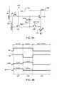
- FIG. 2Ais a circuit diagram of an exemplary driving circuit for a pixel 100 .
- the driving circuit shown in FIG. 1Ais utilized to program, monitor, and drive the pixel 100 and includes a driving transistor 114 for conveying a driving current through an organic light emitting diode (“OLED”) 110 .
- OLEDorganic light emitting diode
- the OLED 110emits light according to the current passing through the OLED 110 , and can be replaced by any current-driven light emitting device.
- the pixel 100can be utilized in the display panel 20 of the display system 50 described in connection with FIG. 1 .
- the driving circuit for the pixel 100also includes a storage capacitor 118 , a switching transistor 116 , and a data switching transistor 112 .
- the pixel 100is coupled to a reference voltage line 102 , a select line 104 , a voltage supply line 106 , and a data/monitor line 108 .
- the driving transistor 114draws a current from the voltage supply line 106 according to a gate-source voltage (“Vgs”) across a gate terminal of the driving transistor 114 and a source terminal of the driving transistor 114 .
- Vgsgate-source voltage
- the storage capacitor 118is coupled across the gate terminal and the source terminal of the driving transistor 114 .
- the storage capacitor 118has a first terminal 118 g , which is referred to for convenience as a gate-side terminal 118 g , and a second terminal 118 s , which is referred to for convenience as a source-side terminal 118 s .
- the gate-side terminal 118 g of the storage capacitor 118is electrically coupled to the gate terminal of the driving transistor 114 .
- the source-side terminal 118 s of the storage capacitor 118is electrically coupled to the source terminal of the driving transistor 114 .
- the gate-source voltage Vgs of the driving transistor 114is also the voltage charged on the storage capacitor 118 .
- the storage capacitor 118can thereby maintain a driving voltage across the driving transistor 114 during an emission phase of the pixel 100 .
- the drain terminal of the driving transistor 114is electrically coupled to the voltage supply line 106 .
- the source terminal of the driving transistor 114is electrically coupled to an anode terminal of the OLED 110 .
- a cathode terminal of the OLED 110can be connected to ground or can optionally be connected to a second voltage supply line, such as a supply line Vss.
- V OLEDoperating voltage
- the OLED 110turns on and emits light.
- the anode to cathode voltageis less than V OLED , current does not pass through the OLED 110 .
- the switching transistor 116is operated according to a select line 104 (e.g., when the select line 104 is at a high level, the switching transistor 116 is turned on, and when the select line 104 is at a low level, the switching transistor is turned off).
- the switching transistor 116electrically couples the gate terminal of the driving transistor (and the gate-side terminal 118 g of the storage capacitor 118 ) to the reference voltage line 102 .
- the reference voltage line 102can be maintained at a ground voltage or another fixed reference voltage (“Vref”) and can optionally be adjusted during a programming phase of the pixel 100 to provide compensation for degradation of the pixel 100 .
- the data switching transistor 112is operated by the select line 104 in the same manner as the switching transistor 116 . Although, it is noted that the data switching transistor 112 can optionally be operated by a second select line in an implementation of the pixel 100 . When turned on, the data switching transistor 112 electrically couples the source terminal of the driving transistor (and the source-side terminal 118 s of the storage capacitor 118 ) to the data/monitor line 108 .
- FIG. 2Bis a schematic timing diagram of exemplary operation cycles for the pixel 100 shown in FIG. 2A .
- the pixel 100can be operated in a monitor phase 121 , a program phase 122 , and an emission phase 123 .
- the select line 104is high and the switching transistor 116 and the data switching transistor 112 are both turned on.
- the data/monitor line 108is fixed at a calibration voltage (“Vcal”). Because the data switching transistor 112 is turned on, the calibration voltage Vcal is applied to the anode terminal of the OLED 110 .
- Vcalcalibration voltage
- Vcalis chosen such that the voltage applied across the anode and cathode terminals of the OLED 110 is less than the operating voltage V OLED of the OLED 110 , and the OLED 110 therefore does not draw current.
- Vcalis set at a level sufficient to turn off the OLED 110 (i.e., sufficient to ensure that the OLED 110 does not draw current)
- the current flowing through the driving transistor 114 during the monitor phase 121does not pass through the OLED 110 and instead travels through the data/monitor line 108 .
- the current on the data/monitor line 108is the current being drawn through the driving transistor 114 .
- the data/monitor line 108can then be coupled to a monitoring system (such as the monitoring system 12 shown in FIG. 1 ) to measure the current during the monitor phase 121 and thereby extract information indicative of a degradation of the pixel 100 .
- a monitoring systemsuch as the monitoring system 12 shown in FIG. 1
- the threshold voltage (“Vt”) of the driving transistorcan be determined.
- Such a determination of the threshold voltagecan be carried out by comparing the measured current with an expected current based on the values of the reference voltage Vref and the calibration voltage Vcal applied to the gate and source terminals, respectively, of the driving transistor 114 .
- degradation of the pixel 100can be extracted according to a stepwise method wherein a comparison is made between Imeas and an expected current and an estimate of the value of Imeas is updated incrementally according to the comparison (e.g., based on determining whether Imeas is lesser than, or greater than, the expected current).
- the monitor phase 121can include measuring a voltage on the data/monitor line 108 while fixing the current on the data/monitor line 108 .
- the monitor phase 121can include indirectly measuring the current on the data/monitor line 108 by, for example, measuring a voltage drop across a load, measuring a current related to the current on the data/monitor line 108 provided via a current conveyor, or by measuring a voltage output from a current controlled voltage source that receives the current on the data/monitor line 108 .
- the select line 104remains high, and the switching transistor 116 and the data switching transistor 112 therefore remain turned on.
- the reference voltage line 102can remain fixed at Vref or can optionally be adjusted by a compensation voltage (“Vcomp”) appropriate to account for degradation of the pixel 100 , such as the degradation determined during the monitor phase 121 .
- Vcompcan be a voltage sufficient to account for a shift in the threshold voltage Vt of the driving transistor 114 .
- the voltage Vref (or Vcomp)is applied to the gate-side terminal 118 g of the storage capacitor 118 .
- the data/monitor line 108is adjusted to a programming voltage (“Vprog”), which is applied to the source-side terminal 118 s of the storage capacitor 118 .
- Vprogprogramming voltage
- the storage capacitor 118is charged with a voltage given by the difference of Vref (or Vcomp) on the reference voltage line 102 and Vprog on the data/monitor line 108 .
- degradation of the pixel 100is compensated for by applying the compensation voltage Vcomp to the gate-side terminal 118 g of the storage capacitor 118 during the program phase 122 .
- the threshold voltage Vt of the driving transistor 114can shift (e.g., increase) and therefore a larger gate-source voltage Vgs is required across the driving transistor 114 to maintain a desired driving current through the OLED 110 .
- the shift in Vtcan first be measured, during the monitor phase 121 , via the data/monitor line 108 , and then the shift in Vt can be compensated for, during the program phase 122 , by applying a compensation voltage Vcomp separate from a programming voltage Vprog to the gate-side terminal 118 g of the storage capacitor 118 . Additionally or alternatively, compensation can be provided via adjustments to the programming voltage Vprog applied to the source-side terminal 118 s of the storage capacitor 118 . Furthermore, the programming voltage Vprog is preferably a voltage sufficient to turn off the OLED 110 during the program phase 122 such that the OLED 110 is prevented from emitting light during the program phase 122 .
- the select line 104is low, and the switching transistor 116 and the data switching transistor 112 are both turned off.
- the storage capacitor 118remains charged with the driving voltage given by the difference of Vref (or Vcomp) and Vprog applied across the storage capacitor 118 during the program phase 122 .
- the storage capacitor 118maintains the driving voltage and the driving transistor 114 draws a driving current from the voltage supply line 106 .
- the driving currentis then conveyed through the OLED 110 which emits light according to the amount of current passed through the OLED 110 .
- the anode terminal of the OLED 110(and the source-side terminal 118 s of the storage capacitor) can change from the program voltage Vprog applied during the program phase 122 to an operating voltage V OLED of the OLED 110 . Furthermore, as the driving current is passed through the OLED 110 , the anode terminal of the OLED 110 can change (e.g., increase) over the course of the emission phase 123 . However, during the emission phase 123 , the storage capacitor 118 self-adjusts the voltage on the gate terminal of the driving transistor 114 to maintain the gate-source voltage of the driving transistor 114 even as the voltage on the anode of the OLED 110 may change. For example, adjustments (e.g., increases) on the source-side terminal 118 s are reflected on the gate-side terminal 118 g so as to maintain the driving voltage that was charged on the storage capacitor 118 during the program phase 122 .
- the driving circuit illustrated in FIG. 2Ais illustrated with n-type transistors, which can be thin-film transistors and can be formed from amorphous silicon
- the driving circuit illustrated in FIG. 2A and the operating cycles illustrated in FIG. 2Bcan be extended to a complementary circuit having one or more p-type transistors and having transistors other than thin film transistors.
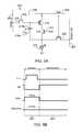
- FIG. 3Ais a circuit diagram for an exemplary pixel circuit configuration for a pixel 130 .
- the driving circuit for the pixel 130is utilized to program, monitor, and drive the pixel 130 .
- the pixel 130includes a driving transistor 148 for conveying a driving current through an OLED 146 .
- the OLED 146is similar to the OLED 110 shown in FIG. 2A and emits light according to the current passing through the OLED 146 .
- the OLED 146can be replaced by any current-driven light emitting device.
- the pixel 130can be utilized in the display panel 20 of the display system 50 described in connection with FIG. 1 , with appropriate modifications to include the connection lines described in connection with the pixel 130 .
- the driving circuit for the pixel 130also includes a storage capacitor 156 , a first switching transistor 152 , and a second switching transistor 154 , a data switching transistor 144 , and an emission transistor 150 .
- the pixel 130is coupled to a reference voltage line 140 , a data/reference line 132 , a voltage supply line 136 , a data/monitor line 138 , a select line 134 , and an emission line 142 .
- the driving transistor 148draws a current from the voltage supply line 136 according to a gate-source voltage (“Vgs”) across a gate terminal of the driving transistor 148 and a source terminal of the driving transistor 148 , and a threshold voltage (“Vt”) of the driving transistor 148 .
- Vgsgate-source voltage
- Vtthreshold voltage
- the storage capacitor 156is coupled across the gate terminal and the source terminal of the driving transistor 148 through the emission transistor 150 .
- the storage capacitor 156has a first terminal 156 g , which is referred to for convenience as a gate-side terminal 156 g , and a second terminal 156 s , which is referred to for convenience as a source-side terminal 156 s .
- the gate-side terminal 156 g of the storage capacitor 156is electrically coupled to the gate terminal of the driving transistor 148 through the emission transistor 150 .
- the source-side terminal 156 s of the storage capacitor 156is electrically coupled to the source terminal of the driving transistor 148 .
- the gate-source voltage Vgs of the driving transistor 148is the voltage charged on the storage capacitor 156 .
- the emission transistor 150is operated according to the emission line 142 (e.g., the emission transistor 150 is turned on when the emission line 142 is set high and vice versa).
- the storage capacitor 156can thereby maintain a driving voltage across the driving transistor 148 during an emission phase of the pixel 130 .
- the drain terminal of the driving transistor 148is electrically coupled to the voltage supply line 136 .
- the source terminal of the driving transistor 148is electrically coupled to an anode terminal of the OLED 146 .
- a cathode terminal of the OLED 146can be connected to ground or can optionally be connected to a second voltage supply line, such as a supply line Vss.
- V OLEDoperating voltage
- the first switching transistor 152 , the second switching transistor 154 , and the data switching transistor 144are each operated according to the select line 134 (e.g., when the select line 134 is at a high level, the transistors 144 , 152 , 154 are turned on, and when the select line 134 is at a low level, the switching transistors 144 , 152 , 154 are turned off).
- the first switching transistor 152electrically couples the gate terminal of the driving transistor 148 to the reference voltage line 140 .
- the reference voltage line 140can be maintained at a fixed first reference voltage (“Vref 1 ”).
- the data switching transistor 144 and/or the second switching transistor 154can optionally be operated by a second select line in an implementation of the pixel 130 .
- the second switching transistor 154electrically couples the gate-side terminal 156 g of the storage capacitor 156 to the data/reference line 132 .
- the data switching transistor 144electrically couples the data/monitor line 138 to the source-side terminal 156 s of the storage capacitor 156 .
- FIG. 3Bis a timing diagram for operating the pixel 130 illustrated in FIG. 3A .
- the pixel 130can be operated in a monitor phase 124 , a program phase 125 , and an emission phase 126 .
- the select line 134is set high while the emission line 142 is set low.
- the first switching transistor 152 , the second switching transistor 154 , and the data switching transistor 144are all turned on while the emission transistor 150 is turned off.
- the data/monitor line 138is fixed at a calibration voltage (“Vcal”), and the reference voltage line 140 is fixed at the first reference voltage Vref 1 .
- the reference voltage line 140applies the first reference voltage Vref 1 to the gate terminal of the driving transistor 148 through the first switching transistor 152 , and the data/monitor line 138 applies the calibration voltage Vcal to the source terminal of the driving transistor 148 through the data switching transistor 144 .
- the first reference voltage Vref 1 and the calibration voltage Vcalthus fix the gate-source potential Vgs of the driving transistor 148 .
- the driving transistor 148draws a current from the voltage supply line 136 according to the gate-source potential difference thus defined.
- the calibration voltage Vcalis also applied to the anode of the OLED 146 and is advantageously selected to be a voltage sufficient to turn off the OLED 146 .
- the calibration voltage Vcalcan cause the voltage drop across the anode and cathode terminals of the OLED 146 to be less than the operating voltage V OLED of the OLED 146 .
- the current through the driving transistor 148is directed entirely to the data/monitor line 138 rather than through the OLED 146 .
- the current measured on the data/monitor line 138 of the pixel 130can be used to extract degradation information for the pixel 130 , such as information indicative of the threshold voltage Vt of the driving transistor 148 .
- the select line 134is set high and the emission line 142 is set low. Similar to the monitor phase 124 , the first switching transistor 152 , the second switching transistor 154 , and the data switching transistor 144 are all turned on while the emission transistor 150 is turned off.
- the data/monitor line 138is set to a program voltage (“Vprog”), the reference voltage line 140 is fixed at the first reference voltage Vref 1 , and the data/reference line 132 is set to a second reference voltage (“Vref 2 ”).
- the second reference voltage Vref 2is thus applied to the gate-side terminal 156 g of the storage capacitor 156 while the program voltage Vprog is applied to the source-side terminal 156 s of the storage capacitor 156 .
- the data/reference line 132can be set (adjusted) to a compensation voltage (“Vcomp”) rather than remain fixed at the second reference voltage Vref 2 during the program phase 125 .
- Vcompcompensation voltage
- Implementations of the present disclosurealso include operations of the program phase 125 where the program voltage Vprog is applied to the data/reference line 132 , while the data/monitor line 138 is fixed at a second reference voltage Vref 2 , or at a compensation voltage Vcomp.
- the storage capacitor 156is charged with a voltage given by the difference of Vprog and Vref 2 (or Vcomp).
- the compensation voltage Vcomp applied to the gate-side terminal 156 gis a proper voltage to account for a degradation of the pixel circuit 130 , such as the degradation measured during the monitor phase 124 (e.g., an increase in the threshold voltage Vt of the driving transistor 148 ).
- the program voltage Vprogis applied to the anode terminal of the OLED 146 during the program phase 125 .
- the program voltage Vprogis advantageously selected to be sufficient to turn off the OLED 146 during the program phase 125 .
- the program voltage Vprogcan advantageously cause the voltage drop across the anode and cathode terminals of the OLED 146 to be less than the operating voltage V OLED of the OLED 146 .
- the second reference voltage Vref 2can be selected to be a voltage that maintains the OLED 146 in an off state.
- the driving transistor 148is advantageously isolated from the storage capacitor 156 while the storage capacitor 156 receives the programming information via the data/reference line 132 and/or the data/monitor line 138 .
- the driving transistor 148is advantageously prevented from turning on during the program phase 125 .
- the pixel circuit 100 in FIG. 2Aprovides an example of a circuit lacking a means to isolate the driving transistor 114 from the storage capacitor 118 during the program phase 122 .
- a voltageis established across the storage capacitor sufficient to turn on the driving transistor 114 .
- the driving transistor 114begins drawing current from the voltage supply line 106 .
- the currentdoes not flow through the OLED 110 , which is reverse biased during the program phase 122 , instead the current from the driving transistor 114 flows through the data switching transistor 112 .
- a voltage dropis therefore developed across the data switching transistor 112 due to the non-zero resistance of the data switching transistor 112 as the current is conveyed through the data switching transistor 112 .
- the voltage drop across the data switching transistor 112causes the voltage that is applied to the source-side terminal 118 s of the storage capacitor 118 to be different from the program voltage Vprog on the data/monitor line 108 .
- the differenceis given by the current flowing through the data switching transistor 112 and the inherent resistance of the data switching transistor 112 .
- the emission transistor 150 of the pixel 130addresses the above-described effect by ensuring that the voltage established on the storage capacitor 156 during the program phase 125 is not applied across the gate-source terminals of the driving transistor 148 during the program phase 125 .
- the emission transistor 150disconnects one of the terminals of the storage capacitor 156 from the driving transistor 148 to ensure that the driving transistor is not turned on during the program phase 125 of the pixel 130 .
- the emission transistor 150allows for programming the pixel circuit 130 (e.g., charging the storage capacitor 156 ) with a voltage that is independent of a resistance of the switching transistor 144 .
- the first reference voltage Vref 1 applied to the reference voltage line 140can be selected such that the gate-source voltage given by the difference between Vref 1 and Vprog is sufficient to prevent the driving transistor 148 from switching on during the program phase 125 .
- the select line 134is set low while the emission line 142 is high.
- the first switching transistor 152 , the second switching transistor 154 , and the data switching transistor 144are all turned off.
- the emission transistor 150is turned on during the emission phase 126 .
- the storage capacitor 156is connected across the gate terminal and the source terminal of the driving transistor 148 .
- the driving transistor 148draws a driving current from the voltage supply line 136 according to driving voltage stored on the storage capacitor 156 and applied across the gate and source terminals of the driving transistor 148 .
- the anode terminal of the OLED 146is no longer set to a program voltage by the data/monitor line 138 because the data switching transistor 144 is turned off, and so the OLED 146 is turned on and the voltage at the anode terminal of the OLED 146 adjusts to the operating voltage V OLED of the OLED 146 .
- the storage capacitor 156maintains the driving voltage charged on the storage capacitor 156 by self-adjusting the voltage of the source terminal and/or gate terminal of the driving transistor 148 so as to account for variations on one or the other.
- the storage capacitor 156adjusts the voltage on the gate terminal of the driving transistor 148 to maintain the driving voltage across the gate and source terminals of the driving transistor 148 .
- the driving circuit illustrated in FIG. 3Ais illustrated with n-type transistors, which can be thin-film transistors and can be formed from amorphous silicon
- the driving circuit illustrated in FIG. 3A for the pixel 130 and the operating cycles illustrated in FIG. 3Bcan be extended to a complementary circuit having one or more p-type transistors and having transistors other than thin film transistors.
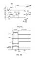
- FIG. 4Ais a circuit diagram for an exemplary pixel circuit configuration for a pixel 160 .
- the driving circuit for the pixel 160is utilized to program, monitor, and drive the pixel 160 .
- the pixel 160includes a driving transistor 174 for conveying a driving current through an OLED 172 .
- the OLED 172is similar to the OLED 110 shown in FIG. 1A and emits light according to the current passing through the OLED 172 .
- the OLED 172can be replaced by any current-driven light emitting device.
- the pixel 160can be utilized in the display panel 20 of the display system 50 described in connection with FIG. 1 , with appropriate connection lines to the data driver, address driver, etc.
- the driving circuit for the pixel 160also includes a storage capacitor 182 , a data switching transistor 180 , a monitor transistor 178 , and an emission transistor 176 .
- the pixel 160is coupled to a data line 162 , a voltage supply line 166 , a monitor line 168 , a select line 164 , and an emission line 170 .
- the driving transistor 174draws a current from the voltage supply line 166 according to a gate-source voltage (“Vgs”) across a gate terminal of the driving transistor 174 and a source terminal of the driving transistor 174 , and a threshold voltage (“Vt”) of the driving transistor 174 .
- Vgsgate-source voltage
- Vtthreshold voltage
- the storage capacitor 182is coupled across the gate terminal and the source terminal of the driving transistor 174 through the emission transistor 176 .
- the storage capacitor 182has a first terminal 182 g , which is referred to for convenience as a gate-side terminal 182 g , and a second terminal 182 s , which is referred to for convenience as a source-side terminal 182 s .
- the gate-side terminal 182 g of the storage capacitor 182is electrically coupled to the gate terminal of the driving transistor 174 .
- the source-side terminal 182 s of the storage capacitor 182is electrically coupled to the source terminal of the driving transistor 174 through the emission transistor 176 .
- the emission transistor 176when the emission transistor 176 is turned on, the gate-source voltage Vgs of the driving transistor 174 is the voltage charged on the storage capacitor 182 .
- the emission transistor 176is operated according to the emission line 170 (e.g., the emission transistor 176 is turned on when the emission line 170 is set high and vice versa).
- the storage capacitor 182can thereby maintain a driving voltage across the driving transistor 174 during an emission phase of the pixel 160 .
- the drain terminal of the driving transistor 174is electrically coupled to the voltage supply line 166 .
- the source terminal of the driving transistor 174is electrically coupled to an anode terminal of the OLED 172 .
- a cathode terminal of the OLED 172can be connected to ground or can optionally be connected to a second voltage supply line, such as a supply line Vss.
- V OLEDoperating voltage
- the data switching transistor 180 and the monitor transistor 178are each operated according to the select line 168 (e.g., when the select line 168 is at a high level, the transistors 178 , 180 are turned on, and when the select line 168 is at a low level, the transistors 178 , 180 are turned off).
- the data switching transistor 180electrically couples the gate terminal of the driving transistor 174 to the data line 162 .
- the data switching transistor 180 and/or the monitor transistor 178can optionally be operated by a second select line in an implementation of the pixel 160 .
- the monitor transistor 178electrically couples the source-side terminal 182 s of the storage capacitor 182 to the monitor line 164 .
- the data switching transistor 180electrically couples the data line 162 to the gate-side terminal 182 g of the storage capacitor 182 .
- FIG. 4Bis a timing diagram for operating the pixel 160 illustrated in FIG. 4A .
- the pixel 160can be operated in a monitor phase 127 , a program phase 128 , and an emission phase 129 .
- the select line 164 and the emission line 170are both set high.
- the data switching transistor 180 , the monitor transistor 178 , and the emission transistor 170are all turned on.
- the data line 162is fixed at a first calibration voltage (“Vcal 1 ”)
- the monitor line 168is fixed at a second calibration voltage (“Vcal 2 ”).
- the first calibration voltage Vcal 1is applied to the gate terminal of the driving transistor 174 through the data switching transistor 180 .
- the second calibration voltage Vcal 2is applied to the source terminal of the driving transistor 174 through the monitor transistor 178 and the emission transistor 176 .
- the first calibration voltage Vcal 1 and the second calibration voltage Vcal 2thereby fix the gate-source potential Vgs of the driving transistor 174 and the driving transistor 174 draws a current from the voltage supply line 166 according to its gate-source potential Vgs.
- the second calibration voltage Vcal 2is also applied to the anode of the OLED 172 and is advantageously selected to be a voltage sufficient to turn off the OLED 172 . Turning off the OLED 172 during the monitor phase 127 ensures that the current flowing through the driving transistor 174 does not pass through the OLED 174 and instead is conveyed to the monitor line 168 via the emission transistor 176 and the monitor transistor 178 . Similar to the description of the monitoring phase 121 in connection with the pixel 100 in FIGS. 2A and 2B , the current measured on the monitor line 168 can be used to extract degradation information for the pixel 160 , such as information indicative of the threshold voltage Vt of the driving transistor 174 .
- the select line 164is set high and the emission line 170 is set low.
- the data switching transistor 180 and the monitor transistor 178are turned on while the emission transistor 176 is turned off.
- the data line 162is set to a program voltage (“Vprog”) and the monitor line 168 is fixed at a reference voltage (“Vref”).
- the monitor line 164can optionally be set to a compensation voltage (“Vcomp”) rather than the reference voltage Vref.
- Vprogprogram voltage
- Vrefreference voltage
- Vcompcompensation voltage
- the gate-side terminal 182 g of the storage capacitor 182is set to the program voltage Vprog and the source-side terminal 182 s is set to the reference voltage Vref (or the compensation voltage Vcomp).
- the storage capacitor 182is thereby charged according to the difference between the program voltage Vprog and the reference voltage Vref (or the compensation voltage Vcomp).
- the voltage charged on the storage capacitor 182 during the program phase 128is referred to as a driving voltage.
- the driving voltageis a voltage appropriate to be applied across the driving transistor 174 to generate a desired driving current that will cause the OLED 172 to emit a desired amount of light. Similar to the operation of the pixel 100 in connection with FIGS.
- the compensation voltage Vcomp optionally applied to the source-side terminal 182 sis a proper voltage to account for a degradation of the pixel circuit 160 , such as the degradation measured during the monitor phase 127 (e.g., an increase in the threshold voltage Vt of the driving transistor 174 ). Additionally or alternatively, compensation for degradation of the pixel 160 can be accounted for by adjustments to the program voltage Vprog applied to the gate-side terminal 182 g.
- the driving transistor 174is isolated from the storage capacitor 182 by the emission transistor 176 , which disconnects the source terminal of the driving transistor 174 from the storage capacitor 182 during the program phase 128 .
- isolating the driving transistor 174 and the storage capacitor 182 during the program phase 128advantageously prevents the driving transistor 182 from turning on during the program phase 128 .
- the voltage applied to the storage capacitor 182 during the program phase 128is advantageously independent of a resistance of the switching transistors as no current is conveyed through the switching transistors.
- the emission transistor 176also advantageously disconnects the storage capacitor 182 from the OLED 172 during the program phase 128 , which prevents the storage capacitor 182 from being influenced by an internal capacitance of the OLED 172 during the program phase 128 .
- the select line 164is set low while the emission line 170 is high.
- the data switching transistor 180 and the monitor transistor 178are turned off and the emission transistor 176 is turned on during the emission phase 129 .
- the storage capacitor 182is connected across the gate terminal and the source terminal of the driving transistor 174 .
- the driving transistor 174draws a driving current from the voltage supply line 166 according to the driving voltage stored on the storage capacitor 182 .
- the OLED 172is turned on and the voltage at the anode terminal of the OLED 172 adjusts to the operating voltage V OLED of the OLED 172 .
- the storage capacitor 182maintains the driving voltage by self-adjusting the voltage of the source terminal and/or gate terminal of the driving transistor 174 so as to account for variations on one or the other. For example, if the voltage on the source-side terminal 182 s changes during the emission cycle 129 due to, for example, the anode terminal of the OLED 172 settling at the operating voltage V OLED , the storage capacitor 182 adjusts the voltage on the gate terminal of the driving transistor 174 to maintain the driving voltage across the gate and source terminals of the driving transistor 174 .
- the driving circuit illustrated in FIG. 4Ais illustrated with n-type transistors, which can be thin-film transistors and can be formed from amorphous silicon
- the driving circuit illustrated in FIG. 4A for the pixel 160 and the operating cycles illustrated in FIG. 4Bcan be extended to a complementary circuit having one or more p-type transistors and having transistors other than thin film transistors.
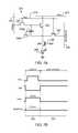
- FIG. 5Ais a circuit diagram for an exemplary pixel circuit configuration for a pixel 200 .
- the driving circuit for the pixel 200is utilized to program, monitor, and drive the pixel 200 .
- the pixel 200includes a driving transistor 214 for conveying a driving current through an OLED 220 .
- the OLED 220is similar to the OLED 110 shown in FIG. 2A and emits light according to the current passing through the OLED 220 .
- the OLED 220can be replaced by any current-driven light emitting device.
- the pixel 200can be incorporated into the display panel 20 and the display system 50 described in connection with FIG. 1 , with appropriate line connections to the data driver, address driver, monitoring system, etc.
- the driving circuit for the pixel 200also includes a storage capacitor 218 , a data switching transistor 216 , a monitor transistor 212 , and an emission transistor 222 .
- the pixel 200is coupled to a data line 202 , a voltage supply line 206 , a monitor line 208 , a select line 204 , and an emission line 210 .
- the driving transistor 214draws a current from the voltage supply line 206 according to a gate-source voltage (“Vgs”) across a gate terminal of the driving transistor 214 and a source terminal of the driving transistor 214 , and a threshold voltage (“Vt”) of the driving transistor 214 .
- Vgsgate-source voltage
- Vtthreshold voltage
- the storage capacitor 218is coupled across the gate terminal and the source terminal of the driving transistor 214 through the emission transistor 222 .
- the storage capacitor 218has a first terminal 218 g , which is referred to for convenience as a gate-side terminal 218 g , and a second terminal 218 s , which is referred to for convenience as a source-side terminal 218 s .
- the gate-side terminal 218 g of the storage capacitor 218is electrically coupled to the gate terminal of the driving transistor 214 .
- the source-side terminal 218 s of the storage capacitor 218is electrically coupled to the source terminal of the driving transistor 214 through the emission transistor 222 .
- the gate-source voltage Vgs of the driving transistor 214is the voltage charged on the storage capacitor 218 .
- the emission transistor 222is operated according to the emission line 210 (e.g., the emission transistor 222 is turned on when the emission line 210 is set high and vice versa).
- the storage capacitor 218can thereby maintain a driving voltage across the driving transistor 214 during an emission phase of the pixel 200 .
- the drain terminal of the driving transistor 214is electrically coupled to the voltage supply line 206 .
- the source terminal of the driving transistor 214is electrically coupled to an anode terminal of the OLED 220 through the emission transistor 222 .
- a cathode terminal of the OLED 220can be connected to ground or can optionally be connected to a second voltage supply line, such as a supply line Vss.
- Vssa supply line
- the OLED 220emits light according to the current passing through the OLED 220 once a voltage drop across the anode and cathode terminals of the OLED 220 achieves an operating voltage (“V OLED ”) of the OLED 220 similar to the description of the OLED 110 provided in connection with FIGS. 2A and 2B .
- V OLEDoperating voltage
- the data switching transistor 216 and the monitor transistor 212are each operated according to the select line 204 (e.g., when the select line 204 is at a high level, the transistors 212 , 216 are turned on, and when the select line 204 is at a low level, the transistors 212 , 216 are turned off).
- the data switching transistor 216electrically couples the gate terminal of the driving transistor 214 to the data line 202 .
- the data switching transistor 216 and/or the monitor transistor 212can optionally be operated by a second select line in an implementation of the pixel 200 .
- the monitor transistor 212electrically couples the source-side terminal 218 s of the storage capacitor 218 to the monitor line 208 .
- the data switching transistor 216electrically couples the data line 202 to the gate-side terminal 218 g of the storage capacitor 218 .
- FIG. 5Bis a timing diagram for operating the pixel 200 illustrated in FIG. 5A in a program phase and an emission phase. As shown in FIG. 5B , the pixel 200 can be operated in a program phase 223 , and an emission phase 224 .
- FIG. 5Cis a timing diagram for operating the pixel 200 illustrated in FIG. 5A in a TFT monitor phase 225 to measure aspects of the driving transistor 214 .
- FIG. 5Dis a timing diagram for operating the pixel 200 illustrated in FIG. 5A in an OLED monitor phase 226 to measure aspects of the OLED 220 .
- the pixel 200may be operated with a program phase 223 and an emission phase 224 for each frame of a video display.
- the pixel 200may also optionally be operated in either or both of the monitor phases 225 , 226 to monitor degradation of the pixel 200 due to the driving transistor 214 or of the OLED 220 , or both.
- the pixel 200may be operated in the monitor phase(s) 225 , 226 intermittently, periodically, or according to a sorting and prioritization algorithm to dynamically determine and identify pixels in a display that require updated degradation information for providing compensation therefore. Therefore, a driving sequence corresponding to a single frame being displayed via the pixel 200 can include the program phase 223 and the emission phase 224 , and can optionally either or both of the monitor phases 225 , 226 .
- the select line 204is set high and the emission line 210 is set low.
- the data switching transistor 216 and the monitor transistor 212are turned on while the emission transistor 222 is turned off.
- the data line 202is set to a program voltage (“Vprog”) and the monitor line 208 is fixed at a reference voltage (“Vref”).
- the monitor line 208can optionally be set to a compensation voltage (“Vcomp”) rather than the reference voltage Vref.
- Vprogprogram voltage
- Vrefreference voltage
- Vcompcompensation voltage
- the gate-side terminal 218 g of the storage capacitor 218is set to the program voltage Vprog and the source-side terminal 218 s is set to the reference voltage Vref (or the compensation voltage Vcomp).
- the storage capacitor 218is thereby charged according to the difference between the program voltage Vprog and the reference voltage Vref (or the compensation voltage Vcomp).
- the voltage charged on the storage capacitor 218 during the program phase 223is referred to as a driving voltage.
- the driving voltageis a voltage appropriate to be applied across the driving transistor to generate a desired driving current that will cause the OLED 220 to emit a desired amount of light. Similar to the operation of the pixel 100 described in connection with FIGS.
- the compensation voltage Vcomp optionally applied to the source-side terminal 218 sis a proper voltage to account for a degradation of the pixel circuit 200 , such as the degradation measured during the monitor phase(s) 225 , 226 (e.g., an increase in the threshold voltage Vt of the driving transistor 214 ). Additionally or alternatively, compensation for degradation of the pixel 200 can be accounted for by adjustments to the program voltage Vprog applied to the gate-side terminal 218 g.
- the emission transistor 222ensures that the driving transistor 214 is isolated from the storage capacitor 218 during the program phase 223 .
- the emission transistor 222ensures that the driving transistor is not turned on during programming such that current flows through a switching transistor.
- isolating the driving transistor 214 from the storage capacitor 218 via the emission transistor 222ensures that the voltage charged on the storage capacitor 218 during the program phase 223 is independent of a resistance of a switching transistor.
- the select line 204is set low while the emission line 210 is high.
- the data switching transistor 216 and the monitor transistor 212are turned off and the emission transistor 222 is turned on during the emission phase 224 .
- the emission transistor 214By turning on the emission transistor 214 , the storage capacitor 218 is connected across the gate terminal and the source terminal of the driving transistor 214 .
- the driving transistor 214draws a driving current from the voltage supply line 206 according to the driving voltage stored on the storage capacitor 218 .
- the OLED 220is turned on and the voltage at the anode terminal of the OLED 220 adjusts to the operating voltage V OLED of the OLED 220 .
- the storage capacitor 218maintains the driving voltage by self-adjusting the voltage of the source terminal and/or gate terminal of the driving transistor 218 so as to account for variations on one or the other. For example, if the voltage on the source-side terminal 218 s changes during the emission cycle 224 due to, for example, the anode terminal of the OLED 220 settling at the operating voltage V OLED , the storage capacitor 218 adjusts the voltage on the gate terminal of the driving transistor 214 to maintain the driving voltage across the gate and source terminals of the driving transistor 214 .
- the select line 204 and the emission line 210are both set high.
- the data switching transistor 216 , the monitor transistor 212 , and the emission transistor 222are all turned on.
- the data line 202is fixed at a first calibration voltage (“Vcal 1 ”)
- the monitor line 208is fixed at a second calibration voltage (“Vcal 2 ”).
- the first calibration voltage Vcal 1is applied to the gate terminal of the driving transistor 214 through the data switching transistor 216 .
- the second calibration voltage Vcal 2is applied to the source terminal of the driving transistor 214 through the monitor transistor 212 and the emission transistor 222 .
- the first calibration voltage Vcal 1 and the second calibration voltage Vcal 2thereby fix the gate-source potential Vgs of the driving transistor 214 and the driving transistor 214 draws a current from the voltage supply line 206 according to its gate-source potential Vgs.
- the second calibration voltage Vcal 2is also applied to the anode of the OLED 220 and is advantageously selected to be a voltage sufficient to turn off the OLED 220 . Turning off the OLED 220 during the TFT monitor phase 225 ensures that the current flowing through the driving transistor 214 does not pass through the OLED 220 and instead is conveyed to the monitor line 208 via the emission transistor 222 and the monitor transistor 212 . Similar to the description of the monitoring phase 121 in connection with the pixel 100 in FIGS. 2A and 2B , the current measured on the monitor line 208 can be used to extract degradation information for the pixel 200 , such as information indicative of the threshold voltage Vt of the driving transistor 214 .
- the select line 204is set high while the emission line 210 is set low.
- the data switching transistor 216 and the monitor transistor 212are turned on while the emission transistor 222 is turned off.
- the data line 202is fixed at a reference voltage Vref, and the monitor line sources or sinks a fixed current on the monitor line 208 .
- the fixed current on the monitor line 208is applied to the OLED 220 through the monitor transistor 212 , and causes the OLED 220 to settle at its operating voltage V OLED .
- V OLED of the OLED 220can be extracted.
- the emission lineis generally set to a level within each operating phase for a longer duration than the select line is set to a particular level.
- aspects of the pixel 200can more accurately settle to stable points prior to subsequent operating cycles. For example, with respect to the program operating cycle 223 , setting the emission line 210 low prior to setting the select line 204 high, allows the driving transistor 214 to cease driving current prior to new programming information being applied to the driving transistor via the data switching transistor 216 .
- the driving circuit illustrated in FIG. 5Ais illustrated with n-type transistors, which can be thin-film transistors and can be formed from amorphous silicon
- the driving circuit illustrated in FIG. 5A for the pixel 200 and the operating cycles illustrated in FIGS. 5B through 5Dcan be extended to a complementary circuit having one or more p-type transistors and having transistors other than thin film transistors.
- FIG. 6Ais a circuit diagram for an exemplary pixel circuit configuration for a pixel 240 .
- the driving circuit for the pixel 240is utilized to program, monitor, and drive the pixel 240 .
- the pixel 240includes a driving transistor 252 for conveying a driving current through an OLED 256 .
- the OLED 256is similar to the OLED 110 shown in FIG. 2A and emits light according to the current passing through the OLED 256 .
- the OLED 256can be replaced by any current-driven light emitting device.
- the pixel 240can be incorporated into the display panel 20 and the display system 50 described in connection with FIG. 1 , with appropriate line connections to the data driver, address driver, monitoring system, etc.
- the driving circuit for the pixel 240also includes a storage capacitor 262 , a data switching transistor 260 , a monitor transistor 258 , and an emission transistor 254 .
- the pixel 240is coupled to a data/monitor line 242 , a voltage supply line 246 , a first select line 244 , a second select line 245 , and an emission line 250 .
- the driving transistor 252draws a current from the voltage supply line 246 according to a gate-source voltage (“Vgs”) across a gate terminal of the driving transistor 252 and a source terminal of the driving transistor 252 , and a threshold voltage (“Vt”) of the driving transistor 252 .
- Vgsgate-source voltage
- Vtthreshold voltage
- the storage capacitor 262is coupled across the gate terminal and the source terminal of the driving transistor 252 through the emission transistor 254 .
- the storage capacitor 262has a first terminal 262 g , which is referred to for convenience as a gate-side terminal 262 g , and a second terminal 262 s , which is referred to for convenience as a source-side terminal 262 s .
- the gate-side terminal 262 g of the storage capacitor 262is electrically coupled to the gate terminal of the driving transistor 252 .
- the source-side terminal 262 s of the storage capacitor 262is electrically coupled to the source terminal of the driving transistor 252 through the emission transistor 254 .
- the gate-source voltage Vgs of the driving transistor 252is the voltage charged on the storage capacitor 262 .
- the emission transistor 254is operated according to the emission line 250 (e.g., the emission transistor 254 is turned on when the emission line 250 is set high and vice versa).
- the storage capacitor 262can thereby maintain a driving voltage across the driving transistor 252 during an emission phase of the pixel 240 .
- the drain terminal of the driving transistor 252is electrically coupled to the voltage supply line 246 .
- the source terminal of the driving transistor 252is electrically coupled to an anode terminal of the OLED 256 through the emission transistor 254 .
- a cathode terminal of the OLED 256can be connected to ground or can optionally be connected to a second voltage supply line, such as a supply line Vss.
- Vssa supply line
- the OLED 256emits light according to the current passing through the OLED 256 once a voltage drop across the anode and cathode terminals of the OLED 256 achieves an operating voltage (“V OLED ”) of the OLED 256 similar to the description of the OLED 110 provided in connection with FIGS. 2A and 2B .
- V OLEDoperating voltage
- the data switching transistor 260is operated according to the first select line 244 (e.g., when the first select line 244 is high, the data switching transistor 260 is turned on, and when the first select line 244 is set low, the data switching transistor is turned off).
- the monitor transistor 258is similarly operated according to the second select line 245 .
- the data switching transistor 260electrically couples the gate-side terminal 262 g of the storage capacitor 262 to the data/monitor line 242 .
- the monitor transistor 258electrically couples the source-side terminal 218 s of the storage capacitor 218 to the data/monitor line 242 .
- FIG. 6Bis a timing diagram for operating the pixel 240 illustrated in FIG. 6A in a program phase and an emission phase. As shown in FIG. 6B , the pixel 240 can be operated in a program phase 227 , and an emission phase 228 .
- FIG. 6Cis a timing diagram for operating the pixel 240 illustrated in FIG. 6A to monitor aspects of the driving transistor 252 .
- FIG. 6Dis a timing diagram for operating the pixel 240 illustrated in FIG. 6A to measure aspects of the OLED 256 .
- the pixel 240may be operated in the program phase 227 and the emission phase 228 for each frame of a video display.
- the pixel 240may also optionally be operated in either or both of the monitor phases monitor degradation of the pixel 200 due to the driving transistor 252 or of the OLED 256 , or both.
- the first select line 244is set high, the second select line 245 is set low, and the emission line 250 is set low.
- the data switching transistor 260is turned on while the emission transistor 254 and the monitor transistor 258 are turned off.
- the data/monitor line 242is set to a program voltage (“Vprog”).
- the program voltage Vprogcan optionally be adjusted according to compensation information to provide compensation for degradation of the pixel 240 .
- the gate-side terminal 262 g of the storage capacitor 262is set to the program voltage Vprog and the source-side terminal 218 s settles at a voltage corresponding to the anode terminal of the OLED 256 while no current is flowing through the OLED 256 .
- the storage capacitor 262is thereby charged according to the program voltage Vprog.
- the voltage charged on the storage capacitor 262 during the program phase 227is referred to as a driving voltage.
- the driving voltageis a voltage appropriate to be applied across the driving transistor 252 to generate a desired driving current that will cause the OLED 256 to emit a desired amount of light.
- the emission transistor 254ensures that the driving transistor 252 is isolated from the storage capacitor 262 during the program phase 227 .
- the emission transistor 254ensures that the driving transistor 252 is not turned on during programming such that current flows through a switching transistor.
- isolating the driving transistor 252 from the storage capacitor 262 via the emission transistor 254ensures that the voltage charged on the storage capacitor 262 during the program phase 227 is independent of a resistance of a switching transistor.
- the first select line 244 and the second select line 245are set low while the emission line 250 is high.
- the data switching transistor 260 and the monitor transistor 258are turned off and the emission transistor 254 is turned on during the emission phase 228 .
- the storage capacitor 262is connected across the gate terminal and the source terminal of the driving transistor 252 .
- the driving transistor 252draws a driving current from the voltage supply line 246 according to the driving voltage stored on the storage capacitor 262 .
- the OLED 256is turned on and the voltage at the anode terminal of the OLED 256 adjusts to the operating voltage V OLED of the OLED 256 .
- the storage capacitor 262maintains the driving voltage by self-adjusting the voltage of the source terminal and/or gate terminal of the driving transistor 252 so as to account for variations on one or the other. For example, if the voltage on the source-side terminal 262 s changes during the emission cycle 228 due to, for example, the anode terminal of the OLED 256 settling at the operating voltage V OLED , the storage capacitor 262 adjusts the voltage on the gate terminal of the driving transistor 252 to maintain the driving voltage across the gate and source terminals of the driving transistor 252 .
- a TFT monitor operationincludes a charge phase 229 and a read phase 230 .
- the first select line 244is set high while the second select line 245 and the emission line 250 are set low.
- the gate-side terminal 262 g of the storage capacitor 262is charged with a first calibration voltage (“Vcal 1 ”) that is applied to the data/monitor line 242 .
- Vcal 1first calibration voltage
- the first select line 244is set low and the second select line 245 and the emission line 250 are set high.
- the data/monitor line 242is set to a second calibration voltage (“Vcal 2 ”).
- the second calibration voltage Vcal 2advantageously reverse biases the OLED 256 such that current flowing through the driving transistor 252 flows to the data/monitor line 242 .
- the data/monitor line 242is maintained at the second calibration voltage Vcal 2 while the current is measured. Comparing the measured current with the first calibration voltage Vcal 1 and the second calibration voltage Vcal 2 allows for the extraction of degradation information related to the driving transistor 252 , similar to the previous descriptions.
- An OLED monitor operationalso includes a charge phase 231 and a read phase 232 .
- the charge phase 231the first select line 244 is set high while the second select line 245 and the emission line 250 are set low.
- the data switching transistor 260is turned on and applies a calibration voltage (“Vcal”) to the gate-side terminal 262 g of the storage capacitor 262 .
- Vcalcalibration voltage
- the current on the data/monitor line 242is fixed while the voltage is measured to extract the operating voltage (“V OLED ”) of the OLED 256 .
- the pixel 240advantageously combines the data line and monitor line in a single line, which allows the pixel 240 to be packaged in a smaller area compared to pixels lacking such a combination, and thereby increase pixel density and display screen resolution.
- the driving circuit illustrated in FIG. 6Ais illustrated with n-type transistors, which can be thin-film transistors and can be formed from amorphous silicon
- the driving circuit illustrated in FIG. 6A for the pixel 240 and the operating cycles illustrated in FIGS. 6B through 6Dcan be extended to a complementary circuit having one or more p-type transistors and having transistors other than thin film transistors.
- FIG. 7Ais a circuit diagram for an exemplary pixel driving circuit for a pixel 270 .
- the pixel 270is structurally similar to the pixel 100 in FIG. 2A , except that the pixel 270 incorporates an additional emission transistor 286 between the driving transistor 284 and the OLED 288 , and except that the configuration of the data line 272 and the monitor line 278 differs from the pixel 100 .
- the emission transistor 286is also positioned between the storage capacitor 292 and the OLED 288 , such that during a program phase of the pixel 270 , the storage capacitor 292 can be electrically disconnected from the OLED 288 .
- Disconnecting the storage capacitor 292 from the OLED 288 during programmingprevents the programming of the storage capacitor 292 from being influenced or perturbed due to the capacitance of the OLED 288 .
- the pixel 270can also operate differently than the pixel 100 , as will be described further below.
- FIG. 7Bis a timing diagram for operating the pixel 270 illustrated in FIG. 7A in a program phase and an emission phase. As shown in FIG. 7B , the pixel 270 can be operated in a program phase 233 , and an emission phase 234 .
- FIG. 7Cis a timing diagram for operating the pixel 270 illustrated in FIG. 7A in a TFT monitor phase 235 to measure aspects of the driving transistor 284 .
- FIG. 7Dis a timing diagram for operating the pixel 270 illustrated in FIG. 7A in an OLED monitor phase 236 to measure aspects of the OLED 288 .
- the pixel 270may be operated with a program phase 233 and an emission phase 234 for each frame of a video display.
- the pixel 270may also optionally be operated in either or both of the monitor phases 235 , 236 to monitor degradation of the pixel 270 due to the driving transistor 284 or of the OLED 288 , or both.
- the pixel 270may be operated in the monitor phase(s) 235 , 236 intermittently, periodically, or according to a sorting and prioritization algorithm to dynamically determine and identify pixels in a display that require updated degradation information for providing compensation therefore. Therefore, a driving sequence corresponding to a single frame being displayed via the pixel 270 can include the program phase 233 and the emission phase 234 , and can optionally either or both of the monitor phases 235 , 236 .
- the select line 274is set high and the emission line 280 is set low.
- the data switching transistor 290 and the monitor transistor 282are turned on while the emission transistor 286 is turned off.
- the data line 272is set to a program voltage (“Vprog”) and the monitor line 278 is fixed at a reference voltage (“Vref”).
- the monitor line 278can optionally be set to a compensation voltage (“Vcomp”) rather than the reference voltage Vref.
- Vprogprogram voltage
- Vrefreference voltage
- Vcompcompensation voltage
- the gate-side terminal 292 g of the storage capacitor 292is set to the program voltage Vprog and the source-side terminal 292 s is set to the reference voltage Vref (or the compensation voltage Vcomp).
- the storage capacitor 292is thereby charged according to the difference between the program voltage Vprog and the reference voltage Vref (or the compensation voltage Vcomp).
- the voltage charged on the storage capacitor 292 during the program phase 233is referred to as a driving voltage.
- the driving voltageis a voltage appropriate to be applied across the driving transistor to generate a desired driving current that will cause the OLED 288 to emit a desired amount of light. Similar to the operation of the pixel 100 described in connection with FIGS.
- the compensation voltage Vcomp optionally applied to the source-side terminal 292 sis a proper voltage to account for a degradation of the pixel circuit 270 , such as the degradation measured during the monitor phase(s) 235 , 236 (e.g., an increase in the threshold voltage Vt of the driving transistor 284 ). Additionally or alternatively, compensation for degradation of the pixel 270 can be accounted for by adjustments to the program voltage Vprog applied to the gate-side terminal 292 g.
- the select line 274is set low while the emission line 280 is high.
- the data switching transistor 290 and the monitor transistor 282are turned off and the emission transistor 286 is turned on during the emission phase 234 .
- the storage capacitor 292is connected across the gate terminal and the source terminal of the driving transistor 284 .
- the driving transistor 284draws a driving current from the voltage supply line 276 according to the driving voltage stored on the storage capacitor 292 .
- the OLED 288is turned on and the voltage at the anode terminal of the OLED 288 adjusts to the operating voltage V OLED of the OLED 288 .
- the storage capacitor 292maintains the driving voltage by self-adjusting the voltage of the source terminal and/or gate terminal of the driving transistor 284 so as to account for variations on one or the other. For example, if the voltage on the source-side terminal 292 s changes during the emission cycle 234 due to, for example, the anode terminal of the OLED 288 settling at the operating voltage V OLED , the storage capacitor 292 adjusts the voltage on the gate terminal of the driving transistor 284 to maintain the driving voltage across the gate and source terminals of the driving transistor 284 .
- the select line 274is set high while the emission line 280 is set low.
- the data switching transistor 290 and the monitor transistor 282are turned on while the emission transistor 286 is turned off.
- the data line 272is fixed at a first calibration voltage (“Vcal 1 ”)
- the monitor line 278is fixed at a second calibration voltage (“Vcal 2 ”).
- the first calibration voltage Vcal 1is applied to the gate terminal of the driving transistor 284 through the data switching transistor 290 .
- the second calibration voltage Vcal 2is applied to the source terminal of the driving transistor 284 through the monitor transistor 282 .
- the first calibration voltage Vcal 1 and the second calibration voltage Vcal 2thereby fix the gate-source potential Vgs of the driving transistor 284 and the driving transistor 284 draws a current from the voltage supply line 276 according to its gate-source potential Vgs.
- the emission transistor 286is turned off, which removes the OLED 288 from the current path of the driving transistor 284 during the TFT monitor phase 235 .
- the current from the driving transistor 284is thus conveyed to the monitor line 278 via the monitor transistor 282 .
- the current measured on the monitor line 278can be used to extract degradation information for the pixel 270 , such as information indicative of the threshold voltage Vt of the driving transistor 284 .
- the select line 274 and the emission line 280are set high.
- the data switching transistor 290 , the monitor transistor 282 , and the emission transistor 286are all turned on.
- the data line 272is fixed at a reference voltage Vref, and the monitor line sources or sinks a fixed current on the monitor line 278 .
- the fixed current on the monitor line 278is applied to the OLED 288 through the monitor transistor 282 , and causes the OLED 288 to settle at its operating voltage V OLED .
- the operating voltage V OLED of the OLED 288can be extracted.
- the driving circuit illustrated in FIG. 7Ais illustrated with n-type transistors, which can be thin-film transistors and can be formed from amorphous silicon
- the driving circuit illustrated in FIG. 7A for the pixel 270 and the operating cycles illustrated in FIGS. 7B through 7Dcan be extended to a complementary circuit having one or more p-type transistors and having transistors other than thin film transistors.
- Circuits disclosed hereingenerally refer to circuit components being connected or coupled to one another.
- the connections referred toare made via direct connections, i.e., with no circuit elements between the connection points other than conductive lines.
- such connectionscan be made by conductive channels defined on substrates of a display panel such as by conductive transparent oxides deposited between the various connection points. Indium tin oxide is one such conductive transparent oxide.
- the components that are coupled and/or connectedmay be coupled via capacitive coupling between the points of connection, such that the points of connection are connected in series through a capacitive element. While not directly connected, such capacitively coupled connections still allow the points of connection to influence one another via changes in voltage which are reflected at the other point of connection via the capacitive coupling effects and without a DC bias.
- the various connections and couplings described hereincan be achieved through non-direct connections, with another circuit element between the two points of connection.
- the one or more circuit element disposed between the points of connectioncan be a diode, a resistor, a transistor, a switch, etc.
- the voltage and/or current between the two points of connectionare sufficiently related, via the connecting circuit elements, to be related such that the two points of connection can influence each another (via voltage changes, current changes, etc.) while still achieving substantially the same functions as described herein.
- voltages and/or current levelsmay be adjusted to account for additional circuit elements providing non-direct connections, as can be appreciated by individuals skilled in the art of circuit design.
- any of the circuits disclosed hereincan be fabricated according to many different fabrication technologies, including for example, poly-silicon, amorphous silicon, organic semiconductor, metal oxide, and conventional CMOS. Any of the circuits disclosed herein can be modified by their complementary circuit architecture counterpart (e.g., n-type transistors can be converted to p-type transistors and vice versa).
- Two or more computing systems or devicesmay be substituted for any one of the controllers described herein. Accordingly, principles and advantages of distributed processing, such as redundancy, replication, and the like, also can be implemented, as desired, to increase the robustness and performance of controllers described herein.
- machine readable instructionscomprise an algorithm for execution by: (a) a processor, (b) a controller, and/or (c) one or more other suitable processing device(s).
- the algorithmmay be embodied in software stored on tangible media such as, for example, a flash memory, a CD-ROM, a floppy disk, a hard drive, a digital video (versatile) disk (DVD), or other memory devices, but persons of ordinary skill in the art will readily appreciate that the entire algorithm and/or parts thereof could alternatively be executed by a device other than a processor and/or embodied in firmware or dedicated hardware in a well known manner (e.g., it may be implemented by an application specific integrated circuit (ASIC), a programmable logic device (PLD), a field programmable logic device (FPLD), a field programmable gate array (FPGA), discrete logic, etc.).
- ASICapplication specific integrated circuit
- PLDprogrammable logic device
- FPLDfield programmable logic device
- FPGAfield programmable gate array
- any or all of the components of the baseline data determination methodscould be implemented by software, hardware, and/or firmware.
- some or all of the machine readable instructions representedmay be implemented
Landscapes
- Engineering & Computer Science (AREA)
- Physics & Mathematics (AREA)
- Computer Hardware Design (AREA)
- General Physics & Mathematics (AREA)
- Theoretical Computer Science (AREA)
- Control Of Indicators Other Than Cathode Ray Tubes (AREA)
- Electroluminescent Light Sources (AREA)
- Control Of El Displays (AREA)
Abstract
Description
Imeas=Ids=β(Vgs−Vt)2=β(Vref−Vcal−Vt)2
can be rearranged to yield
Vt=Vref−Vcal−(Imeas/β)1/2
Claims (24)
Priority Applications (2)
| Application Number | Priority Date | Filing Date | Title |
|---|---|---|---|
| US15/958,037US10417945B2 (en) | 2011-05-27 | 2018-04-20 | Systems and methods for aging compensation in AMOLED displays |
| US16/532,590US11049426B2 (en) | 2011-05-27 | 2019-08-06 | Systems and methods for aging compensation in AMOLED displays |
Applications Claiming Priority (5)
| Application Number | Priority Date | Filing Date | Title |
|---|---|---|---|
| US201161490870P | 2011-05-27 | 2011-05-27 | |
| US201161556972P | 2011-11-08 | 2011-11-08 | |
| US13/481,790US9773439B2 (en) | 2011-05-27 | 2012-05-26 | Systems and methods for aging compensation in AMOLED displays |
| US15/689,210US9984607B2 (en) | 2011-05-27 | 2017-08-29 | Systems and methods for aging compensation in AMOLED displays |
| US15/958,037US10417945B2 (en) | 2011-05-27 | 2018-04-20 | Systems and methods for aging compensation in AMOLED displays |
Related Parent Applications (1)
| Application Number | Title | Priority Date | Filing Date |
|---|---|---|---|
| US15/689,210ContinuationUS9984607B2 (en) | 2011-05-27 | 2017-08-29 | Systems and methods for aging compensation in AMOLED displays |
Related Child Applications (1)
| Application Number | Title | Priority Date | Filing Date |
|---|---|---|---|
| US16/532,590ContinuationUS11049426B2 (en) | 2011-05-27 | 2019-08-06 | Systems and methods for aging compensation in AMOLED displays |
Publications (2)
| Publication Number | Publication Date |
|---|---|
| US20180240386A1 US20180240386A1 (en) | 2018-08-23 |
| US10417945B2true US10417945B2 (en) | 2019-09-17 |
Family
ID=47218947
Family Applications (4)
| Application Number | Title | Priority Date | Filing Date |
|---|---|---|---|
| US13/481,790Active2034-03-12US9773439B2 (en) | 2011-05-27 | 2012-05-26 | Systems and methods for aging compensation in AMOLED displays |
| US15/689,210ActiveUS9984607B2 (en) | 2011-05-27 | 2017-08-29 | Systems and methods for aging compensation in AMOLED displays |
| US15/958,037ActiveUS10417945B2 (en) | 2011-05-27 | 2018-04-20 | Systems and methods for aging compensation in AMOLED displays |
| US16/532,590Active2032-06-11US11049426B2 (en) | 2011-05-27 | 2019-08-06 | Systems and methods for aging compensation in AMOLED displays |
Family Applications Before (2)
| Application Number | Title | Priority Date | Filing Date |
|---|---|---|---|
| US13/481,790Active2034-03-12US9773439B2 (en) | 2011-05-27 | 2012-05-26 | Systems and methods for aging compensation in AMOLED displays |
| US15/689,210ActiveUS9984607B2 (en) | 2011-05-27 | 2017-08-29 | Systems and methods for aging compensation in AMOLED displays |
Family Applications After (1)
| Application Number | Title | Priority Date | Filing Date |
|---|---|---|---|
| US16/532,590Active2032-06-11US11049426B2 (en) | 2011-05-27 | 2019-08-06 | Systems and methods for aging compensation in AMOLED displays |
Country Status (5)
| Country | Link |
|---|---|
| US (4) | US9773439B2 (en) |
| EP (3) | EP3547301A1 (en) |
| JP (1) | JP2014517940A (en) |
| CN (2) | CN106910464B (en) |
| WO (1) | WO2012164475A2 (en) |
Cited By (1)
| Publication number | Priority date | Publication date | Assignee | Title |
|---|---|---|---|---|
| US12424133B2 (en) | 2023-12-21 | 2025-09-23 | Samsung Display Co., Ltd. | Display device |
Families Citing this family (120)
| Publication number | Priority date | Publication date | Assignee | Title |
|---|---|---|---|---|
| CA2443206A1 (en) | 2003-09-23 | 2005-03-23 | Ignis Innovation Inc. | Amoled display backplanes - pixel driver circuits, array architecture, and external compensation |
| CA2472671A1 (en) | 2004-06-29 | 2005-12-29 | Ignis Innovation Inc. | Voltage-programming scheme for current-driven amoled displays |
| CA2490858A1 (en) | 2004-12-07 | 2006-06-07 | Ignis Innovation Inc. | Driving method for compensated voltage-programming of amoled displays |
| US20140111567A1 (en) | 2005-04-12 | 2014-04-24 | Ignis Innovation Inc. | System and method for compensation of non-uniformities in light emitting device displays |
| US9280933B2 (en) | 2004-12-15 | 2016-03-08 | Ignis Innovation Inc. | System and methods for extraction of threshold and mobility parameters in AMOLED displays |
| US9171500B2 (en) | 2011-05-20 | 2015-10-27 | Ignis Innovation Inc. | System and methods for extraction of parasitic parameters in AMOLED displays |
| US8576217B2 (en) | 2011-05-20 | 2013-11-05 | Ignis Innovation Inc. | System and methods for extraction of threshold and mobility parameters in AMOLED displays |
| US9799246B2 (en) | 2011-05-20 | 2017-10-24 | Ignis Innovation Inc. | System and methods for extraction of threshold and mobility parameters in AMOLED displays |
| TWI402790B (en) | 2004-12-15 | 2013-07-21 | Ignis Innovation Inc | Method and system for programming, calibrating and driving a light-emitting element display |
| US10013907B2 (en) | 2004-12-15 | 2018-07-03 | Ignis Innovation Inc. | Method and system for programming, calibrating and/or compensating, and driving an LED display |
| US10012678B2 (en) | 2004-12-15 | 2018-07-03 | Ignis Innovation Inc. | Method and system for programming, calibrating and/or compensating, and driving an LED display |
| US9275579B2 (en) | 2004-12-15 | 2016-03-01 | Ignis Innovation Inc. | System and methods for extraction of threshold and mobility parameters in AMOLED displays |
| CA2496642A1 (en) | 2005-02-10 | 2006-08-10 | Ignis Innovation Inc. | Fast settling time driving method for organic light-emitting diode (oled) displays based on current programming |
| JP5355080B2 (en) | 2005-06-08 | 2013-11-27 | イグニス・イノベイション・インコーポレーテッド | Method and system for driving a light emitting device display |
| CA2518276A1 (en) | 2005-09-13 | 2007-03-13 | Ignis Innovation Inc. | Compensation technique for luminance degradation in electro-luminance devices |
| US9489891B2 (en) | 2006-01-09 | 2016-11-08 | Ignis Innovation Inc. | Method and system for driving an active matrix display circuit |
| TW200746022A (en) | 2006-04-19 | 2007-12-16 | Ignis Innovation Inc | Stable driving scheme for active matrix displays |
| CA2556961A1 (en) | 2006-08-15 | 2008-02-15 | Ignis Innovation Inc. | Oled compensation technique based on oled capacitance |
| US9370075B2 (en) | 2008-12-09 | 2016-06-14 | Ignis Innovation Inc. | System and method for fast compensation programming of pixels in a display |
| CA2669367A1 (en) | 2009-06-16 | 2010-12-16 | Ignis Innovation Inc | Compensation technique for color shift in displays |
| US10319307B2 (en) | 2009-06-16 | 2019-06-11 | Ignis Innovation Inc. | Display system with compensation techniques and/or shared level resources |
| US9311859B2 (en) | 2009-11-30 | 2016-04-12 | Ignis Innovation Inc. | Resetting cycle for aging compensation in AMOLED displays |
| CA2688870A1 (en) | 2009-11-30 | 2011-05-30 | Ignis Innovation Inc. | Methode and techniques for improving display uniformity |
| US9384698B2 (en) | 2009-11-30 | 2016-07-05 | Ignis Innovation Inc. | System and methods for aging compensation in AMOLED displays |
| US10996258B2 (en) | 2009-11-30 | 2021-05-04 | Ignis Innovation Inc. | Defect detection and correction of pixel circuits for AMOLED displays |
| US8803417B2 (en) | 2009-12-01 | 2014-08-12 | Ignis Innovation Inc. | High resolution pixel architecture |
| CA2687631A1 (en) | 2009-12-06 | 2011-06-06 | Ignis Innovation Inc | Low power driving scheme for display applications |
| US10176736B2 (en) | 2010-02-04 | 2019-01-08 | Ignis Innovation Inc. | System and methods for extracting correlation curves for an organic light emitting device |
| US9881532B2 (en) | 2010-02-04 | 2018-01-30 | Ignis Innovation Inc. | System and method for extracting correlation curves for an organic light emitting device |
| US20140313111A1 (en) | 2010-02-04 | 2014-10-23 | Ignis Innovation Inc. | System and methods for extracting correlation curves for an organic light emitting device |
| US10163401B2 (en) | 2010-02-04 | 2018-12-25 | Ignis Innovation Inc. | System and methods for extracting correlation curves for an organic light emitting device |
| CA2692097A1 (en) | 2010-02-04 | 2011-08-04 | Ignis Innovation Inc. | Extracting correlation curves for light emitting device |
| US10089921B2 (en) | 2010-02-04 | 2018-10-02 | Ignis Innovation Inc. | System and methods for extracting correlation curves for an organic light emitting device |
| CA2696778A1 (en) | 2010-03-17 | 2011-09-17 | Ignis Innovation Inc. | Lifetime, uniformity, parameter extraction methods |
| US8907991B2 (en) | 2010-12-02 | 2014-12-09 | Ignis Innovation Inc. | System and methods for thermal compensation in AMOLED displays |
| US20140368491A1 (en) | 2013-03-08 | 2014-12-18 | Ignis Innovation Inc. | Pixel circuits for amoled displays |
| US9886899B2 (en)* | 2011-05-17 | 2018-02-06 | Ignis Innovation Inc. | Pixel Circuits for AMOLED displays |
| US9351368B2 (en)* | 2013-03-08 | 2016-05-24 | Ignis Innovation Inc. | Pixel circuits for AMOLED displays |
| US9530349B2 (en) | 2011-05-20 | 2016-12-27 | Ignis Innovations Inc. | Charged-based compensation and parameter extraction in AMOLED displays |
| US9466240B2 (en) | 2011-05-26 | 2016-10-11 | Ignis Innovation Inc. | Adaptive feedback system for compensating for aging pixel areas with enhanced estimation speed |
| US9773439B2 (en) | 2011-05-27 | 2017-09-26 | Ignis Innovation Inc. | Systems and methods for aging compensation in AMOLED displays |
| US9881587B2 (en) | 2011-05-28 | 2018-01-30 | Ignis Innovation Inc. | Systems and methods for operating pixels in a display to mitigate image flicker |
| US9305486B2 (en)* | 2011-06-29 | 2016-04-05 | Joled Inc. | Display device and method for driving same having selection control wire for scanning wires and secondary data wire |
| US10089924B2 (en) | 2011-11-29 | 2018-10-02 | Ignis Innovation Inc. | Structural and low-frequency non-uniformity compensation |
| US9324268B2 (en) | 2013-03-15 | 2016-04-26 | Ignis Innovation Inc. | Amoled displays with multiple readout circuits |
| US8937632B2 (en) | 2012-02-03 | 2015-01-20 | Ignis Innovation Inc. | Driving system for active-matrix displays |
| US9747834B2 (en) | 2012-05-11 | 2017-08-29 | Ignis Innovation Inc. | Pixel circuits including feedback capacitors and reset capacitors, and display systems therefore |
| US8922544B2 (en) | 2012-05-23 | 2014-12-30 | Ignis Innovation Inc. | Display systems with compensation for line propagation delay |
| US9336717B2 (en) | 2012-12-11 | 2016-05-10 | Ignis Innovation Inc. | Pixel circuits for AMOLED displays |
| US9786223B2 (en) | 2012-12-11 | 2017-10-10 | Ignis Innovation Inc. | Pixel circuits for AMOLED displays |
| KR101980770B1 (en)* | 2012-12-28 | 2019-05-21 | 엘지디스플레이 주식회사 | Organic light emitting diode display device |
| CN108665836B (en) | 2013-01-14 | 2021-09-03 | 伊格尼斯创新公司 | Method and system for compensating for deviations of a measured device current from a reference current |
| US9830857B2 (en) | 2013-01-14 | 2017-11-28 | Ignis Innovation Inc. | Cleaning common unwanted signals from pixel measurements in emissive displays |
| US9721505B2 (en) | 2013-03-08 | 2017-08-01 | Ignis Innovation Inc. | Pixel circuits for AMOLED displays |
| CA2894717A1 (en) | 2015-06-19 | 2016-12-19 | Ignis Innovation Inc. | Optoelectronic device characterization in array with shared sense line |
| CN105210138B (en)* | 2013-03-13 | 2017-10-27 | 伊格尼斯创新公司 | Integrated compensation data channel |
| EP3043338A1 (en) | 2013-03-14 | 2016-07-13 | Ignis Innovation Inc. | Re-interpolation with edge detection for extracting an aging pattern for amoled displays |
| US9245935B2 (en)* | 2013-04-02 | 2016-01-26 | Semiconductor Energy Laboratory Co., Ltd. | Light-emitting device |
| WO2014174427A1 (en) | 2013-04-22 | 2014-10-30 | Ignis Innovation Inc. | Inspection system for oled display panels |
| WO2014208459A1 (en)* | 2013-06-27 | 2014-12-31 | シャープ株式会社 | Display device and drive method for same |
| CN105474296B (en) | 2013-08-12 | 2017-08-18 | 伊格尼斯创新公司 | A method and device for driving a display using image data |
| US9818765B2 (en)* | 2013-08-26 | 2017-11-14 | Apple Inc. | Displays with silicon and semiconducting oxide thin-film transistors |
| JP2015043041A (en)* | 2013-08-26 | 2015-03-05 | 三星ディスプレイ株式會社Samsung Display Co.,Ltd. | Electro-optic device |
| US9552767B2 (en)* | 2013-08-30 | 2017-01-24 | Semiconductor Energy Laboratory Co., Ltd. | Light-emitting device |
| KR101688923B1 (en)* | 2013-11-14 | 2016-12-23 | 엘지디스플레이 주식회사 | Organic light emitting display device and driving method thereof |
| US9761170B2 (en) | 2013-12-06 | 2017-09-12 | Ignis Innovation Inc. | Correction for localized phenomena in an image array |
| US9741282B2 (en) | 2013-12-06 | 2017-08-22 | Ignis Innovation Inc. | OLED display system and method |
| KR102117889B1 (en)* | 2013-12-11 | 2020-06-02 | 엘지디스플레이 주식회사 | Pixel circuit of display device, organic light emitting display device and method for driving thereof |
| JP6357641B2 (en)* | 2013-12-11 | 2018-07-18 | 株式会社Joled | Display device and driving method thereof |
| US9502653B2 (en) | 2013-12-25 | 2016-11-22 | Ignis Innovation Inc. | Electrode contacts |
| DE102015206281A1 (en) | 2014-04-08 | 2015-10-08 | Ignis Innovation Inc. | Display system with shared level resources for portable devices |
| KR102182129B1 (en)* | 2014-05-12 | 2020-11-24 | 엘지디스플레이 주식회사 | Organic light emitting diode display and drving method thereof |
| DE102015210399A1 (en)* | 2014-06-06 | 2015-12-24 | Ignis Innovation Inc. | Pixel circuits for Amoled displays |
| DE102015218248A1 (en)* | 2014-09-23 | 2016-03-24 | Ignis Innovation Inc. | Clean common unwanted signals from pixel measurements in emission displays |
| CN105551427B (en)* | 2014-10-30 | 2019-01-04 | 鸿富锦精密工业(深圳)有限公司 | Organic light emitting diode display and its driving method |
| CA2873476A1 (en) | 2014-12-08 | 2016-06-08 | Ignis Innovation Inc. | Smart-pixel display architecture |
| CA2879462A1 (en) | 2015-01-23 | 2016-07-23 | Ignis Innovation Inc. | Compensation for color variation in emissive devices |
| US20160267834A1 (en)* | 2015-03-12 | 2016-09-15 | Microsoft Technology Licensing, Llc | Display diode relative age |
| US10115339B2 (en)* | 2015-03-27 | 2018-10-30 | Apple Inc. | Organic light-emitting diode display with gate pulse modulation |
| CA2886862A1 (en) | 2015-04-01 | 2016-10-01 | Ignis Innovation Inc. | Adjusting display brightness for avoiding overheating and/or accelerated aging |
| CA2889870A1 (en) | 2015-05-04 | 2016-11-04 | Ignis Innovation Inc. | Optical feedback system |
| CA2892714A1 (en) | 2015-05-27 | 2016-11-27 | Ignis Innovation Inc | Memory bandwidth reduction in compensation system |
| WO2017010286A1 (en)* | 2015-07-10 | 2017-01-19 | シャープ株式会社 | Pixel circuit, display device, and method for driving same |
| CA2898282A1 (en) | 2015-07-24 | 2017-01-24 | Ignis Innovation Inc. | Hybrid calibration of current sources for current biased voltage progra mmed (cbvp) displays |
| US10657895B2 (en) | 2015-07-24 | 2020-05-19 | Ignis Innovation Inc. | Pixels and reference circuits and timing techniques |
| US10373554B2 (en) | 2015-07-24 | 2019-08-06 | Ignis Innovation Inc. | Pixels and reference circuits and timing techniques |
| CA2900170A1 (en) | 2015-08-07 | 2017-02-07 | Gholamreza Chaji | Calibration of pixel based on improved reference values |
| KR102460992B1 (en)* | 2015-08-31 | 2022-11-01 | 엘지디스플레이 주식회사 | Compensation marging controller and organic light emitting display device and method for driving the same |
| CN105047137B (en)* | 2015-09-09 | 2017-05-31 | 深圳市华星光电技术有限公司 | AMOLED real-time compensation systems |
| CA2908285A1 (en) | 2015-10-14 | 2017-04-14 | Ignis Innovation Inc. | Driver with multiple color pixel structure |
| US10121430B2 (en)* | 2015-11-16 | 2018-11-06 | Apple Inc. | Displays with series-connected switching transistors |
| US9818344B2 (en) | 2015-12-04 | 2017-11-14 | Apple Inc. | Display with light-emitting diodes |
| KR102630078B1 (en) | 2015-12-30 | 2024-01-26 | 엘지디스플레이 주식회사 | Pixel, display device comprising the sme and driving method thereof |
| US10181278B2 (en) | 2016-09-06 | 2019-01-15 | Microsoft Technology Licensing, Llc | Display diode relative age |
| CN106409198B (en)* | 2016-11-24 | 2017-11-10 | 京东方科技集团股份有限公司 | A kind of method for detecting drive circuit |
| KR102286762B1 (en)* | 2017-03-14 | 2021-08-05 | 주식회사 실리콘웍스 | Measuring apparatus of oled and measuring method thereof |
| CN108877650B (en)* | 2017-05-12 | 2020-12-18 | 京东方科技集团股份有限公司 | Pixel drive circuit, drive compensation method, display substrate and display device |
| CN106991967A (en)* | 2017-05-27 | 2017-07-28 | 深圳市华星光电技术有限公司 | Pixel-driving circuit and its restorative procedure and display device |
| KR102472310B1 (en)* | 2017-09-27 | 2022-11-30 | 삼성디스플레이 주식회사 | Organic light emitting display device and mehthod for driving the same |
| CN107481675B (en)* | 2017-09-29 | 2023-12-12 | 京东方科技集团股份有限公司 | Pixel driving circuit and driving method thereof, array substrate and display device |
| KR102413192B1 (en)* | 2017-11-03 | 2022-06-24 | 삼성전자주식회사 | Test circuit monitoring nbti or pbti |
| US10615230B2 (en) | 2017-11-08 | 2020-04-07 | Teradyne, Inc. | Identifying potentially-defective picture elements in an active-matrix display panel |
| CN110021275B (en)* | 2018-01-10 | 2020-07-31 | 京东方科技集团股份有限公司 | Pixel driving circuit, pixel driving method, pixel circuit and display device |
| US11257430B2 (en)* | 2018-03-29 | 2022-02-22 | Sharp Kabushiki Kaisha | Drive method and display device |
| CN110473496B (en)* | 2018-05-09 | 2021-01-26 | 京东方科技集团股份有限公司 | Pixel circuit and driving method thereof, display substrate, and display device |
| US10997914B1 (en)* | 2018-09-07 | 2021-05-04 | Apple Inc. | Systems and methods for compensating pixel voltages |
| US10818208B2 (en)* | 2018-09-14 | 2020-10-27 | Novatek Microelectronics Corp. | Source driver |
| TWI682381B (en)* | 2018-10-17 | 2020-01-11 | 友達光電股份有限公司 | Pixel circuit, display device and pixel circuit driving method |
| CN109584763B (en)* | 2019-01-09 | 2020-12-04 | 惠科股份有限公司 | Drive circuit and display panel |
| CN109584788A (en)* | 2019-01-22 | 2019-04-05 | 京东方科技集团股份有限公司 | Pixel-driving circuit, pixel unit and driving method, array substrate, display device |
| CN109493806B (en)* | 2019-01-28 | 2019-08-23 | 苹果公司 | Electronic device including a display with oxide transistor threshold voltage compensation |
| KR102582618B1 (en)* | 2019-02-26 | 2023-09-26 | 삼성디스플레이 주식회사 | Display device and driving method thereof |
| JP7345268B2 (en)* | 2019-04-18 | 2023-09-15 | Tianma Japan株式会社 | Display device and its control method |
| CN110223647A (en)* | 2019-05-06 | 2019-09-10 | 惠科股份有限公司 | drive circuit and display device |
| CN110010058B (en)* | 2019-05-20 | 2021-01-29 | 京东方科技集团股份有限公司 | Array substrate and display panel |
| US11107410B2 (en)* | 2019-08-15 | 2021-08-31 | Hefei Boe Joint Technology Co., Ltd. | Pixel circuit and method of controlling the same, display panel and display device |
| WO2021047562A1 (en) | 2019-09-12 | 2021-03-18 | 京东方科技集团股份有限公司 | Pixel driving circuit, pixel unit, driving method, array substrate, and display device |
| CN110827754B (en)* | 2019-11-04 | 2021-05-11 | Oppo广东移动通信有限公司 | Compensation circuit and display for an OLED drive circuit |
| KR102814742B1 (en)* | 2020-11-03 | 2025-05-29 | 엘지디스플레이 주식회사 | Display Device and Driving Method of the same |
| CN114495795B (en)* | 2022-02-21 | 2023-12-26 | 京东方科技集团股份有限公司 | Display substrate and display device |
Citations (595)
| Publication number | Priority date | Publication date | Assignee | Title |
|---|---|---|---|---|
| US3506851A (en) | 1966-12-14 | 1970-04-14 | North American Rockwell | Field effect transistor driver using capacitor feedback |
| US3774055A (en) | 1972-01-24 | 1973-11-20 | Nat Semiconductor Corp | Clocked bootstrap inverter circuit |
| US4090096A (en) | 1976-03-31 | 1978-05-16 | Nippon Electric Co., Ltd. | Timing signal generator circuit |
| US4160934A (en) | 1977-08-11 | 1979-07-10 | Bell Telephone Laboratories, Incorporated | Current control circuit for light emitting diode |
| US4295091A (en) | 1978-10-12 | 1981-10-13 | Vaisala Oy | Circuit for measuring low capacitances |
| US4354162A (en) | 1981-02-09 | 1982-10-12 | National Semiconductor Corporation | Wide dynamic range control amplifier with offset correction |
| EP0158366A2 (en) | 1984-04-13 | 1985-10-16 | Sharp Kabushiki Kaisha | Color liquid-crystal display apparatus |
| JPH01272298A (en) | 1988-04-25 | 1989-10-31 | Yamaha Corp | Driving device |
| US4943956A (en) | 1988-04-25 | 1990-07-24 | Yamaha Corporation | Driving apparatus |
| US4996523A (en) | 1988-10-20 | 1991-02-26 | Eastman Kodak Company | Electroluminescent storage display with improved intensity driver circuits |
| CA1294034C (en) | 1985-01-09 | 1992-01-07 | Hiromu Hosokawa | Color uniformity compensation apparatus for cathode ray tubes |
| JPH0442619A (en) | 1990-06-08 | 1992-02-13 | Fujitsu Ltd | DA converter |
| JPH04158570A (en) | 1990-10-22 | 1992-06-01 | Seiko Epson Corp | Structure of semiconductor device and manufacture thereof |
| US5153420A (en) | 1990-11-28 | 1992-10-06 | Xerox Corporation | Timing independent pixel-scale light sensing apparatus |
| CA2109951A1 (en) | 1991-05-24 | 1992-11-26 | Robert Hotto | Dc integrating display driver employing pixel status memories |
| US5198803A (en) | 1990-06-06 | 1993-03-30 | Opto Tech Corporation | Large scale movie display system with multiple gray levels |
| US5204661A (en) | 1990-12-13 | 1993-04-20 | Xerox Corporation | Input/output pixel circuit and array of such circuits |
| US5266515A (en) | 1992-03-02 | 1993-11-30 | Motorola, Inc. | Fabricating dual gate thin film transistors |
| TW223092B (en) | 1990-09-25 | 1994-05-01 | Sumitomo Chemical Co | |
| JPH06314977A (en) | 1993-04-28 | 1994-11-08 | Nec Ic Microcomput Syst Ltd | Current output type d/a converter circuit |
| US5489918A (en) | 1991-06-14 | 1996-02-06 | Rockwell International Corporation | Method and apparatus for dynamically and adjustably generating active matrix liquid crystal display gray level voltages |
| US5498880A (en) | 1995-01-12 | 1996-03-12 | E. I. Du Pont De Nemours And Company | Image capture panel using a solid state device |
| US5557342A (en) | 1993-07-06 | 1996-09-17 | Hitachi, Ltd. | Video display apparatus for displaying a plurality of video signals having different scanning frequencies and a multi-screen display system using the video display apparatus |
| US5561381A (en) | 1989-12-13 | 1996-10-01 | International Business Machines Corporation | Method for testing a partially constructed electronic circuit |
| US5572444A (en) | 1992-08-19 | 1996-11-05 | Mtl Systems, Inc. | Method and apparatus for automatic performance evaluation of electronic display devices |
| JPH08340243A (en) | 1995-06-14 | 1996-12-24 | Canon Inc | Bias circuit |
| US5589847A (en) | 1991-09-23 | 1996-12-31 | Xerox Corporation | Switched capacitor analog circuits using polysilicon thin film technology |
| JPH0990405A (en) | 1995-09-21 | 1997-04-04 | Sharp Corp | Thin film transistor |
| US5619033A (en) | 1995-06-07 | 1997-04-08 | Xerox Corporation | Layered solid state photodiode sensor array |
| US5648276A (en) | 1993-05-27 | 1997-07-15 | Sony Corporation | Method and apparatus for fabricating a thin film semiconductor device |
| US5670973A (en) | 1993-04-05 | 1997-09-23 | Cirrus Logic, Inc. | Method and apparatus for compensating crosstalk in liquid crystal displays |
| US5684365A (en) | 1994-12-14 | 1997-11-04 | Eastman Kodak Company | TFT-el display panel using organic electroluminescent media |
| US5691783A (en) | 1993-06-30 | 1997-11-25 | Sharp Kabushiki Kaisha | Liquid crystal display device and method for driving the same |
| US5714968A (en) | 1994-08-09 | 1998-02-03 | Nec Corporation | Current-dependent light-emitting element drive circuit for use in active matrix display device |
| US5723950A (en) | 1996-06-10 | 1998-03-03 | Motorola | Pre-charge driver for light emitting devices and method |
| US5744824A (en) | 1994-06-15 | 1998-04-28 | Sharp Kabushiki Kaisha | Semiconductor device method for producing the same and liquid crystal display including the same |
| US5745660A (en) | 1995-04-26 | 1998-04-28 | Polaroid Corporation | Image rendering system and method for generating stochastic threshold arrays for use therewith |
| US5748160A (en) | 1995-08-21 | 1998-05-05 | Mororola, Inc. | Active driven LED matrices |
| CA2249592A1 (en) | 1997-01-28 | 1998-07-30 | Casio Computer Co., Ltd. | Active matrix electroluminescent display device and a driving method thereof |
| JPH10254410A (en) | 1997-03-12 | 1998-09-25 | Pioneer Electron Corp | Organic electroluminescent display device, and driving method therefor |
| US5815303A (en) | 1997-06-26 | 1998-09-29 | Xerox Corporation | Fault tolerant projective display having redundant light modulators |
| TW342486B (en) | 1994-07-18 | 1998-10-11 | Toshiba Co Ltd | LED dot matrix display device and method for dimming thereof |
| WO1998048403A1 (en) | 1997-04-23 | 1998-10-29 | Sarnoff Corporation | Active matrix light emitting diode pixel structure and method |
| US5870071A (en) | 1995-09-07 | 1999-02-09 | Frontec Incorporated | LCD gate line drive circuit |
| US5874803A (en) | 1997-09-09 | 1999-02-23 | The Trustees Of Princeton University | Light emitting device with stack of OLEDS and phosphor downconverter |
| US5880582A (en) | 1996-09-04 | 1999-03-09 | Sumitomo Electric Industries, Ltd. | Current mirror circuit and reference voltage generating and light emitting element driving circuits using the same |
| US5903248A (en) | 1997-04-11 | 1999-05-11 | Spatialight, Inc. | Active matrix display having pixel driving circuits with integrated charge pumps |
| US5917280A (en) | 1997-02-03 | 1999-06-29 | The Trustees Of Princeton University | Stacked organic light emitting devices |
| US5923794A (en) | 1996-02-06 | 1999-07-13 | Polaroid Corporation | Current-mediated active-pixel image sensing device with current reset |
| JPH11202295A (en) | 1998-01-09 | 1999-07-30 | Seiko Epson Corp | Driving circuit for electro-optical device, electro-optical device, and electronic apparatus |
| JPH11219146A (en) | 1997-09-29 | 1999-08-10 | Mitsubishi Chemical Corp | Active matrix light emitting diode pixel structure and method |
| JPH11231805A (en) | 1998-02-10 | 1999-08-27 | Sanyo Electric Co Ltd | Display device |
| US5945972A (en) | 1995-11-30 | 1999-08-31 | Kabushiki Kaisha Toshiba | Display device |
| US5949398A (en) | 1996-04-12 | 1999-09-07 | Thomson Multimedia S.A. | Select line driver for a display matrix with toggling backplane |
| US5952789A (en) | 1997-04-14 | 1999-09-14 | Sarnoff Corporation | Active matrix organic light emitting diode (amoled) display pixel structure and data load/illuminate circuit therefor |
| US5952991A (en) | 1996-11-14 | 1999-09-14 | Kabushiki Kaisha Toshiba | Liquid crystal display |
| WO1999048079A1 (en) | 1998-03-19 | 1999-09-23 | Holloman Charles J | Analog driver for led or similar display element |
| JPH11282419A (en) | 1998-03-31 | 1999-10-15 | Nec Corp | Element driving device and method and image display device |
| US5982104A (en) | 1995-12-26 | 1999-11-09 | Pioneer Electronic Corporation | Driver for capacitive light-emitting device with degradation compensated brightness control |
| US6023259A (en) | 1997-07-11 | 2000-02-08 | Fed Corporation | OLED active matrix using a single transistor current mode pixel design |
| JP2000056847A (en) | 1998-08-14 | 2000-02-25 | Nec Corp | Constant current driving circuit |
| JP2000081607A (en) | 1998-09-04 | 2000-03-21 | Denso Corp | Matrix type liquid crystal display device |
| CA2242720C (en) | 1998-07-09 | 2000-05-16 | Ibm Canada Limited-Ibm Canada Limitee | Programmable led driver |
| US6069365A (en) | 1997-11-25 | 2000-05-30 | Alan Y. Chow | Optical processor based imaging system |
| CA2354018A1 (en) | 1998-12-14 | 2000-06-22 | Alan Richard | Portable microdisplay system |
| EP1028471A2 (en) | 1999-02-09 | 2000-08-16 | SANYO ELECTRIC Co., Ltd. | Electroluminescence display device |
| US6177915B1 (en) | 1990-06-11 | 2001-01-23 | International Business Machines Corporation | Display system having section brightness control and method of operating system |
| WO2001006484A1 (en) | 1999-07-14 | 2001-01-25 | Sony Corporation | Current drive circuit and display comprising the same, pixel circuit, and drive method |
| WO2001027910A1 (en) | 1999-10-12 | 2001-04-19 | Koninklijke Philips Electronics N.V. | Led display device |
| US6229506B1 (en) | 1997-04-23 | 2001-05-08 | Sarnoff Corporation | Active matrix light emitting diode pixel structure and concomitant method |
| JP2001134217A (en) | 1999-11-09 | 2001-05-18 | Tdk Corp | Driving device for organic el element |
| US20010002703A1 (en) | 1999-11-30 | 2001-06-07 | Jun Koyama | Electric device |
| US6246180B1 (en) | 1999-01-29 | 2001-06-12 | Nec Corporation | Organic el display device having an improved image quality |
| US6252248B1 (en) | 1998-06-08 | 2001-06-26 | Sanyo Electric Co., Ltd. | Thin film transistor and display |
| EP1111577A2 (en) | 1999-12-24 | 2001-06-27 | Sanyo Electric Co., Ltd. | Improvements in power consumption of display apparatus during still image display mode |
| US6259424B1 (en) | 1998-03-04 | 2001-07-10 | Victor Company Of Japan, Ltd. | Display matrix substrate, production method of the same and display matrix circuit |
| US6262589B1 (en) | 1998-05-25 | 2001-07-17 | Asia Electronics, Inc. | TFT array inspection method and device |
| JP2001195014A (en) | 2000-01-14 | 2001-07-19 | Tdk Corp | Driving device for organic el element |
| US20010009283A1 (en) | 2000-01-26 | 2001-07-26 | Tatsuya Arao | Semiconductor device and method of manufacturing the semiconductor device |
| US6271825B1 (en) | 1996-04-23 | 2001-08-07 | Rainbow Displays, Inc. | Correction methods for brightness in electronic display |
| WO2001063587A2 (en) | 2000-02-22 | 2001-08-30 | Sarnoff Corporation | A method and apparatus for calibrating display devices and automatically compensating for loss in their efficiency over time |
| US20010024181A1 (en) | 2000-01-17 | 2001-09-27 | Ibm | Liquid-crystal display, liquid-crystal control circuit, flicker inhibition method, and liquid-crystal driving method |
| US20010026257A1 (en) | 2000-03-27 | 2001-10-04 | Hajime Kimura | Electro-optical device |
| US6304039B1 (en) | 2000-08-08 | 2001-10-16 | E-Lite Technologies, Inc. | Power supply for illuminating an electro-luminescent panel |
| US20010030323A1 (en) | 2000-03-29 | 2001-10-18 | Sony Corporation | Thin film semiconductor apparatus and method for driving the same |
| US6307322B1 (en) | 1999-12-28 | 2001-10-23 | Sarnoff Corporation | Thin-film transistor circuitry with reduced sensitivity to variance in transistor threshold voltage |
| US6310962B1 (en) | 1997-08-20 | 2001-10-30 | Samsung Electronics Co., Ltd. | MPEG2 moving picture encoding/decoding system |
| US20010035863A1 (en) | 2000-04-26 | 2001-11-01 | Hajime Kimura | Electronic device and driving method thereof |
| US20010038367A1 (en) | 2000-05-08 | 2001-11-08 | Kazutaka Inukai | Light emitting device |
| US20010040541A1 (en) | 1997-09-08 | 2001-11-15 | Kiyoshi Yoneda | Semiconductor device having laser-annealed semiconductor device, display device and liquid crystal display device |
| US6320325B1 (en) | 2000-11-06 | 2001-11-20 | Eastman Kodak Company | Emissive display with luminance feedback from a representative pixel |
| US20010043173A1 (en) | 1997-09-04 | 2001-11-22 | Ronald Roy Troutman | Field sequential gray in active matrix led display using complementary transistor pixel circuits |
| US6323631B1 (en) | 2001-01-18 | 2001-11-27 | Sunplus Technology Co., Ltd. | Constant current driver with auto-clamped pre-charge function |
| US20010045929A1 (en) | 2000-01-21 | 2001-11-29 | Prache Olivier F. | Gray scale pixel driver for electronic display and method of operation therefor |
| US6329971B2 (en) | 1996-12-19 | 2001-12-11 | Zight Corporation | Display system having electrode modulation to alter a state of an electro-optic layer |
| US20010052606A1 (en) | 2000-05-22 | 2001-12-20 | Koninklijke Philips Electronics N.V. | Display device |
| US20010052940A1 (en) | 2000-02-01 | 2001-12-20 | Yoshio Hagihara | Solid-state image-sensing device |
| US20020000576A1 (en) | 2000-06-22 | 2002-01-03 | Kazutaka Inukai | Display device |
| US20020011796A1 (en) | 2000-05-08 | 2002-01-31 | Semiconductor Energy Laboratory Co., Ltd. | Light-emitting device, and electric device using the same |
| US20020012057A1 (en) | 2000-05-26 | 2002-01-31 | Hajime Kimura | MOS sensor and drive method thereof |
| US20020011799A1 (en) | 2000-04-06 | 2002-01-31 | Semiconductor Energy Laboratory Co., Ltd. | Electronic device and driving method |
| US20020014851A1 (en) | 2000-06-05 | 2002-02-07 | Ya-Hsiang Tai | Apparatus and method of testing an organic light emitting diode array |
| US20020018034A1 (en) | 2000-07-31 | 2002-02-14 | Shigeru Ohki | Display color temperature corrected lighting apparatus and flat plane display apparatus |
| JP2002055654A (en) | 2000-08-10 | 2002-02-20 | Nec Corp | Electroluminescence display |
| US6356029B1 (en) | 1999-10-02 | 2002-03-12 | U.S. Philips Corporation | Active matrix electroluminescent display device |
| US20020030190A1 (en) | 1998-12-03 | 2002-03-14 | Hisashi Ohtani | Electro-optical device and semiconductor circuit |
| JP2002091376A (en) | 2000-06-27 | 2002-03-27 | Hitachi Ltd | Image display device and driving method thereof |
| EP1194013A1 (en) | 2000-09-29 | 2002-04-03 | Eastman Kodak Company | A flat-panel display with luminance feedback |
| US6373454B1 (en) | 1998-06-12 | 2002-04-16 | U.S. Philips Corporation | Active matrix electroluminescent display devices |
| US6377237B1 (en) | 2000-01-07 | 2002-04-23 | Agilent Technologies, Inc. | Method and system for illuminating a layer of electro-optical material with pulses of light |
| US20020047565A1 (en) | 2000-07-28 | 2002-04-25 | Wintest Corporation | Apparatus and method for evaluating organic EL display |
| US20020052086A1 (en) | 2000-10-31 | 2002-05-02 | Mitsubishi Denki Kabushiki Kaisha | Semiconductor device and method of manufacturing same |
| US6392617B1 (en) | 1999-10-27 | 2002-05-21 | Agilent Technologies, Inc. | Active matrix light emitting diode display |
| US6404139B1 (en) | 1999-07-02 | 2002-06-11 | Seiko Instruments Inc. | Circuit for driving a light emitting elements display device |
| US20020084463A1 (en) | 2001-01-04 | 2002-07-04 | International Business Machines Corporation | Low-power organic light emitting diode pixel circuit |
| US6417825B1 (en) | 1998-09-29 | 2002-07-09 | Sarnoff Corporation | Analog active matrix emissive display |
| US20020101152A1 (en) | 2001-01-30 | 2002-08-01 | Semiconductor Energy Laboratory Co., Ltd. | Light emitting device |
| US20020101172A1 (en) | 2001-01-02 | 2002-08-01 | Bu Lin-Kai | Oled active driving system with current feedback |
| US20020105279A1 (en) | 2001-02-08 | 2002-08-08 | Hajime Kimura | Light emitting device and electronic equipment using the same |
| CA2436451A1 (en) | 2001-02-05 | 2002-08-15 | International Business Machines Corporation | Liquid crystal display device |
| JP2002229513A (en) | 2001-02-06 | 2002-08-16 | Tohoku Pioneer Corp | Device for driving organic el display panel |
| US6437106B1 (en) | 1999-06-24 | 2002-08-20 | Abbott Laboratories | Process for preparing 6-o-substituted erythromycin derivatives |
| WO2002067327A2 (en) | 2001-02-16 | 2002-08-29 | Ignis Innovation Inc. | Pixel current driver for organic light emitting diode displays |
| US20020117722A1 (en) | 1999-05-12 | 2002-08-29 | Kenichi Osada | Semiconductor integrated circuit device |
| CA2438577A1 (en) | 2001-02-16 | 2002-08-29 | Ignis Innovation Inc. | Pixel current driver for organic light emitting diode displays |
| US6445369B1 (en) | 1998-02-20 | 2002-09-03 | The University Of Hong Kong | Light emitting diode dot matrix display system with audio output |
| US20020122308A1 (en) | 2001-03-05 | 2002-09-05 | Fuji Xerox Co., Ltd. | Apparatus for driving light emitting element and system for driving light emitting element |
| TW502233B (en) | 1999-06-17 | 2002-09-11 | Sony Corp | Image display apparatus |
| JP2002278513A (en) | 2001-03-19 | 2002-09-27 | Sharp Corp | Electro-optical device |
| US20020158666A1 (en) | 2001-04-27 | 2002-10-31 | Munehiro Azami | Semiconductor device |
| US20020158587A1 (en) | 2001-02-15 | 2002-10-31 | Naoaki Komiya | Organic EL pixel circuit |
| US20020158823A1 (en) | 1997-10-31 | 2002-10-31 | Matthew Zavracky | Portable microdisplay system |
| US20020167471A1 (en) | 2001-05-09 | 2002-11-14 | Everitt James W. | System for providing pulse amplitude modulation for oled display drivers |
| US20020169575A1 (en) | 2001-05-09 | 2002-11-14 | James Everitt | Matrix element voltage sensing for precharge |
| JP2002333862A (en) | 2001-02-21 | 2002-11-22 | Semiconductor Energy Lab Co Ltd | Light emission device and electronic equipment |
| US20020181276A1 (en) | 2001-06-01 | 2002-12-05 | Semiconductor Energy Laboratory Co., Ltd. | Method of repairing a light-emitting device, and method of manufacturing a light -emitting device |
| US20020180369A1 (en) | 2001-02-21 | 2002-12-05 | Jun Koyama | Light emitting device and electronic appliance |
| US20020180721A1 (en) | 1997-03-12 | 2002-12-05 | Mutsumi Kimura | Pixel circuit display apparatus and electronic apparatus equipped with current driving type light-emitting device |
| US20020186214A1 (en) | 2001-06-05 | 2002-12-12 | Eastman Kodak Company | Method for saving power in an organic electroluminescent display using white light emitting elements |
| US20020190971A1 (en) | 2001-04-27 | 2002-12-19 | Kabushiki Kaisha Toshiba | Display apparatus, digital-to-analog conversion circuit and digital-to-analog conversion method |
| US20020190924A1 (en) | 2001-01-19 | 2002-12-19 | Mitsuru Asano | Active matrix display |
| US20020195967A1 (en) | 2001-06-22 | 2002-12-26 | Kim Sung Ki | Electro-luminescence panel |
| US20020195968A1 (en) | 2001-06-22 | 2002-12-26 | International Business Machines Corporation | Oled current drive pixel circuit |
| US6501466B1 (en) | 1999-11-18 | 2002-12-31 | Sony Corporation | Active matrix type display apparatus and drive circuit thereof |
| US6501098B2 (en) | 1998-11-25 | 2002-12-31 | Semiconductor Energy Laboratory Co, Ltd. | Semiconductor device |
| US20030020413A1 (en) | 2001-07-27 | 2003-01-30 | Masanobu Oomura | Active matrix display |
| US20030030603A1 (en) | 2001-08-09 | 2003-02-13 | Nec Corporation | Drive circuit for display device |
| US6522315B2 (en) | 1997-02-17 | 2003-02-18 | Seiko Epson Corporation | Display apparatus |
| US6525683B1 (en) | 2001-09-19 | 2003-02-25 | Intel Corporation | Nonlinearly converting a signal to compensate for non-uniformities and degradations in a display |
| US20030043088A1 (en) | 2001-08-31 | 2003-03-06 | Booth Lawrence A. | Compensating organic light emitting device displays for color variations |
| JP2003076331A (en) | 2001-08-31 | 2003-03-14 | Seiko Epson Corp | Display device and electronic equipment |
| US20030058226A1 (en) | 1994-08-22 | 2003-03-27 | Bertram William K. | Reduced noise touch screen apparatus and method |
| US20030057895A1 (en) | 2001-09-07 | 2003-03-27 | Semiconductor Energy Laboratory Co., Ltd. | Light emitting device and method of driving the same |
| US6541921B1 (en) | 2001-10-17 | 2003-04-01 | Sierra Design Group | Illumination intensity control in electroluminescent display |
| US6542138B1 (en) | 1999-09-11 | 2003-04-01 | Koninklijke Philips Electronics N.V. | Active matrix electroluminescent display device |
| US20030062524A1 (en) | 2001-08-29 | 2003-04-03 | Hajime Kimura | Light emitting device, method of driving a light emitting device, element substrate, and electronic equipment |
| US20030071821A1 (en) | 2001-10-11 | 2003-04-17 | Sundahl Robert C. | Luminance compensation for emissive displays |
| WO2003034389A2 (en) | 2001-10-19 | 2003-04-24 | Clare Micronix Integrated Systems, Inc. | System and method for providing pulse amplitude modulation for oled display drivers |
| US20030076048A1 (en) | 2001-10-23 | 2003-04-24 | Rutherford James C. | Organic electroluminescent display device driving method and apparatus |
| JP2003124519A (en) | 2001-10-11 | 2003-04-25 | Sharp Corp | Light emitting diode drive circuit and optical transmission device using the same |
| US6555420B1 (en) | 1998-08-31 | 2003-04-29 | Semiconductor Energy Laboratory Co., Ltd. | Semiconductor device and process for producing semiconductor device |
| US20030090447A1 (en) | 2001-09-21 | 2003-05-15 | Hajime Kimura | Display device and driving method thereof |
| US20030090481A1 (en) | 2001-11-13 | 2003-05-15 | Hajime Kimura | Display device and method for driving the same |
| US6577302B2 (en) | 2000-03-31 | 2003-06-10 | Koninklijke Philips Electronics N.V. | Display device having current-addressed pixels |
| US20030107560A1 (en) | 2001-01-15 | 2003-06-12 | Akira Yumoto | Active-matrix display, active-matrix organic electroluminescent display, and methods of driving them |
| US6580408B1 (en) | 1999-06-03 | 2003-06-17 | Lg. Philips Lcd Co., Ltd. | Electro-luminescent display including a current mirror |
| US20030111966A1 (en) | 2001-12-19 | 2003-06-19 | Yoshiro Mikami | Image display apparatus |
| TW538650B (en) | 2000-09-29 | 2003-06-21 | Seiko Epson Corp | Driving method for electro-optical device, electro-optical device, and electronic apparatus |
| US6583398B2 (en) | 1999-12-14 | 2003-06-24 | Koninklijke Philips Electronics N.V. | Image sensor |
| JP2003177709A (en) | 2001-12-13 | 2003-06-27 | Seiko Epson Corp | Pixel circuit for light emitting element |
| US20030122813A1 (en) | 2001-12-28 | 2003-07-03 | Pioneer Corporation | Panel display driving device and driving method |
| US20030122749A1 (en) | 2001-12-31 | 2003-07-03 | Booth Lawrence A. | Energy sensing light emitting diode display |
| JP2003195813A (en) | 2001-09-07 | 2003-07-09 | Semiconductor Energy Lab Co Ltd | Light emitting device |
| WO2003063124A1 (en) | 2002-01-17 | 2003-07-31 | Nec Corporation | Semiconductor device incorporating matrix type current load driving circuits, and driving method thereof |
| US20030142088A1 (en) | 2001-10-19 | 2003-07-31 | Lechevalier Robert | Method and system for precharging OLED/PLED displays with a precharge latency |
| US20030146897A1 (en) | 2002-02-07 | 2003-08-07 | Hunter Robert J. | Method and apparatus to reduce power consumption of a computer system display screen |
| EP1335430A1 (en) | 2002-02-12 | 2003-08-13 | Eastman Kodak Company | A flat-panel light emitting pixel with luminance feedback |
| US20030169241A1 (en) | 2001-10-19 | 2003-09-11 | Lechevalier Robert E. | Method and system for ramp control of precharge voltage |
| US20030174152A1 (en) | 2002-02-04 | 2003-09-18 | Yukihiro Noguchi | Display apparatus with function which makes gradiation control easier |
| WO2003077231A2 (en) | 2002-03-13 | 2003-09-18 | Koninklijke Philips Electronics N.V. | Two sided display device |
| JP2003271095A (en) | 2002-03-14 | 2003-09-25 | Nec Corp | Driving circuit for current control element and image display device |
| US20030185438A1 (en) | 1997-09-16 | 2003-10-02 | Olympus Optical Co., Ltd. | Color image processing apparatus |
| CN1448908A (en) | 2002-03-29 | 2003-10-15 | 精工爱普生株式会社 | Electronic device, method for driving electronic device, electrooptical device and electronic apparatus |
| US20030197663A1 (en) | 2001-12-27 | 2003-10-23 | Lee Han Sang | Electroluminescent display panel and method for operating the same |
| US6639244B1 (en) | 1999-01-11 | 2003-10-28 | Semiconductor Energy Laboratory Co., Ltd. | Semiconductor device and method of fabricating the same |
| JP2003308046A (en) | 2002-02-18 | 2003-10-31 | Sanyo Electric Co Ltd | Display device |
| JP2003317944A (en) | 2002-04-26 | 2003-11-07 | Seiko Epson Corp | Electro-optical devices and electronic equipment |
| US20030210256A1 (en) | 2002-03-25 | 2003-11-13 | Yukio Mori | Display method and display apparatus |
| EP1372136A1 (en) | 2002-06-12 | 2003-12-17 | Seiko Epson Corporation | Scan driver and a column driver for active matrix display device and corresponding method |
| US20030231148A1 (en) | 2002-06-14 | 2003-12-18 | Chun-Hsu Lin | Brightness correction apparatus and method for plasma display |
| US20030230141A1 (en) | 2002-06-18 | 2003-12-18 | Gilmour Daniel A. | Optical fuel level sensor |
| US20030230980A1 (en) | 2002-06-18 | 2003-12-18 | Forrest Stephen R | Very low voltage, high efficiency phosphorescent oled in a p-i-n structure |
| GB2389951A (en) | 2002-06-18 | 2003-12-24 | Cambridge Display Tech Ltd | Display driver circuits for active matrix OLED displays |
| JP2004004675A (en) | 2002-03-29 | 2004-01-08 | Seiko Epson Corp | Electronic device, method of driving electronic device, electro-optical device, and electronic apparatus |
| WO2004003877A2 (en) | 2002-06-27 | 2004-01-08 | Casio Computer Co., Ltd. | Current drive apparatus and drive method thereof, and electroluminescent display apparatus using the circuit |
| US6677713B1 (en) | 2002-08-28 | 2004-01-13 | Au Optronics Corporation | Driving circuit and method for light emitting device |
| EP1381019A1 (en) | 2002-07-10 | 2004-01-14 | Pioneer Corporation | Automatic luminance adjustment device and method |
| CA2463653A1 (en) | 2002-07-09 | 2004-01-15 | Casio Computer Co., Ltd. | Driving device, display apparatus using the same, and driving method therefor |
| US6680580B1 (en) | 2002-09-16 | 2004-01-20 | Au Optronics Corporation | Driving circuit and method for light emitting device |
| US6687266B1 (en) | 2002-11-08 | 2004-02-03 | Universal Display Corporation | Organic light emitting materials and devices |
| US6690344B1 (en) | 1999-05-14 | 2004-02-10 | Ngk Insulators, Ltd. | Method and apparatus for driving device and display |
| US6690000B1 (en) | 1998-12-02 | 2004-02-10 | Nec Corporation | Image sensor |
| JP2004045648A (en) | 2002-07-10 | 2004-02-12 | Pioneer Electronic Corp | Method and device for driving display panel |
| US6697057B2 (en) | 2000-10-27 | 2004-02-24 | Semiconductor Energy Laboratory Co., Ltd. | Display device and method of driving the same |
| US20040041750A1 (en) | 2001-08-29 | 2004-03-04 | Katsumi Abe | Current load device and method for driving the same |
| CA2498136A1 (en) | 2002-09-09 | 2004-03-18 | Matthew Stevenson | Organic electronic device having improved homogeneity |
| WO2004025615A1 (en) | 2002-09-16 | 2004-03-25 | Koninklijke Philips Electronics N.V. | Display device |
| US20040066357A1 (en) | 2002-09-02 | 2004-04-08 | Canon Kabushiki Kaisha | Drive circuit, display apparatus, and information display apparatus |
| US20040070557A1 (en) | 2002-10-11 | 2004-04-15 | Mitsuru Asano | Active-matrix display device and method of driving the same |
| US20040070565A1 (en) | 2001-12-05 | 2004-04-15 | Nayar Shree K | Method and apparatus for displaying images |
| US6724151B2 (en) | 2001-11-06 | 2004-04-20 | Lg. Philips Lcd Co., Ltd. | Apparatus and method of driving electro luminescence panel |
| WO2004034364A1 (en) | 2002-10-08 | 2004-04-22 | Koninklijke Philips Electronics N.V. | Electroluminescent display devices |
| EP1418566A2 (en) | 2002-11-08 | 2004-05-12 | Tohoku Pioneer Corporation | Drive methods and drive devices for active type light emitting display panel |
| US20040090400A1 (en) | 2002-11-05 | 2004-05-13 | Yoo Juhn Suk | Data driving apparatus and method of driving organic electro luminescence display panel |
| US6738034B2 (en) | 2000-06-27 | 2004-05-18 | Hitachi, Ltd. | Picture image display device and method of driving the same |
| US6738035B1 (en) | 1997-09-22 | 2004-05-18 | Nongqiang Fan | Active matrix LCD based on diode switches and methods of improving display uniformity of same |
| JP2004145197A (en) | 2002-10-28 | 2004-05-20 | Mitsubishi Electric Corp | Display device and display panel |
| US20040095297A1 (en) | 2002-11-20 | 2004-05-20 | International Business Machines Corporation | Nonlinear voltage controlled current source with feedback circuit |
| US20040100427A1 (en) | 2002-08-07 | 2004-05-27 | Seiko Epson Corporation | Electronic circuit, electro-optical device, method for driving electro-optical device and electronic apparatus |
| WO2004047058A2 (en) | 2002-11-21 | 2004-06-03 | Koninklijke Philips Electronics N.V. | Method of improving the output uniformity of a display device |
| EP1429312A2 (en) | 2002-12-12 | 2004-06-16 | Seiko Epson Corporation | Electro-optical device, method of driving electro optical device, and electronic apparatus |
| US6753834B2 (en) | 2001-03-30 | 2004-06-22 | Hitachi, Ltd. | Display device and driving method thereof |
| US6753655B2 (en) | 2002-09-19 | 2004-06-22 | Industrial Technology Research Institute | Pixel structure for an active matrix OLED |
| US6756985B1 (en) | 1998-06-18 | 2004-06-29 | Matsushita Electric Industrial Co., Ltd. | Image processor and image display |
| US6756952B1 (en) | 1998-03-05 | 2004-06-29 | Jean-Claude Decaux | Light display panel control |
| US6756958B2 (en) | 2000-11-30 | 2004-06-29 | Hitachi, Ltd. | Liquid crystal display device |
| US6756741B2 (en) | 2002-07-12 | 2004-06-29 | Au Optronics Corp. | Driving circuit for unit pixel of organic light emitting displays |
| US20040135749A1 (en) | 2003-01-14 | 2004-07-15 | Eastman Kodak Company | Compensating for aging in OLED devices |
| US6765549B1 (en) | 1999-11-08 | 2004-07-20 | Semiconductor Energy Laboratory Co., Ltd. | Active matrix display with pixel memory |
| US20040140982A1 (en) | 2003-01-21 | 2004-07-22 | Pate Michael A. | Image projection with display-condition compensation |
| US20040145547A1 (en) | 2003-01-21 | 2004-07-29 | Oh Choon-Yul | Luminescent display, and driving method and pixel circuit thereof, and display device |
| US6771028B1 (en) | 2003-04-30 | 2004-08-03 | Eastman Kodak Company | Drive circuitry for four-color organic light-emitting device |
| US20040150594A1 (en) | 2002-07-25 | 2004-08-05 | Semiconductor Energy Laboratory Co., Ltd. | Display device and drive method therefor |
| WO2004066249A1 (en) | 2003-01-24 | 2004-08-05 | Koninklijke Philips Electronics N.V. | Active matrix display devices |
| US20040150592A1 (en) | 2003-01-10 | 2004-08-05 | Eastman Kodak Company | Correction of pixels in an organic EL display device |
| US20040155841A1 (en) | 2002-11-27 | 2004-08-12 | Seiko Epson Corporation | Electro-optical device, method of driving electro-optical device, and electronic apparatus |
| US6777888B2 (en) | 2001-03-21 | 2004-08-17 | Canon Kabushiki Kaisha | Drive circuit to be used in active matrix type light-emitting element array |
| US6781306B2 (en) | 2001-06-29 | 2004-08-24 | Lg.Philips Lcd Co., Ltd. | Organic electro-luminescence device and fabricating method thereof |
| US6781567B2 (en) | 2000-09-29 | 2004-08-24 | Seiko Epson Corporation | Driving method for electro-optical device, electro-optical device, and electronic apparatus |
| EP1450341A1 (en) | 2001-09-25 | 2004-08-25 | Matsushita Electric Industrial Co., Ltd. | El display panel and el display apparatus comprising it |
| US20040174354A1 (en) | 2003-02-24 | 2004-09-09 | Shinya Ono | Display apparatus controlling brightness of current-controlled light emitting element |
| US20040174349A1 (en) | 2003-03-04 | 2004-09-09 | Libsch Frank Robert | Driving circuits for displays |
| US20040174347A1 (en) | 2003-03-07 | 2004-09-09 | Wein-Town Sun | Data driver and related method used in a display device for saving space |
| US20040178743A1 (en) | 2002-12-16 | 2004-09-16 | Eastman Kodak Company | Color OLED display system having improved performance |
| US20040178974A1 (en) | 2002-12-16 | 2004-09-16 | Eastman Kodak Company | Color OLED display system having improved performance |
| EP1465143A2 (en) | 2003-04-01 | 2004-10-06 | Samsung SDI Co., Ltd. | Light emitting display, display panel, and driving method thereof |
| JP2004287345A (en) | 2003-03-25 | 2004-10-14 | Casio Comput Co Ltd | Display drive device, display device, and drive control method thereof |
| US6806638B2 (en) | 2002-12-27 | 2004-10-19 | Au Optronics Corporation | Display of active matrix organic light emitting diode and fabricating method |
| EP1469448A1 (en) | 2001-12-28 | 2004-10-20 | Sanyo Electric Co., Ltd. | Organic el display luminance control method and luminance control circuit |
| CN1538377A (en) | 2003-03-13 | 2004-10-20 | ��˹���´﹫˾ | Color OLED display system |
| US20040207615A1 (en) | 1999-07-14 | 2004-10-21 | Akira Yumoto | Current drive circuit and display device using same pixel circuit, and drive method |
| US6815975B2 (en) | 2002-05-21 | 2004-11-09 | Wintest Corporation | Inspection method and inspection device for active matrix substrate, inspection program used therefor, and information storage medium |
| CA2522396A1 (en) | 2003-04-25 | 2004-11-11 | Visioneered Image Systems, Inc. | Led illumination source/display with individual led brightness monitoring capability and calibration method |
| US20040227697A1 (en) | 2003-05-14 | 2004-11-18 | Canon Kabushiki Kaisha | Signal processing apparatus, signal processing method, correction value generation apparatus, correction value generation method, and display apparatus manufacturing method |
| US20040233125A1 (en) | 2003-05-23 | 2004-11-25 | Gino Tanghe | Method for displaying images on a large-screen organic light-emitting diode display, and display used therefore |
| KR20040100887A (en) | 2003-05-19 | 2004-12-02 | 세이코 엡슨 가부시키가이샤 | Electrooptical device and driving device thereof |
| WO2004104975A1 (en) | 2003-05-23 | 2004-12-02 | Sony Corporation | Pixel circuit, display unit, and pixel circuit drive method |
| US20040239596A1 (en) | 2003-02-19 | 2004-12-02 | Shinya Ono | Image display apparatus using current-controlled light emitting element |
| US6828950B2 (en) | 2000-08-10 | 2004-12-07 | Semiconductor Energy Laboratory Co., Ltd. | Display device and method of driving the same |
| US20040246246A1 (en) | 2003-06-09 | 2004-12-09 | Mitsubishi Denki Kabushiki Kaisha | Image display device with increased margin for writing image signal |
| US20040252089A1 (en) | 2003-05-16 | 2004-12-16 | Shinya Ono | Image display apparatus controlling brightness of current-controlled light emitting element |
| US20040257355A1 (en) | 2003-06-18 | 2004-12-23 | Nuelight Corporation | Method and apparatus for controlling an active matrix display |
| US20040257313A1 (en) | 2003-04-15 | 2004-12-23 | Samsung Oled Co., Ltd. | Method and apparatus for driving electro-luminescence display panel designed to perform efficient booting |
| US20040263445A1 (en) | 2001-01-29 | 2004-12-30 | Semiconductor Energy Laboratory Co., Ltd, A Japan Corporation | Light emitting device |
| US20040263541A1 (en) | 2003-06-30 | 2004-12-30 | Fujitsu Hitachi Plasma Display Limited | Display apparatus and display driving method for effectively eliminating the occurrence of a moving image false contour |
| US20050007355A1 (en) | 2003-05-26 | 2005-01-13 | Seiko Epson Corporation | Display apparatus, display method and method of manufacturing a display apparatus |
| US20050007392A1 (en) | 2003-05-28 | 2005-01-13 | Seiko Epson Corporation | Electro-optical device, method of driving electro-optical device, and electronic apparatus |
| US20050007357A1 (en) | 2003-05-19 | 2005-01-13 | Sony Corporation | Pixel circuit, display device, and driving method of pixel circuit |
| US20050017650A1 (en) | 2003-07-24 | 2005-01-27 | Fryer Christopher James Newton | Control of electroluminescent displays |
| US20050024081A1 (en) | 2003-07-29 | 2005-02-03 | Kuo Kuang I. | Testing apparatus and method for thin film transistor display array |
| US20050024393A1 (en) | 2003-07-28 | 2005-02-03 | Canon Kabushiki Kaisha | Image forming apparatus and method of controlling image forming apparatus |
| US6853371B2 (en) | 2000-09-18 | 2005-02-08 | Sanyo Electric Co., Ltd. | Display device |
| US20050030267A1 (en) | 2003-08-07 | 2005-02-10 | Gino Tanghe | Method and system for measuring and controlling an OLED display element for improved lifetime and light output |
| JP2005057217A (en) | 2003-08-07 | 2005-03-03 | Renesas Technology Corp | Semiconductor integrated circuit device |
| WO2005022500A1 (en) | 2003-08-29 | 2005-03-10 | Koninklijke Philips Electronics N.V. | Data signal driver for light emitting display |
| WO2005022498A2 (en) | 2003-09-02 | 2005-03-10 | Koninklijke Philips Electronics N.V. | Active matrix display devices |
| US20050057484A1 (en) | 2003-09-15 | 2005-03-17 | Diefenbaugh Paul S. | Automatic image luminance control with backlight adjustment |
| CA2443206A1 (en) | 2003-09-23 | 2005-03-23 | Ignis Innovation Inc. | Amoled display backplanes - pixel driver circuits, array architecture, and external compensation |
| US6873117B2 (en) | 2002-09-30 | 2005-03-29 | Pioneer Corporation | Display panel and display device |
| US20050068275A1 (en) | 2003-09-29 | 2005-03-31 | Kane Michael Gillis | Driver circuit, as for an OLED display |
| WO2005029456A1 (en) | 2003-09-23 | 2005-03-31 | Ignis Innovation Inc. | Circuit and method for driving an array of light emitting pixels |
| US20050067971A1 (en) | 2003-09-29 | 2005-03-31 | Michael Gillis Kane | Pixel circuit for an active matrix organic light-emitting diode display |
| US20050067970A1 (en) | 2003-09-26 | 2005-03-31 | International Business Machines Corporation | Active-matrix light emitting display and method for obtaining threshold voltage compensation for same |
| US20050068270A1 (en) | 2003-09-17 | 2005-03-31 | Hiroki Awakura | Display apparatus and display control method |
| US6876346B2 (en) | 2000-09-29 | 2005-04-05 | Sanyo Electric Co., Ltd. | Thin film transistor for supplying power to element to be driven |
| EP1521203A2 (en) | 2003-10-02 | 2005-04-06 | Alps Electric Co., Ltd. | Capacitance detector circuit, capacitance detector method and fingerprint sensor using the same |
| US20050073264A1 (en) | 2003-09-29 | 2005-04-07 | Shoichiro Matsumoto | Organic EL panel |
| WO2005034072A1 (en) | 2003-10-02 | 2005-04-14 | Pioneer Corporation | Display apparatus having active matrix display panel, and method for driving the same |
| US20050083323A1 (en) | 2003-10-21 | 2005-04-21 | Tohoku Pioneer Corporation | Light emitting display device |
| US6885356B2 (en) | 2000-07-18 | 2005-04-26 | Nec Electronics Corporation | Active-matrix type display device |
| US20050088103A1 (en) | 2003-10-28 | 2005-04-28 | Hitachi., Ltd. | Image display device |
| US20050105031A1 (en) | 2003-11-13 | 2005-05-19 | Po-Sheng Shih | [pixel structure of display and driving method thereof] |
| US20050110807A1 (en) | 2003-11-21 | 2005-05-26 | Au Optronics Company, Ltd. | Method for displaying images on electroluminescence devices with stressed pixels |
| US20050110420A1 (en) | 2003-11-25 | 2005-05-26 | Eastman Kodak Company | OLED display with aging compensation |
| US6900485B2 (en) | 2003-04-30 | 2005-05-31 | Hynix Semiconductor Inc. | Unit pixel in CMOS image sensor with enhanced reset efficiency |
| US6903734B2 (en) | 2000-12-22 | 2005-06-07 | Lg.Philips Lcd Co., Ltd. | Discharging apparatus for liquid crystal display |
| US20050122294A1 (en) | 2002-04-11 | 2005-06-09 | Ilan Ben-David | Color display devices and methods with enhanced attributes |
| WO2005055185A1 (en) | 2003-11-25 | 2005-06-16 | Eastman Kodak Company | Aceing compensation in an oled display |
| US6909243B2 (en) | 2002-05-17 | 2005-06-21 | Semiconductor Energy Laboratory Co., Ltd. | Light-emitting device and method of driving the same |
| US6911964B2 (en) | 2002-11-07 | 2005-06-28 | Duke University | Frame buffer pixel circuit for liquid crystal display |
| US6911960B1 (en) | 1998-11-30 | 2005-06-28 | Sanyo Electric Co., Ltd. | Active-type electroluminescent display |
| US20050140610A1 (en) | 2002-03-14 | 2005-06-30 | Smith Euan C. | Display driver circuits |
| US20050140598A1 (en) | 2003-12-30 | 2005-06-30 | Kim Chang Y. | Electro-luminescence display device and driving method thereof |
| US6914448B2 (en) | 2002-03-15 | 2005-07-05 | Sanyo Electric Co., Ltd. | Transistor circuit |
| US20050156831A1 (en) | 2002-04-23 | 2005-07-21 | Semiconductor Energy Laboratory Co., Ltd. | Light emitting device and production system of the same |
| US20050162079A1 (en) | 2003-02-13 | 2005-07-28 | Fujitsu Limited | Display device and manufacturing method thereof |
| US20050168416A1 (en) | 2004-01-30 | 2005-08-04 | Nec Electronics Corporation | Display apparatus, and driving circuit for the same |
| US20050179626A1 (en) | 2004-02-12 | 2005-08-18 | Canon Kabushiki Kaisha | Drive circuit and image forming apparatus using the same |
| US20050185200A1 (en) | 2003-05-15 | 2005-08-25 | Zih Corp | Systems, methods, and computer program products for converting between color gamuts associated with different image processing devices |
| US6937220B2 (en) | 2001-09-25 | 2005-08-30 | Sharp Kabushiki Kaisha | Active matrix display panel and image display device adapting same |
| US6937215B2 (en) | 2003-11-03 | 2005-08-30 | Wintek Corporation | Pixel driving circuit of an organic light emitting diode display panel |
| US20050200575A1 (en) | 2004-03-10 | 2005-09-15 | Yang-Wan Kim | Light emission display, display panel, and driving method thereof |
| US6947022B2 (en) | 2002-02-11 | 2005-09-20 | National Semiconductor Corporation | Display line drivers and method for signal propagation delay compensation |
| US20050206590A1 (en) | 2002-03-05 | 2005-09-22 | Nec Corporation | Image display and Its control method |
| US20050212787A1 (en) | 2004-03-24 | 2005-09-29 | Sanyo Electric Co., Ltd. | Display apparatus that controls luminance irregularity and gradation irregularity, and method for controlling said display apparatus |
| US20050219184A1 (en) | 1999-04-30 | 2005-10-06 | E Ink Corporation | Methods for driving electro-optic displays, and apparatus for use therein |
| US6954194B2 (en) | 2002-04-04 | 2005-10-11 | Sanyo Electric Co., Ltd. | Semiconductor device and display apparatus |
| US20050225683A1 (en) | 2004-04-12 | 2005-10-13 | Seiko Epson Corporation | Electro-optical device and electronic apparatus |
| US6956547B2 (en) | 2001-06-30 | 2005-10-18 | Lg.Philips Lcd Co., Ltd. | Driving circuit and method of driving an organic electroluminescence device |
| US20050248515A1 (en) | 2004-04-28 | 2005-11-10 | Naugler W E Jr | Stabilized active matrix emissive display |
| US20050269959A1 (en) | 2004-06-02 | 2005-12-08 | Sony Corporation | Pixel circuit, active matrix apparatus and display apparatus |
| US20050269960A1 (en) | 2004-06-07 | 2005-12-08 | Kyocera Corporation | Display with current controlled light-emitting device |
| US6975332B2 (en) | 2004-03-08 | 2005-12-13 | Adobe Systems Incorporated | Selecting a transfer function for a display device |
| US20050280615A1 (en) | 2004-06-16 | 2005-12-22 | Eastman Kodak Company | Method and apparatus for uniformity and brightness correction in an oled display |
| US20050285822A1 (en) | 2004-06-29 | 2005-12-29 | Damoder Reddy | High-performance emissive display device for computers, information appliances, and entertainment systems |
| US20050285825A1 (en) | 2004-06-29 | 2005-12-29 | Ki-Myeong Eom | Light emitting display and driving method thereof |
| CA2472671A1 (en) | 2004-06-29 | 2005-12-29 | Ignis Innovation Inc. | Voltage-programming scheme for current-driven amoled displays |
| US20060001613A1 (en) | 2002-06-18 | 2006-01-05 | Routley Paul R | Display driver circuits for electroluminescent displays, using constant current generators |
| CA2567076A1 (en) | 2004-06-29 | 2006-01-05 | Ignis Innovation Inc. | Voltage-programming scheme for current-driven amoled displays |
| US20060007072A1 (en) | 2004-06-02 | 2006-01-12 | Samsung Electronics Co., Ltd. | Display device and driving method thereof |
| US20060012311A1 (en) | 2004-07-12 | 2006-01-19 | Sanyo Electric Co., Ltd. | Organic electroluminescent display device |
| US20060015272A1 (en) | 2002-11-06 | 2006-01-19 | Andrea Giraldo | Inspecting method and apparatus for a led matrix display |
| US20060012310A1 (en) | 2004-07-16 | 2006-01-19 | Zhining Chen | Circuit for driving an electronic component and method of operating an electronic device having the circuit |
| TWI248321B (en) | 2004-10-18 | 2006-01-21 | Chi Mei Optoelectronics Corp | Active organic electroluminescence display panel module and driving module thereof |
| US20060022204A1 (en) | 2002-10-08 | 2006-02-02 | Koninklijke Philips Electroics N.V. | Electroluminescent display devices |
| US20060022305A1 (en) | 2004-07-30 | 2006-02-02 | Atsuhiro Yamashita | Active-matrix-driven display device |
| US20060022907A1 (en) | 2004-07-05 | 2006-02-02 | Sony Corporation | Pixel circuit, display device, driving method of pixel circuit, and driving method of display device |
| US6995510B2 (en) | 2001-12-07 | 2006-02-07 | Hitachi Cable, Ltd. | Light-emitting unit and method for producing same as well as lead frame used for producing light-emitting unit |
| US20060030084A1 (en) | 2002-08-24 | 2006-02-09 | Koninklijke Philips Electronics, N.V. | Manufacture of electronic devices comprising thin-film circuit elements |
| US20060038762A1 (en) | 2004-08-21 | 2006-02-23 | Chen-Jean Chou | Light emitting device display circuit and drive method thereof |
| US20060038501A1 (en) | 2004-08-23 | 2006-02-23 | Jun Koyama | Display device, driving method of the same, and electronic device |
| CA2526436A1 (en) | 2004-12-07 | 2006-02-28 | Ignis Innovation Inc. | Method and system for programming and driving active matrix light emitting device pixel |
| US20060044227A1 (en) | 2004-06-18 | 2006-03-02 | Eastman Kodak Company | Selecting adjustment for OLED drive voltage |
| US20060061248A1 (en) | 2004-09-22 | 2006-03-23 | Eastman Kodak Company | Uniformity and brightness measurement in OLED displays |
| US20060066533A1 (en) | 2004-09-27 | 2006-03-30 | Toshihiro Sato | Display device and the driving method of the same |
| US7023408B2 (en) | 2003-03-21 | 2006-04-04 | Industrial Technology Research Institute | Pixel circuit for active matrix OLED and driving method |
| US7027078B2 (en) | 2002-10-31 | 2006-04-11 | Oce Printing Systems Gmbh | Method, control circuit, computer program product and printing device for an electrophotographic process with temperature-compensated discharge depth regulation |
| CN1758309A (en) | 2004-10-08 | 2006-04-12 | 三星Sdi株式会社 | Digital/analog converter, display device using the same, and display panel and driving method thereof |
| US20060077135A1 (en) | 2004-10-08 | 2006-04-13 | Eastman Kodak Company | Method for compensating an OLED device for aging |
| US20060077136A1 (en) | 2004-10-08 | 2006-04-13 | Eastman Kodak Company | System for controlling an OLED display |
| CN1760945A (en) | 2004-08-02 | 2006-04-19 | 冲电气工业株式会社 | Display panel driving circuit and driving method |
| CA2526782A1 (en) | 2004-12-15 | 2006-04-20 | Ignis Innovation Inc. | Method and system for programming, calibrating and driving a light emitting device display |
| US7034793B2 (en) | 2001-05-23 | 2006-04-25 | Au Optronics Corporation | Liquid crystal display device |
| US20060092185A1 (en) | 2004-10-19 | 2006-05-04 | Seiko Epson Corporation | Electro-optical device, method of driving the same, and electronic apparatus |
| US20060097628A1 (en) | 2004-11-08 | 2006-05-11 | Mi-Sook Suh | Flat panel display |
| US20060097631A1 (en) | 2004-11-10 | 2006-05-11 | Samsung Sdi Co., Ltd. | Double-sided light emitting organic electroluminescence display device and fabrication method thereof |
| US20060103611A1 (en) | 2004-11-17 | 2006-05-18 | Choi Sang M | Organic light emitting display and method of driving the same |
| US20060103324A1 (en) | 2004-11-15 | 2006-05-18 | Ji-Hoon Kim | Display device and driving method thereof |
| WO2006053424A1 (en) | 2004-11-16 | 2006-05-26 | Ignis Innovation Inc. | System and driving method for active matrix light emitting device display |
| US7057359B2 (en) | 2003-10-28 | 2006-06-06 | Au Optronics Corporation | Method and apparatus for controlling driving current of illumination source in a display system |
| US7061451B2 (en) | 2001-02-21 | 2006-06-13 | Semiconductor Energy Laboratory Co., Ltd, | Light emitting device and electronic device |
| US20060125740A1 (en) | 2004-12-13 | 2006-06-15 | Casio Computer Co., Ltd. | Light emission drive circuit and its drive control method and display unit and its display drive method |
| WO2006063448A1 (en) | 2004-12-15 | 2006-06-22 | Ignis Innovation Inc. | Method and system for programming, calibrating and driving a light emitting device display |
| US7071932B2 (en) | 2001-11-20 | 2006-07-04 | Toppoly Optoelectronics Corporation | Data voltage current drive amoled pixel circuit |
| US20060149493A1 (en) | 2004-12-01 | 2006-07-06 | Sanjiv Sambandan | Method and system for calibrating a light emitting device display |
| CA2541531A1 (en) | 2005-04-12 | 2006-07-19 | Ignis Innovation Inc. | Method and system for compensation of non-uniformities in light emitting device displays |
| US20060170623A1 (en) | 2004-12-15 | 2006-08-03 | Naugler W E Jr | Feedback based apparatus, systems and methods for controlling emissive pixels using pulse width modulation and voltage modulation techniques |
| US7088051B1 (en) | 2005-04-08 | 2006-08-08 | Eastman Kodak Company | OLED display with control |
| WO2006084360A1 (en) | 2005-02-10 | 2006-08-17 | Ignis Innovation Inc. | Driving circuit for current programmed organic light-emitting diode displays |
| CA2550102A1 (en) | 2005-07-06 | 2006-09-18 | Ignis Innovation Inc. | Method and system for driving a pixel circuit in an active matrix display |
| US20060208971A1 (en) | 2003-05-02 | 2006-09-21 | Deane Steven C | Active matrix oled display device with threshold voltage drift compensation |
| US7112820B2 (en) | 2003-06-20 | 2006-09-26 | Au Optronics Corp. | Stacked capacitor having parallel interdigitized structure for use in thin film transistor liquid crystal display |
| US20060214888A1 (en) | 2004-09-20 | 2006-09-28 | Oliver Schneider | Method and circuit arrangement for the ageing compensation of an organic light-emitting diode and circuit arrangement |
| US7116058B2 (en) | 2004-11-30 | 2006-10-03 | Wintek Corporation | Method of improving the stability of active matrix OLED displays driven by amorphous silicon thin-film transistors |
| US7122835B1 (en) | 1999-04-07 | 2006-10-17 | Semiconductor Energy Laboratory Co., Ltd. | Electrooptical device and a method of manufacturing the same |
| US20060231740A1 (en) | 2005-04-19 | 2006-10-19 | Seiko Epson Corporation | Electronic circuit, method of driving electronic circuit, electro-optical device, and electronic apparatus |
| US20060232522A1 (en) | 2005-04-14 | 2006-10-19 | Roy Philippe L | Active-matrix display, the emitters of which are supplied by voltage-controlled current generators |
| JP2006284970A (en) | 2005-04-01 | 2006-10-19 | Sony Corp | Burning phenomenon correction method, self-light emitting apparatus, burning phenomenon correction apparatus and program |
| US7127380B1 (en) | 2000-11-07 | 2006-10-24 | Alliant Techsystems Inc. | System for performing coupled finite analysis |
| US7129914B2 (en) | 2001-12-20 | 2006-10-31 | Koninklijke Philips Electronics N. V. | Active matrix electroluminescent display device |
| US20060244697A1 (en) | 2005-04-28 | 2006-11-02 | Lee Jae S | Light emitting display device and method of driving the same |
| US20060261841A1 (en) | 2004-08-20 | 2006-11-23 | Koninklijke Philips Electronics N.V. | Data signal driver for light emitting display |
| US20060273997A1 (en) | 2005-04-12 | 2006-12-07 | Ignis Innovation, Inc. | Method and system for compensation of non-uniformities in light emitting device displays |
| US20060279481A1 (en) | 2005-05-26 | 2006-12-14 | Fumio Haruna | Image displaying apparatus |
| US20060284895A1 (en) | 2005-06-15 | 2006-12-21 | Marcu Gabriel G | Dynamic gamma correction |
| US20060284801A1 (en) | 2005-06-20 | 2006-12-21 | Lg Philips Lcd Co., Ltd. | Driving circuit for organic light emitting diode, display device using the same and driving method of organic light emitting diode display device |
| US20060284802A1 (en) | 2005-06-15 | 2006-12-21 | Makoto Kohno | Assuring uniformity in the output of an oled |
| US20060290614A1 (en) | 2005-06-08 | 2006-12-28 | Arokia Nathan | Method and system for driving a light emitting device display |
| US20060290618A1 (en) | 2003-09-05 | 2006-12-28 | Masaharu Goto | Display panel conversion data deciding method and measuring apparatus |
| US20070001937A1 (en) | 2005-06-30 | 2007-01-04 | Lg. Philips Lcd Co., Ltd. | Organic light emitting diode display |
| US7161566B2 (en) | 2003-01-31 | 2007-01-09 | Eastman Kodak Company | OLED display with aging compensation |
| US20070008297A1 (en) | 2005-04-20 | 2007-01-11 | Bassetti Chester F | Method and apparatus for image based power control of drive circuitry of a display pixel |
| WO2007003877A2 (en) | 2005-06-30 | 2007-01-11 | Dry Ice Limited | Cooling receptacle |
| US20070008251A1 (en) | 2005-07-07 | 2007-01-11 | Makoto Kohno | Method of correcting nonuniformity of pixels in an oled |
| US20070008268A1 (en) | 2005-06-25 | 2007-01-11 | Lg. Philips Lcd Co., Ltd. | Organic light emitting diode display |
| US7164417B2 (en) | 2001-03-26 | 2007-01-16 | Eastman Kodak Company | Dynamic controller for active-matrix displays |
| CN1897093A (en) | 2005-07-08 | 2007-01-17 | 三星电子株式会社 | Display device and control method thereof |
| JP2007065015A (en) | 2005-08-29 | 2007-03-15 | Seiko Epson Corp | LIGHT EMITTING CONTROL DEVICE, LIGHT EMITTING DEVICE AND ITS CONTROL METHOD |
| US20070057874A1 (en) | 2003-07-03 | 2007-03-15 | Thomson Licensing S.A. | Display device and control circuit for a light modulator |
| US20070076226A1 (en) | 2003-11-04 | 2007-04-05 | Koninklijke Philips Electronics N.V. | Smart clipper for mobile displays |
| US20070075727A1 (en) | 2003-05-21 | 2007-04-05 | International Business Machines Corporation | Inspection device and inspection method for active matrix panel, and manufacturing method for active matrix organic light emitting diode panel |
| US20070080905A1 (en) | 2003-05-07 | 2007-04-12 | Toshiba Matsushita Display Technology Co., Ltd. | El display and its driving method |
| US20070097041A1 (en) | 2005-10-28 | 2007-05-03 | Samsung Electronics Co., Ltd | Display device and driving method thereof |
| US20070097038A1 (en) | 2001-09-28 | 2007-05-03 | Shunpei Yamazaki | Light emitting device and electronic apparatus using the same |
| EP1784055A2 (en) | 2005-10-17 | 2007-05-09 | Semiconductor Energy Laboratory Co., Ltd. | Lighting system |
| US20070103411A1 (en) | 2005-11-07 | 2007-05-10 | Eastman Kodak Company | OLED display with aging compensation |
| US20070115221A1 (en) | 2003-11-13 | 2007-05-24 | Dirk Buchhauser | Full-color organic display with color filter technology and suitable white emissive material and applications thereof |
| US7227519B1 (en) | 1999-10-04 | 2007-06-05 | Matsushita Electric Industrial Co., Ltd. | Method of driving display panel, luminance correction device for display panel, and driving device for display panel |
| US20070126672A1 (en) | 2005-11-25 | 2007-06-07 | Sony Corporation | Self-luminous display apparatus, peak luminance adjustment apparatus, electronic apparatus, peak luminance adjustment method and program |
| JP2007155754A (en) | 2005-11-30 | 2007-06-21 | Kyocera Corp | Image display device and driving method thereof |
| TW200727247A (en) | 2005-10-07 | 2007-07-16 | Sony Corp | Pixel circuit and display apparatus |
| WO2007079572A1 (en) | 2006-01-09 | 2007-07-19 | Ignis Innovation Inc. | Method and system for driving an active matrix display circuit |
| US20070164938A1 (en) | 2006-01-16 | 2007-07-19 | Samsung Electronics Co., Ltd. | Display device and driving method thereof |
| US20070164664A1 (en) | 2006-01-19 | 2007-07-19 | Eastman Kodak Company | OLED device with improved power consumption |
| US7248236B2 (en) | 2001-02-16 | 2007-07-24 | Ignis Innovation Inc. | Organic light emitting diode display having shield electrodes |
| US7246912B2 (en) | 2003-10-03 | 2007-07-24 | Nokia Corporation | Electroluminescent lighting system |
| WO2007090287A1 (en) | 2006-02-10 | 2007-08-16 | Ignis Innovation Inc. | Method and system for light emitting device displays |
| JP2007206590A (en) | 2006-02-06 | 2007-08-16 | Seiko Epson Corp | Pixel circuit, driving method thereof, display device, and electronic apparatus |
| US20070236134A1 (en) | 2006-04-07 | 2007-10-11 | Industrial Technology Research Institute | OLED pixel structure and method for manufacturing the same |
| US20070236440A1 (en) | 2006-04-06 | 2007-10-11 | Emagin Corporation | OLED active matrix cell designed for optimal uniformity |
| US20070236517A1 (en) | 2004-04-15 | 2007-10-11 | Tom Kimpe | Method and Device for Improving Spatial and Off-Axis Display Standard Conformance |
| US20070241999A1 (en) | 2006-04-14 | 2007-10-18 | Toppoly Optoelectronics Corp. | Systems for displaying images involving reduced mura |
| WO2007120849A2 (en) | 2006-04-13 | 2007-10-25 | Leadis Technology, Inc. | Method and apparatus for managing and uniformly maintaining pixel circuitry in a flat panel display |
| US20070273294A1 (en) | 2006-05-23 | 2007-11-29 | Canon Kabushiki Kaisha | Organic elecroluminescence display apparatus, method of producing the same, and method of repairing a defect |
| US20070285359A1 (en) | 2006-05-16 | 2007-12-13 | Shinya Ono | Display apparatus |
| US7310092B2 (en) | 2002-04-24 | 2007-12-18 | Seiko Epson Corporation | Electronic apparatus, electronic system, and driving method for electronic apparatus |
| US20070290958A1 (en) | 2006-06-16 | 2007-12-20 | Eastman Kodak Company | Method and apparatus for averaged luminance and uniformity correction in an amoled display |
| US20070290957A1 (en)* | 2006-06-16 | 2007-12-20 | Eastman Kodak Company | Method and apparatus for compensating aging of oled display |
| US20070296672A1 (en) | 2006-06-22 | 2007-12-27 | Lg.Philips Lcd Co., Ltd. | Organic light-emitting diode display device and driving method thereof |
| US7315295B2 (en) | 2000-09-29 | 2008-01-01 | Seiko Epson Corporation | Driving method for electro-optical device, electro-optical device, and electronic apparatus |
| US20080001525A1 (en) | 2006-06-30 | 2008-01-03 | Au Optronics Corporation | Arrangements of color pixels for full color OLED |
| US20080001544A1 (en) | 2002-12-11 | 2008-01-03 | Hitachi Displays, Ltd. | Organic Light-Emitting Display Device |
| EP1879172A1 (en) | 2006-07-14 | 2008-01-16 | Barco NV | Aging compensation for display boards comprising light emitting elements |
| EP1879169A1 (en) | 2006-07-14 | 2008-01-16 | Barco N.V. | Aging compensation for display boards comprising light emitting elements |
| US20080012804A1 (en) | 2006-06-30 | 2008-01-17 | In Hwan Kim | Organic light emitting diode display and driving method thereof |
| US7321348B2 (en) | 2000-05-24 | 2008-01-22 | Eastman Kodak Company | OLED display with aging compensation |
| US20080030518A1 (en) | 2004-04-09 | 2008-02-07 | Clairvoyante, Inc | Systems and Methods for Selecting a White Point for Image Displays |
| US20080036706A1 (en)* | 2006-08-09 | 2008-02-14 | Seiko Epson Corporation | Active-matrix-type light-emitting device, electronic apparatus, and pixel driving method for active-matrix-type light-emitting device |
| US20080036708A1 (en) | 2006-08-10 | 2008-02-14 | Casio Computer Co., Ltd. | Display apparatus and method for driving the same, and display driver and method for driving the same |
| US20080042942A1 (en) | 2006-04-19 | 2008-02-21 | Seiko Epson Corporation | Electro-optical device, method for driving electro-optical device, and electronic apparatus |
| US20080042948A1 (en) | 2006-08-17 | 2008-02-21 | Sony Corporation | Display device and electronic equipment |
| US7339560B2 (en) | 2004-02-12 | 2008-03-04 | Au Optronics Corporation | OLED pixel |
| US20080055211A1 (en) | 2006-09-04 | 2008-03-06 | Sanyo Electric Co., Ltd. | Method of inspecting defect for electroluminescence display apparatus, defect inspection apparatus, and method of manufacturing electroluminescence display apparatus using defect inspection method and apparatus |
| US20080055209A1 (en) | 2006-08-30 | 2008-03-06 | Eastman Kodak Company | Method and apparatus for uniformity and brightness correction in an amoled display |
| US20080074413A1 (en) | 2006-09-26 | 2008-03-27 | Casio Computer Co., Ltd. | Display apparatus, display driving apparatus and method for driving same |
| US7355574B1 (en) | 2007-01-24 | 2008-04-08 | Eastman Kodak Company | OLED display with aging and efficiency compensation |
| US20080088648A1 (en) | 2006-08-15 | 2008-04-17 | Ignis Innovation Inc. | Oled luminance degradation compensation |
| JP2008102335A (en) | 2006-10-19 | 2008-05-01 | Seiko Epson Corp | Active matrix substrate, electro-optical device, inspection method, and electro-optical device manufacturing method |
| US20080111766A1 (en) | 2006-11-13 | 2008-05-15 | Sony Corporation | Display device, method for driving the same, and electronic apparatus |
| US20080116787A1 (en) | 2006-11-17 | 2008-05-22 | Au Optronics Corporation | Pixel structure of active matrix organic light emitting display and fabrication method thereof |
| US20080136770A1 (en) | 2006-12-07 | 2008-06-12 | Microsemi Corp. - Analog Mixed Signal Group Ltd. | Thermal Control for LED Backlight |
| US20080150847A1 (en) | 2006-12-21 | 2008-06-26 | Hyung-Soo Kim | Organic light emitting display |
| US20080150845A1 (en) | 2006-10-20 | 2008-06-26 | Masato Ishii | Display device |
| US20080158648A1 (en) | 2006-12-29 | 2008-07-03 | Cummings William J | Peripheral switches for MEMS display test |
| US20080158115A1 (en) | 2005-04-04 | 2008-07-03 | Koninklijke Philips Electronics, N.V. | Led Display System |
| US20080170004A1 (en) | 2007-01-15 | 2008-07-17 | Jin-Woung Jung | Organic light emitting display and image compensation method |
| US7411571B2 (en) | 2004-08-13 | 2008-08-12 | Lg Display Co., Ltd. | Organic light emitting display |
| US20080198103A1 (en) | 2007-02-20 | 2008-08-21 | Sony Corporation | Display device and driving method thereof |
| US20080211749A1 (en) | 2004-04-27 | 2008-09-04 | Thomson Licensing Sa | Method for Grayscale Rendition in Am-Oled |
| US20080218451A1 (en) | 2007-03-07 | 2008-09-11 | Hitachi Displays, Ltd. | Organic electroluminescence display |
| US20080231625A1 (en) | 2007-03-22 | 2008-09-25 | Sony Corporation | Display apparatus and drive method thereof and electronic device |
| US20080231558A1 (en) | 2007-03-20 | 2008-09-25 | Leadis Technology, Inc. | Emission control in aged active matrix oled display using voltage ratio or current ratio with temperature compensation |
| US20080231562A1 (en) | 2007-03-22 | 2008-09-25 | Oh-Kyong Kwon | Organic light emitting display and driving method thereof |
| US20080246713A1 (en) | 2007-04-04 | 2008-10-09 | Samsung Electronics Co., Ltd. | Display apparatus and control method thereof |
| US20080252223A1 (en) | 2007-03-16 | 2008-10-16 | Hironori Toyoda | Organic EL Display Device |
| US20080252571A1 (en) | 2005-09-29 | 2008-10-16 | Koninklijke Philips Electronics, N.V. | Method of Compensating an Aging Process of an Illumination Device |
| US20080259020A1 (en) | 2004-05-14 | 2008-10-23 | Koninklijke Philips Electronics, N.V. | Scanning Backlight For a Matrix Display |
| US7453054B2 (en) | 2005-08-23 | 2008-11-18 | Aptina Imaging Corporation | Method and apparatus for calibrating parallel readout paths in imagers |
| US20080284768A1 (en) | 2007-05-18 | 2008-11-20 | Semiconductor Energy Laboratory Co., Ltd. | Method for driving liquid crystal display device |
| US20080290805A1 (en) | 2002-06-07 | 2008-11-27 | Casio Computer Co., Ltd. | Display device and its driving method |
| CN101315742A (en) | 2007-05-30 | 2008-12-03 | 索尼株式会社 | Cathode potential controller, self light emission display device, electronic apparatus, and cathode potential controlling method |
| US7474285B2 (en) | 2002-05-17 | 2009-01-06 | Semiconductor Energy Laboratory Co., Ltd. | Display apparatus and driving method thereof |
| US20090033598A1 (en) | 2007-08-03 | 2009-02-05 | Misook Suh | Organic light emitting display |
| US20090058772A1 (en) | 2007-09-04 | 2009-03-05 | Samsung Electronics Co., Ltd. | Organic light emitting display and method for driving the same |
| WO2009048618A1 (en) | 2007-10-11 | 2009-04-16 | Veraconnex, Llc | Probe card test apparatus and method |
| US20090109142A1 (en) | 2007-03-29 | 2009-04-30 | Toshiba Matsushita Display Technology Co., Ltd. | El display device |
| US7528812B2 (en) | 2001-09-07 | 2009-05-05 | Panasonic Corporation | EL display apparatus, driving circuit of EL display apparatus, and image display apparatus |
| WO2009055920A1 (en) | 2007-10-29 | 2009-05-07 | Ignis Innovation Inc. | High aperture ratio pixel layout for display device |
| US20090121994A1 (en) | 2005-03-15 | 2009-05-14 | Hidekazu Miyata | Display Device, Liquid Crystal Monitor, Liquid Crystal Television Receiver, and Display Method |
| US7535449B2 (en) | 2003-02-12 | 2009-05-19 | Seiko Epson Corporation | Method of driving electro-optical device and electronic apparatus |
| CN101449311A (en) | 2006-02-10 | 2009-06-03 | 伊格尼斯创新有限公司 | Method and system for light emitting device displays |
| US20090146926A1 (en) | 2007-12-05 | 2009-06-11 | Si-Duk Sung | Driving apparatus and driving method for an organic light emitting device |
| US20090160743A1 (en) | 2007-12-21 | 2009-06-25 | Sony Corporation | Self-luminous display device and driving method of the same |
| US20090174628A1 (en) | 2008-01-04 | 2009-07-09 | Tpo Display Corp. | OLED display, information device, and method for displaying an image in OLED display |
| US20090184901A1 (en) | 2008-01-18 | 2009-07-23 | Samsung Sdi Co., Ltd. | Organic light emitting display and driving method thereof |
| US7569849B2 (en) | 2001-02-16 | 2009-08-04 | Ignis Innovation Inc. | Pixel driver circuit and pixel circuit having the pixel driver circuit |
| US20090195483A1 (en) | 2008-02-06 | 2009-08-06 | Leadis Technology, Inc. | Using standard current curves to correct non-uniformity in active matrix emissive displays |
| US20090201281A1 (en) | 2005-09-12 | 2009-08-13 | Cambridge Display Technology Limited | Active Matrix Display Drive Control Systems |
| US7576718B2 (en) | 2003-11-28 | 2009-08-18 | Seiko Epson Corporation | Display apparatus and method of driving the same |
| US20090207160A1 (en) | 2008-02-15 | 2009-08-20 | Casio Computer Co., Ltd. | Display drive apparatus, display apparatus and drive control method thereof |
| US20090206764A1 (en) | 2006-05-18 | 2009-08-20 | Thomson Licensing | Driver for Controlling a Light Emitting Element, in Particular an Organic Light Emitting Diode |
| US7580012B2 (en) | 2004-11-22 | 2009-08-25 | Samsung Mobile Display Co., Ltd. | Pixel and light emitting display using the same |
| US20090213046A1 (en) | 2008-02-22 | 2009-08-27 | Lg Display Co., Ltd. | Organic light emitting diode display and method of driving the same |
| US7589707B2 (en) | 2004-09-24 | 2009-09-15 | Chen-Jean Chou | Active matrix light emitting device display pixel circuit and drive method |
| US20090244046A1 (en) | 2008-03-26 | 2009-10-01 | Fujifilm Corporation | Pixel circuit, display apparatus, and pixel circuit drive control method |
| US7605792B2 (en) | 2005-06-28 | 2009-10-20 | Korea Advanced Institute Of Science And Technology | Driving method and circuit for automatic voltage output of active matrix organic light emitting device and data drive circuit using the same |
| WO2009127065A1 (en) | 2008-04-18 | 2009-10-22 | Ignis Innovation Inc. | System and driving method for light emitting device display |
| US20090262047A1 (en) | 2008-03-23 | 2009-10-22 | Sony Corporation | EL display panel and electronic apparatus |
| US7609239B2 (en) | 2006-03-16 | 2009-10-27 | Princeton Technology Corporation | Display control system of a display panel and control method thereof |
| US7619594B2 (en) | 2005-05-23 | 2009-11-17 | Au Optronics Corp. | Display unit, array display and display panel utilizing the same and control method thereof |
| US20090309503A1 (en) | 2008-06-17 | 2009-12-17 | Yang-Wan Kim | Pixel and organic light emitting display device using the same |
| CN101615376A (en) | 2008-06-25 | 2009-12-30 | 索尼株式会社 | Display device |
| US20100004891A1 (en) | 2006-03-07 | 2010-01-07 | The Boeing Company | Method of analysis of effects of cargo fire on primary aircraft structure temperatures |
| US20100026725A1 (en) | 2006-08-31 | 2010-02-04 | Cambridge Display Technology Limited | Display Drive Systems |
| US20100039422A1 (en) | 2008-08-18 | 2010-02-18 | Fujifilm Corporation | Display apparatus and drive control method for the same |
| US20100045646A1 (en) | 2007-03-08 | 2010-02-25 | Noritaka Kishi | Display device and its driving method |
| US20100045650A1 (en) | 2006-11-28 | 2010-02-25 | Koninklijke Philips Electronics N.V. | Active matrix display device with optical feedback and driving method thereof |
| WO2010023270A1 (en) | 2008-09-01 | 2010-03-04 | Barco N.V. | Method and system for compensating ageing effects in light emitting diode display devices |
| US20100060911A1 (en) | 2008-09-11 | 2010-03-11 | Apple Inc. | Methods and apparatus for color uniformity |
| US20100073357A1 (en) | 2008-09-24 | 2010-03-25 | Samsung Electronics Co., Ltd. | Display device and method of driving the same |
| US20100073335A1 (en) | 2008-09-24 | 2010-03-25 | Samsung Electronics Co., Ltd. | Display device and method of driving the same |
| US20100079419A1 (en) | 2008-09-30 | 2010-04-01 | Makoto Shibusawa | Active matrix display |
| US20100085282A1 (en) | 2008-10-07 | 2010-04-08 | Sangho Yu | Organic light emitting diode display |
| US20100103160A1 (en) | 2008-10-28 | 2010-04-29 | Changhoon Jeon | Organic light emitting diode display |
| US20100103203A1 (en) | 2008-10-23 | 2010-04-29 | Samsung Mobile Display Co., Ltd. | Organic light emitting display and method of driving the same |
| US20100134475A1 (en) | 2008-11-28 | 2010-06-03 | Casio Computer Co., Ltd. | Pixel driving device, light emitting device, and property parameter acquisition method in a pixel driving device |
| US20100134469A1 (en) | 2008-11-28 | 2010-06-03 | Casio Computer Co., Ltd. | Light emitting device and a drive control method for driving a light emitting device |
| CN101763838A (en) | 2010-01-15 | 2010-06-30 | 友达光电股份有限公司 | Backlight module and method for setting its driving current |
| US20100165002A1 (en) | 2008-12-26 | 2010-07-01 | Jiyoung Ahn | Liquid crystal display |
| US20100207960A1 (en) | 2009-02-13 | 2010-08-19 | Tom Kimpe | Devices and methods for reducing artefacts in display devices by the use of overdrive |
| US20100225630A1 (en) | 2009-03-03 | 2010-09-09 | Levey Charles I | Electroluminescent subpixel compensated drive signal |
| US20100251295A1 (en) | 2009-03-31 | 2010-09-30 | At&T Intellectual Property I, L.P. | System and Method to Create a Media Content Summary Based on Viewer Annotations |
| US20100277400A1 (en) | 2009-05-01 | 2010-11-04 | Leadis Technology, Inc. | Correction of aging in amoled display |
| US7847764B2 (en) | 2007-03-15 | 2010-12-07 | Global Oled Technology Llc | LED device compensation method |
| US20100315319A1 (en) | 2009-06-12 | 2010-12-16 | Cok Ronald S | Display with pixel arrangement |
| CN101923828A (en) | 2009-06-16 | 2010-12-22 | 伊格尼斯创新公司 | Compensation Techniques for Color Shifts in Displays |
| WO2010146707A1 (en) | 2009-06-19 | 2010-12-23 | パイオニア株式会社 | Active matrix type organic el display device and method for driving the same |
| US20110032232A1 (en) | 2007-10-05 | 2011-02-10 | Cambridge Display Technology Ltd. | Pixel Circuit |
| US20110050870A1 (en) | 2009-09-03 | 2011-03-03 | Jun Hanari | Organic el display device |
| US20110063197A1 (en) | 2009-09-14 | 2011-03-17 | Bo-Yong Chung | Pixel circuit and organic light emitting display apparatus including the same |
| US20110069096A1 (en) | 2009-09-09 | 2011-03-24 | Ignis Innovation Inc. | Driving System For Active-Matrix Displays |
| US20110069089A1 (en) | 2009-09-23 | 2011-03-24 | Microsoft Corporation | Power management for organic light-emitting diode (oled) displays |
| US20110069094A1 (en) | 2008-09-05 | 2011-03-24 | Knapp David J | Illumination devices and related systems and methods |
| US20110069051A1 (en) | 2009-09-18 | 2011-03-24 | Sony Corporation | Display |
| US20110074762A1 (en) | 2009-09-30 | 2011-03-31 | Casio Computer Co., Ltd. | Light-emitting apparatus and drive control method thereof as well as electronic device |
| US20110074750A1 (en) | 2009-09-29 | 2011-03-31 | Leon Felipe A | Electroluminescent device aging compensation with reference subpixels |
| US7932883B2 (en) | 2005-04-21 | 2011-04-26 | Koninklijke Philips Electronics N.V. | Sub-pixel mapping |
| US20110109610A1 (en) | 2009-11-09 | 2011-05-12 | Sony Corporation | Display device and electronic apparatus |
| WO2011064761A1 (en) | 2009-11-30 | 2011-06-03 | Ignis Innovation Inc. | System and methods for aging compensation in amoled displays |
| WO2011067729A2 (en) | 2009-12-01 | 2011-06-09 | Ignis Innovation Inc. | High resolution pixel architecture |
| US20110149166A1 (en) | 2009-12-23 | 2011-06-23 | Anthony Botzas | Color correction to compensate for displays' luminance and chrominance transfer characteristics |
| US7969390B2 (en) | 2005-09-15 | 2011-06-28 | Semiconductor Energy Laboratory Co., Ltd. | Display device and driving method thereof |
| US20110169798A1 (en) | 2009-09-08 | 2011-07-14 | Au Optronics Corp. | Active Matrix Organic Light Emitting Diode (OLED) Display, Pixel Circuit and Data Current Writing Method Thereof |
| US20110175895A1 (en) | 2010-01-20 | 2011-07-21 | Semiconductor Energy Laboratory Co., Ltd. | Method for driving display device and liquid crystal display device |
| US20110181630A1 (en) | 2008-08-15 | 2011-07-28 | Cambridge Display Technology Limited | Active Matrix Displays |
| US20110191042A1 (en) | 2010-02-04 | 2011-08-04 | Ignis Innovation Inc. | System and methods for extracting correlation curves for an organic light emitting device |
| US7994712B2 (en) | 2008-04-22 | 2011-08-09 | Samsung Electronics Co., Ltd. | Organic light emitting display device having one or more color presenting pixels each with spaced apart color characteristics |
| US20110227964A1 (en) | 2010-03-17 | 2011-09-22 | Ignis Innovation Inc. | Lifetime uniformity parameter extraction methods |
| US8031180B2 (en) | 2001-08-22 | 2011-10-04 | Sharp Kabushiki Kaisha | Touch sensor, display with touch sensor, and method for generating position data |
| US8049420B2 (en) | 2008-12-19 | 2011-11-01 | Samsung Electronics Co., Ltd. | Organic emitting device |
| US20110273399A1 (en) | 2010-05-04 | 2011-11-10 | Samsung Electronics Co., Ltd. | Method and apparatus controlling touch sensing system and touch sensing system employing same |
| US20110292006A1 (en) | 2010-05-25 | 2011-12-01 | Samsung Mobile Display Co. Ltd. | Display device and driving method thereof |
| US20110293480A1 (en) | 2006-10-06 | 2011-12-01 | Ric Investments, Llc | Sensor that compensates for deterioration of a luminescable medium |
| EP2395499A1 (en) | 2008-07-23 | 2011-12-14 | Qualcomm Mems Technologies, Inc | Calibration of pixel elements by determination of white light luminance and compensation of shifts in the colour spectrum |
| US20120056558A1 (en) | 2010-09-02 | 2012-03-08 | Chimei Innolux Corporation | Display device and electronic device using the same |
| US20120062565A1 (en) | 2009-03-06 | 2012-03-15 | Henry Fuchs | Methods, systems, and computer readable media for generating autostereo three-dimensional views of a scene for a plurality of viewpoints using a pseudo-random hole barrier |
| US8208084B2 (en) | 2008-07-16 | 2012-06-26 | Au Optronics Corporation | Array substrate with test shorting bar and display panel thereof |
| US8223177B2 (en) | 2005-07-06 | 2012-07-17 | Ignis Innovation Inc. | Method and system for driving a pixel circuit in an active matrix display |
| CN102656621A (en) | 2009-11-12 | 2012-09-05 | 伊格尼斯创新公司 | Efficient programming and fast calibration schemes for light-emitting displays and stable current source/sinks for the same |
| US8264431B2 (en) | 2003-10-23 | 2012-09-11 | Massachusetts Institute Of Technology | LED array with photodetector |
| US20120262184A1 (en) | 2011-04-14 | 2012-10-18 | Au Optronics Corporation | Display panel and testing method thereof |
| US20120299978A1 (en) | 2011-05-27 | 2012-11-29 | Ignis Innovation Inc. | Systems and methods for aging compensation in amoled displays |
| WO2012160424A1 (en) | 2011-05-26 | 2012-11-29 | Ignis Innovation Inc. | Adaptive feedback system for compensating for aging pixel areas with enhanced estimation speed |
| WO2012160471A1 (en) | 2011-05-20 | 2012-11-29 | Ignis Innovation Inc. | System and methods for extraction of threshold and mobility parameters in amoled displays |
| US20120299970A1 (en)* | 2011-05-24 | 2012-11-29 | Apple Inc. | Application of voltage to data lines during vcom toggling |
| WO2012164474A2 (en) | 2011-05-28 | 2012-12-06 | Ignis Innovation Inc. | System and method for fast compensation programming of pixels in a display |
| US20130002527A1 (en) | 2011-06-28 | 2013-01-03 | Samsung Mobile Display Co., Ltd. | Display devices and methods of manufacturing display devices |
| US20130112960A1 (en) | 2009-12-01 | 2013-05-09 | Ignis Innovation Inc. | High resolution pixel architecture |
| US8441206B2 (en) | 2007-05-08 | 2013-05-14 | Cree, Inc. | Lighting devices and methods for lighting |
| US20130135272A1 (en) | 2011-11-25 | 2013-05-30 | Jaeyeol Park | System and method for calibrating display device using transfer functions |
| US20130162617A1 (en) | 2011-12-26 | 2013-06-27 | Lg Display Co., Ltd. | Organic light emitting diode display device and method for sensing characteristic parameters of pixel driving circuits |
| US20130201223A1 (en) | 2012-02-03 | 2013-08-08 | Ignis Innovation Inc. | Driving system for active-matrix displays |
| CN103280162A (en) | 2013-05-10 | 2013-09-04 | 京东方科技集团股份有限公司 | Display substrate and driving method thereof and display device |
| US20130241813A1 (en) | 2000-07-31 | 2013-09-19 | Semiconductor Energy Laboratory Co., Ltd. | Driving method of an electric circuit |
| CA2773699A1 (en) | 2012-04-10 | 2013-10-10 | Ignis Innovation Inc | External calibration system for amoled displays |
| US20130309821A1 (en) | 2009-06-03 | 2013-11-21 | Samsung Display Co., Ltd. | Thin film transistor array substrate for a display panel and a method for manufacturing a thin film transistor array substrate for a display panel |
| US20130321671A1 (en) | 2012-05-31 | 2013-12-05 | Apple Inc. | Systems and method for reducing fixed pattern noise in image data |
| US20140022289A1 (en) | 2012-07-19 | 2014-01-23 | Lg Display Co., Ltd. | Organic Light Emitting Diode Display Device for Sensing Pixel Current and Pixel Current Sensing Method Thereof |
| US20140043316A1 (en) | 2009-12-06 | 2014-02-13 | Ignis Innovation Inc. | System and methods for power conservation for amoled pixel drivers |
| US8654114B2 (en) | 2007-08-10 | 2014-02-18 | Canon Kabushiki Kaisha | Thin film transistor circuit, light emitting display apparatus, and driving method thereof |
| US20140055500A1 (en) | 2012-08-23 | 2014-02-27 | Research In Motion Limited | Organic light emitting diode based display aging monitoring |
| US20140111567A1 (en) | 2005-04-12 | 2014-04-24 | Ignis Innovation Inc. | System and method for compensation of non-uniformities in light emitting device displays |
| TWM485337U (en) | 2014-05-29 | 2014-09-01 | Jin-Yu Guo | Bellows coupling device |
| US20150366016A1 (en) | 2009-11-09 | 2015-12-17 | Toshiba Lighting & Technology Corporation | Led lighting device and illuminating device |
| US9368063B2 (en) | 2012-05-23 | 2016-06-14 | Ignis Innovation Inc. | Display systems with compensation for line propagation delay |
| US20160275860A1 (en) | 2014-08-22 | 2016-09-22 | Boe Technology Group Co., Ltd. | Pixel circuit, organic light emitting display panel and display apparatus |
| US9489897B2 (en) | 2010-12-02 | 2016-11-08 | Ignis Innovation Inc. | System and methods for thermal compensation in AMOLED displays |
| US9489891B2 (en) | 2006-01-09 | 2016-11-08 | Ignis Innovation Inc. | Method and system for driving an active matrix display circuit |
| US9502653B2 (en) | 2013-12-25 | 2016-11-22 | Ignis Innovation Inc. | Electrode contacts |
| US9530349B2 (en) | 2011-05-20 | 2016-12-27 | Ignis Innovations Inc. | Charged-based compensation and parameter extraction in AMOLED displays |
| US9536465B2 (en) | 2013-03-14 | 2017-01-03 | Ignis Innovation Inc. | Re-interpolation with edge detection for extracting an aging pattern for AMOLED displays |
| US9633597B2 (en) | 2006-04-19 | 2017-04-25 | Ignis Innovation Inc. | Stable driving scheme for active matrix displays |
| US9721512B2 (en) | 2013-03-15 | 2017-08-01 | Ignis Innovation Inc. | AMOLED displays with multiple readout circuits |
| US9741282B2 (en) | 2013-12-06 | 2017-08-22 | Ignis Innovation Inc. | OLED display system and method |
| US9761170B2 (en) | 2013-12-06 | 2017-09-12 | Ignis Innovation Inc. | Correction for localized phenomena in an image array |
Family Cites Families (12)
| Publication number | Priority date | Publication date | Assignee | Title |
|---|---|---|---|---|
| KR101057206B1 (en)* | 2004-04-30 | 2011-08-16 | 엘지디스플레이 주식회사 | Organic light emitting device |
| CN100483486C (en) | 2005-01-27 | 2009-04-29 | 友达光电股份有限公司 | Display device and used display panel, pixel circuit and compensating mechanism |
| KR101160830B1 (en)* | 2005-04-21 | 2012-06-29 | 삼성전자주식회사 | Display device and driving method thereof |
| CA2518276A1 (en)* | 2005-09-13 | 2007-03-13 | Ignis Innovation Inc. | Compensation technique for luminance degradation in electro-luminance devices |
| JP4259592B2 (en)* | 2006-09-13 | 2009-04-30 | セイコーエプソン株式会社 | Electro-optical device and electronic apparatus |
| JP2008164796A (en)* | 2006-12-27 | 2008-07-17 | Sony Corp | Pixel circuit and display device and driving method thereof |
| JP4737120B2 (en)* | 2007-03-08 | 2011-07-27 | セイコーエプソン株式会社 | Pixel circuit driving method, electro-optical device, and electronic apparatus |
| JP5240544B2 (en)* | 2007-03-30 | 2013-07-17 | カシオ計算機株式会社 | Display device and driving method thereof, display driving device and driving method thereof |
| JP2009031711A (en) | 2007-07-27 | 2009-02-12 | Samsung Sdi Co Ltd | Organic electroluminescent display device and driving method thereof |
| US20100007651A1 (en)* | 2008-07-08 | 2010-01-14 | Yang-Wan Kim | Pixel and organic light emitting display using the same |
| JP2010249955A (en)* | 2009-04-13 | 2010-11-04 | Global Oled Technology Llc | Display device |
| DE112014001424T5 (en) | 2013-03-15 | 2015-12-24 | Ignis Innovation Inc. | System and method for extracting parameters in Amoled displays |
- 2012
- 2012-05-26USUS13/481,790patent/US9773439B2/enactiveActive
- 2012-05-26JPJP2014513289Apatent/JP2014517940A/enactivePending
- 2012-05-26EPEP19173242.9Apatent/EP3547301A1/ennot_activeWithdrawn
- 2012-05-26EPEP12792244.1Apatent/EP2715710B1/ennot_activeNot-in-force
- 2012-05-26CNCN201611047953.9Apatent/CN106910464B/enactiveActive
- 2012-05-26EPEP17195377.1Apatent/EP3293726B1/enactiveActive
- 2012-05-26CNCN201280026000.8Apatent/CN103562989B/enactiveActive
- 2012-05-26WOPCT/IB2012/052652patent/WO2012164475A2/enactiveApplication Filing
- 2017
- 2017-08-29USUS15/689,210patent/US9984607B2/enactiveActive
- 2018
- 2018-04-20USUS15/958,037patent/US10417945B2/enactiveActive
- 2019
- 2019-08-06USUS16/532,590patent/US11049426B2/enactiveActive
Patent Citations (763)
| Publication number | Priority date | Publication date | Assignee | Title |
|---|---|---|---|---|
| US3506851A (en) | 1966-12-14 | 1970-04-14 | North American Rockwell | Field effect transistor driver using capacitor feedback |
| US3774055A (en) | 1972-01-24 | 1973-11-20 | Nat Semiconductor Corp | Clocked bootstrap inverter circuit |
| US4090096A (en) | 1976-03-31 | 1978-05-16 | Nippon Electric Co., Ltd. | Timing signal generator circuit |
| US4160934A (en) | 1977-08-11 | 1979-07-10 | Bell Telephone Laboratories, Incorporated | Current control circuit for light emitting diode |
| US4295091A (en) | 1978-10-12 | 1981-10-13 | Vaisala Oy | Circuit for measuring low capacitances |
| US4295091B1 (en) | 1978-10-12 | 1995-08-15 | Vaisala Oy | Circuit for measuring low capacitances |
| US4354162A (en) | 1981-02-09 | 1982-10-12 | National Semiconductor Corporation | Wide dynamic range control amplifier with offset correction |
| EP0158366A2 (en) | 1984-04-13 | 1985-10-16 | Sharp Kabushiki Kaisha | Color liquid-crystal display apparatus |
| CA1294034C (en) | 1985-01-09 | 1992-01-07 | Hiromu Hosokawa | Color uniformity compensation apparatus for cathode ray tubes |
| US4943956A (en) | 1988-04-25 | 1990-07-24 | Yamaha Corporation | Driving apparatus |
| JPH01272298A (en) | 1988-04-25 | 1989-10-31 | Yamaha Corp | Driving device |
| US4996523A (en) | 1988-10-20 | 1991-02-26 | Eastman Kodak Company | Electroluminescent storage display with improved intensity driver circuits |
| US5561381A (en) | 1989-12-13 | 1996-10-01 | International Business Machines Corporation | Method for testing a partially constructed electronic circuit |
| US5198803A (en) | 1990-06-06 | 1993-03-30 | Opto Tech Corporation | Large scale movie display system with multiple gray levels |
| JPH0442619A (en) | 1990-06-08 | 1992-02-13 | Fujitsu Ltd | DA converter |
| US6177915B1 (en) | 1990-06-11 | 2001-01-23 | International Business Machines Corporation | Display system having section brightness control and method of operating system |
| TW223092B (en) | 1990-09-25 | 1994-05-01 | Sumitomo Chemical Co | |
| JPH04158570A (en) | 1990-10-22 | 1992-06-01 | Seiko Epson Corp | Structure of semiconductor device and manufacture thereof |
| US5153420A (en) | 1990-11-28 | 1992-10-06 | Xerox Corporation | Timing independent pixel-scale light sensing apparatus |
| US5204661A (en) | 1990-12-13 | 1993-04-20 | Xerox Corporation | Input/output pixel circuit and array of such circuits |
| CA2109951A1 (en) | 1991-05-24 | 1992-11-26 | Robert Hotto | Dc integrating display driver employing pixel status memories |
| US5489918A (en) | 1991-06-14 | 1996-02-06 | Rockwell International Corporation | Method and apparatus for dynamically and adjustably generating active matrix liquid crystal display gray level voltages |
| US5589847A (en) | 1991-09-23 | 1996-12-31 | Xerox Corporation | Switched capacitor analog circuits using polysilicon thin film technology |
| US5266515A (en) | 1992-03-02 | 1993-11-30 | Motorola, Inc. | Fabricating dual gate thin film transistors |
| US5572444A (en) | 1992-08-19 | 1996-11-05 | Mtl Systems, Inc. | Method and apparatus for automatic performance evaluation of electronic display devices |
| US5670973A (en) | 1993-04-05 | 1997-09-23 | Cirrus Logic, Inc. | Method and apparatus for compensating crosstalk in liquid crystal displays |
| JPH06314977A (en) | 1993-04-28 | 1994-11-08 | Nec Ic Microcomput Syst Ltd | Current output type d/a converter circuit |
| US5648276A (en) | 1993-05-27 | 1997-07-15 | Sony Corporation | Method and apparatus for fabricating a thin film semiconductor device |
| US5691783A (en) | 1993-06-30 | 1997-11-25 | Sharp Kabushiki Kaisha | Liquid crystal display device and method for driving the same |
| US5557342A (en) | 1993-07-06 | 1996-09-17 | Hitachi, Ltd. | Video display apparatus for displaying a plurality of video signals having different scanning frequencies and a multi-screen display system using the video display apparatus |
| US5744824A (en) | 1994-06-15 | 1998-04-28 | Sharp Kabushiki Kaisha | Semiconductor device method for producing the same and liquid crystal display including the same |
| TW342486B (en) | 1994-07-18 | 1998-10-11 | Toshiba Co Ltd | LED dot matrix display device and method for dimming thereof |
| US5714968A (en) | 1994-08-09 | 1998-02-03 | Nec Corporation | Current-dependent light-emitting element drive circuit for use in active matrix display device |
| US20030058226A1 (en) | 1994-08-22 | 2003-03-27 | Bertram William K. | Reduced noise touch screen apparatus and method |
| US5684365A (en) | 1994-12-14 | 1997-11-04 | Eastman Kodak Company | TFT-el display panel using organic electroluminescent media |
| US5498880A (en) | 1995-01-12 | 1996-03-12 | E. I. Du Pont De Nemours And Company | Image capture panel using a solid state device |
| US5745660A (en) | 1995-04-26 | 1998-04-28 | Polaroid Corporation | Image rendering system and method for generating stochastic threshold arrays for use therewith |
| US5619033A (en) | 1995-06-07 | 1997-04-08 | Xerox Corporation | Layered solid state photodiode sensor array |
| JPH08340243A (en) | 1995-06-14 | 1996-12-24 | Canon Inc | Bias circuit |
| US5748160A (en) | 1995-08-21 | 1998-05-05 | Mororola, Inc. | Active driven LED matrices |
| US5870071A (en) | 1995-09-07 | 1999-02-09 | Frontec Incorporated | LCD gate line drive circuit |
| JPH0990405A (en) | 1995-09-21 | 1997-04-04 | Sharp Corp | Thin film transistor |
| US5945972A (en) | 1995-11-30 | 1999-08-31 | Kabushiki Kaisha Toshiba | Display device |
| US5982104A (en) | 1995-12-26 | 1999-11-09 | Pioneer Electronic Corporation | Driver for capacitive light-emitting device with degradation compensated brightness control |
| US5923794A (en) | 1996-02-06 | 1999-07-13 | Polaroid Corporation | Current-mediated active-pixel image sensing device with current reset |
| US5949398A (en) | 1996-04-12 | 1999-09-07 | Thomson Multimedia S.A. | Select line driver for a display matrix with toggling backplane |
| US6271825B1 (en) | 1996-04-23 | 2001-08-07 | Rainbow Displays, Inc. | Correction methods for brightness in electronic display |
| US5723950A (en) | 1996-06-10 | 1998-03-03 | Motorola | Pre-charge driver for light emitting devices and method |
| US5880582A (en) | 1996-09-04 | 1999-03-09 | Sumitomo Electric Industries, Ltd. | Current mirror circuit and reference voltage generating and light emitting element driving circuits using the same |
| US5952991A (en) | 1996-11-14 | 1999-09-14 | Kabushiki Kaisha Toshiba | Liquid crystal display |
| US6329971B2 (en) | 1996-12-19 | 2001-12-11 | Zight Corporation | Display system having electrode modulation to alter a state of an electro-optic layer |
| US5990629A (en) | 1997-01-28 | 1999-11-23 | Casio Computer Co., Ltd. | Electroluminescent display device and a driving method thereof |
| CA2249592A1 (en) | 1997-01-28 | 1998-07-30 | Casio Computer Co., Ltd. | Active matrix electroluminescent display device and a driving method thereof |
| US5917280A (en) | 1997-02-03 | 1999-06-29 | The Trustees Of Princeton University | Stacked organic light emitting devices |
| US6522315B2 (en) | 1997-02-17 | 2003-02-18 | Seiko Epson Corporation | Display apparatus |
| US20030063081A1 (en) | 1997-03-12 | 2003-04-03 | Seiko Epson Corporation | Pixel circuit, display apparatus and electronic apparatus equipped with current driving type light-emitting device |
| US20020180721A1 (en) | 1997-03-12 | 2002-12-05 | Mutsumi Kimura | Pixel circuit display apparatus and electronic apparatus equipped with current driving type light-emitting device |
| US6518962B2 (en) | 1997-03-12 | 2003-02-11 | Seiko Epson Corporation | Pixel circuit display apparatus and electronic apparatus equipped with current driving type light-emitting device |
| JPH10254410A (en) | 1997-03-12 | 1998-09-25 | Pioneer Electron Corp | Organic electroluminescent display device, and driving method therefor |
| US5903248A (en) | 1997-04-11 | 1999-05-11 | Spatialight, Inc. | Active matrix display having pixel driving circuits with integrated charge pumps |
| US5952789A (en) | 1997-04-14 | 1999-09-14 | Sarnoff Corporation | Active matrix organic light emitting diode (amoled) display pixel structure and data load/illuminate circuit therefor |
| WO1998048403A1 (en) | 1997-04-23 | 1998-10-29 | Sarnoff Corporation | Active matrix light emitting diode pixel structure and method |
| JP2002514320A (en) | 1997-04-23 | 2002-05-14 | サーノフ コーポレイション | Active matrix light emitting diode pixel structure and method |
| US6229506B1 (en) | 1997-04-23 | 2001-05-08 | Sarnoff Corporation | Active matrix light emitting diode pixel structure and concomitant method |
| US5815303A (en) | 1997-06-26 | 1998-09-29 | Xerox Corporation | Fault tolerant projective display having redundant light modulators |
| US6023259A (en) | 1997-07-11 | 2000-02-08 | Fed Corporation | OLED active matrix using a single transistor current mode pixel design |
| US6310962B1 (en) | 1997-08-20 | 2001-10-30 | Samsung Electronics Co., Ltd. | MPEG2 moving picture encoding/decoding system |
| US20010043173A1 (en) | 1997-09-04 | 2001-11-22 | Ronald Roy Troutman | Field sequential gray in active matrix led display using complementary transistor pixel circuits |
| US20010040541A1 (en) | 1997-09-08 | 2001-11-15 | Kiyoshi Yoneda | Semiconductor device having laser-annealed semiconductor device, display device and liquid crystal display device |
| US5874803A (en) | 1997-09-09 | 1999-02-23 | The Trustees Of Princeton University | Light emitting device with stack of OLEDS and phosphor downconverter |
| US20030185438A1 (en) | 1997-09-16 | 2003-10-02 | Olympus Optical Co., Ltd. | Color image processing apparatus |
| US6738035B1 (en) | 1997-09-22 | 2004-05-18 | Nongqiang Fan | Active matrix LCD based on diode switches and methods of improving display uniformity of same |
| US20010024186A1 (en) | 1997-09-29 | 2001-09-27 | Sarnoff Corporation | Active matrix light emitting diode pixel structure and concomitant method |
| US6618030B2 (en) | 1997-09-29 | 2003-09-09 | Sarnoff Corporation | Active matrix light emitting diode pixel structure and concomitant method |
| US6229508B1 (en) | 1997-09-29 | 2001-05-08 | Sarnoff Corporation | Active matrix light emitting diode pixel structure and concomitant method |
| JPH11219146A (en) | 1997-09-29 | 1999-08-10 | Mitsubishi Chemical Corp | Active matrix light emitting diode pixel structure and method |
| US6909419B2 (en) | 1997-10-31 | 2005-06-21 | Kopin Corporation | Portable microdisplay system |
| US20020158823A1 (en) | 1997-10-31 | 2002-10-31 | Matthew Zavracky | Portable microdisplay system |
| US6069365A (en) | 1997-11-25 | 2000-05-30 | Alan Y. Chow | Optical processor based imaging system |
| JPH11202295A (en) | 1998-01-09 | 1999-07-30 | Seiko Epson Corp | Driving circuit for electro-optical device, electro-optical device, and electronic apparatus |
| JPH11231805A (en) | 1998-02-10 | 1999-08-27 | Sanyo Electric Co Ltd | Display device |
| US6445369B1 (en) | 1998-02-20 | 2002-09-03 | The University Of Hong Kong | Light emitting diode dot matrix display system with audio output |
| US6259424B1 (en) | 1998-03-04 | 2001-07-10 | Victor Company Of Japan, Ltd. | Display matrix substrate, production method of the same and display matrix circuit |
| US6756952B1 (en) | 1998-03-05 | 2004-06-29 | Jean-Claude Decaux | Light display panel control |
| CA2368386A1 (en) | 1998-03-19 | 1999-09-23 | Charles J. Holloman | Analog driver for led or similar display element |
| US6097360A (en) | 1998-03-19 | 2000-08-01 | Holloman; Charles J | Analog driver for LED or similar display element |
| WO1999048079A1 (en) | 1998-03-19 | 1999-09-23 | Holloman Charles J | Analog driver for led or similar display element |
| US6288696B1 (en) | 1998-03-19 | 2001-09-11 | Charles J Holloman | Analog driver for led or similar display element |
| JPH11282419A (en) | 1998-03-31 | 1999-10-15 | Nec Corp | Element driving device and method and image display device |
| US6091203A (en) | 1998-03-31 | 2000-07-18 | Nec Corporation | Image display device with element driving device for matrix drive of multiple active elements |
| US6262589B1 (en) | 1998-05-25 | 2001-07-17 | Asia Electronics, Inc. | TFT array inspection method and device |
| TW473622B (en) | 1998-05-25 | 2002-01-21 | Asia Electronics Inc | TFT array inspection method and apparatus |
| US6252248B1 (en) | 1998-06-08 | 2001-06-26 | Sanyo Electric Co., Ltd. | Thin film transistor and display |
| US6373454B1 (en) | 1998-06-12 | 2002-04-16 | U.S. Philips Corporation | Active matrix electroluminescent display devices |
| US6756985B1 (en) | 1998-06-18 | 2004-06-29 | Matsushita Electric Industrial Co., Ltd. | Image processor and image display |
| CA2242720C (en) | 1998-07-09 | 2000-05-16 | Ibm Canada Limited-Ibm Canada Limitee | Programmable led driver |
| US6144222A (en) | 1998-07-09 | 2000-11-07 | International Business Machines Corporation | Programmable LED driver |
| JP2000056847A (en) | 1998-08-14 | 2000-02-25 | Nec Corp | Constant current driving circuit |
| US6555420B1 (en) | 1998-08-31 | 2003-04-29 | Semiconductor Energy Laboratory Co., Ltd. | Semiconductor device and process for producing semiconductor device |
| JP2000081607A (en) | 1998-09-04 | 2000-03-21 | Denso Corp | Matrix type liquid crystal display device |
| US6417825B1 (en) | 1998-09-29 | 2002-07-09 | Sarnoff Corporation | Analog active matrix emissive display |
| US6501098B2 (en) | 1998-11-25 | 2002-12-31 | Semiconductor Energy Laboratory Co, Ltd. | Semiconductor device |
| US6911960B1 (en) | 1998-11-30 | 2005-06-28 | Sanyo Electric Co., Ltd. | Active-type electroluminescent display |
| US6690000B1 (en) | 1998-12-02 | 2004-02-10 | Nec Corporation | Image sensor |
| US20020030190A1 (en) | 1998-12-03 | 2002-03-14 | Hisashi Ohtani | Electro-optical device and semiconductor circuit |
| CA2354018A1 (en) | 1998-12-14 | 2000-06-22 | Alan Richard | Portable microdisplay system |
| US6639244B1 (en) | 1999-01-11 | 2003-10-28 | Semiconductor Energy Laboratory Co., Ltd. | Semiconductor device and method of fabricating the same |
| US6246180B1 (en) | 1999-01-29 | 2001-06-12 | Nec Corporation | Organic el display device having an improved image quality |
| US6940214B1 (en) | 1999-02-09 | 2005-09-06 | Sanyo Electric Co., Ltd. | Electroluminescence display device |
| EP1028471A2 (en) | 1999-02-09 | 2000-08-16 | SANYO ELECTRIC Co., Ltd. | Electroluminescence display device |
| US7122835B1 (en) | 1999-04-07 | 2006-10-17 | Semiconductor Energy Laboratory Co., Ltd. | Electrooptical device and a method of manufacturing the same |
| US20050219184A1 (en) | 1999-04-30 | 2005-10-06 | E Ink Corporation | Methods for driving electro-optic displays, and apparatus for use therein |
| US20020117722A1 (en) | 1999-05-12 | 2002-08-29 | Kenichi Osada | Semiconductor integrated circuit device |
| US6690344B1 (en) | 1999-05-14 | 2004-02-10 | Ngk Insulators, Ltd. | Method and apparatus for driving device and display |
| US6580408B1 (en) | 1999-06-03 | 2003-06-17 | Lg. Philips Lcd Co., Ltd. | Electro-luminescent display including a current mirror |
| TW502233B (en) | 1999-06-17 | 2002-09-11 | Sony Corp | Image display apparatus |
| US6583775B1 (en) | 1999-06-17 | 2003-06-24 | Sony Corporation | Image display apparatus |
| US6437106B1 (en) | 1999-06-24 | 2002-08-20 | Abbott Laboratories | Process for preparing 6-o-substituted erythromycin derivatives |
| US6404139B1 (en) | 1999-07-02 | 2002-06-11 | Seiko Instruments Inc. | Circuit for driving a light emitting elements display device |
| EP1130565A1 (en) | 1999-07-14 | 2001-09-05 | Sony Corporation | Current drive circuit and display comprising the same, pixel circuit, and drive method |
| US20040207615A1 (en) | 1999-07-14 | 2004-10-21 | Akira Yumoto | Current drive circuit and display device using same pixel circuit, and drive method |
| WO2001006484A1 (en) | 1999-07-14 | 2001-01-25 | Sony Corporation | Current drive circuit and display comprising the same, pixel circuit, and drive method |
| US6859193B1 (en) | 1999-07-14 | 2005-02-22 | Sony Corporation | Current drive circuit and display device using the same, pixel circuit, and drive method |
| US6693610B2 (en) | 1999-09-11 | 2004-02-17 | Koninklijke Philips Electronics N.V. | Active matrix electroluminescent display device |
| US6542138B1 (en) | 1999-09-11 | 2003-04-01 | Koninklijke Philips Electronics N.V. | Active matrix electroluminescent display device |
| US6356029B1 (en) | 1999-10-02 | 2002-03-12 | U.S. Philips Corporation | Active matrix electroluminescent display device |
| US7227519B1 (en) | 1999-10-04 | 2007-06-05 | Matsushita Electric Industrial Co., Ltd. | Method of driving display panel, luminance correction device for display panel, and driving device for display panel |
| WO2001027910A1 (en) | 1999-10-12 | 2001-04-19 | Koninklijke Philips Electronics N.V. | Led display device |
| US6392617B1 (en) | 1999-10-27 | 2002-05-21 | Agilent Technologies, Inc. | Active matrix light emitting diode display |
| US6765549B1 (en) | 1999-11-08 | 2004-07-20 | Semiconductor Energy Laboratory Co., Ltd. | Active matrix display with pixel memory |
| JP2001134217A (en) | 1999-11-09 | 2001-05-18 | Tdk Corp | Driving device for organic el element |
| US6501466B1 (en) | 1999-11-18 | 2002-12-31 | Sony Corporation | Active matrix type display apparatus and drive circuit thereof |
| US20010002703A1 (en) | 1999-11-30 | 2001-06-07 | Jun Koyama | Electric device |
| US6583398B2 (en) | 1999-12-14 | 2003-06-24 | Koninklijke Philips Electronics N.V. | Image sensor |
| EP1111577A2 (en) | 1999-12-24 | 2001-06-27 | Sanyo Electric Co., Ltd. | Improvements in power consumption of display apparatus during still image display mode |
| US6307322B1 (en) | 1999-12-28 | 2001-10-23 | Sarnoff Corporation | Thin-film transistor circuitry with reduced sensitivity to variance in transistor threshold voltage |
| US6377237B1 (en) | 2000-01-07 | 2002-04-23 | Agilent Technologies, Inc. | Method and system for illuminating a layer of electro-optical material with pulses of light |
| JP2001195014A (en) | 2000-01-14 | 2001-07-19 | Tdk Corp | Driving device for organic el element |
| US20010024181A1 (en) | 2000-01-17 | 2001-09-27 | Ibm | Liquid-crystal display, liquid-crystal control circuit, flicker inhibition method, and liquid-crystal driving method |
| US20010045929A1 (en) | 2000-01-21 | 2001-11-29 | Prache Olivier F. | Gray scale pixel driver for electronic display and method of operation therefor |
| US20010009283A1 (en) | 2000-01-26 | 2001-07-26 | Tatsuya Arao | Semiconductor device and method of manufacturing the semiconductor device |
| US20010052940A1 (en) | 2000-02-01 | 2001-12-20 | Yoshio Hagihara | Solid-state image-sensing device |
| WO2001063587A2 (en) | 2000-02-22 | 2001-08-30 | Sarnoff Corporation | A method and apparatus for calibrating display devices and automatically compensating for loss in their efficiency over time |
| US6414661B1 (en) | 2000-02-22 | 2002-07-02 | Sarnoff Corporation | Method and apparatus for calibrating display devices and automatically compensating for loss in their efficiency over time |
| US20010026257A1 (en) | 2000-03-27 | 2001-10-04 | Hajime Kimura | Electro-optical device |
| US6475845B2 (en) | 2000-03-27 | 2002-11-05 | Semiconductor Energy Laboratory Co., Ltd. | Electro-optical device |
| US20010030323A1 (en) | 2000-03-29 | 2001-10-18 | Sony Corporation | Thin film semiconductor apparatus and method for driving the same |
| US6577302B2 (en) | 2000-03-31 | 2003-06-10 | Koninklijke Philips Electronics N.V. | Display device having current-addressed pixels |
| US20020011799A1 (en) | 2000-04-06 | 2002-01-31 | Semiconductor Energy Laboratory Co., Ltd. | Electronic device and driving method |
| US20010035863A1 (en) | 2000-04-26 | 2001-11-01 | Hajime Kimura | Electronic device and driving method thereof |
| US20010038367A1 (en) | 2000-05-08 | 2001-11-08 | Kazutaka Inukai | Light emitting device |
| US20020011796A1 (en) | 2000-05-08 | 2002-01-31 | Semiconductor Energy Laboratory Co., Ltd. | Light-emitting device, and electric device using the same |
| CN1381032A (en) | 2000-05-22 | 2002-11-20 | 皇家菲利浦电子有限公司 | Active matrix electroluminescent display device |
| US6806857B2 (en) | 2000-05-22 | 2004-10-19 | Koninklijke Philips Electronics N.V. | Display device |
| US20010052606A1 (en) | 2000-05-22 | 2001-12-20 | Koninklijke Philips Electronics N.V. | Display device |
| US7321348B2 (en) | 2000-05-24 | 2008-01-22 | Eastman Kodak Company | OLED display with aging compensation |
| US20020012057A1 (en) | 2000-05-26 | 2002-01-31 | Hajime Kimura | MOS sensor and drive method thereof |
| US20020014851A1 (en) | 2000-06-05 | 2002-02-07 | Ya-Hsiang Tai | Apparatus and method of testing an organic light emitting diode array |
| US20020000576A1 (en) | 2000-06-22 | 2002-01-03 | Kazutaka Inukai | Display device |
| US6738034B2 (en) | 2000-06-27 | 2004-05-18 | Hitachi, Ltd. | Picture image display device and method of driving the same |
| JP2002091376A (en) | 2000-06-27 | 2002-03-27 | Hitachi Ltd | Image display device and driving method thereof |
| US6885356B2 (en) | 2000-07-18 | 2005-04-26 | Nec Electronics Corporation | Active-matrix type display device |
| US20020047565A1 (en) | 2000-07-28 | 2002-04-25 | Wintest Corporation | Apparatus and method for evaluating organic EL display |
| US20130241813A1 (en) | 2000-07-31 | 2013-09-19 | Semiconductor Energy Laboratory Co., Ltd. | Driving method of an electric circuit |
| US20020018034A1 (en) | 2000-07-31 | 2002-02-14 | Shigeru Ohki | Display color temperature corrected lighting apparatus and flat plane display apparatus |
| US6304039B1 (en) | 2000-08-08 | 2001-10-16 | E-Lite Technologies, Inc. | Power supply for illuminating an electro-luminescent panel |
| US6828950B2 (en) | 2000-08-10 | 2004-12-07 | Semiconductor Energy Laboratory Co., Ltd. | Display device and method of driving the same |
| JP2002055654A (en) | 2000-08-10 | 2002-02-20 | Nec Corp | Electroluminescence display |
| US20020067134A1 (en) | 2000-08-10 | 2002-06-06 | Shingo Kawashima | Electroluminescence display which realizes high speed operation and high contrast |
| US6531827B2 (en) | 2000-08-10 | 2003-03-11 | Nec Corporation | Electroluminescence display which realizes high speed operation and high contrast |
| US6853371B2 (en) | 2000-09-18 | 2005-02-08 | Sanyo Electric Co., Ltd. | Display device |
| EP1194013A1 (en) | 2000-09-29 | 2002-04-03 | Eastman Kodak Company | A flat-panel display with luminance feedback |
| US20040032382A1 (en) | 2000-09-29 | 2004-02-19 | Cok Ronald S. | Flat-panel display with luminance feedback |
| US7315295B2 (en) | 2000-09-29 | 2008-01-01 | Seiko Epson Corporation | Driving method for electro-optical device, electro-optical device, and electronic apparatus |
| US6876346B2 (en) | 2000-09-29 | 2005-04-05 | Sanyo Electric Co., Ltd. | Thin film transistor for supplying power to element to be driven |
| TW538650B (en) | 2000-09-29 | 2003-06-21 | Seiko Epson Corp | Driving method for electro-optical device, electro-optical device, and electronic apparatus |
| US6781567B2 (en) | 2000-09-29 | 2004-08-24 | Seiko Epson Corporation | Driving method for electro-optical device, electro-optical device, and electronic apparatus |
| US7064733B2 (en) | 2000-09-29 | 2006-06-20 | Eastman Kodak Company | Flat-panel display with luminance feedback |
| US6697057B2 (en) | 2000-10-27 | 2004-02-24 | Semiconductor Energy Laboratory Co., Ltd. | Display device and method of driving the same |
| US20020052086A1 (en) | 2000-10-31 | 2002-05-02 | Mitsubishi Denki Kabushiki Kaisha | Semiconductor device and method of manufacturing same |
| US6320325B1 (en) | 2000-11-06 | 2001-11-20 | Eastman Kodak Company | Emissive display with luminance feedback from a representative pixel |
| US7127380B1 (en) | 2000-11-07 | 2006-10-24 | Alliant Techsystems Inc. | System for performing coupled finite analysis |
| US6756958B2 (en) | 2000-11-30 | 2004-06-29 | Hitachi, Ltd. | Liquid crystal display device |
| US6903734B2 (en) | 2000-12-22 | 2005-06-07 | Lg.Philips Lcd Co., Ltd. | Discharging apparatus for liquid crystal display |
| US20020101172A1 (en) | 2001-01-02 | 2002-08-01 | Bu Lin-Kai | Oled active driving system with current feedback |
| US6433488B1 (en) | 2001-01-02 | 2002-08-13 | Chi Mei Optoelectronics Corp. | OLED active driving system with current feedback |
| US20020084463A1 (en) | 2001-01-04 | 2002-07-04 | International Business Machines Corporation | Low-power organic light emitting diode pixel circuit |
| US6580657B2 (en) | 2001-01-04 | 2003-06-17 | International Business Machines Corporation | Low-power organic light emitting diode pixel circuit |
| CA2432530A1 (en) | 2001-01-04 | 2002-07-11 | International Business Machines Corporation | Low-power organic light emitting diode pixel circuit |
| US20030179626A1 (en) | 2001-01-04 | 2003-09-25 | International Business Machines Corporation | Low-power organic light emitting diode pixel circuit |
| US6777712B2 (en) | 2001-01-04 | 2004-08-17 | International Business Machines Corporation | Low-power organic light emitting diode pixel circuit |
| US20030107560A1 (en) | 2001-01-15 | 2003-06-12 | Akira Yumoto | Active-matrix display, active-matrix organic electroluminescent display, and methods of driving them |
| US6323631B1 (en) | 2001-01-18 | 2001-11-27 | Sunplus Technology Co., Ltd. | Constant current driver with auto-clamped pre-charge function |
| US20020190924A1 (en) | 2001-01-19 | 2002-12-19 | Mitsuru Asano | Active matrix display |
| US20040263445A1 (en) | 2001-01-29 | 2004-12-30 | Semiconductor Energy Laboratory Co., Ltd, A Japan Corporation | Light emitting device |
| US20020101152A1 (en) | 2001-01-30 | 2002-08-01 | Semiconductor Energy Laboratory Co., Ltd. | Light emitting device |
| CA2436451A1 (en) | 2001-02-05 | 2002-08-15 | International Business Machines Corporation | Liquid crystal display device |
| JP2002229513A (en) | 2001-02-06 | 2002-08-16 | Tohoku Pioneer Corp | Device for driving organic el display panel |
| US20040263444A1 (en) | 2001-02-08 | 2004-12-30 | Semiconductor Energy Laboratory Co., Ltd. | Light emitting device and electronic equipment using the same |
| US20020105279A1 (en) | 2001-02-08 | 2002-08-08 | Hajime Kimura | Light emitting device and electronic equipment using the same |
| US20020158587A1 (en) | 2001-02-15 | 2002-10-31 | Naoaki Komiya | Organic EL pixel circuit |
| US6924602B2 (en) | 2001-02-15 | 2005-08-02 | Sanyo Electric Co., Ltd. | Organic EL pixel circuit |
| US20060027807A1 (en) | 2001-02-16 | 2006-02-09 | Arokia Nathan | Pixel current driver for organic light emitting diode displays |
| US7569849B2 (en) | 2001-02-16 | 2009-08-04 | Ignis Innovation Inc. | Pixel driver circuit and pixel circuit having the pixel driver circuit |
| US7414600B2 (en) | 2001-02-16 | 2008-08-19 | Ignis Innovation Inc. | Pixel current driver for organic light emitting diode displays |
| WO2002067327A2 (en) | 2001-02-16 | 2002-08-29 | Ignis Innovation Inc. | Pixel current driver for organic light emitting diode displays |
| US7248236B2 (en) | 2001-02-16 | 2007-07-24 | Ignis Innovation Inc. | Organic light emitting diode display having shield electrodes |
| CA2438577A1 (en) | 2001-02-16 | 2002-08-29 | Ignis Innovation Inc. | Pixel current driver for organic light emitting diode displays |
| US7061451B2 (en) | 2001-02-21 | 2006-06-13 | Semiconductor Energy Laboratory Co., Ltd, | Light emitting device and electronic device |
| JP2002333862A (en) | 2001-02-21 | 2002-11-22 | Semiconductor Energy Lab Co Ltd | Light emission device and electronic equipment |
| US20020180369A1 (en) | 2001-02-21 | 2002-12-05 | Jun Koyama | Light emitting device and electronic appliance |
| US20020122308A1 (en) | 2001-03-05 | 2002-09-05 | Fuji Xerox Co., Ltd. | Apparatus for driving light emitting element and system for driving light emitting element |
| JP2002278513A (en) | 2001-03-19 | 2002-09-27 | Sharp Corp | Electro-optical device |
| US6777888B2 (en) | 2001-03-21 | 2004-08-17 | Canon Kabushiki Kaisha | Drive circuit to be used in active matrix type light-emitting element array |
| US7164417B2 (en) | 2001-03-26 | 2007-01-16 | Eastman Kodak Company | Dynamic controller for active-matrix displays |
| US6753834B2 (en) | 2001-03-30 | 2004-06-22 | Hitachi, Ltd. | Display device and driving method thereof |
| US6975142B2 (en) | 2001-04-27 | 2005-12-13 | Semiconductor Energy Laboratory Co., Ltd. | Semiconductor device |
| US20020158666A1 (en) | 2001-04-27 | 2002-10-31 | Munehiro Azami | Semiconductor device |
| US20020190971A1 (en) | 2001-04-27 | 2002-12-19 | Kabushiki Kaisha Toshiba | Display apparatus, digital-to-analog conversion circuit and digital-to-analog conversion method |
| US20020167474A1 (en) | 2001-05-09 | 2002-11-14 | Everitt James W. | Method of providing pulse amplitude modulation for OLED display drivers |
| US20020169575A1 (en) | 2001-05-09 | 2002-11-14 | James Everitt | Matrix element voltage sensing for precharge |
| US20020167471A1 (en) | 2001-05-09 | 2002-11-14 | Everitt James W. | System for providing pulse amplitude modulation for oled display drivers |
| US20020183945A1 (en) | 2001-05-09 | 2002-12-05 | Everitt James W. | Method of sensing voltage for precharge |
| US6594606B2 (en) | 2001-05-09 | 2003-07-15 | Clare Micronix Integrated Systems, Inc. | Matrix element voltage sensing for precharge |
| US7034793B2 (en) | 2001-05-23 | 2006-04-25 | Au Optronics Corporation | Liquid crystal display device |
| US20020181276A1 (en) | 2001-06-01 | 2002-12-05 | Semiconductor Energy Laboratory Co., Ltd. | Method of repairing a light-emitting device, and method of manufacturing a light -emitting device |
| US20020186214A1 (en) | 2001-06-05 | 2002-12-12 | Eastman Kodak Company | Method for saving power in an organic electroluminescent display using white light emitting elements |
| WO2003001496A1 (en) | 2001-06-22 | 2003-01-03 | Ibm Corporation | Oled current drive pixel circuit |
| US20020195967A1 (en) | 2001-06-22 | 2002-12-26 | Kim Sung Ki | Electro-luminescence panel |
| US20020195968A1 (en) | 2001-06-22 | 2002-12-26 | International Business Machines Corporation | Oled current drive pixel circuit |
| US6734636B2 (en) | 2001-06-22 | 2004-05-11 | International Business Machines Corporation | OLED current drive pixel circuit |
| US6781306B2 (en) | 2001-06-29 | 2004-08-24 | Lg.Philips Lcd Co., Ltd. | Organic electro-luminescence device and fabricating method thereof |
| US6956547B2 (en) | 2001-06-30 | 2005-10-18 | Lg.Philips Lcd Co., Ltd. | Driving circuit and method of driving an organic electroluminescence device |
| US20030020413A1 (en) | 2001-07-27 | 2003-01-30 | Masanobu Oomura | Active matrix display |
| US6693388B2 (en) | 2001-07-27 | 2004-02-17 | Canon Kabushiki Kaisha | Active matrix display |
| US6809706B2 (en) | 2001-08-09 | 2004-10-26 | Nec Corporation | Drive circuit for display device |
| US20030030603A1 (en) | 2001-08-09 | 2003-02-13 | Nec Corporation | Drive circuit for display device |
| US8031180B2 (en) | 2001-08-22 | 2011-10-04 | Sharp Kabushiki Kaisha | Touch sensor, display with touch sensor, and method for generating position data |
| US20040041750A1 (en) | 2001-08-29 | 2004-03-04 | Katsumi Abe | Current load device and method for driving the same |
| US20030062524A1 (en) | 2001-08-29 | 2003-04-03 | Hajime Kimura | Light emitting device, method of driving a light emitting device, element substrate, and electronic equipment |
| US20030043088A1 (en) | 2001-08-31 | 2003-03-06 | Booth Lawrence A. | Compensating organic light emitting device displays for color variations |
| JP2003076331A (en) | 2001-08-31 | 2003-03-14 | Seiko Epson Corp | Display device and electronic equipment |
| US7027015B2 (en) | 2001-08-31 | 2006-04-11 | Intel Corporation | Compensating organic light emitting device displays for color variations |
| US20050179628A1 (en) | 2001-09-07 | 2005-08-18 | Semiconductor Energy Laboratory Co., Ltd. | Light emitting device and method of driving the same |
| US7088052B2 (en) | 2001-09-07 | 2006-08-08 | Semiconductor Energy Laboratory Co., Ltd. | Light emitting device and method of driving the same |
| US20030057895A1 (en) | 2001-09-07 | 2003-03-27 | Semiconductor Energy Laboratory Co., Ltd. | Light emitting device and method of driving the same |
| TWI221268B (en) | 2001-09-07 | 2004-09-21 | Semiconductor Energy Lab | Light emitting device and method of driving the same |
| JP2003195813A (en) | 2001-09-07 | 2003-07-09 | Semiconductor Energy Lab Co Ltd | Light emitting device |
| US7528812B2 (en) | 2001-09-07 | 2009-05-05 | Panasonic Corporation | EL display apparatus, driving circuit of EL display apparatus, and image display apparatus |
| US6525683B1 (en) | 2001-09-19 | 2003-02-25 | Intel Corporation | Nonlinearly converting a signal to compensate for non-uniformities and degradations in a display |
| US20030090447A1 (en) | 2001-09-21 | 2003-05-15 | Hajime Kimura | Display device and driving method thereof |
| US6937220B2 (en) | 2001-09-25 | 2005-08-30 | Sharp Kabushiki Kaisha | Active matrix display panel and image display device adapting same |
| EP1450341A1 (en) | 2001-09-25 | 2004-08-25 | Matsushita Electric Industrial Co., Ltd. | El display panel and el display apparatus comprising it |
| US20050057580A1 (en) | 2001-09-25 | 2005-03-17 | Atsuhiro Yamano | El display panel and el display apparatus comprising it |
| US20070097038A1 (en) | 2001-09-28 | 2007-05-03 | Shunpei Yamazaki | Light emitting device and electronic apparatus using the same |
| JP2003124519A (en) | 2001-10-11 | 2003-04-25 | Sharp Corp | Light emitting diode drive circuit and optical transmission device using the same |
| US20030071821A1 (en) | 2001-10-11 | 2003-04-17 | Sundahl Robert C. | Luminance compensation for emissive displays |
| CN1623180A (en) | 2001-10-11 | 2005-06-01 | 英特尔公司 | Method and apparatus for brightness compensation of emissive displays |
| US6541921B1 (en) | 2001-10-17 | 2003-04-01 | Sierra Design Group | Illumination intensity control in electroluminescent display |
| WO2003034389A2 (en) | 2001-10-19 | 2003-04-24 | Clare Micronix Integrated Systems, Inc. | System and method for providing pulse amplitude modulation for oled display drivers |
| US20030142088A1 (en) | 2001-10-19 | 2003-07-31 | Lechevalier Robert | Method and system for precharging OLED/PLED displays with a precharge latency |
| US20030169241A1 (en) | 2001-10-19 | 2003-09-11 | Lechevalier Robert E. | Method and system for ramp control of precharge voltage |
| US6943500B2 (en) | 2001-10-19 | 2005-09-13 | Clare Micronix Integrated Systems, Inc. | Matrix element precharge voltage adjusting apparatus and method |
| US20030156101A1 (en) | 2001-10-19 | 2003-08-21 | Lechevalier Robert | Adaptive control boost current method and apparatus |
| US20030076048A1 (en) | 2001-10-23 | 2003-04-24 | Rutherford James C. | Organic electroluminescent display device driving method and apparatus |
| US6724151B2 (en) | 2001-11-06 | 2004-04-20 | Lg. Philips Lcd Co., Ltd. | Apparatus and method of driving electro luminescence panel |
| US20030090481A1 (en) | 2001-11-13 | 2003-05-15 | Hajime Kimura | Display device and method for driving the same |
| US7071932B2 (en) | 2001-11-20 | 2006-07-04 | Toppoly Optoelectronics Corporation | Data voltage current drive amoled pixel circuit |
| US20040070565A1 (en) | 2001-12-05 | 2004-04-15 | Nayar Shree K | Method and apparatus for displaying images |
| US6995510B2 (en) | 2001-12-07 | 2006-02-07 | Hitachi Cable, Ltd. | Light-emitting unit and method for producing same as well as lead frame used for producing light-emitting unit |
| US20030122745A1 (en) | 2001-12-13 | 2003-07-03 | Seiko Epson Corporation | Pixel circuit for light emitting element |
| JP2003177709A (en) | 2001-12-13 | 2003-06-27 | Seiko Epson Corp | Pixel circuit for light emitting element |
| US20030111966A1 (en) | 2001-12-19 | 2003-06-19 | Yoshiro Mikami | Image display apparatus |
| US7129914B2 (en) | 2001-12-20 | 2006-10-31 | Koninklijke Philips Electronics N. V. | Active matrix electroluminescent display device |
| US20030197663A1 (en) | 2001-12-27 | 2003-10-23 | Lee Han Sang | Electroluminescent display panel and method for operating the same |
| EP1469448A1 (en) | 2001-12-28 | 2004-10-20 | Sanyo Electric Co., Ltd. | Organic el display luminance control method and luminance control circuit |
| US20030122813A1 (en) | 2001-12-28 | 2003-07-03 | Pioneer Corporation | Panel display driving device and driving method |
| WO2003058594A1 (en) | 2001-12-28 | 2003-07-17 | Pioneer Corporation | Panel display driving device and driving method |
| US7274363B2 (en) | 2001-12-28 | 2007-09-25 | Pioneer Corporation | Panel display driving device and driving method |
| US20030122749A1 (en) | 2001-12-31 | 2003-07-03 | Booth Lawrence A. | Energy sensing light emitting diode display |
| WO2003063124A1 (en) | 2002-01-17 | 2003-07-31 | Nec Corporation | Semiconductor device incorporating matrix type current load driving circuits, and driving method thereof |
| US20050145891A1 (en) | 2002-01-17 | 2005-07-07 | Nec Corporation | Semiconductor device provided with matrix type current load driving circuits, and driving method thereof |
| US20030174152A1 (en) | 2002-02-04 | 2003-09-18 | Yukihiro Noguchi | Display apparatus with function which makes gradiation control easier |
| US20030146897A1 (en) | 2002-02-07 | 2003-08-07 | Hunter Robert J. | Method and apparatus to reduce power consumption of a computer system display screen |
| US6947022B2 (en) | 2002-02-11 | 2005-09-20 | National Semiconductor Corporation | Display line drivers and method for signal propagation delay compensation |
| EP1335430A1 (en) | 2002-02-12 | 2003-08-13 | Eastman Kodak Company | A flat-panel light emitting pixel with luminance feedback |
| US20030151569A1 (en) | 2002-02-12 | 2003-08-14 | Eastman Kodak Company | Flat-panel light emitting pixel with luminance feedback |
| US6720942B2 (en) | 2002-02-12 | 2004-04-13 | Eastman Kodak Company | Flat-panel light emitting pixel with luminance feedback |
| JP2003308046A (en) | 2002-02-18 | 2003-10-31 | Sanyo Electric Co Ltd | Display device |
| US7876294B2 (en) | 2002-03-05 | 2011-01-25 | Nec Corporation | Image display and its control method |
| US20050206590A1 (en) | 2002-03-05 | 2005-09-22 | Nec Corporation | Image display and Its control method |
| WO2003077231A2 (en) | 2002-03-13 | 2003-09-18 | Koninklijke Philips Electronics N.V. | Two sided display device |
| JP2003271095A (en) | 2002-03-14 | 2003-09-25 | Nec Corp | Driving circuit for current control element and image display device |
| US20050140610A1 (en) | 2002-03-14 | 2005-06-30 | Smith Euan C. | Display driver circuits |
| US6914448B2 (en) | 2002-03-15 | 2005-07-05 | Sanyo Electric Co., Ltd. | Transistor circuit |
| US20030210256A1 (en) | 2002-03-25 | 2003-11-13 | Yukio Mori | Display method and display apparatus |
| US6806497B2 (en) | 2002-03-29 | 2004-10-19 | Seiko Epson Corporation | Electronic device, method for driving the electronic device, electro-optical device, and electronic equipment |
| CN1448908A (en) | 2002-03-29 | 2003-10-15 | 精工爱普生株式会社 | Electronic device, method for driving electronic device, electrooptical device and electronic apparatus |
| US20040108518A1 (en) | 2002-03-29 | 2004-06-10 | Seiko Epson Corporation | Electronic device, method for driving the electronic device, electro-optical device, and electronic equipment |
| JP2004004675A (en) | 2002-03-29 | 2004-01-08 | Seiko Epson Corp | Electronic device, method of driving electronic device, electro-optical device, and electronic apparatus |
| US6954194B2 (en) | 2002-04-04 | 2005-10-11 | Sanyo Electric Co., Ltd. | Semiconductor device and display apparatus |
| US20050122294A1 (en) | 2002-04-11 | 2005-06-09 | Ilan Ben-David | Color display devices and methods with enhanced attributes |
| US20050156831A1 (en) | 2002-04-23 | 2005-07-21 | Semiconductor Energy Laboratory Co., Ltd. | Light emitting device and production system of the same |
| US7310092B2 (en) | 2002-04-24 | 2007-12-18 | Seiko Epson Corporation | Electronic apparatus, electronic system, and driving method for electronic apparatus |
| JP2003317944A (en) | 2002-04-26 | 2003-11-07 | Seiko Epson Corp | Electro-optical devices and electronic equipment |
| US6909243B2 (en) | 2002-05-17 | 2005-06-21 | Semiconductor Energy Laboratory Co., Ltd. | Light-emitting device and method of driving the same |
| US7474285B2 (en) | 2002-05-17 | 2009-01-06 | Semiconductor Energy Laboratory Co., Ltd. | Display apparatus and driving method thereof |
| US6815975B2 (en) | 2002-05-21 | 2004-11-09 | Wintest Corporation | Inspection method and inspection device for active matrix substrate, inspection program used therefor, and information storage medium |
| US20080117144A1 (en) | 2002-05-21 | 2008-05-22 | Daiju Nakano | Inspection device and inspection method for active matrix panel, and manufacturing method for active matrix organic light emitting diode panel |
| US20080290805A1 (en) | 2002-06-07 | 2008-11-27 | Casio Computer Co., Ltd. | Display device and its driving method |
| EP1372136A1 (en) | 2002-06-12 | 2003-12-17 | Seiko Epson Corporation | Scan driver and a column driver for active matrix display device and corresponding method |
| US20030231148A1 (en) | 2002-06-14 | 2003-12-18 | Chun-Hsu Lin | Brightness correction apparatus and method for plasma display |
| US20060038758A1 (en) | 2002-06-18 | 2006-02-23 | Routley Paul R | Display driver circuits |
| GB2389951A (en) | 2002-06-18 | 2003-12-24 | Cambridge Display Tech Ltd | Display driver circuits for active matrix OLED displays |
| US6668645B1 (en) | 2002-06-18 | 2003-12-30 | Ti Group Automotive Systems, L.L.C. | Optical fuel level sensor |
| US20030230980A1 (en) | 2002-06-18 | 2003-12-18 | Forrest Stephen R | Very low voltage, high efficiency phosphorescent oled in a p-i-n structure |
| US7800558B2 (en) | 2002-06-18 | 2010-09-21 | Cambridge Display Technology Limited | Display driver circuits for electroluminescent displays, using constant current generators |
| US20060001613A1 (en) | 2002-06-18 | 2006-01-05 | Routley Paul R | Display driver circuits for electroluminescent displays, using constant current generators |
| US20030230141A1 (en) | 2002-06-18 | 2003-12-18 | Gilmour Daniel A. | Optical fuel level sensor |
| US20040263437A1 (en) | 2002-06-27 | 2004-12-30 | Casio Computer Co., Ltd. | Current drive circuit and drive method thereof, and electroluminescent display apparatus using the circuit |
| WO2004003877A2 (en) | 2002-06-27 | 2004-01-08 | Casio Computer Co., Ltd. | Current drive apparatus and drive method thereof, and electroluminescent display apparatus using the circuit |
| US20040196275A1 (en) | 2002-07-09 | 2004-10-07 | Casio Computer Co., Ltd. | Driving device, display apparatus using the same, and driving method therefor |
| CA2463653A1 (en) | 2002-07-09 | 2004-01-15 | Casio Computer Co., Ltd. | Driving device, display apparatus using the same, and driving method therefor |
| US7245277B2 (en) | 2002-07-10 | 2007-07-17 | Pioneer Corporation | Display panel and display device |
| EP1381019A1 (en) | 2002-07-10 | 2004-01-14 | Pioneer Corporation | Automatic luminance adjustment device and method |
| JP2004045648A (en) | 2002-07-10 | 2004-02-12 | Pioneer Electronic Corp | Method and device for driving display panel |
| US6756741B2 (en) | 2002-07-12 | 2004-06-29 | Au Optronics Corp. | Driving circuit for unit pixel of organic light emitting displays |
| US20040150594A1 (en) | 2002-07-25 | 2004-08-05 | Semiconductor Energy Laboratory Co., Ltd. | Display device and drive method therefor |
| US20040100427A1 (en) | 2002-08-07 | 2004-05-27 | Seiko Epson Corporation | Electronic circuit, electro-optical device, method for driving electro-optical device and electronic apparatus |
| US20060030084A1 (en) | 2002-08-24 | 2006-02-09 | Koninklijke Philips Electronics, N.V. | Manufacture of electronic devices comprising thin-film circuit elements |
| US6677713B1 (en) | 2002-08-28 | 2004-01-13 | Au Optronics Corporation | Driving circuit and method for light emitting device |
| US20040066357A1 (en) | 2002-09-02 | 2004-04-08 | Canon Kabushiki Kaisha | Drive circuit, display apparatus, and information display apparatus |
| US20040183759A1 (en) | 2002-09-09 | 2004-09-23 | Matthew Stevenson | Organic electronic device having improved homogeneity |
| CA2498136A1 (en) | 2002-09-09 | 2004-03-18 | Matthew Stevenson | Organic electronic device having improved homogeneity |
| CN1682267A (en) | 2002-09-16 | 2005-10-12 | 皇家飞利浦电子股份有限公司 | Display device |
| US20050280766A1 (en) | 2002-09-16 | 2005-12-22 | Koninkiljke Phillips Electronics Nv | Display device |
| US6680580B1 (en) | 2002-09-16 | 2004-01-20 | Au Optronics Corporation | Driving circuit and method for light emitting device |
| WO2004025615A1 (en) | 2002-09-16 | 2004-03-25 | Koninklijke Philips Electronics N.V. | Display device |
| US6753655B2 (en) | 2002-09-19 | 2004-06-22 | Industrial Technology Research Institute | Pixel structure for an active matrix OLED |
| US6873117B2 (en) | 2002-09-30 | 2005-03-29 | Pioneer Corporation | Display panel and display device |
| US7554512B2 (en) | 2002-10-08 | 2009-06-30 | Tpo Displays Corp. | Electroluminescent display devices |
| WO2004034364A1 (en) | 2002-10-08 | 2004-04-22 | Koninklijke Philips Electronics N.V. | Electroluminescent display devices |
| US20060022204A1 (en) | 2002-10-08 | 2006-02-02 | Koninklijke Philips Electroics N.V. | Electroluminescent display devices |
| US7675485B2 (en) | 2002-10-08 | 2010-03-09 | Koninklijke Philips Electronics N.V. | Electroluminescent display devices |
| US20040070557A1 (en) | 2002-10-11 | 2004-04-15 | Mitsuru Asano | Active-matrix display device and method of driving the same |
| JP2004145197A (en) | 2002-10-28 | 2004-05-20 | Mitsubishi Electric Corp | Display device and display panel |
| US7027078B2 (en) | 2002-10-31 | 2006-04-11 | Oce Printing Systems Gmbh | Method, control circuit, computer program product and printing device for an electrophotographic process with temperature-compensated discharge depth regulation |
| US20040090400A1 (en) | 2002-11-05 | 2004-05-13 | Yoo Juhn Suk | Data driving apparatus and method of driving organic electro luminescence display panel |
| US20060015272A1 (en) | 2002-11-06 | 2006-01-19 | Andrea Giraldo | Inspecting method and apparatus for a led matrix display |
| US7423617B2 (en) | 2002-11-06 | 2008-09-09 | Tpo Displays Corp. | Light emissive element having pixel sensing circuit |
| US6911964B2 (en) | 2002-11-07 | 2005-06-28 | Duke University | Frame buffer pixel circuit for liquid crystal display |
| US7193589B2 (en) | 2002-11-08 | 2007-03-20 | Tohoku Pioneer Corporation | Drive methods and drive devices for active type light emitting display panel |
| US6687266B1 (en) | 2002-11-08 | 2004-02-03 | Universal Display Corporation | Organic light emitting materials and devices |
| EP1418566A2 (en) | 2002-11-08 | 2004-05-12 | Tohoku Pioneer Corporation | Drive methods and drive devices for active type light emitting display panel |
| US20040090186A1 (en) | 2002-11-08 | 2004-05-13 | Tohoku Pioneer Corporation | Drive methods and drive devices for active type light emitting display panel |
| US20040095297A1 (en) | 2002-11-20 | 2004-05-20 | International Business Machines Corporation | Nonlinear voltage controlled current source with feedback circuit |
| WO2004047058A2 (en) | 2002-11-21 | 2004-06-03 | Koninklijke Philips Electronics N.V. | Method of improving the output uniformity of a display device |
| US20040155841A1 (en) | 2002-11-27 | 2004-08-12 | Seiko Epson Corporation | Electro-optical device, method of driving electro-optical device, and electronic apparatus |
| US20080001544A1 (en) | 2002-12-11 | 2008-01-03 | Hitachi Displays, Ltd. | Organic Light-Emitting Display Device |
| EP1429312A2 (en) | 2002-12-12 | 2004-06-16 | Seiko Epson Corporation | Electro-optical device, method of driving electro optical device, and electronic apparatus |
| US20040150595A1 (en) | 2002-12-12 | 2004-08-05 | Seiko Epson Corporation | Electro-optical device, method of driving electro-optical device, and electronic apparatus |
| US20040178743A1 (en) | 2002-12-16 | 2004-09-16 | Eastman Kodak Company | Color OLED display system having improved performance |
| US20040178974A1 (en) | 2002-12-16 | 2004-09-16 | Eastman Kodak Company | Color OLED display system having improved performance |
| US7397485B2 (en) | 2002-12-16 | 2008-07-08 | Eastman Kodak Company | Color OLED display system having improved performance |
| US6806638B2 (en) | 2002-12-27 | 2004-10-19 | Au Optronics Corporation | Display of active matrix organic light emitting diode and fabricating method |
| US20040150592A1 (en) | 2003-01-10 | 2004-08-05 | Eastman Kodak Company | Correction of pixels in an organic EL display device |
| US20040135749A1 (en) | 2003-01-14 | 2004-07-15 | Eastman Kodak Company | Compensating for aging in OLED devices |
| US20040145547A1 (en) | 2003-01-21 | 2004-07-29 | Oh Choon-Yul | Luminescent display, and driving method and pixel circuit thereof, and display device |
| US20040140982A1 (en) | 2003-01-21 | 2004-07-22 | Pate Michael A. | Image projection with display-condition compensation |
| US20060077134A1 (en) | 2003-01-24 | 2006-04-13 | Koninklijke Philips Electronics N.V. | Active matrix display devices |
| WO2004066249A1 (en) | 2003-01-24 | 2004-08-05 | Koninklijke Philips Electronics N.V. | Active matrix display devices |
| US7161566B2 (en) | 2003-01-31 | 2007-01-09 | Eastman Kodak Company | OLED display with aging compensation |
| US7535449B2 (en) | 2003-02-12 | 2009-05-19 | Seiko Epson Corporation | Method of driving electro-optical device and electronic apparatus |
| US7368868B2 (en) | 2003-02-13 | 2008-05-06 | Fujifilm Corporation | Active matrix organic EL display panel |
| US20050162079A1 (en) | 2003-02-13 | 2005-07-28 | Fujitsu Limited | Display device and manufacturing method thereof |
| EP1594347A1 (en) | 2003-02-13 | 2005-11-09 | Fujitsu Limited | Display apparatus and manufacturing method thereof |
| US20040239596A1 (en) | 2003-02-19 | 2004-12-02 | Shinya Ono | Image display apparatus using current-controlled light emitting element |
| US7358941B2 (en) | 2003-02-19 | 2008-04-15 | Kyocera Corporation | Image display apparatus using current-controlled light emitting element |
| US20040174354A1 (en) | 2003-02-24 | 2004-09-09 | Shinya Ono | Display apparatus controlling brightness of current-controlled light emitting element |
| US20040174349A1 (en) | 2003-03-04 | 2004-09-09 | Libsch Frank Robert | Driving circuits for displays |
| US20040174347A1 (en) | 2003-03-07 | 2004-09-09 | Wein-Town Sun | Data driver and related method used in a display device for saving space |
| CN1538377A (en) | 2003-03-13 | 2004-10-20 | ��˹���´﹫˾ | Color OLED display system |
| US7023408B2 (en) | 2003-03-21 | 2006-04-04 | Industrial Technology Research Institute | Pixel circuit for active matrix OLED and driving method |
| JP2004287345A (en) | 2003-03-25 | 2004-10-14 | Casio Comput Co Ltd | Display drive device, display device, and drive control method thereof |
| US6919871B2 (en) | 2003-04-01 | 2005-07-19 | Samsung Sdi Co., Ltd. | Light emitting display, display panel, and driving method thereof |
| EP1465143A2 (en) | 2003-04-01 | 2004-10-06 | Samsung SDI Co., Ltd. | Light emitting display, display panel, and driving method thereof |
| US20040257313A1 (en) | 2003-04-15 | 2004-12-23 | Samsung Oled Co., Ltd. | Method and apparatus for driving electro-luminescence display panel designed to perform efficient booting |
| CA2522396A1 (en) | 2003-04-25 | 2004-11-11 | Visioneered Image Systems, Inc. | Led illumination source/display with individual led brightness monitoring capability and calibration method |
| US6771028B1 (en) | 2003-04-30 | 2004-08-03 | Eastman Kodak Company | Drive circuitry for four-color organic light-emitting device |
| US6900485B2 (en) | 2003-04-30 | 2005-05-31 | Hynix Semiconductor Inc. | Unit pixel in CMOS image sensor with enhanced reset efficiency |
| US20060208971A1 (en) | 2003-05-02 | 2006-09-21 | Deane Steven C | Active matrix oled display device with threshold voltage drift compensation |
| US20070080905A1 (en) | 2003-05-07 | 2007-04-12 | Toshiba Matsushita Display Technology Co., Ltd. | El display and its driving method |
| US20040227697A1 (en) | 2003-05-14 | 2004-11-18 | Canon Kabushiki Kaisha | Signal processing apparatus, signal processing method, correction value generation apparatus, correction value generation method, and display apparatus manufacturing method |
| US20050185200A1 (en) | 2003-05-15 | 2005-08-25 | Zih Corp | Systems, methods, and computer program products for converting between color gamuts associated with different image processing devices |
| US20040252089A1 (en) | 2003-05-16 | 2004-12-16 | Shinya Ono | Image display apparatus controlling brightness of current-controlled light emitting element |
| US20040257353A1 (en) | 2003-05-19 | 2004-12-23 | Seiko Epson Corporation | Electro-optical device and driving device thereof |
| US20050007357A1 (en) | 2003-05-19 | 2005-01-13 | Sony Corporation | Pixel circuit, display device, and driving method of pixel circuit |
| KR20040100887A (en) | 2003-05-19 | 2004-12-02 | 세이코 엡슨 가부시키가이샤 | Electrooptical device and driving device thereof |
| US20070075727A1 (en) | 2003-05-21 | 2007-04-05 | International Business Machines Corporation | Inspection device and inspection method for active matrix panel, and manufacturing method for active matrix organic light emitting diode panel |
| US20070057873A1 (en) | 2003-05-23 | 2007-03-15 | Sony Corporation | Pixel circuit, display unit, and pixel circuit drive method |
| US20040233125A1 (en) | 2003-05-23 | 2004-11-25 | Gino Tanghe | Method for displaying images on a large-screen organic light-emitting diode display, and display used therefore |
| WO2004104975A1 (en) | 2003-05-23 | 2004-12-02 | Sony Corporation | Pixel circuit, display unit, and pixel circuit drive method |
| US20050007355A1 (en) | 2003-05-26 | 2005-01-13 | Seiko Epson Corporation | Display apparatus, display method and method of manufacturing a display apparatus |
| US20050007392A1 (en) | 2003-05-28 | 2005-01-13 | Seiko Epson Corporation | Electro-optical device, method of driving electro-optical device, and electronic apparatus |
| CN100375141C (en) | 2003-05-28 | 2008-03-12 | 精工爱普生株式会社 | Electro-optical device, driving method of electro-optical device, and electronic device |
| US20040246246A1 (en) | 2003-06-09 | 2004-12-09 | Mitsubishi Denki Kabushiki Kaisha | Image display device with increased margin for writing image signal |
| US7106285B2 (en) | 2003-06-18 | 2006-09-12 | Nuelight Corporation | Method and apparatus for controlling an active matrix display |
| US20040257355A1 (en) | 2003-06-18 | 2004-12-23 | Nuelight Corporation | Method and apparatus for controlling an active matrix display |
| US20070069998A1 (en) | 2003-06-18 | 2007-03-29 | Naugler W Edward Jr | Method and apparatus for controlling pixel emission |
| US7112820B2 (en) | 2003-06-20 | 2006-09-26 | Au Optronics Corp. | Stacked capacitor having parallel interdigitized structure for use in thin film transistor liquid crystal display |
| US20040263541A1 (en) | 2003-06-30 | 2004-12-30 | Fujitsu Hitachi Plasma Display Limited | Display apparatus and display driving method for effectively eliminating the occurrence of a moving image false contour |
| US20070057874A1 (en) | 2003-07-03 | 2007-03-15 | Thomson Licensing S.A. | Display device and control circuit for a light modulator |
| US7119493B2 (en) | 2003-07-24 | 2006-10-10 | Pelikon Limited | Control of electroluminescent displays |
| US20050017650A1 (en) | 2003-07-24 | 2005-01-27 | Fryer Christopher James Newton | Control of electroluminescent displays |
| US20050024393A1 (en) | 2003-07-28 | 2005-02-03 | Canon Kabushiki Kaisha | Image forming apparatus and method of controlling image forming apparatus |
| US20050024081A1 (en) | 2003-07-29 | 2005-02-03 | Kuo Kuang I. | Testing apparatus and method for thin film transistor display array |
| US7102378B2 (en) | 2003-07-29 | 2006-09-05 | Primetech International Corporation | Testing apparatus and method for thin film transistor display array |
| US20050030267A1 (en) | 2003-08-07 | 2005-02-10 | Gino Tanghe | Method and system for measuring and controlling an OLED display element for improved lifetime and light output |
| US7262753B2 (en) | 2003-08-07 | 2007-08-28 | Barco N.V. | Method and system for measuring and controlling an OLED display element for improved lifetime and light output |
| JP2005057217A (en) | 2003-08-07 | 2005-03-03 | Renesas Technology Corp | Semiconductor integrated circuit device |
| WO2005022500A1 (en) | 2003-08-29 | 2005-03-10 | Koninklijke Philips Electronics N.V. | Data signal driver for light emitting display |
| WO2005022498A2 (en) | 2003-09-02 | 2005-03-10 | Koninklijke Philips Electronics N.V. | Active matrix display devices |
| US20060256048A1 (en) | 2003-09-02 | 2006-11-16 | Koninklijke Philips Electronics N.V. | Active matrix display devices |
| US20060290618A1 (en) | 2003-09-05 | 2006-12-28 | Masaharu Goto | Display panel conversion data deciding method and measuring apparatus |
| US20050057484A1 (en) | 2003-09-15 | 2005-03-17 | Diefenbaugh Paul S. | Automatic image luminance control with backlight adjustment |
| US20050068270A1 (en) | 2003-09-17 | 2005-03-31 | Hiroki Awakura | Display apparatus and display control method |
| CA2443206A1 (en) | 2003-09-23 | 2005-03-23 | Ignis Innovation Inc. | Amoled display backplanes - pixel driver circuits, array architecture, and external compensation |
| WO2005029455A1 (en) | 2003-09-23 | 2005-03-31 | Ignis Innovation Inc. | Pixel driver circuit |
| WO2005029456A1 (en) | 2003-09-23 | 2005-03-31 | Ignis Innovation Inc. | Circuit and method for driving an array of light emitting pixels |
| US9472139B2 (en) | 2003-09-23 | 2016-10-18 | Ignis Innovation Inc. | Circuit and method for driving an array of light emitting pixels |
| US20070182671A1 (en) | 2003-09-23 | 2007-08-09 | Arokia Nathan | Pixel driver circuit |
| US20070080908A1 (en) | 2003-09-23 | 2007-04-12 | Arokia Nathan | Circuit and method for driving an array of light emitting pixels |
| US7978187B2 (en) | 2003-09-23 | 2011-07-12 | Ignis Innovation Inc. | Circuit and method for driving an array of light emitting pixels |
| US7038392B2 (en) | 2003-09-26 | 2006-05-02 | International Business Machines Corporation | Active-matrix light emitting display and method for obtaining threshold voltage compensation for same |
| US20050067970A1 (en) | 2003-09-26 | 2005-03-31 | International Business Machines Corporation | Active-matrix light emitting display and method for obtaining threshold voltage compensation for same |
| US20050067971A1 (en) | 2003-09-29 | 2005-03-31 | Michael Gillis Kane | Pixel circuit for an active matrix organic light-emitting diode display |
| US20050073264A1 (en) | 2003-09-29 | 2005-04-07 | Shoichiro Matsumoto | Organic EL panel |
| US7633470B2 (en) | 2003-09-29 | 2009-12-15 | Michael Gillis Kane | Driver circuit, as for an OLED display |
| US20050068275A1 (en) | 2003-09-29 | 2005-03-31 | Kane Michael Gillis | Driver circuit, as for an OLED display |
| US20070080906A1 (en) | 2003-10-02 | 2007-04-12 | Pioneer Corporation | Display apparatus with active matrix display panel, and method for driving same |
| EP1521203A2 (en) | 2003-10-02 | 2005-04-06 | Alps Electric Co., Ltd. | Capacitance detector circuit, capacitance detector method and fingerprint sensor using the same |
| WO2005034072A1 (en) | 2003-10-02 | 2005-04-14 | Pioneer Corporation | Display apparatus having active matrix display panel, and method for driving the same |
| US7246912B2 (en) | 2003-10-03 | 2007-07-24 | Nokia Corporation | Electroluminescent lighting system |
| US20050083323A1 (en) | 2003-10-21 | 2005-04-21 | Tohoku Pioneer Corporation | Light emitting display device |
| US8264431B2 (en) | 2003-10-23 | 2012-09-11 | Massachusetts Institute Of Technology | LED array with photodetector |
| US7057359B2 (en) | 2003-10-28 | 2006-06-06 | Au Optronics Corporation | Method and apparatus for controlling driving current of illumination source in a display system |
| US20050088103A1 (en) | 2003-10-28 | 2005-04-28 | Hitachi., Ltd. | Image display device |
| US6937215B2 (en) | 2003-11-03 | 2005-08-30 | Wintek Corporation | Pixel driving circuit of an organic light emitting diode display panel |
| US20070076226A1 (en) | 2003-11-04 | 2007-04-05 | Koninklijke Philips Electronics N.V. | Smart clipper for mobile displays |
| US20070115221A1 (en) | 2003-11-13 | 2007-05-24 | Dirk Buchhauser | Full-color organic display with color filter technology and suitable white emissive material and applications thereof |
| US20050105031A1 (en) | 2003-11-13 | 2005-05-19 | Po-Sheng Shih | [pixel structure of display and driving method thereof] |
| US20050110807A1 (en) | 2003-11-21 | 2005-05-26 | Au Optronics Company, Ltd. | Method for displaying images on electroluminescence devices with stressed pixels |
| US20050110420A1 (en) | 2003-11-25 | 2005-05-26 | Eastman Kodak Company | OLED display with aging compensation |
| US6995519B2 (en) | 2003-11-25 | 2006-02-07 | Eastman Kodak Company | OLED display with aging compensation |
| WO2005055185A1 (en) | 2003-11-25 | 2005-06-16 | Eastman Kodak Company | Aceing compensation in an oled display |
| CN1886774A (en) | 2003-11-25 | 2006-12-27 | 伊斯曼柯达公司 | OLED display with aging compensation |
| US7224332B2 (en) | 2003-11-25 | 2007-05-29 | Eastman Kodak Company | Method of aging compensation in an OLED display |
| US7576718B2 (en) | 2003-11-28 | 2009-08-18 | Seiko Epson Corporation | Display apparatus and method of driving the same |
| US20050140598A1 (en) | 2003-12-30 | 2005-06-30 | Kim Chang Y. | Electro-luminescence display device and driving method thereof |
| US20070001939A1 (en) | 2004-01-30 | 2007-01-04 | Nec Electronics Corporation | Display apparatus, and driving circuit for the same |
| US20050168416A1 (en) | 2004-01-30 | 2005-08-04 | Nec Electronics Corporation | Display apparatus, and driving circuit for the same |
| US7502000B2 (en) | 2004-02-12 | 2009-03-10 | Canon Kabushiki Kaisha | Drive circuit and image forming apparatus using the same |
| US7339560B2 (en) | 2004-02-12 | 2008-03-04 | Au Optronics Corporation | OLED pixel |
| US20050179626A1 (en) | 2004-02-12 | 2005-08-18 | Canon Kabushiki Kaisha | Drive circuit and image forming apparatus using the same |
| US6975332B2 (en) | 2004-03-08 | 2005-12-13 | Adobe Systems Incorporated | Selecting a transfer function for a display device |
| US20050200575A1 (en) | 2004-03-10 | 2005-09-15 | Yang-Wan Kim | Light emission display, display panel, and driving method thereof |
| US20050212787A1 (en) | 2004-03-24 | 2005-09-29 | Sanyo Electric Co., Ltd. | Display apparatus that controls luminance irregularity and gradation irregularity, and method for controlling said display apparatus |
| US20080030518A1 (en) | 2004-04-09 | 2008-02-07 | Clairvoyante, Inc | Systems and Methods for Selecting a White Point for Image Displays |
| US20050225683A1 (en) | 2004-04-12 | 2005-10-13 | Seiko Epson Corporation | Electro-optical device and electronic apparatus |
| US20070236517A1 (en) | 2004-04-15 | 2007-10-11 | Tom Kimpe | Method and Device for Improving Spatial and Off-Axis Display Standard Conformance |
| US20080211749A1 (en) | 2004-04-27 | 2008-09-04 | Thomson Licensing Sa | Method for Grayscale Rendition in Am-Oled |
| US20050248515A1 (en) | 2004-04-28 | 2005-11-10 | Naugler W E Jr | Stabilized active matrix emissive display |
| US20080259020A1 (en) | 2004-05-14 | 2008-10-23 | Koninklijke Philips Electronics, N.V. | Scanning Backlight For a Matrix Display |
| US20060007072A1 (en) | 2004-06-02 | 2006-01-12 | Samsung Electronics Co., Ltd. | Display device and driving method thereof |
| US20050269959A1 (en) | 2004-06-02 | 2005-12-08 | Sony Corporation | Pixel circuit, active matrix apparatus and display apparatus |
| US20070103419A1 (en) | 2004-06-02 | 2007-05-10 | Sony Corporation | Pixel circuit, active matrix apparatus and display apparatus |
| US20050269960A1 (en) | 2004-06-07 | 2005-12-08 | Kyocera Corporation | Display with current controlled light-emitting device |
| US20050280615A1 (en) | 2004-06-16 | 2005-12-22 | Eastman Kodak Company | Method and apparatus for uniformity and brightness correction in an oled display |
| US20060044227A1 (en) | 2004-06-18 | 2006-03-02 | Eastman Kodak Company | Selecting adjustment for OLED drive voltage |
| CA2567076A1 (en) | 2004-06-29 | 2006-01-05 | Ignis Innovation Inc. | Voltage-programming scheme for current-driven amoled displays |
| US8232939B2 (en) | 2004-06-29 | 2012-07-31 | Ignis Innovation, Inc. | Voltage-programming scheme for current-driven AMOLED displays |
| WO2006000101A1 (en) | 2004-06-29 | 2006-01-05 | Ignis Innovation Inc. | Voltage-programming scheme for current-driven amoled displays |
| US8115707B2 (en) | 2004-06-29 | 2012-02-14 | Ignis Innovation Inc. | Voltage-programming scheme for current-driven AMOLED displays |
| US20050285822A1 (en) | 2004-06-29 | 2005-12-29 | Damoder Reddy | High-performance emissive display device for computers, information appliances, and entertainment systems |
| US20050285825A1 (en) | 2004-06-29 | 2005-12-29 | Ki-Myeong Eom | Light emitting display and driving method thereof |
| US20080191976A1 (en) | 2004-06-29 | 2008-08-14 | Arokia Nathan | Voltage-Programming Scheme for Current-Driven Arnoled Displays |
| US20060007249A1 (en) | 2004-06-29 | 2006-01-12 | Damoder Reddy | Method for operating and individually controlling the luminance of each pixel in an emissive active-matrix display device |
| US20060007206A1 (en) | 2004-06-29 | 2006-01-12 | Damoder Reddy | Device and method for operating a self-calibrating emissive pixel |
| CA2472671A1 (en) | 2004-06-29 | 2005-12-29 | Ignis Innovation Inc. | Voltage-programming scheme for current-driven amoled displays |
| US20060022907A1 (en) | 2004-07-05 | 2006-02-02 | Sony Corporation | Pixel circuit, display device, driving method of pixel circuit, and driving method of display device |
| US20060012311A1 (en) | 2004-07-12 | 2006-01-19 | Sanyo Electric Co., Ltd. | Organic electroluminescent display device |
| US20060012310A1 (en) | 2004-07-16 | 2006-01-19 | Zhining Chen | Circuit for driving an electronic component and method of operating an electronic device having the circuit |
| US20060022305A1 (en) | 2004-07-30 | 2006-02-02 | Atsuhiro Yamashita | Active-matrix-driven display device |
| CN1760945A (en) | 2004-08-02 | 2006-04-19 | 冲电气工业株式会社 | Display panel driving circuit and driving method |
| US7411571B2 (en) | 2004-08-13 | 2008-08-12 | Lg Display Co., Ltd. | Organic light emitting display |
| US20060261841A1 (en) | 2004-08-20 | 2006-11-23 | Koninklijke Philips Electronics N.V. | Data signal driver for light emitting display |
| US7053875B2 (en) | 2004-08-21 | 2006-05-30 | Chen-Jean Chou | Light emitting device display circuit and drive method thereof |
| US20060038762A1 (en) | 2004-08-21 | 2006-02-23 | Chen-Jean Chou | Light emitting device display circuit and drive method thereof |
| US20060038501A1 (en) | 2004-08-23 | 2006-02-23 | Jun Koyama | Display device, driving method of the same, and electronic device |
| US20060214888A1 (en) | 2004-09-20 | 2006-09-28 | Oliver Schneider | Method and circuit arrangement for the ageing compensation of an organic light-emitting diode and circuit arrangement |
| US7656370B2 (en) | 2004-09-20 | 2010-02-02 | Novaled Ag | Method and circuit arrangement for the ageing compensation of an organic light-emitting diode and circuit arrangement |
| US20060061248A1 (en) | 2004-09-22 | 2006-03-23 | Eastman Kodak Company | Uniformity and brightness measurement in OLED displays |
| US7589707B2 (en) | 2004-09-24 | 2009-09-15 | Chen-Jean Chou | Active matrix light emitting device display pixel circuit and drive method |
| US20060066533A1 (en) | 2004-09-27 | 2006-03-30 | Toshihiro Sato | Display device and the driving method of the same |
| US20060077142A1 (en) | 2004-10-08 | 2006-04-13 | Oh-Kyong Kwon | Digital/analog converter, display device using the same, and display panel and driving method thereof |
| CN1758309A (en) | 2004-10-08 | 2006-04-12 | 三星Sdi株式会社 | Digital/analog converter, display device using the same, and display panel and driving method thereof |
| US20060077135A1 (en) | 2004-10-08 | 2006-04-13 | Eastman Kodak Company | Method for compensating an OLED device for aging |
| US20060077136A1 (en) | 2004-10-08 | 2006-04-13 | Eastman Kodak Company | System for controlling an OLED display |
| US20060082523A1 (en) | 2004-10-18 | 2006-04-20 | Hong-Ru Guo | Active organic electroluminescence display panel module and driving module thereof |
| TWI248321B (en) | 2004-10-18 | 2006-01-21 | Chi Mei Optoelectronics Corp | Active organic electroluminescence display panel module and driving module thereof |
| US20060092185A1 (en) | 2004-10-19 | 2006-05-04 | Seiko Epson Corporation | Electro-optical device, method of driving the same, and electronic apparatus |
| US20060097628A1 (en) | 2004-11-08 | 2006-05-11 | Mi-Sook Suh | Flat panel display |
| US20060097631A1 (en) | 2004-11-10 | 2006-05-11 | Samsung Sdi Co., Ltd. | Double-sided light emitting organic electroluminescence display device and fabrication method thereof |
| US20060103324A1 (en) | 2004-11-15 | 2006-05-18 | Ji-Hoon Kim | Display device and driving method thereof |
| WO2006053424A1 (en) | 2004-11-16 | 2006-05-26 | Ignis Innovation Inc. | System and driving method for active matrix light emitting device display |
| US20060103611A1 (en) | 2004-11-17 | 2006-05-18 | Choi Sang M | Organic light emitting display and method of driving the same |
| US7580012B2 (en) | 2004-11-22 | 2009-08-25 | Samsung Mobile Display Co., Ltd. | Pixel and light emitting display using the same |
| US7116058B2 (en) | 2004-11-30 | 2006-10-03 | Wintek Corporation | Method of improving the stability of active matrix OLED displays driven by amorphous silicon thin-film transistors |
| US20060149493A1 (en) | 2004-12-01 | 2006-07-06 | Sanjiv Sambandan | Method and system for calibrating a light emitting device display |
| US8314783B2 (en) | 2004-12-01 | 2012-11-20 | Ignis Innovation Inc. | Method and system for calibrating a light emitting device display |
| CA2526436A1 (en) | 2004-12-07 | 2006-02-28 | Ignis Innovation Inc. | Method and system for programming and driving active matrix light emitting device pixel |
| US20060176250A1 (en) | 2004-12-07 | 2006-08-10 | Arokia Nathan | Method and system for programming and driving active matrix light emitting devcie pixel |
| US20060125740A1 (en) | 2004-12-13 | 2006-06-15 | Casio Computer Co., Ltd. | Light emission drive circuit and its drive control method and display unit and its display drive method |
| WO2006063448A1 (en) | 2004-12-15 | 2006-06-22 | Ignis Innovation Inc. | Method and system for programming, calibrating and driving a light emitting device display |
| US20100033469A1 (en) | 2004-12-15 | 2010-02-11 | Ignis Innovation Inc. | Method and system for programming, calibrating and driving a light emitting device display |
| US20130027381A1 (en) | 2004-12-15 | 2013-01-31 | Ignis Innovation Inc. | Method and system for programming, calibrating and driving a light emitting device display |
| US20060170623A1 (en) | 2004-12-15 | 2006-08-03 | Naugler W E Jr | Feedback based apparatus, systems and methods for controlling emissive pixels using pulse width modulation and voltage modulation techniques |
| CA2526782A1 (en) | 2004-12-15 | 2006-04-20 | Ignis Innovation Inc. | Method and system for programming, calibrating and driving a light emitting device display |
| US8259044B2 (en) | 2004-12-15 | 2012-09-04 | Ignis Innovation Inc. | Method and system for programming, calibrating and driving a light emitting device display |
| US7619597B2 (en) | 2004-12-15 | 2009-11-17 | Ignis Innovation Inc. | Method and system for programming, calibrating and driving a light emitting device display |
| EP1854338A1 (en) | 2005-02-10 | 2007-11-14 | Ignis Innovation Inc. | Driving circuit for current programmed organic light-emitting diode displays |
| WO2006084360A1 (en) | 2005-02-10 | 2006-08-17 | Ignis Innovation Inc. | Driving circuit for current programmed organic light-emitting diode displays |
| US20060208961A1 (en) | 2005-02-10 | 2006-09-21 | Arokia Nathan | Driving circuit for current programmed organic light-emitting diode displays |
| CN101164377A (en) | 2005-02-10 | 2008-04-16 | 伊格尼斯创新有限公司 | Driving circuit for current programmed organic light-emitting diode displays |
| US20090121994A1 (en) | 2005-03-15 | 2009-05-14 | Hidekazu Miyata | Display Device, Liquid Crystal Monitor, Liquid Crystal Television Receiver, and Display Method |
| JP2006284970A (en) | 2005-04-01 | 2006-10-19 | Sony Corp | Burning phenomenon correction method, self-light emitting apparatus, burning phenomenon correction apparatus and program |
| US20080158115A1 (en) | 2005-04-04 | 2008-07-03 | Koninklijke Philips Electronics, N.V. | Led Display System |
| US7088051B1 (en) | 2005-04-08 | 2006-08-08 | Eastman Kodak Company | OLED display with control |
| US20110199395A1 (en) | 2005-04-12 | 2011-08-18 | Ignis Innovation Inc. | System and method for compensation of non-uniformities in light emitting device displays |
| US20060273997A1 (en) | 2005-04-12 | 2006-12-07 | Ignis Innovation, Inc. | Method and system for compensation of non-uniformities in light emitting device displays |
| CA2541531A1 (en) | 2005-04-12 | 2006-07-19 | Ignis Innovation Inc. | Method and system for compensation of non-uniformities in light emitting device displays |
| US20140111567A1 (en) | 2005-04-12 | 2014-04-24 | Ignis Innovation Inc. | System and method for compensation of non-uniformities in light emitting device displays |
| CN101194300A (en) | 2005-04-12 | 2008-06-04 | 伊格尼斯创新有限公司 | Method and system for compensation of non-uniformities in light emitting device displays |
| US20060232522A1 (en) | 2005-04-14 | 2006-10-19 | Roy Philippe L | Active-matrix display, the emitters of which are supplied by voltage-controlled current generators |
| US20060231740A1 (en) | 2005-04-19 | 2006-10-19 | Seiko Epson Corporation | Electronic circuit, method of driving electronic circuit, electro-optical device, and electronic apparatus |
| US20070008297A1 (en) | 2005-04-20 | 2007-01-11 | Bassetti Chester F | Method and apparatus for image based power control of drive circuitry of a display pixel |
| US7932883B2 (en) | 2005-04-21 | 2011-04-26 | Koninklijke Philips Electronics N.V. | Sub-pixel mapping |
| US20060244697A1 (en) | 2005-04-28 | 2006-11-02 | Lee Jae S | Light emitting display device and method of driving the same |
| US7619594B2 (en) | 2005-05-23 | 2009-11-17 | Au Optronics Corp. | Display unit, array display and display panel utilizing the same and control method thereof |
| US20060279481A1 (en) | 2005-05-26 | 2006-12-14 | Fumio Haruna | Image displaying apparatus |
| US20060290614A1 (en) | 2005-06-08 | 2006-12-28 | Arokia Nathan | Method and system for driving a light emitting device display |
| US7859492B2 (en) | 2005-06-15 | 2010-12-28 | Global Oled Technology Llc | Assuring uniformity in the output of an OLED |
| US20060284895A1 (en) | 2005-06-15 | 2006-12-21 | Marcu Gabriel G | Dynamic gamma correction |
| US20060284802A1 (en) | 2005-06-15 | 2006-12-21 | Makoto Kohno | Assuring uniformity in the output of an oled |
| US20060284801A1 (en) | 2005-06-20 | 2006-12-21 | Lg Philips Lcd Co., Ltd. | Driving circuit for organic light emitting diode, display device using the same and driving method of organic light emitting diode display device |
| US20070008268A1 (en) | 2005-06-25 | 2007-01-11 | Lg. Philips Lcd Co., Ltd. | Organic light emitting diode display |
| US7605792B2 (en) | 2005-06-28 | 2009-10-20 | Korea Advanced Institute Of Science And Technology | Driving method and circuit for automatic voltage output of active matrix organic light emitting device and data drive circuit using the same |
| US20070001937A1 (en) | 2005-06-30 | 2007-01-04 | Lg. Philips Lcd Co., Ltd. | Organic light emitting diode display |
| WO2007003877A2 (en) | 2005-06-30 | 2007-01-11 | Dry Ice Limited | Cooling receptacle |
| US8223177B2 (en) | 2005-07-06 | 2012-07-17 | Ignis Innovation Inc. | Method and system for driving a pixel circuit in an active matrix display |
| CA2550102A1 (en) | 2005-07-06 | 2006-09-18 | Ignis Innovation Inc. | Method and system for driving a pixel circuit in an active matrix display |
| US20070008251A1 (en) | 2005-07-07 | 2007-01-11 | Makoto Kohno | Method of correcting nonuniformity of pixels in an oled |
| US20070164937A1 (en) | 2005-07-08 | 2007-07-19 | Jung Kwang-Chui | Display device and control method thereof |
| CN1897093A (en) | 2005-07-08 | 2007-01-17 | 三星电子株式会社 | Display device and control method thereof |
| US7453054B2 (en) | 2005-08-23 | 2008-11-18 | Aptina Imaging Corporation | Method and apparatus for calibrating parallel readout paths in imagers |
| JP2007065015A (en) | 2005-08-29 | 2007-03-15 | Seiko Epson Corp | LIGHT EMITTING CONTROL DEVICE, LIGHT EMITTING DEVICE AND ITS CONTROL METHOD |
| US20090201281A1 (en) | 2005-09-12 | 2009-08-13 | Cambridge Display Technology Limited | Active Matrix Display Drive Control Systems |
| US7969390B2 (en) | 2005-09-15 | 2011-06-28 | Semiconductor Energy Laboratory Co., Ltd. | Display device and driving method thereof |
| US20080252571A1 (en) | 2005-09-29 | 2008-10-16 | Koninklijke Philips Electronics, N.V. | Method of Compensating an Aging Process of an Illumination Device |
| TW200727247A (en) | 2005-10-07 | 2007-07-16 | Sony Corp | Pixel circuit and display apparatus |
| EP1784055A2 (en) | 2005-10-17 | 2007-05-09 | Semiconductor Energy Laboratory Co., Ltd. | Lighting system |
| US20070097041A1 (en) | 2005-10-28 | 2007-05-03 | Samsung Electronics Co., Ltd | Display device and driving method thereof |
| US20070103411A1 (en) | 2005-11-07 | 2007-05-10 | Eastman Kodak Company | OLED display with aging compensation |
| CN101300618A (en) | 2005-11-07 | 2008-11-05 | 伊斯曼柯达公司 | OLED display with aging compensation |
| US20070126672A1 (en) | 2005-11-25 | 2007-06-07 | Sony Corporation | Self-luminous display apparatus, peak luminance adjustment apparatus, electronic apparatus, peak luminance adjustment method and program |
| JP2007155754A (en) | 2005-11-30 | 2007-06-21 | Kyocera Corp | Image display device and driving method thereof |
| US9489891B2 (en) | 2006-01-09 | 2016-11-08 | Ignis Innovation Inc. | Method and system for driving an active matrix display circuit |
| WO2007079572A1 (en) | 2006-01-09 | 2007-07-19 | Ignis Innovation Inc. | Method and system for driving an active matrix display circuit |
| US20080088549A1 (en) | 2006-01-09 | 2008-04-17 | Arokia Nathan | Method and system for driving an active matrix display circuit |
| US20070164938A1 (en) | 2006-01-16 | 2007-07-19 | Samsung Electronics Co., Ltd. | Display device and driving method thereof |
| US20070164664A1 (en) | 2006-01-19 | 2007-07-19 | Eastman Kodak Company | OLED device with improved power consumption |
| JP2007206590A (en) | 2006-02-06 | 2007-08-16 | Seiko Epson Corp | Pixel circuit, driving method thereof, display device, and electronic apparatus |
| CN101449311A (en) | 2006-02-10 | 2009-06-03 | 伊格尼斯创新有限公司 | Method and system for light emitting device displays |
| US7924249B2 (en) | 2006-02-10 | 2011-04-12 | Ignis Innovation Inc. | Method and system for light emitting device displays |
| US20070195020A1 (en) | 2006-02-10 | 2007-08-23 | Ignis Innovation, Inc. | Method and System for Light Emitting Device Displays |
| WO2007090287A1 (en) | 2006-02-10 | 2007-08-16 | Ignis Innovation Inc. | Method and system for light emitting device displays |
| US20100004891A1 (en) | 2006-03-07 | 2010-01-07 | The Boeing Company | Method of analysis of effects of cargo fire on primary aircraft structure temperatures |
| US7609239B2 (en) | 2006-03-16 | 2009-10-27 | Princeton Technology Corporation | Display control system of a display panel and control method thereof |
| US20070236440A1 (en) | 2006-04-06 | 2007-10-11 | Emagin Corporation | OLED active matrix cell designed for optimal uniformity |
| US20070236134A1 (en) | 2006-04-07 | 2007-10-11 | Industrial Technology Research Institute | OLED pixel structure and method for manufacturing the same |
| WO2007120849A2 (en) | 2006-04-13 | 2007-10-25 | Leadis Technology, Inc. | Method and apparatus for managing and uniformly maintaining pixel circuitry in a flat panel display |
| US20080048951A1 (en) | 2006-04-13 | 2008-02-28 | Naugler Walter E Jr | Method and apparatus for managing and uniformly maintaining pixel circuitry in a flat panel display |
| US20070241999A1 (en) | 2006-04-14 | 2007-10-18 | Toppoly Optoelectronics Corp. | Systems for displaying images involving reduced mura |
| US20080042942A1 (en) | 2006-04-19 | 2008-02-21 | Seiko Epson Corporation | Electro-optical device, method for driving electro-optical device, and electronic apparatus |
| US9633597B2 (en) | 2006-04-19 | 2017-04-25 | Ignis Innovation Inc. | Stable driving scheme for active matrix displays |
| US20070285359A1 (en) | 2006-05-16 | 2007-12-13 | Shinya Ono | Display apparatus |
| US20090206764A1 (en) | 2006-05-18 | 2009-08-20 | Thomson Licensing | Driver for Controlling a Light Emitting Element, in Particular an Organic Light Emitting Diode |
| US20070273294A1 (en) | 2006-05-23 | 2007-11-29 | Canon Kabushiki Kaisha | Organic elecroluminescence display apparatus, method of producing the same, and method of repairing a defect |
| US20070290958A1 (en) | 2006-06-16 | 2007-12-20 | Eastman Kodak Company | Method and apparatus for averaged luminance and uniformity correction in an amoled display |
| US20100194670A1 (en) | 2006-06-16 | 2010-08-05 | Cok Ronald S | OLED Display System Compensating for Changes Therein |
| US20070290957A1 (en)* | 2006-06-16 | 2007-12-20 | Eastman Kodak Company | Method and apparatus for compensating aging of oled display |
| US20070296672A1 (en) | 2006-06-22 | 2007-12-27 | Lg.Philips Lcd Co., Ltd. | Organic light-emitting diode display device and driving method thereof |
| US20080012804A1 (en) | 2006-06-30 | 2008-01-17 | In Hwan Kim | Organic light emitting diode display and driving method thereof |
| US20080001525A1 (en) | 2006-06-30 | 2008-01-03 | Au Optronics Corporation | Arrangements of color pixels for full color OLED |
| EP1879172A1 (en) | 2006-07-14 | 2008-01-16 | Barco NV | Aging compensation for display boards comprising light emitting elements |
| EP1879169A1 (en) | 2006-07-14 | 2008-01-16 | Barco N.V. | Aging compensation for display boards comprising light emitting elements |
| US20080036706A1 (en)* | 2006-08-09 | 2008-02-14 | Seiko Epson Corporation | Active-matrix-type light-emitting device, electronic apparatus, and pixel driving method for active-matrix-type light-emitting device |
| US20080036708A1 (en) | 2006-08-10 | 2008-02-14 | Casio Computer Co., Ltd. | Display apparatus and method for driving the same, and display driver and method for driving the same |
| US20130057595A1 (en) | 2006-08-15 | 2013-03-07 | Ignis Innovation Inc. | Oled luminance degradation compensation |
| US8581809B2 (en) | 2006-08-15 | 2013-11-12 | Ignis Innovation Inc. | OLED luminance degradation compensation |
| US9530352B2 (en) | 2006-08-15 | 2016-12-27 | Ignis Innovations Inc. | OLED luminance degradation compensation |
| US8026876B2 (en) | 2006-08-15 | 2011-09-27 | Ignis Innovation Inc. | OLED luminance degradation compensation |
| US20110279488A1 (en) | 2006-08-15 | 2011-11-17 | Ignis Innovation Inc. | Oled luminance degradation compensation |
| US8279143B2 (en) | 2006-08-15 | 2012-10-02 | Ignis Innovation Inc. | OLED luminance degradation compensation |
| US9125278B2 (en) | 2006-08-15 | 2015-09-01 | Ignis Innovation Inc. | OLED luminance degradation compensation |
| US20080088648A1 (en) | 2006-08-15 | 2008-04-17 | Ignis Innovation Inc. | Oled luminance degradation compensation |
| US20080042948A1 (en) | 2006-08-17 | 2008-02-21 | Sony Corporation | Display device and electronic equipment |
| US20080055209A1 (en) | 2006-08-30 | 2008-03-06 | Eastman Kodak Company | Method and apparatus for uniformity and brightness correction in an amoled display |
| US20100026725A1 (en) | 2006-08-31 | 2010-02-04 | Cambridge Display Technology Limited | Display Drive Systems |
| US8493296B2 (en) | 2006-09-04 | 2013-07-23 | Sanyo Semiconductor Co., Ltd. | Method of inspecting defect for electroluminescence display apparatus, defect inspection apparatus, and method of manufacturing electroluminescence display apparatus using defect inspection method and apparatus |
| US20080055211A1 (en) | 2006-09-04 | 2008-03-06 | Sanyo Electric Co., Ltd. | Method of inspecting defect for electroluminescence display apparatus, defect inspection apparatus, and method of manufacturing electroluminescence display apparatus using defect inspection method and apparatus |
| US20080074413A1 (en) | 2006-09-26 | 2008-03-27 | Casio Computer Co., Ltd. | Display apparatus, display driving apparatus and method for driving same |
| US20110293480A1 (en) | 2006-10-06 | 2011-12-01 | Ric Investments, Llc | Sensor that compensates for deterioration of a luminescable medium |
| JP2008102335A (en) | 2006-10-19 | 2008-05-01 | Seiko Epson Corp | Active matrix substrate, electro-optical device, inspection method, and electro-optical device manufacturing method |
| US20080150845A1 (en) | 2006-10-20 | 2008-06-26 | Masato Ishii | Display device |
| US20080111766A1 (en) | 2006-11-13 | 2008-05-15 | Sony Corporation | Display device, method for driving the same, and electronic apparatus |
| US20080116787A1 (en) | 2006-11-17 | 2008-05-22 | Au Optronics Corporation | Pixel structure of active matrix organic light emitting display and fabrication method thereof |
| US20100045650A1 (en) | 2006-11-28 | 2010-02-25 | Koninklijke Philips Electronics N.V. | Active matrix display device with optical feedback and driving method thereof |
| US20080136770A1 (en) | 2006-12-07 | 2008-06-12 | Microsemi Corp. - Analog Mixed Signal Group Ltd. | Thermal Control for LED Backlight |
| US20080150847A1 (en) | 2006-12-21 | 2008-06-26 | Hyung-Soo Kim | Organic light emitting display |
| US20080158648A1 (en) | 2006-12-29 | 2008-07-03 | Cummings William J | Peripheral switches for MEMS display test |
| US20080170004A1 (en) | 2007-01-15 | 2008-07-17 | Jin-Woung Jung | Organic light emitting display and image compensation method |
| US7355574B1 (en) | 2007-01-24 | 2008-04-08 | Eastman Kodak Company | OLED display with aging and efficiency compensation |
| US20080198103A1 (en) | 2007-02-20 | 2008-08-21 | Sony Corporation | Display device and driving method thereof |
| US20080218451A1 (en) | 2007-03-07 | 2008-09-11 | Hitachi Displays, Ltd. | Organic electroluminescence display |
| US20100045646A1 (en) | 2007-03-08 | 2010-02-25 | Noritaka Kishi | Display device and its driving method |
| US7847764B2 (en) | 2007-03-15 | 2010-12-07 | Global Oled Technology Llc | LED device compensation method |
| US20080252223A1 (en) | 2007-03-16 | 2008-10-16 | Hironori Toyoda | Organic EL Display Device |
| US8077123B2 (en) | 2007-03-20 | 2011-12-13 | Leadis Technology, Inc. | Emission control in aged active matrix OLED display using voltage ratio or current ratio with temperature compensation |
| US20080231558A1 (en) | 2007-03-20 | 2008-09-25 | Leadis Technology, Inc. | Emission control in aged active matrix oled display using voltage ratio or current ratio with temperature compensation |
| US20080231625A1 (en) | 2007-03-22 | 2008-09-25 | Sony Corporation | Display apparatus and drive method thereof and electronic device |
| US20080231562A1 (en) | 2007-03-22 | 2008-09-25 | Oh-Kyong Kwon | Organic light emitting display and driving method thereof |
| US20090109142A1 (en) | 2007-03-29 | 2009-04-30 | Toshiba Matsushita Display Technology Co., Ltd. | El display device |
| US20080246713A1 (en) | 2007-04-04 | 2008-10-09 | Samsung Electronics Co., Ltd. | Display apparatus and control method thereof |
| US8441206B2 (en) | 2007-05-08 | 2013-05-14 | Cree, Inc. | Lighting devices and methods for lighting |
| US20080284768A1 (en) | 2007-05-18 | 2008-11-20 | Semiconductor Energy Laboratory Co., Ltd. | Method for driving liquid crystal display device |
| CN101315742A (en) | 2007-05-30 | 2008-12-03 | 索尼株式会社 | Cathode potential controller, self light emission display device, electronic apparatus, and cathode potential controlling method |
| US20080297055A1 (en) | 2007-05-30 | 2008-12-04 | Sony Corporation | Cathode potential controller, self light emission display device, electronic apparatus, and cathode potential controlling method |
| US20090033598A1 (en) | 2007-08-03 | 2009-02-05 | Misook Suh | Organic light emitting display |
| US8654114B2 (en) | 2007-08-10 | 2014-02-18 | Canon Kabushiki Kaisha | Thin film transistor circuit, light emitting display apparatus, and driving method thereof |
| US20090058772A1 (en) | 2007-09-04 | 2009-03-05 | Samsung Electronics Co., Ltd. | Organic light emitting display and method for driving the same |
| US20110032232A1 (en) | 2007-10-05 | 2011-02-10 | Cambridge Display Technology Ltd. | Pixel Circuit |
| WO2009048618A1 (en) | 2007-10-11 | 2009-04-16 | Veraconnex, Llc | Probe card test apparatus and method |
| WO2009055920A1 (en) | 2007-10-29 | 2009-05-07 | Ignis Innovation Inc. | High aperture ratio pixel layout for display device |
| US20090146926A1 (en) | 2007-12-05 | 2009-06-11 | Si-Duk Sung | Driving apparatus and driving method for an organic light emitting device |
| US7868859B2 (en) | 2007-12-21 | 2011-01-11 | Sony Corporation | Self-luminous display device and driving method of the same |
| US20090160743A1 (en) | 2007-12-21 | 2009-06-25 | Sony Corporation | Self-luminous display device and driving method of the same |
| US20090174628A1 (en) | 2008-01-04 | 2009-07-09 | Tpo Display Corp. | OLED display, information device, and method for displaying an image in OLED display |
| US20090184901A1 (en) | 2008-01-18 | 2009-07-23 | Samsung Sdi Co., Ltd. | Organic light emitting display and driving method thereof |
| US20090195483A1 (en) | 2008-02-06 | 2009-08-06 | Leadis Technology, Inc. | Using standard current curves to correct non-uniformity in active matrix emissive displays |
| US20090207160A1 (en) | 2008-02-15 | 2009-08-20 | Casio Computer Co., Ltd. | Display drive apparatus, display apparatus and drive control method thereof |
| US20090213046A1 (en) | 2008-02-22 | 2009-08-27 | Lg Display Co., Ltd. | Organic light emitting diode display and method of driving the same |
| US20090262047A1 (en) | 2008-03-23 | 2009-10-22 | Sony Corporation | EL display panel and electronic apparatus |
| US20090244046A1 (en) | 2008-03-26 | 2009-10-01 | Fujifilm Corporation | Pixel circuit, display apparatus, and pixel circuit drive control method |
| WO2009127065A1 (en) | 2008-04-18 | 2009-10-22 | Ignis Innovation Inc. | System and driving method for light emitting device display |
| US20100039458A1 (en)* | 2008-04-18 | 2010-02-18 | Ignis Innovation Inc. | System and driving method for light emitting device display |
| US7994712B2 (en) | 2008-04-22 | 2011-08-09 | Samsung Electronics Co., Ltd. | Organic light emitting display device having one or more color presenting pixels each with spaced apart color characteristics |
| US20090309503A1 (en) | 2008-06-17 | 2009-12-17 | Yang-Wan Kim | Pixel and organic light emitting display device using the same |
| CN101615376A (en) | 2008-06-25 | 2009-12-30 | 索尼株式会社 | Display device |
| US8208084B2 (en) | 2008-07-16 | 2012-06-26 | Au Optronics Corporation | Array substrate with test shorting bar and display panel thereof |
| EP2395499A1 (en) | 2008-07-23 | 2011-12-14 | Qualcomm Mems Technologies, Inc | Calibration of pixel elements by determination of white light luminance and compensation of shifts in the colour spectrum |
| US20110181630A1 (en) | 2008-08-15 | 2011-07-28 | Cambridge Display Technology Limited | Active Matrix Displays |
| US20100039422A1 (en) | 2008-08-18 | 2010-02-18 | Fujifilm Corporation | Display apparatus and drive control method for the same |
| US20110242074A1 (en) | 2008-09-01 | 2011-10-06 | Tom Bert | Method and system for compensating ageing effects in light emitting diode display devices |
| WO2010023270A1 (en) | 2008-09-01 | 2010-03-04 | Barco N.V. | Method and system for compensating ageing effects in light emitting diode display devices |
| US20110069094A1 (en) | 2008-09-05 | 2011-03-24 | Knapp David J | Illumination devices and related systems and methods |
| US20100060911A1 (en) | 2008-09-11 | 2010-03-11 | Apple Inc. | Methods and apparatus for color uniformity |
| US8294696B2 (en) | 2008-09-24 | 2012-10-23 | Samsung Display Co., Ltd. | Display device and method of driving the same |
| US20100073335A1 (en) | 2008-09-24 | 2010-03-25 | Samsung Electronics Co., Ltd. | Display device and method of driving the same |
| US20100073357A1 (en) | 2008-09-24 | 2010-03-25 | Samsung Electronics Co., Ltd. | Display device and method of driving the same |
| US20100079419A1 (en) | 2008-09-30 | 2010-04-01 | Makoto Shibusawa | Active matrix display |
| US20100085282A1 (en) | 2008-10-07 | 2010-04-08 | Sangho Yu | Organic light emitting diode display |
| US20100103203A1 (en) | 2008-10-23 | 2010-04-29 | Samsung Mobile Display Co., Ltd. | Organic light emitting display and method of driving the same |
| US20100103160A1 (en) | 2008-10-28 | 2010-04-29 | Changhoon Jeon | Organic light emitting diode display |
| US20100134469A1 (en) | 2008-11-28 | 2010-06-03 | Casio Computer Co., Ltd. | Light emitting device and a drive control method for driving a light emitting device |
| US20100134475A1 (en) | 2008-11-28 | 2010-06-03 | Casio Computer Co., Ltd. | Pixel driving device, light emitting device, and property parameter acquisition method in a pixel driving device |
| US8049420B2 (en) | 2008-12-19 | 2011-11-01 | Samsung Electronics Co., Ltd. | Organic emitting device |
| US20100165002A1 (en) | 2008-12-26 | 2010-07-01 | Jiyoung Ahn | Liquid crystal display |
| US20100207960A1 (en) | 2009-02-13 | 2010-08-19 | Tom Kimpe | Devices and methods for reducing artefacts in display devices by the use of overdrive |
| US20100225630A1 (en) | 2009-03-03 | 2010-09-09 | Levey Charles I | Electroluminescent subpixel compensated drive signal |
| CN102414737A (en) | 2009-03-03 | 2012-04-11 | 全球Oled科技有限责任公司 | Electroluminescent subpixel compensated drive signal |
| US20120062565A1 (en) | 2009-03-06 | 2012-03-15 | Henry Fuchs | Methods, systems, and computer readable media for generating autostereo three-dimensional views of a scene for a plurality of viewpoints using a pseudo-random hole barrier |
| US20100251295A1 (en) | 2009-03-31 | 2010-09-30 | At&T Intellectual Property I, L.P. | System and Method to Create a Media Content Summary Based on Viewer Annotations |
| US20100277400A1 (en) | 2009-05-01 | 2010-11-04 | Leadis Technology, Inc. | Correction of aging in amoled display |
| US20130309821A1 (en) | 2009-06-03 | 2013-11-21 | Samsung Display Co., Ltd. | Thin film transistor array substrate for a display panel and a method for manufacturing a thin film transistor array substrate for a display panel |
| US20100315319A1 (en) | 2009-06-12 | 2010-12-16 | Cok Ronald S | Display with pixel arrangement |
| CN101923828A (en) | 2009-06-16 | 2010-12-22 | 伊格尼斯创新公司 | Compensation Techniques for Color Shifts in Displays |
| US9418587B2 (en) | 2009-06-16 | 2016-08-16 | Ignis Innovation Inc. | Compensation technique for color shift in displays |
| WO2010146707A1 (en) | 2009-06-19 | 2010-12-23 | パイオニア株式会社 | Active matrix type organic el display device and method for driving the same |
| US20110050870A1 (en) | 2009-09-03 | 2011-03-03 | Jun Hanari | Organic el display device |
| US20110169798A1 (en) | 2009-09-08 | 2011-07-14 | Au Optronics Corp. | Active Matrix Organic Light Emitting Diode (OLED) Display, Pixel Circuit and Data Current Writing Method Thereof |
| US20110069096A1 (en) | 2009-09-09 | 2011-03-24 | Ignis Innovation Inc. | Driving System For Active-Matrix Displays |
| US20110063197A1 (en) | 2009-09-14 | 2011-03-17 | Bo-Yong Chung | Pixel circuit and organic light emitting display apparatus including the same |
| US20110069051A1 (en) | 2009-09-18 | 2011-03-24 | Sony Corporation | Display |
| US20110069089A1 (en) | 2009-09-23 | 2011-03-24 | Microsoft Corporation | Power management for organic light-emitting diode (oled) displays |
| WO2011041224A1 (en) | 2009-09-29 | 2011-04-07 | Global Oled Technology Llc | Electroluminescent device aging compensation with reference subpixels |
| US8339386B2 (en) | 2009-09-29 | 2012-12-25 | Global Oled Technology Llc | Electroluminescent device aging compensation with reference subpixels |
| US20110074750A1 (en) | 2009-09-29 | 2011-03-31 | Leon Felipe A | Electroluminescent device aging compensation with reference subpixels |
| US20110074762A1 (en) | 2009-09-30 | 2011-03-31 | Casio Computer Co., Ltd. | Light-emitting apparatus and drive control method thereof as well as electronic device |
| US20110109610A1 (en) | 2009-11-09 | 2011-05-12 | Sony Corporation | Display device and electronic apparatus |
| US20150366016A1 (en) | 2009-11-09 | 2015-12-17 | Toshiba Lighting & Technology Corporation | Led lighting device and illuminating device |
| CN102656621A (en) | 2009-11-12 | 2012-09-05 | 伊格尼斯创新公司 | Efficient programming and fast calibration schemes for light-emitting displays and stable current source/sinks for the same |
| US9786209B2 (en) | 2009-11-30 | 2017-10-10 | Ignis Innovation Inc. | System and methods for aging compensation in AMOLED displays |
| WO2011064761A1 (en) | 2009-11-30 | 2011-06-03 | Ignis Innovation Inc. | System and methods for aging compensation in amoled displays |
| CN102725786A (en) | 2009-11-30 | 2012-10-10 | 伊格尼斯创新公司 | System and methods for aging compensation in AMOLED displays |
| WO2011067729A2 (en) | 2009-12-01 | 2011-06-09 | Ignis Innovation Inc. | High resolution pixel architecture |
| US20130112960A1 (en) | 2009-12-01 | 2013-05-09 | Ignis Innovation Inc. | High resolution pixel architecture |
| US20140043316A1 (en) | 2009-12-06 | 2014-02-13 | Ignis Innovation Inc. | System and methods for power conservation for amoled pixel drivers |
| US20110149166A1 (en) | 2009-12-23 | 2011-06-23 | Anthony Botzas | Color correction to compensate for displays' luminance and chrominance transfer characteristics |
| CN101763838A (en) | 2010-01-15 | 2010-06-30 | 友达光电股份有限公司 | Backlight module and method for setting its driving current |
| US20110175895A1 (en) | 2010-01-20 | 2011-07-21 | Semiconductor Energy Laboratory Co., Ltd. | Method for driving display device and liquid crystal display device |
| US20140015824A1 (en) | 2010-02-04 | 2014-01-16 | Ignis Innovation Inc. | System and methods for extracting correlation curves for an organic light emitting device |
| US20170011674A1 (en) | 2010-02-04 | 2017-01-12 | Ignis Innovation Inc. | System and methods for extracting correlation curves for an organic light emitting device |
| US20110191042A1 (en) | 2010-02-04 | 2011-08-04 | Ignis Innovation Inc. | System and methods for extracting correlation curves for an organic light emitting device |
| US9773441B2 (en) | 2010-02-04 | 2017-09-26 | Ignis Innovation Inc. | System and methods for extracting correlation curves for an organic light emitting device |
| US9430958B2 (en) | 2010-02-04 | 2016-08-30 | Ignis Innovation Inc. | System and methods for extracting correlation curves for an organic light emitting device |
| CN102741910A (en) | 2010-02-04 | 2012-10-17 | 伊格尼斯创新公司 | System and methods for extracting correlation curves for an organic light emitting device |
| US20110227964A1 (en) | 2010-03-17 | 2011-09-22 | Ignis Innovation Inc. | Lifetime uniformity parameter extraction methods |
| US20110273399A1 (en) | 2010-05-04 | 2011-11-10 | Samsung Electronics Co., Ltd. | Method and apparatus controlling touch sensing system and touch sensing system employing same |
| US20110292006A1 (en) | 2010-05-25 | 2011-12-01 | Samsung Mobile Display Co. Ltd. | Display device and driving method thereof |
| US20120056558A1 (en) | 2010-09-02 | 2012-03-08 | Chimei Innolux Corporation | Display device and electronic device using the same |
| US9489897B2 (en) | 2010-12-02 | 2016-11-08 | Ignis Innovation Inc. | System and methods for thermal compensation in AMOLED displays |
| US20120262184A1 (en) | 2011-04-14 | 2012-10-18 | Au Optronics Corporation | Display panel and testing method thereof |
| US9530349B2 (en) | 2011-05-20 | 2016-12-27 | Ignis Innovations Inc. | Charged-based compensation and parameter extraction in AMOLED displays |
| WO2012160471A1 (en) | 2011-05-20 | 2012-11-29 | Ignis Innovation Inc. | System and methods for extraction of threshold and mobility parameters in amoled displays |
| US9589490B2 (en) | 2011-05-20 | 2017-03-07 | Ignis Innovation Inc. | System and methods for extraction of threshold and mobility parameters in AMOLED displays |
| US20120299970A1 (en)* | 2011-05-24 | 2012-11-29 | Apple Inc. | Application of voltage to data lines during vcom toggling |
| WO2012160424A1 (en) | 2011-05-26 | 2012-11-29 | Ignis Innovation Inc. | Adaptive feedback system for compensating for aging pixel areas with enhanced estimation speed |
| US9640112B2 (en) | 2011-05-26 | 2017-05-02 | Ignis Innovation Inc. | Adaptive feedback system for compensating for aging pixel areas with enhanced estimation speed |
| US20120299973A1 (en) | 2011-05-26 | 2012-11-29 | Ignis Innovation Inc. | Adaptive Feedback System For Compensating For Aging Pixel Areas With Enhanced Estimation Speed |
| US20120299978A1 (en) | 2011-05-27 | 2012-11-29 | Ignis Innovation Inc. | Systems and methods for aging compensation in amoled displays |
| US9773439B2 (en) | 2011-05-27 | 2017-09-26 | Ignis Innovation Inc. | Systems and methods for aging compensation in AMOLED displays |
| WO2012164475A2 (en) | 2011-05-27 | 2012-12-06 | Ignis Innovation Inc. | Systems and methods for aging compensation in amoled displays |
| WO2012164474A2 (en) | 2011-05-28 | 2012-12-06 | Ignis Innovation Inc. | System and method for fast compensation programming of pixels in a display |
| US20130002527A1 (en) | 2011-06-28 | 2013-01-03 | Samsung Mobile Display Co., Ltd. | Display devices and methods of manufacturing display devices |
| US20130135272A1 (en) | 2011-11-25 | 2013-05-30 | Jaeyeol Park | System and method for calibrating display device using transfer functions |
| US20130162617A1 (en) | 2011-12-26 | 2013-06-27 | Lg Display Co., Ltd. | Organic light emitting diode display device and method for sensing characteristic parameters of pixel driving circuits |
| US20130201223A1 (en) | 2012-02-03 | 2013-08-08 | Ignis Innovation Inc. | Driving system for active-matrix displays |
| CA2773699A1 (en) | 2012-04-10 | 2013-10-10 | Ignis Innovation Inc | External calibration system for amoled displays |
| US9368063B2 (en) | 2012-05-23 | 2016-06-14 | Ignis Innovation Inc. | Display systems with compensation for line propagation delay |
| US9741279B2 (en) | 2012-05-23 | 2017-08-22 | Ignis Innovation Inc. | Display systems with compensation for line propagation delay |
| US9536460B2 (en) | 2012-05-23 | 2017-01-03 | Ignis Innovation Inc. | Display systems with compensation for line propagation delay |
| US20130321671A1 (en) | 2012-05-31 | 2013-12-05 | Apple Inc. | Systems and method for reducing fixed pattern noise in image data |
| US20140022289A1 (en) | 2012-07-19 | 2014-01-23 | Lg Display Co., Ltd. | Organic Light Emitting Diode Display Device for Sensing Pixel Current and Pixel Current Sensing Method Thereof |
| US20140055500A1 (en) | 2012-08-23 | 2014-02-27 | Research In Motion Limited | Organic light emitting diode based display aging monitoring |
| US9536465B2 (en) | 2013-03-14 | 2017-01-03 | Ignis Innovation Inc. | Re-interpolation with edge detection for extracting an aging pattern for AMOLED displays |
| US9721512B2 (en) | 2013-03-15 | 2017-08-01 | Ignis Innovation Inc. | AMOLED displays with multiple readout circuits |
| CN103280162A (en) | 2013-05-10 | 2013-09-04 | 京东方科技集团股份有限公司 | Display substrate and driving method thereof and display device |
| US9741282B2 (en) | 2013-12-06 | 2017-08-22 | Ignis Innovation Inc. | OLED display system and method |
| US9761170B2 (en) | 2013-12-06 | 2017-09-12 | Ignis Innovation Inc. | Correction for localized phenomena in an image array |
| US9502653B2 (en) | 2013-12-25 | 2016-11-22 | Ignis Innovation Inc. | Electrode contacts |
| TWM485337U (en) | 2014-05-29 | 2014-09-01 | Jin-Yu Guo | Bellows coupling device |
| US20160275860A1 (en) | 2014-08-22 | 2016-09-22 | Boe Technology Group Co., Ltd. | Pixel circuit, organic light emitting display panel and display apparatus |
Non-Patent Citations (136)
| Title |
|---|
| Ahnood : "Effect of threshold voltage instability on field effect mobility in thin film transistors deduced from constant current measurements"; dated Aug. 2009. |
| Alexander : "Pixel circuits and drive schemes for glass and elastic AMOLED displays"; dated Jul. 2005 (9 pages). |
| Alexander : "Unique Electrical Measurement Technology for Compensation Inspection and Process Diagnostics of AMOLED HDTV"; dated May 2010 (4 pages). |
| Ashtiani : "AMOLED Pixel Circuit With Electronic Compensation of Luminance Degradation"; dated Mar. 2007 (4 pages). |
| Chaji : "A Current-Mode Comparator for Digital Calibration of Amorphous Silicon AMOLED Displays"; dated Jul. 2008 (5 pages). |
| Chaji : "A fast settling current driver based on the CCII for AMOLED displays"; dated Dec. 2009 (6 pages). |
| Chaji : "A Low-Cost Stable Amorphous Silicon AMOLED Display with Full V˜T- and V˜O˜L˜E˜D Shift Compensation"; dated May 2007 (4 pages). |
| Chaji : "A low-power driving scheme for a-Si:H active-matrix organic light-emitting diode displays"; dated Jun. 2005 (4 pages). |
| Chaji : "A low-power high-performance digital circuit for deep submicron technologies"; dated Jun. 2005 (4 pages). |
| Chaji : "A novel a-Si:H AMOLED pixel circuit based on short-term stress stability of a-Si:H TFTs"; dated Oct. 2005 (3 pages). |
| Chaji : "A Novel Driving Scheme and Pixel Circuit for AMOLED Displays"; dated Jun. 2006 (4 pages). |
| Chaji : "A Novel Driving Scheme for High Resolution Large-area a-Si:H AMOLED displays"; dated Aug. 2005 (3 pages). |
| Chaji : "A Stable Voltage-Programmed Pixel Circuit for a-Si:H AMOLED Displays"; dated Dec. 2006 (12 pages). |
| Chaji : "A Sub-μA fast-settling current-programmed pixel circuit for AMOLED displays"; dated Sep. 2007. |
| Chaji : "An Enhanced and Simplified Optical Feedback Pixel Circuit for AMOLED Displays"; dated Oct. 2006. |
| Chaji : "Compensation technique for DC and transient instability of thin film transistor circuits for large-area devices"; dated Aug. 2008. |
| Chaji : "Driving scheme for stable operation of 2-TFT a-Si AMOLED pixel"; dated Apr. 2005 (2 pages). |
| Chaji : "Dynamic-effect compensating technique for stable a-Si:H AMOLED displays"; dated Aug. 2005 (4 pages). |
| Chaji : "Electrical Compensation of OLED Luminance Degradation"; dated Dec. 2007 (3 pages). |
| Chaji : "eUTDSP: a design study of a new VLIW-based DSP architecture"; dated May 2003 (4 pages). |
| Chaji : "Fast and Offset-Leakage Insensitive Current-Mode Line Driver for Active Matrix Displays and Sensors"; dated Feb. 2009 (8 pages). |
| Chaji : "High Speed Low Power Adder Design With a New Logic Style: Pseudo Dynamic Logic (SDL)"; dated Oct. 2001 (4 pages). |
| Chaji : "High-precision fast current source for large-area current-programmed a-Si flat panels"; dated Sep. 2006 (4 pages). |
| Chaji : "Low-Cost AMOLED Television with IGNIS Compensating Technology"; dated May 2008 (4 pages). |
| Chaji : "Low-Cost Stable a-Si:H AMOLED Display for Portable Applications"; dated Jun. 2006 (4 pages). |
| Chaji : "Low-Power Low-Cost Voltage-Programmed a-Si:H AMOLED Display"; dated Jun. 2008 (5 pages). |
| Chaji : "Merged phototransistor pixel with enhanced near infrared response and flicker noise reduction for biomolecular imaging"; dated Nov. 2008 (3 pages). |
| Chaji : "Parallel Addressing Scheme for Voltage-Programmed Active-Matrix OLED Displays"; dated May 2007 (6 pages). |
| Chaji : "Pseudo dynamic logic (SDL): a high-speed and low-power dynamic logic family"; dated 2002 (4 pages). |
| Chaji : "Stable a-Si:H circuits based on short-term stress stability of amorphous silicon thin film transistors"; dated May 2006 (4 pages). |
| Chaji : "Stable Pixel Circuit for Small-Area High-Resolution a-Si:H AMOLED Displays"; dated Oct. 2008 (6 pages). |
| Chaji : "Stable RGBW AMOLED display with OLED degradation compensation using electrical feedback"; dated Feb. 2010 (2 pages). |
| Chaji : "Thin-Film Transistor Integration for Biomedical Imaging and AMOLED Displays"; dated 2008 (177 pages). |
| European Search Report for Application No. EP 04 78 6661 dated Mar. 9, 2009. |
| European Search Report for Application No. EP 05 75 9141 dated Oct. 30, 2009 (2 pages). |
| European Search Report for Application No. EP 05 81 9617 dated Jan. 30, 2009. |
| European Search Report for Application No. EP 06 70 5133 dated Jul. 18, 2008. |
| European Search Report for Application No. EP 06 72 1798 dated Nov. 12, 2009 (2 pages). |
| European Search Report for Application No. EP 07 71 0608.6 dated Mar. 19, 2010 (7 pages). |
| European Search Report for Application No. EP 07 71 9579 dated May 20, 2009. |
| European Search Report for Application No. EP 07 81 5784 dated Jul. 20, 2010 (2 pages). |
| European Search Report for Application No. EP 10 16 6143 dated Sep. 3, 2010 (2 pages). |
| European Search Report for Application No. EP 10 83 4294.0-1903 dated Apr. 8, 2013 (9 pages). |
| European Supplementary Search Report for Application No. EP 04 78 6662 dated Jan. 19, 2007 (2 pages). |
| Extended European Search Report for Application No. 11 73 9485.8 dated Aug. 6, 2013 (14 pages). |
| Extended European Search Report for Application No. EP 09 73 3076.5 dated Apr. 27, 2011 (13 pages). |
| Extended European Search Report for Application No. EP 10834297 dated Oct. 27, 2014 (6 pages). |
| Extended European Search Report for Application No. EP 11 16 8677.0 dated Nov. 29, 2012 (13 page). |
| Extended European Search Report for Application No. EP 11 19 1641.7 dated Jul. 11, 2012 (14 pages). |
| Extended European Search Report for Application No. EP 11866291.5 dated Mar. 9, 2015 (9 pages). |
| Extended European Search Report for Application No. EP 13794695.0 dated Dec. 18, 2015 (9 pages). |
| Extended European Search Report for Application No. EP 14158051.4 dated Jul. 29, 2014 (4 pages). |
| Extended European Search Report for Application No. EP 14181848.4 dated Mar. 5, 2015 (8 pages). |
| Extended European Search Report for Application No. EP 16157746.5 dated Apr. 8, 2016 (11 pages). |
| Extended European Search Report for Application No. EP 16192749.6 dated Dec. 15, 2016 (17 pages). |
| Extended European Search Report for Application No. EP 17195377.1 dated Feb. 12, 2018 (8 pages). |
| Extended European Search Report for Application No. EP 18150300.4 dated Mar. 14, 2018 (11 pages). |
| Fossum Eric R.. "Active Pixel Sensors: Are CCD's Dinosaurs?" SPIE: Symposium on Electronic Imaging. Feb. 1, 1993 (13 pages). |
| Goh "A New a-Si:H Thin-Film Transistor Pixel Circuit for Active-Matrix Organic Light-Emitting Diodes" IEEE Electron Device Letters vol. 24 No. 9 Sep. 2003 pp. 583-585. |
| International Preliminary Report on Patentability for Application No. PCT/CA2005/001007 dated Oct. 16, 2006 4 pages. |
| International Search Report and Written Opinion of International Searching Authority for Application No. PCT/IB2014/059697 dated Oct. 15, 2014 (13 pages). |
| International Search Report for Application No. PCT/CA2004/001741 dated Feb. 21, 2005. |
| International Search Report for Application No. PCT/CA2004/001742 Canadian Patent Office dated Feb. 21, 2005 (2 pages). |
| International Search Report for Application No. PCT/CA2005/001007 dated Oct. 18, 2005. |
| International Search Report for Application No. PCT/CA2005/001897 dated Mar. 21, 2006 (2 pages). |
| International Search Report for Application No. PCT/CA2007/000652 dated Jul. 25, 2007. |
| International Search Report for Application No. PCT/CA2009/000501 dated Jul. 30, 2009 (4 pages). |
| International Search Report for Application No. PCT/CA2009/001769 dated Apr. 8, 2010 (3 pages). |
| International Search Report for Application No. PCT/IB/2014/066932 dated Mar. 24, 2015. |
| International Search Report for Application No. PCT/IB/2016/054763 dated Nov. 25, 2016 (4 pages). |
| International Search Report for Application No. PCT/IB2010/055481 dated Apr. 7, 2011 3 pages. |
| International Search Report for Application No. PCT/IB2010/055486 dated Apr. 19, 2011 5 pages. |
| International Search Report for Application No. PCT/IB2010/055541 filed Dec. 1, 2010 dated May 26, 2011; 5 pages. |
| International Search Report for Application No. PCT/IB2011/050502 dated Jun. 27, 2011 (6 pages). |
| International Search Report for Application No. PCT/IB2011/051103 dated Jul. 8, 2011 3 pages. |
| International Search Report for Application No. PCT/IB2011/055135 Canadian Patent Office dated Apr. 16, 2012 (5 pages). |
| International Search Report for Application No. PCT/IB2012/052372 dated Sep. 12, 2012 (3 pages). |
| International Search Report for Application No. PCT/IB2013/054251 Canadian Intellectual Property Office dated Sep. 11, 2013; (4 pages). |
| International Search Report for Application No. PCT/IB2014/058244 Canadian Intellectual Property Office dated Apr. 11, 2014; (6 pages). |
| International Search Report for Application No. PCT/IB2014/059753 Canadian Intellectual Property Office dated Jun. 23, 2014; (6 pages). |
| International Search Report for Application No. PCT/IB2014/060879 Canadian Intellectual Property Office dated Jul. 17, 2014 (3 pages). |
| International Search Report for Application No. PCT/IB2014/060959 dated Aug. 28, 2014 5 pages. |
| International Search Report for Application No. PCT/JP02/09668 dated Dec. 3, 2002 (4 pages). |
| International Written Opinion for Application No. PCT/CA2004/001742 Canadian Patent Office dated Feb. 21, 2005 (5 pages). |
| International Written Opinion for Application No. PCT/CA2005/001897 dated Mar. 21, 2006 (4 pages). |
| International Written Opinion for Application No. PCT/CA2009/000501 dated Jul. 30, 2009 (6 pages). |
| International Written Opinion for Application No. PCT/IB2010/055481 dated Apr. 7, 2011 6 pages. |
| International Written Opinion for Application No. PCT/IB2010/055486 dated Apr. 19, 2011 8 pages. |
| International Written Opinion for Application No. PCT/IB2010/055541 dated May 26, 2011; 6 pages. |
| International Written Opinion for Application No. PCT/IB2011/050502 dated Jun. 27, 2011 (7 pages). |
| International Written Opinion for Application No. PCT/IB2011/051103 dated Jul. 8, 2011 6 pages. |
| International Written Opinion for Application No. PCT/IB2011/055135 Canadian Patent Office dated Apr. 16, 2012 (5 pages). |
| International Written Opinion for Application No. PCT/IB2012/052372 dated Sep. 12, 2012 (6 pages). |
| International Written Opinion for Application No. PCT/IB2013/054251 Canadian Intellectual Property Office dated Sep. 11, 2013; (5 pages). |
| Jafarabadiashtiani : "A New Driving Method for a-Si AMOLED Displays Based on Voltage Feedback"; dated 2005 (4 pages). |
| Jafarabadiashtiani, S.; "Pixel Circuits and Driving Schemes for Active-Matrix Organic Light-Emitting Diode Displays"; 2007 University of Waterloo, Electrical and Computer Engineering (188 pages). |
| Kanicki J. "Amorphous Silicon Thin-Film Transistors Based Active-Matrix Organic Light-Emitting Displays." Asia Display: International Display Workshops Sep. 2001 (pp. 315-318). |
| Karim K. S. "Amorphous Silicon Active Pixel Sensor Readout Circuit for Digital Imaging." IEEE: Transactions on Electron Devices. vol. 50 No. 1 Jan. 2003 (pp. 200-208). |
| Lee : "Ambipolar Thin-Film Transistors Fabricated by PECVD Nanocrystalline Silicon"; dated 2006. |
| Lee Wonbok: "Thermal Management in Microprocessor Chips and Dynamic Backlight Control in Liquid Crystal Displays" Ph.D. Dissertation University of Southern California (124 pages). |
| Liu P. Innovative Voltage Driving Pixel Circuit Using Organic Thin-Film Transistor for AMOLEDs Journal of Display Technology vol. 5 Issue 6 Jun. 2009 (pp. 224-227). |
| Ma E Y: "Organic light emitting diode/thin film transistor integration for foldable displays" dated Sep. 15, 1997(4 pages). |
| Matsueda y : "35.1: 2.5-in. AMOLED with Integrated 6-bit Gamma Compensated Digital Data Driver"; dated May 2004. |
| Mendes E. "A High Resolution Switch-Current Memory Base Cell." IEEE: Circuits and Systems. vol. 2 Aug. 1999 (pp. 718-721). |
| Nathan "Amorphous Silicon Thin Film Transistor Circuit Integration for Organic LED Displays on Glass and Plastic" IEEE Journal of Solid-State Circuits vol. 39 No. 9 Sep. 2004 pp. 1477-1486. |
| Nathan : "Backplane Requirements for active Matrix Organic Light Emitting Diode Displays"; dated 2006 (16 pages). |
| Nathan : "Call for papers second international workshop on compact thin-film transistor (TFT) modeling for circuit simulation"; dated Sep. 2009 (1 page). |
| Nathan : "Driving schemes for a-Si and LTPS AMOLED displays"; dated Dec. 2005 (11 pages). |
| Nathan : "Invited Paper: a-Si for AMOLED-Meeting the Performance and Cost Demands of Display Applications (Cell Phone to HDTV)"; dated 2006 (4 pages). |
| Nathan : "Invited Paper: a-Si for AMOLED—Meeting the Performance and Cost Demands of Display Applications (Cell Phone to HDTV)"; dated 2006 (4 pages). |
| Nathan A. "Thin Film imaging technology on glass and plastic" ICM 2000 proceedings of the 12 international conference on microelectronics dated Oct. 31, 2001 (4 pages). |
| Office Action in Chinese Patent Invention No. 201180008188.9 dated Jun. 4, 2014 (17 pages) (w/English translation). |
| Office Action in Chinese Patent Invention No. 201280022957.5 dated Jun. 26, 2015 (7 pages). |
| Office Action in Japanese patent application No. JP2012-541612 dated Jul. 15, 2014. (3 pages). |
| Partial European Search Report for Application No. EP 11 168 677.0 dated Sep. 22, 2011 (5 pages). |
| Partial European Search Report for Application No. EP 11 19 1641.7 dated Mar. 20, 2012 (8 pages). |
| Philipp: "Charge transfer sensing" Sensor Review vol. 19 No. 2 Dec. 31, 1999 (Dec. 31, 1999) 10 pages. |
| Rafati : "Comparison of a 17 b multiplier in Dual-rail domino and in Dual-rail D L (D L) logic styles"; dated 2002 (4 pages). |
| Safavian : "3-TFT active pixel sensor with correlated double sampling readout circuit for real-time medical x-ray imaging"; dated Jun. 2006 (4 pages). |
| Safavian : "A novel current scaling active pixel sensor with correlated double sampling readout circuit for real time medical x-ray imaging"; dated May 2007 (7 pages). |
| Safavian : "A novel hybrid active-passive pixel with correlated double sampling CMOS readout circuit for medical x-ray imaging"; dated May 2008 (4 pages). |
| Safavian : "Self-compensated a-Si:H detector with current-mode readout circuit for digital X-ray fluoroscopy"; dated Aug. 2005 (4 pages). |
| Safavian : "TFT active image sensor with current-mode readout circuit for digital x-ray fluoroscopy [5969D-82]"; dated Sep. 2005 (9 pages). |
| Safavian : "Three-TFT image sensor for real-time digital X-ray imaging"; dated Feb. 2, 2006 (2 pages). |
| Singh "Current Conveyor: Novel Universal Active Block" Samriddhi S-JPSET vol. I Issue 1 2010 pp. 41-48 (12EPPT). |
| Smith Lindsay I. "A tutorial on Principal Components Analysis" dated Feb. 26, 2001 (27 pages). |
| Snorre Aunet: "switched capacitors circuits" University of Oslo Mar. 7, 2011 (Mar. 7, 2011) XP002729694 Retrieved from the Internet: URL:http://www.uio.no/studier/emner/matnat/ifi/INF4420/v11/undervisningsmateriale/INF4420_V11_0308_1.pdf [retrieved on Sep. 9, 2014]. |
| Spindler System Considerations for RGBW OLED Displays Journal of the SID 14/1 2006 pp. 37-48. |
| Stewart M. "Polysilicon TFT technology for active matrix oled displays" IEEE transactions on electron devices vol. 48 No. 5 dated May 2001 (7 pages). |
| Vygranenko : "Stability of indium-oxide thin-film transistors by reactive ion beam assisted deposition"; dated 2009. |
| Wang : "Indium oxides by reactive ion beam assisted evaporation: From material study to device application"; dated Mar. 2009 (6 pages). |
| Written Opinion for Application No. PCT/IB/2014/066932 dated Mar. 24, 2015. |
| Written Opinion for Application No. PCT/IB/2016/054763 dated Nov. 25, 2016 (9 pages). |
| Written Opinion for Application No. PCT/IB2014/059753 Canadian Intellectual Property Office dated Jun. 12, 2014 (6 pages). |
| Yi He "Current-Source a-Si:H Thin Film Transistor Circuit for Active-Matrix Organic Light-Emitting Displays" IEEE Electron Device Letters vol. 21 No. 12 Dec. 2000 pp. 590-592. |
| Yu Jennifer: "Improve OLED Technology for Display" Ph.D. Dissertation Massachusetts Institute of Technology Sep. 2008 (151 pages). |
Cited By (1)
| Publication number | Priority date | Publication date | Assignee | Title |
|---|---|---|---|---|
| US12424133B2 (en) | 2023-12-21 | 2025-09-23 | Samsung Display Co., Ltd. | Display device |
Also Published As
| Publication number | Publication date |
|---|---|
| CN106910464B (en) | 2020-04-24 |
| EP2715710B1 (en) | 2017-10-18 |
| EP2715710A2 (en) | 2014-04-09 |
| JP2014517940A (en) | 2014-07-24 |
| EP3293726B1 (en) | 2019-08-14 |
| WO2012164475A2 (en) | 2012-12-06 |
| CN103562989A (en) | 2014-02-05 |
| US11049426B2 (en) | 2021-06-29 |
| EP3547301A1 (en) | 2019-10-02 |
| US20170358251A1 (en) | 2017-12-14 |
| US20120299978A1 (en) | 2012-11-29 |
| EP2715710A4 (en) | 2014-10-22 |
| CN106910464A (en) | 2017-06-30 |
| US9984607B2 (en) | 2018-05-29 |
| WO2012164475A3 (en) | 2013-03-21 |
| CN103562989B (en) | 2016-12-14 |
| EP3293726A1 (en) | 2018-03-14 |
| US20190362664A1 (en) | 2019-11-28 |
| US9773439B2 (en) | 2017-09-26 |
| US20180240386A1 (en) | 2018-08-23 |
Similar Documents
| Publication | Publication Date | Title |
|---|---|---|
| US11049426B2 (en) | Systems and methods for aging compensation in AMOLED displays | |
| US11935478B2 (en) | AMOLED displays with multiple readout circuits | |
| US20230419906A1 (en) | Pixel circuits for amoled displays | |
| US11074863B2 (en) | Pixel circuits for AMOLED displays | |
| US10593263B2 (en) | Pixel circuits for AMOLED displays | |
| US11030955B2 (en) | Pixel circuits for AMOLED displays | |
| US10650742B2 (en) | Pixel circuits for amoled displays | |
| US20170301292A1 (en) | Pixel circuits for amoled displays |
Legal Events
| Date | Code | Title | Description |
|---|---|---|---|
| AS | Assignment | Owner name:IGNIS INNOVATION INC., CANADA Free format text:ASSIGNMENT OF ASSIGNORS INTEREST;ASSIGNOR:CHAJI, GHOLAMREZA;REEL/FRAME:045595/0877 Effective date:20120716 | |
| FEPP | Fee payment procedure | Free format text:ENTITY STATUS SET TO UNDISCOUNTED (ORIGINAL EVENT CODE: BIG.); ENTITY STATUS OF PATENT OWNER: LARGE ENTITY | |
| STPP | Information on status: patent application and granting procedure in general | Free format text:RESPONSE TO NON-FINAL OFFICE ACTION ENTERED AND FORWARDED TO EXAMINER | |
| STPP | Information on status: patent application and granting procedure in general | Free format text:NOTICE OF ALLOWANCE MAILED -- APPLICATION RECEIVED IN OFFICE OF PUBLICATIONS | |
| STPP | Information on status: patent application and granting procedure in general | Free format text:PUBLICATIONS -- ISSUE FEE PAYMENT VERIFIED | |
| STCF | Information on status: patent grant | Free format text:PATENTED CASE | |
| MAFP | Maintenance fee payment | Free format text:PAYMENT OF MAINTENANCE FEE, 4TH YEAR, LARGE ENTITY (ORIGINAL EVENT CODE: M1551); ENTITY STATUS OF PATENT OWNER: LARGE ENTITY Year of fee payment:4 | |
| AS | Assignment | Owner name:IGNIS INNOVATION INC., VIRGIN ISLANDS, BRITISH Free format text:ASSIGNMENT OF ASSIGNORS INTEREST;ASSIGNOR:IGNIS INNOVATION INC.;REEL/FRAME:063706/0406 Effective date:20230331 |