US10416772B2 - Electrical haptic output array - Google Patents
Electrical haptic output arrayDownload PDFInfo
- Publication number
- US10416772B2 US10416772B2US15/696,876US201715696876AUS10416772B2US 10416772 B2US10416772 B2US 10416772B2US 201715696876 AUS201715696876 AUS 201715696876AUS 10416772 B2US10416772 B2US 10416772B2
- Authority
- US
- United States
- Prior art keywords
- haptic
- haptic output
- output device
- touch
- cells
- Prior art date
- Legal status (The legal status is an assumption and is not a legal conclusion. Google has not performed a legal analysis and makes no representation as to the accuracy of the status listed.)
- Expired - Fee Related
Links
Images


Classifications
- G—PHYSICS
- G06—COMPUTING OR CALCULATING; COUNTING
- G06F—ELECTRIC DIGITAL DATA PROCESSING
- G06F3/00—Input arrangements for transferring data to be processed into a form capable of being handled by the computer; Output arrangements for transferring data from processing unit to output unit, e.g. interface arrangements
- G06F3/01—Input arrangements or combined input and output arrangements for interaction between user and computer
- G06F3/016—Input arrangements with force or tactile feedback as computer generated output to the user
- G—PHYSICS
- G06—COMPUTING OR CALCULATING; COUNTING
- G06F—ELECTRIC DIGITAL DATA PROCESSING
- G06F1/00—Details not covered by groups G06F3/00 - G06F13/00 and G06F21/00
- G06F1/16—Constructional details or arrangements
- G06F1/1613—Constructional details or arrangements for portable computers
- G06F1/1626—Constructional details or arrangements for portable computers with a single-body enclosure integrating a flat display, e.g. Personal Digital Assistants [PDAs]
- G—PHYSICS
- G06—COMPUTING OR CALCULATING; COUNTING
- G06F—ELECTRIC DIGITAL DATA PROCESSING
- G06F1/00—Details not covered by groups G06F3/00 - G06F13/00 and G06F21/00
- G06F1/16—Constructional details or arrangements
- G06F1/1613—Constructional details or arrangements for portable computers
- G06F1/1633—Constructional details or arrangements of portable computers not specific to the type of enclosures covered by groups G06F1/1615 - G06F1/1626
- G06F1/1637—Details related to the display arrangement, including those related to the mounting of the display in the housing
- G06F1/1643—Details related to the display arrangement, including those related to the mounting of the display in the housing the display being associated to a digitizer, e.g. laptops that can be used as penpads
- G—PHYSICS
- G06—COMPUTING OR CALCULATING; COUNTING
- G06F—ELECTRIC DIGITAL DATA PROCESSING
- G06F1/00—Details not covered by groups G06F3/00 - G06F13/00 and G06F21/00
- G06F1/16—Constructional details or arrangements
- G06F1/1613—Constructional details or arrangements for portable computers
- G06F1/1633—Constructional details or arrangements of portable computers not specific to the type of enclosures covered by groups G06F1/1615 - G06F1/1626
- G06F1/1656—Details related to functional adaptations of the enclosure, e.g. to provide protection against EMI, shock, water, or to host detachable peripherals like a mouse or removable expansions units like PCMCIA cards, or to provide access to internal components for maintenance or to removable storage supports like CDs or DVDs, or to mechanically mount accessories
- G06F1/1658—Details related to functional adaptations of the enclosure, e.g. to provide protection against EMI, shock, water, or to host detachable peripherals like a mouse or removable expansions units like PCMCIA cards, or to provide access to internal components for maintenance or to removable storage supports like CDs or DVDs, or to mechanically mount accessories related to the mounting of internal components, e.g. disc drive or any other functional module
- G—PHYSICS
- G06—COMPUTING OR CALCULATING; COUNTING
- G06F—ELECTRIC DIGITAL DATA PROCESSING
- G06F1/00—Details not covered by groups G06F3/00 - G06F13/00 and G06F21/00
- G06F1/16—Constructional details or arrangements
- G06F1/1613—Constructional details or arrangements for portable computers
- G06F1/1633—Constructional details or arrangements of portable computers not specific to the type of enclosures covered by groups G06F1/1615 - G06F1/1626
- G06F1/1684—Constructional details or arrangements related to integrated I/O peripherals not covered by groups G06F1/1635 - G06F1/1675
- G—PHYSICS
- G06—COMPUTING OR CALCULATING; COUNTING
- G06F—ELECTRIC DIGITAL DATA PROCESSING
- G06F3/00—Input arrangements for transferring data to be processed into a form capable of being handled by the computer; Output arrangements for transferring data from processing unit to output unit, e.g. interface arrangements
- G06F3/01—Input arrangements or combined input and output arrangements for interaction between user and computer
- G06F3/03—Arrangements for converting the position or the displacement of a member into a coded form
- G06F3/041—Digitisers, e.g. for touch screens or touch pads, characterised by the transducing means
- G06F3/0416—Control or interface arrangements specially adapted for digitisers
- G—PHYSICS
- G06—COMPUTING OR CALCULATING; COUNTING
- G06F—ELECTRIC DIGITAL DATA PROCESSING
- G06F3/00—Input arrangements for transferring data to be processed into a form capable of being handled by the computer; Output arrangements for transferring data from processing unit to output unit, e.g. interface arrangements
- G06F3/01—Input arrangements or combined input and output arrangements for interaction between user and computer
- G06F3/03—Arrangements for converting the position or the displacement of a member into a coded form
- G06F3/041—Digitisers, e.g. for touch screens or touch pads, characterised by the transducing means
- G06F3/044—Digitisers, e.g. for touch screens or touch pads, characterised by the transducing means by capacitive means
Definitions
- the described embodimentsrelate generally to haptics. More particularly, the present embodiments relate to haptic output using electrical current provided from a haptic output device to a user uni-directionally.
- Electronic devicesmay be operable to receive a variety of different kinds of input from users and provide a variety of different kinds of output.
- Examples of inputinclude key input received via a keyboard, mouse input received via a computer mouse, voice input received via a microphone, button input received via a button, touch input received via a touch display or other touch surface, and so on.
- Examples of outputinclude visual output provided via a display, audio output provided via a speaker, and so on.
- Some electronic devicesare operable to provide output by vibrating and/or otherwise moving a mass. These vibrations may be transferred through a housing where they can be felt tactilely by a user.
- the present disclosurerelates to an electronic device that is operable to provide electrical haptic output.
- the electronic deviceincludes a touch surface and multiple haptic cells disposed on the touch surface.
- the multiple haptic cellsinclude capacitors that are operable to store charges independently of each other and independently provide haptic output when touched by a body by discharging the stored charge to create a current.
- a wide variety of dynamically configurable haptic outputscan be provided without moving parts and without consuming the space and/or power used for haptic actuators that vibrate and/or otherwise move a mass.
- a haptic output deviceincludes a cover layer having an exterior surface and an interior surface, a display layer coupled to the interior surface, a touch sensing layer coupled to the display layer, multiple capacitors that each include a transparent electrode disposed on the exterior surface, and control circuitry coupled to the multiple capacitors operable to independently charge each of the multiple capacitors. Touch of a body to the transparent electrode of a respective capacitor of one of the multiple capacitors provides a haptic output by discharging the respective capacitor to create a current.
- the transparent electrodecomprises indium tin oxide.
- the haptic output devicefurther includes transparent conductive wires disposed on or under the cover layer and that connect each of the multiple capacitors to the control circuitry.
- the haptic output devicefurther includes multiple resistors that each connect the control circuitry to one of the multiple capacitors. In some implementations, the haptic output device further includes multiple amplifiers that each connect the control circuitry to one of the multiple capacitors.
- the haptic output devicefurther includes a frame.
- the frameforms a portion of the exterior of the haptic output device and functions as a ground for each of the multiple capacitors.
- the control circuitryis operable to charge at least one of the multiple capacitors based on a detected touch determined by the touch sensing layer.
- a haptic output deviceincludes a touch surface, multiple haptic cells disposed on the touch surface, and switching circuitry coupled to the multiple haptic cells and a voltage source operable to independently store charges at each of the multiple haptic cells.
- Each of the multiple haptic cellsare operable to provide a haptic output when touched by a body, by discharging the stored charge to create a current.
- the multiple haptic cellsdischarge the charge into the body.
- the haptic output devicefurther includes anisotropic conductive film disposed on the touch surface that connects the switching circuitry to the multiple haptic cells.
- each of the multiple haptic cellsare operable to have a different voltage level from each other.
- the touch surfaceis an opaque housing of the haptic output device.
- the currentsimulates a rougher texture than the touch surface when the body moves across the touch surface.
- a ground connected to the multiple haptic cells and the bodyhave a same potential.
- a haptic output deviceincludes a touch surface having an exterior surface and an interior surface, multiple electrodes disposed on the exterior surface, and circuitry coupled to the multiple electrodes operable to independently store charges at each of the multiple electrodes. Touch of a body to a respective one of the multiple electrodes produces a current by discharging the stored charge.
- a portion of the exterior surface around an electrode of the multiple electrodeshas a different voltage than the electrode.
- the different voltageis a zero voltage.
- the touch surfaceis a non-flat surface.
- the currentcauses the exterior surface to simulate a texture of a material different from the touch surface.
- the currentis perceptible to the body as a haptic output when the body moves across the touch surface.
- FIG. 1depicts an electronic device that is operable to provide haptic output.
- FIG. 2depicts an example circuit that may be used in the haptic cells of the electronic device of FIG. 1 .
- FIG. 3illustrates a user touching one of the haptic cells of the electronic device of FIG. 1 .
- FIG. 4depicts the example circuit of FIG. 1 when the user is touching the haptic cell illustrated in FIG. 3 .
- FIG. 5depicts an example screen stack that may be used in the touch surface of the electronic device of FIG. 1 .
- FIG. 6depicts an example block diagram illustrating the functional relationships between example components that may be used in a haptic output device.
- FIG. 7depicts an example method of providing haptic output.
- the following disclosurerelates to an electronic device that is operable to provide electrical haptic output.
- Multiple haptic cellsmay be disposed on a touch surface.
- Control circuitrymay be operable to independently store charges in a capacitor or similar component of each haptic cell.
- the capacitorWhen a user's body touches an exposed electrode of one of the haptic cells, the capacitor may discharge. This creates a current, providing a haptic output.
- a wide variety of dynamically configurable haptic outputscan be provided without moving parts and without consuming the space and/or power used for haptic actuators that vibrate and/or otherwise move a mass.
- the touch surfacemay be a haptic touch display.
- the haptic cellsmay form a flush surface with the haptic touch display.
- various components of the haptic cellssuch as an exposed transparent electrode
- anisotropic conductive filmmay be disposed on the exterior surface of the haptic touch display to connect the haptic cells to the control circuitry and/or other components.
- the touch surfacemay be an opaque housing of the electronic device.
- the touch surfacemay or may not be configured to receive input from a user.
- the touch surfacemay be configured in a variety of flat and/or non-flat shapes.
- a frame that forms an exterior of the electronic deviceis used as a ground for the haptic cells.
- the electronic devicemay be configured so that users typically touch the frame when using the electronic device. In this way, the user and the haptic cells could share a ground and/or have the same potential. This may enable the haptic output to be more perceptible to a user.
- the haptic cellsmay be individually controlled to provide a variety of different haptic outputs.
- haptic outputsmay be provided in one or more patterns or sequences, based on one or more detected touches and/or touch locations, to simulate materials different than the touch surface (for example, the texture of materials, such as where the current simulates a rougher material than the touch surface when the part of the user's body moves across the touch surface), and so on.
- the amount of the currentmay be controlled so that it is perceptible to a user without causing discomfort. In some implementations, the amount of current may be small enough that it is perceptible to the user when a part of the user's body moves across the touch surface but is not perceptible or is not easily perceptible when the user is touching the touch surface without moving.
- haptic cellsmay be directly adjacent. In other implementations, haptic cells may be separated. Haptic cells may be separated by a surface that has a different voltage than the haptic cells. For example, portions of the touch surface may separate the haptic cells. The portions of the touch surface may have a different voltage than the electrodes, such as a zero voltage.
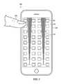
- FIG. 1depicts an electronic device 100 that is operable to provide haptic output.
- the electronic device 100includes a touch surface 103 .
- An array of haptic cells 101are disposed on an exterior surface of the touch surface 103 .
- the electronic device 100can independently charge (i.e., store charges at) each of the haptic cells 101 .
- the haptic cellWhen part of a user's body, such as the user's finger, (see FIG. 3 ) touches a charged haptic cell 101 , the haptic cell provides a haptic output to the user's body by discharging to create a current. The current passes through the user's skin and produces a perceptible sensation (e.g., the haptic output).
- each of the haptic cells 101may include a capacitor.
- a capacitorwhich may be coupled, such as in series, with a resistor
- the capacitormay discharge to create the current.
- the haptic cells 101 shownmay be an exposed electrode of such a capacitor and other portions of the capacitor (such as another electrode separated from the exposed electrode by a dielectric) may be disposed beneath the exposed electrode.
- the touch surface 103may be a haptic touch display.
- the haptic cells 101 and/or portions thereofmay be formed of one or more transparent materials so as not to obscure the display.
- the haptic cells 101may include one or more transparent electrodes, capacitors, and so on formed of one or more transparent conductive materials such as indium tin oxide, fluorine doped tin oxide, doped zinc oxide, gallium zinc oxide, or the like.
- the touch surface 103may be other kinds of surfaces.
- the touch surface 103may be an opaque portion of a housing and the electrodes/capacitors need not be transparent.
- the touch surface 103may or may not be configured to receive input from a user, such as a touch or force input.
- the voltage on each of the haptic cells 101may be monitored; a drop in voltage may correspond to a touch by a user or other object. This touch may be processed by the electronic device as an input. Put another way, if the haptic cell discharges, the electronic device may process an input in the location of that haptic cell 101 .
- Conductive wires 102 or other conductorsmay be disposed on or under the touch surface 103 to electrically connect the haptic cells 101 and/or components thereof to other components of the electronic device 100 .
- the conductive wiresmay electrically connect the haptic cells 101 to control circuitry (such as one or more switches) that are operative to control charging, discharging, and/or other functions of the haptic cells 101 .
- control circuitrymay be included in the haptic cells 101 and the conductive wires 102 may electrically connect the haptic cells to other components, such as a power or voltage source, or a readout (such as a processing unit) operative to determine if a haptic cell has been touched (or otherwise monitor a voltage of the cell).
- These conductive wires 102may also be formed of transparent conductive materials in some embodiments, and may be translucent or opaque in others.
- the conductive wires 102may be anisotropic conductive film disposed on the touch surface 103 . It should be appreciated that the routing of the conductive wires 102 shown in FIG. 3 is one example routing; other routing patterns may be used in other embodiments. It should also be appreciated that multiple haptic cells 101 may be multiplexed to a single voltage source and/or readout.
- the haptic cells 101 , the conductive wires 102 , and/or components thereofmay include a variety of conductive films. In some implementations, the haptic cells 101 , the conductive wires 102 , and/or components thereof may be printed and/or otherwise formed on the touch surface 103 using thin-film transistor technology.
- the haptic cells 101 and/or the conductive wires 102may be flush with the touch surface 103 or may be positioned within or beneath the touch surface at a depth that still permits the cells to discharge when a finger (or other conductive object) passes over them. In these ways, the haptic cells 101 and/or the conductive wires 102 may be visually and/or otherwise imperceptible to users when not providing haptic output.
- the electronic device 100may also include a frame 104 that forms an exterior of the electronic device 100 .
- the frame 104may be a conductive material, such as metal, that is used as a ground for the haptic cells 101 .
- the electronic device 100may be configured so that users typically touch the frame 104 when using the electronic device 100 . In this way, the user and the haptic cells 101 may share a ground and/or have the same potential. This may enable the haptic output to be more perceptible to a user.
- the haptic cells 101may be grounded to some portion of the electronic device other than the frame 104 and need not have a common ground with a user or person holding the device. It may be useful to float the ground of the haptic cells above earth ground, for example, in order to increase the voltage of each cell relative to a user.
- the amount of currentmay be configured based on the haptic output to be produced. Higher amounts of current may be provided for more salient haptic output. The amount of current may be kept below levels that could be uncomfortable for users. In some implementations, the amount of current may be kept sufficiently low that the haptic output is salient when the body of the user moves across a haptic cell 101 (i.e., moves from a region having a positive voltage to one that has a zero voltage, or a voltage low enough not to discharge through skin, and/or where a current is not produced) but not when the body of the user is touching the haptic cell 101 without movement.
- the electronic device 100is illustrated as a smart phone, it is understood that this is an example.
- the electronic devicemay be any kind of haptic output device or other kind of device without departing from the scope of the present disclosure.
- Such devicesinclude, but are not limited to, laptop computing devices, desktop computing devices, wearable devices, tablet computing devices, cellular telephones, displays, printers, mobile computing devices, digital media players, keyboards, track pads, and so on.
- FIG. 2depicts an example circuit 201 that may be used in the haptic cells 101 of the electronic device 100 of FIG. 1 .
- the circuit 201includes a capacitor 214 .
- the capacitor 214is connected to a ground 215 .
- the capacitor 214is also connected in series to a resistor 213 via a node 216 .
- the resistor 213is connected to a voltage source 210 (which may be a variable voltage source operable to provide variable voltage) via a switch 211 and an amplifier 212 .
- the circuit 201may be operable to store charges in the capacitor 214 (i.e., charge the capacitor 214 ) by electrically connecting the voltage source 210 to the amplifier 212 by closing the switch 211 .
- the switch 211closes and connects the voltage source 210 to the amplifier 212
- the resistor 213causes a current to flow to the capacitor 214 via the node 216 .
- the capacitor 214then stores a charge unless the capacity of the capacitor is exceeded, in which case the current flows to the ground 215 .
- the switch 211may then be opened, disconnecting the voltage source 210 from the amplifier 212 .
- FIG. 3illustrates a body 305 of a user touching one of the haptic cells 101 of the electronic device 100 of FIG. 1 . This would cause the circuit 201 of FIG. 2 to change as illustrated in FIG. 4 .
- the body 305functions as a resistor connected to the node 216 and the ground 215 (the resistance of the human body may generally be between 1000 and 100,000 Ohms). This discharges the capacitor 214 , discharging the charge stored by the capacitor 214 and creating a current that is provided to the body 305 . Thus, a haptic output is provided to the user.
- the amplifier 212may function to buffer and/or otherwise at least partially isolate the voltage source 210 from the body 305 . This may prevent the voltage source 210 from being affected by the load caused by the body 305 touching the capacitor 214 . This may also protect the body 305 from the voltage source 210 .
- the values of the resistor 213 and the capacitor 214may be configured such that the haptic output is perceptible when the capacitor 214 is being touched and/or when the body 305 moves across the capacitor 214 .
- the currentmay be the charge stored by the capacitor 214 divided by the resistance of the body 305 .
- the resistor 213 and the capacitor 214may be configured such that the current created at discharge of the capacitor 214 is approximately one milliamp.
- the voltage source 210may provide a voltage of approximately 50 volts.
- the capacitor 214may have a value of approximately 0.1 microfarad
- the resistor 213may have a resistance of approximately 100,000 Ohms
- the body 305may have a resistance of approximately 50,000 Ohms.
- the circuit 201may charge the capacitor 214 in approximately 60 milliseconds when the capacitor 214 is not touched by the body 305 (charging time being roughly equal to the value of the resistor 213 times the value of the capacitor 214 ). This may result in a current of approximately one milliamp when the capacitor 214 is touched by the body 305 . As a result, a haptic output is provided.
- the currentmay drop to approximately 0.3 milliamps within approximately 20 milliseconds (as the current may drop to voltage divided by the resistance of the resistor 213 plus the resistance of the body 305 after the touch, which may be at least less than 50% of the current at touch) and may no longer be perceptible to the user, ending the haptic output.
- the circuit 201may continue to provide haptic output after the capacitor 214 is discharged as long as the body 305 remains touching the capacitor 214 . In some examples, this may result in a less salient haptic output than the initial haptic output provided when the capacitor 214 discharged as the voltage provided by the voltage source 210 may not allow creation of the same amount of current as discharge of the capacitor 214 . In other implementations, the circuit 201 may not be operable to provide a haptic output after the capacitor 214 is discharged until the body 305 stops touching the capacitor 214 and the capacitor 214 is re-charged by closing the switch 211 . For example, the voltage provided by the voltage source 210 may not be sufficient to create an amount of current that is salient as a haptic output when the capacitor 214 is not currently storing a charge. Various configurations are possible and contemplated.
- the voltage at the capacitor 214may be monitored.
- monitoring circuitry or a processing unit or other mechanismmay be connected to the node 216 in order to detect the drop of the voltage stored by the capacitor 214 when touched by the body 305 .
- the switch 211may be closed to re-charge the capacitor 214 .
- touch detection circuitrymay be used to first determine that the body 305 is no longer touching the capacitor 214 prior to re-charging the capacitor 214 after the voltage drop is detected.
- circuit 201is provided for the purposes of example.
- circuits and/or control circuitrymay be provided using a variety of different components connected in a variety of different ways without departing from the scope of the present disclosure.
- the touch surface 103 of the electronic device 100may be a haptic touch display.
- FIG. 5depicts an example screen stack 503 that may be used in the touch surface 103 of the electronic device of FIG. 1 .
- the screen stack 503may include haptic cells 501 that include one or more transparent electrodes disposed on an exterior surface of a cover glass 520 or other transparent cover.
- Transparent conductive wires 502may also be disposed on the exterior surface of the cover glass 520 that electrically connect the haptic cells 501 to control circuitry 523 .
- a display layer 521may be coupled to an interior surface of the cover glass 520 .
- the display layer 521may be a liquid crystal display, and organic liquid crystal display, a light emitting diode display, or any other kind of display.
- a touch and/or force sensing layer 522may be coupled to the display layer 521 .
- the touch and/or force sensing layer 522may be a capacitive sensing layer, a piezoelectric sensing layer, and/or other kind of touch and/or force sensing component.
- the transparency of the haptic cells 501 , the conductive wires 502 , and the cover glass 520may allow the display layer 521 to be seen without obscuring the display layer 521 .
- the touch and/or force sensing layer 522may allow for haptic output provided via the haptic cells 501 to be performed in response to various touches on the exterior surface of the cover glass 520 . For example, when part of a user's body is determined to be moving across the cover glass 520 toward a particular haptic cell 501 , the haptic cell 501 may be charged in order to provide haptic output when the user's body reaches and touches the haptic cell 501 .
- the haptic cells 501 and the conductive wires 502are shown proud of the cover glass 520 , it is understood that this is for the sake of visual clarity. In various implementations, the haptic cells 501 and the conductive wires 502 may be flat and/or otherwise configured so as to be flush with the cover glass 520 .
- the screen stack 503is illustrated and described as including particular components arranged in a particular orientation, it is understood that this is for the purposes of example. In various implementations, various combinations of the same, similar, and/or different components may be arranged in a variety of ways without departing from the scope of the present disclosure.
- the cover glass 520may be omitted.
- the positions of the display layer 521 and the touch and/or force sensing layer 522may be reversed.
- the display layer 521 and the touch and/or force sensing layer 522may be combined into a single layer. Various configurations are possible and contemplated.
- FIG. 6depicts an example block diagram illustrating the functional relationships between example components that may be used in a haptic output device 600 .
- the haptic output device 600may be the electronic device 100 of FIG. 1 .
- the haptic output device 600may include one or more processing units 630 , one or more non-transitory storage media 631 (which may take the form of, but is not limited to, a magnetic storage medium; optical storage medium; magneto-optical storage medium; read only memory; random access memory; erasable programmable memory; flash memory; and so on), one or more sets of control circuitry 632 , one or more displays 633 , one or more touch and/or force sensors 634 , and/or one or more haptic cells 635 .
- processing units 630may include one or more processing units 630 , one or more non-transitory storage media 631 (which may take the form of, but is not limited to, a magnetic storage medium; optical storage medium; magneto-optical storage medium; read only memory; random access memory; erasable programmable memory; flash memory; and so on), one or more sets of control circuitry 632 , one or more displays 633 , one or more touch and/or force sensors 634 , and/or
- the processing unit 630may be operable to execute instructions stored in the non-transitory storage medium 631 to perform various haptic output device 600 functions. Such functions may include detecting touch and/or force via the touch and/or force sensor 634 , providing output via the display 633 , using the control circuitry to charge one or more of the haptic cells 635 , using the control circuitry to provide haptic output via one or more of the haptic cells 635 , and so on.
- FIG. 7depicts an example method 700 of providing haptic output.
- the method 200may be performed by the electronic device 100 of FIG. 1 and/or the haptic output device 600 of FIG. 6 .
- a deviceoperates.
- the flowproceeds to 720 where the device determines whether or not to provide one or more haptic outputs. Such a determination may include whether or not to provide haptic output at all, whether or not to currently provide haptic output, whether or not to prepare to provide haptic output, where out of a number of possible locations to provide haptic output, what kind of haptic output to provide and/or prepare for, and so on. If not, the flow returns to 710 and the device continues to operate. Otherwise, the flow proceeds to 730 .
- the devicecharges one or more capacitors of one or more respective haptic cells that the device determined to use to provide haptic output.
- the flowthen proceeds to 740 .
- the flowproceeds to 760 where the capacitor of the respective haptic cell is discharged to provide current, thus providing the haptic output, before the flow returns to 710 and the device continues to operate. Otherwise, the flow proceeds to 750 where the charged respective haptic cell waits to be touched and the flow returns to 740 .
- example method 700is illustrated and described as including particular operations performed in a particular order, it is understood that this is an example. In various implementations, various orders of the same, similar, and/or different operations may be performed without departing from the scope of the present disclosure.
- the example method 700is illustrated and described as waiting until the capacitor of the haptic cell is touched after being charged.
- a charged capacitormay stay charged for a period of time rather than indefinitely. As such, the capacitor may be re-charged if not touched within a period of time.
- the present disclosurerelates to an electronic device that is operable to provide electrical haptic output.
- Multiple haptic cellsmay be disposed on a touch surface.
- Control circuitrymay be operable to independently store charges in a capacitor or similar component of each haptic cell.
- the capacitorWhen a user's body touches an exposed electrode of one of the haptic cells, the capacitor may discharge. This creates a current, providing a haptic output.
- a wide variety of dynamically configurable haptic outputscan be provided without consuming the space and/or power used for haptic actuators that vibrate and/or otherwise move a mass.
- the methods disclosedmay be implemented as sets of instructions or software readable by a device. Further, it is understood that the specific order or hierarchy of steps in the methods disclosed are examples of sample approaches. In other embodiments, the specific order or hierarchy of steps in the method can be rearranged while remaining within the disclosed subject matter.
- the accompanying method claimspresent elements of the various steps in a sample order, and are not necessarily meant to be limited to the specific order or hierarchy presented.
Landscapes
- Engineering & Computer Science (AREA)
- Theoretical Computer Science (AREA)
- General Engineering & Computer Science (AREA)
- Computer Hardware Design (AREA)
- Human Computer Interaction (AREA)
- Physics & Mathematics (AREA)
- General Physics & Mathematics (AREA)
- User Interface Of Digital Computer (AREA)
Abstract
Description
Claims (20)
Priority Applications (1)
| Application Number | Priority Date | Filing Date | Title |
|---|---|---|---|
| US15/696,876US10416772B2 (en) | 2017-09-06 | 2017-09-06 | Electrical haptic output array |
Applications Claiming Priority (1)
| Application Number | Priority Date | Filing Date | Title |
|---|---|---|---|
| US15/696,876US10416772B2 (en) | 2017-09-06 | 2017-09-06 | Electrical haptic output array |
Publications (2)
| Publication Number | Publication Date |
|---|---|
| US20190073033A1 US20190073033A1 (en) | 2019-03-07 |
| US10416772B2true US10416772B2 (en) | 2019-09-17 |
Family
ID=65518095
Family Applications (1)
| Application Number | Title | Priority Date | Filing Date |
|---|---|---|---|
| US15/696,876Expired - Fee RelatedUS10416772B2 (en) | 2017-09-06 | 2017-09-06 | Electrical haptic output array |
Country Status (1)
| Country | Link |
|---|---|
| US (1) | US10416772B2 (en) |
Cited By (4)
| Publication number | Priority date | Publication date | Assignee | Title |
|---|---|---|---|---|
| US10838501B2 (en) | 2017-09-28 | 2020-11-17 | Apple Inc. | Ground-shifted touch input sensor for capacitively driving an electrostatic plate |
| US11073934B2 (en) | 2017-09-27 | 2021-07-27 | Apple Inc. | Electronic device having an electrostatic conductive layer for providing haptic feedback |
| US11573661B2 (en) | 2017-09-27 | 2023-02-07 | Apple Inc. | Electronic device having a piezoelectric body for friction haptics |
| US12223110B1 (en) | 2021-09-23 | 2025-02-11 | Apple Inc. | Secure integrated circuit for smart haptics |
Citations (58)
| Publication number | Priority date | Publication date | Assignee | Title |
|---|---|---|---|---|
| US5060527A (en) | 1990-02-14 | 1991-10-29 | Burgess Lester E | Tactile sensing transducer |
| US6963762B2 (en) | 2001-05-23 | 2005-11-08 | Nokia Corporation | Mobile phone using tactile icons |
| EP2000885A1 (en) | 2007-06-08 | 2008-12-10 | Research In Motion Limited | Haptic display for a handheld electronic device |
| US20080303795A1 (en) | 2007-06-08 | 2008-12-11 | Lowles Robert J | Haptic display for a handheld electronic device |
| US20100097323A1 (en) | 2008-10-17 | 2010-04-22 | Honeywell International Inc. | Hydrogel-based tactile-feedback touch screen |
| US20110109588A1 (en)* | 2009-11-12 | 2011-05-12 | Senseg Ltd. | Tactile stimulation apparatus having a composite section comprising a semiconducting material |
| US20110286156A1 (en)* | 2010-05-20 | 2011-11-24 | Nokia Corporation | Generating Perceptible Touch Stimulus |
| US20120112894A1 (en) | 2010-11-08 | 2012-05-10 | Korea Advanced Institute Of Science And Technology | Haptic feedback generator, portable device, haptic feedback providing method using the same and recording medium thereof |
| US20120126959A1 (en) | 2008-11-04 | 2012-05-24 | Bayer Materialscience Ag | Electroactive polymer transducers for tactile feedback devices |
| US20120268412A1 (en)* | 2011-04-22 | 2012-10-25 | Immersion Corporation | Electro-vibrotactile display |
| US8314775B2 (en) | 1998-01-26 | 2012-11-20 | Apple Inc. | Multi-touch touch surface |
| US20120306790A1 (en) | 2011-06-02 | 2012-12-06 | Electronics And Telecommunications Research Institute | Film type apparatus for providing haptic feedback and touch screen including the same |
| US8441465B2 (en) | 2009-08-17 | 2013-05-14 | Nokia Corporation | Apparatus comprising an optically transparent sheet and related methods |
| US8466366B2 (en) | 2011-06-28 | 2013-06-18 | Innova Dynamics, Inc. | Transparent conductors incorporating additives and related manufacturing methods |
| US20140192005A1 (en)* | 2012-06-29 | 2014-07-10 | Panasonic Corporation | Method for presenting tactile sensation and device therefor |
| US20150155470A1 (en)* | 2012-11-30 | 2015-06-04 | Kyocera Corporation | Piezoelectric actuator, piezoelectric vibration device, and portable terminal |
| US20150169118A1 (en) | 2013-12-13 | 2015-06-18 | Lg Display Co., Ltd. | Monolithic haptic type touch screen, manufacturing method thereof, and display device including the same |
| US9098113B2 (en) | 2009-08-11 | 2015-08-04 | Koninklijke Philips N.V. | Hybrid display device |
| US9122330B2 (en) | 2012-11-19 | 2015-09-01 | Disney Enterprises, Inc. | Controlling a user's tactile perception in a dynamic physical environment |
| US9231186B2 (en) | 2009-04-11 | 2016-01-05 | Parker-Hannifin Corporation | Electro-switchable polymer film assembly and use thereof |
| US20160124548A1 (en) | 2014-11-03 | 2016-05-05 | Northwestern University | Materials and structures for haptic displays with simultaneous sensing and actuation |
| US20160209958A1 (en) | 2015-01-15 | 2016-07-21 | Samsung Display Co., Ltd. | Touch panel and display device using the same |
| US20160357342A1 (en) | 2012-05-10 | 2016-12-08 | Tanvas Corporation | Electronic controller haptic display with simultaneous sensing and actuation |
| US20160370862A1 (en) | 2015-06-19 | 2016-12-22 | James E. Colgate | Apparatus for unified audio tactile feedback |
| US20170038904A1 (en)* | 2014-04-23 | 2017-02-09 | Sharp Kabushiki Kaisha | Input device |
| US20170060239A1 (en) | 2014-02-28 | 2017-03-02 | Samsung Electronics Co., Ltd | Device and method for providing tactile sensation |
| US9600070B2 (en) | 2008-12-22 | 2017-03-21 | Apple Inc. | User interface having changeable topography |
| US9612674B2 (en) | 2008-09-30 | 2017-04-04 | Apple Inc. | Movable track pad with added functionality |
| US9634225B2 (en) | 2012-12-17 | 2017-04-25 | Apple Inc. | Artificial muscle camera lens actuator |
| US20170168572A1 (en)* | 2014-02-21 | 2017-06-15 | Tanvas Corporation | Haptic display with simultaneous sensing and actuation |
| US9733746B2 (en) | 2011-05-10 | 2017-08-15 | Northwestern University | Touch interface device having an electrostatic multitouch surface and method for controlling the device |
| US20170239130A1 (en) | 2012-06-01 | 2017-08-24 | New York University | Somatosensory feedback wearable object |
| US9746964B2 (en) | 2013-09-27 | 2017-08-29 | Sensel, Inc. | Diamond patterned touch sensor system and method |
| US20170308171A1 (en) | 2015-01-26 | 2017-10-26 | Fujitsu Limited | Drive controlling apparatus, electronic device, computer-readable recording medium, and drive controlling method |
| US9829979B2 (en) | 2014-04-28 | 2017-11-28 | Ford Global Technologies, Llc | Automotive touchscreen controls with simulated texture for haptic feedback |
| US20170364184A1 (en) | 2014-03-14 | 2017-12-21 | Synaptics Incorporated | Transcapacitive and absolute capacitive sensing profiles |
| US20170364158A1 (en) | 2016-06-20 | 2017-12-21 | Apple Inc. | Localized and/or Encapsulated Haptic Actuators and Elements |
| US20170371490A1 (en) | 2016-06-24 | 2017-12-28 | Nlt Technologies, Ltd. | Tactile presentation panel, tactile presentation device and electronic equipment |
| US9875625B2 (en) | 2015-12-18 | 2018-01-23 | Immersion Corporation | Systems and methods for multifunction haptic output devices |
| US9880623B2 (en) | 2013-01-24 | 2018-01-30 | Immersion Corporation | Friction modulation for three dimensional relief in a haptic device |
| US20180081441A1 (en) | 2016-09-20 | 2018-03-22 | Apple Inc. | Integrated Haptic Output and Touch Input System |
| US9927887B2 (en) | 2015-12-31 | 2018-03-27 | Synaptics Incorporated | Localized haptics for two fingers |
| US20180095581A1 (en) | 2016-09-30 | 2018-04-05 | Lg Display Co., Ltd. | Organic Light Emitting Display Device |
| US9939900B2 (en) | 2013-04-26 | 2018-04-10 | Immersion Corporation | System and method for a haptically-enabled deformable surface |
| US20180113512A1 (en) | 2016-10-20 | 2018-04-26 | Samsung Electronics Co., Ltd. | Feedback providing method and electronic device for supporting the same |
| US9965037B2 (en) | 2015-04-24 | 2018-05-08 | Samsung Display Co., Ltd. | Haptic driving method and apparatus therefor in flexible display device |
| US20180151281A1 (en) | 2016-11-28 | 2018-05-31 | Immersion Corporation | Magneto-sensitive elastomers for haptic feedback |
| US10000622B2 (en) | 2013-11-25 | 2018-06-19 | Shikoku Chemicals Corporation | Glycolurils having functional groups and use thereof |
| US20180181202A1 (en) | 2016-12-28 | 2018-06-28 | Immersion Corporation | Unitary sensor and haptic actuator |
| US10038154B2 (en) | 2014-12-30 | 2018-07-31 | Lg Display Co., Ltd. | Flexible display device with chamfered polarization layer |
| US10061448B2 (en) | 2014-11-28 | 2018-08-28 | Samsung Display Co., Ltd. | Manufacturing method of touch screen panel |
| US20180269807A1 (en) | 2017-03-17 | 2018-09-20 | Immersion Corporation | Electret-Based Electrostatic Haptic Actuator |
| US20180312392A1 (en) | 2010-12-08 | 2018-11-01 | Condalign As | Method for assembling conductive particles into conductive pathways and sensors thus formed |
| US10120447B2 (en) | 2013-06-24 | 2018-11-06 | Northwestern University | Haptic display with simultaneous sensing and actuation |
| US20180335659A1 (en) | 2017-05-22 | 2018-11-22 | Asahi Glass Company, Limited | Transparent substrate with antifouling film and capacitance in-cell touch panel-type liquid crystal display device |
| US10147868B2 (en) | 2015-03-12 | 2018-12-04 | Fujifilm Corporation | Polymer composite piezoelectric body, electroacoustic transduction film, and electroacoustic transducer |
| US10208158B2 (en) | 2006-07-10 | 2019-02-19 | Medipacs, Inc. | Super elastic epoxy hydrogel |
| US10257929B2 (en) | 2013-08-22 | 2019-04-09 | Samsung Electronics Co., Ltd. | Variable stiffness film, variable stiffness flexible display, and method of manufacturing the variable stiffness film |
- 2017
- 2017-09-06USUS15/696,876patent/US10416772B2/ennot_activeExpired - Fee Related
Patent Citations (60)
| Publication number | Priority date | Publication date | Assignee | Title |
|---|---|---|---|---|
| US5060527A (en) | 1990-02-14 | 1991-10-29 | Burgess Lester E | Tactile sensing transducer |
| US8314775B2 (en) | 1998-01-26 | 2012-11-20 | Apple Inc. | Multi-touch touch surface |
| US6963762B2 (en) | 2001-05-23 | 2005-11-08 | Nokia Corporation | Mobile phone using tactile icons |
| US10208158B2 (en) | 2006-07-10 | 2019-02-19 | Medipacs, Inc. | Super elastic epoxy hydrogel |
| EP2000885A1 (en) | 2007-06-08 | 2008-12-10 | Research In Motion Limited | Haptic display for a handheld electronic device |
| US20080303795A1 (en) | 2007-06-08 | 2008-12-11 | Lowles Robert J | Haptic display for a handheld electronic device |
| US9612674B2 (en) | 2008-09-30 | 2017-04-04 | Apple Inc. | Movable track pad with added functionality |
| US20100097323A1 (en) | 2008-10-17 | 2010-04-22 | Honeywell International Inc. | Hydrogel-based tactile-feedback touch screen |
| US20120126959A1 (en) | 2008-11-04 | 2012-05-24 | Bayer Materialscience Ag | Electroactive polymer transducers for tactile feedback devices |
| US9600070B2 (en) | 2008-12-22 | 2017-03-21 | Apple Inc. | User interface having changeable topography |
| US9231186B2 (en) | 2009-04-11 | 2016-01-05 | Parker-Hannifin Corporation | Electro-switchable polymer film assembly and use thereof |
| US9098113B2 (en) | 2009-08-11 | 2015-08-04 | Koninklijke Philips N.V. | Hybrid display device |
| US8441465B2 (en) | 2009-08-17 | 2013-05-14 | Nokia Corporation | Apparatus comprising an optically transparent sheet and related methods |
| US20110109588A1 (en)* | 2009-11-12 | 2011-05-12 | Senseg Ltd. | Tactile stimulation apparatus having a composite section comprising a semiconducting material |
| US9063572B2 (en) | 2009-11-12 | 2015-06-23 | Senseg Ltd. | Tactile stimulation apparatus having a composite section comprising a semiconducting material |
| US20110286156A1 (en)* | 2010-05-20 | 2011-11-24 | Nokia Corporation | Generating Perceptible Touch Stimulus |
| US20120112894A1 (en) | 2010-11-08 | 2012-05-10 | Korea Advanced Institute Of Science And Technology | Haptic feedback generator, portable device, haptic feedback providing method using the same and recording medium thereof |
| US20180312392A1 (en) | 2010-12-08 | 2018-11-01 | Condalign As | Method for assembling conductive particles into conductive pathways and sensors thus formed |
| US20120268412A1 (en)* | 2011-04-22 | 2012-10-25 | Immersion Corporation | Electro-vibrotactile display |
| US9733746B2 (en) | 2011-05-10 | 2017-08-15 | Northwestern University | Touch interface device having an electrostatic multitouch surface and method for controlling the device |
| US20120306790A1 (en) | 2011-06-02 | 2012-12-06 | Electronics And Telecommunications Research Institute | Film type apparatus for providing haptic feedback and touch screen including the same |
| US20130277625A1 (en) | 2011-06-28 | 2013-10-24 | Arjun Daniel Srinivas | Transparent conductors incorporating additives and related manufacturing methods |
| US8466366B2 (en) | 2011-06-28 | 2013-06-18 | Innova Dynamics, Inc. | Transparent conductors incorporating additives and related manufacturing methods |
| US20160357342A1 (en) | 2012-05-10 | 2016-12-08 | Tanvas Corporation | Electronic controller haptic display with simultaneous sensing and actuation |
| US20170239130A1 (en) | 2012-06-01 | 2017-08-24 | New York University | Somatosensory feedback wearable object |
| US20140192005A1 (en)* | 2012-06-29 | 2014-07-10 | Panasonic Corporation | Method for presenting tactile sensation and device therefor |
| US9122330B2 (en) | 2012-11-19 | 2015-09-01 | Disney Enterprises, Inc. | Controlling a user's tactile perception in a dynamic physical environment |
| US20150155470A1 (en)* | 2012-11-30 | 2015-06-04 | Kyocera Corporation | Piezoelectric actuator, piezoelectric vibration device, and portable terminal |
| US9634225B2 (en) | 2012-12-17 | 2017-04-25 | Apple Inc. | Artificial muscle camera lens actuator |
| US9880623B2 (en) | 2013-01-24 | 2018-01-30 | Immersion Corporation | Friction modulation for three dimensional relief in a haptic device |
| US9939900B2 (en) | 2013-04-26 | 2018-04-10 | Immersion Corporation | System and method for a haptically-enabled deformable surface |
| US10120447B2 (en) | 2013-06-24 | 2018-11-06 | Northwestern University | Haptic display with simultaneous sensing and actuation |
| US10257929B2 (en) | 2013-08-22 | 2019-04-09 | Samsung Electronics Co., Ltd. | Variable stiffness film, variable stiffness flexible display, and method of manufacturing the variable stiffness film |
| US9746964B2 (en) | 2013-09-27 | 2017-08-29 | Sensel, Inc. | Diamond patterned touch sensor system and method |
| US10000622B2 (en) | 2013-11-25 | 2018-06-19 | Shikoku Chemicals Corporation | Glycolurils having functional groups and use thereof |
| US20150169118A1 (en) | 2013-12-13 | 2015-06-18 | Lg Display Co., Ltd. | Monolithic haptic type touch screen, manufacturing method thereof, and display device including the same |
| US20170168572A1 (en)* | 2014-02-21 | 2017-06-15 | Tanvas Corporation | Haptic display with simultaneous sensing and actuation |
| US20170060239A1 (en) | 2014-02-28 | 2017-03-02 | Samsung Electronics Co., Ltd | Device and method for providing tactile sensation |
| US20170364184A1 (en) | 2014-03-14 | 2017-12-21 | Synaptics Incorporated | Transcapacitive and absolute capacitive sensing profiles |
| US20170038904A1 (en)* | 2014-04-23 | 2017-02-09 | Sharp Kabushiki Kaisha | Input device |
| US9829979B2 (en) | 2014-04-28 | 2017-11-28 | Ford Global Technologies, Llc | Automotive touchscreen controls with simulated texture for haptic feedback |
| US20160124548A1 (en) | 2014-11-03 | 2016-05-05 | Northwestern University | Materials and structures for haptic displays with simultaneous sensing and actuation |
| US10061448B2 (en) | 2014-11-28 | 2018-08-28 | Samsung Display Co., Ltd. | Manufacturing method of touch screen panel |
| US10038154B2 (en) | 2014-12-30 | 2018-07-31 | Lg Display Co., Ltd. | Flexible display device with chamfered polarization layer |
| US20160209958A1 (en) | 2015-01-15 | 2016-07-21 | Samsung Display Co., Ltd. | Touch panel and display device using the same |
| US20170308171A1 (en) | 2015-01-26 | 2017-10-26 | Fujitsu Limited | Drive controlling apparatus, electronic device, computer-readable recording medium, and drive controlling method |
| US10147868B2 (en) | 2015-03-12 | 2018-12-04 | Fujifilm Corporation | Polymer composite piezoelectric body, electroacoustic transduction film, and electroacoustic transducer |
| US9965037B2 (en) | 2015-04-24 | 2018-05-08 | Samsung Display Co., Ltd. | Haptic driving method and apparatus therefor in flexible display device |
| US20160370862A1 (en) | 2015-06-19 | 2016-12-22 | James E. Colgate | Apparatus for unified audio tactile feedback |
| US9875625B2 (en) | 2015-12-18 | 2018-01-23 | Immersion Corporation | Systems and methods for multifunction haptic output devices |
| US9927887B2 (en) | 2015-12-31 | 2018-03-27 | Synaptics Incorporated | Localized haptics for two fingers |
| US20170364158A1 (en) | 2016-06-20 | 2017-12-21 | Apple Inc. | Localized and/or Encapsulated Haptic Actuators and Elements |
| US20170371490A1 (en) | 2016-06-24 | 2017-12-28 | Nlt Technologies, Ltd. | Tactile presentation panel, tactile presentation device and electronic equipment |
| US20180081441A1 (en) | 2016-09-20 | 2018-03-22 | Apple Inc. | Integrated Haptic Output and Touch Input System |
| US20180095581A1 (en) | 2016-09-30 | 2018-04-05 | Lg Display Co., Ltd. | Organic Light Emitting Display Device |
| US20180113512A1 (en) | 2016-10-20 | 2018-04-26 | Samsung Electronics Co., Ltd. | Feedback providing method and electronic device for supporting the same |
| US20180151281A1 (en) | 2016-11-28 | 2018-05-31 | Immersion Corporation | Magneto-sensitive elastomers for haptic feedback |
| US20180181202A1 (en) | 2016-12-28 | 2018-06-28 | Immersion Corporation | Unitary sensor and haptic actuator |
| US20180269807A1 (en) | 2017-03-17 | 2018-09-20 | Immersion Corporation | Electret-Based Electrostatic Haptic Actuator |
| US20180335659A1 (en) | 2017-05-22 | 2018-11-22 | Asahi Glass Company, Limited | Transparent substrate with antifouling film and capacitance in-cell touch panel-type liquid crystal display device |
Non-Patent Citations (3)
| Title |
|---|
| U.S. Appl. No. 15/717,682, filed Sep. 27, 2017, Wen et al. |
| U.S. Appl. No. 15/717,714, filed Sep. 27, 2017, Wen et al. |
| U.S. Appl. No. 15/719,326, filed Sep. 28, 2017, Van Ausdall et al. |
Cited By (4)
| Publication number | Priority date | Publication date | Assignee | Title |
|---|---|---|---|---|
| US11073934B2 (en) | 2017-09-27 | 2021-07-27 | Apple Inc. | Electronic device having an electrostatic conductive layer for providing haptic feedback |
| US11573661B2 (en) | 2017-09-27 | 2023-02-07 | Apple Inc. | Electronic device having a piezoelectric body for friction haptics |
| US10838501B2 (en) | 2017-09-28 | 2020-11-17 | Apple Inc. | Ground-shifted touch input sensor for capacitively driving an electrostatic plate |
| US12223110B1 (en) | 2021-09-23 | 2025-02-11 | Apple Inc. | Secure integrated circuit for smart haptics |
Also Published As
| Publication number | Publication date |
|---|---|
| US20190073033A1 (en) | 2019-03-07 |
Similar Documents
| Publication | Publication Date | Title |
|---|---|---|
| US10416772B2 (en) | Electrical haptic output array | |
| US10622538B2 (en) | Techniques for providing a haptic output and sensing a haptic input using a piezoelectric body | |
| US9733706B2 (en) | Apparatus and associated methods for touchscreen displays | |
| EP3066677B1 (en) | Controller-less quick tactile feedback keyboard | |
| US10990230B2 (en) | Circuit, touch chip, and electronic device for capacitance detection | |
| JP4880299B2 (en) | Capacitive touch panel with button function | |
| US9195350B2 (en) | Apparatus and associated methods | |
| US20110163768A1 (en) | Touch screen device, capacitance measuring circuit thereof, and method of measuring capacitance | |
| KR102214929B1 (en) | Apparatus and method for providing tactile | |
| US20150002176A1 (en) | Touch sensing device and touchscreen apparatus | |
| US20110084910A1 (en) | Portable electronic device including touch-sensitive display and method of controlling same | |
| US20110084912A1 (en) | Portable electronic device including a touch-sensitive display and method of controlling same | |
| US20110248839A1 (en) | Portable electronic device and method of controlling same | |
| CN107544704A (en) | Tactile cue panel, tactile cue device and electronic equipment | |
| US20140071384A1 (en) | Electrostatic discharge arrangement for an active matrix display | |
| US9256317B2 (en) | Hybrid sensing touchscreen apparatus capable of light touch sensing and physical touch sensing and method of driving the same | |
| EP2467772A1 (en) | Methods and apparatus for capacitive sensing | |
| EP2306537A1 (en) | Piezoelectric assembly | |
| KR20100054275A (en) | Touch-input device, mobile device and control method thereof | |
| CN101963865B (en) | Touch identification method, touch key structure and touch device | |
| US9904366B2 (en) | Haptic feedback and capacitive sensing in a transparent touch screen display | |
| KR101250638B1 (en) | Portable electronic device and method of controlling same | |
| US20130328822A1 (en) | Baseline capacitance calibration | |
| CN110892370B (en) | Information processing device, information processing method, and program | |
| US20110128236A1 (en) | Electronic device and method of controlling same |
Legal Events
| Date | Code | Title | Description |
|---|---|---|---|
| AS | Assignment | Owner name:APPLE INC., CALIFORNIA Free format text:ASSIGNMENT OF ASSIGNORS INTEREST;ASSIGNORS:SEN, YI-HENG;OWENS, TRAVIS N.;SIGNING DATES FROM 20170830 TO 20170905;REEL/FRAME:043508/0639 | |
| FEPP | Fee payment procedure | Free format text:ENTITY STATUS SET TO UNDISCOUNTED (ORIGINAL EVENT CODE: BIG.); ENTITY STATUS OF PATENT OWNER: LARGE ENTITY | |
| STPP | Information on status: patent application and granting procedure in general | Free format text:DOCKETED NEW CASE - READY FOR EXAMINATION | |
| STPP | Information on status: patent application and granting procedure in general | Free format text:NON FINAL ACTION MAILED | |
| STPP | Information on status: patent application and granting procedure in general | Free format text:RESPONSE TO NON-FINAL OFFICE ACTION ENTERED AND FORWARDED TO EXAMINER | |
| STPP | Information on status: patent application and granting procedure in general | Free format text:NOTICE OF ALLOWANCE MAILED -- APPLICATION RECEIVED IN OFFICE OF PUBLICATIONS | |
| STPP | Information on status: patent application and granting procedure in general | Free format text:PUBLICATIONS -- ISSUE FEE PAYMENT RECEIVED | |
| STPP | Information on status: patent application and granting procedure in general | Free format text:PUBLICATIONS -- ISSUE FEE PAYMENT VERIFIED | |
| STCF | Information on status: patent grant | Free format text:PATENTED CASE | |
| FEPP | Fee payment procedure | Free format text:MAINTENANCE FEE REMINDER MAILED (ORIGINAL EVENT CODE: REM.); ENTITY STATUS OF PATENT OWNER: LARGE ENTITY | |
| LAPS | Lapse for failure to pay maintenance fees | Free format text:PATENT EXPIRED FOR FAILURE TO PAY MAINTENANCE FEES (ORIGINAL EVENT CODE: EXP.); ENTITY STATUS OF PATENT OWNER: LARGE ENTITY | |
| STCH | Information on status: patent discontinuation | Free format text:PATENT EXPIRED DUE TO NONPAYMENT OF MAINTENANCE FEES UNDER 37 CFR 1.362 | |
| FP | Lapsed due to failure to pay maintenance fee | Effective date:20230917 |