US10411026B2 - Integrated computing structures formed on silicon - Google Patents
Integrated computing structures formed on siliconDownload PDFInfo
- Publication number
- US10411026B2 US10411026B2US15/641,558US201715641558AUS10411026B2US 10411026 B2US10411026 B2US 10411026B2US 201715641558 AUS201715641558 AUS 201715641558AUS 10411026 B2US10411026 B2US 10411026B2
- Authority
- US
- United States
- Prior art keywords
- fet
- gate
- materials
- component
- stack
- Prior art date
- Legal status (The legal status is an assumption and is not a legal conclusion. Google has not performed a legal analysis and makes no representation as to the accuracy of the status listed.)
- Active, expires
Links
- 229910052710siliconInorganic materials0.000titleclaimsabstractdescription56
- 239000010703siliconSubstances0.000titleclaimsabstractdescription56
- 239000000463materialSubstances0.000claimsabstractdescription254
- 239000004065semiconductorSubstances0.000claimsabstractdescription60
- 238000000034methodMethods0.000claimsabstractdescription53
- XUIMIQQOPSSXEZ-UHFFFAOYSA-NSiliconChemical compound[Si]XUIMIQQOPSSXEZ-UHFFFAOYSA-N0.000claimsabstractdescription51
- 230000006870functionEffects0.000claimsabstractdescription46
- 230000000295complement effectEffects0.000claimsabstractdescription4
- 239000012212insulatorSubstances0.000claimsdescription67
- 229910052751metalInorganic materials0.000claimsdescription43
- 239000002184metalSubstances0.000claimsdescription43
- 230000000087stabilizing effectEffects0.000claimsdescription19
- 238000009792diffusion processMethods0.000claimsdescription14
- TWNQGVIAIRXVLR-UHFFFAOYSA-Noxo(oxoalumanyloxy)alumaneChemical compoundO=[Al]O[Al]=OTWNQGVIAIRXVLR-UHFFFAOYSA-N0.000claimsdescription14
- 230000015572biosynthetic processEffects0.000claimsdescription13
- VYPSYNLAJGMNEJ-UHFFFAOYSA-NSilicium dioxideChemical compoundO=[Si]=OVYPSYNLAJGMNEJ-UHFFFAOYSA-N0.000claimsdescription10
- 239000003989dielectric materialSubstances0.000claimsdescription10
- 229910052814silicon oxideInorganic materials0.000claimsdescription10
- 229910021334nickel silicideInorganic materials0.000claimsdescription5
- RUFLMLWJRZAWLJ-UHFFFAOYSA-Nnickel silicideChemical compound[Ni]=[Si]=[Ni]RUFLMLWJRZAWLJ-UHFFFAOYSA-N0.000claimsdescription5
- 229910005487Ni2SiInorganic materials0.000claimsdescription4
- 229910005883NiSiInorganic materials0.000claimsdescription4
- 229910052782aluminiumInorganic materials0.000claimsdescription4
- QVGXLLKOCUKJST-UHFFFAOYSA-Natomic oxygenChemical compound[O]QVGXLLKOCUKJST-UHFFFAOYSA-N0.000claimsdescription4
- 239000001301oxygenSubstances0.000claimsdescription4
- 229910052760oxygenInorganic materials0.000claimsdescription4
- MZLGASXMSKOWSE-UHFFFAOYSA-Ntantalum nitrideChemical compound[Ta]#NMZLGASXMSKOWSE-UHFFFAOYSA-N0.000claimsdescription4
- 229910052721tungstenInorganic materials0.000claimsdescription4
- NRTOMJZYCJJWKI-UHFFFAOYSA-NTitanium nitrideChemical compound[Ti]#NNRTOMJZYCJJWKI-UHFFFAOYSA-N0.000claimsdescription3
- XAGFODPZIPBFFR-UHFFFAOYSA-NaluminiumChemical compound[Al]XAGFODPZIPBFFR-UHFFFAOYSA-N0.000claimsdescription3
- 239000004020conductorSubstances0.000claimsdescription3
- 230000005669field effectEffects0.000claimsdescription3
- WFKWXMTUELFFGS-UHFFFAOYSA-NtungstenChemical compound[W]WFKWXMTUELFFGS-UHFFFAOYSA-N0.000claimsdescription3
- 239000010937tungstenSubstances0.000claimsdescription3
- 230000005641tunnelingEffects0.000claimsdescription3
- 230000008878couplingEffects0.000claims1
- 238000010168coupling processMethods0.000claims1
- 238000005859coupling reactionMethods0.000claims1
- 239000002210silicon-based materialSubstances0.000description26
- 238000000151depositionMethods0.000description15
- 239000000758substrateSubstances0.000description15
- 238000002955isolationMethods0.000description14
- 229910021420polycrystalline siliconInorganic materials0.000description14
- 238000005530etchingMethods0.000description13
- 229920005591polysiliconPolymers0.000description13
- 229920002120photoresistant polymerPolymers0.000description11
- MRELNEQAGSRDBK-UHFFFAOYSA-Nlanthanum(3+);oxygen(2-)Chemical compound[O-2].[O-2].[O-2].[La+3].[La+3]MRELNEQAGSRDBK-UHFFFAOYSA-N0.000description7
- 238000000137annealingMethods0.000description6
- 229910052729chemical elementInorganic materials0.000description6
- 230000010354integrationEffects0.000description6
- 230000008021depositionEffects0.000description5
- 230000000873masking effectEffects0.000description5
- 229910021421monocrystalline siliconInorganic materials0.000description5
- IJGRMHOSHXDMSA-UHFFFAOYSA-NAtomic nitrogenChemical compoundN#NIJGRMHOSHXDMSA-UHFFFAOYSA-N0.000description4
- QGZKDVFQNNGYKY-UHFFFAOYSA-NAmmoniaChemical compoundNQGZKDVFQNNGYKY-UHFFFAOYSA-N0.000description3
- 230000000903blocking effectEffects0.000description3
- 238000005516engineering processMethods0.000description3
- 238000001020plasma etchingMethods0.000description3
- 239000000126substanceSubstances0.000description3
- XKRFYHLGVUSROY-UHFFFAOYSA-NArgonChemical compound[Ar]XKRFYHLGVUSROY-UHFFFAOYSA-N0.000description2
- BLRPTPMANUNPDV-UHFFFAOYSA-NSilaneChemical compound[SiH4]BLRPTPMANUNPDV-UHFFFAOYSA-N0.000description2
- 238000003491arrayMethods0.000description2
- 238000000231atomic layer depositionMethods0.000description2
- 238000005229chemical vapour depositionMethods0.000description2
- 150000001875compoundsChemical class0.000description2
- 239000013078crystalSubstances0.000description2
- -1hafnium lanthanideChemical class0.000description2
- 229910000449hafnium oxideInorganic materials0.000description2
- 238000004518low pressure chemical vapour depositionMethods0.000description2
- 239000000203mixtureSubstances0.000description2
- 150000004767nitridesChemical class0.000description2
- 229910052757nitrogenInorganic materials0.000description2
- 238000000623plasma-assisted chemical vapour depositionMethods0.000description2
- CEPICIBPGDWCRU-UHFFFAOYSA-N[Si].[Hf]Chemical compound[Si].[Hf]CEPICIBPGDWCRU-UHFFFAOYSA-N0.000description1
- 230000006978adaptationEffects0.000description1
- 229910021529ammoniaInorganic materials0.000description1
- 229910052786argonInorganic materials0.000description1
- 230000004888barrier functionEffects0.000description1
- 230000005540biological transmissionEffects0.000description1
- 239000003990capacitorSubstances0.000description1
- 238000000576coating methodMethods0.000description1
- 229910021419crystalline siliconInorganic materials0.000description1
- 238000013500data storageMethods0.000description1
- 238000009795derivationMethods0.000description1
- 238000001312dry etchingMethods0.000description1
- 239000011521glassSubstances0.000description1
- 229910052735hafniumInorganic materials0.000description1
- QKQUUVZIDLJZIJ-UHFFFAOYSA-Nhafnium tantalumChemical compound[Hf].[Ta]QKQUUVZIDLJZIJ-UHFFFAOYSA-N0.000description1
- CJNBYAVZURUTKZ-UHFFFAOYSA-Nhafnium(iv) oxideChemical compoundO=[Hf]=OCJNBYAVZURUTKZ-UHFFFAOYSA-N0.000description1
- 239000001307heliumSubstances0.000description1
- 229910052734heliumInorganic materials0.000description1
- SWQJXJOGLNCZEY-UHFFFAOYSA-Nhelium atomChemical compound[He]SWQJXJOGLNCZEY-UHFFFAOYSA-N0.000description1
- 239000011261inert gasSubstances0.000description1
- 238000010884ion-beam techniqueMethods0.000description1
- 229910052747lanthanoidInorganic materials0.000description1
- 229910000069nitrogen hydrideInorganic materials0.000description1
- 230000003647oxidationEffects0.000description1
- 238000007254oxidation reactionMethods0.000description1
- 230000003071parasitic effectEffects0.000description1
- 230000002093peripheral effectEffects0.000description1
- 238000000206photolithographyMethods0.000description1
- 230000001681protective effectEffects0.000description1
- 229910052594sapphireInorganic materials0.000description1
- 239000010980sapphireSubstances0.000description1
- 229910000077silaneInorganic materials0.000description1
- 238000007740vapor depositionMethods0.000description1
Images


Classifications
- H—ELECTRICITY
- H10—SEMICONDUCTOR DEVICES; ELECTRIC SOLID-STATE DEVICES NOT OTHERWISE PROVIDED FOR
- H10B—ELECTRONIC MEMORY DEVICES
- H10B43/00—EEPROM devices comprising charge-trapping gate insulators
- H10B43/30—EEPROM devices comprising charge-trapping gate insulators characterised by the memory core region
- H01L27/11568—
- H01L21/28282—
- H—ELECTRICITY
- H01—ELECTRIC ELEMENTS
- H01L—SEMICONDUCTOR DEVICES NOT COVERED BY CLASS H10
- H01L21/00—Processes or apparatus adapted for the manufacture or treatment of semiconductor or solid state devices or of parts thereof
- H01L21/02—Manufacture or treatment of semiconductor devices or of parts thereof
- H01L21/04—Manufacture or treatment of semiconductor devices or of parts thereof the devices having potential barriers, e.g. a PN junction, depletion layer or carrier concentration layer
- H01L21/18—Manufacture or treatment of semiconductor devices or of parts thereof the devices having potential barriers, e.g. a PN junction, depletion layer or carrier concentration layer the devices having semiconductor bodies comprising elements of Group IV of the Periodic Table or AIIIBV compounds with or without impurities, e.g. doping materials
- H01L21/28—Manufacture of electrodes on semiconductor bodies using processes or apparatus not provided for in groups H01L21/20 - H01L21/268
- H01L21/283—Deposition of conductive or insulating materials for electrodes conducting electric current
- H01L21/285—Deposition of conductive or insulating materials for electrodes conducting electric current from a gas or vapour, e.g. condensation
- H01L21/28506—Deposition of conductive or insulating materials for electrodes conducting electric current from a gas or vapour, e.g. condensation of conductive layers
- H01L21/28512—Deposition of conductive or insulating materials for electrodes conducting electric current from a gas or vapour, e.g. condensation of conductive layers on semiconductor bodies comprising elements of Group IV of the Periodic Table
- H01L21/28518—Deposition of conductive or insulating materials for electrodes conducting electric current from a gas or vapour, e.g. condensation of conductive layers on semiconductor bodies comprising elements of Group IV of the Periodic Table the conductive layers comprising silicides
- H—ELECTRICITY
- H01—ELECTRIC ELEMENTS
- H01L—SEMICONDUCTOR DEVICES NOT COVERED BY CLASS H10
- H01L21/00—Processes or apparatus adapted for the manufacture or treatment of semiconductor or solid state devices or of parts thereof
- H01L21/70—Manufacture or treatment of devices consisting of a plurality of solid state components formed in or on a common substrate or of parts thereof; Manufacture of integrated circuit devices or of parts thereof
- H01L21/71—Manufacture of specific parts of devices defined in group H01L21/70
- H01L21/76—Making of isolation regions between components
- H01L21/762—Dielectric regions, e.g. EPIC dielectric isolation, LOCOS; Trench refilling techniques, SOI technology, use of channel stoppers
- H01L21/76224—Dielectric regions, e.g. EPIC dielectric isolation, LOCOS; Trench refilling techniques, SOI technology, use of channel stoppers using trench refilling with dielectric materials
- H01L21/76229—Concurrent filling of a plurality of trenches having a different trench shape or dimension, e.g. rectangular and V-shaped trenches, wide and narrow trenches, shallow and deep trenches
- H01L21/823814—
- H01L21/823871—
- H—ELECTRICITY
- H01—ELECTRIC ELEMENTS
- H01L—SEMICONDUCTOR DEVICES NOT COVERED BY CLASS H10
- H01L23/00—Details of semiconductor or other solid state devices
- H01L23/52—Arrangements for conducting electric current within the device in operation from one component to another, i.e. interconnections, e.g. wires, lead frames
- H01L23/535—Arrangements for conducting electric current within the device in operation from one component to another, i.e. interconnections, e.g. wires, lead frames including internal interconnections, e.g. cross-under constructions
- H01L27/092—
- H01L27/11573—
- H01L29/0649—
- H01L29/0847—
- H01L29/4234—
- H01L29/42364—
- H01L29/456—
- H—ELECTRICITY
- H10—SEMICONDUCTOR DEVICES; ELECTRIC SOLID-STATE DEVICES NOT OTHERWISE PROVIDED FOR
- H10B—ELECTRONIC MEMORY DEVICES
- H10B43/00—EEPROM devices comprising charge-trapping gate insulators
- H10B43/40—EEPROM devices comprising charge-trapping gate insulators characterised by the peripheral circuit region
- H—ELECTRICITY
- H10—SEMICONDUCTOR DEVICES; ELECTRIC SOLID-STATE DEVICES NOT OTHERWISE PROVIDED FOR
- H10D—INORGANIC ELECTRIC SEMICONDUCTOR DEVICES
- H10D30/00—Field-effect transistors [FET]
- H10D30/60—Insulated-gate field-effect transistors [IGFET]
- H10D30/69—IGFETs having charge trapping gate insulators, e.g. MNOS transistors
- H10D30/694—IGFETs having charge trapping gate insulators, e.g. MNOS transistors characterised by the shapes, relative sizes or dispositions of the gate electrodes
- H—ELECTRICITY
- H10—SEMICONDUCTOR DEVICES; ELECTRIC SOLID-STATE DEVICES NOT OTHERWISE PROVIDED FOR
- H10D—INORGANIC ELECTRIC SEMICONDUCTOR DEVICES
- H10D62/00—Semiconductor bodies, or regions thereof, of devices having potential barriers
- H10D62/10—Shapes, relative sizes or dispositions of the regions of the semiconductor bodies; Shapes of the semiconductor bodies
- H10D62/113—Isolations within a component, i.e. internal isolations
- H10D62/115—Dielectric isolations, e.g. air gaps
- H—ELECTRICITY
- H10—SEMICONDUCTOR DEVICES; ELECTRIC SOLID-STATE DEVICES NOT OTHERWISE PROVIDED FOR
- H10D—INORGANIC ELECTRIC SEMICONDUCTOR DEVICES
- H10D62/00—Semiconductor bodies, or regions thereof, of devices having potential barriers
- H10D62/10—Shapes, relative sizes or dispositions of the regions of the semiconductor bodies; Shapes of the semiconductor bodies
- H10D62/13—Semiconductor regions connected to electrodes carrying current to be rectified, amplified or switched, e.g. source or drain regions
- H10D62/149—Source or drain regions of field-effect devices
- H10D62/151—Source or drain regions of field-effect devices of IGFETs
- H—ELECTRICITY
- H10—SEMICONDUCTOR DEVICES; ELECTRIC SOLID-STATE DEVICES NOT OTHERWISE PROVIDED FOR
- H10D—INORGANIC ELECTRIC SEMICONDUCTOR DEVICES
- H10D62/00—Semiconductor bodies, or regions thereof, of devices having potential barriers
- H10D62/80—Semiconductor bodies, or regions thereof, of devices having potential barriers characterised by the materials
- H10D62/83—Semiconductor bodies, or regions thereof, of devices having potential barriers characterised by the materials being Group IV materials, e.g. B-doped Si or undoped Ge
- H—ELECTRICITY
- H10—SEMICONDUCTOR DEVICES; ELECTRIC SOLID-STATE DEVICES NOT OTHERWISE PROVIDED FOR
- H10D—INORGANIC ELECTRIC SEMICONDUCTOR DEVICES
- H10D64/00—Electrodes of devices having potential barriers
- H10D64/01—Manufacture or treatment
- H10D64/031—Manufacture or treatment of data-storage electrodes
- H10D64/037—Manufacture or treatment of data-storage electrodes comprising charge-trapping insulators
- H—ELECTRICITY
- H10—SEMICONDUCTOR DEVICES; ELECTRIC SOLID-STATE DEVICES NOT OTHERWISE PROVIDED FOR
- H10D—INORGANIC ELECTRIC SEMICONDUCTOR DEVICES
- H10D64/00—Electrodes of devices having potential barriers
- H10D64/20—Electrodes characterised by their shapes, relative sizes or dispositions
- H10D64/27—Electrodes not carrying the current to be rectified, amplified, oscillated or switched, e.g. gates
- H10D64/311—Gate electrodes for field-effect devices
- H10D64/411—Gate electrodes for field-effect devices for FETs
- H10D64/511—Gate electrodes for field-effect devices for FETs for IGFETs
- H10D64/514—Gate electrodes for field-effect devices for FETs for IGFETs characterised by the insulating layers
- H—ELECTRICITY
- H10—SEMICONDUCTOR DEVICES; ELECTRIC SOLID-STATE DEVICES NOT OTHERWISE PROVIDED FOR
- H10D—INORGANIC ELECTRIC SEMICONDUCTOR DEVICES
- H10D64/00—Electrodes of devices having potential barriers
- H10D64/60—Electrodes characterised by their materials
- H10D64/62—Electrodes ohmically coupled to a semiconductor
- H—ELECTRICITY
- H10—SEMICONDUCTOR DEVICES; ELECTRIC SOLID-STATE DEVICES NOT OTHERWISE PROVIDED FOR
- H10D—INORGANIC ELECTRIC SEMICONDUCTOR DEVICES
- H10D84/00—Integrated devices formed in or on semiconductor substrates that comprise only semiconducting layers, e.g. on Si wafers or on GaAs-on-Si wafers
- H10D84/01—Manufacture or treatment
- H10D84/0123—Integrating together multiple components covered by H10D12/00 or H10D30/00, e.g. integrating multiple IGBTs
- H10D84/0126—Integrating together multiple components covered by H10D12/00 or H10D30/00, e.g. integrating multiple IGBTs the components including insulated gates, e.g. IGFETs
- H10D84/0165—Integrating together multiple components covered by H10D12/00 or H10D30/00, e.g. integrating multiple IGBTs the components including insulated gates, e.g. IGFETs the components including complementary IGFETs, e.g. CMOS devices
- H10D84/017—Manufacturing their source or drain regions, e.g. silicided source or drain regions
- H—ELECTRICITY
- H10—SEMICONDUCTOR DEVICES; ELECTRIC SOLID-STATE DEVICES NOT OTHERWISE PROVIDED FOR
- H10D—INORGANIC ELECTRIC SEMICONDUCTOR DEVICES
- H10D84/00—Integrated devices formed in or on semiconductor substrates that comprise only semiconducting layers, e.g. on Si wafers or on GaAs-on-Si wafers
- H10D84/01—Manufacture or treatment
- H10D84/0123—Integrating together multiple components covered by H10D12/00 or H10D30/00, e.g. integrating multiple IGBTs
- H10D84/0126—Integrating together multiple components covered by H10D12/00 or H10D30/00, e.g. integrating multiple IGBTs the components including insulated gates, e.g. IGFETs
- H10D84/0165—Integrating together multiple components covered by H10D12/00 or H10D30/00, e.g. integrating multiple IGBTs the components including insulated gates, e.g. IGFETs the components including complementary IGFETs, e.g. CMOS devices
- H10D84/0186—Manufacturing their interconnections or electrodes, e.g. source or drain electrodes
- H—ELECTRICITY
- H10—SEMICONDUCTOR DEVICES; ELECTRIC SOLID-STATE DEVICES NOT OTHERWISE PROVIDED FOR
- H10D—INORGANIC ELECTRIC SEMICONDUCTOR DEVICES
- H10D84/00—Integrated devices formed in or on semiconductor substrates that comprise only semiconducting layers, e.g. on Si wafers or on GaAs-on-Si wafers
- H10D84/01—Manufacture or treatment
- H10D84/02—Manufacture or treatment characterised by using material-based technologies
- H10D84/03—Manufacture or treatment characterised by using material-based technologies using Group IV technology, e.g. silicon technology or silicon-carbide [SiC] technology
- H10D84/038—Manufacture or treatment characterised by using material-based technologies using Group IV technology, e.g. silicon technology or silicon-carbide [SiC] technology using silicon technology, e.g. SiGe
- H—ELECTRICITY
- H10—SEMICONDUCTOR DEVICES; ELECTRIC SOLID-STATE DEVICES NOT OTHERWISE PROVIDED FOR
- H10D—INORGANIC ELECTRIC SEMICONDUCTOR DEVICES
- H10D84/00—Integrated devices formed in or on semiconductor substrates that comprise only semiconducting layers, e.g. on Si wafers or on GaAs-on-Si wafers
- H10D84/80—Integrated devices formed in or on semiconductor substrates that comprise only semiconducting layers, e.g. on Si wafers or on GaAs-on-Si wafers characterised by the integration of at least one component covered by groups H10D12/00 or H10D30/00, e.g. integration of IGFETs
- H10D84/82—Integrated devices formed in or on semiconductor substrates that comprise only semiconducting layers, e.g. on Si wafers or on GaAs-on-Si wafers characterised by the integration of at least one component covered by groups H10D12/00 or H10D30/00, e.g. integration of IGFETs of only field-effect components
- H10D84/83—Integrated devices formed in or on semiconductor substrates that comprise only semiconducting layers, e.g. on Si wafers or on GaAs-on-Si wafers characterised by the integration of at least one component covered by groups H10D12/00 or H10D30/00, e.g. integration of IGFETs of only field-effect components of only insulated-gate FETs [IGFET]
- H10D84/85—Complementary IGFETs, e.g. CMOS
- H01L21/823857—
- H01L21/823878—
- H—ELECTRICITY
- H10—SEMICONDUCTOR DEVICES; ELECTRIC SOLID-STATE DEVICES NOT OTHERWISE PROVIDED FOR
- H10D—INORGANIC ELECTRIC SEMICONDUCTOR DEVICES
- H10D84/00—Integrated devices formed in or on semiconductor substrates that comprise only semiconducting layers, e.g. on Si wafers or on GaAs-on-Si wafers
- H10D84/01—Manufacture or treatment
- H10D84/0123—Integrating together multiple components covered by H10D12/00 or H10D30/00, e.g. integrating multiple IGBTs
- H10D84/0126—Integrating together multiple components covered by H10D12/00 or H10D30/00, e.g. integrating multiple IGBTs the components including insulated gates, e.g. IGFETs
- H10D84/0165—Integrating together multiple components covered by H10D12/00 or H10D30/00, e.g. integrating multiple IGBTs the components including insulated gates, e.g. IGFETs the components including complementary IGFETs, e.g. CMOS devices
- H10D84/0181—Manufacturing their gate insulating layers
- H—ELECTRICITY
- H10—SEMICONDUCTOR DEVICES; ELECTRIC SOLID-STATE DEVICES NOT OTHERWISE PROVIDED FOR
- H10D—INORGANIC ELECTRIC SEMICONDUCTOR DEVICES
- H10D84/00—Integrated devices formed in or on semiconductor substrates that comprise only semiconducting layers, e.g. on Si wafers or on GaAs-on-Si wafers
- H10D84/01—Manufacture or treatment
- H10D84/0123—Integrating together multiple components covered by H10D12/00 or H10D30/00, e.g. integrating multiple IGBTs
- H10D84/0126—Integrating together multiple components covered by H10D12/00 or H10D30/00, e.g. integrating multiple IGBTs the components including insulated gates, e.g. IGFETs
- H10D84/0165—Integrating together multiple components covered by H10D12/00 or H10D30/00, e.g. integrating multiple IGBTs the components including insulated gates, e.g. IGFETs the components including complementary IGFETs, e.g. CMOS devices
- H10D84/0188—Manufacturing their isolation regions
Definitions
- the present disclosurerelates generally to semiconductor devices and, more particularly, to integrated computing structures formed on silicon.
- Integration of electronic circuits and/or memory devicesinvolves connecting a specific electronic active element, (e.g. a transistor) with an appropriate passive element (e.g., a resistor or a capacitor) to form, for example, a unit memory cell.
- a specific electronic active elemente.g. a transistor
- an appropriate passive elemente.g., a resistor or a capacitor
- Appropriate integration of active and passive elements properly connected and isolatedmay contribute to, for instance, multiple units of logic circuitry being included in an array of memory cells.
- Such integration on a single semiconductor substratemay contribute to a functional device, such as a processor chip, to execute logical functions and/or memory for data storage.
- FIGS. 1A-1Care each a cross-sectional view of a portion of an embodiment of an integrated computing structure in accordance with a number of embodiments of the present disclosure.
- FIGS. 2A-2Care cross-sectional views of a processing sequence for integration of memory devices and associated structures on a silicon semiconductor material in accordance with a number of embodiments of the present disclosure.
- Non-volatile memory (NVM) devicesmay include an array of memory cells for storage of data and peripheral circuits for accessing and/or controlling data in the array. Within the array, each memory cell may be electrically isolated from adjacent memory cells.
- the degree to which large numbers of memory cells can be integrated on and/or in a single silicon substratemay depend, among other things, on an appropriate nature (e.g., type, degree, etc.) of isolation between the memory cells.
- isolationmay be provided between adjacent devices, such as negative channel MOS (NMOS) transistors or positive channel MOS (PMOS) transistors and/or complementary MOS devices (a CMOS circuit) (e.g., to prevent parasitic channel formation).
- NMOSnegative channel MOS
- PMOSpositive channel MOS
- a CMOS circuitcomplementary MOS devices
- An NMOS transistor and a PMOS transistormay be field effect transistors (FET) that in combination form a portion of a MOSFET CMOS.
- Shallow trench isolationis one technique that may be implemented to isolate devices, such as memory cells and/or transistors, from one another.
- STI formationmay include formation of (e.g., etching) a trench into a semiconductor material, such as a crystalline silicon substrate, for a semiconductor device.
- further isolationmay be provided (e.g., as potentially required) by implementation of a deep trench isolation (DTI) technique to appropriately isolate logic circuitry from an array of memory cells formed on the same silicon substrate (e.g., a DTI structure between CMOS device circuitry and an NVM device).
- DTIdeep trench isolation
- NMOS transistors and PMOS transistors of CMOS devicesmay operate using lower voltages than used for NVM devices.
- an STI structuremay be appropriate between an NMOS transistor and a PMOS transistor, whereas greater isolation provided by a DTI structure may be appropriate between an NMOS transistor and/or a PMOS transistor and an NVM device, although, in a number of embodiments, alternative use and/or positioning of STI and DTI structures are envisioned herein.
- STI and/or DTI structuresmay be formed for further isolation (e.g., on an opposite side thereof).
- An oxidefor instance, a high density plasma oxide, may be deposited to fill the trench of the STI and/or DTI structures, which may be heated to densify the deposited oxide to provide an effective isolation structure in the form of the trench within the silicon substrate.
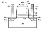
- FIGS. 1A-1Care each a cross-sectional view of a portion of an embodiment of an integrated computing structure 100 in accordance with a number of embodiments of the present disclosure.
- the integrated computing structure 100as described herein may include a CMOS FET structure 105 , as shown and described in connection with FIGS. 1A and 1B , integrated with a FET-based NVM structure, as shown and described in connection with FIG. 1C .
- the present disclosureincludes specific memory devices and associated structures as integrated computing structures 100 on a single silicon material (e.g., a substrate as shown at 108 in FIGS. 1A-1C and/or 208 in FIGS. 2A-2C ).
- the memory devices and associated componentse.g., transistors
- the single silicon material 108may be formed from a single crystal silicon, a polycrystalline silicon (polysilicon) material, and/or a silicon on insulator (SOI) structure.
- the memory devices and associated components (e.g., with compatible structures) of the integrated computing structure 100may, in a number of embodiments, include a number of P-FET devices (e.g., as shown at 102 and described in connection with FIG. 1A ), a number of N-FET devices (e.g., as shown at 104 and described in connection with FIG. 1B ), and/or a number of NVM devices (e.g., FET-based NVM devices as shown at 106 and described in connection with FIG. 1C , although NVM devices described herein are not limited to being FET-based).
- the P-FET device 102includes a PMOS transistor and the N-FET device 104 includes an NMOS transistor.
- the P-FET device 102 and the N-FET device 104may be combined to form a CMOS device 105 .
- An example of a semiconductor structurecan include the single silicon semiconductor material 108 having the integrated computing structure 100 formed thereon.
- the integrated computing structure 100may include the P-FET device 102 and the N-FET device 104 of the CMOS device 105 formed from a plurality of materials (e.g., layers) and the NVM device 106 formed from a plurality of materials (e.g., layers), as described further herein.
- the plurality of materials of the CMOS device 105 and the plurality of materials of the NVM device 106may be formed from, as described further herein, a shared same (e.g., used in common) material in a plurality of materials (e.g., a number of chemical elements and/or a combination of a plurality of chemical elements, and various numbers of each chemical element, to form a chemical compound) at a plurality of corresponding positions in their plurality of materials.
- a shared same (e.g., used in common) material in a plurality of materialse.g., a number of chemical elements and/or a combination of a plurality of chemical elements, and various numbers of each chemical element, to form a chemical compound
- Each of the plurality of materialsmay provide a particular function at the plurality of corresponding positions.
- the shared same materials utilized to form the corresponding positions in the plurality of materials and to provide the particular functions at the plurality of corresponding positionsmay reduce complexity in formation of the integrated computing structure 100 (e.g., when utilizing the STI trench structure 258 and/or DTI trench structure 260 shown and described in connection with FIGS. 2A-2C ).
- Substrateas used herein is intended to mean a semiconductor material such as a base semiconductor layer or a semiconductor material having one or more layers, structures, or regions formed thereon.
- a base semiconductor layermay be the lowest layer of single crystal silicon or a polysilicon material consisting of a silicon wafer or a silicon layer deposited on another material, such as a silicon on sapphire and/or an SOI wafer.
- a “silicon semiconductor material 108 ” and/or a “silicon material 108 ”have been used throughout the present disclosure and these terms are intended to be inclusive of both the p-silicon substrate material 108 and the n-silicon material of well 109 (e.g., in association with the P-FET device 102 shown in and described in connection with FIG. 1A ).
- Layeras used herein can refer to a layer formed on a material (e.g., a substrate) and/or a layer formed on a previously deposited layer using a number of deposition, masking, processing, and thermal techniques, for example, as presented herein.
- layeris meant to include layers specific to the semiconductor industry, such as “barrier layer,” “dielectric layer,” and “conductive layer”, among other types of layers.
- layeris intended to be synonymous with the term “film”, as used in the semiconductor industry.
- the term “layer”also may include layers found in technology outside of semiconductor technology, such as coatings on glass.
- Forminga material as used herein is intended to include depositing the material (e.g., as a layer) using a suitable deposition technique, as used in the semiconductor industry.
- a “material” as used hereinis intended to include a number of chemical elements and/or a combination of a plurality of chemical elements, and various numbers of each chemical element (e.g., to form a chemical compound), that may be used to form the material (e.g., by depositing the material as a layer).
- FIGS. 1A-1CSimilar elements or components between different figures may be identified by the use of similar digits.
- 108may reference element “ 08 ” in FIGS. 1A-1C
- a similar elementmay be referenced as 208 in FIGS. 2A-2C .
- Multiple analogous elements within one figuremay be referenced with a reference numeral followed by a hyphen and another number.
- 116 - 1may reference element 16 - 1 in FIG. 1A and 116-2 may reference element 16 - 2 , which can be analogous to element 16 - 1 .
- Such analogous elementsmay be generally referenced herein without the hyphen and an extra numeral.
- elements 116 - 1 and 116 - 2may be generally referenced as 116 .
- FIGS. 1A-1Ceach illustrate a cross-section of only one device (e.g., memory cell) and associated components (e.g., P-FET device 102 , N-FET device 104 , and NVM device 106 and associated components of each) in an X-Z plane with the silicon material 108 extending across the X direction only.
- the semiconductor structures contemplated hereinmay have integrated computing structures 100 , along with STI and/or DTI trench structures (e.g., as shown at 258 and 260 , respectively, in FIGS. 2A-2C ), for a plurality of memory devices extending in both directions of the X-Z plane and a Y-Z plane.
- a plurality of materials of the CMOS device 105may include a P-FET device 102 , having a gate insulator stack 110 (including associated components), in the integrated computing structure 100 .
- the plurality of materials of the CMOS device 105may further include an N-FET device 104 , having a gate insulator stack 112 (including associated components), in the integrated computing structure 100 .
- FIG. 1Aa plurality of materials of the CMOS device 105 may include a P-FET device 102 , having a gate insulator stack 110 (including associated components), in the integrated computing structure 100 .
- the plurality of materials of the CMOS device 105may further include an N-FET device 104 , having a gate insulator stack 112 (including associated components), in the integrated computing structure 100 .
- FIG. 1Aa plurality of materials of the CMOS device 105 may include a P-FET device 102 , having a gate insulator stack 110 (including associated components), in
- the integrated computing structure 100may include the NVM device 106 (including associated components), which may be, or may include, a FET-based NVM device that includes a charge trapping material (e.g., a layer shown at 138 that may be formed from a hafnium oxide (HfO 2 ) dielectric).
- the FET-based NVM device 106 and associated components 114 illustrated in FIG. 1Cis shown to have a structure based upon the N-FET device 104 and associated components 112 shown in FIG. 1B ; however, embodiments are not limited to this configuration.
- a FET-based NVM device 106 and associated components 114may have a structure based upon the P-FET device 102 and associated components 110 shown in FIG. 1A .
- the FET-based NVM device 106may be configured to output data values based upon a number of logic functions and/or structures (e.g., NAND, NOR, and/or nitride read-only memory (NROM), among other possibilities).
- logic functions and/or structurese.g., NAND, NOR, and/or nitride read-only memory (NROM), among other possibilities.
- the P-FET 102 gate insulator stack and associated components 110 formed from a plurality of materials and the N-FET 104 gate insulator stack and associated components 112 formed from a plurality of materialsmay be coupled as a CMOS device 105 configured to perform compute operations (e.g., add, multiply, and shift, among other compute operations) and/or logical operations (e.g., Boolean operations, among other logical operations).
- the NVM 106 device stack and associated components 114 formed from a plurality of materialsmay be configured for non-volatile storage of data values (e.g., results of performance of the compute and/or logical operations by the CMOS device 105 ).
- a number of embodiments of the integrated computing structure 100may include an STI structure 258 formed between the P-FET 102 gate insulator stack and associated components 110 and the N-FET 104 gate insulator stack and associated components 112 of the CMOS device 105 .
- a DTI structure 260may be formed between the plurality of materials that form a stack and associated components 114 of the NVM device 106 and the plurality of materials that form the gate insulator stacks and associated components 110 , 112 of the CMOS device 105 .
- the shared same materialsmay, in a number of embodiments, be in at least two of: an interface stabilizing material 128 of the stacks contiguous to the silicon semiconductor material 108 ; a metal gate 116 - 1 , 116 - 2 , and/or 118 , as embodiments of associated components, distal from the silicon semiconductor material 208 (e.g., not contiguous with the silicon semiconductor material 208 of N-FET 104 or NVM 106 and/or a well 109 of P-FET 102 ; and a metal gate interface 126 , as an embodiment of an associated component, contiguous to the metal gate component (e.g., control gates 118 ) and between the interface stabilizing material 128 and the metal gate component.
- an interface stabilizing material 128 of the stacks contiguous to the silicon semiconductor material 108e.g., a metal gate 116 - 1 , 116 - 2 , and/or 118 , as embodiments of associated components, distal from the silicon semiconductor material 208
- the metal gate componentmay, in a number of embodiments, include a common control gate material of each of the P-FET and N-FET gate insulator stacks and associated components 110 , 112 and the NVM device stack and associated components 114 (e.g., control gates 118 of the CMOS device 105 and/or the NVM device 106 ).
- the metal gate componentalso may, in a number of embodiments, include a source gate and a drain gate (e.g., the source gate may be the gate shown at 116 - 1 and the drain gate may be the gate shown at 116 - 2 , or vice versa) of each of the P-FET 102 and N-FET 104 gate insulator stacks and the NVM 106 device stack.
- the shared same (e.g., common) material that provides the function of the metal gate component 116 - 1 , 116 - 2 , and/or 118may be a same metal selected from one of tungsten (W) and aluminum (Al).
- the shared same material that provides the function of the metal gate interface component 126may be a same dielectric selected from one of tantalum nitride (TaN) and titanium nitride (TiN).
- the shared same material that provides the function of the interface stabilizing material 128may be a same dielectric selected from one of silicon oxide (SiO 2 ), silicon oxynitride (SiON), and oxygen-rich silicon oxynitride (OR-SiON).
- the interface stabilizing materialmay produce and stabilize a threshold of channel formation in the silicon semiconductor material 108 and/or the well 109 (e.g., between source and drain gates 116 - 1 , 116 - 2 ).
- the interface stabilizing material 128may form a number of electronic bonds with the silicon semiconductor material 108 and/or the well 109 .
- the interface stabilizing material 128may provide a low interface state density for meeting device parameter objectives for both the FET devices and/or the NVM devices described herein.
- a stack design using the metal gate component 118 formed from Al, the metal gate interface component 126 formed from TaN, and a high dielectric constant (k), low leakage material 130 formed from Al 2 O 3may provide a low threshold (e.g., of around negative 0.3 Volts).
- there may be a shared same high k conductive materiale.g., as shown at 136 for NVM 106 ) that provides a tunneling function for the NVM device as well as the primary dielectric layers of the FET devices (e.g., as shown at 129 and 132 , respectively, for P-FET 102 and N-FET 104 ).
- a metal gate interface component 126may be a shared same intermetallic material for the P-FET 102 and N-FET 104 and for the NVM 106 device.
- the material of the metal gate interface component 126may provide work-function control for the FETs, as well as for the NVM device.
- the shared high k dielectric material 126 for P-FET 102 and N-FET 104 and NVM 106 for the gate insulator stacksmay be selected from among several materials that have a dielectric constant that is above 10 (e.g., hafnium lanthanide oxynitride (HfLaON) or hafnium silicon oxynitride (HfSiON) dielectrics, among other such dielectrics).
- the P-FET 102 and N-FET 104 gate insulator stackscontiguous to the metal gate interface component 126 on a side of the metal gate interface component 126 opposite from the metal gate component 118 and/or the polysilicon cap 262 .
- the shared same material that provides the high k dielectric, low leakage function in the P-FET 102 and N-FET 104 gate insulator stacksmay be selected from among materials that have a dielectric constant that is above 6.0 (e.g., aluminum oxide (Al 2 O 3 ) dielectric, among other such dielectrics).
- the additional shared same materialsmay, in a number of embodiments, include a shared same material that provides a function to reduce resistance (e.g., of a diffusion contact as an embodiment of an associated component shown at 120 - 1 and 120 - 2 ) in the P-FET 102 and N-FET 104 gate insulator stacks and associated components 110 , 112 and in the NVM 106 device stack and associated components 114 contiguous to a base of the source gate and the drain gate (e.g., 116 - 1 and 116 - 2 ).
- a shared same materialthat provides a function to reduce resistance (e.g., of a diffusion contact as an embodiment of an associated component shown at 120 - 1 and 120 - 2 ) in the P-FET 102 and N-FET 104 gate insulator stacks and associated components 110 , 112 and in the NVM 106 device stack and associated components 114 contiguous to a base of the source gate and the drain gate (e.g., 116 - 1 and
- the source gate and the drain gatemay each be associated with a well 109 (e.g., as an embodiment of an associated component shown at 122 - 1 and 122 - 2 for P-FET 102 ), while the wells (not shown) for N-FET 104 (e.g., as an embodiment of an associated component shown at 123 - 1 and 123 - 2 ) and/or for NVM 106 (e.g., as an embodiment of an associated component shown at 124 - 1 and 124 - 2 ) may be formed in the silicon semiconductor material 108 (e.g., a p-silicon substrate).
- the silicon semiconductor material 108e.g., a p-silicon substrate
- the source gate and the drain gate for P-FET 102may be associated with an n-silicon material of the well 109 (e.g., as an embodiment of an associated component shown at 122 - 1 and 122 - 2 for P-FET 102 ).
- the shared same material that provides the function of the diffusion contacts 120 - 1 , 120 - 2may be a same nickel silicide selected from one of NiSi, Ni 2 S i , and N i S 2 . Using one of these materials may enable an intended (e.g., desired) lower series resistance for the FET devices and NVM memory cell.
- the P-FET 102 gate insulator stackmay include a second material 129 formed from a HfSiON dielectric to provide a FET gate dielectric function contiguous with and between a first material 128 , selected from one of SiO 2 , SiON, and/or OR-SiON, and a third material 130 (e.g., formed from Al 2 O 3 ).
- the N-FET 104 gate insulator stackmay include a second material 132 , selected from one of a HfLaON dielectric and a hafnium tantalum oxynitride (HfTaON) dielectric, to provide a high k, low leakage function contiguous with and between the first material 128 and a third material 134 , a lanthanum oxide (La 2 O 3 ), to provide a FET gate dielectric function.
- a second material 132selected from one of a HfLaON dielectric and a hafnium tantalum oxynitride (HfTaON) dielectric, to provide a high k, low leakage function contiguous with and between the first material 128 and a third material 134 , a lanthanum oxide (La 2 O 3 ), to provide a FET gate dielectric function.
- the NVM 106 device stackmay include a third material 138 , formed from a HfO 2 dielectric to provide a charge trapping function or formed from an injector silicon-rich nitride (In-SRN) dielectric to provide a floating plate function, contiguous with and between the second material 136 and a fourth material 139 , selected from one of a HfLaON dielectric and a HfTaON dielectric, to provide a high k blocking function.
- a third material 138formed from a HfO 2 dielectric to provide a charge trapping function or formed from an injector silicon-rich nitride (In-SRN) dielectric to provide a floating plate function, contiguous with and between the second material 136 and a fourth material 139 , selected from one of a HfLaON dielectric and a HfTaON dielectric, to provide a high k blocking function.
- In-SRNinjector silicon-rich nitride
- a method of forming a semiconductor structuremay include forming, on a silicon semiconductor material 108 , an integrated computing structure 100 .
- the integrated computing structure 100may be formed by forming a number of CMOS devices 102 , 104 , 105 , formed from a plurality of materials, and forming a NVM device 106 formed from a plurality of materials.
- the methodincludes forming the plurality of materials of the CMOS devices and the plurality of materials of the NVM device from a plurality of same materials shared at a corresponding plurality of positions within the structure, where a particular function is provided by each of the plurality of same materials at the corresponding plurality of positions.
- the methodmay include, as described herein, forming the silicon semiconductor material 108 as a base semiconductor wafer.
- the silicon semiconductor material 108may be selected from one of a single crystal silicon structure and a SOI structure.
- the methodmay include forming the plurality of materials of the CMOS device 105 as a P-FET 102 gate insulator stack and associated components 110 and an N-FET 104 gate insulator stack and associated components 112 .
- the methodmay include forming the NVM 106 device stack and associated components 114 as a FET-based device including a charge trapping material 138 .
- the methodmay include forming an STI 258 structure between the P-FET 102 gate insulator stack and associated components 110 and the N-FET 104 gate insulator stack and associated components 112 of the CMOS device 105 .
- the methodmay include forming a DTI structure 260 between the plurality of materials that form a stack and associated components of the NVM device 114 and the plurality of materials that form the gate insulator stacks and associated components 110 , 112 of the CMOS device 105 .
- FIGS. 2A-2Care cross-sectional views of a processing sequence 250 for integration of memory devices and associated structures on and/or in a silicon semiconductor material 208 (e.g., a substrate such as a single crystal silicon wafer and/or a SOI structure) in accordance with a number of embodiments of the present disclosure.
- the processing sequencemay be for integration of FET elements of both P-type 102 and N-type 104 , as described in connection with FIGS. 1A and 1B , respectively, (e.g., to form an single CMOS 105 logic element) with a single NVM 106 device element, as described in connection with FIG. 1C , on a silicon semiconductor material 208 .
- the memory devicesmay be the plurality of materials of the P-FET 102 and N-FET 104 gate insulator stacks and regions 110 , 112 and the plurality of materials of the NVM 106 device stack and region 114 formed on the silicon material 108 (e.g., a single silicon crystal substrate) shown in and described in connection with FIGS. 1A-1C , respectively.
- the silicon material 108e.g., a single silicon crystal substrate
- the materials (e.g., layers) described herein in connection with FIGS. 1A-1C and FIGS. 2A-2Cmay be formed (e.g., deposited) utilizing a number of deposition techniques.
- a particular deposition techniquemay be selected based upon, for example, suitability of the deposition technique in connection with a particular material (e.g., chemical composition) of the layer to be deposited, a thickness, length, and/or width of the layer to be deposited, whether the layer is to be deposited on a horizontal, vertical, and/or slanted surface, and/or a chemical composition of an underlying layer upon which the layer is to be deposited, among other possible considerations.
- a particular materiale.g., chemical composition
- the particular deposition techniquemay be selected from a group of such techniques that includes, but is not limited to, chemical vapor deposition (CVD), low pressure CVD (LPCVD), plasma enhanced CVD (PECVD), plasma vapor deposition (PVD), and atomic layer deposition (ALD), among other possible deposition techniques.
- CVDchemical vapor deposition
- LPCVDlow pressure CVD
- PECVDplasma enhanced CVD
- PVDplasma vapor deposition
- ALDatomic layer deposition
- oxidation and/or nitridation techniquesmay be performed in association with (e.g., before, during, and/or after) the particular deposition technique.
- Appropriate annealing techniquesalso may be performed (e.g., as described herein or otherwise).
- Suitable techniquesmay be utilized for forming and/or removing portions of the plurality of materials (e.g., as shown and described in connection with FIGS. 2A-2C ) of a P-FET region 252 , an N-FET region 254 , and/or an NVM region 256 formed on a single silicon crystal material 208 (e.g., including the isolation trenches of the STI structures 258 and/or the DTI structures 260 ) to form the integrated computing structures.
- Such techniquesmay include etching techniques such as, but not limited to, reactive ion etching (RIE), plasma etching, chemical dry etching, and/or ion beam etching, among other possible etching techniques.
- RIEreactive ion etching
- plasma etchingplasma etching
- chemical dry etchingchemical dry etching
- ion beam etchingamong other possible etching techniques.
- Control and/or direction of which materials (e.g., layers) may be first formed (e.g., deposited) on the single crystal silicon material and/or the SOI structure 208 , of which materials may be etched (e.g., removed),may be provided by suitable masking techniques. For etching, part of the silicon material 208 and/or a number of layers formed thereon may be protected from an etchant by a “masking” material that resists etching.
- the masking utilized hereinmay, in a number of embodiments, be a photoresist material in combination with a polysilicon cap (e.g., as shown with the cap 262 as a polysilicon hard mask and with photoresist mask 263 and/or with hard mask cap 262 and photoresist mask 264 , as described in connection with FIGS. 2A-2C ), where the photoresist material layer has been patterned using photolithography.
- Masking to remove a materiale.g., a layer
- various portions of a maskmay be added and/or removed, as appropriate for the deposition and/or etching performed in the processing sequence 250 .
- the etch processmay be controlled and/or directed by a suitable mask (e.g., as shown at 262 , 263 , and/or 264 ) for formation of the STI structure 258 and/or the DRI structure 260 in the silicon material 208 .
- a depth to which etching is performed for the STI structure 258may range from around 100 nm to around 800 nm. However, other depths may be implemented depending upon, for example, a desired aspect ratio (depth to width) of the opening into the STI structure 258 and/or the silicon material 208 .
- a depth to which etching is performed for the DTI structure 260may be deeper than that performed for the STI structure 258 .
- the depthmay be at least 1000 nm in order to provide suitable isolation of a CMOS device 105 and an NVM device 104 (e.g., isolation of the P-FET region 252 and the N-FET region 254 from the NVM region 256 ).
- Embodiments described hereinprovide a method of integrating memory structures formed on silicon (e.g., a silicon substrate).
- An example of such a methodmay include forming a plurality of materials of a P-FET 102 gate insulator stack in the PFET region 252 (e.g., depositing materials 228 , 229 , and 230 sequentially on the silicon material 208 ), forming a plurality of initial materials of an N-FET 104 gate insulator stack in the NFET region 254 (e.g., materials 228 , 229 , and 230 ), and forming a plurality of initial materials of an NVM 106 device stack in the NVM region 256 (e.g., materials 228 , 229 , and 230 ).
- the methodmay include forming a same number of stacked materials for each of the plurality of materials of the P-FET 102 gate insulator stack, the plurality of initial materials of the N-FET 104 gate insulator stack, and the plurality of initial materials of the NVM 106 device stack.
- Each stacked material of the same number of stacked materialsmay extend across an intended position of the P-FET 102 gate insulator stack, the N-FET 104 gate insulator stack, and the NVM 106 device stack (e.g., and across the corresponding regions 252 , 254 , and 256 ).
- Each different (e.g., separate) material of the same number of materialsmay be formed from a different material than the other materials, although each of the individual, separate materials at the corresponding positions in the stack may be formed from the same material.
- forming the plurality of materials of the P-FET 102 and the initial materials of the N-FET 104 gate insulator stacks and the plurality of initial materials of the NVM 106 device stackmay include forming a first material 228 , selected from one of an SiO 2 , an SiON, and an OR-SiON dielectric, to provide an interface dielectric function contiguous to the silicon material 208 .
- the methodmay include forming a second material 229 , a HfSiON dielectric, to provide an FET gate dielectric function contiguous with the SiO 2 , the SiON, or the OR-SiON first material.
- the methodmay include forming a third material 230 , an Al 2 O 3 dielectric, to provide a high k low leakage and/or blocking function contiguous with one of the HfLaON or the HfSiON second materials on one side.
- the methodmay include forming a polysilicon cap 262 on an opposite side of the Al 2 O 3 third material to provide an interface (e.g., protective) function to the plurality of integrated computing devices formed on the silicon material 208 .
- the methodmay include forming the STI structure 258 and the DTI structure 260 in the silicon material 208 prior to forming the plurality of materials of the P-FET 102 gate insulator stack, the plurality of initial materials of the N-FET 104 gate insulator stack, and the plurality of initial materials of the NVM 106 device stack.
- the well 109 shown in FIG. 1Amay be an n-silicon material formed on the silicon material 108 (e.g., the p-silicon substrate) and between the silicon material 108 and the interface stabilizing material 128 of the gate insulator stack 110 of the P-FET device 102 .
- the well 109may be formed on the silicon material 108 before or after formation of the STI 258 and DTI 260 structures, although the well 109 is formed prior to forming the plurality of materials of the P-FET gate insulator stack 110 thereon. Processing of the n-silicon material 109 shown in FIG. 1A and the p-silicon material 108 shown in FIGS.
- 1B and 1Cmay, in a number of embodiments, be performed after formation of the STI 258 and DTI 260 structures (e.g., processing for planarization of an upper surface of the n-silicon material 109 , the p-silicon material 108 , and/or the STI 258 and DTI 260 structures and/or for formation of the diffusion contacts 120 and/or the source gate wells and the drain gate wells 122 , 123 , and 124 shown in and described in connection with FIGS. 1A-1C , among other processing operations).
- the dielectric layers for the P-FET 102 devicemay be deposited over the well 109 formed on the silicon substrate 108 followed by deposition of the polysilicon cap layer 262 and a photoresist layer 263 .
- the photoresist layer 263may be formed over the cap 262 to define and protect the P-FET gate dielectric layers 228 , 229 , and 230 in P-FET region 252 , while some of those layers may optionally be removed from the other regions (e.g., N-FET region 254 and/or NVM region 256 ).
- the gate dielectric layers for N-FET 104 device and the common layers for NVM 106 devicemay be deposited, with the polysilicon cap 262 and another photoresist layer 264 being used to define and protect both N-FET and P-FET regions 252 , 254 , as shown in FIG. 2B .
- the methodprotects the gate stack insulators for both the P-FET and N-FET regions 252 , 254 and the STI 258 and may partially overlap the isolation region of DTI 260 .
- Similar process stepsmay be repeated into the NVM region 260 to define the dielectric stack layers of NVM region as shown in FIG. 2C .
- the polysilicon cap 262may be utilized over selected regions to protect dielectric layers in the active regions both for FETs and for NVMs.
- the plurality of materials of the P-FET 102 gate insulator stack and the plurality of initial materials of the N-FET 104 gate insulator stackmay be removed (e.g., by etching in combination with mask 262 , 263 ) from above the STI structure 258 to form the P-FET 102 gate insulator stack and region 252 and to contribute to isolation of the P-FET gate insulator stack and region from the N-FET 104 gate insulator stack and region 254 .
- the methodmay include removing an upper material 230 (e.g., by etching in combination with mask 262 , 263 ) of the plurality of initial materials of the N-FET 104 gate insulator stack and forming a different material 234 in place of the removed upper material 230 .
- Removing the upper material 230 of the plurality of initial materials of the N-FET 104 gate insulator stackmay include removing the third material 230 formed from the Al 2 O 3 dielectric.
- Forming the material from the different material in place of the removed upper material 230may include forming a third material 234 from the La 2 O 3 dielectric to provide a FET gate dielectric in place of the removed Al 2 O 3 dielectric.
- the methodmay include removing the second material 229 formed from the HfSiON dielectric and forming a second material 232 , selected from one of the HfLaON dielectric and the HfTaON dielectric, to provide a high k low leakage function in place of the removed HfSiON dielectric.
- the methodmay include removing (e.g., by etching in combination with mask 262 , 264 ) the plurality of materials of the N-FET 104 gate insulator stack and the plurality of initial materials of the NVM 106 device stack from above the DTI structure 260 to form the N-FET 104 gate insulator stack and region 254 and to contribute to isolation of the N-FET gate insulator stack and region from the NVM 106 device stack and region 256 .
- replacement of the original third material 230 with the different third material 234 and/or the original second material 229 with the different second material 232 for the N-FET 104 gate insulator stackmay include forming the different third material 234 and/or the different second material 232 over the original first material 228 in place of a removed original third material 230 and/or the original second material 229 for both the N-FET 104 gate insulator stack and region 254 and the NVM 106 device stack and region 256 .
- the methodmay include removing an upper material 230 of the plurality of initial materials of the NVM 106 device stack or a replaced upper material 234 of the N-FET 104 gate insulator stack and forming a different material in place of the removed upper material.
- Removing the upper material 230 of the plurality of initial materials of the NVM 106 device stackmay include removing the third material 230 formed from the Al 2 O 3 dielectric.
- Removing the upper material 234 of the replacement material of the NVM 106 device stackmay include removing the third material 234 formed from the La 2 O 3 dielectric.
- Forming the different material in place of the removed upper material 230 , 234may include forming a third material 238 , selected from one of the HfLaON dielectric and the HfTaON dielectric, to provide a high k blocking function in place of the removed Al 2 O 3 dielectric or the removed La 2 O 3 dielectric.
- the methodmay include removing a second material 229 of the plurality of initial materials of the NVM 106 device stack or a replaced second material 232 of the N-FET 104 gate insulator stack and forming a different material in place of the removed second material.
- Removing the second material 229 of the plurality of initial materials of the NVM 106 device stackmay include removing the second material 229 formed from the HfSiON dielectric.
- Removing the second material 232 of the replacement material of the NVM 106 device stackmay include removing the second material 232 formed from the HfLaON dielectric or the HfTaON dielectric.
- Forming the different material in place of the removed second material 229 , 232may include forming a second material 236 , the HfO 2 dielectric, to provide a charge trapping function or the In-SRN dielectric to provide a floating plate function in place of the removed HfSiON, HfLaON, and/or HfTaON dielectrics.
- the second material 236may, in a number of embodiments, be formed on the initially formed first material 228 formed from the SiO 2 , SiON, or OR-SiON dielectrics.
- the methodmay include forming, in the silicon material 208 and/or the well 109 , a diffusion contact (e.g., as an associated component shown at 120 - 1 and 120 - 2 and described in connection with FIGS. 1A-1C ) from a nickel silicide (e.g., NiSi, Ni 2 S i , or N i S 2 ).
- the diffusion contactsmay be formed from the nickel silicide to reduce resistance associated with and/or between a source gate well and a drain gate well (e.g., as shown at 122 - 1 and 122 - 2 , at 123 - 1 and 123 - 2 , and/or at 124 - 1 and 124 - 2 and described in connection with FIGS.
- the methodmay include forming, from one of W and Al, a metal gate (e.g., as an associated component shown at 116 - 1 and described in connection with FIGS.
- the source gate diffusion contacte.g., diffusion contact 120 - 1
- a metal gatee.g., as an associated component shown at 116 - 2
- a drain gate diffusion contacte.g., diffusion contact 120 - 2
- the polysilicon cap 262 as the hard mask and/or the photoresist mask 263 , 264may be added to and/or removed.
- protection of the dielectric layers of the P-FET region 252 , the N-FET region 254 , and the NVM region 256 , and/or the STI and/or DTI trench structures 258 , 260 , provided by the polysilicon cap 262 and/or the photoresist masks 263 , 264may be removed.
- Removal of the polysilicon cap 262 and/or the photoresist masks 263 , 264may enable access to the underlying integrated computing structures for further processing operations.
- the polysilicon cap 262 and/or the photoresist masks 263 , 264may be removed to enable formation of the diffusion contacts 120 , the source gate wells and the drain gate wells 122 , 123 , and 124 , and/or the metal gates 116 - 1 , 116 - 2 , and/or 118 associated with an upper surface of the n-silicon of well 109 and/or the p-silicon of silicon material 108 , among other processing operations).
- the methodmay include annealing the integrated computing structure 100 after forming the metal gate in contact with the source gate diffusion contact and the metal gate in contact with the drain gate diffusion contact.
- annealingcan be performed in an inert gas atmosphere (e.g., nitrogen, argon, helium and the like), which may or may not be mixed with oxygen.
- an atmosphere employed in the annealing step of the present disclosuremay include steam at a temperature about 600° Celsius (C) to about 700° C. for a time interval from about 30 to about 120 seconds.
- the atmosphere employed for the annealing stepmay be steam at a temperature from about 75° C. to about 600° C. for a time interval from about 30 to about 120 seconds.
- the annealingmay be performed in a single ramp step or it can be performed using a series of ramp and soak cycles.
Landscapes
- Engineering & Computer Science (AREA)
- Physics & Mathematics (AREA)
- Condensed Matter Physics & Semiconductors (AREA)
- General Physics & Mathematics (AREA)
- Computer Hardware Design (AREA)
- Microelectronics & Electronic Packaging (AREA)
- Power Engineering (AREA)
- Manufacturing & Machinery (AREA)
- Metal-Oxide And Bipolar Metal-Oxide Semiconductor Integrated Circuits (AREA)
Abstract
Description
Claims (20)
Priority Applications (2)
| Application Number | Priority Date | Filing Date | Title |
|---|---|---|---|
| US15/641,558US10411026B2 (en) | 2017-07-05 | 2017-07-05 | Integrated computing structures formed on silicon |
| US16/550,533US10811424B2 (en) | 2017-07-05 | 2019-08-26 | Integrated computing structures formed on silicon |
Applications Claiming Priority (1)
| Application Number | Priority Date | Filing Date | Title |
|---|---|---|---|
| US15/641,558US10411026B2 (en) | 2017-07-05 | 2017-07-05 | Integrated computing structures formed on silicon |
Related Child Applications (1)
| Application Number | Title | Priority Date | Filing Date |
|---|---|---|---|
| US16/550,533DivisionUS10811424B2 (en) | 2017-07-05 | 2019-08-26 | Integrated computing structures formed on silicon |
Publications (2)
| Publication Number | Publication Date |
|---|---|
| US20190013323A1 US20190013323A1 (en) | 2019-01-10 |
| US10411026B2true US10411026B2 (en) | 2019-09-10 |
Family
ID=64903482
Family Applications (2)
| Application Number | Title | Priority Date | Filing Date |
|---|---|---|---|
| US15/641,558Active2037-07-11US10411026B2 (en) | 2017-07-05 | 2017-07-05 | Integrated computing structures formed on silicon |
| US16/550,533ActiveUS10811424B2 (en) | 2017-07-05 | 2019-08-26 | Integrated computing structures formed on silicon |
Family Applications After (1)
| Application Number | Title | Priority Date | Filing Date |
|---|---|---|---|
| US16/550,533ActiveUS10811424B2 (en) | 2017-07-05 | 2019-08-26 | Integrated computing structures formed on silicon |
Country Status (1)
| Country | Link |
|---|---|
| US (2) | US10411026B2 (en) |
Families Citing this family (8)
| Publication number | Priority date | Publication date | Assignee | Title |
|---|---|---|---|---|
| US20190363135A1 (en)* | 2016-09-29 | 2019-11-28 | Intel Corporation | Resistive random access memory cell |
| JP2020155635A (en)* | 2019-03-20 | 2020-09-24 | キオクシア株式会社 | Semiconductor device |
| JP2021150508A (en)* | 2020-03-19 | 2021-09-27 | キオクシア株式会社 | Semiconductor storage device and manufacturing method for semiconductor storage device |
| US11769765B2 (en)* | 2021-03-15 | 2023-09-26 | Micron Technology, Inc. | Gate dielectric layer protection |
| US20230101155A1 (en)* | 2021-09-27 | 2023-03-30 | Applied Materials, Inc. | Three dimensional memory device and method of fabrication |
| US20240081048A1 (en)* | 2022-09-07 | 2024-03-07 | Micron Technology, Inc. | Microelectronic devices, and related memory devices, electronic systems, and methods |
| US12396165B2 (en)* | 2022-09-12 | 2025-08-19 | Micron Technology, Inc. | Microelectronic devices, and related memory devices, electronic systems, and methods |
| US12438983B2 (en)* | 2023-11-08 | 2025-10-07 | Bank Of America Corporation | Communication session interruption and dynamic learning system |
Citations (39)
| Publication number | Priority date | Publication date | Assignee | Title |
|---|---|---|---|---|
| US4870470A (en) | 1987-10-16 | 1989-09-26 | International Business Machines Corporation | Non-volatile memory cell having Si rich silicon nitride charge trapping layer |
| US20020081826A1 (en)* | 2000-12-21 | 2002-06-27 | Rotondaro Antonio L. P. | Annealing of high-K dielectric materials |
| US6743681B2 (en) | 2001-11-09 | 2004-06-01 | Micron Technology, Inc. | Methods of Fabricating Gate and Storage Dielectric Stacks having Silicon-Rich-Nitride |
| US6743682B2 (en) | 1999-12-17 | 2004-06-01 | Koninklijke Philips Electronics N.V. | Method of manufacturing a semiconductor device |
| US6888200B2 (en) | 2002-08-30 | 2005-05-03 | Micron Technology Inc. | One transistor SOI non-volatile random access memory cell |
| US6903969B2 (en) | 2002-08-30 | 2005-06-07 | Micron Technology Inc. | One-device non-volatile random access memory cell |
| US6917078B2 (en) | 2002-08-30 | 2005-07-12 | Micron Technology Inc. | One transistor SOI non-volatile random access memory cell |
| US7012297B2 (en) | 2001-08-30 | 2006-03-14 | Micron Technology, Inc. | Scalable flash/NV structures and devices with extended endurance |
| US7042027B2 (en) | 2002-08-30 | 2006-05-09 | Micron Technology, Inc. | Gated lateral thyristor-based random access memory cell (GLTRAM) |
| US7145186B2 (en) | 2004-08-24 | 2006-12-05 | Micron Technology, Inc. | Memory cell with trenched gated thyristor |
| US7158410B2 (en) | 2004-08-27 | 2007-01-02 | Micron Technology, Inc. | Integrated DRAM-NVRAM multi-level memory |
| US7166888B2 (en) | 2005-01-27 | 2007-01-23 | Micron Technology, Inc. | Scalable high density non-volatile memory cells in a contactless memory array |
| US20070034922A1 (en) | 2005-08-11 | 2007-02-15 | Micron Technology, Inc. | Integrated surround gate multifunctional memory device |
| US7208793B2 (en) | 2004-11-23 | 2007-04-24 | Micron Technology, Inc. | Scalable integrated logic and non-volatile memory |
| US7224002B2 (en) | 2004-05-06 | 2007-05-29 | Micron Technology, Inc. | Silicon on insulator read-write non-volatile memory comprising lateral thyristor and trapping layer |
| US7244981B2 (en) | 2005-02-25 | 2007-07-17 | Micron Technology, Inc. | Scalable high performance non-volatile memory cells using multi-mechanism carrier transport |
| US7250628B2 (en) | 2003-02-10 | 2007-07-31 | Micron Technology, Inc. | Memory devices and electronic systems comprising thyristors |
| US7276760B2 (en) | 2005-02-25 | 2007-10-02 | Micron Technology, Inc. | Low power memory subsystem with progressive non-volatility |
| US7279740B2 (en) | 2005-05-12 | 2007-10-09 | Micron Technology, Inc. | Band-engineered multi-gated non-volatile memory device with enhanced attributes |
| US7339239B2 (en) | 2003-12-17 | 2008-03-04 | Micron Technology, Inc. | Vertical NROM NAND flash memory array |
| US7365388B2 (en) | 2005-02-25 | 2008-04-29 | Micron Technology, Inc. | Embedded trap direct tunnel non-volatile memory |
| US7429767B2 (en) | 2005-09-01 | 2008-09-30 | Micron Technology, Inc. | High performance multi-level non-volatile memory device |
| US7432562B2 (en) | 2003-06-03 | 2008-10-07 | Micron Technology, Inc. | SRAM devices, and electronic systems comprising SRAM devices |
| US7436018B2 (en) | 2005-08-11 | 2008-10-14 | Micron Technology, Inc. | Discrete trap non-volatile multi-functional memory device |
| US20080303080A1 (en) | 2005-06-21 | 2008-12-11 | Micron Technology, Inc. | Back-sided trapped non-volatile memory device |
| US7476927B2 (en) | 2005-08-24 | 2009-01-13 | Micron Technology, Inc. | Scalable multi-functional and multi-level nano-crystal non-volatile memory device |
| US7482651B2 (en) | 2005-12-09 | 2009-01-27 | Micron Technology, Inc. | Enhanced multi-bit non-volatile memory device with resonant tunnel barrier |
| US7525149B2 (en) | 2005-08-24 | 2009-04-28 | Micron Technology, Inc. | Combined volatile and non-volatile memory device with graded composition insulator stack |
| US7612403B2 (en) | 2005-05-17 | 2009-11-03 | Micron Technology, Inc. | Low power non-volatile memory and gate stack |
| US7625803B2 (en) | 2003-02-10 | 2009-12-01 | Micron Technology, Inc. | Memory devices, electronic systems, and methods of forming memory devices |
| US7629641B2 (en) | 2005-08-31 | 2009-12-08 | Micron Technology, Inc. | Band engineered nano-crystal non-volatile memory device utilizing enhanced gate injection |
| US7662693B2 (en) | 2007-09-26 | 2010-02-16 | Micron Technology, Inc. | Lanthanide dielectric with controlled interfaces |
| US20100090265A1 (en) | 2006-10-19 | 2010-04-15 | Micron Technology, Inc. | High density nanodot nonvolatile memory |
| US7728350B2 (en) | 2003-07-02 | 2010-06-01 | Micron Technology, Inc. | Memory cell with negative differential resistance |
| US7759715B2 (en) | 2007-10-15 | 2010-07-20 | Micron Technology, Inc. | Memory cell comprising dynamic random access memory (DRAM) nanoparticles and nonvolatile memory (NVM) nanoparticle |
| US7964909B2 (en) | 2005-05-26 | 2011-06-21 | Micron Technology, Inc. | Scalable high density non-volatile memory cells in a contactless memory array |
| US8228743B2 (en) | 2007-10-12 | 2012-07-24 | Micron Technology, Inc. | Memory cells containing charge-trapping zones |
| US8242554B2 (en) | 2004-12-21 | 2012-08-14 | Micron Technology, Inc. | Integrated two device non-volatile memory |
| US8883624B1 (en)* | 2013-09-27 | 2014-11-11 | Cypress Semiconductor Corporation | Integration of a memory transistor into high-K, metal gate CMOS process flow |
Family Cites Families (2)
| Publication number | Priority date | Publication date | Assignee | Title |
|---|---|---|---|---|
| US9418864B2 (en)* | 2008-01-30 | 2016-08-16 | Infineon Technologies Ag | Method of forming a non volatile memory device using wet etching |
| KR102282984B1 (en)* | 2015-06-02 | 2021-07-29 | 에스케이하이닉스 주식회사 | Method of fabricating an electronic device having charge trap memory device |
- 2017
- 2017-07-05USUS15/641,558patent/US10411026B2/enactiveActive
- 2019
- 2019-08-26USUS16/550,533patent/US10811424B2/enactiveActive
Patent Citations (77)
| Publication number | Priority date | Publication date | Assignee | Title |
|---|---|---|---|---|
| US4870470A (en) | 1987-10-16 | 1989-09-26 | International Business Machines Corporation | Non-volatile memory cell having Si rich silicon nitride charge trapping layer |
| US6743682B2 (en) | 1999-12-17 | 2004-06-01 | Koninklijke Philips Electronics N.V. | Method of manufacturing a semiconductor device |
| US20020081826A1 (en)* | 2000-12-21 | 2002-06-27 | Rotondaro Antonio L. P. | Annealing of high-K dielectric materials |
| US7750395B2 (en) | 2001-08-30 | 2010-07-06 | Micron Technology, Inc. | Scalable Flash/NV structures and devices with extended endurance |
| US7400012B2 (en) | 2001-08-30 | 2008-07-15 | Micron Technology, Inc. | Scalable Flash/NV structures and devices with extended endurance |
| US7012297B2 (en) | 2001-08-30 | 2006-03-14 | Micron Technology, Inc. | Scalable flash/NV structures and devices with extended endurance |
| US7528043B2 (en) | 2001-11-09 | 2009-05-05 | Micron Technology, Inc. | Scalable gate and storage dielectric |
| US6743681B2 (en) | 2001-11-09 | 2004-06-01 | Micron Technology, Inc. | Methods of Fabricating Gate and Storage Dielectric Stacks having Silicon-Rich-Nitride |
| US6998667B2 (en) | 2001-11-09 | 2006-02-14 | Micron Technology, Inc. | Scalable gate and storage dielectric |
| US7130216B2 (en) | 2002-08-30 | 2006-10-31 | Micron Technology, Inc. | One-device non-volatile random access memory cell |
| US7339830B2 (en) | 2002-08-30 | 2008-03-04 | Micron Technology, Inc. | One transistor SOI non-volatile random access memory cell |
| US7456054B2 (en) | 2002-08-30 | 2008-11-25 | Micron Technology, Inc. | Gated lateral thyristor-based random access memory cell (GLTRAM) |
| US7440317B2 (en) | 2002-08-30 | 2008-10-21 | Micron Technology, Inc. | One transistor SOI non-volatile random access memory cell |
| US7485513B2 (en) | 2002-08-30 | 2009-02-03 | Micron Technology, Inc. | One-device non-volatile random access memory cell |
| US7184312B2 (en) | 2002-08-30 | 2007-02-27 | Micron Technology, Inc. | One transistor SOI non-volatile random access memory cell |
| US7042027B2 (en) | 2002-08-30 | 2006-05-09 | Micron Technology, Inc. | Gated lateral thyristor-based random access memory cell (GLTRAM) |
| US6917078B2 (en) | 2002-08-30 | 2005-07-12 | Micron Technology Inc. | One transistor SOI non-volatile random access memory cell |
| US6903969B2 (en) | 2002-08-30 | 2005-06-07 | Micron Technology Inc. | One-device non-volatile random access memory cell |
| US6888200B2 (en) | 2002-08-30 | 2005-05-03 | Micron Technology Inc. | One transistor SOI non-volatile random access memory cell |
| US7625803B2 (en) | 2003-02-10 | 2009-12-01 | Micron Technology, Inc. | Memory devices, electronic systems, and methods of forming memory devices |
| US7250628B2 (en) | 2003-02-10 | 2007-07-31 | Micron Technology, Inc. | Memory devices and electronic systems comprising thyristors |
| US7432562B2 (en) | 2003-06-03 | 2008-10-07 | Micron Technology, Inc. | SRAM devices, and electronic systems comprising SRAM devices |
| US7968402B2 (en) | 2003-07-02 | 2011-06-28 | Micron Technology, Inc. | Method for forming a high-performance one-transistor memory cell |
| US7728350B2 (en) | 2003-07-02 | 2010-06-01 | Micron Technology, Inc. | Memory cell with negative differential resistance |
| US8125003B2 (en) | 2003-07-02 | 2012-02-28 | Micron Technology, Inc. | High-performance one-transistor memory cell |
| US7339239B2 (en) | 2003-12-17 | 2008-03-04 | Micron Technology, Inc. | Vertical NROM NAND flash memory array |
| US7224002B2 (en) | 2004-05-06 | 2007-05-29 | Micron Technology, Inc. | Silicon on insulator read-write non-volatile memory comprising lateral thyristor and trapping layer |
| US7145186B2 (en) | 2004-08-24 | 2006-12-05 | Micron Technology, Inc. | Memory cell with trenched gated thyristor |
| US7440310B2 (en) | 2004-08-24 | 2008-10-21 | Micron Technology, Inc. | Memory cell with trenched gated thyristor |
| US7379336B2 (en) | 2004-08-27 | 2008-05-27 | Micron Technology, Inc. | Integrated DRAM-NVRAM multi-level memory |
| US7403416B2 (en) | 2004-08-27 | 2008-07-22 | Micron Technology, Inc. | Integrated DRAM-NVRAM multi-level memory |
| US7417893B2 (en) | 2004-08-27 | 2008-08-26 | Micron Technology, Inc. | Integrated DRAM-NVRAM multi-level memory |
| US7459740B2 (en) | 2004-08-27 | 2008-12-02 | Micron Technology, Inc. | Integrated DRAM-NVRAM multi-level memory |
| US7158410B2 (en) | 2004-08-27 | 2007-01-02 | Micron Technology, Inc. | Integrated DRAM-NVRAM multi-level memory |
| US7457159B2 (en) | 2004-08-27 | 2008-11-25 | Micron Technology, Inc. | Integrated DRAM-NVRAM multi-level memory |
| US7349252B2 (en) | 2004-08-27 | 2008-03-25 | Micron Technology, Inc. | Integrated DRAM-NVRAM multi-level memory |
| US7208793B2 (en) | 2004-11-23 | 2007-04-24 | Micron Technology, Inc. | Scalable integrated logic and non-volatile memory |
| US7544990B2 (en) | 2004-11-23 | 2009-06-09 | Micron Technology, Inc. | Scalable integrated logic and non-volatile memory |
| US8242554B2 (en) | 2004-12-21 | 2012-08-14 | Micron Technology, Inc. | Integrated two device non-volatile memory |
| US7273784B2 (en) | 2005-01-27 | 2007-09-25 | Micron Technology, Inc. | Scalable high density non-volatile memory cells in a contactless memory array |
| US7166888B2 (en) | 2005-01-27 | 2007-01-23 | Micron Technology, Inc. | Scalable high density non-volatile memory cells in a contactless memory array |
| US7671407B2 (en) | 2005-02-25 | 2010-03-02 | Micron Technology, Inc. | Embedded trap direct tunnel non-volatile memory |
| US7244981B2 (en) | 2005-02-25 | 2007-07-17 | Micron Technology, Inc. | Scalable high performance non-volatile memory cells using multi-mechanism carrier transport |
| US7838362B2 (en) | 2005-02-25 | 2010-11-23 | Micron Technology, Inc. | Method of making an embedded trap direct tunnel non-volatile memory |
| US7385245B2 (en) | 2005-02-25 | 2008-06-10 | Micron Technology, Inc. | Low power memory subsystem with progressive non-volatility |
| US7553735B2 (en) | 2005-02-25 | 2009-06-30 | Micron Technology, Inc. | Scalable high performance non-volatile memory cells using multi-mechanism carrier transport |
| US7276760B2 (en) | 2005-02-25 | 2007-10-02 | Micron Technology, Inc. | Low power memory subsystem with progressive non-volatility |
| US7365388B2 (en) | 2005-02-25 | 2008-04-29 | Micron Technology, Inc. | Embedded trap direct tunnel non-volatile memory |
| US8063436B2 (en) | 2005-05-12 | 2011-11-22 | Micron Technology, Inc. | Memory cells configured to allow for erasure by enhanced F-N tunneling of holes from a control gate to a charge trapping material |
| US7749848B2 (en) | 2005-05-12 | 2010-07-06 | Micron Technology, Inc. | Band-engineered multi-gated non-volatile memory device with enhanced attributes |
| US7279740B2 (en) | 2005-05-12 | 2007-10-09 | Micron Technology, Inc. | Band-engineered multi-gated non-volatile memory device with enhanced attributes |
| US7612403B2 (en) | 2005-05-17 | 2009-11-03 | Micron Technology, Inc. | Low power non-volatile memory and gate stack |
| US7964909B2 (en) | 2005-05-26 | 2011-06-21 | Micron Technology, Inc. | Scalable high density non-volatile memory cells in a contactless memory array |
| US20080303080A1 (en) | 2005-06-21 | 2008-12-11 | Micron Technology, Inc. | Back-sided trapped non-volatile memory device |
| US8058118B2 (en) | 2005-06-21 | 2011-11-15 | Micron Technology, Inc. | Methods of forming and operating back-side trap non-volatile memory cells |
| US7851827B2 (en) | 2005-06-21 | 2010-12-14 | Micron Technology, Inc. | Back-side trapped non-volatile memory device |
| US7786516B2 (en) | 2005-08-11 | 2010-08-31 | Micron Technology, Inc. | Discrete trap non-volatile multi-functional memory device |
| US8143657B2 (en) | 2005-08-11 | 2012-03-27 | Arup Bhattacharyya | Discrete trap non-volatile multi-functional memory device |
| US20070034922A1 (en) | 2005-08-11 | 2007-02-15 | Micron Technology, Inc. | Integrated surround gate multifunctional memory device |
| US7436018B2 (en) | 2005-08-11 | 2008-10-14 | Micron Technology, Inc. | Discrete trap non-volatile multi-functional memory device |
| US7898022B2 (en) | 2005-08-24 | 2011-03-01 | Micron Technology, Inc. | Scalable multi-functional and multi-level nano-crystal non-volatile memory device |
| US7768062B2 (en) | 2005-08-24 | 2010-08-03 | Micron Technology, Inc. | Combined volatile and non-volatile memory device with graded composition insulator stack |
| US7476927B2 (en) | 2005-08-24 | 2009-01-13 | Micron Technology, Inc. | Scalable multi-functional and multi-level nano-crystal non-volatile memory device |
| US7525149B2 (en) | 2005-08-24 | 2009-04-28 | Micron Technology, Inc. | Combined volatile and non-volatile memory device with graded composition insulator stack |
| US7629641B2 (en) | 2005-08-31 | 2009-12-08 | Micron Technology, Inc. | Band engineered nano-crystal non-volatile memory device utilizing enhanced gate injection |
| US8159875B2 (en) | 2005-09-01 | 2012-04-17 | Micron Technology, Inc. | Methods of storing multiple data-bits in a non-volatile memory cell |
| US7429767B2 (en) | 2005-09-01 | 2008-09-30 | Micron Technology, Inc. | High performance multi-level non-volatile memory device |
| US7579242B2 (en) | 2005-09-01 | 2009-08-25 | Micron Technology, Inc. | High performance multi-level non-volatile memory device |
| US7867850B2 (en) | 2005-12-09 | 2011-01-11 | Micron Technology, Inc. | Enhanced multi-bit non-volatile memory device with resonant tunnel barrier |
| US7482651B2 (en) | 2005-12-09 | 2009-01-27 | Micron Technology, Inc. | Enhanced multi-bit non-volatile memory device with resonant tunnel barrier |
| US20100090265A1 (en) | 2006-10-19 | 2010-04-15 | Micron Technology, Inc. | High density nanodot nonvolatile memory |
| US7956426B2 (en) | 2007-09-26 | 2011-06-07 | Micron Technology, Inc. | Lanthanide dielectric with controlled interfaces |
| US7662693B2 (en) | 2007-09-26 | 2010-02-16 | Micron Technology, Inc. | Lanthanide dielectric with controlled interfaces |
| US8228743B2 (en) | 2007-10-12 | 2012-07-24 | Micron Technology, Inc. | Memory cells containing charge-trapping zones |
| US7759715B2 (en) | 2007-10-15 | 2010-07-20 | Micron Technology, Inc. | Memory cell comprising dynamic random access memory (DRAM) nanoparticles and nonvolatile memory (NVM) nanoparticle |
| US8193568B2 (en) | 2007-10-15 | 2012-06-05 | Micron Technology, Inc. | Nanocrystal based universal memory cells, and memory cells |
| US8883624B1 (en)* | 2013-09-27 | 2014-11-11 | Cypress Semiconductor Corporation | Integration of a memory transistor into high-K, metal gate CMOS process flow |
Non-Patent Citations (39)
| Title |
|---|
| Aoyama et al., "Proposal of New HfSiON CMOS Fabrication Process (HAMDAMA) for Low Standby Power Device", IEEE International Electron Devices Meeting (IEDM) 2004, Dec. 13-15, 2004, San Francisco, CA, pp. 95-98. |
| Bhattacharyya et al., "Properties and Applications of Silicon Oxynitride Films", from IBM Technical Report TR. 19.0399, presented at the Electrochemical Society (ECS) 150th Meeting, Oct. 1976, Las Vegas, NV, 20 pages. |
| Buchanan et al., 80 nm polysilicon gated n-FETs with ultra-thin Al2O3 gate dielectric for ULSI applications, IEEE International Electron Devices Meeting (IEDM) 2000, Dec. 10-13, 2000, San Francisco, CA, pp. 223-226. |
| Buckley et al., "In-depth Investigation of Hf-based High-k Dielectrics as Storage Layer of Charge Trap NVMs", IEEE International Electron Devices Meeting (IEDM) 2006, Dec. 11-13, 2006, San Francisco, CA, pp. 251-254. |
| Cho et al., "Observation of Single Electron Tunneling and Ballistic Transport in Twin Silicon Nanowire MOSFETs (TSNWFETs) Fabricated by Top-Down CMOS Process", IEEE International Electron Devices Meeting (IEDM) 2006, Dec. 11-13, 2006, San Francisco, CA, 4 pages. |
| Choi et al., "High Speed Flash Memory and 1T-DRAM on Dopant Segregated Schottky Barrier (DSSB) FinFET SONOS Device for Multi-functional SoC Applications", IEEE International Electron Devices Meeting (IEDM) 2008, Dec. 15-17, 2008, San Francisco, CA, 4 pages. |
| Dillon et al., "Hybrid Memory combining SRAM and NOR Flash for Code and Data Storage", Flash Memory Summit 2012, Aug. 7-9, 2012, Santa Clara, CA, 18 pages. |
| Han et al., "A Unified-RAM (URAM) Cell for Multi-Functioning Capacitorless DRAM and NVM", IEEE International Electron Devices Meeting (IEDM) 2007, Dec. 10-12, 2007, Washington D.C., pp. 929-932. |
| Huang et al., "45nm High-K Metal Gate CMOS Technology for GPU/NPU Applications with Highest PFET Performance", IEEE International Electron Devices Meeting (IEDM) 2007, Dec. 10-12, 2007, Washington D.C., pp. 285-288. |
| Hubert et al., "A Stacked SONOS Technology, Up to 4 Levels and 6nm Crystalline Nanowires, with Gate-All-Around or Independent Gates (φ-Flash), Suitable for Full 3D Integration", IEEE International Electron Devices Meeting (IEDM) 2009, Dec. 7-9, 2009, Baltimore, MD, 4 pages. |
| Jung et al., "Three-Dimensionally Stacked NAND Flash Memory Technology Using Stacking Single Crystal Si Layers on ILD and TANOS Structure for Beyond 30nm Node", IEEE International Electron Devices Meeting (IEDM) 2006, Dec. 11-13, 2006, San Francisco, CA, pp. 37-40. |
| Kim et al., "Robust Multi-bit Programmable Flash Memory Using a Resonant Tunnel Barrier", IEEE International Electron Devices Meeting (IEDM) 2005, Dec. 5-7, 2005, Washington D.C., pp. 881-884. |
| Kim et al., "Systematic Study of Workfunction Engineering and Scavenging Effect Using NiSi Alloy FUSI Metal Gates with Advanced Gate Stacks", IEEE International Electron Devices Meeting (IEDM) 2005, Dec. 5-7, 2005, Washington D.C., pp. 657-660. |
| Krishnan et al., "A Manufacturable Dual Channel (Si and SiGe) High-K Metal Gate CMOS Technology with Multiple Oxides for High Performance and Low Power Applications", IEEE International Electron Devices Meeting (IEDM) 2011, Dec. 5-7, 2011, Washington, D.C., pp. 634-637. |
| Kubicek et al., ".Low Vt CMOS Using Doped Hf-based Oxides, TaC-based Metals and Laser-only Anneal", IEEE International Electron Devices Meeting (IEDM) 2007, Dec. 10-12, 2007, Washington D.C., pp. 49-52. |
| Lai et al., "A Multi-Layer Stackable Thin-Film Transistor (TFT) NAND-Type Flash Memory", IEEE International Electron Devices Meeting (IEDM) 2006, Dec. 11-13, 2006, San Francisco, CA, 4 pages. |
| Lauwers et al., "Cmos Integration of Dual Work Function Phase Controlled NI FUSI with Simultaneous Silicidation of NMOS (NiSi) and PMOS (Ni-rich silicide) Gates on HfSiON", IEEE International Electron Devices Meeting (IEDM) 2005, Dec. 5-7, 2005, Washington, D.C., pp. 661-664. |
| Lee et al., Effect of Polysilicon Gate on the Flatband Voltage Shift and Mobility Degradation for ALD-Al2O3 Gate Dielectric, IEEE International Electron Devices Meeting (IEDM) 2000, Dec. 10-13, 2000, San Francisco, CA, pp. 645-648. |
| Likharev, "Riding the Crest of a New Wave in Memory", IEEE Circuits and Devices Magazine, vol. 16, Issue 4, Jul. 2000, pp. 16-21. |
| Lue et al., "A Novel P-Channel NAND-type Flash Memory with 2 bit/cell Operation and High Programming Throughput (> 20 Mb/sec)", IEEE International Electron Devices Meeting (IEDM) 2005, Dec. 5-7, 2005, Washington, D.C., 4 pages. |
| Lue et al., "Scaling Feasibility of Planar Thin Floating Gate (FG) NAND Flash Devices and Size Effect Challenges beyond 20nm", IEEE International Electron Devices Meeting (IEDM) 2011, Dec. 5-7, 2011, Washington, D.C., pp. 203-206. |
| Luo et al., "Design of High Performance PFETs with Strained Si Channel and Laser Anneal", IEEE International Electron Devices Meeting (IEDM) 2005, Dec. 5-7, 2005, Washington D.C., pp. 495-498. |
| Manchanda et al., "Gate Quality Doped High K films for CMOS beyond 100 nm: 3-10nm Al2O3 with Low Leakage and Low Interface States", IEEE International Electron Devices Meeting (IEDM) 1998, Dec. 6-9, 1998, San Francisco, CA, pp. 605-608. |
| Manchanda et al., "Si-Doped Aluminates for High Temperature Metal-Gate CMOS: Zr-AlSi-O, a Novel Gate Dielectric for Low Power Applications", IEEE International Electron Devices Meeting (IEDM) 2000, Dec. 10-13, 2000, San Francisco, CA, pp. 23-26. |
| Mayuzumi et al., "Extreme High Performance n- and p- MOSFETs Boosted by Dual-Metal/High-k Gate Damascene Process using Top-Cut Dual Stress Liners on (100) Substrates" IEEE International Electron Devices Meeting (IEDM) 2007, Dec. 10-12, 2007, Washington D.C., pp. 293-296. |
| Moon et al., "Multi-Functional Universal Device using a Band-Engineered Vertical Structure", IEEE International Electron Devices Meeting (IEDM) 2011, Dec. 5-7, 2011, Washington D.C., pp. 551-554. |
| Nemati et al., "A Novel Thyristor-based SRAM Cell (T-RAM) for High-Speed, Low-Voltage, Giga-scale Memories", IEEE International Electron Devices Meeting (IEDM) 1999, Dec. 5-8, 1999, Washington D.C., pp. 283-286. |
| Oh et al., "4-bit Double SONOS Memories (DSMs) Using Single-Level and Multi-Level Cell Schemes", IEEE International Electron Devices Meeting (IEDM) 2006, Dec. 11-13, 2006, San Francisco, CA, pp. 967-970. |
| Ohba et al., "25 nm Planar Bulk SONOS-type Memory with Double Tunnel Junction", IEEE International Electron Devices Meeting (IEDM) 2006, Dec. 11-13, 2006, San Francisco, CA, pp. 959-962. |
| Ohba et al., "35 nm Floating Gate Planar MOSFET Memory using Double Junction Tunneling", IEEE International Electron Devices Meeting (IEDM) 2005, Dec. 5-7, 2005, Washington D.C., 4 pages. |
| Ohta et al., "High performance Sub-40 nm Bulk CMOS with Dopant Confinement Layer (DCL) Techniques as a Strain Booster", IEEE International Electron Devices Meeting (IEDM) 2007, Dec. 10-12, 2007, Washington D.C., pp. 289-292. |
| Ramaswamy et al., "Engineering a Planar NAND Cell Scalable to 20nm and Beyond", 2013 5th IEEE Memory Workshop, May 26-29, 2013, Monterey, CA, pp. 5-8. |
| Ranica et al., "A new 40-nm SONOS Structure Based on Backside Trapping for Nanoscale Memories", IEEE Transactions on Nanotechnology, vol. 4, Issue No. 5, Sep. 2005, pp. 581-587. |
| Sarkar et al., "Dual Floating Gate Unified Memory MOSFET With Simultaneous Dynamic and Non-Volatile Operation", IEEE Electron Device Letters, vol. 35, Issue No. 1, Jan. 2014, pp. 48-50. |
| Taguchi, "NOR Flash Memory Technology", presented at 2006 IEEE International Electron Devices Meeting (IEDM) Short Course on Memory Technologies for 45nm and Beyond, Dec. 2006, 27 pages. |
| Wang et al., "Fast Erasing and Highly Reliable Monos Type Memory with HfO2 High-k Trapping Layer and Si3N4/SiO2 Tunneling Stack", IEEE International Electron Devices Meeting (IEDM) 2006, Dec. 11-13, 2006, San Francisco, CA, pp. 971-974. |
| Whang et al., "Novel 3D Dual Control-Gate with Surrounding Floating-Gate (DC-SF) NAND Flash Cell for 1Tb File Storage Application", IEEE International Electron Devices Meeting (IEDM) 2010, Dec. 6-8, 2010, San Francisco, CA, pp. 668-671. |
| Yu et al., "Advanced MOSFETs Using HfTaON/SiO2 Gate Dielectric and TaN Metal Gate with Excellent Performance for Low Standby Power Applications", IEEE International Electron Devices Meeting (IEDM) 2005, Dec. 5-7, 2005, Washington, D.C., pp. 31-34. |
| Zhang et al. "Novel ZrO2/Si3N4 Dual Charge Storage Layer to Form Step-up Potential Wells for Highly Reliable Multi-level Cell Application", IEEE International Electron Devices Meeting (IEDM) 2007, Dec. 10-12, 2005, Washington D.C., pp. 83-86. |
Also Published As
| Publication number | Publication date |
|---|---|
| US20190386017A1 (en) | 2019-12-19 |
| US20190013323A1 (en) | 2019-01-10 |
| US10811424B2 (en) | 2020-10-20 |
Similar Documents
| Publication | Publication Date | Title |
|---|---|---|
| US10811424B2 (en) | Integrated computing structures formed on silicon | |
| US10784277B2 (en) | Integration of a memory transistor into High-k, metal gate CMOS process flow | |
| US7642146B2 (en) | Semiconductor CMOS devices and methods with NMOS high-k dielectric present in core region that mitigate damage to dielectric materials | |
| US9368499B2 (en) | Method of forming different voltage devices with high-k metal gate | |
| US9536992B2 (en) | Semiconductor structure including a ferroelectric transistor and method for the formation thereof | |
| US7947591B2 (en) | Semiconductor devices with dual-metal gate structures and fabrication methods thereof | |
| US9275864B2 (en) | Method to form a polysilicon nanocrystal thin film storage bitcell within a high k metal gate platform technology using a gate last process to form transistor gates | |
| US9276008B2 (en) | Embedded NVM in a HKMG process | |
| US20080308876A1 (en) | Semiconductor device and method of manufacturing the same | |
| CN114342078A (en) | Embedded SONOS and high voltage select gate with high-k metal gate and method of making the same | |
| US9673210B1 (en) | Semiconductor structure including a nonvolatile memory cell having a charge trapping layer and method for the formation thereof | |
| US9997528B2 (en) | Complimentary SONOS integration into CMOS flow | |
| TW201924028A (en) | Buried SONOS with high dielectric constant metal gate and manufacturing method thereof | |
| CN102376538A (en) | Method of forming polysilicon resistor device and semiconductor device | |
| EP3371812B1 (en) | Integration of metal floating gate in non-volatile memory | |
| EP3300111B1 (en) | Memory cell and semiconductor integrated circuit device | |
| US9337045B2 (en) | Methods of forming a semiconductor circuit element and semiconductor circuit element | |
| CN109994472B (en) | Semiconductor device and method for fabricating the same |
Legal Events
| Date | Code | Title | Description |
|---|---|---|---|
| AS | Assignment | Owner name:MICRON TECHNOLOGY, INC., IDAHO Free format text:ASSIGNMENT OF ASSIGNORS INTEREST;ASSIGNOR:BHATTACHARYYA, ARUP;REEL/FRAME:042902/0362 Effective date:20170701 | |
| AS | Assignment | Owner name:U.S. BANK NATIONAL ASSOCIATION, MINNESOTA Free format text:SUPPLEMENT NO. 5 TO PATENT SECURITY AGREEMENT;ASSIGNOR:MICRON TECHNOLOGY, INC.;REEL/FRAME:043483/0686 Effective date:20170721 Owner name:MORGAN STANLEY SENIOR FUNDING, INC., MARYLAND Free format text:SUPPLEMENT NO. 5 TO PATENT SECURITY AGREEMENT;ASSIGNOR:MICRON TECHNOLOGY, INC.;REEL/FRAME:043482/0776 Effective date:20170721 | |
| AS | Assignment | Owner name:JPMORGAN CHASE BANK, N.A., AS COLLATERAL AGENT, ILLINOIS Free format text:SECURITY INTEREST;ASSIGNORS:MICRON TECHNOLOGY, INC.;MICRON SEMICONDUCTOR PRODUCTS, INC.;REEL/FRAME:047540/0001 Effective date:20180703 Owner name:JPMORGAN CHASE BANK, N.A., AS COLLATERAL AGENT, IL Free format text:SECURITY INTEREST;ASSIGNORS:MICRON TECHNOLOGY, INC.;MICRON SEMICONDUCTOR PRODUCTS, INC.;REEL/FRAME:047540/0001 Effective date:20180703 | |
| AS | Assignment | Owner name:MICRON TECHNOLOGY, INC., IDAHO Free format text:RELEASE BY SECURED PARTY;ASSIGNOR:U.S. BANK NATIONAL ASSOCIATION, AS AGENT;REEL/FRAME:046597/0393 Effective date:20180629 | |
| STPP | Information on status: patent application and granting procedure in general | Free format text:RESPONSE AFTER FINAL ACTION FORWARDED TO EXAMINER | |
| STPP | Information on status: patent application and granting procedure in general | Free format text:NOTICE OF ALLOWANCE MAILED -- APPLICATION RECEIVED IN OFFICE OF PUBLICATIONS | |
| STPP | Information on status: patent application and granting procedure in general | Free format text:PUBLICATIONS -- ISSUE FEE PAYMENT RECEIVED | |
| STPP | Information on status: patent application and granting procedure in general | Free format text:PUBLICATIONS -- ISSUE FEE PAYMENT VERIFIED | |
| STCF | Information on status: patent grant | Free format text:PATENTED CASE | |
| AS | Assignment | Owner name:MICRON TECHNOLOGY, INC., IDAHO Free format text:RELEASE BY SECURED PARTY;ASSIGNOR:MORGAN STANLEY SENIOR FUNDING, INC., AS COLLATERAL AGENT;REEL/FRAME:050700/0535 Effective date:20190731 | |
| AS | Assignment | Owner name:MICRON TECHNOLOGY, INC., IDAHO Free format text:RELEASE BY SECURED PARTY;ASSIGNOR:JPMORGAN CHASE BANK, N.A., AS COLLATERAL AGENT;REEL/FRAME:051028/0001 Effective date:20190731 Owner name:MICRON SEMICONDUCTOR PRODUCTS, INC., IDAHO Free format text:RELEASE BY SECURED PARTY;ASSIGNOR:JPMORGAN CHASE BANK, N.A., AS COLLATERAL AGENT;REEL/FRAME:051028/0001 Effective date:20190731 | |
| MAFP | Maintenance fee payment | Free format text:PAYMENT OF MAINTENANCE FEE, 4TH YEAR, LARGE ENTITY (ORIGINAL EVENT CODE: M1551); ENTITY STATUS OF PATENT OWNER: LARGE ENTITY Year of fee payment:4 |