US10410962B2 - Encapsulated conformal electronic systems and devices, and methods of making and using the same - Google Patents
Encapsulated conformal electronic systems and devices, and methods of making and using the sameDownload PDFInfo
- Publication number
- US10410962B2 US10410962B2US15/108,861US201515108861AUS10410962B2US 10410962 B2US10410962 B2US 10410962B2US 201515108861 AUS201515108861 AUS 201515108861AUS 10410962 B2US10410962 B2US 10410962B2
- Authority
- US
- United States
- Prior art keywords
- conformal
- encapsulation layer
- flexible polymeric
- substrate
- flexible
- Prior art date
- Legal status (The legal status is an assumption and is not a legal conclusion. Google has not performed a legal analysis and makes no representation as to the accuracy of the status listed.)
- Active
Links
Images


Classifications
- H—ELECTRICITY
- H01—ELECTRIC ELEMENTS
- H01L—SEMICONDUCTOR DEVICES NOT COVERED BY CLASS H10
- H01L23/00—Details of semiconductor or other solid state devices
- H01L23/48—Arrangements for conducting electric current to or from the solid state body in operation, e.g. leads, terminal arrangements ; Selection of materials therefor
- H01L23/488—Arrangements for conducting electric current to or from the solid state body in operation, e.g. leads, terminal arrangements ; Selection of materials therefor consisting of soldered or bonded constructions
- H01L23/498—Leads, i.e. metallisations or lead-frames on insulating substrates, e.g. chip carriers
- H01L23/4985—Flexible insulating substrates
- H—ELECTRICITY
- H01—ELECTRIC ELEMENTS
- H01L—SEMICONDUCTOR DEVICES NOT COVERED BY CLASS H10
- H01L21/00—Processes or apparatus adapted for the manufacture or treatment of semiconductor or solid state devices or of parts thereof
- H01L21/02—Manufacture or treatment of semiconductor devices or of parts thereof
- H01L21/02041—Cleaning
- H01L21/02057—Cleaning during device manufacture
- H01L21/0206—Cleaning during device manufacture during, before or after processing of insulating layers
- H—ELECTRICITY
- H01—ELECTRIC ELEMENTS
- H01L—SEMICONDUCTOR DEVICES NOT COVERED BY CLASS H10
- H01L21/00—Processes or apparatus adapted for the manufacture or treatment of semiconductor or solid state devices or of parts thereof
- H01L21/02—Manufacture or treatment of semiconductor devices or of parts thereof
- H01L21/04—Manufacture or treatment of semiconductor devices or of parts thereof the devices having potential barriers, e.g. a PN junction, depletion layer or carrier concentration layer
- H01L21/48—Manufacture or treatment of parts, e.g. containers, prior to assembly of the devices, using processes not provided for in a single one of the groups H01L21/18 - H01L21/326 or H10D48/04 - H10D48/07
- H01L21/4814—Conductive parts
- H01L21/4846—Leads on or in insulating or insulated substrates, e.g. metallisation
- H01L21/4864—Cleaning, e.g. removing of solder
- H—ELECTRICITY
- H01—ELECTRIC ELEMENTS
- H01L—SEMICONDUCTOR DEVICES NOT COVERED BY CLASS H10
- H01L21/00—Processes or apparatus adapted for the manufacture or treatment of semiconductor or solid state devices or of parts thereof
- H01L21/02—Manufacture or treatment of semiconductor devices or of parts thereof
- H01L21/04—Manufacture or treatment of semiconductor devices or of parts thereof the devices having potential barriers, e.g. a PN junction, depletion layer or carrier concentration layer
- H01L21/50—Assembly of semiconductor devices using processes or apparatus not provided for in a single one of the groups H01L21/18 - H01L21/326 or H10D48/04 - H10D48/07 e.g. sealing of a cap to a base of a container
- H01L21/56—Encapsulations, e.g. encapsulation layers, coatings
- H01L21/561—Batch processing
- H—ELECTRICITY
- H01—ELECTRIC ELEMENTS
- H01L—SEMICONDUCTOR DEVICES NOT COVERED BY CLASS H10
- H01L21/00—Processes or apparatus adapted for the manufacture or treatment of semiconductor or solid state devices or of parts thereof
- H01L21/02—Manufacture or treatment of semiconductor devices or of parts thereof
- H01L21/04—Manufacture or treatment of semiconductor devices or of parts thereof the devices having potential barriers, e.g. a PN junction, depletion layer or carrier concentration layer
- H01L21/50—Assembly of semiconductor devices using processes or apparatus not provided for in a single one of the groups H01L21/18 - H01L21/326 or H10D48/04 - H10D48/07 e.g. sealing of a cap to a base of a container
- H01L21/56—Encapsulations, e.g. encapsulation layers, coatings
- H01L21/565—Moulds
- H—ELECTRICITY
- H01—ELECTRIC ELEMENTS
- H01L—SEMICONDUCTOR DEVICES NOT COVERED BY CLASS H10
- H01L22/00—Testing or measuring during manufacture or treatment; Reliability measurements, i.e. testing of parts without further processing to modify the parts as such; Structural arrangements therefor
- H01L22/20—Sequence of activities consisting of a plurality of measurements, corrections, marking or sorting steps
- H—ELECTRICITY
- H01—ELECTRIC ELEMENTS
- H01L—SEMICONDUCTOR DEVICES NOT COVERED BY CLASS H10
- H01L23/00—Details of semiconductor or other solid state devices
- H01L23/28—Encapsulations, e.g. encapsulating layers, coatings, e.g. for protection
- H01L23/29—Encapsulations, e.g. encapsulating layers, coatings, e.g. for protection characterised by the material, e.g. carbon
- H01L23/293—Organic, e.g. plastic
- H01L23/296—Organo-silicon compounds
- H—ELECTRICITY
- H01—ELECTRIC ELEMENTS
- H01L—SEMICONDUCTOR DEVICES NOT COVERED BY CLASS H10
- H01L23/00—Details of semiconductor or other solid state devices
- H01L23/28—Encapsulations, e.g. encapsulating layers, coatings, e.g. for protection
- H01L23/31—Encapsulations, e.g. encapsulating layers, coatings, e.g. for protection characterised by the arrangement or shape
- H01L23/3107—Encapsulations, e.g. encapsulating layers, coatings, e.g. for protection characterised by the arrangement or shape the device being completely enclosed
- H01L23/3121—Encapsulations, e.g. encapsulating layers, coatings, e.g. for protection characterised by the arrangement or shape the device being completely enclosed a substrate forming part of the encapsulation
- H—ELECTRICITY
- H01—ELECTRIC ELEMENTS
- H01L—SEMICONDUCTOR DEVICES NOT COVERED BY CLASS H10
- H01L23/00—Details of semiconductor or other solid state devices
- H01L23/28—Encapsulations, e.g. encapsulating layers, coatings, e.g. for protection
- H01L23/31—Encapsulations, e.g. encapsulating layers, coatings, e.g. for protection characterised by the arrangement or shape
- H01L23/3107—Encapsulations, e.g. encapsulating layers, coatings, e.g. for protection characterised by the arrangement or shape the device being completely enclosed
- H01L23/3135—Double encapsulation or coating and encapsulation
- H—ELECTRICITY
- H01—ELECTRIC ELEMENTS
- H01L—SEMICONDUCTOR DEVICES NOT COVERED BY CLASS H10
- H01L23/00—Details of semiconductor or other solid state devices
- H01L23/48—Arrangements for conducting electric current to or from the solid state body in operation, e.g. leads, terminal arrangements ; Selection of materials therefor
- H01L23/488—Arrangements for conducting electric current to or from the solid state body in operation, e.g. leads, terminal arrangements ; Selection of materials therefor consisting of soldered or bonded constructions
- H01L23/498—Leads, i.e. metallisations or lead-frames on insulating substrates, e.g. chip carriers
- H01L23/49838—Geometry or layout
- H—ELECTRICITY
- H01—ELECTRIC ELEMENTS
- H01L—SEMICONDUCTOR DEVICES NOT COVERED BY CLASS H10
- H01L23/00—Details of semiconductor or other solid state devices
- H01L23/48—Arrangements for conducting electric current to or from the solid state body in operation, e.g. leads, terminal arrangements ; Selection of materials therefor
- H01L23/488—Arrangements for conducting electric current to or from the solid state body in operation, e.g. leads, terminal arrangements ; Selection of materials therefor consisting of soldered or bonded constructions
- H01L23/498—Leads, i.e. metallisations or lead-frames on insulating substrates, e.g. chip carriers
- H01L23/49866—Leads, i.e. metallisations or lead-frames on insulating substrates, e.g. chip carriers characterised by the materials
- H01L23/49894—Materials of the insulating layers or coatings
- H—ELECTRICITY
- H01—ELECTRIC ELEMENTS
- H01L—SEMICONDUCTOR DEVICES NOT COVERED BY CLASS H10
- H01L23/00—Details of semiconductor or other solid state devices
- H01L23/562—Protection against mechanical damage
- H—ELECTRICITY
- H01—ELECTRIC ELEMENTS
- H01H—ELECTRIC SWITCHES; RELAYS; SELECTORS; EMERGENCY PROTECTIVE DEVICES
- H01H13/00—Switches having rectilinearly-movable operating part or parts adapted for pushing or pulling in one direction only, e.g. push-button switch
- H01H13/70—Switches having rectilinearly-movable operating part or parts adapted for pushing or pulling in one direction only, e.g. push-button switch having a plurality of operating members associated with different sets of contacts, e.g. keyboard
- H01H13/86—Switches having rectilinearly-movable operating part or parts adapted for pushing or pulling in one direction only, e.g. push-button switch having a plurality of operating members associated with different sets of contacts, e.g. keyboard characterised by the casing, e.g. sealed casings or casings reducible in size
- H—ELECTRICITY
- H01—ELECTRIC ELEMENTS
- H01L—SEMICONDUCTOR DEVICES NOT COVERED BY CLASS H10
- H01L23/00—Details of semiconductor or other solid state devices
- H01L23/52—Arrangements for conducting electric current within the device in operation from one component to another, i.e. interconnections, e.g. wires, lead frames
- H01L23/538—Arrangements for conducting electric current within the device in operation from one component to another, i.e. interconnections, e.g. wires, lead frames the interconnection structure between a plurality of semiconductor chips being formed on, or in, insulating substrates
- H01L23/5387—Flexible insulating substrates
- H—ELECTRICITY
- H01—ELECTRIC ELEMENTS
- H01L—SEMICONDUCTOR DEVICES NOT COVERED BY CLASS H10
- H01L2924/00—Indexing scheme for arrangements or methods for connecting or disconnecting semiconductor or solid-state bodies as covered by H01L24/00
- H—ELECTRICITY
- H01—ELECTRIC ELEMENTS
- H01L—SEMICONDUCTOR DEVICES NOT COVERED BY CLASS H10
- H01L2924/00—Indexing scheme for arrangements or methods for connecting or disconnecting semiconductor or solid-state bodies as covered by H01L24/00
- H01L2924/0001—Technical content checked by a classifier
- H01L2924/0002—Not covered by any one of groups H01L24/00, H01L24/00 and H01L2224/00
Definitions
- aspects of the present disclosurerelate generally to flexible and stretchable integrated circuit (IC) electronics. More particularly, aspects of this disclosure relate to conformal electronic systems with encapsulated IC device islands.
- ICintegrated circuit
- Integrated circuitsarc the cornerstone of the information age and the foundation of today's information technology industries.
- the integrated circuita.k.a. “microchip,” is a set of interconnected electronic components, such as transistors, capacitors, and resistors, which are etched or imprinted onto a tiny wafer of semiconducting material, such as silicon or germanium.
- Integrated circuitstake on various forms including, as some non-limiting examples, microprocessors, amplifiers, Flash memories, application specific integrated circuits (ASICs), static random access memories (SRAMs), digital signal processors (DSPs), dynamic random access memories (DRAMs), erasable programmable read only memories (EPROMs), and programmable logic.
- Integrated circuitsare used in innumerable products, including personal computers, laptop and tablet computers, smartphones, flat-screen televisions, medical instruments, telecommunication and networking equipment, airplanes, watercraft and automobiles.
- microchipsare generally rigid structures that are not designed to be bent or stretched during normal operating conditions.
- PCBprinted circuit board
- Processes using rigid IC's and rigid PCB'sare generally incompatible for applications requiring stretchable or bendable electronics. Consequently, many schemes have been proposed for embedding microchips on or in a flexible polymeric substrate. This, in turn, enables many useful device configurations not otherwise possible with rigid silicon-based electronic devices.
- many of these schemesuse embedded chips that are thicker than the individual layers of flexible polymer that make up the flexible printed circuit board assembly (FPCBA). Such schemes are not compatible for “thin chip” configurations.
- available processes for making flexible circuitsoftentimes require multiple layers of expensive materials, which not only increases material and manufacturing costs but also results in a composite structure that is undesirably thick.
- encapsulated conformal electronic integrated circuit (IC) devices and conformal electronic systems with encapsulated IC device islandsincluding methods of making and methods of using the same.
- ICintegrated circuit
- systems and methods for encapsulating conformal electronic devicessuch as conformal electronic sensor assemblies.
- Said sensor assembliesmay be used, for example, for sensing, measuring, or otherwise quantifying motion, including motion and/or muscle activity of at least one body part of a mammalian subject.
- conformal electronic sensor assembliescan be configured to attach directly to, lay against, and monitor motion of a human body part.
- Disclosed encapsulation methodscan, for example, increase the durability, comfort, and/or aesthetic appeal of the conformal electronic devices described herein, as well as provide, for example, versatility, cost savings, and scale-up capability.
- Inventive aspects of this disclosureare also directed to conformal electronic devices that include an encapsulation housing that envelops the entire conformal electronics device.
- Encapsulation housingscan be stamped, molded or otherwise fabricated separately from the remainder of the conformal electronics device.
- the encapsulation housingcan be molded or otherwise generated as a single-piece unitary structure that is disposed over portions of the conformal electronic device and laminated or otherwise attached thereto.
- encapsulation housingscan be molded or otherwise generated in two or more separate housing components which can be coupled, assembled, or otherwise combined with an example conformal electronics device to provide an encapsulated conformal electronics device.
- a conformal IC deviceincludes a flexible substrate with electronic circuitry attached to the flexible substrate.
- a flexible encapsulation layeris attached to the flexible substrate.
- the flexible encapsulation layerencases the electronic circuitry between the flexible substrate and the encapsulation layer.
- the encapsulation layer and flexible substrateare fabricated from stretchable and bendable non-conductive polymers.
- the polymermay include a polyimide (PI), a polyethylene terephthalate (PET), a silicone, or a polyurethane, or any combination thereof.
- the electronic circuitrymay comprise an integrated circuit sensor system with at least one sensing device and at least one controller device.
- the electronic circuitrymay comprise multiple spaced device islands that are electrically and physically connected via a plurality of stretchable electrical interconnects.
- a method for encapsulating a conformal electronic deviceincludes: receiving or providing a first silicone sheet; receiving or providing a second silicone sheet; placing the first silicone sheet into an assembly fixture; dispensing a first shot of adhesive onto the first silicone sheet; placing flexible printed circuit board assemblies (FPCBA) on top of the first shot of adhesive in the assembly fixture; dispensing a second shot of adhesive onto the flexible printed circuit board assemblies; placing the second silicone sheet on top of the second shot of adhesive in the assembly fixture to create a stack; and, transporting the assembly fixture with the first and second silicone sheets and the flexible printed circuit board assemblies through a roll laminator.
- FPCBAflexible printed circuit board assemblies
- the methodmay further comprise, singly or in any combination: cleaning bonding surfaces of the silicone sheets prior to the placing the second silicone sheet on top of the second shot of adhesive; inspecting the silicone sheets prior to the cleaning the bonding surfaces; cleaning both sides of the flexible printed circuit board assemblies prior to placing the FPCBA's on top of the first shot of adhesive; inspecting the FPCBA's prior to the cleaning the sides of the FPCBA's; placing a protective laminant sheet over the assembly fixture prior to the transporting the assembly fixture through the roll laminator; removing the assembly fixture from the roll laminator and allowing the shots of adhesive to cure; and/or die cutting a plurality of encapsulated conformal electronic devices from the cured stack.
- FIG. 1is a side-view illustration of an example of a conformal electronics device with an encapsulation layer in accord with aspects of the present disclosure.
- FIG. 2is a side-view illustration of an example of a conformal electronics device with multiple encapsulation layers in accord with aspects of the present disclosure.
- FIGS. 3A and 3Bare plan-view and perspective-view illustrations, respectively, of an encapsulated conformal electronics device in accord with aspects of the present disclosure.
- FIG. 4is a cross-sectional side-view illustration of a portion of the conformal electronics device presented in FIGS. 3A and 3B taken along line 4 - 4 in FIG. 3A .
- FIG. 5is a process flowchart illustrating an exemplary method for encapsulating a conformal electronic device using an overmolding process in accord with aspects of the present disclosure.
- FIG. 6is a process flowchart illustrating a representative method for encapsulating a conformal electronics device using a lamination process in accord with aspects of the present disclosure.
- FIGS. 7A-7Fpresent representative plate-molding tools for encapsulating electronic sensor devices using an overmolding process in accord with aspects of the present disclosure.
- FIG. 8A-8Dare perspective-view illustrations of various encapsulated conformal electronics devices in accord with aspects of the present disclosure.
- FIGS. 9A and 9Bare plan-view and bottom perspective-view illustrations, respectively, of an encapsulated conformal electronics device in accord with aspects of the present disclosure.
- FIGS. 10A and 10Bare top and bottom perspective-view illustrations, respectively of another encapsulated conformal electronics device in accord with aspects of the present disclosure.
- FIGS. 11A-11Hare top and bottom perspective-view illustrations of various other encapsulated conformal electronics devices in accord with aspects of the present disclosure.
- FIGS. 12A-12Dillustrate encapsulated conformal electronics devices with an optional fabric feature in accord with aspects of the present disclosure.
- FIGS. 13A-13Care perspective-view, plan-view and side-view illustrations, respectively, of an example of a conformal electronics device with a “waffle” encapsulation architecture in accord with aspects of the present disclosure.
- FIG. 14is a diagrammatic illustration of yet another representative method for encapsulating a conformal electronic device in accord with aspects of the present disclosure
- any spatial references to “top” and “bottom”are used primarily to indicate relative position, alignment, and/or orientation of various elements/components with respect to the component or substrate and each other. These terms do not necessarily restrict to a particular frame of reference (e.g., a gravitational frame of reference) unless explicitly stated. Thus, reference to a “bottom” of a component, substrate, or a layer does not necessarily require that the indicated component, substrate, or layer be facing a ground surface.
- reference to feature A being “disposed on,” “disposed between,” or “disposed over” feature B in the Detailed Descriptionencompasses examples where feature A is in contact with feature B, as well as examples where other layers and/or other components are positioned between feature A and feature B.
- flexible and “stretchable” and “bendable,” including roots and derivatives thereof, when used as an adjective to modify electrical circuitry, electrical systems, and electrical devices or apparatuses,are meant to encompass electronics that comprise at least some components having pliant or elastic properties such that the circuit is capable of being flexed, stretched and/or bent, respectively, without tearing or breaking or compromising their electrical characteristics.
- circuitry having componentswhether or not the components themselves are individually stretchable, flexible or bendable) that are configured in such a way so as to accommodate and remain functional when applied to a stretchable, bendable, inflatable, or otherwise pliant surface.
- the circuitryis capable of stretching and/or compressing and/or bending while withstanding high translational strains, such as in the range of ⁇ 100% to 100%, ⁇ 1000% to 1000%, and, in some embodiments, up to ⁇ 100,000% to +100,000%, and/or high rotational strains, such as to an extent of 180° or greater, without fracturing or breaking and while substantially maintaining electrical performance found in an unstrained state.
- the encapsulated discrete “islands” or “packages” mentioned hereinare discrete operative devices, e.g., arranged in a “device island” arrangement, and are themselves capable of performing the functionality described herein, or portions thereof.
- Such functionality of the operative devicescan include, for example, integrated circuits, physical sensors (e.g. temperature, pH, light, radiation, etc.), biological sensors, chemical sensors, amplifiers, A/D and D/A converters, optical collectors, electro-mechanical transducers, piezoelectric actuators, light emitting electronics (e.g., LEDs), and any combination thereof.
- a purpose and an advantage of using one or more standard ICsis to use high-quality, high-performance, and high-functioning circuit components that are readily accessible and mass-produced with well-known processes, and which provide a range of functionality and generation of data far superior to that produced by passive means.
- the discrete islandsmay range from about, but not limited to, 10-100 micrometers ( ⁇ m) in size measured on an edge or by diameter.
- Examples described hereingenerally relate to systems and methods for encapsulating conformal electronics technology such as, for example, conformal sensors for sensing, measuring, or otherwise quantifying motion, including motion and/or muscle activity of at least one body part.
- conformal sensorscan be configured to detect and/or quantify motion of a body part or other object.
- Such methodscan help to increase the durability, comfort, and/or aesthetic appeal of the conformal electronic devices described herein, as well provide, for example, versatility, cost and scale-up capability.
- the example conformal sensorsprovide conformal sensing capabilities, providing mechanically transparent close contact with a surface (such as the skin or other portion of the body or the surface of an object) to improve measurement and/or analysis of physiological information of the body or other information associated with the at least one object.
- Conformal sensors of the example systems, methods, and devices described hereincan be formed as patches. These patches are flexible and stretchable, and can be formed from conformal electronics and conformal electrodes disposed in or on a flexible and/or stretchable substrate. In various examples, the conformal electrodes can be formed integral with the conformal sensor, or can be made separable from the conformal sensor.
- the example systems, methods and apparatuses described hereincan be used with subjects that are humans or subjects that are non-human animals.
- the conformal sensorscan be mounted to and caused to conform to, e.g., a portion of the skin or other portion of the body of the human or non-human animal, or the surface of an object.
- Disclosed conformal sensor systems and devicescan be used for sensing, measuring and/or otherwise quantifying at least one parameter associated with portions of the body or other object.
- the systems, methods, and apparatuses described hereincan be configured to use the results of analysis of data indicative of at least one parameter associated with portions of the body or other object, for such applications as medical diagnosis, medical treatment, physical activity, sports, physical therapy and/or clinical purposes.
- Data gathered using at least some of the disclosed conformal sensors based on sensing the at least one parameter associated with portions of the body or other object, along with data gathered based on sensing other physiological measures of the bodycan be analyzed to provide useful information related to medical diagnosis, medical treatment, physical state, physical activity, sports, physical therapy, and/or clinical purposes.
- these measures and metricscan be unimpeded by the size, weight or placement of the measurement devices.
- Example systems, methods, and apparatuses described hereinprovide for creating, building, and deploying thin and conformal electronics that are useful in a wide variety of applications, both inside the body and outside the body.
- the example conformal sensorsinclude silicon-based and other electronics in new form factors allowing the creation of very thin and conformal devices.
- Example systems, methods, and apparatuses described herein including the conformal sensorscan be configured to monitor the body motion and/or muscle activity, and to gather measured data values indicative of the monitoring.
- the monitoringcan be performed in real-time, continuously, systematically, at different time intervals, and/or upon request.
- at least some of the systems, methods, and apparatuses described hereincan be configured to store measured data values to a memory of the system and/or communicate (transmit) the measured data values to an external memory or other storage device, a network, and/or an off-board computing device.
- the external storage devicecan be a server, including a server in a data center.
- Non-limiting examples of computing devices applicable to any of the embodiments according to the principles hereininclude smartphones, tablets, laptops, slates, e-readers or other electronic reader or hand-held or worn computing device, an Xbox®, a Wii®, or other game system(s).
- This example systems, methods, and apparatuscan be used to provide ultra-thin and conformal electrodes that facilitate monitoring and diagnosis of subjects, including when combined with measurements of at least one parameter associated with portions of the body or other object.
- this informationcan be used to monitor and/or determine subject issues including compliance with and/or effects of treatment regimens.
- the example conformal sensorscan be configured to provide a variety of sensing modalities.
- Example conformal sensorscan be configured with sub-systems such as telemetry, power, power management, processing as well as construction and materials.
- sub-systemssuch as telemetry, power, power management, processing as well as construction and materials.
- a wide variety of multi-modal sensing systems that share similar design and deploymentcan be fabricated based on the example conformal electronics.
- conformal sensorscan be configured to include electronics for performing measurements of at least a parameter of an object or a body part that is proximate to the conformal sensor.
- An example conformal sensor systemcan include electronics for performing at least one of an accelerometry measurements and a muscle activation measurement.
- the conformal sensor systemcan include electronics for performing at least one other measurement, such as but not limited to heart rate measurements, electrical activity measurements, temperature measurements, hydration level measurements, neural activity measurements, conductance measurements, environmental measurements, and/or pressure measurements.
- the conformal sensorscan be configured to perform any combination of two or more of these different types of measurements.
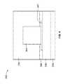
- FIG. 1illustrates a conformal electronics device, designated generally at 100 , which includes a substrate 110 , electronic circuitry 120 , and an encapsulation layer 130 .
- Conformal electronics device 100is configured to provide conformal sensing and/or monitoring capabilities.
- the device 100can provide mechanically transparent close contact with a surface (e.g., the skin or other portion of the body or the surface of an object) to improve measurement and/or analysis of physiological information of the body or other information associated with the at least one object.
- the substrate 110can, for example, be a soft, flexible, or otherwise stretchable substrate of non-conductive material that can conform to the contour of a surface on which the conformal electronics device 100 is disposed. Examples of such surfaces include, but are not limited to, a body part of a human or an animal or any other object.
- Suitable substrates 110 that can be used in the conformal electronics device 100include, for example, a polymer or a polymeric material. Non-limiting examples of applicable polymers or polymeric materials include, but are not limited to, a polyimide (PI), a polyethylene terephthalate (PET), a silicone, or a polyurethane.
- plasticsincluding a thermoplastic, a thermoset plastic, or a biodegradable plastic
- elastomersincluding a thermoplastic elastomer, a thermoset elastomer, or a biodegradable elastomer
- fabricsincluding a natural fabric or a synthetic fabric
- acrylatesacetal polymers, cellulosic polymers, fluoropolymers, nylons, polyacrylonitrile polymers, polyamide-imide polymers, polyarylates, polybenzimidazole, polybutylene, polycarbonate, polyesters, polyetherimide, polyethylene, polyethylene copolymers and modified polyethylenes, polyketones, poly(methyl methacrylate, polymethylpentene, polyphenylene oxides and polyphenylene sulfides, polyphthalamide, polypropylene, polyurethanes, styrenic resins, sulphone based resins,
- the substrate 110can be formed using any suitable process including, for example, casting, molding, stamping, or any other suitable process. Furthermore, the substrate 110 can include other features, for example, holes, protrusions, grooves, indents, non-conducting interconnects, or any other features. In some examples, grooves, which can act as seats for device islands or interconnects, can be formed on the substrate 110 .
- Electronic circuitry 120can be any suitable electronic circuitry that is operable, for example, to provide sensing, detecting, or otherwise quantifying at least one parameter associated with a subject or a surface (e.g., an animal or human body part or other object) on which the conformal electronics device 100 is disposed.
- the electronic circuitry 120is configured to measure, detect, sense, or otherwise quantify motion, muscle activity, temperature (e.g., body temperature), pulse, moisture, pressure, and the like.
- the electronic circuitry 120can include one or more sensor system(s), and one or more other component(s) (e.g., interconnects).
- the one or more sensor systems and one or more other component(s)are disposed on one or more device islands.
- the one or more device islandsare arranged in a spatial configuration based on the desired dimensions and conformability of the overall resulting conformal electronic devices.
- the one or more sensor systems included in the electronic circuitry 120can include at least one component to perform at least one sensor measurement.
- the at least one sensor measurementinclude an accelerometry measurement, a muscle activation measurement, a heart rate measurement, an electrical activity measurement, a temperature measurement, a hydration level measurement, a neural activity measurement, a conductance measurement, an environmental measurement, and/or a pressure measurement.
- the sensor systemscan include, one or more of an accelerometer (such as but not limited to a single-axis accelerometer or a 3-axis accelerometer), a gyroscope (such as but not limited to a 3-axis gyroscope), a nerve conduction study (NCS) component, an electromyography (EMG) component, an electroencephalogram (EEG) component, and/or an electrocardiogram (ECG) component.
- an accelerometersuch as but not limited to a single-axis accelerometer or a 3-axis accelerometer
- a gyroscopesuch as but not limited to a 3-axis gyroscope
- NCSnerve conduction study
- EMGelectromyography
- EEGelectroencephalogram
- ECGelectrocardiogram
- Non-limiting examples of other components that can be included in the electronic circuitry 120include at least one battery, a regulator, a processing unit, a memory (such as but not limited to a read-only memory, a flash memory, and/or a random-access memory), an input interface, an output interface, a communication module, a passive circuit component, an active circuit component, etc.
- the conformal electronics device 100comprises at least one microcontroller and/or other integrated circuit component.
- the electronic circuitry 120includes at least one coil, such as but not limited to a near-field communication (NFC) enabled coil.
- the electronic circuitry 120includes a radio-frequency identification (RFID) component.
- the electronic circuitry 120can include a dynamic NFC/RFID tag integrated circuit with a dual-interface, electrically erasable programmable memory (EEPROM).
- EEPROMelectrically erasable programmable memory
- the configuration of the device islandscan be determined based on, e.g., the type of components that are incorporated in the overall electronic circuitry 120 (including the sensor system), the intended dimensions of the overall conformal electronics device 100 , and the intended degree of conformability of the overall conformal electronics device 100 .
- the configuration of one or more device islandscan be determined based on the type of overall conformal electronics device 100 to be constructed.
- the overall conformal electronics device 100may be a wearable conformal electronics structure, or a passive or active electronic structure that is to be disposed in a flexible and/or stretchable object (including an inflatable or expandable surface of an interventional catheter).
- the configuration of the device island(s)can be determined based on the components to be used in an intended application of the overall conformal electronics device 100 .
- Example applicationsinclude a motion sensor, a temperature sensor, a neuro-sensor, a hydration sensor, a heart sensor, a flow sensor, a pressure sensor, an equipment monitor (e.g., smart equipment), a respiratory rhythm monitor, a skin conductance monitor, an electrical contact, or any combination thereof.
- One or more device islandscan be configured to include at least one multifunctional sensor, including a temperature, strain, and/or electrophysiological sensor, a combined motion-/heart/neuro-sensor, a combined heart-/temperature-sensor, etc.
- the encapsulation layer 130is disposed on at least a portion of the electronic circuitry 120 and at least a portion of the substrate 110 such that the encapsulation layer 130 envelops at least a portion of the electronic circuitry 120 .
- encapsulation layer 130is formed of a material that hermetically seals portions (e.g., surfaces) of the electronic circuitry 120 exposed by the substrate 110 .
- the encapsulation layer 130can act as an “encapsulation housing” by enveloping most or all of the conformal electronics device 100 .
- the encapsulation layer 130is disposed on the device islands and interconnects of the electronic circuitry 120 hermetically sealing the device islands and interconnects.
- the encapsulation layer 130can include holes, apertures, or otherwise openings such that one or more sensors included in the electronic circuitry 120 are exposed (e.g., to contact a skin or body part of an animal or human, or any other object).
- Hermetically sealing at least a portion of the electronic circuitry 120 by the encapsulation layer 130can help to protect the components of the electronic circuitry 120 from corrosive factors, including damage from corrosive chemicals, dust, moisture, oxidation, etc.
- Encapsulation layer 130 of FIG. 1can be formed from a soft, flexible, and non-conductive material.
- the encapsulation layer 130is formed from the same material as the substrate 110 .
- a different materialcan be used to form the encapsulation layer 130 .
- Suitable materials that can be used in the encapsulation layer 130include, for example, a polymer or a polymeric material.
- Non-limiting examples of applicable polymers or polymeric materialsinclude, but are not limited to, a polyimide (PI), a polyethylene terephthalate (PET), a silicone, or a polyurethane.
- plasticsincluding a thermoplastic, a thermoset plastic, or a biodegradable plastic
- elastomersincluding a thermoplastic elastomer, a thermoset elastomer, or a biodegradable elastomer
- fabricsincluding a natural fabric or a synthetic fabric
- acrylatesacetal polymers, cellulosic polymers, fluoropolymers, nylons, polyacrylonitrile polymers, polyimide-imide polymers, polyarylates, polybenzimidazole, polybutylene, polycarbonate, polyesters, polyetherimide, polyethylene, polyethylene copolymers and modified polyethylenes, polyketones, poly(methyl methacrylate, polymethylpentene, polyphenylene oxides and polyphenylene sulfides, polyphthalamide, polypropylene, polyurethanes, styrenic resins, sulphone based resins
- the encapsulation layer 130can be formed using any suitable process, for example, casting, molding, stamping, or any other known or hereinafter developed fabrication methods. Furthermore, the encapsulation layer 130 can include a variety of optional features, such as holes, protrusions, grooves, indents, non-conducting interconnects, or any other features. By way of non-limiting example, encapsulation layer 130 can be formed using an overmolding process. In general, overmolding allows for a previously fabricated part to be inserted into a mould cavity an injection molding machine that forms a new plastic part, section, or layer on or around the first part.
- One such overmolding processincludes directly casting a liquid material capable of forming the encapsulation layer 130 on the electronic circuitry 120 disposed on the substrate 110 .
- the liquid materialcan then be cured (e.g., cool and solidify). Curing can be performed under any suitable conditions, for example, by applying pressure on the casted liquid material, heating the substrate, and/or applying a vacuum.
- the electronic circuitry 120can be embedded in the encapsulation layer 130 using a lamination process.
- the encapsulation layer 130can be pre-casted into a sheet.
- a liquid adhesivee.g., the uncured liquid material used to form the encapsulation layer, or any other suitable adhesive
- the encapsulation layer 130can be then disposed on the adhesive and pressure applied to squeeze out excess adhesive.
- the adhesivecan then be cured to fixedly couple the encapsulation layer 130 to at least a portion of the electronic circuitry 120 and the substrate 130 , thereby forming conformal electronics device 100 of FIG. 1 .
- an adhesive materialcan be used during construction of encapsulated conformal electronic devices.
- the uncured liquid silicones used in the example lamination processcan act as a type of adhesive, and harden, e.g., via curing (through crosslinking) to bind surfaces.
- the electronic device componentsincluding the device islands and electrical interconnects, can be affixed to a pre-cured sheet using a pressure sensitive adhesive prior to overmolding.
- a non-limiting example of a pressure sensitive adhesiveis a rubber-based adhesive.
- a pressure sensitive silicone transfer adhesive or a liquid silicone adhesivecan be applied to the pre-cured sheet.
- Any adhesive described hereinmay be a sprayable or a brushable adhesive for application to a surface.
- An adhesivecan aid in holding the electronic components in a specified position and arrangement, including in an archipelago arrangement, relative to other components of the system, during a subsequent overmolding process.
- Adhesive materialscan be used as a part of the lamination process during construction of an example device herein.
- the electronic device componentsincluding the device islands and/or the interconnects, can be affixed to a pre-cured base layer silicone sheet using a pressure sensitive silicone adhesive prior to applying the top layer of silicone sheet, with an uncured liquid silicone used for lamination.
- the laminationcan also be completed using a pressure sensitive silicone adhesive to embed an ultrathin electronics device between silicone sheets.
- the laminationcan be based on use of a film adhesive that does not require a curing process.
- Encapsulation layer 130 and/or base substrate 110 of FIG. 1can be configured to facilitate modulation of a stress or a strain that might be caused in a portion of the conformal electronics device 100 , for example, due to stretching, bending, compressing, torsion, or other deformation.
- a concentration of stress and/or strainat a transition from a more rigid portion of a system (e.g., a device island) to a more compliant structure (e.g., a flexible and/or stretchable component) when the conformal electronics device 100 is subjected to a deformation.
- Other areas of stress concentrationcan include, for example, edges of interconnects, or boundaries where an interconnect is coupled to a device island.
- Encapsulation layer 130can be formed from a material that is configured to have a thickness and/or disposed locally on portions of the electronic circuitry 120 such as to minimize the stress on the components of the electronic circuitry 120 by adjusting the location of a neutral mechanical plane relative to a functional component of the electronic circuitry.
- the material used to form the encapsulation layer 130can be introduced locally in a region of a component of the electronic circuitry 120 , such as proximate to the portion of the component of the electronic circuitry 120 .
- the locally disposed encapsulation layerprotects the component from applied stresses/strains in the event of a deformation force being applied to the overall conformal electronics device 100 by adjusting the location of the neutral mechanical plane locally in the region of the component. Controlled placement of the neutral mechanical plane relative to a functional component can result in little to no stress or strain being exerted in the region of the component, when the conformal electronics device 100 is subjected to a deformation force.
- the encapsulation layer 130 and/or substrate 110can have an ultrathin thickness and have favorable mechanical and optical properties.
- the encapsulation layer 130can have a thickness in the range of about 0.05 mm to about 0.5 mm.
- the encapsulation layer 130 and/or the substrate 110can have an elongation in the range of about 200% to about 800% or, for some configurations, about 300%, about 400%, about 500%, about 600%, or about 700%, relative to the undeformed length of the encapsulation layer 130 /substrate 110 .
- the encapsulation layer 130 and/or the substrate 110have a tear strength of about 40 pounds per inch (ppi) to about 200 ppi or, for some configurations, about 60 ppi, about 80 ppi, about 100 ppi, about 120 ppi, about 140 ppi, about 160 ppi, or about 180 ppi.
- the encapsulation layer 130 and/or the substrate 110can have a hardness measured by a durometer of about 10 A (e.g., according to the Shore A Hardness Scale) to about 60 A to higher, for example, about 20 A, about 30 A, about 40 A, about 50 A or about 60 A.
- the encapsulation layer 130 and/or the substrate 110can have an optical transparency of greater than about 90% between wavelengths of light about 350 nm to about 1,000 nm.
- the total thickness of encapsulated conformal electronics device 100(e.g., at its thickest point) can be in the range of about 0.20 mm to about 1.0 mm.
- the encapsulation layer 130 and/or the substrate 110can be transparent. In other examples, the encapsulation layer 130 and/or the substrate 110 can be translucent or colored.
- a conformal electronic devicecan be encapsulated using a plurality of thin encapsulation layers.
- conformal electronics device 200 of FIG. 2includes, as some non-limiting examples, electronic circuitry 220 that is coupled to a substrate 210 .
- the substrate 210 and the electronic circuitry 220can be substantially similar to the substrate 110 and the electronic circuitry 120 , respectively, described with respect to the conformal electronics device 100 .
- the substrate 210 and the electronic circuitry 220can each take on any of the various forms, optional configurations, and functional alternatives described above with respect to the corresponding structure illustrated in FIG. 1 .
- Each encapsulation layer 230 a - dcan be an ultrathin layer, for example, having a thickness in the range of about 0.05 mm to about 0.5 mm.
- FIG. 2can be formed from any of the materials described above with respect to conformal electronics device 100 of FIG. 1 . While shown as having four encapsulation layers 230 a - d , any number of encapsulation layers can be used to encapsulate the device 200 . Moreover, while FIG. 2 shows each of the encapsulation layers covering the entire width of the device 200 , in some examples, one or more of the various encapsulation layers 230 a - d can be disposed on only a portion of the electronic circuitry 220 and/or the substrate 210 .
- one or more of the plurality of encapsulation layers 230 a - dcan be disposed in proximity to an area of stress/strain concentration (e.g., a device island or edges of interconnects), thereby adjusting the location of a neutral mechanical plane relative to a functional component of the electronic circuitry.
- an area of stress/strain concentratione.g., a device island or edges of interconnects
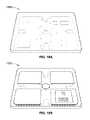
- FIGS. 3A and 3Bshow the mechanical layout and system-level architecture of an example conformal electronics device, designated 300 , configured as a rechargeable patch.
- the example conformal sensor system electronics technologycan be designed and implemented with various mechanical and electrical layouts for single-function and multifunctional platforms.
- Devices including the conformal electronics technologyintegrate stretchable form factors using designs embedded in polymeric layers. These can be formulated to protect the circuits from strain and to achieve mechanical flexibility in an ultra-thin cross-section.
- the devicecan be configured with thicknesses on the order of about 1 mm on average.
- the patchcan be configured with thinner or thicker cross-sectional dimensions.
- the device architecturecan include a reusable module containing surface-mount technology (SMT) components, including as some non-limiting examples, a sensor module 302 (e.g., a triaxial accelerometer), a wireless communication (e.g., Bluetooth®) and microcontroller (MCU) module 304 , and conformal electrode array modules 312 and 314 for sensing, e.g., EMG, EEG and EKG signals, with electrode connectors 313 .
- the conformal electrode arrayscan be disposable 310 and 312 .
- the example devicecan also include a power supply 316 (such as a LiPo Battery of power 2 mA-Hr or 10 mA-Hr), a regulator 318 , a power transfer coil 320 (such as but not limited to a 0.125 oz Cu coil with 1.5/2 mil trace/space ratio), and a memory 322 .
- a power supply 316such as a LiPo Battery of power 2 mA-Hr or 10 mA-Hr
- a regulator 318such as a LiPo Battery of power 2 mA-Hr or 10 mA-Hr
- a power transfer coil 320such as but not limited to a 0.125 oz Cu coil with 1.5/2 mil trace/space ratio
- a memory 322such as but not limited to a 0.125 oz Cu coil with 1.5/2 mil trace/space ratio
- the components of the example conformal sensor system 300are configured as device islands interconnected by stretchable interconnects 328 .
- Stretchable interconnects 328can be electrically conductive to facilitate electrical communication between the components, or electrically non-conductive to assist in maintaining a desired overall form factor or relative aspect ratio of the overall conformation of the conformal sensor device during or after being subjected to deformation forces, such as but not limited to extension, compressive and/or torsional forces.
- the example of FIG. 3also shows the differing shapes and aspect ratios of the island bases 326 that the components of the example conformal sensor system can be disposed on, or otherwise coupled to, to provide the to provide the necessary functionality of the overall system.
- Conformal electronics device 300 of FIGS. 3A and 3Bcomprises a flexible substrate 310 , such as flexible substrates 110 and 210 of FIGS. 1 and 2 , respectively, to which is coupled the electronic circuitry.
- Substrate 310 and electronic circuitryare at least partially encapsulated by a flexible encapsulating layer 330 .
- Electronic circuitry included in the conformal electronics device 300includes a plurality of device islands (ten of which are shown in the drawing, two of which are designated at 326 ) that are electronically coupled together via serpentine interconnects 328 .
- a plurality of contactsmay be disposed at either or each end of the conformal electronics device 300 .
- the conformal electronic devicedoes not include such contacts.
- the device islandscan include any number of interconnects and any number of components as described with respect to conformal electronics device 100 or any other conformal electronic devices described herein.
- FIG. 4shows a cross-section of a portion of the conformal electronics device 300 taken along line 4 - 4 in FIG. 3A .
- the device 300includes a substrate 310 providing subjacent support for a base plate 340 disposed on the substrate 310 .
- Substrate 310can be formed from, for example, RTV silicone or any other suitable substrate material described herein.
- the substrate 310can have a thickness of about 200 ⁇ m.
- the base platecan be formed from polyimide and, optionally, can have a thickness of about 50 ⁇ m.
- One or more electrical contacts 342are disposed on the base plate 310 and coupled to the electronic component 344 .
- the electronic component 344can be any component described with respect to the conformal electronics device 100 , or any other electronic components described herein.
- the electronic component 344has a thickness of about 500 ⁇ m.
- the electrical contact(s) 342can be formed from any suitable electrically conductive material, such as copper. Electrical contact(s) 342 can have a thickness of about 0.5 ⁇ m. Select (upper and side) portions of the electrical contact 342 not coupled with the electronic component 344 are covered with an insulating layer 346 .
- An encapsulation layer 330is disposed on the substrate 310 such that the encapsulation layer completely encapsulates the entire conformal electronic device 300 (or substantially all of the device).
- the encapsulation layer 330can be formed from RTV silicone or any other encapsulation material described herein.
- the conformal electronic device 300is shown and described as having certain components, the conformal electronics device 300 can include any of the other components described herein which can be configured to perform any suitable function as described herein.
- the encapsulating layer 330is configured to define an ultrathin thickness such that the thickness of the encapsulation layer 330 , as measured from a distal end of the electronic component, is approximately 200 ⁇ m.
- the conformal electronic deviceshave an ultrathin profile, e.g., having a maximum thickness at its thickest point of less than about 2 mm or, in some embodiments, less than about 1 mm.
- the encapsulating layer 330can be disposed locally over, or proximate to, a portion of the base plate 340 , electronic component 344 , and/or an interconnect 328 .
- the encapsulating layercan be disposed over, or proximate to, portions of the overall conformal electronic device 300 device structure, including one or more electronic components, base plates, and/or interconnects.
- An encapsulation materialcan be introduced locally in a region of a portion of a component of the conformal electronic device 300 , such as proximate to the portion of the component, to protect the component from an applied stress or strain in the event of a deformation force being applied to the overall conformal device.
- the encapsulation materialcan aid in adjusting a location of a neutral mechanical plane locally in the region of the component. Controlled placement of the neutral mechanical plane relative to a functional component can result in cause little to no stress or strain being exerted in the region of the component, when the overall conformal electronic device 300 is subjected to the deformation force.
- base plate stiffnesscan result in the interconnect coupled to the base plate being subjected to a greater amount of plastic strain on deformation, e.g., a stretching.
- a base plate formed from a polyimide (PI) or a polyethylene terephthalate (PET)can have a value of modulus of about 6.894 MPa and a C10 (a hyper-elasticity material constant) of about is 0.925 MPa.
- the dimensions of, and/or stiffness of the material of, the base platecan be considered, in conjunction with the stiffness properties and/or placement of the encapsulant material, can be controlled to strategically to urge the neutral mechanical plane to fall in a region of the overall conformal device to prevent such a strain concentration near the passive component and/or the interconnects.
- each methodincludes at least those steps enumerated in its respective figure. It is also within the scope and spirit of the present disclosure to omit steps from each method, include additional steps in each method, and/or modify the order presented. It should be further noted that each of the foregoing methods can be representative of a single sequence of related steps; however, it is expected that each of these method will be practiced in a systematic and repetitive manner.
- FIG. 5presents a flow diagram showing an exemplary method 400 for encapsulating a conformal electronic device, such as the conformal electronics device 100 and 200 of FIGS. 1 and 2 , or any other conformal electronic device described herein, using overmolding.
- the method 400begins at Block 402 with disposing a substrate material into a first mold.
- the substrate materialcan include, for example, any of the materials used to form the substrate 110 , substrate 210 , or any other substrate described herein.
- the first moldcan be cleaned using any suitable process.
- a release layersuch as wax, oil, soapy water, or any other suitable release layer, is disposed on the first mold before adding the substrate material.
- the release layercan allow for easy removal of the substrate from the first mold after curing.
- the substrate materialis cured to form a soft and flexible substrate.
- Any suitable curing processcan be used.
- a positive pressurecan be applied on the first mold, the first mold can be heated to a predetermined temperature, and/or a vacuum can be applied on the first mold.
- Electronic circuitryis next disposed on the cured substrate at Block 406 .
- the electronic circuitrycan include, for example, the electronic circuitry 120 , electronic circuitry 220 , or any other electronic circuitry described herein, including those identified in FIG. 3A .
- An encapsulation materialis disposed in a second mold at Block 408 of the method 400 in FIG. 5 .
- the encapsulation materialcan include, for example, the materials used for forming the encapsulation layer 130 , encapsulation layer 230 , or any other encapsulation materials described herein.
- a release layersuch as wax, oil, soapy water, or any other suitable release layer, is disposed on the second mold before adding the encapsulation material. The release layer allows for easy removal of the encapsulation material from the second mold after curing.
- Block 410includes positioning the first mold, which includes the substrate and the electronic circuitry disposed on the substrate, in an inverted position (e.g., upside down) on the second mold.
- the first mold and the second moldare then cured to form the encapsulated conformal electronic device at Block 412 .
- Any suitable curing processcan be used. For instance, a positive pressure can be applied on the first mold and the second mold, the first mold and the second mold can be heated to a predetermined temperature, and/or a vacuum can be applied on the first mold and the second mold. After curing, the encapsulated conformal electronic device can be removed from the first mold and the second mold at Block 414 .
- FIG. 6is a flow diagram showing an exemplary method 500 for encapsulating conformal electronic devices, such as the conformal electronics device 100 , 200 , or any other conformal electronic device described herein, using lamination.
- the method 500 of FIG. 6begins at Block 502 with cutting a fully cured sheet of a stretchable material to a predetermined size to form a substrate.
- the stretchable materialcan include any of the materials described with respect to the substrate 110 , substrate 210 , or any other stretchable materials described herein.
- An uncured lamination materialis then disposed on the stretchable material at Block 504 .
- the lamination materialcan include any suitable material, for example, the stretchable material used to form the substrate described herein. In some examples, the lamination material can include the material used to form an encapsulation layer.
- electronic circuitryis disposed on the uncured lamination material.
- the electronic circuitrycan include the electronic circuitry 120 , electronic circuitry 220 , or any other electronic circuitry described herein. Excess amounts of the uncured lamination material is then disposed on the electronic circuitry, e.g., at Block 508 , such that the electronic circuitry is completely covered with the lamination material.
- a sheet of a fully cured encapsulating materiali.e., the encapsulation layer
- the encapsulation layercan be formed from any of the encapsulation materials described with reference to the encapsulation layer 130 , or any other encapsulation materials described herein.
- Pressurecan be applied on the encapsulation layer to remove excess lamination material.
- the encapsulation materialis then cured to form the encapsulated conformal electronic device at Block 512 .
- Any suitable curing processcan be used.
- a positive pressure, heat or a vacuumcan be used to cure the lamination material. Curing the lamination layer couples together the substrate sheet, the electronic circuitry, and the encapsulation sheet to form the encapsulated conformal electronic device.
- a conformal electronic devicehereinafter “Ex 1 Device”—which includes moisture sensors is encapsulated using an overmolding process.
- the Ex 1 Deviceis encapsulated to have a final thickness of about 6 mm for higher thickness measurements, or a final thickness of about 2 mm for water-proof capability measurements.
- the plate surfaces shown in FIGS. 7A, 7C and 7Eare used to form a cap for an opening for a connector on a portion of the Ex 1 Device for the higher thickness measurements, while the plates shown in FIGS.
- 7B, 7D and 7Fare used to form an encapsulation layer for a water-proof capability measurement.
- a Model 44-226 25-Ton 5′′-Stroke Self-leveling laboratory Hydraulic Press available from the Dake Corporationcan be used for the foregoing molding processes.
- Two different encapsulation materialscan be used for the higher thickness measurement and the water-proof capability measurement.
- ECOFLEX® from SMOOTH-ONTMcan be used to form the encapsulation layer.
- Bluestar SILBIONE® RTV4545 siliconecan be used to form the encapsulation layer.
- Suitable materialse.g., Bluestar SILBIONE® LSR4325
- suitable materialse.g., Bluestar SILBIONE® LSR4325
- Example primers that can be usedare MED-142 and MED-166 from Nusil Silicone Technology. These primers can substantially increase the adhesion of the encapsulation material to a surface on which the primer is applied.
- the precursors of encapsulation materialare mixed according to the manufacturer's instructions, degassed under vacuum, and stored at approximately 4 degrees Celsius prior to use.
- the molding plates 701 - 703can be sprayed with a cleaning fluid, such as dilute soapy water or alcohol, for easy release of the molded layers.
- the mixed encapsulating materialis then poured into the molding cavities 710 of plate 702 .
- Plate 701is disposed on plate 702 to form a first closed mold assembly, and the assembly is disposed in the press for approximately 30 minutes at about 20,000 psi of pressure and a temperature of about 110 degrees Fahrenheit. After 30 minutes, the assembly is removed from the press. Plate 701 is removed leaving a first sheet of encapsulation material disposed on Plate 702 . The first sheet is used as a substrate for the Ex 1 Device. Excess flash of the encapsulation material is cleaned.
- the Ex 1 Device that includes the moisture sensorsis cleaned with alcohol. Primer is applied on the electronic circuitry and is allowed to dry for approximately 30 minutes. The cleaned Ex 1 Device is then disposed on the substrate. The mixed encapsulating material is poured into the molding cavities 712 of Plate 703 . Plate 702 is then carefully and slowly placed on top of Plate 703 such as to allow trapped air to exit and to form a second closed mold assembly. The second assembly is placed in the press and maintained for about 30 minutes at a pressure of about 20,000 psi and a temperature of about 110 degrees Fahrenheit to form the encapsulated Ex 1 Device.
- much lower pressurescan be used, including assembly at near atmospheric pressure, e.g., when there is a potential that using a higher pressure could damage any of the electronic device components of the structure.
- Using a low pressure encapsulation process during overmolding and laminationcan achieve high yield.
- temperatures other than about 110 degrees Fahrenheitcan be used to form the encapsulation layer of an example device. The encapsulated device is removed from the mold and excess material removed.
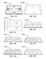
- FIGS. 8A-8Dare perspective-view illustrations of various encapsulated conformal electronics devices in accord with aspects of the present disclosure.
- FIGS. 8A and 8Bshow a top view and a bottom view, respectively, of a first example of the Ex 1 Device, designated generally at 800 A, encapsulated for higher thickness measurements.
- the overall thickness of Ex 1 Device 800 A, as shown,is approximately 5.85 mm.
- the encapsulation layeris smooth, soft and defect free.
- FIGS. 8C and 8Din contrast, show a top view and a bottom view, respectively, of a second example of the Ex 1 Device, designated generally at 800 B, encapsulated for water-proof capability measurements.
- the overall thickness of the device 800 Bis approximately 2.2 mm and the thinnest layer is about 0.21 mm. Defects, such as tears and delaminated sections, may appear on the edges and/or the bottom side of the encapsulated device where the encapsulation layer is thinner.
- An overmolding processis used to encapsulate a conformal electronic device-hereinafter “Ex 2 Device”—that includes device islands and interconnects.
- the Ex 2 Devicefor at least some embodiments, is similar or substantially identical to the conformal electronics device 200 and/or 300 described with respect to FIGS. 2 and 3A -B, and thus can include any of the corresponding options and features discussed with reference thereto.
- the Ex 2 Deviceis then encapsulated using substantially the same overmolding process used to encapsulate the Ex 1 Device.
- the encapsulation material usedis Bluestar SILBIONE® RTV4545. In other examples, alternative encapsulation materials can be used in forming the Ex 2 Device.
- the encapsulated Ex 2 Devicehas a total thickness of about 1 mm.
- FIGS. 9A and 9Bshow the top and the bottom of a representative embodiment 900 of the encapsulated Ex 2 Device. Some air bubbles may be visible in the encapsulation layer and some delamination may occur at or proximate to the device islands without denigrating the functionality of the Ex 2 Device.
- a lamination processis used to encapsulate a moisture-sensing conformal electronic device—hereinafter “Ex 3 Device.”
- the Ex 3 Devicein at least some embodiments, is similar or substantially identical to the Ex 1 Device, and thus can include any of the corresponding options and features discussed with reference thereto.
- the Ex 3 Deviceis encapsulated to have a thickness of about 1.0 mm to about 1.5 mm for water-proof and reliability measurements.
- the surfaces of the unencapsulated Ex 3 Deviceare cleaned, in this example, using a DOW CORNING® OS20TM cleaning fluid or other suitable cleaning material, and then allowed to dry.
- a DOW CORNING® OS20TM cleaning fluid or other suitable cleaning materialAs a non-limiting example, the surfaces of the Ex 3 Device are coated with a thin layer of DOW CORNING 1200® OSTM primer using a lint-free towel and allowed to cure in ambient air for at least about 1 hour.
- the adhesive material usedcan be a two part (part A and B) liquid silicone, such as SORTA-CLEAR 18® (SMOOTH-ONTM), or any other equivalent polymer having medium viscosity can also be used.
- the part A precursor and the part B precursor of the liquid siliconeare mixed together, for example, in a ratio of about 10:1, degassed under vacuum and stored at a temperature of about 4 degrees Celsius prior to use.
- Silicone rubber sheetse.g., Rogers Corp, HT-6240 having a thickness of about 0.25 mm, or GELPAK® PF-60-x4 having a thickness of about 0.15 mm
- One side of the liner of the silicone rubber sheetsis removed.
- a thin layer of liquid siliconeis disposed on a first silicone rubber sheet using a brush. The first silicone sheet is used as the base layer.
- the Ex 3 Deviceis disposed on the first sheet and an excess amount of liquid silicone is deposited on the Ex 3 Device.
- a second sheet of siliconeis disposed over the Ex 3 Device and the first sheet of silicone, such that the Ex 3 Device is sandwiched or laminated between two sheets of silicone. Pressure can be applied using a roller to remove excess liquid silicone.
- the laminated Ex 3 Deviceis cured for at least about 5 hours while maintained at a pressure of about 20-30 pounds. In this example, the curing is continued for about 24 hours to fully cure the liquid silicone. In another example, the curing process can be accelerated to 5 minutes at ambient temperature by using a fast cure silicone such as but not limited to ECOFLEX® 5.
- the encapsulated Ex 3 Devicecan be cut into individual sample patches using a scalper. FIGS.
- 10A and 10Bshow the top and the bottom, respectively, of a representative embodiment 1000 the encapsulated Ex 3 Device.
- the thickness of the illustrated Ex 3 Device, at various locations,can range from about 0.33 mm to about 2.13 mm when the 0.15 mm thick silicone sheets are used, or range from about 0.6 mm to about 2.33 mm when the 0.25 mm thick silicone sheets are used.
- Ex 4 DeviceAnother representative conformal electronic device—referred to hereinafter as “Ex 4 Device”—is encapsulated using a lamination process.
- Ex 4 Deviceincludes embedded Near Field Communication (NFC) microchips.
- the liquid silicone used for the lamination procedureis Bluestar SILBIONE® RTV4545 which has low viscosity.
- the Ex 4 Deviceis encapsulated using substantially the same lamination procedure as the Ex 3 Device.
- FIGS. 9A and 9Bcan therefore be representative of the top and bottom, respectively, of the encapsulated Ex 4 Device.
- the thickness of the Ex 4 Device at various locationsis less than about 0.7 mm when the 0.15 mm thick silicone sheets are used, and is thickness is less than about 1 mm when the 0.25 mm thick silicone sheets are used.
- Ex 5 Deviceyet another conformal electronic device—referred to hereinafter as “Ex 5 Device”—is encapsulated using a lamination process.
- the Ex 5 Deviceis similar or substantially identical to the Ex 2 Device described herein, and thus can include any of the corresponding options and features discussed with reference thereto.
- the liquid silicone used for the lamination procedureis Bluestar SILBIONE® RTV4545, which has low viscosity.
- the Ex 5 Deviceis encapsulated using substantially the same lamination procedure as the Ex 3 Device discussed hereinabove.
- the silicone sheets used for encapsulatingare transparent, colored or translucent.
- FIGS. 11 and 11Bshow a top view and a bottom view, respectively, of a first representative embodiment 1100 A of the Ex 5 device that is encapsulated with transparent translucent (or substantially transparent) silicone sheets.
- FIGS. 11E and 11Fshow a top view and a bottom view, respectively, of a third representative embodiment 1100 C of the Ex 5 device that is encapsulated with colored silicone sheets.
- the Ex 5 device arrangements presented in FIGS. 11C to 11Hhave archipelago structures (e.g., a chain of IC device islands) that are encapsulated using transparent, translucent, or colored silicone sheets.
- the thicknesses of the encapsulated Ex 5 Devices 1100 A, 1100 B, 1100 C and 1100 D of FIGS. 11A-11His less than about 0.20 mm, e.g., when encapsulated with 0.076 mm thick silicone sheets, and less than about 0.70 mm, e.g., when encapsulated with 0.25 mm thick silicone sheets.
- the moisture sensing devicesnamely Ex 1 and Ex 3 Devices, which include functional RFID chips and are formed using overmolding and lamination methods, respectively, are subjected to a water-proof measurement.
- Three (3) Ex 1 Devices and six (6) Ex 3 Devices(three each of 0.15 mm laminated devices and 0.25 mm laminated devices) are immersed in tap water and 0.7 ⁇ PBS solution and cycled between a temperature of about 37 degrees Celsius and about 50 degrees Celsius sequentially for 28 days with a periodic change of measurement condition about every 7 days.
- the immersion depthis in the range of about 15-20 cm and devices are immersed continuously for about 28 days with a replacement of the bath solution every 7 days.
- the devicescan measured periodically with an RFID reader, e.g., once every hour, to monitor the viability of the devices.
- the devicesremain functional at the end of the measurement period. Visual inspection of each device does not reveal any noticeable signs of damage or penetration of the liquid into the encapsulated devices. Following the water-proof measurement, all the devices are re-tested per an Ingress Protection (IP) Rating procedure.
- IP rating procedureprovides a standardized method of evaluating the environmental capability of a device or product. Briefly, all the devices are immersed in water to a depth of about 1 meter for about 30 minutes (in an IP7 procedure that requires full immersion to 1 meter for 30 minutes). Visual inspection does not reveal any noticeable changes for overmolded and 0.25 mm silicone sheet laminated devices. Some delamination can develop on the 0.15 mm silicone sheet laminated devices. The devices pass the IP7 rating test.
- FIGS. 12A-12Dshow examples of the use of fabrics for strain limiting, strength reinforcement, and aesthetics effect in encapsulated conformal electronics devices.
- the electronic structuresinclude device islands and electronic components that are interconnected using stretchable electrical interconnects.
- the electronic structuresare disposed on a material that can have different colors for differing aesthetic effect.
- the material that forms a portion of the base of the conformal electronics device 1200 A of FIG. 12Ais yellow in color, giving a yellow appearance to the example system.
- the material that forms a portion of the base of the conformal electronics device 1200 Bis green in color, giving a green appearance to the example system.
- FIG. 12Bthe material that forms a portion of the base of the conformal electronics device 1200 B is green in color, giving a green appearance to the example system.
- the material that forms a portion of the base of the conformal electronics device 1200 Cis light grey in color, giving a light grey appearance to the example system.
- FIG. 12Dthere is shown the opposite side of the example system of FIG. 12B , showing the green-colored material that is included to form the base of the example system.
- any of the disclosed encapsulated conformal electronics device architecturescan be provided with one or more FPCBA strain limiters that: (1) limit strain in a single direction (e.g., a uniaxial or unidirectional strain limiter), (2) limit strain in multiple directions (e.g., a multi-axial or multidirectional strain limiter), (3) limit only stretching, (4) limit only bending, (5) limit only torsion, or (6) limits only stretching and bending, only stretching and torsion, or only bending and torsion.
- the strain limiteris configured to readily stretch within the product's predetermine “design window” (e.g., within 0-85% of stretchability range to failure).
- the strain limitermay then be configured to immediately increase strain limiting at or near the product's predetermined “design limit” (e.g., within last 15% of stretchability range to failure). It is desirable, for at least some configurations, to maintain stretch limiting up to the ultimate force rating for the limiter/product.
- design limite.g., within last 15% of stretchability range to failure. It is desirable, for at least some configurations, to maintain stretch limiting up to the ultimate force rating for the limiter/product.
- an encapsulated conformal electronics patchcan begin to experience plastic deformation at approximately 20% global elongation on a one time basis; strain limiter in this example is designed to fully limit stretch at 15% global elongation.
- the limiterprevents or eliminates fully creasing the patch over on itself.
- tensile strengthis greater than approximately 5 lbf; maximum elongation before full tension is less than approximately 15%; minimize force to stretch to 15% elongation when encapsulated.
- FIGS. 13A-13Cthere is shown a “waffle” type flexible printed circuit board assembly (FPCBA) housing 1300 for encapsulating therein conformal electronics.
- the resultant encapsulated conformal electronics device with the FPCBA housing 1300can be fabricated from a hybrid molding and lamination process, such as that described below with reference to FIG. 14 , using a liquid silicone material.
- the illustrated waffle design FPCBA housing 1300results in a ⁇ 23% reduction in force to stretch over comparable non-waffle designs (e.g., planar designs). It has been determined that the force to stretch ratio can be modulated by configuring a flexible material with a selected durometer rating.
- a 50% reduction in silicone durometerresults in a ⁇ 50% reduction in force to stretch in the FPCBA housing 1300 .
- the waffle design shown in FIGS. 13-13Chelps to support stretchable interconnects with smaller cross-sections by limiting the type and amount of deformation that the assembly can experience.
- FPCBA housing 1300comprises a plurality of compartments, namely first, second, third and fourth partially hollow, vaulted compartments 1302 - 1305 , that are spaced longitudinally along the length of the housing. Each said compartment 1302 - 1305 nests therein one or more IC device islands or other electronic module.
- a recessed perimeter 1306surrounds the first three compartments 1302 - 1304 such that recessed gaps 1307 - 1309 ( FIG. 13C ) separate the four compartment 1302 - 1305 .
- the waffle geometryallows designers to localize deformation at preferred locations and thereby restrict the deformation that can be experienced by the waffle design FPCBA housing 1300 .
- the design in FIGS. 13A-13Cgenerally restricts deformation to longitudinal stretching (i.e., elongation of the housing 1300 along the major central axis A L ), longitudinal torsion (i.e., twisting about the major central axis), and transverse bending (i.e., flexure around a central transverse axis A T ).
- the vaulted compartmentscan be reconfigured (e.g., reshaped, reoriented and/or repositioned) such that deformation is limited to stretching along a lateral (minor) axis and bending along a longitudinal (major) axis.
- This designalso helps to reduces perceptibility of the conformal device on a user by reducing elastic force that restore the assembly to a planar nature.
- the waffle design FPCBA housing 1300has a length L of approximately 66 mm, a major width W of approximately 34 mm at its widest point, and a minor width of approximately 31 mm at its narrowest point (e.g., center in FIG. 3B ).
- Waffle design FPCBA housing 1300has a first (largest) thickness T 1 of approximately 3.14 mm defined by the fourth compartment 1305 , a second (medium) thickness T 2 of approximately 2.64 mm defined by the first, second and third compartments 1302 - 1304 , and a third (smallest) thickness T 3 of approximately 1.22 mm defined by the recessed perimeter 1306 .
- the housing 1300be fabricated from a material that is soft enough to conform to the body of a human, that is comfortable for continuous wear over an extended period of time, that is biocompatible and hypoallergenic, and/or is rugged enough to not tear or allow damage to the internal electronics.
- FIG. 14is a flow chart diagrammatically illustrating a representative method 1400 for encapsulating a conformal electronic device with a hybrid injection molding-lamination process.
- the method 1400includes at least those steps enumerated in FIG. 14 . Nevertheless, the method 1400 may omit some of the illustrated steps, include additional steps, and/or modify the order presented.
- the method 1400starts with liquid injection molding (LIM) of a liquid silicone resin (LSR) top sheet, e.g., from Bluestar SILBIONE® LSR4325.
- Block 1402comprises inspecting the LSR top sheet (#1 LSR).
- the LSR top sheetmay be inspected manually or via automated sampling or by other known or hereinafter developed methods of robotic high-speed vision inspection of IC componentry. Such inspection of parts may be conducted in accordance with quality acceptance specifications developed for engineering review by the manufacturer.
- Block 1403which is shown with dashed lines in FIG. 14 as it is not desirable for some embodiments, comprises an isopropyl alcohol (IPA) clean of the bonding surfaces of the LSR top sheet.
- IPAisopropyl alcohol
- the LSR top sheetis placed, e.g., on a clean TEXWIPE®, with the bonding side up, then IPA is sprayed liberally across the surfaces with the excess being removed, for example, using a cleanroom all-purpose 4 ⁇ 4 cotton TEXWIPE®. Cleaned LSR parts are then placed onto a tray to dry, e.g., for at least 5 minutes. Then, at Block 1404 , the bonding surfaces of the LSR bottom sheet are O2 plasma cleaned.
- IPAisopropyl alcohol
- Plasma cleaningmay comprise positioning an O2 Plasma Pen at least 10 mm but no more than 20 mm away from each part, applying plasma to the surface in a sweeping motion while trying to ensure all of the surfaces see plasma. Batch plasma cleaning of the bonding surfaces of the LSR parts can be automated or manual.
- the LSR top sheetis placed into an assembly fixture at Block 1405 .
- the LSR top sheet(LSR #1) is placed into the bottom assembly fixture while ensuring that the LSR component is centered properly and flush with the aluminum assembly fixture.
- Thismay comprise robotic or operator placement of the LSR top sheet into a multi-cavity assembly fixture.
- the first shot of adhesiveis dispensed into the top sheet cavities.
- Thismay comprise automated or manual dispensing of an adhesive (shot #1) using a pneumatic adhesive dispenser to apply adhesive (e.g., DOW CORNING® 3140 room temperature vulcanization (RTV) silicone adhesive coating) to the LSR part (e.g., into the top sheet cavities).
- adhesivee.g., DOW CORNING® 3140 room temperature vulcanization (RTV) silicone adhesive coating
- a lot paper traveleris started to receive incoming flexible printed circuit board assemblies (FPCBA), with the incoming FPCBA boards being shipped to LSR and received in trays with lids and foam inserts.
- Incoming FPCBA'scan be inspected manually or via an automated sampling device at Block 1407 , e.g., to ensure that all parts have been shipped and received without being bent or grossly damaged. This may include confirming that all of the FPCBA islands are symmetrically separated without being improperly stretched, compressed or bent.
- Block 1408which is shown with dashed lines in FIG. 14 as it is not desirable for some embodiments, comprises an isopropyl alcohol (IPA) clean of top and bottom surfaces of the FPCBA.
- IPAisopropyl alcohol
- Block 1408the FPCBA is placed on a clean TEXWIPE® with the die side up. IPA is sprayed across the surface with the excess being removed, for example, using a foam brush. The FPCBA is then flipped over and IPA is sprayed onto the back side with any excess IPA being removed, e.g., using a 4 ⁇ 4 TEXWIPE®. Cleaned FPCBA is placed onto a tray to dry, e.g., for at least 5 minutes. Next, at Block 1409 , both sides of the FPCBA are O2 plasma cleaned.
- Plasma clean both sides of the FPCBAe.g., with an O2 Plasma Pen positioned at least 10 mm but no more than 20 mm away, applying plasma to the surface in a sweeping motion while trying to ensure all surfaces are exposed to plasma.
- the FPCBAis subsequently flipped over and the plasma clean is repeated for the obverse side. Batch plasma cleaning of the FPCBA surfaces can be automated or manual.
- the cleaned FPCBAis placed into the assembly fixture.
- the FPCBAis placed board face down into the top assembly fixture while ensuring it is properly centered.
- Automated or operator placement of the FPCBA on top of the adhesive in the multi-cavity assembly fixtureis an available option.
- gentle pressureis applied, e.g., using a cotton swab, until adhesive starts to squeeze out at the edges from between the FPCBA and LSR top sheet.
- the second shot of adhesiveis dispensed into the assembly fixture. This may comprise automated or manual dispensing of an adhesive (shot #2) using the pneumatic adhesive dispenser to apply the adhesive (DOW CORNING® 3140 ) to the backside of the FPCBA.
- the method 1400 of FIG. 14continues with liquid injection molding (LIM) of a liquid silicone resin (LSR) bottom sheet, e.g., from Bluestar SILBIONE® LSR4325.
- LIMliquid injection molding
- Block 1413comprises inspecting the LSR bottom sheet (#2 LSR). This step may be performed in the same or a similar manner to that explicated above with respect to Block 1402 .
- an isopropyl alcohol (IPA) clean of the bonding surfaces of the LSR bottom sheetmay optionally be performed, as indicated at Block 1414 .
- the bonding surfaces of the LSR bottom sheetare O2 plasma cleaned.
- Blocks 1403 and 1404for performing the steps presented at Blocks 1414 and 1415 , respectively.
- the LSR bottom sheetis placed into an assembly fixture and locked into place at Block 1416 .
- Thismay comprise robotic or operator placement of the LSR bottom sheet into the assembly fixture.
- external LSR mating featuressuch as complementary posts and slots in the now-opposing LSR parts
- the #2 LSR partis placed onto the FPCBA assembly. The posts are pushed into place while ensuring that all posts and holes have mated properly.
- the multi-cavity assembly fixtureis fed, pulled, or otherwise transported through a roll laminator.
- An optional protective laminant sheetcan be placed over the assembly fixture for this portion of the method 1400 .
- Block 1417may comprise adjusting roller height on opposing lateral sides to ensure that the roller is set at a desired/predetermined height.
- Roller speedcan be set to a slow speed or the slowest available speed prior to initiating the lamination process.
- the assembly fixturecan be passed through the roll laminator for a single pass or for multiple passes. For a representative multi-pass scenario, which may be fully or partially automated, the first run is initiated, e.g., with the fixture fed through the rollers in a first orientation.
- the fixtureis repositioned and then fed through the rollers again.
- the roller heightmay be readjusted.
- a third runmay be performed by first repositioning and tightening the roller height, repositioning the fixture, and then feeding the fixture through the rollers.
- One or more additional passesmay be performed as necessary or desired.
- Method 1400 of FIG. 14continues to Block 1418 where the assembled stack is removed from the fixture and set aside to cure. This may comprise peeling off or otherwise removing the laminant sheet from the assembled stack, and placing the assembled stack on curing trays. In the event that excess adhesive is present (e.g., has squeezed out onto the backside of the stack), any overflow adhesive can be cut away and removed from the assembled stack. The assembled part is then gently placed onto a designated drying tray and left on a shelf, e.g., for at least approximately 24 hours. Block 1419 then requires die cutting, with a final inspection at Block 1420 .
- One or more of the moldscan be provided with overflow channels such that, during lamination, excess adhesive can “squish out” or otherwise flow beyond the cavity of the functional part and into a scrap area on the periphery that can be cut/removed after assembly and cure.
- overflow channelshelp to reduce the need to be extremely precise with the amount of adhesive added to the mold before insertion into a press. It has been determined that lower modulus glues can act as a buffer between the liquid silicone rubber (LSR) and the electronic components. It has also been determined that layered modulus structures affect reliability, deformability and feel of the device. Features in the molded silicone can be provided to capture the board and make sure it is in a relaxed/stress neutral state during and after assembly.
- embodiments of the inventionmay be implemented in any of numerous ways. For example, some embodiments may be implemented using hardware, software or a combination thereof.
- the software codemay be executed on any suitable processor or collection of processors, whether provided in a single device or computer or distributed among multiple devices/computers.
- the technology described hereinmay be embodied as a method, of which at least one example has been provided. The acts performed as part of the method may be ordered in any suitable way. Accordingly, embodiments may be constructed in which acts are performed in an order different than illustrated, which may include performing some acts simultaneously, even though shown as sequential acts in illustrative embodiments.
Landscapes
- Engineering & Computer Science (AREA)
- Microelectronics & Electronic Packaging (AREA)
- Physics & Mathematics (AREA)
- Computer Hardware Design (AREA)
- Power Engineering (AREA)
- Condensed Matter Physics & Semiconductors (AREA)
- General Physics & Mathematics (AREA)
- Manufacturing & Machinery (AREA)
- Geometry (AREA)
- Ceramic Engineering (AREA)
- Structure Of Printed Boards (AREA)
- Structures Or Materials For Encapsulating Or Coating Semiconductor Devices Or Solid State Devices (AREA)
- Encapsulation Of And Coatings For Semiconductor Or Solid State Devices (AREA)
- Non-Metallic Protective Coatings For Printed Circuits (AREA)
Abstract
Description
Claims (30)
Priority Applications (1)
| Application Number | Priority Date | Filing Date | Title |
|---|---|---|---|
| US15/108,861US10410962B2 (en) | 2014-01-06 | 2015-01-06 | Encapsulated conformal electronic systems and devices, and methods of making and using the same |
Applications Claiming Priority (4)
| Application Number | Priority Date | Filing Date | Title |
|---|---|---|---|
| US201461924111P | 2014-01-06 | 2014-01-06 | |
| US201461947709P | 2014-03-04 | 2014-03-04 | |
| PCT/US2015/010236WO2015103580A2 (en) | 2014-01-06 | 2015-01-06 | Encapsulated conformal electronic systems and devices, and methods of making and using the same |
| US15/108,861US10410962B2 (en) | 2014-01-06 | 2015-01-06 | Encapsulated conformal electronic systems and devices, and methods of making and using the same |
Publications (2)
| Publication Number | Publication Date |
|---|---|
| US20160322283A1 US20160322283A1 (en) | 2016-11-03 |
| US10410962B2true US10410962B2 (en) | 2019-09-10 |
Family
ID=53494238
Family Applications (1)
| Application Number | Title | Priority Date | Filing Date |
|---|---|---|---|
| US15/108,861ActiveUS10410962B2 (en) | 2014-01-06 | 2015-01-06 | Encapsulated conformal electronic systems and devices, and methods of making and using the same |
Country Status (7)
| Country | Link |
|---|---|
| US (1) | US10410962B2 (en) |
| EP (1) | EP3092661A4 (en) |
| JP (2) | JP6549150B2 (en) |
| KR (1) | KR102396850B1 (en) |
| CN (1) | CN105874606B (en) |
| CA (1) | CA2935372C (en) |
| WO (1) | WO2015103580A2 (en) |
Cited By (4)
| Publication number | Priority date | Publication date | Assignee | Title |
|---|---|---|---|---|
| US20190123299A1 (en)* | 2016-04-01 | 2019-04-25 | Lg Chem, Ltd. | Encapsulation film |
| US10986465B2 (en) | 2015-02-20 | 2021-04-20 | Medidata Solutions, Inc. | Automated detection and configuration of wearable devices based on on-body status, location, and/or orientation |
| US11992326B2 (en) | 2016-04-19 | 2024-05-28 | Medidata Solutions, Inc. | Method and system for measuring perspiration |
| US12016124B2 (en) | 2020-04-27 | 2024-06-18 | Covidien Lp | Coating for electrical components of surgical devices |
Families Citing this family (60)
| Publication number | Priority date | Publication date | Assignee | Title |
|---|---|---|---|---|
| US9123614B2 (en) | 2008-10-07 | 2015-09-01 | Mc10, Inc. | Methods and applications of non-planar imaging arrays |
| US8389862B2 (en) | 2008-10-07 | 2013-03-05 | Mc10, Inc. | Extremely stretchable electronics |
| US8097926B2 (en) | 2008-10-07 | 2012-01-17 | Mc10, Inc. | Systems, methods, and devices having stretchable integrated circuitry for sensing and delivering therapy |
| JP5646492B2 (en) | 2008-10-07 | 2014-12-24 | エムシー10 インコーポレイテッドMc10,Inc. | Stretchable integrated circuit and device with sensor array |
| US9545216B2 (en) | 2011-08-05 | 2017-01-17 | Mc10, Inc. | Catheter balloon methods and apparatus employing sensing elements |
| WO2011041727A1 (en) | 2009-10-01 | 2011-04-07 | Mc10, Inc. | Protective cases with integrated electronics |
| JP2014523633A (en) | 2011-05-27 | 2014-09-11 | エムシー10 インコーポレイテッド | Electronic, optical and / or mechanical devices and systems and methods of manufacturing these devices and systems |
| US9226402B2 (en) | 2012-06-11 | 2015-12-29 | Mc10, Inc. | Strain isolation structures for stretchable electronics |
| US9168094B2 (en) | 2012-07-05 | 2015-10-27 | Mc10, Inc. | Catheter device including flow sensing |
| US9295842B2 (en) | 2012-07-05 | 2016-03-29 | Mc10, Inc. | Catheter or guidewire device including flow sensing and use thereof |
| US9171794B2 (en) | 2012-10-09 | 2015-10-27 | Mc10, Inc. | Embedding thin chips in polymer |
| WO2014058473A1 (en) | 2012-10-09 | 2014-04-17 | Mc10, Inc. | Conformal electronics integrated with apparel |
| US9706647B2 (en) | 2013-05-14 | 2017-07-11 | Mc10, Inc. | Conformal electronics including nested serpentine interconnects |
| CA2920485A1 (en) | 2013-08-05 | 2015-02-12 | Mc10, Inc. | Flexible temperature sensor including conformable electronics |
| EP3071096A4 (en) | 2013-11-22 | 2017-08-09 | Mc10, Inc. | Conformal sensor systems for sensing and analysis of cardiac activity |
| CN105874606B (en) | 2014-01-06 | 2021-01-12 | Mc10股份有限公司 | Encapsulated conformal electronic systems and devices and methods of making and using the same |
| US10485118B2 (en) | 2014-03-04 | 2019-11-19 | Mc10, Inc. | Multi-part flexible encapsulation housing for electronic devices and methods of making the same |
| US10143383B2 (en)* | 2014-07-08 | 2018-12-04 | Iweecare Co., Ltd. | Attachable monitoring device |
| US9899330B2 (en) | 2014-10-03 | 2018-02-20 | Mc10, Inc. | Flexible electronic circuits with embedded integrated circuit die |
| US10297572B2 (en) | 2014-10-06 | 2019-05-21 | Mc10, Inc. | Discrete flexible interconnects for modules of integrated circuits |
| USD781270S1 (en) | 2014-10-15 | 2017-03-14 | Mc10, Inc. | Electronic device having antenna |
| WO2016140961A1 (en) | 2015-03-02 | 2016-09-09 | Mc10, Inc. | Perspiration sensor |
| WO2017015000A1 (en) | 2015-07-17 | 2017-01-26 | Mc10, Inc. | Conductive stiffener, method of making a conductive stiffener, and conductive adhesive and encapsulation layers |
| US9646857B2 (en)* | 2015-08-14 | 2017-05-09 | Qorvo Us, Inc. | Low pressure encapsulant for size-reduced semiconductor package |
| US10709384B2 (en) | 2015-08-19 | 2020-07-14 | Mc10, Inc. | Wearable heat flux devices and methods of use |
| CN107924906B (en) | 2015-08-20 | 2021-01-05 | 苹果公司 | Fabric-based article with array of electronic components |
| WO2017030851A2 (en) | 2015-08-20 | 2017-02-23 | Oletquin Management Llc | Fabric with embedded electrical components |
| EP4079383A3 (en) | 2015-10-01 | 2023-02-22 | Medidata Solutions, Inc. | Method and system for interacting with a virtual environment |
| US10532211B2 (en) | 2015-10-05 | 2020-01-14 | Mc10, Inc. | Method and system for neuromodulation and stimulation |
| US10673280B2 (en) | 2016-02-22 | 2020-06-02 | Mc10, Inc. | System, device, and method for coupled hub and sensor node on-body acquisition of sensor information |
| US10277386B2 (en) | 2016-02-22 | 2019-04-30 | Mc10, Inc. | System, devices, and method for on-body data and power transmission |
| US20170344055A1 (en)* | 2016-05-25 | 2017-11-30 | Intel Corporation | Structural brace for electronic circuit with stretchable substrate |
| US10447347B2 (en) | 2016-08-12 | 2019-10-15 | Mc10, Inc. | Wireless charger and high speed data off-loader |
| CN106328547B (en)* | 2016-09-26 | 2019-03-15 | 昆山工研院新型平板显示技术中心有限公司 | A kind of preparation method and preparation structure of flexible electronic device |
| CN108075024B (en)* | 2016-11-15 | 2019-09-13 | 致伸科技股份有限公司 | Fingerprint identification module with luminous function and manufacturing method thereof |
| CN108074827A (en)* | 2016-11-15 | 2018-05-25 | 致伸科技股份有限公司 | Fingerprint identification module and manufacturing method thereof |
| US10885420B2 (en) | 2016-12-14 | 2021-01-05 | Ajay Khoche | Package sealing tape types with varied transducer sampling densities |
| US10445634B2 (en) | 2016-12-14 | 2019-10-15 | Trackonomy Systems, Inc. | Fabricating multifunction adhesive product for ubiquitous realtime tracking |
| CN110325107A (en)* | 2017-01-18 | 2019-10-11 | Mc10股份有限公司 | Use the digital stethoscope of mechanical acoustic sensor suite |
| CN110164824B (en)* | 2018-02-14 | 2021-07-13 | 浙江清华柔性电子技术研究院 | Flexible packaging structure, manufacturing method and wearable device with flexible packaging structure |
| US10453800B1 (en)* | 2018-03-29 | 2019-10-22 | International Business Machines Corporation | Optical chip ID definition using nanoimprint lithography |
| US11259580B2 (en)* | 2018-07-23 | 2022-03-01 | Cornerstone Research Group, Inc. | Health monitoring garment and system |
| JP7269347B2 (en) | 2018-08-22 | 2023-05-08 | リキッド ワイヤ インコーポレイテッド | Structures with deformable conductors |
| GB201816600D0 (en)* | 2018-10-11 | 2018-11-28 | Univ Southampton | Method of achieving a functional electronic textile |
| FR3087936B1 (en) | 2018-10-24 | 2022-07-15 | Aledia | ELECTRONIC DEVICE |
| US11317516B2 (en)* | 2019-09-13 | 2022-04-26 | Trackonomy Systems, Inc. | Roll-to-roll additive manufacturing method and device |
| CN114615928A (en)* | 2019-10-02 | 2022-06-10 | 捷普有限公司 | Wearable band for tracking biomarkers |
| KR102358056B1 (en)* | 2020-01-17 | 2022-02-08 | 청지에 인텔리전트 이큅먼트 (동관) 컴퍼니 리미티드 | Grooming, impregnating and sealing all-in-one |
| EP3865051A1 (en)* | 2020-02-13 | 2021-08-18 | Linxens Holding | Sensing system, smart wearing arrangement and method of fabricating a sensing system |
| US11123011B1 (en) | 2020-03-23 | 2021-09-21 | Nix, Inc. | Wearable systems, devices, and methods for measurement and analysis of body fluids |
| US11864058B1 (en) | 2020-10-04 | 2024-01-02 | Trackonomy Systems, Inc. | Flexible tracking device for cables and equipment |
| US12124904B2 (en) | 2020-09-05 | 2024-10-22 | Trackonomy Systems, Inc. | Wireless sensor device with an attachable external sensor probe |
| US12051916B1 (en) | 2020-10-05 | 2024-07-30 | Trackonomy Systems, Inc. | Method for recharging wireless IOT devices and system thereof |
| WO2022126020A1 (en) | 2020-12-12 | 2022-06-16 | Trackonomy Systems, Inc. | Flexible solar-powered wireless communication device |
| EP4119069B1 (en)* | 2021-07-12 | 2025-09-03 | Sensome | Insertable device including flexible circuitry |
| JP2024505439A (en)* | 2021-01-20 | 2024-02-06 | センサム | Insertable devices containing flexible circuits |
| CN113809453B (en)* | 2021-09-09 | 2023-11-14 | 嘉兴极展科技有限公司 | Manufacturing method of flexible stretchable battery pack |
| GB2613561A (en) | 2021-12-03 | 2023-06-14 | H K Wentworth Ltd | Expandable protective coating |
| CN115597671A (en)* | 2022-06-24 | 2023-01-13 | 北京理工大学(Cn) | Dual-mode flexible calorimetric flow sensor based on paper-cut structure and preparation method thereof |
| FI20245201A1 (en)* | 2024-02-19 | 2025-08-20 | Teknologian Tutkimuskeskus Vtt Oy | Flexible electronics |
Citations (270)
| Publication number | Priority date | Publication date | Assignee | Title |
|---|---|---|---|---|
| US3716861A (en) | 1971-03-22 | 1973-02-13 | J Root | Serpentine antenna mounted on a rotatable capacitive coupler |
| US3805427A (en) | 1972-12-18 | 1974-04-23 | H Epstein | Medical alarm bracelet |
| US3838240A (en) | 1973-04-04 | 1974-09-24 | Rca Corp | Bonding tool and method of bonding therewith |
| US4278474A (en) | 1980-03-25 | 1981-07-14 | The United States Of America As Represented By The United States Department Of Energy | Device for conversion of electromagnetic radiation into electrical current |
| US4304235A (en) | 1978-09-12 | 1981-12-08 | Kaufman John George | Electrosurgical electrode |
| US4416288A (en) | 1980-08-14 | 1983-11-22 | The Regents Of The University Of California | Apparatus and method for reconstructing subsurface electrophysiological patterns |
| US4658153A (en) | 1984-06-18 | 1987-04-14 | Amnon Brosh | Planar coil apparatus for providing a frequency output vs. position |
| US5085924A (en)* | 1990-03-23 | 1992-02-04 | General Electric Company | UV-curable pre-crosslinked epoxy functional silicones |
| JPH0587511A (en) | 1991-07-24 | 1993-04-06 | Yamaha Corp | Bending detection device |
| US5272375A (en) | 1991-12-26 | 1993-12-21 | E. I. Du Pont De Nemours And Company | Electronic assembly with optimum heat dissipation |
| EP0585670A2 (en) | 1992-08-12 | 1994-03-09 | Reliant Laser Corporation | Electro-optical system for measuring and analying accumulated short-wave and long-wave ultraviolet radiation exposure |
| US5326521A (en) | 1993-05-26 | 1994-07-05 | East Douglas A | Method for preparing silicone mold tooling |
| US5331966A (en) | 1991-04-05 | 1994-07-26 | Medtronic, Inc. | Subcutaneous multi-electrode sensing system, method and pacer |
| US5360987A (en) | 1993-11-17 | 1994-11-01 | At&T Bell Laboratories | Semiconductor photodiode device with isolation region |
| US5454270A (en) | 1994-06-06 | 1995-10-03 | Motorola, Inc. | Hermetically sealed pressure sensor and method thereof |
| US5471982A (en) | 1992-09-29 | 1995-12-05 | Ep Technologies, Inc. | Cardiac mapping and ablation systems |
| US5491651A (en) | 1992-05-15 | 1996-02-13 | Key, Idea Development | Flexible wearable computer |
| US5567975A (en) | 1994-06-30 | 1996-10-22 | Santa Barbara Research Center | Group II-VI radiation detector for simultaneous visible and IR detection |
| US5580794A (en) | 1993-08-24 | 1996-12-03 | Metrika Laboratories, Inc. | Disposable electronic assay device |
| US5617870A (en) | 1993-04-29 | 1997-04-08 | Scimed Life Systems, Inc. | Intravascular flow measurement system |
| EP0779059A1 (en) | 1995-12-13 | 1997-06-18 | Cordis Corporation | Catheter with plate-like electrode array |
| JPH09201338A (en) | 1996-01-26 | 1997-08-05 | Hiromichi Omura | Flexible living body information signal generating device |
| US5811790A (en) | 1996-02-22 | 1998-09-22 | Canon Kabushiki Kaisha | Photoelectric conversion device having thermal conductive member |
| US5817008A (en) | 1996-10-31 | 1998-10-06 | Spacelabs Medical, Inc. | Conformal pulse oximetry sensor and monitor |
| US5907477A (en) | 1995-09-19 | 1999-05-25 | Micron Communications, Inc. | Substrate assembly including a compartmental dam for use in the manufacturing of an enclosed electrical circuit using an encapsulant |
| WO1999038211A1 (en) | 1998-01-22 | 1999-07-29 | Fraunhofer-Gesellschaft zur Förderung der angewandten Forschung e.V. | Microsystem and method for the production thereof |
| US6034441A (en)* | 1997-11-26 | 2000-03-07 | Lucent Technologies, Inc. | Overcast semiconductor package |
| US6063046A (en) | 1997-04-11 | 2000-05-16 | Allum; John H. | Method and apparatus for the diagnosis and rehabilitation of balance disorders |
| US6265090B1 (en) | 1998-06-05 | 2001-07-24 | Murata Maufacturing Co., Ltd. | Electrically conductive paste ceramic multi-layered substrate |
| US20010012918A1 (en) | 1995-07-28 | 2001-08-09 | Swanson David K. | Systems and methods for conducting electrophysiological testing using high-voltage energy pulses to stun tissue |
| US6282960B1 (en) | 1996-03-15 | 2001-09-04 | Analog Devices, Inc. | Micromachined device with enhanced dimensional control |
| US20010021867A1 (en) | 1993-03-16 | 2001-09-13 | Kordis Thomas F. | Cardiac mapping and ablation systems |
| US6343514B1 (en) | 1996-01-30 | 2002-02-05 | Radi Medical Systems Ab | Combined flow, pressure and temperature sensor |
| US20020026127A1 (en) | 2000-03-23 | 2002-02-28 | Balbierz Daniel J. | Tissue biopsy and treatment apparatus and method |
| US6387052B1 (en) | 1991-01-29 | 2002-05-14 | Edwards Lifesciences Corporation | Thermodilution catheter having a safe, flexible heating element |
| US6410971B1 (en) | 2001-07-12 | 2002-06-25 | Ferrotec (Usa) Corporation | Thermoelectric module with thin film substrates |
| US20020082515A1 (en) | 1999-07-01 | 2002-06-27 | Campbell Thomas H. | Thermography catheter |
| US6421016B1 (en) | 2000-10-23 | 2002-07-16 | Motorola, Inc. | Antenna system with channeled RF currents |
| US20020094701A1 (en) | 2000-11-29 | 2002-07-18 | Biegelsen David Kalman | Stretchable interconnects using stress gradient films |
| US20020113739A1 (en) | 2000-12-14 | 2002-08-22 | Howard David Amundson | Arrayed-segment loop antenna |
| US20020128700A1 (en) | 2001-03-08 | 2002-09-12 | Cross Thomas E. | Lead with adjustable angular and spatial relationships between electrodes |
| US6455931B1 (en) | 2001-05-15 | 2002-09-24 | Raytheon Company | Monolithic microelectronic array structure having substrate islands and its fabrication |
| US20020145467A1 (en) | 2001-04-05 | 2002-10-10 | Minch Bradley A. | Folded floating-gate differential pair amplifier |
| US20020151934A1 (en) | 2001-04-12 | 2002-10-17 | Levine Paul A. | System and method for programmably controlling electrode activation sequence in a multi-site cardiac stimulation device |
| US20020158330A1 (en) | 2001-04-30 | 2002-10-31 | Ho-Jeong Moon | Circuit board having a heating means and a hermetically sealed multi-chip package |
| US20030017848A1 (en) | 2001-07-17 | 2003-01-23 | Engstrom G. Eric | Personalizing electronic devices and smart covering |
| US20030045025A1 (en) | 2000-01-26 | 2003-03-06 | Coyle Anthony L. | Method of fabricating a molded package for micromechanical devices |
| WO2003021679A2 (en) | 2001-09-03 | 2003-03-13 | National Microelectronic Research Centre University College Cork - National University Of Ireland Cork | Integrated circuit structure and a method of making an integrated circuit structure |
| US6567158B1 (en) | 1999-01-26 | 2003-05-20 | Consiglio Nazionale Delle Ricerche | Fiber optic sensor with photochromic transducer, and corresponding method |
| US20030097165A1 (en) | 2001-11-16 | 2003-05-22 | The Regents Of The University Of California. | Flexible electrode array for artificial vision |
| US20030120271A1 (en) | 2000-06-30 | 2003-06-26 | Scimed Life Systems, Inc. | Medical probe with reduced number of temperature sensor wires |
| US20030162507A1 (en) | 2002-02-20 | 2003-08-28 | Vatt Gregory B. | Semiconductor structure for high speed digital and radio frequency processing |
| US6626940B2 (en) | 2001-06-15 | 2003-09-30 | Scimed Life Systems, Inc. | Medical device activation system |
| US6641860B1 (en) | 2000-01-03 | 2003-11-04 | T-Ink, L.L.C. | Method of manufacturing printed circuit boards |
| US20030214408A1 (en) | 2002-05-14 | 2003-11-20 | Motorola, Inc. | Apparel having multiple alternative sensors and corresponding method |
| US20030236455A1 (en) | 2000-10-05 | 2003-12-25 | Scimed Life Systems, Inc. | Probe assembly for mapping and ablating pulmonary vein tissue and method of using same |
| US20040006264A1 (en) | 2001-11-20 | 2004-01-08 | Mojarradi Mohammad M. | Neural prosthetic micro system |
| US20040085469A1 (en) | 2002-10-30 | 2004-05-06 | Eastman Kodak Company | Method to eliminate bus voltage drop effects for pixel source follower amplifiers |
| US20040092806A1 (en) | 2001-12-11 | 2004-05-13 | Sagon Stephen W | Microelectrode catheter for mapping and ablation |
| US20040106334A1 (en) | 2000-06-14 | 2004-06-03 | Tatsuo Suzuki | Microparticle arrangement film, electrical connection film, electrical connection structure, and microparticle arrangement method |
| US20040135094A1 (en) | 2002-11-25 | 2004-07-15 | Hamamatsu Photonics K.K. | UV sensor |
| US20040138558A1 (en) | 2002-11-14 | 2004-07-15 | Dunki-Jacobs Robert J | Methods and devices for detecting tissue cells |
| US20040149921A1 (en) | 2003-02-05 | 2004-08-05 | Alexander Smyk | Personal solar adviser |
| US6775906B1 (en) | 2000-10-20 | 2004-08-17 | Silverbrook Research Pty Ltd | Method of manufacturing an integrated circuit carrier |
| US6784844B1 (en) | 1999-10-08 | 2004-08-31 | Nokia Mobile Phone Limited | Antenna assembly and method of construction |
| US20040178466A1 (en) | 2003-01-31 | 2004-09-16 | Foveon, Inc. | Vertical color filter sensor group and semiconductor integrated circuit fabrication method for fabricating same |
| US20040192082A1 (en) | 2003-03-28 | 2004-09-30 | Sigurd Wagner | Stretchable and elastic interconnects |
| US20040201134A1 (en) | 2001-08-01 | 2004-10-14 | Hideharu Kawai | Forming method of magnetic body, magnetic body, and printed circuit board |
| US20040203486A1 (en) | 2002-07-31 | 2004-10-14 | Robert Shepherd | Smart pouch cover for mobile device |
| US20040221370A1 (en) | 2002-10-01 | 2004-11-11 | Nellcor Puritan Bennett Incorporated | Headband with tension indicator |
| US20040243204A1 (en) | 2003-04-30 | 2004-12-02 | The Regents Of The University Of California | Stretchable polymer-based electronic device |
| US20050021103A1 (en) | 1998-08-05 | 2005-01-27 | Dilorenzo Daniel John | Apparatus and method for closed-loop intracranial stimulation for optimal control of neurological disease |
| US20050029680A1 (en) | 2002-01-21 | 2005-02-10 | Infineon Technologies Ag | Method and apparatus for the integration of electronics in textiles |
| JP2005052212A (en) | 2003-08-05 | 2005-03-03 | Axiom Co Ltd | Skin sensor |
| US20050067293A1 (en) | 2003-09-29 | 2005-03-31 | Toshiki Naito | Producing method of flexible wired circuit board |
| US20050070778A1 (en) | 2003-08-20 | 2005-03-31 | Lackey Robert P. | Hydration monitoring |
| US20050096513A1 (en) | 1997-11-11 | 2005-05-05 | Irvine Sensors Corporation | Wearable biomonitor with flexible thinned integrated circuit |
| US20050113744A1 (en) | 2003-11-21 | 2005-05-26 | Cyberkinetics, Inc. | Agent delivery systems and related methods under control of biological electrical signals |
| US20050139683A1 (en) | 2003-12-26 | 2005-06-30 | Curitel Communications, Inc. | Communication terminal equipped with a replaceable cover and method of changing themes of communication terminal using the same |
| US20050171524A1 (en) | 2004-01-09 | 2005-08-04 | Barrx, Inc. | Devices and methods for treatment of luminal tissue |
| US20050203366A1 (en) | 2004-03-12 | 2005-09-15 | Donoghue John P. | Neurological event monitoring and therapy systems and related methods |
| US20050248312A1 (en) | 2004-05-05 | 2005-11-10 | Advanced Connectek Inc. | Portable power supply with computer port |
| US6965160B2 (en) | 2002-08-15 | 2005-11-15 | Micron Technology, Inc. | Semiconductor dice packages employing at least one redistribution layer |
| WO2005122285A2 (en) | 2004-06-04 | 2005-12-22 | The Board Of Trustees Of The University Of Illinois | Methods and devices for fabricating and assembling printable semiconductor elements |
| US20050285262A1 (en) | 2002-09-10 | 2005-12-29 | James Knapp | Semiconductor device with wire bond inductor and method |
| US20060003709A1 (en) | 2004-06-30 | 2006-01-05 | Nokia Corporation | Protective enclosure for a mobile terminal |
| US6987314B1 (en) | 2004-06-08 | 2006-01-17 | Amkor Technology, Inc. | Stackable semiconductor package with solder on pads on which second semiconductor package is stacked |
| US20060071349A1 (en) | 2004-10-06 | 2006-04-06 | Nobuaki Tokushige | Semiconductor device and semiconductor device unit |
| US20060084394A1 (en) | 2001-01-22 | 2006-04-20 | Engstrom G E | Visualization supplemented wireless wireless mobile telephony |
| US20060106321A1 (en) | 2003-01-16 | 2006-05-18 | Galil Medical Ltd. | Device, system, and method for detecting, localizing, and characterizing plaque-induced stenosis of a blood vessel |
| US20060128346A1 (en) | 2004-12-13 | 2006-06-15 | Nec Corporation | Flexible circuit board, electronic circuit device, and mobile communication terminal |
| US20060154398A1 (en) | 2003-06-20 | 2006-07-13 | Acellent Technologies, Inc. | Method of manufacturing a structural health monitoring layer |
| US20060160560A1 (en) | 2003-06-12 | 2006-07-20 | Michael Josenhans | Mobile communication device cover and method for its operation |
| US20060248946A1 (en) | 2004-12-20 | 2006-11-09 | Howell Thomas A | Moisture sensor for skin |
| US20060257945A1 (en) | 2005-05-02 | 2006-11-16 | Bioscale, Inc. | Methods and apparatus for detecting cardiac injury markers using an acoustic device |
| US20060264767A1 (en) | 2005-05-17 | 2006-11-23 | Cardiovu, Inc. | Programmable ECG sensor patch |
| US20060270135A1 (en) | 2001-07-31 | 2006-11-30 | Chrysler Gregory M | Electronic assembly including a die having an integrated circuit and a layer of diamond to transfer heat |
| US20060286785A1 (en) | 2004-06-04 | 2006-12-21 | The Board Of Trustees Of The University Of Illinois | A Stretchable Form of Single Crystal Silicon for High Performance Electronics on Rubber Substrates |
| WO2007003019A2 (en) | 2005-07-01 | 2007-01-11 | K.U. Leuven Research & Development | Means for functional restoration of a damaged nervous system |
| US20070027514A1 (en) | 2005-07-29 | 2007-02-01 | Medtronic, Inc. | Electrical stimulation lead with conformable array of electrodes |
| US20070031283A1 (en) | 2005-06-23 | 2007-02-08 | Davis Charles Q | Assay cartridges and methods for point of care instruments |
| JP2007042829A (en) | 2005-08-03 | 2007-02-15 | Matsushita Electric Ind Co Ltd | Electronic component built-in module, electronic component built-in substrate, and manufacturing method thereof |
| WO2007024983A2 (en) | 2005-08-22 | 2007-03-01 | Ablation Frontiers | User interface for tissue ablation system |
| US20070108389A1 (en) | 2005-11-15 | 2007-05-17 | Nokia Corporation | UV radiation meter using visible light sensors |
| US20070113399A1 (en) | 2005-05-24 | 2007-05-24 | American Standard Circuits, Inc. | Thermally Conductive Interface |
| US20070123756A1 (en) | 2005-10-14 | 2007-05-31 | Konica Minolta Sensing, Inc. | Vital information measuring device |
| EP1808124A2 (en) | 2006-01-12 | 2007-07-18 | Biosense Webster | Mapping of complex fractionated atrial electrogram |
| US7259030B2 (en) | 2004-03-29 | 2007-08-21 | Articulated Technologies, Llc | Roll-to-roll fabricated light sheet and encapsulated semiconductor circuit devices |
| US7265298B2 (en) | 2003-05-30 | 2007-09-04 | The Regents Of The University Of California | Serpentine and corduroy circuits to enhance the stretchability of a stretchable electronic device |
| WO2007116344A1 (en) | 2006-04-07 | 2007-10-18 | Koninklijke Philips Electronics N.V. | Elastically deformable integrated-circuit device |
| US20070270672A1 (en) | 2004-08-31 | 2007-11-22 | Hayter Paul G | Wearable Sensor Device and System |
| WO2007136726A2 (en) | 2006-05-18 | 2007-11-29 | Ndi Medical, Llc | Portable assemblies, systems, and methods for providing functional or therapeutic neurostimulation |
| US7302751B2 (en) | 2004-04-30 | 2007-12-04 | Hewlett-Packard Development Company, L.P. | Method of fabricating a rat's nest RFID antenna |
| US20080036097A1 (en) | 2006-08-10 | 2008-02-14 | Teppei Ito | Semiconductor package, method of production thereof and encapsulation resin |
| US20080046080A1 (en) | 2006-07-07 | 2008-02-21 | Interuniversitair Microelektronica Centrum (Imec) | Method for forming packaged microelectronic devices and devices thus obtained |
| WO2008030960A2 (en) | 2006-09-06 | 2008-03-13 | The Board Of Trustees Of The University Of Illinois | Controlled buckling structures in semiconductor interconnects and nanomembranes for stretchable electronics |
| US20080074383A1 (en) | 2006-09-27 | 2008-03-27 | Dean Kenneth A | Portable electronic device having appearance customizable housing |
| US20080096620A1 (en) | 2006-10-20 | 2008-04-24 | Lee Min-Soo | Mobile terminal and case for mobile terminal |
| US20080139894A1 (en) | 2006-12-08 | 2008-06-12 | Joanna Szydlo-Moore | Devices and systems for remote physiological monitoring |
| US20080157235A1 (en) | 2004-06-04 | 2008-07-03 | Rogers John A | Controlled buckling structures in semiconductor interconnects and nanomembranes for stretchable electronics |
| US20080188912A1 (en) | 2004-09-10 | 2008-08-07 | Minnow Medical, Inc. | System for inducing desirable temperature effects on body tissue |
| US20080193749A1 (en) | 2007-02-13 | 2008-08-14 | Thompson D Scott | Molded optical articles and methods of making same |
| US20080204021A1 (en) | 2004-06-17 | 2008-08-28 | Koninklijke Philips Electronics N.V. | Flexible and Wearable Radio Frequency Coil Garments for Magnetic Resonance Imaging |
| US20080211087A1 (en) | 2006-12-20 | 2008-09-04 | Infineon Technologies Ag | Chip module and method for producing a chip module |
| US20080237840A1 (en) | 2007-03-26 | 2008-10-02 | Endicott Interconnect Technologies, Inc. | Flexible circuit electronic package with standoffs |
| US20080259576A1 (en) | 2005-10-13 | 2008-10-23 | Nxp B.V. | Electronic Device or Circuit and Method for Fabricating the Same |
| US20080262381A1 (en) | 2007-04-12 | 2008-10-23 | Magneto Inertial Sensing Technology, Inc. | Infant SID Monitor Based On Accelerometer |
| US20080287167A1 (en) | 2007-04-04 | 2008-11-20 | Motorola, Inc. | Method and apparatus for controlling a skin texture surface on a device |
| US20080313552A1 (en) | 2005-05-13 | 2008-12-18 | Imbibo Ncorporated | Method for Customizing Cover for Electronic Device |
| US20090000377A1 (en) | 2007-06-29 | 2009-01-01 | Shipps J Clay | Brain impact measurement system |
| US20090001550A1 (en) | 2007-06-28 | 2009-01-01 | Yonggang Li | Method of Forming a Multilayer Substrate Core Structure Using Sequential Microvia Laser Drilling And Substrate Core Structure Formed According to the Method |
| US20090015560A1 (en) | 2007-07-13 | 2009-01-15 | Motorola, Inc. | Method and apparatus for controlling a display of a device |
| US20090017884A1 (en) | 2006-03-09 | 2009-01-15 | Carmel Rotschild | Method and system for using a cellular phone in water activities |
| US7487587B2 (en) | 2005-03-22 | 2009-02-10 | Interuniversitair Microelektronica Centrum Vzw (Imec) | Methods of producing a composite substrate |
| US20090048556A1 (en) | 2007-08-17 | 2009-02-19 | Isis Biopolymer Llc | Iontophoretic drug delivery system |
| US20090088750A1 (en) | 2007-09-28 | 2009-04-02 | Tyco Healthcare Group Lp | Insulating Boot with Silicone Overmold for Electrosurgical Forceps |
| US20090154736A1 (en) | 2007-12-17 | 2009-06-18 | Electronics And Telecommunications Research Institute | Apparatus for generating directional sound and mobile terminal using the same |
| US20090184254A1 (en) | 2008-01-22 | 2009-07-23 | Noriyuki Miura | Ultraviolet sensor and method of manufacturing ultraviolet sensor |
| JP2009170173A (en) | 2008-01-11 | 2009-07-30 | Denso Corp | El element, and manufacturing method thereof |
| US20090204168A1 (en) | 2005-07-29 | 2009-08-13 | Medtronic, Inc. | Implantable medical device bus system and method |
| US20090215385A1 (en) | 2005-02-15 | 2009-08-27 | Vodafone Group Pic | Security for wireless communication |
| US20090225751A1 (en) | 2007-05-22 | 2009-09-10 | Koenck Steven E | Mobile nodal based communication system, method and apparatus |
| WO2009111641A1 (en) | 2008-03-05 | 2009-09-11 | The Board Of Trustees Of The University Of Illinois | Stretchable and foldable electronic devices |
| WO2009114689A1 (en) | 2008-03-12 | 2009-09-17 | The Trustees Of The University Of Pennsylvania | Flexible and scalable sensor arrays for recording and modulating physiologic activity |
| US20090261828A1 (en) | 2008-04-17 | 2009-10-22 | Universitat Zurich | Coil assembly and multiple coil arrangement for magnetic resonance imaging |
| US20090273909A1 (en) | 2004-09-10 | 2009-11-05 | Samsung Electronics Co., Ltd. | Flexible device, flexible pressure sensor, and fabrication method thereof |
| US7618260B2 (en) | 2004-02-27 | 2009-11-17 | Daniel Simon R | Wearable modular interface strap |
| US20090291508A1 (en) | 2008-05-20 | 2009-11-26 | Rapid Pathogen Screening Inc. | Nanoparticles in diagnostic tests |
| US20090322480A1 (en) | 2008-06-30 | 2009-12-31 | Robert Leon Benedict | Rfid tag and method of vehicle attachment thereof |
| US20100073669A1 (en) | 2008-09-19 | 2010-03-25 | Sensors For Medicine & Science, Inc. | Optical sensor assembly |
| WO2010036807A1 (en) | 2008-09-24 | 2010-04-01 | The Board Of Trustees Of The University Of Illinois | Arrays of ultrathin silicon solar microcells |
| US20100087782A1 (en) | 2008-10-07 | 2010-04-08 | Roozbeh Ghaffari | Catheter balloon having stretchable integrated circuitry and sensor array |
| US20100090824A1 (en) | 2008-10-14 | 2010-04-15 | Hong Kong Applied Science And Technology Research Institute Co., Ltd. | Miniature and Multi-Band RF Coil Design |
| WO2010042957A2 (en) | 2008-10-07 | 2010-04-15 | Mc10, Inc. | Systems, devices, and methods utilizing stretchable electronics to measure tire or road surface conditions |
| US20100090781A1 (en) | 2005-09-30 | 2010-04-15 | Kenichi Yamamoto | Sheet-like composite electronic component and method for manufacturing same |
| WO2010046883A1 (en) | 2008-10-23 | 2010-04-29 | L'oreal | A device for dispensing a preparation, with automatic or semi-automatic adjustment of the properties of the preparation by means of an integrated sensor of the surroundings |
| US20100116526A1 (en) | 2008-10-07 | 2010-05-13 | Arora William J | Extremely stretchable electronics |
| US20100117660A1 (en) | 2007-01-19 | 2010-05-13 | Douglas Malcolm F | Cable for a capacitive proximity sensor |
| WO2010056857A2 (en) | 2008-11-12 | 2010-05-20 | Mc10, Inc. | Extremely stretchable electronics |
| US7727228B2 (en) | 2004-03-23 | 2010-06-01 | Medtronic Cryocath Lp | Method and apparatus for inflating and deflating balloon catheters |
| US7739791B2 (en) | 2007-10-26 | 2010-06-22 | Delphi Technologies, Inc. | Method of producing an overmolded electronic module with a flexible circuit pigtail |
| WO2010081137A2 (en) | 2009-01-12 | 2010-07-15 | Mc10, Inc. | Methods and applications of non-planar imaging arrays |
| US20100178722A1 (en) | 2008-10-07 | 2010-07-15 | De Graff Bassel | Methods and applications of non-planar imaging arrays |
| US7759167B2 (en) | 2005-11-23 | 2010-07-20 | Imec | Method for embedding dies |
| WO2010082993A2 (en) | 2008-12-11 | 2010-07-22 | Mc10, Inc. | Systems, methods, and devices using stretchable or flexible electronics for medical applications |
| WO2010102310A2 (en) | 2009-03-03 | 2010-09-10 | Mc10, Inc. | Systems, methods, and devices having stretchable integrated circuitry for sensing and delivering therapy |
| US20100245011A1 (en) | 2009-01-16 | 2010-09-30 | Alkiviades Chatzopoulos | Integrated or printed margarita shaped inductor |
| US7815095B2 (en) | 2005-01-11 | 2010-10-19 | Kaijo Corporation | Wire loop, semiconductor device having same and wire bonding method |
| US20100271191A1 (en) | 2008-10-07 | 2010-10-28 | De Graff Bassel | Systems, devices, and methods utilizing stretchable electronics to measure tire or road surface conditions |
| WO2010132552A1 (en) | 2009-05-12 | 2010-11-18 | The Board Of Trustees Of The University Of Illinois | Printed assemblies of ultrathin, microscale inorganic light emitting diodes for deformable and semitransparent displays |
| US20100298895A1 (en) | 2008-10-07 | 2010-11-25 | Roozbeh Ghaffari | Systems, methods, and devices using stretchable or flexible electronics for medical applications |
| EP2259062A2 (en) | 2005-11-21 | 2010-12-08 | Universal Biosensors, Pty. Ltd. | Biosensor apparatus and methods of use |
| US20100321161A1 (en) | 2009-06-23 | 2010-12-23 | Avery Dennison Corporation | Washable rfid device for apparel tracking |
| US20100327387A1 (en) | 2009-06-26 | 2010-12-30 | Ichiro Kasai | Avalanche Photodiode |
| WO2011003181A1 (en) | 2009-07-06 | 2011-01-13 | Autonomous Identity Management Systems Inc. - Aims | Gait-based authentication system |
| US20110011179A1 (en) | 2009-07-16 | 2011-01-20 | Gustafsson Goeran | Moister sensor |
| US20110019370A1 (en) | 2009-07-27 | 2011-01-27 | Gainteam Holdings Limited | Flexible circuit module |
| US20110034912A1 (en) | 2008-10-07 | 2011-02-10 | Mc10, Inc. | Systems,methods, and devices having stretchable integrated circuitry for sensing and delivering therapy |
| US20110049730A1 (en)* | 2008-01-30 | 2011-03-03 | Osram Opto Semiconductors Gmbh | Device Comprising an Encapsulation Unit |
| US20110051384A1 (en) | 2006-02-02 | 2011-03-03 | Arno Kriechbaum | Printed circuit board element having at least one component embedded therein and method for embedding at least one component in a printed circuit board element |
| WO2011041727A1 (en) | 2009-10-01 | 2011-04-07 | Mc10, Inc. | Protective cases with integrated electronics |
| JP2011082050A (en) | 2009-10-08 | 2011-04-21 | Asahi Kasei Fibers Corp | Expansive wire |
| US20110098583A1 (en) | 2009-09-15 | 2011-04-28 | Texas Instruments Incorporated | Heart monitors and processes with accelerometer motion artifact cancellation, and other electronic systems |
| US20110101789A1 (en) | 2008-12-01 | 2011-05-05 | Salter Jr Thomas Steven | Rf power harvesting circuit |
| US20110121822A1 (en) | 2009-11-23 | 2011-05-26 | Harris Corporation | Planar communications antenna having an epicyclic structure and isotropic radiation, and associated methods |
| US7960246B2 (en) | 2004-06-04 | 2011-06-14 | Imec | Method for the manufacture of electronic devices on substrates and devices related thereto |
| US20110140897A1 (en) | 2011-02-16 | 2011-06-16 | Connor Kent Purks | Circuits, systems, and methods for monitoring and reporting foot impact, foot placement, shoe life, and other running/walking characteristics |
| WO2011084450A1 (en) | 2009-12-16 | 2011-07-14 | The Board Of Trustees Of The University Of Illinois | Electrophysiology in-vivo using conformal electronics |
| WO2011084709A2 (en) | 2009-12-17 | 2011-07-14 | Mc10, Inc. | Methods and apparatus for conformal sensing of force and/or change in motion |
| US20110175735A1 (en) | 2010-01-19 | 2011-07-21 | Avery Dennison Corporation | Medication regimen compliance monitoring systems and methods |
| US20110184320A1 (en) | 2010-01-26 | 2011-07-28 | Shipps J Clay | Measurement system using body mounted physically decoupled sensor |
| US20110215931A1 (en) | 2009-10-01 | 2011-09-08 | Mc10, Inc. | Methods and apparatus for assessing head trauma based on conformal sensing of force and/or change in motion of a person's head |
| WO2011127331A2 (en) | 2010-04-07 | 2011-10-13 | Mc10, Inc. | Methods and apparatus for measuring technical parameters of equipment, tools and components via conformal electronics |
| US20110263950A1 (en) | 2010-04-22 | 2011-10-27 | Centauri Medical, INC. | Systems, devices and methods for preventing, detecting and treating pressure-induced ischemia, pressure ulcers, and other conditions |
| US20110284268A1 (en) | 2010-05-20 | 2011-11-24 | 3M Innovative Properties Company | Flexible circuit coverfilm adhesion enhancement |
| US20110306851A1 (en) | 2011-08-26 | 2011-12-15 | Jie Wang | Mapping sympathetic nerve distribution for renal ablation and catheters for same |
| US20120016258A1 (en) | 2010-07-14 | 2012-01-19 | Prima-Temp, Inc. | Wireless vaginal sensor probe |
| US20120051005A1 (en) | 2009-01-30 | 2012-03-01 | Universiteit Gent | Stretchable electronic device |
| US20120052268A1 (en) | 2009-01-30 | 2012-03-01 | Universiteit Gent | Stretchable electronic device |
| US20120065937A1 (en) | 2009-10-01 | 2012-03-15 | Mc10, Inc. | Methods and apparatus for measuring technical parameters of equipment, tools and components via conformal electronics |
| US20120074546A1 (en) | 2010-09-24 | 2012-03-29 | Chooi Mei Chong | Multi-chip Semiconductor Packages and Assembly Thereof |
| US20120087216A1 (en) | 2010-10-12 | 2012-04-12 | P.S.L. Limited | Watch |
| US20120092222A1 (en) | 2009-07-03 | 2012-04-19 | Murata Manufacturing Co., Ltd. | Antenna and antenna module |
| US20120091594A1 (en) | 2010-10-18 | 2012-04-19 | Christof Landesberger | Method of Producing a Chip Package, and Chip Package |
| US20120101413A1 (en) | 2010-10-20 | 2012-04-26 | Medtronic Ardian Luxembourg S.a.r.I. | Catheter apparatuses having expandable mesh structures for renal neuromodulation and associated systems and methods |
| US20120101538A1 (en) | 2010-10-25 | 2012-04-26 | Medtronic Ardian Luxembourg S.A.R.L. | Devices, systems and methods for evaluation and feedback of neuromodulation treatment |
| US20120108012A1 (en) | 2009-07-09 | 2012-05-03 | Hiroyuki Yasuda | Film for semiconductor and semiconductor device manufacturing method |
| US20120126418A1 (en) | 2010-11-24 | 2012-05-24 | Texas Instruments Incorporated | Integrated circuit device having die bonded to the polymer side of a polymer substrate |
| US8207473B2 (en) | 2008-06-24 | 2012-06-26 | Imec | Method for manufacturing a stretchable electronic device |
| US20120172697A1 (en) | 2010-12-30 | 2012-07-05 | Roy Urman | Catheter with sheet array of electrodes |
| JP2012134272A (en) | 2010-12-21 | 2012-07-12 | Nec Corp | Component built-in module, electronic apparatus including the component built-in module, and manufacturing method of the component built-in module |
| US20120178367A1 (en) | 2010-07-23 | 2012-07-12 | Michihiro Matsumoto | Near field communication device and method of controlling the same |
| WO2012125494A2 (en) | 2011-03-11 | 2012-09-20 | Mc10, Inc. | Integrated devices to facilitate quantitative assays and diagnostics |
| US20120256308A1 (en) | 2011-04-11 | 2012-10-11 | Imec | Method for Sealing a Micro-Cavity |
| WO2012166686A2 (en) | 2011-05-27 | 2012-12-06 | Mc10, Inc. | Electronic, optical and/or mechanical apparatus and systems and methods for fabricating same |
| US20120316455A1 (en) | 2011-06-10 | 2012-12-13 | Aliphcom | Wearable device and platform for sensory input |
| WO2013010171A1 (en) | 2011-07-14 | 2013-01-17 | Mc10, Inc. | Detection of a force on a foot or footwear |
| US20130041235A1 (en) | 2009-12-16 | 2013-02-14 | John A. Rogers | Flexible and Stretchable Electronic Systems for Epidermal Electronics |
| WO2013022853A1 (en) | 2011-08-05 | 2013-02-14 | Mc10, Inc. | Catheter balloon methods and apparatus employing sensing elements |
| WO2013033724A1 (en) | 2011-09-01 | 2013-03-07 | Mc10, Inc. | Electronics for detection of a condition of tissue |
| WO2013034987A2 (en) | 2011-09-08 | 2013-03-14 | Offshore Incorporations (Cayman) Limited, | Sensor device and system for fitness equipment |
| WO2013049716A1 (en) | 2011-09-28 | 2013-04-04 | Mc10, Inc. | Electronics for detection of a property of a surface |
| WO2013052919A2 (en) | 2011-10-05 | 2013-04-11 | Mc10, Inc. | Cardiac catheter employing conformal electronics for mapping |
| US20130116520A1 (en) | 2011-09-01 | 2013-05-09 | Masoud Roham | Single and multi node, semi-disposable wearable medical electronic patches for bio-signal monitoring and robust feature extraction |
| US20130192356A1 (en) | 2009-10-01 | 2013-08-01 | Mc10, Inc. | Methods and apparatus for measuring technical parameters of equipment, tools, and components via conformal electronics |
| US20130211761A1 (en) | 2012-02-10 | 2013-08-15 | Nxp B.V. | Calibration method, calibration device and measurement device |
| US20130215467A1 (en) | 2012-02-21 | 2013-08-22 | Zih Corp. | Method and apparatus for implementing near field communications with a printer |
| US20130214300A1 (en) | 2010-08-27 | 2013-08-22 | Quarkstar Llc | Solid State Light Sheet Having Wide Support Substrate and Narrow Strips Enclosing LED Dies in Series |
| US20130237150A1 (en) | 2012-03-12 | 2013-09-12 | Broadcom Corporation | Near field communications (nfc) device having adjustable gain |
| WO2013170032A2 (en) | 2012-05-09 | 2013-11-14 | Aliphcom | System and method for monitoring the health of a user |
| US20130316487A1 (en) | 2008-10-07 | 2013-11-28 | Bassel de Graff | Methods and applications of non-planar imaging arrays |
| US20130316645A1 (en) | 2012-05-23 | 2013-11-28 | Health & Life Co., Ltd. | Near field communication enabled medical device system |
| US20130316442A1 (en) | 2011-02-07 | 2013-11-28 | Ecole Polytechnique Federale De Lausanne (Epfl) | Monitoring system for cell culture |
| US20130321373A1 (en) | 2012-05-31 | 2013-12-05 | Semiconductor Energy Laboratory Co., Ltd. | Electronic device, program, and recording medium |
| US20130328219A1 (en) | 2011-10-17 | 2013-12-12 | Invensas Corporation | Package-on-package assembly with wire bond vias |
| US8609471B2 (en) | 2008-02-29 | 2013-12-17 | Freescale Semiconductor, Inc. | Packaging an integrated circuit die using compression molding |
| US8618656B2 (en) | 2008-11-06 | 2013-12-31 | Hynix Semiconductor Inc. | Flexible semiconductor package apparatus having a responsive bendable conductive wire member and a manufacturing the same |
| WO2014007871A1 (en) | 2012-07-05 | 2014-01-09 | Mc10, Inc. | Catheter device including flow sensing |
| US20140012160A1 (en) | 2011-08-05 | 2014-01-09 | Mc10, Inc. | Catheter balloon employing force sensing elements |
| US20140022746A1 (en) | 2012-06-11 | 2014-01-23 | MC10 ,Inc. | Strain relief structures for stretachble interconnects |
| US20140042005A1 (en)* | 2012-08-09 | 2014-02-13 | Lite-On Technology Corporation | Resilient pressing member structure |
| US20140097944A1 (en) | 2012-10-09 | 2014-04-10 | Mc10, Inc. | Conformal electronics integrated with apparel |
| WO2014059032A1 (en) | 2012-10-09 | 2014-04-17 | Mc10, Inc. | Embedding thin chips in polymer |
| US20140188426A1 (en) | 2012-12-27 | 2014-07-03 | Steven FASTERT | Monitoring hit count for impact events |
| WO2014110176A1 (en) | 2013-01-08 | 2014-07-17 | Fastert Steven | Application for monitoring a property of a surface |
| US20140240932A1 (en) | 2012-06-11 | 2014-08-28 | Mc10, Inc. | Strain isolation structures for stretchable electronics |
| US20140249520A1 (en) | 2012-07-05 | 2014-09-04 | Mc10, Inc. | Catheter or guidewire device including flow sensing and use thereof |
| US20140303680A1 (en) | 2007-06-13 | 2014-10-09 | Zoll Medical Corporation | Wearable medical treatment device |
| US20140303452A1 (en) | 2008-10-07 | 2014-10-09 | Roozbeh Ghaffari | Systems, Methods, and Devices Having Stretchable Integrated Circuitry for Sensing and Delivering Therapy |
| WO2014186467A2 (en) | 2013-05-14 | 2014-11-20 | Yung-Yu Hsu | Conformal electronics including nested serpentine interconnects |
| WO2014197443A1 (en) | 2013-06-03 | 2014-12-11 | Kacyvenski Isaiah | Motion sensor and analysis |
| WO2014205434A2 (en) | 2013-06-21 | 2014-12-24 | Mc10, Inc. | Band with conformable electronics |
| US20150025394A1 (en) | 2012-06-22 | 2015-01-22 | Fitbit, Inc. | Wearable heart rate monitor |
| US20150035680A1 (en) | 2013-08-05 | 2015-02-05 | Mc10, Inc. | Flexible temperature sensor including conformable electronics |
| US20150100135A1 (en) | 2013-10-09 | 2015-04-09 | Mc10, Inc. | Utility gear including conformal sensors |
| WO2015077559A1 (en) | 2013-11-22 | 2015-05-28 | Mc10, Inc. | Conformal sensor systems for sensing and analysis of cardiac activity |
| US20150194817A1 (en) | 2014-01-03 | 2015-07-09 | Mc10, Inc. | Integrated devices for low power quantitative measurements |
| WO2015103580A2 (en) | 2014-01-06 | 2015-07-09 | Mc10, Inc. | Encapsulated conformal electronic systems and devices, and methods of making and using the same |
| WO2015102951A2 (en) | 2014-01-03 | 2015-07-09 | Mc10, Inc. | Catheter or guidewire device including flow sensing and use thereof |
| WO2015127458A1 (en) | 2014-02-24 | 2015-08-27 | Mc10, Inc. | Conformal electronics with deformation indicators |
| WO2015134588A1 (en) | 2014-03-04 | 2015-09-11 | Mc10, Inc. | Multi-part flexible encapsulation housing for electronic devices |
| WO2015138712A1 (en) | 2014-03-12 | 2015-09-17 | Mc10, Inc. | Quantification of a change in assay |
| US20160086909A1 (en) | 2014-09-22 | 2016-03-24 | Mc10, Inc. | Methods and apparatuses for shaping and looping bonding wires that serve as stretchable and bendable interconnects |
| US20160099227A1 (en) | 2014-10-06 | 2016-04-07 | Mc10, Inc. | Flexible interconnects for modules of integrated circuits and methods of making and using the same |
| WO2016054512A1 (en) | 2014-10-03 | 2016-04-07 | Mc10, Inc. | Flexible electronic circuits with embedded integrated circuit die and methods of making and using the same |
| WO2016081244A1 (en) | 2014-11-18 | 2016-05-26 | Mc10, Inc. | System, device, and method for electronic device activation |
| WO2016127050A1 (en) | 2015-02-05 | 2016-08-11 | Mc10, Inc. | Method and system for interacting with an environment |
| US20160232807A1 (en) | 2013-10-07 | 2016-08-11 | Mc10, Inc. | Conformal sensor systems for sensing and analysis |
| WO2016134306A1 (en) | 2015-02-20 | 2016-08-25 | Mc10, Inc. | Automated detection and configuration of wearable devices based on on-body status, location, and/or orientation |
| US20160256070A1 (en) | 2015-03-02 | 2016-09-08 | Mc10, Inc. | Perspiration sensor |
Family Cites Families (8)
| Publication number | Priority date | Publication date | Assignee | Title |
|---|---|---|---|---|
| US4222516A (en)* | 1975-12-31 | 1980-09-16 | Compagnie Internationale Pour L'informatique Cii-Honeywell Bull | Standardized information card |
| TWI224722B (en)* | 2000-05-19 | 2004-12-01 | Asulab Sa | Electronic device for generating and displaying an item of information |
| US7566633B2 (en)* | 2005-02-25 | 2009-07-28 | Semiconductor Energy Laboratory Co., Ltd. | Semiconductor device and method for manufacturing the same |
| JP5697919B2 (en)* | 2010-07-29 | 2015-04-08 | Towa株式会社 | Resin sealing device and resin sealing method |
| JP5562874B2 (en)* | 2011-01-12 | 2014-07-30 | ルネサスエレクトロニクス株式会社 | Manufacturing method of semiconductor device |
| CN102420582A (en)* | 2011-11-29 | 2012-04-18 | 浙江大学 | Structure of surface acoustic wave device based on flexible substrate and manufacturing method thereof |
| US9412725B2 (en)* | 2012-04-27 | 2016-08-09 | Taiwan Semiconductor Manufacturing Company, Ltd. | Method and apparatus for image sensor packaging |
| CN202678302U (en)* | 2012-07-16 | 2013-01-16 | 江阴长电先进封装有限公司 | Fanout-type wafer level chip packaging structure |
- 2015
- 2015-01-06CNCN201580003645.3Apatent/CN105874606B/enactiveActive
- 2015-01-06KRKR1020167019663Apatent/KR102396850B1/enactiveActive
- 2015-01-06JPJP2016562729Apatent/JP6549150B2/enactiveActive
- 2015-01-06EPEP15733182.8Apatent/EP3092661A4/ennot_activeWithdrawn
- 2015-01-06USUS15/108,861patent/US10410962B2/enactiveActive
- 2015-01-06CACA2935372Apatent/CA2935372C/enactiveActive
- 2015-01-06WOPCT/US2015/010236patent/WO2015103580A2/enactiveApplication Filing
- 2019
- 2019-06-26JPJP2019118389Apatent/JP6968849B2/enactiveActive
Patent Citations (386)
| Publication number | Priority date | Publication date | Assignee | Title |
|---|---|---|---|---|
| US3716861A (en) | 1971-03-22 | 1973-02-13 | J Root | Serpentine antenna mounted on a rotatable capacitive coupler |
| US3805427A (en) | 1972-12-18 | 1974-04-23 | H Epstein | Medical alarm bracelet |
| US3838240A (en) | 1973-04-04 | 1974-09-24 | Rca Corp | Bonding tool and method of bonding therewith |
| US4304235A (en) | 1978-09-12 | 1981-12-08 | Kaufman John George | Electrosurgical electrode |
| US4278474A (en) | 1980-03-25 | 1981-07-14 | The United States Of America As Represented By The United States Department Of Energy | Device for conversion of electromagnetic radiation into electrical current |
| US4416288A (en) | 1980-08-14 | 1983-11-22 | The Regents Of The University Of California | Apparatus and method for reconstructing subsurface electrophysiological patterns |
| US4658153A (en) | 1984-06-18 | 1987-04-14 | Amnon Brosh | Planar coil apparatus for providing a frequency output vs. position |
| US5085924A (en)* | 1990-03-23 | 1992-02-04 | General Electric Company | UV-curable pre-crosslinked epoxy functional silicones |
| US6387052B1 (en) | 1991-01-29 | 2002-05-14 | Edwards Lifesciences Corporation | Thermodilution catheter having a safe, flexible heating element |
| US5331966A (en) | 1991-04-05 | 1994-07-26 | Medtronic, Inc. | Subcutaneous multi-electrode sensing system, method and pacer |
| JPH0587511A (en) | 1991-07-24 | 1993-04-06 | Yamaha Corp | Bending detection device |
| US5272375A (en) | 1991-12-26 | 1993-12-21 | E. I. Du Pont De Nemours And Company | Electronic assembly with optimum heat dissipation |
| US5491651A (en) | 1992-05-15 | 1996-02-13 | Key, Idea Development | Flexible wearable computer |
| US5306917A (en) | 1992-08-12 | 1994-04-26 | Reliant Laser Corporation | Electro-optical system for measuring and analyzing accumulated short-wave and long-wave ultraviolet radiation exposure |
| EP0585670A2 (en) | 1992-08-12 | 1994-03-09 | Reliant Laser Corporation | Electro-optical system for measuring and analying accumulated short-wave and long-wave ultraviolet radiation exposure |
| US5471982A (en) | 1992-09-29 | 1995-12-05 | Ep Technologies, Inc. | Cardiac mapping and ablation systems |
| US20010021867A1 (en) | 1993-03-16 | 2001-09-13 | Kordis Thomas F. | Cardiac mapping and ablation systems |
| US5617870A (en) | 1993-04-29 | 1997-04-08 | Scimed Life Systems, Inc. | Intravascular flow measurement system |
| US5326521A (en) | 1993-05-26 | 1994-07-05 | East Douglas A | Method for preparing silicone mold tooling |
| US5580794A (en) | 1993-08-24 | 1996-12-03 | Metrika Laboratories, Inc. | Disposable electronic assay device |
| US5360987A (en) | 1993-11-17 | 1994-11-01 | At&T Bell Laboratories | Semiconductor photodiode device with isolation region |
| US5454270A (en) | 1994-06-06 | 1995-10-03 | Motorola, Inc. | Hermetically sealed pressure sensor and method thereof |
| US5567975A (en) | 1994-06-30 | 1996-10-22 | Santa Barbara Research Center | Group II-VI radiation detector for simultaneous visible and IR detection |
| US20010012918A1 (en) | 1995-07-28 | 2001-08-09 | Swanson David K. | Systems and methods for conducting electrophysiological testing using high-voltage energy pulses to stun tissue |
| US5907477A (en) | 1995-09-19 | 1999-05-25 | Micron Communications, Inc. | Substrate assembly including a compartmental dam for use in the manufacturing of an enclosed electrical circuit using an encapsulant |
| EP0779059A1 (en) | 1995-12-13 | 1997-06-18 | Cordis Corporation | Catheter with plate-like electrode array |
| JPH09201338A (en) | 1996-01-26 | 1997-08-05 | Hiromichi Omura | Flexible living body information signal generating device |
| US6343514B1 (en) | 1996-01-30 | 2002-02-05 | Radi Medical Systems Ab | Combined flow, pressure and temperature sensor |
| US5811790A (en) | 1996-02-22 | 1998-09-22 | Canon Kabushiki Kaisha | Photoelectric conversion device having thermal conductive member |
| US6282960B1 (en) | 1996-03-15 | 2001-09-04 | Analog Devices, Inc. | Micromachined device with enhanced dimensional control |
| US5817008A (en) | 1996-10-31 | 1998-10-06 | Spacelabs Medical, Inc. | Conformal pulse oximetry sensor and monitor |
| US6063046A (en) | 1997-04-11 | 2000-05-16 | Allum; John H. | Method and apparatus for the diagnosis and rehabilitation of balance disorders |
| US20050096513A1 (en) | 1997-11-11 | 2005-05-05 | Irvine Sensors Corporation | Wearable biomonitor with flexible thinned integrated circuit |
| US6034441A (en)* | 1997-11-26 | 2000-03-07 | Lucent Technologies, Inc. | Overcast semiconductor package |
| WO1999038211A1 (en) | 1998-01-22 | 1999-07-29 | Fraunhofer-Gesellschaft zur Förderung der angewandten Forschung e.V. | Microsystem and method for the production thereof |
| US6265090B1 (en) | 1998-06-05 | 2001-07-24 | Murata Maufacturing Co., Ltd. | Electrically conductive paste ceramic multi-layered substrate |
| US20050021103A1 (en) | 1998-08-05 | 2005-01-27 | Dilorenzo Daniel John | Apparatus and method for closed-loop intracranial stimulation for optimal control of neurological disease |
| US6567158B1 (en) | 1999-01-26 | 2003-05-20 | Consiglio Nazionale Delle Ricerche | Fiber optic sensor with photochromic transducer, and corresponding method |
| US20020082515A1 (en) | 1999-07-01 | 2002-06-27 | Campbell Thomas H. | Thermography catheter |
| US6784844B1 (en) | 1999-10-08 | 2004-08-31 | Nokia Mobile Phone Limited | Antenna assembly and method of construction |
| US6641860B1 (en) | 2000-01-03 | 2003-11-04 | T-Ink, L.L.C. | Method of manufacturing printed circuit boards |
| US20030045025A1 (en) | 2000-01-26 | 2003-03-06 | Coyle Anthony L. | Method of fabricating a molded package for micromechanical devices |
| US20020026127A1 (en) | 2000-03-23 | 2002-02-28 | Balbierz Daniel J. | Tissue biopsy and treatment apparatus and method |
| US20040106334A1 (en) | 2000-06-14 | 2004-06-03 | Tatsuo Suzuki | Microparticle arrangement film, electrical connection film, electrical connection structure, and microparticle arrangement method |
| US20030120271A1 (en) | 2000-06-30 | 2003-06-26 | Scimed Life Systems, Inc. | Medical probe with reduced number of temperature sensor wires |
| US20030236455A1 (en) | 2000-10-05 | 2003-12-25 | Scimed Life Systems, Inc. | Probe assembly for mapping and ablating pulmonary vein tissue and method of using same |
| US6775906B1 (en) | 2000-10-20 | 2004-08-17 | Silverbrook Research Pty Ltd | Method of manufacturing an integrated circuit carrier |
| US6421016B1 (en) | 2000-10-23 | 2002-07-16 | Motorola, Inc. | Antenna system with channeled RF currents |
| US20020094701A1 (en) | 2000-11-29 | 2002-07-18 | Biegelsen David Kalman | Stretchable interconnects using stress gradient films |
| US20020113739A1 (en) | 2000-12-14 | 2002-08-22 | Howard David Amundson | Arrayed-segment loop antenna |
| US20060084394A1 (en) | 2001-01-22 | 2006-04-20 | Engstrom G E | Visualization supplemented wireless wireless mobile telephony |
| US20020128700A1 (en) | 2001-03-08 | 2002-09-12 | Cross Thomas E. | Lead with adjustable angular and spatial relationships between electrodes |
| US20020145467A1 (en) | 2001-04-05 | 2002-10-10 | Minch Bradley A. | Folded floating-gate differential pair amplifier |
| US20020151934A1 (en) | 2001-04-12 | 2002-10-17 | Levine Paul A. | System and method for programmably controlling electrode activation sequence in a multi-site cardiac stimulation device |
| US20020158330A1 (en) | 2001-04-30 | 2002-10-31 | Ho-Jeong Moon | Circuit board having a heating means and a hermetically sealed multi-chip package |
| US6455931B1 (en) | 2001-05-15 | 2002-09-24 | Raytheon Company | Monolithic microelectronic array structure having substrate islands and its fabrication |
| US6626940B2 (en) | 2001-06-15 | 2003-09-30 | Scimed Life Systems, Inc. | Medical device activation system |
| US6410971B1 (en) | 2001-07-12 | 2002-06-25 | Ferrotec (Usa) Corporation | Thermoelectric module with thin film substrates |
| US20030017848A1 (en) | 2001-07-17 | 2003-01-23 | Engstrom G. Eric | Personalizing electronic devices and smart covering |
| US20060270135A1 (en) | 2001-07-31 | 2006-11-30 | Chrysler Gregory M | Electronic assembly including a die having an integrated circuit and a layer of diamond to transfer heat |
| US20040201134A1 (en) | 2001-08-01 | 2004-10-14 | Hideharu Kawai | Forming method of magnetic body, magnetic body, and printed circuit board |
| WO2003021679A2 (en) | 2001-09-03 | 2003-03-13 | National Microelectronic Research Centre University College Cork - National University Of Ireland Cork | Integrated circuit structure and a method of making an integrated circuit structure |
| US20030097165A1 (en) | 2001-11-16 | 2003-05-22 | The Regents Of The University Of California. | Flexible electrode array for artificial vision |
| US20040006264A1 (en) | 2001-11-20 | 2004-01-08 | Mojarradi Mohammad M. | Neural prosthetic micro system |
| US20040092806A1 (en) | 2001-12-11 | 2004-05-13 | Sagon Stephen W | Microelectrode catheter for mapping and ablation |
| US20050029680A1 (en) | 2002-01-21 | 2005-02-10 | Infineon Technologies Ag | Method and apparatus for the integration of electronics in textiles |
| US20030162507A1 (en) | 2002-02-20 | 2003-08-28 | Vatt Gregory B. | Semiconductor structure for high speed digital and radio frequency processing |
| US20030214408A1 (en) | 2002-05-14 | 2003-11-20 | Motorola, Inc. | Apparel having multiple alternative sensors and corresponding method |
| US20040203486A1 (en) | 2002-07-31 | 2004-10-14 | Robert Shepherd | Smart pouch cover for mobile device |
| US6965160B2 (en) | 2002-08-15 | 2005-11-15 | Micron Technology, Inc. | Semiconductor dice packages employing at least one redistribution layer |
| US20050285262A1 (en) | 2002-09-10 | 2005-12-29 | James Knapp | Semiconductor device with wire bond inductor and method |
| US20040221370A1 (en) | 2002-10-01 | 2004-11-11 | Nellcor Puritan Bennett Incorporated | Headband with tension indicator |
| US20040085469A1 (en) | 2002-10-30 | 2004-05-06 | Eastman Kodak Company | Method to eliminate bus voltage drop effects for pixel source follower amplifiers |
| US20040138558A1 (en) | 2002-11-14 | 2004-07-15 | Dunki-Jacobs Robert J | Methods and devices for detecting tissue cells |
| US20040135094A1 (en) | 2002-11-25 | 2004-07-15 | Hamamatsu Photonics K.K. | UV sensor |
| US20060106321A1 (en) | 2003-01-16 | 2006-05-18 | Galil Medical Ltd. | Device, system, and method for detecting, localizing, and characterizing plaque-induced stenosis of a blood vessel |
| US20040178466A1 (en) | 2003-01-31 | 2004-09-16 | Foveon, Inc. | Vertical color filter sensor group and semiconductor integrated circuit fabrication method for fabricating same |
| US20040149921A1 (en) | 2003-02-05 | 2004-08-05 | Alexander Smyk | Personal solar adviser |
| US7491892B2 (en) | 2003-03-28 | 2009-02-17 | Princeton University | Stretchable and elastic interconnects |
| US20040192082A1 (en) | 2003-03-28 | 2004-09-30 | Sigurd Wagner | Stretchable and elastic interconnects |
| US7337012B2 (en) | 2003-04-30 | 2008-02-26 | Lawrence Livermore National Security, Llc | Stretchable polymer-based electronic device |
| US20040243204A1 (en) | 2003-04-30 | 2004-12-02 | The Regents Of The University Of California | Stretchable polymer-based electronic device |
| US7265298B2 (en) | 2003-05-30 | 2007-09-04 | The Regents Of The University Of California | Serpentine and corduroy circuits to enhance the stretchability of a stretchable electronic device |
| US20060160560A1 (en) | 2003-06-12 | 2006-07-20 | Michael Josenhans | Mobile communication device cover and method for its operation |
| US20060154398A1 (en) | 2003-06-20 | 2006-07-13 | Acellent Technologies, Inc. | Method of manufacturing a structural health monitoring layer |
| JP2005052212A (en) | 2003-08-05 | 2005-03-03 | Axiom Co Ltd | Skin sensor |
| US20050070778A1 (en) | 2003-08-20 | 2005-03-31 | Lackey Robert P. | Hydration monitoring |
| US20050067293A1 (en) | 2003-09-29 | 2005-03-31 | Toshiki Naito | Producing method of flexible wired circuit board |
| US20050113744A1 (en) | 2003-11-21 | 2005-05-26 | Cyberkinetics, Inc. | Agent delivery systems and related methods under control of biological electrical signals |
| US20050139683A1 (en) | 2003-12-26 | 2005-06-30 | Curitel Communications, Inc. | Communication terminal equipped with a replaceable cover and method of changing themes of communication terminal using the same |
| US20050171524A1 (en) | 2004-01-09 | 2005-08-04 | Barrx, Inc. | Devices and methods for treatment of luminal tissue |
| US7618260B2 (en) | 2004-02-27 | 2009-11-17 | Daniel Simon R | Wearable modular interface strap |
| US20050203366A1 (en) | 2004-03-12 | 2005-09-15 | Donoghue John P. | Neurological event monitoring and therapy systems and related methods |
| US7727228B2 (en) | 2004-03-23 | 2010-06-01 | Medtronic Cryocath Lp | Method and apparatus for inflating and deflating balloon catheters |
| US7259030B2 (en) | 2004-03-29 | 2007-08-21 | Articulated Technologies, Llc | Roll-to-roll fabricated light sheet and encapsulated semiconductor circuit devices |
| US7302751B2 (en) | 2004-04-30 | 2007-12-04 | Hewlett-Packard Development Company, L.P. | Method of fabricating a rat's nest RFID antenna |
| US20050248312A1 (en) | 2004-05-05 | 2005-11-10 | Advanced Connectek Inc. | Portable power supply with computer port |
| US20120327608A1 (en) | 2004-06-04 | 2012-12-27 | Rogers John A | Controlled Buckling Structures in Semiconductor Interconnects and Nanomembranes for Stretchable Electronics |
| US20080157235A1 (en) | 2004-06-04 | 2008-07-03 | Rogers John A | Controlled buckling structures in semiconductor interconnects and nanomembranes for stretchable electronics |
| US20060286785A1 (en) | 2004-06-04 | 2006-12-21 | The Board Of Trustees Of The University Of Illinois | A Stretchable Form of Single Crystal Silicon for High Performance Electronics on Rubber Substrates |
| US7982296B2 (en) | 2004-06-04 | 2011-07-19 | The Board Of Trustees Of The University Of Illinois | Methods and devices for fabricating and assembling printable semiconductor elements |
| US20110220890A1 (en) | 2004-06-04 | 2011-09-15 | The Board Of Trustees Of The University Of Illinois | Methods and Devices for Fabricating and Assembling Printable Semiconductor Elements |
| US7521292B2 (en) | 2004-06-04 | 2009-04-21 | The Board Of Trustees Of The University Of Illinois | Stretchable form of single crystal silicon for high performance electronics on rubber substrates |
| US7960246B2 (en) | 2004-06-04 | 2011-06-14 | Imec | Method for the manufacture of electronic devices on substrates and devices related thereto |
| US8198621B2 (en) | 2004-06-04 | 2012-06-12 | The Board Of Trustees Of The University Of Illinois | Stretchable form of single crystal silicon for high performance electronics on rubber substrates |
| US8217381B2 (en) | 2004-06-04 | 2012-07-10 | The Board Of Trustees Of The University Of Illinois | Controlled buckling structures in semiconductor interconnects and nanomembranes for stretchable electronics |
| US20100072577A1 (en) | 2004-06-04 | 2010-03-25 | The Board Of Trustees Of The University Of Illinois | Methods and Devices for Fabricating and Assembling Printable Semiconductor Elements |
| US7557367B2 (en) | 2004-06-04 | 2009-07-07 | The Board Of Trustees Of The University Of Illinois | Stretchable semiconductor elements and stretchable electrical circuits |
| US20090294803A1 (en) | 2004-06-04 | 2009-12-03 | The Board Of Trustees Of The University Of Illinois | Methods and devices for fabricating and assembling printable semiconductor elements |
| US9324733B2 (en) | 2004-06-04 | 2016-04-26 | The Board Of Trustees Of The University Of Illinois | Controlled buckling structures in semiconductor interconnects and nanomembranes for stretchable electronics |
| US9105555B2 (en) | 2004-06-04 | 2015-08-11 | The Board Of Trustees Of The University Of Illinois | Stretchable form of single crystal silicon for high performance electronics on rubber substrates |
| US20130100618A1 (en) | 2004-06-04 | 2013-04-25 | The Board Of Trustees Of The University Of Illinoi | Stretchable Form of Single Crystal Silicon for High Performance Electronics on Rubber Substrates |
| US20150001462A1 (en) | 2004-06-04 | 2015-01-01 | The Board Of Trustees Of The University Of Illinois | Stretchable Form of Single Crystal Silicon for High Performance Electronics on Rubber Substrates |
| WO2005122285A2 (en) | 2004-06-04 | 2005-12-22 | The Board Of Trustees Of The University Of Illinois | Methods and devices for fabricating and assembling printable semiconductor elements |
| US20060038182A1 (en) | 2004-06-04 | 2006-02-23 | The Board Of Trustees Of The University | Stretchable semiconductor elements and stretchable electrical circuits |
| US8440546B2 (en) | 2004-06-04 | 2013-05-14 | The Board Of Trustees Of The University Of Illinois | Methods and devices for fabricating and assembling printable semiconductor elements |
| US20130320503A1 (en) | 2004-06-04 | 2013-12-05 | The Board Of Trustees Of The University Of Illinois | Methods and devices for fabricating and assembling printable semiconductor elements |
| US20140374872A1 (en) | 2004-06-04 | 2014-12-25 | The Board Of Trustees Of The University Of Illinois | Controlled Buckling Structures in Semiconductor Interconnects and Nanomembranes for Stretchable Electronics |
| US8664699B2 (en) | 2004-06-04 | 2014-03-04 | The Board Of Trustees Of The University Of Illinois | Methods and devices for fabricating and assembling printable semiconductor elements |
| US8729524B2 (en) | 2004-06-04 | 2014-05-20 | The Board Of Trustees Of The University Of Illinois | Controlled buckling structures in semiconductor interconnects and nanomembranes for stretchable electronics |
| US7622367B1 (en) | 2004-06-04 | 2009-11-24 | The Board Of Trustees Of The University Of Illinois | Methods and devices for fabricating and assembling printable semiconductor elements |
| US8754396B2 (en) | 2004-06-04 | 2014-06-17 | The Board Of Trustees Of The University Of Illinois | Stretchable form of single crystal silicon for high performance electronics on rubber substrates |
| US20100059863A1 (en) | 2004-06-04 | 2010-03-11 | The Board Of Trustees Of The University Of Illinois | Stretchable Form of Single Crystal Silicon for High Performance Electronics on Rubber Substrates |
| US20140191236A1 (en) | 2004-06-04 | 2014-07-10 | The Board Of Trustees Of The University Of Iiiinois | Methods and Devices for Fabricating and Assembling Printable Semiconductor Elements |
| US6987314B1 (en) | 2004-06-08 | 2006-01-17 | Amkor Technology, Inc. | Stackable semiconductor package with solder on pads on which second semiconductor package is stacked |
| US20080204021A1 (en) | 2004-06-17 | 2008-08-28 | Koninklijke Philips Electronics N.V. | Flexible and Wearable Radio Frequency Coil Garments for Magnetic Resonance Imaging |
| US20060003709A1 (en) | 2004-06-30 | 2006-01-05 | Nokia Corporation | Protective enclosure for a mobile terminal |
| US20070270672A1 (en) | 2004-08-31 | 2007-11-22 | Hayter Paul G | Wearable Sensor Device and System |
| US20080188912A1 (en) | 2004-09-10 | 2008-08-07 | Minnow Medical, Inc. | System for inducing desirable temperature effects on body tissue |
| US20090273909A1 (en) | 2004-09-10 | 2009-11-05 | Samsung Electronics Co., Ltd. | Flexible device, flexible pressure sensor, and fabrication method thereof |
| US20060071349A1 (en) | 2004-10-06 | 2006-04-06 | Nobuaki Tokushige | Semiconductor device and semiconductor device unit |
| US20060128346A1 (en) | 2004-12-13 | 2006-06-15 | Nec Corporation | Flexible circuit board, electronic circuit device, and mobile communication terminal |
| US20060248946A1 (en) | 2004-12-20 | 2006-11-09 | Howell Thomas A | Moisture sensor for skin |
| US7815095B2 (en) | 2005-01-11 | 2010-10-19 | Kaijo Corporation | Wire loop, semiconductor device having same and wire bonding method |
| US20090215385A1 (en) | 2005-02-15 | 2009-08-27 | Vodafone Group Pic | Security for wireless communication |
| US7487587B2 (en) | 2005-03-22 | 2009-02-10 | Interuniversitair Microelektronica Centrum Vzw (Imec) | Methods of producing a composite substrate |
| US8431828B2 (en) | 2005-03-22 | 2013-04-30 | Imec | Composite substrate |
| US20090107704A1 (en) | 2005-03-22 | 2009-04-30 | Interuniversitair Microelektronica Centrum Vzw (Imec) | Composite substrate |
| US20060257945A1 (en) | 2005-05-02 | 2006-11-16 | Bioscale, Inc. | Methods and apparatus for detecting cardiac injury markers using an acoustic device |
| US20080313552A1 (en) | 2005-05-13 | 2008-12-18 | Imbibo Ncorporated | Method for Customizing Cover for Electronic Device |
| US20060264767A1 (en) | 2005-05-17 | 2006-11-23 | Cardiovu, Inc. | Programmable ECG sensor patch |
| US20070113399A1 (en) | 2005-05-24 | 2007-05-24 | American Standard Circuits, Inc. | Thermally Conductive Interface |
| US20070031283A1 (en) | 2005-06-23 | 2007-02-08 | Davis Charles Q | Assay cartridges and methods for point of care instruments |
| WO2007003019A2 (en) | 2005-07-01 | 2007-01-11 | K.U. Leuven Research & Development | Means for functional restoration of a damaged nervous system |
| US20070027514A1 (en) | 2005-07-29 | 2007-02-01 | Medtronic, Inc. | Electrical stimulation lead with conformable array of electrodes |
| US20090204168A1 (en) | 2005-07-29 | 2009-08-13 | Medtronic, Inc. | Implantable medical device bus system and method |
| JP2007042829A (en) | 2005-08-03 | 2007-02-15 | Matsushita Electric Ind Co Ltd | Electronic component built-in module, electronic component built-in substrate, and manufacturing method thereof |
| WO2007024983A2 (en) | 2005-08-22 | 2007-03-01 | Ablation Frontiers | User interface for tissue ablation system |
| US20100090781A1 (en) | 2005-09-30 | 2010-04-15 | Kenichi Yamamoto | Sheet-like composite electronic component and method for manufacturing same |
| US20080259576A1 (en) | 2005-10-13 | 2008-10-23 | Nxp B.V. | Electronic Device or Circuit and Method for Fabricating the Same |
| US20070123756A1 (en) | 2005-10-14 | 2007-05-31 | Konica Minolta Sensing, Inc. | Vital information measuring device |
| US20070108389A1 (en) | 2005-11-15 | 2007-05-17 | Nokia Corporation | UV radiation meter using visible light sensors |
| EP2259062A2 (en) | 2005-11-21 | 2010-12-08 | Universal Biosensors, Pty. Ltd. | Biosensor apparatus and methods of use |
| US7759167B2 (en) | 2005-11-23 | 2010-07-20 | Imec | Method for embedding dies |
| EP1808124A2 (en) | 2006-01-12 | 2007-07-18 | Biosense Webster | Mapping of complex fractionated atrial electrogram |
| US20110051384A1 (en) | 2006-02-02 | 2011-03-03 | Arno Kriechbaum | Printed circuit board element having at least one component embedded therein and method for embedding at least one component in a printed circuit board element |
| US20090017884A1 (en) | 2006-03-09 | 2009-01-15 | Carmel Rotschild | Method and system for using a cellular phone in water activities |
| US20090283891A1 (en) | 2006-04-07 | 2009-11-19 | Koninklijke Philips Electronics N.V. | Elastically deformable integrated-circuit device |
| WO2007116344A1 (en) | 2006-04-07 | 2007-10-18 | Koninklijke Philips Electronics N.V. | Elastically deformable integrated-circuit device |
| WO2007136726A2 (en) | 2006-05-18 | 2007-11-29 | Ndi Medical, Llc | Portable assemblies, systems, and methods for providing functional or therapeutic neurostimulation |
| US20080046080A1 (en) | 2006-07-07 | 2008-02-21 | Interuniversitair Microelektronica Centrum (Imec) | Method for forming packaged microelectronic devices and devices thus obtained |
| US20080036097A1 (en) | 2006-08-10 | 2008-02-14 | Teppei Ito | Semiconductor package, method of production thereof and encapsulation resin |
| WO2008030960A2 (en) | 2006-09-06 | 2008-03-13 | The Board Of Trustees Of The University Of Illinois | Controlled buckling structures in semiconductor interconnects and nanomembranes for stretchable electronics |
| US20080074383A1 (en) | 2006-09-27 | 2008-03-27 | Dean Kenneth A | Portable electronic device having appearance customizable housing |
| US20080096620A1 (en) | 2006-10-20 | 2008-04-24 | Lee Min-Soo | Mobile terminal and case for mobile terminal |
| US20080139894A1 (en) | 2006-12-08 | 2008-06-12 | Joanna Szydlo-Moore | Devices and systems for remote physiological monitoring |
| US20080211087A1 (en) | 2006-12-20 | 2008-09-04 | Infineon Technologies Ag | Chip module and method for producing a chip module |
| US20100117660A1 (en) | 2007-01-19 | 2010-05-13 | Douglas Malcolm F | Cable for a capacitive proximity sensor |
| US20080193749A1 (en) | 2007-02-13 | 2008-08-14 | Thompson D Scott | Molded optical articles and methods of making same |
| US20080237840A1 (en) | 2007-03-26 | 2008-10-02 | Endicott Interconnect Technologies, Inc. | Flexible circuit electronic package with standoffs |
| US20080287167A1 (en) | 2007-04-04 | 2008-11-20 | Motorola, Inc. | Method and apparatus for controlling a skin texture surface on a device |
| US20080262381A1 (en) | 2007-04-12 | 2008-10-23 | Magneto Inertial Sensing Technology, Inc. | Infant SID Monitor Based On Accelerometer |
| US20090225751A1 (en) | 2007-05-22 | 2009-09-10 | Koenck Steven E | Mobile nodal based communication system, method and apparatus |
| US20140303680A1 (en) | 2007-06-13 | 2014-10-09 | Zoll Medical Corporation | Wearable medical treatment device |
| US20090001550A1 (en) | 2007-06-28 | 2009-01-01 | Yonggang Li | Method of Forming a Multilayer Substrate Core Structure Using Sequential Microvia Laser Drilling And Substrate Core Structure Formed According to the Method |
| US20090000377A1 (en) | 2007-06-29 | 2009-01-01 | Shipps J Clay | Brain impact measurement system |
| US20090015560A1 (en) | 2007-07-13 | 2009-01-15 | Motorola, Inc. | Method and apparatus for controlling a display of a device |
| US20090048556A1 (en) | 2007-08-17 | 2009-02-19 | Isis Biopolymer Llc | Iontophoretic drug delivery system |
| US20090088750A1 (en) | 2007-09-28 | 2009-04-02 | Tyco Healthcare Group Lp | Insulating Boot with Silicone Overmold for Electrosurgical Forceps |
| US7739791B2 (en) | 2007-10-26 | 2010-06-22 | Delphi Technologies, Inc. | Method of producing an overmolded electronic module with a flexible circuit pigtail |
| US20090154736A1 (en) | 2007-12-17 | 2009-06-18 | Electronics And Telecommunications Research Institute | Apparatus for generating directional sound and mobile terminal using the same |
| JP2009170173A (en) | 2008-01-11 | 2009-07-30 | Denso Corp | El element, and manufacturing method thereof |
| US20090184254A1 (en) | 2008-01-22 | 2009-07-23 | Noriyuki Miura | Ultraviolet sensor and method of manufacturing ultraviolet sensor |
| US20110049730A1 (en)* | 2008-01-30 | 2011-03-03 | Osram Opto Semiconductors Gmbh | Device Comprising an Encapsulation Unit |
| US8609471B2 (en) | 2008-02-29 | 2013-12-17 | Freescale Semiconductor, Inc. | Packaging an integrated circuit die using compression molding |
| US8905772B2 (en) | 2008-03-05 | 2014-12-09 | The Board Of Trustees Of The University Of Illinois | Stretchable and foldable electronic devices |
| US20140140020A1 (en) | 2008-03-05 | 2014-05-22 | John A. Rogers | Stretchable and Foldable Electronic Devices |
| US8552299B2 (en) | 2008-03-05 | 2013-10-08 | The Board Of Trustees Of The University Of Illinois | Stretchable and foldable electronic devices |
| US20150237711A1 (en) | 2008-03-05 | 2015-08-20 | The Board Of Trustees Of The University Of Illinois | Stretchable and Foldable Electronic Devices |
| US20100002402A1 (en) | 2008-03-05 | 2010-01-07 | Rogers John A | Stretchable and Foldable Electronic Devices |
| WO2009111641A1 (en) | 2008-03-05 | 2009-09-11 | The Board Of Trustees Of The University Of Illinois | Stretchable and foldable electronic devices |
| US20110054583A1 (en) | 2008-03-12 | 2011-03-03 | Brian Litt | Flexible and Scalable Sensor Arrays for Recording and Modulating Physiologic Activity |
| WO2009114689A1 (en) | 2008-03-12 | 2009-09-17 | The Trustees Of The University Of Pennsylvania | Flexible and scalable sensor arrays for recording and modulating physiologic activity |
| US20090261828A1 (en) | 2008-04-17 | 2009-10-22 | Universitat Zurich | Coil assembly and multiple coil arrangement for magnetic resonance imaging |
| US20090291508A1 (en) | 2008-05-20 | 2009-11-26 | Rapid Pathogen Screening Inc. | Nanoparticles in diagnostic tests |
| US8207473B2 (en) | 2008-06-24 | 2012-06-26 | Imec | Method for manufacturing a stretchable electronic device |
| US20090322480A1 (en) | 2008-06-30 | 2009-12-31 | Robert Leon Benedict | Rfid tag and method of vehicle attachment thereof |
| US20100073669A1 (en) | 2008-09-19 | 2010-03-25 | Sensors For Medicine & Science, Inc. | Optical sensor assembly |
| US20140216524A1 (en) | 2008-09-24 | 2014-08-07 | John A. Rogers | Arrays of ultrathin silicon solar microcells |
| US8679888B2 (en) | 2008-09-24 | 2014-03-25 | The Board Of Trustees Of The University Of Illinois | Arrays of ultrathin silicon solar microcells |
| WO2010036807A1 (en) | 2008-09-24 | 2010-04-01 | The Board Of Trustees Of The University Of Illinois | Arrays of ultrathin silicon solar microcells |
| US9105782B2 (en) | 2008-09-24 | 2015-08-11 | The Board Of Trustees Of The University Of Illinois | Arrays of ultrathin silicon solar microcells |
| US20110277813A1 (en) | 2008-09-24 | 2011-11-17 | Rogers John A | Arrays of Ultrathin Silicon Solar Microcells |
| US20110034912A1 (en) | 2008-10-07 | 2011-02-10 | Mc10, Inc. | Systems,methods, and devices having stretchable integrated circuitry for sensing and delivering therapy |
| US20100298895A1 (en) | 2008-10-07 | 2010-11-25 | Roozbeh Ghaffari | Systems, methods, and devices using stretchable or flexible electronics for medical applications |
| US20160135740A1 (en) | 2008-10-07 | 2016-05-19 | Mc10, Inc. | Methods of detecting parameters of a lumen |
| US20100087782A1 (en) | 2008-10-07 | 2010-04-08 | Roozbeh Ghaffari | Catheter balloon having stretchable integrated circuitry and sensor array |
| US9289132B2 (en) | 2008-10-07 | 2016-03-22 | Mc10, Inc. | Catheter balloon having stretchable integrated circuitry and sensor array |
| US8536667B2 (en) | 2008-10-07 | 2013-09-17 | Mc10, Inc. | Systems, methods, and devices having stretchable integrated circuitry for sensing and delivering therapy |
| US20130316487A1 (en) | 2008-10-07 | 2013-11-28 | Bassel de Graff | Methods and applications of non-planar imaging arrays |
| US20130313713A1 (en) | 2008-10-07 | 2013-11-28 | Mc10, Inc. | Extremely stretchable electronics |
| US20160045162A1 (en) | 2008-10-07 | 2016-02-18 | Mc10, Inc. | Systems, methods, and devices having stretchable integrated circuitry for sensing and delivering therapy |
| US20160027834A1 (en) | 2008-10-07 | 2016-01-28 | Mc10, Inc. | Methods and applications of non-planar imaging arrays |
| US9186060B2 (en) | 2008-10-07 | 2015-11-17 | Mc10, Inc. | Systems, methods and devices having stretchable integrated circuitry for sensing and delivering therapy |
| US8886334B2 (en) | 2008-10-07 | 2014-11-11 | Mc10, Inc. | Systems, methods, and devices using stretchable or flexible electronics for medical applications |
| US9123614B2 (en) | 2008-10-07 | 2015-09-01 | Mc10, Inc. | Methods and applications of non-planar imaging arrays |
| US9119533B2 (en) | 2008-10-07 | 2015-09-01 | Mc10, Inc. | Systems, methods, and devices having stretchable integrated circuitry for sensing and delivering therapy |
| US8097926B2 (en)* | 2008-10-07 | 2012-01-17 | Mc10, Inc. | Systems, methods, and devices having stretchable integrated circuitry for sensing and delivering therapy |
| US20140303452A1 (en) | 2008-10-07 | 2014-10-09 | Roozbeh Ghaffari | Systems, Methods, and Devices Having Stretchable Integrated Circuitry for Sensing and Delivering Therapy |
| US20140039290A1 (en) | 2008-10-07 | 2014-02-06 | Bassel de Graff | Systems, Methods and Devices Having Stretchable Integrated Circuitry for Sensing and Delivering Therapy |
| US20120226130A1 (en) | 2008-10-07 | 2012-09-06 | Mc10, Inc. | Systems, methods, and devices having stretchable integrated circuitry for sensing and delivering therapy |
| US8389862B2 (en) | 2008-10-07 | 2013-03-05 | Mc10, Inc. | Extremely stretchable electronics |
| WO2010042957A2 (en) | 2008-10-07 | 2010-04-15 | Mc10, Inc. | Systems, devices, and methods utilizing stretchable electronics to measure tire or road surface conditions |
| WO2010042653A1 (en) | 2008-10-07 | 2010-04-15 | Mc10, Inc. | Catheter balloon having stretchable integrated circuitry and sensor array |
| US20100271191A1 (en) | 2008-10-07 | 2010-10-28 | De Graff Bassel | Systems, devices, and methods utilizing stretchable electronics to measure tire or road surface conditions |
| US8372726B2 (en) | 2008-10-07 | 2013-02-12 | Mc10, Inc. | Methods and applications of non-planar imaging arrays |
| US9012784B2 (en) | 2008-10-07 | 2015-04-21 | Mc10, Inc. | Extremely stretchable electronics |
| US20150099976A1 (en) | 2008-10-07 | 2015-04-09 | Mc10 Inc. | Systems, methods, and devices using stretchable or flexible electronics for medical applications |
| US20150069617A1 (en) | 2008-10-07 | 2015-03-12 | Mc10, Inc. | Extremely stretchable electronics |
| US20130225965A1 (en) | 2008-10-07 | 2013-08-29 | MC10, Inc | Catheter balloon having stretchable integrated circuitry and sensor array |
| US20100178722A1 (en) | 2008-10-07 | 2010-07-15 | De Graff Bassel | Methods and applications of non-planar imaging arrays |
| US20100116526A1 (en) | 2008-10-07 | 2010-05-13 | Arora William J | Extremely stretchable electronics |
| US20100090824A1 (en) | 2008-10-14 | 2010-04-15 | Hong Kong Applied Science And Technology Research Institute Co., Ltd. | Miniature and Multi-Band RF Coil Design |
| WO2010046883A1 (en) | 2008-10-23 | 2010-04-29 | L'oreal | A device for dispensing a preparation, with automatic or semi-automatic adjustment of the properties of the preparation by means of an integrated sensor of the surroundings |
| US8618656B2 (en) | 2008-11-06 | 2013-12-31 | Hynix Semiconductor Inc. | Flexible semiconductor package apparatus having a responsive bendable conductive wire member and a manufacturing the same |
| WO2010056857A2 (en) | 2008-11-12 | 2010-05-20 | Mc10, Inc. | Extremely stretchable electronics |
| US20110101789A1 (en) | 2008-12-01 | 2011-05-05 | Salter Jr Thomas Steven | Rf power harvesting circuit |
| WO2010082993A2 (en) | 2008-12-11 | 2010-07-22 | Mc10, Inc. | Systems, methods, and devices using stretchable or flexible electronics for medical applications |
| JP2012515436A (en) | 2009-01-12 | 2012-07-05 | エムシー10 インコーポレイテッド | Non-planar imaging array methods and applications |
| WO2010081137A2 (en) | 2009-01-12 | 2010-07-15 | Mc10, Inc. | Methods and applications of non-planar imaging arrays |
| US20100245011A1 (en) | 2009-01-16 | 2010-09-30 | Alkiviades Chatzopoulos | Integrated or printed margarita shaped inductor |
| US20120052268A1 (en) | 2009-01-30 | 2012-03-01 | Universiteit Gent | Stretchable electronic device |
| US20120051005A1 (en) | 2009-01-30 | 2012-03-01 | Universiteit Gent | Stretchable electronic device |
| WO2010102310A2 (en) | 2009-03-03 | 2010-09-10 | Mc10, Inc. | Systems, methods, and devices having stretchable integrated circuitry for sensing and delivering therapy |
| US8865489B2 (en) | 2009-05-12 | 2014-10-21 | The Board Of Trustees Of The University Of Illinois | Printed assemblies of ultrathin, microscale inorganic light emitting diodes for deformable and semitransparent displays |
| US20100317132A1 (en) | 2009-05-12 | 2010-12-16 | Rogers John A | Printed Assemblies of Ultrathin, Microscale Inorganic Light Emitting Diodes for Deformable and Semitransparent Displays |
| WO2010132552A1 (en) | 2009-05-12 | 2010-11-18 | The Board Of Trustees Of The University Of Illinois | Printed assemblies of ultrathin, microscale inorganic light emitting diodes for deformable and semitransparent displays |
| US20100321161A1 (en) | 2009-06-23 | 2010-12-23 | Avery Dennison Corporation | Washable rfid device for apparel tracking |
| US20100327387A1 (en) | 2009-06-26 | 2010-12-30 | Ichiro Kasai | Avalanche Photodiode |
| US20120092222A1 (en) | 2009-07-03 | 2012-04-19 | Murata Manufacturing Co., Ltd. | Antenna and antenna module |
| WO2011003181A1 (en) | 2009-07-06 | 2011-01-13 | Autonomous Identity Management Systems Inc. - Aims | Gait-based authentication system |
| US20120108012A1 (en) | 2009-07-09 | 2012-05-03 | Hiroyuki Yasuda | Film for semiconductor and semiconductor device manufacturing method |
| US20110011179A1 (en) | 2009-07-16 | 2011-01-20 | Gustafsson Goeran | Moister sensor |
| US20110019370A1 (en) | 2009-07-27 | 2011-01-27 | Gainteam Holdings Limited | Flexible circuit module |
| US20110098583A1 (en) | 2009-09-15 | 2011-04-28 | Texas Instruments Incorporated | Heart monitors and processes with accelerometer motion artifact cancellation, and other electronic systems |
| US20120065937A1 (en) | 2009-10-01 | 2012-03-15 | Mc10, Inc. | Methods and apparatus for measuring technical parameters of equipment, tools and components via conformal electronics |
| US20120092178A1 (en) | 2009-10-01 | 2012-04-19 | Mc10, Inc. | Methods and apparatus for conformal sensing of change in motion at an arbitrarily-shaped surface |
| WO2011041727A1 (en) | 2009-10-01 | 2011-04-07 | Mc10, Inc. | Protective cases with integrated electronics |
| US20120244848A1 (en) | 2009-10-01 | 2012-09-27 | Mc10, Inc. | Protective cases with integrated electronics |
| US20110218756A1 (en) | 2009-10-01 | 2011-09-08 | Mc10, Inc. | Methods and apparatus for conformal sensing of force and/or acceleration at a person's head |
| US20110218757A1 (en) | 2009-10-01 | 2011-09-08 | Mc10, Inc. | Methods and apparatus having power control features for conformal sensing of change in motion of a body part |
| US20130192356A1 (en) | 2009-10-01 | 2013-08-01 | Mc10, Inc. | Methods and apparatus for measuring technical parameters of equipment, tools, and components via conformal electronics |
| US20110215931A1 (en) | 2009-10-01 | 2011-09-08 | Mc10, Inc. | Methods and apparatus for assessing head trauma based on conformal sensing of force and/or change in motion of a person's head |
| JP2011082050A (en) | 2009-10-08 | 2011-04-21 | Asahi Kasei Fibers Corp | Expansive wire |
| US20110121822A1 (en) | 2009-11-23 | 2011-05-26 | Harris Corporation | Planar communications antenna having an epicyclic structure and isotropic radiation, and associated methods |
| US20130041235A1 (en) | 2009-12-16 | 2013-02-14 | John A. Rogers | Flexible and Stretchable Electronic Systems for Epidermal Electronics |
| WO2011084450A1 (en) | 2009-12-16 | 2011-07-14 | The Board Of Trustees Of The University Of Illinois | Electrophysiology in-vivo using conformal electronics |
| US20120157804A1 (en) | 2009-12-16 | 2012-06-21 | Rogers John A | High-Speed, High-Resolution Electrophysiology In-Vivo Using Conformal Electronics |
| WO2011084709A2 (en) | 2009-12-17 | 2011-07-14 | Mc10, Inc. | Methods and apparatus for conformal sensing of force and/or change in motion |
| US20130118255A1 (en) | 2009-12-17 | 2013-05-16 | Gilman Callsen | Methods and apparatus for conformal sensing of force and/or change in motion |
| US20110175735A1 (en) | 2010-01-19 | 2011-07-21 | Avery Dennison Corporation | Medication regimen compliance monitoring systems and methods |
| US20110184320A1 (en) | 2010-01-26 | 2011-07-28 | Shipps J Clay | Measurement system using body mounted physically decoupled sensor |
| WO2011127331A2 (en) | 2010-04-07 | 2011-10-13 | Mc10, Inc. | Methods and apparatus for measuring technical parameters of equipment, tools and components via conformal electronics |
| US20110263950A1 (en) | 2010-04-22 | 2011-10-27 | Centauri Medical, INC. | Systems, devices and methods for preventing, detecting and treating pressure-induced ischemia, pressure ulcers, and other conditions |
| US20110284268A1 (en) | 2010-05-20 | 2011-11-24 | 3M Innovative Properties Company | Flexible circuit coverfilm adhesion enhancement |
| US20120016258A1 (en) | 2010-07-14 | 2012-01-19 | Prima-Temp, Inc. | Wireless vaginal sensor probe |
| US20120178367A1 (en) | 2010-07-23 | 2012-07-12 | Michihiro Matsumoto | Near field communication device and method of controlling the same |
| US20130214300A1 (en) | 2010-08-27 | 2013-08-22 | Quarkstar Llc | Solid State Light Sheet Having Wide Support Substrate and Narrow Strips Enclosing LED Dies in Series |
| US20120074546A1 (en) | 2010-09-24 | 2012-03-29 | Chooi Mei Chong | Multi-chip Semiconductor Packages and Assembly Thereof |
| US20120087216A1 (en) | 2010-10-12 | 2012-04-12 | P.S.L. Limited | Watch |
| US20120091594A1 (en) | 2010-10-18 | 2012-04-19 | Christof Landesberger | Method of Producing a Chip Package, and Chip Package |
| US20120101413A1 (en) | 2010-10-20 | 2012-04-26 | Medtronic Ardian Luxembourg S.a.r.I. | Catheter apparatuses having expandable mesh structures for renal neuromodulation and associated systems and methods |
| US20120101538A1 (en) | 2010-10-25 | 2012-04-26 | Medtronic Ardian Luxembourg S.A.R.L. | Devices, systems and methods for evaluation and feedback of neuromodulation treatment |
| US20120126418A1 (en) | 2010-11-24 | 2012-05-24 | Texas Instruments Incorporated | Integrated circuit device having die bonded to the polymer side of a polymer substrate |
| JP2012134272A (en) | 2010-12-21 | 2012-07-12 | Nec Corp | Component built-in module, electronic apparatus including the component built-in module, and manufacturing method of the component built-in module |
| US20120172697A1 (en) | 2010-12-30 | 2012-07-05 | Roy Urman | Catheter with sheet array of electrodes |
| US20130316442A1 (en) | 2011-02-07 | 2013-11-28 | Ecole Polytechnique Federale De Lausanne (Epfl) | Monitoring system for cell culture |
| US20110140897A1 (en) | 2011-02-16 | 2011-06-16 | Connor Kent Purks | Circuits, systems, and methods for monitoring and reporting foot impact, foot placement, shoe life, and other running/walking characteristics |
| US20140001058A1 (en) | 2011-03-11 | 2014-01-02 | Mc10, Inc. | Integrated devices to facilitate quantitative assays and diagnostics |
| WO2012125494A2 (en) | 2011-03-11 | 2012-09-20 | Mc10, Inc. | Integrated devices to facilitate quantitative assays and diagnostics |
| US20120256308A1 (en) | 2011-04-11 | 2012-10-11 | Imec | Method for Sealing a Micro-Cavity |
| US9159635B2 (en) | 2011-05-27 | 2015-10-13 | Mc10, Inc. | Flexible electronic structure |
| US20150342036A1 (en) | 2011-05-27 | 2015-11-26 | Mc10, Inc. | Method for fabricating a flexible electronic structure and a flexible electronic structure |
| WO2012166686A2 (en) | 2011-05-27 | 2012-12-06 | Mc10, Inc. | Electronic, optical and/or mechanical apparatus and systems and methods for fabricating same |
| US20130099358A1 (en) | 2011-05-27 | 2013-04-25 | Mc10, Inc. | Electronic, optical and/or mechanical apparatus and systems and methods for fabricating same |
| US20120316455A1 (en) | 2011-06-10 | 2012-12-13 | Aliphcom | Wearable device and platform for sensory input |
| US20130185003A1 (en) | 2011-07-14 | 2013-07-18 | Mc10, Inc. | Detection of a force on a foot or footwear |
| WO2013010171A1 (en) | 2011-07-14 | 2013-01-17 | Mc10, Inc. | Detection of a force on a foot or footwear |
| WO2013022853A1 (en) | 2011-08-05 | 2013-02-14 | Mc10, Inc. | Catheter balloon methods and apparatus employing sensing elements |
| US20140012160A1 (en) | 2011-08-05 | 2014-01-09 | Mc10, Inc. | Catheter balloon employing force sensing elements |
| US20130150693A1 (en) | 2011-08-05 | 2013-06-13 | Robert D'Angelo | Catheter balloon methods and apparatus employing sensing elements |
| US20150320472A1 (en) | 2011-08-05 | 2015-11-12 | Mc10, Inc. | Catheter balloon methods and apparatus employing sensing elements |
| US20110306851A1 (en) | 2011-08-26 | 2011-12-15 | Jie Wang | Mapping sympathetic nerve distribution for renal ablation and catheters for same |
| US20130245388A1 (en) | 2011-09-01 | 2013-09-19 | Mc10, Inc. | Electronics for detection of a condition of tissue |
| US20130116520A1 (en) | 2011-09-01 | 2013-05-09 | Masoud Roham | Single and multi node, semi-disposable wearable medical electronic patches for bio-signal monitoring and robust feature extraction |
| WO2013033724A1 (en) | 2011-09-01 | 2013-03-07 | Mc10, Inc. | Electronics for detection of a condition of tissue |
| WO2013034987A3 (en) | 2011-09-08 | 2013-08-22 | Offshore Incorporations (Cayman) Limited, | Sensor device and system for fitness equipment |
| WO2013034987A2 (en) | 2011-09-08 | 2013-03-14 | Offshore Incorporations (Cayman) Limited, | Sensor device and system for fitness equipment |
| US20130200268A1 (en) | 2011-09-28 | 2013-08-08 | Mc10, Inc. | Electronics for detection of a property of a surface |
| WO2013049716A1 (en) | 2011-09-28 | 2013-04-04 | Mc10, Inc. | Electronics for detection of a property of a surface |
| US20150272652A1 (en) | 2011-10-05 | 2015-10-01 | Mc10, Inc. | Cardiac catheter employing conformal electronics for mapping |
| WO2013052919A2 (en) | 2011-10-05 | 2013-04-11 | Mc10, Inc. | Cardiac catheter employing conformal electronics for mapping |
| US20130274562A1 (en) | 2011-10-05 | 2013-10-17 | Mc10, Inc. | Cardiac catheter employing conformal electronics for mapping |
| US20130328219A1 (en) | 2011-10-17 | 2013-12-12 | Invensas Corporation | Package-on-package assembly with wire bond vias |
| US20130211761A1 (en) | 2012-02-10 | 2013-08-15 | Nxp B.V. | Calibration method, calibration device and measurement device |
| US20130215467A1 (en) | 2012-02-21 | 2013-08-22 | Zih Corp. | Method and apparatus for implementing near field communications with a printer |
| US20130237150A1 (en) | 2012-03-12 | 2013-09-12 | Broadcom Corporation | Near field communications (nfc) device having adjustable gain |
| WO2013170032A2 (en) | 2012-05-09 | 2013-11-14 | Aliphcom | System and method for monitoring the health of a user |
| US20130316645A1 (en) | 2012-05-23 | 2013-11-28 | Health & Life Co., Ltd. | Near field communication enabled medical device system |
| US20130321373A1 (en) | 2012-05-31 | 2013-12-05 | Semiconductor Energy Laboratory Co., Ltd. | Electronic device, program, and recording medium |
| US9226402B2 (en) | 2012-06-11 | 2015-12-29 | Mc10, Inc. | Strain isolation structures for stretchable electronics |
| US9408305B2 (en) | 2012-06-11 | 2016-08-02 | Mc10, Inc. | Strain isolation structures for stretchable electronics |
| US20140022746A1 (en) | 2012-06-11 | 2014-01-23 | MC10 ,Inc. | Strain relief structures for stretachble interconnects |
| US20160081192A1 (en) | 2012-06-11 | 2016-03-17 | Mc10, Inc. | Strain isolation structures for stretchable electronics |
| US9247637B2 (en) | 2012-06-11 | 2016-01-26 | Mc10, Inc. | Strain relief structures for stretchable interconnects |
| US20140240932A1 (en) | 2012-06-11 | 2014-08-28 | Mc10, Inc. | Strain isolation structures for stretchable electronics |
| US20150025394A1 (en) | 2012-06-22 | 2015-01-22 | Fitbit, Inc. | Wearable heart rate monitor |
| WO2014007871A1 (en) | 2012-07-05 | 2014-01-09 | Mc10, Inc. | Catheter device including flow sensing |
| US9168094B2 (en) | 2012-07-05 | 2015-10-27 | Mc10, Inc. | Catheter device including flow sensing |
| US20140012242A1 (en) | 2012-07-05 | 2014-01-09 | Mc10, Inc. | Catheter device including flow sensing |
| US20160095652A1 (en) | 2012-07-05 | 2016-04-07 | Mc10, Inc. | Catheter device including flow sensing |
| US20160213262A1 (en) | 2012-07-05 | 2016-07-28 | Mc10, Inc. | Catheter or guidewire device including flow sensing and use thereof |
| US9295842B2 (en) | 2012-07-05 | 2016-03-29 | Mc10, Inc. | Catheter or guidewire device including flow sensing and use thereof |
| US20140249520A1 (en) | 2012-07-05 | 2014-09-04 | Mc10, Inc. | Catheter or guidewire device including flow sensing and use thereof |
| US20160213424A1 (en) | 2012-07-05 | 2016-07-28 | Mc10, Inc. | Catheter or guidewire device including flow sensing and use thereof |
| US20140042005A1 (en)* | 2012-08-09 | 2014-02-13 | Lite-On Technology Corporation | Resilient pressing member structure |
| WO2014058473A1 (en) | 2012-10-09 | 2014-04-17 | Mc10, Inc. | Conformal electronics integrated with apparel |
| US20150286913A1 (en) | 2012-10-09 | 2015-10-08 | Mc10, Inc. | Conformal Electronics Integrated With Apparel |
| US20140097944A1 (en) | 2012-10-09 | 2014-04-10 | Mc10, Inc. | Conformal electronics integrated with apparel |
| WO2014059032A1 (en) | 2012-10-09 | 2014-04-17 | Mc10, Inc. | Embedding thin chips in polymer |
| US20140110859A1 (en) | 2012-10-09 | 2014-04-24 | Mc10, Inc. | Embedding thin chips in polymer |
| US9082025B2 (en) | 2012-10-09 | 2015-07-14 | Mc10, Inc. | Conformal electronics integrated with apparel |
| US20160111353A1 (en) | 2012-10-09 | 2016-04-21 | Mc10, Inc. | Embedding thin chips in polymer |
| US9171794B2 (en) | 2012-10-09 | 2015-10-27 | Mc10, Inc. | Embedding thin chips in polymer |
| US20140188426A1 (en) | 2012-12-27 | 2014-07-03 | Steven FASTERT | Monitoring hit count for impact events |
| WO2014106041A1 (en) | 2012-12-27 | 2014-07-03 | Fastert Steven | Monitoring hit count from impact events |
| WO2014110176A1 (en) | 2013-01-08 | 2014-07-17 | Fastert Steven | Application for monitoring a property of a surface |
| US20150335254A1 (en) | 2013-01-08 | 2015-11-26 | Mc10, Inc. | Application For Monitoring A Property Of A Surface |
| WO2014130928A2 (en) | 2013-02-25 | 2014-08-28 | Yung-Yu Hsu | Strain isolation structures for stretchable electronics |
| WO2014130931A1 (en) | 2013-02-25 | 2014-08-28 | Yung-Yu Hsu | Strain relief structures for stretchable interconnects |
| WO2014186467A2 (en) | 2013-05-14 | 2014-11-20 | Yung-Yu Hsu | Conformal electronics including nested serpentine interconnects |
| US20140340857A1 (en) | 2013-05-14 | 2014-11-20 | Mc10, Inc. | Conformal electronics including nested serpentine interconnects |
| WO2015054312A1 (en) | 2013-06-03 | 2015-04-16 | Mc10, Inc. | Conformal sensor systems for sensing and analysis |
| WO2014197443A1 (en) | 2013-06-03 | 2014-12-11 | Kacyvenski Isaiah | Motion sensor and analysis |
| US20150019135A1 (en) | 2013-06-03 | 2015-01-15 | Mc10, Inc. | Motion sensor and analysis |
| US20140375465A1 (en) | 2013-06-21 | 2014-12-25 | Mc10, Inc. | Band with conformable electronics |
| WO2014205434A2 (en) | 2013-06-21 | 2014-12-24 | Mc10, Inc. | Band with conformable electronics |
| US9372123B2 (en) | 2013-08-05 | 2016-06-21 | Mc10, Inc. | Flexible temperature sensor including conformable electronics |
| WO2015021039A1 (en) | 2013-08-05 | 2015-02-12 | Xia Li | Flexible temperature sensor including conformable electronics |
| US20150035680A1 (en) | 2013-08-05 | 2015-02-05 | Mc10, Inc. | Flexible temperature sensor including conformable electronics |
| US20160240061A1 (en) | 2013-08-05 | 2016-08-18 | Mc10, Inc. | Flexible temperature sensor including conformable electronics |
| US20160232807A1 (en) | 2013-10-07 | 2016-08-11 | Mc10, Inc. | Conformal sensor systems for sensing and analysis |
| US20150100135A1 (en) | 2013-10-09 | 2015-04-09 | Mc10, Inc. | Utility gear including conformal sensors |
| WO2015077559A1 (en) | 2013-11-22 | 2015-05-28 | Mc10, Inc. | Conformal sensor systems for sensing and analysis of cardiac activity |
| WO2015080991A1 (en) | 2013-11-29 | 2015-06-04 | Mc10, Inc. | Systems, methods, and devices having stretchable integrated circuitry for sensing and delivering therapy |
| US20150194817A1 (en) | 2014-01-03 | 2015-07-09 | Mc10, Inc. | Integrated devices for low power quantitative measurements |
| WO2015102951A2 (en) | 2014-01-03 | 2015-07-09 | Mc10, Inc. | Catheter or guidewire device including flow sensing and use thereof |
| WO2015103483A1 (en) | 2014-01-03 | 2015-07-09 | Mc10, Inc. | Integrated devices for low power quantitative measurements |
| WO2015103580A2 (en) | 2014-01-06 | 2015-07-09 | Mc10, Inc. | Encapsulated conformal electronic systems and devices, and methods of making and using the same |
| US20150241288A1 (en) | 2014-02-24 | 2015-08-27 | Mc10. Inc. | Conformal electronics with deformation indicators |
| WO2015127458A1 (en) | 2014-02-24 | 2015-08-27 | Mc10, Inc. | Conformal electronics with deformation indicators |
| WO2015134588A1 (en) | 2014-03-04 | 2015-09-11 | Mc10, Inc. | Multi-part flexible encapsulation housing for electronic devices |
| US20150260713A1 (en) | 2014-03-12 | 2015-09-17 | Mc10, Inc. | Quantification of a change in assay |
| WO2015138712A1 (en) | 2014-03-12 | 2015-09-17 | Mc10, Inc. | Quantification of a change in assay |
| WO2016048888A1 (en) | 2014-09-22 | 2016-03-31 | Mc10, Inc. | Methods and apparatuses for shaping and looping bonding wires that serve as stretchable and bendable interconnects |
| US20160086909A1 (en) | 2014-09-22 | 2016-03-24 | Mc10, Inc. | Methods and apparatuses for shaping and looping bonding wires that serve as stretchable and bendable interconnects |
| US20160099214A1 (en) | 2014-10-03 | 2016-04-07 | Mc10, Inc. | Flexible electronic circuits with embedded integrated circuit die and methods of making and using the same |
| WO2016054512A1 (en) | 2014-10-03 | 2016-04-07 | Mc10, Inc. | Flexible electronic circuits with embedded integrated circuit die and methods of making and using the same |
| WO2016057318A1 (en) | 2014-10-06 | 2016-04-14 | Mc10, Inc. | Flexible interconnects for modules of integrated circuits and methods of making and using the same |
| US20160099227A1 (en) | 2014-10-06 | 2016-04-07 | Mc10, Inc. | Flexible interconnects for modules of integrated circuits and methods of making and using the same |
| WO2016081244A1 (en) | 2014-11-18 | 2016-05-26 | Mc10, Inc. | System, device, and method for electronic device activation |
| WO2016127050A1 (en) | 2015-02-05 | 2016-08-11 | Mc10, Inc. | Method and system for interacting with an environment |
| US20160228640A1 (en) | 2015-02-05 | 2016-08-11 | Mc10, Inc. | Method and system for interacting with an environment |
| WO2016134306A1 (en) | 2015-02-20 | 2016-08-25 | Mc10, Inc. | Automated detection and configuration of wearable devices based on on-body status, location, and/or orientation |
| US20160249174A1 (en) | 2015-02-20 | 2016-08-25 | Mc10, Inc. | Automated detection and configuration of wearable devices based on on-body status, location, and/or orientation |
| US20160256070A1 (en) | 2015-03-02 | 2016-09-08 | Mc10, Inc. | Perspiration sensor |
Non-Patent Citations (22)
| Title |
|---|
| Carvalhal et al., "Electrochemical Detection in a Paper-Based Separation Device", Analytical Chemistry, vol. 82, No. 3, (1162-1165) (4 pages) (Jan. 7, 2010). |
| Demura et al., "Immobilization of Glucose Oxidase with Bombyx mori Silk Fibroin by Only Stretching Treatment and its Application to Glucose Sensor," Biotechnology and Bioengineering, vol. 33, 598-603 (6 pages) (1989). |
| Ellerbee et al., "Quantifying Colorimetric Assays in Paper-Based Microfluidic Devices by Measuring the Transmission of Light through Paper," Analytical Chemistry, vol. 81, No. 20 8447-8452, (6 pages) (Oct. 15, 2009). |
| Halsted, "Ligature and Suture Material," Journal of the American Medical Association, vol. LX, No. 15, 1119-1126, (8 pages) (Apr. 12, 1913). |
| International Search Report, PCT/US2015/010236, dated Jun. 4, 2015 (4 pages). |
| Kim et al., "Complementary Metal Oxide Silicon Integrated Circuits Incorporating Monolithically Integrated Stretchable Wavy Interconnects," Applied Physics Letters, vol. 93, 044102-044102.3 (3 pages) (Jul. 31, 2008). |
| Kim et al., "Dissolvable Films of Silk Fibroin for Ultrathin Conformal Bio-Integrated Electronics," Nature, 1-8 (8 pages) (Apr. 18, 2010). |
| Kim et al., "Electrowetting on Paper for Electronic Paper Display," ACS Applied Materials & Interfaces, vol. 2, No. 11, (3318-3323) (6 pages) (Nov. 24, 2010). |
| Kim et al., "Materials and Noncoplanar Mesh Designs for Integrated Circuits with Linear Elastic Responses to Extreme Mechanical Deformations," PNAS, vol. 105, No. 48, 18675-18680 (6 pages) (Dec. 2, 2008). |
| Kim et al., "Stretchable and Foldable Silicon Integrated Circuits," Science, vol. 320, 507-511 (5 pages) (Apr. 25, 2008). |
| Kinkeldei et al., "Encapsulation for Flexible Electronic Devices," IEEE Electron Device Letters, vol. 32, No. 12, 1743-1745 (3 pages) (Dec. 1, 2011). |
| Ko et al., "A Hemispherical Electronic Eye Camera Based on Compressible Silicon Optoelectronics," Nature, vol. 454, 748-753 (6 pages) (Aug. 7, 2008). |
| Lawrence et al., "Bioactive Silk Protein Biomaterial Systems for Optical Devices," Biomacromolecules, vol. 9, 1214-1220 (7 pages) (Nov. 4, 2008). |
| Meitl et al., "Transfer Printing by Kinetic Control of Adhesion to an Elastomeric Stamp," Nature, vol. 5, 33-38 (6 pages) (Jan. 2006). |
| Omenetto et al., "A New Route for Silk," Nature Photonics, vol. 2, 641-643 (3 pages) (Nov. 2008). |
| Omenetto et al., "New Opportunities for an Ancient Material," Science, vol. 329, 528-531 (5 pages) (Jul. 30, 2010). |
| Siegel et al., "Foldable Printed Circuit Boards on Paper Substrates," Advanced Functional Materials, vol. 20, No. 1, 28-35, (8 pages) (Jan. 8, 2010). |
| Supplementary European Search Report, EP15733182.8, dated Aug. 28, 2017 (7 pages). |
| Tsukada et al., "Structural Changes of Silk Fibroin Membranes Induced by Immersion in Methanol Aqueous Solutions," Journal of Polymer Science, vol. 32, 961-968 (8 pages) (1994). |
| Wang et al., "Controlled Release From Multilayer Silk Biomaterial Coatings to Modulate Vascular Cell Responses" Biomaterials, 29, 894-903 (10 pages) (Nov. 28, 2008). |
| Wikipedia, "Ball bonding" article [online]. Cited in PCT/US2015/051210 search report dated Mar. 1, 2016 with the following information "Jun. 15, 2011 [retrieved on Nov. 15, 2015}. Retrieved Dec. 29, 2018 from the Internet: <URL: https://web.archive.org/web/20110615221003/hltp://en.wikipedia.org/wiki/Ball_bonding>., entire document, especially para 1, 4, 5, 6," 2 pages, last page says ("last modified on May 11, 2011"). |
| Written Opinion of the International Searching Authority, PCT/US2015/010236, dated Jun. 4, 2015 (6 pages). |
Cited By (5)
| Publication number | Priority date | Publication date | Assignee | Title |
|---|---|---|---|---|
| US10986465B2 (en) | 2015-02-20 | 2021-04-20 | Medidata Solutions, Inc. | Automated detection and configuration of wearable devices based on on-body status, location, and/or orientation |
| US20190123299A1 (en)* | 2016-04-01 | 2019-04-25 | Lg Chem, Ltd. | Encapsulation film |
| US10910594B2 (en)* | 2016-04-01 | 2021-02-02 | Lg Chem Ltd. | Encapsulation film |
| US11992326B2 (en) | 2016-04-19 | 2024-05-28 | Medidata Solutions, Inc. | Method and system for measuring perspiration |
| US12016124B2 (en) | 2020-04-27 | 2024-06-18 | Covidien Lp | Coating for electrical components of surgical devices |
Also Published As
| Publication number | Publication date |
|---|---|
| CA2935372C (en) | 2023-08-08 |
| JP2019195080A (en) | 2019-11-07 |
| WO2015103580A2 (en) | 2015-07-09 |
| KR102396850B1 (en) | 2022-05-11 |
| US20160322283A1 (en) | 2016-11-03 |
| CA2935372A1 (en) | 2015-07-09 |
| JP6968849B2 (en) | 2021-11-17 |
| JP2017503358A (en) | 2017-01-26 |
| CN105874606B (en) | 2021-01-12 |
| CN105874606A (en) | 2016-08-17 |
| JP6549150B2 (en) | 2019-07-24 |
| KR20160135164A (en) | 2016-11-25 |
| EP3092661A4 (en) | 2017-09-27 |
| EP3092661A2 (en) | 2016-11-16 |
| WO2015103580A3 (en) | 2015-11-19 |
Similar Documents
| Publication | Publication Date | Title |
|---|---|---|
| US10410962B2 (en) | Encapsulated conformal electronic systems and devices, and methods of making and using the same | |
| US20200281082A1 (en) | Multi-part flexible encapsulation housing for electronic devices | |
| US20150241288A1 (en) | Conformal electronics with deformation indicators | |
| WO2018125446A1 (en) | Stretchable electronic system based on controlled buckled flexible printed circuit board (pcb) | |
| US20140178565A1 (en) | Component protective overmolding using protective external coatings | |
| Behfar et al. | Fully integrated wireless elastic wearable systems for health monitoring applications | |
| US20170344055A1 (en) | Structural brace for electronic circuit with stretchable substrate | |
| US20140291896A1 (en) | Component protective overmolding | |
| CA2873748A1 (en) | Component protective overmolding using protective external coatings | |
| CN210322105U (en) | Conducting wire | |
| US20150286245A1 (en) | Component protective overmolding using protective external coatings | |
| CN112930106A (en) | Flexible electronic equipment and assembling method thereof | |
| CN110567620A (en) | Conducting wire and preparation method thereof |
Legal Events
| Date | Code | Title | Description |
|---|---|---|---|
| AS | Assignment | Owner name:MC10, INC., MASSACHUSETTS Free format text:ASSIGNMENT OF ASSIGNORS INTEREST;ASSIGNORS:MCMAHON, NICHOLAS;WANG, XIANYAN;ELOLAMPI, BRIAN;AND OTHERS;SIGNING DATES FROM 20150105 TO 20150113;REEL/FRAME:039040/0981 | |
| STPP | Information on status: patent application and granting procedure in general | Free format text:RESPONSE TO NON-FINAL OFFICE ACTION ENTERED AND FORWARDED TO EXAMINER | |
| STPP | Information on status: patent application and granting procedure in general | Free format text:NOTICE OF ALLOWANCE MAILED -- APPLICATION RECEIVED IN OFFICE OF PUBLICATIONS | |
| STPP | Information on status: patent application and granting procedure in general | Free format text:PUBLICATIONS -- ISSUE FEE PAYMENT VERIFIED | |
| STCF | Information on status: patent grant | Free format text:PATENTED CASE | |
| AS | Assignment | Owner name:BRAEMAR ENERGY VENTURES III, L.P., NEW YORK Free format text:SECURITY INTEREST;ASSIGNOR:MC10, INC.;REEL/FRAME:052296/0969 Effective date:20191112 Owner name:NORTH BRIDGE VENTURE PARTNERS VI, L.P., MASSACHUSETTS Free format text:SECURITY INTEREST;ASSIGNOR:MC10, INC.;REEL/FRAME:052296/0969 Effective date:20191112 Owner name:ABERDARE PARTNERS IV, LP, CALIFORNIA Free format text:SECURITY INTEREST;ASSIGNOR:MC10, INC.;REEL/FRAME:052296/0969 Effective date:20191112 Owner name:NORTH BRIDGE VENTURE PARTNERS 7, L.P., MASSACHUSETTS Free format text:SECURITY INTEREST;ASSIGNOR:MC10, INC.;REEL/FRAME:052296/0969 Effective date:20191112 Owner name:LABORATORY CORPORATION OF AMERICA HOLDINGS, NORTH CAROLINA Free format text:SECURITY INTEREST;ASSIGNOR:MC10, INC.;REEL/FRAME:052296/0969 Effective date:20191112 Owner name:WINDHAM-MC INVESTMENT I, LLC, MARYLAND Free format text:SECURITY INTEREST;ASSIGNOR:MC10, INC.;REEL/FRAME:052296/0969 Effective date:20191112 Owner name:WINDHAM LIFE SCIENCES PARTNERS, LP, MARYLAND Free format text:SECURITY INTEREST;ASSIGNOR:MC10, INC.;REEL/FRAME:052296/0969 Effective date:20191112 Owner name:ABERDARE VENTURES IV, LP, CALIFORNIA Free format text:SECURITY INTEREST;ASSIGNOR:MC10, INC.;REEL/FRAME:052296/0969 Effective date:20191112 | |
| AS | Assignment | Owner name:MC10, INC., MASSACHUSETTS Free format text:RELEASE BY SECURED PARTY;ASSIGNORS:BRAEMAR ENERGY VENTURES III, L.P.;NORTH BRIDGE VENTURE PARTNERS VI, L.P.;NORTH BRIDGE VENTURE PARTNERS 7, L.P.;AND OTHERS;REEL/FRAME:054456/0903 Effective date:20200930 Owner name:MEDIDATA SOLUTIONS, INC., NEW YORK Free format text:ASSIGNMENT OF ASSIGNORS INTEREST;ASSIGNOR:MC10, INC.;REEL/FRAME:054476/0075 Effective date:20200930 | |
| FEPP | Fee payment procedure | Free format text:ENTITY STATUS SET TO UNDISCOUNTED (ORIGINAL EVENT CODE: BIG.); ENTITY STATUS OF PATENT OWNER: LARGE ENTITY | |
| MAFP | Maintenance fee payment | Free format text:PAYMENT OF MAINTENANCE FEE, 4TH YEAR, LARGE ENTITY (ORIGINAL EVENT CODE: M1551); ENTITY STATUS OF PATENT OWNER: LARGE ENTITY Year of fee payment:4 |