US10408916B2 - Geolocation using guided surface waves - Google Patents
Geolocation using guided surface wavesDownload PDFInfo
- Publication number
- US10408916B2 US10408916B2US14/850,056US201514850056AUS10408916B2US 10408916 B2US10408916 B2US 10408916B2US 201514850056 AUS201514850056 AUS 201514850056AUS 10408916 B2US10408916 B2US 10408916B2
- Authority
- US
- United States
- Prior art keywords
- guided surface
- surface wave
- receive structure
- location
- guided
- Prior art date
- Legal status (The legal status is an assumption and is not a legal conclusion. Google has not performed a legal analysis and makes no representation as to the accuracy of the status listed.)
- Active, expires
Links
Images


Classifications
- G—PHYSICS
- G01—MEASURING; TESTING
- G01C—MEASURING DISTANCES, LEVELS OR BEARINGS; SURVEYING; NAVIGATION; GYROSCOPIC INSTRUMENTS; PHOTOGRAMMETRY OR VIDEOGRAMMETRY
- G01C21/00—Navigation; Navigational instruments not provided for in groups G01C1/00 - G01C19/00
- G01C21/38—Electronic maps specially adapted for navigation; Updating thereof
- G—PHYSICS
- G01—MEASURING; TESTING
- G01S—RADIO DIRECTION-FINDING; RADIO NAVIGATION; DETERMINING DISTANCE OR VELOCITY BY USE OF RADIO WAVES; LOCATING OR PRESENCE-DETECTING BY USE OF THE REFLECTION OR RERADIATION OF RADIO WAVES; ANALOGOUS ARRANGEMENTS USING OTHER WAVES
- G01S5/00—Position-fixing by co-ordinating two or more direction or position line determinations; Position-fixing by co-ordinating two or more distance determinations
- G01S5/02—Position-fixing by co-ordinating two or more direction or position line determinations; Position-fixing by co-ordinating two or more distance determinations using radio waves
- G01S5/06—Position of source determined by co-ordinating a plurality of position lines defined by path-difference measurements
- G—PHYSICS
- G01—MEASURING; TESTING
- G01C—MEASURING DISTANCES, LEVELS OR BEARINGS; SURVEYING; NAVIGATION; GYROSCOPIC INSTRUMENTS; PHOTOGRAMMETRY OR VIDEOGRAMMETRY
- G01C21/00—Navigation; Navigational instruments not provided for in groups G01C1/00 - G01C19/00
- G—PHYSICS
- G01—MEASURING; TESTING
- G01S—RADIO DIRECTION-FINDING; RADIO NAVIGATION; DETERMINING DISTANCE OR VELOCITY BY USE OF RADIO WAVES; LOCATING OR PRESENCE-DETECTING BY USE OF THE REFLECTION OR RERADIATION OF RADIO WAVES; ANALOGOUS ARRANGEMENTS USING OTHER WAVES
- G01S1/00—Beacons or beacon systems transmitting signals having a characteristic or characteristics capable of being detected by non-directional receivers and defining directions, positions, or position lines fixed relatively to the beacon transmitters; Receivers co-operating therewith
- G01S1/02—Beacons or beacon systems transmitting signals having a characteristic or characteristics capable of being detected by non-directional receivers and defining directions, positions, or position lines fixed relatively to the beacon transmitters; Receivers co-operating therewith using radio waves
- G01S1/08—Systems for determining direction or position line
- G—PHYSICS
- G01—MEASURING; TESTING
- G01S—RADIO DIRECTION-FINDING; RADIO NAVIGATION; DETERMINING DISTANCE OR VELOCITY BY USE OF RADIO WAVES; LOCATING OR PRESENCE-DETECTING BY USE OF THE REFLECTION OR RERADIATION OF RADIO WAVES; ANALOGOUS ARRANGEMENTS USING OTHER WAVES
- G01S5/00—Position-fixing by co-ordinating two or more direction or position line determinations; Position-fixing by co-ordinating two or more distance determinations
- G01S5/02—Position-fixing by co-ordinating two or more direction or position line determinations; Position-fixing by co-ordinating two or more distance determinations using radio waves
- G01S5/0205—Details
- G01S5/0221—Receivers
- G—PHYSICS
- G01—MEASURING; TESTING
- G01S—RADIO DIRECTION-FINDING; RADIO NAVIGATION; DETERMINING DISTANCE OR VELOCITY BY USE OF RADIO WAVES; LOCATING OR PRESENCE-DETECTING BY USE OF THE REFLECTION OR RERADIATION OF RADIO WAVES; ANALOGOUS ARRANGEMENTS USING OTHER WAVES
- G01S5/00—Position-fixing by co-ordinating two or more direction or position line determinations; Position-fixing by co-ordinating two or more distance determinations
- G01S5/02—Position-fixing by co-ordinating two or more direction or position line determinations; Position-fixing by co-ordinating two or more distance determinations using radio waves
- G01S5/0257—Hybrid positioning
- H02J5/005—
- G—PHYSICS
- G01—MEASURING; TESTING
- G01S—RADIO DIRECTION-FINDING; RADIO NAVIGATION; DETERMINING DISTANCE OR VELOCITY BY USE OF RADIO WAVES; LOCATING OR PRESENCE-DETECTING BY USE OF THE REFLECTION OR RERADIATION OF RADIO WAVES; ANALOGOUS ARRANGEMENTS USING OTHER WAVES
- G01S5/00—Position-fixing by co-ordinating two or more direction or position line determinations; Position-fixing by co-ordinating two or more distance determinations
- G01S5/02—Position-fixing by co-ordinating two or more direction or position line determinations; Position-fixing by co-ordinating two or more distance determinations using radio waves
- G01S5/14—Determining absolute distances from a plurality of spaced points of known location
- H—ELECTRICITY
- H04—ELECTRIC COMMUNICATION TECHNIQUE
- H04W—WIRELESS COMMUNICATION NETWORKS
- H04W4/00—Services specially adapted for wireless communication networks; Facilities therefor
- H04W4/02—Services making use of location information
Definitions
- radio frequency (RF) and power transmissionhave existed since the early 1900's.
- FIG. 1is a chart that depicts field strength as a function of distance for a guided electromagnetic field and a radiated electromagnetic field.
- FIG. 2is a drawing that illustrates a propagation interface with two regions employed for transmission of a guided surface wave according to various embodiments of the present disclosure.
- FIG. 3is a drawing that illustrates a guided surface waveguide probe disposed with respect to a propagation interface of FIG. 2 according to various embodiments of the present disclosure.
- FIG. 4is a plot of an example of the magnitudes of close-in and far-out asymptotes of first order Hankel functions according to various embodiments of the present disclosure.
- FIGS. 5A and 5Bare drawings that illustrate a complex angle of incidence of an electric field synthesized by a guided surface waveguide probe according to various embodiments of the present disclosure.
- FIG. 6is a graphical representation illustrating the effect of elevation of a charge terminal on the location where the electric field of FIG. 5A intersects with the lossy conducting medium at a Brewster angle according to various embodiments of the present disclosure.
- FIG. 7is a graphical representation of an example of a guided surface waveguide probe according to various embodiments of the present disclosure.
- FIGS. 8A through 8Care graphical representations illustrating examples of equivalent image plane models of the guided surface waveguide probe of FIGS. 3 and 7 according to various embodiments of the present disclosure.
- FIGS. 9A and 9Bare graphical representations illustrating examples of single-wire transmission line and classic transmission line models of the equivalent image plane models of FIGS. 8B and 8C according to various embodiments of the present disclosure.
- FIG. 10is a flow chart illustrating an example of adjusting a guided surface waveguide probe of FIGS. 3 and 7 to launch a guided surface wave along the surface of a lossy conducting medium according to various embodiments of the present disclosure.
- FIG. 11is a plot illustrating an example of the relationship between a wave tilt angle and the phase delay of a guided surface waveguide probe of FIGS. 3 and 7 according to various embodiments of the present disclosure.
- FIG. 12is a drawing that illustrates an example of a guided surface waveguide probe according to various embodiments of the present disclosure.
- FIG. 13is a graphical representation illustrating the incidence of a synthesized electric field at a complex Brewster angle to match the guided surface waveguide mode at the Hankel crossover distance according to various embodiments of the present disclosure.
- FIG. 14is a graphical representation of an example of a guided surface waveguide probe of FIG. 12 according to various embodiments of the present disclosure.
- FIG. 15Aincludes plots of an example of the imaginary and real parts of a phase delay ( ⁇ U ) of a charge terminal T 1 of a guided surface waveguide probe according to various embodiments of the present disclosure.
- FIG. 15Bis a schematic diagram of the guided surface waveguide probe of FIG. 14 according to various embodiments of the present disclosure.
- FIG. 16is a drawing that illustrates an example of a guided surface waveguide probe according to various embodiments of the present disclosure.
- FIG. 17is a graphical representation of an example of a guided surface waveguide probe of FIG. 16 according to various embodiments of the present disclosure.
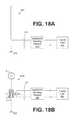
- FIGS. 18A through 18Cdepict examples of receiving structures that can be employed to receive energy transmitted in the form of a guided surface wave launched by a guided surface waveguide probe according to the various embodiments of the present disclosure.
- FIG. 18Dis a flow chart illustrating an example of adjusting a receiving structure according to various embodiments of the present disclosure.
- FIG. 19depicts an example of an additional receiving structure that can be employed to receive energy transmitted in the form of a guided surface wave launched by a guided surface waveguide probe according to the various embodiments of the present disclosure.
- FIGS. 20A-Edepict various circuit symbols used in the discussion of the application of guided surface waves for geolocation according to various embodiments of the present disclosure.
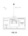
- FIG. 21is schematic block diagram depicting a navigation unit capable of determining its location based upon guided surface waves launched by one or more guided surface wave probes, according to various embodiments of the present disclosure.
- FIG. 22is a diagram illustrating the location of the navigation unit depicted in FIG. 21 , according to various embodiments of the present disclosure.
- FIG. 23is a diagram illustrating the location of the navigation unit depicted in FIG. 21 , according to various embodiments of the present disclosure.
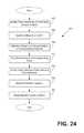
- FIG. 24is a flowchart illustrating one example of functionality implemented as portions of the multilateration application executed in the receiver depicted in FIG. 21 , according to various embodiments of the present disclosure.
- a radiated electromagnetic fieldcomprises electromagnetic energy that is emitted from a source structure in the form of waves that are not bound to a waveguide.
- a radiated electromagnetic fieldis generally a field that leaves an electric structure such as an antenna and propagates through the atmosphere or other medium and is not bound to any waveguide structure. Once radiated electromagnetic waves leave an electric structure such as an antenna, they continue to propagate in the medium of propagation (such as air) independent of their source until they dissipate regardless of whether the source continues to operate. Once electromagnetic waves are radiated, they are not recoverable unless intercepted, and, if not intercepted, the energy inherent in the radiated electromagnetic waves is lost forever.
- Radio structuressuch as antennas are designed to radiate electromagnetic fields by maximizing the ratio of the radiation resistance to the structure loss resistance. Radiated energy spreads out in space and is lost regardless of whether a receiver is present. The energy density of the radiated fields is a function of distance due to geometric spreading. Accordingly, the term “radiate” in all its forms as used herein refers to this form of electromagnetic propagation.
- a guided electromagnetic fieldis a propagating electromagnetic wave whose energy is concentrated within or near boundaries between media having different electromagnetic properties.
- a guided electromagnetic fieldis one that is bound to a waveguide and may be characterized as being conveyed by the current flowing in the waveguide. If there is no load to receive and/or dissipate the energy conveyed in a guided electromagnetic wave, then no energy is lost except for that dissipated in the conductivity of the guiding medium. Stated another way, if there is no load for a guided electromagnetic wave, then no energy is consumed.
- a generator or other source generating a guided electromagnetic fielddoes not deliver real power unless a resistive load is present. To this end, such a generator or other source essentially runs idle until a load is presented.
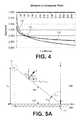
- FIG. 1shown is a graph 100 of field strength in decibels (dB) above an arbitrary reference in volts per meter as a function of distance in kilometers on a log-dB plot to further illustrate the distinction between radiated and guided electromagnetic fields.
- the graph 100 of FIG. 1depicts a guided field strength curve 103 that shows the field strength of a guided electromagnetic field as a function of distance.
- This guided field strength curve 103is essentially the same as a transmission line mode.
- the graph 100 of FIG. 1depicts a radiated field strength curve 106 that shows the field strength of a radiated electromagnetic field as a function of distance.
- the radiated field strength curve 106falls off geometrically (1/d, where d is distance), which is depicted as a straight line on the log-log scale.
- the guided field strength curve 103has a characteristic exponential decay of e ⁇ d / ⁇ square root over (d) ⁇ and exhibits a distinctive knee 109 on the log-log scale.
- the guided field strength curve 103 and the radiated field strength curve 106intersect at point 112 , which occurs at a crossing distance. At distances less than the crossing distance at intersection point 112 , the field strength of a guided electromagnetic field is significantly greater at most locations than the field strength of a radiated electromagnetic field.
- the guided and radiated field strength curves 103 and 106further illustrate the fundamental propagation difference between guided and radiated electromagnetic fields.
- MilliganT., Modern Antenna Design , McGraw-Hill, 1 st Edition, 1985, pp. 8-9, which is incorporated herein by reference in its entirety.
- the wave equationis a differential operator whose eigenfunctions possess a continuous spectrum of eigenvalues on the complex wave-number plane.
- This transverse electro-magnetic (TEM) fieldis called the radiation field, and those propagating fields are called “Hertzian waves.”
- TEMtransverse electro-magnetic
- the wave equation plus boundary conditionsmathematically lead to a spectral representation of wave-numbers composed of a continuous spectrum plus a sum of discrete spectra.
- Sommerfeld, A.“Uber die Ausbreitung der Wellen in der Drahtlosen Telegraphie,” Annalen der Physik, Vol. 28, 1909, pp. 665-736.
- ground waveand “surface wave” identify two distinctly different physical propagation phenomena.
- a surface wavearises analytically from a distinct pole yielding a discrete component in the plane wave spectrum. See, e.g., “The Excitation of Plane Surface Waves” by Cullen, A. L., ( Proceedings of the IEE (British), Vol. 101, Part IV, August 1954, pp. 225-235).
- a surface waveis considered to be a guided surface wave.
- the surface wavein the Zenneck-Sommerfeld guided wave sense
- the surface waveis, physically and mathematically, not the same as the ground wave (in the Weyl-Norton-FCC sense) that is now so familiar from radio broadcasting.
- the continuous part of the wave-number eigenvalue spectrumproduces the radiation field
- the discrete spectra, and corresponding residue sum arising from the poles enclosed by the contour of integrationresult in non-TEM traveling surface waves that are exponentially damped in the direction transverse to the propagation.
- Such surface wavesare guided transmission line modes.
- Friedman, B.Principles and Techniques of Applied Mathematics , Wiley, 1956, pp. pp. 214, 283-286, 290, 298-300.
- antennasexcite the continuum eigenvalues of the wave equation, which is a radiation field, where the outwardly propagating RF energy with E z and H ⁇ in-phase is lost forever.
- waveguide probesexcite discrete eigenvalues, which results in transmission line propagation. See Collin, R. E., Field Theory of Guided Waves , McGraw-Hill, 1960, pp. 453, 474-477. While such theoretical analyses have held out the hypothetical possibility of launching open surface guided waves over planar or spherical surfaces of lossy, homogeneous media, for more than a century no known structures in the engineering arts have existed for accomplishing this with any practical efficiency.
- various guided surface waveguide probesare described that are configured to excite electric fields that couple into a guided surface waveguide mode along the surface of a lossy conducting medium.
- Such guided electromagnetic fieldsare substantially mode-matched in magnitude and phase to a guided surface wave mode on the surface of the lossy conducting medium.
- Such a guided surface wave modecan also be termed a Zenneck waveguide mode.
- the resultant fields excited by the guided surface waveguide probes described hereinare substantially mode-matched to a guided surface waveguide mode on the surface of the lossy conducting medium, a guided electromagnetic field in the form of a guided surface wave is launched along the surface of the lossy conducting medium.
- the lossy conducting mediumcomprises a terrestrial medium such as the Earth.
- FIG. 2shown is a propagation interface that provides for an examination of the boundary value solutions to Maxwell's equations derived in 1907 by Jonathan Zenneck as set forth in his paper Zenneck, J., “On the Propagation of Plane Electromagnetic Waves Along a Flat Conducting Surface and their Relation to Wireless Telegraphy,” Annalen der Physik, Serial 4, Vol. 23, Sep. 20, 1907, pp. 846-866.
- FIG. 2depicts cylindrical coordinates for radially propagating waves along the interface between a lossy conducting medium specified as Region 1 and an insulator specified as Region 2 .
- Region 1can comprise, for example, any lossy conducting medium.
- such a lossy conducting mediumcan comprise a terrestrial medium such as the Earth or other medium.
- Region 2is a second medium that shares a boundary interface with Region 1 and has different constitutive parameters relative to Region 1 .
- Region 2can comprise, for example, any insulator such as the atmosphere or other medium.
- the reflection coefficient for such a boundary interfacegoes to zero only for incidence at a complex Brewster angle. See Stratton, J. A., Electromagnetic Theory , McGraw-Hill, 1941, p. 516.
- the present disclosuresets forth various guided surface waveguide probes that generate electromagnetic fields that are substantially mode-matched to a guided surface waveguide mode on the surface of the lossy conducting medium comprising Region 1 .
- such electromagnetic fieldssubstantially synthesize a wave front incident at a complex Brewster angle of the lossy conducting medium that can result in zero reflection.
- zis the vertical coordinate normal to the surface of Region 1 and ⁇ is the radial coordinate
- H n (2) ( ⁇ j ⁇ )is a complex argument Hankel function of the second kind and order n
- u 1is the propagation constant in the positive vertical (z) direction in Region 1
- u 2is the propagation constant in the vertical (z) direction in Region 2
- ⁇ 1is the conductivity of Region 1
- ⁇is equal to 2 ⁇ f, where f is a frequency of excitation
- ⁇ 0is the permittivity of free space
- ⁇ 1is the permittivity of Region 1
- Ais a source constant imposed by the source
- ⁇is a surface wave radial propagation constant.
- the propagation constants in the ⁇ z directionsare determined by separating the wave equation above and below the interface between Regions 1 and 2 , and imposing the boundary conditions. This exercise gives, in Region 2 ,
- ⁇ rcomprises the relative permittivity of Region 1
- ⁇ 1is the conductivity of Region 1
- ⁇ 0is the permittivity of free space
- ⁇ 0comprises the permeability of free space.
- Equations (1)-(3)can be considered to be a cylindrically-symmetric, radially-propagating waveguide mode. See Barlow, H. M., and Brown, J., Radio Surface Waves , Oxford University Press, 1962, pp. 10-12, 29-33.
- the present disclosuredetails structures that excite this “open boundary” waveguide mode.
- a guided surface waveguide probeis provided with a charge terminal of appropriate size that is fed with voltage and/or current and is positioned relative to the boundary interface between Region 2 and Region 1 . This may be better understood with reference to FIG.
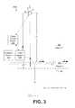
- FIG. 3which shows an example of a guided surface waveguide probe 200 a that includes a charge terminal T 1 elevated above a lossy conducting medium 203 (e.g., the Earth) along a vertical axis z that is normal to a plane presented by the lossy conducting medium 203 .
- the lossy conducting medium 203makes up Region 1
- a second medium 206makes up Region 2 and shares a boundary interface with the lossy conducting medium 203 .
- the lossy conducting medium 203can comprise a terrestrial medium such as the planet Earth.
- a terrestrial mediumcomprises all structures or formations included thereon whether natural or man-made.
- such a terrestrial mediumcan comprise natural elements such as rock, soil, sand, fresh water, sea water, trees, vegetation, and all other natural elements that make up our planet.
- such a terrestrial mediumcan comprise man-made elements such as concrete, asphalt, building materials, and other man-made materials.
- the lossy conducting medium 203can comprise some medium other than the Earth, whether naturally occurring or man-made.
- the lossy conducting medium 203can comprise other media such as man-made surfaces and structures such as automobiles, aircraft, man-made materials (such as plywood, plastic sheeting, or other materials) or other media.
- the second medium 206can comprise the atmosphere above the ground.
- the atmospherecan be termed an “atmospheric medium” that comprises air and other elements that make up the atmosphere of the Earth.
- the second medium 206can comprise other media relative to the lossy conducting medium 203 .
- the guided surface waveguide probe 200 aincludes a feed network 209 that couples an excitation source 212 to the charge terminal T 1 via, e.g., a vertical feed line conductor.
- a charge Q 1is imposed on the charge terminal T 1 to synthesize an electric field based upon the voltage applied to terminal T 1 at any given instant.
- ⁇ ithe angle of incidence
- Ethe electric field
- the negative signmeans that when source current (I 0 ) flows vertically upward as illustrated in FIG. 3 , the “close-in” ground current flows radially inward.
- Equation (14)the radial surface current density of Equation (14) can be restated as
- Equation (1)-(6)I o ⁇ ⁇ 4 ⁇ H 1 ( 2 ) ⁇ ( - j ⁇ ⁇ ⁇ ⁇ ⁇ ⁇ ′ ) .
- Equations (1)-(6) and (17)have the nature of a transmission line mode bound to a lossy interface, not radiation fields that are associated with groundwave propagation. See Barlow, H. M. and Brown, J., Radio Surface Waves , Oxford University Press, 1962, pp. 1-5.
- H n (1) ( x )J n ( x )+ jN n ( x )
- H n (2) ( x )J n ( x ) ⁇ jN n ( x )
- These functionsrepresent cylindrical waves propagating radially inward (H n (1) ) and outward (H n (2) ), respectively.
- Equation (20b) and (21)differ in phase by ⁇ square root over (j) ⁇ , which corresponds to an extra phase advance or “phase boost” of 45° or, equivalently, ⁇ /8.
- the “far out” representationpredominates over the “close-in” representation of the Hankel function.
- Curve 115is the magnitude of the far-out asymptote of Equation (20b)
- the vertical component of the mode-matched electric field of Equation (3)asymptotically passes to
- the height H 1 of the elevated charge terminal T 1 in FIG. 3affects the amount of free charge on the charge terminal T 1 .
- the charge terminal T 1is near the ground plane of Region 1 , most of the charge Q 1 on the terminal is “bound.” As the charge terminal T 1 is elevated, the bound charge is lessened until the charge terminal T 1 reaches a height at which substantially all of the isolated charge is free.
- the advantage of an increased capacitive elevation for the charge terminal T 1is that the charge on the elevated charge terminal T 1 is further removed from the ground plane, resulting in an increased amount of free charge q free to couple energy into the guided surface waveguide mode. As the charge terminal T 1 is moved away from the ground plane, the charge distribution becomes more uniformly distributed about the surface of the terminal. The amount of free charge is related to the self-capacitance of the charge terminal T 1 .
- the capacitance of a spherical terminalcan be expressed as a function of physical height above the ground plane.
- an increase in the terminal height hreduces the capacitance C of the charge terminal.
- the charge distributionis approximately uniform about the spherical terminal, which can improve the coupling into the guided surface waveguide mode.
- the charge terminal T 1can include any shape such as a sphere, a disk, a cylinder, a cone, a torus, a hood, one or more rings, or any other randomized shape or combination of shapes.
- An equivalent spherical diametercan be determined and used for positioning of the charge terminal T 1 .
- the charge terminal T 1can be positioned at a physical height that is at least four times the spherical diameter (or equivalent spherical diameter) of the charge terminal T 1 to reduce the bounded charge effects.
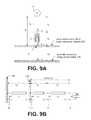
- FIG. 5Ashown is a ray optics interpretation of the electric field produced by the elevated charge Q 1 on charge terminal T 1 of FIG. 3 .
- minimizing the reflection of the incident electric fieldcan improve and/or maximize the energy coupled into the guided surface waveguide mode of the lossy conducting medium 203 .
- the amount of reflection of the incident electric fieldmay be determined using the Fresnel reflection coefficient, which can be expressed as
- the ray optic interpretationshows the incident field polarized parallel to the plane of incidence having an angle of incidence of ⁇ i , which is measured with respect to the surface normal ( ⁇ circumflex over (z) ⁇ ).
- ⁇ iangle of incidence
- This complex angle of incidence( ⁇ i,B ) is referred to as the Brewster angle.
- Equation (22)it can be seen that the same complex Brewster angle ( ⁇ i,B ) relationship is present in both Equations (22) and (26).
- the electric field vector Ecan be depicted as an incoming non-uniform plane wave, polarized parallel to the plane of incidence.
- a generalized parameter Wis noted herein as the ratio of the horizontal electric field component to the vertical electric field component given by
- the wave tilt angle ( ⁇ )is equal to the angle between the normal of the wave-front at the boundary interface with Region 1 and the tangent to the boundary interface. This may be easier to see in FIG. 5B , which illustrates equi-phase surfaces of an electromagnetic wave and their normals for a radial cylindrical guided surface wave.
- Equation (30b)Applying Equation (30b) to a guided surface wave gives
- the concept of an electrical effective heightcan provide further insight into synthesizing an electric field with a complex angle of incidence with a guided surface waveguide probe 200 .
- the electrical effective height (h eff )has been defined as
- h eff1 I 0 ⁇ ⁇ 0 h p ⁇ I ⁇ ( z ) ⁇ dz ( 33 ) for a monopole with a physical height (or length) of h p . Since the expression depends upon the magnitude and phase of the source distribution along the structure, the effective height (or length) is complex in general.
- the integration of the distributed current I(z) of the structureis performed over the physical height of the structure (h p ), and normalized to the ground current (I 0 ) flowing upward through the base (or input) of the structure.
- I Cis the current that is distributed along the vertical structure of the guided surface waveguide probe 200 a.
- a feed network 209that includes a low loss coil (e.g., a helical coil) at the bottom of the structure and a vertical feed line conductor connected between the coil and the charge terminal T 1 .
- V fis the velocity factor on the structure
- ⁇ 0is the wavelength at the supplied frequency
- ⁇ pis the propagation wavelength resulting from the velocity factor V f .
- the phase delayis measured relative to the ground (stake) current I 0 .
- h eff1 I 0 ⁇ ⁇ 0 h p ⁇ I 0 ⁇ e j ⁇ ⁇ ⁇ ⁇ cos ⁇ ( ⁇ 0 ⁇ z ) ⁇ dz ⁇ h p ⁇ e j ⁇ ⁇ ⁇ , ( 37 ) for the case where the physical height h p ⁇ 0 .
- ray opticsare used to illustrate the complex angle trigonometry of the incident electric field (E) having a complex Brewster angle of incidence ( ⁇ i,B ) at the Hankel crossover distance (R x ) 121 .
- Equation (26)that, for a lossy conducting medium, the Brewster angle is complex and specified by
- the wave tilt of the electric field at the Hankel crossover distancecan be expressed as the ratio of the electrical effective height and the Hankel crossover distance
- a right triangleis depicted having an adjacent side of length R x along the lossy conducting medium surface and a complex Brewster angle ⁇ i,B measured between a ray 124 extending between the Hankel crossover point 121 at R x and the center of the charge terminal T 1 , and the lossy conducting medium surface 127 between the Hankel crossover point 121 and the charge terminal T 1 .
- the charge terminal T 1positioned at physical height h p and excited with a charge having the appropriate phase delay ⁇ , the resulting electric field is incident with the lossy conducting medium boundary interface at the Hankel crossover distance R x , and at the Brewster angle. Under these conditions, the guided surface waveguide mode can be excited without reflection or substantially negligible reflection.
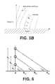
- FIG. 6graphically illustrates the effect of decreasing the physical height of the charge terminal T 1 on the distance where the electric field is incident at the Brewster angle.
- the point where the electric field intersects with the lossy conducting medium (e.g., the Earth) at the Brewster anglemoves closer to the charge terminal position.
- Equation (39)indicates, the height H 1 ( FIG.
- the height of the charge terminal T 1should be at or higher than the physical height (h p ) in order to excite the far-out component of the Hankel function.
- the heightshould be at least four times the spherical diameter (or equivalent spherical diameter) of the charge terminal T 1 as mentioned above.
- a guided surface waveguide probe 200can be configured to establish an electric field having a wave tilt that corresponds to a wave illuminating the surface of the lossy conducting medium 203 at a complex Brewster angle, thereby exciting radial surface currents by substantially mode-matching to a guided surface wave mode at (or beyond) the Hankel crossover point 121 at R x .
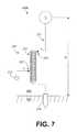
- FIG. 7shown is a graphical representation of an example of a guided surface waveguide probe 200 b that includes a charge terminal T 1 .
- An AC source 212acts as the excitation source for the charge terminal T 1 , which is coupled to the guided surface waveguide probe 200 b through a feed network 209 ( FIG. 3 ) comprising a coil 215 such as, e.g., a helical coil.
- the AC source 212can be inductively coupled to the coil 215 through a primary coil.
- an impedance matching networkmay be included to improve and/or maximize coupling of the AC source 212 to the coil 215 .
- the guided surface waveguide probe 200 bcan include the upper charge terminal T 1 (e.g., a sphere at height h p ) that is positioned along a vertical axis z that is substantially normal to the plane presented by the lossy conducting medium 203 .
- a second medium 206is located above the lossy conducting medium 203 .
- the charge terminal T 1has a self-capacitance C T .
- charge Q 1is imposed on the terminal T 1 depending on the voltage applied to the terminal T 1 at any given instant.
- the coil 215is coupled to a ground stake 218 at a first end and to the charge terminal T 1 via a vertical feed line conductor 221 .
- the coil connection to the charge terminal T 1can be adjusted using a tap 224 of the coil 215 as shown in FIG. 7 .
- the coil 215can be energized at an operating frequency by the AC source 212 through a tap 227 at a lower portion of the coil 215 .
- the AC source 212can be inductively coupled to the coil 215 through a primary coil.
- the construction and adjustment of the guided surface waveguide probe 200is based upon various operating conditions, such as the transmission frequency, conditions of the lossy conducting medium (e.g., soil conductivity a and relative permittivity ⁇ r ), and size of the charge terminal T 1 .
- the conductivity a and relative permittivity ⁇ rcan be determined through test measurements of the lossy conducting medium 203 .
- Equation ( 43 )The wave tilt at the Hankel crossover distance (W Rx ) can also be found using Equation (40).
- the Hankel crossover distancecan also be found by equating the magnitudes of Equations (20b) and (21) for ⁇ j ⁇ , and solving for R x as illustrated by FIG. 4 .
- the complex effective height (h eff )includes a magnitude that is associated with the physical height (h p ) of the charge terminal T 1 and a phase delay ( ⁇ ) that is to be associated with the angle ( ⁇ ) of the wave tilt at the Hankel crossover distance (R x ).
- the feed network 209( FIG. 3 ) and/or the vertical feed line connecting the feed network to the charge terminal T 1 can be adjusted to match the phase ( ⁇ ) of the charge Q 1 on the charge terminal T 1 to the angle ( ⁇ ) of the wave tilt (W).
- the size of the charge terminal T 1can be chosen to provide a sufficiently large surface for the charge Q 1 imposed on the terminals. In general, it is desirable to make the charge terminal T 1 as large as practical. The size of the charge terminal T 1 should be large enough to avoid ionization of the surrounding air, which can result in electrical discharge or sparking around the charge terminal.
- phase delay ⁇ c of a helically-wound coilcan be determined from Maxwell's equations as has been discussed by Corum, K. L. and J. F. Corum, “RF Coils, Helical Resonators and Voltage Magnification by Coherent Spatial Modes,” Microwave Review , Vol. 7, No. 2, September 2001, pp. 36-45., which is incorporated herein by reference in its entirety.
- H/Dthe ratio of the velocity of propagation ( ⁇ ) of a wave along the coil's longitudinal axis to the speed of light (c), or the “velocity factor”
- His the axial length of the solenoidal helix
- Dis the coil diameter
- Nis the number of turns of the coil
- ⁇ 0is the free-space wavelength.
- the principleis the same if the helix is wound spirally or is short and fat, but V f and ⁇ c are easier to obtain by experimental measurement.
- the expression for the characteristic (wave) impedance of a helical transmission linehas also been derived as
- the spatial phase delay ⁇ y of the structurecan be determined using the traveling wave phase delay of the vertical feed line conductor 221 ( FIG. 7 ).
- the capacitance of a cylindrical vertical conductor above a prefect ground planecan be expressed as
- ⁇ wis the propagation phase constant for the vertical feed line conductor
- h wis the vertical length (or height) of the vertical feed line conductor
- V wis the velocity factor on the wire
- ⁇ 0is the wavelength at the supplied frequency
- ⁇ wis the propagation wavelength resulting from the velocity factor V w .
- the velocity factoris a constant with V w ⁇ 0.94, or in a range from about 0.93 to about 0.98. If the mast is considered to be a uniform transmission line, its average characteristic impedance can be approximated by
- Equation (51)implies that Z w for a single-wire feeder varies with frequency.
- the phase delaycan be determined based upon the capacitance and characteristic impedance.
- the electric field produced by the charge oscillating Q 1 on the charge terminal T 1is coupled into a guided surface waveguide mode traveling along the surface of a lossy conducting medium 203 .
- the Brewster angle ( ⁇ i,B )the phase delay ( ⁇ y ) associated with the vertical feed line conductor 221 ( FIG. 7 ), and the configuration of the coil 215 ( FIG.
- the position of the tap 224may be adjusted to maximize coupling the traveling surface waves into the guided surface waveguide mode. Excess coil length beyond the position of the tap 224 can be removed to reduce the capacitive effects.
- the vertical wire height and/or the geometrical parameters of the helical coilmay also be varied.
- the coupling to the guided surface waveguide mode on the surface of the lossy conducting medium 203can be improved and/or optimized by tuning the guided surface waveguide probe 200 for standing wave resonance with respect to a complex image plane associated with the charge Q 1 on the charge terminal T 1 .
- the performance of the guided surface waveguide probe 200can be adjusted for increased and/or maximum voltage (and thus charge Q 1 ) on the charge terminal T 1 .
- the effect of the lossy conducting medium 203 in Region 1can be examined using image theory analysis.
- an elevated charge Q 1 placed over a perfectly conducting planeattracts the free charge on the perfectly conducting plane, which then “piles up” in the region under the elevated charge Q 1 .
- the resulting distribution of “bound” electricity on the perfectly conducting planeis similar to a bell-shaped curve.
- the boundary value problem solution that describes the fields in the region above the perfectly conducting planemay be obtained using the classical notion of image charges, where the field from the elevated charge is superimposed with the field from a corresponding “image” charge below the perfectly conducting plane.
- This analysismay also be used with respect to a lossy conducting medium 203 by assuming the presence of an effective image charge Q 1 ′ beneath the guided surface waveguide probe 200 .
- the effective image charge Q 1 ′coincides with the charge Q 1 on the charge terminal T 1 about a conducting image ground plane 130 , as illustrated in FIG. 3 .
- the image charge Q 1 ′is not merely located at some real depth and 180° out of phase with the primary source charge Q 1 on the charge terminal T 1 , as they would be in the case of a perfect conductor. Rather, the lossy conducting medium 203 (e.g., a terrestrial medium) presents a phase shifted image.
- the image charge Q 1 ′is at a complex depth below the surface (or physical boundary) of the lossy conducting medium 203 .
- complex image depthreference is made to Wait, J. R., “Complex Image Theory—Revisited,” IEEE Antennas and Propagation Magazine , Vol. 33, No. 4, August 1991, pp. 27-29, which is incorporated herein by reference in its entirety.
- the complex spacing of the image chargeimplies that the external field will experience extra phase shifts not encountered when the interface is either a dielectric or a perfect conductor.
- the lossy conducting medium 203is a finitely conducting Earth 133 with a physical boundary 136 .
- the finitely conducting Earth 133may be replaced by a perfectly conducting image ground plane 139 as shown in FIG. 8B , which is located at a complex depth z 1 below the physical boundary 136 .
- This equivalent representationexhibits the same impedance when looking down into the interface at the physical boundary 136 .
- the equivalent representation of FIG. 8Bcan be modeled as an equivalent transmission line, as shown in FIG. 8C .
- the depth z 1can be determined by equating the TEM wave impedance looking down at the Earth to an image ground plane impedance z in seen looking into the transmission line of FIG. 8C .
- the distance to the perfectly conducting image ground plane 139can be approximated by
- the guided surface waveguide probe 200 b of FIG. 7can be modeled as an equivalent single-wire transmission line image plane model that can be based upon the perfectly conducting image ground plane 139 of FIG. 8B .
- FIG. 9Ashows an example of the equivalent single-wire transmission line image plane model
- FIG. 9Billustrates an example of the equivalent classic transmission line model, including the shorted transmission line of FIG. 8C .
- Z wis the characteristic impedance of the elevated vertical feed line conductor 221 in ohms
- Z cis the characteristic impedance of the coil 215 in ohms
- Z 0is the characteristic impedance of free space.
- Z ⁇Z in , which is given by:
- the impedance at the physical boundary 136 “looking up” into the guided surface waveguide probe 200is the conjugate of the impedance at the physical boundary 136 “looking down” into the lossy conducting medium 203 .
- the equivalent image plane models of FIGS. 9A and 9Bcan be tuned to resonance with respect to the image ground plane 139 .
- the impedance of the equivalent complex image plane modelis purely resistive, which maintains a superposed standing wave on the probe structure that maximizes the voltage and elevated charge on terminal T 1 , and by equations (1)-(3) and (16) maximizes the propagating surface wave.
- the guided surface wave excited by the guided surface waveguide probe 200is an outward propagating traveling wave.
- the source distribution along the feed network 209 between the charge terminal T 1 and the ground stake 218 of the guided surface waveguide probe 200( FIGS. 3 and 7 ) is actually composed of a superposition of a traveling wave plus a standing wave on the structure.
- the phase delay of the traveling wave moving through the feed network 209is matched to the angle of the wave tilt associated with the lossy conducting medium 203 . This mode-matching allows the traveling wave to be launched along the lossy conducting medium 203 .
- the load impedance Z L of the charge terminal T 1is adjusted to bring the probe structure into standing wave resonance with respect to the image ground plane ( 130 of FIG. 3 or 139 of FIG. 8 ), which is at a complex depth of ⁇ d/2. In that case, the impedance seen from the image ground plane has zero reactance and the charge on the charge terminal T 1 is maximized.
- two relatively short transmission line sections of widely differing characteristic impedancemay be used to provide a very large phase shift.
- a probe structurecomposed of two sections of transmission line, one of low impedance and one of high impedance, together totaling a physical length of, say, 0.05 ⁇ , may be fabricated to provide a phase shift of 90° which is equivalent to a 0.25 ⁇ resonance. This is due to the large jump in characteristic impedances.
- a physically short probe structurecan be electrically longer than the two physical lengths combined. This is illustrated in FIGS. 9A and 9B , where the discontinuities in the impedance ratios provide large jumps in phase. The impedance discontinuity provides a substantial phase shift where the sections are joined together.
- FIG. 10shown is a flow chart 150 illustrating an example of adjusting a guided surface waveguide probe 200 ( FIGS. 3 and 7 ) to substantially mode-match to a guided surface waveguide mode on the surface of the lossy conducting medium, which launches a guided surface traveling wave along the surface of a lossy conducting medium 203 ( FIG. 3 ).
- the charge terminal T 1 of the guided surface waveguide probe 200is positioned at a defined height above a lossy conducting medium 203 .
- the Hankel crossover distancecan also be found by equating the magnitudes of Equations (20b) and (21) for ⁇ j ⁇ , and solving for R x as illustrated by FIG. 4 .
- the complex index of refraction (n)can be determined using Equation (41), and the complex Brewster angle ( ⁇ i,B ) can then be determined from Equation (42).
- the physical height (h p ) of the charge terminal T 1can then be determined from Equation (44).
- the charge terminal T 1should be at or higher than the physical height (h p ) in order to excite the far-out component of the Hankel function. This height relationship is initially considered when launching surface waves.
- the heightshould be at least four times the spherical diameter (or equivalent spherical diameter) of the charge terminal T 1 .
- the electrical phase delay ⁇ of the elevated charge Q 1 on the charge terminal T 1is matched to the complex wave tilt angle ⁇ .
- the phase delay ( ⁇ c ) of the helical coil and/or the phase delay ( ⁇ y ) of the vertical feed line conductorcan be adjusted to make ⁇ equal to the angle ( ⁇ ) of the wave tilt (W). Based on Equation (31), the angle ( ⁇ ) of the wave tilt can be determined from:
- the electrical phase ⁇can then be matched to the angle of the wave tilt. This angular (or phase) relationship is next considered when launching surface waves.
- the load impedance of the charge terminal T 1is tuned to resonate the equivalent image plane model of the guided surface waveguide probe 200 .
- the depth (d/2) of the conducting image ground plane 139 of FIGS. 9A and 9B (or 130 of FIG. 3 )can be determined using Equations (52), (53) and (54) and the values of the lossy conducting medium 203 (e.g., the Earth), which can be measured.
- the impedance (Z in ) as seen “looking down” into the lossy conducting medium 203can then be determined using Equation (65). This resonance relationship can be considered to maximize the launched surface waves.
- the velocity factor, phase delay, and impedance of the coil 215 and vertical feed line conductor 221can be determined using Equations (45) through (51).
- the self-capacitance (C T ) of the charge terminal T 1can be determined using, e.g., Equation (24).
- the propagation factor ( ⁇ p ) of the coil 215can be determined using Equation (35) and the propagation phase constant ( ⁇ w ) for the vertical feed line conductor 221 can be determined using Equation (49).
- the impedance (Z base ) of the guided surface waveguide probe 200 as seen “looking up” into the coil 215can be determined using Equations (62), (63) and (64).
- the impedance at the physical boundary 136 “looking up” into the guided surface waveguide probe 200is the conjugate of the impedance at the physical boundary 136 “looking down” into the lossy conducting medium 203 .
- An iterative approachmay be taken to tune the load impedance Z L for resonance of the equivalent image plane model with respect to the conducting image ground plane 139 (or 130 ). In this way, the coupling of the electric field to a guided surface waveguide mode along the surface of the lossy conducting medium 203 (e.g., Earth) can be improved and/or maximized.
- the lossy conducting medium 203e.g., Earth
- the wave lengthcan be determined as:
- Equation (66)the wave tilt values can be determined to be:
- the velocity factor of the vertical feed line conductor(approximated as a uniform cylindrical conductor with a diameter of 0.27 inches) can be given as V w ⁇ 0.93. Since h p ⁇ 0 , the propagation phase constant for the vertical feed line conductor can be approximated as:
- FIG. 11shows a plot of both over a range of frequencies. As both ⁇ and ⁇ are frequency dependent, it can be seen that their respective curves cross over each other at approximately 1.85 MHz.
- Equation (45)For a helical coil having a conductor diameter of 0.0881 inches, a coil diameter (D) of 30 inches and a turn-to-turn spacing (s) of 4 inches, the velocity factor for the coil can be determined using Equation (45) as:
- Equation (46)the axial length of the solenoidal helix (H) can be determined using Equation (46) such that:
- the load impedance (Z L ) of the charge terminal T 1can be adjusted for standing wave resonance of the equivalent image plane model of the guided surface wave probe 200 .
- Equation (52)Equation (52)
- the coupling into the guided surface waveguide modemay be maximized. This can be accomplished by adjusting the capacitance of the charge terminal T 1 without changing the traveling wave phase delays of the coil and vertical feed line conductor. For example, by adjusting the charge terminal capacitance (C T ) to 61.8126 pF, the load impedance from Equation (62) is:
- Equation (51)the impedance of the vertical feed line conductor (having a diameter (2 ⁇ ) of 0.27 inches) is given as
- Equation (63)the impedance seen “looking up” into the vertical feed line conductor is given by Equation (63) as:
- Equation (64)the impedance seen “looking up” into the coil at the base is given by Equation (64) as:
- the guided field strength curve 103 of the guided electromagnetic fieldhas a characteristic exponential decay of e ⁇ d / ⁇ square root over (d) ⁇ and exhibits a distinctive knee 109 on the log-log scale.
- the charge terminal T 1is of sufficient height H 1 of FIG. 3 (h ⁇ R x tan ⁇ i,B ) so that electromagnetic waves incident onto the lossy conducting medium 203 at the complex Brewster angle do so out at a distance ( ⁇ R x ) where the 1/ ⁇ square root over (r) ⁇ term is predominant.
- Receive circuitscan be utilized with one or more guided surface waveguide probes to facilitate wireless transmission and/or power delivery systems.
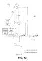
- operation of a guided surface waveguide probe 200may be controlled to adjust for variations in operational conditions associated with the guided surface waveguide probe 200 .
- an adaptive probe control system 230can be used to control the feed network 209 and/or the charge terminal T 1 to control the operation of the guided surface waveguide probe 200 .
- Operational conditionscan include, but are not limited to, variations in the characteristics of the lossy conducting medium 203 (e.g., conductivity a and relative permittivity ⁇ r ), variations in field strength and/or variations in loading of the guided surface waveguide probe 200 .
- e k ⁇ )can be affected by changes in soil conductivity and permittivity resulting from, e.g., weather conditions.
- Equipmentsuch as, e.g., conductivity measurement probes, permittivity sensors, ground parameter meters, field meters, current monitors and/or load receivers can be used to monitor for changes in the operational conditions and provide information about current operational conditions to the adaptive probe control system 230 .
- the probe control system 230can then make one or more adjustments to the guided surface waveguide probe 200 to maintain specified operational conditions for the guided surface waveguide probe 200 .
- Conductivity measurement probes and/or permittivity sensorsmay be located at multiple locations around the guided surface waveguide probe 200 . Generally, it would be desirable to monitor the conductivity and/or permittivity at or about the Hankel crossover distance R x for the operational frequency.
- Conductivity measurement probes and/or permittivity sensorsmay be located at multiple locations (e.g., in each quadrant) around the guided surface waveguide probe 200 .
- the conductivity measurement probes and/or permittivity sensorscan be configured to evaluate the conductivity and/or permittivity on a periodic basis and communicate the information to the probe control system 230 .
- the informationmay be communicated to the probe control system 230 through a network such as, but not limited to, a LAN, WLAN, cellular network, or other appropriate wired or wireless communication network.
- the probe control system 230may evaluate the variation in the index of refraction (n), the complex Brewster angle ( ⁇ i,B ), and/or the wave tilt (
- the probe control system 230can adjust the self-capacitance of the charge terminal T 1 and/or the phase delay ( ⁇ y , ⁇ c ) applied to the charge terminal T 1 to maintain the electrical launching efficiency of the guided surface wave at or near its maximum.
- the self-capacitance of the charge terminal T 1can be varied by changing the size of the terminal.
- the charge distributioncan also be improved by increasing the size of the charge terminal T 1 , which can reduce the chance of an electrical discharge from the charge terminal T 1 .
- the charge terminal T 1can include a variable inductance that can be adjusted to change the load impedance Z L .
- the phase applied to the charge terminal T 1can be adjusted by varying the tap position on the coil 215 ( FIG. 7 ), and/or by including a plurality of predefined taps along the coil 215 and switching between the different predefined tap locations to maximize the launching efficiency.
- Field or field strength (FS) metersmay also be distributed about the guided surface waveguide probe 200 to measure field strength of fields associated with the guided surface wave.
- the field or FS meterscan be configured to detect the field strength and/or changes in the field strength (e.g., electric field strength) and communicate that information to the probe control system 230 .
- the informationmay be communicated to the probe control system 230 through a network such as, but not limited to, a LAN, WLAN, cellular network, or other appropriate communication network.
- the guided surface waveguide probe 200may be adjusted to maintain specified field strength(s) at the FS meter locations to ensure appropriate power transmission to the receivers and the loads they supply.
- the guided surface waveguide probe 200can be adjusted to ensure the wave tilt corresponds to the complex Brewster angle. This can be accomplished by adjusting a tap position on the coil 215 ( FIG. 7 ) to change the phase delay supplied to the charge terminal T 1 .
- the voltage level supplied to the charge terminal T 1can also be increased or decreased to adjust the electric field strength. This may be accomplished by adjusting the output voltage of the excitation source 212 or by adjusting or reconfiguring the feed network 209 . For instance, the position of the tap 227 ( FIG.
- the AC source 212can be adjusted to increase the voltage seen by the charge terminal T 1 . Maintaining field strength levels within predefined ranges can improve coupling by the receivers, reduce ground current losses, and avoid interference with transmissions from other guided surface waveguide probes 200 .
- the probe control system 230can be implemented with hardware, firmware, software executed by hardware, or a combination thereof.
- the probe control system 230can include processing circuitry including a processor and a memory, both of which can be coupled to a local interface such as, for example, a data bus with an accompanying control/address bus as can be appreciated by those with ordinary skill in the art.
- a probe control applicationmay be executed by the processor to adjust the operation of the guided surface waveguide probe 200 based upon monitored conditions.
- the probe control system 230can also include one or more network interfaces for communicating with the various monitoring devices. Communications can be through a network such as, but not limited to, a LAN, WLAN, cellular network, or other appropriate communication network.
- the probe control system 230may comprise, for example, a computer system such as a server, desktop computer, laptop, or other system with like capability.
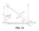
- the complex angle trigonometryis shown for the ray optic interpretation of the incident electric field (E) of the charge terminal T 1 with a complex Brewster angle ( ⁇ i,B ) at the Hankel crossover distance (R x ).
- the Brewster angleis complex and specified by equation (38).
- the geometric parametersare related by the electrical effective height (h eff ) of the charge terminal T 1 by equation (39). Since both the physical height (h p ) and the Hankel crossover distance (R x ) are real quantities, the angle of the desired guided surface wave tilt at the Hankel crossover distance (W Rx ) is equal to the phase ( ⁇ ) of the complex effective height (h eff ).
- the guided surface waveguide modecan be excited without reflection or substantially negligible reflection.
- Equation (39)means that the physical height of the guided surface waveguide probe 200 can be relatively small. While this will excite the guided surface waveguide mode, this can result in an unduly large bound charge with little free charge.
- the charge terminal T 1can be raised to an appropriate elevation to increase the amount of free charge. As one example rule of thumb, the charge terminal T 1 can be positioned at an elevation of about 4-5 times (or more) the effective diameter of the charge terminal T 1 .
- FIG. 6illustrates the effect of raising the charge terminal T 1 above the physical height (h p ) shown in FIG. 5A . The increased elevation causes the distance at which the wave tilt is incident with the lossy conductive medium to move beyond the Hankel crossover point 121 ( FIG. 5A ).
- a lower compensation terminal T 2can be used to adjust the total effective height (h TE ) of the charge terminal T 1 such that the wave tilt at the Hankel crossover distance is at the Brewster angle.
- a guided surface waveguide probe 200 cthat includes an elevated charge terminal T 1 and a lower compensation terminal T 2 that are arranged along a vertical axis z that is normal to a plane presented by the lossy conducting medium 203 .
- the charge terminal T 1is placed directly above the compensation terminal T 2 although it is possible that some other arrangement of two or more charge and/or compensation terminals T N can be used.
- the guided surface waveguide probe 200 cis disposed above a lossy conducting medium 203 according to an embodiment of the present disclosure.
- the lossy conducting medium 203makes up Region 1 with a second medium 206 that makes up Region 2 sharing a boundary interface with the lossy conducting medium 203 .
- the guided surface waveguide probe 200 cincludes a feed network 209 that couples an excitation source 212 to the charge terminal T 1 and the compensation terminal T 2 .
- charges Q 1 and Q 2can be imposed on the respective charge and compensation terminals T 1 and T 2 , depending on the voltages applied to terminals T 1 and T 2 at any given instant.
- I 1is the conduction current feeding the charge Q 1 on the charge terminal T 1 via the terminal lead
- I 2is the conduction current feeding the charge Q 2 on the compensation terminal T 2 via the terminal lead.
- the charge terminal T 1is positioned over the lossy conducting medium 203 at a physical height H 1
- the compensation terminal T 2is positioned directly below T 1 along the vertical axis z at a physical height H 2 , where H 2 is less than H 1 .
- the charge terminal T 1has an isolated (or self) capacitance C 1
- the compensation terminal T 2has an isolated (or self) capacitance C 2 .
- a mutual capacitance C Mcan also exist between the terminals T 1 and T 2 depending on the distance therebetween.
- charges Q 1 and Q 2are imposed on the charge terminal T 1 and the compensation terminal T 2 , respectively, depending on the voltages applied to the charge terminal T 1 and the compensation terminal T 2 at any given instant.
- FIG. 13shown is a ray optics interpretation of the effects produced by the elevated charge Q 1 on charge terminal T 1 and compensation terminal T 2 of FIG. 12 .
- the compensation terminal T 2can be used to adjust h TE by compensating for the increased height.
- the effect of the compensation terminal T 2is to reduce the electrical effective height of the guided surface waveguide probe (or effectively raise the lossy medium interface) such that the wave tilt at the Hankel crossover distance is at the Brewster angle as illustrated by line 166 .
- the lower effective heightcan be used to adjust the total effective height (h TE ) to equal the complex effective height (h eff ) of FIG. 5A .
- Equations (85) or (86)can be used to determine the physical height of the lower disk of the compensation terminal T 2 and the phase angles to feed the terminals in order to obtain the desired wave tilt at the Hankel crossover distance.
- Equation (86)can be rewritten as the phase shift applied to the charge terminal T 1 as a function of the compensation terminal height (h d ) to give
- the total effective height (h TE )is the superposition of the complex effective height (h UE ) of the upper charge terminal T 1 and the complex effective height (h LE ) of the lower compensation terminal T 2 as expressed in Equation (86).
- the tangent of the angle of incidencecan be expressed geometrically as
- the h TEcan be adjusted to make the wave tilt of the incident ray match the complex Brewster angle at the Hankel crossover point 121 . This can be accomplished by adjusting h p , ⁇ U , and/or h d .
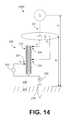
- FIG. 14shown is a graphical representation of an example of a guided surface waveguide probe 200 d including an upper charge terminal T 1 (e.g., a sphere at height h T ) and a lower compensation terminal T 2 (e.g., a disk at height h d ) that are positioned along a vertical axis z that is substantially normal to the plane presented by the lossy conducting medium 203 .
- charges Q 1 and Q 2are imposed on the charge and compensation terminals T 1 and T 2 , respectively, depending on the voltages applied to the terminals T 1 and T 2 at any given instant.
- An AC source 212acts as the excitation source for the charge terminal T 1 , which is coupled to the guided surface waveguide probe 200 d through a feed network 209 comprising a coil 215 such as, e.g., a helical coil.
- the AC source 212can be connected across a lower portion of the coil 215 through a tap 227 , as shown in FIG. 14 , or can be inductively coupled to the coil 215 by way of a primary coil.
- the coil 215can be coupled to a ground stake 218 at a first end and the charge terminal T 1 at a second end. In some implementations, the connection to the charge terminal T 1 can be adjusted using a tap 224 at the second end of the coil 215 .
- the compensation terminal T 2is positioned above and substantially parallel with the lossy conducting medium 203 (e.g., the ground or Earth), and energized through a tap 233 coupled to the coil 215 .
- An ammeter 236 located between the coil 215 and ground stake 218can be used to provide an indication of the magnitude of the current flow (I 0 ) at the base of the guided surface waveguide probe.
- a current clampmay be used around the conductor coupled to the ground stake 218 to obtain an indication of the magnitude of the current flow (I 0 ).
- the coil 215is coupled to a ground stake 218 at a first end and the charge terminal T 1 at a second end via a vertical feed line conductor 221 .
- the connection to the charge terminal T 1can be adjusted using a tap 224 at the second end of the coil 215 as shown in FIG. 14 .
- the coil 215can be energized at an operating frequency by the AC source 212 through a tap 227 at a lower portion of the coil 215 .
- the AC source 212can be inductively coupled to the coil 215 through a primary coil.
- the compensation terminal T 2is energized through a tap 233 coupled to the coil 215 .
- An ammeter 236 located between the coil 215 and ground stake 218can be used to provide an indication of the magnitude of the current flow at the base of the guided surface waveguide probe 200 d .
- a current clampmay be used around the conductor coupled to the ground stake 218 to obtain an indication of the magnitude of the current flow.
- the compensation terminal T 2is positioned above and substantially parallel with the lossy conducting medium 203 (e.g., the ground).
- connection to the charge terminal T 1 located on the coil 215 above the connection point of tap 233 for the compensation terminal T 2allows an increased voltage (and thus a higher charge Q 1 ) to be applied to the upper charge terminal T 1 .
- the connection points for the charge terminal T 1 and the compensation terminal T 2can be reversed. It is possible to adjust the total effective height (h TE ) of the guided surface waveguide probe 200 d to excite an electric field having a guided surface wave tilt at the Hankel crossover distance R x .
- the Hankel crossover distancecan also be found by equating the magnitudes of equations (20b) and (21) for ⁇ j ⁇ , and solving for R x as illustrated by FIG. 4 .
- a spherical diameter(or the effective spherical diameter) can be determined.
- the terminal configurationmay be modeled as a spherical capacitance having an effective spherical diameter.
- the size of the charge terminal T 1can be chosen to provide a sufficiently large surface for the charge Q 1 imposed on the terminals. In general, it is desirable to make the charge terminal T 1 as large as practical. The size of the charge terminal T 1 should be large enough to avoid ionization of the surrounding air, which can result in electrical discharge or sparking around the charge terminal.
- the desired elevation to provide free charge on the charge terminal T 1 for launching a guided surface waveshould be at least 4-5 times the effective spherical diameter above the lossy conductive medium (e.g., the Earth).
- the compensation terminal T 2can be used to adjust the total effective height (h TE ) of the guided surface waveguide probe 200 d to excite an electric field having a guided surface wave tilt at R x .
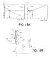
- the coil phase ⁇ Ucan be determined from Re ⁇ U ⁇ , as graphically illustrated in plot 175 .
- FIG. 15Bshows a schematic diagram of the general electrical hookup of FIG. 14 in which V 1 is the voltage applied to the lower portion of the coil 215 from the AC source 212 through tap 227 , V 2 is the voltage at tap 224 that is supplied to the upper charge terminal T 1 , and V 3 is the voltage applied to the lower compensation terminal T 2 through tap 233 .
- the resistances R p and R drepresent the ground return resistances of the charge terminal T 1 and compensation terminal T 2 , respectively.
- the charge and compensation terminals T 1 and T 2may be configured as spheres, cylinders, toroids, rings, hoods, or any other combination of capacitive structures.
- the size of the charge and compensation terminals T 1 and T 2can be chosen to provide a sufficiently large surface for the charges Q 1 and Q 2 imposed on the terminals. In general, it is desirable to make the charge terminal T 1 as large as practical.
- the size of the charge terminal T 1should be large enough to avoid ionization of the surrounding air, which can result in electrical discharge or sparking around the charge terminal.
- the self-capacitance C p and C d of the charge and compensation terminals T 1 and T 2 respectively,can be determined using, for example, equation (24).
- a resonant circuitis formed by at least a portion of the inductance of the coil 215 , the self-capacitance C d of the compensation terminal T 2 , and the ground return resistance R d associated with the compensation terminal T 2 .
- the parallel resonancecan be established by adjusting the voltage V 3 applied to the compensation terminal T 2 (e.g., by adjusting a tap 233 position on the coil 215 ) or by adjusting the height and/or size of the compensation terminal T 2 to adjust C d .
- the position of the coil tap 233can be adjusted for parallel resonance, which will result in the ground current through the ground stake 218 and through the ammeter 236 reaching a maximum point.
- the position of the tap 227 for the AC source 212can be adjusted to the 50 ⁇ point on the coil 215 .
- Voltage V 2 from the coil 215can be applied to the charge terminal T 1 , and the position of tap 224 can be adjusted such that the phase ( ⁇ ) of the total effective height (h TE ) approximately equals the angle of the guided surface wave tilt (W Rx ) at the Hankel crossover distance (R x ).
- the position of the coil tap 224can be adjusted until this operating point is reached, which results in the ground current through the ammeter 236 increasing to a maximum.
- the resultant fields excited by the guided surface waveguide probe 200 dare substantially mode-matched to a guided surface waveguide mode on the surface of the lossy conducting medium 203 , resulting in the launching of a guided surface wave along the surface of the lossy conducting medium 203 . This can be verified by measuring field strength along a radial extending from the guided surface waveguide probe 200 .
- Resonance of the circuit including the compensation terminal T 2may change with the attachment of the charge terminal T 1 and/or with adjustment of the voltage applied to the charge terminal T 1 through tap 224 . While adjusting the compensation terminal circuit for resonance aids the subsequent adjustment of the charge terminal connection, it is not necessary to establish the guided surface wave tilt (W Rx ) at the Hankel crossover distance (R x ).
- the systemmay be further adjusted to improve coupling by iteratively adjusting the position of the tap 227 for the AC source 212 to be at the 50 ⁇ point on the coil 215 and adjusting the position of tap 233 to maximize the ground current through the ammeter 236 .
- Resonance of the circuit including the compensation terminal T 2may drift as the positions of taps 227 and 233 are adjusted, or when other components are attached to the coil 215 .
- the voltage V 2 from the coil 215can be applied to the charge terminal T 1 , and the position of tap 233 can be adjusted such that the phase ( ⁇ ) of the total effective height (h TE ) approximately equals the angle ( ⁇ ) of the guided surface wave tilt at R x .
- the position of the coil tap 224can be adjusted until the operating point is reached, resulting in the ground current through the ammeter 236 substantially reaching a maximum.
- the resultant fieldsare substantially mode-matched to a guided surface waveguide mode on the surface of the lossy conducting medium 203 , and a guided surface wave is launched along the surface of the lossy conducting medium 203 . This can be verified by measuring field strength along a radial extending from the guided surface waveguide probe 200 .
- the systemmay be further adjusted to improve coupling by iteratively adjusting the position of the tap 227 for the AC source 212 to be at the 50 ⁇ point on the coil 215 and adjusting the position of tap 224 and/or 233 to maximize the ground current through the ammeter 236 .
- operation of a guided surface waveguide probe 200may be controlled to adjust for variations in operational conditions associated with the guided surface waveguide probe 200 .
- a probe control system 230can be used to control the feed network 209 and/or positioning of the charge terminal T 1 and/or compensation terminal T 2 to control the operation of the guided surface waveguide probe 200 .
- Operational conditionscan include, but are not limited to, variations in the characteristics of the lossy conducting medium 203 (e.g., conductivity ⁇ and relative permittivity ⁇ r ), variations in field strength and/or variations in loading of the guided surface waveguide probe 200 .
- Equipmentsuch as, e.g., conductivity measurement probes, permittivity sensors, ground parameter meters, field meters, current monitors and/or load receivers can be used to monitor for changes in the operational conditions and provide information about current operational conditions to the probe control system 230 .
- the probe control system 230can then make one or more adjustments to the guided surface waveguide probe 200 to maintain specified operational conditions for the guided surface waveguide probe 200 .
- Conductivity measurement probes and/or permittivity sensorsmay be located at multiple locations around the guided surface waveguide probe 200 . Generally, it would be desirable to monitor the conductivity and/or permittivity at or about the Hankel crossover distance R x for the operational frequency.
- Conductivity measurement probes and/or permittivity sensorsmay be located at multiple locations (e.g., in each quadrant) around the guided surface waveguide probe 200 .
- a guided surface waveguide probe 200 ethat includes a charge terminal T 1 and a charge terminal T 2 that are arranged along a vertical axis z.
- the guided surface waveguide probe 200 eis disposed above a lossy conducting medium 203 , which makes up Region 1 .
- a second medium 206shares a boundary interface with the lossy conducting medium 203 and makes up Region 2 .
- the charge terminals T 1 and T 2are positioned over the lossy conducting medium 203 .
- the charge terminal T 1is positioned at height H 1
- the charge terminal T 2is positioned directly below T 1 along the vertical axis z at height H 2 , where H 2 is less than H 1 .
- the guided surface waveguide probe 200 eincludes a feed network 209 that couples an excitation source 212 to the charge terminals T 1 and T 2 .
- the charge terminals T 1 and/or T 2include a conductive mass that can hold an electrical charge, which may be sized to hold as much charge as practically possible.
- the charge terminal T 1has a self-capacitance C 1
- the charge terminal T 2has a self-capacitance C 2 , which can be determined using, for example, equation (24).
- a mutual capacitance C Mis created between the charge terminals T 1 and T 2 .
- the charge terminals T 1 and T 2need not be identical, but each can have a separate size and shape, and can include different conducting materials.
- the field strength of a guided surface wave launched by a guided surface waveguide probe 200 eis directly proportional to the quantity of charge on the terminal T 1 .
- the guided surface waveguide probe 200 eWhen properly adjusted to operate at a predefined operating frequency, the guided surface waveguide probe 200 e generates a guided surface wave along the surface of the lossy conducting medium 203 .
- the excitation source 212can generate electrical energy at the predefined frequency that is applied to the guided surface waveguide probe 200 e to excite the structure.
- the electromagnetic fields generated by the guided surface waveguide probe 200 eare substantially mode-matched with the lossy conducting medium 203 , the electromagnetic fields substantially synthesize a wave front incident at a complex Brewster angle that results in little or no reflection.
- the surface waveguide probe 200 edoes not produce a radiated wave, but launches a guided surface traveling wave along the surface of a lossy conducting medium 203 .
- the energy from the excitation source 212can be transmitted as Zenneck surface currents to one or more receivers that are located within an effective transmission range of the guided surface waveguide probe 200 e.
- the asymptotes representing the radial current close-in and far-out as set forth by equations (90) and (91)are complex quantities.
- a physical surface current J( ⁇ )is synthesized to match as close as possible the current asymptotes in magnitude and phase. That is to say close-in,
- the phase of J( ⁇ )should transition from the phase of J 1 close-in to the phase of J 2 far-out.
- far-outshould differ from the phase of the surface current
- the properly adjusted synthetic radial surface currentis
- an iterative approachmay be used. Specifically, analysis may be performed of a given excitation and configuration of a guided surface waveguide probe 200 e taking into account the feed currents to the terminals T 1 and T 2 , the charges on the charge terminals T 1 and T 2 , and their images in the lossy conducting medium 203 in order to determine the radial surface current density generated. This process may be performed iteratively until an optimal configuration and excitation for a given guided surface waveguide probe 200 e is determined based on desired parameters.
- a guided field strength curve 103may be generated using equations (1)-(12) based on values for the conductivity of Region 1 ( ⁇ 1 ) and the permittivity of Region 1 ( ⁇ 1 ) at the location of the guided surface waveguide probe 200 e .
- Such a guided field strength curve 103can provide a benchmark for operation such that measured field strengths can be compared with the magnitudes indicated by the guided field strength curve 103 to determine if optimal transmission has been achieved.
- various parameters associated with the guided surface waveguide probe 200 emay be adjusted.
- One parameter that may be varied to adjust the guided surface waveguide probe 200 eis the height of one or both of the charge terminals T 1 and/or T 2 relative to the surface of the lossy conducting medium 203 .
- the distance or spacing between the charge terminals T 1 and T 2may also be adjusted. In doing so, one may minimize or otherwise alter the mutual capacitance C M or any bound capacitances between the charge terminals T 1 and T 2 and the lossy conducting medium 203 as can be appreciated.
- the size of the respective charge terminals T 1 and/or T 2can also be adjusted. By changing the size of the charge terminals T 1 and/or T 2 , one will alter the respective self-capacitances C 1 and/or C 2 , and the mutual capacitance C M as can be appreciated.
- the feed network 209 associated with the guided surface waveguide probe 200 eis another parameter that can be adjusted. This may be accomplished by adjusting the size of the inductive and/or capacitive reactances that make up the feed network 209 . For example, where such inductive reactances comprise coils, the number of turns on such coils may be adjusted. Ultimately, the adjustments to the feed network 209 can be made to alter the electrical length of the feed network 209 , thereby affecting the voltage magnitudes and phases on the charge terminals T 1 and T 2 .
- the iterations of transmission performed by making the various adjustmentsmay be implemented by using computer models or by adjusting physical structures as can be appreciated.
- By making the above adjustmentsone can create corresponding “close-in” surface current J 1 and “far-out” surface current J 2 that approximate the same currents J( ⁇ ) of the guided surface wave mode specified in Equations (90) and (91) set forth above. In doing so, the resulting electromagnetic fields would be substantially or approximately mode-matched to a guided surface wave mode on the surface of the lossy conducting medium 203 .
- operation of the guided surface waveguide probe 200 emay be controlled to adjust for variations in operational conditions associated with the guided surface waveguide probe 200 .
- a probe control system 230 shown in FIG. 12can be used to control the feed network 209 and/or positioning and/or size of the charge terminals T 1 and/or T 2 to control the operation of the guided surface waveguide probe 200 e .
- Operational conditionscan include, but are not limited to, variations in the characteristics of the lossy conducting medium 203 (e.g., conductivity ⁇ and relative permittivity ⁇ r ), variations in field strength and/or variations in loading of the guided surface waveguide probe 200 e.
- the guided surface waveguide probe 200 fincludes the charge terminals T 1 and T 2 that are positioned along a vertical axis z that is substantially normal to the plane presented by the lossy conducting medium 203 (e.g., the Earth).
- the second medium 206is above the lossy conducting medium 203 .
- the charge terminal T 1has a self-capacitance C 1
- the charge terminal T 2has a self-capacitance C 2 .
- charges Q 1 and Q 2are imposed on the charge terminals T 1 and T 2 , respectively, depending on the voltages applied to the charge terminals T 1 and T 2 at any given instant.
- a mutual capacitance C Mmay exist between the charge terminals T 1 and T 2 depending on the distance there between.
- bound capacitancesmay exist between the respective charge terminals T 1 and T 2 and the lossy conducting medium 203 depending on the heights of the respective charge terminals T 1 and T 2 with respect to the lossy conducting medium 203 .
- the guided surface waveguide probe 200 fincludes a feed network 209 that comprises an inductive impedance comprising a coil L 1a having a pair of leads that are coupled to respective ones of the charge terminals T 1 and T 2 .
- the coil L 1ais specified to have an electrical length that is one-half (1 ⁇ 2) of the wavelength at the operating frequency of the guided surface waveguide probe 200 f.
- the electrical length of the coil L 1ais specified as approximately one-half (1 ⁇ 2) the wavelength at the operating frequency, it is understood that the coil L 1a may be specified with an electrical length at other values. According to one embodiment, the fact that the coil L 1a has an electrical length of approximately one-half the wavelength at the operating frequency provides for an advantage in that a maximum voltage differential is created on the charge terminals T 1 and T 2 . Nonetheless, the length or diameter of the coil L 1a may be increased or decreased when adjusting the guided surface waveguide probe 200 f to obtain optimal excitation of a guided surface wave mode. Adjustment of the coil length may be provided by taps located at one or both ends of the coil. In other embodiments, it may be the case that the inductive impedance is specified to have an electrical length that is significantly less than or greater than 1 ⁇ 2 the wavelength at the operating frequency of the guided surface waveguide probe 200 f.
- the excitation source 212can be coupled to the feed network 209 by way of magnetic coupling. Specifically, the excitation source 212 is coupled to a coil L P that is inductively coupled to the coil L 1a . This may be done by link coupling, a tapped coil, a variable reactance, or other coupling approach as can be appreciated. To this end, the coil L P acts as a primary, and the coil L 1a acts as a secondary as can be appreciated.
- the heights of the respective charge terminals T 1 and T 2may be altered with respect to the lossy conducting medium 203 and with respect to each other.
- the sizes of the charge terminals T 1 and T 2may be altered.
- the size of the coil L 1amay be altered by adding or eliminating turns or by changing some other dimension of the coil L 1a .
- the coil L 1acan also include one or more taps for adjusting the electrical length as shown in FIG. 17 . The position of a tap connected to either charge terminal T 1 or T 2 can also be adjusted.
- FIGS. 18A, 18B, 18C and 19shown are examples of generalized receive circuits for using the surface-guided waves in wireless power delivery systems.
- FIGS. 18A and 18B-18Cinclude a linear probe 303 and a tuned resonator 306 , respectively.
- FIG. 19is a magnetic coil 309 according to various embodiments of the present disclosure.
- each one of the linear probe 303 , the tuned resonator 306 , and the magnetic coil 309may be employed to receive power transmitted in the form of a guided surface wave on the surface of a lossy conducting medium 203 according to various embodiments.
- the lossy conducting medium 203comprises a terrestrial medium (or Earth).
- the open-circuit terminal voltage at the output terminals 312 of the linear probe 303depends upon the effective height of the linear probe 303 .
- An electrical load 315is coupled to the output terminals 312 through an impedance matching network 318 .
- the electrical load 315should be substantially impedance matched to the linear probe 303 as will be described below.
- a ground current excited coil 306 a possessing a phase shift equal to the wave tilt of the guided surface waveincludes a charge terminal T R that is elevated (or suspended) above the lossy conducting medium 203 .
- the charge terminal T Rhas a self-capacitance C R .
- the bound capacitanceshould preferably be minimized as much as is practicable, although this may not be entirely necessary in every instance.
- the tuned resonator 306 aalso includes a receiver network comprising a coil L R having a phase shift ⁇ . One end of the coil L R is coupled to the charge terminal T R , and the other end of the coil L R is coupled to the lossy conducting medium 203 .
- the receiver networkcan include a vertical supply line conductor that couples the coil L R to the charge terminal T R .
- the coil L R(which may also be referred to as tuned resonator L R -C R ) comprises a series-adjusted resonator as the charge terminal C R and the coil L R are situated in series.
- the phase delay of the coil L Rcan be adjusted by changing the size and/or height of the charge terminal T R , and/or adjusting the size of the coil L R so that the phase ⁇ of the structure is made substantially equal to the angle of the wave tilt ⁇ .
- the phase delay of the vertical supply linecan also be adjusted by, e.g., changing length of the conductor.
- the reactance presented by the self-capacitance C Ris calculated as 1/j ⁇ C R .
- the total capacitance of the structure 306 amay also include capacitance between the charge terminal T R and the lossy conducting medium 203 , where the total capacitance of the structure 306 a may be calculated from both the self-capacitance C R and any bound capacitance as can be appreciated.
- the charge terminal T Rmay be raised to a height so as to substantially reduce or eliminate any bound capacitance. The existence of a bound capacitance may be determined from capacitance measurements between the charge terminal T R and the lossy conducting medium 203 as previously discussed.
- the inductive reactance presented by a discrete-element coil L Rmay be calculated as j ⁇ L, where L is the lumped-element inductance of the coil L R . If the coil L R is a distributed element, its equivalent terminal-point inductive reactance may be determined by conventional approaches.
- To tune the structure 306 aone would make adjustments so that the phase delay is equal to the wave tilt for the purpose of mode-matching to the surface waveguide at the frequency of operation. Under this condition, the receiving structure may be considered to be “mode-matched” with the surface waveguide.
- a transformer link around the structure and/or an impedance matching network 324may be inserted between the probe and the electrical load 327 in order to couple power to the load. Inserting the impedance matching network 324 between the probe terminals 321 and the electrical load 327 can effect a conjugate-match condition for maximum power transfer to the electrical load 327 .
- an electrical load 327may be coupled to the structure 306 a by way of magnetic coupling, capacitive coupling, or conductive (direct tap) coupling.
- the elements of the coupling networkmay be lumped components or distributed elements as can be appreciated.
- magnetic couplingis employed where a coil L S is positioned as a secondary relative to the coil L R that acts as a transformer primary.
- the coil L Smay be link-coupled to the coil L R by geometrically winding it around the same core structure and adjusting the coupled magnetic flux as can be appreciated.
- the receiving structure 306 acomprises a series-tuned resonator, a parallel-tuned resonator or even a distributed-element resonator of the appropriate phase delay may also be used.
- a receiving structure immersed in an electromagnetic fieldmay couple energy from the field
- polarization-matched structureswork best by maximizing the coupling, and conventional rules for probe-coupling to waveguide modes should be observed.
- a TE 20 (transverse electric mode) waveguide probemay be optimal for extracting energy from a conventional waveguide excited in the TE 20 mode.
- a mode-matched and phase-matched receiving structurecan be optimized for coupling power from a surface-guided wave.
- the guided surface wave excited by a guided surface waveguide probe 200 on the surface of the lossy conducting medium 203can be considered a waveguide mode of an open waveguide. Excluding waveguide losses, the source energy can be completely recovered.
- Useful receiving structuresmay be E-field coupled, H-field coupled, or surface-current excited.
- the receiving structurecan be adjusted to increase or maximize coupling with the guided surface wave based upon the local characteristics of the lossy conducting medium 203 in the vicinity of the receiving structure.
- a receiving structurecomprising the tuned resonator 306 a of FIG. 18B , including a coil L R and a vertical supply line connected between the coil L R and a charge terminal T R .
- the charge terminal T Rpositioned at a defined height above the lossy conducting medium 203 .
- the total phase shift ⁇ of the coil L R and vertical supply linecan be matched with the angle ( ⁇ ) of the wave tilt at the location of the tuned resonator 306 a . From Equation (22), it can be seen that the wave tilt asymptotically passes to
- ⁇ rcomprises the relative permittivity
- ⁇ 1is the conductivity of the lossy conducting medium 203 at the location of the receiving structure
- ⁇ 0is the permittivity of free space
- ⁇2 ⁇ f, where f is the frequency of excitation.
- the wave tilt angle ( ⁇ )can be determined from Equation (97).
- phase delays( ⁇ C + ⁇ y ) can be adjusted to match the phase shift ⁇ to the angle ( ⁇ ) of the wave tilt.
- a portion of the coilcan be bypassed by the tap connection as illustrated in FIG. 18B .
- the vertical supply line conductorcan also be connected to the coil L R via a tap, whose position on the coil may be adjusted to match the total phase shift to the angle of the wave tilt.
- the coupling into the guided surface waveguide modemay be maximized.
- the tuned resonator 306 bdoes not include a charge terminal T R at the top of the receiving structure.
- the tuned resonator 306 bdoes not include a vertical supply line coupled between the coil L R and the charge terminal T R .
- the total phase shift ( ⁇ ) of the tuned resonator 306 bincludes only the phase delay ( ⁇ c ) through the coil L R .
- FIG. 18Dshown is a flow chart 180 illustrating an example of adjusting a receiving structure to substantially mode-match to a guided surface waveguide mode on the surface of the lossy conducting medium 203 .
- the receiving structureincludes a charge terminal T R (e.g., of the tuned resonator 306 a of FIG. 18B )
- the charge terminal T Ris positioned at a defined height above a lossy conducting medium 203 at 184 .
- the physical height (h p ) of the charge terminal T Rmay be below that of the effective height.
- the physical heightmay be selected to reduce or minimize the bound charge on the charge terminal T R (e.g., four times the spherical diameter of the charge terminal). If the receiving structure does not include a charge terminal T R (e.g., of the tuned resonator 306 b of FIG. 18C ), then the flow proceeds to 187 .
- the electrical phase delay ⁇ of the receiving structureis matched to the complex wave tilt angle ⁇ defined by the local characteristics of the lossy conducting medium 203 .
- the phase delay ( ⁇ c ) of the helical coil and/or the phase delay ( ⁇ y ) of the vertical supply linecan be adjusted to make ⁇ equal to the angle ( ⁇ ) of the wave tilt (W).
- the angle ( ⁇ ) of the wave tiltcan be determined from Equation (86).
- the electrical phase ⁇can then be matched to the angle of the wave tilt.
- the load impedance of the charge terminal T Rcan be tuned to resonate the equivalent image plane model of the tuned resonator 306 a .
- the depth (d/2) of the conducting image ground plane 139 ( FIG. 9A ) below the receiving structurecan be determined using Equation (100) and the values of the lossy conducting medium 203 (e.g., the Earth) at the receiving structure, which can be locally measured.
- the impedance (Z in ) as seen “looking down” into the lossy conducting medium 203can then be determined using Equation (99). This resonance relationship can be considered to maximize coupling with the guided surface waves.
- the velocity factor, phase delay, and impedance of the coil L R and vertical supply linecan be determined.
- the self-capacitance (C R ) of the charge terminal T Rcan be determined using, e.g., Equation (24).
- the propagation factor ( ⁇ p ) of the coil L Rcan be determined using Equation (98), and the propagation phase constant ( ⁇ w ) for the vertical supply line can be determined using Equation (49).
- the impedance (Z base ) of the tuned resonator 306 a as seen “looking up” into the coil L Rcan be determined using Equations (101), (102), and (103).
- the equivalent image plane model of FIG. 9Aalso applies to the tuned resonator 306 a of FIG. 18B .
- the impedance at the physical boundary 136 ( FIG. 9A ) “looking up” into the coil of the tuned resonator 306 ais the conjugate of the impedance at the physical boundary 136 “looking down” into the lossy conducting medium 203 .
- An iterative approachmay be taken to tune the load impedance Z R for resonance of the equivalent image plane model with respect to the conducting image ground plane 139 . In this way, the coupling of the electric field to a guided surface waveguide mode along the surface of the lossy conducting medium 203 (e.g., Earth) can be improved and/or maximized.
- the magnetic coil 309comprises a receive circuit that is coupled through an impedance matching network 333 to an electrical load 336 .
- the magnetic coil 309may be positioned so that the magnetic flux of the guided surface wave, H ⁇ , passes through the magnetic coil 309 , thereby inducing a current in the magnetic coil 309 and producing a terminal point voltage at its output terminals 330 .
- the open-circuit induced voltage appearing at the output terminals 330 of the magnetic coil 309is
- the magnetic coil 309may be tuned to the guided surface wave frequency either as a distributed resonator or with an external capacitor across its output terminals 330 , as the case may be, and then impedance-matched to an external electrical load 336 through a conjugate impedance matching network 333 .
- the current induced in the magnetic coil 309may be employed to optimally power the electrical load 336 .
- the receive circuit presented by the magnetic coil 309provides an advantage in that it does not have to be physically connected to the ground.
- the receive circuits presented by the linear probe 303 , the mode-matched structure 306 , and the magnetic coil 309each facilitate receiving electrical power transmitted from any one of the embodiments of guided surface waveguide probes 200 described above.
- the energy receivedmay be used to supply power to an electrical load 315 / 327 / 336 via a conjugate matching network as can be appreciated.
- the receive circuits presented by the linear probe 303 , the mode-matched structure 306 , and the magnetic coil 309will load the excitation source 212 (e.g., FIGS. 3, 12 and 16 ) that is applied to the guided surface waveguide probe 200 , thereby generating the guided surface wave to which such receive circuits are subjected.
- the excitation source 212e.g., FIGS. 3, 12 and 16
- the guided surface wave generated by a given guided surface waveguide probe 200 described abovecomprises a transmission line mode.
- a power source that drives a radiating antenna that generates a radiated electromagnetic waveis not loaded by the receivers, regardless of the number of receivers employed.
- one or more guided surface waveguide probes 200 and one or more receive circuits in the form of the linear probe 303 , the tuned mode-matched structure 306 , and/or the magnetic coil 309can make up a wireless distribution system.
- the distance of transmission of a guided surface wave using a guided surface waveguide probe 200 as set forth abovedepends upon the frequency, it is possible that wireless power distribution can be achieved across wide areas and even globally.
- the conventional wireless-power transmission/distribution systems extensively investigated todayinclude “energy harvesting” from radiation fields and also sensor coupling to inductive or reactive near-fields.
- the present wireless-power systemdoes not waste power in the form of radiation which, if not intercepted, is lost forever.
- the presently disclosed wireless-power systemlimited to extremely short ranges as with conventional mutual-reactance coupled near-field systems.
- the wireless-power system disclosed hereinprobe-couples to the novel surface-guided transmission line mode, which is equivalent to delivering power to a load by a waveguide or a load directly wired to the distant power generator.
- FIGS. 20A-Eshown are examples of various schematic symbols that are used with reference to the discussion that follows.
- a depiction of this symbolwill be referred to as a guided surface waveguide probe P.
- any reference to the guided surface waveguide probe Pis a reference to any one of the guided surface waveguide probes 200 a , 200 b , 200 c , 200 e , 200 d , or 200 f ; or variations thereof.
- a symbol that represents a guided surface wave receive structurethat may comprise any one of the linear probe 303 ( FIG. 18A ), the tuned resonator 306 ( FIGS. 18B-18C ), or the magnetic coil 309 ( FIG. 19 ).
- a depiction of this symbolwill be referred to as a guided surface wave receive structure R.
- any reference to the guided surface wave receive structure Ris a reference to any one of the linear probe 303 , the tuned resonator 306 , or the magnetic coil 309 ; or variations thereof.
- FIG. 20Cshown is a symbol that specifically represents the linear probe 303 ( FIG. 18A ).
- a depiction of this symbolwill be referred to as a guided surface wave receive structure R P .
- any reference to the guided surface wave receive structure R Pis a reference to the linear probe 303 or variations thereof.
- FIG. 20Dshown is a symbol that specifically represents the tuned resonator 306 ( FIGS. 18B-18C ).
- a depiction of this symbolwill be referred to as a guided surface wave receive structure R R .
- any reference to the guided surface wave receive structure R Ris a reference to the tuned resonator 306 or variations thereof.
- FIG. 20Eshown is a symbol that specifically represents the magnetic coil 309 ( FIG. 19 ).
- a depiction of this symbolwill be referred to as a guided surface wave receive structure R M .
- any reference to the guided surface wave receive structure R Mis a reference to the magnetic coil 309 or variations thereof.
- a navigation devicedetects multiple guided surface waves launched from multiple guided surface wave waveguide probes P. By analyzing the time difference on arrival of the guided surface waves, the time each of the guided surface waves spent traveling from the corresponding guided surface wave waveguide probe P to the location of the navigation device, the difference in the intensity of the guided surface waves at the location of the navigation device compared to the original intensity of the guided surface waves, the phase shift between the guided surface waves measured at the location of the navigation device, or some combination of these approaches, the location of the navigation device on the Earth may be determined. Further, in some embodiments, the navigation device may be powered by one or more of the guided surface waves. Moreover, the guide surface waves may be used for time synchronization to improve the accuracy of the navigation device and/or other devices.
- the range of the guided surface wavesis dependent on the frequency of the guided surface waves.
- guided surface waves with a frequency of approximately 20 KHz or lessare generally capable of travelling or propagating around the earth.
- the various embodiments of the present disclosuremay be used for global positioning and navigation. Higher frequencies will go shorter distances, such as thousands, hundreds or tens of miles, limiting the various embodiments to regional usage for position and navigation.
- the navigation unit 400includes a receiver 403 , an antenna mount 406 , and a computing device 409 .
- the receiver 403is connected to the antenna mount 406 , which is in turn connected to the computing device 409 .
- the navigation unit 400may include a display.
- the displaymay comprise, for example, one or more devices such as liquid crystal display (LCD) displays, gas plasma-based flat panel displays, organic light emitting diode (OLED) displays, electrophoretic ink (E ink) displays, LCD projectors, or other types of display devices, etc.
- LCDliquid crystal display
- OLEDorganic light emitting diode
- E inkelectrophoretic ink
- the navigation unit 400may be enclosed in an external case that protects the various components of the navigation unit 400 .
- the navigation unit 400may be a portable or handheld unit, with the receiver 403 , the antenna mount 406 , and the computing device 409 enclosed within a single shell.
- Such embodimentsmay include a mobile computing device, such as a tablet computer, a cellular phone, a smart phone, a personal digital assistant (PDA), and/or similar mobile computing device.
- PDApersonal digital assistant
- Such embodimentsmay also include a dedicated navigation unit, such as personal navigation devices, handheld navigation devices, or navigation devices that can be mounted to the dashboard of a bus, automobile, motor boat, or similar vehicle.
- the receiver 403may be remote or external to the computing device 409 and connected to the computing device via the antenna mount 406 .
- vehicular navigation units 400such as those found on ships or in airplanes.
- the receiver 403may correspond to one or more structures capable of receiving a guided surface wave.
- the receiver 403may include, for example, a linear probe, a tuned resonator, a magnetic coil, and/or similar structures for receiving a guided surface wave, as previously described above.
- the receiver 403may represent a plurality of receivers 403 , each of which is tuned to receive a guided surface wave on a different frequency from the other receivers 403 .
- the receiver 403may be configured to be tuned to receive multiple guided surface waves on different frequencies simultaneously.
- the receiver 403may be configured to alternate frequencies in order to detect, receive, and/or measure a guided surface wave on a first frequency and then switch to a second frequency to detect a second guided surface wave on a second frequency.
- the antenna mount 406may correspond to any physical structure capable of connecting the receiver 403 to the computing device 409 .
- the computing device 409can include a compass 411 .
- the compass 411corresponds to any circuit, system, or apparatus that can identify the direction of magnetic north or true north. Accordingly, the compass 411 can correspond to a magnetic compass or magnetometer for embodiments described herein that rely upon the magnetic north pole or a non-magnetic compass (e.g. gyrocompass, optical compass, or other non-magnetic compass) for embodiments described herein that rely upon true north.
- a non-magnetic compasse.g. gyrocompass, optical compass, or other non-magnetic compass
- the computing device 409can also include at least one processor circuit having a processor 413 and a memory 416 , both of which are coupled to a local interface 419 .
- the local interface 419may comprise, for example, a data bus with an accompanying address/control bus or other bus structure as can be appreciated.
- Stored in the memory 416are both data and several components that are executable by the processor 413 .
- a multilateration application 423stored in the memory 416 and executable by the processor 413 is a multilateration application 423 , and potentially other applications.
- Also stored in the memory 416may be a data store 426 , which may store map data 429 , inertial data 431 , phase shift curves 433 , and/or potentially other data.
- an operating systemmay be stored in the memory 416 and executable by the processor 413 .
- the map data 429represents one or more geographies which the navigation unit 400 may be navigating or in which geolocation may be occurring.
- Map data 429may include global data, or data related to particular regions or locales, such as a hemisphere, continent, ocean, sea, lake, country, state/province, city, and/or portions thereof.
- Map data 429may also include one or more coordinate systems for identifying a location on the globe, or within a particular region or locale. Such coordinate systems may include latitude and longitude lines, the Universal Transverse Mercator (UTM) coordinate system, the Universal Polar Stereographic (UPS) coordinate system, a grid system, and/or other coordinate systems.
- UDMUniversal Transverse Mercator
- UPSUniversal Polar Stereographic
- the map data 429may include relevant data necessary to disambiguate between locations on the globe. This can include a list of cellular networks in various countries or regions. This can include a list of radio or television broadcast stations in various countries or regions. In some instances, this can include a list of media access control (MAC) addresses for wireless network access points at various locations. In various instances, this can also include a list of angles that would be formed between guided surface wavefronts launched from guided surface waveguide probes with a known location and the polar axis running from the North Pole to the South Pole and the locations on the Earth. In addition, the map data 429 could also include a list of locations where those angles would be formed if the navigation unit 400 were a given distance from the guided surface waveguide probe that launched the guided surface wave or its antipode.
- MACmedia access control
- the inertial data 431represents navigational data describing the current and historical trajectories of the navigation unit 400 .
- Inertial data 431may represent, for example, a current speed, a current altitude, and/or a current heading of the navigation unit 400 or an object to which the navigation unit 400 is attached, as well as other navigation data.
- Inertial data 431may also include historical data, such as an initial or starting location, past speeds and corresponding headings, past altitudes, and/or other navigation data.
- the multilateration application 423is executed to identify the location of the navigation unit 400 based on one or more guided surface waves received by the navigation unit 400 . For example, the multilateration application 423 can calculate the time that occurs between when a guided surface wave is received and when a reflection from the antipode is received. Based on the calculated time difference, the multilateration application 423 can determine how far the navigation unit 400 is from the antipode and therefore how far the navigation unit 400 is from the guided surface waveguide probe P used to launch the guided surface wave. The multilateration application 423 can further rely upon compass readings to disambiguate the position of the navigation unit 400 from multiple possible positions, as further described herein. In one or more of these various embodiments, the multilateration application 423 may make use of additional data, such as map data 429 , phase shift curves 433 , inertial data 431 , and/or other navigational data
- any component discussed hereinis implemented in the form of software, any one of a number of programming languages may be employed such as, for example, C, C++, C#, Objective C, Java®, JavaScript®, Perl, PHP, Visual Basic®, Python®, Ruby, Flash or other programming languages.
- executablemeans a program file that is in a form that can ultimately be run by the processor 413 .
- Examples of executable programsmay be, for example, a compiled program that can be translated into machine code in a format that can be loaded into a random access portion of the memory 416 and run by the processor 413 , source code that may be expressed in proper format such as object code that is capable of being loaded into a random access portion of the memory 416 and executed by the processor 413 , or source code that may be interpreted by another executable program to generate instructions in a random access portion of the memory 416 to be executed by the processor 413 , etc.
- An executable programmay be stored in any portion or component of the memory 416 including, for example, random access memory (RAM), read-only memory (ROM), hard drive, solid-state drive, USB flash drive, memory card, optical disc such as compact disc (CD) or digital versatile disc (DVD), floppy disk, magnetic tape, or other memory components.
- RAMrandom access memory
- ROMread-only memory
- hard drivesolid-state drive
- USB flash driveUSB flash drive
- memory cardsuch as compact disc (CD) or digital versatile disc (DVD), floppy disk, magnetic tape, or other memory components.
- CDcompact disc
- DVDdigital versatile disc
- the memory 416is defined herein as including both volatile and nonvolatile memory and data storage components. Volatile components are those that do not retain data values upon loss of power. Nonvolatile components are those that retain data upon a loss of power.
- the memory 416may comprise, for example, random access memory (RAM), read-only memory (ROM), hard disk drives, solid-state drives, USB flash drives, memory cards accessed via a memory card reader, floppy disks accessed via an associated floppy disk drive, optical discs accessed via an optical disc drive, magnetic tapes accessed via an appropriate tape drive, and/or other memory components, or a combination of any two or more of these memory components.
- the RAMmay comprise, for example, static random access memory (SRAM), dynamic random access memory (DRAM), or magnetic random access memory (MRAM) and other such devices.
- the ROMmay comprise, for example, a programmable read-only memory (PROM), an erasable programmable read-only memory (EPROM), an electrically erasable programmable read-only memory (EEPROM), or other like memory device.
- the processor 413may represent multiple processors 413 and/or multiple processor cores and the memory 416 may represent multiple memories 416 that operate in parallel processing circuits, respectively.
- the local interface 419may be an appropriate network that facilitates communication between any two of the multiple processors 413 , between any processor 413 and any of the memories 416 , or between any two of the memories 416 , etc.
- the local interface 419may comprise additional systems designed to coordinate this communication, including, for example, performing load balancing.
- the processor 413may be of electrical or of some other available construction.
- multilateration application 423may be embodied in software or code executed by general purpose hardware as discussed above, as an alternative the same may also be embodied in dedicated hardware or a combination of software/general purpose hardware and dedicated hardware. If embodied in dedicated hardware, each can be implemented as a circuit or state machine that employs any one of or a combination of a number of technologies. These technologies may include, but are not limited to, discrete logic circuits having logic gates for implementing various logic functions upon an application of one or more data signals, application specific integrated circuits (ASICs) having appropriate logic gates, field-programmable gate arrays (FPGAs), or other components, etc. Such technologies are generally well known by those skilled in the art and, consequently, are not described in detail herein.
- FIG. 22shown is a graphical representation of a determination of a location of the navigation unit 400 ( FIG. 21 ) by the multilateration application 423 ( FIG. 21 ).
- a ground station 500launches a guided surface wave using a respective guided surface wave waveguide probe P.
- the navigation unit 400receives or detects the guided surface wave and then later receives or detects a corresponding reflected guided surface wave that has been reflected from the antipode relative to the respective ground station 500 .
- the multilateration application 423may calculate the amount of time that elapsed between when the guided surface wave was received and when the corresponding reflected guided surface wave was received.
- the multilateration application 423can use this time to determine the distance from the antipode to the navigation unit 400 and the corresponding distance from the navigation unit 400 to the respective ground station 500 .
- the multilateration application 423may then calculate a circumference 503 around the ground station 500 with a radius equal to the distance from the ground station 500 to the navigation unit 400 .
- the multilateration application 423could calculate a circumference around the antipode with a radius equal to the distance from the antipode to the navigation unit 400 .
- the multilateration application 423can then use the compass 411 to determine the location or magnetic north or true north.
- the angle between the direction of the guided surface wave and the location of magnetic north or true northcan isolate the location of the navigation unit 400 to two possible locations on opposite hemispheres relative to the ground station 500 .
- the magnetic dip detected by a magnetic compass 411can further be used to isolate the location of the navigation unit 400 to a single location.
- the multilateration application 423can also use additional data, such as map data 429 or inertial data 431 to further isolate or otherwise resolve or disambiguate the location of the navigation unit 400 .
- FIG. 23shown is a graphical representation of the angle ⁇ formed by the normal vector of the guided surface wave front 603 of a guided surface wave launched from a ground station 500 and the polar axis 606 running from the North Pole to the South Pole of the Earth.
- the angle ⁇is unique to two points on a circumference of a circle centered on the ground station 500 or the corresponding antipode that crosses through the location 509 of the navigation unit 400 ( FIG. 21 ). Accordingly, a measurement of the angle ⁇ formed between the polar axis 606 and the normal vector of the guided surface wave front 603 would indicate two possible locations 609 for the navigation unit 400 , each in an opposite hemisphere from the other.
- the multilateration application 423could use additional information to disambiguate which of the two possible locations 609 corresponds to the actual location 609 of the navigation unit 400 .
- the frequency of the guided surface wavemay determine whether the guided surface wave travels at a uniform speed around the entire Earth. Specifically, the lower the frequency, the more likely that the guided surface wave front 603 will be uniform around its circumference. However, at higher frequencies, local terrain or water may cause a difference in the speed of propagation. Such effects should be taken into account in the various embodiments described herein if they are significant.
- FIG. 24shown is a flowchart that provides one example of the operation of a portion of the multilateration application 423 according to various embodiments. It is understood that the flowchart of FIG. 24 provides merely an example of the many different types of functional arrangements that may be employed to implement the operation of the portion of the multilateration application 423 as described herein. As an alternative, the flowchart of FIG. 24 may be viewed as depicting an example of elements of a method implemented in the computing device 409 ( FIG. 21 ) according to one or more embodiments.
- the multilateration application 423identifies the first pulse or the leading edge of each guided surface wave received at the location 609 ( FIG. 23 ) of the navigation unit 400 ( FIG. 21 ). For each guided surface wave, the multilateration application 423 may record the time that the pulse or leading edge of each guided surface wave was received at the location 609 of the navigation unit 400 and the corresponding ground station 500 ( FIG. 23 ) for the guided surface wave.
- the multilateration application 423identifies the reflection from the antipode of the guided surface wave received at the location 609 of the navigation unit 400 .
- the multilateration application 423may record the time that the reflected guided surface wave was received at the location 506 of the navigation unit 400 .
- the multilateration application 423calculates the distance from the navigation unit 400 to the ground station 500 or its corresponding antipode, according to various embodiments of the present disclosure. For example, the multilateration application 423 can calculate the length of time between when the first pulse or the leading edge of a guided surface wave was received and when the corresponding reflected guided surface wave was received. The calculated length of time indicates how far the navigation unit 400 is from the ground station 500 and its antipode.
- D A( T/ 2)* V GSW (106) where D A represents the distance from the navigation unit 400 to the antipode, T represents the time that elapsed between when the first pulse or the leading edge of the guided surface wave was received and when the corresponding reflected guided surface wave was received and V GSW represents the velocity of the guided surface wave along the lossy terrestrial medium.
- D GS( C E /2) ⁇ D A (107) where D GS represents the distance from the navigation unit 400 to the ground station 500 , C E represents the circumference of the Earth, and D A represents the distance from the navigation unit 400 to the antipode.
- the multilateration application 423calculates, plots, or otherwise generates a circumference 503 ( FIG. 22 ) around the ground station 500 or its antipode to identify the location 506 ( FIG. 22 ) of the navigation unit 400 .
- the circumferencemay, for example, be calculated by creating a circle with a center equivalent to the location of the ground station 500 or corresponding antipode and with a radius equal to the calculated distance to the location of the ground station 500 or antipode, as described above.
- the location of the ground station 500 and corresponding antipodemay be previously known and stored in the memory 416 ( FIG. 21 ) of the navigation device 400 , such as in the map data 429 ( FIG. 21 ), or may be determined using various approaches.
- the multilateration application 423identifies the angle ⁇ formed between the polar axis 606 of the earth and the guided surface wave front 603 ( FIG. 23 ) or the circumference 503 calculated previously in box 713 .
- the multilateration application 423can cause the compass 411 ( FIG. 21 ) to determine the location of the magnetic North Pole or the true North Pole, depending on the embodiment.
- the location of the magnetic North Pole or the true North Pole relative to the guided surface wave front 603 ( FIG. 23 ) or the circumference 503is used to calculate a value for ⁇ .
- the multilateration application 423determines potential locations 609 ( FIG. 23 ) for the navigation unit 400 .
- the multilateration application 423may reference the map data 429 to identify potential locations where the angle ⁇ would be formed at the calculated distance from the ground station 500 or its antipode.
- the multilateration application 423disambiguates between the potential locations 609 of the navigation unit to determine the current location 609 of the navigation unit.
- Various approachescan be used to disambiguate between multiple positions, include the examples provided below.
- multiple approachesmay be used together to increase the accuracy of the disambiguation process or as a redundant approach if a first approach is not viable for disambiguating between potential locations 609 .
- the multilateration application 423could use inertial data 431 to disambiguate between multiple locations. For example, if the inertial data 431 indicated that the navigation unit 400 began its current journey in New York City, had been travelling at a speed of 500 miles-per-hour, and had been travelling for 1 hour, then the multilateration application 423 would know that it is located on a circumference of a circle with a radius of 500 miles and centered on New York City. Whichever location 609 identified at box 719 fell along that circumference would correspond to the current location 609 of the navigation unit 400 . Similarly, if one location determined at box 719 were located within North America and the other location determined at box 719 were located in Asia, the multilateration application 423 could identify the North American location as the current location 609 of the navigation unit 400 .
- the multilateration application 423could make use of external data sources to disambiguate between multiple locations. As an example, one location determined at box 719 could be located within North America and the other location determined at box 719 could be located in Asia. If the navigation unit 400 were able to receive signals from a North American cellular phone provider, the multilateration application 423 could determine that the North American position identified at box 719 was the correct current location 506 of the navigation unit 400 . Similar determinations could be made based on whether the navigation unit 400 was receiving broadcasts of particular radio stations (e.g. an AM or FM radio station located in North America versus an AM or FM radio station located in Asia), television stations, wireless network signals (e.g. from a network access point with a MAC address previously identified as being located in North America), or similar signals.
- radio stationse.g. an AM or FM radio station located in North America versus an AM or FM radio station located in Asia
- wireless network signalse.g. from a network access point with a MAC address previously identified as being located in North America
- the multilateration application 423can disambiguate between potential locations 609 through the use of magnetic dip.
- Magnetic diprefers to the angle between the Earth's magnetic field lines and the horizon. Because the Earth's magnetic field lines are not parallel to the surface of the Earth, the north end of a compass needle will point towards the ground in the northern hemisphere (positive magnetic dip) and away from the ground in the southern hemisphere (negative magnetic dip) as the magnetic needle attempts to align itself with the lines of force of the Earth's magnetic field.
- multilateration application 423can use the magnetic dip measured at the current location 609 of the navigation unit 400 to disambiguate between potential locations 609 .
- executionAfter disambiguating the current location 506 of the navigation unit 400 , execution subsequently ends.
- each blockmay represent a module, segment, or portion of code that comprises program instructions to implement the specified logical function(s).
- the program instructionsmay be embodied in the form of source code that comprises human-readable statements written in a programming language or machine code that comprises numerical instructions recognizable by a suitable execution system such as a processor 413 ( FIG. 21 ) in a computer system or other system.
- the machine codemay be converted from the source code, etc.
- each blockmay represent a circuit or a number of interconnected circuits to implement the specified logical function(s).
- FIG. 24shows a specific order of execution, it is understood that the order of execution may differ from that which is depicted. For example, the order of execution of two or more blocks may be scrambled relative to the order shown. Also, two or more blocks shown in succession in FIG. 24 may be executed concurrently or with partial concurrence. Further, in some embodiments, one or more of the blocks shown in FIG. 24 may be skipped or omitted. In addition, any number of counters, state variables, warning semaphores, or messages might be added to the logical flow described herein, for purposes of enhanced utility, accounting, performance measurement, or providing troubleshooting aids, etc. It is understood that all such variations are within the scope of the present disclosure.
- any logic or application described herein, including the multilateration application 423that comprises software or code can be embodied in any non-transitory computer-readable medium for use by or in connection with an instruction execution system such as, for example, a processor 413 in a computer system or other system.
- the logicmay comprise, for example, statements including instructions and declarations that can be fetched from the computer-readable medium and executed by the instruction execution system.
- a “computer-readable medium”can be any medium that can contain, store, or maintain the logic or application described herein for use by or in connection with the instruction execution system.
- the computer-readable mediumcan comprise any one of many physical media such as, for example, magnetic, optical, or semiconductor media. More specific examples of a suitable computer-readable medium would include, but are not limited to, magnetic tapes, magnetic floppy diskettes, magnetic hard drives, memory cards, solid-state drives, USB flash drives, or optical discs. Also, the computer-readable medium may be a random access memory (RAM) including, for example, static random access memory (SRAM) and dynamic random access memory (DRAM), or magnetic random access memory (MRAM).
- RAMrandom access memory
- SRAMstatic random access memory
- DRAMdynamic random access memory
- MRAMmagnetic random access memory
- the computer-readable mediummay be a read-only memory (ROM), a programmable read-only memory (PROM), an erasable programmable read-only memory (EPROM), an electrically erasable programmable read-only memory (EEPROM), or other type of memory device.
- ROMread-only memory
- PROMprogrammable read-only memory
- EPROMerasable programmable read-only memory
- EEPROMelectrically erasable programmable read-only memory
- any logic or application described herein, including the multilateration application 423may be implemented and structured in a variety of ways.
- one or more applications describedmay be implemented as modules or components of a single application.
- terms such as “application,” “service,” “system,” “engine,” “module,” and so onmay be interchangeable and are not intended to be limiting.
- Disjunctive languagesuch as the phrase “at least one of X, Y, or Z,” unless specifically stated otherwise, is otherwise understood with the context as used in general to present that an item, term, etc., may be either X, Y, or Z, or any combination thereof (e.g., X, Y, and/or Z). Thus, such disjunctive language is not generally intended to, and should not, imply that certain embodiments require at least one of X, at least one of Y, or at least one of Z to each be present.
Landscapes
- Engineering & Computer Science (AREA)
- Radar, Positioning & Navigation (AREA)
- Remote Sensing (AREA)
- Physics & Mathematics (AREA)
- General Physics & Mathematics (AREA)
- Computer Networks & Wireless Communication (AREA)
- Automation & Control Theory (AREA)
- Signal Processing (AREA)
- Radar Systems Or Details Thereof (AREA)
- Position Fixing By Use Of Radio Waves (AREA)
Abstract
Description
H2ϕ=Ae−u
H1ϕ=Aeu
and gives, in
u1=−u2(εr−jx). (8)
The radial propagation constant γ is given by
which is a complex expression where n is the complex index of refraction given by
n=√{square root over (εr−jx)}. (10)
In all of the above Equations,
where εrcomprises the relative permittivity of
{circumflex over (z)}×


where {circumflex over (z)} is a unit normal in the positive vertical (+z) direction and
Jρ(ρ′)=−AH1(2)(−jγρ′) (14)
where A is a constant. Further, it should be noted that close-in to the guided surface waveguide probe200 (for ρ<<λ), Equation (14) above has the behavior
The negative sign means that when source current (I0) flows vertically upward as illustrated in
where q1=C1V1, in Equations (1)-(6) and (14). Therefore, the radial surface current density of Equation (14) can be restated as
The fields expressed by Equations (1)-(6) and (17) have the nature of a transmission line mode bound to a lossy interface, not radiation fields that are associated with groundwave propagation. See Barlow, H. M. and Brown, J.,Radio Surface Waves, Oxford University Press, 1962, pp. 1-5.
Hn(1)(x)=Jn(x)+jNn(x), and (18)
Hn(2)(x)=Jn(x)−jNn(x), (19)
These functions represent cylindrical waves propagating radially inward (Hn(1)) and outward (Hn(2)), respectively. The definition is analogous to the relationship e±jx=cos x±j sin x. See, for example, Harrington, R. F.,Time-Harmonic Fields, McGraw-Hill, 1961, pp. 460-463.
which, when multiplied by ejωt, is an outward propagating cylindrical wave of the form ej(ωt-kρ)with a 1/√{square root over (ρ)} spatial variation. The first order (n=1) solution can be determined from Equation (20a) to be
Close-in to the guided surface waveguide probe (for ρ>>λ), the Hankel function of first order and the second kind behaves as
Note that these asymptotic expressions are complex quantities. When x is a real quantity, Equations (20b) and (21) differ in phase by √{square root over (j)}, which corresponds to an extra phase advance or “phase boost” of 45° or, equivalently, λ/8. The close-in and far-out asymptotes of the first order Hankel function of the second kind have a Hankel “crossover” or transition point where they are of equal magnitude at a distance of ρ=Rx.
where n is the complex index of refraction of Equation (10) and θiis the angle of incidence of the electric field. In addition, the vertical component of the mode-matched electric field of Equation (3) asymptotically passes to
which is linearly proportional to free charge on the isolated component of the elevated charge terminal's capacitance at the terminal voltage, qfree=Cfree×VT.
Celevated sphere=4πε0α(1+M+M2+M3+2M4+3M5+ . . . ), (24)
where the diameter of the sphere is 2α, and where M=α/2h with h being the height of the spherical terminal. As can be seen, an increase in the terminal height h reduces the capacitance C of the charge terminal. It can be shown that for elevations of the charge terminal T1that are at a height of about four times the diameter (4D=8α) or greater, the charge distribution is approximately uniform about the spherical terminal, which can improve the coupling into the guided surface waveguide mode.
where θiis the conventional angle of incidence measured with respect to the surface normal.
θi=arctan(√{square root over (εr−jx)})=θi,B, (26)
where x=σ/ωε0. This complex angle of incidence (θi,B) is referred to as the Brewster angle. Referring back to Equation (22), it can be seen that the same complex Brewster angle (θi,B) relationship is present in both Equations (22) and (26).

Geometrically, the illustration in
Eρ(ρ,z)=E(ρ,z)cos θi, and (28a)
which means that the field ratio is
which is complex and has both magnitude and phase. For an electromagnetic wave in
With the angle of incidence equal to the complex Brewster angle (θi,B), the Fresnel reflection coefficient of Equation (25) vanishes, as shown by
By adjusting the complex field ratio of Equation (22), an incident field can be synthesized to be incident at a complex angle at which the reflection is reduced or eliminated. Establishing this ratio as n=√{square root over (εr−jx)} results in the synthesized electric field being incident at the complex Brewster angle, making the reflections vanish.
for a monopole with a physical height (or length) of hp. Since the expression depends upon the magnitude and phase of the source distribution along the structure, the effective height (or length) is complex in general. The integration of the distributed current I(z) of the structure is performed over the physical height of the structure (hp), and normalized to the ground current (I0) flowing upward through the base (or input) of the structure. The distributed current along the structure can be expressed by
I(z)=ICcos(β0z), (34)
where β0is the propagation factor for current propagating on the structure. In the example of
where Vfis the velocity factor on the structure, λ0is the wavelength at the supplied frequency, and λpis the propagation wavelength resulting from the velocity factor Vf. The phase delay is measured relative to the ground (stake) current I0.
IC(θc+θy)=I0ejΦ, (36)
with the total phase delay Φ measured relative to the ground (stake) current I0. Consequently, the electrical effective height of a guided surface waveguide probe200 can be approximated by
for the case where the physical height hp<<λ0. The complex effective height of a monopole, heff=hpat an angle (or phase shift) of Φ, may be adjusted to cause the source fields to match a guided surface waveguide mode and cause a guided surface wave to be launched on the
Electrically, the geometric parameters are related by the electrical effective height (heff) of the charge terminal T1by
Rxtan ψi,B=Rx×W=heff=hpejΦ, (39)
where ψi,B=(π/2)−θi,Bis the Brewster angle measured from the surface of the lossy conducting medium. To couple into the guided surface waveguide mode, the wave tilt of the electric field at the Hankel crossover distance can be expressed as the ratio of the electrical effective height and the Hankel crossover distance
Since both the physical height (hp) and the Hankel crossover distance (Rx) are real quantities, the angle (Ψ) of the desired guided surface wave tilt at the Hankel crossover distance (Rx) is equal to the phase (Φ) of the complex effective height (heff). This implies that by varying the phase at the supply point of the coil, and thus the phase shift in Equation (37), the phase, Φ, of the complex effective height can be manipulated to match the angle of the wave tilt, Ψ, of the guided surface waveguide mode at the Hankel crossover point121: Φ=Ψ.
n=√{square root over (εr−jx)}, (41)
where x=σ/ωε0, with ω=2πf. The conductivity a and relative permittivity εrcan be determined through test measurements of the
θi,B=arctan(√{square root over (εr−jx)}), (42)
or measured from the surface as shown in
The wave tilt at the Hankel crossover distance (WRx) can also be found using Equation (40).
heff=hpejΦ=Rxtan ψi,B. (44)
As can be seen from Equation (44), the complex effective height (heff) includes a magnitude that is associated with the physical height (hp) of the charge terminal T1and a phase delay (Φ) that is to be associated with the angle (Ψ) of the wave tilt at the Hankel crossover distance (Rx). With these variables and the selected charge terminal T1configuration, it is possible to determine the configuration of a guided surface waveguide probe200.
where H is the axial length of the solenoidal helix, D is the coil diameter, N is the number of turns of the coil, s=H/N is the turn-to-turn spacing (or helix pitch) of the coil, and λ0is the free-space wavelength. Based upon this relationship, the electrical length, or phase delay, of the helical coil is given by
The principle is the same if the helix is wound spirally or is short and fat, but Vfand θcare easier to obtain by experimental measurement. The expression for the characteristic (wave) impedance of a helical transmission line has also been derived as
where hwis the vertical length (or height) of the conductor and α is the radius (in mks units). As with the helical coil, the traveling wave phase delay of the vertical feed line conductor can be given by
where βwis the propagation phase constant for the vertical feed line conductor, hwis the vertical length (or height) of the vertical feed line conductor, Vwis the velocity factor on the wire, λ0is the wavelength at the supplied frequency, and λwis the propagation wavelength resulting from the velocity factor Vw. For a uniform cylindrical conductor, the velocity factor is a constant with Vw≈0.94, or in a range from about 0.93 to about 0.98. If the mast is considered to be a uniform transmission line, its average characteristic impedance can be approximated by
where Vw≈0.94 for a uniform cylindrical conductor and a is the radius of the conductor. An alternative expression that has been employed in amateur radio literature for the characteristic impedance of a single-wire feed line can be given by
Equation (51) implies that Zwfor a single-wire feeder varies with frequency. The phase delay can be determined based upon the capacitance and characteristic impedance.
where
γe2=jωμ1σ1−ω2μ1ε1, and (53)
k0=ω√{square root over (μ0ε0)}, (54)
as indicated in Equation (12). The complex spacing of the image charge, in turn, implies that the external field will experience extra phase shifts not encountered when the interface is either a dielectric or a perfect conductor. In the lossy conducting medium, the wave front normal is parallel to the tangent of the conducting
γ0=jω√{square root over (μ0ε0)}=0+jβ0, and (55)
In the
γe=√{square root over (jωμ1(σ1+jωε1))}, and (57)
For normal incidence, the equivalent representation of
Zin=Z0tanh(γ0z1). (59)
Equating the image ground plane impedance Zinassociated with the equivalent model of
where only the first term of the series expansion for the inverse hyperbolic tangent is considered for this approximation. Note that in the
Additionally, the “image charge” will be “equal and opposite” to the real charge, so the potential of the perfectly conducting
where CTis the self-capacitance of the charge terminal T1, the impedance seen “looking up” into the vertical feed line conductor221 (
and the impedance seen “looking up” into the coil215 (
At the base of the guided surface waveguide probe200, the impedance seen “looking down” into the
where Zs=0.
The electrical phase Φ can then be matched to the angle of the wave tilt. This angular (or phase) relationship is next considered when launching surface waves. For example, the electrical phase delay Φ=θc+θycan be adjusted by varying the geometrical parameters of the coil215 (
where c is the speed of light. The complex index of refraction is:
n=√{square root over (εr−jx)}=7.529−j6.546, (68)
from Equation (41), where x=σ1/ωε0with ω=2πf0, and the complex Brewster angle is:
θi,B=arctan(√{square root over (εr−jx)})=85.6−j3.744°. (69)
from Equation (42). Using Equation (66), the wave tilt values can be determined to be:
Thus, the helical coil can be adjusted to match Φ=Ψ=40.614°
From Equation (49) the phase delay of the vertical feed line conductor is:
θy=βwhw≈βwhp=11.640°. (72)
By adjusting the phase delay of the helical coil so that θc=28.974°=40.614°−11.640°, Φ will equal Ψ to match the guided surface waveguide mode. To illustrate the relationship between Φ and Ψ,
and the propagation factor from Equation (35) is:
With θc=28.974°, the axial length of the solenoidal helix (H) can be determined using Equation (46) such that:
This height determines the location on the helical coil where the vertical feed line conductor is connected, resulting in a coil with 8.818 turns (N=H/s).
γe=√{square root over (jωu1(σ1+jωε1))}=0.25+j0.292 m−1, (76)
And the complex depth of the conducting image ground plane can be approximated from Equation (52) as:
with a corresponding phase shift between the conducting image ground plane and the physical boundary of the Earth given by:
θd=β0(d/2)=4.015−j4.73°. (78)
Using Equation (65), the impedance seen “looking down” into the lossy conducting medium203 (i.e., Earth) can be determined as:
Zin=Z0tanh(jθd)=Rin+jXin,=31.191+j26.27 ohms. (79)
and the reactive components at the boundary are matched.
and the impedance seen “looking up” into the vertical feed line conductor is given by Equation (63) as:
Using Equation (47), the characteristic impedance of the helical coil is given as
and the impedance seen “looking up” into the coil at the base is given by Equation (64) as:
When compared to the solution of Equation (79), it can be seen that the reactive components are opposite and approximately equal, and thus are conjugates of each other. Thus, the impedance (Zip) seen “looking up” into the equivalent image plane model of
hTE=hUE+hLE=hpej(βh
where ΦUis the phase delay applied to the upper charge terminal T1, ΦLis the phase delay applied to the lower compensation terminal T2, β=2π/λpis the propagation factor from Equation (35), hpis the physical height of the charge terminal T1and hdis the physical height of the compensation terminal T2. If extra lead lengths are taken into consideration, they can be accounted for by adding the charge terminal lead length z to the physical height hpof the charge terminal T1and the compensation terminal lead length y to the physical height hdof the compensation terminal T2as shown in
hTE=(hp+z)ej(β(h
The lower effective height can be used to adjust the total effective height (hTE) to equal the complex effective height (heff) of
which is equal to the definition of the wave tilt, W. Finally, given the desired Hankel crossover distance Rx, the hTEcan be adjusted to make the wave tilt of the incident ray match the complex Brewster angle at the
In alternative embodiments, the compensation terminal T2can be positioned at a height hdwhere Im{ΦL}=0. This is graphically illustrated in
where I1is the conduction current feeding the charge Q1on the first charge terminal T1, and I2is the conduction current feeding the charge Q2on the second charge terminal T2. The charge Q1on the upper charge terminal T1is determined by Q1=C1V1, where C1is the isolated capacitance of the charge terminal T1. Note that there is a third component to J1set forth above given by (EρQ
Note that this is consistent with equation (17). By Maxwell's equations, such a J(ρ) surface current automatically creates fields that conform to
Thus, the difference in phase between the surface current |J2| far-out and the surface current |J1| close-in for the guided surface wave mode that is to be matched is due to the characteristics of the Hankel functions in equations (93)-(95), which are consistent with equations (1)-(3). It is of significance to recognize that the fields expressed by equations (1)-(6) and (17) and equations (92)-(95) have the nature of a transmission line mode bound to a lossy interface, not radiation fields that are associated with groundwave propagation.
VT=∫0h
where Eincis the strength of the incident electric field induced on the
where εrcomprises the relative permittivity and σ1is the conductivity of the lossy conducting medium203 at the location of the receiving structure, ε0is the permittivity of free space, and ω=2πf, where f is the frequency of excitation. Thus, the wave tilt angle (Ψ) can be determined from Equation (97).
where Vfis the velocity factor on the structure, λ0is the wavelength at the supplied frequency, and λpis the propagation wavelength resulting from the velocity factor Vf. One or both of the phase delays (θC+θy) can be adjusted to match the phase shift Φ to the angle (Ψ) of the wave tilt. For example, a tap position may be adjusted on the coil LRof
Zin=Rin+jXin=Z0tanh(jβ0(d/2)), (99)
where β0=ω√{square root over (μ0ε0)}. For vertically polarized sources over the Earth, the depth of the complex image plane can be given by:
d/2≈1/√{square root over (jωμ1σ1−ω2μ1ε1)}, (100)
where μ1is the permeability of the
where CRis the self-capacitance of the charge terminal TR, the impedance seen “looking up” into the vertical supply line conductor of the
and the impedance seen “looking up” into the coil LRof the
By matching the reactive component (Xin) seen “looking down” into the lossy conducting medium203 with the reactive component (Xbase) seen “looking up” into the

where
where the variables are defined above. The
DA=(T/2)*VGSW (106)
where DArepresents the distance from the
DGS=(CE/2)−DA (107)
where DGSrepresents the distance from the
Claims (20)
Priority Applications (16)
| Application Number | Priority Date | Filing Date | Title |
|---|---|---|---|
| US14/850,056US10408916B2 (en) | 2015-09-10 | 2015-09-10 | Geolocation using guided surface waves |
| AU2016320717AAU2016320717B2 (en) | 2015-09-10 | 2016-08-22 | Geolocation with guided surface waves |
| CA2997753ACA2997753A1 (en) | 2015-09-10 | 2016-08-22 | Geolocation with guided surface waves |
| CN201680064970.5ACN108351211A (en) | 2015-09-10 | 2016-08-22 | Geo-location with lead schedule surface wave |
| EP16760272.1AEP3341684B1 (en) | 2015-09-10 | 2016-08-22 | Geolocation with guided surface waves |
| KR1020187009985AKR20180052684A (en) | 2015-09-10 | 2016-08-22 | Geo-location by induced surface waves |
| BR112018004915ABR112018004915A2 (en) | 2015-09-10 | 2016-08-22 | system and method |
| PCT/US2016/047956WO2017044296A1 (en) | 2015-09-10 | 2016-08-22 | Geolocation with guided surface waves |
| MX2018002873AMX2018002873A (en) | 2015-09-10 | 2016-08-22 | Geolocation with guided surface waves. |
| EA201890693AEA201890693A1 (en) | 2015-09-10 | 2016-08-22 | DETERMINATION OF A GEOGRAPHIC LOCATION BY MEANS OF GUIDED SURFACE WAVES |
| JP2018513320AJP2018526653A (en) | 2015-09-10 | 2016-08-22 | Geographic location using induced surface waves |
| HK18113541.7AHK1254455A1 (en) | 2015-09-10 | 2016-08-22 | Geolocation with guided surface waves |
| TW105128787ATW201721178A (en) | 2015-09-10 | 2016-09-06 | Geolocation with guided surface waves |
| IL257943AIL257943A (en) | 2015-09-10 | 2018-03-07 | Geolocation with guided surface waves |
| PH12018500526APH12018500526A1 (en) | 2015-09-10 | 2018-03-09 | Geolocation with guided surface waves |
| ZA2018/02276AZA201802276B (en) | 2015-09-10 | 2018-04-06 | Geolocation with guided surface waves |
Applications Claiming Priority (1)
| Application Number | Priority Date | Filing Date | Title |
|---|---|---|---|
| US14/850,056US10408916B2 (en) | 2015-09-10 | 2015-09-10 | Geolocation using guided surface waves |
Publications (2)
| Publication Number | Publication Date |
|---|---|
| US20170074969A1 US20170074969A1 (en) | 2017-03-16 |
| US10408916B2true US10408916B2 (en) | 2019-09-10 |
Family
ID=56853842
Family Applications (1)
| Application Number | Title | Priority Date | Filing Date |
|---|---|---|---|
| US14/850,056Active2037-04-16US10408916B2 (en) | 2015-09-10 | 2015-09-10 | Geolocation using guided surface waves |
Country Status (16)
| Country | Link |
|---|---|
| US (1) | US10408916B2 (en) |
| EP (1) | EP3341684B1 (en) |
| JP (1) | JP2018526653A (en) |
| KR (1) | KR20180052684A (en) |
| CN (1) | CN108351211A (en) |
| AU (1) | AU2016320717B2 (en) |
| BR (1) | BR112018004915A2 (en) |
| CA (1) | CA2997753A1 (en) |
| EA (1) | EA201890693A1 (en) |
| HK (1) | HK1254455A1 (en) |
| IL (1) | IL257943A (en) |
| MX (1) | MX2018002873A (en) |
| PH (1) | PH12018500526A1 (en) |
| TW (1) | TW201721178A (en) |
| WO (1) | WO2017044296A1 (en) |
| ZA (1) | ZA201802276B (en) |
Cited By (2)
| Publication number | Priority date | Publication date | Assignee | Title |
|---|---|---|---|---|
| US11448677B2 (en)* | 2020-02-20 | 2022-09-20 | Cpg Technologies, Llc | System and method for measuring fields over distance |
| US20220404411A1 (en)* | 2020-02-20 | 2022-12-22 | Cpg Technologies, Llc | Low-frequency transmission monitoring system with fixed and mobile metering devices |
Families Citing this family (2)
| Publication number | Priority date | Publication date | Assignee | Title |
|---|---|---|---|---|
| WO2017044265A2 (en)* | 2015-09-10 | 2017-03-16 | Cpg Technologies, Llc. | Geolocation using guided surface waves |
| US10408915B2 (en)* | 2015-09-10 | 2019-09-10 | Cpg Technologies, Llc | Geolocation using guided surface waves |
Citations (179)
| Publication number | Priority date | Publication date | Assignee | Title |
|---|---|---|---|---|
| US645576A (en) | 1897-09-02 | 1900-03-20 | Nikola Tesla | System of transmission of electrical energy. |
| US685012A (en) | 1900-03-21 | 1901-10-22 | Nikola Tesla | Means for increasing the intensity of electrical oscillations. |
| US685954A (en) | 1899-08-01 | 1901-11-05 | Nikola Tesla | Method of utilizing effects transmitted through natural media. |
| US685956A (en) | 1899-08-01 | 1901-11-05 | Nikola Tesla | Apparatus for utilizing effects transmitted through natural media. |
| US685953A (en) | 1899-06-24 | 1901-11-05 | Nikola Tesla | Method of intensifying and utilizing effects transmitted through natural media. |
| US685955A (en) | 1899-06-24 | 1901-11-05 | Nikola Tesla | Apparatus for utilizing effects transmitted from a distance to a receiving device through natural media. |
| US723188A (en) | 1900-07-16 | 1903-03-17 | Nikola Tesla | Method of signaling. |
| US787412A (en) | 1900-05-16 | 1905-04-18 | Nikola Tesla | Art of transmitting electrical energy through the natural mediums. |
| US851336A (en) | 1905-06-27 | 1907-04-23 | Georg Von Arco | Transmitter for wireless telegraphy. |
| CA142352A (en) | 1905-04-17 | 1912-08-13 | Nikola Tesla | Electrical energy transmission |
| GB191220981A (en) | 1912-09-14 | 1913-05-22 | Arthur Reed | A New or Improved Folding or Collapsible Lifeboat. |
| GB191324421A (en) | 1913-10-28 | 1914-04-02 | Frank Billings | Loading and Conveying Machines. |
| GB191414579A (en) | 1913-10-28 | 1914-10-22 | Antonio Scato | Improvements in and relating to Devices for Supporting the Hands of Pianoforte Players. |
| US1119732A (en) | 1907-05-04 | 1914-12-01 | Nikola Tesla | Apparatus for transmitting electrical energy. |
| GB191513563A (en) | 1915-09-23 | 1916-05-18 | Harald Borgen | Improvements in the Method of and Apparatus for Making Margarine. |
| GB191511293A (en) | 1915-08-04 | 1916-06-22 | Frederick Lamplough | Improvements in or relating to Internal-combustion Engines. |
| GB191508200A (en) | 1914-06-13 | 1916-09-21 | Joseph Ricchini | An Improved Bearer or Support for Scaffolding and the like. |
| US1452849A (en) | 1921-12-13 | 1923-04-24 | Rca Corp | Wireless transmitting station |
| US1652516A (en) | 1924-12-23 | 1927-12-13 | Westinghouse Electric & Mfg Co | Radio transmitting system |
| US1691338A (en) | 1923-10-05 | 1928-11-13 | Westinghouse Electric & Mfg Co | Aerial system |
| US1947256A (en) | 1930-01-11 | 1934-02-13 | Bell Telephone Labor Inc | Antenna counterpoise system |
| US2685068A (en) | 1950-03-21 | 1954-07-27 | Surface Conduction Inc | Surface wave transmission line |
| US2921277A (en) | 1956-07-13 | 1960-01-12 | Surface Conduction Inc | Launching and receiving of surface waves |
| US3123767A (en) | 1964-03-03 | Uator | ||
| US3219954A (en) | 1957-05-31 | 1965-11-23 | Giovanni P Rutelli | Surface wave transmission system for telecommunication and power transmission |
| US3445844A (en) | 1968-01-11 | 1969-05-20 | Raytheon Co | Trapped electromagnetic radiation communications system |
| US3582838A (en) | 1966-09-27 | 1971-06-01 | Zenith Radio Corp | Surface wave devices |
| US3670247A (en) | 1960-05-31 | 1972-06-13 | Henri Gutton | Method and device for radiating megametric radio waves |
| US3706046A (en) | 1971-12-13 | 1972-12-12 | Bell Telephone Labor Inc | Phase-locked signal source |
| US3742511A (en) | 1971-06-15 | 1973-06-26 | Smith Electronics Inc | Low-loss antenna system with counterpoise insulated from earth |
| US3742509A (en) | 1971-11-11 | 1973-06-26 | Raytheon Co | Subsurface traveling wave antenna |
| GB1471860A (en) | 1974-07-02 | 1977-04-27 | Plessey Co Ltd | Radio antenna incorporating low-loss high relative permittivity dielectric material |
| US4665404A (en) | 1983-10-24 | 1987-05-12 | Offshore Navigation, Inc. | High frequency spread spectrum positioning system and method therefor |
| US4751515A (en) | 1980-07-09 | 1988-06-14 | Corum James F | Electromagnetic structure and method |
| US4808950A (en) | 1986-10-06 | 1989-02-28 | Sanders Associates, Inc. | Electromagnetic dispersive delay line |
| GB2215524A (en) | 1988-02-02 | 1989-09-20 | Maurice Clifford Hately | Radio antenna |
| US5045825A (en) | 1990-07-05 | 1991-09-03 | Hewlett-Packard Company | Coupling port for multiple capacitor, distributed inductor resonator |
| US5074489A (en) | 1989-03-03 | 1991-12-24 | Eliyahu Gamzon | Method and system for supporting an airborne vehicle in space |
| US5107261A (en)* | 1990-02-23 | 1992-04-21 | Viz Manufacturing Company | Passive ranging system for radiosondes |
| US5173690A (en)* | 1990-02-23 | 1992-12-22 | Viz Manufacturing Company | Passive ranging system utilizing range tone signals |
| US5197039A (en)* | 1988-03-29 | 1993-03-23 | Shell Oil Company | Methods for processing seismic data |
| US5220324A (en)* | 1990-06-12 | 1993-06-15 | Seiko Instruments, Inc. | Wireless coordinate reader and switch state detection system for coordinate indicator |
| WO1993013495A1 (en) | 1992-01-03 | 1993-07-08 | Siemens Aktiengesellschaft | Passive surface wave sensor which can be wirelessly interrogated |
| WO1993023907A1 (en) | 1992-05-08 | 1993-11-25 | New Systems Limited | Apparatus and method for single line electrical transmission |
| US5293308A (en) | 1991-03-26 | 1994-03-08 | Auckland Uniservices Limited | Inductive power distribution system |
| US5301096A (en) | 1991-09-27 | 1994-04-05 | Electric Power Research Institute | Submersible contactless power delivery system |
| JPH06225481A (en) | 1993-01-21 | 1994-08-12 | Takeo Oe | Wireless type power supply apparatus for submerged electric machine |
| WO1995029516A1 (en) | 1994-04-26 | 1995-11-02 | Maurice Clifford Hately | Radio antennas |
| US5708971A (en)* | 1994-01-11 | 1998-01-13 | Ericsson Inc. | Two-way paging system and apparatus |
| US5714917A (en) | 1996-10-02 | 1998-02-03 | Nokia Mobile Phones Limited | Device incorporating a tunable thin film bulk acoustic resonator for performing amplitude and phase modulation |
| US5835067A (en) | 1994-04-28 | 1998-11-10 | Goodman; Edward A. | Short vertical 160 meter band antenna |
| US5920261A (en) | 1996-12-31 | 1999-07-06 | Design Vision Inc. | Methods and apparatus for tracking and displaying objects |
| US5945947A (en)* | 1998-06-25 | 1999-08-31 | Doppler Systems, Inc. | Synthetic doppler direction finder for use with FSK encoded transmitters |
| RU2143775C1 (en) | 1999-03-25 | 1999-12-27 | Стребков Дмитрий Семенович | Power transmission method and device |
| US6025813A (en) | 1997-08-30 | 2000-02-15 | Hately; Maurice Clifford | Radio antenna |
| US6049507A (en)* | 1997-09-30 | 2000-04-11 | Mobil Oil Corporation | Method and apparatus for correcting effects of ship motion in marine seismology measurements |
| US6075498A (en) | 1993-01-08 | 2000-06-13 | American Nucleonics Corp. | Surface wave directional detection system and method |
| US6107791A (en) | 1997-07-25 | 2000-08-22 | Korea Advanced Institute Of Science And Technology | Non-disturbing electric field sensor using piezoelectric and converse piezoelectric resonances |
| US6151556A (en)* | 1999-06-18 | 2000-11-21 | Mobil Oil Corporation | Method and apparatus for doppler smear correction in marine seismology measurements |
| RU2161850C1 (en) | 1999-07-14 | 2001-01-10 | Стребков Дмитрий Семенович | Technique and gear to transmit electric energy |
| WO2001091238A1 (en) | 2000-05-23 | 2001-11-29 | Hart Robert T | E h antenna |
| US20020008614A1 (en)* | 2000-07-24 | 2002-01-24 | Yeh Shipong Norman | Parked vehicle location finder |
| RU2183376C2 (en) | 2000-07-03 | 2002-06-10 | Стребков Дмитрий Семенович | Procedure and gear to transmit electric energy ( alternatives ) |
| US20020107048A1 (en) | 2000-11-03 | 2002-08-08 | Henry Berger | Pattern detection using the bragg effect at RF Frequencies |
| US6515878B1 (en) | 1997-08-08 | 2003-02-04 | Meins Juergen G. | Method and apparatus for supplying contactless power |
| US20030106731A1 (en) | 2001-12-12 | 2003-06-12 | Mark Marino | Driverless vehicle guidance system and method |
| US20030154792A1 (en)* | 2002-02-15 | 2003-08-21 | Mitsubishi Denki Kabushiki Kaisha | Inclination angle measurement apparatus |
| US6650556B2 (en) | 2001-10-31 | 2003-11-18 | Intel Corporation | Multi-phase DC—DC converter |
| US20040227667A1 (en) | 2003-05-12 | 2004-11-18 | Hrl Laboratories, Llc | Meta-element antenna and array |
| US20040263409A1 (en) | 2003-06-30 | 2004-12-30 | Hart Robert T. | Coaxial inductor and dipole EH antenna |
| US6864849B2 (en) | 2000-05-23 | 2005-03-08 | Robert T. Hart | Method and apparatus for creating an EH antenna |
| FR2859538A1 (en) | 2001-11-12 | 2005-03-11 | Telstra Corp Ltd | SURFACE WAVE RADAR SYSTEM |
| US20050083301A1 (en)* | 2003-10-21 | 2005-04-21 | Nec Viewtechnology, Ltd. | Projector, electronic whiteboard system using projector and method of acquiring indicated point |
| US20050111533A1 (en) | 2003-10-15 | 2005-05-26 | Berkman William H. | Surface wave power line communications system and method |
| US20050128154A1 (en) | 2002-04-13 | 2005-06-16 | Hately Maurice C. | Radio antennas |
| RU2255406C2 (en) | 2003-02-21 | 2005-06-27 | Государственное научное учреждение Всероссийский научно-исследовательский институт электрификации сельского хозяйства (ГНУ ВИЭСХ) | Method and device for electrical energy transmission |
| RU2273939C1 (en) | 2004-12-01 | 2006-04-10 | Государственное научное учреждение Всероссийский научно-исследовательский институт электрификации сельского хозяйства (ГНУ ВИЭСХ) | Method and device for transferring electric energy (variants) |
| US20060247847A1 (en) | 2005-03-18 | 2006-11-02 | Carter Scott J | Navigation systems and methods for wheeled objects |
| US20060281423A1 (en) | 2004-10-15 | 2006-12-14 | Caimi Frank M | Methods and Apparatuses for Adaptively Controlling Antenna Parameters to Enhance Efficiency and Maintain Antenna Size Compactness |
| US20070035356A1 (en) | 2005-08-15 | 2007-02-15 | Nokia Corporation | Integrated load impedance sensing for tunable matching networks |
| US20070132489A1 (en) | 2005-02-18 | 2007-06-14 | Corum James F | Parametric Power Multiplication |
| US20070159408A1 (en) | 2006-01-12 | 2007-07-12 | Harris Corporation | Broadband omnidirectional loop antenna and associated methods |
| JP2007244015A (en) | 2006-03-06 | 2007-09-20 | Kyoto Univ | In-building wireless power transmission system |
| RU2310964C1 (en) | 2006-02-10 | 2007-11-20 | Российская Академия сельскохозяйственных наук Государственное научное учреждение Всероссийский научно-исследовательский институт электрификации сельского хозяйства (ГНУ ВИЭСХ РОССЕЛЬХОЗАКАДЕМИИ) | Electrical energy transmission method and device |
| US7307589B1 (en) | 2005-12-29 | 2007-12-11 | Hrl Laboratories, Llc | Large-scale adaptive surface sensor arrays |
| WO2007146164A2 (en) | 2006-06-14 | 2007-12-21 | Powercast Corporation | Wireless power transmission |
| EP1898532A2 (en) | 2006-09-11 | 2008-03-12 | Sony Corporation | Communication system and communication apparatus |
| US20080064331A1 (en) | 2006-09-11 | 2008-03-13 | Takanori Washiro | Communication System |
| US20080122449A1 (en) | 2006-11-27 | 2008-05-29 | Besser David A | Power extractor for impedance matching |
| EP1965223A1 (en) | 2007-03-02 | 2008-09-03 | Saab Ab | Subsurface Imaging radar |
| US20080273201A1 (en) | 2004-12-13 | 2008-11-06 | Intest Corporation | Signal Module With Reduced Reflections |
| RU2340064C1 (en) | 2007-03-29 | 2008-11-27 | Российская Академия сельскохозяйственных наук Государственное научное учреждение Всероссийский научно-исследовательский институт электрификации сельского хозяйства (ГНУ ВИЭСХ РОССЕЛЬХОЗАКАДЕМИИ) | Method and device for electrical energy transmission (versions) |
| US20080298174A1 (en)* | 2007-06-01 | 2008-12-04 | Baker Hughes Incorporated | Method for determining seismic anisotropy |
| RU2341860C2 (en) | 2006-07-04 | 2008-12-20 | Виктор Иванович Петрик | Method and device for transmission of electric power (versions) |
| RU2342761C1 (en) | 2007-09-07 | 2008-12-27 | Российская Академия сельскохозяйственных наук Государственное научное учреждение Всероссийский научно-исследовательский институт электрификации сельского хозяйства (ГНУ ВИЭСХ РОССЕЛЬХОЗАКАДЕМИИ) | Method and device for electric energy transmission (versions) |
| RU2366057C1 (en) | 2008-04-25 | 2009-08-27 | Российская Академия сельскохозяйственных наук Государственное учреждение Всероссийский научно-исследовательский институт электрификации сельского хозяйства (ГНУ ВИЭСХ РОССЕЛЬХОЗАКАДЕМИИ) | Electric power transmission method and device |
| RU2366058C1 (en) | 2008-05-16 | 2009-08-27 | Российская Академия сельскохозяйственных наук Государственное научное учреждение Всероссийский научно-исследовательский институт электрификации сельского хозяйства (ГНУ ВИЭСХ РОССЕЛЬХОЗАКАДЕМИИ) | Electric power transmission method and device |
| WO2010020813A1 (en) | 2008-08-20 | 2010-02-25 | Bae Systems Plc | High frequency surfacewave radar |
| US20100149029A1 (en) | 2008-12-15 | 2010-06-17 | Sony Ericsson Mobile Communications Ab | System and Method for Obtaining Location Assistance Data |
| US7741734B2 (en) | 2005-07-12 | 2010-06-22 | Massachusetts Institute Of Technology | Wireless non-radiative energy transfer |
| US20100194206A1 (en) | 2009-02-05 | 2010-08-05 | Qualcomm Incorporated | Wireless power for charging devices |
| US7775112B2 (en) | 2003-06-09 | 2010-08-17 | Ge Medical Systems Global Technology Company, Llc | Method of sector probe driving and ultrasound diagnostic apparatus |
| US7782264B1 (en) | 2006-03-28 | 2010-08-24 | The Board Of Governors For Higher Education, State Of Rhode Island And Providence Plantations | Systems and methods for providing distributed load monopole antenna systems |
| US7782710B1 (en)* | 2005-08-09 | 2010-08-24 | Uzes Charles A | System for detecting, tracking, and reconstructing signals in spectrally competitive environments |
| EP2221743A2 (en) | 2009-02-18 | 2010-08-25 | Brother Kogyo Kabushiki Kaisha | Radio-frequency tag communication device |
| WO2010111541A2 (en) | 2009-03-25 | 2010-09-30 | Qualcomm Incorporated | Optimization of wireless power devices |
| US20100259111A1 (en) | 2009-04-08 | 2010-10-14 | John Ruocco | Method and apparatus for wireless transmission and reception of electric power |
| US20100260076A1 (en) | 2009-04-13 | 2010-10-14 | Viasat, Inc. | Half-Duplex Phased Array Antenna System |
| US20100264748A1 (en) | 2009-06-21 | 2010-10-21 | Christopher Allen Tucker | System of Transmission of Wireless Energy |
| US7825543B2 (en) | 2005-07-12 | 2010-11-02 | Massachusetts Institute Of Technology | Wireless energy transfer |
| WO2010129369A2 (en) | 2009-04-28 | 2010-11-11 | Mojo Mobility, Inc. | System and methods for inductive charging, and improvements and uses thereof |
| RU2409883C1 (en) | 2009-09-11 | 2011-01-20 | Российская Академия сельскохозяйственных наук Государственное научное учреждение Всероссийский научно-исследовательский институт электрификации сельского хозяйства (ГНУ ВИЭСХ РОССЕЛЬХОЗАКАДЕМИИ) | Electric energy transmission method and device |
| US20110013172A1 (en)* | 2008-12-15 | 2011-01-20 | Toyota Jidosha Kabushiki Kaisha | Object measuring device and method for use in the device |
| US20110049997A1 (en) | 2009-09-03 | 2011-03-03 | Tdk Corporation | Wireless power feeder and wireless power transmission system |
| US20110062916A1 (en) | 2009-09-17 | 2011-03-17 | Qualcomm Incorporated | Movable magnetically resonant antenna for wireless charging |
| US20110080050A1 (en) | 2009-10-02 | 2011-04-07 | Ut-Battelle, Llc | Systems and Methods for Directional Reactive Power Ground Plane Transmission |
| US20110133564A1 (en) | 2009-12-03 | 2011-06-09 | Koon Hoo Teo | Wireless Energy Transfer with Negative Index Material |
| US20110133565A1 (en) | 2009-12-03 | 2011-06-09 | Koon Hoo Teo | Wireless Energy Transfer with Negative Index Material |
| US20110156494A1 (en) | 2008-08-25 | 2011-06-30 | Governing Dynamics Llc | Wireless Energy Transfer System |
| RU2423772C1 (en) | 2010-03-23 | 2011-07-10 | Российская академия сельскохозяйственных наук Государственное научное учреждение Всероссийский научно-исследовательский институт электрификации сельского хозяйства Российской академии сельскохозяйственных наук (ГНУ ВИЭСХ Россельхозакадемии) | Method and device of electric energy transfer (versions) |
| US20110169336A1 (en) | 2010-01-13 | 2011-07-14 | Yerazunis William S | Wireless Energy Transfer to Moving Devices |
| WO2011097046A2 (en) | 2010-02-04 | 2011-08-11 | Sensis Corporation | Conductive line communication apparatus and conductive line radar system and method |
| US8063717B2 (en) | 2009-07-27 | 2011-11-22 | Avago Technologies Wireless Ip (Singapore) Pte. Ltd. | Duplexer having resonator filters |
| US8076801B2 (en) | 2008-05-14 | 2011-12-13 | Massachusetts Institute Of Technology | Wireless energy transfer, including interference enhancement |
| US20120119575A1 (en) | 2008-09-27 | 2012-05-17 | Kurs Andre B | Wireless energy transfer for vehicles |
| US20120169568A1 (en) | 2011-01-03 | 2012-07-05 | Palm, Inc. | Multiband antenna with ground resonator and tuning element |
| RU2459340C2 (en) | 2010-09-21 | 2012-08-20 | Российская академия сельскохозяйственных наук Государственное научное учреждение Всероссийский научно-исследовательский институт электрификации сельского хозяйства Российской академии сельскохозяйственных наук (ГНУ ВИЭСХ Россельхозакадемии) | Method and device for transmission of power |
| US20120248889A1 (en)* | 2011-03-30 | 2012-10-04 | Kabushiki Kaisha Toshiba | Power transmitting apparatus, power receiving apparatus, and power transmission system |
| US20120249449A1 (en) | 2011-04-01 | 2012-10-04 | Qualcomm Incorporated | Touchscreen controller with adjustable parameters |
| US8299936B2 (en) | 2008-12-18 | 2012-10-30 | Bae Systems Information And Electronic Systems Integration Inc. | Method and apparatus for establishing low frequency/ultra low frequency and very low frequency communications |
| US8315649B1 (en) | 2012-03-23 | 2012-11-20 | Google Inc. | Providing a geographic location of a device while maintaining geographic location anonymity of access points |
| US8338991B2 (en) | 2009-03-20 | 2012-12-25 | Qualcomm Incorporated | Adaptive impedance tuning in wireless power transmission |
| US8350769B1 (en) | 2008-03-20 | 2013-01-08 | United States Of America As Represented By Secretary Of The Navy | Frequency agile electrically small tactical AM broadcast band antenna system |
| RU2473160C2 (en) | 2009-12-04 | 2013-01-20 | Российская академия сельскохозяйственных наук Государственное научное учреждение Всероссийский научно-исследовательский институт электрификации сельского хозяйства Российской академии сельскохозяйственных наук (ГНУ ВИЭСХ Россельхозакадемии) | Method and device for electrical energy transmission |
| RU2474031C2 (en) | 2010-09-22 | 2013-01-27 | Российская академия сельскохозяйственных наук Государственное научное учреждение Всероссийский научно-исследовательский институт электрификации сельского хозяйства Российской академии сельскохозяйственных наук (ГНУ ВИЭСХ Россельхозакадемии) | Method and device for electrical energy transmission (versions) |
| US20130029595A1 (en) | 2011-07-29 | 2013-01-31 | Qualcomm Incorporated | Communications related to electric vehicle wired and wireless charging |
| US8378524B2 (en) | 2008-09-02 | 2013-02-19 | Sony Corporation | Non-contact power transmission device |
| US20130049674A1 (en) | 2011-08-24 | 2013-02-28 | Qualcomm Incorporated | Integrated photo voltaic solar plant and electric vehicle charging station and method of operation |
| EP2568528A2 (en) | 2011-09-08 | 2013-03-13 | Roke Manor Research Limited | Apparatus for the transmission of electromagnetic waves |
| US8428580B1 (en)* | 2010-06-30 | 2013-04-23 | Rockwell Collins, Inc. | Aviation cellular communications system and method |
| US20130099584A1 (en) | 2011-10-21 | 2013-04-25 | Qualcomm Incorporated | Wireless power carrier-synchronous communication |
| WO2013093922A2 (en) | 2011-12-21 | 2013-06-27 | Powermat Technologies Ltd. | System and method for providing wireless power transfer functionality to an electrical device |
| RU2488207C1 (en) | 2011-11-17 | 2013-07-20 | Российская академия сельскохозяйственных наук Государственное научное учреждение Всероссийский научно-исследовательский институт электрификации сельского хозяйства Российской академии сельскохозяйственных наук (ГНУ ВИЭСХ Россельхозакадемии) | Method and device for transmission of power |
| RU2488208C1 (en) | 2011-12-22 | 2013-07-20 | Российская академия сельскохозяйственных наук Государственное научное учреждение Всероссийский научно-исследовательский институт электрификации сельского хозяйства Российской академии сельскохозяйственных наук (ГНУ ВИЭСХ Россельхозакадемии) | Method and device for transmission of electric power |
| US8536738B2 (en) | 2009-05-07 | 2013-09-17 | Telecom Italia S.P.A. | System for transferring energy wirelessly |
| US20130241790A1 (en) | 2010-10-07 | 2013-09-19 | Tdf | Large-area broadband surface-wave antenna |
| US8587490B2 (en) | 2009-07-27 | 2013-11-19 | New Jersey Institute Of Technology | Localized wave generation via model decomposition of a pulse by a wave launcher |
| US20140015344A1 (en) | 2012-07-10 | 2014-01-16 | Farrokh Mohamadi | Flat panel, stationary or mobile, spatially beam-formed wireless energy delivery system |
| US20140062813A1 (en) | 2012-08-29 | 2014-03-06 | Intel Mobile Communications GmbH | Antenna tuning via multi-feed transceiver architecture |
| US20140104132A1 (en) | 2012-10-12 | 2014-04-17 | Infineon Technologies Ag | Impedance Matching Network with Improved Quality Factor and Method for Matching an Impedance |
| US20140169127A1 (en)* | 2012-12-18 | 2014-06-19 | Schlumberger Technology Corporation | Data Processing Systems and Methods for Downhole Seismic Investigations |
| US20140169129A1 (en)* | 2012-12-18 | 2014-06-19 | Schlumberger Technology Corporation | Downhole Receiver Systems and Methods for Low Frequency Seismic Investigations |
| US20140244164A1 (en) | 2013-02-28 | 2014-08-28 | Navteq B.V. | Method and apparatus for formulating a positioning extent for map matching |
| US20140252865A1 (en) | 2013-03-07 | 2014-09-11 | Cpg Technologies, Llc | Excitation and use of guided surface wave modes on lossy media |
| US20140252886A1 (en) | 2013-03-07 | 2014-09-11 | Cpg Technologies, Llc | Excitation and use of guided surface wave modes on lossy media |
| US20140273918A1 (en)* | 2013-03-15 | 2014-09-18 | Cornerturn, LLC | Methods, apparatuses, systems and computer readable mediums for determining location of assets |
| US20140308901A1 (en) | 2013-04-10 | 2014-10-16 | Roke Manor Research Limited | System and Method for Detecting Scattered Signals |
| US20140319922A1 (en) | 2013-04-30 | 2014-10-30 | Canon Kabushiki Kaisha | Power supply device, power supply method, and program |
| US8890472B2 (en) | 2007-09-26 | 2014-11-18 | Alex Mashinsky | Self-charging electric vehicles and aircraft, and wireless energy distribution system |
| RU2533060C2 (en) | 2013-02-01 | 2014-11-20 | Дмитрий Семенович Стребков | Method and device for transmission of electric power |
| US8897697B1 (en) | 2013-11-06 | 2014-11-25 | At&T Intellectual Property I, Lp | Millimeter-wave surface-wave communications |
| US8941448B2 (en) | 2011-10-13 | 2015-01-27 | Mediatek Singapore Pte. Ltd. | M-way coupler |
| US20150042172A1 (en) | 2012-01-06 | 2015-02-12 | Keith Maxwell Howard | System for Wireless Distribution of Power |
| RU2544380C2 (en) | 2013-01-24 | 2015-03-20 | Дмитрий Семенович Стребков | Method and device for transmission of electric power |
| RU2548571C2 (en) | 2013-04-04 | 2015-04-20 | Федеральное государственное бюджетное научное учреждение "Всероссийский научно-исследовательский институт электрификации сельского хозяйства (ФГБНУ ВИЭСХ) | System for wireless electric power supply to remote consumers of electrical energy via laser beam |
| US20150109181A1 (en) | 2013-10-21 | 2015-04-23 | Elwha LLC, a limited liability company of the State of Delaware | Antenna system facilitating reduction of interfering signals |
| US9030363B2 (en) | 2009-12-29 | 2015-05-12 | Kathrein-Werke Ag | Method and apparatus for tilting beams in a mobile communications network |
| US20150145339A1 (en) | 2013-11-28 | 2015-05-28 | Tdk Corporation | Power feeding coil unit and wireless power transmission device |
| US20150153436A1 (en)* | 2013-12-03 | 2015-06-04 | The Boeing Company | Systems and methods of transmitter location detection |
| RU2554723C2 (en) | 2013-06-13 | 2015-06-27 | Федеральное государственное бюджетное научное учреждение "Всероссийский научно-исследовательский институт электрификации сельского хозяйства" (ФГБНУ ВИЭСХ) | Aircraft power supply method and device (versions) |
| US20150207334A1 (en) | 2012-08-24 | 2015-07-23 | Drayson Wireless Limited | Inductive Power Transfer System |
| US20150207335A1 (en) | 2012-08-28 | 2015-07-23 | Duleepa Jayanath Thrimawithana | Polyphase inductive power transfer system with individual control of phases |
| US20150280444A1 (en) | 2012-05-21 | 2015-10-01 | University Of Washington Through Its Center For Commercialization | Wireless power delivery in dynamic environments |
| US9156364B2 (en) | 2012-02-14 | 2015-10-13 | Ut-Battelle, Llc | Wireless power charging using point of load controlled high frequency power converters |
| US9178504B2 (en) | 2011-01-14 | 2015-11-03 | Sony Corporation | Signal transmission device, electronic device, and signal transmission method |
| US20150355362A1 (en)* | 2014-06-05 | 2015-12-10 | Conocophillips Company | Magnetic field measurement via streamer cables |
| US20170005529A1 (en) | 2014-01-21 | 2017-01-05 | The Welding Institute | System and method for transmitting data or power across a structural component |
| US20170018852A1 (en) | 2015-07-14 | 2017-01-19 | At&T Intellectual Property I, Lp | Method and apparatus for coupling an antenna to a device |
| US20180123218A1 (en) | 2015-05-18 | 2018-05-03 | Tdf | Surface wave antenna system |
Family Cites Families (2)
| Publication number | Priority date | Publication date | Assignee | Title |
|---|---|---|---|---|
| US6382022B1 (en)* | 2000-03-27 | 2002-05-07 | The United States Of America As Represented By The Secretary Of The Navy | Shipboard wave measurement system |
| US20110013481A1 (en)* | 2007-11-12 | 2011-01-20 | David Alan Clark | Method and apparatus for detecting marine deposits |
- 2015
- 2015-09-10USUS14/850,056patent/US10408916B2/enactiveActive
- 2016
- 2016-08-22BRBR112018004915Apatent/BR112018004915A2/ennot_activeApplication Discontinuation
- 2016-08-22WOPCT/US2016/047956patent/WO2017044296A1/enactiveApplication Filing
- 2016-08-22MXMX2018002873Apatent/MX2018002873A/enunknown
- 2016-08-22CNCN201680064970.5Apatent/CN108351211A/enactivePending
- 2016-08-22HKHK18113541.7Apatent/HK1254455A1/enunknown
- 2016-08-22AUAU2016320717Apatent/AU2016320717B2/ennot_activeCeased
- 2016-08-22CACA2997753Apatent/CA2997753A1/ennot_activeAbandoned
- 2016-08-22KRKR1020187009985Apatent/KR20180052684A/ennot_activeWithdrawn
- 2016-08-22JPJP2018513320Apatent/JP2018526653A/enactivePending
- 2016-08-22EPEP16760272.1Apatent/EP3341684B1/enactiveActive
- 2016-08-22EAEA201890693Apatent/EA201890693A1/enunknown
- 2016-09-06TWTW105128787Apatent/TW201721178A/enunknown
- 2018
- 2018-03-07ILIL257943Apatent/IL257943A/enunknown
- 2018-03-09PHPH12018500526Apatent/PH12018500526A1/enunknown
- 2018-04-06ZAZA2018/02276Apatent/ZA201802276B/enunknown
Patent Citations (199)
| Publication number | Priority date | Publication date | Assignee | Title |
|---|---|---|---|---|
| US3123767A (en) | 1964-03-03 | Uator | ||
| US649621A (en) | 1897-09-02 | 1900-05-15 | Nikola Tesla | Apparatus for transmission of electrical energy. |
| US645576A (en) | 1897-09-02 | 1900-03-20 | Nikola Tesla | System of transmission of electrical energy. |
| US685953A (en) | 1899-06-24 | 1901-11-05 | Nikola Tesla | Method of intensifying and utilizing effects transmitted through natural media. |
| US685955A (en) | 1899-06-24 | 1901-11-05 | Nikola Tesla | Apparatus for utilizing effects transmitted from a distance to a receiving device through natural media. |
| US685954A (en) | 1899-08-01 | 1901-11-05 | Nikola Tesla | Method of utilizing effects transmitted through natural media. |
| US685956A (en) | 1899-08-01 | 1901-11-05 | Nikola Tesla | Apparatus for utilizing effects transmitted through natural media. |
| US685012A (en) | 1900-03-21 | 1901-10-22 | Nikola Tesla | Means for increasing the intensity of electrical oscillations. |
| US787412A (en) | 1900-05-16 | 1905-04-18 | Nikola Tesla | Art of transmitting electrical energy through the natural mediums. |
| US723188A (en) | 1900-07-16 | 1903-03-17 | Nikola Tesla | Method of signaling. |
| US725605A (en) | 1900-07-16 | 1903-04-14 | Nikola Tesla | System of signaling. |
| CA142352A (en) | 1905-04-17 | 1912-08-13 | Nikola Tesla | Electrical energy transmission |
| US851336A (en) | 1905-06-27 | 1907-04-23 | Georg Von Arco | Transmitter for wireless telegraphy. |
| US1119732A (en) | 1907-05-04 | 1914-12-01 | Nikola Tesla | Apparatus for transmitting electrical energy. |
| GB191220981A (en) | 1912-09-14 | 1913-05-22 | Arthur Reed | A New or Improved Folding or Collapsible Lifeboat. |
| GB191414579A (en) | 1913-10-28 | 1914-10-22 | Antonio Scato | Improvements in and relating to Devices for Supporting the Hands of Pianoforte Players. |
| GB191324421A (en) | 1913-10-28 | 1914-04-02 | Frank Billings | Loading and Conveying Machines. |
| GB191508200A (en) | 1914-06-13 | 1916-09-21 | Joseph Ricchini | An Improved Bearer or Support for Scaffolding and the like. |
| GB191511293A (en) | 1915-08-04 | 1916-06-22 | Frederick Lamplough | Improvements in or relating to Internal-combustion Engines. |
| GB191513563A (en) | 1915-09-23 | 1916-05-18 | Harald Borgen | Improvements in the Method of and Apparatus for Making Margarine. |
| US1452849A (en) | 1921-12-13 | 1923-04-24 | Rca Corp | Wireless transmitting station |
| US1691338A (en) | 1923-10-05 | 1928-11-13 | Westinghouse Electric & Mfg Co | Aerial system |
| US1652516A (en) | 1924-12-23 | 1927-12-13 | Westinghouse Electric & Mfg Co | Radio transmitting system |
| US1947256A (en) | 1930-01-11 | 1934-02-13 | Bell Telephone Labor Inc | Antenna counterpoise system |
| US2685068A (en) | 1950-03-21 | 1954-07-27 | Surface Conduction Inc | Surface wave transmission line |
| US2921277A (en) | 1956-07-13 | 1960-01-12 | Surface Conduction Inc | Launching and receiving of surface waves |
| US3219954A (en) | 1957-05-31 | 1965-11-23 | Giovanni P Rutelli | Surface wave transmission system for telecommunication and power transmission |
| US3670247A (en) | 1960-05-31 | 1972-06-13 | Henri Gutton | Method and device for radiating megametric radio waves |
| US3582838A (en) | 1966-09-27 | 1971-06-01 | Zenith Radio Corp | Surface wave devices |
| US3445844A (en) | 1968-01-11 | 1969-05-20 | Raytheon Co | Trapped electromagnetic radiation communications system |
| US3742511A (en) | 1971-06-15 | 1973-06-26 | Smith Electronics Inc | Low-loss antenna system with counterpoise insulated from earth |
| US3742509A (en) | 1971-11-11 | 1973-06-26 | Raytheon Co | Subsurface traveling wave antenna |
| US3706046A (en) | 1971-12-13 | 1972-12-12 | Bell Telephone Labor Inc | Phase-locked signal source |
| GB1471860A (en) | 1974-07-02 | 1977-04-27 | Plessey Co Ltd | Radio antenna incorporating low-loss high relative permittivity dielectric material |
| US4751515A (en) | 1980-07-09 | 1988-06-14 | Corum James F | Electromagnetic structure and method |
| US4665404A (en) | 1983-10-24 | 1987-05-12 | Offshore Navigation, Inc. | High frequency spread spectrum positioning system and method therefor |
| US4808950A (en) | 1986-10-06 | 1989-02-28 | Sanders Associates, Inc. | Electromagnetic dispersive delay line |
| US5155495A (en) | 1988-02-02 | 1992-10-13 | Hately Maurice C | Radio antennas |
| GB2215524A (en) | 1988-02-02 | 1989-09-20 | Maurice Clifford Hately | Radio antenna |
| US5197039A (en)* | 1988-03-29 | 1993-03-23 | Shell Oil Company | Methods for processing seismic data |
| US5074489A (en) | 1989-03-03 | 1991-12-24 | Eliyahu Gamzon | Method and system for supporting an airborne vehicle in space |
| US5107261A (en)* | 1990-02-23 | 1992-04-21 | Viz Manufacturing Company | Passive ranging system for radiosondes |
| US5173690A (en)* | 1990-02-23 | 1992-12-22 | Viz Manufacturing Company | Passive ranging system utilizing range tone signals |
| US5220324A (en)* | 1990-06-12 | 1993-06-15 | Seiko Instruments, Inc. | Wireless coordinate reader and switch state detection system for coordinate indicator |
| US5045825A (en) | 1990-07-05 | 1991-09-03 | Hewlett-Packard Company | Coupling port for multiple capacitor, distributed inductor resonator |
| US5293308A (en) | 1991-03-26 | 1994-03-08 | Auckland Uniservices Limited | Inductive power distribution system |
| US5301096A (en) | 1991-09-27 | 1994-04-05 | Electric Power Research Institute | Submersible contactless power delivery system |
| WO1993013495A1 (en) | 1992-01-03 | 1993-07-08 | Siemens Aktiengesellschaft | Passive surface wave sensor which can be wirelessly interrogated |
| WO1993023907A1 (en) | 1992-05-08 | 1993-11-25 | New Systems Limited | Apparatus and method for single line electrical transmission |
| EP0639301A1 (en) | 1992-05-08 | 1995-02-22 | New Systems Ltd | Apparatus and method for single line electrical transmission. |
| US6104107A (en) | 1992-05-08 | 2000-08-15 | Uniline Limited | Method and apparatus for single line electrical transmission |
| US6075498A (en) | 1993-01-08 | 2000-06-13 | American Nucleonics Corp. | Surface wave directional detection system and method |
| JPH06225481A (en) | 1993-01-21 | 1994-08-12 | Takeo Oe | Wireless type power supply apparatus for submerged electric machine |
| US5708971A (en)* | 1994-01-11 | 1998-01-13 | Ericsson Inc. | Two-way paging system and apparatus |
| WO1995029516A1 (en) | 1994-04-26 | 1995-11-02 | Maurice Clifford Hately | Radio antennas |
| US5835067A (en) | 1994-04-28 | 1998-11-10 | Goodman; Edward A. | Short vertical 160 meter band antenna |
| US5714917A (en) | 1996-10-02 | 1998-02-03 | Nokia Mobile Phones Limited | Device incorporating a tunable thin film bulk acoustic resonator for performing amplitude and phase modulation |
| US5920261A (en) | 1996-12-31 | 1999-07-06 | Design Vision Inc. | Methods and apparatus for tracking and displaying objects |
| US6107791A (en) | 1997-07-25 | 2000-08-22 | Korea Advanced Institute Of Science And Technology | Non-disturbing electric field sensor using piezoelectric and converse piezoelectric resonances |
| US6515878B1 (en) | 1997-08-08 | 2003-02-04 | Meins Juergen G. | Method and apparatus for supplying contactless power |
| GB2330695B (en) | 1997-08-30 | 2002-06-26 | Maurice Clifford Hately | Radio antenna |
| US6025813A (en) | 1997-08-30 | 2000-02-15 | Hately; Maurice Clifford | Radio antenna |
| US6049507A (en)* | 1997-09-30 | 2000-04-11 | Mobil Oil Corporation | Method and apparatus for correcting effects of ship motion in marine seismology measurements |
| US5945947A (en)* | 1998-06-25 | 1999-08-31 | Doppler Systems, Inc. | Synthetic doppler direction finder for use with FSK encoded transmitters |
| RU2143775C1 (en) | 1999-03-25 | 1999-12-27 | Стребков Дмитрий Семенович | Power transmission method and device |
| US6151556A (en)* | 1999-06-18 | 2000-11-21 | Mobil Oil Corporation | Method and apparatus for doppler smear correction in marine seismology measurements |
| RU2161850C1 (en) | 1999-07-14 | 2001-01-10 | Стребков Дмитрий Семенович | Technique and gear to transmit electric energy |
| WO2001091238A1 (en) | 2000-05-23 | 2001-11-29 | Hart Robert T | E h antenna |
| US6486846B1 (en) | 2000-05-23 | 2002-11-26 | Robert T. Hart | E H antenna |
| US6864849B2 (en) | 2000-05-23 | 2005-03-08 | Robert T. Hart | Method and apparatus for creating an EH antenna |
| RU2183376C2 (en) | 2000-07-03 | 2002-06-10 | Стребков Дмитрий Семенович | Procedure and gear to transmit electric energy ( alternatives ) |
| US20020008614A1 (en)* | 2000-07-24 | 2002-01-24 | Yeh Shipong Norman | Parked vehicle location finder |
| US20020107048A1 (en) | 2000-11-03 | 2002-08-08 | Henry Berger | Pattern detection using the bragg effect at RF Frequencies |
| US6650556B2 (en) | 2001-10-31 | 2003-11-18 | Intel Corporation | Multi-phase DC—DC converter |
| FR2859538A1 (en) | 2001-11-12 | 2005-03-11 | Telstra Corp Ltd | SURFACE WAVE RADAR SYSTEM |
| US20030106731A1 (en) | 2001-12-12 | 2003-06-12 | Mark Marino | Driverless vehicle guidance system and method |
| US20030154792A1 (en)* | 2002-02-15 | 2003-08-21 | Mitsubishi Denki Kabushiki Kaisha | Inclination angle measurement apparatus |
| US7113138B2 (en) | 2002-04-13 | 2006-09-26 | Maurice Clifford Hately | Radio antennas |
| GB2387969B (en) | 2002-04-13 | 2005-11-30 | Maurice Clifford Hately | Radio antennas |
| US20050128154A1 (en) | 2002-04-13 | 2005-06-16 | Hately Maurice C. | Radio antennas |
| RU2255406C2 (en) | 2003-02-21 | 2005-06-27 | Государственное научное учреждение Всероссийский научно-исследовательский институт электрификации сельского хозяйства (ГНУ ВИЭСХ) | Method and device for electrical energy transmission |
| US20040227667A1 (en) | 2003-05-12 | 2004-11-18 | Hrl Laboratories, Llc | Meta-element antenna and array |
| US7775112B2 (en) | 2003-06-09 | 2010-08-17 | Ge Medical Systems Global Technology Company, Llc | Method of sector probe driving and ultrasound diagnostic apparatus |
| US6956535B2 (en) | 2003-06-30 | 2005-10-18 | Hart Robert T | Coaxial inductor and dipole EH antenna |
| US20040263409A1 (en) | 2003-06-30 | 2004-12-30 | Hart Robert T. | Coaxial inductor and dipole EH antenna |
| US20050111533A1 (en) | 2003-10-15 | 2005-05-26 | Berkman William H. | Surface wave power line communications system and method |
| US20050083301A1 (en)* | 2003-10-21 | 2005-04-21 | Nec Viewtechnology, Ltd. | Projector, electronic whiteboard system using projector and method of acquiring indicated point |
| US20060281423A1 (en) | 2004-10-15 | 2006-12-14 | Caimi Frank M | Methods and Apparatuses for Adaptively Controlling Antenna Parameters to Enhance Efficiency and Maintain Antenna Size Compactness |
| RU2273939C1 (en) | 2004-12-01 | 2006-04-10 | Государственное научное учреждение Всероссийский научно-исследовательский институт электрификации сельского хозяйства (ГНУ ВИЭСХ) | Method and device for transferring electric energy (variants) |
| US20080273201A1 (en) | 2004-12-13 | 2008-11-06 | Intest Corporation | Signal Module With Reduced Reflections |
| US20070132489A1 (en) | 2005-02-18 | 2007-06-14 | Corum James F | Parametric Power Multiplication |
| US20060247847A1 (en) | 2005-03-18 | 2006-11-02 | Carter Scott J | Navigation systems and methods for wheeled objects |
| US8084889B2 (en) | 2005-07-12 | 2011-12-27 | Massachusetts Institute Of Technology | Wireless non-radiative energy transfer |
| US7741734B2 (en) | 2005-07-12 | 2010-06-22 | Massachusetts Institute Of Technology | Wireless non-radiative energy transfer |
| US8097983B2 (en) | 2005-07-12 | 2012-01-17 | Massachusetts Institute Of Technology | Wireless energy transfer |
| US7825543B2 (en) | 2005-07-12 | 2010-11-02 | Massachusetts Institute Of Technology | Wireless energy transfer |
| US8395282B2 (en) | 2005-07-12 | 2013-03-12 | Massachusetts Institute Of Technology | Wireless non-radiative energy transfer |
| US7782710B1 (en)* | 2005-08-09 | 2010-08-24 | Uzes Charles A | System for detecting, tracking, and reconstructing signals in spectrally competitive environments |
| US20070035356A1 (en) | 2005-08-15 | 2007-02-15 | Nokia Corporation | Integrated load impedance sensing for tunable matching networks |
| US7307589B1 (en) | 2005-12-29 | 2007-12-11 | Hrl Laboratories, Llc | Large-scale adaptive surface sensor arrays |
| US20070159408A1 (en) | 2006-01-12 | 2007-07-12 | Harris Corporation | Broadband omnidirectional loop antenna and associated methods |
| RU2310964C1 (en) | 2006-02-10 | 2007-11-20 | Российская Академия сельскохозяйственных наук Государственное научное учреждение Всероссийский научно-исследовательский институт электрификации сельского хозяйства (ГНУ ВИЭСХ РОССЕЛЬХОЗАКАДЕМИИ) | Electrical energy transmission method and device |
| JP2007244015A (en) | 2006-03-06 | 2007-09-20 | Kyoto Univ | In-building wireless power transmission system |
| US7782264B1 (en) | 2006-03-28 | 2010-08-24 | The Board Of Governors For Higher Education, State Of Rhode Island And Providence Plantations | Systems and methods for providing distributed load monopole antenna systems |
| WO2007146164A2 (en) | 2006-06-14 | 2007-12-21 | Powercast Corporation | Wireless power transmission |
| RU2341860C2 (en) | 2006-07-04 | 2008-12-20 | Виктор Иванович Петрик | Method and device for transmission of electric power (versions) |
| US20080064331A1 (en) | 2006-09-11 | 2008-03-13 | Takanori Washiro | Communication System |
| US7890053B2 (en) | 2006-09-11 | 2011-02-15 | Sony Corporation | Communication system |
| US7894770B2 (en) | 2006-09-11 | 2011-02-22 | Sony Corporation | Communication system and communication apparatus |
| EP1898532A2 (en) | 2006-09-11 | 2008-03-12 | Sony Corporation | Communication system and communication apparatus |
| US20080122449A1 (en) | 2006-11-27 | 2008-05-29 | Besser David A | Power extractor for impedance matching |
| EP1965223A1 (en) | 2007-03-02 | 2008-09-03 | Saab Ab | Subsurface Imaging radar |
| US7561096B2 (en) | 2007-03-02 | 2009-07-14 | Saab Ab | Subsurface imaging radar |
| RU2340064C1 (en) | 2007-03-29 | 2008-11-27 | Российская Академия сельскохозяйственных наук Государственное научное учреждение Всероссийский научно-исследовательский институт электрификации сельского хозяйства (ГНУ ВИЭСХ РОССЕЛЬХОЗАКАДЕМИИ) | Method and device for electrical energy transmission (versions) |
| US20080298174A1 (en)* | 2007-06-01 | 2008-12-04 | Baker Hughes Incorporated | Method for determining seismic anisotropy |
| RU2342761C1 (en) | 2007-09-07 | 2008-12-27 | Российская Академия сельскохозяйственных наук Государственное научное учреждение Всероссийский научно-исследовательский институт электрификации сельского хозяйства (ГНУ ВИЭСХ РОССЕЛЬХОЗАКАДЕМИИ) | Method and device for electric energy transmission (versions) |
| US8890472B2 (en) | 2007-09-26 | 2014-11-18 | Alex Mashinsky | Self-charging electric vehicles and aircraft, and wireless energy distribution system |
| US8350769B1 (en) | 2008-03-20 | 2013-01-08 | United States Of America As Represented By Secretary Of The Navy | Frequency agile electrically small tactical AM broadcast band antenna system |
| RU2366057C1 (en) | 2008-04-25 | 2009-08-27 | Российская Академия сельскохозяйственных наук Государственное учреждение Всероссийский научно-исследовательский институт электрификации сельского хозяйства (ГНУ ВИЭСХ РОССЕЛЬХОЗАКАДЕМИИ) | Electric power transmission method and device |
| US8076801B2 (en) | 2008-05-14 | 2011-12-13 | Massachusetts Institute Of Technology | Wireless energy transfer, including interference enhancement |
| RU2366058C1 (en) | 2008-05-16 | 2009-08-27 | Российская Академия сельскохозяйственных наук Государственное научное учреждение Всероссийский научно-исследовательский институт электрификации сельского хозяйства (ГНУ ВИЭСХ РОССЕЛЬХОЗАКАДЕМИИ) | Electric power transmission method and device |
| WO2010020813A1 (en) | 2008-08-20 | 2010-02-25 | Bae Systems Plc | High frequency surfacewave radar |
| US20110156494A1 (en) | 2008-08-25 | 2011-06-30 | Governing Dynamics Llc | Wireless Energy Transfer System |
| US8378524B2 (en) | 2008-09-02 | 2013-02-19 | Sony Corporation | Non-contact power transmission device |
| US20120119575A1 (en) | 2008-09-27 | 2012-05-17 | Kurs Andre B | Wireless energy transfer for vehicles |
| US20110013172A1 (en)* | 2008-12-15 | 2011-01-20 | Toyota Jidosha Kabushiki Kaisha | Object measuring device and method for use in the device |
| US20100149029A1 (en) | 2008-12-15 | 2010-06-17 | Sony Ericsson Mobile Communications Ab | System and Method for Obtaining Location Assistance Data |
| US8299936B2 (en) | 2008-12-18 | 2012-10-30 | Bae Systems Information And Electronic Systems Integration Inc. | Method and apparatus for establishing low frequency/ultra low frequency and very low frequency communications |
| US20100194206A1 (en) | 2009-02-05 | 2010-08-05 | Qualcomm Incorporated | Wireless power for charging devices |
| EP2221743A2 (en) | 2009-02-18 | 2010-08-25 | Brother Kogyo Kabushiki Kaisha | Radio-frequency tag communication device |
| US8338991B2 (en) | 2009-03-20 | 2012-12-25 | Qualcomm Incorporated | Adaptive impedance tuning in wireless power transmission |
| WO2010111541A2 (en) | 2009-03-25 | 2010-09-30 | Qualcomm Incorporated | Optimization of wireless power devices |
| US20100259111A1 (en) | 2009-04-08 | 2010-10-14 | John Ruocco | Method and apparatus for wireless transmission and reception of electric power |
| US20100260076A1 (en) | 2009-04-13 | 2010-10-14 | Viasat, Inc. | Half-Duplex Phased Array Antenna System |
| WO2010129369A2 (en) | 2009-04-28 | 2010-11-11 | Mojo Mobility, Inc. | System and methods for inductive charging, and improvements and uses thereof |
| US8536738B2 (en) | 2009-05-07 | 2013-09-17 | Telecom Italia S.P.A. | System for transferring energy wirelessly |
| US20100264748A1 (en) | 2009-06-21 | 2010-10-21 | Christopher Allen Tucker | System of Transmission of Wireless Energy |
| US8063717B2 (en) | 2009-07-27 | 2011-11-22 | Avago Technologies Wireless Ip (Singapore) Pte. Ltd. | Duplexer having resonator filters |
| US8587490B2 (en) | 2009-07-27 | 2013-11-19 | New Jersey Institute Of Technology | Localized wave generation via model decomposition of a pulse by a wave launcher |
| US20110049997A1 (en) | 2009-09-03 | 2011-03-03 | Tdk Corporation | Wireless power feeder and wireless power transmission system |
| RU2409883C1 (en) | 2009-09-11 | 2011-01-20 | Российская Академия сельскохозяйственных наук Государственное научное учреждение Всероссийский научно-исследовательский институт электрификации сельского хозяйства (ГНУ ВИЭСХ РОССЕЛЬХОЗАКАДЕМИИ) | Electric energy transmission method and device |
| US20110062916A1 (en) | 2009-09-17 | 2011-03-17 | Qualcomm Incorporated | Movable magnetically resonant antenna for wireless charging |
| US20110080050A1 (en) | 2009-10-02 | 2011-04-07 | Ut-Battelle, Llc | Systems and Methods for Directional Reactive Power Ground Plane Transmission |
| US20110133564A1 (en) | 2009-12-03 | 2011-06-09 | Koon Hoo Teo | Wireless Energy Transfer with Negative Index Material |
| US20110133565A1 (en) | 2009-12-03 | 2011-06-09 | Koon Hoo Teo | Wireless Energy Transfer with Negative Index Material |
| RU2473160C2 (en) | 2009-12-04 | 2013-01-20 | Российская академия сельскохозяйственных наук Государственное научное учреждение Всероссийский научно-исследовательский институт электрификации сельского хозяйства Российской академии сельскохозяйственных наук (ГНУ ВИЭСХ Россельхозакадемии) | Method and device for electrical energy transmission |
| US9030363B2 (en) | 2009-12-29 | 2015-05-12 | Kathrein-Werke Ag | Method and apparatus for tilting beams in a mobile communications network |
| US8384247B2 (en) | 2010-01-13 | 2013-02-26 | Mitsubishi Electric Research Laboratories, Inc. | Wireless energy transfer to moving devices |
| US20110169336A1 (en) | 2010-01-13 | 2011-07-14 | Yerazunis William S | Wireless Energy Transfer to Moving Devices |
| WO2011097046A2 (en) | 2010-02-04 | 2011-08-11 | Sensis Corporation | Conductive line communication apparatus and conductive line radar system and method |
| RU2423772C1 (en) | 2010-03-23 | 2011-07-10 | Российская академия сельскохозяйственных наук Государственное научное учреждение Всероссийский научно-исследовательский институт электрификации сельского хозяйства Российской академии сельскохозяйственных наук (ГНУ ВИЭСХ Россельхозакадемии) | Method and device of electric energy transfer (versions) |
| US8428580B1 (en)* | 2010-06-30 | 2013-04-23 | Rockwell Collins, Inc. | Aviation cellular communications system and method |
| RU2459340C2 (en) | 2010-09-21 | 2012-08-20 | Российская академия сельскохозяйственных наук Государственное научное учреждение Всероссийский научно-исследовательский институт электрификации сельского хозяйства Российской академии сельскохозяйственных наук (ГНУ ВИЭСХ Россельхозакадемии) | Method and device for transmission of power |
| RU2474031C2 (en) | 2010-09-22 | 2013-01-27 | Российская академия сельскохозяйственных наук Государственное научное учреждение Всероссийский научно-исследовательский институт электрификации сельского хозяйства Российской академии сельскохозяйственных наук (ГНУ ВИЭСХ Россельхозакадемии) | Method and device for electrical energy transmission (versions) |
| US20130241790A1 (en) | 2010-10-07 | 2013-09-19 | Tdf | Large-area broadband surface-wave antenna |
| US20120169568A1 (en) | 2011-01-03 | 2012-07-05 | Palm, Inc. | Multiband antenna with ground resonator and tuning element |
| US9178504B2 (en) | 2011-01-14 | 2015-11-03 | Sony Corporation | Signal transmission device, electronic device, and signal transmission method |
| US20120248889A1 (en)* | 2011-03-30 | 2012-10-04 | Kabushiki Kaisha Toshiba | Power transmitting apparatus, power receiving apparatus, and power transmission system |
| US20120249449A1 (en) | 2011-04-01 | 2012-10-04 | Qualcomm Incorporated | Touchscreen controller with adjustable parameters |
| US20130029595A1 (en) | 2011-07-29 | 2013-01-31 | Qualcomm Incorporated | Communications related to electric vehicle wired and wireless charging |
| US20130049674A1 (en) | 2011-08-24 | 2013-02-28 | Qualcomm Incorporated | Integrated photo voltaic solar plant and electric vehicle charging station and method of operation |
| EP2568528A2 (en) | 2011-09-08 | 2013-03-13 | Roke Manor Research Limited | Apparatus for the transmission of electromagnetic waves |
| US20130064311A1 (en) | 2011-09-08 | 2013-03-14 | Roke Manor Research Limited | Apparatus for the Transmission of Electromagnetic Waves |
| US8941448B2 (en) | 2011-10-13 | 2015-01-27 | Mediatek Singapore Pte. Ltd. | M-way coupler |
| US20130099584A1 (en) | 2011-10-21 | 2013-04-25 | Qualcomm Incorporated | Wireless power carrier-synchronous communication |
| RU2488207C1 (en) | 2011-11-17 | 2013-07-20 | Российская академия сельскохозяйственных наук Государственное научное учреждение Всероссийский научно-исследовательский институт электрификации сельского хозяйства Российской академии сельскохозяйственных наук (ГНУ ВИЭСХ Россельхозакадемии) | Method and device for transmission of power |
| WO2013093922A2 (en) | 2011-12-21 | 2013-06-27 | Powermat Technologies Ltd. | System and method for providing wireless power transfer functionality to an electrical device |
| RU2488208C1 (en) | 2011-12-22 | 2013-07-20 | Российская академия сельскохозяйственных наук Государственное научное учреждение Всероссийский научно-исследовательский институт электрификации сельского хозяйства Российской академии сельскохозяйственных наук (ГНУ ВИЭСХ Россельхозакадемии) | Method and device for transmission of electric power |
| US20150042172A1 (en) | 2012-01-06 | 2015-02-12 | Keith Maxwell Howard | System for Wireless Distribution of Power |
| US9156364B2 (en) | 2012-02-14 | 2015-10-13 | Ut-Battelle, Llc | Wireless power charging using point of load controlled high frequency power converters |
| US8315649B1 (en) | 2012-03-23 | 2012-11-20 | Google Inc. | Providing a geographic location of a device while maintaining geographic location anonymity of access points |
| US20150280444A1 (en) | 2012-05-21 | 2015-10-01 | University Of Washington Through Its Center For Commercialization | Wireless power delivery in dynamic environments |
| US20140015344A1 (en) | 2012-07-10 | 2014-01-16 | Farrokh Mohamadi | Flat panel, stationary or mobile, spatially beam-formed wireless energy delivery system |
| US20150207334A1 (en) | 2012-08-24 | 2015-07-23 | Drayson Wireless Limited | Inductive Power Transfer System |
| US20150207335A1 (en) | 2012-08-28 | 2015-07-23 | Duleepa Jayanath Thrimawithana | Polyphase inductive power transfer system with individual control of phases |
| US20140062813A1 (en) | 2012-08-29 | 2014-03-06 | Intel Mobile Communications GmbH | Antenna tuning via multi-feed transceiver architecture |
| US20140104132A1 (en) | 2012-10-12 | 2014-04-17 | Infineon Technologies Ag | Impedance Matching Network with Improved Quality Factor and Method for Matching an Impedance |
| US20140169129A1 (en)* | 2012-12-18 | 2014-06-19 | Schlumberger Technology Corporation | Downhole Receiver Systems and Methods for Low Frequency Seismic Investigations |
| US20140169127A1 (en)* | 2012-12-18 | 2014-06-19 | Schlumberger Technology Corporation | Data Processing Systems and Methods for Downhole Seismic Investigations |
| RU2544380C2 (en) | 2013-01-24 | 2015-03-20 | Дмитрий Семенович Стребков | Method and device for transmission of electric power |
| RU2533060C2 (en) | 2013-02-01 | 2014-11-20 | Дмитрий Семенович Стребков | Method and device for transmission of electric power |
| US20140244164A1 (en) | 2013-02-28 | 2014-08-28 | Navteq B.V. | Method and apparatus for formulating a positioning extent for map matching |
| US20140252886A1 (en) | 2013-03-07 | 2014-09-11 | Cpg Technologies, Llc | Excitation and use of guided surface wave modes on lossy media |
| US20140252865A1 (en) | 2013-03-07 | 2014-09-11 | Cpg Technologies, Llc | Excitation and use of guided surface wave modes on lossy media |
| US20140273918A1 (en)* | 2013-03-15 | 2014-09-18 | Cornerturn, LLC | Methods, apparatuses, systems and computer readable mediums for determining location of assets |
| RU2548571C2 (en) | 2013-04-04 | 2015-04-20 | Федеральное государственное бюджетное научное учреждение "Всероссийский научно-исследовательский институт электрификации сельского хозяйства (ФГБНУ ВИЭСХ) | System for wireless electric power supply to remote consumers of electrical energy via laser beam |
| US20140308901A1 (en) | 2013-04-10 | 2014-10-16 | Roke Manor Research Limited | System and Method for Detecting Scattered Signals |
| US20140319922A1 (en) | 2013-04-30 | 2014-10-30 | Canon Kabushiki Kaisha | Power supply device, power supply method, and program |
| RU2554723C2 (en) | 2013-06-13 | 2015-06-27 | Федеральное государственное бюджетное научное учреждение "Всероссийский научно-исследовательский институт электрификации сельского хозяйства" (ФГБНУ ВИЭСХ) | Aircraft power supply method and device (versions) |
| US20150109181A1 (en) | 2013-10-21 | 2015-04-23 | Elwha LLC, a limited liability company of the State of Delaware | Antenna system facilitating reduction of interfering signals |
| US9154966B2 (en) | 2013-11-06 | 2015-10-06 | At&T Intellectual Property I, Lp | Surface-wave communications and methods thereof |
| US9042812B1 (en) | 2013-11-06 | 2015-05-26 | At&T Intellectual Property I, Lp | Surface-wave communications and methods thereof |
| US8897697B1 (en) | 2013-11-06 | 2014-11-25 | At&T Intellectual Property I, Lp | Millimeter-wave surface-wave communications |
| US20150145339A1 (en) | 2013-11-28 | 2015-05-28 | Tdk Corporation | Power feeding coil unit and wireless power transmission device |
| US20150153436A1 (en)* | 2013-12-03 | 2015-06-04 | The Boeing Company | Systems and methods of transmitter location detection |
| US20170005529A1 (en) | 2014-01-21 | 2017-01-05 | The Welding Institute | System and method for transmitting data or power across a structural component |
| US20150355362A1 (en)* | 2014-06-05 | 2015-12-10 | Conocophillips Company | Magnetic field measurement via streamer cables |
| US20180123218A1 (en) | 2015-05-18 | 2018-05-03 | Tdf | Surface wave antenna system |
| US20170018852A1 (en) | 2015-07-14 | 2017-01-19 | At&T Intellectual Property I, Lp | Method and apparatus for coupling an antenna to a device |
Non-Patent Citations (379)
| Title |
|---|
| "Wireless Transmission Theory, The Tesla Effect," Tesla Radio, Dec. 23, 2011, pp. 1-6. |
| Andriyas, T., Surface Wave Propagation in a Dielectric Waveguide Loaded with an Anistropic, Conductive, and Spatially Dispersive Substrate, Utah State University, May 2009, p. 12. |
| Anonymous, Tesla Wireless Technology, Mar. 8, 2007, http://montalk.net/notes/tesla-wireless-technology. |
| Ashe, G. B., A Counterpoise Investigation, QST, Dec. 1924, pp. 34-35. |
| Bannister, P. R., Summary of Image Theory Expressions for the Quasi-Static Fields of Antennas at or Above the Earth's Surface, Jul. 1979, pp. 1001-1008, vol. 67, No. 7, Proceedings of the IEEE. |
| Banos et al., Sommerfeld Surface Wave, Summary of Normal Mode Theory Symposium, IRE Transactions on Antennas and Propagation, Jan. 1956, p. 92, vol. AP-4, No. 1. |
| Banos, A., Dipole Radiation in the Presence of a Conducting Half-Space, 1966, pp. 148-158, Pergamon Press. |
| Barfield, R. H., "The Attenuation of Wireless Waves Over Land," Journal of the I.E.E. (British), Jan. 1928, pp. 204-214, vol. 66. |
| Barlow et al., An Investigation of the Characteristics of Cylindrical Surface Waves, The Proceedings of the Institution of Electrical Engineers, Nov. 1953, pp. 321-328, vol. 100, Part III, No. 68. |
| Barlow et al., Radio Surface Waves, 1962, pp. 1-5, 10-12, 29-33, Oxford University Press. |
| Barlow et al., Surface Waves, The Proceedings of the Institution of Electrical Engineers, Nov. 1953, pp. 329-347, vol. 100, part iii. |
| Barlow, H. M., Launching a Surface Wave over the Earth, Electronics Letters, Jul. 1967, pp. 304-305, vol. 3, No. 7. |
| Baybakov et al., Experimental Discovery of Zenneck's Surface Electromagnetic Waves, UFN, 1989, vol. 157, 722-724. |
| Beaty, W., Tesla's Big Mistake?, Sep. 1999, http://amasci.com/tesla/tmistk.html. |
| Belrose, John S., A Radioscientist's Reaction to Marconi's First Transatlantic Wireless Experiment-Revisited, Conference Digest, Jul. 2001, pp. 22-25, vol. 1, IEEE Antennas & Propagation Society International Symposium, Boston, MA, US. |
| Belrose, John S., A Radioscientist's Reaction to Marconi's First Transatlantic Wireless Experiment—Revisited, Conference Digest, Jul. 2001, pp. 22-25, vol. 1, IEEE Antennas & Propagation Society International Symposium, Boston, MA, US. |
| Belrose, John S., An Electrically Small Umbrella Antenna for 160 Meters, ARRL Antenna Compendium, 2002, pp. 3-8, vol. 7. |
| Belrose, John S., Characteristics of the Crossed Field Antenna Obtained by Numerical and Experimental Modelling, IEEE Antennas and Propagation Society International Symposium, 2005, pp. 21-24, vol. 1B. |
| Belrose, John S., On the EH Antenna, antenneX Online, Apr. 2003, pp. 1-4, Issue No. 72. |
| Belrose, John S., Radiation Characteristics of an Electrically Small MF Broadcast Antenna-by Simulation, 11th International Conference on Antennas and Propagation, Apr. 17-20, 2001, pp. 90-94, IEEE Conference Publication No. 480. |
| Belrose, John S., Radiation Characteristics of an Electrically Small MF Broadcast Antenna—by Simulation, 11th International Conference on Antennas and Propagation, Apr. 17-20, 2001, pp. 90-94, IEEE Conference Publication No. 480. |
| Belrose, John S., The Crossed Field Antenna-Analyzed by Simulation and Experiment, ICAP-JINA Millennium Conference on Antennas and Propagation, Apr. 9-12, 2000, pp. 1-4, Davos, Switzerland. |
| Belrose, John S., The Crossed Field Antenna—Analyzed by Simulation and Experiment, ICAP-JINA Millennium Conference on Antennas and Propagation, Apr. 9-12, 2000, pp. 1-4, Davos, Switzerland. |
| Belrose, John S., The Truth and Untruth About Electrically Small Antennas, Amateur Radio Technical Session, QCWA 2004 International Convention, Oct. 15, 2004, pp. 1-8, Ottawa, ON, Canada. |
| Beverage, H.H., Improving the CW Ground System, OST, Nov. 1921, pp. 25-26. |
| Brainerd et al., Ultra High Frequency Techniques, 1942, pp. 477-480, D. Van Nostrand Company, Inc., New York. |
| Bronwell et al., Theory and Application of Microwaves, 1947, pp. 384-387, 390, McGraw-Hill. |
| Brown et al., The Launching of Radial Cylindrical Surface Waves by a Circumferential Slot, The Proceedings of the Institution of Electrical Engineers, Mar. 1959, pp. 123-128, vol. 106, Part B. |
| Bucher, E. E., The Alexanderson System for Radio Communication, General Electric Review, Oct. 1920, pp. 813-839 (See Fig. 11, p. 820.) vol. 23, No. 10. |
| Burrows, C. R., Addendum to the Effect of the Earth's Curvature on Ground Wave Propagation, IEEE Transactions on Antennas and Propagation, Nov. 1964, pp. 789-791, vol. 12, No. 6. |
| Burrows, C. R., Radio Gain, IEEE Transactions on Antennas and Propagation, May 1967, pp. 404-410, vol. AP-15, No. 3. |
| Burrows, C. R., Radio Propagation Over Spherical Earth, Proc. IRE, May 1935, pp. 470-480, vol. 23, No. 5; Reprinted in Bell System Tech. Jour., Jul. 1935, pp. 477-488, vol. 14, No. 3. |
| Burrows, C. R., The Surface Wave in Radio Transmission, Bell Laboratories Record, Jun. 1937, pp. 321-324, vol. 15. |
| Burrows, Charles R., Addendum to: Radio Propagation Over Plane Earth-Field Strength Curves, Bell System Technical Journal, Oct. 1937, pp. 574-577, vol. 16, No. 4. |
| Burrows, Charles R., Existence of a Surface Wave in Radio Propagation, Nature, Aug. 15, 1936, p. 284, vol. 138, Nature Publishing Group. |
| Burrows, Charles R., Radio Propagation Over Plane Earth-Field Strength Curves, Bell System Technical Journal, Jan. 1937, pp. 45-75, vol. 16, No. 1. |
| Burrows, Charles R., The History of Radio Wave Propagation Up to the End of World War I, Proceedings of the IRE, May 1962, pp. 682-684, vol. 50, Issue 5. |
| Burrows, Charles R., The Surface Wave in Radio Propagation Over Plane Earth, Proceedings of the Institute of Radio Engineers, Feb. 1937, pp. 219-229, vol. 25, No. 2. |
| Burrows, Charles R., The Surface Wave in Radio Propagation, Proceedings of the Radio Club of America, Aug. 1937, pp. 15-18, vol. 14, No. 2. |
| Cheney, Margaret, Tesla: Man Out of Time, 1981, pp. 171-191, Touchstone, New York, NY. |
| Christ, Andreas et al., Assessing Human Exposure to Electromagnetic Fields from Wireless Power Transmission Systems, Proceedings of the IEEE, Jun. 2013, pp. 1482-1493, vol. 101, No. 6. |
| Chu et al., Electromagnetic Waves in Hollow Metal Tubes of Rectangular Cross Section, Proceedings of the IRE, Dec. 1938, pp. 1520-1555, vol. 26, No. 12. |
| Chu, L. J., Physical Limitations on Omni-Directional Antennas, Journal of Applied Physics, Dec. 1948, pp. 1163-1175, vol. 19, AIP Publishing. |
| Clemmow, P.C., The Plane Wave Spectrum Representation of Electromagnetic Fields, 1966, pp. 30-31, Pergamon Press. |
| Cobos et al., A Modified Goubau-Type Antenna with Two Octaves of Impedance Bandwidth, Antennas and Propagation Society International Symposium, Jun. 2004, pp. 3051-3054, vol. 3, IEEE. |
| Collin et al., Electromagnetic Fields, Antenna Theory-Part 1, 1969, p. 18, vol. 7, McGraw-Hill. |
| Collin et al., Electromagnetic Fields, Antenna Theory—Part 1, 1969, p. 18, vol. 7, McGraw-Hill. |
| Collin R.E., Hertzian Dipole Radiating Over a Lossy Earth or Sea: Some Early and Late 20th-Century Controversies, IEEE Antennas and Propagation Magazine, Apr. 2004, pp. 64-79, vol. 46, No. 2. |
| Collin, R.E., Antennas and Radiowave Propagation, 1985, pp. 377-385, McGraw-Hill. |
| Collin, R.E., Field Theory of Guided Waves, 1960, pp. 453-454, McGraw-Hill. |
| Corum et al., A Concentric Array for Low and Medium Frequencies, 1990 Antennas and Propagation Society International Symposium Digest, May 1990, pp. 832-835, vol. 2, IEEE, Dallas, Texas. |
| Corum et al., A Technical Analysis of the Extra Coil as a Slow Wave Helical Resonator, Proceedings of the 2nd International Tesla Symposium, 1986, pp. 2-1 to 2-24, International Tesla Society, Colorado Springs, CO, USA. |
| Corum et al., Class Notes: Tesla Coils and the Failure of Lumped-Element Circuit Theory, published on the World Wide Web at http://www.teslatechnologyresearch.com/corum/, 1999. |
| Corum et al., Dr. Mahlon Loomis: Terra Alta's Neglected Discoverer of RF Communication, Proceedings of the 1992 International Tesla Symposium, pp. 19-34, International Tesla Society, Colorado Springs, CO, USA. |
| Corum et al., Experimental Replication of Loomis' RF Experiments, AAPT Summer Meeting, Jul. 24, 2006, Syracuse, NY, USA. (Power Point Presentation). |
| Corum et al., Experimental Validation of the Improved Directivity Element-Elevation Plane Control, 1989 Antennas and Propagation Society International Symposium Digest, Jun. 1989, pp. 702-705, vol. 2, IEEE, San Jose, CA. |
| Corum et al., Experimental Validation of the Improved Directivity Element—Elevation Plane Control, 1989 Antennas and Propagation Society International Symposium Digest, Jun. 1989, pp. 702-705, vol. 2, IEEE, San Jose, CA. |
| Corum et al., Goodness, Q and Power Factor in Electrical Science and Machinery, Infinite Energy Magazine, Jan./Feb. 2010, pp. 1-17, vol. 15, No. 89, New Energy Foundation, Concord, NH, USA. |
| Corum et al., Multiple Resonances in RF Coils and the Failure of Lumped Inductance Models, Sixth International Symposium Nikola Tesla, Oct. 18-20, 2006, Belgrade, SASA, Serbia. |
| Corum et al., RF Coils, Helical Resonators and Voltage Magnification by Coherent Spatial Modes, Microwave Review, Sep. 2001, pp. 36-45. |
| Corum et al., Summary Notes on Tesla Coils, Tesla Conference 2011, Published as Appendix 8 in Electrical Storms in Tesla's Colorado Springs Notes and the Transmission of Energy Without Wires, Nov. 5, 2011, pp. 1-14, Tesla Science Center at Wardenclyffe, Shoreham, NY, USA. |
| Corum et al., Tesla Coil Research, U.S. Army Armament Research, Development and Engineering Center, Contract No. DAAA21-90-C-0084, Jun. 1992. |
| Corum et al., Toroidal Helix Antenna, IEEE Antennas and Propagation Society International Symposium, Jun. 14-19, 1987, pp. 832-835, vol. 25. |
| Corum, J. et al., The Application of Transmission Line Resonators to High Voltage RF Power Processing: History, Analysis and Experiment, IEEE 19th Southeastern Symposium on System Theory, Mar. 1987, pp. 45-50, Held at Clemson University, Clemson, South Carolina, United States. |
| Counterpoises, QST, Sep. 1920, pp. 24-25. |
| Covic, Grant A. et al., Inductive Power Transfer, Proceedings of the IEEE, Jun. 2013, pp. 1276-1289, vol. 101, No. 6. |
| Cross et al., An Advanced VHF/UHF Short Range, Groundwave Propagation Model for Paths with Near-Earth Antennas, MegaWave Corporation, Nov. 1, 2006, Boylston, MA. |
| Datsko, V.N. and A.A. Kopylov, On Surface Electromagnetic Waves, UFN, 2008, vol. 178, No. 1, 109-110. |
| Deminco, N., Propagation Prediction Techniques and Antenna Modeling (150 to 1750 kHz) for Intelligent Transportation Systems (ITS) Broadcast Applications, IEEE Antennas and Propagation Magazine, Aug. 2000, pp. 9-34, vol. 42, No. 4. |
| Eckert, R. P., History of Ground Wave Propagation Prediction Curves for AM Standard Broadcast, IEEE Transactions on Broadcasting, Mar. 1986, pp. 1-4, vol. BC-32, No. 1. |
| Eckert, Robert P., Modern Methods for Calculating Ground-Wave Field Strength Over a Smooth Spherical Earth, Report to the Federal Communications Division, Feb. 1986. |
| EPO Communication dated Dec. 17, 2018 (European Patent Application No. 16760272.1). |
| Epstein, P., On the Possibility of Electromagnetic Surface Waves, Proc. National Academy of Sciences, Dec. 1954, pp. 1158-1165, vol. 40, No. 12. |
| Epstein, P., Radio-Wave Propagation and Electromagnetic Surface Waves, Proc. National Academy of Sciences, Jun. 1947, pp. 195-199, vol. 33, No. 6. |
| Everitt et al., Communication Engineering, 3rd edition, 1956, p. 407, McGraw-Hill. |
| Examination Report issued in Australian Application No. 2014226221 dated Sep. 20, 2017. |
| Examination Report issued in Australian Application No. 2014226221 dated Sep. 22, 2016. |
| Examination Report issued in New Zealand Application No. 712566 dated Jun. 10, 2016. |
| Examination Report issued in New Zealand Application No. 712566 dated Nov. 30, 2015. |
| Examination Report issued in New Zealand Application No. 720048 dated Jan. 25, 2017. |
| Examination Report issued in New Zealand Application No. 720048 dated May 12, 2017. |
| Examination Report issued in New Zealand for Application No. 720048 dated Jun. 28, 2016. |
| Feldman, C.B., The Optical Behavior of the Ground for Short Radio Waves, Proceedings of the IRE, Jun. 1933, pp. 764-801, vol. 21, No. 6. |
| Felsen et al., Radiation and Scattering of Waves, 1973, pp. 506-513, 554-559, Prentice-Hall. |
| Fernando et al., An Investigation of the Properties of Radial Cylindrical Surface Waves Launched Over Flat Reactive Surfaces, The Proceedings of the Institution of Electrical Engineers, May 1956, pp. 307-318, vol. 103, Part B. |
| Final Office Action dated Jul. 27, 2018 (U.S. Appl. No. 14/850,042). |
| Friedman, B., Excitation of Surface Waves, The Institution of Electrical Engineers, Jan. 1958, pp. 252-258, Monograph No. 277 R. |
| Friedman, B., Principles and Techniques of Applied Mathematics, 1956, pp. 213-214, 283-286, 290, 298-300, Wiley. |
| Fujimoto et al., Small Antennas, Research Studies Press, 1987, p. 4. |
| Garnica, J. et al., Wireless Power Transmission: From Far Field to Near Field, Proceedings of the IEEE, Apr. 4, 2013, pp. 1321-1331, vol. 101, No. 6, IEEE, Gainesville, FL, USA. |
| Garnica, Jaime et al., Wireless Power Transmission: From Far Field to Near Field, Proceedings of the IEEE, Jun. 2013, pp. 1321-1331, vol. 101, No. 6. |
| Goubau, G., Single Conductor Surface Wave Transmission Lines, Proc. IRE, Jun. 1951, pp. 619-624, vol. 39, No. 6. |
| Goubau, G., Über die Zennecksche Bodenwelle (On the Zenneeck Surface Wave), Zeitschrift fur Angewandte Physik, 1951, pp. 103-107, vol. 3, No. 3/4, as translated by James F. Corum. |
| Goubau, Georg, Surface Waves and Their Application to Transmission Lines, Journal of Applied Physics, Nov. 1950, pp. 1119-1128, vol. 21. |
| Guohua Wang et al., High Resolution MIMO-HFSWR Radar Using Sparse Frequency Waveforms, Wireless Sensor Network, Oct. 1, 2009, pp. 152-162, vol. 1, No. 3. |
| H. M. Barlow et al., Surface Waves, Proceedings of the IRE, Nov. 1, 1953, pp. 329-341, vol. 100, No. 68, US. |
| Hack, F., Die Ausbreitung ebener elektromagnetischer Wellen längs eines geschrichteten Leiters, besonders in den Fällen der drahtlosen Telegraphie, Annallen der Physik, 1908, pp. 43-63, vol. 27 (Includes English Translation and German Original). |
| Hambling, David, "Skimming the Surface: The Return of Tesla's Surface Waves", Published by Popular Mechanics on the Internet at http://www.popularmechanics.com/technology/infrastructure/a8778/ skimming-the-surface-the-return-of-teslas-surface-waves-15322250/, Apr. 8, 2013, Popular Mechanics. |
| Hansen et al., Small Antenna Handbook, 2011, pp. 147-150, Wiley, New Jersey. |
| Hansen, R.C., Electrically Small, Superdirective, and Superconducting Antennas, 2006, pp. 62-64, Wiley Interscience. |
| Hardesty et al., Electrical Storms in Tesla's Colorado Springs Notes (& the Transmission of Energy w/o Wires), Tesla Science Center Conference, Nov. 5, 2011, Long Island, NY, USA. (Power Point Presentation). |
| Hardesty et al., Franklin-Loomis-Tesla: The Origin and Development of Wireless Technology, Tesla Science Foundation Conference, Jul. 9-11, 2010, Philadelphia, PA, USA. (Power Point Presentation). |
| Hardesty et al., Franklin—Loomis—Tesla: The Origin and Development of Wireless Technology, Tesla Science Foundation Conference, Jul. 9-11, 2010, Philadelphia, PA, USA. (Power Point Presentation). |
| Hardesty et al., Franklin-Loomis-Tesla: The Origin of Modern Wireless Phenomena, Tesla Science Foundation Conference, Jul. 9-11, 2010, pp. 1-99, Philadelphia, PA, USA. |
| Hardesty et al., Franklin—Loomis—Tesla: The Origin of Modern Wireless Phenomena, Tesla Science Foundation Conference, Jul. 9-11, 2010, pp. 1-99, Philadelphia, PA, USA. |
| Harrington, R.F., Time-Harmonic Electromagnetic Fields, 1961, pp. 460-463, McGraw-Hill. |
| Hately et al., An Operational MF Broadcast Antenna Using Poynting Vector Synthesis, IEEE ICAP Seventh International Conference 1991, Apr. 1991, pp. 645-648, Conference Publication 333, Part 2. |
| Hately et al., CFA: Working Assumption, Electronics World + Wireless World, Dec. 1990, pp. 1094-1099, vol. 96. |
| Hendry et al., Surface Waves for Communication Systems, 3rd SEAS DTC Technical Conference, 2008, A18, Edinburgh, Scotland. |
| Hendry, J. Surface Waves: what Are They? Why Are They Interesting?, Roke Manor Research Limited, 2009, pp. 1-10, Ramsey, England. |
| Hesse et al., A Single Probe Spatial Averaging Technique for Guided Waves and Its Application to Surface Wave Rail Inspection, IEEE Transactions on Ultrasonics, Ferroelectrics, and Frequency Control, vol. 54, No. 11, Nov. 2007, 2344-2356. |
| Hessel, A., General Characteristics of Traveling-Wave Antennas, Antenna Theory-Part 2, Chapter 19, Appendix B, 1969, pp. 238-241, McGraw-Hill Book Company, New York. |
| Hessel, A., General Characteristics of Traveling-Wave Antennas, Antenna Theory—Part 2, Chapter 19, Appendix B, 1969, pp. 238-241, McGraw-Hill Book Company, New York. |
| Hill et al., Excitation of the Zenneck Surface Wave by a Vertical Aperture, Radio Science, Nov.-Dec. 1978, pp. 969-977, vol. 13, No. 6. |
| Hill, et. al. "On the excitation of the Zenneck surface wave over the ground at 1OHz," May 1980, Ann ales des Telecommunications, vol. 35, Issue 5, pp. 179-182. |
| Ho, John S. et al., Midfield Wireless Powering for Implantable Systems, Proceedings of the IEEE, Jun. 2013, pp. 1369-1378, vol. 101, No. 6. |
| Holland, Ralph, Egyptian Daytime Wave Pockets-Speculative Causes, antenneX Online, Apr. 2002, pp. 1-38, Issue No. 60. |
| Holland, Ralph, Egyptian Daytime Wave Pockets—Speculative Causes, antenneX Online, Apr. 2002, pp. 1-38, Issue No. 60. |
| Hui, S. Y., Planar Wireless Charging Technology for Portable Electronic Products and Qi, Proceedings of the IEEE, Jun. 2013, pp. 1290-1301, vol. 101, No. 6. |
| International Search Report and Written Opinion dated Oct. 21, 2016 (PCT/US2016/047956). |
| International Search Report and Written Opinion for PCT/US2015/035598 dated Jul. 21, 2014. |
| International Search Report and Written Opinion for PCT/US2015/035598 dated Sep. 11, 2015. |
| International Search Report and Written Opinion for PCT/US2015/049064 dated Dec. 11, 2015. |
| International Search Report and Written Opinion for PCT/US2015/049151 dated Dec. 17, 2015. |
| International Search Report and Written Opinion for PCT/US2015/049154 dated Dec. 15, 2015. |
| International Search Report and Written Opinion for PCT/US2015/049161 dated Dec. 17, 2015. |
| International Search Report and Written Opinion for PCT/US2015/049171 dated Dec. 16, 2015. |
| International Search Report and Written Opinion for PCT/US2015/049394 dated Dec. 14, 2015. |
| International Search Report and Written Opinion for PCT/US2015/049424 dated Dec. 18, 2015. |
| International Search Report and Written Opinion for PCT/US2015/049435 dated Dec. 22, 2015. |
| International Search Report and Written Opinion for PCT/US2015/049505 dated Dec. 14, 2015. |
| International Search Report and Written Opinion for PCT/US2015/049509 dated Dec. 18, 2015. |
| International Search Report and Written Opinion for PCT/US2015/049518 dated Dec. 18, 2015. |
| International Search Report and Written Opinion for PCT/US2015/053242 dated Jan. 25, 2016. |
| International Search Report and Written Opinion for PCT/US2016/047448 dated Nov. 15, 2016. |
| International Search Report and Written Opinion for PCT/US2016/047677 dated Oct. 18, 2016. |
| International Search Report and Written Opinion for PCT/US2016/047956 dated Oct. 21, 2016. |
| Ishimaru, A., Electromagnetic Wave Propagation, Radiation and Scattering, 1991, pp. 456-461, Prentice-Hall, New Jersey. |
| J. O. Hinz et al., A MIMO FMCW radar approach to HFSWR, Advances in Radio Science: ARS, Jul. 29, 2011, pp. 159-163, retrieved from the Internet: http://www.adv-radio-sci.net/9/159/2011/ars-9-159-2011.pdf (retrieved on Dec. 4, 2015), Katlenburg-Lindau, Germany. |
| Jaffe, Paul et al., Energy Conversion and Transmission Modules for Space Solar Power, Proceedings of the IEEE, Jun. 2013, pp. 1424-1437, vol. 101, No. 6. |
| Jahnke et al., Tables of Functions with Formulae and Curves, 1945, p. 145, 4th Edition, Dover Publications, New York. |
| James R. Wait "A Note on Antipodal Focussing" (US Department of Commerce, National Bureau of Standards, Sep. 9, 1963). |
| Jones, E.M.T., An Annular Corrugated-Surface Antenna, Proceedings of the I.R.E., Jun. 1952, pp. 721-725, vol. 40. |
| Jordan, E. C. et al., Electromagnetic Waves and Radiating Systems, Second Edition, 1968, pp. 558-560, 730-734, Prentice-Hall, Inc., Englewood Cliffs, New Jersey. |
| Kabbary et al., Four Egyptian MW Broadcast Crossed-Field Antennas, Proceedings of the National Association of Broadcasters 1999 Engineering Conference, Apr. 1999, pp. 235-241, Las Vegas, Nevada. |
| Kabbary et al., Maxwell's Equations and the Crossed-Field Antenna, Electronics World + Wireless World, Mar. 1989, pp. 216-218, vol. 95. |
| Kabbary et al., Phasing and Matching Units for the CFA, URSI Seventeenth National Radio Science Conference, Feb. 22-24, 2000, pp. B22.1-B22.8, Minufiya University, Egypt. |
| Kabbary, F. M., Extremely Small High Power MW Broadcasting Antennas, IEE International Broadcasting Convention, Sep. 12-16, 1997, Conference Publication No. 447, Amsterdam. |
| Kahan et al., On the Existence of a Surface Wave in Dipole Radiation over a Plane Earth, Proc. IRE, Jul. 1950, pp. 807-812, vol. 38, No. 7. |
| Karalis, A., et al., Efficient Wireless Non-radiative Mid-range Energy Transfer, Annals of Physics, 2008, pp. 34-48, No. 323, Elsevier, Inc. (also made available online on Apr. 27, 2007). |
| Karbowiak, A. E., Theory of Composite Guides: Stratified Guides for Surface Waves, Proc. IEE (British), 1954, pp. 238-242, vol. 101, No. 72. |
| Keller, J. B. et al., Surface Waves Excitation and Propagation, Journal of Applied Physics, Jun. 1960, pp. 1039-1046, vol. 31, No. 6., AIP Publishing. |
| Kim, Jiseong et al., Coil Design and Shielding Methods for a Magnetic Resonant Wireless Power Transfer System, Proceedings of the IEEE, Jun. 2013, pp. 1332-1342, vol. 101, No. 6. |
| King et al., Groundwave Attenuation Function for Propagation Over a Highly Inductive Earth, Radio Science, Jul. 1967, pp. 687-693, vol. 2, No. 7. |
| Kistovich, Yu. V., On the Possibility of Observing Surface Zenneck Waves in the Radiation of a Source with a Small Vertical Aperture, Journal of Technical Physics, 1989, vol. 59(4), 16-21. |
| Kogan, S.H., Distribution of Waves Along an Infinite Helix, Reports of the Academy of Sciences of the USSR, 1949, pp. 1-5, vol. 66, No. 5, as translated by P.J. Pesavento and E. Corum. |
| Kraus, J.D., Antennas, 1950, pp. 33-34, 452-453, 461-463, McGraw-Hill. |
| Kukushkin, A. V., On the Existence and Physical Meaning of the Zenneck Wave, UFN, 2009, vol. 179, No. 7, 801-803. |
| Kukushkin, A.V., On the Existence and Physical Meaning of the Zenneck Wave, Physics-Uspekhi, 2009, pp. 755-756, vol. 52, No. 7, Uspekhi Fizicheskikh Nauk, Russian Academy of Sciences. |
| Kukushkin, A.V., On the Existence and Physical Meaning of the Zenneck Wave, Physics—Uspekhi, 2009, pp. 755-756, vol. 52, No. 7, Uspekhi Fizicheskikh Nauk, Russian Academy of Sciences. |
| Kume, Hideyoshi, "Dengyo Converts Microwave Into Electricity with High Efficiency," Nikkei Electronics, May 17, 2011, http://techon.nikkeibp.co.jp/english/NEWS_EN/20110517/191846/. |
| Lebo, J.R., The Man Before Marconi: A Biography of Dr. Mahlon Loomis, QST, Aug. 1948, pp. 42-44. |
| Leonhard, W., Electrical Engineering Between Energy and Information, Power Electronics and Motion Control Conference, 2000. Proceedings. PI EMC 2000. The Third International Aug. 15-18, 2000, IEEE, vol. 1, Aug. 15, 2000, pp. 197-202, Piscataway, NJ, USA. |
| Letter to James Corum from John Musselman regarding the Antenna Installation at Kodiak, Alaska, Jun. 2011. |
| Leyh, G.E. et al., Efficient Wireless Transmission of Power Using Resonators with Coupled Electric Fields, Power Symposium, 2008. NAPS '08. 40th North American, pp. 1-4, IEEE, Nevada Lightning Lab., NV, USA. |
| Li, Joshua Le-Wei et al., Keynote Speakers: Wireless Power Transfer: From Long-Distance Transmission to Short-Range Charging, 2013 IEEE International RF and Microwave Conference (RFM), Dec. 9-11, 2013, IEEE, Penang, Malaysia. |
| Li, R., The Accuracy of Norton's Empirical Approximations for Ground Wave Attenuation, IEEE Trans. Antennas and Propagation, Jul. 1983, pp. 624-628, vol. AP-31, No. 4. |
| Lindell et al., Exact Image Theory for the Sommerfeld Half-Space Problem, Part I: Vertical Magnetic Dipole, IEEE Transactions on Antennas and Propagation, Feb. 1984, pp. 126-133, vol. AP-32, No. 2. |
| Lindell et al., Exact Image Theory for the Sommerfeld Half-Space Problem, Part II: Vertical Electric Dipole, IEEE Transactions on Antennas and Propagation, Aug. 1984, pp. 841-847, vol. AP-32, No. 8. |
| Lindell et al., Exact Image Theory for the Sommerfeld Half-Space Problem, Part III: General Formulation, IEEE Transactions on Antennas and Propagation, Oct. 1984, pp. 1027-1032, vol. AP-32, No. 10. |
| Ling et al., The Propagation and Excitation of Surface Waves in an Absorbing Layer, Progress in Electromagnetics Research, 1998, pp. 49-91, vol. 19. |
| Lodge et al., Syntonic Wireless Telegraphy; with Specimens of Large-scale Measurements, Proceedings of the Royal Society-London, Series A, May 26, 1909, pp. 227-256, vol. 82, No. 554. |
| Lodge et al., Syntonic Wireless Telegraphy; with Specimens of Large-scale Measurements, Proceedings of the Royal Society—London, Series A, May 26, 1909, pp. 227-256, vol. 82, No. 554. |
| Mahmoud, S. F. et al, Reflection of Surface Waves on a Dielectric Image Line with Application to ‘Guided RADAR’, Microwave Symposium, 1972 IEEE GMTT International, May 22, 1972, pp. 139-141, Piscataway, NJ, US. |
| Mahmoud, S. F. et al, Reflection of Surface Waves on a Dielectric Image Line with Application to 'Guided RADAR', Microwave Symposium, 1972 IEEE GMTT International, May 22, 1972, pp. 139-141, Piscataway, NJ, US. |
| Marconi, Guglielmo, Wireless Telegraphic Communication, Nobel Lecture, Dec. 11, 1909, pp. 196-222. |
| Marincic, A. et al., Tesla's Contribution to Radiowave Propagation, Telecommunications in Modern Satellite, Cable and Broadcasting Service, Sep. 2001, pp. 327-331, vol. 1, IEEE, Belgrade, Serbia. |
| Marincic, A. S., Nikola Tesla and the Wireless Transmission of Energy, IEEE Transactions on Power Apparatus and Systems, Oct. 1982, pp. 4064-4068, vol. PAS-101, No. 10. |
| Marincic, A. S., Nikola Tesla and the Wireless Transmission of Energy, IEEE Transactions on Power Apparatus and Systems, Oct. 1982, pp. 58-59, vol. PAS-101, No. 10, IEEE, University of Belgrade, Belgrade, Yugoslavia. |
| Marriott, R. H., How Radio Grew Up, Radio Broadcast, Dec. 1925, pp. 159-162, vol. VIII, No. 2, Doubleday, Page & Co., Garden City, Ny, USA. |
| Mason, H. F., The Nodal Point Explained, QST, Sep. 1923, pp. 11-14. |
| Massa, Andrea et al., Array Designs for Long-Distance Wireless Power Transmission: State-of-the-Art and Innovative Solutions, Proceedings of the IEEE, Jun. 2013, pp. 1464-1481, vol. 101, No. 6. |
| Mayordomo, Iker et al., An Overview of Technical Challenges and Advances of Inductive Wireless Power Transmission, Proceedings of the IEEE, Jun. 2013, pp. 1302-1311, vol. 101, No. 6. |
| McDonald, Kirk T., "Crossed-Field" and "EH" Antennas Including Radiation from the Feed Lines and Reflection from the Earth's Surface, Published at http://www.physics.princeton.edu/˜mcdonald/examples/crossedfield.pdf, Jul. 2006; updated Jun. 2008, pp. 1-18. |
| McDonald, Kirk T., "Crossed-Field" and "EH" Antennas Including Radiation from the Feed Lines and Reflection from the Earth's Surface, Published at http://www.physics.princeton.edu/˜mcdonald/examples/crossedfield.pdf, Jul. 2006; updated Mar. 2010, pp. 1-11. |
| McMichael, I., A Note on the Brewster Angle in Lossy Dielectric Media, Night Vision and Electronic Sensors Directorate, Oct. 2010, pp. 1-11, US Army RDECOM CERDEC NVESD, Fort Belvior, Virginia. |
| Menelle M et al., Full digital high frequency surface wave radar: French trials in the Biscay bay, 2008 International Conference on RADAR, Sep. 2, 2008, pp. 224-229, IEEE, Piscataway, NJ, USA. |
| Michaels, Charles J., A Load-Tracking L Network, QST, Apr. 1992, p. 74, American Radio Relay League, Inc. |
| Michalski, K. A. et al., "The Sommerfeld half-space problem revisited: from radio frequencies and Zenneck waves to visible light and Fano modes," Journal of Electromagnetic Waves and Applications, Jan. 2016, pp. 1-42, vol. 30, No. 1, Taylor & Francis. |
| Milligan, T., Modern Antenna Design, 1985, pp. 8-9, 1st Edition, McGraw-Hill, New York. |
| Miyakoshi, Junji, Cellular and Molecular Responses to Radio-Frequency Electromagnetic Fields, Proceedings of the IEEE, Jun. 2013, pp. 1494-1502, vol. 101, No. 6. |
| Niessen, K.F., Bemerkung zu einer Arbeit von Murry und einer Arbeit von van der Pol und Niessen uber die Ausbreitung elektromagnitischen Wellen, Ann. der Physik, Apr. 3, 1933, pp. 810-820, Series 5, vol. 16 (Includes English Translation and German Original). |
| Niessen, K.F., Über die Entfemtun Raumwellen eines vertikalen Dipolesenders oberhalb einer ebenen Erde von beliebiger Dielektrizitätskonstante und beliebiger Lightfähigkeit, Ann. der Physik, Dec. 24, 1933, pp. 893-912, Series 5, vol. 18 (Includes English Translation and German Original). |
| Niessen, K.F., Zur Entscheidung zwischen den Beiden Sommerfeldschen Formeln für die Fortpflanzeng von Drahtlosen Wellen, Ann. der Physik, 1937, pp. 585-596, vol. 29 (Includes English Translation and German Original). |
| Nikola Tesla, Nikola Tesla on His Work With Alternating Currents and Their Application to Wireless Telegraphy, Telephony, and Transmission of Power, 2002, pp. 1-240, Twenty First Century Books, Breckenridge, Colorado. |
| Noether, F., "Spreading of Electric Waves Along the Earth," published in the book translation Theory of Functions As Applied to Engineering Problems, Technology Press, 1942, pp. 167-184, Part 2, Section E, MIT. [Originally published by Springer, Berlin, in 1931 under the title Funktionentheorie und Ihre Anwendung in der Technik, Part II, R. Rothe, F. Ollendorf, and K. Pohlhausen, editors.]. |
| Non-Final Office Action dated Aug. 9, 2018 (U.S. Appl. No. 14/850,071). |
| Non-Final Office Action dated Dec. 14, 2017 (U.S. Appl. No. 15/239,226). |
| Non-Final Office Action dated Dec. 29, 2017 (U.S. Appl. No. 14/850,042). |
| Non-Final Office Action dated Jan. 26, 2018 (U.S. Appl. No. 14/850,071). |
| Non-Final Office Action dated Nov. 6, 2017 (U.S. Appl. No. 14/839,175). |
| Non-Final Office Action dated Oct. 18, 2018 (U.S. Appl. No. 14/850,071). |
| Non-Final Office Action dated Oct. 5, 2018 (U.S. Appl. No. 14/850,042). |
| Non-Final Office Action dated Oct. 9, 2018 (U.S. Appl. No. 14/850,051). |
| Norton, K. A., The Calculation of Ground-Wave Field Intensity Over a Finitely Conducting Spherical Earth, Proceedings of the IRE, Dec. 1941, pp. 623-639, vol. 29, No. 12. |
| Norton, K. A., The Physical Reality of Space and Surface Waves in the Radiation Field of Radio Antennas, Proceedings of the IRE, Sep. 1937, pp. 1192-1202, vol. 25, No. 9. |
| Norton, K. A., The Propagation of Radio Waves Over the Surface of the Earth and in the Upper Atmosphere: Part I Ground-Wave Propagation from Short Antennas, Proc. IRE, Oct. 1936, pp. 1367-1387, vol. 24, No. 10. |
| Norton, K.A., Propagation of Radio Waves Over a Plane Earth, Nature, Jun. 8, 1935, pp. 954-955, Nature Publishing Group. |
| Norton, K.A., The Propagation of Radio Waves over the Surface of the Earth and in the Upper Atmosphere: Part II The Propagation from Vertical, Horizontal, and Loop Antennas Over a Plane Earth of Finite Conductivity, Proceedings of the IRE, Sep. 1937, pp. 1203-1236, vol. 25, No. 9. |
| Notice of Allowance dated Feb. 25, 2019 (U.S. Appl. No. 14/850,071). |
| Notice of Allowance dated Jul. 3, 2018 (U.S. Appl. No. 15/239,226). |
| Office Action Issued in Chilean Application No. 2506-2015 dated Sep. 29, 2016. (Partial English Translation included). |
| Olivier Balosso et al., Brief overview about Surface Wave theory and applications, 2012 15th International Symposium on Antenna Technology and Applied Electromagnetics (Antem), Jun. 25, 2012, pp. 1-7, IEEE. |
| O'Neill, John J., Prodigal Genius: The Life of Nikola Tesla, 2008, pp. 121-217, Adventures Unlimited Press, Kempton, Illinois. |
| Paknys, R., Evaluation of Hankel Functions with Complex Argument and Complex Order, IEEE Transactions on Antennas and Propagation, May 1992, pp. 569-578, vol. 40, No. 5. |
| Patent Application PCT/US16/47986 filed on Aug. 22, 2016, International Search Report and Written Opinion dated Nov. 17, 2016. |
| Patent Application PCT/US2015/049171 filed on Sep. 9, 2015, International Search Report and Written Opinion dated Dec. 16, 2015. |
| Patent Application PCT/US2015/049236 filed on Sep. 9, 2015, International Search Report and Written Opinion dated Jan. 4, 2016. |
| Patent Application PCT/US2015/049497 filed on Sep. 10, 2015, International Search Report and Written Opinion dated Dec. 23, 2015. |
| Patent Application PCT/US2015/049511 filed on Sep. 10, 2015, International Search Report and Written Opinion dated Jan. 5, 2016. |
| Patent Application PCT/US2015/049520 filed on Sep. 10, 2015, International Search Report and Written Opinion dated Jan. 15, 2016. |
| Patent Application PCT/US2015/049523 filed on Sep. 10, 2015, International Search Report and Written Opinion dated Jan. 7, 2016. |
| Patent Application PCT/US2016/046488 filed on Aug. 11, 2016, International Search Report dated Dec. 19, 2016. |
| Patent Application PCT/US2016/047167 filed on Aug. 16, 2016, International Search Report dated Oct. 27, 2016. |
| Patent Application PCT/US2016/047170 filed on Aug. 16, 2016, International Search Report dated Nov. 11, 2016. |
| Patent Application PCT/US2016/047338 filed on Aug. 17, 2016, International Search Report and Written Opinion dated Nov. 17, 2016. |
| Patent Application PCT/US2016/047344 filed on Aug. 17, 2016, International Search Report dated Feb. 8, 2017. |
| Patent Application PCT/US2016/047350 filed on Aug. 17, 2016, International Search Report dated Mar. 9, 2017. |
| Patent Application PCT/US2016/047353 filed on Aug. 17, 2016, International Search Report dated Nov. 16, 2016. |
| Patent Application PCT/US2016/047368 filed on Aug. 17, 2016, International Search Report and Written Opinion dated Nov. 4, 2016. |
| Patent Application PCT/US2016/047375 filed on Aug. 17, 2016, International Search Report dated Dec. 2, 2016. |
| Patent Application PCT/US2016/047446 filed on Aug. 18, 2016, International Search Report dated Nov. 3, 2016. |
| Patent Application PCT/US2016/047451 filed on Aug. 18, 2016, International Search Report and Written Opinion dated Nov. 17, 2016. |
| Patent Application PCT/US2016/047452 filed on Aug. 18, 2016, International Search Report and Written Opinion dated Nov. 17, 2016. |
| Patent Application PCT/US2016/047455 filed on Aug. 18, 2016, International Search Report and Written Opinion dated Nov. 7, 2016. |
| Patent Application PCT/US2016/047457 filed on Aug. 18, 2016, International Search and Written Opinion dated Nov. 18, 2016. |
| Patent Application PCT/US2016/047598 filed on Aug. 18, 2016, International Search Report and Written Opinion dated Nov. 3, 2016. |
| Patent Application PCT/US2016/047599 filed on Aug. 18, 2016, International Search Report dated Nov. 23, 2016. |
| Patent Application PCT/US2016/047611 filed on Aug. 18, 2016, International Search Report dated Nov. 11, 2016. |
| Patent Application PCT/US2016/047672 filed on Aug. 19, 2016, International Search Report dated Nov. 3, 2016. |
| Patent Application PCT/US2016/047673 filed on Aug. 19, 2016, International Search Report dated Nov. 29, 2016. |
| Patent Application PCT/US2016/047674 filed on Aug. 19, 2016, International Search Report dated Dec. 20, 2016. |
| Patent Application PCT/US2016/047675 filed on Aug. 19, 2016, International Search Report and Written Opinion dated Nov. 25, 2016. |
| Patent Application PCT/US2016/047676 filed on Aug. 19, 2016, International Search Report dated Jan. 31, 2017. |
| Patent Application PCT/US2016/047954 filed on Aug. 22, 2016, International Search Report and Written Opinion dated Nov. 24, 2016. |
| Patent Application PCT/US2016/047955 filed on Aug. 22, 2016, International Search Report and Written Opinion dated Nov. 17, 2016. |
| Patent Application PCT/US2016/047957 filed on Aug. 22, 2016, International Search Report and Written Opinion dated Nov. 17, 2016. |
| Patent Application PCT/US2016/048314 filed on Aug. 24, 2016, International Search Report and Written Opinion dated Nov. 17, 2016. |
| Peterson, G., The Application of Electromagnetic Surface Waves to Wireless Energy Transfer, 2015 IEEE Wireless Power Transfer Conference (WPTC), May 1, 2015, pp. 1-4, Shoreham, Long Island, New York, USA. |
| Peterson, Gary, "Comparing the Hertz-Wave and Tesla Wireless Systems," Feedline, Oct. 27, 2012, pp. 1-7, 9, 21st Century Books, Breckenridge, CO. |
| Peterson, Gary, "Rediscovering the zenneck surface wave," Feb. 8, 2008, Feedline No. 4, 1-5. |
| Pinzone et al., A New Low Profile Anti-Skywave Antenna for AM Broadcasting, NAB Engineering Conference Proceedings, 1988, 7-15. |
| Pinzone et al., A Novel Structure for Improved Directivity, 1988 Antennas and Propagation Society International Symposium Digest, Jun. 1988, pp. 824-827, vol. 2, IEEE, Syracuse, NY. |
| Pinzone, B.F., Pinzone Antiskywave Design, Radio World, May 15, 1988, pp. 45-46. |
| Poljak, D. et al., Full Wave Model versus Transmission Line Representation of Tesla's Wave Propagation: 155th Anniversary of Birth of Nikola Tesla, 2011 19th International Conference on Software, Telecommunications and Computer Networks (SoftCOM), Sep. 15-17, 2011, pp. 1-5, IEEE, Split, Croatia. |
| Popovic, Zoya et al., Low-Power Far-Field Wireless Powering for Wireless Sensors, Proceedings of the IEEE, Jun. 2013, pp. 1397-1409, vol. 101, No. 6. |
| Pover et al., The Silsden Crossed Field Antenna, Extracts from the report on the performance of an elevated 8 Metre CFA constructed and tested at Silsden in West Yorkshire on Sep. 23-26, 2009. |
| Pover, B., Report on the Performance of the Silsden 8 Metre Crossed Field Antenna, Published on the Internet at ok1mjo.com/all/ostatni/t-dab_dvb-t.../CFA_antena_silsden-report.pdf, Oct. 2009, pp. 1-28. |
| Ramo et al., Fields and Waves in Communication Electronics, 3rd Edition, 1994, pp. 435-437, Wiley. |
| Ranfagni, A. et al, Observation of Zenneck-type Waves in Microwave Propagation Experiments, Journal of Applied Physics, Jul. 2006, pp. 024910-1-024910-5, vol. 100, No. 2, US. |
| Ravipati et al., The Goubau Multi Element Monopole Antenna-Revisited, Antennas and Propagation Society International Symposium, Jun. 2007, pp. 233-236, IEEE. |
| Ravipati et al., The Goubau Multi Element Monopole Antenna—Revisited, Antennas and Propagation Society International Symposium, Jun. 2007, pp. 233-236, IEEE. |
| Reich et al., Microwave Theory and Techniques, 1953, pp. 291-293, Van Nostrand. |
| Reinartz, J. L., 1XAM's transmitter, QST, Jan. 1924, pp. 26-27. |
| Rice, S.O., Series for the Wave Functions of a Radiating Dipole at the Earth's Surface, BSTJ, Jan. 1937, pp. 101-109, vol. 16, No. 1. |
| Rich, G. J., The Launching of a Plane Surface Wave, Proceedings of the IEEE-Part B: Radio and Electronic Engineering, Mar. 1, 1955, pp. 237-246, vol. 102, No. 2, US. |
| Rich, G. J., The Launching of a Plane Surface Wave, Proceedings of the IEEE—Part B: Radio and Electronic Engineering, Mar. 1, 1955, pp. 237-246, vol. 102, No. 2, US. |
| Rolf, Bruno, Graphs to Prof. Sommerfeld's Attenuation Formula for Radio Waves, Proceedings of the Institute of Radio Engineers, Mar. 1930, pp. 391-402, vol. 18, No. 3. |
| Ryder, J.D., Networks, Lines and Fields, 1949, pp. 422-425, Prentice Hall, New York. |
| Sample, Alanson P. et al., Enabling Seamless Wireless Power Delivery in Dynamic Environments, Proceedings of the IEEE, Jun. 2013, pp. 1343-1358, vol. 101, No. 6. |
| Sarbacher et al., Hyper and Ultrahigh Frequency Engineering, 1943, pp. 201-202, Wiley & Sons, Inc. |
| Sarkar et al., Electromagnetic Macro Modeling of Propagation in Mobile Wireless Communication: Theory and Experiment, IEEE Antennas and Propagation Magazine, Dec. 2012, pp. 17-43, vol. 54, No. 6. |
| Sarkar et al., History of Wireless, Jan. 17, 2006, Wiley-IEEE Press, Hoboken, NJ, USA. (submitted in 4 parts). |
| Sasaki, Susumu et al., Microwave Power Transmission Technologies for Solar Power Satellites, Proceedings of the IEEE, Jun. 2013, pp. 1438-1447, vol. 101, No. 6. |
| Schelkunoff, S. A., Modified Sommerfeld's Integral and Its Applications, Proceedings of the Institute of Radio Engineers, Oct. 1936, pp. 1388-1398, vol. 24, No. 10, IEEE, New York, NY, USA. |
| Schelkunoff, S.A., Electromagnetic Waves, 1943, pp. 49, 428-437, Van Nostrand Company, New York. |
| Search Report and Written Opinion, PCT/US2014/019477, International Publication No. WO 2014/137817, entitled Excitation and Use of Guided Surface Waves on Lossy Media, dated Sep. 12, 2014, International Filing Date: Feb. 28, 2014. |
| Shinohara, Naoki, Beam Control Technologies with a High-Efficiency Phased Array for Microwave Power Transmission in Japan, Proceedings of the IEEE, Jun. 2013, pp. 1448-1463, vol. 101, No. 6. |
| Shoki, Hiroki, Issues and Initiatives for Practical Deployment of Wireless Power Transfer Technologies in Japan, Proceedings of the IEEE, Jun. 2013, pp. 1312-1320, vol. 101, No. 6. |
| Singh A. K. et al., Excitation of surface electromagnetic waves on water, App Optics, Nov. 1, 1978, pp. 3459-3465, vol. 17, No. 21. |
| Smith, Carl E., Antenna Coupling Unit Network Fig. 2.4, Installed at Radio Station KVOK, exact date unknown, installed some time around or before 1980, Kodiak, Alaska. |
| Smith, Carl E., Short Low Loss AM Antenna, IEEE Transactions on Broadcasting, Jun. 1989, pp. 237-240, vol. 35, vol. 2, IEEE. |
| Smith, M.S., Conventional Explanation for Crossed-Field Antenna, Electronics Letters, Feb. 13, 1992, pp. 360-361, vol. 28, No. 4. |
| Smythe, W. R., Static and Dynamic Electricity, 1950, pp. 542-547, McGraw-Hill Book Company, Inc., New York. |
| Sommerfeld, A., Ausbreitung der Wellen in der Drahtlosen Telegraphie. Einfluss der Bodenbeschaffenheit auf gerichtete und un gerichtete Wellenzuge, Jahrbuch der drahtlose Telegraphie und Telephonie, Dec. 1910, pp. 157-176 (Includes English Translation and German Original). |
| Sommerfeld, A., Problems of Radio, Partial Differential Equations in Physics-Lectures on Theoretical Physics, 1949, pp. 246-257, vol. VI, Academic Press, New York. |
| Sommerfeld, A., Problems of Radio, Partial Differential Equations in Physics—Lectures on Theoretical Physics, 1949, pp. 246-257, vol. VI, Academic Press, New York. |
| Sommerfeld, A., Uber die Ausbreitung der Wellen in der Drahtlosen Telegraphi, Annalen der Physik, 1920 , pp. 95-96, vol. 367, No. 9 (Includes English Translation and German Original). |
| Sommerfeld, A., Uber die Ausbreitung der Wellen in der Drahtlosen Telegraphie, Annalen der Physik, 1909, pp. 665-737, vol. 28, No. 4 (Includes English Translation and German Original). |
| Sommerfeld, A., Uber die Ausbreitung der Wellen in der Drahtlosen Telegraphie, Annalen der Physik, Dec. 1926, pp. 1135-1153, vol. 81 (Includes English Translation and German Original). |
| Sommerfeld, A., Uber die Fortplfanzung elektrodynamischer Wellen längs eines Drahtes, Annalen der Physik, 1899, pp. 233-290, vol. 67 (Includes English Translation and German Original). |
| Stark III, J.C., Wireless Power Transmission Utilizing a Phased Array of Tesla Coils (Master's Thesis), May 13, 2004, pp. 1-247, MIT, Cambridge, MA, USA. (submitted in 2 parts). |
| Stewart, Brian G., Planning Application submitted by Isle of Man International Broadcasting plc to construct a Crossed Field Antenna at Cranstal, near Bride, Isle of Man, Department of Engineering Glasgow Caledonian University, Aug. 2000, pp. 1-19. |
| Strassner, Bernd et al., Microwave Power Transmission: Historical Milestones and System Components, Proceedings of the IEEE, Jun. 2013, pp. 1379-1396, vol. 101, No. 6. |
| Stratton, J. A., Electromagnetic Theory, 1941, p. 516, McGraw-Hill, New York. |
| Stutzman et al., Antenna Theory and Design, 1981, p. 82, 92-93, Wiley & Sons, New York. |
| Tesla, N., Colorado Springs Notes: 1899-1900, 1978, pp. 1-437, Nolit, Beograd, Yugoslavia. |
| Tesla, N., From Colorado Springs to Long Island, Nikola Tesla Museum, 2008, pp. 485, 487, Nikola Tesla Museum. |
| Tesla, N., The Problem of Increasing Human Energy with Special References to the Harnessing of the Sun's Energy, The Century Illustrated Monthly Magazine, Jun. 1900, pp. 1-35. |
| Tesla, N., The Transmission of Electrical Energy Without Wires as a Means of Furthering Peace, Electrical World and Engineer, Jan. 7, 1905, pp. 21-24. |
| Tesla, N., The True Wireless, Electrical Experimenter, May 1919, pp. 1-13. |
| Tesla, Nikola, From Colorado Springs to Long Island, Research Notes: Colorado Springs 1899-1900 New York 1900-1901, 2008, Nikola Tesla Museum. |
| Tesla, Nikola, My Inventions, The Autobiography of Nikola Tesla, 2013, pp. 61-72, Lexington, KY. |
| Tesla, Nikola, The Transmission of Electrical Energy Without Wires, Electrical World & Engineer, Mar. 5, 1904, pp. 429-431. |
| Trainotti et al., On the Crossed Field Antenna Performance, IEEE Transactions on Broadcasting, Sep. 2006, pp. 299-317, vol. 52, No. 3. |
| Trainotti et al., Short Low and Medium Frequency Antenna Performance, IEEE Antennas and Propagation Magazine, Oct. 2005, pp. 66-90, vol. 47, No. 5. |
| Trainotti, Valentin, Short Medium Frequency AM Antennas, IEEE Transactions on Broadcasting, Sep. 2001, pp. 263-284, vol. 47, No. 3. |
| True, H, Über die Erdström in der Nähe einer Sendeantenne für drahtlose Telegraphie,Jahrbuch der drahtlose Telegraphie und Telephonie, Feb. 1911, pp. 125-175, vol. 5, No. 2 (Includes English Translation and German Driginal). |
| Turner, J., Isolation of the Zenneck Surface Wave: Update, Roke Manor Research Limited, Romsey, England. |
| Tyras, G., Radiation and Propagation of Electromagnetic Waves, 1969, pp. 33-36, Academic Press. |
| U.S. Appl. No. 13/789,525, filed Mar. 7, 2013, Final Office Action dated Sep. 16, 2016. |
| U.S. Appl. No. 13/789,525, filed Mar. 7, 2013, Non-Final Office Action dated Feb. 11, 2016. |
| U.S. Appl. No. 13/789,525, filed Mar. 7, 2013, Response to Final Office Action dated Sep. 16, 2016. |
| U.S. Appl. No. 13/789,525, filed Mar. 7, 2013, Response to Non-Final Office Action dated Feb. 11, 2016. |
| U.S. Appl. No. 13/789,525, filed Mar. 7, 2013, Response to Restriction Requirement dated Oct. 7, 2015. |
| U.S. Appl. No. 13/789,525, filed Mar. 7, 2013, Restriction Requirement dated Oct. 7, 2015. |
| U.S. Appl. No. 13/789,535, filed Mar. 7, 2013, Response to Non-Final Office Action dated Feb. 8, 2016. |
| U.S. Appl. No. 13/789,538, filed Mar. 7, 2013, Non-Final Office Action dated Feb. 8, 2016. |
| U.S. Appl. No. 13/789,538, filed Mar. 7, 2013, Notice of Allowance dated Oct. 7, 2016. |
| U.S. Appl. No. 13/789,538, filed Mar. 7, 2013, Response to Restriction Requirement dated Oct. 7, 2015. |
| U.S. Appl. No. 13/789,538, filed Mar. 7, 2013, Restriction Requirement dated Oct. 7, 2015. |
| U.S. Appl. No. 14/483,089, filed Sep. 10, 2014, Non-Final Office Action dated Apr. 6, 2017. |
| U.S. Appl. No. 14/728,492, filed Jun. 2, 2015, Non-Final Office Action dated Dec. 16, 2016. |
| U.S. Appl. No. 14/728,507, filed Jun. 2, 2015, Final Office Action dated Jul. 28, 2017. |
| U.S. Appl. No. 14/728,507, filed Jun. 2, 2015, Non-Final Office Action dated Jan. 3, 2017. |
| U.S. Appl. No. 14/848,653, filed Sep. 9, 2015, Final Office Action dated Sep. 25, 2017. |
| U.S. Appl. No. 14/849,643, filed Sep. 10, 2015, Non-Final Office Action dated Nov. 17, 2017. |
| Ufimtsev et al., Transformation of Surface Waves in Homogeneous Absorbing Layers, IEEE Transactions on Antennas and Propagation, Feb. 2000, pp. 214-222, vol. 48, No. 2. |
| Underhill, M.J., The Estimation and Measurement of the Efficiency and Effectiveness of Small Antennas in an Environment, HF Radio 2003-Ninth International IEE Conference on HF Radio Systems and Techniques, Jun. 23-26, 2003, pp. 1-6, University of Bath, UK. |
| Underhill, M.J., The Estimation and Measurement of the Efficiency and Effectiveness of Small Antennas in an Environment, HF Radio 2003—Ninth International IEE Conference on HF Radio Systems and Techniques, Jun. 23-26, 2003, pp. 1-6, University of Bath, UK. |
| Underhill, Mike, All sorts of small antennas-they are better than you think-heuristics shows why!, Lecture Presentation to the Adelaide Hills Amateur Radio Society, Feb. 2008, pp. 1-144. |
| Underhill, Mike, All sorts of small antennas—they are better than you think—heuristics shows why!, Lecture Presentation to the Adelaide Hills Amateur Radio Society, Feb. 2008, pp. 1-144. |
| Underhill, Mike, Tuneable Coupled (Multi-) Mode Small Antennas-CFA, CFL, EH etc?, Lecture Presentation at the Radio Society of Great Britain Convention, Oct. 2010, pp. 1-167. |
| Underhill, Mike, Tuneable Coupled (Multi-) Mode Small Antennas—CFA, CFL, EH etc?, Lecture Presentation at the Radio Society of Great Britain Convention, Oct. 2010, pp. 1-167. |
| Valentinuzzi, M.E., Nikola Tesla: Why Was He So Much Resisted and Forgotten?, IEEE Engineering in Medicine and Biology Magazine, Jul./Aug. 1998, pp. 74-75, vol. 17, No. 4, IEEE, Inst. de Bioingenieria, Univ. Nacional de Tucuman, Mexico. |
| Valone, Thomas, Harnessing the Wheelwork of Nature, Tesla's Science of Energy, 2002, pp. 147-269, Adventures Unlimited Press, Kempton, Illinois. |
| Van Der Pol et al., Über die Ausbreitung Elektromagnetischer Wellen üeber eine Ebene Erde, Ann. der Physik, Aug. 22, 1930, pp. 273-294, Ser. 5, vol. 6 (Includes English Translation and German Original). |
| Van Der Pol et al., Über die Raum Wellen von einem vertikalen Dipolesender auf Ebene Erde, Ann. der Physik, Jul. 21, 1931, pp. 485-510, Ser. 5, vol. 10 (Includes English Translation and German Original). |
| Van Der Pol, B., On Discontinuous Electromagnetic Waves and the Occurrence of a Surface Wave, IEEE Transactions on Antennas and Propagation, Jul. 1956, pp. 288-293, vol. AP-4. |
| Van Der Pol, B., Theory of the Reflection of the Light from a Point Source by a Finitely Conducting Flat Mirror, with an Application to Radiotelegraphy, Physica, Aug. 1935, pp. 843-853, vol. 2. |
| Van Der Pol, B., Über die Ausbreitung Elektromagnetischer Wellen, Jahrbuch für Drahtlosen Telegraphie und Telephonie, Apr. 1931, pp. 152-156, vol. 37 (Includes English Translation and German Original). |
| Visser, Hubregt J. et al., RF Energy Harvesting and Transport for Wireless Sensor Network Applications: Principles and Requirements, Proceedings of the IEEE, Jun. 2013, pp. 1410-1423, vol. 101, No. 6. |
| Vogler, L.E., A Note on the Attenuation Function for Propagation Over a Flat Layered Ground, IEEE Transactions on Antennas and Propagation, Mar. 1964, pp. 240-242, vol. AP-12, No. 2. |
| Wadsworth, D., Approximate Integration Methods Applied to Wave Propagation (Thesis), Department of Geology and Geophysics, Massachusetts Institute of Technology, Thesis Submitted in Feb. 1958, pp. 1-128, Massachusetts Institute of Technology, Cambridge, Massachusetts, United States. |
| Wait et al., Excitation of the HF Surface Wave by Vertical and Horizontal Antennas, Radio Science, Sep.-Oct. 1979, pp. 767-780, vol. 14, No. 5. |
| Wait et al., Radiation from a Vertical Dipole over a Stratified Ground (Part II), IRE Transactions on Antennas and Propagation, Oct. 1954, pp. 144-146, vol. AP-3, No. 4. |
| Wait, J. R., Complex Image Theory-Revisited, IEEE Antennas and Propagation Magazine, Aug. 1991, pp. 27-29, vol. 33, No. 4. |
| Wait, J. R., Complex Image Theory—Revisited, IEEE Antennas and Propagation Magazine, Aug. 1991, pp. 27-29, vol. 33, No. 4. |
| Wait, J. R., Excitation of Surface Waves on Conducting, Stratified, Dielectric-clad and Corrugated Surfaces, Research of the National Bureau of Standards, Dec. 1957, pp. 365-377, vol. 59, No. 6. |
| Wait, J.R., Electromagnetic Wave Theory, 1985, pp. 254-259, Harper and Row, Publishers, New York. |
| Wait, J.R., Theory of Ground Wave Propagation, Electromagnetic Probing in Geophysics, 1971, pp. 163-207, Golem Press. |
| Wait, J.R., Wave Propagation Theory, 1981, pp. 67-75, 117-127, Pergamon Press. |
| Wait, James R., The Ancient and Modem History of EM Ground-Wave Propagation, IEEE Antennas and Propagation Magazine, Oct. 1998, pp. 7-24, vol. 40, No. 5. |
| Wait, Jr., A Note on Surface Waves and Ground Waves, IEEE Transactions on Antennas and Propagation, Nov. 1965, pp. 996-997, vol. AP-13. |
| Wait, Jr., Characteristics of Antennas over Lossy Earth, Antenna Theory-Part 2, Chapter 23, 1969, pp. 386-391, McGraw-Hill Book Company, New York. |
| Wait, Jr., Characteristics of Antennas over Lossy Earth, Antenna Theory—Part 2, Chapter 23, 1969, pp. 386-391, McGraw-Hill Book Company, New York. |
| Wait, Jr., Electromagnetic Waves in Stratified Media, 1996, pp. 8-10, IEEE Press, Reprint from 1962 edition, Pergamon Press. |
| Wait, Jr., Theory of Ground Wave Propagation, Electromagnetic Probing in Geophysics, Chapter 5, 1971, pp. 163-172, 204-207, Golem Press, Boulder, Colorado. |
| Wang, Bingnan et al., Wireless Power Transfer: Metamaterials and Array of Coupled Resonators, Proceedings of the IEEE, Jun. 2013, pp. 1359-1368, vol. 101, No. 6. |
| Watson, W.H., The Physical Principles of Wave Guide Transmission and Antenna Systems, 1947, p. 25, Oxford at the Clarendon Press. |
| Wells, C.B., The Cross-Field Antenna in Practice, Electronics World + Wireless World, Nov. 1989, pp. 1109-1111, vol. 95. |
| Westman, H. P., Antenna-Counterpoise Fundamentals, QST, May 1926, p. 46. |
| Weyl, H., Ausbreitung elektromagnetischer Wellen über einem ebenen Leiter (Propagation of Electromagnetic Waves Over a Plane Conductor), Annalen der Physik, Nov. 1919, pp. 97-109, vol. 60 (Includes English Translation and German Original). |
| Weyl, H., Erwiderung auf Herrn Sommerfelds Bemerkungen über die Ausbreitung der Wellen in der drahtlosen Telegraphie, Annalen der Physik, 1920, pp. 110-112, vol. 62 (Includes English Translation and German Original). |
| Winters, S.R., The Story of Mahlon Loomis: Pioneer of Radio, Radio News, Nov. 1922, pp. 836-837, 966-980. |
| Wise, W. H., Note on Dipole Radiation Theory, Journal of Applied Physics, Oct. 1933, pp. 354-358, vol. 4, AIP Publishing. |
| Wise, W. H., TPhysical Reality of Zenneck's Surface Wave, Bell System Technical Journal, No. 1, Jan. 1937, pp. 35-44, vol. 16, No. 1. |
| Wise, W. Howard , Note on the Accuracy of Rolf's Graphs of Sommerfeld's Attenuation Formula, Proceedings of the Institute of Radio Engineers, Nov. 1930, pp. 1971-1972, vol. 18, No. 11. |
| Wise, W.H., Asymptotic Dipole Radiation Formulas, Bell System Technical Journal, Oct. 1929, pp. 662-671, vol. 8. |
| Wise, W.H., The Grounded Condenser Antenna Radiation Formula, Proc. IRE, Sep. 1931, pp. 1684-1689, vol. 19, No. 9. |
| Wolff, Christian, "Over the Horizon Oceanography Radar WERA," Oct. 13, 2011, https://web.archive.org/web/20111013010047/http:/www.radartutorial.eu/19.kartei/karte712.en.html. |
| Wolff, Edward A., Antenna Analysis, 1966, p. 33, John Wiley & Sons, Inc. |
| Written Opinion dated Apr. 9, 2018 (Singapore Application No. 11201701367T). |
| Wu, KE et al., Wireless Power Transmission, Technology, and Applications, Proceedings of the IEEE, Jun. 2013, pp. 1271-1275, vol. 101, No. 6. |
| Yells, C.B., CFA Experiments, Electronics World + Wireless World, Mar. 1990, pp. 253-255, vol. 96. |
| Zenneck, J., "Über die Fortpflanzung ebener elektromagnetischer Wellen längs einer ebenen Leiterfläche und ihre Beziehung zur drahtlosen Telegraphie," (On the propagation of plane electromagnetic waves along a flat conducting surface and their relation to wireless telegraphy), Annalen der Physik, Sep. 20, 1907, pp. 846-866, Serial 4, vol. 23 (Includes English Translation and German Original). |
| Zenneck, J., Wireless Telegraphy, Mar. 1918, McGraw-Hill Book Company, Inc., New York, NY, USA. (submitted in 2 parts). |
| Zoran, B. et al, Some Notes on Transmission Line Representations of Tesla's Transmitters, 16th International Conference on Software, Telecommunications and Computer Networks, SOFTCOM 2008, IEEE. Sep. 25, 2008, pp. 60-69, Piscataway. NJ, USA. |
| Zucker, Francis J., Surface-Wave Antennas, Antenna Engineering Handbook, 2007, pp. 10.1-10.32, Chp. 10, McGraw-Hill. |
Cited By (3)
| Publication number | Priority date | Publication date | Assignee | Title |
|---|---|---|---|---|
| US11448677B2 (en)* | 2020-02-20 | 2022-09-20 | Cpg Technologies, Llc | System and method for measuring fields over distance |
| US20220404411A1 (en)* | 2020-02-20 | 2022-12-22 | Cpg Technologies, Llc | Low-frequency transmission monitoring system with fixed and mobile metering devices |
| US12259418B2 (en)* | 2020-02-20 | 2025-03-25 | Cpg Technologies, Llc | Low-frequency transmission monitoring system with fixed and mobile metering devices |
Also Published As
| Publication number | Publication date |
|---|---|
| BR112018004915A2 (en) | 2018-10-09 |
| CA2997753A1 (en) | 2017-03-16 |
| KR20180052684A (en) | 2018-05-18 |
| TW201721178A (en) | 2017-06-16 |
| EP3341684A1 (en) | 2018-07-04 |
| ZA201802276B (en) | 2019-07-31 |
| US20170074969A1 (en) | 2017-03-16 |
| EA201890693A1 (en) | 2018-09-28 |
| HK1254455A1 (en) | 2019-07-19 |
| MX2018002873A (en) | 2018-06-15 |
| JP2018526653A (en) | 2018-09-13 |
| IL257943A (en) | 2018-05-31 |
| AU2016320717A1 (en) | 2018-04-26 |
| CN108351211A (en) | 2018-07-31 |
| PH12018500526A1 (en) | 2018-08-29 |
| WO2017044296A1 (en) | 2017-03-16 |
| EP3341684B1 (en) | 2020-03-25 |
| AU2016320717B2 (en) | 2019-03-21 |
Similar Documents
| Publication | Publication Date | Title |
|---|---|---|
| US10001553B2 (en) | Geolocation with guided surface waves | |
| US20190025060A1 (en) | Geolocation using guided surface waves | |
| EP3341684B1 (en) | Geolocation with guided surface waves | |
| US10396566B2 (en) | Geolocation using guided surface waves | |
| US10324163B2 (en) | Geolocation using guided surface waves | |
| US20180203049A1 (en) | Detecting Unauthorized Consumption of Electrical Energy | |
| US10408915B2 (en) | Geolocation using guided surface waves | |
| US20190148831A1 (en) | Magnetic coils having cores with high magnetic permeability |
Legal Events
| Date | Code | Title | Description |
|---|---|---|---|
| AS | Assignment | Owner name:CPG TECHNOLOGIES, LLC, TEXAS Free format text:ASSIGNMENT OF ASSIGNORS INTEREST;ASSIGNOR:CORUM, KENNETH L.;REEL/FRAME:039858/0690 Effective date:20160119 Owner name:CPG TECHNOLOGIES, LLC, TEXAS Free format text:ASSIGNMENT OF ASSIGNORS INTEREST;ASSIGNOR:CORUM, JAMES F.;REEL/FRAME:039858/0681 Effective date:20160115 | |
| AS | Assignment | Owner name:CPG TECHNOLOGIES, LLC, TEXAS Free format text:ASSIGNMENT OF ASSIGNORS INTEREST;ASSIGNOR:D'AURELIO, MICHAEL J.;REEL/FRAME:041090/0198 Effective date:20160302 Owner name:CPG TECHNOLOGIES, LLC, TEXAS Free format text:ASSIGNMENT OF ASSIGNORS INTEREST;ASSIGNOR:LILLY, JAMES D.;REEL/FRAME:041086/0955 Effective date:20160314 | |
| STPP | Information on status: patent application and granting procedure in general | Free format text:RESPONSE TO NON-FINAL OFFICE ACTION ENTERED AND FORWARDED TO EXAMINER | |
| STPP | Information on status: patent application and granting procedure in general | Free format text:NOTICE OF ALLOWANCE MAILED -- APPLICATION RECEIVED IN OFFICE OF PUBLICATIONS | |
| STPP | Information on status: patent application and granting procedure in general | Free format text:AWAITING TC RESP., ISSUE FEE NOT PAID | |
| STPP | Information on status: patent application and granting procedure in general | Free format text:NOTICE OF ALLOWANCE MAILED -- APPLICATION RECEIVED IN OFFICE OF PUBLICATIONS | |
| STPP | Information on status: patent application and granting procedure in general | Free format text:PUBLICATIONS -- ISSUE FEE PAYMENT VERIFIED | |
| STCF | Information on status: patent grant | Free format text:PATENTED CASE | |
| FEPP | Fee payment procedure | Free format text:MAINTENANCE FEE REMINDER MAILED (ORIGINAL EVENT CODE: REM.); ENTITY STATUS OF PATENT OWNER: SMALL ENTITY | |
| FEPP | Fee payment procedure | Free format text:SURCHARGE FOR LATE PAYMENT, SMALL ENTITY (ORIGINAL EVENT CODE: M2554); ENTITY STATUS OF PATENT OWNER: SMALL ENTITY | |
| MAFP | Maintenance fee payment | Free format text:PAYMENT OF MAINTENANCE FEE, 4TH YR, SMALL ENTITY (ORIGINAL EVENT CODE: M2551); ENTITY STATUS OF PATENT OWNER: SMALL ENTITY Year of fee payment:4 | |
| AS | Assignment | Owner name:QUANTUM WAVE, LLC, IDAHO Free format text:ASSIGNMENT OF ASSIGNORS INTEREST;ASSIGNOR:CPG TECHNOLOGIES, LLC;REEL/FRAME:064148/0031 Effective date:20230331 |