US10403766B2 - NAND flash memory with vertical cell stack structure and method for manufacturing same - Google Patents
NAND flash memory with vertical cell stack structure and method for manufacturing sameDownload PDFInfo
- Publication number
- US10403766B2 US10403766B2US13/803,085US201313803085AUS10403766B2US 10403766 B2US10403766 B2US 10403766B2US 201313803085 AUS201313803085 AUS 201313803085AUS 10403766 B2US10403766 B2US 10403766B2
- Authority
- US
- United States
- Prior art keywords
- cell
- substrate
- pillar
- flash memory
- source lines
- Prior art date
- Legal status (The legal status is an assumption and is not a legal conclusion. Google has not performed a legal analysis and makes no representation as to the accuracy of the status listed.)
- Active, expires
Links
Images


Classifications
- H—ELECTRICITY
- H10—SEMICONDUCTOR DEVICES; ELECTRIC SOLID-STATE DEVICES NOT OTHERWISE PROVIDED FOR
- H10D—INORGANIC ELECTRIC SEMICONDUCTOR DEVICES
- H10D30/00—Field-effect transistors [FET]
- H10D30/60—Insulated-gate field-effect transistors [IGFET]
- H10D30/69—IGFETs having charge trapping gate insulators, e.g. MNOS transistors
- H10D30/693—Vertical IGFETs having charge trapping gate insulators
- H01L29/7926—
- G—PHYSICS
- G11—INFORMATION STORAGE
- G11C—STATIC STORES
- G11C11/00—Digital stores characterised by the use of particular electric or magnetic storage elements; Storage elements therefor
- G11C11/56—Digital stores characterised by the use of particular electric or magnetic storage elements; Storage elements therefor using storage elements with more than two stable states represented by steps, e.g. of voltage, current, phase, frequency
- G11C11/5621—Digital stores characterised by the use of particular electric or magnetic storage elements; Storage elements therefor using storage elements with more than two stable states represented by steps, e.g. of voltage, current, phase, frequency using charge storage in a floating gate
- G—PHYSICS
- G11—INFORMATION STORAGE
- G11C—STATIC STORES
- G11C16/00—Erasable programmable read-only memories
- G11C16/02—Erasable programmable read-only memories electrically programmable
- G11C16/04—Erasable programmable read-only memories electrically programmable using variable threshold transistors, e.g. FAMOS
- G11C16/0483—Erasable programmable read-only memories electrically programmable using variable threshold transistors, e.g. FAMOS comprising cells having several storage transistors connected in series
- H01L27/11573—
- H01L27/11582—
- H01L29/66833—
- H—ELECTRICITY
- H10—SEMICONDUCTOR DEVICES; ELECTRIC SOLID-STATE DEVICES NOT OTHERWISE PROVIDED FOR
- H10B—ELECTRONIC MEMORY DEVICES
- H10B43/00—EEPROM devices comprising charge-trapping gate insulators
- H10B43/20—EEPROM devices comprising charge-trapping gate insulators characterised by three-dimensional arrangements, e.g. with cells on different height levels
- H10B43/23—EEPROM devices comprising charge-trapping gate insulators characterised by three-dimensional arrangements, e.g. with cells on different height levels with source and drain on different levels, e.g. with sloping channels
- H10B43/27—EEPROM devices comprising charge-trapping gate insulators characterised by three-dimensional arrangements, e.g. with cells on different height levels with source and drain on different levels, e.g. with sloping channels the channels comprising vertical portions, e.g. U-shaped channels
- H—ELECTRICITY
- H10—SEMICONDUCTOR DEVICES; ELECTRIC SOLID-STATE DEVICES NOT OTHERWISE PROVIDED FOR
- H10B—ELECTRONIC MEMORY DEVICES
- H10B43/00—EEPROM devices comprising charge-trapping gate insulators
- H10B43/40—EEPROM devices comprising charge-trapping gate insulators characterised by the peripheral circuit region
- H—ELECTRICITY
- H10—SEMICONDUCTOR DEVICES; ELECTRIC SOLID-STATE DEVICES NOT OTHERWISE PROVIDED FOR
- H10D—INORGANIC ELECTRIC SEMICONDUCTOR DEVICES
- H10D30/00—Field-effect transistors [FET]
- H10D30/01—Manufacture or treatment
- H10D30/021—Manufacture or treatment of FETs having insulated gates [IGFET]
- H10D30/0413—Manufacture or treatment of FETs having insulated gates [IGFET] of FETs having charge-trapping gate insulators, e.g. MNOS transistors
- G—PHYSICS
- G11—INFORMATION STORAGE
- G11C—STATIC STORES
- G11C2213/00—Indexing scheme relating to G11C13/00 for features not covered by this group
- G11C2213/70—Resistive array aspects
- G11C2213/71—Three dimensional array
Definitions
- the present disclosurerelates generally to a semiconductor device. More particularly, the present disclosure relates to a nonvolatile memory.
- Flash memoryis a commonly used type of non-volatile memory in widespread use as storage for consumer electronics and mass storage applications. Flash memory is pervasive in popular consumer products such as digital audio/video players, cell phones and digital cameras, for storing application data and/or media data. Flash memory can further be used as a dedicated storage device, such as a portable flash drive pluggable into a universal serial port (USB) of a personal computer, and a magnetic hard disk drive (HDD) replacement for example. It is well known that flash memory is non-volatile, meaning that it retains stored data in the absence of power, which provides a power savings advantage for the above mentioned consumer products. Flash memory is suited for such applications due to its relatively high density for a given area of its memory array.
- a broad aspect of the disclosureprovides a method of manufacturing flash memory with a vertical cell stack structure, the method comprising: forming source lines in a cell area of a substrate having an ion-implanted well and forming an alignment mark relative to the source lines, the alignment mark being formed in the substrate outside the cell area of the substrate; after formation of the source lines, forming cell stacking layers; and after forming the cell stacking layers, forming cell pillars in the cell stacking layers at locations relative to the previously formed source lines using the alignment mark to correctly locate the cell pillars.
- a flash memorycomprising: a substrate; a plurality of source lines formed in the substrate; a plurality of cell stacking layers formed on the substrate containing the source lines; a plurality of cell pillars in the cell stacking layers, each cell pillar having a pillar body, each pillar body being such that during an erase operation, the pillar body and the ion-implanted well form a single node; a plurality of bitlines and a plurality of wordlines, the plurality of source lines being parallel to the plurality of bitlines and comprising a respective source line for each bitline.
- Another broad aspect of the present disclosureprovides a method for making a flash memory device, comprising: forming a cell substrate in a way that a silicon surface has regions with n-type and p-type silicon; depositing cell stacking layers having gate material and interlayer dielectric; and patterning word lines.
- Another broad aspect of the present disclosureprovides a device having a vertical structure of cells and diffused source lines running in a direction perpendicular to word lines, the device comprising cell pillars and a substrate having an ion-implanted well, wherein the cell pillars are formed so that during an erase operation, each cell pillar and the ion-implanted substrate form a single node.
- Another broad aspect of the present disclosureprovides a method comprising: forming diffused source lines; forming a cell stack; performing patterning on the cell stack; wherein forming diffused source lines is performed before proceeding with forming the cell stack and performing patterning.
- Another broad aspect of the present disclosureprovides a method comprising: forming diffused source lines at a same photolithography mask step used to define a location of an alignment mark.
- FIG. 1illustrates a string (A), page (B) and block (C) in a NAND Flash cell array
- FIG. 2illustrates a NAND flash cell array structure
- FIG. 3illustrates a structure of one NAND flash block consisting of 2m programmable pages
- FIG. 4illustrates a NAND flash page structure
- FIG. 5illustrates a NAND flash cell transistor
- FIG. 6illustrates a cell threshold voltage distribution for single level cells ( 1 bit—2 states);
- FIG. 7illustrates a cell threshold voltage distribution for multi-level cells ( 2 bit—4 states).
- FIG. 8illustrates an erase operation by Fowler-Nordheim (F-N) tunneling
- FIG. 9illustrates a program operation by Fowler-Nordheim (F-N) tunneling
- FIG. 10illustrates a read erased cell (data ‘1’).
- FIG. 11illustrates a read programmed cell (data ‘0’).
- FIG. 12illustrates page read bias conditions
- FIG. 13illustrates a cell substrate structure
- FIG. 14illustrates a bias condition during erase for a selected and an unselected block
- FIG. 15illustrates page program bias conditions
- FIG. 16illustrates program timing
- FIG. 17illustrates vertical pillar NAND Flash strings with electrically isolated pillar bodies
- FIG. 18illustrates vertical pillar NAND Flash strings with pillar bodies electrically connected to the cell array substrate
- FIG. 19illustrates cell current flowing in entire page to a single source line
- FIG. 20illustrates a source line manufacturing step
- FIG. 21illustrates an alternative source line manufacturing step
- FIG. 22illustrates dopant diffusion between the substrate and the cell body
- FIG. 23illustrates a p-well implant manufacturing step
- FIG. 24illustrates an active/field patterning manufacturing step
- FIG. 25illustrates a source line formation manufacturing step (embodiment).
- FIG. 26illustrates a cell stack deposition manufacturing step
- FIG. 27illustrates a pillar hole formation manufacturing step
- FIG. 28illustrates a cell gate dielectric deposition manufacturing step
- FIG. 29illustrates a cell pillar hole second etching manufacturing step
- FIG. 30illustrates a cell body fill manufacturing step
- FIG. 31illustrates cell pillar fill layer details
- FIG. 32illustrates a word line patterning manufacturing step
- FIG. 33illustrates a String drain n+ implant step and bit line formation manufacturing step
- FIG. 34illustrates a p-well implant manufacturing step
- FIG. 35illustrates a source line formation manufacturing step (embodiment).
- FIG. 36illustrates a cell stack deposition manufacturing step
- FIG. 37illustrates a pillar hole formation manufacturing step
- FIG. 38illustrates a cell gate dielectric deposition manufacturing step
- FIG. 39illustrates a cell pillar hole 2nd etching manufacturing step
- FIG. 40illustrates a cell body fill manufacturing step
- FIG. 41illustrates a word line patterning manufacturing step
- FIG. 42illustrates a string drain n+ implant step and bit line formation manufacturing step
- FIG. 43illustrates an example of a photolithography mask step to define source lines and location of alignment mark
- FIG. 44illustrates a further photolithography mask step to finish the alignment mark
- FIG. 45illustrates a hard mask strip step
- FIG. 46illustrates a cell stack deposition step
- FIG. 47illustrates an alignment mark open step
- FIG. 48illustrates cell current flowing in entire page to separate source lines
- FIG. 49illustrates dopant diffusion from the n-type source line to the cell body in case of tube-shaped cell bodies.
- the present disclosurerelates to a nonvolatile memory device, such as, for example, a flash memory device.
- the flash memorymay comprise NAND flash memory and other types of flash memories.
- NAND Flash memory devicesA general non-limiting example description of NAND Flash memory devices will be given in subsequent sections.
- junctionless NAND cell transistorsconsist of n-channel transistors on p-type substrate.
- present disclosureis not restricted to this case.
- N and p-type impurity regionsmay be interchanged so as to form p-channel transistors on n-type substrate.
- the proposed method and apparatusmay be applied to, for example:
- FIG. 1serves as an illustration to describe the terms string, page and block in a NAND Flash memory device.
- a NAND cell string as illustrated in the box “A” of FIG. 1consists of at least one string select transistor (SST) which is placed in series with the cell transistors and with one terminal (hereinafter referred to as the drain) being connected to the bit line.
- a NAND cell stringalso contains a certain number of memory cell transistors and at least one ground select transistor which is serially connected between the cell transistors and the source line.
- the stringconsists of 16 cells
- the present disclosureis not restricted to any specific number of cells per string.
- the number of cells per stringvaries, with 4 cells per string, 8 cells per string, 32 cells per string, 64 cells per string, 128 cells per string or any other number >1 also being possible embodiments.
- Memory cell gates in FIG. 1are coupled to word lines (commonly abbreviated WL in embodiment of the present disclosure) 0 to 15.
- the gate of the string select transistor (SST)is connected to a string select line (SSL) while the drain of the string select transistor (SST) is connected to a bit line (BL).
- the gate of the ground select transistor (GST)is connected to a ground select line (GSL) while the source of the ground select transistor (GST) is connected to a source line (SL or CSL).
- drain directionthe direction towards the SSL of a string
- source directionthe direction towards the GSL of a string
- the box “B” in FIG. 1illustrates a common example of a page in a NAND Flash device.
- a pageis the smallest unit addressed by a row address.
- the smallest unit for which a read or program operation can be performedis also one page.
- one pageis identical to all cells connected to one word line.
- other examplesalso exist where cells connected to a certain word line are subdivided into multiple subgroups which thus constitute multiple pages per word line, whereby each one of the multiple pages in one word line has a different row address.
- different bitscan belong to different pages although they are physically located in the same cell transistor and thus connected to the same word line.
- the proposed techniquewill be described using but not be restricted to the example in FIG. 1 where each word line corresponds to one page.
- the box “C” in FIG. 1illustrates the meaning of a cell block. It is constituted by the entirety of strings which share the same word lines, string select lines and ground select lines. In the most common examples of NAND Flash memory devices the smallest unit for which an erase operation can be performed is one cell block, which is therefore often named “erase block”.
- FIG. 2illustrates the cell array structure of NAND flash memory. It consists of 2 n erase blocks, with each block subdivided into 2 m programmable pages as shown in FIG. 3 .
- Each pageconsists of (j+k) bytes (times 8 bits) as shown in FIG. 4 .
- the pagesare further divided into a j-byte data storage region (data field) with a separate k-byte area (spare field).
- the k-byte areais typically used for error management functions.
- NAND flash cell transistorsstore information by trapping electrons in a floating node either by a technology commonly referred to as “floating gate” or by a technology commonly referred to as “charge trap”.
- the electrons trapped in the floating node of a cell transistormodify the threshold voltage of this cell transistor to different levels depending on the data (0 or 1) stored in the cell.
- the threshold voltage of the cell transistorinfluences the channel resistance of the cell transistor.
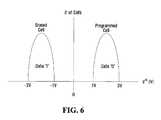
- memory cellsstore two logic states; data ‘1’ and data ‘0’ and each memory cell corresponded to one bit.
- the flash memory cellcan have one of two threshold voltages corresponding to data ‘1’ and data ‘0’.
- the cell threshold voltage distribution for these SLC (single level cells)is shown in FIG. 6 .
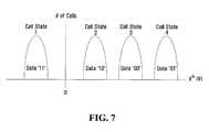
- cellscan also be programmed to more than two threshold levels and thus multiple bits can be stored in one physical cell (see FIG. 7 ), which are referred to as MLC (multi-level cells). Even if no explicit reference is made to multiple bit storage examples of the proposed systems and methods can be applied equally to NAND memory devices with single and multiple bit storage per cell.
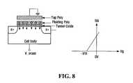
- a NAND flash memory cellis erased and programmed by Fowler-Nordheim (F-N) tunneling.
- the top poly electrode (i.e. top gate) of the cellis biased to Vss (ground) while the cell body is biased to an erase voltage V_erase and the source and drain of the cell are floated (in the case that the source and the drain consist of N+ diffusion layers they are automatically biased to V_erase due to junction-forward-bias from the cell body to the source/drain).
- V_eraseerase voltage
- trapped electrons (charge) in the floating polyi.e. floating gate
- the cell threshold voltage (Vth) of the erased cellbecomes negative as also shown in FIG. 8 .
- the erased cell transistoris in an on-state with a gate bias Vg of 0V.
- the cell threshold voltage Vth of the programmed cellbecomes positive as also shown in FIG. 9 .
- the programmed cellis turned off with a gate bias Vg of 0V).
- the gate and drain of the selected cellsare biased to 0V and a read voltage Vrd, respectively while the source of the selected cells are set to 0V. If the cell is in an erased state as shown in FIG. 10 , the erased cell has a negative threshold voltage and thus a cell current (Icell) from the drain to the source flows under the given bias condition. Similarly if the cell is in a programmed state as shown in FIG. 11 , the programmed cell has a positive threshold voltage and there is no cell current from the drain to the source under the given bias condition. Finally a sense amplifier connected to each bit line senses and latches cell data; an erased cell (on-cell) is sensed as data ‘1’ and a programmed cell (off-cell) is sensed as data ‘0’.
- FIG. 12shows bias conditions during page read operations.
- the selected word lineis set to 0V while unselected word lines, SSL, and GSL are biased to a read pass voltage Vread that is sufficiently high to render unselected cell transistors conductive regardless of their programmed state (i.e. cell Vth).
- the common source line CSLis set to ground.
- the Vth of the selected celldetermines cell current Icell. This cell current Icell is sensed by a bit line sense amplifier in a page buffer. An entire page is read in parallel. In order for a read operation to work without disturbance, the source line needs to be solidly tied to ground without any modification by the cell currents.
- FIG. 13shows the structure of the cell array substrate for most widely used NAND Flash devices.
- the cell bodyis formed by a pocket p-well which is isolated from the p-substrate of chip.
- FIG. 14 and Table 1show typical bias conditions during erase operations.
- the cell bodyis biased to the erase voltage V_erase while the floating bit lines and the source lines (SL) in the selected block are clamped to V_erase-0.6V through the S/D diodes of the SSL and GSL transistors.
- all word lines in the selected blockare biased to 0V while the string select line (SSL) and the ground select line (GSL) are biased to erase voltage V_erase. Therefore all cells within the selected block are erased by F-N tunneling as described in previous section.
- the substrate of the cellsis biased to erase voltage V_erase and the source/drain/substrate of cells in the selected block are electrically connected, the erase operation must occur on a block basis. In other words, the minimum erasable array size is a block.
- program cellswhich are intended to be programmed during program operation will be referred to as “program cells” or “selected cells” hereinafter.
- a string to which a cell to be programmed during program operation belongswill be referred to as a “selected string” or “program string”, and bit lines which are connected to such strings will be referred to as “program bit lines” or “selected bit lines” hereinafter.
- Strings of which the cells should not be programmed during the program operationwill be referred to as “unselected strings” or “program inhibited strings”, and bit lines which are connected to such strings will be referred to as “program inhibit bit lines” or “unselected bit lines” hereinafter.
- FIG. 15depicts known page program bias conditions (see, e.g., Kang-Deog Suh et al., “A 3.3 V 32 Mb NAND Flash Memory with Incremental Step Pulse Programming Scheme,” IEEE J Solid-State Circuits, vol. 30, no. 11, pp. 1149-1156, April 1995).
- FIG. 15is used to describe the program and program inhibit operations of NAND Flash devices.
- channel self-boosting program inhibit schemewhich is used in some existing techniques will be described.
- the needed bias conditionsare applied to selected cells as follows in the most common technique:
- the program voltage Vpgmis applied to the control gate of a selected cell through the word line to which the program cell is connected.
- this word linewill be referred to as “selected word line” hereinafter.
- the SSL transistor of the selected stringis turned on with Vcc applied to the SSL and the GSL transistor turned off.
- Vss0 V.
- drain side cellsare in a turned on state with Vpass applied to their control gates to be able to pass on the channel voltage Vss.
- source side cellsare also turned on with Vpass applied to their control gates in most existing techniques.
- a continuous channelis formed from the bit line to the selected cell (and beyond) with a channel voltage Vch of 0V.
- the connected program inhibit bit lineis set to Vcc.
- the bit line level of Vccinitially precharges the associated channel through the turned on SSL transistor, the gate of which is biased also with Vcc as it is connected to the same SSL which also turns on the SSL transistors of program strings.
- the coupled channel voltagerises, and once the channel voltage reaches Vcc-Vth (SSL) the SSL transistor shuts off and the string channel of the program inhibit string becomes a floating node.
- FIG. 16shows an example of timing the voltages during program operation. Numerous variations of this program timing scheme exist including the application of multiple pulses for Vpgm and Vpass. Although the embodiments of the present disclosure will be described using the program timing given in FIG. 16 , they are not restricted to any program timing scheme in particular.
- This embodimentdeals with a specific type of NAND Flash transistor cells, where NAND cell strings are stacked in a direction which runs perpendicular to the chip surface.
- a vertical unit which comprises a cell stringwill be called “pillar” hereinafter. Examples of these kinds of NAND cells have been described in the following references:
- FIG. 17 and FIG. 18show two different examples of such vertically aligned NAND cell strings.
- the gates and the word lineswrap around the pillar bodies thus forming a gate-all-around structure.
- NAND cell transistorsconsist of n-channel transistors on p-type substrate.
- N and p-type impuritiesmay be interchanged so as to form p-channel transistors on n-type substrate.
- the bodies of the cellsare identical to the overall underlying cell substrate as it consists of the same pocket p-well. In vertical devices this is not necessarily so.
- the bodies of the cell transistorsare located within the individual pillars. These are spatially in locations different from the overall cell array substrate and may or may not be electrically connected with the cell array substrate. Therefore the bodies of the cell pillars may or may not be identical to the cell “body” or “substrate” that is formed by the underlying p-well. In the present description, whenever the body within a cell pillar is meant this will be named “pillar body”.
- cell substrateor “cell array substrate”.
- thiscan be a pocket p-well, or it can be the entire substrate.
- the first kindis shown in FIG. 17 .
- the p-type pillar bodyis isolated from the p-type cell substrate by an n+ type diffusion layer which forms the source line of the cell strings.
- This type of vertical NAND deviceis not the subject of the proposed technique.
- the second kindis shown in FIG. 18 , where the p-type pillar body is connected to the p-type cell substrate without any junction in between.
- the cell pillarsthus have an opening at the bottom where the pillar body and cell array substrate, which are of the same impurity type, are electrically connected with each other.
- the mechanism through which the bodies of the cell pillars are biased during erase operationis one aspect of the difference in the cell structure.
- GIDL mechanismshave been proposed to charge the pillar bodies. This will not be described in detail here.
- the n-type and p-type regions at the bottom of the cell pillarstake a different shape in the two cases, respectively.
- the bottom diffusion layermay be allowed to form a continuous n-type region if viewed from above without p-type regions.
- the n-type regionmay extend in both directions, the bit line and the word line direction. This is indicated in the schematic on the right side of FIG. 17 by the line connection between adjacent source lines.
- the pillar bodyis not isolated from the cell substrate certain restrictions apply to the exact shape of the n-type region, as there always have to exist regions under the cell pillars which are not n-type to ensure the p-type pillar bodies are electrically connected to the p-type cell substrate, but the n-type channels of the pillar transistors are connected to the n-type regions of the substrate. Those restrictions may result in difficulties connecting source lines arbitrary directions.
- the proposed techniqueapplies to the second of the mentioned cases where p-type pillar bodies are connected to the p-type substrate of the cell array without any junction in-between.
- the applicationprovides a method of manufacturing vertically stacked NAND Flash memory cells of a type as described in FIG. 18 with a diffused n+ source line where the cell body is of the same impurity type as and electrically connected to the chip substrate and not separated by a pn junction, and corresponding devices.
- the proposed manufacturing schemeimproves weak points present with prior manufacturing schemes.
- a first weak point to be improvedis present with some prior manufacturing schemes described in the next section.
- the problemis known as source line bounce which is caused by high cell currents and high source line resistances. It is of foremost importance that the source line maintains the voltage applied to it during read or write operations throughout the entirety of the cell array. There are, however, practical obstacles to it.
- the source linesrun in the word line direction as all the currents of cells belonging to the same page will crowd on the same source line.
- the source line running in a direction parallel to the word lineis a natural outcome of some prior manufacturing schemes.
- a second weak pointis present with some other manufacturing schemes described in the next section. It is related to the fact that although the manufacturing process may be aimed at forming a structure such that the pillar body is open at the bottom and connected to the p-type substrate of the chip, in some specific cell structure n-type dopant diffusion from the source line may isolate the open path between the cell pillar body and the chip substrate (see example 2 in the next section).
- FIG. 20An existing method of forming diffused source lines is shown FIG. 20 . This is the underlying method for forming vertical NAND Flash cells as described in US8203211B2, US8278170B2.
- the source lineis formed by impurity implantation and diffusion after etching the word lines, using the word line patterns as a mask. It can be easily seen that the direction of the source lines in the word line direction follows naturally from the manufacturing method.
- This schememay be weak to n-type dopant diffusion from the n+ source to the cell pillar body, especially for some schemes where the cell pillar body does not consist of bulk poly-Si which fills the entire hole, but where the cell pillar body consists of a thin poly-Si film surrounding a dielectric contact filler.
- N-type dopant diffusion from the substrate n+ regionmay turn the impurity type of the tube type cell body at the bottom region into n-type as shown in FIG. 22 , thereby disconnecting cell body from the substrate p-well.
- FIG. 23 to FIG. 33show the step-by-step manufacturing process. It is understood that the shown manufacturing steps include only common semiconductor processes.
- the left of each Figureshows a top view of a region of a cell area
- the middle of each Figureshows a vertical cut in a region of a cell area in the direction of the word lines
- the right of each Figureshows a vertical cut in a region of a cell area in the direction of the bit lines.
- the source line itselfis not only formed by diffusion but by patterning, (including etching) as well.
- the patterning step used to perform patterning in the cell areais also used to create a photo alignment mark in a photo alignment mark region, outside the cell area. Further details of the photo alignment mark are described below in the context of the second embodiment.
- a p-well in the cell regionis formed by ion implantation.
- the ion implanted p-wellis indicated at 101 .
- the p-well in the cell regionmay be a pocket p-well which is separated from the p-well substrate of the chip periphery circuitry.
- stripe-shaped active/field regionsare formed by a standard semiconductor manufacturing process, for example the so-called STI (shallow trench isolation) process.
- the trenchesrun in the direction of the bit lines.
- stripe-shaped trenches (fields)are formed and filled with a dielectric material 102 , for example silicon oxide.
- this Active/field patterning processis performed at the same time as the Active/field patterning of the rest of the chip circuitry such that no separate process exists for the cell area.
- n-type conductive regions 103 in the active regions, but not in the non-conducting field regions 102are formed in the next step as shown in FIG. 25 .
- this source/drain formation processis performed at the same time as the source/drain formation process of the rest of the chip circuitry such that no separate process exists for the cell area.
- the order of the steps in FIG. 24 and FIG. 25may be interchanged such that the n+ diffusion process is performed first and the active/field patterning process thereafter.
- non-conductive dielectric layers 104 a - 104 c and conducting layers 105 a - 105 care deposited. From the conducting layers 105 a - 105 c the gates of the cell transistors are formed in later steps.
- the non-conducting layersare interlayer dielectric layers between the cell transistor gates.
- the conducting layersmay be for example n+ or p+ doped poly-Si.
- the lowest non-conducting layers 104 amay be of lower thickness (for example around 10 nm) than the intermediate non-conducting layers 104 b , which may be around 20 nm thick.
- the lowest non-conducting layer 104 amay be of a different material, for example undoped silicon oxide, from the intermediate non-conducting layers 104 b , which may be for example doped silicon oxide. In some embodiments the lowest non-conducting layer 104 a may be formed through an oxidization process of the silicon substrate and not through a layer deposition process.
- the top non-conducting layer 104 cmay be of a higher thickness, for example 40 nm, than the intermediate non-conducting layers 104 b .
- the highest non-conducting layer 104 cmay be of a different material, for example silicon nitride, from the intermediate non-conducting layers 104 b . Although only 4 conductive layers are shown it is understood that as in most known NAND Flash devices, the number of layers corresponds to the numbers of transistors in NAND Flash strings which may be a number higher than 4, for example the number of intermediate conductive layers may be 64.
- holes 106are etched in a first etching step such that pillar holes are formed in a regular row and column pattern and such that the holes are formed on regions where the stripe shaped field patterns 102 were formed in an earlier step. This is achieved by aligned this step to an alignment mark which was formed during the active/field patterning step. Furthermore the holes 106 are etched through the cell stack layers 104 a - 104 c and 105 a - 105 c but not through the field dielectric 102 .
- the gate dielectric layers 107are deposited.
- the gate dielectric layer 107may for example be a multi-layer structure consisting of the tunnel dielectric, the charge trap layer and a coupling dielectric as in some common NAND Flash cells.
- the tunnel dielectricmay be silicon oxide
- the charge trap layermay be silicon nitride
- the coupling dielectricmay be silicon oxide.
- the dielectric formation stepmay be multiple steps to form different dielectric layers at the lowest 105 a , the intermediate 105 b and the highest 105 c regions.
- a second etch stepis performed which extends the existing pillar holes ( 106 of FIG. 27 ) through the field dielectric to produce holes 108 shown in FIG. 29 and thereby expose the underlying p-well substrate.
- the etch step of FIG. 29is divided into two steps. These would include a first etch step removes the gate dielectric layer 7 except from the vertical inner sidewalls of the pillar holes. A second etch step then extends the existing pillar holes ( 106 of FIG. 27 ) through the field dielectric to produce holes 108 shown in FIG. 29 and exposes the underlying p-well substrate.
- the first and second etch stepmay be either separate or combined into one etch step.
- a pillar body 109is formed in each pillar hole.
- the pillar bodyis p-doped silicon such that the pillar body and the p-type ion implanted well form a single node during an erase operation of the resulting NAND flash memory. They form a single node in the sense that if one is charged, the other is charged as well; there is no junction in between.
- FIG. 31shows an example of a cross section of a multilayer filled cell pillar employed in some embodiments.
- the pillaris surrounded by the gate material 105 .
- the outermost layerscomprise the gate dielectrics 107 a - 107 c .
- the filling layersconsist of a tunnel dielectric 107 a which may be silicon oxide, a charge trap layer 107 b which may be silicon nitride, a coupling layer 107 c which may be silicon oxide, the transistor body 109 a which may be undoped poly silicon and a dielectric filler 109 b which may be silicon oxide.
- there is no dielectric filler 109 bbut the silicon body 109 a fills all the remaining innermost part of the pillar.
- the word lines of all vertically stacked layersare etched at the same single photolithography mask step to form alternating fin patterns 110 and slit patterns 111 .
- the slits 111 of FIG. 32are filled with an isolating dielectric such as for example silicon oxide as indicated at 112 .
- the topmost part of the cell pillarsis doped such as to form an n+ diffusion layer 113 which is at the same time the drain of the NAND Cell pillar.
- the bit lines 114are formed with a standard metallization process such as to form electrical connections to the string drains 113 .
- FIG. 34 to FIG. 47show a step-by-step manufacturing process in the second embodiment.
- the step in FIG. 34is identical to the step in FIG. 23 in the first embodiment. Contrary to the first embodiment there is no active/field patterning process that includes etching in the cell region. In other words, the step of FIG. 24 is not performed.
- an n+ source implant processis performed at a photolithography mask step such as to form a stripe-shaped diffusion layer 300 of n-type and a stripe-shaped 301 diffusion layer of p-type. Contrary to the first embodiment no patterning of the active substrate through etching takes place.
- this stepcomprises a photolithography mask step used to define the n-type source lines that at the same time defines a location of a photo alignment mark through patterning, including etching, outside the cell area.
- a photolithography mask stepused to define the n-type source lines that at the same time defines a location of a photo alignment mark through patterning, including etching, outside the cell area.
- the next step in FIG. 36is identical to the step in FIG. 26 in the first embodiment.
- the next step in FIG. 37is identical to the step in FIG. 27 in the first embodiment.
- the cell pillar holes 106are aligned to the substrate n+ diffusion regions in a way that the holes are formed on regions which are of p-type diffusion.
- the alignment of this photolithography mask stepis performed using an alignment mark, the formation of which is described later.
- the step in FIG. 38is identical to the step in FIG. 28 in the first embodiment.
- the step in FIG. 39is identical to the step in FIG. 29 in the first embodiment. However, contrary to the first embodiment the second etch step does not extend the pillar hole through a field dielectric layer but through to the substrate silicon. In some embodiments, the pillar holes are extended a defined distance into the substrate silicon.
- a methodis provided to align the pillar patterns to the underlying n and p-type diffusion regions.
- etched photolithography alignment marksare formed. This is shown in FIG. 43 to FIG. 47 .
- a first photolithography mask stepis shown in FIG. 43 .
- a hard mask materialwhich has a different etch selectivity from the substrate silicon is deposited. The material may be for example silicon oxide.
- a photoresistis applied and then the hard mask is etched at the cell region and at the alignment mark region such as to expose the substrate silicon at the regions which are to be doped with the n+ type ion implantation to define the location of the source lines and the alignment mark. Subsequently, ion implantation to form the bottom source line is performed at the cell region and at the alignment mark region alike.
- FIG. 44shows a subsequent photolithography mask step where an etched pattern is formed in the substrate at the alignment mark but not in the cell area.
- the hard mask materialis stripped by a selective etch process.
- this photo alignment markcan be utilized for the alignment in the subsequent cell pillar patterning process.
- the first methodsimply the height difference of the alignment mark can be directly used.
- an alignment mark open stepcan be performed as depicted in FIG. 47 to remove the cell stack layers only from the photo alignment mark region and thus to enhance the visibility of the alignment mark.
- the source line patternsconsisting of impurity implanted (and diffused) regions are formed before the stacking and patterning of the cell stack layers takes place. This gives the freedom to align the source line patterns so as to run in a direction perpendicular to the word lines.
- the location of the photolithography alignment markis defined at the same photolithography mask step as the source line formation. This way it is ensured that alignment of cell pillar patterns relative to the source line patterns can take place in a later step.
- the proposed scheme with stripe-shaped impurity regionsmay be more robust than the scheme in Y. Noh et al., “A New Metal Control Gate Last Process (MCGL process) for High Performance DC-SF (Dual Control gate with Surrounding Floating gate) 3D NAND Flash Memory”, 2012 Symposium on VLSI Technology Digest of Technical Papers, p. 19-20, where the bottom source part of the cell pillar is surrounded by an n-type impurity region (see FIG. 49 ).
- NAND cell transistorsconsist of n-channel transistors on p-type substrate and source lines consisting of n-type regions
- the proposed techniqueis not restricted to this case.
- the polarity of the impurity typesmay be exchanged.
- N and p-type impurity regionsmay be interchanged so as to form p-channel transistors on n-type substrate and p-type source lines.
- the conductive layers 105 a - 105 c which form the gate and word line materialmay be some metal such as tungsten instead of doped poly-Si.
- the second embodimentis described in a way that the etching of the hard mask occurs before the impurity implant steps, it is equally possible to first perform the impurity implant steps through the hard mask material using the photoresist mask and afterwards to etch the hard mask to pattern the alignment marks, as long as source line impurity implant and the location of the alignment mark is defined in the same photolithography mask step.
- n-type source line strapping regionsmay be additionally interconnected in the word line direction.
- additional strapping regionswhich provide additional connections between regions of the same impurity type are also possible in connection with the present disclosure.
- the source linesare not necessarily parallel to the bit lines.
- the pillar bodyis p-type silicon and the ion-implanted well is p-type silicon. More generally, in any of the embodiments described herein, the pillar body may instead be intrinsic (undoped) silicon or be lightly n-doped silicon, if in any of these cases it is still true that during an erase operation, the pillar body and the p-type ion-implanted well form a single node, with no junction in between.
- the pillar holeis filled with a multi-layer structure consisting of that material that will form the connection to the ion-implanted well and a dielectric filler like silicon oxide which fills the innermost part of the hole.
- a photolithography mask stepcan be viewed as the sum of all semiconductor chip manufacturing steps which are used to create one photoresist pattern, wherein as a result of this photoresist pattern, the photoresist covers some lateral regions in the chip but not other, AND the sum of all semiconductor chip manufacturing steps (e.g. etching, ion implant) which are applied on some lateral regions but not on other lateral regions in the chip, whereby the distinction between these different lateral regions is done using the same photoresist pattern for all these manufacturing steps, and whereby this photoresist pattern was created exactly once using a photolithography mask.
- semiconductor chip manufacturing stepse.g. etching, ion implant
- a photoresist patternis created using a photolithography mask, and a first manufacturing step is performed using this photoresist pattern and a second manufacturing step is performed using the same photoresist pattern (without removing and recreating the photoresist pattern in between the two manufacturing steps), it is said that the first manufacturing step and the second manufacturing step occur at the same photolithography mask step.
- a first photoresist patternis created using a photolithography mask, and a first manufacturing step is performed using the first photoresist pattern, the first photoresist pattern is removed, a second photoresist pattern is created using a different or the same photolithography mask, a second manufacturing step is performed using the second photoresist pattern, it is said that the first and the second manufacturing steps do not occur at the same photolithography mask step.
- a photolithography maskis a device which is used (and reused) within a photolithography tool, whenever a certain kind of photoresist pattern needs to be created. It is not to be confused with photoresist masks (or patterns) or hard masks, which are patterns on the wafer.
- the device elements and circuitsare connected to each other as shown in the figures for the sake of simplicity. In practical applications these devices, elements circuits, etc., may be connected directly to each other or indirectly through other devices elements, circuits, etc. Thus, in an actual configuration, the elements, circuits and devices are coupled either directly or indirectly with each other.
Landscapes
- Engineering & Computer Science (AREA)
- Microelectronics & Electronic Packaging (AREA)
- Computer Hardware Design (AREA)
- Semiconductor Memories (AREA)
- Non-Volatile Memory (AREA)
- Read Only Memory (AREA)
Abstract
Description
- 1. NAND Flash memory devices with cell strings being located in a way that cell are stacked in a direction perpendicular to the chip surface and cell strings are aligned in a way as to form a pillar vertically to the chip surface.
- 2. The source of the cell string is located below the layers forming the cells at the bottom of each cell pillar and is located in the cell array substrate formed as an n-type diffusion layer.
- 3. When cell transistors (including the string select transistor and ground select transistor) of a string are turned on, and a channel is formed in the pillar, the channel of the transistor most close to the string source (usually the ground select transistor) is electrically connected to the source of the cell string and thus the source line.
- 4. Sources of adjacent cell strings are connected with each other forming a source line consisting of an n-type diffusion layer.
- 5. The p-type bodies of the pillars are electrically connected to the underlying p-type substrate of the cell array without a junction in-between.
- 1 page=(j+k) bytes
- 1 block=2mpages=(j+k) bytes*2m
- Total memory array size=2nblocks=(j+k) bytes*2m+n
| TABLE 1 |
| Bias Conditions during Erase |
| Selected Block | Unselected Block | |||
| Bitlines (BL) | Clamped to V_erase- | Clamped to V_erase- | ||
| 0.6 V | 0.6 V | |||
| String Select | Boosted to approx. | Boosted to approx. | ||
| Line (SSL) | 90% of V_erase | 90% of | ||
| Wordlines | ||||
| 0 V | Boosted to approx. | |||
| (WL0~WL15) | 90% of V_erase | |||
| Ground Select | Bossted to approx. | Boosted to approx. | ||
| Line (GSL) | 90% of V_erase | 90% of V_erase | ||
| Source Line (SL) | Clamped to V_erase- | Clamped to V_erase- | ||
| 0.6 V | 0.6 V | |||
| Cell body | V_erase | V_erase | ||
- H. Tanaka, “Bit Cost Scalable Technology with Punch and Plug Process for Ultra High Density Flash Memory”, 2007 Symposium on VLSI Technology Digest of Technical Papers
- Jaehoon Jang et al. “Vertical Cell Array using TCAT (Terabit Cell Array Transistor) Technology for Ultra High Density NAND Flash Memory”, 2009 Symposium on VLSI Technology Digest of Technical Papers
- Yoohyun Noh et al. “A New Metal Control Gate Last Process (MCGL process) for High Performance DC-SF (Dual Control gate with Surrounding Floating gate) 3D NAND Flash Memory”, 2012 Symposium on VLSI Technology Digest of Technical Papers
- As the source line consists of diffusion layers in some common vertical NAND Flash devices the sheet resistance may be up to several ohms/square, which can add up through the entire length of the source line to a resistance of several hundred kiloohms and more, even if a silicidation process is applied to reduce the resistance.
- If the resistance of the source lines is high it is disadvantageous if all cells of the same page are connected to the same source line. See for example
FIG. 19 where the source lines run in the same direction as the word lines. In a read operation a cell current flows through all cell strings which are part of a selected block, e.g. 64 K cells for 8 KB sized pages. Assuming a sheet resistance of a few ohms/square for the silicided diffusion layer and cell currents around 100 nanoampere, the source line bounce can add up to be in the volt range in the middle of the source line if no other measures are taken.
- 1. have as a result that source line diffused regions are connected in a direction perpendicular to the word lines and parallel to the bit line direction;
- 2. bodies of cell pillars are electrically connected to the ion-implanted well and are of the same impurity type;
- 3. cell pillar patterns are aligned to the impurity regions forming the source lines; and
- 4. are robust to dopant diffusion of unwanted impurity type.
Claims (13)
Priority Applications (8)
| Application Number | Priority Date | Filing Date | Title |
|---|---|---|---|
| US13/803,085US10403766B2 (en) | 2012-12-04 | 2013-03-14 | NAND flash memory with vertical cell stack structure and method for manufacturing same |
| PCT/CA2013/000997WO2014085904A1 (en) | 2012-12-04 | 2013-11-29 | Nand flash memory with vertical cell stack structure and method for manufacturing same |
| EP13861240.3AEP2929536A1 (en) | 2012-12-04 | 2013-11-29 | Nand flash memory with vertical cell stack structure and method for manufacturing same |
| TW102143782ATW201428899A (en) | 2012-12-04 | 2013-11-29 | Anti-flash memory with vertical cell stack structure and manufacturing method thereof |
| US16/521,066US10622488B2 (en) | 2012-12-04 | 2019-07-24 | NAND flash memory with vertical cell stack structure and method for manufacturing same |
| US16/816,520US11088289B2 (en) | 2012-12-04 | 2020-03-12 | NAND flash memory with vertical cell stack structure and method for manufacturing same |
| US17/369,007US11664463B2 (en) | 2012-12-04 | 2021-07-07 | NAND flash memory with vertical cell stack structure and method for manufacturing same |
| US18/305,537US12119411B2 (en) | 2012-12-04 | 2023-04-24 | NAND flash memory with vertical cell stack structure and method for manufacturing same |
Applications Claiming Priority (2)
| Application Number | Priority Date | Filing Date | Title |
|---|---|---|---|
| US201261733063P | 2012-12-04 | 2012-12-04 | |
| US13/803,085US10403766B2 (en) | 2012-12-04 | 2013-03-14 | NAND flash memory with vertical cell stack structure and method for manufacturing same |
Related Child Applications (1)
| Application Number | Title | Priority Date | Filing Date |
|---|---|---|---|
| US16/521,066ContinuationUS10622488B2 (en) | 2012-12-04 | 2019-07-24 | NAND flash memory with vertical cell stack structure and method for manufacturing same |
Publications (2)
| Publication Number | Publication Date |
|---|---|
| US20140151774A1 US20140151774A1 (en) | 2014-06-05 |
| US10403766B2true US10403766B2 (en) | 2019-09-03 |
Family
ID=50824618
Family Applications (5)
| Application Number | Title | Priority Date | Filing Date |
|---|---|---|---|
| US13/803,085Active2035-07-30US10403766B2 (en) | 2012-12-04 | 2013-03-14 | NAND flash memory with vertical cell stack structure and method for manufacturing same |
| US16/521,066ActiveUS10622488B2 (en) | 2012-12-04 | 2019-07-24 | NAND flash memory with vertical cell stack structure and method for manufacturing same |
| US16/816,520ActiveUS11088289B2 (en) | 2012-12-04 | 2020-03-12 | NAND flash memory with vertical cell stack structure and method for manufacturing same |
| US17/369,007Active2033-08-03US11664463B2 (en) | 2012-12-04 | 2021-07-07 | NAND flash memory with vertical cell stack structure and method for manufacturing same |
| US18/305,537ActiveUS12119411B2 (en) | 2012-12-04 | 2023-04-24 | NAND flash memory with vertical cell stack structure and method for manufacturing same |
Family Applications After (4)
| Application Number | Title | Priority Date | Filing Date |
|---|---|---|---|
| US16/521,066ActiveUS10622488B2 (en) | 2012-12-04 | 2019-07-24 | NAND flash memory with vertical cell stack structure and method for manufacturing same |
| US16/816,520ActiveUS11088289B2 (en) | 2012-12-04 | 2020-03-12 | NAND flash memory with vertical cell stack structure and method for manufacturing same |
| US17/369,007Active2033-08-03US11664463B2 (en) | 2012-12-04 | 2021-07-07 | NAND flash memory with vertical cell stack structure and method for manufacturing same |
| US18/305,537ActiveUS12119411B2 (en) | 2012-12-04 | 2023-04-24 | NAND flash memory with vertical cell stack structure and method for manufacturing same |
Country Status (4)
| Country | Link |
|---|---|
| US (5) | US10403766B2 (en) |
| EP (1) | EP2929536A1 (en) |
| TW (1) | TW201428899A (en) |
| WO (1) | WO2014085904A1 (en) |
Cited By (4)
| Publication number | Priority date | Publication date | Assignee | Title |
|---|---|---|---|---|
| TWI727652B (en)* | 2019-09-10 | 2021-05-11 | 日商鎧俠股份有限公司 | Memory device |
| US11664463B2 (en) | 2012-12-04 | 2023-05-30 | Mosaid Technologies Incorporated | NAND flash memory with vertical cell stack structure and method for manufacturing same |
| US11887936B2 (en) | 2021-03-22 | 2024-01-30 | Samsung Electronics Co., Ltd. | Semiconductor device including alignment key, electronic system, and method of forming the same |
| US12439600B2 (en) | 2022-01-27 | 2025-10-07 | Samsung Electronics Co., Ltd. | Semiconductor devices and data storage systems including the same |
Families Citing this family (237)
| Publication number | Priority date | Publication date | Assignee | Title |
|---|---|---|---|---|
| KR101495800B1 (en)* | 2009-04-10 | 2015-02-27 | 삼성전자주식회사 | Nonvolatile memory device |
| US10388863B2 (en) | 2009-10-12 | 2019-08-20 | Monolithic 3D Inc. | 3D memory device and structure |
| US11984445B2 (en) | 2009-10-12 | 2024-05-14 | Monolithic 3D Inc. | 3D semiconductor devices and structures with metal layers |
| US10354995B2 (en) | 2009-10-12 | 2019-07-16 | Monolithic 3D Inc. | Semiconductor memory device and structure |
| US10366970B2 (en) | 2009-10-12 | 2019-07-30 | Monolithic 3D Inc. | 3D semiconductor device and structure |
| US9941332B2 (en)* | 2009-10-12 | 2018-04-10 | Monolithic 3D Inc. | Semiconductor memory device and structure |
| US11018133B2 (en) | 2009-10-12 | 2021-05-25 | Monolithic 3D Inc. | 3D integrated circuit |
| US12027518B1 (en) | 2009-10-12 | 2024-07-02 | Monolithic 3D Inc. | 3D semiconductor devices and structures with metal layers |
| US10157909B2 (en) | 2009-10-12 | 2018-12-18 | Monolithic 3D Inc. | 3D semiconductor device and structure |
| US10043781B2 (en) | 2009-10-12 | 2018-08-07 | Monolithic 3D Inc. | 3D semiconductor device and structure |
| US10910364B2 (en) | 2009-10-12 | 2021-02-02 | Monolitaic 3D Inc. | 3D semiconductor device |
| US11374118B2 (en) | 2009-10-12 | 2022-06-28 | Monolithic 3D Inc. | Method to form a 3D integrated circuit |
| US10217667B2 (en) | 2011-06-28 | 2019-02-26 | Monolithic 3D Inc. | 3D semiconductor device, fabrication method and system |
| US10497713B2 (en) | 2010-11-18 | 2019-12-03 | Monolithic 3D Inc. | 3D semiconductor memory device and structure |
| US11482440B2 (en) | 2010-12-16 | 2022-10-25 | Monolithic 3D Inc. | 3D semiconductor device and structure with a built-in test circuit for repairing faulty circuits |
| US12362219B2 (en) | 2010-11-18 | 2025-07-15 | Monolithic 3D Inc. | 3D semiconductor memory device and structure |
| US11315980B1 (en) | 2010-10-11 | 2022-04-26 | Monolithic 3D Inc. | 3D semiconductor device and structure with transistors |
| US11469271B2 (en) | 2010-10-11 | 2022-10-11 | Monolithic 3D Inc. | Method to produce 3D semiconductor devices and structures with memory |
| US11227897B2 (en) | 2010-10-11 | 2022-01-18 | Monolithic 3D Inc. | Method for producing a 3D semiconductor memory device and structure |
| US10896931B1 (en) | 2010-10-11 | 2021-01-19 | Monolithic 3D Inc. | 3D semiconductor device and structure |
| US11257867B1 (en) | 2010-10-11 | 2022-02-22 | Monolithic 3D Inc. | 3D semiconductor device and structure with oxide bonds |
| US11158674B2 (en) | 2010-10-11 | 2021-10-26 | Monolithic 3D Inc. | Method to produce a 3D semiconductor device and structure |
| US11018191B1 (en) | 2010-10-11 | 2021-05-25 | Monolithic 3D Inc. | 3D semiconductor device and structure |
| US11024673B1 (en) | 2010-10-11 | 2021-06-01 | Monolithic 3D Inc. | 3D semiconductor device and structure |
| US10290682B2 (en) | 2010-10-11 | 2019-05-14 | Monolithic 3D Inc. | 3D IC semiconductor device and structure with stacked memory |
| US11600667B1 (en) | 2010-10-11 | 2023-03-07 | Monolithic 3D Inc. | Method to produce 3D semiconductor devices and structures with memory |
| US11327227B2 (en) | 2010-10-13 | 2022-05-10 | Monolithic 3D Inc. | Multilevel semiconductor device and structure with electromagnetic modulators |
| US12080743B2 (en) | 2010-10-13 | 2024-09-03 | Monolithic 3D Inc. | Multilevel semiconductor device and structure with image sensors and wafer bonding |
| US11043523B1 (en) | 2010-10-13 | 2021-06-22 | Monolithic 3D Inc. | Multilevel semiconductor device and structure with image sensors |
| US11163112B2 (en) | 2010-10-13 | 2021-11-02 | Monolithic 3D Inc. | Multilevel semiconductor device and structure with electromagnetic modulators |
| US11984438B2 (en) | 2010-10-13 | 2024-05-14 | Monolithic 3D Inc. | Multilevel semiconductor device and structure with oxide bonding |
| US12360310B2 (en) | 2010-10-13 | 2025-07-15 | Monolithic 3D Inc. | Multilevel semiconductor device and structure with oxide bonding |
| US11855114B2 (en) | 2010-10-13 | 2023-12-26 | Monolithic 3D Inc. | Multilevel semiconductor device and structure with image sensors and wafer bonding |
| US10833108B2 (en) | 2010-10-13 | 2020-11-10 | Monolithic 3D Inc. | 3D microdisplay device and structure |
| US11869915B2 (en) | 2010-10-13 | 2024-01-09 | Monolithic 3D Inc. | Multilevel semiconductor device and structure with image sensors and wafer bonding |
| US12094892B2 (en) | 2010-10-13 | 2024-09-17 | Monolithic 3D Inc. | 3D micro display device and structure |
| US11164898B2 (en) | 2010-10-13 | 2021-11-02 | Monolithic 3D Inc. | Multilevel semiconductor device and structure |
| US11133344B2 (en) | 2010-10-13 | 2021-09-28 | Monolithic 3D Inc. | Multilevel semiconductor device and structure with image sensors |
| US11437368B2 (en) | 2010-10-13 | 2022-09-06 | Monolithic 3D Inc. | Multilevel semiconductor device and structure with oxide bonding |
| US11404466B2 (en) | 2010-10-13 | 2022-08-02 | Monolithic 3D Inc. | Multilevel semiconductor device and structure with image sensors |
| US11694922B2 (en) | 2010-10-13 | 2023-07-04 | Monolithic 3D Inc. | Multilevel semiconductor device and structure with oxide bonding |
| US11929372B2 (en) | 2010-10-13 | 2024-03-12 | Monolithic 3D Inc. | Multilevel semiconductor device and structure with image sensors and wafer bonding |
| US10679977B2 (en) | 2010-10-13 | 2020-06-09 | Monolithic 3D Inc. | 3D microdisplay device and structure |
| US11855100B2 (en) | 2010-10-13 | 2023-12-26 | Monolithic 3D Inc. | Multilevel semiconductor device and structure with oxide bonding |
| US11063071B1 (en) | 2010-10-13 | 2021-07-13 | Monolithic 3D Inc. | Multilevel semiconductor device and structure with waveguides |
| US10943934B2 (en) | 2010-10-13 | 2021-03-09 | Monolithic 3D Inc. | Multilevel semiconductor device and structure |
| US10978501B1 (en) | 2010-10-13 | 2021-04-13 | Monolithic 3D Inc. | Multilevel semiconductor device and structure with waveguides |
| US11605663B2 (en) | 2010-10-13 | 2023-03-14 | Monolithic 3D Inc. | Multilevel semiconductor device and structure with image sensors and wafer bonding |
| US10998374B1 (en) | 2010-10-13 | 2021-05-04 | Monolithic 3D Inc. | Multilevel semiconductor device and structure |
| US11094576B1 (en) | 2010-11-18 | 2021-08-17 | Monolithic 3D Inc. | Methods for producing a 3D semiconductor memory device and structure |
| US11804396B2 (en) | 2010-11-18 | 2023-10-31 | Monolithic 3D Inc. | Methods for producing a 3D semiconductor device and structure with memory cells and multiple metal layers |
| US11901210B2 (en) | 2010-11-18 | 2024-02-13 | Monolithic 3D Inc. | 3D semiconductor device and structure with memory |
| US11923230B1 (en) | 2010-11-18 | 2024-03-05 | Monolithic 3D Inc. | 3D semiconductor device and structure with bonding |
| US11508605B2 (en) | 2010-11-18 | 2022-11-22 | Monolithic 3D Inc. | 3D semiconductor memory device and structure |
| US11211279B2 (en) | 2010-11-18 | 2021-12-28 | Monolithic 3D Inc. | Method for processing a 3D integrated circuit and structure |
| US12144190B2 (en) | 2010-11-18 | 2024-11-12 | Monolithic 3D Inc. | 3D semiconductor device and structure with bonding and memory cells preliminary class |
| US12125737B1 (en) | 2010-11-18 | 2024-10-22 | Monolithic 3D Inc. | 3D semiconductor device and structure with metal layers and memory cells |
| US11004719B1 (en) | 2010-11-18 | 2021-05-11 | Monolithic 3D Inc. | Methods for producing a 3D semiconductor memory device and structure |
| US11443971B2 (en) | 2010-11-18 | 2022-09-13 | Monolithic 3D Inc. | 3D semiconductor device and structure with memory |
| US12033884B2 (en) | 2010-11-18 | 2024-07-09 | Monolithic 3D Inc. | Methods for producing a 3D semiconductor device and structure with memory cells and multiple metal layers |
| US11495484B2 (en) | 2010-11-18 | 2022-11-08 | Monolithic 3D Inc. | 3D semiconductor devices and structures with at least two single-crystal layers |
| US11521888B2 (en) | 2010-11-18 | 2022-12-06 | Monolithic 3D Inc. | 3D semiconductor device and structure with high-k metal gate transistors |
| US11121021B2 (en) | 2010-11-18 | 2021-09-14 | Monolithic 3D Inc. | 3D semiconductor device and structure |
| US11355380B2 (en) | 2010-11-18 | 2022-06-07 | Monolithic 3D Inc. | Methods for producing 3D semiconductor memory device and structure utilizing alignment marks |
| US11862503B2 (en) | 2010-11-18 | 2024-01-02 | Monolithic 3D Inc. | Method for producing a 3D semiconductor device and structure with memory cells and multiple metal layers |
| US11610802B2 (en) | 2010-11-18 | 2023-03-21 | Monolithic 3D Inc. | Method for producing a 3D semiconductor device and structure with single crystal transistors and metal gate electrodes |
| US11107721B2 (en) | 2010-11-18 | 2021-08-31 | Monolithic 3D Inc. | 3D semiconductor device and structure with NAND logic |
| US11735462B2 (en) | 2010-11-18 | 2023-08-22 | Monolithic 3D Inc. | 3D semiconductor device and structure with single-crystal layers |
| US11482439B2 (en) | 2010-11-18 | 2022-10-25 | Monolithic 3D Inc. | Methods for producing a 3D semiconductor memory device comprising charge trap junction-less transistors |
| US11569117B2 (en) | 2010-11-18 | 2023-01-31 | Monolithic 3D Inc. | 3D semiconductor device and structure with single-crystal layers |
| US11784082B2 (en) | 2010-11-18 | 2023-10-10 | Monolithic 3D Inc. | 3D semiconductor device and structure with bonding |
| US12068187B2 (en) | 2010-11-18 | 2024-08-20 | Monolithic 3D Inc. | 3D semiconductor device and structure with bonding and DRAM memory cells |
| US11854857B1 (en) | 2010-11-18 | 2023-12-26 | Monolithic 3D Inc. | Methods for producing a 3D semiconductor device and structure with memory cells and multiple metal layers |
| US12272586B2 (en) | 2010-11-18 | 2025-04-08 | Monolithic 3D Inc. | 3D semiconductor memory device and structure with memory and metal layers |
| US11615977B2 (en) | 2010-11-18 | 2023-03-28 | Monolithic 3D Inc. | 3D semiconductor memory device and structure |
| US11355381B2 (en) | 2010-11-18 | 2022-06-07 | Monolithic 3D Inc. | 3D semiconductor memory device and structure |
| US11482438B2 (en) | 2010-11-18 | 2022-10-25 | Monolithic 3D Inc. | Methods for producing a 3D semiconductor memory device and structure |
| US12100611B2 (en) | 2010-11-18 | 2024-09-24 | Monolithic 3D Inc. | Methods for producing a 3D semiconductor device and structure with memory cells and multiple metal layers |
| US11164770B1 (en) | 2010-11-18 | 2021-11-02 | Monolithic 3D Inc. | Method for producing a 3D semiconductor memory device and structure |
| US12243765B2 (en) | 2010-11-18 | 2025-03-04 | Monolithic 3D Inc. | 3D semiconductor device and structure with metal layers and memory cells |
| US12154817B1 (en) | 2010-11-18 | 2024-11-26 | Monolithic 3D Inc. | Methods for producing a 3D semiconductor memory device and structure |
| US11018042B1 (en) | 2010-11-18 | 2021-05-25 | Monolithic 3D Inc. | 3D semiconductor memory device and structure |
| US12136562B2 (en) | 2010-11-18 | 2024-11-05 | Monolithic 3D Inc. | 3D semiconductor device and structure with single-crystal layers |
| US11031275B2 (en) | 2010-11-18 | 2021-06-08 | Monolithic 3D Inc. | 3D semiconductor device and structure with memory |
| US10388568B2 (en) | 2011-06-28 | 2019-08-20 | Monolithic 3D Inc. | 3D semiconductor device and system |
| KR101868047B1 (en)* | 2011-11-09 | 2018-06-19 | 에스케이하이닉스 주식회사 | Nonvolatile memory device and method for fabricating the same |
| US10600888B2 (en) | 2012-04-09 | 2020-03-24 | Monolithic 3D Inc. | 3D semiconductor device |
| US11476181B1 (en) | 2012-04-09 | 2022-10-18 | Monolithic 3D Inc. | 3D semiconductor device and structure with metal layers |
| US11694944B1 (en) | 2012-04-09 | 2023-07-04 | Monolithic 3D Inc. | 3D semiconductor device and structure with metal layers and a connective path |
| US11410912B2 (en) | 2012-04-09 | 2022-08-09 | Monolithic 3D Inc. | 3D semiconductor device with vias and isolation layers |
| US11881443B2 (en) | 2012-04-09 | 2024-01-23 | Monolithic 3D Inc. | 3D semiconductor device and structure with metal layers and a connective path |
| US11594473B2 (en) | 2012-04-09 | 2023-02-28 | Monolithic 3D Inc. | 3D semiconductor device and structure with metal layers and a connective path |
| US11616004B1 (en) | 2012-04-09 | 2023-03-28 | Monolithic 3D Inc. | 3D semiconductor device and structure with metal layers and a connective path |
| US11735501B1 (en) | 2012-04-09 | 2023-08-22 | Monolithic 3D Inc. | 3D semiconductor device and structure with metal layers and a connective path |
| US11088050B2 (en) | 2012-04-09 | 2021-08-10 | Monolithic 3D Inc. | 3D semiconductor device with isolation layers |
| US11164811B2 (en) | 2012-04-09 | 2021-11-02 | Monolithic 3D Inc. | 3D semiconductor device with isolation layers and oxide-to-oxide bonding |
| US9136277B2 (en) | 2012-10-16 | 2015-09-15 | Macronix International Co., Ltd. | Three dimensional stacked semiconductor structure and method for manufacturing the same |
| US11961827B1 (en) | 2012-12-22 | 2024-04-16 | Monolithic 3D Inc. | 3D semiconductor device and structure with metal layers |
| US11784169B2 (en) | 2012-12-22 | 2023-10-10 | Monolithic 3D Inc. | 3D semiconductor device and structure with metal layers |
| US12051674B2 (en) | 2012-12-22 | 2024-07-30 | Monolithic 3D Inc. | 3D semiconductor device and structure with metal layers |
| US11063024B1 (en) | 2012-12-22 | 2021-07-13 | Monlithic 3D Inc. | Method to form a 3D semiconductor device and structure |
| US11217565B2 (en) | 2012-12-22 | 2022-01-04 | Monolithic 3D Inc. | Method to form a 3D semiconductor device and structure |
| US11018116B2 (en) | 2012-12-22 | 2021-05-25 | Monolithic 3D Inc. | Method to form a 3D semiconductor device and structure |
| US11967583B2 (en) | 2012-12-22 | 2024-04-23 | Monolithic 3D Inc. | 3D semiconductor device and structure with metal layers |
| US11916045B2 (en) | 2012-12-22 | 2024-02-27 | Monolithic 3D Inc. | 3D semiconductor device and structure with metal layers |
| US11309292B2 (en) | 2012-12-22 | 2022-04-19 | Monolithic 3D Inc. | 3D semiconductor device and structure with metal layers |
| US10115663B2 (en) | 2012-12-29 | 2018-10-30 | Monolithic 3D Inc. | 3D semiconductor device and structure |
| US11004694B1 (en) | 2012-12-29 | 2021-05-11 | Monolithic 3D Inc. | 3D semiconductor device and structure |
| US11177140B2 (en) | 2012-12-29 | 2021-11-16 | Monolithic 3D Inc. | 3D semiconductor device and structure |
| US10892169B2 (en) | 2012-12-29 | 2021-01-12 | Monolithic 3D Inc. | 3D semiconductor device and structure |
| US10651054B2 (en) | 2012-12-29 | 2020-05-12 | Monolithic 3D Inc. | 3D semiconductor device and structure |
| US11430667B2 (en) | 2012-12-29 | 2022-08-30 | Monolithic 3D Inc. | 3D semiconductor device and structure with bonding |
| US11430668B2 (en) | 2012-12-29 | 2022-08-30 | Monolithic 3D Inc. | 3D semiconductor device and structure with bonding |
| US10903089B1 (en) | 2012-12-29 | 2021-01-26 | Monolithic 3D Inc. | 3D semiconductor device and structure |
| US11087995B1 (en) | 2012-12-29 | 2021-08-10 | Monolithic 3D Inc. | 3D semiconductor device and structure |
| US10600657B2 (en) | 2012-12-29 | 2020-03-24 | Monolithic 3D Inc | 3D semiconductor device and structure |
| US12249538B2 (en) | 2012-12-29 | 2025-03-11 | Monolithic 3D Inc. | 3D semiconductor device and structure including power distribution grids |
| US11935949B1 (en) | 2013-03-11 | 2024-03-19 | Monolithic 3D Inc. | 3D semiconductor device and structure with metal layers and memory cells |
| US12094965B2 (en) | 2013-03-11 | 2024-09-17 | Monolithic 3D Inc. | 3D semiconductor device and structure with metal layers and memory cells |
| US10325651B2 (en) | 2013-03-11 | 2019-06-18 | Monolithic 3D Inc. | 3D semiconductor device with stacked memory |
| US8902663B1 (en) | 2013-03-11 | 2014-12-02 | Monolithic 3D Inc. | Method of maintaining a memory state |
| US11869965B2 (en) | 2013-03-11 | 2024-01-09 | Monolithic 3D Inc. | 3D semiconductor device and structure with metal layers and memory cells |
| US11398569B2 (en) | 2013-03-12 | 2022-07-26 | Monolithic 3D Inc. | 3D semiconductor device and structure |
| US11088130B2 (en) | 2014-01-28 | 2021-08-10 | Monolithic 3D Inc. | 3D semiconductor device and structure |
| US12100646B2 (en) | 2013-03-12 | 2024-09-24 | Monolithic 3D Inc. | 3D semiconductor device and structure with metal layers |
| US11923374B2 (en) | 2013-03-12 | 2024-03-05 | Monolithic 3D Inc. | 3D semiconductor device and structure with metal layers |
| US10840239B2 (en) | 2014-08-26 | 2020-11-17 | Monolithic 3D Inc. | 3D semiconductor device and structure |
| US10224279B2 (en) | 2013-03-15 | 2019-03-05 | Monolithic 3D Inc. | Semiconductor device and structure |
| US11487928B2 (en) | 2013-04-15 | 2022-11-01 | Monolithic 3D Inc. | Automation for monolithic 3D devices |
| US11030371B2 (en) | 2013-04-15 | 2021-06-08 | Monolithic 3D Inc. | Automation for monolithic 3D devices |
| US11574109B1 (en) | 2013-04-15 | 2023-02-07 | Monolithic 3D Inc | Automation methods for 3D integrated circuits and devices |
| US11270055B1 (en) | 2013-04-15 | 2022-03-08 | Monolithic 3D Inc. | Automation for monolithic 3D devices |
| US11341309B1 (en) | 2013-04-15 | 2022-05-24 | Monolithic 3D Inc. | Automation for monolithic 3D devices |
| US9021414B1 (en) | 2013-04-15 | 2015-04-28 | Monolithic 3D Inc. | Automation for monolithic 3D devices |
| US11720736B2 (en) | 2013-04-15 | 2023-08-08 | Monolithic 3D Inc. | Automation methods for 3D integrated circuits and devices |
| US10056371B2 (en) | 2013-08-13 | 2018-08-21 | Macronix International Co., Ltd. | Memory structure having array-under-periphery structure |
| US9293348B2 (en)* | 2013-12-30 | 2016-03-22 | Macronix International Co., Ltd. | Semiconductor structure including stacked structure and method for forming the same |
| US10297586B2 (en) | 2015-03-09 | 2019-05-21 | Monolithic 3D Inc. | Methods for processing a 3D semiconductor device |
| US12094829B2 (en) | 2014-01-28 | 2024-09-17 | Monolithic 3D Inc. | 3D semiconductor device and structure |
| US11031394B1 (en) | 2014-01-28 | 2021-06-08 | Monolithic 3D Inc. | 3D semiconductor device and structure |
| US11107808B1 (en) | 2014-01-28 | 2021-08-31 | Monolithic 3D Inc. | 3D semiconductor device and structure |
| US9484356B2 (en)* | 2014-09-02 | 2016-11-01 | Macronix International Co., Ltd. | Semiconductor structure and method for manufacturing the same |
| US9305937B1 (en) | 2014-10-21 | 2016-04-05 | Sandisk Technologies Inc. | Bottom recess process for an outer blocking dielectric layer inside a memory opening |
| TWI565006B (en)* | 2014-10-31 | 2017-01-01 | 旺宏電子股份有限公司 | Method for fabricating memory device |
| CN105789272A (en)* | 2014-12-22 | 2016-07-20 | 旺宏电子股份有限公司 | Semiconductor structure and manufacturing method thereof |
| US9478558B2 (en) | 2015-01-20 | 2016-10-25 | Sandisk Technologies Llc | Semiconductor structure with concave blocking dielectric sidewall and method of making thereof by isotropically etching the blocking dielectric layer |
| US10825779B2 (en) | 2015-04-19 | 2020-11-03 | Monolithic 3D Inc. | 3D semiconductor device and structure |
| US11056468B1 (en) | 2015-04-19 | 2021-07-06 | Monolithic 3D Inc. | 3D semiconductor device and structure |
| US11011507B1 (en) | 2015-04-19 | 2021-05-18 | Monolithic 3D Inc. | 3D semiconductor device and structure |
| US10381328B2 (en) | 2015-04-19 | 2019-08-13 | Monolithic 3D Inc. | Semiconductor device and structure |
| WO2016172673A1 (en)* | 2015-04-24 | 2016-10-27 | Aplus Flash Technology, Inc. | Partial/full array/block erase for 2d/3d hierarchical nand |
| JP2016225613A (en) | 2015-05-26 | 2016-12-28 | 株式会社半導体エネルギー研究所 | Semiconductor device and method of driving the same |
| US9613977B2 (en) | 2015-06-24 | 2017-04-04 | Sandisk Technologies Llc | Differential etch of metal oxide blocking dielectric layer for three-dimensional memory devices |
| US11956952B2 (en) | 2015-08-23 | 2024-04-09 | Monolithic 3D Inc. | Semiconductor memory device and structure |
| US11114427B2 (en) | 2015-11-07 | 2021-09-07 | Monolithic 3D Inc. | 3D semiconductor processor and memory device and structure |
| US12250830B2 (en) | 2015-09-21 | 2025-03-11 | Monolithic 3D Inc. | 3D semiconductor memory devices and structures |
| US11978731B2 (en) | 2015-09-21 | 2024-05-07 | Monolithic 3D Inc. | Method to produce a multi-level semiconductor memory device and structure |
| US11937422B2 (en) | 2015-11-07 | 2024-03-19 | Monolithic 3D Inc. | Semiconductor memory device and structure |
| US12178055B2 (en) | 2015-09-21 | 2024-12-24 | Monolithic 3D Inc. | 3D semiconductor memory devices and structures |
| CN108401468A (en) | 2015-09-21 | 2018-08-14 | 莫诺利特斯3D有限公司 | 3D semiconductor devices and structures |
| US12100658B2 (en) | 2015-09-21 | 2024-09-24 | Monolithic 3D Inc. | Method to produce a 3D multilayer semiconductor device and structure |
| US11120884B2 (en) | 2015-09-30 | 2021-09-14 | Sunrise Memory Corporation | Implementing logic function and generating analog signals using NOR memory strings |
| US9842651B2 (en) | 2015-11-25 | 2017-12-12 | Sunrise Memory Corporation | Three-dimensional vertical NOR flash thin film transistor strings |
| US9892800B2 (en) | 2015-09-30 | 2018-02-13 | Sunrise Memory Corporation | Multi-gate NOR flash thin-film transistor strings arranged in stacked horizontal active strips with vertical control gates |
| US10121553B2 (en) | 2015-09-30 | 2018-11-06 | Sunrise Memory Corporation | Capacitive-coupled non-volatile thin-film transistor NOR strings in three-dimensional arrays |
| US10522225B1 (en) | 2015-10-02 | 2019-12-31 | Monolithic 3D Inc. | Semiconductor device with non-volatile memory |
| US11296115B1 (en) | 2015-10-24 | 2022-04-05 | Monolithic 3D Inc. | 3D semiconductor device and structure |
| US10418369B2 (en) | 2015-10-24 | 2019-09-17 | Monolithic 3D Inc. | Multi-level semiconductor memory device and structure |
| US12016181B2 (en) | 2015-10-24 | 2024-06-18 | Monolithic 3D Inc. | 3D semiconductor device and structure with logic and memory |
| US10847540B2 (en) | 2015-10-24 | 2020-11-24 | Monolithic 3D Inc. | 3D semiconductor memory device and structure |
| US12120880B1 (en) | 2015-10-24 | 2024-10-15 | Monolithic 3D Inc. | 3D semiconductor device and structure with logic and memory |
| US11114464B2 (en) | 2015-10-24 | 2021-09-07 | Monolithic 3D Inc. | 3D semiconductor device and structure |
| US12219769B2 (en) | 2015-10-24 | 2025-02-04 | Monolithic 3D Inc. | 3D semiconductor device and structure with logic and memory |
| US11991884B1 (en) | 2015-10-24 | 2024-05-21 | Monolithic 3D Inc. | 3D semiconductor device and structure with logic and memory |
| US12035531B2 (en) | 2015-10-24 | 2024-07-09 | Monolithic 3D Inc. | 3D semiconductor device and structure with logic and memory |
| US9659955B1 (en) | 2015-10-28 | 2017-05-23 | Sandisk Technologies Llc | Crystalinity-dependent aluminum oxide etching for self-aligned blocking dielectric in a memory structure |
| US9704923B1 (en) | 2015-12-23 | 2017-07-11 | Intel Corporation | Dual-layer dielectric in memory device |
| KR102549452B1 (en)* | 2016-03-31 | 2023-06-30 | 에스케이하이닉스 주식회사 | Semiconductor device and manufacturing method thereof |
| KR102600997B1 (en) | 2016-06-02 | 2023-11-14 | 삼성전자주식회사 | Memory device |
| TWI645541B (en)* | 2016-07-19 | 2018-12-21 | 旺宏電子股份有限公司 | Memory structure having array-under-periphery structure |
| US11869591B2 (en) | 2016-10-10 | 2024-01-09 | Monolithic 3D Inc. | 3D memory devices and structures with control circuits |
| US11812620B2 (en) | 2016-10-10 | 2023-11-07 | Monolithic 3D Inc. | 3D DRAM memory devices and structures with control circuits |
| US11251149B2 (en) | 2016-10-10 | 2022-02-15 | Monolithic 3D Inc. | 3D memory device and structure |
| US11711928B2 (en) | 2016-10-10 | 2023-07-25 | Monolithic 3D Inc. | 3D memory devices and structures with control circuits |
| US12225704B2 (en) | 2016-10-10 | 2025-02-11 | Monolithic 3D Inc. | 3D memory devices and structures with memory arrays and metal layers |
| US11329059B1 (en) | 2016-10-10 | 2022-05-10 | Monolithic 3D Inc. | 3D memory devices and structures with thinned single crystal substrates |
| US11930648B1 (en) | 2016-10-10 | 2024-03-12 | Monolithic 3D Inc. | 3D memory devices and structures with metal layers |
| US10860923B2 (en) | 2016-12-20 | 2020-12-08 | Samsung Electronics Co., Ltd. | High-density neuromorphic computing element |
| US10431591B2 (en)* | 2017-02-01 | 2019-10-01 | Micron Technology, Inc. | NAND memory arrays |
| CN106910746B (en)* | 2017-03-08 | 2018-06-19 | 长江存储科技有限责任公司 | A kind of 3D nand memories part and its manufacturing method, packaging method |
| WO2018226696A1 (en)* | 2017-06-05 | 2018-12-13 | Applied Materials, Inc. | Methods of lowering wordline resistance |
| US10692874B2 (en) | 2017-06-20 | 2020-06-23 | Sunrise Memory Corporation | 3-dimensional NOR string arrays in segmented stacks |
| KR102719982B1 (en) | 2017-06-20 | 2024-10-22 | 선라이즈 메모리 코포레이션 | 3D NOR memory array architecture and its manufacturing method |
| US11180861B2 (en) | 2017-06-20 | 2021-11-23 | Sunrise Memory Corporation | 3-dimensional NOR string arrays in segmented stacks |
| US10608008B2 (en) | 2017-06-20 | 2020-03-31 | Sunrise Memory Corporation | 3-dimensional nor strings with segmented shared source regions |
| US10438964B2 (en) | 2017-06-26 | 2019-10-08 | Sandisk Technologies Llc | Three-dimensional memory device having direct source contact and metal oxide blocking dielectric and method of making thereof |
| CN107579073B (en)* | 2017-08-22 | 2018-11-27 | 长江存储科技有限责任公司 | A kind of preparation method and its structure of three-dimensional storage |
| US10366763B2 (en)* | 2017-10-31 | 2019-07-30 | Micron Technology, Inc. | Block read count voltage adjustment |
| US10896916B2 (en) | 2017-11-17 | 2021-01-19 | Sunrise Memory Corporation | Reverse memory cell |
| WO2019133534A1 (en) | 2017-12-28 | 2019-07-04 | Sunrise Memory Corporation | 3-dimensional nor memory array with very fine pitch: device and method |
| US10475812B2 (en) | 2018-02-02 | 2019-11-12 | Sunrise Memory Corporation | Three-dimensional vertical NOR flash thin-film transistor strings |
| CN109196643B (en)* | 2018-06-12 | 2019-11-05 | 长江存储科技有限责任公司 | Memory device and forming method thereof |
| US11751391B2 (en) | 2018-07-12 | 2023-09-05 | Sunrise Memory Corporation | Methods for fabricating a 3-dimensional memory structure of nor memory strings |
| US11069696B2 (en) | 2018-07-12 | 2021-07-20 | Sunrise Memory Corporation | Device structure for a 3-dimensional NOR memory array and methods for improved erase operations applied thereto |
| CN112567516B (en) | 2018-07-12 | 2025-02-25 | 日升存储公司 | Method for manufacturing three-dimensional NOR memory array |
| US20200051994A1 (en)* | 2018-08-10 | 2020-02-13 | Applied Materials, Inc. | Memory device improvement |
| TWI713195B (en) | 2018-09-24 | 2020-12-11 | 美商森恩萊斯記憶體公司 | Wafer bonding in fabrication of 3-dimensional nor memory circuits and integrated circuit formed therefrom |
| KR20200051301A (en)* | 2018-11-05 | 2020-05-13 | 에스케이하이닉스 주식회사 | Method of Manufacturing 3-Dimensional Non-Volatile Memory Device |
| EP3891780A4 (en) | 2018-12-07 | 2022-12-21 | Sunrise Memory Corporation | METHOD OF FABRICATION OF MULTILAYER VERTICAL NOR STORAGE STRING ARRAYS |
| WO2020160169A1 (en) | 2019-01-30 | 2020-08-06 | Sunrise Memory Corporation | Device with embedded high-bandwidth, high-capacity memory using wafer bonding |
| EP3925004A4 (en) | 2019-02-11 | 2023-03-08 | Sunrise Memory Corporation | VERTICAL THIN-FILM TRANSISTOR AND APPLICATION AS A BITLINE CONNECTOR FOR THREE-DIMENSIONAL MEMORY ARRAYS |
| US10892016B1 (en) | 2019-04-08 | 2021-01-12 | Monolithic 3D Inc. | 3D memory semiconductor devices and structures |
| US11158652B1 (en) | 2019-04-08 | 2021-10-26 | Monolithic 3D Inc. | 3D memory semiconductor devices and structures |
| US11018156B2 (en) | 2019-04-08 | 2021-05-25 | Monolithic 3D Inc. | 3D memory semiconductor devices and structures |
| US11763864B2 (en) | 2019-04-08 | 2023-09-19 | Monolithic 3D Inc. | 3D memory semiconductor devices and structures with bit-line pillars |
| US11296106B2 (en) | 2019-04-08 | 2022-04-05 | Monolithic 3D Inc. | 3D memory semiconductor devices and structures |
| WO2021007399A1 (en) | 2019-07-09 | 2021-01-14 | Sunrise Memory Corporation | Process for a 3-dimensional array of horizontal nor-type memory strings |
| US11917821B2 (en) | 2019-07-09 | 2024-02-27 | Sunrise Memory Corporation | Process for a 3-dimensional array of horizontal nor-type memory strings |
| KR102760678B1 (en) | 2019-11-28 | 2025-02-04 | 삼성전자주식회사 | Three-dimensional semiconductor memory device |
| WO2021127218A1 (en) | 2019-12-19 | 2021-06-24 | Sunrise Memory Corporation | Process for preparing a channel region of a thin-film transistor |
| TWI767512B (en) | 2020-01-22 | 2022-06-11 | 美商森恩萊斯記憶體公司 | Cool electron erasing in thin-film storage transistors |
| WO2021158994A1 (en) | 2020-02-07 | 2021-08-12 | Sunrise Memory Corporation | Quasi-volatile system-level memory |
| TWI836184B (en) | 2020-02-07 | 2024-03-21 | 美商森恩萊斯記憶體公司 | High capacity memory circuit with low effective latency |
| US10957394B1 (en)* | 2020-02-10 | 2021-03-23 | Sandisk Technologies Llc | NAND string pre-charge during programming by injecting holes via substrate |
| US11508693B2 (en) | 2020-02-24 | 2022-11-22 | Sunrise Memory Corporation | High capacity memory module including wafer-section memory circuit |
| US11507301B2 (en) | 2020-02-24 | 2022-11-22 | Sunrise Memory Corporation | Memory module implementing memory centric architecture |
| US11561911B2 (en) | 2020-02-24 | 2023-01-24 | Sunrise Memory Corporation | Channel controller for shared memory access |
| US11705496B2 (en) | 2020-04-08 | 2023-07-18 | Sunrise Memory Corporation | Charge-trapping layer with optimized number of charge-trapping sites for fast program and erase of a memory cell in a 3-dimensional NOR memory string array |
| US11937424B2 (en) | 2020-08-31 | 2024-03-19 | Sunrise Memory Corporation | Thin-film storage transistors in a 3-dimensional array of nor memory strings and process for fabricating the same |
| WO2022108848A1 (en) | 2020-11-17 | 2022-05-27 | Sunrise Memory Corporation | Methods for reducing disturb errors by refreshing data alongside programming or erase operations |
| US11848056B2 (en) | 2020-12-08 | 2023-12-19 | Sunrise Memory Corporation | Quasi-volatile memory with enhanced sense amplifier operation |
| TW202310429A (en) | 2021-07-16 | 2023-03-01 | 美商日升存儲公司 | 3-dimensional memory string array of thin-film ferroelectric transistors |
| JP2023034791A (en)* | 2021-08-31 | 2023-03-13 | キオクシア株式会社 | Radiation detection device, semiconductor storage device, and radiation detection method |
| WO2023033338A1 (en)* | 2021-09-02 | 2023-03-09 | 한양대학교 산학협력단 | Ferroelectric-based three-dimensional flash memory |
| KR102649118B1 (en)* | 2021-09-02 | 2024-03-20 | 한양대학교 산학협력단 | 3d flash memory for high-speed operation based on ferroelectric |
| US12402319B2 (en) | 2021-09-14 | 2025-08-26 | Sunrise Memory Corporation | Three-dimensional memory string array of thin-film ferroelectric transistors formed with an oxide semiconductor channel |
| US12288586B2 (en)* | 2022-09-26 | 2025-04-29 | SanDisk Technologies, Inc. | Non-volatile memory with sub-planes having individually biasable source lines |
Citations (38)
| Publication number | Priority date | Publication date | Assignee | Title |
|---|---|---|---|---|
| US5473563A (en) | 1993-01-13 | 1995-12-05 | Samsung Electronics Co., Ltd. | Nonvolatile semiconductor memory |
| US6560162B2 (en) | 2000-11-18 | 2003-05-06 | Samsung Electronics Co., Ltd. | Memory cell decoder not including a charge pump |
| US20040179391A1 (en) | 2003-03-11 | 2004-09-16 | Arup Bhattacharyya | Electronic systems, constructions for detecting properties of objects, and assemblies for identifying persons |
| US20060083062A1 (en) | 2004-10-05 | 2006-04-20 | Hynix Semiconductor Inc. | Block switch in flash memory device |
| US7161837B2 (en) | 2004-10-07 | 2007-01-09 | Hynix Semiconductor Inc. | Row decoder circuit of NAND flash memory and method of supplying an operating voltage using the same |
| US7440326B2 (en) | 2006-09-06 | 2008-10-21 | Sandisk Corporation | Programming non-volatile memory with improved boosting |
| US20080310216A1 (en)* | 2007-06-13 | 2008-12-18 | Hitachi, Ltd. | Memory element utilizing magnetization switching caused by spin accumulation and spin RAM device using the memory element |
| US7525841B2 (en) | 2006-06-14 | 2009-04-28 | Micron Technology, Inc. | Programming method for NAND flash |
| US7551492B2 (en) | 2006-03-29 | 2009-06-23 | Mosaid Technologies, Inc. | Non-volatile semiconductor memory with page erase |
| US20100078701A1 (en) | 2008-09-30 | 2010-04-01 | Samsung Electronics Co., Ltd. | Three-dimensional microelectronic devices including repeating layer patterns of different thicknesses |
| US20100120214A1 (en)* | 2008-11-12 | 2010-05-13 | Samsung Electronics Co., Ltd. | Method of manufacturing nonvolatile memory device and nonvolatile memory device manufactured by the method |
| US7813184B2 (en) | 2006-09-26 | 2010-10-12 | Samsung Electronics Co. Ltd. | Multi-block memory device erasing methods and related memory devices |
| US7813169B2 (en) | 2008-01-18 | 2010-10-12 | Qimonda Flash Gmbh | Integrated circuit and method to operate an integrated circuit |
| US7852676B2 (en) | 2008-04-23 | 2010-12-14 | Kabushiki Kaisha Toshiba | Three dimensional stacked nonvolatile semiconductor memory |
| US7885115B2 (en) | 2008-05-15 | 2011-02-08 | Samsung Electronics Co., Ltd. | Non-volatile memory devices and methods of operating non-volatile memory devices |
| US7940578B2 (en) | 2008-01-21 | 2011-05-10 | Samsung Electronics Co., Ltd. | Flash memory device having row decoders sharing single high voltage level shifter, system including the same, and associated methods |
| US7944752B2 (en) | 2006-09-29 | 2011-05-17 | Hynix Semiconductor Inc. | Method for programming a flash memory device |
| US7952943B2 (en) | 2005-10-10 | 2011-05-31 | Hynix Semiconductor Inc. | Semiconductor memory device having low power consumption type column decoder and read operation method thereof |
| US7978518B2 (en) | 2007-12-21 | 2011-07-12 | Mosaid Technologies Incorporated | Hierarchical common source line structure in NAND flash memory |
| US20110170352A1 (en) | 2008-01-07 | 2011-07-14 | Mosaid Technologies Incorporated | Nand flash memory having multiple cell substrates |
| US8045386B2 (en) | 2007-02-27 | 2011-10-25 | Micron Technology, Inc. | Methods and apparatus for programming a memory cell using one or more blocking memory cells |
| WO2011137257A1 (en) | 2010-04-30 | 2011-11-03 | Sandisk Corporation | Non-volatile memory and method with even/odd combined interleaved block decoding with adapted word line activation circuitry |
| US8085616B2 (en) | 2007-08-06 | 2011-12-27 | Hynix Semiconductor Inc. | Block decoder of a flash memory device |
| US20120051137A1 (en) | 2010-09-01 | 2012-03-01 | Macronix International Co., Ltd. | Memory Architecture of 3D Array With Diode In Memory String |
| US20120098051A1 (en)* | 2010-10-26 | 2012-04-26 | Byoungkeun Son | Nonvolatile memory device and method of forming the same |
| US8189391B2 (en) | 2009-01-08 | 2012-05-29 | Kabushiki Kaisha Toshiba | Non-volatile semiconductor storage device including a control circuit |
| US8189390B2 (en) | 2009-03-05 | 2012-05-29 | Mosaid Technologies Incorporated | NAND flash architecture with multi-level row decoding |
| US8199573B2 (en) | 2009-09-25 | 2012-06-12 | Kabushiki Kaisha Toshiba | Nonvolatile semiconductor memory device |
| US8203882B2 (en) | 2009-03-23 | 2012-06-19 | Kabushiki Kaisha Toshiba | Non-volatile semiconductor storage device |
| US8203211B2 (en) | 2009-04-10 | 2012-06-19 | Samsung Electronics Co., Ltd. | Nonvolatile memory devices having a three dimensional structure |
| US20120182806A1 (en) | 2011-01-19 | 2012-07-19 | Macronix International Co., Ltd. | Memory Architecture of 3D Array With Alternating Memory String Orientation and String Select Structures |
| US20120182802A1 (en) | 2011-01-19 | 2012-07-19 | Macronix International Co., Ltd. | Memory Architecture of 3D Array With Improved Uniformity of Bit Line Capacitances |
| US20120181699A1 (en) | 2011-01-19 | 2012-07-19 | Macronix International Co., Ltd. | Semiconductor Structure and Manufacturing Method of the Same |
| US8259503B2 (en) | 2005-12-20 | 2012-09-04 | Samsung Electronics Co., Ltd. | Semiconductor device having a field effect source/drain region |
| US20120223380A1 (en) | 2000-08-14 | 2012-09-06 | Sandisk 3D Llc | Dense arrays and charge storage devices |
| US8264031B2 (en) | 2009-02-06 | 2012-09-11 | Kabushiki Kaisha Toshiba | Nonvolatile semiconductor memory device and method for manufacturing same |
| US8278170B2 (en) | 2010-07-02 | 2012-10-02 | Samsung Electronics Co., Ltd. | Methods of forming nonvolatile memory devices having vertically integrated nonvolatile memory cell sub-strings therein |
| US8278695B2 (en) | 2006-09-15 | 2012-10-02 | Kabushiki Kaisha Toshiba | Nonvolatile semiconductor memory device and manufacturing method thereof |
Family Cites Families (5)
| Publication number | Priority date | Publication date | Assignee | Title |
|---|---|---|---|---|
| US6136651A (en)* | 1999-11-01 | 2000-10-24 | Winbond Electronics Corp. | Method of making self-aligned flash memory cell to prevent source line from trench by field oxide bird beak punch-through |
| JP2004241558A (en)* | 2003-02-05 | 2004-08-26 | Toshiba Corp | Nonvolatile semiconductor memory device and manufacturing method thereof, semiconductor integrated circuit, and nonvolatile semiconductor memory device system |
| KR101810699B1 (en)* | 2009-06-30 | 2018-01-25 | 가부시키가이샤 한도오따이 에네루기 켄큐쇼 | Method for manufacturing semiconductor device |
| JP5554973B2 (en)* | 2009-12-01 | 2014-07-23 | ルネサスエレクトロニクス株式会社 | Manufacturing method of semiconductor integrated circuit device |
| US10403766B2 (en) | 2012-12-04 | 2019-09-03 | Conversant Intellectual Property Management Inc. | NAND flash memory with vertical cell stack structure and method for manufacturing same |
- 2013
- 2013-03-14USUS13/803,085patent/US10403766B2/enactiveActive
- 2013-11-29WOPCT/CA2013/000997patent/WO2014085904A1/enactiveApplication Filing
- 2013-11-29TWTW102143782Apatent/TW201428899A/enunknown
- 2013-11-29EPEP13861240.3Apatent/EP2929536A1/ennot_activeWithdrawn
- 2019
- 2019-07-24USUS16/521,066patent/US10622488B2/enactiveActive
- 2020
- 2020-03-12USUS16/816,520patent/US11088289B2/enactiveActive
- 2021
- 2021-07-07USUS17/369,007patent/US11664463B2/enactiveActive
- 2023
- 2023-04-24USUS18/305,537patent/US12119411B2/enactiveActive
Patent Citations (40)
| Publication number | Priority date | Publication date | Assignee | Title |
|---|---|---|---|---|
| US5473563A (en) | 1993-01-13 | 1995-12-05 | Samsung Electronics Co., Ltd. | Nonvolatile semiconductor memory |
| US20120223380A1 (en) | 2000-08-14 | 2012-09-06 | Sandisk 3D Llc | Dense arrays and charge storage devices |
| US6560162B2 (en) | 2000-11-18 | 2003-05-06 | Samsung Electronics Co., Ltd. | Memory cell decoder not including a charge pump |
| US20040179391A1 (en) | 2003-03-11 | 2004-09-16 | Arup Bhattacharyya | Electronic systems, constructions for detecting properties of objects, and assemblies for identifying persons |
| US20050099839A1 (en) | 2003-03-11 | 2005-05-12 | Arup Bhattacharyya | Methods for machine detection of al least one aspect of an object, methods for machine identification of a person, and methods of forming electronic systems |
| US20060083062A1 (en) | 2004-10-05 | 2006-04-20 | Hynix Semiconductor Inc. | Block switch in flash memory device |
| US7161837B2 (en) | 2004-10-07 | 2007-01-09 | Hynix Semiconductor Inc. | Row decoder circuit of NAND flash memory and method of supplying an operating voltage using the same |
| US7952943B2 (en) | 2005-10-10 | 2011-05-31 | Hynix Semiconductor Inc. | Semiconductor memory device having low power consumption type column decoder and read operation method thereof |
| US8259503B2 (en) | 2005-12-20 | 2012-09-04 | Samsung Electronics Co., Ltd. | Semiconductor device having a field effect source/drain region |
| US7551492B2 (en) | 2006-03-29 | 2009-06-23 | Mosaid Technologies, Inc. | Non-volatile semiconductor memory with page erase |
| US7525841B2 (en) | 2006-06-14 | 2009-04-28 | Micron Technology, Inc. | Programming method for NAND flash |
| US7440326B2 (en) | 2006-09-06 | 2008-10-21 | Sandisk Corporation | Programming non-volatile memory with improved boosting |
| US8278695B2 (en) | 2006-09-15 | 2012-10-02 | Kabushiki Kaisha Toshiba | Nonvolatile semiconductor memory device and manufacturing method thereof |
| US7813184B2 (en) | 2006-09-26 | 2010-10-12 | Samsung Electronics Co. Ltd. | Multi-block memory device erasing methods and related memory devices |
| US7944752B2 (en) | 2006-09-29 | 2011-05-17 | Hynix Semiconductor Inc. | Method for programming a flash memory device |
| US8045386B2 (en) | 2007-02-27 | 2011-10-25 | Micron Technology, Inc. | Methods and apparatus for programming a memory cell using one or more blocking memory cells |
| US20080310216A1 (en)* | 2007-06-13 | 2008-12-18 | Hitachi, Ltd. | Memory element utilizing magnetization switching caused by spin accumulation and spin RAM device using the memory element |
| US8085616B2 (en) | 2007-08-06 | 2011-12-27 | Hynix Semiconductor Inc. | Block decoder of a flash memory device |
| US7978518B2 (en) | 2007-12-21 | 2011-07-12 | Mosaid Technologies Incorporated | Hierarchical common source line structure in NAND flash memory |
| US20110170352A1 (en) | 2008-01-07 | 2011-07-14 | Mosaid Technologies Incorporated | Nand flash memory having multiple cell substrates |
| US7813169B2 (en) | 2008-01-18 | 2010-10-12 | Qimonda Flash Gmbh | Integrated circuit and method to operate an integrated circuit |
| US7940578B2 (en) | 2008-01-21 | 2011-05-10 | Samsung Electronics Co., Ltd. | Flash memory device having row decoders sharing single high voltage level shifter, system including the same, and associated methods |
| US7852676B2 (en) | 2008-04-23 | 2010-12-14 | Kabushiki Kaisha Toshiba | Three dimensional stacked nonvolatile semiconductor memory |
| US7885115B2 (en) | 2008-05-15 | 2011-02-08 | Samsung Electronics Co., Ltd. | Non-volatile memory devices and methods of operating non-volatile memory devices |
| US20100078701A1 (en) | 2008-09-30 | 2010-04-01 | Samsung Electronics Co., Ltd. | Three-dimensional microelectronic devices including repeating layer patterns of different thicknesses |
| US7994011B2 (en) | 2008-11-12 | 2011-08-09 | Samsung Electronics Co., Ltd. | Method of manufacturing nonvolatile memory device and nonvolatile memory device manufactured by the method |
| US20100120214A1 (en)* | 2008-11-12 | 2010-05-13 | Samsung Electronics Co., Ltd. | Method of manufacturing nonvolatile memory device and nonvolatile memory device manufactured by the method |
| US8189391B2 (en) | 2009-01-08 | 2012-05-29 | Kabushiki Kaisha Toshiba | Non-volatile semiconductor storage device including a control circuit |
| US8264031B2 (en) | 2009-02-06 | 2012-09-11 | Kabushiki Kaisha Toshiba | Nonvolatile semiconductor memory device and method for manufacturing same |
| US8189390B2 (en) | 2009-03-05 | 2012-05-29 | Mosaid Technologies Incorporated | NAND flash architecture with multi-level row decoding |
| US8203882B2 (en) | 2009-03-23 | 2012-06-19 | Kabushiki Kaisha Toshiba | Non-volatile semiconductor storage device |
| US8203211B2 (en) | 2009-04-10 | 2012-06-19 | Samsung Electronics Co., Ltd. | Nonvolatile memory devices having a three dimensional structure |
| US8199573B2 (en) | 2009-09-25 | 2012-06-12 | Kabushiki Kaisha Toshiba | Nonvolatile semiconductor memory device |
| WO2011137257A1 (en) | 2010-04-30 | 2011-11-03 | Sandisk Corporation | Non-volatile memory and method with even/odd combined interleaved block decoding with adapted word line activation circuitry |
| US8278170B2 (en) | 2010-07-02 | 2012-10-02 | Samsung Electronics Co., Ltd. | Methods of forming nonvolatile memory devices having vertically integrated nonvolatile memory cell sub-strings therein |
| US20120051137A1 (en) | 2010-09-01 | 2012-03-01 | Macronix International Co., Ltd. | Memory Architecture of 3D Array With Diode In Memory String |
| US20120098051A1 (en)* | 2010-10-26 | 2012-04-26 | Byoungkeun Son | Nonvolatile memory device and method of forming the same |
| US20120182806A1 (en) | 2011-01-19 | 2012-07-19 | Macronix International Co., Ltd. | Memory Architecture of 3D Array With Alternating Memory String Orientation and String Select Structures |
| US20120182802A1 (en) | 2011-01-19 | 2012-07-19 | Macronix International Co., Ltd. | Memory Architecture of 3D Array With Improved Uniformity of Bit Line Capacitances |
| US20120181699A1 (en) | 2011-01-19 | 2012-07-19 | Macronix International Co., Ltd. | Semiconductor Structure and Manufacturing Method of the Same |
Non-Patent Citations (29)
| Title |
|---|
| Akihiro Nitayama et al, "Bit Cost Scalable (BiCS) Flash Technology for Future Ultra High Density Storage Devices", VLSI Technology Systems and Applications (VLSI TSA), 2010 International Symposium, Apr. 2010, pp. 130-131. |
| Andrew Walker, "Sub-50-nm Dual-Gate Thin-Film Transistors for Monolithic 3-D Flash",IEEE Transactions on Electron Devices, vol. 56, No. 11, Nov. 2009 , pp. 2703-2710. |
| Chang, et al., "Memory Architecture of 3D Vertical Gate (3DVG) NAND Flash Using Plural Island-Gate SSL Decoding Method and Study of It's Program Inhibit Characteristics", Macronix International Co., Ltd., Emerging Central Lab, Technology Development Center, Design Center, IEEE, May 2012, pp. 1-4. |
| Chang-Hyoun Lee et al, "Highly Scalable NAND Flash Memory with Robust Immunity to Program Disturbance Using Symmetric Inversion-Type Source and Drain Structure", 2008 Symposium on VLSI Technology Digest of Technical Papers; Jun. 2008, pp. 118-119. |
| Chen, et al., "A Highly Pitch Scalable 3D Vertical Gate (VG) NAND Flash Decoded by a Novel Self-Aligned Independently Controlled Double Gate (IDG) String Select Transistor (SSL)", Emerging Central Lab, Technology Development Center, Macronix International Co., Ltd., 2012 Symposium on VLSI Technology Digest of Technical Papers, Jun. 2012, pp. 91-92. |
| Chen, et al., "A Highly Scalable 8-layer Vertical Gate 3D NAND with Split-page Bit Line Layout and Efficient Binary-sum MiLC (Minimal Incremental Layer Cost) Staircase Contacts", Macronix International Co., Ltd., IEEE, Dec. 2012, pp. 1-4. |
| Dongyean Oh et al, "A New Self-Boosting Phenomenon by Soure/Drain Depletion Cut-off in NAND Flash Memory", 2007 IEEE Non-Volatile Semiconductor Memory Workshop, Aug. 2007, pp. 1-3. |
| Fukuzumi, et al., "Optimal Integration and Characteristics of Vertical Array Devices for Ultra-High Density, Bit-Cost Scalable Flash Memory", Center for Semiconductor Research and Development, Toshiba Corporation, Semiconductor Company, Toshiba Information Systems (Japan) Corporation, Dec. 2007, pp. 449-452. |
| Hiroshi Nakamura et al, "A Novel Sense Amplifier for Flexible Voltage Operation NAND Flash Memories", 1995 Symposium on VLSI Circuits Digest of Technical Papers, Jun. 1995, pp. 71-72. |
| Hubert, et al., "A Stacked SONOS Technology, up to 4 Levels and 6nm Crystalline Nanowires, with Gate-all-around or Independent Gates (-Flash), Suitable for Full 3D Integration", CEA-LETI, MINATEC, STMicroelectronics, IEEE, Dec. 2009, pp. 1-4. |
| Hung, et al., "Design Innovations to Optimize the 3D Stackable Vertical Gate (VG) NAND Flash", Macronix International Co., Ltd., IEEE, Dec. 2012, pp. 1-4. |
| Hyun-Jin Cho et al, "Modeling of Surrounding Gate MOSFETs With Bulk Trap States", IEEE Transactions on Electron Devices, vol. 54, No. 1, Jan. 2007, pp. 166-169. |
| Il Han Park et al, "Depletion-Enhanced Body-Isolation (DEBI) Array on SOI for Highly Scalable and Reliable NAND Flash Memories", IEEE Transactions on Nanotechnology, vol. 5, No. 3, May 2006, pp. 201-204. |
| Jang, et al., "Vertical Cell Array using TCAT (Terabit Cell Array Transistor) Technology for Ultra High Density NAND Flash Memory" Advanced Technology Development Team 2 and Process Development Team, Memory R and D Center, Memory Division, Samsung Electronics Co. Ltd., 2009 Symposium on VLSI Technology Digest of Technical Papers, Jun. 2009, pp. 192-193. |
| Jin-Ki Kim et al, "A 120mm2 64Mb NAND Flash Memory Achieving 180nslByte Effective Program Speed", 1996 Symposium on VLSI Circuits Digest of Technical Papers, Jun. 1996, pp. 168-169. |
| Jung, T. et al, A 117-MM2 3.3-V Only 128-MB Multilevel NAND Flash Memory for Mass Storage Applications, IEEE Journal of Solid-State Circuits, vol. 31, No. 11, Nov. 1996, pp. 1575-1583. |
| Ki-Tae Park et al, "A 45nm 4Gb 3-Dimensional Double-Stacked Multi-Level NAND Flash Memory with Shared Bitline Structure", Solid-State Circuits Conference, ISSCC 2008 Digest of Technical Papers pp. 510-511 and 632, Feb. 6, 2008. |
| Ki-Tae Park et al, "A Novel NAND Flash Memory With Asymmetric S/D Structure Using Fringe-Field-Induced Inversion Layer", IEEE Transactions on Electron Devices, vol. 55, Issue 1;, pp. 404-410, Jan. 1, 2008. |
| L. Cippa et al, "Nonvolatile Memories: NOR vs. NAND Architectures", Memories in Wireless Systems, Aug. 2008, pp. 29-53. |
| Lee, June et al, High-Performance 1-GB NAND Flash Memory With .012-um Technology, IEEE Journal of Solid-State Circuits, vol. 37, No. 11, Nov. 2002, pp. 1502-1509. |
| Lue, et al., "A Highly Scalable 8-Layer 3D Vertical-Gate (VG) TFT NAND Flash Using Junction-Free Buried Channel BE-SONOS Device", Emerging Central Lab, Technology Development Center, Macronix International Co., Ltd., 2010 Symposium on VLSI Technology Digest of Technical Papers, Jun. 2010, pp. 131-132. |
| Lue, et al., "A Novel Junction-Free BE-SONOS NAND Flash"; Emerging Central Lab, Technology Development Center, Macronix International Co., Ltd.; 2008 Symposium on VLSI Technology Digest of Technical Papers; IEEE; Jan. 2008, pp. 140-141. |
| Megumi Ishiduki et al, "Optimal Device Structure for Pipe-shaped BiCS Flash Memory for Ultra High Density Storage Device with Excellent Performance and Reliability", Electron Devices Meeting (IEDM), 2009 IEEE International, Dec. 2009, pp. 27.3.1-27.3.4. |
| Meikei Ieong et al, "DC and AC Performance Analysis of 25 nm Symmetric/Asymmetric Double-Gate, Back-Gate and Bulk CMOS", 2000 Simulation of Semiconductor Processes and Devices, Sep. 2000, pp. 147-150. |
| Ryota Katsumata et al, "Pipe-shaped BiCS Flash Memory with 16 Stacked Layers and Multi-Level-Cell Operation for Ultra High Density Storage Devices", VLSI Technology Symposium, Jun. 2009, pp. 136-137. |
| Suh, K. et al, A 3.3 V 32 MB NAND Flash Memory With Incremental Step Pulse Programming Scheme, IEEE Journal of Solid-State Circuits, vol. 30, No. 11, Nov. 1995, pp. 1149-1156. |
| Tanaka, et al., "Bit Cost Scalable Technology with Punch and Plug Process for Ultra High Density Flash Memory", Center for Semiconductor Research and Development and Process and Manufacturing Engineering Center, Toshiba Corporation, Semiconductor Company, 2007 Symposium on VLSI Technology Digest of Technical Papers, Jun. 2007, pp. 14-15. |
| Yoohyun Noh et al, "A New Metal Control Gate Last Process (MCGL Process) for High Performance DC-SF (Dual Control Gate With Surrounding Floating Gate) 3D NAND Flash Memory", 2012 Symposium on VLSI Technology Digest of Technical Papers; Jun. 2012, pp. 1-2. |
| Yosuke Komori et al, "Disturbless Flash Memory due to High Boost Efficiency on BiCS Structure and Optimal Memory Film Stack for Ultra High Density Storage Device", 2008 Electron Devices Meeting, Dec. 2008, pp. 1-4. |
Cited By (5)
| Publication number | Priority date | Publication date | Assignee | Title |
|---|---|---|---|---|
| US11664463B2 (en) | 2012-12-04 | 2023-05-30 | Mosaid Technologies Incorporated | NAND flash memory with vertical cell stack structure and method for manufacturing same |
| US12119411B2 (en) | 2012-12-04 | 2024-10-15 | Mosaid Technologies Incorporated | NAND flash memory with vertical cell stack structure and method for manufacturing same |
| TWI727652B (en)* | 2019-09-10 | 2021-05-11 | 日商鎧俠股份有限公司 | Memory device |
| US11887936B2 (en) | 2021-03-22 | 2024-01-30 | Samsung Electronics Co., Ltd. | Semiconductor device including alignment key, electronic system, and method of forming the same |
| US12439600B2 (en) | 2022-01-27 | 2025-10-07 | Samsung Electronics Co., Ltd. | Semiconductor devices and data storage systems including the same |
Also Published As
| Publication number | Publication date |
|---|---|
| US20200381566A1 (en) | 2020-12-03 |
| US11664463B2 (en) | 2023-05-30 |
| US10622488B2 (en) | 2020-04-14 |
| TW201428899A (en) | 2014-07-16 |
| US20230268447A1 (en) | 2023-08-24 |
| US11088289B2 (en) | 2021-08-10 |
| EP2929536A1 (en) | 2015-10-14 |
| US20210408301A1 (en) | 2021-12-30 |
| US20190348544A1 (en) | 2019-11-14 |
| US12119411B2 (en) | 2024-10-15 |
| US20140151774A1 (en) | 2014-06-05 |
| WO2014085904A1 (en) | 2014-06-12 |
Similar Documents
| Publication | Publication Date | Title |
|---|---|---|
| US12119411B2 (en) | NAND flash memory with vertical cell stack structure and method for manufacturing same | |
| US9893084B2 (en) | U-shaped common-body type cell string | |
| US8681555B2 (en) | Strings of memory cells having string select gates, memory devices incorporating such strings, and methods of accessing and forming the same | |
| JP4822841B2 (en) | Semiconductor memory device and manufacturing method thereof | |
| US7408806B2 (en) | Memory array architecture for a memory device and method of operating the memory array architecture | |
| US8792280B2 (en) | Strings of memory cells having string select gates, memory devices incorporating such strings, and methods of accessing and forming the same | |
| US9368222B2 (en) | Bit line pre-charge with current reduction | |
| US8837216B2 (en) | Non-volatile storage system with shared bit lines connected to a single selection device | |
| KR20120022676A (en) | Memory architecture of 3d array with diode in memory string | |
| US9343473B2 (en) | Structure and method for manufacture of memory device with thin silicon body | |
| US20130128669A1 (en) | Operation for non-volatile storage system with shared bit lines | |
| US20150048434A1 (en) | Structure and Method of Manufacturing a Stacked Memory Array for Junction-Free Cell Transistors | |
| CN110571223A (en) | Three-dimensional memory and its forming method and control method | |
| 김도빈 | Methods for Threshold Voltage Setting of String Select Transistors in Channel Stacked NAND Flash Memory | |
| CN112820330A (en) | Programming method of 3D memory device | |
| CN112700811A (en) | Programming method of 3D memory device | |
| Kim | Investigation of Three Dimensional NAND Flash Memory Based on Gate STacked ARray (GSTAR) |
Legal Events
| Date | Code | Title | Description |
|---|---|---|---|
| AS | Assignment | Owner name:MOSAID TECHNOLOGIES INCORPORATED, CANADA Free format text:ASSIGNMENT OF ASSIGNORS INTEREST;ASSIGNOR:RHIE, HYOUNG SEUB;REEL/FRAME:030390/0044 Effective date:20130410 | |
| AS | Assignment | Owner name:CONVERSANT INTELLECTUAL PROPERTY MANAGEMENT INC., Free format text:CHANGE OF NAME;ASSIGNOR:MOSAID TECHNOLOGIES INCORPORATED;REEL/FRAME:032457/0560 Effective date:20140101 Owner name:CONVERSANT INTELLECTUAL PROPERTY MANAGEMENT INC., CANADA Free format text:CHANGE OF NAME;ASSIGNOR:MOSAID TECHNOLOGIES INCORPORATED;REEL/FRAME:032457/0560 Effective date:20140101 | |
| AS | Assignment | Owner name:CONVERSANT INTELLECTUAL PROPERTY MANAGEMENT INC., CANADA Free format text:CHANGE OF ADDRESS;ASSIGNOR:CONVERSANT INTELLECTUAL PROPERTY MANAGEMENT INC.;REEL/FRAME:033678/0096 Effective date:20140820 Owner name:CONVERSANT INTELLECTUAL PROPERTY MANAGEMENT INC., Free format text:CHANGE OF ADDRESS;ASSIGNOR:CONVERSANT INTELLECTUAL PROPERTY MANAGEMENT INC.;REEL/FRAME:033678/0096 Effective date:20140820 | |
| AS | Assignment | Owner name:ROYAL BANK OF CANADA, AS LENDER, CANADA Free format text:U.S. PATENT SECURITY AGREEMENT (FOR NON-U.S. GRANTORS);ASSIGNOR:CONVERSANT INTELLECTUAL PROPERTY MANAGEMENT INC.;REEL/FRAME:033706/0367 Effective date:20140611 Owner name:CPPIB CREDIT INVESTMENTS INC., AS LENDER, CANADA Free format text:U.S. PATENT SECURITY AGREEMENT (FOR NON-U.S. GRANTORS);ASSIGNOR:CONVERSANT INTELLECTUAL PROPERTY MANAGEMENT INC.;REEL/FRAME:033706/0367 Effective date:20140611 | |
| AS | Assignment | Owner name:CPPIB CREDIT INVESTMENTS, INC., CANADA Free format text:AMENDED AND RESTATED U.S. PATENT SECURITY AGREEMENT (FOR NON-U.S. GRANTORS);ASSIGNOR:CONVERSANT INTELLECTUAL PROPERTY MANAGEMENT INC.;REEL/FRAME:046900/0136 Effective date:20180731 | |
| AS | Assignment | Owner name:CONVERSANT INTELLECTUAL PROPERTY MANAGEMENT INC., CANADA Free format text:RELEASE OF U.S. PATENT AGREEMENT (FOR NON-U.S. GRANTORS);ASSIGNOR:ROYAL BANK OF CANADA, AS LENDER;REEL/FRAME:047645/0424 Effective date:20180731 Owner name:CONVERSANT INTELLECTUAL PROPERTY MANAGEMENT INC., Free format text:RELEASE OF U.S. PATENT AGREEMENT (FOR NON-U.S. GRANTORS);ASSIGNOR:ROYAL BANK OF CANADA, AS LENDER;REEL/FRAME:047645/0424 Effective date:20180731 | |
| STPP | Information on status: patent application and granting procedure in general | Free format text:NON FINAL ACTION MAILED | |
| STPP | Information on status: patent application and granting procedure in general | Free format text:RESPONSE TO NON-FINAL OFFICE ACTION ENTERED AND FORWARDED TO EXAMINER | |
| STPP | Information on status: patent application and granting procedure in general | Free format text:NOTICE OF ALLOWANCE MAILED -- APPLICATION RECEIVED IN OFFICE OF PUBLICATIONS | |
| STPP | Information on status: patent application and granting procedure in general | Free format text:PUBLICATIONS -- ISSUE FEE PAYMENT VERIFIED | |
| STCF | Information on status: patent grant | Free format text:PATENTED CASE | |
| AS | Assignment | Owner name:CONVERSANT INTELLECTUAL PROPERTY MANAGEMENT INC., CANADA Free format text:RELEASE BY SECURED PARTY;ASSIGNOR:CPPIB CREDIT INVESTMENTS INC.;REEL/FRAME:054445/0390 Effective date:20201028 | |
| MAFP | Maintenance fee payment | Free format text:PAYMENT OF MAINTENANCE FEE, 4TH YEAR, LARGE ENTITY (ORIGINAL EVENT CODE: M1551); ENTITY STATUS OF PATENT OWNER: LARGE ENTITY Year of fee payment:4 |