US10401904B2 - Housing for portable electronic device with reduced border region - Google Patents
Housing for portable electronic device with reduced border regionDownload PDFInfo
- Publication number
- US10401904B2 US10401904B2US16/008,151US201816008151AUS10401904B2US 10401904 B2US10401904 B2US 10401904B2US 201816008151 AUS201816008151 AUS 201816008151AUS 10401904 B2US10401904 B2US 10401904B2
- Authority
- US
- United States
- Prior art keywords
- electronic device
- glass
- portable electronic
- housing
- adhesive
- Prior art date
- Legal status (The legal status is an assumption and is not a legal conclusion. Google has not performed a legal analysis and makes no representation as to the accuracy of the status listed.)
- Active
Links
Images


Classifications
- H—ELECTRICITY
- H05—ELECTRIC TECHNIQUES NOT OTHERWISE PROVIDED FOR
- H05K—PRINTED CIRCUITS; CASINGS OR CONSTRUCTIONAL DETAILS OF ELECTRIC APPARATUS; MANUFACTURE OF ASSEMBLAGES OF ELECTRICAL COMPONENTS
- H05K5/00—Casings, cabinets or drawers for electric apparatus
- H05K5/0017—Casings, cabinets or drawers for electric apparatus with operator interface units
- G—PHYSICS
- G06—COMPUTING OR CALCULATING; COUNTING
- G06F—ELECTRIC DIGITAL DATA PROCESSING
- G06F1/00—Details not covered by groups G06F3/00 - G06F13/00 and G06F21/00
- G06F1/16—Constructional details or arrangements
- G06F1/1613—Constructional details or arrangements for portable computers
- G06F1/1626—Constructional details or arrangements for portable computers with a single-body enclosure integrating a flat display, e.g. Personal Digital Assistants [PDAs]
- G—PHYSICS
- G06—COMPUTING OR CALCULATING; COUNTING
- G06F—ELECTRIC DIGITAL DATA PROCESSING
- G06F1/00—Details not covered by groups G06F3/00 - G06F13/00 and G06F21/00
- G06F1/16—Constructional details or arrangements
- G06F1/1613—Constructional details or arrangements for portable computers
- G06F1/1633—Constructional details or arrangements of portable computers not specific to the type of enclosures covered by groups G06F1/1615 - G06F1/1626
- G06F1/1637—Details related to the display arrangement, including those related to the mounting of the display in the housing
- G—PHYSICS
- G06—COMPUTING OR CALCULATING; COUNTING
- G06F—ELECTRIC DIGITAL DATA PROCESSING
- G06F1/00—Details not covered by groups G06F3/00 - G06F13/00 and G06F21/00
- G06F1/16—Constructional details or arrangements
- G06F1/1613—Constructional details or arrangements for portable computers
- G06F1/1633—Constructional details or arrangements of portable computers not specific to the type of enclosures covered by groups G06F1/1615 - G06F1/1626
- G06F1/1656—Details related to functional adaptations of the enclosure, e.g. to provide protection against EMI, shock, water, or to host detachable peripherals like a mouse or removable expansions units like PCMCIA cards, or to provide access to internal components for maintenance or to removable storage supports like CDs or DVDs, or to mechanically mount accessories
- G—PHYSICS
- G06—COMPUTING OR CALCULATING; COUNTING
- G06F—ELECTRIC DIGITAL DATA PROCESSING
- G06F3/00—Input arrangements for transferring data to be processed into a form capable of being handled by the computer; Output arrangements for transferring data from processing unit to output unit, e.g. interface arrangements
- G06F3/01—Input arrangements or combined input and output arrangements for interaction between user and computer
- G06F3/03—Arrangements for converting the position or the displacement of a member into a coded form
- G06F3/041—Digitisers, e.g. for touch screens or touch pads, characterised by the transducing means
- H—ELECTRICITY
- H05—ELECTRIC TECHNIQUES NOT OTHERWISE PROVIDED FOR
- H05K—PRINTED CIRCUITS; CASINGS OR CONSTRUCTIONAL DETAILS OF ELECTRIC APPARATUS; MANUFACTURE OF ASSEMBLAGES OF ELECTRICAL COMPONENTS
- H05K5/00—Casings, cabinets or drawers for electric apparatus
- H05K5/0086—Casings, cabinets or drawers for electric apparatus portable, e.g. battery operated apparatus
- G—PHYSICS
- G06—COMPUTING OR CALCULATING; COUNTING
- G06F—ELECTRIC DIGITAL DATA PROCESSING
- G06F2203/00—Indexing scheme relating to G06F3/00 - G06F3/048
- G06F2203/041—Indexing scheme relating to G06F3/041 - G06F3/045
- G06F2203/04103—Manufacturing, i.e. details related to manufacturing processes specially suited for touch sensitive devices
- H—ELECTRICITY
- H04—ELECTRIC COMMUNICATION TECHNIQUE
- H04M—TELEPHONIC COMMUNICATION
- H04M1/00—Substation equipment, e.g. for use by subscribers
- H04M1/02—Constructional features of telephone sets
- H04M1/0202—Portable telephone sets, e.g. cordless phones, mobile phones or bar type handsets
- H04M1/026—Details of the structure or mounting of specific components
- H04M1/0266—Details of the structure or mounting of specific components for a display module assembly
- Y—GENERAL TAGGING OF NEW TECHNOLOGICAL DEVELOPMENTS; GENERAL TAGGING OF CROSS-SECTIONAL TECHNOLOGIES SPANNING OVER SEVERAL SECTIONS OF THE IPC; TECHNICAL SUBJECTS COVERED BY FORMER USPC CROSS-REFERENCE ART COLLECTIONS [XRACs] AND DIGESTS
- Y10—TECHNICAL SUBJECTS COVERED BY FORMER USPC
- Y10T—TECHNICAL SUBJECTS COVERED BY FORMER US CLASSIFICATION
- Y10T29/00—Metal working
- Y10T29/49—Method of mechanical manufacture
- Y10T29/49002—Electrical device making
- Y10T29/49004—Electrical device making including measuring or testing of device or component part
Definitions
- a portable electronic devicehas a housing that encases the various electrical components of the portable electronic device.
- the portable electronic devicehas a display arrangement that includes various layers.
- the various layersusually include at least a display technology layer, and may additionally include a sensing arrangement (e.g., touch sensors or touch screen) and/or a cover window disposed over the display technology layer.
- the cover windowcan be a plastic or glass cover that provides a protective outer surface that protects the display technology layer.
- the cover windowcan form part of an outer surface for the housing of the portable electronic device. Conventionally, supporting or securing the cover window to other portions of the housing tends to impede usage of a peripheral area of the cover window.
- the inventionpertains to an electronic device having a housing structure that is configured to receive at least one glass cover.
- the glass coverserves to cover a display assembly provided within the electronic device.
- the glass covercan be secured to the housing structure so as to facilitate providing a narrow border between an active display area and an outer edge of the housing structure.
- the enclosure for the electronic devicecan be thin yet be sufficiently strong to be suitable for use in electronic devices, such as portable electronic devices.
- the inventioncan be implemented in numerous ways, including as a method, system, device, or apparatus. Several embodiments of the invention are discussed below.
- one embodimentcan, for example, include at least: an electronic device housing including a bottom surface and side surfaces; a glass cover for a top surface for the electronic device enclosure; at least one peripheral internal support structure secured to a peripheral region of a bottom surface of the glass cover, wherein the at least one peripheral internal support structure is within the periphery of the glass cover; a screen assembly having a top surface and a bottom surface, the top surface being secured to a central region of the bottom surface of the glass cover; and at least one surface support structure secured within the electronic device housing such that the at least one surface support structure is adjacent the bottom surface of the screen assembly.
- one embodimentcan, for example, include at least: obtaining a glass member having a top surface and a bottom surface, the top surface providing an outer surface for substantially all of a surface of the electronic device; attaching at least one peripheral support structure to a peripheral region of the bottom surface of the glass member; attaching a screen assembly to a central region of the bottom surface of the glass member; attaching at least one surface support structure to the at least one peripheral support structure, wherein the glass member, the screen assembly, and the at least one peripheral support structure form a resulting display assembly; and thereafter securing the resulting display assembly to a product housing using at least the peripheral support structure.
- one embodimentcan, for example, include at least: an electronic device housing including a bottom surface and side surfaces; a glass cover for a top surface for the electronic device enclosure; at least one mounting bracket secured to a peripheral region of a bottom surface of the glass cover; a touch screen assembly having a top surface and a bottom surface, the top surface being secured to a central region of the bottom surface of the glass cover; and a frame secured within the electronic device housing such that the frame is adjacent the bottom surface of the touch screen assembly.
- one embodimentcan, for example, include at least: obtain a glass member having a top surface and a bottom surface, the top surface providing an outer surface for substantially all of a surface of the electronic device; attach mounting brackets to a peripheral region of the bottom surface of the glass member; attach a top surface of a screen assembly to a central region of the bottom surface of the glass member; attach a frame adjacent a bottom surface of the screen assembly, wherein the glass member, the frame, the screen assembly, and the mounting brackets form a resulting display assembly; and thereafter secure the resulting display assembly to a product housing using the mounting brackets and/or frame.
- one embodimentcan, for example, include at least: an electronic device housing including a bottom surface and side surfaces; a glass cover for a top surface for the electronic device enclosure; a frame secured to a peripheral region of a bottom surface of the glass cover; a screen assembly having a top surface and a bottom surface, the top surface being secured to a central region of the bottom surface of the glass cover; and at least one mounting bracket secured to the frame.
- one embodimentcan, for example, include at least: obtain a glass member having a top surface and a bottom surface, the top surface providing an outer surface for substantially all of a surface of the electronic device; attach a frame to a peripheral region of the bottom surface of the glass member; attach a screen assembly to a central region of the bottom surface of the glass member; attach mounting brackets to the frame, wherein the glass member, the frame, the screen assembly, and the mounting brackets form a resulting display assembly; and thereafter secure the resulting display assembly to a product housing using the mounting brackets and/or frame.
- FIG. 1a flow diagram of a housing formation process according to one embodiment.
- FIG. 2Ais a cross-sectional view of an electronic device housing according to one embodiment.
- FIGS. 2B-2Eare cross-sectional assembly diagrams for the electronic device housing shown in FIG. 2A , according to one embodiment.
- FIG. 3is a cross-sectional view of an electronic device housing according to one embodiment.
- FIG. 4Aillustrates a side member and a mounting bracket of an electronic device housing according to one embodiment.
- FIG. 4Billustrates a side member and a mounting bracket of an electronic device housing according to another embodiment.
- FIG. 4Cillustrates a side member, a mounting bracket, and a frame (portion thereof) of an electronic device housing according to one embodiment.
- FIG. 5is a flow diagram of a housing formation process according to one embodiment.
- FIG. 6is a cross-sectional view of an electronic device housing according to one embodiment.
- FIG. 7is a perspective diagram of a handheld electronic device according to one embodiment.
- Embodimentsare described herein in the context of a housing for an electronic device.
- the housingcan make use of an outer member, which can be formed of glass.
- the outer membercan be aligned, protected, and/or secured with respect to other portions of the housing for the electronic device.
- the electronic devicecan be portable and in some cases handheld.
- the inventionpertains to an electronic device having a housing structure that is configured to receive at least one glass cover.
- the glass coverserves to cover a display assembly provided within the electronic device.
- the glass covercan be secured to the housing structure so as to facilitate providing a narrow border between an active display area and an outer edge of the housing structure.
- the enclosure for the electronic devicecan be thin yet be sufficiently strong to be suitable for use in electronic devices, such as portable electronic devices.
- Embodiments of the inventioncan relate to an apparatus, systems, and methods for forming a housing having a thin glass member for an electronic device.
- the glass membermay be an outer surface of an electronic device.
- the glass membermay, for example, correspond to a glass cover that helps form part of a display area of an electronic device (i.e., situated in front of a display either as a separate part or integrated within the display).
- the glass membermay form a part of the housing. For example, it may form an outer surface other than in the display area.
- the apparatus, systems and methods for improving strength of thin glassare especially suitable for glass covers, or displays (e.g., LCD displays), assembled in small form factor electronic devices such as handheld electronic devices (e.g., mobile phones, media players, personal digital assistants, remote controls, etc.).
- the glasscan be thin in these small form factor embodiments, such as less than 3 mm, or more particularly between 0.5 and 2.5 mm, or even more particularly between 0.3 and 1.0 mm.
- the apparatus, systems, and methodscan also be used for glass covers or displays for other devices including, but not limited to, relatively larger form factor electronic devices (e.g., portable computers, tablet computers, displays, monitors, televisions, etc.).
- the glasscan also be thin in these larger form factor embodiments, such as less than 5 mm, or more particularly between 0.5 and 3 mm, or even more particularly between 0.3 and 2.0 mm.
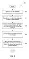
- FIG. 1is a flow diagram of a housing formation process 100 according to one embodiment.
- the housing formation process 100can operate to produce a housing for an electronic device, or at least a portion of such a housing.
- the housing formation process 100can initially obtain 102 a glass member.
- a top surface of the glass membercan represent an outer surface for the housing, and the bottom surface of the glass member is an inner surface that is not exposed.
- the glass membercan serve as a significant outer surface for the housing.
- the glass membercan correspond to a top surface for the housing.
- the glass membercan correspond to a bottom surface for the housing.
- the glass memberis typically thin, particularly when used with portable electronic devices. In one embodiment, the glass member has a thickness of less than 5 mm, or more particularly less than 1 mm.
- mounting bracketscan be attached 104 to a peripheral region on the bottom surface of the glass member.
- the mounting bracketscan be attached to the bottom surface of the glass member using an adhesive.
- the adhesivecan, for example, be provided as a film or layer. Also, the manner by which the adhesive is deposited can vary. In one implementation, the adhesive can be deposited by forming a peripheral pattern of adhesive that can be placed on the bottom surface of the glass member so as to provide adhesive at the regions on the bottom surface of the glass member where the mounting brackets are to be placed. In another implementation, the adhesive can be screen printed on appropriate peripheral portions on the bottom surface of the glass member. In still another embodiment, the adhesive can be applied to the surface of the mounting brackets that is to be secured to the bottom surface of the glass member.
- a touch screen assemblycan be attached 106 to a central region of the bottom surface of the glass member.
- the touch screen assemblycan include a plurality of touch and display components that are laminated together to implement a touch screen.
- the touch and display componentscan, for example, include a display technology layer (e.g., LCD panel), a sensing layer (e.g., touch sensors) and/or a back light component.
- the touch screen assemblycan be attached 106 using an adhesive.
- the adhesivecan, for example, be provided as film or layer. Also, the manner by which the adhesive is deposited can vary. In one implementation, the adhesive can be deposited by forming a pattern of adhesive (e.g., translucent adhesive) that can be placed on the bottom surface of the glass member so as to provide adhesive at the bottom surface of the glass member where the touch screen assembly is to be placed. The adhesive can additionally or alternatively be deposited on the top surface of the touch screen assembly. In another implementation, the adhesive can be screen printed or sprayed on an appropriate portion of the bottom surface of the glass member and/or a top surface of the touch screen assembly.
- adhesivecan, for example, be provided as film or layer. Also, the manner by which the adhesive is deposited can vary. In one implementation, the adhesive can be deposited by forming a pattern of adhesive (e.g., translucent adhesive) that can be placed on the bottom surface of the glass member so as to provide adhesive at the bottom surface of the glass member where the touch screen assembly is to be placed
- a framecan be attached 108 such that the frame is adjacent to the bottom surface of the touch screen assembly.
- the frame being attached 108can serve to protect the touch screen assembly from damage and can provide structural stiffness to the housing for the electronic device.
- the framecan be attached 108 to the mounting members or side members of the housing for the electronic device.
- the framecan be attached 108 using any of a variety of means, such as adhesive, screws, snaps or welds.
- the resulting display assemblyincluding the glass member, the mounting brackets, the touch screen assembly, and the frame can be secured to the housing of the electronic device.
- the resulting display assemblycan be secured 110 to the housing of the electronic device by way of the mounting brackets and/or the frame.
- the housing formation process 100can end.
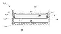
- FIG. 2Ais a cross-sectional view of an electronic device housing 200 according to one embodiment.
- the electronic device housing 200can result from the housing formation process 100 illustrated in FIG. 1 .
- the electronic device housing 200includes a housing 202 .
- the housing 202includes side members 204 and a bottom member 206 .
- a translucent member 208can be provided as a top surface for the electronic device housing 200 .
- the translucent member 208can be a glass member, often referred to as a cover glass, or a polymer-based member (e.g., plastic).
- the electronic device housing 200can include a touch screen assembly 210 .
- the touch screen assembly 210can include a plurality of touch and display components that are laminated together.
- the touch and display componentscan, for example, include a display technology layer (e.g., LCD panel), a sensing layer (e.g., touch sensors) and/or a backlight layer.
- the touch screen assembly 210can be secured to a bottom surface of the translucent member 208 by a layer of adhesive 212 .
- the electronic device housing 200can include mounting brackets 214 that are secured to the peripheral portion of the bottom surface of the translucent member 208 with a layer of adhesive 216 .
- the mounting brackets 214can be formed of metal (e.g., aluminum, stainless steel) or a polymer.
- the mounting brackets 214can be thin such as on the order of 0.1-0.6 mm.
- the mounting brackets 214can include a pair of rails secured to opposite sides of the peripheral portion of the bottom surface of the translucent member 208 with the layer of adhesive 216 .
- the electronic device housing 200can also include a frame 218 .
- the frame 218is provided within the electronic device housing 200 and provided adjacent to a bottom surface of the touch screen assembly 210 . In one embodiment, there is a small gap between the frame 218 and the bottom surface on the touch screen assembly 210 .
- the frame 218can serve to provide stiffness to the electronic device housing 200 and can also provide a surface that protects the touch screen assembly 210 .
- the frame 218can be secured to the mounting brackets 214 or the side members 204 by any of a variety of techniques (e.g., welding, screws, snaps, adhesive).
- An internal space 220is provided internal to the electronic device housing 200 whereby various electrical components (e.g., including processor, memory, battery, and circuit board) can be attached, affixed, or placed so as to provide electronic operations for the electronic device.
- various electrical componentse.g., including processor, memory, battery, and circuit board
- the various members, parts or assemblies of the electronic device housing 200can be formed of any of a variety of materials, e.g., glass, polymers or metal.
- the translucent member 208is glass
- the mounting brackets 214 and the frame 218are formed from metal or polymer (e.g., plastic)
- the housing 202is formed from glass, polymer (e.g., plastic) or metal.
- FIGS. 2B-2Eare cross-sectional assembly diagrams for the electronic device housing 200 shown in FIG. 2A , according to one embodiment.
- the FIGS. 2A-2Drepresent a sequence of exemplary assembly steps to assemble the electronic device housing 200 .
- the translucent member 208having a top surface and a bottom surface is provided.
- the bottom surface of the translucent member 208can have the adhesive 216 applied as a layer of adhesive at selected regions along certain sides of a periphery of the bottom surface of the translucent member 208 .
- the mounting brackets 214can then be secured to the translucent member 208 via the adhesive 216 .
- the touch screen assembly 210can then be secured to the translucent member 208 through use of the layer of adhesive 212 .
- the layer of adhesive 212would be translucent (e.g., clear).
- the top surface of the touch screen assembly 210is secured to the bottom surface of the translucent member 208 .
- the frame 218can then be secured to the mounting brackets 214 .
- the frame 218can be secured to the mounting brackets 214 or the side members 204 through use of adhesive, welds, screws, etc.
- the frame 218is adjacent a bottom surface of the touch screen assembly 210 .
- the frame 218is typically not contacting the bottom surface of the touch screen assembly 210 . Instead, there is a small gap 206 between the frame 218 and the bottom surface of the touch screen assembly 210 .
- the assembly resulting at FIG. 2Dcan then be inserted into the housing 202 for the electronic device.
- the assemblycan be secured to the housing 202 .
- the assemblycan be secured in place through use of adhesive, snaps, welds, screws, etc.
- the mounting brackets 214can be secured to side members 204 of the housing 202 .
- FIG. 3is a cross-sectional view of an electronic device housing 300 according to one embodiment.
- the electronic device housing 300is generally similar to the electronic device housing 200 illustrated in FIG. 2A .
- the electronic device housing 300includes a housing 302 .
- the housing 302includes side members 304 and a bottom member 306 .
- a translucent member 308can be provided as a top surface for the electronic device housing 300 .
- the translucent member 308can be a glass member, often referred to as a cover glass, or a polymer-based member (e.g., plastic).
- the electronic device housing 300can include a touch screen assembly 310 .
- the touch screen assembly 310can include a plurality of touch and display components that are laminated together.
- the touch and display componentscan, for example, include a display technology layer (e.g., LCD panel), a sensing layer (e.g., touch sensors), and/or a backlight layer.
- the touch screen assembly 310can be secured to the bottom surface of the translucent member 308 by a layer of adhesive 312 .
- the electronic device housing 300can include mounting brackets 314 that are secured to the peripheral portion of the bottom surface of the translucent member 308 with a layer of adhesive 316 .
- the mounting brackets 314can be formed of metal (e.g., aluminum, stainless steel) or a polymer.
- the mounting brackets 314can be thin such as on the order of 0.1-0.6 mm.
- the configuration and placement of the mounting brackets 314can be the same as the mounting brackets 214 used in FIG. 2A , except that the mounting brackets 314 can, in one embodiment, be longer (i.e., have greater height) than the mounting brackets 214 .
- the mounting brackets 314can include a pair of rails secured to opposite sides of the peripheral portion of the bottom surface of the translucent member 308 with the layer of adhesive 316 .
- the electronic device housing 300can also include a frame 318 .
- the frame 318is provided within the electronic device housing 300 and provided adjacent to a bottom surface of the touch screen assembly 310 . In one embodiment, there is a small gap between the frame 318 and the bottom surface on the touch screen assembly 310 .
- the frame 318can serve to provide stiffness to the electronic device housing 300 and can also provide a surface that protects the touch screen assembly 310 .
- the frame 318can be secured to the mounting brackets 314 or the side members 304 by any of a variety of techniques (e.g., welding, screws, snaps, adhesive).
- the configuration and placement of the frame 318can be the same as the frame 218 used in FIG. 2A , except that the frame 318 can be secured to the mounting brackets 314 at a lower position than used in FIG. 2A .
- An internal space 320is provided internal to the electronic device housing 300 whereby various electrical components (e.g., including processor, memory, battery, and circuit board) can be attached, affixed, or placed so as to provide electronic operations for the electronic device.
- various electrical componentse.g., including processor, memory, battery, and circuit board
- the various members, parts, or assemblies of the electronic device housing 300can be formed of any of a variety of materials, e.g., glass, polymers, or metal.
- the translucent member 308is glass
- the mounting brackets 314 and the frame 318are formed from metal or polymer (e.g., plastic)
- the housing 302is formed from glass, polymer (e.g., plastic), or metal.
- a top portion of the mounting bracket 314 that is secured to the bottom surface of the translucent member 308 with the layer of adhesive 316can slightly vertically overlap with a least one layer of the touch screen assembly 310 .
- FIG. 3illustrates the top portion of the mounting bracket 314 that is secured to the bottom surface of the translucent member 308 with the layer of adhesive 316 being slightly overlapped (e.g., horizontally overlapped) with a middle layer of the touch screen assembly 310 .
- the ability to overlap these components slightly in the horizontal directionprovides for improved compact designs that are able to have even further reduced border thickness (between an edge of an active display area and an edge of the housing).
- FIG. 4Aillustrates a side member 400 and a mounting bracket 402 of an electronic device housing according to one embodiment.
- the electronic device housingcan, for example, pertain to the electronic device housing 200 illustrated in FIG. 2A or the electronic device housing 300 illustrated in FIG. 3 .
- the mounting bracket 402is attached to the side member 400 by welds 404 .
- FIG. 4Billustrates a side member 420 and a mounting bracket 422 of an electronic device housing according to one embodiment.
- the electronic device housingcan, for example, pertain to the electronic device housing 200 illustrated in FIG. 2A or the electronic device housing 300 illustrated in FIG. 3 .
- the mounting bracket 422is attached to the side member 420 by at least one snap 424 which provides a mechanical retention therebetween.
- FIG. 4Cillustrates a side member 440 , a mounting bracket 442 , and a frame 444 (portion thereof) of an electronic device housing according to one embodiment.
- the electronic device housingcan, for example, pertain to the electronic device housing 200 illustrated in FIG. 2A or the electronic device housing 300 illustrated in FIG. 3 .
- the mounting bracket 442is attached to the side member 440 by any of the above-noted techniques (e.g., adhesive, snap, screw, weld), and the frame 444 can be secured to the mounting bracket 442 by at least one screw 446 (or bolt).
- the screw 446can further extend into or through the side member 440 to secure the mounting bracket 442 and the frame 444 to themselves and the side member 440 .
- the mounting bracketis secured to the bottom surface of a translucent member that can serve as a significant outer surface for a housing of an electronic device, such as a portable electronic device.
- a frame or other structural componentcan instead be secured to the bottom surface of the translucent member
- FIG. 5a flow diagram of a housing formation process 500 according to one embodiment.
- the housing formation process 500can operate to produce a housing for an electronic device, or at least a portion of such a housing.
- the housing formation process 500can initially obtain 502 a glass member.
- a top surface of the glass membercan represent an outer surface for the housing, and the bottom surface of the glass member is an inner surface that is not exposed.
- the glass membercan serve as a significant outer surface for the housing.
- the glass membercan correspond to a top surface for the housing.
- the glass membercan correspond to a bottom surface for the housing.
- the glass memberis typically thin, particularly when used with portable electronic devices. In one embodiment, the glass member has a thickness of less than 5 mm, or more particularly less than 1 mm.
- a framecan be attached 504 to a peripheral region on the bottom surface of the glass member.
- the frameonce attached 504 , can serve to protect the touch screen assembly from damage and can provide structural stiffness to the housing for the electronic device.
- the frameis adjacent to the bottom surface of the touch screen assembly.
- the framecan be attached to the bottom surface of the glass member using an adhesive.
- the adhesivecan, for example, by provided as film or layer. Also, the manner by which the adhesive is deposited can vary. In one implementation, the adhesive can be deposited by forming a peripheral pattern of adhesive that can be placed on the bottom surface of the glass member so as to provide adhesive at the regions on the bottom surface of the glass member where the mounting brackets are to be placed. In another implementation, the adhesive can be screen printed on appropriate peripheral portions on the bottom surface of the glass member. In still another embodiments, the adhesive can be applied to the surface of the mounting brackets that is to be secured to the bottom surface of the glass member.
- a touch screen assemblycan be attached 506 to a central region of the bottom surface of the glass member.
- the touch screen assemblycan include a plurality of touch and display components that are laminated together to implement a touch screen.
- the touch and display componentscan, for example, include a display technology layer (e.g., LCD panel), a sensing layer (e.g., touch sensors) and/or a backlight component.
- the touch screen assemblycan be attached 506 using an adhesive.
- the adhesivecan, for example, be provided as film or layer. Also, the manner by which the adhesive is deposited can vary. In one implementation, the adhesive can be deposited by forming a pattern of adhesive (e.g., translucent adhesive) that can be placed on the bottom surface of the glass member so as to provide adhesive at the bottom surface of the glass member where the touch screen assembly is to be placed. The adhesive can additionally or alternatively be deposited on the top surface of the touch screen assembly. In another implementation, the adhesive can be screen printed or sprayed on an appropriate portion of the bottom surface of the glass member and/or a top surface of the touch screen assembly.
- adhesivecan, for example, be provided as film or layer. Also, the manner by which the adhesive is deposited can vary. In one implementation, the adhesive can be deposited by forming a pattern of adhesive (e.g., translucent adhesive) that can be placed on the bottom surface of the glass member so as to provide adhesive at the bottom surface of the glass member where the touch screen assembly is to be placed
- mounting bracketscan be attached 508 to the frame.
- the framecan be attached 508 to the frame using any of a variety of means, such as adhesive, screws, snaps or welds.
- the resulting display assemblyincluding the glass member, the mounting brackets, the touch screen assembly and the frame can be secured 550 to the housing of the electronic device.
- the resulting display assemblycan be secured to the housing of the electronic device by way of the mounting brackets and/or the frame.
- the housing formation process 500can end.
- FIG. 6is a cross-sectional view of an electronic device housing 600 according to one embodiment.
- the electronic device housing 600can result from the housing formation process 500 illustrated in FIG. 5 .
- the electronic device housing 600includes a housing 602 .
- the housing 602includes side members 604 and a bottom member 606 .
- a translucent member 608can be provided as a top surface for the electronic device housing 600 .
- the translucent member 608can be a glass member, often referred to as a cover glass, or a polymer-based member (e.g., plastic).
- the electronic device housing 600can include a touch screen assembly 610 .
- the touch screen assembly 610can include a plurality of touch and display components that are laminated together.
- the touch and display componentscan, for example, include a display technology layer (e.g., LCD panel), a sensing layer (e.g., touch sensors) and/or a backlight layer.
- the touch screen assembly 610can be secured to a bottom surface of the translucent member 608 by a layer of adhesive 612 .
- the electronic device housing 600can include a frame 614 which can be secured to the peripheral portion of the bottom surface of the translucent member 608 with a layer of adhesive 616 .
- the frame 614is provided within the electronic device housing 600 and provided adjacent to a bottom surface of the touch screen assembly 610 . In one embodiment, there is a small gap between the frame 614 and the bottom surface on the touch screen assembly 610 .
- the frame 614can serve to provide stiffness to the electronic device housing 600 and can also provide a surface that protects the touch screen assembly 610 .
- a top portion of the frame 614 that is secured to the bottom surface of the translucent member 608 with the layer of adhesive 616can slightly overlap (e.g., horizontally overlapped) with a least one layer of the touch screen assembly 610 .
- FIG. 6illustrates the top portion of the frame 614 that is secured to the bottom surface of the translucent member 608 with the layer of adhesive 616 being slightly vertically overlapped with a middle layer of the touch screen assembly 610 .
- the ability to overlap slightly in the horizontal directionprovides for improved compact designs that are able to have even further reduced border thickness (between the edge of the active display area and the edge of the housing).
- the electronic device housing 600can include mounting brackets 618 .
- the mounting brackets 618can be secured to the side members 604 .
- the mounting brackets 618can be formed of metal (e.g., aluminum, stainless steel) or a polymer.
- the mounting brackets 618can be thin such as on the order of 0.1-0.6 mm.
- the mounting brackets 618can be secured to the frame 614 as well as to the side members 604 by any of a variety of techniques (e.g., welding, screws, snaps, adhesive).
- An internal space 620is provided internal to the electronic device housing 600 whereby various electrical components (e.g., including processor, memory, battery, and circuit board) can be attached, affixed, or placed so as to provide electronic operations for the electronic device.
- various electrical componentse.g., including processor, memory, battery, and circuit board
- the various members, parts, or assemblies of the electronic device housing 600can be formed of any of a variety of materials, e.g., glass, polymers, or metal.
- the translucent member 608is glass
- the frame 614 and the mounting brackets 618are formed from metal or polymer (e.g., plastic)
- the housing 602is formed from glass, polymer (e.g., plastic), or metal.
- FIG. 7is a perspective diagram of a handheld electronic device 700 according to one embodiment.
- the handheld electronic device 700may include a housing 702 , e.g., a periphery member, that is arranged to at least partially surround the periphery of the handheld electronic device 700 to form some or all of the outer-most side, top, and bottom surfaces of the handheld electronic device 700 .
- the handheld electronic device 700also includes a cover piece 704 that is arranged to be substantially coupled to the housing 702 to effectively enclose an inner volume of the handheld electronic device 700 .
- the cover piece 704may include a glass member 706 , e.g., cover glass provided over a display of the handheld electronic device 700 .
- the cover piece 704includes a protective frame 708 in which the glass member 706 is held.
- the glass member 706can serve as the top surface of the housing 702 .
- a display region 707 of the glass member 706is that portion of the glass member 706 that corresponds to the display (e.g., active display region).
- the displaycan be secured to the housing 702 such that the active display region is able to nearly reach the edge of the housing.
- the border thickness (t) at the sides of the housing 702is able to be reduced as compared to conventional designs.
- the border thickness (t)can be 2 mm or less.
- the housing 702may have any suitable shape, including, for example, one or more elements that may be combined to form a rectangular structure.
- the housing 702may at least partially enclose an inner volume in which electronic device components may be assembled and retained.
- the shape of the housing 702may substantially define boundaries of the inner volume, and may be determined based upon the size and type of components placed within the inner volume.
- the housing 702may have any suitable size, and the size may be determined based on any suitable criteria. Suitable criteria may include, but are not limited to, aesthetics or industrial design, structural considerations, components required for a desired functionality, and/or product design.
- the housing 702may have any suitable cross-section, including, for example, a variable cross-section or a constant cross-section. In some embodiments, the cross-section may be selected based on desired structural properties for the housing 702 .
- the cross-section of the housing 702may be substantially rectangular, such that the height of the housing 702 is substantially larger than the width of the housing 702 . Such a cross-sectional shape may provide structural stiffness in compression and tension, as well as in bending.
- the dimensions of the housing 702 cross-sectionmay be determined relative to the dimensions of the components contained by the housing 702 .
- the housing 702may include features 710 .
- the features 710may generally include one or more openings, knobs, extensions, flanges, chamfers, or other features for receiving components or elements of the device.
- the features 710 of the housing 702extend from any surface of the housing 702 , including, for example, from internal surfaces, e.g., to retain internal components or component layers, or from external surfaces.
- the housing 702may include a slot or opening (not shown) for receiving a card or tray within the handheld electronic device 700 .
- the housing 702may also include a connector opening (not shown), e.g., for a 30-pin connector, through which a connector may engage one or more conductive pins of the handheld electronic device 700 .
- features 710 included on the housing 702may include, but are not limited to, an opening for providing audio to a user, an opening for receiving audio from a user, an opening for a connector (e.g., audio connector or power supply connector), and/or features for retaining and enabling a button such as a volume control or silencing switch.
- a connectore.g., audio connector or power supply connector
- mounting brackets and a frame for a display assemblyare discussed above as separate components (which can facilitate assembly), it should be understood that the mounting brackets and frame are structural components that are used in an electronic device. In one embodiment, the mounting brackets and frame are integral. In another embodiment, the mounting brackets and frame are interchangeable.
- a display assemblywould be used in place of the touch screen assembly.
- the display assemblyincludes at least a display technology layer.
- the display assemblycan also include a backlight component.
Landscapes
- Engineering & Computer Science (AREA)
- Theoretical Computer Science (AREA)
- General Engineering & Computer Science (AREA)
- Computer Hardware Design (AREA)
- Human Computer Interaction (AREA)
- Physics & Mathematics (AREA)
- General Physics & Mathematics (AREA)
- Microelectronics & Electronic Packaging (AREA)
- Devices For Indicating Variable Information By Combining Individual Elements (AREA)
- Telephone Set Structure (AREA)
- Casings For Electric Apparatus (AREA)
Abstract
Description
This application is a continuation patent application of U.S. patent application Ser. No. 15/274,251, filed Sep. 23, 2016 and titled “Housing for Portable Electronic Device with Reduced Border Region,” now U.S. Pat. No. 10,007,295, which is a continuation patent application of U.S. patent application Ser. No. 14/801,550, filed Jul. 16, 2015 and titled “Housing for Portable Electronic Device with Reduced Border Region,” now U.S. Pat. No. 9,513,664, which is a continuation patent application of U.S. patent application Ser. No. 13/246,697, filed Sep. 27, 2011 and titled “Housing for Portable Electronic Device with Reduced Border Region,” now U.S. Pat. No. 9,128,666, which is a nonprovisional patent application of and claims the benefit of U.S. Provisional Patent Application No. 61,482,513, filed May 4, 2011 and titled “Housing for Portable Electronic Device with Reduced Border Region,” the disclosures of which are hereby incorporated herein by reference in their entireties.
Conventionally, a portable electronic device has a housing that encases the various electrical components of the portable electronic device. Often, the portable electronic device has a display arrangement that includes various layers. The various layers usually include at least a display technology layer, and may additionally include a sensing arrangement (e.g., touch sensors or touch screen) and/or a cover window disposed over the display technology layer. The cover window can be a plastic or glass cover that provides a protective outer surface that protects the display technology layer. The cover window can form part of an outer surface for the housing of the portable electronic device. Conventionally, supporting or securing the cover window to other portions of the housing tends to impede usage of a peripheral area of the cover window.
Nevertheless, as portable electronic devices continue to be made smaller, thinner, and/or more powerful, there remains a continuing need to provide improved techniques and structures for supporting cover windows of portable electronic device housings.
The invention pertains to an electronic device having a housing structure that is configured to receive at least one glass cover. The glass cover serves to cover a display assembly provided within the electronic device. The glass cover can be secured to the housing structure so as to facilitate providing a narrow border between an active display area and an outer edge of the housing structure. The enclosure for the electronic device can be thin yet be sufficiently strong to be suitable for use in electronic devices, such as portable electronic devices.
The invention can be implemented in numerous ways, including as a method, system, device, or apparatus. Several embodiments of the invention are discussed below.
As a portable electronic device, one embodiment can, for example, include at least: an electronic device housing including a bottom surface and side surfaces; a glass cover for a top surface for the electronic device enclosure; at least one peripheral internal support structure secured to a peripheral region of a bottom surface of the glass cover, wherein the at least one peripheral internal support structure is within the periphery of the glass cover; a screen assembly having a top surface and a bottom surface, the top surface being secured to a central region of the bottom surface of the glass cover; and at least one surface support structure secured within the electronic device housing such that the at least one surface support structure is adjacent the bottom surface of the screen assembly.
As a method for assembling an electronic device, one embodiment can, for example, include at least: obtaining a glass member having a top surface and a bottom surface, the top surface providing an outer surface for substantially all of a surface of the electronic device; attaching at least one peripheral support structure to a peripheral region of the bottom surface of the glass member; attaching a screen assembly to a central region of the bottom surface of the glass member; attaching at least one surface support structure to the at least one peripheral support structure, wherein the glass member, the screen assembly, and the at least one peripheral support structure form a resulting display assembly; and thereafter securing the resulting display assembly to a product housing using at least the peripheral support structure.
As a portable electronic device, one embodiment can, for example, include at least: an electronic device housing including a bottom surface and side surfaces; a glass cover for a top surface for the electronic device enclosure; at least one mounting bracket secured to a peripheral region of a bottom surface of the glass cover; a touch screen assembly having a top surface and a bottom surface, the top surface being secured to a central region of the bottom surface of the glass cover; and a frame secured within the electronic device housing such that the frame is adjacent the bottom surface of the touch screen assembly.
As a method for assembling an electronic device, one embodiment can, for example, include at least: obtain a glass member having a top surface and a bottom surface, the top surface providing an outer surface for substantially all of a surface of the electronic device; attach mounting brackets to a peripheral region of the bottom surface of the glass member; attach a top surface of a screen assembly to a central region of the bottom surface of the glass member; attach a frame adjacent a bottom surface of the screen assembly, wherein the glass member, the frame, the screen assembly, and the mounting brackets form a resulting display assembly; and thereafter secure the resulting display assembly to a product housing using the mounting brackets and/or frame.
As a portable electronic device, one embodiment can, for example, include at least: an electronic device housing including a bottom surface and side surfaces; a glass cover for a top surface for the electronic device enclosure; a frame secured to a peripheral region of a bottom surface of the glass cover; a screen assembly having a top surface and a bottom surface, the top surface being secured to a central region of the bottom surface of the glass cover; and at least one mounting bracket secured to the frame.
As a method for assembling an electronic device, one embodiment can, for example, include at least: obtain a glass member having a top surface and a bottom surface, the top surface providing an outer surface for substantially all of a surface of the electronic device; attach a frame to a peripheral region of the bottom surface of the glass member; attach a screen assembly to a central region of the bottom surface of the glass member; attach mounting brackets to the frame, wherein the glass member, the frame, the screen assembly, and the mounting brackets form a resulting display assembly; and thereafter secure the resulting display assembly to a product housing using the mounting brackets and/or frame.
Other aspects and advantages of the invention will become apparent from the following detailed description taken in conjunction with the accompanying drawings which illustrate, by way of example, the principles of the invention.
The invention will be readily understood by the following detailed description in conjunction with the accompanying drawings, wherein like reference numerals designate like structural elements, and in which:
Embodiments are described herein in the context of a housing for an electronic device. The housing can make use of an outer member, which can be formed of glass. The outer member can be aligned, protected, and/or secured with respect to other portions of the housing for the electronic device. The electronic device can be portable and in some cases handheld.
According to one aspect, the invention pertains to an electronic device having a housing structure that is configured to receive at least one glass cover. The glass cover serves to cover a display assembly provided within the electronic device. The glass cover can be secured to the housing structure so as to facilitate providing a narrow border between an active display area and an outer edge of the housing structure. The enclosure for the electronic device can be thin yet be sufficiently strong to be suitable for use in electronic devices, such as portable electronic devices.
The following detailed description is illustrative only, and is not intended to be in any way limiting. Other embodiments will readily suggest themselves to skilled persons having the benefit of this disclosure. Reference will now be made in detail to implementations as illustrated in the accompanying drawings. The same reference indicators will generally be used throughout the drawings and the following detailed description to refer to the same or like parts. It should be appreciated that the drawings are generally not drawn to scale, and at least some features of the drawings have been exaggerated for ease of illustration.
Embodiments of the invention can relate to an apparatus, systems, and methods for forming a housing having a thin glass member for an electronic device. In one example, the glass member may be an outer surface of an electronic device. The glass member may, for example, correspond to a glass cover that helps form part of a display area of an electronic device (i.e., situated in front of a display either as a separate part or integrated within the display). Alternatively or additionally, the glass member may form a part of the housing. For example, it may form an outer surface other than in the display area.
The apparatus, systems and methods for improving strength of thin glass are especially suitable for glass covers, or displays (e.g., LCD displays), assembled in small form factor electronic devices such as handheld electronic devices (e.g., mobile phones, media players, personal digital assistants, remote controls, etc.). The glass can be thin in these small form factor embodiments, such as less than 3 mm, or more particularly between 0.5 and 2.5 mm, or even more particularly between 0.3 and 1.0 mm. The apparatus, systems, and methods can also be used for glass covers or displays for other devices including, but not limited to, relatively larger form factor electronic devices (e.g., portable computers, tablet computers, displays, monitors, televisions, etc.). The glass can also be thin in these larger form factor embodiments, such as less than 5 mm, or more particularly between 0.5 and 3 mm, or even more particularly between 0.3 and 2.0 mm.
Embodiments are discussed below with reference toFIGS. 1-7 . However, those skilled in the art will readily appreciate that the detailed description given herein with respect to these figures is for explanatory purposes as the invention extends beyond these limited embodiments.
Thehousing formation process 100 can initially obtain102 a glass member. A top surface of the glass member can represent an outer surface for the housing, and the bottom surface of the glass member is an inner surface that is not exposed. The glass member can serve as a significant outer surface for the housing. For example, the glass member can correspond to a top surface for the housing. Alternatively or additionally, the glass member can correspond to a bottom surface for the housing. The glass member is typically thin, particularly when used with portable electronic devices. In one embodiment, the glass member has a thickness of less than 5 mm, or more particularly less than 1 mm.
After the glass member has been obtained102, mounting brackets can be attached104 to a peripheral region on the bottom surface of the glass member. The mounting brackets can be attached to the bottom surface of the glass member using an adhesive. The adhesive can, for example, be provided as a film or layer. Also, the manner by which the adhesive is deposited can vary. In one implementation, the adhesive can be deposited by forming a peripheral pattern of adhesive that can be placed on the bottom surface of the glass member so as to provide adhesive at the regions on the bottom surface of the glass member where the mounting brackets are to be placed. In another implementation, the adhesive can be screen printed on appropriate peripheral portions on the bottom surface of the glass member. In still another embodiment, the adhesive can be applied to the surface of the mounting brackets that is to be secured to the bottom surface of the glass member.
After the mounting brackets have been attached104, a touch screen assembly can be attached106 to a central region of the bottom surface of the glass member. The touch screen assembly can include a plurality of touch and display components that are laminated together to implement a touch screen. The touch and display components can, for example, include a display technology layer (e.g., LCD panel), a sensing layer (e.g., touch sensors) and/or a back light component.
The touch screen assembly can be attached106 using an adhesive. The adhesive can, for example, be provided as film or layer. Also, the manner by which the adhesive is deposited can vary. In one implementation, the adhesive can be deposited by forming a pattern of adhesive (e.g., translucent adhesive) that can be placed on the bottom surface of the glass member so as to provide adhesive at the bottom surface of the glass member where the touch screen assembly is to be placed. The adhesive can additionally or alternatively be deposited on the top surface of the touch screen assembly. In another implementation, the adhesive can be screen printed or sprayed on an appropriate portion of the bottom surface of the glass member and/or a top surface of the touch screen assembly.
Next, after the touch screen assembly has been attached106, a frame can be attached108 such that the frame is adjacent to the bottom surface of the touch screen assembly. The frame being attached108 can serve to protect the touch screen assembly from damage and can provide structural stiffness to the housing for the electronic device. The frame can be attached108 to the mounting members or side members of the housing for the electronic device. In one embodiment, the frame can be attached108 using any of a variety of means, such as adhesive, screws, snaps or welds.
After the frame has been attached108, the resulting display assembly, including the glass member, the mounting brackets, the touch screen assembly, and the frame can be secured to the housing of the electronic device. For example, the resulting display assembly can be secured110 to the housing of the electronic device by way of the mounting brackets and/or the frame. Following theblock 110, thehousing formation process 100 can end.
Theelectronic device housing 200 includes ahousing 202. Thehousing 202 includesside members 204 and abottom member 206. Atranslucent member 208 can be provided as a top surface for theelectronic device housing 200. For example, thetranslucent member 208 can be a glass member, often referred to as a cover glass, or a polymer-based member (e.g., plastic).
Theelectronic device housing 200 can include atouch screen assembly 210. Thetouch screen assembly 210 can include a plurality of touch and display components that are laminated together. The touch and display components can, for example, include a display technology layer (e.g., LCD panel), a sensing layer (e.g., touch sensors) and/or a backlight layer. Thetouch screen assembly 210 can be secured to a bottom surface of thetranslucent member 208 by a layer ofadhesive 212.
Additionally, theelectronic device housing 200 can include mountingbrackets 214 that are secured to the peripheral portion of the bottom surface of thetranslucent member 208 with a layer ofadhesive 216. The mountingbrackets 214 can be formed of metal (e.g., aluminum, stainless steel) or a polymer. The mountingbrackets 214 can be thin such as on the order of 0.1-0.6 mm. In one embodiment, the mountingbrackets 214 can include a pair of rails secured to opposite sides of the peripheral portion of the bottom surface of thetranslucent member 208 with the layer ofadhesive 216.
Theelectronic device housing 200 can also include aframe 218. Theframe 218 is provided within theelectronic device housing 200 and provided adjacent to a bottom surface of thetouch screen assembly 210. In one embodiment, there is a small gap between theframe 218 and the bottom surface on thetouch screen assembly 210. Theframe 218 can serve to provide stiffness to theelectronic device housing 200 and can also provide a surface that protects thetouch screen assembly 210. Theframe 218 can be secured to the mountingbrackets 214 or theside members 204 by any of a variety of techniques (e.g., welding, screws, snaps, adhesive).
Aninternal space 220 is provided internal to theelectronic device housing 200 whereby various electrical components (e.g., including processor, memory, battery, and circuit board) can be attached, affixed, or placed so as to provide electronic operations for the electronic device.
In general, the various members, parts or assemblies of theelectronic device housing 200 can be formed of any of a variety of materials, e.g., glass, polymers or metal. In one embodiment, thetranslucent member 208 is glass, the mountingbrackets 214 and theframe 218 are formed from metal or polymer (e.g., plastic), and thehousing 202 is formed from glass, polymer (e.g., plastic) or metal.
InFIG. 2B , thetranslucent member 208 having a top surface and a bottom surface is provided. The bottom surface of thetranslucent member 208 can have the adhesive216 applied as a layer of adhesive at selected regions along certain sides of a periphery of the bottom surface of thetranslucent member 208. The mountingbrackets 214 can then be secured to thetranslucent member 208 via the adhesive216.
InFIG. 2C , thetouch screen assembly 210 can then be secured to thetranslucent member 208 through use of the layer ofadhesive 212. Typically, the layer of adhesive212 would be translucent (e.g., clear). Here, the top surface of thetouch screen assembly 210 is secured to the bottom surface of thetranslucent member 208.
InFIG. 2D , theframe 218 can then be secured to the mountingbrackets 214. Theframe 218 can be secured to the mountingbrackets 214 or theside members 204 through use of adhesive, welds, screws, etc. When attached, theframe 218 is adjacent a bottom surface of thetouch screen assembly 210. However, theframe 218 is typically not contacting the bottom surface of thetouch screen assembly 210. Instead, there is asmall gap 206 between theframe 218 and the bottom surface of thetouch screen assembly 210.
InFIG. 2E , the assembly resulting atFIG. 2D can then be inserted into thehousing 202 for the electronic device. The assembly can be secured to thehousing 202. For example, the assembly can be secured in place through use of adhesive, snaps, welds, screws, etc. In one embodiment, the mountingbrackets 214 can be secured toside members 204 of thehousing 202. Once the assembly resulting atFIG. 2D is inserted and then secured, theelectronic device housing 200 as shown inFIG. 2A results.
Theelectronic device housing 300 can include atouch screen assembly 310. Thetouch screen assembly 310 can include a plurality of touch and display components that are laminated together. The touch and display components can, for example, include a display technology layer (e.g., LCD panel), a sensing layer (e.g., touch sensors), and/or a backlight layer. Thetouch screen assembly 310 can be secured to the bottom surface of thetranslucent member 308 by a layer ofadhesive 312.
Additionally, theelectronic device housing 300 can include mountingbrackets 314 that are secured to the peripheral portion of the bottom surface of thetranslucent member 308 with a layer ofadhesive 316. The mountingbrackets 314 can be formed of metal (e.g., aluminum, stainless steel) or a polymer. The mountingbrackets 314 can be thin such as on the order of 0.1-0.6 mm. The configuration and placement of the mountingbrackets 314 can be the same as the mountingbrackets 214 used inFIG. 2A , except that the mountingbrackets 314 can, in one embodiment, be longer (i.e., have greater height) than the mountingbrackets 214. In one embodiment, the mountingbrackets 314 can include a pair of rails secured to opposite sides of the peripheral portion of the bottom surface of thetranslucent member 308 with the layer ofadhesive 316.
Theelectronic device housing 300 can also include aframe 318. Theframe 318 is provided within theelectronic device housing 300 and provided adjacent to a bottom surface of thetouch screen assembly 310. In one embodiment, there is a small gap between theframe 318 and the bottom surface on thetouch screen assembly 310. Theframe 318 can serve to provide stiffness to theelectronic device housing 300 and can also provide a surface that protects thetouch screen assembly 310. Theframe 318 can be secured to the mountingbrackets 314 or theside members 304 by any of a variety of techniques (e.g., welding, screws, snaps, adhesive). The configuration and placement of theframe 318 can be the same as theframe 218 used inFIG. 2A , except that theframe 318 can be secured to the mountingbrackets 314 at a lower position than used inFIG. 2A .
Aninternal space 320 is provided internal to theelectronic device housing 300 whereby various electrical components (e.g., including processor, memory, battery, and circuit board) can be attached, affixed, or placed so as to provide electronic operations for the electronic device.
In general, the various members, parts, or assemblies of theelectronic device housing 300 can be formed of any of a variety of materials, e.g., glass, polymers, or metal. In one embodiment, thetranslucent member 308 is glass, the mountingbrackets 314 and theframe 318 are formed from metal or polymer (e.g., plastic), and thehousing 302 is formed from glass, polymer (e.g., plastic), or metal.
Additionally, in one embodiment, such as shown inFIG. 3 , a top portion of the mountingbracket 314 that is secured to the bottom surface of thetranslucent member 308 with the layer of adhesive316 can slightly vertically overlap with a least one layer of thetouch screen assembly 310. For example,FIG. 3 illustrates the top portion of the mountingbracket 314 that is secured to the bottom surface of thetranslucent member 308 with the layer of adhesive316 being slightly overlapped (e.g., horizontally overlapped) with a middle layer of thetouch screen assembly 310. The ability to overlap these components slightly in the horizontal direction provides for improved compact designs that are able to have even further reduced border thickness (between an edge of an active display area and an edge of the housing).
InFIGS. 1-3 discussed above, the mounting bracket is secured to the bottom surface of a translucent member that can serve as a significant outer surface for a housing of an electronic device, such as a portable electronic device. However, in other embodiments, a frame or other structural component can instead be secured to the bottom surface of the translucent member
Thehousing formation process 500 can initially obtain502 a glass member. A top surface of the glass member can represent an outer surface for the housing, and the bottom surface of the glass member is an inner surface that is not exposed. The glass member can serve as a significant outer surface for the housing. For example, the glass member can correspond to a top surface for the housing. Alternatively or additionally, the glass member can correspond to a bottom surface for the housing. The glass member is typically thin, particularly when used with portable electronic devices. In one embodiment, the glass member has a thickness of less than 5 mm, or more particularly less than 1 mm.
After the glass member has been obtained502, a frame can be attached504 to a peripheral region on the bottom surface of the glass member. The frame, once attached504, can serve to protect the touch screen assembly from damage and can provide structural stiffness to the housing for the electronic device. When attached, the frame is adjacent to the bottom surface of the touch screen assembly. The frame can be attached to the bottom surface of the glass member using an adhesive. The adhesive can, for example, by provided as film or layer. Also, the manner by which the adhesive is deposited can vary. In one implementation, the adhesive can be deposited by forming a peripheral pattern of adhesive that can be placed on the bottom surface of the glass member so as to provide adhesive at the regions on the bottom surface of the glass member where the mounting brackets are to be placed. In another implementation, the adhesive can be screen printed on appropriate peripheral portions on the bottom surface of the glass member. In still another embodiments, the adhesive can be applied to the surface of the mounting brackets that is to be secured to the bottom surface of the glass member.
After the frame has been attached504, a touch screen assembly can be attached506 to a central region of the bottom surface of the glass member. The touch screen assembly can include a plurality of touch and display components that are laminated together to implement a touch screen. The touch and display components can, for example, include a display technology layer (e.g., LCD panel), a sensing layer (e.g., touch sensors) and/or a backlight component.
The touch screen assembly can be attached506 using an adhesive. The adhesive can, for example, be provided as film or layer. Also, the manner by which the adhesive is deposited can vary. In one implementation, the adhesive can be deposited by forming a pattern of adhesive (e.g., translucent adhesive) that can be placed on the bottom surface of the glass member so as to provide adhesive at the bottom surface of the glass member where the touch screen assembly is to be placed. The adhesive can additionally or alternatively be deposited on the top surface of the touch screen assembly. In another implementation, the adhesive can be screen printed or sprayed on an appropriate portion of the bottom surface of the glass member and/or a top surface of the touch screen assembly.
Next, after the touch screen assembly has been attached506, mounting brackets can be attached508 to the frame. In one embodiment, the frame can be attached508 to the frame using any of a variety of means, such as adhesive, screws, snaps or welds.
After the mounting brackets have been attached508, the resulting display assembly, including the glass member, the mounting brackets, the touch screen assembly and the frame can be secured550 to the housing of the electronic device. For example, the resulting display assembly can be secured to the housing of the electronic device by way of the mounting brackets and/or the frame. Following theblock 550, thehousing formation process 500 can end.
Theelectronic device housing 600 includes ahousing 602. Thehousing 602 includesside members 604 and abottom member 606. Atranslucent member 608 can be provided as a top surface for theelectronic device housing 600. For example, thetranslucent member 608 can be a glass member, often referred to as a cover glass, or a polymer-based member (e.g., plastic).
Theelectronic device housing 600 can include atouch screen assembly 610. Thetouch screen assembly 610 can include a plurality of touch and display components that are laminated together. The touch and display components can, for example, include a display technology layer (e.g., LCD panel), a sensing layer (e.g., touch sensors) and/or a backlight layer. Thetouch screen assembly 610 can be secured to a bottom surface of thetranslucent member 608 by a layer ofadhesive 612.
Additionally, theelectronic device housing 600 can include aframe 614 which can be secured to the peripheral portion of the bottom surface of thetranslucent member 608 with a layer ofadhesive 616. Theframe 614 is provided within theelectronic device housing 600 and provided adjacent to a bottom surface of thetouch screen assembly 610. In one embodiment, there is a small gap between theframe 614 and the bottom surface on thetouch screen assembly 610. Theframe 614 can serve to provide stiffness to theelectronic device housing 600 and can also provide a surface that protects thetouch screen assembly 610. Additionally, in one embodiment, a top portion of theframe 614 that is secured to the bottom surface of thetranslucent member 608 with the layer of adhesive616 can slightly overlap (e.g., horizontally overlapped) with a least one layer of thetouch screen assembly 610. For example,FIG. 6 illustrates the top portion of theframe 614 that is secured to the bottom surface of thetranslucent member 608 with the layer of adhesive616 being slightly vertically overlapped with a middle layer of thetouch screen assembly 610. The ability to overlap slightly in the horizontal direction provides for improved compact designs that are able to have even further reduced border thickness (between the edge of the active display area and the edge of the housing).
Theelectronic device housing 600 can include mountingbrackets 618. The mountingbrackets 618 can be secured to theside members 604. The mountingbrackets 618 can be formed of metal (e.g., aluminum, stainless steel) or a polymer. The mountingbrackets 618 can be thin such as on the order of 0.1-0.6 mm. The mountingbrackets 618 can be secured to theframe 614 as well as to theside members 604 by any of a variety of techniques (e.g., welding, screws, snaps, adhesive).
Aninternal space 620 is provided internal to theelectronic device housing 600 whereby various electrical components (e.g., including processor, memory, battery, and circuit board) can be attached, affixed, or placed so as to provide electronic operations for the electronic device.
In general, the various members, parts, or assemblies of theelectronic device housing 600 can be formed of any of a variety of materials, e.g., glass, polymers, or metal. In one embodiment, thetranslucent member 608 is glass, theframe 614 and the mountingbrackets 618 are formed from metal or polymer (e.g., plastic), and thehousing 602 is formed from glass, polymer (e.g., plastic), or metal.
Thehousing 702 may have any suitable shape, including, for example, one or more elements that may be combined to form a rectangular structure. Thehousing 702 may at least partially enclose an inner volume in which electronic device components may be assembled and retained. The shape of thehousing 702 may substantially define boundaries of the inner volume, and may be determined based upon the size and type of components placed within the inner volume.
Thehousing 702 may have any suitable size, and the size may be determined based on any suitable criteria. Suitable criteria may include, but are not limited to, aesthetics or industrial design, structural considerations, components required for a desired functionality, and/or product design. Thehousing 702 may have any suitable cross-section, including, for example, a variable cross-section or a constant cross-section. In some embodiments, the cross-section may be selected based on desired structural properties for thehousing 702. For example, the cross-section of thehousing 702 may be substantially rectangular, such that the height of thehousing 702 is substantially larger than the width of thehousing 702. Such a cross-sectional shape may provide structural stiffness in compression and tension, as well as in bending. In some embodiments, the dimensions of thehousing 702 cross-section may be determined relative to the dimensions of the components contained by thehousing 702.
In some embodiments, thehousing 702 may include features710. Thefeatures 710 may generally include one or more openings, knobs, extensions, flanges, chamfers, or other features for receiving components or elements of the device. Thefeatures 710 of thehousing 702 extend from any surface of thehousing 702, including, for example, from internal surfaces, e.g., to retain internal components or component layers, or from external surfaces. In particular, thehousing 702 may include a slot or opening (not shown) for receiving a card or tray within the handheldelectronic device 700. Thehousing 702 may also include a connector opening (not shown), e.g., for a 30-pin connector, through which a connector may engage one or more conductive pins of the handheldelectronic device 700.Other features 710 included on thehousing 702 may include, but are not limited to, an opening for providing audio to a user, an opening for receiving audio from a user, an opening for a connector (e.g., audio connector or power supply connector), and/or features for retaining and enabling a button such as a volume control or silencing switch.
Additional details on electronic device housings using insert molding for certain components are contained in: (i) U.S. application Ser. No. 12/895,822, filed Sep. 30, 2010, and entitled “Insert Molded Device Housings for Portable Electronic Devices,” which is hereby incorporated herein by reference; and (ii) U.S. application Ser. No. 12/944,671, filed Nov. 11, 2010, and entitled “Insert Molding Around Glass Members for Portable Electronic Devices,” which is hereby incorporated herein by reference.
Although mounting brackets and a frame for a display assembly are discussed above as separate components (which can facilitate assembly), it should be understood that the mounting brackets and frame are structural components that are used in an electronic device. In one embodiment, the mounting brackets and frame are integral. In another embodiment, the mounting brackets and frame are interchangeable.
Although various embodiments discussed herein include a touch screen assembly, various other embodiments may not include touch screen capabilities. In such other embodiments, a display assembly would be used in place of the touch screen assembly. The display assembly includes at least a display technology layer. The display assembly can also include a backlight component.
In general, the steps associated with the methods of the present invention may vary widely. Steps may be added, removed, altered, combined, and reordered without departing from the spirit or the scope of the present invention.
The various aspects, features, embodiments, or implementations of the invention described above may be used alone or in various combinations.
While this specification contains many specifics, these should not be construed as limitations on the scope of the disclosure or of what may be claimed, but rather as descriptions of features specific to particular embodiments of the disclosure. Certain features that are described in the context of separate embodiments may also be implemented in combination. Conversely, various features that are described in the context of a single embodiment may also be implemented in multiple embodiments separately or in any suitable subcombination. Moreover, although features may be described above as acting in certain combinations, one or more features from a claimed combination can in some cases be excised from the combination, and the claimed combination may be directed to a subcombination or variation of a subcombination.
While embodiments and applications have been shown and described, it would be apparent to those skilled in the art having the benefit of this disclosure that many more modifications than mentioned above are possible without departing from the inventive concepts herein.
Claims (20)
1. A portable electronic device, comprising;
a housing defining:
a glass front;
a glass back; and
a glass side;
an internal support structure positioned within and secured to the housing; and
a display assembly positioned within the housing and coupled to the internal support structure.
2. The portable electronic device ofclaim 1 , wherein:
the first glass member defines a front exterior surface of the portable electronic device; and
the third glass member defines a back exterior surface of the portable electronic device.
3. The portable electronic device ofclaim 1 , wherein the display assembly comprises:
a touch sensing layer;
a liquid crystal display; and
a backlight.
4. The portable electronic device ofclaim 1 , wherein the internal support structure comprises a metal sheet having a thickness of between 0.1-0.6 mm.
5. The portable electronic device ofclaim 2 , wherein:
the first glass member defines an interior surface opposite the front exterior surface; and
the display assembly is attached to the interior surface.
6. The portable electronic device ofclaim 5 , wherein:
the second glass member defines a mounting surface; and
a peripheral region of the interior surface is attached to the mounting surface.
7. The portable electronic device ofclaim 1 , wherein the internal support structure comprises a polymer.
8. A portable electronic device, comprising:
a glass housing structure defining:
an interior volume;
a front exterior surface;
a back exterior surface;
side exterior surfaces; and
side interior surfaces opposite the side exterior surfaces;
a screen assembly defining a front side and a back side, the front side secured to a front interior surface of the glass housing structure opposite the front exterior surface; and
a metal frame within the interior volume coupled to at least one of the side interior surfaces and adjacent the back exterior surface of the screen assembly.
9. The portable electronic device ofclaim 8 , wherein electronic components are disposed within the interior volume.
10. The portable electronic device ofclaim 8 , wherein:
the screen assembly defines an active display area;
the front interior surface defines a display region corresponding to the active display area; and
the active display area of the screen assembly is attached to the display region.
11. The portable electronic device ofclaim 8 , wherein the metal frame comprises a metal sheet having a thickness of between 0.1-0.6 mm.
12. The portable electronic device ofclaim 8 , wherein the screen assembly comprises:
a touch sensing layer;
a liquid crystal display; and
a backlight.
13. A portable electronic device, comprising:
a glass housing defining an interior volume and comprising:
a glass front portion defining a front exterior surface and a front interior surface opposite the front exterior surface;
a glass back portion; and
a glass side portion;
a touch-screen display assembly coupled to the front interior surface; and
an internal frame structure disposed within the interior volume of the glass housing and attached to an interior surface of the glass side portion.
14. The portable electronic device ofclaim 13 , wherein:
the glass side portion defines a mounting surface; and
a peripheral region of the glass front portion is attached to the mounting surface.
15. The portable electronic device ofclaim 13 , wherein the internal frame structure is positioned adjacent to a back surface of the touch-screen display assembly.
16. The portable electronic device ofclaim 13 , wherein:
the internal frame structure is secured to the front interior surface of the glass front portion using an adhesive; and
the touch-screen display assembly is secured to the front interior surface of the glass front portion using the adhesive.
17. The portable electronic device ofclaim 16 , wherein the adhesive is an adhesive film.
18. The portable electronic device ofclaim 13 , wherein the interior volume further comprises electronic components disposed therein.
19. The portable electronic device ofclaim 18 , wherein the glass front portion further defines a speaker port for providing audio to a user.
20. The portable electronic device ofclaim 19 , wherein:
the electronic components comprise a speaker; and
the speaker port is aligned with the speaker.
Priority Applications (6)
| Application Number | Priority Date | Filing Date | Title |
|---|---|---|---|
| US16/008,151US10401904B2 (en) | 2011-05-04 | 2018-06-14 | Housing for portable electronic device with reduced border region |
| US16/538,696US10656674B2 (en) | 2011-05-04 | 2019-08-12 | Housing for portable electronic device with reduced border region |
| US16/855,729US10983557B2 (en) | 2011-05-04 | 2020-04-22 | Housing for portable electronic device with reduced border region |
| US17/232,308US11681326B2 (en) | 2011-05-04 | 2021-04-16 | Housing for portable electronic device with reduced border region |
| US18/200,502US12079032B2 (en) | 2011-05-04 | 2023-05-22 | Housing for portable electronic device with reduced border region |
| US18/788,777US20240385647A1 (en) | 2011-05-04 | 2024-07-30 | Housing for portable electronic device with reduced border region |
Applications Claiming Priority (5)
| Application Number | Priority Date | Filing Date | Title |
|---|---|---|---|
| US201161482513P | 2011-05-04 | 2011-05-04 | |
| US13/246,697US9128666B2 (en) | 2011-05-04 | 2011-09-27 | Housing for portable electronic device with reduced border region |
| US14/801,550US9513664B2 (en) | 2011-05-04 | 2015-07-16 | Housing for portable electronic device with reduced border region |
| US15/274,251US10007295B2 (en) | 2011-05-04 | 2016-09-23 | Housing for portable electronic device with reduced border region |
| US16/008,151US10401904B2 (en) | 2011-05-04 | 2018-06-14 | Housing for portable electronic device with reduced border region |
Related Parent Applications (1)
| Application Number | Title | Priority Date | Filing Date |
|---|---|---|---|
| US15/274,251ContinuationUS10007295B2 (en) | 2011-05-04 | 2016-09-23 | Housing for portable electronic device with reduced border region |
Related Child Applications (1)
| Application Number | Title | Priority Date | Filing Date |
|---|---|---|---|
| US16/538,696ContinuationUS10656674B2 (en) | 2011-05-04 | 2019-08-12 | Housing for portable electronic device with reduced border region |
Publications (2)
| Publication Number | Publication Date |
|---|---|
| US20180292862A1 US20180292862A1 (en) | 2018-10-11 |
| US10401904B2true US10401904B2 (en) | 2019-09-03 |
Family
ID=47090091
Family Applications (9)
| Application Number | Title | Priority Date | Filing Date |
|---|---|---|---|
| US13/246,697Active2032-09-22US9128666B2 (en) | 2011-05-04 | 2011-09-27 | Housing for portable electronic device with reduced border region |
| US14/801,550ActiveUS9513664B2 (en) | 2011-05-04 | 2015-07-16 | Housing for portable electronic device with reduced border region |
| US15/274,251ActiveUS10007295B2 (en) | 2011-05-04 | 2016-09-23 | Housing for portable electronic device with reduced border region |
| US16/008,151ActiveUS10401904B2 (en) | 2011-05-04 | 2018-06-14 | Housing for portable electronic device with reduced border region |
| US16/538,696ActiveUS10656674B2 (en) | 2011-05-04 | 2019-08-12 | Housing for portable electronic device with reduced border region |
| US16/855,729ActiveUS10983557B2 (en) | 2011-05-04 | 2020-04-22 | Housing for portable electronic device with reduced border region |
| US17/232,308Active2032-02-05US11681326B2 (en) | 2011-05-04 | 2021-04-16 | Housing for portable electronic device with reduced border region |
| US18/200,502ActiveUS12079032B2 (en) | 2011-05-04 | 2023-05-22 | Housing for portable electronic device with reduced border region |
| US18/788,777PendingUS20240385647A1 (en) | 2011-05-04 | 2024-07-30 | Housing for portable electronic device with reduced border region |
Family Applications Before (3)
| Application Number | Title | Priority Date | Filing Date |
|---|---|---|---|
| US13/246,697Active2032-09-22US9128666B2 (en) | 2011-05-04 | 2011-09-27 | Housing for portable electronic device with reduced border region |
| US14/801,550ActiveUS9513664B2 (en) | 2011-05-04 | 2015-07-16 | Housing for portable electronic device with reduced border region |
| US15/274,251ActiveUS10007295B2 (en) | 2011-05-04 | 2016-09-23 | Housing for portable electronic device with reduced border region |
Family Applications After (5)
| Application Number | Title | Priority Date | Filing Date |
|---|---|---|---|
| US16/538,696ActiveUS10656674B2 (en) | 2011-05-04 | 2019-08-12 | Housing for portable electronic device with reduced border region |
| US16/855,729ActiveUS10983557B2 (en) | 2011-05-04 | 2020-04-22 | Housing for portable electronic device with reduced border region |
| US17/232,308Active2032-02-05US11681326B2 (en) | 2011-05-04 | 2021-04-16 | Housing for portable electronic device with reduced border region |
| US18/200,502ActiveUS12079032B2 (en) | 2011-05-04 | 2023-05-22 | Housing for portable electronic device with reduced border region |
| US18/788,777PendingUS20240385647A1 (en) | 2011-05-04 | 2024-07-30 | Housing for portable electronic device with reduced border region |
Country Status (7)
| Country | Link |
|---|---|
| US (9) | US9128666B2 (en) |
| EP (2) | EP2705416B1 (en) |
| JP (1) | JP5883122B2 (en) |
| KR (1) | KR101627024B1 (en) |
| CN (3) | CN103002682B (en) |
| AU (1) | AU2012250671B2 (en) |
| WO (1) | WO2012151434A1 (en) |
Families Citing this family (51)
| Publication number | Priority date | Publication date | Assignee | Title |
|---|---|---|---|---|
| CN102388003B (en) | 2009-03-02 | 2014-11-19 | 苹果公司 | Technology for Strengthening Glass Covers for Portable Electronic Devices |
| US9778685B2 (en) | 2011-05-04 | 2017-10-03 | Apple Inc. | Housing for portable electronic device with reduced border region |
| US10189743B2 (en) | 2010-08-18 | 2019-01-29 | Apple Inc. | Enhanced strengthening of glass |
| US8824140B2 (en) | 2010-09-17 | 2014-09-02 | Apple Inc. | Glass enclosure |
| US9235240B2 (en)* | 2010-11-11 | 2016-01-12 | Apple Inc. | Insert molding around glass members for portable electronic devices |
| US9725359B2 (en) | 2011-03-16 | 2017-08-08 | Apple Inc. | Electronic device having selectively strengthened glass |
| US10781135B2 (en) | 2011-03-16 | 2020-09-22 | Apple Inc. | Strengthening variable thickness glass |
| US9128666B2 (en) | 2011-05-04 | 2015-09-08 | Apple Inc. | Housing for portable electronic device with reduced border region |
| US9944554B2 (en) | 2011-09-15 | 2018-04-17 | Apple Inc. | Perforated mother sheet for partial edge chemical strengthening and method therefor |
| US9516149B2 (en) | 2011-09-29 | 2016-12-06 | Apple Inc. | Multi-layer transparent structures for electronic device housings |
| US10144669B2 (en) | 2011-11-21 | 2018-12-04 | Apple Inc. | Self-optimizing chemical strengthening bath for glass |
| US10133156B2 (en) | 2012-01-10 | 2018-11-20 | Apple Inc. | Fused opaque and clear glass for camera or display window |
| EP2879690A1 (en)* | 2012-07-31 | 2015-06-10 | Aston University | Targeted oesophageal administration of zn-alpha2-glycoproteins (zag), methods and formulations thereof |
| US9946302B2 (en)* | 2012-09-19 | 2018-04-17 | Apple Inc. | Exposed glass article with inner recessed area for portable electronic device housing |
| FR3000591B1 (en)* | 2012-12-27 | 2018-05-18 | Valeo Systemes Thermiques | DISPLAY MODULE AND DISPLAY DEVICE COMPRISING SUCH A MODULE |
| US9440878B2 (en) | 2013-02-28 | 2016-09-13 | Corning Incorporated | Fusion formable lithium aluminosilicate glass ceramic |
| JP2014182223A (en)* | 2013-03-18 | 2014-09-29 | Toshiba Corp | Portable information apparatus |
| CH707155B1 (en) | 2013-05-01 | 2014-05-15 | Raphael Oberholzer | Holder for tablet computers. |
| KR101621279B1 (en)* | 2013-05-27 | 2016-05-17 | 크루셜텍 (주) | Electronic device having bezeless touch screen and display |
| KR20150066832A (en)* | 2013-12-09 | 2015-06-17 | 삼성전자주식회사 | An electronic device including openable cover |
| US9946306B2 (en)* | 2014-01-08 | 2018-04-17 | Htc Corporation | Electronic assembly and assemblying method |
| KR102162169B1 (en)* | 2014-02-04 | 2020-10-07 | 삼성디스플레이 주식회사 | Display device and method of manufacturing the same |
| US9674957B2 (en)* | 2014-02-04 | 2017-06-06 | Samsung Display Co., Ltd. | Display device and method of manufacturing the same |
| US20160009064A1 (en)* | 2014-07-10 | 2016-01-14 | Apple Inc. | Method for activating adhesives on complex surfaces |
| US9743536B2 (en)* | 2014-11-24 | 2017-08-22 | Microsoft Technology Licensing, Llc | Mobile device assembly |
| CN104464521A (en)* | 2014-12-19 | 2015-03-25 | 广东欧珀移动通信有限公司 | Display screen structure and its mobile terminal equipment |
| CN104735196A (en)* | 2014-12-19 | 2015-06-24 | 广东欧珀移动通信有限公司 | mobile terminal equipment |
| CN104460091B (en)* | 2014-12-22 | 2018-05-25 | 中航华东光电有限公司 | A kind of LCD MODULE and preparation method thereof |
| KR102296846B1 (en)* | 2015-02-06 | 2021-09-01 | 삼성전자주식회사 | Key button assembly and electronic device having it |
| EP3322162B1 (en) | 2015-02-06 | 2019-03-06 | Samsung Electronics Co., Ltd. | Electronic device including display with bent area |
| EP3054656B1 (en) | 2015-02-06 | 2021-12-15 | Samsung Electronics Co., Ltd. | Housing, manufacturing method thereof, and electronic device having the housing |
| US20160342177A1 (en)* | 2015-05-20 | 2016-11-24 | Motorola Mobility Llc | Screen Attachment in a Portable Electronic Device |
| US10019046B2 (en)* | 2015-08-17 | 2018-07-10 | Asia Vital Components Co., Ltd. | Internal frame structure with heat insulation effect and electronic apparatus with the internal frame structure |
| DE102015012178A1 (en)* | 2015-09-16 | 2017-03-16 | e.solutions GmbH | Touch-sensitive device with haptic feedback |
| CN105242434A (en)* | 2015-10-22 | 2016-01-13 | 业成光电(深圳)有限公司 | Touch-control display device for optical visual narrow bezel |
| WO2017071725A1 (en)* | 2015-10-30 | 2017-05-04 | Diehl Ako Stiftung & Co. Kg | Capacitive touch switch |
| KR101912056B1 (en)* | 2016-08-04 | 2018-10-25 | 보에 테크놀로지 그룹 컴퍼니 리미티드 | DISPLAY MODULE, DISPLAY DEVICE HAVING THE SAME |
| US10932380B2 (en)* | 2016-08-29 | 2021-02-23 | Microsoft Technology Licensing, Llc | Systems and methods for display integration |
| US10716223B2 (en)* | 2017-04-17 | 2020-07-14 | Google Llc | Frame assembly for an electronic device display |
| JP6876553B2 (en)* | 2017-07-11 | 2021-05-26 | 株式会社ジャパンディスプレイ | Display device |
| US11445094B2 (en)* | 2017-08-07 | 2022-09-13 | Apple Inc. | Electronic device having a vision system assembly held by a self-aligning bracket assembly |
| US10996713B2 (en) | 2017-08-07 | 2021-05-04 | Apple Inc. | Portable electronic device |
| US10268234B2 (en) | 2017-08-07 | 2019-04-23 | Apple Inc. | Bracket assembly for a multi-component vision system in an electronic device |
| CN107659688A (en)* | 2017-10-31 | 2018-02-02 | 努比亚技术有限公司 | A kind of method, screen mounting structure and mobile terminal for increasing front panel accounting |
| KR102610245B1 (en)* | 2018-01-10 | 2023-12-05 | 삼성디스플레이 주식회사 | Display device and method for manufacturing the display device |
| JP7129286B2 (en)* | 2018-01-15 | 2022-09-01 | Tianma Japan株式会社 | Display device and manufacturing method thereof |
| US10838452B2 (en) | 2018-02-07 | 2020-11-17 | Microsoft Technology Licensing, Llc | Computing device display bonding |
| CN208063255U (en)* | 2018-02-09 | 2018-11-06 | 广东欧珀移动通信有限公司 | Mobile terminal |
| WO2019158194A1 (en)* | 2018-02-14 | 2019-08-22 | Huawei Technologies Co., Ltd. | Housing structure comprising panel elements for an electronic device |
| CN113365447B (en)* | 2020-03-03 | 2023-05-16 | 华为机器有限公司 | Shell, electronic equipment and manufacturing method of shell |
| FR3114277B1 (en)* | 2020-09-18 | 2022-08-19 | Valeo Comfort & Driving Assistance | Display device |
Citations (338)
| Publication number | Priority date | Publication date | Assignee | Title |
|---|---|---|---|---|
| US2643020A (en) | 1946-03-04 | 1953-06-23 | Corning Glass Works | Soft glass and composite article |
| US3415637A (en) | 1967-06-14 | 1968-12-10 | Saint Gobain Corp | Strengthening glass sheets by ion exchange |
| US3441398A (en) | 1964-08-10 | 1969-04-29 | Ppg Industries Inc | Method of removing ion from salt bath by ion exchange regeneration |
| DE1496586A1 (en) | 1962-12-19 | 1969-06-04 | Philips Nv | Process for the production of glass objects with high mechanical strength |
| US3467508A (en) | 1965-07-09 | 1969-09-16 | Pilkington Brothers Ltd | Float glass surface modification process |
| US3498773A (en) | 1966-02-23 | 1970-03-03 | Owens Illinois Inc | Method of strengthening glass by ion exchange |
| AT283630B (en) | 1967-04-28 | 1970-08-10 | Glaverbel | Method and device for the production of bent and toughened glass sheets |
| US3558415A (en) | 1969-01-13 | 1971-01-26 | Ppg Industries Inc | Glass window having a compressively stressed outer glass sheet |
| US3607172A (en) | 1968-11-01 | 1971-09-21 | Brockway Glass Co Inc | Tripotassium phosphate treatment for strengthening glass |
| US3619240A (en) | 1967-04-25 | 1971-11-09 | Glaverbel | Mechanically strengthening articles made of vitreous or ceramic materials |
| US3626723A (en) | 1967-04-28 | 1971-12-14 | Glaverbel | Production of chemically strengthened curved glass bodies |
| DE1771268A1 (en) | 1967-04-28 | 1971-12-23 | Glaverbel | Method and device for bending glass |
| US3652244A (en) | 1967-04-27 | 1972-03-28 | Glaverbel | Chemical treatments for modifying physical properties of various materials |
| JPS486925B1 (en) | 1966-08-31 | 1973-03-01 | ||
| US3753840A (en) | 1970-01-19 | 1973-08-21 | Glaverbel | Fabrication of curved glass sheets |
| GB1346747A (en) | 1971-07-28 | 1974-02-13 | Saint Gobain | Method for strengthening glass by ion exchange |
| US3798013A (en) | 1971-04-26 | 1974-03-19 | Nippon Sheet Glass Co Ltd | Double ion exchange method for strengthening glass articles |
| US3843472A (en) | 1971-05-21 | 1974-10-22 | Glaverbel | Method of strengthening an edge of a glass article and article with strengthened edge |
| US3857689A (en) | 1971-12-28 | 1974-12-31 | Nippon Selfoc Co Ltd | Ion exchange process for manufacturing integrated optical circuits |
| US3926605A (en) | 1974-06-27 | 1975-12-16 | Ppg Industries Inc | Method and apparatus for forming a ribbon of glass on a molten metal bath |
| US3951707A (en) | 1973-04-02 | 1976-04-20 | Kulite Semiconductor Products, Inc. | Method for fabricating glass-backed transducers and glass-backed structures |
| JPS5231757A (en) | 1975-09-05 | 1977-03-10 | Hitachi Ltd | Manufacturing method of liquid crystal display element |
| US4015045A (en) | 1974-01-09 | 1977-03-29 | Ppg Industries, Inc. | Chemical strengthening of glass |
| US4052184A (en) | 1976-03-23 | 1977-10-04 | Corning Glass Works | Contouring glass seal edge |
| US4119760A (en) | 1975-08-15 | 1978-10-10 | Ppg Industries, Inc. | Chemical strengthening of glass |
| US4156755A (en) | 1978-04-19 | 1979-05-29 | Ppg Industries, Inc. | Lithium containing ion exchange strengthened glass |
| US4165228A (en) | 1977-05-26 | 1979-08-21 | Agency Of Industrial Science And Technology | Process and apparatus for heat treating edge of plate glass |
| US4178082A (en) | 1976-12-18 | 1979-12-11 | Carl Zeiss-Stiftung | Hardened circular spectacle-lens element and method of making the same |
| JPS5531944A (en) | 1978-08-29 | 1980-03-06 | Toshiba Corp | Surface stress measuring unit for wind cooled tempered glass |
| JPS5567529A (en) | 1978-11-10 | 1980-05-21 | Asahi Glass Co Ltd | Glass article strengthening method |
| US4212919A (en) | 1979-06-28 | 1980-07-15 | Corning Glass Works | Strengthened polychromatic glasses |
| JPS5595645A (en) | 1979-01-17 | 1980-07-21 | Seiko Instr & Electronics Ltd | Tempering treatment method for inorganic glass |
| US4218230A (en) | 1978-08-04 | 1980-08-19 | Brockway Glass Company, Inc. | Method of glass strengthening by ion exchange |
| JPS55136979A (en) | 1979-04-13 | 1980-10-25 | Seiko Instr & Electronics Ltd | Digital watch with curved surface |
| JPS55144450A (en) | 1979-04-23 | 1980-11-11 | Seiko Instr & Electronics Ltd | Reinforcing treatment of inorganic glass for watch |
| US4346601A (en) | 1980-08-18 | 1982-08-31 | The Post Office | Testing glass fibres |
| US4353649A (en) | 1979-07-06 | 1982-10-12 | Tokyo Shibaura Denki Kabushiki Kaisha | Apparatus for surface stress measurement of glass coating and transparent plastic product |
| DE3212612A1 (en) | 1982-04-05 | 1983-10-13 | Schott Glaswerke, 6500 Mainz | Chemically curable watch glass of high Knoop hardness |
| US4425810A (en) | 1981-11-05 | 1984-01-17 | Chevron Research Company | Apparatus for physical properties measurements at high temperatures and pressures |
| JPS5913638A (en) | 1982-07-08 | 1984-01-24 | Matsushita Electronics Corp | Method and apparatus for manufacturing box-shaped cover glass |
| JPS5937451A (en) | 1982-05-27 | 1984-02-29 | イ−ドウエス | Method and device for automatically inspecting vessel |
| JPS6066696A (en) | 1983-09-20 | 1985-04-16 | Toshiba Corp | Stepping motor control method |
| US4537820A (en) | 1983-11-01 | 1985-08-27 | Union Carbide Corporation | Insulation board and process of making |
| JPS6197147A (en) | 1984-10-16 | 1986-05-15 | Seiko Epson Corp | high strength glass |
| US4646722A (en) | 1984-12-10 | 1987-03-03 | Opielab, Inc. | Protective endoscope sheath and method of installing same |
| JPS6360129A (en) | 1986-08-28 | 1988-03-16 | Central Glass Co Ltd | Method for chemically tempering glass |
| US4733973A (en) | 1986-05-12 | 1988-03-29 | American Glass Research, Inc. | Method and apparatus for testing glassware |
| JPS63106617A (en) | 1986-10-23 | 1988-05-11 | Olympus Optical Co Ltd | Endoscope |
| JPS63222234A (en) | 1987-03-11 | 1988-09-16 | Mitsubishi Heavy Ind Ltd | Strain/stress measuring film |
| US4842629A (en) | 1986-12-01 | 1989-06-27 | Siemens Aktiengesellschaft | Method for producing buried regions of raised refractive index in a glass member by ion exchange |
| US4844724A (en) | 1984-11-29 | 1989-07-04 | Hoya Corporation | Method of adjusting refractive index distribution lenses |
| US4846868A (en) | 1986-09-05 | 1989-07-11 | Central Glass Company, Limited | Chemically strengthened glass article and method of producing same |
| US4849002A (en) | 1987-10-27 | 1989-07-18 | Kigre, Inc. | Ion-exchangeable germanate method for strengthened germanate glass articles |
| US4872896A (en) | 1988-05-27 | 1989-10-10 | Alfred University | Process for strengthening glass |
| US4911743A (en) | 1986-05-29 | 1990-03-27 | Hughes Aircraft Company | Glass structure strengthening by etching |
| US4937129A (en) | 1988-01-06 | 1990-06-26 | Semiconductor Energy Laboratory Co., Ltd. | Thin film pattern structure formed on a glass substrate |
| US4957364A (en) | 1989-04-18 | 1990-09-18 | Hughes Aircraft Company | Helical bend proof testing of optical fibers |
| US4959548A (en) | 1989-05-02 | 1990-09-25 | The United States Of America As Represented By The United States Department Of Energy | Neutron apparatus for measuring strain in composites |
| US4983197A (en) | 1988-08-09 | 1991-01-08 | Froning Edilbert A K | Method for producing waveguides in a glass substrate by ion exchange |
| US4986130A (en) | 1989-10-19 | 1991-01-22 | Engelhaupt Darell E | Apparatus and method for monitoring stress as a coating is applied |
| US5041173A (en) | 1985-03-25 | 1991-08-20 | Kabushiki Kaisha Toshiba | Lapping tools |
| US5104435A (en) | 1985-03-05 | 1992-04-14 | Nippon Sheet Glass Co., Ltd. | Method of making a plate microlens |
| US5129934A (en) | 1990-12-24 | 1992-07-14 | Ford Motor Company | Method and apparatus for bending glass sheets |
| US5157746A (en) | 1990-06-08 | 1992-10-20 | Brother Kogyo Kabushiki Kaisha | Optical waveguide array including two-dimensional lens and its manufacturing method |
| US5160523A (en) | 1990-07-10 | 1992-11-03 | Oy Nokia Ab | Method of producing optical waveguides by an ion exchange technique on a glass substrate |
| JPH0532431A (en) | 1991-05-20 | 1993-02-09 | Hoya Corp | Glass for chemical reinforcement |
| JPH05249422A (en) | 1992-03-06 | 1993-09-28 | Casio Comput Co Ltd | Liquid crystal display device manufacturing method |
| US5254149A (en) | 1992-04-06 | 1993-10-19 | Ford Motor Company | Process for determining the quality of temper of a glass sheet using a laser beam |
| US5269888A (en) | 1990-04-19 | 1993-12-14 | Cselt - Centro Studi E Laboratori Telecomunicazioni S.P.A. | Method of fabricating integrated optical devices by means of field-assisted ion exchange |
| US5281303A (en) | 1991-09-27 | 1994-01-25 | Corning Incorporated | Process for manufacturing integrated optical components using silicon mask |
| JPH06242260A (en) | 1993-02-12 | 1994-09-02 | Kyocera Corp | Cover glass for watches |
| US5369267A (en) | 1993-05-18 | 1994-11-29 | Intevac, Inc. | Microchannel image intensifier tube with novel sealing feature |
| JPH0750144A (en) | 1993-08-04 | 1995-02-21 | Nec Kagoshima Ltd | Fluorescent character display tube |
| US5411563A (en) | 1993-06-25 | 1995-05-02 | Industrial Technology Research Institute | Strengthening of multilayer ceramic/glass articles |
| US5437193A (en) | 1994-03-22 | 1995-08-01 | The United States Of America As Represented By The United States Department Of Energy | Method and apparatus for testing microfilaments |
| US5445871A (en) | 1990-10-30 | 1995-08-29 | Kansai Paint Co., Ltd. | Surface-modified plastic plate |
| US5483261A (en) | 1992-02-14 | 1996-01-09 | Itu Research, Inc. | Graphical input controller and method with rear screen image detection |
| US5488204A (en) | 1992-06-08 | 1996-01-30 | Synaptics, Incorporated | Paintbrush stylus for capacitive touch sensor pad |
| US5525138A (en) | 1994-05-26 | 1996-06-11 | Ford Motor Company | Determination of tensile membrane stress and compressive layer thickness in tempered glass using a CO2 laser beam |
| JPH08274054A (en) | 1995-03-30 | 1996-10-18 | Dainippon Screen Mfg Co Ltd | Replacement of treating liquid in substrate treating device and substrate treating device |
| JPH0973072A (en) | 1995-03-01 | 1997-03-18 | Canon Inc | Display device |
| US5625154A (en) | 1993-12-24 | 1997-04-29 | Ngk Ceramics Europe S.A. | Method and apparatus for testing ceramic specimens by simultaneous application of mechanical and thermal stresses |
| JPH09507206A (en) | 1994-10-13 | 1997-07-22 | サン−ゴバン ビトラージュ ソシエテ アノニム | Tempered glass base material |
| US5654057A (en) | 1994-12-28 | 1997-08-05 | Hoya Corporation | Sheet glass flattening method, method of manufacturing glass substrate for an information recording disk using flattened glass, method of manufacturing a magnetic recording disk using glass substrate, and magnetic recording medium |
| JPH09312245A (en) | 1996-05-21 | 1997-12-02 | Hoya Corp | Thin-film-deposited substrate and manufacture thereof |
| US5733622A (en) | 1995-06-07 | 1998-03-31 | International Business Machines Corporation | Edge strengthened substrate of a data storage disk and method for fabricating same |
| US5766493A (en) | 1995-07-06 | 1998-06-16 | Lg Electronics Inc. | Method of fabricating a liquid crystal display substrate |
| US5816225A (en) | 1996-05-14 | 1998-10-06 | I.A.T. Technologies Limited | Device for the treatment of engine and heating fuels obtained from mineral oil or from plants |
| US5825352A (en) | 1996-01-04 | 1998-10-20 | Logitech, Inc. | Multiple fingers contact sensing method for emulating mouse buttons and mouse operations on a touch sensor pad |
| US5835079A (en) | 1996-06-13 | 1998-11-10 | International Business Machines Corporation | Virtual pointing device for touchscreens |
| US5880411A (en) | 1992-06-08 | 1999-03-09 | Synaptics, Incorporated | Object position detector with edge motion feature and gesture recognition |
| US5930047A (en) | 1995-04-21 | 1999-07-27 | Xelux Holding Ag | Anti-glare device |
| US5953094A (en) | 1997-04-04 | 1999-09-14 | Sanyo Electric Co., Ltd. | Liquid crystal display device |
| JPH11281501A (en) | 1998-03-30 | 1999-10-15 | Orihara Seisakusho:Kk | Surface stress measuring device |
| US5985014A (en) | 1996-10-01 | 1999-11-16 | Minolta Co., Ltd. | Ink for ink-jet recording containing specified glycol derivatives |
| JP2000086261A (en) | 1998-09-14 | 2000-03-28 | Nippon Electric Glass Co Ltd | Glass substrate, flat-panel display device using the same glass substrate and heat treatment of the same glass substrate |
| US6050870A (en) | 1994-12-09 | 2000-04-18 | Seiko Instruments, Inc. | Display device and method of manufacturing the same |
| JP2000163031A (en) | 1998-11-25 | 2000-06-16 | Seiko Epson Corp | Portable information devices and information storage media |
| WO2000047529A1 (en) | 1999-02-12 | 2000-08-17 | The Pennsylvania State University | Strengthening, crack arrest and multiple cracking in brittle materials using residual stresses |
| US6114039A (en) | 1996-02-07 | 2000-09-05 | Saint Gobain Vitrage | Process for treating glass substrates |
| US6120908A (en) | 1997-09-08 | 2000-09-19 | Elf Atochem North America, Inc. | Strengthening flat glass by edge coating |
| EP1038663A2 (en) | 1999-03-26 | 2000-09-27 | Agfa-Gevaert N.V. | Method of making an electronic module comprising a glass laminate |
| CN1277090A (en) | 1999-06-14 | 2000-12-20 | 康宁股份有限公司 | Method for finishing glass plate edge |
| US6166915A (en) | 1996-01-11 | 2000-12-26 | Micron Technology, Inc. | Electronic circuits and circuit boards |
| US6188391B1 (en) | 1998-07-09 | 2001-02-13 | Synaptics, Inc. | Two-layer capacitive touchpad and method of making same |
| FR2797627A1 (en) | 1999-08-19 | 2001-02-23 | Stein Heurtey | Improved annealing unit for flat glass has single cooling air manifold at junction of pre-annealing and annealing zones and at junction of annealing and post annealing zones |
| JP2001083887A (en) | 1999-09-10 | 2001-03-30 | Nec Eng Ltd | Mounting structure of liquid crystal display device |
| JP3162733B2 (en) | 1991-04-17 | 2001-05-08 | 小島プレス工業株式会社 | Indicator lamp control circuit for vehicles |
| FR2801302A1 (en) | 1999-11-22 | 2001-05-25 | Saint Gobain Vitrage | Treatment of glass substrates used for production of display screens involves ion-exchange and thermal processing |
| US6245313B1 (en) | 1998-05-19 | 2001-06-12 | Toshiba Machine Co., Ltd. | Process for manufacturing a product of glassy carbon |
| US6287674B1 (en) | 1997-10-24 | 2001-09-11 | Agfa-Gevaert | Laminate comprising a thin borosilicate glass substrate as a constituting layer |
| US6307590B1 (en) | 1997-01-30 | 2001-10-23 | Fuji Photo Film Co., Ltd. | Cooled CCD camera |
| US6310610B1 (en) | 1997-12-04 | 2001-10-30 | Nortel Networks Limited | Intelligent touch display |
| CN1322339A (en) | 1999-09-27 | 2001-11-14 | 时至准钟表股份有限公司 | Method for driving color liquid crystal display panel and method for control of display of time piece |
| US6323846B1 (en) | 1998-01-26 | 2001-11-27 | University Of Delaware | Method and apparatus for integrating manual input |
| US6327011B2 (en) | 1997-10-20 | 2001-12-04 | Lg Electronics, Inc. | Liquid crystal display device having thin glass substrate on which protective layer formed and method of making the same |
| JP2002003895A (en) | 2000-06-26 | 2002-01-09 | Lion Hygiene Kk | Solid detergent and its manufacturing method |
| US6350664B1 (en) | 1999-09-02 | 2002-02-26 | Matsushita Electric Industrial Co., Ltd. | Semiconductor device and method of manufacturing the same |
| US6393180B1 (en) | 1997-10-07 | 2002-05-21 | Jds Fitel Inc. | Providing a refractive index change in an ion diffused material |
| WO2002042838A1 (en) | 2000-11-27 | 2002-05-30 | Seamless Display Limited | Visual display screen arrangement |
| JP2002160932A (en) | 2000-11-17 | 2002-06-04 | Sony Corp | Method of producing glass substrate, glass substrate, and electronic device having the glass plate |
| US20020105793A1 (en) | 2000-12-12 | 2002-08-08 | Masaharu Oda | Surface lighting device |
| US6437867B2 (en) | 1996-12-04 | 2002-08-20 | The Research Foundation Of The City University Of New York | Performing selected optical measurements with optical coherence domain reflectometry |
| CN1369449A (en) | 2002-03-26 | 2002-09-18 | 中国建筑材料科学研究院 | Process for over-all strengthening of glass |
| US20020155302A1 (en) | 2001-04-19 | 2002-10-24 | Smith Novis W. | Method for preparing laminated safety glass |
| US20020157199A1 (en) | 2000-05-19 | 2002-10-31 | International Business Machines Corporation | Lanthanide oxide dissolution from glass surface |
| JP2002338283A (en) | 2001-05-21 | 2002-11-27 | Nippon Sheet Glass Co Ltd | Glass substrate manufacturing method and glass substrate manufactured by the manufacturing method |
| JP2002342033A (en) | 2001-05-21 | 2002-11-29 | Sony Corp | Non-contact type user input device |
| JP2003502257A (en) | 1999-06-15 | 2003-01-21 | ホヤ・コリア・カンパニー・リミテッド | Cover glass for flat panel display device and manufacturing method thereof |
| US20030024274A1 (en) | 2001-08-06 | 2003-02-06 | Cho Doo Hee | Method of manufacturing a planar waveguide using ion exchange method |
| US6521862B1 (en) | 2001-10-09 | 2003-02-18 | International Business Machines Corporation | Apparatus and method for improving chamfer quality of disk edge surfaces with laser treatment |
| US20030057183A1 (en) | 2001-09-21 | 2003-03-27 | Cho Gyu Sn | Method of fabricating thin liquid crystal display device |
| US20030077453A1 (en) | 2001-10-18 | 2003-04-24 | Hitoshi Oaku | Display device substrate and display device formed therewith |
| JP2003146705A (en) | 2001-11-09 | 2003-05-21 | Nippon Sheet Glass Co Ltd | Method for chemically strengthened glass substrate for information recording medium |
| US6621542B1 (en) | 1999-10-29 | 2003-09-16 | Seiko Epson Corporation | Electro-optic panel, device, and apparatus having a mark on a planarized layer on an irregular surface |
| US20030234771A1 (en) | 2002-06-21 | 2003-12-25 | Mulligan Roger C. | Capacitive touch sensor architecture with unique sensor bar addressing |
| US6690387B2 (en) | 2001-12-28 | 2004-02-10 | Koninklijke Philips Electronics N.V. | Touch-screen image scrolling system and method |
| WO2004014109A1 (en) | 2002-07-31 | 2004-02-12 | Nippon Sheet Glass Co., Ltd. | Sealing plate for electroluminecense element and mother glass substrate for taking a large number of sealing plates |
| JP2004094256A (en) | 2002-09-03 | 2004-03-25 | Samsung Electronics Co Ltd | Flat panel display |
| US6718612B2 (en) | 1999-08-04 | 2004-04-13 | Asahi Glass Company, Ltd. | Method for manufacturing a magnetic disk comprising a glass substrate using a protective layer over a glass workpiece |
| US20040119701A1 (en) | 2002-12-19 | 2004-06-24 | Mulligan Roger C. | Lattice touch-sensing system |
| US20040137828A1 (en) | 2002-07-17 | 2004-07-15 | Hoya Corporation | Glass substrate for a mask blank, method of producing a glass substrate for a mask blank, mask blank, method of producing the mask blank, transfer mask, and method of producing a transfer mask |
| WO2004061806A1 (en) | 2002-12-27 | 2004-07-22 | Semiconductor Energy Laboratory Co., Ltd. | Display and electronic device |
| US20040142118A1 (en) | 2003-01-10 | 2004-07-22 | Nec Corporation | Flexible electronic device and production method of the same |
| US20040163414A1 (en) | 2003-02-20 | 2004-08-26 | Hoya Corporation | Method of processing a glass substrate for a magnetic disk and method of manufacturing the glass substrate |
| JP2004259402A (en) | 2003-02-27 | 2004-09-16 | Hoya Corp | Manufacturing method of glass substrate for magnetic disk and manufacturing method of magnetic disk |
| JP2004292247A (en) | 2003-03-27 | 2004-10-21 | Fujikura Ltd | Glass substrate bonding method |
| JP2004339019A (en) | 2003-05-16 | 2004-12-02 | Asahi Glass Co Ltd | Tempered glass member and vacuum envelope for display using the same |
| WO2004106253A1 (en) | 2003-05-28 | 2004-12-09 | Central Glass Company, Limited | Chemically reinforced glass and method for production thereof |
| DE10322350A1 (en) | 2003-05-17 | 2004-12-09 | Schott Ag | Production of optical device comprises coating first region of substrate with coating having first layer with exchange atoms, removing substrate material from second region, and exchanging substrate ions with exchange ions |
| US20050105071A1 (en) | 2003-06-03 | 2005-05-19 | Fusao Ishii | Methods for patterning substrates having arbitrary and unexpected dimensional changes |
| JP2005140901A (en) | 2003-11-05 | 2005-06-02 | Nippon Sheet Glass Co Ltd | Filter glass substrate and its manufacturing method |
| JP2005156766A (en) | 2003-11-25 | 2005-06-16 | Nec Corp | Display system and electronic apparatus using same |
| JP2005162549A (en) | 2003-12-03 | 2005-06-23 | Toshiba Ceramics Co Ltd | Silica glass crucible |
| US20050135724A1 (en) | 2003-12-19 | 2005-06-23 | Henry Helvajian | Integrated glass ceramic systems |
| US20050174525A1 (en) | 2004-01-06 | 2005-08-11 | International Business Machines Corporation | Liquid crystal display device, liquid crystal cell, transparent substrate, and method of manufacturing liquid crystal cell |
| US6936741B2 (en) | 2003-06-30 | 2005-08-30 | Bayer Materialscience Ag | Process for working up the waste water obtained in the preparation of dinitrotoluene |
| US20050193772A1 (en) | 2004-03-05 | 2005-09-08 | Davidson Ronald A. | Closed cassette and method for heat treating glass sheets |
| US6955971B2 (en) | 2002-11-12 | 2005-10-18 | S.O.I.Tec Silicon On Insulator Technologies S.A. | Semiconductor structure and methods for fabricating same |
| EP1592073A1 (en) | 2004-04-30 | 2005-11-02 | Kabushiki Kaisha Toyota Jidoshokki | Method for thinning substrates of EL devices |
| EP1593658A1 (en) | 2004-05-07 | 2005-11-09 | Schott AG | Chemically and thermally pre-stressable lithium aluminosilicate float glass of high temperature resistance |
| US20050259438A1 (en) | 2003-02-21 | 2005-11-24 | Minebea Co., Ltd. | Spread illuminating apparatus with light conductive plate having polygonal configuration |
| JP2005348338A (en) | 2004-06-07 | 2005-12-15 | Alps Electric Co Ltd | Radio interference deciding method and terminal device |
| JP2005353592A (en) | 2004-06-09 | 2005-12-22 | Thomson Licensing | Glass lid and electronic device enclosing package comprising such a lid |
| US20050285991A1 (en) | 2004-06-28 | 2005-12-29 | Kabushiki Kaisha Toshiba | Liquid crystal display device protection structure for electronic equipment |
| KR20060005920A (en) | 2004-07-14 | 2006-01-18 | 삼성코닝 주식회사 | Manufacturing Method of Glass Panel |
| US20060026521A1 (en) | 2004-07-30 | 2006-02-02 | Apple Computer, Inc. | Gestures for touch sensitive input devices |
| US6996324B2 (en) | 2001-09-19 | 2006-02-07 | Matsushita Electric Industrial Co., Ltd. | Optical waveguide and method for fabricating the same |
| US7012700B2 (en) | 2002-06-17 | 2006-03-14 | Zygo Corporation | Interferometric optical systems having simultaneously scanned optical path length and focus |
| US20060055936A1 (en) | 2004-09-10 | 2006-03-16 | The General Hospital Corporation | System and method for optical coherence imaging |
| US7015894B2 (en) | 2001-09-28 | 2006-03-21 | Ricoh Company, Ltd. | Information input and output system, method, storage medium, and carrier wave |
| US7013709B2 (en) | 2002-01-31 | 2006-03-21 | Symyx Technologies, Inc. | High throughput preparation and analysis of plastically shaped material samples |
| US20060063351A1 (en) | 2004-09-10 | 2006-03-23 | Versatilis Llc | Method of making a microelectronic and/or optoelectronic circuitry sheet |
| US20060070694A1 (en) | 2000-05-03 | 2006-04-06 | Saint-Gobain Glass France | Laminated glazing material |
| US20060097991A1 (en) | 2004-05-06 | 2006-05-11 | Apple Computer, Inc. | Multipoint touchscreen |
| US7070837B2 (en) | 2001-08-08 | 2006-07-04 | Mark Ross | Screen protector |
| US20060197753A1 (en) | 2005-03-04 | 2006-09-07 | Hotelling Steven P | Multi-functional hand-held device |
| US20060227331A1 (en) | 2005-04-06 | 2006-10-12 | Frank Vollmer | Method and apparatus for measuring and monitoring optical properties based on a ring-resonator |
| US20060238695A1 (en) | 2005-04-26 | 2006-10-26 | Sharp Kabushiki Kaisha | Display device and method for manufacturing the same |
| US20060250559A1 (en) | 2003-07-03 | 2006-11-09 | Bocko Peter L | Glass product for use in ultra-thin glass display applications |
| US20060268528A1 (en) | 2004-07-02 | 2006-11-30 | Apple Computer, Inc. | Handheld computing device |
| US20060292822A1 (en) | 2005-06-27 | 2006-12-28 | Ya-Hong Xie | Method for producing dislocation-free strained crystalline films |
| US20070003796A1 (en) | 2005-06-03 | 2007-01-04 | Hoya Corporation | Method for manufacturing magnetic disk glass substrate and method for manufacturing magnetic disk |
| US20070013822A1 (en) | 2005-07-15 | 2007-01-18 | Toshiba Matsushita Display Technology Co., Ltd | Display device and method of manufacturing the same |
| US7166531B1 (en) | 2005-01-31 | 2007-01-23 | Novellus Systems, Inc. | VLSI fabrication processes for introducing pores into dielectric materials |
| US20070029519A1 (en) | 2001-08-24 | 2007-02-08 | Hirohisa Kikuyama | Surface treating solution for fine processing of glass base plate having a plurality of components |
| US20070030436A1 (en) | 2005-08-05 | 2007-02-08 | Seiko Epson Corporation | Liquid crystal device, electro-optical device, projector, and micro-device |
| US20070039353A1 (en) | 2003-09-29 | 2007-02-22 | Naohiro Kamiya | Chemical strengthening treatment method of magnetic disk glass substrate |
| US20070046200A1 (en) | 2005-08-31 | 2007-03-01 | Chung-Lin Fu | Plasma display panel and manufacturing method of barrier ribs thereof |
| US20070063876A1 (en) | 2005-08-24 | 2007-03-22 | Wong Alex K | Multiple sensing element touch sensor |
| JP2007099557A (en) | 2005-10-04 | 2007-04-19 | Nippon Electric Glass Co Ltd | Tempered glass article and method for producing the same |
| US20070089827A1 (en) | 2004-06-01 | 2007-04-26 | Asahi Glass Co., Ltd. | Method for producing an optical element |
| US20070122542A1 (en) | 2003-07-03 | 2007-05-31 | Donnelly Corporation | Method of manufacturing a touch screen |
| US20070132737A1 (en) | 2005-12-09 | 2007-06-14 | Mulligan Roger C | Systems and methods for determining touch location |
| WO2007089054A1 (en) | 2006-01-31 | 2007-08-09 | Optron-Tec Co., Ltd. | Protective glass complex and method of manufacturing the same |
| US20070196578A1 (en) | 2006-10-10 | 2007-08-23 | Michael Karp | Method and system for coating |
| US20070236618A1 (en) | 2006-03-31 | 2007-10-11 | 3M Innovative Properties Company | Touch Screen Having Reduced Visibility Transparent Conductor Pattern |
| JP2008001590A (en) | 2006-05-25 | 2008-01-10 | Nippon Electric Glass Co Ltd | Tempered glass and method for producing the same |
| JP2008007360A (en) | 2006-06-28 | 2008-01-17 | Optrex Corp | Mother glass substrate, glass substrate and method for manufacturing the glass substrate |
| US20080020919A1 (en) | 2006-05-25 | 2008-01-24 | Nippon Electric Glass Co., Ltd. | Tempered glass and process for producing the same |
| US20080026260A1 (en) | 2006-07-03 | 2008-01-31 | Hideki Kawai | Method for fabricating a glass substrate, magnetic disk, and method for fabricating the same |
| JP2008066126A (en) | 2006-09-07 | 2008-03-21 | Pentax Corp | Sealing member and organic electroluminescence element |
| JP2008063166A (en) | 2006-09-05 | 2008-03-21 | Casio Comput Co Ltd | Method for reducing deformation of workpiece, method for machining workpiece, and method for manufacturing reactor |
| US20080074028A1 (en) | 2002-09-03 | 2008-03-27 | Helmars Ozolins | Bezel-less electronic display |
| WO2008044694A1 (en) | 2006-10-10 | 2008-04-17 | Nippon Electric Glass Co., Ltd. | Reinforced glass substrate |
| US20080094716A1 (en) | 2004-09-10 | 2008-04-24 | Toshihiko Ushiro | Transmission-Type Display Panel and Method of Manufacturing the Same |
| US20080135175A1 (en) | 2005-08-09 | 2008-06-12 | Asahi Glass Company, Limited | Thin plate glass laminate and process for producing display device using thin plate glass laminate |
| CN101206314A (en) | 2006-12-19 | 2008-06-25 | 蔡孟廷 | Touch panel display device, touch panel unit manufacturing method, and glass grinder for manufacturing touch panel unit |
| US20080158181A1 (en) | 2007-01-03 | 2008-07-03 | Apple Computer, Inc. | Double-sided touch sensitive panel and flex circuit bonding |
| JP2008192194A (en) | 2007-01-31 | 2008-08-21 | Hoya Corp | Manufacturing method of glass substrate for magnetic disk, manufacturing method of magnetic disk, magnetic disk and manufacturing system of glass substrate for magnetic disk |
| JP2008195602A (en) | 2007-01-16 | 2008-08-28 | Nippon Electric Glass Co Ltd | Method for manufacturing tempered glass substrate and tempered glass substrate |
| US20080202167A1 (en) | 2007-02-23 | 2008-08-28 | Nicholas Dominic Cavallaro | Thermal edge finishing |
| CN101267509A (en) | 2008-04-28 | 2008-09-17 | 刘圣平 | A bluetooth TV receiving device and its method |
| JP2008216938A (en) | 2007-03-08 | 2008-09-18 | Epson Imaging Devices Corp | Electrooptical device, electronic equipment, and manufacturing method of electrooptical device |
| US20080230177A1 (en) | 2007-03-19 | 2008-09-25 | White Electronic Designs Corp. | Enhanced liquid crystal display system and methods |
| US20080243321A1 (en) | 2005-02-11 | 2008-10-02 | Econtrols, Inc. | Event sensor |
| US20080261057A1 (en) | 2007-04-20 | 2008-10-23 | White Electronic Designs Corp. | Bezelless display system |
| US20080264176A1 (en) | 2007-04-30 | 2008-10-30 | Snecma | Method of making an alumina deposit on a substrate covered in sic |
| US20080286548A1 (en) | 2007-05-18 | 2008-11-20 | Adam James Ellison | Down-drawable, chemically strengthened glass for cover plate |
| US7461564B2 (en) | 2006-10-04 | 2008-12-09 | Corning Incorporated | Method and apparatus for proof testing a sheet of brittle material |
| JP2008306149A (en) | 2007-07-24 | 2008-12-18 | Hoya Candeo Optronics株式会社 | Wafer support glass |
| WO2009003029A2 (en) | 2007-06-25 | 2008-12-31 | Brewer Science Inc. | High-temperature spin-on temporary bonding compositions |
| EP2025556A2 (en) | 2007-08-07 | 2009-02-18 | Murakami Corporation | Image pickup device-equipped rear view mirror |
| US20090046240A1 (en) | 2007-08-16 | 2009-02-19 | Brian Bolton | Methods and Systems for Strengthening LCD Modules |
| US20090067141A1 (en) | 2007-09-04 | 2009-03-12 | Apple Inc. | Assembly of a handheld electronic device |
| EP2036867A1 (en) | 2006-06-08 | 2009-03-18 | Hoya Corporation | Glass for use as substrate for information recording medium, substrate for information recording medium, information recording medium, and their production methods |
| US20090091551A1 (en) | 2007-10-04 | 2009-04-09 | Apple Inc. | Single-layer touch-sensitive display |
| US20090096937A1 (en) | 2007-08-16 | 2009-04-16 | Bauer Frederick T | Vehicle Rearview Assembly Including a Display for Displaying Video Captured by a Camera and User Instructions |
| US20090153729A1 (en) | 2007-12-17 | 2009-06-18 | Jari Hiltunen | Reflowable Camera Module With Integrated Flash |
| CN101465892A (en) | 2007-12-19 | 2009-06-24 | 深圳富泰宏精密工业有限公司 | Pick-up head protective cover structure |
| US20090162703A1 (en) | 2006-10-16 | 2009-06-25 | Konica Minolta | Glass Substrate for Information Recording Medium, and Method of Manufacturing Glass Substrate for Magnetic Recording Medium and Information Recording Medium |
| WO2009078406A1 (en) | 2007-12-18 | 2009-06-25 | Hoya Corporation | Cover glass for portable terminal, method for manufacturing cover glass for portable terminal, and portable terminal apparatus |
| US7558054B1 (en) | 2008-01-03 | 2009-07-07 | Apple Inc. | Display window securing system |
| US20090197048A1 (en) | 2008-02-05 | 2009-08-06 | Jaymin Amin | Damage resistant glass article for use as a cover plate in electronic devices |
| US20090202808A1 (en) | 2008-02-08 | 2009-08-13 | Gregory Scott Glaesemann | Damage resistant chemically-toughened protective cover glass |
| WO2009102326A1 (en) | 2008-02-13 | 2009-08-20 | Hewlett-Packard Development Company, L.P. | Reinforced display devices |
| CN101523275A (en) | 2006-10-17 | 2009-09-02 | 精工电子有限公司 | Display device |
| US20090220761A1 (en) | 2008-02-29 | 2009-09-03 | Matthew John Dejneka | Ion exchanged, fast cooled glasses |
| US20090247236A1 (en) | 2008-03-31 | 2009-10-01 | Fujitsu Limited | Mobile terminal device |
| JP2009230341A (en) | 2008-03-21 | 2009-10-08 | Epson Imaging Devices Corp | Input device, electro-optical device, and electronic appliance |
| US20090257189A1 (en) | 2008-04-11 | 2009-10-15 | Wang Erik L | Portable electronic device housing structures |
| JP2009234856A (en) | 2008-03-27 | 2009-10-15 | Hoya Corp | Glass base material and method for manufacturing the same |
| US20090257207A1 (en) | 2008-04-11 | 2009-10-15 | Wang Erik L | Portable electronic device with two-piece housing |
| WO2009125133A2 (en) | 2008-03-27 | 2009-10-15 | Saint-Gobain Glass France | Method of manufacturing flat optical elements, and elements obtained |
| US7626807B2 (en) | 2007-01-17 | 2009-12-01 | Askey Computer Corp. | Display device capable of protecting a display panel |
| US20090294420A1 (en) | 2008-05-30 | 2009-12-03 | Anatoli Anatolyevich Abramov | Laser Cutting of Glass Along A Predetermined Line |
| US20090324899A1 (en) | 2008-06-30 | 2009-12-31 | Feinstein Casey J | Full perimeter chemical strengthening of substrates |
| US20090324939A1 (en) | 2008-06-27 | 2009-12-31 | Feinstein Casey J | Method for Fabricating Thin Sheets of Glass |
| WO2010005578A1 (en) | 2008-07-11 | 2010-01-14 | Corning Incorporated | Glass with compressive surface for consumer applications |
| WO2010014163A1 (en) | 2008-07-29 | 2010-02-04 | Corning Incorporated | Dual stage ion exchange for chemical strengthening of glass |
| US20100024484A1 (en) | 2007-01-31 | 2010-02-04 | Hoya Corporation | Method of manufacturing glass substrate for magnetic disk and system for manufacturing glass substrate for magnetic disk |
| US20100035038A1 (en) | 2008-08-08 | 2010-02-11 | Barefoot Kristen L | Strengthened glass articles and methods of making |
| TW201007521A (en) | 2008-08-12 | 2010-02-16 | Cando Corp | Cover lens with touch-sensing function and method for fabricating the same |
| WO2010019829A1 (en) | 2008-08-13 | 2010-02-18 | Robert Stancel | Impact resistant thin-glass solar modules |
| US20100053632A1 (en) | 2004-11-12 | 2010-03-04 | Medeikon Corporation | Single Trace Multi-Channel Low Coherence Interferometric Sensor |
| WO2010027565A2 (en) | 2008-09-05 | 2010-03-11 | Apple Inc. | Handheld computing device |
| US20100062284A1 (en) | 2006-12-04 | 2010-03-11 | Toru Watanabe | Method of manufacturing glass substrate for recording medium, glass substrate for recording medium, recording medium and holding jig |
| JP2010060908A (en) | 2008-09-04 | 2010-03-18 | Panasonic Corp | Video display device |
| JP2010064943A (en) | 2008-09-12 | 2010-03-25 | Olympus Corp | Method for producing glass substrate and apparatus for reinforcing glass substrate |
| CN101689573A (en) | 2007-07-18 | 2010-03-31 | 三菱电机株式会社 | Terminal box |
| US20100119846A1 (en) | 2007-03-02 | 2010-05-13 | Masahiro Sawada | Reinforced plate glass and method for manufacturing the same |
| JP2010116276A (en) | 2008-11-11 | 2010-05-27 | Nippon Electric Glass Co Ltd | Tempered glass substrate and producing method of the same |
| US20100137031A1 (en) | 2008-12-01 | 2010-06-03 | Research In Motion Limited | Portable electronic device and method of controlling same |
| EP2196870A1 (en) | 2007-09-26 | 2010-06-16 | Citizen Holdings Co., Ltd. | Cover glass for watch |
| US20100154992A1 (en) | 2008-12-22 | 2010-06-24 | Feinstein Casey J | Layer-Specific Energy Distribution Delamination |
| US20100167059A1 (en) | 2008-12-26 | 2010-07-01 | Kazuaki Hashimoto | Glass substrate and method for manufacturing the same |
| US20100171920A1 (en) | 2007-06-22 | 2010-07-08 | Tomohiro Nishiyama | Display device and method for producing the same |
| WO2010080988A2 (en) | 2009-01-09 | 2010-07-15 | Apple Inc. | A method for fabricating thin touch sensor panels |
| US20100179044A1 (en) | 2007-09-03 | 2010-07-15 | Saint- Gobain Glass France | Glass substrate with refractive index gradient and manufacturing process of same |
| US20100206008A1 (en) | 2009-02-19 | 2010-08-19 | Harvey Daniel R | Method of separating strengthened glass |
| US20100216514A1 (en) | 2009-02-25 | 2010-08-26 | Embarq Holdings Company, Llc | Multi-directional display communication devices, systems, and methods |
| US20100215862A1 (en) | 2009-02-26 | 2010-08-26 | Sinue Gomez | Method for forming an opal glass |
| US20100224767A1 (en) | 2009-03-04 | 2010-09-09 | Tdk Corporation | Photodetector, method for manufacturing the same, and photodetection system |
| JP2010195600A (en) | 2009-02-23 | 2010-09-09 | Nishiyama Stainless Chemical Kk | Methods for manufacturing glass substrate for electronic device and electronic device |
| WO2010101961A2 (en) | 2009-03-02 | 2010-09-10 | Apple Inc. | Techniques for strengthening glass covers for portable electronic devices |
| JP2010237493A (en) | 2009-03-31 | 2010-10-21 | Toshiba Mobile Display Co Ltd | Liquid crystal display |
| US20100265188A1 (en) | 2009-04-20 | 2010-10-21 | Shih Chang Chang | Touch actuated sensor configuration integrated with an oled structure |
| US20100279067A1 (en) | 2009-04-30 | 2010-11-04 | Robert Sabia | Glass sheet having enhanced edge strength |
| US20100285275A1 (en) | 2009-05-06 | 2010-11-11 | Adra Smith Baca | Fingerprint-resistant glass substrates |
| US20100315570A1 (en) | 2009-06-11 | 2010-12-16 | Mathew Dinesh C | Portable computer display structures |
| US20100321305A1 (en) | 2009-06-18 | 2010-12-23 | Shih Chang Chang | Driving an oled display structure integrated with a touch sensor configuration |
| US7872644B2 (en) | 2005-12-01 | 2011-01-18 | Lg Display Co., Ltd. | Aging pad and flat panel display device having the same |
| WO2011008433A1 (en) | 2009-07-15 | 2011-01-20 | Apple Inc. | Display modules |
| US20110019354A1 (en) | 2009-03-02 | 2011-01-27 | Christopher Prest | Techniques for Strengthening Glass Covers for Portable Electronic Devices |
| JP2011032124A (en) | 2009-07-31 | 2011-02-17 | Bridgestone Plant Engineering Co Ltd | Processing apparatus for thin sheet glass |
| JP2011032140A (en) | 2009-08-05 | 2011-02-17 | Hoya Corp | Method for producing ion exchange treatment glass, method for producing chemically strengthened glass and ion exchange treatment apparatus |
| US20110050657A1 (en) | 2009-08-25 | 2011-03-03 | Seiko Epson Corporation | Electro-optical device and electronic apparatus |
| US20110063550A1 (en) | 2009-09-11 | 2011-03-17 | Gettemy Shawn R | Electronic device display structures with alignment features |
| US20110067447A1 (en) | 2010-08-18 | 2011-03-24 | Stephen Paul Zadesky | Enhanced Strengthening of Glass |
| KR20110030919A (en) | 2009-09-18 | 2011-03-24 | 엘지전자 주식회사 | Handheld terminal |
| US20110072856A1 (en) | 2009-09-30 | 2011-03-31 | Andrew Davidson | Pre-Processing Techniques to Produce Complex Edges Using a Glass Slumping Process |
| WO2011041484A1 (en) | 2009-09-30 | 2011-04-07 | Apple Inc. | Techniques for strengthening glass covers for portable electronic devices |
| US20110102346A1 (en) | 2009-10-30 | 2011-05-05 | Orsley Timothy J | Methods and apparatus for providing touch sensitive displays |
| US20110159321A1 (en) | 2009-12-29 | 2011-06-30 | Hoya Corporation | Glass substrate for magnetic disk and manufacturing method thereof |
| CN102117104A (en) | 2010-01-06 | 2011-07-06 | 苹果公司 | Assembly of display module |
| US20110164372A1 (en) | 2010-01-06 | 2011-07-07 | Apple Inc. | Display module |
| CN102131357A (en) | 2010-02-02 | 2011-07-20 | 苹果公司 | Hand-held device shell |
| US20110182084A1 (en) | 2008-09-29 | 2011-07-28 | Andrew Michael Tomlinson | Light guide device |
| US20110188846A1 (en) | 2008-04-25 | 2011-08-04 | Osram Opto Semiconductors Gmbh | Illumination Unit |
| US20110186345A1 (en) | 2010-02-02 | 2011-08-04 | David Pakula | Offset Control for Assemblying an Electronic Device Housing |
| JP2011158799A (en) | 2010-02-03 | 2011-08-18 | Sony Corp | Electro-optical device and electronic device |
| US8013834B2 (en) | 2005-08-04 | 2011-09-06 | Lg Electronics Inc. | Display apparatus and mobile communication terminal having the same |
| US20110248152A1 (en) | 2010-04-13 | 2011-10-13 | Silicon Laboratories, Inc. | Apparatus and Circuit with a Multi-Directional Arrangement of Optical Elements |
| US20110255250A1 (en) | 2010-04-19 | 2011-10-20 | Richard Hung Minh Dinh | Printed circuit board components for electronic devices |
| US20110255000A1 (en) | 2010-04-19 | 2011-10-20 | Trent Weber | Camera alignment and mounting structures |
| US20110267833A1 (en) | 2008-10-27 | 2011-11-03 | Saint-Gobain Glass France | Light-emitting diode module for a vehicle, and productions |
| US20110279383A1 (en) | 2010-05-14 | 2011-11-17 | Wilson Stephen S | Touch Screen Shield |
| JP2011231009A (en) | 2011-08-12 | 2011-11-17 | Hoya Corp | Glass substrate of cover glass for portable equipment |
| US20110300908A1 (en) | 2010-06-04 | 2011-12-08 | Silvio Grespan | Thin Glass for Touch Panel Sensors and Methods Therefor |
| US20120018323A1 (en) | 2010-07-20 | 2012-01-26 | Otter Products, Llc | Flash Isolation for Device Covers |
| WO2012015960A2 (en) | 2010-07-30 | 2012-02-02 | Apple Inc. | Electronic device having selectively strengthened cover glass |
| US8111248B2 (en) | 2008-09-12 | 2012-02-07 | Lg Display Co., Ltd. | Liquid crystal display device and method of manufacturing thereof |
| US8110268B2 (en) | 2006-11-03 | 2012-02-07 | Skinit, Inc. | Adhesive cover for consumer devices |
| WO2012027220A2 (en) | 2010-08-26 | 2012-03-01 | Corning Incorporated | Glass interposer panels and methods for making the same |
| US20120099113A1 (en) | 2008-11-05 | 2012-04-26 | The General Hospital Corporation | System and method for providing full jones matrix-based analysis to determine non-depolarizing polarization parameters using optical frequency domain imaging |
| US20120105400A1 (en) | 2010-10-29 | 2012-05-03 | Mathew Dinesh C | Camera lens structures and display structures for electronic devices |
| US20120118628A1 (en) | 2010-11-11 | 2012-05-17 | David Pakula | Insert Molding Around Glass Members for Portable Electronic Devices |
| US20120135195A1 (en) | 2010-11-30 | 2012-05-31 | Gregory Scott Glaesemann | Methods for separating glass articles from strengthened glass substrate sheets |
| US20120136259A1 (en) | 2006-06-05 | 2012-05-31 | Volcano Corporation | Polarization-sensitive spectral interferometry |
| US20120151760A1 (en) | 2010-12-15 | 2012-06-21 | Sony Ericsson Mobile Communications Ab | Non-planar display glass for mobile device |
| US20120188743A1 (en) | 2010-05-14 | 2012-07-26 | Wilson Stephen S | Touch screen shield |
| US20120196071A1 (en) | 2011-02-01 | 2012-08-02 | Cornejo Ivan A | Strengthened glass substrate sheets and methods for fabricating glass panels from glass substrate sheets |
| TW201235744A (en) | 2010-11-22 | 2012-09-01 | 3M Innovative Properties Co | Electronic display including an obscuring layer and method of making same |
| US20120236477A1 (en) | 2011-03-16 | 2012-09-20 | Weber Douglas J | Electronic device having selectively strengthened glass |
| US20120236526A1 (en) | 2011-03-16 | 2012-09-20 | Weber Douglas J | Strengthening variable thickness glass |
| US20120281381A1 (en) | 2011-05-04 | 2012-11-08 | Sanford Emery A | Housing for Portable Electronic Device with Reduced Border Region |
| US8312743B2 (en) | 2005-05-18 | 2012-11-20 | City University Of Hong Kong | Method for fabricating buried ion-exchanged waveguides using field-assisted annealing |
| US20120328843A1 (en) | 2011-06-24 | 2012-12-27 | Cleary Thomas M | Light-weight hybrid glass laminates |
| US8391010B2 (en) | 2010-08-19 | 2013-03-05 | Apple Inc. | Internal frame optimized for stiffness and heat transfer |
| US8393175B2 (en) | 2010-08-26 | 2013-03-12 | Corning Incorporated | Methods for extracting strengthened glass substrates from glass sheets |
| CN202799425U (en) | 2011-05-04 | 2013-03-13 | 苹果公司 | Portable electronic device |
| US20130071601A1 (en) | 2011-09-16 | 2013-03-21 | Amazon Technologies, Inc. | Cover glass for electronic devices |
| US20130083506A1 (en) | 2011-09-29 | 2013-04-04 | Derek W. Wright | Multi-layer transparent structures for electronic device housings |
| US20130182259A1 (en) | 2009-12-01 | 2013-07-18 | Mark Brezinski | System and method for calibrated spectral domain optical coherence tomography and low coherence interferometry |
| WO2013106242A2 (en) | 2012-01-10 | 2013-07-18 | Apple Inc. | Integrated camera window |
| US20130213565A1 (en) | 2009-04-28 | 2013-08-22 | Cheil Industries Inc. | Flexible substrate for display panel and manufacturing method thereof |
| EP2635540A1 (en) | 2010-11-04 | 2013-09-11 | Apple Inc. | Enhanced strengthening of glass |
| US8824140B2 (en) | 2010-09-17 | 2014-09-02 | Apple Inc. | Glass enclosure |
Family Cites Families (25)
| Publication number | Priority date | Publication date | Assignee | Title |
|---|---|---|---|---|
| JPS486925Y1 (en) | 1970-08-18 | 1973-02-22 | ||
| JPS5231757Y2 (en) | 1972-01-26 | 1977-07-19 | ||
| JPS5531944Y2 (en) | 1975-07-23 | 1980-07-30 | ||
| JPS5937451Y2 (en) | 1978-10-13 | 1984-10-17 | 株式会社クボタ | label pasting equipment |
| JPS5567529U (en) | 1978-11-02 | 1980-05-09 | ||
| JPS5822688Y2 (en) | 1978-12-22 | 1983-05-14 | 東芝テック株式会社 | vacuum cleaner |
| JPS6333394Y2 (en) | 1979-04-03 | 1988-09-06 | ||
| JPS5653208A (en) | 1979-10-01 | 1981-05-12 | Kanebo Ltd | Composite acrylic fiber and its production |
| JPS6197147U (en) | 1984-11-29 | 1986-06-21 | ||
| JPH0532431Y2 (en) | 1987-08-25 | 1993-08-19 | ||
| JPH09113880A (en) | 1995-10-16 | 1997-05-02 | Alpine Electron Inc | Display device |
| JP2004004281A (en)* | 2002-05-31 | 2004-01-08 | Toshiba Corp | Information processing apparatus and object display method used in the information processing apparatus |
| JP2005165249A (en) | 2003-11-10 | 2005-06-23 | Olympus Corp | Antireflection film, optical lens equipped therewith and optical lens unit |
| US8004629B2 (en)* | 2005-11-30 | 2011-08-23 | Sharp Kabushiki Kaisha | Liquid crystal module, audio function-equipped liquid crystal module, mobile communication device, and mobile information processing device |
| KR100614855B1 (en) | 2006-03-03 | 2006-08-22 | 이응순 | LCD protective cover for mobile phone with adhesive coating layer and its manufacturing method |
| US20090003141A1 (en)* | 2007-06-27 | 2009-01-01 | Seiko Epson Corporation | Timepiece |
| JP5180642B2 (en) | 2008-03-28 | 2013-04-10 | 京セラ株式会社 | Display unit, portable terminal device including the display unit, and method for assembling the display unit |
| US20090267891A1 (en)* | 2008-04-25 | 2009-10-29 | Bamidele Ali | Virtual paper |
| US7630200B1 (en)* | 2008-05-29 | 2009-12-08 | Research In Motion Limited | Electronic device and tactile touch screen display |
| JP5504583B2 (en)* | 2008-05-30 | 2014-05-28 | 日本電気株式会社 | Electronic device display device fixing structure and electronic device including the structure |
| JP5217921B2 (en)* | 2008-11-10 | 2013-06-19 | 富士通株式会社 | Module and module mounting structure |
| JP5451140B2 (en)* | 2009-03-31 | 2014-03-26 | パナソニック液晶ディスプレイ株式会社 | Display device |
| KR101710647B1 (en)* | 2009-08-25 | 2017-02-27 | 삼성전자 주식회사 | Display apparatus and portable computer having the same |
| US8385060B2 (en)* | 2009-08-31 | 2013-02-26 | Apple Inc. | Handheld computing device |
| JP3162733U (en) | 2010-06-28 | 2010-09-16 | 株式会社パワーサポート | Cases such as information terminals |
- 2011
- 2011-09-27USUS13/246,697patent/US9128666B2/enactiveActive
- 2012
- 2012-05-03JPJP2014509454Apatent/JP5883122B2/enactiveActive
- 2012-05-03KRKR1020137029111Apatent/KR101627024B1/enactiveActive
- 2012-05-03EPEP12724007.5Apatent/EP2705416B1/enactiveActive
- 2012-05-03AUAU2012250671Apatent/AU2012250671B2/enactiveActive
- 2012-05-03EPEP19181393.0Apatent/EP3611594A1/enactivePending
- 2012-05-03WOPCT/US2012/036379patent/WO2012151434A1/enactiveApplication Filing
- 2012-05-04CNCN201210210612.4Apatent/CN103002682B/enactiveActive
- 2012-05-04CNCN2012203000349Upatent/CN202799425U/ennot_activeExpired - Lifetime
- 2012-05-04CNCN201610862111.2Apatent/CN106341963B/enactiveActive
- 2015
- 2015-07-16USUS14/801,550patent/US9513664B2/enactiveActive
- 2016
- 2016-09-23USUS15/274,251patent/US10007295B2/enactiveActive
- 2018
- 2018-06-14USUS16/008,151patent/US10401904B2/enactiveActive
- 2019
- 2019-08-12USUS16/538,696patent/US10656674B2/enactiveActive
- 2020
- 2020-04-22USUS16/855,729patent/US10983557B2/enactiveActive
- 2021
- 2021-04-16USUS17/232,308patent/US11681326B2/enactiveActive
- 2023
- 2023-05-22USUS18/200,502patent/US12079032B2/enactiveActive
- 2024
- 2024-07-30USUS18/788,777patent/US20240385647A1/enactivePending
Patent Citations (386)
| Publication number | Priority date | Publication date | Assignee | Title |
|---|---|---|---|---|
| US2643020A (en) | 1946-03-04 | 1953-06-23 | Corning Glass Works | Soft glass and composite article |
| DE1496586A1 (en) | 1962-12-19 | 1969-06-04 | Philips Nv | Process for the production of glass objects with high mechanical strength |
| US3441398A (en) | 1964-08-10 | 1969-04-29 | Ppg Industries Inc | Method of removing ion from salt bath by ion exchange regeneration |
| US3467508A (en) | 1965-07-09 | 1969-09-16 | Pilkington Brothers Ltd | Float glass surface modification process |
| US3498773A (en) | 1966-02-23 | 1970-03-03 | Owens Illinois Inc | Method of strengthening glass by ion exchange |
| JPS486925B1 (en) | 1966-08-31 | 1973-03-01 | ||
| US3619240A (en) | 1967-04-25 | 1971-11-09 | Glaverbel | Mechanically strengthening articles made of vitreous or ceramic materials |
| US3652244A (en) | 1967-04-27 | 1972-03-28 | Glaverbel | Chemical treatments for modifying physical properties of various materials |
| AT283630B (en) | 1967-04-28 | 1970-08-10 | Glaverbel | Method and device for the production of bent and toughened glass sheets |
| US3626723A (en) | 1967-04-28 | 1971-12-14 | Glaverbel | Production of chemically strengthened curved glass bodies |
| DE1771268A1 (en) | 1967-04-28 | 1971-12-23 | Glaverbel | Method and device for bending glass |
| US3415637A (en) | 1967-06-14 | 1968-12-10 | Saint Gobain Corp | Strengthening glass sheets by ion exchange |
| US3607172A (en) | 1968-11-01 | 1971-09-21 | Brockway Glass Co Inc | Tripotassium phosphate treatment for strengthening glass |
| US3558415A (en) | 1969-01-13 | 1971-01-26 | Ppg Industries Inc | Glass window having a compressively stressed outer glass sheet |
| US3753840A (en) | 1970-01-19 | 1973-08-21 | Glaverbel | Fabrication of curved glass sheets |
| US3798013A (en) | 1971-04-26 | 1974-03-19 | Nippon Sheet Glass Co Ltd | Double ion exchange method for strengthening glass articles |
| US3843472A (en) | 1971-05-21 | 1974-10-22 | Glaverbel | Method of strengthening an edge of a glass article and article with strengthened edge |
| GB1346747A (en) | 1971-07-28 | 1974-02-13 | Saint Gobain | Method for strengthening glass by ion exchange |
| US3857689A (en) | 1971-12-28 | 1974-12-31 | Nippon Selfoc Co Ltd | Ion exchange process for manufacturing integrated optical circuits |
| US3951707A (en) | 1973-04-02 | 1976-04-20 | Kulite Semiconductor Products, Inc. | Method for fabricating glass-backed transducers and glass-backed structures |
| US4015045A (en) | 1974-01-09 | 1977-03-29 | Ppg Industries, Inc. | Chemical strengthening of glass |
| US3926605A (en) | 1974-06-27 | 1975-12-16 | Ppg Industries Inc | Method and apparatus for forming a ribbon of glass on a molten metal bath |
| US4119760A (en) | 1975-08-15 | 1978-10-10 | Ppg Industries, Inc. | Chemical strengthening of glass |
| JPS5231757A (en) | 1975-09-05 | 1977-03-10 | Hitachi Ltd | Manufacturing method of liquid crystal display element |
| US4052184A (en) | 1976-03-23 | 1977-10-04 | Corning Glass Works | Contouring glass seal edge |
| US4178082A (en) | 1976-12-18 | 1979-12-11 | Carl Zeiss-Stiftung | Hardened circular spectacle-lens element and method of making the same |
| US4165228A (en) | 1977-05-26 | 1979-08-21 | Agency Of Industrial Science And Technology | Process and apparatus for heat treating edge of plate glass |
| US4156755A (en) | 1978-04-19 | 1979-05-29 | Ppg Industries, Inc. | Lithium containing ion exchange strengthened glass |
| US4218230A (en) | 1978-08-04 | 1980-08-19 | Brockway Glass Company, Inc. | Method of glass strengthening by ion exchange |
| JPS5531944A (en) | 1978-08-29 | 1980-03-06 | Toshiba Corp | Surface stress measuring unit for wind cooled tempered glass |
| JPS5567529A (en) | 1978-11-10 | 1980-05-21 | Asahi Glass Co Ltd | Glass article strengthening method |
| JPS5595645A (en) | 1979-01-17 | 1980-07-21 | Seiko Instr & Electronics Ltd | Tempering treatment method for inorganic glass |
| JPS55136979A (en) | 1979-04-13 | 1980-10-25 | Seiko Instr & Electronics Ltd | Digital watch with curved surface |
| JPS55144450A (en) | 1979-04-23 | 1980-11-11 | Seiko Instr & Electronics Ltd | Reinforcing treatment of inorganic glass for watch |
| US4212919A (en) | 1979-06-28 | 1980-07-15 | Corning Glass Works | Strengthened polychromatic glasses |
| US4353649A (en) | 1979-07-06 | 1982-10-12 | Tokyo Shibaura Denki Kabushiki Kaisha | Apparatus for surface stress measurement of glass coating and transparent plastic product |
| US4346601A (en) | 1980-08-18 | 1982-08-31 | The Post Office | Testing glass fibres |
| US4425810A (en) | 1981-11-05 | 1984-01-17 | Chevron Research Company | Apparatus for physical properties measurements at high temperatures and pressures |
| DE3212612A1 (en) | 1982-04-05 | 1983-10-13 | Schott Glaswerke, 6500 Mainz | Chemically curable watch glass of high Knoop hardness |
| JPS5937451A (en) | 1982-05-27 | 1984-02-29 | イ−ドウエス | Method and device for automatically inspecting vessel |
| JPS5913638A (en) | 1982-07-08 | 1984-01-24 | Matsushita Electronics Corp | Method and apparatus for manufacturing box-shaped cover glass |
| JPS6066696A (en) | 1983-09-20 | 1985-04-16 | Toshiba Corp | Stepping motor control method |
| US4537820A (en) | 1983-11-01 | 1985-08-27 | Union Carbide Corporation | Insulation board and process of making |
| JPS6197147A (en) | 1984-10-16 | 1986-05-15 | Seiko Epson Corp | high strength glass |
| US4844724A (en) | 1984-11-29 | 1989-07-04 | Hoya Corporation | Method of adjusting refractive index distribution lenses |
| US4646722A (en) | 1984-12-10 | 1987-03-03 | Opielab, Inc. | Protective endoscope sheath and method of installing same |
| US5104435A (en) | 1985-03-05 | 1992-04-14 | Nippon Sheet Glass Co., Ltd. | Method of making a plate microlens |
| US5041173A (en) | 1985-03-25 | 1991-08-20 | Kabushiki Kaisha Toshiba | Lapping tools |
| US4733973A (en) | 1986-05-12 | 1988-03-29 | American Glass Research, Inc. | Method and apparatus for testing glassware |
| US4911743A (en) | 1986-05-29 | 1990-03-27 | Hughes Aircraft Company | Glass structure strengthening by etching |
| JPS6360129A (en) | 1986-08-28 | 1988-03-16 | Central Glass Co Ltd | Method for chemically tempering glass |
| US4846868A (en) | 1986-09-05 | 1989-07-11 | Central Glass Company, Limited | Chemically strengthened glass article and method of producing same |
| JPS63106617A (en) | 1986-10-23 | 1988-05-11 | Olympus Optical Co Ltd | Endoscope |
| US4842629A (en) | 1986-12-01 | 1989-06-27 | Siemens Aktiengesellschaft | Method for producing buried regions of raised refractive index in a glass member by ion exchange |
| JPS63222234A (en) | 1987-03-11 | 1988-09-16 | Mitsubishi Heavy Ind Ltd | Strain/stress measuring film |
| US4849002A (en) | 1987-10-27 | 1989-07-18 | Kigre, Inc. | Ion-exchangeable germanate method for strengthened germanate glass articles |
| US4937129A (en) | 1988-01-06 | 1990-06-26 | Semiconductor Energy Laboratory Co., Ltd. | Thin film pattern structure formed on a glass substrate |
| US4872896A (en) | 1988-05-27 | 1989-10-10 | Alfred University | Process for strengthening glass |
| US4983197A (en) | 1988-08-09 | 1991-01-08 | Froning Edilbert A K | Method for producing waveguides in a glass substrate by ion exchange |
| US4957364A (en) | 1989-04-18 | 1990-09-18 | Hughes Aircraft Company | Helical bend proof testing of optical fibers |
| US4959548A (en) | 1989-05-02 | 1990-09-25 | The United States Of America As Represented By The United States Department Of Energy | Neutron apparatus for measuring strain in composites |
| US4986130A (en) | 1989-10-19 | 1991-01-22 | Engelhaupt Darell E | Apparatus and method for monitoring stress as a coating is applied |
| US5269888A (en) | 1990-04-19 | 1993-12-14 | Cselt - Centro Studi E Laboratori Telecomunicazioni S.P.A. | Method of fabricating integrated optical devices by means of field-assisted ion exchange |
| US5157746A (en) | 1990-06-08 | 1992-10-20 | Brother Kogyo Kabushiki Kaisha | Optical waveguide array including two-dimensional lens and its manufacturing method |
| US5160523A (en) | 1990-07-10 | 1992-11-03 | Oy Nokia Ab | Method of producing optical waveguides by an ion exchange technique on a glass substrate |
| US5445871A (en) | 1990-10-30 | 1995-08-29 | Kansai Paint Co., Ltd. | Surface-modified plastic plate |
| US5129934A (en) | 1990-12-24 | 1992-07-14 | Ford Motor Company | Method and apparatus for bending glass sheets |
| JP3162733B2 (en) | 1991-04-17 | 2001-05-08 | 小島プレス工業株式会社 | Indicator lamp control circuit for vehicles |
| JPH0532431A (en) | 1991-05-20 | 1993-02-09 | Hoya Corp | Glass for chemical reinforcement |
| US5281303A (en) | 1991-09-27 | 1994-01-25 | Corning Incorporated | Process for manufacturing integrated optical components using silicon mask |
| US5483261A (en) | 1992-02-14 | 1996-01-09 | Itu Research, Inc. | Graphical input controller and method with rear screen image detection |
| JPH05249422A (en) | 1992-03-06 | 1993-09-28 | Casio Comput Co Ltd | Liquid crystal display device manufacturing method |
| US5254149A (en) | 1992-04-06 | 1993-10-19 | Ford Motor Company | Process for determining the quality of temper of a glass sheet using a laser beam |
| US5880411A (en) | 1992-06-08 | 1999-03-09 | Synaptics, Incorporated | Object position detector with edge motion feature and gesture recognition |
| US5488204A (en) | 1992-06-08 | 1996-01-30 | Synaptics, Incorporated | Paintbrush stylus for capacitive touch sensor pad |
| JPH06242260A (en) | 1993-02-12 | 1994-09-02 | Kyocera Corp | Cover glass for watches |
| US5369267A (en) | 1993-05-18 | 1994-11-29 | Intevac, Inc. | Microchannel image intensifier tube with novel sealing feature |
| US5411563A (en) | 1993-06-25 | 1995-05-02 | Industrial Technology Research Institute | Strengthening of multilayer ceramic/glass articles |
| JPH0750144A (en) | 1993-08-04 | 1995-02-21 | Nec Kagoshima Ltd | Fluorescent character display tube |
| US5625154A (en) | 1993-12-24 | 1997-04-29 | Ngk Ceramics Europe S.A. | Method and apparatus for testing ceramic specimens by simultaneous application of mechanical and thermal stresses |
| US5437193A (en) | 1994-03-22 | 1995-08-01 | The United States Of America As Represented By The United States Department Of Energy | Method and apparatus for testing microfilaments |
| US5525138A (en) | 1994-05-26 | 1996-06-11 | Ford Motor Company | Determination of tensile membrane stress and compressive layer thickness in tempered glass using a CO2 laser beam |
| JPH09507206A (en) | 1994-10-13 | 1997-07-22 | サン−ゴバン ビトラージュ ソシエテ アノニム | Tempered glass base material |
| US5780371A (en) | 1994-10-13 | 1998-07-14 | Saint-Gobain Vitrage S.A. | Reinforced glass substrate |
| US6050870A (en) | 1994-12-09 | 2000-04-18 | Seiko Instruments, Inc. | Display device and method of manufacturing the same |
| US5654057A (en) | 1994-12-28 | 1997-08-05 | Hoya Corporation | Sheet glass flattening method, method of manufacturing glass substrate for an information recording disk using flattened glass, method of manufacturing a magnetic recording disk using glass substrate, and magnetic recording medium |
| US5725625A (en) | 1994-12-28 | 1998-03-10 | Hoya Corporation | Method of manufacturing a magnetic recording disk using glass substrate |
| JPH0973072A (en) | 1995-03-01 | 1997-03-18 | Canon Inc | Display device |
| JPH08274054A (en) | 1995-03-30 | 1996-10-18 | Dainippon Screen Mfg Co Ltd | Replacement of treating liquid in substrate treating device and substrate treating device |
| US5826601A (en) | 1995-03-30 | 1998-10-27 | Dainippon Screen Mfg., Co. | Treating liquid replacing method, substrate treating method and substrate treating apparatus |
| US5930047A (en) | 1995-04-21 | 1999-07-27 | Xelux Holding Ag | Anti-glare device |
| US5733622A (en) | 1995-06-07 | 1998-03-31 | International Business Machines Corporation | Edge strengthened substrate of a data storage disk and method for fabricating same |
| US5766493A (en) | 1995-07-06 | 1998-06-16 | Lg Electronics Inc. | Method of fabricating a liquid crystal display substrate |
| US5825352A (en) | 1996-01-04 | 1998-10-20 | Logitech, Inc. | Multiple fingers contact sensing method for emulating mouse buttons and mouse operations on a touch sensor pad |
| US6166915A (en) | 1996-01-11 | 2000-12-26 | Micron Technology, Inc. | Electronic circuits and circuit boards |
| US6114039A (en) | 1996-02-07 | 2000-09-05 | Saint Gobain Vitrage | Process for treating glass substrates |
| US5816225A (en) | 1996-05-14 | 1998-10-06 | I.A.T. Technologies Limited | Device for the treatment of engine and heating fuels obtained from mineral oil or from plants |
| JPH09312245A (en) | 1996-05-21 | 1997-12-02 | Hoya Corp | Thin-film-deposited substrate and manufacture thereof |
| US5835079A (en) | 1996-06-13 | 1998-11-10 | International Business Machines Corporation | Virtual pointing device for touchscreens |
| US5985014A (en) | 1996-10-01 | 1999-11-16 | Minolta Co., Ltd. | Ink for ink-jet recording containing specified glycol derivatives |
| US6437867B2 (en) | 1996-12-04 | 2002-08-20 | The Research Foundation Of The City University Of New York | Performing selected optical measurements with optical coherence domain reflectometry |
| US6307590B1 (en) | 1997-01-30 | 2001-10-23 | Fuji Photo Film Co., Ltd. | Cooled CCD camera |
| US5953094A (en) | 1997-04-04 | 1999-09-14 | Sanyo Electric Co., Ltd. | Liquid crystal display device |
| US6120908A (en) | 1997-09-08 | 2000-09-19 | Elf Atochem North America, Inc. | Strengthening flat glass by edge coating |
| US6393180B1 (en) | 1997-10-07 | 2002-05-21 | Jds Fitel Inc. | Providing a refractive index change in an ion diffused material |
| US6327011B2 (en) | 1997-10-20 | 2001-12-04 | Lg Electronics, Inc. | Liquid crystal display device having thin glass substrate on which protective layer formed and method of making the same |
| US6287674B1 (en) | 1997-10-24 | 2001-09-11 | Agfa-Gevaert | Laminate comprising a thin borosilicate glass substrate as a constituting layer |
| US6310610B1 (en) | 1997-12-04 | 2001-10-30 | Nortel Networks Limited | Intelligent touch display |
| US6323846B1 (en) | 1998-01-26 | 2001-11-27 | University Of Delaware | Method and apparatus for integrating manual input |
| JPH11281501A (en) | 1998-03-30 | 1999-10-15 | Orihara Seisakusho:Kk | Surface stress measuring device |
| US6245313B1 (en) | 1998-05-19 | 2001-06-12 | Toshiba Machine Co., Ltd. | Process for manufacturing a product of glassy carbon |
| US6188391B1 (en) | 1998-07-09 | 2001-02-13 | Synaptics, Inc. | Two-layer capacitive touchpad and method of making same |
| JP2000086261A (en) | 1998-09-14 | 2000-03-28 | Nippon Electric Glass Co Ltd | Glass substrate, flat-panel display device using the same glass substrate and heat treatment of the same glass substrate |
| JP2000163031A (en) | 1998-11-25 | 2000-06-16 | Seiko Epson Corp | Portable information devices and information storage media |
| WO2000047529A1 (en) | 1999-02-12 | 2000-08-17 | The Pennsylvania State University | Strengthening, crack arrest and multiple cracking in brittle materials using residual stresses |
| US6516634B1 (en) | 1999-02-12 | 2003-02-11 | The Penn State Research Foundation | Strengthening, crack arrest and multiple cracking in brittle materials using residual stresses |
| EP1038663A2 (en) | 1999-03-26 | 2000-09-27 | Agfa-Gevaert N.V. | Method of making an electronic module comprising a glass laminate |
| US20020035853A1 (en) | 1999-06-14 | 2002-03-28 | Corning Incorporated | Method for finishing edges of glass sheets |
| CN1277090A (en) | 1999-06-14 | 2000-12-20 | 康宁股份有限公司 | Method for finishing glass plate edge |
| US6325704B1 (en) | 1999-06-14 | 2001-12-04 | Corning Incorporated | Method for finishing edges of glass sheets |
| JP2003502257A (en) | 1999-06-15 | 2003-01-21 | ホヤ・コリア・カンパニー・リミテッド | Cover glass for flat panel display device and manufacturing method thereof |
| US6718612B2 (en) | 1999-08-04 | 2004-04-13 | Asahi Glass Company, Ltd. | Method for manufacturing a magnetic disk comprising a glass substrate using a protective layer over a glass workpiece |
| EP1206422A1 (en) | 1999-08-19 | 2002-05-22 | Stein Heurtey | Improved flat glass annealing lehrs |
| US6772610B1 (en) | 1999-08-19 | 2004-08-10 | Stein Heurtey | Flat glass annealing lehrs |
| FR2797627A1 (en) | 1999-08-19 | 2001-02-23 | Stein Heurtey | Improved annealing unit for flat glass has single cooling air manifold at junction of pre-annealing and annealing zones and at junction of annealing and post annealing zones |
| US6350664B1 (en) | 1999-09-02 | 2002-02-26 | Matsushita Electric Industrial Co., Ltd. | Semiconductor device and method of manufacturing the same |
| JP2001083887A (en) | 1999-09-10 | 2001-03-30 | Nec Eng Ltd | Mounting structure of liquid crystal display device |
| CN1322339A (en) | 1999-09-27 | 2001-11-14 | 时至准钟表股份有限公司 | Method for driving color liquid crystal display panel and method for control of display of time piece |
| US6429840B1 (en) | 1999-09-27 | 2002-08-06 | Citizen Watch Co., Ltd. | Method of driving color liquid crystal display panel and method of controlling display of timepiece |
| US6621542B1 (en) | 1999-10-29 | 2003-09-16 | Seiko Epson Corporation | Electro-optic panel, device, and apparatus having a mark on a planarized layer on an irregular surface |
| US6810688B1 (en) | 1999-11-22 | 2004-11-02 | Saint-Gobain Glass France | Method for treating glass substrates and glass substrates for the producing of display screens |
| FR2801302A1 (en) | 1999-11-22 | 2001-05-25 | Saint Gobain Vitrage | Treatment of glass substrates used for production of display screens involves ion-exchange and thermal processing |
| US20060070694A1 (en) | 2000-05-03 | 2006-04-06 | Saint-Gobain Glass France | Laminated glazing material |
| US20020157199A1 (en) | 2000-05-19 | 2002-10-31 | International Business Machines Corporation | Lanthanide oxide dissolution from glass surface |
| JP2002003895A (en) | 2000-06-26 | 2002-01-09 | Lion Hygiene Kk | Solid detergent and its manufacturing method |
| JP2002160932A (en) | 2000-11-17 | 2002-06-04 | Sony Corp | Method of producing glass substrate, glass substrate, and electronic device having the glass plate |
| WO2002042838A1 (en) | 2000-11-27 | 2002-05-30 | Seamless Display Limited | Visual display screen arrangement |
| US20040051944A1 (en) | 2000-11-27 | 2004-03-18 | Stark Bernard Harry | Visual display screen arrangement |
| US20020105793A1 (en) | 2000-12-12 | 2002-08-08 | Masaharu Oda | Surface lighting device |
| US20020155302A1 (en) | 2001-04-19 | 2002-10-24 | Smith Novis W. | Method for preparing laminated safety glass |
| JP2002338283A (en) | 2001-05-21 | 2002-11-27 | Nippon Sheet Glass Co Ltd | Glass substrate manufacturing method and glass substrate manufactured by the manufacturing method |
| JP2002342033A (en) | 2001-05-21 | 2002-11-29 | Sony Corp | Non-contact type user input device |
| US6769274B2 (en) | 2001-08-06 | 2004-08-03 | Electronics And Telecommunications Research Institute | Method of manufacturing a planar waveguide using ion exchange method |
| US20030024274A1 (en) | 2001-08-06 | 2003-02-06 | Cho Doo Hee | Method of manufacturing a planar waveguide using ion exchange method |
| US7070837B2 (en) | 2001-08-08 | 2006-07-04 | Mark Ross | Screen protector |
| US20070029519A1 (en) | 2001-08-24 | 2007-02-08 | Hirohisa Kikuyama | Surface treating solution for fine processing of glass base plate having a plurality of components |
| US6996324B2 (en) | 2001-09-19 | 2006-02-07 | Matsushita Electric Industrial Co., Ltd. | Optical waveguide and method for fabricating the same |
| US20030057183A1 (en) | 2001-09-21 | 2003-03-27 | Cho Gyu Sn | Method of fabricating thin liquid crystal display device |
| US7015894B2 (en) | 2001-09-28 | 2006-03-21 | Ricoh Company, Ltd. | Information input and output system, method, storage medium, and carrier wave |
| US6521862B1 (en) | 2001-10-09 | 2003-02-18 | International Business Machines Corporation | Apparatus and method for improving chamfer quality of disk edge surfaces with laser treatment |
| US20030077453A1 (en) | 2001-10-18 | 2003-04-24 | Hitoshi Oaku | Display device substrate and display device formed therewith |
| JP2003146705A (en) | 2001-11-09 | 2003-05-21 | Nippon Sheet Glass Co Ltd | Method for chemically strengthened glass substrate for information recording medium |
| US6690387B2 (en) | 2001-12-28 | 2004-02-10 | Koninklijke Philips Electronics N.V. | Touch-screen image scrolling system and method |
| US7184064B2 (en) | 2001-12-28 | 2007-02-27 | Koninklijke Philips Electronics N.V. | Touch-screen image scrolling system and method |
| US7013709B2 (en) | 2002-01-31 | 2006-03-21 | Symyx Technologies, Inc. | High throughput preparation and analysis of plastically shaped material samples |
| CN1369449A (en) | 2002-03-26 | 2002-09-18 | 中国建筑材料科学研究院 | Process for over-all strengthening of glass |
| US7012700B2 (en) | 2002-06-17 | 2006-03-14 | Zygo Corporation | Interferometric optical systems having simultaneously scanned optical path length and focus |
| US20030234771A1 (en) | 2002-06-21 | 2003-12-25 | Mulligan Roger C. | Capacitive touch sensor architecture with unique sensor bar addressing |
| US20040137828A1 (en) | 2002-07-17 | 2004-07-15 | Hoya Corporation | Glass substrate for a mask blank, method of producing a glass substrate for a mask blank, mask blank, method of producing the mask blank, transfer mask, and method of producing a transfer mask |
| WO2004014109A1 (en) | 2002-07-31 | 2004-02-12 | Nippon Sheet Glass Co., Ltd. | Sealing plate for electroluminecense element and mother glass substrate for taking a large number of sealing plates |
| JP2004094256A (en) | 2002-09-03 | 2004-03-25 | Samsung Electronics Co Ltd | Flat panel display |
| US20080074028A1 (en) | 2002-09-03 | 2008-03-27 | Helmars Ozolins | Bezel-less electronic display |
| US6955971B2 (en) | 2002-11-12 | 2005-10-18 | S.O.I.Tec Silicon On Insulator Technologies S.A. | Semiconductor structure and methods for fabricating same |
| US20040119701A1 (en) | 2002-12-19 | 2004-06-24 | Mulligan Roger C. | Lattice touch-sensing system |
| WO2004061806A1 (en) | 2002-12-27 | 2004-07-22 | Semiconductor Energy Laboratory Co., Ltd. | Display and electronic device |
| US20040142118A1 (en) | 2003-01-10 | 2004-07-22 | Nec Corporation | Flexible electronic device and production method of the same |
| CN101025502A (en) | 2003-01-10 | 2007-08-29 | 日本电气株式会社 | Production method of flexible electronic device |
| US20040163414A1 (en) | 2003-02-20 | 2004-08-26 | Hoya Corporation | Method of processing a glass substrate for a magnetic disk and method of manufacturing the glass substrate |
| US20050259438A1 (en) | 2003-02-21 | 2005-11-24 | Minebea Co., Ltd. | Spread illuminating apparatus with light conductive plate having polygonal configuration |
| JP2004259402A (en) | 2003-02-27 | 2004-09-16 | Hoya Corp | Manufacturing method of glass substrate for magnetic disk and manufacturing method of magnetic disk |
| JP2004292247A (en) | 2003-03-27 | 2004-10-21 | Fujikura Ltd | Glass substrate bonding method |
| JP2004339019A (en) | 2003-05-16 | 2004-12-02 | Asahi Glass Co Ltd | Tempered glass member and vacuum envelope for display using the same |
| US20050058423A1 (en) | 2003-05-17 | 2005-03-17 | Schott Glas | Optical device, and process for producing it |
| DE10322350A1 (en) | 2003-05-17 | 2004-12-09 | Schott Ag | Production of optical device comprises coating first region of substrate with coating having first layer with exchange atoms, removing substrate material from second region, and exchanging substrate ions with exchange ions |
| WO2004106253A1 (en) | 2003-05-28 | 2004-12-09 | Central Glass Company, Limited | Chemically reinforced glass and method for production thereof |
| US20050105071A1 (en) | 2003-06-03 | 2005-05-19 | Fusao Ishii | Methods for patterning substrates having arbitrary and unexpected dimensional changes |
| US6936741B2 (en) | 2003-06-30 | 2005-08-30 | Bayer Materialscience Ag | Process for working up the waste water obtained in the preparation of dinitrotoluene |
| US20070122542A1 (en) | 2003-07-03 | 2007-05-31 | Donnelly Corporation | Method of manufacturing a touch screen |
| US20060250559A1 (en) | 2003-07-03 | 2006-11-09 | Bocko Peter L | Glass product for use in ultra-thin glass display applications |
| US20070039353A1 (en) | 2003-09-29 | 2007-02-22 | Naohiro Kamiya | Chemical strengthening treatment method of magnetic disk glass substrate |
| JP2005140901A (en) | 2003-11-05 | 2005-06-02 | Nippon Sheet Glass Co Ltd | Filter glass substrate and its manufacturing method |
| JP2005156766A (en) | 2003-11-25 | 2005-06-16 | Nec Corp | Display system and electronic apparatus using same |
| JP2005162549A (en) | 2003-12-03 | 2005-06-23 | Toshiba Ceramics Co Ltd | Silica glass crucible |
| US20050135724A1 (en) | 2003-12-19 | 2005-06-23 | Henry Helvajian | Integrated glass ceramic systems |
| US20050174525A1 (en) | 2004-01-06 | 2005-08-11 | International Business Machines Corporation | Liquid crystal display device, liquid crystal cell, transparent substrate, and method of manufacturing liquid crystal cell |
| US20050193772A1 (en) | 2004-03-05 | 2005-09-08 | Davidson Ronald A. | Closed cassette and method for heat treating glass sheets |
| US20050245165A1 (en) | 2004-04-30 | 2005-11-03 | Masayuki Harada | Method for thinning substrate of EL device |
| EP1592073A1 (en) | 2004-04-30 | 2005-11-02 | Kabushiki Kaisha Toyota Jidoshokki | Method for thinning substrates of EL devices |
| CN1694589A (en) | 2004-04-30 | 2005-11-09 | 株式会社丰田自动织机 | Method for thinning substrate of EL device |
| US7663607B2 (en) | 2004-05-06 | 2010-02-16 | Apple Inc. | Multipoint touchscreen |
| US20060097991A1 (en) | 2004-05-06 | 2006-05-11 | Apple Computer, Inc. | Multipoint touchscreen |
| EP1593658A1 (en) | 2004-05-07 | 2005-11-09 | Schott AG | Chemically and thermally pre-stressable lithium aluminosilicate float glass of high temperature resistance |
| US20070089827A1 (en) | 2004-06-01 | 2007-04-26 | Asahi Glass Co., Ltd. | Method for producing an optical element |
| JP2005348338A (en) | 2004-06-07 | 2005-12-15 | Alps Electric Co Ltd | Radio interference deciding method and terminal device |
| JP2005353592A (en) | 2004-06-09 | 2005-12-22 | Thomson Licensing | Glass lid and electronic device enclosing package comprising such a lid |
| US20050285991A1 (en) | 2004-06-28 | 2005-12-29 | Kabushiki Kaisha Toshiba | Liquid crystal display device protection structure for electronic equipment |
| US20060268528A1 (en) | 2004-07-02 | 2006-11-30 | Apple Computer, Inc. | Handheld computing device |
| KR20060005920A (en) | 2004-07-14 | 2006-01-18 | 삼성코닝 주식회사 | Manufacturing Method of Glass Panel |
| US20060026521A1 (en) | 2004-07-30 | 2006-02-02 | Apple Computer, Inc. | Gestures for touch sensitive input devices |
| US20080094716A1 (en) | 2004-09-10 | 2008-04-24 | Toshihiko Ushiro | Transmission-Type Display Panel and Method of Manufacturing the Same |
| US20060063351A1 (en) | 2004-09-10 | 2006-03-23 | Versatilis Llc | Method of making a microelectronic and/or optoelectronic circuitry sheet |
| US20060055936A1 (en) | 2004-09-10 | 2006-03-16 | The General Hospital Corporation | System and method for optical coherence imaging |
| US20100053632A1 (en) | 2004-11-12 | 2010-03-04 | Medeikon Corporation | Single Trace Multi-Channel Low Coherence Interferometric Sensor |
| US7166531B1 (en) | 2005-01-31 | 2007-01-23 | Novellus Systems, Inc. | VLSI fabrication processes for introducing pores into dielectric materials |
| US20080243321A1 (en) | 2005-02-11 | 2008-10-02 | Econtrols, Inc. | Event sensor |
| US20060197753A1 (en) | 2005-03-04 | 2006-09-07 | Hotelling Steven P | Multi-functional hand-held device |
| US20060227331A1 (en) | 2005-04-06 | 2006-10-12 | Frank Vollmer | Method and apparatus for measuring and monitoring optical properties based on a ring-resonator |
| US20060238695A1 (en) | 2005-04-26 | 2006-10-26 | Sharp Kabushiki Kaisha | Display device and method for manufacturing the same |
| US8312743B2 (en) | 2005-05-18 | 2012-11-20 | City University Of Hong Kong | Method for fabricating buried ion-exchanged waveguides using field-assisted annealing |
| US20070003796A1 (en) | 2005-06-03 | 2007-01-04 | Hoya Corporation | Method for manufacturing magnetic disk glass substrate and method for manufacturing magnetic disk |
| US20060292822A1 (en) | 2005-06-27 | 2006-12-28 | Ya-Hong Xie | Method for producing dislocation-free strained crystalline films |
| US20070013822A1 (en) | 2005-07-15 | 2007-01-18 | Toshiba Matsushita Display Technology Co., Ltd | Display device and method of manufacturing the same |
| US8013834B2 (en) | 2005-08-04 | 2011-09-06 | Lg Electronics Inc. | Display apparatus and mobile communication terminal having the same |
| US20070030436A1 (en) | 2005-08-05 | 2007-02-08 | Seiko Epson Corporation | Liquid crystal device, electro-optical device, projector, and micro-device |
| US20080135175A1 (en) | 2005-08-09 | 2008-06-12 | Asahi Glass Company, Limited | Thin plate glass laminate and process for producing display device using thin plate glass laminate |
| US20070063876A1 (en) | 2005-08-24 | 2007-03-22 | Wong Alex K | Multiple sensing element touch sensor |
| US20070046200A1 (en) | 2005-08-31 | 2007-03-01 | Chung-Lin Fu | Plasma display panel and manufacturing method of barrier ribs thereof |
| JP2007099557A (en) | 2005-10-04 | 2007-04-19 | Nippon Electric Glass Co Ltd | Tempered glass article and method for producing the same |
| US7872644B2 (en) | 2005-12-01 | 2011-01-18 | Lg Display Co., Ltd. | Aging pad and flat panel display device having the same |
| US20070132737A1 (en) | 2005-12-09 | 2007-06-14 | Mulligan Roger C | Systems and methods for determining touch location |
| WO2007089054A1 (en) | 2006-01-31 | 2007-08-09 | Optron-Tec Co., Ltd. | Protective glass complex and method of manufacturing the same |
| US20070236618A1 (en) | 2006-03-31 | 2007-10-11 | 3M Innovative Properties Company | Touch Screen Having Reduced Visibility Transparent Conductor Pattern |
| JP2008001590A (en) | 2006-05-25 | 2008-01-10 | Nippon Electric Glass Co Ltd | Tempered glass and method for producing the same |
| US20080020919A1 (en) | 2006-05-25 | 2008-01-24 | Nippon Electric Glass Co., Ltd. | Tempered glass and process for producing the same |
| US20120136259A1 (en) | 2006-06-05 | 2012-05-31 | Volcano Corporation | Polarization-sensitive spectral interferometry |
| EP2036867A1 (en) | 2006-06-08 | 2009-03-18 | Hoya Corporation | Glass for use as substrate for information recording medium, substrate for information recording medium, information recording medium, and their production methods |
| JP2008007360A (en) | 2006-06-28 | 2008-01-17 | Optrex Corp | Mother glass substrate, glass substrate and method for manufacturing the glass substrate |
| US20080026260A1 (en) | 2006-07-03 | 2008-01-31 | Hideki Kawai | Method for fabricating a glass substrate, magnetic disk, and method for fabricating the same |
| JP2008063166A (en) | 2006-09-05 | 2008-03-21 | Casio Comput Co Ltd | Method for reducing deformation of workpiece, method for machining workpiece, and method for manufacturing reactor |
| JP2008066126A (en) | 2006-09-07 | 2008-03-21 | Pentax Corp | Sealing member and organic electroluminescence element |
| US7461564B2 (en) | 2006-10-04 | 2008-12-09 | Corning Incorporated | Method and apparatus for proof testing a sheet of brittle material |
| WO2008044694A1 (en) | 2006-10-10 | 2008-04-17 | Nippon Electric Glass Co., Ltd. | Reinforced glass substrate |
| EP2075237A1 (en) | 2006-10-10 | 2009-07-01 | Nippon Electric Glass Co., Ltd. | Reinforced glass substrate |
| US20070196578A1 (en) | 2006-10-10 | 2007-08-23 | Michael Karp | Method and system for coating |
| US20090162703A1 (en) | 2006-10-16 | 2009-06-25 | Konica Minolta | Glass Substrate for Information Recording Medium, and Method of Manufacturing Glass Substrate for Magnetic Recording Medium and Information Recording Medium |
| CN101523275A (en) | 2006-10-17 | 2009-09-02 | 精工电子有限公司 | Display device |
| US20100296027A1 (en) | 2006-10-17 | 2010-11-25 | Tsutomu Matsuhira | Display device |
| US8110268B2 (en) | 2006-11-03 | 2012-02-07 | Skinit, Inc. | Adhesive cover for consumer devices |
| US20100062284A1 (en) | 2006-12-04 | 2010-03-11 | Toru Watanabe | Method of manufacturing glass substrate for recording medium, glass substrate for recording medium, recording medium and holding jig |
| CN101206314A (en) | 2006-12-19 | 2008-06-25 | 蔡孟廷 | Touch panel display device, touch panel unit manufacturing method, and glass grinder for manufacturing touch panel unit |
| US20080158181A1 (en) | 2007-01-03 | 2008-07-03 | Apple Computer, Inc. | Double-sided touch sensitive panel and flex circuit bonding |
| JP2008195602A (en) | 2007-01-16 | 2008-08-28 | Nippon Electric Glass Co Ltd | Method for manufacturing tempered glass substrate and tempered glass substrate |
| US7626807B2 (en) | 2007-01-17 | 2009-12-01 | Askey Computer Corp. | Display device capable of protecting a display panel |
| JP2008192194A (en) | 2007-01-31 | 2008-08-21 | Hoya Corp | Manufacturing method of glass substrate for magnetic disk, manufacturing method of magnetic disk, magnetic disk and manufacturing system of glass substrate for magnetic disk |
| US20100024484A1 (en) | 2007-01-31 | 2010-02-04 | Hoya Corporation | Method of manufacturing glass substrate for magnetic disk and system for manufacturing glass substrate for magnetic disk |
| US20080202167A1 (en) | 2007-02-23 | 2008-08-28 | Nicholas Dominic Cavallaro | Thermal edge finishing |
| US20100119846A1 (en) | 2007-03-02 | 2010-05-13 | Masahiro Sawada | Reinforced plate glass and method for manufacturing the same |
| JP2008216938A (en) | 2007-03-08 | 2008-09-18 | Epson Imaging Devices Corp | Electrooptical device, electronic equipment, and manufacturing method of electrooptical device |
| US20080230177A1 (en) | 2007-03-19 | 2008-09-25 | White Electronic Designs Corp. | Enhanced liquid crystal display system and methods |
| US20080261057A1 (en) | 2007-04-20 | 2008-10-23 | White Electronic Designs Corp. | Bezelless display system |
| US20080264176A1 (en) | 2007-04-30 | 2008-10-30 | Snecma | Method of making an alumina deposit on a substrate covered in sic |
| KR20100019526A (en) | 2007-05-18 | 2010-02-18 | 코닝 인코포레이티드 | Down-drawable, chemically strengthened glass for cover plate |
| US20080286548A1 (en) | 2007-05-18 | 2008-11-20 | Adam James Ellison | Down-drawable, chemically strengthened glass for cover plate |
| WO2008143999A1 (en) | 2007-05-18 | 2008-11-27 | Corning Incorporated | Down-drawable, chemically strengthened glass for cover plate |
| US20100171920A1 (en) | 2007-06-22 | 2010-07-08 | Tomohiro Nishiyama | Display device and method for producing the same |
| WO2009003029A2 (en) | 2007-06-25 | 2008-12-31 | Brewer Science Inc. | High-temperature spin-on temporary bonding compositions |
| CN101689573A (en) | 2007-07-18 | 2010-03-31 | 三菱电机株式会社 | Terminal box |
| JP2008306149A (en) | 2007-07-24 | 2008-12-18 | Hoya Candeo Optronics株式会社 | Wafer support glass |
| EP2025556A2 (en) | 2007-08-07 | 2009-02-18 | Murakami Corporation | Image pickup device-equipped rear view mirror |
| US20090096937A1 (en) | 2007-08-16 | 2009-04-16 | Bauer Frederick T | Vehicle Rearview Assembly Including a Display for Displaying Video Captured by a Camera and User Instructions |
| US20090046240A1 (en) | 2007-08-16 | 2009-02-19 | Brian Bolton | Methods and Systems for Strengthening LCD Modules |
| US20100179044A1 (en) | 2007-09-03 | 2010-07-15 | Saint- Gobain Glass France | Glass substrate with refractive index gradient and manufacturing process of same |
| US20090067141A1 (en) | 2007-09-04 | 2009-03-12 | Apple Inc. | Assembly of a handheld electronic device |
| EP2196870A1 (en) | 2007-09-26 | 2010-06-16 | Citizen Holdings Co., Ltd. | Cover glass for watch |
| US20090091551A1 (en) | 2007-10-04 | 2009-04-09 | Apple Inc. | Single-layer touch-sensitive display |
| US20090153729A1 (en) | 2007-12-17 | 2009-06-18 | Jari Hiltunen | Reflowable Camera Module With Integrated Flash |
| WO2009078406A1 (en) | 2007-12-18 | 2009-06-25 | Hoya Corporation | Cover glass for portable terminal, method for manufacturing cover glass for portable terminal, and portable terminal apparatus |
| US20110003619A1 (en) | 2007-12-18 | 2011-01-06 | Hoya Corporation | Cover glass for mobile terminals, manufacturing method of the same and mobile terminal device |
| JP2009167086A (en) | 2007-12-18 | 2009-07-30 | Hoya Corp | Cover glass for portable terminal, its manufacturing method, and portable terminal apparatus |
| EP2233447A1 (en) | 2007-12-18 | 2010-09-29 | Hoya Corporation | Cover glass for portable terminal, method for manufacturing cover glass for portable terminal, and portable terminal apparatus |
| CN101465892A (en) | 2007-12-19 | 2009-06-24 | 深圳富泰宏精密工业有限公司 | Pick-up head protective cover structure |
| US7558054B1 (en) | 2008-01-03 | 2009-07-07 | Apple Inc. | Display window securing system |
| WO2009099615A1 (en) | 2008-02-05 | 2009-08-13 | Corning Incorporated | Damage resistant glass article for use as a cover plate in electronic devices |
| US20090197048A1 (en) | 2008-02-05 | 2009-08-06 | Jaymin Amin | Damage resistant glass article for use as a cover plate in electronic devices |
| US20090202808A1 (en) | 2008-02-08 | 2009-08-13 | Gregory Scott Glaesemann | Damage resistant chemically-toughened protective cover glass |
| WO2009102326A1 (en) | 2008-02-13 | 2009-08-20 | Hewlett-Packard Development Company, L.P. | Reinforced display devices |
| US20090220761A1 (en) | 2008-02-29 | 2009-09-03 | Matthew John Dejneka | Ion exchanged, fast cooled glasses |
| JP2009230341A (en) | 2008-03-21 | 2009-10-08 | Epson Imaging Devices Corp | Input device, electro-optical device, and electronic appliance |
| WO2009125133A2 (en) | 2008-03-27 | 2009-10-15 | Saint-Gobain Glass France | Method of manufacturing flat optical elements, and elements obtained |
| US20110199687A1 (en) | 2008-03-27 | 2011-08-18 | Saint-Gobain Glass France | Process for the manufacture of flat optical elements and elements thus obtained |
| JP2009234856A (en) | 2008-03-27 | 2009-10-15 | Hoya Corp | Glass base material and method for manufacturing the same |
| US20090247236A1 (en) | 2008-03-31 | 2009-10-01 | Fujitsu Limited | Mobile terminal device |
| US20090257189A1 (en) | 2008-04-11 | 2009-10-15 | Wang Erik L | Portable electronic device housing structures |
| US20090257207A1 (en) | 2008-04-11 | 2009-10-15 | Wang Erik L | Portable electronic device with two-piece housing |
| US20110188846A1 (en) | 2008-04-25 | 2011-08-04 | Osram Opto Semiconductors Gmbh | Illumination Unit |
| CN101267509A (en) | 2008-04-28 | 2008-09-17 | 刘圣平 | A bluetooth TV receiving device and its method |
| US20090294420A1 (en) | 2008-05-30 | 2009-12-03 | Anatoli Anatolyevich Abramov | Laser Cutting of Glass Along A Predetermined Line |
| US8673163B2 (en) | 2008-06-27 | 2014-03-18 | Apple Inc. | Method for fabricating thin sheets of glass |
| US20090324939A1 (en) | 2008-06-27 | 2009-12-31 | Feinstein Casey J | Method for Fabricating Thin Sheets of Glass |
| US20090324899A1 (en) | 2008-06-30 | 2009-12-31 | Feinstein Casey J | Full perimeter chemical strengthening of substrates |
| US7810355B2 (en) | 2008-06-30 | 2010-10-12 | Apple Inc. | Full perimeter chemical strengthening of substrates |
| JP2011527661A (en) | 2008-07-11 | 2011-11-04 | コーニング インコーポレイテッド | Glass with compression surface for consumer use |
| WO2010005578A1 (en) | 2008-07-11 | 2010-01-14 | Corning Incorporated | Glass with compressive surface for consumer applications |
| US20100009154A1 (en) | 2008-07-11 | 2010-01-14 | Douglas Clippinger Allan | Glass with compressive surface for consumer applications |
| WO2010014163A1 (en) | 2008-07-29 | 2010-02-04 | Corning Incorporated | Dual stage ion exchange for chemical strengthening of glass |
| US20100028607A1 (en) | 2008-07-29 | 2010-02-04 | Christopher Morton Lee | Dual stage ion exchange for chemical strengthening of glass |
| US20120202040A1 (en) | 2008-08-08 | 2012-08-09 | Barefoot Kristen L | Strengthened glass articles and methods of making |
| US20100035038A1 (en) | 2008-08-08 | 2010-02-11 | Barefoot Kristen L | Strengthened glass articles and methods of making |
| TW201007521A (en) | 2008-08-12 | 2010-02-16 | Cando Corp | Cover lens with touch-sensing function and method for fabricating the same |
| WO2010019829A1 (en) | 2008-08-13 | 2010-02-18 | Robert Stancel | Impact resistant thin-glass solar modules |
| JP2010060908A (en) | 2008-09-04 | 2010-03-18 | Panasonic Corp | Video display device |
| WO2010027565A2 (en) | 2008-09-05 | 2010-03-11 | Apple Inc. | Handheld computing device |
| US8111248B2 (en) | 2008-09-12 | 2012-02-07 | Lg Display Co., Ltd. | Liquid crystal display device and method of manufacturing thereof |
| JP2010064943A (en) | 2008-09-12 | 2010-03-25 | Olympus Corp | Method for producing glass substrate and apparatus for reinforcing glass substrate |
| US20110182084A1 (en) | 2008-09-29 | 2011-07-28 | Andrew Michael Tomlinson | Light guide device |
| US20110267833A1 (en) | 2008-10-27 | 2011-11-03 | Saint-Gobain Glass France | Light-emitting diode module for a vehicle, and productions |
| US20120099113A1 (en) | 2008-11-05 | 2012-04-26 | The General Hospital Corporation | System and method for providing full jones matrix-based analysis to determine non-depolarizing polarization parameters using optical frequency domain imaging |
| JP2010116276A (en) | 2008-11-11 | 2010-05-27 | Nippon Electric Glass Co Ltd | Tempered glass substrate and producing method of the same |
| US20100137031A1 (en) | 2008-12-01 | 2010-06-03 | Research In Motion Limited | Portable electronic device and method of controlling same |
| US20100154992A1 (en) | 2008-12-22 | 2010-06-24 | Feinstein Casey J | Layer-Specific Energy Distribution Delamination |
| US20100167059A1 (en) | 2008-12-26 | 2010-07-01 | Kazuaki Hashimoto | Glass substrate and method for manufacturing the same |
| WO2010080988A2 (en) | 2009-01-09 | 2010-07-15 | Apple Inc. | A method for fabricating thin touch sensor panels |
| US20110030209A1 (en) | 2009-01-09 | 2011-02-10 | Shih Chang Chang | Method for fabricating thin touch sensor panels |
| US7918019B2 (en) | 2009-01-09 | 2011-04-05 | Apple Inc. | Method for fabricating thin touch sensor panels |
| US20100206008A1 (en) | 2009-02-19 | 2010-08-19 | Harvey Daniel R | Method of separating strengthened glass |
| JP2010195600A (en) | 2009-02-23 | 2010-09-09 | Nishiyama Stainless Chemical Kk | Methods for manufacturing glass substrate for electronic device and electronic device |
| US20100216514A1 (en) | 2009-02-25 | 2010-08-26 | Embarq Holdings Company, Llc | Multi-directional display communication devices, systems, and methods |
| US20100215862A1 (en) | 2009-02-26 | 2010-08-26 | Sinue Gomez | Method for forming an opal glass |
| WO2010101961A2 (en) | 2009-03-02 | 2010-09-10 | Apple Inc. | Techniques for strengthening glass covers for portable electronic devices |
| US20110019123A1 (en) | 2009-03-02 | 2011-01-27 | Christopher Prest | Techniques for Strengthening Glass Covers for Portable Electronic Devices |
| US20110019354A1 (en) | 2009-03-02 | 2011-01-27 | Christopher Prest | Techniques for Strengthening Glass Covers for Portable Electronic Devices |
| US20100224767A1 (en) | 2009-03-04 | 2010-09-09 | Tdk Corporation | Photodetector, method for manufacturing the same, and photodetection system |
| JP2010237493A (en) | 2009-03-31 | 2010-10-21 | Toshiba Mobile Display Co Ltd | Liquid crystal display |
| US20100265188A1 (en) | 2009-04-20 | 2010-10-21 | Shih Chang Chang | Touch actuated sensor configuration integrated with an oled structure |
| US20130213565A1 (en) | 2009-04-28 | 2013-08-22 | Cheil Industries Inc. | Flexible substrate for display panel and manufacturing method thereof |
| US20100279067A1 (en) | 2009-04-30 | 2010-11-04 | Robert Sabia | Glass sheet having enhanced edge strength |
| US20100285275A1 (en) | 2009-05-06 | 2010-11-11 | Adra Smith Baca | Fingerprint-resistant glass substrates |
| US20100315570A1 (en) | 2009-06-11 | 2010-12-16 | Mathew Dinesh C | Portable computer display structures |
| US20100321305A1 (en) | 2009-06-18 | 2010-12-23 | Shih Chang Chang | Driving an oled display structure integrated with a touch sensor configuration |
| US20110012873A1 (en) | 2009-07-15 | 2011-01-20 | Prest Christopher D | Display modules |
| WO2011008433A1 (en) | 2009-07-15 | 2011-01-20 | Apple Inc. | Display modules |
| JP2011032124A (en) | 2009-07-31 | 2011-02-17 | Bridgestone Plant Engineering Co Ltd | Processing apparatus for thin sheet glass |
| JP2011032140A (en) | 2009-08-05 | 2011-02-17 | Hoya Corp | Method for producing ion exchange treatment glass, method for producing chemically strengthened glass and ion exchange treatment apparatus |
| US20110050657A1 (en) | 2009-08-25 | 2011-03-03 | Seiko Epson Corporation | Electro-optical device and electronic apparatus |
| US20110063550A1 (en) | 2009-09-11 | 2011-03-17 | Gettemy Shawn R | Electronic device display structures with alignment features |
| KR20110030919A (en) | 2009-09-18 | 2011-03-24 | 엘지전자 주식회사 | Handheld terminal |
| EP2483216A1 (en) | 2009-09-30 | 2012-08-08 | Apple Inc. | Techniques for strengthening glass covers for portable electronic devices |
| US20110072856A1 (en) | 2009-09-30 | 2011-03-31 | Andrew Davidson | Pre-Processing Techniques to Produce Complex Edges Using a Glass Slumping Process |
| WO2011041484A1 (en) | 2009-09-30 | 2011-04-07 | Apple Inc. | Techniques for strengthening glass covers for portable electronic devices |
| US20110102346A1 (en) | 2009-10-30 | 2011-05-05 | Orsley Timothy J | Methods and apparatus for providing touch sensitive displays |
| US20130182259A1 (en) | 2009-12-01 | 2013-07-18 | Mark Brezinski | System and method for calibrated spectral domain optical coherence tomography and low coherence interferometry |
| US20110159321A1 (en) | 2009-12-29 | 2011-06-30 | Hoya Corporation | Glass substrate for magnetic disk and manufacturing method thereof |
| CN102117104A (en) | 2010-01-06 | 2011-07-06 | 苹果公司 | Assembly of display module |
| US20110164372A1 (en) | 2010-01-06 | 2011-07-07 | Apple Inc. | Display module |
| CN102131357A (en) | 2010-02-02 | 2011-07-20 | 苹果公司 | Hand-held device shell |
| US8551283B2 (en) | 2010-02-02 | 2013-10-08 | Apple Inc. | Offset control for assembling an electronic device housing |
| US20110186345A1 (en) | 2010-02-02 | 2011-08-04 | David Pakula | Offset Control for Assemblying an Electronic Device Housing |
| JP2011158799A (en) | 2010-02-03 | 2011-08-18 | Sony Corp | Electro-optical device and electronic device |
| US20110248152A1 (en) | 2010-04-13 | 2011-10-13 | Silicon Laboratories, Inc. | Apparatus and Circuit with a Multi-Directional Arrangement of Optical Elements |
| US20110255000A1 (en) | 2010-04-19 | 2011-10-20 | Trent Weber | Camera alignment and mounting structures |
| US20110255250A1 (en) | 2010-04-19 | 2011-10-20 | Richard Hung Minh Dinh | Printed circuit board components for electronic devices |
| US20110279383A1 (en) | 2010-05-14 | 2011-11-17 | Wilson Stephen S | Touch Screen Shield |
| US20120188743A1 (en) | 2010-05-14 | 2012-07-26 | Wilson Stephen S | Touch screen shield |
| US20110300908A1 (en) | 2010-06-04 | 2011-12-08 | Silvio Grespan | Thin Glass for Touch Panel Sensors and Methods Therefor |
| US20120018323A1 (en) | 2010-07-20 | 2012-01-26 | Otter Products, Llc | Flash Isolation for Device Covers |
| WO2012015960A2 (en) | 2010-07-30 | 2012-02-02 | Apple Inc. | Electronic device having selectively strengthened cover glass |
| US20120027399A1 (en) | 2010-07-30 | 2012-02-02 | Yeates Kyle H | Electronic Device Having Selectively Strengthening Glass Cover Glass |
| US20110067447A1 (en) | 2010-08-18 | 2011-03-24 | Stephen Paul Zadesky | Enhanced Strengthening of Glass |
| US8391010B2 (en) | 2010-08-19 | 2013-03-05 | Apple Inc. | Internal frame optimized for stiffness and heat transfer |
| US8393175B2 (en) | 2010-08-26 | 2013-03-12 | Corning Incorporated | Methods for extracting strengthened glass substrates from glass sheets |
| JP2013537723A (en) | 2010-08-26 | 2013-10-03 | コーニング インコーポレイテッド | Glass interposer panel and method of manufacturing the same |
| WO2012027220A2 (en) | 2010-08-26 | 2012-03-01 | Corning Incorporated | Glass interposer panels and methods for making the same |
| US8824140B2 (en) | 2010-09-17 | 2014-09-02 | Apple Inc. | Glass enclosure |
| US20120105400A1 (en) | 2010-10-29 | 2012-05-03 | Mathew Dinesh C | Camera lens structures and display structures for electronic devices |
| EP2635540A1 (en) | 2010-11-04 | 2013-09-11 | Apple Inc. | Enhanced strengthening of glass |
| US20120118628A1 (en) | 2010-11-11 | 2012-05-17 | David Pakula | Insert Molding Around Glass Members for Portable Electronic Devices |
| TW201235744A (en) | 2010-11-22 | 2012-09-01 | 3M Innovative Properties Co | Electronic display including an obscuring layer and method of making same |
| US20120135195A1 (en) | 2010-11-30 | 2012-05-31 | Gregory Scott Glaesemann | Methods for separating glass articles from strengthened glass substrate sheets |
| US20120151760A1 (en) | 2010-12-15 | 2012-06-21 | Sony Ericsson Mobile Communications Ab | Non-planar display glass for mobile device |
| US20120196071A1 (en) | 2011-02-01 | 2012-08-02 | Cornejo Ivan A | Strengthened glass substrate sheets and methods for fabricating glass panels from glass substrate sheets |
| WO2012106280A1 (en) | 2011-02-01 | 2012-08-09 | Corning Incorporated | Strengthened glass substrate sheets and methods for fabricating glass panels from glass substrate sheets |
| US20120236526A1 (en) | 2011-03-16 | 2012-09-20 | Weber Douglas J | Strengthening variable thickness glass |
| US20120236477A1 (en) | 2011-03-16 | 2012-09-20 | Weber Douglas J | Electronic device having selectively strengthened glass |
| US9513664B2 (en) | 2011-05-04 | 2016-12-06 | Apple Inc. | Housing for portable electronic device with reduced border region |
| US9128666B2 (en) | 2011-05-04 | 2015-09-08 | Apple Inc. | Housing for portable electronic device with reduced border region |
| US10007295B2 (en)* | 2011-05-04 | 2018-06-26 | Apple Inc. | Housing for portable electronic device with reduced border region |
| CN202799425U (en) | 2011-05-04 | 2013-03-13 | 苹果公司 | Portable electronic device |
| US20120281381A1 (en) | 2011-05-04 | 2012-11-08 | Sanford Emery A | Housing for Portable Electronic Device with Reduced Border Region |
| US20120328843A1 (en) | 2011-06-24 | 2012-12-27 | Cleary Thomas M | Light-weight hybrid glass laminates |
| JP2011231009A (en) | 2011-08-12 | 2011-11-17 | Hoya Corp | Glass substrate of cover glass for portable equipment |
| CN103958423A (en) | 2011-09-16 | 2014-07-30 | 亚马逊技术公司 | Cover glass for electronic devices |
| US20130071601A1 (en) | 2011-09-16 | 2013-03-21 | Amazon Technologies, Inc. | Cover glass for electronic devices |
| US20130083506A1 (en) | 2011-09-29 | 2013-04-04 | Derek W. Wright | Multi-layer transparent structures for electronic device housings |
| US20140176779A1 (en) | 2012-01-10 | 2014-06-26 | Apple Inc. | Integrated camera window |
| US8684613B2 (en) | 2012-01-10 | 2014-04-01 | Apple Inc. | Integrated camera window |
| WO2013106242A2 (en) | 2012-01-10 | 2013-07-18 | Apple Inc. | Integrated camera window |
Non-Patent Citations (16)
| Title |
|---|
| "iPhone 4", Wikipedia, Jan. 4, 2012, 17 pgs. |
| "Toward Making Smart Phone Touch-Screens More Glare and Smudge Resistant", e! Science News, http://eciencenews.com/articles/2009/08/19toward.makingsmart.phone.touch.screens.more.glare.and.smudge.resistant, Aug. 19, 2009, 1 pg. |
| Aben "Laboratory of Photoelasticity", Institute of Cybernetics at TTU, www.ioc.ee/res/photo.html, Oct. 5, 2000. |
| Arun K. Varshneya, Chemical Strengthening of Glass: Lessons Learned and Yet to be Learned International Journal of Applied Glass Science, 2010, 1, 2, pp. 131-142. |
| Chemically Strengthened Glass, Wikipedia, Apr. 19, 2009, http://en/wikipedia.org/w/index.php?title=Chemically.sub.--strengthened.s- ub.--glass&oldid=284794988. |
| Forooghian et al., Investigative Ophthalmology & Visual Science; Oct. 2008, vol. 49, No. 10. |
| Karlsson et al., "The Technology of Chemical Glass Strengthening-a review", Apr. 2010, Glass Technology, European Journal of Glass Science and Technology A., vol. 51, No. 2, pp. 41-54. |
| Karlsson et al., "The Technology of Chemical Glass Strengthening—a review", Apr. 2010, Glass Technology, European Journal of Glass Science and Technology A., vol. 51, No. 2, pp. 41-54. |
| Lee et al., "A Multi-Touch Three Dimensional Touch-Sensitive Tablet", Proceedings of CHI: ACM Conference on Human Factors in Computing Systems, Apr. 1985, pp. 21-25. |
| Mehrl et al., "Designer's Noticebook: Proximity Detection IR LED and Optical Crosstalk", http://ams.com/eng/content/view/download/145137, Aug. 1, 2011, 5 pages. |
| Ohkuma, "Development of a Manufacturing Process of a Thin, Lightweight LCD Cell", Department of Cell Process Development, IBM, Japan, Section 13.4, 2000. |
| Rubine, "Combining Gestures and Direct Manipulation", CHI'92, May 1992, pp. 659-660. |
| Rubine, "The Automatic Recognition of Gestures", CMU-CS-91-202, Submitted in Partial Fulfillment of the Requirements of the Degree of Doctor of Philosophy in Computer Science at Carnegie Mellon University, Dec. 1991, 285 pages. |
| Saxer et al., "High-Speed Fiber-Based Polarization-sensitive optical coherence tomography of in vivo human skin", Optics Letters, vol. 25, No. 18, Sep. 15, 2000, pp. 1355-1357. |
| Westerman, "Hand Tracking, Finger Identification and Chronic Manipulation of a Multi-Touch Surface", A Dissertation Submitted to the Faculty of the University of Delaware in Partial Fulfillment of the Requirements for the degree of Doctor of Philosophy in Electrical Engineering, Spring 1999, 364 pages. |
| Wikipedia: "Iphone 4", www.wikipedia.org, retrieved Oct. 31, 2011, 15 pgs. |
Also Published As
| Publication number | Publication date |
|---|---|
| EP2705416A1 (en) | 2014-03-12 |
| US20170031385A1 (en) | 2017-02-02 |
| US12079032B2 (en) | 2024-09-03 |
| KR101627024B1 (en) | 2016-06-03 |
| US20230297134A1 (en) | 2023-09-21 |
| CN106341963B (en) | 2019-04-09 |
| CN103002682B (en) | 2016-08-24 |
| EP3611594A1 (en) | 2020-02-19 |
| EP2705416B1 (en) | 2021-03-10 |
| KR20130135386A (en) | 2013-12-10 |
| US9128666B2 (en) | 2015-09-08 |
| US20180292862A1 (en) | 2018-10-11 |
| US20120281380A1 (en) | 2012-11-08 |
| AU2012250671A1 (en) | 2013-11-21 |
| US20240385647A1 (en) | 2024-11-21 |
| US9513664B2 (en) | 2016-12-06 |
| US20200249718A1 (en) | 2020-08-06 |
| US20150323962A1 (en) | 2015-11-12 |
| US20210232181A1 (en) | 2021-07-29 |
| US10656674B2 (en) | 2020-05-19 |
| WO2012151434A1 (en) | 2012-11-08 |
| US10983557B2 (en) | 2021-04-20 |
| JP2014514880A (en) | 2014-06-19 |
| CN202799425U (en) | 2013-03-13 |
| CN103002682A (en) | 2013-03-27 |
| US11681326B2 (en) | 2023-06-20 |
| JP5883122B2 (en) | 2016-03-09 |
| AU2012250671B2 (en) | 2015-07-16 |
| US20190361496A1 (en) | 2019-11-28 |
| CN106341963A (en) | 2017-01-18 |
| US10007295B2 (en) | 2018-06-26 |
Similar Documents
| Publication | Publication Date | Title |
|---|---|---|
| US12079032B2 (en) | Housing for portable electronic device with reduced border region | |
| US10761563B2 (en) | Housing for portable electronic device with reduced border region | |
| AU2016201026B2 (en) | Housing for portable electronic device with reduced border region | |
| HK1193887B (en) | Housing for portable electronic device with reduced border region | |
| HK1193887A (en) | Housing for portable electronic device with reduced border region | |
| HK1182576A (en) | Housing for portable electronic device with reduced border region | |
| HK1182576B (en) | Housing for portable electronic device with reduced border region |
Legal Events
| Date | Code | Title | Description |
|---|---|---|---|
| FEPP | Fee payment procedure | Free format text:ENTITY STATUS SET TO UNDISCOUNTED (ORIGINAL EVENT CODE: BIG.); ENTITY STATUS OF PATENT OWNER: LARGE ENTITY | |
| STPP | Information on status: patent application and granting procedure in general | Free format text:PRE-INTERVIEW COMMUNICATION MAILED | |
| STPP | Information on status: patent application and granting procedure in general | Free format text:NOTICE OF ALLOWANCE MAILED -- APPLICATION RECEIVED IN OFFICE OF PUBLICATIONS | |
| STPP | Information on status: patent application and granting procedure in general | Free format text:AWAITING TC RESP, ISSUE FEE PAYMENT VERIFIED | |
| STPP | Information on status: patent application and granting procedure in general | Free format text:PUBLICATIONS -- ISSUE FEE PAYMENT VERIFIED | |
| STCF | Information on status: patent grant | Free format text:PATENTED CASE | |
| CC | Certificate of correction | ||
| MAFP | Maintenance fee payment | Free format text:PAYMENT OF MAINTENANCE FEE, 4TH YEAR, LARGE ENTITY (ORIGINAL EVENT CODE: M1551); ENTITY STATUS OF PATENT OWNER: LARGE ENTITY Year of fee payment:4 |