US10396255B2 - Light emitting component - Google Patents
Light emitting componentDownload PDFInfo
- Publication number
- US10396255B2 US10396255B2US15/823,480US201715823480AUS10396255B2US 10396255 B2US10396255 B2US 10396255B2US 201715823480 AUS201715823480 AUS 201715823480AUS 10396255 B2US10396255 B2US 10396255B2
- Authority
- US
- United States
- Prior art keywords
- light emitting
- emitting component
- wavelength converting
- converting layer
- light
- Prior art date
- Legal status (The legal status is an assumption and is not a legal conclusion. Google has not performed a legal analysis and makes no representation as to the accuracy of the status listed.)
- Active
Links
- 238000005538encapsulationMethods0.000claims10
- 238000006243chemical reactionMethods0.000claims7
- 238000000465mouldingMethods0.000abstractdescription32
- 150000001875compoundsChemical class0.000abstractdescription19
- OAICVXFJPJFONN-UHFFFAOYSA-NPhosphorusChemical compound[P]OAICVXFJPJFONN-UHFFFAOYSA-N0.000description16
- WWTBZEKOSBFBEM-SPWPXUSOSA-N(2s)-2-[[2-benzyl-3-[hydroxy-[(1r)-2-phenyl-1-(phenylmethoxycarbonylamino)ethyl]phosphoryl]propanoyl]amino]-3-(1h-indol-3-yl)propanoic acidChemical compoundN([C@@H](CC=1C2=CC=CC=C2NC=1)C(=O)O)C(=O)C(CP(O)(=O)[C@H](CC=1C=CC=CC=1)NC(=O)OCC=1C=CC=CC=1)CC1=CC=CC=C1WWTBZEKOSBFBEM-SPWPXUSOSA-N0.000description13
- 229940126208compound 22Drugs0.000description13
- 239000000843powderSubstances0.000description10
- 239000000463materialSubstances0.000description9
- 238000000034methodMethods0.000description8
- 230000008569processEffects0.000description7
- 230000008901benefitEffects0.000description3
- 239000004593EpoxySubstances0.000description2
- GWEVSGVZZGPLCZ-UHFFFAOYSA-NTitan oxideChemical compoundO=[Ti]=OGWEVSGVZZGPLCZ-UHFFFAOYSA-N0.000description2
- XLOMVQKBTHCTTD-UHFFFAOYSA-NZinc monoxideChemical compound[Zn]=OXLOMVQKBTHCTTD-UHFFFAOYSA-N0.000description2
- MCMNRKCIXSYSNV-UHFFFAOYSA-NZirconium dioxideChemical compoundO=[Zr]=OMCMNRKCIXSYSNV-UHFFFAOYSA-N0.000description2
- 239000011521glassSubstances0.000description2
- 229910044991metal oxideInorganic materials0.000description2
- 150000004706metal oxidesChemical class0.000description2
- 239000002861polymer materialSubstances0.000description2
- 229920001296polysiloxanePolymers0.000description2
- 229910052594sapphireInorganic materials0.000description2
- 239000010980sapphireSubstances0.000description2
- 230000004075alterationEffects0.000description1
- PNEYBMLMFCGWSK-UHFFFAOYSA-Naluminium oxideInorganic materials[O-2].[O-2].[O-2].[Al+3].[Al+3]PNEYBMLMFCGWSK-UHFFFAOYSA-N0.000description1
- 230000008859changeEffects0.000description1
- 229910052593corundumInorganic materials0.000description1
- 239000003292glueSubstances0.000description1
- 230000001788irregularEffects0.000description1
- 238000004519manufacturing processMethods0.000description1
- 239000007769metal materialSubstances0.000description1
- 239000000203mixtureSubstances0.000description1
- 230000004048modificationEffects0.000description1
- 238000012986modificationMethods0.000description1
- 239000004065semiconductorSubstances0.000description1
- 229910052709silverInorganic materials0.000description1
- 238000005507sprayingMethods0.000description1
- 229910001845yogo sapphireInorganic materials0.000description1
Images


Classifications
- H—ELECTRICITY
- H10—SEMICONDUCTOR DEVICES; ELECTRIC SOLID-STATE DEVICES NOT OTHERWISE PROVIDED FOR
- H10H—INORGANIC LIGHT-EMITTING SEMICONDUCTOR DEVICES HAVING POTENTIAL BARRIERS
- H10H20/00—Individual inorganic light-emitting semiconductor devices having potential barriers, e.g. light-emitting diodes [LED]
- H10H20/80—Constructional details
- H10H20/85—Packages
- H10H20/851—Wavelength conversion means
- H10H20/8514—Wavelength conversion means characterised by their shape, e.g. plate or foil
- H01L33/505—
- H01L33/507—
- H01L33/54—
- H01L33/56—
- H01L33/60—
- H—ELECTRICITY
- H10—SEMICONDUCTOR DEVICES; ELECTRIC SOLID-STATE DEVICES NOT OTHERWISE PROVIDED FOR
- H10H—INORGANIC LIGHT-EMITTING SEMICONDUCTOR DEVICES HAVING POTENTIAL BARRIERS
- H10H20/00—Individual inorganic light-emitting semiconductor devices having potential barriers, e.g. light-emitting diodes [LED]
- H10H20/80—Constructional details
- H10H20/85—Packages
- H10H20/851—Wavelength conversion means
- H10H20/8515—Wavelength conversion means not being in contact with the bodies
- H—ELECTRICITY
- H10—SEMICONDUCTOR DEVICES; ELECTRIC SOLID-STATE DEVICES NOT OTHERWISE PROVIDED FOR
- H10H—INORGANIC LIGHT-EMITTING SEMICONDUCTOR DEVICES HAVING POTENTIAL BARRIERS
- H10H20/00—Individual inorganic light-emitting semiconductor devices having potential barriers, e.g. light-emitting diodes [LED]
- H10H20/80—Constructional details
- H10H20/85—Packages
- H10H20/852—Encapsulations
- H10H20/853—Encapsulations characterised by their shape
- H—ELECTRICITY
- H10—SEMICONDUCTOR DEVICES; ELECTRIC SOLID-STATE DEVICES NOT OTHERWISE PROVIDED FOR
- H10H—INORGANIC LIGHT-EMITTING SEMICONDUCTOR DEVICES HAVING POTENTIAL BARRIERS
- H10H20/00—Individual inorganic light-emitting semiconductor devices having potential barriers, e.g. light-emitting diodes [LED]
- H10H20/80—Constructional details
- H10H20/85—Packages
- H10H20/852—Encapsulations
- H10H20/854—Encapsulations characterised by their material, e.g. epoxy or silicone resins
- H—ELECTRICITY
- H10—SEMICONDUCTOR DEVICES; ELECTRIC SOLID-STATE DEVICES NOT OTHERWISE PROVIDED FOR
- H10H—INORGANIC LIGHT-EMITTING SEMICONDUCTOR DEVICES HAVING POTENTIAL BARRIERS
- H10H20/00—Individual inorganic light-emitting semiconductor devices having potential barriers, e.g. light-emitting diodes [LED]
- H10H20/80—Constructional details
- H10H20/85—Packages
- H10H20/855—Optical field-shaping means, e.g. lenses
- H10H20/856—Reflecting means
Definitions
- the inventionrelates to a light emitting component and, more particularly, to a light emitting component having a wavelength converting layer with at least one non-planar surface.
- FIG. 1is a schematic view illustrating a light emitting component 1 of the prior art.
- the light emitting component 1comprises a light emitting diode 10 and a phosphor member 12 .
- the phosphor member 12is formed on the light emitting diode 10 by a dispensing process or a spraying process, so as to package the light emitting diode 10 .
- the phosphor member 12contains phosphor powders for converting light emitted by the light emitting diode 10 into a desired light color. As shown in FIG.
- the phosphor member 12since the phosphor member 12 covers the light emitting diode 10 directly, a decrease in light intensity may occur in the phosphor powders of the phosphor member 12 due to heat generated by the light emitting diode 10 . Furthermore, since a surface 120 of the phosphor member 12 is planar, total reflection may occur easily while the light emitted by the light emitting diode 10 passes through the surface 120 . Moreover, the phosphor powders excited by the light of the light emitting diode 10 at the surface 120 are limited, such that the quantity of light output is limited accordingly.
- the inventionprovides a light emitting component having a wavelength converting layer with at least one non-planar surface, so as to solve the aforesaid problems.
- a light emitting componentcomprises a light emitting unit, a molding compound and a wavelength converting layer.
- the light emitting unithas a forward light emitting surface.
- the molding compoundcovers the light emitting unit.
- the wavelength converting layeris disposed above the molding compound.
- the wavelength converting layerhas a first surface and a second surface opposite to the first surface, wherein the first surface is located between the forward light emitting surface and the second surface, and at least one of the first and second surfaces is non-planar.
- the first surfacecontacts the molding compound and is non-planar.
- the second surfaceis non-planar.
- the light emitting componentfurther comprises a light transmissible member disposed on the wavelength converting layer, wherein the second surface contacts the light transmissible member and is planar.
- the light emitting componentfurther comprises a light transmissible member disposed between the molding compound and the wavelength converting layer, wherein the first surface contacts the light transmissible member and is planar, and the second surface is non-planar.
- the wavelength converting layeris capable of deforming when a mechanical force is exerted on the wavelength converting layer.
- the light emitting componentfurther comprises a reflective layer disposed on a side light emitting surface of the light emitting unit around the forward light emitting surface.
- the inventiondisposed the wavelength converting layer above the molding compound, such that the wavelength converting layer does not contact the light emitting unit, so as to prevent the decrease in light intensity from occurring in the phosphor powders of the wavelength converting layer due to heat generated by the light emitting unit. Furthermore, at least one of the first and second surfaces of the wavelength converting layer is non-planar. When the first surface of the wavelength converting layer, which contacts the molding compound, is non-planar, the contact area between the wavelength converting layer and the molding compound increases, such that the phosphor powders excited by the light of the light emitting unit at the first surface increase, so as to enhance the quantity of light output.
- the inventionmay dispose the light transmissible member on the wavelength converting layer or between the molding compound and the wavelength converting layer, wherein the light transmissible member is used for guiding the light emitted by the light emitting unit, so as to enhance the quantity of light output.
- the light transmissible membermay solidify the light emitting component.
- the inventionmay dispose the reflective layer on the side light emitting surface of the light emitting unit to reflect the light emitted by the side light emitting surface of the light emitting unit, so as to enhance the quantity of light output.
- FIG. 1is a schematic view illustrating a light emitting component of the prior art.
- FIG. 2is a schematic view illustrating a light emitting component according to a first embodiment of the invention.
- FIG. 3is a schematic view illustrating a light emitting component according to a second embodiment of the invention.
- FIG. 4is a schematic view illustrating a light emitting component according to a third embodiment of the invention.
- FIG. 5is a schematic view illustrating a light emitting component according to a fourth embodiment of the invention.
- FIG. 6is a schematic view illustrating a light emitting component according to a fifth embodiment of the invention.
- FIG. 7is a schematic view illustrating a light emitting component according to a sixth embodiment of the invention.
- FIG. 2is a schematic view illustrating a light emitting component 2 according to a first embodiment of the invention.
- the light emitting component 2comprises a light emitting unit 20 , a molding compound 22 and a wavelength converting layer 24 .
- the light emitting unit 20has a forward light emitting surface 200 .
- the molding compound 22covers the light emitting unit 20 .
- the wavelength converting layer 24is disposed above the molding compound 22 .
- the wavelength converting layer 24has a first surface 240 and a second surface 242 opposite to the first surface 240 , wherein the first surface 240 is located between the forward light emitting surface 200 and the second surface 242 .
- the light emitting unit 20may be, but not limited to, a light emitting diode.
- a material of the molding compound 22may be silicone, epoxy or other molding compounds.
- the wavelength converting layer 24may be made of a mixture of a transparent glue and phosphor powders. The wavelength converting layer 24 may convert a wavelength of the light emitted by the light emitting unit 20 into another wavelength, so as to change the light color of the light emitting unit 20 .
- the first surface 240 of the wavelength converting layer 24contacts the molding compound 22 and is non-planar. Furthermore, the second surface 242 of the wavelength converting layer 24 is also non-planar. In this embodiment, the first surface 240 and the second surface 242 of the wavelength converting layer 24 may be wave-shaped. However, in another embodiment, the first surface 240 and the second surface 242 of the wavelength converting layer 24 may be saw-toothed, scraggy or other regular/irregular shapes according to practical applications.
- the wavelength converting layer 24may be made through, but not limited to, the disclosure of Taiwan Patent Application No. 102132241.
- the wavelength converting layer 24 of the inventionis capable of deforming when a mechanical force is exerted on the wavelength converting layer 24 .
- the wavelength converting layer 24is flexible. Accordingly, a non-planar surface may be formed between the wavelength converting layer 24 and the molding compound 22 through a bonding process or other simple processes without a complicated semiconductor process when the first surface 240 of the wavelength converting layer 24 contacts the molding compound 22 .
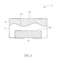
- FIG. 3is a schematic view illustrating a light emitting component 3 according to a second embodiment of the invention.
- the main difference between the light emitting component 3 and the aforesaid light emitting component 2is that the second surface 242 of the wavelength converting layer 24 of the light emitting component 3 is planar.
- FIG. 3 and FIG. 2are represented by the same numerals, so the repeated explanation will not be depicted herein again.
- FIG. 4is a schematic view illustrating a light emitting component 4 according to a third embodiment of the invention.
- the main difference between the light emitting component 4 and the aforesaid light emitting component 2is that the first surface 240 of the wavelength converting layer 24 of the light emitting unit 4 is planar.
- FIG. 4 and FIG. 2are represented by the same numerals, so the repeated explanation will not be depicted herein again.
- the inventionmay make at least one of the first surface 240 and the second surface 242 of the wavelength converting layer 24 to be non-planar according to practical applications.
- the contact area between the wavelength converting layer 24 and the molding compound 22increases (e.g. the non-planar contact area of the invention may be 1.1 times the planar contact are of the prior art), such that the phosphor powders excited by the light of the light emitting unit 20 at the first surface 240 increase, so as to enhance the quantity of light output.
- the inventiondisposed the wavelength converting layer 24 above the molding compound 22 , such that the wavelength converting layer 24 does not contact the light emitting unit 20 , so as to prevent the decrease in light intensity from occurring in the phosphor powders of the wavelength converting layer 24 due to heat generated by the light emitting unit 20 .
- FIG. 5is a schematic view illustrating a light emitting component 5 according to a fourth embodiment of the invention.
- the light emitting component 5further comprises a light transmissible member 50 .
- the light transmissible member 50is disposed on the wavelength converting layer 24 , wherein the second surface 242 of the wavelength converting layer 24 contacts the light transmissible member 50 and is planar.
- the light transmissible member 50is used for guiding the light emitted by the light emitting unit 20 , so as to enhance the quantity of light output.
- the light transmissible member 50may solidify the light emitting component 5 .
- a material of the light transmissible member 50may be glass, sapphire or other light transmissible materials.
- the inventionsince the wavelength converting layer 24 of the invention is capable of deforming when a mechanical force is exerted on the wavelength converting layer 24 , the invention may dispose the wavelength converting layer 24 on the light transmissible member 50 first, dispose the light transmissible member 50 on the molding compound 22 , and then perform a bonding process or the like to form the non-planar first surface 240 . Accordingly, the invention can save manufacture time and cost. It should be noted that the same elements in FIG. 5 and FIG. 2 are represented by the same numerals, so the repeated explanation will not be depicted herein again.
- FIG. 6is a schematic view illustrating a light emitting component 6 according to a fifth embodiment of the invention.
- the light emitting component 6further comprises a light transmissible member 60 .
- the light transmissible member 60is disposed between the molding compound 22 and the wavelength converting layer 24 , wherein the first surface 240 of the wavelength converting layer 24 contacts the light transmissible member 60 and is planar, and the second surface 242 is non-planar.
- the light transmissible member 60is used for guiding the light emitted by the light emitting unit 20 , so as to enhance the quantity of light output.
- the light transmissible member 60may solidify the light emitting component 6 .
- a material of the light transmissible member 60may be glass, sapphire or other light transmissible materials. It should be noted that the same elements in FIG. 6 and FIG. 2 are represented by the same numerals, so the repeated explanation will not be depicted herein again.
- FIG. 7is a schematic view illustrating a light emitting component 7 according to a sixth embodiment of the invention.
- the light emitting component 7further comprises a reflective layer 70 .
- the reflective layer 70is disposed on a side light emitting surface 202 of the light emitting unit 20 around the forward light emitting surface 200 .
- the reflective layer 70can reflect the light emitted by the side light emitting surface 202 of the light emitting unit 20 , so as to enhance the quantity of light output.
- a vertical height H 1 of the reflective layer 70may be larger than or equal to a vertical height H 2 of the side light emitting surface 202 of the light emitting unite 20 , so as to reflect the light emitted by the side light emitting surface 202 of the light emitting unit 20 effectively.
- a side surface 700 of the reflective layer 70 and a side surface 244 of the wavelength converting layer 24may be coplanar.
- a material of the reflective layer 70may comprise polymer material (e.g. silicone, epoxy, etc.), metal oxide material (e.g. TiO 2 , ZrO 2 , Al 2 O 3 , ZnO, etc.), metal material (e.g. Al, Ag, etc.) or a combination thereof.
- the material of the reflective layer 70may be the combination of the polymer material and the metal oxide material, so as to reduce the cost and simplify the process. It should be noted that the same elements in FIG. 7 and FIG. 2 are represented by the same numerals, so the repeated explanation will not be depicted herein again.
- the inventiondisposed the wavelength converting layer above the molding compound, such that the wavelength converting layer does not contact the light emitting unit, so as to prevent the decrease in light intensity from occurring in the phosphor powders of the wavelength converting layer due to heat generated by the light emitting unit. Furthermore, at least one of the first and second surfaces of the wavelength converting layer is non-planar. When the first surface of the wavelength converting layer, which contacts the molding compound, is non-planar, the contact area between the wavelength converting layer and the molding compound increases, such that the phosphor powders excited by the light of the light emitting unit at the first surface increase, so as to enhance the quantity of light output.
- the inventionmay dispose the light transmissible member on the wavelength converting layer or between the molding compound and the wavelength converting layer, wherein the light transmissible member is used for guiding the light emitted by the light emitting unit, so as to enhance the quantity of light output.
- the light transmissible membermay solidify the light emitting component.
- the inventionmay dispose the reflective layer on the side light emitting surface of the light emitting unit to reflect the light emitted by the side light emitting surface of the light emitting unit, so as to enhance the quantity of light output.
Landscapes
- Led Device Packages (AREA)
Abstract
Description
Claims (15)
Priority Applications (1)
| Application Number | Priority Date | Filing Date | Title |
|---|---|---|---|
| US15/823,480US10396255B2 (en) | 2014-06-12 | 2017-11-27 | Light emitting component |
Applications Claiming Priority (6)
| Application Number | Priority Date | Filing Date | Title |
|---|---|---|---|
| TW103120334A | 2014-06-12 | ||
| TW103120334 | 2014-06-12 | ||
| TW103120334ATWI557952B (en) | 2014-06-12 | 2014-06-12 | Light-emitting element |
| US14/462,581US9356205B2 (en) | 2014-06-12 | 2014-08-19 | Light emitting component |
| US15/168,218US9831399B2 (en) | 2014-06-12 | 2016-05-30 | Light emitting component |
| US15/823,480US10396255B2 (en) | 2014-06-12 | 2017-11-27 | Light emitting component |
Related Parent Applications (1)
| Application Number | Title | Priority Date | Filing Date |
|---|---|---|---|
| US15/168,218ContinuationUS9831399B2 (en) | 2014-06-12 | 2016-05-30 | Light emitting component |
Publications (2)
| Publication Number | Publication Date |
|---|---|
| US20180083168A1 US20180083168A1 (en) | 2018-03-22 |
| US10396255B2true US10396255B2 (en) | 2019-08-27 |
Family
ID=54836893
Family Applications (3)
| Application Number | Title | Priority Date | Filing Date |
|---|---|---|---|
| US14/462,581ActiveUS9356205B2 (en) | 2014-06-12 | 2014-08-19 | Light emitting component |
| US15/168,218ActiveUS9831399B2 (en) | 2014-06-12 | 2016-05-30 | Light emitting component |
| US15/823,480ActiveUS10396255B2 (en) | 2014-06-12 | 2017-11-27 | Light emitting component |
Family Applications Before (2)
| Application Number | Title | Priority Date | Filing Date |
|---|---|---|---|
| US14/462,581ActiveUS9356205B2 (en) | 2014-06-12 | 2014-08-19 | Light emitting component |
| US15/168,218ActiveUS9831399B2 (en) | 2014-06-12 | 2016-05-30 | Light emitting component |
Country Status (3)
| Country | Link |
|---|---|
| US (3) | US9356205B2 (en) |
| CN (1) | CN105304790A (en) |
| TW (1) | TWI557952B (en) |
Families Citing this family (18)
| Publication number | Priority date | Publication date | Assignee | Title |
|---|---|---|---|---|
| JP6398611B2 (en)* | 2013-11-07 | 2018-10-03 | 日亜化学工業株式会社 | LIGHT EMITTING DEVICE AND LIGHT EMITTING DEVICE MANUFACTURING METHOD |
| US9997676B2 (en) | 2014-05-14 | 2018-06-12 | Genesis Photonics Inc. | Light emitting device and manufacturing method thereof |
| TWI557952B (en) | 2014-06-12 | 2016-11-11 | 新世紀光電股份有限公司 | Light-emitting element |
| DE102017102112A1 (en)* | 2016-02-04 | 2017-08-10 | Epistar Corporation | Light-emitting element and its production method |
| TWI780041B (en) | 2016-02-04 | 2022-10-11 | 晶元光電股份有限公司 | Light-emitting element and the manufacturing method thereof |
| EP3491679B1 (en) | 2016-07-26 | 2023-02-22 | CreeLED, Inc. | Light emitting diodes, components and related methods |
| CN107689409B (en)* | 2016-08-03 | 2019-09-20 | 展晶科技(深圳)有限公司 | led |
| JP2019009429A (en)* | 2017-06-28 | 2019-01-17 | 日亜化学工業株式会社 | Light-emitting device |
| CN109712967B (en)* | 2017-10-25 | 2020-09-29 | 隆达电子股份有限公司 | Light emitting diode device and manufacturing method thereof |
| CN108011011B (en)* | 2017-11-28 | 2020-02-18 | 深圳市穗晶光电股份有限公司 | An LED packaging structure |
| CN108428696A (en)* | 2018-03-09 | 2018-08-21 | 广州大学 | CSP based on dot matrix type LED chip exempts to encapsulate fluorescent glue film assembly and preparation method |
| US11121298B2 (en) | 2018-05-25 | 2021-09-14 | Creeled, Inc. | Light-emitting diode packages with individually controllable light-emitting diode chips |
| CN110957408A (en)* | 2018-08-17 | 2020-04-03 | 新世纪光电股份有限公司 | Light emitting device and method for manufacturing the same |
| US11335833B2 (en) | 2018-08-31 | 2022-05-17 | Creeled, Inc. | Light-emitting diodes, light-emitting diode arrays and related devices |
| US11233183B2 (en)* | 2018-08-31 | 2022-01-25 | Creeled, Inc. | Light-emitting diodes, light-emitting diode arrays and related devices |
| USD902448S1 (en) | 2018-08-31 | 2020-11-17 | Cree, Inc. | Light emitting diode package |
| CN109037418B (en)* | 2018-09-05 | 2023-10-20 | 佛山市国星光电股份有限公司 | Packaging device |
| US11101411B2 (en) | 2019-06-26 | 2021-08-24 | Creeled, Inc. | Solid-state light emitting devices including light emitting diodes in package structures |
Citations (84)
| Publication number | Priority date | Publication date | Assignee | Title |
|---|---|---|---|---|
| US6155699A (en) | 1999-03-15 | 2000-12-05 | Agilent Technologies, Inc. | Efficient phosphor-conversion led structure |
| US20030006509A1 (en) | 2001-07-05 | 2003-01-09 | Takehiro Suzuki | Semiconductor device |
| US20030067070A1 (en) | 2001-10-05 | 2003-04-10 | Samsung Electronics Co., Ltd. | Semiconductor package |
| US20050045897A1 (en) | 2003-08-27 | 2005-03-03 | Shen-Hong Chou | Light emitting apparatus |
| US20060055309A1 (en) | 2004-09-14 | 2006-03-16 | Masato Ono | Light emitting device |
| US7045828B2 (en) | 2001-08-09 | 2006-05-16 | Matsushita Electric Industrial Co., Ltd. | Card-type LED illumination source |
| US20060169994A1 (en) | 2005-02-03 | 2006-08-03 | United Epitaxy Company, Ltd. | Light emitting device and manufacture method thereof |
| US20070114552A1 (en) | 2005-11-23 | 2007-05-24 | Samsung Electro-Mechanics Co., Ltd. | Vertical gallium-nitride based light emitting diode |
| US20080150119A1 (en) | 2006-12-22 | 2008-06-26 | Stats Chippac Ltd. | Integrated circuit package system employing mold flash prevention technology |
| US20090242917A1 (en) | 2008-03-28 | 2009-10-01 | Toyoda Gosei Co., Ltd. | Light-emitting device including light-emitting diode |
| US20090296389A1 (en) | 2008-05-30 | 2009-12-03 | Chia-Liang Hsu | Light source module, related light bar and related liquid crystal display |
| US20100066236A1 (en) | 2008-09-12 | 2010-03-18 | Bridgelux, Inc. | Method and Apparatus for Generating Phosphor Film with Textured Surface |
| TW201017934A (en) | 2008-08-29 | 2010-05-01 | Philips Lumileds Lighting Co | Light source including a wavelength-converted semiconductor light emitting device and a filter |
| CN101855735A (en) | 2007-11-19 | 2010-10-06 | 松下电器产业株式会社 | Semiconductor light emitting device and method for manufacturing semiconductor light emitting device |
| US20100258419A1 (en) | 2009-04-10 | 2010-10-14 | Avago Technologies Ecbu Ip (Singapore) Pte. Ltd. | Light guide film with cut lines |
| CN101867003A (en) | 2009-04-20 | 2010-10-20 | 日亚化学工业株式会社 | light emitting device |
| CN101878540A (en) | 2007-11-29 | 2010-11-03 | 日亚化学工业株式会社 | Light emitting device and manufacturing method thereof |
| US20110001157A1 (en) | 2008-01-28 | 2011-01-06 | Photonstar Led Limited | Light emitting module with optically-transparent thermally-conductive element |
| CN101978516A (en) | 2008-03-21 | 2011-02-16 | 皇家飞利浦电子股份有限公司 | A luminous device |
| US20110079805A1 (en) | 2009-10-02 | 2011-04-07 | Yu Kuohui | Light-emitting diode and method for manufacturing the same |
| TW201114072A (en) | 2009-05-22 | 2011-04-16 | Panasonic Corp | Semiconductor light-emitting device and light source device using the same |
| US20110102883A1 (en) | 2006-11-17 | 2011-05-05 | Rensselaer Polytechnic Institute | High-power white leds and manufacturing method thereof |
| CN102132428A (en) | 2008-09-02 | 2011-07-20 | 普瑞光电股份有限公司 | Phosphor Converted Light Emitting Diodes |
| WO2011093454A1 (en) | 2010-01-29 | 2011-08-04 | シチズン電子株式会社 | Method for producing light-emitting device and light emitting device |
| TW201133956A (en) | 2010-02-16 | 2011-10-01 | Koninkl Philips Electronics Nv | Light emitting device with molded wavelength converting layer |
| CN102222757A (en) | 2010-04-15 | 2011-10-19 | 三星Led株式会社 | Light emitting diode package, lighting apparatus having the same, and method for manufacturing light emitting diode package |
| CN102263194A (en) | 2011-04-13 | 2011-11-30 | 日月光半导体制造股份有限公司 | Semiconductor package and method of manufacturing the same |
| CN102290500A (en) | 2010-06-16 | 2011-12-21 | 斯坦雷电气株式会社 | Semiconductor light-emitting device and manufacturing method |
| US20120025218A1 (en) | 2010-08-02 | 2012-02-02 | Ito Kosaburo | Semiconductor light-emitting device and manufacturing method |
| CN102347423A (en) | 2010-07-27 | 2012-02-08 | 日东电工株式会社 | Component for light-emitting device, light-emitting device and producing method thereof |
| TW201210819A (en) | 2010-06-22 | 2012-03-16 | Nitto Denko Corp | Composite film and semiconductor light emitting device using the same |
| TW201220534A (en) | 2010-06-07 | 2012-05-16 | Toshiba Kk | Semiconductor light emitting device and method for manufacturing same |
| CN102468417A (en) | 2010-11-10 | 2012-05-23 | 三星Led株式会社 | Light emitting device package and method of manufacturing the same |
| CN102637809A (en) | 2011-02-15 | 2012-08-15 | 新世纪光电股份有限公司 | Light emitting diode packaging device and manufacturing method thereof |
| US20120235126A1 (en) | 2011-03-18 | 2012-09-20 | Semiconductor Energy Laboratory Co., Ltd. | Light-Emitting Device and Manufacturing Method Thereof |
| US20120236582A1 (en) | 2011-01-24 | 2012-09-20 | Waragaya Takeshi | Semiconductor light emitting device and manufacturing method |
| TW201242108A (en) | 2011-04-14 | 2012-10-16 | Nitto Denko Corp | Producing method of light emitting element transfer sheet, producing method of light emitting device, light emitting element transfer sheet, and light emitting device |
| CN102738368A (en) | 2011-04-14 | 2012-10-17 | 日东电工株式会社 | Phosphor reflecting sheet, light emitting diode device, and producing method thereof |
| JP2012227470A (en)* | 2011-04-22 | 2012-11-15 | Citizen Holdings Co Ltd | Semiconductor light emitting device and manufacturing method of the same |
| US20120305942A1 (en) | 2011-05-31 | 2012-12-06 | Aceplux Optotech Inc. | Epitaxial substrate, light-emitting diode, and methods for making the epitaxial substrate and the light-emitting diode |
| TW201249898A (en) | 2011-06-01 | 2012-12-16 | Nitto Denko Corp | Reflecting material and light emitting diode device |
| US20130001605A1 (en) | 2011-07-01 | 2013-01-03 | Citizen Holdings Co., Ltd. | Light-emitting device |
| CN103022010A (en) | 2011-09-21 | 2013-04-03 | 西铁城电子株式会社 | Light-emitting device, lighting device and method of manufacturing the light-emitting device |
| CN103050601A (en) | 2009-03-11 | 2013-04-17 | 晶元光电股份有限公司 | light emitting device |
| US20130093313A1 (en) | 2011-10-13 | 2013-04-18 | Citizen Holdings Co., Ltd. | Light-emitting device |
| US20130105978A1 (en) | 2011-10-26 | 2013-05-02 | Episil Technologies Inc. | Silicon submount for light emitting diode and method of forming the same |
| US20130121000A1 (en) | 2011-11-16 | 2013-05-16 | Song Eun Lee | Light emitting device and lighting apparatus having the same |
| CN103137571A (en) | 2013-01-22 | 2013-06-05 | 日月光半导体制造股份有限公司 | Semiconductor package structure and manufacturing method thereof |
| CN103187515A (en) | 2011-12-30 | 2013-07-03 | 财团法人工业技术研究院 | Light conversion structure and packaging structure of light emitting diode applying same |
| US8482016B2 (en)* | 2011-02-14 | 2013-07-09 | Stanley Electric Co., Ltd. | Semiconductor light-emitting device and manufacturing method |
| US20130194794A1 (en)* | 2012-02-01 | 2013-08-01 | Samsung Electronics Co., Ltd. | Light emitting device |
| US20130207141A1 (en) | 2012-02-13 | 2013-08-15 | Cree, Inc. | Lighting device including multiple encapsulant material layers |
| US20130207142A1 (en) | 2012-02-13 | 2013-08-15 | Jesse Colin Reiherzer | Light emitter devices having improved chemical and physical resistance and related methods |
| US20130256711A1 (en) | 2012-03-30 | 2013-10-03 | Cree, Inc. | Substrate based light emitter devices, components, and related methods |
| US20130277093A1 (en) | 2012-04-24 | 2013-10-24 | Genesis Photonics Inc. | Substrate structure |
| US20130313594A1 (en) | 2003-07-04 | 2013-11-28 | Epistar Corporation | Optoelectronic element and manufacturing method thereof |
| CN103534822A (en) | 2011-04-20 | 2014-01-22 | 株式会社Elm | Light emitting device and method for manufacturing same |
| CN103531725A (en) | 2013-10-16 | 2014-01-22 | 上海和辉光电有限公司 | Electroluminescent component and packaging method thereof |
| US20140021493A1 (en) | 2012-07-20 | 2014-01-23 | Peter Andrews | Solid state lighting component package with layer |
| US20140054621A1 (en) | 2012-08-23 | 2014-02-27 | Stanley Electric Co., Ltd. | Semiconductor light-emitting device including transparent plate with slanted side surface |
| US20140124812A1 (en) | 2011-05-16 | 2014-05-08 | Nichia Corporation | Light emitting device and method for manufacturing the same |
| US20140131753A1 (en) | 2012-11-09 | 2014-05-15 | Nichia Corporation | Method for manufacturing light emitting device and light emitting device |
| US20140138725A1 (en) | 2012-11-12 | 2014-05-22 | Citizen Electronics Co., Ltd. | Semiconductor light-emitting device and producing method thereof |
| US20140252389A1 (en) | 2013-03-05 | 2014-09-11 | Kabushiki Kaisha Toshiba | Semiconductor light emitting device and method for manufacturing the same |
| US8860061B2 (en) | 2012-01-23 | 2014-10-14 | Stanley Electric Co., Ltd. | Semiconductor light-emitting device, manufacturing method for the same and vehicle headlight |
| US20150014720A1 (en) | 2013-07-10 | 2015-01-15 | Lextar Electronics Corporation | Light emitting diode package structure |
| CN104347610A (en) | 2013-07-23 | 2015-02-11 | 深圳市瑞丰光电子股份有限公司 | Embedded LED device, manufacture method thereof, and luminescence device |
| TW201515282A (en) | 2013-10-14 | 2015-04-16 | Genesis Photonics Inc | Flip-chip LED package structure |
| US20150102373A1 (en) | 2013-10-10 | 2015-04-16 | Samsung Electronics Co., Ltd. | Light emitting diode package and method of manufacturing the same |
| US20150115300A1 (en) | 2013-10-28 | 2015-04-30 | Kabushiki Kaisha Toshiba | Semiconductor light emitting device |
| US20150179901A1 (en) | 2013-12-23 | 2015-06-25 | Jung-Tae OK | Method of fabricating white led devices |
| US20150188004A1 (en) | 2013-12-27 | 2015-07-02 | Nichia Corporation | Semiconductor light emitting device |
| US20150263242A1 (en) | 2014-03-11 | 2015-09-17 | Kabushiki Kaisha Toshiba | Semiconductor light emitting device |
| US20150311405A1 (en) | 2012-12-10 | 2015-10-29 | Citizen Holding Co., Ltd. | Led device and manufacturing method thereof |
| TW201541674A (en) | 2014-04-23 | 2015-11-01 | Lite On Opto Technology Changzhou Co Ltd | LED carrier and manufacturing method thereof |
| US20160013373A1 (en) | 2014-07-11 | 2016-01-14 | Cree, Inc. | Method to form primary optic with variable shapes and/or geometries without a substrate |
| US20160035952A1 (en) | 2010-02-09 | 2016-02-04 | Nichia Corporation | Light emitting device and method for manufacturing light emitting device |
| US20160079496A1 (en) | 2013-10-14 | 2016-03-17 | Genesis Photonics Inc. | Light-emitting diode package structure |
| US20160155900A1 (en) | 2013-03-14 | 2016-06-02 | Commissariat A L'energie Atomique Et Aux Energies Alternatives | Process for forming light-emitting diodes |
| US20160155915A1 (en) | 2014-12-02 | 2016-06-02 | Achrolux Inc. | Method of manufacturing light emitting diode package structure |
| US20160181476A1 (en) | 2014-12-17 | 2016-06-23 | Apple Inc. | Micro led with dielectric side mirror |
| US20160190406A1 (en) | 2014-12-24 | 2016-06-30 | Epistar Corporation | Light-emitting device and manufacturing method thereof |
| US9419189B1 (en) | 2013-11-04 | 2016-08-16 | Soraa, Inc. | Small LED source with high brightness and high efficiency |
| US9922963B2 (en) | 2015-09-18 | 2018-03-20 | Genesis Photonics Inc. | Light-emitting device |
Family Cites Families (34)
| Publication number | Priority date | Publication date | Assignee | Title |
|---|---|---|---|---|
| US6952079B2 (en) | 2002-12-18 | 2005-10-04 | General Electric Company | Luminaire for light extraction from a flat light source |
| JP4747726B2 (en) | 2004-09-09 | 2011-08-17 | 豊田合成株式会社 | Light emitting device |
| JP3985850B2 (en) | 2005-01-31 | 2007-10-03 | 凸版印刷株式会社 | Optical sheet and backlight unit and display using the same |
| US9018655B2 (en) | 2005-02-03 | 2015-04-28 | Epistar Corporation | Light emitting apparatus and manufacture method thereof |
| TWI309480B (en) | 2006-07-24 | 2009-05-01 | Everlight Electronics Co Ltd | Led packaging structure |
| KR101319209B1 (en) | 2006-11-24 | 2013-10-16 | 엘지디스플레이 주식회사 | Backlight unit of liquid crystal display device |
| TW200841089A (en)* | 2007-04-09 | 2008-10-16 | Chu-Liang Cheng | Light source module and liquid crystal display |
| US7810956B2 (en) | 2007-08-23 | 2010-10-12 | Koninklijke Philips Electronics N.V. | Light source including reflective wavelength-converting layer |
| US7928655B2 (en) | 2008-11-10 | 2011-04-19 | Visera Technologies Company Limited | Light-emitting diode device and method for fabricating the same |
| US20110031516A1 (en) | 2009-08-07 | 2011-02-10 | Koninklijke Philips Electronics N.V. | Led with silicone layer and laminated remote phosphor layer |
| JP2011114093A (en)* | 2009-11-25 | 2011-06-09 | Panasonic Electric Works Co Ltd | Lighting system |
| JP5759790B2 (en) | 2010-06-07 | 2015-08-05 | 株式会社東芝 | Manufacturing method of semiconductor light emitting device |
| US20120061700A1 (en) | 2010-09-09 | 2012-03-15 | Andreas Eder | Method and system for providing a reliable light emitting diode semiconductor device |
| CN102412344A (en) | 2010-09-23 | 2012-04-11 | 展晶科技(深圳)有限公司 | Light emitting diode packaging method |
| TW201218428A (en) | 2010-10-25 | 2012-05-01 | Hon Hai Prec Ind Co Ltd | Light emitting diode package structure |
| KR20120072962A (en) | 2010-12-24 | 2012-07-04 | 삼성엘이디 주식회사 | Light emitting device package and method of manufacturing the same |
| KR20120082190A (en) | 2011-01-13 | 2012-07-23 | 삼성엘이디 주식회사 | Light emitting device package |
| US20120250320A1 (en)* | 2011-03-31 | 2012-10-04 | Xicato, Inc. | Color conversion cavities for led-based illumination modules |
| DE102011050450A1 (en) | 2011-05-18 | 2012-11-22 | Osram Opto Semiconductors Gmbh | Optoelectronic semiconductor chip, optoelectronic semiconductor component and method for producing an optoelectronic semiconductor component |
| JP2013021175A (en) | 2011-07-12 | 2013-01-31 | Toshiba Corp | Semiconductor light-emitting element |
| US8555503B2 (en)* | 2011-07-20 | 2013-10-15 | Ford Global Technologies, Llc | Casting-integrated control body processing |
| US20130094177A1 (en) | 2011-10-13 | 2013-04-18 | Intematix Corporation | Wavelength conversion component with improved thermal conductive characteristics for remote wavelength conversion |
| CN103855142B (en)* | 2012-12-04 | 2017-12-29 | 东芝照明技术株式会社 | Light-emitting device and lighting device |
| KR20140094752A (en) | 2013-01-22 | 2014-07-31 | 삼성전자주식회사 | An electronic device package and a packaging substrate for the same |
| TW201507209A (en) | 2013-08-01 | 2015-02-16 | Genesis Photonics Inc | Light emitting diode package structure and manufacturing method thereof |
| KR101584201B1 (en) | 2014-01-13 | 2016-01-13 | 삼성전자주식회사 | Semiconductor light emitting device |
| US20150280078A1 (en)* | 2014-03-31 | 2015-10-01 | SemiLEDs Optoelectronics Co., Ltd. | White flip chip light emitting diode (fc led) and fabrication method |
| CN105098027A (en) | 2014-05-14 | 2015-11-25 | 新世纪光电股份有限公司 | Light emitting element packaging structure and manufacturing method thereof |
| US9997676B2 (en) | 2014-05-14 | 2018-06-12 | Genesis Photonics Inc. | Light emitting device and manufacturing method thereof |
| TWI557952B (en) | 2014-06-12 | 2016-11-11 | 新世紀光電股份有限公司 | Light-emitting element |
| TWI583019B (en) | 2015-02-17 | 2017-05-11 | 新世紀光電股份有限公司 | Light emitting diode and manufacturing method thereof |
| US20160276546A1 (en) | 2015-03-18 | 2016-09-22 | Genesis Photonics Inc. | Chip package structure and method of manufacturing the same |
| JP2016181689A (en) | 2015-03-18 | 2016-10-13 | 新世紀光電股▲ふん▼有限公司Genesis Photonics Inc. | Light emitting diode structure and method for manufacturing the same |
| TWI657597B (en) | 2015-03-18 | 2019-04-21 | 新世紀光電股份有限公司 | Edge lighting light emitting diode structure and method of manufacturing the same |
- 2014
- 2014-06-12TWTW103120334Apatent/TWI557952B/enactive
- 2014-07-28CNCN201410362787.6Apatent/CN105304790A/enactivePending
- 2014-08-19USUS14/462,581patent/US9356205B2/enactiveActive
- 2016
- 2016-05-30USUS15/168,218patent/US9831399B2/enactiveActive
- 2017
- 2017-11-27USUS15/823,480patent/US10396255B2/enactiveActive
Patent Citations (90)
| Publication number | Priority date | Publication date | Assignee | Title |
|---|---|---|---|---|
| US6155699A (en) | 1999-03-15 | 2000-12-05 | Agilent Technologies, Inc. | Efficient phosphor-conversion led structure |
| US20030006509A1 (en) | 2001-07-05 | 2003-01-09 | Takehiro Suzuki | Semiconductor device |
| US7045828B2 (en) | 2001-08-09 | 2006-05-16 | Matsushita Electric Industrial Co., Ltd. | Card-type LED illumination source |
| US20030067070A1 (en) | 2001-10-05 | 2003-04-10 | Samsung Electronics Co., Ltd. | Semiconductor package |
| US20130313594A1 (en) | 2003-07-04 | 2013-11-28 | Epistar Corporation | Optoelectronic element and manufacturing method thereof |
| US20050045897A1 (en) | 2003-08-27 | 2005-03-03 | Shen-Hong Chou | Light emitting apparatus |
| US20060055309A1 (en) | 2004-09-14 | 2006-03-16 | Masato Ono | Light emitting device |
| US20060169994A1 (en) | 2005-02-03 | 2006-08-03 | United Epitaxy Company, Ltd. | Light emitting device and manufacture method thereof |
| US20070114552A1 (en) | 2005-11-23 | 2007-05-24 | Samsung Electro-Mechanics Co., Ltd. | Vertical gallium-nitride based light emitting diode |
| US20110102883A1 (en) | 2006-11-17 | 2011-05-05 | Rensselaer Polytechnic Institute | High-power white leds and manufacturing method thereof |
| US20080150119A1 (en) | 2006-12-22 | 2008-06-26 | Stats Chippac Ltd. | Integrated circuit package system employing mold flash prevention technology |
| US20100258830A1 (en) | 2007-11-19 | 2010-10-14 | Yoshiyuki Ide | Semiconductor light-emitting device and manufacturing method of the same |
| CN101855735A (en) | 2007-11-19 | 2010-10-06 | 松下电器产业株式会社 | Semiconductor light emitting device and method for manufacturing semiconductor light emitting device |
| CN101878540A (en) | 2007-11-29 | 2010-11-03 | 日亚化学工业株式会社 | Light emitting device and manufacturing method thereof |
| US20110001157A1 (en) | 2008-01-28 | 2011-01-06 | Photonstar Led Limited | Light emitting module with optically-transparent thermally-conductive element |
| CN101978516A (en) | 2008-03-21 | 2011-02-16 | 皇家飞利浦电子股份有限公司 | A luminous device |
| US20090242917A1 (en) | 2008-03-28 | 2009-10-01 | Toyoda Gosei Co., Ltd. | Light-emitting device including light-emitting diode |
| US20090296389A1 (en) | 2008-05-30 | 2009-12-03 | Chia-Liang Hsu | Light source module, related light bar and related liquid crystal display |
| TW201017934A (en) | 2008-08-29 | 2010-05-01 | Philips Lumileds Lighting Co | Light source including a wavelength-converted semiconductor light emitting device and a filter |
| CN102132428A (en) | 2008-09-02 | 2011-07-20 | 普瑞光电股份有限公司 | Phosphor Converted Light Emitting Diodes |
| US20100066236A1 (en) | 2008-09-12 | 2010-03-18 | Bridgelux, Inc. | Method and Apparatus for Generating Phosphor Film with Textured Surface |
| CN103050601A (en) | 2009-03-11 | 2013-04-17 | 晶元光电股份有限公司 | light emitting device |
| US20100258419A1 (en) | 2009-04-10 | 2010-10-14 | Avago Technologies Ecbu Ip (Singapore) Pte. Ltd. | Light guide film with cut lines |
| CN101867003A (en) | 2009-04-20 | 2010-10-20 | 日亚化学工业株式会社 | light emitting device |
| TW201114072A (en) | 2009-05-22 | 2011-04-16 | Panasonic Corp | Semiconductor light-emitting device and light source device using the same |
| US20110079805A1 (en) | 2009-10-02 | 2011-04-07 | Yu Kuohui | Light-emitting diode and method for manufacturing the same |
| WO2011093454A1 (en) | 2010-01-29 | 2011-08-04 | シチズン電子株式会社 | Method for producing light-emitting device and light emitting device |
| US9887329B2 (en) | 2010-02-09 | 2018-02-06 | Nichia Corporation | Light emitting device and method for manufacturing light emitting device |
| US20160035952A1 (en) | 2010-02-09 | 2016-02-04 | Nichia Corporation | Light emitting device and method for manufacturing light emitting device |
| TW201133956A (en) | 2010-02-16 | 2011-10-01 | Koninkl Philips Electronics Nv | Light emitting device with molded wavelength converting layer |
| CN102222757A (en) | 2010-04-15 | 2011-10-19 | 三星Led株式会社 | Light emitting diode package, lighting apparatus having the same, and method for manufacturing light emitting diode package |
| US8350283B2 (en) | 2010-06-07 | 2013-01-08 | Kabushiki Kaisha Toshiba | Semiconductor light emitting device and method for manufacturing same |
| TW201220534A (en) | 2010-06-07 | 2012-05-16 | Toshiba Kk | Semiconductor light emitting device and method for manufacturing same |
| CN102290500A (en) | 2010-06-16 | 2011-12-21 | 斯坦雷电气株式会社 | Semiconductor light-emitting device and manufacturing method |
| TW201210819A (en) | 2010-06-22 | 2012-03-16 | Nitto Denko Corp | Composite film and semiconductor light emitting device using the same |
| CN102347423A (en) | 2010-07-27 | 2012-02-08 | 日东电工株式会社 | Component for light-emitting device, light-emitting device and producing method thereof |
| US20120025218A1 (en) | 2010-08-02 | 2012-02-02 | Ito Kosaburo | Semiconductor light-emitting device and manufacturing method |
| CN102468417A (en) | 2010-11-10 | 2012-05-23 | 三星Led株式会社 | Light emitting device package and method of manufacturing the same |
| US20120236582A1 (en) | 2011-01-24 | 2012-09-20 | Waragaya Takeshi | Semiconductor light emitting device and manufacturing method |
| US8482016B2 (en)* | 2011-02-14 | 2013-07-09 | Stanley Electric Co., Ltd. | Semiconductor light-emitting device and manufacturing method |
| CN102637809A (en) | 2011-02-15 | 2012-08-15 | 新世纪光电股份有限公司 | Light emitting diode packaging device and manufacturing method thereof |
| US20120235126A1 (en) | 2011-03-18 | 2012-09-20 | Semiconductor Energy Laboratory Co., Ltd. | Light-Emitting Device and Manufacturing Method Thereof |
| CN102263194A (en) | 2011-04-13 | 2011-11-30 | 日月光半导体制造股份有限公司 | Semiconductor package and method of manufacturing the same |
| TW201242108A (en) | 2011-04-14 | 2012-10-16 | Nitto Denko Corp | Producing method of light emitting element transfer sheet, producing method of light emitting device, light emitting element transfer sheet, and light emitting device |
| CN102738368A (en) | 2011-04-14 | 2012-10-17 | 日东电工株式会社 | Phosphor reflecting sheet, light emitting diode device, and producing method thereof |
| CN103534822A (en) | 2011-04-20 | 2014-01-22 | 株式会社Elm | Light emitting device and method for manufacturing same |
| JP2012227470A (en)* | 2011-04-22 | 2012-11-15 | Citizen Holdings Co Ltd | Semiconductor light emitting device and manufacturing method of the same |
| US20140124812A1 (en) | 2011-05-16 | 2014-05-08 | Nichia Corporation | Light emitting device and method for manufacturing the same |
| US20120305942A1 (en) | 2011-05-31 | 2012-12-06 | Aceplux Optotech Inc. | Epitaxial substrate, light-emitting diode, and methods for making the epitaxial substrate and the light-emitting diode |
| TW201249898A (en) | 2011-06-01 | 2012-12-16 | Nitto Denko Corp | Reflecting material and light emitting diode device |
| US20130001605A1 (en) | 2011-07-01 | 2013-01-03 | Citizen Holdings Co., Ltd. | Light-emitting device |
| CN103022010A (en) | 2011-09-21 | 2013-04-03 | 西铁城电子株式会社 | Light-emitting device, lighting device and method of manufacturing the light-emitting device |
| US20130093313A1 (en) | 2011-10-13 | 2013-04-18 | Citizen Holdings Co., Ltd. | Light-emitting device |
| US20130105978A1 (en) | 2011-10-26 | 2013-05-02 | Episil Technologies Inc. | Silicon submount for light emitting diode and method of forming the same |
| US20130121000A1 (en) | 2011-11-16 | 2013-05-16 | Song Eun Lee | Light emitting device and lighting apparatus having the same |
| CN103187515A (en) | 2011-12-30 | 2013-07-03 | 财团法人工业技术研究院 | Light conversion structure and packaging structure of light emitting diode applying same |
| US8860061B2 (en) | 2012-01-23 | 2014-10-14 | Stanley Electric Co., Ltd. | Semiconductor light-emitting device, manufacturing method for the same and vehicle headlight |
| US20130194794A1 (en)* | 2012-02-01 | 2013-08-01 | Samsung Electronics Co., Ltd. | Light emitting device |
| US20130207141A1 (en) | 2012-02-13 | 2013-08-15 | Cree, Inc. | Lighting device including multiple encapsulant material layers |
| US20130207142A1 (en) | 2012-02-13 | 2013-08-15 | Jesse Colin Reiherzer | Light emitter devices having improved chemical and physical resistance and related methods |
| US20130256711A1 (en) | 2012-03-30 | 2013-10-03 | Cree, Inc. | Substrate based light emitter devices, components, and related methods |
| US20130277093A1 (en) | 2012-04-24 | 2013-10-24 | Genesis Photonics Inc. | Substrate structure |
| US20140021493A1 (en) | 2012-07-20 | 2014-01-23 | Peter Andrews | Solid state lighting component package with layer |
| US20140054621A1 (en) | 2012-08-23 | 2014-02-27 | Stanley Electric Co., Ltd. | Semiconductor light-emitting device including transparent plate with slanted side surface |
| US20140131753A1 (en) | 2012-11-09 | 2014-05-15 | Nichia Corporation | Method for manufacturing light emitting device and light emitting device |
| CN203774363U (en) | 2012-11-12 | 2014-08-13 | 西铁城控股株式会社 | Semiconductor light-emitting device |
| US20140138725A1 (en) | 2012-11-12 | 2014-05-22 | Citizen Electronics Co., Ltd. | Semiconductor light-emitting device and producing method thereof |
| US20150311405A1 (en) | 2012-12-10 | 2015-10-29 | Citizen Holding Co., Ltd. | Led device and manufacturing method thereof |
| US9490398B2 (en) | 2012-12-10 | 2016-11-08 | Citizen Holdings Co., Ltd. | Manufacturing method of light emitting device in a flip-chip configuration with reduced package size |
| CN103137571A (en) | 2013-01-22 | 2013-06-05 | 日月光半导体制造股份有限公司 | Semiconductor package structure and manufacturing method thereof |
| US20140252389A1 (en) | 2013-03-05 | 2014-09-11 | Kabushiki Kaisha Toshiba | Semiconductor light emitting device and method for manufacturing the same |
| US20160155900A1 (en) | 2013-03-14 | 2016-06-02 | Commissariat A L'energie Atomique Et Aux Energies Alternatives | Process for forming light-emitting diodes |
| US20150014720A1 (en) | 2013-07-10 | 2015-01-15 | Lextar Electronics Corporation | Light emitting diode package structure |
| CN104347610A (en) | 2013-07-23 | 2015-02-11 | 深圳市瑞丰光电子股份有限公司 | Embedded LED device, manufacture method thereof, and luminescence device |
| US20150102373A1 (en) | 2013-10-10 | 2015-04-16 | Samsung Electronics Co., Ltd. | Light emitting diode package and method of manufacturing the same |
| TW201515282A (en) | 2013-10-14 | 2015-04-16 | Genesis Photonics Inc | Flip-chip LED package structure |
| US20160079496A1 (en) | 2013-10-14 | 2016-03-17 | Genesis Photonics Inc. | Light-emitting diode package structure |
| US20150102377A1 (en) | 2013-10-14 | 2015-04-16 | Genesis Photonics Inc. | Flip chip light emitting diode package structure |
| CN103531725A (en) | 2013-10-16 | 2014-01-22 | 上海和辉光电有限公司 | Electroluminescent component and packaging method thereof |
| US20150115300A1 (en) | 2013-10-28 | 2015-04-30 | Kabushiki Kaisha Toshiba | Semiconductor light emitting device |
| US9419189B1 (en) | 2013-11-04 | 2016-08-16 | Soraa, Inc. | Small LED source with high brightness and high efficiency |
| US20150179901A1 (en) | 2013-12-23 | 2015-06-25 | Jung-Tae OK | Method of fabricating white led devices |
| US20150188004A1 (en) | 2013-12-27 | 2015-07-02 | Nichia Corporation | Semiconductor light emitting device |
| US20150263242A1 (en) | 2014-03-11 | 2015-09-17 | Kabushiki Kaisha Toshiba | Semiconductor light emitting device |
| TW201541674A (en) | 2014-04-23 | 2015-11-01 | Lite On Opto Technology Changzhou Co Ltd | LED carrier and manufacturing method thereof |
| US20160013373A1 (en) | 2014-07-11 | 2016-01-14 | Cree, Inc. | Method to form primary optic with variable shapes and/or geometries without a substrate |
| US20160155915A1 (en) | 2014-12-02 | 2016-06-02 | Achrolux Inc. | Method of manufacturing light emitting diode package structure |
| US20160181476A1 (en) | 2014-12-17 | 2016-06-23 | Apple Inc. | Micro led with dielectric side mirror |
| US20160190406A1 (en) | 2014-12-24 | 2016-06-30 | Epistar Corporation | Light-emitting device and manufacturing method thereof |
| US9922963B2 (en) | 2015-09-18 | 2018-03-20 | Genesis Photonics Inc. | Light-emitting device |
Non-Patent Citations (15)
Also Published As
| Publication number | Publication date |
|---|---|
| US9356205B2 (en) | 2016-05-31 |
| US9831399B2 (en) | 2017-11-28 |
| TW201547063A (en) | 2015-12-16 |
| US20180083168A1 (en) | 2018-03-22 |
| US20150364660A1 (en) | 2015-12-17 |
| TWI557952B (en) | 2016-11-11 |
| CN105304790A (en) | 2016-02-03 |
| US20160276554A1 (en) | 2016-09-22 |
Similar Documents
| Publication | Publication Date | Title |
|---|---|---|
| US10396255B2 (en) | Light emitting component | |
| US11114595B2 (en) | Optical component and transparent body | |
| KR102390293B1 (en) | Light emitting apparatus and manufacturing method of the same | |
| JP6424738B2 (en) | Light emitting device and method of manufacturing light emitting device | |
| CN105531833B (en) | LED with scattering features in substrate | |
| US20150292687A1 (en) | Light emitting device | |
| JP2016219743A5 (en) | ||
| JP2007287713A (en) | Light emitting device and manufacturing method thereof | |
| JP2007311445A (en) | Semiconductor light emitting device and manufacturing method thereof | |
| JP2013175531A (en) | Light-emitting device | |
| US10141482B2 (en) | Semiconductor light emitting device | |
| JP2014207349A (en) | Light-emitting device and manufacturing method thereof | |
| JP6387787B2 (en) | LIGHT EMITTING DEVICE, PACKAGE AND METHOD FOR MANUFACTURING THE SAME | |
| US20140284652A1 (en) | Method for manufacturing light emitting device, and light emitting device | |
| US20160005922A1 (en) | Light emitting component | |
| JP6171749B2 (en) | Light emitting device and manufacturing method thereof | |
| US10026880B2 (en) | Optoelectronic component | |
| JP2016006821A (en) | Light emitting element and light emitting device using the same | |
| JP6696550B2 (en) | Light emitting device | |
| US20110316027A1 (en) | Chip-type light emitting device having precisely coated wavelength-converting layer and packaged structure thereof | |
| JP2016062980A (en) | Semiconductor light emitting device | |
| JP2016048718A (en) | Light-emitting device | |
| KR20180101288A (en) | Convex chip scale package and method for manufacturing thereof | |
| TWI603509B (en) | Light emitting component | |
| WO2014162650A1 (en) | Light-emitting device |
Legal Events
| Date | Code | Title | Description |
|---|---|---|---|
| FEPP | Fee payment procedure | Free format text:ENTITY STATUS SET TO UNDISCOUNTED (ORIGINAL EVENT CODE: BIG.); ENTITY STATUS OF PATENT OWNER: LARGE ENTITY | |
| STPP | Information on status: patent application and granting procedure in general | Free format text:NON FINAL ACTION MAILED | |
| STPP | Information on status: patent application and granting procedure in general | Free format text:RESPONSE TO NON-FINAL OFFICE ACTION ENTERED AND FORWARDED TO EXAMINER | |
| STPP | Information on status: patent application and granting procedure in general | Free format text:NOTICE OF ALLOWANCE MAILED -- APPLICATION RECEIVED IN OFFICE OF PUBLICATIONS | |
| STPP | Information on status: patent application and granting procedure in general | Free format text:AWAITING TC RESP, ISSUE FEE PAYMENT VERIFIED | |
| STCF | Information on status: patent grant | Free format text:PATENTED CASE | |
| FEPP | Fee payment procedure | Free format text:MAINTENANCE FEE REMINDER MAILED (ORIGINAL EVENT CODE: REM.); ENTITY STATUS OF PATENT OWNER: LARGE ENTITY | |
| FEPP | Fee payment procedure | Free format text:SURCHARGE FOR LATE PAYMENT, LARGE ENTITY (ORIGINAL EVENT CODE: M1554); ENTITY STATUS OF PATENT OWNER: LARGE ENTITY | |
| MAFP | Maintenance fee payment | Free format text:PAYMENT OF MAINTENANCE FEE, 4TH YEAR, LARGE ENTITY (ORIGINAL EVENT CODE: M1551); ENTITY STATUS OF PATENT OWNER: LARGE ENTITY Year of fee payment:4 | |
| AS | Assignment | Owner name:NICHIA CORPORATION, JAPAN Free format text:ASSIGNMENT OF ASSIGNORS INTEREST;ASSIGNOR:GENESIS PHOTONICS INC.;REEL/FRAME:066044/0807 Effective date:20231123 Owner name:GENESIS PHOTONICS INC., TAIWAN Free format text:ADDRESS CHANGE REGISTRATION FORM;ASSIGNOR:GENESIS PHOTONICS INC.;REEL/FRAME:066044/0133 Effective date:20221201 |