US10393946B2 - Method of manufacturing directional backlight apparatus and directional structured optical film - Google Patents
Method of manufacturing directional backlight apparatus and directional structured optical filmDownload PDFInfo
- Publication number
- US10393946B2 US10393946B2US15/273,074US201615273074AUS10393946B2US 10393946 B2US10393946 B2US 10393946B2US 201615273074 AUS201615273074 AUS 201615273074AUS 10393946 B2US10393946 B2US 10393946B2
- Authority
- US
- United States
- Prior art keywords
- light
- optical film
- stepped waveguide
- optical
- diagram illustrating
- Prior art date
- Legal status (The legal status is an assumption and is not a legal conclusion. Google has not performed a legal analysis and makes no representation as to the accuracy of the status listed.)
- Active
Links
Images


Classifications
- G—PHYSICS
- G02—OPTICS
- G02B—OPTICAL ELEMENTS, SYSTEMS OR APPARATUS
- G02B6/00—Light guides; Structural details of arrangements comprising light guides and other optical elements, e.g. couplings
- G02B6/0001—Light guides; Structural details of arrangements comprising light guides and other optical elements, e.g. couplings specially adapted for lighting devices or systems
- G02B6/0011—Light guides; Structural details of arrangements comprising light guides and other optical elements, e.g. couplings specially adapted for lighting devices or systems the light guides being planar or of plate-like form
- G02B6/0033—Means for improving the coupling-out of light from the light guide
- G02B6/0035—Means for improving the coupling-out of light from the light guide provided on the surface of the light guide or in the bulk of it
- G02B6/0045—Means for improving the coupling-out of light from the light guide provided on the surface of the light guide or in the bulk of it by shaping at least a portion of the light guide
- G02B6/0046—Tapered light guide, e.g. wedge-shaped light guide
- G02B6/0048—Tapered light guide, e.g. wedge-shaped light guide with stepwise taper
- G02B27/2214—
- G02B27/225—
- G—PHYSICS
- G02—OPTICS
- G02B—OPTICAL ELEMENTS, SYSTEMS OR APPARATUS
- G02B30/00—Optical systems or apparatus for producing three-dimensional [3D] effects, e.g. stereoscopic images
- G02B30/20—Optical systems or apparatus for producing three-dimensional [3D] effects, e.g. stereoscopic images by providing first and second parallax images to an observer's left and right eyes
- G02B30/26—Optical systems or apparatus for producing three-dimensional [3D] effects, e.g. stereoscopic images by providing first and second parallax images to an observer's left and right eyes of the autostereoscopic type
- G02B30/27—Optical systems or apparatus for producing three-dimensional [3D] effects, e.g. stereoscopic images by providing first and second parallax images to an observer's left and right eyes of the autostereoscopic type involving lenticular arrays
- G—PHYSICS
- G02—OPTICS
- G02B—OPTICAL ELEMENTS, SYSTEMS OR APPARATUS
- G02B30/00—Optical systems or apparatus for producing three-dimensional [3D] effects, e.g. stereoscopic images
- G02B30/20—Optical systems or apparatus for producing three-dimensional [3D] effects, e.g. stereoscopic images by providing first and second parallax images to an observer's left and right eyes
- G02B30/26—Optical systems or apparatus for producing three-dimensional [3D] effects, e.g. stereoscopic images by providing first and second parallax images to an observer's left and right eyes of the autostereoscopic type
- G02B30/33—Optical systems or apparatus for producing three-dimensional [3D] effects, e.g. stereoscopic images by providing first and second parallax images to an observer's left and right eyes of the autostereoscopic type involving directional light or back-light sources
- G—PHYSICS
- G02—OPTICS
- G02B—OPTICAL ELEMENTS, SYSTEMS OR APPARATUS
- G02B6/00—Light guides; Structural details of arrangements comprising light guides and other optical elements, e.g. couplings
- G02B6/0001—Light guides; Structural details of arrangements comprising light guides and other optical elements, e.g. couplings specially adapted for lighting devices or systems
- G02B6/0011—Light guides; Structural details of arrangements comprising light guides and other optical elements, e.g. couplings specially adapted for lighting devices or systems the light guides being planar or of plate-like form
- G02B6/0013—Means for improving the coupling-in of light from the light source into the light guide
- G02B6/0023—Means for improving the coupling-in of light from the light source into the light guide provided by one optical element, or plurality thereof, placed between the light guide and the light source, or around the light source
- G02B6/0025—Diffusing sheet or layer; Prismatic sheet or layer
- G—PHYSICS
- G02—OPTICS
- G02B—OPTICAL ELEMENTS, SYSTEMS OR APPARATUS
- G02B6/00—Light guides; Structural details of arrangements comprising light guides and other optical elements, e.g. couplings
- G02B6/0001—Light guides; Structural details of arrangements comprising light guides and other optical elements, e.g. couplings specially adapted for lighting devices or systems
- G02B6/0011—Light guides; Structural details of arrangements comprising light guides and other optical elements, e.g. couplings specially adapted for lighting devices or systems the light guides being planar or of plate-like form
- G02B6/0013—Means for improving the coupling-in of light from the light source into the light guide
- G02B6/0023—Means for improving the coupling-in of light from the light source into the light guide provided by one optical element, or plurality thereof, placed between the light guide and the light source, or around the light source
- G02B6/0026—Wavelength selective element, sheet or layer, e.g. filter or grating
- G—PHYSICS
- G02—OPTICS
- G02B—OPTICAL ELEMENTS, SYSTEMS OR APPARATUS
- G02B6/00—Light guides; Structural details of arrangements comprising light guides and other optical elements, e.g. couplings
- G02B6/0001—Light guides; Structural details of arrangements comprising light guides and other optical elements, e.g. couplings specially adapted for lighting devices or systems
- G02B6/0011—Light guides; Structural details of arrangements comprising light guides and other optical elements, e.g. couplings specially adapted for lighting devices or systems the light guides being planar or of plate-like form
- G02B6/0033—Means for improving the coupling-out of light from the light guide
- G02B6/005—Means for improving the coupling-out of light from the light guide provided by one optical element, or plurality thereof, placed on the light output side of the light guide
- G02B6/0053—Prismatic sheet or layer; Brightness enhancement element, sheet or layer
- G—PHYSICS
- G02—OPTICS
- G02B—OPTICAL ELEMENTS, SYSTEMS OR APPARATUS
- G02B6/00—Light guides; Structural details of arrangements comprising light guides and other optical elements, e.g. couplings
- G02B6/0001—Light guides; Structural details of arrangements comprising light guides and other optical elements, e.g. couplings specially adapted for lighting devices or systems
- G02B6/0011—Light guides; Structural details of arrangements comprising light guides and other optical elements, e.g. couplings specially adapted for lighting devices or systems the light guides being planar or of plate-like form
- G02B6/0033—Means for improving the coupling-out of light from the light guide
- G02B6/005—Means for improving the coupling-out of light from the light guide provided by one optical element, or plurality thereof, placed on the light output side of the light guide
- G02B6/0055—Reflecting element, sheet or layer
- G—PHYSICS
- G02—OPTICS
- G02B—OPTICAL ELEMENTS, SYSTEMS OR APPARATUS
- G02B6/00—Light guides; Structural details of arrangements comprising light guides and other optical elements, e.g. couplings
- G02B6/0001—Light guides; Structural details of arrangements comprising light guides and other optical elements, e.g. couplings specially adapted for lighting devices or systems
- G02B6/0011—Light guides; Structural details of arrangements comprising light guides and other optical elements, e.g. couplings specially adapted for lighting devices or systems the light guides being planar or of plate-like form
- G02B6/0033—Means for improving the coupling-out of light from the light guide
- G02B6/0058—Means for improving the coupling-out of light from the light guide varying in density, size, shape or depth along the light guide
- G02B6/0061—Means for improving the coupling-out of light from the light guide varying in density, size, shape or depth along the light guide to provide homogeneous light output intensity
- G—PHYSICS
- G02—OPTICS
- G02B—OPTICAL ELEMENTS, SYSTEMS OR APPARATUS
- G02B6/00—Light guides; Structural details of arrangements comprising light guides and other optical elements, e.g. couplings
- G02B6/0001—Light guides; Structural details of arrangements comprising light guides and other optical elements, e.g. couplings specially adapted for lighting devices or systems
- G02B6/0011—Light guides; Structural details of arrangements comprising light guides and other optical elements, e.g. couplings specially adapted for lighting devices or systems the light guides being planar or of plate-like form
- G02B6/0065—Manufacturing aspects; Material aspects
- G—PHYSICS
- G02—OPTICS
- G02B—OPTICAL ELEMENTS, SYSTEMS OR APPARATUS
- G02B6/00—Light guides; Structural details of arrangements comprising light guides and other optical elements, e.g. couplings
- G02B6/0001—Light guides; Structural details of arrangements comprising light guides and other optical elements, e.g. couplings specially adapted for lighting devices or systems
- G02B6/0011—Light guides; Structural details of arrangements comprising light guides and other optical elements, e.g. couplings specially adapted for lighting devices or systems the light guides being planar or of plate-like form
- G02B6/0066—Light guides; Structural details of arrangements comprising light guides and other optical elements, e.g. couplings specially adapted for lighting devices or systems the light guides being planar or of plate-like form characterised by the light source being coupled to the light guide
- G02B6/0068—Arrangements of plural sources, e.g. multi-colour light sources
- Y—GENERAL TAGGING OF NEW TECHNOLOGICAL DEVELOPMENTS; GENERAL TAGGING OF CROSS-SECTIONAL TECHNOLOGIES SPANNING OVER SEVERAL SECTIONS OF THE IPC; TECHNICAL SUBJECTS COVERED BY FORMER USPC CROSS-REFERENCE ART COLLECTIONS [XRACs] AND DIGESTS
- Y10—TECHNICAL SUBJECTS COVERED BY FORMER USPC
- Y10T—TECHNICAL SUBJECTS COVERED BY FORMER US CLASSIFICATION
- Y10T29/00—Metal working
- Y10T29/49—Method of mechanical manufacture
- Y10T29/49002—Electrical device making
Definitions
- This disclosuregenerally relates to manufacturing methods for apparatus for illumination of light modulation devices, and more specifically relates to light guides for providing large area illumination from localized light sources for use in 2D, 3D, and/or autostereoscopic display devices.
- Spatially multiplexed autostereoscopic displaystypically align a parallax component such as a lenticular screen or parallax barrier with an array of images arranged as at least first and second sets of pixels on a spatial light modulator, for example an LCD.
- the parallax componentdirects light from each of the sets of pixels into different respective directions to provide first and second viewing windows in front of the display.
- An observer with an eye placed in the first viewing windowcan see a first image with light from the first set of pixels; and with an eye placed in the second viewing window can see a second image, with light from the second set of pixels.
- Such displayshave reduced spatial resolution compared to the native resolution of the spatial light modulator and further, the structure of the viewing windows is determined by the pixel aperture shape and parallax component imaging function. Gaps between the pixels, for example for electrodes, typically produce non-uniform viewing windows. Undesirably such displays exhibit image flicker as an observer moves laterally with respect to the display and so limit the viewing freedom of the display. Such flicker can be reduced by defocusing the optical elements; however such defocusing results in increased levels of image cross talk and increases visual strain for an observer. Such flicker can be reduced by adjusting the shape of the pixel aperture, however such changes can reduce display brightness and can comprise addressing electronics in the spatial light modulator.
- a method to form a stepped imaging directional illumination apparatuswhich may include forming a structured optical film, aligning the common substrate with at least one side of an optical body which may include a taper, and arranging the common substrate on the optical body.
- the structured filmmay include a plurality of guiding features and a plurality of extraction features. The extraction features and the guiding features may be connected to and alternate with one another respectively. Additionally, the structured film may include at least one further optical element in approximate alignment with the plurality of guiding features and plurality of extraction features and also may include a common substrate.
- Display backlights in generalemploy waveguides and edge emitting sources. Certain imaging directional backlights have the additional capability of directing the illumination through a display panel into viewing windows.
- An imaging systemmay be formed between multiple sources and the respective window images.
- One example of an imaging directional backlightis an optical valve that may employ a folded optical system and hence may also be an example of a folded imaging directional backlight. Light may propagate substantially without loss in one direction through the optical valve while counter-propagating light may be extracted by reflection off tilted facets as described in patent application Ser. No. 13/300,293, which is herein incorporated by reference, in its entirety.
- the present embodimentsadvantageously achieve a convenient and low cost method for manufacturing a stepped waveguide apparatus.
- At least two different optical functionscan be arranged on a single structured optical film and combined with a separate substrate to achieve a stepped imaging directional backlight.
- Optical functionsmay include light extraction surfaces, imaging reflectors and lenses, light input coupling optical elements and elements arranged to direct light at the non-guiding sides of the waveguide.
- many devicescan be made in parallel in a roll-to-roll processing manner, thus achieving highly parallel manufacture of large area and large number of devices.
- Advantageously such structured optical filmscan be fabricated with low scatter and high efficiency.
- structured optical filmscan be conveniently coated over large areas in a continuous process for example with metallic or dichroic coating layers. Further additional optical functions can be incorporated onto the structured optical film surface by attachment of additional elements.
- Embodiments hereinmay provide an autostereoscopic display with large area and thin structure. Further, as will be described, the structured optical film of the present disclosure may be used to achieve thin optical components with large back working distances. Such components can be used in directional backlights, to provide directional displays including autostereoscopic displays. Further, embodiments may provide a controlled illuminator for the purposes of an efficient autostereoscopic display.
- Embodiments of the present disclosuremay be used in a variety of optical systems.
- the embodimentmay include or work with a variety of projectors, projection systems, optical components, displays, microdisplays, computer systems, processors, self-contained projector systems, visual and/or audiovisual systems and electrical and/or optical devices.
- aspects of the present disclosuremay be used with practically any apparatus related to optical and electrical devices, optical systems, presentation systems or any apparatus that may contain any type of optical system. Accordingly, embodiments of the present disclosure may be employed in optical systems, devices used in visual and/or optical presentations, visual peripherals and so on and in a number of computing environments.
- Directional backlightsoffer control over the illumination emanating from substantially the entire output surface controlled typically through modulation of independent LED light sources arranged at the input aperture side of an optical waveguide. Controlling the emitted light directional distribution can achieve single person viewing for a security function, where the display can only be seen by a single viewer from a limited range of angles; high electrical efficiency, where illumination is only provided over a small angular directional distribution; alternating left and right eye viewing for time sequential stereoscopic and autostereoscopic display; and low cost.
- FIG. 1Ais a schematic diagram illustrating a front view of light propagation in one embodiment of a directional display device, in accordance with the present disclosure
- FIG. 1Bis a schematic diagram illustrating a side view of light propagation in one embodiment of the directional display device of FIG. 1A , in accordance with the present disclosure
- FIG. 2Ais a schematic diagram illustrating in a top view of light propagation in another embodiment of a directional display device, in accordance with the present disclosure
- FIG. 2Bis a schematic diagram illustrating light propagation in a front view of the directional display device of FIG. 2A , in accordance with the present disclosure
- FIG. 2Cis a schematic diagram illustrating light propagation in a side view of the directional display device of FIG. 2A , in accordance with the present disclosure
- FIG. 3is a schematic diagram illustrating in a side view of a directional display device, in accordance with the present disclosure
- FIG. 4Ais schematic diagram illustrating in a front view, generation of a viewing window in a directional display device and including curved light extraction features, in accordance with the present disclosure
- FIG. 4Bis a schematic diagram illustrating in a front view, generation of a first and a second viewing window in a directional display device and including curved light extraction features, in accordance with the present disclosure
- FIG. 5is a schematic diagram illustrating generation of a first viewing window in a directional display device including linear light extraction features, in accordance with the present disclosure
- FIG. 6Ais a schematic diagram illustrating one embodiment of the generation of a first viewing window in a time multiplexed imaging directional display device in a first time slot, in accordance with the present disclosure
- FIG. 6Bis a schematic diagram illustrating another embodiment of the generation of a second viewing window in a time multiplexed directional display device in a second time slot, in accordance with the present disclosure
- FIG. 6Cis a schematic diagram illustrating another embodiment of the generation of a first and a second viewing window in a time multiplexed directional display device, in accordance with the present disclosure
- FIG. 7is a schematic diagram illustrating an observer tracking autostereoscopic display apparatus including a time multiplexed directional display device, in accordance with the present disclosure
- FIG. 8is a schematic diagram illustrating a multi-viewer directional display device, in accordance with the present disclosure.
- FIG. 9is a schematic diagram illustrating a privacy directional display device, in accordance with the present disclosure.
- FIG. 10is a schematic diagram illustrating in side view, the structure of a time multiplexed directional display device, in accordance with the present disclosure
- FIG. 11Ais a schematic diagram illustrating a plan view of an optical inline directional backlight apparatus, in accordance with the present disclosure
- FIG. 11Bis a schematic diagram illustrating a front view of a wedge type directional backlight, in accordance with the present disclosure
- FIG. 11Cis a schematic diagram illustrating a side view of a wedge type directional backlight, in accordance with the present disclosure.
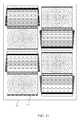
- FIGS. 12A-Care schematic diagrams illustrating views of a structured optical film for use in a stepped waveguide, in accordance with the present disclosure
- FIGS. 13A-Care schematic diagrams illustrating views of a structured optical film for use in a stepped waveguide, in accordance with the present disclosure
- FIG. 14is a schematic diagram illustrating a front view of a structured optical film for use in a stepped waveguide, in accordance with the present disclosure
- FIG. 15is a schematic diagram illustrating a front view of a structured optical film for use in a stepped waveguide, in accordance with the present disclosure
- FIGS. 16A-Dare schematic diagrams illustrating side views of an assembly method for a stepped waveguide, in accordance with the present disclosure
- FIGS. 17A-Eare schematic diagrams illustrating side views of an assembly method for a stepped waveguide, in accordance with the present disclosure
- FIG. 18is a schematic diagram illustrating a side view of a structured optical film for a stepped waveguide in accordance with the present disclosure
- FIG. 19is a schematic diagram illustrating a side view of a tool for fabrication of a structured optical film, in accordance with the present disclosure.
- FIG. 20is a schematic diagram illustrating a side view of a tool for fabrication of a structured optical film, in accordance with the present disclosure
- FIG. 21is a schematic diagram illustrating a side view of a tool for fabrication of a structured optical film, in accordance with the present disclosure
- FIG. 22is a schematic diagram illustrating a stepped imaging directional backlight, in accordance with the present disclosure.
- FIG. 23is a schematic diagram illustrating a front view of a structured optical film for use in a stepped waveguide, in accordance with the present disclosure
- FIG. 24is a schematic diagram illustrating a side view of an assembly method for a stepped waveguide, in accordance with the present disclosure
- FIG. 25is a schematic diagram illustrating a side view of an assembly method for a stepped waveguide, in accordance with the present disclosure
- FIG. 26is a schematic diagram illustrating a stepped imaging directional backlight, in accordance with the present disclosure.
- FIG. 27is a schematic diagram illustrating a side view of a structured optical film for use in a stepped waveguide further comprising a field Fresnel lens element, in accordance with the present disclosure
- FIG. 28is a schematic diagram illustrating a front view of a structured optical film for use in a stepped waveguide, in accordance with the present disclosure
- FIG. 29is a schematic diagram illustrating a side view of an assembly method for a stepped waveguide, in accordance with the present disclosure.
- FIG. 30is a schematic diagram illustrating a side view of an assembly method for a stepped waveguide, in accordance with the present disclosure
- FIG. 31is a schematic diagram illustrating a stepped imaging directional backlight, in accordance with the present disclosure.
- FIG. 32is a schematic diagram illustrating a front view of a structured optical film for use in a stepped waveguide, in accordance with the present disclosure
- FIG. 33is a schematic diagram illustrating a side view of an assembly method for a stepped waveguide, in accordance with the present disclosure
- FIG. 34is a schematic diagram illustrating a side view of an assembly method for a stepped waveguide, in accordance with the present disclosure
- FIG. 35is a schematic diagram illustrating a side view of an assembly method for a stepped waveguide, in accordance with the present disclosure
- FIG. 36is a schematic diagram illustrating a stepped imaging directional backlight, in accordance with the present disclosure.
- FIG. 37is a schematic diagram illustrating a front view of a structured optical film for use in a stepped waveguide, in accordance with the present disclosure
- FIG. 38is a schematic diagram illustrating a front view of a structured optical film for use in a stepped waveguide, in accordance with the present disclosure
- FIG. 39is a schematic diagram illustrating a side view of a structured optical film for use in a stepped waveguide, in accordance with the present disclosure.
- FIGS. 40A-Gare schematic diagrams illustrating a fabrication method for a structured optical film for use in a stepped waveguide, in accordance with the present disclosure
- FIG. 41is a schematic diagram illustrating an array of structured elements of a structured optical film for use in a stepped waveguide, in accordance with the present disclosure
- FIG. 42Ais a schematic diagram illustrating a side view of a structured optical film structure and tool for use in a stepped waveguide, in accordance with the present disclosure
- FIG. 42Bis a schematic diagram illustrating a side view of a structured optical film structure for use in a stepped waveguide, in accordance with the present disclosure
- FIG. 43is a schematic diagram illustrating a side view of a structured optical film structure for use in a stepped waveguide, in accordance with the present disclosure
- FIG. 44is a schematic diagram illustrating an optical inline directional backlight stepped waveguide optical element, in accordance with the present disclosure.
- FIG. 45is a schematic diagram illustrating a side view of a stepped imaging directional backlight comprising a structured optical film, in accordance with the present disclosure
- FIG. 46is a schematic diagram illustrating a front view of a structured optical film for use in a stepped waveguide, in accordance with the present disclosure.
- FIG. 47is a schematic diagram illustrating a side view of an optical body element, arranged for approximate alignment with a structured optical film, in accordance with the present disclosure.
- Time multiplexed autostereoscopic displayscan advantageously improve the spatial resolution of autostereoscopic display by directing light from all of the pixels of a spatial light modulator to a first viewing window in a first time slot, and all of the pixels to a second viewing window in a second time slot.
- Time multiplexed displayscan advantageously achieve directional illumination by directing an illuminator array through a substantially transparent time multiplexed spatial light modulator using directional optical elements, wherein the directional optical elements substantially form an image of the illuminator array in the window plane.
- the uniformity of the viewing windowsmay be advantageously independent of the arrangement of pixels in the spatial light modulator.
- Such displayscan provide observer tracking displays which have low flicker, with low levels of cross talk for a moving observer.
- the illuminator elements of the time sequential illumination systemmay be provided, for example, by pixels of a spatial light modulator with size approximately 100 micrometers in combination with a lens array.
- pixelssuffer from similar difficulties as for spatially multiplexed displays. Further, such devices may have low efficiency and higher cost, requiring additional display components.
- High window plane uniformitycan be conveniently achieved with macroscopic illuminators, for example, an array of LEDs in combination with homogenizing and diffusing optical elements that are typically of size 1 mm or greater.
- the increased size of the illuminator elementsmeans that the size of the directional optical elements increases proportionately. For example, a 16 mm wide illuminator imaged to a 65 mm wide viewing window may require a 200 mm back working distance.
- the increased thickness of the optical elementscan prevent useful application, for example, to mobile displays, or large area displays.
- optical valves as described in commonly-owned U.S. patent application Ser. No. 13/300,293advantageously can be arranged in combination with fast switching transmissive spatial light modulators to achieve time multiplexed autostereoscopic illumination in a thin package while providing high resolution images with flicker free observer tracking and low levels of cross talk.
- Describedis a one dimensional array of viewing positions, or windows, that can display different images in a first, typically horizontal, direction, but contain the same images when moving in a second, typically vertical, direction.
- imaging directional backlightsare arranged to direct the illumination from multiple light sources through a display panel to respective multiple viewing windows in at least one axis.
- Each viewing windowis substantially formed as an image in at least one axis of a light source by the imaging system of the imaging directional backlight.
- An imaging systemmay be formed between multiple light sources and the respective window images. In this manner, the light from each of the multiple light sources is substantially not visible for an observer's eye outside of the respective viewing window.
- Non-imaging backlightsare used for illumination of 2D displays. See, e.g., Kälil Käläntär et al., Backlight Unit With Double Surface Light Emission , J. Soc. Inf. Display, Vol. 12, Issue 4, pp. 379-387 (December 2004).
- Non-imaging backlightsare typically arranged to direct the illumination from multiple light sources through a display panel into a substantially common viewing zone for each of the multiple light sources to achieve wide viewing angle and high display uniformity.
- non-imaging backlightsdo not form viewing windows. In this manner, the light from each of the multiple light sources may be visible for an observer's eye at substantially all positions across the viewing zone.
- Such conventional non-imaging backlightsmay have some directionality, for example, to increase screen gain compared to Lambertian illumination, which may be provided by brightness enhancement films such as BEFTM from 3M. However, such directionality may be substantially the same for each of the respective light sources. Thus, for these reasons and others that should be apparent to persons of ordinary skill, conventional non-imaging backlights are different to imaging directional backlights.
- Edge lit non-imaging backlight illumination structuresmay be used in liquid crystal display systems such as those seen in 2D Laptops, Monitors and TVs. Light propagates from the edge of a lossy waveguide which may include sparse features; typically local indentations in the surface of the guide which cause light to be lost regardless of the propagation direction of the light.
- an optical valveis an optical structure that may be a type of light guiding structure or device referred to as, for example, a light valve, an optical valve directional backlight, and a valve directional backlight (“v-DBL”).
- optical valveis different to a spatial light modulator (which is sometimes referred to as a “light valve”).
- a spatial light modulatorwhich is sometimes referred to as a “light valve”.
- an imaging directional backlightis an optical valve that may employ a folded optical system. Light may propagate substantially without loss in one direction through the optical valve, may be incident on an imaging reflector, and may counter-propagate such that the light may be extracted by reflection off tilted light extraction features, and directed to viewing windows as described in U.S. patent application Ser. No. 13/300,293, which is herein incorporated by reference in its entirety.
- an imaging directional backlightexamples include a stepped waveguide imaging directional backlight, a folded imaging directional backlight, a wedge type directional backlight, or an optical valve.
- a stepped waveguide imaging directional backlightmay be an optical valve.
- a stepped waveguideis a waveguide for an imaging directional backlight comprising a waveguide for guiding light, which may include a first light guiding surface and a second light guiding surface, opposite the first light guiding surface, further comprising a plurality of light guiding features interspersed with a plurality of extraction features arranged as steps.
- a folded imaging directional backlightmay be at least one of a wedge type directional backlight, or an optical valve.
- lightmay propagate within an exemplary optical valve in a first direction from an input end to a reflective end and may be transmitted substantially without loss.
- Lightmay be reflected at the reflective end and propagates in a second direction substantially opposite the first direction.
- the lightmay be incident on light extraction features, which are operable to redirect the light outside the optical valve.
- the optical valvegenerally allows light to propagate in the first direction and may allow light to be extracted while propagating in the second direction.
- the optical valvemay achieve time sequential directional illumination of large display areas. Additionally, optical elements may be employed that are thinner than the back working distance of the optical elements to direct light from macroscopic illuminators to a nominal window plane. Such displays may use an array of light extraction features arranged to extract light counter propagating in a substantially parallel waveguide.
- Thin imaging directional backlight implementations for use with LCDshave been proposed and demonstrated by 3M, for example U.S. Pat. No. 7,528,893; by Microsoft, for example U.S. Pat. No. 7,970,246 which may be referred to herein as a “wedge type directional backlight;” by RealD, for example U.S. patent application Ser. No. 13/300,293 which may be referred to herein as an “optical valve” or “optical valve directional backlight,” all of which are herein incorporated by reference in their entirety.
- the present disclosureprovides stepped waveguide imaging directional backlights in which light may reflect back and forth between the internal faces of, for example, a stepped waveguide which may include a first side and a first set of features. As the light travels along the length of the stepped waveguide, the light may not substantially change angle of incidence with respect to the first side and first set of surfaces and so may not reach the critical angle of the medium at these internal faces. Light extraction may be advantageously achieved by a second set of surfaces (the step “risers”) that are inclined to the first set of surfaces (the step “treads”). Note that the second set of surfaces may not be part of the light guiding operation of the stepped waveguide, but may be arranged to provide light extraction from the structure.
- a wedge type imaging directional backlightmay allow light to guide within a wedge profiled waveguide having continuous internal surfaces. The optical valve is thus not a wedge type imaging directional backlight.
- FIG. 1Ais a schematic diagram illustrating a front view of light propagation in one embodiment of a directional display device
- FIG. 1Bis a schematic diagram illustrating a side view of light propagation in the optical valve structure of FIG. 1A .
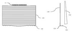
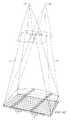
- FIG. 1Aillustrates a front view in the xy plane of a directional backlight of a directional display device, and includes an illuminator array 15 which may be used to illuminate a stepped waveguide 1 .
- Illuminator array 15includes illuminator elements 15 a through illuminator element 15 n (where n is an integer greater than one).
- the stepped waveguide 1 of FIG. 1Amay be a stepped, display sized waveguide 1 .
- Illuminator elements 15 a through 15 nare light sources that may be light emitting diodes (LEDs).
- FIG. 1Billustrates a side view in the xz plane, and includes illuminator array 15 , SLM (spatial light modulator) 48 , extraction features 12 , guiding features 10 , and stepped waveguide 1 , arranged as shown.
- the side view provided in FIG. 1Bis an alternative view of the front view shown in FIG. 1A . Accordingly, the illuminator array 15 of FIGS. 1A and 1B corresponds to one another and the stepped waveguide 1 of FIGS. 1A and 1B may correspond to one another.
- the stepped waveguide 1may have an input end 2 that is thin and a reflective end 4 that is thick.
- the waveguide 1extends between the input end 2 that receives input light and the reflective end 4 that reflects the input light back through the waveguide 1 .
- the length of the input end 2 in a lateral direction across the waveguideis greater than the height of the input end 2 .
- the illuminator elements 15 a - 15 nare disposed at different input positions in a lateral direction across the input end 2 .
- the waveguide 1has first and second, opposed guide surfaces extending between the input end 2 and the reflective end 4 for guiding light forwards and back along the waveguide 1 by total internal reflection.
- the first guide surfaceis planar.
- the second guide surfacehas a plurality of light extraction features 12 facing the reflective end 4 and inclined to reflect at least some of the light guided back through the waveguide 1 from the reflective end in directions that break the total internal reflection at the first guide surface and allow output through the first guide surface, for example, upwards in FIG. 1B , that is supplied to the SLM 48 .
- the light extraction features 12are reflective facets, although other reflective features could be used.
- the light extraction features 12do not guide light through the waveguide, whereas the intermediate regions of the second guide surface intermediate the light extraction features 12 guide light without extracting it. Those regions of the second guide surface are planar and may extend parallel to the first guide surface, or at a relatively low inclination.
- the light extraction features 12extend laterally to those regions so that the second guide surface has a stepped shape including the light extraction features 12 and intermediate regions.
- the light extraction features 12are oriented to reflect light from the light sources, after reflection from the reflective end 4 , through the first guide surface.
- the light extraction features 12are arranged to direct input light from different input positions in the lateral direction across the input end in different directions relative to the first guide surface that are dependent on the input position.
- the illumination elements 15 a - 15 nare arranged at different input positions, the light from respective illumination elements 15 a - 15 n is reflected in those different directions.
- each of the illumination elements 15 a - 15 ndirects light into a respective optical window in output directions distributed in the lateral direction in dependence on the input positions.
- the lateral direction across the input end 2 in which the input positions are distributedcorresponds with regard to the output light to a lateral direction to the normal to the first guide surface.
- the illuminator elements 15 a - 15 nmay be selectively operated to direct light into a selectable optical window.
- an optical windowmay correspond to the image of a single light source in the window plane, being a nominal plane in which optical windows form across the entirety of the display device.
- an optical windowsmay correspond to the image of a groups of light sources that are driven together.
- such groups of light sourcesmay increase uniformity of the optical windows of the array 121 .
- a viewing windowis a region in the window plane wherein light is provided comprising image data of substantially the same image from across the display area.
- a viewing windowmay be formed from a single optical window or from plural optical windows.
- the SLM 48extends across the waveguide is transmissive and modulates the light passing therethrough.
- the SLM 48may be a liquid crystal display (LCD) but this is merely by way of example, and other spatial light modulators or displays may be used including LCOS, DLP devices, and so forth, as this illuminator may work in reflection.
- the SLM 48is disposed across the first guide surface of the waveguide and modulates the light output through the first guide surface after reflection from the light extraction features 12 .
- FIG. 1AThe operation of a directional display device that may provide a one dimensional array of viewing windows is illustrated in front view in FIG. 1A , with its side profile shown in FIG. 1B .
- the lightmay propagate along +x in a first direction, within the stepped waveguide 1 , while at the same time, the light may fan out in the xy plane and upon reaching the far curved end side 4 , may substantially or entirely fill the curved end side 4 . While propagating, the light may spread out to a set of angles in the xz plane up to, but not exceeding the critical angle of the guide material.
- the extraction features 12 that link the guiding features 10 of the bottom side of the stepped waveguide 1may have a tilt angle greater than the critical angle and hence may be missed by substantially all light propagating along +x in the first direction, ensuring the substantially lossless forward propagation.
- the curved end side 4 of the stepped waveguide 1may be made reflective, typically by being coated with a reflective material such as, for example, silver, although other reflective techniques may be employed.
- Lightmay therefore be redirected in a second direction, back down the guide in the direction of ⁇ x and may be substantially collimated in the xy or display plane.
- the angular spreadmay be substantially preserved in the xz plane about the principal propagation direction, which may allow light to hit the riser edges and reflect out of the guide.
- lightmay be effectively directed approximately normal to the xy display plane with the xz angular spread substantially maintained relative to the propagation direction. This angular spread may be increased when light exits the stepped waveguide 1 through refraction, but may be decreased somewhat dependent on the reflective properties of the extraction features 12 .
- reflectionmay be reduced when total internal reflection (TIR) fails, squeezing the xz angular profile and shifting off normal.
- TIRtotal internal reflection
- the increased angular spread and central normal directionmay be preserved.
- lightmay exit the stepped waveguide 1 approximately collimated and may be directed off normal in proportion to the y-position of the respective illuminator element 15 a - 15 n in illuminator array 15 from the input edge center. Having independent illuminator elements 15 a - 15 n along the input edge 2 then enables light to exit from the entire first light directing side 6 and propagate at different external angles, as illustrated in FIG. 1A .
- a display devicemay include a stepped waveguide or light valve which in turn, may include a first guide surface that may be arranged to guide light by total internal reflection.
- the light valvemay include a second guide surface which may have a plurality of light extraction features inclined to reflect light guided through the waveguide in directions allowing exit through the first guide surface as the output light.
- the second guide surfacemay also have regions between the light extraction features that may be arranged to direct light through the waveguide without extracting it.
- a display devicemay include a waveguide with at least a first guide surface which may be arranged to guide light by total internal reflection and a second guide surface which may be substantially planar and inclined at an angle to reflect light in directions that break the total internal reflection for outputting light through the first guide surface,
- the display devicemay include a deflection element extending across the first guide surface of the waveguide for deflecting light towards the normal to the SLM 48 .
- a display devicemay include a waveguide which may have a reflective end facing the input end for reflecting light from the input light back through the waveguide.
- the waveguidemay further be arranged to output light through the first guide surface after reflection from the reflective end.
- Illuminating an SLM 48 such as a fast liquid crystal display (LCD) panel with such a devicemay achieve autostereoscopic 3D as shown in top view or yz-plane viewed from the illuminator array 15 end in FIG. 2A , front view in FIG. 2B and side view in FIG. 2C .
- FIG. 2Ais a schematic diagram illustrating in a top view, propagation of light in a directional display device
- FIG. 2Bis a schematic diagram illustrating in a front view, propagation of light in a directional display device
- FIG. 2Cis a schematic diagram illustrating in side view propagation of light in a directional display device.
- a stepped waveguide 1may be located behind a fast (e.g., greater than 100 Hz) LCD panel SLM 48 that displays sequential right and left eye images.
- a faste.g., greater than 100 Hz
- specific illuminator elements 15 a through 15 n of illuminator array 15may be selectively turned on and off, providing illuminating light that enters right and left eyes substantially independently by virtue of the system's directionality.
- sets of illuminator elements of illuminator array 15are turned on together, providing a one dimensional viewing window 26 or an optical pupil with limited width in the horizontal direction, but extended in the vertical direction, in which both eyes horizontally separated may view a left eye image, and another viewing window 44 in which a right eye image may primarily be viewed by both eyes, and a central position in which both the eyes may view different images.
- 3Dmay be viewed when the head of a viewer is approximately centrally aligned. Movement to the side away from the central position may result in the scene collapsing onto a 2D image.
- the reflective end 4may have positive optical power in the lateral direction across the waveguide.
- the optical axismay be defined with reference to the shape of the reflective end 4 , for example being a line that passes through the centre of curvature of the reflective end 4 and coincides with the axis of reflective symmetry of the end 4 about the x-axis.
- the optical axismay be similarly defined with respect to other components having optical power, for example the light extraction features 12 if they are curved, or the Fresnel lens 62 described below.
- the optical axis 238is typically coincident with the mechanical axis of the waveguide 1 .
- the optical axis 238is a line that passes through the centre of curvature of the surface at end 4 and coincides with the axis of reflective symmetry of the side 4 about the x-axis.
- the optical axis 238is typically coincident with the mechanical axis of the waveguide 1 .
- the cylindrical reflecting surface at end 4may typically comprise a spherical profile to optimize performance for on-axis and off-axis viewing positions. Other profiles may be used.
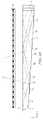
- FIG. 3is a schematic diagram illustrating in side view a directional display device. Further, FIG. 3 illustrates additional detail of a side view of the operation of a stepped waveguide 1 , which may be a transparent material.
- the stepped waveguide 1may include an illuminator input end 2 , a reflective end 4 , a first light directing side 6 which may be substantially planar, and a second light directing side 8 which includes guiding features 10 and light extraction features 12 .
- light rays 16 from an illuminator element 15 c of an illuminator array 15(not shown in FIG.
- reflective end 4may be a mirrored surface and may reflect light, it may in some embodiments also be possible for light to pass through reflective end 4 .
- light ray 18 reflected by the reflective end 4may be further guided in the stepped waveguide 1 by total internal reflection at the reflective end 4 and may be reflected by extraction features 12 .
- Light rays 18 that are incident on extraction features 12may be substantially deflected away from guiding modes of the stepped waveguide 1 and may be directed, as shown by ray 20 , through the side 6 to an optical pupil that may form a viewing window 26 of an autostereoscopic display.
- the width of the viewing window 26may be determined by at least the size of the illuminator, output design distance and optical power in the side 4 and extraction features 12 .
- each viewing window 26represents a range of separate output directions with respect to the surface normal direction of the SLM 48 that intersect with a plane at the nominal viewing distance.
- FIG. 4Ais a schematic diagram illustrating in front view a directional display device which may be illuminated by a first illuminator element and including curved light extraction features.
- the directional backlightmay include the stepped waveguide 1 and the light source illuminator array 15 .
- FIG. 4Ashows in front view further guiding of light rays from illuminator element 15 c of illuminator array 15 , in the stepped waveguide 1 .
- Each of the output raysare directed towards the same viewing window 26 from the respective illuminator 14 .
- light ray 30may intersect the ray 20 in the window 26 , or may have a different height in the window as shown by ray 32 .
- sides 22 , 24 of the waveguidemay be transparent, mirrored, or blackened surfaces.
- light extraction features 12may be elongate, and the orientation of light extraction features 12 in a first region 34 of the light directing side 8 (light directing side 8 shown in FIG. 3 , but not shown in FIG. 4A ) may be different to the orientation of light extraction features 12 in a second region 36 of the light directing side 8 .
- FIG. 4Bis a schematic diagram illustrating in front view a directional display device which may illuminated by a second illuminator element. Further, FIG. 4B shows the light rays 40 , 42 from a second illuminator element 15 h of the illuminator array 15 . The curvature of the reflective surface on the side 4 and the light extraction features 12 cooperatively produce a second viewing window 44 laterally separated from the viewing window 26 with light rays from the illuminator element 15 h.
- the arrangement illustrated in FIG. 4Bmay provide a real image of the illuminator element 15 c at a viewing window 26 in which the real image may be formed by cooperation of optical power in reflective end 4 and optical power which may arise from different orientations of elongate light extraction features 12 between regions 34 and 36 , as shown in FIG. 4A .
- the arrangement of FIG. 4Bmay achieve improved aberrations of the imaging of illuminator element 15 c to lateral positions in viewing window 26 . Improved aberrations may achieve an extended viewing freedom for an autostereoscopic display while achieving low cross talk levels.
- FIG. 5is a schematic diagram illustrating in front view an embodiment of a directional display device comprising a waveguide 1 having substantially linear light extraction features. Further, FIG. 5 shows a similar arrangement of components to FIG. 1 (with corresponding elements being similar), with one of the differences being that the light extraction features 12 are substantially linear and parallel to each other. Advantageously, such an arrangement may provide substantially uniform illumination across a display surface and may be more convenient to manufacture than the curved extraction features of FIG. 4A and FIG. 4B .
- FIG. 6Ais a schematic diagram illustrating one embodiment of the generation of a first viewing window in a time multiplexed imaging directional display device, namely an optical valve apparatus in a first time slot.
- FIG. 6Bis a schematic diagram illustrating another embodiment of the generation of a second viewing window in a time multiplexed imaging directional backlight apparatus in a second time slot.
- FIG. 6Cis a schematic diagram illustrating another embodiment of the generation of a first and a second viewing window in a time multiplexed imaging directional display device.
- FIG. 6Ashows schematically the generation of illumination window 26 from stepped waveguide 1 .
- Illuminator element group 31 in illuminator array 15may provide a light cone 17 directed towards a viewing window 26 .
- Illuminator element group 33 in illuminator array 15may provide a light cone 19 directed towards viewing window 44 .
- windows 26 and 44may be provided in sequence as shown in FIG. 6C . If the image on a SLM 48 (not shown in FIGS. 6A, 6B, 6C ) is adjusted in correspondence with the light direction output, then an autostereoscopic image may be achieved for a suitably placed viewer. Similar operation can be achieved with all the directional backlights and directional display devices described herein.
- illuminator element groups 31 , 33each include one or more illumination elements from illumination elements 15 a to 15 n , where n is an integer greater than one.
- FIG. 7is a schematic diagram illustrating one embodiment of an observer tracking autostereoscopic directional display device including a time multiplexed directional backlight.
- selectively turning on and off illuminator elements 15 a to 15 n along axis 29provides for directional control of viewing windows.
- the head 45 positionmay be monitored with a camera, motion sensor, motion detector, or any other appropriate optical, mechanical or electrical means, and the appropriate illuminator elements of illuminator array 15 may be turned on and off to provide substantially independent images to each eye irrespective of the head 45 position.
- the head tracking system(or a second head tracking system) may provide monitoring of more than one head 45 , 47 (head 47 not shown in FIG. 7 ) and may supply the same left and right eye images to each viewers' left and right eyes providing 3D to all viewers. Again similar operation can be achieved with all the directional backlights and directional display devices described herein.
- FIG. 8is a schematic diagram illustrating one embodiment of a multi-viewer directional display device as an example including an imaging directional backlight.
- at least two 2D imagesmay be directed towards a pair of viewers 45 , 47 so that each viewer may watch a different image on the SLM 48 .
- the two 2D images of FIG. 8may be generated in a similar manner as described with respect to FIG. 7 in that the two images would be displayed in sequence and in synchronization with sources whose light is directed toward the two viewers.
- One imageis presented on the SLM 48 in a first phase
- a second imageis presented on the SLM 48 in a second phase different from the first phase.
- the output illuminationis adjusted to provide first and second viewing windows 26 , 44 respectively. An observer with both eyes in window 26 will perceive a first image while an observer with both eyes in window 44 will perceive a second image.
- FIG. 9is a schematic diagram illustrating a privacy directional display device which includes an imaging directional backlight.
- 2D image display systemsmay also utilize directional backlighting for security and efficiency purposes in which light may be primarily directed at the eyes of a first viewer 45 as shown in FIG. 9 .
- first viewer 45may be able to view an image on device 50
- lightis not directed towards second viewer 47 .
- second viewer 47is prevented from viewing an image on device 50 .
- Each of the embodiments of the present disclosuremay advantageously provide autostereoscopic, dual image or privacy display functions.
- FIG. 10is a schematic diagram illustrating in side view the structure of a time multiplexed directional display device as an example including an imaging directional backlight. Further, FIG. 10 shows in side view an autostereoscopic directional display device, which may include the stepped waveguide 1 and a Fresnel lens 62 arranged to provide the viewing window 26 for a substantially collimated output across the stepped waveguide 1 output surface. A vertical diffuser 68 may be arranged to extend the height of the window 26 further. The light may then be imaged through the SLM 48 . Vertical diffusers may incorporate asymmetric diffusion properties, for example to diffuse light in a vertical direction with larger cone angle than in the horizontal (lateral) direction.
- the illuminator array 15may include light emitting diodes (LEDs) that may, for example, be phosphor converted blue LEDs, or may be separate RGB LEDs.
- the illuminator elements in illuminator array 15may include a uniform light source and SLM 48 arranged to provide separate illumination regions.
- the illuminator elementsmay include laser light source(s).
- the laser outputmay be directed onto a diffuser by means of scanning, for example, using a galvo or MEMS scanner.
- laser lightmay thus be used to provide the appropriate illuminator elements in illuminator array 15 to provide a substantially uniform light source with the appropriate output angle, and further to provide reduction in speckle.
- the illuminator array 15may be an array of laser light emitting elements.
- the diffusermay be a wavelength converting phosphor, so that illumination may be at a different wavelength to the visible output light.
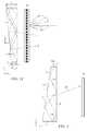
- FIG. 11Ais a schematic diagram illustrating a front view of an optical inline directional backlight apparatus as another example of an imaging directional backlight apparatus. Further, FIG. 11A shows another imaging directional backlight apparatus described herein as an optical inline directional backlight.
- the optical inline directional backlightmay operate in a similar manner to the optical valve, with the difference that light may not be reversed at the end interface. Instead, the optical inline directional backlight may allow light to fan out in a guiding region before refracting light approximately half way down its length into a region containing extraction features 12 and in which light may be directed out of the guide and toward a viewer.
- an illuminator element 15 de.g., LED
- a refractive imaging element 119which may include in this case, a Fresnel lens surface between dissimilar refractive index materials 111 and 113 .
- Extraction features 12may extract the light between guiding regions 10 to provide directed rays 5 , which may converge to form viewing windows in a similar manner to the optical valve.
- the optical inline directional backlightcan be constructed and may operate as an unfolded optical valve in which the reflecting mirror 4 may be replaced by the refractive cylindrical lens 119 .
- FIG. 11Bis a schematic diagram illustrating a front view of another imaging directional display device, as illustrated, a wedge type directional backlight
- FIG. 11Cis a schematic diagram illustrating a side view of the same wedge type directional display device.
- a wedge type directional backlightis generally discussed by U.S. Pat. No. 7,660,047 and entitled “Flat Panel Lens,” which is herein incorporated by reference in its entirety.
- the structuremay include a wedge type waveguide 1104 with a bottom surface which may be preferentially coated with a reflecting layer 1106 and with an end corrugated surface 1102 , which may also be preferentially coated with a reflecting layer 1106 . As shown in FIG.
- lightmay enter the wedge type waveguide 1104 from local sources 1101 and the light may propagate in a first direction before reflecting off the end surface.
- Lightmay exit the wedge type waveguide 1104 while on its return path and may illuminate a display panel 1110 .
- a wedge type waveguideprovides extraction by a taper that reduces the incidence angle of propagating light so that when the light is incident at the critical angle on an output surface, it may escape. Escaping light at the critical angle in the wedge type waveguide propagates substantially parallel to the surface until deflected by a redirection layer 1108 such as a prism array. Errors or dust on the wedge type waveguide output surface may change the critical angle, creating stray light and uniformity errors.
- an imaging directional backlight that uses a mirror to fold the beam path in the wedge type directional backlightmay employ a faceted mirror that biases the light cone directions in the wedge type waveguide.
- Such faceted mirrorsare generally complex to fabricate and may result in illumination uniformity errors as well as stray light.
- the wedge type directional backlight and optical valvefurther process light beams in different ways.
- light input at an appropriate anglewill output at a defined position on a major surface, but light rays will exit at substantially the same angle and substantially parallel to the major surface.
- light input to a stepped waveguide of an optical valve at a certain anglemay output from points across the first side, with output angle determined by input angle.
- the stepped waveguide of the optical valvemay not require further light re-direction films to extract light towards an observer and angular non-uniformities of input may not provide non-uniformities across the display surface.
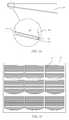
- FIG. 12Ais a schematic diagram illustrating a front view of a structured optical film for use in a stepped waveguide. Further, FIG. 12A is a schematic diagram illustrating a structured optical film 100 which may include an array of light extracting features 12 and light guiding features 10 . The film 100 may include a curved side 101 arranged to approximately align with the curved side 4 of a tapered body 104 in an assembled stepped waveguide.
- FIG. 12Bis a schematic diagram illustrating assembly of a stepped waveguide. Further, FIG. 12B is a schematic diagram illustrating the assembly of a stepped waveguide including the structured optical film 100 .
- a film 100can be arranged with an optical body 104 that may include substantially planar sides, and arranged with a taper along the x-direction.
- the structured optical film 100may be formed on substrate 102 , for example, on a polymer film such as, but not limited to, PET, PMMA, COC, and so forth.
- the body 104may be a plastic substrate that may be substantially the same as the material of substrate 102 , or may be a different material, for example, a different plastic or glass. As shown in FIG.
- FIG. 12Cis a schematic diagram illustrating assembly of a stepped waveguide.
- the layer 108may be formed by a pressure sensitive adhesive, a UV cured adhesive, a thermally cured adhesive, by solvent bonding, and so forth, for example.
- the processing of the optical structures of the stepped waveguidemay be processed in a film 100 rather than in molding of the optical body 104 .
- the high repeatability optical componentsmay be formed in a roll-to-roll processing regime as compared to the batch processing of a single element.
- such an arrangementmay achieve reduced cost and higher precision than batch processed elements.
- FIG. 13Ais a schematic diagram illustrating a front view of a structured optical film for use in a stepped waveguide. Further, FIG. 13A is a schematic diagram illustrating a further structured optical film 100 including an array of light extracting features 12 and light guiding features 10 in which the features in the segment region 112 bounded by side 101 may be removed. Advantageously in use, little to no light extraction may occur in the segment region so that the output efficiency may be increased.
- FIG. 13Bis a schematic diagram illustrating assembly of a stepped waveguide. Further, FIG. 13B is a schematic diagram illustrating the assembly of a stepped waveguide including the structured optical film 100 .
- Such a staggering artifact in the window profilecan be reduced or removed by providing a substantially parallel sided body 104 in the segment region 112 , while the region to which the film 100 is attached may be provided by a tapered body.
- FIG. 13Cis a schematic diagram illustrating assembly of a stepped waveguide. Similar to FIG. 12C , in FIG. 13C , a bonding layer 108 may be formed between the film 102 and body 104 to provide an index matching interface between the structured optical film 100 , 102 and the body 104 .
- FIG. 14is a schematic diagram illustrating a front view of a structured optical film for use in a stepped waveguide. Further, FIG. 14 is a schematic diagram illustrating a further structured optical film 100 including multiple curved sides 115 , 116 arranged to be approximately aligned with a matching shaped body 104 . Such an arrangement can advantageously achieve large display area and increased f-number, thus reducing off-axis aberrations in observer tracking displays. Further, the features 10 , 12 may be substantially continuous so that the visibility of the boundary between the two sides 115 , 116 is minimized and thus display uniformity may be optimized.
- FIG. 15is a schematic diagram illustrating a front view of a structured optical film for use in a stepped waveguide. Further, FIG. 15 is a schematic diagram illustrating a further structured optical film 100 including edge regions 118 and separated from the light extraction region which may include features 10 , 12 by means of boundary 120 .
- Edge regions 118may include a substantially planar layer that may be metallized, may have other coatings, or may have optical structures as described herein.
- the optical surface of the stepped waveguidemay be formed on a film separately to the body, and thus may be provided at low cost and in high volume by roll-to-roll processing methods.
- the edge regions 118may be arranged to achieve increased angle of view of the stepped waveguide during operation as generally discussed in U.S. patent application Ser. No. 13/839,552, entitled “Wide angle imaging directional backlights”), which may be referred to herein as an “Wide angle imaging directional backlights” which is herein incorporated by reference in its entirety.
- FIGS. 16A-Dare schematic diagrams illustrating a side view of one method of assembly for a stepped waveguide comprising a structured optical film 100 . Further, FIGS. 16A-D are schematic diagrams illustrating a method to form a stepped waveguide.
- optical film 100 and regions 118may be formed on the upper side of the substrate 102 .
- the substrate 102may be removed or weakened, for example, by scribing or cutting to produce a cut 121 in the region of the boundary 120 on the lower side of the substrate 102 . The cut may be through part of the thickness of the substrate 102 .
- the substrate 102may be arranged with the body 104 and substrate 102 which may include regions 118 folded so that regions 118 may be approximately aligned with the sides of the body 104 .
- the substrate 102 and regions 122may be finished, for example, by cutting away extra film 100 to provide a substantially planar lower surface to the assembled structure.
- the film 100may be provided with a metallized coating so that the side 4 of the assembled stepped waveguide is fully metallized after the assembly step.
- a metallizationmay be formed on the side 4 of the assembled body 104 and film 100 after assembly.
- the post metallizationmore conveniently achieves a high area coverage of the metallization material without a seam between the optical body 104 and film 100 .
- the film 100 and body 104can be pre-metallized and a final reflective layer formed on the assembled stepped waveguide to achieve a uniform reflectivity at the side 4 of the stepped waveguide.
- FIGS. 17A-Eare schematic diagrams illustrating a side view of an assembly method for a stepped waveguide. Further, FIGS. 17A-E are schematic diagrams illustrating a method to form a stepped waveguide.
- the substrate 102may be cut in region 120 on the upper side as shown in FIG. 17B .
- the substratemay then be folded in another step shown in FIG. 17C and attached to the body 104 as shown in FIG. 17D .
- a cutting tool 124may be used to remove additional material in the boundary 120 to provide a gap 126 as shown in FIG. 17E in the separated regions, thus reducing stress during attachment of the substrate 102 to the body 104 .
- FIG. 18is a schematic diagram illustrating a side view of a stepped waveguide including a structured optical film. Further, FIG. 18 is a schematic diagram illustrating a side view of an optical body 104 and an attached film 100 .
- a layer 130may be incorporated to provide index matching of the film 100 and substrate 102 to the body 104 .
- the layer 130may include an adhesive or may be formed by solvent bonding between the substrate 102 and body 104 .
- the substrate 102may be omitted and the film 100 bonded adjacently or directly onto the body 104 .
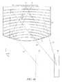
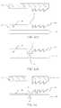
- FIG. 19is a schematic diagram illustrating a side view of a tool for fabrication of a structured optical film. Further, FIG. 19 is a schematic diagram illustrating a first arrangement of a surface relief stamp 132 that may be used to form an array of films 100 .
- the stampmay be arranged with an array of structured regions 101 , each with the inverse shape of the structured optical film 100 .
- the stampmay be arranged to provide a large area film including multiple films 100 by means of a replication method.
- the replication methodmay include, but is not limited to, UV embossing, hot embossing, injection molding, other known replication methods, or any combination thereof.
- the films 100may be extracted from the film by cutting after replication.
- FIG. 20is a schematic diagram illustrating a side view of a tool for fabrication of a structured optical film
- FIG. 21is a schematic diagram illustrating a side view of a tool for fabrication of a structured optical film.
- FIGS. 20 and 21are schematic diagrams illustrating further arrangements of a surface relief stamp 132 that may be used to form an array of films 100 .
- FIG. 20advantageously may increase the area utilization and may employ less cutting as compared to FIG. 19 .
- FIG. 21may provide a substantially continuous area of structure from which separate films may be extracted after replication for example by die cutting.
- FIG. 21may enable different shape and sizes of stepped waveguides which may be formed from the same film 100 .
- FIG. 22is a schematic diagram illustrating a stepped imaging directional backlight
- FIG. 23is a schematic diagram illustrating a front view of a structured optical film for use in a stepped waveguide.
- FIG. 22is a schematic diagram illustrating a stepped waveguide apparatus including a reflective Fresnel element 140 arranged on side 4 of the respective waveguide.
- such an arrangementmay provide optical power to light from the light emitting element array 15 while achieving a reduction in the section 112 under the reflecting surface.
- FIG. 23is a schematic diagram illustrating a structured optical film 100 .
- reflective Fresnel element 140can be formed by a second surface relief optical structure on the same substrate 102 as the structured optical film 100 , separated by boundary 120 .
- such an arrangementcan be formed on a large area sheet in a small number of replication operations and in a single 2D plane and is thus well suited to low cost roll-to-roll processing.
- FIG. 24is a schematic diagram illustrating a side view of an assembly method for a stepped waveguide. Further, FIG. 24 is a schematic diagram illustrating a side view of the assembly of a stepped waveguide including the structured optical film 100 and Fresnel lens element 142 .
- the substrate 102Prior to assembly, the substrate 102 (for illustrative convenience not shown in FIG. 24 ) may be scored at boundary 120 and the substrate 102 may be folded. The substrate 102 may then be approximately aligned with the body 104 as illustrated in schematic diagram FIG. 25 .
- FIG. 25is a schematic diagram illustrating a side view of an assembly method for a stepped waveguide.
- approximate alignment between reflective Fresnel element 140 and structured optical film 100can be achieved at the time of replication, rather than employing two separate alignment steps when the elements are attached to body 104 , such that the film 100 and element 140 may remain approximately aligned during the attachment to the body 104 .
- FIG. 26is a schematic diagram illustrating a stepped imaging directional backlight. Further, FIG. 26 is a schematic diagram illustrating a stepped waveguide optical valve apparatus including a reflective Fresnel element 140 arranged on side 4 of the respective stepped waveguide and a transmissive Fresnel element 62 arranged on side 6 of the respective stepped waveguide.
- a reflective Fresnel element 140arranged on side 4 of the respective stepped waveguide
- a transmissive Fresnel element 62arranged on side 6 of the respective stepped waveguide.
- Such an arrangementcan distribute optical power between the elements 140 , 62 thus reducing total aberrations of the system, and reducing off-axis cross talk.
- FIG. 27is a schematic diagram illustrating a side view of a structured optical film 100 for use in a stepped waveguide further including a field Fresnel lens element. Further, FIG. 27 is a schematic diagram illustrating a side view of part of a stepped waveguide valve apparatus including a transmissive Fresnel element 62 arranged on a first side of body 104 and structured optical film 100 on a second side of body 104 .
- Layer 130may include a material with refractive index arranged to provide index matching between the body 104 and substrate 102 .
- An air gapmay be arranged between the element 62 and body 104 .
- Fresnel element 62may alternatively be arranged with a layer 63 of refractive index lower than the refractive index of body 104 .
- the layer 63may be, but is not limited to, a silicone, a fluorinated material, an aerogel, and so forth.
- a silicone with an approximate refractive index 1.4may be arranged with a body of approximate refractive index 1.5 such that the critical angle within the body 1.4 is approximately 69 degrees.
- light rays 65 propagating within the body 104may be reflected from layer 63 whereas light rays 64 that are at angles less than the critical angle may be outputted through the Fresnel element 62 .
- FIG. 28is a schematic diagram illustrating a front view of a structured optical film for use in a stepped waveguide
- FIG. 29is a schematic diagram illustrating a side view of an assembly method for a stepped waveguide
- FIG. 30is a schematic diagram illustrating a side view of an assembly method for a stepped waveguide.
- FIG. 28is a schematic diagram illustrating a composite structured optical film which may be a structured optical film 100 , reflective Fresnel element 140 and transmissive Fresnel element 62 , separated by boundaries 120 .
- FIG. 29is a schematic diagram illustrating a side view of, folding of a composite structured optical film which may be a structured optical film 100 , reflective Fresnel element 140 and transmissive Fresnel element 62 , separated by boundaries 120 .
- FIG. 30is a schematic diagram illustrating approximate alignment of a structured optical film which may be a structured optical film 100 , reflective Fresnel element 140 and transmissive Fresnel element 62 , separated by boundaries 120 with body 104 .
- adhesive layers 130 , 63which may be patterned may be formed in approximate alignment with respective film 100 and element 62 on the rear of substrate 102 .
- the elementmay be approximately aligned with a single alignment step for all three sides of the body 104 .
- FIG. 31is a schematic diagram illustrating a stepped imaging directional backlight. Further, FIG. 31 is a schematic diagram illustrating a stepped waveguide including a structured optical film 100 which may include curved features 10 , 12 , a reflective Fresnel element 140 and an input optical element 144 which may be arranged to direct light from an array of light sources in air, into the valve with a common illumination direction, thus increasing efficiency and viewing angle in an autostereoscopic display.
- the input optical element 144may further comprise colored filters, optical diffusers or other cross talk reduction layers as generally discussed in U.S. patent application Ser. No. 13/836,443 (entitled “Cross talk suppression apparatus and method thereof”), which is herein incorporated by reference in its entirety.
- FIG. 32is a schematic diagram illustrating a front view of a structured optical film for use in a stepped waveguide. Further, FIG. 32 is a schematic diagram illustrating a composite structured optical film including a structured optical film 100 , reflective Fresnel element 140 and input optical element 144 , separated by boundaries 120 .
- FIG. 33is a schematic diagram illustrating a side view of an assembly method for a stepped waveguide
- FIG. 34is a schematic diagram illustrating a side view of an assembly method for a stepped waveguide
- FIG. 35is a schematic diagram illustrating a side view of an assembly method for a stepped waveguide. Further, FIGS.
- 33, 34 and 35are schematic diagram illustrating a side view of the respective folding, assembly and trimming of the substrate 102 with optical body 104 .
- the alignment of the optical structurescan be achieved in a single alignment step, reducing cost and complexity.
- the optical film 100may be slightly undersized so that trimming may not be needed.
- FIG. 36is a schematic diagram illustrating a stepped imaging directional backlight. Further, FIG. 36 is a schematic diagram illustrating a stepped waveguide including a structured optical film 100 which may include features 10 , 12 , and a structured edge input optical element 152 which may be arranged to direct light from an array of light sources 150 into the side of the valve, providing a switchable wide viewing angle for an autostereoscopic display, as generally described in U.S. patent application Ser. No. 13/839,552 (entitled “Wide angle imaging directional backlights”), and herein incorporated by reference, in its entirety.
- FIG. 37is a schematic diagram illustrating a front view of a structured optical film for use in a stepped waveguide. Further, FIG. 37 is a schematic diagram illustrating a structured optical film 100 , and input optical elements 154 , separated by boundaries 120 . Such an arrangement can advantageously be provided in approximate alignment with body 104 in a single alignment step. The external parts of substrate 102 may be removed by cutting for example prior to or after assembly with the body 104 .
- FIG. 38is a schematic diagram illustrating a front view of a structured optical film for use in a stepped waveguide.
- FIG. 38is a schematic diagram illustrating a composite structured optical film 159 including a structured optical film 100 , and input optical elements 154 , reflective Fresnel element 140 , transmissive Fresnel element 62 , and input optical element 156 .
- absorbing regions 158may be arranged in approximate alignment with features of the various optical structures including at boundaries between the film and optical elements. Such absorbing regions may reduce scatter in the device. Further regions in alignment with film 100 and element 62 may be metallized to provide a reflective function. Such absorbing regions 158 may be provided by printing of dye or pigment materials.
- the reflector formed on the sides of the waveguide 1may comprise a reflector film such as metallized aluminum or Enhanced Specular Reflector ESRTM from 3M corporation.
- FIG. 39is a schematic diagram illustrating a side view of a structured optical film for use in a stepped waveguide. Further, FIG. 39 is a schematic diagram illustrating a side view along section 160 of a structure optical film 100 .
- Optical element 156may, for example, include a structure optical element such as element 144 or may include a stack of films and other optical element that are attached to the element. For example layers 166 , 168 that may comprise color filters or diffusers may be attached by adhesive 170 to compensate for cross talk for reflected light from side 2 of the stepped waveguide.
- a lens element 164such as a cylindrical lens may be arranged on the optical element 156 , for example to achieve a two dimensional array of viewing windows as generally described in U.S. Patent Application No. 61/648,873 (entitled “Imaging directional backlight with two dimensional window arrays”), filed concurrently herewith, and herein incorporated by reference, in its entirety.
- FIGS. 40A-Gare schematic diagrams illustrating a fabrication method for a structured optical film for use in a stepped waveguide. Further, FIGS. 40A-G are schematic diagrams illustrating a side view of a method to form a composite structured element similar to that shown in FIGS. 38 and 39 .
- a substrate 102may be processed to modify its surface energy properties, for example, the substrate may be a PET or COC film that is ozone plasma treated.
- optical structures including structured optical film 100 and reflective Fresnel structure 140may be formed on the surface, for example, by means of UV casting.
- absorbing regions 158may be applied to the substrate, for example by printing a black ink in appropriate positions.
- the film 100 and structure 140may have a reflective layer 162 applied, for example, by Aluminium or Silver in a vacuum coating chamber.
- the absorbing or the reflecting layersmay be formed separately and attached by adhesive.
- Further protective layersmay be applied to the top surface of the metal to increase its reflectivity and ruggedness.
- further optical elementsincluding transmissive Fresnel element 62 and optical layers 166 , 168 may be attached and a cylindrical lens 164 may be attached to the optical films.
- the substrate 102may be partially cut to provide regions that may be bent during the approximate alignment to the body 104 .
- such approximate alignmentscan be achieved for many elements in parallel and over large area, providing a low cost and high volume manufacturing process.
- FIG. 41is a schematic diagram illustrating an array of structured elements of a structured optical film for use in a stepped waveguide. Further, FIG. 41 is a schematic diagram illustrating a composite substrate 133 comprising multiple composite structured optical films 159 that may be formed in parallel so that many elements can be processed in a web format prior to cutting and alignment with body 104 , advantageously reducing cost.
- FIG. 42Ais a schematic diagram illustrating a side view of a structured optical film structure and tool for use in a stepped waveguide. Further, FIG. 42A is a schematic diagram illustrating a side view of a composite substrate and tool used to form the substrate. A single tool 175 may be used be used be used to replicate into a single layer 177 such that film 100 and structure 140 may be separated by mesa 172 .
- FIG. 42Bis a schematic diagram illustrating a side view of a structured optical film structure for use in a stepped waveguide. Further, FIG. 42B is a schematic diagram illustrating a side view of a composite substrate that may also be formed by a single tool. In this case, a mesa 174 may be arranged to have much lower depth to reduced stress during bending of the substrate 102 .
- FIG. 43is a schematic diagram illustrating a side view of a structured optical film structure for use in a stepped waveguide. Further, FIG. 43 is a schematic diagram illustrating a side view of a composite substrate and tool which may be used to form the substrate. Two separate tools 181 , 183 may be used in two separate replication steps to form layers for film 100 and element 140 that may have different thicknesses. Advantageously the amount of material that may be used can be reduced and the base thickness of the replication material can be adapted to suit the depth of the structure. Further a gap can be provided in the boundary region 120 to reduce stress during bending of substrate 102 .
- FIG. 44is a schematic diagram illustrating an optical inline directional backlight stepped waveguide optical element. Further, FIG. 44 is a schematic diagram illustrating a stepped waveguide optical inline backlight as generally described in U.S. Patent Application No. 61/649,124 (entitled “Optical inline directional backlight apparatus and method thereof, filed concurrently herewith, and herein incorporated by reference, in its entirety.
- Beam expanding region 9may include a substantially planar parallel waveguide while light extraction region 11 may include light guiding features 10 and light extracting features 12 with similar function to the stepped waveguide described herein.
- a transmissive Fresnel element 180may be arranged at the input to the light extracting region.
- the light extracting regionmay be formed in a similar manner to that shown in FIGS. 24 and 25 within advantages described herein.
- FIG. 45is a schematic diagram illustrating a stepped imaging directional backlight including a structured optical film that remains planar during operation. Further, FIG. 45 is a schematic diagram illustrating a stepped waveguide in which the structured components may be arranged on one side of a tapered body 186 .
- the structured bodymay have a metallized and inclined side 188 and metallized side 189 .
- Light rays 190 from light emitting element array 15may be substantially coupled into the waveguide by means of prismatic structure 184 and reflective side 189 . After reflection at side 188 and redirection by reflective Fresnel element 182 the light may be output by light extraction features 12 .
- FIG. 46is a schematic diagram illustrating a front view of a structured optical film for use in a stepped waveguide. Further, FIG. 46 is a schematic diagram illustrating an unfolded composite optical structure which may be formed on one side of the body 186 with film 100 , light input structure 184 and reflective Fresnel element 182 , with profile 192 shown as a side view for comparison. Structures 182 may be metallized and film 100 may also be metallized.
- FIG. 47is a schematic diagram illustrating a side view of an optical body element, arranged for approximate alignment with a structured optical film. Further, FIG. 47 is a schematic diagram illustrating the optical body 186 for approximate alignment with the unfolded composite structure of FIG. 46 .
- FIGS. 45 to 47may achieve a single layer optical structure that may combine multiple optical functions and can be formed on a single substrate.
- the terms “substantially” and “approximately”provide an industry-accepted tolerance for its corresponding term and/or relativity between items. Such an industry-accepted tolerance ranges from zero percent to ten percent and corresponds to, but is not limited to, component values, angles, et cetera. Such relativity between items ranges between approximately zero percent to ten percent.
Landscapes
- Physics & Mathematics (AREA)
- General Physics & Mathematics (AREA)
- Optics & Photonics (AREA)
- Engineering & Computer Science (AREA)
- Manufacturing & Machinery (AREA)
- Planar Illumination Modules (AREA)
Abstract
Description
Claims (16)
Priority Applications (1)
| Application Number | Priority Date | Filing Date | Title |
|---|---|---|---|
| US15/273,074US10393946B2 (en) | 2010-11-19 | 2016-09-22 | Method of manufacturing directional backlight apparatus and directional structured optical film |
Applications Claiming Priority (4)
| Application Number | Priority Date | Filing Date | Title |
|---|---|---|---|
| US41581010P | 2010-11-19 | 2010-11-19 | |
| US201261649133P | 2012-05-18 | 2012-05-18 | |
| US13/897,163US20140041205A1 (en) | 2010-11-19 | 2013-05-17 | Method of manufacturing directional backlight apparatus and directional structured optical film |
| US15/273,074US10393946B2 (en) | 2010-11-19 | 2016-09-22 | Method of manufacturing directional backlight apparatus and directional structured optical film |
Related Parent Applications (1)
| Application Number | Title | Priority Date | Filing Date |
|---|---|---|---|
| US13/897,163ContinuationUS20140041205A1 (en) | 2010-11-19 | 2013-05-17 | Method of manufacturing directional backlight apparatus and directional structured optical film |
Publications (2)
| Publication Number | Publication Date |
|---|---|
| US20170075057A1 US20170075057A1 (en) | 2017-03-16 |
| US10393946B2true US10393946B2 (en) | 2019-08-27 |
Family
ID=50065058
Family Applications (2)
| Application Number | Title | Priority Date | Filing Date |
|---|---|---|---|
| US13/897,163AbandonedUS20140041205A1 (en) | 2010-11-19 | 2013-05-17 | Method of manufacturing directional backlight apparatus and directional structured optical film |
| US15/273,074ActiveUS10393946B2 (en) | 2010-11-19 | 2016-09-22 | Method of manufacturing directional backlight apparatus and directional structured optical film |
Family Applications Before (1)
| Application Number | Title | Priority Date | Filing Date |
|---|---|---|---|
| US13/897,163AbandonedUS20140041205A1 (en) | 2010-11-19 | 2013-05-17 | Method of manufacturing directional backlight apparatus and directional structured optical film |
Country Status (1)
| Country | Link |
|---|---|
| US (2) | US20140041205A1 (en) |
Cited By (5)
| Publication number | Priority date | Publication date | Assignee | Title |
|---|---|---|---|---|
| US11249355B2 (en) | 2018-01-29 | 2022-02-15 | Gary Sharp Innovations, Llc | Color switch for reduced color cross-talk |
| US11269123B2 (en) | 2018-01-29 | 2022-03-08 | Gary Sharp Innovations, Llc | Hollow triple-pass optical elements |
| US11294113B2 (en) | 2017-07-17 | 2022-04-05 | Gary Sharp Innovations, Llc | Wide-angle compensation of uniaxial retarder stacks |
| US11320665B2 (en) | 2018-03-02 | 2022-05-03 | Gary Sharp Innovatnons, Llc | Retarder stack pairs for polarization basis vector transformations |
| US11543669B2 (en) | 2017-03-08 | 2023-01-03 | Meta Platforms Technologies, Llc | Wide angle variable neutral density filter |
Families Citing this family (25)
| Publication number | Priority date | Publication date | Assignee | Title |
|---|---|---|---|---|
| US9678267B2 (en) | 2012-05-18 | 2017-06-13 | Reald Spark, Llc | Wide angle imaging directional backlights |
| EP2850488A4 (en) | 2012-05-18 | 2016-03-02 | Reald Inc | Directional backlight |
| US9188731B2 (en) | 2012-05-18 | 2015-11-17 | Reald Inc. | Directional backlight |
| KR102099590B1 (en) | 2012-05-18 | 2020-04-10 | 리얼디 스파크, 엘엘씨 | Controlling light sources of a directional backlight |
| CN111487707A (en) | 2013-02-22 | 2020-08-04 | 瑞尔D斯帕克有限责任公司 | directional backlight |
| KR102366346B1 (en) | 2013-10-14 | 2022-02-23 | 리얼디 스파크, 엘엘씨 | Light input for directional backlight |
| EP3058562A4 (en) | 2013-10-14 | 2017-07-26 | RealD Spark, LLC | Control of directional display |
| WO2016057690A1 (en) | 2014-10-08 | 2016-04-14 | Reald Inc. | Directional backlight |
| RU2596062C1 (en) | 2015-03-20 | 2016-08-27 | Автономная Некоммерческая Образовательная Организация Высшего Профессионального Образования "Сколковский Институт Науки И Технологий" | Method for correction of eye image using machine learning and method of machine learning |
| WO2016168345A1 (en)* | 2015-04-13 | 2016-10-20 | Reald Inc. | Wide angle imaging directional backlights |
| WO2017083583A1 (en)* | 2015-11-13 | 2017-05-18 | Reald Spark, Llc | Surface features for imaging directional backlights |
| CN114143495B (en) | 2016-01-05 | 2025-07-15 | 瑞尔D斯帕克有限责任公司 | Gaze Correction for Multi-View Images |
| EP3458897B1 (en) | 2016-05-19 | 2025-04-02 | RealD Spark, LLC | Wide angle imaging directional backlights |
| US10425635B2 (en) | 2016-05-23 | 2019-09-24 | Reald Spark, Llc | Wide angle imaging directional backlights |
| WO2018129059A1 (en) | 2017-01-04 | 2018-07-12 | Reald Spark, Llc | Optical stack for imaging directional backlights |
| EP3607387A4 (en) | 2017-04-03 | 2020-11-25 | RealD Spark, LLC | Segmented imaging directional backlights |
| CN111183405A (en) | 2017-08-08 | 2020-05-19 | 瑞尔D斯帕克有限责任公司 | Adjust the digital representation of the head area |
| WO2019090246A1 (en) | 2017-11-06 | 2019-05-09 | Reald Spark, Llc | Privacy display apparatus |
| KR102759510B1 (en) | 2018-01-25 | 2025-02-04 | 리얼디 스파크, 엘엘씨 | Touchscreen for privacy display |
| FR3080464B1 (en)* | 2018-04-24 | 2022-01-28 | Valeo Comfort & Driving Assistance | LIGHT GUIDE FOR GESTURES INTERFACE MODULE |
| CN111413799A (en)* | 2020-03-31 | 2020-07-14 | 青岛歌尔声学科技有限公司 | Optical system, assembly method, and virtual reality device |
| CN116194812A (en) | 2020-09-16 | 2023-05-30 | 瑞尔D斯帕克有限责任公司 | Vehicle Exterior Lighting |
| CN118284768A (en)* | 2021-09-20 | 2024-07-02 | 亮锐有限责任公司 | Optical coupler, design method thereof and car lamp with optical coupler |
| US11966049B2 (en) | 2022-08-02 | 2024-04-23 | Reald Spark, Llc | Pupil tracking near-eye display |
| WO2024035796A1 (en) | 2022-08-11 | 2024-02-15 | Reald Spark, Llc | Anamorphic directional illumination device |
Citations (130)
| Publication number | Priority date | Publication date | Assignee | Title |
|---|---|---|---|---|
| US2133121A (en) | 1936-04-02 | 1938-10-11 | Richard I Stearns | Stereoscopic screen and method stereoscopic vision |
| US2810905A (en) | 1949-08-23 | 1957-10-22 | Sperry Rand Corp | High frequency directive beam apparatus |
| US5347644A (en) | 1992-06-11 | 1994-09-13 | Sedlmayr Steven R | Three-dimensional image display device and systems and methods for implementation thereof |
| US5528720A (en)* | 1992-03-23 | 1996-06-18 | Minnesota Mining And Manufacturing Co. | Tapered multilayer luminaire devices |
| JPH08237691A (en) | 1994-12-29 | 1996-09-13 | Sharp Corp | Observer tracking type autostereoscopic display device and observer tracking method |
| JPH08254617A (en) | 1995-01-30 | 1996-10-01 | Hoshi Seisakusho:Kk | Surface light emitting device |
| JPH08340556A (en) | 1995-06-14 | 1996-12-24 | Mitsubishi Electric Corp | 3D image display device |
| US5703667A (en) | 1996-05-31 | 1997-12-30 | Shimada Precision, Co., Ltd. | Light guide plates and light guide plate assembly utilizing diffraction grating |
| US5727107A (en) | 1995-08-03 | 1998-03-10 | Nitto Denko Corporation | Light guide plate, surface light source device, polarized light source device and liquid crystal display |
| US5771066A (en) | 1997-01-03 | 1998-06-23 | Barnea; Daniel I. | Three dimensional display device |
| EP0860729A2 (en) | 1997-02-20 | 1998-08-26 | Canon Kabushiki Kaisha | Image display system, information processing apparatus, and method of controlling the same |
| US5896225A (en) | 1993-05-24 | 1999-04-20 | Deutsche Thomson Brandt Gmbh | Device for stereoscopic image observation within an increased observation area |
| US5903388A (en) | 1992-06-11 | 1999-05-11 | Sedlmayr Steven R | High efficiency electromagnetic beam projector and systems and method for implementation thereof |
| EP0939273A1 (en) | 1998-02-26 | 1999-09-01 | Nitto Denko Corporation | Light guide plate, planar light source unit and reflection-type liquid-crystal display device |
| US5971559A (en) | 1994-08-12 | 1999-10-26 | Enplas Corporation | Surface light source device |
| US6014164A (en) | 1993-12-01 | 2000-01-11 | Sharp Kabushiki Kaisha | Display for 3D images |
| US6061489A (en) | 1994-10-12 | 2000-05-09 | Sharp Kabushiki Kaisha | Light source and display |
| US6075557A (en) | 1997-04-17 | 2000-06-13 | Sharp Kabushiki Kaisha | Image tracking system and method and observer tracking autostereoscopic display |
| JP2000200049A (en) | 1998-11-02 | 2000-07-18 | Sony Corp | Reflection type display device |
| US6108059A (en) | 1998-03-10 | 2000-08-22 | Sony Corporation | Reflective display having a laminated structure of a polarizer and quarter wave plate being attached to a light guide plate |
| US6144118A (en) | 1998-09-18 | 2000-11-07 | General Scanning, Inc. | High-speed precision positioning apparatus |
| JP2001093321A (en) | 1999-09-22 | 2001-04-06 | Hitachi Ltd | Illumination device and display device using the same |
| WO2001061241A1 (en) | 2000-02-16 | 2001-08-23 | 3M Innovative Properties Company | Wedge light extractor with risers |
| US6305813B1 (en) | 1999-08-11 | 2001-10-23 | North American Lighting, Inc. | Display device using a light guide for exterior automotive lighting |
| JP2002049004A (en) | 2000-07-31 | 2002-02-15 | Mixed Reality Systems Laboratory Inc | Display controller and method |
| US20020113866A1 (en) | 1996-01-31 | 2002-08-22 | Naosato Taniguchi | Stereoscopic image display apparatus whose observation area is widened |
| US6464365B1 (en) | 1999-07-23 | 2002-10-15 | Bae Systems Information And Electronic Systems Integration Inc. | Light collimator for liquid crystal displays |
| US20030137738A1 (en) | 2002-01-18 | 2003-07-24 | Fuji Photo Optical Co., Ltd. | Optical device with barrier layer, optical system, and projector apparatus |
| JP2003215705A (en) | 2001-11-06 | 2003-07-30 | Samsung Electronics Co Ltd | Illumination system and projection system adopting the same |
| KR20030064258A (en) | 2002-01-23 | 2003-07-31 | 후지쯔 디스플레이 테크놀로지스 코포레이션 | Light guide plate, light source device equipped therewith and display device |
| US6663254B2 (en) | 2000-03-30 | 2003-12-16 | Enplas Corporation | Light guide plate, surface light source device and display |
| US20040108971A1 (en) | 1998-04-09 | 2004-06-10 | Digilens, Inc. | Method of and apparatus for viewing an image |
| US20040170011A1 (en) | 2002-11-04 | 2004-09-02 | Samsung Electronics Co., Ltd. | Backlight unit |
| JP2004319364A (en) | 2003-04-18 | 2004-11-11 | Alps Electric Co Ltd | Lighting system and liquid crystal display device |
| US20040264911A1 (en)* | 2003-06-26 | 2004-12-30 | Minoru Toeda | Optical waveguide, area light source apparatus, and liquid crystal display |
| US20040263968A1 (en) | 2003-04-21 | 2004-12-30 | Masanori Kobayashi | Method and apparatus for displaying three-dimensional stereo image using light deflector |
| US6847488B2 (en) | 2001-04-07 | 2005-01-25 | Cambridge Flat Projection Displays Limited | Far-field display |
| US6870671B2 (en) | 2000-10-03 | 2005-03-22 | Cambridge 3D Display Limited | Flat-panel display |
| US6883919B2 (en) | 2000-11-25 | 2005-04-26 | Cambridge Flat Projection Displays Limited | Achromatic flat-panel display |
| JP2005135844A (en) | 2003-10-31 | 2005-05-26 | Sony Corp | Optical element and backlight device |
| US20050135116A1 (en) | 2003-12-17 | 2005-06-23 | 3M Innovative Properties Company | Illumination device |
| JP2005183030A (en) | 2003-12-16 | 2005-07-07 | Seiko Epson Corp | Light guide plate and lighting device |
| US20050180167A1 (en) | 2002-03-28 | 2005-08-18 | Hoelen Christoph G.A. | Compact lighting system and display device |
| JP2005259361A (en) | 2004-03-09 | 2005-09-22 | Goyo Paper Working Co Ltd | Surface light source device |
| US20050264717A1 (en) | 2004-05-25 | 2005-12-01 | Ko-Wei Chien | Three-dimensional display system and method thereof |
| US20050276071A1 (en) | 2002-09-19 | 2005-12-15 | Mitsubishi Denki Kabushiki Kaisha | Display unit and electronic apparatus with display unit |
| JP2006004877A (en) | 2004-06-21 | 2006-01-05 | Nippon Leiz Co Ltd | Light guide plate, and flat illumination device |
| JP2006031941A (en) | 2004-07-12 | 2006-02-02 | Sharp Corp | Planar light source unit |
| US7058252B2 (en) | 2001-08-06 | 2006-06-06 | Ocuity Limited | Optical switching apparatus |
| US20060132423A1 (en) | 2003-06-06 | 2006-06-22 | Travis Adrian R L | Scanning backlight for flat-panel display |
| US20060139447A1 (en) | 2004-12-23 | 2006-06-29 | Unkrich Mark A | Eye detection system and method for control of a three-dimensional display |
| US20060158729A1 (en) | 2003-02-21 | 2006-07-20 | Koninklijke Philips Electronics N.V. | Autostereoscopic display |
| US7101048B2 (en) | 2001-09-25 | 2006-09-05 | Cambridge Flat Protection Displays Limited | Flat-panel projection display |
| US20060215129A1 (en) | 2003-04-16 | 2006-09-28 | Upstream Engineering Oy | 2D/3D data projector |
| US7136031B2 (en) | 2000-12-18 | 2006-11-14 | Byoungho Lee | Reflecting three-dimensional display system |
| US20060269213A1 (en) | 2005-05-31 | 2006-11-30 | Bright View Electronics Co., Ltd. | Illumination apparatus providing longitudinal illumination |
| US20060291243A1 (en) | 2005-06-24 | 2006-12-28 | Nec Corporation | Optical member, light source apparatus, display apparatus, and terminal apparatus |
| US20060291053A1 (en) | 2006-01-23 | 2006-12-28 | Colorlink, Inc. | Achromatic Polarization Switches |
| US20070025680A1 (en) | 1992-03-23 | 2007-02-01 | 3M Innovative Properties Company | Luminaire device |
| US7215415B2 (en) | 2003-03-14 | 2007-05-08 | Fujitsu Limited | Measurement method by OTDR and terminal station apparatus |
| US20070115551A1 (en) | 2005-04-01 | 2007-05-24 | Alexis Spilman | Space-variant waveplate for polarization conversion, methods and applications |
| US20070115552A1 (en) | 2005-09-02 | 2007-05-24 | Colorlink, Inc. | Polarization beam splitter and combiner |
| US20070188667A1 (en) | 2003-12-18 | 2007-08-16 | Seereal Technologies Gmbh | Multi-user autostereoscopic display with position tracking |
| US20070223252A1 (en) | 2006-03-24 | 2007-09-27 | Junwon Lee | Illumination apparatus and film |
| JP2007273288A (en) | 2006-03-31 | 2007-10-18 | Nippon Leiz Co Ltd | Light guide plate and flat lighting system |
| US20080086289A1 (en) | 2006-10-06 | 2008-04-10 | 3M Innovative Properties Company | Method of designing a matched light guide for a stereoscopic 3d liquid crystal display |
| US7410286B2 (en) | 2001-08-02 | 2008-08-12 | Microsoft Corporation | Flat-panel display using tapered waveguide |
| JP2008204874A (en) | 2007-02-21 | 2008-09-04 | Fujifilm Corp | Surface lighting device |
| US20080225205A1 (en) | 2007-03-13 | 2008-09-18 | Microsoft Corporation | Display With Focussed Illumination |
| US7430358B2 (en) | 2005-04-20 | 2008-09-30 | Wavefront Technology, Inc. | Elliptical diffusers used in displays |
| US20080259012A1 (en) | 1994-10-25 | 2008-10-23 | Fergason James L | Optical display system and method, active and passive dithering using birefringence, color image superpositioning and display enhancement with phase coordinated polarization switching |
| US20080297459A1 (en) | 2004-01-15 | 2008-12-04 | Hitachi Chemical Co., Ltd. | Reflector and Backlight Device |
| US20080304282A1 (en) | 2007-06-11 | 2008-12-11 | Xiang-Dong Mi | Backlight containing formed birefringence reflective polarizer |
| US20080316768A1 (en) | 2005-02-05 | 2008-12-25 | Cambridge Flat Projection Displays Limited | Flat Panel Lens |
| US20090016057A1 (en) | 2006-12-29 | 2009-01-15 | Oy Modines Ltd | Incoupling structure for lighting applications |
| US20090067156A1 (en) | 2004-01-17 | 2009-03-12 | Sharp Kabushiki Kaisha | Illumination system and display device |
| US7528893B2 (en) | 2007-05-18 | 2009-05-05 | 3M Innovative Properties Company | Backlight for liquid crystal display |
| US20090140656A1 (en) | 2005-08-12 | 2009-06-04 | Seiji Kohashikawa | Light source control device, illuminaton device, and liquid crystal display device |
| US7545429B2 (en) | 2000-11-30 | 2009-06-09 | Microsoft Corporation | Flat-panel camera |
| US20090160757A1 (en) | 2007-12-20 | 2009-06-25 | Real D | Intra-pixel illumination system |
| US20090190079A1 (en) | 2002-03-19 | 2009-07-30 | Seiko Epson Corporation | Electro-optic device, electronic instrument, and projection display |
| US20090225380A1 (en) | 2005-05-06 | 2009-09-10 | Seereal Technologies S.A. | Device for holographic reconstruction of three-dimensional scenes |
| US20090278936A1 (en) | 2004-12-11 | 2009-11-12 | Siegmund Pastoor | Method for autostereoscopically producing three-dimensional image information from scanned sub-pixel extracts and device for carrying out said method |
| US20090303411A1 (en)* | 2006-06-21 | 2009-12-10 | Idemitsu Kosan Co., Ltd. | Multilayered sheet for light reflection, reflector, lighting unit and liquid crystal display device using the same |
| KR100932304B1 (en) | 2007-10-30 | 2009-12-16 | 제일모직주식회사 | Light guide plate for backlight unit having an asymmetric prism on the back and liquid crystal display using the same |
| US7660047B1 (en) | 2008-09-03 | 2010-02-09 | Microsoft Corporation | Flat panel lens |
| US20100091254A1 (en) | 2006-10-02 | 2010-04-15 | Microsoft Corporation | Flat-Panel Optical Projection Apparatus with Reduced Distortion |
| US20100165598A1 (en) | 2008-12-31 | 2010-07-01 | National Tsing Hua University (Taiwan) | Microstructural polarized light-guide device |
| US7750981B2 (en) | 2005-08-04 | 2010-07-06 | Samsung Electronics Co., Ltd. | High-resolution autostereoscopic display |
| US7750982B2 (en) | 2008-03-19 | 2010-07-06 | 3M Innovative Properties Company | Autostereoscopic display with fresnel lens element and double sided prism film adjacent a backlight having a light transmission surface with left and right eye light sources at opposing ends modulated at a rate of at least 90 hz |
| US20100177387A1 (en) | 2009-01-15 | 2010-07-15 | Microsoft Corporation | End reflector for a flat panel lens |
| US20100188602A1 (en) | 2009-01-28 | 2010-07-29 | Sharp Laboratories Of America, Inc. | Area active backlight with steerable light source |
| US20100188438A1 (en) | 2007-07-20 | 2010-07-29 | Lg Innotek Co., Ltd. | Backlight and Liquid Crystal Display Device |
| US20100214135A1 (en) | 2009-02-26 | 2010-08-26 | Microsoft Corporation | Dynamic rear-projected user interface |
| US20100220260A1 (en) | 2009-03-02 | 2010-09-02 | Hitachi Displays, Ltd. | Liquid crystal display device |
| US20100231498A1 (en) | 2009-03-13 | 2010-09-16 | Microsoft Corporation | Image display via multiple light guide sections |
| US20100278480A1 (en) | 2009-04-21 | 2010-11-04 | Vasylyev Sergiy V | Light collection and illumination systems employing planar waveguide |
| US20100277575A1 (en) | 2009-04-30 | 2010-11-04 | Tetracam, Inc. | Method and apparatus for providing a 3d image via a media device |
| US20100295930A1 (en) | 2007-04-20 | 2010-11-25 | Stunny 3D, Llc | Stereoscopic method and a device for implementation thereof |
| US20100300608A1 (en) | 2009-05-28 | 2010-12-02 | Microsoft Corporation | Making an optic with a cladding |
| KR20110006773A (en) | 2009-07-15 | 2011-01-21 | 삼성전자주식회사 | Display and Television |
| US20110032483A1 (en) | 2009-08-07 | 2011-02-10 | Hruska Curtis R | Multi-segment optical retarder for creating 3d images |
| KR20110017918A (en) | 2008-06-18 | 2011-02-22 | 쓰리엠 이노베이티브 프로퍼티즈 컴파니 | Film that enables autostereoscopic methods |
| US20110044579A1 (en) | 2009-08-21 | 2011-02-24 | Microsoft Corporation | Efficient collimation of light with optical wedge |
| US20110044056A1 (en) | 2009-08-21 | 2011-02-24 | Microsoft Corporation | Light collector for an illumination optic |
| US20110051237A1 (en) | 2009-08-25 | 2011-03-03 | Sony Corporation | Stereoscopic image displaying device and a method of manufacturing the same |
| KR20110067534A (en) | 2009-12-14 | 2011-06-22 | 엘지전자 주식회사 | Optical assembly, backlight unit and display device having same |
| US20110188120A1 (en) | 2010-01-29 | 2011-08-04 | Beam Engineering For Advanced Measurement Co. | Broadband optics for manipulating light beams and images |
| US20110216266A1 (en) | 2010-03-02 | 2011-09-08 | Microsoft Corporation | Wedge backlight with diffraction grating |
| US8016475B2 (en) | 2006-10-10 | 2011-09-13 | Microsoft Corporation | Prismatic film backlight |
| US20110242298A1 (en) | 2009-08-21 | 2011-10-06 | Microsoft Corporation | Private video presentation |
| US20110255303A1 (en) | 2010-04-16 | 2011-10-20 | Anthony John Nichol | Illumination device comprising a film-based lightguide |
| US20110285927A1 (en) | 2010-05-24 | 2011-11-24 | Schultz John C | Directional Backlight with Reduced Crosstalk |
| US20110310232A1 (en) | 2010-06-21 | 2011-12-22 | Microsoft Corporation | Spatial and temporal multiplexing display |
| US20120002136A1 (en) | 2006-09-26 | 2012-01-05 | Takayuki Nagata | Planar illumination device and liquid crystal display device using the same |
| KR20120004989A (en) | 2009-03-12 | 2012-01-13 | 스테리트록스 리미티드 | Sterilization and / or Purification of Confined Environments |
| US20120013720A1 (en) | 2010-07-14 | 2012-01-19 | Shinichi Kadowaki | Display device |
| KR20120048301A (en) | 2010-11-05 | 2012-05-15 | 삼성전자주식회사 | Display apparatus and method |
| US20120127573A1 (en) | 2010-11-19 | 2012-05-24 | Reald Inc. | Directional flat illuminators |
| US8223296B2 (en) | 2008-08-25 | 2012-07-17 | Lg Display Co. Ltd. | Backlight unit and liquid crystal display device having the same |
| US20120243204A1 (en) | 2010-11-19 | 2012-09-27 | Reald Inc. | Efficient polarized directional backlight |
| US8354806B2 (en) | 2009-08-21 | 2013-01-15 | Microsoft Corporation | Scanning collimation of light via flat panel lamp |
| US20130101253A1 (en) | 2011-10-19 | 2013-04-25 | Milan Momcilo Popovich | Compact wearable display |
| US20130135588A1 (en) | 2011-11-29 | 2013-05-30 | Milan Momcilo Popovich | 3D display apparatus |
| US8477261B2 (en)* | 2010-05-26 | 2013-07-02 | Microsoft Corporation | Shadow elimination in the backlight for a 3-D display |
| US8534901B2 (en) | 2010-09-13 | 2013-09-17 | Teledyne Reynolds, Inc. | Collimating waveguide apparatus and method |
| US20130258709A1 (en)* | 2010-12-04 | 2013-10-03 | 3M Innovation Properties Company | Illumination assembly and method of forming same |
| US8556491B2 (en) | 2010-01-20 | 2013-10-15 | Samsung Display Co., Ltd. | Backlight assembly having a plurality of light guide plates |
| US8651725B2 (en) | 2010-09-30 | 2014-02-18 | Global Lighting Technology Inc. | Backlight module |
| US8714804B2 (en) | 2010-10-29 | 2014-05-06 | Samsung Display Co., Ltd | Backlight assembly and display apparatus having the same |
Family Cites Families (6)
| Publication number | Priority date | Publication date | Assignee | Title |
|---|---|---|---|---|
| US7088333B1 (en)* | 1999-03-12 | 2006-08-08 | Matsushita Electric Industrial Co., Ltd. | Surface lighting device and portable terminal using the same |
| JP3457591B2 (en)* | 1999-10-08 | 2003-10-20 | インターナショナル・ビジネス・マシーンズ・コーポレーション | Liquid crystal display |
| TWI266933B (en)* | 2004-11-05 | 2006-11-21 | Hannstar Display Corp | Back light module |
| US20090030341A1 (en)* | 2007-07-27 | 2009-01-29 | 3M Innovative Properties Company | Sample release system |
| JP2010049846A (en)* | 2008-08-20 | 2010-03-04 | Funai Electric Co Ltd | Direct backlight device of liquid crystal module |
| US8978762B2 (en)* | 2011-07-28 | 2015-03-17 | Baker Hughes Incorporated | Well servicing fluid and method of servicing a well with the fluid |
- 2013
- 2013-05-17USUS13/897,163patent/US20140041205A1/ennot_activeAbandoned
- 2016
- 2016-09-22USUS15/273,074patent/US10393946B2/enactiveActive
Patent Citations (145)
| Publication number | Priority date | Publication date | Assignee | Title |
|---|---|---|---|---|
| US2133121A (en) | 1936-04-02 | 1938-10-11 | Richard I Stearns | Stereoscopic screen and method stereoscopic vision |
| US2810905A (en) | 1949-08-23 | 1957-10-22 | Sperry Rand Corp | High frequency directive beam apparatus |
| US20070025680A1 (en) | 1992-03-23 | 2007-02-01 | 3M Innovative Properties Company | Luminaire device |
| US5528720A (en)* | 1992-03-23 | 1996-06-18 | Minnesota Mining And Manufacturing Co. | Tapered multilayer luminaire devices |
| US5347644A (en) | 1992-06-11 | 1994-09-13 | Sedlmayr Steven R | Three-dimensional image display device and systems and methods for implementation thereof |
| US5903388A (en) | 1992-06-11 | 1999-05-11 | Sedlmayr Steven R | High efficiency electromagnetic beam projector and systems and method for implementation thereof |
| US5896225A (en) | 1993-05-24 | 1999-04-20 | Deutsche Thomson Brandt Gmbh | Device for stereoscopic image observation within an increased observation area |
| US6014164A (en) | 1993-12-01 | 2000-01-11 | Sharp Kabushiki Kaisha | Display for 3D images |
| US5971559A (en) | 1994-08-12 | 1999-10-26 | Enplas Corporation | Surface light source device |
| US6061489A (en) | 1994-10-12 | 2000-05-09 | Sharp Kabushiki Kaisha | Light source and display |
| US20080259012A1 (en) | 1994-10-25 | 2008-10-23 | Fergason James L | Optical display system and method, active and passive dithering using birefringence, color image superpositioning and display enhancement with phase coordinated polarization switching |
| JPH08237691A (en) | 1994-12-29 | 1996-09-13 | Sharp Corp | Observer tracking type autostereoscopic display device and observer tracking method |
| US5959664A (en) | 1994-12-29 | 1999-09-28 | Sharp Kabushiki Kaisha | Observer tracking autostereoscopic display and method of tracking an observer |
| JPH08254617A (en) | 1995-01-30 | 1996-10-01 | Hoshi Seisakusho:Kk | Surface light emitting device |
| JPH08340556A (en) | 1995-06-14 | 1996-12-24 | Mitsubishi Electric Corp | 3D image display device |
| US5727107A (en) | 1995-08-03 | 1998-03-10 | Nitto Denko Corporation | Light guide plate, surface light source device, polarized light source device and liquid crystal display |
| US20020113866A1 (en) | 1996-01-31 | 2002-08-22 | Naosato Taniguchi | Stereoscopic image display apparatus whose observation area is widened |
| US5703667A (en) | 1996-05-31 | 1997-12-30 | Shimada Precision, Co., Ltd. | Light guide plates and light guide plate assembly utilizing diffraction grating |
| US5771066A (en) | 1997-01-03 | 1998-06-23 | Barnea; Daniel I. | Three dimensional display device |
| EP0860729A2 (en) | 1997-02-20 | 1998-08-26 | Canon Kabushiki Kaisha | Image display system, information processing apparatus, and method of controlling the same |
| EP0860729B1 (en) | 1997-02-20 | 2006-07-19 | Canon Kabushiki Kaisha | Image display system, information processing apparatus, and method of controlling the same |
| US6075557A (en) | 1997-04-17 | 2000-06-13 | Sharp Kabushiki Kaisha | Image tracking system and method and observer tracking autostereoscopic display |
| US6199995B1 (en) | 1998-02-26 | 2001-03-13 | Nitto Denko Corporation | Light guide plate, planer light source unit and reflection-type liquid-crystal display device |
| EP0939273A1 (en) | 1998-02-26 | 1999-09-01 | Nitto Denko Corporation | Light guide plate, planar light source unit and reflection-type liquid-crystal display device |
| US6108059A (en) | 1998-03-10 | 2000-08-22 | Sony Corporation | Reflective display having a laminated structure of a polarizer and quarter wave plate being attached to a light guide plate |
| US20040108971A1 (en) | 1998-04-09 | 2004-06-10 | Digilens, Inc. | Method of and apparatus for viewing an image |
| US6144118A (en) | 1998-09-18 | 2000-11-07 | General Scanning, Inc. | High-speed precision positioning apparatus |
| JP2000200049A (en) | 1998-11-02 | 2000-07-18 | Sony Corp | Reflection type display device |
| US6464365B1 (en) | 1999-07-23 | 2002-10-15 | Bae Systems Information And Electronic Systems Integration Inc. | Light collimator for liquid crystal displays |
| US6305813B1 (en) | 1999-08-11 | 2001-10-23 | North American Lighting, Inc. | Display device using a light guide for exterior automotive lighting |
| JP2001093321A (en) | 1999-09-22 | 2001-04-06 | Hitachi Ltd | Illumination device and display device using the same |
| WO2001061241A1 (en) | 2000-02-16 | 2001-08-23 | 3M Innovative Properties Company | Wedge light extractor with risers |
| US6663254B2 (en) | 2000-03-30 | 2003-12-16 | Enplas Corporation | Light guide plate, surface light source device and display |
| JP3968742B2 (en) | 2000-03-30 | 2007-08-29 | 株式会社エンプラス | Light guide plate, surface light source device and display device |
| JP2002049004A (en) | 2000-07-31 | 2002-02-15 | Mixed Reality Systems Laboratory Inc | Display controller and method |
| US6870671B2 (en) | 2000-10-03 | 2005-03-22 | Cambridge 3D Display Limited | Flat-panel display |
| US6883919B2 (en) | 2000-11-25 | 2005-04-26 | Cambridge Flat Projection Displays Limited | Achromatic flat-panel display |
| US7545429B2 (en) | 2000-11-30 | 2009-06-09 | Microsoft Corporation | Flat-panel camera |
| US7136031B2 (en) | 2000-12-18 | 2006-11-14 | Byoungho Lee | Reflecting three-dimensional display system |
| US6847488B2 (en) | 2001-04-07 | 2005-01-25 | Cambridge Flat Projection Displays Limited | Far-field display |
| US7410286B2 (en) | 2001-08-02 | 2008-08-12 | Microsoft Corporation | Flat-panel display using tapered waveguide |
| US7058252B2 (en) | 2001-08-06 | 2006-06-06 | Ocuity Limited | Optical switching apparatus |
| US7101048B2 (en) | 2001-09-25 | 2006-09-05 | Cambridge Flat Protection Displays Limited | Flat-panel projection display |
| JP2003215705A (en) | 2001-11-06 | 2003-07-30 | Samsung Electronics Co Ltd | Illumination system and projection system adopting the same |
| US20030137738A1 (en) | 2002-01-18 | 2003-07-24 | Fuji Photo Optical Co., Ltd. | Optical device with barrier layer, optical system, and projector apparatus |
| US7073933B2 (en)* | 2002-01-23 | 2006-07-11 | Sharp Kabushiki Kaisha | Light guide plate, light source device equipped therewith and display device |
| KR20030064258A (en) | 2002-01-23 | 2003-07-31 | 후지쯔 디스플레이 테크놀로지스 코포레이션 | Light guide plate, light source device equipped therewith and display device |
| US20090190079A1 (en) | 2002-03-19 | 2009-07-30 | Seiko Epson Corporation | Electro-optic device, electronic instrument, and projection display |
| US20050180167A1 (en) | 2002-03-28 | 2005-08-18 | Hoelen Christoph G.A. | Compact lighting system and display device |
| US20050276071A1 (en) | 2002-09-19 | 2005-12-15 | Mitsubishi Denki Kabushiki Kaisha | Display unit and electronic apparatus with display unit |
| US20040170011A1 (en) | 2002-11-04 | 2004-09-02 | Samsung Electronics Co., Ltd. | Backlight unit |
| US20060158729A1 (en) | 2003-02-21 | 2006-07-20 | Koninklijke Philips Electronics N.V. | Autostereoscopic display |
| US7215415B2 (en) | 2003-03-14 | 2007-05-08 | Fujitsu Limited | Measurement method by OTDR and terminal station apparatus |
| US20060215129A1 (en) | 2003-04-16 | 2006-09-28 | Upstream Engineering Oy | 2D/3D data projector |
| JP2004319364A (en) | 2003-04-18 | 2004-11-11 | Alps Electric Co Ltd | Lighting system and liquid crystal display device |
| US20040263968A1 (en) | 2003-04-21 | 2004-12-30 | Masanori Kobayashi | Method and apparatus for displaying three-dimensional stereo image using light deflector |
| US20060132423A1 (en) | 2003-06-06 | 2006-06-22 | Travis Adrian R L | Scanning backlight for flat-panel display |
| US7944428B2 (en) | 2003-06-06 | 2011-05-17 | Microsoft Corporation | Scanning backlight for flat-panel display |
| US20110187293A1 (en) | 2003-06-06 | 2011-08-04 | Microsoft Corporation | Scanning backlight for flat-panel display |
| US20040264911A1 (en)* | 2003-06-26 | 2004-12-30 | Minoru Toeda | Optical waveguide, area light source apparatus, and liquid crystal display |
| JP2005135844A (en) | 2003-10-31 | 2005-05-26 | Sony Corp | Optical element and backlight device |
| JP2005183030A (en) | 2003-12-16 | 2005-07-07 | Seiko Epson Corp | Light guide plate and lighting device |
| US20050135116A1 (en) | 2003-12-17 | 2005-06-23 | 3M Innovative Properties Company | Illumination device |
| US7052168B2 (en) | 2003-12-17 | 2006-05-30 | 3M Innovative Properties Company | Illumination device |
| US20070188667A1 (en) | 2003-12-18 | 2007-08-16 | Seereal Technologies Gmbh | Multi-user autostereoscopic display with position tracking |
| US20080297459A1 (en) | 2004-01-15 | 2008-12-04 | Hitachi Chemical Co., Ltd. | Reflector and Backlight Device |
| US20090067156A1 (en) | 2004-01-17 | 2009-03-12 | Sharp Kabushiki Kaisha | Illumination system and display device |
| JP2005259361A (en) | 2004-03-09 | 2005-09-22 | Goyo Paper Working Co Ltd | Surface light source device |
| US20050264717A1 (en) | 2004-05-25 | 2005-12-01 | Ko-Wei Chien | Three-dimensional display system and method thereof |
| JP2006004877A (en) | 2004-06-21 | 2006-01-05 | Nippon Leiz Co Ltd | Light guide plate, and flat illumination device |
| JP2006031941A (en) | 2004-07-12 | 2006-02-02 | Sharp Corp | Planar light source unit |
| US20090278936A1 (en) | 2004-12-11 | 2009-11-12 | Siegmund Pastoor | Method for autostereoscopically producing three-dimensional image information from scanned sub-pixel extracts and device for carrying out said method |
| US20060139447A1 (en) | 2004-12-23 | 2006-06-29 | Unkrich Mark A | Eye detection system and method for control of a three-dimensional display |
| US20080316768A1 (en) | 2005-02-05 | 2008-12-25 | Cambridge Flat Projection Displays Limited | Flat Panel Lens |
| US7976208B2 (en) | 2005-02-05 | 2011-07-12 | Microsoft Corporation | Flat panel lens |
| US20070115551A1 (en) | 2005-04-01 | 2007-05-24 | Alexis Spilman | Space-variant waveplate for polarization conversion, methods and applications |
| US7430358B2 (en) | 2005-04-20 | 2008-09-30 | Wavefront Technology, Inc. | Elliptical diffusers used in displays |
| US20090225380A1 (en) | 2005-05-06 | 2009-09-10 | Seereal Technologies S.A. | Device for holographic reconstruction of three-dimensional scenes |
| US20060269213A1 (en) | 2005-05-31 | 2006-11-30 | Bright View Electronics Co., Ltd. | Illumination apparatus providing longitudinal illumination |
| US20060291243A1 (en) | 2005-06-24 | 2006-12-28 | Nec Corporation | Optical member, light source apparatus, display apparatus, and terminal apparatus |
| US7750981B2 (en) | 2005-08-04 | 2010-07-06 | Samsung Electronics Co., Ltd. | High-resolution autostereoscopic display |
| US20090140656A1 (en) | 2005-08-12 | 2009-06-04 | Seiji Kohashikawa | Light source control device, illuminaton device, and liquid crystal display device |
| US20070115552A1 (en) | 2005-09-02 | 2007-05-24 | Colorlink, Inc. | Polarization beam splitter and combiner |
| US20060291053A1 (en) | 2006-01-23 | 2006-12-28 | Colorlink, Inc. | Achromatic Polarization Switches |
| US20070223252A1 (en) | 2006-03-24 | 2007-09-27 | Junwon Lee | Illumination apparatus and film |
| JP2007273288A (en) | 2006-03-31 | 2007-10-18 | Nippon Leiz Co Ltd | Light guide plate and flat lighting system |
| US20090303411A1 (en)* | 2006-06-21 | 2009-12-10 | Idemitsu Kosan Co., Ltd. | Multilayered sheet for light reflection, reflector, lighting unit and liquid crystal display device using the same |
| US20120002136A1 (en) | 2006-09-26 | 2012-01-05 | Takayuki Nagata | Planar illumination device and liquid crystal display device using the same |
| US20100091254A1 (en) | 2006-10-02 | 2010-04-15 | Microsoft Corporation | Flat-Panel Optical Projection Apparatus with Reduced Distortion |
| US20080086289A1 (en) | 2006-10-06 | 2008-04-10 | 3M Innovative Properties Company | Method of designing a matched light guide for a stereoscopic 3d liquid crystal display |
| US20080084519A1 (en) | 2006-10-06 | 2008-04-10 | 3M Innovative Properties Company | Stereoscopic 3d liquid crystal display apparatus with scanning backlight |
| US8016475B2 (en) | 2006-10-10 | 2011-09-13 | Microsoft Corporation | Prismatic film backlight |
| US20090016057A1 (en) | 2006-12-29 | 2009-01-15 | Oy Modines Ltd | Incoupling structure for lighting applications |
| JP2008204874A (en) | 2007-02-21 | 2008-09-04 | Fujifilm Corp | Surface lighting device |
| US20080225205A1 (en) | 2007-03-13 | 2008-09-18 | Microsoft Corporation | Display With Focussed Illumination |
| US20100295930A1 (en) | 2007-04-20 | 2010-11-25 | Stunny 3D, Llc | Stereoscopic method and a device for implementation thereof |
| US7528893B2 (en) | 2007-05-18 | 2009-05-05 | 3M Innovative Properties Company | Backlight for liquid crystal display |
| EP2003394A2 (en) | 2007-06-11 | 2008-12-17 | Rohm and Haas Denmark Finance A/S | Backlight containing formed birefringence reflective polarizer |
| US20080304282A1 (en) | 2007-06-11 | 2008-12-11 | Xiang-Dong Mi | Backlight containing formed birefringence reflective polarizer |
| US20100188438A1 (en) | 2007-07-20 | 2010-07-29 | Lg Innotek Co., Ltd. | Backlight and Liquid Crystal Display Device |
| KR100932304B1 (en) | 2007-10-30 | 2009-12-16 | 제일모직주식회사 | Light guide plate for backlight unit having an asymmetric prism on the back and liquid crystal display using the same |
| US20090160757A1 (en) | 2007-12-20 | 2009-06-25 | Real D | Intra-pixel illumination system |
| US7750982B2 (en) | 2008-03-19 | 2010-07-06 | 3M Innovative Properties Company | Autostereoscopic display with fresnel lens element and double sided prism film adjacent a backlight having a light transmission surface with left and right eye light sources at opposing ends modulated at a rate of at least 90 hz |
| KR20110017918A (en) | 2008-06-18 | 2011-02-22 | 쓰리엠 이노베이티브 프로퍼티즈 컴파니 | Film that enables autostereoscopic methods |
| US8223296B2 (en) | 2008-08-25 | 2012-07-17 | Lg Display Co. Ltd. | Backlight unit and liquid crystal display device having the same |
| US7660047B1 (en) | 2008-09-03 | 2010-02-09 | Microsoft Corporation | Flat panel lens |
| US20100053771A1 (en) | 2008-09-03 | 2010-03-04 | Microsoft Corporation | Flat panel lens |
| US20100165598A1 (en) | 2008-12-31 | 2010-07-01 | National Tsing Hua University (Taiwan) | Microstructural polarized light-guide device |
| US20100177387A1 (en) | 2009-01-15 | 2010-07-15 | Microsoft Corporation | End reflector for a flat panel lens |
| US20100188602A1 (en) | 2009-01-28 | 2010-07-29 | Sharp Laboratories Of America, Inc. | Area active backlight with steerable light source |
| US20100214135A1 (en) | 2009-02-26 | 2010-08-26 | Microsoft Corporation | Dynamic rear-projected user interface |
| US20100220260A1 (en) | 2009-03-02 | 2010-09-02 | Hitachi Displays, Ltd. | Liquid crystal display device |
| US8325295B2 (en) | 2009-03-02 | 2012-12-04 | Hitachi Displays, Ltd. | Liquid crystal display device |
| KR20120004989A (en) | 2009-03-12 | 2012-01-13 | 스테리트록스 리미티드 | Sterilization and / or Purification of Confined Environments |
| US20100231498A1 (en) | 2009-03-13 | 2010-09-16 | Microsoft Corporation | Image display via multiple light guide sections |
| US20100278480A1 (en) | 2009-04-21 | 2010-11-04 | Vasylyev Sergiy V | Light collection and illumination systems employing planar waveguide |
| US20100277575A1 (en) | 2009-04-30 | 2010-11-04 | Tetracam, Inc. | Method and apparatus for providing a 3d image via a media device |
| US8216405B2 (en) | 2009-05-28 | 2012-07-10 | Microsoft Corporation | Making an optic with a cladding |
| US20100300608A1 (en) | 2009-05-28 | 2010-12-02 | Microsoft Corporation | Making an optic with a cladding |
| KR20110006773A (en) | 2009-07-15 | 2011-01-21 | 삼성전자주식회사 | Display and Television |
| US20110032483A1 (en) | 2009-08-07 | 2011-02-10 | Hruska Curtis R | Multi-segment optical retarder for creating 3d images |
| US7970246B2 (en) | 2009-08-21 | 2011-06-28 | Microsoft Corporation | Efficient collimation of light with optical wedge |
| US20110242298A1 (en) | 2009-08-21 | 2011-10-06 | Microsoft Corporation | Private video presentation |
| US8354806B2 (en) | 2009-08-21 | 2013-01-15 | Microsoft Corporation | Scanning collimation of light via flat panel lamp |
| US20110044579A1 (en) | 2009-08-21 | 2011-02-24 | Microsoft Corporation | Efficient collimation of light with optical wedge |
| US20110044056A1 (en) | 2009-08-21 | 2011-02-24 | Microsoft Corporation | Light collector for an illumination optic |
| US20110051237A1 (en) | 2009-08-25 | 2011-03-03 | Sony Corporation | Stereoscopic image displaying device and a method of manufacturing the same |
| KR20110067534A (en) | 2009-12-14 | 2011-06-22 | 엘지전자 주식회사 | Optical assembly, backlight unit and display device having same |
| US8556491B2 (en) | 2010-01-20 | 2013-10-15 | Samsung Display Co., Ltd. | Backlight assembly having a plurality of light guide plates |
| US20110188120A1 (en) | 2010-01-29 | 2011-08-04 | Beam Engineering For Advanced Measurement Co. | Broadband optics for manipulating light beams and images |
| US20110216266A1 (en) | 2010-03-02 | 2011-09-08 | Microsoft Corporation | Wedge backlight with diffraction grating |
| US20110255303A1 (en) | 2010-04-16 | 2011-10-20 | Anthony John Nichol | Illumination device comprising a film-based lightguide |
| US20110285927A1 (en) | 2010-05-24 | 2011-11-24 | Schultz John C | Directional Backlight with Reduced Crosstalk |
| US8477261B2 (en)* | 2010-05-26 | 2013-07-02 | Microsoft Corporation | Shadow elimination in the backlight for a 3-D display |
| US20110310232A1 (en) | 2010-06-21 | 2011-12-22 | Microsoft Corporation | Spatial and temporal multiplexing display |
| US20120013720A1 (en) | 2010-07-14 | 2012-01-19 | Shinichi Kadowaki | Display device |
| US8534901B2 (en) | 2010-09-13 | 2013-09-17 | Teledyne Reynolds, Inc. | Collimating waveguide apparatus and method |
| US8651725B2 (en) | 2010-09-30 | 2014-02-18 | Global Lighting Technology Inc. | Backlight module |
| US8714804B2 (en) | 2010-10-29 | 2014-05-06 | Samsung Display Co., Ltd | Backlight assembly and display apparatus having the same |
| KR20120048301A (en) | 2010-11-05 | 2012-05-15 | 삼성전자주식회사 | Display apparatus and method |
| US20120243204A1 (en) | 2010-11-19 | 2012-09-27 | Reald Inc. | Efficient polarized directional backlight |
| US20120127573A1 (en) | 2010-11-19 | 2012-05-24 | Reald Inc. | Directional flat illuminators |
| US20130258709A1 (en)* | 2010-12-04 | 2013-10-03 | 3M Innovation Properties Company | Illumination assembly and method of forming same |
| US20130101253A1 (en) | 2011-10-19 | 2013-04-25 | Milan Momcilo Popovich | Compact wearable display |
| US20130135588A1 (en) | 2011-11-29 | 2013-05-30 | Milan Momcilo Popovich | 3D display apparatus |
Non-Patent Citations (21)
| Title |
|---|
| International Preliminary Report on Patentability in PCT/US2011/061511 dated May 21, 2013. |
| International search report and written opinion of international searching authority for co-pending PCT application No. PCT/US2013/041192 dated Aug. 28, 2013. |
| International search report and written opinion of international searching authority for co-pending PCT application No. PCT/US2013/041228 dated Aug. 23, 2013. |
| International search report and written opinion of international searching authority for co-pending PCT application No. PCT/US2013/041235 dated Aug. 23, 2013. |
| International search report and written opinion of international searching authority for co-pending PCT application No. PCT/US2013/041548 dated Aug. 27, 2013. |
| International search report and written opinion of international searching authority for co-pending PCT application No. PCT/US2013/041619 dated Aug. 27, 2013. |
| International search report and written opinion of international searching authority for co-pending PCT application No. PCT/US2013/041655 dated Aug. 27, 2013. |
| International search report and written opinion of international searching authority for co-pending PCT application No. PCT/US2013/041683 dated Aug. 27, 2013. |
| International search report and written opinion of international searching authority for co-pending PCT application No. PCT/US2013/041697 dated Aug. 23, 2013. |
| International search report and written opinion of international searching authority for co-pending PCT application No. PCT/US2013/041703 dated Aug. 27, 2013. |
| International search report and written opinion of international searching authority for PCT application PCT/US2013/063125 dated Jan. 20, 2014. |
| International search report and written opinion of international searching authority for PCT application PCT/US2013/063133 dated Jan. 20, 2014. |
| International search report and written opinion of international searching authority for PCT application PCT/US2013/077288 dated Apr. 18, 2014. |
| International search report and written opinion of international searching authority for PCT application PCT/US2014/017779 dated May 28, 2014. |
| International search report and written opinion of international searching authority in PCT/US2011/061511 dated Jun. 29, 2012. |
| International search report and written opinion of international searching authority in PCT/US2012/037677 dated Jun. 29, 2012. |
| International search report and written opinion of international searching authority in PCT/US2012/042279 dated Feb. 26, 2013. |
| International search report and written opinion of the international searching authority from PCT/US12/052189 dated Jan. 29, 2013. |
| Kalantar, et al. "Backlight Unit With Double Surface Light Emission," J. Soc. Inf. Display, vol. 12, Issue 4, pp. 379-387 (Dec. 2004 ). |
| Tabiryan et al., "The Promise of Diffractive Waveplates," Optics and Photonics News, vol. 21, Issue 3, pp. 40-45 (Mar. 2010). |
| Travis, et al. "Backlight for view-sequential autostereo 3D". |
Cited By (6)
| Publication number | Priority date | Publication date | Assignee | Title |
|---|---|---|---|---|
| US11543669B2 (en) | 2017-03-08 | 2023-01-03 | Meta Platforms Technologies, Llc | Wide angle variable neutral density filter |
| US11294113B2 (en) | 2017-07-17 | 2022-04-05 | Gary Sharp Innovations, Llc | Wide-angle compensation of uniaxial retarder stacks |
| US11703623B2 (en) | 2017-07-17 | 2023-07-18 | Meta Platforms Technologies, Llc | Wide-angle compensation of uniaxial retarder stacks |
| US11249355B2 (en) | 2018-01-29 | 2022-02-15 | Gary Sharp Innovations, Llc | Color switch for reduced color cross-talk |
| US11269123B2 (en) | 2018-01-29 | 2022-03-08 | Gary Sharp Innovations, Llc | Hollow triple-pass optical elements |
| US11320665B2 (en) | 2018-03-02 | 2022-05-03 | Gary Sharp Innovatnons, Llc | Retarder stack pairs for polarization basis vector transformations |
Also Published As
| Publication number | Publication date |
|---|---|
| US20170075057A1 (en) | 2017-03-16 |
| US20140041205A1 (en) | 2014-02-13 |
Similar Documents
| Publication | Publication Date | Title |
|---|---|---|
| US10393946B2 (en) | Method of manufacturing directional backlight apparatus and directional structured optical film | |
| US10228505B2 (en) | Wide angle imaging directional backlights | |
| US10365426B2 (en) | Directional backlight | |
| US9420266B2 (en) | Stepped waveguide autostereoscopic display apparatus with a reflective directional element | |
| US9250448B2 (en) | Segmented directional backlight and related methods of backlight illumination | |
| US9436015B2 (en) | Superlens component for directional display | |
| EP2850483B1 (en) | Polarization recovery in a directional display device | |
| US20130328866A1 (en) | Spatially multiplexed imaging directional backlight displays | |
| US9709723B2 (en) | Directional backlight | |
| US20130335821A1 (en) | Source conditioning for imaging directional backlights | |
| US10488578B2 (en) | Light input for directional backlight | |
| KR20200123175A (en) | Directional backlight | |
| US20170139097A1 (en) | Wide angle imaging directional backlights | |
| WO2012174132A2 (en) | Segmented directional backlight and related methods of backlight illumination |
Legal Events
| Date | Code | Title | Description |
|---|---|---|---|
| AS | Assignment | Owner name:REALD INC., CALIFORNIA Free format text:ASSIGNMENT OF ASSIGNORS INTEREST;ASSIGNORS:ROBINSON, MICHAEL G.;SHARP, GARY D.;SCHUCK, MILLER H.;AND OTHERS;SIGNING DATES FROM 20130517 TO 20131031;REEL/FRAME:043746/0464 | |
| AS | Assignment | Owner name:REALD SPARK, LLC, CALIFORNIA Free format text:ASSIGNMENT OF ASSIGNORS INTEREST;ASSIGNOR:REALD INC.;REEL/FRAME:043758/0919 Effective date:20170928 | |
| AS | Assignment | Owner name:JEFFERIES FINANCE LLC, AS COLLATERAL AGENT, NEW YORK Free format text:SECURITY INTEREST;ASSIGNORS:REALD INC.;RHOMBUS INTERMEDIATE HOLDINGS, LP;REALD HOLDINGS, INC;AND OTHERS;REEL/FRAME:047723/0767 Effective date:20181130 Owner name:JEFFERIES FINANCE LLC, AS COLLATERAL AGENT, NEW YO Free format text:SECURITY INTEREST;ASSIGNORS:REALD INC.;RHOMBUS INTERMEDIATE HOLDINGS, LP;REALD HOLDINGS, INC;AND OTHERS;REEL/FRAME:047723/0767 Effective date:20181130 | |
| AS | Assignment | Owner name:JEFFERIES FINANCE LLC, AS COLLATERAL AGENT, NEW YORK Free format text:SECURITY INTEREST;ASSIGNORS:REALD INC.;RHOMBUS INTERMEDIATE HOLDINGS, LP;REALD HOLDINGS, INC;AND OTHERS;REEL/FRAME:047740/0085 Effective date:20181130 Owner name:JEFFERIES FINANCE LLC, AS COLLATERAL AGENT, NEW YO Free format text:SECURITY INTEREST;ASSIGNORS:REALD INC.;RHOMBUS INTERMEDIATE HOLDINGS, LP;REALD HOLDINGS, INC;AND OTHERS;REEL/FRAME:047740/0085 Effective date:20181130 | |
| STPP | Information on status: patent application and granting procedure in general | Free format text:NON FINAL ACTION MAILED | |
| STPP | Information on status: patent application and granting procedure in general | Free format text:RESPONSE TO NON-FINAL OFFICE ACTION ENTERED AND FORWARDED TO EXAMINER | |
| STPP | Information on status: patent application and granting procedure in general | Free format text:NOTICE OF ALLOWANCE MAILED -- APPLICATION RECEIVED IN OFFICE OF PUBLICATIONS | |
| STPP | Information on status: patent application and granting procedure in general | Free format text:PUBLICATIONS -- ISSUE FEE PAYMENT VERIFIED | |
| STCF | Information on status: patent grant | Free format text:PATENTED CASE | |
| FEPP | Fee payment procedure | Free format text:ENTITY STATUS SET TO UNDISCOUNTED (ORIGINAL EVENT CODE: BIG.); ENTITY STATUS OF PATENT OWNER: LARGE ENTITY | |
| AS | Assignment | Owner name:HPS INVESTMENT PARTNERS, LLC, AS THE SUCCESSOR-IN-INTEREST, NEW YORK Free format text:SECURITY INTEREST;ASSIGNOR:JEFFERIES FINANCE LLC, AS COLLATERAL AGENT;REEL/FRAME:052622/0104 Effective date:20200506 Owner name:CORTLAND CAPITAL MARKET SERVICES LLC, AS THE SUCCESSOR COLLATERAL AGENT, ILLINOIS Free format text:ASSIGNMENT OF SECURITY INTEREST IN COLLATERAL;ASSIGNOR:JEFFERIES FINANCE LLC, AS COLLATERAL AGENT;REEL/FRAME:052623/0086 Effective date:20200506 | |
| AS | Assignment | Owner name:REALD INC., CALIFORNIA Free format text:RELEASE OF SECURITY INTEREST RECORDED AT REEL/FRAME 047740/0085;ASSIGNOR:CORTLAND CAPITAL MARKET SERVICES, LLC;REEL/FRAME:054593/0247 Effective date:20201120 Owner name:REALD SPARK, LLC, CALIFORNIA Free format text:RELEASE OF SECURITY INTEREST RECORDED AT REEL/FRAME 047740/0085;ASSIGNOR:CORTLAND CAPITAL MARKET SERVICES, LLC;REEL/FRAME:054593/0247 Effective date:20201120 Owner name:COLORLINK, INC., CALIFORNIA Free format text:RELEASE OF SECURITY INTEREST RECORDED AT REEL/FRAME 047740/0085;ASSIGNOR:CORTLAND CAPITAL MARKET SERVICES, LLC;REEL/FRAME:054593/0247 Effective date:20201120 Owner name:REALD DDMG ACQUISITION, LLC, CALIFORNIA Free format text:RELEASE OF SECURITY INTEREST RECORDED AT REEL/FRAME 047740/0085;ASSIGNOR:CORTLAND CAPITAL MARKET SERVICES, LLC;REEL/FRAME:054593/0247 Effective date:20201120 Owner name:RHOMBUS INTERMEDIATE HOLDINGS, LP, CALIFORNIA Free format text:RELEASE OF SECURITY INTEREST RECORDED AT REEL/FRAME 047740/0085;ASSIGNOR:CORTLAND CAPITAL MARKET SERVICES, LLC;REEL/FRAME:054593/0247 Effective date:20201120 | |
| AS | Assignment | Owner name:REALD SPARK, LLC, CALIFORNIA Free format text:PARTIAL RELEASE OF SECURITY INTEREST;ASSIGNOR:HPS INVESTMENT PARTNERS, LLC;REEL/FRAME:055333/0559 Effective date:20210217 | |
| MAFP | Maintenance fee payment | Free format text:PAYMENT OF MAINTENANCE FEE, 4TH YEAR, LARGE ENTITY (ORIGINAL EVENT CODE: M1551); ENTITY STATUS OF PATENT OWNER: LARGE ENTITY Year of fee payment:4 |