US10388333B2 - Apparatuses and methods to selectively perform logical operations - Google Patents
Apparatuses and methods to selectively perform logical operationsDownload PDFInfo
- Publication number
- US10388333B2 US10388333B2US15/797,759US201715797759AUS10388333B2US 10388333 B2US10388333 B2US 10388333B2US 201715797759 AUS201715797759 AUS 201715797759AUS 10388333 B2US10388333 B2US 10388333B2
- Authority
- US
- United States
- Prior art keywords
- coupled
- boolean
- accumulator
- selection circuitry
- sense amplifier
- Prior art date
- Legal status (The legal status is an assumption and is not a legal conclusion. Google has not performed a legal analysis and makes no representation as to the accuracy of the status listed.)
- Active, expires
Links
- 238000000034methodMethods0.000titleclaimsabstractdescription16
- 230000008439repair processEffects0.000claimsdescription16
- 230000000903blocking effectEffects0.000claimsdescription2
- 238000001514detection methodMethods0.000claims4
- 238000007599dischargingMethods0.000claims2
- 230000000295complement effectEffects0.000description30
- 238000012545processingMethods0.000description21
- 238000010586diagramMethods0.000description14
- 238000005070samplingMethods0.000description11
- 238000011067equilibrationMethods0.000description10
- 239000003990capacitorSubstances0.000description8
- 238000013459approachMethods0.000description7
- 230000006870functionEffects0.000description5
- 238000003491arrayMethods0.000description4
- 230000000873masking effectEffects0.000description4
- 238000012546transferMethods0.000description4
- 230000003213activating effectEffects0.000description3
- 230000004044responseEffects0.000description3
- 230000004913activationEffects0.000description2
- 239000004065semiconductorSubstances0.000description2
- 230000003068static effectEffects0.000description2
- 230000006978adaptationEffects0.000description1
- 230000008859changeEffects0.000description1
- 238000004891communicationMethods0.000description1
- 230000008878couplingEffects0.000description1
- 238000010168coupling processMethods0.000description1
- 238000005859coupling reactionMethods0.000description1
- 238000010304firingMethods0.000description1
- 238000007667floatingMethods0.000description1
- 230000002085persistent effectEffects0.000description1
- 238000002360preparation methodMethods0.000description1
- 230000008569processEffects0.000description1
- 238000012163sequencing techniqueMethods0.000description1
- 230000001360synchronised effectEffects0.000description1
Images


Classifications
- G—PHYSICS
- G11—INFORMATION STORAGE
- G11C—STATIC STORES
- G11C7/00—Arrangements for writing information into, or reading information out from, a digital store
- G11C7/06—Sense amplifiers; Associated circuits, e.g. timing or triggering circuits
- G—PHYSICS
- G11—INFORMATION STORAGE
- G11C—STATIC STORES
- G11C11/00—Digital stores characterised by the use of particular electric or magnetic storage elements; Storage elements therefor
- G11C11/21—Digital stores characterised by the use of particular electric or magnetic storage elements; Storage elements therefor using electric elements
- G11C11/34—Digital stores characterised by the use of particular electric or magnetic storage elements; Storage elements therefor using electric elements using semiconductor devices
- G11C11/40—Digital stores characterised by the use of particular electric or magnetic storage elements; Storage elements therefor using electric elements using semiconductor devices using transistors
- G11C11/401—Digital stores characterised by the use of particular electric or magnetic storage elements; Storage elements therefor using electric elements using semiconductor devices using transistors forming cells needing refreshing or charge regeneration, i.e. dynamic cells
- G11C11/4063—Auxiliary circuits, e.g. for addressing, decoding, driving, writing, sensing or timing
- G11C11/407—Auxiliary circuits, e.g. for addressing, decoding, driving, writing, sensing or timing for memory cells of the field-effect type
- G11C11/409—Read-write [R-W] circuits
- G11C11/4091—Sense or sense/refresh amplifiers, or associated sense circuitry, e.g. for coupled bit-line precharging, equalising or isolating
- G—PHYSICS
- G11—INFORMATION STORAGE
- G11C—STATIC STORES
- G11C7/00—Arrangements for writing information into, or reading information out from, a digital store
- G11C7/06—Sense amplifiers; Associated circuits, e.g. timing or triggering circuits
- G11C7/065—Differential amplifiers of latching type
- G—PHYSICS
- G11—INFORMATION STORAGE
- G11C—STATIC STORES
- G11C7/00—Arrangements for writing information into, or reading information out from, a digital store
- G11C7/06—Sense amplifiers; Associated circuits, e.g. timing or triggering circuits
- G11C7/08—Control thereof
- G—PHYSICS
- G11—INFORMATION STORAGE
- G11C—STATIC STORES
- G11C7/00—Arrangements for writing information into, or reading information out from, a digital store
- G11C7/10—Input/output [I/O] data interface arrangements, e.g. I/O data control circuits, I/O data buffers
- G11C7/1006—Data managing, e.g. manipulating data before writing or reading out, data bus switches or control circuits therefor
- G—PHYSICS
- G11—INFORMATION STORAGE
- G11C—STATIC STORES
- G11C8/00—Arrangements for selecting an address in a digital store
- G11C8/12—Group selection circuits, e.g. for memory block selection, chip selection, array selection
- H—ELECTRICITY
- H03—ELECTRONIC CIRCUITRY
- H03K—PULSE TECHNIQUE
- H03K19/00—Logic circuits, i.e. having at least two inputs acting on one output; Inverting circuits
- H03K19/20—Logic circuits, i.e. having at least two inputs acting on one output; Inverting circuits characterised by logic function, e.g. AND, OR, NOR, NOT circuits
- G—PHYSICS
- G11—INFORMATION STORAGE
- G11C—STATIC STORES
- G11C2207/00—Indexing scheme relating to arrangements for writing information into, or reading information out from, a digital store
- G11C2207/002—Isolation gates, i.e. gates coupling bit lines to the sense amplifier
- G—PHYSICS
- G11—INFORMATION STORAGE
- G11C—STATIC STORES
- G11C2207/00—Indexing scheme relating to arrangements for writing information into, or reading information out from, a digital store
- G11C2207/005—Transfer gates, i.e. gates coupling the sense amplifier output to data lines, I/O lines or global bit lines
Definitions
- the present disclosurerelates generally to semiconductor memory and methods, and more particularly, to apparatuses and methods related to selectively performing logical operations.
- Memory devicesare typically provided as internal, semiconductor, integrated circuits in computing systems. There are many different types of memory including volatile and non-volatile memory. Volatile memory can require power to maintain its data (e.g., host data, error data, etc.) and includes random access memory (RAM), dynamic random access memory (DRAM), static random access memory (SRAM), synchronous dynamic random access memory (SDRAM), and thyristor random access memory (TRAM), among others.
- RAMrandom access memory
- DRAMdynamic random access memory
- SRAMstatic random access memory
- SDRAMsynchronous dynamic random access memory
- TAMthyristor random access memory
- Non-volatile memorycan provide persistent data by retaining stored data when not powered and can include NAND flash memory, NOR flash memory, and resistance variable memory such as phase change random access memory (PCRAM), resistive random access memory (RRAM), and magnetoresistive random access memory (MRAM), such as spin torque transfer random access memory (STT RAM), among others.
- PCRAMphase change random access memory
- RRAMresistive random access memory
- MRAMmagnetoresistive random access memory
- STT RAMspin torque transfer random access memory
- Computing systemsoften include a number of processing resources (e.g., one or more processors), which may retrieve and execute instructions and store the results of the executed instructions to a suitable location.
- a processing resourcecan comprise a number of functional units such as arithmetic logic unit (ALU) circuitry, floating point unit (FPU) circuitry, and a combinatorial logic block, for example, which can be used to execute instructions by performing logical operations such as AND, OR, NOT, NAND, NOR, and XOR, and invert (e.g., inversion) logical operations on data (e.g., one or more operands).
- ALUarithmetic logic unit
- FPUfloating point unit
- combinatorial logic blockfor example, which can be used to execute instructions by performing logical operations such as AND, OR, NOT, NAND, NOR, and XOR, and invert (e.g., inversion) logical operations on data (e.g., one or more operands).
- functional unit circuitrymay be used to perform
- a number of components in a computing systemmay be involved in providing instructions to the functional unit circuitry for execution.
- the instructionsmay be executed, for instance, by a processing resource such as a controller and/or host processor.
- Datae.g., the operands on which the instructions will be executed
- the instructions and datamay be retrieved from the memory array and sequenced and/or buffered before the functional unit circuitry begins to execute instructions on the data.
- intermediate results of the instructions and datamay also be sequenced and/or buffered.
- the processing resourcesmay be external to the memory array, and data is accessed via a bus between the processing resources and the memory array to execute a set of instructions.
- Processing performancemay be improved in a processing-in-memory (PIM) device, in which a processing resource may be implemented internal and/or near to a memory (e.g., directly on a same chip as the memory array).
- PIMprocessing-in-memory
- a PIM devicemay reduce time in processing and may also conserve power.
- Data movement between and within arrays and/or subarrays of various memory devices, such as PIM devices,can affect processing time and/or power consumption.
- FIG. 1is a block diagram of an apparatus in the form of a computing system including a memory device in accordance with a number of embodiments of the present disclosure.
- FIG. 2is a schematic diagram of a portion of a memory array including sensing circuitry in accordance with a number of embodiments of the present disclosure.
- FIG. 3is a schematic diagram illustrating a portion of a memory array including compute component comprising selection logic circuitry and compute component storage location(s)/shift logic circuitry in accordance with a number of embodiments of the present disclosure.
- FIG. 4is another schematic diagram illustrating a portion of a memory array including compute component comprising selection logic circuitry and compute component storage location(s)/shift logic circuitry in accordance with a number of embodiments of the present disclosure.
- FIG. 5is another schematic diagram illustrating a portion of a memory array including compute component comprising selection logic circuitry and compute component storage location(s)/shift logic circuitry in accordance with a number of embodiments of the present disclosure.
- FIG. 6is a schematic diagram illustrating sensing circuitry in accordance with a number of embodiments of the present disclosure.
- FIG. 7Ais a logic table illustrating selectable logical operation results implemented by sensing circuitry in accordance with a number of embodiments of the present disclosure.
- FIG. 7Bis another logic table illustrating selectable logical operation results implemented by sensing circuitry in accordance with a number of embodiments of the present disclosure.
- FIG. 8is a table illustrating selective performance of a logical operation in accordance with a number of embodiments of the present disclosure.
- FIG. 9is a timing diagram for performing a selected logical operation in accordance with a number of embodiments of the present disclosure.
- FIG. 10illustrates an example configuration of sensing circuitry in accordance with a number of embodiments of the present disclosure.
- An example apparatuscomprises sensing circuitry including a sense amplifier and a compute component.
- a controlleris coupled to the sensing circuitry and is configured to cause storing of an indication of whether a logical operation is to be selectively performed between an operand stored in the sensing circuitry and an operand stored in the sense amplifier.
- sensing circuitryincludes a sense amplifier and a compute component.
- sensing circuitrymay include one or more storage locations associated therewith.
- sensing circuitrymay include one or more latches configured to store a data value (e.g., an operand).
- compute component circuitrymay include one or more storage locations (e.g., compute component storage locations) associated therewith.
- compute component circuitrymay include one or more latches configured to store an operand (e.g., a data value which may serve as an input to a logical operation).
- the sensing circuitrycan be formed on pitch with sense lines (e.g., digit lines) of an array.
- sensing circuitry coupled to respective columns of an arraycan be referred to as sensing components (e.g., with each sensing component comprising a sense amplifier and corresponding compute component).
- the sensing componentscan be controlled to perform various operations (e.g., logical operations) on a per column basis.
- the sensing components corresponding to respect columnse.g., pairs of complementary digit lines
- respective processing resourcese.g, 1-bit processing elements
- a number of embodiments of the present disclosurecan provide benefits such as restricting (e.g., masking) particular logical operations comprising a logical computation to a selected group of bits in the memory device to limit power consumption and/or an amount of time consumed in performing logical operations be selectively performing such logical operations.
- selectively performing logical operationsmay reduce a number of row operations associated with performing a logical operation, which may increase performance and/or efficiency of the memory device.
- Some approaches to performing logical operations in a memory devicecan include performing multiple row cycles to perform logical operations. For example, in some approaches, multiple row cycles may be used to perform operations (e.g., Boolean logical operations) by transferring a mask, operand, and/or resultant data between rows of a memory device.
- a “mask”is one or more data values that provide an indication of whether a logical operation is to be performed between a first operand stored in sensing circuitry and a second operand stored in sensing circuitry.
- embodiments of the present disclosureinclude providing dedicated circuitry in the sensing components to store logical operation masking data locally, which can reduce the number of row cycles associated with some approaches to logical operation masking.
- the dedicated circuitrymay be provided such that an impact to the size of the die is minimized.
- a sensing componentmay be connected to another sensing component such that data values (e.g., bits) may be moved (e.g., shifted) from one sensing component to another sensing component. Shifting data values between one sensing component and another sensing component may be done synchronously such that a first sensing component receives a data value from a second sensing component as the second sensing component passes its data value to a third sensing component. In some embodiments, shifting data between sensing components can facilitate various processing functions such as the multiplication, addition, etc. of two data values (e.g., operands).
- data valuese.g., bits
- Shifting data values between one sensing component and another sensing componentmay be done synchronously such that a first sensing component receives a data value from a second sensing component as the second sensing component passes its data value to a third sensing component.
- shifting data between sensing componentscan facilitate various processing functions such as the multiplication, addition, etc. of two data values (e.g.,
- data values that are used as operands to perform logical operations in sensing circuitryhave been stored using a dynamic capacitance associated with a latch on which the data value is stored.
- Embodiments of the present disclosuremay alleviate lost charge, leaked charge, and/or charge coupling, which may affect storing data values using dynamic capacitance, by providing one or more active storage locations (e.g., static latches).
- some embodimentscan allow for selectively performing logical operations in sensing circuitry without depending upon (or relying on) dynamic capacitance, and instead may allow for data values to be actively held (e.g., latched).
- a number of a particular thingrefers to one or more of such things (e.g., a number of memory arrays can refer to one or more memory arrays).
- a “plurality of”is intended to refer to more than one of such things.
- FIG. 1is a block diagram of an apparatus in the form of a computing system 100 including a memory device 120 in accordance with a number of embodiments of the present disclosure.
- a memory device 120 , controller 140 , channel controller 143 , memory array 130 , and/or sensing circuitry 150might also be separately considered an “apparatus.”
- System 100includes a host 111 coupled (e.g., connected) to memory device 120 , which includes a memory array 130 .
- Host 111can be a host system such as a personal laptop computer, a desktop computer, a digital camera, a smart phone, or a memory card reader, among various other types of hosts.
- Host 111can include a system motherboard and/or backplane and can include a number of processing resources (e.g., one or more processors, microprocessors, or some other type of controlling circuitry).
- the system 100can include separate integrated circuits or both the host 111 and the memory device 120 can be part of a same integrated circuit (e.g., on a same chip).
- the system 100can be, for instance, a server system and/or a high performance computing (HPC) system and/or a portion thereof.
- HPChigh performance computing
- FIG. 1illustrates a system having a Von Neumann architecture
- embodiments of the present disclosurecan be implemented in non-Von Neumann architectures, which may not include one or more components (e.g., CPU, ALU, etc.) often associated with a Von Neumann architecture.
- the memory array 130can be a DRAM array, SRAM array, STT RAM array, PCRAM array, TRAM array, RRAM array, NAND flash array, and/or NOR flash array, for instance.
- the array 130can comprise memory cells arranged in rows coupled by access lines, which may be referred to herein as word lines or select lines, and columns coupled by sense lines, which may be referred to herein as data lines or digit lines. Although a single array 130 is shown in FIG. 1 , embodiments are not so limited.
- memory device 120may include a number of arrays 130 (e.g., a number of banks of DRAM cells, NAND flash cells, etc.).
- the memory device 120includes address circuitry 142 to latch address signals for data provided over a bus 156 (e.g., a data/address bus) through I/O circuitry 144 .
- Status and/or exception informationcan be provided from the controller 140 on the memory device 120 to a channel controller 143 , through a high speed interface (HSI) including an out-of-band bus 157 , which in turn can be provided from the channel controller 143 to the host 111 .
- Address signalsare received through address circuitry 142 and decoded by a row decoder 146 and a column decoder 152 to access the memory array 130 .
- Datacan be read from memory array 130 by sensing voltage and/or current changes on the digit lines using sensing circuitry 150 .
- the sensing circuitry 150can read and latch a page (e.g., row) of data from the memory array 130 .
- the I/O circuitry 144can be used for bi-directional data communication with host 111 over the bus 156 .
- the write circuitry 148can be used to write data to the memory array 130 .
- Controller 140decodes signals provided by control bus 154 from the host 111 . These signals can include chip enable signals, write enable signals, and address latch signals that are used to control operations performed on the memory array 130 , including data read, data write, and data erase operations.
- the controller 140is responsible for executing instructions from the host 111 and sequencing access to the array 130 .
- the controller 140can be a state machine, sequencer, or some other type of controller and include hardware and/or firmware (e.g., microcode instructions) in the form of an application specific integrated circuit (ASIC).
- the controller 140may include cache 171 .
- the controller 140can control, for example, sensing circuitry in accordance with embodiments described herein. For example, the controller 140 can control generation of clock signals and application of the clock signals to compute components in association with performing logical operations and/or data shifting operations.
- the sensing circuitry 150can comprise a plurality of sensing components, which can each include a sense amplifier and a compute component.
- the compute componentmay also be referred to herein as an accumulator, and can be used to perform logical operations (e.g., on data associated with complementary digit lines).
- the compute componentcan comprise a number of storage locations (e.g., latches) that can serve as stages of a shift register, for example.
- the sensing circuitry 150can be used to perform logical operations using data stored in array 130 as inputs and/or store the results of the logical operations back to the array 130 without transferring data via a digit line address access (e.g., without firing a column decode signal).
- various operationse.g., compute functions
- processing resources external to the sensing circuitrye.g., by a processing resource associated with host 111 and/or other processing circuitry, such as ALU circuitry, located on device 120 (e.g., on controller 140 or elsewhere)).
- sensing circuitry 150is configured to perform logical operations on data stored in memory array 130 and store the result back to the memory array 130 without enabling an I/O line (e.g., a local I/O line) coupled to the sensing circuitry 150 .
- the sensing circuitry 150can be formed on pitch with the memory cells of the array.
- An example configuration of the sensing circuitry 150 being formed on pitchis illustrated in FIG. 7 .
- Additional logic circuitry 170can be coupled to the sensing circuitry 150 and can be used to store (e.g., cache and/or buffer) results of operations described herein.
- circuitry external to array 130 and sensing circuitry 150is not needed to perform compute functions as the sensing circuitry 150 can perform the appropriate logical operations to perform such compute functions without the use of an external processing resource. Therefore, the sensing circuitry 150 may be used to compliment and/or to replace, at least to some extent, such an external processing resource (or at least the bandwidth consumption of such an external processing resource).
- the sensing circuitry 150may be used to perform logical operations (e.g., to execute instructions) in addition to logical operations performed by an external processing resource (e.g., host 111 ).
- host 111 and/or sensing circuitry 150may be limited to performing only certain logical operations and/or a certain number of logical operations.
- Enabling an I/O linecan include enabling (e.g., turning on) a transistor having a gate coupled to a decode signal (e.g., a column decode signal) and a source/drain coupled to the I/O line.
- a decode signale.g., a column decode signal
- embodimentsare not limited to performing logical operations using sensing circuitry (e.g., 150 ) without enabling column decode lines of the array.
- the local I/O line(s)may be enabled in order to transfer a result to a suitable location other than back to the array 130 (e.g., to an external register).
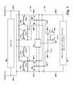
- FIG. 2is a schematic diagram illustrating a portion of a memory array 230 including sensing circuitry in accordance with a number of embodiments of the present disclosure.
- FIG. 2illustrates one sensing component 250 which can be one of a number of sensing components corresponding to sensing circuitry 150 shown in FIG. 1 .
- the memory array 230is a DRAM array of 1T1C (one transistor one capacitor) memory cells in which a transistor serves as the access device and a capacitor serves as the storage element; although other embodiments of configurations can be used (e.g., 2T2C with two transistors and two capacitors per memory cell).
- a first memory cellcomprises transistor 202 - 1 and capacitor 203 - 1
- a second memory cellcomprises transistor 202 - 2 and capacitor 203 - 2 , etc.
- the cells of the memory array 230can be arranged in rows coupled by access lines 204 -X (Row X), 204 -Y (Row Y), etc., and columns coupled by pairs of complementary digit lines (e.g., digit lines 205 - 1 labelled DIGIT(n) and 205 - 2 labelled DIGIT(n)_ in FIG. 2 ). Although only one pair of complementary digit lines are shown in FIG. 2 , embodiments of the present disclosure are not so limited, and an array of memory cells can include additional columns of memory cells and complementary digit lines (e.g., 4,096, 8,192, 16,384, etc.).
- Memory cellscan be coupled to different digit lines and word lines. For instance, in this example, a first source/drain region of transistor 202 - 1 is coupled to digit line 205 - 1 , a second source/drain region of transistor 202 - 1 is coupled to capacitor 203 - 1 , and a gate of transistor 202 - 1 is coupled to word line 204 -Y.
- a first source/drain region of transistor 202 - 2is coupled to digit line 205 - 2
- a second source/drain region of transistor 202 - 2is coupled to capacitor 203 - 2
- a gate of transistor 202 - 2is coupled to word line 204 -X.
- a cell plateas shown in FIG. 2 , can be coupled to each of capacitors 203 - 1 and 203 - 2 .
- the cell platecan be a common node to which a reference voltage (e.g., ground) can be applied in various memory array configurations.
- the digit lines 205 - 1 and 205 - 2 of memory array 230are coupled to sensing component 250 in accordance with a number of embodiments of the present disclosure.
- the sensing component 250comprises a sense amplifier 206 and a compute component 231 corresponding to a respective column of memory cells (e.g., coupled to a respective pair of complementary digit lines).
- the sense amplifier 206is coupled to the pair of complementary digit lines 205 - 1 and 205 - 2 .
- the sense amplifier 206is coupled to the compute component 231 .
- the compute component 231includes selection logic circuitry 213 and compute component storage locations/shift logic circuitry 221 , which are coupled via accumulator signal lines 209 - 1 and 209 - 2 .
- selection logiccan include logical operation selection logic, for example, logic selectively operated to perform selected logical operations (e.g., Boolean logical operations).
- the selection logic circuitry 213can be coupled to the pair of complementary digit lines 205 - 1 and 205 - 2 and configured to perform logical operations on data stored in array 230 .
- compute component 231can be formed on pitch with the digit lines of the array.
- the compute component 231may conform to a same pitch as adjacent digit lines of the array 230 such that the compute component 231 and the sense amplifier 206 obey a particular sense line pitch constraint (e.g., 4 F, 6 F, etc., where “F” is a feature size).
- the sense amplifier 206can be operated to determine a data value (e.g., logic state) stored in a selected memory cell.
- the sense amplifier 206can comprise a cross coupled latch 215 (e.g., gates of a pair of transistors, such as n-channel transistors 227 - 1 and 227 - 2 are cross coupled with the gates of another pair of transistors, such as p-channel transistors 229 - 1 and 229 - 2 ), which can be referred to herein as a primary latch.
- a cross coupled latch 215e.g., gates of a pair of transistors, such as n-channel transistors 227 - 1 and 227 - 2 are cross coupled with the gates of another pair of transistors, such as p-channel transistors 229 - 1 and 229 - 2
- a primary latche.g., embodiments are not limited to this example.
- ACTis driven high to a rail voltage such as VDD and RNL* is driven low to a rail voltage such as ground
- the sense amplifier 206can be activated (e.g., ACT is driven high to a rail voltage such as VDD and RNL* is driven low to a rail voltage such as ground) to enable (e.g., fire) the sense amplifier 206 .
- the digit line 205 - 1 or 205 - 2 having the lower voltagewill turn on one of the transistors 229 - 1 or 229 - 2 to a greater extent than the other of transistors 229 - 1 or 229 - 2 , thereby driving high the digit line 205 - 1 or 205 - 2 having the higher voltage to a greater extent than the other digit line 205 - 1 or 205 - 2 is driven high.
- the digit line 205 - 1 or 205 - 2 having the higher voltagewill turn on one of the transistors 227 - 1 or 227 - 2 to a greater extent than the other of the transistors 227 - 1 or 227 - 2 , thereby driving low the digit line 205 - 1 or 205 - 2 having the lower voltage to a greater extent than the other digit line 205 - 1 or 205 - 2 is driven low.
- the digit line 205 - 1 or 205 - 2 having the slightly greater voltageis driven to the voltage of the supply voltage VDD through a source transistor, and the other digit line 205 - 1 or 205 - 2 is driven to the voltage of the reference voltage (e.g., ground) through a sink transistor. Therefore, the cross coupled transistors 227 - 1 and 227 - 2 and transistors 229 - 1 and 229 - 2 serve as a sense amplifier pair, which amplify the differential voltage on the digit lines 205 - 1 and 205 - 2 and operate to store (e.g., latch) a data value sensed from the selected memory cell.
- Embodimentsare not limited to the sensing component configuration illustrated in FIG. 2 .
- the sense amplifier 206can be a current-mode sense amplifier and/or a single-ended sense amplifier (e.g., sense amplifier coupled to one digit line).
- embodiments of the present disclosureare not limited to a folded digit line architecture such as that shown in FIG. 2 .
- the sense amplifier 206includes equilibration circuitry 214 , which can be configured to equilibrate the digit lines 205 - 1 and 205 - 2 .
- the equilibration circuitry 214comprises a transistor 224 coupled between digit lines 205 - 1 and 205 - 2 .
- the equilibration circuitry 214also comprises transistors 225 - 1 and 225 - 2 each having a first source/drain region coupled to an equilibration voltage (e.g., VDD/2), where VDD is a supply voltage associated with the array.
- VDD/2equilibration voltage
- a second source/drain region of transistor 225 - 1is coupled to digit line 205 - 1
- a second source/drain region of transistor 225 - 2is coupled to digit line 205 - 2
- Gates of transistors 224 , 225 - 1 , and 225 - 2can be coupled together and to an equilibration (EQ) control signal line 226 .
- EQequilibration
- activating EQenables the transistors 224 , 225 - 1 , and 225 - 2 , which effectively shorts digit lines 205 - 1 and 205 - 2 together and to the equilibration voltage (e.g., VDD/2).
- sense amplifier 206comprising the equilibration circuitry 214
- embodimentsare not so limited, and the equilibration circuitry 214 may be implemented discretely from the sense amplifier 206 , implemented in a different configuration than that shown in FIG. 2 , or not implemented at all.
- FIG. 3is a schematic diagram illustrating a portion of a memory array including compute component 331 comprising selection logic circuitry 313 and compute component storage location(s)/shift logic circuitry 321 in accordance with a number of embodiments of the present disclosure.
- memory cellssuch as those described in FIG. 2 , are coupled to pairs of complementary sense lines (e.g., digit lines 305 - 1 and 305 - 2 ).
- the selection logic circuitry 313 illustrated in FIG. 3is an example of logic circuitry that can be used to perform operations in accordance with embodiments of the present disclosure.
- the selection logic circuitry 313comprises four pairs of transistors 373 - 1 / 373 - 2 , 375 - 1 / 375 - 2 , 377 - 1 / 377 - 2 , and 379 - 1 / 379 - 2 coupled to the pair of complementary digit lines 305 - 1 and 305 - 2 via their source/drain regions.
- the gates of the transistor pairs 373 - 1 / 373 - 2 , 375 - 1 / 375 - 2 , 377 - 1 / 377 - 2 , and 379 - 1 / 379 - 2are configured to receive respective selection logic signals BOOL 0 , BOOL 1 , BOOL 2 , and BOOL 3 .
- the selection logic signalscan be selectively operated to perform logical operations using the sensing circuitry as described in more detail with respect to FIGS. 7A-7B .
- a first source/drain region of transistor 373 - 1is coupled to sense line 305 - 1 and a first source/drain region of transistor 373 - 2 is coupled to sense line 305 - 2
- a first source/drain region of transistor 375 - 1is coupled to sense line 305 - 2 and a first source/drain region of transistor 375 - 2 is coupled to sense line 305 - 1
- a first source/drain region of transistor 377 - 1is coupled to sense line 305 - 1 and a first source/drain region of transistor 377 - 2 is coupled to sense line 305 - 2
- a first source/drain region of transistor 379 - 1is coupled to sense line 305 - 2 and a first source/drain region of transistor 379 - 2 is coupled to sense line 305 - 1 .
- the selection logic circuitry 313can be coupled to the compute component 331 and/or compute component storage location(s)/shift logical circuitry 321 via the first storage location lines 309 - 1 and 309 - 2 and/or the second storage location lines 310 - 1 and 310 - 2 .
- the compute component 331can be analogous to the compute component 631 illustrated in FIG. 6 and discussed in more detail herein.
- the first storage location lines 309 - 1 and 309 - 2can be coupled to source drain regions of transistors other than the four pairs of transistors previously described.
- the second storage location line 310 - 1can couple node 364 of the compute component 331 (shown in detail as the compute component 631 in FIG.
- the second storage location line 310 - 2can couple node 366 of the compute component 331 (shown in detail as the compute component 631 in FIG. 6 ) to gates and source drain regions of transistors (e.g., transistor 308 - 2 ) other than the four pairs of transistors previously described.
- a source/drain region of each of the transistors 308 - 1 and 308 - 2can be coupled to a reference voltage (e.g., Vss).
- the two n-channel transistors 308 - 1 and 308 - 2may be operated to cause nodes 364 and 366 to be grounded when a logical mask value is low, thereby selectively disabling a logical operation for a respective sensing circuitry.
- a p-channel transistor 334is provided to reduce contention between nodes 364 and 366 as they are brought to ground, for example.
- an n-channel transistor 336may be provided to globally clear stored logical operation values simultaneously.
- first storage locatione.g., first storage location 633 illustrated in FIG. 6
- the original state of the first storage locationmay be held dynamically by capacitance when the SHIFT 1 control signal line (e.g., SHIFT 1 control signal line 681 illustrated in FIG. 6 ) and the SHIFT 2 control signal line (e.g., SHIFT 1 control signal line 682 illustrated in FIG. 6 ) are disabled. This may allow for a possible new state to be written from selection logic circuitry 313 , for example via first storage location signal lines 309 - 1 and 309 - 2 .
- the first storage location signal lines 309 - 1 and 309 - 2may not be driven from the selection logic circuitry 313 such that the original value of the first storage location 633 may be preserved when the SHIFT 1 control signal line 681 and the SHIFT 2 control signal line 682 are enabled as part of the logical operation. This may allow for a signal on nodes 364 and 366 to be held by dynamic capacitance, for example.
- the selection logic circuitry 313 and/or the compute component 331can include logic circuitry storage location 332 .
- Logic circuitry storage location 332may be configured to actively store (e.g., latch) a data value received thereto.
- logic circuitry storage location 332can comprise a latch that can be configured to receive a data value from the first storage location 633 , and may actively store the data value.
- logic circuitry storage location 332can store an indication of whether a logical operation is to be selectively performed between an operand stored in the sensing circuitry and an operand stored in the sense amplifier.
- FIG. 4is another schematic diagram illustrating a portion of a memory array including compute component 431 comprising selection logic circuitry 413 and compute component storage location(s)/shift logic circuitry 421 in accordance with a number of embodiments of the present disclosure.
- memory cellssuch as those described in FIG. 2 , are coupled to pairs of complementary sense lines (e.g., digit lines 405 - 1 and 405 - 2 ).
- the selection logic circuitry 413 illustrated in FIG. 4is an example of logic circuitry that can be used to perform operations in accordance with embodiments of the present disclosure.
- the selection logic circuitry 413comprises four pairs of transistors 473 - 1 / 473 - 2 , 475 - 1 / 475 - 2 , 477 - 1 / 477 - 2 , and 479 - 1 / 479 - 2 coupled to the pair of complementary digit lines 405 - 1 and 405 - 2 via their source/drain regions.
- the gates of the transistor pairs 473 - 1 / 473 - 2 , 475 - 1 / 475 - 2 , 477 - 1 / 477 - 2 , and 479 - 1 / 479 - 2are configured to receive respective selection logic signals BOOL 0 , BOOL 1 , BOOL 2 , and BOOL 3 .
- the selection logic signalscan be selectively operated to perform logical operations using the sensing circuitry as described in more detail with respect to FIGS. 7A-7B .
- a first source/drain region of transistor 473 - 1is coupled to sense line 405 - 1 and a first source/drain region of transistor 473 - 2 is coupled to sense line 405 - 2
- a first source/drain region of transistor 475 - 1is coupled to sense line 405 - 2 and a first source/drain region of transistor 475 - 2 is coupled to sense line 405 - 1
- a first source/drain region of transistor 477 - 1is coupled to sense line 405 - 1 and a first source/drain region of transistor 477 - 2 is coupled to sense line 405 - 2
- a first source/drain region of transistor 479 - 1is coupled to sense line 405 - 2 and a first source/drain region of transistor 479 - 2 is coupled to sense line 405 - 1 .
- the selection logic circuitry 413can be coupled to the compute component 431 via the first storage location lines 409 - 1 and 409 - 2 and/or the second storage location lines 410 - 1 and 410 - 2 .
- the compute component 431can be analogous to the compute component 631 illustrated in FIG. 6 and discussed in more detail herein.
- the first storage location lines 409 - 1 and 409 - 2can be coupled to source drain regions of transistors other than the four pairs of transistors previously described.
- the second storage location line 410 - 1can couple node 464 of the compute component 431 to gates and source drain regions of transistors (e.g., 408 - 1 ) other than the four pairs of transistors previously described.
- the second storage location line 410 - 2can couple node 466 of the compute component 431 to gates and source drain regions of transistors (e.g., transistor 408 - 2 ) other than the four pairs of transistors previously described.
- a terminal of each of the transistors 408 - 1 and 408 - 2can be coupled to a reference voltage (e.g., Vss).
- space limitations and/or layout difficultiesmay arise due to insufficient routing paths between the selection logic circuitry 413 and compute component 431 .
- these limitations and/or difficultiesmay be alleviated by adding an active area to the selection logic circuitry 413 .
- space limitations and/or layout difficulties associated with selectively performing logical operationsmay be alleviated by providing the selection logic circuitry 413 with a mask storage location 441 , as illustrated in FIG. 4 .
- a p-channel transistor 434is provided to reduce contention between nodes 464 and 466 as they are discharged to ground.
- n-channel transistor 436may be provided to globally clear stored logical operation values simultaneously.
- the selection logic circuitry 413may include a logic circuitry storage location 432 , and a mask storage location 441 .
- the mask storage location 441may be coupled to the p-channel transistor 434 at a source drain region of the p-channel transistor 434 .
- the configuration illustrated in FIG. 4may allow for data values to be masked (e.g., data values with which logical operations are to be selectively performed) to be transferred between the logic selection circuitry 413 and the compute component 431 using first storage location lines 409 - 1 and 409 - 2 and/or the pair of complimentary digit lines 405 - 1 and 405 - 2 .
- first storage location lines 409 - 1 and 409 - 2 and/or the pair of complimentary digit lines 405 - 1 and 405 - 2to transfer data values to be masked between the logic selection circuitry 413 and the compute component 431 , operations may be performed in less time compared to some approaches.
- FIG. 5is yet another schematic diagram illustrating a portion of a memory array including compute component 531 comprising selection logic circuitry 513 and compute component storage location(s)/shift logic circuitry 521 in accordance with a number of embodiments of the present disclosure.
- memory cellssuch as those described in FIG. 2 , are coupled to pairs of complementary sense lines (e.g., digit lines 505 - 1 and 505 - 2 ).
- the selection logic circuitry 513 illustrated in FIG. 5is an example of logic circuitry that can be used to perform operations in accordance with embodiments of the present disclosure.
- the selection logic circuitry 513comprises four pairs of transistors 573 - 1 / 573 - 2 , 575 - 1 / 575 - 2 , 577 - 1 / 577 - 2 , and 579 - 1 / 579 - 2 coupled to the pair of complementary digit lines 505 - 1 and 505 - 2 via their source/drain regions.
- the gates of the transistor pairs 573 - 1 / 573 - 2 , 575 - 1 / 575 - 2 , 577 - 1 / 577 - 2 , and 579 - 1 / 579 - 2are configured to receive respective selection logic signals BOOL 0 , BOOL 1 , BOOL 2 , and BOOL 3 .
- the selection logic signalscan be selectively operated to perform logical operations using the sensing circuitry as described in more detail with respect to FIGS. 7A-7B .
- a first source/drain region of transistor 573 - 1is coupled to sense line 505 - 1 and a first source/drain region of transistor 573 - 2 is coupled to sense line 505 - 2
- a first source/drain region of transistor 575 - 1is coupled to sense line 505 - 2 and a first source/drain region of transistor 575 - 2 is coupled to sense line 505 - 1
- a first source/drain region of transistor 577 - 1is coupled to sense line 505 - 1 and a first source/drain region of transistor 577 - 2 is coupled to sense line 505 - 2
- a first source/drain region of transistor 579 - 1is coupled to sense line 505 - 2 and a first source/drain region of transistor 579 - 2 is coupled to sense line 505 - 1 .
- the selection logic circuitry 513can be coupled to the compute component 531 via the first storage location lines 509 - 1 and 509 - 2 and the second storage location lines 510 - 1 and 510 - 2 .
- the compute component 531can be analogous to the compute component 631 illustrated in FIG. 6 and discussed in more detail herein.
- the first storage location lines 509 - 1 and 509 - 2can be coupled to source drain regions of transistors other than the four pairs of transistors previously described.
- the second storage location line 510 - 1can couple node 564 of the compute component 531 to gates and source drain regions of transistors (e.g., 508 - 1 ) other than the four pairs of transistors previously described.
- the second storage location line 510 - 2can couple node 566 of the compute component 531 to gates and source drain regions of transistors (e.g., transistor 508 - 2 ) other than the four pairs of transistors previously described.
- a terminal of each of the transistors 508 - 1 and 508 - 2can be coupled to a reference voltage (e.g., Vss).
- the selection logic circuitry 513 and/or the compute component 531can include logic circuitry storage location 532 .
- Logic circuitry storage location 532may be configured to actively store (e.g., latch) a data value received thereto.
- logic circuitry storage location 532can comprise a latch that can be configured to receive a data value from the first storage location 633 , and may actively store the data value.
- logic circuitry storage location 532can store an indication of whether a logical operation is to be selectively performed between an operand stored in the sensing circuitry and an operand stored in the sense amplifier.
- a column repair (ColRep) signal linecan be connected to node 564 and/or node 566 .
- a signalmay be provided on ColRep signal line to provide a column repair signal that may be used to provide a repair capability by blocking signals carried on the first storage location lines 509 - 1 and 509 - 2 and/or the second storage location lines 510 - 1 and 510 - 2 .
- a signalmay be provided on ColRep signal line to block signals carried on the first storage location lines 509 - 1 and 509 - 2 and/or the second storage location lines 510 - 1 and 510 - 2 to remove (e.g., short) sense amplifier 506 and/or compute component 531 such that sense amplifier 506 and/or compute component 531 are effectively removed from a particular sensing component.
- removee.g., short
- ColRep signal lineis connected to physically adjacent storage locations (e.g., storage locations 633 and 635 illustrated in FIG. 6 ) that are connected to a same main input/output (MIO) signal line (not shown).
- the MIO signal linemay be connected to the physically adjacent storage locations via a multiplexer that may be configured to multiplex column select signals to the MIO.
- signalsmay be provided to the ColRep signal line during shifting operations, but may not be utilized while logical operations are performed.
- the lack of signals on the ColRep signal line during performance of logical operationsallows for the ColRep signal line to be used when a column repair signal is not active on ColRep signal line to facilitate selective performance of logical operations.
- an indication of whether a logical operation is to be selectively performedmay be sent via ColRep signal line when shifting signals are not present on ColRep signal line.
- the indicationcan be an indication that a logical operation is not to be performed between an operand stored in the sensing circuitry (e.g., an operand stored in a storage location associated with the compute component 531 ) and an operand stored in the sense amplifier 506 .
- ColRep signalmay be multiplexed to a plurality of compute components 531 such that a signal on ColRep signal line is sent to a plurality of storage locations associated with a plurality of compute components 531 .
- ColRep signalmay be multiplexed to eight compute components 531 .
- ColRep signalcan provide the indication of whether a logical operation is to be selectively performed to a portion of a row of memory array (e.g., about 2K bits per ColRep signal).
- FIG. 6is a schematic diagram illustrating sensing circuitry in accordance with a number of embodiments of the present disclosure.
- FIG. 6shows a number of sense amplifiers 606 coupled to respective pairs of complementary sense lines 605 - 1 and 605 - 2 , and a corresponding number of compute components 631 coupled to the sense amplifiers 606 .
- the sense amplifiers 606 and compute components 631 shown in FIG. 6can correspond to sensing circuitry 150 shown in FIG. 1 , for example.
- the sensing circuitry shown in FIG. 6includes selection logic circuitry 613 , which can be operated as described further herein.
- the selection logic circuitry 613 shown in FIG. 6can correspond to selection logic circuitry 213 shown in FIG. 2 or selection logic circuitry 313 / 413 / 513 shown in FIGS. 3, 4, and 5 , for example.
- memory cellssuch as those described in FIG. 2 are coupled to the pairs of complementary sense lines 605 - 1 and 605 - 2
- the cells of the memory arraycan be arranged in rows coupled by word lines and columns coupled by pairs of complementary sense lines DIGIT(n ⁇ 1)/DIGIT(n ⁇ 1)_, DIGIT(n)/DIGIT(n)_, DIGIT(n+1)/DIGIT(n+1)_, etc.
- the individual sense lines corresponding to each pair of complementary sense linescan also be referred to as data lines. Although only three pairs of complementary sense lines (e.g., three columns) are shown in FIG. 6 , embodiments of the present disclosure are not so limited.
- the sensing componentscan comprise a sense amplifier 606 and a compute component 631 , which comprises selection logic circuitry 613 and compute component storage locations/shift logic circuitry 621 corresponding to respective columns of memory cells (e.g., coupled to respective pairs of complementary sense lines).
- the compute component 631may include storage location 632 . Although storage location 632 is illustrated as part of the selection logic circuitry 613 , embodiments are not so limited, and storage location 632 can be located at other locations within the compute component 631 .
- Storage location 632may be a cross-coupled latch, D latch, or other circuit configuration capable of storing an operand (e.g., a data value).
- the sense amplifier 606can comprise, for example, a cross coupled latch, which can be referred to herein as a primary latch.
- the sense amplifiers 606can be configured, for example, as described with respect to FIG. 2 .
- a data value present on the pair of complementary sense lines 605 - 1 and 605 - 2can be loaded into the corresponding compute component 631 .
- the compute component storage locations/shift logic circuitry 621can include a pair of compute component storage locations (e.g., first compute component storage location 633 and second compute component storage location 635 ) associated with each compute component 631 .
- the first compute component storage location 633 and the second compute component storage location 635can comprise stages of a shift register.
- the compute component storage locationscan serve as respective stages of a shift register capable of shifting data values (e.g., right and/or left) and/or performing rotation operations (e.g., rotate right and/or rotate left).
- the data valuescan be loaded into the compute component storage locations of a corresponding compute component 631 by overwriting of the data values currently stored in the compute component storage locations of the corresponding compute components 631 with a data value stored in the corresponding sense amplifier 606 .
- the data value on the pair of complementary sense lines 605 - 1 and 605 - 2can be the data value stored in the sense amplifier 606 when the sense amplifier is enabled (e.g., fired).
- a first latching/activation signal ACTis applied to the two p-channel transistors 651 - 1 and 651 - 2 of the first compute component storage location 633 and a second latching/activation signal RNL* is applied to the two n-channel transistors 653 - 1 and 653 - 2 of the second compute component storage location 635 .
- a second ACT signalis applied to the two p-channel transistors 655 - 1 and 655 - 2 of the second compute component storage location 635 and a second RNL* signal is applied to the two n-channel transistors 657 - 1 and 657 - 2 of the second compute component storage location 635 .
- the respective ACT and RNL* signalscontrol operation of the first compute component storage location 633 and the second compute component storage location 635 .
- power to the first compute component storage location 633 and the second compute component storage location 635can be provided via a pairs of complementary enable signals (e.g., EnA/EnC, and EnB/EnD, respectively).
- first compute component storage location 633is coupled to EnA at power node 691
- second compute component storage locationis coupled to EnB at power node 693
- First compute component storage location 633is coupled to EnC at power node 695
- second compute component storage location 635is coupled to EnD at power node 697 .
- a power supply transistorcan be coupled to each of the enable signals EnA, EnB, EnC, and EnD and to a reference voltage (e.g., Vss).
- signal input lines 637 and 639are coupled to respective accumulator signal lines 609 - 1 and 609 - 2 at ST 2 and SF 1 , respectively.
- signal input lines 637 and 639are coupled to respective storage location lines 610 - 1 and 610 - 2 at SF 2 and ST 1 , respectively.
- the voltage on one of the signal input lines 637 or 639will be slightly greater than the voltage on one of the other signal input lines 637 or 639 .
- the signal input line 637 or 639 having the lower voltagewill turn on one of the p-channel transistors 651 - 1 or 651 - 2 in the first secondary latch (e.g., first compute component storage location 633 ) to a greater extent than the other of p-channel transistors 651 - 1 or 651 - 2 , thereby driving higher the first compute component storage location signal lines 609 - 1 or 609 - 2 having a higher voltage to a greater extent than the other first compute component storage location signal line 609 - 1 or 609 - 2 is driven high.
- the first secondary latche.g., first compute component storage location 633
- the signal input line 637 or 639 having the lower voltagewill turn on one of the p-channel transistors 655 - 1 or 655 - 2 in the second secondary latch (e.g., second compute component storage location 635 ) to a greater extent than the other of transistors 655 - 1 or 655 - 2 , thereby driving higher the first compute component storage location signal line 609 - 1 or 609 - 2 having a higher voltage to a greater extent than the other first compute component storage location signal line 609 - 1 or 609 - 2 is driven high.
- the second secondary latche.g., second compute component storage location 635
- the signal input line 637 or 639 having the higher voltagewill turn on one of the n-channel transistors 653 - 1 or 653 - 2 in the first secondary latch to a greater extent than the other of the transistors 653 - 1 or 653 - 2 , thereby driving lower the first s compute component storage location signal line 609 - 1 or 609 - 2 having the lower voltage to a greater extent than the other first compute component storage location signal line 609 - 1 or 609 - 2 is driven low.
- the signal input line 637 or 639 having the higher voltagewill turn on one of the n-channel transistors 657 - 1 or 657 - 2 in the second secondary latch to a greater extent than the other of the transistors 657 - 1 or 657 - 2 , thereby driving lower the first compute component storage location signal line 609 - 1 or 609 - 2 having the lower voltage to a greater extent than the other first compute component storage location signal line 609 - 1 or 609 - 2 is driven low.
- a “high side” or “high node,” and a “low side” or “low node” of the first compute component storage location 633 and/or the second compute component storage location 635refer to a side of the storage location on which a differential voltage is comparatively high or comparatively low, respectively.
- the first and second sampling transistors 683 - 1 and 683 - 2can be controlled by a shift signal.
- an input of first compute component storage location 633can be coupled to the first and second sampling transistors 683 - 1 and 683 - 2
- an input of second compute component storage location 635can be coupled to the third and fourth sampling transistors 685 - 1 and 685 - 2 .
- the first and second sampling transistors 683 - 1 and 683 - 2 and/or the third and fourth sampling transistors 685 - 1 and 685 - 2can control storing and/or shifting of data values between the first compute component storage location 633 and the second compute component storage location 635 .
- the first and second sampling transistors 683 - 1 and 683 - 2 and/or the third and fourth sampling transistors 685 - 1 and 685 - 2may be enabled or disabled in response to a control signal.
- the first and second sampling transistors 683 - 1 and 683 - 2may be enabled or disabled in response to a SHIFT 1 control signal line 681
- the third and fourth sampling transistors 685 - 1 and 685 - 2may be enabled or disabled in response to a SHIFT 2 control signal line 682 , as described in more detail, herein.
- the SHIFT 1 control signal line 681can carry a shift right phase 2 , left phase 1 control signal
- the SHIFT 2 control signal line 682can carry a shift right phase 1 , left phase 2 control signal.
- transferring a data value from the first compute component storage location 633 to the second compute component storage location 635is carried out by controlling which of power nodes 691 , 693 , 695 , and 697 are providing a voltage to each of the first compute component storage location 633 and the second compute component storage location 635 over time.
- transferring a data value from the first compute component storage location 633 to the second compute component storage location 635can include applying a voltage to first compute component storage location at power nodes 691 and/or 695 when a voltage is not applied to second storage location 635 at power nodes 693 and/or 697 , and synchronously switching the applied voltages such that the voltage is no longer applied to first compute component storage location 633 at power nodes 691 and/or 695 and the voltage is instead applied to second compute component storage location 635 at power nodes 693 and/or 697 .
- the first and second sampling transistors 683 - 1 and 683 - 2 and/or the third and fourth sampling transistors 685 - 1 and 685 - 2may be enabled when the voltage is switched from power node 691 and/or 695 to power node 693 and/or 697 , or vice versa.
- the first compute component storage location 633 and/or the second compute component storage location 635are equalized when their respective power node 691 / 695 or 693 / 697 is not receiving a voltage signal.
- first compute component storage location 633is the destination of a logical operation
- the original state of the first compute component storage locationmay be held dynamically by capacitance when the SHIFT 1 control signal line 681 and the SHIFT 2 control signal line 682 are disabled. This may allow for a possible new data value to be written from selection logic circuitry 613 , for example via first compute component storage location signal lines 609 - 1 and 609 - 2 .
- the first compute component storage location 633 and the second compute component storage location 635can each operate in several stages.
- a first stage of operationcan include an equalization stage in preparation for receiving a differential input signal.
- the differential input signalcan be received from signal input lines 637 and/or 639 .
- a second stage of operationcan include a sample stage in which the differential input signal is received by the first compute component storage location 633 and/or the second compute component storage location 635 .
- a data valuecan be received and/or stored by the first compute component storage location 633 and/or the second compute component storage location 635 based on the differential input signal on compute component signal lines 609 - 1 and 609 - 2 .
- a third stage of operationcan include an “amplify and latch” stage where the received differential input signal is amplified and latched by the first compute component storage location 633 and/or the second compute component storage location 635 .
- the third stagecan be facilitated by cross coupled transistors 653 - 1 and 653 - 2 , and 651 - 1 and 651 - 2 associated with the first compute component storage location 633 , which can amplify the differential voltage on signal input lines 637 and 639 and operate to latch a data value received at the first compute component storage location 633 .
- coupled transistors 657 - 1 and 657 - 2 , and 655 - 1 and 655 - 2 associated with the second compute component storage location 635can amplify the differential voltage on signal input lines 637 and 639 and operate to latch a data value received at the second compute component storage location 635 .
- the third stagecan include driving the data value from one compute component storage location to a next compute component storage location (e.g., driving the data value from the first compute component storage location 633 to the second compute component storage location 635 ).
- each column of memory cellscan be coupled to a column decode line that can be activated to transfer, via a local I/O line, data values from corresponding sense amplifiers 606 and/or compute components 631 to a control component external to the array such as an external processing resource (e.g., host processor and/or other functional unit circuitry).
- the column decode linecan be coupled to a column decoder.
- dataneed not be transferred via such I/O lines to perform shift operations in accordance with embodiments of the present disclosure.
- sense amplifiers 606 and compute components 631may be operated to perform logical operations without transferring data to a control component external to the array, for instance.
- transferring datawhich may also be referred to as moving data or shifting data is an inclusive term that can include, for example, copying data from a source location to a destination location and/or moving data from a source location to a destination location without necessarily maintaining a copy of the data at the source location.
- Embodiments of the present disclosureare not limited to the logical operation performance capability described in association with the compute components 631 .
- a number of embodimentscan include circuitry in addition to and/or instead of the circuitry described in association with the compute component 631 .
- FIG. 7Ais a logic table illustrating selectable logical operation results implemented by sensing circuitry in accordance with a number of embodiments of the present disclosure.
- FIG. 7Ashows a resultant data value that is initially stored in the first compute component storage location (e.g., first compute component storage location 633 shown in FIG. 6 ) after the sense amplifier (e.g., sense amplifier 606 shown in FIG. 6 is enabled (e.g., fired).
- Starting data valuese.g., operands
- a first operand(e.g., “A”) is a data value that can be read from a memory array and stored in the first compute component storage location and a second operand (e.g., “B”), is a data value that can be read from the memory array by the sense amplifier.
- Aa data value that can be read from a memory array and stored in the first compute component storage location
- Ba second operand
- a number of embodimentscan include reading operand A into a sense amplifier (e.g., 606 ), transferring operand A from the sense amplifier to a first compute component storage location (e.g., 633 ), transferring operand A from the first compute component storage location to a second compute component storage location (e.g., 632 ), and then operating the sensing circuitry to perform a selected logical operation between operand A and an operand B by activating the appropriate corresponding selection logic signals (e.g., BOOL 0 , BOOL 1 , BOOL 2 , and BOOL 3 ) at the appropriate time (e.g., either before or after enabling the sense amplifier to sense operand B from a selected memory cell).
- a selected logical operation between the first data value and a second data valuecan be performed based on the appropriate control signals corresponding to the selected logical operation being provided to the logic circuitry (e.g., selection logic circuitry 213 shown in FIG. 2 , selections logic circuitry 313 shown in FIG. 3 , selection logic circuitry 413 shown in FIG. 4 , etc.).
- the logic circuitrye.g., selection logic circuitry 213 shown in FIG. 2 , selections logic circuitry 313 shown in FIG. 3 , selection logic circuitry 413 shown in FIG. 4 , etc.
- “RESULT IN FIRST STORAGE LOCATION—(AFTER SENSE AMP FIRE)”indicates that the control signals corresponding to the selected logical operation are enabled after the sense amplifier is enabled, such that the result of the selected logical operation is initially stored in the first compute component storage location.
- FIG. 7A“RESULT IN FIRST STORAGE LOCATION—(AFTER SENSE AMP FIRE)” indicates that the control signals corresponding to the
- “RESULT IN SENSE AMP—(BEFORE SENSE AMP FIRE)”indicates that the control signals corresponding to the selected logical operation are enabled before the sense amplifier is enabled, such that the result of the selected logical operation is initially stored in the sense amplifier.
- the logic table illustrated in FIG. 7Ashows the starting data value stored in the first compute component storage location in column A at 770 , and shows the starting data value stored in the sense amplifier in column B at 772 .
- the various combinations of the control signals BOOL 0 , BOOL 1 , BOOL 2 , and BOOL 3are shown in FIG. 7A in the column headings in row 774 .
- the column heading of “0110”indicates that the results in that column correspond to control signal BOOL 3 being a “0,” control signal BOOL 2 being a “1,” control signal BOOL 1 being a “1,” and control signal BOOL 0 being a “0.”
- results for each combination of starting data values in the first compute component storage location (“A”) and in the sense amplifier (“B”)can be summarized by the logical operation shown for each column in row 776 .
- the result for the values of BOOL 3 , BOOL 2 , BOOL 1 , and BOOL 0 of “0000”are summarized as “A” since the result (initially stored in the first storage location after the sense amplifier fires) is the same as the starting value in the first compute component storage location.
- Other columns of resultsare similarly annotated in row 776 , where “A*B” intends A AND B, “A+B” intends A OR B, and “AXB” intends A XOR B.
- a bar over a data value or a logical operationindicates an inverted value of the quantity shown under the bar.
- AXB barintends NOT A XOR B, which is also A XNOR B.
- FIG. 7Bis another logic table illustrating selectable logical operation results implemented by sensing circuitry in accordance with a number of embodiments of the present disclosure.
- FIG. 7Bshows a resultant data value that is initially stored in the sense amplifier (e.g., sense amplifier 606 shown in FIG. 6 ) after the sense amplifier is enabled corresponding to the various combinations of control signals BOOL 3 , BOOL 2 , BOOL 1 , and BOOL 0 .
- the logic table illustratedis arranged similar to that described with respect to FIG. 7A , with the starting data value stored in the first compute component storage location shown in column A at 770 , and the starting data value stored in the sense amplifier shown in column B at 772 .
- control signals BOOL 0 , BOOL 1 , BOOL 2 , and BOOL 3is shown in FIG. 7B in the column headings shown in row 774 , and the logical operation represented by each respective column of results shown in the column subheading at row 776 .
- the logical operations summarized in the logic table illustrated in FIG. 7Awhich reflects a logical operation result initially stored in the first compute component storage location after the sense amplifier is enabled
- the logical operations summarized in the logic table illustrated in FIG. 7Breflects a logical operation result initially stored in the sense amplifier 606 after the sense amplifier is enabled (e.g., with the control signals corresponding to the selected logical operation being provided to the selection logic circuitry 213 , 313 , 413 , 513 , 613 before the sense amplifier is enabled).
- the logical operations summarized in the logic table illustrated in FIG. 7Binclude several different logical operations from those shown in the logic table illustrated in FIG.
- FIG. 8is a table illustrating selective performance of a logical operation in accordance with a number of embodiments of the present disclosure.
- a 873represents data stored in a storage location (e.g., storage location 633 illustrated in FIG. 6 ) associated with the compute component (e.g., compute component 631 illustrated in FIG. 6 )
- Vm 875represents a row of a memory array that contains an indication of whether a logical operation is to be selectively performed
- Rn 877represents data stored in a row of a memory array following a logical operation
- Rn AFTER MASK 879represents data stored in a row of a memory array following a selectively performed logical operation.
- data stored in Vm 875can be transferred to one or more storage locations represented by A 873 . Subsequently, the data now stored in the one or more storage locations represented by A 873 can be transferred to a different storage location (e.g., logic circuitry storage location 332 illustrated in FIG. 3 ). Once the data are transferred to the different storage location, a row of data from the memory array (e.g., ROW X illustrated in FIG. 2 ) can be transferred to the one or more storage locations represented by A 873 . Data stored in Rn 877 can then be transferred to one or more sense amplifiers (e.g., sense amplifier 206 illustrated in FIG.
- data from A 873can be selectively transferred to one or more sense amplifiers based on the data stored in Vm 875 .
- a result of a logical operation associated with the foregoing stepsmay then be stored in Rn 877 concurrently with selectively transferring the data from A 873 to the one or more sense amplifiers.
- FIG. 9is a timing diagram for performing a logical operation in accordance with a number of embodiments of the present disclosure.
- the example described in FIG. 9includes a logical AND operation performed between an operand A and an operand B using the sensing circuitry described in FIGS. 3-6 .
- operand Ais initially stored in a memory cell coupled to a particular row and column of an array
- operand Bis initially stored in a memory cell coupled to a different particular row and to the same column.
- a data value(Previous Data) may be stored in (e.g., latched by) a first compute component storage location (e.g., 633 ). Data values may also be stored in the sense amplifier (e.g., 606 ) and/or one or more other compute component storage locations (e.g., 635 , 632 ).
- operand Ais sensed (e.g., by activating the row to which the cell storing operand A is coupled and enabling the sense amplifier 606 ) such that the sense amplifier stores the data value (e.g., Data A, which can be a logic 1 or 0) corresponding to operand A.
- the first compute component storage locatione.g., latch 633
- the logic selection signals BOOL 0 and BOOL 2are activated (with BOOL 1 and BOOL 3 remaining deactivated), which passes the voltages on the digit lines DIGIT(n)/DIGIT(n)_ (e.g., the data value corresponding to operand A and stored in sense amplifier 606 ) through one of transistor pairs (e.g., transistor pairs 373 - 1 / 373 - 2 and 377 - 1 / 377 - 2 ), depending on which of complementary nodes 361 - 1 and 361 - 2 is high (e.g., if node 361 - 1 is high and 361 - 2 is low, then transistor pair 367 - 1 / 367 - 2 will be enabled, and if node 361 - 1 is low and 361 - 2
- the data value stored in the latch 633can subsequently be transferred from latch 633 to compute component storage location 632 .
- the power nodes of compute component storage location 632are disabled (e.g., OpAct 361 - 1 goes low and OpActF 361 - 2 goes high) and at time t 6 Pass Acm goes high, which enables pass gates 308 - 1 and 308 - 2 such that the voltage on line 309 - 1 is transferred to node 363 - 1 and the voltage on line 309 - 2 is transferred to node 363 - 2 .
- the latch 632is enabled (e.g., OpAct 361 - 1 goes high and OpActF 361 - 2 goes low) to store the operand A data value (e.g., DATA A) in latch 432 , and at time t 8 , Pass Acm returns low, which isolates the input nodes of latch 632 from the input nodes of latch 633 .
- the row to which the cell storing operand B is coupledis activated and the sense amplifier 606 is enabled.
- latch 633is disabled (e.g., EnA goes low and EnC goes high). While the latch 633 is disabled, at time t 10 , the logic selection signal BOOL 0 is activated (with BOOL 1 , BOOL 2 , and BOOL 3 remaining deactivated), since in this example the operation (e.g., Op 1 ) to be performed is a logical AND operation (see the table in FIG. 7A ).
- BOOL 0 going highenables transistor pair 373 - 1 / 373 - 2 , which couples the digit lines DIGIT(n)/DIGIT(n)_ to respective signal lines 309 - 1 / 309 - 2 , depending on the state of complementary nodes 363 - 1 / 363 - 2 .
- transistor pair 367 - 1 / 367 - 2will be enabled such that DIGIT(n)/DIGIT(n)_ are coupled to respective signal lines 309 - 1 / 309 - 2
- transistor pair 367 - 1 / 367 - 2will be disabled such that DIGIT(n)/DIGIT(n)_ remain decoupled (e.g., isolated) from respective signal lines 309 - 1 / 309 - 2 .
- the latch 633is enabled (e.g., EnA goes high and EnC goes low) such that the data value corresponding to the complementary voltages on signal lines 309 - 1 / 309 - 2 is stored in latch 633 as the result of the logical operation (e.g., Operand A AND Operand B).
- the power nodes of compute component storage location 632are disabled (e.g., OpAct 361 - 1 goes low and OpActF 361 - 2 goes high) and at time t 13 Pass Acm goes high, which enables pass gates 308 - 1 and 308 - 2 such that the voltage on line 309 - 1 is transferred to node 363 - 1 and the voltage on line 309 - 2 is transferred to node 363 - 2 .
- the latch 632is enabled (e.g., OpAct 361 - 1 goes high and OpActF 361 - 2 goes low) to store the operand A data value (e.g., DATA A) in latch 632 , and at time t 15 , Pass Acm returns low, which isolates the input nodes of latch 632 from the input nodes of latch 633 .
- subsequent operationsmay be performed by repeating one or more of the steps described above in connection with FIG. 9 .
- FIG. 10illustrates an example configuration of sensing circuitry in accordance with a number of embodiments of the present disclosure.
- the sensing circuitrycan include a plurality of sense amplifiers 1006 - 1 , . . . , 1006 -N, and compute component 1031 .
- Each respective sense amplifiere.g., sense amplifier 1006 - 1
- a respective sense amplifier (e.g., 1006 - 1 ) and a respective compute component 1031 associated with the respective sense amplifier (e.g., 1006 - 1 )can be formed such that each respective sense amplifier (e.g., 1006 - 1 ) and each respective compute component 1031 is located between a respective pair of complementary sense lines 1005 - 1 / 1005 - 2 .
- the respective sense amplifiers 1006 - 1 , . . . , 1006 -N and compute components 1031can be formed on pitch with respective pairs of complementary sense lines (e.g., complementary sense lines 1005 - 1 and 1005 - 2 ) of an array of memory cells.
Landscapes
- Engineering & Computer Science (AREA)
- Computer Hardware Design (AREA)
- Microelectronics & Electronic Packaging (AREA)
- Physics & Mathematics (AREA)
- Computing Systems (AREA)
- General Engineering & Computer Science (AREA)
- Mathematical Physics (AREA)
- Dram (AREA)
- Semiconductor Memories (AREA)
Abstract
Description
Claims (22)
Priority Applications (2)
| Application Number | Priority Date | Filing Date | Title |
|---|---|---|---|
| US15/797,759US10388333B2 (en) | 2016-10-20 | 2017-10-30 | Apparatuses and methods to selectively perform logical operations |
| US16/537,775US10854247B2 (en) | 2016-10-20 | 2019-08-12 | Apparatuses and methods to selectively perform logical operations |
Applications Claiming Priority (2)
| Application Number | Priority Date | Filing Date | Title |
|---|---|---|---|
| US15/298,798US9805772B1 (en) | 2016-10-20 | 2016-10-20 | Apparatuses and methods to selectively perform logical operations |
| US15/797,759US10388333B2 (en) | 2016-10-20 | 2017-10-30 | Apparatuses and methods to selectively perform logical operations |
Related Parent Applications (1)
| Application Number | Title | Priority Date | Filing Date |
|---|---|---|---|
| US15/298,798ContinuationUS9805772B1 (en) | 2016-10-20 | 2016-10-20 | Apparatuses and methods to selectively perform logical operations |
Related Child Applications (1)
| Application Number | Title | Priority Date | Filing Date |
|---|---|---|---|
| US16/537,775ContinuationUS10854247B2 (en) | 2016-10-20 | 2019-08-12 | Apparatuses and methods to selectively perform logical operations |
Publications (2)
| Publication Number | Publication Date |
|---|---|
| US20180114551A1 US20180114551A1 (en) | 2018-04-26 |
| US10388333B2true US10388333B2 (en) | 2019-08-20 |
Family
ID=60142729
Family Applications (3)
| Application Number | Title | Priority Date | Filing Date |
|---|---|---|---|
| US15/298,798ActiveUS9805772B1 (en) | 2016-10-20 | 2016-10-20 | Apparatuses and methods to selectively perform logical operations |
| US15/797,759Active2037-03-05US10388333B2 (en) | 2016-10-20 | 2017-10-30 | Apparatuses and methods to selectively perform logical operations |
| US16/537,775ActiveUS10854247B2 (en) | 2016-10-20 | 2019-08-12 | Apparatuses and methods to selectively perform logical operations |
Family Applications Before (1)
| Application Number | Title | Priority Date | Filing Date |
|---|---|---|---|
| US15/298,798ActiveUS9805772B1 (en) | 2016-10-20 | 2016-10-20 | Apparatuses and methods to selectively perform logical operations |
Family Applications After (1)
| Application Number | Title | Priority Date | Filing Date |
|---|---|---|---|
| US16/537,775ActiveUS10854247B2 (en) | 2016-10-20 | 2019-08-12 | Apparatuses and methods to selectively perform logical operations |
Country Status (1)
| Country | Link |
|---|---|
| US (3) | US9805772B1 (en) |
Cited By (3)
| Publication number | Priority date | Publication date | Assignee | Title |
|---|---|---|---|---|
| US20190362759A1 (en)* | 2016-10-20 | 2019-11-28 | Micron Technology, Inc. | Apparatuses and methods to selectively perform logical operations |
| US20200152246A1 (en)* | 2013-08-08 | 2020-05-14 | Micron Technology, Inc. | Apparatuses and methods for performing logical operations using sensing circuitry |
| US11942137B2 (en) | 2021-11-08 | 2024-03-26 | Samsung Electronics Co., Ltd. | Memory controller and memory system including the same |
Families Citing this family (5)
| Publication number | Priority date | Publication date | Assignee | Title |
|---|---|---|---|---|
| US11746047B2 (en) | 2010-11-19 | 2023-09-05 | Aaron Chien | Wired and detachable charging-unit of electric product |
| US10796729B2 (en)* | 2019-02-05 | 2020-10-06 | Micron Technology, Inc. | Dynamic allocation of a capacitive component in a memory device |
| WO2020172290A1 (en)* | 2019-02-19 | 2020-08-27 | Marcroft Kyle Mitchell | Systems, methods, and devices for the sorting of digital lists |
| US11270756B2 (en)* | 2019-08-28 | 2022-03-08 | Micron Technology, Inc. | Row hammer mitigation |
| CN117437944B (en)* | 2023-12-20 | 2024-03-08 | 长鑫存储技术有限公司 | Memory device |
Citations (301)
| Publication number | Priority date | Publication date | Assignee | Title |
|---|---|---|---|---|
| US4380046A (en) | 1979-05-21 | 1983-04-12 | Nasa | Massively parallel processor computer |
| US4435793A (en) | 1979-07-26 | 1984-03-06 | Tokyo Shibaura Denki Kabushiki Kaisha | Semiconductor memory device with dummy word line/sense amplifier activation |
| US4435792A (en) | 1982-06-30 | 1984-03-06 | Sun Microsystems, Inc. | Raster memory manipulation apparatus |
| EP0214718A2 (en) | 1985-07-22 | 1987-03-18 | Alliant Computer Systems Corporation | Digital computer |
| US4691122A (en)* | 1985-03-29 | 1987-09-01 | Advanced Micro Devices, Inc. | CMOS D-type flip-flop circuits |
| US4727474A (en) | 1983-02-18 | 1988-02-23 | Loral Corporation | Staging memory for massively parallel processor |
| US4843264A (en) | 1987-11-25 | 1989-06-27 | Visic, Inc. | Dynamic sense amplifier for CMOS static RAM |
| US4958378A (en) | 1989-04-26 | 1990-09-18 | Sun Microsystems, Inc. | Method and apparatus for detecting changes in raster data |
| US4977542A (en) | 1988-08-30 | 1990-12-11 | Mitsubishi Denki Kabushiki Kaisha | Dynamic semiconductor memory device of a twisted bit line system having improved reliability of readout |
| US5023838A (en) | 1988-12-02 | 1991-06-11 | Ncr Corporation | Random access memory device with integral logic capability |
| US5034636A (en) | 1990-06-04 | 1991-07-23 | Motorola, Inc. | Sense amplifier with an integral logic function |
| US5052026A (en)* | 1989-02-07 | 1991-09-24 | Harris Corporation | Bit synchronizer for short duration burst communications |
| US5201039A (en) | 1987-09-30 | 1993-04-06 | Mitsubishi Denki Kabushiki Kaisha | Multiple address-space data processor with addressable register and context switching |
| US5210850A (en) | 1990-06-15 | 1993-05-11 | Compaq Computer Corporation | Memory address space determination using programmable limit registers with single-ended comparators |
| US5253308A (en) | 1989-06-21 | 1993-10-12 | Amber Engineering, Inc. | Massively parallel digital image data processor using pixel-mapped input/output and relative indexed addressing |
| US5276643A (en) | 1988-08-11 | 1994-01-04 | Siemens Aktiengesellschaft | Integrated semiconductor circuit |
| US5325519A (en) | 1991-10-18 | 1994-06-28 | Texas Microsystems, Inc. | Fault tolerant computer with archival rollback capabilities |
| US5367488A (en) | 1992-03-18 | 1994-11-22 | Goldstar Electron Co., Ltd. | DRAM having bidirectional global bit lines |
| US5379257A (en) | 1990-11-16 | 1995-01-03 | Mitsubishi Denki Kabushiki Kaisha | Semiconductor integrated circuit device having a memory and an operational unit integrated therein |
| US5386379A (en) | 1992-01-03 | 1995-01-31 | France Telecom, Establissement Autonome De Droit Public | Memory cell for associative memory |
| US5398213A (en) | 1992-10-08 | 1995-03-14 | Samsung Electronics Co., Ltd. | Access time speed-up circuit for a semiconductor memory device |
| US5440482A (en) | 1993-03-25 | 1995-08-08 | Taligent, Inc. | Forward and reverse Boyer-Moore string searching of multilingual text having a defined collation order |
| US5446690A (en) | 1993-08-10 | 1995-08-29 | Hitachi, Ltd. | Semiconductor nonvolatile memory device |
| US5473576A (en) | 1993-07-27 | 1995-12-05 | Nec Corporation | Dynamic random access memory device with low-power consumption column selector |
| US5481500A (en) | 1994-07-22 | 1996-01-02 | International Business Machines Corporation | Precharged bit decoder and sense amplifier with integrated latch usable in pipelined memories |
| US5485373A (en) | 1993-03-25 | 1996-01-16 | Taligent, Inc. | Language-sensitive text searching system with modified Boyer-Moore process |
| JPH0831168A (en) | 1994-07-13 | 1996-02-02 | Hitachi Ltd | Semiconductor memory device |
| US5506811A (en) | 1993-04-20 | 1996-04-09 | Micron Technology Inc. | Dynamic memory with isolated digit lines |
| US5615404A (en) | 1994-10-31 | 1997-03-25 | Intel Corporation | System having independently addressable bus interfaces coupled to serially connected multi-ported signal distributors generating and maintaining frame based polling schedule favoring isochronous peripherals |
| US5638317A (en) | 1990-08-22 | 1997-06-10 | Texas Instruments Incorporated | Hierarchical DRAM array with grouped I/O lines and high speed sensing circuit |
| US5638128A (en) | 1994-11-08 | 1997-06-10 | General Instrument Corporation Of Delaware | Pixel interpolation filters for video decompression processor |
| US5654936A (en) | 1995-05-25 | 1997-08-05 | Samsung Electronics Co., Ltd. | Control circuit and method for controlling a data line switching circuit in a semiconductor memory device |
| US5678021A (en) | 1992-08-25 | 1997-10-14 | Texas Instruments Incorporated | Apparatus and method for a memory unit with a processor integrated therein |
| US5724291A (en) | 1995-11-30 | 1998-03-03 | Nec Corporation | Semiconductor memory device with reduced chip area |
| US5724366A (en) | 1995-05-16 | 1998-03-03 | Mitsubishi Denki Kabushiki Kaisha | Semiconductor memory device |
| US5751987A (en) | 1990-03-16 | 1998-05-12 | Texas Instruments Incorporated | Distributed processing memory chip with embedded logic having both data memory and broadcast memory |
| US5787458A (en) | 1995-08-31 | 1998-07-28 | Nec Corporation | Content addressable memory of a simple construction capable of retrieving a variable word length data |
| US5854636A (en) | 1994-04-11 | 1998-12-29 | Hitachi, Ltd. | Semiconductor IC with a plurality of processing circuits which receive parallel data via a parallel data transfer circuit |
| US5867429A (en) | 1997-11-19 | 1999-02-02 | Sandisk Corporation | High density non-volatile flash memory without adverse effects of electric field coupling between adjacent floating gates |
| US5870504A (en) | 1996-02-29 | 1999-02-09 | International Business Machines Corporation | High speed outline smoothing method and apparatus including the operation of shifting bits of the current, preceding, and succeeding lines left and right |
| US5915084A (en) | 1996-09-30 | 1999-06-22 | Advanced Micro Devices, Inc. | Scannable sense amplifier circuit |
| US5935263A (en) | 1997-07-01 | 1999-08-10 | Micron Technology, Inc. | Method and apparatus for memory array compressed data testing |
| US5986942A (en) | 1998-01-20 | 1999-11-16 | Nec Corporation | Semiconductor memory device |
| US5991785A (en) | 1997-11-13 | 1999-11-23 | Lucent Technologies Inc. | Determining an extremum value and its index in an array using a dual-accumulation processor |
| US5991209A (en) | 1997-04-11 | 1999-11-23 | Raytheon Company | Split sense amplifier and staging buffer for wide memory architecture |
| US6005799A (en) | 1998-08-06 | 1999-12-21 | Silicon Aquarius | Methods and circuits for single-memory dynamic cell multivalue data storage |
| US6009020A (en) | 1998-03-13 | 1999-12-28 | Nec Corporation | Semiconductor memory device having dynamic data amplifier circuit capable of reducing power dissipation |
| US6092186A (en) | 1996-05-07 | 2000-07-18 | Lucent Technologies Inc. | Apparatus and method for aborting un-needed instruction fetches in a digital microprocessor device |
| US6122211A (en) | 1993-04-20 | 2000-09-19 | Micron Technology, Inc. | Fast, low power, write scheme for memory circuits using pulsed off isolation device |
| US6125071A (en) | 1998-04-22 | 2000-09-26 | Kabushiki Kaisha Toshiba | Semiconductor memory device with high data read rate |
| US6134164A (en) | 1999-04-22 | 2000-10-17 | International Business Machines Corp. | Sensing circuit for a memory cell array |
| US6147514A (en) | 1997-12-11 | 2000-11-14 | Kabushiki Kaisha Toshiba | Sense amplifier circuit |
| US6151244A (en) | 1998-03-17 | 2000-11-21 | Mitsubishi Denki Kabushiki Kaisha | Dynamic semiconductor memory device |
| US6157578A (en) | 1999-07-15 | 2000-12-05 | Stmicroelectronics, Inc. | Method and apparatus for accessing a memory device |
| US6163862A (en) | 1997-12-01 | 2000-12-19 | International Business Machines Corporation | On-chip test circuit for evaluating an on-chip signal using an external test signal |
| US6166942A (en) | 1998-08-21 | 2000-12-26 | Micron Technology, Inc. | Embedded DRAM architecture with local data drivers and programmable number of data read and data write lines |
| US6172918B1 (en) | 1998-12-08 | 2001-01-09 | Mitsubishi Denki Kabushiki Kaisha | Semiconductor memory device allowing high-speed operation of internal data buses |
| US6175514B1 (en) | 1999-01-15 | 2001-01-16 | Fast-Chip, Inc. | Content addressable memory device |
| US6181698B1 (en) | 1997-07-09 | 2001-01-30 | Yoichi Hariguchi | Network routing table using content addressable memory |
| US6208544B1 (en) | 1999-09-09 | 2001-03-27 | Harris Corporation | Content addressable memory cell providing simultaneous read and compare capability |
| US6226215B1 (en) | 1998-12-30 | 2001-05-01 | Hyundai Electronics Industries Co., Ltd. | Semiconductor memory device having reduced data access time and improve speed |
| US20010007112A1 (en) | 1997-07-02 | 2001-07-05 | Porterfield A. Kent | System for implementing a graphic address remapping table as a virtual register file in system memory |
| US20010008492A1 (en) | 2000-01-18 | 2001-07-19 | Fujitsu Limited | Semiconductor memory and method for controlling the same |
| US20010010057A1 (en) | 1997-06-24 | 2001-07-26 | Matsushita Electronics Corporation | Semiconductor integrated circuit, computer system, data processor and data processing method |
| WO2001065359A2 (en) | 2000-02-29 | 2001-09-07 | Peter Petrov | Method and apparatus for building a memory image |
| US6301164B1 (en) | 2000-08-25 | 2001-10-09 | Micron Technology, Inc. | Antifuse method to repair columns in a prefetched output memory architecture |
| US6301153B1 (en) | 1997-04-30 | 2001-10-09 | Kabushiki Kaisha Toshiba | Nonvolatile semiconductor memory device |
| US20010028584A1 (en) | 2000-03-28 | 2001-10-11 | Kabushiki Kaisha Toshiba | Semiconductor memory device having replacing defective columns with redundant columns |
| US6304477B1 (en) | 2001-01-31 | 2001-10-16 | Motorola, Inc. | Content addressable magnetic random access memory |
| US6311299B1 (en) | 1999-03-01 | 2001-10-30 | Micron Technology, Inc. | Data compression circuit and method for testing embedded memory devices |
| US20010043089A1 (en) | 1999-05-26 | 2001-11-22 | Leonard Forbes | Dram sense amplifier for low voltages |
| US6389507B1 (en) | 1999-01-15 | 2002-05-14 | Gigabus, Inc. | Memory device search system and method |
| US20020059355A1 (en) | 1995-08-31 | 2002-05-16 | Intel Corporation | Method and apparatus for performing multiply-add operations on packed data |
| US6418498B1 (en) | 1999-12-30 | 2002-07-09 | Intel Corporation | Integrated system management memory for system management interrupt handler independent of BIOS and operating system |
| US6466499B1 (en) | 2000-07-11 | 2002-10-15 | Micron Technology, Inc. | DRAM sense amplifier having pre-charged transistor body nodes |
| US6510098B1 (en) | 1997-05-28 | 2003-01-21 | Cirrus Logic, Inc. | Method and apparatus for transferring data in a dual port memory |
| US6563754B1 (en) | 2001-02-08 | 2003-05-13 | Integrated Device Technology, Inc. | DRAM circuit with separate refresh memory |
| US6578058B1 (en) | 1999-10-06 | 2003-06-10 | Agilent Technologies, Inc. | System and method for comparing values from target systems |
| US20030167426A1 (en) | 2001-12-20 | 2003-09-04 | Richard Slobodnik | Method and apparatus for memory self testing |
| US20030222879A1 (en) | 2002-04-09 | 2003-12-04 | University Of Rochester | Multiplier-based processor-in-memory architectures for image and graphics processing |
| US20040073592A1 (en) | 2002-06-10 | 2004-04-15 | International Business Machines Corporation | Sense-amp based adder with source follower evaluation tree |
| US20040073773A1 (en) | 2002-02-06 | 2004-04-15 | Victor Demjanenko | Vector processor architecture and methods performed therein |
| US6731542B1 (en) | 2002-12-05 | 2004-05-04 | Advanced Micro Devices, Inc. | Circuit for accurate memory read operations |
| US20040085840A1 (en) | 2001-08-29 | 2004-05-06 | Micron Technology, Inc. | High voltage low power sensing device for flash memory |
| US20040095826A1 (en) | 2002-11-19 | 2004-05-20 | Frederick Perner | System and method for sensing memory cells of an array of memory cells |
| US6754746B1 (en) | 1994-07-05 | 2004-06-22 | Monolithic System Technology, Inc. | Memory array with read/write methods |
| US6768679B1 (en) | 2003-02-10 | 2004-07-27 | Advanced Micro Devices, Inc. | Selection circuit for accurate memory read operations |
| US20040154002A1 (en) | 2003-02-04 | 2004-08-05 | Ball Michael S. | System & method of linking separately compiled simulations |
| US20040205289A1 (en) | 2003-04-11 | 2004-10-14 | Sujaya Srinivasan | Reclaiming blocks in a block-alterable memory |
| US6807614B2 (en) | 2001-07-19 | 2004-10-19 | Shine C. Chung | Method and apparatus for using smart memories in computing |
| US6816422B2 (en) | 2002-05-13 | 2004-11-09 | Renesas Technology Corp. | Semiconductor memory device having multi-bit testing function |
| US6819612B1 (en) | 2003-03-13 | 2004-11-16 | Advanced Micro Devices, Inc. | Apparatus and method for a sense amplifier circuit that samples and holds a reference voltage |
| US20040240251A1 (en) | 2003-05-27 | 2004-12-02 | Rohm Co., Ltd. | Memory device with function to perform operation, and method of performing operation and storage |
| US20050015557A1 (en) | 2002-12-27 | 2005-01-20 | Chih-Hung Wang | Nonvolatile memory unit with specific cache |
| US20050078514A1 (en) | 2003-09-30 | 2005-04-14 | Scheuerlein Roy E. | Multiple twin cell non-volatile memory array and logic block structure and method therefor |
| US20050097417A1 (en) | 2003-11-04 | 2005-05-05 | Agrawal Ghasi R. | Novel bisr mode to test the redundant elements and regular functional memory to avoid test escapes |
| US6894549B2 (en) | 2001-02-21 | 2005-05-17 | Ramtron International Corporation | Ferroelectric non-volatile logic elements |
| US6943579B1 (en) | 2002-12-20 | 2005-09-13 | Altera Corporation | Variable fixed multipliers using memory blocks |
| US6948056B1 (en) | 2000-09-28 | 2005-09-20 | Intel Corporation | Maintaining even and odd array pointers to extreme values by searching and comparing multiple elements concurrently where a pointer is adjusted after processing to account for a number of pipeline stages |
| US6950898B2 (en) | 2000-08-31 | 2005-09-27 | Micron Technology, Inc. | Data amplifier having reduced data lines and/or higher data rates |
| US6950771B1 (en) | 2003-12-09 | 2005-09-27 | Xilinx, Inc. | Correlation of electrical test data with physical defect data |
| US6956770B2 (en) | 2003-09-17 | 2005-10-18 | Sandisk Corporation | Non-volatile memory and method with bit line compensation dependent on neighboring operating modes |
| US6961272B2 (en) | 2002-02-15 | 2005-11-01 | Micron Technology, Inc. | Physically alternating sense amplifier activation |
| US6965648B1 (en) | 2000-05-04 | 2005-11-15 | Sun Microsystems, Inc. | Source synchronous link integrity validation |
| US6985394B2 (en) | 2002-12-05 | 2006-01-10 | Samsung Electronics Co., Ltd | Integrated circuit devices including input/output line pairs and precharge circuits and related memory devices |
| US6987693B2 (en) | 2002-09-24 | 2006-01-17 | Sandisk Corporation | Non-volatile memory and method with reduced neighboring field errors |
| US20060047937A1 (en) | 2004-08-30 | 2006-03-02 | Ati Technologies Inc. | SIMD processor and addressing method |
| US7020017B2 (en) | 2004-04-06 | 2006-03-28 | Sandisk Corporation | Variable programming of non-volatile memory |
| US20060069849A1 (en) | 2004-09-30 | 2006-03-30 | Rudelic John C | Methods and apparatus to update information in a memory |
| US7028170B2 (en) | 2000-03-08 | 2006-04-11 | Sun Microsystems, Inc. | Processing architecture having a compare capability |
| US7045834B2 (en) | 1997-08-22 | 2006-05-16 | Micron Technology, Inc. | Memory cell arrays |
| US7054178B1 (en) | 2002-09-06 | 2006-05-30 | Etron Technology, Inc. | Datapath architecture for high area efficiency |
| US7061817B2 (en) | 2004-06-30 | 2006-06-13 | Micron Technology, Inc. | Data path having grounded precharge operation and test compression capability |
| US20060146623A1 (en) | 2000-02-04 | 2006-07-06 | Renesas Technology Corp. | Semiconductor device |
| US20060149804A1 (en) | 2004-11-30 | 2006-07-06 | International Business Machines Corporation | Multiply-sum dot product instruction with mask and splat |
| US7079407B1 (en) | 2002-10-18 | 2006-07-18 | Netlogic Microsystems, Inc. | Content addressable memory (CAM) device including match line sensing |
| US20060181917A1 (en) | 2005-01-28 | 2006-08-17 | Kang Hee-Bok | Semiconductor memory device for low voltage |
| US20060215432A1 (en) | 2005-03-28 | 2006-09-28 | Wickeraad John A | TCAM BIST with redundancy |
| US20060225072A1 (en) | 2004-05-18 | 2006-10-05 | Oracle International Corporation | Packaging multiple groups of read-only files of an application's components into multiple shared libraries |
| US20060291282A1 (en) | 2004-05-07 | 2006-12-28 | Zhizheng Liu | Flash memory cell and methods for programming and erasing |
| US7173857B2 (en) | 2002-05-23 | 2007-02-06 | Renesas Technology Corp. | Nonvolatile semiconductor memory device capable of uniformly inputting/outputting data |
| US7187585B2 (en) | 2005-04-05 | 2007-03-06 | Sandisk Corporation | Read operation for non-volatile storage that includes compensation for coupling |
| US7196928B2 (en) | 2005-04-05 | 2007-03-27 | Sandisk Corporation | Compensating for coupling during read operations of non-volatile memory |
| US20070171747A1 (en) | 2006-01-23 | 2007-07-26 | Freescale Semiconductor, Inc. | Memory and method for sensing data in a memory using complementary sensing scheme |
| US20070180184A1 (en) | 2005-12-13 | 2007-08-02 | Mototada Sakashita | Semiconductor device and control method therefor |
| US20070180006A1 (en) | 2006-01-31 | 2007-08-02 | Renesas Technology Corp. | Parallel operational processing device |
| US7260672B2 (en) | 2001-09-07 | 2007-08-21 | Intel Corporation | Using data stored in a destructive-read memory |
| US7260565B2 (en) | 2000-03-09 | 2007-08-21 | Broadcom Corporation | Method and apparatus for high speed table search |
| US20070195602A1 (en) | 2004-12-23 | 2007-08-23 | Yupin Fong | Reducing floating gate to floating gate coupling effect |
| US20070285979A1 (en) | 2004-03-10 | 2007-12-13 | Altera Corporation | Dynamic ram storage techniques |
| US20070285131A1 (en) | 2006-04-28 | 2007-12-13 | Young-Soo Sohn | Sense amplifier circuit and sense amplifier-based flip-flop having the same |
| US20070291532A1 (en) | 2004-02-23 | 2007-12-20 | Renesas Technology Corp. | Semiconductor integrated circuit device and magnetic memory device capable of maintaining data integrity |
| US20080025073A1 (en) | 2006-07-14 | 2008-01-31 | Igor Arsovski | Self-Referenced Match-Line Sense Amplifier For Content Addressable Memories |
| US20080037333A1 (en) | 2006-04-17 | 2008-02-14 | Kyoung Ho Kim | Memory device with separate read and write gate voltage controls |
| US20080052711A1 (en) | 1998-09-09 | 2008-02-28 | Microsoft Corporation | Highly componentized system architecture with loadable virtual memory manager |
| US7372715B2 (en) | 2006-06-14 | 2008-05-13 | Micron Technology, Inc. | Architecture and method for NAND flash memory |
| US20080137388A1 (en) | 2006-12-08 | 2008-06-12 | Krishnan Rengarajan S | Novel match mismatch emulation scheme for an addressed location in a cam |
| US20080165601A1 (en) | 2007-01-05 | 2008-07-10 | International Business Machines Corporation | eDRAM HIERARCHICAL DIFFERENTIAL SENSE AMP |
| US7400532B2 (en) | 2006-02-16 | 2008-07-15 | Micron Technology, Inc. | Programming method to reduce gate coupling interference for non-volatile memory |
| US20080178053A1 (en) | 2004-01-29 | 2008-07-24 | Gorman Kevin W | Hybrid built-in self test (bist) architecture for embedded memory arrays and an associated method |
| US7406494B2 (en) | 2002-05-14 | 2008-07-29 | Texas Instruments Incorporated | Method of generating a cycle-efficient bit-reverse index array for a wireless communication system |
| US20080215937A1 (en) | 2004-01-29 | 2008-09-04 | International Business Machines Corporation | Remote bist for high speed test and redundancy calculation |
| US7447720B2 (en) | 2003-04-23 | 2008-11-04 | Micron Technology, Inc. | Method for finding global extrema of a set of bytes distributed across an array of parallel processing elements |
| US7454451B2 (en) | 2003-04-23 | 2008-11-18 | Micron Technology, Inc. | Method for finding local extrema of a set of values for a parallel processing element |
| US7457181B2 (en) | 2005-11-17 | 2008-11-25 | Samsung Electronics Co., Ltd. | Memory device and method of operating the same |
| EP2026209A2 (en) | 2007-08-14 | 2009-02-18 | Dell Products, L.P. | System and method for using a memory mapping function to map memory defects |
| US20090067218A1 (en) | 2007-09-06 | 2009-03-12 | Philippe Graber | Sense amplifier circuitry for integrated circuit having memory cell array, and method of operating same |
| US7535769B2 (en) | 2005-06-20 | 2009-05-19 | Sandisk Corporation | Time-dependent compensation currents in non-volatile memory read operations |
| US7546438B2 (en) | 2001-07-19 | 2009-06-09 | Chung Shine C | Algorithm mapping, specialized instructions and architecture features for smart memory computing |
| US20090154238A1 (en) | 2007-07-25 | 2009-06-18 | Micron Technology, Inc. | Programming multilevel cell memory arrays |
| US20090154273A1 (en) | 2007-12-17 | 2009-06-18 | Stmicroelectronics Sa | Memory including a performance test circuit |
| US7562198B2 (en) | 2004-06-09 | 2009-07-14 | Renesas Technology Corp. | Semiconductor device and semiconductor signal processing apparatus |
| US7574466B2 (en) | 2003-04-23 | 2009-08-11 | Micron Technology, Inc. | Method for finding global extrema of a set of shorts distributed across an array of parallel processing elements |
| US20090254697A1 (en) | 2008-04-02 | 2009-10-08 | Zikbit Ltd. | Memory with embedded associative section for computations |
| US7602647B2 (en) | 2006-07-20 | 2009-10-13 | Sandisk Corporation | System that compensates for coupling based on sensing a neighbor using coupling |
| JP2009259193A (en) | 2008-02-20 | 2009-11-05 | Renesas Technology Corp | Semiconductor signal processor |
| US7663928B2 (en) | 2007-10-09 | 2010-02-16 | Ememory Technology Inc. | Sense amplifier circuit having current mirror architecture |
| US20100067296A1 (en) | 2006-07-20 | 2010-03-18 | Yan Li | Compensating for coupling during programming |
| US7685365B2 (en) | 2004-09-30 | 2010-03-23 | Intel Corporation | Transactional memory execution utilizing virtual memory |
| US7692466B2 (en) | 2006-08-18 | 2010-04-06 | Ati Technologies Ulc | Sense amplifier based flip-flop |
| US20100091582A1 (en) | 2008-10-09 | 2010-04-15 | Micron Technology, Inc. | Architecture and method for memory programming |
| US7752417B2 (en) | 2006-06-05 | 2010-07-06 | Oracle America, Inc. | Dynamic selection of memory virtualization techniques |
| US20100172190A1 (en) | 2007-09-18 | 2010-07-08 | Zikbit, Inc. | Processor Arrays Made of Standard Memory Cells |
| WO2010079451A1 (en) | 2009-01-08 | 2010-07-15 | Zikbit Ltd. | Memory with smaller, faster, and/or less complex storage cells |
| US20100210076A1 (en) | 2003-04-29 | 2010-08-19 | Infineon Technologies Ag | Memory circuit arrangement and method for the production thereof |
| US20100226183A1 (en) | 2007-03-07 | 2010-09-09 | Mosaid Technologies Incorporated | Partial block erase architecture for flash memory |
| US7796453B2 (en) | 2007-06-29 | 2010-09-14 | Elpida Memory, Inc. | Semiconductor device |
| US7805587B1 (en) | 2006-11-01 | 2010-09-28 | Nvidia Corporation | Memory addressing controlled by PTE fields |
| US7808854B2 (en) | 2008-02-19 | 2010-10-05 | Kabushiki Kaisha Toshiba | Systems and methods for data transfers between memory cells |
| US7827372B2 (en) | 2003-09-04 | 2010-11-02 | Nxp B.V. | Intergrated circuit and a method of cache remapping |
| KR20100134235A (en) | 2009-06-15 | 2010-12-23 | 삼성전자주식회사 | Semiconductor memory device |
| US20100332895A1 (en) | 2009-06-30 | 2010-12-30 | Gurkirat Billing | Non-volatile memory to store memory remap information |
| US7869273B2 (en) | 2007-09-04 | 2011-01-11 | Sandisk Corporation | Reducing the impact of interference during programming |
| US7898864B2 (en) | 2009-06-24 | 2011-03-01 | Sandisk Corporation | Read operation for memory with compensation for coupling based on write-erase cycles |
| US20110051523A1 (en) | 2009-09-02 | 2011-03-03 | Micron Technology, Inc. | Small unit internal verify read in a memory device |
| US20110063919A1 (en) | 2009-09-14 | 2011-03-17 | Micron Technology, Inc. | Memory kink checking |
| US7924628B2 (en) | 2007-11-14 | 2011-04-12 | Spansion Israel Ltd | Operation of a non-volatile memory array |
| US20110093662A1 (en) | 2009-10-21 | 2011-04-21 | Micron Technology, Inc. | Memory having internal processors and data communication methods in memory |
| US7937535B2 (en) | 2007-02-22 | 2011-05-03 | Arm Limited | Managing cache coherency in a data processing apparatus |
| US20110103151A1 (en) | 2009-11-03 | 2011-05-05 | Samsung Electronics Co., Ltd. | Methods of Programming Semiconductor Memory Devices |
| US20110119467A1 (en) | 2009-11-13 | 2011-05-19 | Nec Laboratories America, Inc. | Massively parallel, smart memory based accelerator |
| US20110122695A1 (en) | 2009-11-24 | 2011-05-26 | Yan Li | Programming memory with bit line floating to reduce channel-to-floating gate coupling |
| US7957206B2 (en) | 2008-04-04 | 2011-06-07 | Micron Technology, Inc. | Read circuitry for an integrated circuit having memory cells and/or a memory cell array, and method of operating same |
| US20110140741A1 (en) | 1999-10-19 | 2011-06-16 | Zerbe Jared L | Integrating receiver with precharge circuitry |
| US7979667B2 (en) | 2007-12-10 | 2011-07-12 | Spansion Llc | Memory array search engine |
| CN102141905A (en) | 2010-01-29 | 2011-08-03 | 上海芯豪微电子有限公司 | Processor system structure |
| US7996749B2 (en) | 2007-07-03 | 2011-08-09 | Altera Corporation | Signal loss detector for high-speed serial interface of a programmable logic device |
| US20110219260A1 (en) | 2007-01-22 | 2011-09-08 | Micron Technology, Inc. | Defective memory block remapping method and system, and memory device and processor-based system using same |
| US8042082B2 (en) | 2007-09-12 | 2011-10-18 | Neal Solomon | Three dimensional memory in a system on a chip |
| US8045391B2 (en) | 2007-06-07 | 2011-10-25 | Sandisk Technologies Inc. | Non-volatile memory and method with improved sensing having bit-line lockout control |
| US20110267883A1 (en) | 2010-05-03 | 2011-11-03 | Peter Wung Lee | Dram-like nvm memory array and sense amplifier design for high temperature and high endurance operation |
| US8059438B2 (en) | 2009-08-28 | 2011-11-15 | International Business Machines Corporation | Content addressable memory array programmed to perform logic operations |
| US20110317496A1 (en) | 2010-06-23 | 2011-12-29 | International Business Machines Corporation | Jam latch for latching memory array output data |
| US20120005397A1 (en) | 2010-07-02 | 2012-01-05 | Hynix Semiconductor Inc. | Sense amplifier and semiconductor apparatus including the same |
| US8095825B2 (en) | 2006-01-16 | 2012-01-10 | Renesas Electronics Corporation | Error correction method with instruction level rollback |
| US20120017039A1 (en) | 2010-07-16 | 2012-01-19 | Plx Technology, Inc. | Caching using virtual memory |
| US20120023281A1 (en) | 1993-09-17 | 2012-01-26 | Shumpei Kawasaki | Single-chip microcomputer |
| US8117462B2 (en) | 2000-08-21 | 2012-02-14 | United States Postal Service | Delivery point validation system |
| US8164942B2 (en) | 2010-02-01 | 2012-04-24 | International Business Machines Corporation | High performance eDRAM sense amplifier |
| US20120120705A1 (en) | 2010-11-11 | 2012-05-17 | Elpida Memory, Inc. | Semiconductor device having bit lines and local i/o lines |
| US20120134225A1 (en) | 2010-11-29 | 2012-05-31 | Chow Daniel C | Sense amplifier latch with integrated test data multiplexer |
| US20120134216A1 (en) | 2006-06-26 | 2012-05-31 | Micron Technology, Inc. | Integrated circuit having memory array including ecc and column redundancy, and method of operating same |
| US20120140540A1 (en) | 2009-07-16 | 2012-06-07 | Agam Oren | Charge sharing in a tcam array |
| US8213248B2 (en) | 2009-03-06 | 2012-07-03 | Samsung Electronics Co., Ltd. | Semiconductor memory device having improved local input/output line precharge scheme |
| US8223568B2 (en) | 2008-12-19 | 2012-07-17 | Samsung Electronics Co., Ltd. | Semiconductor memory device adopting improved local input/output line precharging scheme |
| US20120182798A1 (en) | 2000-03-08 | 2012-07-19 | Kabushiki Kaisha Toshiba | Non-Volatile Semiconductor Memory |
| US20120198310A1 (en) | 2010-09-28 | 2012-08-02 | Texas Instruments Incorporated | Configurable source based/requestor based error detection and correction for soft errors in multi-level cache memory to minimize cpu interrupt service routines |
| US20120195146A1 (en) | 2011-02-01 | 2012-08-02 | Jun In-Woo | Local sense amplifier circuit and semiconductor memory device including the same |
| US8238173B2 (en) | 2009-07-16 | 2012-08-07 | Zikbit Ltd | Using storage cells to perform computation |
| US20120246380A1 (en) | 2009-10-21 | 2012-09-27 | Avidan Akerib | Neighborhood operations for parallel processing |
| US8279683B2 (en) | 2004-07-15 | 2012-10-02 | Micron Technology, Inc. | Digit line comparison circuits |
| US20120265964A1 (en) | 2011-02-22 | 2012-10-18 | Renesas Electronics Corporation | Data processing device and data processing method thereof |
| US20120281486A1 (en) | 2008-08-18 | 2012-11-08 | Elpida Memory, Inc | Semiconductor memory device and method with auxiliary i/o line assist circuit and functionality |
| US8310884B2 (en) | 2009-08-06 | 2012-11-13 | Kabushiki Kaisha Toshiba | Semiconductor memory device |
| US20120303627A1 (en) | 2011-05-23 | 2012-11-29 | Kimberly Keeton | Responding to a query in a data processing system |
| US8332367B2 (en) | 2010-10-20 | 2012-12-11 | International Business Machines Corporation | Parallel data redundancy removal |
| US8339824B2 (en) | 2008-07-02 | 2012-12-25 | Cooke Laurence H | Nearest neighbor serial content addressable memory |
| US8339883B2 (en) | 2009-11-18 | 2012-12-25 | Samsung Electronics Co., Ltd. | Semiconductor memory device |
| US8347154B2 (en) | 2010-09-21 | 2013-01-01 | International Business Machines Corporation | Use of hashing function to distinguish random and repeat errors in a memory system |
| US8351292B2 (en) | 2010-01-15 | 2013-01-08 | Elpida Memory, Inc. | Semiconductor device and data processing system |
| US8356144B2 (en) | 2005-02-10 | 2013-01-15 | Richard Hessel | Vector processor system |
| US20130061006A1 (en) | 2011-09-01 | 2013-03-07 | Elpida Memory, Inc. | Data mask encoding in data bit inversion scheme |
| US8417921B2 (en) | 2008-08-15 | 2013-04-09 | Apple Inc. | Running-min and running-max instructions for processing vectors using a base value from a key element of an input vector |
| WO2013062596A1 (en) | 2011-10-28 | 2013-05-02 | Hewlett-Packard Development Company, L.P. | Row shifting shiftable memory |
| US20130107623A1 (en) | 2011-11-01 | 2013-05-02 | Micron Technology, Inc. | Memory cell sensing |
| US20130117541A1 (en) | 2011-11-04 | 2013-05-09 | Jack Hilaire Choquette | Speculative execution and rollback |
| KR20130049421A (en) | 2011-11-04 | 2013-05-14 | 에스케이하이닉스 주식회사 | Semiconductor memory apparatus and test circuit therefor |
| US20130124783A1 (en) | 2011-11-14 | 2013-05-16 | Samsung Electronics Co., Ltd. | Method of operating nonvolatile memory devices storing randomized data generated by copyback operation |
| US20130132702A1 (en) | 2011-11-22 | 2013-05-23 | Mips Technologies, Inc. | Processor with Kernel Mode Access to User Space Virtual Addresses |
| US20130138646A1 (en) | 2010-04-27 | 2013-05-30 | Emin Gun Sirer | System and methods for mapping and searching objects in multidimensional space |
| WO2013081588A1 (en) | 2011-11-30 | 2013-06-06 | Intel Corporation | Instruction and logic to provide vector horizontal compare functionality |
| US8462532B1 (en) | 2010-08-31 | 2013-06-11 | Netlogic Microsystems, Inc. | Fast quaternary content addressable memory cell |
| WO2013095592A1 (en) | 2011-12-22 | 2013-06-27 | Intel Corporation | Apparatus and method for vector compute and accumulate |
| US20130163362A1 (en) | 2011-12-22 | 2013-06-27 | SK Hynix Inc. | Precharge circuit and non-volatile memory device |
| US20130173888A1 (en) | 1998-08-24 | 2013-07-04 | Microunity Systems Engineering, Inc. | Processor for Executing Wide Operand Operations Using a Control Register and a Results Register |
| US8484276B2 (en) | 2009-03-18 | 2013-07-09 | International Business Machines Corporation | Processing array data on SIMD multi-core processor architectures |
| US8495438B2 (en) | 2007-12-28 | 2013-07-23 | Texas Instruments Incorporated | Technique for memory imprint reliability improvement |
| US8503250B2 (en) | 2000-07-07 | 2013-08-06 | Mosaid Technologies Incorporated | High speed DRAM architecture with uniform access latency |
| US20130205114A1 (en) | 2006-12-06 | 2013-08-08 | Fusion-Io | Object-based memory storage |
| US20130219112A1 (en) | 2007-10-19 | 2013-08-22 | Virident Systems Inc. | Managing memory systems containing components with asymmetric characteristics |
| US20130227361A1 (en) | 2009-06-30 | 2013-08-29 | Micro Technology, Inc. | Hardwired remapped memory |
| US8526239B2 (en) | 2010-04-29 | 2013-09-03 | Hynix Semiconductor Inc. | Semiconductor memory device and method of operating the same |
| US8533245B1 (en) | 2010-03-03 | 2013-09-10 | Altera Corporation | Multipliers with a reduced number of memory blocks |
| US8555037B2 (en) | 2008-08-15 | 2013-10-08 | Apple Inc. | Processing vectors using wrapping minima and maxima instructions in the macroscalar architecture |
| US20130283122A1 (en) | 2009-10-15 | 2013-10-24 | Apple Inc. | Error Correction Coding Over Multiple Memory Pages |
| US20130286705A1 (en) | 2012-04-26 | 2013-10-31 | David B. Grover | Low power content addressable memory hitline precharge and sensing circuit |
| US8599613B2 (en) | 2011-03-29 | 2013-12-03 | Kabushiki Kaisha Toshiba | Nonvolatile semiconductor memory |
| US20130326154A1 (en) | 2012-05-31 | 2013-12-05 | Samsung Electronics Co., Ltd. | Cache system optimized for cache miss detection |
| US8605015B2 (en) | 2009-12-23 | 2013-12-10 | Syndiant, Inc. | Spatial light modulator with masking-comparators |
| US20130332707A1 (en) | 2012-06-07 | 2013-12-12 | Intel Corporation | Speed up big-number multiplication using single instruction multiple data (simd) architectures |
| US8625376B2 (en) | 2010-11-02 | 2014-01-07 | Hynix Semiconductor Inc. | Semiconductor memory device and method of operation the same |
| US8650232B2 (en) | 2009-10-26 | 2014-02-11 | Via Technologies, Inc. | System and method for determination of a horizontal minimum of digital values |
| US20140185395A1 (en) | 2013-01-03 | 2014-07-03 | Seong-young Seo | Methods of copying a page in a memory device and methods of managing pages in a memory system |
| US20140215185A1 (en) | 2013-01-29 | 2014-07-31 | Atmel Norway | Fetching instructions of a loop routine |
| US20140250279A1 (en) | 2013-03-04 | 2014-09-04 | Micron Technology, Inc. | Apparatuses and methods for performing logical operations using sensing circuitry |
| US20140344934A1 (en) | 2013-05-17 | 2014-11-20 | Hewlett-Packard Development Company, L.P. | Bloom filter with memory element |
| US20150029798A1 (en) | 2013-07-26 | 2015-01-29 | Micron Technology, Inc. | Apparatuses and methods for performing compare operations using sensing circuitry |
| US20150042380A1 (en) | 2013-08-08 | 2015-02-12 | Micron Technology, Inc. | Apparatuses and methods for performing logical operations using sensing circuitry |
| US20150063052A1 (en) | 2013-08-30 | 2015-03-05 | Micron Technology, Inc. | Independently addressable memory array address spaces |
| US20150078108A1 (en) | 2013-09-19 | 2015-03-19 | Micron Technology, Inc. | Data shifting via a number of isolation devices |
| US9015390B2 (en) | 2003-04-25 | 2015-04-21 | Micron Technology, Inc. | Active memory data compression system and method |
| US20150120987A1 (en) | 2013-10-31 | 2015-04-30 | Micron Technology, Inc. | Apparatuses and methods for identifying an extremum value stored in an array of memory cells |
| US20150134713A1 (en) | 2013-11-08 | 2015-05-14 | Micron Technology, Inc. | Divsion operations for memory |
| US20150270015A1 (en) | 2014-03-19 | 2015-09-24 | Micron Technology, Inc. | Memory mapping |
| US20150279466A1 (en) | 2014-03-31 | 2015-10-01 | Micron Technology, Inc. | Apparatuses and methods for comparing data patterns in memory |
| US9165023B2 (en) | 2011-01-31 | 2015-10-20 | Freescale Semiconductor, Inc. | Integrated circuit device and method for determining an index of an extreme value within an array of values |
| US20150325272A1 (en) | 2014-05-08 | 2015-11-12 | Richard C. Murphy | In-memory lightweight coherency |
| US20150324290A1 (en) | 2014-05-08 | 2015-11-12 | John Leidel | Hybrid memory cube system interconnect directory-based cache coherence methodology |
| US20150357007A1 (en) | 2014-06-05 | 2015-12-10 | Micron Technology, Inc. | Apparatuses and methods for parity determination using sensing circuitry |
| US20150357019A1 (en) | 2014-06-05 | 2015-12-10 | Micron Technology, Inc. | Comparison operations in memory |
| US20150357021A1 (en) | 2014-06-05 | 2015-12-10 | Micron Technology, Inc. | Performing logical operations using sensing circuitry |
| US20150357008A1 (en) | 2014-06-05 | 2015-12-10 | Micron Technology, Inc. | Apparatuses and methods for performing logical operations using sensing circuitry |
| US20150357024A1 (en) | 2014-06-05 | 2015-12-10 | Micron Technology, Inc. | Apparatuses and methods for performing logical operations using sensing circuitry |
| US20150356022A1 (en) | 2014-06-05 | 2015-12-10 | Micron Technology, Inc. | Virtual address table |
| US20150356009A1 (en) | 2014-06-05 | 2015-12-10 | Micron Technology, Inc. | Data storage layout |
| US20150357022A1 (en) | 2014-06-05 | 2015-12-10 | Micron Technology, Inc. | Performing logical operations using sensing circuitry |
| US20150357047A1 (en) | 2014-06-05 | 2015-12-10 | Micron Technology, Inc. | Comparison operations in memory |
| US20150357023A1 (en) | 2014-06-05 | 2015-12-10 | Micron Technology, Inc. | Performing logical operations using sensing circuitry |
| US20150357020A1 (en) | 2014-06-05 | 2015-12-10 | Micron Technology, Inc. | Apparatuses and methods for performing an exclusive or operation using sensing circuitry |
| US20160063284A1 (en) | 2014-09-03 | 2016-03-03 | Micron Technology, Inc. | Multiplication operations in memory |
| US20160062672A1 (en) | 2014-09-03 | 2016-03-03 | Micron Technology, Inc. | Swap operations in memory |
| US20160064045A1 (en) | 2014-09-03 | 2016-03-03 | Micron Technology, Inc. | Apparatuses and methods for storing a data value in multiple columns |
| US20160062673A1 (en) | 2014-09-03 | 2016-03-03 | Micron Technology, Inc. | Division operations in memory |
| US20160064047A1 (en) | 2014-09-03 | 2016-03-03 | Micron Technology, Inc. | Comparison operations in memory |
| US20160062733A1 (en) | 2014-09-03 | 2016-03-03 | Micron Technology, Inc. | Multiplication operations in memory |
| US20160062692A1 (en) | 2014-09-03 | 2016-03-03 | Micron Technology, Inc. | Apparatuses and methods for determining population count |
| US20160098209A1 (en) | 2014-10-03 | 2016-04-07 | Micron Technology, Inc. | Multidimensional contiguous memory allocation |
| US20160098208A1 (en) | 2014-10-03 | 2016-04-07 | Micron Technology, Inc. | Computing reduction and prefix sum operations in memory |
| US20160110135A1 (en) | 2014-10-16 | 2016-04-21 | Micron Technology, Inc. | Multiple endianness compatibility |
| US20160125919A1 (en) | 2014-10-29 | 2016-05-05 | Micron Technology, Inc. | Apparatuses and methods for performing logical operations using sensing circuitry |
| US20160154596A1 (en) | 2014-12-01 | 2016-06-02 | Micron Technology, Inc. | Multiple endianness compatibility |
| US20160155482A1 (en) | 2014-12-01 | 2016-06-02 | Micron Technology, Inc. | Apparatuses and methods for converting a mask to an index |
| US20160188250A1 (en) | 2014-10-24 | 2016-06-30 | Micron Technology, Inc. | Sort operation in memory |
| US20160196142A1 (en) | 2015-01-07 | 2016-07-07 | Micron Technology, Inc. | Generating and executing a control flow |
| US20160196856A1 (en) | 2015-01-07 | 2016-07-07 | Micron Technology, Inc. | Longest element length determination in memory |
| US20160225422A1 (en) | 2015-02-03 | 2016-08-04 | Micron Technology, Inc. | Loop structure for operations in memory |
| US20160267951A1 (en) | 2015-03-11 | 2016-09-15 | Micron Technology, Inc. | Data shift by elements of a vector in memory |
| US20160266899A1 (en) | 2015-03-13 | 2016-09-15 | Micron Technology, Inc. | Vector population count determination in memory |
| US20160266873A1 (en) | 2015-03-11 | 2016-09-15 | Micron Technology, Inc. | Division operations on variable length elements in memory |
| US20160292080A1 (en) | 2015-04-01 | 2016-10-06 | Micron Technology, Inc. | Virtual register file |
| US9805772B1 (en)* | 2016-10-20 | 2017-10-31 | Micron Technology, Inc. | Apparatuses and methods to selectively perform logical operations |
Family Cites Families (5)
| Publication number | Priority date | Publication date | Assignee | Title |
|---|---|---|---|---|
| US5502390A (en)* | 1994-03-15 | 1996-03-26 | International Business Machines Corporation | Adiabatic conductor analyzer method and system |
| US7131092B2 (en)* | 2004-12-21 | 2006-10-31 | Via Technologies, Inc. | Clock gating circuit |
| US7746717B1 (en)* | 2007-09-07 | 2010-06-29 | Xilinx, Inc. | Desensitizing static random access memory (SRAM) to process variation |
| US10140104B2 (en) | 2015-04-14 | 2018-11-27 | Micron Technology, Inc. | Target architecture determination |
| US9959923B2 (en) | 2015-04-16 | 2018-05-01 | Micron Technology, Inc. | Apparatuses and methods to reverse data stored in memory |
- 2016
- 2016-10-20USUS15/298,798patent/US9805772B1/enactiveActive
- 2017
- 2017-10-30USUS15/797,759patent/US10388333B2/enactiveActive
- 2019
- 2019-08-12USUS16/537,775patent/US10854247B2/enactiveActive
Patent Citations (314)
| Publication number | Priority date | Publication date | Assignee | Title |
|---|---|---|---|---|
| US4380046A (en) | 1979-05-21 | 1983-04-12 | Nasa | Massively parallel processor computer |
| US4435793A (en) | 1979-07-26 | 1984-03-06 | Tokyo Shibaura Denki Kabushiki Kaisha | Semiconductor memory device with dummy word line/sense amplifier activation |
| US4435792A (en) | 1982-06-30 | 1984-03-06 | Sun Microsystems, Inc. | Raster memory manipulation apparatus |
| US4727474A (en) | 1983-02-18 | 1988-02-23 | Loral Corporation | Staging memory for massively parallel processor |
| US4691122A (en)* | 1985-03-29 | 1987-09-01 | Advanced Micro Devices, Inc. | CMOS D-type flip-flop circuits |
| EP0214718A2 (en) | 1985-07-22 | 1987-03-18 | Alliant Computer Systems Corporation | Digital computer |
| US5201039A (en) | 1987-09-30 | 1993-04-06 | Mitsubishi Denki Kabushiki Kaisha | Multiple address-space data processor with addressable register and context switching |
| US4843264A (en) | 1987-11-25 | 1989-06-27 | Visic, Inc. | Dynamic sense amplifier for CMOS static RAM |
| US5276643A (en) | 1988-08-11 | 1994-01-04 | Siemens Aktiengesellschaft | Integrated semiconductor circuit |
| US4977542A (en) | 1988-08-30 | 1990-12-11 | Mitsubishi Denki Kabushiki Kaisha | Dynamic semiconductor memory device of a twisted bit line system having improved reliability of readout |
| US5023838A (en) | 1988-12-02 | 1991-06-11 | Ncr Corporation | Random access memory device with integral logic capability |
| US5052026A (en)* | 1989-02-07 | 1991-09-24 | Harris Corporation | Bit synchronizer for short duration burst communications |
| US4958378A (en) | 1989-04-26 | 1990-09-18 | Sun Microsystems, Inc. | Method and apparatus for detecting changes in raster data |
| US5253308A (en) | 1989-06-21 | 1993-10-12 | Amber Engineering, Inc. | Massively parallel digital image data processor using pixel-mapped input/output and relative indexed addressing |
| US5751987A (en) | 1990-03-16 | 1998-05-12 | Texas Instruments Incorporated | Distributed processing memory chip with embedded logic having both data memory and broadcast memory |
| US5034636A (en) | 1990-06-04 | 1991-07-23 | Motorola, Inc. | Sense amplifier with an integral logic function |
| US5210850A (en) | 1990-06-15 | 1993-05-11 | Compaq Computer Corporation | Memory address space determination using programmable limit registers with single-ended comparators |
| US5638317A (en) | 1990-08-22 | 1997-06-10 | Texas Instruments Incorporated | Hierarchical DRAM array with grouped I/O lines and high speed sensing circuit |
| US5379257A (en) | 1990-11-16 | 1995-01-03 | Mitsubishi Denki Kabushiki Kaisha | Semiconductor integrated circuit device having a memory and an operational unit integrated therein |
| US5325519A (en) | 1991-10-18 | 1994-06-28 | Texas Microsystems, Inc. | Fault tolerant computer with archival rollback capabilities |
| US5386379A (en) | 1992-01-03 | 1995-01-31 | France Telecom, Establissement Autonome De Droit Public | Memory cell for associative memory |
| US5367488A (en) | 1992-03-18 | 1994-11-22 | Goldstar Electron Co., Ltd. | DRAM having bidirectional global bit lines |
| US5678021A (en) | 1992-08-25 | 1997-10-14 | Texas Instruments Incorporated | Apparatus and method for a memory unit with a processor integrated therein |
| US5398213A (en) | 1992-10-08 | 1995-03-14 | Samsung Electronics Co., Ltd. | Access time speed-up circuit for a semiconductor memory device |
| US5440482A (en) | 1993-03-25 | 1995-08-08 | Taligent, Inc. | Forward and reverse Boyer-Moore string searching of multilingual text having a defined collation order |
| US5485373A (en) | 1993-03-25 | 1996-01-16 | Taligent, Inc. | Language-sensitive text searching system with modified Boyer-Moore process |
| US6122211A (en) | 1993-04-20 | 2000-09-19 | Micron Technology, Inc. | Fast, low power, write scheme for memory circuits using pulsed off isolation device |
| US5506811A (en) | 1993-04-20 | 1996-04-09 | Micron Technology Inc. | Dynamic memory with isolated digit lines |
| US5473576A (en) | 1993-07-27 | 1995-12-05 | Nec Corporation | Dynamic random access memory device with low-power consumption column selector |
| US5446690A (en) | 1993-08-10 | 1995-08-29 | Hitachi, Ltd. | Semiconductor nonvolatile memory device |
| US20120023281A1 (en) | 1993-09-17 | 2012-01-26 | Shumpei Kawasaki | Single-chip microcomputer |
| US5854636A (en) | 1994-04-11 | 1998-12-29 | Hitachi, Ltd. | Semiconductor IC with a plurality of processing circuits which receive parallel data via a parallel data transfer circuit |
| US6754746B1 (en) | 1994-07-05 | 2004-06-22 | Monolithic System Technology, Inc. | Memory array with read/write methods |
| JPH0831168A (en) | 1994-07-13 | 1996-02-02 | Hitachi Ltd | Semiconductor memory device |
| US5481500A (en) | 1994-07-22 | 1996-01-02 | International Business Machines Corporation | Precharged bit decoder and sense amplifier with integrated latch usable in pipelined memories |
| US5615404A (en) | 1994-10-31 | 1997-03-25 | Intel Corporation | System having independently addressable bus interfaces coupled to serially connected multi-ported signal distributors generating and maintaining frame based polling schedule favoring isochronous peripherals |
| US5638128A (en) | 1994-11-08 | 1997-06-10 | General Instrument Corporation Of Delaware | Pixel interpolation filters for video decompression processor |
| US5724366A (en) | 1995-05-16 | 1998-03-03 | Mitsubishi Denki Kabushiki Kaisha | Semiconductor memory device |
| US5654936A (en) | 1995-05-25 | 1997-08-05 | Samsung Electronics Co., Ltd. | Control circuit and method for controlling a data line switching circuit in a semiconductor memory device |
| US20020059355A1 (en) | 1995-08-31 | 2002-05-16 | Intel Corporation | Method and apparatus for performing multiply-add operations on packed data |
| US5787458A (en) | 1995-08-31 | 1998-07-28 | Nec Corporation | Content addressable memory of a simple construction capable of retrieving a variable word length data |
| KR100211482B1 (en) | 1995-11-30 | 1999-08-02 | 가네꼬 히사시 | Semiconductor memory device with reduced chip area |
| US5724291A (en) | 1995-11-30 | 1998-03-03 | Nec Corporation | Semiconductor memory device with reduced chip area |
| US5870504A (en) | 1996-02-29 | 1999-02-09 | International Business Machines Corporation | High speed outline smoothing method and apparatus including the operation of shifting bits of the current, preceding, and succeeding lines left and right |
| US6092186A (en) | 1996-05-07 | 2000-07-18 | Lucent Technologies Inc. | Apparatus and method for aborting un-needed instruction fetches in a digital microprocessor device |
| US5915084A (en) | 1996-09-30 | 1999-06-22 | Advanced Micro Devices, Inc. | Scannable sense amplifier circuit |
| US5991209A (en) | 1997-04-11 | 1999-11-23 | Raytheon Company | Split sense amplifier and staging buffer for wide memory architecture |
| US6301153B1 (en) | 1997-04-30 | 2001-10-09 | Kabushiki Kaisha Toshiba | Nonvolatile semiconductor memory device |
| US6510098B1 (en) | 1997-05-28 | 2003-01-21 | Cirrus Logic, Inc. | Method and apparatus for transferring data in a dual port memory |
| US20010010057A1 (en) | 1997-06-24 | 2001-07-26 | Matsushita Electronics Corporation | Semiconductor integrated circuit, computer system, data processor and data processing method |
| US5935263A (en) | 1997-07-01 | 1999-08-10 | Micron Technology, Inc. | Method and apparatus for memory array compressed data testing |
| US20010007112A1 (en) | 1997-07-02 | 2001-07-05 | Porterfield A. Kent | System for implementing a graphic address remapping table as a virtual register file in system memory |
| US6181698B1 (en) | 1997-07-09 | 2001-01-30 | Yoichi Hariguchi | Network routing table using content addressable memory |
| US7045834B2 (en) | 1997-08-22 | 2006-05-16 | Micron Technology, Inc. | Memory cell arrays |
| US5991785A (en) | 1997-11-13 | 1999-11-23 | Lucent Technologies Inc. | Determining an extremum value and its index in an array using a dual-accumulation processor |
| US5867429A (en) | 1997-11-19 | 1999-02-02 | Sandisk Corporation | High density non-volatile flash memory without adverse effects of electric field coupling between adjacent floating gates |
| US6163862A (en) | 1997-12-01 | 2000-12-19 | International Business Machines Corporation | On-chip test circuit for evaluating an on-chip signal using an external test signal |
| US6147514A (en) | 1997-12-11 | 2000-11-14 | Kabushiki Kaisha Toshiba | Sense amplifier circuit |
| US5986942A (en) | 1998-01-20 | 1999-11-16 | Nec Corporation | Semiconductor memory device |
| US6009020A (en) | 1998-03-13 | 1999-12-28 | Nec Corporation | Semiconductor memory device having dynamic data amplifier circuit capable of reducing power dissipation |
| US6151244A (en) | 1998-03-17 | 2000-11-21 | Mitsubishi Denki Kabushiki Kaisha | Dynamic semiconductor memory device |
| US6125071A (en) | 1998-04-22 | 2000-09-26 | Kabushiki Kaisha Toshiba | Semiconductor memory device with high data read rate |
| US6005799A (en) | 1998-08-06 | 1999-12-21 | Silicon Aquarius | Methods and circuits for single-memory dynamic cell multivalue data storage |
| US6166942A (en) | 1998-08-21 | 2000-12-26 | Micron Technology, Inc. | Embedded DRAM architecture with local data drivers and programmable number of data read and data write lines |
| US20130173888A1 (en) | 1998-08-24 | 2013-07-04 | Microunity Systems Engineering, Inc. | Processor for Executing Wide Operand Operations Using a Control Register and a Results Register |
| US20080052711A1 (en) | 1998-09-09 | 2008-02-28 | Microsoft Corporation | Highly componentized system architecture with loadable virtual memory manager |
| US6172918B1 (en) | 1998-12-08 | 2001-01-09 | Mitsubishi Denki Kabushiki Kaisha | Semiconductor memory device allowing high-speed operation of internal data buses |
| US6226215B1 (en) | 1998-12-30 | 2001-05-01 | Hyundai Electronics Industries Co., Ltd. | Semiconductor memory device having reduced data access time and improve speed |
| US6389507B1 (en) | 1999-01-15 | 2002-05-14 | Gigabus, Inc. | Memory device search system and method |
| US6175514B1 (en) | 1999-01-15 | 2001-01-16 | Fast-Chip, Inc. | Content addressable memory device |
| US6311299B1 (en) | 1999-03-01 | 2001-10-30 | Micron Technology, Inc. | Data compression circuit and method for testing embedded memory devices |
| US6134164A (en) | 1999-04-22 | 2000-10-17 | International Business Machines Corp. | Sensing circuit for a memory cell array |
| US20010043089A1 (en) | 1999-05-26 | 2001-11-22 | Leonard Forbes | Dram sense amplifier for low voltages |
| US6157578A (en) | 1999-07-15 | 2000-12-05 | Stmicroelectronics, Inc. | Method and apparatus for accessing a memory device |
| US6208544B1 (en) | 1999-09-09 | 2001-03-27 | Harris Corporation | Content addressable memory cell providing simultaneous read and compare capability |
| US6578058B1 (en) | 1999-10-06 | 2003-06-10 | Agilent Technologies, Inc. | System and method for comparing values from target systems |
| US20110140741A1 (en) | 1999-10-19 | 2011-06-16 | Zerbe Jared L | Integrating receiver with precharge circuitry |
| US6418498B1 (en) | 1999-12-30 | 2002-07-09 | Intel Corporation | Integrated system management memory for system management interrupt handler independent of BIOS and operating system |
| US20010008492A1 (en) | 2000-01-18 | 2001-07-19 | Fujitsu Limited | Semiconductor memory and method for controlling the same |
| US20060146623A1 (en) | 2000-02-04 | 2006-07-06 | Renesas Technology Corp. | Semiconductor device |
| WO2001065359A2 (en) | 2000-02-29 | 2001-09-07 | Peter Petrov | Method and apparatus for building a memory image |
| US7028170B2 (en) | 2000-03-08 | 2006-04-11 | Sun Microsystems, Inc. | Processing architecture having a compare capability |
| US20120182798A1 (en) | 2000-03-08 | 2012-07-19 | Kabushiki Kaisha Toshiba | Non-Volatile Semiconductor Memory |
| US7260565B2 (en) | 2000-03-09 | 2007-08-21 | Broadcom Corporation | Method and apparatus for high speed table search |
| US20010028584A1 (en) | 2000-03-28 | 2001-10-11 | Kabushiki Kaisha Toshiba | Semiconductor memory device having replacing defective columns with redundant columns |
| US6965648B1 (en) | 2000-05-04 | 2005-11-15 | Sun Microsystems, Inc. | Source synchronous link integrity validation |
| US8503250B2 (en) | 2000-07-07 | 2013-08-06 | Mosaid Technologies Incorporated | High speed DRAM architecture with uniform access latency |
| US6466499B1 (en) | 2000-07-11 | 2002-10-15 | Micron Technology, Inc. | DRAM sense amplifier having pre-charged transistor body nodes |
| US8117462B2 (en) | 2000-08-21 | 2012-02-14 | United States Postal Service | Delivery point validation system |
| US6301164B1 (en) | 2000-08-25 | 2001-10-09 | Micron Technology, Inc. | Antifuse method to repair columns in a prefetched output memory architecture |
| US6950898B2 (en) | 2000-08-31 | 2005-09-27 | Micron Technology, Inc. | Data amplifier having reduced data lines and/or higher data rates |
| US6948056B1 (en) | 2000-09-28 | 2005-09-20 | Intel Corporation | Maintaining even and odd array pointers to extreme values by searching and comparing multiple elements concurrently where a pointer is adjusted after processing to account for a number of pipeline stages |
| US6304477B1 (en) | 2001-01-31 | 2001-10-16 | Motorola, Inc. | Content addressable magnetic random access memory |
| US6563754B1 (en) | 2001-02-08 | 2003-05-13 | Integrated Device Technology, Inc. | DRAM circuit with separate refresh memory |
| US6894549B2 (en) | 2001-02-21 | 2005-05-17 | Ramtron International Corporation | Ferroelectric non-volatile logic elements |
| US7546438B2 (en) | 2001-07-19 | 2009-06-09 | Chung Shine C | Algorithm mapping, specialized instructions and architecture features for smart memory computing |
| US6807614B2 (en) | 2001-07-19 | 2004-10-19 | Shine C. Chung | Method and apparatus for using smart memories in computing |
| US20040085840A1 (en) | 2001-08-29 | 2004-05-06 | Micron Technology, Inc. | High voltage low power sensing device for flash memory |
| US7260672B2 (en) | 2001-09-07 | 2007-08-21 | Intel Corporation | Using data stored in a destructive-read memory |
| US20030167426A1 (en) | 2001-12-20 | 2003-09-04 | Richard Slobodnik | Method and apparatus for memory self testing |
| US20040073773A1 (en) | 2002-02-06 | 2004-04-15 | Victor Demjanenko | Vector processor architecture and methods performed therein |
| US6961272B2 (en) | 2002-02-15 | 2005-11-01 | Micron Technology, Inc. | Physically alternating sense amplifier activation |
| US20030222879A1 (en) | 2002-04-09 | 2003-12-04 | University Of Rochester | Multiplier-based processor-in-memory architectures for image and graphics processing |
| US6816422B2 (en) | 2002-05-13 | 2004-11-09 | Renesas Technology Corp. | Semiconductor memory device having multi-bit testing function |
| US7406494B2 (en) | 2002-05-14 | 2008-07-29 | Texas Instruments Incorporated | Method of generating a cycle-efficient bit-reverse index array for a wireless communication system |
| US7173857B2 (en) | 2002-05-23 | 2007-02-06 | Renesas Technology Corp. | Nonvolatile semiconductor memory device capable of uniformly inputting/outputting data |
| US20040073592A1 (en) | 2002-06-10 | 2004-04-15 | International Business Machines Corporation | Sense-amp based adder with source follower evaluation tree |
| US7054178B1 (en) | 2002-09-06 | 2006-05-30 | Etron Technology, Inc. | Datapath architecture for high area efficiency |
| US6987693B2 (en) | 2002-09-24 | 2006-01-17 | Sandisk Corporation | Non-volatile memory and method with reduced neighboring field errors |
| US7079407B1 (en) | 2002-10-18 | 2006-07-18 | Netlogic Microsystems, Inc. | Content addressable memory (CAM) device including match line sensing |
| US20040095826A1 (en) | 2002-11-19 | 2004-05-20 | Frederick Perner | System and method for sensing memory cells of an array of memory cells |
| US6985394B2 (en) | 2002-12-05 | 2006-01-10 | Samsung Electronics Co., Ltd | Integrated circuit devices including input/output line pairs and precharge circuits and related memory devices |
| US6731542B1 (en) | 2002-12-05 | 2004-05-04 | Advanced Micro Devices, Inc. | Circuit for accurate memory read operations |
| US6943579B1 (en) | 2002-12-20 | 2005-09-13 | Altera Corporation | Variable fixed multipliers using memory blocks |
| US20050015557A1 (en) | 2002-12-27 | 2005-01-20 | Chih-Hung Wang | Nonvolatile memory unit with specific cache |
| US20040154002A1 (en) | 2003-02-04 | 2004-08-05 | Ball Michael S. | System & method of linking separately compiled simulations |
| US6768679B1 (en) | 2003-02-10 | 2004-07-27 | Advanced Micro Devices, Inc. | Selection circuit for accurate memory read operations |
| US6819612B1 (en) | 2003-03-13 | 2004-11-16 | Advanced Micro Devices, Inc. | Apparatus and method for a sense amplifier circuit that samples and holds a reference voltage |
| US20040205289A1 (en) | 2003-04-11 | 2004-10-14 | Sujaya Srinivasan | Reclaiming blocks in a block-alterable memory |
| US7454451B2 (en) | 2003-04-23 | 2008-11-18 | Micron Technology, Inc. | Method for finding local extrema of a set of values for a parallel processing element |
| US7447720B2 (en) | 2003-04-23 | 2008-11-04 | Micron Technology, Inc. | Method for finding global extrema of a set of bytes distributed across an array of parallel processing elements |
| US7574466B2 (en) | 2003-04-23 | 2009-08-11 | Micron Technology, Inc. | Method for finding global extrema of a set of shorts distributed across an array of parallel processing elements |
| US9015390B2 (en) | 2003-04-25 | 2015-04-21 | Micron Technology, Inc. | Active memory data compression system and method |
| US20100210076A1 (en) | 2003-04-29 | 2010-08-19 | Infineon Technologies Ag | Memory circuit arrangement and method for the production thereof |
| US20040240251A1 (en) | 2003-05-27 | 2004-12-02 | Rohm Co., Ltd. | Memory device with function to perform operation, and method of performing operation and storage |
| US7827372B2 (en) | 2003-09-04 | 2010-11-02 | Nxp B.V. | Intergrated circuit and a method of cache remapping |
| US6956770B2 (en) | 2003-09-17 | 2005-10-18 | Sandisk Corporation | Non-volatile memory and method with bit line compensation dependent on neighboring operating modes |
| US20050078514A1 (en) | 2003-09-30 | 2005-04-14 | Scheuerlein Roy E. | Multiple twin cell non-volatile memory array and logic block structure and method therefor |
| US20050097417A1 (en) | 2003-11-04 | 2005-05-05 | Agrawal Ghasi R. | Novel bisr mode to test the redundant elements and regular functional memory to avoid test escapes |
| US6950771B1 (en) | 2003-12-09 | 2005-09-27 | Xilinx, Inc. | Correlation of electrical test data with physical defect data |
| US20080215937A1 (en) | 2004-01-29 | 2008-09-04 | International Business Machines Corporation | Remote bist for high speed test and redundancy calculation |
| US20080178053A1 (en) | 2004-01-29 | 2008-07-24 | Gorman Kevin W | Hybrid built-in self test (bist) architecture for embedded memory arrays and an associated method |
| US20070291532A1 (en) | 2004-02-23 | 2007-12-20 | Renesas Technology Corp. | Semiconductor integrated circuit device and magnetic memory device capable of maintaining data integrity |
| US20070285979A1 (en) | 2004-03-10 | 2007-12-13 | Altera Corporation | Dynamic ram storage techniques |
| US7020017B2 (en) | 2004-04-06 | 2006-03-28 | Sandisk Corporation | Variable programming of non-volatile memory |
| US20060291282A1 (en) | 2004-05-07 | 2006-12-28 | Zhizheng Liu | Flash memory cell and methods for programming and erasing |
| US20060225072A1 (en) | 2004-05-18 | 2006-10-05 | Oracle International Corporation | Packaging multiple groups of read-only files of an application's components into multiple shared libraries |
| US20100308858A1 (en) | 2004-06-09 | 2010-12-09 | Renesas Technology Corp. | Semiconductor device and semiconductor signal processing apparatus |
| US7791962B2 (en) | 2004-06-09 | 2010-09-07 | Renesas Technology Corp. | Semiconductor device and semiconductor signal processing apparatus |
| US7562198B2 (en) | 2004-06-09 | 2009-07-14 | Renesas Technology Corp. | Semiconductor device and semiconductor signal processing apparatus |
| US7061817B2 (en) | 2004-06-30 | 2006-06-13 | Micron Technology, Inc. | Data path having grounded precharge operation and test compression capability |
| US20130003467A1 (en) | 2004-07-15 | 2013-01-03 | Micron Technology, Inc. | Digit line comparison circuits |
| US8279683B2 (en) | 2004-07-15 | 2012-10-02 | Micron Technology, Inc. | Digit line comparison circuits |
| US20060047937A1 (en) | 2004-08-30 | 2006-03-02 | Ati Technologies Inc. | SIMD processor and addressing method |
| US7685365B2 (en) | 2004-09-30 | 2010-03-23 | Intel Corporation | Transactional memory execution utilizing virtual memory |
| US20060069849A1 (en) | 2004-09-30 | 2006-03-30 | Rudelic John C | Methods and apparatus to update information in a memory |
| US20060149804A1 (en) | 2004-11-30 | 2006-07-06 | International Business Machines Corporation | Multiply-sum dot product instruction with mask and splat |
| US20070195602A1 (en) | 2004-12-23 | 2007-08-23 | Yupin Fong | Reducing floating gate to floating gate coupling effect |
| US20060181917A1 (en) | 2005-01-28 | 2006-08-17 | Kang Hee-Bok | Semiconductor memory device for low voltage |
| US8356144B2 (en) | 2005-02-10 | 2013-01-15 | Richard Hessel | Vector processor system |
| US20060215432A1 (en) | 2005-03-28 | 2006-09-28 | Wickeraad John A | TCAM BIST with redundancy |
| US20070103986A1 (en) | 2005-04-05 | 2007-05-10 | Jian Chen | Compensating for coupling during read operations of non-volatile memory |
| US7187585B2 (en) | 2005-04-05 | 2007-03-06 | Sandisk Corporation | Read operation for non-volatile storage that includes compensation for coupling |
| US7196928B2 (en) | 2005-04-05 | 2007-03-27 | Sandisk Corporation | Compensating for coupling during read operations of non-volatile memory |
| US7535769B2 (en) | 2005-06-20 | 2009-05-19 | Sandisk Corporation | Time-dependent compensation currents in non-volatile memory read operations |
| US7457181B2 (en) | 2005-11-17 | 2008-11-25 | Samsung Electronics Co., Ltd. | Memory device and method of operating the same |
| US20070180184A1 (en) | 2005-12-13 | 2007-08-02 | Mototada Sakashita | Semiconductor device and control method therefor |
| US8095825B2 (en) | 2006-01-16 | 2012-01-10 | Renesas Electronics Corporation | Error correction method with instruction level rollback |
| US20070171747A1 (en) | 2006-01-23 | 2007-07-26 | Freescale Semiconductor, Inc. | Memory and method for sensing data in a memory using complementary sensing scheme |
| US20070180006A1 (en) | 2006-01-31 | 2007-08-02 | Renesas Technology Corp. | Parallel operational processing device |
| US7400532B2 (en) | 2006-02-16 | 2008-07-15 | Micron Technology, Inc. | Programming method to reduce gate coupling interference for non-volatile memory |
| US20080037333A1 (en) | 2006-04-17 | 2008-02-14 | Kyoung Ho Kim | Memory device with separate read and write gate voltage controls |
| US20070285131A1 (en) | 2006-04-28 | 2007-12-13 | Young-Soo Sohn | Sense amplifier circuit and sense amplifier-based flip-flop having the same |
| US7752417B2 (en) | 2006-06-05 | 2010-07-06 | Oracle America, Inc. | Dynamic selection of memory virtualization techniques |
| US7372715B2 (en) | 2006-06-14 | 2008-05-13 | Micron Technology, Inc. | Architecture and method for NAND flash memory |
| US20120134216A1 (en) | 2006-06-26 | 2012-05-31 | Micron Technology, Inc. | Integrated circuit having memory array including ecc and column redundancy, and method of operating same |
| US20080025073A1 (en) | 2006-07-14 | 2008-01-31 | Igor Arsovski | Self-Referenced Match-Line Sense Amplifier For Content Addressable Memories |
| US20100067296A1 (en) | 2006-07-20 | 2010-03-18 | Yan Li | Compensating for coupling during programming |
| US7602647B2 (en) | 2006-07-20 | 2009-10-13 | Sandisk Corporation | System that compensates for coupling based on sensing a neighbor using coupling |
| US7692466B2 (en) | 2006-08-18 | 2010-04-06 | Ati Technologies Ulc | Sense amplifier based flip-flop |
| US7805587B1 (en) | 2006-11-01 | 2010-09-28 | Nvidia Corporation | Memory addressing controlled by PTE fields |
| US20130205114A1 (en) | 2006-12-06 | 2013-08-08 | Fusion-Io | Object-based memory storage |
| US20080137388A1 (en) | 2006-12-08 | 2008-06-12 | Krishnan Rengarajan S | Novel match mismatch emulation scheme for an addressed location in a cam |
| US20080165601A1 (en) | 2007-01-05 | 2008-07-10 | International Business Machines Corporation | eDRAM HIERARCHICAL DIFFERENTIAL SENSE AMP |
| US20110219260A1 (en) | 2007-01-22 | 2011-09-08 | Micron Technology, Inc. | Defective memory block remapping method and system, and memory device and processor-based system using same |
| US7937535B2 (en) | 2007-02-22 | 2011-05-03 | Arm Limited | Managing cache coherency in a data processing apparatus |
| US20100226183A1 (en) | 2007-03-07 | 2010-09-09 | Mosaid Technologies Incorporated | Partial block erase architecture for flash memory |
| US8045391B2 (en) | 2007-06-07 | 2011-10-25 | Sandisk Technologies Inc. | Non-volatile memory and method with improved sensing having bit-line lockout control |
| US7796453B2 (en) | 2007-06-29 | 2010-09-14 | Elpida Memory, Inc. | Semiconductor device |
| US7996749B2 (en) | 2007-07-03 | 2011-08-09 | Altera Corporation | Signal loss detector for high-speed serial interface of a programmable logic device |
| US20090154238A1 (en) | 2007-07-25 | 2009-06-18 | Micron Technology, Inc. | Programming multilevel cell memory arrays |
| EP2026209A2 (en) | 2007-08-14 | 2009-02-18 | Dell Products, L.P. | System and method for using a memory mapping function to map memory defects |
| US7869273B2 (en) | 2007-09-04 | 2011-01-11 | Sandisk Corporation | Reducing the impact of interference during programming |
| US20090067218A1 (en) | 2007-09-06 | 2009-03-12 | Philippe Graber | Sense amplifier circuitry for integrated circuit having memory cell array, and method of operating same |
| US8042082B2 (en) | 2007-09-12 | 2011-10-18 | Neal Solomon | Three dimensional memory in a system on a chip |
| US20100172190A1 (en) | 2007-09-18 | 2010-07-08 | Zikbit, Inc. | Processor Arrays Made of Standard Memory Cells |
| US7663928B2 (en) | 2007-10-09 | 2010-02-16 | Ememory Technology Inc. | Sense amplifier circuit having current mirror architecture |
| US20130219112A1 (en) | 2007-10-19 | 2013-08-22 | Virident Systems Inc. | Managing memory systems containing components with asymmetric characteristics |
| US7924628B2 (en) | 2007-11-14 | 2011-04-12 | Spansion Israel Ltd | Operation of a non-volatile memory array |
| US7979667B2 (en) | 2007-12-10 | 2011-07-12 | Spansion Llc | Memory array search engine |
| US20090154273A1 (en) | 2007-12-17 | 2009-06-18 | Stmicroelectronics Sa | Memory including a performance test circuit |
| US8495438B2 (en) | 2007-12-28 | 2013-07-23 | Texas Instruments Incorporated | Technique for memory imprint reliability improvement |
| US7808854B2 (en) | 2008-02-19 | 2010-10-05 | Kabushiki Kaisha Toshiba | Systems and methods for data transfers between memory cells |
| JP2009259193A (en) | 2008-02-20 | 2009-11-05 | Renesas Technology Corp | Semiconductor signal processor |
| US8274841B2 (en) | 2008-02-20 | 2012-09-25 | Renesas Electronics Corporation | Semiconductor signal processing device |
| US20090254697A1 (en) | 2008-04-02 | 2009-10-08 | Zikbit Ltd. | Memory with embedded associative section for computations |
| US7957206B2 (en) | 2008-04-04 | 2011-06-07 | Micron Technology, Inc. | Read circuitry for an integrated circuit having memory cells and/or a memory cell array, and method of operating same |
| US8339824B2 (en) | 2008-07-02 | 2012-12-25 | Cooke Laurence H | Nearest neighbor serial content addressable memory |
| US8417921B2 (en) | 2008-08-15 | 2013-04-09 | Apple Inc. | Running-min and running-max instructions for processing vectors using a base value from a key element of an input vector |
| US8555037B2 (en) | 2008-08-15 | 2013-10-08 | Apple Inc. | Processing vectors using wrapping minima and maxima instructions in the macroscalar architecture |
| US20120281486A1 (en) | 2008-08-18 | 2012-11-08 | Elpida Memory, Inc | Semiconductor memory device and method with auxiliary i/o line assist circuit and functionality |
| US20100091582A1 (en) | 2008-10-09 | 2010-04-15 | Micron Technology, Inc. | Architecture and method for memory programming |
| US8223568B2 (en) | 2008-12-19 | 2012-07-17 | Samsung Electronics Co., Ltd. | Semiconductor memory device adopting improved local input/output line precharging scheme |
| WO2010079451A1 (en) | 2009-01-08 | 2010-07-15 | Zikbit Ltd. | Memory with smaller, faster, and/or less complex storage cells |
| US8213248B2 (en) | 2009-03-06 | 2012-07-03 | Samsung Electronics Co., Ltd. | Semiconductor memory device having improved local input/output line precharge scheme |
| US8484276B2 (en) | 2009-03-18 | 2013-07-09 | International Business Machines Corporation | Processing array data on SIMD multi-core processor architectures |
| KR20100134235A (en) | 2009-06-15 | 2010-12-23 | 삼성전자주식회사 | Semiconductor memory device |
| US8208328B2 (en) | 2009-06-15 | 2012-06-26 | Samsung Electronics Co., Ltd. | Semiconductor memory device |
| US7898864B2 (en) | 2009-06-24 | 2011-03-01 | Sandisk Corporation | Read operation for memory with compensation for coupling based on write-erase cycles |
| US20100332895A1 (en) | 2009-06-30 | 2010-12-30 | Gurkirat Billing | Non-volatile memory to store memory remap information |
| US20130227361A1 (en) | 2009-06-30 | 2013-08-29 | Micro Technology, Inc. | Hardwired remapped memory |
| US20120140540A1 (en) | 2009-07-16 | 2012-06-07 | Agam Oren | Charge sharing in a tcam array |
| US8238173B2 (en) | 2009-07-16 | 2012-08-07 | Zikbit Ltd | Using storage cells to perform computation |
| US8310884B2 (en) | 2009-08-06 | 2012-11-13 | Kabushiki Kaisha Toshiba | Semiconductor memory device |
| US8059438B2 (en) | 2009-08-28 | 2011-11-15 | International Business Machines Corporation | Content addressable memory array programmed to perform logic operations |
| US20110051523A1 (en) | 2009-09-02 | 2011-03-03 | Micron Technology, Inc. | Small unit internal verify read in a memory device |
| US20110063919A1 (en) | 2009-09-14 | 2011-03-17 | Micron Technology, Inc. | Memory kink checking |
| US20130283122A1 (en) | 2009-10-15 | 2013-10-24 | Apple Inc. | Error Correction Coding Over Multiple Memory Pages |
| US20120246380A1 (en) | 2009-10-21 | 2012-09-27 | Avidan Akerib | Neighborhood operations for parallel processing |
| US20110093662A1 (en) | 2009-10-21 | 2011-04-21 | Micron Technology, Inc. | Memory having internal processors and data communication methods in memory |
| US8650232B2 (en) | 2009-10-26 | 2014-02-11 | Via Technologies, Inc. | System and method for determination of a horizontal minimum of digital values |
| US20110103151A1 (en) | 2009-11-03 | 2011-05-05 | Samsung Electronics Co., Ltd. | Methods of Programming Semiconductor Memory Devices |
| US20110119467A1 (en) | 2009-11-13 | 2011-05-19 | Nec Laboratories America, Inc. | Massively parallel, smart memory based accelerator |
| US8339883B2 (en) | 2009-11-18 | 2012-12-25 | Samsung Electronics Co., Ltd. | Semiconductor memory device |
| US20110122695A1 (en) | 2009-11-24 | 2011-05-26 | Yan Li | Programming memory with bit line floating to reduce channel-to-floating gate coupling |
| US8605015B2 (en) | 2009-12-23 | 2013-12-10 | Syndiant, Inc. | Spatial light modulator with masking-comparators |
| US8351292B2 (en) | 2010-01-15 | 2013-01-08 | Elpida Memory, Inc. | Semiconductor device and data processing system |
| US9047193B2 (en) | 2010-01-29 | 2015-06-02 | Shanghai Xin Hao Micro Electronics Co. Ltd. | Processor-cache system and method |
| CN102141905A (en) | 2010-01-29 | 2011-08-03 | 上海芯豪微电子有限公司 | Processor system structure |
| US8164942B2 (en) | 2010-02-01 | 2012-04-24 | International Business Machines Corporation | High performance eDRAM sense amplifier |
| US8533245B1 (en) | 2010-03-03 | 2013-09-10 | Altera Corporation | Multipliers with a reduced number of memory blocks |
| US20130138646A1 (en) | 2010-04-27 | 2013-05-30 | Emin Gun Sirer | System and methods for mapping and searching objects in multidimensional space |
| US8526239B2 (en) | 2010-04-29 | 2013-09-03 | Hynix Semiconductor Inc. | Semiconductor memory device and method of operating the same |
| US20110267883A1 (en) | 2010-05-03 | 2011-11-03 | Peter Wung Lee | Dram-like nvm memory array and sense amplifier design for high temperature and high endurance operation |
| US20110317496A1 (en) | 2010-06-23 | 2011-12-29 | International Business Machines Corporation | Jam latch for latching memory array output data |
| US20120005397A1 (en) | 2010-07-02 | 2012-01-05 | Hynix Semiconductor Inc. | Sense amplifier and semiconductor apparatus including the same |
| US20120017039A1 (en) | 2010-07-16 | 2012-01-19 | Plx Technology, Inc. | Caching using virtual memory |
| US8462532B1 (en) | 2010-08-31 | 2013-06-11 | Netlogic Microsystems, Inc. | Fast quaternary content addressable memory cell |
| US8347154B2 (en) | 2010-09-21 | 2013-01-01 | International Business Machines Corporation | Use of hashing function to distinguish random and repeat errors in a memory system |
| US20120198310A1 (en) | 2010-09-28 | 2012-08-02 | Texas Instruments Incorporated | Configurable source based/requestor based error detection and correction for soft errors in multi-level cache memory to minimize cpu interrupt service routines |
| US8332367B2 (en) | 2010-10-20 | 2012-12-11 | International Business Machines Corporation | Parallel data redundancy removal |
| US8625376B2 (en) | 2010-11-02 | 2014-01-07 | Hynix Semiconductor Inc. | Semiconductor memory device and method of operation the same |
| US20120120705A1 (en) | 2010-11-11 | 2012-05-17 | Elpida Memory, Inc. | Semiconductor device having bit lines and local i/o lines |
| US20120134226A1 (en) | 2010-11-29 | 2012-05-31 | Chow Daniel C | Sense amplifier and sense amplifier latch having common control |
| US20120134225A1 (en) | 2010-11-29 | 2012-05-31 | Chow Daniel C | Sense amplifier latch with integrated test data multiplexer |
| US9165023B2 (en) | 2011-01-31 | 2015-10-20 | Freescale Semiconductor, Inc. | Integrated circuit device and method for determining an index of an extreme value within an array of values |
| US8644101B2 (en) | 2011-02-01 | 2014-02-04 | Samsung Electronics Co., Ltd. | Local sense amplifier circuit and semiconductor memory device including the same |
| US20120195146A1 (en) | 2011-02-01 | 2012-08-02 | Jun In-Woo | Local sense amplifier circuit and semiconductor memory device including the same |
| US20120265964A1 (en) | 2011-02-22 | 2012-10-18 | Renesas Electronics Corporation | Data processing device and data processing method thereof |
| US8599613B2 (en) | 2011-03-29 | 2013-12-03 | Kabushiki Kaisha Toshiba | Nonvolatile semiconductor memory |
| US20120303627A1 (en) | 2011-05-23 | 2012-11-29 | Kimberly Keeton | Responding to a query in a data processing system |
| US20130061006A1 (en) | 2011-09-01 | 2013-03-07 | Elpida Memory, Inc. | Data mask encoding in data bit inversion scheme |
| WO2013062596A1 (en) | 2011-10-28 | 2013-05-02 | Hewlett-Packard Development Company, L.P. | Row shifting shiftable memory |
| US20130107623A1 (en) | 2011-11-01 | 2013-05-02 | Micron Technology, Inc. | Memory cell sensing |
| US8873272B2 (en) | 2011-11-04 | 2014-10-28 | SK Hynix Inc. | Semiconductor memory apparatus and test circuit therefor |
| KR20130049421A (en) | 2011-11-04 | 2013-05-14 | 에스케이하이닉스 주식회사 | Semiconductor memory apparatus and test circuit therefor |
| US20130117541A1 (en) | 2011-11-04 | 2013-05-09 | Jack Hilaire Choquette | Speculative execution and rollback |
| US20130124783A1 (en) | 2011-11-14 | 2013-05-16 | Samsung Electronics Co., Ltd. | Method of operating nonvolatile memory devices storing randomized data generated by copyback operation |
| US20130132702A1 (en) | 2011-11-22 | 2013-05-23 | Mips Technologies, Inc. | Processor with Kernel Mode Access to User Space Virtual Addresses |
| WO2013081588A1 (en) | 2011-11-30 | 2013-06-06 | Intel Corporation | Instruction and logic to provide vector horizontal compare functionality |
| US20130163362A1 (en) | 2011-12-22 | 2013-06-27 | SK Hynix Inc. | Precharge circuit and non-volatile memory device |
| WO2013095592A1 (en) | 2011-12-22 | 2013-06-27 | Intel Corporation | Apparatus and method for vector compute and accumulate |
| US20130286705A1 (en) | 2012-04-26 | 2013-10-31 | David B. Grover | Low power content addressable memory hitline precharge and sensing circuit |
| US20130326154A1 (en) | 2012-05-31 | 2013-12-05 | Samsung Electronics Co., Ltd. | Cache system optimized for cache miss detection |
| US20130332707A1 (en) | 2012-06-07 | 2013-12-12 | Intel Corporation | Speed up big-number multiplication using single instruction multiple data (simd) architectures |
| US20140185395A1 (en) | 2013-01-03 | 2014-07-03 | Seong-young Seo | Methods of copying a page in a memory device and methods of managing pages in a memory system |
| US20140215185A1 (en) | 2013-01-29 | 2014-07-31 | Atmel Norway | Fetching instructions of a loop routine |
| US20140250279A1 (en) | 2013-03-04 | 2014-09-04 | Micron Technology, Inc. | Apparatuses and methods for performing logical operations using sensing circuitry |
| US20140344934A1 (en) | 2013-05-17 | 2014-11-20 | Hewlett-Packard Development Company, L.P. | Bloom filter with memory element |
| US20150029798A1 (en) | 2013-07-26 | 2015-01-29 | Micron Technology, Inc. | Apparatuses and methods for performing compare operations using sensing circuitry |
| US8964496B2 (en) | 2013-07-26 | 2015-02-24 | Micron Technology, Inc. | Apparatuses and methods for performing compare operations using sensing circuitry |
| US20150042380A1 (en) | 2013-08-08 | 2015-02-12 | Micron Technology, Inc. | Apparatuses and methods for performing logical operations using sensing circuitry |
| US8971124B1 (en) | 2013-08-08 | 2015-03-03 | Micron Technology, Inc. | Apparatuses and methods for performing logical operations using sensing circuitry |
| US20150063052A1 (en) | 2013-08-30 | 2015-03-05 | Micron Technology, Inc. | Independently addressable memory array address spaces |
| US20150078108A1 (en) | 2013-09-19 | 2015-03-19 | Micron Technology, Inc. | Data shifting via a number of isolation devices |
| US20150120987A1 (en) | 2013-10-31 | 2015-04-30 | Micron Technology, Inc. | Apparatuses and methods for identifying an extremum value stored in an array of memory cells |
| US20150134713A1 (en) | 2013-11-08 | 2015-05-14 | Micron Technology, Inc. | Divsion operations for memory |
| US20150270015A1 (en) | 2014-03-19 | 2015-09-24 | Micron Technology, Inc. | Memory mapping |
| US20150279466A1 (en) | 2014-03-31 | 2015-10-01 | Micron Technology, Inc. | Apparatuses and methods for comparing data patterns in memory |
| US20150325272A1 (en) | 2014-05-08 | 2015-11-12 | Richard C. Murphy | In-memory lightweight coherency |
| US20150324290A1 (en) | 2014-05-08 | 2015-11-12 | John Leidel | Hybrid memory cube system interconnect directory-based cache coherence methodology |
| US20150356009A1 (en) | 2014-06-05 | 2015-12-10 | Micron Technology, Inc. | Data storage layout |
| US20150357019A1 (en) | 2014-06-05 | 2015-12-10 | Micron Technology, Inc. | Comparison operations in memory |
| US20150357021A1 (en) | 2014-06-05 | 2015-12-10 | Micron Technology, Inc. | Performing logical operations using sensing circuitry |
| US20150357008A1 (en) | 2014-06-05 | 2015-12-10 | Micron Technology, Inc. | Apparatuses and methods for performing logical operations using sensing circuitry |
| US20150357024A1 (en) | 2014-06-05 | 2015-12-10 | Micron Technology, Inc. | Apparatuses and methods for performing logical operations using sensing circuitry |
| US20150356022A1 (en) | 2014-06-05 | 2015-12-10 | Micron Technology, Inc. | Virtual address table |
| US20150357007A1 (en) | 2014-06-05 | 2015-12-10 | Micron Technology, Inc. | Apparatuses and methods for parity determination using sensing circuitry |
| US20150357022A1 (en) | 2014-06-05 | 2015-12-10 | Micron Technology, Inc. | Performing logical operations using sensing circuitry |
| US20150357047A1 (en) | 2014-06-05 | 2015-12-10 | Micron Technology, Inc. | Comparison operations in memory |
| US20150357023A1 (en) | 2014-06-05 | 2015-12-10 | Micron Technology, Inc. | Performing logical operations using sensing circuitry |
| US20150357020A1 (en) | 2014-06-05 | 2015-12-10 | Micron Technology, Inc. | Apparatuses and methods for performing an exclusive or operation using sensing circuitry |
| US20160062692A1 (en) | 2014-09-03 | 2016-03-03 | Micron Technology, Inc. | Apparatuses and methods for determining population count |
| US20160064045A1 (en) | 2014-09-03 | 2016-03-03 | Micron Technology, Inc. | Apparatuses and methods for storing a data value in multiple columns |
| US20160062673A1 (en) | 2014-09-03 | 2016-03-03 | Micron Technology, Inc. | Division operations in memory |
| US20160064047A1 (en) | 2014-09-03 | 2016-03-03 | Micron Technology, Inc. | Comparison operations in memory |
| US20160062733A1 (en) | 2014-09-03 | 2016-03-03 | Micron Technology, Inc. | Multiplication operations in memory |
| US20160063284A1 (en) | 2014-09-03 | 2016-03-03 | Micron Technology, Inc. | Multiplication operations in memory |
| US20160062672A1 (en) | 2014-09-03 | 2016-03-03 | Micron Technology, Inc. | Swap operations in memory |
| US20160098209A1 (en) | 2014-10-03 | 2016-04-07 | Micron Technology, Inc. | Multidimensional contiguous memory allocation |
| US20160098208A1 (en) | 2014-10-03 | 2016-04-07 | Micron Technology, Inc. | Computing reduction and prefix sum operations in memory |
| US20160110135A1 (en) | 2014-10-16 | 2016-04-21 | Micron Technology, Inc. | Multiple endianness compatibility |
| US20160188250A1 (en) | 2014-10-24 | 2016-06-30 | Micron Technology, Inc. | Sort operation in memory |
| US20160125919A1 (en) | 2014-10-29 | 2016-05-05 | Micron Technology, Inc. | Apparatuses and methods for performing logical operations using sensing circuitry |
| US20160154596A1 (en) | 2014-12-01 | 2016-06-02 | Micron Technology, Inc. | Multiple endianness compatibility |
| US20160155482A1 (en) | 2014-12-01 | 2016-06-02 | Micron Technology, Inc. | Apparatuses and methods for converting a mask to an index |
| US20160196142A1 (en) | 2015-01-07 | 2016-07-07 | Micron Technology, Inc. | Generating and executing a control flow |
| US20160196856A1 (en) | 2015-01-07 | 2016-07-07 | Micron Technology, Inc. | Longest element length determination in memory |
| US20160225422A1 (en) | 2015-02-03 | 2016-08-04 | Micron Technology, Inc. | Loop structure for operations in memory |
| US20160267951A1 (en) | 2015-03-11 | 2016-09-15 | Micron Technology, Inc. | Data shift by elements of a vector in memory |
| US20160266873A1 (en) | 2015-03-11 | 2016-09-15 | Micron Technology, Inc. | Division operations on variable length elements in memory |
| US20160266899A1 (en) | 2015-03-13 | 2016-09-15 | Micron Technology, Inc. | Vector population count determination in memory |
| US20160292080A1 (en) | 2015-04-01 | 2016-10-06 | Micron Technology, Inc. | Virtual register file |
| US9805772B1 (en)* | 2016-10-20 | 2017-10-31 | Micron Technology, Inc. | Apparatuses and methods to selectively perform logical operations |
Non-Patent Citations (18)
| Title |
|---|
| "4.9.3 MINLOC and MAXLOC", Jun. 12, 1995, (5pgs.), Message Passing Interface Forum 1.1, retrieved from http://www.mpi-forum.org/docs/mpi-1.1/mpi-11-html/node79.html. |
| Adibi, et al., "Processing-In-Memory Technology for Knowledge Discovery Algorithms," Jun. 25, 2006, (10 pgs.), Proceeding of the Second International Workshop on Data Management on New Hardward, retrieved from: http://www.cs.cmu.edu/˜damon2006/pdf/adibi06inmemory.pdf. |
| Boyd et al., "On the General Applicability of Instruction-Set Randomization", Jul.-Sep. 2010, (14 pgs.), vol. 7, Issue 3, IEEE Transactions on Dependable and Secure Computing. |
| Debnath, Biplob, Bloomflash: Bloom Filter on Flash-Based Storage, 2011 31st Annual Conference on Distributed Computing Systems, Jun. 20-24, 2011, 10 pgs. |
| Derby, et al., "A High-Performance Embedded DSP Core with Novel SIMD Features", Apr. 6-10, 2003, (4 pgs), vol. 2, pp. 301-304, 2003 IEEE International Conference on Accoustics, Speech, and Signal Processing. |
| Draper, et al., "The Architecture of the DIVA Processing-In-Memory Chip," Jun. 22-26, 2002, (12 pgs.), ICS '02, retrieved from: http://www.isi.edu/˜draper/papers/ics02.pdf. |
| Dybdahl, et al., "Destructive-Read in Embedded DRAM, Impact on Power Consumption," Apr. 2006, (10 pgs.), vol. 2, Issue 2, Journal of Embedded Computing-Issues in embedded single-chip multicore architectures. |
| Elliot, et al., "Computational RAM: Implementing Processors in Memory", Jan.-Mar. 1999, (10 pgs.), vol. 16, Issue 1, IEEE Design and Test of Computers Magazine. |
| International Search Report and Written Opinion for PCT Application No. PCT/US2013/043702, dated Sep. 26, 2013, (11 pgs.). |
| Kogge, et al., "Processing in Memory: Chips to Petaflops," May 23, 1997, (8 pgs.), retrieved from: http://www.cs.ucf.edu/courses/cda5106/summer02/papers/kogge97PIM.pdf. |
| Pagiamtzis, et al., "Content-Addressable Memory (CAM) Circuits and Architectures: A Tutorial and Survey", Mar. 2006, (16 pgs.), vol. 41, No. 3, IEEE Journal of Solid-State Circuits. |
| Pagiamtzis, Kostas, "Content-Addressable Memory Introduction", Jun. 25, 2007, (6 pgs.), retrieved from: http://www.pagiamtzis.com/cam/camintro. |
| Stojmenovic, "Multiplicative Circulant Networks Topological Properties and Communication Algorithms", (25 pgs.), Discrete Applied Mathematics 77 (1997) 281-305. |
| U.S. Appl. No. 13/449,082, entitled "Methods and Apparatus for Pattern Matching," filed Apr. 17, 2012, (37 pgs.). |
| U.S. Appl. No. 13/743,686, entitled, "Weighted Search and Compare in a Memory Device," filed Jan. 17, 2013, (25 pgs.). |
| U.S. Appl. No. 13/774,553, entitled, "Neural Network in a Memory Device," filed Feb. 22, 2013, (63 pgs.). |
| U.S. Appl. No. 13/774,636, entitled, "Memory as a Programmable Logic Device," filed Feb. 22, 2013, (30 pgs.). |
| U.S. Appl. No. 13/796,189, entitled, "Performing Complex Arithmetic Functions in a Memory Device," filed Mar. 12, 2013, (23 pgs.). |
Cited By (5)
| Publication number | Priority date | Publication date | Assignee | Title |
|---|---|---|---|---|
| US20200152246A1 (en)* | 2013-08-08 | 2020-05-14 | Micron Technology, Inc. | Apparatuses and methods for performing logical operations using sensing circuitry |
| US10878863B2 (en)* | 2013-08-08 | 2020-12-29 | Micron Technology, Inc. | Apparatuses and methods for performing logical operations using sensing circuitry |
| US20190362759A1 (en)* | 2016-10-20 | 2019-11-28 | Micron Technology, Inc. | Apparatuses and methods to selectively perform logical operations |
| US10854247B2 (en)* | 2016-10-20 | 2020-12-01 | Micron Technology, Inc. | Apparatuses and methods to selectively perform logical operations |
| US11942137B2 (en) | 2021-11-08 | 2024-03-26 | Samsung Electronics Co., Ltd. | Memory controller and memory system including the same |
Also Published As
| Publication number | Publication date |
|---|---|
| US10854247B2 (en) | 2020-12-01 |
| US9805772B1 (en) | 2017-10-31 |
| US20180114551A1 (en) | 2018-04-26 |
| US20190362759A1 (en) | 2019-11-28 |
Similar Documents
| Publication | Publication Date | Title |
|---|---|---|
| US10971214B2 (en) | Apparatuses and methods to perform logical operations using sensing circuitry | |
| US10789996B2 (en) | Shifting data in sensing circuitry | |
| US10529387B2 (en) | Apparatuses and methods for performing logical operations using sensing circuitry | |
| US20210390988A1 (en) | Memory power coordination | |
| US10854247B2 (en) | Apparatuses and methods to selectively perform logical operations | |
| US10510381B2 (en) | Data transfer between subarrays in memory | |
| US10242721B2 (en) | Shifting data in sensing circuitry | |
| US10418123B2 (en) | Column repair in memory | |
| US10839870B2 (en) | Apparatuses and methods for storing a data value in a sensing circuitry element | |
| US12183387B2 (en) | Logical operations using memory cells | |
| US20180301173A1 (en) | Element value comparison in memory | |
| US10496310B2 (en) | Shift skip |
Legal Events
| Date | Code | Title | Description |
|---|---|---|---|
| AS | Assignment | Owner name:MICRON TECHNOLOGY, INC., IDAHO Free format text:ASSIGNMENT OF ASSIGNORS INTEREST;ASSIGNORS:PENNEY, DANIEL B.;VENKATA, HARISH N.;REEL/FRAME:043984/0410 Effective date:20161020 | |
| FEPP | Fee payment procedure | Free format text:ENTITY STATUS SET TO UNDISCOUNTED (ORIGINAL EVENT CODE: BIG.); ENTITY STATUS OF PATENT OWNER: LARGE ENTITY | |
| AS | Assignment | Owner name:MORGAN STANLEY SENIOR FUNDING, INC., AS COLLATERAL AGENT, MARYLAND Free format text:SUPPLEMENT NO. 7 TO PATENT SECURITY AGREEMENT;ASSIGNOR:MICRON TECHNOLOGY, INC.;REEL/FRAME:045267/0833 Effective date:20180123 Owner name:MORGAN STANLEY SENIOR FUNDING, INC., AS COLLATERAL Free format text:SUPPLEMENT NO. 7 TO PATENT SECURITY AGREEMENT;ASSIGNOR:MICRON TECHNOLOGY, INC.;REEL/FRAME:045267/0833 Effective date:20180123 | |
| AS | Assignment | Owner name:JPMORGAN CHASE BANK, N.A., AS COLLATERAL AGENT, ILLINOIS Free format text:SECURITY INTEREST;ASSIGNORS:MICRON TECHNOLOGY, INC.;MICRON SEMICONDUCTOR PRODUCTS, INC.;REEL/FRAME:047540/0001 Effective date:20180703 Owner name:JPMORGAN CHASE BANK, N.A., AS COLLATERAL AGENT, IL Free format text:SECURITY INTEREST;ASSIGNORS:MICRON TECHNOLOGY, INC.;MICRON SEMICONDUCTOR PRODUCTS, INC.;REEL/FRAME:047540/0001 Effective date:20180703 | |
| STPP | Information on status: patent application and granting procedure in general | Free format text:RESPONSE TO NON-FINAL OFFICE ACTION ENTERED AND FORWARDED TO EXAMINER | |
| STPP | Information on status: patent application and granting procedure in general | Free format text:NOTICE OF ALLOWANCE MAILED -- APPLICATION RECEIVED IN OFFICE OF PUBLICATIONS | |
| STPP | Information on status: patent application and granting procedure in general | Free format text:PUBLICATIONS -- ISSUE FEE PAYMENT VERIFIED | |
| STCF | Information on status: patent grant | Free format text:PATENTED CASE | |
| AS | Assignment | Owner name:MICRON TECHNOLOGY, INC., CALIFORNIA Free format text:RELEASE BY SECURED PARTY;ASSIGNOR:MORGAN STANLEY SENIOR FUNDING, INC., AS COLLATERAL AGENT;REEL/FRAME:050716/0678 Effective date:20190731 | |
| AS | Assignment | Owner name:MICRON SEMICONDUCTOR PRODUCTS, INC., IDAHO Free format text:RELEASE BY SECURED PARTY;ASSIGNOR:JPMORGAN CHASE BANK, N.A., AS COLLATERAL AGENT;REEL/FRAME:051028/0001 Effective date:20190731 Owner name:MICRON TECHNOLOGY, INC., IDAHO Free format text:RELEASE BY SECURED PARTY;ASSIGNOR:JPMORGAN CHASE BANK, N.A., AS COLLATERAL AGENT;REEL/FRAME:051028/0001 Effective date:20190731 | |
| MAFP | Maintenance fee payment | Free format text:PAYMENT OF MAINTENANCE FEE, 4TH YEAR, LARGE ENTITY (ORIGINAL EVENT CODE: M1551); ENTITY STATUS OF PATENT OWNER: LARGE ENTITY Year of fee payment:4 |