US10379772B2 - Apparatuses and methods for operations using compressed and decompressed data - Google Patents
Apparatuses and methods for operations using compressed and decompressed dataDownload PDFInfo
- Publication number
- US10379772B2 US10379772B2US15/072,147US201615072147AUS10379772B2US 10379772 B2US10379772 B2US 10379772B2US 201615072147 AUS201615072147 AUS 201615072147AUS 10379772 B2US10379772 B2US 10379772B2
- Authority
- US
- United States
- Prior art keywords
- data
- operations
- sensing circuitry
- component
- memory
- Prior art date
- Legal status (The legal status is an assumption and is not a legal conclusion. Google has not performed a legal analysis and makes no representation as to the accuracy of the status listed.)
- Active, expires
Links
Images


Classifications
- G—PHYSICS
- G06—COMPUTING OR CALCULATING; COUNTING
- G06F—ELECTRIC DIGITAL DATA PROCESSING
- G06F3/00—Input arrangements for transferring data to be processed into a form capable of being handled by the computer; Output arrangements for transferring data from processing unit to output unit, e.g. interface arrangements
- G06F3/06—Digital input from, or digital output to, record carriers, e.g. RAID, emulated record carriers or networked record carriers
- G06F3/0601—Interfaces specially adapted for storage systems
- G06F3/0628—Interfaces specially adapted for storage systems making use of a particular technique
- G06F3/0638—Organizing or formatting or addressing of data
- G—PHYSICS
- G06—COMPUTING OR CALCULATING; COUNTING
- G06F—ELECTRIC DIGITAL DATA PROCESSING
- G06F3/00—Input arrangements for transferring data to be processed into a form capable of being handled by the computer; Output arrangements for transferring data from processing unit to output unit, e.g. interface arrangements
- G06F3/06—Digital input from, or digital output to, record carriers, e.g. RAID, emulated record carriers or networked record carriers
- G06F3/0601—Interfaces specially adapted for storage systems
- G06F3/0602—Interfaces specially adapted for storage systems specifically adapted to achieve a particular effect
- G06F3/0604—Improving or facilitating administration, e.g. storage management
- G—PHYSICS
- G06—COMPUTING OR CALCULATING; COUNTING
- G06F—ELECTRIC DIGITAL DATA PROCESSING
- G06F3/00—Input arrangements for transferring data to be processed into a form capable of being handled by the computer; Output arrangements for transferring data from processing unit to output unit, e.g. interface arrangements
- G06F3/06—Digital input from, or digital output to, record carriers, e.g. RAID, emulated record carriers or networked record carriers
- G06F3/0601—Interfaces specially adapted for storage systems
- G06F3/0628—Interfaces specially adapted for storage systems making use of a particular technique
- G06F3/0646—Horizontal data movement in storage systems, i.e. moving data in between storage devices or systems
- G06F3/0647—Migration mechanisms
- G—PHYSICS
- G06—COMPUTING OR CALCULATING; COUNTING
- G06F—ELECTRIC DIGITAL DATA PROCESSING
- G06F3/00—Input arrangements for transferring data to be processed into a form capable of being handled by the computer; Output arrangements for transferring data from processing unit to output unit, e.g. interface arrangements
- G06F3/06—Digital input from, or digital output to, record carriers, e.g. RAID, emulated record carriers or networked record carriers
- G06F3/0601—Interfaces specially adapted for storage systems
- G06F3/0628—Interfaces specially adapted for storage systems making use of a particular technique
- G06F3/0655—Vertical data movement, i.e. input-output transfer; data movement between one or more hosts and one or more storage devices
- G06F3/0656—Data buffering arrangements
- G—PHYSICS
- G06—COMPUTING OR CALCULATING; COUNTING
- G06F—ELECTRIC DIGITAL DATA PROCESSING
- G06F3/00—Input arrangements for transferring data to be processed into a form capable of being handled by the computer; Output arrangements for transferring data from processing unit to output unit, e.g. interface arrangements
- G06F3/06—Digital input from, or digital output to, record carriers, e.g. RAID, emulated record carriers or networked record carriers
- G06F3/0601—Interfaces specially adapted for storage systems
- G06F3/0668—Interfaces specially adapted for storage systems adopting a particular infrastructure
- G06F3/0671—In-line storage system
- G06F3/0673—Single storage device
- G—PHYSICS
- G06—COMPUTING OR CALCULATING; COUNTING
- G06T—IMAGE DATA PROCESSING OR GENERATION, IN GENERAL
- G06T1/00—General purpose image data processing
- G06T1/0007—Image acquisition
- G—PHYSICS
- G06—COMPUTING OR CALCULATING; COUNTING
- G06T—IMAGE DATA PROCESSING OR GENERATION, IN GENERAL
- G06T1/00—General purpose image data processing
- G06T1/60—Memory management
- G—PHYSICS
- G11—INFORMATION STORAGE
- G11C—STATIC STORES
- G11C11/00—Digital stores characterised by the use of particular electric or magnetic storage elements; Storage elements therefor
- G11C11/21—Digital stores characterised by the use of particular electric or magnetic storage elements; Storage elements therefor using electric elements
- G11C11/34—Digital stores characterised by the use of particular electric or magnetic storage elements; Storage elements therefor using electric elements using semiconductor devices
- G11C11/40—Digital stores characterised by the use of particular electric or magnetic storage elements; Storage elements therefor using electric elements using semiconductor devices using transistors
- G11C11/401—Digital stores characterised by the use of particular electric or magnetic storage elements; Storage elements therefor using electric elements using semiconductor devices using transistors forming cells needing refreshing or charge regeneration, i.e. dynamic cells
- G11C11/4063—Auxiliary circuits, e.g. for addressing, decoding, driving, writing, sensing or timing
- G11C11/407—Auxiliary circuits, e.g. for addressing, decoding, driving, writing, sensing or timing for memory cells of the field-effect type
- G11C11/409—Read-write [R-W] circuits
- G11C11/4091—Sense or sense/refresh amplifiers, or associated sense circuitry, e.g. for coupled bit-line precharging, equalising or isolating
- G—PHYSICS
- G11—INFORMATION STORAGE
- G11C—STATIC STORES
- G11C11/00—Digital stores characterised by the use of particular electric or magnetic storage elements; Storage elements therefor
- G11C11/21—Digital stores characterised by the use of particular electric or magnetic storage elements; Storage elements therefor using electric elements
- G11C11/34—Digital stores characterised by the use of particular electric or magnetic storage elements; Storage elements therefor using electric elements using semiconductor devices
- G11C11/40—Digital stores characterised by the use of particular electric or magnetic storage elements; Storage elements therefor using electric elements using semiconductor devices using transistors
- G11C11/401—Digital stores characterised by the use of particular electric or magnetic storage elements; Storage elements therefor using electric elements using semiconductor devices using transistors forming cells needing refreshing or charge regeneration, i.e. dynamic cells
- G11C11/4063—Auxiliary circuits, e.g. for addressing, decoding, driving, writing, sensing or timing
- G11C11/407—Auxiliary circuits, e.g. for addressing, decoding, driving, writing, sensing or timing for memory cells of the field-effect type
- G11C11/409—Read-write [R-W] circuits
- G11C11/4096—Input/output [I/O] data management or control circuits, e.g. reading or writing circuits, I/O drivers or bit-line switches
- G—PHYSICS
- G11—INFORMATION STORAGE
- G11C—STATIC STORES
- G11C7/00—Arrangements for writing information into, or reading information out from, a digital store
- G11C7/10—Input/output [I/O] data interface arrangements, e.g. I/O data control circuits, I/O data buffers
- G11C7/1006—Data managing, e.g. manipulating data before writing or reading out, data bus switches or control circuits therefor
- G—PHYSICS
- G11—INFORMATION STORAGE
- G11C—STATIC STORES
- G11C7/00—Arrangements for writing information into, or reading information out from, a digital store
- G11C7/10—Input/output [I/O] data interface arrangements, e.g. I/O data control circuits, I/O data buffers
- G11C7/1015—Read-write modes for single port memories, i.e. having either a random port or a serial port
- G11C7/1036—Read-write modes for single port memories, i.e. having either a random port or a serial port using data shift registers
- H—ELECTRICITY
- H04—ELECTRIC COMMUNICATION TECHNIQUE
- H04N—PICTORIAL COMMUNICATION, e.g. TELEVISION
- H04N19/00—Methods or arrangements for coding, decoding, compressing or decompressing digital video signals
- H04N19/10—Methods or arrangements for coding, decoding, compressing or decompressing digital video signals using adaptive coding
- H04N19/169—Methods or arrangements for coding, decoding, compressing or decompressing digital video signals using adaptive coding characterised by the coding unit, i.e. the structural portion or semantic portion of the video signal being the object or the subject of the adaptive coding
- H04N19/186—Methods or arrangements for coding, decoding, compressing or decompressing digital video signals using adaptive coding characterised by the coding unit, i.e. the structural portion or semantic portion of the video signal being the object or the subject of the adaptive coding the unit being a colour or a chrominance component
- G—PHYSICS
- G11—INFORMATION STORAGE
- G11C—STATIC STORES
- G11C2207/00—Indexing scheme relating to arrangements for writing information into, or reading information out from, a digital store
- G11C2207/005—Transfer gates, i.e. gates coupling the sense amplifier output to data lines, I/O lines or global bit lines
- G—PHYSICS
- G11—INFORMATION STORAGE
- G11C—STATIC STORES
- G11C2207/00—Indexing scheme relating to arrangements for writing information into, or reading information out from, a digital store
- G11C2207/10—Aspects relating to interfaces of memory device to external buses
- G11C2207/102—Compression or decompression of data before storage
- G—PHYSICS
- G11—INFORMATION STORAGE
- G11C—STATIC STORES
- G11C2207/00—Indexing scheme relating to arrangements for writing information into, or reading information out from, a digital store
- G11C2207/10—Aspects relating to interfaces of memory device to external buses
- G11C2207/104—Embedded memory devices, e.g. memories with a processing device on the same die or ASIC memory designs
Definitions
- the present disclosurerelates generally to semiconductor memory and methods, and more particularly, to apparatuses and methods for operations using compressed and decompressed data.
- Memory devicesare typically provided as internal, semiconductor, integrated circuits in computers or other electronic systems. There are many different types of memory including volatile and non-volatile memory. Volatile memory can require power to maintain its data (e.g., host data, error data, etc.) and includes random access memory (RAM), dynamic random access memory (DRAM), static random access memory (SRAM), synchronous dynamic random access memory (SDRAM), and thyristor random access memory (TRAM), among others.
- RAMrandom access memory
- DRAMdynamic random access memory
- SRAMstatic random access memory
- SDRAMsynchronous dynamic random access memory
- TAMthyristor random access memory
- Non-volatile memorycan provide persistent data by retaining stored data when not powered and can include NAND flash memory, NOR flash memory, and resistance variable memory such as phase change random access memory (PCRAM), resistive random access memory (RRAM), and magnetoresistive random access memory (MRAM), such as spin torque transfer random access memory (STT RAM), among others.
- PCRAMphase change random access memory
- RRAMresistive random access memory
- MRAMmagnetoresistive random access memory
- STT RAMspin torque transfer random access memory
- a processorcan comprise a number of functional units such as arithmetic logic unit (ALU) circuitry, floating point unit (FPU) circuitry, and a combinatorial logic block, for example, which can be used to execute instructions by performing an operation on data (e.g., one or more operands).
- ALUarithmetic logic unit
- FPUfloating point unit
- combinatorial logic blockfor example, which can be used to execute instructions by performing an operation on data (e.g., one or more operands).
- an operationcan be, for example, a Boolean operation, such as AND, OR, NOT, NOT, NAND, NOR, and XOR, and/or other operations (e.g., invert, shift, arithmetic, statistics, among many other possible operations).
- functional unit circuitrymay be used to perform the arithmetic operations, such as addition, subtraction, multiplication, and division on operands, via a number of operations.
- a number of components in an electronic systemmay be involved in providing instructions to the functional unit circuitry for execution.
- the instructionsmay be executed, for instance, by a processing resource such as a controller and/or host processor.
- Datae.g., the operands on which the instructions will be executed
- the instructions and/or datamay be stored in a memory array that is accessible by the functional unit circuitry.
- the instructions and/or datamay be retrieved from the memory array and sequenced and/or buffered before the functional unit circuitry begins to execute instructions on the data.
- intermediate results of the instructions and/or datamay also be sequenced and/or buffered.
- a sequence to complete an operation in one or more clock cyclesmay be referred to as an operation cycle. Time consumed to complete an operation cycle costs in terms of processing and computing performance and power consumption, of a computing apparatus and/or system.
- the processing resourcesmay be external to the memory array, and data is accessed via a bus between the processing resources and the memory array to execute a set of instructions.
- Processing performancemay be improved in a processor-in-memory device, in which a processor may be implemented internally and/or near to a memory (e.g., directly on a same chip as the memory array).
- a processing in memory devicemay save time by reducing and eliminating external communications and may also conserve power.
- FIG. 1Ais a block diagram of an apparatus in the form of a computing system including a memory device in accordance with a number of embodiments of the present disclosure.
- FIG. 1Bis another block diagram of an apparatus in the form of a computing system including a memory device in accordance with a number of embodiments of the present disclosure.
- FIG. 1Cis a block diagram of a bank section of a memory device in accordance with a number of embodiments of the present disclosure.
- FIGS. 2A and 2Bare schematic diagrams illustrating sensing circuitry in accordance with a number of embodiments of the present disclosure.
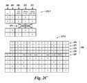
- FIG. 2Cshows logic tables illustrating selectable logical operation results implemented by sensing circuitry in accordance with a number of embodiments of the present disclosure.
- FIG. 3is a block diagram of a memory device in accordance with a number of embodiments of the present disclosure.
- a methodincludes receiving compressed data to a PIM device and decompressing the compressed data on the PIM device.
- datamay be transferred from a memory array and sensing circuitry (e.g., via a bus comprising input/output (I/O) lines) to a processing resource such as a processor, microprocessor, and/or compute engine, which may comprise ALU circuitry and/or other functional unit circuitry configured to perform the appropriate operations.
- a processing resourcesuch as a processor, microprocessor, and/or compute engine, which may comprise ALU circuitry and/or other functional unit circuitry configured to perform the appropriate operations.
- transferring data from the memory array and sensing circuitry to such processing resource(s)can involve significant time and/or power consumption.
- a sense linewhich may be referred to herein as a digit line or data line
- I/O linese.g., local I/O lines
- transferring the data peripheral to the memory arraywhich may be transfer to a cache in a host, and providing the data to the peripheral compute circuitry (e.g., associated with a central processing unit (CPU) of the host).
- CPUcentral processing unit
- the circuitry of the processing resource(s)may not conform to pitch rules associated with a memory array.
- the memory cells of a memory arraymay have a 4F 2 or 6F 2 cell size, where “F” is a feature size corresponding to the cells.
- the devicese.g., logic gates
- ALU circuitry of previous PIM systemsmay not be capable of being formed on pitch with the memory cells, which can affect chip size and/or memory density, for example.
- a number of embodiments of the present disclosurecan include the sensing circuitry (e.g., including sense amplifiers and/or compute components) and/or an operations component, as described herein, being formed on pitch with the memory cells of the array and being configured to (e.g., being capable of performing) compute functions (e.g., operations), such as those described herein, on pitch with the memory cells.
- sensing circuitrye.g., including sense amplifiers and/or compute components
- an operations componentas described herein, being formed on pitch with the memory cells of the array and being configured to (e.g., being capable of performing) compute functions (e.g., operations), such as those described herein, on pitch with the memory cells.
- the sensing circuitry 150 described hereincan be formed on a same pitch as a pair of complementary sense lines.
- a pair of complementary memory cellsmay have a cell size with a 6F 2 pitch (e.g., 3F ⁇ 2F). If the pitch of a pair of complementary sense lines for the complementary memory cells is 3F, then the sensing circuitry being on pitch indicates the sensing circuitry (e.g., a sense amplifier and corresponding compute component per respective pair of complementary sense lines) is formed to fit within the 3F pitch of the complementary sense lines.
- the circuitry of the processing resource(s)may not conform to pitch rules associated with a memory array.
- the memory cells of a memory arraymay have a 4F 2 or 6F 2 cell size.
- the devices (e.g., logic gates) associated with ALU circuitry of previous systemsmay not be capable of being formed on pitch with the memory cells (e.g., on a same pitch as the sense lines), which can affect chip size and/or memory density, for example.
- datamay be processed in a location that is not on pitch and/or on chip with memory (e.g., memory cells in the array), as described herein.
- the datamay be processed by a processing resource associated with a host, for instance, rather than on pitch with the memory.
- a number of embodiments of the present disclosurecan include the sensing circuitry 150 (e.g., including sense amplifiers and/or compute components) being formed on pitch with the memory cells of the array.
- the sensing circuitry 150can be configured for (e.g., capable of) performing compute functions (e.g., logical operations).
- datamay be processed in a location that is not on pitch with memory cells in the array and/or corresponding pairs of complementary sense lines and/or on chip with memory (e.g., formed on the same chip as the memory cells in the array) and/or a controller for the memory, as described herein.
- the datamay be processed by a processing resource associated with a host, for instance, rather than on pitch and/or on chip with the memory and/or on chip with the controller. As such, the data may be sent to and from memory in the same format as the data was in before or after being processed elsewhere.
- datamay be sent in compressed form to a frame buffer.
- imaging coordinatese.g., textures, depths, etc.
- the memorymay then send the compressed data to a GPU in the compressed form, with the GPU responsible for decompressing the data and sending uncompressed data (e.g., which may also have been depth textured and/or depth buffered, as described herein, by the GPU) back to the memory and/or to the frame buffer.
- uncompressed datae.g., which may also have been depth textured and/or depth buffered, as described herein, by the GPU
- Such movemente.g., copying, transferring, and/or transporting of data off pitch for processing, including decompression of compressed data, may increase memory bandwidth requirements, which also may increase time, power, and/or cost relative to an ability to perform such operations by sensing circuitry on pitch with the memory array.
- a memory device configured for on pitch data processing operationscan perform operations on data that have been received (e.g., stored) in its original format, as directed by an operations component (e.g., programmed for bitwise logical operations).
- PIM capable device operationscan use bit vector based operations.
- bit vectoris intended to mean a physically contiguous number of bits on a bit vector memory device (e.g., a PIM device) stored physically contiguous in a row of an array of memory cells.
- a “bit vector operation”is intended to mean an operation that is performed on a bit vector that is a contiguous portion of virtual address space (e.g., used by a PIM device).
- a row of virtual address space in the PIM devicemay have a bit length of 16K bits (e.g., corresponding to 16K complementary pairs of memory cells in a DRAM configuration).
- Sensing circuitry, as described herein, for such a 16K bit rowmay include a corresponding 16K processing elements (e.g., compute components, as described herein) formed on pitch with the sense lines selectably coupled to corresponding memory cells in the 16 bit row.
- a compute component in the PIM devicemay operate as a one bit processing element on a single bit of the bit vector of the row of memory cells sensed by the sensing circuitry (e.g., sensed by and/or stored in a sense amplifier paired with the compute component, as described herein).
- the datamay be stored in a compressed form (e.g., using either a lossy or lossless compression algorithm).
- image datamay be sent to the memory in the form of subsampled YUV compressed data, which reduces resolution of color data compared to standard RGB formats.
- the memory device itselfcan decompress the data into another format and can then perform operations on the decompressed data (e.g., alpha blending, as directed by the operations component, among other operations described herein).
- Alpha blending as used hereinis intended to mean a compositing operation in which one image is combined (e.g., overlaid) with at least one other image and where, through partial or full transparency, an image can, for example, serve as a background image and another can serve as a foreground image.
- Dataalso may be received and/or stored at a reduced image size and rescaled to a larger size (e.g., by increasing a number of pixels that the image contains), as directed by the operations component.
- the operations componentcan be configured to direct compensation for a reduced bit depth in a received and/or stored image, (e.g., by increasing an 8 bit image having 256 possible colors to a 24 bit image having about 16 million possible colors).
- the operations componentalso can be configured to decompress, for example, a highly compressed format (e.g., Joint Photographic Experts Group (JPEG), Moving Pictures Experts Group (MPEG), among other such formats), in addition to other possible operations.
- JPEGJoint Photographic Experts Group
- MPEGMoving Pictures Experts Group
- the operations component 172 described hereinmay contribute to an “intelligent frame buffer” (e.g., in combination with the sensing circuitry 150 and/or arrays 130 of memory cells, as shown in and described in connection with FIG. 1A and elsewhere) that can perform the just-described operations, among other operations described herein, on pitch with the array of memory cells in which the data may be stored.
- the operations being performed on pitch in association with the intelligent frame buffermay reduce memory traffic, and thus time, power, and/or cost.
- the memory trafficmay be reduced relative to sending the data off pitch to be decompressed (e.g., by a GPU associated with the host).
- the memory trafficalso may be reduced by the operations component being configured to direct operations that affect perceived quality of data output (e.g., alpha blending, among other compositing operations, and operations on texture, depth, etc.), which can convert read-modify-write data movement operations involved with exchange of data between the memory and, for example, a GPU into a one-way movement of data into the memory for processing.
- Data in a reduced-size formatcan be sent to a memory device, as described herein, to be expanded into a larger format on pitch with the memory.
- image datacan be stored in a subsampled YUV format and converted to non-subsampled RGB format, as directed by the operations component and performed on pitch.
- the reformatted image datathen can be stored as such in memory and/or can have one or more additional operations performed thereon, as described herein.
- Using a compressed format for input to memory and/or the memory device being configured to decompress and perform other operations on pitch with the memorymay reduce bandwidth requirements into and out of the memory device, thereby increasing performance and/or reducing time, usage of electrical power, and/or cost based on the reduced memory traffic.
- the embodimentscan allow a host system to allocate a number of locations (e.g., sub-arrays (or “subarrays”)) and portions of subarrays, in one or more DRAM banks to receive (e.g., store) and/or process data.
- a host system and/or a controllermay perform the address resolution on an entire block of program instructions (e.g., PIM command instructions) and data and direct (e.g., control) allocation, storage, and/or movement (e.g., flow) of data and commands into allocated locations (e.g., subarrays and portions of subarrays) within a destination (e.g., target) bank.
- Writing data and/or executing commandsmay utilize a normal DRAM write path to the DRAM device.
- a DRAM-style PIM deviceis discussed with regard to examples presented herein, embodiments are not limited to a PIM DRAM implementation.
- the memory devices described hereincan use a number of controllers for a bank of subarrays, controllers for individual subarrays, and/or controllers for operations components (e.g., each controller being a sequencer, a state machine, a microcontroller, a sub-processor, ALU circuitry, or some other type of controller) to execute a set of instructions to perform an operation on data (e.g., one or more operands).
- controllers for a bank of subarrayse.g., controllers for individual subarrays, and/or controllers for operations components (e.g., each controller being a sequencer, a state machine, a microcontroller, a sub-processor, ALU circuitry, or some other type of controller) to execute a set of instructions to perform an operation on data (e.g., one or more operands).
- an operationcan be, for example, a Boolean logical operation (e.g., AND, OR, NOT, NOT, NAND, NOR, and/or XOR) and/or other operations (e.g., invert, shift, arithmetic, statistics, and various operations on image and/or audio files, among many other possible operations).
- a Boolean logical operatione.g., AND, OR, NOT, NOT, NAND, NOR, and/or XOR
- other operationse.g., invert, shift, arithmetic, statistics, and various operations on image and/or audio files, among many other possible operations.
- functional unit circuitrymay be used to perform the arithmetic operations, such as addition, subtraction, multiplication, and division on operands, via a number of logical operations.
- the present disclosuredescribes enablement of operations (e.g., PIM operations, such as AND, OR, refresh, row copy, shift, add, multiply, decompression, compression, alpha blending, operations affecting texture, depth, etc.) to be performed on data values as received by (e.g., stored in) sensing circuitry and/or memory cells (e.g., when directed by the operations component 172 , as described herein).
- PIM operationssuch as AND, OR, refresh, row copy, shift, add, multiply, decompression, compression, alpha blending, operations affecting texture, depth, etc.
- the operationscan be performed on data values substantially simultaneously with the data values being received (e.g., at least temporarily stored and/or cached) by sensing circuitry 150 (e.g., a sensing component stripe 124 ) of a subarray 125 and/or upon subsequent retrieval of the data values as stored in a row 119 of memory cells of the subarray, as shown in and described in connection with FIG. 1C .
- sensing circuitry 150e.g., a sensing component stripe 124
- Implementations of PIM DRAM architecturemay perform processing (e.g., in a sensing component stripe 124 ) at the level of the sense amplifier 206 and/or compute component 231 (e.g., as shown in and described in connection with FIGS. 2A-2C ). Implementations of PIM DRAM architecture may allow a finite number of memory cells to be connected to each sense amplifier (e.g., around 1K or 1024 memory cells).
- a sensing component stripemay include from around 8K to around 16K sense amplifiers.
- a sensing component stripemay be configured to couple to an array of 1K rows and around 16K columns.
- a sensing component stripecan be used as a building block to construct the larger memory.
- a bank of memory(e.g., of memory cells in a DRAM array) may, in some embodiments, include 64K rows by 16K columns of DRAM to provide around 1 gigabit of memory.
- This bank architecturemay be divided into 64 subarrays that each have a configuration of 1K rows by 16K columns.
- Each subarraymay, for example, be configured to be coupled to an adjacent 16K sensing component stripe to yield a total of 64 sensing component stripes.
- the sense amplifiers 206 and/or compute components 231 in a sensing component stripe 124may be directed by instructions sent from the operations component 172 (e.g., via coupled I/O lines), to perform particular operations on data stored (cached) in the sensing component stripe.
- a number of factorsmay influence how an operation is performed in the sensing component stripe 124 . Comparative complexity of some operations may affect the choice. For example, Boolean operations (e.g., AND, OR, NOT, NOT, NAND, NOR, and/or XOR) and/or shift operations may be effectively performed using functionality resident in and/or local to the sensing component stripe (e.g., as described in connection with FIGS.
- decompression operations, alpha blending operations, etc.may be more effectively performed in combination with retrieval of machine instructions stored in one or more rows of coupled subarrays (e.g., as described in connection with FIG. 3 ) or elsewhere in connection with the computing system 100 (e.g., the controller 140 , the operations component 172 , and/or the host 110 ).
- the sensing circuitry 150e.g., sense amplifiers and/or compute components of a sensing component stripe
- the operations component 172may, in some embodiments, not be directly coupled to the memory cells of the subarrays.
- the operations component 172 described hereincan be indirectly coupled to the memory cells of a column via a selectably coupled sensing component stripe and a number of selectably coupled I/O lines.
- designatorssuch as “X”, “Y”, “N”, “M”, etc., particularly with respect to reference numerals in the drawings, indicate that a number of the particular feature so designated can be included. It is also to be understood that the terminology used herein is for the purpose of describing particular embodiments only, and is not intended to be limiting. As used herein, the singular forms “a”, “an”, and “the” can include both singular and plural referents, unless the context clearly dictates otherwise. In addition, “a number of”, “at least one”, and “one or more” (e.g., a number of memory arrays) can refer to one or more memory arrays, whereas a “plurality of” is intended to refer to more than one of such things.
- the words “can” and “may”are used throughout this application in a permissive sense (i.e., having the potential to, being able to), not in a mandatory sense (i.e., must).
- the term “include,” and derivations thereof,means “including, but not limited to”.
- the terms “coupled” and “coupling”mean to be directly or indirectly connected physically or for access to and movement (transmission) of commands and/or data, as appropriate to the context.
- the terms “data”, “data units”, and “data values”are used interchangeably herein and can have the same meaning, as appropriate to the context.
- an I/O linecan be selectably shared by a plurality of subarrays, rows, and/or particular columns of memory cells via the sensing component stripe coupled to each of the subarrays.
- the sense amplifier and/or compute component of each of a selectable subset of a number of columnse.g., eight column subsets of a total number of columns
- the I/O linecan, in some embodiments, be further shared by the operations component.
- a shared I/O linecan be used to refer to “a plurality of shared I/O lines”, unless the context clearly dictates otherwise.
- shared I/O linesis an abbreviation of “plurality of shared I/O lines”.
- FIG. 1Ais a block diagram of an apparatus in the form of a computing system 100 including a memory device 120 in accordance with a number of embodiments of the present disclosure.
- a memory device 120 , controller 140 , channel controller 143 , bank arbiter 145 , high speed interface (HSI) 141 , memory array 130 , sensing circuitry 150 , I/O processing component 171 , operations component 172 , and peripheral sense amplifiers and/or logic 170might also be separately considered an “apparatus.”
- System 100 in FIG. 1Aincludes the host 110 coupled (e.g., connected) to memory device 120 , which includes a memory array 130 .
- Host 110can be a host system such as a personal laptop computer, a desktop computer, a digital camera, a smart phone, or a memory card reader, a digital versatile disc player, a JPEG compressed image, a MPEG compressed audio recording, a MPEG compressed video recording, and/or an audio input (e.g., a soundtrack of a video recording, a live performance, a recording on a compact disc, a vinyl disc, etc.), among various other types of hosts.
- a host systemsuch as a personal laptop computer, a desktop computer, a digital camera, a smart phone, or a memory card reader, a digital versatile disc player, a JPEG compressed image, a MPEG compressed audio recording, a MPEG compressed video recording, and/or an audio input (e.g., a soundtrack of a video recording, a live performance, a recording
- Host 110can include a system motherboard and/or backplane and can include a number of processing resources (e.g., one or more processors, microprocessors, or some other type of controlling circuitry).
- the system 100can include separate integrated circuits or both the host 110 and the memory device 120 that can be on the same integrated circuit.
- the system 100can be, for instance, a server system and/or a high performance computing (HPC) system and/or a portion thereof.
- HPChigh performance computing
- the memory array 130can be a DRAM array, SRAM array, STT RAM array, PCRAM array, TRAM array, RRAM array, NAND flash array, and/or NOR flash array, among other types of arrays.
- the array 130can include memory cells arranged in rows coupled by access lines (which may be referred to herein as word lines or select lines) and columns coupled by sense lines (which may be referred to herein as data lines or digit lines). Although a single array 130 is shown in FIG. 1 , embodiments are not so limited.
- memory device 120may include a number of arrays 130 (e.g., a number of banks of DRAM cells, NAND flash cells, etc.).
- the memory device 120can include address circuitry 142 to latch address signals provided over a data bus 156 (e.g., an I/O bus from the host 110 ) by I/O circuitry 144 (e.g., provided to external ALU circuitry and to DRAM data lines (DQs) via local I/O lines and global I/O lines).
- DRAM DQscan enable input of data to and output of data from a bank (e.g., from and to the controller 140 and/or host 110 ) via a bus (e.g., data bus 156 ).
- a DQe.g., a pin.
- a data value read from a selected memory cellcan appear at the DQ once access is complete and the output is enabled.
- DQscan be in state such that the DQs do not source or sink current and do not present a signal to the system. This also may reduce DQ contention when two or more devices (e.g., banks) share the data bus.
- Status and exception informationcan be provided from the controller 140 of the memory device 120 to a channel controller 143 , for example, through a high speed interface (HSI) out-of-band (OOB) bus 157 , which in turn can be provided from the channel controller 143 to the host 110 .
- the channel controller 143can include a logic component 160 to allocate a plurality of locations (e.g., controllers for subarrays) in the arrays of each respective bank to store bank commands, application instructions (e.g., for sequences of operations), and arguments (PIM commands) for the various banks associated with operations of each of a plurality of memory devices (e.g., 120 - 1 , . . . , 120 -N as shown in FIG. 1B ).
- locationse.g., controllers for subarrays
- application instructionse.g., for sequences of operations
- PIM commandsarguments
- the channel controller 143can dispatch commands (e.g., PIM commands) to the plurality of memory devices 120 - 1 , . . . , 120 -N to store those program instructions within a given bank of a memory device.
- the channel controller 143can, in various embodiments, issue instructions for operations to be stored by the operations component 172 (e.g., as addressed via controller 140 ) such that the operations component can direct the operations described herein.
- Address signalsare received through address circuitry 142 and decoded by a row decoder 146 and a column decoder 152 to access the memory array 130 .
- Datacan be sensed (read) from memory array 130 by sensing voltage and/or current changes on sense lines (digit lines) using a number of sense amplifiers 206 , as described herein, of the sensing circuitry 150 .
- a sense amplifiercan read and latch a page (e.g., a row) of data from the memory array 130 .
- Additional compute circuitrycan be coupled to the sensing circuitry 150 and can be used in combination with the sense amplifiers to sense, store (e.g., cache and/or buffer), perform compute functions (e.g., operations), and/or move data.
- the I/O circuitry 144can be used for bi-directional data communication with host 110 over the data bus 156 (e.g., a 64 bit wide data bus).
- the write circuitry 148can be used to write data to the memory array 130 .
- Controller 140can decode signals (e.g., commands) provided by control bus 154 from the host 110 . These signals can include chip enable signals, write enable signals, and/or address latch signals that can be used to control operations performed on the memory array 130 , including data sense, data store, data movement (e.g., copying, transferring, and/or transporting data values), data decompression, data write, and/or data erase operations, among other operations described herein.
- the controller 140can be responsible for executing instructions from the host 110 and accessing the memory array 130 .
- the controller 140can be a state machine, a sequencer, or some other type of controller.
- the controller 140can, for example, control performance of Boolean logical operations and/or shifting data (e.g., right or left) in a row of an array (e.g., memory array 130 ).
- the sensing circuitry 150can include a number of sense amplifiers 206 and a number of compute components 231 , which may serve as an accumulator and can be used to perform operations in each subarray (e.g., on data associated with complementary sense lines).
- a compute component 231can be coupled to each sense amplifier 206 within the sensing circuitry 150 in each respective sensing component stripe coupled to a subarray (e.g., in sensing component stripes 124 - 0 and 124 - 1 coupled respectively to subarrays 125 - 0 and 125 - 1 ).
- embodimentsare not so limited.
- there may not be a 1:1 correlation between the number of sense amplifiers and compute componentse.g., there may be more than one sense amplifier per compute component or more than one compute component per sense amplifier, which may vary between subarrays, banks, etc.).
- the sensing circuitry 150can be used to perform on pitch operations using data stored in memory array 130 as input and participate in movement of the data for copy, transfer, transport, writing, logic, and/or storage operations to a different location in the memory array 130 without transferring the data via a sense line address access (e.g., without firing a column decode signal).
- various compute functionsmay, in some embodiments, be performed on pitch using, and within, sensing circuitry 150 rather than (or in association with) being performed by processing resources external to the sensing circuitry 150 (e.g., by a processor associated with host 110 and/or other processing circuitry, such as ALU circuitry, located on device 120 , such as on controller 140 or elsewhere).
- data associated with an operandwould be read from memory via sensing circuitry and provided to external ALU circuitry via I/O lines (e.g., via local I/O lines and/or global I/O lines).
- the external ALU circuitrycould include a number of registers and would perform compute functions using the operands, and the result would be transferred back to the array via the I/O lines.
- sensing circuitry 150is configured to perform operations on data stored in memory array 130 and store the result back to the memory array 130 without enabling an I/O line (e.g., a local I/O line) coupled to the sensing circuitry 150 .
- the sensing circuitry 150may be formed on pitch with the memory cells of the array.
- the operations component 172can be coupled to the sensing circuitry 150 (e.g., via an I/O line), but may be distinct from the sensing circuitry 150 .
- the memory array 130 , the sensing circuitry 150 , and the operations component 172in various embodiments, can cooperate in performing operations, according to embodiments described herein, and can collectively be termed an intelligent frame buffer.
- Additional peripheral sense amplifiers and/or logic 170can, in some embodiments, be coupled to the memory array 130 , the sensing circuitry 150 , and/or the operations component 172 .
- the peripheral sense amplifiers and/or logic 170can cooperate with and/or be part of the intelligent frame buffer in performance of some operations described herein.
- circuitry external to array 130 , sensing circuitry 150 , and operations component 172is not needed to perform compute functions because the sensing circuitry 150 and/or the operations component 172 can perform the appropriate operations to perform such compute functions without the use of an external processing resource. Therefore, the sensing circuitry 150 and operations component 172 may be used to complement or to replace, at least to some extent, such an external processing resource (or at least reduce the bandwidth consumption of transfer of data to and/or from such an external processing resource).
- the sensing circuitry 150 and operations component 172may be used to perform operations (e.g., to execute instructions) in addition to operations performed by an external processing resource (e.g., host 110 ).
- host 110 and/or sensing circuitry 150 and operations component 172each may be limited to performing only certain operations and/or a certain number of operations.
- Enabling an I/O linecan include enabling (e.g., turning on, activating) a transistor having a gate coupled to a decode signal (e.g., a column decode signal) and a source/drain coupled to the I/O line.
- a decode signale.g., a column decode signal
- embodimentsare not limited to not enabling an I/O line.
- the sensing circuitry 150can be used to perform operations without enabling column decode lines of the array.
- the local I/O line(s)may be enabled in order to transfer a result to a suitable location other than back to the array 130 (e.g., to an external register).
- FIG. 1Acan represent an apparatus architecture in the form of a computing system 100 including a memory device 120 having a plurality of banks (e.g., 121 - 0 , . . . , 121 -N as shown in FIG. 1B ) coupled to the host 110 via the channel controller 143 .
- the channel controller 143may be coupled to and integrated with the plurality of banks of the memory device 120 and/or the channel controller 143 may be coupled to and integrated with the host 110 .
- the channel controller 143can be coupled to each of the plurality of banks of the memory device via an address and control (A/C) bus 154 , which in turn can be coupled to the host 110 .
- A/Caddress and control
- the channel controller 143can also be coupled to each of the plurality of banks via a combined data bus 156 , which in turn can be coupled to the host 110 .
- the channel controller 143can be coupled to each of the plurality of banks via an OOB bus 157 associated with the HSI 141 , also referred to herein as a status channel interface, which is configured to report status, exception and other data information to the channel controller 143 to exchange with the host 110 .
- the channel controller 143can receive the status and exception information from the HSI 141 .
- the HSI 141may be associated with a bank arbiter that is associated with each of the plurality of banks (e.g., as shown and described in FIG. 1B for bank arbiter 145 - 1 associated with banks 121 - 0 , . . . , 120 - 7 ).
- a bank arbitermay not be included.
- Such a bank arbitercan sequence control and data with the plurality of banks (e.g., Bank zero (0), Bank one (1), . . .
- a controller 140can be associated with each particular bank (e.g., Bank 0, . . . , Bank 7) in a given memory device 120 and can decode signals provided by control bus 154 from the host 110 .
- Each of the plurality of bankscan include the controller 140 and an I/O processing component 171 - 1 that, in some embodiments, can be associated with the controller 140 to process input of data of various types to an appropriate bank, bank section, and/or subarray and/or output of such data, for example, to an appropriate destination subsequent to performance of the operations described herein.
- the I/O processing component 171 - 1can be configured to, for example, perform functions (e.g., operations) consistent with the functions performed by a CPU and/or GPU to coordinate output from memory 130 , the sensing circuitry 150 , and/or the operations component 172 to provide a product (e.g., static images, video images, and/or audio files, etc.) suitable for video and/or audio output.
- functionse.g., operations
- Each of the plurality of banksalso can include other components, including an array of memory cells 130 and sensing circuitry 150 , the operations component 172 , etc.
- each of the plurality of bankscan include address circuitry 142 to latch address signals provided over a portion of a combined data bus 156 (e.g., an I/O bus) through I/O circuitry 144 .
- a combined data bus 156e.g., an I/O bus
- Status and/or exception informationcan be provided from a controller 140 associated with (e.g., on chip with) each bank to the channel controller 143 , using the OOB bus 157 , which in turn can be provided from the plurality of banks to the host 110 .
- address signalscan be received through address circuitry 142 and decoded by a row decoder 146 and a column decoder 152 to access the memory array 130 .
- Datacan be read from memory array 130 by sensing voltage and/or current changes on the sense lines using sensing circuitry 150 .
- the sensing circuitry 150can read and latch a page (e.g., row) of data from the memory array 130 .
- the I/O circuitry 144can be used for bi-directional data communication with host 110 over the data bus 156 .
- the write circuitry 148is used to write data to the memory array 130 and the OOB bus 157 can be used to report status and/or exception information to the channel controller 143 .
- the channel controller 143can dispatch commands to the plurality of banks (e.g., Bank 0, . . . , Bank 7) and field return results and/or data from such operations.
- the return results and/or datacan be returned to the channel controller 143 via the OOB bus 157 associated with the status channel interface on each of the plurality of banks.
- Embodiments described hereinprovide a method for operating a memory device 120 to implement operations using compressed and decompressed data.
- the operationsmay be performed by execution of non-transitory instructions (e.g., from operations component 172 ) by a processing resource (e.g., sensing circuitry 150 in sensing component stripes 124 - 0 , 124 - 1 , . . . , 124 -N ⁇ 1).
- the methodcan include receiving compressed data to a PIM device and decompressing the compressed data on the PIM device.
- the compressed datacan be received to an intelligent frame buffer on the PIM device.
- the intelligent frame buffercan include an operations component 172 and sensing circuitry 150 associated with an array 130 of memory cells, as described herein.
- the compressed datacan be received to (e.g., at least temporarily stored and/or cached in) sensing circuitry 150 associated with a DRAM array on the PIM device.
- the compressed datacan, in some embodiments, be image data received in, for example, a subsampled YUV image format.
- the subsampled YUV image formatcan be received to (e.g., at least temporarily stored and/or cached in) the intelligent frame buffer associated with a random access memory (RAM) array of memory cells on the PIM device.
- the compressed datacan be decompressed by, for example, converting the subsampled YUV image format to a non-subsampled RGB image format using the intelligent frame buffer on the PIM device.
- the methodcan include storing an image in, for example, the non-subsampled RGB image format to the RAM array.
- the methodcan include compositing a plurality of images in the non-subsampled RGB image format into a different image using an alpha blending technique (e.g., in which a first image may be overlaid with at least a second image to form a composite image, as described further herein).
- the image datamay, for example, be received as having a reduced bit depth compared to a bit depth stored on and/or sent from a host 110 , as described further herein.
- the image datamay, for example, be received in JPEG format to the intelligent frame buffer on the PIM device.
- Alpha blending and/or other compositing operations, rescaling, depth texturing, and/or depth buffering, among other possible operations,can be performed on the decompressed data using the sensing circuitry 150 of the intelligent frame buffer associated with, for example, the DRAM array on the PIM device.
- Compressed datacan, in some embodiments, be received into (e.g., stored in) selected memory cells of an array 130 of the memory cells.
- the methodcan, in some embodiments, include decompressing the compressed data to produce decompressed data using the sensing circuitry 150 selectably coupled to the selected memory cells.
- the sensing circuitry 150may be on pitch with the selected memory cells.
- the methodcan include directing decompression of the compressed data using an operations component 172 selectably coupled via the sensing circuitry 150 to data values stored in the selected memory cells of the array 130 .
- the operations component 172can be associated with a controller 140 on a bank 121 of the array 130 .
- FIG. 1Bis a block diagram of another apparatus architecture in the form of a computing system 100 including a plurality of memory devices 120 - 1 , . . . , 120 -N coupled to a host 110 via a channel controller 143 in accordance with a number of embodiments of the present disclosure.
- the channel controller 143may be coupled to the plurality of memory devices 120 - 1 , . . . , 120 -N in an integrated manner in the form of a module 118 (e.g., formed on same chip with the plurality of memory devices 120 - 1 , . . . , 120 -N).
- the channel controller 143may be integrated with the host 110 , as illustrated by dashed lines 111 (e.g., formed on a separate chip from the plurality of memory devices 120 - 1 , . . . , 120 -N).
- an I/O processing component 171 - 2can, in some embodiments, be associated with the channel controller 143 to process input of data of various types to an appropriate memory device, bank, bank section, and/or subarray and/or output of such data, for example, to an appropriate destination subsequent to performance of the operations described herein.
- an appropriate memory devicebank, bank section, and/or subarray and/or output of such data, for example, to an appropriate destination subsequent to performance of the operations described herein.
- particular (e.g., different) memory devices, banks, bank sections, and/or subarraysmay be more appropriate (e.g., based upon particular programming of operations components thereof) for processing of (e.g., directing performance of operations on) static images (e.g., digital photographs), video images (e.g., a video camera recording), audio recordings (e.g., music), among other types of data input.
- static imagese.g., digital photographs
- video imagese.g., a video camera recording
- audio recordings
- the I/O processing component 171 - 2can be configured to perform functions (e.g., operations) consistent with the functions performed by a CPU and/or GPU to contribute to output from memory, sensing component stripes, and/or operations components to provide a product (e.g., static images, video images, and/or audio files, etc.) suitable for video and/or audio output.
- functionse.g., operations
- a producte.g., static images, video images, and/or audio files, etc.
- the channel controller 143can receive the status and/or exception information from a HSI 141 (also referred to herein as a status channel interface) associated with a bank arbiter 145 in each of the plurality of memory devices 120 - 1 , . . . , 120 -N.
- a HSI 141also referred to herein as a status channel interface
- each of the plurality of memory devices 120 - 1 , . . . , 120 -Ncan include a bank arbiter 145 to sequence control and data with a plurality of banks (e.g., Bank 0, . . . , Bank 7, etc.).
- Each of the plurality of bankscan include a controller 140 and other components, including an array of memory cells 130 and sensing circuitry 150 , operations component 172 , etc., as described in connection with FIG. 1A .
- the channel controller 143can include one or more local buffers 159 to store program instructions and can include logic 160 to allocate a plurality of locations (e.g., subarrays or portions of subarrays) in the arrays of each respective bank to store bank commands, and arguments (e.g., PIM commands) for the various banks associated with operation of each of the plurality of memory devices 120 - 1 , . . . , 120 -N.
- the channel controller 143can dispatch commands (e.g., PIM commands) to the plurality of memory devices 120 - 1 , . . . , 120 -N to store those program instructions within a given bank of a memory device.
- a controller 140e.g., bank control logic and/or sequencer associated with any subarray in a particular bank (e.g., Bank 0, . . . , Bank 7, etc.) in a given memory device (e.g., 120 - 1 , . . . , 120 -N) can decode signals provided by control bus 154 from the host 110 . These signals can include chip enable signals, write enable signals, and/or address latch signals that are used to control operations performed on the memory array 130 , including data read, data write, data copy, data movement, and/or data erase operations.
- the controller 140is responsible for executing instructions from the host 110 .
- FIG. 1Cis a block diagram of a bank section 123 of a memory device in accordance with a number of embodiments of the present disclosure.
- bank section 123can represent an example section of a number of bank sections of a bank of a memory device (e.g., bank section 0, bank section 1, . . . , bank section M ⁇ 1).
- a bank section 123can include a plurality of memory columns 122 shown horizontally as X (e.g., 4096, 8192, or 16,384 columns, among various possibilities, in an example DRAM bank and bank section). Additionally, the bank section 123 may be divided into subarray 0, subarray 1, . . .
- subarray N ⁇ 1(e.g., 32, 64, or 128 subarrays, among various possibilities) shown at 125 - 0 , 125 - 1 , . . . , 125 -N ⁇ 1, respectively, that are separated by amplification regions configured to be coupled to a data path.
- the subarrays 125 - 0 , 125 - 1 , . . . , 125 -N ⁇ 1can each have amplification regions 124 - 0 , 124 - 1 , . . . , 124 -N ⁇ 1 that correspond to sensing component stripe 0, sensing component stripe 1, . . . , and sensing component stripe N ⁇ 1, respectively.
- Each column 122is configured to be coupled to sensing circuitry 150 , as described in connection with FIG. 1A and elsewhere herein. As such, each column in a subarray can be coupled individually to a sense amplifier 206 and/or compute component 231 that contribute to a sensing component stripe 124 for that subarray 125 .
- the bank section 123can include sensing component stripe 0, sensing component stripe 1, . . .
- sensing component stripe N ⁇ 1that each have sensing circuitry 150 with sense amplifiers that can, in various embodiments, be used as registers, cache and/or data buffering and that are coupled to each column 122 in the subarrays 125 - 0 , 125 - 1 , . . . , 125 -N ⁇ 1.
- Each of the of the subarrays 125 - 0 , 125 - 1 , . . . , 125 -N ⁇ 1can include a plurality of rows 119 shown vertically as Y (e.g., each subarray may include 256, 512, 1024 rows, among various possibilities, in an example DRAM bank).
- Example embodimentsare not limited to the example horizontal and vertical orientation of columns and rows described herein or the example numbers thereof.
- the sense amplifiers 206 used in sensing data values in memory cells of the subarrays 125 and/or the compute components 231 used in performance of compute operationsare located in the plurality of sensing component stripes 124 that are each physically associated with a subarray 125 of memory cells in the bank section 123 shown in FIG. 1C .
- the operations component 172configured to direct operations performed on the data values may, in some embodiments, be located on a periphery of the bank section 123 .
- the operations component 172may, in various embodiments, be located on chip with memory (e.g., formed on the same chip as the memory cells in the array) and/or a controller 140 for the memory, as described herein, the operations component 172 may not be physically associated with a subarray 125 of memory cells, as shown in FIGS. 1A and 1C .
- Each banke.g., banks 121 - 0 , . . . , 121 - 7 shown in FIG.
- a controller 140 with which the operations component 172 is associatedmay be located in the same bank (e.g., on chip) with the operations component 172 .
- the controller 140 and/or the operations component 172may be located elsewhere (e.g., in a different bank 121 , in a different memory device 121 , and/or in association with the host 110 ).
- the bank section 123can be associated with controller 140 .
- the controller 140 shown in FIG. 1Ccan, in various examples, represent at least a portion of the functionality embodied by and contained in the controllers 140 shown in FIGS. 1A and 1B .
- the controller 140e.g., which may serve as a source, as described herein
- the controller 140can direct (e.g., control) input of commands and data 141 to the section 123 and output (e.g., movement) of data from the bank section 123 (e.g., to the host 110 ) along with control of data movement in the section 123 in combination with the operations component 172 , as described herein.
- the bank section 123can include a data bus 156 (e.g., a 64 bit wide data bus) to DRAM DQs, which can correspond to the data bus 156 described in connection with FIG. 1A .
- Each data bus 156 for each bank (e.g., 121 - 0 , . . . , 121 - 7 ) of subarrays (e.g., 125 - 0 , 125 - 1 , . . . , 125 -N ⁇ 1)can be referred to as a portion of a data bus that contributes to formation of a combined data bus (e.g., as described in connection with FIG. 1B for a plurality of banks and/or memory devices).
- eight 64 bit wide data bus portions for eight bankscan contribute to a 512 bit wide combined data bus, although embodiments are not so limited.
- FIG. 2Ais a schematic diagram illustrating sensing circuitry 250 in accordance with a number of embodiments of the present disclosure.
- the sensing circuitry 250can correspond to sensing circuitry 150 shown in FIG. 1A .
- FIG. 2Ashows a number of sense amplifiers 206 coupled to respective pairs of complementary sense lines 205 - 1 and 205 - 2 , and a corresponding number of compute components 231 coupled to the sense amplifiers 206 via pass gates 207 - 1 and 207 - 2 .
- the sense amplifiers 206 and compute components 231 shown in FIG. 2Acan correspond to sensing circuitry 150 shown in FIG. 1A and/or the sensing circuitry 250 associated with the plurality of sensing component stripes 124 shown in FIG. 1B , for example.
- the sensing circuitry 250 shown in FIG. 2Aincludes logical operation selection logic 213 , which can be operated as described further herein.
- memory cellsare coupled to the pairs of complementary sense lines 205 - 1 and 205 - 2 (e.g., columns).
- a memory cellcan comprise a transistor and a capacitor.
- the memory cellscan be, for example, 1T1C DRAM cells each comprising a storage element (e.g., capacitor) and an access device (e.g., transistor), although other embodiments of configurations can be used (e.g., 2T2C with two transistors and two capacitors per memory cell).
- the memory cellsmay be destructive read memory cells (e.g., reading the data stored in the cell destroys the data such that the data originally stored in the cell may be refreshed after being read).
- the cells of the memory arraycan be arranged in rows coupled by word lines and columns coupled by pairs of complementary data lines DIGIT(n ⁇ 1)/DIGIT(n ⁇ 1)_, DIGIT(n)/DIGIT(n)_, DIGIT(n+1)/DIGIT(n+1)_.
- the individual data lines corresponding to each pair of complementary data linescan also be referred to as data lines 205 - 1 (D) and 205 - 2 (D_) respectively.
- data lines 205 - 1 (D) and 205 - 2 (D_)respectively.
- an array of memory cellscan include additional columns of memory cells and/or data lines (e.g., 4,096, 8,192, 16,384, etc.).
- Memory cellscan be coupled to different data lines and/or word lines.
- a first source/drain region of an access transistor of a memory cellcan be coupled to a data line 205 - 1 (D)
- a second source/drain region of the access transistor of the memory cellcan be coupled to a capacitor of the memory cell
- a gate of the access transistor of the memory cellcan be coupled to a word line of the memory array.
- the sensing circuitry 250can comprise a sense amplifier 206 , a compute component 231 , and logical operation selection logic 213 corresponding to respective columns of memory cells (e.g., coupled to respective pairs of complementary data lines).
- the sense amplifier 206can comprise, for example, a cross coupled latch, which can be referred to herein as a primary latch.
- the sense amplifiers 206can be configured, for example, as described with respect to FIG. 2B .
- each compute component 231comprises a latch, which may be referred to herein as a secondary latch, and an additional number of transistors operable to move (e.g., shift) data units right and/or left (e.g., to a latch of an adjacent compute component 231 ).
- the latch of the compute component 231can serve as an accumulator.
- the compute component 231can operate as and/or may be referred to herein as an accumulator.
- the gates of the pass gates 207 - 1 and 207 - 2can be controlled by a logical operation selection logic signal, Pass.
- a logical operation selection logic signal, PassFor example, an output of the logical operation selection logic 213 can be coupled to the gates of the pass gates 207 - 1 and 207 - 2 , as shown in FIG. 2A .
- the sensing circuitry 250 illustrated in FIG. 2Aalso shows logical operation selection logic 213 coupled to a number of logic selection control input control lines, including ISO, TF, TT, FT, and FF. Selection of a logical operation from a plurality of logical operations is determined from the condition of logic selection control signals on the logic selection control input control lines, as well as the data units present on the pairs of complementary sense lines 205 - 1 and 205 - 2 when the isolation transistors (e.g., 251 - 1 and 251 - 2 ) are enabled via an ISO control signal being activated.
- the isolation transistorse.g., 251 - 1 and 251 - 2
- the logical operation selection logic 213can include four logic selection transistors: logic selection transistor 262 coupled between the gates of the swap transistors 242 and a TF signal control line, logic selection transistor 252 coupled between the gates of the pass gates 207 - 1 and 207 - 2 and a TT signal control line, logic selection transistor 254 coupled between the gates of the pass gates 207 - 1 and 207 - 2 and a FT signal control line, and logic selection transistor 264 coupled between the gates of the swap transistors 242 and a FF signal control line.
- Gates of logic selection transistors 262 and 252are coupled to the true sense line through isolation transistor 251 - 1 (having a gate coupled to an ISO signal control line).
- Gates of logic selection transistors 264 and 254are coupled to the complementary sense line through isolation transistor 251 - 2 (also having a gate coupled to an ISO signal control line).
- Data units present on the pair of complementary sense lines 205 - 1 and 205 - 2can be loaded into the compute component 231 via the pass gates 207 - 1 and 207 - 2 .
- the pass gates 207 - 1 and 207 - 2are OPEN, data units on the pair of complementary sense lines 205 - 1 and 205 - 2 are passed to the compute component 231 and thereby loaded into the loadable shift register.
- the data unit on the pair of complementary sense lines 205 - 1 and 205 - 2can be the data unit stored at least temporarily in the sense amplifier 206 when the sense amplifier is enabled (e.g., fired).
- the logical operation selection logic signal, Passis activated to OPEN (e.g., turn on) the pass gates 207 - 1 and 207 - 2 .
- the ISO, TF, TT, FT, and FF control signalscan operate to select a logical operation to implement based on the data unit (“B”) in the sense amplifier 206 and the data unit (“A”) in the compute component 231 (e.g., as used herein, the data unit stored in a latch of a sense amplifier is referred to as a “B” data unit, and the data unit stored in a latch of a compute component is referred to as an “A” data unit).
- the ISO, TF, TT, FT, and FF control signalsare configured to select the logical operation (e.g., function) to implement independent from the data unit present on the pair of complementary sense lines 205 - 1 and 205 - 2 (although the result of the implemented logical operation can be dependent on the data unit present on the pair of complementary sense lines 205 - 1 and 205 - 2 ).
- the ISO, TF, TT, FT, and FF control signalscan select the logical operation to implement directly because the data unit present on the pair of complementary sense lines 205 - 1 and 205 - 2 is not passed through logic to operate the gates of the pass gates 207 - 1 and 207 - 2 .
- FIG. 2Ashows swap transistors 242 configured to swap the orientation of the pair of complementary sense lines 205 - 1 and 205 - 2 between the sense amplifier 206 and the compute component 231 .
- the swap transistors 242are OPEN (e.g., turned on)
- data units on the pair of complementary sense lines 205 - 1 and 205 - 2 on the sense amplifier 206 side of the swap transistors 242are oppositely-coupled to the pair of complementary sense lines 205 - 1 and 205 - 2 on the compute component 231 side of the swap transistors 242 , and thereby loaded into the loadable shift register of the compute component 231 in a complementary manner.
- the logical operation selection logic signal Passcan be activated (e.g., high) to OPEN (e.g., turn on) the pass gates 207 - 1 and 207 - 2 when the ISO control signal line is activated and either the TT control signal is activated (e.g., high) with the data unit on the true sense line being “1” or the FT control signal is activated (e.g., high) with the data unit on the complement sense line being “1.”
- the data unit on the true sense linebeing a “1” OPENs logic selection transistors 252 and 262 .
- the data unit on the complementary sense linebeing a “1” OPENs logic selection transistors 254 and 264 . If the ISO control signal or either the respective TT/FT control signal or the data unit on the corresponding sense line (e.g., sense line to which the gate of the particular logic selection transistor is coupled) is not high, then the pass gates 207 - 1 and 207 - 2 will not be OPENed by a particular logic selection transistor.
- the logical operation selection logic signal Pass*can be activated (e.g., high) to OPEN (e.g., turn on) the swap transistors 242 when the ISO control signal line is activated and either the TF control signal is activated (e.g., high) with data unit on the true sense line being “1,” or the FF control signal is activated (e.g., high) with the data unit on the complement sense line being “1.” If either the respective control signal or the data unit on the corresponding sense line (e.g., sense line to which the gate of the particular logic selection transistor is coupled) is not high, then the swap transistors 242 will not be OPENed by a particular logic selection transistor.
- OPENe.g., turn on
- the sensing circuitry 250 illustrated in FIG. 2Ais configured to select one of a plurality of logical operations to implement directly from the four logic selection control signals (e.g., logical operation selection is not dependent on the data unit present on the pair of complementary sense lines). Some combinations of the logic selection control signals can cause both the pass gates 207 - 1 and 207 - 2 and swap transistors 242 to be OPEN (e.g., conducting) at the same time, which shorts the pair of complementary sense lines 205 - 1 and 205 - 2 together.
- the logical operations which can be implemented by the sensing circuitry 250 illustrated in FIG. 2Acan be the logical operations summarized in the logic tables shown in FIG. 2C .
- each column of memory cellscan be coupled to a column decode line that can be activated to move, via a local I/O line, a data unit from a corresponding sense amplifier 206 and/or compute component 231 .
- the data unitmay be moved (e.g., transferred) to a control component external to the array, such as an external processing resource (e.g., host processor and/or other functional unit circuitry) and/or to an I/O processing component 171 , which may be on chip or off chip relative to the sensing circuitry 250 .
- the column decode linecan be coupled to a column decoder (e.g., column decoder 152 in FIG. 1A ).
- shift circuitrycan be operated in conjunction with sense amplifiers 206 and compute components 231 to perform shift operations without transferring data to a control component external to the array, for example.
- transferring datawhich may also be referred to as moving data is an inclusive term that can include, for example, copying data from a source location to a destination location and/or moving data from a source location to a destination location without necessarily maintaining a copy of the data at the source location.
- each compute component 231can comprise a loadable shift register.
- each compute component 231is coupled to a corresponding pair of complementary data lines 205 - 1 / 205 - 2 , with a node ST 2 being coupled to the particular data line (e.g., DIGIT(n)) communicating a “true” data unit and with node SF 2 being coupled to the corresponding complementary data line (e.g., DIGIT(n)_) communicating the complementary data unit (e.g., “false” data unit).
- the loadable shift registercomprises a first right-shift transistor 281 of a particular compute component 231 having a gate coupled to a first right-shift control line 282 (e.g., PHASE 1 R), and a second right-shift transistor 286 of the particular compute component 231 having a gate coupled to a second right-shift control line 283 (e.g., PHASE 2 R).
- Node ST 2 of the particular control componentis coupled to an input of a first inverter 287 , whose output (e.g., node SF 1 ) is coupled to a first source/drain region of transistor 286 .
- the second source/drain region of transistor 286is coupled to the input (e.g., node SF 2 ) of a second inverter 288 .
- the output (e.g., node ST 1 ) of inverter 288is coupled to a first source/drain region of transistor 281
- a second source/drain region of transistor 281 the particular compute component 231is coupled to an input (e.g., node ST 2 ) of a first inverter 287 of an adjacent compute component 231 .
- the loadable shift register shown in FIG. 2Aincludes a first left-shift transistor 289 coupled between node SF 2 of a particular compute component and node SF 1 of an adjacent compute component 231 .
- 2Aalso includes a second left-shift transistor 290 of a particular compute component 231 having a first source/drain region coupled to node ST 2 and a second source/drain region coupled to node ST 1 .
- the gate of the first left-shift transistor 289is coupled to a first left-shift control line 291 (e.g., PHASE 1 L), and the gate of the second left-shift transistor 290 is coupled to a second left-shift control line 492 (e.g., PHASE 2 L).
- a data unit on a pair of complementary data linescan be loaded into a corresponding compute component 231 (e.g., by operating logical operation selection logic as described above).
- a data unitcan be loaded into a compute component 231 via overwriting of the data unit currently stored in the compute component 231 with the data unit stored in the corresponding sense amplifier 206 .
- a data unitmay be loaded into a compute component by deactivating the control lines 282 , 283 , 291 , and 292 .
- Shifting data to the rightcan include alternating operation of the first right-shift transistor 281 and the second right-shift transistor 286 , for example, via the PHASE 1 R and PHASE 2 R control signals being periodic signals that go high out of phase from one another (e.g., non-overlapping alternating square waves 180 out of phase).
- the transistor 290can be turned on to latch the shifted data unit.
- An example of shifting data left via the shift register shown in FIG. 2Acan include operating control signals 291 and 292 to move a data unit one control component to the left through transistors 289 and 290 .
- Data from node ST 2is inverted through inverter 287 to node SF 1 .
- Activation of control signal 291causes the data from node SF 1 to move left through transistor 289 to node SF 2 of a left-adjacent compute component 231 .
- Data from node SF 2is inverted through inverter 288 to node ST 1 .
- Subsequent activation of control signal 292causes the data from node ST 1 to move through transistor 290 left to node ST 2 , which completes a left shift by one compute component 231 .
- Datacan be “bubbled” to the left by repeating the left shift sequence multiple times. Data units can be latched (and prevented from being further shifted) by maintaining the control signal 292 activated.
- Embodiments of the present disclosureare not limited to the shifting capability described in association with the compute components 231 .
- a number of embodimentscan include shift circuitry in addition to and/or instead of the shift circuitry described in association with a loadable shift register.
- the sensing circuitry 250 in FIG. 2Acan be operated in several modes to perform logical operations, including a first mode in which a result of the logical operation is initially stored in the sense amplifier 206 , and a second mode in which a result of the logical operation is initially stored in the compute component 231 . Additionally with respect to the first operating mode, sensing circuitry 250 can be operated in both pre-sensing (e.g., sense amplifiers fired before logical operation control signal active) and post-sensing (e.g., sense amplifiers fired after logical operation control signal active) modes with a result of a logical operation being initially stored in the sense amplifier 206 .
- pre-sensinge.g., sense amplifiers fired before logical operation control signal active
- post-sensinge.g., sense amplifiers fired after logical operation control signal active
- the sense amplifier 206 and the compute component 231can be in at least one of two states associated with the first mode and the second mode.
- a state of a sense amplifier 206 and/or the compute component 231can describe a movement (e.g., transfer) of data between the sense amplifier 206 and/or the compute component 231 .
- the state of the sense amplifier 206 and/or the compute component 231can also be described as whether the sense amplifier 206 and/or the compute component 231 is in an equilibration state or is storing a data unit (e.g., a binary 0 or 1 data value).
- a sense amplifiercan be configured to be in an initial state, wherein the initial state is one of an equilibration state and a data storage state.
- a data storage statecan include the sense amplifiers 206 storing a data unit.
- a data unitcan be referred to as a bit and/or a digit value.
- Datacan be moved (e.g., transferred) from a compute component 231 to a sense amplifier 206 in response to enabling a pass gate (e.g., activating the PASS and/or PASS* control signals via the TF 262 , TT 252 , FT 254 , and/or FF 264 control signals that are referred to herein as a logical operation selection logic) and the sense amplifier 206 being in a equilibration state.
- a pass gatee.g., activating the PASS and/or PASS* control signals via the TF 262 , TT 252 , FT 254 , and/or FF 264 control signals that are referred to herein as a logical operation selection logic
- Datacan be moved from a sense amplifier 206 to a compute component 231 in response to enabling the pass gate (e.g., activating the PASS and/or PASS* control signals via the TF 262 , TT 252 , FT 254 , and/or FF 264 control signals that are referred to herein as a logical operation selection logic) and the sense amplifier 206 being in a data storage state.
- the pass gatee.g., activating the PASS and/or PASS* control signals via the TF 262 , TT 252 , FT 254 , and/or FF 264 control signals that are referred to herein as a logical operation selection logic
- the direction of the movement of data between the sense amplifier 206 and the compute component 231is determined by whether the sense amplifier 206 is in an equilibration state or stores a data unit before the PASS and/or PASS* control signals are activated and by a particular operation selected via the logical operation selection logic (e.g., TF 262 , TT 252 , FT 254 , and FF 264 control signals).
- the logical operation selection logice.g., TF 262 , TT 252 , FT 254 , and FF 264 control signals.
- a data unit stored in the compute component 231can be moved from the compute component 231 to the sense amplifier 206 .
- the sense amplifier 206is configured to store a first bit (e.g., first data unit) and the PASS and/or PASS* control signals are activated to provide a conduction path between the sense amplifier 206 and the compute component 231 , then a second bit (e.g., second data unit) that is stored in the compute component 231 before the activation of the PASS and/or PASS* control signals can be replaced by the first bit and the sense amplifier 206 retains the first bit. Furthermore, a number of operations can be performed using the first bit and the second bit using the logical operation selection logic and the result of the operation can be stored in the compute component 231 .
- Using an equilibration signal to direct the movement of data between the sense amplifier 206 and the compute component 231can provide the ability to selectively perform an operation in sense amplifiers that are not equilibrated without performing the operation in sense amplifiers that are equilibrated.
- a PASS and/or a PASS* control signalcan be activated in a plurality of sensing components to move data between a first group of a plurality of sense amplifiers that are equilibrated and a first group of a plurality of compute components.
- the PASS and/or PASS* control signalscan also be activated to move data between a second group of the plurality of sense amplifiers and a second group of the plurality of component components that are not equilibrated to selectively perform an operation in a second group of sense components while not performing the operation on a first group of sense components.
- FIG. 2Billustrates a schematic diagram of a portion of sensing circuitry in accordance with a number of embodiments of the present disclosure.
- the portion of the sensing circuitry shown in FIG. 2Bcan correspond to a portion of the sensing circuitry 250 shown in FIG. 2A , for example.
- a sense amplifier 206can comprise a cross coupled latch.
- embodiments of the sense amplifier 206are not limited to a cross coupled latch.
- the sense amplifier 206 in FIG. 2Bcan be current-mode sense amplifier and/or single-ended sense amplifier (e.g., sense amplifier coupled to one data line).
- Embodiments of the present disclosurealso are not limited to a folded data line architecture.
- a sense amplifier 206can comprise a number of transistors formed on pitch with the transistors of the corresponding compute component 231 and/or the memory cells of an array (e.g., memory array 130 shown in FIG. 1A ) to which they are coupled, which may conform to a particular feature size (e.g., 4F 2 , 6F 2 , etc.).
- Sense amplifier 206comprises a latch 215 including four transistors coupled to a pair of complementary data lines D 205 - 1 and D — 205 - 2 .
- the latch 215can be a cross coupled latch.
- the gates of a pair of transistorssuch as n-channel transistors (e.g., NMOS transistors) 227 - 1 and 227 - 2 can be cross coupled with the gates of another pair of transistors, such as p-channel transistors (e.g., PMOS transistors) 229 - 1 and 229 - 2 .
- the latch 215comprising transistors 227 - 1 , 227 - 2 , 229 - 1 , and 229 - 2 can be referred to as a primary latch.
- embodimentsare not limited to this example.
- the voltages or currents on the respective data lines D and D —can be provided to the respective latch inputs 233 - 1 and 233 - 2 of the cross coupled latch 215 (e.g., the input of the primary latch).
- the latch input 233 - 1is coupled to a first source/drain region of transistors 227 - 1 and 229 - 1 as well as to the gates of transistors 227 - 2 and 229 - 2 .
- the latch input 233 - 2can be coupled to a first source/drain region of transistors 227 - 2 and 229 - 2 as well as to the gates of transistors 227 - 1 and 229 - 1 .
- the compute component 231which may be referred to herein as an accumulator, can be coupled to latch inputs 233 - 1 and 233 - 2 of the cross coupled latch 215 as shown.
- embodimentsare not limited to the example shown in FIG. 2B .
- a second source/drain region of transistors 227 - 1 and 227 - 2can be commonly coupled to a negative control signal (RnIF) 228 .
- a second source/drain region of transistors 229 - 1 and 229 - 2can be commonly coupled to an active positive control signal (ACT) 265 .
- the ACT signal 265can be a supply voltage (e.g., V DD ) and the RnIF signal can be a reference voltage (e.g., ground).
- RnIF signal 228 and ACT signal 265can function as activating signals that enable the cross coupled latch 215 .
- the enabled cross coupled latch 215can operate to amplify a differential voltage between latch input 233 - 1 (e.g., first common node) and latch input 233 - 2 (e.g., second common node) such that latch input 233 - 1 is driven to one of the ACT signal voltage and the RnIF signal voltage (e.g., to one of V DD and ground), and latch input 233 - 2 is driven to the other of the ACT signal voltage and the RnIF signal voltage.
- latch input 233 - 1e.g., first common node
- latch input 233 - 2e.g., second common node
- the sense amplifier 206can also include circuitry configured to equilibrate the data lines D and D — (e.g., in association with preparing the sense amplifier for a sensing operation).
- the equilibration circuitrycomprises a transistor 224 having a first source/drain region coupled to a first source/drain region of transistor 225 - 1 and data line D 205 - 1 .
- a second source/drain region of transistor 224can be coupled to a first source/drain region of transistor 225 - 2 and data line D — 205 - 2 .
- a gate of transistor 224can be coupled to gates of transistors 225 - 1 and 225 - 2 .
- the second source drain regions of transistors 225 - 1 and 225 - 2can be coupled to an equilibration voltage 238 , which can be equal to V DD /2, where V DD is a supply voltage associated with the array.
- the gates of transistors 224 , 225 - 1 , and 225 - 2can be coupled to control signal 226 (EQ).
- activating EQcan enable the transistors 224 , 225 - 1 , and 225 - 2 , which can effectively short data line D to data line D — such that the data lines D and D — are equilibrated to equilibration voltage V DD /2.
- a number of logical operations and/or shift operationscan be performed using the sense amplifier 206 and compute component 231 , and the result can be at least temporarily stored in the sense amplifier and/or compute component.
- the sensing circuitry 250 in FIG. 2Acan be operated in several modes to perform logical operations, including a first mode in which a result of the shift operation and/or logical operation is initially stored in the sense amplifier 206 , and a second mode in which a result of the shift operation and/or logical operation is initially stored in the compute component 231 . Additionally with respect to the first operating mode, sensing circuitry 250 can be operated in both pre-sensing (e.g., sense amplifiers fired before operation control signal active) and post-sensing (e.g., sense amplifiers fired after operation control signal active) modes with a result of a shift operation and/or logical operation being initially stored in the sense amplifier 206 .
- pre-sensinge.g., sense amplifiers fired before operation control signal active
- post-sensinge.g., sense amplifiers fired after operation control signal active
- the sense amplifier 206can, in conjunction with the compute component 231 , be operated to perform various logical operations and/or shift operations (e.g., using data from an array as input).
- the result of a logical operation and/or shift operationcan be stored back to the array without transferring the data via a data line address access (e.g., without firing a column decode signal such that data is transferred to circuitry external to the array and sensing circuitry via local I/O lines).
- embodiments of the present disclosurecan enable performing various operations (e.g., logical operations, shift operations, mathematical operations, etc.) that contribute to performance of, for example, compression, decompression, alpha blending, and other graphics operations using less power than various previous approaches.
- various embodimentscan reduce or eliminate moving (e.g., transferring) data across I/O lines in order to perform operations (e.g., between memory and a discrete processor, which may be off pitch), such embodiments may enable an increased parallel processing capability as compared to previous approaches.
- FIG. 2Cshows logic tables illustrating selectable logical operation results implemented by sensing circuitry in accordance with a number of embodiments of the present disclosure.
- the four logic selection control signalse.g., TF, TT, FT, and FF
- TF, TT, FT, and FFdescribed in connection with the sensing circuitry 250 shown in FIG. 2A , in conjunction with a particular data unit (e.g., sensed on the complementary sense lines)
- a particular data unite.g., sensed on the complementary sense lines
- the four control signalsin conjunction with the particular data unit, controls the state (conducting or not conducting) of the pass gates 207 - 1 and 207 - 2 and swap transistors 242 , which in turn affects the data unit in the compute component 231 and/or sense amplifier 206 before/after firing.
- the capability to selectably control the state of the swap transistors 242facilitates implementing logical operations involving inverse data units (e.g., to inverse operands and/or inverse a result of an operation), among others.
- Logic Table 213 - 1 illustrated in FIG. 2Cshows a starting data unit stored in the compute component 231 in FIG. 2A shown in column A at 244 , and a starting data unit stored in the sense amplifier 206 shown in column B at 245 .
- the other three column headings in Logic Table 213 - 1refer to the state of the pass gates 207 - 1 and 207 - 2 and the swap transistors 242 , which can respectively be controlled to be OPEN (e.g., conducting/on) or CLOSED (e.g., not conducting/off) depending on the state of the four logic selection control signals (e.g., TF, TT, FT, and FF), in conjunction with a particular data unit (e.g., present on the pair of complementary sense lines 205 - 1 and 205 - 2 ) when the ISO control signal is activated.
- OPENe.g., conducting/on
- CLOSEDe.g., not conducting/off
- the “Not Open” columncorresponds to the pass gates 207 - 1 and 207 - 2 and the swap transistors 242 both being in a non-conducting condition
- the “Open True”corresponds to the pass gates 207 - 1 and 207 - 2 being in a conducting condition
- the “Open Invert”corresponds to the swap transistors 242 being in a conducting condition.
- the configuration corresponding to the pass gates 207 - 1 and 207 - 2 and the swap transistors 242 both being in a conducting conditionis not reflected in Logic Table 213 - 1 because this can result in the sense lines being shorted together.
- the logic tables illustrated in FIG. 2Ccan reflect a result initially stored in the compute component 231 in FIG. 2A . Therefore, when the pass gates 207 - 1 and 207 - 2 are controlled to be CLOSED (e.g., not conducting), the result initially stored in the compute component 231 is the same as the starting data unit in the compute component 231 .
- the sense sensing circuitry 250is configured such that the sense amplifier 206 can overpower the compute component 231 , as shown in the “Not Open” column 256 of the Logic Table 213 - 1 , the result initially stored in the compute component 231 is the same as the starting data unit in the sense amplifier 206 when the pass gates 207 - 1 and 207 - 2 are controlled to be OPEN (e.g., conducting) as shown in the “Open True” column 270 of the Logic Table 213 - 1 .
- OPENe.g., conducting
- the compute component 231can be inverted as shown in the “Open Invert” column 271 when the swap transistors 242 are in a conducting condition.
- the nine different selectable logical operations that can be implemented by the sensing circuitry 250are summarized in Logic Table 213 - 2 illustrated in FIG. 2C .
- the columns of Logic Table 213 - 2 illustrated in FIG. 2Cshow a heading 280 that includes the state of logic selection control signals.
- the state of a first logic selection control signalis provided in row 276
- the state of a second logic selection control signalis provided in row 277
- the state of a third logic selection control signalis provided in row 278
- the state of a fourth logic selection control signalis provided in row 279 .
- the particular logical operation corresponding to the resultsis summarized in row 247 .
- results for the values of FF, FT, TF, and TT of “0000”are summarized as “A” because the result (initially stored in the compute component after the sense amplifier fires) is the same as the starting value in the compute component.
- Other columns of resultsare similarly annotated in row 247 , where “A*B” intends A AND B, “A+B” intends A OR B, and “AXB” intends A XOR B.
- a bar over a data unit or a logical operationindicates an inverted value of the quantity shown under the bar. For example, AXB bar intends not A XOR B, which is also A XNOR B.
- FIG. 3is a block diagram of a memory device 320 in accordance with a number of embodiments of the present disclosure.
- the memory device 320 shown in FIG. 3has PIM capabilities, as described in connection with memory devices 120 shown in FIGS. 1A and 1B and sensing circuitry 250 in FIGS. 2A-2C .
- a HSI 341may be coupled to a bank arbiter 345 in the PIM device 320 .
- the HSI 141may be configured to receive commands and/or data from a host 110 , as described in connection with and shown in FIGS. 1A and 1B .
- the HSI 341may receive commands and/or data from a channel controller 143 via an address/control (A/C) bus 154 , a data bus 156 , and/or an OOB bus 157 as illustrated in FIGS. 1A-1C .
- the bank arbiter 345may be coupled to a plurality of banks 321 - 1 , . . . , 321 - 7 including associated arrays 130 and registers.
- each bank 321 - 1 , . . . , 321 - 7may be configured with a respective controller 340 - 1 , . . . , 340 - 7 .
- the controllers 340 - 1 , . . . , 340 - 7may represent one or more portions of the controller 140 described in connection with FIG. 1A .
- each controller 340 - 1 , . . . , 340 - 7may comprise respective control logic (e.g., control state machines) 331 - 1 , . . . , 331 - 7 , a sequencer 332 - 1 , . . . , 332 - 7 , and an atomic state machine (Atto state machine) 333 - 1 , . . . , 333 - 7 .
- control logice.g., control state machines
- 331 - 1 , . . . , 331 - 7
- control logic 331 - 1 , . . . , 331 - 7may be responsible for fetching machine instructions (e.g., microcode instructions) from an array of memory cells (e.g., a DRAM array) in each bank 321 - 1 , . . . , 321 - 7 .
- the control logic 331 - 1 , . . . , 331 - 7may decode the microcode instructions into calls (e.g., microcode functions), implemented by the sequencers 332 - 1 , . . . , 332 - 7 .
- the microcode functionscan be the operations that the sequencers 332 - 1 , . . . , 332 - 7 receive and operate on to cause the PIM device 320 to perform particular operations, which may include the operations described herein.
- control logic 331can fetch machine instructions, which when executed, direct performance of operations by the intelligent frame buffer comprising the sensing circuitry 150 (e.g., sensing component stripes 124 - 0 , . . . , 124 -N ⁇ 1 in FIG. 1C ).
- the sensing circuitry 150may, in some embodiments, be on pitch with sense lines (e.g., formed to fit within the 3F pitch of pairs of complementary sense lines 205 - 1 and 205 - 2 in FIG. 2B ) of the subarrays (e.g., 125 - 0 , 125 - 1 , . . . , 125 -N ⁇ 1 in FIG. 1C ) in each bank 321 - 1 , .
- the sensing circuitry 150may, in some embodiments, be on chip with (e.g., formed on the same chip as the memory cells in the array) the operations component 172 associated with the controller 340 .
- the operations component 172can be part of the controller 340 , such that the operations component 172 and/or the controller 340 can be configured to execute the received machine instructions (e.g., fetched by the control logic 331 ).
- Operations performed based on execution of the machine instructionscan, as described herein, include data compression and/or decompression, alpha blending, rescaling, depth texturing operation, and/or depth buffering, among others.
- the Atto state machines 333 - 1 , . . . , 333 - 7may provide timing and be responsible for providing conflict free access to the arrays.
- the sequencers 332 - 1 , . . . , 332 - 7 , and atomic state machines (Atto state machines) 333 - 1 , . . . , 333 - 7may be state machines and the control logic 331 - 1 , . . . , 331 - 7 may be a very large instruction word (VLIW) type processing resource (e.g., containing a program counter, instruction memory, etc.)
- VLIWvery large instruction word
- operationsmay be received to and operated on by the sequencers 332 - 1 , . . . , 332 - 7 to cause sensing circuitry 250 shown in FIGS. 2A-2C to perform an operation, such as addition, multiplication, etc., and/or, as a more specific example, a Boolean logical operation, such as an AND, OR, XOR, etc., operation, which can be utilized in performance of the operations on images, for example, as described herein.
- a Boolean logical operationsuch as an AND, OR, XOR, etc.
- Such operationsmay additionally comprise DRAM operations, such as a read, write, copy, and/or erase operations, etc.
- the controllers 340 - 1 , . . . , 340 - 7may be coupled to sensing circuitry 350 and/or logic 370 , including cache, buffers, sense amplifiers, extended row address (XRA) latches, and/or registers, associated with arrays of memory cells via control lines and data paths 355 .
- sensing circuitry 350 and logic 370can further be associated to the arrays of memory cells via data I/O lines shown as 355 - 1 , . . . , 355 - 7 .
- the sequencers 332 - 1 , . . . , 332 - 7may generate sequences of operation cycles for a DRAM array.
- each sequencemay be designed to perform operations, such as a Boolean logic operation (AND, OR, XOR, etc.), which together achieve a specific function, such as repetitively calculating the logic equations for a one (1) bit add in order to calculate a multiple bit sum.
- Each of these operationsmay be fed into a first in/first out (FIFO) buffer provided by the Atto state machines 333 - 1 , . . . , 333 - 7 for providing timing coordination with the sensing circuitry 350 and/or logic 370 associated with the array of memory cells (e.g., DRAM arrays).
- FIFOfirst in/first out
- the Atto state machines 333 - 1 , . . . , 333 - 7provide timing and are responsible for providing conflict free access to the arrays from a number of FIFO queues.
- the Atto state machines 333 - 1 , . . . , 333 - 7include timing circuitry coupled to the array and sensing circuitry (e.g., sensing component stripes 124 - 0 , . . . , 124 -N ⁇ 1 coupled to subarrays 125 - 0 , 125 - 1 , . . .
- one FIFO queue 368may support receipt and processing of PIM operations via a control state machine 331 - 1 , a sequencer 332 - 1 , and/or an Atto state machine 333 - 1
- one FIFO queue 373may be for instruction fetch and/or for microcode instruction fetch (e.g., from subarrays 125 - 0 , 125 - 1 , . . . , 125 -N ⁇ 1 via respective sensing component stripes 124 - 0 , 124 - 1 , . . .
- both the control logic 331 - 1 , . . . , 331 - 7 and the sequencers 332 - 1 , . . . , 332 - 7may generate status information, which can be routed back to the bank arbiter 345 via a FIFO interface (e.g., 368 - 1 , . . . , 368 - 7 ).
- the bank arbiter 345may aggregate this status data and report it back to a channel controller, such as a channel controller 143 associated with host 110 , via the HSI 341 .
- an operations component 172(e.g., in combination with the controller 140 ) can direct that data values from a selectable row 119 of a selectable subarray 125 be at least temporarily stored (cached) in a sensing component stripe 124 coupled to that subarray and that a number of operations be performed on at least one of the data values in the sensing component stripe 124 by the sense amplifier 206 and/or the compute component 231 .
- the operations component 172can direct that these data values be subsequently returned for storage in the memory cells of the same or a different row of the subarray and/or that these data values be subsequently moved (e.g., via a shared I/O line) to selectably coupled sensing circuitry 150 (e.g., in a different sensing component stripe 124 ) for further processing (e.g., operations) to be performed on the data values.
- the operations component 172can be selectably coupled to the sensing circuitry 150 of the plurality of subarrays.
- the operations componentcan, in various embodiments, be configured to direct performance of an operation by the sensing circuitry with respect to data stored in a selectable subarray of the respective plurality of subarrays.
- the memory devicecan be configured to, as described herein, store a data value as received from a source (e.g., store a data set before an operation has been performed on the data) in a memory cell in a row of the selectable subarray (e.g., store at least part of the data set in the row).
- the memory devicecan be further configured to output the data value to an output processing component 171 (e.g., an I/O processing component to perform CPU/GPU type functions) associated with a controller subsequent to performance of the operation thereon in the sensing circuitry, as directed by the operations component 172 .
- an output processing component 171e.g., an I/O processing component to perform CPU/GPU type functions
- the controller with which output processing component 171 - 1 is associatedmay be a controller 140 for a bank 121 of the respective plurality of subarrays, as shown in FIG. 1A .
- the controller with which output processing component 171 - 2 is associatedmay be a channel controller 143 associated with a plurality of banks of the respective plurality of subarrays and/or a plurality of memory devices, as shown in FIG. 1B .
- the channel controller 143may be associated with a host 110 coupled to the memory device 120 - 1 and/or a plurality of memory devices 120 - 1 , . . . , 120 -N that each include banks 121 - 0 , . . . , 121 -N of the respective plurality of subarrays.
- the memory devicecan be configured to receive (e.g., store) a plurality of compressed data values, as received from the source, to the selectable subarray.
- the compressed data valuescan be from a compressed video recording having a number of video images, a compressed static image, and/or a compressed audio file, as described herein, among other possibilities.
- the memory devicecan be configured, in some embodiments, to decompress, as directed by the operations component, a plurality of the compressed data values, as received from the source to the selectable subarray, prior to performance of the operation thereon (e.g., prior to performance of an operation other than the decompression).
- the memory devicecan be configured, in some embodiments, to perform an alpha blending operation, as directed by the operations component, on a plurality of data values as received from the source to (e.g., stored in) the selectable subarray.
- the memory devicecan be configured, in some embodiments, to perform a rescale operation, as directed by the operations component, on a plurality of resized data values received from the source to the selectable subarray.
- the memory devicecan be configured, in some embodiments, to perform a depth texturing operation, as directed by the operations component, on a plurality of data values received from the source to the selectable subarray.
- a depth texturealso known as a shadow map, as used herein is intended to mean a texture that contains data from a depth buffer for a particular image. Each pixel value may contain a depth of the geometry in that pixel.
- a depth texturemay be used to render appropriate shadows in the image.
- a depth texturing operationmay be used to adjust the shadows that indicate image depth.
- the memory devicecan be configured, in some embodiments, to perform a depth buffering operation, as directed by the operations component, on a plurality of data values received from the source to the selectable subarray.
- Depth bufferingalso known as z-buffering, as used herein is intended to mean management of image depth coordinates in a three-dimensional graphics context. Depth buffering can be used to affect visibility, by determining which elements of a rendered image are visible and which are hidden. When an image is rendered, the depth of a generated pixel can be stored in a buffer (e.g., the z-buffer and/or a depth buffer).
- depth bufferingmay allow an image to appropriately reproduce depth perception where a close object can hide an object that is farther away.
- depth bufferingmay allow rendering a surface from a point of view of a light source through adjusting of shadows by the depth texturing technique.
- the alpha blending operation, the rescale operation, the depth texturing operation, and/or the depth buffering operation, among other possible operationscan be performed on a plurality of data values decompressed, as directed by the operations component, from compressed data values received from the source to the selectable subarray.
- the operations componentcan be further configured to direct storage of data values to a selectable subarray after decompression and a second operation (e.g., alpha blending, among possible others) have been performed thereon.
- the selectable subarray for storagemay be the same selectable subarray to which the data values were originally stored or a different selectable subarray.
- the source that provides the data values to the selectable subarraysmay, in some embodiments, be a controller 140 for a bank 121 of the respective plurality of subarrays, as shown in FIG. 1A .
- the sourcemay be a channel controller 143 associated with a plurality of banks of the respective plurality of subarrays and/or a plurality of memory devices, as shown in FIG. 1B .
- the channel controller 143may be connected to the host 110 coupled to the memory device and/or a plurality of memory devices that include banks of the respective plurality of subarrays.
- a hostmay be selected from a group of devices that can provide data suitable for digital processing, as described herein.
- the hostmay, for example, be a personal laptop computer, a desktop computer, a tablet computer, a digital camera, a smart phone, a memory card reader, a digital versatile disc player, a JPEG compressed image, a MPEG compressed audio recording, a MPEG compressed video recording, and/or an audio input, among various other types of hosts.
- the memory devicecan be configured to receive a plurality of data values from a source, where each of the plurality of data values can be received to (e.g., stored by) at least one selectable subarray in the respective plurality of subarrays.
- the memory devicealso may be configured to output the plurality of data values to an output processing component 171 - 1 and/or 171 - 2 associated with a controller subsequent to performance of an operation thereon, as directed by the operations component 172 (e.g., using instructions stored in the operations component).
- the memory devicecan be configured to receive the data values from an input processing component 171 - 1 and/or 171 - 2 .
- the I/O processing component 171 - 1 and/or 171 - 2may be associated with a controller 140 for a bank, or a channel controller 143 associated with a plurality of banks, a plurality of memory devices, and/or a host.
- the input processing component 171 - 1 and/or 171 - 2can be configured to perform various CPU/GPU type functions (operations), including to select a row of the selectable subarray for storage of the data values inputted from the source to the selectable subarray.
- the plurality of data valuescan be stored (cached) in at least one selectable sensing component stripe (e.g., 124 ) coupled to at least one selectable subarray. As such, the plurality of data values can be stored in at least one selectable row of the at least one selectable subarray.
- the memory devicecan be configured to receive the data values from an input processing component 171 - 1 and/or 171 - 2 configured to compress the data values to correspond to a storage capacity of (e.g., a number of memory cells in) a selected row of the selectable subarray.
- a storage capacity ofe.g., a number of memory cells in
- a compression algorithmmay be directed and/or performed to compress the data in the video and/or audio file to fit a row of a subarray with 16,384 memory cells.
- the compressed data valuesmay be sent into (e.g., stored in) the selected row.
- the compression and/or sending of the data valuesmay be directed by the operations component 172 described herein.
- the input processing component 171 - 1 and/or 171 - 2may be separate from a memory device 120 and/or a bank 121 that includes an array of memory cells 130 .
- the input processing component 171 - 1 and/or 171 - 2may not be on pitch and/or on chip with the array of memory cells 130 and may be associated with and/or part of the host 110 or a separate component.
- the operations component 172can be configured to store a set of instructions to direct the performance of the operation by the sensing circuitry with respect to the data stored in the selectable subarray of the respective plurality of subarrays.
- the operations componentcan be configured to direct the sensing circuitry in a sensing component stripe (e.g., 124 ) to perform the operation.
- the sensing circuitrycan include a sense amplifier and/or a compute component (e.g., 206 and 231 , respectively, in FIG. 2 ) coupled to each of the sense lines.
- the sensing circuitrycan be included in a plurality of sensing component stripes and each sensing component stripe can be physically associated with a respective subarray of the respective plurality of subarrays in the bank.
- the circuitry described hereinis configured such that the operation performed in the sensing component stripe can be a first operation performed on the data value subsequent to storage of the data value in the selected row of the selectable subarray.
- the operations component 172can be configured to move a data value (e.g., via a shared I/O line) corresponding to a result of an operation with respect to data stored in a first selectable subarray of the respective plurality of subarrays to a memory cell in a row of a second selectable subarray of the respective plurality of subarrays.
- the operations componentcan be configured to direct performance of a first operation by the sensing circuitry of the first subarray with respect to data values stored in the first subarray and direct performance of a second operation by the sensing circuitry of a second subarray with respect to data values stored in the second subarray.
- the first and second operationscan be at least part of a sequence of operations.
- the second operationcan be different than the first operation (e.g., in a sequence of operations).
- the operations componentcan be configured to execute a first set of instructions to direct performance of the first operation and execute a second set of instructions to direct performance of the second operation.
- the sensing circuitrycan be configured to couple to the respective plurality of subarrays to implement parallel movement of data values stored in a first subarray, upon which a first operation has been performed, to a plurality of memory cells in a second subarray.
- the memory devicecan include a plurality of I/O lines shared by the respective plurality of subarrays and configured to couple to the sensing circuitry of a first subarray and a second subarray to selectably implement parallel movement of a plurality of data values stored in the first subarray, upon which a first operation has been performed, to a plurality of memory cells in the second subarray.
- the apparatuscan include a bank arbiter (e.g., as shown at 145 and described in connection with FIGS. 1A and 1B ).
- the bank arbiter 145can be configured to receive a set of instructions from the host 110 to perform an operation or sequence of operations (e.g., on a received static image, video image, and/or audio file, among others).
- the bank arbitercan pass command instructions to execute the set of instructions to an operations component and/or controller in at least one of a plurality of banks.
- the bank arbiter 145can aggregate status of the execution of the set of instructions to report back to a channel controller 143 of the host, where the status can include a status of the output of the data values on which the operation(s) has been performed from at least one sensing component stripe in the plurality of banks (e.g., to be stored in at least one subarray and/or output to a combined data bus of at least one of the plurality of banks).
- the memory devicecan include a sensing component stripe (e.g., 124 ) configured to include a number of a plurality of sense amplifiers and compute components that corresponds to a number of the plurality of columns of the memory cells (e.g., where each column of memory cells is coupled to a sense amplifier and a compute component).
- the number of a plurality of sensing component stripes in the bank sectione.g., 124 - 0 through 124 -N ⁇ 1
- an array of memory cellscan include a column of memory cells having a pair of complementary sense (digit) lines (e.g., 205 - 1 and 205 - 2 in FIG. 2A ).
- the sensing circuitrycan, in some embodiments, include a sense amplifier (e.g., 206 ) selectably coupled to each of the pair of complementary sense (digit) lines and a compute component (e.g., 231 ) coupled to the sense amplifier via pass gates (e.g., 207 - 1 and 207 - 2 ).
- An operation performed in the sensing circuitry 150 of the intelligent frame buffermay, in some embodiments, be a first operation performed on the data value subsequent to storage of the data value in the selected row of the selectable subarray.
- the operation performed in the sensing circuitry 150 of the intelligent frame buffermay be at least a second operation (e.g., second, third, fourth, etc.) performed on the data value subsequent to storage of the data value in the selectable subarray.
- the first operationmay have been decompression performed on the data by the sensing circuitry in a sensing component stripe of a selectable subarray and the second operation may be a different operation (e.g., alpha blending, among other possible operations) performed on the decompressed data.
- the controller 140can be configured to provide a set of instructions to the operations component to direct performance of a number of operations with respect to data stored in the selectable subarray of the respective plurality of subarrays.
- the host 110as described herein, can provide the data to the controller for the controller, in combination with the operations component 172 , to issue the commands for operations using compressed and decompressed data.
- Embodiments described hereinprovide a method for operating a memory device 120 to implement the operations using compressed and decompressed data.
- the operationsmay be performed by execution of non-transitory instructions (e.g., from operations component 172 ) by a processing resource (e.g., sensing circuitry 150 in sensing component stripes 124 - 0 , 124 - 1 , . . . , 124 -N ⁇ 1).
- the methodcan include storing data, as received from a source, as data values in a selected row of a selected subarray (e.g., in one or more rows selected in any one of, any combinations of, or all of subarrays 125 - 0 , . . .
- the data valuescan be output to an output processing component 171 - 1 and/or 171 - 2 associated with a controller subsequent to performance of the digital processing operation thereon, as directed by the operations component.
- the methodcan include receiving (e.g., in parallel via a number of I/O lines) the data values to (e.g., storing the data values in) either a sensing component stripe (e.g., 124 ) and/or a row (e.g., 319 ) of the selected subarray.
- the data valuescan be stored as at least two thousand bits (e.g., prior to performing an operation thereon). Storing a file size of at least two thousand bits, corresponding to some or all of the number of memory cells (e.g., 16,384) in a row of a subarray, as described herein, may be too many bits for a cache save for processing in a GPU associated with a host.
- the methodcan further include compressing the received data values (e.g., in an image frame or a plurality of received image frames) to a number of bits that corresponds to a number of sense amplifiers and/or compute components in a sensing component stripe and/or a number of memory cells in a row of the selected subarray.
- a compressed image framecan be stored as received from the source.
- the compressed image framecan be decompressed, as directed by the operations component, and the digital processing operation can be performed on the decompressed data values, as directed by the operations component.
- the methodcan further include receiving (e.g., at least temporarily storing and/or caching) the data values (e.g., as received either from the source or as sensed from the selected subarray) to a sensing component stripe coupled to the selected subarray.
- the digital processing operationcan be performed on the data values by sensing circuitry in the sensing component stripe, as directed by the operations component.
- the methodcan further include performing the digital processing operation on the data values in the sensing component stripe coupled to the selected subarray either as received from the source or as sensed from the selected subarray.
- the methodcan include receiving the data values to (e.g., storing the data values in) a sensing component stripe selectably coupled to the selected subarray and performing the operation on the data values using the sensing circuitry in the sensing component stripe, as directed by the operations component.
- the methodcan include receiving the data values to a selected row of the selected subarray, moving the data values from the selected row to the sensing component stripe selectably coupled to the selected row, and performing the operation on the data values using sensing circuitry in the sensing component stripe.
- the sense amplifiers and/or compute components of the sensing component stripemay be formed on pitch with the selected subarray and/or the selected row (e.g., the corresponding pairs of complementary sense lines thereof).
- the data valuescan be received to (e.g., stored in) a selected subarray of the memory device subsequent to performance of the digital processing operation thereon (e.g., in the sensing component stripe) and prior to outputting the data values to the output processing component 171 - 1 and/or 171 - 2 .
- the methodcan further include receiving the data values from the source (e.g., a source device).
- the source devicecan, in various embodiments, be a controller 140 for a bank 121 of a plurality of subarrays and/or a channel controller 143 that is associated with a plurality of banks (e.g., 121 - 1 , 121 - 2 , . . . , 121 -N) of the respective plurality of subarrays and/or is connected to a host 110 coupled to the memory device.
- the sourcecan be on chip with the sensing circuitry 150 and memory 130 described herein.
- the sourcemay be a controller 140 for a bank 121 of a respective plurality of subarrays 125 , as shown in FIGS. 1A-1C and not a GPU associated with the host that already processes the image frame before it is sent to and/or stored in the selected subarray.
- the plurality of data values stored in the selectable subarray as received from the sourcecan, in various embodiments, include data values from a static image, data values of a video image, and/or a plurality of audio data values, among many other possibilities.
- controllersoperations components, sensing circuitry, sense amplifiers, compute components, and/or sensing component stripes, etc.
- embodiments of the present disclosureare not limited to those combinations explicitly recited herein.
- Other combinations and configurations of the controllers, operations components, sensing circuitry, sense amplifiers, compute components, and/or sensing component stripes, etc., disclosed hereinare expressly included within the scope of this disclosure.
Landscapes
- Engineering & Computer Science (AREA)
- Theoretical Computer Science (AREA)
- Physics & Mathematics (AREA)
- General Physics & Mathematics (AREA)
- Human Computer Interaction (AREA)
- General Engineering & Computer Science (AREA)
- Microelectronics & Electronic Packaging (AREA)
- Computer Hardware Design (AREA)
- Databases & Information Systems (AREA)
- Multimedia (AREA)
- Signal Processing (AREA)
- Dram (AREA)
Abstract
Description
Claims (14)
Priority Applications (6)
| Application Number | Priority Date | Filing Date | Title |
|---|---|---|---|
| US15/072,147US10379772B2 (en) | 2016-03-16 | 2016-03-16 | Apparatuses and methods for operations using compressed and decompressed data |
| EP17767205.2AEP3430522A4 (en) | 2016-03-16 | 2017-03-10 | APPARATUSES AND METHODS FOR OPERATIONS USING COMPRESSED AND DECOMPRESSED DATA |
| CN201780017504.6ACN108885600B (en) | 2016-03-16 | 2017-03-10 | Apparatus and method for operating using compressed and decompressed data |
| PCT/US2017/021758WO2017160623A1 (en) | 2016-03-16 | 2017-03-10 | Apparatuses and methods for operations using compressed and decompressed data |
| TW106108692ATWI637313B (en) | 2016-03-16 | 2017-03-16 | Apparatuses and methods for operations using compressed and decompressed data |
| US16/529,525US11314429B2 (en) | 2016-03-16 | 2019-08-01 | Apparatuses and methods for operations using compressed and decompressed data |
Applications Claiming Priority (1)
| Application Number | Priority Date | Filing Date | Title |
|---|---|---|---|
| US15/072,147US10379772B2 (en) | 2016-03-16 | 2016-03-16 | Apparatuses and methods for operations using compressed and decompressed data |
Related Child Applications (1)
| Application Number | Title | Priority Date | Filing Date |
|---|---|---|---|
| US16/529,525ContinuationUS11314429B2 (en) | 2016-03-16 | 2019-08-01 | Apparatuses and methods for operations using compressed and decompressed data |
Publications (2)
| Publication Number | Publication Date |
|---|---|
| US20170269865A1 US20170269865A1 (en) | 2017-09-21 |
| US10379772B2true US10379772B2 (en) | 2019-08-13 |
Family
ID=59851143
Family Applications (2)
| Application Number | Title | Priority Date | Filing Date |
|---|---|---|---|
| US15/072,147Active2036-05-13US10379772B2 (en) | 2016-03-16 | 2016-03-16 | Apparatuses and methods for operations using compressed and decompressed data |
| US16/529,525ActiveUS11314429B2 (en) | 2016-03-16 | 2019-08-01 | Apparatuses and methods for operations using compressed and decompressed data |
Family Applications After (1)
| Application Number | Title | Priority Date | Filing Date |
|---|---|---|---|
| US16/529,525ActiveUS11314429B2 (en) | 2016-03-16 | 2019-08-01 | Apparatuses and methods for operations using compressed and decompressed data |
Country Status (5)
| Country | Link |
|---|---|
| US (2) | US10379772B2 (en) |
| EP (1) | EP3430522A4 (en) |
| CN (1) | CN108885600B (en) |
| TW (1) | TWI637313B (en) |
| WO (1) | WO2017160623A1 (en) |
Cited By (3)
| Publication number | Priority date | Publication date | Assignee | Title |
|---|---|---|---|---|
| US20220345624A1 (en)* | 2021-04-23 | 2022-10-27 | Samsung Electronics Co., Ltd. | Image sensor module and method of operating the same |
| US11943557B2 (en) | 2021-04-27 | 2024-03-26 | Samsung Electronics Co., Ltd. | Image sensor module, image processing system, and operating method of image sensor module |
| US20250110861A1 (en)* | 2023-09-29 | 2025-04-03 | Advanced Micro Devices, Inc. | Data Compression Using Reconfigurable Hardware based on Data Redundancy Patterns |
Families Citing this family (31)
| Publication number | Priority date | Publication date | Assignee | Title |
|---|---|---|---|---|
| US9997232B2 (en)* | 2016-03-10 | 2018-06-12 | Micron Technology, Inc. | Processing in memory (PIM) capable memory device having sensing circuitry performing logic operations |
| US10198349B2 (en)* | 2016-09-19 | 2019-02-05 | Advanced Micro Devices, Inc. | Programming in-memory accelerators to improve the efficiency of datacenter operations |
| US10255717B2 (en)* | 2016-11-01 | 2019-04-09 | Nvidia Corporation | Geometry shadow maps with per-fragment atomics |
| CN207637499U (en) | 2016-11-08 | 2018-07-20 | 美光科技公司 | The equipment for being used to form the computation module above memory cell array |
| US10185674B2 (en) | 2017-03-22 | 2019-01-22 | Micron Technology, Inc. | Apparatus and methods for in data path compute operations |
| JP2019045888A (en)* | 2017-08-29 | 2019-03-22 | 東芝メモリ株式会社 | Storage device having nonvolatile memory and data management method thereof |
| US10409739B2 (en) | 2017-10-24 | 2019-09-10 | Micron Technology, Inc. | Command selection policy |
| US10522210B2 (en) | 2017-12-14 | 2019-12-31 | Micron Technology, Inc. | Apparatuses and methods for subarray addressing |
| US10332586B1 (en) | 2017-12-19 | 2019-06-25 | Micron Technology, Inc. | Apparatuses and methods for subrow addressing |
| US10614875B2 (en) | 2018-01-30 | 2020-04-07 | Micron Technology, Inc. | Logical operations using memory cells |
| US11194477B2 (en) | 2018-01-31 | 2021-12-07 | Micron Technology, Inc. | Determination of a match between data values stored by three or more arrays |
| US10437557B2 (en) | 2018-01-31 | 2019-10-08 | Micron Technology, Inc. | Determination of a match between data values stored by several arrays |
| TWI701946B (en)* | 2018-03-30 | 2020-08-11 | 香港商科科串流股份有限公司 | Video optimization processing system and method |
| US10725696B2 (en) | 2018-04-12 | 2020-07-28 | Micron Technology, Inc. | Command selection policy with read priority |
| US10440341B1 (en) | 2018-06-07 | 2019-10-08 | Micron Technology, Inc. | Image processor formed in an array of memory cells |
| US11175915B2 (en) | 2018-10-10 | 2021-11-16 | Micron Technology, Inc. | Vector registers implemented in memory |
| US10769071B2 (en) | 2018-10-10 | 2020-09-08 | Micron Technology, Inc. | Coherent memory access |
| US11157213B2 (en) | 2018-10-12 | 2021-10-26 | Micron Technology, Inc. | Parallel memory access and computation in memory devices |
| US20200117449A1 (en)* | 2018-10-12 | 2020-04-16 | Micron Technology, Inc. | Accelerated Access to Computations Results Generated from Data Stored in Memory Devices |
| US10483978B1 (en) | 2018-10-16 | 2019-11-19 | Micron Technology, Inc. | Memory device processing |
| US10461076B1 (en) | 2018-10-24 | 2019-10-29 | Micron Technology, Inc. | 3D stacked integrated circuits having functional blocks configured to accelerate artificial neural network (ANN) computation |
| US11184446B2 (en) | 2018-12-05 | 2021-11-23 | Micron Technology, Inc. | Methods and apparatus for incentivizing participation in fog networks |
| CN109816105B (en)* | 2019-01-16 | 2021-02-23 | 北京时代民芯科技有限公司 | Configurable neural network activation function implementation device |
| US12118056B2 (en) | 2019-05-03 | 2024-10-15 | Micron Technology, Inc. | Methods and apparatus for performing matrix transformations within a memory array |
| US10867655B1 (en) | 2019-07-08 | 2020-12-15 | Micron Technology, Inc. | Methods and apparatus for dynamically adjusting performance of partitioned memory |
| US11360768B2 (en) | 2019-08-14 | 2022-06-14 | Micron Technolgy, Inc. | Bit string operations in memory |
| US11449577B2 (en) | 2019-11-20 | 2022-09-20 | Micron Technology, Inc. | Methods and apparatus for performing video processing matrix operations within a memory array |
| US11853385B2 (en) | 2019-12-05 | 2023-12-26 | Micron Technology, Inc. | Methods and apparatus for performing diversity matrix operations within a memory array |
| US11227641B1 (en) | 2020-07-21 | 2022-01-18 | Micron Technology, Inc. | Arithmetic operations in memory |
| KR20230126114A (en)* | 2022-02-22 | 2023-08-29 | 삼성전자주식회사 | Memory device and computing method performed by the same |
| US12050531B2 (en)* | 2022-09-26 | 2024-07-30 | Advanced Micro Devices, Inc. | Data compression and decompression for processing in memory |
Citations (302)
| Publication number | Priority date | Publication date | Assignee | Title |
|---|---|---|---|---|
| US4380046A (en) | 1979-05-21 | 1983-04-12 | Nasa | Massively parallel processor computer |
| US4435792A (en) | 1982-06-30 | 1984-03-06 | Sun Microsystems, Inc. | Raster memory manipulation apparatus |
| US4435793A (en) | 1979-07-26 | 1984-03-06 | Tokyo Shibaura Denki Kabushiki Kaisha | Semiconductor memory device with dummy word line/sense amplifier activation |
| US4496944A (en)* | 1980-02-29 | 1985-01-29 | Calma Company | Graphics display system and method including associative addressing |
| EP0214718A2 (en) | 1985-07-22 | 1987-03-18 | Alliant Computer Systems Corporation | Digital computer |
| US4727474A (en) | 1983-02-18 | 1988-02-23 | Loral Corporation | Staging memory for massively parallel processor |
| US4843264A (en) | 1987-11-25 | 1989-06-27 | Visic, Inc. | Dynamic sense amplifier for CMOS static RAM |
| US4958378A (en) | 1989-04-26 | 1990-09-18 | Sun Microsystems, Inc. | Method and apparatus for detecting changes in raster data |
| US4977542A (en) | 1988-08-30 | 1990-12-11 | Mitsubishi Denki Kabushiki Kaisha | Dynamic semiconductor memory device of a twisted bit line system having improved reliability of readout |
| US5023838A (en) | 1988-12-02 | 1991-06-11 | Ncr Corporation | Random access memory device with integral logic capability |
| US5034636A (en) | 1990-06-04 | 1991-07-23 | Motorola, Inc. | Sense amplifier with an integral logic function |
| US5201039A (en) | 1987-09-30 | 1993-04-06 | Mitsubishi Denki Kabushiki Kaisha | Multiple address-space data processor with addressable register and context switching |
| US5210850A (en) | 1990-06-15 | 1993-05-11 | Compaq Computer Corporation | Memory address space determination using programmable limit registers with single-ended comparators |
| US5253308A (en) | 1989-06-21 | 1993-10-12 | Amber Engineering, Inc. | Massively parallel digital image data processor using pixel-mapped input/output and relative indexed addressing |
| US5276643A (en) | 1988-08-11 | 1994-01-04 | Siemens Aktiengesellschaft | Integrated semiconductor circuit |
| US5325519A (en) | 1991-10-18 | 1994-06-28 | Texas Microsystems, Inc. | Fault tolerant computer with archival rollback capabilities |
| US5367488A (en) | 1992-03-18 | 1994-11-22 | Goldstar Electron Co., Ltd. | DRAM having bidirectional global bit lines |
| US5379257A (en) | 1990-11-16 | 1995-01-03 | Mitsubishi Denki Kabushiki Kaisha | Semiconductor integrated circuit device having a memory and an operational unit integrated therein |
| US5386379A (en) | 1992-01-03 | 1995-01-31 | France Telecom, Establissement Autonome De Droit Public | Memory cell for associative memory |
| US5398213A (en) | 1992-10-08 | 1995-03-14 | Samsung Electronics Co., Ltd. | Access time speed-up circuit for a semiconductor memory device |
| US5440482A (en) | 1993-03-25 | 1995-08-08 | Taligent, Inc. | Forward and reverse Boyer-Moore string searching of multilingual text having a defined collation order |
| US5446690A (en) | 1993-08-10 | 1995-08-29 | Hitachi, Ltd. | Semiconductor nonvolatile memory device |
| US5467087A (en)* | 1992-12-18 | 1995-11-14 | Apple Computer, Inc. | High speed lossless data compression system |
| US5473576A (en) | 1993-07-27 | 1995-12-05 | Nec Corporation | Dynamic random access memory device with low-power consumption column selector |
| US5481500A (en) | 1994-07-22 | 1996-01-02 | International Business Machines Corporation | Precharged bit decoder and sense amplifier with integrated latch usable in pipelined memories |
| US5485373A (en) | 1993-03-25 | 1996-01-16 | Taligent, Inc. | Language-sensitive text searching system with modified Boyer-Moore process |
| JPH0831168A (en) | 1994-07-13 | 1996-02-02 | Hitachi Ltd | Semiconductor memory device |
| US5506811A (en) | 1993-04-20 | 1996-04-09 | Micron Technology Inc. | Dynamic memory with isolated digit lines |
| US5615404A (en) | 1994-10-31 | 1997-03-25 | Intel Corporation | System having independently addressable bus interfaces coupled to serially connected multi-ported signal distributors generating and maintaining frame based polling schedule favoring isochronous peripherals |
| US5638128A (en) | 1994-11-08 | 1997-06-10 | General Instrument Corporation Of Delaware | Pixel interpolation filters for video decompression processor |
| US5638317A (en) | 1990-08-22 | 1997-06-10 | Texas Instruments Incorporated | Hierarchical DRAM array with grouped I/O lines and high speed sensing circuit |
| US5654936A (en) | 1995-05-25 | 1997-08-05 | Samsung Electronics Co., Ltd. | Control circuit and method for controlling a data line switching circuit in a semiconductor memory device |
| US5678021A (en) | 1992-08-25 | 1997-10-14 | Texas Instruments Incorporated | Apparatus and method for a memory unit with a processor integrated therein |
| US5706451A (en) | 1993-04-16 | 1998-01-06 | Media 100 Inc. | Displaying a subsampled video image on a computer display |
| US5724366A (en) | 1995-05-16 | 1998-03-03 | Mitsubishi Denki Kabushiki Kaisha | Semiconductor memory device |
| US5724291A (en) | 1995-11-30 | 1998-03-03 | Nec Corporation | Semiconductor memory device with reduced chip area |
| US5751987A (en) | 1990-03-16 | 1998-05-12 | Texas Instruments Incorporated | Distributed processing memory chip with embedded logic having both data memory and broadcast memory |
| US5787458A (en) | 1995-08-31 | 1998-07-28 | Nec Corporation | Content addressable memory of a simple construction capable of retrieving a variable word length data |
| US5854636A (en) | 1994-04-11 | 1998-12-29 | Hitachi, Ltd. | Semiconductor IC with a plurality of processing circuits which receive parallel data via a parallel data transfer circuit |
| US5867429A (en) | 1997-11-19 | 1999-02-02 | Sandisk Corporation | High density non-volatile flash memory without adverse effects of electric field coupling between adjacent floating gates |
| US5870504A (en) | 1996-02-29 | 1999-02-09 | International Business Machines Corporation | High speed outline smoothing method and apparatus including the operation of shifting bits of the current, preceding, and succeeding lines left and right |
| US5915084A (en) | 1996-09-30 | 1999-06-22 | Advanced Micro Devices, Inc. | Scannable sense amplifier circuit |
| US5935263A (en) | 1997-07-01 | 1999-08-10 | Micron Technology, Inc. | Method and apparatus for memory array compressed data testing |
| US5986942A (en) | 1998-01-20 | 1999-11-16 | Nec Corporation | Semiconductor memory device |
| US5991785A (en) | 1997-11-13 | 1999-11-23 | Lucent Technologies Inc. | Determining an extremum value and its index in an array using a dual-accumulation processor |
| US5991209A (en) | 1997-04-11 | 1999-11-23 | Raytheon Company | Split sense amplifier and staging buffer for wide memory architecture |
| US6005799A (en) | 1998-08-06 | 1999-12-21 | Silicon Aquarius | Methods and circuits for single-memory dynamic cell multivalue data storage |
| US6009020A (en) | 1998-03-13 | 1999-12-28 | Nec Corporation | Semiconductor memory device having dynamic data amplifier circuit capable of reducing power dissipation |
| US6092186A (en) | 1996-05-07 | 2000-07-18 | Lucent Technologies Inc. | Apparatus and method for aborting un-needed instruction fetches in a digital microprocessor device |
| US6122211A (en) | 1993-04-20 | 2000-09-19 | Micron Technology, Inc. | Fast, low power, write scheme for memory circuits using pulsed off isolation device |
| US6125071A (en) | 1998-04-22 | 2000-09-26 | Kabushiki Kaisha Toshiba | Semiconductor memory device with high data read rate |
| US6134164A (en) | 1999-04-22 | 2000-10-17 | International Business Machines Corp. | Sensing circuit for a memory cell array |
| US6147514A (en) | 1997-12-11 | 2000-11-14 | Kabushiki Kaisha Toshiba | Sense amplifier circuit |
| US6151244A (en) | 1998-03-17 | 2000-11-21 | Mitsubishi Denki Kabushiki Kaisha | Dynamic semiconductor memory device |
| US6157578A (en) | 1999-07-15 | 2000-12-05 | Stmicroelectronics, Inc. | Method and apparatus for accessing a memory device |
| US6163862A (en) | 1997-12-01 | 2000-12-19 | International Business Machines Corporation | On-chip test circuit for evaluating an on-chip signal using an external test signal |
| US6166942A (en) | 1998-08-21 | 2000-12-26 | Micron Technology, Inc. | Embedded DRAM architecture with local data drivers and programmable number of data read and data write lines |
| US6172918B1 (en) | 1998-12-08 | 2001-01-09 | Mitsubishi Denki Kabushiki Kaisha | Semiconductor memory device allowing high-speed operation of internal data buses |
| US6175514B1 (en) | 1999-01-15 | 2001-01-16 | Fast-Chip, Inc. | Content addressable memory device |
| US6181698B1 (en) | 1997-07-09 | 2001-01-30 | Yoichi Hariguchi | Network routing table using content addressable memory |
| US6208544B1 (en) | 1999-09-09 | 2001-03-27 | Harris Corporation | Content addressable memory cell providing simultaneous read and compare capability |
| US6226215B1 (en) | 1998-12-30 | 2001-05-01 | Hyundai Electronics Industries Co., Ltd. | Semiconductor memory device having reduced data access time and improve speed |
| US20010007112A1 (en) | 1997-07-02 | 2001-07-05 | Porterfield A. Kent | System for implementing a graphic address remapping table as a virtual register file in system memory |
| US20010008492A1 (en) | 2000-01-18 | 2001-07-19 | Fujitsu Limited | Semiconductor memory and method for controlling the same |
| US20010010057A1 (en) | 1997-06-24 | 2001-07-26 | Matsushita Electronics Corporation | Semiconductor integrated circuit, computer system, data processor and data processing method |
| WO2001065359A2 (en) | 2000-02-29 | 2001-09-07 | Peter Petrov | Method and apparatus for building a memory image |
| US6301164B1 (en) | 2000-08-25 | 2001-10-09 | Micron Technology, Inc. | Antifuse method to repair columns in a prefetched output memory architecture |
| US6301153B1 (en) | 1997-04-30 | 2001-10-09 | Kabushiki Kaisha Toshiba | Nonvolatile semiconductor memory device |
| US20010028584A1 (en) | 2000-03-28 | 2001-10-11 | Kabushiki Kaisha Toshiba | Semiconductor memory device having replacing defective columns with redundant columns |
| US6304477B1 (en) | 2001-01-31 | 2001-10-16 | Motorola, Inc. | Content addressable magnetic random access memory |
| US20010043089A1 (en) | 1999-05-26 | 2001-11-22 | Leonard Forbes | Dram sense amplifier for low voltages |
| US6389507B1 (en) | 1999-01-15 | 2002-05-14 | Gigabus, Inc. | Memory device search system and method |
| US20020059355A1 (en) | 1995-08-31 | 2002-05-16 | Intel Corporation | Method and apparatus for performing multiply-add operations on packed data |
| US6418498B1 (en) | 1999-12-30 | 2002-07-09 | Intel Corporation | Integrated system management memory for system management interrupt handler independent of BIOS and operating system |
| US6466499B1 (en) | 2000-07-11 | 2002-10-15 | Micron Technology, Inc. | DRAM sense amplifier having pre-charged transistor body nodes |
| US6510098B1 (en) | 1997-05-28 | 2003-01-21 | Cirrus Logic, Inc. | Method and apparatus for transferring data in a dual port memory |
| US20030046485A1 (en) | 2001-08-30 | 2003-03-06 | Micron Technology, Inc. | Flash memory with data decompression |
| US6563754B1 (en) | 2001-02-08 | 2003-05-13 | Integrated Device Technology, Inc. | DRAM circuit with separate refresh memory |
| US6578058B1 (en) | 1999-10-06 | 2003-06-10 | Agilent Technologies, Inc. | System and method for comparing values from target systems |
| US20030167426A1 (en) | 2001-12-20 | 2003-09-04 | Richard Slobodnik | Method and apparatus for memory self testing |
| US20030222879A1 (en) | 2002-04-09 | 2003-12-04 | University Of Rochester | Multiplier-based processor-in-memory architectures for image and graphics processing |
| US20040012599A1 (en)* | 2002-03-19 | 2004-01-22 | 3D Labs Inc. Ltd. | 3D graphics with optional memory write before texturing |
| US6704022B1 (en) | 2000-02-25 | 2004-03-09 | Ati International Srl | System for accessing graphics data from memory and method thereof |
| US20040073592A1 (en) | 2002-06-10 | 2004-04-15 | International Business Machines Corporation | Sense-amp based adder with source follower evaluation tree |
| US20040073773A1 (en) | 2002-02-06 | 2004-04-15 | Victor Demjanenko | Vector processor architecture and methods performed therein |
| US6731542B1 (en) | 2002-12-05 | 2004-05-04 | Advanced Micro Devices, Inc. | Circuit for accurate memory read operations |
| US20040085840A1 (en) | 2001-08-29 | 2004-05-06 | Micron Technology, Inc. | High voltage low power sensing device for flash memory |
| US20040095826A1 (en) | 2002-11-19 | 2004-05-20 | Frederick Perner | System and method for sensing memory cells of an array of memory cells |
| US6754746B1 (en) | 1994-07-05 | 2004-06-22 | Monolithic System Technology, Inc. | Memory array with read/write methods |
| US6768679B1 (en) | 2003-02-10 | 2004-07-27 | Advanced Micro Devices, Inc. | Selection circuit for accurate memory read operations |
| US20040154002A1 (en) | 2003-02-04 | 2004-08-05 | Ball Michael S. | System & method of linking separately compiled simulations |
| US20040205289A1 (en) | 2003-04-11 | 2004-10-14 | Sujaya Srinivasan | Reclaiming blocks in a block-alterable memory |
| US6807614B2 (en) | 2001-07-19 | 2004-10-19 | Shine C. Chung | Method and apparatus for using smart memories in computing |
| US6816422B2 (en) | 2002-05-13 | 2004-11-09 | Renesas Technology Corp. | Semiconductor memory device having multi-bit testing function |
| US6819612B1 (en) | 2003-03-13 | 2004-11-16 | Advanced Micro Devices, Inc. | Apparatus and method for a sense amplifier circuit that samples and holds a reference voltage |
| US20040240251A1 (en) | 2003-05-27 | 2004-12-02 | Rohm Co., Ltd. | Memory device with function to perform operation, and method of performing operation and storage |
| US20050015557A1 (en) | 2002-12-27 | 2005-01-20 | Chih-Hung Wang | Nonvolatile memory unit with specific cache |
| US20050078514A1 (en) | 2003-09-30 | 2005-04-14 | Scheuerlein Roy E. | Multiple twin cell non-volatile memory array and logic block structure and method therefor |
| US20050097417A1 (en) | 2003-11-04 | 2005-05-05 | Agrawal Ghasi R. | Novel bisr mode to test the redundant elements and regular functional memory to avoid test escapes |
| US6894549B2 (en) | 2001-02-21 | 2005-05-17 | Ramtron International Corporation | Ferroelectric non-volatile logic elements |
| US6943579B1 (en) | 2002-12-20 | 2005-09-13 | Altera Corporation | Variable fixed multipliers using memory blocks |
| US6948056B1 (en) | 2000-09-28 | 2005-09-20 | Intel Corporation | Maintaining even and odd array pointers to extreme values by searching and comparing multiple elements concurrently where a pointer is adjusted after processing to account for a number of pipeline stages |
| US6950771B1 (en) | 2003-12-09 | 2005-09-27 | Xilinx, Inc. | Correlation of electrical test data with physical defect data |
| US6950898B2 (en) | 2000-08-31 | 2005-09-27 | Micron Technology, Inc. | Data amplifier having reduced data lines and/or higher data rates |
| US6956770B2 (en) | 2003-09-17 | 2005-10-18 | Sandisk Corporation | Non-volatile memory and method with bit line compensation dependent on neighboring operating modes |
| US6961272B2 (en) | 2002-02-15 | 2005-11-01 | Micron Technology, Inc. | Physically alternating sense amplifier activation |
| US6965648B1 (en) | 2000-05-04 | 2005-11-15 | Sun Microsystems, Inc. | Source synchronous link integrity validation |
| US6985394B2 (en) | 2002-12-05 | 2006-01-10 | Samsung Electronics Co., Ltd | Integrated circuit devices including input/output line pairs and precharge circuits and related memory devices |
| US6987693B2 (en) | 2002-09-24 | 2006-01-17 | Sandisk Corporation | Non-volatile memory and method with reduced neighboring field errors |
| US20060047937A1 (en) | 2004-08-30 | 2006-03-02 | Ati Technologies Inc. | SIMD processor and addressing method |
| US7020017B2 (en) | 2004-04-06 | 2006-03-28 | Sandisk Corporation | Variable programming of non-volatile memory |
| US20060069849A1 (en) | 2004-09-30 | 2006-03-30 | Rudelic John C | Methods and apparatus to update information in a memory |
| US7028170B2 (en) | 2000-03-08 | 2006-04-11 | Sun Microsystems, Inc. | Processing architecture having a compare capability |
| US20060092681A1 (en)* | 2004-10-21 | 2006-05-04 | Fujitsu Limited | Semiconductor device and method for testing semiconductor device |
| US7045834B2 (en) | 1997-08-22 | 2006-05-16 | Micron Technology, Inc. | Memory cell arrays |
| US7054178B1 (en) | 2002-09-06 | 2006-05-30 | Etron Technology, Inc. | Datapath architecture for high area efficiency |
| US7061817B2 (en) | 2004-06-30 | 2006-06-13 | Micron Technology, Inc. | Data path having grounded precharge operation and test compression capability |
| US20060149804A1 (en) | 2004-11-30 | 2006-07-06 | International Business Machines Corporation | Multiply-sum dot product instruction with mask and splat |
| US20060146623A1 (en) | 2000-02-04 | 2006-07-06 | Renesas Technology Corp. | Semiconductor device |
| US7079407B1 (en) | 2002-10-18 | 2006-07-18 | Netlogic Microsystems, Inc. | Content addressable memory (CAM) device including match line sensing |
| US20060181917A1 (en) | 2005-01-28 | 2006-08-17 | Kang Hee-Bok | Semiconductor memory device for low voltage |
| US20060215432A1 (en) | 2005-03-28 | 2006-09-28 | Wickeraad John A | TCAM BIST with redundancy |
| US20060225072A1 (en) | 2004-05-18 | 2006-10-05 | Oracle International Corporation | Packaging multiple groups of read-only files of an application's components into multiple shared libraries |
| US20060291282A1 (en) | 2004-05-07 | 2006-12-28 | Zhizheng Liu | Flash memory cell and methods for programming and erasing |
| US7173857B2 (en) | 2002-05-23 | 2007-02-06 | Renesas Technology Corp. | Nonvolatile semiconductor memory device capable of uniformly inputting/outputting data |
| US7187585B2 (en) | 2005-04-05 | 2007-03-06 | Sandisk Corporation | Read operation for non-volatile storage that includes compensation for coupling |
| US7196928B2 (en) | 2005-04-05 | 2007-03-27 | Sandisk Corporation | Compensating for coupling during read operations of non-volatile memory |
| US20070171747A1 (en) | 2006-01-23 | 2007-07-26 | Freescale Semiconductor, Inc. | Memory and method for sensing data in a memory using complementary sensing scheme |
| US20070180184A1 (en) | 2005-12-13 | 2007-08-02 | Mototada Sakashita | Semiconductor device and control method therefor |
| US20070180006A1 (en) | 2006-01-31 | 2007-08-02 | Renesas Technology Corp. | Parallel operational processing device |
| US7260672B2 (en) | 2001-09-07 | 2007-08-21 | Intel Corporation | Using data stored in a destructive-read memory |
| US7260565B2 (en) | 2000-03-09 | 2007-08-21 | Broadcom Corporation | Method and apparatus for high speed table search |
| US20070195602A1 (en) | 2004-12-23 | 2007-08-23 | Yupin Fong | Reducing floating gate to floating gate coupling effect |
| US20070263876A1 (en) | 2006-05-11 | 2007-11-15 | Global Iqx, Inc. | In-memory compression and encryption |
| US20070285131A1 (en) | 2006-04-28 | 2007-12-13 | Young-Soo Sohn | Sense amplifier circuit and sense amplifier-based flip-flop having the same |
| US20070285979A1 (en) | 2004-03-10 | 2007-12-13 | Altera Corporation | Dynamic ram storage techniques |
| US20070291532A1 (en) | 2004-02-23 | 2007-12-20 | Renesas Technology Corp. | Semiconductor integrated circuit device and magnetic memory device capable of maintaining data integrity |
| US20080025073A1 (en) | 2006-07-14 | 2008-01-31 | Igor Arsovski | Self-Referenced Match-Line Sense Amplifier For Content Addressable Memories |
| US20080037333A1 (en) | 2006-04-17 | 2008-02-14 | Kyoung Ho Kim | Memory device with separate read and write gate voltage controls |
| US20080052711A1 (en) | 1998-09-09 | 2008-02-28 | Microsoft Corporation | Highly componentized system architecture with loadable virtual memory manager |
| US7372715B2 (en) | 2006-06-14 | 2008-05-13 | Micron Technology, Inc. | Architecture and method for NAND flash memory |
| US20080137388A1 (en) | 2006-12-08 | 2008-06-12 | Krishnan Rengarajan S | Novel match mismatch emulation scheme for an addressed location in a cam |
| US20080165601A1 (en) | 2007-01-05 | 2008-07-10 | International Business Machines Corporation | eDRAM HIERARCHICAL DIFFERENTIAL SENSE AMP |
| US7400532B2 (en) | 2006-02-16 | 2008-07-15 | Micron Technology, Inc. | Programming method to reduce gate coupling interference for non-volatile memory |
| US20080178053A1 (en) | 2004-01-29 | 2008-07-24 | Gorman Kevin W | Hybrid built-in self test (bist) architecture for embedded memory arrays and an associated method |
| US7406494B2 (en) | 2002-05-14 | 2008-07-29 | Texas Instruments Incorporated | Method of generating a cycle-efficient bit-reverse index array for a wireless communication system |
| US20080215937A1 (en) | 2004-01-29 | 2008-09-04 | International Business Machines Corporation | Remote bist for high speed test and redundancy calculation |
| US7447720B2 (en) | 2003-04-23 | 2008-11-04 | Micron Technology, Inc. | Method for finding global extrema of a set of bytes distributed across an array of parallel processing elements |
| US7454451B2 (en) | 2003-04-23 | 2008-11-18 | Micron Technology, Inc. | Method for finding local extrema of a set of values for a parallel processing element |
| US7457181B2 (en) | 2005-11-17 | 2008-11-25 | Samsung Electronics Co., Ltd. | Memory device and method of operating the same |
| EP2026209A2 (en) | 2007-08-14 | 2009-02-18 | Dell Products, L.P. | System and method for using a memory mapping function to map memory defects |
| US20090066840A1 (en)* | 2007-09-10 | 2009-03-12 | Ncomputing Inc. | System and method for low bandwidth display information transport |
| US20090067218A1 (en) | 2007-09-06 | 2009-03-12 | Philippe Graber | Sense amplifier circuitry for integrated circuit having memory cell array, and method of operating same |
| US7535769B2 (en) | 2005-06-20 | 2009-05-19 | Sandisk Corporation | Time-dependent compensation currents in non-volatile memory read operations |
| US7546438B2 (en) | 2001-07-19 | 2009-06-09 | Chung Shine C | Algorithm mapping, specialized instructions and architecture features for smart memory computing |
| US20090154238A1 (en) | 2007-07-25 | 2009-06-18 | Micron Technology, Inc. | Programming multilevel cell memory arrays |
| US20090154273A1 (en) | 2007-12-17 | 2009-06-18 | Stmicroelectronics Sa | Memory including a performance test circuit |
| US7562198B2 (en) | 2004-06-09 | 2009-07-14 | Renesas Technology Corp. | Semiconductor device and semiconductor signal processing apparatus |
| US7574466B2 (en) | 2003-04-23 | 2009-08-11 | Micron Technology, Inc. | Method for finding global extrema of a set of shorts distributed across an array of parallel processing elements |
| US20090254697A1 (en) | 2008-04-02 | 2009-10-08 | Zikbit Ltd. | Memory with embedded associative section for computations |
| US7602647B2 (en) | 2006-07-20 | 2009-10-13 | Sandisk Corporation | System that compensates for coupling based on sensing a neighbor using coupling |
| JP2009259193A (en) | 2008-02-20 | 2009-11-05 | Renesas Technology Corp | Semiconductor signal processor |
| US20100007678A1 (en)* | 2008-07-10 | 2010-01-14 | Alpha Imaging Technology Corp. | Handheld electrical communication device and image processing method thereof |
| US7663928B2 (en) | 2007-10-09 | 2010-02-16 | Ememory Technology Inc. | Sense amplifier circuit having current mirror architecture |
| US20100067296A1 (en) | 2006-07-20 | 2010-03-18 | Yan Li | Compensating for coupling during programming |
| US7685365B2 (en) | 2004-09-30 | 2010-03-23 | Intel Corporation | Transactional memory execution utilizing virtual memory |
| US7692466B2 (en) | 2006-08-18 | 2010-04-06 | Ati Technologies Ulc | Sense amplifier based flip-flop |
| US20100091582A1 (en) | 2008-10-09 | 2010-04-15 | Micron Technology, Inc. | Architecture and method for memory programming |
| US7752417B2 (en) | 2006-06-05 | 2010-07-06 | Oracle America, Inc. | Dynamic selection of memory virtualization techniques |
| US20100172190A1 (en) | 2007-09-18 | 2010-07-08 | Zikbit, Inc. | Processor Arrays Made of Standard Memory Cells |
| WO2010079451A1 (en) | 2009-01-08 | 2010-07-15 | Zikbit Ltd. | Memory with smaller, faster, and/or less complex storage cells |
| US20100210076A1 (en) | 2003-04-29 | 2010-08-19 | Infineon Technologies Ag | Memory circuit arrangement and method for the production thereof |
| US20100226183A1 (en) | 2007-03-07 | 2010-09-09 | Mosaid Technologies Incorporated | Partial block erase architecture for flash memory |
| US7796453B2 (en) | 2007-06-29 | 2010-09-14 | Elpida Memory, Inc. | Semiconductor device |
| US20100231616A1 (en)* | 2009-03-16 | 2010-09-16 | Samsung Electronics Co., Ltd. | Method and apparatus for reducing power consumption in electronic equipment using self-emitting type display |
| US7805587B1 (en) | 2006-11-01 | 2010-09-28 | Nvidia Corporation | Memory addressing controlled by PTE fields |
| US7808854B2 (en) | 2008-02-19 | 2010-10-05 | Kabushiki Kaisha Toshiba | Systems and methods for data transfers between memory cells |
| US7827372B2 (en) | 2003-09-04 | 2010-11-02 | Nxp B.V. | Intergrated circuit and a method of cache remapping |
| KR20100134235A (en) | 2009-06-15 | 2010-12-23 | 삼성전자주식회사 | Semiconductor memory device |
| US20100332895A1 (en) | 2009-06-30 | 2010-12-30 | Gurkirat Billing | Non-volatile memory to store memory remap information |
| US7869273B2 (en) | 2007-09-04 | 2011-01-11 | Sandisk Corporation | Reducing the impact of interference during programming |
| US7898864B2 (en) | 2009-06-24 | 2011-03-01 | Sandisk Corporation | Read operation for memory with compensation for coupling based on write-erase cycles |
| US20110051523A1 (en) | 2009-09-02 | 2011-03-03 | Micron Technology, Inc. | Small unit internal verify read in a memory device |
| US20110063919A1 (en) | 2009-09-14 | 2011-03-17 | Micron Technology, Inc. | Memory kink checking |
| US7924628B2 (en) | 2007-11-14 | 2011-04-12 | Spansion Israel Ltd | Operation of a non-volatile memory array |
| US20110093662A1 (en) | 2009-10-21 | 2011-04-21 | Micron Technology, Inc. | Memory having internal processors and data communication methods in memory |
| US7937535B2 (en) | 2007-02-22 | 2011-05-03 | Arm Limited | Managing cache coherency in a data processing apparatus |
| US20110103151A1 (en) | 2009-11-03 | 2011-05-05 | Samsung Electronics Co., Ltd. | Methods of Programming Semiconductor Memory Devices |
| US20110119467A1 (en) | 2009-11-13 | 2011-05-19 | Nec Laboratories America, Inc. | Massively parallel, smart memory based accelerator |
| US20110122695A1 (en) | 2009-11-24 | 2011-05-26 | Yan Li | Programming memory with bit line floating to reduce channel-to-floating gate coupling |
| US7957206B2 (en) | 2008-04-04 | 2011-06-07 | Micron Technology, Inc. | Read circuitry for an integrated circuit having memory cells and/or a memory cell array, and method of operating same |
| US20110140741A1 (en) | 1999-10-19 | 2011-06-16 | Zerbe Jared L | Integrating receiver with precharge circuitry |
| US7979667B2 (en) | 2007-12-10 | 2011-07-12 | Spansion Llc | Memory array search engine |
| CN102141905A (en) | 2010-01-29 | 2011-08-03 | 上海芯豪微电子有限公司 | Processor system structure |
| US7996749B2 (en) | 2007-07-03 | 2011-08-09 | Altera Corporation | Signal loss detector for high-speed serial interface of a programmable logic device |
| US20110219260A1 (en) | 2007-01-22 | 2011-09-08 | Micron Technology, Inc. | Defective memory block remapping method and system, and memory device and processor-based system using same |
| US8042082B2 (en) | 2007-09-12 | 2011-10-18 | Neal Solomon | Three dimensional memory in a system on a chip |
| US8045391B2 (en) | 2007-06-07 | 2011-10-25 | Sandisk Technologies Inc. | Non-volatile memory and method with improved sensing having bit-line lockout control |
| US20110267883A1 (en) | 2010-05-03 | 2011-11-03 | Peter Wung Lee | Dram-like nvm memory array and sense amplifier design for high temperature and high endurance operation |
| US8059438B2 (en) | 2009-08-28 | 2011-11-15 | International Business Machines Corporation | Content addressable memory array programmed to perform logic operations |
| US20110317496A1 (en) | 2010-06-23 | 2011-12-29 | International Business Machines Corporation | Jam latch for latching memory array output data |
| US20120005397A1 (en) | 2010-07-02 | 2012-01-05 | Hynix Semiconductor Inc. | Sense amplifier and semiconductor apparatus including the same |
| US8095825B2 (en) | 2006-01-16 | 2012-01-10 | Renesas Electronics Corporation | Error correction method with instruction level rollback |
| US20120017039A1 (en) | 2010-07-16 | 2012-01-19 | Plx Technology, Inc. | Caching using virtual memory |
| US20120023281A1 (en) | 1993-09-17 | 2012-01-26 | Shumpei Kawasaki | Single-chip microcomputer |
| US8117462B2 (en) | 2000-08-21 | 2012-02-14 | United States Postal Service | Delivery point validation system |
| US8164942B2 (en) | 2010-02-01 | 2012-04-24 | International Business Machines Corporation | High performance eDRAM sense amplifier |
| US20120120705A1 (en) | 2010-11-11 | 2012-05-17 | Elpida Memory, Inc. | Semiconductor device having bit lines and local i/o lines |
| US20120135225A1 (en) | 2009-08-18 | 2012-05-31 | Andre Colas | Multi-layer Transdermal Patch |
| US20120134216A1 (en) | 2006-06-26 | 2012-05-31 | Micron Technology, Inc. | Integrated circuit having memory array including ecc and column redundancy, and method of operating same |
| US20120134226A1 (en) | 2010-11-29 | 2012-05-31 | Chow Daniel C | Sense amplifier and sense amplifier latch having common control |
| US20120140540A1 (en) | 2009-07-16 | 2012-06-07 | Agam Oren | Charge sharing in a tcam array |
| US8213248B2 (en) | 2009-03-06 | 2012-07-03 | Samsung Electronics Co., Ltd. | Semiconductor memory device having improved local input/output line precharge scheme |
| US8223568B2 (en) | 2008-12-19 | 2012-07-17 | Samsung Electronics Co., Ltd. | Semiconductor memory device adopting improved local input/output line precharging scheme |
| US20120182798A1 (en) | 2000-03-08 | 2012-07-19 | Kabushiki Kaisha Toshiba | Non-Volatile Semiconductor Memory |
| US20120195146A1 (en) | 2011-02-01 | 2012-08-02 | Jun In-Woo | Local sense amplifier circuit and semiconductor memory device including the same |
| US20120198310A1 (en) | 2010-09-28 | 2012-08-02 | Texas Instruments Incorporated | Configurable source based/requestor based error detection and correction for soft errors in multi-level cache memory to minimize cpu interrupt service routines |
| US8238173B2 (en) | 2009-07-16 | 2012-08-07 | Zikbit Ltd | Using storage cells to perform computation |
| US20120210048A1 (en)* | 2011-02-14 | 2012-08-16 | Sheng-Chuang Chang | Semiconductor memory device capable of compression and decompression |
| US20120219236A1 (en)* | 2011-02-28 | 2012-08-30 | Sony Corporation | Method and apparatus for performing a blur rendering process on an image |
| US20120246380A1 (en) | 2009-10-21 | 2012-09-27 | Avidan Akerib | Neighborhood operations for parallel processing |
| US8279683B2 (en) | 2004-07-15 | 2012-10-02 | Micron Technology, Inc. | Digit line comparison circuits |
| US20120265964A1 (en) | 2011-02-22 | 2012-10-18 | Renesas Electronics Corporation | Data processing device and data processing method thereof |
| US20120281486A1 (en) | 2008-08-18 | 2012-11-08 | Elpida Memory, Inc | Semiconductor memory device and method with auxiliary i/o line assist circuit and functionality |
| US8310884B2 (en) | 2009-08-06 | 2012-11-13 | Kabushiki Kaisha Toshiba | Semiconductor memory device |
| US20120303627A1 (en) | 2011-05-23 | 2012-11-29 | Kimberly Keeton | Responding to a query in a data processing system |
| US8332367B2 (en) | 2010-10-20 | 2012-12-11 | International Business Machines Corporation | Parallel data redundancy removal |
| US8339883B2 (en) | 2009-11-18 | 2012-12-25 | Samsung Electronics Co., Ltd. | Semiconductor memory device |
| US8339824B2 (en) | 2008-07-02 | 2012-12-25 | Cooke Laurence H | Nearest neighbor serial content addressable memory |
| US8347154B2 (en) | 2010-09-21 | 2013-01-01 | International Business Machines Corporation | Use of hashing function to distinguish random and repeat errors in a memory system |
| US8351292B2 (en) | 2010-01-15 | 2013-01-08 | Elpida Memory, Inc. | Semiconductor device and data processing system |
| US8356144B2 (en) | 2005-02-10 | 2013-01-15 | Richard Hessel | Vector processor system |
| US20130061006A1 (en) | 2011-09-01 | 2013-03-07 | Elpida Memory, Inc. | Data mask encoding in data bit inversion scheme |
| US8417921B2 (en) | 2008-08-15 | 2013-04-09 | Apple Inc. | Running-min and running-max instructions for processing vectors using a base value from a key element of an input vector |
| US20130107623A1 (en) | 2011-11-01 | 2013-05-02 | Micron Technology, Inc. | Memory cell sensing |
| US20130107652A1 (en)* | 2010-07-08 | 2013-05-02 | Jae Man Yoon | Semiconductor memory device |
| WO2013062596A1 (en) | 2011-10-28 | 2013-05-02 | Hewlett-Packard Development Company, L.P. | Row shifting shiftable memory |
| US20130117541A1 (en) | 2011-11-04 | 2013-05-09 | Jack Hilaire Choquette | Speculative execution and rollback |
| KR20130049421A (en) | 2011-11-04 | 2013-05-14 | 에스케이하이닉스 주식회사 | Semiconductor memory apparatus and test circuit therefor |
| US20130124783A1 (en) | 2011-11-14 | 2013-05-16 | Samsung Electronics Co., Ltd. | Method of operating nonvolatile memory devices storing randomized data generated by copyback operation |
| US20130132702A1 (en) | 2011-11-22 | 2013-05-23 | Mips Technologies, Inc. | Processor with Kernel Mode Access to User Space Virtual Addresses |
| US20130138646A1 (en) | 2010-04-27 | 2013-05-30 | Emin Gun Sirer | System and methods for mapping and searching objects in multidimensional space |
| WO2013081588A1 (en) | 2011-11-30 | 2013-06-06 | Intel Corporation | Instruction and logic to provide vector horizontal compare functionality |
| US8462532B1 (en) | 2010-08-31 | 2013-06-11 | Netlogic Microsystems, Inc. | Fast quaternary content addressable memory cell |
| US20130163362A1 (en) | 2011-12-22 | 2013-06-27 | SK Hynix Inc. | Precharge circuit and non-volatile memory device |
| WO2013095592A1 (en) | 2011-12-22 | 2013-06-27 | Intel Corporation | Apparatus and method for vector compute and accumulate |
| US20130173888A1 (en) | 1998-08-24 | 2013-07-04 | Microunity Systems Engineering, Inc. | Processor for Executing Wide Operand Operations Using a Control Register and a Results Register |
| US8484276B2 (en) | 2009-03-18 | 2013-07-09 | International Business Machines Corporation | Processing array data on SIMD multi-core processor architectures |
| US8495438B2 (en) | 2007-12-28 | 2013-07-23 | Texas Instruments Incorporated | Technique for memory imprint reliability improvement |
| US8503250B2 (en) | 2000-07-07 | 2013-08-06 | Mosaid Technologies Incorporated | High speed DRAM architecture with uniform access latency |
| US20130205114A1 (en) | 2006-12-06 | 2013-08-08 | Fusion-Io | Object-based memory storage |
| US20130219112A1 (en) | 2007-10-19 | 2013-08-22 | Virident Systems Inc. | Managing memory systems containing components with asymmetric characteristics |
| US20130227361A1 (en) | 2009-06-30 | 2013-08-29 | Micro Technology, Inc. | Hardwired remapped memory |
| US8526239B2 (en) | 2010-04-29 | 2013-09-03 | Hynix Semiconductor Inc. | Semiconductor memory device and method of operating the same |
| US8533245B1 (en) | 2010-03-03 | 2013-09-10 | Altera Corporation | Multipliers with a reduced number of memory blocks |
| US8555037B2 (en) | 2008-08-15 | 2013-10-08 | Apple Inc. | Processing vectors using wrapping minima and maxima instructions in the macroscalar architecture |
| US20130283122A1 (en) | 2009-10-15 | 2013-10-24 | Apple Inc. | Error Correction Coding Over Multiple Memory Pages |
| US20130286705A1 (en) | 2012-04-26 | 2013-10-31 | David B. Grover | Low power content addressable memory hitline precharge and sensing circuit |
| US8599613B2 (en) | 2011-03-29 | 2013-12-03 | Kabushiki Kaisha Toshiba | Nonvolatile semiconductor memory |
| US20130326154A1 (en) | 2012-05-31 | 2013-12-05 | Samsung Electronics Co., Ltd. | Cache system optimized for cache miss detection |
| US8605015B2 (en) | 2009-12-23 | 2013-12-10 | Syndiant, Inc. | Spatial light modulator with masking-comparators |
| US20130332707A1 (en) | 2012-06-07 | 2013-12-12 | Intel Corporation | Speed up big-number multiplication using single instruction multiple data (simd) architectures |
| US8625376B2 (en) | 2010-11-02 | 2014-01-07 | Hynix Semiconductor Inc. | Semiconductor memory device and method of operation the same |
| US8650232B2 (en) | 2009-10-26 | 2014-02-11 | Via Technologies, Inc. | System and method for determination of a horizontal minimum of digital values |
| US20140137119A1 (en)* | 2012-11-15 | 2014-05-15 | Elwha LLC, a limited liability corporation of the State of Delaware | Multi-core processing in memory |
| US20140185395A1 (en) | 2013-01-03 | 2014-07-03 | Seong-young Seo | Methods of copying a page in a memory device and methods of managing pages in a memory system |
| US20140215185A1 (en) | 2013-01-29 | 2014-07-31 | Atmel Norway | Fetching instructions of a loop routine |
| US20140250279A1 (en) | 2013-03-04 | 2014-09-04 | Micron Technology, Inc. | Apparatuses and methods for performing logical operations using sensing circuitry |
| US20140344934A1 (en) | 2013-05-17 | 2014-11-20 | Hewlett-Packard Development Company, L.P. | Bloom filter with memory element |
| US20150029798A1 (en)* | 2013-07-26 | 2015-01-29 | Micron Technology, Inc. | Apparatuses and methods for performing compare operations using sensing circuitry |
| US20150042380A1 (en) | 2013-08-08 | 2015-02-12 | Micron Technology, Inc. | Apparatuses and methods for performing logical operations using sensing circuitry |
| US20150063052A1 (en) | 2013-08-30 | 2015-03-05 | Micron Technology, Inc. | Independently addressable memory array address spaces |
| US20150078108A1 (en) | 2013-09-19 | 2015-03-19 | Micron Technology, Inc. | Data shifting via a number of isolation devices |
| US9015390B2 (en) | 2003-04-25 | 2015-04-21 | Micron Technology, Inc. | Active memory data compression system and method |
| US20150120987A1 (en) | 2013-10-31 | 2015-04-30 | Micron Technology, Inc. | Apparatuses and methods for identifying an extremum value stored in an array of memory cells |
| US20150134713A1 (en) | 2013-11-08 | 2015-05-14 | Micron Technology, Inc. | Divsion operations for memory |
| US20150270015A1 (en) | 2014-03-19 | 2015-09-24 | Micron Technology, Inc. | Memory mapping |
| US20150279466A1 (en) | 2014-03-31 | 2015-10-01 | Micron Technology, Inc. | Apparatuses and methods for comparing data patterns in memory |
| US9165023B2 (en) | 2011-01-31 | 2015-10-20 | Freescale Semiconductor, Inc. | Integrated circuit device and method for determining an index of an extreme value within an array of values |
| US20150325272A1 (en) | 2014-05-08 | 2015-11-12 | Richard C. Murphy | In-memory lightweight coherency |
| US20150324290A1 (en) | 2014-05-08 | 2015-11-12 | John Leidel | Hybrid memory cube system interconnect directory-based cache coherence methodology |
| US20150357022A1 (en) | 2014-06-05 | 2015-12-10 | Micron Technology, Inc. | Performing logical operations using sensing circuitry |
| US20150357021A1 (en) | 2014-06-05 | 2015-12-10 | Micron Technology, Inc. | Performing logical operations using sensing circuitry |
| US20150357047A1 (en) | 2014-06-05 | 2015-12-10 | Micron Technology, Inc. | Comparison operations in memory |
| US20150357023A1 (en) | 2014-06-05 | 2015-12-10 | Micron Technology, Inc. | Performing logical operations using sensing circuitry |
| US20150357019A1 (en) | 2014-06-05 | 2015-12-10 | Micron Technology, Inc. | Comparison operations in memory |
| US20150357007A1 (en) | 2014-06-05 | 2015-12-10 | Micron Technology, Inc. | Apparatuses and methods for parity determination using sensing circuitry |
| US20150357024A1 (en) | 2014-06-05 | 2015-12-10 | Micron Technology, Inc. | Apparatuses and methods for performing logical operations using sensing circuitry |
| US20150356022A1 (en) | 2014-06-05 | 2015-12-10 | Micron Technology, Inc. | Virtual address table |
| US20150357020A1 (en) | 2014-06-05 | 2015-12-10 | Micron Technology, Inc. | Apparatuses and methods for performing an exclusive or operation using sensing circuitry |
| US20150357008A1 (en) | 2014-06-05 | 2015-12-10 | Micron Technology, Inc. | Apparatuses and methods for performing logical operations using sensing circuitry |
| US20150356009A1 (en) | 2014-06-05 | 2015-12-10 | Micron Technology, Inc. | Data storage layout |
| US20160064045A1 (en) | 2014-09-03 | 2016-03-03 | Micron Technology, Inc. | Apparatuses and methods for storing a data value in multiple columns |
| US20160064047A1 (en) | 2014-09-03 | 2016-03-03 | Micron Technology, Inc. | Comparison operations in memory |
| US20160062692A1 (en) | 2014-09-03 | 2016-03-03 | Micron Technology, Inc. | Apparatuses and methods for determining population count |
| US20160062673A1 (en) | 2014-09-03 | 2016-03-03 | Micron Technology, Inc. | Division operations in memory |
| US20160063284A1 (en) | 2014-09-03 | 2016-03-03 | Micron Technology, Inc. | Multiplication operations in memory |
| US20160062733A1 (en) | 2014-09-03 | 2016-03-03 | Micron Technology, Inc. | Multiplication operations in memory |
| US20160062672A1 (en) | 2014-09-03 | 2016-03-03 | Micron Technology, Inc. | Swap operations in memory |
| TW201640386A (en) | 2015-05-11 | 2016-11-16 | 上海兆芯集成電路有限公司 | Hardware data compressor with multiple string match search hash tables each based on different hash size |
| TW201643758A (en) | 2015-05-11 | 2016-12-16 | 上海兆芯集成電路有限公司 | Hardware data compressor using dynamic hash algorithm based on input block type |
| US20170127068A1 (en)* | 2015-11-04 | 2017-05-04 | Nvidia Corporation | Techniques for nonlinear chrominance upsampling |
Family Cites Families (4)
| Publication number | Priority date | Publication date | Assignee | Title |
|---|---|---|---|---|
| US4419741A (en)* | 1980-01-28 | 1983-12-06 | Rca Corporation | Read only memory (ROM) having high density memory array with on pitch decoder circuitry |
| US5933725A (en)* | 1998-05-27 | 1999-08-03 | Vanguard International Semiconductor Corporation | Word line resistance reduction method and design for high density memory with relaxed metal pitch |
| KR100834439B1 (en)* | 2004-05-29 | 2008-06-04 | 삼성전자주식회사 | Graphic data compression and decompression device and method |
| US9772936B2 (en)* | 2008-07-10 | 2017-09-26 | Micron Technology, Inc. | Data collection and compression in a solid state storage device |
- 2016
- 2016-03-16USUS15/072,147patent/US10379772B2/enactiveActive
- 2017
- 2017-03-10WOPCT/US2017/021758patent/WO2017160623A1/ennot_activeCeased
- 2017-03-10EPEP17767205.2Apatent/EP3430522A4/ennot_activeCeased
- 2017-03-10CNCN201780017504.6Apatent/CN108885600B/enactiveActive
- 2017-03-16TWTW106108692Apatent/TWI637313B/enactive
- 2019
- 2019-08-01USUS16/529,525patent/US11314429B2/enactiveActive
Patent Citations (317)
| Publication number | Priority date | Publication date | Assignee | Title |
|---|---|---|---|---|
| US4380046A (en) | 1979-05-21 | 1983-04-12 | Nasa | Massively parallel processor computer |
| US4435793A (en) | 1979-07-26 | 1984-03-06 | Tokyo Shibaura Denki Kabushiki Kaisha | Semiconductor memory device with dummy word line/sense amplifier activation |
| US4496944A (en)* | 1980-02-29 | 1985-01-29 | Calma Company | Graphics display system and method including associative addressing |
| US4435792A (en) | 1982-06-30 | 1984-03-06 | Sun Microsystems, Inc. | Raster memory manipulation apparatus |
| US4727474A (en) | 1983-02-18 | 1988-02-23 | Loral Corporation | Staging memory for massively parallel processor |
| EP0214718A2 (en) | 1985-07-22 | 1987-03-18 | Alliant Computer Systems Corporation | Digital computer |
| US5201039A (en) | 1987-09-30 | 1993-04-06 | Mitsubishi Denki Kabushiki Kaisha | Multiple address-space data processor with addressable register and context switching |
| US4843264A (en) | 1987-11-25 | 1989-06-27 | Visic, Inc. | Dynamic sense amplifier for CMOS static RAM |
| US5276643A (en) | 1988-08-11 | 1994-01-04 | Siemens Aktiengesellschaft | Integrated semiconductor circuit |
| US4977542A (en) | 1988-08-30 | 1990-12-11 | Mitsubishi Denki Kabushiki Kaisha | Dynamic semiconductor memory device of a twisted bit line system having improved reliability of readout |
| US5023838A (en) | 1988-12-02 | 1991-06-11 | Ncr Corporation | Random access memory device with integral logic capability |
| US4958378A (en) | 1989-04-26 | 1990-09-18 | Sun Microsystems, Inc. | Method and apparatus for detecting changes in raster data |
| US5253308A (en) | 1989-06-21 | 1993-10-12 | Amber Engineering, Inc. | Massively parallel digital image data processor using pixel-mapped input/output and relative indexed addressing |
| US5751987A (en) | 1990-03-16 | 1998-05-12 | Texas Instruments Incorporated | Distributed processing memory chip with embedded logic having both data memory and broadcast memory |
| US5034636A (en) | 1990-06-04 | 1991-07-23 | Motorola, Inc. | Sense amplifier with an integral logic function |
| US5210850A (en) | 1990-06-15 | 1993-05-11 | Compaq Computer Corporation | Memory address space determination using programmable limit registers with single-ended comparators |
| US5638317A (en) | 1990-08-22 | 1997-06-10 | Texas Instruments Incorporated | Hierarchical DRAM array with grouped I/O lines and high speed sensing circuit |
| US5379257A (en) | 1990-11-16 | 1995-01-03 | Mitsubishi Denki Kabushiki Kaisha | Semiconductor integrated circuit device having a memory and an operational unit integrated therein |
| US5325519A (en) | 1991-10-18 | 1994-06-28 | Texas Microsystems, Inc. | Fault tolerant computer with archival rollback capabilities |
| US5386379A (en) | 1992-01-03 | 1995-01-31 | France Telecom, Establissement Autonome De Droit Public | Memory cell for associative memory |
| US5367488A (en) | 1992-03-18 | 1994-11-22 | Goldstar Electron Co., Ltd. | DRAM having bidirectional global bit lines |
| US5678021A (en) | 1992-08-25 | 1997-10-14 | Texas Instruments Incorporated | Apparatus and method for a memory unit with a processor integrated therein |
| US5398213A (en) | 1992-10-08 | 1995-03-14 | Samsung Electronics Co., Ltd. | Access time speed-up circuit for a semiconductor memory device |
| US5467087A (en)* | 1992-12-18 | 1995-11-14 | Apple Computer, Inc. | High speed lossless data compression system |
| US5485373A (en) | 1993-03-25 | 1996-01-16 | Taligent, Inc. | Language-sensitive text searching system with modified Boyer-Moore process |
| US5440482A (en) | 1993-03-25 | 1995-08-08 | Taligent, Inc. | Forward and reverse Boyer-Moore string searching of multilingual text having a defined collation order |
| US5706451A (en) | 1993-04-16 | 1998-01-06 | Media 100 Inc. | Displaying a subsampled video image on a computer display |
| US5506811A (en) | 1993-04-20 | 1996-04-09 | Micron Technology Inc. | Dynamic memory with isolated digit lines |
| US6122211A (en) | 1993-04-20 | 2000-09-19 | Micron Technology, Inc. | Fast, low power, write scheme for memory circuits using pulsed off isolation device |
| US5473576A (en) | 1993-07-27 | 1995-12-05 | Nec Corporation | Dynamic random access memory device with low-power consumption column selector |
| US5446690A (en) | 1993-08-10 | 1995-08-29 | Hitachi, Ltd. | Semiconductor nonvolatile memory device |
| US20120023281A1 (en) | 1993-09-17 | 2012-01-26 | Shumpei Kawasaki | Single-chip microcomputer |
| US5854636A (en) | 1994-04-11 | 1998-12-29 | Hitachi, Ltd. | Semiconductor IC with a plurality of processing circuits which receive parallel data via a parallel data transfer circuit |
| US6754746B1 (en) | 1994-07-05 | 2004-06-22 | Monolithic System Technology, Inc. | Memory array with read/write methods |
| JPH0831168A (en) | 1994-07-13 | 1996-02-02 | Hitachi Ltd | Semiconductor memory device |
| US5481500A (en) | 1994-07-22 | 1996-01-02 | International Business Machines Corporation | Precharged bit decoder and sense amplifier with integrated latch usable in pipelined memories |
| US5615404A (en) | 1994-10-31 | 1997-03-25 | Intel Corporation | System having independently addressable bus interfaces coupled to serially connected multi-ported signal distributors generating and maintaining frame based polling schedule favoring isochronous peripherals |
| US5638128A (en) | 1994-11-08 | 1997-06-10 | General Instrument Corporation Of Delaware | Pixel interpolation filters for video decompression processor |
| US5724366A (en) | 1995-05-16 | 1998-03-03 | Mitsubishi Denki Kabushiki Kaisha | Semiconductor memory device |
| US5654936A (en) | 1995-05-25 | 1997-08-05 | Samsung Electronics Co., Ltd. | Control circuit and method for controlling a data line switching circuit in a semiconductor memory device |
| US5787458A (en) | 1995-08-31 | 1998-07-28 | Nec Corporation | Content addressable memory of a simple construction capable of retrieving a variable word length data |
| US20020059355A1 (en) | 1995-08-31 | 2002-05-16 | Intel Corporation | Method and apparatus for performing multiply-add operations on packed data |
| US5724291A (en) | 1995-11-30 | 1998-03-03 | Nec Corporation | Semiconductor memory device with reduced chip area |
| KR100211482B1 (en) | 1995-11-30 | 1999-08-02 | 가네꼬 히사시 | Semiconductor memory device with reduced chip area |
| US5870504A (en) | 1996-02-29 | 1999-02-09 | International Business Machines Corporation | High speed outline smoothing method and apparatus including the operation of shifting bits of the current, preceding, and succeeding lines left and right |
| US6092186A (en) | 1996-05-07 | 2000-07-18 | Lucent Technologies Inc. | Apparatus and method for aborting un-needed instruction fetches in a digital microprocessor device |
| US5915084A (en) | 1996-09-30 | 1999-06-22 | Advanced Micro Devices, Inc. | Scannable sense amplifier circuit |
| US5991209A (en) | 1997-04-11 | 1999-11-23 | Raytheon Company | Split sense amplifier and staging buffer for wide memory architecture |
| US6301153B1 (en) | 1997-04-30 | 2001-10-09 | Kabushiki Kaisha Toshiba | Nonvolatile semiconductor memory device |
| US6510098B1 (en) | 1997-05-28 | 2003-01-21 | Cirrus Logic, Inc. | Method and apparatus for transferring data in a dual port memory |
| US20010010057A1 (en) | 1997-06-24 | 2001-07-26 | Matsushita Electronics Corporation | Semiconductor integrated circuit, computer system, data processor and data processing method |
| US5935263A (en) | 1997-07-01 | 1999-08-10 | Micron Technology, Inc. | Method and apparatus for memory array compressed data testing |
| US20010007112A1 (en) | 1997-07-02 | 2001-07-05 | Porterfield A. Kent | System for implementing a graphic address remapping table as a virtual register file in system memory |
| US6181698B1 (en) | 1997-07-09 | 2001-01-30 | Yoichi Hariguchi | Network routing table using content addressable memory |
| US7045834B2 (en) | 1997-08-22 | 2006-05-16 | Micron Technology, Inc. | Memory cell arrays |
| US5991785A (en) | 1997-11-13 | 1999-11-23 | Lucent Technologies Inc. | Determining an extremum value and its index in an array using a dual-accumulation processor |
| US5867429A (en) | 1997-11-19 | 1999-02-02 | Sandisk Corporation | High density non-volatile flash memory without adverse effects of electric field coupling between adjacent floating gates |
| US6163862A (en) | 1997-12-01 | 2000-12-19 | International Business Machines Corporation | On-chip test circuit for evaluating an on-chip signal using an external test signal |
| US6147514A (en) | 1997-12-11 | 2000-11-14 | Kabushiki Kaisha Toshiba | Sense amplifier circuit |
| US5986942A (en) | 1998-01-20 | 1999-11-16 | Nec Corporation | Semiconductor memory device |
| US6009020A (en) | 1998-03-13 | 1999-12-28 | Nec Corporation | Semiconductor memory device having dynamic data amplifier circuit capable of reducing power dissipation |
| US6151244A (en) | 1998-03-17 | 2000-11-21 | Mitsubishi Denki Kabushiki Kaisha | Dynamic semiconductor memory device |
| US6125071A (en) | 1998-04-22 | 2000-09-26 | Kabushiki Kaisha Toshiba | Semiconductor memory device with high data read rate |
| US6005799A (en) | 1998-08-06 | 1999-12-21 | Silicon Aquarius | Methods and circuits for single-memory dynamic cell multivalue data storage |
| US6166942A (en) | 1998-08-21 | 2000-12-26 | Micron Technology, Inc. | Embedded DRAM architecture with local data drivers and programmable number of data read and data write lines |
| US20130173888A1 (en) | 1998-08-24 | 2013-07-04 | Microunity Systems Engineering, Inc. | Processor for Executing Wide Operand Operations Using a Control Register and a Results Register |
| US20080052711A1 (en) | 1998-09-09 | 2008-02-28 | Microsoft Corporation | Highly componentized system architecture with loadable virtual memory manager |
| US6172918B1 (en) | 1998-12-08 | 2001-01-09 | Mitsubishi Denki Kabushiki Kaisha | Semiconductor memory device allowing high-speed operation of internal data buses |
| US6226215B1 (en) | 1998-12-30 | 2001-05-01 | Hyundai Electronics Industries Co., Ltd. | Semiconductor memory device having reduced data access time and improve speed |
| US6389507B1 (en) | 1999-01-15 | 2002-05-14 | Gigabus, Inc. | Memory device search system and method |
| US6175514B1 (en) | 1999-01-15 | 2001-01-16 | Fast-Chip, Inc. | Content addressable memory device |
| US6134164A (en) | 1999-04-22 | 2000-10-17 | International Business Machines Corp. | Sensing circuit for a memory cell array |
| US20010043089A1 (en) | 1999-05-26 | 2001-11-22 | Leonard Forbes | Dram sense amplifier for low voltages |
| US6157578A (en) | 1999-07-15 | 2000-12-05 | Stmicroelectronics, Inc. | Method and apparatus for accessing a memory device |
| US6208544B1 (en) | 1999-09-09 | 2001-03-27 | Harris Corporation | Content addressable memory cell providing simultaneous read and compare capability |
| US6578058B1 (en) | 1999-10-06 | 2003-06-10 | Agilent Technologies, Inc. | System and method for comparing values from target systems |
| US20110140741A1 (en) | 1999-10-19 | 2011-06-16 | Zerbe Jared L | Integrating receiver with precharge circuitry |
| US6418498B1 (en) | 1999-12-30 | 2002-07-09 | Intel Corporation | Integrated system management memory for system management interrupt handler independent of BIOS and operating system |
| US20010008492A1 (en) | 2000-01-18 | 2001-07-19 | Fujitsu Limited | Semiconductor memory and method for controlling the same |
| US20060146623A1 (en) | 2000-02-04 | 2006-07-06 | Renesas Technology Corp. | Semiconductor device |
| US6704022B1 (en) | 2000-02-25 | 2004-03-09 | Ati International Srl | System for accessing graphics data from memory and method thereof |
| WO2001065359A2 (en) | 2000-02-29 | 2001-09-07 | Peter Petrov | Method and apparatus for building a memory image |
| US7028170B2 (en) | 2000-03-08 | 2006-04-11 | Sun Microsystems, Inc. | Processing architecture having a compare capability |
| US20120182798A1 (en) | 2000-03-08 | 2012-07-19 | Kabushiki Kaisha Toshiba | Non-Volatile Semiconductor Memory |
| US7260565B2 (en) | 2000-03-09 | 2007-08-21 | Broadcom Corporation | Method and apparatus for high speed table search |
| US20010028584A1 (en) | 2000-03-28 | 2001-10-11 | Kabushiki Kaisha Toshiba | Semiconductor memory device having replacing defective columns with redundant columns |
| US6965648B1 (en) | 2000-05-04 | 2005-11-15 | Sun Microsystems, Inc. | Source synchronous link integrity validation |
| US8503250B2 (en) | 2000-07-07 | 2013-08-06 | Mosaid Technologies Incorporated | High speed DRAM architecture with uniform access latency |
| US6466499B1 (en) | 2000-07-11 | 2002-10-15 | Micron Technology, Inc. | DRAM sense amplifier having pre-charged transistor body nodes |
| US8117462B2 (en) | 2000-08-21 | 2012-02-14 | United States Postal Service | Delivery point validation system |
| US6301164B1 (en) | 2000-08-25 | 2001-10-09 | Micron Technology, Inc. | Antifuse method to repair columns in a prefetched output memory architecture |
| US6950898B2 (en) | 2000-08-31 | 2005-09-27 | Micron Technology, Inc. | Data amplifier having reduced data lines and/or higher data rates |
| US6948056B1 (en) | 2000-09-28 | 2005-09-20 | Intel Corporation | Maintaining even and odd array pointers to extreme values by searching and comparing multiple elements concurrently where a pointer is adjusted after processing to account for a number of pipeline stages |
| US6304477B1 (en) | 2001-01-31 | 2001-10-16 | Motorola, Inc. | Content addressable magnetic random access memory |
| US6563754B1 (en) | 2001-02-08 | 2003-05-13 | Integrated Device Technology, Inc. | DRAM circuit with separate refresh memory |
| US6894549B2 (en) | 2001-02-21 | 2005-05-17 | Ramtron International Corporation | Ferroelectric non-volatile logic elements |
| US6807614B2 (en) | 2001-07-19 | 2004-10-19 | Shine C. Chung | Method and apparatus for using smart memories in computing |
| US7546438B2 (en) | 2001-07-19 | 2009-06-09 | Chung Shine C | Algorithm mapping, specialized instructions and architecture features for smart memory computing |
| US20040085840A1 (en) | 2001-08-29 | 2004-05-06 | Micron Technology, Inc. | High voltage low power sensing device for flash memory |
| US20030046485A1 (en) | 2001-08-30 | 2003-03-06 | Micron Technology, Inc. | Flash memory with data decompression |
| US7260672B2 (en) | 2001-09-07 | 2007-08-21 | Intel Corporation | Using data stored in a destructive-read memory |
| US20030167426A1 (en) | 2001-12-20 | 2003-09-04 | Richard Slobodnik | Method and apparatus for memory self testing |
| US20040073773A1 (en) | 2002-02-06 | 2004-04-15 | Victor Demjanenko | Vector processor architecture and methods performed therein |
| US6961272B2 (en) | 2002-02-15 | 2005-11-01 | Micron Technology, Inc. | Physically alternating sense amplifier activation |
| US20040012599A1 (en)* | 2002-03-19 | 2004-01-22 | 3D Labs Inc. Ltd. | 3D graphics with optional memory write before texturing |
| US20030222879A1 (en) | 2002-04-09 | 2003-12-04 | University Of Rochester | Multiplier-based processor-in-memory architectures for image and graphics processing |
| US6816422B2 (en) | 2002-05-13 | 2004-11-09 | Renesas Technology Corp. | Semiconductor memory device having multi-bit testing function |
| US7406494B2 (en) | 2002-05-14 | 2008-07-29 | Texas Instruments Incorporated | Method of generating a cycle-efficient bit-reverse index array for a wireless communication system |
| US7173857B2 (en) | 2002-05-23 | 2007-02-06 | Renesas Technology Corp. | Nonvolatile semiconductor memory device capable of uniformly inputting/outputting data |
| US20040073592A1 (en) | 2002-06-10 | 2004-04-15 | International Business Machines Corporation | Sense-amp based adder with source follower evaluation tree |
| US7054178B1 (en) | 2002-09-06 | 2006-05-30 | Etron Technology, Inc. | Datapath architecture for high area efficiency |
| US6987693B2 (en) | 2002-09-24 | 2006-01-17 | Sandisk Corporation | Non-volatile memory and method with reduced neighboring field errors |
| US7079407B1 (en) | 2002-10-18 | 2006-07-18 | Netlogic Microsystems, Inc. | Content addressable memory (CAM) device including match line sensing |
| US20040095826A1 (en) | 2002-11-19 | 2004-05-20 | Frederick Perner | System and method for sensing memory cells of an array of memory cells |
| US6985394B2 (en) | 2002-12-05 | 2006-01-10 | Samsung Electronics Co., Ltd | Integrated circuit devices including input/output line pairs and precharge circuits and related memory devices |
| US6731542B1 (en) | 2002-12-05 | 2004-05-04 | Advanced Micro Devices, Inc. | Circuit for accurate memory read operations |
| US6943579B1 (en) | 2002-12-20 | 2005-09-13 | Altera Corporation | Variable fixed multipliers using memory blocks |
| US20050015557A1 (en) | 2002-12-27 | 2005-01-20 | Chih-Hung Wang | Nonvolatile memory unit with specific cache |
| US20040154002A1 (en) | 2003-02-04 | 2004-08-05 | Ball Michael S. | System & method of linking separately compiled simulations |
| US6768679B1 (en) | 2003-02-10 | 2004-07-27 | Advanced Micro Devices, Inc. | Selection circuit for accurate memory read operations |
| US6819612B1 (en) | 2003-03-13 | 2004-11-16 | Advanced Micro Devices, Inc. | Apparatus and method for a sense amplifier circuit that samples and holds a reference voltage |
| US20040205289A1 (en) | 2003-04-11 | 2004-10-14 | Sujaya Srinivasan | Reclaiming blocks in a block-alterable memory |
| US7574466B2 (en) | 2003-04-23 | 2009-08-11 | Micron Technology, Inc. | Method for finding global extrema of a set of shorts distributed across an array of parallel processing elements |
| US7454451B2 (en) | 2003-04-23 | 2008-11-18 | Micron Technology, Inc. | Method for finding local extrema of a set of values for a parallel processing element |
| US7447720B2 (en) | 2003-04-23 | 2008-11-04 | Micron Technology, Inc. | Method for finding global extrema of a set of bytes distributed across an array of parallel processing elements |
| US9015390B2 (en) | 2003-04-25 | 2015-04-21 | Micron Technology, Inc. | Active memory data compression system and method |
| US20100210076A1 (en) | 2003-04-29 | 2010-08-19 | Infineon Technologies Ag | Memory circuit arrangement and method for the production thereof |
| US20040240251A1 (en) | 2003-05-27 | 2004-12-02 | Rohm Co., Ltd. | Memory device with function to perform operation, and method of performing operation and storage |
| US7827372B2 (en) | 2003-09-04 | 2010-11-02 | Nxp B.V. | Intergrated circuit and a method of cache remapping |
| US6956770B2 (en) | 2003-09-17 | 2005-10-18 | Sandisk Corporation | Non-volatile memory and method with bit line compensation dependent on neighboring operating modes |
| US20050078514A1 (en) | 2003-09-30 | 2005-04-14 | Scheuerlein Roy E. | Multiple twin cell non-volatile memory array and logic block structure and method therefor |
| US20050097417A1 (en) | 2003-11-04 | 2005-05-05 | Agrawal Ghasi R. | Novel bisr mode to test the redundant elements and regular functional memory to avoid test escapes |
| US6950771B1 (en) | 2003-12-09 | 2005-09-27 | Xilinx, Inc. | Correlation of electrical test data with physical defect data |
| US20080215937A1 (en) | 2004-01-29 | 2008-09-04 | International Business Machines Corporation | Remote bist for high speed test and redundancy calculation |
| US20080178053A1 (en) | 2004-01-29 | 2008-07-24 | Gorman Kevin W | Hybrid built-in self test (bist) architecture for embedded memory arrays and an associated method |
| US20070291532A1 (en) | 2004-02-23 | 2007-12-20 | Renesas Technology Corp. | Semiconductor integrated circuit device and magnetic memory device capable of maintaining data integrity |
| US20070285979A1 (en) | 2004-03-10 | 2007-12-13 | Altera Corporation | Dynamic ram storage techniques |
| US7020017B2 (en) | 2004-04-06 | 2006-03-28 | Sandisk Corporation | Variable programming of non-volatile memory |
| US20060291282A1 (en) | 2004-05-07 | 2006-12-28 | Zhizheng Liu | Flash memory cell and methods for programming and erasing |
| US20060225072A1 (en) | 2004-05-18 | 2006-10-05 | Oracle International Corporation | Packaging multiple groups of read-only files of an application's components into multiple shared libraries |
| US20100308858A1 (en) | 2004-06-09 | 2010-12-09 | Renesas Technology Corp. | Semiconductor device and semiconductor signal processing apparatus |
| US7791962B2 (en) | 2004-06-09 | 2010-09-07 | Renesas Technology Corp. | Semiconductor device and semiconductor signal processing apparatus |
| US7562198B2 (en) | 2004-06-09 | 2009-07-14 | Renesas Technology Corp. | Semiconductor device and semiconductor signal processing apparatus |
| US7061817B2 (en) | 2004-06-30 | 2006-06-13 | Micron Technology, Inc. | Data path having grounded precharge operation and test compression capability |
| US8279683B2 (en) | 2004-07-15 | 2012-10-02 | Micron Technology, Inc. | Digit line comparison circuits |
| US20130003467A1 (en) | 2004-07-15 | 2013-01-03 | Micron Technology, Inc. | Digit line comparison circuits |
| US20060047937A1 (en) | 2004-08-30 | 2006-03-02 | Ati Technologies Inc. | SIMD processor and addressing method |
| US7685365B2 (en) | 2004-09-30 | 2010-03-23 | Intel Corporation | Transactional memory execution utilizing virtual memory |
| US20060069849A1 (en) | 2004-09-30 | 2006-03-30 | Rudelic John C | Methods and apparatus to update information in a memory |
| US20060092681A1 (en)* | 2004-10-21 | 2006-05-04 | Fujitsu Limited | Semiconductor device and method for testing semiconductor device |
| US20060149804A1 (en) | 2004-11-30 | 2006-07-06 | International Business Machines Corporation | Multiply-sum dot product instruction with mask and splat |
| US20070195602A1 (en) | 2004-12-23 | 2007-08-23 | Yupin Fong | Reducing floating gate to floating gate coupling effect |
| US20060181917A1 (en) | 2005-01-28 | 2006-08-17 | Kang Hee-Bok | Semiconductor memory device for low voltage |
| US8356144B2 (en) | 2005-02-10 | 2013-01-15 | Richard Hessel | Vector processor system |
| US20060215432A1 (en) | 2005-03-28 | 2006-09-28 | Wickeraad John A | TCAM BIST with redundancy |
| US7187585B2 (en) | 2005-04-05 | 2007-03-06 | Sandisk Corporation | Read operation for non-volatile storage that includes compensation for coupling |
| US20070103986A1 (en) | 2005-04-05 | 2007-05-10 | Jian Chen | Compensating for coupling during read operations of non-volatile memory |
| US7196928B2 (en) | 2005-04-05 | 2007-03-27 | Sandisk Corporation | Compensating for coupling during read operations of non-volatile memory |
| US7535769B2 (en) | 2005-06-20 | 2009-05-19 | Sandisk Corporation | Time-dependent compensation currents in non-volatile memory read operations |
| US7457181B2 (en) | 2005-11-17 | 2008-11-25 | Samsung Electronics Co., Ltd. | Memory device and method of operating the same |
| US20070180184A1 (en) | 2005-12-13 | 2007-08-02 | Mototada Sakashita | Semiconductor device and control method therefor |
| US8095825B2 (en) | 2006-01-16 | 2012-01-10 | Renesas Electronics Corporation | Error correction method with instruction level rollback |
| US20070171747A1 (en) | 2006-01-23 | 2007-07-26 | Freescale Semiconductor, Inc. | Memory and method for sensing data in a memory using complementary sensing scheme |
| US20070180006A1 (en) | 2006-01-31 | 2007-08-02 | Renesas Technology Corp. | Parallel operational processing device |
| US7400532B2 (en) | 2006-02-16 | 2008-07-15 | Micron Technology, Inc. | Programming method to reduce gate coupling interference for non-volatile memory |
| US20080037333A1 (en) | 2006-04-17 | 2008-02-14 | Kyoung Ho Kim | Memory device with separate read and write gate voltage controls |
| US20070285131A1 (en) | 2006-04-28 | 2007-12-13 | Young-Soo Sohn | Sense amplifier circuit and sense amplifier-based flip-flop having the same |
| US20070263876A1 (en) | 2006-05-11 | 2007-11-15 | Global Iqx, Inc. | In-memory compression and encryption |
| US7752417B2 (en) | 2006-06-05 | 2010-07-06 | Oracle America, Inc. | Dynamic selection of memory virtualization techniques |
| US7372715B2 (en) | 2006-06-14 | 2008-05-13 | Micron Technology, Inc. | Architecture and method for NAND flash memory |
| US20120134216A1 (en) | 2006-06-26 | 2012-05-31 | Micron Technology, Inc. | Integrated circuit having memory array including ecc and column redundancy, and method of operating same |
| US20080025073A1 (en) | 2006-07-14 | 2008-01-31 | Igor Arsovski | Self-Referenced Match-Line Sense Amplifier For Content Addressable Memories |
| US20100067296A1 (en) | 2006-07-20 | 2010-03-18 | Yan Li | Compensating for coupling during programming |
| US7602647B2 (en) | 2006-07-20 | 2009-10-13 | Sandisk Corporation | System that compensates for coupling based on sensing a neighbor using coupling |
| US7692466B2 (en) | 2006-08-18 | 2010-04-06 | Ati Technologies Ulc | Sense amplifier based flip-flop |
| US7805587B1 (en) | 2006-11-01 | 2010-09-28 | Nvidia Corporation | Memory addressing controlled by PTE fields |
| US20130205114A1 (en) | 2006-12-06 | 2013-08-08 | Fusion-Io | Object-based memory storage |
| US20080137388A1 (en) | 2006-12-08 | 2008-06-12 | Krishnan Rengarajan S | Novel match mismatch emulation scheme for an addressed location in a cam |
| US20080165601A1 (en) | 2007-01-05 | 2008-07-10 | International Business Machines Corporation | eDRAM HIERARCHICAL DIFFERENTIAL SENSE AMP |
| US20110219260A1 (en) | 2007-01-22 | 2011-09-08 | Micron Technology, Inc. | Defective memory block remapping method and system, and memory device and processor-based system using same |
| US7937535B2 (en) | 2007-02-22 | 2011-05-03 | Arm Limited | Managing cache coherency in a data processing apparatus |
| US20100226183A1 (en) | 2007-03-07 | 2010-09-09 | Mosaid Technologies Incorporated | Partial block erase architecture for flash memory |
| US8045391B2 (en) | 2007-06-07 | 2011-10-25 | Sandisk Technologies Inc. | Non-volatile memory and method with improved sensing having bit-line lockout control |
| US7796453B2 (en) | 2007-06-29 | 2010-09-14 | Elpida Memory, Inc. | Semiconductor device |
| US7996749B2 (en) | 2007-07-03 | 2011-08-09 | Altera Corporation | Signal loss detector for high-speed serial interface of a programmable logic device |
| US20090154238A1 (en) | 2007-07-25 | 2009-06-18 | Micron Technology, Inc. | Programming multilevel cell memory arrays |
| EP2026209A2 (en) | 2007-08-14 | 2009-02-18 | Dell Products, L.P. | System and method for using a memory mapping function to map memory defects |
| US7869273B2 (en) | 2007-09-04 | 2011-01-11 | Sandisk Corporation | Reducing the impact of interference during programming |
| US20090067218A1 (en) | 2007-09-06 | 2009-03-12 | Philippe Graber | Sense amplifier circuitry for integrated circuit having memory cell array, and method of operating same |
| US20090066840A1 (en)* | 2007-09-10 | 2009-03-12 | Ncomputing Inc. | System and method for low bandwidth display information transport |
| US8042082B2 (en) | 2007-09-12 | 2011-10-18 | Neal Solomon | Three dimensional memory in a system on a chip |
| US20100172190A1 (en) | 2007-09-18 | 2010-07-08 | Zikbit, Inc. | Processor Arrays Made of Standard Memory Cells |
| US7663928B2 (en) | 2007-10-09 | 2010-02-16 | Ememory Technology Inc. | Sense amplifier circuit having current mirror architecture |
| US20130219112A1 (en) | 2007-10-19 | 2013-08-22 | Virident Systems Inc. | Managing memory systems containing components with asymmetric characteristics |
| US7924628B2 (en) | 2007-11-14 | 2011-04-12 | Spansion Israel Ltd | Operation of a non-volatile memory array |
| US7979667B2 (en) | 2007-12-10 | 2011-07-12 | Spansion Llc | Memory array search engine |
| US20090154273A1 (en) | 2007-12-17 | 2009-06-18 | Stmicroelectronics Sa | Memory including a performance test circuit |
| US8495438B2 (en) | 2007-12-28 | 2013-07-23 | Texas Instruments Incorporated | Technique for memory imprint reliability improvement |
| US7808854B2 (en) | 2008-02-19 | 2010-10-05 | Kabushiki Kaisha Toshiba | Systems and methods for data transfers between memory cells |
| JP2009259193A (en) | 2008-02-20 | 2009-11-05 | Renesas Technology Corp | Semiconductor signal processor |
| US8274841B2 (en) | 2008-02-20 | 2012-09-25 | Renesas Electronics Corporation | Semiconductor signal processing device |
| US20090254697A1 (en) | 2008-04-02 | 2009-10-08 | Zikbit Ltd. | Memory with embedded associative section for computations |
| US7957206B2 (en) | 2008-04-04 | 2011-06-07 | Micron Technology, Inc. | Read circuitry for an integrated circuit having memory cells and/or a memory cell array, and method of operating same |
| US8339824B2 (en) | 2008-07-02 | 2012-12-25 | Cooke Laurence H | Nearest neighbor serial content addressable memory |
| US20100007678A1 (en)* | 2008-07-10 | 2010-01-14 | Alpha Imaging Technology Corp. | Handheld electrical communication device and image processing method thereof |
| US8417921B2 (en) | 2008-08-15 | 2013-04-09 | Apple Inc. | Running-min and running-max instructions for processing vectors using a base value from a key element of an input vector |
| US8555037B2 (en) | 2008-08-15 | 2013-10-08 | Apple Inc. | Processing vectors using wrapping minima and maxima instructions in the macroscalar architecture |
| US20120281486A1 (en) | 2008-08-18 | 2012-11-08 | Elpida Memory, Inc | Semiconductor memory device and method with auxiliary i/o line assist circuit and functionality |
| US20100091582A1 (en) | 2008-10-09 | 2010-04-15 | Micron Technology, Inc. | Architecture and method for memory programming |
| US8223568B2 (en) | 2008-12-19 | 2012-07-17 | Samsung Electronics Co., Ltd. | Semiconductor memory device adopting improved local input/output line precharging scheme |
| WO2010079451A1 (en) | 2009-01-08 | 2010-07-15 | Zikbit Ltd. | Memory with smaller, faster, and/or less complex storage cells |
| US8213248B2 (en) | 2009-03-06 | 2012-07-03 | Samsung Electronics Co., Ltd. | Semiconductor memory device having improved local input/output line precharge scheme |
| US20100231616A1 (en)* | 2009-03-16 | 2010-09-16 | Samsung Electronics Co., Ltd. | Method and apparatus for reducing power consumption in electronic equipment using self-emitting type display |
| US8484276B2 (en) | 2009-03-18 | 2013-07-09 | International Business Machines Corporation | Processing array data on SIMD multi-core processor architectures |
| KR20100134235A (en) | 2009-06-15 | 2010-12-23 | 삼성전자주식회사 | Semiconductor memory device |
| US8208328B2 (en) | 2009-06-15 | 2012-06-26 | Samsung Electronics Co., Ltd. | Semiconductor memory device |
| US7898864B2 (en) | 2009-06-24 | 2011-03-01 | Sandisk Corporation | Read operation for memory with compensation for coupling based on write-erase cycles |
| US20130227361A1 (en) | 2009-06-30 | 2013-08-29 | Micro Technology, Inc. | Hardwired remapped memory |
| US20100332895A1 (en) | 2009-06-30 | 2010-12-30 | Gurkirat Billing | Non-volatile memory to store memory remap information |
| US20120140540A1 (en) | 2009-07-16 | 2012-06-07 | Agam Oren | Charge sharing in a tcam array |
| US8238173B2 (en) | 2009-07-16 | 2012-08-07 | Zikbit Ltd | Using storage cells to perform computation |
| US8310884B2 (en) | 2009-08-06 | 2012-11-13 | Kabushiki Kaisha Toshiba | Semiconductor memory device |
| US20120135225A1 (en) | 2009-08-18 | 2012-05-31 | Andre Colas | Multi-layer Transdermal Patch |
| US8059438B2 (en) | 2009-08-28 | 2011-11-15 | International Business Machines Corporation | Content addressable memory array programmed to perform logic operations |
| US20110051523A1 (en) | 2009-09-02 | 2011-03-03 | Micron Technology, Inc. | Small unit internal verify read in a memory device |
| US20110063919A1 (en) | 2009-09-14 | 2011-03-17 | Micron Technology, Inc. | Memory kink checking |
| US20130283122A1 (en) | 2009-10-15 | 2013-10-24 | Apple Inc. | Error Correction Coding Over Multiple Memory Pages |
| US20120246380A1 (en) | 2009-10-21 | 2012-09-27 | Avidan Akerib | Neighborhood operations for parallel processing |
| US20110093662A1 (en) | 2009-10-21 | 2011-04-21 | Micron Technology, Inc. | Memory having internal processors and data communication methods in memory |
| US8650232B2 (en) | 2009-10-26 | 2014-02-11 | Via Technologies, Inc. | System and method for determination of a horizontal minimum of digital values |
| US20110103151A1 (en) | 2009-11-03 | 2011-05-05 | Samsung Electronics Co., Ltd. | Methods of Programming Semiconductor Memory Devices |
| US20110119467A1 (en) | 2009-11-13 | 2011-05-19 | Nec Laboratories America, Inc. | Massively parallel, smart memory based accelerator |
| US8339883B2 (en) | 2009-11-18 | 2012-12-25 | Samsung Electronics Co., Ltd. | Semiconductor memory device |
| US20110122695A1 (en) | 2009-11-24 | 2011-05-26 | Yan Li | Programming memory with bit line floating to reduce channel-to-floating gate coupling |
| US8605015B2 (en) | 2009-12-23 | 2013-12-10 | Syndiant, Inc. | Spatial light modulator with masking-comparators |
| US8351292B2 (en) | 2010-01-15 | 2013-01-08 | Elpida Memory, Inc. | Semiconductor device and data processing system |
| US9047193B2 (en) | 2010-01-29 | 2015-06-02 | Shanghai Xin Hao Micro Electronics Co. Ltd. | Processor-cache system and method |
| CN102141905A (en) | 2010-01-29 | 2011-08-03 | 上海芯豪微电子有限公司 | Processor system structure |
| US8164942B2 (en) | 2010-02-01 | 2012-04-24 | International Business Machines Corporation | High performance eDRAM sense amplifier |
| US8533245B1 (en) | 2010-03-03 | 2013-09-10 | Altera Corporation | Multipliers with a reduced number of memory blocks |
| US20130138646A1 (en) | 2010-04-27 | 2013-05-30 | Emin Gun Sirer | System and methods for mapping and searching objects in multidimensional space |
| US8526239B2 (en) | 2010-04-29 | 2013-09-03 | Hynix Semiconductor Inc. | Semiconductor memory device and method of operating the same |
| US20110267883A1 (en) | 2010-05-03 | 2011-11-03 | Peter Wung Lee | Dram-like nvm memory array and sense amplifier design for high temperature and high endurance operation |
| US20110317496A1 (en) | 2010-06-23 | 2011-12-29 | International Business Machines Corporation | Jam latch for latching memory array output data |
| US20120005397A1 (en) | 2010-07-02 | 2012-01-05 | Hynix Semiconductor Inc. | Sense amplifier and semiconductor apparatus including the same |
| US20130107652A1 (en)* | 2010-07-08 | 2013-05-02 | Jae Man Yoon | Semiconductor memory device |
| US8958257B2 (en) | 2010-07-08 | 2015-02-17 | Jae Man Yoon | Semiconductor memory device |
| US20120017039A1 (en) | 2010-07-16 | 2012-01-19 | Plx Technology, Inc. | Caching using virtual memory |
| US8462532B1 (en) | 2010-08-31 | 2013-06-11 | Netlogic Microsystems, Inc. | Fast quaternary content addressable memory cell |
| US8347154B2 (en) | 2010-09-21 | 2013-01-01 | International Business Machines Corporation | Use of hashing function to distinguish random and repeat errors in a memory system |
| US20120198310A1 (en) | 2010-09-28 | 2012-08-02 | Texas Instruments Incorporated | Configurable source based/requestor based error detection and correction for soft errors in multi-level cache memory to minimize cpu interrupt service routines |
| US8332367B2 (en) | 2010-10-20 | 2012-12-11 | International Business Machines Corporation | Parallel data redundancy removal |
| US8625376B2 (en) | 2010-11-02 | 2014-01-07 | Hynix Semiconductor Inc. | Semiconductor memory device and method of operation the same |
| US20120120705A1 (en) | 2010-11-11 | 2012-05-17 | Elpida Memory, Inc. | Semiconductor device having bit lines and local i/o lines |
| US20120134226A1 (en) | 2010-11-29 | 2012-05-31 | Chow Daniel C | Sense amplifier and sense amplifier latch having common control |
| US9165023B2 (en) | 2011-01-31 | 2015-10-20 | Freescale Semiconductor, Inc. | Integrated circuit device and method for determining an index of an extreme value within an array of values |
| US8644101B2 (en) | 2011-02-01 | 2014-02-04 | Samsung Electronics Co., Ltd. | Local sense amplifier circuit and semiconductor memory device including the same |
| US20120195146A1 (en) | 2011-02-01 | 2012-08-02 | Jun In-Woo | Local sense amplifier circuit and semiconductor memory device including the same |
| US20120210048A1 (en)* | 2011-02-14 | 2012-08-16 | Sheng-Chuang Chang | Semiconductor memory device capable of compression and decompression |
| US20120265964A1 (en) | 2011-02-22 | 2012-10-18 | Renesas Electronics Corporation | Data processing device and data processing method thereof |
| US20120219236A1 (en)* | 2011-02-28 | 2012-08-30 | Sony Corporation | Method and apparatus for performing a blur rendering process on an image |
| US8599613B2 (en) | 2011-03-29 | 2013-12-03 | Kabushiki Kaisha Toshiba | Nonvolatile semiconductor memory |
| US20120303627A1 (en) | 2011-05-23 | 2012-11-29 | Kimberly Keeton | Responding to a query in a data processing system |
| US20130061006A1 (en) | 2011-09-01 | 2013-03-07 | Elpida Memory, Inc. | Data mask encoding in data bit inversion scheme |
| WO2013062596A1 (en) | 2011-10-28 | 2013-05-02 | Hewlett-Packard Development Company, L.P. | Row shifting shiftable memory |
| US20130107623A1 (en) | 2011-11-01 | 2013-05-02 | Micron Technology, Inc. | Memory cell sensing |
| US20130117541A1 (en) | 2011-11-04 | 2013-05-09 | Jack Hilaire Choquette | Speculative execution and rollback |
| US8873272B2 (en) | 2011-11-04 | 2014-10-28 | SK Hynix Inc. | Semiconductor memory apparatus and test circuit therefor |
| KR20130049421A (en) | 2011-11-04 | 2013-05-14 | 에스케이하이닉스 주식회사 | Semiconductor memory apparatus and test circuit therefor |
| US20130124783A1 (en) | 2011-11-14 | 2013-05-16 | Samsung Electronics Co., Ltd. | Method of operating nonvolatile memory devices storing randomized data generated by copyback operation |
| US20130132702A1 (en) | 2011-11-22 | 2013-05-23 | Mips Technologies, Inc. | Processor with Kernel Mode Access to User Space Virtual Addresses |
| WO2013081588A1 (en) | 2011-11-30 | 2013-06-06 | Intel Corporation | Instruction and logic to provide vector horizontal compare functionality |
| WO2013095592A1 (en) | 2011-12-22 | 2013-06-27 | Intel Corporation | Apparatus and method for vector compute and accumulate |
| US20130163362A1 (en) | 2011-12-22 | 2013-06-27 | SK Hynix Inc. | Precharge circuit and non-volatile memory device |
| US20130286705A1 (en) | 2012-04-26 | 2013-10-31 | David B. Grover | Low power content addressable memory hitline precharge and sensing circuit |
| US20130326154A1 (en) | 2012-05-31 | 2013-12-05 | Samsung Electronics Co., Ltd. | Cache system optimized for cache miss detection |
| US20130332707A1 (en) | 2012-06-07 | 2013-12-12 | Intel Corporation | Speed up big-number multiplication using single instruction multiple data (simd) architectures |
| US20140137119A1 (en)* | 2012-11-15 | 2014-05-15 | Elwha LLC, a limited liability corporation of the State of Delaware | Multi-core processing in memory |
| US20140185395A1 (en) | 2013-01-03 | 2014-07-03 | Seong-young Seo | Methods of copying a page in a memory device and methods of managing pages in a memory system |
| US20140215185A1 (en) | 2013-01-29 | 2014-07-31 | Atmel Norway | Fetching instructions of a loop routine |
| US20140250279A1 (en) | 2013-03-04 | 2014-09-04 | Micron Technology, Inc. | Apparatuses and methods for performing logical operations using sensing circuitry |
| US20140344934A1 (en) | 2013-05-17 | 2014-11-20 | Hewlett-Packard Development Company, L.P. | Bloom filter with memory element |
| US8964496B2 (en) | 2013-07-26 | 2015-02-24 | Micron Technology, Inc. | Apparatuses and methods for performing compare operations using sensing circuitry |
| US20150029798A1 (en)* | 2013-07-26 | 2015-01-29 | Micron Technology, Inc. | Apparatuses and methods for performing compare operations using sensing circuitry |
| US8971124B1 (en) | 2013-08-08 | 2015-03-03 | Micron Technology, Inc. | Apparatuses and methods for performing logical operations using sensing circuitry |
| US20150042380A1 (en) | 2013-08-08 | 2015-02-12 | Micron Technology, Inc. | Apparatuses and methods for performing logical operations using sensing circuitry |
| US20150063052A1 (en) | 2013-08-30 | 2015-03-05 | Micron Technology, Inc. | Independently addressable memory array address spaces |
| US20150078108A1 (en) | 2013-09-19 | 2015-03-19 | Micron Technology, Inc. | Data shifting via a number of isolation devices |
| US20150120987A1 (en) | 2013-10-31 | 2015-04-30 | Micron Technology, Inc. | Apparatuses and methods for identifying an extremum value stored in an array of memory cells |
| US20150134713A1 (en) | 2013-11-08 | 2015-05-14 | Micron Technology, Inc. | Divsion operations for memory |
| US20150270015A1 (en) | 2014-03-19 | 2015-09-24 | Micron Technology, Inc. | Memory mapping |
| US20150279466A1 (en) | 2014-03-31 | 2015-10-01 | Micron Technology, Inc. | Apparatuses and methods for comparing data patterns in memory |
| US20150325272A1 (en) | 2014-05-08 | 2015-11-12 | Richard C. Murphy | In-memory lightweight coherency |
| US20150324290A1 (en) | 2014-05-08 | 2015-11-12 | John Leidel | Hybrid memory cube system interconnect directory-based cache coherence methodology |
| US20150357019A1 (en) | 2014-06-05 | 2015-12-10 | Micron Technology, Inc. | Comparison operations in memory |
| US20150357021A1 (en) | 2014-06-05 | 2015-12-10 | Micron Technology, Inc. | Performing logical operations using sensing circuitry |
| US20150357047A1 (en) | 2014-06-05 | 2015-12-10 | Micron Technology, Inc. | Comparison operations in memory |
| US20150357023A1 (en) | 2014-06-05 | 2015-12-10 | Micron Technology, Inc. | Performing logical operations using sensing circuitry |
| US20150357022A1 (en) | 2014-06-05 | 2015-12-10 | Micron Technology, Inc. | Performing logical operations using sensing circuitry |
| US20150357007A1 (en) | 2014-06-05 | 2015-12-10 | Micron Technology, Inc. | Apparatuses and methods for parity determination using sensing circuitry |
| US20150357024A1 (en) | 2014-06-05 | 2015-12-10 | Micron Technology, Inc. | Apparatuses and methods for performing logical operations using sensing circuitry |
| US20150356022A1 (en) | 2014-06-05 | 2015-12-10 | Micron Technology, Inc. | Virtual address table |
| US20150357020A1 (en) | 2014-06-05 | 2015-12-10 | Micron Technology, Inc. | Apparatuses and methods for performing an exclusive or operation using sensing circuitry |
| US20150357008A1 (en) | 2014-06-05 | 2015-12-10 | Micron Technology, Inc. | Apparatuses and methods for performing logical operations using sensing circuitry |
| US20150356009A1 (en) | 2014-06-05 | 2015-12-10 | Micron Technology, Inc. | Data storage layout |
| US20160064045A1 (en) | 2014-09-03 | 2016-03-03 | Micron Technology, Inc. | Apparatuses and methods for storing a data value in multiple columns |
| US20160064047A1 (en) | 2014-09-03 | 2016-03-03 | Micron Technology, Inc. | Comparison operations in memory |
| US20160062692A1 (en) | 2014-09-03 | 2016-03-03 | Micron Technology, Inc. | Apparatuses and methods for determining population count |
| US20160062673A1 (en) | 2014-09-03 | 2016-03-03 | Micron Technology, Inc. | Division operations in memory |
| US20160063284A1 (en) | 2014-09-03 | 2016-03-03 | Micron Technology, Inc. | Multiplication operations in memory |
| US20160062733A1 (en) | 2014-09-03 | 2016-03-03 | Micron Technology, Inc. | Multiplication operations in memory |
| US20160062672A1 (en) | 2014-09-03 | 2016-03-03 | Micron Technology, Inc. | Swap operations in memory |
| TW201640386A (en) | 2015-05-11 | 2016-11-16 | 上海兆芯集成電路有限公司 | Hardware data compressor with multiple string match search hash tables each based on different hash size |
| TW201643758A (en) | 2015-05-11 | 2016-12-16 | 上海兆芯集成電路有限公司 | Hardware data compressor using dynamic hash algorithm based on input block type |
| US9628111B2 (en) | 2015-05-11 | 2017-04-18 | Via Alliance Semiconductor Co., Ltd. | Hardware data compressor with multiple string match search hash tables each based on different hash size |
| US9768803B2 (en) | 2015-05-11 | 2017-09-19 | Via Alliance Semiconductor Co., Ltd. | Hardware data compressor using dynamic hash algorithm based on input block type |
| US20170127068A1 (en)* | 2015-11-04 | 2017-05-04 | Nvidia Corporation | Techniques for nonlinear chrominance upsampling |
Non-Patent Citations (22)
| Title |
|---|
| "4.9.3 Minloc and Maxloc", Jun. 12, 1995, (5pgs.), Message Passing Interface Forum 1.1, retrieved from http://www.mpi-forum.org/docs/mpi-1.1/mpi-11-html/node79.html. |
| Adibi, et al., "Processing-In-Memory Technology for Knowledge Discovery Algorithms," Jun. 25, 2006, (10 pgs.), Proceeding of the Second International Workshop on Data Management on New Hardware, retrieved from: http://www.cs.cmu.edu/˜damon2006/pdf/adibi06inmemory.pdf. |
| Boyd et al., "On the General Applicability of Instruction-Set Randomization", Jul.-Sep. 2010, (14 pgs.), vol. 7, Issue 3, IEEE Transactions on Dependable and Secure Computing. |
| Debnath, Biplob, Bloomflash: Bloom Filter on Flash-Based Storage, 2011 31st Annual Conference on Distributed Computing Systems, Jun. 20-24, 2011, 10 pgs. |
| Derby, et al., "A High-Performance Embedded DSP Core with Novel SIMD Features", Apr. 6-10, 2003, (4 pgs), vol. 2, pp. 301-304, 2003 IEEE International Conference on Accoustics, Speech, and Signal Processing. |
| Draper, et al., "The Architecture of the DIVA Processing-In-Memory Chip," Jun. 22-26, 2002, (12 pgs.), ICS '02, retrieved from: http://www.isi.edu/˜draper/papers/ics02.pdf. |
| Dybdahl, et al., "Destructive-Read in Embedded DRAM, Impact on Power Consumption," Apr. 2006, (10 pgs.), vol. 2, Issue 2, Journal of Embedded Computing-Issues in embedded single-chip multicore architectures. |
| Elliot, et al., "Computational RAM: Implementing Processors in Memory", Jan.-Mar. 1999, (10 pgs.), vol. 16, Issue 1, IEEE Design and Test of Computers Magazine. |
| International Search Report and Written Opinion for PCT Application No. PCT/US2013/043702, dated Sep. 26, 2013, (11 pgs.). |
| International Search Report and Written Opinion for related PCT Application No. PCT/US2017/021758, dated May 24, 2017, 14 pages. |
| Kogge, et al., "Processing in Memory: Chips to Petaflops," May 23, 1997, (8 pgs.), retrieved from: http://www.cs.ucf.edu/courses/cda5106/summer02/papers/kogge97PIM.pdf. |
| Office Action for related Taiwan Patent Application No. 106108692, dated Jan. 9, 2018, 25 pages. |
| Pagiamtzis, et al., "Content-Addressable Memory (CAM) Circuits and Architectures: A Tutorial and Survey", Mar. 2006, (16 pgs.), vol. 41, No. 3, IEEE Journal of Solid-State Circuits. |
| Pagiamtzis, Kostas, "Content-Addressable Memory Introduction", Jun. 25, 2007, (6 pgs.), retrieved from: http://www.pagiamtzis.com/cam/camintro. |
| Stojmenovic, "Multiplicative Circulant Networks Topological Properties and Communication Algorithms", (25 pgs.), Discrete Applied Mathematics 77 (1997) 281-305. |
| U.S. Appl. No. 13/449,082, entitled, "Methods and Apparatus for Pattern Matching," filed Apr. 17, 2012, (37 pgs.). |
| U.S. Appl. No. 13/743,686, entitled, "Weighted Search and Compare in a Memory Device," filed Jan. 17, 2013, (25 pgs.). |
| U.S. Appl. No. 13/774,553, entitled, "Neural Network in a Memory Device," filed Feb. 2, 2013, (63 pgs). |
| U.S. Appl. No. 13/774,553, entitled, "Neural Network in a Memory Device," filed Feb. 22, 2013, (63 pgs.). |
| U.S. Appl. No. 13/774,636, entitled, "Memory as a Programmable Logic Device," filed Feb. 22, 2013, (30 pgs.). |
| U.S. Appl. No. 13/774,636, entitled, "Memory as a Programmable Logic Device," filed Feb. 22, 2013. |
| U.S. Appl. No. 13/796,189, entitled, "Performing Complex Arithmetic Functions in a Memory Device," filed Mar. 12, 2013, (23 pgs.). |
Cited By (4)
| Publication number | Priority date | Publication date | Assignee | Title |
|---|---|---|---|---|
| US20220345624A1 (en)* | 2021-04-23 | 2022-10-27 | Samsung Electronics Co., Ltd. | Image sensor module and method of operating the same |
| US12302008B2 (en)* | 2021-04-23 | 2025-05-13 | Samsung Electronics Co., Ltd. | Image sensor module and method of operating the same |
| US11943557B2 (en) | 2021-04-27 | 2024-03-26 | Samsung Electronics Co., Ltd. | Image sensor module, image processing system, and operating method of image sensor module |
| US20250110861A1 (en)* | 2023-09-29 | 2025-04-03 | Advanced Micro Devices, Inc. | Data Compression Using Reconfigurable Hardware based on Data Redundancy Patterns |
Also Published As
| Publication number | Publication date |
|---|---|
| EP3430522A4 (en) | 2019-10-09 |
| US20170269865A1 (en) | 2017-09-21 |
| TWI637313B (en) | 2018-10-01 |
| TW201802662A (en) | 2018-01-16 |
| WO2017160623A1 (en) | 2017-09-21 |
| US20190354303A1 (en) | 2019-11-21 |
| CN108885600B (en) | 2022-09-09 |
| EP3430522A1 (en) | 2019-01-23 |
| CN108885600A (en) | 2018-11-23 |
| US11314429B2 (en) | 2022-04-26 |
Similar Documents
| Publication | Publication Date | Title |
|---|---|---|
| US11314429B2 (en) | Apparatuses and methods for operations using compressed and decompressed data | |
| US11693783B2 (en) | Apparatuses and methods for cache operations | |
| US12050536B2 (en) | Apparatuses and methods for compute enabled cache | |
| US10915249B2 (en) | Apparatuses and methods for in-memory operations | |
| US11614877B2 (en) | Apparatuses and methods for data movement | |
| US20240184450A1 (en) | Apparatuses and methods for simultaneous in data path compute operations | |
| US11682449B2 (en) | Apparatuses and methods for compute in data path | |
| US11468944B2 (en) | Utilization of data stored in an edge section of an array | |
| US10878856B2 (en) | Data transfer between subarrays in memory | |
| US11410717B2 (en) | Apparatuses and methods for in-memory operations |
Legal Events
| Date | Code | Title | Description |
|---|---|---|---|
| AS | Assignment | Owner name:MICRON TECHNOLOGY, INC., IDAHO Free format text:ASSIGNMENT OF ASSIGNORS INTEREST;ASSIGNORS:WILLCOCK, JEREMIAH J.;LEA, PERRY V.;KORZH, ANTON;SIGNING DATES FROM 20160315 TO 20160316;REEL/FRAME:038005/0080 | |
| AS | Assignment | Owner name:U.S. BANK NATIONAL ASSOCIATION, AS COLLATERAL AGENT, CALIFORNIA Free format text:SECURITY INTEREST;ASSIGNOR:MICRON TECHNOLOGY, INC.;REEL/FRAME:038669/0001 Effective date:20160426 Owner name:U.S. BANK NATIONAL ASSOCIATION, AS COLLATERAL AGEN Free format text:SECURITY INTEREST;ASSIGNOR:MICRON TECHNOLOGY, INC.;REEL/FRAME:038669/0001 Effective date:20160426 | |
| AS | Assignment | Owner name:MORGAN STANLEY SENIOR FUNDING, INC., AS COLLATERAL AGENT, MARYLAND Free format text:PATENT SECURITY AGREEMENT;ASSIGNOR:MICRON TECHNOLOGY, INC.;REEL/FRAME:038954/0001 Effective date:20160426 Owner name:MORGAN STANLEY SENIOR FUNDING, INC., AS COLLATERAL Free format text:PATENT SECURITY AGREEMENT;ASSIGNOR:MICRON TECHNOLOGY, INC.;REEL/FRAME:038954/0001 Effective date:20160426 | |
| AS | Assignment | Owner name:U.S. BANK NATIONAL ASSOCIATION, AS COLLATERAL AGENT, CALIFORNIA Free format text:CORRECTIVE ASSIGNMENT TO CORRECT THE REPLACE ERRONEOUSLY FILED PATENT #7358718 WITH THE CORRECT PATENT #7358178 PREVIOUSLY RECORDED ON REEL 038669 FRAME 0001. ASSIGNOR(S) HEREBY CONFIRMS THE SECURITY INTEREST;ASSIGNOR:MICRON TECHNOLOGY, INC.;REEL/FRAME:043079/0001 Effective date:20160426 Owner name:U.S. BANK NATIONAL ASSOCIATION, AS COLLATERAL AGEN Free format text:CORRECTIVE ASSIGNMENT TO CORRECT THE REPLACE ERRONEOUSLY FILED PATENT #7358718 WITH THE CORRECT PATENT #7358178 PREVIOUSLY RECORDED ON REEL 038669 FRAME 0001. ASSIGNOR(S) HEREBY CONFIRMS THE SECURITY INTEREST;ASSIGNOR:MICRON TECHNOLOGY, INC.;REEL/FRAME:043079/0001 Effective date:20160426 | |
| AS | Assignment | Owner name:JPMORGAN CHASE BANK, N.A., AS COLLATERAL AGENT, ILLINOIS Free format text:SECURITY INTEREST;ASSIGNORS:MICRON TECHNOLOGY, INC.;MICRON SEMICONDUCTOR PRODUCTS, INC.;REEL/FRAME:047540/0001 Effective date:20180703 Owner name:JPMORGAN CHASE BANK, N.A., AS COLLATERAL AGENT, IL Free format text:SECURITY INTEREST;ASSIGNORS:MICRON TECHNOLOGY, INC.;MICRON SEMICONDUCTOR PRODUCTS, INC.;REEL/FRAME:047540/0001 Effective date:20180703 | |
| AS | Assignment | Owner name:MICRON TECHNOLOGY, INC., IDAHO Free format text:RELEASE BY SECURED PARTY;ASSIGNOR:U.S. BANK NATIONAL ASSOCIATION, AS COLLATERAL AGENT;REEL/FRAME:047243/0001 Effective date:20180629 | |
| STPP | Information on status: patent application and granting procedure in general | Free format text:NOTICE OF ALLOWANCE MAILED -- APPLICATION RECEIVED IN OFFICE OF PUBLICATIONS | |
| STCF | Information on status: patent grant | Free format text:PATENTED CASE | |
| AS | Assignment | Owner name:MICRON TECHNOLOGY, INC., IDAHO Free format text:RELEASE BY SECURED PARTY;ASSIGNOR:MORGAN STANLEY SENIOR FUNDING, INC., AS COLLATERAL AGENT;REEL/FRAME:050937/0001 Effective date:20190731 | |
| AS | Assignment | Owner name:MICRON TECHNOLOGY, INC., IDAHO Free format text:RELEASE BY SECURED PARTY;ASSIGNOR:JPMORGAN CHASE BANK, N.A., AS COLLATERAL AGENT;REEL/FRAME:051028/0001 Effective date:20190731 Owner name:MICRON SEMICONDUCTOR PRODUCTS, INC., IDAHO Free format text:RELEASE BY SECURED PARTY;ASSIGNOR:JPMORGAN CHASE BANK, N.A., AS COLLATERAL AGENT;REEL/FRAME:051028/0001 Effective date:20190731 | |
| MAFP | Maintenance fee payment | Free format text:PAYMENT OF MAINTENANCE FEE, 4TH YEAR, LARGE ENTITY (ORIGINAL EVENT CODE: M1551); ENTITY STATUS OF PATENT OWNER: LARGE ENTITY Year of fee payment:4 |