US10374109B2 - Silicon-based visible and near-infrared optoelectric devices - Google Patents
Silicon-based visible and near-infrared optoelectric devicesDownload PDFInfo
- Publication number
- US10374109B2 US10374109B2US15/784,756US201715784756AUS10374109B2US 10374109 B2US10374109 B2US 10374109B2US 201715784756 AUS201715784756 AUS 201715784756AUS 10374109 B2US10374109 B2US 10374109B2
- Authority
- US
- United States
- Prior art keywords
- silicon
- range
- microstructured
- fluence
- responsivity
- Prior art date
- Legal status (The legal status is an assumption and is not a legal conclusion. Google has not performed a legal analysis and makes no representation as to the accuracy of the status listed.)
- Expired - Fee Related
Links
Images


Classifications
- H01L31/02363—
- H—ELECTRICITY
- H10—SEMICONDUCTOR DEVICES; ELECTRIC SOLID-STATE DEVICES NOT OTHERWISE PROVIDED FOR
- H10F—INORGANIC SEMICONDUCTOR DEVICES SENSITIVE TO INFRARED RADIATION, LIGHT, ELECTROMAGNETIC RADIATION OF SHORTER WAVELENGTH OR CORPUSCULAR RADIATION
- H10F77/00—Constructional details of devices covered by this subclass
- H10F77/70—Surface textures, e.g. pyramid structures
- H10F77/703—Surface textures, e.g. pyramid structures of the semiconductor bodies, e.g. textured active layers
- H—ELECTRICITY
- H01—ELECTRIC ELEMENTS
- H01L—SEMICONDUCTOR DEVICES NOT COVERED BY CLASS H10
- H01L21/00—Processes or apparatus adapted for the manufacture or treatment of semiconductor or solid state devices or of parts thereof
- H01L21/02—Manufacture or treatment of semiconductor devices or of parts thereof
- H01L21/04—Manufacture or treatment of semiconductor devices or of parts thereof the devices having potential barriers, e.g. a PN junction, depletion layer or carrier concentration layer
- H01L21/18—Manufacture or treatment of semiconductor devices or of parts thereof the devices having potential barriers, e.g. a PN junction, depletion layer or carrier concentration layer the devices having semiconductor bodies comprising elements of Group IV of the Periodic Table or AIIIBV compounds with or without impurities, e.g. doping materials
- H01L21/26—Bombardment with radiation
- H01L21/263—Bombardment with radiation with high-energy radiation
- H01L21/268—Bombardment with radiation with high-energy radiation using electromagnetic radiation, e.g. laser radiation
- H01L31/0236—
- H01L31/028—
- H01L31/0288—
- H01L31/036—
- H01L31/068—
- H01L31/1804—
- H01L31/1864—
- H01L31/1872—
- H—ELECTRICITY
- H10—SEMICONDUCTOR DEVICES; ELECTRIC SOLID-STATE DEVICES NOT OTHERWISE PROVIDED FOR
- H10F—INORGANIC SEMICONDUCTOR DEVICES SENSITIVE TO INFRARED RADIATION, LIGHT, ELECTROMAGNETIC RADIATION OF SHORTER WAVELENGTH OR CORPUSCULAR RADIATION
- H10F10/00—Individual photovoltaic cells, e.g. solar cells
- H10F10/10—Individual photovoltaic cells, e.g. solar cells having potential barriers
- H10F10/14—Photovoltaic cells having only PN homojunction potential barriers
- H—ELECTRICITY
- H10—SEMICONDUCTOR DEVICES; ELECTRIC SOLID-STATE DEVICES NOT OTHERWISE PROVIDED FOR
- H10F—INORGANIC SEMICONDUCTOR DEVICES SENSITIVE TO INFRARED RADIATION, LIGHT, ELECTROMAGNETIC RADIATION OF SHORTER WAVELENGTH OR CORPUSCULAR RADIATION
- H10F71/00—Manufacture or treatment of devices covered by this subclass
- H10F71/121—The active layers comprising only Group IV materials
- H—ELECTRICITY
- H10—SEMICONDUCTOR DEVICES; ELECTRIC SOLID-STATE DEVICES NOT OTHERWISE PROVIDED FOR
- H10F—INORGANIC SEMICONDUCTOR DEVICES SENSITIVE TO INFRARED RADIATION, LIGHT, ELECTROMAGNETIC RADIATION OF SHORTER WAVELENGTH OR CORPUSCULAR RADIATION
- H10F71/00—Manufacture or treatment of devices covered by this subclass
- H10F71/128—Annealing
- H—ELECTRICITY
- H10—SEMICONDUCTOR DEVICES; ELECTRIC SOLID-STATE DEVICES NOT OTHERWISE PROVIDED FOR
- H10F—INORGANIC SEMICONDUCTOR DEVICES SENSITIVE TO INFRARED RADIATION, LIGHT, ELECTROMAGNETIC RADIATION OF SHORTER WAVELENGTH OR CORPUSCULAR RADIATION
- H10F71/00—Manufacture or treatment of devices covered by this subclass
- H10F71/131—Recrystallisation; Crystallization of amorphous or microcrystalline semiconductors
- H—ELECTRICITY
- H10—SEMICONDUCTOR DEVICES; ELECTRIC SOLID-STATE DEVICES NOT OTHERWISE PROVIDED FOR
- H10F—INORGANIC SEMICONDUCTOR DEVICES SENSITIVE TO INFRARED RADIATION, LIGHT, ELECTROMAGNETIC RADIATION OF SHORTER WAVELENGTH OR CORPUSCULAR RADIATION
- H10F77/00—Constructional details of devices covered by this subclass
- H10F77/10—Semiconductor bodies
- H10F77/12—Active materials
- H10F77/122—Active materials comprising only Group IV materials
- H10F77/1223—Active materials comprising only Group IV materials characterised by the dopants
- H—ELECTRICITY
- H10—SEMICONDUCTOR DEVICES; ELECTRIC SOLID-STATE DEVICES NOT OTHERWISE PROVIDED FOR
- H10F—INORGANIC SEMICONDUCTOR DEVICES SENSITIVE TO INFRARED RADIATION, LIGHT, ELECTROMAGNETIC RADIATION OF SHORTER WAVELENGTH OR CORPUSCULAR RADIATION
- H10F77/00—Constructional details of devices covered by this subclass
- H10F77/10—Semiconductor bodies
- H10F77/16—Material structures, e.g. crystalline structures, film structures or crystal plane orientations
- H—ELECTRICITY
- H10—SEMICONDUCTOR DEVICES; ELECTRIC SOLID-STATE DEVICES NOT OTHERWISE PROVIDED FOR
- H10F—INORGANIC SEMICONDUCTOR DEVICES SENSITIVE TO INFRARED RADIATION, LIGHT, ELECTROMAGNETIC RADIATION OF SHORTER WAVELENGTH OR CORPUSCULAR RADIATION
- H10F77/00—Constructional details of devices covered by this subclass
- H10F77/70—Surface textures, e.g. pyramid structures
- H—ELECTRICITY
- H01—ELECTRIC ELEMENTS
- H01L—SEMICONDUCTOR DEVICES NOT COVERED BY CLASS H10
- H01L21/00—Processes or apparatus adapted for the manufacture or treatment of semiconductor or solid state devices or of parts thereof
- H01L21/02—Manufacture or treatment of semiconductor devices or of parts thereof
- H01L21/02104—Forming layers
- H01L21/02365—Forming inorganic semiconducting materials on a substrate
- H01L21/02518—Deposited layers
- H01L21/02521—Materials
- H01L21/02524—Group 14 semiconducting materials
- H01L21/02532—Silicon, silicon germanium, germanium
- H—ELECTRICITY
- H01—ELECTRIC ELEMENTS
- H01L—SEMICONDUCTOR DEVICES NOT COVERED BY CLASS H10
- H01L21/00—Processes or apparatus adapted for the manufacture or treatment of semiconductor or solid state devices or of parts thereof
- H01L21/02—Manufacture or treatment of semiconductor devices or of parts thereof
- H01L21/02104—Forming layers
- H01L21/02365—Forming inorganic semiconducting materials on a substrate
- H01L21/02656—Special treatments
- H01L21/02664—Aftertreatments
- H01L21/02667—Crystallisation or recrystallisation of non-monocrystalline semiconductor materials, e.g. regrowth
- H01L21/02675—Crystallisation or recrystallisation of non-monocrystalline semiconductor materials, e.g. regrowth using laser beams
- H01L21/02686—Pulsed laser beam
- Y—GENERAL TAGGING OF NEW TECHNOLOGICAL DEVELOPMENTS; GENERAL TAGGING OF CROSS-SECTIONAL TECHNOLOGIES SPANNING OVER SEVERAL SECTIONS OF THE IPC; TECHNICAL SUBJECTS COVERED BY FORMER USPC CROSS-REFERENCE ART COLLECTIONS [XRACs] AND DIGESTS
- Y02—TECHNOLOGIES OR APPLICATIONS FOR MITIGATION OR ADAPTATION AGAINST CLIMATE CHANGE
- Y02E—REDUCTION OF GREENHOUSE GAS [GHG] EMISSIONS, RELATED TO ENERGY GENERATION, TRANSMISSION OR DISTRIBUTION
- Y02E10/00—Energy generation through renewable energy sources
- Y02E10/50—Photovoltaic [PV] energy
- Y02E10/52—PV systems with concentrators
- Y—GENERAL TAGGING OF NEW TECHNOLOGICAL DEVELOPMENTS; GENERAL TAGGING OF CROSS-SECTIONAL TECHNOLOGIES SPANNING OVER SEVERAL SECTIONS OF THE IPC; TECHNICAL SUBJECTS COVERED BY FORMER USPC CROSS-REFERENCE ART COLLECTIONS [XRACs] AND DIGESTS
- Y02—TECHNOLOGIES OR APPLICATIONS FOR MITIGATION OR ADAPTATION AGAINST CLIMATE CHANGE
- Y02E—REDUCTION OF GREENHOUSE GAS [GHG] EMISSIONS, RELATED TO ENERGY GENERATION, TRANSMISSION OR DISTRIBUTION
- Y02E10/00—Energy generation through renewable energy sources
- Y02E10/50—Photovoltaic [PV] energy
- Y02E10/547—Monocrystalline silicon PV cells
- Y—GENERAL TAGGING OF NEW TECHNOLOGICAL DEVELOPMENTS; GENERAL TAGGING OF CROSS-SECTIONAL TECHNOLOGIES SPANNING OVER SEVERAL SECTIONS OF THE IPC; TECHNICAL SUBJECTS COVERED BY FORMER USPC CROSS-REFERENCE ART COLLECTIONS [XRACs] AND DIGESTS
- Y02—TECHNOLOGIES OR APPLICATIONS FOR MITIGATION OR ADAPTATION AGAINST CLIMATE CHANGE
- Y02P—CLIMATE CHANGE MITIGATION TECHNOLOGIES IN THE PRODUCTION OR PROCESSING OF GOODS
- Y02P70/00—Climate change mitigation technologies in the production process for final industrial or consumer products
- Y02P70/50—Manufacturing or production processes characterised by the final manufactured product
- Y02P70/521—
- Y—GENERAL TAGGING OF NEW TECHNOLOGICAL DEVELOPMENTS; GENERAL TAGGING OF CROSS-SECTIONAL TECHNOLOGIES SPANNING OVER SEVERAL SECTIONS OF THE IPC; TECHNICAL SUBJECTS COVERED BY FORMER USPC CROSS-REFERENCE ART COLLECTIONS [XRACs] AND DIGESTS
- Y10—TECHNICAL SUBJECTS COVERED BY FORMER USPC
- Y10S—TECHNICAL SUBJECTS COVERED BY FORMER USPC CROSS-REFERENCE ART COLLECTIONS [XRACs] AND DIGESTS
- Y10S438/00—Semiconductor device manufacturing: process
- Y10S438/94—Laser ablative material removal
Definitions
- the present inventionrelates generally to silicon photodetectors, and more particularly to silicon photodetectors that are suitable for detecting electromagnetic radiation over a wide wavelength range, e.g., from visible to the infrared, with enhanced responsivity.
- Modern semiconductor circuitsare predominantly based on silicon, which can be readily procured at a lower cost than any other semiconductor and can be easily oxidized. Further, a band gap of 1.05 eV renders silicon suitable for detection of visible light and conversion of sunlight into electricity. Silicon, however, has several shortcomings. For example, it is an indirect band-gap material, and hence it is a relatively poor light emitter. In addition, silicon is not particularly suitable for use in detecting radiation having long wavelengths, such as, infrared radiation employed for telecommunications. Although other semiconductor materials are available that can detect long wavelength radiation better than silicon, they are generally more costly and can not be readily integrated in optoelectronic circuits that are primarily silicon-based.
- the present inventionprovides a photodetector that includes a silicon substrate having a surface layer, configured for exposure to external radiation, that is doped with sulfur inclusions with an average concentration in a range of about 0.5 atom percent to about 5 atom percent so as to exhibit a diodic current-voltage characteristic.
- the photodetectorfurther includes a plurality of electric contacts, e.g., in the form of metallic coatings, that are disposed on selected portions of the substrate for applying a selected reverse bias voltage, e.g., in a range of about 0.1 to about 15 volts, to the surface layer for facilitating generation of an electrical signal, e.g., a photocurrent, in response to exposure of the surface layer to electromagnetic radiation.
- the surface layeris configured such that an electrical signal in response to an incident radiation having at least a wavelength in a range of about 250 nm to about 1050 nm can be generated at a responsivity greater than about 1 A/W.
- the responsivity over the entire range of about 250 nm to about 1050 nmis greater than about 1 A/W.
- the responsivity to at least one wavelength in this wavelength span, and preferably to all wavelengths in this spancan be in a range of about 1 A/W to about 100 A/W, or in a range of about 10 A/W to about 100 A/W, or in a range of about 10 A/W to about 200 A/W.
- the photodetectorcan exhibit an average responsivity (i.e., responsivity averaged over a wavelength range) to wavelengths in a range of about 250 nm to about 1050 nm that is greater than about 1 A/W, e.g., an average responsivity in a range of about 1 A/W to about 100 A/W, or an average responsivity in a range of about 10 A/W to about 200 A/W.
- an average responsivityi.e., responsivity averaged over a wavelength range
- the photodetectorcan exhibit a responsivity greater than about 1 A/W (e.g., in a range of about 1 A/W to about 100 A/W) for wavelengths in a range of about 250 nm to about 600 nm, as well as in a range of about 600 nm to about 1050 nm.
- a responsivitygreater than about 1 A/W (e.g., in a range of about 1 A/W to about 100 A/W) for wavelengths in a range of about 250 nm to about 600 nm, as well as in a range of about 600 nm to about 1050 nm.
- the photodetectorcan exhibit a responsivity greater than about 0.1 A/W for incident radiation having at least one wavelength in a range of about 1050 nm to about 2000 nm, and preferably in a range of about 1050 nm to about 3500 nm.
- the photodetector's responsivity to all wavelengths in this rangeis greater than about 0.1 A/W.
- the detector's responsivity in this wavelength spancan be in a range of about 0.1 A/W to about 100 A/W.
- the photodetectorcan exhibit an average responsivity greater than about 0.1 A/W (e.g., a responsivity in a range of about 0.1 A/W to about 100 A/W) for radiation having wavelengths in a range of about 1050 nm to about 2000 nm, and preferably in a range of about 1050 nm to about 3500 nm.
- 0.1 A/We.g., a responsivity in a range of about 0.1 A/W to about 100 A/W
- the photodetectorcan exhibit an average responsivity greater than about 0.1 A/W (e.g., a responsivity in a range of about 0.1 A/W to about 100 A/W) for radiation having wavelengths in a range of about 1050 nm to about 2000 nm, and preferably in a range of about 1050 nm to about 3500 nm.
- Photodetectors according to the teachings of the inventionprovide a marked improvement over conventional silicon photodiodes where responsivities greater than 1 A/W for wavelengths in a range of about 250 nm to about 1050 nm are unknown. Further, responsivities of conventional silicon photodiodes degrade drastically for wavelengths beyond 1050 nm, and are significantly less than those that can be achieved by photodetectors of the present invention.
- the surface layercan have a thickness in a range of about 10 nanometers to about 1 micron, and a microstructured morphology.
- the micro structured layercan be formed by a plurality of conical microstructures, each of which can be composed of a core silicon portion forming a junction with a surface portion that is doped with sulfur.
- a term “conical structure or micro structure” as used hereinrefers to a generally cone-like or columnar protrusion above the silicon surface that can have vertical walls, or slanted walls that taper in the vertical direction.
- the microstructurescan have a height in a range of about 0.5 micron to about 30 microns protruding from a base portion on the surface of the silicon substrate to a tip portion having a radius of curvature of about a few hundred nanometers.
- the gradient of sulfur concentration across the junctionis substantially abrupt, although in some cases it can be gradual with the core portion having some sulfur dopants.
- the sulfur-doped surface layercan comprise silicon nanocrystals having diameters in a range of about 10 about 50 nanometers.
- the inventionprovides a photodetector that includes a silicon substrate having a microstructured layer incorporating inclusions containing an electron-donating constituent.
- the microstructured layeris adjacent an underlying bulk silicon portion and forms a diode junction therewith.
- the term “diode junction”is known in the art and generally refers to a junction that can exhibit current rectification (e.g., a junction that exhibits drastically different conductivities in one bias direction relative to the other).
- a well-known example of a diode junctionis a p-n junction.
- An electrical contactis disposed on a surface portion of the microstructured layer such that at least another surface portion of that layer remains available for receiving incident electromagnetic radiation.
- the photodetectorcan further include another electrical contact disposed on a surface of the bulk silicon portion opposed to the microstructured layer.
- the electrical contact layersallow application of a reverse bias voltage to the substrate to facilitate generation of an electrical signal, e.g., a photocurrent, in response to exposure of the microstructured layer to incident radiation having wavelengths in range of about 250 nm to about 1050 nm at a responsivity in a range of about 1 A/W to about 200 A/W.
- the substratecan generate a photocurrent in response to irradiation of the microstructured layer with radiation having wavelengths in a range of about 1050 nm to about 3500 nm at a responsivity in a range of about 0.1 A/W to about 100 A/W.
- the electron-donating constituentcan be, for example, sulfur, chlorine or nitrogen, and can be present in the microstructured layer at a concentration in a range of about 0.5 to about 5 atom percent, or in a range of about 0.5 to about 1.5 atom percent, or in a range of about 0.5 to about 1 atom percent.
- the present inventionprovides a photodetector for use in the visible and the infrared regions of the electromagnetic spectrum that includes a crystalline silicon substrate having a microstructured surface layer characterized by a plurality of substantially conical microstructures.
- the microstructured layerincludes a doped layer having a plurality of silicon nanocrystals that contain an electron-donating dopant, such as sulfur, chlorine or nitrogen, with an average concentration in a range of about 0.5 to about 1.5 atom percent.
- the microstructured layerexhibits a diodic current-voltage curve and is configured to receive an external radiation.
- a plurality of electrical contactsare disposed on selected portions of the substrate for applying a reverse bias voltage to the microstructured layer in order to facilitate generation of an electrical signal in response to irradiation of at least a portion of that layer.
- the photodetectorexhibits a responsivity greater that about 1 amperes/watt (A/W) for radiation wavelengths in a range of about 250 nm to about 1050 ran and a responsivity greater than about 0.1 amperes/watt for radiation wavelengths in a range of about 1050 nm to about 3500 nm.
- FIG. 1is a flow chart depicting various steps in an exemplary embodiment for generating a microstructured silicon wafer suitable for absorbing radiation
- FIG. 2is a schematic diagram of an exemplary apparatus for microstructuring silicon wafers in accordance with one aspect of the invention
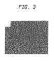
- FIG. 3is a scanning electron micrograph of a silicon surface, obtained at a 45-degree angle relative to the surface, after irradiation of the surface with 100 fsec pulses having a central wavelength of 800 nm and a fluence of about 5 kJ/m 2 ,
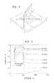
- FIG. 4schematically illustrates an experimental set-up for performing resistivity and Hall effect measurements on a silicon sample microstructured in accordance with the teachings of the invention
- FIG. 5presents a plurality of graphs depicting wavelength absorptance of prototype microstructured silicon wafers as a function of an average number of 100 laser shots (8 kJ/m 2 ) per location employed for microstructuring the wafers in the presence of SF 6 ,
- FIG. 6presents a plurality of graphs depicting wavelength dependence of absorptance of a plurality of prototype silicon wafers annealed at different temperatures subsequent to their micro structuring by a plurality of femtosecond laser pulses (the room temperature (300 K) data corresponds to a wafer that was not annealed),
- FIG. 7presents graphs depicting wavelength dependence of absorptance for exemplary femtosecond-laser-formed and nanosecond-laser-formed microstructured silicon wafers, before and after thermal annealing at 875 K for about 30 minutes (the absorptance of an unstructured silicon substrate as a function of wavelength is also shown for comparative purposes),
- FIG. 8Apresents graphs depicting absorptance as a function of wavelength for a plurality of prototype silicon wafers micro structured by exposure to 500 laser shots of femtosecond pulses (fluence of 8 kJ/m 2 ) in the presence of different gases in the absence of annealing (the graph designated vacuum relates to wafer microstructured in a vacuum chamber at a base pressure less than about 10 ⁇ 6 bar),
- FIG. 8Bpresents absorptance data as a function of wavelength for a plurality of prototype silicon wafers microstructured by exposure to 500 shots of 100 femtosecond laser pulses (fluence of 8 kJ/m 2 in the presence of sulfur-bearing and non-sulfur-bearing gases) indicating the positive effects of sulfur incorporation in enhancing below band-gap absorptance,
- FIG. 9presents graphs depicting wavelength dependence of absorptance for a plurality of prototype silicon wafers microstructured by femtosecond laser pulses in the presence of SF 6 at different partial pressures
- FIG. 10schematically illustrates a p-n junction in thermal equilibrium
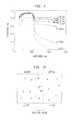
- FIG. 11Ais a perspective view of a photodetector formed in accordance with one embodiment of the invention.
- FIG. 11Bis a side view of the photodetector depicted in FIG. 11A .
- FIG. 12presents graphs depicting current-voltage characteristics of a plurality of exemplary silicon wafer microstructured by exposure to femtosecond laser pulses in the absence of annealing as well as in the presence of annealing at different annealing temperatures,
- FIG. 13presents graphs depicting responsivity of a plurality of silicon wafers microstructured by exposure to femtosecond laser pulses in the presence of SF 6 (with no annealing and with annealing at different temperatures) as a function of wavelength in comparison with that of a commercial photodiode illustrating that a significantly enhanced responsivity can be obtained by judicious annealing of wafers subjected to laser micro structuring,
- FIG. 14present graphs depicting current-voltage characteristics of a plurality of exemplary prototype silicon wafers microstructured by femtosecond laser pulses at different laser fluences and each annealed at 825 K,
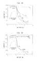
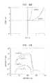
- FIG. 15Apresents comparative responsivity measurements for prototype silicon wafers microstructured by femtosecond laser pulses at different fluences and each annealed at 825 K for about 30 minutes,
- FIG. 15Bpresents comparative responsivity measurements for prototype silicon wafers microstructured by femtosecond laser pulses at different fluences and each annealed at 1075 K for about 30 minutes,
- FIG. 16Apresents current-voltage characteristics for n-doped and p-doped silicon substrates microstructured by exposure to femtosecond laser pulses at a fluence of 6 kJ/m 2 followed by annealing at 825 K for about 30 minutes,
- FIG. 16Bpresents current-voltage characteristics for n-doped and p-doped silicon substrates microstructured by exposure to femtosecond laser pluses at a fluence of 4 kJ/m 2 followed by annealing at 1075 K for about 30 minutes,
- FIG. 17Apresents responsivity measurements for prototype exemplary n-doped and p-doped silicon substrates microstructured at two different laser fluences (4 kJ/m 2 and 6 kJ/m 2 ) and annealed at 825 K for about 30 minutes,
- FIG. 17Bpresents responsivity measurements for prototype exemplary n-doped and p-doped silicon substrates microstructured by femtosecond laser pulses at a fluence of 4 kJ/m 2 and annealed at 1075 K for about 30 minutes,
- FIG. 18presents a graph depicting responsivity as a function of back bias for an n-doped silicon substrate microstructured via irradiation by femtosecond laser pulses at a fluence of 4 kJ/m 2 and annealed at 825 K for about 30 minutes (the measurement was performed by employing a white light source with an approximate power of 50 microwatts),
- FIG. 19Apresents graphs depicting current-voltage characteristics of an n-doped silicon sample microstructured by femtosecond laser pulses at a fluence of 4 kJ/m 2 and annealed at 825 K as a function of operating temperature
- FIG. 19Bpresents a graph depicting the responsivity of a microstructured silicon wafer to incident radiation having a wavelength of 1064 nm as a function of operating temperature
- FIG. 20illustrates current-voltage characteristics for a high resistivity (resistivity greater than 1 Ohm-m) microstructured silicon wafer that can be utilized as a solar cell, with and without one sun illumination,
- FIG. 21illustrates current-voltage characteristics for a low resistivity (e.g., a resistivity in a range of about 0.01 to about 0.1 Ohm-m) microstructured silicon wafer that can be utilized as solar, with and without one sun illumination,
- a low resistivitye.g., a resistivity in a range of about 0.01 to about 0.1 Ohm-m
- FIG. 22schematically depicts an exemplary experimental set-up for measuring field emission of a silicon substrate microstructured in accordance with the teachings of the invention.
- FIG. 23shows a graph depicting field emission current generated by a silicon wafer microstructured by exposure to femtosecond laser pulses in the presence of SF 6 as a function of a potential difference applied thereto.
- the present inventionprovides a method of fabricating a radiation-absorbing semiconductor structure in which, in an initial step 10 a , each of a plurality of locations on a surface of a silicon substrate is irradiated with one or more laser pulses while exposing the surface to a substance having an electron-donating constituent so as to generate surface inclusions containing a concentration of the electron-donating constituent.
- the laser pulsescan have a central wavelength in a range of about 200 nm to about 1200 nm, and a pulse width in a range of about tens of femtoseconds to about hundreds of nanometers.
- the laser pulse widthsare in a range of about 50 femtoseconds to about 50 picoseconds. More preferably, the laser pulse widths are in the range of about 50 to 500 femtoseconds.
- the number of laser pulses irradiating the silicon surfacecan be in a range of about 2 to about 2000, and more preferably, in a range of about 20 to about 500. Further, the repetition rate of the pulses can be selected to be in a range of about 1 kHz to about 50 MHz, or in a range of about 1 kHz to about 1 MHz.
- the fluence of each laser pulsecan be in a range of about 1 kJ/m 2 to about 12 kJ/m 2 , and more preferably in a range of about 3 kJ/m 2 to about 8 kJ/m 2 .
- the electron donating constituentis a fluid (gas or liquid), in other embodiments it can be a solid deposited over the silicon surface exposed to laser pulses.
- the silicon surfacecan be exposed to a sulfur-containing gas (e.g., SF 6 or H 2 S) while irradiated with the laser pulses.
- a sulfur-containing gase.g., SF 6 or H 2 S
- Cl 2 or N 2is employed as the electron-donating substance with which the silicon surface is in contact during laser irradiation.
- selenium or telluriumcan be employed.
- the silicon substrateis p-doped (e.g., doped with Boron) with a doping level in a range of about 10 11 to about 10 18 .
- the silicon substrateis slightly n-doped (e.g., doped with Phosphorus) with a doping level in a range of about 10 11 to about 10 18 , and preferably in a range of about 10 12 to about 10 15 .
- the substrate thicknessis not typically a critical parameter, and can be in a range of about 2 microns to about 1000 microns.
- the substratecan have an electrical resistivity in a range of about 0.001 ohm-m to about 10 ohm-m.
- FIG. 2schematically depicts an exemplary apparatus 12 that can be utilized for irradiating a silicon sample with a plurality of femtosecond pulses.
- the apparatus 12includes a sample processing chamber 14 that comprises a stainless steel cube 16 with Conflat flange connections on each of its six sides.
- a three-axis, precision motion controller 18is attached to the back side of the cube. This controller contains two orthogonal micrometer precision axes driven by computer controlled motors. The third axis is hand-controlled with about 1 mil precision.
- the controllercan translate a one-inch diameter stainless steel rod 20 that supports a 2-inch diameter mounting magnet 22 in the center of the cube to which a magnetizable sample holder can be mounted.
- a two-stage roughing pump 24is coupled to the cube to evacuate the chamber to a base pressure of approximately 10 ⁇ 3 torr.
- Two pressure gauges 26 and 28are employed to monitor the chamber's pressure.
- a leak valve 30 and a gas-handling manifold(not shown) allow introduction of gases of interest into the chamber.
- An optical grade, 4.5 inch quartz window 32is attached to the front of the chamber for providing laser access. Further, a quick-access viewport door 34 allows rapid loading and removal of samples as well as safe viewing of the sample during micro structuring.
- a regeneratively amplified, femtosecond TkSapphire laser system(not shown) provides approximately 100 fs laser pulses having a central wavelength of 800 nm at a repetition rate of 1 kHz.
- the laser pulsesare focused by a anti-reflection coated, plano-convex lens 36 (e.g., having a focal length of about 250-nm) through the quartz window onto the sample surface.
- the lensis mounted on a single axis linear translation stage and positioned such that its focal point is behind the sample. By moving the lens, and hence its focal point, the laser spot size can be varied at the sample surface (e.g., from a diameter of about 30 microns to 250 microns).
- a CCD (charge coupled device) camera 38can be placed at the same distance as the sample surface from the lens.
- a flipper mounted mirror 40can redirect the laser beam onto the camera to determine its spot size on the sample surface.
- a second CCD camera 42can measure reflections of light generated by a white light fiber lamp 44 from the sample surface to monitor progress during micro structuring.
- samples attached to a magnetizable sample holdercan be loaded through the access door and attached to the mounting magnet. Samples can be then positioned in the center of the magnet to allow for maximum translation.
- the chambercan be evacuated to a base pressure of 10 ⁇ 3 torr and then filled to the desired pressure with an ambient gas (e.g., 0.67 bar of sulfur hexafluoride).
- the samplecan then be irradiated with a 1-kHz train of 100-femtosecond 800-nm laser pulses.
- the fluence of each pulsecan be set by selecting a spot size (e.g., 150 microns) and employing a waveplate/polarizing cube combination to vary the pulse energy.
- Either a single spotcan be irradiated, or more typically the sample can be translated by utilizing the motion controller relative to the laser beam.
- the samplecan be translated in a raster scan pattern.
- An average number of pulses irradiating a given spot on the samplecan be controlled by utilizing a shutter and varying the horizontal translation speed.
- the irradiation of the silicon surface with the laser pulses in the presence of SF 6 at a selected partial pressurecan cause formation of a sulfur-rich layer having a sulfur concentration in a range of about 0.1 atom percent to about 5 atom percent, and more preferably, in a range of about 0.5 atom percent to about 1 atom percent.
- This sulfur-rich layerexhibits an undulating surface morphology (topography) with micron-sized surface height variations.
- FIG. 3shows a scanning electron micrograph (SEM) of a such a micro-structured silicon surface (obtained in a direction forming a 45 degree angle relative to the surface) after irradiation of the silicon surface with an average of 5 shots of femtosecond laser pluses (100 femtoseconds) at a wavelength of 800 nm and having a fluence of 8 kJ/m2 in 0.67 bar of SF 6 .
- SEMscanning electron micrograph
- the sulfur-rich layercan be a substantially disordered layer that is several hundred nanometers thick and made up of nanocrystallites (e.g., about 10-50 nm in diameter) and nanopores.
- Selected area diffraction (SAD) measurementsindicate that the surface layer retains a substantial crystalline order with a strong possibility that amorphous-like material is present between the nanocrystalline grains.
- SAD measurements performed on silicon substrates exposed to either 10 or 500 pulses per locationindicate that the substrate below the disordered layer comprises substantially undisturbed crystalline silicon (when a crystalline silicon substrate is utilized).
- RBSRutherford backscattering spectroscopy
- EDXenergy dispersive X-ray emission spectroscopy
- RBS spectra obtained from silicon samples exposed to different femtosecond (100 femtoseconds) laser shots per irradiation locationshow that the concentration of sulfur increases with increasing laser pulse numbers up to about 50 pulses.
- the measured sulfur concentrationincreases from about 0.2 atom percent for a sample exposed to 2 pulses per location to about 0.7 atom percent for a sample exposed to 50 laser pulses per location with the sulfur concentration exhibiting a plateau for laser pulses higher than about 50.
- the microstructures in the stationary sampleshave a micrometer-sized sphere at the tip while the translated samples are sharper and lack the spheres. Further, the translated samples have a larger amount of nanoscale particles spread across the microstructured surface.
- the wavelength of the irradiating laser pulses, their fluence, and pulsewidthscan also affect the morphology of the micro structured surface.
- the morphologyshowed a transition from laser-induced periodic surface structures, to a coarsened surface, to sharp microstructures, such as those depicted in the above FIG. 3 .
- the fluenceis preferably selected to be above a threshold fluence that would cause melting (e.g., 1.5 kJ/m 2 ).
- a threshold fluencethat would cause melting
- material removalcan become extreme and gaussian-shaped holes, rather than conical structures, can be formed in the surface.
- the micro structuring of the surfacecan also be achieved by employing picosecond or nanosecond pulses.
- picosecond or nanosecond pulsesFor example, a number of silicon samples were microstructured by utilizing a train of 248-nm, 30-ns laser pulses with a flat-top spatial profile and a fluence of 30 kJ/m 2 generated by a KrF+ excimer laser in the presence of 1 bar of SF 6 (an average of 1500 pulses per spot were employed).
- the nanosecond-laser-formed microstructuresshowed some similarities and some differences relative to the femtosecond-laser-formed microstructures.
- the microstructureswere roughly conical, but the structures formed with the femtosecond laser pulses were smaller and more densely packed.
- the femtosecond structureswere roughly 8 microns tall and separated by about 4 microns while the nanosecond-formed structures were roughly 40 microns tall and separated by about 20 microns.
- the femtosecond-formed structureswere covered with nanoparticles 10-50 nm in diameter while the surface of the nanosecond-formed structures were much smoother.
- Sample silicon wafers exposed to picosecond pulses (e.g., 10 picosecond) in the presence of SF 6also showed a microstructured surface.
- the average separation between the microstructuresexhibited a decrease from about 100 femtosecond pulse widths to about 5 picosecond pulse widths but then showed an increase for pulse widths longer than about 5 picoseconds.
- the laser wavelengthcan also affect the final morphology of the microstructures.
- a prototype silicon sample micro structured with a train of 400 nm pulsesexhibited a higher density of microstructures (but smaller) than those generated by 800 nm pulses at a similar fluence.
- microstructures' morphologyinclude laser polarization and laser propagation direction relative to the irradiated silicon surface.
- the direction of microstructure growthis parallel to the direction of incident light, and appears to be independent of the substrate's crystallographic planes.
- the base of microstructurecan have an elliptical shape with the long axis perpendicular to the polarization of the irradiating laser light. Without being limited to any theory, this elliptical shape can be understood as being due to a higher absorption of p-polarized light relative to s-polarized light. For circularly polarized light, there is no preferential ablation, and the base of the microstructures can be substantially circular.
- the fluid or solid in contact with the silicon surface during its micro structuringcan also affect the resultant surface morphology.
- utilizing SF 6 or Cl 2 as the ambient gascan lead to sharp-tipped conical structures with a radius of curvature of about 500 nm.
- structures made in air, N 2 or vacuumare much more rounded (the radius of curvature of their tips is approximately 2-3 microns) than those made in these halogen-containing gases.
- those made in SF 6exhibited the greatest density of microstructures followed by those made in Cl 2 .
- the microstructure densities produced in the presence of N 2were approximately equal to those made in air, but approximately a factor of two less than the densities obtained by employing SF 6 .
- the laser micro structuring of a silicon waferis performed in the presence of a mixture of two or more substances.
- samples micro structured in the presence of a mixture of SF 6 and Cl 2exhibited an increase in the microstructure density at higher partial pressure of SF 6 .
- the sulfur-rich microstructured layerhas unique optical and electrical properties. For example, it can exhibit a sheet charge carrier density in a range of about 10 12 cm ⁇ 2 to about 10 14 cm ⁇ 2 .
- a sheet charge carrier densityin a range of about 10 12 cm ⁇ 2 to about 10 14 cm ⁇ 2 .
- resistivity and Hall effect measurementsthe van der Pauw technique, well-known to those having ordinary skill in the art, was employed. Briefly, four ohmic electrical contacts were formed on the disordered microstructured layer.
- the electrical contactswere formed by initially dipping a microstructured sample in a 5% HF solution for 5 minutes to remove any native oxide layer. Subsequently, with a mask covering all but the very corners of a selected microstructured surface area (e.g., a 10 ⁇ 10 mm 2 surface area), chromium/gold (Cr/gold) was evaporated onto the surface to form metal contacts at the exposed corners. A dicing saw was then used to cut slivers (e.g., 0.25 mm slivers) from each side. Cutting the sample edges ensures that the contacts are only connected to the surface layer and not the substrate layer. Finally, a wire bonder is utilized to connect the contacts on the corners of the sample to four Cr/Au contact pads evaporated onto a glass slide. It should be understood that this experimental arrangement, shown schematically in FIG. 4 , is sensitive primarily to the electronic properties of the microstructured layer, and not that of the substrate.
- the resistivity measurementscan be performed by applying a small DC current (e.g., 10 microamperes) from corner 2 to corner 1 while measuring a voltage from corner 3 to corner 4.
- Hall effect measurementscan be performed by placing the sample in a strong magnetic field (e.g., a field of several thousand gauss) with the magnetic field perpendicular to the silicon surface.
- a small AC currentabout 1-2 microamperes was then applied from contact 1 to contact 3 while measuring an induced voltage across contacts 2 and 4.
- micro structured layerexhibits a higher sheet carrier density than the original substrate, but a lower carrier mobility—presumably as a result of the disorder in the micro structured layer.
- the substratecan annealed (step 10 b ) at a sufficiently elevated temperature for a selected time duration so as to cause an increase in the charge carrier density in the micro structured layer, e.g., by a factor in a range of about 10 percent to about 200 percent.
- the substratecan be annealed at a temperature in a range of about 500 K to about 1100 K, and more preferably, in a range of about 500 K to about 900 K, for a selected time duration, e.g., a time duration in a range of about a few minutes to about a few hours (e.g., one-half hour).
- the annealing stepcan be performed by employing a variety of different techniques.
- the substratecan be placed in a thermal oven to be exposed to an elevated temperature for a selected duration.
- the substratecan be exposed to laser radiation, e.g., radiation having a wavelength in a range of about 200 to about 1200 nm, to cause its heating to a desired temperature.
- the annealing stepcan be performed, for example, in an inert atmosphere (e.g., an argon atmosphere) or in a vacuum (a low-pressure environment).
- the annealing stepcan be applied simultaneously with the irradiation step. That is, the irradiation of the silicon substrate with the laser pulses can be performed while the substrate is maintained at an elevated temperature.
- the annealing stepis designed to cause a rearrangement of the atomic bonds within the metastable micro structured layer to enhance the density of charge carriers—electrons—within that layer.
- charge carrier densityis known to those having ordinary skill in the art. To the extent that any further explanation may be required, it refers to density of those charged particles, e.g., electrons, that are primarily responsible for current conduction, e.g., electrons in the conduction band states or in shallow impurity states below the conduction band. Such charged carriers are also herein referred to as free electrons or holes.
- the annealing temperature and durationare selected to cause structural changes in the microstructured layer that result in increasing the carrier density in that layer while substantially maintaining responsivity of the layer for generating an electrical current when exposed to radiation within a selected wavelength range at a given applied back bias voltage, as discussed in more detail below.
- the structural changes caused in the microstructured sulfur-rich layer by an annealing step according to the teachings of the inventioncan be appreciated by considering that in many embodiments in which a p-doped silicon substrate is exposed to a plurality of laser pulses to generate a microstructured surface layer therein, holes, rather than electrons, constitute the dominant charge carriers even after incorporation of about 1 atom percent sulfur having two possible donor electrons per atom.
- electronscan constitute the dominant charge carriers in the microstructured layer.
- sulfur in the microstructured layerbefore annealing, is incorporated in silicon such that its donor electrons do not substantially contribute to conduction (the donor electrons are likely locked up in a trap, or perhaps the coordination number of the implanted sulfur is larger than four).
- An annealing step according to the teachings of the inventioncauses atomic bond rearrangements in the microstructured layer so as to free up donor electrons for contributing to electrical conduction.
- the number of donor electrons released during annealingcan be sufficiently large to eliminate the holes as the dominant charge carriers and turn the microstructured layer into an n-doped layer having a sheet carrier concentration on the order of about 10 14 cm ⁇ 2 .
- a microstructured silicon wafer formed in accordance with the teachings of the inventionexhibits absorption of incident electromagnetic radiation, particularly radiation having wavelengths in a range of about 250 nm to about 2500 run.
- FIG. 5presents absorption data for a microstructured silicon wafer (an n-Si (111) wafer having a thickness of about 260 microns and a resistivity in a range of about 8-12 ohm-m), each of which was generated by exposing its surface to 100 femtosecond laser pulses (2 to 500 shots per location) having a central wavelength of 800 nm and a fluence of about 8 kJ/m 2 .
- This exemplary absorption datawas recorded in a manner known in the art, prior to annealing the wafer, by employing an spectrophotometer equipped with an integrating sphere.
- the absorption data for an unstructured silicon waferis also provided for comparative purposes.
- This exemplary dataindicates that the microstructured wafers exhibit an enhanced absorption of incident electromagnetic radiation, relative to unstructured silicon, across the entire recorded wavelength range, and particularly for wavelengths above about 1050 nm, which corresponds to the band-gap energy of crystalline silicon (1.05 eV).
- unstructured siliconlight photons having wavelengths longer than a wavelength corresponding to the band-gap energy do not contain sufficient energy to promote an electron from the valence band to the conduction band, leading to a drastic drop in absorption.
- the silicon wafers microstructured in accordance with the teachings of the inventionexhibit significant absorption not only for wavelengths below the band-gap but also for those above it.
- the exemplary data of FIG. 5shows that silicon wafers structured by exposure to 20 pulses per location or higher (e.g., 500 pulses in this exemplary data set) exhibit near-unity, featureless absorption of wavelengths from about 0.4 micron to about 1 micron, a small decrease in absorption for wavelengths around about 1.05 micron (a wavelength corresponding to the band edge of unstructured silicon), and strong featureless absorption from about 1.05 microns to about 2.5 microns. It should be understood that this data is presented only for illustrative purposes, and is not necessarily intended to present the optimal absorption of a silicon wafer structured in accordance with the teachings of the invention.
- a microstructured waferis annealed at a temperature and for a duration designed to enhance the charge carrier concentration in its microstructured layer.
- Such annealingcan be performed at a variety of different temperatures.
- FIG. 6schematically illustrates electromagnetic radiation absorptance data for a plurality of microstructured silicon wafers generated by utilizing 500 laser pulses per surface location (100 fs pulses at a central wavelength of 800 nm and a fluence of 8 kJ/m2) in the presence of 0.67 bar of SF 6 relative to that of unstructured silicon.
- Each structured waferwas annealed at a selected temperature in a range of about 575 K to about 875 K for about 30 minutes.
- a microstructured silicon wafer according to the teachings of the inventioncan be generated not only by utilizing femtosecond pulses, but also other pulse widths (e.g., nanosecond and picosecond pulse widths).
- FIG. 7illustrates exemplary absorptance graphs as a function of incident radiation wavelength for femtosecond-laser-formed and nanosecond-laser-formed microstructured silicon surfaces, before and after annealing at about 875 K for about 30 minutes, as well as that of an unstructured silicon wafer.
- the femtosecond-formed microstructureswere generated by employing 100 fs laser pulses (500 shots per location) having a central wavelength of about 800 nm and a fluence of about 8 kJ/m 2 .
- the nanosecond-formed microstructureswere generated by employing 30 ns laser pulses (about 1500 shots per location) having a central wavelength of 248 nm and a fluence of about 30 kJ/m 2 . It should be understood that this data is presented only for illustrative purposes and is not intended to necessarily indicate absorptance exhibited by a microstructured silicon formed in accordance with the teachings of the invention under all circumstances.
- micro structuring of a silicon wafercan be accomplished in the presence of a background fluid rather than SF 6 .
- a background fluidrather than SF 6 .
- H 2 S, Cl 2 , N 2 or aircan be utilized.
- FIGS. 8A and 8Bcompare absorptance of some exemplary prototype microstructured silicon wafers generated by employing femtosecond laser pulses (100 fs, 800 nm, 8 kJ/m 2 and 500 shots per location) in the presence of various fluids—without an annealing step—with that of unstructured silicon.
- the vacuum datacorresponds to micro structuring the wafer in a chamber evacuated to a base pressure that is less than about 10′′ bar.
- FIG. 9shows absorptance data for a number of exemplary prototype microstructured silicon wafers generated in SF 6 (100 fs pulses, 800 nm, 500 shots per location) at different ambient pressures, as well as a wafer microstructured in vacuum (e.g., a pressure of less than 10 ⁇ 6 ). The greatest rate of increase is observed at low pressures.
- the below band-gap absorptancedoes not show much variation with wavelength, while at lower pressures, it decreases with increasing wavelength.
- microstructured silicon wafers generated in accordance with the teachings of the inventionparticularly those subjected to an annealing step at an elevated temperature in a range of about 500 K to about 900 K, not only exhibit enhanced absorption of electromagnetic radiation over a wide range (e.g., from ultraviolet wavelengths to near infrared), but they also exhibit voltage-versus-current profiles that are characteristic of diodes. As discussed in more detail below, these properties allow the use of such microstructured silicon wafers in fabricating photodetectors that exhibit enhanced responsivity relative to conventional silicon photodetectors.
- a microstructured silicon layer formed in accordance with the teachings of the inventionforms a diode junction, e.g., a p-n junction, with the underlying silicon substrate.
- a diode junctionas used herein can also refer a junction formed between two n-doped portions having different free electron densities. As shown schematically in FIG.
- a p-n junctioncan be formed by bringing a semiconductor material having acceptor impurity atoms (p-doped) into contact with a semiconductor material having donor impurity atoms (n-doped).
- the difference in charge carrier concentration between the p-doped and the n-doped portionsgenerates a diffusion potential across the junction—electrons and holes begin to diffuse across the junction to portions having a respective lower concentration. As they cross to the other side of the junction, they recombine with their oppositely charged electrical counterparts in a region very close to the junction.
- This migration of charge carries across the junctioncauses formation of space charges (immobile ions) with opposite polarities on the two sides of junction. As the number of space charges increases (positively charged for the n-type side and negatively changed for the p-type side), a potential difference builds up across the junction, which results in an electric field in a direction opposite that of the diffusion potential.
- a thin insulating layeris present near the junction in which charge carriers have been depleted by recombination (depletion region).
- a strong electric fieldis present in the depletion region and a large electric potential exists across this region.
- the junctioncan be reverse-biased by applying an electric field across it that reinforces this internal electric field. Such a reverse-bias voltage expands the insulating depletion region and enhances both the internal electric field and the potential difference across the junction.
- the junctioncan also be forward-biased by applying an electric field that is opposite to the internal field across it. Such a forward-bias voltage shrinks the depletion region, thereby diminishing the internal electric field and the potential difference across the junction.
- a silicon wafer in which a microstructured layer is formed according to the teachings of the inventioncan exhibit an I-V curve characteristic of that obtained by a diode junction.
- a current-voltage behaviorcan be understood by considering that the wafer includes two adjacent, yet distinct, layers: a surface layer in which a concentration of an electron-donating constituent is incorporated and an underlying substantially undisturbed silicon substrate layer. These two layers exhibit different crystalline structures, chemical compositions, and charge carrier doping concentrations.
- the microstructured layerhas unique optical properties including high absorptance of incident electromagnetic radiation from the near ultraviolet into the near-infrared wavelengths.
- the inventionemploys such microstructured silicon wafers for fabricating photodiodes, as discussed in more detail below.
- FIG. 11Aschematically illustrates a photodetector 46 according to one embodiment of the invention that includes a microstructured silicon wafer 48 having a microstructured surface layer 50 that is formed in a silicon substrate 51 by irradiating a plurality of locations on a substrate's surface with short laser pulses (e.g., pulse widths in a range of about tens of femtoseconds to tens of nanoseconds) while exposing the surface to a substance having an electron-donating constituent (e.g., SF 6 ).
- short laser pulsese.g., pulse widths in a range of about tens of femtoseconds to tens of nanoseconds
- the laser-irradiated waferis then annealed under conditions (e.g., at an elevated temperature and for a selected duration) designed to enhance concentration of electrons in the microstructured surface layer (e.g., annealing at a temperature in a range of about 500 K to about 900 K for a duration of a few minutes to a few hours).
- conditionse.g., at an elevated temperature and for a selected duration
- concentration of electrons in the microstructured surface layere.g., annealing at a temperature in a range of about 500 K to about 900 K for a duration of a few minutes to a few hours.
- the exemplary photodetector 46functioning as a photodiode, also includes a plurality of metallic electrical contacts 52 , which have a finger grid geometry, that are disposed on the microstructured surface layer.
- an electrical contact 54in the form of a metallic coating layer, is disposed on the back surface of the silicon substrate (i.e., the undisturbed silicon surface opposite the microstructured surface) that substantially covers the entire surface.
- a chromium/gold alloyCr/Au
- the contactscan be formed of other metals, as well.
- the metallic contacts 52 and 54allow applying a bias voltage, e.g., a reverse bias voltage, across the wafer by employing, for example, a voltage source 56 .
- the reverse bias voltagecan reinforce the internal electrical field in the depletion layer of a diode junction formed between the microstructured layer 50 and the underlying silicon substrate 51 .
- the photodetector 46can operate with small bias voltages, e.g., voltages in a range of about 0.1 V to about 15 V, with a responsivity (i.e., photocurrent generated per unit of power of incident light (amperes/watts)) that is considerably better than that typically exhibited by a conventional silicon photodetector.
- These attributesallow incorporating silicon photodetectors formed according to the teachings of the invention, such as the exemplary photodetector 46 , into integrated silicon photo-electronic circuits as high sensitivity detectors.
- radiationi.e., photons
- the micro structured surface layer of the photodiode's silicon waferis absorbed (when the radiation wavelength is in the operating range of the photodetector), e.g., by valence electrons, in the micro structured layer.
- the absorption of the incident radiationcauses generation of electron-hole pairs.
- the electric field within the depletion regioncauses separation of the generated electron-hole pairs, especially those created at or in proximity of the diode junction, which is formed between the micro structured silicon layer and the underlying silicon substrate.
- the separated electron-hole pairsprovide a photocurrent that is proportional to the number of incident photons (those skilled in the art appreciate that such a photocurrent is added to a generation current and a recombination current that can be inherently present in a diode junction). Hence, incident radiation can be detected, and quantified, by measuring the induced photocurrent.
- a photodetector formed according to the teachings of the inventionnot only exhibits absorptance across a wide range of wavelengths (the absorptance is generally commensurate with that exhibited by the photodetector's microstructured silicon wafer), but it also exhibits a diodic I-V behavior.
- FIG. 12illustrates a plurality of graphs, each representing current as a function of bias voltage for a plurality of microstructured silicon samples prepared under different conditions in an n-doped silicon substrate for use as the active component of photodetectors.
- the graph Arepresents the current-voltage curve associated with a microstructured sample that was not annealed. This curve is substantially linear, indicating that the junction between the microstructured layer and the underlying silicon substrate in this sample is not diodic, but is merely resistive. In other words, such a wafer is not optimal for fabricating a photodetector.
- graphs B, C, and Dillustrate current-versus-voltage behavior of those microstructured silicon samples that were subjected to annealing at different temperatures (the annealing duration was about 30 minutes in all cases).
- This exemplary dataindicates that with an increase in the annealing temperature, the measured I-V curve approaches one expected from a diode. For example, at an annealing temperature of about 825 K, the I-V curve is diodic, characterized by an exponentially increasing current for a forward bias and a smaller, less rapidly increasing current for a reverse bias. The I-V curve corresponding to an annealing temperature of about 1075 K is also diodic.
- annealing a microstructured silicon wafer for a significant duration at a very elevated temperaturecan lead to a degradation of the below-band gap absorptance, and hence a degradation in the performance of a photodetector utilizing such a microstructured wafer in the near-infrared.
- the substrate annealed at 825 Kexhibit an optimal I-V characteristic. It should, however, be understood that such very elevated annealing temperatures may be employed so long as the annealing duration is sufficiently short.
- the annealing of a microstructured silicon wafer to be employed in a photodetector of the inventionshould be carefully designed (i.e., annealing temperature and duration) to cause release of electro ns in the microstructured surface layer without significantly degrading the wafer's absorptance of and responsivity to incident radiation.
- a photodetector of the inventionsuch as the above exemplary photodetector 46 , exhibits a responsivity that can be superior across a wavelength range of about 250 nm to about 10 microns to that of a conventional silicon photodiode.
- FIG. 13presents experimental graphs representing responsivity of exemplary photodetectors formed in accordance with the teachings of the invention, over a selected wavelength range, in comparison with a conventional photodiode and those fabricated by employing microstructured silicon, but with no annealing or annealing at too high a temperature.
- graphs A and Bshow that photodetectors of the invention that employ silicon wafers microstructured by femtosecond laser pulses in the presence of SF 6 (100 fs, 800 nm central wavelength and a fluence of 4 kJ/m 2 ) followed by annealing at 825 K or 725 K, exhibit a significantly enhanced responsivity relative to that of a conventional commercially available silicon photodiode.
- these photodetectorsexhibit a responsivity that is more than an order of magnitude greater than that of the conventional photodiode in a wavelength range of about 250 nm to about 1050 nm.
- the responsivityshows a decrease for wavelengths longer than the band-gap edge (i.e., wavelengths longer than about 1050 nm), nonetheless, it remains significantly higher than that exhibited by a conventional silicon detector.
- conventional silicon detectorstypically do not operate at useful levels of responsivity at wavelengths that are longer than the band-gap edge.
- the responsivity of the commercial photodiodedrops steeply to about 10 ⁇ 6 A/W for wavelengths longer than about 1050 nm
- the responsitivity data for wafers formed according to the teachings of the inventionwere obtained by applying small bias voltages (e.g., a bias voltage of about ⁇ 0.5 volts in this exemplary embodiment).
- small bias voltagese.g., a bias voltage of about ⁇ 0.5 volts in this exemplary embodiment
- conventional silicon photodetectorsexhibit much lower responsivities, or require much higher bias voltages (e.g., 100 to 1000 volts) and/or have more complex structures. This indicates that while photodetectors formed in accordance with the teachings of the invention can be readily incorporated in integrated silicon circuitry, the incorporation of conventional silicon detectors, which require large bias voltages, into integrated silicon circuits can be impractical.
- the data depicted in FIG. 13also shows that proper annealing of a silicon wafer irradiated by a plurality of short laser pulses, as described above, can considerably enhance the responsivity of a photodetector that employs that wafer.
- This exemplary dataalso shows that a photodetector that incorporates a microstructured wafer annealed, subsequent to irradiation by laser pulses, at a temperature of 1075 for thirty minutes exhibits a much degraded responsitivity relative to those annealed at 725 K or 825 K.
- one aspect of the inventionrelates to annealing a silicon wafer, subsequent to—or simultaneous with—its irradiation by a plurality of short pulses in the presence of a substance having an electron-donating constituent, under conditions that would release electrons in the microstructured layer while preserving the responsivity of the wafer for detecting electromagnetic radiation.
- the annealing temperatureis selected to be in range of about 500 K to about 1100 K, and more preferably in a range of about 700 K to about 900 K
- the annealing durationis selected to be in a range of about 1 minute to about several hours, and more preferably in a range of about 5 minutes to about 30 minutes.
- annealing temperaturecan be employed so long as the annealing duration is properly selected to avoid degrading the responsivity of the resultant annealed wafer.
- this annealing temperature with a lower annealing durationcan be suitable for practicing the invention in certain applications.
- annealing temperature and durationare inter-related. For example, shorter annealing time at a higher temperature can be employed in certain applications.
- annealing temperature and its durationneed to be properly selected to ensure that a photodetector exhibiting enhanced responsivity over a wide wavelength range can be fabricated by utilizing the annealed wafer. It has been discovered that annealing a silicon wafer subsequent to, or simultaneous with, its exposure to short laser pulses in presence of a substance having an electron-donating constituent at a temperature that is too low can lead to noisy photodiode and annealing at too high a temperature and duration can lower the wafer's response to both visible and infrared wavelengths.
- the annealing temperature and durationare preferably selected to enhance the concentration of carrier electrons in the micro structured layer—formed by laser irradiation in presence of a substance having an electron-donating constituent—by a factor in a range of about 10% to about 200% while ensuring that the resultant annealed wafer exhibits a responsivity greater than about 20 A/W at least at one wavelength, and preferably over the entire span, of a wavelength range of about 250 ran to about 1050 nm, and a responsivity greater than about 0.1 A/W at least at one wavelength, and preferably over the entire span, of a wavelength range of about 1050 nm to about 3500 nm.
- the annealing temperatureis preferably selected to be in a range of about 700 to about 900 K.
- FIG. 14presents exemplary data corresponding to current-voltage characteristics of a plurality of silicon wafers irradiated with a plurality of femtosecond laser pulses (100 fs, 800 nm central wavelength, 200 pulses per location) in the presence of SF 6 followed by annealing at 825 K for about 30 minutes.
- the laser pulse fluencesdiffered from one wafer to another.
- FIG. 15Aillustrates the responsivity of a plurality of photodetectors incorporating the above silicon wafers that were microstructured with different laser pulse fluences (the wafers were annealed at 825 K for 30 minutes).
- This exemplary responsivity dataindicates that, in this sample set, the photodetector's responsivity decreases, and the wavelength of peak response shifts to longer wavelengths, with increasing fluence (the sample made with a fluence of 4 kJ/m 2 exhibits the highest response).
- FIG. 15Aillustrates the responsivity of a plurality of photodetectors incorporating the above silicon wafers that were microstructured with different laser pulse fluences (the wafers were annealed at 825 K for 30 minutes).
- This exemplary responsivity dataindicates that, in this sample set, the photodetector's responsivity decreases, and the wavelength of peak response shifts to longer wavelengths, with increasing fluence (the sample made with a fluence of 4
- the samples annealed at the higher temperatureexhibit much less variation in responsivity as a function of fluence. Further, the samples annealed at 1075 K—though exhibiting a lower responsivity—are less noisy and have a higher quantum efficiency.
- the above datais presented only for illustration purposes, and is not intended to necessarily indicate an optimal fluence under all conditions.
- the above exemplary sampleswere made with an average laser shot number of about 200 pulses, and may exhibit improved characteristics with a greater shot number.
- the laser pulse fluenceis selected to be greater than about 3 kJ/m 2 . More preferably, the fluence is chosen to be in a range of about 3 kJ/m 2 to about 10 kJ/m 2 , or a range of about 3 kJ/m 2 to about 8 kJ/m 2 .
- an n-doped silicon substrateis employed for forming a microstructured wafer, as described above.
- a p-doped silicon wafercan be utilized.
- FIG. 16Apresents graphs comparing the diodic characteristics of a microstructured wafer generated according to the teachings of the invention, such as those described above, employing a p-doped silicon substrate (p-Si(100), 350 micron thick, resistivity (p) greater than 1 ohm-cm) with one fabricated utilizing an n-doped silicon substrate.
- This exemplary datashows that the p-doped samples annealed at 825 K exhibit a higher forward bias current than equivalently generated n-doped samples.
- the dark current for back biasesalso increases more rapidly for p-doped samples.
- the p-doped samplesexhibit very good diodic properties with the back bias decreasing to substantially the same level as that in equivalently generated n-doped samples.
- the forward bias currentincreases more rapidly, resulting in good rectification ratios.
- annealing at higher temperaturescan increase donor concentration from sulfur doping. Such increase in the donor concentration can lead p-doped samples annealed at higher temperature to exhibit better rectification.
- FIG. 17Ashows measured responsivity data for two n-doped microstructured wafers and two p-doped microstructured wafers, both of which were annealed at 825 K for about 30 minutes.
- This exemplary dataindicates that the responsivity of n-doped substrates is higher over the measured spectral range.
- FIG. 17Bshows that the responsivities of microstructured wafers formed in p-doped and n-doped substrates, via laser irradiation and annealing at a higher temperature of about 1075 K, are nearly identical.
- the above illustrative dataindicates that microstructured p-doped samples have a lower response but exhibit a better quantum efficiency. It should be understood that the above data is presented only for illustrative purposes and is not intended to limit the scope of the invention. In general, both p-doped and n-doped substrates can be employed in the practice of the invention, and the resultant diodic characteristics and responsivity of microstructured wafers generated by utilizing such substrates can be different than those depicted above based on selection of other parameters, such as laser fluence, number of pulses, etc.
- quantum efficiencyis known in the art, and is generally defined as the number of electron-hole pairs generated per incident photon at a zero applied voltage.
- a microstructured sample that exhibits a high level of responsivitymay not show a correspondingly high level of quantum efficiency.
- samples fabricated by employing n-doped substrates, laser pulses having a fluence of 4 kJ/m 2 , and an annealing temperature of about 825 Kexhibit the highest responsivity, but not the highest quantum efficiency.
- the responsivity of a photodetector fabricated in accordance with the teachings of the inventioncan also vary as a function of a back bias applied thereto. Typically, the responsivity increases as the applied back bias increases.
- FIG. 18exhibits the responsivity of a silicon wafer microstructured in accordance with the teachings of the invention through irradiation by a plurality of femtosecond pulses at a fluence of 4 kJ/m 2 followed by annealing at 825 K for about 30 minutes, as a function of an applied back bias voltage.
- the samplewas illuminated with a white light source with an approximate power of 50 microwatts.
- the responsivity, and hence gain,increases quickly up to a bias voltage of ⁇ 5 volts and more slowly up to ⁇ 15 volts. At voltages beyond ⁇ 15 volts, the responsivity begins to fall. In some cases, the responsivity of a photodetector that exhibits a large gain may not be sufficiently linear for certain applications. Hence, in selecting a proper back voltage, in addition to responsivity, other factors, such as the linearity of the response should be considered. In addition, in applications in which the photodetectors are incorporated in an integrated silicon circuit, the bias voltage should be compatible with the requirements of that circuit.
- FIG. 19Apresents current-voltage curves corresponding to an n-doped microstructured silicon sample made with femtosecond pulses at a fluence of about 4 kJ/m 2 and annealed at 825 K at different operating temperatures. The measured current in both the back bias and forward bias conditions decreases with decreasing the temperature. At very low temperatures (below 100 K), conduction becomes very low for both forward and back biases.
- FIG. 19Apresents current-voltage curves corresponding to an n-doped microstructured silicon sample made with femtosecond pulses at a fluence of about 4 kJ/m 2 and annealed at 825 K at different operating temperatures. The measured current in both the back bias and forward bias conditions decreases with decreasing the temperature. At very low temperatures (below 100 K), conduction becomes very low for both forward and back biases.
- 19Bshows the responsivity of such a microstructured wafer to incident radiation having a wavelength of 1064 nm (a wavelength close to the band gap of silicon at room temperature) at a back bias of ⁇ 0.5 V as a function of operating temperature.
- the measured responsivitydrops with temperature. This behavior may be, however, different if the wavelength of the illuminating light is far from the silicon band gap.
- a graph of the dark current at a bias voltage of ⁇ 0.5 V as a function of temperatureshows that the noise decreases much more rapidly that the responsivity.
- photodiodes formed according to the teachings of the inventioncan exhibit responsivities in a wide region of the electromagnetic spectrum (e.g., wavelengths in a range of about 250 nm to about 1100 nm) that are nearly two orders of magnitude higher than those exhibited by conventional commercial silicon photodiodes. Further, responsivities at longer wavelengths, e.g., as long as 1600 nm, can be nearly five orders of magnitude greater than those exhibited by conventional silicon photodiodes in this range.
- the carrier mobility in the surface layerwas measured to be about 101 cm 2 V ⁇ 1 s ⁇ 1 ; the response times included a rise time of about 10 ns and a fall time of about 30 ns; and a diode capacitance of about 63.9 nF at a back bias of ⁇ 0.5 V was measured.
- a photodiode of the inventioncan exhibit a large gain at very small applied bias voltages, e.g., a gain greater than 1000 for an applied bias voltage of ⁇ 0.5 V.
- a silicon photodetector according to the teachings of the inventioncan be fabricated by employing a variety of techniques.
- a selected portion of a silicon wafere.g., a 5 ⁇ 5 mm 2 area
- a suitable materiale.g., SF 6
- the waferis then dipped in a solution of HF (e.g., a 5% solution) in order to remove any native oxide layer before forming electric contacts with the micro structured layer.
- HFe.g., a 5% solution
- a maskis deposited over the surface of the micro structured layer having exposed portions which correspond to a desired pattern of a conductive electrode to be formed on that surface.
- a selected metale.g., a Cr/Au alloy
- a patterned conductive layersuch as the conductive layer 52 shown in FIG. 11A
- uncoated portions suitable for receiving radiatione.g., a conductive layer can be formed on a back surface of the wafer, an unstructured surface opposed to the micro structured layer, such as the layer 54 shown in FIG. 11A . In many embodiments, the entire back surface is coated with the metal.
- the wafercan be then be coupled to a voltage source, such as the source 56 shown in FIG. 11A , that can apply a bias voltage thereto and optionally other electronic elements, e.g., capacitors, in a manner known in the art. Further, a the wafer and its associated circuitry can be placed in an appropriate housing by employing techniques known in the art.
- a voltage sourcesuch as the source 56 shown in FIG. 11A
- other electronic elementse.g., capacitors
- microstructured silicon wafers formed according to the teachings of the inventionare not limited to photodetectors.
- silicon waferscan be employed in fabricating solar cells.
- the optimal values of various parameters, such as substrate doping, associated with the microstructured wafer utilized in generating solar cellscan be different than those in fabricating silicon photodetectors.
- a solar cellcan be considered a p-n junction photodiode with high quantum efficiency.
- the conversion of photons into photocarriersis the physical mechanism by which light is converted in a solar cell into electricity.
- a photodetectoris generally operated in a “photoconductive” mode: a back bias is applied thereto and a current is measured.
- a solar cellis operated in a “photovoltaic” mode: it is operated in an open circuit mode or attached to a load without application of a bias voltage.
- a microstructured layeris formed in a p-doped crystalline silicon substrate by initially irradiating a plurality of locations on a surface thereof with femtosecond (e.g., 100 fs, and a central wavelength of 800 nm) laser pulses having a fluence of about 4 kJ/m 2 followed by annealing at 1075 K for about one hour.
- femtoseconde.g., 100 fs, and a central wavelength of 800 nm
- the wafercan then be utilized in fabricating a solar cell.
- metal contactse.g., Cr/Au contacts, can be evaporated on the microstructure layer's surface so as to coat selected portions thereof while leaving at least a portion of the surface uncovered for receiving radiation, e.g., a finger grid metallic pattern can be disposed on the surface.
- the back surface of the substrate, the unstructured surface opposing the structured surfacecan be coated, e.g., via evaporation, with a metallic coating.
- a loadcan be attached the wafer via electrical coupling to the metallic layers on the both sides of the wafer.
- FIG. 20presents data comparing current-voltage (I-V) behavior of such a wafer, formed in a high resistivity (resistivity greater than about 1 ohm-m) silicon substrate, that can be utilized as a solar cell in the presence and in the absence of illumination.
- FIG. 21presents a similar comparative data for a wafer formed in low resistivity silicon substrate (resistivity in a range of about 0.01-0.1 ohm-m).
- the solar cell fabricated by employing the high resistivity substratehas an open circuit voltage of 0.4 volts and a short circuit current of 13.4 mA while the solar cell fabricated by utilizing the low resistivity substrate has an open circuit voltage of 0.31 volts and a short circuit current of 13.45 mA.
- a silicon wafer microstructured in accordance with the teachings of the inventioncan be utilized as a field emitter.
- an electric fieldcan be applied to the microstructured surface to cause emission of electrons therefrom.
- a number of prototype exemplary microstructured waferswere fabricated and field emission currents generated by them were measured. The experimental step-up for performing these measurements is shown schematically in FIG. 22 .
- a microstructured silicon sample 58 with a gold coating 60 evaporated on a back surfaceis mounted to a silicon wafer 62 having a gold coating 64 , which functions as an anode, and is separated therefrom by a pair of mica spacers 66 and 68 .
- the mounted sampleis placed in a vacuum chamber, which is evacuated to a pressure of about 10 ⁇ 6 torr.
- a potential differencecan be applied between the microstructured sample 58 and the gold-coated anode.
- emission currentcan be measured at each applied voltage, e.g., via a picoammeter 70 , a resistive elements 72 placed in series with the ammeter to protect it from unexpected surges in current.
- FIG. 23shows exemplary results of field emission currents measured for silicon samples microstructured in SF 6 .
- the typical figures of merit for a field emitting surfaceare turn-on-field, defined as the electric field (bias voltage divided by the tip-to-anode spacing) for which a current density of 0.01 microampere/mm 2 is observed, and threshold field, defined as the field at which a current density of 0.1 microamperes/mm 2 is produced.
- the turn-on field for a plurality of exemplary prototype substrates micro structured in SF 6was measured as 1.3 V/micrometer, and the threshold field was measured as 2.15 V/micrometer—excellent values that are on par with those exhibited by nanotubes.
Landscapes
- Physics & Mathematics (AREA)
- Engineering & Computer Science (AREA)
- High Energy & Nuclear Physics (AREA)
- Optics & Photonics (AREA)
- Computer Hardware Design (AREA)
- Power Engineering (AREA)
- Microelectronics & Electronic Packaging (AREA)
- Condensed Matter Physics & Semiconductors (AREA)
- General Physics & Mathematics (AREA)
- Manufacturing & Machinery (AREA)
- Toxicology (AREA)
- Health & Medical Sciences (AREA)
- Electromagnetism (AREA)
- Chemical & Material Sciences (AREA)
- Crystallography & Structural Chemistry (AREA)
- Light Receiving Elements (AREA)
- Life Sciences & Earth Sciences (AREA)
- Sustainable Development (AREA)
- Investigating Or Analysing Materials By Optical Means (AREA)
- Photovoltaic Devices (AREA)
Abstract
Description
| Doping | Sheet | ||||
| Average | after | Sheet | carrier | Hall | |
| Original | fluence | struc- | resistance | density ns | mobility μ |
| doping | (kJ/m2) | turing | Rs (Ohm) | (cm−2) | (cm2V−1s−1) |
| n | unstructured | — | 31931 | 1.78 × 10¹¹ | 1101 |
| n | 4.0 | N | 4865 | 7.37 × 10¹² | 174 |
| n | 6.0 | N | 4992 | 7.15 × 10¹² | 175 |
| n | 8.0 | N | 6253 | 4.52 × 10¹² | 221 |
| n | 10.0 | N | 4554 | 8.83 × 10¹² | 155 |
Claims (17)
Priority Applications (2)
| Application Number | Priority Date | Filing Date | Title |
|---|---|---|---|
| US15/784,756US10374109B2 (en) | 2001-05-25 | 2017-10-16 | Silicon-based visible and near-infrared optoelectric devices |
| US16/532,146US20200028002A1 (en) | 2001-05-25 | 2019-08-05 | Silicon-based visible and near-infrared optoelectric devices |
Applications Claiming Priority (10)
| Application Number | Priority Date | Filing Date | Title |
|---|---|---|---|
| US29359001P | 2001-05-25 | 2001-05-25 | |
| US10/155,429US7390689B2 (en) | 2001-05-25 | 2002-05-24 | Systems and methods for light absorption and field emission using microstructured silicon |
| US10/950,230US7057256B2 (en) | 2001-05-25 | 2004-09-24 | Silicon-based visible and near-infrared optoelectric devices |
| US11/445,900US7504702B2 (en) | 2001-05-25 | 2006-06-02 | Silicon-based visible and near-infrared optoelectric devices |
| US12/365,492US7781856B2 (en) | 2001-05-25 | 2009-02-04 | Silicon-based visible and near-infrared optoelectric devices |
| US12/776,694US8080467B2 (en) | 2001-05-25 | 2010-05-10 | Silicon-based visible and near-infrared optoelectric devices |
| US13/267,618US8604580B2 (en) | 2001-05-25 | 2011-10-06 | Silicon-based visible and near-infrared optoelectric devices |
| US14/100,954US9276143B2 (en) | 2001-05-25 | 2013-12-09 | Silicon-based visible and near-infrared optoelectric devices |
| US15/003,210US9793425B2 (en) | 2001-05-25 | 2016-01-21 | Silicon-based visible and near-infrared optoelectric devices |
| US15/784,756US10374109B2 (en) | 2001-05-25 | 2017-10-16 | Silicon-based visible and near-infrared optoelectric devices |
Related Parent Applications (1)
| Application Number | Title | Priority Date | Filing Date |
|---|---|---|---|
| US15/003,210ContinuationUS9793425B2 (en) | 2001-05-25 | 2016-01-21 | Silicon-based visible and near-infrared optoelectric devices |
Related Child Applications (1)
| Application Number | Title | Priority Date | Filing Date |
|---|---|---|---|
| US16/532,146ContinuationUS20200028002A1 (en) | 2001-05-25 | 2019-08-05 | Silicon-based visible and near-infrared optoelectric devices |
Publications (2)
| Publication Number | Publication Date |
|---|---|
| US20180083146A1 US20180083146A1 (en) | 2018-03-22 |
| US10374109B2true US10374109B2 (en) | 2019-08-06 |
Family
ID=41682660
Family Applications (10)
| Application Number | Title | Priority Date | Filing Date |
|---|---|---|---|
| US10/950,230Expired - LifetimeUS7057256B2 (en) | 2001-05-25 | 2004-09-24 | Silicon-based visible and near-infrared optoelectric devices |
| US11/445,900Expired - LifetimeUS7504702B2 (en) | 2001-05-25 | 2006-06-02 | Silicon-based visible and near-infrared optoelectric devices |
| US12/365,492Expired - LifetimeUS7781856B2 (en) | 2001-05-25 | 2009-02-04 | Silicon-based visible and near-infrared optoelectric devices |
| US12/365,513Expired - LifetimeUS7884439B2 (en) | 2001-05-25 | 2009-02-04 | Silicon-based visible and near-infrared optoelectric devices |
| US12/776,694Expired - LifetimeUS8080467B2 (en) | 2001-05-25 | 2010-05-10 | Silicon-based visible and near-infrared optoelectric devices |
| US13/267,618Expired - LifetimeUS8604580B2 (en) | 2001-05-25 | 2011-10-06 | Silicon-based visible and near-infrared optoelectric devices |
| US14/100,954Expired - Fee RelatedUS9276143B2 (en) | 2001-05-25 | 2013-12-09 | Silicon-based visible and near-infrared optoelectric devices |
| US15/003,210Expired - LifetimeUS9793425B2 (en) | 2001-05-25 | 2016-01-21 | Silicon-based visible and near-infrared optoelectric devices |
| US15/784,756Expired - Fee RelatedUS10374109B2 (en) | 2001-05-25 | 2017-10-16 | Silicon-based visible and near-infrared optoelectric devices |
| US16/532,146AbandonedUS20200028002A1 (en) | 2001-05-25 | 2019-08-05 | Silicon-based visible and near-infrared optoelectric devices |
Family Applications Before (8)
| Application Number | Title | Priority Date | Filing Date |
|---|---|---|---|
| US10/950,230Expired - LifetimeUS7057256B2 (en) | 2001-05-25 | 2004-09-24 | Silicon-based visible and near-infrared optoelectric devices |
| US11/445,900Expired - LifetimeUS7504702B2 (en) | 2001-05-25 | 2006-06-02 | Silicon-based visible and near-infrared optoelectric devices |
| US12/365,492Expired - LifetimeUS7781856B2 (en) | 2001-05-25 | 2009-02-04 | Silicon-based visible and near-infrared optoelectric devices |
| US12/365,513Expired - LifetimeUS7884439B2 (en) | 2001-05-25 | 2009-02-04 | Silicon-based visible and near-infrared optoelectric devices |
| US12/776,694Expired - LifetimeUS8080467B2 (en) | 2001-05-25 | 2010-05-10 | Silicon-based visible and near-infrared optoelectric devices |
| US13/267,618Expired - LifetimeUS8604580B2 (en) | 2001-05-25 | 2011-10-06 | Silicon-based visible and near-infrared optoelectric devices |
| US14/100,954Expired - Fee RelatedUS9276143B2 (en) | 2001-05-25 | 2013-12-09 | Silicon-based visible and near-infrared optoelectric devices |
| US15/003,210Expired - LifetimeUS9793425B2 (en) | 2001-05-25 | 2016-01-21 | Silicon-based visible and near-infrared optoelectric devices |
Family Applications After (1)
| Application Number | Title | Priority Date | Filing Date |
|---|---|---|---|
| US16/532,146AbandonedUS20200028002A1 (en) | 2001-05-25 | 2019-08-05 | Silicon-based visible and near-infrared optoelectric devices |
Country Status (1)
| Country | Link |
|---|---|
| US (10) | US7057256B2 (en) |
Cited By (5)
| Publication number | Priority date | Publication date | Assignee | Title |
|---|---|---|---|---|
| US10741399B2 (en) | 2004-09-24 | 2020-08-11 | President And Fellows Of Harvard College | Femtosecond laser-induced formation of submicrometer spikes on a semiconductor substrate |
| US20220057269A1 (en)* | 2020-08-21 | 2022-02-24 | Analog Devices, Inc. | Multi-sensor using a thermal camera |
| US11402271B2 (en)* | 2017-06-03 | 2022-08-02 | Teledyne Flir, Llc | Extensible architecture for surveillance and targeting imaging systems and methods |
| US20220377219A1 (en)* | 2021-05-18 | 2022-11-24 | Magna Electronics Inc. | Vehicular driver monitoring system with camera view optimization |
| US20240420477A1 (en)* | 2009-06-04 | 2024-12-19 | Optics Innovation Llc | Method and apparatus for a wearable computer |
Families Citing this family (112)
| Publication number | Priority date | Publication date | Assignee | Title |
|---|---|---|---|---|
| US7390689B2 (en)* | 2001-05-25 | 2008-06-24 | President And Fellows Of Harvard College | Systems and methods for light absorption and field emission using microstructured silicon |
| US7057256B2 (en)* | 2001-05-25 | 2006-06-06 | President & Fellows Of Harvard College | Silicon-based visible and near-infrared optoelectric devices |
| US7668325B2 (en) | 2005-05-03 | 2010-02-23 | Earlens Corporation | Hearing system having an open chamber for housing components and reducing the occlusion effect |
| US8401212B2 (en) | 2007-10-12 | 2013-03-19 | Earlens Corporation | Multifunction system and method for integrated hearing and communication with noise cancellation and feedback management |
| US8399331B2 (en) | 2007-10-06 | 2013-03-19 | Solexel | Laser processing for high-efficiency thin crystalline silicon solar cell fabrication |
| US9508886B2 (en)* | 2007-10-06 | 2016-11-29 | Solexel, Inc. | Method for making a crystalline silicon solar cell substrate utilizing flat top laser beam |
| US8637340B2 (en) | 2004-11-30 | 2014-01-28 | Solexel, Inc. | Patterning of silicon oxide layers using pulsed laser ablation |
| US8184284B2 (en)* | 2005-06-14 | 2012-05-22 | Ebstein Steven M | Laser-processed substrate for molecular diagnostics |
| US7715003B2 (en)* | 2005-06-14 | 2010-05-11 | President & Fellows Of Harvard College | Metalized semiconductor substrates for raman spectroscopy |
| EP1896805A4 (en) | 2005-06-14 | 2010-03-31 | Steven M Ebstein | Applications of laser-processed substrate for molecular diagnostics |
| WO2008127807A1 (en)* | 2007-03-09 | 2008-10-23 | University Of Virginia Patent Foundation | Systems and methods of laser texturing of material surfaces and their applications |
| US8846551B2 (en) | 2005-12-21 | 2014-09-30 | University Of Virginia Patent Foundation | Systems and methods of laser texturing of material surfaces and their applications |
| WO2008091242A2 (en)* | 2005-12-21 | 2008-07-31 | Uva Patent Foundation | Systems and methods of laser texturing and crystallization of material surfaces |
| WO2008091858A2 (en)* | 2007-01-23 | 2008-07-31 | President & Fellows Of Harvard College | Non-invasive optical analysis using surface enhanced raman spectroscopy |
| US20100208237A1 (en)* | 2007-01-23 | 2010-08-19 | President & Fellows Of Harvard College | Polymeric substrates for raman spectroscopy |
| US8431818B2 (en)* | 2007-05-08 | 2013-04-30 | Vanguard Solar, Inc. | Solar cells and photodetectors with semiconducting nanostructures |
| WO2009017846A1 (en)* | 2007-07-30 | 2009-02-05 | President And Fellows Of Harvard College | Substrates for raman spectroscopy having discontinuous metal coatings |
| US9455362B2 (en) | 2007-10-06 | 2016-09-27 | Solexel, Inc. | Laser irradiation aluminum doping for monocrystalline silicon substrates |
| CN102017088B (en)* | 2008-01-31 | 2013-08-07 | 哈佛大学校长及研究员协会 | Structure flat surfaces on materials doped by pulsed laser irradiation |
| WO2009100023A2 (en)* | 2008-02-01 | 2009-08-13 | President & Fellows Of Harvard College | A multijunction photovoltaic device |
| US7816220B2 (en)* | 2008-02-27 | 2010-10-19 | President & Fellows Of Harvard College | Laser-induced structuring of substrate surfaces |
| US8058615B2 (en) | 2008-02-29 | 2011-11-15 | Sionyx, Inc. | Wide spectral range hybrid image detector |
| US20090219403A1 (en)* | 2008-02-29 | 2009-09-03 | Sionyx, Inc. | Compact passive low-light imaging apparatus |
| WO2009111327A2 (en)* | 2008-02-29 | 2009-09-11 | Sionyx, Inc. | Vertically integrated light sensor and arrays |
| US8212327B2 (en)* | 2008-03-06 | 2012-07-03 | Sionyx, Inc. | High fill-factor laser-treated semiconductor device on bulk material with single side contact scheme |
| WO2009111748A2 (en)* | 2008-03-06 | 2009-09-11 | Sionyx, Inc. | High fill-factor laser-treated semiconductor device on bulk material with single side contact scheme |
| US7910391B2 (en)* | 2008-04-17 | 2011-03-22 | Sionyx, Inc. | Getter formed by laser-treatment and methods of making same |
| WO2009155358A1 (en) | 2008-06-17 | 2009-12-23 | Earlens Corporation | Optical electro-mechanical hearing devices with separate power and signal components |
| US20100013036A1 (en)* | 2008-07-16 | 2010-01-21 | Carey James E | Thin Sacrificial Masking Films for Protecting Semiconductors From Pulsed Laser Process |
| US7847253B2 (en)* | 2008-08-15 | 2010-12-07 | Sionyx, Inc. | Wideband semiconducting light detector |
| WO2010028177A1 (en)* | 2008-09-03 | 2010-03-11 | Sionyx, Inc. | High sensitivity photodetectors, imaging arrays, and high efficiency photovoltaic devices produced using ion implantation and femtosecond laser irradiation |
| BRPI0919266A2 (en) | 2008-09-22 | 2017-05-30 | SoundBeam LLC | device and method for transmitting an audio signal to a user, methods for manufacturing a device for transmitting an audio signal to the user, and for providing an audio device for a user, and device and method for transmitting a sound for a user. user having a tympanic membrane |
| US7968834B2 (en)* | 2008-09-22 | 2011-06-28 | Sionyx, Inc. | Response-enhanced monolithic-hybrid pixel |
| US20100090347A1 (en)* | 2008-10-09 | 2010-04-15 | Saylor Stephen D | Apparatus and method for contact formation in semiconductor devices |
| US20120041285A1 (en) | 2008-12-04 | 2012-02-16 | Searete Llc, A Limited Liability Corporation Of The State Of Delaware | Systems, devices, and methods including implantable devices with anti-microbial properties |
| US20100147383A1 (en)* | 2008-12-17 | 2010-06-17 | Carey James E | Method and apparatus for laser-processing a semiconductor photovoltaic apparatus |
| US7834456B2 (en) | 2009-01-20 | 2010-11-16 | Raytheon Company | Electrical contacts for CMOS devices and III-V devices formed on a silicon substrate |
| US8853745B2 (en) | 2009-01-20 | 2014-10-07 | Raytheon Company | Silicon based opto-electric circuits |
| US7745901B1 (en)* | 2009-01-29 | 2010-06-29 | Sionyx, Inc. | Highly-depleted laser doped semiconductor volume |
| US20100210930A1 (en)* | 2009-02-13 | 2010-08-19 | Saylor Stephen D | Physiological Blood Gas Detection Apparatus and Method |
| JP5185206B2 (en)* | 2009-02-24 | 2013-04-17 | 浜松ホトニクス株式会社 | Semiconductor photo detector |
| JP5185205B2 (en)* | 2009-02-24 | 2013-04-17 | 浜松ホトニクス株式会社 | Semiconductor photo detector |
| JP5185208B2 (en)* | 2009-02-24 | 2013-04-17 | 浜松ホトニクス株式会社 | Photodiode and photodiode array |
| JP5185207B2 (en) | 2009-02-24 | 2013-04-17 | 浜松ホトニクス株式会社 | Photodiode array |
| US7928355B2 (en)* | 2009-02-25 | 2011-04-19 | Sionyx, Inc. | Current subtraction pixel |
| CN101824653B (en)* | 2009-03-04 | 2012-03-28 | 中国科学院半导体研究所 | Method for making black silicon material by scanning irradiation with wide pulse laser light source |
| CN101824654B (en)* | 2009-03-04 | 2012-04-11 | 中国科学院半导体研究所 | Method for manufacturing black silicon material |
| WO2010104842A1 (en)* | 2009-03-09 | 2010-09-16 | Sionyx, Inc. | Multi-junction semiconductor photovoltaic apparatus and methods |
| US8207051B2 (en)* | 2009-04-28 | 2012-06-26 | Sionyx, Inc. | Semiconductor surface modification |
| WO2010127298A2 (en)* | 2009-04-30 | 2010-11-04 | Sionyx, Inc. | Low oxygen content semiconductor material for surface enhanced photonic devices associated methods |
| EP2438768B1 (en) | 2009-06-05 | 2016-03-16 | Earlens Corporation | Optically coupled acoustic middle ear implant device |
| US9544700B2 (en) | 2009-06-15 | 2017-01-10 | Earlens Corporation | Optically coupled active ossicular replacement prosthesis |
| CN102598713A (en) | 2009-06-18 | 2012-07-18 | 音束有限责任公司 | Eardrum implantable devices for hearing systems and methods |
| JP2012530552A (en) | 2009-06-18 | 2012-12-06 | サウンドビーム エルエルシー | Optically coupled cochlear implant system and method |
| US10555100B2 (en) | 2009-06-22 | 2020-02-04 | Earlens Corporation | Round window coupled hearing systems and methods |
| EP2446645B1 (en) | 2009-06-22 | 2020-05-06 | Earlens Corporation | Optically coupled bone conduction systems and methods |
| US8715154B2 (en)* | 2009-06-24 | 2014-05-06 | Earlens Corporation | Optically coupled cochlear actuator systems and methods |
| WO2010151636A2 (en) | 2009-06-24 | 2010-12-29 | SoundBeam LLC | Optical cochlear stimulation devices and methods |
| US20110203648A1 (en)* | 2009-08-20 | 2011-08-25 | James Carey | Laser processed heterojunction photovoltaic devices and associated methods |
| US8476598B1 (en) | 2009-08-31 | 2013-07-02 | Sionyx, Inc. | Electromagnetic radiation imaging devices and associated methods |
| US8309389B1 (en) | 2009-09-10 | 2012-11-13 | Sionyx, Inc. | Photovoltaic semiconductor devices and associated methods |
| US9911781B2 (en) | 2009-09-17 | 2018-03-06 | Sionyx, Llc | Photosensitive imaging devices and associated methods |
| US8476681B2 (en) | 2009-09-17 | 2013-07-02 | Sionyx, Inc. | Photosensitive imaging devices and associated methods |
| KR101893331B1 (en)* | 2009-09-17 | 2018-08-30 | 사이오닉스, 엘엘씨 | Photosensitive imaging devices and associated methods |
| US9673243B2 (en) | 2009-09-17 | 2017-06-06 | Sionyx, Llc | Photosensitive imaging devices and associated methods |
| WO2011050336A2 (en)* | 2009-10-22 | 2011-04-28 | Sionyx, Inc. | Semiconductor devices having an enhanced absorption region and associated methods |
| CN102947953A (en) | 2010-03-24 | 2013-02-27 | 西奥尼克斯公司 | Device with enhanced electromagnetic radiation detection and related methods |
| US8692198B2 (en)* | 2010-04-21 | 2014-04-08 | Sionyx, Inc. | Photosensitive imaging devices and associated methods |
| US20110265875A1 (en)* | 2010-05-03 | 2011-11-03 | Sionyx, Inc. | Copper and indium based photovoltaic devices and associated methods |
| CN101880914B (en)* | 2010-05-25 | 2012-09-12 | 中国科学院微电子研究所 | Method for preparing black silicon by plasma immersion ion implantation |
| WO2011160130A2 (en) | 2010-06-18 | 2011-12-22 | Sionyx, Inc | High speed photosensitive devices and associated methods |
| WO2012014723A1 (en)* | 2010-07-26 | 2012-02-02 | 浜松ホトニクス株式会社 | Method for manufacturing light-absorbing substrate and method for manufacturing die for manufacturing light-absorbing substrate |
| DE102010061831A1 (en)* | 2010-11-24 | 2012-05-24 | Fraunhofer-Gesellschaft zur Förderung der angewandten Forschung e.V. | Semiconductor component and method for its production |
| EP2656639B1 (en) | 2010-12-20 | 2020-05-13 | Earlens Corporation | Anatomically customized ear canal hearing apparatus |
| KR20140014121A (en) | 2010-12-21 | 2014-02-05 | 사이오닉스, 아이엔씨. | Semiconductor devices having reduced substrate damage and associated methods |
| JP2014514733A (en) | 2011-03-10 | 2014-06-19 | サイオニクス、インク. | Three-dimensional sensor, system, and related methods |
| CN102280513A (en)* | 2011-05-10 | 2011-12-14 | 中国科学院半导体研究所 | Broad-spectrum-absorbent amorphous black silicon hetero junction solar cell structure and manufacturing method thereof |
| US20120292729A1 (en)* | 2011-05-17 | 2012-11-22 | Sionyx, Inc. | Optoelectronic Devices Having Deep Level Defects and Associated Methods |
| US9496308B2 (en) | 2011-06-09 | 2016-11-15 | Sionyx, Llc | Process module for increasing the response of backside illuminated photosensitive imagers and associated methods |
| US10131086B2 (en) | 2011-06-30 | 2018-11-20 | University Of Virginia Patent Foundation | Micro-structure and nano-structure replication methods and article of manufacture |
| WO2013010127A2 (en)* | 2011-07-13 | 2013-01-17 | Sionyx, Inc. | Biometric imaging devices and associated methods |
| CN102270668B (en)* | 2011-09-07 | 2014-04-02 | 中国科学院微电子研究所 | Heterojunction solar cell and preparation method thereof |
| US8865507B2 (en) | 2011-09-16 | 2014-10-21 | Sionyx, Inc. | Integrated visible and infrared imager devices and associated methods |
| CN102400227B (en)* | 2011-11-22 | 2013-03-13 | 深圳光启高等理工研究院 | Preparation method for pile face black silicon material |
| US9583651B2 (en) | 2011-12-26 | 2017-02-28 | Solexel, Inc. | Systems and methods for enhanced light trapping in solar cells |
| US9064764B2 (en) | 2012-03-22 | 2015-06-23 | Sionyx, Inc. | Pixel isolation elements, devices, and associated methods |
| CN103107483B (en)* | 2013-01-05 | 2014-11-26 | 中国计量科学研究院 | Infrared source and manufacturing method thereof |
| US9762830B2 (en) | 2013-02-15 | 2017-09-12 | Sionyx, Llc | High dynamic range CMOS image sensor having anti-blooming properties and associated methods |
| WO2014151093A1 (en) | 2013-03-15 | 2014-09-25 | Sionyx, Inc. | Three dimensional imaging utilizing stacked imager devices and associated methods |
| CN103268858B (en)* | 2013-05-13 | 2015-11-18 | 华南师范大学 | A kind of preparation method of near-infrared photoelectricity silicon materials |
| US9209345B2 (en) | 2013-06-29 | 2015-12-08 | Sionyx, Inc. | Shallow trench textured regions and associated methods |
| US9880200B2 (en)* | 2013-09-04 | 2018-01-30 | Kla-Tencor Corporation | Method and apparatus for non-contact measurement of forward voltage, saturation current density, ideality factor and I-V curves in P-N junctions |
| US9441480B2 (en) | 2013-10-03 | 2016-09-13 | Baker Hughes Incorporated | Wavelength-selective, high temperature, near infrared photodetectors for downhole applications |
| MY164423A (en)* | 2013-12-09 | 2017-12-15 | Mimos Berhad | Process of texturing silicon surface for optimal sunlight capture in solar cells |
| US9337229B2 (en) | 2013-12-26 | 2016-05-10 | Taiwan Semiconductor Manufacturing Company Ltd. | Semiconductor device and manufacturing method thereof |
| CN103746041B (en)* | 2014-01-24 | 2016-03-30 | 哈尔滨工业大学 | A kind of method that silica-based APD infrared-sensitive strengthens |
| US10034103B2 (en) | 2014-03-18 | 2018-07-24 | Earlens Corporation | High fidelity and reduced feedback contact hearing apparatus and methods |
| DK3169396T3 (en) | 2014-07-14 | 2021-06-28 | Earlens Corp | Sliding bias and peak limitation for optical hearing aids |
| US10121667B2 (en) | 2014-11-12 | 2018-11-06 | President And Fellows Of Harvard College | Creation of hyperdoped semiconductors with concurrent high crystallinity and high sub-bandgap absorptance using nanosecond laser annealing |
| US9924276B2 (en) | 2014-11-26 | 2018-03-20 | Earlens Corporation | Adjustable venting for hearing instruments |
| US9793478B2 (en)* | 2015-07-10 | 2017-10-17 | Si-Ware Systems | Structured silicon-based thermal emitter |
| DK3888564T3 (en) | 2015-10-02 | 2025-07-14 | Earlens Corp | DEVICE FOR CUSTOMIZED DELIVERY OF MEDICINE IN THE EAR CANAL |
| US20170133525A1 (en)* | 2015-11-09 | 2017-05-11 | University Of Massachusetts | Infrared absorption by crystalline silicon, compositions and methods thereof |
| US11350226B2 (en) | 2015-12-30 | 2022-05-31 | Earlens Corporation | Charging protocol for rechargeable hearing systems |
| US10178483B2 (en) | 2015-12-30 | 2019-01-08 | Earlens Corporation | Light based hearing systems, apparatus, and methods |
| US10492010B2 (en) | 2015-12-30 | 2019-11-26 | Earlens Corporations | Damping in contact hearing systems |
| EP3510796A4 (en) | 2016-09-09 | 2020-04-29 | Earlens Corporation | Contact hearing systems, apparatus and methods |
| WO2018093733A1 (en) | 2016-11-15 | 2018-05-24 | Earlens Corporation | Improved impression procedure |
| US10371579B1 (en) | 2016-12-21 | 2019-08-06 | The United States Of America As Represented By The Administrator Of The National Aeronautics And Space Administration | Black silicon blackbody calibration target |
| WO2019173470A1 (en) | 2018-03-07 | 2019-09-12 | Earlens Corporation | Contact hearing device and retention structure materials |
| US10276740B1 (en) | 2018-03-19 | 2019-04-30 | The United States Of America As Represented By The Secretary Of The Air Force | Co-deposition of black silicon |
| WO2019199680A1 (en) | 2018-04-09 | 2019-10-17 | Earlens Corporation | Dynamic filter |
Citations (716)
| Publication number | Priority date | Publication date | Assignee | Title |
|---|---|---|---|---|
| US3487223A (en) | 1968-07-10 | 1969-12-30 | Us Air Force | Multiple internal reflection structure in a silicon detector which is obtained by sandblasting |
| US3922571A (en) | 1974-06-12 | 1975-11-25 | Bell Telephone Labor Inc | Semiconductor voltage transformer |
| US3973994A (en) | 1974-03-11 | 1976-08-10 | Rca Corporation | Solar cell with grooved surface |
| US3994012A (en) | 1975-05-07 | 1976-11-23 | The Regents Of The University Of Minnesota | Photovoltaic semi-conductor devices |
| US4017887A (en) | 1972-07-25 | 1977-04-12 | The United States Of America As Represented By The Secretary Of The Air Force | Method and means for passivation and isolation in semiconductor devices |
| US4105955A (en) | 1976-03-11 | 1978-08-08 | Nippon Electric Co., Ltd. | Heterostructure laser having a stripe region defined in an active layer by a difference in impurity |
| US4149174A (en) | 1976-03-24 | 1979-04-10 | U.S. Philips Corporation | Majority charge carrier bipolar diode with fully depleted barrier region at zero bias |
| US4176365A (en) | 1978-05-08 | 1979-11-27 | Sperry Rand Corporation | Josephson tunnel junction device with hydrogenated amorphous silicon, germanium or silicon-germanium alloy tunneling barrier |
| US4181538A (en) | 1978-09-26 | 1980-01-01 | The United States Of America As Represented By The United States Department Of Energy | Method for making defect-free zone by laser-annealing of doped silicon |
| GB2030766A (en) | 1978-09-02 | 1980-04-10 | Plessey Co Ltd | Laser treatment of semiconductor material |
| US4201450A (en) | 1978-04-03 | 1980-05-06 | Polaroid Corporation | Rigid electro-optic device using a transparent ferroelectric ceramic element |
| US4242149A (en) | 1979-07-31 | 1980-12-30 | The United States Of America As Represented By The Secretary Of The Army | Method of making photodetectors using ion implantation and laser annealing |
| US4253882A (en) | 1980-02-15 | 1981-03-03 | University Of Delaware | Multiple gap photovoltaic device |
| US4277793A (en) | 1979-07-16 | 1981-07-07 | Rca Corporation | Photodiode having enhanced long wavelength response |
| US4322571A (en) | 1980-07-17 | 1982-03-30 | The Boeing Company | Solar cells and methods for manufacture thereof |
| JPS5771188A (en) | 1980-10-21 | 1982-05-01 | Mitsubishi Electric Corp | Amorphous solar cell |
| JPS57173966A (en) | 1981-04-20 | 1982-10-26 | Fuji Photo Film Co Ltd | Solid state image pickup device |
| US4419533A (en) | 1982-03-03 | 1983-12-06 | Energy Conversion Devices, Inc. | Photovoltaic device having incident radiation directing means for total internal reflection |
| US4452826A (en) | 1980-11-24 | 1984-06-05 | Hughes Aircraft Company | Use of polysilicon for smoothing of liquid crystal MOS displays |
| US4493942A (en) | 1983-01-18 | 1985-01-15 | Exxon Research And Engineering Co. | Solar cell with two-dimensional reflecting diffraction grating |
| US4514582A (en) | 1982-09-17 | 1985-04-30 | Exxon Research And Engineering Co. | Optical absorption enhancement in amorphous silicon deposited on rough substrate |
| AU3666484A (en) | 1983-12-23 | 1985-06-27 | Unisearch Limited | Laser grooved solar cell |
| US4536608A (en) | 1983-04-25 | 1985-08-20 | Exxon Research And Engineering Co. | Solar cell with two-dimensional hexagonal reflecting diffraction grating |
| US4546945A (en) | 1981-04-30 | 1985-10-15 | Sea Co Services Limited | Freight-carrying platforms |
| US4568960A (en) | 1980-10-23 | 1986-02-04 | Rockwell International Corporation | Blocked impurity band detectors |
| US4593313A (en) | 1983-09-05 | 1986-06-03 | Olympus Optical Co., Ltd. | Endoscope |
| US4593303A (en) | 1981-07-10 | 1986-06-03 | Fairchild Camera & Instrument Corporation | Self-aligned antiblooming structure for charge-coupled devices |
| US4617593A (en) | 1984-08-07 | 1986-10-14 | Texas Instruments Incorporated | Visible and near infrared imaging system |
| US4630082A (en) | 1979-03-12 | 1986-12-16 | Clarion Co., Ltd. | Semiconductor device with multi-electrode construction equivalent to variable capacitance diode |
| US4648936A (en) | 1985-10-11 | 1987-03-10 | The United States Of America As Represented By The United States Department Of Energy | Dopant type and/or concentration selective dry photochemical etching of semiconductor materials |
| US4663188A (en) | 1982-09-27 | 1987-05-05 | Rca Corporation | Method for making a photodetector with enhanced light absorption |
| US4672206A (en) | 1984-09-25 | 1987-06-09 | Matsushita Electric Works, Ltd. | Passive infrared detector |
| US4673770A (en) | 1985-10-21 | 1987-06-16 | Joseph Mandelkorn | Glass sealed silicon membrane solar cell |
| US4679068A (en) | 1985-07-25 | 1987-07-07 | General Electric Company | Composite visible/thermal-infrared imaging system |
| US4703996A (en) | 1984-08-24 | 1987-11-03 | American Telephone And Telegraph Company, At&T Bell Laboratories | Integrated optical device having integral photodetector |
| JPS63116421A (en) | 1986-11-05 | 1988-05-20 | Mitsubishi Electric Corp | Manufacturing method of semiconductor device |
| US4751571A (en) | 1987-07-29 | 1988-06-14 | General Electric Company | Composite visible/thermal-infrared imaging apparatus |
| US4773944A (en) | 1987-09-08 | 1988-09-27 | Energy Conversion Devices, Inc. | Large area, low voltage, high current photovoltaic modules and method of fabricating same |
| US4775425A (en) | 1987-07-27 | 1988-10-04 | Energy Conversion Devices, Inc. | P and n-type microcrystalline semiconductor alloy material including band gap widening elements, devices utilizing same |
| US4777490A (en) | 1986-04-22 | 1988-10-11 | General Electric Company | Monolithic antenna with integral pin diode tuning |
| US4829013A (en) | 1983-01-12 | 1989-05-09 | Semiconductor Energy Laboratory Co., Ltd. | Semiconductor photoelectric conversion device, light-transparent substrate therefor and their manufacturing methods |
| US4838952A (en) | 1988-04-29 | 1989-06-13 | Spectrolab, Inc. | Controlled reflectance solar cell |
| US4883962A (en) | 1979-07-30 | 1989-11-28 | The Secretary Of State For Defence In Her Britannic Majesty's Government Of The United Kingdom Of Great Britain And Northern Ireland | Thermal imaging devices |
| US4887255A (en) | 1986-08-25 | 1989-12-12 | Canon Kabushiki Kaisha | Integrated optical head |
| US4886958A (en) | 1988-03-25 | 1989-12-12 | Texas Instruments Incorporated | Autofocus system for scanning laser inspector or writer |
| US4894526A (en) | 1987-01-15 | 1990-01-16 | American Telephone And Telegraph Company, At&T Bell Laboratories | Infrared-radiation detector device |
| US4910588A (en) | 1983-10-13 | 1990-03-20 | Canon Kabushiki Kaisha | Image pick-up apparatus with high resolution and anti-bloom characteristics |
| US4910568A (en) | 1986-05-26 | 1990-03-20 | Fujitsu Limited | Image sensor |
| JPH02152226A (en) | 1988-12-02 | 1990-06-12 | Fujitsu Ltd | Manufacturing method of semiconductor device |
| JPH02237026A (en) | 1989-03-09 | 1990-09-19 | Sony Corp | Manufacture of semiconductor device |
| US4964134A (en) | 1987-02-18 | 1990-10-16 | British Telecommunications Public Limited Company | Semiconductor laser structures |
| US4965784A (en) | 1988-05-31 | 1990-10-23 | Sandia Corporation | Method and apparatus for bistable optical information storage for erasable optical disks |
| US4968372A (en) | 1988-08-12 | 1990-11-06 | Licentia Patent-Verwaltungs-Gmbh | Method of producing a flexible carrier substrate |
| US4999308A (en) | 1987-11-09 | 1991-03-12 | Fuji Electric Co., Ltd. | Method of making thin film solar cell array |
| US5021854A (en) | 1987-12-03 | 1991-06-04 | Xsirius Photonics, Inc. | Silicon avalanche photodiode array |
| US5021100A (en) | 1989-03-10 | 1991-06-04 | Mitsubishi Denki Kabushiki Kaisha | Tandem solar cell |
| JPH03183037A (en) | 1989-12-11 | 1991-08-09 | Nec Corp | Optical memory medium |
| WO1991014284A1 (en) | 1990-03-06 | 1991-09-19 | Unisearch Limited | Schottky junction charge coupled device |
| US5081049A (en) | 1988-07-18 | 1992-01-14 | Unisearch Limited | Sculpted solar cell surfaces |
| US5080725A (en) | 1987-12-17 | 1992-01-14 | Unisearch Limited | Optical properties of solar cells using tilted geometrical features |
| US5089437A (en) | 1989-10-17 | 1992-02-18 | Mitsubishi Denki Kabushiki Kaisha | Semiconductor laser manufacturing method |
| EP0473439A2 (en) | 1990-08-31 | 1992-03-04 | Cooper Industries, Inc. | Electronic switch comprising a photosensitive semiconductor |
| US5101260A (en) | 1989-05-01 | 1992-03-31 | Energy Conversion Devices, Inc. | Multilayer light scattering photovoltaic back reflector and method of making same |
| US5100478A (en) | 1989-12-01 | 1992-03-31 | Mitsubishi Denki Kabushiki Kaisha | Solar cell |
| US5114876A (en) | 1990-12-07 | 1992-05-19 | The United States Of America As Represented By The United States Department Of Energy | Selective epitaxy using the gild process |
| US5127964A (en) | 1981-11-04 | 1992-07-07 | Kanegafuchi Kagaku Kogyo Kabushiki Kaisha | Flexible photovoltaic device |
| JPH04318970A (en) | 1991-04-17 | 1992-11-10 | Mitsubishi Electric Corp | Manufacture of photosensor |
| US5164324A (en) | 1990-03-29 | 1992-11-17 | The United States Of America As Represented By The Secretary Of The Navy | Laser texturing |
| US5208822A (en) | 1990-07-19 | 1993-05-04 | Kokusai Denshin Denwa Co., Ltd. | Semiconductor element having opposite signs of α parameter |
| US5223043A (en) | 1991-02-11 | 1993-06-29 | The United States Of America As Represented By The United States Department Of Energy | Current-matched high-efficiency, multijunction monolithic solar cells |
| US5234790A (en) | 1991-03-04 | 1993-08-10 | E. I. Du Pont De Nemours And Company | Peel-apart photosensitive element |
| US5236863A (en) | 1992-06-01 | 1993-08-17 | National Semiconductor Corporation | Isolation process for VLSI |
| US5244817A (en) | 1992-08-03 | 1993-09-14 | Eastman Kodak Company | Method of making backside illuminated image sensors |
| EP0566156A1 (en) | 1992-04-17 | 1993-10-20 | Terumo Kabushiki Kaisha | Infrared sensor and method for production thereof |
| US5296045A (en) | 1992-09-04 | 1994-03-22 | United Solar Systems Corporation | Composite back reflector for photovoltaic device |
| JPH06104414A (en) | 1992-09-18 | 1994-04-15 | Toshiba Corp | Solid-state imaging device |
| US5309275A (en) | 1990-06-21 | 1994-05-03 | Canon Kabushiki Kaisha | Semiconductor optical amplifying apparatus |
| US5322988A (en) | 1990-03-29 | 1994-06-21 | The United States Of America As Represented By The Secretary Of The Navy | Laser texturing |
| JPH06244444A (en) | 1993-02-18 | 1994-09-02 | Hitachi Ltd | Light confining structure and light receiving element using the same |
| US5346850A (en) | 1992-10-29 | 1994-09-13 | Regents Of The University Of California | Crystallization and doping of amorphous silicon on low temperature plastic |
| JPH06267868A (en) | 1993-03-16 | 1994-09-22 | Fuji Electric Co Ltd | Formation of silicon oxide semiconductor film |
| JPH06275641A (en) | 1993-03-22 | 1994-09-30 | Semiconductor Energy Lab Co Ltd | Method of forming thin film transistor |
| US5351446A (en) | 1991-10-15 | 1994-10-04 | Wacker-Chemtronic Gesellschaft fur Elecktronik-Grundstoffe mbH | Method and apparatus for the rotary sawing of brittle and hard materials |
| US5370747A (en) | 1991-11-25 | 1994-12-06 | Sanyo Electric Co., Ltd. | Photovoltaic device |
| US5373182A (en) | 1993-01-12 | 1994-12-13 | Santa Barbara Research Center | Integrated IR and visible detector |
| US5381431A (en) | 1993-08-13 | 1995-01-10 | Massachusetts Institute Of Technology | Picosecond Q-switched microlasers |
| US5383217A (en) | 1989-05-09 | 1995-01-17 | Nikon Corporation | Exposure apparatus with laser source requiring new gas introduction |
| US5390201A (en) | 1992-12-04 | 1995-02-14 | Fuji Xerox Co., Ltd. | Self-frequency-doubler laser element |
| JPH0774240A (en) | 1993-06-15 | 1995-03-17 | Nec Corp | Semiconductor device |
| US5410168A (en) | 1991-11-06 | 1995-04-25 | Mitsubishi Denki Kabushiki Kaisha | Infrared imaging device |
| US5413100A (en) | 1991-07-17 | 1995-05-09 | Effets Biologiques Exercice | Non-invasive method for the in vivo determination of the oxygen saturation rate of arterial blood, and device for carrying out the method |
| JPH07183484A (en) | 1993-09-24 | 1995-07-21 | Fr Telecom | Monolithic integrated structure, manufacturing method thereof, and monolithic integrated heterodyne receiver circuit |
| JPH07235658A (en) | 1994-02-22 | 1995-09-05 | Sony Corp | Solid-state imaging device and method for forming sensor structure thereof |
| US5449626A (en) | 1991-12-27 | 1995-09-12 | Hezel; Rudolf | Method for manufacture of a solar cell |
| US5454347A (en) | 1992-07-03 | 1995-10-03 | Agency Of Industrial Science & Technology | Laser-beam annealing apparatus |
| US5502329A (en) | 1992-01-31 | 1996-03-26 | Sgs-Thomson Microelectronics S.A. | Protection component for automobile circuit |
| US5523570A (en) | 1994-07-15 | 1996-06-04 | Loral Infrared & Imaging Systems, Inc. | Double direct injection dual band sensor readout input circuit |
| US5559361A (en) | 1993-04-13 | 1996-09-24 | Sgs-Thomson Microelectronics S.A. | Monolithic diode assay |
| US5569615A (en) | 1992-10-30 | 1996-10-29 | Semiconductor Energy Laboratory Co., Ltd. | Method for forming a flash memory by forming shallow and deep regions adjacent the gate |
| US5578858A (en) | 1992-10-13 | 1996-11-26 | Fraunhofer-Gesellschaft Zur Foerderung Der Angewandten Forschung E.V. | Infrared radiation absorption device |
| US5580615A (en) | 1983-12-27 | 1996-12-03 | Kabushiki Kaisha Toshiba | Method of forming a conductive film on an insulating region of a substrate |
| US5583704A (en) | 1991-10-31 | 1996-12-10 | Asahi Kogaku Kogyo Kabushiki Kaisha | Surface reflecting mirror having a surface reflecting multilayer film |
| US5589704A (en) | 1995-01-27 | 1996-12-31 | Lucent Technologies Inc. | Article comprising a Si-based photodetector |
| US5589008A (en) | 1993-10-11 | 1996-12-31 | Universite De Neuchatel | Photovoltaic cell and method for fabrication of said cell |
| US5597621A (en) | 1995-12-01 | 1997-01-28 | University Of Florida | Method of manufacturing photoluminescing semiconductor material using lasers |
| US5600130A (en) | 1994-06-17 | 1997-02-04 | The Regents Of The University Of Colorado | Two-dimensional optoelectronic array module |
| US5627081A (en) | 1994-11-29 | 1997-05-06 | Midwest Research Institute | Method for processing silicon solar cells |
| US5626687A (en) | 1995-03-29 | 1997-05-06 | The United States Of America As Represented By The United States Department Of Energy | Thermophotovoltaic in-situ mirror cell |
| US5635089A (en) | 1993-07-13 | 1997-06-03 | University Of Florida | Ceramic, metal and composite materials having increased surface area |
| JPH09148594A (en) | 1995-11-27 | 1997-06-06 | Sanyo Electric Co Ltd | Photovoltaic element and its manufacture |
| US5640013A (en) | 1995-04-07 | 1997-06-17 | Mitsubishi Denki Kabushiki Kaisha | Infrared sensor having a heat sensitive semiconductor portion that detects and absorbs infrared rays |
| US5641969A (en) | 1996-03-28 | 1997-06-24 | Applied Materials, Inc. | Ion implantation apparatus |
| US5641362A (en) | 1995-11-22 | 1997-06-24 | Ebara Solar, Inc. | Structure and fabrication process for an aluminum alloy junction self-aligned back contact silicon solar cell |
| JPH09298308A (en) | 1996-04-30 | 1997-11-18 | Sharp Corp | Light receiving element and manufacturing method thereof |
| US5705828A (en) | 1991-08-10 | 1998-01-06 | Sanyo Electric Co., Ltd. | Photovoltaic device |
| US5705413A (en) | 1995-10-12 | 1998-01-06 | U.S. Philips Corporation | Method of manufacturing an electronic device using thermally stable mask |
| US5708486A (en) | 1995-09-14 | 1998-01-13 | Canon Kabushiki Kaisha | LCD having a shading layer exhibiting a different reflection characteristic from reflection electrodes |
| US5710442A (en) | 1995-02-03 | 1998-01-20 | Hitachi, Ltd. | Semiconductor device and method of manufacturing same |
| US5714404A (en) | 1993-11-18 | 1998-02-03 | Regents Of The University Of California | Fabrication of polycrystalline thin films by pulsed laser processing |
| US5731213A (en) | 1992-07-28 | 1998-03-24 | Kabushiki Kaisha Toshiba | Semiconductor light receiving device and method of manufacturing the same |
| US5751005A (en) | 1996-12-20 | 1998-05-12 | Raytheon Company | Low-crosstalk column differencing circuit architecture for integrated two-color focal plane arrays |
| US5758644A (en) | 1995-06-07 | 1998-06-02 | Masimo Corporation | Manual and automatic probe calibration |
| US5766964A (en) | 1994-09-09 | 1998-06-16 | Georgia Tech Research Corporation | Processes for producing low cost, high efficiency silicon solar cells |
| US5766127A (en) | 1996-04-15 | 1998-06-16 | Ohmeda Inc. | Method and apparatus for improved photoplethysmographic perfusion-index monitoring |
| US5773820A (en) | 1995-06-12 | 1998-06-30 | Motorola, Inc. | Rotary position sensor with reference and grey scales |
| US5781392A (en) | 1997-05-12 | 1998-07-14 | Tii Industries, Inc. | Balanced overvoltage protector for a dual-wire system |
| US5779631A (en) | 1988-11-02 | 1998-07-14 | Non-Invasive Technology, Inc. | Spectrophotometer for measuring the metabolic condition of a subject |
| US5792280A (en) | 1994-05-09 | 1998-08-11 | Sandia Corporation | Method for fabricating silicon cells |
| US5802091A (en) | 1996-11-27 | 1998-09-01 | Lucent Technologies Inc. | Tantalum-aluminum oxide coatings for semiconductor devices |
| US5808350A (en) | 1997-01-03 | 1998-09-15 | Raytheon Company | Integrated IR, visible and NIR sensor and methods of fabricating same |
| US5859446A (en) | 1996-02-28 | 1999-01-12 | Hitachi, Ltd. | Diode and power converting apparatus |
| US5861639A (en) | 1994-11-25 | 1999-01-19 | Sgs-Thomson Microelectronics S.A. | Breakover-triggered dipole component having a controlled sensitivity |
| JPH1177348A (en) | 1997-08-29 | 1999-03-23 | Canon Inc | Welding method and photovoltaic element |
| JPH1197724A (en) | 1997-09-25 | 1999-04-09 | Citizen Watch Co Ltd | Solar cell and its manufacture |
| US5898672A (en) | 1994-11-11 | 1999-04-27 | Nokia Telecommunications Oy | Overload prevention in a telecommunication network node |
| US5923071A (en) | 1992-06-12 | 1999-07-13 | Seiko Instruments Inc. | Semiconductor device having a semiconductor film of low oxygen concentration |
| US5935320A (en) | 1996-09-12 | 1999-08-10 | Wacker Siltronic Gesellschaft Fur Halbleitermaterialien Ag | Process for producing silicon semiconductor wafers with low defect density |
| US5943584A (en) | 1996-11-22 | 1999-08-24 | Samsung Electronics Co., Ltd. | Annealing methods of doping electrode surfaces using dopant gases |
| US5942789A (en) | 1996-07-30 | 1999-08-24 | Nec Corporation | Photodetector and method for fabricating same |
| US5963790A (en) | 1992-07-22 | 1999-10-05 | Mitsubshiki Denki Kabushiki Kaisha | Method of producing thin film solar cell |
| US5977603A (en) | 1995-12-18 | 1999-11-02 | Mitsubishi Denki Kabushiki Kaisha | Infrared detector and fabrication method thereof |
| US5995606A (en) | 1995-03-13 | 1999-11-30 | At&T Corp. | Client-server architecture using internet and public switched networks |
| DE19838439C1 (en) | 1998-08-24 | 2000-04-27 | Fraunhofer Ges Forschung | Vertically integrated thin film photodiode, for photodetector used e.g. in optical data storage and transmission, is produced by thinning and reflective coating of a photodiode substrate bonded to a temporary substrate |
| WO2000031679A1 (en) | 1998-11-25 | 2000-06-02 | Iriscan, Inc. | Iris imaging telephone security module and method |
| US6071796A (en) | 1998-10-30 | 2000-06-06 | Sharp Laboratories Of America, Inc. | Method of controlling oxygen incorporation during crystallization of silicon film by excimer laser anneal in air ambient |
| US6072117A (en) | 1996-02-27 | 2000-06-06 | Canon Kabushiki Kaisha | Photovoltaic device provided with an opaque substrate having a specific irregular surface structure |
| JP2000164914A (en) | 1998-09-10 | 2000-06-16 | Electrowatt Technol Innov Ag | Photosensitive semiconductor device, photosensitive semiconductor device, photosensitive circuit, and method for controlling flame using photosensitive semiconductor device or photosensitive semiconductor device |
| US6080988A (en) | 1996-12-20 | 2000-06-27 | Nikon Corporation | Optically readable radiation-displacement-conversion devices and methods, and image-rendering apparatus and methods employing same |
| US6082858A (en) | 1998-04-29 | 2000-07-04 | Carnegie Mellon University | Apparatus and method of monitoring a subject's eyes using two different wavelengths of light |
| US6097031A (en) | 1997-07-25 | 2000-08-01 | Honeywell Inc. | Dual bandwith bolometer |
| US6106689A (en) | 1997-01-20 | 2000-08-22 | Canon Kabushiki Kaisha | Process for forming zinc oxide film and processes for producing semiconductor device substrate and photo-electricity generating device using the film |
| US6107618A (en) | 1997-07-14 | 2000-08-22 | California Institute Of Technology | Integrated infrared and visible image sensors |
| US6111300A (en) | 1998-12-01 | 2000-08-29 | Agilent Technologies | Multiple color detection elevated pin photo diode active pixel sensor |
| US6117499A (en) | 1997-04-09 | 2000-09-12 | Komag, Inc. | Micro-texture media made by polishing of a selectively irradiated surface |
| US6121130A (en) | 1998-11-16 | 2000-09-19 | Chartered Semiconductor Manufacturing Ltd. | Laser curing of spin-on dielectric thin films |
| US6128379A (en) | 1997-12-03 | 2000-10-03 | Telcordia Technologies, Inc. | Intelligent data peripheral systems and methods |
| US6131512A (en) | 1998-02-03 | 2000-10-17 | Agfa-Gevaert, N.V. | Printing master comprising strain gauges |
| US6131511A (en) | 1996-06-14 | 2000-10-17 | Matsushita Electric Industrial Co., Ltd. | Screen printing method and screen printing apparatus |
| US6147297A (en) | 1995-06-21 | 2000-11-14 | Fraunhofer Gesellschaft Zur Foerderung Der Angewandten Forschung E.V. | Solar cell having an emitter provided with a surface texture and a process for the fabrication thereof |
| US6160833A (en) | 1998-05-06 | 2000-12-12 | Xerox Corporation | Blue vertical cavity surface emitting laser |
| US6168965B1 (en) | 1999-08-12 | 2001-01-02 | Tower Semiconductor Ltd. | Method for making backside illuminated image sensor |
| JP2001007381A (en) | 1999-06-24 | 2001-01-12 | Nippon Hoso Kyokai <Nhk> | Photoelectric conversion film and manufacturing method thereof |
| JP2001024936A (en) | 1999-07-09 | 2001-01-26 | Matsushita Electric Ind Co Ltd | Image capture device |
| US6194722B1 (en) | 1997-03-28 | 2001-02-27 | Interuniversitair Micro-Elektronica Centrum, Imec, Vzw | Method of fabrication of an infrared radiation detector and infrared detector device |
| US6204506B1 (en) | 1997-06-05 | 2001-03-20 | Hamamatsu Photonics K.K. | Back illuminated photodetector and method of fabricating the same |
| WO2001031842A2 (en) | 1999-10-26 | 2001-05-03 | Telefonaktiebolaget Lm Ericsson (Publ) | System and method for improved resource management in an integrated telecommunications network having a packet-switched network portion and a circuit-switched network portion |
| US6229192B1 (en) | 1998-01-27 | 2001-05-08 | Ois Optical Imaging Systems, Inc. | Image sensor or LCD including switching pin diodes |
| WO2001035601A1 (en) | 1999-11-10 | 2001-05-17 | Rainfinity, Inc. | Distributed traffic controlling system and method for network data |
| US6242291B1 (en) | 1996-12-12 | 2001-06-05 | Semiconductor Energy Laboratory Co., Ltd. | Laser annealing method and laser annealing device |
| US6252256B1 (en) | 1992-12-04 | 2001-06-26 | Stmicroelectronics, Inc. | Overvoltage protection circuit |
| KR20010061058A (en) | 1999-12-28 | 2001-07-07 | 박종섭 | Method for manufacturing image sensor |
| JP2001189478A (en) | 1999-12-28 | 2001-07-10 | Sanyo Electric Co Ltd | Semiconductor device and manufacturing method thereof |
| US6272768B1 (en) | 1999-11-12 | 2001-08-14 | Michael J. Danese | Apparatus for treating an object using ultra-violet light |
| US20010017344A1 (en) | 1999-07-20 | 2001-08-30 | Aebi Verle W. | Electron bombarded passive pixel sensor imaging |
| US6291302B1 (en) | 2000-01-14 | 2001-09-18 | Advanced Micro Devices, Inc. | Selective laser anneal process using highly reflective aluminum mask |
| US6290713B1 (en) | 1999-08-24 | 2001-09-18 | Thomas A. Russell | Flexible illuminators for phototherapy |
| US20010022768A1 (en) | 2000-02-22 | 2001-09-20 | Shinichi Takahashi | Optical pickup apparatus and laser diode chip |
| JP2001257927A (en) | 2000-03-09 | 2001-09-21 | Technosonic:Kk | Object tracking device |
| US6313901B1 (en) | 1999-09-01 | 2001-11-06 | National Semiconductor Corporation | Liquid crystal display fabrication process using a final rapid thermal anneal |
| US6320296B1 (en) | 1997-10-06 | 2001-11-20 | Sumitomo Electric Industries, Ltd. | Diamond wafer, method of estimating a diamond wafer and diamond surface acoustic wave device |
| US20010044175A1 (en) | 1999-04-13 | 2001-11-22 | Howard Ted Barrett | Micro heating of selective regions |
| US20010044251A1 (en) | 2000-05-17 | 2001-11-22 | Cho Young-Rae | Cathode structure for field emission device and method of fabricating the same |
| US20010044266A1 (en) | 2000-05-16 | 2001-11-22 | Seiji Katsuoka | Polishing apparatus |
| US6327022B1 (en) | 1997-01-27 | 2001-12-04 | Nikon Corporation | Projection exposure method and apparatus |
| JP2001339057A (en) | 2000-05-30 | 2001-12-07 | Mitsumasa Koyanagi | Manufacturing method of three-dimensional image processing device |
| US6331445B1 (en) | 1999-05-07 | 2001-12-18 | National Research Council Of Canada | Phototonic device with strain-induced three dimensional growth morphology |
| US6331885B1 (en) | 1997-09-19 | 2001-12-18 | Nikon Corporation | Stage apparatus, scanning type exposure apparatus, and device produced with the same |
| US6340281B1 (en) | 1998-04-16 | 2002-01-22 | Matsushita Electric Industrial Co., Ltd. | Method and apparatus for positioning a disk-shaped object |
| JP2002043594A (en) | 2000-07-21 | 2002-02-08 | Sharp Corp | Light transmission type thin film solar cell module |
| US20020020893A1 (en) | 1995-06-22 | 2002-02-21 | Andre Lhorte | Monolithic assembly of semiconductor components including a fast diode |
| US20020024618A1 (en) | 2000-08-31 | 2002-02-28 | Nec Corporation | Field sequential display of color video picture with color breakup prevention |
| US20020034645A1 (en) | 2000-05-31 | 2002-03-21 | Takaharu Kondo | Method of forming silicon-based thin film, silicon-based thin film and photovoltaic element |
| US6372611B1 (en) | 1997-01-24 | 2002-04-16 | Nec Corporation | Semiconductor manufacturing method including gettering of metal impurities |
| US6372591B1 (en) | 1997-12-03 | 2002-04-16 | Nec Corporation | Fabrication method of semiconductor device using ion implantation |
| US6372536B1 (en) | 1997-07-09 | 2002-04-16 | Osram Opto Semiconductors & Co. Ohg | II-VI semiconductor component having at least one junction between a layer containing Se and a layer containing BeTe, and process for producing the junction |
| US6379979B1 (en) | 1998-07-06 | 2002-04-30 | Intel Corporation | Method of making infrared and visible light detector |
| JP2002134640A (en) | 2000-10-11 | 2002-05-10 | United Test Center Inc | Thin photosensitive semiconductor device |
| US20020056845A1 (en) | 2000-11-14 | 2002-05-16 | Yasuhiro Iguchi | Semiconductor photodiode and an optical receiver |
| WO2002041363A2 (en) | 2000-11-16 | 2002-05-23 | Solarflex Technologies, Inc. | System and methods for laser assisted deposition |
| US20020060322A1 (en) | 2000-11-20 | 2002-05-23 | Hiroshi Tanabe | Thin film transistor having high mobility and high on-current and method for manufacturing the same |
| US20020079290A1 (en) | 1998-03-18 | 2002-06-27 | Konstantin Holdermann | Etching solution for wet chemical pyramidal texture etching of silicon surfaces |
| JP2002190386A (en) | 2000-12-20 | 2002-07-05 | Daicel Chem Ind Ltd | Material for organic electroluminescence element and method for producing the same |
| US6420706B1 (en) | 1999-01-08 | 2002-07-16 | Sarnoff Corporation | Optical detectors using nulling for high linearity and large dynamic range |
| US6429037B1 (en) | 1998-06-29 | 2002-08-06 | Unisearch Limited | Self aligning method for forming a selective emitter and metallization in a solar cell |
| US6429036B1 (en) | 1999-01-14 | 2002-08-06 | Micron Technology, Inc. | Backside illumination of CMOS image sensor |
| US20020117699A1 (en) | 2001-02-12 | 2002-08-29 | Roy Francois | High-capacitance photodiode |
| US20020126333A1 (en) | 1999-12-17 | 2002-09-12 | Hideo Hosono | Production method and device for hologram |
| US6457478B1 (en) | 1999-11-12 | 2002-10-01 | Michael J. Danese | Method for treating an object using ultra-violet light |
| US6465860B2 (en) | 1998-09-01 | 2002-10-15 | Kabushiki Kaisha Toshiba | Multi-wavelength semiconductor image sensor and method of manufacturing the same |
| US20020148964A1 (en) | 2001-04-13 | 2002-10-17 | Mcnc | Electromagnetic radiation detectors having a micromachined electrostatic chopper device |
| US6475839B2 (en) | 1993-11-05 | 2002-11-05 | Semiconductor Energy Laboratory Co., Ltd. | Manufacturing of TFT device by backside laser irradiation |
| US6479093B2 (en) | 2000-08-29 | 2002-11-12 | International Business Machines Corporation | Composite laminate circuit structure and methods of interconnecting the same |
| US6483116B1 (en) | 2000-04-25 | 2002-11-19 | Innovative Technology Licensing, Llc | High performance ultraviolet imager for operation at room temperature |
| US6483929B1 (en) | 2000-06-08 | 2002-11-19 | Tarian Llc | Method and apparatus for histological and physiological biometric operation and authentication |
| US6486046B2 (en) | 2000-09-18 | 2002-11-26 | Kabushiki Kaisha Toshiba | Method of forming polycrystalline semiconductor film |
| US6486522B1 (en) | 1999-09-28 | 2002-11-26 | Pictos Technologies, Inc. | Light sensing system with high pixel fill factor |
| US20020176650A1 (en) | 2001-02-12 | 2002-11-28 | Yiping Zhao | Ultrafast all-optical switch using carbon nanotube polymer composites |
| US20020182769A1 (en) | 2001-01-29 | 2002-12-05 | Xoptix, Inc. | Transparent solar cell and method of fabrication |
| US6493567B1 (en) | 1997-10-14 | 2002-12-10 | Transonic Systems, Inc. | Single light sensor optical probe for monitoring blood parameters and cardiovascular measurements |
| US6498336B1 (en) | 2000-11-15 | 2002-12-24 | Pixim, Inc. | Integrated light sensors with back reflectors for increased quantum efficiency |
| US6500690B1 (en) | 1999-10-27 | 2002-12-31 | Kaneka Corporation | Method of producing a thin-film photovoltaic device |
| US6504178B2 (en) | 1999-07-02 | 2003-01-07 | Digirad Corporation | Indirect back surface contact to semiconductor devices |
| US20030016708A1 (en) | 2001-06-07 | 2003-01-23 | Hans-Stephan Albrecht | Chirp compensation method and apparatus |
| FR2827707A1 (en) | 2001-07-20 | 2003-01-24 | Fr De Detecteurs Infrarouges S | METHOD FOR PRODUCING A BOLOMETRIC DETECTOR AND DETECTOR CARRIED OUT ACCORDING TO THIS METHOD |
| US20030024269A1 (en) | 2001-05-30 | 2003-02-06 | Shepard Chester L. | System and method for glass processing and temperature sensing |
| US20030030083A1 (en) | 1998-06-27 | 2003-02-13 | Hyundai Electronics Industries Co., Ltd. | Photodiode having a plurality of PN injections and image sensor having the same |
| US20030029495A1 (en) | 2001-05-25 | 2003-02-13 | President And Fellows Of Harvard College | Systems and methods for light absorption and field emission using microstructured silicon |
| JP2003058269A (en) | 2001-08-09 | 2003-02-28 | Mitsubishi Heavy Ind Ltd | Individual authentication system |
| US20030045092A1 (en) | 2001-09-05 | 2003-03-06 | Dong Suk Shin | Method of fabricating a semiconductor device having reduced contact resistance |
| US20030045074A1 (en) | 2001-08-29 | 2003-03-06 | Cindy Seibel | Method for semiconductor gate doping |
| US20030057357A1 (en) | 1999-12-29 | 2003-03-27 | Uppal Jack S. | Method of fabricating image sensors using a thin film photodiode above active CMOS circuitry |
| JP2003104121A (en) | 2001-09-27 | 2003-04-09 | Matsushita Electric Ind Co Ltd | Rear view display device |
| US6562705B1 (en) | 1999-10-26 | 2003-05-13 | Kabushiki Kaisha Toshiba | Method and apparatus for manufacturing semiconductor element |
| JP2003163360A (en) | 2000-12-07 | 2003-06-06 | Seiko Epson Corp | Photoelectric conversion element |
| US6580053B1 (en) | 2000-08-31 | 2003-06-17 | Sharp Laboratories Of America, Inc. | Apparatus to control the amount of oxygen incorporated into polycrystalline silicon film during excimer laser processing of silicon films |
| US20030111106A1 (en) | 2001-08-24 | 2003-06-19 | Yasue Nagano | Stacked photoelectric conversion device |
| US6583936B1 (en) | 2002-03-11 | 2003-06-24 | Eastman Kodak Company | Patterned roller for the micro-replication of complex lenses |
| US20030132449A1 (en) | 2000-01-28 | 2003-07-17 | Hideo Hosono | Light emitting diode and semiconductor laser |
| US6597025B2 (en) | 2001-03-15 | 2003-07-22 | Koninklijke Philips Electronics N.V. | Light sensitive semiconductor component |
| WO2003059390A1 (en) | 2002-01-16 | 2003-07-24 | Dong Wha Pharm. Ind. Co., Ltd. | Oral mucoadhesive film |
| US6607927B2 (en) | 2001-09-28 | 2003-08-19 | Agere Systems, Inc. | Method and apparatus for monitoring in-line copper contamination |
| JP2003242125A (en) | 2002-02-18 | 2003-08-29 | Canon Inc | Mobile information terminal, authentication auxiliary terminal and personal authentication method |
| JP2003258285A (en) | 2002-02-27 | 2003-09-12 | Sharp Corp | Method for producing surface uneven structure and solar cell |
| US6624049B1 (en) | 1996-07-08 | 2003-09-23 | Semiconductor Energy Laboratory Co., Ltd. | Semiconductor device and method of manufacturing the same |
| EP1347670A1 (en) | 2000-12-20 | 2003-09-24 | Daicel Chemical Industries, Ltd. | Material for organic electroluminescence device and its manufacturing method |
| US20030183270A1 (en) | 2000-08-31 | 2003-10-02 | Fritz Falk | Multicrystalline laser-crystallized silicon thin layer solar cell deposited on a glass substrate |
| US6639253B2 (en) | 2001-04-07 | 2003-10-28 | Bourns Limited | Overvoltage protection device |
| JP2003308130A (en) | 2002-04-15 | 2003-10-31 | Matsushita Electric Ind Co Ltd | Information device |
| US20030210332A1 (en) | 2002-05-08 | 2003-11-13 | Frame Wayne W. | One chip, low light level color camera |
| US20030213515A1 (en) | 1998-02-26 | 2003-11-20 | Canon Kabushiki Kaisha | Stacked photovoltaic device |
| US20030214595A1 (en) | 2002-05-20 | 2003-11-20 | Keiji Mabuchi | Solid-state image pickup device |
| US6667528B2 (en) | 2002-01-03 | 2003-12-23 | International Business Machines Corporation | Semiconductor-on-insulator lateral p-i-n photodetector with a reflecting mirror and backside contact and method for forming the same |
| US6677655B2 (en) | 2000-08-04 | 2004-01-13 | Amberwave Systems Corporation | Silicon wafer with embedded optoelectronic material for monolithic OEIC |
| US20040014307A1 (en) | 2002-07-19 | 2004-01-22 | Shin Dong Suk | Method for fabricating semiconductor device |
| US20040016886A1 (en) | 2002-07-25 | 2004-01-29 | General Electric Company | Flexible imager and digital imaging method |
| US6690968B2 (en) | 1999-12-29 | 2004-02-10 | Ge Medical Systems Information Technologies, Inc. | Method of and apparatus for identifying a portion of a waveform representing a physiological event |
| US6689209B2 (en) | 2000-11-03 | 2004-02-10 | Memc Electronic Materials, Inc. | Process for preparing low defect density silicon using high growth rates |
| JP2004047682A (en) | 2002-07-11 | 2004-02-12 | Toshiba Corp | Solid-state imaging device |
| US20040041168A1 (en) | 2002-08-29 | 2004-03-04 | Hembree David R | Test insert with electrostatic discharge structures and associated methods |
| US20040046224A1 (en) | 2000-04-10 | 2004-03-11 | Pierre Rossel | Schottky-diode semiconductor device |
| US20040077117A1 (en) | 2002-10-18 | 2004-04-22 | Xiaoyi Ding | Feedthrough design and method for a hermetically sealed microdevice |
| US20040080638A1 (en) | 2002-10-23 | 2004-04-29 | Won-Ho Lee | CMOS image sensor including photodiodes having different depth accordong to wavelength of light |
| US20040112426A1 (en) | 2002-12-11 | 2004-06-17 | Sharp Kabushiki Kaisha | Solar cell and method of manufacturing the same |
| US6753585B1 (en) | 2002-12-05 | 2004-06-22 | National Semiconductor Corporation | Vertical color photo-detector with increased sensitivity and compatible video interface |
| CN1507075A (en) | 2002-12-10 | 2004-06-23 | 北京力诺桑普光伏高科技有限公司 | Surface structure of monocrystalline silicon solar cell and its making process |
| US6756104B2 (en) | 1998-04-21 | 2004-06-29 | Lsp Technologies, Inc. | Surface finishes on laser rods and slabs for laser peening systems |
| US6759262B2 (en) | 2001-12-18 | 2004-07-06 | Agilent Technologies, Inc. | Image sensor with pixel isolation system and manufacturing method therefor |
| US20040130020A1 (en) | 2002-12-27 | 2004-07-08 | Semiconductor Energy Laboratory Co., Ltd. | Semiconductor device and manufacturing method thereof |
| US20040161868A1 (en) | 2003-02-19 | 2004-08-19 | Hong Sungkwon (Chris) | CMOS image sensor and method of fabrication |
| US20040169834A1 (en) | 2002-11-18 | 2004-09-02 | Infineon Technologies Ag | Optical device for use with a lithography method |
| JP2004273887A (en) | 2003-03-11 | 2004-09-30 | Hitachi Cable Ltd | Crystal thin film semiconductor device and solar cell element |
| JP2004273886A (en) | 2003-03-11 | 2004-09-30 | Hitachi Cable Ltd | Crystal thin film semiconductor device and photovoltaic device |
| US6800541B2 (en) | 1999-07-22 | 2004-10-05 | Nec Corporation | Pulse laser irradiation method for forming a semiconductor thin film |
| US6801799B2 (en) | 2000-10-05 | 2004-10-05 | Cybro Medical, Ltd. | Pulse oximeter and method of operation |
| US6803555B1 (en) | 2001-09-07 | 2004-10-12 | Indigo Systems Corporation | Two-stage auto-zero amplifier circuit for electro-optical arrays |
| US6815685B2 (en) | 1999-12-22 | 2004-11-09 | Photonfocus Ag | Photodetector and method for detecting radiation |
| US20040222187A1 (en) | 2003-05-02 | 2004-11-11 | Kun-Chih Lin | Method of fabricating polysilicon film by excimer laser crystallization process |
| US6818535B2 (en) | 1999-12-28 | 2004-11-16 | Xerox Corporation | Thin phosphorus nitride film as an n-type doping source used in a laser doping technology |
| US6822313B2 (en) | 2001-03-27 | 2004-11-23 | Kabushiki Kaisha Toshiba | Diode |
| US6825057B1 (en) | 1997-11-25 | 2004-11-30 | Robert Bosch Gmbh | Thermal membrane sensor and method for the production thereof |
| US20040252931A1 (en) | 2001-11-15 | 2004-12-16 | Marc Belleville | Multilayer monolithic electronic device and method for producing such a device |
| US20040256561A1 (en) | 2003-06-17 | 2004-12-23 | Allyson Beuhler | Wide band light sensing pixel array |
| US20050032249A1 (en) | 2000-03-21 | 2005-02-10 | Im James S. | Surface planarization of thin silicon films during and after processing by the sequential lateral solidification method |
| US20050040440A1 (en) | 2003-08-20 | 2005-02-24 | Sony Corporation | Photo-electric converting device and its driving method, and its manufacturing method, solid-state image pickup device and its driving method and its manufacturing method |
| US6864190B2 (en) | 2002-10-17 | 2005-03-08 | National Research Council Of Canada | Laser chemical fabrication of nanostructures |
| US6864156B1 (en) | 2003-04-04 | 2005-03-08 | Xilinx, Inc. | Semiconductor wafer with well contacts on back side |
| US20050051822A1 (en) | 2003-09-04 | 2005-03-10 | Manning Homer M. | Support for vertically oriented capacitors during the formation of a semiconductor device |
| US6867806B1 (en) | 1999-11-04 | 2005-03-15 | Taiwan Advanced Sensors Corporation | Interlace overlap pixel design for high sensitivity CMOS image sensors |
| US20050063566A1 (en) | 2001-10-17 | 2005-03-24 | Beek Gary A . Van | Face imaging system for recordal and automated identity confirmation |
| US20050062041A1 (en) | 2003-09-24 | 2005-03-24 | Sanyo Electric Co., Ltd. | Photovoltaic cell and method of fabricating the same |
| WO2005029599A2 (en) | 2003-09-24 | 2005-03-31 | Matsushita Electric Works, Ltd. | Semiconductor light-emitting device and its manufacturing method |
| US6876003B1 (en) | 1999-04-15 | 2005-04-05 | Sumitomo Electric Industries, Ltd. | Semiconductor light-emitting device, method of manufacturing transparent conductor film and method of manufacturing compound semiconductor light-emitting device |
| US20050088634A1 (en) | 2002-03-15 | 2005-04-28 | Nikon Corporation | Exposure system and device production process |
| KR20050039273A (en) | 2003-10-24 | 2005-04-29 | 준 신 이 | Module integrated solar cell and method for manufacturing the same |
| US20050093100A1 (en) | 2003-11-03 | 2005-05-05 | International Business Machines Corporation | Method for fabricating SiGe-on-insulator (SGOI) and Ge-on-insulator (GOI) substrates |
| CN1614789A (en) | 2004-09-30 | 2005-05-11 | 无锡尚德太阳能电力有限公司 | Method for preparing polycrystalline silicon suede |
| US20050101100A1 (en) | 2003-11-06 | 2005-05-12 | General Electric Company | Integrated devices with optical and electrical isolation and method for making |
| US20050101160A1 (en) | 2003-11-12 | 2005-05-12 | Diwakar Garg | Silicon thin film transistors and solar cells on plastic substrates |
| US6900839B1 (en) | 2000-09-29 | 2005-05-31 | Rockwell Science Center, Llc | High gain detector amplifier with enhanced dynamic range for single photon read-out of photodetectors |
| US6907135B2 (en) | 1997-03-03 | 2005-06-14 | British Telecommunications Public Limited Company | Security check provision |
| US20050127401A1 (en) | 2001-05-25 | 2005-06-16 | President & Fellows Of Harvard Coll | Silicon-based visible and near-infrared optoelectric devices |
| US20050134698A1 (en) | 2003-12-18 | 2005-06-23 | Schroeder Dale W. | Color image sensor with imaging elements imaging on respective regions of sensor elements |
| US6911375B2 (en) | 2003-06-02 | 2005-06-28 | International Business Machines Corporation | Method of fabricating silicon devices on sapphire with wafer bonding at low temperature |
| US20050150542A1 (en) | 2004-01-13 | 2005-07-14 | Arun Madan | Stable Three-Terminal and Four-Terminal Solar Cells and Solar Cell Panels Using Thin-Film Silicon Technology |
| US6919587B2 (en) | 2001-12-21 | 2005-07-19 | Stmicroelectronics S.A. | Low-capacitance bidirectional protection device |
| US20050158969A1 (en) | 2001-04-11 | 2005-07-21 | Memc Electronic Materials, Inc. | Control of thermal donor formation in high resistivity CZ silicon |
| US6923625B2 (en) | 2002-01-07 | 2005-08-02 | Integrated Sensing Systems, Inc. | Method of forming a reactive material and article formed thereby |
| US6927432B2 (en) | 2003-08-13 | 2005-08-09 | Motorola, Inc. | Vertically integrated photosensor for CMOS imagers |
| US20050184291A1 (en) | 2004-02-20 | 2005-08-25 | Cole Bryan G. | Isolation structures for preventing photons and carriers from reaching active areas and methods of formation |
| US20050184353A1 (en) | 2004-02-20 | 2005-08-25 | Chandra Mouli | Reduced crosstalk sensor and method of formation |
| US20050211996A1 (en) | 2003-10-14 | 2005-09-29 | Sanjay Krishna | Intersubband detector with avalanche multiplier region |
| US20050226287A1 (en) | 2004-03-31 | 2005-10-13 | Imra America, Inc. | Femtosecond laser processing system with process parameters, controls and feedback |
| US20050227390A1 (en) | 2004-04-13 | 2005-10-13 | Max Shtein | Method of fabricating an optoelectronic device having a bulk heterojunction |
| US20050227457A1 (en) | 2001-03-22 | 2005-10-13 | Takaharu Kondo | Method of forming silicon-based thin film, silicon-based thin film, and photovoltaic element |
| JP2005339425A (en) | 2004-05-31 | 2005-12-08 | Sanyo Electric Co Ltd | Personal identification device |
| US6984816B2 (en) | 2003-08-13 | 2006-01-10 | Motorola, Inc. | Vertically integrated photosensor for CMOS imagers |
| US20060006482A1 (en) | 2002-07-16 | 2006-01-12 | Stmicroelectronics N.V. | Tfa image sensor with stability-optimized photodiode |
| US20060011955A1 (en) | 2004-07-19 | 2006-01-19 | Baggenstoss William J | Pixel cell having a grated interface |
| US20060011954A1 (en) | 2004-07-16 | 2006-01-19 | Tetsuzo Ueda | Semiconductor photodetecting device and method of manufacturing the same |
| JP2006033493A (en) | 2004-07-16 | 2006-02-02 | Matsushita Electric Ind Co Ltd | Imaging device |
| EP1630871A1 (en) | 2003-11-10 | 2006-03-01 | Matsushita Electric Industrial Co., Ltd. | An imaging device and an imaging method |
| KR20060020400A (en) | 2004-08-31 | 2006-03-06 | 매그나칩 반도체 유한회사 | Manufacturing method of CMOS image sensor with reduced light loss |
| US7008854B2 (en) | 2003-05-21 | 2006-03-07 | Micron Technology, Inc. | Silicon oxycarbide substrates for bonded silicon on insulator |
| US20060060848A1 (en) | 2004-09-23 | 2006-03-23 | Chih-Hsiung Chang | Semiconductor device and method of fabricating a ltps film |
| US20060071254A1 (en) | 2004-09-28 | 2006-04-06 | Rhodes Howard E | High dynamic range image sensor |
| US20060079062A1 (en) | 2004-09-24 | 2006-04-13 | President & Fellows Of Harvard College | Femtosecond laser-induced formation of submicrometer spikes on a semiconductor substrate |
| WO2006043690A1 (en) | 2004-10-20 | 2006-04-27 | Semiconductor Energy Laboratory Co., Ltd. | Laser irradiation method, laser irradiation apparatus and method for manufacturing semiconductor device |
| US20060086956A1 (en) | 2004-10-20 | 2006-04-27 | Masakazu Furukawa | Solid-state imaging device |
| US7041525B2 (en) | 2001-08-06 | 2006-05-09 | International Business Machines Corporation | Three-dimensional island pixel photo-sensor |
| US20060097172A1 (en) | 2004-11-09 | 2006-05-11 | Samsung Electronics Co., Ltd. | Imaging apparatus, medium, and method using infrared rays with image discrimination |
| US20060097290A1 (en) | 2002-07-26 | 2006-05-11 | Iiro Hietanen | Semiconductor structure for imaging detectors |
| US20060102901A1 (en) | 2004-11-18 | 2006-05-18 | The Trustees Of Columbia University In The City Of New York | Systems and methods for creating crystallographic-orientation controlled poly-Silicon films |
| KR20060052278A (en) | 2004-10-28 | 2006-05-19 | 소니 가부시끼 가이샤 | Solid-state image sensor, its manufacturing method, semiconductor device, and its manufacturing method |
| WO2006054758A1 (en) | 2004-11-18 | 2006-05-26 | Semiconductor Energy Laboratory Co., Ltd. | Semiconductor device and manufacturing method of the same |
| US20060118781A1 (en) | 2004-12-03 | 2006-06-08 | Omnivision Technologies, Inc. | Image sensor and pixel having a polysilicon layer over the photodiode |
| JP2006147991A (en) | 2004-11-24 | 2006-06-08 | Canon Inc | Solid-state imaging device and optical apparatus having the same |
| US20060121680A1 (en) | 2004-12-03 | 2006-06-08 | Semiconductor Energy Laboratory Co., Ltd. | Semiconductor device and manufacturing method thereof |
| US20060128087A1 (en) | 2000-11-09 | 2006-06-15 | Canesta, Inc. | Methods and devices for improved charge management for three-dimensional and color sensing |
| US20060132633A1 (en) | 2004-12-16 | 2006-06-22 | Samsung Electronics Co., Ltd. | CMOS image sensors having pixel arrays with uniform light sensitivity |
| JP2006173381A (en) | 2004-12-16 | 2006-06-29 | Toyota Motor Corp | Photovoltaic element |
| US20060138396A1 (en) | 2004-12-29 | 2006-06-29 | Industrial Technology Research Institute | Quantum-dot infrared photodetector |
| US20060145148A1 (en) | 2005-01-05 | 2006-07-06 | Katsura Hirai | Method for forming organic semiconductor layer and organic thin film transistor |
| US20060145176A1 (en) | 2004-12-30 | 2006-07-06 | Dongbuanam Semiconductor Inc. | CMOS image sensor and fabricating method thereof |
| US7075079B2 (en) | 2001-06-27 | 2006-07-11 | Wood Roland A | Sensor for dual wavelength bands |
| US20060160343A1 (en) | 2005-01-20 | 2006-07-20 | Chong Yung F | Laser activation of implanted contact plug for memory bitline fabrication |
| US20060166475A1 (en) | 2003-03-10 | 2006-07-27 | Siegfried Mantl | Method for the production of stree-relaxed layer structure on a non-lattice adapted substrate and utilization of said layer system in electronic and/or optoelectronic components |
| TW200627675A (en) | 2004-09-23 | 2006-08-01 | Lumileds Lighting Llc | Growth of Ⅲ-nitride light-emitting devices on textured substrates |
| US20060175529A1 (en) | 2003-11-06 | 2006-08-10 | Harmon Eric S | Large-area detector |
| JP2006210701A (en) | 2005-01-28 | 2006-08-10 | Sanyo Electric Co Ltd | Solid-state imaging device and manufacturing method thereof |
| US20060181627A1 (en) | 2005-01-06 | 2006-08-17 | Recon/Optical, Inc. | Hybrid infrared detector array and CMOS readout integrated circuit with improved dynamic range |
| US20060180885A1 (en) | 2005-02-14 | 2006-08-17 | Omnivision Technologies, Inc. | Image sensor using deep trench isolation |
| WO2006086014A2 (en) | 2004-09-24 | 2006-08-17 | President And Fellows Of Harvard College | Method for manufacturing of silicon-based detektors having laser-microstructured sulfur-doped surface layers |
| US7109517B2 (en) | 2001-11-16 | 2006-09-19 | Zaidi Saleem H | Method of making an enhanced optical absorption and radiation tolerance in thin-film solar cells and photodetectors |
| US20060210122A1 (en) | 2005-03-16 | 2006-09-21 | Dixon Cleveland | System and method for eyeball surface topography as a biometric discriminator |
| US7112545B1 (en) | 1999-09-10 | 2006-09-26 | The Board Of Trustees Of The University Of Arkansas | Passivation of material using ultra-fast pulsed laser |
| JP2006261372A (en) | 2005-03-17 | 2006-09-28 | Sony Corp | Solid-state imaging device, manufacturing method of solid-state imaging device, and image photographing apparatus |
| JP2006255430A (en) | 2006-04-24 | 2006-09-28 | Fujitsu Ltd | Personal recognition device |
| US20060214121A1 (en) | 2003-10-29 | 2006-09-28 | Olaf Schrey | Distance sensor and method for detecting a distance |
| US20060228897A1 (en) | 2005-04-08 | 2006-10-12 | Timans Paul J | Rapid thermal processing using energy transfer layers |
| US7126212B2 (en) | 1999-10-01 | 2006-10-24 | Ziptronix, Inc. | Three dimensional device integration method and integrated device |
| US20060238632A1 (en) | 2005-04-26 | 2006-10-26 | Micron Technology, Inc. | Rolling shutter for prevention of blooming |
| US20060244090A1 (en) | 2005-04-11 | 2006-11-02 | Stmicroelectronics S.A. | Method for fabricating an integrated circuit comprising a photodiode and corresponding integrated circuit |
| US7132724B1 (en) | 2000-09-25 | 2006-11-07 | Foveon, Inc. | Complete-charge-transfer vertical color filter detector |
| US20060257140A1 (en) | 2003-02-07 | 2006-11-16 | Ulrich Seger | Device and method for generating images |
| US20060255340A1 (en) | 2005-05-12 | 2006-11-16 | Venkatesan Manivannan | Surface passivated photovoltaic devices |
| US20070035879A1 (en) | 2003-12-29 | 2007-02-15 | Sherwood Information Partners, Inc. | Disk-drive system supporting massively parallel video streams and method |
| US20070035849A1 (en) | 2005-08-11 | 2007-02-15 | Jin Li | Method and apparatus providing graded-index microlenses |
| US20070052050A1 (en) | 2005-09-07 | 2007-03-08 | Bart Dierickx | Backside thinned image sensor with integrated lens stack |
| US20070051876A1 (en) | 2005-02-25 | 2007-03-08 | Hirofumi Sumi | Imager |
| US20070063219A1 (en) | 2003-04-21 | 2007-03-22 | Yissum Research Development Company Of The Hebrew University Of Jerusalem | Voltage tunable integrated infrared imager |
| US20070076481A1 (en) | 2005-10-03 | 2007-04-05 | Rockwell Scientific Licensing, Llc | Multimode focal plane array with electrically isolated commons for independent sub-array biasing |
| US7202102B2 (en) | 2001-11-27 | 2007-04-10 | Jds Uniphase Corporation | Doped absorption for enhanced responsivity for high speed photodiodes |
| US7211214B2 (en) | 2000-07-18 | 2007-05-01 | Princeton University | Laser assisted direct imprint lithography |
| US7211501B2 (en) | 2002-12-12 | 2007-05-01 | Intel Corporation | Method and apparatus for laser annealing |
| US20070102709A1 (en) | 2003-05-20 | 2007-05-10 | On International, Inc. | P-type group ii-vi semiconductor compounds |
| US20070103580A1 (en) | 2005-11-10 | 2007-05-10 | Goro Noto | Image capturing apparatus |
| JP2007122237A (en) | 2005-10-26 | 2007-05-17 | Mitsubishi Electric Corp | Imaging device for forgery determination and personal identification device |
| US20070115554A1 (en) | 2005-11-22 | 2007-05-24 | Breitung Eric M | Antireflective surfaces, methods of manufacture thereof and articles comprising the same |
| US20070123005A1 (en) | 2005-09-27 | 2007-05-31 | Semiconductor Energy Laboratory Co., Ltd. | Film formation apparatus, method for forming film, and method for manufacturing photoelectric conversion device |
| US20070125951A1 (en) | 2005-11-08 | 2007-06-07 | General Atomics | Apparatus and methods for use in flash detection |
| US20070131275A1 (en) | 2005-12-13 | 2007-06-14 | The Boeing Company | Multijunction solar cell with bonded transparent conductive interlayer |
| US20070138590A1 (en) | 2005-12-15 | 2007-06-21 | Micron Technology, Inc. | Light sensor having undulating features for CMOS imager |
| US7235812B2 (en) | 2004-09-13 | 2007-06-26 | International Business Machines Corporation | Method of creating defect free high Ge content (>25%) SiGe-on-insulator (SGOI) substrates using wafer bonding techniques |
| JP2007165909A (en) | 2005-12-16 | 2007-06-28 | Icemos Technology Corp | Manufacturing method of backlit photodiode and backlit photo diode auto |
| US20070145505A1 (en) | 2005-12-28 | 2007-06-28 | Dongbu Electronics Co., Ltd. | Image sensor and method for manufacturing the same |
| JP2007180642A (en) | 2005-12-27 | 2007-07-12 | Swcc Showa Device Technology Co Ltd | High definition image serial data transmission apparatus |
| JP2007180643A (en) | 2005-12-27 | 2007-07-12 | Sony Corp | Switching device, signal transmission circuit device, and switching method |
| US7247527B2 (en) | 2003-07-31 | 2007-07-24 | Semiconductor Energy Laboratory Co., Ltd. | Method for manufacturing semiconductor device, and laser irradiation apparatus |
| US7247812B2 (en) | 2002-11-22 | 2007-07-24 | Au Optronics Corporation | Laser annealing apparatus |
| US7256102B2 (en) | 2003-10-30 | 2007-08-14 | Nec Corporation | Manufacturing method of thin film device substrate |
| US20070187670A1 (en) | 2006-02-16 | 2007-08-16 | International Business Machines Corporation | Opto-thermal annealing mask and method |
| US20070189583A1 (en) | 2006-02-13 | 2007-08-16 | Smart Wireless Corporation | Infrared face authenticating apparatus, and portable terminal and security apparatus including the same |
| US20070195056A1 (en) | 2006-02-17 | 2007-08-23 | Beverly Lloyd | Optical device for producing a virtual image |
| US20070194356A1 (en) | 2006-01-31 | 2007-08-23 | Chang-Rok Moon | Image sensor having improved sensitivity and decreased crosstalk and method of fabricating same |
| US20070194401A1 (en) | 2006-02-22 | 2007-08-23 | Youichi Nagai | Photodetector |
| US20070201859A1 (en) | 2006-02-24 | 2007-08-30 | Logitech Europe S.A. | Method and system for use of 3D sensors in an image capture device |
| US20070200940A1 (en) | 2006-02-28 | 2007-08-30 | Gruhlke Russell W | Vertical tri-color sensor |
| US7271445B2 (en) | 2003-05-21 | 2007-09-18 | Micron Technology, Inc. | Ultra-thin semiconductors bonded on glass substrates |
| US7271835B2 (en) | 2002-09-18 | 2007-09-18 | Sony Corporation | Solid-state image pickup device and device driving control method for solid-state image pickup |
| JP2007258684A (en) | 2006-02-24 | 2007-10-04 | Sony Corp | Solid-state imaging device, manufacturing method thereof, and camera |
| US20070235827A1 (en) | 2006-04-07 | 2007-10-11 | Micron Technology, Inc. | Method and apparatus providing isolation well for increasing shutter efficiency in global storage pixels |
| US20070237504A1 (en) | 2006-04-11 | 2007-10-11 | Nec Electronics Corporation | Solid state imaging device |
| US20070243701A1 (en) | 2006-04-14 | 2007-10-18 | Takayuki Ito | Semiconductor device fabrication method using ultra-rapid thermal annealing |
| US7285482B2 (en) | 2004-01-09 | 2007-10-23 | Matsushita Electric Industrial Co., Ltd. | Method for producing solid-state imaging device |
| US20070247414A1 (en) | 2006-04-21 | 2007-10-25 | Cree, Inc. | Solid state luminaires for general illumination |
| US20070262366A1 (en) | 2004-09-11 | 2007-11-15 | Samsung Electronics Co,. Ltd. | Cmos image sensor and method of manufacturing same |
| JP2007305675A (en) | 2006-05-09 | 2007-11-22 | Sony Corp | Solid-state imaging device, imaging device |
| US20070293056A1 (en) | 2004-04-28 | 2007-12-20 | Emd Corporation | Surface Modification Method for Solid Sample, Impurity Activation Method, and Method for Manufacturing Semiconductor Device |
| US20070290283A1 (en) | 2005-12-29 | 2007-12-20 | Sang-Wook Park | Solar cell and manufacturing method thereof |
| US20070298533A1 (en) | 2006-06-26 | 2007-12-27 | Micron Technology, Inc. | Method and apparatus providing imager pixel array with grating structure and imager device containing the same |
| US20070296060A1 (en) | 2004-08-06 | 2007-12-27 | Keiichiro Tanabe | Method for Forming P-Type Semiconductor Region, and Semiconductor Element |
| US7314832B2 (en) | 2002-10-03 | 2008-01-01 | Pan Jit Americas, Inc. | Low temperature texturing layer to enhance adhesion of subsequent layers |
| US7315014B2 (en) | 2005-08-30 | 2008-01-01 | Micron Technology, Inc. | Image sensors with optical trench |
| EP1873840A1 (en) | 2006-06-30 | 2008-01-02 | General Electric Company | Photovoltaic device which includes all-back-contact configuration; and related fabrication processes |
| US20080002863A1 (en) | 2004-12-07 | 2008-01-03 | Aoptix Technologies, Inc. | Iris imaging using reflection from the eye |
| US20080020555A1 (en) | 2006-07-21 | 2008-01-24 | Semiconductor Energy Laboratory Co., Ltd. | Method for manufacturing semiconductor device |
| US20080026550A1 (en) | 2004-07-26 | 2008-01-31 | Werner Jurgen H | Laser doping of solid bodies using a linear-focussed laser beam and production of solar-cell emitters based on said method |
| KR20080014301A (en) | 2006-08-10 | 2008-02-14 | 삼성전자주식회사 | Back-illumination type CMOS image sensor including a deep trench device isolation film and a method of manufacturing the same |
| US20080036022A1 (en) | 2006-08-11 | 2008-02-14 | Sung-Ho Hwang | Image sensor and method of manufacturing the same |
| US20080044943A1 (en) | 2001-05-25 | 2008-02-21 | President & Fellows Of Harvard | Manufacture of silicon-based devices having disordered sulfur-doped surface layers |
| US20080076240A1 (en) | 2006-09-22 | 2008-03-27 | Commissariat A L'energie Atomique | Method for producing doped regions in a substrate, and photovoltaic cell |
| US7358498B2 (en) | 2003-08-04 | 2008-04-15 | Technest Holdings, Inc. | System and a method for a smart surveillance system |
| TW200818529A (en) | 2006-08-31 | 2008-04-16 | Newsouth Innovations Pty Ltd | Thin-film diode structure using a sacrificial doped dielectric layer |
| JP2008099158A (en) | 2006-10-16 | 2008-04-24 | Sony Corp | Solid-state imaging apparatus, method of driving solid-state imaging apparatus and imaging apparatus |
| KR100825808B1 (en) | 2007-02-26 | 2008-04-29 | 삼성전자주식회사 | Image sensor of back lighting structure and manufacturing method of image sensor |
| US20080099804A1 (en) | 2006-10-26 | 2008-05-01 | Omnivision Technologies, Inc. | Image sensor having curved micro-mirrors over the sensing photodiode and method for fabricating |
| US20080121805A1 (en) | 2006-11-04 | 2008-05-29 | Tweet Douglas J | Ge short wavelength infrared imager |
| US20080121280A1 (en) | 2005-05-17 | 2008-05-29 | Interuniversitair Microelektronica Centrum (Imec) Vzw | Method for the production of photovoltaic cells |
| US20080135099A1 (en) | 2004-02-19 | 2008-06-12 | Dong Yu | Solution-based fabrication of photovoltaic cell |
| US20080142686A1 (en) | 2006-12-15 | 2008-06-19 | Yasutaka Konno | Solid-state imaging element, photo-detector and authentication system using the photo-detector |
| US20080158398A1 (en) | 2006-06-27 | 2008-07-03 | Transchip, Inc. | CMOS Image Sensor With Increased Dynamic Range |
| US20080170173A1 (en) | 2007-01-11 | 2008-07-17 | Samsung Electronics Co., Ltd. | Compact backlight assembly capable of adjusting light color level |
| JP2008167004A (en) | 2006-12-27 | 2008-07-17 | Sony Corp | Solid-state imaging device, driving method of solid-state imaging device, and imaging device |
| US20080174685A1 (en) | 2007-01-22 | 2008-07-24 | Omnivision Technologies, Inc. | Image sensors with blooming reduction mechanisms |
| US20080173620A1 (en) | 2005-09-26 | 2008-07-24 | Ultratech, Inc. | Apparatuses and methods for irradiating a substrate to avoid substrate edge damage |
| US20080179762A1 (en) | 2007-01-25 | 2008-07-31 | Au Optronics Corporation | Layered structure with laser-induced aggregation silicon nano-dots in a silicon-rich dielectric layer, and applications of the same |
| US20080178932A1 (en) | 2006-11-02 | 2008-07-31 | Guardian Industries Corp. | Front electrode including transparent conductive coating on patterned glass substrate for use in photovoltaic device and method of making same |
| WO2008091242A2 (en) | 2005-12-21 | 2008-07-31 | Uva Patent Foundation | Systems and methods of laser texturing and crystallization of material surfaces |
| CN101241923A (en) | 2007-02-08 | 2008-08-13 | 台湾积体电路制造股份有限公司 | Image sensor semiconductor device |
| US20080192133A1 (en) | 2007-02-08 | 2008-08-14 | Sony Corporation | Solid-state imaging device and image capture apparatus |
| JP2008187003A (en) | 2007-01-30 | 2008-08-14 | Fujitsu Ltd | Infrared detector |
| US20080192132A1 (en) | 2007-02-09 | 2008-08-14 | Gentex Corporation | Imaging device |
| US20080191310A1 (en) | 2007-02-12 | 2008-08-14 | Weng-Jin Wu | By-product removal for wafer bonding process |
| US7413909B2 (en) | 1993-05-28 | 2008-08-19 | Baylor College Of Medicine | Method and apparatus for desorption and ionization of analytes |
| WO2008099524A1 (en) | 2007-02-16 | 2008-08-21 | Mitsubishi Heavy Industries, Ltd. | Photoelectric converter and method for fabricating the same |
| US20080198251A1 (en) | 2007-02-15 | 2008-08-21 | Micron Technology, Inc. | Method, apparatus, and system providing multiple pixel integration periods |
| US20080202576A1 (en) | 2007-02-16 | 2008-08-28 | Henry Hieslmair | Solar cell structures, photovoltaic panels and corresponding processes |
| US20080213936A1 (en) | 2007-01-23 | 2008-09-04 | Sharp Kabushiki Kaisha | Alignment mark forming method, alignment method, semiconductor device manufacturing method, and solid-state image capturing apparatus manufacturing method |
| US7425471B2 (en) | 2004-06-18 | 2008-09-16 | Electro Scientific Industries, Inc. | Semiconductor structure processing using multiple laser beam spots spaced on-axis with cross-axis offset |
| US20080223436A1 (en) | 2007-03-15 | 2008-09-18 | Guardian Industries Corp. | Back reflector for use in photovoltaic device |
| US20080242005A1 (en) | 2007-03-26 | 2008-10-02 | Semiconductor Energy Laboratory Co., Ltd. | Method for manufacturing semiconductor device |
| US7432148B2 (en) | 2005-08-31 | 2008-10-07 | Micron Technology, Inc. | Shallow trench isolation by atomic-level silicon reconstruction |
| US20080251812A1 (en) | 2007-04-16 | 2008-10-16 | Woo Sik Yoo | Heteroepitaxial Crystal Quality Improvement |
| US20080257409A1 (en) | 2007-04-09 | 2008-10-23 | Amberwave Systems Corporation | Photovoltaics on silicon |
| US20080266435A1 (en) | 2005-02-11 | 2008-10-30 | Gennadiy Agranov | Method and apparatus for dark current and hot pixel reduction in active pixel image sensors |
| US20080266434A1 (en) | 2004-04-12 | 2008-10-30 | Shigetoshi Sugawa | Solid-State Imaging Device, Optical Sensor and Method of Operating Solid-State Imaging Device |
| US7446807B2 (en) | 2004-12-03 | 2008-11-04 | Micron Technology, Inc. | Imager pixel with capacitance for boosting reset voltage |
| US7446359B2 (en) | 2004-06-28 | 2008-11-04 | Samsung Electronics Co., Ltd. | Image sensor integrated circuit devices including a photo absorption layer |
| KR20080097709A (en) | 2007-05-03 | 2008-11-06 | 동부일렉트로닉스 주식회사 | Image sensor and manufacturing method thereof |
| US20080281174A1 (en) | 2006-06-16 | 2008-11-13 | Thomas Dietiker | System and method for a non-invasive medical sensor |
| JP2008283219A (en) | 2008-08-14 | 2008-11-20 | Toshiba Corp | Optical device |
| US20080284884A1 (en) | 2007-05-17 | 2008-11-20 | Sony Corporation | Image sensor, electronic apparatus, and driving method of electronic apparatus |
| JP2008294698A (en) | 2007-05-24 | 2008-12-04 | Sony Corp | Solid-state imaging device, signal processing device and signal processing method for solid-state imaging device, and imaging device |
| WO2008145097A2 (en) | 2007-05-25 | 2008-12-04 | Fraunhofer-Gesellschaft zur Förderung der angewandten Forschung e.V. | Photosensitive semiconductor component |
| US20080303932A1 (en) | 2007-06-11 | 2008-12-11 | Taiwan Semiconductor Manufacturing Company, Ltd | Isolation structure for image sensor device |
| US20080309913A1 (en) | 2007-06-14 | 2008-12-18 | James John Fallon | Systems and methods for laser radar imaging for the blind and visually impaired |
| US20090002528A1 (en) | 2007-06-29 | 2009-01-01 | Sohei Manabe | High dynamic range sensor with blooming drain |
| US20090009596A1 (en) | 2006-02-13 | 2009-01-08 | Max-Viz, Inc | System for and method of synchronous acquisition of pulsed source light in performance of monitoring aircraft flight operation |
| US20090014056A1 (en) | 2007-07-09 | 2009-01-15 | Energy Related Devices, Inc. | Micro concentrators elastically coupled with spherical photovoltaic cells |
| US7482532B2 (en) | 2005-01-19 | 2009-01-27 | Massachusetts Institute Of Technology | Light trapping in thin film solar cells using textured photonic crystal |
| JP2009021479A (en) | 2007-07-13 | 2009-01-29 | Omron Corp | CIS solar cell and manufacturing method thereof |
| US20090027640A1 (en) | 2007-07-24 | 2009-01-29 | Nikon Corporation | Movable body drive method and movable body drive system, pattern formation method and apparatus, exposure method and apparatus, position control method and position control system, and device manufacturing method |
| US20090036783A1 (en) | 2007-07-30 | 2009-02-05 | Sony Corporation | Biometric image pickup apparatus |
| WO2009016846A1 (en) | 2007-08-02 | 2009-02-05 | Panasonic Corporation | Iris authentication device and iris authentication system |
| US20090038669A1 (en) | 2006-09-20 | 2009-02-12 | Translucent Photonics, Inc. | Thin Film Solar Cell III |
| US20090039397A1 (en) | 2007-08-09 | 2009-02-12 | Micromedia Technology Corp. | Image sensor structure |
| US7498650B2 (en) | 2007-03-08 | 2009-03-03 | Teledyne Licensing, Llc | Backside illuminated CMOS image sensor with pinned photodiode |
| US20090057536A1 (en) | 2007-08-28 | 2009-03-05 | Matsushita Electric Industrial Co., Ltd. | Image sensor and electromagnetic radiation imaging device |
| US20090056797A1 (en) | 2007-08-28 | 2009-03-05 | Blue Square Energy Incorporated | Photovoltaic Thin-Film Solar Cell and Method Of Making The Same |
| US20090065051A1 (en) | 2007-09-11 | 2009-03-12 | Silicon China (Hk) Limited | Method and structure for hydrogenation of silicon substrates with shaped covers |
| US7504325B2 (en) | 2002-11-05 | 2009-03-17 | Semiconductor Energy Laboratory Co., Ltd. | Laser doping processing method and method for manufacturing semiconductor device |
| US20090078316A1 (en) | 2007-09-24 | 2009-03-26 | Qualcomm Incorporated | Interferometric photovoltaic cell |
| CN101404307A (en) | 2008-10-29 | 2009-04-08 | 中山大学 | Production method for polycrystalline silicon solar cell texture surface |
| US20090090988A1 (en) | 2007-10-03 | 2009-04-09 | Sony Corporation | Solid state imaging device, method of manufacturing the same, and imaging apparatus |
| US20090095887A1 (en) | 2007-10-10 | 2009-04-16 | Valeri Saveliev | Avalanche pixel sensors and related methods |
| US20090096049A1 (en) | 2007-05-07 | 2009-04-16 | Sony Corporation | Solid state imaging device, method of manufacturing the same, and imaging apparatus |
| US7521737B2 (en) | 2002-09-19 | 2009-04-21 | Quantum Semiconductor Llc | Light-sensing device |
| US20090101197A1 (en) | 2005-05-11 | 2009-04-23 | Mitsubishi Electric Corporation | Solar Battery and Production Method Thereof |
| US20090109305A1 (en) | 2007-10-31 | 2009-04-30 | Tiejun Dai | One-step black level calibration for image sensors |
| CN101423942A (en) | 2008-11-13 | 2009-05-06 | 蒋冬 | Alkali etch solution and method for preparing monocrystalline silicon pile fabrics |
| US20090114630A1 (en) | 2007-11-05 | 2009-05-07 | Hawryluk Andrew M | Minimization of surface reflectivity variations |
| US7542085B2 (en) | 2003-11-26 | 2009-06-02 | Aptina Imaging Corporation | Image sensor with a capacitive storage node linked to transfer gate |
| US20090142879A1 (en) | 2007-11-30 | 2009-06-04 | Semiconductor Energy Laboratory Co., Ltd. | Method of manufacturing photoelectric conversion device |
| US7547616B2 (en) | 2005-06-01 | 2009-06-16 | International Business Machines Corporation | Laser processing method for trench-edge-defect-free solid phase epitaxy in confined geometrics |
| US20090151785A1 (en) | 2007-12-12 | 2009-06-18 | Soshchin Naum | Solar cell and its spectrum converter |
| EP2073270A2 (en) | 2007-12-18 | 2009-06-24 | Sony Corporation | Solid-state imaging device and camera |
| CN101465361A (en) | 2007-12-18 | 2009-06-24 | 台湾积体电路制造股份有限公司 | Isolation structure of image sensor element |
| US20090160983A1 (en) | 2007-12-19 | 2009-06-25 | Micron Technology, Inc. | Method and apparatus providing light traps for optical crosstalk reduction |
| CN101478013A (en) | 2008-12-30 | 2009-07-08 | 无锡尚德太阳能电力有限公司 | Method for producing solar cell silicon wafer suede by reactive ion etching and solar cell produced thereby |
| JP2009152569A (en) | 2007-11-30 | 2009-07-09 | Semiconductor Energy Lab Co Ltd | Method for manufacturing photoelectric conversion device |
| US7560750B2 (en) | 2003-06-26 | 2009-07-14 | Kyocera Corporation | Solar cell device |
| KR20090077274A (en) | 2008-01-10 | 2009-07-15 | 엘지전자 주식회사 | A method of manufacturing a bulk solar cell comprising a semiconductor wafer substrate having a nano texturing structure |
| US20090180010A1 (en) | 2008-01-14 | 2009-07-16 | Adkisson James W | Low lag transfer gate device |
| US20090179199A1 (en) | 2004-11-10 | 2009-07-16 | Canon Kabushiki Kaisha | Field effect transistor with amorphous oxide layer containing microcrystals |
| US20090194671A1 (en) | 2008-01-31 | 2009-08-06 | Omnivision Technologies, Inc. | Image sensor reflector |
| US20090200586A1 (en) | 2008-02-08 | 2009-08-13 | Omnivision Technologies, Inc. | Backside illuminated imaging sensor with silicide light reflecting layer |
| US20090200631A1 (en) | 2008-02-08 | 2009-08-13 | Omnivision Technologies, Inc. | Backside illuminated imaging sensor with light attenuating layer |
| US20090200626A1 (en) | 2008-02-08 | 2009-08-13 | Omnivision Technologies Inc. | Backside illuminated imaging sensor with vertical pixel sensor |
| US20090200454A1 (en) | 2008-01-10 | 2009-08-13 | Stmicroelectronics S.A. | Pixel circuit for global electronic shutter |
| US20090200625A1 (en) | 2008-02-08 | 2009-08-13 | Omnivision Technologies, Inc. | Backside illuminated image sensor having deep light reflective trenches |
| WO2009100023A2 (en) | 2008-02-01 | 2009-08-13 | President & Fellows Of Harvard College | A multijunction photovoltaic device |
| US20090206237A1 (en) | 2004-01-24 | 2009-08-20 | Shannon John M | Phototransistor |
| US20090213883A1 (en) | 2008-02-27 | 2009-08-27 | President & Fellows Of Harvard College | Laser-induced structuring of substrate surfaces |
| US20090211627A1 (en) | 2008-02-25 | 2009-08-27 | Suniva, Inc. | Solar cell having crystalline silicon p-n homojunction and amorphous silicon heterojunctions for surface passivation |
| US7582515B2 (en) | 2007-01-18 | 2009-09-01 | Applied Materials, Inc. | Multi-junction solar cells and methods and apparatuses for forming the same |
| US20090218493A1 (en) | 2008-02-29 | 2009-09-03 | Mccaffrey Nathaniel J | Wide spectral range hybrid image detector |
| JP2009206356A (en) | 2008-02-28 | 2009-09-10 | Toshiba Corp | Solid-state imaging device and manufacturing method thereof |
| US20090223561A1 (en) | 2008-02-19 | 2009-09-10 | Lg Electronics Inc. | Method of etching asymmetric wafer, solar cell including the asymmetrically etched wafer, and method of manufacturing the same |
| US20090227061A1 (en) | 2008-03-05 | 2009-09-10 | Nicholas Bateman | Establishing a high phosphorus concentration in solar cells |
| US7592593B2 (en) | 2006-07-26 | 2009-09-22 | Northrop Grumman Corporation | Multi-band focal plane array |
| US7595213B2 (en) | 2005-12-15 | 2009-09-29 | Samsung Electronics Co., Ltd. | Semiconductor devices, CMOS image sensors, and methods of manufacturing same |
| US20090242933A1 (en) | 2008-03-28 | 2009-10-01 | Jds Uniphase Corporation | Semiconductor Photodiode And Method Of Manufacture Thereof |
| US20090242032A1 (en) | 2008-03-28 | 2009-10-01 | Semiconductor Energy Laboratory Co., Ltd. | Photoelectric conversion device and method for manufacturing the same |
| US20090242019A1 (en) | 2007-12-19 | 2009-10-01 | Silexos, Inc | Method to create high efficiency, low cost polysilicon or microcrystalline solar cell on flexible substrates using multilayer high speed inkjet printing and, rapid annealing and light trapping |
| US20090256156A1 (en) | 2008-04-09 | 2009-10-15 | E-Phocus, Inc | Hybrid imaging sensor with approximately equal potential photodiodes |
| US20090256226A1 (en) | 2008-04-09 | 2009-10-15 | Sony Corporation | Solid-state imaging device, production method thereof, and electronic device |
| US7605064B2 (en) | 2000-02-29 | 2009-10-20 | Agere Systems Inc. | Selective laser annealing of semiconductor material |
| US7605397B2 (en) | 2005-08-17 | 2009-10-20 | Digirad Corporation | Capacitive bypass |
| US20090261255A1 (en) | 2004-12-21 | 2009-10-22 | Hitachi Metals, Ltd. | Fluorescent material, a method of manufacturing the fluorescent material, a radiation detector using the fluorescent material, and an X-ray CT scanner |
| JP2009253683A (en) | 2008-04-07 | 2009-10-29 | Konica Minolta Holdings Inc | Photosensor |
| US7615808B2 (en) | 2004-09-17 | 2009-11-10 | California Institute Of Technology | Structure for implementation of back-illuminated CMOS or CCD imagers |
| US20090278967A1 (en) | 2008-05-09 | 2009-11-12 | Sony Corporation | Solid-state image pickup device and electronic apparatus |
| US7619269B2 (en) | 2003-03-19 | 2009-11-17 | Fujitsu Microelectronics Limited | Semiconductor device, manufacturing process thereof and imaging device |
| US7618839B2 (en) | 2003-07-02 | 2009-11-17 | Aptina Imaging Corporation | Pinned photodiode structure and method of formation |
| US20090283807A1 (en) | 2008-05-14 | 2009-11-19 | International Business Machines Corporation | Anti-Reflection Structures For CMOS Image Sensors |
| US20090294787A1 (en) | 2008-06-02 | 2009-12-03 | Mitsubishi Electric Corporation | Optical semiconductor device |
| US7629234B2 (en) | 2004-06-18 | 2009-12-08 | Electro Scientific Industries, Inc. | Semiconductor structure processing using multiple laterally spaced laser beam spots with joint velocity profiling |
| US7629582B2 (en) | 2006-10-24 | 2009-12-08 | Raytheon Company | Dual band imager with visible or SWIR detectors combined with uncooled LWIR detectors |
| WO2009147085A1 (en) | 2008-06-06 | 2009-12-10 | Robert Bosch Gmbh | Multispectral sensor |
| US20090308450A1 (en) | 2008-06-11 | 2009-12-17 | Solar Implant Technologies Inc. | Solar cell fabrication with faceting and ion implantation |
| US20090308457A1 (en) | 2008-06-12 | 2009-12-17 | Smith David D | Trench Process And Structure For Backside Contact Solar Cells With Polysilicon Doped Regions |
| US20100000597A1 (en) | 2008-07-01 | 2010-01-07 | Peter John Cousins | Front Contact Solar Cell With Formed Electrically Conducting Layers On the Front Side And Backside |
| US7648851B2 (en) | 2006-03-06 | 2010-01-19 | Taiwan Semiconductor Manufacturing Company, Ltd. | Method of fabricating backside illuminated image sensor |
| US7649156B2 (en) | 2003-11-27 | 2010-01-19 | Samsung Mobile Display Co., Ltd. | Laser annealing apparatus for processing semiconductor devices in inline manner |
| US20100013039A1 (en) | 2008-07-21 | 2010-01-21 | Omnivision Technologies, Inc. | Backside-illuminated imaging sensor including backside passivation |
| US20100013036A1 (en) | 2008-07-16 | 2010-01-21 | Carey James E | Thin Sacrificial Masking Films for Protecting Semiconductors From Pulsed Laser Process |
| US20100013593A1 (en) | 2008-07-16 | 2010-01-21 | IP Filepoint, LLC A Delaware LLC | Biometric authentication and verification |
| CN101634026A (en) | 2009-08-26 | 2010-01-27 | 北京市太阳能研究所有限公司 | Corrosive liquid for preparing monocrystal silicon textured surface and method thereof |
| CN101634027A (en) | 2009-08-26 | 2010-01-27 | 北京市太阳能研究所有限公司 | Method for preparing monocrystal silicon textured surface |
| US20100024871A1 (en) | 2008-07-31 | 2010-02-04 | Min-Seok Oh | Photovoltaic device and method of manufacturing the same |
| US20100032008A1 (en) | 2006-12-11 | 2010-02-11 | Lumenz Llc | Zinc oxide multi-junction photovoltaic cells and optoelectronic devices |
| US20100038542A1 (en) | 2008-08-15 | 2010-02-18 | Sionyx, Inc. | Wideband Semiconducting Light Detector |
| US20100038523A1 (en) | 2008-02-12 | 2010-02-18 | Omnivision Technologies, Inc. | Image sensor with buried self aligned focusing element |
| US20100037952A1 (en) | 2008-08-18 | 2010-02-18 | Semiconductor Manufacturing International (Shanghai) Corporation | Selective Emitter Solar Cell and Fabrication Method Thereof |
| US20100040981A1 (en) | 2007-02-05 | 2010-02-18 | Palo Alto Research Center Incorporated | Tuning Optical Cavities |
| US20100044552A1 (en) | 2008-08-19 | 2010-02-25 | Lockheed Martin Corporation | Automatic simultaneous dual gain readout integrated circuit using threshold voltage shifts of mosfet bulk to source potential |
| US20100055887A1 (en) | 2008-09-03 | 2010-03-04 | IP Photonics Corporation | Laser Diffusion Fabrication of Solar Cells |
| US20100051809A1 (en) | 2008-09-02 | 2010-03-04 | Princeton Lightwave, Inc. | Monolithic Dual Band Imager |
| US20100053382A1 (en) | 2006-12-26 | 2010-03-04 | Nikon Corporation | Image processing device for correcting signal irregularity, calibration method,imaging device, image processing program, and image processing method |
| US20100052088A1 (en) | 2008-09-03 | 2010-03-04 | Sionyx, Inc. | High sensitivity photodetectors, imaging arrays, and high efficiency photovoltaic devices produced using ion implantation and femtosecond laser irradiation |
| KR20100026463A (en) | 2008-08-29 | 2010-03-10 | 엘지전자 주식회사 | Method for manufacturing solar cell |
| US20100059803A1 (en) | 2008-09-05 | 2010-03-11 | Commissariat A L'energie Atomique | Light reflecting cmos image sensor |
| US20100059385A1 (en) | 2008-09-06 | 2010-03-11 | Delin Li | Methods for fabricating thin film solar cells |
| US20100072349A1 (en) | 2008-09-22 | 2010-03-25 | Kenton Veeder | Response-enhanced monolithic-hybrid pixel |
| WO2010033127A1 (en) | 2008-09-22 | 2010-03-25 | Sionyx, Inc. | Response-enhanced monolithic-hybrid pixel |
| US20100074396A1 (en) | 2008-07-07 | 2010-03-25 | Siemens Medical Solutions Usa, Inc. | Medical imaging with black silicon photodetector |
| US7687740B2 (en) | 2004-06-18 | 2010-03-30 | Electro Scientific Industries, Inc. | Semiconductor structure processing using multiple laterally spaced laser beam spots delivering multiple blows |
| US20100083997A1 (en) | 2008-10-02 | 2010-04-08 | International Business Machines Corporation | QUANTUM WELL GaP/Si TANDEM PHOTOVOLTAIC CELLS |
| US20100084009A1 (en) | 2007-03-16 | 2010-04-08 | Bp Corporation North America Inc. | Solar Cells |
| US20100097609A1 (en) | 2006-11-30 | 2010-04-22 | Arndt Jaeger | Radiation Detector |
| US20100096718A1 (en) | 2008-10-21 | 2010-04-22 | Jaroslav Hynecek | Backside illuminated image sensor |
| US20100102206A1 (en) | 2008-10-27 | 2010-04-29 | Stmicroelectronics S.A. | Near infrared/color image sensor |
| US20100102366A1 (en) | 2008-10-24 | 2010-04-29 | Jong-Jan Lee | Integrated Infrared and Color CMOS Imager Sensor |
| US20100108864A1 (en) | 2008-10-30 | 2010-05-06 | Sony Corporation | Solid-state imaging device, manufacturing method of the same, and imaging apparatus |
| US20100109060A1 (en) | 2008-11-06 | 2010-05-06 | Omnivision Technologies Inc. | Image sensor with backside photodiode implant |
| US20100118172A1 (en) | 2008-11-13 | 2010-05-13 | Mccarten John P | Image sensors having gratings for color separation |
| US20100116312A1 (en) | 2004-06-24 | 2010-05-13 | The Trustees Of Princeton University | Solar cells |
| US20100117181A1 (en) | 2008-11-13 | 2010-05-13 | Samsung Electronics Co., Ltd. | Semiconductor package and method of manufacturing the same |
| US20100128161A1 (en) | 2008-11-21 | 2010-05-27 | Sony Corporation | Solid-state imaging device, method for manufacturing solid-state imaging device, and imaging apparatus |
| US20100128937A1 (en) | 2008-11-24 | 2010-05-27 | Electronics And Telecommunications Research Institute | Multi-image acquisition apparatus |
| US7728274B2 (en) | 2007-03-30 | 2010-06-01 | Subrahmanyam Pilla | Imaging system with negative electron affinity photocathode |
| US20100133635A1 (en) | 2008-11-28 | 2010-06-03 | Samsung Electronics Co., Ltd. | image sensor and image sensing system including the same |
| US7731665B2 (en) | 2005-09-07 | 2010-06-08 | Lg Electronics, Inc. | Apparatus and method for measuring biological information |
| US20100140733A1 (en) | 2008-12-05 | 2010-06-10 | Samsung Electronics Co., Ltd. | Back-side illuminated image sensor |
| US20100140768A1 (en) | 2008-12-10 | 2010-06-10 | Zafiropoulo Arthur W | Systems and processes for forming three-dimensional circuits |
| US20100143744A1 (en) | 2007-03-09 | 2010-06-10 | University Of Virginia Patent Foundation | Systems and Methods of Laser Texturing of Material Surfaces and their Applications |
| US20100147383A1 (en) | 2008-12-17 | 2010-06-17 | Carey James E | Method and apparatus for laser-processing a semiconductor photovoltaic apparatus |
| US7741666B2 (en) | 2008-02-08 | 2010-06-22 | Omnivision Technologies, Inc. | Backside illuminated imaging sensor with backside P+ doped layer |
| US7745901B1 (en) | 2009-01-29 | 2010-06-29 | Sionyx, Inc. | Highly-depleted laser doped semiconductor volume |
| US20100171948A1 (en) | 2006-06-14 | 2010-07-08 | President And Fellows Of Harvard College | Metalized semiconductor substrates for raman spectroscopy |
| US7763913B2 (en) | 2006-12-12 | 2010-07-27 | Aptina Imaging Corporation | Imaging method, apparatus, and system providing improved imager quantum efficiency |
| US20100190292A1 (en) | 2003-08-14 | 2010-07-29 | University Of Johannesburg | Method for the preparation of group ib-iiia-via quaternary or higher alloy semiconductor films |
| US7772028B2 (en) | 2004-12-23 | 2010-08-10 | International Business Machines Corporation | CMOS imager with Cu wiring and method of eliminating high reflectivity interfaces therefrom |
| US20100201834A1 (en) | 2009-02-10 | 2010-08-12 | Sony Corporation | Solid-state imaging device, method of manufacturing the same, and electronic apparatus |
| US20100200658A1 (en) | 2009-02-11 | 2010-08-12 | Datalogic Scanning, Inc. | High-resolution optical code imaging using a color imager |
| US20100213582A9 (en) | 2003-02-18 | 2010-08-26 | Couillard James G | Glass-based soi structures |
| CN101818348A (en) | 2010-04-02 | 2010-09-01 | 浙江大学 | Method for preparing texture of monocrystalline-silicon solar cell by one-step process |
| US20100224229A1 (en) | 2009-03-09 | 2010-09-09 | Pralle Martin U | Multi-junction semiconductor photovoltaic apparatus and methods |
| US20100240169A1 (en) | 2009-03-19 | 2010-09-23 | Tswin Creeks Technologies, Inc. | Method to make electrical contact to a bonded face of a photovoltaic cell |
| US20100245647A1 (en) | 2009-03-24 | 2010-09-30 | Sony Corporation | Solid-state imaging device, driving method of solid-state imaging device, and electronic apparatus |
| JP2010226071A (en) | 2009-02-24 | 2010-10-07 | Hamamatsu Photonics Kk | Semiconductor photo detector |
| US20100258176A1 (en) | 2009-06-04 | 2010-10-14 | Juwan Kang | Solar cell and method of manufacturing the same |
| KR20100118864A (en) | 2009-04-29 | 2010-11-08 | 주식회사 효성 | A fabricating method of buried contact solar cell |
| US7828983B2 (en) | 2001-11-29 | 2010-11-09 | Transform Solar Pty Ltd | Semiconductor texturing process |
| US20100289885A1 (en) | 2007-10-04 | 2010-11-18 | Yuesheng Lu | Combined RGB and IR Imaging Sensor |
| US20100290668A1 (en) | 2006-09-15 | 2010-11-18 | Friedman Marc D | Long distance multimodal biometric system and method |
| US20100300505A1 (en) | 2009-05-26 | 2010-12-02 | Chen Yung T | Multiple junction photovolatic devices and process for making the same |
| US20100300507A1 (en) | 2009-06-02 | 2010-12-02 | Sierra Solar Power, Inc. | High efficiency low cost crystalline-si thin film solar module |
| US7847326B2 (en) | 2007-06-29 | 2010-12-07 | Park Sung-Hyung | Backside illuminated image sensor |
| JP2010278472A (en) | 2010-08-30 | 2010-12-09 | Sony Corp | Method of manufacturing solid-state imaging device |
| US20100313932A1 (en) | 2007-12-19 | 2010-12-16 | Oerlikon Solar Ip Ag, Trubbach | Method for obtaining high performance thin film devices deposited on highly textured substrates |
| US7855406B2 (en) | 2006-07-13 | 2010-12-21 | Kabushiki Kaisha Toshiba | Solid-state imaging device and method of manufacturing the same |
| JP2011003860A (en) | 2009-06-22 | 2011-01-06 | Sony Corp | Solid-state imaging device and manufacturing method thereof, and electronic apparatus |
| US20110003424A1 (en) | 2005-12-21 | 2011-01-06 | Denis De Ceuster | Back Side Contact Solar Cell Structures And Fabrication Processes |
| WO2011003871A1 (en) | 2009-07-07 | 2011-01-13 | International Business Machines Corporation | A temperature control device for optoelectronic devices |
| US7875498B2 (en) | 2006-06-30 | 2011-01-25 | Fairchild Semiconductor Corporation | Chip module for complete power train |
| CN201725796U (en) | 2010-06-01 | 2011-01-26 | 格科微电子(上海)有限公司 | CMOS image sensor with back illumination |
| US20110025842A1 (en) | 2009-02-18 | 2011-02-03 | King Martin T | Automatically capturing information, such as capturing information using a document-aware device |
| US7897942B1 (en) | 2007-12-20 | 2011-03-01 | Kla-Tencor Corporation | Dynamic tracking of wafer motion and distortion during lithography |
| US20110056544A1 (en) | 2009-09-04 | 2011-03-10 | Lg Electronics Inc. | Solar cell |
| US7910964B2 (en) | 2005-08-30 | 2011-03-22 | National University Corporation Shizuoka University | Semiconductor range-finding element and solid-state imaging device |
| WO2011035188A2 (en) | 2009-09-17 | 2011-03-24 | Sionyx, Inc. | Photosensitive imaging devices and associated methods |
| US20110073976A1 (en) | 2009-09-30 | 2011-03-31 | Stmicroelectronics S.A. | Back-side image sensor |
| US7923801B2 (en) | 2007-04-18 | 2011-04-12 | Invisage Technologies, Inc. | Materials, systems and methods for optoelectronic devices |
| US20110095387A1 (en) | 2009-10-22 | 2011-04-28 | James Carey | Semiconductor devices having an enhanced absorption region and associated methods |
| US7935941B2 (en) | 2004-06-18 | 2011-05-03 | Electro Scientific Industries, Inc. | Semiconductor structure processing using multiple laser beam spots spaced on-axis on non-adjacent structures |
| US20110104850A1 (en) | 2007-11-19 | 2011-05-05 | Weidman Timothy W | Solar cell contact formation process using a patterned etchant material |
| JP2011091128A (en) | 2009-10-21 | 2011-05-06 | Canon Inc | Solid-state image pickup element |
| US20110127567A1 (en) | 2008-06-02 | 2011-06-02 | Korea University Industrial & Academic Collaboration Foundation | Supporting substrate for preparing semiconductor light-emitting device and semiconductor light-emitting device using supporting substrates |
| US20110150304A1 (en) | 2009-12-21 | 2011-06-23 | Tadayuki Abe | Personal authentication apparatus and mobile communication terminal |
| KR20110079323A (en) | 2009-12-31 | 2011-07-07 | 주식회사 동부하이텍 | Image sensor and its manufacturing method |
| US8008205B2 (en) | 2006-03-08 | 2011-08-30 | Sharp Kabushiki Kaisha | Methods for producing a semiconductor device having planarization films |
| US8013411B2 (en) | 2005-03-07 | 2011-09-06 | Micron Technology, Inc. | Method and structure to reduce optical crosstalk in a solid state imager |
| US20110220971A1 (en) | 2009-09-17 | 2011-09-15 | Sionyx, Inc. | Photosensitive imaging devices and associated methods |
| WO2011119618A2 (en) | 2010-03-24 | 2011-09-29 | Sionyx, Inc. | Devices having enhanced electromagnetic radiation detection and associated methods |
| US20110241152A1 (en) | 2010-04-02 | 2011-10-06 | Taiwan Semiconductor Manufacturing Company, Ltd. | Sensor element isolation in a backside illuminated image sensor |
| US20110241148A1 (en) | 2010-03-31 | 2011-10-06 | Sony Corporation | Solid-state imaging device, method of manufacturing the same, and electronic equipment |
| US8035343B2 (en) | 2007-10-15 | 2011-10-11 | Black & Decker Inc. | Method for balancing cells in a battery pack |
| US20110251478A1 (en) | 2007-08-10 | 2011-10-13 | Koninklijke Philips Electronics N.V. | Motion detection in medical systems |
| US20110260059A1 (en) | 2010-04-21 | 2011-10-27 | Sionyx, Inc. | Photosensitive imaging devices and associated methods |
| US20110266644A1 (en) | 2009-02-24 | 2011-11-03 | Hamamatsu Photonics K.K. | Semiconductor photodetection element |
| US20110292380A1 (en) | 2009-02-17 | 2011-12-01 | Canesta, Inc. | CMOS three-dimensional image sensor detectors having reduced inter-gate capacitance, and enhanced modulation contrast |
| CN102270646A (en) | 2010-06-01 | 2011-12-07 | 格科微电子(上海)有限公司 | Backside illuminated CMOS imaging sensor |
| US8076746B2 (en) | 2009-06-26 | 2011-12-13 | Omnivision Technologies, Inc. | Back-illuminated image sensors having both frontside and backside photodetectors |
| US8088219B2 (en) | 2006-07-27 | 2012-01-03 | Siltronic Ag | Monocrystalline semiconductor wafer comprising defect-reduced regions and method for producing it |
| US20120001841A1 (en) | 2010-06-30 | 2012-01-05 | Jeff Gokingco | Identifying ambient light type and illuminance compensation using a plurality of photodetectors |
| US8093559B1 (en) | 2008-12-02 | 2012-01-10 | Hrl Laboratories, Llc | Methods and apparatus for three-color infrared sensors |
| US20120025199A1 (en) | 2010-07-27 | 2012-02-02 | Taiwan Semiconductor Manufacturing Company, Ltd | Image Sensor with Deep Trench Isolation Structure |
| US20120024363A1 (en) | 2010-08-02 | 2012-02-02 | Von Ardenne Anlagentechnik Gmbh | Thin film solar cell and method for producing it |
| USRE43169E1 (en) | 1998-10-15 | 2012-02-07 | Masimo Corporation | Universal modular pulse oximeter probe for use with reusable and disposable patient attachment devices |
| US20120038811A1 (en) | 2008-04-23 | 2012-02-16 | International Business Machines Corporation | Methods for enhancing quality of pixel sensor image frames for global shutter imaging |
| US20120043637A1 (en) | 2002-12-18 | 2012-02-23 | Infrared Newco, Inc. | Image sensor comprising isolated germanium photodetectors integrated with a silicon substrate and silicon circuitry |
| US20120049306A1 (en) | 2010-08-31 | 2012-03-01 | Sony Corporation | Solid-state imaging element, method of manufacturing the same, solid-state imaging apparatus, and imaging apparatus |
| US20120049242A1 (en) | 2009-04-21 | 2012-03-01 | The Silanna Group Pty Ltd | Optoelectronic device with lateral pin or pin junction |
| WO2012027290A1 (en) | 2010-08-23 | 2012-03-01 | Red. Com, Inc. | High dynamic range video |
| US20120080733A1 (en) | 2010-09-30 | 2012-04-05 | Doan Hung Q | Photodetector isolation in image sensors |
| US20120111396A1 (en) | 2010-05-04 | 2012-05-10 | Sionyx, Inc. | Photovoltaic Devices and Associated Methods |
| US20120153127A1 (en) | 2010-12-21 | 2012-06-21 | Stmicroelectronics Sa | Image sensor with reduced crosstalk |
| US20120153128A1 (en) | 2010-12-21 | 2012-06-21 | Stmicroelectronics Sa | Image sensor with reduced optical crosstalk |
| US8207051B2 (en) | 2009-04-28 | 2012-06-26 | Sionyx, Inc. | Semiconductor surface modification |
| US20120171804A1 (en) | 2004-11-30 | 2012-07-05 | Solexel, Inc. | Patterning of silicon oxide layers using pulsed laser ablation |
| US20120187190A1 (en) | 2005-03-11 | 2012-07-26 | Hand Held Products, Inc. | Image reader having image sensor array |
| US20120188431A1 (en) | 2011-01-26 | 2012-07-26 | Sony Corporation | Solid-state image pickup device, method of manufacturing solid-state image pickup device, and electronic apparatus |
| US8247259B2 (en) | 2007-12-20 | 2012-08-21 | Osram Opto Semiconductors Gmbh | Method for the production of an optoelectronic component using thin-film technology |
| US20120217602A1 (en) | 2011-02-25 | 2012-08-30 | Sony Corporation | Solid-state imaging device, manufacturing method thereof, and electronic apparatus |
| US8259293B2 (en) | 2007-03-15 | 2012-09-04 | Johns Hopkins University | Deep submicron and nano CMOS single photon photodetector pixel with event based circuits for readout data-rate reduction communication system |
| JP2012169530A (en) | 2011-02-16 | 2012-09-06 | Sony Corp | Solid state image sensor, manufacturing method therefor, and electronic apparatus |
| US20120222396A1 (en) | 2011-03-04 | 2012-09-06 | Rolls-Royce Deutschland Ltd & Co Kg | Jet engine device with a bypass duct |
| WO2012117931A1 (en) | 2011-03-02 | 2012-09-07 | ソニー株式会社 | Solid state imaging device and fabrication method therefor, and electronic instrument |
| US20120228473A1 (en) | 2011-03-10 | 2012-09-13 | Sony Corporation | Solid-state imaging device, method of manufacturing solid-state imaging device, and imaging apparatus |
| US8268403B2 (en) | 2004-05-11 | 2012-09-18 | Jsr Corporation | Method for forming organic silica film, organic silica film, wiring structure, semiconductor device, and composition for film formation |
| EP2509107A1 (en) | 2010-06-01 | 2012-10-10 | Boly Media Communications (Shenzhen) Co., Ltd | Multispectral photosensitive device |
| JP2012212349A (en) | 2011-03-31 | 2012-11-01 | Hitachi Solutions Ltd | Biometric authentication device |
| US20120274744A1 (en) | 2011-04-26 | 2012-11-01 | Aptina Imaging Corporation | Structured light imaging system |
| US20120291859A1 (en) | 2011-05-17 | 2012-11-22 | Christopher Vineis | Multi-Junction Semiconductor Photovoltaic Apparatus and Methods |
| US20120300037A1 (en) | 2010-02-03 | 2012-11-29 | Battelle Memorial Institute | Three-dimensional imaging system using a single lens system |
| US20120305063A1 (en) | 2009-12-09 | 2012-12-06 | Solexel, Inc. | High-efficiency photovoltaic back-contact solar cell structures and manufacturing methods using thin planar semiconductor absorbers |
| US20120313205A1 (en) | 2011-06-10 | 2012-12-13 | Homayoon Haddad | Photosensitive Imagers Having Defined Textures for Light Trapping and Associated Methods |
| US20120312304A1 (en) | 2005-01-12 | 2012-12-13 | Resmed Limited | Reinforcing member for a patient interface |
| US20120313204A1 (en) | 2011-06-09 | 2012-12-13 | Homayoon Haddad | Process Module for Increasing the Response of Backside Illuminated Photosensitive Imagers and Associated Methods |
| US20120326008A1 (en) | 2010-12-21 | 2012-12-27 | Sionyx, Inc. | Photodetecting imager devices having correlated double sampling and associated methods |
| WO2012174752A1 (en) | 2011-06-24 | 2012-12-27 | 博立码杰通讯(深圳)有限公司 | Multi scene depth photo sensitive device, system thereof, scene depth expanding method, and optical imaging system |
| US20130001553A1 (en) | 2010-12-21 | 2013-01-03 | Sionyx, Inc. | Semiconductor devices having reduced substrate damage and associated methods |
| US8355545B2 (en) | 2007-04-10 | 2013-01-15 | Lumidigm, Inc. | Biometric detection using spatial, temporal, and/or spectral techniques |
| US20130020468A1 (en) | 2011-07-19 | 2013-01-24 | Sony Corporation | Solid-state imaging device, manufacturing method of solid-state imaging device, manufacturing method of semiconductor device, semiconductor device, and electronic device |
| US20130026531A1 (en) | 2011-02-11 | 2013-01-31 | Seoul Opto Device Co., Ltd. | Non-polar light emitting diode having photonic crystal structure and method of fabricating the same |
| US20130082343A1 (en) | 2011-10-04 | 2013-04-04 | Canon Kabushiki Kaisha | Photoelectric conversion device, method of manufacturing the same and photoelectric conversion system |
| US8445950B2 (en) | 2009-12-28 | 2013-05-21 | Kabushiki Kaisha Toshiba | Solid-state imaging device |
| US20130135439A1 (en) | 2011-11-29 | 2013-05-30 | Fujitsu Limited | Stereoscopic image generating device and stereoscopic image generating method |
| US8470619B2 (en) | 2008-12-17 | 2013-06-25 | Palo Alto Research Center Incorporated | Selective decomposition of nitride semiconductors to enhance LED light extraction |
| US20130168803A1 (en) | 2011-09-16 | 2013-07-04 | Sionyx, Inc. | Semiconductor-On-Insulator Devices and Associated Methods |
| US20130168792A1 (en) | 2011-09-16 | 2013-07-04 | Sionyx, Inc. | Three Dimensional Architecture Semiconductor Devices and Associated Methods |
| US20130200251A1 (en) | 2012-02-07 | 2013-08-08 | Aptina Imaging Corporation | Imaging sensors with optical cavity pixels |
| US20130207214A1 (en) | 2011-09-16 | 2013-08-15 | Sionyx, Inc. | Integrated Visible and Infrared Imager Devices and Associated Methods |
| US20130207212A1 (en) | 2012-02-09 | 2013-08-15 | Omnivision Technologies, Inc. | Lateral light shield in backside illuminated imaging sensors |
| US8530264B2 (en) | 2010-08-02 | 2013-09-10 | Imec | Methods for manufacturing arrays for CMOS imagers |
| US8564087B2 (en) | 2009-02-25 | 2013-10-22 | Hamamatsu Photonics K.K. | Photodiode manufacturing method and photodiodes |
| US20130285130A1 (en) | 2012-04-25 | 2013-10-31 | Taiwan Semiconductor Manufacturing Company, Ltd. | Backside illuminated image sensor with negatively charged layer |
| US8604405B2 (en) | 2009-03-31 | 2013-12-10 | Taiwan Semiconductor Manufacturing Company, Ltd. | Backside illuminated image sensor device with refractive index dependent layer thicknesses and method of forming the same |
| US8603902B2 (en) | 2008-01-31 | 2013-12-10 | President And Fellows Of Harvard College | Engineering flat surfaces on materials doped via pulsed laser irradiation |
| US8649568B2 (en) | 2007-07-20 | 2014-02-11 | Sony Corporation | Vein authentication apparatus, imaging apparatus for vein authentication, and vein illuminating method |
| US8729678B2 (en) | 2011-10-21 | 2014-05-20 | Samsung Electronics Co., Ltd. | Image sensor for stabilizing a black level |
| US8742528B2 (en) | 2009-02-24 | 2014-06-03 | Hamamatsu Photonics K.K. | Photodiode and photodiode array |
| WO2014110484A2 (en) | 2013-01-11 | 2014-07-17 | Digimarc Corporation | Next generation imaging methods and systems |
| US20140247378A1 (en) | 2013-03-01 | 2014-09-04 | Apple Inc. | Exposure control for image sensors |
| US8884226B2 (en) | 2010-01-25 | 2014-11-11 | Hamamatsu Photonics K.K. | OCT device |
| US20140352779A1 (en) | 2012-01-18 | 2014-12-04 | Wostec. Inc. | Arrangements with pyramidal features having at least one nanostructured surface and methods of making and using |
| US8906670B2 (en) | 2009-09-11 | 2014-12-09 | Pacific Bioscience Of California, Inc. | Zero-mode waveguides with non-reflecting walls |
| US20140374868A1 (en) | 2013-06-20 | 2014-12-25 | Samsung Electronics Co., Ltd. | Image sensor and method of manufacturing the same |
| US20150076468A1 (en) | 2012-04-13 | 2015-03-19 | Asahi Kasei E-Materials Corporation | Light extraction product for semiconductor light emitting device and light emitting device |
| US9190551B2 (en) | 2009-02-24 | 2015-11-17 | Hamamatsu Photonics K.K. | Photodiode and photodiode array |
| US9209345B2 (en) | 2013-06-29 | 2015-12-08 | Sionyx, Inc. | Shallow trench textured regions and associated methods |
| US9478572B2 (en) | 2011-02-24 | 2016-10-25 | Sony Corporation | Solid-state imaging device, manufacturing method thereof, and electronic apparatus |
| US9559215B1 (en) | 2015-12-23 | 2017-01-31 | Intel Corporation | Method and apparatus for making p-channel thin film transistors for OLED and LED active matrix flat panel displays |
| US20170141258A1 (en) | 2011-11-14 | 2017-05-18 | Hypersolar, Inc. | Methods for manufacturing photoelectrosynthetically active heterostructures |
| US9659984B2 (en) | 2011-09-16 | 2017-05-23 | Sony Corporation | Solid-state image sensor including a photoelectric conversion element, a charge conversion element, and a light shielding element, method for producing the same solid-state image sensor, and electronic apparatus including the same solid-state image sensor |
- 2004
- 2004-09-24USUS10/950,230patent/US7057256B2/ennot_activeExpired - Lifetime
- 2006
- 2006-06-02USUS11/445,900patent/US7504702B2/ennot_activeExpired - Lifetime
- 2009
- 2009-02-04USUS12/365,492patent/US7781856B2/ennot_activeExpired - Lifetime
- 2009-02-04USUS12/365,513patent/US7884439B2/ennot_activeExpired - Lifetime
- 2010
- 2010-05-10USUS12/776,694patent/US8080467B2/ennot_activeExpired - Lifetime
- 2011
- 2011-10-06USUS13/267,618patent/US8604580B2/ennot_activeExpired - Lifetime
- 2013
- 2013-12-09USUS14/100,954patent/US9276143B2/ennot_activeExpired - Fee Related
- 2016
- 2016-01-21USUS15/003,210patent/US9793425B2/ennot_activeExpired - Lifetime
- 2017
- 2017-10-16USUS15/784,756patent/US10374109B2/ennot_activeExpired - Fee Related
- 2019
- 2019-08-05USUS16/532,146patent/US20200028002A1/ennot_activeAbandoned
Patent Citations (791)
| Publication number | Priority date | Publication date | Assignee | Title |
|---|---|---|---|---|
| US3487223A (en) | 1968-07-10 | 1969-12-30 | Us Air Force | Multiple internal reflection structure in a silicon detector which is obtained by sandblasting |
| US4017887A (en) | 1972-07-25 | 1977-04-12 | The United States Of America As Represented By The Secretary Of The Air Force | Method and means for passivation and isolation in semiconductor devices |
| US3973994A (en) | 1974-03-11 | 1976-08-10 | Rca Corporation | Solar cell with grooved surface |
| US3922571A (en) | 1974-06-12 | 1975-11-25 | Bell Telephone Labor Inc | Semiconductor voltage transformer |
| US3994012A (en) | 1975-05-07 | 1976-11-23 | The Regents Of The University Of Minnesota | Photovoltaic semi-conductor devices |
| US4105955A (en) | 1976-03-11 | 1978-08-08 | Nippon Electric Co., Ltd. | Heterostructure laser having a stripe region defined in an active layer by a difference in impurity |
| US4149174A (en) | 1976-03-24 | 1979-04-10 | U.S. Philips Corporation | Majority charge carrier bipolar diode with fully depleted barrier region at zero bias |
| US4201450A (en) | 1978-04-03 | 1980-05-06 | Polaroid Corporation | Rigid electro-optic device using a transparent ferroelectric ceramic element |
| US4176365A (en) | 1978-05-08 | 1979-11-27 | Sperry Rand Corporation | Josephson tunnel junction device with hydrogenated amorphous silicon, germanium or silicon-germanium alloy tunneling barrier |
| GB2030766A (en) | 1978-09-02 | 1980-04-10 | Plessey Co Ltd | Laser treatment of semiconductor material |
| US4181538A (en) | 1978-09-26 | 1980-01-01 | The United States Of America As Represented By The United States Department Of Energy | Method for making defect-free zone by laser-annealing of doped silicon |
| US4630082A (en) | 1979-03-12 | 1986-12-16 | Clarion Co., Ltd. | Semiconductor device with multi-electrode construction equivalent to variable capacitance diode |
| US4277793A (en) | 1979-07-16 | 1981-07-07 | Rca Corporation | Photodiode having enhanced long wavelength response |
| US4883962A (en) | 1979-07-30 | 1989-11-28 | The Secretary Of State For Defence In Her Britannic Majesty's Government Of The United Kingdom Of Great Britain And Northern Ireland | Thermal imaging devices |
| US4242149A (en) | 1979-07-31 | 1980-12-30 | The United States Of America As Represented By The Secretary Of The Army | Method of making photodetectors using ion implantation and laser annealing |
| US4253882A (en) | 1980-02-15 | 1981-03-03 | University Of Delaware | Multiple gap photovoltaic device |
| US4322571A (en) | 1980-07-17 | 1982-03-30 | The Boeing Company | Solar cells and methods for manufacture thereof |
| JPS5771188A (en) | 1980-10-21 | 1982-05-01 | Mitsubishi Electric Corp | Amorphous solar cell |
| US4568960A (en) | 1980-10-23 | 1986-02-04 | Rockwell International Corporation | Blocked impurity band detectors |
| US4452826A (en) | 1980-11-24 | 1984-06-05 | Hughes Aircraft Company | Use of polysilicon for smoothing of liquid crystal MOS displays |
| JPS57173966A (en) | 1981-04-20 | 1982-10-26 | Fuji Photo Film Co Ltd | Solid state image pickup device |
| US4546945A (en) | 1981-04-30 | 1985-10-15 | Sea Co Services Limited | Freight-carrying platforms |
| US4593303A (en) | 1981-07-10 | 1986-06-03 | Fairchild Camera & Instrument Corporation | Self-aligned antiblooming structure for charge-coupled devices |
| US5127964A (en) | 1981-11-04 | 1992-07-07 | Kanegafuchi Kagaku Kogyo Kabushiki Kaisha | Flexible photovoltaic device |
| US4419533A (en) | 1982-03-03 | 1983-12-06 | Energy Conversion Devices, Inc. | Photovoltaic device having incident radiation directing means for total internal reflection |
| US4514582A (en) | 1982-09-17 | 1985-04-30 | Exxon Research And Engineering Co. | Optical absorption enhancement in amorphous silicon deposited on rough substrate |
| US4663188A (en) | 1982-09-27 | 1987-05-05 | Rca Corporation | Method for making a photodetector with enhanced light absorption |
| US4829013A (en) | 1983-01-12 | 1989-05-09 | Semiconductor Energy Laboratory Co., Ltd. | Semiconductor photoelectric conversion device, light-transparent substrate therefor and their manufacturing methods |
| US4493942A (en) | 1983-01-18 | 1985-01-15 | Exxon Research And Engineering Co. | Solar cell with two-dimensional reflecting diffraction grating |
| US4536608A (en) | 1983-04-25 | 1985-08-20 | Exxon Research And Engineering Co. | Solar cell with two-dimensional hexagonal reflecting diffraction grating |
| US4593313A (en) | 1983-09-05 | 1986-06-03 | Olympus Optical Co., Ltd. | Endoscope |
| US4910588A (en) | 1983-10-13 | 1990-03-20 | Canon Kabushiki Kaisha | Image pick-up apparatus with high resolution and anti-bloom characteristics |
| AU3666484A (en) | 1983-12-23 | 1985-06-27 | Unisearch Limited | Laser grooved solar cell |
| US5580615A (en) | 1983-12-27 | 1996-12-03 | Kabushiki Kaisha Toshiba | Method of forming a conductive film on an insulating region of a substrate |
| US4617593A (en) | 1984-08-07 | 1986-10-14 | Texas Instruments Incorporated | Visible and near infrared imaging system |
| US4703996A (en) | 1984-08-24 | 1987-11-03 | American Telephone And Telegraph Company, At&T Bell Laboratories | Integrated optical device having integral photodetector |
| US4672206A (en) | 1984-09-25 | 1987-06-09 | Matsushita Electric Works, Ltd. | Passive infrared detector |
| US4679068A (en) | 1985-07-25 | 1987-07-07 | General Electric Company | Composite visible/thermal-infrared imaging system |
| US4648936A (en) | 1985-10-11 | 1987-03-10 | The United States Of America As Represented By The United States Department Of Energy | Dopant type and/or concentration selective dry photochemical etching of semiconductor materials |
| US4673770A (en) | 1985-10-21 | 1987-06-16 | Joseph Mandelkorn | Glass sealed silicon membrane solar cell |
| US4777490A (en) | 1986-04-22 | 1988-10-11 | General Electric Company | Monolithic antenna with integral pin diode tuning |
| US4910568A (en) | 1986-05-26 | 1990-03-20 | Fujitsu Limited | Image sensor |
| US4887255A (en) | 1986-08-25 | 1989-12-12 | Canon Kabushiki Kaisha | Integrated optical head |
| JPS63116421A (en) | 1986-11-05 | 1988-05-20 | Mitsubishi Electric Corp | Manufacturing method of semiconductor device |
| US4894526A (en) | 1987-01-15 | 1990-01-16 | American Telephone And Telegraph Company, At&T Bell Laboratories | Infrared-radiation detector device |
| US4964134A (en) | 1987-02-18 | 1990-10-16 | British Telecommunications Public Limited Company | Semiconductor laser structures |
| US4775425A (en) | 1987-07-27 | 1988-10-04 | Energy Conversion Devices, Inc. | P and n-type microcrystalline semiconductor alloy material including band gap widening elements, devices utilizing same |
| US4751571A (en) | 1987-07-29 | 1988-06-14 | General Electric Company | Composite visible/thermal-infrared imaging apparatus |
| US4773944A (en) | 1987-09-08 | 1988-09-27 | Energy Conversion Devices, Inc. | Large area, low voltage, high current photovoltaic modules and method of fabricating same |
| US4999308A (en) | 1987-11-09 | 1991-03-12 | Fuji Electric Co., Ltd. | Method of making thin film solar cell array |
| US5021854A (en) | 1987-12-03 | 1991-06-04 | Xsirius Photonics, Inc. | Silicon avalanche photodiode array |
| US5080725A (en) | 1987-12-17 | 1992-01-14 | Unisearch Limited | Optical properties of solar cells using tilted geometrical features |
| US4886958A (en) | 1988-03-25 | 1989-12-12 | Texas Instruments Incorporated | Autofocus system for scanning laser inspector or writer |
| US4838952A (en) | 1988-04-29 | 1989-06-13 | Spectrolab, Inc. | Controlled reflectance solar cell |
| US4965784A (en) | 1988-05-31 | 1990-10-23 | Sandia Corporation | Method and apparatus for bistable optical information storage for erasable optical disks |
| US5081049A (en) | 1988-07-18 | 1992-01-14 | Unisearch Limited | Sculpted solar cell surfaces |
| US4968372A (en) | 1988-08-12 | 1990-11-06 | Licentia Patent-Verwaltungs-Gmbh | Method of producing a flexible carrier substrate |
| US5779631A (en) | 1988-11-02 | 1998-07-14 | Non-Invasive Technology, Inc. | Spectrophotometer for measuring the metabolic condition of a subject |
| JPH02152226A (en) | 1988-12-02 | 1990-06-12 | Fujitsu Ltd | Manufacturing method of semiconductor device |
| JPH02237026A (en) | 1989-03-09 | 1990-09-19 | Sony Corp | Manufacture of semiconductor device |
| US5021100A (en) | 1989-03-10 | 1991-06-04 | Mitsubishi Denki Kabushiki Kaisha | Tandem solar cell |
| US5101260A (en) | 1989-05-01 | 1992-03-31 | Energy Conversion Devices, Inc. | Multilayer light scattering photovoltaic back reflector and method of making same |
| US5383217A (en) | 1989-05-09 | 1995-01-17 | Nikon Corporation | Exposure apparatus with laser source requiring new gas introduction |
| US5089437A (en) | 1989-10-17 | 1992-02-18 | Mitsubishi Denki Kabushiki Kaisha | Semiconductor laser manufacturing method |
| US5100478A (en) | 1989-12-01 | 1992-03-31 | Mitsubishi Denki Kabushiki Kaisha | Solar cell |
| JPH03183037A (en) | 1989-12-11 | 1991-08-09 | Nec Corp | Optical memory medium |
| WO1991014284A1 (en) | 1990-03-06 | 1991-09-19 | Unisearch Limited | Schottky junction charge coupled device |
| US5322988A (en) | 1990-03-29 | 1994-06-21 | The United States Of America As Represented By The Secretary Of The Navy | Laser texturing |
| US5164324A (en) | 1990-03-29 | 1992-11-17 | The United States Of America As Represented By The Secretary Of The Navy | Laser texturing |
| US5309275A (en) | 1990-06-21 | 1994-05-03 | Canon Kabushiki Kaisha | Semiconductor optical amplifying apparatus |
| US5208822A (en) | 1990-07-19 | 1993-05-04 | Kokusai Denshin Denwa Co., Ltd. | Semiconductor element having opposite signs of α parameter |
| EP0473439A2 (en) | 1990-08-31 | 1992-03-04 | Cooper Industries, Inc. | Electronic switch comprising a photosensitive semiconductor |
| US5114876A (en) | 1990-12-07 | 1992-05-19 | The United States Of America As Represented By The United States Department Of Energy | Selective epitaxy using the gild process |
| US5223043A (en) | 1991-02-11 | 1993-06-29 | The United States Of America As Represented By The United States Department Of Energy | Current-matched high-efficiency, multijunction monolithic solar cells |
| US5234790A (en) | 1991-03-04 | 1993-08-10 | E. I. Du Pont De Nemours And Company | Peel-apart photosensitive element |
| JPH04318970A (en) | 1991-04-17 | 1992-11-10 | Mitsubishi Electric Corp | Manufacture of photosensor |
| US5413100A (en) | 1991-07-17 | 1995-05-09 | Effets Biologiques Exercice | Non-invasive method for the in vivo determination of the oxygen saturation rate of arterial blood, and device for carrying out the method |
| US5705828A (en) | 1991-08-10 | 1998-01-06 | Sanyo Electric Co., Ltd. | Photovoltaic device |
| US5351446A (en) | 1991-10-15 | 1994-10-04 | Wacker-Chemtronic Gesellschaft fur Elecktronik-Grundstoffe mbH | Method and apparatus for the rotary sawing of brittle and hard materials |
| US5583704A (en) | 1991-10-31 | 1996-12-10 | Asahi Kogaku Kogyo Kabushiki Kaisha | Surface reflecting mirror having a surface reflecting multilayer film |
| US5410168A (en) | 1991-11-06 | 1995-04-25 | Mitsubishi Denki Kabushiki Kaisha | Infrared imaging device |
| US5370747A (en) | 1991-11-25 | 1994-12-06 | Sanyo Electric Co., Ltd. | Photovoltaic device |
| US5449626A (en) | 1991-12-27 | 1995-09-12 | Hezel; Rudolf | Method for manufacture of a solar cell |
| US5502329A (en) | 1992-01-31 | 1996-03-26 | Sgs-Thomson Microelectronics S.A. | Protection component for automobile circuit |
| EP0566156A1 (en) | 1992-04-17 | 1993-10-20 | Terumo Kabushiki Kaisha | Infrared sensor and method for production thereof |
| US5236863A (en) | 1992-06-01 | 1993-08-17 | National Semiconductor Corporation | Isolation process for VLSI |
| US5923071A (en) | 1992-06-12 | 1999-07-13 | Seiko Instruments Inc. | Semiconductor device having a semiconductor film of low oxygen concentration |
| US5454347A (en) | 1992-07-03 | 1995-10-03 | Agency Of Industrial Science & Technology | Laser-beam annealing apparatus |
| US5963790A (en) | 1992-07-22 | 1999-10-05 | Mitsubshiki Denki Kabushiki Kaisha | Method of producing thin film solar cell |
| US5731213A (en) | 1992-07-28 | 1998-03-24 | Kabushiki Kaisha Toshiba | Semiconductor light receiving device and method of manufacturing the same |
| US5244817A (en) | 1992-08-03 | 1993-09-14 | Eastman Kodak Company | Method of making backside illuminated image sensors |
| US5296045A (en) | 1992-09-04 | 1994-03-22 | United Solar Systems Corporation | Composite back reflector for photovoltaic device |
| JPH06104414A (en) | 1992-09-18 | 1994-04-15 | Toshiba Corp | Solid-state imaging device |
| US5578858A (en) | 1992-10-13 | 1996-11-26 | Fraunhofer-Gesellschaft Zur Foerderung Der Angewandten Forschung E.V. | Infrared radiation absorption device |
| US5346850A (en) | 1992-10-29 | 1994-09-13 | Regents Of The University Of California | Crystallization and doping of amorphous silicon on low temperature plastic |
| US20030025156A1 (en) | 1992-10-30 | 2003-02-06 | Semiconductor Energy Laboratory Co., Ltd. | Laser processing method, method for forming a flash memory, insulated gate semiconductor device and method for forming the same |
| US5569615A (en) | 1992-10-30 | 1996-10-29 | Semiconductor Energy Laboratory Co., Ltd. | Method for forming a flash memory by forming shallow and deep regions adjacent the gate |
| US6252256B1 (en) | 1992-12-04 | 2001-06-26 | Stmicroelectronics, Inc. | Overvoltage protection circuit |
| US5390201A (en) | 1992-12-04 | 1995-02-14 | Fuji Xerox Co., Ltd. | Self-frequency-doubler laser element |
| US5373182A (en) | 1993-01-12 | 1994-12-13 | Santa Barbara Research Center | Integrated IR and visible detector |
| JPH06244444A (en) | 1993-02-18 | 1994-09-02 | Hitachi Ltd | Light confining structure and light receiving element using the same |
| JPH06267868A (en) | 1993-03-16 | 1994-09-22 | Fuji Electric Co Ltd | Formation of silicon oxide semiconductor film |
| JPH06275641A (en) | 1993-03-22 | 1994-09-30 | Semiconductor Energy Lab Co Ltd | Method of forming thin film transistor |
| US5559361A (en) | 1993-04-13 | 1996-09-24 | Sgs-Thomson Microelectronics S.A. | Monolithic diode assay |
| US7413909B2 (en) | 1993-05-28 | 2008-08-19 | Baylor College Of Medicine | Method and apparatus for desorption and ionization of analytes |
| JPH0774240A (en) | 1993-06-15 | 1995-03-17 | Nec Corp | Semiconductor device |
| US5635089A (en) | 1993-07-13 | 1997-06-03 | University Of Florida | Ceramic, metal and composite materials having increased surface area |
| US5381431A (en) | 1993-08-13 | 1995-01-10 | Massachusetts Institute Of Technology | Picosecond Q-switched microlasers |
| US5727096A (en) | 1993-09-24 | 1998-03-10 | France Telecom | Process for making a monolithic integrated structure incorporating opto-electronic components and structure made in this way |
| JPH07183484A (en) | 1993-09-24 | 1995-07-21 | Fr Telecom | Monolithic integrated structure, manufacturing method thereof, and monolithic integrated heterodyne receiver circuit |
| US5589008A (en) | 1993-10-11 | 1996-12-31 | Universite De Neuchatel | Photovoltaic cell and method for fabrication of said cell |
| US6475839B2 (en) | 1993-11-05 | 2002-11-05 | Semiconductor Energy Laboratory Co., Ltd. | Manufacturing of TFT device by backside laser irradiation |
| US5714404A (en) | 1993-11-18 | 1998-02-03 | Regents Of The University Of California | Fabrication of polycrystalline thin films by pulsed laser processing |
| JPH07235658A (en) | 1994-02-22 | 1995-09-05 | Sony Corp | Solid-state imaging device and method for forming sensor structure thereof |
| US5792280A (en) | 1994-05-09 | 1998-08-11 | Sandia Corporation | Method for fabricating silicon cells |
| US5600130A (en) | 1994-06-17 | 1997-02-04 | The Regents Of The University Of Colorado | Two-dimensional optoelectronic array module |
| US5523570A (en) | 1994-07-15 | 1996-06-04 | Loral Infrared & Imaging Systems, Inc. | Double direct injection dual band sensor readout input circuit |
| US5766964A (en) | 1994-09-09 | 1998-06-16 | Georgia Tech Research Corporation | Processes for producing low cost, high efficiency silicon solar cells |
| US5898672A (en) | 1994-11-11 | 1999-04-27 | Nokia Telecommunications Oy | Overload prevention in a telecommunication network node |
| US5861639A (en) | 1994-11-25 | 1999-01-19 | Sgs-Thomson Microelectronics S.A. | Breakover-triggered dipole component having a controlled sensitivity |
| US5627081A (en) | 1994-11-29 | 1997-05-06 | Midwest Research Institute | Method for processing silicon solar cells |
| US5589704A (en) | 1995-01-27 | 1996-12-31 | Lucent Technologies Inc. | Article comprising a Si-based photodetector |
| US5710442A (en) | 1995-02-03 | 1998-01-20 | Hitachi, Ltd. | Semiconductor device and method of manufacturing same |
| US5995606A (en) | 1995-03-13 | 1999-11-30 | At&T Corp. | Client-server architecture using internet and public switched networks |
| US5626687A (en) | 1995-03-29 | 1997-05-06 | The United States Of America As Represented By The United States Department Of Energy | Thermophotovoltaic in-situ mirror cell |
| US5640013A (en) | 1995-04-07 | 1997-06-17 | Mitsubishi Denki Kabushiki Kaisha | Infrared sensor having a heat sensitive semiconductor portion that detects and absorbs infrared rays |
| US5758644A (en) | 1995-06-07 | 1998-06-02 | Masimo Corporation | Manual and automatic probe calibration |
| US5773820A (en) | 1995-06-12 | 1998-06-30 | Motorola, Inc. | Rotary position sensor with reference and grey scales |
| US6147297A (en) | 1995-06-21 | 2000-11-14 | Fraunhofer Gesellschaft Zur Foerderung Der Angewandten Forschung E.V. | Solar cell having an emitter provided with a surface texture and a process for the fabrication thereof |
| US20020020893A1 (en) | 1995-06-22 | 2002-02-21 | Andre Lhorte | Monolithic assembly of semiconductor components including a fast diode |
| US5708486A (en) | 1995-09-14 | 1998-01-13 | Canon Kabushiki Kaisha | LCD having a shading layer exhibiting a different reflection characteristic from reflection electrodes |
| US5705413A (en) | 1995-10-12 | 1998-01-06 | U.S. Philips Corporation | Method of manufacturing an electronic device using thermally stable mask |
| US5641362A (en) | 1995-11-22 | 1997-06-24 | Ebara Solar, Inc. | Structure and fabrication process for an aluminum alloy junction self-aligned back contact silicon solar cell |
| JPH09148594A (en) | 1995-11-27 | 1997-06-06 | Sanyo Electric Co Ltd | Photovoltaic element and its manufacture |
| US5597621A (en) | 1995-12-01 | 1997-01-28 | University Of Florida | Method of manufacturing photoluminescing semiconductor material using lasers |
| US5977603A (en) | 1995-12-18 | 1999-11-02 | Mitsubishi Denki Kabushiki Kaisha | Infrared detector and fabrication method thereof |
| US6072117A (en) | 1996-02-27 | 2000-06-06 | Canon Kabushiki Kaisha | Photovoltaic device provided with an opaque substrate having a specific irregular surface structure |
| US5859446A (en) | 1996-02-28 | 1999-01-12 | Hitachi, Ltd. | Diode and power converting apparatus |
| US5641969A (en) | 1996-03-28 | 1997-06-24 | Applied Materials, Inc. | Ion implantation apparatus |
| US5766127A (en) | 1996-04-15 | 1998-06-16 | Ohmeda Inc. | Method and apparatus for improved photoplethysmographic perfusion-index monitoring |
| JPH09298308A (en) | 1996-04-30 | 1997-11-18 | Sharp Corp | Light receiving element and manufacturing method thereof |
| US6131511A (en) | 1996-06-14 | 2000-10-17 | Matsushita Electric Industrial Co., Ltd. | Screen printing method and screen printing apparatus |
| US6624049B1 (en) | 1996-07-08 | 2003-09-23 | Semiconductor Energy Laboratory Co., Ltd. | Semiconductor device and method of manufacturing the same |
| US5942789A (en) | 1996-07-30 | 1999-08-24 | Nec Corporation | Photodetector and method for fabricating same |
| US5935320A (en) | 1996-09-12 | 1999-08-10 | Wacker Siltronic Gesellschaft Fur Halbleitermaterialien Ag | Process for producing silicon semiconductor wafers with low defect density |
| US5943584A (en) | 1996-11-22 | 1999-08-24 | Samsung Electronics Co., Ltd. | Annealing methods of doping electrode surfaces using dopant gases |
| US5802091A (en) | 1996-11-27 | 1998-09-01 | Lucent Technologies Inc. | Tantalum-aluminum oxide coatings for semiconductor devices |
| US6242291B1 (en) | 1996-12-12 | 2001-06-05 | Semiconductor Energy Laboratory Co., Ltd. | Laser annealing method and laser annealing device |
| US6080988A (en) | 1996-12-20 | 2000-06-27 | Nikon Corporation | Optically readable radiation-displacement-conversion devices and methods, and image-rendering apparatus and methods employing same |
| US5751005A (en) | 1996-12-20 | 1998-05-12 | Raytheon Company | Low-crosstalk column differencing circuit architecture for integrated two-color focal plane arrays |
| US5808350A (en) | 1997-01-03 | 1998-09-15 | Raytheon Company | Integrated IR, visible and NIR sensor and methods of fabricating same |
| US6106689A (en) | 1997-01-20 | 2000-08-22 | Canon Kabushiki Kaisha | Process for forming zinc oxide film and processes for producing semiconductor device substrate and photo-electricity generating device using the film |
| US6372611B1 (en) | 1997-01-24 | 2002-04-16 | Nec Corporation | Semiconductor manufacturing method including gettering of metal impurities |
| US6327022B1 (en) | 1997-01-27 | 2001-12-04 | Nikon Corporation | Projection exposure method and apparatus |
| US6907135B2 (en) | 1997-03-03 | 2005-06-14 | British Telecommunications Public Limited Company | Security check provision |
| US6194722B1 (en) | 1997-03-28 | 2001-02-27 | Interuniversitair Micro-Elektronica Centrum, Imec, Vzw | Method of fabrication of an infrared radiation detector and infrared detector device |
| US6117499A (en) | 1997-04-09 | 2000-09-12 | Komag, Inc. | Micro-texture media made by polishing of a selectively irradiated surface |
| US5781392A (en) | 1997-05-12 | 1998-07-14 | Tii Industries, Inc. | Balanced overvoltage protector for a dual-wire system |
| US6204506B1 (en) | 1997-06-05 | 2001-03-20 | Hamamatsu Photonics K.K. | Back illuminated photodetector and method of fabricating the same |
| US6372536B1 (en) | 1997-07-09 | 2002-04-16 | Osram Opto Semiconductors & Co. Ohg | II-VI semiconductor component having at least one junction between a layer containing Se and a layer containing BeTe, and process for producing the junction |
| US6107618A (en) | 1997-07-14 | 2000-08-22 | California Institute Of Technology | Integrated infrared and visible image sensors |
| US6097031A (en) | 1997-07-25 | 2000-08-01 | Honeywell Inc. | Dual bandwith bolometer |
| JPH1177348A (en) | 1997-08-29 | 1999-03-23 | Canon Inc | Welding method and photovoltaic element |
| US6331885B1 (en) | 1997-09-19 | 2001-12-18 | Nikon Corporation | Stage apparatus, scanning type exposure apparatus, and device produced with the same |
| JPH1197724A (en) | 1997-09-25 | 1999-04-09 | Citizen Watch Co Ltd | Solar cell and its manufacture |
| US6320296B1 (en) | 1997-10-06 | 2001-11-20 | Sumitomo Electric Industries, Ltd. | Diamond wafer, method of estimating a diamond wafer and diamond surface acoustic wave device |
| US6493567B1 (en) | 1997-10-14 | 2002-12-10 | Transonic Systems, Inc. | Single light sensor optical probe for monitoring blood parameters and cardiovascular measurements |
| US6825057B1 (en) | 1997-11-25 | 2004-11-30 | Robert Bosch Gmbh | Thermal membrane sensor and method for the production thereof |
| US6372591B1 (en) | 1997-12-03 | 2002-04-16 | Nec Corporation | Fabrication method of semiconductor device using ion implantation |
| US6128379A (en) | 1997-12-03 | 2000-10-03 | Telcordia Technologies, Inc. | Intelligent data peripheral systems and methods |
| US6229192B1 (en) | 1998-01-27 | 2001-05-08 | Ois Optical Imaging Systems, Inc. | Image sensor or LCD including switching pin diodes |
| US6131512A (en) | 1998-02-03 | 2000-10-17 | Agfa-Gevaert, N.V. | Printing master comprising strain gauges |
| US20030213515A1 (en) | 1998-02-26 | 2003-11-20 | Canon Kabushiki Kaisha | Stacked photovoltaic device |
| US20020079290A1 (en) | 1998-03-18 | 2002-06-27 | Konstantin Holdermann | Etching solution for wet chemical pyramidal texture etching of silicon surfaces |
| US6340281B1 (en) | 1998-04-16 | 2002-01-22 | Matsushita Electric Industrial Co., Ltd. | Method and apparatus for positioning a disk-shaped object |
| US6756104B2 (en) | 1998-04-21 | 2004-06-29 | Lsp Technologies, Inc. | Surface finishes on laser rods and slabs for laser peening systems |
| US6082858A (en) | 1998-04-29 | 2000-07-04 | Carnegie Mellon University | Apparatus and method of monitoring a subject's eyes using two different wavelengths of light |
| JP2002513176A (en) | 1998-04-29 | 2002-05-08 | カーネギー−メロン ユニバーシティ | Apparatus and method for monitoring a subject's eye using two different wavelengths of light |
| US6160833A (en) | 1998-05-06 | 2000-12-12 | Xerox Corporation | Blue vertical cavity surface emitting laser |
| US20030030083A1 (en) | 1998-06-27 | 2003-02-13 | Hyundai Electronics Industries Co., Ltd. | Photodiode having a plurality of PN injections and image sensor having the same |
| US6429037B1 (en) | 1998-06-29 | 2002-08-06 | Unisearch Limited | Self aligning method for forming a selective emitter and metallization in a solar cell |
| US6379979B1 (en) | 1998-07-06 | 2002-04-30 | Intel Corporation | Method of making infrared and visible light detector |
| DE19838439C1 (en) | 1998-08-24 | 2000-04-27 | Fraunhofer Ges Forschung | Vertically integrated thin film photodiode, for photodetector used e.g. in optical data storage and transmission, is produced by thinning and reflective coating of a photodiode substrate bonded to a temporary substrate |
| US6465860B2 (en) | 1998-09-01 | 2002-10-15 | Kabushiki Kaisha Toshiba | Multi-wavelength semiconductor image sensor and method of manufacturing the same |
| US6790701B2 (en) | 1998-09-01 | 2004-09-14 | Kabushiki Kaisha Toshiba | Method of manufacturing a multi-wavelength semiconductor image sensor |
| JP2000164914A (en) | 1998-09-10 | 2000-06-16 | Electrowatt Technol Innov Ag | Photosensitive semiconductor device, photosensitive semiconductor device, photosensitive circuit, and method for controlling flame using photosensitive semiconductor device or photosensitive semiconductor device |
| USRE43169E1 (en) | 1998-10-15 | 2012-02-07 | Masimo Corporation | Universal modular pulse oximeter probe for use with reusable and disposable patient attachment devices |
| US6071796A (en) | 1998-10-30 | 2000-06-06 | Sharp Laboratories Of America, Inc. | Method of controlling oxygen incorporation during crystallization of silicon film by excimer laser anneal in air ambient |
| US6121130A (en) | 1998-11-16 | 2000-09-19 | Chartered Semiconductor Manufacturing Ltd. | Laser curing of spin-on dielectric thin films |
| WO2000031679A1 (en) | 1998-11-25 | 2000-06-02 | Iriscan, Inc. | Iris imaging telephone security module and method |
| US6111300A (en) | 1998-12-01 | 2000-08-29 | Agilent Technologies | Multiple color detection elevated pin photo diode active pixel sensor |
| US6420706B1 (en) | 1999-01-08 | 2002-07-16 | Sarnoff Corporation | Optical detectors using nulling for high linearity and large dynamic range |
| US6429036B1 (en) | 1999-01-14 | 2002-08-06 | Micron Technology, Inc. | Backside illumination of CMOS image sensor |
| US20010044175A1 (en) | 1999-04-13 | 2001-11-22 | Howard Ted Barrett | Micro heating of selective regions |
| US6876003B1 (en) | 1999-04-15 | 2005-04-05 | Sumitomo Electric Industries, Ltd. | Semiconductor light-emitting device, method of manufacturing transparent conductor film and method of manufacturing compound semiconductor light-emitting device |
| US6331445B1 (en) | 1999-05-07 | 2001-12-18 | National Research Council Of Canada | Phototonic device with strain-induced three dimensional growth morphology |
| JP2001007381A (en) | 1999-06-24 | 2001-01-12 | Nippon Hoso Kyokai <Nhk> | Photoelectric conversion film and manufacturing method thereof |
| US6504178B2 (en) | 1999-07-02 | 2003-01-07 | Digirad Corporation | Indirect back surface contact to semiconductor devices |
| JP2001024936A (en) | 1999-07-09 | 2001-01-26 | Matsushita Electric Ind Co Ltd | Image capture device |
| US20010017344A1 (en) | 1999-07-20 | 2001-08-30 | Aebi Verle W. | Electron bombarded passive pixel sensor imaging |
| US6800541B2 (en) | 1999-07-22 | 2004-10-05 | Nec Corporation | Pulse laser irradiation method for forming a semiconductor thin film |
| US6168965B1 (en) | 1999-08-12 | 2001-01-02 | Tower Semiconductor Ltd. | Method for making backside illuminated image sensor |
| US6290713B1 (en) | 1999-08-24 | 2001-09-18 | Thomas A. Russell | Flexible illuminators for phototherapy |
| US6313901B1 (en) | 1999-09-01 | 2001-11-06 | National Semiconductor Corporation | Liquid crystal display fabrication process using a final rapid thermal anneal |
| US7112545B1 (en) | 1999-09-10 | 2006-09-26 | The Board Of Trustees Of The University Of Arkansas | Passivation of material using ultra-fast pulsed laser |
| US6486522B1 (en) | 1999-09-28 | 2002-11-26 | Pictos Technologies, Inc. | Light sensing system with high pixel fill factor |
| US7126212B2 (en) | 1999-10-01 | 2006-10-24 | Ziptronix, Inc. | Three dimensional device integration method and integrated device |
| WO2001031842A2 (en) | 1999-10-26 | 2001-05-03 | Telefonaktiebolaget Lm Ericsson (Publ) | System and method for improved resource management in an integrated telecommunications network having a packet-switched network portion and a circuit-switched network portion |
| US6562705B1 (en) | 1999-10-26 | 2003-05-13 | Kabushiki Kaisha Toshiba | Method and apparatus for manufacturing semiconductor element |
| US6500690B1 (en) | 1999-10-27 | 2002-12-31 | Kaneka Corporation | Method of producing a thin-film photovoltaic device |
| US6867806B1 (en) | 1999-11-04 | 2005-03-15 | Taiwan Advanced Sensors Corporation | Interlace overlap pixel design for high sensitivity CMOS image sensors |
| WO2001035601A1 (en) | 1999-11-10 | 2001-05-17 | Rainfinity, Inc. | Distributed traffic controlling system and method for network data |
| US6457478B1 (en) | 1999-11-12 | 2002-10-01 | Michael J. Danese | Method for treating an object using ultra-violet light |
| US6272768B1 (en) | 1999-11-12 | 2001-08-14 | Michael J. Danese | Apparatus for treating an object using ultra-violet light |
| US20020126333A1 (en) | 1999-12-17 | 2002-09-12 | Hideo Hosono | Production method and device for hologram |
| US6815685B2 (en) | 1999-12-22 | 2004-11-09 | Photonfocus Ag | Photodetector and method for detecting radiation |
| JP2001189478A (en) | 1999-12-28 | 2001-07-10 | Sanyo Electric Co Ltd | Semiconductor device and manufacturing method thereof |
| KR20010061058A (en) | 1999-12-28 | 2001-07-07 | 박종섭 | Method for manufacturing image sensor |
| US6818535B2 (en) | 1999-12-28 | 2004-11-16 | Xerox Corporation | Thin phosphorus nitride film as an n-type doping source used in a laser doping technology |
| US20030057357A1 (en) | 1999-12-29 | 2003-03-27 | Uppal Jack S. | Method of fabricating image sensors using a thin film photodiode above active CMOS circuitry |
| US6690968B2 (en) | 1999-12-29 | 2004-02-10 | Ge Medical Systems Information Technologies, Inc. | Method of and apparatus for identifying a portion of a waveform representing a physiological event |
| US6291302B1 (en) | 2000-01-14 | 2001-09-18 | Advanced Micro Devices, Inc. | Selective laser anneal process using highly reflective aluminum mask |
| US20030132449A1 (en) | 2000-01-28 | 2003-07-17 | Hideo Hosono | Light emitting diode and semiconductor laser |
| US20010022768A1 (en) | 2000-02-22 | 2001-09-20 | Shinichi Takahashi | Optical pickup apparatus and laser diode chip |
| US7605064B2 (en) | 2000-02-29 | 2009-10-20 | Agere Systems Inc. | Selective laser annealing of semiconductor material |
| JP2001257927A (en) | 2000-03-09 | 2001-09-21 | Technosonic:Kk | Object tracking device |
| US20050032249A1 (en) | 2000-03-21 | 2005-02-10 | Im James S. | Surface planarization of thin silicon films during and after processing by the sequential lateral solidification method |
| US20040046224A1 (en) | 2000-04-10 | 2004-03-11 | Pierre Rossel | Schottky-diode semiconductor device |
| US6483116B1 (en) | 2000-04-25 | 2002-11-19 | Innovative Technology Licensing, Llc | High performance ultraviolet imager for operation at room temperature |
| US20010044266A1 (en) | 2000-05-16 | 2001-11-22 | Seiji Katsuoka | Polishing apparatus |
| US20010044251A1 (en) | 2000-05-17 | 2001-11-22 | Cho Young-Rae | Cathode structure for field emission device and method of fabricating the same |
| JP2001339057A (en) | 2000-05-30 | 2001-12-07 | Mitsumasa Koyanagi | Manufacturing method of three-dimensional image processing device |
| US20020034645A1 (en) | 2000-05-31 | 2002-03-21 | Takaharu Kondo | Method of forming silicon-based thin film, silicon-based thin film and photovoltaic element |
| US6483929B1 (en) | 2000-06-08 | 2002-11-19 | Tarian Llc | Method and apparatus for histological and physiological biometric operation and authentication |
| US7211214B2 (en) | 2000-07-18 | 2007-05-01 | Princeton University | Laser assisted direct imprint lithography |
| JP2002043594A (en) | 2000-07-21 | 2002-02-08 | Sharp Corp | Light transmission type thin film solar cell module |
| US6677655B2 (en) | 2000-08-04 | 2004-01-13 | Amberwave Systems Corporation | Silicon wafer with embedded optoelectronic material for monolithic OEIC |
| US6479093B2 (en) | 2000-08-29 | 2002-11-12 | International Business Machines Corporation | Composite laminate circuit structure and methods of interconnecting the same |
| US7091411B2 (en) | 2000-08-31 | 2006-08-15 | Institut Fur Physikalische Hochtechnologie E.V. | Multicrystalline laser-crystallized silicon thin layer solar cell deposited on a glass substrate and method of producing |
| US6580053B1 (en) | 2000-08-31 | 2003-06-17 | Sharp Laboratories Of America, Inc. | Apparatus to control the amount of oxygen incorporated into polycrystalline silicon film during excimer laser processing of silicon films |
| US20020024618A1 (en) | 2000-08-31 | 2002-02-28 | Nec Corporation | Field sequential display of color video picture with color breakup prevention |
| US20030183270A1 (en) | 2000-08-31 | 2003-10-02 | Fritz Falk | Multicrystalline laser-crystallized silicon thin layer solar cell deposited on a glass substrate |
| US6486046B2 (en) | 2000-09-18 | 2002-11-26 | Kabushiki Kaisha Toshiba | Method of forming polycrystalline semiconductor film |
| US7132724B1 (en) | 2000-09-25 | 2006-11-07 | Foveon, Inc. | Complete-charge-transfer vertical color filter detector |
| US6900839B1 (en) | 2000-09-29 | 2005-05-31 | Rockwell Science Center, Llc | High gain detector amplifier with enhanced dynamic range for single photon read-out of photodetectors |
| US6801799B2 (en) | 2000-10-05 | 2004-10-05 | Cybro Medical, Ltd. | Pulse oximeter and method of operation |
| JP2002134640A (en) | 2000-10-11 | 2002-05-10 | United Test Center Inc | Thin photosensitive semiconductor device |
| US6689209B2 (en) | 2000-11-03 | 2004-02-10 | Memc Electronic Materials, Inc. | Process for preparing low defect density silicon using high growth rates |
| US20060128087A1 (en) | 2000-11-09 | 2006-06-15 | Canesta, Inc. | Methods and devices for improved charge management for three-dimensional and color sensing |
| US6683326B2 (en) | 2000-11-14 | 2004-01-27 | Sumitomo Electric Industries, Ltd. | Semiconductor photodiode and an optical receiver |
| US20020056845A1 (en) | 2000-11-14 | 2002-05-16 | Yasuhiro Iguchi | Semiconductor photodiode and an optical receiver |
| US6498336B1 (en) | 2000-11-15 | 2002-12-24 | Pixim, Inc. | Integrated light sensors with back reflectors for increased quantum efficiency |
| WO2002041363A2 (en) | 2000-11-16 | 2002-05-23 | Solarflex Technologies, Inc. | System and methods for laser assisted deposition |
| US20020060322A1 (en) | 2000-11-20 | 2002-05-23 | Hiroshi Tanabe | Thin film transistor having high mobility and high on-current and method for manufacturing the same |
| JP2003163360A (en) | 2000-12-07 | 2003-06-06 | Seiko Epson Corp | Photoelectric conversion element |
| EP1347670A1 (en) | 2000-12-20 | 2003-09-24 | Daicel Chemical Industries, Ltd. | Material for organic electroluminescence device and its manufacturing method |
| JP2002190386A (en) | 2000-12-20 | 2002-07-05 | Daicel Chem Ind Ltd | Material for organic electroluminescence element and method for producing the same |
| US20020182769A1 (en) | 2001-01-29 | 2002-12-05 | Xoptix, Inc. | Transparent solar cell and method of fabrication |
| US6677656B2 (en) | 2001-02-12 | 2004-01-13 | Stmicroelectronics S.A. | High-capacitance photodiode |
| US20020176650A1 (en) | 2001-02-12 | 2002-11-28 | Yiping Zhao | Ultrafast all-optical switch using carbon nanotube polymer composites |
| US20020117699A1 (en) | 2001-02-12 | 2002-08-29 | Roy Francois | High-capacitance photodiode |
| US6597025B2 (en) | 2001-03-15 | 2003-07-22 | Koninklijke Philips Electronics N.V. | Light sensitive semiconductor component |
| US20050227457A1 (en) | 2001-03-22 | 2005-10-13 | Takaharu Kondo | Method of forming silicon-based thin film, silicon-based thin film, and photovoltaic element |
| US6822313B2 (en) | 2001-03-27 | 2004-11-23 | Kabushiki Kaisha Toshiba | Diode |
| US6639253B2 (en) | 2001-04-07 | 2003-10-28 | Bourns Limited | Overvoltage protection device |
| US20050158969A1 (en) | 2001-04-11 | 2005-07-21 | Memc Electronic Materials, Inc. | Control of thermal donor formation in high resistivity CZ silicon |
| US20020148964A1 (en) | 2001-04-13 | 2002-10-17 | Mcnc | Electromagnetic radiation detectors having a micromachined electrostatic chopper device |
| US20120024364A1 (en) | 2001-05-25 | 2012-02-02 | President And Fellows Of Harvard College | Silicon-based visible and near-infrared optoelectric devices |
| US20030029495A1 (en) | 2001-05-25 | 2003-02-13 | President And Fellows Of Harvard College | Systems and methods for light absorption and field emission using microstructured silicon |
| US20090146240A1 (en) | 2001-05-25 | 2009-06-11 | President And Fellows Of Harvard College | Silicon-based visible and near-infrared optoelectric devices |
| US20090174026A1 (en) | 2001-05-25 | 2009-07-09 | President And Fellows Of Harvard College | Silicon-based visible and near-infrared optoelectric devices |
| US20060231914A1 (en) | 2001-05-25 | 2006-10-19 | President & Fellows Of Harvard College | Silicon-based visible and near-infrared optoelectric devices |
| US20050127401A1 (en) | 2001-05-25 | 2005-06-16 | President & Fellows Of Harvard Coll | Silicon-based visible and near-infrared optoelectric devices |
| US7390689B2 (en) | 2001-05-25 | 2008-06-24 | President And Fellows Of Harvard College | Systems and methods for light absorption and field emission using microstructured silicon |
| US9276143B2 (en) | 2001-05-25 | 2016-03-01 | President And Fellows Of Harvard College | Silicon-based visible and near-infrared optoelectric devices |
| US20080258604A1 (en) | 2001-05-25 | 2008-10-23 | President And Fellows Of Harvard College | Systems and methods for light absorption and field emission using microstructured silicon |
| US20080044943A1 (en) | 2001-05-25 | 2008-02-21 | President & Fellows Of Harvard | Manufacture of silicon-based devices having disordered sulfur-doped surface layers |
| US7057256B2 (en) | 2001-05-25 | 2006-06-06 | President & Fellows Of Harvard College | Silicon-based visible and near-infrared optoelectric devices |
| US8080467B2 (en) | 2001-05-25 | 2011-12-20 | President And Fellows Of Harvard College | Silicon-based visible and near-infrared optoelectric devices |
| US7504702B2 (en) | 2001-05-25 | 2009-03-17 | President & Fellows Of Harvard College | Silicon-based visible and near-infrared optoelectric devices |
| US20030024269A1 (en) | 2001-05-30 | 2003-02-06 | Shepard Chester L. | System and method for glass processing and temperature sensing |
| US6796144B2 (en) | 2001-05-30 | 2004-09-28 | Battelle Memorial Institute | System and method for glass processing and temperature sensing |
| US20030016708A1 (en) | 2001-06-07 | 2003-01-23 | Hans-Stephan Albrecht | Chirp compensation method and apparatus |
| US7075079B2 (en) | 2001-06-27 | 2006-07-11 | Wood Roland A | Sensor for dual wavelength bands |
| FR2827707A1 (en) | 2001-07-20 | 2003-01-24 | Fr De Detecteurs Infrarouges S | METHOD FOR PRODUCING A BOLOMETRIC DETECTOR AND DETECTOR CARRIED OUT ACCORDING TO THIS METHOD |
| US7041525B2 (en) | 2001-08-06 | 2006-05-09 | International Business Machines Corporation | Three-dimensional island pixel photo-sensor |
| JP2003058269A (en) | 2001-08-09 | 2003-02-28 | Mitsubishi Heavy Ind Ltd | Individual authentication system |
| US20030111106A1 (en) | 2001-08-24 | 2003-06-19 | Yasue Nagano | Stacked photoelectric conversion device |
| US20030045074A1 (en) | 2001-08-29 | 2003-03-06 | Cindy Seibel | Method for semiconductor gate doping |
| US20030045092A1 (en) | 2001-09-05 | 2003-03-06 | Dong Suk Shin | Method of fabricating a semiconductor device having reduced contact resistance |
| US6803555B1 (en) | 2001-09-07 | 2004-10-12 | Indigo Systems Corporation | Two-stage auto-zero amplifier circuit for electro-optical arrays |
| JP2003104121A (en) | 2001-09-27 | 2003-04-09 | Matsushita Electric Ind Co Ltd | Rear view display device |
| US6607927B2 (en) | 2001-09-28 | 2003-08-19 | Agere Systems, Inc. | Method and apparatus for monitoring in-line copper contamination |
| US20050063566A1 (en) | 2001-10-17 | 2005-03-24 | Beek Gary A . Van | Face imaging system for recordal and automated identity confirmation |
| US20040252931A1 (en) | 2001-11-15 | 2004-12-16 | Marc Belleville | Multilayer monolithic electronic device and method for producing such a device |
| US7109517B2 (en) | 2001-11-16 | 2006-09-19 | Zaidi Saleem H | Method of making an enhanced optical absorption and radiation tolerance in thin-film solar cells and photodetectors |
| US7202102B2 (en) | 2001-11-27 | 2007-04-10 | Jds Uniphase Corporation | Doped absorption for enhanced responsivity for high speed photodiodes |
| US7828983B2 (en) | 2001-11-29 | 2010-11-09 | Transform Solar Pty Ltd | Semiconductor texturing process |
| US6759262B2 (en) | 2001-12-18 | 2004-07-06 | Agilent Technologies, Inc. | Image sensor with pixel isolation system and manufacturing method therefor |
| US6919587B2 (en) | 2001-12-21 | 2005-07-19 | Stmicroelectronics S.A. | Low-capacitance bidirectional protection device |
| US6667528B2 (en) | 2002-01-03 | 2003-12-23 | International Business Machines Corporation | Semiconductor-on-insulator lateral p-i-n photodetector with a reflecting mirror and backside contact and method for forming the same |
| US6923625B2 (en) | 2002-01-07 | 2005-08-02 | Integrated Sensing Systems, Inc. | Method of forming a reactive material and article formed thereby |
| WO2003059390A1 (en) | 2002-01-16 | 2003-07-24 | Dong Wha Pharm. Ind. Co., Ltd. | Oral mucoadhesive film |
| JP2003242125A (en) | 2002-02-18 | 2003-08-29 | Canon Inc | Mobile information terminal, authentication auxiliary terminal and personal authentication method |
| JP2003258285A (en) | 2002-02-27 | 2003-09-12 | Sharp Corp | Method for producing surface uneven structure and solar cell |
| US6583936B1 (en) | 2002-03-11 | 2003-06-24 | Eastman Kodak Company | Patterned roller for the micro-replication of complex lenses |
| US20050088634A1 (en) | 2002-03-15 | 2005-04-28 | Nikon Corporation | Exposure system and device production process |
| US20030228883A1 (en) | 2002-04-15 | 2003-12-11 | Takashi Kusakari | Information device |
| JP2003308130A (en) | 2002-04-15 | 2003-10-31 | Matsushita Electric Ind Co Ltd | Information device |
| US20030210332A1 (en) | 2002-05-08 | 2003-11-13 | Frame Wayne W. | One chip, low light level color camera |
| US20030214595A1 (en) | 2002-05-20 | 2003-11-20 | Keiji Mabuchi | Solid-state image pickup device |
| JP2004047682A (en) | 2002-07-11 | 2004-02-12 | Toshiba Corp | Solid-state imaging device |
| US20060006482A1 (en) | 2002-07-16 | 2006-01-12 | Stmicroelectronics N.V. | Tfa image sensor with stability-optimized photodiode |
| US20040014307A1 (en) | 2002-07-19 | 2004-01-22 | Shin Dong Suk | Method for fabricating semiconductor device |
| US20040016886A1 (en) | 2002-07-25 | 2004-01-29 | General Electric Company | Flexible imager and digital imaging method |
| US20060097290A1 (en) | 2002-07-26 | 2006-05-11 | Iiro Hietanen | Semiconductor structure for imaging detectors |
| US20040041168A1 (en) | 2002-08-29 | 2004-03-04 | Hembree David R | Test insert with electrostatic discharge structures and associated methods |
| US7271835B2 (en) | 2002-09-18 | 2007-09-18 | Sony Corporation | Solid-state image pickup device and device driving control method for solid-state image pickup |
| US7521737B2 (en) | 2002-09-19 | 2009-04-21 | Quantum Semiconductor Llc | Light-sensing device |
| US7314832B2 (en) | 2002-10-03 | 2008-01-01 | Pan Jit Americas, Inc. | Low temperature texturing layer to enhance adhesion of subsequent layers |
| US6864190B2 (en) | 2002-10-17 | 2005-03-08 | National Research Council Of Canada | Laser chemical fabrication of nanostructures |
| US20040077117A1 (en) | 2002-10-18 | 2004-04-22 | Xiaoyi Ding | Feedthrough design and method for a hermetically sealed microdevice |
| US20040080638A1 (en) | 2002-10-23 | 2004-04-29 | Won-Ho Lee | CMOS image sensor including photodiodes having different depth accordong to wavelength of light |
| US7504325B2 (en) | 2002-11-05 | 2009-03-17 | Semiconductor Energy Laboratory Co., Ltd. | Laser doping processing method and method for manufacturing semiconductor device |
| US20040169834A1 (en) | 2002-11-18 | 2004-09-02 | Infineon Technologies Ag | Optical device for use with a lithography method |
| US7247812B2 (en) | 2002-11-22 | 2007-07-24 | Au Optronics Corporation | Laser annealing apparatus |
| US6753585B1 (en) | 2002-12-05 | 2004-06-22 | National Semiconductor Corporation | Vertical color photo-detector with increased sensitivity and compatible video interface |
| CN1507075A (en) | 2002-12-10 | 2004-06-23 | 北京力诺桑普光伏高科技有限公司 | Surface structure of monocrystalline silicon solar cell and its making process |
| US20040112426A1 (en) | 2002-12-11 | 2004-06-17 | Sharp Kabushiki Kaisha | Solar cell and method of manufacturing the same |
| US7211501B2 (en) | 2002-12-12 | 2007-05-01 | Intel Corporation | Method and apparatus for laser annealing |
| US20120043637A1 (en) | 2002-12-18 | 2012-02-23 | Infrared Newco, Inc. | Image sensor comprising isolated germanium photodetectors integrated with a silicon substrate and silicon circuitry |
| US20040130020A1 (en) | 2002-12-27 | 2004-07-08 | Semiconductor Energy Laboratory Co., Ltd. | Semiconductor device and manufacturing method thereof |
| US20060257140A1 (en) | 2003-02-07 | 2006-11-16 | Ulrich Seger | Device and method for generating images |
| US20100213582A9 (en) | 2003-02-18 | 2010-08-26 | Couillard James G | Glass-based soi structures |
| US20040161868A1 (en) | 2003-02-19 | 2004-08-19 | Hong Sungkwon (Chris) | CMOS image sensor and method of fabrication |
| US20090050944A1 (en) | 2003-02-19 | 2009-02-26 | Hong Sungkwon Chris | CMOS image sensor and method of fabrication |
| US20060166475A1 (en) | 2003-03-10 | 2006-07-27 | Siegfried Mantl | Method for the production of stree-relaxed layer structure on a non-lattice adapted substrate and utilization of said layer system in electronic and/or optoelectronic components |
| JP2004273887A (en) | 2003-03-11 | 2004-09-30 | Hitachi Cable Ltd | Crystal thin film semiconductor device and solar cell element |
| JP2004273886A (en) | 2003-03-11 | 2004-09-30 | Hitachi Cable Ltd | Crystal thin film semiconductor device and photovoltaic device |
| US7619269B2 (en) | 2003-03-19 | 2009-11-17 | Fujitsu Microelectronics Limited | Semiconductor device, manufacturing process thereof and imaging device |
| US6864156B1 (en) | 2003-04-04 | 2005-03-08 | Xilinx, Inc. | Semiconductor wafer with well contacts on back side |
| US20070063219A1 (en) | 2003-04-21 | 2007-03-22 | Yissum Research Development Company Of The Hebrew University Of Jerusalem | Voltage tunable integrated infrared imager |
| US20040222187A1 (en) | 2003-05-02 | 2004-11-11 | Kun-Chih Lin | Method of fabricating polysilicon film by excimer laser crystallization process |
| US20070102709A1 (en) | 2003-05-20 | 2007-05-10 | On International, Inc. | P-type group ii-vi semiconductor compounds |
| US7528463B2 (en) | 2003-05-21 | 2009-05-05 | Micron Technolgy, Inc. | Semiconductor on insulator structure |
| US7271445B2 (en) | 2003-05-21 | 2007-09-18 | Micron Technology, Inc. | Ultra-thin semiconductors bonded on glass substrates |
| US7008854B2 (en) | 2003-05-21 | 2006-03-07 | Micron Technology, Inc. | Silicon oxycarbide substrates for bonded silicon on insulator |
| US6911375B2 (en) | 2003-06-02 | 2005-06-28 | International Business Machines Corporation | Method of fabricating silicon devices on sapphire with wafer bonding at low temperature |
| US20040256561A1 (en) | 2003-06-17 | 2004-12-23 | Allyson Beuhler | Wide band light sensing pixel array |
| US7560750B2 (en) | 2003-06-26 | 2009-07-14 | Kyocera Corporation | Solar cell device |
| US7618839B2 (en) | 2003-07-02 | 2009-11-17 | Aptina Imaging Corporation | Pinned photodiode structure and method of formation |
| US7247527B2 (en) | 2003-07-31 | 2007-07-24 | Semiconductor Energy Laboratory Co., Ltd. | Method for manufacturing semiconductor device, and laser irradiation apparatus |
| US7358498B2 (en) | 2003-08-04 | 2008-04-15 | Technest Holdings, Inc. | System and a method for a smart surveillance system |
| US6927432B2 (en) | 2003-08-13 | 2005-08-09 | Motorola, Inc. | Vertically integrated photosensor for CMOS imagers |
| US6984816B2 (en) | 2003-08-13 | 2006-01-10 | Motorola, Inc. | Vertically integrated photosensor for CMOS imagers |
| US20100190292A1 (en) | 2003-08-14 | 2010-07-29 | University Of Johannesburg | Method for the preparation of group ib-iiia-via quaternary or higher alloy semiconductor films |
| JP2005072097A (en) | 2003-08-20 | 2005-03-17 | Sony Corp | PHOTOELECTRIC CONVERSION DEVICE AND ITS DRIVING METHOD, ITS MANUFACTURING METHOD, SOLID-STATE IMAGING DEVICE, ITS DRIVE METHOD, AND ITS MANUFACTURING METHOD |
| US7511750B2 (en) | 2003-08-20 | 2009-03-31 | Sony Corporation | Photo-electric converting device and its driving method, and its manufacturing method, solid-state image pickup device and its driving method and its manufacturing method |
| US20050040440A1 (en) | 2003-08-20 | 2005-02-24 | Sony Corporation | Photo-electric converting device and its driving method, and its manufacturing method, solid-state image pickup device and its driving method and its manufacturing method |
| US20050051822A1 (en) | 2003-09-04 | 2005-03-10 | Manning Homer M. | Support for vertically oriented capacitors during the formation of a semiconductor device |
| WO2005029599A2 (en) | 2003-09-24 | 2005-03-31 | Matsushita Electric Works, Ltd. | Semiconductor light-emitting device and its manufacturing method |
| US20050062041A1 (en) | 2003-09-24 | 2005-03-24 | Sanyo Electric Co., Ltd. | Photovoltaic cell and method of fabricating the same |
| US20060231853A1 (en) | 2003-09-24 | 2006-10-19 | Matsushita Electric Works, Ltd | Semiconductor light-emitting device and its manufacturing method |
| US20050211996A1 (en) | 2003-10-14 | 2005-09-29 | Sanjay Krishna | Intersubband detector with avalanche multiplier region |
| KR20050039273A (en) | 2003-10-24 | 2005-04-29 | 준 신 이 | Module integrated solar cell and method for manufacturing the same |
| US20060214121A1 (en) | 2003-10-29 | 2006-09-28 | Olaf Schrey | Distance sensor and method for detecting a distance |
| US7256102B2 (en) | 2003-10-30 | 2007-08-14 | Nec Corporation | Manufacturing method of thin film device substrate |
| US20050093100A1 (en) | 2003-11-03 | 2005-05-05 | International Business Machines Corporation | Method for fabricating SiGe-on-insulator (SGOI) and Ge-on-insulator (GOI) substrates |
| US20060175529A1 (en) | 2003-11-06 | 2006-08-10 | Harmon Eric S | Large-area detector |
| US20050101100A1 (en) | 2003-11-06 | 2005-05-12 | General Electric Company | Integrated devices with optical and electrical isolation and method for making |
| EP1630871A1 (en) | 2003-11-10 | 2006-03-01 | Matsushita Electric Industrial Co., Ltd. | An imaging device and an imaging method |
| US20050101160A1 (en) | 2003-11-12 | 2005-05-12 | Diwakar Garg | Silicon thin film transistors and solar cells on plastic substrates |
| US7542085B2 (en) | 2003-11-26 | 2009-06-02 | Aptina Imaging Corporation | Image sensor with a capacitive storage node linked to transfer gate |
| US7649156B2 (en) | 2003-11-27 | 2010-01-19 | Samsung Mobile Display Co., Ltd. | Laser annealing apparatus for processing semiconductor devices in inline manner |
| US20050134698A1 (en) | 2003-12-18 | 2005-06-23 | Schroeder Dale W. | Color image sensor with imaging elements imaging on respective regions of sensor elements |
| US20070035879A1 (en) | 2003-12-29 | 2007-02-15 | Sherwood Information Partners, Inc. | Disk-drive system supporting massively parallel video streams and method |
| US7285482B2 (en) | 2004-01-09 | 2007-10-23 | Matsushita Electric Industrial Co., Ltd. | Method for producing solid-state imaging device |
| US20050150542A1 (en) | 2004-01-13 | 2005-07-14 | Arun Madan | Stable Three-Terminal and Four-Terminal Solar Cells and Solar Cell Panels Using Thin-Film Silicon Technology |
| US20090206237A1 (en) | 2004-01-24 | 2009-08-20 | Shannon John M | Phototransistor |
| US20080135099A1 (en) | 2004-02-19 | 2008-06-12 | Dong Yu | Solution-based fabrication of photovoltaic cell |
| US20050184291A1 (en) | 2004-02-20 | 2005-08-25 | Cole Bryan G. | Isolation structures for preventing photons and carriers from reaching active areas and methods of formation |
| US20050184353A1 (en) | 2004-02-20 | 2005-08-25 | Chandra Mouli | Reduced crosstalk sensor and method of formation |
| US20050226287A1 (en) | 2004-03-31 | 2005-10-13 | Imra America, Inc. | Femtosecond laser processing system with process parameters, controls and feedback |
| US20080266434A1 (en) | 2004-04-12 | 2008-10-30 | Shigetoshi Sugawa | Solid-State Imaging Device, Optical Sensor and Method of Operating Solid-State Imaging Device |
| US20050227390A1 (en) | 2004-04-13 | 2005-10-13 | Max Shtein | Method of fabricating an optoelectronic device having a bulk heterojunction |
| US20070293056A1 (en) | 2004-04-28 | 2007-12-20 | Emd Corporation | Surface Modification Method for Solid Sample, Impurity Activation Method, and Method for Manufacturing Semiconductor Device |
| US8268403B2 (en) | 2004-05-11 | 2012-09-18 | Jsr Corporation | Method for forming organic silica film, organic silica film, wiring structure, semiconductor device, and composition for film formation |
| JP2005339425A (en) | 2004-05-31 | 2005-12-08 | Sanyo Electric Co Ltd | Personal identification device |
| US7629234B2 (en) | 2004-06-18 | 2009-12-08 | Electro Scientific Industries, Inc. | Semiconductor structure processing using multiple laterally spaced laser beam spots with joint velocity profiling |
| US7425471B2 (en) | 2004-06-18 | 2008-09-16 | Electro Scientific Industries, Inc. | Semiconductor structure processing using multiple laser beam spots spaced on-axis with cross-axis offset |
| US7687740B2 (en) | 2004-06-18 | 2010-03-30 | Electro Scientific Industries, Inc. | Semiconductor structure processing using multiple laterally spaced laser beam spots delivering multiple blows |
| US7935941B2 (en) | 2004-06-18 | 2011-05-03 | Electro Scientific Industries, Inc. | Semiconductor structure processing using multiple laser beam spots spaced on-axis on non-adjacent structures |
| US20100116312A1 (en) | 2004-06-24 | 2010-05-13 | The Trustees Of Princeton University | Solar cells |
| US7446359B2 (en) | 2004-06-28 | 2008-11-04 | Samsung Electronics Co., Ltd. | Image sensor integrated circuit devices including a photo absorption layer |
| US20060011954A1 (en) | 2004-07-16 | 2006-01-19 | Tetsuzo Ueda | Semiconductor photodetecting device and method of manufacturing the same |
| JP2006033493A (en) | 2004-07-16 | 2006-02-02 | Matsushita Electric Ind Co Ltd | Imaging device |
| US20060011955A1 (en) | 2004-07-19 | 2006-01-19 | Baggenstoss William J | Pixel cell having a grated interface |
| US20080026550A1 (en) | 2004-07-26 | 2008-01-31 | Werner Jurgen H | Laser doping of solid bodies using a linear-focussed laser beam and production of solar-cell emitters based on said method |
| US20070296060A1 (en) | 2004-08-06 | 2007-12-27 | Keiichiro Tanabe | Method for Forming P-Type Semiconductor Region, and Semiconductor Element |
| KR20060020400A (en) | 2004-08-31 | 2006-03-06 | 매그나칩 반도체 유한회사 | Manufacturing method of CMOS image sensor with reduced light loss |
| US20070262366A1 (en) | 2004-09-11 | 2007-11-15 | Samsung Electronics Co,. Ltd. | Cmos image sensor and method of manufacturing same |
| US7235812B2 (en) | 2004-09-13 | 2007-06-26 | International Business Machines Corporation | Method of creating defect free high Ge content (>25%) SiGe-on-insulator (SGOI) substrates using wafer bonding techniques |
| US7615808B2 (en) | 2004-09-17 | 2009-11-10 | California Institute Of Technology | Structure for implementation of back-illuminated CMOS or CCD imagers |
| US20060060848A1 (en) | 2004-09-23 | 2006-03-23 | Chih-Hsiung Chang | Semiconductor device and method of fabricating a ltps film |
| TW200627675A (en) | 2004-09-23 | 2006-08-01 | Lumileds Lighting Llc | Growth of Ⅲ-nitride light-emitting devices on textured substrates |
| US7442629B2 (en) | 2004-09-24 | 2008-10-28 | President & Fellows Of Harvard College | Femtosecond laser-induced formation of submicrometer spikes on a semiconductor substrate |
| US20060079062A1 (en) | 2004-09-24 | 2006-04-13 | President & Fellows Of Harvard College | Femtosecond laser-induced formation of submicrometer spikes on a semiconductor substrate |
| WO2006086014A2 (en) | 2004-09-24 | 2006-08-17 | President And Fellows Of Harvard College | Method for manufacturing of silicon-based detektors having laser-microstructured sulfur-doped surface layers |
| US20060071254A1 (en) | 2004-09-28 | 2006-04-06 | Rhodes Howard E | High dynamic range image sensor |
| CN1614789A (en) | 2004-09-30 | 2005-05-11 | 无锡尚德太阳能电力有限公司 | Method for preparing polycrystalline silicon suede |
| WO2006043690A1 (en) | 2004-10-20 | 2006-04-27 | Semiconductor Energy Laboratory Co., Ltd. | Laser irradiation method, laser irradiation apparatus and method for manufacturing semiconductor device |
| US20060086956A1 (en) | 2004-10-20 | 2006-04-27 | Masakazu Furukawa | Solid-state imaging device |
| US20070178672A1 (en) | 2004-10-20 | 2007-08-02 | Semiconductor Energy Laboratory Co., Ltd. | Laser irradiation method, laser irradiation apparatus and method for manufacturing semiconductor device |
| US8030726B2 (en) | 2004-10-28 | 2011-10-04 | Sony Corporation | Solid-state image sensor and method for manufacturing thereof as well as semiconductor device and method for manufacturing thereof |
| KR20060052278A (en) | 2004-10-28 | 2006-05-19 | 소니 가부시끼 가이샤 | Solid-state image sensor, its manufacturing method, semiconductor device, and its manufacturing method |
| US20060097172A1 (en) | 2004-11-09 | 2006-05-11 | Samsung Electronics Co., Ltd. | Imaging apparatus, medium, and method using infrared rays with image discrimination |
| US20090179199A1 (en) | 2004-11-10 | 2009-07-16 | Canon Kabushiki Kaisha | Field effect transistor with amorphous oxide layer containing microcrystals |
| WO2006054758A1 (en) | 2004-11-18 | 2006-05-26 | Semiconductor Energy Laboratory Co., Ltd. | Semiconductor device and manufacturing method of the same |
| US20060102901A1 (en) | 2004-11-18 | 2006-05-18 | The Trustees Of Columbia University In The City Of New York | Systems and methods for creating crystallographic-orientation controlled poly-Silicon films |
| JP2006147991A (en) | 2004-11-24 | 2006-06-08 | Canon Inc | Solid-state imaging device and optical apparatus having the same |
| US20120171804A1 (en) | 2004-11-30 | 2012-07-05 | Solexel, Inc. | Patterning of silicon oxide layers using pulsed laser ablation |
| US20060118781A1 (en) | 2004-12-03 | 2006-06-08 | Omnivision Technologies, Inc. | Image sensor and pixel having a polysilicon layer over the photodiode |
| US7446807B2 (en) | 2004-12-03 | 2008-11-04 | Micron Technology, Inc. | Imager pixel with capacitance for boosting reset voltage |
| US20060121680A1 (en) | 2004-12-03 | 2006-06-08 | Semiconductor Energy Laboratory Co., Ltd. | Semiconductor device and manufacturing method thereof |
| US20080002863A1 (en) | 2004-12-07 | 2008-01-03 | Aoptix Technologies, Inc. | Iris imaging using reflection from the eye |
| US20060132633A1 (en) | 2004-12-16 | 2006-06-22 | Samsung Electronics Co., Ltd. | CMOS image sensors having pixel arrays with uniform light sensitivity |
| JP2006173381A (en) | 2004-12-16 | 2006-06-29 | Toyota Motor Corp | Photovoltaic element |
| US20090261255A1 (en) | 2004-12-21 | 2009-10-22 | Hitachi Metals, Ltd. | Fluorescent material, a method of manufacturing the fluorescent material, a radiation detector using the fluorescent material, and an X-ray CT scanner |
| US7772028B2 (en) | 2004-12-23 | 2010-08-10 | International Business Machines Corporation | CMOS imager with Cu wiring and method of eliminating high reflectivity interfaces therefrom |
| US20060138396A1 (en) | 2004-12-29 | 2006-06-29 | Industrial Technology Research Institute | Quantum-dot infrared photodetector |
| US20060145176A1 (en) | 2004-12-30 | 2006-07-06 | Dongbuanam Semiconductor Inc. | CMOS image sensor and fabricating method thereof |
| US20060145148A1 (en) | 2005-01-05 | 2006-07-06 | Katsura Hirai | Method for forming organic semiconductor layer and organic thin film transistor |
| US7551059B2 (en) | 2005-01-06 | 2009-06-23 | Goodrich Corporation | Hybrid infrared detector array and CMOS readout integrated circuit with improved dynamic range |
| US20060181627A1 (en) | 2005-01-06 | 2006-08-17 | Recon/Optical, Inc. | Hybrid infrared detector array and CMOS readout integrated circuit with improved dynamic range |
| US20120312304A1 (en) | 2005-01-12 | 2012-12-13 | Resmed Limited | Reinforcing member for a patient interface |
| US7482532B2 (en) | 2005-01-19 | 2009-01-27 | Massachusetts Institute Of Technology | Light trapping in thin film solar cells using textured photonic crystal |
| US20060160343A1 (en) | 2005-01-20 | 2006-07-20 | Chong Yung F | Laser activation of implanted contact plug for memory bitline fabrication |
| JP2006210701A (en) | 2005-01-28 | 2006-08-10 | Sanyo Electric Co Ltd | Solid-state imaging device and manufacturing method thereof |
| US20080266435A1 (en) | 2005-02-11 | 2008-10-30 | Gennadiy Agranov | Method and apparatus for dark current and hot pixel reduction in active pixel image sensors |
| US20060180885A1 (en) | 2005-02-14 | 2006-08-17 | Omnivision Technologies, Inc. | Image sensor using deep trench isolation |
| US20070051876A1 (en) | 2005-02-25 | 2007-03-08 | Hirofumi Sumi | Imager |
| US8013411B2 (en) | 2005-03-07 | 2011-09-06 | Micron Technology, Inc. | Method and structure to reduce optical crosstalk in a solid state imager |
| US20120187190A1 (en) | 2005-03-11 | 2012-07-26 | Hand Held Products, Inc. | Image reader having image sensor array |
| US20060210122A1 (en) | 2005-03-16 | 2006-09-21 | Dixon Cleveland | System and method for eyeball surface topography as a biometric discriminator |
| JP2006261372A (en) | 2005-03-17 | 2006-09-28 | Sony Corp | Solid-state imaging device, manufacturing method of solid-state imaging device, and image photographing apparatus |
| US20060228897A1 (en) | 2005-04-08 | 2006-10-12 | Timans Paul J | Rapid thermal processing using energy transfer layers |
| US20060244090A1 (en) | 2005-04-11 | 2006-11-02 | Stmicroelectronics S.A. | Method for fabricating an integrated circuit comprising a photodiode and corresponding integrated circuit |
| US20060238632A1 (en) | 2005-04-26 | 2006-10-26 | Micron Technology, Inc. | Rolling shutter for prevention of blooming |
| US20090101197A1 (en) | 2005-05-11 | 2009-04-23 | Mitsubishi Electric Corporation | Solar Battery and Production Method Thereof |
| US20060255340A1 (en) | 2005-05-12 | 2006-11-16 | Venkatesan Manivannan | Surface passivated photovoltaic devices |
| US7375378B2 (en) | 2005-05-12 | 2008-05-20 | General Electric Company | Surface passivated photovoltaic devices |
| US20080121280A1 (en) | 2005-05-17 | 2008-05-29 | Interuniversitair Microelektronica Centrum (Imec) Vzw | Method for the production of photovoltaic cells |
| US7547616B2 (en) | 2005-06-01 | 2009-06-16 | International Business Machines Corporation | Laser processing method for trench-edge-defect-free solid phase epitaxy in confined geometrics |
| US20070035849A1 (en) | 2005-08-11 | 2007-02-15 | Jin Li | Method and apparatus providing graded-index microlenses |
| US7564631B2 (en) | 2005-08-11 | 2009-07-21 | Aptina Imaging Corporation | Method and apparatus providing graded-index microlenses |
| US7605397B2 (en) | 2005-08-17 | 2009-10-20 | Digirad Corporation | Capacitive bypass |
| US7315014B2 (en) | 2005-08-30 | 2008-01-01 | Micron Technology, Inc. | Image sensors with optical trench |
| US7910964B2 (en) | 2005-08-30 | 2011-03-22 | National University Corporation Shizuoka University | Semiconductor range-finding element and solid-state imaging device |
| US7432148B2 (en) | 2005-08-31 | 2008-10-07 | Micron Technology, Inc. | Shallow trench isolation by atomic-level silicon reconstruction |
| US20070052050A1 (en) | 2005-09-07 | 2007-03-08 | Bart Dierickx | Backside thinned image sensor with integrated lens stack |
| US7731665B2 (en) | 2005-09-07 | 2010-06-08 | Lg Electronics, Inc. | Apparatus and method for measuring biological information |
| US20080173620A1 (en) | 2005-09-26 | 2008-07-24 | Ultratech, Inc. | Apparatuses and methods for irradiating a substrate to avoid substrate edge damage |
| US20070123005A1 (en) | 2005-09-27 | 2007-05-31 | Semiconductor Energy Laboratory Co., Ltd. | Film formation apparatus, method for forming film, and method for manufacturing photoelectric conversion device |
| US20070076481A1 (en) | 2005-10-03 | 2007-04-05 | Rockwell Scientific Licensing, Llc | Multimode focal plane array with electrically isolated commons for independent sub-array biasing |
| JP2007122237A (en) | 2005-10-26 | 2007-05-17 | Mitsubishi Electric Corp | Imaging device for forgery determination and personal identification device |
| US20070125951A1 (en) | 2005-11-08 | 2007-06-07 | General Atomics | Apparatus and methods for use in flash detection |
| US20070103580A1 (en) | 2005-11-10 | 2007-05-10 | Goro Noto | Image capturing apparatus |
| JP2007135005A (en) | 2005-11-10 | 2007-05-31 | Canon Inc | Imaging device |
| US20070115554A1 (en) | 2005-11-22 | 2007-05-24 | Breitung Eric M | Antireflective surfaces, methods of manufacture thereof and articles comprising the same |
| US20070131275A1 (en) | 2005-12-13 | 2007-06-14 | The Boeing Company | Multijunction solar cell with bonded transparent conductive interlayer |
| US7456452B2 (en) | 2005-12-15 | 2008-11-25 | Micron Technology, Inc. | Light sensor having undulating features for CMOS imager |
| US7595213B2 (en) | 2005-12-15 | 2009-09-29 | Samsung Electronics Co., Ltd. | Semiconductor devices, CMOS image sensors, and methods of manufacturing same |
| US20070138590A1 (en) | 2005-12-15 | 2007-06-21 | Micron Technology, Inc. | Light sensor having undulating features for CMOS imager |
| JP2007165909A (en) | 2005-12-16 | 2007-06-28 | Icemos Technology Corp | Manufacturing method of backlit photodiode and backlit photo diode auto |
| US20100219506A1 (en) | 2005-12-21 | 2010-09-02 | University Of Virginia Patent Foundation | Systems and Methods of Laser Texturing and Crystallization of Material Surfaces |
| WO2008091242A2 (en) | 2005-12-21 | 2008-07-31 | Uva Patent Foundation | Systems and methods of laser texturing and crystallization of material surfaces |
| US20110003424A1 (en) | 2005-12-21 | 2011-01-06 | Denis De Ceuster | Back Side Contact Solar Cell Structures And Fabrication Processes |
| JP2007180642A (en) | 2005-12-27 | 2007-07-12 | Swcc Showa Device Technology Co Ltd | High definition image serial data transmission apparatus |
| JP2007180643A (en) | 2005-12-27 | 2007-07-12 | Sony Corp | Switching device, signal transmission circuit device, and switching method |
| US20070145505A1 (en) | 2005-12-28 | 2007-06-28 | Dongbu Electronics Co., Ltd. | Image sensor and method for manufacturing the same |
| US20070290283A1 (en) | 2005-12-29 | 2007-12-20 | Sang-Wook Park | Solar cell and manufacturing method thereof |
| US20070194356A1 (en) | 2006-01-31 | 2007-08-23 | Chang-Rok Moon | Image sensor having improved sensitivity and decreased crosstalk and method of fabricating same |
| US20070189583A1 (en) | 2006-02-13 | 2007-08-16 | Smart Wireless Corporation | Infrared face authenticating apparatus, and portable terminal and security apparatus including the same |
| US7705879B2 (en) | 2006-02-13 | 2010-04-27 | Max-Viz, Inc. | System for and method of synchronous acquisition of pulsed source light in performance of monitoring aircraft flight operation |
| US20090009596A1 (en) | 2006-02-13 | 2009-01-08 | Max-Viz, Inc | System for and method of synchronous acquisition of pulsed source light in performance of monitoring aircraft flight operation |
| US20070187670A1 (en) | 2006-02-16 | 2007-08-16 | International Business Machines Corporation | Opto-thermal annealing mask and method |
| US20070195056A1 (en) | 2006-02-17 | 2007-08-23 | Beverly Lloyd | Optical device for producing a virtual image |
| US20070194401A1 (en) | 2006-02-22 | 2007-08-23 | Youichi Nagai | Photodetector |
| US20070201859A1 (en) | 2006-02-24 | 2007-08-30 | Logitech Europe S.A. | Method and system for use of 3D sensors in an image capture device |
| JP2007258684A (en) | 2006-02-24 | 2007-10-04 | Sony Corp | Solid-state imaging device, manufacturing method thereof, and camera |
| US20120147241A1 (en) | 2006-02-24 | 2012-06-14 | Sony Corporation | Solid-state imaging device, method for producing same, and camera |
| US20070200940A1 (en) | 2006-02-28 | 2007-08-30 | Gruhlke Russell W | Vertical tri-color sensor |
| US7648851B2 (en) | 2006-03-06 | 2010-01-19 | Taiwan Semiconductor Manufacturing Company, Ltd. | Method of fabricating backside illuminated image sensor |
| US8008205B2 (en) | 2006-03-08 | 2011-08-30 | Sharp Kabushiki Kaisha | Methods for producing a semiconductor device having planarization films |
| US20070235827A1 (en) | 2006-04-07 | 2007-10-11 | Micron Technology, Inc. | Method and apparatus providing isolation well for increasing shutter efficiency in global storage pixels |
| US20070237504A1 (en) | 2006-04-11 | 2007-10-11 | Nec Electronics Corporation | Solid state imaging device |
| US20070243701A1 (en) | 2006-04-14 | 2007-10-18 | Takayuki Ito | Semiconductor device fabrication method using ultra-rapid thermal annealing |
| US20070247414A1 (en) | 2006-04-21 | 2007-10-25 | Cree, Inc. | Solid state luminaires for general illumination |
| JP2006255430A (en) | 2006-04-24 | 2006-09-28 | Fujitsu Ltd | Personal recognition device |
| US7800684B2 (en) | 2006-05-09 | 2010-09-21 | Sony Corporation | Solid-state image pickup device and image pickup apparatus with a low reflective film on the substrate |
| JP2007305675A (en) | 2006-05-09 | 2007-11-22 | Sony Corp | Solid-state imaging device, imaging device |
| US20100171948A1 (en) | 2006-06-14 | 2010-07-08 | President And Fellows Of Harvard College | Metalized semiconductor substrates for raman spectroscopy |
| US20080281174A1 (en) | 2006-06-16 | 2008-11-13 | Thomas Dietiker | System and method for a non-invasive medical sensor |
| US20070298533A1 (en) | 2006-06-26 | 2007-12-27 | Micron Technology, Inc. | Method and apparatus providing imager pixel array with grating structure and imager device containing the same |
| US20080158398A1 (en) | 2006-06-27 | 2008-07-03 | Transchip, Inc. | CMOS Image Sensor With Increased Dynamic Range |
| US7875498B2 (en) | 2006-06-30 | 2011-01-25 | Fairchild Semiconductor Corporation | Chip module for complete power train |
| EP1873840A1 (en) | 2006-06-30 | 2008-01-02 | General Electric Company | Photovoltaic device which includes all-back-contact configuration; and related fabrication processes |
| US7855406B2 (en) | 2006-07-13 | 2010-12-21 | Kabushiki Kaisha Toshiba | Solid-state imaging device and method of manufacturing the same |
| US20080020555A1 (en) | 2006-07-21 | 2008-01-24 | Semiconductor Energy Laboratory Co., Ltd. | Method for manufacturing semiconductor device |
| US7592593B2 (en) | 2006-07-26 | 2009-09-22 | Northrop Grumman Corporation | Multi-band focal plane array |
| US8088219B2 (en) | 2006-07-27 | 2012-01-03 | Siltronic Ag | Monocrystalline semiconductor wafer comprising defect-reduced regions and method for producing it |
| KR20080014301A (en) | 2006-08-10 | 2008-02-14 | 삼성전자주식회사 | Back-illumination type CMOS image sensor including a deep trench device isolation film and a method of manufacturing the same |
| US20080036022A1 (en) | 2006-08-11 | 2008-02-14 | Sung-Ho Hwang | Image sensor and method of manufacturing the same |
| TW200818529A (en) | 2006-08-31 | 2008-04-16 | Newsouth Innovations Pty Ltd | Thin-film diode structure using a sacrificial doped dielectric layer |
| US20100290668A1 (en) | 2006-09-15 | 2010-11-18 | Friedman Marc D | Long distance multimodal biometric system and method |
| US20090038669A1 (en) | 2006-09-20 | 2009-02-12 | Translucent Photonics, Inc. | Thin Film Solar Cell III |
| US20080076240A1 (en) | 2006-09-22 | 2008-03-27 | Commissariat A L'energie Atomique | Method for producing doped regions in a substrate, and photovoltaic cell |
| JP2008099158A (en) | 2006-10-16 | 2008-04-24 | Sony Corp | Solid-state imaging apparatus, method of driving solid-state imaging apparatus and imaging apparatus |
| US7629582B2 (en) | 2006-10-24 | 2009-12-08 | Raytheon Company | Dual band imager with visible or SWIR detectors combined with uncooled LWIR detectors |
| US20110140221A1 (en) | 2006-10-26 | 2011-06-16 | Omnivision Technologies, Inc. | Image sensor having curved micro-mirrors over the sensing photodiode and method for fabricating |
| US20080099804A1 (en) | 2006-10-26 | 2008-05-01 | Omnivision Technologies, Inc. | Image sensor having curved micro-mirrors over the sensing photodiode and method for fabricating |
| US20080178932A1 (en) | 2006-11-02 | 2008-07-31 | Guardian Industries Corp. | Front electrode including transparent conductive coating on patterned glass substrate for use in photovoltaic device and method of making same |
| US20080121805A1 (en) | 2006-11-04 | 2008-05-29 | Tweet Douglas J | Ge short wavelength infrared imager |
| US20100097609A1 (en) | 2006-11-30 | 2010-04-22 | Arndt Jaeger | Radiation Detector |
| US20100032008A1 (en) | 2006-12-11 | 2010-02-11 | Lumenz Llc | Zinc oxide multi-junction photovoltaic cells and optoelectronic devices |
| US7763913B2 (en) | 2006-12-12 | 2010-07-27 | Aptina Imaging Corporation | Imaging method, apparatus, and system providing improved imager quantum efficiency |
| US20080142686A1 (en) | 2006-12-15 | 2008-06-19 | Yasutaka Konno | Solid-state imaging element, photo-detector and authentication system using the photo-detector |
| JP2008153361A (en) | 2006-12-15 | 2008-07-03 | Hitachi Ltd | Solid-state image sensor, photodetector, and authentication device using the same |
| US20100053382A1 (en) | 2006-12-26 | 2010-03-04 | Nikon Corporation | Image processing device for correcting signal irregularity, calibration method,imaging device, image processing program, and image processing method |
| JP2008167004A (en) | 2006-12-27 | 2008-07-17 | Sony Corp | Solid-state imaging device, driving method of solid-state imaging device, and imaging device |
| US20090273695A1 (en) | 2006-12-27 | 2009-11-05 | Sony Corporation | Solid-state image pickup apparatus, drive method for the solid-state image pickup apparatus, and image pickup apparatus |
| US20080170173A1 (en) | 2007-01-11 | 2008-07-17 | Samsung Electronics Co., Ltd. | Compact backlight assembly capable of adjusting light color level |
| US7582515B2 (en) | 2007-01-18 | 2009-09-01 | Applied Materials, Inc. | Multi-junction solar cells and methods and apparatuses for forming the same |
| US20080174685A1 (en) | 2007-01-22 | 2008-07-24 | Omnivision Technologies, Inc. | Image sensors with blooming reduction mechanisms |
| US20080213936A1 (en) | 2007-01-23 | 2008-09-04 | Sharp Kabushiki Kaisha | Alignment mark forming method, alignment method, semiconductor device manufacturing method, and solid-state image capturing apparatus manufacturing method |
| US20080179762A1 (en) | 2007-01-25 | 2008-07-31 | Au Optronics Corporation | Layered structure with laser-induced aggregation silicon nano-dots in a silicon-rich dielectric layer, and applications of the same |
| JP2008187003A (en) | 2007-01-30 | 2008-08-14 | Fujitsu Ltd | Infrared detector |
| US20100040981A1 (en) | 2007-02-05 | 2010-02-18 | Palo Alto Research Center Incorporated | Tuning Optical Cavities |
| US20080192133A1 (en) | 2007-02-08 | 2008-08-14 | Sony Corporation | Solid-state imaging device and image capture apparatus |
| US20080191296A1 (en) | 2007-02-08 | 2008-08-14 | Taiwan Semiconductor Manufacturing Company, Ltd. | Optical Transmission Improvement On Multi-Dielectric Structure In Advance CMOS Imager |
| CN101241923A (en) | 2007-02-08 | 2008-08-13 | 台湾积体电路制造股份有限公司 | Image sensor semiconductor device |
| US20080192132A1 (en) | 2007-02-09 | 2008-08-14 | Gentex Corporation | Imaging device |
| US20080191310A1 (en) | 2007-02-12 | 2008-08-14 | Weng-Jin Wu | By-product removal for wafer bonding process |
| US20080198251A1 (en) | 2007-02-15 | 2008-08-21 | Micron Technology, Inc. | Method, apparatus, and system providing multiple pixel integration periods |
| US20080196761A1 (en) | 2007-02-16 | 2008-08-21 | Mitsubishi Heavy Industries, Ltd | Photovoltaic device and process for producing same |
| WO2008099524A1 (en) | 2007-02-16 | 2008-08-21 | Mitsubishi Heavy Industries, Ltd. | Photoelectric converter and method for fabricating the same |
| US20080202576A1 (en) | 2007-02-16 | 2008-08-28 | Henry Hieslmair | Solar cell structures, photovoltaic panels and corresponding processes |
| KR100825808B1 (en) | 2007-02-26 | 2008-04-29 | 삼성전자주식회사 | Image sensor of back lighting structure and manufacturing method of image sensor |
| US8164126B2 (en) | 2007-02-26 | 2012-04-24 | Samsung Electronics Co., Ltd. | CMOS image sensors including backside illumination structure |
| US7498650B2 (en) | 2007-03-08 | 2009-03-03 | Teledyne Licensing, Llc | Backside illuminated CMOS image sensor with pinned photodiode |
| US20100143744A1 (en) | 2007-03-09 | 2010-06-10 | University Of Virginia Patent Foundation | Systems and Methods of Laser Texturing of Material Surfaces and their Applications |
| US8259293B2 (en) | 2007-03-15 | 2012-09-04 | Johns Hopkins University | Deep submicron and nano CMOS single photon photodetector pixel with event based circuits for readout data-rate reduction communication system |
| US20080223436A1 (en) | 2007-03-15 | 2008-09-18 | Guardian Industries Corp. | Back reflector for use in photovoltaic device |
| US20100084009A1 (en) | 2007-03-16 | 2010-04-08 | Bp Corporation North America Inc. | Solar Cells |
| US20080242005A1 (en) | 2007-03-26 | 2008-10-02 | Semiconductor Energy Laboratory Co., Ltd. | Method for manufacturing semiconductor device |
| US7728274B2 (en) | 2007-03-30 | 2010-06-01 | Subrahmanyam Pilla | Imaging system with negative electron affinity photocathode |
| US20080257409A1 (en) | 2007-04-09 | 2008-10-23 | Amberwave Systems Corporation | Photovoltaics on silicon |
| US8355545B2 (en) | 2007-04-10 | 2013-01-15 | Lumidigm, Inc. | Biometric detection using spatial, temporal, and/or spectral techniques |
| US20080251812A1 (en) | 2007-04-16 | 2008-10-16 | Woo Sik Yoo | Heteroepitaxial Crystal Quality Improvement |
| US7923801B2 (en) | 2007-04-18 | 2011-04-12 | Invisage Technologies, Inc. | Materials, systems and methods for optoelectronic devices |
| KR20080097709A (en) | 2007-05-03 | 2008-11-06 | 동부일렉트로닉스 주식회사 | Image sensor and manufacturing method thereof |
| US20090096049A1 (en) | 2007-05-07 | 2009-04-16 | Sony Corporation | Solid state imaging device, method of manufacturing the same, and imaging apparatus |
| US20080284884A1 (en) | 2007-05-17 | 2008-11-20 | Sony Corporation | Image sensor, electronic apparatus, and driving method of electronic apparatus |
| US8456546B2 (en) | 2007-05-24 | 2013-06-04 | Sony Corporation | Solid-state imaging device, signal processing device and signal processing method for solid-state imaging device, and imaging apparatus |
| JP2008294698A (en) | 2007-05-24 | 2008-12-04 | Sony Corp | Solid-state imaging device, signal processing device and signal processing method for solid-state imaging device, and imaging device |
| WO2008145097A2 (en) | 2007-05-25 | 2008-12-04 | Fraunhofer-Gesellschaft zur Förderung der angewandten Forschung e.V. | Photosensitive semiconductor component |
| US20080303932A1 (en) | 2007-06-11 | 2008-12-11 | Taiwan Semiconductor Manufacturing Company, Ltd | Isolation structure for image sensor device |
| US20080309913A1 (en) | 2007-06-14 | 2008-12-18 | James John Fallon | Systems and methods for laser radar imaging for the blind and visually impaired |
| US7847326B2 (en) | 2007-06-29 | 2010-12-07 | Park Sung-Hyung | Backside illuminated image sensor |
| US20090002528A1 (en) | 2007-06-29 | 2009-01-01 | Sohei Manabe | High dynamic range sensor with blooming drain |
| US20090014056A1 (en) | 2007-07-09 | 2009-01-15 | Energy Related Devices, Inc. | Micro concentrators elastically coupled with spherical photovoltaic cells |
| JP2009021479A (en) | 2007-07-13 | 2009-01-29 | Omron Corp | CIS solar cell and manufacturing method thereof |
| US8649568B2 (en) | 2007-07-20 | 2014-02-11 | Sony Corporation | Vein authentication apparatus, imaging apparatus for vein authentication, and vein illuminating method |
| US20090027640A1 (en) | 2007-07-24 | 2009-01-29 | Nikon Corporation | Movable body drive method and movable body drive system, pattern formation method and apparatus, exposure method and apparatus, position control method and position control system, and device manufacturing method |
| US20090036783A1 (en) | 2007-07-30 | 2009-02-05 | Sony Corporation | Biometric image pickup apparatus |
| WO2009016846A1 (en) | 2007-08-02 | 2009-02-05 | Panasonic Corporation | Iris authentication device and iris authentication system |
| US20090039397A1 (en) | 2007-08-09 | 2009-02-12 | Micromedia Technology Corp. | Image sensor structure |
| US20110251478A1 (en) | 2007-08-10 | 2011-10-13 | Koninklijke Philips Electronics N.V. | Motion detection in medical systems |
| US20090057536A1 (en) | 2007-08-28 | 2009-03-05 | Matsushita Electric Industrial Co., Ltd. | Image sensor and electromagnetic radiation imaging device |
| US20090056797A1 (en) | 2007-08-28 | 2009-03-05 | Blue Square Energy Incorporated | Photovoltaic Thin-Film Solar Cell and Method Of Making The Same |
| US20090065051A1 (en) | 2007-09-11 | 2009-03-12 | Silicon China (Hk) Limited | Method and structure for hydrogenation of silicon substrates with shaped covers |
| US20090078316A1 (en) | 2007-09-24 | 2009-03-26 | Qualcomm Incorporated | Interferometric photovoltaic cell |
| US20090090988A1 (en) | 2007-10-03 | 2009-04-09 | Sony Corporation | Solid state imaging device, method of manufacturing the same, and imaging apparatus |
| US20100289885A1 (en) | 2007-10-04 | 2010-11-18 | Yuesheng Lu | Combined RGB and IR Imaging Sensor |
| US20090095887A1 (en) | 2007-10-10 | 2009-04-16 | Valeri Saveliev | Avalanche pixel sensors and related methods |
| US8035343B2 (en) | 2007-10-15 | 2011-10-11 | Black & Decker Inc. | Method for balancing cells in a battery pack |
| US20090109305A1 (en) | 2007-10-31 | 2009-04-30 | Tiejun Dai | One-step black level calibration for image sensors |
| US20090114630A1 (en) | 2007-11-05 | 2009-05-07 | Hawryluk Andrew M | Minimization of surface reflectivity variations |
| US20110104850A1 (en) | 2007-11-19 | 2011-05-05 | Weidman Timothy W | Solar cell contact formation process using a patterned etchant material |
| JP2009152569A (en) | 2007-11-30 | 2009-07-09 | Semiconductor Energy Lab Co Ltd | Method for manufacturing photoelectric conversion device |
| US20090142879A1 (en) | 2007-11-30 | 2009-06-04 | Semiconductor Energy Laboratory Co., Ltd. | Method of manufacturing photoelectric conversion device |
| US20090151785A1 (en) | 2007-12-12 | 2009-06-18 | Soshchin Naum | Solar cell and its spectrum converter |
| CN101465361A (en) | 2007-12-18 | 2009-06-24 | 台湾积体电路制造股份有限公司 | Isolation structure of image sensor element |
| EP2073270A2 (en) | 2007-12-18 | 2009-06-24 | Sony Corporation | Solid-state imaging device and camera |
| US7880168B2 (en) | 2007-12-19 | 2011-02-01 | Aptina Imaging Corporation | Method and apparatus providing light traps for optical crosstalk reduction |
| US20090160983A1 (en) | 2007-12-19 | 2009-06-25 | Micron Technology, Inc. | Method and apparatus providing light traps for optical crosstalk reduction |
| US20090242019A1 (en) | 2007-12-19 | 2009-10-01 | Silexos, Inc | Method to create high efficiency, low cost polysilicon or microcrystalline solar cell on flexible substrates using multilayer high speed inkjet printing and, rapid annealing and light trapping |
| US20100313932A1 (en) | 2007-12-19 | 2010-12-16 | Oerlikon Solar Ip Ag, Trubbach | Method for obtaining high performance thin film devices deposited on highly textured substrates |
| US8247259B2 (en) | 2007-12-20 | 2012-08-21 | Osram Opto Semiconductors Gmbh | Method for the production of an optoelectronic component using thin-film technology |
| US7897942B1 (en) | 2007-12-20 | 2011-03-01 | Kla-Tencor Corporation | Dynamic tracking of wafer motion and distortion during lithography |
| KR20090077274A (en) | 2008-01-10 | 2009-07-15 | 엘지전자 주식회사 | A method of manufacturing a bulk solar cell comprising a semiconductor wafer substrate having a nano texturing structure |
| US20090200454A1 (en) | 2008-01-10 | 2009-08-13 | Stmicroelectronics S.A. | Pixel circuit for global electronic shutter |
| US20090180010A1 (en) | 2008-01-14 | 2009-07-16 | Adkisson James W | Low lag transfer gate device |
| US8603902B2 (en) | 2008-01-31 | 2013-12-10 | President And Fellows Of Harvard College | Engineering flat surfaces on materials doped via pulsed laser irradiation |
| US20090194671A1 (en) | 2008-01-31 | 2009-08-06 | Omnivision Technologies, Inc. | Image sensor reflector |
| WO2009100023A2 (en) | 2008-02-01 | 2009-08-13 | President & Fellows Of Harvard College | A multijunction photovoltaic device |
| US7741666B2 (en) | 2008-02-08 | 2010-06-22 | Omnivision Technologies, Inc. | Backside illuminated imaging sensor with backside P+ doped layer |
| CN101978498A (en) | 2008-02-08 | 2011-02-16 | 美商豪威科技股份有限公司 | Backside illuminated image sensor having deep light reflective trenches |
| US20090200586A1 (en) | 2008-02-08 | 2009-08-13 | Omnivision Technologies, Inc. | Backside illuminated imaging sensor with silicide light reflecting layer |
| US20090200631A1 (en) | 2008-02-08 | 2009-08-13 | Omnivision Technologies, Inc. | Backside illuminated imaging sensor with light attenuating layer |
| US20090200626A1 (en) | 2008-02-08 | 2009-08-13 | Omnivision Technologies Inc. | Backside illuminated imaging sensor with vertical pixel sensor |
| US7800192B2 (en) | 2008-02-08 | 2010-09-21 | Omnivision Technologies, Inc. | Backside illuminated image sensor having deep light reflective trenches |
| US20090200625A1 (en) | 2008-02-08 | 2009-08-13 | Omnivision Technologies, Inc. | Backside illuminated image sensor having deep light reflective trenches |
| US20100038523A1 (en) | 2008-02-12 | 2010-02-18 | Omnivision Technologies, Inc. | Image sensor with buried self aligned focusing element |
| US20090223561A1 (en) | 2008-02-19 | 2009-09-10 | Lg Electronics Inc. | Method of etching asymmetric wafer, solar cell including the asymmetrically etched wafer, and method of manufacturing the same |
| US20090211627A1 (en) | 2008-02-25 | 2009-08-27 | Suniva, Inc. | Solar cell having crystalline silicon p-n homojunction and amorphous silicon heterojunctions for surface passivation |
| US20090213883A1 (en) | 2008-02-27 | 2009-08-27 | President & Fellows Of Harvard College | Laser-induced structuring of substrate surfaces |
| US20110019050A1 (en) | 2008-02-28 | 2011-01-27 | Hirofumi Yamashita | Solid-state imaging device and manufacturing method thereof |
| JP2009206356A (en) | 2008-02-28 | 2009-09-10 | Toshiba Corp | Solid-state imaging device and manufacturing method thereof |
| US8058615B2 (en) | 2008-02-29 | 2011-11-15 | Sionyx, Inc. | Wide spectral range hybrid image detector |
| US20090218493A1 (en) | 2008-02-29 | 2009-09-03 | Mccaffrey Nathaniel J | Wide spectral range hybrid image detector |
| US20090227061A1 (en) | 2008-03-05 | 2009-09-10 | Nicholas Bateman | Establishing a high phosphorus concentration in solar cells |
| US20090242032A1 (en) | 2008-03-28 | 2009-10-01 | Semiconductor Energy Laboratory Co., Ltd. | Photoelectric conversion device and method for manufacturing the same |
| US20090242933A1 (en) | 2008-03-28 | 2009-10-01 | Jds Uniphase Corporation | Semiconductor Photodiode And Method Of Manufacture Thereof |
| JP2009253683A (en) | 2008-04-07 | 2009-10-29 | Konica Minolta Holdings Inc | Photosensor |
| US20090256156A1 (en) | 2008-04-09 | 2009-10-15 | E-Phocus, Inc | Hybrid imaging sensor with approximately equal potential photodiodes |
| US20090256226A1 (en) | 2008-04-09 | 2009-10-15 | Sony Corporation | Solid-state imaging device, production method thereof, and electronic device |
| US20120038811A1 (en) | 2008-04-23 | 2012-02-16 | International Business Machines Corporation | Methods for enhancing quality of pixel sensor image frames for global shutter imaging |
| US20090278967A1 (en) | 2008-05-09 | 2009-11-12 | Sony Corporation | Solid-state image pickup device and electronic apparatus |
| US20100264473A1 (en) | 2008-05-14 | 2010-10-21 | International Business Machines Corporation | Anti-reflection structures for cmos image sensors |
| US20090283807A1 (en) | 2008-05-14 | 2009-11-19 | International Business Machines Corporation | Anti-Reflection Structures For CMOS Image Sensors |
| US20110127567A1 (en) | 2008-06-02 | 2011-06-02 | Korea University Industrial & Academic Collaboration Foundation | Supporting substrate for preparing semiconductor light-emitting device and semiconductor light-emitting device using supporting substrates |
| US20090294787A1 (en) | 2008-06-02 | 2009-12-03 | Mitsubishi Electric Corporation | Optical semiconductor device |
| US20110194100A1 (en) | 2008-06-06 | 2011-08-11 | Michael Thiel | Multispectral sensor |
| WO2009147085A1 (en) | 2008-06-06 | 2009-12-10 | Robert Bosch Gmbh | Multispectral sensor |
| US20090308450A1 (en) | 2008-06-11 | 2009-12-17 | Solar Implant Technologies Inc. | Solar cell fabrication with faceting and ion implantation |
| US20090308457A1 (en) | 2008-06-12 | 2009-12-17 | Smith David D | Trench Process And Structure For Backside Contact Solar Cells With Polysilicon Doped Regions |
| US20100000597A1 (en) | 2008-07-01 | 2010-01-07 | Peter John Cousins | Front Contact Solar Cell With Formed Electrically Conducting Layers On the Front Side And Backside |
| US20100074396A1 (en) | 2008-07-07 | 2010-03-25 | Siemens Medical Solutions Usa, Inc. | Medical imaging with black silicon photodetector |
| US20100013593A1 (en) | 2008-07-16 | 2010-01-21 | IP Filepoint, LLC A Delaware LLC | Biometric authentication and verification |
| US20100013036A1 (en) | 2008-07-16 | 2010-01-21 | Carey James E | Thin Sacrificial Masking Films for Protecting Semiconductors From Pulsed Laser Process |
| US20100013039A1 (en) | 2008-07-21 | 2010-01-21 | Omnivision Technologies, Inc. | Backside-illuminated imaging sensor including backside passivation |
| US20100024871A1 (en) | 2008-07-31 | 2010-02-04 | Min-Seok Oh | Photovoltaic device and method of manufacturing the same |
| JP2008283219A (en) | 2008-08-14 | 2008-11-20 | Toshiba Corp | Optical device |
| US7847253B2 (en) | 2008-08-15 | 2010-12-07 | Sionyx, Inc. | Wideband semiconducting light detector |
| US20100038542A1 (en) | 2008-08-15 | 2010-02-18 | Sionyx, Inc. | Wideband Semiconducting Light Detector |
| US20100037952A1 (en) | 2008-08-18 | 2010-02-18 | Semiconductor Manufacturing International (Shanghai) Corporation | Selective Emitter Solar Cell and Fabrication Method Thereof |
| US20100044552A1 (en) | 2008-08-19 | 2010-02-25 | Lockheed Martin Corporation | Automatic simultaneous dual gain readout integrated circuit using threshold voltage shifts of mosfet bulk to source potential |
| KR20100026463A (en) | 2008-08-29 | 2010-03-10 | 엘지전자 주식회사 | Method for manufacturing solar cell |
| US20100051809A1 (en) | 2008-09-02 | 2010-03-04 | Princeton Lightwave, Inc. | Monolithic Dual Band Imager |
| US20100052088A1 (en) | 2008-09-03 | 2010-03-04 | Sionyx, Inc. | High sensitivity photodetectors, imaging arrays, and high efficiency photovoltaic devices produced using ion implantation and femtosecond laser irradiation |
| US20100055887A1 (en) | 2008-09-03 | 2010-03-04 | IP Photonics Corporation | Laser Diffusion Fabrication of Solar Cells |
| US20100059803A1 (en) | 2008-09-05 | 2010-03-11 | Commissariat A L'energie Atomique | Light reflecting cmos image sensor |
| US20100059385A1 (en) | 2008-09-06 | 2010-03-11 | Delin Li | Methods for fabricating thin film solar cells |
| WO2010033127A1 (en) | 2008-09-22 | 2010-03-25 | Sionyx, Inc. | Response-enhanced monolithic-hybrid pixel |
| US20100072349A1 (en) | 2008-09-22 | 2010-03-25 | Kenton Veeder | Response-enhanced monolithic-hybrid pixel |
| US8288702B2 (en) | 2008-09-22 | 2012-10-16 | Sionyx, Inc. | Response-enhanced monolithic-hybrid pixel |
| US7968834B2 (en) | 2008-09-22 | 2011-06-28 | Sionyx, Inc. | Response-enhanced monolithic-hybrid pixel |
| US20100083997A1 (en) | 2008-10-02 | 2010-04-08 | International Business Machines Corporation | QUANTUM WELL GaP/Si TANDEM PHOTOVOLTAIC CELLS |
| US20100096718A1 (en) | 2008-10-21 | 2010-04-22 | Jaroslav Hynecek | Backside illuminated image sensor |
| US20100102366A1 (en) | 2008-10-24 | 2010-04-29 | Jong-Jan Lee | Integrated Infrared and Color CMOS Imager Sensor |
| US20100102206A1 (en) | 2008-10-27 | 2010-04-29 | Stmicroelectronics S.A. | Near infrared/color image sensor |
| CN101404307A (en) | 2008-10-29 | 2009-04-08 | 中山大学 | Production method for polycrystalline silicon solar cell texture surface |
| US20100108864A1 (en) | 2008-10-30 | 2010-05-06 | Sony Corporation | Solid-state imaging device, manufacturing method of the same, and imaging apparatus |
| US20100109060A1 (en) | 2008-11-06 | 2010-05-06 | Omnivision Technologies Inc. | Image sensor with backside photodiode implant |
| US20100117181A1 (en) | 2008-11-13 | 2010-05-13 | Samsung Electronics Co., Ltd. | Semiconductor package and method of manufacturing the same |
| CN101423942A (en) | 2008-11-13 | 2009-05-06 | 蒋冬 | Alkali etch solution and method for preparing monocrystalline silicon pile fabrics |
| US20100118172A1 (en) | 2008-11-13 | 2010-05-13 | Mccarten John P | Image sensors having gratings for color separation |
| CN101740597A (en) | 2008-11-21 | 2010-06-16 | 索尼株式会社 | Solid-state imaging device, method for manufacturing solid-state imaging device and imaging apparatus |
| US20100128161A1 (en) | 2008-11-21 | 2010-05-27 | Sony Corporation | Solid-state imaging device, method for manufacturing solid-state imaging device, and imaging apparatus |
| US9064762B2 (en) | 2008-11-21 | 2015-06-23 | Sony Corporation | Solid-state imaging device, method for manufacturing solid-state imaging device, and imaging apparatus |
| US20100128937A1 (en) | 2008-11-24 | 2010-05-27 | Electronics And Telecommunications Research Institute | Multi-image acquisition apparatus |
| US20100133635A1 (en) | 2008-11-28 | 2010-06-03 | Samsung Electronics Co., Ltd. | image sensor and image sensing system including the same |
| US8093559B1 (en) | 2008-12-02 | 2012-01-10 | Hrl Laboratories, Llc | Methods and apparatus for three-color infrared sensors |
| US20100140733A1 (en) | 2008-12-05 | 2010-06-10 | Samsung Electronics Co., Ltd. | Back-side illuminated image sensor |
| US20100140768A1 (en) | 2008-12-10 | 2010-06-10 | Zafiropoulo Arthur W | Systems and processes for forming three-dimensional circuits |
| US8470619B2 (en) | 2008-12-17 | 2013-06-25 | Palo Alto Research Center Incorporated | Selective decomposition of nitride semiconductors to enhance LED light extraction |
| US20100147383A1 (en) | 2008-12-17 | 2010-06-17 | Carey James E | Method and apparatus for laser-processing a semiconductor photovoltaic apparatus |
| CN101478013A (en) | 2008-12-30 | 2009-07-08 | 无锡尚德太阳能电力有限公司 | Method for producing solar cell silicon wafer suede by reactive ion etching and solar cell produced thereby |
| US7745901B1 (en) | 2009-01-29 | 2010-06-29 | Sionyx, Inc. | Highly-depleted laser doped semiconductor volume |
| US8928784B2 (en) | 2009-02-10 | 2015-01-06 | Sony Corporation | Solid-state imaging device, method of manufacturing the same, and electronic apparatus |
| US20100201834A1 (en) | 2009-02-10 | 2010-08-12 | Sony Corporation | Solid-state imaging device, method of manufacturing the same, and electronic apparatus |
| US20100200658A1 (en) | 2009-02-11 | 2010-08-12 | Datalogic Scanning, Inc. | High-resolution optical code imaging using a color imager |
| US20110292380A1 (en) | 2009-02-17 | 2011-12-01 | Canesta, Inc. | CMOS three-dimensional image sensor detectors having reduced inter-gate capacitance, and enhanced modulation contrast |
| US20110025842A1 (en) | 2009-02-18 | 2011-02-03 | King Martin T | Automatically capturing information, such as capturing information using a document-aware device |
| US9190551B2 (en) | 2009-02-24 | 2015-11-17 | Hamamatsu Photonics K.K. | Photodiode and photodiode array |
| US8629485B2 (en) | 2009-02-24 | 2014-01-14 | Hamamatsu Photonics K.K. | Semiconductor photodetection element |
| US20110266644A1 (en) | 2009-02-24 | 2011-11-03 | Hamamatsu Photonics K.K. | Semiconductor photodetection element |
| US8994135B2 (en) | 2009-02-24 | 2015-03-31 | Hamamatsu Photonics K.K. | Photodiode and photodiode array |
| US9419159B2 (en) | 2009-02-24 | 2016-08-16 | Hamamatsu Photonics K.K. | Semiconductor light-detecting element |
| US8916945B2 (en) | 2009-02-24 | 2014-12-23 | Hamamatsu Photonics K.K. | Semiconductor light-detecting element |
| JP2010226071A (en) | 2009-02-24 | 2010-10-07 | Hamamatsu Photonics Kk | Semiconductor photo detector |
| US20110303999A1 (en) | 2009-02-24 | 2011-12-15 | Hamamatsu Photonics K.K. | Semiconductor light-detecting element |
| US8742528B2 (en) | 2009-02-24 | 2014-06-03 | Hamamatsu Photonics K.K. | Photodiode and photodiode array |
| US8564087B2 (en) | 2009-02-25 | 2013-10-22 | Hamamatsu Photonics K.K. | Photodiode manufacturing method and photodiodes |
| US20100224229A1 (en) | 2009-03-09 | 2010-09-09 | Pralle Martin U | Multi-junction semiconductor photovoltaic apparatus and methods |
| US20100240169A1 (en) | 2009-03-19 | 2010-09-23 | Tswin Creeks Technologies, Inc. | Method to make electrical contact to a bonded face of a photovoltaic cell |
| US20100245647A1 (en) | 2009-03-24 | 2010-09-30 | Sony Corporation | Solid-state imaging device, driving method of solid-state imaging device, and electronic apparatus |
| US8604405B2 (en) | 2009-03-31 | 2013-12-10 | Taiwan Semiconductor Manufacturing Company, Ltd. | Backside illuminated image sensor device with refractive index dependent layer thicknesses and method of forming the same |
| US20120049242A1 (en) | 2009-04-21 | 2012-03-01 | The Silanna Group Pty Ltd | Optoelectronic device with lateral pin or pin junction |
| US8207051B2 (en) | 2009-04-28 | 2012-06-26 | Sionyx, Inc. | Semiconductor surface modification |
| KR20100118864A (en) | 2009-04-29 | 2010-11-08 | 주식회사 효성 | A fabricating method of buried contact solar cell |
| US20100300505A1 (en) | 2009-05-26 | 2010-12-02 | Chen Yung T | Multiple junction photovolatic devices and process for making the same |
| US20100300507A1 (en) | 2009-06-02 | 2010-12-02 | Sierra Solar Power, Inc. | High efficiency low cost crystalline-si thin film solar module |
| US20100258176A1 (en) | 2009-06-04 | 2010-10-14 | Juwan Kang | Solar cell and method of manufacturing the same |
| JP2011003860A (en) | 2009-06-22 | 2011-01-06 | Sony Corp | Solid-state imaging device and manufacturing method thereof, and electronic apparatus |
| US8076746B2 (en) | 2009-06-26 | 2011-12-13 | Omnivision Technologies, Inc. | Back-illuminated image sensors having both frontside and backside photodetectors |
| WO2011003871A1 (en) | 2009-07-07 | 2011-01-13 | International Business Machines Corporation | A temperature control device for optoelectronic devices |
| CN101634026A (en) | 2009-08-26 | 2010-01-27 | 北京市太阳能研究所有限公司 | Corrosive liquid for preparing monocrystal silicon textured surface and method thereof |
| CN101634027A (en) | 2009-08-26 | 2010-01-27 | 北京市太阳能研究所有限公司 | Method for preparing monocrystal silicon textured surface |
| US20110056544A1 (en) | 2009-09-04 | 2011-03-10 | Lg Electronics Inc. | Solar cell |
| US8906670B2 (en) | 2009-09-11 | 2014-12-09 | Pacific Bioscience Of California, Inc. | Zero-mode waveguides with non-reflecting walls |
| US8476681B2 (en) | 2009-09-17 | 2013-07-02 | Sionyx, Inc. | Photosensitive imaging devices and associated methods |
| US20110227138A1 (en) | 2009-09-17 | 2011-09-22 | Homayoon Haddad | Photosensitive Imaging Devices And Associated Methods |
| US20110220971A1 (en) | 2009-09-17 | 2011-09-15 | Sionyx, Inc. | Photosensitive imaging devices and associated methods |
| US8680591B2 (en) | 2009-09-17 | 2014-03-25 | Sionyx, Inc. | Photosensitive imaging devices and associated methods |
| WO2011035188A2 (en) | 2009-09-17 | 2011-03-24 | Sionyx, Inc. | Photosensitive imaging devices and associated methods |
| US20110073976A1 (en) | 2009-09-30 | 2011-03-31 | Stmicroelectronics S.A. | Back-side image sensor |
| JP2011091128A (en) | 2009-10-21 | 2011-05-06 | Canon Inc | Solid-state image pickup element |
| US20110095387A1 (en) | 2009-10-22 | 2011-04-28 | James Carey | Semiconductor devices having an enhanced absorption region and associated methods |
| US20120305063A1 (en) | 2009-12-09 | 2012-12-06 | Solexel, Inc. | High-efficiency photovoltaic back-contact solar cell structures and manufacturing methods using thin planar semiconductor absorbers |
| US20110150304A1 (en) | 2009-12-21 | 2011-06-23 | Tadayuki Abe | Personal authentication apparatus and mobile communication terminal |
| US8445950B2 (en) | 2009-12-28 | 2013-05-21 | Kabushiki Kaisha Toshiba | Solid-state imaging device |
| KR20110079323A (en) | 2009-12-31 | 2011-07-07 | 주식회사 동부하이텍 | Image sensor and its manufacturing method |
| US8884226B2 (en) | 2010-01-25 | 2014-11-11 | Hamamatsu Photonics K.K. | OCT device |
| US20120300037A1 (en) | 2010-02-03 | 2012-11-29 | Battelle Memorial Institute | Three-dimensional imaging system using a single lens system |
| WO2011119618A2 (en) | 2010-03-24 | 2011-09-29 | Sionyx, Inc. | Devices having enhanced electromagnetic radiation detection and associated methods |
| US8445985B2 (en) | 2010-03-31 | 2013-05-21 | Sony Corporation | Solid-state imaging device, method of manufacturing the same, and electronic equipment |
| US20110241148A1 (en) | 2010-03-31 | 2011-10-06 | Sony Corporation | Solid-state imaging device, method of manufacturing the same, and electronic equipment |
| CN101818348A (en) | 2010-04-02 | 2010-09-01 | 浙江大学 | Method for preparing texture of monocrystalline-silicon solar cell by one-step process |
| US20110241152A1 (en) | 2010-04-02 | 2011-10-06 | Taiwan Semiconductor Manufacturing Company, Ltd. | Sensor element isolation in a backside illuminated image sensor |
| US20110260059A1 (en) | 2010-04-21 | 2011-10-27 | Sionyx, Inc. | Photosensitive imaging devices and associated methods |
| US20120111396A1 (en) | 2010-05-04 | 2012-05-10 | Sionyx, Inc. | Photovoltaic Devices and Associated Methods |
| CN201725796U (en) | 2010-06-01 | 2011-01-26 | 格科微电子(上海)有限公司 | CMOS image sensor with back illumination |
| EP2509107A1 (en) | 2010-06-01 | 2012-10-10 | Boly Media Communications (Shenzhen) Co., Ltd | Multispectral photosensitive device |
| CN102270646A (en) | 2010-06-01 | 2011-12-07 | 格科微电子(上海)有限公司 | Backside illuminated CMOS imaging sensor |
| US9184204B2 (en) | 2010-06-01 | 2015-11-10 | Boly Media Communications (Shenzhen) Co., Ltd. | Multi-spectrum photosensitive device |
| US20120001841A1 (en) | 2010-06-30 | 2012-01-05 | Jeff Gokingco | Identifying ambient light type and illuminance compensation using a plurality of photodetectors |
| US20120025199A1 (en) | 2010-07-27 | 2012-02-02 | Taiwan Semiconductor Manufacturing Company, Ltd | Image Sensor with Deep Trench Isolation Structure |
| US20120024363A1 (en) | 2010-08-02 | 2012-02-02 | Von Ardenne Anlagentechnik Gmbh | Thin film solar cell and method for producing it |
| US8530264B2 (en) | 2010-08-02 | 2013-09-10 | Imec | Methods for manufacturing arrays for CMOS imagers |
| WO2012027290A1 (en) | 2010-08-23 | 2012-03-01 | Red. Com, Inc. | High dynamic range video |
| JP2010278472A (en) | 2010-08-30 | 2010-12-09 | Sony Corp | Method of manufacturing solid-state imaging device |
| US20120049306A1 (en) | 2010-08-31 | 2012-03-01 | Sony Corporation | Solid-state imaging element, method of manufacturing the same, solid-state imaging apparatus, and imaging apparatus |
| JP2012054321A (en) | 2010-08-31 | 2012-03-15 | Sony Corp | Solid state image sensor and method of manufacturing the same, and solid state image pick-up device and image pick-up device |
| US20120080733A1 (en) | 2010-09-30 | 2012-04-05 | Doan Hung Q | Photodetector isolation in image sensors |
| US20130001553A1 (en) | 2010-12-21 | 2013-01-03 | Sionyx, Inc. | Semiconductor devices having reduced substrate damage and associated methods |
| US20120153127A1 (en) | 2010-12-21 | 2012-06-21 | Stmicroelectronics Sa | Image sensor with reduced crosstalk |
| US20120326008A1 (en) | 2010-12-21 | 2012-12-27 | Sionyx, Inc. | Photodetecting imager devices having correlated double sampling and associated methods |
| US8698272B2 (en) | 2010-12-21 | 2014-04-15 | Sionyx, Inc. | Semiconductor devices having reduced substrate damage and associated methods |
| US20120153128A1 (en) | 2010-12-21 | 2012-06-21 | Stmicroelectronics Sa | Image sensor with reduced optical crosstalk |
| US20120188431A1 (en) | 2011-01-26 | 2012-07-26 | Sony Corporation | Solid-state image pickup device, method of manufacturing solid-state image pickup device, and electronic apparatus |
| US20130026531A1 (en) | 2011-02-11 | 2013-01-31 | Seoul Opto Device Co., Ltd. | Non-polar light emitting diode having photonic crystal structure and method of fabricating the same |
| JP2012169530A (en) | 2011-02-16 | 2012-09-06 | Sony Corp | Solid state image sensor, manufacturing method therefor, and electronic apparatus |
| US9478572B2 (en) | 2011-02-24 | 2016-10-25 | Sony Corporation | Solid-state imaging device, manufacturing method thereof, and electronic apparatus |
| US20120217602A1 (en) | 2011-02-25 | 2012-08-30 | Sony Corporation | Solid-state imaging device, manufacturing method thereof, and electronic apparatus |
| US20140054662A1 (en) | 2011-03-02 | 2014-02-27 | Sony Corporation | Solid-state imaging device, manufacturing method of solid-state imaging device, and electronic device |
| KR20170070266A (en) | 2011-03-02 | 2017-06-21 | 소니 주식회사 | Solid state imaging device and fabrication method therefor, and electronic instrument |
| WO2012117931A1 (en) | 2011-03-02 | 2012-09-07 | ソニー株式会社 | Solid state imaging device and fabrication method therefor, and electronic instrument |
| US20120222396A1 (en) | 2011-03-04 | 2012-09-06 | Rolls-Royce Deutschland Ltd & Co Kg | Jet engine device with a bypass duct |
| US20120228473A1 (en) | 2011-03-10 | 2012-09-13 | Sony Corporation | Solid-state imaging device, method of manufacturing solid-state imaging device, and imaging apparatus |
| JP2012191005A (en) | 2011-03-10 | 2012-10-04 | Sony Corp | Solid state image sensor, manufacturing method therefor, and imaging device |
| JP2012212349A (en) | 2011-03-31 | 2012-11-01 | Hitachi Solutions Ltd | Biometric authentication device |
| US20120274744A1 (en) | 2011-04-26 | 2012-11-01 | Aptina Imaging Corporation | Structured light imaging system |
| US20120291859A1 (en) | 2011-05-17 | 2012-11-22 | Christopher Vineis | Multi-Junction Semiconductor Photovoltaic Apparatus and Methods |
| US20120313204A1 (en) | 2011-06-09 | 2012-12-13 | Homayoon Haddad | Process Module for Increasing the Response of Backside Illuminated Photosensitive Imagers and Associated Methods |
| US20120313205A1 (en) | 2011-06-10 | 2012-12-13 | Homayoon Haddad | Photosensitive Imagers Having Defined Textures for Light Trapping and Associated Methods |
| WO2012174752A1 (en) | 2011-06-24 | 2012-12-27 | 博立码杰通讯(深圳)有限公司 | Multi scene depth photo sensitive device, system thereof, scene depth expanding method, and optical imaging system |
| US9369641B2 (en) | 2011-06-24 | 2016-06-14 | Boly Media Communications (Shenzhen) Co., Ltd | Multi-depth-of-field light-sensing device, and system and method for use thereof having plural light-sensing pixel layers sense light signals with different wavelength bands from different distances |
| US20130020468A1 (en) | 2011-07-19 | 2013-01-24 | Sony Corporation | Solid-state imaging device, manufacturing method of solid-state imaging device, manufacturing method of semiconductor device, semiconductor device, and electronic device |
| US20130168803A1 (en) | 2011-09-16 | 2013-07-04 | Sionyx, Inc. | Semiconductor-On-Insulator Devices and Associated Methods |
| US20170244920A1 (en) | 2011-09-16 | 2017-08-24 | Sony Corporation | Solid-state image sensor, method for producing solid-state image sensor, and electronic apparatus |
| US9659984B2 (en) | 2011-09-16 | 2017-05-23 | Sony Corporation | Solid-state image sensor including a photoelectric conversion element, a charge conversion element, and a light shielding element, method for producing the same solid-state image sensor, and electronic apparatus including the same solid-state image sensor |
| US20130168792A1 (en) | 2011-09-16 | 2013-07-04 | Sionyx, Inc. | Three Dimensional Architecture Semiconductor Devices and Associated Methods |
| US20130207214A1 (en) | 2011-09-16 | 2013-08-15 | Sionyx, Inc. | Integrated Visible and Infrared Imager Devices and Associated Methods |
| US20130082343A1 (en) | 2011-10-04 | 2013-04-04 | Canon Kabushiki Kaisha | Photoelectric conversion device, method of manufacturing the same and photoelectric conversion system |
| US8729678B2 (en) | 2011-10-21 | 2014-05-20 | Samsung Electronics Co., Ltd. | Image sensor for stabilizing a black level |
| US20170141258A1 (en) | 2011-11-14 | 2017-05-18 | Hypersolar, Inc. | Methods for manufacturing photoelectrosynthetically active heterostructures |
| US20130135439A1 (en) | 2011-11-29 | 2013-05-30 | Fujitsu Limited | Stereoscopic image generating device and stereoscopic image generating method |
| US20140352779A1 (en) | 2012-01-18 | 2014-12-04 | Wostec. Inc. | Arrangements with pyramidal features having at least one nanostructured surface and methods of making and using |
| US20130200251A1 (en) | 2012-02-07 | 2013-08-08 | Aptina Imaging Corporation | Imaging sensors with optical cavity pixels |
| US20130207212A1 (en) | 2012-02-09 | 2013-08-15 | Omnivision Technologies, Inc. | Lateral light shield in backside illuminated imaging sensors |
| US20150076468A1 (en) | 2012-04-13 | 2015-03-19 | Asahi Kasei E-Materials Corporation | Light extraction product for semiconductor light emitting device and light emitting device |
| US20130285130A1 (en) | 2012-04-25 | 2013-10-31 | Taiwan Semiconductor Manufacturing Company, Ltd. | Backside illuminated image sensor with negatively charged layer |
| WO2014110484A2 (en) | 2013-01-11 | 2014-07-17 | Digimarc Corporation | Next generation imaging methods and systems |
| US20140198240A1 (en) | 2013-01-11 | 2014-07-17 | Digimarc Corporation | Next generation imaging methods and systems |
| US20140247378A1 (en) | 2013-03-01 | 2014-09-04 | Apple Inc. | Exposure control for image sensors |
| US20140374868A1 (en) | 2013-06-20 | 2014-12-25 | Samsung Electronics Co., Ltd. | Image sensor and method of manufacturing the same |
| US9209345B2 (en) | 2013-06-29 | 2015-12-08 | Sionyx, Inc. | Shallow trench textured regions and associated methods |
| US9673250B2 (en) | 2013-06-29 | 2017-06-06 | Sionyx, Llc | Shallow trench textured regions and associated methods |
| US9559215B1 (en) | 2015-12-23 | 2017-01-31 | Intel Corporation | Method and apparatus for making p-channel thin film transistors for OLED and LED active matrix flat panel displays |
Non-Patent Citations (255)
| Title |
|---|
| "Masimo Rainbow SET Pulse CO-Oximetry," 2010, Masimo Corporation, Irvine, California, http://www.masimo.com/Rainbow/about.htm. |
| A. Arndt, J.F. Allison, J.G. Haynos, and A. Meulenberg, Jr., "Optical Properties of the COMSAT Non-reflective Cell," 11th IEEE Photovoltaic Spec. Conf., p. 40, 1975. |
| Aberle, Progress with polycrystalline silicon thin-film solar cells on glass at UNSW. Journal of Crystal Growth 287,386-390 (2006). |
| Agranov, et al., Pixel continues to shrink . . . Small Pixels for Novel CMOS Image Sensors, 4 pages. |
| Amoruso et al., Emission of nanoparticles during ultrashort laser irradiation of silicon targets. Europhysics Letters 67, 404-410 (2004). |
| Arango et al., Charge transfer in photovoltaics consisting of interpenetrating networks of conjugated polymer and Ti02 nanoparticles. Applied Physics Letters 74, 1698-1700 (1999). |
| Asom et al., Interstitial Defect Reactions in Silicon; Appl. Phys. Lett.; Jul. 27, 1987; pp. 256-258; vol. 51(4); American Institute of Physics. |
| Basic Photovoltaic Principles and Methods, Solar Energy Research Institute, Van Nostrand Reinhold Company, NY, 1984, pp. 45-47 and 138-142. |
| Beek et al., Efficient hybrid solar cells from zinc oxide nanoparticles and a conjugated polymer. Advanced Materials 16, 1009-1013 (2004). |
| Bentini et al., Surface doping of semiconductors by pulsed-laser irradiation in reactive atmosphere. Applied Physics A: Materials Science & Processing. 1988;45(4):317-324. |
| Berger, Michael; Moth Eyes Inspire Self-Cleaning Antireflection Nanotechnology Coatings; 2008; 3 pages; Nanowerk LLC. |
| Berger, O., Inns, D. and Aberle, A.E. "Commercial White Paint as Back Surface Reflector for Thin-Film Solar Cells", Solar Energy Materials & Solar Cells, vol. 91, pp. 1215-1221,2007. |
| Bernhard, C.G., "Structural and Functional Adaptation in a Visual System" Endevor vol. 26, pp. 79-84, May 1967. |
| Betta et al.; Si—PIN X-Ray Detector Technology; Nuclear Instruments and Methods in Physics Research; 1997; pp. 344-348; vol. A, No. 395; Elsevier Science B.V. |
| Blood et al., Electrical Characterization of Semiconductors. Reports on Progress in Physics 41, 157-257 (1978). |
| Boden, S.A. et al.; Nanoimprinting for Antireflective Moth-Eye Surfaces; 4 pages; 2008. |
| Bogue: "From bolometers to beetles: the development of the thermal imaging sensors;" sensor Review; 2007; pp. 278-281; Emerald Group Publishing Limited (ISSN 0260-2288). |
| Bonse et al. "Femtosecond laser ablation of silicon-modifiation thresholds and morphology," Appl. Phys A. 74, 19-25 publish onle Jun. 2001).* |
| Borghesi et al.; "Oxygen Precipitation in Silicon," J. Appl. Phys., v. 77(9), pp. 4169-4244 (May 1, 1995). |
| Born, M. and E.Wolf, "Princip les of Optics, 7th Ed.", Cambridge University Press, 1999, pp. 246-255. |
| Bouhdata, et al., "Modeling of the spectral response of PIN photodetectors Impact of exposed zone thickness, surface recombination velocity and trap concentration," Microelectronics Reliability 44 (2004) pp. 223-228. |
| Brieger,S., O.Dubbers, S.Fricker, A.Manzke, C.Pfahler, A.Plettl, and P.Zlemann, "An Approach for the Fabrication of Hexagonally Ordered Arrays of Cylindrical Nanoholes in Crystalline and Amorphous Silicon Based on the Self-Organization of Polymer Micelles", Nanotechnology, vol. 17, pp. 4991-4994, 2006, doi:10.1088/0957-4884/17/19/036. |
| Brus, Luminescence of Silicon Materials—Chains, Sheets, Nanoc1ystals, Nanowires, Microcrystals, and Porous Silicon. Journal of Physical Chemistry 98,3575-3581 (1994). |
| Bucksbaum et al., Rapid Melting and Regrowth Velocities in Silicon Heated by Ultraviolet Picosecond Laser-Pulses, Physical Review Letters 53, 182-185 (1984). |
| Bulgakov et al., Silicon clusters produced by femtosecond laser ablation: non-thermal emission and gas-phase condensation. Applied Physics AMaterials Science & Processing 79, 1591-1594 (2004). |
| Buttgen, B.; "Demodulation Pixel Based on Static Drift Fields"; IEEE Transactions on Electron Devices, vol. 53, No. 11, Nov. 2006. |
| Byung Jun Park et al, Jpn. J. Appl. Phys. 46 2454, 2007, 5 pages. |
| Campbell et al., Light Trapping Properties of Pyramidally Textured Surfaces. Journal of Applied Physics 62, 243-249 (1987). |
| Campbell, Stephen A., "The Science and Engineering of Microeletronic Fabrication, 2nd Ed.", Oxford University Press, 2001, pp. 406-411. |
| Carey et al. "Femtosecond-Laser-Assisted Microstructuring of Silicon for Novel Detector, Sensing and Display Technologies",26, 2003 (Tuscon, AR 2003) pp. 481-482. |
| Carey et al. "Field emission from Silicon Microstructures Formed by Femtosecond Laser Assisted Etching," Proc. CLEO 2001 (Baltimore, MD 2001) pp. 555-557. |
| Carey et al., "Fabrication of Micrometer-Sized Concical Field Emitters Using Femto-second Laser-Assisted Etching of Silicon," Proc. IVMC 2001 (Davis, CA 2001) pp. 75-76 (2001). |
| Carey et al., "Femtosecond laser-assisted microstructuring of silicon for novel detector, sensing and display technologies", Electro-Optics Society, IEEE, vol. 1 (Oct. 26, 2003), pp. 481-482. |
| Carey et al., "Femtosecond Laser-Assisted Microstructuring of Silicon for Novel Detector, Sensing and Display Technologies", LEOS 2002 (Glasgow, Scotland, 2002) pp. 97-98. |
| Carey et al., "Femtosecond-Laser-Assisted Microstructuring of Silicon Surfaces", Optics and Photonics News, 14, pp. 32-36 (2003). |
| Carey et al., "High Sensitivity Silicon-Based VIS/NIR Photodetectors", CLEO 2004 (San Francisco, CA 2004) pp. 1-2. |
| Carey et al., In-situ doping of silicon using the gas immersion laser doping (GILD) process. Applied Surface Science. vol. 43, Issues 1-4, Dec. 2, 1989, pp. 325-332. |
| Carey et al., Visible and near-infared responsivity of femtosecondlaser microstrnctured silicon photodiodes. Opt. Lett. 2005;30: 1773-5. |
| Carey, et al., "High Sensitivity Silicon-Based VIS/NIR Photodetectors", Optical Society of America (2003) 1-2. |
| Carey, Femtosecond-laser microstructuring of silicon for novel optoelectronic devices. Thesis. The Division of Engineering and Applied Sciences. Harvard University. Cambridge, MA. Jul. 2004 162 pages. |
| Carey, III; "Femtosecond-laser Microstructuring of Silicon for Novel Optoelectronic Devices"; Harvard University, Jul. 2004; (Thesis). |
| Carey, P.G. et al., "In-situ Doping of Silicon Using Gas Immersion Laser Doping (GILD) Process," Appl. Surf. Sci. 43, 325-332 (1989). |
| Chang, S.W., V.P.Chuang, S.T.Boles, and C.V.Thompson, "Metal-Catalyzed Etching of Vertically Aligned Polysilicon and Amorphous Silicon Nanowire Arrays by Etching Direction Confinement", Advanced Functional Materials, vol. 20, No. 24, pp. 4364-4370, 2010. |
| Chen, Q. et al.; Broadband moth-eye antireflection coatings fabricated by low-cost nanoimprinting; Applied Physics Letters 94; pp. 263118-1-263118-3; 2009; American Institute of Physics. |
| Chiang, Wen Jen Et al., "Silicon Nanocrystal-Based Photosensor on Low-Temperature Polycrystalline-Silicone Panels", Applied Physics Letters, 2007, 51120-1-51120-3, Ltt. 91, American Inst. Of Physics, Melville, NY. |
| Chichkov, B.N. et al, "Femtosecond, picosecond and nanosecond laser ablation of solids" Appl. Phys. A 63, 109-115; 1996. |
| Chien et al, "Pulse Width Effect in Ultrafast Laser Processing of Materials," Applied Physics A, 2005, 1257-1263, 81, Springer Berlin, Heidelberg, Germany. |
| Choubey et al., On Evolution of CMOS Image Sensors, Proceedings of the 8th International Conference on Sensing Technology, Sep. 2-4, 2014, Liverpool, UK, pages. |
| Cifre, Polycrystalline Silicon Films Obtained by Hot-Wire Chemical-Vapor-Deposition. Applied Physics aMaterials Science & Processing 59, 645-651 (1994). |
| Cilingiroglu et al., "An evaluation of MOS Interface-Trap Charge Pump as and Ultralow Constant-Current Generator," IEEE Journal of Solid-State Circuit, 2003, vol. 38, No. 1, Jan. 2003, 71-83. |
| Clapham, P.B. et al, "Reduction of Lens Reflexion by the Moth Eye Principle" Nature, vol. 244. Aug. 1973, pp. 281-282. |
| CMOSIS; "Global Shutter Image Sensors for Machine Vision Application"; Image Sensors Europe 2010, Mar. 23-25, 2010; .Copyrgt. copyright 2010. |
| Contreras et al., Progress toward 20% efficiency in Cu(In,Ca)Se-2 polycrystalline thin-film solar cells. Progress in Photovoltaics 7, 311-316 (1999). |
| Cotter, Jeffrey E.; Optical intensity of light in layers of silicon with rear diffuse reflectors; Journal of Applied Physics; Jul. 1, 1998; pp. 618-624; vol. 84, No. 1; American Institute of Physics. |
| Crouch et al. "Comparison of Structure and Properties of Femtosecond and Nanosecond Laser-Structure Silicon", Appl. Phys. Lett., 84, 1850-1852 (2004). |
| Crouch et al., "Infrared Absorption by Sulfur-Doped Silicon Formed by Femtosecond Laser Irradiation", Appl. Phys. A. 79, pp. 1635-1641 (2004). |
| Cuadra et al., Present status of intermediate band solar cell research. Thin Solid Films 451-52, 593-599 (2004). |
| Curtins et al., High-Rate Deposition of Amorphous Hydrogenated Silicon-Effect of Plasma Excitation-Frequency. Electronics Letters 23, 228-230 (1987). |
| Delley et al., Quantum Confinement in Si Nanocrystals. Physical Review B 47, 1397-1400 (1993). |
| Despeisse, et al.; "Thin Film Silicon Solar Cell on Highly Textured Substrates for High Conversion Efficiency"; 2004. |
| Detection of X-ray and Gamma-ray Photons Using Silicon Diodes; Dec. 2000; Detection Technology, Inc.; Micropolis, Finland. |
| Dewan, Rahul et al.; Light Trapping in Thin-Film Silicon Solar Cells with Submicron Surface Texture; Optics Express; vol. 17, No. 25; Dec. 7, 2009; Optical Society of America. |
| Deych et al.; Advances in Computed Tomography and Digital Mammography; Power Point; Nov. 18, 2008; Analogic Corp.; Peabody, MA. |
| Dobie, et al.; "Minimization of reflected light in photovoltaic modules"; Mar. 1, 2009. |
| Dobrzanski, L.A. et al.; Laser Surface Treatment of Multicrystalline Silicon for Enhancing Optical Properties; Journal of Materials Processing Technology; p. 291-296; 2007; Elsevier B.V. |
| Dolgaev et al., "Formation of Conical Microstructures Upon Laser Evaporation of Solids", Appl. Phys. A. 73, pp. 177-181 (2001). |
| Duerinckx, et al.; "Optical Path Length Enhancement for >13% Screenprinted Thin Film Silicon Solar Cells"; 2006. |
| Dulinski, Wojciech et al.; Tests of backside illumincated monolithic CMOS pixel sensor in an HPD set-up; Nuclear Instruments and methods in Physics Research; Apr. 19, 2005; pp. 274-280; Elsevier B.V. |
| European Search Report, Appl. No. EP 01201953, dated Oct. 30, 2001, pp. 1-3. |
| Fontaine, A Review of the 1.4 μm Pixel Generation, Technology Analysis Group Chipworks Inc., 2011, 4 pages. |
| Fontaine, Ray, A Survey of Enabling Technologies in Successful Consumer Digital Imaging Products (Part 3: Pixel Isolation Structures), http://www.techinsights.com,Jul. 24, 2017, 13 pages. |
| Forbes, L. and M.Y. Louie, "Backside Nanoscale Texturing to Improve IR Response of Silicon Photodetectors and Solar Cells," Nanotech, vol. 2, pp. 9-12, Jun. 2010. |
| Forbes; "Texturing, reflectivity, diffuse scattering and light trapping in silicon solar cells"; 2012. |
| Fowlkes et al., "Surface Microstructuring and Long-Range Ordering of Silicon Nanoparticles", Appl. Phys. Lett., 80 (20), pp. 3799-380 (2002). |
| Gibbons, J., "Ion Implantation in Semiconductors—Part II; Damage Production and Annealing", proceedings of the IEEE vol. 60, No. 9 pp. 1062-1096. Jun. 1972. |
| Gjessing, J. et al.; 2D back-side diffraction grating for impored light trapping in thin silicon solar cells; Optics Express; vol. 18, No. 6; pp. 5481-5495; Mar. 15, 2010; Optical Society of America. |
| Gjessing, J. et al.; 2D blazed grating for light trapping in thin silicon solar cells; 3 pages; 2010; Optical Society of America. |
| Glezer et al., Ultrafast-laser driven micro-explosions in transparent materials. Applied Physics Letters 71, 882-884 ( 1997). |
| Gloeckler et al. Band-Gap Grading in Cu(In,Ga)Se2 Solar Cells, Journal of Physics and Chemistry of Solids; 2005; pp. 189-194; vol. 66. |
| Glover et al., Probing paiticle synthesis during femtosecond laser ablation: initial phase transition kinetics. Applied Physics B Lasers and Optics 78, 995-1000 (2004). |
| Glover, Hydrodynamics of particle formation following femtosecond laser ablation. Journal of the Optical Society of America B-Optical Physics 20, 125-131 (2003). |
| Goetzberger, et al.; "Solar Energy Materials & Solar Cells"; vol. 92 (2008) pp. 1570-1578. |
| Goetzbergeret al., Crystalline Silicon Solar Cells (ed.), Chapter 6, High Efficiency Solar Cells. New York: John Wiley&Sons Ltd, 1994. |
| Green, Recent developments in photovoltaics. Solar Energy 76, 3-8 (2004). |
| Greenham et al.,Charge sepai⋅ation and transport in conjugatedpolymerjsemiconductor-nanocrystal composites studied by photoluminescence quenching and photoconductivity. Physical Review B 54, 17628-17637 (1996). |
| Halls et al., Efficient Photodiodes from Interpenet:rating Polymer Networks. Nature 376, 498-500 (1995). |
| Han et al., "Evaluation of a Small Negative Transfer Gate Bias on the Performance of 4T CMOS Image Sensor Pixels," 2007 International Image Sensor Workshop, 238-240, Ogunquit, Maine. |
| Haug, et al.; "Light Trapping effects in thin film silicon solar cells"; 2009. |
| Heisterkamp et al., Pulse energy dependence of subcellular dissection by femtosecond laser pulses. Optics Express 13, 3690-3696 (2005). |
| Henry, Limiting Efficiencies of Ideal Single and Multiple Energy Gap Terrestrial Solar-Cells. Journal of Applied Physics 51, 4494-4500 (1980). |
| Her et al., "Femtosecond Laser-Induced Formation of Spikes on Silicon", Appl. Phys. A. 70, pp. 383-385 (2000). |
| Her et al., "Microstructuring of Silicon With Femtosecond Laser Pulses", Appl. Phys. Lett, 73, pp. 1673-1675 (1998). |
| Her et al., "Novel Conical Microstructures Created in Silicon With Femtosecond Laser Pulses", CLEO 1998 (San Francisco, CA 1998) pp. 511-512. |
| Her et. al. "Femtosecond laser-induced formation of spikes on silicon," Appl. Phys. A 70, 383 (2000).* |
| Hermann, S. et al.; Impact of Surface Topography and Laser Pulse Duration for Laser Ablation of Solar Cell Front Side Passivating SiNx Layers; Journal of Applied Physics; vol. 108, No. 11; pp. 114514-1-114514-8; 2010; American Institute of Physics. |
| High-Performance Technologies for Advanced Biomedical Applications; .Copyrgt. 2004Brochure; pp. 1-46; PerkinElmerOptoelectronics. |
| Holland; Fabrication of Detectors and Transistors on High-Resistivity Silicon; Nuclear Instruments and Methods in Physics Research, vol. A275, pp. 537-541 (1989). |
| Hong et al., "Cryogenic processed metal-semiconductor-metal (MSM) photodetectors on MBE grown ZnSe,", 1999, IEEE Transactions on Electron Devices, vol. 46, No. 6, pp. 1127-1134. |
| Hsieh et al., "Focal-Plane-Arrays and CMOS Readout Techniques of Infrared Imaging Systems," IEE Transactions on Circuits and Systems for Video Technology, 1997, vol. 7, No. 4, Aug. 1997, 594-605. |
| http://electroiq.com/insights-from-leading-edge/2016/09/iftle-303-sony-introduces-ziptronix-dbi-technology-in-samsung-galaxy-s7, "Omnivision was the first to sample BSI in 2007 but costs were too high and adoption was thus very low", (2016). |
| http://joseph-tang.blogspot.com/2017/, Oshiyama et al. , Near-infrared Sensitivity Enhancement of a Back-illuminated Complementary Metal Oxide Semiconductor Image Sensor with a Pyramid Surface for Diffraction Structure,(2017). |
| https://blogs.yahoo.co.jp/miyabiman_now/25628945.html. |
| Hu et al., Solar Cells from Basic to Advanced Systems, MCGraw-Hill Book Company, NY , 1983, p. 39. |
| Huang et al., "A uniform 290 nm periodic Square Strcuture on ZnO Fabricated by Two-Beam Femtosecond Laser Ablation," Nanotechnolgoy, 8 pp. 1-6 (2007). |
| Huang, et al.; "Key Technique for texturing a uniform pyramid structure with a layer of silicon nitride on monocrystalline silicon wafer" Applied Surface Science; 2013 pp. 245-249. |
| Huang, et al.; "Microstructured silicon photodetector"; Applied Physics Letters 89, 033506; 2006 American Institute of Physics; 2006. |
| Hüpkes, J. et al.; Light Scattering and Trapping in Different Thin Film Photovoltaic Devices; 24th European Photovoltaic Solar Energy Conference, Hamburg, Germany (Sep. 21-25, 2009); pp. 2766-2769. |
| Igalson et al. Defect States in the CIGS Solar cells by Photocapacitance and Deep Level Optical Spectroscopy; Bulletin of the Polish Academy of Sciences Technical Sciences; 2005; pp. 157-161; vol. 53(2). |
| IMEC, 3D Integrated Image Sensors for Smart Imaging Systems, Piet De Moor, 2010, 32 pages. |
| Itonaga et al., "Extremely-low-noise CMOS Image Sensor with high saturation capacity," 2011 International Electron Devices Meeting, Washington, DC, 2011, pp. 8.1.1-8.1.4. |
| Jansen, H. et al., "The Black Silicon Method: a universal method for determining the parameter setting of a flourine-based reactive ion etcher in deep silicon trench etching with profile control",J. Micromech. Microeng. vol. 5, 1995 pp. 115-120. |
| Job et al., "Doping of Oxidized Float Zone Silincon by Thermal Donors—A low Thermal Budget Doping Method for Device Applications?" Mat. Res. Soc. Symp. Pro.; v. 719, F9.5.1-F9.5.6 (2002). |
| Joy, T. et al.; Development of a Production-Ready, Back-Illuminated CMOS Image Sensor with Small Pixels; Electron Devices Meeting; pp. 1007-1010; 2007; IEEE. |
| Juntunen et al.; Advanced Photodiode Detector for Medical CT Imaging: Design and Performance; 2007; pp. 2730-2735; IEEE. |
| Keppner et al., Passivation Properties of Amorphous and Microcrystalline Silicon Layers Deposited by Vhf-Gd for Crystalline Silicon Solar-Cells. Solar Energy Materials and Solar Cells 34, 201-209 (1994). |
| Kim et al.; "Strong Sub-Band-Gap Infrared Absorption in Silicon Supersaturated with Sulfur"; 2006 Appl. Phys. Lett. 88, 241902-1-241902-3. |
| Kitamura et al., "Suppression of crosstalk by using backside deep trench isolation for 1.12 μm backside illuminated CMOS image sensor," 2012 International Electron Devices Meeting, San Francisco, CA, 2012, pp. 24.2.1-24.2.4. |
| Koh et al., "Simple nanostructuring on silicon surfaceby means of focused beam patterning and wet etching", Applied Surface Science, 2000 pp. 599-603. |
| Kolasinski et al., "Laser Assisted and Wet Chemical Etching of Silicon Nanostructures," J. Vac. Sci. Technol., A 24(4), Jul./Aug. 2006, 1474-1479. |
| Konstantatos et al., "Engineering the Temproal Response of Photoconductive Photodetectors via Selective Introduction of Surface Trap States," Nano Letters, v. 8(5), pp. 1446-1450 (Apr. 2, 2008). |
| Konstantatos et al., "PbS Colloidal Quantum Dot Photoconductive Photodetectors: Transport, Traps, and Gain," Appl. Phys. Lett., v. 91, pp. 173505-1-173505-3 (Oct. 23, 2007). |
| Korean Intellectual Property Office (KIPO), CMOS Image Sensor, KIPO, 2004, 29 pages. |
| Kray, D. et al.; Laser-doped Silicon Soalr Cells by Laser Chemical Processing (LCP) exceeding 20% Efficiency; 33rd IEEE Photovoltaic Specialist Conference; 3 pages; May 2008; IEEE. |
| Kroning et al.; X-ray Imaging Systems for NDT and General Applications; 2002; Fraunhofer Institute for Nondestructive Testing; Saarbrucken and Dresden, Germany. |
| Kryski; A High Speed 4 Megapixel Digital CMOS Sensor; 2007 International Image Sensor Workshop; Jun. 6-10, 2007. |
| L. van der Zel, "SF6 and the Environment", Nov. 2003. |
| Lee et al., SNR Performance Comparison of 1.4um Pixel : FSI, Light-guide, and BSI, 2011, 3 pages. |
| Li et al., "Gettering in High Resistive Float Zone Silicon Wafers," Transaction on Nuclear Science, vol. 36(1), pp. 290-294 (Feb. 1, 1989). |
| Li, "Design and Simulation of an Uncooled Double-Cantilever Microbolometer with the Potential for .about.mK NETD," 2004, Sensors and Actuators A, 351-359, vol. 112, Elsevier B.V. |
| Li, Hongsong et al.; An experimental study of the correlation between surface roughness and light scattering for rough metallic surfaces; Advanced Characterization Techniques for Optics, Semiconductors, and Nanotechnologies II; 2005; pp. 25780V-1-25780V-15; vol. 5878; SPIE Bellingham, WA. |
| Lin, A. et al.; Optimization of Random Diffraction Gratings in Thin-Film Solar Cells Using Genetic Algorithms; 2007; 1 page; SSEL Annual Report. |
| Low Dose Technologies; Power Point. |
| Luque et al., Increasing the efficiency of ideal solar cells by photon induced transitions at intermediate levels. Physical Review Letters 78, 5014-5017 (1997). |
| Madzharov, et al.; "Light trapping in thin-firm silicon solar cells for superstrate and substrate configuration" Abstract #1614, 218.sup.th ECS Meeting .Copyrgt. 2010 the Electrochemical Society. |
| Marti et al., Limiting efficiencies for photovoltaic energy conversion in multigap systems. Solar Energy Materials and Solar Cells 43, 203-222 (1996). |
| Mateus; C.F.R. et al.; Ultrabroadband Mirror Using Low-Index Cladded Subwavelength Grating; Photonics Technology Letters; vol. 16, Issue No. 2; pp. 518-520; Feb. 2004; IEEE. |
| Matsuno, Shigeru et al.; Advanced Technologies for High Efficiency Photovoltaic Systems; Mitsubishi Electric Advance; vol. 122; pp. 17-19; Jun. 2008. |
| Meier et al., Recent progress in micromorph solar cells. Journal of Non-Crystalline Solids 230, 1250-1256 (1998). |
| Meier etal., Complete Microc1ystalline P-1-N. SolarCell-Crystalline or Amorphous Cell Behavior. Applied Physics Letters 65, 860-862 (1994). |
| Meynants, et al.; "Backside illuminated global shutter COMOS image sensors"; 2011 International Image Sensor Workshop; Jun. 11, 2011. |
| Minoglou et al., "Reduction of Electrical Crosstalk in Hybrid Backside Illuminated CMOS Imagers using Deep Trench Isolation," 2008 International Interconnect Technology Conference, Burlingame, CA, USA, 2008, pp. 129-131. |
| Mo et al., Sulfm point defects in crystalline and amorphous silicon. Physical Review B 70 (2004). |
| Moloney, A.M. et al.; Novel Black Silicon PIN Photodiodes; 8 pages; Jan. 25, 2006; SPIE. |
| Moon et al. Selective emitter using porous silicon for crystalline silicon solar cells. Solar Energy Materials & Solar Cells, v. 93, pp. 846-850 (2009). |
| Morneault, K. et al., "ISDN Q.921—User Adaptation Layer," Newtwork Working Group, Request for Comments: 3057, The Internet Society, pp. 1-66, (2001). |
| Morneault, K. et al., "SS7 MTP2-User Adaptation Layer," Network Working Group, Internet Draft, The Internet Engineering Task Force, pp. 1-94, (Feb. 2001). |
| Moses; Nuclear Medical Imaging—Techniques and Challenges; Power Point; Feb. 9, 2005; Lawrence Berkeley National Laboratory Department of Functional Imaging. |
| Munck, Generic building blocks for 3D integration and their application on hybrid CMOS image sensors, Katholieke Universiteit Leuven, Kapeldreef 75 ? B-3001 Heverlee, Sep. 2008, 328 pages. |
| Munday, J.N. et al.; Large Integrated Absorption Enhancement in Plasmonic Solar Cells by Combining Metallic Gratings and Antireflection Coatings; Nano Letters; vol. 11, No. 6; pp. 2195-2201; Oct. 14, 2010; American Chemical Society. |
| Murkin, JM and Arangol, M, "Near Infrared spectroscopy as an index of rain and tissue oxygenation," Bri. J. of Anathesia (BJA/PGA Supplement):13-il3 (2009). |
| Myers et al., Enhancing nearinfrared avalanche photodiode performance by femtosecond laser microstructuring. Applied Optics 45, 8825-8831 (2006). |
| Myers, Richard et al., "Enhancing Near-IR Avalanche Photodiodes Performance by Femtosecond Laser Microstructuring" Harvard Dept. of Physics. |
| Nauka et al., "New Intrinsic Gettering Process in Silicon Based on Interactions of Silicon Interstitials," J. App. Phys., vol. 60(2), pp. 615-621, Jul. 15, 1986. |
| Nauka et al., Intrinsic Gettering in Oxygen-Free Silicon; App. Phys. Lett., vol. 46(7), Apr. 4, 1985. |
| Nayak et al, "Semiconductor Laesr Crystallization of a—Si:H," SPIE Digital Library, 2003, 277-380, vol. 4977, Bellingham, Washington. 2003. |
| Nayak et al, "Semiconductor Laser Crystallization of a—Si:H on Conducting Tin-Oxide-Coated Glass for Solar Cell and Display Applications," Applied Physics A, 2005, 1077-1080, 80, Springer Berlin, Heidelberg, Germany. |
| Nayak et al, "Ultrafast-Laser-Assisted Chemical Restructuring of Silicon and Germanium Surfaces," Applied Surface Science, 2007, 6580-6583, vol. 253, Issue 15, Elsevier B.V. |
| Nayak et al.; "Femtosecond Laser-Induced Micro-Structuring of Thin a-Si:H Films", Material Research Society Symposium proceeedings; vol. 850; Nov. 28-Dec. 2, 2004; pp. MM1.8.1-MM 1.8.5. |
| Nayak, B.K. et al.; Ultrafast Laser Textured Silicon Solar Cells; Mater. Res. Soc. Symp. Proc.; vol. 1123; 6 pages; 2009; Materials Research Society. |
| Nayak, et al.; "Efficient light trapping in silicon solar cells by ultrafast-laser-induced self-assembled micro/nano structures"; Progress in Photovoltaics: Research and Applications; 2011. |
| Nirmal et al., Lwninescence photophysics in semiconductor nanocrystals. Accounts of Chemical Research 32. 407-414 (1999). |
| Oden, et al.; "Optical and Infrared Detection Using Microcantilevers;" SPIE Digital Library on Oct. 13, 2010; vol. 2744; 10 pages. |
| Ohring, Milton."The Materials of Science of Thin Films"; pp. 176-179; Academic Press, 1992. |
| Ong et al., "Framework Architecture for Signaling Transport," Network Working Group, Request for Comments: 2719, The Intenet Society, pp. 1-24 (Oct. 1999). |
| O'Regan et al., A Low-Cost, High-Efficiency Solar-Cell Based on DyeSensitized Colloidal Tio2 Films. Nature 353, 737-740 (1991). |
| Pain, Bedabrata; "A Back-Illuminated Megapixel CMOS Image Sensor"; http://hdl.handle.net/2014/39312; May 1, 2005. |
| Pain, Bedabrata; Backside Illumination Technology for SOI-CMOS Image Sensors; 2009 IISW Symposium on Backside Illujination of Solid-State Image Sensors, Bergen Norway; Jun. 25, 2009; pp. 1-23. |
| Palm et al. CIGSSe Thin Film PB Modules: From Fundamental Investigators to Advanced Performance and Stability; Thin Solid Films; 2004; pp. 544-551; vol. 451-2. |
| Park et al., "Deep Trench Isolation for Crosstalk Suppression in Active Pixel Sensors with 1.7 μm Pixel Pitch", in Japanese Journal of Applied Physics, vol. 46, No. 4B, pp. 2454-5457, 2007. |
| Partial European Search Report for Application Serial No. EP 09015646 dated Apr. 15, 2010. |
| Pavesi, Optical gain in silicon nanocrystals. Nature 408, 440-444 (2000). |
| Payne, D.N.R. et al.; Characterization of Experimental Textured ZnO:Al Films for Thin Film Solar Cell Applications and Comparison with Commercial and Plasmonic Alternatives; Photovoltaic Specialists Conference (PVSC); pp. 1560-1564; 2010; IEEE. |
| Pedraza et al., "Silicon Microcolumn Arrays Grown by Nanosecond Pulsed Excimer Laser Irradiation", Appl. Phys. Lett. 74 (16), pp. 2322-2324 (1999). |
| Pedraza et al., "Surface Nanostructuring of Silicon", Appl. Phys. A. 77, pp. 277-284 (2003). |
| Rao, et al., Monolithic and Fully-Hybrid Backside Illuminated CMOS Imagers for Smart Sensing, IMEC, Kapeldreef 75, B-3001 Leuven, Belgium, 4 pages. |
| Rashkeev et al., "Hydrogen passivation and Activation of Oxygen Complexes in Silicon," American Institute of Physics, vol. 78(11), pp. 1571-1573 (Mar. 12, 2001). |
| Rath et al., Limited influence of grain boundary defects in hot-wire CVD polysilicon films on solar cell performance. Journal of Noncrystalline Solids 230, 1277-1281 (1998). |
| Reber et al., Crystalline silicon thin-film solar cellsrecent results at Fraunhofer ISE, Solar Energy 77, 865-875 (2004). |
| Russell, et al.; "Nanosecond Eximer Laser Processing for Novel Microelectronic Fabrication"; Nanosecond Excimer Laser Processing; 6 pages; 1989. |
| Russell, Ramirez and Kelley, "Nanosecond Excimer Laser Processing for Novel Microelectronic Devices," US Navy, SPAWAR, San Diego, Techical Report, 2003. |
| Russell, Ramirez, Kelley, "Nanosecond Excimer Laser Processing for Novel Microelectronic Fabrication," SSC Pacific Technical Reports , pp. 228-233, 2003, vol. 4, US Navy. |
| Sai, H. et al.; Enhancement of Light Trapping in Thin-Film Hydrogenated Microcrystalline Si Solar Cells Using Back Reflectors with Self-Ordered Dimple Pattern; Applied Physics Letters; vol. 93; 2008; American Institute of Physics. |
| Samet et al., Laser doping for microelectronics and microtechnology. Proc.of SPIE vol. 5448 pp. 669-680. |
| Sanchez et al., "Dynamics of the Hydrodynamical Growth of Columns on Silicon Exposed to ArF Excimer-Laser Irradiation", Appl. Phys. A, 66, pp. 83-86 (1998). |
| Sanchez et al., "Whiskerlike Structure Growth on Silicon Exposed to ArF Excimer Laser Irradiation", Appl. Phys. Lett., 69 (5), pp. 620-622 (1996). |
| Sarnet et al.; "Femtosecond laser for black silicon and photovoltaic cells"; Feb. 21, 2008, Proc. of SPIE; vol. 6881; pp. 1-15. |
| Schaffer et al., Micromachining bulk glass by use offemtosecond laser pulses with nanojoule energy. Optics Letters 26, 93-95(2001). |
| Schuppler et al., Size, Shape, and Composition of Luminescent Species in Oxidized Si Nanocrystals and H-Passivated Porous Si. Physical Review B 52, 4910-4925 (1995). |
| Senoussaoui, N. et al.; Thin-Film Solar Cells with Periodic Grating Coupler; Thin Solid Films; pp. 397-401; 2003; Elsevier B.V. |
| Serpenguzel et al., "Temperature Dependence of Photluminescence in Non-Crystalline Silicon", Photonics West (San Jose, CA, 2004) 454-462. |
| Serpenguzel et al., "Temperature Dependence of Photoluminescence in Non-Crystalline Silicon", Photonics West (San Jose, CA 2004) pp. 454-462. |
| Seto, Electrical Properties of Polydystalline Silicon Films. Jomnal of Applied Physics 46, 5247-5254 (1975). |
| Shall et al., Thin-film silicon solar cell technology. Progress in Photovoltaics 12, 113-142 (2004). |
| Sheehy et al., Chalcogen doping of silicon via intense femtosecondlaser irradiation. Materials Science and Engineering B-Solid State Materials for Advanced Technology 137, 289-294 (2007). |
| Sheehy et al., Role of the Background Gas in the Morphology and Optical Properties of Laser-Microstructured Silicon. Chem Mater. 2005; 17(14):3582-6. |
| Shen et al., "Femtosecond laser-induced formation of submicrometer spikes on silicon in water", Appllied Physics Letter, vol. 85(23 ), p. 5694 (2004). |
| Shen et al., "Formation of Regular Arrays of Silicon Microspikes by Femtosecond Laser Irradiation Through a Mask", Appl. .Phys. Lett., 82, pp. 1715-1717 (2003). |
| Shockley et al., Detailed Balance Limit ofEfficiency of p-n Junction Solar Cells. Journal of Applied Physics 32,510-519 (1961). |
| Sidebotton, G. et al., "SSY MTP3-User Adaptation Layer (M3UA)," Network Working Group, Internet Draft, The Internet Engineering Task Force, pp. 1-128 (Feb. 2001). |
| Sipe et al., Laser-Induced Periodic Surface-Structure .1. Theory. Physical Review B 27, 1141-1154 (1983). |
| Slaoui et al., Advanced inorganic materials for photovoltaics. Mrs Bulletin 32, 211-218 (2007). |
| Solar Energy Research Institute, "Basic Photovoltaic Principles and Methods," Van Nostrand Reinhold Co., NY 1984, pp. 45-47 and pp. 138-142. |
| Solhusvik, J. et al. "A 1280×960 3.75um pixel CMOS imager with Triple Exposure HDR," Proc. of 2009 International Image Sensor Workshop, Bergen, Norway, Jun. 22-28, 2009. |
| Staebler et al., Stability of N—I—P. Amorphous-Silicon Solar-Cells. Applied Physics Letters 39, 733-735 (1981). |
| Stalmans et al. Porous silicon in crystalline silicon solar cells: A review and the effect on the internal quantum efficiency. Progress in Photovoltaics 6 233-246 ( 1998). |
| Stewart, R. et al., "Stream Control Transmission Protocol," Network Working Group, Request for Comments: 2960, The Internet Society, pp. 1-134 (Oct. 2000). |
| STMicroelctronics, BSI—technical challenges, IISW-2009, Bergen. Jun. 25, 2009, 37 pages. |
| Stocks et al., Texturing ofpolycrystalline silicon. Solar Energy Materials and Solar Cells 40, 33-42 (1996). |
| Stone et al.; The X-ray Sensitivity of Amorphous Selenium for Mammography;.Am. Assoc. Phys. Med.; Mar. 2002; pp. 319-324; vol. 29 No. 3; Am. Assoc. Phys. Med. |
| Stupca et al., Enhancement of polycrystalline silicon solar cells using ultrathin films of silicon nanoparticle. Applied Physics Letters 91, 063107 (2007). |
| Svrcek et al., Ex situ prepared Si nanocrystals embedded in silica glass: Formation and characterization. Journal of Applied Physics 95, 3158-3163 (2004). |
| Svrcek et al., Silicon nanocrystals as light converter for solar cells. Thin Solid Films 451-52, 384-388 (2004). |
| Szlufcik, J. et al.; Simple Integral Screenprinting process for selective emitter polycrystalline silicon solar cells; Applied Physics Letters; vol. 59, No. 13; Sep. 23, 1991; American Institute of Physics. |
| Tabbal et al., "Formation of Single Crystal Sulfur Supersaturated Silicon Based Junctions by Pulsed Laser Melting". 2007, J. Vac. Sci. Technol. B25(6), 1847-1852. |
| Takayanagi, et al.; "A 600.times.600 Pixel, 500, fps CMOS Image Sensor with a 4.4 jum Pinned Photodiode 5-Transistor Global Shutter Pixel"; 2007 International Image Sensor Workshop; Jun. 6-10, 2007. |
| Tiwari et al., A silicon nanocrystals based memo1y. Applied Physics Letters 68, 1377-1379 (1996). |
| Torres et al., Device grade microcrystalline silicon owing to reduced oxygen contamination, Applied Physics Letters 69, 1373-1375 (1996). |
| Tournier, et al., Pixel-to-Pixel isolation by Deep Trench technology, STMicroelectronics, 850, rue Jean Monnet—F-38926 Crolles Cedex—France, 2011, 4 pages. |
| Tournier, et al., Pixel-to-Pixel isolation by Deep Trench technology: Application to CMOS Image Sensor, https://www.researchgate.net/publication/268300742, 2011, 5 pages. |
| Tower, John R. et al.; Large Format Backside Illuminated CCD Imager for Space Surveillance; IEEE Transactions on Electron Devices, vol. 50, No. 1; Jan. 2003; pp. 218-224. |
| Tsing-Hua Her, "Femtochemistry at gas/solid interfaces", The Division of Engin. and Appl. Sciences, Harvard University Cambridge, Massachusetts, May 1998, pp. 138. |
| Tull et al., Formation of silicon nanoparticles and web-like aggregates by femtosecond laser ablation in a background gas. Applied Physics a—Materials Science & Processing 83, 341-346 (2006). |
| Tull et al., Silicon surface morphologies after femtosecond laser irradiation, Mrs Bulletin 31, 626-633 (2006). |
| Tull; "Femtosecond Laser Ablation of Silicon: Nanoparticles, Doping and Photovotaics"; Harvard University, Jun. 2007 (Thesis). |
| Uehara et al., "A High-Sensitive Digital Photosensor Using MOS Interface-Trap Charge Pumping," IEICE Electronics Express, 2004, vol. 1, No. 18, 556-561. |
| Vigue et al., "Zn(MgBe)SE Ultraviolet Photodetetors", Journal of Electronic Materials, vol. 30, No. 6 (2001). |
| Wilson et al., Quantum Confinement in Size-Selected, Surface-Oxidized Silicon Nanocrystals. Science 262, 1242-1244 (1993 ). |
| Wilson, "Depth Distributions of Sulfur Implanted Into Silicon as a Function of Ion energy, Ion Fluence, and Anneal Temperature," 1984, Appl. Phys. 55(10, 3490-3494. |
| Winderbaum, S. et al.; Reactive ion etching (RIE) as a method for texturing polycrystalline silicon solar cells; Solar Energy Materials and Solar Cells; 1997; pp. 239-248; Elsevier Science B.V. |
| Wronski, Electronic Properties of Amorphous Silicon in Solar-Cell Operation Ieee Transactions on Electron Devices 24, 351-357 (1977). |
| Wu et al. "Near-unity below-band-dap absorption by microstructured silicon," Applied Physics Letters, vol. 78, No. 13, Mar. 20, 2001. |
| Wu et al., "13.9%-efficient CdTe polycrystalline thin-film solar cells with an infrared transmission of ˜so%", Progress in Photovoltaics 14, 471-483 (2006). |
| Wu et al., "Black silicon a new light absorber," APS Centennial Meeting, Mar. 23, 1999. |
| Wu et al., "Black Silicon" Harvard UPS 1999. |
| Wu et al., "Femtosecond laser-gas-solid interactions," Thesis presented to the Department of Physics at Harvard University, pp. 1-113, 126-136, Aug. 2000. |
| Wu et al., "Visible Luminescence From Silicon Surfaces Microstructured in Air", Appl. Phys Lett., 81, pp. 1999-2001 (2002). |
| Wu, C. et al. "Black silicon a new light absorber," APS Centennial meeting (Mar. 23, 1999). |
| Xiong , Y., et al, "Depth from focusing and defocusing", Computer Vision and Pattern Recognition, 1993. Proceedings CVPR '93., 1993 IEEE , Los Alamitos, CA, USA.IEEE Comput. Soc, Jun. 15, 1993 (Jun. 15, 1993), pp. 68-73. |
| Xu, Y., et al, "Infrared Detection Using Thermally Isolated Diode," Sensors and Actuators A, Elsevier Sequoia S.A., 1993, vol. 36, 209-217, Lausanne, Switzerland. |
| Yablonovitch, et al.; "Intensity Enhancement in Textured Optical Sheets for Solar Cells"; .Copyrgt. 1982 IEEE. |
| Yamamoto, K. et al.; NIR Sensitivity Enhancement by Laser Treatment for Si Detectors; Nuclear Instruments and Methods in Physics Research A; pp. 520-523; Mar. 31, 2010; Elsevier. |
| Yan, B.; Light Trapping Effect from Randomized Textures of Ag/ZnO Back Reflector on Hyrdrogenated Amorphous and Nanocrystalline Silicon Based Solar Cells; Thin Film Solar Technology II; vol. 7771; 2010; SPIE. |
| Yasutomi, et al.; "Two-Stage Charge Transfer Pixel Using Pinned Diodes for Low-Noise Global Shutter Imaging"; 2009 International Image Sensor Workshop; Mar. 28, 2009. |
| Yaung et al., "High performance 300mm backside illumination technology for continuous pixel shrinkage," 2011 International Electron Devices Meeting, Washington, DC, 2011, pp. 8.2.1-8.2.4. |
| Younkin et al, "Infrared absorption by conical silicon microstructures made in a variety of background gases using femtosecond-laser pulses," Proc. CLEO 2001 (Baltimore, MD, 2001) pp. 556 May 11, 2001. |
| Younkin et al., "Infrared Absorption by Conical Silicon Microstructures Made in a Variety of Background Gases Using Femtosecond-Laser Pulses"., J. Appl. Phys. 93, pp. 2626-2629 (2003). |
| Younkin, "Surface Studies and Microstructure Fabrication Using Ferntosecond Laser Pulses", Ph.D. Thesis, Harvard University, 2001, 118 pages. |
| Yu et al., Polymer Photovoltaic CellsEnhanced Efficiencies Via a Network ofIntemal Donor-Acceptor Heterojunctions. Science 270, 1789-1791 ( 1995). |
| Yuan, et al.; "Efficient black silicon solar cell with a density-graded nanoporous surface: Optical properties, performance limitations, and design rules"; American Institute of Physics; Applied Physics Letters 95. 1230501 (2009) 3 pages. |
| Zaidi, S.H. et al.; Diffraction Grating Structures in Solar Cells; Photovoltaic Specialists Conference, 2000; 4 pages; Sep. 2000; IEEE. |
| Zhang et al, "Ultra-Shallow P+-Junction Formation in Silicon by Excimer Laser Doping: a Heat and Mass Transfer Perspective," Int. J. Heat Mass Transfer, 1996, 3835-3844, vol. 39, No. 18, Elsevier Science Ltd., Great Britain. |
| Zhao et al., 19.8% efficient "honeycomb" textured multicrystalline and 24.4% monocrystalline silicon solar cells. Applied Physics Letters 73, 1991-1993 (1998). |
| Zhong, S. et al. "Excellent Light Trapping in Ultrathin Solar Cells," AFM-Journal, May 2016 pp. 1-11. |
| Zhu et al., "Evolution of Silicon Surface Microstructures by Picosecond and Femtosecond Laser Irradiations," Applied Surface Science, 2005, 102-108, Elsevie, Amsterdam, NL.Ultra-Shallow P+-Junction Formation in Silicon by Excimer Laser Doping: a Heat and Mass Transfer Perspective, Int. J. Heat Mass Transfer, 1996, 3835-3844, vol. 39, No. 18, Elsevier Science Ltd., Great Britain. |
| Ziou et al., "Depth from defocus using the hermite transform", Image Processing, 1998. ICIP 98. Intl. Conference on Chicago, IL Oct. 1998 pp. 958-962. |
Cited By (9)
| Publication number | Priority date | Publication date | Assignee | Title |
|---|---|---|---|---|
| US10741399B2 (en) | 2004-09-24 | 2020-08-11 | President And Fellows Of Harvard College | Femtosecond laser-induced formation of submicrometer spikes on a semiconductor substrate |
| US20240420477A1 (en)* | 2009-06-04 | 2024-12-19 | Optics Innovation Llc | Method and apparatus for a wearable computer |
| US12340590B2 (en)* | 2009-06-04 | 2025-06-24 | Optics Innovation Llc | Method and apparatus for a wearable computer |
| US11402271B2 (en)* | 2017-06-03 | 2022-08-02 | Teledyne Flir, Llc | Extensible architecture for surveillance and targeting imaging systems and methods |
| US20220057269A1 (en)* | 2020-08-21 | 2022-02-24 | Analog Devices, Inc. | Multi-sensor using a thermal camera |
| US20220377219A1 (en)* | 2021-05-18 | 2022-11-24 | Magna Electronics Inc. | Vehicular driver monitoring system with camera view optimization |
| US11930264B2 (en)* | 2021-05-18 | 2024-03-12 | Magna Electronics Inc. | Vehicular driver monitoring system with camera view optimization |
| US20240214666A1 (en)* | 2021-05-18 | 2024-06-27 | Magna Electronics Inc. | Vehicular driver monitoring system with camera view optimization |
| US12225278B2 (en)* | 2021-05-18 | 2025-02-11 | Magna Electronics Inc. | Vehicular driver monitoring system with camera view optimization |
Also Published As
| Publication number | Publication date |
|---|---|
| US9276143B2 (en) | 2016-03-01 |
| US20060231914A1 (en) | 2006-10-19 |
| US20120024364A1 (en) | 2012-02-02 |
| US20160155864A1 (en) | 2016-06-02 |
| US7057256B2 (en) | 2006-06-06 |
| US9793425B2 (en) | 2017-10-17 |
| US20200028002A1 (en) | 2020-01-23 |
| US7781856B2 (en) | 2010-08-24 |
| US8080467B2 (en) | 2011-12-20 |
| US20140099745A1 (en) | 2014-04-10 |
| US20100240203A1 (en) | 2010-09-23 |
| US20090174026A1 (en) | 2009-07-09 |
| US7884439B2 (en) | 2011-02-08 |
| US20180083146A1 (en) | 2018-03-22 |
| US8604580B2 (en) | 2013-12-10 |
| US20090146240A1 (en) | 2009-06-11 |
| US7504702B2 (en) | 2009-03-17 |
| US20050127401A1 (en) | 2005-06-16 |
Similar Documents
| Publication | Publication Date | Title |
|---|---|---|
| US10374109B2 (en) | Silicon-based visible and near-infrared optoelectric devices | |
| US7354792B2 (en) | Manufacture of silicon-based devices having disordered sulfur-doped surface layers | |
| EP1794804B1 (en) | Method for manufacturing of silicon-based detectors having laser-microstructured surface layers having electron-donating constituents | |
| Carey III | Femtosecond-laser microstructuring of silicon for novel optoelectronic devices | |
| Bao et al. | Germanium pn junctions by laser doping for photonics/microelectronic devices | |
| JP5253561B2 (en) | Semiconductor device manufacturing method, semiconductor device, and dispersion | |
| Ismail et al. | Characteristics of a silicon Schottky photodetector produced from colloidal gold nanoparticles | |
| HK1108060B (en) | Method for manufacturing of silicon-based detectors having laser-microstructured surface layers having electron-donating constituents | |
| HK1142168A (en) | Apparatus and method for fabrication of silicon-based detectors having laser-microstructured sulfur-doped surface layers | |
| Mazur et al. | Silicon-based visible and near-infrared optoelectric devices | |
| WO2018231330A1 (en) | Hyperdoped germanium-based photodiodes with sub-bandgap photoresponse at room temperature | |
| Dong et al. | Enhancing infrared photodiode performance by femtosecond laser hyperdoping | |
| Tkachuk et al. | Dislocation-related conductivity in Au (In)/Cd1–xZnxTe (x= 0, 0.1) Schottky contacts | |
| Çiftpinar | Selective emitter formation via single step doping through laser patterned mask oxide layer for monocrystalline silicon solar cells | |
| Nair et al. | Non-aqueous electrodeposited CdHgTe films for solar cell application | |
| Asirvatham | Characterization of Type-II GaSb Quantum Rings in GaAs Solar Cells | |
| Tsybeskov et al. | Electroluminescence and carrier transport in LEDs based on silicon-rich silicon oxide | |
| Small | Application of Silicon Nanohair Textured pn Junctions in a Photovoltaic Device | |
| Iyengar | Efficient Solar Cells Using Ultrafast-Laser Micro-Textured Silicon Surfaces | |
| Gupta | Arthur W. Lichtenberger Andreas Beling Joshua Choi | |
| Tajik | Sulfur Passivation of III-V Semiconductor Nanowires | |
| Wagh et al. | Gallium‐implanted silicon |
Legal Events
| Date | Code | Title | Description |
|---|---|---|---|
| FEPP | Fee payment procedure | Free format text:ENTITY STATUS SET TO UNDISCOUNTED (ORIGINAL EVENT CODE: BIG.); ENTITY STATUS OF PATENT OWNER: LARGE ENTITY | |
| STPP | Information on status: patent application and granting procedure in general | Free format text:NOTICE OF ALLOWANCE MAILED -- APPLICATION RECEIVED IN OFFICE OF PUBLICATIONS | |
| STPP | Information on status: patent application and granting procedure in general | Free format text:PUBLICATIONS -- ISSUE FEE PAYMENT RECEIVED | |
| STCF | Information on status: patent grant | Free format text:PATENTED CASE | |
| FEPP | Fee payment procedure | Free format text:MAINTENANCE FEE REMINDER MAILED (ORIGINAL EVENT CODE: REM.); ENTITY STATUS OF PATENT OWNER: LARGE ENTITY | |
| AS | Assignment | Owner name:UNITED STATES DEPARTMENT OF ENERGY, DISTRICT OF COLUMBIA Free format text:CONFIRMATORY LICENSE;ASSIGNOR:HARVARD UNIVERSITY;REEL/FRAME:064274/0303 Effective date:20221214 | |
| LAPS | Lapse for failure to pay maintenance fees | Free format text:PATENT EXPIRED FOR FAILURE TO PAY MAINTENANCE FEES (ORIGINAL EVENT CODE: EXP.); ENTITY STATUS OF PATENT OWNER: LARGE ENTITY | |
| STCH | Information on status: patent discontinuation | Free format text:PATENT EXPIRED DUE TO NONPAYMENT OF MAINTENANCE FEES UNDER 37 CFR 1.362 | |
| FP | Lapsed due to failure to pay maintenance fee | Effective date:20230806 |