US10361637B2 - Universal input electronic transformer - Google Patents
Universal input electronic transformerDownload PDFInfo
- Publication number
- US10361637B2 US10361637B2US14/664,379US201514664379AUS10361637B2US 10361637 B2US10361637 B2US 10361637B2US 201514664379 AUS201514664379 AUS 201514664379AUS 10361637 B2US10361637 B2US 10361637B2
- Authority
- US
- United States
- Prior art keywords
- voltage
- input
- input voltage
- output
- inverter
- Prior art date
- Legal status (The legal status is an assumption and is not a legal conclusion. Google has not performed a legal analysis and makes no representation as to the accuracy of the status listed.)
- Expired - Fee Related, expires
Links
Images


Classifications
- H—ELECTRICITY
- H02—GENERATION; CONVERSION OR DISTRIBUTION OF ELECTRIC POWER
- H02M—APPARATUS FOR CONVERSION BETWEEN AC AND AC, BETWEEN AC AND DC, OR BETWEEN DC AND DC, AND FOR USE WITH MAINS OR SIMILAR POWER SUPPLY SYSTEMS; CONVERSION OF DC OR AC INPUT POWER INTO SURGE OUTPUT POWER; CONTROL OR REGULATION THEREOF
- H02M5/00—Conversion of AC power input into AC power output, e.g. for change of voltage, for change of frequency, for change of number of phases
- H02M5/40—Conversion of AC power input into AC power output, e.g. for change of voltage, for change of frequency, for change of number of phases with intermediate conversion into DC
- H02M5/42—Conversion of AC power input into AC power output, e.g. for change of voltage, for change of frequency, for change of number of phases with intermediate conversion into DC by static converters
- H02M5/44—Conversion of AC power input into AC power output, e.g. for change of voltage, for change of frequency, for change of number of phases with intermediate conversion into DC by static converters using discharge tubes or semiconductor devices to convert the intermediate DC into AC
- H02M5/453—Conversion of AC power input into AC power output, e.g. for change of voltage, for change of frequency, for change of number of phases with intermediate conversion into DC by static converters using discharge tubes or semiconductor devices to convert the intermediate DC into AC using devices of a triode or transistor type requiring continuous application of a control signal
- H02M5/458—Conversion of AC power input into AC power output, e.g. for change of voltage, for change of frequency, for change of number of phases with intermediate conversion into DC by static converters using discharge tubes or semiconductor devices to convert the intermediate DC into AC using devices of a triode or transistor type requiring continuous application of a control signal using semiconductor devices only
- H—ELECTRICITY
- H02—GENERATION; CONVERSION OR DISTRIBUTION OF ELECTRIC POWER
- H02M—APPARATUS FOR CONVERSION BETWEEN AC AND AC, BETWEEN AC AND DC, OR BETWEEN DC AND DC, AND FOR USE WITH MAINS OR SIMILAR POWER SUPPLY SYSTEMS; CONVERSION OF DC OR AC INPUT POWER INTO SURGE OUTPUT POWER; CONTROL OR REGULATION THEREOF
- H02M3/00—Conversion of DC power input into DC power output
- H02M3/22—Conversion of DC power input into DC power output with intermediate conversion into AC
- H02M3/24—Conversion of DC power input into DC power output with intermediate conversion into AC by static converters
- H02M3/28—Conversion of DC power input into DC power output with intermediate conversion into AC by static converters using discharge tubes with control electrode or semiconductor devices with control electrode to produce the intermediate AC
- H02M3/325—Conversion of DC power input into DC power output with intermediate conversion into AC by static converters using discharge tubes with control electrode or semiconductor devices with control electrode to produce the intermediate AC using devices of a triode or a transistor type requiring continuous application of a control signal
- H02M3/335—Conversion of DC power input into DC power output with intermediate conversion into AC by static converters using discharge tubes with control electrode or semiconductor devices with control electrode to produce the intermediate AC using devices of a triode or a transistor type requiring continuous application of a control signal using semiconductor devices only
- H02M3/33569—Conversion of DC power input into DC power output with intermediate conversion into AC by static converters using discharge tubes with control electrode or semiconductor devices with control electrode to produce the intermediate AC using devices of a triode or a transistor type requiring continuous application of a control signal using semiconductor devices only having several active switching elements
- H02M3/33573—Full-bridge at primary side of an isolation transformer
- H—ELECTRICITY
- H02—GENERATION; CONVERSION OR DISTRIBUTION OF ELECTRIC POWER
- H02M—APPARATUS FOR CONVERSION BETWEEN AC AND AC, BETWEEN AC AND DC, OR BETWEEN DC AND DC, AND FOR USE WITH MAINS OR SIMILAR POWER SUPPLY SYSTEMS; CONVERSION OF DC OR AC INPUT POWER INTO SURGE OUTPUT POWER; CONTROL OR REGULATION THEREOF
- H02M1/00—Details of apparatus for conversion
- H02M1/10—Arrangements incorporating converting means for enabling loads to be operated at will from different kinds of power supplies, e.g. from AC or DC
- H—ELECTRICITY
- H02—GENERATION; CONVERSION OR DISTRIBUTION OF ELECTRIC POWER
- H02M—APPARATUS FOR CONVERSION BETWEEN AC AND AC, BETWEEN AC AND DC, OR BETWEEN DC AND DC, AND FOR USE WITH MAINS OR SIMILAR POWER SUPPLY SYSTEMS; CONVERSION OF DC OR AC INPUT POWER INTO SURGE OUTPUT POWER; CONTROL OR REGULATION THEREOF
- H02M3/00—Conversion of DC power input into DC power output
- H02M3/22—Conversion of DC power input into DC power output with intermediate conversion into AC
- H02M3/24—Conversion of DC power input into DC power output with intermediate conversion into AC by static converters
- H02M3/28—Conversion of DC power input into DC power output with intermediate conversion into AC by static converters using discharge tubes with control electrode or semiconductor devices with control electrode to produce the intermediate AC
- H02M3/325—Conversion of DC power input into DC power output with intermediate conversion into AC by static converters using discharge tubes with control electrode or semiconductor devices with control electrode to produce the intermediate AC using devices of a triode or a transistor type requiring continuous application of a control signal
- H02M3/335—Conversion of DC power input into DC power output with intermediate conversion into AC by static converters using discharge tubes with control electrode or semiconductor devices with control electrode to produce the intermediate AC using devices of a triode or a transistor type requiring continuous application of a control signal using semiconductor devices only
- H02M3/33569—Conversion of DC power input into DC power output with intermediate conversion into AC by static converters using discharge tubes with control electrode or semiconductor devices with control electrode to produce the intermediate AC using devices of a triode or a transistor type requiring continuous application of a control signal using semiconductor devices only having several active switching elements
- H02M3/33571—Half-bridge at primary side of an isolation transformer
- H—ELECTRICITY
- H02—GENERATION; CONVERSION OR DISTRIBUTION OF ELECTRIC POWER
- H02M—APPARATUS FOR CONVERSION BETWEEN AC AND AC, BETWEEN AC AND DC, OR BETWEEN DC AND DC, AND FOR USE WITH MAINS OR SIMILAR POWER SUPPLY SYSTEMS; CONVERSION OF DC OR AC INPUT POWER INTO SURGE OUTPUT POWER; CONTROL OR REGULATION THEREOF
- H02M3/00—Conversion of DC power input into DC power output
- H02M3/22—Conversion of DC power input into DC power output with intermediate conversion into AC
- H02M3/24—Conversion of DC power input into DC power output with intermediate conversion into AC by static converters
- H02M3/28—Conversion of DC power input into DC power output with intermediate conversion into AC by static converters using discharge tubes with control electrode or semiconductor devices with control electrode to produce the intermediate AC
- H02M3/325—Conversion of DC power input into DC power output with intermediate conversion into AC by static converters using discharge tubes with control electrode or semiconductor devices with control electrode to produce the intermediate AC using devices of a triode or a transistor type requiring continuous application of a control signal
- H02M3/335—Conversion of DC power input into DC power output with intermediate conversion into AC by static converters using discharge tubes with control electrode or semiconductor devices with control electrode to produce the intermediate AC using devices of a triode or a transistor type requiring continuous application of a control signal using semiconductor devices only
- H02M3/337—Conversion of DC power input into DC power output with intermediate conversion into AC by static converters using discharge tubes with control electrode or semiconductor devices with control electrode to produce the intermediate AC using devices of a triode or a transistor type requiring continuous application of a control signal using semiconductor devices only in push-pull configuration
- H—ELECTRICITY
- H02—GENERATION; CONVERSION OR DISTRIBUTION OF ELECTRIC POWER
- H02M—APPARATUS FOR CONVERSION BETWEEN AC AND AC, BETWEEN AC AND DC, OR BETWEEN DC AND DC, AND FOR USE WITH MAINS OR SIMILAR POWER SUPPLY SYSTEMS; CONVERSION OF DC OR AC INPUT POWER INTO SURGE OUTPUT POWER; CONTROL OR REGULATION THEREOF
- H02M7/00—Conversion of AC power input into DC power output; Conversion of DC power input into AC power output
- H02M7/02—Conversion of AC power input into DC power output without possibility of reversal
- H02M7/04—Conversion of AC power input into DC power output without possibility of reversal by static converters
- H02M7/06—Conversion of AC power input into DC power output without possibility of reversal by static converters using discharge tubes without control electrode or semiconductor devices without control electrode
- H—ELECTRICITY
- H02—GENERATION; CONVERSION OR DISTRIBUTION OF ELECTRIC POWER
- H02M—APPARATUS FOR CONVERSION BETWEEN AC AND AC, BETWEEN AC AND DC, OR BETWEEN DC AND DC, AND FOR USE WITH MAINS OR SIMILAR POWER SUPPLY SYSTEMS; CONVERSION OF DC OR AC INPUT POWER INTO SURGE OUTPUT POWER; CONTROL OR REGULATION THEREOF
- H02M1/00—Details of apparatus for conversion
- H02M1/0003—Details of control, feedback or regulation circuits
- H02M1/0006—Arrangements for supplying an adequate voltage to the control circuit of converters
- H—ELECTRICITY
- H02—GENERATION; CONVERSION OR DISTRIBUTION OF ELECTRIC POWER
- H02M—APPARATUS FOR CONVERSION BETWEEN AC AND AC, BETWEEN AC AND DC, OR BETWEEN DC AND DC, AND FOR USE WITH MAINS OR SIMILAR POWER SUPPLY SYSTEMS; CONVERSION OF DC OR AC INPUT POWER INTO SURGE OUTPUT POWER; CONTROL OR REGULATION THEREOF
- H02M1/00—Details of apparatus for conversion
- H02M1/0064—Magnetic structures combining different functions, e.g. storage, filtering or transformation
- H—ELECTRICITY
- H02—GENERATION; CONVERSION OR DISTRIBUTION OF ELECTRIC POWER
- H02M—APPARATUS FOR CONVERSION BETWEEN AC AND AC, BETWEEN AC AND DC, OR BETWEEN DC AND DC, AND FOR USE WITH MAINS OR SIMILAR POWER SUPPLY SYSTEMS; CONVERSION OF DC OR AC INPUT POWER INTO SURGE OUTPUT POWER; CONTROL OR REGULATION THEREOF
- H02M1/00—Details of apparatus for conversion
- H02M1/0067—Converter structures employing plural converter units, other than for parallel operation of the units on a single load
- H02M1/007—Plural converter units in cascade
- H—ELECTRICITY
- H02—GENERATION; CONVERSION OR DISTRIBUTION OF ELECTRIC POWER
- H02M—APPARATUS FOR CONVERSION BETWEEN AC AND AC, BETWEEN AC AND DC, OR BETWEEN DC AND DC, AND FOR USE WITH MAINS OR SIMILAR POWER SUPPLY SYSTEMS; CONVERSION OF DC OR AC INPUT POWER INTO SURGE OUTPUT POWER; CONTROL OR REGULATION THEREOF
- H02M1/00—Details of apparatus for conversion
- H02M1/42—Circuits or arrangements for compensating for or adjusting power factor in converters or inverters
- H02M1/4208—Arrangements for improving power factor of AC input
- H02M1/4258—Arrangements for improving power factor of AC input using a single converter stage both for correction of AC input power factor and generation of a regulated and galvanically isolated DC output voltage
- H02M2001/0006—
- H02M2001/0064—
- H02M2001/007—
- H—ELECTRICITY
- H02—GENERATION; CONVERSION OR DISTRIBUTION OF ELECTRIC POWER
- H02M—APPARATUS FOR CONVERSION BETWEEN AC AND AC, BETWEEN AC AND DC, OR BETWEEN DC AND DC, AND FOR USE WITH MAINS OR SIMILAR POWER SUPPLY SYSTEMS; CONVERSION OF DC OR AC INPUT POWER INTO SURGE OUTPUT POWER; CONTROL OR REGULATION THEREOF
- H02M3/00—Conversion of DC power input into DC power output
- H02M3/02—Conversion of DC power input into DC power output without intermediate conversion into AC
- H02M3/04—Conversion of DC power input into DC power output without intermediate conversion into AC by static converters
- H02M3/10—Conversion of DC power input into DC power output without intermediate conversion into AC by static converters using discharge tubes with control electrode or semiconductor devices with control electrode
- H02M3/145—Conversion of DC power input into DC power output without intermediate conversion into AC by static converters using discharge tubes with control electrode or semiconductor devices with control electrode using devices of a triode or transistor type requiring continuous application of a control signal
- H02M3/155—Conversion of DC power input into DC power output without intermediate conversion into AC by static converters using discharge tubes with control electrode or semiconductor devices with control electrode using devices of a triode or transistor type requiring continuous application of a control signal using semiconductor devices only
- H02M3/156—Conversion of DC power input into DC power output without intermediate conversion into AC by static converters using discharge tubes with control electrode or semiconductor devices with control electrode using devices of a triode or transistor type requiring continuous application of a control signal using semiconductor devices only with automatic control of output voltage or current, e.g. switching regulators
- H—ELECTRICITY
- H02—GENERATION; CONVERSION OR DISTRIBUTION OF ELECTRIC POWER
- H02M—APPARATUS FOR CONVERSION BETWEEN AC AND AC, BETWEEN AC AND DC, OR BETWEEN DC AND DC, AND FOR USE WITH MAINS OR SIMILAR POWER SUPPLY SYSTEMS; CONVERSION OF DC OR AC INPUT POWER INTO SURGE OUTPUT POWER; CONTROL OR REGULATION THEREOF
- H02M5/00—Conversion of AC power input into AC power output, e.g. for change of voltage, for change of frequency, for change of number of phases
- H02M5/40—Conversion of AC power input into AC power output, e.g. for change of voltage, for change of frequency, for change of number of phases with intermediate conversion into DC
- H02M5/42—Conversion of AC power input into AC power output, e.g. for change of voltage, for change of frequency, for change of number of phases with intermediate conversion into DC by static converters
- H02M5/44—Conversion of AC power input into AC power output, e.g. for change of voltage, for change of frequency, for change of number of phases with intermediate conversion into DC by static converters using discharge tubes or semiconductor devices to convert the intermediate DC into AC
- H02M5/443—Conversion of AC power input into AC power output, e.g. for change of voltage, for change of frequency, for change of number of phases with intermediate conversion into DC by static converters using discharge tubes or semiconductor devices to convert the intermediate DC into AC using devices of a thyratron or thyristor type requiring extinguishing means
- H02M5/45—Conversion of AC power input into AC power output, e.g. for change of voltage, for change of frequency, for change of number of phases with intermediate conversion into DC by static converters using discharge tubes or semiconductor devices to convert the intermediate DC into AC using devices of a thyratron or thyristor type requiring extinguishing means using semiconductor devices only
- Y—GENERAL TAGGING OF NEW TECHNOLOGICAL DEVELOPMENTS; GENERAL TAGGING OF CROSS-SECTIONAL TECHNOLOGIES SPANNING OVER SEVERAL SECTIONS OF THE IPC; TECHNICAL SUBJECTS COVERED BY FORMER USPC CROSS-REFERENCE ART COLLECTIONS [XRACs] AND DIGESTS
- Y02—TECHNOLOGIES OR APPLICATIONS FOR MITIGATION OR ADAPTATION AGAINST CLIMATE CHANGE
- Y02B—CLIMATE CHANGE MITIGATION TECHNOLOGIES RELATED TO BUILDINGS, e.g. HOUSING, HOUSE APPLIANCES OR RELATED END-USER APPLICATIONS
- Y02B70/00—Technologies for an efficient end-user side electric power management and consumption
- Y02B70/10—Technologies improving the efficiency by using switched-mode power supplies [SMPS], i.e. efficient power electronics conversion e.g. power factor correction or reduction of losses in power supplies or efficient standby modes
- Y02B70/126—
Definitions
- the present applicationgenerally relates to transformers, more specifically, electronic transformers used for providing power to light-emitting diodes (LEDs).
- LEDslight-emitting diodes
- Transformersare commonly used in alternating-current (AC) voltage distribution systems. Traditionally, transformers are electromagnetic devices for use at low AC line frequencies. Electronic transformers are a variation of electromagnetic transformers. Both electromagnetic transformers and electronic transformers are commonly used in the lighting industry. While the electromagnetic transformer remains a ubiquitous industry standard for use in stepping up, stepping down, and/or isolating electrical distribution, electromagnetic transformers have severe limitations of size, weight, and technological characteristics.
- a device consistent with one or more of the exemplary embodiments disclosed hereinprovides an electronic transformer including an input receiving an input voltage.
- the input voltagebeing at least one selected from the group consisting of a first input voltage and a second input voltage.
- the electronic transformerfurther including a rectifier receiving the input voltage and outputting a rectified voltage, an inverter receiving the rectified voltage and selectively outputting an inverted voltage, a controller receiving the rectified voltage and controlling the inverter to output the inverted voltage and an output transformer receiving the inverted voltage and outputting an output voltage.
- the output voltage according to one or more exemplary embodimentsis substantially the same regardless of the input voltage being the first input voltage or the second input voltage.
- an electronic transformerincluding an input receiving an input voltage.
- the input voltageis at least one selected from the group consisting of a first input voltage and a second input voltage.
- the electronic transformerfurther including a rectifier receiving the input voltage and outputting a rectified voltage, a first inverter receiving the rectified voltage and selectively outputting a first inverted voltage, a second inverter receiving the rectified voltage and selectively outputting a second inverted voltage and a controller.
- the controllerreceives the rectified voltage.
- the controller in this and other exemplary embodimentsis configured to selectively control the first inverter to output the first inverted voltage when the input voltage is the second input voltage, and selectively control the first and second inverters to output the first and second inverted voltages when the input voltage is the first input voltage.
- the electronic transformerfurther includes an output transformer receiving at least one selected from the group consisting of the first inverted voltage and a combination of the first and second inverted voltages, where the output transformer further outputs an output voltage.
- Another exemplary embodiment of the disclosureprovides a method of transforming a voltage.
- This exemplary methodincludes receiving an input voltage, the input voltage being at least one selected from the group consisting of a first input voltage and a second input voltage, rectifying the input voltage, outputting a rectified voltage, inverting the rectified voltage, selectively outputting an inverted voltage, receiving the inverted voltage and outputting an output voltage.
- the output voltageis substantially the same regardless of the input voltage being the first input voltage or the second input voltage.
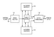
- FIG. 1is a block diagram illustrating a universal input electronic transformer according to one embodiment of the present application.
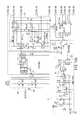
- FIG. 2is a circuit diagram illustrating the universal input electronic transformer of FIG. 1 .
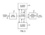
- FIG. 3is a block diagram illustrating a universal input electronic transformer according to another embodiment of the present application.
- FIGS. 4A and 4Bare a circuit diagram illustrating the universal input electronic transformer of FIG. 3 .
- FIG. 5is a block diagram illustrating a universal input electronic transformer according to another embodiment of the present application.
- FIGS. 6A and 6Bare a circuit diagram illustrating the universal input electronic transformer of FIG. 5 .
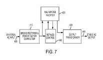
- FIG. 7is a block diagram illustrating a universal input electronic transformer according to another embodiment of the present application.
- FIG. 8is a circuit diagram illustrating the universal input electronic transformer of FIG. 7 .
- FIG. 9is a block diagram illustrating a universal input electronic transformer according to another embodiment of the present application.
- FIGS. 10A and 10Bare a circuit diagram illustrating the universal input electronic transformer of FIG. 9 .
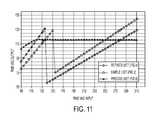
- FIG. 11is a chart illustrating input voltage verse output voltages of the universal input electronic transformers according to FIGS. 1, 3, and 7 .
- FIG. 1is a block diagram illustrating a simple universal input electronic transformer (SUIET) 100 according to one embodiment of the present application.
- the SUIET 100includes an input 105 , a rectifier 110 , a first inverter 120 , an output transformer 130 , a second inverter 140 , a controller, or control, 150 , and an output 155 .
- the input 105receives an input voltage.
- the input voltageis approximately 120VAC having a 50 Hz or 60 Hz frequency or approximately 277VAC having a 50 Hz or 60 Hz frequency.
- the input voltageis within a range of approximately 90VAC to approximately 305VAC.
- FIG. 2is a circuit diagram illustrating the components of the SUIET 100 .
- the rectifier 110receives the input voltage at the input 105 , rectifies the input voltage, and outputs a rectified voltage (e.g., a positively pulsating, direct-current (DC) half sine wave voltage).
- the rectifier 110is a bridge rectifier including four diodes D 1 -D 4 .
- the rectifier 110includes only two diodes.
- the rectifier 110further includes a filter capacitor configured and minimized to maintain a half sine wave, 120 Hz envelope of rectified voltage.
- the rectified voltageis output to the first inverter 120 , the second inverter 140 , and the controller 150 .
- the rectified voltageis also received by a power supply 160 .
- the power supply 160supplies a nominal DC voltage (e.g., 5V DC, 10V DC, 15V DC, etc.) to the controller 150 and/or other components or modules of the SUIET 100 (e.g., a first drive U 1 and a second driver U 2 of the first inverter 120 and the second inverter 140 respectively).
- the power supply 160is also configured to supply lower voltages to operate circuits and components within the controller 150 or SUIET 100 .
- the power supply 160 and the rectifier 110are a single module that receives the input voltage and outputs the rectified voltage and the nominal DC voltage.
- the controller 150receives power (e.g., in the form of the rectified voltage) directly from the rectifier 110 .
- the first inverter 120 and the second inverter 140switch the rectified voltage (i.e., invert the rectified DC-voltage to a switched AC-voltage).
- the first inverter 120 and the second inverter 140are half-bridge inverters, the first inverter 120 including switches M 1 , M 2 and the first driver U 1 and the second inverter 140 including switches M 3 , M 4 and the second driver U 2 .
- switches M 1 -M 4are semiconductors, such as but not limited to, transistors, field-effect transistors (FETs), bipolar junction transistors (BJT), junction field-effect transistor (JFET), metal-oxide-semiconductor field-effect transistors (MOSFETs), insulated-gate bipolar transistors (IGBTs), and insulated-gate field-effect transistors (IGFETs).
- the first and second drivers U 1 , U 2receive control signals (e.g., a high-voltage signal [5V DC] or a low-voltage signal [0V DC]) and selectively turn the switches M 1 -M 4 on and off based on received control signals.
- control signalse.g., a high-voltage signal [5V DC] or a low-voltage signal [0V DC]
- M 1when M 1 is turned on, M 2 must be turned off, and vice-versa.
- M 3when M 4 is turned on, and vice-versa.
- first driver U 1receives a high-voltage signal
- first driver U 1turns switch M 1 on and switch M 2 off.
- first driver U 1receives a low-voltage signal
- first driver U 1turns switch M 1 off and switch M 2 on.
- the controller 150outputs the control signals to the first and second drivers U 1 , U 2 for selectively controlling the switches M 1 -M 4 .
- the outputted control signalsare based on the received rectified voltage.
- the controller 150includes a plurality of electrical and electronic components that provide power, operational control, and protection to the components and modules within the controller 150 .
- the controller 150includes, among other things, a processing unit (e.g., a microprocessor, a microcontroller, or another suitable programmable device), a memory, input units and output units.
- the controller 150is implemented partially or entirely on a semiconductor (e.g., a field-programmable gate array [“FPGA”] semiconductor) chip, such as a chip developed through a register transfer level (“RTL”) design process.
- a semiconductore.g., a field-programmable gate array [“FPGA”] semiconductor
- the memoryincludes, for example, a program storage area and a data storage area.
- the program storage area and the data storage areacan include combinations of different types of memory, such as read-only memory (“ROM”), random access memory (“RAM”) (e.g., dynamic RAM [“DRAM”], synchronous DRAM [“SDRAM”], etc.), electrically erasable programmable read-only memory (“EEPROM”), flash memory, a hard disk, an SD card, or other suitable magnetic, optical, physical, or electronic memory devices.
- ROMread-only memory
- RAMrandom access memory
- EEPROMelectrically erasable programmable read-only memory
- flash memorye.g., a hard disk, an SD card, or other suitable magnetic, optical, physical, or electronic memory devices.
- the processing unitis connected to the memory and executes software instructions that are capable of being stored in a RAM of the memory (e.g., during execution), a ROM of the memory (e.g., on a generally permanent basis), or another non-transitory computer readable medium such as another memory or a disc.
- Software included in the implementation of the SUIET 100can be stored in the memory of the controller 150 .
- the softwareincludes, for example, firmware, one or more applications, program data, filters, rules, one or more program modules, and other executable instructions.
- the controller 150is configured to retrieve from memory and execute, among other things, instructions related to the control processes and methods described herein. In other constructions, the controller 150 includes additional, fewer, or different components.
- the output transformer 130includes a primary coil L 1 and a secondary coil L 2 .
- the primary coil L 1receives the inverted voltage.
- the primary coil L 1electromagnetically induces a switched high frequency (e.g., 50 KHz) output voltage to the secondary coil L 2 .
- the output voltageis then output from the output 155 .
- the output voltageis substantially the same regardless of the fixed input voltage (e.g., 120VAC RMS or 277VAC RMS).
- the output voltageis approximately 106VAC RMS at 120VAC RMS input and 133VAC RMS at 277VAC RMS input; or, approximately 12VAC RMS at the two input voltages of merit (e.g., 120VAC RMS or 277VAC RMS); or, approximately 24VAC RMS at the two input voltages of merit (e.g., 120VAC RMS or 277VAC RMS).
- an input voltage of either 120VAC RMS or 277VAC RMSis received at the input 105 .
- the input voltageis rectified by the rectifier 110 and output to the first inverter 120 , the second inverter 140 , and the controller 150 .
- the controller 150outputs control signals to the first inverter 120 and the second inverter 140 to selectively output switched voltages to the output transformer 130 .
- the controller 150outputs control signals to only the first inverter 120 to selectively output a switched voltage to the output transformer 130 .
- the output transformer 130then outputs a transformed voltage that is approximately the same (e.g., approximately 106VAC RMS to approximately 133VAC RMS; or approximately 12VAC RMS to approximately 24VAC RMS) regardless of the input voltage being 120VAC RMS or 277VAC RMS.
- FIG. 3is a block diagram illustrating a refined universal input electronic transformer (RUIET) 200 according to another embodiment of the present application.
- the RUIET 200includes an input 205 , a rectifier 210 , a first inverter 220 , an output transformer & relay 230 , a second inverter 240 , a refined control, or controller 250 , and an output 255 .
- the input 205receives the input voltage (e.g., 120VAC RMS or 277VAC RMS).
- FIGS. 4A and 4Bis a circuit diagram illustrating the components of the RUIET 200 .
- the rectifier 210is substantially similar to the rectifier 110 .
- the rectifier 210receives the input voltage from the input 205 and outputs a rectified voltage to the first inverter 220 , the second inverter 240 , and the controller 250 .
- the first inverter 220 and the second inverter 240switch the rectified voltage (i.e., invert the rectified DC-voltage to an inverted AC-voltage).
- the first inverter 220 and the second inverter 240are substantially similar to the first inverter 120 and the second inverter 140 .
- the first inverter 220includes switches M 1 , M 2 and a first driver U 1
- the second inverter 240includes switches M 3 , M 4 and a second driver U 2
- the first and second drivers U 1 , U 2receive control signals and selectively turn the switches M 1 -M 4 on and off based on received control signals.
- the output transformer & relay 230receives the switched voltage from the first inverter 220 and the second inverter 240 .
- the output transformer & relay 230includes a primary coil L 1 , a secondary coil (L 2 or both L 2 and L 3 ), a first relay switch S 1 , and a second relay switch S 2 .
- the primary coil L 1receives the switched voltage.
- the primary coil L 1electromagnetically induces a switched high frequency (e.g., 50 KHz) output voltage to the secondary coil (L 2 or both L 2 and L 3 ).
- the first relay switch S 1 and second relay switch S 2are configured to switch the turns ratios of the secondary coil, such that the secondary coil is equivalent to either L 2 or both L 2 and L 3 . Switching the turns ratio of the secondary coil produces a substantially similar output voltage regardless of the input voltage.
- the output voltage of the RUIET 200is more constant that the than the previously disclosed SUIET 100 of FIG. 1 .
- the first relay switch S 1 and the second relay switch S 2are controlled by the controller 250 .
- the controller 250is a timing circuit, although other controls may be used.
- the controller 250controls the first relay switch S 1 and the second relay switch S 2 according to the received rectified voltage, and thus the input voltage. If the input voltage is 120VAC RMS, the controller 250 turns relay switch S 2 on and relay switch S 1 off, therefore the secondary coil equals L 2 and L 3 together. If the input voltage is 277VAC RMS, the controller 250 turns relay switch S 2 off and relay switch S 1 on, therefore the secondary coil equals L 2 only.
- the output voltageis then output from the output 255 .
- the output voltageis substantially the same regardless of the input voltage (e.g., 120VAC RMS or 277VAC RMS).
- the output voltageis 120VAC RMS regardless of the input being 120VAC RMS or 277VAC RMS.
- the outputcan be 12VAC RMS or 24VAC RMS, depending on the turns ratios and regardless of the input voltage being approximately 120VAC RMS or approximately 277VAC RMS.
- FIG. 5is a block diagram illustrating an alternate refined universal input electronic transformer (aRUIET) 300 according to another embodiment of the present application.
- the aRUIET 300includes an input 305 , a rectifier & fixed boost 310 , a first inverter 320 , an output transformer 330 , a refined control, or controller 340 , and an output 345 .
- the input 305receives the input voltage (e.g., 120VAC RMS or 277VAC RMS).
- FIGS. 6A and 6Bis a circuit diagram illustrating the components of the aRUIET 300 .
- the rectifier 310receives the input voltage from the input 305 , rectifies the input voltage, and outputs a rectified voltage (e.g., a positively-pulsating, direct-current (DC) half sine wave voltage).
- a rectified voltagee.g., a positively-pulsating, direct-current (DC) half sine wave voltage.
- the rectifier 310is substantially the same as rectifier 110 of FIG. 2 .
- the rectifier & fixed boost 310includes a bridge rectifier (e.g., diodes D 1 -D 4 ) and a fixed boost, or booster circuit, 350 .
- the fixed boost 350receives the rectified voltage.
- the fixed boost 350may further boost (e.g., increase the amplitude) of the rectified voltage.
- the rectifier & fixed boost 310includes the bridge rectifier (e.g., diodes D 1 -D 4 ), the fixed boost 350 , and a power supply 360 .
- the power supply 360may be substantially similar to the power supply 160 of FIG. 2 .
- the fixed boost 350 and the power supply 360receives the rectified voltage.
- the fixed boost 350outputs the rectified voltage or a boosted voltage (depending on the amplitude of the rectified voltage) while the power supply 360 outputs the nominal DC voltage (e.g., 5V DC, 10V DC, 15V DC, etc.).
- the bridge rectifierincludes only two diodes.
- the rectifier & fixed boost 310further includes a smoothing capacitor configured to smooth out the rectified voltage.
- the controller 340receives the rectified voltage.
- controller 340is substantially similar to controller 150 of FIGS. 1 and 2 .
- the controller 340controls the fixed boost 350 to either output the boosted voltage or the non-boosted rectified voltage.
- the controller 340will control the fixed boost 350 to boost the rectified voltage to approximately 392V peak (e.g., the peak of a 277VAC RMS sine wave). If the rectified voltage has an amplitude of approximately 277V, the controller 340 will control the fixed boost 350 not to boost the rectified voltage.
- the controller 340further controls the first inverter 320 in a similar fashion as the embodiment illustrated in FIGS. 1 and 2 .
- the present embodimentonly one half-bridge inverter is necessary. This is because the fixed boost 350 provides a substantially similar rectified voltage to the first inverter 320 , regardless of the amplitude of the input voltage.
- the first inverter 320switches the rectified voltage (e.g., boosted rectified voltage or non-boosted rectified voltage) and outputs a switched voltage to the output transformer 330 .
- the first inverter 320is substantially similar to the first inverter 120 of the embodiment illustrated in FIGS. 1 and 2 .
- the output transformer 330receives the switched voltage and outputs an outputted voltage in a similar fashion as the embodiment of FIGS. 1 and 2 .
- the output transformer 330is substantially similar to the output transformer 130 of the embodiment illustrated in FIGS. 1 and 2 .
- the output voltageis then output via the output 345 .
- the output voltage of the aRUIET 300is substantially similar regardless of the amplitude of the input voltage.
- FIG. 7is a block diagram illustrating a precise universal input electronic transformer (PUIET) 400 according to another embodiment of the present application.
- the PUIET 400includes an input 405 , a rectifier & power factor corrector 410 , a first inverter 420 , an output transformer 430 , a refined control, or controller 440 , and an output 445 .
- the input 405receives the input voltage (e.g., 120VAC RMS or 277VAC RMS).
- FIG. 8is a circuit diagram illustrating the components of the PUIET 400 .
- the rectifier & power factor corrector 410includes a bridge rectifier (e.g., diodes D 1 -D 4 ) and a power factor corrector 450 .
- the bridge rectifierrectifies the input voltage received at the input 405 .
- the power factor corrector 410receives the rectified voltage and outputs a substantially constant DC voltage, regardless of the amplitude of the input voltage.
- the power factor corrector 450includes a primary coil L 1 and a secondary coil L 2 . In one example of operation, a voltage is expressed across the primary coil L 1 when switch M 1 is turned on, thus storing energy in the magnetic field of the primary coil L 1 .
- the energy stored in the primary coil L 1is released into a storage capacitor C 19 , through rectifier D 7 .
- the voltage across the primary coil L 1reverses polarity such that it is effectively in series with the input voltage, thus providing a boosted voltage.
- the secondary coil L 2provides a signal to the controller 440 .
- the operationis equivalent to a high-frequency switching process that outputs a substantially direct-current output at capacitor C 19 , that is then output to the half-bridge inverter 420 .
- the bridge rectifierincludes only two diodes.
- the rectifier & power factor corrector 410includes the bridge rectifier (e.g., diodes D 1 -D 4 ), the power factor corrector 450 , and a power supply 460 .
- the power supply 460may be substantially similar to the power supply 160 of FIG. 2 .
- the power supply 460may supply a nominal DC voltage (e.g., 5V DC, 10V DC, 15V DC, etc.) to the controller 440 , for powering the controller 440 .
- the substantially constant DC voltage, output from the power factor corrector 450 ,is received by the first inverter 420 and the controller 440 .
- the controller 440controls the first inverter 420 in a similar fashion as the embodiment illustrated in FIGS. 5 and 6 .
- the first inverter 420switches the substantially constant DC voltage and outputs a switched voltage to the output transformer 430 .
- the output transformer 430receives the switched voltage and outputs an output voltage in a similar fashion as the embodiment of FIGS. 1 and 2 .
- the output transformer 430is substantially similar to the output transformer 130 of the embodiment illustrated in FIGS. 1 and 2 .
- the output voltageis then output via the output 445 .
- the output voltage of the PUIET 400is substantially similar regardless of the amplitude of the input voltage across the entire range of input voltages from 120VAC RMS through 305VAC RMS in, as well as all voltages in-between.
- FIG. 9is a block diagram illustrating dimmable universal input electronic transformer (DUIET) 500 according to another embodiment of the present application.
- the DUIET 500includes an input 505 , a rectifier & power factor corrector 510 , a first inverter 520 , a dimming control, or dimming control circuit, 530 , an output transformer 540 , a refined control, or controller 550 , and an output 555 .
- the DUIET 500is substantially similar to the embodiment illustrated in FIGS. 7 and 8 , but further includes the dimming control 530 .
- FIGS. 10A and 10Bis a circuit diagram illustrating the DUIET 500 .
- the dimming control 530includes a dimming input 535 , an opto-isolator, or opto-coupler, U 10 , and a plurality of electrical and electronic components that provide operational control and protection to the components and modules of the dimming control 530 .
- the dimming control 530is electrically connected to the other components of the DUIET 500 , however, in other embodiments, the dimming control 530 may be wireless connected, or connected by any other analog and/or digital protocol known to one skilled in the art.
- a userprovides a user-input (e.g., approximately 0VDC to approximately 10VDC), in some embodiments via a current-sinking standard controller, at the dimming input 535 of the dimming control 530 .
- the opto-isolator U 10outputs a DC level signal, based on the user-input, to the controller 550 .
- a user-input of a current-sinking 10VDCwill result in a PWM signal having a duty cycle of approximately of 90%, while a user-input of 1VDC will result in a PWM signal having a duty cycle of approximately 10%.
- the DUIET 500can be adjusted to provide a 0% duty cycle for an approximately 0VDC control to provide a dim-to-off feature.
- the controller 550receives the PWM signal and outputs a control signal to the first inverter 520 based on the PWM signal.
- the control signalselectively controls the first inverter 520 to output a switched voltage relating to the user-input received by the dimming control 530 .
- the output transformer 540receives the switched voltage and outputs an output voltage in a similar fashion as the embodiment of FIGS. 1 and 2 .
- the output transformer 540is substantially similar to the output transformer 130 of the embodiment illustrated in FIGS. 1 and 2 .
- the output voltageis then output via the output 545 .
- the output voltageis substantially the same regardless of the input voltage; rather the output voltage varies based on the received user-input at the dimming control 530 .
- FIG. 11is a chart illustrating and comparing the input voltage verse the output voltage of the SUIET 100 ( FIGS. 1 and 2 ), the RUIET 200 ( FIGS. 3 and 4 ), and the PUIET 400 ( FIGS. 7 and 8 ).
- SUIET 100outputs a voltage of approximately 75VAC RMS to approximately 145VAC RMS regardless when the input voltage is approximately 90VAC RMS to approximately 310VAC RMS.
- the RUIET 200outputs a voltage of approximately 60VAC RMS to approximately 135VAC RMS when the input voltage is approximately 90VAC RMS to approximately 310VAC RMS.
- the aRUIET 300outputs substantially similar output voltages to the RUIET 200 .
- the PUIET 400outputs a voltage of approximately 110VAC RMS to approximately 125VAC RMS when the input voltage is approximately 90VAC RMS to approximately 310VAC RMS. All of the various embodiments discussed above can be adjusted at the output transformer, (e.g., 430 of the PUIET 400 , 540 of the DUIET 500 ) to provide 24VAC or 12VAC outputs.
- the main advantage of the DUIET 500 and PUIET 400 over the SUIET 100 , RUIET 200 , and RUIET 300is that the switched output does not exist within a 120 Hz, (twice the line frequency) envelope as in standard electronic transformers today; therefore, 120 Hz ripple usually transmitted on to the light source is eliminated.
- the present applicationprovides, among other things, a universal input electronic transformer operable to output a substantially constant voltage regardless of the amplitude of the received input voltage.
Landscapes
- Engineering & Computer Science (AREA)
- Power Engineering (AREA)
- Dc-Dc Converters (AREA)
Abstract
Description
Claims (18)
Priority Applications (3)
| Application Number | Priority Date | Filing Date | Title |
|---|---|---|---|
| US14/664,379US10361637B2 (en) | 2015-03-20 | 2015-03-20 | Universal input electronic transformer |
| PCT/US2016/023104WO2016153985A1 (en) | 2015-03-20 | 2016-03-18 | Universal input electronic transformer |
| US16/519,209US11557977B2 (en) | 2015-03-20 | 2019-07-23 | Universal input electronic transformer |
Applications Claiming Priority (1)
| Application Number | Priority Date | Filing Date | Title |
|---|---|---|---|
| US14/664,379US10361637B2 (en) | 2015-03-20 | 2015-03-20 | Universal input electronic transformer |
Related Child Applications (1)
| Application Number | Title | Priority Date | Filing Date |
|---|---|---|---|
| US16/519,209ContinuationUS11557977B2 (en) | 2015-03-20 | 2019-07-23 | Universal input electronic transformer |
Publications (2)
| Publication Number | Publication Date |
|---|---|
| US20160276949A1 US20160276949A1 (en) | 2016-09-22 |
| US10361637B2true US10361637B2 (en) | 2019-07-23 |
Family
ID=56924287
Family Applications (2)
| Application Number | Title | Priority Date | Filing Date |
|---|---|---|---|
| US14/664,379Expired - Fee RelatedUS10361637B2 (en) | 2015-03-20 | 2015-03-20 | Universal input electronic transformer |
| US16/519,209ActiveUS11557977B2 (en) | 2015-03-20 | 2019-07-23 | Universal input electronic transformer |
Family Applications After (1)
| Application Number | Title | Priority Date | Filing Date |
|---|---|---|---|
| US16/519,209ActiveUS11557977B2 (en) | 2015-03-20 | 2019-07-23 | Universal input electronic transformer |
Country Status (2)
| Country | Link |
|---|---|
| US (2) | US10361637B2 (en) |
| WO (1) | WO2016153985A1 (en) |
Citations (32)
| Publication number | Priority date | Publication date | Assignee | Title |
|---|---|---|---|---|
| US3324377A (en)* | 1963-06-06 | 1967-06-06 | Bell Telephone Labor Inc | Regulated inverter system |
| US3414801A (en)* | 1967-04-25 | 1968-12-03 | Bell Telephone Labor Inc | Inverter symmetry correction circuit |
| US3448367A (en)* | 1966-09-19 | 1969-06-03 | Gen Electric | Inverter inhibit circuits |
| US3470449A (en)* | 1968-04-08 | 1969-09-30 | Cutler Hammer Inc | Constant frequency inverter with frequency override |
| US4060757A (en)* | 1976-09-17 | 1977-11-29 | General Electric Co. | Inverters having a transformer-coupled commutating circuit |
| US4426564A (en)* | 1979-12-26 | 1984-01-17 | General Electric Company | Parallel resonant induction cooking surface unit |
| US4471419A (en)* | 1981-10-20 | 1984-09-11 | Siemens Aktiengesellschaft | Circuitry and method of operation for an intermediate-like converter |
| US4709318A (en)* | 1986-10-22 | 1987-11-24 | Liebert Corporation | UPS apparatus with control protocols |
| US4717994A (en)* | 1986-12-11 | 1988-01-05 | Zenith Electronics Corporation | Current mode control for DC converters operating over 50% duty cycle |
| US4719550A (en)* | 1986-09-11 | 1988-01-12 | Liebert Corporation | Uninterruptible power supply with energy conversion and enhancement |
| US5563777A (en) | 1994-04-25 | 1996-10-08 | Matsushita Electric Works, Ltd. | Inverter AC power supply |
| US5661645A (en) | 1996-06-27 | 1997-08-26 | Hochstein; Peter A. | Power supply for light emitting diode array |
| US5925990A (en) | 1997-12-19 | 1999-07-20 | Energy Savings, Inc. | Microprocessor controlled electronic ballast |
| US6396715B1 (en)* | 2000-11-30 | 2002-05-28 | Delta Electronics, Inc. | DC to DC converter for operating in selectable voltage modes |
| US20020071299A1 (en)* | 2000-12-13 | 2002-06-13 | Patent-Treuhand-Gesellschaft Fuer Elektrische Gluehlampen Mbh | Electronic transformer with good immunity against high-voltage pulses |
| US20020149892A1 (en)* | 2000-10-04 | 2002-10-17 | Williams Marion S. | Apparatus and method for controlling LED arrays |
| US20040090800A1 (en)* | 2002-01-23 | 2004-05-13 | Moisin Mihail S. | Ballast circuit having enhanced output isolation transformer circuit with high power factor |
| US20050029966A1 (en) | 2001-12-19 | 2005-02-10 | Nicholas Buonocunto | Electronic ballast system having emergency lighting provisions and electronic chip |
| US7109438B2 (en)* | 2003-06-06 | 2006-09-19 | Sansha Electric Manufacturing Company, Limited | Power supply apparatus for arc-utilizing apparatus |
| US20070279019A1 (en) | 2003-12-09 | 2007-12-06 | Nujira Ltd. | Transformer Based Voltage Supply |
| US20080224633A1 (en) | 2007-03-12 | 2008-09-18 | Cirrus Logic, Inc. | Lighting System with Lighting Dimmer Output Mapping |
| US20090196072A1 (en)* | 2007-12-03 | 2009-08-06 | Zhong Ye | Phase-shifted dual-bridge DC/DC converter with wide-range ZVS and zero circulating current |
| US7920392B2 (en)* | 2007-05-11 | 2011-04-05 | Soft Switching Technologies Corporation | Dynamic voltage sag correction |
| US20110155703A1 (en) | 2009-12-30 | 2011-06-30 | Itt Kaliburn | Universal input power supply utilizing parallel power modules |
| US8030853B1 (en) | 2008-12-19 | 2011-10-04 | National Semiconductor Corporation | Circuit and method for improving the performance of a light emitting diode (LED) driver |
| US20110266966A1 (en) | 2008-12-30 | 2011-11-03 | Koninklijke Philips Electronics N.V. | Electronic circuit for driving a fluorescent lamp and lighting application |
| US8305779B2 (en)* | 2008-09-01 | 2012-11-06 | Delta Electronics, Inc. | Parallel-connected uninterrupted power supply circuit |
| US20130049622A1 (en)* | 2011-08-31 | 2013-02-28 | Power Integrations, Inc. | Load current management circuit |
| US20130271021A1 (en) | 2010-12-22 | 2013-10-17 | Koninklijke Philips N.V. | Power converter device for driving solid state lighting load |
| US20140021180A1 (en) | 2012-07-23 | 2014-01-23 | Illinois Tool Works Inc. | Method and Apparatus For Providing Welding Type Power |
| US20140376287A1 (en)* | 2013-06-20 | 2014-12-25 | Rockwell Automation Technologies, Inc. | Multilevel voltage source converters and systems |
| US20150036403A1 (en)* | 2013-08-02 | 2015-02-05 | Infineon Technologies Austria Ag | System and Method for a Power Converter |
Family Cites Families (36)
| Publication number | Priority date | Publication date | Assignee | Title |
|---|---|---|---|---|
| US4414493A (en)* | 1981-10-06 | 1983-11-08 | Thomas Industries Inc. | Light dimmer for solid state ballast |
| US5583402A (en)* | 1994-01-31 | 1996-12-10 | Magnetek, Inc. | Symmetry control circuit and method |
| US6366062B2 (en)* | 1997-12-08 | 2002-04-02 | Microplanet, Inc. | Method and apparatus for electronic power control |
| US5747942A (en)* | 1996-07-10 | 1998-05-05 | Enersol Systems, Inc. | Inverter for an electronic ballast having independent start-up and operational output voltages |
| WO2001093748A2 (en)* | 2000-06-08 | 2001-12-13 | Nuvasive, Inc. | Relative nerve movement and status detection system and method |
| US6359391B1 (en)* | 2000-09-08 | 2002-03-19 | Philips Electronics North America Corporation | System and method for overvoltage protection during pulse width modulation dimming of an LCD backlight inverter |
| US6841979B2 (en)* | 2001-05-22 | 2005-01-11 | Powerdsine, Ltd. | Power distribution with digital current control |
| GB2369730B (en)* | 2001-08-30 | 2002-11-13 | Integrated Syst Tech Ltd | Illumination control system |
| US6979959B2 (en)* | 2002-12-13 | 2005-12-27 | Microsemi Corporation | Apparatus and method for striking a fluorescent lamp |
| US7187139B2 (en)* | 2003-09-09 | 2007-03-06 | Microsemi Corporation | Split phase inverters for CCFL backlight system |
| US20070279368A1 (en)* | 2004-09-01 | 2007-12-06 | Drs Tactical Systems, Inc. | Low intensity displays compatible with night vision imaging systems |
| US20080136343A1 (en)* | 2005-08-11 | 2008-06-12 | Yu Chung-Che | Resonant DC/AC inverter |
| US7414371B1 (en)* | 2005-11-21 | 2008-08-19 | Microsemi Corporation | Voltage regulation loop with variable gain control for inverter circuit |
| JP4627320B2 (en)* | 2005-11-22 | 2011-02-09 | ローム株式会社 | Inverter and its control circuit, and light emitting device and liquid crystal television using the same |
| US8076920B1 (en)* | 2007-03-12 | 2011-12-13 | Cirrus Logic, Inc. | Switching power converter and control system |
| CN101919318A (en)* | 2008-02-08 | 2010-12-15 | 夏普株式会社 | Illumination device and display device |
| US8279648B2 (en)* | 2008-03-20 | 2012-10-02 | Pratt & Whitney Canada Corp. | Power inverter and method |
| CN101552563B (en)* | 2009-03-20 | 2011-09-14 | Bcd半导体制造有限公司 | Device and method for controlling constant-current output in switch power supply |
| WO2011050453A1 (en)* | 2009-10-26 | 2011-05-05 | Light-Based Technologies Incorporated | Holding current circuits for phase-cut power control |
| US9246391B2 (en)* | 2010-01-22 | 2016-01-26 | Power Systems Technologies Ltd. | Controller for providing a corrected signal to a sensed peak current through a circuit element of a power converter |
| CN101951177B (en)* | 2010-09-06 | 2014-05-07 | Bcd半导体制造有限公司 | Switching power supply system and switching power supply control circuit |
| US9013896B2 (en)* | 2010-12-30 | 2015-04-21 | Echostar Technologies L.L.C. | Apparatus, systems and methods for power supply employing single-stage forward voltage conversion |
| CN102368662B (en)* | 2011-03-10 | 2013-11-27 | 杭州士兰微电子股份有限公司 | Current reference generating circuit, control circuit and method of constant current switching power supply |
| TWI469686B (en)* | 2011-05-10 | 2015-01-11 | Richtek Technology Corp | Light emitting device current regulator circuit and control method thereof |
| US8503204B2 (en)* | 2011-08-05 | 2013-08-06 | Infineon Technologies Ag | Power converter circuit |
| JP2013110269A (en)* | 2011-11-21 | 2013-06-06 | Samsung Electro-Mechanics Co Ltd | Cmos integrated circuit and amplifier circuit |
| US9313850B2 (en)* | 2012-07-24 | 2016-04-12 | Wei Zhao | Dimming apparatus for LEDs |
| US9240726B1 (en)* | 2013-05-16 | 2016-01-19 | Universal Lighting Technologies, Inc. | Dimming LED driver circuit with dynamically controlled resonant tank gain |
| US9572207B2 (en)* | 2013-08-14 | 2017-02-14 | Infineon Technologies Austria Ag | Dimming range extension |
| US20150318787A1 (en)* | 2013-11-08 | 2015-11-05 | Lutron Electronics Co., Inc. | Load control device for a light-emitting diode light source |
| US9300206B2 (en)* | 2013-11-15 | 2016-03-29 | Power Systems Technologies Ltd. | Method for estimating power of a power converter |
| JP6272691B2 (en)* | 2013-12-27 | 2018-01-31 | ローム株式会社 | Amplitude normalization circuit, power supply device and electronic device |
| DE102014107991B4 (en)* | 2014-06-05 | 2020-01-30 | Krohne Messtechnik Gmbh | Field device with switching converter circuit |
| CN104578799B (en)* | 2014-12-25 | 2017-04-12 | 成都芯源系统有限公司 | Switching power supply system and control circuit and control method thereof |
| US9331566B1 (en)* | 2015-02-18 | 2016-05-03 | Adaptive Frequency Holdings, LLC | Adaptive AC power exchanger |
| WO2018052970A1 (en)* | 2016-09-16 | 2018-03-22 | Lutron Electronics Co., Inc. | Load control device for a light-emitting diode light source having different operating modes |
- 2015
- 2015-03-20USUS14/664,379patent/US10361637B2/ennot_activeExpired - Fee Related
- 2016
- 2016-03-18WOPCT/US2016/023104patent/WO2016153985A1/ennot_activeCeased
- 2019
- 2019-07-23USUS16/519,209patent/US11557977B2/enactiveActive
Patent Citations (32)
| Publication number | Priority date | Publication date | Assignee | Title |
|---|---|---|---|---|
| US3324377A (en)* | 1963-06-06 | 1967-06-06 | Bell Telephone Labor Inc | Regulated inverter system |
| US3448367A (en)* | 1966-09-19 | 1969-06-03 | Gen Electric | Inverter inhibit circuits |
| US3414801A (en)* | 1967-04-25 | 1968-12-03 | Bell Telephone Labor Inc | Inverter symmetry correction circuit |
| US3470449A (en)* | 1968-04-08 | 1969-09-30 | Cutler Hammer Inc | Constant frequency inverter with frequency override |
| US4060757A (en)* | 1976-09-17 | 1977-11-29 | General Electric Co. | Inverters having a transformer-coupled commutating circuit |
| US4426564A (en)* | 1979-12-26 | 1984-01-17 | General Electric Company | Parallel resonant induction cooking surface unit |
| US4471419A (en)* | 1981-10-20 | 1984-09-11 | Siemens Aktiengesellschaft | Circuitry and method of operation for an intermediate-like converter |
| US4719550A (en)* | 1986-09-11 | 1988-01-12 | Liebert Corporation | Uninterruptible power supply with energy conversion and enhancement |
| US4709318A (en)* | 1986-10-22 | 1987-11-24 | Liebert Corporation | UPS apparatus with control protocols |
| US4717994A (en)* | 1986-12-11 | 1988-01-05 | Zenith Electronics Corporation | Current mode control for DC converters operating over 50% duty cycle |
| US5563777A (en) | 1994-04-25 | 1996-10-08 | Matsushita Electric Works, Ltd. | Inverter AC power supply |
| US5661645A (en) | 1996-06-27 | 1997-08-26 | Hochstein; Peter A. | Power supply for light emitting diode array |
| US5925990A (en) | 1997-12-19 | 1999-07-20 | Energy Savings, Inc. | Microprocessor controlled electronic ballast |
| US20020149892A1 (en)* | 2000-10-04 | 2002-10-17 | Williams Marion S. | Apparatus and method for controlling LED arrays |
| US6396715B1 (en)* | 2000-11-30 | 2002-05-28 | Delta Electronics, Inc. | DC to DC converter for operating in selectable voltage modes |
| US20020071299A1 (en)* | 2000-12-13 | 2002-06-13 | Patent-Treuhand-Gesellschaft Fuer Elektrische Gluehlampen Mbh | Electronic transformer with good immunity against high-voltage pulses |
| US20050029966A1 (en) | 2001-12-19 | 2005-02-10 | Nicholas Buonocunto | Electronic ballast system having emergency lighting provisions and electronic chip |
| US20040090800A1 (en)* | 2002-01-23 | 2004-05-13 | Moisin Mihail S. | Ballast circuit having enhanced output isolation transformer circuit with high power factor |
| US7109438B2 (en)* | 2003-06-06 | 2006-09-19 | Sansha Electric Manufacturing Company, Limited | Power supply apparatus for arc-utilizing apparatus |
| US20070279019A1 (en) | 2003-12-09 | 2007-12-06 | Nujira Ltd. | Transformer Based Voltage Supply |
| US20080224633A1 (en) | 2007-03-12 | 2008-09-18 | Cirrus Logic, Inc. | Lighting System with Lighting Dimmer Output Mapping |
| US7920392B2 (en)* | 2007-05-11 | 2011-04-05 | Soft Switching Technologies Corporation | Dynamic voltage sag correction |
| US20090196072A1 (en)* | 2007-12-03 | 2009-08-06 | Zhong Ye | Phase-shifted dual-bridge DC/DC converter with wide-range ZVS and zero circulating current |
| US8305779B2 (en)* | 2008-09-01 | 2012-11-06 | Delta Electronics, Inc. | Parallel-connected uninterrupted power supply circuit |
| US8030853B1 (en) | 2008-12-19 | 2011-10-04 | National Semiconductor Corporation | Circuit and method for improving the performance of a light emitting diode (LED) driver |
| US20110266966A1 (en) | 2008-12-30 | 2011-11-03 | Koninklijke Philips Electronics N.V. | Electronic circuit for driving a fluorescent lamp and lighting application |
| US20110155703A1 (en) | 2009-12-30 | 2011-06-30 | Itt Kaliburn | Universal input power supply utilizing parallel power modules |
| US20130271021A1 (en) | 2010-12-22 | 2013-10-17 | Koninklijke Philips N.V. | Power converter device for driving solid state lighting load |
| US20130049622A1 (en)* | 2011-08-31 | 2013-02-28 | Power Integrations, Inc. | Load current management circuit |
| US20140021180A1 (en) | 2012-07-23 | 2014-01-23 | Illinois Tool Works Inc. | Method and Apparatus For Providing Welding Type Power |
| US20140376287A1 (en)* | 2013-06-20 | 2014-12-25 | Rockwell Automation Technologies, Inc. | Multilevel voltage source converters and systems |
| US20150036403A1 (en)* | 2013-08-02 | 2015-02-05 | Infineon Technologies Austria Ag | System and Method for a Power Converter |
Non-Patent Citations (1)
| Title |
|---|
| PCTUS2016/023104 International Search Report and Written Opinion dated Jun. 20, 2016. |
Also Published As
| Publication number | Publication date |
|---|---|
| US20160276949A1 (en) | 2016-09-22 |
| US11557977B2 (en) | 2023-01-17 |
| WO2016153985A1 (en) | 2016-09-29 |
| US20190348922A1 (en) | 2019-11-14 |
Similar Documents
| Publication | Publication Date | Title |
|---|---|---|
| US9960686B2 (en) | System and method for detecting a loss of AC power in a switched-mode power supply | |
| US9837913B1 (en) | Control method to avoid capacitive mode switching for resonant converters | |
| US8390209B2 (en) | Circuit arrangement for conversion of an input AC voltage to a DC voltage, retrofit lamp having a circuit arrangement such as this, as well as a lighting system | |
| US20100079085A1 (en) | Supply circuit | |
| KR101768179B1 (en) | Device for preventing turn-off delay and afterlight of led lamp | |
| CN103493348A (en) | Lighting power circuit with peak current limiter for EMI filter | |
| US9125259B1 (en) | Constant current drive circuit for multi-channel LED lighting | |
| KR20100105633A (en) | Power factor control circuit and mains power supply | |
| CN118826017B (en) | A power supply guarantee control circuit and system based on power supply data | |
| US9748844B2 (en) | Systems and methods for controlling and improving power converters | |
| CN107852800B (en) | Dimming device | |
| US9894718B1 (en) | Constant current source LED driver circuit with self-clamped output | |
| US20180138800A1 (en) | Dc-dc converter for controlling an aircraft fan inverter, and associated control method and fan | |
| US20130170253A1 (en) | Auxiliary power generation circuit | |
| US9192003B2 (en) | Electrical load driving apparatus | |
| US8154212B2 (en) | Circuit for driving light sources and related method | |
| US11557977B2 (en) | Universal input electronic transformer | |
| WO2015107498A1 (en) | Power control by phase cutting | |
| US9426854B1 (en) | Electronic driver for controlling an illumination device | |
| US10073423B2 (en) | Low voltage environment controller with power factor correction flyback power supply | |
| US20230094863A1 (en) | A power converter having multiple main switches in series and a power conversion method | |
| US10390392B2 (en) | Method for controlling an output of an electrical AC voltage | |
| US20180254696A1 (en) | Power Supply for Welding and Cutting Apparatus | |
| JP3163655B2 (en) | Inverter device | |
| JP7592240B2 (en) | Discharge lighting device and light irradiation device |
Legal Events
| Date | Code | Title | Description |
|---|---|---|---|
| AS | Assignment | Owner name:HUBBELL INCORPORATED, CONNECTICUT Free format text:ASSIGNMENT OF ASSIGNORS INTEREST;ASSIGNORS:BANDEL, MICHAEL WILLIAM;DAYAL PANDEY, ALOK VISHAMBHAR;GARBOWICZ, GLENN DONALD;SIGNING DATES FROM 20161220 TO 20170117;REEL/FRAME:040996/0924 | |
| STPP | Information on status: patent application and granting procedure in general | Free format text:NOTICE OF ALLOWANCE MAILED -- APPLICATION RECEIVED IN OFFICE OF PUBLICATIONS | |
| STPP | Information on status: patent application and granting procedure in general | Free format text:AWAITING TC RESP., ISSUE FEE NOT PAID | |
| STPP | Information on status: patent application and granting procedure in general | Free format text:NOTICE OF ALLOWANCE MAILED -- APPLICATION RECEIVED IN OFFICE OF PUBLICATIONS | |
| STPP | Information on status: patent application and granting procedure in general | Free format text:PUBLICATIONS -- ISSUE FEE PAYMENT VERIFIED | |
| STCF | Information on status: patent grant | Free format text:PATENTED CASE | |
| AS | Assignment | Owner name:HUBBELL LIGHTING, INC., CONNECTICUT Free format text:NUNC PRO TUNC ASSIGNMENT;ASSIGNOR:HUBBELL INCORPORATED;REEL/FRAME:058838/0162 Effective date:20220112 | |
| AS | Assignment | Owner name:ALLY BANK, AS COLLATERAL AGENT, NEW YORK Free format text:SECURITY AGREEMENT;ASSIGNORS:HUBBELL LIGHTING, INC.;LITECONTROL CORPORATION;CURRENT LIGHTING SOLUTIONS, LLC;AND OTHERS;REEL/FRAME:058982/0844 Effective date:20220201 | |
| AS | Assignment | Owner name:ATLANTIC PARK STRATEGIC CAPITAL FUND, L.P., AS COLLATERAL AGENT, NEW YORK Free format text:SECURITY INTEREST;ASSIGNORS:HUBBELL LIGHTING, INC.;LITECONTROL CORPORATION;CURRENT LIGHTING SOLUTIONS, LLC;AND OTHERS;REEL/FRAME:059034/0469 Effective date:20220201 | |
| FEPP | Fee payment procedure | Free format text:MAINTENANCE FEE REMINDER MAILED (ORIGINAL EVENT CODE: REM.); ENTITY STATUS OF PATENT OWNER: LARGE ENTITY | |
| LAPS | Lapse for failure to pay maintenance fees | Free format text:PATENT EXPIRED FOR FAILURE TO PAY MAINTENANCE FEES (ORIGINAL EVENT CODE: EXP.); ENTITY STATUS OF PATENT OWNER: LARGE ENTITY | |
| STCH | Information on status: patent discontinuation | Free format text:PATENT EXPIRED DUE TO NONPAYMENT OF MAINTENANCE FEES UNDER 37 CFR 1.362 | |
| FP | Lapsed due to failure to pay maintenance fee | Effective date:20230723 | |
| AS | Assignment | Owner name:ALLY BANK, AS COLLATERAL AGENT, NEW YORK Free format text:CORRECTIVE ASSIGNMENT TO CORRECT THE PATENT NUMBER 10841994 TO PATENT NUMBER 11570872 PREVIOUSLY RECORDED ON REEL 058982 FRAME 0844. ASSIGNOR(S) HEREBY CONFIRMS THE SECURITY AGREEMENT;ASSIGNORS:HUBBELL LIGHTING, INC.;LITECONTROL CORPORATION;CURRENT LIGHTING SOLUTIONS, LLC;AND OTHERS;REEL/FRAME:066355/0455 Effective date:20220201 | |
| AS | Assignment | Owner name:ATLANTIC PARK STRATEGIC CAPITAL FUND, L.P., AS COLLATERAL AGENT, NEW YORK Free format text:CORRECTIVE ASSIGNMENT TO CORRECT THE PATENT NUMBER PREVIOUSLY RECORDED AT REEL: 059034 FRAME: 0469. ASSIGNOR(S) HEREBY CONFIRMS THE SECURITY INTEREST;ASSIGNORS:HUBBELL LIGHTING, INC.;LITECONTROL CORPORATION;CURRENT LIGHTING SOLUTIONS, LLC;AND OTHERS;REEL/FRAME:066372/0590 Effective date:20220201 |