US10360846B2 - Distributed pulse-width modulation system with multi-bit digital storage and output device - Google Patents
Distributed pulse-width modulation system with multi-bit digital storage and output deviceDownload PDFInfo
- Publication number
- US10360846B2 US10360846B2US15/590,827US201715590827AUS10360846B2US 10360846 B2US10360846 B2US 10360846B2US 201715590827 AUS201715590827 AUS 201715590827AUS 10360846 B2US10360846 B2US 10360846B2
- Authority
- US
- United States
- Prior art keywords
- bit digital
- bit
- counter
- output
- digital value
- Prior art date
- Legal status (The legal status is an assumption and is not a legal conclusion. Google has not performed a legal analysis and makes no representation as to the accuracy of the status listed.)
- Active, expires
Links
Images


Classifications
- G—PHYSICS
- G09—EDUCATION; CRYPTOGRAPHY; DISPLAY; ADVERTISING; SEALS
- G09G—ARRANGEMENTS OR CIRCUITS FOR CONTROL OF INDICATING DEVICES USING STATIC MEANS TO PRESENT VARIABLE INFORMATION
- G09G3/00—Control arrangements or circuits, of interest only in connection with visual indicators other than cathode-ray tubes
- G09G3/20—Control arrangements or circuits, of interest only in connection with visual indicators other than cathode-ray tubes for presentation of an assembly of a number of characters, e.g. a page, by composing the assembly by combination of individual elements arranged in a matrix no fixed position being assigned to or needed to be assigned to the individual characters or partial characters
- G09G3/22—Control arrangements or circuits, of interest only in connection with visual indicators other than cathode-ray tubes for presentation of an assembly of a number of characters, e.g. a page, by composing the assembly by combination of individual elements arranged in a matrix no fixed position being assigned to or needed to be assigned to the individual characters or partial characters using controlled light sources
- G09G3/30—Control arrangements or circuits, of interest only in connection with visual indicators other than cathode-ray tubes for presentation of an assembly of a number of characters, e.g. a page, by composing the assembly by combination of individual elements arranged in a matrix no fixed position being assigned to or needed to be assigned to the individual characters or partial characters using controlled light sources using electroluminescent panels
- G09G3/32—Control arrangements or circuits, of interest only in connection with visual indicators other than cathode-ray tubes for presentation of an assembly of a number of characters, e.g. a page, by composing the assembly by combination of individual elements arranged in a matrix no fixed position being assigned to or needed to be assigned to the individual characters or partial characters using controlled light sources using electroluminescent panels semiconductive, e.g. using light-emitting diodes [LED]
- G09G3/3208—Control arrangements or circuits, of interest only in connection with visual indicators other than cathode-ray tubes for presentation of an assembly of a number of characters, e.g. a page, by composing the assembly by combination of individual elements arranged in a matrix no fixed position being assigned to or needed to be assigned to the individual characters or partial characters using controlled light sources using electroluminescent panels semiconductive, e.g. using light-emitting diodes [LED] organic, e.g. using organic light-emitting diodes [OLED]
- G09G3/3225—Control arrangements or circuits, of interest only in connection with visual indicators other than cathode-ray tubes for presentation of an assembly of a number of characters, e.g. a page, by composing the assembly by combination of individual elements arranged in a matrix no fixed position being assigned to or needed to be assigned to the individual characters or partial characters using controlled light sources using electroluminescent panels semiconductive, e.g. using light-emitting diodes [LED] organic, e.g. using organic light-emitting diodes [OLED] using an active matrix
- G—PHYSICS
- G09—EDUCATION; CRYPTOGRAPHY; DISPLAY; ADVERTISING; SEALS
- G09G—ARRANGEMENTS OR CIRCUITS FOR CONTROL OF INDICATING DEVICES USING STATIC MEANS TO PRESENT VARIABLE INFORMATION
- G09G3/00—Control arrangements or circuits, of interest only in connection with visual indicators other than cathode-ray tubes
- G09G3/20—Control arrangements or circuits, of interest only in connection with visual indicators other than cathode-ray tubes for presentation of an assembly of a number of characters, e.g. a page, by composing the assembly by combination of individual elements arranged in a matrix no fixed position being assigned to or needed to be assigned to the individual characters or partial characters
- G09G3/2007—Display of intermediate tones
- G09G3/2014—Display of intermediate tones by modulation of the duration of a single pulse during which the logic level remains constant
- G—PHYSICS
- G09—EDUCATION; CRYPTOGRAPHY; DISPLAY; ADVERTISING; SEALS
- G09G—ARRANGEMENTS OR CIRCUITS FOR CONTROL OF INDICATING DEVICES USING STATIC MEANS TO PRESENT VARIABLE INFORMATION
- G09G2300/00—Aspects of the constitution of display devices
- G09G2300/08—Active matrix structure, i.e. with use of active elements, inclusive of non-linear two terminal elements, in the pixels together with light emitting or modulating elements
- G09G2300/0809—Several active elements per pixel in active matrix panels
- G09G2300/0842—Several active elements per pixel in active matrix panels forming a memory circuit, e.g. a dynamic memory with one capacitor
- G09G2300/0857—Static memory circuit, e.g. flip-flop
- G—PHYSICS
- G09—EDUCATION; CRYPTOGRAPHY; DISPLAY; ADVERTISING; SEALS
- G09G—ARRANGEMENTS OR CIRCUITS FOR CONTROL OF INDICATING DEVICES USING STATIC MEANS TO PRESENT VARIABLE INFORMATION
- G09G2310/00—Command of the display device
- G09G2310/02—Addressing, scanning or driving the display screen or processing steps related thereto
- G09G2310/0264—Details of driving circuits
- G09G2310/0286—Details of a shift registers arranged for use in a driving circuit
- G—PHYSICS
- G09—EDUCATION; CRYPTOGRAPHY; DISPLAY; ADVERTISING; SEALS
- G09G—ARRANGEMENTS OR CIRCUITS FOR CONTROL OF INDICATING DEVICES USING STATIC MEANS TO PRESENT VARIABLE INFORMATION
- G09G2310/00—Command of the display device
- G09G2310/06—Details of flat display driving waveforms
- G09G2310/061—Details of flat display driving waveforms for resetting or blanking
- G—PHYSICS
- G09—EDUCATION; CRYPTOGRAPHY; DISPLAY; ADVERTISING; SEALS
- G09G—ARRANGEMENTS OR CIRCUITS FOR CONTROL OF INDICATING DEVICES USING STATIC MEANS TO PRESENT VARIABLE INFORMATION
- G09G2310/00—Command of the display device
- G09G2310/08—Details of timing specific for flat panels, other than clock recovery
- G—PHYSICS
- G09—EDUCATION; CRYPTOGRAPHY; DISPLAY; ADVERTISING; SEALS
- G09G—ARRANGEMENTS OR CIRCUITS FOR CONTROL OF INDICATING DEVICES USING STATIC MEANS TO PRESENT VARIABLE INFORMATION
- G09G2320/00—Control of display operating conditions
- G09G2320/06—Adjustment of display parameters
- G09G2320/0626—Adjustment of display parameters for control of overall brightness
- G09G2320/064—Adjustment of display parameters for control of overall brightness by time modulation of the brightness of the illumination source
Definitions
- the present inventionrelates to systems using digital values driven by pulse-width modulation.
- Flat-panel displaysare widely used in conjunction with computing devices, in portable devices, and for entertainment devices such as televisions.
- Such displaystypically employ a plurality of pixels distributed over a display substrate to display images, graphics, or text.
- each pixelincludes light emitters that emit light of different colors, such as red, green, and blue.
- LCDsliquid crystal displays
- OLEDorganic light-emitting diode
- Displays using inorganic light emitting diodes (LEDs)are also in widespread use for outdoor signage and have been demonstrated in a 55-inch television.
- Displaysare typically controlled with either a passive-matrix (PM) control employing electronic circuitry external to the display substrate or an active-matrix (AM) control employing electronic circuitry formed directly on the display substrate and associated with each light-emitting element.
- PMpassive-matrix
- AMactive-matrix
- Both OLED displays and LCDs using passive-matrix control and active-matrix controlare available.
- An example of such an AM OLED display deviceis disclosed in U.S. Pat. No. 5,550,066.
- Active-matrix circuitsare commonly constructed with thin-film transistors (TFTs) in a semiconductor layer formed over a display substrate and employing a separate TFT circuit to control each light-emitting pixel in the display.
- the semiconductor layeris typically amorphous silicon or poly-crystalline silicon and is distributed over the entire flat-panel display substrate.
- the semiconductor layeris photolithographically processed to form electronic control elements, such as transistors and capacitors. Additional layers, for example insulating dielectric layers and conductive metal layers are provided, often by evaporation or sputtering, and photolithographically patterned to form electrical interconnections, or wires.
- each display sub-pixelis controlled by one control element, and each control element includes at least one transistor.
- each control elementincludes two transistors (a select transistor and a power transistor) and one capacitor for storing a charge specifying the luminance of the sub-pixel.
- Each OLED elementemploys an independent control electrode connected to the power transistor and a common electrode.
- an LCDtypically uses a single transistor to control each pixel. Control of the light-emitting elements is usually provided through a data signal line, a select signal line, a power connection and a ground connection.
- Active-matrix elementsare not necessarily limited to displays and can be distributed over a substrate and employed in other applications requiring spatially distributed control.
- Liquid crystalsare readily controlled by a voltage applied to the single control transistor.
- the light output from both organic and inorganic LEDsis a function of the current that passes through the LEDs.
- the light output by an LEDis generally linear in response to current but is very non-linear in response to voltage.
- inorganic LEDstypically have variable efficiency at different current, voltage, or luminance levels. It is therefore more efficient to drive the inorganic LED with a particular desired constant current.
- Pulse width modulation (PWM) schemescontrol luminance by varying the time during which a constant current is supplied to a light emitter.
- a fast response to a pulseis desirable to control the current and provide good temporal resolution for the light emitter.
- capacitance and inductance inherent in circuitry on a light-emitter substratecan reduce the frequency with which pulses can be applied to a light emitter.
- This problemis sometimes addressed by using pre-charge current pulses on the leading edge of the driving waveform and a discharge pulse on the trailing edge of the waveform.
- thisincreases power consumption in the system and can, for example, consume approximately half of the total power for controlling the light emitters.
- Pulse-width modulationis used to provide dimming for light-emissive devices such as back-light units in liquid crystal displays.
- U.S. Patent Publication No. 2008/0180381describes a display apparatus with a PWM dimming control function in which the brightness of groups of LEDs in a backlight are controlled to provide local dimming and thereby improve the contrast of the LCD.
- OLED displaysare also known to include PWM control, for example as taught in U.S. Patent Publication No. 2011/0084993.
- a storage capacitoris used to store the data value desired for display at the pixel.
- a variable-length control signal for controlling a drive transistor with a constant currentis formed by a difference between the analog data value and a triangular wave form.
- this designrequires a large circuit and six control signals, limiting the display resolution for a thin-film transistor backplane.
- U.S. Pat. No. 7,738,001describes a passive-matrix control method for OLED displays. By comparing a data value to a counter in a row or column driver, a binary control signal indicates when the pixel in the corresponding row or column should be turned on. This approach requires a counter and comparison circuit for each pixel in a row or column and is only feasible for passive-matrix displays.
- U.S. Pat. No. 5,731,802describes a passive-matrix control method for displays. However, large passive-matrix displays can suffer from flicker.
- U.S. Pat. No. 5,912,712discloses a method for expanding a pulse width modulation sequence to adapt to varying video frame times by controlling a clock signal. This design does not use pulse width modulation for controlling a display pixel.
- the present inventionincludes, among various embodiments, a system incorporating a plurality of distributed elements, each incorporating a multi-bit pulse-width modulation circuit for independently providing multi-bit pulse-width modulation control to each element.
- the systemis a digital-drive display system or, more succinctly, a digital display.
- An array of elementssuch as display pixels is arranged, for example on a display substrate.
- Each elementincludes an output device, such as a light emitter, a digital memory for storing a multi-bit digital value, such as a pixel value, and a drive circuit that drives the output device in response to the multi-bit digital value.
- the drive circuitcan provide a voltage or a current in response to the value of the multi-bit digital value.
- the drive circuitcan provide a constant current source that is supplied to the output device for a time period corresponding to the multi-bit digital value.
- Constant current sourcesare useful for driving light-emitting diodes (LEDs) because LEDs are typically most efficient within a limited range of currents so that a temporally varied constant current drive is more efficient than a variable current drive or variable voltage drive.
- conventional schemes for providing temporal controlfor example pulse width modulation (PWM) are generally employed in passive-matrix displays which suffer from flicker and are therefore limited to relatively small displays.
- PWMpulse width modulation
- a prior-art constant-current drive used in an OLED active-matrix displayrequires analog storage and complex control schemes with relatively large circuits and many control signals to provide a temporal control, limiting the density of pixels on a display substrate.
- the present inventionat least partially addresses these limitations by providing digital storage for a multi-bit digital value at each element location.
- Digital storageis not practical for conventional flat-panel displays that use thin-film transistors because the thin-film circuits required for digital pixel value storage are much too large to achieve desirable display resolution.
- small micro transfer printed integrated circuits (chiplets) having a crystalline semiconductor substratecan provide small, high-performance digital pixel value storage circuits and temporally controlled constant-current LED drive circuits in a digital display with practical resolution.
- Such a displayhas excellent resolution because the chiplets are very small, has excellent efficiency by using constant-current drive for LEDs, and has reduced flicker by using a high-frequency active-matrix control structure.
- display pixelsare repeatedly loaded with different multi-bit digital values making up a full-bit digital value to provide arbitrary bit depth and gray-scale resolution.
- Control signals provided by a system controllerenables output devices, such as micro-light-emitting diodes, in each element for a period corresponding to the multi-bit digital values loaded into the array of elements.
- a distributed pulse-width modulation systemcomprises:
- each elementincluding a digital memory for storing a multi-bit digital value and a drive circuit that drives an output device in response to the multi-bit digital value stored in the digital memory;
- a system controllerincluding a memory for storing a multi-bit digital value for each element and a communication circuit for communicating each multi-bit digital value to each corresponding pulse-width modulation element.
- the present inventionis a distributed pulse-width modulation system because pulse-width modulation elements in the array are spatially distributed over a substrate and each provided an independent pulse-width modulation control to the output device in the element.
- Each elementcan store a different multi-bit digital value and each output device in the element in the array can independently output the different multi-bit digital value, so that each element has a different output.
- a pixel circuit for a digital display systemcomprises a digital memory for storing a multi-bit digital value and a drive circuit that drives a light emitter in response to the multi-bit digital value stored in the digital memory.
- a method of controlling a distributed pulse-width modulation systemcomprises:
- the disclosed technologyincludes a distributed pulse-width modulation system, including: an array of pulse-width modulation elements, each element including a digital memory for storing a plurality of multi-bit digital values, the multi-bit digital values all having the same number of bits; a drive circuit for each stored multi-bit digital value; and an output device for each stored multi-bit digital value, wherein for each stored multi-bit digital value, the corresponding drive circuit driving the corresponding output device in response to the multi-bit digital value stored in the digital memory; and a system controller including a memory for storing the multi-bit digital values for each pulse-width modulation element and a communication circuit for communicating each multi-bit digital value to each corresponding pulse-width modulation element.
- the system controllerincludes a timing circuit for providing timing signals to each element and wherein the timing signals control the rate at which the output devices are driven in response to the multi-bit digital values stored in the digital memory.
- each elementcomprises a PWM counter with a counter output having as many bits as the number of bits in the multi-bit digital values and a comparator circuit for each stored multi-bit digital value, wherein each comparator circuit compares the counter output to the corresponding multi-bit digital value, and wherein each drive circuit is responsive to the output of the corresponding comparator circuit.
- the comparator circuitis a parallel comparator circuit.
- the comparator circuitis a serial comparator circuit.
- the drive circuitdrives the output device to output a signal in a constant state over time when the output state is on.
- the signalis an electrical signal and the constant state is a constant current or a constant voltage, or both.
- the systemincludes a cycle counter and wherein the cycle counter is separate from the PWM counter or wherein the cycle counter and the PWM counter are part of a common counter, the PWM counter operating with the cycle counter to provide multiple cycles of PWM timing signals for the multi-bit digital values.
- the drive circuitcomprises an output state indicating whether the output is off or on and wherein the drive circuit includes circuitry to set the output state to the off state when the lower counter bits are equal to zero.
- the comparator circuitincludes an exclusive NOR combination of at least a portion of the bits of the counter value and the bits of the corresponding multi-bit digital value.
- the digital memoryis a register, a random access memory, or a content addressable memory.
- the output deviceis a light emitter, a light-emitting diode, an inorganic light-emitting diode, or a micro-light-emitting diode.
- the disclosed technologyincludes a method of operating the distributed pulse-width modulation system as described in an exemplary embodiment above, the method including: loading the multi-bit digital values into the digital memory of each element; and driving each output device in response to the corresponding multi-bit digital value.
- the disclosed technologyincludes a method of operating the distributed pulse-width modulation system of an exemplary embodiment above, the method including: loading the multi-bit digital values into each element; setting the PWM counter to an initial count value; and repeatedly operating the PWM counter to count and comparing the PWM counter output to each multi-bit digital value with the comparator circuit and, if the PWM counter output matches the multi-bit digital value, driving each output device with the drive circuit to output a signal or to stop outputting a signal.
- the elementincludes a cycle counter and comprising restarting the PWM counter each time the cycle counter counts and restarting the cycle counter responsive to the communication circuit.
- the drive circuitincludes an output state indicating whether the output is off or on.
- the methodincludes setting the output state to the off state responsive to the PWM counter output equaling zero or starting a count cycle.
- the methodincludes setting the output state to the on state responsive to the PWM counter output equaling zero or starting a count cycle.
- the drive circuitcomprises an output state indicating whether the output is off or on.
- the methodincludes setting the output state to the on state responsive to the PWM counter bits equaling the stored multi-bit digital value.
- the methodincludes setting the output state to the off state responsive to the PWM counter bits equaling the stored multi-bit digital value.
- each comparator circuitis a parallel comparator circuit and the digital memory includes registers having parallel register outputs, and comprising simultaneously comparing each bit of the multi-bit digital value in the corresponding register to the corresponding bit of the PWM counter output with the corresponding parallel comparator circuit and driving each output device, with the corresponding drive circuit, to output a signal in response to a match between the corresponding multi-bit digital value and the PWM counter output.
- each comparator circuitis a serial comparator circuit and the digital memory is a random access memory storing the bits of each multi-bit digital value at a common address in corresponding bit planes, and comprising sequentially comparing each bit of the multi-bit digital values to the corresponding bit of the PWM counter output with the corresponding serial comparator circuit and driving each output device, with the corresponding drive circuit, to output a signal in response to a match between the corresponding multi-bit digital value and the PWM counter output.
- FIG. 1is a schematic perspective of an exemplary embodiment of the present invention
- FIG. 2is a schematic diagram of an element of the illustrative embodiment of FIG. 1 ;
- FIGS. 3-5are timing diagrams illustrating the operation of various embodiments of the present invention.
- FIG. 6is a schematic diagram of an alternate element of the illustrative embodiment of FIG. 1 ;
- FIG. 7 and FIG. 8are flow diagrams illustrating exemplary methods of the present invention.
- FIG. 9is a schematic of an exemplary embodiment of the present invention having an array of pulse-width modulation elements
- FIG. 10is a schematic of an exemplary embodiment of the present invention having an array of pulse-width modulation elements including registers and parallel comparators;
- FIG. 11is a schematic of an exemplary embodiment of the present invention having an array of pulse-width modulation elements including content addressable memories;
- FIG. 12is a schematic of an exemplary embodiment of the present invention having an array of pulse-width modulation elements including random access memory (RAM);
- RAMrandom access memory
- FIG. 13is a more detailed schematic of an exemplary embodiment of the present invention having an array of pulse-width modulation elements including random access memory (RAM);
- RAMrandom access memory
- FIG. 14is a layout of the embodiment of FIG. 13 in an exemplary embodiment of the present invention.
- FIGS. 15-16are flow diagrams illustrating methods of the present invention.
- FIG. 17is a simulation of an exemplary embodiment of the present invention.
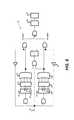
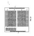
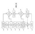
- a distributed pulse-width modulation system 10includes an array of pulse-width modulation elements 20 .
- the array of pulse-width modulation elements 20is spatially distributed over a system substrate 82 in rows and columns.
- Each element 20includes a digital memory 28 for storing a multi-bit digital value and a drive circuit 26 that drives an output device 27 in response to the multi-bit digital value stored in the digital memory 28 .
- a system controller 40includes a memory 42 for storing a multi-bit digital value for each element 20 and a communication circuit 44 for communicating each multi-bit digital value to each corresponding pulse-width modulation element 20 , for example through a bus 60 electrically connecting the system controller 40 to the elements 20 .
- the system controller 40can be, for example, an integrated circuit including the memory 42 , such as a static or dynamic memory, and the communication circuit 44 can be a logic circuit with output drivers (such as transistors) providing signals on output wires connected, for example, to the bus 60 connected to the system substrate 82 and to row lines 84 and column lines 86 to provide active-matrix-addressed control to the array of elements 20 .
- the electrical connections on the system substrate 82can be electrically conductive wires.
- the electrical connections between the bus 60 and the row lines 84 and column lines 86are not shown.
- the element 20can be, for example, an integrated circuit including the digital memory 28 and the drive circuit 26 can be an analog or digital or mixed-signal circuit with output drivers (such as transistors) controlling the output device 27 .
- the element 20can be provided in a bare die, unpackaged integrated circuit, or discrete components and can be mounted on the system substrate 82 using micro-transfer printing.
- the distributed pulse-width modulation system 10can be a display system
- the output device 27can be a light emitter, for example a light-emitting diode (LED) such as an inorganic micro-light-emitting diode
- the system controller 40can be a display controller.
- the elements 20can be pixels and the multi-bit digital values can be pixel values specifying light output from the LEDs.
- the elements 20can form an array of elements 20 arranged in rows and columns on the system substrate 82 to form a display. As illustrated in FIG. 1 , three elements 20 are included in a common integrated circuit chiplet 21 (also indicated as a common element 20 ). Each of the elements 20 in the chiplet 21 includes a different output device 27 .
- Each different output deviceis an inorganic micro-light emitter that emits a different color of light.
- the output devices 27are a red light emitter 50 R that emits red light, a green light emitter 50 G that emits green light, and a blue light emitter 50 B that emits blue light.
- the full-color pixelincludes three elements 20 (one for each color of light emitter 50 ).
- a pixelincludes a single output device 27 .
- the three elements 20are provided in a single integrated circuit, for example a small chiplet 21 such as a bare die.
- each element 20can be a separate integrated circuit chiplet 21 or can be provided in discrete components (not shown).
- the system controller 40provides a multi-bit digital value to each element 20 . This can be done in any of a variety of ways. In the embodiment illustrated in FIG. 1 , the system controller 40 serially shifts a sequence of multi-bit digital values through each of a series of elements 20 arranged in a row with a common clock signal 32 . Multiple rows of elements 20 can be loaded at the same time or at different times. In other embodiments, the elements 20 can be accessed using matrix addressing and the multi-bit digital values can be provided in parallel rather than as a serial bit stream. In such cases, the digital memory 28 can have a parallel data input control rather than the serial input control illustrated in FIG. 2 . Other logical designs can be used.
- the digital memory 28 of the element 20is a serial shift register that receives multi-bit digital values through a serial input 30 attached to the bus 60 ( FIG. 1 ).
- the serial input 30can be a row line 84 or column line 86 .
- the multi-bit digital valuesare clocked into the digital memory 28 with the common clock signal 32 .
- the stored multi-bit digital valuesare loaded into an up or down counter 22 , for example using a logic circuit 29 .
- the up or down counter 22can also be a digital memory 28 .
- the counter 22can be an up or down counter, it is more clearly explicated herein as a down counter that counts down to zero from a pre-determined value, but is not limited to a down counter embodiment.
- the logic circuit 29can also provide the clock signal 32 to the counter 22 after the multi-bit digital value is loaded to cause the counter 22 to increment or decrement.
- the logic circuit 29 , the digital memory 28 , and the counter 22can be a common circuit, separate circuits, or any combination of circuits.
- the multi-bit digital valuecan have any number of bits greater than one. In various embodiments, the multi-bit digital value is a 2-bit value, a 3-bit value, a 4-bit value, a 6-bit value, or an 8-bit value. In the FIG.
- the multi-bit digital valuehas four bits and the counter 22 is a 4-bit counter.
- the counter 22counts down to zero when supplied with the clock signal 32 or a signal derived from the clock signal 32 , such as a specific PWM clock, and maintains a zero output thereafter, even if additional clock signals 32 or derived clock signals are provided.
- a variety of different clock signalssuch as a PWM clock or data load or read signals, can be derived from a generic clock signal 32 to provide desired control or clock signals.
- the counter 22can count at a frequency different from the clock rate at which the multi-bit-digital values are loaded into the digital memory 28 so that the multi-bit digital values can be loaded at a higher rate than the down counter 22 counts down.
- a cycle counteris provided, for example in the logic circuit 29 to clock the down counter 22 at least a number of times equal to 2**n (two raised to the power of n) where n is the number of bits in the multi-bit digital value.
- An OR logic circuit 24receives the bits B 0 , B 1 , B 2 , and B 3 output by the down counter 22 and provides an output enable signal 25 as long as the down counter 22 has a non-zero value.
- the enable signal 25controls a drive circuit 26 (in this example connected to the gate of a drive transistor) that drives an output device 27 (in this example an LED).
- Other logic circuitscan provide the functionality described in FIG. 2 .
- FIG. 2is only one example of a logic circuit useful for the present invention.
- circuits describedcan be integrated into a common circuit or divided into separate circuits or can be implemented according to different designs.
- the digital memory/serial shift register 28 and down counter 22can be combined into a single universal counter and are illustrated as separate elements for descriptive clarity.
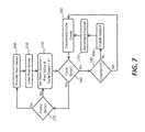
- a method of operating the distributed pulse-width modulation system 10 of the present inventionincludes first providing multi-bit digital value, for example pixel values from an image frame of an image sequence, to the system controller 40 and storing the multi-bit digital values in the memory 42 of the system controller 40 in step 100 .
- Each pixel valueis a multi-bit digital value specifying a desired luminance output over a period of time by the output device 27 of each element 20 .
- each element 20corresponds to a pixel and is spatially located on the system substrate 82 in correspondence with the relative location of the pixel provided to the element 20 in the image so that the array of elements 20 forms a display for displaying the pixel values of the image.
- the multi-bit digital pixel valuesare loaded into the corresponding elements 20 by the system controller 40 in step 110 and the down counter 22 is set to the loaded multi-bit digital value in step 120 .
- a cycle controlleris also set to the value 2**n where n is the number of bits in the multi-bit digital value.
- the counter valueis tested in step 140 and, if it is not zero, the output is enabled in step 150 , the down counter 22 is decremented in step 130 , and the cycle counter is decremented in step 180 , responsive to the clock signal 32 .
- the test processis then repeated by testing the cycle state in step 160 . If the counter value is zero, the cycle counter is decremented in step 180 and the test process is repeated by testing the cycle state in step 160 .
- the time required to count down the cycle countercan be less than a frame time period (to reduce flicker).
- the system controller 40includes a timing circuit 46 (for example, as in FIG. 1 ) for providing timing signals to each element 20 .
- the time periodcan be formed with a counter controlled by the timing signal.
- the element 20can include a timing circuit (for example in logic circuit 29 ) to provide a derived clock signal used by the down counter 22 .
- the timing signalscan control the rate at which the output device 27 is driven in response to the multi-bit digital value stored in the digital memory 28 and can be different from the rate at which data is loaded into the array of elements 20 .
- the multi-bit digital valuescan be loaded at a 1 MHz rate.
- the least-significant bit of the multi-bit digital valuecan correspond to a 1 msec time period and the clock signal 32 (or derived clock signal) can have a corresponding 1 msec period so that the down counter 22 decrements at a 1 kHz frequency. Therefore, the output device 27 can be enabled for any time period from zero to 15 msecs depending on the multi-bit digital value provided to the down counter 22 .
- the element 20provides a pulse-width modulation of the output device 27 . Any frequency compatible with the element 20 hardware can be provided by the system controller 40 so that different pulse rates can be used according to the desired application of the distributed pulse-width modulation system 10 , for example 10 kHz or 100 kHz.
- Pulse-width modulationis usefully employed with light-emitting diodes, since light-emitting diodes tend to have an optimum current and voltage operating parameter at which the LED performance is optimal for some operating characteristic, for example efficiency, or the LED current-to-illuminance transfer function is non-linear.
- the drive circuit 26provides a voltage or a current corresponding for a portion of a time period corresponding to the value of the multi-bit digital value and provides a constant current or voltage that is supplied to the output device 27 for that time period.
- the system controller 40includes a memory 42 for storing a full-bit digital value for each element 20 .
- the full-bit digital valueincludes a plurality of multi-bit digital values, and the communication circuit 44 communicates each multi-bit digital value to each corresponding element 20 sequentially.
- the full-bit digital valueis the desired output value for the output devices 27 over a time period, for example a frame period.
- a full-bit digital valuecan be an 8-bit value having values ranging from zero to 255 and representing a range of luminance values from minimum luminance at zero to maximum luminance at 255 (i.e., from off to maximum brightness). If the multi-bit value loaded into the elements 20 has the same number of bits as the full-bit digital value, a pulse-width modulation function is provided as described above with respect to FIG. 2 and FIG. 7 .
- the digital memory 28 and the counter 22 in the elements 20have fewer bits than the full-bit pixel value.
- the full-bit digital valuecan be 8 bits but the digital memory 28 and the counter 22 in the elements 20 can store only 4 bits.
- the multi-bit digital value (the value that is loaded into the elements 20 )is only 4 bits so that the full-bit digital value (having 8 bits) includes a plurality (two) of multi-bit digital values (of four bits each).
- the multi-bit digital value (the value that is loaded into the elements 20 )is only 2 bits so that the full-bit digital value (having 8 bits) includes a plurality (four) of multi-bit digital values (of two bits each).
- every multi-bit digital valuehas the same number of bits, so long as the digital memory 28 is sufficiently large for the bits in the largest multi-bit digital value.
- the full-bit digital valuehas 8 bits
- the multi-bit valuescan be two bits, three bits, and three bits.
- the number of bits in each of the multi-bit digital values of a full-bit digital valuemust sum to the number of bits in the full-bit digital value.
- a full-bit digital valuecan be divided in different ways into different numbers of different multi-bit digital values.
- the multi-bit valuescan include six two-bit multi-bit digital values, four three-bit multi-bit digital values, three four-bit multi-bit digital values, or six two-bit multi-bit digital values.
- the multi-bit valuescan include one three-bit multi-bit digital values, one five-bit multi-bit digital values, and one four-bit multi-bit digital values.
- bits in a numberare labeled B 0 , B 1 , B 2 , and so on corresponding to the place of the bit in the binary number and arranged sequentially from right to left in a graphic numerical depiction. Each successive place to the left represents a value twice that of the previous place to the right.
- B 0is typically designated the least significant bit and has a place value of one.
- B 1is the next bit and has a place value twice that of B 0 , in this case two, and B 2 has a place value twice that of B 1 , in this case four.
- nth bithas a place value equal to 2**n and is conventionally designated as B(n ⁇ 1), where 2**n (or 2 ⁇ circumflex over ( ) ⁇ n) represents 2 raised to the n th power or 2 raised to the exponent n.
- the different multi-bit digital values making up a full-bit digital valuetherefore have different relative values depending on their relative places in the full-bit digital value.
- the least significant bit of each multi-bit digital valuewill have a value 2**n, where n is the place of the least significant bit of the multi-bit digital value.
- the full-bit digital valuehas 8 bits and is made up of a first four-bit multi-bit digital value corresponding to the first lower four bits of the full-bit digital value (B 0 , B 1 , B 2 , B 3 )
- the second four-bit multi-bit digital values corresponding to the second upper four bits of the full-bit digital value (B 4 , B 5 , B 6 , B 7 )have a value 2**4 (equal to 16) greater than the first four-bit multi-bit digital value.
- the valuesrepresent portions of a time period where the maximum value is equivalent to the maximum time period and the minimum value (typically zero) is equal to the minimum time period, typically zero time.
- One bit in the valueis the minimum change and is chosen to correspond to the desired minimum change in the chosen time period.
- each multi-bit digital value in a full-bit digital valuehas a minimum period value corresponding to its least significant bit value.
- each of the first four-bit multi-bit digital valuesrepresents a one-msec time period.
- FIGS. 3, 4, and 5illustrate three different examples of multi-bit digital values making up a full-bit digital value applied to a distributed pulse-width modulated system 10 of the present invention.
- a full-bit digital valuehas four bits made up of two two-bit multi-bit digital values.
- the first multi-bit digital valuesare supplied by the system controller 40 and loaded into the respective elements 20 during the Load M 0 time period (corresponding to steps 100 , 110 , and 120 of FIG. 7 ).
- the clock signal 32is then supplied for four cycles (equal to 2**n where n is the number of bits in the first multi-bit digital value, two in this example) to cause the down counter 22 and cycle counter to decrement, and if the output of the down counter 22 is non-zero, the output device 27 is enabled (corresponding to steps 130 , 140 , 150 , and 160 of FIG. 7 ) during the Count M 0 time period.
- the second multi-bit digital valuesare then supplied by the system controller 40 and loaded into the respective elements 20 during the Load M 1 time period (corresponding to steps 100 , 110 , and 120 of FIG. 7 ).
- the clock signal 32is then supplied for 4 cycles (equal to 2**n where n is the number of bits in the second multi-bit digital value, 2 in this example) to cause the down counter 22 and cycle counter to decrement during the Count M 1 time period. If the output of the down counter 22 is non-zero, the output device 27 is enabled. However, for the second multi-bit digital value cycle, as shown in FIG. 3 the clock rate (or, more precisely, the PWM pulse rate) has a period equal to four times the period of the clock used for the first multi-bit digital value because the least significant bit of the second multi-bit digital value is the second bit B 2 and four is equal to 2**n where n equals 2, the place of the least significant bit of the second multi-bit digital value.
- a full-bit digital valuehas six bits made up of three two-bit multi-bit digital values.
- the first multi-bit digital valuesare supplied by the system controller 40 and loaded into the respective elements 20 during the Load M 0 time period (corresponding to steps 100 , 110 , and 120 of FIG. 7 ).
- the clock signal 32is then supplied for 4 cycles (equal to 2**n where n is the number of bits in the first multi-bit digital value, 2 in this example) to cause the down counter 22 and cycle counter to decrement, and if the output of the down counter 22 is non-zero, the output device 27 is enabled (corresponding to steps 130 , 140 , 150 , and 160 of FIG. 7 ) during the Count M 0 time period.
- the second multi-bit digital valuesare then supplied by the system controller 40 and loaded into the respective elements 20 during the Load M 1 time period.
- the clock signal 32is then supplied for 4 cycles (equal to 2**n where n is the number of bits in the second multi-bit digital value, 2 in this example) to cause the down counter 22 and cycle counter to decrement during the Count M 1 time period. If the output of the down counter 22 is non-zero, the output device 27 is enabled.
- the clock ratehas a period equal to four times the period of the clock used for the first multi-bit digital value because the least significant bit of the second multi-bit digital value is the second bit B 2 and four is equal to 2**n where n equals 2, the place of the least significant bit of the second multi-bit digital value.
- the third multi-bit digital valuesare then supplied by the system controller 40 and loaded into the respective elements 20 during the Load M 2 time period.
- the clock signal 32is then supplied for 4 cycles (equal to 2**n where n is the number of bits in the third multi-bit digital value, 2 in this example) to cause the down counter 22 and cycle counter to decrement during the Count M 2 time period.
- the clock ratehas a period equal to 16 times the period of the clock used for the first multi-bit digital value because the least significant bit of the second multi-bit digital value is the fourth bit B 4 and 16 is equal to 2**n where n equals 4, the place of the least significant bit of the third multi-bit digital value.
- a full-bit digital valuehas eight bits made up of two four-bit multi-bit digital values.
- the first multi-bit digital valuesare supplied by the system controller 40 and loaded into the respective elements 20 during the Load M 0 time period (corresponding to steps 100 , 110 , and 120 of FIG. 7 ).
- the clock signal 32is then supplied for 16 cycles (equal to 2**n where n is the number of bits in the first multi-bit digital value, 4 in this example) to cause the down counter 22 and cycle counter to decrement during the Count M 0 time period, and if the output of the down counter 22 is non-zero, the output device 27 is enabled (corresponding to steps 130 , 140 , 150 , and 160 of FIG. 7 ).
- the second multi-bit digital valuesare then supplied by the system controller 40 and loaded into the respective elements 20 during the Load M 1 time period (corresponding to steps 100 , 110 , and 120 of FIG. 7 ).
- the clock signal 32is then supplied for 16 cycles (equal to 2**n where n is the number of bits in the second multi-bit digital value, 4 in this example) to cause the down counter 22 and cycle counter to decrement during the Count M 1 time period. If the output of the down counter 22 is non-zero, the output device 27 is enabled.
- the clock ratehas a period equal to 16 times the period of the clock used for the first multi-bit digital value because the least significant bit of the second multi-bit digital value is the fourth bit B 2 and 16 is equal to 2**n where n equals 4, the place of the least significant bit of the second multi-bit digital value.
- the first multi-bit digital valuehas a clock signal 32 with a first period and the second multi-bit digital value has a clock signal 32 with a second period that is related to the first period by the relative values of the lower bits and the upper bits in the full-bit digital value.
- the second periodhas a length that is 2**n times the first period wherein n is the place value of the least significant bit in the second multi-bit digital value.
- the period of the clock signal 32can be set by the timing circuit 46 of the system controller 40 .
- the period of the clock signal 32can be determined by the logic circuit 29 , for example by providing a frequency divider for the clock signal 32 used to drive the cycle counter and the down counter 22 .
- the clock signal 32 used to load data into the elements 20can have a different frequency, for example much higher than the counting frequency to reduce the time spent loading data into the elements 20 .
- an array of full-bit digital valuesare provided, for example to the system controller 40 in step 102 .
- the full-bit digital valuescan be pixel values, as indicated in FIG. 7 but as in FIG. 7 can be other values and are not necessarily pixel values.
- the number of multi-bit valuesis determined and the first multi-bit values and corresponding clock rate are initialized in step 105 and loaded into the elements 20 in step 115 .
- the process of FIG. 7then proceeds (pulse-width modulation control is provided to the output device 27 for the current multi-bit digital value).
- a testis performed to determine whether other multi-bit digital values are to be processed in step 145 .
- step 155the next set of multi-bit digital values and corresponding clock rates are calculated or provided in step 155 and then initialized or loaded into the elements 20 in step 115 and the process repeats until all of the multi-bit digital values comprising the full-bit digital value are operated.
- the frame statusis checked in step 170 and if the frame is not done the process repeats with step 105 . If the frame is done, new full-bit digital values are provided in step 102 .
- an array of full-bit digital valuesis provided, each full-bit digital value including at least first and second multi-bit digital values.
- Each element 20 of the array of elements 20is loaded with the first multi-bit digital value of the array of full-bit digital values and a first timing signal provided to each element 20 .
- the timing signal and the first multi-bit digital valueare combined to provide a control signal in each element 20 , the control signal responsive to the value of the first multi-bit digital value, and the output device of each element 20 is driven in response to the control signal.
- Each element 20 of the array of elements 20is loaded with the second multi-bit digital value of the array of full-bit digital values and a second timing signal provided to each element 20 .
- the second timing signal and the second multi-bit digital valueare combined to provide a control signal in each element 20 , the control signal responsive to the value of the second multi-bit digital value, and the output device 27 of each element 20 is driven in response to the control signal.
- the first and second timing signalscan be the same timing signal and the different clock signal rates corresponding to the different first and second multi-bit digital values formed in the element 20 or, alternatively, different clock signal rates corresponding to the different first and second multi-bit digital values formed in the element 20 can be provided by the system controller 40 , for example with the timing circuit 46 .
- the circuit of FIG. 2will enable the output device 27 for an uninterrupted period of time corresponding to the value loaded into the down counter 22 . After the down counter 22 has reached zero, the output device 27 will be uninterruptedly disabled for the remainder of the cycle.
- the enabled and disabled periodscan be alternated, reducing the appearance of flicker for a display application of the present invention.
- the down counter 22is a first counter and the elements 20 include a second counter responsive to the timing signal.
- a control circuitalternates the signals from the first counter and the second counter so that the output device 27 is responsive to the alternating signal. As shown in FIG.
- the element 20includes two each of the digital memory 28 , the down counter 22 , and the OR logic circuit 24 , except that the second counter is an up counter 23 while the first counter is a down counter 22 as in FIG. 2 .
- the clock signal 32is applied through an AND gate to a Toggle flip-flop that alternates state with each applied clock signal 32 .
- the first state of the two states of the toggle flip-flopprovides the output of the down counter 22 to the drive circuit 26 and the output device 27 (that can, for example, be the circuit shown in FIG. 2 ).
- the second state of the two states of the toggle flip-flopprovides the output of the up counter 23 to the drive circuit 26 and the output device 27 .
- the down counter 22provides an enable signal when the down counted multi-bit digital value is non-zero; it counts the number of periods when the output device 27 should be enabled.
- the up counter 23provides a disable signal when the up counted multi-bit digital value is non-zero; it counts the number of periods when the output device 27 should not be enabled. For example, for a four-bit multi-bit digital value of 12, the down counter 22 provides 12 periods when the output device 27 should be enabled and the up counter 23 provides 4 periods when the output device 27 should not be enabled.
- the circuit of FIG. 6temporally intersperses the disabled periods and the enable periods.
- the digital memories 28are loaded together through the serial input 30 in response to the clock signal 32 . (Loading logic is not shown but can be controlled by the logic circuit 29 in each counter.) The multi-bit digital values are then applied to the up and down counters 23 , 22 using the logic circuit 29 . Digital circuits for controlling serial shift registers, loading counters, and providing clock signals can be made using convention Boolean logic and available integrated circuit modules. Once the output of the up and down counters 23 , 22 are combined through the respective OR logic circuit 24 , operation of the output device 27 can begin.
- the Toggle flip-flopwill respond to the clock signal 32 and alternately provide a signal to the AND gates on the inputs applied to the counters. If the Q output of the Toggle flip-flop is positive and the down counter 22 is clocked, its value is decremented and the Toggle flip-flop changes state to enable the clock input to the up counter. The next clock signal 32 will increment the up counter 23 and switch the Toggle state again.
- the up and down counters 23 , 22are alternately controlled by the Toggle flip-flop as long as they have non-zero contents.
- the delay circuits 25prevent race conditions and ensure that the changes in Toggle flip-flop state do not inadvertently clock the up or down counters 23 , 22 . (Other logic designs can also prevent race conditions.)
- the Toggle flip-flop stateis fixed so that the other counter is selected and responds to each clock signal 32 .
- the up counter 23counts up to the maximum value of the counter and then once more until it is at zero and then no longer responds to further clock signals 32 .
- the down counter 22counts down until it is at zero and then no longer responds to further clock signals 32 .
- the Toggle flip-flop Q output(corresponding to the down counter state) is combined with the output of the down counter OR logic circuit 24 to provide an Enable signal for the output device 27 .
- the Toggle flip-flop QNOT output(inverse of output Q and corresponding to the up counter state) is combined with the output of the up counter OR logic circuit 24 to provide a disable signal for the output device 27 .
- Enable and Disable signalsare mutually exclusive, in some embodiments, it is not necessary to produce both, but they are both provided for clarity of exposition.
- the logic circuits of FIG. 6are provided to demonstrate the concept of alternating enable and disable signals provided to the output device 27 and other circuit designs are possible and can be preferred.
- FIGS. 2 and 6are exemplary and not limiting. Other circuit designs can implement the functions described and are included as part of the present invention.
- each pulse-width modulation element 20(also referred to as element 20 ) includes an output device 27 driven by a drive circuit 26 associated with each digital memory 28 and a PWM counter 22 (also referred to as down counter 22 ).
- a distributed pulse-width modulation system 10includes an array 12 of pulse-width modulation elements 20 .
- Each pulse-width modulation element 20includes a digital memory 28 for storing a plurality of multi-bit digital values, a drive circuit 26 for each stored multi-bit digital value, and an output device 27 for each stored multi-bit digital value.
- the multi-bit digital valuesall have the same maximum number of bits, for example 8 bits, 10 bits, 12 bits, 14 bits, or 16 bits.
- Each multi-bit digital valuecan store a different number ranging from zero to 2 n ⁇ 1 where n is the number of bits in the multi-bit digital value.
- the corresponding drive circuit 26drives the corresponding output device 27 in response to the multi-bit digital value stored in the digital memory 28 .
- a system controller 40includes a memory 42 for storing the multi-bit digital values for each element 20 and a communication circuit 44 for communicating each multi-bit digital value to each corresponding pulse-width modulation element 20 .
- the digital memory 28can be a common memory for all of the multi-bit digital values in the element 20 (as shown) or can include a plurality of separate memories, for example a separate memory for each multi-bit digital values.
- the drive circuits 26can be entirely separate circuits (as shown), or can have portions or components in common.
- the dashed lines joining circuit elements in FIG. 9 (and in some of the following figures)indicate that multiple, similarly connected additional circuit elements are included in the circuit.
- the system controller 40can include a timing circuit 46 for providing timing signals, for example clock signals, to each element 20 . The timing signals can control the rate at which the output devices 27 are driven in response to the multi-bit digital values stored in the digital memory 28 .
- the element 20 of FIG. 10includes only a single pulse-width modulation up or down counter 22 for providing pulse-width modulation timing for all of the multi-bit digital values stored in the digital memory 28 .
- the element 20requires less circuitry and has a lower cost in a smaller integrated circuit package.
- the down counter 22Rather than counting down the value of each multi-bit digital value with a separate down counter 22 (e.g., as in FIG. 2 ), the down counter 22 provides a single pulse-width modulation down-counted counter output that is compared to each of the multi-bit digital values in the digital memory 28 with a comparator circuit 90 .
- the output of the comparator circuit 90is supplied to the drive circuit 26 to drive the output device 27 so that each drive circuit 26 and output device 27 are responsive to a corresponding multi-bit digital value.
- the down counter 22is also referred to as a PWM counter 22 to distinguish it from a cycle counter 98 described below and is responsive to a PWM clock 32 (clock signal 32 ), for example as provided from the timing circuit 46 of the system controller 40 .
- each registerpresents all of the bits of the stored multi-bit digital value at the same time on parallel output lines and the pulse-width modulation cycle can begin.
- Each of the stored bitsis combined with the corresponding bit of the PWM counter 22 with a logical AND and the output of each logical AND bit combination is combined in a multi-input AND gate whose output is HIGH only if each of the bits in the stored multi-bit digital value matches the corresponding bit of the PWM counter 22 counter output.
- An output state flip-flop 92 or latchstores the output state.
- the output state flip-flop 92is illustrated as a T flip-flop for simplicity and understanding, since its state toggles between off and on, but the output state flip-flop 92 can be a T flip-flop, an SR flip-flop, a D flip-flop, or a latch. If the output state is off (for example the output state flip-flop 92 stores a LOW value), the output device 27 does not output a signal. If the output state is on (for example the output state flip-flop 92 stores a HIGH value), the output device 27 does output a signal.
- the output state flip-flop 92can be set to an off (LOW) state, for example with the PWM counter reset signal as shown.
- the PWM counter reset signalsets the PWM counter 22 to its maximum value (e.g., 1023 for a 10-bit multi-bit digital value) for example by providing a PWM clock 32 signal when the PWM counter 22 stores a zero value.
- the bits representing this maximum value (all 1s)are compared to the actual multi-bit digital value.
- the T flip-flop making up the output state flip-flop 92toggles into a HIGH state and the output device 27 is turned on. (An inverted clock signal is combined with the comparison signal using an AND gate to clock the output state flip-flop 92 to allow the comparator circuit 90 to settle and avoid race conditions.) If a match is not found, the output state of the output state flip-flop 92 is not changed and the output device 27 remains off. In either case, the PWM counter 22 counts down one value in response to the PWM clock 32 and a comparison is performed again and the process is repeated.
- the output state flip-flop 92remains in an off state until a match is found and once a match is found, the output state flip-flop 92 remains in an on state until the PWM clock finishes counting down (since only one match can be found) after which the output state flip-flop 92 is reset and the process begins again.
- the output device 27is off until a match is found and remains on until the counter output of the PWM counter 22 reaches zero. Therefore, the output device 27 is on for as many PWM clock 32 cycles as is the number stored in the digital memory 28 and is off for the remaining cycles.
- the PWM counter reset signalcan be responsive to a zero value in the PWM counter 22 . Since all of the bits in the multi-bit digital value and all of the bits in the PWM counter 22 are compared at the same time, the comparator circuit 90 is a parallel comparator.
- a content addressable memoryis a memory that provides a signal (for example a HIGH signal) when the CAM stores a value equal to the value provided to the CAM's input.
- a CAMcan require a smaller circuit than a register but can also require more power to operate.
- read, write, and data signalsprovide a way to load multi-bit digital values into the CAM. Once the multi-bit digital values are loaded, the output state flip-flop 92 can be reset to an off state and the PWM counter 22 can count down and provide the counter output to the CAM inputs.
- the output state flip-flop 92is toggled from an off state to an on state.
- the CAMincorporates both the digital memory 28 and the comparator circuit 90 .
- the drive circuit 26operates as described above with respect to FIG. 10 as does the pulse-width modulation control.
- the comparator circuit 90 in the embodiment of FIG. 11is also a parallel comparator.
- the embodiment of FIG. 12uses a serial comparator.
- the digital memory 28is a random access memory (RAM) such as a static random access memory (SRAM).
- RAMrandom access memory
- SRAMstatic random access memory
- An SRAMcan require a smaller circuit than registers on a CAM but can require a higher frequency clock to perform serial bit comparisons and can thus require more power.
- read, write, and data signalscan control the SRAM to load the multi-bit digital values into the SRAM in bit planes so that each SRAM address, generated by the bit address circuit, stores a common bit of each of the multi-bit digital values.
- address 0can store bit 0 of the multi-bit digital values
- address 1can store bit 1 of the multi-bit digital values
- address 2can store bit 2 of multi-bit digital values and so on.
- the PWM counter 22operates as in the embodiments of FIGS. 10 and 11 . However, rather than providing the counter output in parallel to a parallel comparator circuit 90 , the counter output is provided to a bit select circuit responsive to a bit clock signal in concert with the bit address generation circuit.
- the bit clockprovides as many signals as bits in the multi-bit digital values for each PWM clock 32 signal.
- the bit select circuitselects the counter output bit corresponding to the address provided by the bit address circuit.
- the bit select circuitselects bit 0 of the PWM counter output. If the bit address generates the address of multi-bit digital value bit 1 in the CAM, the bit select circuit selects bit 1 of the PWM counter output, and so on.
- the multi-bit digital value bit (designated as Bx in FIG. 12 ) and the counter output bit (designated as Cx in FIG. 12 )are presented as inputs to the serial comparator 91 .
- the serial comparator 91uses an exclusive NOR (XNOR) circuit to compare the multi-bit digital value bit and the counter output bit and produce a HIGH signal when the multi-bit digital value bit and the counter output bit are the same (i.e., both LOW or both HIGH).
- XNORexclusive NOR
- a serial state flip-flop 94(indicating the state of the comparison) is initially set to a HIGH value and the state of the serial state flip-flop 94 is combined with the XNOR output. If the XNOR output is HIGH, the state of the serial state flip-flop 94 remains high when clocked by the selected edge of the bit clock (to provide time for the circuit to settle and avoid race conditions. If the XNOR output is LOW, the state of the serial state flip-flop 94 changes to LOW.
- serial state flip-flop 94Since the state of the serial state flip-flop 94 is now LOW and is combined with the XNOR output as an input to the serial state flip-flop 94 , the serial state flip-flop 94 output will remain LOW until it is reset.
- the bit clockthen operates to increase the bit address and bit selection and present the next multi-bit digital value bit and PWM counter output bit to the XNOR circuit and the process repeats until all of the bits in the multi-bit digital value and the PWM counter output have been compared.
- the state of the serial state flip-flop 94will only remain HIGH if all of the bits in the multi-bit digital value match the bits in the PWM counter 22 .
- the state of the serial state flip-flop 94is clocked into the output state flip-flop 92 with the bit address reset signal that restarts the comparison process. If the state of the serial state flip-flop 94 is HIGH (indicating a match between the multi-bit digital value and the PWM counter 22 output), the output state flip-flop 92 will toggle into a HIGH state. If there is no match, the clock input of the output state flip-flop 92 will not go HIGH and the state of the output state flip-flop 92 will not change. Since only one match between the multi-bit digital value and the PWM counter 22 output is possible, the output state flip-flop 92 cannot toggle back into a LOW (off) state until it is reset. Thus, as in the embodiments of FIGS.
- the state of the output state flip-flop 92will remain LOW until a match with the PWM counter 22 output is established, after which the output state flip-flop 92 will transition HIGH until it is reset, providing a pulse-width modulation signal responsive to the multi-bit digital value.
- the logic signalscan correspond to relatively high or low voltages in a logic circuit such as a CMOS circuit.
- the SRAM digital memory 28is arranged in 48 columns of 10 bits each. Each column is selected with a 1-of-12 column decoder and selection circuit.
- the PWM counteris used during SRAM data load as a four-bit column selector counter and is not needed for PWM counting during this time.
- the first 10-bit serial valueis input to column 1
- the second 10-bit serial valueis input to column 2, and so forth, for each of the four column data inputs.
- the 4-bit word countercounts from 0 to 9 (for 10 bits) and the corresponding bit address is selected by the 1-of-10 word line decoder.
- the column select and word line decoder circuitsenable a serial bit stream to be properly loaded into the SRAM digital memory 28 .
- the datais loaded so that, for example, address zero stores the zero bit of each of the 48 digital values in parallel, address one stores the one bit of each of the 48 digital values in parallel, and so forth.
- a frame timecorresponds to each full count cycle of the PWM counter 22 , so that new data is loaded before each time the PWM counter 22 counts down.
- the PWM counter 22counts down multiple times between each new data set is loaded in the SRAM digital memory 28 so that multiple cycles of data are output for each data set.
- These multiple cyclescan be controlled by a cycle counter 98 .
- the cycle counter 98can be separate from the PWM counter 22 (as shown) or the cycle counter 98 and the PWM counter 22 are part of a common counter. In either case, the PWM counter 22 is operating with the cycle counter 98 to provide multiple cycles of PWM timing signals for the multi-bit digital values, for example in collaboration with the communication circuit 44 and timing circuit 46 .
- the cycle counter 98 and PWM counter 22are part of a common counter that is set to a desired value each time new data is loaded into the SRAM digital memory 28 and when the common counter reaches zero, new data is loaded into the SRAM digital memory 28 .
- the PWM counter 22will complete an entire count cycle each time the cycle counter 98 decrements.
- the cycle counter 98 and PWM counter 22 together decrement to zero (the common counter equals zero)the process for one data set is complete.
- FIG. 14is a layout for the circuit of FIG. 13 .
- the SRAM digital memory 28is divided into two portions, as are the serial comparators 91 , and the drive circuit 26 .
- This circuithas an area of approximately 100 microns by 100 microns on a crystalline silicon substrate in a 0.18-micron photolithography process.
- the circuithas an area of approximately 63 microns by 63 microns in a 90-nm process.
- a method of operating the distributed pulse-width modulation system 10includes loading the multi-bit digital values into the digital memory 28 of each element 20 and then driving each output device 27 in response to the corresponding multi-bit digital value.
- a system 10is a digital system, can be a digital drive system, or can be a digital display, since the communicated and stored data is digital and every module in the system is digitally controlled.
- a method of operating the distributed pulse-width modulation system 10includes loading the multi-bit digital values into each element 20 in step 200 .
- the PWM counter 22is set to an initial count value, in step 220 .
- the initial count valuecan be at least as large as the largest possible multi-bit digital value, the maximum value, and the output device 27 is turned off in step 230 .
- the ten bits of the countercan be turned on (i.e., set to 1023) and then controlled to count down to zero, as illustrated.
- the PWM counter 22operates as an up counter
- the initial count valuecan be set to zero and the output device 27 is turned on in step 230 (not shown).
- the ten bits of the countercan be turned off (i.e., set to 0) and then controlled to count up to 1023 (not shown).
- Steps 220 and 230can be interchanged. This resets the system to begin a PWM output cycle.
- the PWM counter 22is optionally operated in step 240 to count (e.g., with an enable control signal) and the counter output is compared to each multi-bit digital value with the comparator circuit 90 (either in parallel with all of the bits at once or serially bit by bit) in step 250 . If the PWM counter 22 output matches the multi-bit digital value (step 260 ), each output device 27 is driven with the drive circuit 26 to output a signal, for example light output from an LED, in step 270 , in the down counter case of the PWM counter 22 . The PWM counter 22 is then decremented in step 280 and tested in step 290 . If the PWM counter 22 does not equal zero, the comparison process is repeated. If the PWM counter 22 equals zero, then the cycle counter 98 (if present) is also decremented in step 300 and tested in step 310 .
- the output device 27is driven with the drive circuit 26 to cease outputting a signal in step 270 .
- the PWM counter 22is then incremented in step 280 and tested in step 290 . If the PWM counter 22 does not equal the maximum value, the comparison process is repeated. If the PWM counter 22 equals the maximum value, then the cycle counter 98 (if present) is also decremented in step 300 and tested in step 310 .
- cycle counteris not equal to zero, the PWM counter 22 process is repeated for another cycle. If the cycle counter does equal zero, then the cycle process is complete and new data can be loaded and the cycle counter reset. In display terms, when the cycle counter equals zero, a new frame time can begin, for example by loading new data (e.g., a new image) from the communication circuit 44 .
- each bit of the multi-bit digital valueis sequentially compared to the PWM counter 22 output.
- the bit orderis arbitrary but can be from low bit to high bit or high bit to low bit, as in this example.
- the state of the comparisonis stored in the serial state flip-flop 94 ( FIG. 12 ) and is initially set to a TRUE or match state in step 251 .
- the bit counter(bit address generator) generates a multi-bit digital value bit and is set to the number of bits in the multi-bit digital value in step 252 and optionally enabled in step 253 .
- the PWM counter 22 bitis compared to the corresponding multi-bit digital value bit indicated by the bit counter.
- step 255the bit counter is decremented to the next bit in step 257 and, if the bit count is not zero (step 258 ) the comparison repeated for the next bit. If a match is not found, the comparison state of the serial state flip-flop 94 is set to FALSE in step 256 , indicating that the PWM counter 22 output does not match the multi-bit digital value, and the bit counter decremented in step 257 . If the bit count reaches zero, step 258 , the serial comparison process is complete.
- a method of the present inventionincludes sequentially comparing each bit of the multi-bit digital values to the corresponding bit of the PWM counter 22 output with the corresponding serial comparator 91 and driving each output device 27 to output a signal with the corresponding drive circuit 26 in response to a match between the corresponding multi-bit digital value and the PWM counter 22 output.
- the drive circuit 26includes an output state, for example stored in an output state flip-flop 92 , as shown in FIGS. 10-12 .
- the output state flip-flop 92indicates and controls whether the output device 27 is off or on and, at the beginning of each frame is initially set to the off state, for example responsive to the PWM counter output equaling zero.
- the output state flip-flop 92is turned on.
- FIG. 17illustrates a behavioral RTL logic simulation of the embodiment of the present invention shown in FIGS. 13 and 14 .
- This simulationuses a single ASIC (application-specific integrated circuit) active-matrix drive to a 4 ⁇ 4 sub-array or block of pixels having one row input wire and four column input wires to the 4 ⁇ 4 block.
- the ASICreceives data on a row basis on all 4 columns in parallel so that the block data is loaded in four row times or 1/540 of frame rate.
- Each pixelis driven by a 10-bit PWM control signal generated in the ASIC with a constant current.
- the datais single-buffered resulting in a progressive scan image.
- a row pulseis generated to reset the ASIC and prepare for data.
- a zero data signalis sent on all columns to identify the start of data (a reset or start signal).
- a sequence of 12 10-bit serial words starting with value of 0 and counting by 1 up to 11is sent for each column in parallel.
- the design goalis to enable the LEDs with pulse widths ranging from 0 to 11 clock pulses wide.
- the PWM generatorcreates PWM output pulses using an up-counting mode so that Led[0] pulse width is zero resulting in no pulse, Led[1] pulse width is one clock wide, and so forth so that the Led[11] pulse width is 11 clocks wide.
- PWM clocksare shown as transitions on the maincount variable.
- Embodiments of the present inventioncan be made using conventional integrated circuit and printed circuit board materials and tools.
- some or all of the elements 20can be provided in one or more chiplets 21 , integrated circuits, or discrete parts some or all of which can be disposed on the system substrate 82 using micro-transfer printing techniques.
- the one or more chiplets 21 , integrated circuits, or discrete partscan be micro-transfer printed onto a module substrate and electrically interconnected on the module substrate.
- the module substratecan then be disposed onto the system substrate 82 , either by conventional means or by micro-transfer printing, and electrically interconnected to make the distributed pulse-width modulation system 10 of the present invention.
- the chiplets 21 or integrated circuitscan be supplied as bare die or unpackaged integrated circuits suitable for micro-transfer printing from a source wafer, such as a semiconductor wafer.
- Output devices 27e.g., light emitters such as LEDs
- the circuit componentsfor example CMOS on silicon
- Electrical interconnectionscan be made using conventional photolithographic methods.
- the system controller 40can be one or more integrated circuits and can, for example, include an image frame store, digital logic, input and output data signal circuits, and input and output control signal circuits such as communication circuits 44 , control circuits, and a clock signal 32 (e.g., as part of the timing circuit 46 ).
- the communication circuit 44can drive row lines 84 and column lines 86 to provide sequential rows of multi-bit digital values to corresponding selected rows of elements 20 .
- the system controller 40can include an image frame store memory for storing digital pixel and calibration values.
- the system controller 40can have a display controller substrate separate and distinct from the system substrate 82 that is mounted on the system substrate 82 or is separate from the system substrate 82 (as shown in FIG. 1 ) and connected to it by a wire bus 60 , for example with ribbon cables, flex connectors, or the like.
- the digital memory 28is a multi-bit memory with various numbers of bits in various embodiments of the invention.
- the elements 20 and the light emitterscan be made in one or more integrated circuits having separate, independent, and distinct substrates from the system substrate 82 .
- the elements 20can be or include one or more chiplets 21 —small, unpackaged integrated circuits such as unpackaged dies interconnected with wires connected to contact pads on the chiplets.
- the chipletscan be disposed on an independent substrate, such as the system substrate 82 .
- the chipletsare made in or on a semiconductor wafer and have a semiconductor substrate.
- the system substrate 82 or a module substratecan include glass, resin, polymer, plastic, or metal.
- the module substrateis a semiconductor substrate and the digital memory 28 or the drive circuit 26 are formed in or on and are native to the module substrate.
- the chiplets or modulescan have an area of, for example, 50 square microns, 100 square microns, 500 square microns, or 1 square mm and can be only a few microns thick, for example, 5 microns, 10 microns, 20 microns, or 50 microns thick.
- the elements 20 (or portions thereof) or the light emittersare disposed on the system substrate 82 by micro transfer printing.
- the elements 20 (or portions thereof) or the light emittersare disposed on the module substrate to form a heterogeneous module and the modules are disposed on the system substrate 82 using compound micro assembly structures and methods, for example as described in U.S. patent application Ser. No. 14/822,868 filed Aug. 10, 2015, entitled Compound Micro-Assembly Strategies and Devices.
- the modulesare larger than the chiplets or light emitters
- the modulesare disposed on the system substrate 82 using pick-and-place methods found in the printed-circuit board industry, for example using vacuum grippers.
- the modulescan be interconnected with the system substrate 82 using photolithographic methods and materials or printed circuit board methods and materials.
- the drive circuits 26drive the output devices 27 (e.g., 50 R, 50 G, 50 B) with a current-controlled drive signal.
- the drive circuits 26can convert a multi-bit digital value such as a pixel value to a current drive signal, thus forming a bit-to-current converter.
- Current-drive circuits, such as current replicators,can be controlled with a pulse-width modulation scheme whose pulse width is determined by the multi-bit digital value.
- a separate drive circuit 26can be provided for each light emitter, or a common drive circuit 26 , or a drive circuit 26 with some common components can be used to drive the light emitters in response to the multi-bit digital values stored in the digital memory 28 . Power connections, ground connections, and clock signal connections can also be included in the elements 20 .
- providing the system controller 40 and the elements 20can include forming conductive wires (e.g., row lines 84 and column lines 86 ) on the system substrate 82 or module substrate by using photolithographic and display substrate processing techniques, for example photolithographic processes employing metal or metal oxide deposition using evaporation or sputtering, curable resin coatings (e.g. SU8), positive or negative photo-resist coating, radiation (e.g. ultraviolet radiation) exposure through a patterned mask, and etching methods to form patterned metal structures, vias, insulating layers, and electrical interconnections. Inkjet and screen-printing deposition processes and materials can be used to form patterned conductors or other electrical elements.
- photolithographic and display substrate processing techniquesfor example photolithographic processes employing metal or metal oxide deposition using evaporation or sputtering, curable resin coatings (e.g. SU8), positive or negative photo-resist coating, radiation (e.g. ultraviolet radiation) exposure through a patterned mask, and
- the red, green, and blue light emitters 50 R, 50 G, 50 Bare micro transfer printed to the module substrates or the system substrate 82 in one or more transfers.
- the transferred light emittersare then interconnected, for example with conductive wires and optionally including connection pads and other electrical connection structures, to enable the system controller 40 to electrically interact with the light emitters to emit light in the digital-drive distributed pulse-width modulation system 10 of the present invention.
- the transfer of the light emittersis performed before or after all of the conductive wires are in place.
- the construction of the conductive wirescan be performed before the light emitters are printed or after the light emitters are printed or both.
- the system controller 40is externally located (for example on a separate printed circuit board substrate) and electrically connected to the conductive wires using connectors, ribbon cables, or the like comprising the bus 60 .
- the system controller 40is affixed to the system substrate 82 outside the display area, for example using surface mount and soldering technology, and electrically connected to the conductive wires using wires and buses formed on the system substrate 82 .
- an array of elements 20can include 40,000, 62,500, 100,000, 500,000, one million, two million, three million, six million or more display pixels 20 , for example for a quarter VGA, VGA, HD, or 4 k display having various resolutions.
- the light emitterscan be considered integrated circuits, since they are formed in a substrate, for example a wafer substrate, using integrated-circuit processes.
- the system substrate 82usefully has two opposing smooth sides suitable for material deposition, photolithographic processing, or micro-transfer printing of micro-LEDs.
- the system substrate 82can have a size of a conventional display, for example a rectangle with a diagonal of a few centimeters to one or more meters.
- the system substrate 82can include polymer, plastic, resin, polyimide, PEN, PET, metal, metal foil, glass, a semiconductor, or sapphire and have a transparency greater than or equal to 50%, 80%, 90%, or 95% for visible light.
- the light emittersemit light through the system substrate 82 . In other embodiments, the light emitters emit light in a direction opposite the system substrate 82 .
- the system substrate 82can have a thickness from 5 to 10 microns, 10 to 50 microns, 50 to 100 microns, 100 to 200 microns, 200 to 500 microns, 500 microns to 0.5 mm, 0.5 to 1 mm, 1 mm to 5 mm, 5 mm to 10 mm, or 10 mm to 20 mm.
- the system substrate 82can include layers formed on an underlying structure or substrate, for example a rigid or flexible glass or plastic substrate.
- the system substrate 82can have a single, connected, contiguous system substrate area that includes the elements 20 and the output devices 27 each have a functional area.
- the combined functional area of the plurality of output devices 27is less than or equal to one-quarter of the contiguous system substrate area.
- the combined functional areas of the plurality of output devices 27is less than or equal to one eighth, one tenth, one twentieth, one fiftieth, one hundredth, one five-hundredth, one thousandth, one two-thousandth, or one ten-thousandth of the contiguous system substrate area.
- the functional areas of the output devices 27can be only a portion of the element 20 or output device 27 . In a typical light-emitting diode, for example, not all of the semiconductor material in the light-emitting diode necessarily emits light. Therefore, in other embodiments, the output devices 27 occupy less than one quarter of the system substrate area.
- the output devices 27are micro-light-emitting diodes (micro-LEDs), for example having light-emissive areas of less than 10, 20, 50, or 100 square microns.
- the light emittershave physical dimensions that are less than 100 ⁇ m, for example having a width from 2 to 5 ⁇ m, 5 to 10 ⁇ m, 10 to 20 ⁇ m, or 20 to 50 ⁇ m, having a length from 2 to 5 ⁇ m, 5 to 10 ⁇ m, 10 to 20 ⁇ m, or 20 to 50 ⁇ m, or having a height from 2 to 5 ⁇ m, 4 to 10 ⁇ m, 10 to 20 ⁇ m, or 20 to 50 ⁇ m.
- the light emitterscan have a size of one square micron to 500 square microns.
- Such micro-LEDshave the advantage of a small light-emissive area compared to their brightness as well as color purity providing highly saturated display colors and a substantially Lambertian emission providing a wide viewing angle.
- the digital-drive distributed pulse-width modulation system 10includes a variety of designs having a variety of resolutions, light emitter sizes, and displays having a range of display substrate areas.
- display substrate areasranging from 1 cm by 1 cm to 10 m by 10 m in size are contemplated.
- larger light emittersare most useful, but are not limited to, larger display substrate areas.
- the resolution of light emitters over a display substratecan also vary, for example from 50 light emitters per inch to hundreds of light emitters per inch, or even thousands of light emitters per inch.
- a three-color displaycan have one thousand 10 ⁇ m ⁇ 10 ⁇ m light emitters per inch (i.e., on a 25-micron pitch).
- an approximately one-inch 128-by-128 pixel display having 3.5 micron by 10-micron emitters, suitable for modification to form a pulse-width modulation system as described herein,has been constructed and successfully operated as described in U.S. patent application Ser. No. 14/743,981, filed Jun. 18, 2015, entitled Micro Assembled Micro LED Displays and Lighting Elements.
- the present inventionhas application in both low-resolution and very high-resolution displays.
- the elements 20form a regular array on the system substrate 82 .
- at least some of the elements 20have an irregular arrangement on the system substrate 82 .
- the chiplets 21are formed in substrates or on supports separate from the system substrate 82 .
- the output devices 27are separately formed in a semiconductor wafer. The output devices 27 are then removed from the wafer and transferred, for example using micro transfer printing, to the system substrate 82 or module substrate.
- This arrangementhas the advantage of using a crystalline semiconductor substrate that provides higher-performance integrated circuit components than can be made in the amorphous or polysilicon semiconductor available on a large substrate such as the system substrate 82 .
- a first layer on a second layerin some embodiments means a first layer directly on and in contact with a second layer. In other embodiments, a first layer on a second layer can include another layer there between.
Landscapes
- Engineering & Computer Science (AREA)
- Physics & Mathematics (AREA)
- Computer Hardware Design (AREA)
- General Physics & Mathematics (AREA)
- Theoretical Computer Science (AREA)
- Control Of El Displays (AREA)
- Control Of Indicators Other Than Cathode Ray Tubes (AREA)
Abstract
Description
- B0 multi-bit
digital value bit 0 - B1 multi-bit
digital value bit 1 - B2 multi-bit
digital value bit 2 - B3 multi-bit
digital value bit 3 - B4 multi-bit
digital value bit 4 - B5 multi-bit
digital value bit 5 - B6 multi-bit digital value bit6
- B7 multi-bit digital value bit7
- B8 multi-bit digital value bit8
- B9 multi-bit digital value bit9
- C0
counter output bit 0 - C1
counter output bit 1 - C2
counter output bit 2 - C3
counter output bit 3 - C4
counter output bit 4 - C5
counter output bit 5 - C6 counter output bit6
- C7 counter output bit7
- C8 counter output bit8
- C9 counter output bit9
- 10 pulse-width modulation system
- 12 array
- 20 pulse-width modulation element
- 21 chiplet
- 22 counter/down counter/PWM counter
- 23 up counter
- 24 OR logic circuit
- 25 enable signal
- 26 drive circuit
- 27 output device
- 28 digital memory/serial shift register
- 29 logic circuit
- 30 serial input
- 32 clock signal/PWM clock
- 34 delay circuit
- 40 system controller
- 42 memory
- 44 communication circuit
- 46 timing circuit
- 50 light emitter
- 50R red light emitter
- 50G green light emitter
- 50B blue light emitter
- 60 bus
- 70 full-color pixel
- 82 system substrate
- 84 row lines
- 96 column lines
- 90 comparator circuit/parallel comparator
- 91 serial comparator
- 92 output state flip-flop
- 94 serial state flip-flop
- 98 cycle counter
- 100 provide pixel values step
- 102 provide full-bit digital values step
- 105 set multi-bit count and rate to 0 step
- 110 load pixel values step
- 115 load multi-bit pixel value step
- 120 set counter=pixel value step
- 130 test counter=0 step
- 140 decrement counter step
- 145 test multi-bit count done step
- 150 enable output step
- 155 increment multi-bit count and rate step
- 160 test cycle done step
- 170 test frame done step
- 200 load multi-bit digital values step
- 210 set cycle counter step
- 220 set PWM counter step
- 230 turn output device off step
- 240 enable PWM counter step
- 250 compare count output to multi-bit digital values step
- 251 reset bit compare state step
- 252 set bit counter step
- 253 enable bit counter step
- 254 compare PWM count output bit to multi-bit digital bit step
- 255 match step
- 256 set bit compare state step
- 257 decrement bit counter step
- 258 test bit count=0 step
- 260 match step
- 270 turn output device on step
- 280 decrement PWM counter step
- 290 test PWM count=0 step
- 300 decrement cycle counter step
- 310 test cycle count=0 step
Claims (10)
Priority Applications (1)
| Application Number | Priority Date | Filing Date | Title |
|---|---|---|---|
| US15/590,827US10360846B2 (en) | 2016-05-10 | 2017-05-09 | Distributed pulse-width modulation system with multi-bit digital storage and output device |
Applications Claiming Priority (2)
| Application Number | Priority Date | Filing Date | Title |
|---|---|---|---|
| US201662334351P | 2016-05-10 | 2016-05-10 | |
| US15/590,827US10360846B2 (en) | 2016-05-10 | 2017-05-09 | Distributed pulse-width modulation system with multi-bit digital storage and output device |
Publications (2)
| Publication Number | Publication Date |
|---|---|
| US20170330509A1 US20170330509A1 (en) | 2017-11-16 |
| US10360846B2true US10360846B2 (en) | 2019-07-23 |
Family
ID=60297092
Family Applications (1)
| Application Number | Title | Priority Date | Filing Date |
|---|---|---|---|
| US15/590,827Active2037-05-27US10360846B2 (en) | 2016-05-10 | 2017-05-09 | Distributed pulse-width modulation system with multi-bit digital storage and output device |
Country Status (1)
| Country | Link |
|---|---|
| US (1) | US10360846B2 (en) |
Cited By (11)
| Publication number | Priority date | Publication date | Assignee | Title |
|---|---|---|---|---|
| US11282439B2 (en) | 2020-07-16 | 2022-03-22 | X Display Company Technology Limited | Analog pulse-width-modulation control circuits |
| US11430375B1 (en) | 2021-03-19 | 2022-08-30 | X Display Company Technology Limited | Pulse-density-modulation pixel control circuits and devices including them |
| US11488518B2 (en) | 2020-10-19 | 2022-11-01 | X Display Company Technology Limited | Pixel group and column token display architectures |
| US11495172B2 (en) | 2020-10-19 | 2022-11-08 | X Display Company Technology Limited | Pixel group and column token display architectures |
| US20230015972A1 (en)* | 2021-05-25 | 2023-01-19 | Jvckenwood Corporation | Comparator circuit and driver |
| US11568803B1 (en) | 2022-04-27 | 2023-01-31 | X Display Company Technology Limited | Multi-row buffering for active-matrix cluster displays |
| US12112678B2 (en)* | 2022-08-29 | 2024-10-08 | X Display Company Technology Limited | Hybrid pulse-width-modulation pixels |
| TWI880759B (en)* | 2024-05-29 | 2025-04-11 | 友達光電股份有限公司 | Micro led display panel and pixel driving circuit |
| US12288511B2 (en) | 2022-04-01 | 2025-04-29 | X Display Company Technology Limited | Dynamic-voltage control for displays |
| US12387658B2 (en) | 2022-11-30 | 2025-08-12 | X Display Company Technology Limited | Display dimming for pulse-width-modulation pixel control |
| US12394361B2 (en) | 2022-07-08 | 2025-08-19 | X Display Company Technology Limited | Multiplexed column drivers for passive-matrix control |
Families Citing this family (59)
| Publication number | Priority date | Publication date | Assignee | Title |
|---|---|---|---|---|
| EP3061083B1 (en)* | 2013-10-21 | 2022-04-20 | NXP USA, Inc. | A control unit for a segment liquid crystal display and a method thereof |
| US9640108B2 (en) | 2015-08-25 | 2017-05-02 | X-Celeprint Limited | Bit-plane pulse width modulated digital display system |
| US10091446B2 (en) | 2015-12-23 | 2018-10-02 | X-Celeprint Limited | Active-matrix displays with common pixel control |
| US9930277B2 (en) | 2015-12-23 | 2018-03-27 | X-Celeprint Limited | Serial row-select matrix-addressed system |
| US9928771B2 (en) | 2015-12-24 | 2018-03-27 | X-Celeprint Limited | Distributed pulse width modulation control |
| US10453826B2 (en) | 2016-06-03 | 2019-10-22 | X-Celeprint Limited | Voltage-balanced serial iLED pixel and display |
| JP2018063351A (en)* | 2016-10-13 | 2018-04-19 | 株式会社ジャパンディスプレイ | Organic EL display device and driving method of organic EL display device |
| US10832609B2 (en) | 2017-01-10 | 2020-11-10 | X Display Company Technology Limited | Digital-drive pulse-width-modulated output system |
| US11615297B2 (en) | 2017-04-04 | 2023-03-28 | Hailo Technologies Ltd. | Structured weight based sparsity in an artificial neural network compiler |
| US11544545B2 (en) | 2017-04-04 | 2023-01-03 | Hailo Technologies Ltd. | Structured activation based sparsity in an artificial neural network |
| US12430543B2 (en) | 2017-04-04 | 2025-09-30 | Hailo Technologies Ltd. | Structured sparsity guided training in an artificial neural network |
| US10387298B2 (en) | 2017-04-04 | 2019-08-20 | Hailo Technologies Ltd | Artificial neural network incorporating emphasis and focus techniques |
| US11551028B2 (en) | 2017-04-04 | 2023-01-10 | Hailo Technologies Ltd. | Structured weight based sparsity in an artificial neural network |
| US11238334B2 (en)* | 2017-04-04 | 2022-02-01 | Hailo Technologies Ltd. | System and method of input alignment for efficient vector operations in an artificial neural network |
| US10468397B2 (en) | 2017-05-05 | 2019-11-05 | X-Celeprint Limited | Matrix addressed tiles and arrays |
| US10720098B2 (en)* | 2017-11-15 | 2020-07-21 | Facebook Technologies, Llc | Pulse-width-modulation control of micro LED |
| US10631376B2 (en)* | 2018-01-30 | 2020-04-21 | Monolithic Power Systems, Inc. | High brightness LED matrix driving system |
| US10694597B2 (en) | 2018-04-19 | 2020-06-23 | Innolux Corporation | LED pixel circuits with PWM dimming |
| CN109064991B (en)* | 2018-10-23 | 2020-12-29 | 京东方科技集团股份有限公司 | Gate drive circuit and control method thereof, and display device |
| FR3088408B1 (en)* | 2018-11-09 | 2020-11-13 | Valeo Vision | LIGHT DEVICE FOR A MOTOR VEHICLE INCLUDING A MATRIX LIGHT SOURCE |
| US11138920B2 (en)* | 2019-02-04 | 2021-10-05 | Facebook Technologies, Llc | Pulse width modulation for driving pixel using comparator |
| DE102019105001B4 (en)* | 2019-02-27 | 2022-06-15 | OSRAM Opto Semiconductors Gesellschaft mit beschränkter Haftung | INDICATOR |
| JP7336217B2 (en)* | 2019-03-12 | 2023-08-31 | キヤノン株式会社 | Information processing device, imaging device, imaging device, and information processing method |
| US12198605B2 (en) | 2019-03-29 | 2025-01-14 | Creeled, Inc. | Active control of light emitting diodes and light emitting diode displays |
| US11727857B2 (en) | 2019-03-29 | 2023-08-15 | Creeled, Inc. | Active control of light emitting diodes and light emitting diode displays |
| US12142716B2 (en) | 2019-03-29 | 2024-11-12 | Creeled, Inc. | Active control of light emitting diodes and light emitting diode displays |
| US11637219B2 (en) | 2019-04-12 | 2023-04-25 | Google Llc | Monolithic integration of different light emitting structures on a same substrate |
| US10750593B1 (en)* | 2019-04-15 | 2020-08-18 | Innolux Corporation | Driving circuits |
| DE102019111805A1 (en)* | 2019-05-07 | 2020-11-12 | OSRAM Opto Semiconductors Gesellschaft mit beschränkter Haftung | METHOD FOR GENERATING A PWM SIGNAL AND CIRCUIT FOR GENERATING A PWM SIGNAL |
| KR102620829B1 (en)* | 2019-08-27 | 2024-01-03 | 삼성전자주식회사 | Light emitting device package and display apparatus including the same |
| TWI707328B (en)* | 2019-09-17 | 2020-10-11 | 友達光電股份有限公司 | Driving chip and display device having the same |
| GB201914186D0 (en)* | 2019-10-01 | 2019-11-13 | Barco Nv | Driver for LED or OLED display |
| TWI745024B (en)* | 2019-12-27 | 2021-11-01 | 大陸商北京集創北方科技股份有限公司 | Pulse width modulation signal generating circuit, source driver chip, and LED display device |
| US11942052B2 (en)* | 2020-01-06 | 2024-03-26 | Snap Inc. | Dynamic pixel modulation |
| KR20240134047A (en)* | 2020-03-11 | 2024-09-05 | 크리엘이디, 인크. | Active control of light emitting diodes and light emitting diode displays |
| US11527209B2 (en)* | 2020-03-31 | 2022-12-13 | Apple Inc. | Dual-memory driving of an electronic display |
| TWI745185B (en)* | 2020-06-10 | 2021-11-01 | 友達光電股份有限公司 | Pixel circuit |
| KR102845462B1 (en)* | 2020-06-23 | 2025-08-11 | 삼성전자주식회사 | Light emitting diode package and display apparatus including the same |
| US11610875B2 (en) | 2020-09-18 | 2023-03-21 | Lextar Electronics Corporation | Light emitting array structure and display |
| US12094861B2 (en) | 2020-09-18 | 2024-09-17 | Lextar Electronics Corporation | Light emitting array structure and display |
| US11263077B1 (en) | 2020-09-29 | 2022-03-01 | Hailo Technologies Ltd. | Neural network intermediate results safety mechanism in an artificial neural network processor |
| US11221929B1 (en) | 2020-09-29 | 2022-01-11 | Hailo Technologies Ltd. | Data stream fault detection mechanism in an artificial neural network processor |
| US11874900B2 (en) | 2020-09-29 | 2024-01-16 | Hailo Technologies Ltd. | Cluster interlayer safety mechanism in an artificial neural network processor |
| US12248367B2 (en) | 2020-09-29 | 2025-03-11 | Hailo Technologies Ltd. | Software defined redundant allocation safety mechanism in an artificial neural network processor |
| US11811421B2 (en) | 2020-09-29 | 2023-11-07 | Hailo Technologies Ltd. | Weights safety mechanism in an artificial neural network processor |
| US11237894B1 (en) | 2020-09-29 | 2022-02-01 | Hailo Technologies Ltd. | Layer control unit instruction addressing safety mechanism in an artificial neural network processor |
| US11567325B2 (en)* | 2020-10-09 | 2023-01-31 | Meta Platforms Technologies, Llc | Artificial reality systems including digital and analog control of pixel intensity |
| WO2022109447A1 (en)* | 2020-11-23 | 2022-05-27 | Compound Photonics U.S. Corporation | System and method for driving a pixel with optimized power and area |
| US11191141B1 (en) | 2020-12-17 | 2021-11-30 | Lumileds Llc | Powering microLEDs considering outlier pixels |
| CN115050308B (en)* | 2021-03-08 | 2025-02-18 | 隆达电子股份有限公司 | Display device |
| KR102845460B1 (en)* | 2021-06-18 | 2025-08-11 | 삼성전자주식회사 | A display device including a cell matrix |
| EP4195187A1 (en)* | 2021-12-09 | 2023-06-14 | Micledi Microdisplays BV | Display system with global emission and method for luminance control thereof |
| US12014673B2 (en) | 2022-02-07 | 2024-06-18 | Creeled, Inc. | Light-emitting diodes with mixed clock domain signaling |
| EP4476714A1 (en) | 2022-02-07 | 2024-12-18 | Creeled, Inc. | Light-emitting diodes with mixed clock domain signaling |
| WO2023164222A1 (en)* | 2022-02-28 | 2023-08-31 | Meta Platforms Technologies, Llc | Digital gray control in display systems |
| CN115344079B (en)* | 2022-10-18 | 2023-03-10 | 武汉亚为电子科技有限公司 | Pulse control equipment and use method thereof |
| US12014677B1 (en) | 2023-04-10 | 2024-06-18 | Creeled, Inc. | Light-emitting diode packages with transformation and shifting of pulse width modulation signals and related methods |
| US12437707B2 (en) | 2023-09-27 | 2025-10-07 | Creeled, Inc. | Pseudo-exponential encoding for light-emitting devices and related methods |
| US20250316208A1 (en)* | 2024-04-03 | 2025-10-09 | Omnivision Technologies, Inc. | Method to implement global dimming for microled display |
Citations (169)
| Publication number | Priority date | Publication date | Assignee | Title |
|---|---|---|---|---|
| US5550066A (en) | 1994-12-14 | 1996-08-27 | Eastman Kodak Company | Method of fabricating a TFT-EL pixel |
| US5621555A (en) | 1993-12-31 | 1997-04-15 | Goldstar Co., Ltd. | Liquid crystal display having redundant pixel electrodes and thin film transistors and a manufacturing method thereof |
| US5731802A (en) | 1996-04-22 | 1998-03-24 | Silicon Light Machines | Time-interleaved bit-plane, pulse-width-modulation digital display system |
| US5815303A (en) | 1997-06-26 | 1998-09-29 | Xerox Corporation | Fault tolerant projective display having redundant light modulators |
| US5912712A (en) | 1997-05-14 | 1999-06-15 | Texas Instruments Incorporated | Time expansion of pulse width modulation sequences by clock dropping |
| US5994722A (en) | 1996-10-31 | 1999-11-30 | Siemens Aktiengesellschaft | Image display device that emits multicolored light |
| US6084579A (en) | 1996-11-29 | 2000-07-04 | Sanyo Electric Co., Ltd. | Display apparatus using electroluminescence elements |
| US6184477B1 (en) | 1998-12-02 | 2001-02-06 | Kyocera Corporation | Multi-layer circuit substrate having orthogonal grid ground and power planes |
| US6278242B1 (en) | 2000-03-20 | 2001-08-21 | Eastman Kodak Company | Solid state emissive display with on-demand refresh |
| US20010022564A1 (en) | 1998-07-27 | 2001-09-20 | John S. Youngquist | Led display assembly |
| US6392340B2 (en) | 1998-02-27 | 2002-05-21 | Sanyo Electric Co., Ltd. | Color display apparatus having electroluminescence elements |
| US20020078559A1 (en) | 2000-12-27 | 2002-06-27 | International Business Machines Corporation | Display fabrication using modular active devices |
| US20020096994A1 (en) | 2000-07-18 | 2002-07-25 | Toshiaki Iwafuchi | Image display unit and method of producing image display unit |
| US6448718B1 (en) | 1999-10-23 | 2002-09-10 | Koninklijke Philips Electronics N.V. | Active matrix electroluminescent display device |
| US6466281B1 (en) | 1999-08-23 | 2002-10-15 | Industrial Technology Research Institute | Integrated black matrix/color filter structure for TFT-LCD |
| US20020154101A1 (en) | 1999-02-26 | 2002-10-24 | Naoto Abe | Image display apparatus and image display method |
| US6577367B2 (en) | 2000-01-12 | 2003-06-10 | Lg. Philips Lcd Co., Ltd | Array substrate for a liquid crystal display device and method for fabricating the same |
| US20030189829A1 (en) | 2001-08-09 | 2003-10-09 | Matsushita Electric Industrial Co., Ltd. | LED illumination apparatus and card-type LED illumination source |
| US20030201986A1 (en)* | 2002-04-30 | 2003-10-30 | Willis Thomas E. | Generating pulse width modulated waveforms to digitally drive pixels |
| US20030223275A1 (en) | 2002-05-28 | 2003-12-04 | Shininchi Abe | Drive current regulator circuit, organic EL element drive circuit using the same drive current regulator circuit and organic EL display device using the same organic EL element drive circuit |
| US6660457B1 (en) | 1998-11-26 | 2003-12-09 | Kansai Paint Co., Ltd. | Method of forming conductive pattern |
| US6717560B2 (en) | 2000-05-15 | 2004-04-06 | Eastman Kodak Company | Self-illuminating imaging device |
| US6756576B1 (en) | 2000-08-30 | 2004-06-29 | Micron Technology, Inc. | Imaging system having redundant pixel groupings |
| US20040212296A1 (en) | 2003-04-04 | 2004-10-28 | Nitto Denko Corporation | Organic electroluminescence device, planar light source and display device using the same |
| US6812637B2 (en) | 2003-03-13 | 2004-11-02 | Eastman Kodak Company | OLED display with auxiliary electrode |
| US20040227704A1 (en) | 2003-05-14 | 2004-11-18 | Wen-Chun Wang | Apparatus for improving yields and uniformity of active matrix oled panels |
| US20040252933A1 (en) | 2003-06-13 | 2004-12-16 | Sylvester Gail M. | Light distribution apparatus |
| US20050012076A1 (en) | 2002-09-20 | 2005-01-20 | Sharp Kabushiki Kaisha | Fluorescent member, and illumination device and display device including the same |
| US20050040754A1 (en) | 2003-08-22 | 2005-02-24 | Seiko Epson Corporation | Pixel element substrate, display device, electronic device, and method for manufacturing the pixel element substrate |
| US20050104833A1 (en) | 2003-03-26 | 2005-05-19 | Yutaka Ochi | Method of driving vertically aligned liquid crystal display |
| US20050116621A1 (en) | 2003-11-18 | 2005-06-02 | Erika Bellmann | Electroluminescent devices and methods of making electroluminescent devices including a color conversion element |
| US20050140275A1 (en) | 2003-12-29 | 2005-06-30 | L.G.Philips Lcd Co. Ltd. | Organic electroluminescence device |
| US20050168987A1 (en) | 1999-07-26 | 2005-08-04 | Labosphere Institute | Bulk-shaped lens, light-emitting unit, lighting equipment and optical information system |
| US6933532B2 (en) | 2003-03-28 | 2005-08-23 | Eastman Kodak Company | OLED display with photosensor |
| US20050275615A1 (en) | 2004-06-09 | 2005-12-15 | Eastman Kodak Company | Display device using vertical cavity laser arrays |
| US7012382B2 (en) | 2004-04-30 | 2006-03-14 | Tak Meng Cheang | Light emitting diode based light system with a redundant light source |
| WO2006027730A1 (en) | 2004-09-09 | 2006-03-16 | Philips Intellectual Property & Standards Gmbh | Light-generating body |
| US20060063309A1 (en) | 2004-09-21 | 2006-03-23 | Eiji Sugiyama | Method for manufacturing semiconductor device |
| US20060170623A1 (en) | 2004-12-15 | 2006-08-03 | Naugler W E Jr | Feedback based apparatus, systems and methods for controlling emissive pixels using pulse width modulation and voltage modulation techniques |
| US7091523B2 (en) | 2004-05-13 | 2006-08-15 | Eastman Kodak Company | Color OLED device having improved performance |
| WO2006099741A1 (en) | 2005-03-24 | 2006-09-28 | Tir Systems Ltd. | Solid-state lighting device package |
| US20070035340A1 (en) | 2005-08-12 | 2007-02-15 | Semiconductor Energy Laboratory Co., Ltd. | Semiconductor device, display device and electronic device equipped with the semiconductor device |
| US7195733B2 (en) | 2004-04-27 | 2007-03-27 | The Board Of Trustees Of The University Of Illinois | Composite patterning devices for soft lithography |
| US20070077349A1 (en) | 2005-09-30 | 2007-04-05 | Eastman Kodak Company | Patterning OLED device electrodes and optical material |
| US20070132674A1 (en) | 2003-12-02 | 2007-06-14 | Toshiba Matsushita Display Technology Co., Ltd. | Driving method of self-luminous type display unit, display control device of self-luminous type display unit, current output type drive circuit of self-luminous type display unit |
| US20070201056A1 (en) | 2006-02-24 | 2007-08-30 | Eastman Kodak Company | Light-scattering color-conversion material layer |
| US7288753B2 (en) | 2004-05-05 | 2007-10-30 | Eastman Kodak Company | OLED display with composite photosensor |
| US7402951B2 (en) | 2005-09-27 | 2008-07-22 | Eastman Kodak Company | OLED device having improved contrast |
| US20080180381A1 (en) | 2007-01-25 | 2008-07-31 | Samsung Electronics Co., Ltd. | Pulse width modulation dimming control method and display apparatus having pulse width modulation dimming control function |
| WO2008103931A2 (en) | 2007-02-23 | 2008-08-28 | Strategic Patent Acquisitions Llc | Techniques for three dimensional displays |
| US7420221B2 (en) | 2004-09-17 | 2008-09-02 | Matsushita Electric Industrial Co., Ltd. | Semiconductor light-emitting device, lighting module, lighting device and method for manufacturing semiconductor light-emitting device |
| US20080259019A1 (en)* | 2005-06-16 | 2008-10-23 | Ng Sunny Yat-San | Asynchronous display driving scheme and display |
| US7443438B2 (en) | 2003-12-12 | 2008-10-28 | Konica Minolta Holdings, Inc. | Solid-state image-sensing device with selectively grouped pixels |
| US7466075B2 (en) | 2005-12-08 | 2008-12-16 | Eastman Kodak Company | OLED device having improved output and contrast with light-scattering layer and contrast-enhancement layer |
| US20090096742A1 (en)* | 2007-10-10 | 2009-04-16 | Innocom Technology(Shenzhen)Co.,Ltd | Backlight modulation circuit having rough and fine illumination signal processing circuit |
| US7521292B2 (en) | 2004-06-04 | 2009-04-21 | The Board Of Trustees Of The University Of Illinois | Stretchable form of single crystal silicon for high performance electronics on rubber substrates |
| US20090147033A1 (en) | 2007-12-06 | 2009-06-11 | Kazuma Arai | Color display system |
| US7557367B2 (en) | 2004-06-04 | 2009-07-07 | The Board Of Trustees Of The University Of Illinois | Stretchable semiconductor elements and stretchable electrical circuits |
| US7586497B2 (en) | 2005-12-20 | 2009-09-08 | Eastman Kodak Company | OLED display with improved power performance |
| US20090273303A1 (en) | 2006-11-23 | 2009-11-05 | Semisilicon Technology Corp. | Synchronous light emitting diode lamp string controller |
| US20090289559A1 (en) | 2008-05-20 | 2009-11-26 | Texas Instruments Incorporated | Led device and led driver |
| US20090315054A1 (en) | 2008-06-24 | 2009-12-24 | Yu-Sik Kim | Light emitting elements, light emitting devices including light emitting elements and methods of manufacturing such light emitting elements and/or devices |
| US7662545B2 (en) | 2004-10-14 | 2010-02-16 | The Board Of Trustees Of The University Of Illinois | Decal transfer lithography |
| US20100039030A1 (en) | 2008-08-14 | 2010-02-18 | Winters Dustin L | Oled device with embedded chip driving |
| US20100045690A1 (en) | 2007-01-04 | 2010-02-25 | Handschy Mark A | Digital display |
| WO2010032603A1 (en) | 2008-09-19 | 2010-03-25 | Semiconductor Energy Laboratory Co., Ltd. | Semiconductor device and wireless tag using the same |
| US7687812B2 (en) | 2007-06-15 | 2010-03-30 | Tpo Displays Corp. | Light-emitting diode arrays and methods of manufacture |
| US20100078670A1 (en) | 2008-10-01 | 2010-04-01 | Samsung Electronics Co., Ltd. | Light emitting element with improved light extraction efficiency, light emitting device comprising the same, and fabricating method of the light emitting element and the light emitting device |
| US20100085295A1 (en) | 2008-10-03 | 2010-04-08 | Freescale Semiconductor, Inc. | Frequency synthesis and synchronization for led drivers |
| US7704684B2 (en) | 2003-12-01 | 2010-04-27 | The Board Of Trustees Of The University Of Illinois | Methods and devices for fabricating three-dimensional nanoscale structures |
| US20100123268A1 (en) | 2008-11-19 | 2010-05-20 | Etienne Menard | Printing Semiconductor Elements by Shear-Assisted Elastomeric Stamp Transfer |
| US7738001B2 (en) | 2003-04-29 | 2010-06-15 | Cambridge Display Technology Limited | PWM driver for a passive matrix display and corresponding method |
| US20100156766A1 (en) | 2008-12-18 | 2010-06-24 | Levey Charles I | Digital-drive electroluminescent display with aging compensation |
| US20100207852A1 (en) | 2009-02-13 | 2010-08-19 | Cok Ronald S | Dividing pixels between chiplets in display device |
| US20100214247A1 (en) | 2009-02-20 | 2010-08-26 | Acrosense Technology Co., Ltd. | Capacitive Touch Panel |
| US7791271B2 (en) | 2006-02-24 | 2010-09-07 | Global Oled Technology Llc | Top-emitting OLED device with light-scattering layer and color-conversion |
| US7799699B2 (en) | 2004-06-04 | 2010-09-21 | The Board Of Trustees Of The University Of Illinois | Printable semiconductor structures and related methods of making and assembling |
| US20100248484A1 (en) | 2009-03-26 | 2010-09-30 | Christopher Bower | Methods of Forming Printable Integrated Circuit Devices and Devices Formed Thereby |
| US20100258710A1 (en) | 2009-04-14 | 2010-10-14 | Intersil Americas Inc. | Optical sensors that reduce spectral reflections |
| US7816856B2 (en) | 2009-02-25 | 2010-10-19 | Global Oled Technology Llc | Flexible oled display with chiplets |
| US7834541B2 (en) | 2006-10-05 | 2010-11-16 | Global Oled Technology Llc | OLED device having improved light output |
| WO2010132552A1 (en) | 2009-05-12 | 2010-11-18 | The Board Of Trustees Of The University Of Illinois | Printed assemblies of ultrathin, microscale inorganic light emitting diodes for deformable and semitransparent displays |
| US7893612B2 (en) | 2008-02-27 | 2011-02-22 | Global Oled Technology Llc | LED device having improved light output |
| US20110057861A1 (en) | 2009-09-08 | 2011-03-10 | Cok Ronald S | Tiled display with overlapping flexible substrates |
| US7919342B2 (en) | 2007-03-05 | 2011-04-05 | Eastman Kodak Company | Patterned inorganic LED device |
| US20110084993A1 (en) | 2008-03-19 | 2011-04-14 | Global Oled Technology Llc | Oled display panel with pwm control |
| US7927976B2 (en) | 2008-07-23 | 2011-04-19 | Semprius, Inc. | Reinforced composite stamp for dry transfer printing of semiconductor elements |
| US7932123B2 (en) | 2006-09-20 | 2011-04-26 | The Board Of Trustees Of The University Of Illinois | Release strategies for making transferable semiconductor structures, devices and device components |
| US7943491B2 (en) | 2004-06-04 | 2011-05-17 | The Board Of Trustees Of The University Of Illinois | Pattern transfer printing by kinetic control of adhesion to an elastomeric stamp |
| US7969085B2 (en) | 2006-08-18 | 2011-06-28 | Global Oled Technology Llc | Color-change material layer |
| US7972875B2 (en) | 2007-01-17 | 2011-07-05 | The Board Of Trustees Of The University Of Illinois | Optical systems fabricated by printing-based assembly |
| US20110199011A1 (en) | 2009-01-09 | 2011-08-18 | Ken Nakazawa | Light-emitting diode driving circuit and planar illuminating device having same |
| US20110211348A1 (en) | 2010-04-01 | 2011-09-01 | Kyong Jun Kim | Light emitting device package and lighting system |
| US8029139B2 (en) | 2008-01-29 | 2011-10-04 | Eastman Kodak Company | 2D/3D switchable color display apparatus with narrow band emitters |
| US8115380B2 (en) | 2008-08-14 | 2012-02-14 | Global Oled Technology Llc | Display device with chiplets |
| US20120126229A1 (en) | 2010-11-23 | 2012-05-24 | Christopher Bower | Interconnection structures and methods for transfer-printed integrated circuit elements with improved interconnection alignment tolerance |
| US8207635B2 (en) | 2009-02-20 | 2012-06-26 | Redwood Systems, Inc. | Digital switch communication |
| US8207547B2 (en) | 2009-06-10 | 2012-06-26 | Brudgelux, Inc. | Thin-film LED with P and N contacts electrically isolated from the substrate |
| US8243027B2 (en) | 2006-06-09 | 2012-08-14 | Apple Inc. | Touch screen liquid crystal display |
| US20120206499A1 (en) | 2011-02-10 | 2012-08-16 | Cok Ronald S | Chiplet display device with serial control |
| US20120206421A1 (en) | 2011-02-10 | 2012-08-16 | Cok Ronald S | Digital display with integrated computing circuit |
| US8261660B2 (en) | 2009-07-22 | 2012-09-11 | Semprius, Inc. | Vacuum coupled tool apparatus for dry transfer printing semiconductor elements |
| US20120228669A1 (en) | 2009-09-16 | 2012-09-13 | Christopher Bower | High-yield fabrication of large-format substrates with distributed, independent control elements |
| US20120307123A1 (en) | 2011-06-01 | 2012-12-06 | Cok Ronald S | Apparatus for displaying and sensing images |
| US20120314388A1 (en) | 2011-06-08 | 2012-12-13 | Semprius, Inc. | Substrates with transferable chiplets |
| US8334545B2 (en) | 2010-03-24 | 2012-12-18 | Universal Display Corporation | OLED display architecture |
| US20130015483A1 (en) | 2011-07-12 | 2013-01-17 | Kabushiki Kaisha Toshiba | Semiconductor light emitting device |
| US20130069275A1 (en) | 2011-09-20 | 2013-03-21 | Etienne Menard | Printing transferable components using microstructured elastomeric surfaces with pressure modulated reversible adhesion |
| US20130088416A1 (en) | 2011-10-11 | 2013-04-11 | Cambridge Display Technology Limited | OLED Display Driver Circuits and Techniques |
| US8421791B2 (en) | 2008-11-25 | 2013-04-16 | Kabushiki Kaisha Toshiba | Liquid crystal display device |
| GB2496183A (en) | 2011-11-05 | 2013-05-08 | Optovate Ltd | Illumination apparatus |
| US8450927B2 (en) | 2007-09-14 | 2013-05-28 | Switch Bulb Company, Inc. | Phosphor-containing LED light bulb |
| US20130141469A1 (en) | 2011-12-01 | 2013-06-06 | Chihao Xu | Active matrix organic light-emitting diode display and method for driving the same |
| US20130153277A1 (en) | 2010-03-29 | 2013-06-20 | Etienne Menard | Electrically bonded arrays of transfer printed active components |
| US8470701B2 (en) | 2008-04-03 | 2013-06-25 | Advanced Diamond Technologies, Inc. | Printable, flexible and stretchable diamond for thermal management |
| US20130196474A1 (en) | 2010-08-06 | 2013-08-01 | Matthew Meitl | Materials and processes for releasing printable compound semiconductor devices |
| US8502192B2 (en) | 2010-01-12 | 2013-08-06 | Varian Semiconductor Equipment Associates, Inc. | LED with uniform current spreading and method of fabrication |
| US20130207964A1 (en) | 2012-02-15 | 2013-08-15 | Rod G. Fleck | Imaging structure with embedded light sources |
| US20130221355A1 (en) | 2010-08-26 | 2013-08-29 | Christopher Bower | Structures and methods for testing printable integrated circuits |
| US20130273695A1 (en) | 2010-03-29 | 2013-10-17 | Semprius, Inc. | Selective transfer of active components |
| WO2013165124A1 (en) | 2012-04-30 | 2013-11-07 | 부경대학교 산학협력단 | Light emitting diode package and method for manufacturing same |
| US20140055654A1 (en) | 2012-08-21 | 2014-02-27 | Aptina Imaging Corporation | Backside illuminated image sensors with stacked dies |
| US8686447B2 (en) | 2011-03-01 | 2014-04-01 | Sony Corporation | Light emitting unit and display device |
| US20140104243A1 (en) | 2012-10-15 | 2014-04-17 | Kapil V. Sakariya | Content-Based Adaptive Refresh Schemes For Low-Power Displays |
| US8766970B2 (en) | 2008-05-05 | 2014-07-01 | Au Optronics Corporation | Pixel circuit, display panel, and driving method thereof |
| US20140184667A1 (en) | 2012-12-28 | 2014-07-03 | Nvidia Corporation | Display device with binary mode amoled pixel pattern |
| US8791474B1 (en) | 2013-03-15 | 2014-07-29 | LuxVue Technology Corporation | Light emitting diode display with redundancy scheme |
| US8794501B2 (en) | 2011-11-18 | 2014-08-05 | LuxVue Technology Corporation | Method of transferring a light emitting diode |
| US20140217448A1 (en) | 2013-02-05 | 2014-08-07 | Samsung Electronics Co., Ltd. | Semiconductor light emitting device |
| WO2014121635A1 (en) | 2013-02-07 | 2014-08-14 | 厦门市三安光电科技有限公司 | White light-emitting device and manufacturing method therefor |
| US8817369B2 (en) | 2009-08-31 | 2014-08-26 | Samsung Display Co., Ltd. | Three dimensional display device and method of controlling parallax barrier |
| US8835940B2 (en) | 2012-09-24 | 2014-09-16 | LuxVue Technology Corporation | Micro device stabilization post |
| US20140264763A1 (en) | 2013-03-15 | 2014-09-18 | Semprius, Inc. | Engineered substrates for semiconductor epitaxy and methods of fabricating the same |
| US20140267683A1 (en) | 2013-03-15 | 2014-09-18 | LuxVue Technology Corporation | Method of fabricating a light emitting diode display with integrated defect detection test |
| WO2014149864A1 (en) | 2013-03-15 | 2014-09-25 | LuxVue Technology Corporation | Light emitting diode display with redundancy scheme and method of fabricating a light emitting diode display with integrated defect detection test |
| US8854294B2 (en) | 2009-03-06 | 2014-10-07 | Apple Inc. | Circuitry for independent gamma adjustment points |
| US20140367633A1 (en) | 2013-06-18 | 2014-12-18 | LuxVue Technology Corporation | Led display with wavelength conversion layer |
| US20140367705A1 (en) | 2013-06-17 | 2014-12-18 | LuxVue Technology Corporation | Reflective bank structure and method for integrating a light emitting device |
| US20150169011A1 (en) | 2013-12-17 | 2015-06-18 | LuxVue Technology Corporation | Display module and system applications |
| US20150181148A1 (en) | 2013-12-23 | 2015-06-25 | Alexander Krymski D.B.A. Alexima | Cameras and methods with data processing, memories, and an image sensor with multiple data ports |
| US20150263066A1 (en) | 2014-03-13 | 2015-09-17 | LuxVue Technology Corporation | Led device with embedded nanowire leds |
| US20150280089A1 (en) | 2014-03-27 | 2015-10-01 | Kabushiki Kaisha Toshiba | Semiconductor light-emitting device and method of manufacturing the same |
| US20150280066A1 (en) | 2014-03-27 | 2015-10-01 | Kabushiki Kaisha Toshiba | Semiconductor light emitting device |
| US9153171B2 (en) | 2012-12-17 | 2015-10-06 | LuxVue Technology Corporation | Smart pixel lighting and display microcontroller |
| US20150302795A1 (en) | 2012-11-01 | 2015-10-22 | Imec Vzw | Digital Driving of Active Matrix Displays |
| US9202996B2 (en) | 2012-11-30 | 2015-12-01 | Corning Incorporated | LED lighting devices with quantum dot glass containment plates |
| US20150372053A1 (en) | 2014-06-18 | 2015-12-24 | X-Celeprint Limited | Micro assembled led displays and lighting elements |
| US20150371591A1 (en) | 2013-01-11 | 2015-12-24 | Sony Corporation | Display panel, pixel chip, and electronic apparatus |
| US20160064363A1 (en) | 2014-08-26 | 2016-03-03 | X-Celeprint Limited | Micro assembled hybrid displays and lighting elements |
| US20160093600A1 (en) | 2014-09-25 | 2016-03-31 | X-Celeprint Limited | Compound micro-assembly strategies and devices |
| US20160118026A1 (en) | 2013-04-01 | 2016-04-28 | The Hong Kong Polytechnic University | Drive method and system for led display panel |
| US20160119565A1 (en) | 2013-06-07 | 2016-04-28 | Hamamatsu Photonics K.K. | Solid state imaging apparatus |
| US20160127668A1 (en) | 2013-06-11 | 2016-05-05 | Hamamatsu Photonics K.K. | Solid-state imaging device |
| US20160163253A1 (en)* | 2014-12-08 | 2016-06-09 | Ignis Innovation Inc. | Integrated display system |
| US20160212361A1 (en) | 2013-10-08 | 2016-07-21 | Olympus Corporation | Imaging device |
| US20160276326A1 (en) | 2015-03-18 | 2016-09-22 | Kumaran Natarajan | Micro Solar Cell Powered Micro LED Display |
| US20160343771A1 (en) | 2014-09-25 | 2016-11-24 | X-Celeprint Limited | Small-aperture-ratio display with electrical component |
| US20170040371A1 (en) | 2014-04-21 | 2017-02-09 | Sony Corporation | Solid-state imaging device, manufacturing method of solid-state imaging device, and electronic apparatus |
| US20170047393A1 (en) | 2014-09-25 | 2017-02-16 | X-Celeprint Limited | Display tile structure and tiled display |
| US20170061867A1 (en) | 2015-08-25 | 2017-03-02 | X-Celeprint Limited | Bit-plane pulse width modulated digital display system |
| US20170154819A1 (en) | 2014-06-18 | 2017-06-01 | X-Celeprint Limited | Systems and methods for controlling release of transferable semiconductor structures |
| US20170186356A1 (en) | 2015-12-24 | 2017-06-29 | X-Celeprint Limited | Distributed pulse width modulation control |
| US20170187976A1 (en) | 2015-12-23 | 2017-06-29 | X-Celeprint Limited | Serial row-select matrix-addressed system |
| US9786646B2 (en) | 2015-12-23 | 2017-10-10 | X-Celeprint Limited | Matrix addressed device repair |
| US9818725B2 (en) | 2015-06-01 | 2017-11-14 | X-Celeprint Limited | Inorganic-light-emitter display with integrated black matrix |
| US20170352647A1 (en) | 2016-06-03 | 2017-12-07 | X-Celeprint Limited | Voltage-balanced serial iled pixel and display |
| US20180191978A1 (en) | 2015-12-23 | 2018-07-05 | X-Celeprint Limited | Active-matrix displays with common pixel control |
| US20180197471A1 (en) | 2017-01-10 | 2018-07-12 | X-Celeprint Limited | Digital-drive pulse-width-modulated output system |
| US20180315793A1 (en) | 2016-06-29 | 2018-11-01 | Applied Materials, Inc. | Systems and methods for transfer of micro-devices |
- 2017
- 2017-05-09USUS15/590,827patent/US10360846B2/enactiveActive
Patent Citations (215)
| Publication number | Priority date | Publication date | Assignee | Title |
|---|---|---|---|---|
| US5621555A (en) | 1993-12-31 | 1997-04-15 | Goldstar Co., Ltd. | Liquid crystal display having redundant pixel electrodes and thin film transistors and a manufacturing method thereof |
| US5550066A (en) | 1994-12-14 | 1996-08-27 | Eastman Kodak Company | Method of fabricating a TFT-EL pixel |
| US5731802A (en) | 1996-04-22 | 1998-03-24 | Silicon Light Machines | Time-interleaved bit-plane, pulse-width-modulation digital display system |
| US5994722A (en) | 1996-10-31 | 1999-11-30 | Siemens Aktiengesellschaft | Image display device that emits multicolored light |
| US6084579A (en) | 1996-11-29 | 2000-07-04 | Sanyo Electric Co., Ltd. | Display apparatus using electroluminescence elements |
| US5912712A (en) | 1997-05-14 | 1999-06-15 | Texas Instruments Incorporated | Time expansion of pulse width modulation sequences by clock dropping |
| US5815303A (en) | 1997-06-26 | 1998-09-29 | Xerox Corporation | Fault tolerant projective display having redundant light modulators |
| US6392340B2 (en) | 1998-02-27 | 2002-05-21 | Sanyo Electric Co., Ltd. | Color display apparatus having electroluminescence elements |
| US20010022564A1 (en) | 1998-07-27 | 2001-09-20 | John S. Youngquist | Led display assembly |
| US6660457B1 (en) | 1998-11-26 | 2003-12-09 | Kansai Paint Co., Ltd. | Method of forming conductive pattern |
| US6184477B1 (en) | 1998-12-02 | 2001-02-06 | Kyocera Corporation | Multi-layer circuit substrate having orthogonal grid ground and power planes |
| US20020154101A1 (en) | 1999-02-26 | 2002-10-24 | Naoto Abe | Image display apparatus and image display method |
| US20050168987A1 (en) | 1999-07-26 | 2005-08-04 | Labosphere Institute | Bulk-shaped lens, light-emitting unit, lighting equipment and optical information system |
| US6466281B1 (en) | 1999-08-23 | 2002-10-15 | Industrial Technology Research Institute | Integrated black matrix/color filter structure for TFT-LCD |
| US6448718B1 (en) | 1999-10-23 | 2002-09-10 | Koninklijke Philips Electronics N.V. | Active matrix electroluminescent display device |
| US6577367B2 (en) | 2000-01-12 | 2003-06-10 | Lg. Philips Lcd Co., Ltd | Array substrate for a liquid crystal display device and method for fabricating the same |
| US6278242B1 (en) | 2000-03-20 | 2001-08-21 | Eastman Kodak Company | Solid state emissive display with on-demand refresh |
| US6717560B2 (en) | 2000-05-15 | 2004-04-06 | Eastman Kodak Company | Self-illuminating imaging device |
| US20020096994A1 (en) | 2000-07-18 | 2002-07-25 | Toshiaki Iwafuchi | Image display unit and method of producing image display unit |
| US6756576B1 (en) | 2000-08-30 | 2004-06-29 | Micron Technology, Inc. | Imaging system having redundant pixel groupings |
| US7129457B2 (en) | 2000-08-30 | 2006-10-31 | Micron Technology, Inc. | Redundant imaging systems |
| US20040140763A1 (en) | 2000-12-27 | 2004-07-22 | Buchwalter Stephen L. | Display fabrication using modular active devices |
| US20020078559A1 (en) | 2000-12-27 | 2002-06-27 | International Business Machines Corporation | Display fabrication using modular active devices |
| US20030189829A1 (en) | 2001-08-09 | 2003-10-09 | Matsushita Electric Industrial Co., Ltd. | LED illumination apparatus and card-type LED illumination source |
| US20030201986A1 (en)* | 2002-04-30 | 2003-10-30 | Willis Thomas E. | Generating pulse width modulated waveforms to digitally drive pixels |
| US20030223275A1 (en) | 2002-05-28 | 2003-12-04 | Shininchi Abe | Drive current regulator circuit, organic EL element drive circuit using the same drive current regulator circuit and organic EL display device using the same organic EL element drive circuit |
| US20050012076A1 (en) | 2002-09-20 | 2005-01-20 | Sharp Kabushiki Kaisha | Fluorescent member, and illumination device and display device including the same |
| US6812637B2 (en) | 2003-03-13 | 2004-11-02 | Eastman Kodak Company | OLED display with auxiliary electrode |
| US20050104833A1 (en) | 2003-03-26 | 2005-05-19 | Yutaka Ochi | Method of driving vertically aligned liquid crystal display |
| US6933532B2 (en) | 2003-03-28 | 2005-08-23 | Eastman Kodak Company | OLED display with photosensor |
| US20040212296A1 (en) | 2003-04-04 | 2004-10-28 | Nitto Denko Corporation | Organic electroluminescence device, planar light source and display device using the same |
| US7738001B2 (en) | 2003-04-29 | 2010-06-15 | Cambridge Display Technology Limited | PWM driver for a passive matrix display and corresponding method |
| US20040227704A1 (en) | 2003-05-14 | 2004-11-18 | Wen-Chun Wang | Apparatus for improving yields and uniformity of active matrix oled panels |
| US20040252933A1 (en) | 2003-06-13 | 2004-12-16 | Sylvester Gail M. | Light distribution apparatus |
| US20050040754A1 (en) | 2003-08-22 | 2005-02-24 | Seiko Epson Corporation | Pixel element substrate, display device, electronic device, and method for manufacturing the pixel element substrate |
| US20050116621A1 (en) | 2003-11-18 | 2005-06-02 | Erika Bellmann | Electroluminescent devices and methods of making electroluminescent devices including a color conversion element |
| US7704684B2 (en) | 2003-12-01 | 2010-04-27 | The Board Of Trustees Of The University Of Illinois | Methods and devices for fabricating three-dimensional nanoscale structures |
| US20070132674A1 (en) | 2003-12-02 | 2007-06-14 | Toshiba Matsushita Display Technology Co., Ltd. | Driving method of self-luminous type display unit, display control device of self-luminous type display unit, current output type drive circuit of self-luminous type display unit |
| US7443438B2 (en) | 2003-12-12 | 2008-10-28 | Konica Minolta Holdings, Inc. | Solid-state image-sensing device with selectively grouped pixels |
| US20050140275A1 (en) | 2003-12-29 | 2005-06-30 | L.G.Philips Lcd Co. Ltd. | Organic electroluminescence device |
| US7195733B2 (en) | 2004-04-27 | 2007-03-27 | The Board Of Trustees Of The University Of Illinois | Composite patterning devices for soft lithography |
| US7012382B2 (en) | 2004-04-30 | 2006-03-14 | Tak Meng Cheang | Light emitting diode based light system with a redundant light source |
| US7288753B2 (en) | 2004-05-05 | 2007-10-30 | Eastman Kodak Company | OLED display with composite photosensor |
| US7091523B2 (en) | 2004-05-13 | 2006-08-15 | Eastman Kodak Company | Color OLED device having improved performance |
| US8039847B2 (en) | 2004-06-04 | 2011-10-18 | The Board Of Trustees Of The University Of Illinois | Printable semiconductor structures and related methods of making and assembling |
| US7521292B2 (en) | 2004-06-04 | 2009-04-21 | The Board Of Trustees Of The University Of Illinois | Stretchable form of single crystal silicon for high performance electronics on rubber substrates |
| US7622367B1 (en) | 2004-06-04 | 2009-11-24 | The Board Of Trustees Of The University Of Illinois | Methods and devices for fabricating and assembling printable semiconductor elements |
| US8198621B2 (en) | 2004-06-04 | 2012-06-12 | The Board Of Trustees Of The University Of Illinois | Stretchable form of single crystal silicon for high performance electronics on rubber substrates |
| US7557367B2 (en) | 2004-06-04 | 2009-07-07 | The Board Of Trustees Of The University Of Illinois | Stretchable semiconductor elements and stretchable electrical circuits |
| US7799699B2 (en) | 2004-06-04 | 2010-09-21 | The Board Of Trustees Of The University Of Illinois | Printable semiconductor structures and related methods of making and assembling |
| US8440546B2 (en) | 2004-06-04 | 2013-05-14 | The Board Of Trustees Of The University Of Illinois | Methods and devices for fabricating and assembling printable semiconductor elements |
| US7982296B2 (en) | 2004-06-04 | 2011-07-19 | The Board Of Trustees Of The University Of Illinois | Methods and devices for fabricating and assembling printable semiconductor elements |
| US8394706B2 (en) | 2004-06-04 | 2013-03-12 | The Board Of Trustees Of The University Of Illinois | Printable semiconductor structures and related methods of making and assembling |
| US7943491B2 (en) | 2004-06-04 | 2011-05-17 | The Board Of Trustees Of The University Of Illinois | Pattern transfer printing by kinetic control of adhesion to an elastomeric stamp |
| US8754396B2 (en) | 2004-06-04 | 2014-06-17 | The Board Of Trustees Of The University Of Illinois | Stretchable form of single crystal silicon for high performance electronics on rubber substrates |
| US8664699B2 (en) | 2004-06-04 | 2014-03-04 | The Board Of Trustees Of The University Of Illinois | Methods and devices for fabricating and assembling printable semiconductor elements |
| US20050275615A1 (en) | 2004-06-09 | 2005-12-15 | Eastman Kodak Company | Display device using vertical cavity laser arrays |
| WO2006027730A1 (en) | 2004-09-09 | 2006-03-16 | Philips Intellectual Property & Standards Gmbh | Light-generating body |
| US7420221B2 (en) | 2004-09-17 | 2008-09-02 | Matsushita Electric Industrial Co., Ltd. | Semiconductor light-emitting device, lighting module, lighting device and method for manufacturing semiconductor light-emitting device |
| US20060063309A1 (en) | 2004-09-21 | 2006-03-23 | Eiji Sugiyama | Method for manufacturing semiconductor device |
| US7662545B2 (en) | 2004-10-14 | 2010-02-16 | The Board Of Trustees Of The University Of Illinois | Decal transfer lithography |
| US20060170623A1 (en) | 2004-12-15 | 2006-08-03 | Naugler W E Jr | Feedback based apparatus, systems and methods for controlling emissive pixels using pulse width modulation and voltage modulation techniques |
| WO2006099741A1 (en) | 2005-03-24 | 2006-09-28 | Tir Systems Ltd. | Solid-state lighting device package |
| US20080259019A1 (en)* | 2005-06-16 | 2008-10-23 | Ng Sunny Yat-San | Asynchronous display driving scheme and display |
| US20070035340A1 (en) | 2005-08-12 | 2007-02-15 | Semiconductor Energy Laboratory Co., Ltd. | Semiconductor device, display device and electronic device equipped with the semiconductor device |
| US7402951B2 (en) | 2005-09-27 | 2008-07-22 | Eastman Kodak Company | OLED device having improved contrast |
| US20070077349A1 (en) | 2005-09-30 | 2007-04-05 | Eastman Kodak Company | Patterning OLED device electrodes and optical material |
| US7466075B2 (en) | 2005-12-08 | 2008-12-16 | Eastman Kodak Company | OLED device having improved output and contrast with light-scattering layer and contrast-enhancement layer |
| US7586497B2 (en) | 2005-12-20 | 2009-09-08 | Eastman Kodak Company | OLED display with improved power performance |
| US7791271B2 (en) | 2006-02-24 | 2010-09-07 | Global Oled Technology Llc | Top-emitting OLED device with light-scattering layer and color-conversion |
| US20070201056A1 (en) | 2006-02-24 | 2007-08-30 | Eastman Kodak Company | Light-scattering color-conversion material layer |
| US7990058B2 (en) | 2006-02-24 | 2011-08-02 | Global Oled Technology Llc | Top-emitting OLED device with light-scattering layer and color-conversion |
| US8243027B2 (en) | 2006-06-09 | 2012-08-14 | Apple Inc. | Touch screen liquid crystal display |
| US7969085B2 (en) | 2006-08-18 | 2011-06-28 | Global Oled Technology Llc | Color-change material layer |
| US8895406B2 (en) | 2006-09-20 | 2014-11-25 | The Board Of Trustees Of The University Of Illinois | Release strategies for making transferable semiconductor structures, devices and device components |
| US7932123B2 (en) | 2006-09-20 | 2011-04-26 | The Board Of Trustees Of The University Of Illinois | Release strategies for making transferable semiconductor structures, devices and device components |
| US7834541B2 (en) | 2006-10-05 | 2010-11-16 | Global Oled Technology Llc | OLED device having improved light output |
| US20090273303A1 (en) | 2006-11-23 | 2009-11-05 | Semisilicon Technology Corp. | Synchronous light emitting diode lamp string controller |
| US20100045690A1 (en) | 2007-01-04 | 2010-02-25 | Handschy Mark A | Digital display |
| US8722458B2 (en) | 2007-01-17 | 2014-05-13 | The Board Of Trustees Of The University Of Illinois | Optical systems fabricated by printing-based assembly |
| US7972875B2 (en) | 2007-01-17 | 2011-07-05 | The Board Of Trustees Of The University Of Illinois | Optical systems fabricated by printing-based assembly |
| US20080180381A1 (en) | 2007-01-25 | 2008-07-31 | Samsung Electronics Co., Ltd. | Pulse width modulation dimming control method and display apparatus having pulse width modulation dimming control function |
| WO2008103931A2 (en) | 2007-02-23 | 2008-08-28 | Strategic Patent Acquisitions Llc | Techniques for three dimensional displays |
| US7919342B2 (en) | 2007-03-05 | 2011-04-05 | Eastman Kodak Company | Patterned inorganic LED device |
| US7687812B2 (en) | 2007-06-15 | 2010-03-30 | Tpo Displays Corp. | Light-emitting diode arrays and methods of manufacture |
| US8450927B2 (en) | 2007-09-14 | 2013-05-28 | Switch Bulb Company, Inc. | Phosphor-containing LED light bulb |
| US20090096742A1 (en)* | 2007-10-10 | 2009-04-16 | Innocom Technology(Shenzhen)Co.,Ltd | Backlight modulation circuit having rough and fine illumination signal processing circuit |
| US20090147033A1 (en) | 2007-12-06 | 2009-06-11 | Kazuma Arai | Color display system |
| US8029139B2 (en) | 2008-01-29 | 2011-10-04 | Eastman Kodak Company | 2D/3D switchable color display apparatus with narrow band emitters |
| US7893612B2 (en) | 2008-02-27 | 2011-02-22 | Global Oled Technology Llc | LED device having improved light output |
| US20110084993A1 (en) | 2008-03-19 | 2011-04-14 | Global Oled Technology Llc | Oled display panel with pwm control |
| US8470701B2 (en) | 2008-04-03 | 2013-06-25 | Advanced Diamond Technologies, Inc. | Printable, flexible and stretchable diamond for thermal management |
| US8766970B2 (en) | 2008-05-05 | 2014-07-01 | Au Optronics Corporation | Pixel circuit, display panel, and driving method thereof |
| US20090289559A1 (en) | 2008-05-20 | 2009-11-26 | Texas Instruments Incorporated | Led device and led driver |
| US20090315054A1 (en) | 2008-06-24 | 2009-12-24 | Yu-Sik Kim | Light emitting elements, light emitting devices including light emitting elements and methods of manufacturing such light emitting elements and/or devices |
| US7927976B2 (en) | 2008-07-23 | 2011-04-19 | Semprius, Inc. | Reinforced composite stamp for dry transfer printing of semiconductor elements |
| US20100039030A1 (en) | 2008-08-14 | 2010-02-18 | Winters Dustin L | Oled device with embedded chip driving |
| US7999454B2 (en) | 2008-08-14 | 2011-08-16 | Global Oled Technology Llc | OLED device with embedded chip driving |
| US8115380B2 (en) | 2008-08-14 | 2012-02-14 | Global Oled Technology Llc | Display device with chiplets |
| WO2010032603A1 (en) | 2008-09-19 | 2010-03-25 | Semiconductor Energy Laboratory Co., Ltd. | Semiconductor device and wireless tag using the same |
| US20100078670A1 (en) | 2008-10-01 | 2010-04-01 | Samsung Electronics Co., Ltd. | Light emitting element with improved light extraction efficiency, light emitting device comprising the same, and fabricating method of the light emitting element and the light emitting device |
| US20100085295A1 (en) | 2008-10-03 | 2010-04-08 | Freescale Semiconductor, Inc. | Frequency synthesis and synchronization for led drivers |
| US8506867B2 (en) | 2008-11-19 | 2013-08-13 | Semprius, Inc. | Printing semiconductor elements by shear-assisted elastomeric stamp transfer |
| US20100123268A1 (en) | 2008-11-19 | 2010-05-20 | Etienne Menard | Printing Semiconductor Elements by Shear-Assisted Elastomeric Stamp Transfer |
| US8421791B2 (en) | 2008-11-25 | 2013-04-16 | Kabushiki Kaisha Toshiba | Liquid crystal display device |
| US20100156766A1 (en) | 2008-12-18 | 2010-06-24 | Levey Charles I | Digital-drive electroluminescent display with aging compensation |
| US20110199011A1 (en) | 2009-01-09 | 2011-08-18 | Ken Nakazawa | Light-emitting diode driving circuit and planar illuminating device having same |
| US20100207852A1 (en) | 2009-02-13 | 2010-08-19 | Cok Ronald S | Dividing pixels between chiplets in display device |
| US8207635B2 (en) | 2009-02-20 | 2012-06-26 | Redwood Systems, Inc. | Digital switch communication |
| US20100214247A1 (en) | 2009-02-20 | 2010-08-26 | Acrosense Technology Co., Ltd. | Capacitive Touch Panel |
| US7816856B2 (en) | 2009-02-25 | 2010-10-19 | Global Oled Technology Llc | Flexible oled display with chiplets |
| US8854294B2 (en) | 2009-03-06 | 2014-10-07 | Apple Inc. | Circuitry for independent gamma adjustment points |
| US8877648B2 (en) | 2009-03-26 | 2014-11-04 | Semprius, Inc. | Methods of forming printable integrated circuit devices by selective etching to suspend the devices from a handling substrate and devices formed thereby |
| US20100248484A1 (en) | 2009-03-26 | 2010-09-30 | Christopher Bower | Methods of Forming Printable Integrated Circuit Devices and Devices Formed Thereby |
| WO2010111601A2 (en) | 2009-03-26 | 2010-09-30 | Semprius, Inc. | Methods of forming printable integrated circuit devices and devices formed thereby |
| US20100258710A1 (en) | 2009-04-14 | 2010-10-14 | Intersil Americas Inc. | Optical sensors that reduce spectral reflections |
| WO2010132552A1 (en) | 2009-05-12 | 2010-11-18 | The Board Of Trustees Of The University Of Illinois | Printed assemblies of ultrathin, microscale inorganic light emitting diodes for deformable and semitransparent displays |
| US20100317132A1 (en) | 2009-05-12 | 2010-12-16 | Rogers John A | Printed Assemblies of Ultrathin, Microscale Inorganic Light Emitting Diodes for Deformable and Semitransparent Displays |
| US8207547B2 (en) | 2009-06-10 | 2012-06-26 | Brudgelux, Inc. | Thin-film LED with P and N contacts electrically isolated from the substrate |
| US8261660B2 (en) | 2009-07-22 | 2012-09-11 | Semprius, Inc. | Vacuum coupled tool apparatus for dry transfer printing semiconductor elements |
| US8817369B2 (en) | 2009-08-31 | 2014-08-26 | Samsung Display Co., Ltd. | Three dimensional display device and method of controlling parallax barrier |
| US20110057861A1 (en) | 2009-09-08 | 2011-03-10 | Cok Ronald S | Tiled display with overlapping flexible substrates |
| US20120228669A1 (en) | 2009-09-16 | 2012-09-13 | Christopher Bower | High-yield fabrication of large-format substrates with distributed, independent control elements |
| US9660008B2 (en) | 2009-09-16 | 2017-05-23 | Semprius, Inc. | High-yield fabrication of large-format substrates with distributed, independent control elements |
| US8502192B2 (en) | 2010-01-12 | 2013-08-06 | Varian Semiconductor Equipment Associates, Inc. | LED with uniform current spreading and method of fabrication |
| US8334545B2 (en) | 2010-03-24 | 2012-12-18 | Universal Display Corporation | OLED display architecture |
| US20130153277A1 (en) | 2010-03-29 | 2013-06-20 | Etienne Menard | Electrically bonded arrays of transfer printed active components |
| US20130273695A1 (en) | 2010-03-29 | 2013-10-17 | Semprius, Inc. | Selective transfer of active components |
| US20110211348A1 (en) | 2010-04-01 | 2011-09-01 | Kyong Jun Kim | Light emitting device package and lighting system |
| US20130196474A1 (en) | 2010-08-06 | 2013-08-01 | Matthew Meitl | Materials and processes for releasing printable compound semiconductor devices |
| US9923133B2 (en) | 2010-08-26 | 2018-03-20 | X-Celeprint Limited | Structures and methods for testing printable integrated circuits |
| US20130221355A1 (en) | 2010-08-26 | 2013-08-29 | Christopher Bower | Structures and methods for testing printable integrated circuits |
| US20120126229A1 (en) | 2010-11-23 | 2012-05-24 | Christopher Bower | Interconnection structures and methods for transfer-printed integrated circuit elements with improved interconnection alignment tolerance |
| US20120206499A1 (en) | 2011-02-10 | 2012-08-16 | Cok Ronald S | Chiplet display device with serial control |
| US20120206421A1 (en) | 2011-02-10 | 2012-08-16 | Cok Ronald S | Digital display with integrated computing circuit |
| US8803857B2 (en) | 2011-02-10 | 2014-08-12 | Ronald S. Cok | Chiplet display device with serial control |
| US8686447B2 (en) | 2011-03-01 | 2014-04-01 | Sony Corporation | Light emitting unit and display device |
| US20120307123A1 (en) | 2011-06-01 | 2012-12-06 | Cok Ronald S | Apparatus for displaying and sensing images |
| US8889485B2 (en) | 2011-06-08 | 2014-11-18 | Semprius, Inc. | Methods for surface attachment of flipped active componenets |
| US20150135525A1 (en) | 2011-06-08 | 2015-05-21 | Semprius, Inc. | Methods for surface attachment of flipped active components |
| US20120314388A1 (en) | 2011-06-08 | 2012-12-13 | Semprius, Inc. | Substrates with transferable chiplets |
| US20130015483A1 (en) | 2011-07-12 | 2013-01-17 | Kabushiki Kaisha Toshiba | Semiconductor light emitting device |
| US20130069275A1 (en) | 2011-09-20 | 2013-03-21 | Etienne Menard | Printing transferable components using microstructured elastomeric surfaces with pressure modulated reversible adhesion |
| US20130088416A1 (en) | 2011-10-11 | 2013-04-11 | Cambridge Display Technology Limited | OLED Display Driver Circuits and Techniques |
| WO2013064800A1 (en) | 2011-11-05 | 2013-05-10 | Optovate Limited | Illumination apparatus |
| GB2496183A (en) | 2011-11-05 | 2013-05-08 | Optovate Ltd | Illumination apparatus |
| US8794501B2 (en) | 2011-11-18 | 2014-08-05 | LuxVue Technology Corporation | Method of transferring a light emitting diode |
| US20130141469A1 (en) | 2011-12-01 | 2013-06-06 | Chihao Xu | Active matrix organic light-emitting diode display and method for driving the same |
| US20130207964A1 (en) | 2012-02-15 | 2013-08-15 | Rod G. Fleck | Imaging structure with embedded light sources |
| US20140306248A1 (en) | 2012-04-30 | 2014-10-16 | Pukyong National University Industry- University Cooperation Foundation | Light emitting diode package and method for manufacturing the same |
| WO2013165124A1 (en) | 2012-04-30 | 2013-11-07 | 부경대학교 산학협력단 | Light emitting diode package and method for manufacturing same |
| US20140055654A1 (en) | 2012-08-21 | 2014-02-27 | Aptina Imaging Corporation | Backside illuminated image sensors with stacked dies |
| US8835940B2 (en) | 2012-09-24 | 2014-09-16 | LuxVue Technology Corporation | Micro device stabilization post |
| US20140104243A1 (en) | 2012-10-15 | 2014-04-17 | Kapil V. Sakariya | Content-Based Adaptive Refresh Schemes For Low-Power Displays |
| US9905159B2 (en) | 2012-11-01 | 2018-02-27 | Imec Vzw | Digital driving of active matrix displays |
| US20150302795A1 (en) | 2012-11-01 | 2015-10-22 | Imec Vzw | Digital Driving of Active Matrix Displays |
| US9202996B2 (en) | 2012-11-30 | 2015-12-01 | Corning Incorporated | LED lighting devices with quantum dot glass containment plates |
| US20170206845A1 (en) | 2012-12-17 | 2017-07-20 | Apple Inc. | Smart pixel lighting and display microcontroller |
| US9626908B2 (en) | 2012-12-17 | 2017-04-18 | Apple Inc. | Smart pixel lighting and display microcontroller |
| US9153171B2 (en) | 2012-12-17 | 2015-10-06 | LuxVue Technology Corporation | Smart pixel lighting and display microcontroller |
| US20140184667A1 (en) | 2012-12-28 | 2014-07-03 | Nvidia Corporation | Display device with binary mode amoled pixel pattern |
| US20150371591A1 (en) | 2013-01-11 | 2015-12-24 | Sony Corporation | Display panel, pixel chip, and electronic apparatus |
| US20140217448A1 (en) | 2013-02-05 | 2014-08-07 | Samsung Electronics Co., Ltd. | Semiconductor light emitting device |
| WO2014121635A1 (en) | 2013-02-07 | 2014-08-14 | 厦门市三安光电科技有限公司 | White light-emitting device and manufacturing method therefor |
| US20140264763A1 (en) | 2013-03-15 | 2014-09-18 | Semprius, Inc. | Engineered substrates for semiconductor epitaxy and methods of fabricating the same |
| US8791474B1 (en) | 2013-03-15 | 2014-07-29 | LuxVue Technology Corporation | Light emitting diode display with redundancy scheme |
| WO2014149864A1 (en) | 2013-03-15 | 2014-09-25 | LuxVue Technology Corporation | Light emitting diode display with redundancy scheme and method of fabricating a light emitting diode display with integrated defect detection test |
| US20140267683A1 (en) | 2013-03-15 | 2014-09-18 | LuxVue Technology Corporation | Method of fabricating a light emitting diode display with integrated defect detection test |
| US20160118026A1 (en) | 2013-04-01 | 2016-04-28 | The Hong Kong Polytechnic University | Drive method and system for led display panel |
| US20160119565A1 (en) | 2013-06-07 | 2016-04-28 | Hamamatsu Photonics K.K. | Solid state imaging apparatus |
| US20160127668A1 (en) | 2013-06-11 | 2016-05-05 | Hamamatsu Photonics K.K. | Solid-state imaging device |
| US8987765B2 (en) | 2013-06-17 | 2015-03-24 | LuxVue Technology Corporation | Reflective bank structure and method for integrating a light emitting device |
| US20140367705A1 (en) | 2013-06-17 | 2014-12-18 | LuxVue Technology Corporation | Reflective bank structure and method for integrating a light emitting device |
| US20150137153A1 (en) | 2013-06-17 | 2015-05-21 | LuxVue Technology Corporation | Method for integrating a light emitting device |
| US20140367633A1 (en) | 2013-06-18 | 2014-12-18 | LuxVue Technology Corporation | Led display with wavelength conversion layer |
| US20160212361A1 (en) | 2013-10-08 | 2016-07-21 | Olympus Corporation | Imaging device |
| US20150169011A1 (en) | 2013-12-17 | 2015-06-18 | LuxVue Technology Corporation | Display module and system applications |
| US20150181148A1 (en) | 2013-12-23 | 2015-06-25 | Alexander Krymski D.B.A. Alexima | Cameras and methods with data processing, memories, and an image sensor with multiple data ports |
| US20150263066A1 (en) | 2014-03-13 | 2015-09-17 | LuxVue Technology Corporation | Led device with embedded nanowire leds |
| US20150280066A1 (en) | 2014-03-27 | 2015-10-01 | Kabushiki Kaisha Toshiba | Semiconductor light emitting device |
| US20150280089A1 (en) | 2014-03-27 | 2015-10-01 | Kabushiki Kaisha Toshiba | Semiconductor light-emitting device and method of manufacturing the same |
| US20170040371A1 (en) | 2014-04-21 | 2017-02-09 | Sony Corporation | Solid-state imaging device, manufacturing method of solid-state imaging device, and electronic apparatus |
| US20150372053A1 (en) | 2014-06-18 | 2015-12-24 | X-Celeprint Limited | Micro assembled led displays and lighting elements |
| US20160005721A1 (en) | 2014-06-18 | 2016-01-07 | X-Celeprint Limited | Micro assembled led displays and lighting elements |
| US20150372052A1 (en) | 2014-06-18 | 2015-12-24 | X-Celeprint Limited | Micro assembled led displays and lighting elements |
| US20150371585A1 (en) | 2014-06-18 | 2015-12-24 | X-Celeprint Limited | Micro assembled led displays and lighting elements |
| US20170154819A1 (en) | 2014-06-18 | 2017-06-01 | X-Celeprint Limited | Systems and methods for controlling release of transferable semiconductor structures |
| US20150373793A1 (en) | 2014-06-18 | 2015-12-24 | X-Celeprint Limited | Micro assembled led displays and lighting elements |
| US9520537B2 (en) | 2014-06-18 | 2016-12-13 | X-Celeprint Limited | Micro assembled LED displays and lighting elements |
| US20160018094A1 (en) | 2014-06-18 | 2016-01-21 | X-Celeprint Limited | Micro assembled led displays and lighting elements |
| US20150372051A1 (en) | 2014-06-18 | 2015-12-24 | X-Celeprint Limited | Micro assembled led displays and lighting elements |
| US20150371974A1 (en) | 2014-06-18 | 2015-12-24 | X-Celeprint Limited | Micro assembled led displays and lighting elements |
| US20160064363A1 (en) | 2014-08-26 | 2016-03-03 | X-Celeprint Limited | Micro assembled hybrid displays and lighting elements |
| US20170047393A1 (en) | 2014-09-25 | 2017-02-16 | X-Celeprint Limited | Display tile structure and tiled display |
| US20160093600A1 (en) | 2014-09-25 | 2016-03-31 | X-Celeprint Limited | Compound micro-assembly strategies and devices |
| US20160343771A1 (en) | 2014-09-25 | 2016-11-24 | X-Celeprint Limited | Small-aperture-ratio display with electrical component |
| US20160163253A1 (en)* | 2014-12-08 | 2016-06-09 | Ignis Innovation Inc. | Integrated display system |
| US20160276326A1 (en) | 2015-03-18 | 2016-09-22 | Kumaran Natarajan | Micro Solar Cell Powered Micro LED Display |
| US9818725B2 (en) | 2015-06-01 | 2017-11-14 | X-Celeprint Limited | Inorganic-light-emitter display with integrated black matrix |
| US20170188427A1 (en) | 2015-08-10 | 2017-06-29 | X-Celeprint Limited | Two-terminal store-and-control circuit |
| US20170061867A1 (en) | 2015-08-25 | 2017-03-02 | X-Celeprint Limited | Bit-plane pulse width modulated digital display system |
| US9640108B2 (en) | 2015-08-25 | 2017-05-02 | X-Celeprint Limited | Bit-plane pulse width modulated digital display system |
| US20180342191A1 (en) | 2015-08-25 | 2018-11-29 | X-Celeprint Limited | Bit-plane pulse width modulated digital display system |
| US20170206820A1 (en) | 2015-08-25 | 2017-07-20 | X-Celeprint Limited | Bit-plane pulse width modulated digital display system |
| US20180191978A1 (en) | 2015-12-23 | 2018-07-05 | X-Celeprint Limited | Active-matrix displays with common pixel control |
| US9930277B2 (en) | 2015-12-23 | 2018-03-27 | X-Celeprint Limited | Serial row-select matrix-addressed system |
| US20180131886A1 (en) | 2015-12-23 | 2018-05-10 | X-Celeprint Limited | Serial row-select matrix-addressed system |
| US20170187976A1 (en) | 2015-12-23 | 2017-06-29 | X-Celeprint Limited | Serial row-select matrix-addressed system |
| US10091446B2 (en) | 2015-12-23 | 2018-10-02 | X-Celeprint Limited | Active-matrix displays with common pixel control |
| US9786646B2 (en) | 2015-12-23 | 2017-10-10 | X-Celeprint Limited | Matrix addressed device repair |
| US20170186356A1 (en) | 2015-12-24 | 2017-06-29 | X-Celeprint Limited | Distributed pulse width modulation control |
| US9928771B2 (en) | 2015-12-24 | 2018-03-27 | X-Celeprint Limited | Distributed pulse width modulation control |
| US20170352647A1 (en) | 2016-06-03 | 2017-12-07 | X-Celeprint Limited | Voltage-balanced serial iled pixel and display |
| US20180315793A1 (en) | 2016-06-29 | 2018-11-01 | Applied Materials, Inc. | Systems and methods for transfer of micro-devices |
| US20180197471A1 (en) | 2017-01-10 | 2018-07-12 | X-Celeprint Limited | Digital-drive pulse-width-modulated output system |
Non-Patent Citations (5)
| Title |
|---|
| Cok, R. S. et al., AMOLED displays with transfer-printed integrated circuits, Journal of SID 19/(4):335-341(2011). |
| Hamer et al., 63.2: AMOLED Displays Using Transfer-Printed Integrated Circuits, SID 09 Digest, 40(2):947-950 (2009). |
| Lee, S. H. etal, Laser Lift-Offof GaN Thin Film and its Application to the Flexible Light Emitting Diodes, Proc. of SPIE 8460:846011-1-846011-6 (2012). |
| Roscher, H., VCSEL Arrays with Redundant Pixel Designs for 10Gbits/s 2-D Space-Parallel MMF Transmission, Annual Report, optoelectronics Department, (2005). |
| Yaniv et al., A 640×480 Pixel Computer Display Using Pin Diodes with Device Redundancy, 1988 International Display Research Conference, IEEE, CH-2678-1/88:152-154 (1988). |
Cited By (15)
| Publication number | Priority date | Publication date | Assignee | Title |
|---|---|---|---|---|
| US11282439B2 (en) | 2020-07-16 | 2022-03-22 | X Display Company Technology Limited | Analog pulse-width-modulation control circuits |
| US11817040B2 (en) | 2020-10-19 | 2023-11-14 | X Display Company Technology Limited | Pixel group and column token display architectures |
| US12198616B2 (en) | 2020-10-19 | 2025-01-14 | X Display Company Technology Limited | Pixel group and column token display architectures |
| US11495172B2 (en) | 2020-10-19 | 2022-11-08 | X Display Company Technology Limited | Pixel group and column token display architectures |
| US11488518B2 (en) | 2020-10-19 | 2022-11-01 | X Display Company Technology Limited | Pixel group and column token display architectures |
| US11430375B1 (en) | 2021-03-19 | 2022-08-30 | X Display Company Technology Limited | Pulse-density-modulation pixel control circuits and devices including them |
| US20230015972A1 (en)* | 2021-05-25 | 2023-01-19 | Jvckenwood Corporation | Comparator circuit and driver |
| US11996841B2 (en)* | 2021-05-25 | 2024-05-28 | Jvckenwood Corporation | Comparator circuit and driver |
| US12288511B2 (en) | 2022-04-01 | 2025-04-29 | X Display Company Technology Limited | Dynamic-voltage control for displays |
| US11568803B1 (en) | 2022-04-27 | 2023-01-31 | X Display Company Technology Limited | Multi-row buffering for active-matrix cluster displays |
| US11935464B2 (en) | 2022-04-27 | 2024-03-19 | X Display Company Technology Limited | Multi-row buffering for active-matrix cluster displays |
| US12394361B2 (en) | 2022-07-08 | 2025-08-19 | X Display Company Technology Limited | Multiplexed column drivers for passive-matrix control |
| US12112678B2 (en)* | 2022-08-29 | 2024-10-08 | X Display Company Technology Limited | Hybrid pulse-width-modulation pixels |
| US12387658B2 (en) | 2022-11-30 | 2025-08-12 | X Display Company Technology Limited | Display dimming for pulse-width-modulation pixel control |
| TWI880759B (en)* | 2024-05-29 | 2025-04-11 | 友達光電股份有限公司 | Micro led display panel and pixel driving circuit |
Also Published As
| Publication number | Publication date |
|---|---|
| US20170330509A1 (en) | 2017-11-16 |
Similar Documents
| Publication | Publication Date | Title |
|---|---|---|
| US10360846B2 (en) | Distributed pulse-width modulation system with multi-bit digital storage and output device | |
| US9928771B2 (en) | Distributed pulse width modulation control | |
| US10832609B2 (en) | Digital-drive pulse-width-modulated output system | |
| US10388205B2 (en) | Bit-plane pulse width modulated digital display system | |
| US10158819B2 (en) | Matrix-addressed systems with row-select circuits comprising a serial shift register | |
| US11138918B2 (en) | Emission control apparatuses and methods for a display panel | |
| EP3871211B1 (en) | Display panel and driving method of the display panel | |
| US10091446B2 (en) | Active-matrix displays with common pixel control | |
| CN100476939C (en) | Organic Light Emitting Diode Display | |
| KR101080350B1 (en) | Display device and method of driving thereof | |
| US8054266B2 (en) | Display device, driving apparatus for display device, and driving method of display device | |
| KR20210087873A (en) | Display module | |
| WO2021139648A1 (en) | Display substrate and driving method therefor, and display device | |
| CN108806612A (en) | Pixel circuit and its driving method, display device | |
| CN112669760A (en) | Light emitting display device and driving method thereof | |
| CN112820237B (en) | Electronic substrate, driving method thereof and display device | |
| US11935464B2 (en) | Multi-row buffering for active-matrix cluster displays | |
| US12039917B2 (en) | Displays with hybrid-control pixel clusters | |
| US11862071B2 (en) | Display device | |
| CN100511365C (en) | Method and appts. of driving electroluminiescent display device | |
| US20250118249A1 (en) | Display device and controlling method thereof | |
| US20250273164A1 (en) | Driving circuit | |
| KR20030024404A (en) | Driving method of electro-luminescence display panel | |
| KR100583129B1 (en) | Light emitting display and data driver | |
| CN116704948A (en) | Redundant pixel circuit, display panel, manufacturing and driving method thereof, and display device |
Legal Events
| Date | Code | Title | Description |
|---|---|---|---|
| AS | Assignment | Owner name:X-CELEPRINT LIMITED, IRELAND Free format text:ASSIGNMENT OF ASSIGNORS INTEREST;ASSIGNORS:COK, RONALD S.;ROTZOLL, ROBERT R.;SIGNING DATES FROM 20170605 TO 20170714;REEL/FRAME:043478/0983 | |
| STPP | Information on status: patent application and granting procedure in general | Free format text:FINAL REJECTION MAILED | |
| STPP | Information on status: patent application and granting procedure in general | Free format text:RESPONSE AFTER FINAL ACTION FORWARDED TO EXAMINER | |
| STPP | Information on status: patent application and granting procedure in general | Free format text:NOTICE OF ALLOWANCE MAILED -- APPLICATION RECEIVED IN OFFICE OF PUBLICATIONS | |
| FEPP | Fee payment procedure | Free format text:ENTITY STATUS SET TO UNDISCOUNTED (ORIGINAL EVENT CODE: BIG.); ENTITY STATUS OF PATENT OWNER: LARGE ENTITY | |
| STPP | Information on status: patent application and granting procedure in general | Free format text:PUBLICATIONS -- ISSUE FEE PAYMENT RECEIVED | |
| STPP | Information on status: patent application and granting procedure in general | Free format text:AWAITING TC RESP, ISSUE FEE PAYMENT VERIFIED | |
| STPP | Information on status: patent application and granting procedure in general | Free format text:PUBLICATIONS -- ISSUE FEE PAYMENT VERIFIED | |
| STCF | Information on status: patent grant | Free format text:PATENTED CASE | |
| AS | Assignment | Owner name:X DISPLAY COMPANY TECHNOLOGY LIMITED, IRELAND Free format text:CHANGE OF NAME;ASSIGNOR:X-CELEPRINT LIMITED;REEL/FRAME:052631/0800 Effective date:20191223 | |
| AS | Assignment | Owner name:X DISPLAY COMPANY TECHNOLOGY LIMITED, IRELAND Free format text:CHANGE OF NAME;ASSIGNOR:X-CELEPRINT LIMITED;REEL/FRAME:057498/0800 Effective date:20191223 | |
| MAFP | Maintenance fee payment | Free format text:PAYMENT OF MAINTENANCE FEE, 4TH YEAR, LARGE ENTITY (ORIGINAL EVENT CODE: M1551); ENTITY STATUS OF PATENT OWNER: LARGE ENTITY Year of fee payment:4 |