US10359560B2 - Wide angle imaging directional backlights - Google Patents
Wide angle imaging directional backlightsDownload PDFInfo
- Publication number
- US10359560B2 US10359560B2US15/097,750US201615097750AUS10359560B2US 10359560 B2US10359560 B2US 10359560B2US 201615097750 AUS201615097750 AUS 201615097750AUS 10359560 B2US10359560 B2US 10359560B2
- Authority
- US
- United States
- Prior art keywords
- light
- waveguide
- input
- directional
- guide surface
- Prior art date
- Legal status (The legal status is an assumption and is not a legal conclusion. Google has not performed a legal analysis and makes no representation as to the accuracy of the status listed.)
- Active, expires
Links
Images


Classifications
- G—PHYSICS
- G02—OPTICS
- G02B—OPTICAL ELEMENTS, SYSTEMS OR APPARATUS
- G02B5/00—Optical elements other than lenses
- G02B5/08—Mirrors
- G02B5/09—Multifaceted or polygonal mirrors, e.g. polygonal scanning mirrors; Fresnel mirrors
- G—PHYSICS
- G02—OPTICS
- G02B—OPTICAL ELEMENTS, SYSTEMS OR APPARATUS
- G02B6/00—Light guides; Structural details of arrangements comprising light guides and other optical elements, e.g. couplings
- G02B6/0001—Light guides; Structural details of arrangements comprising light guides and other optical elements, e.g. couplings specially adapted for lighting devices or systems
- G02B6/0011—Light guides; Structural details of arrangements comprising light guides and other optical elements, e.g. couplings specially adapted for lighting devices or systems the light guides being planar or of plate-like form
- G02B6/0033—Means for improving the coupling-out of light from the light guide
- G02B6/0035—Means for improving the coupling-out of light from the light guide provided on the surface of the light guide or in the bulk of it
- G02B6/0038—Linear indentations or grooves, e.g. arc-shaped grooves or meandering grooves, extending over the full length or width of the light guide
- G—PHYSICS
- G02—OPTICS
- G02B—OPTICAL ELEMENTS, SYSTEMS OR APPARATUS
- G02B6/00—Light guides; Structural details of arrangements comprising light guides and other optical elements, e.g. couplings
- G02B6/0001—Light guides; Structural details of arrangements comprising light guides and other optical elements, e.g. couplings specially adapted for lighting devices or systems
- G02B6/0011—Light guides; Structural details of arrangements comprising light guides and other optical elements, e.g. couplings specially adapted for lighting devices or systems the light guides being planar or of plate-like form
- G02B6/0033—Means for improving the coupling-out of light from the light guide
- G02B6/0035—Means for improving the coupling-out of light from the light guide provided on the surface of the light guide or in the bulk of it
- G02B6/0045—Means for improving the coupling-out of light from the light guide provided on the surface of the light guide or in the bulk of it by shaping at least a portion of the light guide
- G02B6/0046—Tapered light guide, e.g. wedge-shaped light guide
- G02B6/0048—Tapered light guide, e.g. wedge-shaped light guide with stepwise taper
- G—PHYSICS
- G02—OPTICS
- G02B—OPTICAL ELEMENTS, SYSTEMS OR APPARATUS
- G02B6/00—Light guides; Structural details of arrangements comprising light guides and other optical elements, e.g. couplings
- G02B6/0001—Light guides; Structural details of arrangements comprising light guides and other optical elements, e.g. couplings specially adapted for lighting devices or systems
- G02B6/0011—Light guides; Structural details of arrangements comprising light guides and other optical elements, e.g. couplings specially adapted for lighting devices or systems the light guides being planar or of plate-like form
- G02B6/0033—Means for improving the coupling-out of light from the light guide
- G02B6/005—Means for improving the coupling-out of light from the light guide provided by one optical element, or plurality thereof, placed on the light output side of the light guide
- G02B6/0055—Reflecting element, sheet or layer
- G—PHYSICS
- G02—OPTICS
- G02B—OPTICAL ELEMENTS, SYSTEMS OR APPARATUS
- G02B6/00—Light guides; Structural details of arrangements comprising light guides and other optical elements, e.g. couplings
- G02B6/0001—Light guides; Structural details of arrangements comprising light guides and other optical elements, e.g. couplings specially adapted for lighting devices or systems
- G02B6/0011—Light guides; Structural details of arrangements comprising light guides and other optical elements, e.g. couplings specially adapted for lighting devices or systems the light guides being planar or of plate-like form
- G02B6/0081—Mechanical or electrical aspects of the light guide and light source in the lighting device peculiar to the adaptation to planar light guides, e.g. concerning packaging
- G02B6/0086—Positioning aspects
- G02B6/009—Positioning aspects of the light source in the package
- B—PERFORMING OPERATIONS; TRANSPORTING
- B29—WORKING OF PLASTICS; WORKING OF SUBSTANCES IN A PLASTIC STATE IN GENERAL
- B29D—PRODUCING PARTICULAR ARTICLES FROM PLASTICS OR FROM SUBSTANCES IN A PLASTIC STATE
- B29D11/00—Producing optical elements, e.g. lenses or prisms
- B29D11/00009—Production of simple or compound lenses
- B29D11/00269—Fresnel lenses
- B—PERFORMING OPERATIONS; TRANSPORTING
- B29—WORKING OF PLASTICS; WORKING OF SUBSTANCES IN A PLASTIC STATE IN GENERAL
- B29D—PRODUCING PARTICULAR ARTICLES FROM PLASTICS OR FROM SUBSTANCES IN A PLASTIC STATE
- B29D11/00—Producing optical elements, e.g. lenses or prisms
- B29D11/00596—Mirrors
- G—PHYSICS
- G02—OPTICS
- G02B—OPTICAL ELEMENTS, SYSTEMS OR APPARATUS
- G02B6/00—Light guides; Structural details of arrangements comprising light guides and other optical elements, e.g. couplings
- G02B6/0001—Light guides; Structural details of arrangements comprising light guides and other optical elements, e.g. couplings specially adapted for lighting devices or systems
- G02B6/0011—Light guides; Structural details of arrangements comprising light guides and other optical elements, e.g. couplings specially adapted for lighting devices or systems the light guides being planar or of plate-like form
- G02B6/0013—Means for improving the coupling-in of light from the light source into the light guide
- G02B6/0023—Means for improving the coupling-in of light from the light source into the light guide provided by one optical element, or plurality thereof, placed between the light guide and the light source, or around the light source
- G02B6/0031—Reflecting element, sheet or layer
- G—PHYSICS
- G02—OPTICS
- G02B—OPTICAL ELEMENTS, SYSTEMS OR APPARATUS
- G02B6/00—Light guides; Structural details of arrangements comprising light guides and other optical elements, e.g. couplings
- G02B6/0001—Light guides; Structural details of arrangements comprising light guides and other optical elements, e.g. couplings specially adapted for lighting devices or systems
- G02B6/0011—Light guides; Structural details of arrangements comprising light guides and other optical elements, e.g. couplings specially adapted for lighting devices or systems the light guides being planar or of plate-like form
- G02B6/0033—Means for improving the coupling-out of light from the light guide
- G02B6/0035—Means for improving the coupling-out of light from the light guide provided on the surface of the light guide or in the bulk of it
- G02B6/004—Scattering dots or dot-like elements, e.g. microbeads, scattering particles, nanoparticles
- G02B6/0043—Scattering dots or dot-like elements, e.g. microbeads, scattering particles, nanoparticles provided on the surface of the light guide
- G—PHYSICS
- G02—OPTICS
- G02B—OPTICAL ELEMENTS, SYSTEMS OR APPARATUS
- G02B6/00—Light guides; Structural details of arrangements comprising light guides and other optical elements, e.g. couplings
- G02B6/0001—Light guides; Structural details of arrangements comprising light guides and other optical elements, e.g. couplings specially adapted for lighting devices or systems
- G02B6/0011—Light guides; Structural details of arrangements comprising light guides and other optical elements, e.g. couplings specially adapted for lighting devices or systems the light guides being planar or of plate-like form
- G02B6/0033—Means for improving the coupling-out of light from the light guide
- G02B6/0058—Means for improving the coupling-out of light from the light guide varying in density, size, shape or depth along the light guide
- G02B6/0061—Means for improving the coupling-out of light from the light guide varying in density, size, shape or depth along the light guide to provide homogeneous light output intensity
- G—PHYSICS
- G02—OPTICS
- G02B—OPTICAL ELEMENTS, SYSTEMS OR APPARATUS
- G02B6/00—Light guides; Structural details of arrangements comprising light guides and other optical elements, e.g. couplings
- G02B6/0001—Light guides; Structural details of arrangements comprising light guides and other optical elements, e.g. couplings specially adapted for lighting devices or systems
- G02B6/0011—Light guides; Structural details of arrangements comprising light guides and other optical elements, e.g. couplings specially adapted for lighting devices or systems the light guides being planar or of plate-like form
- G02B6/0065—Manufacturing aspects; Material aspects
- G—PHYSICS
- G02—OPTICS
- G02B—OPTICAL ELEMENTS, SYSTEMS OR APPARATUS
- G02B6/00—Light guides; Structural details of arrangements comprising light guides and other optical elements, e.g. couplings
- G02B6/0001—Light guides; Structural details of arrangements comprising light guides and other optical elements, e.g. couplings specially adapted for lighting devices or systems
- G02B6/0011—Light guides; Structural details of arrangements comprising light guides and other optical elements, e.g. couplings specially adapted for lighting devices or systems the light guides being planar or of plate-like form
- G02B6/0066—Light guides; Structural details of arrangements comprising light guides and other optical elements, e.g. couplings specially adapted for lighting devices or systems the light guides being planar or of plate-like form characterised by the light source being coupled to the light guide
- G02B6/0068—Arrangements of plural sources, e.g. multi-colour light sources
Definitions
- This disclosuregenerally relates to illumination of light modulation devices, and more specifically relates to light guides for providing large area illumination from localized light sources for use in 2D, 3D, and/or autostereoscopic display devices.
- Spatially multiplexed autostereoscopic displaystypically align a parallax component such as a lenticular screen or parallax barrier with an array of images arranged as at least first and second sets of pixels on a spatial light modulator, for example an LCD.
- the parallax componentdirects light from each of the sets of pixels into different respective directions to provide first and second viewing windows in front of the display.
- An observer with an eye placed in the first viewing windowcan see a first image with light from the first set of pixels; and with an eye placed in the second viewing window can see a second image, with light from the second set of pixels.
- Such displayshave reduced spatial resolution compared to the native resolution of the spatial light modulator and further, the structure of the viewing windows is determined by the pixel aperture shape and parallax component imaging function. Gaps between the pixels, for example for electrodes, typically produce non-uniform viewing windows. Undesirably such displays exhibit image flicker as an observer moves laterally with respect to the display and so limit the viewing freedom of the display. Such flicker can be reduced by defocusing the optical elements; however such defocusing results in increased levels of image cross talk and increases visual strain for an observer. Such flicker can be reduced by adjusting the shape of the pixel aperture, however such changes can reduce display brightness and can comprise addressing electronics in the spatial light modulator.
- a directional illumination apparatusmay include an imaging directional backlight for directing light, an illuminator array for providing light to the imaging directional backlight.
- the imaging directional backlightmay include a waveguide for guiding light.
- the waveguidemay include a first light guiding surface and a second light guiding surface, opposite the first light guiding surface.
- Display backlights in generalemploy waveguides and edge emitting sources. Certain imaging directional backlights have the additional capability of directing the illumination through a display panel into viewing windows.
- An imaging systemmay be formed between multiple sources and the respective window images.
- One example of an imaging directional backlightis an optical valve that may employ a folded optical system and hence may also be an example of a folded imaging directional backlight. Light may propagate substantially without loss in one direction through the optical valve while counter-propagating light may be extracted by reflection off tilted facets as described in U.S. Patent Publication No. 2012/0127573, which is herein incorporated by reference in its entirety.
- Directional backlightsprovide illumination through a waveguide with directions within the waveguide imaged to viewing windows. Diverging light from light sources at the input end and propagating within the waveguide is provided with reduced divergence, and typically collimated, by a curved reflecting mirror at a reflecting end of the waveguide and is imaged towards a viewing window by means of curved light extraction features or a lens such as a Fresnel lens.
- the collimated lightis substantially parallel to the edges of a rectangular shaped waveguide and so light is output across the entire area of the waveguide towards the viewing window.
- the direction of the collimated lightis not parallel to the edges of a rectangular waveguide but is inclined at a non-zero angle.
- a non-illuminated (or void) outer portion(that may be triangular in shape) is formed between one edge of the collimated beam and the respective edge of the waveguide.
- no lightis directed to the respective viewing window from within the outer portion and the display will appear dark in this region. It would be desirable to reduce the appearance of the dark outer portions for off-axis viewing positions so that more of the area of the waveguide can be used to illuminate a spatial light modulator, advantageously reducing system size and cost.
- Modification of the systemmay overcome this limitation by introducing light into regions that are void.
- Such modified illumination apparatus embodimentsmay lead to increased brightness, local independent illumination and directional capabilities.
- a directional waveguidemay comprise: an input end; first and second opposed, laterally extending guide surfaces for guiding light along the waveguide; and a reflective end facing the input end for reflecting the input light back along the waveguide, the second guide surface being arranged to deflect the reflected input light through the first guide surface as output light, and the waveguide being arranged to direct the output light into optical windows in output directions that are distributed in a lateral direction in dependence on the input position of the input light, wherein the reflective end is a Fresnel reflector comprising alternating reflective facets and draft facets, the reflective facets providing the Fresnel reflector with positive optical power laterally, and the ratio between (a) height of the input end between the first and second guide surfaces and (b) the height of the reflective end between the first and second guide surfaces has a profile across the lateral direction that is greatest at the optical axis of the Fresnel reflector and reduces towards each side of the optical axis.
- Said profile of said ratiomay compensate for reduction with lateral position in the efficiency of reflection of light by the Fresnel reflector.
- the height of the input end between the first and second guide surfacesmay have a profile across the lateral direction that is highest at the optical axis of the Fresnel reflector and reduces towards each side of the optical axis.
- the spatial uniformity of the display in the lateral directionmay be improved for on-axis and off-axis viewing positions in comparison to arrangements with a uniform ratio in the lateral direction.
- the edge of the input end at the first guide surfacemay be straight and the edge of the input end at the second guide surface may be curved to provide said profile.
- the edges of the input end at the first guide surface and at the second guide surfacemay each be curved to provide said profile.
- the height of the reflective end between the first and second guide surfacesmay have a profile that is flat.
- the first guide surfacemay be arranged to guide light by total internal reflection and the second guide surface comprises a plurality of light extraction features oriented to direct light guided along the waveguide in directions allowing exit through the first guide surface as the output light and intermediate regions between the light extraction features that may be arranged to guide light along the waveguide.
- the second guide surfacemay have a stepped shape in which said light extraction features may be facets between the intermediate regions.
- the light extraction featuresmay have positive optical power in the lateral direction.
- the toolcan be conveniently formed to provide such curved first and second guide surfaces, providing low cost waveguides with appropriate shape.
- a directional waveguidecomprising: an input end; first and second opposed, laterally extending guide surfaces for guiding light along the waveguide; and a reflective end facing the input end for reflecting the input light back along the waveguide, the second guide surface being arranged to deflect the reflected input light through the first guide surface as output light, and the waveguide being arranged to direct the output light into optical windows in output directions that are distributed in a lateral direction in dependence on the input position of the input light, wherein the reflective end is a Fresnel reflector comprising alternating reflective facets and draft facets, the reflective facets providing the Fresnel reflector with positive optical power laterally, and the height of the input end between the first and second guide surfaces has a profile that is highest at the optical axis of the Fresnel reflector and reduces towards each side of the optical axis.
- Said profile of the height of the input endmay compensate for reduction with lateral position in the efficiency of reflection of light by the Fresnel reflector.
- the edge of the input end at the first guide surfacemay be curved and the edge of the input end at the second guide surface may be straight to provide said profile.
- a directional backlightmay comprise: a directional waveguide according to the first aspect; and an array of input light sources arranged at different input positions in a lateral direction across the input end of the waveguide and arranged to input light into the waveguide.
- a directional display devicemay comprise a directional backlight according to the second aspect; and a transmissive spatial light modulator arranged to receive the output light from the waveguide and to modulate it to display an image.
- a directional display apparatusmay comprise a directional display device according to the third aspect; and a control system arranged to control the light sources.
- an array of optical windowscan be formed, to provide a controllable directionality of optical output.
- the optical windowscan be arranged to provide modes of operation that may be switched between (i) wide viewing angle mode that has similar spatial and angular uniformity to conventional non-imaging backlights, (ii) autostereoscopic 3D mode, (iii) privacy mode, (iv) dual view mode, (v) power savings mode, and (vi) efficient high luminance mode for outdoors operation.
- a directional backlightmay comprise: a waveguide comprising an input end; an array of input light sources arranged at different input positions in a lateral direction across the input end of the waveguide and arranged to input light into the waveguide, the waveguide further comprising first and second opposed, laterally extending guide surfaces for guiding light along the waveguide, side surfaces extending between the first and second guide surfaces, and a reflective end facing the input end for reflecting the input light back along the waveguide and having positive optical power laterally, the second guide surface being arranged to deflect the reflected input light through the first guide surface as output light, and the waveguide being arranged to direct the output light into optical windows in output directions that are distributed in a lateral direction in dependence on the input position of the input light; and additional light sources arranged to direct additional light into the waveguide in a direction in which the additional light is reflected by the reflective end onto the opposite side surface and by the opposite side surface into a segment of the waveguide adjacent the opposite side surface extending from a corner between the
- the spatial uniformity of the output of the backlightcan be improved for off-axis viewing positions by means of filling of illumination voids.
- the additional light sourcesmay be disposed along at least a part of each side surface adjacent the input end, the additional light sources being arranged to direct additional light into the waveguide through one of the side surfaces.
- the efficiency of filling of illumination voidsmay be optimized, reducing power consumption while maintaining high spatial uniformity.
- the additional light sourcesmay be disposed along only said part of each side surface. Said part of each side surface along which the additional light sources are disposed may be at least 20% of the side surface. Said part of each side surface along which the additional light sources are disposed may be at most 80% of the side surface.
- the devicemay further comprise a reflector element arranged along at least a part of each side surface adjacent the input end, the additional light sources may be disposed along the input end of the waveguide on each side of the array of input light sources, and may be arranged to direct additional light into the waveguide through the input end onto the reflector element, and the reflector element is arranged to reflect the additional light towards the reflective end so that the additional light is reflected by the reflective end onto the opposite side surface and by the opposite side surface into a segment of the waveguide adjacent the opposite side surface extending from a corner between the reflective surface and the side surface.
- the reflector elementmay be disposed along only said part of each side surface. Said part of each side surface along which the reflector element disposed may be at least 20% of the side surface.
- each side surface along which the reflector element is disposedmay be at most 80% of the side surface.
- Said reflector elementmay comprise an array of facets that are arranged to reflect light in a different direction from light rays of the additional light that are reflected from the side surface.
- the input endmay have facets against which the additional light sources are disposed, which facets face the reflector element.
- a single light barmay be provided, reducing complexity of assembly and cost. Further hot spots in regions adjacent to the sides may be reduced.
- the first guide surfacemay be arranged to guide light by total internal reflection and the second guide surface may comprise a plurality of light extraction features oriented to direct light guided along the waveguide in directions allowing exit through the first guide surface as the output light and intermediate regions between the light extraction features that are arranged to guide light along the waveguide.
- the second guide surfacemay have a stepped shape in which said light extraction features are facets between the intermediate regions.
- the light extraction featuresmay have positive optical power in the lateral direction.
- the reflective endmay be a Fresnel reflector comprising alternating reflective facets and draft facets, the reflective facets may provide the Fresnel reflector with positive optical power.
- the number of additional light sources providedmay be minimized, reducing cost and complexity.
- a directional display devicemay comprise a directional backlight according to the fifth aspect; and a transmissive spatial light modulator arranged to receive the output light from the waveguide and to modulate it to display an image.
- a directional display apparatusmay comprise said directional display device according to the sixth aspect and a control system arranged to control the light sources.
- an array of optical windowscan be formed, to provide a controllable directionality of optical output.
- the optical windowscan be arranged to provide modes of operation that may be switched between (i) wide viewing angle mode that has similar spatial and angular uniformity to conventional non-imaging backlights, (ii) autostereoscopic 3D mode, (iii) privacy mode, (iv) dual view mode, (v) power savings mode, and (vi) efficient high luminance mode for outdoors operation.
- the control systemmay be arranged to control input light sources selected to direct output light into desired optical windows, and may be further arranged to control at least one additional light source selected to provide additional light that is output from the directional backlight in the same output directions as the desired optical windows.
- the control systemmay be arranged, when a selected input light source is off-center of the array of input light surfaces, to control at least one additional light source that is on the opposite side of the directional backlight from the selected input light source.
- illumination voids that are not illuminated by at least a first light sourcemay be illuminated by a second light source, achieving increased illumination uniformity, while achieving directional viewing.
- a directional waveguidecomprising: an input end for receiving input light at different input positions in a lateral direction across the input end; first and second opposed guide surfaces for guiding input light along the waveguide; and a reflective end for reflecting input light back along the waveguide, wherein the second guide surface is arranged to deflect light reflected from the reflective end through the first guide surface as output light, and the waveguide is arranged to direct the output light into respective optical windows in output directions that are distributed laterally in dependence on the position of the input light, and further comprising a light blocking layer disposed across at least one of the first and second opposed guide surfaces adjacent the input end and arranged to absorb light incident thereon.
- Said light blocking layermay be disposed across each of the first and second opposed guide surfaces adjacent the input end.
- the light blocking layermay comprise tape attached to said at least one of the first and second opposed guide surfaces.
- the light blocking layermay comprise paint on said at least one of the first and second opposed guide surfaces.
- the directional waveguidemay be mounted to a mounting element, in which case the light blocking layer may be provided on the mounting element.
- the light blocking layermay extend along the entire extent of the input end.
- a directional display devicemay comprising a directional backlight according to the eighth aspect; and a transmissive spatial light modulator arranged to receive the output light from the waveguide and to modulate it to display an image, the light blocking layer being arranged outside the area of the spatial light modulator.
- stray light near the input of the waveguidemay be reduced. Further reflections at the input side may be reduced, so that cross talk is improved for modes of operation of the directional display device including autostereoscopic 3D and off-axis observers of a privacy display.
- Embodiments hereinmay provide an autostereoscopic display that provides wide angle viewing which may allow for directional viewing and conventional 2D compatibility.
- the wide angle viewing modemay be for observer tracked autostereoscopic 3D display, observer tracked 2D display (for example for privacy or power saving applications), for wide viewing angle 2D display or for wide viewing angle stereoscopic 3D display.
- embodimentsmay provide a controlled illuminator for the purposes of an efficient autostereoscopic display.
- Such componentscan be used in directional backlights, to provide directional displays including autostereoscopic displays.
- embodimentsmay relate to a directional backlight apparatus and a directional display which may incorporate the directional backlight apparatus.
- Such an apparatusmay be used for autostereoscopic displays, privacy displays, multi-user displays and other directional display applications that may achieve for example power savings operation and/or high luminance operation.
- Embodiments hereinmay provide an autostereoscopic display with large area and thin structure. Further, as will be described, the optical valves of the present disclosure may achieve thin optical components with large back working distances. Such components can be used in directional backlights, to provide directional displays including autostereoscopic displays. Further, embodiments may provide a controlled illuminator for the purposes of an efficient autostereoscopic display.
- Embodiments of the present disclosuremay be used in a variety of optical systems.
- the embodimentmay include or work with a variety of projectors, projection systems, optical components, displays, microdisplays, computer systems, processors, self-contained projector systems, visual and/or audiovisual systems and electrical and/or optical devices.
- aspects of the present disclosuremay be used with practically any apparatus related to optical and electrical devices, optical systems, presentation systems or any apparatus that may contain any type of optical system. Accordingly, embodiments of the present disclosure may be employed in optical systems, devices used in visual and/or optical presentations, visual peripherals and so on and in a number of computing environments.
- Directional backlightsoffer control over the illumination emanating from substantially the entire output surface controlled typically through modulation of independent LED light sources arranged at the input aperture side of an optical waveguide. Controlling the emitted light directional distribution can achieve single person viewing for a security function, where the display can only be seen by a single viewer from a limited range of angles; high electrical efficiency, where illumination is primarily provided over a small angular directional distribution; alternating left and right eye viewing for time sequential stereoscopic and autostereoscopic display; and low cost.
- FIG. 1Ais a schematic diagram illustrating a front view of light propagation in one embodiment of a directional display device, in accordance with the present disclosure
- FIG. 1Bis a schematic diagram illustrating a side view of light propagation in one embodiment of the directional display device of FIG. 1A , in accordance with the present disclosure
- FIG. 2Ais a schematic diagram illustrating in a top view of light propagation in another embodiment of a directional display device, in accordance with the present disclosure
- FIG. 2Bis a schematic diagram illustrating light propagation in a front view of the directional display device of FIG. 2A , in accordance with the present disclosure
- FIG. 2Cis a schematic diagram illustrating light propagation in a side view of the directional display device of FIG. 2A , in accordance with the present disclosure
- FIG. 3is a schematic diagram illustrating in a side view of a directional display device, in accordance with the present disclosure
- FIG. 4Ais a schematic diagram illustrating in a front view, generation of a viewing window in a directional display device including curved light extraction features, in accordance with the present disclosure
- FIG. 4Bis a schematic diagram illustrating in a front view, generation of a first and a second viewing window in a directional display device including curved light extraction features, in accordance with the present disclosure
- FIG. 5is a schematic diagram illustrating generation of a first viewing window in a directional display device including linear light extraction features, in accordance with the present disclosure
- FIG. 6Ais a schematic diagram illustrating one embodiment of the generation of a first viewing window in a time multiplexed directional display device in a first time slot, in accordance with the present disclosure
- FIG. 6Bis a schematic diagram illustrating another embodiment of the generation of a second viewing window in a time multiplexed directional display device in a second time slot, in accordance with the present disclosure
- FIG. 6Cis a schematic diagram illustrating another embodiment of the generation of a first and a second viewing window in a time multiplexed directional display device, in accordance with the present disclosure
- FIG. 7is a schematic diagram illustrating an observer tracking autostereoscopic directional display device, in accordance with the present disclosure.
- FIG. 8is a schematic diagram illustrating a multi-viewer directional display device, in accordance with the present disclosure.
- FIG. 9is a schematic diagram illustrating a privacy directional display device, in accordance with the present disclosure.
- FIG. 10is a schematic diagram illustrating in side view, the structure of a time multiplexed directional display device, in accordance with the present disclosure
- FIG. 11is a schematic diagram illustrating a directional display apparatus comprising a directional display device and a control system, in accordance with the present disclosure
- FIG. 12is a schematic diagram illustrating in side view, the structure of a directional display device comprising a wedge waveguide, in accordance with the present disclosure
- FIG. 13is a schematic diagram illustrating in top, front and bottom views a stepped imaging waveguide comprising a continuously curved mirror end and rectangular mirror and input ends, in accordance with the present disclosure
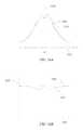
- FIG. 14is a graph illustrating variation of luminance with lateral position for the waveguide arrangements of FIG. 13 , in accordance with the present disclosure
- FIG. 15is a schematic diagram illustrating in top, front and bottom views a stepped imaging waveguide comprising a Fresnel reflector end and rectangular mirror and input ends, in accordance with the present disclosure
- FIG. 16is a schematic diagram illustrating in front view reflection efficiency at the facets of a Fresnel reflector, in accordance with the present disclosure
- FIG. 17Ais a graph illustrating variation of Fresnel reflector reflection efficiency with lateral position for the waveguide arrangement of FIG. 15 comprising a substantially rectangular input aperture shape, in accordance with the present disclosure
- FIG. 17Bis a graph illustrating variation of luminance with lateral position for the waveguide arrangements of FIG. 15 , in accordance with the present disclosure
- FIG. 18A and FIG. 18Bare schematic diagrams illustrating stepped imaging waveguides with different efficiencies, in accordance with the present disclosure
- FIG. 19is a schematic diagram illustrating a graph in which the ratio between (a) height of the input end between the first and second guide surfaces and (b) the height of the reflective end between the first and second guide surfaces has a profile across the lateral direction that is greatest at the optical axis of the Fresnel reflector and reduces towards each side of the optical axis, in accordance with the present disclosure;
- FIG. 20is a schematic diagram illustrating in top, front and bottom views a stepped imaging waveguide comprising a rectilinear Fresnel reflector end and variable height input end, in accordance with the present disclosure
- FIG. 21is a graph illustrating variation of luminance with lateral position for the waveguide arrangements of FIG. 20 , in accordance with the present disclosure
- FIG. 22 , FIG. 23 , FIG. 24 , FIG. 25 , FIG. 26 , FIG. 27 , FIG. 28 , FIG. 29 , FIG. 30 , and FIG. 31are schematic diagrams illustrating stepped imaging waveguides with different combinations of input and mirror aperture shapes, in accordance with the present disclosure
- FIG. 32is a schematic diagram illustrating in front view the origin of illumination void non-uniformities in a directional waveguide, in accordance with the present disclosure
- FIG. 33is a schematic diagram illustrating in front view correction of illumination void non-uniformities in a directional waveguide, in accordance with the present disclosure
- FIG. 34is a schematic diagram illustrating in perspective view correction of illumination void non-uniformities in a directional waveguide, in accordance with the present disclosure
- FIG. 35is a schematic diagram illustrating a control method arranged to provide correction of void non-uniformities in a directional waveguide, in accordance with the present disclosure
- FIG. 36A and FIG. 36Bare schematic diagrams illustrating in front view arrangements of LEDs arranged to achieve void A filling, in accordance with the present disclosure
- FIG. 37A , FIG. 37B , FIG. 37C , and FIG. 37Dare schematic diagrams illustrating in front view illumination of an imaging waveguide using planar input surfaces, in accordance with the present disclosure
- FIG. 38A and FIG. 38Bare schematic diagrams illustrating in front view arrangements of input aperture cross section comprising planar and structured surfaces arranged to achieve void B filling for a wide angular range, in accordance with the present disclosure
- FIG. 39Ais a schematic diagram illustrating in front view a directional waveguide and an array of light sources arranged to provide off-axis illumination of voids, in accordance with the present disclosure
- FIG. 39B and FIG. 39Care schematic diagrams illustrating in front view one input corner of a directional waveguide and an array of light sources arranged to provide off-axis illumination of voids for planar and structured reflectors respectively, in accordance with the present disclosure
- FIG. 40 and FIG. 41are schematic diagrams illustrating in front view arrangements of input side microstructures arranged to provide structured illumination, in accordance with the present disclosure
- FIG. 42is a schematic graph illustrating angular luminance distribution profile for light input in plastic for a planar input facet and Lambertian light source, in accordance with the present disclosure
- FIG. 43is a schematic graph illustrating angular luminance distribution profile for light input in plastic for a structured input facet similar to that shown in FIG. 41 and Lambertian light source, in accordance with the present disclosure
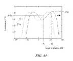
- FIG. 44is a schematic graph illustrating angular luminance distribution profile for light input in plastic for a tilted structured input facet similar to that shown in FIG. 41 and Lambertian light source, in accordance with the present disclosure
- FIG. 45is a schematic diagram illustrating control of luminance uniformity by means of LED control for adjacent LEDs, in accordance with the present disclosure
- FIG. 46A and FIG. 46Bare schematic graphs illustrating control of luminance uniformity by means of LED control for adjacent LEDs, in accordance with the present disclosure
- FIG. 47is a schematic diagram illustrating uniformity control using a partially reflective input side, in accordance with the present disclosure.
- FIG. 48is a schematic diagram illustrating uniformity control using a partially reflective input side and side LEDs, in accordance with the present disclosure
- FIG. 49Ais a schematic diagram illustrating a side view of a directional waveguide comprising extraction facets with a 45° facet angle and vertical input facet angle, in accordance with the present disclosure
- FIG. 49Bis a schematic diagram illustrating a side view of a directional waveguide comprising extraction facets with a facet angle greater than 45° and vertical input facet angle, in accordance with the present disclosure
- FIG. 49Cis a schematic diagram illustrating a side view of a directional waveguide comprising extraction facets with a facet angle greater than 45° and tilted input facet angle, in accordance with the present disclosure
- FIG. 50A , FIG. 50B , FIG. 50C , FIG. 50D , and FIG. 50Eare schematic diagrams illustrating arrangements of LED connections to achieve correction of luminance uniformity, in accordance with the present disclosure
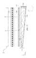
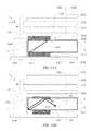
- FIG. 51Ais a schematic diagram illustrating in side view light blocking layers arranged across the upper and lower sides of a waveguide comprising black tape, in accordance with the present disclosure
- FIG. 51Bis a schematic diagram illustrating in side view light blocking layers arranged across the upper and lower sides of a waveguide comprising black tape on a lower surface and paint on an upper surface, in accordance with the present disclosure
- FIG. 51Cis a schematic diagram illustrating in side view light blocking layers arranged across the upper and lower sides of a waveguide comprising absorbing paint on upper and lower surfaces, in accordance with the present disclosure
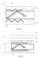
- FIG. 51Dis a schematic diagram illustrating in side view a light blocking layer arranged across the upper side of a waveguide comprising a transmitting adhesive and an absorbing layer, in accordance with the present disclosure
- FIG. 51Eis a schematic diagram illustrating in side view a light blocking layer arranged across the lower side of a waveguide comprising a transmitting adhesive and an absorbing layer that forms part of a printed circuit for a light emitting element, in accordance with the present disclosure
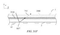
- FIG. 51Fis a schematic diagram illustrating in top view a light blocking layer arranged near to the input of a waveguide, in accordance with the present disclosure
- FIG. 52 and FIG. 53are schematic diagrams illustrating further light blocking layers arranged to improve uniformity of light escaping from scatter in the regions of the edge of the waveguide, in accordance with the present disclosure
- FIG. 54Ais a schematic diagram illustrating a further graph of optical window luminous intensity against viewing position in the window plane of a waveguide, in accordance with the present disclosure
- FIG. 54Bis a schematic diagram illustrating a graph of luminous flux distribution for an array of light sources to compensate for light source degradation, in accordance with the present disclosure
- FIG. 55Ais a schematic diagram illustrating in side view a display and integrated camera arranged to provide in-field LED array calibration, in accordance with the present disclosure
- FIG. 55B and FIG. 55Care schematic diagrams illustrating in front view a waveguide and keyboard mounted detectors arranged to provide in-field LED calibration, in accordance with the present disclosure
- FIG. 56is a schematic diagram illustrating a control system and front view of a directional backlight apparatus, in accordance with the present disclosure
- FIG. 57Ais a schematic diagram illustrating a further graph of optical window luminous intensity against viewing position in the window plane of a waveguide comprising a luminous intensity defect, in accordance with the present disclosure
- FIG. 57Bis a schematic diagram illustrating a graph of optical window luminous intensity against viewing position in the window plane of a waveguide further illustrating a correction of the defect of FIG. 57A , in accordance with the present disclosure
- FIG. 58Ais a schematic diagram illustrating a graph of nominal LED output against time, in accordance with the present disclosure.
- FIG. 58Bis a schematic diagram illustrating a flowchart for compensation of LED ageing, in accordance with the present disclosure
- FIG. 59Ais a schematic diagram illustrating in perspective view, the structure of a directional display device comprising an directional backlight arranged with a spatial light modulator, in accordance with the present disclosure
- FIG. 59Bis a schematic diagram illustrating in front view, an optical valve comprising a side light source arranged to achieve an on-axis optical window, in accordance with the present disclosure
- FIG. 59Cis a schematic diagram illustrating in side view, an optical valve comprising a side light source arranged to achieve an on-axis optical window, in accordance with the present disclosure
- FIG. 59Dis a schematic diagram illustrating in perspective view, the formation of first and second optical windows by edge and side light sources with a valve with arrangement similar to that shown in FIGS. 59B-C , in accordance with the present disclosure.
- FIG. 59Eis a schematic diagram illustrating in perspective view, the structure of a directional display device comprising a directional backlight comprising a side light source arranged with a spatial light modulator, in accordance with the present disclosure.
- Time multiplexed autostereoscopic displayscan advantageously improve the spatial resolution of autostereoscopic display by directing light from all of the pixels of a spatial light modulator to a first viewing window in a first time slot, and all of the pixels to a second viewing window in a second time slot.
- Time multiplexed displayscan advantageously achieve directional illumination by directing an illuminator array through a substantially transparent time multiplexed spatial light modulator using directional optical elements, wherein the directional optical elements substantially form an image of the illuminator array in the window plane.
- the uniformity of the viewing windowsmay be advantageously independent of the arrangement of pixels in the spatial light modulator.
- Such displayscan provide observer tracking displays which have low flicker, with low levels of cross talk for a moving observer.
- the illuminator elements of the time sequential illumination systemmay be provided, for example, by pixels of a spatial light modulator with size approximately 100 micrometers in combination with a lens array.
- pixelssuffer from similar difficulties as for spatially multiplexed displays. Further, such devices may have low efficiency and higher cost, requiring additional display components.
- High window plane uniformitycan be conveniently achieved with macroscopic illuminators, for example, an array of LEDs in combination with homogenizing and diffusing optical elements that are typically of size 1 mm or greater.
- the increased size of the illuminator elementsmeans that the size of the directional optical elements increases proportionately. For example, a 16 mm wide illuminator imaged to a 65 mm wide viewing window may require a 200 mm back working distance.
- the increased thickness of the optical elementscan prevent useful application, for example, to mobile displays, or large area displays.
- optical valvesas described in commonly-owned U.S. patent application Ser. No. 13/300,293 (U.S. Patent Publication No. 2012/0127573), herein incorporated by reference in its entirety, advantageously can be arranged in combination with fast switching transmissive spatial light modulators to achieve time multiplexed autostereoscopic illumination in a thin package while providing high resolution images with flicker free observer tracking and low levels of cross talk.
- Describedis a one dimensional array of viewing positions, or windows, that can display different images in a first, typically horizontal, direction, but contain the same images when moving in a second, typically vertical, direction.
- imaging directional backlightsare arranged to direct the illumination from multiple light sources through a display panel to respective multiple viewing windows in at least one axis.
- Each viewing windowis substantially formed as an image in at least one axis of a light source by the imaging system of the imaging directional backlight.
- An imaging systemmay be formed between multiple light sources and the respective window images. In this manner, the light from each of the multiple light sources is substantially not visible for an observer's eye outside of the respective viewing window.
- Non-imaging backlightsare used for illumination of 2D displays. See. e.g., Kälil Käläntär et al., Backlight Unit With Double Surface Light Emission , J. Soc. Inf. Display, Vol. 12, Issue 4, pp. 379-387 (December 2004).
- Non-imaging backlightsare typically arranged to direct the illumination from multiple light sources through a display panel into a substantially common viewing zone for each of the multiple light sources to achieve wide viewing angle and high display uniformity.
- non-imaging backlightsdo not form viewing windows. In this manner, the light from each of the multiple light sources may be visible for an observer's eye at substantially all positions across the viewing zone.
- Such conventional non-imaging backlightsmay have some directionality, for example, to increase screen gain compared to Lambertian illumination, which may be provided by brightness enhancement films such as BEFTM from 3M. However, such directionality may be substantially the same for each of the respective light sources. Thus, for these reasons and others that should be apparent to persons of ordinary skill, conventional non-imaging backlights are different to imaging directional backlights.
- Edge lit non-imaging backlight illumination structuresmay be used in liquid crystal display systems such as those seen in 2D Laptops, Monitors and TVs. Light propagates from the edge of a lossy waveguide which may include sparse features; typically local indentations in the surface of the guide which cause light to be lost regardless of the propagation direction of the light.
- an optical valveis an optical structure that may be a type of light guiding structure or device referred to as, for example, a light valve, an optical valve directional backlight, and a valve directional backlight (“v-DBL”).
- optical valveis different to a spatial light modulator (even though spatial light modulators may be sometimes generally referred to as a “light valve” in the art).
- One example of an imaging directional backlightis an optical valve that may employ a folded optical system. Light may propagate substantially without loss in one direction through the optical valve, may be incident on an imaging reflector, and may counter-propagate such that the light may be extracted by reflection off tilted light extraction features, and directed to viewing windows as described in U.S. patent application Ser. No. 13/300,293 (U.S. Pat. Publ. No. 2012/0127573), which is herein incorporated by reference in its entirety.
- a stepped waveguide imaging directional backlightmay be at least one of an optical valve.
- a stepped waveguideis a waveguide for an imaging directional backlight comprising a waveguide for guiding light, further comprising: a first light guiding surface; and a second light guiding surface, opposite the first light guiding surface, further comprising a plurality of light guiding features interspersed with a plurality of extraction features arranged as steps.
- lightmay propagate within an exemplary optical valve in a first direction from an input side to a reflective side and may be transmitted substantially without loss.
- Lightmay be reflected at the reflective side and propagates in a second direction substantially opposite the first direction.
- the lightmay be incident on light extraction features, which are operable to redirect the light outside the optical valve.
- the optical valvegenerally allows light to propagate in the first direction and may allow light to be extracted while propagating in the second direction.
- the optical valvemay achieve time sequential directional illumination of large display areas. Additionally, optical elements may be employed that are thinner than the back working distance of the optical elements to direct light from macroscopic illuminators to a window plane. Such displays may use an array of light extraction features arranged to extract light counter propagating in a substantially parallel waveguide.
- Thin imaging directional backlight implementations for use with LCDshave been proposed and demonstrated by 3M, for example U.S. Pat. No. 7,528,893; by Microsoft, for example U.S. Pat. No. 7,970,246 which may be referred to herein as a “wedge type directional backlight;” by RealD, for example U.S. patent application Ser. No. 13/300,293 (U.S. Patent Publication No. 2012/0127573) which may be referred to herein as an “optical valve” or “optical valve directional backlight,” all of which are herein incorporated by reference in their entirety.
- the present disclosureprovides stepped waveguide imaging directional backlights in which light may reflect back and forth between the internal faces of, for example, a stepped waveguide which may include a first side and a first set of features. As the light travels along the length of the stepped waveguide, the light may not substantially change angle of incidence with respect to the first side and first set of surfaces and so may not reach the critical angle of the medium at these internal faces. Light extraction may be advantageously achieved by a second set of surfaces (the step “risers”) that are inclined to the first set of surfaces (the step “treads”). Note that the second set of surfaces may not be part of the light guiding operation of the stepped waveguide, but may be arranged to provide light extraction from the structure.
- a wedge type imaging directional backlightmay allow light to guide within a wedge profiled waveguide having continuous internal surfaces. The optical valve is thus not a wedge type imaging directional backlight.
- FIG. 1Ais a schematic diagram illustrating a front view of light propagation in one embodiment of a directional display device
- FIG. 1Bis a schematic diagram illustrating a side view of light propagation in the directional display device of FIG. 1A .
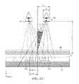
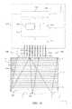
- FIG. 1Aillustrates a front view in the xy plane of a directional backlight of a directional display device, and includes an illuminator array 15 which may be used to illuminate a stepped waveguide 1 .
- Illuminator array 15includes illuminator elements 15 a through illuminator element 15 n (where n is an integer greater than one).
- the stepped waveguide 1 of FIG. 1Amay be a stepped, display sized waveguide 1 .
- Illumination elements 15 a through 15 nare light sources that may be light emitting diodes (LEDs).
- FIG. 1Billustrates a side view in the xz plane, and includes illuminator array 15 , SLM 48 , extraction features 12 , guiding features 10 , and stepped waveguide 1 , arranged as shown.
- the side view provided in FIG. 1Bis an alternative view of the front view shown in FIG. 1A . Accordingly, the illuminator array 15 of FIGS. 1A and 1B corresponds to one another and the stepped waveguide 1 of FIGS. 1A and 1B may correspond to one another.
- the stepped waveguide 1may have an input end 2 that is thin and a reflective end 4 that is thick.
- the waveguide 1extends between the input end 2 that receives input light and the reflective end 4 that reflects the input light back through the waveguide 1 .
- the length of the input end 2 in a lateral direction across the waveguideis greater than the height of the input end 2 .
- the illuminator elements 15 a - 15 nare disposed at different input positions in a lateral direction across the input end 2 .
- the waveguide 1has first and second, opposed guide surfaces extending between the input end 2 and the reflective end 4 for guiding light forwards and back along the waveguide 1 .
- the second guide surfacehas a plurality of light extraction features 12 facing the reflective end 4 and arranged to reflect at least some of the light guided back through the waveguide 1 from the reflective end from different input positions across the input end in different directions through the first guide surface that are dependent on the input position.
- the light extraction features 12are reflective facets, although other reflective features could be used.
- the light extraction features 12do not guide light through the waveguide, whereas the intermediate regions of the second guide surface intermediate the light extraction features 12 guide light without extracting it. Those regions of the second guide surface are planar and may extend parallel to the first guide surface, or at a relatively low inclination.
- the light extraction features 12extend laterally to those regions so that the second guide surface has a stepped shape which may include the light extraction features 12 and intermediate regions.
- the light extraction features 12are oriented to reflect light from the light sources, after reflection from the reflective end 4 , through the first guide surface.
- the light extraction features 12are arranged to direct input light from different input positions in the lateral direction across the input end in different directions relative to the first guide surface that are dependent on the input position.
- the illumination elements 15 a - 15 nare arranged at different input positions, the light from respective illumination elements 15 a - 15 n is reflected in those different directions.
- each of the illumination elements 15 a - 15 ndirects light into a respective optical window in output directions distributed in the lateral direction in dependence on the input positions.
- the lateral direction across the input end 2 in which the input positions are distributedcorresponds with regard to the output light to a lateral direction to the normal to the first guide surface.
- the illuminator elements 15 a - 15 nmay be selectively operated to direct light into a selectable optical window.
- the optical windowsmay be used individually or in groups as viewing windows.
- the SLM 48extends across the waveguide and modulates the light output therefrom.
- the SLM 48may a liquid crystal display (LCD), this is merely by way of example and other spatial light modulators or displays may be used including LCOS, DLP devices, and so forth, as this illuminator may work in reflection.
- the SLM 48is disposed across the first guide surface of the waveguide and modulates the light output through the first guide surface after reflection from the light extraction features 12 .
- FIG. 1AThe operation of a directional display device that may provide a one dimensional array of viewing windows is illustrated in front view in FIG. 1A , with its side profile shown in FIG. 1B .
- the lightmay propagate along +x in a first direction, within the stepped waveguide 1 , while at the same time, the light may fan out in the xy plane and upon reaching the far curved end side 4 , may substantially or entirely fill the curved end side 4 . While propagating, the light may spread out to a set of angles in the xz plane up to, but not exceeding the critical angle of the guide material.
- the extraction features 12 that link the guiding features 10 of the bottom side of the stepped waveguide 1may have a tilt angle greater than the critical angle and hence may be missed by substantially all light propagating along +x in the first direction, ensuring the substantially lossless forward propagation.
- the curved end side 4 of the stepped waveguide 1may be made reflective, typically by being coated with a reflective material such as, for example, silver, although other reflective techniques may be employed.
- Lightmay therefore be redirected in a second direction, back down the guide in the direction of ⁇ x and may be substantially collimated in the xy or display plane.
- the angular spreadmay be substantially preserved in the xz plane about the principal propagation direction, which may allow light to hit the riser edges and reflect out of the guide.
- lightmay be effectively directed approximately normal to the xy display plane with the xz angular spread substantially maintained relative to the propagation direction. This angular spread may be increased when light exits the stepped waveguide 1 through refraction, but may be decreased somewhat dependent on the reflective properties of the extraction features 12 .
- reflectionmay be reduced when total internal reflection (TIR) fails, squeezing the xz angular profile and shifting off normal.
- TIRtotal internal reflection
- the increased angular spread and central normal directionmay be preserved.
- lightmay exit the stepped waveguide 1 approximately collimated and may be directed off normal in proportion to the y-position of the respective illuminator element 15 a - 15 n in illuminator array 15 from the input edge center. Having independent illuminator elements 15 a - 15 n along the input edge 2 then enables light to exit from the entire first light directing side 6 and propagate at different external angles, as illustrated in FIG. 1A .
- Illuminating a spatial light modulator (SLM) 48 such as a fast liquid crystal display (LCD) panel with such a devicemay achieve autostereoscopic 3D as shown in top view or yz-plane viewed from the illuminator array 15 end in FIG. 2A , front view in FIG. 2B and side view in FIG. 2C .
- FIG. 2Ais a schematic diagram illustrating in a top view, propagation of light in a directional display device
- FIG. 21is a schematic diagram illustrating in a front view, propagation of light in a directional display device
- FIG. 2Cis a schematic diagram illustrating in side view propagation of light in a directional display device.
- FIGS. 1spatial light modulator
- a stepped waveguide 1may be located behind a fast (e.g., greater than 100 Hz) LCD panel SLM 48 that displays sequential right and left eye images.
- a faste.g., greater than 100 Hz
- specific illuminator elements 15 a through 15 n of illuminator array 15may be selectively turned on and off, providing illuminating light that enters right and left eyes substantially independently by virtue of the system's directionality.
- sets of illuminator elements of illuminator array 15are turned on together, providing a one dimensional viewing window 26 or an optical pupil with limited width in the horizontal direction, but extended in the vertical direction, in which both eyes horizontally separated may view a left eye image, and another viewing window 44 in which a right eye image may primarily be viewed by both eyes, and a central position in which both the eyes may view different images.
- 3Dmay be viewed when the head of a viewer is approximately centrally aligned. Movement to the side away from the central position may result in the scene collapsing onto a 2D image.
- the reflective end 4may have positive optical power in the lateral direction across the waveguide.
- the optical axismay be defined with reference to the shape of the reflective end 4 , for example being a line that passes through the center of curvature of the reflective end 4 and coincides with the axis of reflective symmetry of the end 4 about the x-axis.
- the optical axismay be similarly defined with respect to other components having optical power, for example the light extraction features 12 if they are curved, or the Fresnel lens 62 described below.
- the optical axis 238is typically coincident with the mechanical axis of the waveguide 1 .
- the optical axis 238is a line that passes through the center of curvature of the surface at end 4 and coincides with the axis of reflective symmetry of the side 4 about the x-axis.
- the optical axis 238is typically coincident with the mechanical axis of the waveguide 1 .
- the cylindrical reflecting surface at end 4may typically comprise a spherical profile to optimize performance for on-axis and off-axis viewing positions. Other profiles may be used.
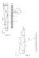
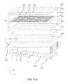
- FIG. 3is a schematic diagram illustrating in side view a directional display device. Further, FIG. 3 illustrates additional detail of a side view of the operation of a stepped waveguide 1 , which may be a transparent material.
- the stepped waveguide 1may include an illuminator input side 2 , a reflective side 4 , a first light directing side 6 which may be substantially planar, and a second light directing side 8 which includes guiding features 10 and light extraction features 12 .
- light rays 16 from an illuminator element 15 c of an illuminator array 15(not shown in FIG.
- reflective side 4may be a mirrored surface and may reflect light, it may in some embodiments also be possible for light to pass through reflective side 4 .
- light ray 18 reflected by the reflective side 4may be further guided in the stepped waveguide 1 by total internal reflection at the reflective side 4 and may be reflected by extraction features 12 .
- Light rays 18 that are incident on extraction features 12may be substantially deflected away from guiding modes of the stepped waveguide 1 and may be directed, as shown by ray 20 , through the side 6 to an optical pupil that may form a viewing window 26 of an autostereoscopic display.
- the width of the viewing window 26may be determined by at least the size of the illuminator, output design distance and optical power in the side 4 and extraction features 12 .
- each viewing window 26represents a range of separate output directions with respect to the surface normal direction of the spatial light modulator 48 that intersect with a plane at the nominal viewing distance.
- FIG. 4Ais a schematic diagram illustrating in front view a directional display device which may be illuminated by a first illuminator element and including curved light extraction features. Further, FIG. 4A shows in front view further guiding of light rays from illuminator element 15 c of illuminator array 15 , in the stepped waveguide 1 . Each of the output rays are directed towards the same viewing window 26 from the respective illuminator 14 . Thus light ray 30 may intersect the ray 20 in the window 26 , or may have a different height in the window as shown by ray 32 . Additionally, in various embodiments, sides 22 , 24 of the waveguide 1 may be transparent, mirrored, or blackened surfaces. Continuing the discussion of FIG.
- light extraction features 12may be elongate, and the orientation of light extraction features 12 in a first region 34 of the light directing side 8 (light directing side 8 shown in FIG. 3 , but not shown in FIG. 4A ) may be different to the orientation of light extraction features 12 in a second region 36 of the light directing side 8 .
- FIG. 4Bis a schematic diagram illustrating in front view an optical valve which may illuminated by a second illuminator element. Further, FIG. 4B shows the light rays 40 , 42 from a second illuminator element 15 h of the illuminator array 15 . The curvature of the reflective end on the side 4 and the light extraction features 12 cooperatively produce a second viewing window 44 laterally separated from the viewing window 26 with light rays from the illuminator element 15 h.
- the arrangement illustrated in FIG. 4Bmay provide a real image of the illuminator element 15 c at a viewing window 26 in which the real image may be formed by cooperation of optical power in reflective side 4 and optical power which may arise from different orientations of elongate light extraction features 12 between regions 34 and 36 , as shown in FIG. 4A .
- the arrangement of FIG. 4Bmay achieve improved aberrations of the imaging of illuminator element 15 c to lateral positions in viewing window 26 . Improved aberrations may achieve an extended viewing freedom for an autostereoscopic display while achieving low cross talk levels.
- FIG. 5is a schematic diagram illustrating in front view an embodiment of a directional display device having substantially linear light extraction features. Further, FIG. 5 shows a similar arrangement of components to FIG. 1 (with corresponding elements being similar), with one of the differences being that the light extraction features 12 are substantially linear and parallel to each other. Advantageously, such an arrangement may provide substantially uniform illumination across a display surface and may be more convenient to manufacture than the curved extraction features of FIG. 4A and FIG. 4B .
- FIG. 6Ais a schematic diagram illustrating one embodiment of the generation of a first viewing window in a time multiplexed imaging directional display device in a first time slot
- FIG. 6Bis a schematic diagram illustrating another embodiment of the generation of a second viewing window in a time multiplexed imaging directional backlight apparatus in a second time slot
- FIG. 6Cis a schematic diagram illustrating another embodiment of the generation of a first and a second viewing window in a time multiplexed imaging directional display device.
- FIG. 6Ashows schematically the generation of illumination window 26 from stepped waveguide 1 .
- Illuminator element group 31 in illuminator array 15may provide a light cone 17 directed towards a viewing window 26 .
- Illuminator element group 33 in illuminator array 15may provide a light cone 19 directed towards viewing window 44 .
- windows 26 and 44may be provided in sequence as shown in FIG. 6C . If the image on a spatial light modulator 48 (not shown in FIGS. 6A, 6B, 6C ) is adjusted in correspondence with the light direction output, then an autostereoscopic image may be achieved for a suitably placed viewer. Similar operation can be achieved with all the directional backlights described herein.
- illuminator element groups 31 , 33each include one or more illumination elements from illumination elements 15 a to 15 n , where n is an integer greater than one.
- FIG. 7is a schematic diagram illustrating one embodiment of an observer tracking autostereoscopic directional display device.
- selectively turning on and off illuminator elements 15 a to 15 n along axis 29provides for directional control of viewing windows.
- the head 45 positionmay be monitored with a camera, motion sensor, motion detector, or any other appropriate optical, mechanical or electrical means, and the appropriate illuminator elements of illuminator array 15 may be turned on and off to provide substantially independent images to each eye irrespective of the head 45 position.
- the head tracking system(or a second head tracking system) may provide monitoring of more than one head 45 , 47 (head 47 not shown in FIG. 7 ) and may supply the same left and right eye images to each viewers' left and right eyes providing 3D to all viewers. Again similar operation can be achieved with all the directional backlights described herein.
- FIG. 8is a schematic diagram illustrating one embodiment of a multi-viewer directional display device as an example including an imaging directional backlight.
- at least two 2D imagesmay be directed towards a pair of viewers 45 , 47 so that each viewer may watch a different image on the spatial light modulator 48 .
- the two 2D images of FIG. 8may be generated in a similar manner as described with respect to FIG. 7 in that the two images would be displayed in sequence and in synchronization with sources whose light is directed toward the two viewers.
- One imageis presented on the spatial light modulator 48 in a first phase
- a second imageis presented on the spatial light modulator 48 in a second phase different from the first phase.
- the output illuminationis adjusted to provide first and second viewing windows 26 , 44 respectively. An observer with both eyes in window 26 will perceive a first image while an observer with both eyes in window 44 will perceive a second image.
- FIG. 9is a schematic diagram illustrating a privacy directional display device which includes an imaging directional backlight.
- 2D display systemsmay also utilize directional backlighting for security and efficiency purposes in which light may be primarily directed at the eyes of a first viewer 45 as shown in FIG. 9 .
- first viewer 45may be able to view an image on device 50
- lightis not directed towards second viewer 47 .
- second viewer 47is prevented from viewing an image on device 50 .
- Each of the embodiments of the present disclosuremay advantageously provide autostereoscopic, dual image or privacy display functions.
- FIG. 10is a schematic diagram illustrating in side view the structure of a time multiplexed directional display device as an example including an imaging directional backlight. Further, FIG. 10 shows in side view an autostereoscopic directional display device, which may include the stepped waveguide 1 and a Fresnel lens 62 arranged to provide the viewing window 26 in a window plane 106 at a nominal viewing distance from the spatial light modulator for a substantially collimated output across the stepped waveguide 1 output surface.
- a vertical diffuser 68may be arranged to extend the height of the window 26 further. The light may then be imaged through the spatial light modulator 48 .
- the illuminator array 15may include light emitting diodes (LEDs) that may, for example, be phosphor converted blue LEDs, or may be separate RGB LEDs.
- the illuminator elements in illuminator array 15may include a uniform light source and spatial light modulator arranged to provide separate illumination regions.
- the illuminator elementsmay include laser light source(s).
- the laser outputmay be directed onto a diffuser by means of scanning, for example, using a galvo or MEMS scanner.
- laser lightmay thus be used to provide the appropriate illuminator elements in illuminator array 15 to provide a substantially uniform light source with the appropriate output angle, and further to provide reduction in speckle.
- the illuminator array 15may be an array of laser light emitting elements.
- the diffusermay be a wavelength converting phosphor, so that illumination may be at a different wavelength to the visible output light.
- a further wedge type directional backlightis generally discussed by U.S. Pat. No. 7,660,047 which is herein incorporated by reference in its entirety.
- the wedge type directional backlight and optical valvefurther process light beams in different ways.
- light input at an appropriate anglewill output at a defined position on a major surface, but light rays will exit at substantially the same angle and substantially parallel to the major surface.
- light input to a stepped waveguide of an optical valve at a certain anglemay output from points across the first side, with output angle determined by input angle.
- the stepped waveguide of the optical valvemay not require further light redirection films to extract light towards an observer and angular non-uniformities of input may not provide non-uniformities across the display surface.
- waveguides, directional backlights and directional display devicesthat are based on and incorporate the structures of FIGS. 1 to 10 above. Except for the modifications and/or additional features which will now be described, the above description applies equally to the following waveguides, directional backlights and display devices, but for brevity will not be repeated.
- the waveguides described belowmay be incorporated into a directional backlight or a directional display device as described above.
- the directional backlights described belowmay be incorporated into a directional display device as described above.
- FIG. 11is a schematic diagram illustrating a directional display apparatus comprising a directional display device and a control system.
- the arrangement and operation of the control systemwill now be described and may be applied, with changes as necessary, to each of the display devices disclosed herein.
- the directional backlightcomprises a waveguide 1 and an array 15 of illumination elements 15 a - 15 n arranged as described above.
- the control systemis arranged to selectively operate the illumination elements 15 a - 15 n to direct light into selectable viewing windows.
- Fresnel lens 62may be arranged to cooperate with reflective end 4 to achieve viewing windows at a viewing plane.
- Transmissive spatial light modulator 48may be arranged to receive the light from the directional backlight. The image displayed on the SLM 48 may be presented in synchronization with the illumination of the light sources of the array 15 .
- the control systemmay comprise a sensor system arranged to detect the position of the observer 99 relative to the display device 100 .
- the sensor systemcomprises a position sensor 406 , such as a camera arranged to determine the position of an observer 408 ; and a head position measurement system 404 that may for example comprise a computer vision image processing system.
- the position sensor 406may comprise known sensors including those comprising cameras and image processing units arranged to detect the position of observer faces.
- Position sensor 406may further comprise a stereo sensor arranged to improve the measure of longitudinal position compared to a monoscopic camera.
- position sensor 406may comprise measurement of eye spacing to give a measure of required placement of respective arrays of viewing windows from tiles of the directional display.
- the control systemmay further comprise an illumination controller and an image controller 403 that are both supplied with the detected position of the observer supplied from the head position measurement system 404 .
- the illumination controllercomprises an LED controller 402 arranged to determine which light sources of array 15 should be switched to direct light to respective eyes of observer 408 in cooperation with waveguide 1 ; and an LED driver 400 arranged to control the operation of light sources of light source array 15 by means of drive lines 407 .
- the illumination controller 74selects the illuminator elements 15 to be operated in dependence on the position of the observer detected by the head position measurement system 72 , so that the viewing windows 26 into which light is directed are in positions corresponding to the left and right eyes of the observer 99 . In this manner, the lateral output directionality of the waveguide 1 corresponds with the observer position.
- the image controller 403is arranged to control the SLM 48 to display images.
- the image controller 403 and the illumination controllermay operate as follows.
- the image controller 403controls the SLM 48 to display temporally multiplexed left and right eye images and the LED controller 402 operates the light sources 15 to direct light into viewing windows in positions corresponding to the left and right eyes of an observer synchronously with the display of left and right eye images.
- an autostereoscopic effectis achieved using a time division multiplexing technique.
- a single viewing windowmay be illuminated by operation of light source 409 (which may comprise one or more LEDs) by means of drive line 410 wherein other drive lines are not driven as described elsewhere.
- the head position measurement system 404detects the position of an observer relative to the display device 100 .
- the LED controller 402selects the light sources 15 to be operated in dependence on the position of the observer detected by the head position measurement system 404 , so that the viewing windows into which light is directed are in positions corresponding to the left and right eyes of the observer. In this manner, the output directionality of the waveguide 1 may be achieved to correspond with the viewer position so that a first image may be directed to the observer's right eye in a first phase and directed to the observer's left eye in a second phase.
- FIG. 12is a schematic diagram illustrating in side view, the structure of a directional display device comprising a wedge directional backlight comprising a wedge waveguide 1104 with faceted mirror end 1102 .
- the first guide surface 1105 of the waveguide 1104is arranged to guide light by total internal reflection and the second guide surface 1106 is substantially planar and inclined at an angle to direct light in directions that break the total internal reflection for outputting light through the first guide surface 1105 .
- the display devicefurther comprises a deflection element 1108 extending across the first guide surface 1105 of the waveguide 1104 for deflecting light from array 1101 of light sources towards the normal to the first guide surface 1105 .
- the waveguide 1104may further comprise a reflective end 1102 for reflecting input light back through the waveguide 1104 , the second guide 1106 surface being arranged to deflect light as output light through the first guide surface 1105 after reflection from the reflective end 1102 .
- the reflective endhas positive optical power in the lateral direction (y-axis) in a similar manner to the reflective end shown in FIG. 5 for example. Further facets in the reflective end 1102 deflect the reflected light cones within the waveguide 1104 to achieve output coupling on the return path. Thus viewing windows are produced in a similar manner to that shown in FIG. 11 .
- the directional displaymay comprise a spatial light modulator 1110 and parallax element 1100 aligned to the spatial light modulator 1110 that is further arranged to provide optical windows.
- a control system 72 similar to that shown in FIG. 11may be arranged to provide control of directional illumination providing viewing windows 26 and windows 109 from the parallax element and aligned spatial light modulator.
- a first guide surfacemay be arranged to guide light by total internal reflection and the second guide surface may be substantially planar and inclined at an angle to direct light in directions that break that total internal reflection for outputting light through the first guide surface, and the display device may further comprise a deflection element extending across the first guide surface of the waveguide for deflecting light towards the normal to the first guide surface.
- FIG. 13is a schematic diagram illustrating in top, front and bottom views a stepped imaging waveguide comprising a continuously curved mirror end 4 and rectangular mirror end 4 and input end 2 .
- Light source 15illuminates the input aperture of the directional imaging waveguide such as stepped waveguide 1 .
- Light rays 200are reflected by curved mirror 4 and are collimated.
- the output light reflected by facets 12may have a luminance profile with respect to position across the width of the waveguide 1 .
- FIG. 14is a graph illustrating variation of luminance 204 with lateral position 206 across the waveguide 1 for the waveguide arrangements of FIG. 13 .
- Profile 208that is substantially flat is achieved.
- high lateral uniformityis provided for a central light source 15 of array of light sources 15 a - n.
- the continuous curve to the mirror end 4increases the footprint of the waveguide in comparison to conventional scattering waveguides, increasing bezel size. It would be desirable to reduce the bezel of the waveguide 1 while maintaining lateral uniformity of profile 208 .
- the uniformity profile 208 across the line 202represents the spatial uniformity across the waveguide 1 . This is separate to the angular uniformity across the array of optical windows.
- a backlightis arranged to provide high spatial uniformity, typically greater than 70% across the display area.
- the same backlightmay provide angular uniformity in wide angle mode that may be greater than 20% across a +/ ⁇ 45 degrees angular range.
- the angular uniformitymay be greater than 2% across a +/ ⁇ 45 degrees.
- the present embodimentsare arranged to provide desirable spatial uniformity for directional backlight with controllable angular uniformity in a lateral direction.
- FIG. 15is a schematic diagram illustrating in top, front and bottom views a stepped imaging waveguide 1 comprising a Fresnel reflector end 4 and rectangular mirror end 4 and input end 2 .
- Fresnel reflectorhas an optical axis 199 .
- Fresnel reflectormay comprise facets 220 arranged to achieve a collimating function to light rays 200 and drafts 222 . After reflection from curved facets 12 , optical windows 26 are provided as described elsewhere herein.
- a directional waveguide 1comprising: an input end 2 ; first and second opposed, laterally extending guide surfaces 6 , 8 for guiding light along the waveguide 1 ; and a reflective end 4 facing the input end 2 for reflecting the input light back along the waveguide 1 , the second guide surface 8 being arranged to deflect the reflected input light through the first guide surface 6 as output light, and the waveguide 1 being arranged to direct the output light into optical windows 26 in output directions that are distributed in a lateral direction (y-axis) in dependence on the input position of the input light.
- FIG. 16is a schematic diagram illustrating in front view light loss at the facets of a Fresnel reflector end 4 .
- the reflective end 4is thus a Fresnel reflector comprising alternating reflective facets 220 and draft facets 222 , the reflective facets providing the Fresnel reflector with positive optical power.
- substantially collimated light rays 200may be provided for source 15 by the Fresnel reflector.
- Off-axis light beam 224is incident on the facets 220 that are shadowed by drafts 222 .
- reflected beam 228 of width ais provided across pitch A of the facets 220 .
- the reflection efficiencymay then be given by the ratio a/A:
- a Acos ⁇ ( ⁇ ⁇ ⁇ i ) cos ⁇ ( ⁇ ⁇ ⁇ i - 2 ⁇ ⁇ ⁇ ⁇ f ) eqn . ⁇ 1 where ⁇ i is the incident angle and ⁇ f is the facet 220 angle.
- ⁇ iis the incident angle
- ⁇ fis the facet 220 angle.
- FIG. 17Ais a graph illustrating profile 232 of Fresnel reflector reflection efficiency 212 with lateral position 206 for the Fresnel reflector waveguide arrangement of FIG. 15 comprising a substantially rectangular input aperture shape.
- FIG. 17Bis a graph illustrating the corresponding variation of luminance 204 with lateral position for the waveguide 1 arrangement of FIG. 15 .
- the shading of the facets 220 by the drafts 222 of the Fresnel reflectorprovides a lateral roll off in luminance 204 with position 206 across line 202 for a central light source 15 .
- FIGS. 18A-18Bare schematic diagrams illustrating stepped imaging waveguides with different efficiencies, being cross sections in the x-direction.
- FIG. 18Aillustrates a first cross section with input side 2 height 221 , b and Fresnel reflector end 4 height 223 , m and
- FIG. 18Billustrates a second cross section with input end 2 height 227 , B and mirror end 4 height 231 , M.
- sides 6are not generally parallel to elements 10 of the stepped side 8 .
- Height differencemay arise from regions 10 that are not typically not parallel to side 6 .
- Further height difference 225is provided by steps 12 of the stepped waveguide.
- the step heightmay be at least 0.5 micrometers, preferably at least 1.0 micrometers and more preferably at least 1.5 micrometers to minimize facet rounding during tooling and molding of the waveguide 1 .
- the pitch of the facets 12may be desirably less than 500 micrometers, more preferably less than 350 micrometers and most preferably less than 200 micrometers.
- the range of height difference 225may be determined by fabrication and image appearance characteristics of the light guide.
- FIG. 19is a schematic diagram illustrating a graph in which the ratio 205 between (a) height of the input end 2 between the first and second guide surfaces 6 , 8 and (b) the height of the reflective end 4 between the first and second guide surfaces 6 , 8 has a profile 211 across the lateral direction that is greatest at the optical axis 199 of the Fresnel reflector and reduces towards each side of the optical axis 199 .
- FIG. 20is a schematic diagram illustrating in top, front and bottom views a stepped imaging waveguide comprising a rectilinear Fresnel reflector end and variable height input end.
- a waveguide of height 180 mm in the x direction and width in the 7 direction of 300 mmmay comprise a mirror end of uniform height 223 of 1.5 mm.
- t 0is the thickness of the input aperture aligned with the optical axis 199 which may be for example 0.7 mm and ⁇ is the variation parameter which may be for example 0.000008 mm ⁇ 1 .
- the height of the input end 2 between the first and second guide surfaces 6 , 8thus has a profile that is highest at the optical axis 199 of the Fresnel reflector and reduces towards each side of the optical axis 199 .
- FIG. 21is a graph illustrating variation of uniformity with lateral position for the waveguide arrangements of FIG. 20 .
- Said profile t(y) of the height of the input end 2thus compensates for reduction with lateral position 206 in the efficiency 212 of reflection of light by the Fresnel reflector.
- comparison profile 209is also shown, the peak luminance being dependent on the relative central efficiencies of the two arrangements of FIGS. 15 and 20 respectively.
- the output from waveguide 1may be provided with a substantially uniform profile 208 while maintaining the small footprint of the Fresnel reflector end 4 .
- FIGS. 22-25are schematic diagrams illustrating stepped imaging waveguides with varying input aperture height with lateral position.
- the edge of the input end 2 at the first guide surface 6is curved, for example convex (concave in the air around the guide) and the edge of the input end at the second guide surface 8 is straight to provide said profile t(y).
- the edge of the input end 2 at the first guide surface 6is straight and the edge of the input end 2 at the second guide surface 8 is curved to provide said profile t(y).
- the edges of the input end 2 at the first guide surface 6 and at the second guide surface 8are each curved to provide said profile t(y).
- the height of the reflective end 4 between the first and second guide surfaces 6 , 8has a profile across the lateral direction that may be flat.
- the first guide surface 6is arranged to guide light by total internal reflection and the second guide surface 8 comprises a plurality of light extraction features 12 oriented to direct light guided along the waveguide 1 in directions allowing exit through the first guide surface 6 as the output light and intermediate regions 10 between the light extraction features 12 that are arranged to guide light along the waveguide 1 .
- the second guide surface 8has a stepped shape in which said light extraction features are facets 12 between the intermediate regions 10 .
- the light extraction features 12may have positive optical power in the lateral direction (y-axis).
- a directional waveguide 1may be arranged wherein the height of the input end 2 between the first and second guide surfaces 6 , 8 has a profile 205 across the lateral direction that is flat.
- the height of the reflective end 2 between the first and second guide surfaces 6 , 8may have a profile 205 across the lateral direction that is lowest at the optical axis 199 of the Fresnel reflector and increases towards each side of the optical axis 199 .
- a directional backlightmay comprise: a directional waveguide 1 arranged to achieve small footprint and high lateral uniformity for central light sources of array 15 , as described herein; and an array 15 of input light sources 15 a - n arranged at different input positions in a lateral direction across the input end 2 of the waveguide 1 and arranged to input light into the waveguide 1 .
- a directional display devicecomprising: a directional backlight; and a transmissive spatial light modulator arranged to receive the output light from the waveguide and to modulate it to display an image.
- a directional display apparatuscomprising: a directional display device; and a control system arranged to control the light sources.
- FIGS. 26-31are schematic diagrams illustrating stepped imaging waveguides with different combinations of input and Fresnel reflector aperture shapes. From equation 2 it can be seen that relative efficiency also increases if the Fresnel reflector height is lower in the center of the end 4 .
- the height of the reflective end 4 between the first and second guide surfaces 6 , 8may have a profile that is lowest at the optical axis 199 of the Fresnel reflector and increases towards each side of the optical axis. Said profile of the height of the reflective end 4 compensates for reduction with lateral position 206 in the efficiency 212 of reflection of light by the Fresnel reflector.
- the edge of the reflective end at the first guide surfaceis straight and the edge of the input end at the second guide surface 8 is convex to provide said profile.
- the edge of the reflective end 4 at the first guide surface 6is convex and the edge of the reflective end at the second guide surface 8 is straight to provide said profile.
- the edges of the reflective end 4 at the first guide surface 6 and at the second guide surface 8are each convex to provide said profile.
- the height of the input end 2 between the first and second guide surfaceshas a profile across the lateral direction that is flat.
- the height variation for a single surfacemay be reduced, increasing manufacturing yield.
- the height of the input end 2 between the first and second guide surfaces 6 , 8has a profile across the lateral direction that is flat or curved and the reflective end 4 between the first and second guide surfaces has a profile across the lateral direction that is flat or convex.
- the profilesmay compensate for reduction with lateral position in the efficiency of reflection of light by the Fresnel reflector.
- said ratio 205compensates for reduction with lateral position 206 in the efficiency of reflection of light by the Fresnel reflector.
- Advantageously tooling efficiency, manufacturing yield and device molding uniformitymay be improved.
- FIG. 32is a schematic diagram illustrating in front view the origin of illumination void non-uniformities in a directional waveguide.
- on-axis light sources of array 15those close to the optical axis 199 of the Fresnel reflector, then uniformity can be controlled by means of compensation of Fresnel mirror efficiency roll-off.
- off-axis sourcesthen additional void regions are provided.
- Void A, 300is provided by light that is outside a cone angle subtended by the light source and adjacent edge of the Fresnel reflector.
- Boundary 301separates void A from the main illumination region.
- Void B, 302is provided by light rays that are outside the critical angle ⁇ c of the light entering the waveguide for a light source in air.
- Boundary 303separates void B from the main illumination region. Both voids create undesirable non-uniformities for off-axis viewing positions.
- FIGS. 35A-35Bare schematic diagrams illustrating in front view correction of illumination void non-uniformities in a directional waveguide.
- void Athat is provided for example by input light source 15 e on the right side of the optical axis 199 can be compensated by light source array 17 arranged on the left side 22 of the waveguide 1 .
- Void Bcan be compensated by modification of the structure of the input end.
- a directional backlightmay comprise a waveguide 1 comprising an input end 2 ; an array 15 of input light sources arranged at different input positions in a lateral direction across the input end 2 of the waveguide 1 and arranged to input light into the waveguide 1 , the waveguide 1 further comprising first and second opposed, laterally extending guide surfaces 6 , 8 for guiding light along the waveguide 1 , side surfaces 22 , 24 extending between the first and second guide surfaces 6 , 8 , and a reflective end 4 having positive optical power facing the input end 2 for reflecting the input light back along the waveguide 1 , the second guide surface 8 being arranged to deflect the reflected input light through the first guide surface 6 as output light, and the waveguide 1 being arranged to direct the output light into optical windows 26 a - n in output directions that are distributed in a lateral direction in dependence on the input position of the input light; and additional light sources 17 a - n arranged to direct additional light into the waveguide 1 in a direction in which the additional light is reflected by the reflective
- the additional light sources 19 a - nmay be arranged to direct additional light into the waveguide 1 through one of the side surfaces 24 in a direction in which the additional light is reflected by the reflective end 4 onto the opposite side surface 222 and by the opposite side surface 22 into a segment of the waveguide 1 adjacent the opposite side surface 22 extending from a corner between the reflective surface 4 and the side surface 22 .
- Region 305 between lines 301 , 303is illuminated by light source 15 .
- Advantageously void A, 300may be filled in a controllable manner by adjustment of the flux from the light sources 17 , for a wide range of viewing positions. Further the angular illumination profile of the output windows may be controlled to provide a wide angle mode of similar or better performance compared to conventional waveguides 1 .
- light source 15 emay be arranged to provide optical window 26 e from region 305 of the waveguide 1 .
- Light source 15 emay be arranged to the right of the optical axis 199 when viewed from the position of the optical window 26 e .
- Further light source 17 emay be arranged to substantially illuminate optical window 26 e from void A regions 300 of the waveguide 1 .
- Void correcting light source 17 eis to the left of the optical axis 199 when viewed from the front.
- optical aberrationswill create an overlap of optical windows 26 a - n from sources 15 a - n and sources 17 a - n , 19 a - n that is not identical but similar. Illumination of multiple sources provides a final uniform illuminated waveguide with desirable angular and spatial uniformity characteristics.
- FIG. 35is a schematic diagram illustrating a control method arranged to provide correction of void non-uniformities in a directional waveguide.
- the control system illustrated by steps 890 , 892 , 894 , 896 , 897 , 898is arranged to control input light sources 15 e selected to direct output light into desired optical windows 26 a - n , and is further arranged to control at least one additional light source 17 a - n , 19 a - n (or 815 a - n as will be described with reference to FIG. 39A below) selected to provide additional light that is output from the directional backlight in substantially the same output directions as the desired optical windows 26 a - n .
- control systemis arranged, when a selected input light source is off-center of the array of input light surfaces, to control at least one additional light source that is on the opposite side of the directional backlight from the selected input light source.
- the control systemmay be used to determine look up tables for LED flux control in various modes of operation such as wide angle, privacy, 3D and power savings.
- Control systemmay further comprise LED array current control apparatus as described elsewhere herein, for example FIG. 45 .
- FIGS. 36A-36Bare schematic diagrams illustrating in front view arrangements of LEDs arranged to achieve void A filling.
- FIG. 36Bis a detail of the corner of FIG. 36A .
- the additional light sources 17 a - n , 19 a - nmay be disposed along at least a part 877 , 879 of each side surface 22 , 24 adjacent the input end 2 , the additional light sources 17 a - n , 19 a - n being arranged to direct additional light into the waveguide 1 through one of the side surfaces 22 , 24 .
- void A, 300 fillingfor optical windows 26 that are up to approximately 45 degrees off-axis in a lateral direction.
- general diffusion and stray light in the waveguide 1 and diffuser elementsmay be provided to achieve void A, 300 filling and window 26 provision.
- Such a window directionrequires the uppermost light source 17 n to create a ray 307 that has an angle ⁇ to the side 24 that may be approximately 30 degrees inside the waveguide in the x-y plane.
- a waveguide 1 with 16:9 aspect ratiomay be provided with an edge facet 220 facet angle ⁇ ef of approximately 20 degrees.
- ⁇ lmay be 70 degrees.
- Wis the waveguide 1 width (in y direction)
- Lis its height (in x direction).
- ⁇65% and the light sources 17 are required for 35% of the height of the waveguide 1 from the input side.
- the minimum ⁇is approximately 25%.
- said part 877 , 879 of each side surface along which the additional light sources are disposedis at least 20% of the side surface from the input end 2 and preferably at least 40% of the side surface.
- Said part 877 , 879 of each side surface along which the additional light sources are disposedis at most 80% of the side surface from the input end 2 and preferably at most 60% of the side surface.
- void Amay be filled and the number of light sources 17 , 19 may be reduced, minimizing cost and optimizing uniformity.
- light sources 17 , 19are arranged to provide illumination for off-axis optical windows in wide angle operation.
- the flux provided by such LEDsmay be minimized due to the relatively low illumination levels at high angles compared to the on-axis LEDs of array 15 .
- FIGS. 37A-37Dare schematic diagrams illustrating in front view illumination of an imaging waveguide using planar input surfaces.
- filling of void B, 302may be achieved by injecting light into the waveguide 1 at angles that are greater than the critical angle ⁇ c for an input surface that is normal to the optical axis 199 . Further the angular luminance profile of corresponding optical windows is desirably maintained.
- FIG. 37Billustrates the illumination of the reflective end 4 by a central light source 15 in air inputting light to a planar transmissive input surface at end 2 .
- cone 320that may also be represented by polar illumination profile 324 is provided which may conveniently overfill a 16:9 aspect ratio display.
- the reflective endis under-filled on one side.
- FIG. 37Cillustrates an arrangement of input sources wherein primary input facets 326 and draft facets 328 are provided. Further, light sources 15 are rotated to be parallel to the facets 328 . As illustrated in FIG. 37D , the resulting output in the waveguide 1 can be arranged to overfill the Fresnel reflector at end 4 .
- the tilt angle 325 of facets 326may be adjusted with respect to lateral position so as to maintain the pointing direction of the cone 322 to fill the Fresnel reflector.
- the included angle ⁇ i between facets 326 , 328may be for example 130 degrees at positions across the width of the input side 2 . Such an angle conveniently minimizes retroreflection of light into the waveguide, minimizing stray light artifacts in the uniformity of the output.
- lightcan be provided to the opposite end of the Fresnel mirror with respect to the displacement of the light source, and Void B, 322 may be filled, increasing uniformity. It would be desirable to control the amount of light that is directed towards Void B, 322 .
- FIGS. 38-39are schematic diagrams illustrating in front view arrangements of input side cross section comprising planar and structured surfaces arranged to achieve illumination void B filling for a wide angular range.
- FIG. 38Aillustrates that the input facets 326 may be provided with either planar (P) with polar profiles limited by the critical angle or structured (S) surfaces with polar profiles that may be greater than the critical angle.
- the P and S surfacesmay be aligned with respective addressable light sources 15 x and 15 y .
- the angular profiles in a particular directionmay be controlled by the surface profile, thus polar profiles 324 , 330 may be provided.
- the amount or light directedmay comprise a mixture of cones 324 and 330 , enabling tuning of actual light distribution in said direction.
- the axis of said directionmay be determined by the slope 325 of the P or S surface.
- FIG. 38Billustrates one half of the input side 2 of a waveguide 1 .
- the central facets in region 331corresponding to central LEDs may be planar (P) type, thus achieving high efficiency of illumination of the reflective end 4 .
- Pplanar
- the outer region 335higher angular distributions of light may be desirable so that S type surfaces may be used.
- some control of illuminationmay be desirable so that interlaced pairs of S and P surfaces, with aligned addressable light sources 15 x , 15 y may be provided to advantageously achieve control of uniformity at mid optical window 26 positions.
- Void Bmay be controlled for a wide range of optical window positions in the lateral direction. Both angular profile uniformity and image uniformity from a given angular direction may be achieved.
- FIG. 39Ais a schematic diagram illustrating in front view an array of light sources arranged to provide off-axis illumination of voids.
- the devicefurther comprises reflector elements 822 , 824 arranged along at least a part 872 , 874 of each side surface 22 , 24 respectively adjacent the input end 2 .
- the additional light sources 815 a - care disposed along the input end 2 of the waveguide 1 on each side of the array 15 of input light sources 15 a - n , and are arranged to direct additional light such as illustrated by ray 821 into the waveguide 1 through the input end 2 onto the reflector elements 822 , 824 .
- the reflector element 824is arranged to reflect the additional light ray 821 towards the reflective end 4 so that the additional light ray 821 is reflected by the reflective end 4 onto the opposite side surface 22 and by the opposite side surface 22 into a segment of the waveguide 1 adjacent the opposite side surface 22 extending from a corner 823 between the reflective surface 4 and the side surface 22 .
- the reflector element 824may be disposed along only said part 874 of each side surface 24 , similarly the reflector element 822 may be disposed along only said part of each side surface 22 .
- Said part 872 , 874 of each side surface along which the reflector element is disposedis at least 20% of the side surface and preferably at least 40% of the side surface.
- Said part 872 , 874 of each side surface 22 , 24 along which the reflector element 822 , 824 is disposedis at most 80% of the side surface and preferably at most 60% of the side surface.
- the input end 2may have facets 328 against which the additional light sources 815 a - n are disposed, which facets 326 face the reflector element 822 , 824 .
- Light sources 815 a - care arranged on draft facets 328 of the input side 2 .
- outer light sourcesare not shown on the left hand outer region of the input side but would be present on both sides.
- light from sources 815 a - cis directed through facets 328 towards side 24 .
- Reflector 824such as ESRTM from 3M corporation may be arranged adjacent to side 24 to reflect light from sources 815 a - c towards reflective end 4 . After reflection from end 4 , light may be incident on side 22 and reflected to provide filling of illumination voids as described elsewhere herein. Alternatively the sides 22 , 24 may be metallized.
- Advantageously light sources 815 a - cmay be arranged on the same lightbar as sources 15 a - n , reducing complexity and cost. Further, light sources 17 a - n and 19 a - n may be removed, reducing complexity and cost. Further illumination hotspots scatter in the waveguide 1 near the input region of light from light sources 17 a - n and 19 a - n may be reduced, improving uniformity.
- FIGS. 39B-Care a schematic diagram illustrating in front view one input corner of a directional waveguide 1 and an array of light sources 815 a - c arranged to provide off-axis illumination of voids for planar and structured reflectors respectively.
- Said reflector element 822 , 824may comprise an array of facets that are arranged to reflect light in a different direction from light rays of the additional light that are reflected from the side surface.
- reflector 824may comprise a plane surface as shown in further detail in FIG. 39B or may alternatively comprise an array of microstructures such as plane facets 825 and draft facets 827 as shown in FIG. 39C .
- light rays 832are reflected from the facets 825 in a direction that is different to light rays 830 that are reflected from the planar side 24 .
- Advantageously tuning of void fillingcan be achieved, improving uniformity. Further light from central LEDs is not directed to voids that are visible from high angles, advantageously reducing off-axis cross talk in privacy mode of operation.
- FIGS. 40-41are schematic diagrams illustrating in front view arrangements of input side microstructures arranged to provide structured illumination.
- the type S surfacemay be provided by curved surfaces that may be convex structures of radius 260 typically 30 micrometers or less and tip 262 of radius less than 5 micrometers. Such a structure conveniently achieves a batwing type profile as will be described below.
- Transmitted angular profile of input light from a light source of array 15may be controlled by means of adjusting the pitch of placement of radius 260 during a tooling step. Further returning light after reflection from side 4 that is incident on the input side 2 may have reflectivity that can be controlled by means of adjusting the pitch 259 of placement of radius 260 that may be achieved during a tooling step.
- the lateral uniformity, privacy level and visible image streaksmay be controlled by means of adjusting said pitch 259 .
- FIG. 41illustrates curved surfaces that may be concave that provide different retroreflection properties for light rays 264 .
- FIG. 42is a schematic graph illustrating angular luminance distribution profile 274 for light input in plastic for a planar input P type facet and Lambertian light source, equivalent to polar profile 324 in FIG. 38A .
- FIG. 43is a schematic graph illustrating angular luminance distribution profile 276 for light input in plastic for a structured S type input facet similar to that shown in FIG. 41A and Lambertian light source in air, providing a batwing type angular profile, equivalent to polar profile 330 in FIG. 38A .
- the cornerswill be illuminated for a particular optical window with different intensities, and spatial non-uniformity will be provided for an observer at the particular optical window position.
- FIG. 44is a schematic graph illustrating angular luminance distribution profile for light input in plastic for a tilted structured input facet similar to that shown in FIG. 41C and Lambertian light source.
- the profiles 276can be translated through LED rotation at the input, as shown in FIG. 38A and described graphically in FIG. 44 .
- FIG. 45is a schematic diagram illustrating control of luminance uniformity by means of LED control for adjacent LEDs.
- adjacent LEDs with luminous flux I 1 and I 2can be controlled by illumination uniformity controller 281 .
- FIGS. 46A-46Bare schematic graphs illustrating control of luminance uniformity by means of LED control for adjacent LEDs.
- FIG. 46Ashows an unbalanced arrangement whereas FIG. 46B shows a balanced arrangement. Balancing can be achieved by adjusting the relative intensities of adjacent LEDs that provide different angular outputs.
- FIG. 47is a schematic diagram illustrating uniformity control using a partially reflective input side.
- Light source array 15 a - nmay be arranged in a first region 905 while the input side 2 may be reflective in region 900 . Further portion 901 of the sides 22 , 24 may be reflective. Thus light rays 902 that are incident on the input side 2 are reflected by the reflective regions 900 with a profile arranged to partially illuminate side regions 901 and re-reflect to the mirror end 4 . Rays 906 may be provided that fill voids for off axis position and advantageously uniform illumination is provided for reduced cost and complexity/
- FIG. 48is a schematic diagram illustrating uniformity control using a partially reflective input side and side LEDs. Increased illumination output can be achieved in void regions using a combination of reflective input side 2 and side mounted light source arrays 17 a - n , 19 a - n . Advantageously improved uniformity control can be achieved compared to the embodiment of FIG. 47 .
- the input facets 326 , 328provide angular redirection of input light to increase high lateral uniformity.
- the dimensions of the waveguide 1may alter, and so lights sources 15 a - n may vary in relative location with respect to the waveguide 1 in x and y directions, reducing efficiency and creating hotspots. It would be desirable to reduce degradations of uniformity due to thermal cycling, while maintaining lateral uniformity and minimizing reflection of light in privacy operation for off-axis positions on the input side 2 .
- FIG. 49Ais a schematic diagram illustrating a side view of a directional waveguide comprising extraction facets with a 45° facet angle and vertical input facet angle
- FIG. 49Bis a schematic diagram illustrating a side view of a directional waveguide comprising extraction facets with a facet angle greater than 45° and vertical input facet angle.
- Input side 2is substantially normal to sides 6 , 8 .
- Light source 15directs rays 1650 comprising a central beam with cone 1652 into the waveguide 1 . After reflection from the reflective end 4 , light ray 1651 may be extracted by facet 12 at angle 1654 of 450 with cone angle 1652 .
- the diffusion cone angle 1653 in the x-z plane of the waveguide 1may be determined by the cone angle 1652 , profile of the facet 12 and tilt angle 1654 of the facet 12 .
- the tilt angle 1654 of the facet 12may cooperate with the tilt angle of a prismatic rear reflector (not shown).
- the angle 1654may be for example 55° to best cooperate with the angle of the rear reflector (not shown).
- the luminancemay be decreased with respect to the surface normal direction and cone 1657 may be directed away from the surface normal direction, reducing the luminance in the normal direction.
- FIG. 49Cis a schematic diagram illustrating a side view of a directional waveguide comprising extraction facets with a facet angle greater than 45° and tilted input facet angle.
- Input side 2may be inclined at angle 1660 to side 6 .
- light ray 1650 and cone 1662are inclined to the central beam direction (ray 1650 in FIG. 49A ).
- cones 1662 , 1664are provided, thus increasing the size of the light cone in the waveguide 1 .
- the facet 12may have angle 1655 that is greater than 45°.
- the cone that propagates in airhas increased size, and the luminance normal to the surface is increased.
- the rear reflectormay be arranged to provide a complimentary reflection in the x-z plane.
- the uniformity in the direction orthogonal to the lateral directionis increased and the luminance normal to the output side 6 is increased.
- FIG. 50Ais a schematic diagram illustrating in front view arrangements of LED for use in cooperation with the waveguide input of FIG. 38B arranged to achieve void B filling.
- Light source arrays 15 , 19 connected by means of electrodes 251may be provided by LEDs that are arranged in multiple groups comprising pairs 250 a - 250 c in region 331 , pairs 250 d - 250 g in region 333 and pairs 250 h - 2501 in region 335 .
- light source array 19may comprise LEDs 19 a - 19 n arranged in pairs 252 a - 252 d that extend approximately 1 ⁇ 3 of the height of the waveguide 1 from in the input side.
- the separation of the LEDs 15 a - n and 19 a - nmay advantageously be non-uniform.
- the diffusion properties of elements in the backlightmay be angularly dependent, thus higher separations may be provided at higher angular input positions. Further, higher lumens per millimeters can desirably be provided in the central region of the waveguide 1 .
- the number of LEDs and the number of addressable channels of the control systemmay be reduced, reducing cost while maintaining angular and spatial uniformity performance.
- FIG. 50Bis a schematic diagram illustrating an arrangement of LED connections to achieve correction of luminance uniformity.
- FIG. 50Billustrates an arrangement similar to FIG. 50A wherein the complete array of 64 LEDs is shown, using 32 connections with LEDs arranged in pairs.
- the number of connectionsis reduced compared to individual LED control.
- FIG. 50Cis a schematic diagram illustrating an arrangement of LED connections to further reduce the number of connections.
- Light in the waveguide that is reflected from LED elements after reflection from the Fresnel reflectorundesirably can increase the level of stray light and reduce the stray light performance of the display. It would be desirable to reduce stray light levels in privacy mode of operation.
- FIG. 50Dis a schematic diagram illustrating an arrangement of LED connections to further reduce the number of connections.
- first group 241may comprise dual die LEDs, that is LEDs comprising two separate gallium nitride emitting dies, whereas group 243 may comprise single die LEDs.
- the addressing voltage for each inputis the same for the first and second groups 241 , 243 but the total number of connections is reduced.
- the light output at the edges of the array, for example in group 243is typically more uniform and lower luminous flux than for group 241 .
- Advantageously desirable luminous flux variation across the arraycan be achieved while reducing the total number of connections.
- Such an arrangementcan be used in combination with the symmetric designs described elsewhere herein.
- FIG. 50Eis a schematic diagram illustrating a further arrangement of LED connections and input surfaces to further improve privacy performance by reducing the amount of stray light in off-axis positions.
- LEDs 291 , 293 , 295are removed, thus reducing the stray light resulting from LED reflections.
- the optical surface in the region between the remaining LEDscan be arranged to transmit light or direct returning light to the sides 22 , 24 to remove stray light artifacts. Such an arrangement advantageously improves privacy performance by reducing reflection from the input side.
- a further origin of spatial non-uniformityarises from stray light scatter in the vicinity of the sides 2 , 4 , 22 , 24 of the waveguide 1 .
- the waveguideis desirably attached to the remainder of the backlight and spatial light modulator 48 to provide mechanical ruggedness.
- FIG. 51Ais a schematic diagram illustrating in side view light blocking layers arranged across the upper and lower sides of a waveguide 1 comprising a light blocking layer that is black tape.
- spatial light modulator 48may comprise output polarizer 2218 , substrates 2212 , 2214 and input polarizer 2210 .
- Diffusers, polarization rotation elements and/or reflective polarizersmay be provided in optical stack 2208 that may be attached to polarizer 2210 .
- Spatial light modulator 48may have pixels formed in active area 2302 with active area boundary 2300 .
- LED 15may be provided on a support substrate 2500 such as a flexible printed circuit board, FPC 2500 that may have a white, black or other colour upper layer 2502 .
- a support substrate 2500such as a flexible printed circuit board, FPC 2500 that may have a white, black or other colour upper layer 2502 .
- a directional waveguidemay thus comprise an input end 2 for receiving input light at different input positions in a lateral direction across the input end 2 ; first and second opposed guide surfaces 6 , 8 for guiding input light 2511 along the waveguide 1 ; and a reflective end 4 for reflecting input light back along the waveguide 1 , wherein the second guide surface 8 is arranged to deflect light reflected from the reflective end 4 through the first guide surface 6 as output light, and the waveguide 1 is arranged to direct the output light into respective optical windows 26 in output directions that are distributed laterally in dependence on the position of the input light.
- stray light from aperture 2504 of light source 15 a of light source array 15may create undesirable image streaks. Stray light may arise for example from manufacturing defects, parting lines, inadequate surface quality and light source misalignment to the input side 2 .
- Reflections from input side 2 of light that has reflected from reflective end 4 of waveguide 1may further provide undesirable cross talk that degrades privacy and autostereoscopic performance. It would be desirable to reduce light streaks and stray light.
- the directional waveguidemay further comprising a light blocking layers 2510 disposed across the first and second opposed guide surfaces 6 , 8 adjacent the input end 2 and arranged to absorb light 2511 incident thereon.
- the light blocking layers 2510may comprise an absorbing layer 2509 and an adhesive layer 2512 arranged to provide optical coupling between the waveguide 1 and absorbing layer 2509 .
- the absorbing layer 2509may be black tape for example so that the light blocking layer comprises tape attached to the first and second opposed guide surfaces 6 , 8 .
- the light blocking layers 2510may be arranged outside of the active area 2302 of the spatial light modulator 48 (the area 2302 of the spatial light modulator 48 where image pixels are arranged), between the boundary 2300 and in the input side 2 .
- the light blocking layers 2510may be arranged to absorb some of the light from the input side 2 , enabling some light to pass without blocking.
- the light blocking layers 2510are disposed across each of the first and second opposed guide surfaces 6 , 8 , as an alternative a light blocking layer 2510 may be disposed across only one of the first and second opposed guide surfaces 6 , 8 .
- a directional display devicemay comprise a directional backlight 1 , 15 and a transmissive spatial light modulator 48 arranged to receive the output light from the waveguide 1 and to modulate it to display an image, the light blocking layer 2510 being arranged outside the active area 2302 of the spatial light modulator.
- Scatter from regions 2513 near the input sidemay create light rays 2511 that can be extracted to cause image streaks 2 . Such unwanted light may be absorbed in the absorbing layer 2510 .
- Advantageously light streaks near the inputcan be reduced by absorbing layer 2510 .
- Further adhesive layer 2514may be provided to achieve attachment of the waveguide 1 and light blocking layer to a printed circuit such as a flexible printed circuit (FPC) 2500 .
- the absorbing layer 2510may further provide attachment to FPC 2500 to improve mechanical stability of the assembled unit.
- Said light blocking layer 2510may be disposed on each or either of the first and second opposed guide surfaces 6 , 8 adjacent the input end 2 .
- the waveguide 1can be attached to the polarizer 2210 to further improve mechanical stability.
- FIG. 51Bis a schematic diagram illustrating in side view light blocking layers arranged across the upper and lower sides of a waveguide comprising black tape on the lower side and paint layer 700 on the upper side.
- the light blocking layersthus comprise: an absorbing layer 2509 and an adhesive layer 2512 similar to the arrangement of FIG. 51A across the first guide surface 8 ; and paint 700 on the first guide surface 6 .
- paint 700may be a coating material such as dye or pigment in binder materials including inks that may be formed on one or both surfaces 6 , 8 of the waveguide 1 by printing or coating for example.
- assembly of the unitmay be less complicated than the embodiment of FIG. 51A , improving yield and reducing assembly cost.
- the present embodimentsalso reduce unwanted light rays 2517 from reflective end 4 that may be further reflected by light source 15 or input side 2 .
- Such rays 2517provide undesirable cross talk and streak artefacts that may degrade autostereoscopic and privacy modes of operation.
- Such unwanted lightmay be partially absorbed in the light blocking layer 2510 .
- Such lightis incident on light blocking layer 2510 in both forwards and backwards directions (+x and ⁇ x directions), and so may be incident on the light blocking layer 2510 twice in comparison to the directly injected light from side 2 which sees the light blocking layer 2510 once.
- cross talkis preferentially reduced in comparison to directly input light.
- Advantageously cross talkmay be reduced, and improved off-axis image quality achieved for privacy mode and reduced left to right eye cross talk for autostereoscopic mode.
- FIG. 51Cis a schematic diagram illustrating in side view light blocking layers arranged across the upper and lower sides of a waveguide comprising absorbing paint on upper and lower surfaces.
- the width of paint layers 700 , 702may be different to control the amount of light that is blocked.
- FIG. 51Dis a schematic diagram illustrating in side view a light blocking layer arranged on the upper side of a waveguide, that is across the first guide surface 6 , and comprising a transmitting adhesive 710 and an mounting element which may be absorbing.
- the directional waveguide 1may thus be mounted to a mounting element 706 , the light blocking layer 2510 being provided on the mounting element 706 and optical coupling to the surface 6 by means of the adhesive 710 .
- a wider variety of adhesivesmay be used in comparison to black tape or black adhesives, reducing cost and complexity. Further thickness may be reduced, as the thickness of a black tape is removed.
- FIG. 51Eis a schematic diagram illustrating in side view a light blocking layer arranged on the lower side of a waveguide, that is across the second guide surface 8 , and comprising a transmitting adhesive and an absorbing layer that forms part of a printed circuit for a light emitting element.
- the FPC 2500may be attached to the waveguide 1 , improving mechanical alignment of the FPC 2500 and LEDs of the light source array 15 to the waveguide 1 and reducing light loss.
- the FPC 2500is a mounting element to which the waveguide 1 is mounted, similar to FIG. 51E .
- FIG. 51Fis a schematic diagram illustrating in top view a light blocking layer arranged near to the input of a waveguide 44 .
- the light blocking layer 2510may take any of the forms described above with reference to FIGS. 51A-51E and extends along the entire extent of the input end 2 .
- the light blocking layer 2510may be arranged between the input end 2 and the active area boundary 2300 .
- light rays 511may be absorbed rather than guided within waveguide 1 and light loss may occur.
- Black tape 2509may be replaced by reflective tape so that stray light rays are prevented from directing to the observer through the spatial light modulator, but light rays are directed into the waveguide 1 .
- the reflective tapemay for example by ESRTM from 3M.
- FIG. 52illustrates a further arrangement wherein a diffuser 257 and prismatic reflection film 255 may be coated with respective black layers 290 near to Fresnel reflector at end 4 .
- black layersmay be substantially in contact with the waveguide 1 without substantial light loss, providing high efficiency light propagation while achieving adequate removal of appearance of stray light from the edges of the waveguide 1 .
- Such black layers 290may function as light blocking layers as described above.
- FIG. 53illustrates a combined arrangement of FIGS. 51B and 52 at the input end.
- Advantageously stray lightmay be controlled while maintaining efficiency of coupling into the waveguide 1 .
- FIG. 54Ais a schematic diagram illustrating a graph of optical window luminous intensity 1264 against viewing position 1262 in the window plane of a directional waveguide 1 , corresponding to the angle of the output direction
- FIG. 54Bis a schematic diagram illustrating a graph of luminous flux 1263 distribution for an array 15 of illuminator elements to compensate for light source degradation.
- Illuminator elementssuch as LEDs including gallium nitride blue emitters and yellow phosphors may undergo ageing wherein the scaled luminous fluxes and chromaticity may vary with usage.
- on-axis illuminator elementsmay be used more frequently or at higher average currents and thus junction temperatures than off-axis illuminator elements that may provide a non-uniform degradation in luminous emittance across the array 15 .
- Such errorscan be corrected as shown by distribution 1279 of scaled luminous fluxes from the respective illuminator elements in comparison to a reference level 1269 .
- the luminance distribution of the displaymay be maintained throughout the device lifetime.
- FIG. 55Ais a schematic diagram illustrating in side view a display and integrated camera arranged to provide in-field LED array calibration.
- Waveguide 1may be arranged within a display unit within hingeup 1420 further comprising camera 1410 .
- Hinge 1424may be used to connect base unit 1422 which may comprise a keyboard, photodetector 1400 and reflective region 1423 .
- Camera 1410may be arranged to receive light from the waveguide 1 , for example after reflection from region 1423 .
- FIGS. 55B-55Care schematic diagrams illustrating in front view a waveguide and keyboard mounted detectors arranged to provide in-field LED calibration.
- FIG. 55Bshows that photodetectors 1400 , 1402 , 1406 may be arranged in parts of the base unit 1422 including under keys of keyboard 1421 or other part of the base unit 1422 , so that when the lid of the notebook is closed or substantially closed then light can be received from the waveguide unit.
- the photodetectorsmay be integrated with the illuminated keyboard control where provided.
- FIG. 55Cshows the relative position of detectors 1400 , 1402 , 1406 with respect to the waveguide 1 of the display in the hingeup unit 1420 .
- the detectorscan measure the output of the display across various different areas of the waveguide.
- Voids A and Bmay otherwise mean that some parts of the waveguide do not illuminate a photodetector for certain light sources in the array 15 .
- ambient light sensor 1430 or camera 1410may observer reflected light from the keyboard or reflector 1423 .
- Such lightcan be used to calibrate the light source array 15 to compensate for ageing or loss of single LEDs.
- FIG. 56is a schematic diagram illustrating a control system and front view of a directional backlight apparatus comprising a directional backlight as described above including a waveguide 1 and array 15 of illuminator elements.
- the directional backlight apparatusincludes a control system, as described above, that implements a method of controlling the illuminator elements 15 n making a calibration of the drive signals, as follows.
- Light rays 1210 from illuminator element 1216are directed to reflective end 4 , reflected and directed back towards the input end 2 . Some of the light from source 1216 will be extracted by means of light extraction features 12 , while some of the light will be incident on at least a portion of the input end 2 .
- Sensor elementsthat may include 1400 , 1402 may be arranged as described above.
- Measured signals from sensors 1400 , 1402may be passed to illumination controller 1274 which drives illuminator elements of array 15 using an illuminator element driver 1233 which may be a current driver with grey level control to drive lines 1244 to provide drive signals to the array of illuminator elements.
- the illumination controller 1274calibrates the drive signals supplied to the illuminator elements 15 n in response the measured signals representing the sensed light, as follows.
- Array luminous flux distribution controller 1224may include for example a stored reference grey level profile 1230 from front of screen measurements that may be provided at the time of manufacture. This enables the control system to output scaled luminous fluxes that have a predetermined distribution across the array of light sources, for example to vary the scaled luminous fluxes as described above.
- Data from sensors 1400 , 1402may be supplied for example to calibration measurement system 1222 that may provide data to a look up table 1226 within the luminous flux distribution controller 1224 . Further selection of luminous intensity distribution (for example to select between luminous intensity distributions 1266 , 1272 , 1274 , 1276 , 1294 ) may be provided by selection controller 1228 . Selection controller may have user input or an automatic input that is determined by sensing of display viewing conditions. For example the number of viewers, the room brightness, display orientation, the image quality settings and/or the power savings mode settings may be used to vary the selected distribution.
- the output of the sensors 1400 , 1402 in response to each of the light sources of the array 15may be compared to the signal from a camera or detector placed in the window plane of the display. This achieves an initial calibration or referencing of the internal sensors with respect to light in the window plane. Such calibration may be stored in a look up table or similar.
- a single illuminator element of the array 15is illuminated and sensors 1400 , 1402 may measure a signal for the said illuminator element.
- the said illuminator elementis extinguished and the next source of the array operated and a measurement taken.
- the output of the array of measurementsis compared with a factory calibration so that the output luminous intensity for the given luminous flux distribution can be interpolated.
- the appropriate luminous flux distribution for the required luminous intensity distributionis then derived by the controller 1224 and the illuminator element controller 1233 appropriately configured to achieve the desired luminous flux distribution.
- the light from the whole array 15may be measured by a combination of sensors 1400 , 1402 and a desired luminous intensity distribution may be achieved.
- the sensor systemmay be arranged with the waveguide 1 during the fabrication of the display for characterization purposes and removed after completion of product fabrication.
- the sensor systemmay be arranged with the waveguide 1 during normal operation.
- the in-field calibration phasemay be applied during display switch-on.
- the spatial light modulatormay be arranged with a black image during calibration to remove visibility to the user of the calibration phase.
- the calibration phasemay be repeated on a daily, weekly or monthly basis for example to compensated for ageing artefacts as shown in FIGS. 54A-B .
- FIG. 57Ais a schematic diagram illustrating a further graph of optical window luminous intensity 1264 against viewing position 1262 in the window plane of a waveguide comprising a luminous intensity defect, when cycling through illumination of each LED.
- the diffusion properties of the optical systemmean that such a plot may be different to the output when luminous intensity outputs from the light sources are combined in normal operation. Thus a single LED 15 of the array of light sources may have failed in region 1272 compared to the desired output 1288 .
- FIG. 57Bis a schematic diagram illustrating a graph of optical window luminous intensity against viewing position in the window plane of a waveguide further illustrating a correction of the defect of FIG. 57A .
- Such an outputmay occur in the symmetric drive scheme of FIG. 50C for example.
- the calibration system illustrated in FIG. 56may detect the loss of angular output when a particular LED pair is illuminated.
- the failed channelmay be undriven creating a symmetric drop region 1277 .
- adjacent LEDs on both sides of the optical axis 199may be illuminated with higher outputs 1273 , 1275 such that after diffusion the desired output 1288 may be provided.
- Advantageously LED compensationmay be achieved in symmetric drive systems.
- FIG. 58Ais a schematic diagram illustrating a graph of nominal LED output against time.
- Luminous flux 1500 of a nominal light source of the array 15may degrade with time 1502 as shown by profiles 1504 , 1506 for different drive conditions.
- FIG. 58Bis a schematic diagram illustrating a flowchart for compensation of LED ageing.
- the peak current, Ipeak a (t) and average current, Iav n (t)may be recorded.
- the peak currentmay be significantly higher than the average current.
- the average expected luminancemay be computed using data similar to FIG. 58A .
- the corrected current after PWM control Iav nmay be computed and applied to the respective LED.
- Advantageously LED ageing effectsmay be compensated and cost and complexity reduced.
- FIG. 59Ais a schematic diagram illustrating in perspective view, the structure of a directional display device comprising a waveguide 1 arranged with a spatial light modulator 48 .
- Reflective end 4may be provided by a Fresnel mirror.
- Taper region 2204may be arranged at the input to the waveguide 1 to increase input coupling efficiency from the light sources 15 a - 15 n of the array of illuminator elements 15 and to increase illumination uniformity.
- Shading layer 2206 with aperture 2203may be arranged to hide light scattering regions at the edge of the waveguide 1 .
- Rear reflector 2200may comprise facets 2202 that are curved and arranged to provide viewing windows 26 from groups of optical windows provided by imaging light sources of the array 15 to the window plane 106 .
- Optical stack 2208may comprise reflective polarizers, retarder layers and diffusers.
- Rear reflectors 2200 and optical stack 2208are described further in U.S. patent application Ser. No. 14/186,862, filed Feb. 21, 2014, entitled “Directional backlight” (U.S. Patent Publication No. 2104/0240828;) incorporated herein by reference in its entirety.
- Spatial light modulator 48may comprise a liquid crystal display that may comprise an input polarizer 2210 , TFT glass substrate 2212 , liquid crystal layer 2214 , color filter glass substrate 2216 and output polarizer 2218 .
- Red pixels 2220 , green pixels 2222 and blue pixels 2224may be arranged in an array at the liquid crystal layer 2214 .
- White, yellow, additional green or other color pixelsmay be further arranged in the liquid crystal layer to increase transmission efficiency, color gamut or perceived image resolution.
- injection of input light into the waveguideis along the long edge.
- the physical size of the LED packages of the array 15 and scatter from waveguide and other surfaces near the input end 2limit the minimum bezel width that can be achieved. It would be desirable to reduce the width of the side bezel along the long edges of the waveguide.
- FIGS. 59B-Eare schematic diagrams illustrating in perspective, front, side and perspective views respectively, an optical valve comprising a light source 1317 a arranged to achieve an on-axis optical window.
- FIG. 59Billustrates in top view the propagation of light rays from light source arrays 1319 a - n and 1317 a - n arranged on the short side of a directional waveguide.
- FIG. 59Csimilarly illustrates in side view the propagation of rays from light source array 1317 a - n .
- FIG. 59Dillustrates in perspective view the formation of optical windows by light source array 1317 a - n .
- FIG. 59Eillustrates in perspective view a display apparatus comprising an optical stack comprising a waveguide as illustrated in FIGS. 59B-D .
- a directional display devicemay comprise a waveguide 1301 that further comprises a reflective end 1304 that is elongated in a lateral direction (y-axis), the first and second guide surfaces 6 , 8 extending from laterally extending edges of the reflective end 1304 , the waveguide 1301 further comprising side surfaces 1322 , 1324 extending between the first and second guide surfaces 6 , 8 , and wherein the light sources include an array 1317 of light sources 1317 a - n arranged along a side surface 1322 to provide said input light through that side surface 1322 , and the reflective end 1304 , comprises first and second facets 1327 , 1329 alternating with each other in the lateral direction, the first facets 1327 being reflective and forming reflective facets of a Fresnel reflector having positive optical power in the lateral direction, the second facets 1329 forming draft facets of the Fresnel reflector,
- angle 1277is non-zero.
- the second facets 1329may be reflective and form reflective facets of a Fresnel reflector having positive optical power in the lateral direction, the Fresnel reflector 1304 having an optical axis 1289 that is inclined towards the side surface 1324 in a direction in which the Fresnel reflector 1304 deflects input light from the array of light sources 1319 into the waveguide 1301 .
- Illustrative light ray 1363 from source 1317 amay be arranged to provide optical window 1326 a and light ray 1365 from source 1317 b may be arranged to provide optical window 1326 b .
- Other layerssuch as diffusers, prismatic reflection films, retarders and spatial light modulators may be arranged in series with the waveguide 1301 in a similar manner to that described for waveguide 1 in the arrangement of FIG. 59A for example.
- a thin backlight with low bezel sizemay be achieved.
- Such an arrangementhas light sources that are not arranged on the long sides of the waveguide 1301 and thus may have small form factor. Further light sources 1317 and 1319 may be arranged with overlapping optical windows, and thus display luminance may be increased.
- the embodiments related to stepped waveguide directional backlightsmay be applied with changes as necessary to the wedge directional backlight as described herein.
- the terms “substantially” and “approximately”provide an industry-accepted tolerance for its corresponding term and/or relativity between items. Such an industry-accepted tolerance ranges from zero percent to ten percent and corresponds to, but is not limited to, component values, angles, et cetera. Such relativity between items ranges between approximately zero percent to ten percent.
Landscapes
- Physics & Mathematics (AREA)
- General Physics & Mathematics (AREA)
- Optics & Photonics (AREA)
- Planar Illumination Modules (AREA)
Abstract
Description
where θiis the incident angle and θfis the
Relative Geometric Efficiency=(1−b/m)/(1−B/M) eqn. 2
t(y)=t0−δ*y2 eqn. 3
where t0is the thickness of the input aperture aligned with the
θl=θ+2·θef eqn. 5
To continue the illustrative embodiment θl may be 70 degrees. The relative size of the region of the
Δ=W/(L·tan(θl)) eqn. 6
Where W is the
Claims (19)
Priority Applications (2)
| Application Number | Priority Date | Filing Date | Title |
|---|---|---|---|
| US15/097,750US10359560B2 (en) | 2015-04-13 | 2016-04-13 | Wide angle imaging directional backlights |
| US16/450,507US10634840B2 (en) | 2015-04-13 | 2019-06-24 | Wide angle imaging directional backlights |
Applications Claiming Priority (6)
| Application Number | Priority Date | Filing Date | Title |
|---|---|---|---|
| US201562146648P | 2015-04-13 | 2015-04-13 | |
| US201562154932P | 2015-04-30 | 2015-04-30 | |
| US201562167185P | 2015-05-27 | 2015-05-27 | |
| US201562167203P | 2015-05-27 | 2015-05-27 | |
| US201562255248P | 2015-11-13 | 2015-11-13 | |
| US15/097,750US10359560B2 (en) | 2015-04-13 | 2016-04-13 | Wide angle imaging directional backlights |
Related Child Applications (1)
| Application Number | Title | Priority Date | Filing Date |
|---|---|---|---|
| US16/450,507DivisionUS10634840B2 (en) | 2015-04-13 | 2019-06-24 | Wide angle imaging directional backlights |
Publications (2)
| Publication Number | Publication Date |
|---|---|
| US20160299281A1 US20160299281A1 (en) | 2016-10-13 |
| US10359560B2true US10359560B2 (en) | 2019-07-23 |
Family
ID=57111367
Family Applications (4)
| Application Number | Title | Priority Date | Filing Date |
|---|---|---|---|
| US15/097,750Active2038-01-01US10359560B2 (en) | 2015-04-13 | 2016-04-13 | Wide angle imaging directional backlights |
| US15/098,084Active2037-09-18US10459152B2 (en) | 2015-04-13 | 2016-04-13 | Wide angle imaging directional backlights |
| US16/450,507ActiveUS10634840B2 (en) | 2015-04-13 | 2019-06-24 | Wide angle imaging directional backlights |
| US16/596,935ActiveUS11061181B2 (en) | 2015-04-13 | 2019-10-09 | Wide angle imaging directional backlights |
Family Applications After (3)
| Application Number | Title | Priority Date | Filing Date |
|---|---|---|---|
| US15/098,084Active2037-09-18US10459152B2 (en) | 2015-04-13 | 2016-04-13 | Wide angle imaging directional backlights |
| US16/450,507ActiveUS10634840B2 (en) | 2015-04-13 | 2019-06-24 | Wide angle imaging directional backlights |
| US16/596,935ActiveUS11061181B2 (en) | 2015-04-13 | 2019-10-09 | Wide angle imaging directional backlights |
Country Status (4)
| Country | Link |
|---|---|
| US (4) | US10359560B2 (en) |
| EP (3) | EP3779527B1 (en) |
| CN (2) | CN108323187B (en) |
| WO (2) | WO2016168345A1 (en) |
Cited By (1)
| Publication number | Priority date | Publication date | Assignee | Title |
|---|---|---|---|---|
| US11281010B2 (en)* | 2017-12-22 | 2022-03-22 | Dispelix Oy | Curved staircase waveguide element, personal display device and method of producing an image |
Families Citing this family (27)
| Publication number | Priority date | Publication date | Assignee | Title |
|---|---|---|---|---|
| GB2484713A (en) | 2010-10-21 | 2012-04-25 | Optovate Ltd | Illumination apparatus |
| US9823406B2 (en)* | 2012-10-31 | 2017-11-21 | Fluxwerx Illumination Inc. | Light extraction elements |
| WO2016168345A1 (en)* | 2015-04-13 | 2016-10-20 | Reald Inc. | Wide angle imaging directional backlights |
| CN107850804B (en)* | 2015-05-27 | 2021-06-11 | 瑞尔D斯帕克有限责任公司 | Wide-angle imaging directional backlight |
| WO2017039725A1 (en)* | 2015-09-05 | 2017-03-09 | Leia Inc. | Dual-direction collimator |
| EP3374692B1 (en)* | 2015-11-13 | 2021-02-24 | RealD Spark, LLC | Wide angle imaging directional backlights |
| US10425635B2 (en) | 2016-05-23 | 2019-09-24 | Reald Spark, Llc | Wide angle imaging directional backlights |
| GB201705365D0 (en) | 2017-04-03 | 2017-05-17 | Optovate Ltd | Illumination apparatus |
| GB201705364D0 (en) | 2017-04-03 | 2017-05-17 | Optovate Ltd | Illumination apparatus |
| GB201718307D0 (en) | 2017-11-05 | 2017-12-20 | Optovate Ltd | Display apparatus |
| GB201800574D0 (en) | 2018-01-14 | 2018-02-28 | Optovate Ltd | Illumination apparatus |
| GB201803767D0 (en)* | 2018-03-09 | 2018-04-25 | Optovate Ltd | Illumination apparatus |
| GB201807747D0 (en) | 2018-05-13 | 2018-06-27 | Optovate Ltd | Colour micro-LED display apparatus |
| DE102019208982A1 (en) | 2019-03-22 | 2020-09-24 | Fraunhofer-Gesellschaft zur Förderung der angewandten Forschung e.V. | CURVED LIGHT GUIDE STRUCTURE, METHOD OF MANUFACTURING THE SAME AND OPTICAL TRANSMISSION SYSTEM |
| TW202102883A (en) | 2019-07-02 | 2021-01-16 | 美商瑞爾D斯帕克有限責任公司 | Directional display apparatus |
| JP7685306B2 (en) | 2019-08-23 | 2025-05-29 | リアルディー スパーク エルエルシー | Directional lighting devices and privacy displays |
| US11016341B2 (en) | 2019-09-11 | 2021-05-25 | Reald Spark, Llc | Directional illumination apparatus and privacy display |
| EP4028805A4 (en) | 2019-09-11 | 2023-10-18 | RealD Spark, LLC | Switchable illumination apparatus and privacy display |
| EP4038313A4 (en) | 2019-10-03 | 2023-11-22 | RealD Spark, LLC | Illumination apparatus comprising passive optical nanostructures |
| WO2021067639A1 (en) | 2019-10-03 | 2021-04-08 | Reald Spark, Llc | Illumination apparatus comprising passive optical nanostructures |
| CN114556018B (en)* | 2019-10-15 | 2025-02-14 | 镭亚股份有限公司 | Privacy mode backlight, privacy display and method |
| US11287562B2 (en) | 2020-02-20 | 2022-03-29 | Reald Spark, Llc | Illumination apparatus including mask with plurality of apertures and display apparatus comprising same |
| BR112022017165A2 (en)* | 2020-05-13 | 2022-10-11 | 3M Innovative Properties Co | IMAGING DEVICE WITH LIGHTING COMPONENTS |
| WO2022271582A1 (en) | 2021-06-22 | 2022-12-29 | Reald Spark, Llc | Illumination apparatus |
| CN114967118B (en)* | 2022-04-20 | 2024-02-09 | 清华大学深圳国际研究生院 | Method and device for controlling optical parameters of orthogonal reflector array |
| US20230367041A1 (en)* | 2022-05-13 | 2023-11-16 | Meta Platforms Technologies, Llc | Reflective polarizer coated fresnel lens |
| DE102023113885A1 (en)* | 2023-05-26 | 2024-11-28 | Bayerische Motoren Werke Aktiengesellschaft | HUD for a vehicle with an exact and low-loss reflecting screen in the projector-based imager |
Citations (409)
| Publication number | Priority date | Publication date | Assignee | Title |
|---|---|---|---|---|
| US1128979A (en) | 1912-06-01 | 1915-02-16 | Walter Hess | Stereoscopic picture. |
| US1970311A (en) | 1931-02-14 | 1934-08-14 | Bell Telephone Labor Inc | Projection of images for viewing in stereoscopic relief |
| US2133121A (en) | 1936-04-02 | 1938-10-11 | Richard I Stearns | Stereoscopic screen and method stereoscopic vision |
| US2247969A (en) | 1937-12-31 | 1941-07-01 | Adlake Co | Edge glow lighting system |
| US2480178A (en) | 1946-05-08 | 1949-08-30 | Ivan H Zinberg | Light conductor |
| US2810905A (en) | 1949-08-23 | 1957-10-22 | Sperry Rand Corp | High frequency directive beam apparatus |
| US3409351A (en) | 1966-02-07 | 1968-11-05 | Douglas F. Winnek | Composite stereography |
| US3715154A (en) | 1970-03-11 | 1973-02-06 | Agfa Gevaert Ag | Three-dimensional picture projection |
| US4057323A (en) | 1974-08-30 | 1977-11-08 | Ward Jr Robertson | Projection screen |
| US4528617A (en) | 1982-02-08 | 1985-07-09 | Sheltered Workshop For The Disabled, Inc. | Light distribution apparatus |
| US4542958A (en) | 1983-01-13 | 1985-09-24 | Vasco, Ltd. | Variable aspect display |
| US4804253A (en) | 1986-05-15 | 1989-02-14 | General Electric Company | Lenticular filter for display devices |
| US4807978A (en) | 1987-09-10 | 1989-02-28 | Hughes Aircraft Company | Color display device and method using holographic lenses |
| US4829365A (en) | 1986-03-07 | 1989-05-09 | Dimension Technologies, Inc. | Autostereoscopic display with illuminating lines, light valve and mask |
| US4914553A (en) | 1984-07-26 | 1990-04-03 | Sharp Kabushiki Kaisha | Lighting device |
| US5050946A (en) | 1990-09-27 | 1991-09-24 | Compaq Computer Corporation | Faceted light pipe |
| US5278608A (en) | 1992-05-19 | 1994-01-11 | Eastman Kodak Company | Electronically printed depth photography system with improved viewing range |
| WO1994006249A1 (en) | 1992-09-09 | 1994-03-17 | Eichenlaub Jesse B | Stroboscopic illumination system for video displays |
| WO1994006249B1 (en) | 1993-09-07 | 1994-04-14 | Stroboscopic illumination system for video displays | |
| US5347644A (en) | 1992-06-11 | 1994-09-13 | Sedlmayr Steven R | Three-dimensional image display device and systems and methods for implementation thereof |
| US5349419A (en) | 1992-04-15 | 1994-09-20 | Fuji Photo Film Co., Ltd. | Method and apparatus for recording stereoscopic images |
| EP0653891A1 (en) | 1993-11-12 | 1995-05-17 | Sharp Kabushiki Kaisha | Three-dimensional projection display apparatus |
| EP0656555A1 (en) | 1993-12-01 | 1995-06-07 | SHARP Corporation | Display for 3D images |
| WO1995020811A1 (en) | 1994-01-31 | 1995-08-03 | Sdl, Inc. | Laser illuminated display system |
| US5459592A (en) | 1992-04-24 | 1995-10-17 | Sharp Kabushiki Kaisha | Projection display system including a collimating tapered waveguide or lens with the normal to optical axis angle increasing toward the lens center |
| WO1995027915A1 (en) | 1994-04-11 | 1995-10-19 | Minnesota, Mining And Manufacture Company | Tapered multilayer luminaire device |
| JPH07270792A (en) | 1994-03-31 | 1995-10-20 | Enplas Corp | Surface light source device with polarizing function having polarization conversion means |
| US5466926A (en) | 1992-01-27 | 1995-11-14 | Kabushiki Kaisha Toshiba | Colored microlens array and method of manufacturing same |
| JPH0870475A (en) | 1994-06-23 | 1996-03-12 | Sanyo Electric Co Ltd | Method and device for encoding and decoding stereoscopic animation |
| US5510831A (en) | 1994-02-10 | 1996-04-23 | Vision Iii Imaging, Inc. | Autostereoscopic imaging apparatus and method using suit scanning of parallax images |
| US5528720A (en) | 1992-03-23 | 1996-06-18 | Minnesota Mining And Manufacturing Co. | Tapered multilayer luminaire devices |
| EP0721131A2 (en) | 1994-12-29 | 1996-07-10 | Sharp Kabushiki Kaisha | Observer tracking autostereoscopic display and method of tracking an observer |
| JPH08211334A (en) | 1994-10-21 | 1996-08-20 | Sharp Corp | Light sources, 3D displays and directional displays |
| JPH08254617A (en) | 1995-01-30 | 1996-10-01 | Hoshi Seisakusho:Kk | Surface light emitting device |
| US5581402A (en) | 1993-11-22 | 1996-12-03 | Eastman Kodak Company | Method for producing an improved stereoscopic picture and stereoscopic picture obtained according to this method |
| JPH08340556A (en) | 1995-06-14 | 1996-12-24 | Mitsubishi Electric Corp | 3D image display device |
| US5588526A (en) | 1994-04-01 | 1996-12-31 | Insight, Inc. | Flat box system with multiple view optics |
| CN1142869A (en) | 1993-12-21 | 1997-02-12 | 美国3M公司 | Reflective polarizer with brightness enhancement |
| US5697006A (en) | 1992-02-06 | 1997-12-09 | Fuji Photo Film Co., Ltd. | Method and apparatus for recording stereoscopic images and lenticular recording material used therefor |
| US5703667A (en) | 1996-05-31 | 1997-12-30 | Shimada Precision, Co., Ltd. | Light guide plates and light guide plate assembly utilizing diffraction grating |
| JPH1042315A (en) | 1996-07-22 | 1998-02-13 | Sanyo Electric Co Ltd | Stereoscopic picture display device |
| US5727107A (en) | 1995-08-03 | 1998-03-10 | Nitto Denko Corporation | Light guide plate, surface light source device, polarized light source device and liquid crystal display |
| EP0830984A2 (en) | 1996-09-19 | 1998-03-25 | Hella KG Hueck & Co. | Vehicle light |
| EP0833183A1 (en) | 1996-09-27 | 1998-04-01 | Sharp Kabushiki Kaisha | LCD spatial light modulator as electronic parallax barrier |
| WO1998021620A1 (en) | 1996-11-14 | 1998-05-22 | Philips Electronics N.V. | Autostereoscopic display apparatus |
| JPH10142556A (en) | 1996-11-11 | 1998-05-29 | Fujitsu Ltd | Image display apparatus and method |
| US5771066A (en) | 1997-01-03 | 1998-06-23 | Barnea; Daniel I. | Three dimensional display device |
| US5796451A (en) | 1993-10-23 | 1998-08-18 | Samsung Display Devices Co., Ltd. | Liquid crystal cell with an external color filter |
| EP0860729A2 (en) | 1997-02-20 | 1998-08-26 | Canon Kabushiki Kaisha | Image display system, information processing apparatus, and method of controlling the same |
| US5808792A (en) | 1995-02-09 | 1998-09-15 | Sharp Kabushiki Kaisha | Autostereoscopic display and method of controlling an autostereoscopic display |
| US5875055A (en) | 1995-06-29 | 1999-02-23 | Canon Kabushiki Kaisha | Stereoscopic image display method and stereoscopic image display apparatus using the same |
| WO1999011074A1 (en) | 1997-08-22 | 1999-03-04 | HEINRICH-HERTZ-INSTITUT FüR NACHRICHTENTECHNIK BERLIN GMBH | Device for automatically adjusting an autostereoscopic flat screen |
| US5896225A (en) | 1993-05-24 | 1999-04-20 | Deutsche Thomson Brandt Gmbh | Device for stereoscopic image observation within an increased observation area |
| US5903388A (en) | 1992-06-11 | 1999-05-11 | Sedlmayr Steven R | High efficiency electromagnetic beam projector and systems and method for implementation thereof |
| US5933276A (en) | 1994-04-13 | 1999-08-03 | Board Of Trustees, University Of Arkansas, N.A. | Aberration-free directional image window sheet |
| EP0939273A1 (en) | 1998-02-26 | 1999-09-01 | Nitto Denko Corporation | Light guide plate, planar light source unit and reflection-type liquid-crystal display device |
| JPH11242908A (en) | 1998-02-25 | 1999-09-07 | Hitachi Ltd | Illumination device and liquid crystal display device using the same |
| US5956001A (en) | 1996-03-15 | 1999-09-21 | Sharp Kabushiki Kaisha | Image display device |
| US5959702A (en) | 1996-10-04 | 1999-09-28 | Goodman; John Mott | Lensless video projector |
| US5971559A (en) | 1994-08-12 | 1999-10-26 | Enplas Corporation | Surface light source device |
| US6008484A (en) | 1996-09-27 | 1999-12-28 | Sharp Kabushiki Kaisha | Observer tracking directional display and observer tracking illumination system |
| US6023315A (en) | 1995-07-04 | 2000-02-08 | Sharp Kabushiki Kaisha | Spatial light modulator and directional display |
| JP2000048618A (en) | 1998-07-29 | 2000-02-18 | Casio Comput Co Ltd | Lighting panel and display device using the same |
| JP2000069504A (en) | 1998-08-25 | 2000-03-03 | Terumo Corp | Stereoscopic image display device |
| US6044196A (en) | 1992-03-23 | 2000-03-28 | Minnesota Mining & Manufacturing, Co. | Luminaire device |
| US6055013A (en) | 1997-02-04 | 2000-04-25 | Sharp Kabushiki Kaisha | Autostereoscopic display |
| US6061179A (en) | 1996-01-23 | 2000-05-09 | Canon Kabushiki Kaisha | Stereoscopic image display apparatus with two-/three-dimensional image display switching function |
| JP2000131683A (en) | 1998-10-29 | 2000-05-12 | Hitachi Ltd | Color display |
| US6064424A (en) | 1996-02-23 | 2000-05-16 | U.S. Philips Corporation | Autostereoscopic display apparatus |
| US6075557A (en) | 1997-04-17 | 2000-06-13 | Sharp Kabushiki Kaisha | Image tracking system and method and observer tracking autostereoscopic display |
| JP2000200049A (en) | 1998-11-02 | 2000-07-18 | Sony Corp | Reflection type display device |
| US6094216A (en) | 1995-05-22 | 2000-07-25 | Canon Kabushiki Kaisha | Stereoscopic image display method, and stereoscopic image display apparatus using the method |
| US6108059A (en) | 1998-03-10 | 2000-08-22 | Sony Corporation | Reflective display having a laminated structure of a polarizer and quarter wave plate being attached to a light guide plate |
| US6118584A (en) | 1995-07-05 | 2000-09-12 | U.S. Philips Corporation | Autostereoscopic display apparatus |
| US6128054A (en) | 1996-09-06 | 2000-10-03 | Central Research Laboratories Limited | Apparatus for displaying an image |
| US6144118A (en) | 1998-09-18 | 2000-11-07 | General Scanning, Inc. | High-speed precision positioning apparatus |
| US6172723B1 (en) | 1997-11-10 | 2001-01-09 | Canon Kabushiki Kaisha | Reflection type LCD pixel having outer low reflectivity region surrounding high reflectivity region upon which microlens light is focussed |
| JP2001093321A (en) | 1999-09-22 | 2001-04-06 | Hitachi Ltd | Illumination device and display device using the same |
| US6219113B1 (en) | 1996-12-17 | 2001-04-17 | Matsushita Electric Industrial Co., Ltd. | Method and apparatus for driving an active matrix display panel |
| WO2001027528A1 (en) | 1999-10-08 | 2001-04-19 | 3M Innovative Properties Company | Display illumination device and method of enhancing brightness in a display illumination device |
| US6224214B1 (en) | 1997-03-27 | 2001-05-01 | Litton Systems, Inc. | Autostereo projection system |
| US6232592B1 (en) | 1998-07-10 | 2001-05-15 | Canon Kabushiki Kaisha | Light guide member, illumination device, and image reading apparatus using them |
| US20010001566A1 (en) | 1996-07-12 | 2001-05-24 | Richard Robert Moseley | Directional display for a directional display having an angular intensity profile compensator |
| US6256447B1 (en) | 1998-12-31 | 2001-07-03 | Physical Optics Corporation | Backlight for correcting diagonal line distortion |
| US6262786B1 (en) | 1996-05-27 | 2001-07-17 | C.R.F. Societa Consortile Per Azioni | Devices with micro-filters and micro-choppers for dynamic selection of colours and images |
| CN1307481A (en) | 1998-04-27 | 2001-08-08 | 普雷西斯药品公司 | Methods for treating hot flashes and gynaecomastia |
| WO2001061241A1 (en) | 2000-02-16 | 2001-08-23 | 3M Innovative Properties Company | Wedge light extractor with risers |
| US6295109B1 (en) | 1997-12-26 | 2001-09-25 | Sharp Kabushiki Kaisha | LCD with plurality of pixels having reflective and transmissive regions |
| US6302541B1 (en) | 1998-06-20 | 2001-10-16 | Christoph Grossmann | Method and device for autostereoscopy |
| US6305813B1 (en) | 1999-08-11 | 2001-10-23 | North American Lighting, Inc. | Display device using a light guide for exterior automotive lighting |
| WO2001079923A1 (en) | 2000-04-18 | 2001-10-25 | 3M Innovative Properties Company | Transflective display with non-inverting image |
| US20010050686A1 (en) | 2000-02-15 | 2001-12-13 | U.S. Philips Corporation | Autostereoscopic display driver |
| US20020018299A1 (en) | 2000-03-17 | 2002-02-14 | Stephen Daniell | Optical reproduction system |
| JP2002049004A (en) | 2000-07-31 | 2002-02-15 | Mixed Reality Systems Laboratory Inc | Display controller and method |
| US6373637B1 (en) | 2000-09-13 | 2002-04-16 | Eastman Kodak Company | Diagonal lenticular image system |
| US6377295B1 (en) | 1996-09-12 | 2002-04-23 | Sharp Kabushiki Kaisha | Observer tracking directional display |
| US6422713B1 (en) | 2000-10-17 | 2002-07-23 | Ford Global Technologies, Inc. | Thin-sheet collimation optics for diode laser illumination systems for use in night vision and exterior lighting applications |
| US20020113866A1 (en) | 1996-01-31 | 2002-08-22 | Naosato Taniguchi | Stereoscopic image display apparatus whose observation area is widened |
| US20020113246A1 (en) | 2001-01-25 | 2002-08-22 | Hideo Nagai | Light-emitting unit, light-emitting unit assembly, and lighting apparatus produced using a plurality of light-emitting units |
| US6456340B1 (en) | 1998-08-12 | 2002-09-24 | Pixonics, Llc | Apparatus and method for performing image transforms in a digital display system |
| US6464365B1 (en) | 1999-07-23 | 2002-10-15 | Bae Systems Information And Electronic Systems Integration Inc. | Light collimator for liquid crystal displays |
| US6476850B1 (en) | 1998-10-09 | 2002-11-05 | Kenneth Erbey | Apparatus for the generation of a stereoscopic display |
| US20030046839A1 (en) | 1999-02-10 | 2003-03-13 | Dai Nippon Printing Co., Ltd. | Display apparatus |
| US20030117790A1 (en) | 2001-12-21 | 2003-06-26 | Au Optronics Corp. | Backlight unit of liquid crystal display |
| US20030133191A1 (en) | 2002-01-16 | 2003-07-17 | Kazuo Morita | Three-dimensional observation apparatus |
| US20030137821A1 (en)* | 2002-01-23 | 2003-07-24 | Fujitsu Display Technologies Corp. | Light guide plate, light source device equipped therewith and display device |
| US20030137738A1 (en) | 2002-01-18 | 2003-07-24 | Fuji Photo Optical Co., Ltd. | Optical device with barrier layer, optical system, and projector apparatus |
| JP2003215705A (en) | 2001-11-06 | 2003-07-30 | Samsung Electronics Co Ltd | Illumination system and projection system adopting the same |
| US6654156B1 (en) | 1998-12-23 | 2003-11-25 | Holographic Imaging Llc | Image display system |
| US6663254B2 (en) | 2000-03-30 | 2003-12-16 | Enplas Corporation | Light guide plate, surface light source device and display |
| CN1466005A (en) | 2002-06-20 | 2004-01-07 | 三星电子株式会社 | Lighting device for flat panel display |
| US20040008877A1 (en) | 2002-02-15 | 2004-01-15 | Ocular Sciences, Inc. | Systems and methods for inspection of ophthalmic lenses |
| US20040015729A1 (en) | 2002-06-04 | 2004-01-22 | Kim Elms | Sensitive display system |
| US20040021809A1 (en) | 2000-07-11 | 2004-02-05 | Ken Sumiyoshi | Liquid crystal display device |
| EP1394593A1 (en) | 2002-08-27 | 2004-03-03 | Nec Corporation | 3D image / 2D image switching display apparatus and portable terminal device |
| US20040042233A1 (en) | 2002-08-30 | 2004-03-04 | Fujitsu Display Technologies Corporation | Lighting unit and display device |
| US20040046709A1 (en) | 2002-09-05 | 2004-03-11 | Kazutora Yoshino | 3 Dimensional image projector and holodeck |
| CN1487332A (en) | 2002-09-17 | 2004-04-07 | ������������ʽ���� | autostereoscopic display |
| JP2004112814A (en) | 2003-10-02 | 2004-04-08 | Mitsubishi Electric Corp | Display device |
| US6724452B1 (en) | 1997-06-12 | 2004-04-20 | Fujitsu Display Technologies Corporation | Vertically aligned (VA) liquid crystal display device |
| US6731355B2 (en) | 2002-03-08 | 2004-05-04 | Citizen Electronics Co., Ltd. | Lighting panel for a display |
| US6736512B2 (en) | 2000-02-21 | 2004-05-18 | Sony International (Europe) Gmbh | Pixel element for a three-dimensional screen |
| US20040105264A1 (en) | 2002-07-12 | 2004-06-03 | Yechezkal Spero | Multiple Light-Source Illuminating System |
| US20040109303A1 (en) | 2002-12-04 | 2004-06-10 | Eugene Olczak | Polarization sensitive optical substrate |
| US20040108971A1 (en) | 1998-04-09 | 2004-06-10 | Digilens, Inc. | Method of and apparatus for viewing an image |
| US20040135741A1 (en) | 2002-10-31 | 2004-07-15 | Pioneer Corporation | Apparatus and method for displaying three-dimensional image |
| US20040170011A1 (en) | 2002-11-04 | 2004-09-02 | Samsung Electronics Co., Ltd. | Backlight unit |
| JP2004265813A (en) | 2003-03-04 | 2004-09-24 | Mitsubishi Electric Corp | Surface light source device and display device |
| US6798406B1 (en) | 1999-09-15 | 2004-09-28 | Sharp Kabushiki Kaisha | Stereo images with comfortable perceived depth |
| US6801243B1 (en) | 1997-07-23 | 2004-10-05 | Koninklijke Philips Electronics N.V. | Lenticular screen adaptor |
| US6816158B1 (en) | 1998-10-30 | 2004-11-09 | Lemelson Jerome H | Three-dimensional display system |
| JP2004319364A (en) | 2003-04-18 | 2004-11-11 | Alps Electric Co Ltd | Lighting system and liquid crystal display device |
| US6825985B2 (en) | 2001-07-13 | 2004-11-30 | Mems Optical, Inc. | Autostereoscopic display with rotated microlens and method of displaying multidimensional images, especially color images |
| US20040263969A1 (en) | 2002-11-25 | 2004-12-30 | Lenny Lipton | Lenticular antireflection display |
| US20040263968A1 (en) | 2003-04-21 | 2004-12-30 | Masanori Kobayashi | Method and apparatus for displaying three-dimensional stereo image using light deflector |
| US20050007753A1 (en) | 2001-06-01 | 2005-01-13 | Van Hees Antonius Johannes Maria | Compact illumination system and display device |
| US6847488B2 (en) | 2001-04-07 | 2005-01-25 | Cambridge Flat Projection Displays Limited | Far-field display |
| US6847354B2 (en) | 2000-03-23 | 2005-01-25 | The United States Of America As Represented By The Administrator Of The National Aeronautics And Space Administration | Three dimensional interactive display |
| US6859240B1 (en) | 2000-01-27 | 2005-02-22 | Mems Optical Inc. | Autostereoscopic display |
| CN1588196A (en) | 2004-07-12 | 2005-03-02 | 友达光电股份有限公司 | Backlight module with polarized light conversion function |
| GB2405542A (en) | 2003-08-30 | 2005-03-02 | Sharp Kk | Multiple view directional display having display layer and parallax optic sandwiched between substrates. |
| US6867828B2 (en) | 1999-10-08 | 2005-03-15 | International Business Machines Corporation | Light guide apparatus, a backlight apparatus and a liquid crystal display apparatus |
| US6870671B2 (en) | 2000-10-03 | 2005-03-22 | Cambridge 3D Display Limited | Flat-panel display |
| US6883919B2 (en) | 2000-11-25 | 2005-04-26 | Cambridge Flat Projection Displays Limited | Achromatic flat-panel display |
| US20050094295A1 (en) | 2002-01-31 | 2005-05-05 | Tomoyoshi Yamashita | Light deflection element and light source apparatus using the same |
| JP2005135844A (en) | 2003-10-31 | 2005-05-26 | Sony Corp | Optical element and backlight device |
| US20050110980A1 (en) | 2003-03-14 | 2005-05-26 | Fujitsu Limited | Measurement method by OTDR and terminal station apparatus |
| US20050135116A1 (en) | 2003-12-17 | 2005-06-23 | 3M Innovative Properties Company | Illumination device |
| JP2005181914A (en) | 2003-12-24 | 2005-07-07 | Hitachi Ltd | DISPLAY DEVICE, DISPLAY METHOD, AND DEVICE USING THEM |
| JP2005183030A (en) | 2003-12-16 | 2005-07-07 | Seiko Epson Corp | Light guide plate and lighting device |
| JP2005203182A (en) | 2004-01-14 | 2005-07-28 | Sanyo Electric Co Ltd | Light guide plate and surface light source device using it |
| US20050174768A1 (en) | 2004-02-11 | 2005-08-11 | 3M Innovative Properties Company | Illumination system |
| US20050180167A1 (en) | 2002-03-28 | 2005-08-18 | Hoelen Christoph G.A. | Compact lighting system and display device |
| US20050190180A1 (en) | 2004-02-27 | 2005-09-01 | Eastman Kodak Company | Stereoscopic display system with flexible rendering of disparity map according to the stereoscopic fusing capability of the observer |
| US20050190345A1 (en) | 2004-02-27 | 2005-09-01 | Dubin Matthew B. | Electro-optical dimming system |
| JP2005259361A (en) | 2004-03-09 | 2005-09-22 | Goyo Paper Working Co Ltd | Surface light source device |
| CN1678943A (en) | 2002-09-19 | 2005-10-05 | 三菱电机株式会社 | Display device and electronic equipment having the display device |
| US20050237488A1 (en) | 2004-04-22 | 2005-10-27 | Futoshi Yamasaki | Image display apparatus |
| CN1696788A (en) | 2004-05-11 | 2005-11-16 | 株式会社日立显示器 | LCD Monitor |
| US20050254127A1 (en) | 2004-05-12 | 2005-11-17 | Allan Evans | Time-sequential colour projection |
| US20050264717A1 (en) | 2004-05-25 | 2005-12-01 | Ko-Wei Chien | Three-dimensional display system and method thereof |
| US20050274956A1 (en) | 2004-05-26 | 2005-12-15 | Bhat Jerome C | LED chip with integrated fast switching diode for ESD protection |
| US20050280637A1 (en) | 2004-06-18 | 2005-12-22 | Nec Corporation | Input and output device and terminal device |
| JP2006004877A (en) | 2004-06-21 | 2006-01-05 | Nippon Leiz Co Ltd | Light guide plate, and flat illumination device |
| US20060002678A1 (en) | 2004-06-30 | 2006-01-05 | Weber Michael F | Phosphor based illumination system having a long pass reflector and method of making same |
| JP2006010935A (en) | 2004-06-24 | 2006-01-12 | Olympus Corp | Video display device and in-vehicle video display device |
| US20060012845A1 (en) | 2004-07-13 | 2006-01-19 | Imation Corp. | Spatial light modulator device with diffusive element |
| JP2006031941A (en) | 2004-07-12 | 2006-02-02 | Sharp Corp | Planar light source unit |
| US7001058B2 (en) | 2001-05-16 | 2006-02-21 | Ben-Zion Inditsky | Ultra-thin backlight |
| EP1634119A1 (en) | 2003-06-06 | 2006-03-15 | Cambridge Flat Projection Displays Limited | Scanning backlight for flat-panel display |
| US20060056166A1 (en) | 2004-09-09 | 2006-03-16 | Yeo Terence E | Enhanced LCD backlight |
| CN1769971A (en) | 2004-02-13 | 2006-05-10 | 住友化学株式会社 | Light guide plate main body, light guide plate, back-illuminated light assembly and liquid crystal display device thereof |
| US20060114664A1 (en) | 2004-12-01 | 2006-06-01 | Seiko Epson Corporation | Light source device and image display device |
| US7058252B2 (en) | 2001-08-06 | 2006-06-06 | Ocuity Limited | Optical switching apparatus |
| US20060139447A1 (en) | 2004-12-23 | 2006-06-29 | Unkrich Mark A | Eye detection system and method for control of a three-dimensional display |
| US20060158729A1 (en) | 2003-02-21 | 2006-07-20 | Koninklijke Philips Electronics N.V. | Autostereoscopic display |
| US20060176912A1 (en) | 2005-02-07 | 2006-08-10 | Anikitchev Serguei G | Apparatus for projecting a line of light from a diode-laser array |
| US7091931B2 (en) | 2001-08-17 | 2006-08-15 | Geo-Rae Co., Ltd. | Method and system of stereoscopic image display for guiding a viewer's eye motion using a three-dimensional mouse |
| CN1823292A (en) | 2003-07-10 | 2006-08-23 | 奥库提有限公司 | directional display device |
| CN1826553A (en) | 2003-07-23 | 2006-08-30 | 夏普株式会社 | Liquid crystal display device |
| US7101048B2 (en) | 2001-09-25 | 2006-09-05 | Cambridge Flat Protection Displays Limited | Flat-panel projection display |
| US20060203200A1 (en) | 2003-03-07 | 2006-09-14 | Jun Koide | Illumination optical system and projection display optical system |
| US20060215129A1 (en) | 2003-04-16 | 2006-09-28 | Upstream Engineering Oy | 2D/3D data projector |
| US20060221642A1 (en) | 2005-03-31 | 2006-10-05 | Casio Computer Co., Ltd. | Illuminator for emitting at least two lights having directivity and display apparatus using same |
| US20060227427A1 (en) | 2003-09-22 | 2006-10-12 | Gene Dolgoff | Omnidirectional lenticular and barrier-grid image displays and methods for making them |
| US20060244918A1 (en) | 2005-04-27 | 2006-11-02 | Actuality Systems, Inc. | Minimized-thickness angular scanner of electromagnetic radiation |
| US20060250580A1 (en) | 2005-05-03 | 2006-11-09 | Eastman Kodak Company | Display apparatus using LCD panel |
| US7136031B2 (en) | 2000-12-18 | 2006-11-14 | Byoungho Lee | Reflecting three-dimensional display system |
| US20060262376A1 (en) | 2005-05-19 | 2006-11-23 | Jonathan Mather | Display |
| US20060269213A1 (en)* | 2005-05-31 | 2006-11-30 | Bright View Electronics Co., Ltd. | Illumination apparatus providing longitudinal illumination |
| US20060284974A1 (en) | 2005-04-08 | 2006-12-21 | Lenny Lipton | Autostereoscopic display with planar pass-through |
| EP1736702A1 (en) | 2004-01-15 | 2006-12-27 | Hitachi Chemical Co., Ltd. | Reflector and backlight device |
| US20060291243A1 (en) | 2005-06-24 | 2006-12-28 | Nec Corporation | Optical member, light source apparatus, display apparatus, and terminal apparatus |
| US20060291053A1 (en) | 2006-01-23 | 2006-12-28 | Colorlink, Inc. | Achromatic Polarization Switches |
| US20070008406A1 (en) | 2005-07-08 | 2007-01-11 | Samsung Electronics Co., Ltd. | High resolution 2D-3D switchable autostereoscopic display apparatus |
| US20070013624A1 (en) | 2005-07-13 | 2007-01-18 | Grant Bourhill | Display |
| CN1900785A (en) | 2005-07-20 | 2007-01-24 | 清华大学 | Light conductive plate and back light module |
| CN1908753A (en) | 2005-08-05 | 2007-02-07 | 鸿富锦精密工业(深圳)有限公司 | Polarized light converter, method for fabrication and backlight component |
| US20070035706A1 (en) | 2005-06-20 | 2007-02-15 | Digital Display Innovations, Llc | Image and light source modulation for a digital display system |
| US20070035964A1 (en) | 2002-12-06 | 2007-02-15 | General Electric Company | Brightness enhancement film with improved view angle |
| US20070035829A1 (en) | 2003-09-30 | 2007-02-15 | Ocuity Limited | Directional display apparatus |
| CN2872404Y (en) | 2006-03-06 | 2007-02-21 | 胡国辉 | High-brightness light-conductive board |
| JP2007094035A (en) | 2005-09-29 | 2007-04-12 | Casio Comput Co Ltd | Surface light source and liquid crystal display device |
| US20070081110A1 (en) | 2005-10-10 | 2007-04-12 | Eastman Kodak Company | Backlight unit with linearly reduced divergence |
| US20070085105A1 (en) | 2005-10-18 | 2007-04-19 | Goldeneye, Inc. | Light emitting diode and side emitting lens |
| US7215391B2 (en) | 2004-07-16 | 2007-05-08 | United Microelectronics Corp. | Liquid crystal on silicon display with micro color filters positioned on the top surface of the transparent substrate |
| US7215475B2 (en) | 2003-07-10 | 2007-05-08 | Ocuity Limited | Lens array structure |
| US20070109401A1 (en) | 2005-11-14 | 2007-05-17 | Real D | Monitor with integral interdigitation |
| US20070115552A1 (en) | 2005-09-02 | 2007-05-24 | Colorlink, Inc. | Polarization beam splitter and combiner |
| US20070115551A1 (en) | 2005-04-01 | 2007-05-24 | Alexis Spilman | Space-variant waveplate for polarization conversion, methods and applications |
| US7227567B1 (en) | 2004-09-14 | 2007-06-05 | Avaya Technology Corp. | Customizable background for video communications |
| US7239293B2 (en) | 1998-01-21 | 2007-07-03 | New York University | Autostereoscopic display |
| US20070153160A1 (en) | 2005-12-29 | 2007-07-05 | Hye-Sun Lee | Liquid crystal display device and method of fabricating the same |
| US20070183466A1 (en) | 2006-02-09 | 2007-08-09 | Samsung Electronics Co., Ltd. | Laser display device |
| US20070188667A1 (en) | 2003-12-18 | 2007-08-16 | Seereal Technologies Gmbh | Multi-user autostereoscopic display with position tracking |
| US20070189701A1 (en) | 2006-02-10 | 2007-08-16 | Chakmakjian Stephen H | Optical devices for guiding illumination |
| CN101029975A (en) | 2006-02-27 | 2007-09-05 | 三星电子株式会社 | High resolution 2d-3d switchable autostereoscopic display apparatus |
| US20070223252A1 (en) | 2006-03-24 | 2007-09-27 | Junwon Lee | Illumination apparatus and film |
| CN101049028A (en) | 2004-09-21 | 2007-10-03 | 夏普株式会社 | multi-view display |
| JP2007273288A (en) | 2006-03-31 | 2007-10-18 | Nippon Leiz Co Ltd | Light guide plate and flat lighting system |
| JP2007286652A (en) | 2003-07-23 | 2007-11-01 | Sharp Corp | Liquid crystal display |
| CN200983052Y (en) | 2006-11-27 | 2007-11-28 | 比亚迪股份有限公司 | A backlight module for 3D LCD |
| US20070279727A1 (en) | 2006-06-05 | 2007-12-06 | Pixtronix, Inc. | Display apparatus with optical cavities |
| US20070279554A1 (en) | 2006-06-05 | 2007-12-06 | Kowarz Marek W | Reflective polarizer with polarization splitting microstructure |
| CN101114080A (en) | 2006-07-26 | 2008-01-30 | 三星电子株式会社 | Light-emitting device and display device using the light-emitting device |
| CN101142823A (en) | 2005-03-17 | 2008-03-12 | 皇家飞利浦电子股份有限公司 | Autostereoscopic display device and its color filter |
| US20080079662A1 (en) | 2006-10-03 | 2008-04-03 | Kabushiki Kaisha Toshiba. | Stereoscopic display apparatus |
| WO2008038539A1 (en) | 2006-09-26 | 2008-04-03 | Panasonic Corporation | Planar illuminating device and liquid crystal display device using the same |
| US20080086289A1 (en) | 2006-10-06 | 2008-04-10 | 3M Innovative Properties Company | Method of designing a matched light guide for a stereoscopic 3d liquid crystal display |
| US7365908B2 (en) | 2001-11-08 | 2008-04-29 | Eugene Dolgoff | Tiling of panels for multiple-image displays |
| US7375886B2 (en) | 2004-04-19 | 2008-05-20 | Stereographics Corporation | Method and apparatus for optimizing the viewing distance of a lenticular stereogram |
| US20080128728A1 (en) | 2004-09-10 | 2008-06-05 | Luminus Devices, Inc. | Polarized light-emitting devices and methods |
| US7410286B2 (en) | 2001-08-02 | 2008-08-12 | Microsoft Corporation | Flat-panel display using tapered waveguide |
| JP2008204874A (en) | 2007-02-21 | 2008-09-04 | Fujifilm Corp | Surface lighting device |
| CN101266338A (en) | 2007-03-15 | 2008-09-17 | 精工爱普生株式会社 | Image display device and optical member therefor |
| US20080225205A1 (en) | 2007-03-13 | 2008-09-18 | Microsoft Corporation | Display With Focussed Illumination |
| US7430358B2 (en) | 2005-04-20 | 2008-09-30 | Wavefront Technology, Inc. | Elliptical diffusers used in displays |
| US20080259643A1 (en) | 2005-12-21 | 2008-10-23 | Koninklijke Philips Electronics, N.V. | Backlight Arrangement |
| US20080259012A1 (en) | 1994-10-25 | 2008-10-23 | Fergason James L | Optical display system and method, active and passive dithering using birefringence, color image superpositioning and display enhancement with phase coordinated polarization switching |
| US20080291359A1 (en) | 2007-05-08 | 2008-11-27 | Junji Miyashita | Optical member, backlight unit and display apparatus |
| US20080297431A1 (en) | 2004-02-13 | 2008-12-04 | Mitsubishi Electric Corporation | Liquid Crystal Display Apparatus and Information Device |
| US20080304282A1 (en) | 2007-06-11 | 2008-12-11 | Xiang-Dong Mi | Backlight containing formed birefringence reflective polarizer |
| US20080316768A1 (en) | 2005-02-05 | 2008-12-25 | Cambridge Flat Projection Displays Limited | Flat Panel Lens |
| CN100449353C (en) | 2005-08-04 | 2009-01-07 | 三星电子株式会社 | High-Resolution Autostereoscopic Displays |
| US20090014700A1 (en) | 2005-09-29 | 2009-01-15 | W.P.R.W.M.D.M., L.L.C. | Equipment handling apparatus and method |
| US20090016057A1 (en) | 2006-12-29 | 2009-01-15 | Oy Modines Ltd | Incoupling structure for lighting applications |
| CN101364004A (en) | 2007-08-07 | 2009-02-11 | 碧森科技股份有限公司 | Light guide plate of backlight unit with patterns |
| US20090040426A1 (en) | 2004-01-20 | 2009-02-12 | Jonathan Mather | Directional backlight, a multiple view display and a multi-direction display |
| US7492346B2 (en) | 1999-03-12 | 2009-02-17 | Panasonic Corporation | Surface lighting device and portable terminal using the same |
| US20090067156A1 (en) | 2004-01-17 | 2009-03-12 | Sharp Kabushiki Kaisha | Illumination system and display device |
| KR20090032304A (en) | 2007-09-27 | 2009-04-01 | 삼성전자주식회사 | Nonvolatile Memory Device and Formation Method |
| US20090109705A1 (en) | 2007-10-30 | 2009-04-30 | Edward Pakhchyan | Back-light assembly |
| US7528893B2 (en) | 2007-05-18 | 2009-05-05 | 3M Innovative Properties Company | Backlight for liquid crystal display |
| US20090128735A1 (en) | 2007-11-19 | 2009-05-21 | Honeywell International, Inc. | Backlight systems for liquid crystal displays |
| US20090135623A1 (en) | 2007-11-27 | 2009-05-28 | Minebea Co., Ltd. | Spread illuminating apparatus |
| US20090140656A1 (en) | 2005-08-12 | 2009-06-04 | Seiji Kohashikawa | Light source control device, illuminaton device, and liquid crystal display device |
| US7545429B2 (en) | 2000-11-30 | 2009-06-09 | Microsoft Corporation | Flat-panel camera |
| US20090160757A1 (en) | 2007-12-20 | 2009-06-25 | Real D | Intra-pixel illumination system |
| US20090167651A1 (en) | 2005-07-28 | 2009-07-02 | Light Prescriptions Innovators, Llc | Etendue-conserving illumination-optics for backlights and frontlights |
| US20090168459A1 (en) | 2007-12-27 | 2009-07-02 | Qualcomm Incorporated | Light guide including conjugate film |
| US20090174840A1 (en) | 2008-01-09 | 2009-07-09 | Young-Keun Lee | Light Source Unit, Backlight Unit and Liquid Crystal Display Having the Same |
| US20090190079A1 (en) | 2002-03-19 | 2009-07-30 | Seiko Epson Corporation | Electro-optic device, electronic instrument, and projection display |
| US20090190072A1 (en) | 2008-01-23 | 2009-07-30 | Takayuki Nagata | Wavelength separator, planar illumination device and liquid crystal display device using the wavelength separator |
| WO2009098809A1 (en) | 2008-02-05 | 2009-08-13 | Sharp Kabushiki Kaisha | Illuminating device and liquid crystal display device |
| US20090207629A1 (en) | 2008-02-15 | 2009-08-20 | Sharp Kabushiki Kaisha | Planar illuminating device and display apparatus |
| US20090225380A1 (en) | 2005-05-06 | 2009-09-10 | Seereal Technologies S.A. | Device for holographic reconstruction of three-dimensional scenes |
| US7614777B2 (en) | 2006-04-10 | 2009-11-10 | Hitachi Displays, Ltd. | Liquid crystal display device |
| US20090278936A1 (en) | 2004-12-11 | 2009-11-12 | Siegmund Pastoor | Method for autostereoscopically producing three-dimensional image information from scanned sub-pixel extracts and device for carrying out said method |
| US20090290203A1 (en) | 2004-12-23 | 2009-11-26 | Seereal Technologies Gmbh | Method and Device for Computing Computer-Generated Video Holograms |
| US20090315915A1 (en) | 2008-06-19 | 2009-12-24 | Motorola, Inc. | Modulation of background substitution based on camera attitude and motion |
| US7660047B1 (en) | 2008-09-03 | 2010-02-09 | Microsoft Corporation | Flat panel lens |
| US20100034987A1 (en) | 2006-10-27 | 2010-02-11 | Hideki Fujii | White polyester film for light reflective plate |
| US20100040280A1 (en) | 2008-08-15 | 2010-02-18 | Real D | Enhanced ghost compensation for stereoscopic imagery |
| WO2010021926A2 (en) | 2008-08-18 | 2010-02-25 | Microsoft Corporation | Web page privacy risk detection |
| CN101660689A (en) | 2008-08-25 | 2010-03-03 | 乐金显示有限公司 | Backlight unit and liquid crystal display device having the same |
| US20100053938A1 (en) | 2008-09-02 | 2010-03-04 | Hyun-Jin Kim | Backlight assembly and a display device having the same |
| US20100091254A1 (en) | 2006-10-02 | 2010-04-15 | Microsoft Corporation | Flat-Panel Optical Projection Apparatus with Reduced Distortion |
| US20100091093A1 (en) | 2008-10-03 | 2010-04-15 | Real D | Optimal depth mapping |
| US20100165598A1 (en) | 2008-12-31 | 2010-07-01 | National Tsing Hua University (Taiwan) | Microstructural polarized light-guide device |
| US7750982B2 (en) | 2008-03-19 | 2010-07-06 | 3M Innovative Properties Company | Autostereoscopic display with fresnel lens element and double sided prism film adjacent a backlight having a light transmission surface with left and right eye light sources at opposing ends modulated at a rate of at least 90 hz |
| US20100177387A1 (en) | 2009-01-15 | 2010-07-15 | Microsoft Corporation | End reflector for a flat panel lens |
| JP2010160527A (en) | 2008-04-03 | 2010-07-22 | Sumitomo Chemical Co Ltd | Liquid crystal display |
| US20100182542A1 (en) | 2009-01-19 | 2010-07-22 | Hitachi Displays, Ltd. | Liquid crystal display device |
| US20100188438A1 (en) | 2007-07-20 | 2010-07-29 | Lg Innotek Co., Ltd. | Backlight and Liquid Crystal Display Device |
| US20100188602A1 (en) | 2009-01-28 | 2010-07-29 | Sharp Laboratories Of America, Inc. | Area active backlight with steerable light source |
| US7771102B2 (en) | 2007-06-07 | 2010-08-10 | Fujifilm Corporation | Planar lighting device |
| EP2219067A1 (en) | 2009-02-12 | 2010-08-18 | LG Innotek Co., Ltd. | A backlight unit comprising a light emitting diode on a module substrate, a device comprising said unit |
| US20100214135A1 (en) | 2009-02-26 | 2010-08-26 | Microsoft Corporation | Dynamic rear-projected user interface |
| US20100220260A1 (en) | 2009-03-02 | 2010-09-02 | Hitachi Displays, Ltd. | Liquid crystal display device |
| US20100231498A1 (en) | 2009-03-13 | 2010-09-16 | Microsoft Corporation | Image display via multiple light guide sections |
| US7798699B2 (en) | 2008-11-10 | 2010-09-21 | Nokia Corporation | Layered light guide with diffractive structures |
| US7798698B2 (en) | 2007-03-23 | 2010-09-21 | Victor Company Of Japan, Limited | Lighting device and display device |
| US20100271838A1 (en) | 2006-01-27 | 2010-10-28 | Masao Yamaguchi | Surface Light Source Device and Display |
| US20100277575A1 (en) | 2009-04-30 | 2010-11-04 | Tetracam, Inc. | Method and apparatus for providing a 3d image via a media device |
| US20100278480A1 (en) | 2009-04-21 | 2010-11-04 | Vasylyev Sergiy V | Light collection and illumination systems employing planar waveguide |
| US20100289870A1 (en) | 2009-05-13 | 2010-11-18 | Seereal Technologies S.A. | 3D Display Device with Controllable Device for Tracking Visibility Regions |
| US20100295920A1 (en) | 2009-05-21 | 2010-11-25 | Mcgowan James William | Method and apparatus for enabling improved eye contact in video teleconferencing applications |
| US20100295930A1 (en) | 2007-04-20 | 2010-11-25 | Stunny 3D, Llc | Stereoscopic method and a device for implementation thereof |
| US20100300608A1 (en) | 2009-05-28 | 2010-12-02 | Microsoft Corporation | Making an optic with a cladding |
| US20100309296A1 (en) | 2009-06-03 | 2010-12-09 | Au Optronics Corporation | Autostereoscopic Display Apparatus |
| US20100321953A1 (en) | 2009-05-01 | 2010-12-23 | Zane Coleman | Light emitting devices and applications thereof |
| US20100328438A1 (en) | 2009-06-30 | 2010-12-30 | Sony Corporation | Stereoscopic image displaying device, object proximity detecting device, and electronic apparatus |
| US20110013417A1 (en) | 2007-03-30 | 2011-01-20 | Honeywell International Inc. | Luminaire having a two-way waveguide |
| KR20110006773A (en) | 2009-07-15 | 2011-01-21 | 삼성전자주식회사 | Display and Television |
| US20110019112A1 (en) | 1991-02-21 | 2011-01-27 | Gene Dolgoff | Projection System with Enhanced Brightness |
| US20110032724A1 (en) | 2009-08-10 | 2011-02-10 | Harison Toshiba Lighting Corp. | Light emitting device and method for manufacturing same, lighting fixture, and lighting system |
| US20110032483A1 (en) | 2009-08-07 | 2011-02-10 | Hruska Curtis R | Multi-segment optical retarder for creating 3d images |
| KR20110017918A (en) | 2008-06-18 | 2011-02-22 | 쓰리엠 이노베이티브 프로퍼티즈 컴파니 | Film that enables autostereoscopic methods |
| WO2011020962A1 (en) | 2009-08-18 | 2011-02-24 | Screen Research | Method for manufacturing a projection screen, and corresponding screen |
| WO2011022342A2 (en) | 2009-08-21 | 2011-02-24 | Microsoft Corporation | Scanning collimation of light via flat panel lamp |
| US20110043501A1 (en) | 2009-01-15 | 2011-02-24 | Tyler Jon Daniel | Material Simulation Device |
| US20110044056A1 (en) | 2009-08-21 | 2011-02-24 | Microsoft Corporation | Light collector for an illumination optic |
| US20110044579A1 (en) | 2009-08-21 | 2011-02-24 | Microsoft Corporation | Efficient collimation of light with optical wedge |
| US20110051237A1 (en) | 2009-08-25 | 2011-03-03 | Sony Corporation | Stereoscopic image displaying device and a method of manufacturing the same |
| WO2011068907A1 (en) | 2009-12-01 | 2011-06-09 | Luminit Llc | Projection screen for displaying two-dimensional and three-dimensional motion pictures and method of use thereof |
| KR20110067534A (en) | 2009-12-14 | 2011-06-22 | 엘지전자 주식회사 | Optical assembly, backlight unit and display device having same |
| US20110187635A1 (en) | 2010-02-04 | 2011-08-04 | Hong Seok Lee | Three-dimensional image display apparatus and method |
| US20110188120A1 (en) | 2010-01-29 | 2011-08-04 | Beam Engineering For Advanced Measurement Co. | Broadband optics for manipulating light beams and images |
| CN102147079A (en) | 2010-01-20 | 2011-08-10 | 三星电子株式会社 | Backlight assembly having a plurality of light guide plates |
| US20110199459A1 (en) | 2008-10-21 | 2011-08-18 | Koninklijke Philips Electronics N.V. | Method and system for processing an input three dimensional video signal |
| US20110211142A1 (en) | 2007-08-24 | 2011-09-01 | Kabushiki Kaisha Toshiba | Directional backlight, display apparatus, and stereoscopic display apparatus |
| US20110216266A1 (en) | 2010-03-02 | 2011-09-08 | Microsoft Corporation | Wedge backlight with diffraction grating |
| US8016475B2 (en) | 2006-10-10 | 2011-09-13 | Microsoft Corporation | Prismatic film backlight |
| US20110221998A1 (en) | 2010-03-12 | 2011-09-15 | Hitachi Displays, Ltd. | Illuminating device and liquid crystal display device |
| US20110228183A1 (en) | 2010-03-16 | 2011-09-22 | Sony Corporation | Display device and electronic apparatus |
| US20110235359A1 (en) | 2003-05-14 | 2011-09-29 | Jian-Qiang Liu | Waveguide display |
| US20110242277A1 (en) | 2010-03-30 | 2011-10-06 | Do Minh N | Systems and methods for embedding a foreground video into a background feed based on a control input |
| US20110242150A1 (en) | 2010-03-31 | 2011-10-06 | Samsung Electronics Co., Ltd. | Backlight unit, 3d display having the same, and method of forming 3d image |
| US20110242298A1 (en) | 2009-08-21 | 2011-10-06 | Microsoft Corporation | Private video presentation |
| US20110255303A1 (en) | 2010-04-16 | 2011-10-20 | Anthony John Nichol | Illumination device comprising a film-based lightguide |
| JP2011216281A (en) | 2010-03-31 | 2011-10-27 | Shimada Precision Kk | Light guide plate using diffraction grating, and direct backlight device for liquid crystal television |
| US20110267563A1 (en) | 2009-02-17 | 2011-11-03 | Sharp Kabushiki Kaisha | Light guide, surface light source device, and liquid crystal display device |
| US20110285927A1 (en) | 2010-05-24 | 2011-11-24 | Schultz John C | Directional Backlight with Reduced Crosstalk |
| WO2011149739A2 (en) | 2010-05-26 | 2011-12-01 | Microsoft Corporation | Shadow elimination in the backlight for a 3-d display |
| US20110310232A1 (en) | 2010-06-21 | 2011-12-22 | Microsoft Corporation | Spatial and temporal multiplexing display |
| US20120002295A1 (en) | 2009-02-25 | 2012-01-05 | Carl Zeiss Ag | Display device comprising multifunction glass, production method, and optical element having a fresnel structure |
| US20120008067A1 (en) | 2010-07-09 | 2012-01-12 | Samsung Electronics Co., Ltd. | Backlight unit and display device including the same |
| US20120013720A1 (en) | 2010-07-14 | 2012-01-19 | Shinichi Kadowaki | Display device |
| US20120056971A1 (en) | 2010-09-03 | 2012-03-08 | At&T Intellectual Property I, L.P. | Virtual Presence Via Mobile |
| US20120062991A1 (en) | 2009-05-28 | 2012-03-15 | Koninklijke Philips Electronics N.V. | Autostereoscopic display device |
| US20120063166A1 (en) | 2010-09-13 | 2012-03-15 | Teledyne Lighting And Display Products, Inc. | Collimating waveguide apparatus and method |
| JP2012060607A (en) | 2010-09-13 | 2012-03-22 | Toshiba Corp | Three-dimensional image display apparatus, method, and program |
| US20120075285A1 (en) | 2010-09-28 | 2012-03-29 | Nintendo Co., Ltd. | Storage medium having stored therein image processing program, image processing apparatus, image processing system, and image processing method |
| US20120081920A1 (en) | 2010-09-30 | 2012-04-05 | Global Lighting Technology Inc. | Backlight module |
| US20120086776A1 (en) | 2010-10-08 | 2012-04-12 | 3Dv Co. Ltd | 3D display system with active shutter plate |
| US20120092435A1 (en) | 2010-10-13 | 2012-04-19 | At&T Intellectual Property I, L.P. | System and Method to Enable Layered Video Messaging |
| US20120106193A1 (en) | 2010-10-29 | 2012-05-03 | Kim Guk-Hyun | Backlight assembly and display apparatus having the same |
| EP2451180A2 (en) | 2010-11-05 | 2012-05-09 | Samsung Electronics Co., Ltd. | Display apparatus and method |
| US20120127573A1 (en) | 2010-11-19 | 2012-05-24 | Reald Inc. | Directional flat illuminators |
| US20120154450A1 (en) | 2010-12-16 | 2012-06-21 | 3M Innovative Properties Company | Dual-orientation autostereoscopic backlight and display |
| US20120162966A1 (en) | 2010-12-28 | 2012-06-28 | Lg Electronics Inc. | Display apparatus |
| US20120169838A1 (en) | 2011-01-05 | 2012-07-05 | Hitoshi Sekine | Three-dimensional video conferencing system with eye contact |
| US8223296B2 (en) | 2008-08-25 | 2012-07-17 | Lg Display Co. Ltd. | Backlight unit and liquid crystal display device having the same |
| US20120206050A1 (en) | 2002-07-12 | 2012-08-16 | Yechezkal Evan Spero | Detector Controlled Illuminating System |
| US8251562B2 (en) | 2006-07-21 | 2012-08-28 | Fujifilm Corporation | Unitary light guide plate, light guide plate unit, planar lighting device and liquid crystal display device |
| US20120236484A1 (en) | 2009-12-01 | 2012-09-20 | Hideyuki Miyake | Foldable mobile terminal |
| US20120243261A1 (en) | 2011-03-23 | 2012-09-27 | Sony Corporation | Light-source circuit unit, illumination device, and display device |
| US20120243204A1 (en) | 2010-11-19 | 2012-09-27 | Reald Inc. | Efficient polarized directional backlight |
| CN202486493U (en) | 2012-02-07 | 2012-10-10 | 天津三多水科技有限公司 | Projection curtain |
| US20120293721A1 (en) | 2010-02-10 | 2012-11-22 | Sharp Kabushiki Kaisha | Backlight device, liquid crystal display device and television receiver |
| US20120314145A1 (en) | 2010-11-19 | 2012-12-13 | Reald Inc. | Segmented directional backlight and related methods of backlight illumination |
| US20120327172A1 (en) | 2011-06-22 | 2012-12-27 | Microsoft Corporation | Modifying video regions using mobile device input |
| KR20130002646A (en) | 2011-06-29 | 2013-01-08 | 엘지전자 주식회사 | Mobile terminal and control method for mobile terminal |
| JP2013015619A (en) | 2011-07-01 | 2013-01-24 | Japan Display West Co Ltd | Display device |
| US20130101253A1 (en) | 2011-10-19 | 2013-04-25 | Milan Momcilo Popovich | Compact wearable display |
| US20130107340A1 (en) | 2011-10-31 | 2013-05-02 | Yoon Kean Wong | Autostereoscopic Steering Light-Guide Three-Dimensional Displays |
| US20130127861A1 (en) | 2011-11-18 | 2013-05-23 | Jacques Gollier | Display apparatuses and methods for simulating an autostereoscopic display device |
| US20130135588A1 (en) | 2011-11-29 | 2013-05-30 | Milan Momcilo Popovich | 3D display apparatus |
| US20130156265A1 (en) | 2010-08-16 | 2013-06-20 | Tandemlaunch Technologies Inc. | System and Method for Analyzing Three-Dimensional (3D) Media Content |
| US20130169701A1 (en) | 2002-03-13 | 2013-07-04 | Dolby Laboratories Licensing Corporation | Display with red, green, and blue light sources |
| US8502253B2 (en) | 2011-04-28 | 2013-08-06 | Lg Innotek Co., Ltd. | Light emitting device package |
| US20130230136A1 (en) | 2011-08-25 | 2013-09-05 | Toshiba Medical Systems Corporation | Medical image display apparatus and x-ray diagnosis apparatus |
| US20130235561A1 (en) | 2012-03-09 | 2013-09-12 | Michael Etienne | Bezel-free display device using directional backlighting |
| JP2013540083A (en) | 2010-10-22 | 2013-10-31 | エス.シー. ジョンソン アンド サン、インコーポレイテッド | Compressible bag with multiple crushable channels across the bottom |
| US20130294684A1 (en) | 2008-10-24 | 2013-11-07 | Reald Inc. | Stereoscopic image format with depth information |
| US20130307946A1 (en)* | 2012-05-18 | 2013-11-21 | Reald Inc. | Crosstalk suppression in a directional backlight |
| US20130307831A1 (en)* | 2012-05-18 | 2013-11-21 | Reald Inc. | Wide angle imaging directional backlights |
| US20130308339A1 (en) | 2012-05-18 | 2013-11-21 | Reald Inc. | Directional backlight |
| US20130321432A1 (en)* | 2012-06-01 | 2013-12-05 | QUALCOMM MEMES Technologies, Inc. | Light guide with embedded fresnel reflectors |
| US20130321599A1 (en)* | 2012-05-18 | 2013-12-05 | Reald Inc. | Directional display apparatus |
| US20130328866A1 (en)* | 2010-11-19 | 2013-12-12 | Reald Inc. | Spatially multiplexed imaging directional backlight displays |
| US20130335821A1 (en)* | 2012-05-18 | 2013-12-19 | Reald Inc. | Source conditioning for imaging directional backlights |
| US20140009508A1 (en) | 2012-05-18 | 2014-01-09 | Reald Inc. | Controlling light sources of a directional backlight |
| US20140016354A1 (en) | 2012-07-13 | 2014-01-16 | Research In Motion Limited | Backlight module |
| US20140022619A1 (en) | 2012-07-23 | 2014-01-23 | Reald Inc. | Observer tracking autostereoscopic display |
| US20140036361A1 (en) | 2012-05-18 | 2014-02-06 | Reald Inc. | Directionally illuminated waveguide arrangement |
| US20140043323A1 (en) | 2012-08-13 | 2014-02-13 | Naoki Sumi | Three-dimensional image display apparatus and three-dimensional image processing method |
| US20140041205A1 (en)* | 2010-11-19 | 2014-02-13 | Reald Inc. | Method of manufacturing directional backlight apparatus and directional structured optical film |
| US8684588B2 (en) | 2008-06-04 | 2014-04-01 | Sharp Kabushiki Kaisha | Light guide elements for display device |
| US20140098558A1 (en) | 2011-10-08 | 2014-04-10 | Sergiy Victorovich Vasylyev | Collimating illumination systems employing a waveguide |
| US20140126238A1 (en) | 2012-11-07 | 2014-05-08 | Wistron Corporation | Light source module and manufacturing method thereof |
| US8752995B2 (en) | 2011-08-24 | 2014-06-17 | Lg Innotek Co., Ltd. | Light emitting module and backlight unit having the same |
| US8760762B1 (en) | 2011-08-12 | 2014-06-24 | Google Inc. | Image waveguide utilizing two mirrored or polarized surfaces |
| US20140240828A1 (en)* | 2013-02-22 | 2014-08-28 | Reald Inc. | Directional Backlight |
| US20140240344A1 (en) | 2013-02-22 | 2014-08-28 | Fujitsu Limited | Display device with automatic viewing angle control |
| US8842366B2 (en)* | 2007-05-11 | 2014-09-23 | Zetta Research and Development LLC—RPO Series | Transmissive body |
| US20140289835A1 (en) | 2011-07-12 | 2014-09-25 | At&T Intellectual Property I, L.P. | Devices, Systems and Methods for Security Using Magnetic Field Based Identification |
| US20140340728A1 (en) | 2012-01-31 | 2014-11-20 | Alphamicron Incorporated | Electronically dimmable optical device |
| KR20140139730A (en) | 2013-05-28 | 2014-12-08 | 주식회사 포디컬쳐 | Method for classifying elements of face using depth difference |
| US20140368602A1 (en) | 2013-06-17 | 2014-12-18 | Reald Inc. | Controlling light sources of a directional backlight |
| US8926112B2 (en) | 2011-05-09 | 2015-01-06 | Canon Kabushiki Kaisha | Backlight device and display apparatus |
| US8942434B1 (en) | 2011-12-20 | 2015-01-27 | Amazon Technologies, Inc. | Conflict resolution for pupil detection |
| US20150116212A1 (en) | 2010-03-05 | 2015-04-30 | Amazon Technologies, Inc. | Viewer-based device control |
| US20150268479A1 (en) | 2011-11-18 | 2015-09-24 | Reald Inc. | Directional backlight |
| US20150334365A1 (en) | 2012-11-29 | 2015-11-19 | Sharp Kabushiki Kaisha | Stereoscopic image processing apparatus, stereoscopic image processing method, and recording medium |
| US9197884B2 (en) | 2010-08-09 | 2015-11-24 | Lg Electronics Inc. | System, apparatus, and method for displaying 3-dimensional image and location tracking device |
| US20150339512A1 (en) | 2012-07-13 | 2015-11-26 | Samsung Electronics Co., Ltd. | Method for correcting user's gaze direction in image, machine-readable storage medium and communication terminal |
| US9740034B2 (en)* | 2013-10-14 | 2017-08-22 | Reald Spark, Llc | Control of directional display |
| EP3939273A1 (en) | 2019-03-15 | 2022-01-19 | Qualcomm Incorporated | Video coding with unfiltered reference samples using different chroma formats |
Family Cites Families (20)
| Publication number | Priority date | Publication date | Assignee | Title |
|---|---|---|---|---|
| US4315671A (en)* | 1977-10-03 | 1982-02-16 | Bunch Jesse C | Lenticulated lens |
| US5676453A (en) | 1992-04-16 | 1997-10-14 | Tir Technologies, Inc. | Collimating TIR lens devices employing fluorescent light sources |
| US6407859B1 (en)* | 1999-01-13 | 2002-06-18 | 3M Innovative Properties Company | Fresnel lens for projection screen |
| US6682211B2 (en)* | 2001-09-28 | 2004-01-27 | Osram Sylvania Inc. | Replaceable LED lamp capsule |
| JP4556749B2 (en)* | 2005-04-08 | 2010-10-06 | 凸版印刷株式会社 | Light guide plate and display device |
| CN101158763A (en)* | 2005-06-01 | 2008-04-09 | 友达光电股份有限公司 | Liquid crystal display with light leakage prevention function and backlight module thereof |
| EP2039988A4 (en)* | 2006-07-11 | 2010-04-21 | Sharp Kk | Light unit, backlight, front light, and display |
| JP2008034240A (en)* | 2006-07-28 | 2008-02-14 | Citizen Electronics Co Ltd | Backlight |
| WO2008149509A1 (en)* | 2007-06-06 | 2008-12-11 | Sharp Kabushiki Kaisha | Liquid crystal display device |
| CN102282499B (en)* | 2009-01-16 | 2014-06-11 | Eizo株式会社 | image display device |
| WO2011056396A2 (en)* | 2009-10-26 | 2011-05-12 | 3M Innovative Properties Company | Fresnel lens |
| DE102009056934A1 (en) | 2009-12-04 | 2011-06-09 | Giesecke & Devrient Gmbh | Security element, value document with such a security element and manufacturing method of a security element |
| ES2553420T3 (en) | 2009-12-28 | 2015-12-09 | Pirelli & C. S.P.A. | Photovoltaic concentrator with stepped optical lens and procedure to design it |
| WO2011112475A2 (en)* | 2010-03-06 | 2011-09-15 | John Mcentee | Fresnel reflection device for concentration or collimation |
| TW201209483A (en)* | 2010-08-18 | 2012-03-01 | Coretronic Corp | Backlight module and display device having the same |
| US9235057B2 (en)* | 2012-05-18 | 2016-01-12 | Reald Inc. | Polarization recovery in a directional display device |
| EP2850488A4 (en)* | 2012-05-18 | 2016-03-02 | Reald Inc | Directional backlight |
| KR102366346B1 (en)* | 2013-10-14 | 2022-02-23 | 리얼디 스파크, 엘엘씨 | Light input for directional backlight |
| EP3161550A4 (en)* | 2014-06-26 | 2018-04-18 | RealD Spark, LLC | Directional privacy display |
| WO2016168345A1 (en)* | 2015-04-13 | 2016-10-20 | Reald Inc. | Wide angle imaging directional backlights |
- 2016
- 2016-04-13WOPCT/US2016/027350patent/WO2016168345A1/ennot_activeCeased
- 2016-04-13EPEP20189810.3Apatent/EP3779527B1/enactiveActive
- 2016-04-13WOPCT/US2016/027297patent/WO2016168305A1/ennot_activeCeased
- 2016-04-13EPEP16780663.7Apatent/EP3283911B1/enactiveActive
- 2016-04-13USUS15/097,750patent/US10359560B2/enactiveActive
- 2016-04-13CNCN201680029491.XApatent/CN108323187B/enactiveActive
- 2016-04-13EPEP16780629.8Apatent/EP3283906B1/enactiveActive
- 2016-04-13CNCN201680029493.9Apatent/CN107636502B/enactiveActive
- 2016-04-13USUS15/098,084patent/US10459152B2/enactiveActive
- 2019
- 2019-06-24USUS16/450,507patent/US10634840B2/enactiveActive
- 2019-10-09USUS16/596,935patent/US11061181B2/enactiveActive
Patent Citations (475)
| Publication number | Priority date | Publication date | Assignee | Title |
|---|---|---|---|---|
| US1128979A (en) | 1912-06-01 | 1915-02-16 | Walter Hess | Stereoscopic picture. |
| US1970311A (en) | 1931-02-14 | 1934-08-14 | Bell Telephone Labor Inc | Projection of images for viewing in stereoscopic relief |
| US2133121A (en) | 1936-04-02 | 1938-10-11 | Richard I Stearns | Stereoscopic screen and method stereoscopic vision |
| US2247969A (en) | 1937-12-31 | 1941-07-01 | Adlake Co | Edge glow lighting system |
| US2480178A (en) | 1946-05-08 | 1949-08-30 | Ivan H Zinberg | Light conductor |
| US2810905A (en) | 1949-08-23 | 1957-10-22 | Sperry Rand Corp | High frequency directive beam apparatus |
| US3409351A (en) | 1966-02-07 | 1968-11-05 | Douglas F. Winnek | Composite stereography |
| US3715154A (en) | 1970-03-11 | 1973-02-06 | Agfa Gevaert Ag | Three-dimensional picture projection |
| US4057323A (en) | 1974-08-30 | 1977-11-08 | Ward Jr Robertson | Projection screen |
| US4528617A (en) | 1982-02-08 | 1985-07-09 | Sheltered Workshop For The Disabled, Inc. | Light distribution apparatus |
| US4542958A (en) | 1983-01-13 | 1985-09-24 | Vasco, Ltd. | Variable aspect display |
| US4914553A (en) | 1984-07-26 | 1990-04-03 | Sharp Kabushiki Kaisha | Lighting device |
| US4829365A (en) | 1986-03-07 | 1989-05-09 | Dimension Technologies, Inc. | Autostereoscopic display with illuminating lines, light valve and mask |
| US4804253A (en) | 1986-05-15 | 1989-02-14 | General Electric Company | Lenticular filter for display devices |
| US4807978A (en) | 1987-09-10 | 1989-02-28 | Hughes Aircraft Company | Color display device and method using holographic lenses |
| US5050946A (en) | 1990-09-27 | 1991-09-24 | Compaq Computer Corporation | Faceted light pipe |
| US20110019112A1 (en) | 1991-02-21 | 2011-01-27 | Gene Dolgoff | Projection System with Enhanced Brightness |
| US5466926A (en) | 1992-01-27 | 1995-11-14 | Kabushiki Kaisha Toshiba | Colored microlens array and method of manufacturing same |
| US5697006A (en) | 1992-02-06 | 1997-12-09 | Fuji Photo Film Co., Ltd. | Method and apparatus for recording stereoscopic images and lenticular recording material used therefor |
| US5850580A (en) | 1992-02-06 | 1998-12-15 | Fuji Photo Film Co., Ltd. | Method and apparatus for recording stereoscopic images and lenticular recording material used thereof |
| US7587117B2 (en) | 1992-03-23 | 2009-09-08 | 3M Innovative Properties Company | Luminaire device |
| US6044196A (en) | 1992-03-23 | 2000-03-28 | Minnesota Mining & Manufacturing, Co. | Luminaire device |
| US20070025680A1 (en) | 1992-03-23 | 2007-02-01 | 3M Innovative Properties Company | Luminaire device |
| US5528720A (en) | 1992-03-23 | 1996-06-18 | Minnesota Mining And Manufacturing Co. | Tapered multilayer luminaire devices |
| US6335999B1 (en) | 1992-03-23 | 2002-01-01 | Minnesota Mining & Mfg. Co. | Multilayer luminaire device |
| US5349419A (en) | 1992-04-15 | 1994-09-20 | Fuji Photo Film Co., Ltd. | Method and apparatus for recording stereoscopic images |
| US5459592A (en) | 1992-04-24 | 1995-10-17 | Sharp Kabushiki Kaisha | Projection display system including a collimating tapered waveguide or lens with the normal to optical axis angle increasing toward the lens center |
| US5278608A (en) | 1992-05-19 | 1994-01-11 | Eastman Kodak Company | Electronically printed depth photography system with improved viewing range |
| US5903388A (en) | 1992-06-11 | 1999-05-11 | Sedlmayr Steven R | High efficiency electromagnetic beam projector and systems and method for implementation thereof |
| US5347644A (en) | 1992-06-11 | 1994-09-13 | Sedlmayr Steven R | Three-dimensional image display device and systems and methods for implementation thereof |
| WO1994006249A1 (en) | 1992-09-09 | 1994-03-17 | Eichenlaub Jesse B | Stroboscopic illumination system for video displays |
| US5896225A (en) | 1993-05-24 | 1999-04-20 | Deutsche Thomson Brandt Gmbh | Device for stereoscopic image observation within an increased observation area |
| WO1994006249B1 (en) | 1993-09-07 | 1994-04-14 | Stroboscopic illumination system for video displays | |
| US5796451A (en) | 1993-10-23 | 1998-08-18 | Samsung Display Devices Co., Ltd. | Liquid crystal cell with an external color filter |
| EP0653891A1 (en) | 1993-11-12 | 1995-05-17 | Sharp Kabushiki Kaisha | Three-dimensional projection display apparatus |
| US5581402A (en) | 1993-11-22 | 1996-12-03 | Eastman Kodak Company | Method for producing an improved stereoscopic picture and stereoscopic picture obtained according to this method |
| US6014164A (en) | 1993-12-01 | 2000-01-11 | Sharp Kabushiki Kaisha | Display for 3D images |
| EP0656555A1 (en) | 1993-12-01 | 1995-06-07 | SHARP Corporation | Display for 3D images |
| EP0656555B1 (en) | 1993-12-01 | 2003-03-19 | Sharp Kabushiki Kaisha | Display for 3D images |
| CN1142869A (en) | 1993-12-21 | 1997-02-12 | 美国3M公司 | Reflective polarizer with brightness enhancement |
| WO1995020811A1 (en) | 1994-01-31 | 1995-08-03 | Sdl, Inc. | Laser illuminated display system |
| US5510831A (en) | 1994-02-10 | 1996-04-23 | Vision Iii Imaging, Inc. | Autostereoscopic imaging apparatus and method using suit scanning of parallax images |
| JPH07270792A (en) | 1994-03-31 | 1995-10-20 | Enplas Corp | Surface light source device with polarizing function having polarization conversion means |
| US5588526A (en) | 1994-04-01 | 1996-12-31 | Insight, Inc. | Flat box system with multiple view optics |
| WO1995027915A1 (en) | 1994-04-11 | 1995-10-19 | Minnesota, Mining And Manufacture Company | Tapered multilayer luminaire device |
| US5933276A (en) | 1994-04-13 | 1999-08-03 | Board Of Trustees, University Of Arkansas, N.A. | Aberration-free directional image window sheet |
| JPH0870475A (en) | 1994-06-23 | 1996-03-12 | Sanyo Electric Co Ltd | Method and device for encoding and decoding stereoscopic animation |
| US5971559A (en) | 1994-08-12 | 1999-10-26 | Enplas Corporation | Surface light source device |
| US6061489A (en) | 1994-10-12 | 2000-05-09 | Sharp Kabushiki Kaisha | Light source and display |
| JPH08211334A (en) | 1994-10-21 | 1996-08-20 | Sharp Corp | Light sources, 3D displays and directional displays |
| US20080259012A1 (en) | 1994-10-25 | 2008-10-23 | Fergason James L | Optical display system and method, active and passive dithering using birefringence, color image superpositioning and display enhancement with phase coordinated polarization switching |
| JPH08237691A (en) | 1994-12-29 | 1996-09-13 | Sharp Corp | Observer tracking type autostereoscopic display device and observer tracking method |
| US5959664A (en) | 1994-12-29 | 1999-09-28 | Sharp Kabushiki Kaisha | Observer tracking autostereoscopic display and method of tracking an observer |
| EP0721131A2 (en) | 1994-12-29 | 1996-07-10 | Sharp Kabushiki Kaisha | Observer tracking autostereoscopic display and method of tracking an observer |
| JPH08254617A (en) | 1995-01-30 | 1996-10-01 | Hoshi Seisakusho:Kk | Surface light emitting device |
| US5808792A (en) | 1995-02-09 | 1998-09-15 | Sharp Kabushiki Kaisha | Autostereoscopic display and method of controlling an autostereoscopic display |
| US6094216A (en) | 1995-05-22 | 2000-07-25 | Canon Kabushiki Kaisha | Stereoscopic image display method, and stereoscopic image display apparatus using the method |
| JPH08340556A (en) | 1995-06-14 | 1996-12-24 | Mitsubishi Electric Corp | 3D image display device |
| US5875055A (en) | 1995-06-29 | 1999-02-23 | Canon Kabushiki Kaisha | Stereoscopic image display method and stereoscopic image display apparatus using the same |
| US6023315A (en) | 1995-07-04 | 2000-02-08 | Sharp Kabushiki Kaisha | Spatial light modulator and directional display |
| US6118584A (en) | 1995-07-05 | 2000-09-12 | U.S. Philips Corporation | Autostereoscopic display apparatus |
| US5727107A (en) | 1995-08-03 | 1998-03-10 | Nitto Denko Corporation | Light guide plate, surface light source device, polarized light source device and liquid crystal display |
| US6061179A (en) | 1996-01-23 | 2000-05-09 | Canon Kabushiki Kaisha | Stereoscopic image display apparatus with two-/three-dimensional image display switching function |
| US20020113866A1 (en) | 1996-01-31 | 2002-08-22 | Naosato Taniguchi | Stereoscopic image display apparatus whose observation area is widened |
| US6064424A (en) | 1996-02-23 | 2000-05-16 | U.S. Philips Corporation | Autostereoscopic display apparatus |
| US5956001A (en) | 1996-03-15 | 1999-09-21 | Sharp Kabushiki Kaisha | Image display device |
| US6262786B1 (en) | 1996-05-27 | 2001-07-17 | C.R.F. Societa Consortile Per Azioni | Devices with micro-filters and micro-choppers for dynamic selection of colours and images |
| US5703667A (en) | 1996-05-31 | 1997-12-30 | Shimada Precision, Co., Ltd. | Light guide plates and light guide plate assembly utilizing diffraction grating |
| US20010001566A1 (en) | 1996-07-12 | 2001-05-24 | Richard Robert Moseley | Directional display for a directional display having an angular intensity profile compensator |
| JPH1042315A (en) | 1996-07-22 | 1998-02-13 | Sanyo Electric Co Ltd | Stereoscopic picture display device |
| US6128054A (en) | 1996-09-06 | 2000-10-03 | Central Research Laboratories Limited | Apparatus for displaying an image |
| US6377295B1 (en) | 1996-09-12 | 2002-04-23 | Sharp Kabushiki Kaisha | Observer tracking directional display |
| EP0830984A2 (en) | 1996-09-19 | 1998-03-25 | Hella KG Hueck & Co. | Vehicle light |
| US6008484A (en) | 1996-09-27 | 1999-12-28 | Sharp Kabushiki Kaisha | Observer tracking directional display and observer tracking illumination system |
| US5969850A (en) | 1996-09-27 | 1999-10-19 | Sharp Kabushiki Kaisha | Spatial light modulator, directional display and directional light source |
| EP0833183A1 (en) | 1996-09-27 | 1998-04-01 | Sharp Kabushiki Kaisha | LCD spatial light modulator as electronic parallax barrier |
| US5959702A (en) | 1996-10-04 | 1999-09-28 | Goodman; John Mott | Lensless video projector |
| JPH10142556A (en) | 1996-11-11 | 1998-05-29 | Fujitsu Ltd | Image display apparatus and method |
| WO1998021620A1 (en) | 1996-11-14 | 1998-05-22 | Philips Electronics N.V. | Autostereoscopic display apparatus |
| US6219113B1 (en) | 1996-12-17 | 2001-04-17 | Matsushita Electric Industrial Co., Ltd. | Method and apparatus for driving an active matrix display panel |
| US5771066A (en) | 1997-01-03 | 1998-06-23 | Barnea; Daniel I. | Three dimensional display device |
| US6055013A (en) | 1997-02-04 | 2000-04-25 | Sharp Kabushiki Kaisha | Autostereoscopic display |
| EP0860729A2 (en) | 1997-02-20 | 1998-08-26 | Canon Kabushiki Kaisha | Image display system, information processing apparatus, and method of controlling the same |
| US6481849B2 (en) | 1997-03-27 | 2002-11-19 | .Litton Systems, Inc. | Autostereo projection system |
| US6224214B1 (en) | 1997-03-27 | 2001-05-01 | Litton Systems, Inc. | Autostereo projection system |
| US6075557A (en) | 1997-04-17 | 2000-06-13 | Sharp Kabushiki Kaisha | Image tracking system and method and observer tracking autostereoscopic display |
| US6724452B1 (en) | 1997-06-12 | 2004-04-20 | Fujitsu Display Technologies Corporation | Vertically aligned (VA) liquid crystal display device |
| US6801243B1 (en) | 1997-07-23 | 2004-10-05 | Koninklijke Philips Electronics N.V. | Lenticular screen adaptor |
| WO1999011074A1 (en) | 1997-08-22 | 1999-03-04 | HEINRICH-HERTZ-INSTITUT FüR NACHRICHTENTECHNIK BERLIN GMBH | Device for automatically adjusting an autostereoscopic flat screen |
| US6172723B1 (en) | 1997-11-10 | 2001-01-09 | Canon Kabushiki Kaisha | Reflection type LCD pixel having outer low reflectivity region surrounding high reflectivity region upon which microlens light is focussed |
| US6295109B1 (en) | 1997-12-26 | 2001-09-25 | Sharp Kabushiki Kaisha | LCD with plurality of pixels having reflective and transmissive regions |
| US7239293B2 (en) | 1998-01-21 | 2007-07-03 | New York University | Autostereoscopic display |
| JPH11242908A (en) | 1998-02-25 | 1999-09-07 | Hitachi Ltd | Illumination device and liquid crystal display device using the same |
| EP0939273A1 (en) | 1998-02-26 | 1999-09-01 | Nitto Denko Corporation | Light guide plate, planar light source unit and reflection-type liquid-crystal display device |
| US6199995B1 (en) | 1998-02-26 | 2001-03-13 | Nitto Denko Corporation | Light guide plate, planer light source unit and reflection-type liquid-crystal display device |
| US6108059A (en) | 1998-03-10 | 2000-08-22 | Sony Corporation | Reflective display having a laminated structure of a polarizer and quarter wave plate being attached to a light guide plate |
| US20040108971A1 (en) | 1998-04-09 | 2004-06-10 | Digilens, Inc. | Method of and apparatus for viewing an image |
| CN1307481A (en) | 1998-04-27 | 2001-08-08 | 普雷西斯药品公司 | Methods for treating hot flashes and gynaecomastia |
| US6302541B1 (en) | 1998-06-20 | 2001-10-16 | Christoph Grossmann | Method and device for autostereoscopy |
| US6232592B1 (en) | 1998-07-10 | 2001-05-15 | Canon Kabushiki Kaisha | Light guide member, illumination device, and image reading apparatus using them |
| JP2000048618A (en) | 1998-07-29 | 2000-02-18 | Casio Comput Co Ltd | Lighting panel and display device using the same |
| US6456340B1 (en) | 1998-08-12 | 2002-09-24 | Pixonics, Llc | Apparatus and method for performing image transforms in a digital display system |
| JP2000069504A (en) | 1998-08-25 | 2000-03-03 | Terumo Corp | Stereoscopic image display device |
| US6144118A (en) | 1998-09-18 | 2000-11-07 | General Scanning, Inc. | High-speed precision positioning apparatus |
| US6476850B1 (en) | 1998-10-09 | 2002-11-05 | Kenneth Erbey | Apparatus for the generation of a stereoscopic display |
| JP2000131683A (en) | 1998-10-29 | 2000-05-12 | Hitachi Ltd | Color display |
| US6816158B1 (en) | 1998-10-30 | 2004-11-09 | Lemelson Jerome H | Three-dimensional display system |
| JP2000200049A (en) | 1998-11-02 | 2000-07-18 | Sony Corp | Reflection type display device |
| US6654156B1 (en) | 1998-12-23 | 2003-11-25 | Holographic Imaging Llc | Image display system |
| US6256447B1 (en) | 1998-12-31 | 2001-07-03 | Physical Optics Corporation | Backlight for correcting diagonal line distortion |
| US20030046839A1 (en) | 1999-02-10 | 2003-03-13 | Dai Nippon Printing Co., Ltd. | Display apparatus |
| US7492346B2 (en) | 1999-03-12 | 2009-02-17 | Panasonic Corporation | Surface lighting device and portable terminal using the same |
| US6464365B1 (en) | 1999-07-23 | 2002-10-15 | Bae Systems Information And Electronic Systems Integration Inc. | Light collimator for liquid crystal displays |
| US6305813B1 (en) | 1999-08-11 | 2001-10-23 | North American Lighting, Inc. | Display device using a light guide for exterior automotive lighting |
| US6798406B1 (en) | 1999-09-15 | 2004-09-28 | Sharp Kabushiki Kaisha | Stereo images with comfortable perceived depth |
| JP2001093321A (en) | 1999-09-22 | 2001-04-06 | Hitachi Ltd | Illumination device and display device using the same |
| US6867828B2 (en) | 1999-10-08 | 2005-03-15 | International Business Machines Corporation | Light guide apparatus, a backlight apparatus and a liquid crystal display apparatus |
| WO2001027528A1 (en) | 1999-10-08 | 2001-04-19 | 3M Innovative Properties Company | Display illumination device and method of enhancing brightness in a display illumination device |
| CN1377453A (en) | 1999-10-08 | 2002-10-30 | 3M创新有限公司 | Display illumination device and method of enhancing brightness in a display illumination device |
| US6859240B1 (en) | 2000-01-27 | 2005-02-22 | Mems Optical Inc. | Autostereoscopic display |
| US20010050686A1 (en) | 2000-02-15 | 2001-12-13 | U.S. Philips Corporation | Autostereoscopic display driver |
| WO2001061241A1 (en) | 2000-02-16 | 2001-08-23 | 3M Innovative Properties Company | Wedge light extractor with risers |
| US6736512B2 (en) | 2000-02-21 | 2004-05-18 | Sony International (Europe) Gmbh | Pixel element for a three-dimensional screen |
| US20020018299A1 (en) | 2000-03-17 | 2002-02-14 | Stephen Daniell | Optical reproduction system |
| US6847354B2 (en) | 2000-03-23 | 2005-01-25 | The United States Of America As Represented By The Administrator Of The National Aeronautics And Space Administration | Three dimensional interactive display |
| JP3968742B2 (en) | 2000-03-30 | 2007-08-29 | 株式会社エンプラス | Light guide plate, surface light source device and display device |
| US6663254B2 (en) | 2000-03-30 | 2003-12-16 | Enplas Corporation | Light guide plate, surface light source device and display |
| CN1454329A (en) | 2000-04-18 | 2003-11-05 | 3M创新有限公司 | Transflective display with non-inverting image |
| WO2001079923A1 (en) | 2000-04-18 | 2001-10-25 | 3M Innovative Properties Company | Transflective display with non-inverting image |
| US20040021809A1 (en) | 2000-07-11 | 2004-02-05 | Ken Sumiyoshi | Liquid crystal display device |
| JP2002049004A (en) | 2000-07-31 | 2002-02-15 | Mixed Reality Systems Laboratory Inc | Display controller and method |
| US6373637B1 (en) | 2000-09-13 | 2002-04-16 | Eastman Kodak Company | Diagonal lenticular image system |
| US6870671B2 (en) | 2000-10-03 | 2005-03-22 | Cambridge 3D Display Limited | Flat-panel display |
| US6422713B1 (en) | 2000-10-17 | 2002-07-23 | Ford Global Technologies, Inc. | Thin-sheet collimation optics for diode laser illumination systems for use in night vision and exterior lighting applications |
| US6883919B2 (en) | 2000-11-25 | 2005-04-26 | Cambridge Flat Projection Displays Limited | Achromatic flat-panel display |
| US7545429B2 (en) | 2000-11-30 | 2009-06-09 | Microsoft Corporation | Flat-panel camera |
| US7136031B2 (en) | 2000-12-18 | 2006-11-14 | Byoungho Lee | Reflecting three-dimensional display system |
| US20020113246A1 (en) | 2001-01-25 | 2002-08-22 | Hideo Nagai | Light-emitting unit, light-emitting unit assembly, and lighting apparatus produced using a plurality of light-emitting units |
| US6847488B2 (en) | 2001-04-07 | 2005-01-25 | Cambridge Flat Projection Displays Limited | Far-field display |
| US7001058B2 (en) | 2001-05-16 | 2006-02-21 | Ben-Zion Inditsky | Ultra-thin backlight |
| US20050007753A1 (en) | 2001-06-01 | 2005-01-13 | Van Hees Antonius Johannes Maria | Compact illumination system and display device |
| US6825985B2 (en) | 2001-07-13 | 2004-11-30 | Mems Optical, Inc. | Autostereoscopic display with rotated microlens and method of displaying multidimensional images, especially color images |
| US7410286B2 (en) | 2001-08-02 | 2008-08-12 | Microsoft Corporation | Flat-panel display using tapered waveguide |
| US7058252B2 (en) | 2001-08-06 | 2006-06-06 | Ocuity Limited | Optical switching apparatus |
| US7091931B2 (en) | 2001-08-17 | 2006-08-15 | Geo-Rae Co., Ltd. | Method and system of stereoscopic image display for guiding a viewer's eye motion using a three-dimensional mouse |
| US7101048B2 (en) | 2001-09-25 | 2006-09-05 | Cambridge Flat Protection Displays Limited | Flat-panel projection display |
| JP2003215705A (en) | 2001-11-06 | 2003-07-30 | Samsung Electronics Co Ltd | Illumination system and projection system adopting the same |
| US7365908B2 (en) | 2001-11-08 | 2008-04-29 | Eugene Dolgoff | Tiling of panels for multiple-image displays |
| US20030117790A1 (en) | 2001-12-21 | 2003-06-26 | Au Optronics Corp. | Backlight unit of liquid crystal display |
| US20030133191A1 (en) | 2002-01-16 | 2003-07-17 | Kazuo Morita | Three-dimensional observation apparatus |
| US20030137738A1 (en) | 2002-01-18 | 2003-07-24 | Fuji Photo Optical Co., Ltd. | Optical device with barrier layer, optical system, and projector apparatus |
| US20030137821A1 (en)* | 2002-01-23 | 2003-07-24 | Fujitsu Display Technologies Corp. | Light guide plate, light source device equipped therewith and display device |
| JP2003215349A (en) | 2002-01-23 | 2003-07-30 | Fujitsu Display Technologies Corp | Light guide plate, and light source device and display device provided with the same |
| KR20030064258A (en) | 2002-01-23 | 2003-07-31 | 후지쯔 디스플레이 테크놀로지스 코포레이션 | Light guide plate, light source device equipped therewith and display device |
| US7073933B2 (en) | 2002-01-23 | 2006-07-11 | Sharp Kabushiki Kaisha | Light guide plate, light source device equipped therewith and display device |
| US20050094295A1 (en) | 2002-01-31 | 2005-05-05 | Tomoyoshi Yamashita | Light deflection element and light source apparatus using the same |
| US20040008877A1 (en) | 2002-02-15 | 2004-01-15 | Ocular Sciences, Inc. | Systems and methods for inspection of ophthalmic lenses |
| US6731355B2 (en) | 2002-03-08 | 2004-05-04 | Citizen Electronics Co., Ltd. | Lighting panel for a display |
| US20130169701A1 (en) | 2002-03-13 | 2013-07-04 | Dolby Laboratories Licensing Corporation | Display with red, green, and blue light sources |
| US20090190079A1 (en) | 2002-03-19 | 2009-07-30 | Seiko Epson Corporation | Electro-optic device, electronic instrument, and projection display |
| US20050180167A1 (en) | 2002-03-28 | 2005-08-18 | Hoelen Christoph G.A. | Compact lighting system and display device |
| US20040015729A1 (en) | 2002-06-04 | 2004-01-22 | Kim Elms | Sensitive display system |
| CN1466005A (en) | 2002-06-20 | 2004-01-07 | 三星电子株式会社 | Lighting device for flat panel display |
| US20040105264A1 (en) | 2002-07-12 | 2004-06-03 | Yechezkal Spero | Multiple Light-Source Illuminating System |
| US20120206050A1 (en) | 2002-07-12 | 2012-08-16 | Yechezkal Evan Spero | Detector Controlled Illuminating System |
| EP1394593B1 (en) | 2002-08-27 | 2010-06-02 | Nec Corporation | 3D image / 2D image switching display apparatus |
| EP1394593A1 (en) | 2002-08-27 | 2004-03-03 | Nec Corporation | 3D image / 2D image switching display apparatus and portable terminal device |
| US20040042233A1 (en) | 2002-08-30 | 2004-03-04 | Fujitsu Display Technologies Corporation | Lighting unit and display device |
| US20040046709A1 (en) | 2002-09-05 | 2004-03-11 | Kazutora Yoshino | 3 Dimensional image projector and holodeck |
| CN1487332A (en) | 2002-09-17 | 2004-04-07 | ������������ʽ���� | autostereoscopic display |
| CN1678943A (en) | 2002-09-19 | 2005-10-05 | 三菱电机株式会社 | Display device and electronic equipment having the display device |
| US20050276071A1 (en) | 2002-09-19 | 2005-12-15 | Mitsubishi Denki Kabushiki Kaisha | Display unit and electronic apparatus with display unit |
| US20040135741A1 (en) | 2002-10-31 | 2004-07-15 | Pioneer Corporation | Apparatus and method for displaying three-dimensional image |
| US20040170011A1 (en) | 2002-11-04 | 2004-09-02 | Samsung Electronics Co., Ltd. | Backlight unit |
| US20040263969A1 (en) | 2002-11-25 | 2004-12-30 | Lenny Lipton | Lenticular antireflection display |
| US20040109303A1 (en) | 2002-12-04 | 2004-06-10 | Eugene Olczak | Polarization sensitive optical substrate |
| US20070035964A1 (en) | 2002-12-06 | 2007-02-15 | General Electric Company | Brightness enhancement film with improved view angle |
| US20060158729A1 (en) | 2003-02-21 | 2006-07-20 | Koninklijke Philips Electronics N.V. | Autostereoscopic display |
| JP2004265813A (en) | 2003-03-04 | 2004-09-24 | Mitsubishi Electric Corp | Surface light source device and display device |
| US20060203200A1 (en) | 2003-03-07 | 2006-09-14 | Jun Koide | Illumination optical system and projection display optical system |
| US20050110980A1 (en) | 2003-03-14 | 2005-05-26 | Fujitsu Limited | Measurement method by OTDR and terminal station apparatus |
| US7215415B2 (en) | 2003-03-14 | 2007-05-08 | Fujitsu Limited | Measurement method by OTDR and terminal station apparatus |
| US20060215129A1 (en) | 2003-04-16 | 2006-09-28 | Upstream Engineering Oy | 2D/3D data projector |
| JP2004319364A (en) | 2003-04-18 | 2004-11-11 | Alps Electric Co Ltd | Lighting system and liquid crystal display device |
| US20040263968A1 (en) | 2003-04-21 | 2004-12-30 | Masanori Kobayashi | Method and apparatus for displaying three-dimensional stereo image using light deflector |
| US20110235359A1 (en) | 2003-05-14 | 2011-09-29 | Jian-Qiang Liu | Waveguide display |
| EP1634119A1 (en) | 2003-06-06 | 2006-03-15 | Cambridge Flat Projection Displays Limited | Scanning backlight for flat-panel display |
| US7944428B2 (en) | 2003-06-06 | 2011-05-17 | Microsoft Corporation | Scanning backlight for flat-panel display |
| US20110187293A1 (en) | 2003-06-06 | 2011-08-04 | Microsoft Corporation | Scanning backlight for flat-panel display |
| US20060132423A1 (en) | 2003-06-06 | 2006-06-22 | Travis Adrian R L | Scanning backlight for flat-panel display |
| EP1634119B1 (en) | 2003-06-06 | 2012-08-08 | Cambridge Flat Projection Displays Limited | Flat-panel display comprising a scanning backlight |
| US7215475B2 (en) | 2003-07-10 | 2007-05-08 | Ocuity Limited | Lens array structure |
| US20070109400A1 (en) | 2003-07-10 | 2007-05-17 | Ocuity Limited | Directional display apparatus |
| CN100591141C (en) | 2003-07-10 | 2010-02-17 | 友达光电股份有限公司 | Lens array structure and display device |
| CN1823292A (en) | 2003-07-10 | 2006-08-23 | 奥库提有限公司 | directional display device |
| CN1826553A (en) | 2003-07-23 | 2006-08-30 | 夏普株式会社 | Liquid crystal display device |
| JP2007286652A (en) | 2003-07-23 | 2007-11-01 | Sharp Corp | Liquid crystal display |
| GB2405542A (en) | 2003-08-30 | 2005-03-02 | Sharp Kk | Multiple view directional display having display layer and parallax optic sandwiched between substrates. |
| US20060227427A1 (en) | 2003-09-22 | 2006-10-12 | Gene Dolgoff | Omnidirectional lenticular and barrier-grid image displays and methods for making them |
| US20070035829A1 (en) | 2003-09-30 | 2007-02-15 | Ocuity Limited | Directional display apparatus |
| JP2004112814A (en) | 2003-10-02 | 2004-04-08 | Mitsubishi Electric Corp | Display device |
| JP2005135844A (en) | 2003-10-31 | 2005-05-26 | Sony Corp | Optical element and backlight device |
| JP2005183030A (en) | 2003-12-16 | 2005-07-07 | Seiko Epson Corp | Light guide plate and lighting device |
| TW200528780A (en) | 2003-12-17 | 2005-09-01 | 3M Innovative Properties Co | Illumination device |
| US7052168B2 (en) | 2003-12-17 | 2006-05-30 | 3M Innovative Properties Company | Illumination device |
| US20050135116A1 (en) | 2003-12-17 | 2005-06-23 | 3M Innovative Properties Company | Illumination device |
| US20070188667A1 (en) | 2003-12-18 | 2007-08-16 | Seereal Technologies Gmbh | Multi-user autostereoscopic display with position tracking |
| JP2005181914A (en) | 2003-12-24 | 2005-07-07 | Hitachi Ltd | DISPLAY DEVICE, DISPLAY METHOD, AND DEVICE USING THEM |
| JP2005203182A (en) | 2004-01-14 | 2005-07-28 | Sanyo Electric Co Ltd | Light guide plate and surface light source device using it |
| US8179361B2 (en) | 2004-01-15 | 2012-05-15 | Hitachi Chemical Co., Ltd. | Reflector and backlight device |
| US20080297459A1 (en) | 2004-01-15 | 2008-12-04 | Hitachi Chemical Co., Ltd. | Reflector and Backlight Device |
| EP1736702A1 (en) | 2004-01-15 | 2006-12-27 | Hitachi Chemical Co., Ltd. | Reflector and backlight device |
| CN1910399A (en) | 2004-01-15 | 2007-02-07 | 日立化成工业株式会社 | Reflector and backlight device |
| US20090067156A1 (en) | 2004-01-17 | 2009-03-12 | Sharp Kabushiki Kaisha | Illumination system and display device |
| US20090040426A1 (en) | 2004-01-20 | 2009-02-12 | Jonathan Mather | Directional backlight, a multiple view display and a multi-direction display |
| US20050174768A1 (en) | 2004-02-11 | 2005-08-11 | 3M Innovative Properties Company | Illumination system |
| CN1769971A (en) | 2004-02-13 | 2006-05-10 | 住友化学株式会社 | Light guide plate main body, light guide plate, back-illuminated light assembly and liquid crystal display device thereof |
| US20080297431A1 (en) | 2004-02-13 | 2008-12-04 | Mitsubishi Electric Corporation | Liquid Crystal Display Apparatus and Information Device |
| US20050190345A1 (en) | 2004-02-27 | 2005-09-01 | Dubin Matthew B. | Electro-optical dimming system |
| US20050190180A1 (en) | 2004-02-27 | 2005-09-01 | Eastman Kodak Company | Stereoscopic display system with flexible rendering of disparity map according to the stereoscopic fusing capability of the observer |
| JP2005259361A (en) | 2004-03-09 | 2005-09-22 | Goyo Paper Working Co Ltd | Surface light source device |
| US7375886B2 (en) | 2004-04-19 | 2008-05-20 | Stereographics Corporation | Method and apparatus for optimizing the viewing distance of a lenticular stereogram |
| US20050237488A1 (en) | 2004-04-22 | 2005-10-27 | Futoshi Yamasaki | Image display apparatus |
| CN1696788A (en) | 2004-05-11 | 2005-11-16 | 株式会社日立显示器 | LCD Monitor |
| US20050254127A1 (en) | 2004-05-12 | 2005-11-17 | Allan Evans | Time-sequential colour projection |
| US20050264717A1 (en) | 2004-05-25 | 2005-12-01 | Ko-Wei Chien | Three-dimensional display system and method thereof |
| US20050274956A1 (en) | 2004-05-26 | 2005-12-15 | Bhat Jerome C | LED chip with integrated fast switching diode for ESD protection |
| US20050280637A1 (en) | 2004-06-18 | 2005-12-22 | Nec Corporation | Input and output device and terminal device |
| JP2006004877A (en) | 2004-06-21 | 2006-01-05 | Nippon Leiz Co Ltd | Light guide plate, and flat illumination device |
| JP2006010935A (en) | 2004-06-24 | 2006-01-12 | Olympus Corp | Video display device and in-vehicle video display device |
| US20060002678A1 (en) | 2004-06-30 | 2006-01-05 | Weber Michael F | Phosphor based illumination system having a long pass reflector and method of making same |
| CN1588196A (en) | 2004-07-12 | 2005-03-02 | 友达光电股份有限公司 | Backlight module with polarized light conversion function |
| JP2006031941A (en) | 2004-07-12 | 2006-02-02 | Sharp Corp | Planar light source unit |
| US20060012845A1 (en) | 2004-07-13 | 2006-01-19 | Imation Corp. | Spatial light modulator device with diffusive element |
| US7215391B2 (en) | 2004-07-16 | 2007-05-08 | United Microelectronics Corp. | Liquid crystal on silicon display with micro color filters positioned on the top surface of the transparent substrate |
| US20060056166A1 (en) | 2004-09-09 | 2006-03-16 | Yeo Terence E | Enhanced LCD backlight |
| US20080128728A1 (en) | 2004-09-10 | 2008-06-05 | Luminus Devices, Inc. | Polarized light-emitting devices and methods |
| US7227567B1 (en) | 2004-09-14 | 2007-06-05 | Avaya Technology Corp. | Customizable background for video communications |
| CN101049028A (en) | 2004-09-21 | 2007-10-03 | 夏普株式会社 | multi-view display |
| US20060114664A1 (en) | 2004-12-01 | 2006-06-01 | Seiko Epson Corporation | Light source device and image display device |
| US20090278936A1 (en) | 2004-12-11 | 2009-11-12 | Siegmund Pastoor | Method for autostereoscopically producing three-dimensional image information from scanned sub-pixel extracts and device for carrying out said method |
| US20060139447A1 (en) | 2004-12-23 | 2006-06-29 | Unkrich Mark A | Eye detection system and method for control of a three-dimensional display |
| US20090290203A1 (en) | 2004-12-23 | 2009-11-26 | Seereal Technologies Gmbh | Method and Device for Computing Computer-Generated Video Holograms |
| US20080316768A1 (en) | 2005-02-05 | 2008-12-25 | Cambridge Flat Projection Displays Limited | Flat Panel Lens |
| US7976208B2 (en) | 2005-02-05 | 2011-07-12 | Microsoft Corporation | Flat panel lens |
| US20060176912A1 (en) | 2005-02-07 | 2006-08-10 | Anikitchev Serguei G | Apparatus for projecting a line of light from a diode-laser array |
| CN101142823A (en) | 2005-03-17 | 2008-03-12 | 皇家飞利浦电子股份有限公司 | Autostereoscopic display device and its color filter |
| CN101598863B (en) | 2005-03-31 | 2013-07-17 | 卡西欧计算机株式会社 | Display device |
| CN1866112A (en) | 2005-03-31 | 2006-11-22 | 卡西欧计算机株式会社 | Lighting device and display device using the same |
| CN101598863A (en) | 2005-03-31 | 2009-12-09 | 卡西欧计算机株式会社 | Driving method of display device |
| JP2006310269A (en) | 2005-03-31 | 2006-11-09 | Casio Comput Co Ltd | Illumination device that emits at least two illumination lights having directivity and display device using the same |
| US20060221642A1 (en) | 2005-03-31 | 2006-10-05 | Casio Computer Co., Ltd. | Illuminator for emitting at least two lights having directivity and display apparatus using same |
| US20090174700A1 (en) | 2005-03-31 | 2009-07-09 | Casio Computer Co., Ltd. | Illuminator for emitting at least two lights having directivity and display apparatus using same |
| US20070115551A1 (en) | 2005-04-01 | 2007-05-24 | Alexis Spilman | Space-variant waveplate for polarization conversion, methods and applications |
| US20060284974A1 (en) | 2005-04-08 | 2006-12-21 | Lenny Lipton | Autostereoscopic display with planar pass-through |
| US7430358B2 (en) | 2005-04-20 | 2008-09-30 | Wavefront Technology, Inc. | Elliptical diffusers used in displays |
| US20060244918A1 (en) | 2005-04-27 | 2006-11-02 | Actuality Systems, Inc. | Minimized-thickness angular scanner of electromagnetic radiation |
| US20060250580A1 (en) | 2005-05-03 | 2006-11-09 | Eastman Kodak Company | Display apparatus using LCD panel |
| US20090225380A1 (en) | 2005-05-06 | 2009-09-10 | Seereal Technologies S.A. | Device for holographic reconstruction of three-dimensional scenes |
| US20060262376A1 (en) | 2005-05-19 | 2006-11-23 | Jonathan Mather | Display |
| US20060269213A1 (en)* | 2005-05-31 | 2006-11-30 | Bright View Electronics Co., Ltd. | Illumination apparatus providing longitudinal illumination |
| US20070035706A1 (en) | 2005-06-20 | 2007-02-15 | Digital Display Innovations, Llc | Image and light source modulation for a digital display system |
| US20060291243A1 (en) | 2005-06-24 | 2006-12-28 | Nec Corporation | Optical member, light source apparatus, display apparatus, and terminal apparatus |
| US20070008406A1 (en) | 2005-07-08 | 2007-01-11 | Samsung Electronics Co., Ltd. | High resolution 2D-3D switchable autostereoscopic display apparatus |
| US20070013624A1 (en) | 2005-07-13 | 2007-01-18 | Grant Bourhill | Display |
| CN1900785A (en) | 2005-07-20 | 2007-01-24 | 清华大学 | Light conductive plate and back light module |
| US20090167651A1 (en) | 2005-07-28 | 2009-07-02 | Light Prescriptions Innovators, Llc | Etendue-conserving illumination-optics for backlights and frontlights |
| US7750981B2 (en) | 2005-08-04 | 2010-07-06 | Samsung Electronics Co., Ltd. | High-resolution autostereoscopic display |
| CN100449353C (en) | 2005-08-04 | 2009-01-07 | 三星电子株式会社 | High-Resolution Autostereoscopic Displays |
| CN1908753A (en) | 2005-08-05 | 2007-02-07 | 鸿富锦精密工业(深圳)有限公司 | Polarized light converter, method for fabrication and backlight component |
| US20090140656A1 (en) | 2005-08-12 | 2009-06-04 | Seiji Kohashikawa | Light source control device, illuminaton device, and liquid crystal display device |
| US20070115552A1 (en) | 2005-09-02 | 2007-05-24 | Colorlink, Inc. | Polarization beam splitter and combiner |
| US20090014700A1 (en) | 2005-09-29 | 2009-01-15 | W.P.R.W.M.D.M., L.L.C. | Equipment handling apparatus and method |
| JP2007094035A (en) | 2005-09-29 | 2007-04-12 | Casio Comput Co Ltd | Surface light source and liquid crystal display device |
| US20070081110A1 (en) | 2005-10-10 | 2007-04-12 | Eastman Kodak Company | Backlight unit with linearly reduced divergence |
| US20070085105A1 (en) | 2005-10-18 | 2007-04-19 | Goldeneye, Inc. | Light emitting diode and side emitting lens |
| US20070109401A1 (en) | 2005-11-14 | 2007-05-17 | Real D | Monitor with integral interdigitation |
| US20080259643A1 (en) | 2005-12-21 | 2008-10-23 | Koninklijke Philips Electronics, N.V. | Backlight Arrangement |
| US20070153160A1 (en) | 2005-12-29 | 2007-07-05 | Hye-Sun Lee | Liquid crystal display device and method of fabricating the same |
| US20060291053A1 (en) | 2006-01-23 | 2006-12-28 | Colorlink, Inc. | Achromatic Polarization Switches |
| US20100271838A1 (en) | 2006-01-27 | 2010-10-28 | Masao Yamaguchi | Surface Light Source Device and Display |
| US20070183466A1 (en) | 2006-02-09 | 2007-08-09 | Samsung Electronics Co., Ltd. | Laser display device |
| US20070189701A1 (en) | 2006-02-10 | 2007-08-16 | Chakmakjian Stephen H | Optical devices for guiding illumination |
| CN101029975A (en) | 2006-02-27 | 2007-09-05 | 三星电子株式会社 | High resolution 2d-3d switchable autostereoscopic display apparatus |
| CN2872404Y (en) | 2006-03-06 | 2007-02-21 | 胡国辉 | High-brightness light-conductive board |
| US20070223252A1 (en) | 2006-03-24 | 2007-09-27 | Junwon Lee | Illumination apparatus and film |
| JP2007273288A (en) | 2006-03-31 | 2007-10-18 | Nippon Leiz Co Ltd | Light guide plate and flat lighting system |
| US7614777B2 (en) | 2006-04-10 | 2009-11-10 | Hitachi Displays, Ltd. | Liquid crystal display device |
| US20070279554A1 (en) | 2006-06-05 | 2007-12-06 | Kowarz Marek W | Reflective polarizer with polarization splitting microstructure |
| US20070279727A1 (en) | 2006-06-05 | 2007-12-06 | Pixtronix, Inc. | Display apparatus with optical cavities |
| US8251562B2 (en) | 2006-07-21 | 2012-08-28 | Fujifilm Corporation | Unitary light guide plate, light guide plate unit, planar lighting device and liquid crystal display device |
| CN101114080A (en) | 2006-07-26 | 2008-01-30 | 三星电子株式会社 | Light-emitting device and display device using the light-emitting device |
| US20120002136A1 (en) | 2006-09-26 | 2012-01-05 | Takayuki Nagata | Planar illumination device and liquid crystal display device using the same |
| WO2008038539A1 (en) | 2006-09-26 | 2008-04-03 | Panasonic Corporation | Planar illuminating device and liquid crystal display device using the same |
| US20100091254A1 (en) | 2006-10-02 | 2010-04-15 | Microsoft Corporation | Flat-Panel Optical Projection Apparatus with Reduced Distortion |
| US20080079662A1 (en) | 2006-10-03 | 2008-04-03 | Kabushiki Kaisha Toshiba. | Stereoscopic display apparatus |
| US20080086289A1 (en) | 2006-10-06 | 2008-04-10 | 3M Innovative Properties Company | Method of designing a matched light guide for a stereoscopic 3d liquid crystal display |
| US20080084519A1 (en) | 2006-10-06 | 2008-04-10 | 3M Innovative Properties Company | Stereoscopic 3d liquid crystal display apparatus with scanning backlight |
| WO2008045681A1 (en) | 2006-10-06 | 2008-04-17 | 3M Innovative Properties Company | Backlight modules for autostereoscopic 3d display devices and scanning backlights for lcd devices |
| US8016475B2 (en) | 2006-10-10 | 2011-09-13 | Microsoft Corporation | Prismatic film backlight |
| US20100034987A1 (en) | 2006-10-27 | 2010-02-11 | Hideki Fujii | White polyester film for light reflective plate |
| CN200983052Y (en) | 2006-11-27 | 2007-11-28 | 比亚迪股份有限公司 | A backlight module for 3D LCD |
| US20090016057A1 (en) | 2006-12-29 | 2009-01-15 | Oy Modines Ltd | Incoupling structure for lighting applications |
| JP2008204874A (en) | 2007-02-21 | 2008-09-04 | Fujifilm Corp | Surface lighting device |
| US20080225205A1 (en) | 2007-03-13 | 2008-09-18 | Microsoft Corporation | Display With Focussed Illumination |
| CN101266338A (en) | 2007-03-15 | 2008-09-17 | 精工爱普生株式会社 | Image display device and optical member therefor |
| US7798698B2 (en) | 2007-03-23 | 2010-09-21 | Victor Company Of Japan, Limited | Lighting device and display device |
| US20110013417A1 (en) | 2007-03-30 | 2011-01-20 | Honeywell International Inc. | Luminaire having a two-way waveguide |
| US20100295930A1 (en) | 2007-04-20 | 2010-11-25 | Stunny 3D, Llc | Stereoscopic method and a device for implementation thereof |
| US20080291359A1 (en) | 2007-05-08 | 2008-11-27 | Junji Miyashita | Optical member, backlight unit and display apparatus |
| US8842366B2 (en)* | 2007-05-11 | 2014-09-23 | Zetta Research and Development LLC—RPO Series | Transmissive body |
| US7528893B2 (en) | 2007-05-18 | 2009-05-05 | 3M Innovative Properties Company | Backlight for liquid crystal display |
| US7771102B2 (en) | 2007-06-07 | 2010-08-10 | Fujifilm Corporation | Planar lighting device |
| US20080304282A1 (en) | 2007-06-11 | 2008-12-11 | Xiang-Dong Mi | Backlight containing formed birefringence reflective polarizer |
| EP2003394A2 (en) | 2007-06-11 | 2008-12-17 | Rohm and Haas Denmark Finance A/S | Backlight containing formed birefringence reflective polarizer |
| US20100188438A1 (en) | 2007-07-20 | 2010-07-29 | Lg Innotek Co., Ltd. | Backlight and Liquid Crystal Display Device |
| CN101364004A (en) | 2007-08-07 | 2009-02-11 | 碧森科技股份有限公司 | Light guide plate of backlight unit with patterns |
| US20110211142A1 (en) | 2007-08-24 | 2011-09-01 | Kabushiki Kaisha Toshiba | Directional backlight, display apparatus, and stereoscopic display apparatus |
| KR20090032304A (en) | 2007-09-27 | 2009-04-01 | 삼성전자주식회사 | Nonvolatile Memory Device and Formation Method |
| US20090109705A1 (en) | 2007-10-30 | 2009-04-30 | Edward Pakhchyan | Back-light assembly |
| US20100302135A1 (en) | 2007-11-19 | 2010-12-02 | Honeywell International Inc. | Backlight systems for liquid crystal displays |
| US20090128735A1 (en) | 2007-11-19 | 2009-05-21 | Honeywell International, Inc. | Backlight systems for liquid crystal displays |
| US20090135623A1 (en) | 2007-11-27 | 2009-05-28 | Minebea Co., Ltd. | Spread illuminating apparatus |
| US20090160757A1 (en) | 2007-12-20 | 2009-06-25 | Real D | Intra-pixel illumination system |
| US20090168459A1 (en) | 2007-12-27 | 2009-07-02 | Qualcomm Incorporated | Light guide including conjugate film |
| US20090174840A1 (en) | 2008-01-09 | 2009-07-09 | Young-Keun Lee | Light Source Unit, Backlight Unit and Liquid Crystal Display Having the Same |
| US20090190072A1 (en) | 2008-01-23 | 2009-07-30 | Takayuki Nagata | Wavelength separator, planar illumination device and liquid crystal display device using the wavelength separator |
| WO2009098809A1 (en) | 2008-02-05 | 2009-08-13 | Sharp Kabushiki Kaisha | Illuminating device and liquid crystal display device |
| US20090207629A1 (en) | 2008-02-15 | 2009-08-20 | Sharp Kabushiki Kaisha | Planar illuminating device and display apparatus |
| US7750982B2 (en) | 2008-03-19 | 2010-07-06 | 3M Innovative Properties Company | Autostereoscopic display with fresnel lens element and double sided prism film adjacent a backlight having a light transmission surface with left and right eye light sources at opposing ends modulated at a rate of at least 90 hz |
| JP2010160527A (en) | 2008-04-03 | 2010-07-22 | Sumitomo Chemical Co Ltd | Liquid crystal display |
| US8684588B2 (en) | 2008-06-04 | 2014-04-01 | Sharp Kabushiki Kaisha | Light guide elements for display device |
| KR20110017918A (en) | 2008-06-18 | 2011-02-22 | 쓰리엠 이노베이티브 프로퍼티즈 컴파니 | Film that enables autostereoscopic methods |
| US20090315915A1 (en) | 2008-06-19 | 2009-12-24 | Motorola, Inc. | Modulation of background substitution based on camera attitude and motion |
| US20100040280A1 (en) | 2008-08-15 | 2010-02-18 | Real D | Enhanced ghost compensation for stereoscopic imagery |
| WO2010021926A2 (en) | 2008-08-18 | 2010-02-25 | Microsoft Corporation | Web page privacy risk detection |
| CN101660689A (en) | 2008-08-25 | 2010-03-03 | 乐金显示有限公司 | Backlight unit and liquid crystal display device having the same |
| US8223296B2 (en) | 2008-08-25 | 2012-07-17 | Lg Display Co. Ltd. | Backlight unit and liquid crystal display device having the same |
| US20100053938A1 (en) | 2008-09-02 | 2010-03-04 | Hyun-Jin Kim | Backlight assembly and a display device having the same |
| US7660047B1 (en) | 2008-09-03 | 2010-02-09 | Microsoft Corporation | Flat panel lens |
| US20100053771A1 (en) | 2008-09-03 | 2010-03-04 | Microsoft Corporation | Flat panel lens |
| US20100091093A1 (en) | 2008-10-03 | 2010-04-15 | Real D | Optimal depth mapping |
| US20110199459A1 (en) | 2008-10-21 | 2011-08-18 | Koninklijke Philips Electronics N.V. | Method and system for processing an input three dimensional video signal |
| US20130294684A1 (en) | 2008-10-24 | 2013-11-07 | Reald Inc. | Stereoscopic image format with depth information |
| US7798699B2 (en) | 2008-11-10 | 2010-09-21 | Nokia Corporation | Layered light guide with diffractive structures |
| US20100165598A1 (en) | 2008-12-31 | 2010-07-01 | National Tsing Hua University (Taiwan) | Microstructural polarized light-guide device |
| US20110043501A1 (en) | 2009-01-15 | 2011-02-24 | Tyler Jon Daniel | Material Simulation Device |
| US20100177387A1 (en) | 2009-01-15 | 2010-07-15 | Microsoft Corporation | End reflector for a flat panel lens |
| US20100182542A1 (en) | 2009-01-19 | 2010-07-22 | Hitachi Displays, Ltd. | Liquid crystal display device |
| US20100188602A1 (en) | 2009-01-28 | 2010-07-29 | Sharp Laboratories Of America, Inc. | Area active backlight with steerable light source |
| EP2219067A1 (en) | 2009-02-12 | 2010-08-18 | LG Innotek Co., Ltd. | A backlight unit comprising a light emitting diode on a module substrate, a device comprising said unit |
| US20110267563A1 (en) | 2009-02-17 | 2011-11-03 | Sharp Kabushiki Kaisha | Light guide, surface light source device, and liquid crystal display device |
| US20120002295A1 (en) | 2009-02-25 | 2012-01-05 | Carl Zeiss Ag | Display device comprising multifunction glass, production method, and optical element having a fresnel structure |
| US20100214135A1 (en) | 2009-02-26 | 2010-08-26 | Microsoft Corporation | Dynamic rear-projected user interface |
| US8325295B2 (en) | 2009-03-02 | 2012-12-04 | Hitachi Displays, Ltd. | Liquid crystal display device |
| US20100220260A1 (en) | 2009-03-02 | 2010-09-02 | Hitachi Displays, Ltd. | Liquid crystal display device |
| US20100231498A1 (en) | 2009-03-13 | 2010-09-16 | Microsoft Corporation | Image display via multiple light guide sections |
| US20100278480A1 (en) | 2009-04-21 | 2010-11-04 | Vasylyev Sergiy V | Light collection and illumination systems employing planar waveguide |
| US20100277575A1 (en) | 2009-04-30 | 2010-11-04 | Tetracam, Inc. | Method and apparatus for providing a 3d image via a media device |
| US20100321953A1 (en) | 2009-05-01 | 2010-12-23 | Zane Coleman | Light emitting devices and applications thereof |
| US20100289870A1 (en) | 2009-05-13 | 2010-11-18 | Seereal Technologies S.A. | 3D Display Device with Controllable Device for Tracking Visibility Regions |
| US20100295920A1 (en) | 2009-05-21 | 2010-11-25 | Mcgowan James William | Method and apparatus for enabling improved eye contact in video teleconferencing applications |
| US20100300608A1 (en) | 2009-05-28 | 2010-12-02 | Microsoft Corporation | Making an optic with a cladding |
| US8216405B2 (en) | 2009-05-28 | 2012-07-10 | Microsoft Corporation | Making an optic with a cladding |
| US20120062991A1 (en) | 2009-05-28 | 2012-03-15 | Koninklijke Philips Electronics N.V. | Autostereoscopic display device |
| US20100309296A1 (en) | 2009-06-03 | 2010-12-09 | Au Optronics Corporation | Autostereoscopic Display Apparatus |
| US20100328438A1 (en) | 2009-06-30 | 2010-12-30 | Sony Corporation | Stereoscopic image displaying device, object proximity detecting device, and electronic apparatus |
| KR20110006773A (en) | 2009-07-15 | 2011-01-21 | 삼성전자주식회사 | Display and Television |
| US20110032483A1 (en) | 2009-08-07 | 2011-02-10 | Hruska Curtis R | Multi-segment optical retarder for creating 3d images |
| US20110032724A1 (en) | 2009-08-10 | 2011-02-10 | Harison Toshiba Lighting Corp. | Light emitting device and method for manufacturing same, lighting fixture, and lighting system |
| WO2011020962A1 (en) | 2009-08-18 | 2011-02-24 | Screen Research | Method for manufacturing a projection screen, and corresponding screen |
| US7970246B2 (en) | 2009-08-21 | 2011-06-28 | Microsoft Corporation | Efficient collimation of light with optical wedge |
| US20110043142A1 (en) | 2009-08-21 | 2011-02-24 | Microsoft Corporation | Scanning collimation of light via flat panel lamp |
| US20110242298A1 (en) | 2009-08-21 | 2011-10-06 | Microsoft Corporation | Private video presentation |
| WO2011022342A2 (en) | 2009-08-21 | 2011-02-24 | Microsoft Corporation | Scanning collimation of light via flat panel lamp |
| US20110044579A1 (en) | 2009-08-21 | 2011-02-24 | Microsoft Corporation | Efficient collimation of light with optical wedge |
| JP2013502693A (en) | 2009-08-21 | 2013-01-24 | マイクロソフト コーポレーション | Scanning collimation of light by flat panel lamp |
| US8354806B2 (en) | 2009-08-21 | 2013-01-15 | Microsoft Corporation | Scanning collimation of light via flat panel lamp |
| US20110228562A1 (en) | 2009-08-21 | 2011-09-22 | Microsoft Corporation | Efficient collimation of light with optical wedge |
| KR20120049890A (en) | 2009-08-21 | 2012-05-17 | 마이크로소프트 코포레이션 | Efficient collimation of light with optical wedge |
| US20110044056A1 (en) | 2009-08-21 | 2011-02-24 | Microsoft Corporation | Light collector for an illumination optic |
| US20110051237A1 (en) | 2009-08-25 | 2011-03-03 | Sony Corporation | Stereoscopic image displaying device and a method of manufacturing the same |
| WO2011068907A1 (en) | 2009-12-01 | 2011-06-09 | Luminit Llc | Projection screen for displaying two-dimensional and three-dimensional motion pictures and method of use thereof |
| US20120236484A1 (en) | 2009-12-01 | 2012-09-20 | Hideyuki Miyake | Foldable mobile terminal |
| KR20110067534A (en) | 2009-12-14 | 2011-06-22 | 엘지전자 주식회사 | Optical assembly, backlight unit and display device having same |
| US8556491B2 (en) | 2010-01-20 | 2013-10-15 | Samsung Display Co., Ltd. | Backlight assembly having a plurality of light guide plates |
| CN102147079A (en) | 2010-01-20 | 2011-08-10 | 三星电子株式会社 | Backlight assembly having a plurality of light guide plates |
| US20110188120A1 (en) | 2010-01-29 | 2011-08-04 | Beam Engineering For Advanced Measurement Co. | Broadband optics for manipulating light beams and images |
| US20110187635A1 (en) | 2010-02-04 | 2011-08-04 | Hong Seok Lee | Three-dimensional image display apparatus and method |
| US20120293721A1 (en) | 2010-02-10 | 2012-11-22 | Sharp Kabushiki Kaisha | Backlight device, liquid crystal display device and television receiver |
| US20110216266A1 (en) | 2010-03-02 | 2011-09-08 | Microsoft Corporation | Wedge backlight with diffraction grating |
| US20150116212A1 (en) | 2010-03-05 | 2015-04-30 | Amazon Technologies, Inc. | Viewer-based device control |
| US20110221998A1 (en) | 2010-03-12 | 2011-09-15 | Hitachi Displays, Ltd. | Illuminating device and liquid crystal display device |
| JP2011192468A (en) | 2010-03-12 | 2011-09-29 | Hitachi Displays Ltd | Illuminating device and liquid crystal display device |
| US20110228183A1 (en) | 2010-03-16 | 2011-09-22 | Sony Corporation | Display device and electronic apparatus |
| US20110242277A1 (en) | 2010-03-30 | 2011-10-06 | Do Minh N | Systems and methods for embedding a foreground video into a background feed based on a control input |
| US20110242150A1 (en) | 2010-03-31 | 2011-10-06 | Samsung Electronics Co., Ltd. | Backlight unit, 3d display having the same, and method of forming 3d image |
| JP2011216281A (en) | 2010-03-31 | 2011-10-27 | Shimada Precision Kk | Light guide plate using diffraction grating, and direct backlight device for liquid crystal television |
| US20110255303A1 (en) | 2010-04-16 | 2011-10-20 | Anthony John Nichol | Illumination device comprising a film-based lightguide |
| US20110285927A1 (en) | 2010-05-24 | 2011-11-24 | Schultz John C | Directional Backlight with Reduced Crosstalk |
| US20110292321A1 (en) | 2010-05-26 | 2011-12-01 | Microsoft Corporation | Shadow elimination in the backlight for a 3-d display |
| WO2011149739A2 (en) | 2010-05-26 | 2011-12-01 | Microsoft Corporation | Shadow elimination in the backlight for a 3-d display |
| US8477261B2 (en) | 2010-05-26 | 2013-07-02 | Microsoft Corporation | Shadow elimination in the backlight for a 3-D display |
| US20110310232A1 (en) | 2010-06-21 | 2011-12-22 | Microsoft Corporation | Spatial and temporal multiplexing display |
| US20120008067A1 (en) | 2010-07-09 | 2012-01-12 | Samsung Electronics Co., Ltd. | Backlight unit and display device including the same |
| US20120013720A1 (en) | 2010-07-14 | 2012-01-19 | Shinichi Kadowaki | Display device |
| US9197884B2 (en) | 2010-08-09 | 2015-11-24 | Lg Electronics Inc. | System, apparatus, and method for displaying 3-dimensional image and location tracking device |
| US20130156265A1 (en) | 2010-08-16 | 2013-06-20 | Tandemlaunch Technologies Inc. | System and Method for Analyzing Three-Dimensional (3D) Media Content |
| US20120056971A1 (en) | 2010-09-03 | 2012-03-08 | At&T Intellectual Property I, L.P. | Virtual Presence Via Mobile |
| US20120063166A1 (en) | 2010-09-13 | 2012-03-15 | Teledyne Lighting And Display Products, Inc. | Collimating waveguide apparatus and method |
| JP2012060607A (en) | 2010-09-13 | 2012-03-22 | Toshiba Corp | Three-dimensional image display apparatus, method, and program |
| US8534901B2 (en) | 2010-09-13 | 2013-09-17 | Teledyne Reynolds, Inc. | Collimating waveguide apparatus and method |
| US20120075285A1 (en) | 2010-09-28 | 2012-03-29 | Nintendo Co., Ltd. | Storage medium having stored therein image processing program, image processing apparatus, image processing system, and image processing method |
| US20120081920A1 (en) | 2010-09-30 | 2012-04-05 | Global Lighting Technology Inc. | Backlight module |
| US8651725B2 (en) | 2010-09-30 | 2014-02-18 | Global Lighting Technology Inc. | Backlight module |
| US20120086776A1 (en) | 2010-10-08 | 2012-04-12 | 3Dv Co. Ltd | 3D display system with active shutter plate |
| US20120092435A1 (en) | 2010-10-13 | 2012-04-19 | At&T Intellectual Property I, L.P. | System and Method to Enable Layered Video Messaging |
| JP2013540083A (en) | 2010-10-22 | 2013-10-31 | エス.シー. ジョンソン アンド サン、インコーポレイテッド | Compressible bag with multiple crushable channels across the bottom |
| US8714804B2 (en) | 2010-10-29 | 2014-05-06 | Samsung Display Co., Ltd | Backlight assembly and display apparatus having the same |
| US20120106193A1 (en) | 2010-10-29 | 2012-05-03 | Kim Guk-Hyun | Backlight assembly and display apparatus having the same |
| KR20120048301A (en) | 2010-11-05 | 2012-05-15 | 삼성전자주식회사 | Display apparatus and method |
| EP2451180A2 (en) | 2010-11-05 | 2012-05-09 | Samsung Electronics Co., Ltd. | Display apparatus and method |
| US20140041205A1 (en)* | 2010-11-19 | 2014-02-13 | Reald Inc. | Method of manufacturing directional backlight apparatus and directional structured optical film |
| US20120314145A1 (en) | 2010-11-19 | 2012-12-13 | Reald Inc. | Segmented directional backlight and related methods of backlight illumination |
| US20120127573A1 (en) | 2010-11-19 | 2012-05-24 | Reald Inc. | Directional flat illuminators |
| US20130328866A1 (en)* | 2010-11-19 | 2013-12-12 | Reald Inc. | Spatially multiplexed imaging directional backlight displays |
| US20120243204A1 (en) | 2010-11-19 | 2012-09-27 | Reald Inc. | Efficient polarized directional backlight |
| US9519153B2 (en) | 2010-11-19 | 2016-12-13 | Reald Inc. | Directional flat illuminators |
| US20120299913A1 (en) | 2010-11-19 | 2012-11-29 | ReaID Inc. | Directional flat illuminators |
| US20120154450A1 (en) | 2010-12-16 | 2012-06-21 | 3M Innovative Properties Company | Dual-orientation autostereoscopic backlight and display |
| US20120162966A1 (en) | 2010-12-28 | 2012-06-28 | Lg Electronics Inc. | Display apparatus |
| US20120169838A1 (en) | 2011-01-05 | 2012-07-05 | Hitoshi Sekine | Three-dimensional video conferencing system with eye contact |
| US20120243261A1 (en) | 2011-03-23 | 2012-09-27 | Sony Corporation | Light-source circuit unit, illumination device, and display device |
| US8502253B2 (en) | 2011-04-28 | 2013-08-06 | Lg Innotek Co., Ltd. | Light emitting device package |
| US8926112B2 (en) | 2011-05-09 | 2015-01-06 | Canon Kabushiki Kaisha | Backlight device and display apparatus |
| US20120327172A1 (en) | 2011-06-22 | 2012-12-27 | Microsoft Corporation | Modifying video regions using mobile device input |
| KR20130002646A (en) | 2011-06-29 | 2013-01-08 | 엘지전자 주식회사 | Mobile terminal and control method for mobile terminal |
| JP2013015619A (en) | 2011-07-01 | 2013-01-24 | Japan Display West Co Ltd | Display device |
| US20140289835A1 (en) | 2011-07-12 | 2014-09-25 | At&T Intellectual Property I, L.P. | Devices, Systems and Methods for Security Using Magnetic Field Based Identification |
| US8760762B1 (en) | 2011-08-12 | 2014-06-24 | Google Inc. | Image waveguide utilizing two mirrored or polarized surfaces |
| US8752995B2 (en) | 2011-08-24 | 2014-06-17 | Lg Innotek Co., Ltd. | Light emitting module and backlight unit having the same |
| US20130230136A1 (en) | 2011-08-25 | 2013-09-05 | Toshiba Medical Systems Corporation | Medical image display apparatus and x-ray diagnosis apparatus |
| US20140098558A1 (en) | 2011-10-08 | 2014-04-10 | Sergiy Victorovich Vasylyev | Collimating illumination systems employing a waveguide |
| US20130101253A1 (en) | 2011-10-19 | 2013-04-25 | Milan Momcilo Popovich | Compact wearable display |
| US20130107340A1 (en) | 2011-10-31 | 2013-05-02 | Yoon Kean Wong | Autostereoscopic Steering Light-Guide Three-Dimensional Displays |
| US20150268479A1 (en) | 2011-11-18 | 2015-09-24 | Reald Inc. | Directional backlight |
| US20130127861A1 (en) | 2011-11-18 | 2013-05-23 | Jacques Gollier | Display apparatuses and methods for simulating an autostereoscopic display device |
| US20130135588A1 (en) | 2011-11-29 | 2013-05-30 | Milan Momcilo Popovich | 3D display apparatus |
| US8942434B1 (en) | 2011-12-20 | 2015-01-27 | Amazon Technologies, Inc. | Conflict resolution for pupil detection |
| US20140340728A1 (en) | 2012-01-31 | 2014-11-20 | Alphamicron Incorporated | Electronically dimmable optical device |
| CN202486493U (en) | 2012-02-07 | 2012-10-10 | 天津三多水科技有限公司 | Projection curtain |
| US20130235561A1 (en) | 2012-03-09 | 2013-09-12 | Michael Etienne | Bezel-free display device using directional backlighting |
| US20130307831A1 (en)* | 2012-05-18 | 2013-11-21 | Reald Inc. | Wide angle imaging directional backlights |
| US20140009508A1 (en) | 2012-05-18 | 2014-01-09 | Reald Inc. | Controlling light sources of a directional backlight |
| US20130307946A1 (en)* | 2012-05-18 | 2013-11-21 | Reald Inc. | Crosstalk suppression in a directional backlight |
| US9350980B2 (en) | 2012-05-18 | 2016-05-24 | Reald Inc. | Crosstalk suppression in a directional backlight |
| US20130308339A1 (en) | 2012-05-18 | 2013-11-21 | Reald Inc. | Directional backlight |
| US9188731B2 (en) | 2012-05-18 | 2015-11-17 | Reald Inc. | Directional backlight |
| US20140036361A1 (en) | 2012-05-18 | 2014-02-06 | Reald Inc. | Directionally illuminated waveguide arrangement |
| US20130321599A1 (en)* | 2012-05-18 | 2013-12-05 | Reald Inc. | Directional display apparatus |
| US20130335821A1 (en)* | 2012-05-18 | 2013-12-19 | Reald Inc. | Source conditioning for imaging directional backlights |
| US20130321432A1 (en)* | 2012-06-01 | 2013-12-05 | QUALCOMM MEMES Technologies, Inc. | Light guide with embedded fresnel reflectors |
| US20150339512A1 (en) | 2012-07-13 | 2015-11-26 | Samsung Electronics Co., Ltd. | Method for correcting user's gaze direction in image, machine-readable storage medium and communication terminal |
| US20140016354A1 (en) | 2012-07-13 | 2014-01-16 | Research In Motion Limited | Backlight module |
| US20140022619A1 (en) | 2012-07-23 | 2014-01-23 | Reald Inc. | Observer tracking autostereoscopic display |
| US20140043323A1 (en) | 2012-08-13 | 2014-02-13 | Naoki Sumi | Three-dimensional image display apparatus and three-dimensional image processing method |
| US20140126238A1 (en) | 2012-11-07 | 2014-05-08 | Wistron Corporation | Light source module and manufacturing method thereof |
| US20150334365A1 (en) | 2012-11-29 | 2015-11-19 | Sharp Kabushiki Kaisha | Stereoscopic image processing apparatus, stereoscopic image processing method, and recording medium |
| WO2014130860A1 (en) | 2013-02-22 | 2014-08-28 | Reald Inc. | Directional backlight |
| US20140240344A1 (en) | 2013-02-22 | 2014-08-28 | Fujitsu Limited | Display device with automatic viewing angle control |
| US20140240828A1 (en)* | 2013-02-22 | 2014-08-28 | Reald Inc. | Directional Backlight |
| KR20140139730A (en) | 2013-05-28 | 2014-12-08 | 주식회사 포디컬쳐 | Method for classifying elements of face using depth difference |
| US20140368602A1 (en) | 2013-06-17 | 2014-12-18 | Reald Inc. | Controlling light sources of a directional backlight |
| US9740034B2 (en)* | 2013-10-14 | 2017-08-22 | Reald Spark, Llc | Control of directional display |
| EP3939273A1 (en) | 2019-03-15 | 2022-01-19 | Qualcomm Incorporated | Video coding with unfiltered reference samples using different chroma formats |
Non-Patent Citations (143)
| Title |
|---|
| 3M™ ePrivacy Filter software professional version; http://www.cdw.com/shop/products/3M-ePrivacy-Filter-software-professional-version/3239412.aspx?cm_mmc=ShoppingFeeds-_-ChannelIntelligence-_-Software-_-3239412_3MT%20ePrivacy%20Filter%20software%20professional%20version_3MF-EPFPRO&cpncode=37-7582919&srccode=cii_10191459#PO;Copyright 2007-2016. |
| AU-2011329639 Australia Patent Examination Report No. 1 dated Mar. 6, 2014. |
| AU-2013262869 Australian Office Action of Australian Patent Office dated Feb. 22, 2016. |
| AU-2014218711 Examination report No. 1 dated Mar. 20, 2017. |
| AU-2015258258 Australian Office Action of Australian Patent Office dated Jun. 9, 2016. |
| Bahadur, "Liquid crystals applications and uses," World Scientific, vol. 1, pp. 178 (1990). |
| Beato: "Understanding Comfortable stereography", Dec. 31, 2011 (Dec. 31, 2011), XP055335952, Retrieved from the Internet: URL:http://64.17.134.112/Affonso Beato/Understanding Comfortable Stereography.html [retrieved-on Jan. 17, 2017]. |
| Braverman: "The 3D Toolbox : News", Aug. 13, 2010 (Aug. 13, 2010), XP055336081, Retrieved from the Internet: URL:http://www.dashwood3d.com/blog/the-3d-toolbox/ [retrieved on Jan. 17, 2017]. |
| CA-2817044 Canadian office action of Jul. 14, 2016. |
| CN-201180065590.0 Office first action dated Dec. 31, 2014. |
| CN-201180065590.0 Office fourth action dated Jan. 4, 2017. |
| CN-201180065590.0 Office second action dated Oct. 21, 2015. |
| CN-201180065590.0 Office Third action dated Jun. 6, 2016. |
| CN-201280034488.9 1st Office Action from the State Intellectual Property Office of P.R. China dated Jun. 11, 2015. |
| CN-201280034488.9 2d Office Action from the State Intellectual Property Office of P.R. China dated Mar. 22, 2016. |
| CN-201380026045.X Chinese First Office Action of Chinese Patent Office dated Aug. 29, 2016. |
| CN-201380026046.4 Chinese 1st Office Action of the State Intellectual Property Office of P.R. China dated Oct. 24, 2016. |
| CN-201380026047.9 Chinese 1st Office Action of the State Intellectual Property Office of P.R. dated Dec. 18, 2015. |
| CN-201380026047.9 Chinese 2d Office Action of the State Intellectual Property Office of P.R. dated Jul. 12, 2016. |
| CN-201380026050.0 Chinese 1st Office Action of the State Intellectual Property Office of P.R. dated Jun. 3, 2016. |
| CN-201380026050.0 Chinese 2nd Office Action of the State Intellectual Property Office of P.R. dated Apr. 1, 2017. |
| CN-201380026058.7 Chinese 1st Office Action of the State Intellectual Property Office of P.R. China dated Nov. 2, 2016. |
| CN-201380026059.1 Chinese 1st Office Action of the State Intellectual Property Office of P.R. dated Apr. 25, 2016. |
| CN-201380026059.1 Chinese 2nd Office Action of the State Intellectual Property Office of P.R. dated Feb. 22, 2017. |
| CN-201380026064.2 Chinese First Office Action of Chinese Patent Office dated Jun. 9, 2017. |
| CN-201380026076.5 Office first action dated May 11, 2016. |
| CN-201380049451.8 Chinese Office Action of the State Intellectual Property Office of P.R. dated Apr. 5, 2016. |
| CN-201380063047.6 Chinese Office Action of the State Intellectual Property Office of P.R. China dated Oct. 9, 2016. |
| CN-201380063055.0 Chinese 1st Office Action of the State Intellectual Property Office of P.R. dated Jun. 23, 2016. |
| CN-201380073381.X Chinese Office Action of the State Intellectual Property Office of P.R. China dated Nov. 16, 2016. |
| CN-201480023023.2 Office first action dated Aug. 12, 2016. |
| CN-201480023023.2 Office second action dated May 11, 2017. |
| Cootes et al., "Active Appearance Models", IEEE Trans. Pattern Analysis and Machine Intelligence, 23(6):681-685, 2001. |
| Cootes et al., "Active Shape Models—Their Training and Application" Computer Vision and Image Understanding 61(1):38-59 Jan. 1995. |
| Dalal et al., "Histogram of Oriented Gradients for Human Detection", Computer Vision and Pattern Recognition, pp. 886-893, 2005. |
| Drucker et al., "Support Vector Regression Machines", Advances in Neural Information Processing Systems 9, pp. 155-161, NIPS 1996. |
| EP-07864751.8 European Search Report dated Jun. 1, 2012. |
| EP-07864751.8 Supplementary European Search Report dated May 29, 2015. |
| EP-09817048.3 European Search Report dated Apr. 29, 2016. |
| EP-11842021.5 Office Action dated Oct. 2, 2015. |
| EP-11842021.5 Office Action dated Sep. 2, 2016. |
| EP-13758536.0 European Extended Search Report of European Patent Office dated Feb. 4, 2016. |
| EP-13790013.0 European Extended Search Report of European Patent Office dated Jan. 26, 2016. |
| EP-13790141.9 European Extended Search Report of European Patent Office dated Feb. 11, 2016. |
| EP-13790195.5 European Extended Search Report of European Patent Office dated Mar. 2, 2016. |
| EP-13790267.2 European Extended Search Report of European Patent Office dated Feb. 25, 2016. |
| EP-13790274.8 European Extended Search Report of European Patent Office dated Feb. 8, 2016. |
| EP-13790775.4 European Extended Search Report of European Patent Office dated Oct. 9, 2015. |
| EP-13790775.4 Office Action dated Aug. 29, 2016. |
| EP-13790809.1 European Extended Search Report of European Patent Office dated Feb. 16, 2016. |
| EP-13790942.0 European Extended Search Report of European Patent Office dated May 23, 2016. |
| EP-13791332.3 European Extended Search Report of European Patent Office dated Feb. 1, 2016. |
| EP-13791437.0 European Extended Search Report of European Patent Office dated Feb. 1, 2016. |
| EP-13791437.0 European first office action dated Aug. 30, 2016. |
| EP-13822472.0 European Extended Search Report of European Patent Office dated Mar. 2, 2016. |
| EP-13843659.7 European Extended Search Report of European Patent Office dated May 10, 2016. |
| EP-13844510.1 European Extended Search Report of European Patent Office dated May 13, 2016. |
| EP-13865893.5 European Extended Search Report of European Patent Office dated Oct. 6, 2016. |
| EP-14754859.8 European Extended Search Report of European Patent Office dated Oct. 14, 2016. |
| EP-14813739.1 European Extended Search Report of European Patent Office dated Jan. 25, 2017. |
| EP-14853532.1 European Extended Search Report of European Patent Office dated May 23, 2017. |
| Ho, "Random Decision Forests", Proceedings of the 3rd International Conference on Document Analysis and Recognition, Montreal, QC, pp. 278-282, Aug. 14-16, 1995. |
| Ian Sexton et al: "Stereoscopic and autostereoscopic display-systems", - IEEE Signal Processing Magazine, May 1, 1999 (May 1, 1999), pp. 85-99, XP055305471, Retrieved from the Internet: RL:http://ieeexplore.ieee.org/iel5/79/16655/00768575.pdf [retrieved on Sep. 26, 2016]. |
| JP-200980150139.1 1st Office Action dated Nov. 2, 2014. |
| JP-200980150139.1 2d Office Action dated May 4, 2015. |
| JP-2013540083 Notice of reasons for rejection of Jun. 30, 2015. |
| JP-2015-512794 1st Office Action (translated) dated Feb. 14, 2017. |
| JP-2015-512809 1st Office Action dated Mar. 28, 2017. |
| JP-2015-512810 1st Office Action (translated) dated Feb. 7, 2017. |
| JP-2015-512879 1st Office Action (translated) dated Apr. 11, 2017. |
| JP-2015-512887 1st Office Action (translated) dated Feb. 7, 2017. |
| JP-2015-512896 1st Office Action (translated) dated May 9, 2017. |
| JP-2015-512901 1st Office Action dated Mar. 28, 2017. |
| JP-2015-512905 1st Office Action (translated) dated Feb. 7, 2017. |
| Kalantar, et al. "Backlight Unit With Double Surface Light Emission," J. Soc. Inf. Display, vol. 12, Issue 4, pp. 379-387 (Dec. 2004). |
| Kononenko et al., "Learning to Look Up: Realtime Monocular Gaze Correction Using Machine Learning", Computer Vision and Pattern Recognition, pp. 4667-4675, 2015. |
| KR-20117010839 1st Office action (translated) dated Aug. 28, 2015. |
| KR-20117010839 2d Office action (translated) dated Apr. 28, 2016. |
| KR-20137015775 Office action (translated) dated Oct. 18, 2016. |
| L. LIPTON: "Stereographics: Developers' Handbook", STEREOGRAPHICS DEVELOPERS HANDBOOK, XX, XX, 1 January 1997 (1997-01-01), XX, pages complete, XP002239311 |
| Languy et al., "Performance comparison of four kinds of flat nonimaging Fresnel lenses made of polycarbonates and polymethyl methacrylate for concentrated photovoltaics", Optics Letters, 36, pp. 2743-2745. |
| Lipton, "Stereographics: Developers' Handbook", Stereographic Developers Handbook, Jan. 1, 1997, XP002239311, p. 42-49. |
| Lipton: "Stereoscopic Composition Lenny Lipton", Feb. 15, 2009 (Feb. 15, 2009), XP055335930, Retrieved from the Internet: URL:https://lennylipton.wordpress.com/2009/02/15/stereoscopic-composition/ [retrieved on Jan. 17, 2017]. |
| Lowe, "Distinctive Image Features from Scale-Invariant Keypoints", International Journal of Computer Vision 60 (2), pp. 91-110, 2004. |
| Lucid et al: "RGBD Camera Effects", Aug. 1, 2012 (Aug. 1, 2012), XP055335831, SIBGRAPI—Conference on Graphics, Patterns and Images Retrieved from the Internet: URL:https://www.researchgate.net/profile/Leandro Cruz/publication/233398182RGBD Camera Effects/links/0912150a2922010eb2000000.pdf [retrieved on Jan. 17, 2017]. |
| Marjanovic, M.,"Interlace, Interleave, and Field Dominance," http://www.mir.com/DMG/interl.html, pp. 1-5 (2001). |
| Ozuysal et al., "Fast Keypoint recognition in Ten Lines of Code", Computer Vision and Pattern Recognition, pp. 1-8, 2007. |
| PCT/US2007/85475 International preliminary report on patentability dated May 26, 2009. |
| PCT/US2007/85475 International search report and written opinion dated Apr. 10, 2008. |
| PCT/US2009/060686 international search report and written opinion of international searching authority dated Dec. 10, 2009. |
| PCT/US2011/061511 International Preliminary Report on Patentability dated May 21, 2013. |
| PCT/US2011/061511 International search report and written opinion of international searching authority dated Jun. 29, 2012. |
| PCT/US2012/037677 International search report and written opinion of international searching authority dated Jun. 29, 2012. |
| PCT/US2012/042279 International search report and written opinion of international searching authority dated Feb. 26, 2013. |
| PCT/US2012/052189 International search report and written opinion of the international searching authority dated Jan. 29, 2013. |
| PCT/US2013/041192 International search report and written opinion of international searching authority dated Aug. 28, 2013. |
| PCT/US2013/041228 International search report and written opinion of international searching authority dated Aug. 23, 2013. |
| PCT/US2013/041235 International search report and written opinion of international searching authority dated Aug. 23, 2013. |
| PCT/US2013/041237 International search report and written opinion of international searching authority dated May 15, 2013. |
| PCT/US2013/041548 International search report and written opinion of international searching authority dated Aug. 27, 2013. |
| PCT/US2013/041619 International search report and written opinion of international searching authority dated Aug. 27, 2013. |
| PCT/US2013/041655 International search report and written opinion of international searching authority dated Aug. 27, 2013. |
| PCT/US2013/041683 International search report and written opinion of international searching authority dated Aug. 27, 2013. |
| PCT/US2013/041697 International search report and written opinion of international searching authority dated Aug. 23, 2013. |
| PCT/US2013/041703 International search report and written opinion of international searching authority dated Aug. 27, 2013. |
| PCT/US2013/049969 International search report and written opinion of international searching authority dated Oct. 23, 2013. |
| PCT/US2013/063125 International search report and written opinion of international searching authority dated Jan. 20, 2014. |
| PCT/US2013/063133 International search report and written opinion of international searching authority dated Jan. 20, 2014. |
| PCT/US2013/077288 International search report and written opinion of international searching authority dated Apr. 18, 2014. |
| PCT/US2014/017779 International search report and written opinion of international searching authority dated May 28, 2014. |
| PCT/US2014/042721 International search report and written opinion of international searching authority dated Oct. 10, 2014. |
| PCT/US2014/057860 International Preliminary Report on Patentability dated Apr. 5, 2016. |
| PCT/US2014/057860 International search report and written opinion of international searching authority dated Jan. 5, 2015. |
| PCT/US2014/060312 International search report and written opinion of international searching authority dated Jan. 19, 2015. |
| PCT/US2014/060368 International search report and written opinion of international searching authority dated Jan. 14, 2015. |
| PCT/US2014/065020 International search report and written opinion of international searching authority dated May 21, 2015. |
| PCT/US2015/000327 International search report and written opinion of international searching authority dated Apr. 25, 2016. |
| PCT/US2015/021583 International search report and written opinion of international searching authority dated Sep. 10, 2015. |
| PCT/US2015/038024 International search report and written opinion of international searching authority dated Dec. 30, 2015. |
| PCT/US2015/054523 International search report and written opinion of international searching authority dated Mar. 18, 2016. |
| PCT/US2016/027297 International search report and written opinion of international searching authority dated Jul. 26, 2016. |
| PCT/US2016/027350 International search report and written opinion of the international searching authority dated Jul. 25, 2016. |
| PCT/US2016/034418 International search report and written opinion of the international searching authority dated Sep. 7, 2016. |
| PCT/US2016/056410 International search report and written opinion of the international searching authority dated Jan. 25, 2017. |
| PCT/US2016/058695 International search report and written opinion of international searching authority dated Feb. 28, 2017. |
| PCT/US2016/061428 International search report and written opinion of international searching authority dated Jan. 20, 2017. |
| PCT/US2017/012203 International search report and written opinion of international searching authority dated Apr. 18, 2017. |
| Robinson et al., U.S. Appl. No. 14/751,878 entitled "Directional privacy display" filed Jun. 26, 2015. |
| Robinson et al., U.S. Appl. No. 15/097,750 entitled "Wide angle imaging directional backlights" filed Apr. 13, 2016. |
| Robinson et al., U.S. Appl. No. 15/098,084 entitled "Wide angle imaging directional backlights" filed Apr. 13, 2016. |
| Robinson et al., U.S. Appl. No. 15/165,960 entitled "Wide Angle Imaging Directional Backlights" filed May 26, 2016. |
| Robinson et al., U.S. Appl. No. 15/290,543 entitled "Wide angle imaging directional backlights" filed Oct. 11, 2016. |
| Robinson, U.S. Appl. No. 13/300,293 entitled "Directional flat illuminators" filed Nov. 18, 2011. |
| RU-2013122560 First office action dated Jan. 1, 2014. |
| RU-2013122560 Second office action dated Apr. 10, 2015. |
| RU-201401264 Office action dated Jan. 18, 2017. |
| Tabiryan et al., "The Promise of Diffractive Waveplates," Optics and Photonics News, vol. 21, Issue 3, pp. 40-45 (Mar. 2010). |
| Travis, et al. "Backlight for view-sequential autostereo 3D", Microsoft E&DD Applied Sciences, (date unknown), 25 pages. |
| Travis, et al. "Collimated light from a waveguide for a display," Optics Express, vol. 17, No. 22, pp. 19714-19 (2009). |
| Viola and Jones, "Rapid Object Detection using a Boosted Cascade of Simple Features", pp. 1-9 CVPR 2001. |
| Williams S P et al., "New Computational Control Techniques and Increased Understanding for Stereo 3-D Displays", Proceedings of SPIE, SPIE, US, vol. 1256, Jan. 1, 1990, XP000565512, p. 75, 77, 79. |
| WILLIAMS S. P., PARRISH R. V.: "NEW COMPUTATIONAL CONTROL TECHNIQUES AND INCREASED UNDERSTANDING FOR STEREO 3-D DISPLAYS.", VISUAL COMMUNICATIONS AND IMAGE PROCESSING; 20-1-2004 - 20-1-2004; SAN JOSE, vol. 1256., 1 January 1990 (1990-01-01), pages 73 - 82., XP000565512, ISBN: 978-1-62841-730-2, DOI: 10.1117/12.19891 |
| Zach et al., "A Duality Based Approach for Realtime TV-L1 Optical Flow", Pattern Recognition (Proc. DAGM), 2007, pp. 214-223. |
Cited By (1)
| Publication number | Priority date | Publication date | Assignee | Title |
|---|---|---|---|---|
| US11281010B2 (en)* | 2017-12-22 | 2022-03-22 | Dispelix Oy | Curved staircase waveguide element, personal display device and method of producing an image |
Also Published As
| Publication number | Publication date |
|---|---|
| US20200096694A1 (en) | 2020-03-26 |
| US10634840B2 (en) | 2020-04-28 |
| CN107636502B (en) | 2021-08-10 |
| EP3283911A4 (en) | 2018-12-26 |
| EP3283906B1 (en) | 2020-09-23 |
| WO2016168345A1 (en) | 2016-10-20 |
| EP3283906A4 (en) | 2018-11-21 |
| US11061181B2 (en) | 2021-07-13 |
| CN108323187A (en) | 2018-07-24 |
| EP3779527A1 (en) | 2021-02-17 |
| US20190369320A1 (en) | 2019-12-05 |
| CN108323187B (en) | 2024-03-08 |
| EP3283906A1 (en) | 2018-02-21 |
| US20160299281A1 (en) | 2016-10-13 |
| EP3283911B1 (en) | 2021-12-08 |
| US10459152B2 (en) | 2019-10-29 |
| CN107636502A (en) | 2018-01-26 |
| US20160306099A1 (en) | 2016-10-20 |
| EP3779527B1 (en) | 2025-02-19 |
| WO2016168305A1 (en) | 2016-10-20 |
| EP3283911A1 (en) | 2018-02-21 |
Similar Documents
| Publication | Publication Date | Title |
|---|---|---|
| US10634840B2 (en) | Wide angle imaging directional backlights | |
| US11681359B2 (en) | Controlling light sources of a directional backlight | |
| US10175418B2 (en) | Wide angle imaging directional backlights | |
| US10228505B2 (en) | Wide angle imaging directional backlights | |
| US10425635B2 (en) | Wide angle imaging directional backlights | |
| US11067736B2 (en) | Directional privacy display | |
| US10488578B2 (en) | Light input for directional backlight | |
| US10330843B2 (en) | Wide angle imaging directional backlights |
Legal Events
| Date | Code | Title | Description |
|---|---|---|---|
| AS | Assignment | Owner name:REALD INC., CALIFORNIA Free format text:ASSIGNMENT OF ASSIGNORS INTEREST;ASSIGNORS:ROBINSON, MICHAEL G.;WOODGATE, GRAHAM J.;HARROLD, JONATHAN;AND OTHERS;SIGNING DATES FROM 20160415 TO 20160720;REEL/FRAME:039630/0798 | |
| AS | Assignment | Owner name:REALD INC., CALIFORNIA Free format text:ASSIGNMENT OF ASSIGNORS INTEREST;ASSIGNORS:ROBINSON, MICHAEL G.;WOODGATE, GRAHAM J.;HARROLD, JONATHAN;AND OTHERS;SIGNING DATES FROM 20160415 TO 20160720;REEL/FRAME:039863/0128 | |
| AS | Assignment | Owner name:REALD SPARK, LLC, CALIFORNIA Free format text:ASSIGNMENT OF ASSIGNORS INTEREST;ASSIGNOR:REALD INC.;REEL/FRAME:043758/0919 Effective date:20170928 | |
| AS | Assignment | Owner name:JEFFERIES FINANCE LLC, AS COLLATERAL AGENT, NEW YORK Free format text:SECURITY INTEREST;ASSIGNORS:REALD INC.;RHOMBUS INTERMEDIATE HOLDINGS, LP;REALD HOLDINGS, INC;AND OTHERS;REEL/FRAME:047723/0767 Effective date:20181130 Owner name:JEFFERIES FINANCE LLC, AS COLLATERAL AGENT, NEW YO Free format text:SECURITY INTEREST;ASSIGNORS:REALD INC.;RHOMBUS INTERMEDIATE HOLDINGS, LP;REALD HOLDINGS, INC;AND OTHERS;REEL/FRAME:047723/0767 Effective date:20181130 | |
| AS | Assignment | Owner name:JEFFERIES FINANCE LLC, AS COLLATERAL AGENT, NEW YORK Free format text:SECURITY INTEREST;ASSIGNORS:REALD INC.;RHOMBUS INTERMEDIATE HOLDINGS, LP;REALD HOLDINGS, INC;AND OTHERS;REEL/FRAME:047740/0085 Effective date:20181130 Owner name:JEFFERIES FINANCE LLC, AS COLLATERAL AGENT, NEW YO Free format text:SECURITY INTEREST;ASSIGNORS:REALD INC.;RHOMBUS INTERMEDIATE HOLDINGS, LP;REALD HOLDINGS, INC;AND OTHERS;REEL/FRAME:047740/0085 Effective date:20181130 | |
| STPP | Information on status: patent application and granting procedure in general | Free format text:NOTICE OF ALLOWANCE MAILED -- APPLICATION RECEIVED IN OFFICE OF PUBLICATIONS | |
| STPP | Information on status: patent application and granting procedure in general | Free format text:PUBLICATIONS -- ISSUE FEE PAYMENT RECEIVED | |
| STPP | Information on status: patent application and granting procedure in general | Free format text:PUBLICATIONS -- ISSUE FEE PAYMENT VERIFIED | |
| STCF | Information on status: patent grant | Free format text:PATENTED CASE | |
| FEPP | Fee payment procedure | Free format text:ENTITY STATUS SET TO UNDISCOUNTED (ORIGINAL EVENT CODE: BIG.); ENTITY STATUS OF PATENT OWNER: LARGE ENTITY | |
| AS | Assignment | Owner name:HPS INVESTMENT PARTNERS, LLC, AS THE SUCCESSOR-IN-INTEREST, NEW YORK Free format text:SECURITY INTEREST;ASSIGNOR:JEFFERIES FINANCE LLC, AS COLLATERAL AGENT;REEL/FRAME:052622/0104 Effective date:20200506 Owner name:CORTLAND CAPITAL MARKET SERVICES LLC, AS THE SUCCESSOR COLLATERAL AGENT, ILLINOIS Free format text:ASSIGNMENT OF SECURITY INTEREST IN COLLATERAL;ASSIGNOR:JEFFERIES FINANCE LLC, AS COLLATERAL AGENT;REEL/FRAME:052623/0086 Effective date:20200506 | |
| AS | Assignment | Owner name:REALD INC., CALIFORNIA Free format text:RELEASE OF SECURITY INTEREST RECORDED AT REEL/FRAME 047740/0085;ASSIGNOR:CORTLAND CAPITAL MARKET SERVICES, LLC;REEL/FRAME:054593/0247 Effective date:20201120 Owner name:RHOMBUS INTERMEDIATE HOLDINGS, LP, CALIFORNIA Free format text:RELEASE OF SECURITY INTEREST RECORDED AT REEL/FRAME 047740/0085;ASSIGNOR:CORTLAND CAPITAL MARKET SERVICES, LLC;REEL/FRAME:054593/0247 Effective date:20201120 Owner name:REALD SPARK, LLC, CALIFORNIA Free format text:RELEASE OF SECURITY INTEREST RECORDED AT REEL/FRAME 047740/0085;ASSIGNOR:CORTLAND CAPITAL MARKET SERVICES, LLC;REEL/FRAME:054593/0247 Effective date:20201120 Owner name:COLORLINK, INC., CALIFORNIA Free format text:RELEASE OF SECURITY INTEREST RECORDED AT REEL/FRAME 047740/0085;ASSIGNOR:CORTLAND CAPITAL MARKET SERVICES, LLC;REEL/FRAME:054593/0247 Effective date:20201120 Owner name:REALD DDMG ACQUISITION, LLC, CALIFORNIA Free format text:RELEASE OF SECURITY INTEREST RECORDED AT REEL/FRAME 047740/0085;ASSIGNOR:CORTLAND CAPITAL MARKET SERVICES, LLC;REEL/FRAME:054593/0247 Effective date:20201120 | |
| AS | Assignment | Owner name:REALD SPARK, LLC, CALIFORNIA Free format text:PARTIAL RELEASE OF SECURITY INTEREST;ASSIGNOR:HPS INVESTMENT PARTNERS, LLC;REEL/FRAME:055333/0559 Effective date:20210217 | |
| MAFP | Maintenance fee payment | Free format text:PAYMENT OF MAINTENANCE FEE, 4TH YEAR, LARGE ENTITY (ORIGINAL EVENT CODE: M1551); ENTITY STATUS OF PATENT OWNER: LARGE ENTITY Year of fee payment:4 |