US10357850B2 - Method and apparatus for machining a workpiece - Google Patents
Method and apparatus for machining a workpieceDownload PDFInfo
- Publication number
- US10357850B2 US10357850B2US14/033,368US201314033368AUS10357850B2US 10357850 B2US10357850 B2US 10357850B2US 201314033368 AUS201314033368 AUS 201314033368AUS 10357850 B2US10357850 B2US 10357850B2
- Authority
- US
- United States
- Prior art keywords
- region
- workpiece
- laser
- exterior surface
- machining
- Prior art date
- Legal status (The legal status is an assumption and is not a legal conclusion. Google has not performed a legal analysis and makes no representation as to the accuracy of the status listed.)
- Expired - Fee Related, expires
Links
Images


Classifications
- B—PERFORMING OPERATIONS; TRANSPORTING
- B23—MACHINE TOOLS; METAL-WORKING NOT OTHERWISE PROVIDED FOR
- B23K—SOLDERING OR UNSOLDERING; WELDING; CLADDING OR PLATING BY SOLDERING OR WELDING; CUTTING BY APPLYING HEAT LOCALLY, e.g. FLAME CUTTING; WORKING BY LASER BEAM
- B23K26/00—Working by laser beam, e.g. welding, cutting or boring
- B23K26/352—Working by laser beam, e.g. welding, cutting or boring for surface treatment
- B—PERFORMING OPERATIONS; TRANSPORTING
- B23—MACHINE TOOLS; METAL-WORKING NOT OTHERWISE PROVIDED FOR
- B23K—SOLDERING OR UNSOLDERING; WELDING; CLADDING OR PLATING BY SOLDERING OR WELDING; CUTTING BY APPLYING HEAT LOCALLY, e.g. FLAME CUTTING; WORKING BY LASER BEAM
- B23K26/00—Working by laser beam, e.g. welding, cutting or boring
- B23K26/0006—Working by laser beam, e.g. welding, cutting or boring taking account of the properties of the material involved
- B—PERFORMING OPERATIONS; TRANSPORTING
- B23—MACHINE TOOLS; METAL-WORKING NOT OTHERWISE PROVIDED FOR
- B23K—SOLDERING OR UNSOLDERING; WELDING; CLADDING OR PLATING BY SOLDERING OR WELDING; CUTTING BY APPLYING HEAT LOCALLY, e.g. FLAME CUTTING; WORKING BY LASER BEAM
- B23K26/00—Working by laser beam, e.g. welding, cutting or boring
- B23K26/352—Working by laser beam, e.g. welding, cutting or boring for surface treatment
- B23K26/359—Working by laser beam, e.g. welding, cutting or boring for surface treatment by providing a line or line pattern, e.g. a dotted break initiation line
- B—PERFORMING OPERATIONS; TRANSPORTING
- B23—MACHINE TOOLS; METAL-WORKING NOT OTHERWISE PROVIDED FOR
- B23K—SOLDERING OR UNSOLDERING; WELDING; CLADDING OR PLATING BY SOLDERING OR WELDING; CUTTING BY APPLYING HEAT LOCALLY, e.g. FLAME CUTTING; WORKING BY LASER BEAM
- B23K26/00—Working by laser beam, e.g. welding, cutting or boring
- B23K26/36—Removing material
- B23K26/38—Removing material by boring or cutting
- B23K26/382—Removing material by boring or cutting by boring
- B23K26/389—Removing material by boring or cutting by boring of fluid openings, e.g. nozzles, jets
- B—PERFORMING OPERATIONS; TRANSPORTING
- B23—MACHINE TOOLS; METAL-WORKING NOT OTHERWISE PROVIDED FOR
- B23K—SOLDERING OR UNSOLDERING; WELDING; CLADDING OR PLATING BY SOLDERING OR WELDING; CUTTING BY APPLYING HEAT LOCALLY, e.g. FLAME CUTTING; WORKING BY LASER BEAM
- B23K26/00—Working by laser beam, e.g. welding, cutting or boring
- B23K26/36—Removing material
- B23K26/40—Removing material taking account of the properties of the material involved
- B—PERFORMING OPERATIONS; TRANSPORTING
- B23—MACHINE TOOLS; METAL-WORKING NOT OTHERWISE PROVIDED FOR
- B23K—SOLDERING OR UNSOLDERING; WELDING; CLADDING OR PLATING BY SOLDERING OR WELDING; CUTTING BY APPLYING HEAT LOCALLY, e.g. FLAME CUTTING; WORKING BY LASER BEAM
- B23K2103/00—Materials to be soldered, welded or cut
- B23K2103/02—Iron or ferrous alloys
- B23K2103/04—Steel or steel alloys
- B23K2103/05—Stainless steel
- B—PERFORMING OPERATIONS; TRANSPORTING
- B23—MACHINE TOOLS; METAL-WORKING NOT OTHERWISE PROVIDED FOR
- B23K—SOLDERING OR UNSOLDERING; WELDING; CLADDING OR PLATING BY SOLDERING OR WELDING; CUTTING BY APPLYING HEAT LOCALLY, e.g. FLAME CUTTING; WORKING BY LASER BEAM
- B23K2103/00—Materials to be soldered, welded or cut
- B23K2103/08—Non-ferrous metals or alloys
- B23K2103/10—Aluminium or alloys thereof
- B—PERFORMING OPERATIONS; TRANSPORTING
- B23—MACHINE TOOLS; METAL-WORKING NOT OTHERWISE PROVIDED FOR
- B23K—SOLDERING OR UNSOLDERING; WELDING; CLADDING OR PLATING BY SOLDERING OR WELDING; CUTTING BY APPLYING HEAT LOCALLY, e.g. FLAME CUTTING; WORKING BY LASER BEAM
- B23K2103/00—Materials to be soldered, welded or cut
- B23K2103/08—Non-ferrous metals or alloys
- B23K2103/14—Titanium or alloys thereof
- B—PERFORMING OPERATIONS; TRANSPORTING
- B23—MACHINE TOOLS; METAL-WORKING NOT OTHERWISE PROVIDED FOR
- B23K—SOLDERING OR UNSOLDERING; WELDING; CLADDING OR PLATING BY SOLDERING OR WELDING; CUTTING BY APPLYING HEAT LOCALLY, e.g. FLAME CUTTING; WORKING BY LASER BEAM
- B23K2103/00—Materials to be soldered, welded or cut
- B23K2103/50—Inorganic material, e.g. metals, not provided for in B23K2103/02 – B23K2103/26
- B23K2103/52—Ceramics
- B—PERFORMING OPERATIONS; TRANSPORTING
- B23—MACHINE TOOLS; METAL-WORKING NOT OTHERWISE PROVIDED FOR
- B23K—SOLDERING OR UNSOLDERING; WELDING; CLADDING OR PLATING BY SOLDERING OR WELDING; CUTTING BY APPLYING HEAT LOCALLY, e.g. FLAME CUTTING; WORKING BY LASER BEAM
- B23K2103/00—Materials to be soldered, welded or cut
- B23K2103/50—Inorganic material, e.g. metals, not provided for in B23K2103/02 – B23K2103/26
- B23K2103/54—Glass
- B—PERFORMING OPERATIONS; TRANSPORTING
- B23—MACHINE TOOLS; METAL-WORKING NOT OTHERWISE PROVIDED FOR
- B23K—SOLDERING OR UNSOLDERING; WELDING; CLADDING OR PLATING BY SOLDERING OR WELDING; CUTTING BY APPLYING HEAT LOCALLY, e.g. FLAME CUTTING; WORKING BY LASER BEAM
- B23K2103/00—Materials to be soldered, welded or cut
- B23K2103/50—Inorganic material, e.g. metals, not provided for in B23K2103/02 – B23K2103/26
- B23K2103/56—Inorganic material, e.g. metals, not provided for in B23K2103/02 – B23K2103/26 semiconducting
Definitions
- Embodiments of the present inventionrelate generally to methods and apparatus for machining workpieces and, more specifically, to methods for reliably and consistently machining workpieces with a laser.
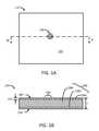
- FIG. 1Aillustrates a top plan view of a workpiece having an exterior surface with a region that has been processed to facilitate subsequent machining of the workpiece.
- FIGS. 5 to 8illustrate one embodiment of a method of machining a feature within the workpiece shown in FIGS. 1A and 1B after performing a pre-machining enhancement process as illustrated in FIG. 3 .
- FIG. 10illustrates an exemplary apparatus for machining a workpiece, according to one embodiment.
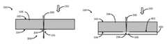
- a workpiece 100includes an exterior surface having a first major surface region 102 , a second primary surface region 104 opposite the first major surface region 102 , and one or more side surface regions extending from the first major surface region 102 to the second major surface region 104 .
- the first major surface region 102 and the second major surface region 104are both substantially flat and parallel to one another. Accordingly, the distance from the first major surface region 102 and the second major surface region 104 can define the thickness, t, of the workpiece 100 .
- the thickness of the workpiece 100is in a range from 200 ⁇ m to 10 mm.
- the thickness of the workpiece 100can be less than 200 ⁇ m or greater than 10 mm.
- the first major surface region 102 and the second major surface region 104may not be substantially flat, may not be parallel to one another, or a combination thereof.
- Exemplary semiconductor materials from which the workpiece 100 can be formedinclude Group IV elemental or compound semiconductors (e.g., silicon, germanium, silicon-germanium, silicon carbide, or the like or a combination thereof), III-V compound semiconductors, II-VI compound semiconductors, II-V compound semiconductors, I-VII compound semiconductors, IV-VI compound semiconductors, semiconductor oxides, or the like, or a combination thereof.
- Exemplary metals and metal alloys from which the workpiece 100 can be formedinclude aluminum, titanium, stainless steel, or the like, or alloys or other combinations thereof.
- Exemplary glasses from which the workpiece 100 can be formedinclude soda-lime glass, borosilicate glass, aluminosilicate glass, aluminoborosilicate glass, sodium-aluminosilicate glass, calcium-aluminosilicate glass, phosphate glass, fluoride glass, chalcogenide glass, bulk metallic glass, or the like, or a combination thereof.
- CTCS ⁇ DOL t - 2 ⁇ DOL
- CSthe aforementioned surface compression at the first major surface region 102 and second major surface region 104
- tthe thickness of the sheet of glass (expressed in millimeters, mm)
- DOLthe depth of layer of the compression region(s) (expressed in mm)
- CTthe maximum central tension within the sheet of glass (expressed in MPa).
- the workpiece 100can be reliably and repeatably laser-machined (e.g., by directing laser energy onto the workpiece 100 ) to form features such as blind holes, through holes, openings, slots, cracks, and the like (collectively referred to herein as “features”).
- featuressuch as blind holes, through holes, openings, slots, cracks, and the like.
- the workpiece 100is laser-machined using laser light having a wavelength to which the workpiece 100 is at least substantially transparent.
- interactions between the laser light and material of the workpiece 100 during the laser-machiningcan typically be characterized as those involving non-linear absorption of laser energy by the workpiece material.
- one or more of any of the aforementioned pre-machining enhancement processesmay be performed by introducing negatively charged ions (atomic or molecular) into the exterior surface, or into the interior 108 of the workpiece 100 .
- the ionsmay be introduced by any suitable method including, for example, ion implantation, diffusion (e.g., from a liquid or a gas), or the like or a combination thereof.
- the surface morphology of the workpiece 100may be modified by forming one or more cracks within the exterior surface of the workpiece 100 , by chemically etching at least a portion of the exterior surface of the workpiece 100 , by sputter etching at least a portion of the exterior surface of the workpiece 100 , by mechanically abrading at least a portion of the exterior surface of the workpiece 100 , or the like or a combination thereof.
- one or more cracksmay be formed by mechanically impacting the exterior surface of the workpiece 100 at a location within or near the enhancement region 106 (e.g., with a cutting or scribing blade, or the like), by generating thermally-induced tensile and/or compressive stresses at a location within or near the enhancement region 106 , by subjecting the workpiece 100 to a bending moment or other physical stress, by generating a region of laser-induced optical breakdown at a location within or near the enhancement region 106 , or the like or a combination thereof.
- the chemical etchingmay involve a wet etching process, a dry etching process, or the like or a combination thereof, where the particular etchant used may depend on the material forming the enhancement region 106 and the desired change in surface morphology.
- the etchantmay include hydrofluoric acidic, HNA (hydrofluoric acid/nitric acid/acetic acid), or the like or a combination thereof.
- the sputter etchingmay involve any etching process involving momentum transfer between accelerated ions (either inert or reactive) and the workpiece 100 .
- the enhancement region 106it is desirable for the enhancement region 106 to have an Ra (avg) surface roughness value in a range between 2.0 ⁇ m and 9.0 ⁇ m, or an Rq (rms) surface roughness value in a range between 4.0 ⁇ m and 11.0 ⁇ m.
- the Ra and Rq values for the enhancement region 106may be higher than 9.0 ⁇ m and 11.0 ⁇ m, respectively, if desired. Results of experiments by the inventors tend to indicate that the quality of laser-machined features increases as the surface roughness at the enhancement region 106 increases.
- a relatively high-quality laser-machined featurewill be associated will have relatively fewer and/or smaller surface chips (e.g., having, on average, a size of less than 40 ⁇ m, less than 30 ⁇ m, or less than 20 ⁇ m) in the exterior surface of the workpiece 100 surrounding the laser-machined feature than a relatively low-quality laser-machined feature.
- the wavelength of the laser beamcan be in a range from 100 nm to 3000 nm (e.g., 355 nm, 532 nm, 1064 nm, or the like or a combination thereof).
- the pulse duration of the laser beamcan be less than 1 ns (or less than about 1 ns). In one embodiment, the pulse duration of the laser beam can be less than 100 ps. In another embodiment, the pulse duration of the laser beam can be in a range from 10 ps to 15 ps.
- the pulse repetition rate of the laser beamcan be in a range from 30 kHz to 1 MHz. In one embodiment, the pulse repetition rate of the laser beam can be in a range from 30 kHz to 500 kHz.
- the pulse repetition rate of the laser beamcan be 200 kHz.
- the spot size of the laser beamcan be in a range from 3 ⁇ m to 50 ⁇ m. In one embodiment, the spot size of the laser beam can be 7 ⁇ m.
- the average power of the laser beamcan be in a range from 0.5 W to 75 W. In one embodiment, the average power of the laser beam can be 2 W.
- the scan speed of the laser beamcan be in a range from 100 mm/s to 5000 mm/s. In one embodiment, the scan speed of the laser beam can be 140 mm/s.
- One or more of the aforementioned laser beam parameterscan be selected and controlled so that the laser beam irradiates the exterior surface of the workpiece at a pitch in a range from about 50% to about 70% of the spot size.
- a pre-machining enhancement processcan be performed, according to one embodiment, by directing a laser beam 200 from a laser system (not shown) onto the exterior surface of the workpiece 100 along the direction indicated by arrow 202 .
- the workpiece 100is oriented relative to the laser system (not shown) such that the laser beam 200 impinges the first major surface region 102 at the enhancement region 106 .
- the laser beam 200may be focused at a beam waist 204 located either at or above the first major surface region 102 (e.g., so as to be located outside the workpiece 100 ) so that the laser beam 200 irradiates a spot at a portion of the first major surface region 102 with laser energy having a peak intensity sufficient to modify (e.g., increase) the surface roughness of the workpiece surface irradiated by the laser beam 200 , thereby creating a roughened surface 204 within the enhancement region 106 . Parameters of this pre-machining enhancement process can be controlled to ensure that the roughened surface has a desired surface roughness. In one embodiment, the laser beam 200 may be scanned and/or the workpiece 100 may be translated to cause the spot to be moved along the exterior surface of the workpiece 100 within the enhancement region 106 .
- the aforementioned pre-machining enhancement processwas performed by providing the workpiece as a piece of unstrengthened soda-lime glass and the laser 200 directed 10 ns pulses of green light onto the first major surface 102 .
- the resultant roughened surfacehad surface roughness values of 8.5 ⁇ m (Ra) and 10.6 ⁇ m (Rq).
- the laser beam 200is focused at a beam waist 204 located either at or below the second major surface region 104 (e.g., so as to be located outside the workpiece 100 ) so that the laser beam 200 irradiates a spot at a portion of the second major surface region 104 with laser energy having a peak intensity sufficient to modify (e.g., increase) the surface roughness of the workpiece surface irradiated by the laser beam 200 , thereby creating the roughened surface 204 at an enhancement region 106 located at the second major surface region 104 .
- the laser beam 200may be directed (e.g., along the direction indicated by arrow 202 ) onto the workpiece 100 such that the laser beam 200 first impinges the first major surface region 102 and this then transmitted through the workpiece 100 and through the second major surface region 104 to impinge upon the donor object 400 .
- the removal of donor materialis effected such that the removed donor material impacts against, is implanted into, is diffused through, or is otherwise introduced to an enhancement region 106 at the second major surface region 104 of the exterior surface of the workpiece 100 .
- one or more or all of the aforementioned pre-machining enhancement processese.g., generating free electrons at the enhancement region 106 , creating defects within the enhancement region 106 , modifying a composition of at least a portion of exterior surface within the enhancement region 106 , modifying the surface morphology of at least a portion of exterior surface within the enhancement region 106 , etc.
- the aforementioned pre-machining enhancement processese.g., generating free electrons at the enhancement region 106 , creating defects within the enhancement region 106 , modifying a composition of at least a portion of exterior surface within the enhancement region 106 , modifying the surface morphology of at least a portion of exterior surface within the enhancement region 106 , etc.
- the workpiece 100may be machined (e.g., in a laser-machining process) by directing laser energy onto the workpiece 100 in such a manner as to machine (e.g., crack, remove, or the like or a combination thereof) a portion within the interior 108 of the workpiece 100 that adjoins the enhancement region 106 .
- the portion within the interior 108 of the workpiece 100is removed to form a feature such as a through-hole, a blind-hole, or the like or a combination thereof.
- laser-machining of the workpiece 100can include directing laser energy (e.g., in the form of a beam of one or more laser pulses) onto the workpiece 100 .
- Laser energy within the beamcan have a wavelength to which the workpiece 100 is at least substantially transparent.
- the one or more pulsescan be directed to irradiate a spot at the enhancement region 106 , formed during the pre-machining enhancement process, with laser energy having a laser fluence and/or peak intensity sufficient to stimulate non-linear absorption of the laser energy by the workpiece 100 .
- the non-linear absorptionincludes avalanche-dominated absorption of the laser energy by the workpiece 100 .
- the one or more laser pulses directed onto the workpiece 100 during the laser-machiningmay have a pulse duration in a range from 10 fs to 500 ns and at least one wavelength in a range from 100 nm to 3000 nm.
- the pulse duration of the one or more pulses directed onto the workpiece 100 during the laser-machiningmay be the same as or different from the pulse duration of the at least one laser pulse of the laser beam directed during the pre-machining enhancement process.
- the wavelength of the one or more pulses directed onto the workpiece 100 during the laser-machiningmay be the same as or different from the wavelength of the at least one laser pulse of the laser beam directed during the pre-machining enhancement process.
- the one or more laser pulses directed onto the workpiece 100 during the laser-machiningmay have a pulse duration of 10 ns and a wavelength in the green light range (e.g., about 523 nm, 532 nm, 543 nm, or the like or a combination thereof).
- the laser energyis directed onto the workpiece 100 during the laser-machining process as a beam having a plurality of pulses, wherein the pulse duration of at least one of the pulses can be the same as or different from the pulse duration of at least one of the other pulses.
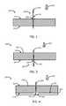
- a workpiece 100having been previously subjected to a pre-machining enhancement process as discussed above with respect to FIG. 3 , may be provided and laser energy (e.g., in the form of a beam 500 of at least one laser pulse) may be directed onto the workpiece 100 from a laser system (not shown) along the direction indicated by arrow 502 .
- laser energye.g., in the form of a beam 500 of at least one laser pulse
- the workpiece 100is oriented relative to the laser system such that the beam 500 first impinges the first major surface region 102 and is then transmitted through the workpiece 100 .
- the laser beam 500is focused at a beam waist 504 located either at or below the second major surface region 104 (e.g., so as to be located outside the workpiece 100 ) so that the beam 500 irradiates a spot at the enhancement region 106 (see FIG. 3 ) with laser energy having a laser fluence and/or peak intensity sufficient to stimulate non-linear absorption of the laser energy by the workpiece 100 at the enhancement region 106 .
- a portion of the workpiece 100 adjoining the enhancement region 106 at the exterior surface of the workpiece 100may be laser-machined (e.g., cracked, removed, or the like or a combination thereof).
- the portion of the workpiece 100 adjoining the enhancement region 106is removed to form a preliminary feature 504 .
- the beam 500may be scanned and/or the workpiece 100 may be translated to cause the spot to be moved along the exterior surface of the workpiece 100 within the enhancement region 106 to ensure that the preliminary feature 504 has a desired shape.
- the laser systemmay be controlled to move the beam waist 504 along the direction indicated by arrow 506 to be at or below a new workpiece surface created upon formation of the preliminary feature 504 to laser-machine the new workpiece surface.
- the process of moving the beam waist and laser-machine new workpiece surfacescan be repeated as desired to form a blind-hole (e.g., blind-hole 600 extending to any depth, d, into the workpiece 100 , as shown in FIG. 6 ), a through-hole (e.g., through-hole 700 extending completely through the thickness of the workpiece 100 , as shown in FIG. 7 ), or the like or a combination thereof.
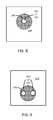
- FIGS. 8 and 9illustrate feature openings intersecting the enhancement region 106 which are circular in shape
- the feature openingsmay be of any shape (e.g., elliptical, irregular, triangular, rectangular, etc.).
- the featuresmay have relatively small dimensions and remain unclogged by undesirable post-machining debris or other unprocessed material.
- FIGS. 5 to 9illustrate some embodiments of a laser-machining process in which the enhancement region 106 has been formed at the second major surface region 104 of the workpiece 100
- the above-described laser-machining processcan be performed on a workpiece having an enhancement region 106 formed at the first major surface region 102 .
- the workpiece 100can simply be flipped over (e.g., such that the first major surface region 102 is disposed below the second major surface region) so that the beam 500 travels through the workpiece 100 before irradiating the enhancement region 106 .
- the workpiece 100may be subjected to a laser-machining process as exemplarily described in U.S. patent application Ser. No. 13/779,183.
- the workpiececan be characterized as an article.
- the articlecan be used as a protective cover plate for display and touch screen applications such as, but not limited to, portable communication and entertainment devices such as telephones, music players, video players, or the like; and as a display screen for information-related terminals (IT) (e.g., portable computer, laptop computer, etc.) devices; as well as in other applications.
- ITinformation-related terminals
- FIG. 10schematically illustrates one embodiment of an apparatus configured to perform the processes exemplarily described with respect to FIGS. 1A-9 .
- an apparatussuch as apparatus 1000 can machine a workpiece such as workpiece 100 .
- the apparatus 100may include a workpiece support system 1002 and a laser system 1004 .
- a support frame 1008may be disposed between the chuck 1006 and the workpiece 100 (e.g., so the second major surface region 104 can be suspended away from the chuck 1006 ).
- the chuck 1006can function as the aforementioned donor object 400 .
- the support frame 1008can be omitted so the second major surface region 104 of the workpiece 100 can contact the chuck 1006 .
- the chuck 1006can function as the aforementioned donor object 400 .
- the laser system 1004is configured to direct a beam such as the beam 500 and, optionally, the laser beam 200 along an optical path (wherein the beam 202 has a beam waist as exemplarily described above with respect to beam waist 504 and, optionally 204 ).
- the laser system 1004may include a laser 1010 configured to produce a beam 1010 a of laser light and an optical assembly 1012 configured to focus the beam 1010 a to produce the beam 500 (having beam waist 504 ) and, optionally laser beam 200 (having beam waist 204 ).
- the laser system 1004is illustrated as including only one laser 1010 , only one beam steering system 1014 , and only one optical assembly 1012 , it will be appreciated that the laser system 1004 may include any number of lasers, beam steering systems, and optical assemblies as desired in the event that the beam 500 and the laser beam 200 cannot be generated, directed, or focused using common equipment.
- the apparatus 1000may further include a controller 1016 communicatively coupled to one or more of the components of the laser system 1004 , to one or more of the components of the workpiece support system 1002 , or a combination thereof.
- the controller 1016may include a processor 1018 and a memory 1020 .
- the processor 1018may be configured to execute instructions stored by the memory 1020 to control an operation of at least one component of the laser system 1004 , the workpiece support system 1002 , or a combination thereof so that the embodiments exemplarily described above with respect to FIGS. 1A to 9 can be performed.
- the controller 1016may control an operation of one or both the laser system 1004 and the workpiece support system 1002 to form the enhancement region 106 . In another embodiment, the controller 1016 may control an operation of at least one of the workpiece support system 1002 and a pre-machining enhancement system 1022 to form the enhancement region 106 .
- a pre-machining enhancement systemsuch as pre-machining enhancement system 1022 may be included within the apparatus 1000 .
- the pre-machining enhancement system 1022can include a enhancement region forming device 1024 operative to form the aforementioned enhancement region 106 .
- the enhancement region forming device 1024may be coupled to a positioning assembly 1026 (e.g., a dual-axis robot) configured to move the enhancement region forming device 1024 (e.g., along a direction indicated by one or both of arrows 1024 a and 1024 b ).
- the enhancement region forming device 1024may include any device capable of forming the enhancement region 106 discussed above (e.g., a grinding wheel, a cutting blade, a laser source, an ion source, an etchant nozzle, a coolant nozzle, or the like or a combination thereof).
- the processor 1018can include operating logic (not shown) that defines various control functions, and may be in the form of dedicated hardware, such as a hardwired state machine, a processor executing programming instructions, and/or a different form as would occur to those skilled in the art. Operating logic may include digital circuitry, analog circuitry, software, or a hybrid combination of any of these types.
- processor 1018includes a programmable microcontroller microprocessor, or other processor that can include one or more processing units arranged to execute instructions stored in memory 1020 in accordance with the operating logic.
- Memory 1020can include one or more types including semiconductor, magnetic, and/or optical varieties, and/or may be of a volatile and/or nonvolatile variety.
Landscapes
- Engineering & Computer Science (AREA)
- Physics & Mathematics (AREA)
- Optics & Photonics (AREA)
- Mechanical Engineering (AREA)
- Plasma & Fusion (AREA)
- Chemical & Material Sciences (AREA)
- Inorganic Chemistry (AREA)
- Laser Beam Processing (AREA)
- Health & Medical Sciences (AREA)
- Toxicology (AREA)
- Life Sciences & Earth Sciences (AREA)
- Chemical Kinetics & Catalysis (AREA)
- General Chemical & Material Sciences (AREA)
- Geochemistry & Mineralogy (AREA)
- Materials Engineering (AREA)
- Organic Chemistry (AREA)
Abstract
Description
where CS is the aforementioned surface compression at the first
Claims (50)
Priority Applications (7)
| Application Number | Priority Date | Filing Date | Title |
|---|---|---|---|
| US14/033,368US10357850B2 (en) | 2012-09-24 | 2013-09-20 | Method and apparatus for machining a workpiece |
| EP13845791.6AEP2897760A4 (en) | 2012-09-24 | 2013-09-23 | METHOD AND APPARATUS FOR WORK MACHINING |
| KR1020157010309AKR20150060826A (en) | 2012-09-24 | 2013-09-23 | Method and apparatus for machining a workpiece |
| CN201380049563.3ACN104703748B (en) | 2012-09-24 | 2013-09-23 | Method and apparatus for processing workpiece |
| PCT/US2013/061212WO2014058606A1 (en) | 2012-09-24 | 2013-09-23 | Method and apparatus for machining a workpiece |
| JP2015533250AJP2015533654A (en) | 2012-09-24 | 2013-09-23 | Method and apparatus for machining a workpiece |
| US14/094,656US9828278B2 (en) | 2012-02-28 | 2013-12-02 | Method and apparatus for separation of strengthened glass and articles produced thereby |
Applications Claiming Priority (3)
| Application Number | Priority Date | Filing Date | Title |
|---|---|---|---|
| US201261705038P | 2012-09-24 | 2012-09-24 | |
| US201261705559P | 2012-09-25 | 2012-09-25 | |
| US14/033,368US10357850B2 (en) | 2012-09-24 | 2013-09-20 | Method and apparatus for machining a workpiece |
Related Child Applications (2)
| Application Number | Title | Priority Date | Filing Date |
|---|---|---|---|
| US13/778,950Continuation-In-PartUS9828277B2 (en) | 2012-02-28 | 2013-02-27 | Methods for separation of strengthened glass |
| US14/094,656Continuation-In-PartUS9828278B2 (en) | 2012-02-28 | 2013-12-02 | Method and apparatus for separation of strengthened glass and articles produced thereby |
Publications (2)
| Publication Number | Publication Date |
|---|---|
| US20140083986A1 US20140083986A1 (en) | 2014-03-27 |
| US10357850B2true US10357850B2 (en) | 2019-07-23 |
Family
ID=50337865
Family Applications (1)
| Application Number | Title | Priority Date | Filing Date |
|---|---|---|---|
| US14/033,368Expired - Fee RelatedUS10357850B2 (en) | 2012-02-28 | 2013-09-20 | Method and apparatus for machining a workpiece |
Country Status (7)
| Country | Link |
|---|---|
| US (1) | US10357850B2 (en) |
| EP (1) | EP2897760A4 (en) |
| JP (1) | JP2015533654A (en) |
| KR (1) | KR20150060826A (en) |
| CN (1) | CN104703748B (en) |
| TW (1) | TWI611856B (en) |
| WO (1) | WO2014058606A1 (en) |
Cited By (1)
| Publication number | Priority date | Publication date | Assignee | Title |
|---|---|---|---|---|
| DE102020123147B4 (en) | 2019-09-06 | 2022-01-27 | Cericom GmbH | Method, device, control device and computer program product for making a cut in a glass workpiece |
Families Citing this family (21)
| Publication number | Priority date | Publication date | Assignee | Title |
|---|---|---|---|---|
| JP5996260B2 (en)* | 2012-05-09 | 2016-09-21 | 株式会社ディスコ | Workpiece division method |
| EP2754524B1 (en) | 2013-01-15 | 2015-11-25 | Corning Laser Technologies GmbH | Method of and apparatus for laser based processing of flat substrates being wafer or glass element using a laser beam line |
| EP2781296B1 (en) | 2013-03-21 | 2020-10-21 | Corning Laser Technologies GmbH | Device and method for cutting out contours from flat substrates using a laser |
| US9328011B2 (en)* | 2013-06-04 | 2016-05-03 | Coherent, Inc. | Laser-scribing of chemically strengthened glass |
| US11556039B2 (en) | 2013-12-17 | 2023-01-17 | Corning Incorporated | Electrochromic coated glass articles and methods for laser processing the same |
| US10293436B2 (en) | 2013-12-17 | 2019-05-21 | Corning Incorporated | Method for rapid laser drilling of holes in glass and products made therefrom |
| GB2527553B (en)* | 2014-06-25 | 2017-08-23 | Fianium Ltd | Laser processing |
| CN106687419A (en)* | 2014-07-08 | 2017-05-17 | 康宁股份有限公司 | Methods and apparatuses for laser processing materials |
| KR20170028943A (en) | 2014-07-14 | 2017-03-14 | 코닝 인코포레이티드 | System for and method of processing transparent materials using laser beam focal lines adjustable in length and diameter |
| HUE055461T2 (en) | 2015-03-24 | 2021-11-29 | Corning Inc | Laser cutting and processing of display glass compositions |
| JP6294378B2 (en) | 2016-03-30 | 2018-03-14 | ファナック株式会社 | Laser processing apparatus and laser processing method provided with pre-processing control unit |
| CN109862991A (en)* | 2016-07-28 | 2019-06-07 | 伊雷克托科学工业股份有限公司 | The method of radium-shine processing equipment and radium-shine processing workpiece |
| WO2018047823A1 (en)* | 2016-09-09 | 2018-03-15 | 三菱電機株式会社 | Laser machining device |
| US10730783B2 (en) | 2016-09-30 | 2020-08-04 | Corning Incorporated | Apparatuses and methods for laser processing transparent workpieces using non-axisymmetric beam spots |
| EP3529214B1 (en) | 2016-10-24 | 2020-12-23 | Corning Incorporated | Substrate processing station for laser-based machining of sheet-like glass substrates |
| JP6717758B2 (en)* | 2017-01-10 | 2020-07-01 | ファナック株式会社 | Complex machining method and complex machining program |
| JPWO2018181522A1 (en)* | 2017-03-31 | 2020-02-13 | 株式会社ジャパンディスプレイ | Electronic equipment and manufacturing method thereof |
| US20190233321A1 (en) | 2018-01-26 | 2019-08-01 | Corning Incorporated | Liquid-assisted laser micromachining of transparent dielectrics |
| TWI866446B (en) | 2018-10-08 | 2024-12-11 | 美商伊雷克托科學工業股份有限公司 | Methods for forming a through-via in a substrate |
| KR20220011848A (en)* | 2020-07-21 | 2022-02-03 | 삼성디스플레이 주식회사 | Laser apparatus and method for manufacturing display device |
| CN113226632A (en)* | 2021-03-31 | 2021-08-06 | 长江存储科技有限责任公司 | Laser system for cutting semiconductor structure and operation method thereof |
Citations (179)
| Publication number | Priority date | Publication date | Assignee | Title |
|---|---|---|---|---|
| US3287200A (en) | 1962-10-04 | 1966-11-22 | Pittsburgh Plate Glass Co | Method of strengthening glass by ion exchange and articles therefrom |
| US4702042A (en) | 1984-09-27 | 1987-10-27 | Libbey-Owens-Ford Co. | Cutting strengthened glass |
| US4828900A (en) | 1987-12-23 | 1989-05-09 | Ppg Industries, Inc. | Discrete glass cutting and edge shaping |
| US4847184A (en)* | 1986-04-21 | 1989-07-11 | Kanzaki Paper Manufacturing Co., Ltd. | Method for producing a laser-printed picture |
| US5043553A (en) | 1988-10-12 | 1991-08-27 | Rolls-Royce Plc | Method and apparatus for drilling a shaped hole in a workpiece |
| US5413664A (en) | 1990-05-09 | 1995-05-09 | Canon Kabushiki Kaisha | Apparatus for preparing a semiconductor device, photo treatment apparatus, pattern forming apparatus and fabrication apparatus |
| US5543365A (en) | 1994-12-02 | 1996-08-06 | Texas Instruments Incorporated | Wafer scribe technique using laser by forming polysilicon |
| US5609284A (en) | 1992-04-02 | 1997-03-11 | Fonon Technology Limited | Method of splitting non-metallic materials |
| US5637244A (en) | 1993-05-13 | 1997-06-10 | Podarok International, Inc. | Method and apparatus for creating an image by a pulsed laser beam inside a transparent material |
| US5656186A (en) | 1994-04-08 | 1997-08-12 | The Regents Of The University Of Michigan | Method for controlling configuration of laser induced breakdown and ablation |
| US5665134A (en) | 1995-06-07 | 1997-09-09 | Hughes Missile Systems Company | Laser machining of glass-ceramic materials |
| JPH10128563A (en) | 1996-10-24 | 1998-05-19 | Nippon Sheet Glass Co Ltd | Laser beam machining method for micro lens |
| US5826772A (en) | 1995-08-31 | 1998-10-27 | Corning Incorporated | Method and apparatus for breaking brittle materials |
| JPH11163403A (en) | 1997-11-28 | 1999-06-18 | Nichia Chem Ind Ltd | Method for manufacturing nitride semiconductor device |
| US5968441A (en) | 1997-10-21 | 1999-10-19 | Nec Corporation | Laser processing method |
| US5973290A (en) | 1997-02-26 | 1999-10-26 | W. L. Gore & Associates, Inc. | Laser apparatus having improved via processing rate |
| US6143382A (en) | 1997-06-04 | 2000-11-07 | Nippon Sheet Glass Co., Ltd. | Glass substrate having fine holes |
| US6211488B1 (en) | 1998-12-01 | 2001-04-03 | Accudyne Display And Semiconductor Systems, Inc. | Method and apparatus for separating non-metallic substrates utilizing a laser initiated scribe |
| JP2001274441A (en) | 2000-03-23 | 2001-10-05 | Mitsubishi Heavy Ind Ltd | Method for collectively cutting solar battery panel |
| US20010035447A1 (en) | 2000-05-05 | 2001-11-01 | Andreas Gartner | Methods for laser cut initiation |
| US6313435B1 (en)* | 1998-11-20 | 2001-11-06 | 3M Innovative Properties Company | Mask orbiting for laser ablated feature formation |
| US20010038930A1 (en) | 1997-07-24 | 2001-11-08 | Hiroki Yamamoto | Glass substrate for a magnetic disk, a magnetic disk which can be formed with a stable texture |
| US20010040150A1 (en) | 1997-10-30 | 2001-11-15 | Hoya Corporation | Glass substrate for information-recording medium and manufacturing method of the glass substrate |
| US6326589B1 (en) | 1997-09-19 | 2001-12-04 | Fraunhofer-Gesellschaft Zur Forderung Der Angewandten Forschung E.V. | Method and device for treating materials with plasma-inducing high energy radiation |
| US6333485B1 (en) | 1998-12-11 | 2001-12-25 | International Business Machines Corporation | Method for minimizing sample damage during the ablation of material using a focused ultrashort pulsed beam |
| US20020005805A1 (en) | 2000-06-12 | 2002-01-17 | Hiroshi Ogura | Method of machining glass substrate and method of fabricating high-frequency circuit |
| US20020033558A1 (en) | 2000-09-20 | 2002-03-21 | Fahey Kevin P. | UV laser cutting or shape modification of brittle, high melting temperature target materials such as ceramics or glasses |
| WO2002022301A1 (en) | 2000-09-13 | 2002-03-21 | Hamamatsu Photonics K.K. | Laser beam machining method and laser beam machining device |
| US20020037132A1 (en)* | 2000-02-17 | 2002-03-28 | Sercel Peter C. | Resonant optical power control device assemblies |
| US20020041946A1 (en) | 2000-08-18 | 2002-04-11 | Nippon Sheet Glass Co., Ltd. | Process for cutting a glass sheet and a glass disk for a recording medium |
| US20020060978A1 (en) | 2000-10-10 | 2002-05-23 | Akemi Hirotsune | Information recording media, a method for recording/reproducing information, an apparatus for recording/reproducing information |
| JP2002192369A (en) | 2000-09-13 | 2002-07-10 | Hamamatsu Photonics Kk | Laser beam machining method and laser beam machining device |
| US6442974B1 (en)* | 1994-03-24 | 2002-09-03 | Laserplus Oy | Method and device for making visually observable markings onto transparent material |
| WO2003002289A1 (en) | 2001-06-28 | 2003-01-09 | Electro Scientific Industries, Inc. | Multistep laser processing of wafers supporting surface device layers |
| US6521862B1 (en) | 2001-10-09 | 2003-02-18 | International Business Machines Corporation | Apparatus and method for improving chamfer quality of disk edge surfaces with laser treatment |
| US20030044539A1 (en) | 2001-02-06 | 2003-03-06 | Oswald Robert S. | Process for producing photovoltaic devices |
| JP2003088976A (en) | 2001-09-12 | 2003-03-25 | Hamamatsu Photonics Kk | Laser beam machining method |
| US20030071020A1 (en)* | 2001-10-16 | 2003-04-17 | Minghui Hong | Method of laser marking and apparatus therefor |
| US20030096078A1 (en) | 2001-11-21 | 2003-05-22 | Nippon Sheet Glass Co., Ltd. | Glass substrate for data recording medium and manufacturing method thereof |
| US20030102291A1 (en) | 2001-11-30 | 2003-06-05 | Xinbing Liu | System and method of laser drilling |
| US20030111447A1 (en) | 2000-01-27 | 2003-06-19 | Corkum Paul B. | Method and apparatus for repair of defects in materials with short laser pulses |
| US20030150839A1 (en) | 2002-02-05 | 2003-08-14 | Fumitoshi Kobayashi | Glass substrate with fine hole and method for producing the same |
| US20030201261A1 (en) | 2000-12-01 | 2003-10-30 | Lg Electronics Inc. | Glass cutting method and apparatus |
| US6642477B1 (en) | 2001-10-23 | 2003-11-04 | Imra America, Inc. | Method for laser drilling a counter-tapered through-hole in a material |
| US6642476B2 (en) | 2001-07-23 | 2003-11-04 | Siemens Automative Corporation | Apparatus and method of forming orifices and chamfers for uniform orifice coefficient and surface properties by laser |
| US20030217568A1 (en) | 2002-02-22 | 2003-11-27 | Hirotaka Koyo | Glass structure and method for producing the same |
| US20040089644A1 (en)* | 2002-11-12 | 2004-05-13 | Kazuma Sekiya | Laser machining method and laser machining apparatus |
| US6756563B2 (en) | 2002-03-07 | 2004-06-29 | Orbotech Ltd. | System and method for forming holes in substrates containing glass |
| US20040128016A1 (en)* | 2001-03-22 | 2004-07-01 | Stewart David H. | Method for manufacturing a near net-shape mold |
| US6795274B1 (en) | 1999-09-07 | 2004-09-21 | Asahi Glass Company, Ltd. | Method for manufacturing a substantially circular substrate by utilizing scribing |
| US6809291B1 (en) | 2002-08-30 | 2004-10-26 | Southeastern Universities Research Assn., Inc. | Process for laser machining and surface treatment |
| JP2004299969A (en) | 2003-03-31 | 2004-10-28 | Toshiba Ceramics Co Ltd | How to slice silica glass |
| US6820330B1 (en) | 1996-12-13 | 2004-11-23 | Tessera, Inc. | Method for forming a multi-layer circuit assembly |
| US20050029240A1 (en)* | 2003-08-07 | 2005-02-10 | Translume, Inc. | Dual light source machining method and system |
| US20050042805A1 (en) | 2003-07-11 | 2005-02-24 | Swenson Edward J. | Method of forming a scribe line on a passive electronic component substrate |
| US20050064137A1 (en)* | 2003-01-29 | 2005-03-24 | Hunt Alan J. | Method for forming nanoscale features and structures produced thereby |
| JP2005081715A (en) | 2003-09-09 | 2005-03-31 | Sony Corp | Laser beam machining apparatus and laser beam machining method |
| JP2005088023A (en) | 2003-09-12 | 2005-04-07 | Seiko Epson Corp | Transparency processing method |
| US20050087522A1 (en) | 2003-10-24 | 2005-04-28 | Yunlong Sun | Laser processing of a locally heated target material |
| JP2005144530A (en) | 2003-11-19 | 2005-06-09 | National Institute Of Advanced Industrial & Technology | Laser precision processing of transparent media |
| CN1657220A (en) | 2004-02-19 | 2005-08-24 | 佳能株式会社 | Laser based splitting method, object to be split, and semiconductor element chip |
| US20050184035A1 (en) | 1995-08-07 | 2005-08-25 | Mitsubishi Denki Kabushiki Kaisha | Pulsed laser beam machining method and apparatus for machining a wiring board at multiple locations |
| US20050221044A1 (en) | 2002-05-07 | 2005-10-06 | Saint-Gobain Glass France | Glass cutting method which does not involve breaking |
| US20050230365A1 (en)* | 2004-04-14 | 2005-10-20 | Weisheng Lei | Methods of drilling through-holes in homogenous and non-homogeneous substrates |
| US6962279B1 (en) | 2000-10-18 | 2005-11-08 | Ge Medical Systems Global Technology Company, Llc | Apparatus and method for glass separation for flat panel displays |
| US20060021978A1 (en) | 2002-02-21 | 2006-02-02 | Alexeev Andrey M | Method for cutting non-metallic materials and device for carring out said method |
| US20060032842A1 (en)* | 2003-02-04 | 2006-02-16 | Kuniaki Hiromatsu | Method for removing foreign matter on glass substrate surface |
| US7007512B2 (en) | 2000-11-17 | 2006-03-07 | National Institute Of Advanced Industrial Science And Technology | Method for machining glass substrate |
| US20060049156A1 (en)* | 2002-02-15 | 2006-03-09 | Michael Mulloy | Method of forming substrate for fluid ejection device |
| US7023001B2 (en) | 2003-03-31 | 2006-04-04 | Institut National D'optique | Method for engraving materials using laser etched V-grooves |
| US20060091125A1 (en) | 2004-11-03 | 2006-05-04 | Intel Corporation | Laser micromachining method |
| DE10029110B4 (en) | 1999-06-15 | 2006-05-18 | Fraunhofer-Gesellschaft zur Förderung der angewandten Forschung e.V. | Method for material processing and use thereof |
| US7060933B2 (en) | 2004-06-08 | 2006-06-13 | Igor Troitski | Method and laser system for production of laser-induced images inside and on the surface of transparent material |
| US20060151450A1 (en) | 2003-01-06 | 2006-07-13 | Ki-Yong You | Glass-plate cutting machine |
| US20060169677A1 (en) | 2005-02-03 | 2006-08-03 | Laserfacturing Inc. | Method and apparatus for via drilling and selective material removal using an ultrafast pulse laser |
| TW200631718A (en) | 2004-12-08 | 2006-09-16 | Laser Solutions Co Ltd | Division starting point forming method in body to be divided, dividing method for body to be divided, and method of processing work by pulse laser beam |
| US20070012665A1 (en) | 2005-07-12 | 2007-01-18 | Hewlett-Packard Development Company Lp | Laser ablation |
| US20070039932A1 (en) | 2004-04-27 | 2007-02-22 | Michael Haase | Device for separative machining of components made from brittle material with stress-free component mounting |
| US7232612B2 (en)* | 1996-07-18 | 2007-06-19 | Hitachi, Ltd. | Glass substrate of disk for recording information, a disk for recording information, and a disk device for recording information |
| US20070170162A1 (en) | 2004-05-14 | 2007-07-26 | Oliver Haupt | Method and device for cutting through semiconductor materials |
| US20070221826A1 (en)* | 2006-03-24 | 2007-09-27 | Gentex Corporation | Vision system |
| US20070231542A1 (en)* | 2006-04-03 | 2007-10-04 | General Electric Company | Articles having low wettability and high light transmission |
| JP2007283318A (en) | 2006-04-13 | 2007-11-01 | Seiko Epson Corp | Substrate manufacturing method, laser processing device, display device, electro-optical device, electronic device |
| CN101073145A (en) | 2004-12-08 | 2007-11-14 | 雷射先进科技株式会社 | Division starting poin forming method in body to be divided, dividing method for body to be divided, and method of processing work by pulse laser beam |
| US20070262464A1 (en) | 2004-08-24 | 2007-11-15 | Micron Technology, Inc. | Method of forming vias in semiconductor substrates and resulting structures |
| US20070272666A1 (en) | 2006-05-25 | 2007-11-29 | O'brien James N | Infrared laser wafer scribing using short pulses |
| US20070272668A1 (en) | 2006-05-25 | 2007-11-29 | Albelo Jeffrey A | Ultrashort laser pulse wafer scribing |
| JP2007319881A (en) | 2006-05-31 | 2007-12-13 | Seiko Epson Corp | Substrate manufacturing method, laser processing device, display device, electro-optical device, electronic device |
| US20070291496A1 (en) | 2006-06-02 | 2007-12-20 | Electro Scientific Industries, Inc. | Process for optically transparent via filling |
| DE102006046313B3 (en) | 2006-09-29 | 2008-01-24 | Fraunhofer-Gesellschaft zur Förderung der angewandten Forschung e.V. | Method for structuring fiber optic line along longitudinal axis e.g., for telecommunications, involves passing laser beam through focusing optics onto surface of fiber |
| US20080050888A1 (en) | 2006-08-24 | 2008-02-28 | Sean Matthew Garner | Laser separation of thin laminated glass substrates for flexible display applications |
| US20080047933A1 (en) | 2004-03-18 | 2008-02-28 | Antti Salminen | Method For Machining A Material With High-Power Density Electromagnetic Radiation |
| US20080093775A1 (en) | 2006-08-19 | 2008-04-24 | Colorado State University Research Foundation | Nanometer-scale ablation using focused, coherent extreme ultraviolet/soft x-ray light |
| US7378342B2 (en) | 2004-08-27 | 2008-05-27 | Micron Technology, Inc. | Methods for forming vias varying lateral dimensions |
| US20080128953A1 (en) | 2003-05-19 | 2008-06-05 | Yusuke Nagai | Workpiece dividing method utilizing laser beam |
| US20080156780A1 (en)* | 2006-12-29 | 2008-07-03 | Sergei Voronov | Substrate markings |
| US20080185367A1 (en) | 2007-02-01 | 2008-08-07 | Uri El-Hanany | Method and system of machining using a beam of photons |
| DE102007009786A1 (en) | 2007-02-27 | 2008-08-28 | Schott Ag | Process to surface harden a glass panel whose material contains sodium by treatment with potassium nitrate |
| WO2008108332A1 (en) | 2007-03-02 | 2008-09-12 | Nippon Electric Glass Co., Ltd. | Reinforced plate glass and method for manufacturing the same |
| US20080283509A1 (en) | 2007-05-15 | 2008-11-20 | Anatoli Anatolyevich Abramov | Method and apparatus for scoring and separating a brittle material with a single beam of radiation |
| US20080290077A1 (en) | 2007-05-22 | 2008-11-27 | Demeritt Jeffery Alan | Separation of transparent glasses and systems and methods therefor |
| US20080296273A1 (en) | 2007-06-01 | 2008-12-04 | Electro Scientific Industries, Inc. | Method of and apparatus for laser drilling holes with improved taper |
| US20090020511A1 (en) | 2007-07-17 | 2009-01-22 | Kommera Swaroop K | Ablation |
| US20090045179A1 (en) | 2007-08-15 | 2009-02-19 | Ellen Marie Kosik Williams | Method and system for cutting solid materials using short pulsed laser |
| JP2009061462A (en) | 2007-09-05 | 2009-03-26 | Sumitomo Electric Ind Ltd | Substrate manufacturing method and substrate |
| JP2009072829A (en) | 2007-09-21 | 2009-04-09 | Icu Research & Industrial Cooperation Group | Substrate cutting apparatus using ultra-short pulse laser beam and cutting method therefor |
| US20090201444A1 (en) | 2001-11-08 | 2009-08-13 | Koji Yamabuchi | Method and apparatus for cutting apart a glass substrate, liquid crystal panel, and apparatus for fabricating a liquid crystal panel |
| US20090212030A1 (en)* | 2008-02-25 | 2009-08-27 | Optisolar, Inc., A Delaware Corporation | Autofocus for Ablation Laser |
| EP2096375A1 (en) | 2008-02-26 | 2009-09-02 | Rioglass Solar, S.A. | A reflector element for a solar heat reflector and the method for producing the same |
| US20090242525A1 (en) | 2008-03-31 | 2009-10-01 | Electro Scientific Industries, Inc. | Laser machining of fired ceramic and other hard and/or thick materials |
| US7605344B2 (en) | 2003-07-18 | 2009-10-20 | Hamamatsu Photonics K.K. | Laser beam machining method, laser beam machining apparatus, and laser beam machining product |
| JP2009280452A (en) | 2008-05-23 | 2009-12-03 | Central Glass Co Ltd | Glass substrate and method for producing the same |
| US20100029459A1 (en)* | 2006-07-26 | 2010-02-04 | Josef Wilson Zwanziger | Glasses having a reduced stress-optic coefficient |
| US20100025387A1 (en)* | 2005-09-08 | 2010-02-04 | Imra America, Inc. | Transparent material processing with an ultrashort pulse laser |
| CN101670487A (en) | 2008-09-12 | 2010-03-17 | 欧姆龙株式会社 | Method and device for forming line used for cutting |
| US7723212B2 (en) | 2004-07-30 | 2010-05-25 | Mitsuboshi Diamond Industrial Co., Ltd | Method for forming median crack in substrate and apparatus for forming median crack in substrate |
| US20100147813A1 (en) | 2008-12-17 | 2010-06-17 | Electro Scientific Industries, Inc. | Method for laser processing glass with a chamfered edge |
| JP2010142862A (en) | 2008-12-22 | 2010-07-01 | Cyber Laser Kk | Method for producing nano-periodic structure on surface of dielectric material |
| US20100197116A1 (en) | 2008-03-21 | 2010-08-05 | Imra America, Inc. | Laser-based material processing methods and systems |
| US20100210442A1 (en) | 2009-02-19 | 2010-08-19 | Anatoli Anatolyevich Abramov | Method of separating strengthened glass |
| US20100206008A1 (en) | 2009-02-19 | 2010-08-19 | Harvey Daniel R | Method of separating strengthened glass |
| US20100221583A1 (en) | 2009-02-27 | 2010-09-02 | Applied Materials, Inc. | Hdd pattern implant system |
| US20100243626A1 (en) | 2009-03-28 | 2010-09-30 | Electro Scientific Industries, Inc. | Method and Apparatus for Laser Machining |
| US20100285275A1 (en)* | 2009-05-06 | 2010-11-11 | Adra Smith Baca | Fingerprint-resistant glass substrates |
| US20100291353A1 (en) | 2009-02-19 | 2010-11-18 | Matthew John Dejneka | Method of separating strengthened glass |
| CN101903301A (en) | 2007-12-18 | 2010-12-01 | Hoya株式会社 | Cover glass for mobile terminal, method for manufacturing same, and mobile terminal device |
| US20100301024A1 (en) | 2009-05-28 | 2010-12-02 | Electro Scientific Industries, Inc. | Laser processing systems using through-the-lens alignment of a laser beam with a target feature |
| US20100320179A1 (en) | 2007-10-16 | 2010-12-23 | Hideki Morita | Method for Creating Trench in U Shape in Brittle Material Substrate, Method for Removing Process, Method for Hollowing Process and Chamfering Method Using Same |
| US20110049765A1 (en) | 2009-08-28 | 2011-03-03 | Xinghua Li | Methods for Laser Cutting Glass Substrates |
| WO2011025908A1 (en) | 2009-08-28 | 2011-03-03 | Corning Incorporated | Methods for laser cutting articles from chemically strengthened glass substrates |
| US7931849B2 (en)* | 2008-06-25 | 2011-04-26 | Applied Micro Circuits Corporation | Non-destructive laser optical integrated circuit package marking |
| JP2011088179A (en) | 2009-10-22 | 2011-05-06 | V Technology Co Ltd | Laser beam machining apparatus |
| US20110115129A1 (en)* | 2008-07-09 | 2011-05-19 | Fei Company | Method and Apparatus for Laser Machining |
| US20110127242A1 (en) | 2009-11-30 | 2011-06-02 | Xinghua Li | Methods for laser scribing and separating glass substrates |
| US20110127244A1 (en) | 2009-11-30 | 2011-06-02 | Xinghua Li | Methods for laser scribing and separating glass substrates |
| US20110183116A1 (en) | 2010-01-27 | 2011-07-28 | Jeng-Jye Hung | Method for cutting tempered glass and preparatory tempered glass structure |
| US20110206903A1 (en)* | 2010-02-24 | 2011-08-25 | Prantik Mazumder | Oleophobic glass substrates |
| JP2011164508A (en) | 2010-02-15 | 2011-08-25 | Sony Corp | Method for manufacturing electric solid-state device, and electric solid-state device |
| US20110226832A1 (en) | 2010-03-19 | 2011-09-22 | John Frederick Bayne | Mechanical scoring and separation of strengthened glass |
| WO2011117006A1 (en) | 2010-03-22 | 2011-09-29 | Fraunhofer-Gesellschaft zur Förderung der angewandten Forschung e.V. | Process and apparatus for separating individual panes from a laminated glass sheet |
| TW201132604A (en) | 2009-11-30 | 2011-10-01 | Corning Inc | Methods of forming scribe vents in strengthenedglass substrates |
| EP2371778A1 (en) | 2010-03-30 | 2011-10-05 | Linde Aktiengesellschaft | Method for producing toughened flat glass with anti-reflective properties |
| US20110240611A1 (en) | 2010-03-05 | 2011-10-06 | Micronic MyData Systems AB | Methods and Device for Laser Processing |
| US20110240616A1 (en) | 2010-04-02 | 2011-10-06 | Electro Scientific Industries, Inc. | method and apparatus for laser singulation of brittle materials |
| US20110240617A1 (en)* | 2004-03-31 | 2011-10-06 | Imra America, Inc. | Laser-based material processing apparatus and methods |
| US20110250423A1 (en) | 2008-12-25 | 2011-10-13 | Asahi Glass Company, Limited | Process and system for cutting a brittle-material plate, and window glass for a vehicle |
| US20110259631A1 (en) | 2008-12-13 | 2011-10-27 | M-Solv Ltd. | Method and apparatus for laser machining relatively narrow and relatively wide structures |
| US20110266264A1 (en) | 2009-01-03 | 2011-11-03 | Philip Thomas Rumsby | Method and apparatus for forming grooves in the surface of a polymer layer |
| JP2011230940A (en) | 2010-04-26 | 2011-11-17 | Mitsuboshi Diamond Industrial Co Ltd | Cutting method for brittle material substrate |
| US8075999B2 (en) | 2008-08-08 | 2011-12-13 | Corning Incorporated | Strengthened glass articles and methods of making |
| JP2011251879A (en) | 2010-06-02 | 2011-12-15 | Asahi Glass Co Ltd | Method and device for cutting chemically strengthened glass |
| US20110318996A1 (en) | 2010-06-28 | 2011-12-29 | Shin-Etsu Chemical Co., Ltd. | Method for manufacturing electronic grade synthetic quartz glass substrate |
| US8110419B2 (en)* | 2009-08-20 | 2012-02-07 | Integrated Photovoltaic, Inc. | Process of manufacturing photovoltaic device |
| JP2012031018A (en) | 2010-07-30 | 2012-02-16 | Asahi Glass Co Ltd | Tempered glass substrate, method for grooving tempered glass substrate, and method for cutting tempered glass substrate |
| KR20120015366A (en) | 2010-07-19 | 2012-02-21 | 엘지디스플레이 주식회사 | Tempered glass cutting method and cutting device |
| US20120052252A1 (en) | 2010-08-26 | 2012-03-01 | Jeffrey Todd Kohli | Methods for extracting strengthened glass substrates from glass sheets |
| US8134099B2 (en)* | 2007-08-03 | 2012-03-13 | Hamamatsu Photonics K.K. | Laser working method, laser working apparatus, and its manufacturing method |
| US20120061361A1 (en)* | 2010-09-10 | 2012-03-15 | Disco Corporation | Method of dividing workpiece |
| CN102405520A (en) | 2009-03-27 | 2012-04-04 | 伊雷克托科学工业股份有限公司 | Method for laser singulation of chip scale packages on glass substrates |
| JP2012096257A (en) | 2010-11-01 | 2012-05-24 | Disco Corp | Machining method and machining device |
| US20120135177A1 (en) | 2010-11-30 | 2012-05-31 | Cornejo Ivan A | Methods for forming grooves and separating strengthened glass substrate sheets |
| US20120135195A1 (en)* | 2010-11-30 | 2012-05-31 | Gregory Scott Glaesemann | Methods for separating glass articles from strengthened glass substrate sheets |
| US20120168412A1 (en) | 2011-01-05 | 2012-07-05 | Electro Scientific Industries, Inc | Apparatus and method for forming an aperture in a substrate |
| US20120196071A1 (en)* | 2011-02-01 | 2012-08-02 | Cornejo Ivan A | Strengthened glass substrate sheets and methods for fabricating glass panels from glass substrate sheets |
| US20120211923A1 (en) | 2011-02-18 | 2012-08-23 | Sean Matthew Garner | Laser cutting method |
| US20130037992A1 (en)* | 2006-08-04 | 2013-02-14 | Erel Milshtein | Laser scribing apparatus, systems, and methods |
| US8383983B2 (en) | 2009-03-25 | 2013-02-26 | Samsung Display Co., Ltd. | Substrate cutting apparatus and method of cutting substrate using the same |
| JP2013043795A (en) | 2011-08-23 | 2013-03-04 | Nippon Electric Glass Co Ltd | Tempered glass and method of manufacturing the same |
| US20130129947A1 (en) | 2011-11-18 | 2013-05-23 | Daniel Ralph Harvey | Glass article having high damage resistance |
| US20130155004A1 (en) | 2011-12-16 | 2013-06-20 | Micro Technology Co., Ltd. | Strengthened glass, touch panel and method of manufacturing strengthened glass |
| US20130192305A1 (en) | 2011-08-10 | 2013-08-01 | Matthew L. Black | Methods for separating glass substrate sheets by laser-formed grooves |
| US20130221053A1 (en) | 2012-02-28 | 2013-08-29 | Electro Scientific Industries, Inc. | Method and apparatus for separation of strengthened glass and articles produced thereby |
| US20130224439A1 (en) | 2012-02-28 | 2013-08-29 | Electro Scientific Industries, Inc. | Method and apparatus for separation of strengthened glass and articles produced thereby |
| US8584354B2 (en) | 2010-08-26 | 2013-11-19 | Corning Incorporated | Method for making glass interposer panels |
| US20130323469A1 (en) | 2012-06-05 | 2013-12-05 | Corning Incorporated | Methods of cutting glass using a laser |
| US20130328905A1 (en) | 2010-01-06 | 2013-12-12 | Canon Kabushiki Kaisha | Image processing apparatus and image processing method |
| US20140093693A1 (en) | 2012-02-28 | 2014-04-03 | Electro Scientific Industries, Inc. | Method and apparatus for separation of strengthened glass and articles produced thereby |
| US8720228B2 (en) | 2010-08-31 | 2014-05-13 | Corning Incorporated | Methods of separating strengthened glass substrates |
| US9018562B2 (en)* | 2006-04-10 | 2015-04-28 | Board Of Trustees Of Michigan State University | Laser material processing system |
Family Cites Families (2)
| Publication number | Priority date | Publication date | Assignee | Title |
|---|---|---|---|---|
| US20080160295A1 (en)* | 2006-04-12 | 2008-07-03 | Picodeon Ltd Oy | Method for adjusting ablation threshold |
| JP4959422B2 (en)* | 2007-05-30 | 2012-06-20 | 株式会社ディスコ | Wafer division method |
- 2013
- 2013-09-20USUS14/033,368patent/US10357850B2/ennot_activeExpired - Fee Related
- 2013-09-23JPJP2015533250Apatent/JP2015533654A/enactivePending
- 2013-09-23CNCN201380049563.3Apatent/CN104703748B/ennot_activeExpired - Fee Related
- 2013-09-23WOPCT/US2013/061212patent/WO2014058606A1/enactiveApplication Filing
- 2013-09-23KRKR1020157010309Apatent/KR20150060826A/ennot_activeCeased
- 2013-09-23EPEP13845791.6Apatent/EP2897760A4/ennot_activeWithdrawn
- 2013-09-24TWTW102134208Apatent/TWI611856B/ennot_activeIP Right Cessation
Patent Citations (204)
| Publication number | Priority date | Publication date | Assignee | Title |
|---|---|---|---|---|
| US3287200A (en) | 1962-10-04 | 1966-11-22 | Pittsburgh Plate Glass Co | Method of strengthening glass by ion exchange and articles therefrom |
| US4702042A (en) | 1984-09-27 | 1987-10-27 | Libbey-Owens-Ford Co. | Cutting strengthened glass |
| US4847184A (en)* | 1986-04-21 | 1989-07-11 | Kanzaki Paper Manufacturing Co., Ltd. | Method for producing a laser-printed picture |
| US4828900A (en) | 1987-12-23 | 1989-05-09 | Ppg Industries, Inc. | Discrete glass cutting and edge shaping |
| EP0321838A1 (en) | 1987-12-23 | 1989-06-28 | Ppg Industries, Inc. | Discrete glass cutting and edge shaping |
| EP0321838B1 (en) | 1987-12-23 | 1993-02-24 | Ppg Industries, Inc. | Discrete glass cutting and edge shaping |
| US5043553A (en) | 1988-10-12 | 1991-08-27 | Rolls-Royce Plc | Method and apparatus for drilling a shaped hole in a workpiece |
| US5413664A (en) | 1990-05-09 | 1995-05-09 | Canon Kabushiki Kaisha | Apparatus for preparing a semiconductor device, photo treatment apparatus, pattern forming apparatus and fabrication apparatus |
| US5609284A (en) | 1992-04-02 | 1997-03-11 | Fonon Technology Limited | Method of splitting non-metallic materials |
| US5637244A (en) | 1993-05-13 | 1997-06-10 | Podarok International, Inc. | Method and apparatus for creating an image by a pulsed laser beam inside a transparent material |
| US6442974B1 (en)* | 1994-03-24 | 2002-09-03 | Laserplus Oy | Method and device for making visually observable markings onto transparent material |
| US5656186A (en) | 1994-04-08 | 1997-08-12 | The Regents Of The University Of Michigan | Method for controlling configuration of laser induced breakdown and ablation |
| US5543365A (en) | 1994-12-02 | 1996-08-06 | Texas Instruments Incorporated | Wafer scribe technique using laser by forming polysilicon |
| US5665134A (en) | 1995-06-07 | 1997-09-09 | Hughes Missile Systems Company | Laser machining of glass-ceramic materials |
| US20050184035A1 (en) | 1995-08-07 | 2005-08-25 | Mitsubishi Denki Kabushiki Kaisha | Pulsed laser beam machining method and apparatus for machining a wiring board at multiple locations |
| US5826772A (en) | 1995-08-31 | 1998-10-27 | Corning Incorporated | Method and apparatus for breaking brittle materials |
| US7232612B2 (en)* | 1996-07-18 | 2007-06-19 | Hitachi, Ltd. | Glass substrate of disk for recording information, a disk for recording information, and a disk device for recording information |
| JPH10128563A (en) | 1996-10-24 | 1998-05-19 | Nippon Sheet Glass Co Ltd | Laser beam machining method for micro lens |
| US6820330B1 (en) | 1996-12-13 | 2004-11-23 | Tessera, Inc. | Method for forming a multi-layer circuit assembly |
| US5973290A (en) | 1997-02-26 | 1999-10-26 | W. L. Gore & Associates, Inc. | Laser apparatus having improved via processing rate |
| US6143382A (en) | 1997-06-04 | 2000-11-07 | Nippon Sheet Glass Co., Ltd. | Glass substrate having fine holes |
| US20010038930A1 (en) | 1997-07-24 | 2001-11-08 | Hiroki Yamamoto | Glass substrate for a magnetic disk, a magnetic disk which can be formed with a stable texture |
| US6326589B1 (en) | 1997-09-19 | 2001-12-04 | Fraunhofer-Gesellschaft Zur Forderung Der Angewandten Forschung E.V. | Method and device for treating materials with plasma-inducing high energy radiation |
| US5968441A (en) | 1997-10-21 | 1999-10-19 | Nec Corporation | Laser processing method |
| US20010040150A1 (en) | 1997-10-30 | 2001-11-15 | Hoya Corporation | Glass substrate for information-recording medium and manufacturing method of the glass substrate |
| JPH11163403A (en) | 1997-11-28 | 1999-06-18 | Nichia Chem Ind Ltd | Method for manufacturing nitride semiconductor device |
| US6313435B1 (en)* | 1998-11-20 | 2001-11-06 | 3M Innovative Properties Company | Mask orbiting for laser ablated feature formation |
| US6211488B1 (en) | 1998-12-01 | 2001-04-03 | Accudyne Display And Semiconductor Systems, Inc. | Method and apparatus for separating non-metallic substrates utilizing a laser initiated scribe |
| US6333485B1 (en) | 1998-12-11 | 2001-12-25 | International Business Machines Corporation | Method for minimizing sample damage during the ablation of material using a focused ultrashort pulsed beam |
| DE10029110B4 (en) | 1999-06-15 | 2006-05-18 | Fraunhofer-Gesellschaft zur Förderung der angewandten Forschung e.V. | Method for material processing and use thereof |
| US6795274B1 (en) | 1999-09-07 | 2004-09-21 | Asahi Glass Company, Ltd. | Method for manufacturing a substantially circular substrate by utilizing scribing |
| US20030111447A1 (en) | 2000-01-27 | 2003-06-19 | Corkum Paul B. | Method and apparatus for repair of defects in materials with short laser pulses |
| US20020037132A1 (en)* | 2000-02-17 | 2002-03-28 | Sercel Peter C. | Resonant optical power control device assemblies |
| JP2001274441A (en) | 2000-03-23 | 2001-10-05 | Mitsubishi Heavy Ind Ltd | Method for collectively cutting solar battery panel |
| US20010035447A1 (en) | 2000-05-05 | 2001-11-01 | Andreas Gartner | Methods for laser cut initiation |
| US20020005805A1 (en) | 2000-06-12 | 2002-01-17 | Hiroshi Ogura | Method of machining glass substrate and method of fabricating high-frequency circuit |
| US20040200067A1 (en) | 2000-06-12 | 2004-10-14 | Masushita Electric Industrial Co., Ltd. | Method of machining glass substrate and method of fabricating high-frequency circuit |
| US20040104846A1 (en) | 2000-06-12 | 2004-06-03 | Matsushita Electrical Industrial Co., Ltd. | Method of machining glass substrate and method of fabricating high-frequency circuit |
| US20020041946A1 (en) | 2000-08-18 | 2002-04-11 | Nippon Sheet Glass Co., Ltd. | Process for cutting a glass sheet and a glass disk for a recording medium |
| US6634186B2 (en) | 2000-08-18 | 2003-10-21 | Nippon Sheet Glass Co., Ltd. | Process for cutting a glass sheet and a glass disk for a recording medium |
| JP2002192369A (en) | 2000-09-13 | 2002-07-10 | Hamamatsu Photonics Kk | Laser beam machining method and laser beam machining device |
| US6992026B2 (en) | 2000-09-13 | 2006-01-31 | Hamamatsu Photonics K.K. | Laser processing method and laser processing apparatus |
| CN100471609C (en) | 2000-09-13 | 2009-03-25 | 浜松光子学株式会社 | Object cutting method |
| WO2002022301A1 (en) | 2000-09-13 | 2002-03-21 | Hamamatsu Photonics K.K. | Laser beam machining method and laser beam machining device |
| US20040002199A1 (en)* | 2000-09-13 | 2004-01-01 | Hamamatsu Photonics K.K. | Laser processing method and laser processing apparatus |
| US20020033558A1 (en) | 2000-09-20 | 2002-03-21 | Fahey Kevin P. | UV laser cutting or shape modification of brittle, high melting temperature target materials such as ceramics or glasses |
| US20020060978A1 (en) | 2000-10-10 | 2002-05-23 | Akemi Hirotsune | Information recording media, a method for recording/reproducing information, an apparatus for recording/reproducing information |
| US6962279B1 (en) | 2000-10-18 | 2005-11-08 | Ge Medical Systems Global Technology Company, Llc | Apparatus and method for glass separation for flat panel displays |
| US7007512B2 (en) | 2000-11-17 | 2006-03-07 | National Institute Of Advanced Industrial Science And Technology | Method for machining glass substrate |
| US20030201261A1 (en) | 2000-12-01 | 2003-10-30 | Lg Electronics Inc. | Glass cutting method and apparatus |
| US20030044539A1 (en) | 2001-02-06 | 2003-03-06 | Oswald Robert S. | Process for producing photovoltaic devices |
| US20040128016A1 (en)* | 2001-03-22 | 2004-07-01 | Stewart David H. | Method for manufacturing a near net-shape mold |
| WO2003002289A1 (en) | 2001-06-28 | 2003-01-09 | Electro Scientific Industries, Inc. | Multistep laser processing of wafers supporting surface device layers |
| US6642476B2 (en) | 2001-07-23 | 2003-11-04 | Siemens Automative Corporation | Apparatus and method of forming orifices and chamfers for uniform orifice coefficient and surface properties by laser |
| JP2003088976A (en) | 2001-09-12 | 2003-03-25 | Hamamatsu Photonics Kk | Laser beam machining method |
| US6521862B1 (en) | 2001-10-09 | 2003-02-18 | International Business Machines Corporation | Apparatus and method for improving chamfer quality of disk edge surfaces with laser treatment |
| US20030071020A1 (en)* | 2001-10-16 | 2003-04-17 | Minghui Hong | Method of laser marking and apparatus therefor |
| US6642477B1 (en) | 2001-10-23 | 2003-11-04 | Imra America, Inc. | Method for laser drilling a counter-tapered through-hole in a material |
| US20090201444A1 (en) | 2001-11-08 | 2009-08-13 | Koji Yamabuchi | Method and apparatus for cutting apart a glass substrate, liquid crystal panel, and apparatus for fabricating a liquid crystal panel |
| US20050223744A1 (en) | 2001-11-21 | 2005-10-13 | Tamaki Horisaka | Glass substrate for data recording medium and manufacturing method thereof |
| US20030096078A1 (en) | 2001-11-21 | 2003-05-22 | Nippon Sheet Glass Co., Ltd. | Glass substrate for data recording medium and manufacturing method thereof |
| US20030102291A1 (en) | 2001-11-30 | 2003-06-05 | Xinbing Liu | System and method of laser drilling |
| US20030150839A1 (en) | 2002-02-05 | 2003-08-14 | Fumitoshi Kobayashi | Glass substrate with fine hole and method for producing the same |
| US20060127640A1 (en) | 2002-02-05 | 2006-06-15 | Fumitoshi Kobayashi | Glass substrate with fine hole and method for producing the same |
| US20060049156A1 (en)* | 2002-02-15 | 2006-03-09 | Michael Mulloy | Method of forming substrate for fluid ejection device |
| US20060021978A1 (en) | 2002-02-21 | 2006-02-02 | Alexeev Andrey M | Method for cutting non-metallic materials and device for carring out said method |
| US7217448B2 (en) | 2002-02-22 | 2007-05-15 | Nippon Sheet Glass Co., Ltd. | Glass structure and method for producing the same |
| US20030217568A1 (en) | 2002-02-22 | 2003-11-27 | Hirotaka Koyo | Glass structure and method for producing the same |
| US6756563B2 (en) | 2002-03-07 | 2004-06-29 | Orbotech Ltd. | System and method for forming holes in substrates containing glass |
| US20050221044A1 (en) | 2002-05-07 | 2005-10-06 | Saint-Gobain Glass France | Glass cutting method which does not involve breaking |
| US6809291B1 (en) | 2002-08-30 | 2004-10-26 | Southeastern Universities Research Assn., Inc. | Process for laser machining and surface treatment |
| US20040089644A1 (en)* | 2002-11-12 | 2004-05-13 | Kazuma Sekiya | Laser machining method and laser machining apparatus |
| US20060151450A1 (en) | 2003-01-06 | 2006-07-13 | Ki-Yong You | Glass-plate cutting machine |
| US20050064137A1 (en)* | 2003-01-29 | 2005-03-24 | Hunt Alan J. | Method for forming nanoscale features and structures produced thereby |
| US20060032842A1 (en)* | 2003-02-04 | 2006-02-16 | Kuniaki Hiromatsu | Method for removing foreign matter on glass substrate surface |
| JP2004299969A (en) | 2003-03-31 | 2004-10-28 | Toshiba Ceramics Co Ltd | How to slice silica glass |
| US7023001B2 (en) | 2003-03-31 | 2006-04-04 | Institut National D'optique | Method for engraving materials using laser etched V-grooves |
| US20080128953A1 (en) | 2003-05-19 | 2008-06-05 | Yusuke Nagai | Workpiece dividing method utilizing laser beam |
| US20050042805A1 (en) | 2003-07-11 | 2005-02-24 | Swenson Edward J. | Method of forming a scribe line on a passive electronic component substrate |
| US7605344B2 (en) | 2003-07-18 | 2009-10-20 | Hamamatsu Photonics K.K. | Laser beam machining method, laser beam machining apparatus, and laser beam machining product |
| US20050029240A1 (en)* | 2003-08-07 | 2005-02-10 | Translume, Inc. | Dual light source machining method and system |
| JP2005081715A (en) | 2003-09-09 | 2005-03-31 | Sony Corp | Laser beam machining apparatus and laser beam machining method |
| JP2005088023A (en) | 2003-09-12 | 2005-04-07 | Seiko Epson Corp | Transparency processing method |
| US20050087522A1 (en) | 2003-10-24 | 2005-04-28 | Yunlong Sun | Laser processing of a locally heated target material |
| JP2005144530A (en) | 2003-11-19 | 2005-06-09 | National Institute Of Advanced Industrial & Technology | Laser precision processing of transparent media |
| CN1657220A (en) | 2004-02-19 | 2005-08-24 | 佳能株式会社 | Laser based splitting method, object to be split, and semiconductor element chip |
| US20080047933A1 (en) | 2004-03-18 | 2008-02-28 | Antti Salminen | Method For Machining A Material With High-Power Density Electromagnetic Radiation |
| US20110240617A1 (en)* | 2004-03-31 | 2011-10-06 | Imra America, Inc. | Laser-based material processing apparatus and methods |
| US20050230365A1 (en)* | 2004-04-14 | 2005-10-20 | Weisheng Lei | Methods of drilling through-holes in homogenous and non-homogeneous substrates |
| US20070039932A1 (en) | 2004-04-27 | 2007-02-22 | Michael Haase | Device for separative machining of components made from brittle material with stress-free component mounting |
| US20070170162A1 (en) | 2004-05-14 | 2007-07-26 | Oliver Haupt | Method and device for cutting through semiconductor materials |
| US7060933B2 (en) | 2004-06-08 | 2006-06-13 | Igor Troitski | Method and laser system for production of laser-induced images inside and on the surface of transparent material |
| US7723212B2 (en) | 2004-07-30 | 2010-05-25 | Mitsuboshi Diamond Industrial Co., Ltd | Method for forming median crack in substrate and apparatus for forming median crack in substrate |
| US20070262464A1 (en) | 2004-08-24 | 2007-11-15 | Micron Technology, Inc. | Method of forming vias in semiconductor substrates and resulting structures |
| US7378342B2 (en) | 2004-08-27 | 2008-05-27 | Micron Technology, Inc. | Methods for forming vias varying lateral dimensions |
| US7169687B2 (en)* | 2004-11-03 | 2007-01-30 | Intel Corporation | Laser micromachining method |
| US20060091125A1 (en) | 2004-11-03 | 2006-05-04 | Intel Corporation | Laser micromachining method |
| TW200631718A (en) | 2004-12-08 | 2006-09-16 | Laser Solutions Co Ltd | Division starting point forming method in body to be divided, dividing method for body to be divided, and method of processing work by pulse laser beam |
| CN101073145A (en) | 2004-12-08 | 2007-11-14 | 雷射先进科技株式会社 | Division starting poin forming method in body to be divided, dividing method for body to be divided, and method of processing work by pulse laser beam |
| US20090224432A1 (en) | 2004-12-08 | 2009-09-10 | Syohei Nagatomo | Method of forming split originating point on object to be split, method of splitting object to be split, and method of processing object to be processed by pulse laser beam |
| US20060169677A1 (en) | 2005-02-03 | 2006-08-03 | Laserfacturing Inc. | Method and apparatus for via drilling and selective material removal using an ultrafast pulse laser |
| US20070012665A1 (en) | 2005-07-12 | 2007-01-18 | Hewlett-Packard Development Company Lp | Laser ablation |
| US20100025387A1 (en)* | 2005-09-08 | 2010-02-04 | Imra America, Inc. | Transparent material processing with an ultrashort pulse laser |
| US20070221826A1 (en)* | 2006-03-24 | 2007-09-27 | Gentex Corporation | Vision system |
| US20070231542A1 (en)* | 2006-04-03 | 2007-10-04 | General Electric Company | Articles having low wettability and high light transmission |
| US9018562B2 (en)* | 2006-04-10 | 2015-04-28 | Board Of Trustees Of Michigan State University | Laser material processing system |
| JP2007283318A (en) | 2006-04-13 | 2007-11-01 | Seiko Epson Corp | Substrate manufacturing method, laser processing device, display device, electro-optical device, electronic device |
| US20070272668A1 (en) | 2006-05-25 | 2007-11-29 | Albelo Jeffrey A | Ultrashort laser pulse wafer scribing |
| US20070272666A1 (en) | 2006-05-25 | 2007-11-29 | O'brien James N | Infrared laser wafer scribing using short pulses |
| JP2007319881A (en) | 2006-05-31 | 2007-12-13 | Seiko Epson Corp | Substrate manufacturing method, laser processing device, display device, electro-optical device, electronic device |
| US20070291496A1 (en) | 2006-06-02 | 2007-12-20 | Electro Scientific Industries, Inc. | Process for optically transparent via filling |
| US20100029459A1 (en)* | 2006-07-26 | 2010-02-04 | Josef Wilson Zwanziger | Glasses having a reduced stress-optic coefficient |
| US20130037992A1 (en)* | 2006-08-04 | 2013-02-14 | Erel Milshtein | Laser scribing apparatus, systems, and methods |
| US20080093775A1 (en) | 2006-08-19 | 2008-04-24 | Colorado State University Research Foundation | Nanometer-scale ablation using focused, coherent extreme ultraviolet/soft x-ray light |
| US20080050888A1 (en) | 2006-08-24 | 2008-02-28 | Sean Matthew Garner | Laser separation of thin laminated glass substrates for flexible display applications |
| DE102006046313B3 (en) | 2006-09-29 | 2008-01-24 | Fraunhofer-Gesellschaft zur Förderung der angewandten Forschung e.V. | Method for structuring fiber optic line along longitudinal axis e.g., for telecommunications, involves passing laser beam through focusing optics onto surface of fiber |
| US20080156780A1 (en)* | 2006-12-29 | 2008-07-03 | Sergei Voronov | Substrate markings |
| US20080185367A1 (en) | 2007-02-01 | 2008-08-07 | Uri El-Hanany | Method and system of machining using a beam of photons |
| DE102007009786A1 (en) | 2007-02-27 | 2008-08-28 | Schott Ag | Process to surface harden a glass panel whose material contains sodium by treatment with potassium nitrate |
| WO2008108332A1 (en) | 2007-03-02 | 2008-09-12 | Nippon Electric Glass Co., Ltd. | Reinforced plate glass and method for manufacturing the same |
| US20080283509A1 (en) | 2007-05-15 | 2008-11-20 | Anatoli Anatolyevich Abramov | Method and apparatus for scoring and separating a brittle material with a single beam of radiation |
| US20080290077A1 (en) | 2007-05-22 | 2008-11-27 | Demeritt Jeffery Alan | Separation of transparent glasses and systems and methods therefor |
| US20080296273A1 (en) | 2007-06-01 | 2008-12-04 | Electro Scientific Industries, Inc. | Method of and apparatus for laser drilling holes with improved taper |
| US20090020511A1 (en) | 2007-07-17 | 2009-01-22 | Kommera Swaroop K | Ablation |
| US8134099B2 (en)* | 2007-08-03 | 2012-03-13 | Hamamatsu Photonics K.K. | Laser working method, laser working apparatus, and its manufacturing method |
| US20090045179A1 (en) | 2007-08-15 | 2009-02-19 | Ellen Marie Kosik Williams | Method and system for cutting solid materials using short pulsed laser |
| JP2009061462A (en) | 2007-09-05 | 2009-03-26 | Sumitomo Electric Ind Ltd | Substrate manufacturing method and substrate |
| JP2009072829A (en) | 2007-09-21 | 2009-04-09 | Icu Research & Industrial Cooperation Group | Substrate cutting apparatus using ultra-short pulse laser beam and cutting method therefor |
| US20100320179A1 (en) | 2007-10-16 | 2010-12-23 | Hideki Morita | Method for Creating Trench in U Shape in Brittle Material Substrate, Method for Removing Process, Method for Hollowing Process and Chamfering Method Using Same |
| US20110003619A1 (en) | 2007-12-18 | 2011-01-06 | Hoya Corporation | Cover glass for mobile terminals, manufacturing method of the same and mobile terminal device |
| CN101903301A (en) | 2007-12-18 | 2010-12-01 | Hoya株式会社 | Cover glass for mobile terminal, method for manufacturing same, and mobile terminal device |
| US20090212030A1 (en)* | 2008-02-25 | 2009-08-27 | Optisolar, Inc., A Delaware Corporation | Autofocus for Ablation Laser |
| EP2096375A1 (en) | 2008-02-26 | 2009-09-02 | Rioglass Solar, S.A. | A reflector element for a solar heat reflector and the method for producing the same |
| WO2009106582A2 (en) | 2008-02-26 | 2009-09-03 | Rioglass Solar, S.A. | A reflector element for a solar heat reflector and the method for producing the same |
| JP2011517299A (en) | 2008-03-07 | 2011-06-02 | イムラ アメリカ インコーポレイテッド | Transparent material processing with ultrashort pulse laser |
| US20100197116A1 (en) | 2008-03-21 | 2010-08-05 | Imra America, Inc. | Laser-based material processing methods and systems |
| US20090242525A1 (en) | 2008-03-31 | 2009-10-01 | Electro Scientific Industries, Inc. | Laser machining of fired ceramic and other hard and/or thick materials |
| JP2009280452A (en) | 2008-05-23 | 2009-12-03 | Central Glass Co Ltd | Glass substrate and method for producing the same |
| US7931849B2 (en)* | 2008-06-25 | 2011-04-26 | Applied Micro Circuits Corporation | Non-destructive laser optical integrated circuit package marking |
| US20110115129A1 (en)* | 2008-07-09 | 2011-05-19 | Fei Company | Method and Apparatus for Laser Machining |
| US8075999B2 (en) | 2008-08-08 | 2011-12-13 | Corning Incorporated | Strengthened glass articles and methods of making |
| CN101670487A (en) | 2008-09-12 | 2010-03-17 | 欧姆龙株式会社 | Method and device for forming line used for cutting |
| CN101670487B (en) | 2008-09-12 | 2013-01-09 | 欧姆龙株式会社 | Method and device for forming line used for cutting |
| KR20100031462A (en) | 2008-09-12 | 2010-03-22 | 오므론 가부시키가이샤 | Forming method and device of scribing-line for cutting |
| US20110259631A1 (en) | 2008-12-13 | 2011-10-27 | M-Solv Ltd. | Method and apparatus for laser machining relatively narrow and relatively wide structures |
| US20100147813A1 (en) | 2008-12-17 | 2010-06-17 | Electro Scientific Industries, Inc. | Method for laser processing glass with a chamfered edge |
| JP2010142862A (en) | 2008-12-22 | 2010-07-01 | Cyber Laser Kk | Method for producing nano-periodic structure on surface of dielectric material |
| US20110250423A1 (en) | 2008-12-25 | 2011-10-13 | Asahi Glass Company, Limited | Process and system for cutting a brittle-material plate, and window glass for a vehicle |
| US20110266264A1 (en) | 2009-01-03 | 2011-11-03 | Philip Thomas Rumsby | Method and apparatus for forming grooves in the surface of a polymer layer |
| US20100210442A1 (en) | 2009-02-19 | 2010-08-19 | Anatoli Anatolyevich Abramov | Method of separating strengthened glass |
| WO2010096359A1 (en) | 2009-02-19 | 2010-08-26 | Corning Incorporated | Method of separating strengthened glass |
| US20100291353A1 (en) | 2009-02-19 | 2010-11-18 | Matthew John Dejneka | Method of separating strengthened glass |
| CN102356050A (en) | 2009-02-19 | 2012-02-15 | 康宁股份有限公司 | Method of separating strengthened glass |
| US20100206008A1 (en) | 2009-02-19 | 2010-08-19 | Harvey Daniel R | Method of separating strengthened glass |
| US20100221583A1 (en) | 2009-02-27 | 2010-09-02 | Applied Materials, Inc. | Hdd pattern implant system |
| US8383983B2 (en) | 2009-03-25 | 2013-02-26 | Samsung Display Co., Ltd. | Substrate cutting apparatus and method of cutting substrate using the same |
| US8609512B2 (en) | 2009-03-27 | 2013-12-17 | Electro Scientific Industries, Inc. | Method for laser singulation of chip scale packages on glass substrates |
| CN102405520A (en) | 2009-03-27 | 2012-04-04 | 伊雷克托科学工业股份有限公司 | Method for laser singulation of chip scale packages on glass substrates |
| US20100243626A1 (en) | 2009-03-28 | 2010-09-30 | Electro Scientific Industries, Inc. | Method and Apparatus for Laser Machining |
| US20100285275A1 (en)* | 2009-05-06 | 2010-11-11 | Adra Smith Baca | Fingerprint-resistant glass substrates |
| US20100301024A1 (en) | 2009-05-28 | 2010-12-02 | Electro Scientific Industries, Inc. | Laser processing systems using through-the-lens alignment of a laser beam with a target feature |
| US8110419B2 (en)* | 2009-08-20 | 2012-02-07 | Integrated Photovoltaic, Inc. | Process of manufacturing photovoltaic device |
| US20110049765A1 (en) | 2009-08-28 | 2011-03-03 | Xinghua Li | Methods for Laser Cutting Glass Substrates |
| US8932510B2 (en) | 2009-08-28 | 2015-01-13 | Corning Incorporated | Methods for laser cutting glass substrates |
| US20120145331A1 (en) | 2009-08-28 | 2012-06-14 | Kior, Inc, | Methods for laser cutting articles from ion exchanged glass substrates |
| WO2011025903A1 (en) | 2009-08-28 | 2011-03-03 | Corning Incorporated | Methods for laser cutting glass substrates |
| WO2011025908A1 (en) | 2009-08-28 | 2011-03-03 | Corning Incorporated | Methods for laser cutting articles from chemically strengthened glass substrates |
| JP2011088179A (en) | 2009-10-22 | 2011-05-06 | V Technology Co Ltd | Laser beam machining apparatus |
| TW201132604A (en) | 2009-11-30 | 2011-10-01 | Corning Inc | Methods of forming scribe vents in strengthenedglass substrates |
| US20110127244A1 (en) | 2009-11-30 | 2011-06-02 | Xinghua Li | Methods for laser scribing and separating glass substrates |
| US20110127242A1 (en) | 2009-11-30 | 2011-06-02 | Xinghua Li | Methods for laser scribing and separating glass substrates |
| US20130328905A1 (en) | 2010-01-06 | 2013-12-12 | Canon Kabushiki Kaisha | Image processing apparatus and image processing method |
| US20110183116A1 (en) | 2010-01-27 | 2011-07-28 | Jeng-Jye Hung | Method for cutting tempered glass and preparatory tempered glass structure |
| JP2011164508A (en) | 2010-02-15 | 2011-08-25 | Sony Corp | Method for manufacturing electric solid-state device, and electric solid-state device |
| US20110206903A1 (en)* | 2010-02-24 | 2011-08-25 | Prantik Mazumder | Oleophobic glass substrates |
| US20110240611A1 (en) | 2010-03-05 | 2011-10-06 | Micronic MyData Systems AB | Methods and Device for Laser Processing |
| US20110226832A1 (en) | 2010-03-19 | 2011-09-22 | John Frederick Bayne | Mechanical scoring and separation of strengthened glass |
| WO2011117006A1 (en) | 2010-03-22 | 2011-09-29 | Fraunhofer-Gesellschaft zur Förderung der angewandten Forschung e.V. | Process and apparatus for separating individual panes from a laminated glass sheet |
| EP2371778A1 (en) | 2010-03-30 | 2011-10-05 | Linde Aktiengesellschaft | Method for producing toughened flat glass with anti-reflective properties |
| US20110240616A1 (en) | 2010-04-02 | 2011-10-06 | Electro Scientific Industries, Inc. | method and apparatus for laser singulation of brittle materials |
| JP2011230940A (en) | 2010-04-26 | 2011-11-17 | Mitsuboshi Diamond Industrial Co Ltd | Cutting method for brittle material substrate |
| JP2011251879A (en) | 2010-06-02 | 2011-12-15 | Asahi Glass Co Ltd | Method and device for cutting chemically strengthened glass |
| US20110318996A1 (en) | 2010-06-28 | 2011-12-29 | Shin-Etsu Chemical Co., Ltd. | Method for manufacturing electronic grade synthetic quartz glass substrate |
| KR20120015366A (en) | 2010-07-19 | 2012-02-21 | 엘지디스플레이 주식회사 | Tempered glass cutting method and cutting device |
| JP2012031018A (en) | 2010-07-30 | 2012-02-16 | Asahi Glass Co Ltd | Tempered glass substrate, method for grooving tempered glass substrate, and method for cutting tempered glass substrate |
| US20120052252A1 (en) | 2010-08-26 | 2012-03-01 | Jeffrey Todd Kohli | Methods for extracting strengthened glass substrates from glass sheets |
| US8584354B2 (en) | 2010-08-26 | 2013-11-19 | Corning Incorporated | Method for making glass interposer panels |
| US8720228B2 (en) | 2010-08-31 | 2014-05-13 | Corning Incorporated | Methods of separating strengthened glass substrates |
| US20120061361A1 (en)* | 2010-09-10 | 2012-03-15 | Disco Corporation | Method of dividing workpiece |
| JP2012096257A (en) | 2010-11-01 | 2012-05-24 | Disco Corp | Machining method and machining device |
| US20120135195A1 (en)* | 2010-11-30 | 2012-05-31 | Gregory Scott Glaesemann | Methods for separating glass articles from strengthened glass substrate sheets |
| US20120135177A1 (en) | 2010-11-30 | 2012-05-31 | Cornejo Ivan A | Methods for forming grooves and separating strengthened glass substrate sheets |
| US20120168412A1 (en) | 2011-01-05 | 2012-07-05 | Electro Scientific Industries, Inc | Apparatus and method for forming an aperture in a substrate |
| US20120196071A1 (en)* | 2011-02-01 | 2012-08-02 | Cornejo Ivan A | Strengthened glass substrate sheets and methods for fabricating glass panels from glass substrate sheets |
| US20120211923A1 (en) | 2011-02-18 | 2012-08-23 | Sean Matthew Garner | Laser cutting method |
| US20130192305A1 (en) | 2011-08-10 | 2013-08-01 | Matthew L. Black | Methods for separating glass substrate sheets by laser-formed grooves |
| US8635887B2 (en) | 2011-08-10 | 2014-01-28 | Corning Incorporated | Methods for separating glass substrate sheets by laser-formed grooves |
| JP2013043795A (en) | 2011-08-23 | 2013-03-04 | Nippon Electric Glass Co Ltd | Tempered glass and method of manufacturing the same |
| US20130129947A1 (en) | 2011-11-18 | 2013-05-23 | Daniel Ralph Harvey | Glass article having high damage resistance |
| US20130155004A1 (en) | 2011-12-16 | 2013-06-20 | Micro Technology Co., Ltd. | Strengthened glass, touch panel and method of manufacturing strengthened glass |
| US20130221053A1 (en) | 2012-02-28 | 2013-08-29 | Electro Scientific Industries, Inc. | Method and apparatus for separation of strengthened glass and articles produced thereby |
| US20130224439A1 (en) | 2012-02-28 | 2013-08-29 | Electro Scientific Industries, Inc. | Method and apparatus for separation of strengthened glass and articles produced thereby |
| US20140093693A1 (en) | 2012-02-28 | 2014-04-03 | Electro Scientific Industries, Inc. | Method and apparatus for separation of strengthened glass and articles produced thereby |
| US20130323469A1 (en) | 2012-06-05 | 2013-12-05 | Corning Incorporated | Methods of cutting glass using a laser |
Non-Patent Citations (27)
| Title |
|---|
| Anatoli A. Abramov et al., "Laser Separation of Chemically Strengthened Glass" Physics Procedia 5 (2010), 285-290. |
| Beat Neuenschwander et al., "Processing of Metals and Dielectric Materials with PS-Laserpulses: Results, Strategies, Limitations and Needs" Proc. SPIE 7584, Laser Applications in Microelectronic and Optoelectronic Manufacturing XV, 75840R (Feb. 17, 2010); 14 pages. |
| Bradley Elkins Riley, "Evporative Etching for Non-Contact Glass Scribing Using a Single-Mode Ytterbium Fiber Laser", North Carolina State University, 2007, 96 pages. |
| English translation of the Apr. 19, 2017 Office action concerning Chinese Patent Application No. 2013-80009631.3, which corresponds with the subject U.S. Appl. No. 13/778,950, 11 pages. |
| English translation of the Aug. 1, 2016 Office action concerning Chinese Patent Application No. 201380009749.6, which corresponds with the U.S. Appl. No. 13/779,183. |
| English translation of the Aug. 17, 2015 Office action concerning Chinese Patent Application No. 200980153523.7, which corresponds with the subject U.S. Appl. No. 12/336,609. |
| English translation of the Aug. 30, 2016 Office action concerning Taiwan Patent Application No. 102107470, which corresponds with the U.S. Appl. No. 13/779,183. |
| English translation of the Feb. 22, 2016 Office action concerning Chinese Patent Application No. 200980153523.7, which corresponds with the subject U.S. Appl. No. 12/336,609. |
| English translation of the Feb. 7, 2017 Office action concerning Japanese Patent Application No. 2014-559964,which corresponds with the subject U.S. Appl. No. 13/778,950, 4pages. |
| English translation of the Jul. 20, 2016 Office action concerning Chinese Patent Application No. 201380009726.5, which corresponds with the U.S. Appl. No. 13/779,050. |
| English translation of the Jun. 17, 2016 Office action concerning Chinese Patent Application No. 201380009631.3, which corresponds with the U.S. Appl. No. 13/778,950. |
| English translation of the Jun. 27, 2017 Office action concerning Japanese Patent Application No. 2015-533250. |
| English translation of the Mar. 17, 2016 Office action concerning Chinese Patent Application No. 201380049563.3, which corresponds with the subject U.S. Appl. No. 14/033,368. |
| English translation of the Mar. 3, 2016 Office action concerning Chinese Patent Application No. 201380009726.5, which corresponds with U.S. Appl. No. 138779,050. |
| English translation of the Mar. 7, 2017 Office action concerning Japanese Patent Application No. 2014-559989, which corresponds with related U.S. Appl. No. 13/779,183, 3 pages. |
| English translation of the May 25, 2017 Office action concerning Taiwan Patent Application No. 102134208. |
| International Search Report of PCT/US2013/061212, 5 pages. |
| J. Zhang et al., "High-Speed Machining of Glass Materials by Laser-Induced Plasma-Assisted Ablation Using a 532-nm Laser", Appl. Phys. A 67, 499-501, 1998. |
| Kunihito Nagayama et al. (2011), Pulse Laser Ablation by Reflection of Laser Pulse at Interface of Transparent Materials, Lasers—Applications in Science and Industry, Dr Krzysztof Jakubczak (Ed.), ISBN: 978-953-307-755-0, InTech, Available from: http://www.intechopen.com/books/lasers-applications-in-science-and-industry/pulse-laser-ablation-byreflection-of-laser-pulse-at-interface-of-transparent-materials. |
| Lawrence Shah et al., "Femtosecond Laser Deep Hole Drilling of Silicate Glasses in Air", applied Surface Science, 2001, p. 151-164. |
| Loeschner, U., et al. "Micromachining of glass with short ns-pulses and highly repetitive fs-laser pulses." Proceedings of the ICALEO. 2008. 9 pages. |
| M B Strigin, A N Chudinov, "Laser Processing of Glass by Picosecond Pulses", Quantum Electronics 24 (8) 732-735 (1994). |
| Rabia Qindeel et al., "IR Laser Plasma Interaction With Glass", American Journal of Applied Science 4 (12), 2007, pp. 1009-1015. |
| Rico Böhme, "Laser-Induced Backside Wet Etching of Glasses and Crystals", Nov. 6, 2007, 139 pages. |
| Thomas Paul Dumont et al., "Laser Interaction With Materials: From Transparent Materials to Thin Films", 2006, 162 Pages. |
| Written Opinion of PCT/US2013/061212, 10 pages. |
| Y. Hanada et al., "Laser-Induced Plasma-assisted Ablation (LIPAA): Fundamental and Industrial Applications", High-Power Laser Ablation VI, Proc. of SPIE vol. 6261, 626111-1 to -15 (2006). |
Cited By (1)
| Publication number | Priority date | Publication date | Assignee | Title |
|---|---|---|---|---|
| DE102020123147B4 (en) | 2019-09-06 | 2022-01-27 | Cericom GmbH | Method, device, control device and computer program product for making a cut in a glass workpiece |
Also Published As
| Publication number | Publication date |
|---|---|
| CN104703748B (en) | 2017-10-03 |
| JP2015533654A (en) | 2015-11-26 |
| US20140083986A1 (en) | 2014-03-27 |
| TW201431635A (en) | 2014-08-16 |
| CN104703748A (en) | 2015-06-10 |
| EP2897760A1 (en) | 2015-07-29 |
| TWI611856B (en) | 2018-01-21 |
| EP2897760A4 (en) | 2016-07-20 |
| KR20150060826A (en) | 2015-06-03 |
| WO2014058606A1 (en) | 2014-04-17 |
Similar Documents
| Publication | Publication Date | Title |
|---|---|---|
| US10357850B2 (en) | Method and apparatus for machining a workpiece | |
| US9828278B2 (en) | Method and apparatus for separation of strengthened glass and articles produced thereby | |
| US20210053160A1 (en) | Method and System for Ultrafast Laser-based Material Removal, Figuring and Polishing | |
| JP7313390B2 (en) | Laser cutting and processing of display glass compositions | |
| US9828277B2 (en) | Methods for separation of strengthened glass | |
| CN109311725B (en) | Laser cutting and removing profile shapes from transparent substrates | |
| US10010971B1 (en) | Method and apparatus for performing laser curved filamentation within transparent materials | |
| US10597321B2 (en) | Edge chamfering methods | |
| US9610653B2 (en) | Method and apparatus for separation of workpieces and articles produced thereby | |
| US9227868B2 (en) | Method and apparatus for machining strengthened glass and articles produced thereby | |
| Neuenschwander et al. | Processing of metals and dielectric materials with ps-laserpulses: results, strategies, limitations and needs | |
| TWI672187B (en) | Device and method for cutting out contours from planar substrates by means of laser | |
| CN105209218B (en) | The method and apparatus that the processing based on laser is carried out to flat substrate | |
| US20150059411A1 (en) | Method of separating a glass sheet from a carrier | |
| WO2015113024A1 (en) | Edge chamfering methods | |
| TW201201945A (en) | Improved method and apparatus for laser singulation of brittle materials | |
| Shin et al. | Glass scribing by a UV picosecond laser | |
| CN118598498A (en) | Laser processing method and system for glass-ceramics | |
| JP2013078803A (en) | Laser machining method and laser-machined product |
Legal Events
| Date | Code | Title | Description |
|---|---|---|---|
| AS | Assignment | Owner name:ELECTRO SCIENTIFIC INDUSTRIES, INC., OREGON Free format text:ASSIGNMENT OF ASSIGNORS INTEREST;ASSIGNORS:ZHANG, HAIBIN;SIMENSON, GLENN;SIGNING DATES FROM 20140624 TO 20140630;REEL/FRAME:033213/0893 | |
| STPP | Information on status: patent application and granting procedure in general | Free format text:DOCKETED NEW CASE - READY FOR EXAMINATION | |
| AS | Assignment | Owner name:BARCLAYS BANK PLC, AS COLLATERAL AGENT, NEW YORK Free format text:PATENT SECURITY AGREEMENT (TERM LOAN);ASSIGNORS:ELECTRO SCIENTIFIC INDUSTRIES, INC.;MKS INSTRUMENTS, INC.;NEWPORT CORPORATION;REEL/FRAME:048211/0227 Effective date:20190201 Owner name:BARCLAYS BANK PLC, AS COLLATERAL AGENT, NEW YORK Free format text:PATENT SECURITY AGREEMENT (ABL);ASSIGNORS:ELECTRO SCIENTIFIC INDUSTRIES, INC.;MKS INSTRUMENTS, INC.;NEWPORT CORPORATION;REEL/FRAME:048211/0312 Effective date:20190201 | |
| STPP | Information on status: patent application and granting procedure in general | Free format text:NOTICE OF ALLOWANCE MAILED -- APPLICATION RECEIVED IN OFFICE OF PUBLICATIONS | |
| STPP | Information on status: patent application and granting procedure in general | Free format text:PUBLICATIONS -- ISSUE FEE PAYMENT RECEIVED | |
| STPP | Information on status: patent application and granting procedure in general | Free format text:PUBLICATIONS -- ISSUE FEE PAYMENT VERIFIED | |
| STCF | Information on status: patent grant | Free format text:PATENTED CASE | |
| AS | Assignment | Owner name:BARCLAYS BANK PLC, AS COLLATERAL AGENT, NEW YORK Free format text:CORRECTIVE ASSIGNMENT TO CORRECT THE REMOVE U.S. PATENT NO. 7,919,646 PREVIOUSLY RECORDED ON REEL 048211 FRAME 0227. ASSIGNOR(S) HEREBY CONFIRMS THE PATENT SECURITY AGREEMENT (TERM LOAN);ASSIGNORS:ELECTRO SCIENTIFIC INDUSTRIES, INC.;MKS INSTRUMENTS, INC.;NEWPORT CORPORATION;REEL/FRAME:055006/0492 Effective date:20190201 Owner name:BARCLAYS BANK PLC, AS COLLATERAL AGENT, NEW YORK Free format text:CORRECTIVE ASSIGNMENT TO CORRECT THE REMOVE U.S. PATENT NO.7,919,646 PREVIOUSLY RECORDED ON REEL 048211 FRAME 0312. ASSIGNOR(S) HEREBY CONFIRMS THE PATENT SECURITY AGREEMENT (ABL);ASSIGNORS:ELECTRO SCIENTIFIC INDUSTRIES, INC.;MKS INSTRUMENTS, INC.;NEWPORT CORPORATION;REEL/FRAME:055668/0687 Effective date:20190201 | |
| AS | Assignment | Owner name:JPMORGAN CHASE BANK, N.A., AS COLLATERAL AGENT, ILLINOIS Free format text:SECURITY INTEREST;ASSIGNORS:MKS INSTRUMENTS, INC.;NEWPORT CORPORATION;ELECTRO SCIENTIFIC INDUSTRIES, INC.;REEL/FRAME:061572/0069 Effective date:20220817 | |
| AS | Assignment | Owner name:ELECTRO SCIENTIFIC INDUSTRIES, INC., OREGON Free format text:RELEASE BY SECURED PARTY;ASSIGNOR:BARCLAYS BANK PLC;REEL/FRAME:063009/0001 Effective date:20220817 Owner name:NEWPORT CORPORATION, MASSACHUSETTS Free format text:RELEASE BY SECURED PARTY;ASSIGNOR:BARCLAYS BANK PLC;REEL/FRAME:063009/0001 Effective date:20220817 Owner name:MKS INSTRUMENTS, INC., MASSACHUSETTS Free format text:RELEASE BY SECURED PARTY;ASSIGNOR:BARCLAYS BANK PLC;REEL/FRAME:063009/0001 Effective date:20220817 Owner name:ELECTRO SCIENTIFIC INDUSTRIES, INC., OREGON Free format text:RELEASE BY SECURED PARTY;ASSIGNOR:BARCLAYS BANK PLC;REEL/FRAME:062739/0001 Effective date:20220817 Owner name:NEWPORT CORPORATION, MASSACHUSETTS Free format text:RELEASE BY SECURED PARTY;ASSIGNOR:BARCLAYS BANK PLC;REEL/FRAME:062739/0001 Effective date:20220817 Owner name:MKS INSTRUMENTS, INC., MASSACHUSETTS Free format text:RELEASE BY SECURED PARTY;ASSIGNOR:BARCLAYS BANK PLC;REEL/FRAME:062739/0001 Effective date:20220817 | |
| FEPP | Fee payment procedure | Free format text:MAINTENANCE FEE REMINDER MAILED (ORIGINAL EVENT CODE: REM.); ENTITY STATUS OF PATENT OWNER: LARGE ENTITY | |
| LAPS | Lapse for failure to pay maintenance fees | Free format text:PATENT EXPIRED FOR FAILURE TO PAY MAINTENANCE FEES (ORIGINAL EVENT CODE: EXP.); ENTITY STATUS OF PATENT OWNER: LARGE ENTITY | |
| STCH | Information on status: patent discontinuation | Free format text:PATENT EXPIRED DUE TO NONPAYMENT OF MAINTENANCE FEES UNDER 37 CFR 1.362 | |
| FP | Lapsed due to failure to pay maintenance fee | Effective date:20230723 |