US10353432B2 - Portable computer display structures - Google Patents
Portable computer display structuresDownload PDFInfo
- Publication number
- US10353432B2 US10353432B2US15/782,458US201715782458AUS10353432B2US 10353432 B2US10353432 B2US 10353432B2US 201715782458 AUS201715782458 AUS 201715782458AUS 10353432 B2US10353432 B2US 10353432B2
- Authority
- US
- United States
- Prior art keywords
- layer
- light
- thin
- electronic device
- film transistor
- Prior art date
- Legal status (The legal status is an assumption and is not a legal conclusion. Google has not performed a legal analysis and makes no representation as to the accuracy of the status listed.)
- Active, expires
Links
Images


Classifications
- G—PHYSICS
- G06—COMPUTING OR CALCULATING; COUNTING
- G06F—ELECTRIC DIGITAL DATA PROCESSING
- G06F1/00—Details not covered by groups G06F3/00 - G06F13/00 and G06F21/00
- G06F1/16—Constructional details or arrangements
- G06F1/1613—Constructional details or arrangements for portable computers
- G06F1/1633—Constructional details or arrangements of portable computers not specific to the type of enclosures covered by groups G06F1/1615 - G06F1/1626
- G06F1/1637—Details related to the display arrangement, including those related to the mounting of the display in the housing
- G—PHYSICS
- G06—COMPUTING OR CALCULATING; COUNTING
- G06F—ELECTRIC DIGITAL DATA PROCESSING
- G06F1/00—Details not covered by groups G06F3/00 - G06F13/00 and G06F21/00
- G06F1/16—Constructional details or arrangements
- G06F1/1601—Constructional details related to the housing of computer displays, e.g. of CRT monitors, of flat displays
- G—PHYSICS
- G06—COMPUTING OR CALCULATING; COUNTING
- G06F—ELECTRIC DIGITAL DATA PROCESSING
- G06F1/00—Details not covered by groups G06F3/00 - G06F13/00 and G06F21/00
- G06F1/16—Constructional details or arrangements
- G06F1/1613—Constructional details or arrangements for portable computers
- G06F1/1633—Constructional details or arrangements of portable computers not specific to the type of enclosures covered by groups G06F1/1615 - G06F1/1626
- G06F1/1656—Details related to functional adaptations of the enclosure, e.g. to provide protection against EMI, shock, water, or to host detachable peripherals like a mouse or removable expansions units like PCMCIA cards, or to provide access to internal components for maintenance or to removable storage supports like CDs or DVDs, or to mechanically mount accessories
- G06F1/1658—Details related to functional adaptations of the enclosure, e.g. to provide protection against EMI, shock, water, or to host detachable peripherals like a mouse or removable expansions units like PCMCIA cards, or to provide access to internal components for maintenance or to removable storage supports like CDs or DVDs, or to mechanically mount accessories related to the mounting of internal components, e.g. disc drive or any other functional module
- H—ELECTRICITY
- H05—ELECTRIC TECHNIQUES NOT OTHERWISE PROVIDED FOR
- H05K—PRINTED CIRCUITS; CASINGS OR CONSTRUCTIONAL DETAILS OF ELECTRIC APPARATUS; MANUFACTURE OF ASSEMBLAGES OF ELECTRICAL COMPONENTS
- H05K5/00—Casings, cabinets or drawers for electric apparatus
- H05K5/0017—Casings, cabinets or drawers for electric apparatus with operator interface units
- G—PHYSICS
- G02—OPTICS
- G02F—OPTICAL DEVICES OR ARRANGEMENTS FOR THE CONTROL OF LIGHT BY MODIFICATION OF THE OPTICAL PROPERTIES OF THE MEDIA OF THE ELEMENTS INVOLVED THEREIN; NON-LINEAR OPTICS; FREQUENCY-CHANGING OF LIGHT; OPTICAL LOGIC ELEMENTS; OPTICAL ANALOGUE/DIGITAL CONVERTERS
- G02F1/00—Devices or arrangements for the control of the intensity, colour, phase, polarisation or direction of light arriving from an independent light source, e.g. switching, gating or modulating; Non-linear optics
- G02F1/01—Devices or arrangements for the control of the intensity, colour, phase, polarisation or direction of light arriving from an independent light source, e.g. switching, gating or modulating; Non-linear optics for the control of the intensity, phase, polarisation or colour
- G02F1/13—Devices or arrangements for the control of the intensity, colour, phase, polarisation or direction of light arriving from an independent light source, e.g. switching, gating or modulating; Non-linear optics for the control of the intensity, phase, polarisation or colour based on liquid crystals, e.g. single liquid crystal display cells
- G02F1/133—Constructional arrangements; Operation of liquid crystal cells; Circuit arrangements
- G02F1/1333—Constructional arrangements; Manufacturing methods
- G02F1/133308—Support structures for LCD panels, e.g. frames or bezels
- G02F1/133317—Intermediate frames, e.g. between backlight housing and front frame
- G—PHYSICS
- G02—OPTICS
- G02F—OPTICAL DEVICES OR ARRANGEMENTS FOR THE CONTROL OF LIGHT BY MODIFICATION OF THE OPTICAL PROPERTIES OF THE MEDIA OF THE ELEMENTS INVOLVED THEREIN; NON-LINEAR OPTICS; FREQUENCY-CHANGING OF LIGHT; OPTICAL LOGIC ELEMENTS; OPTICAL ANALOGUE/DIGITAL CONVERTERS
- G02F1/00—Devices or arrangements for the control of the intensity, colour, phase, polarisation or direction of light arriving from an independent light source, e.g. switching, gating or modulating; Non-linear optics
- G02F1/01—Devices or arrangements for the control of the intensity, colour, phase, polarisation or direction of light arriving from an independent light source, e.g. switching, gating or modulating; Non-linear optics for the control of the intensity, phase, polarisation or colour
- G02F1/13—Devices or arrangements for the control of the intensity, colour, phase, polarisation or direction of light arriving from an independent light source, e.g. switching, gating or modulating; Non-linear optics for the control of the intensity, phase, polarisation or colour based on liquid crystals, e.g. single liquid crystal display cells
- G02F1/133—Constructional arrangements; Operation of liquid crystal cells; Circuit arrangements
- G02F1/1333—Constructional arrangements; Manufacturing methods
- G02F1/133308—Support structures for LCD panels, e.g. frames or bezels
- G02F1/13332—Front frames
- G—PHYSICS
- G02—OPTICS
- G02F—OPTICAL DEVICES OR ARRANGEMENTS FOR THE CONTROL OF LIGHT BY MODIFICATION OF THE OPTICAL PROPERTIES OF THE MEDIA OF THE ELEMENTS INVOLVED THEREIN; NON-LINEAR OPTICS; FREQUENCY-CHANGING OF LIGHT; OPTICAL LOGIC ELEMENTS; OPTICAL ANALOGUE/DIGITAL CONVERTERS
- G02F1/00—Devices or arrangements for the control of the intensity, colour, phase, polarisation or direction of light arriving from an independent light source, e.g. switching, gating or modulating; Non-linear optics
- G02F1/01—Devices or arrangements for the control of the intensity, colour, phase, polarisation or direction of light arriving from an independent light source, e.g. switching, gating or modulating; Non-linear optics for the control of the intensity, phase, polarisation or colour
- G02F1/13—Devices or arrangements for the control of the intensity, colour, phase, polarisation or direction of light arriving from an independent light source, e.g. switching, gating or modulating; Non-linear optics for the control of the intensity, phase, polarisation or colour based on liquid crystals, e.g. single liquid crystal display cells
- G02F1/133—Constructional arrangements; Operation of liquid crystal cells; Circuit arrangements
- G02F1/1333—Constructional arrangements; Manufacturing methods
- G02F1/133308—Support structures for LCD panels, e.g. frames or bezels
- G02F1/133331—Cover glasses
- G02F2001/133317—
- G02F2001/13332—
- G02F2001/133331—
- H01L27/1214—
- H01L27/1218—
- H01L27/124—
- H—ELECTRICITY
- H10—SEMICONDUCTOR DEVICES; ELECTRIC SOLID-STATE DEVICES NOT OTHERWISE PROVIDED FOR
- H10D—INORGANIC ELECTRIC SEMICONDUCTOR DEVICES
- H10D86/00—Integrated devices formed in or on insulating or conducting substrates, e.g. formed in silicon-on-insulator [SOI] substrates or on stainless steel or glass substrates
- H10D86/40—Integrated devices formed in or on insulating or conducting substrates, e.g. formed in silicon-on-insulator [SOI] substrates or on stainless steel or glass substrates characterised by multiple TFTs
- H10D86/411—Integrated devices formed in or on insulating or conducting substrates, e.g. formed in silicon-on-insulator [SOI] substrates or on stainless steel or glass substrates characterised by multiple TFTs characterised by materials, geometry or structure of the substrates
- H—ELECTRICITY
- H10—SEMICONDUCTOR DEVICES; ELECTRIC SOLID-STATE DEVICES NOT OTHERWISE PROVIDED FOR
- H10D—INORGANIC ELECTRIC SEMICONDUCTOR DEVICES
- H10D86/00—Integrated devices formed in or on insulating or conducting substrates, e.g. formed in silicon-on-insulator [SOI] substrates or on stainless steel or glass substrates
- H10D86/40—Integrated devices formed in or on insulating or conducting substrates, e.g. formed in silicon-on-insulator [SOI] substrates or on stainless steel or glass substrates characterised by multiple TFTs
- H10D86/441—Interconnections, e.g. scanning lines
- H—ELECTRICITY
- H10—SEMICONDUCTOR DEVICES; ELECTRIC SOLID-STATE DEVICES NOT OTHERWISE PROVIDED FOR
- H10D—INORGANIC ELECTRIC SEMICONDUCTOR DEVICES
- H10D86/00—Integrated devices formed in or on insulating or conducting substrates, e.g. formed in silicon-on-insulator [SOI] substrates or on stainless steel or glass substrates
- H10D86/40—Integrated devices formed in or on insulating or conducting substrates, e.g. formed in silicon-on-insulator [SOI] substrates or on stainless steel or glass substrates characterised by multiple TFTs
- H10D86/60—Integrated devices formed in or on insulating or conducting substrates, e.g. formed in silicon-on-insulator [SOI] substrates or on stainless steel or glass substrates characterised by multiple TFTs wherein the TFTs are in active matrices
Definitions
- This inventionrelates to electronic devices and, more particularly, to display structures for electronic devices such as portable computers.
- Portable computerstypically have upper and lower housing portions that are connected by a hinge.
- the lower housing portioncontains components such as printed circuit boards, disk drives, a keyboard, and a battery.
- the upper housing portioncontains a display. When the computer is in an open configuration, the upper housing portion is vertical and the display is visible to the user of the portable computer. When the computer is closed, the upper housing lies flat against the lower housing. This protects the display and keyboard and allows the portable computer to be transported.
- Portable computer displaystypically contain fragile structures such as layers of glass and can be challenging to mount properly within the upper housing. If care is not taken, the display and the surrounding portions of the upper housing will be bulky and unsightly. At the same time, the elimination of certain structures in the display may result in display that is overly fragile. This could lead to damage to the display during normal use.
- An electronic devicesuch as a portable computer may have a housing.
- the housingmay have upper and lower portions that are connected by a hinge.
- a display modulemay be mounted in a portion of the housing such as the upper housing portion.
- the upper housingmay have a planar rear surface and portions that extend upwards to form peripheral housing sidewalls.
- the housing sidewallsmay extend around the display module to form a border or the display module may be mounted so that the outermost edges of the display module are aligned with the outermost edges of the peripheral housing sidewalls.
- the display modulemay have a color filter glass layer and a thin-film transistor substrate layer.
- a layer of light-guide structuresmay be mounted under the thin-film transistor substrate layer.
- the peripheral edges of the color glass layer and the thin-film transistor substrate layermay extend laterally past the peripheral edges of the light guide structures to form an overhanging structure.
- the overhanging structuremay rest on the peripheral housing edges without any intervening display module chassis members.
- An openingmay be provided through the color filter and thin-film transistor substrate layers.
- a cameramay receive light through the opening.
- Other electronic componentsmay also be mounted within the housing of the electronic device such as ambient light sensors, proximity sensors, other sensors, indicator lights such a light-emitting diodes, input-output ports, buttons, microphones and speakers, antennas, etc. These electrical components can be electrically connected to traces formed on the underside of the thin-film transistor substrate layer or traces formed on other glass surfaces.
- the display modulemay be provided with an opaque border.
- the opaque bordermay be formed from a peripheral ring of black ink.
- the black inkmay be formed on a glass layer such as the color filter glass.
- a polymer film that includes a black inkmay also be used in forming the opaque border.
- the display modulemay contain no cover glass layers.
- the outermost glass layer in the display modulemay be formed from the color filter glass.
- the polymer film layer and other layers such as polarizing layersmay be formed on top of the color filter glass layer.
- the display modulemay contain integrated circuits such as display driver circuits.
- a display driver circuitmay be mounted on the thin-film transistor substrate.
- a support structuresuch as a glass member with a recess to accommodate the drive circuit may be placed over the driver circuit.
- the support structuremay support coating layers such as the polymer film layer with the opaque border.
- FIG. 1is a perspective view of an illustrative portable computer with display structures in accordance with an embodiment of the present invention.
- FIG. 2is a cross-sectional side view of a conventional liquid crystal display (LCD) module in a portable computer display housing.
- LCDliquid crystal display
- FIG. 3is a cross-sectional side view of an edge portion of a conventional LCD module.
- FIG. 4is a cross-sectional side view of an illustrative display module in an electronic device such as a portable computer in accordance with an embodiment of the present invention.
- FIG. 5is a cross-sectional side view of an illustrative display module with a thin plastic coating that has a border region that is coated with an opaque ink in accordance with an embodiment of the present invention.
- FIG. 6is a cross-sectional side view of a portion of an illustrative display module for an electronic device such as a portable computer in accordance with an embodiment of the present invention.
- FIG. 7is a cross-sectional side view of a portion of an illustrative display module that has extending portions that rest on housing walls in an electronic device such as a portable computer in accordance with an embodiment of the present invention.
- FIG. 8is a cross-sectional view of an illustrative electronic device showing how components such as a camera module and antenna may be formed through an opening in display module layers such as a color filter glass layer and thin-film transistor substrate layer in accordance with an embodiment of the present invention.
- FIG. 9is a cross-sectional side view of an illustrative electronic device showing how a camera module or other electronic component may be mounted to the underside of a layer of glass in a display module and how the component may operate through a clear window region in the glass in accordance with an embodiment of the present invention.
- FIG. 10is a perspective view of a portion of a display module in which an electrical component has been mounted to an upper surface of a thin-film transistor substrate layer and in which conductive traces have been formed that route signals on the upper surface of the thin-film transistor substrate outside of the active area of the display module in accordance with an embodiment of the present invention.
- FIG. 11is a perspective view of a portion of a display module in which an electrical component has been mounted to an upper surface of a color filter glass layer and in which conductive traces have been formed that route signals outside of the active area of the display module in accordance with an embodiment of the present invention.
- FIG. 12is a cross-sectional side view of a portion of a display module showing how edge portions of layers of glass such as a cover glass layer, color filter, and thin-film transistor substrate layer may rest on a housing wall ledge above a metal chassis portion in accordance with an embodiment of the present invention.
- FIG. 13is a cross-sectional side view of a portion of a display module in which an elastomeric trim structure has been used to cover the uppermost surfaces of a housing wall in accordance with an embodiment of the present invention.
- FIG. 1An illustrative electronic device such as a portable computer in which display structures may be provided is shown in FIG. 1 .
- portable computer 10may have housing 12 .
- Housing 12which is sometimes referred to as a case, may be formed from one or more individual structures.
- housing 12may have a main structural support member that is formed from a solid block of machined aluminum or other suitable metal.
- One or more additional structuresmay be connected to the housing 12 . These structures may include, for example, internal frame members, external coverings such as sheets of metal, etc.
- Housing 12 and its associated componentsmay, in general, be formed from any suitable materials such as plastic, ceramics, metal, glass, etc.
- An advantage of forming housing 12 at least partly from metalis that metal is durable and attractive in appearance. Metals such as aluminum may be anodized to form an insulating oxide coating.
- Housing 12may have an upper portion 26 and a lower portion 28 .
- Lower portion 28may be referred to as the base or main unit of computer 10 and may contain components such as a hard disk drive, battery, and main logic board.
- Upper portion 26which is sometimes referred to as a cover, lid, or display housing, may rotate relative to lower portion 28 about rotational axis 16 .
- Portion 18 of computer 10may contain a hinge and associated clutch structures and is sometimes referred to as a clutch barrel.
- Lower housing portion 28may have a slot such as slot 22 through which optical disks may be loaded into an optical disk drive.
- Lower housing portionmay also have a touchpad such as touchpad 24 and may have keys 20 .
- additional componentsmay be mounted to upper and lower housing portions 26 and 28 .
- upper and lower housing portions 26 and 28may have ports to which cables can be connected (e.g., universal serial bus ports, an Ethernet port, a Firewire port, audio jacks, card slots, etc.). Buttons and other controls may also be mounted to housing 12 .
- Speaker openingssuch as speaker openings 30 may be formed in lower housing portion 28 by creating an array of small openings (perforations) in the surface of housing 12 .
- a display such as display 14may be mounted within upper housing portion 26 .
- Display 14may be, for example, a liquid crystal display (LCD), organic light emitting diode (OLED) display, or plasma display (as examples).
- Display 14may contain a number of layers of material. These layers may include, for example, layers of optically transparent glass. Layers of plastic and optical adhesive may also be incorporated into display 14 .
- layers of polarizer, light diffusing elements and light guides for backlight structures, a liquid crystal layer, and a thin-film transistor array that drives the image pixels in the displaymay be incorporated into the display.
- the collection of material layers and associated support structures that are used to form display 14are sometimes referred to as a module. Display 14 may therefore sometimes be referred to as a display module.
- Computer 10may have input-output components such as touch pad 24 .
- Touch pad 24may include a touch sensitive surface that allows a user of computer 10 to control computer 10 using touch-based commands (gestures). A portion of touchpad 24 may be depressed by the user when the user desires to “click” on a displayed item on screen 14 .
- FIG. 2A cross-sectional side view of a conventional liquid crystal display (LCD) display module is shown in FIG. 2 .
- display module 32may have display structures 46 such as an upper polarizer layer, a color filter, a thin-film transistor glass layer, a lower polarizer, and a layer of light-guide structures such as light guides and diffuser layers.
- Display module 32may also have a plastic chassis member such as plastic chassis member 44 and a metal chassis member such as metal chassis member 42 into which the layers of glass and other display module structures may be mounted.
- Cover glass 36may be placed on top of structures 46 .
- Metal chassis member 42may have a tab with a hole through which screw 40 passes. Screw 40 may be screwed into a threaded hole in housing 34 .
- housing 34is formed of aluminum. The presence of the extending tab portion of chassis 42 allows module 32 to be firmly secured in housing 34 , but adds undesirable width to the perimeter of display module 32 .
- Elastomeric gasket 38is used to form a cushioned interface between cover glass layer 36 and housing 34 . This helps to prevent damage to cover glass layer 36 .
- Cover glass 36is formed from clear glass and helps to protect layers 46 of LCD module 32 from damage, but adds undesirable thickness.
- FIG. 3Another cross-sectional view of a conventional liquid crystal display module is shown in FIG. 3 .
- display module 32may have polarizers such as upper polarizer layer 50 and lower polarizer 62 .
- Light guide structure 64may provide backlight for module 32 . The light from structure 64 passes through the display pixels of module 32 and exits display module 32 in direction 31 .
- Color filter glass layer 52liquid crystal layer 54 , and thin-film transistor (TFT) glass layer 58 are interposed between polarizer layers 50 and 62 .
- TFTthin-film transistor
- the polarization of individual pixels of liquid crystal material in liquid crystal layer 54interacts with the polarizing effects of layers 50 and 62 to determine which display pixels block light and which pixels allow light to pass.
- Color filter glass layer 52contains an array of colored filters that provide display 32 with the ability to represent different colors.
- the polarization of liquid crystal material in liquid crystal layer 54is controlled electrically by thin-film transistor array 56 .
- Thin-film transistors in array 56are formed on the upper surface of thin-film transistor (TFT) glass layer 58 .
- Thin-film transistors 56are controlled by drivers contained in driver circuit 60 .
- Color filter layer 52is horizontally (laterally) recessed with respect to TFT layer 58 to form a ledge on which driver circuit 60 is mounted.
- driver circuit 60there may be a number of driver chips such as circuit 60 that are mounted around the periphery of the display.
- Conductive traces on the upper surface of TFT layer 58interconnect driver circuit 60 with thin-film transistors 56 .
- black ink 48is placed on the underside of cover glass 36 around the periphery of the display. This creates an opaque region that blocks inactive peripheral portions of display module 32 from view. Black ink 48 can also hide mounting structures such as screw 40 of FIG. 2 from view.
- Display glass 36may help provide structural support to the display housing of the portable computer in which display module 32 is mounted, but the presence of glass 36 can add a non-negligible amount of extra thickness and weight to a display.
- Display 14 in device 10may be implemented using a display module with structural enhancements.
- a display module with illustrative enhancementsis shown in FIG. 4 .
- FIG. 4shows a cross-sectional side view of a portion of upper housing 26 of device 10 ( FIG. 1 ) in which display module 82 has been mounted.
- Upper housing 26may, for example, be formed from machined aluminum.
- Elastomeric gasket 66may be used to provide a soft interface between potentially fragile glass layers in module 82 and housing 26 .
- Display module 82may produce an image using any suitable display technology (e.g., light-emitting diodes such as an array of organic light-emitting diodes, liquid crystal display pixels, plasma-based pixels, etc.).
- a suitable display technologye.g., light-emitting diodes such as an array of organic light-emitting diodes, liquid crystal display pixels, plasma-based pixels, etc.
- An arrangement in which display module 82 is based on liquid crystal display (LCD) technologyis sometimes described herein as an example.
- LCD structures in display module 82is, however, merely illustrative.
- Display module 82may, in general, be formed from any suitable type of display structures.
- display module 82may have an upper polarizer layer 68 and a lower polarizer layer 78 .
- Light guide structure layer 80may provide backlight for module 82 .
- Light-guide structure layer 80may include light guide structures and diffuser layers. These structures may help route light from a light-emitting diode light source or other backlight source through the layers of module 82 in direction 75 .
- Thin-film transistor substrate glass layer 76may contain thin-film transistors in array 73 .
- Color filter glass layer 70may contain an array of optical filters of different colors to provide display module 82 with the ability to display color images.
- Color filter layer 70may be formed from glass into which dye of different colors has been impregnated, from a glass layer coated with a pattern of colored dye, from a glass or plastic layer that is covered with a pattern of thin colored filter structures (e.g., filters formed from polymer or glass containing dye), or any other suitable color filter structures.
- Liquid crystal layer 72may be controlled by the electric fields produced by the thin-film transistors of array 73 .
- color filter layer 70serves as the uppermost glass layer in module 82 and device 10 .
- color filter layer 70may be thickened or may be stiffened using support structures on the underside of display module 82 .
- Color filter layer 70may be formed of a durable clear layer (e.g., a strong glass or plastic) that resists damage from contact. Anti-scratch coatings may also be provided on the surface of color filter layer 70 (e.g., as part of polarizer layer 68 or above polarizer layer 68 ).
- an opaque materialsuch as black ink layer 74 may be incorporated around the periphery of display module 82 to form a black border.
- Opaque layer 74may be formed on the underside of color filter layer 70 or on the upper surface of thin-film transistor glass layer 76 (as examples).
- color filter layer 70 and thin-film transistor layer 76have been extended outwardly (in the leftward direction in the orientation of FIG. 4 ) so as to form an overhanging portion 84 that is supported by the matching ledge in housing 26 .
- only color filter layer 70may be extended in this way (e.g., so that the overhanging portion of layer 70 rests on the ledge formed by housing 26 ).
- the thin-film transistor layermay extend only as far as light-guide structures 80 of FIG. 4 .
- portions of gasket 66may be interposed between module 82 and housing 26 in region 84 .
- black ink layer 74may be formed above color filter glass layer 70 .
- a layer of materialsuch as layer 86 may be provided on the upper surface of color filter glass layer 70 .
- Layer 86may, for example, be a layer of plastic such as polyester.
- Ink layer 88may be printed on the underside of plastic layer 86 in region 90 .
- the ink in region 90will block unsightly internal components in housing 26 and module 82 from view by a user.
- Layers in module 82may be interconnected using fastening mechanisms and adhesive (e.g., optically clear adhesive such as epoxy).
- circuits such as display driver circuitsmay be incorporated into display module 82 to drive display signals into thin-film transistor array 73 ( FIG. 4 ). If desired, circuits such as these or other circuits may be mounted on the upper surface of thin-film transistor substrate layer 76 under a support member. This type of configuration is shown in FIG. 6 . As shown in FIG. 6 , circuit 600 may be mounted under support 92 . Support 92 may have a recessed portion that accommodates the thickness of circuit 600 . Circuit 600 may be a display driver circuit or other suitable electrical component for device 10 .
- support 92has about the same thickness as color filter glass layer 70 and straddles circuit 600 . This allows support structure 92 to support layer 86 in peripheral region 96 .
- Support 92may be formed from glass, plastic, metal, or other suitable materials. If desired, color filter glass layer 70 may be provided with a recess on its underside that accommodates circuit 600 . In this situation, a separate support structure need not be used.
- Conductive traces, thin-film transistors, and other circuitry 94may be formed on the upper surface of thin-film transistor substrate 76 .
- the traces on the surface of substrate layer 76may convey signals (e.g., display driver signals) to the thin-film transistors on layer 76 .
- Other signalsmay also be routed using these traces.
- the traces on layer 76may be used to route radio-frequency signals, touch sensor signals, signals associated with status indicator lights or other output devices, proximity sensor signals, etc.
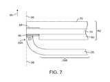
- housing 26may be formed directly under the edge of the display module layers. This type of arrangement is shown in FIG. 7 .
- display module 82may have an upper layer formed from color filter 70 .
- Color filter layer 70may be formed from glass or other suitable material and includes a pattern of colored pixel-sized filters.
- a band of opaque material such as ink 88may be formed on the underside of the periphery of color filter layer 70 . Ink 88 may hide inactive portions of display module 82 and other structures such as housing 26 from view through the upper surface of display module.
- An elastomeric member such as gasket 66may be used to provide an interface between housing 26 and the underside of thin-film transistor substrate layer 76 .
- Gasket 66may help prevent glass structures and other structures in display module 82 from being scratched by housing 26 (e.g., when housing 26 is formed from aluminum or other hard materials). If desired, gasket 66 may be omitted or gaskets of other shapes may be used.
- Light-guide structure 80may be located under thin-film transistor layer 76 .
- Structure 80may contain light guides for directing light through the display, diffuser layers for diffusing light, etc.
- Polarizer layersmay be incorporated into display module 82 above cover glass layer 70 and below thin-film transistor layer 76 .
- housing 26may have housing walls that form a substantially planar rear portion with a substantially planar exterior rear surface. In the example of FIG. 7 , this is shown by planar rear portion 26 B. Portions of the housing sidewalls may also protrude vertically upward (in the orientation of FIG. 7 ). For example, at least some of housing wall portions 26 A around the periphery of housing 26 may extend vertically upward in direction 99 . At the uppermost portion of peripheral housing walls 26 A, housing wall 26 A may be provided with a flat horizontal upper surface 101 that supports the overhanging lower surface of color filter layer 70 and/or thin-film transistor substrate layer 76 (with optional intervening gasket 66 ).
- the display modulemay have the appearance of being borderless. This configuration also allows the active region of the display to be extended close to the outer edge of housing 26 .
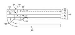
- Electronic devicemay contain electrical components such as integrated circuits, antennas, and cameras, etc. Traces may be formed on the underside of thin-film transistor layer 76 (i.e., the opposite surface of layer 76 from the surface on which the thin-film transistors are formed). These traces may be used to help route signals to and from the electrical components. Openings may also be formed in the layers of display module 82 to accommodate components. For example, a vertical hole may be formed through color filter layer 70 and thin-film transistor layer 76 . This hole may be used to receive light for a camera or to accommodate other electronic components such as a status light indicator (i.e., a status light-emitting diode), a speaker, a microphone, a button, or other suitable electrical component.
- a status light indicatori.e., a status light-emitting diode
- FIG. 8is a cross-sectional side view of a display module that incorporates features such as these.
- display module 82may have color filter glass 70 and thin-film transistor glass layer 76 .
- Upper polarizer 68may be located above color filter glass 70 .
- Lower polarizer 78may be located below thin-film transistor glass layer 76 .
- a cylindrical hole or other suitable opening such as opening 100may be formed through color filter glass 70 and thin-film transistor glass layer 76 . This hole may be used to accommodate electrical component 102 .
- Electronic component 102may be a camera, a proximity sensor, an ambient light sensor, an antenna, a microphone, a speaker, a digital data port, an audio jack or other analog port, a button, a touch sensor, etc. Arrangements in which component 102 is a camera are sometimes described herein as an example.
- Opaque layer 88may be formed by printing black ink or other suitable opaque material on a plastic layer such as layer 86 that is attached to the upper surface of polarizer 68 and color filter 70 (as an example). Opaque layer 88 may be formed in a border around the periphery of display module 82 (i.e., along the outermost edge of housing 26 ). To prevent interference with camera 102 (or other electronic component 102 ), it may be desirable omit black ink in the region above opening 100 .
- the illustrative display module configuration of FIG. 8is mounted in housing 26 so that the outermost peripheral edges of housing 26 (e.g., edge 103 ) and the outermost edges of filter layer 70 and thin-film transistor layer 76 (e.g., edges 105 ) are laterally aligned (i.e., outermost edges 103 of housing 26 and the outermost edges 105 of display module 82 are horizontally aligned with the same vertical axis—axis 98 —in the cross-sectional view of FIG. 8 ).
- the outermost peripheral edges of housing 26e.g., edge 103
- the outermost edges of filter layer 70 and thin-film transistor layer 76e.g., edges 105
- this edge alignmentcan be maintained around the entire periphery of display module 82 , providing device 10 with a borderless appearance (i.e., with no visible border-shaped housing structures surrounding the display).
- other configurationssuch as the configuration of FIG. 5 may be used (e.g., configurations in which housing 26 has vertical sidewalls within which module 82 is mounted to create a visible housing border that surrounds module 82 on all four of its outer edges).
- Camera 102contains a digital sensor that generates image data.
- a flex circuit cable or other data pathmay be used to covey camera data from camera 102 to storage and processing circuitry in device 10 .
- the upper surface of thin-film transistor layer 76contains an array of thin-film transistors and associated conductive traces. As shown in the cross-sectional view of FIG. 8 , the lower surface of thin-film transistor layer 76 may be provided with traces 104 .
- Flex circuit cable 106may have contact pads that are electrically connected to camera 102 at end 108 and contact pads that are electrically connected to traces 104 at end 110 . Using this type of arrangement, camera data can be conveyed using traces 104 . This may help reduce or eliminate the need for additional cables in device 10 .
- Camera 102is merely an example of an electrical component for which signals may be routed through underside traces on thin-film transistor substrate 76 .
- any electrical component that produces or receives electrical signals in device 10can be electrically connected to traces 104 .
- the use of traces 104 on layer 76can reduce the number of cables used to route signals between these electrical components and processing circuitry in device 10 (i.e., circuits on a main logic board and other storage and processing circuitry in device 10 ).
- an antennamay be formed from some of the traces 104 on layer 76 .
- Antenna 112may be, for example, an antenna for a local wireless network or a cellular telephone.
- Traces 104may be formed from any suitable conductor. In typical configurations for display module 82 , backlighting is provided by structures 80 . It is therefore typically desirable to form traces 104 from transparent conductive materials such as indium-tin oxide. This is, however, merely one illustrative material that may be used for traces 104 . In general, any suitable conductor may be used. Moreover, it is not necessary to form traces 104 on the underside of thin-film transistor substrate layer 76 . Traces 104 may be formed on other glass layers in module 82 .
- signal paths for camera signals, antenna signals, or other electrical component signalscan be formed from indium-tin oxide patterns on the surface of a cover glass layer, a color filter layer (e.g., layer 70 ), a glass layer in structures 80 , or other suitable display module layers.
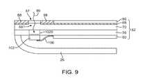
- ink border 88may be provided with opening 87 and polarizer 68 may be provided with opening 681 .
- Thisallows light to pass to and from the lower layers of display module 82 , without forming holes in thin-film transistor substrate layer 76 and color filter glass layer 70 . Even though no hole is formed in layers 70 and 76 (in the FIG. 9 example), light for electronic component 102 may still pass through openings 87 and 681 and may pass through the clear portions of layers 70 and 76 under openings 87 and 681 .
- Electronic component 102may be a camera, sensor, or other suitable electronic component.
- Component 102may receive light along path 89 .
- Component 102may be mounted to the underside of thin-film-transistor layer or, as indicated by dashed line 1020 , may be mounted to the underside of color filter glass layer 70 .
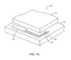
- FIG. 10shows how an electrical component 102 (e.g., a camera, sensor, antenna, button, or any other suitable component) may be mounted to the upper surface of thin-film transistor substrate layer 76 outside of the active area of display module 82 .
- the active area of display module 82may be aligned with color filter 70 or may have an area that is somewhat smaller than the surface area of color filter 70 (i.e., in alignment with the thin-film transistor array on thin-film transistor substrate 76 ).
- conductive traces 94may also be formed outside of the active area to route signals to and from electrical component 102 .
- electrical component 102has been mounted to an upper surface of color filter glass layer 70 .
- Conductive traces 94 that lie outside of the active area of display module 82may be used to convey signals to and from electrical component 102 .
- Conductive traces 94may be formed on the upper surface of color filter glass layer 70 (e.g., under a polymer coating layer or other protective layer) or may be formed on the lower surface of color filter glass layer 70 or the upper surface layer of thin-film transistor substrate layer 76 .
- Vias 95may be formed through color filter glass layer 70 to interconnect component 102 and conductive traces that have been formed lower in the display module stack. Vias may also be formed through other glass layers such as thin-film transistor substrate layer 76 (e.g., to use traces on the lower surface of the thin-film transistor substrate layer to route signals in module 82 ).
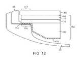
- FIG. 12is a cross-sectional side view of a portion of a display module showing how layers of glass such as cover glass layer 360 , color filter glass 70 , and thin-film transistor substrate layer 76 may each have peripheral edge portions 117 that rest on housing wall ledge portion 116 of housing 26 .
- Module 82may be provided with a chassis such as metal chassis member 420 .
- a laterally extending edge portion of member 420may also rest on ledge 116 below cover glass 360 , color filter 70 , and thin-film transistor substrate 76 .
- Adhesive 114may be used to secure these layers to housing 26 .
- FIG. 13shows an arrangement of the type shown in FIG. 12 in which elastomeric trim 66 (sometimes referred to as a gasket) has extending portion 660 .
- Extending portion 660covers portion 26 AA of housing 26 and all of the exposed upper surfaces of housing 26 (i.e., all of surfaces 263 , 265 , and 267 , including the portions of surface 263 that are adjacent to peripheral outer edge 269 of housing 26 ). Because all upper surface portions of housing 26 are covered (either with cover glass or trim), the arrangement of FIG. 13 helps improve the cosmetic appearance of device 10 when viewed from direction 661 .
Landscapes
- Engineering & Computer Science (AREA)
- Theoretical Computer Science (AREA)
- Computer Hardware Design (AREA)
- General Engineering & Computer Science (AREA)
- Human Computer Interaction (AREA)
- Physics & Mathematics (AREA)
- General Physics & Mathematics (AREA)
- Microelectronics & Electronic Packaging (AREA)
- Devices For Indicating Variable Information By Combining Individual Elements (AREA)
- Liquid Crystal (AREA)
Abstract
Description
This application is a continuation of U.S. patent application Ser. No. 14/520,079, filed Oct. 21, 2014, which is a continuation of U.S. patent application Ser. No. 13/786,344, filed Mar. 5, 2013, now U.S. Pat. No. 8,866,989, which is a continuation of U.S. patent application Pat. Ser. No. 13/249,174, filed Sep. 29, 2011, now U.S. Pat. No. 8,395,722, which is a continuation of U.S. patent application Ser. No. 12/483,206, filed Jun. 11, 2009, now U.S. Pat. No. 8,456,586, each of which is hereby incorporated by reference herein in its entirety.
This invention relates to electronic devices and, more particularly, to display structures for electronic devices such as portable computers.
Portable computers typically have upper and lower housing portions that are connected by a hinge. The lower housing portion contains components such as printed circuit boards, disk drives, a keyboard, and a battery. The upper housing portion contains a display. When the computer is in an open configuration, the upper housing portion is vertical and the display is visible to the user of the portable computer. When the computer is closed, the upper housing lies flat against the lower housing. This protects the display and keyboard and allows the portable computer to be transported.
Portable computer displays typically contain fragile structures such as layers of glass and can be challenging to mount properly within the upper housing. If care is not taken, the display and the surrounding portions of the upper housing will be bulky and unsightly. At the same time, the elimination of certain structures in the display may result in display that is overly fragile. This could lead to damage to the display during normal use.
It would therefore be desirable to be able to provide improved display structures in electronic devices such as portable computers.
An electronic device such as a portable computer may have a housing. The housing may have upper and lower portions that are connected by a hinge. A display module may be mounted in a portion of the housing such as the upper housing portion.
The upper housing may have a planar rear surface and portions that extend upwards to form peripheral housing sidewalls. The housing sidewalls may extend around the display module to form a border or the display module may be mounted so that the outermost edges of the display module are aligned with the outermost edges of the peripheral housing sidewalls.
The display module may have a color filter glass layer and a thin-film transistor substrate layer. A layer of light-guide structures may be mounted under the thin-film transistor substrate layer. The peripheral edges of the color glass layer and the thin-film transistor substrate layer may extend laterally past the peripheral edges of the light guide structures to form an overhanging structure. The overhanging structure may rest on the peripheral housing edges without any intervening display module chassis members.
An opening may be provided through the color filter and thin-film transistor substrate layers. A camera may receive light through the opening. Other electronic components may also be mounted within the housing of the electronic device such as ambient light sensors, proximity sensors, other sensors, indicator lights such a light-emitting diodes, input-output ports, buttons, microphones and speakers, antennas, etc. These electrical components can be electrically connected to traces formed on the underside of the thin-film transistor substrate layer or traces formed on other glass surfaces.
To block unsightly portions of the device from view around the periphery of the display module, the display module may be provided with an opaque border. The opaque border may be formed from a peripheral ring of black ink. The black ink may be formed on a glass layer such as the color filter glass. A polymer film that includes a black ink may also be used in forming the opaque border.
If desired, the display module may contain no cover glass layers. In this type of configuration, the outermost glass layer in the display module may be formed from the color filter glass. The polymer film layer and other layers such as polarizing layers may be formed on top of the color filter glass layer.
The display module may contain integrated circuits such as display driver circuits. A display driver circuit may be mounted on the thin-film transistor substrate. A support structure such as a glass member with a recess to accommodate the drive circuit may be placed over the driver circuit. The support structure may support coating layers such as the polymer film layer with the opaque border.
Further features of the invention, its nature and various advantages will be more apparent from the accompanying drawings and the following detailed description of the preferred embodiments.
An illustrative electronic device such as a portable computer in which display structures may be provided is shown inFIG. 1 . As shown inFIG. 1 ,portable computer 10 may have housing12.Housing 12, which is sometimes referred to as a case, may be formed from one or more individual structures. For example,housing 12 may have a main structural support member that is formed from a solid block of machined aluminum or other suitable metal. One or more additional structures may be connected to thehousing 12. These structures may include, for example, internal frame members, external coverings such as sheets of metal, etc.Housing 12 and its associated components may, in general, be formed from any suitable materials such as plastic, ceramics, metal, glass, etc. An advantage of forminghousing 12 at least partly from metal is that metal is durable and attractive in appearance. Metals such as aluminum may be anodized to form an insulating oxide coating.
A display such asdisplay 14 may be mounted withinupper housing portion 26.Display 14 may be, for example, a liquid crystal display (LCD), organic light emitting diode (OLED) display, or plasma display (as examples).Display 14 may contain a number of layers of material. These layers may include, for example, layers of optically transparent glass. Layers of plastic and optical adhesive may also be incorporated intodisplay 14. In a liquid crystal display, layers of polarizer, light diffusing elements and light guides for backlight structures, a liquid crystal layer, and a thin-film transistor array that drives the image pixels in the display may be incorporated into the display. The collection of material layers and associated support structures that are used to formdisplay 14 are sometimes referred to as a module.Display 14 may therefore sometimes be referred to as a display module.
A cross-sectional side view of a conventional liquid crystal display (LCD) display module is shown inFIG. 2 . As shown inFIG. 2 ,display module 32 may havedisplay structures 46 such as an upper polarizer layer, a color filter, a thin-film transistor glass layer, a lower polarizer, and a layer of light-guide structures such as light guides and diffuser layers.Display module 32 may also have a plastic chassis member such asplastic chassis member 44 and a metal chassis member such asmetal chassis member 42 into which the layers of glass and other display module structures may be mounted.Cover glass 36 may be placed on top ofstructures 46.
Another cross-sectional view of a conventional liquid crystal display module is shown inFIG. 3 . As shown inFIG. 3 ,display module 32 may have polarizers such asupper polarizer layer 50 andlower polarizer 62.Light guide structure 64 may provide backlight formodule 32. The light fromstructure 64 passes through the display pixels ofmodule 32 and exits displaymodule 32 in direction31.
Colorfilter glass layer 52,liquid crystal layer 54, and thin-film transistor (TFT) glass layer58 are interposed between polarizer layers50 and62.
The polarization of individual pixels of liquid crystal material inliquid crystal layer 54 interacts with the polarizing effects oflayers filter glass layer 52 contains an array of colored filters that providedisplay 32 with the ability to represent different colors. The polarization of liquid crystal material inliquid crystal layer 54 is controlled electrically by thin-film transistor array 56. Thin-film transistors inarray 56 are formed on the upper surface of thin-film transistor (TFT) glass layer58.
Thin-film transistors 56 are controlled by drivers contained in driver circuit60.Color filter layer 52 is horizontally (laterally) recessed with respect to TFT layer58 to form a ledge on which driver circuit60 is mounted. In a typical display module, there may be a number of driver chips such as circuit60 that are mounted around the periphery of the display. Conductive traces on the upper surface of TFT layer58 interconnect driver circuit60 with thin-film transistors 56.
In conventional arrangements of the type shown inFIG. 3 ,black ink 48 is placed on the underside ofcover glass 36 around the periphery of the display. This creates an opaque region that blocks inactive peripheral portions ofdisplay module 32 from view.Black ink 48 can also hide mounting structures such asscrew 40 ofFIG. 2 from view.Display glass 36 may help provide structural support to the display housing of the portable computer in whichdisplay module 32 is mounted, but the presence ofglass 36 can add a non-negligible amount of extra thickness and weight to a display.
As shown inFIG. 4 ,display module 82 may have anupper polarizer layer 68 and alower polarizer layer 78. Lightguide structure layer 80 may provide backlight formodule 82. Light-guide structure layer 80 may include light guide structures and diffuser layers. These structures may help route light from a light-emitting diode light source or other backlight source through the layers ofmodule 82 indirection 75.
Thin-film transistorsubstrate glass layer 76 may contain thin-film transistors inarray 73. Colorfilter glass layer 70 may contain an array of optical filters of different colors to providedisplay module 82 with the ability to display color images.Color filter layer 70 may be formed from glass into which dye of different colors has been impregnated, from a glass layer coated with a pattern of colored dye, from a glass or plastic layer that is covered with a pattern of thin colored filter structures (e.g., filters formed from polymer or glass containing dye), or any other suitable color filter structures.Liquid crystal layer 72 may be controlled by the electric fields produced by the thin-film transistors ofarray 73.
As shown inFIG. 4 , the layer of cover glass that is present in conventional display modules is not present indisplay module 82 anddevice 10. Rather,color filter layer 70 serves as the uppermost glass layer inmodule 82 anddevice 10. To ensure thatmodule 82 is sufficiently robust,color filter layer 70 may be thickened or may be stiffened using support structures on the underside ofdisplay module 82.Color filter layer 70 may be formed of a durable clear layer (e.g., a strong glass or plastic) that resists damage from contact. Anti-scratch coatings may also be provided on the surface of color filter layer70 (e.g., as part ofpolarizer layer 68 or above polarizer layer68).
To hide the peripheral portions ofdisplay module 82 that lie along the outer edges ofdisplay housing 26 from view, an opaque material such asblack ink layer 74 may be incorporated around the periphery ofdisplay module 82 to form a black border.Opaque layer 74 may be formed on the underside ofcolor filter layer 70 or on the upper surface of thin-film transistor glass layer76 (as examples).
With the arrangement ofFIG. 4 ,color filter layer 70 and thin-film transistor layer 76 have been extended outwardly (in the leftward direction in the orientation ofFIG. 4 ) so as to form an overhangingportion 84 that is supported by the matching ledge inhousing 26. If desired, onlycolor filter layer 70 may be extended in this way (e.g., so that the overhanging portion oflayer 70 rests on the ledge formed by housing26). In this type of arrangement, the thin-film transistor layer may extend only as far as light-guide structures 80 ofFIG. 4 . If desired, portions ofgasket 66 may be interposed betweenmodule 82 andhousing 26 inregion 84.
If desired,black ink layer 74 may be formed above colorfilter glass layer 70. As shown inFIG. 5 , for example, a layer of material such aslayer 86 may be provided on the upper surface of colorfilter glass layer 70.Layer 86 may, for example, be a layer of plastic such as polyester.Ink layer 88 may be printed on the underside ofplastic layer 86 inregion 90. Whenplastic layer 86 is attached to the surface ofdisplay module 82, the ink inregion 90 will block unsightly internal components inhousing 26 andmodule 82 from view by a user. Layers inmodule 82 may be interconnected using fastening mechanisms and adhesive (e.g., optically clear adhesive such as epoxy).
Integrated circuits such as display driver circuits may be incorporated intodisplay module 82 to drive display signals into thin-film transistor array73 (FIG. 4 ). If desired, circuits such as these or other circuits may be mounted on the upper surface of thin-filmtransistor substrate layer 76 under a support member. This type of configuration is shown inFIG. 6 . As shown inFIG. 6 ,circuit 600 may be mounted undersupport 92.Support 92 may have a recessed portion that accommodates the thickness ofcircuit 600.Circuit 600 may be a display driver circuit or other suitable electrical component fordevice 10.
With arrangements of the type shown inFIG. 6 ,support 92 has about the same thickness as colorfilter glass layer 70 and straddlescircuit 600. This allowssupport structure 92 to supportlayer 86 inperipheral region 96.Support 92 may be formed from glass, plastic, metal, or other suitable materials. If desired, colorfilter glass layer 70 may be provided with a recess on its underside that accommodatescircuit 600. In this situation, a separate support structure need not be used.
Conductive traces, thin-film transistors, andother circuitry 94 may be formed on the upper surface of thin-film transistor substrate 76. Whencircuit 600 is mounted onsubstrate 76, the traces on the surface ofsubstrate layer 76 may convey signals (e.g., display driver signals) to the thin-film transistors onlayer 76. Other signals may also be routed using these traces. For example, the traces onlayer 76 may be used to route radio-frequency signals, touch sensor signals, signals associated with status indicator lights or other output devices, proximity sensor signals, etc.
If desired,housing 26 may be formed directly under the edge of the display module layers. This type of arrangement is shown inFIG. 7 . As shown inFIG. 7 ,display module 82 may have an upper layer formed fromcolor filter 70.Color filter layer 70 may be formed from glass or other suitable material and includes a pattern of colored pixel-sized filters. A band of opaque material such asink 88 may be formed on the underside of the periphery ofcolor filter layer 70.Ink 88 may hide inactive portions ofdisplay module 82 and other structures such ashousing 26 from view through the upper surface of display module.
An elastomeric member such asgasket 66 may be used to provide an interface betweenhousing 26 and the underside of thin-filmtransistor substrate layer 76.Gasket 66 may help prevent glass structures and other structures indisplay module 82 from being scratched by housing26 (e.g., whenhousing 26 is formed from aluminum or other hard materials). If desired,gasket 66 may be omitted or gaskets of other shapes may be used.
Light-guide structure 80 may be located under thin-film transistor layer 76.Structure 80 may contain light guides for directing light through the display, diffuser layers for diffusing light, etc. Polarizer layers may be incorporated intodisplay module 82 abovecover glass layer 70 and below thin-film transistor layer 76.
With arrangements of the type shown inFIG. 7 ,housing 26 may have housing walls that form a substantially planar rear portion with a substantially planar exterior rear surface. In the example ofFIG. 7 , this is shown by planarrear portion 26B. Portions of the housing sidewalls may also protrude vertically upward (in the orientation ofFIG. 7 ). For example, at least some ofhousing wall portions 26A around the periphery ofhousing 26 may extend vertically upward indirection 99. At the uppermost portion ofperipheral housing walls 26A,housing wall 26A may be provided with a flat horizontalupper surface 101 that supports the overhanging lower surface ofcolor filter layer 70 and/or thin-film transistor substrate layer76 (with optional intervening gasket66). Because the outermost edge of display module82 (i.e., the leftmost edges oflayers 70 and76) are laterally (horizontally) aligned with the outermost edge portions ofhousing walls 26A alongvertical axis 98, the display module may have the appearance of being borderless. This configuration also allows the active region of the display to be extended close to the outer edge ofhousing 26.
Electronic device may contain electrical components such as integrated circuits, antennas, and cameras, etc. Traces may be formed on the underside of thin-film transistor layer76 (i.e., the opposite surface oflayer 76 from the surface on which the thin-film transistors are formed). These traces may be used to help route signals to and from the electrical components. Openings may also be formed in the layers ofdisplay module 82 to accommodate components. For example, a vertical hole may be formed throughcolor filter layer 70 and thin-film transistor layer 76. This hole may be used to receive light for a camera or to accommodate other electronic components such as a status light indicator (i.e., a status light-emitting diode), a speaker, a microphone, a button, or other suitable electrical component.
As with the example ofFIG. 7 , the illustrative display module configuration ofFIG. 8 is mounted inhousing 26 so that the outermost peripheral edges of housing26 (e.g., edge103) and the outermost edges offilter layer 70 and thin-film transistor layer76 (e.g., edges105) are laterally aligned (i.e.,outermost edges 103 ofhousing 26 and theoutermost edges 105 ofdisplay module 82 are horizontally aligned with the same vertical axis—axis 98—in the cross-sectional view ofFIG. 8 ). As with theFIG. 7 arrangement, this edge alignment can be maintained around the entire periphery ofdisplay module 82, providingdevice 10 with a borderless appearance (i.e., with no visible border-shaped housing structures surrounding the display). If desired, other configurations such as the configuration ofFIG. 5 may be used (e.g., configurations in whichhousing 26 has vertical sidewalls within whichmodule 82 is mounted to create a visible housing border that surroundsmodule 82 on all four of its outer edges).
As shown by dashedline 112, an antenna may be formed from some of thetraces 104 onlayer 76.Antenna 112 may be, for example, an antenna for a local wireless network or a cellular telephone.
As shown in the cross-sectional view ofFIG. 9 ,ink border 88 may be provided withopening 87 andpolarizer 68 may be provided withopening 681. This allows light to pass to and from the lower layers ofdisplay module 82, without forming holes in thin-filmtransistor substrate layer 76 and colorfilter glass layer 70. Even though no hole is formed inlayers 70 and76 (in theFIG. 9 example), light forelectronic component 102 may still pass throughopenings layers openings Electronic component 102 may be a camera, sensor, or other suitable electronic component.Component 102 may receive light alongpath 89.Component 102 may be mounted to the underside of thin-film-transistor layer or, as indicated by dashedline 1020, may be mounted to the underside of colorfilter glass layer 70.
The perspective view ofFIG. 10 shows how an electrical component102 (e.g., a camera, sensor, antenna, button, or any other suitable component) may be mounted to the upper surface of thin-filmtransistor substrate layer 76 outside of the active area ofdisplay module 82. The active area ofdisplay module 82 may be aligned withcolor filter 70 or may have an area that is somewhat smaller than the surface area of color filter70 (i.e., in alignment with the thin-film transistor array on thin-film transistor substrate76). As shown inFIG. 10 , conductive traces94 may also be formed outside of the active area to route signals to and fromelectrical component 102.
In the illustrative arrangement ofFIG. 11 ,electrical component 102 has been mounted to an upper surface of colorfilter glass layer 70. Conductive traces94 that lie outside of the active area ofdisplay module 82 may be used to convey signals to and fromelectrical component 102. Conductive traces94 may be formed on the upper surface of color filter glass layer70 (e.g., under a polymer coating layer or other protective layer) or may be formed on the lower surface of colorfilter glass layer 70 or the upper surface layer of thin-filmtransistor substrate layer 76.Vias 95 may be formed through colorfilter glass layer 70 to interconnectcomponent 102 and conductive traces that have been formed lower in the display module stack. Vias may also be formed through other glass layers such as thin-film transistor substrate layer76 (e.g., to use traces on the lower surface of the thin-film transistor substrate layer to route signals in module82).
The foregoing is merely illustrative of the principles of this invention and various modifications can be made by those skilled in the art without departing from the scope and spirit of the invention.
Claims (20)
1. An electronic device comprising:
a display having an active area and an inactive area, the display comprising:
a thin-film transistor layer;
a polarizer that overlaps the active area and the inactive area, wherein the polarizer has an opening in the inactive area;
an opaque border in the inactive area, wherein the opaque border has an opening in the inactive area; and
a cover layer that overlaps the thin-film transistor layer and the polarizer and that overlaps the active area and the inactive area, wherein the opaque border is coupled to the cover layer; and
a light-sensing component overlapped by the cover layer in the inactive area, wherein the light-sensing component receives light through the opening in the polarizer and the opening in the opaque border.
2. The electronic device defined inclaim 1 , wherein the light-sensing component is a camera.
3. The electronic device defined inclaim 1 , wherein the light-sensing component is an ambient light sensor.
4. The electronic device defined inclaim 1 , wherein the light-sensing component is a proximity sensor.
5. The electronic device defined inclaim 1 , wherein the display is an organic light-emitting diode display.
6. The electronic device defined inclaim 1 , wherein the thin-film transistor layer overlaps the opening in the polarizer, and wherein the light-sensing component receives light through the thin-film transistor layer.
7. An electronic device comprising:
a display comprising:
a polarizer layer having an opening;
a thin-film transistor layer that overlaps the opening in the polarizer layer; and
a layer that overlaps the thin-film transistor layer and the polarizer layer; and
a light-sensing component that receives light through the layer, the thin-film transistor layer, and the opening in the polarizer layer.
8. The electronic device defined inclaim 7 , wherein the display is an organic light-emitting diode display.
9. The electronic device defined inclaim 8 , wherein the organic light-emitting diode display has an active area and an inactive area, and wherein the polarizer layer overlaps the active area and the inactive area.
10. The electronic device defined inclaim 9 , wherein the light-sensing component is mounted in the inactive area and wherein the opening in the polarizer layer is formed in the inactive area.
11. The electronic device defined inclaim 10 further comprising:
an opaque border in the inactive area, wherein the opaque border has an opening that is aligned with the opening in the polarizer layer.
12. The electronic device defined inclaim 11 , wherein the light-sensing component is a camera.
13. The electronic device defined inclaim 11 , wherein the light-sensing component is an ambient light sensor.
14. An electronic device comprising:
an organic light-emitting diode display comprising:
a thin-film transistor layer;
a polarizer having an opening;
an opaque border having an opening that is aligned with the opening in the polarizer; and
a transparent layer that overlies the thin-film transistor layer, the polarizer, and the opaque border; and
a light-sensing component that receives light through the opening in the polarizer and through the transparent layer.
15. The electronic device defined inclaim 14 , wherein the opening in the polarizer does not extend into the thin-film transistor layer, and wherein the light-sensing component receives light through the thin-film transistor layer and through the opening in the opaque border.
16. The electronic device defined inclaim 15 , wherein the organic light-emitting diode display has an active area and an inactive area, and wherein the light-sensing component is mounted in the inactive area.
17. The electronic device defined inclaim 16 , wherein the polarizer and the opaque border overlap the inactive area.
18. The electronic device defined inclaim 17 , further comprising:
a housing in which the organic light-emitting diode display and the light-sensing component are mounted.
19. The electronic device defined inclaim 18 , wherein the light-sensing component is a camera.
20. The electronic device defined inclaim 18 , wherein the light-sensing component is an ambient light sensor.
Priority Applications (4)
| Application Number | Priority Date | Filing Date | Title |
|---|---|---|---|
| US15/782,458US10353432B2 (en) | 2009-06-11 | 2017-10-12 | Portable computer display structures |
| US16/437,830US11003213B2 (en) | 2009-06-11 | 2019-06-11 | Portable computer display structures |
| US17/221,533US11740658B2 (en) | 2009-06-11 | 2021-04-02 | Portable computer display structures |
| US18/349,682US12189424B2 (en) | 2009-06-11 | 2023-07-10 | Portable computer display structures |
Applications Claiming Priority (5)
| Application Number | Priority Date | Filing Date | Title |
|---|---|---|---|
| US12/483,206US8456586B2 (en) | 2009-06-11 | 2009-06-11 | Portable computer display structures |
| US13/249,174US8395722B2 (en) | 2009-06-11 | 2011-09-29 | Portable computer display structures |
| US13/786,344US8866989B2 (en) | 2009-06-11 | 2013-03-05 | Portable computer display structures |
| US14/520,079US20150138710A1 (en) | 2009-06-11 | 2014-10-21 | Portable Computer Display Structures |
| US15/782,458US10353432B2 (en) | 2009-06-11 | 2017-10-12 | Portable computer display structures |
Related Parent Applications (1)
| Application Number | Title | Priority Date | Filing Date |
|---|---|---|---|
| US14/520,079ContinuationUS20150138710A1 (en) | 2009-06-11 | 2014-10-21 | Portable Computer Display Structures |
Related Child Applications (1)
| Application Number | Title | Priority Date | Filing Date |
|---|---|---|---|
| US16/437,830ContinuationUS11003213B2 (en) | 2009-06-11 | 2019-06-11 | Portable computer display structures |
Publications (2)
| Publication Number | Publication Date |
|---|---|
| US20180032105A1 US20180032105A1 (en) | 2018-02-01 |
| US10353432B2true US10353432B2 (en) | 2019-07-16 |
Family
ID=43306147
Family Applications (9)
| Application Number | Title | Priority Date | Filing Date |
|---|---|---|---|
| US12/483,206Active2030-05-30US8456586B2 (en) | 2009-06-11 | 2009-06-11 | Portable computer display structures |
| US13/249,174ActiveUS8395722B2 (en) | 2009-06-11 | 2011-09-29 | Portable computer display structures |
| US13/249,653ActiveUS8711304B2 (en) | 2009-06-11 | 2011-09-30 | Portable computer display structures |
| US13/786,344ActiveUS8866989B2 (en) | 2009-06-11 | 2013-03-05 | Portable computer display structures |
| US14/520,079AbandonedUS20150138710A1 (en) | 2009-06-11 | 2014-10-21 | Portable Computer Display Structures |
| US15/782,458Active2029-07-15US10353432B2 (en) | 2009-06-11 | 2017-10-12 | Portable computer display structures |
| US16/437,830ActiveUS11003213B2 (en) | 2009-06-11 | 2019-06-11 | Portable computer display structures |
| US17/221,533Active2029-07-31US11740658B2 (en) | 2009-06-11 | 2021-04-02 | Portable computer display structures |
| US18/349,682ActiveUS12189424B2 (en) | 2009-06-11 | 2023-07-10 | Portable computer display structures |
Family Applications Before (5)
| Application Number | Title | Priority Date | Filing Date |
|---|---|---|---|
| US12/483,206Active2030-05-30US8456586B2 (en) | 2009-06-11 | 2009-06-11 | Portable computer display structures |
| US13/249,174ActiveUS8395722B2 (en) | 2009-06-11 | 2011-09-29 | Portable computer display structures |
| US13/249,653ActiveUS8711304B2 (en) | 2009-06-11 | 2011-09-30 | Portable computer display structures |
| US13/786,344ActiveUS8866989B2 (en) | 2009-06-11 | 2013-03-05 | Portable computer display structures |
| US14/520,079AbandonedUS20150138710A1 (en) | 2009-06-11 | 2014-10-21 | Portable Computer Display Structures |
Family Applications After (3)
| Application Number | Title | Priority Date | Filing Date |
|---|---|---|---|
| US16/437,830ActiveUS11003213B2 (en) | 2009-06-11 | 2019-06-11 | Portable computer display structures |
| US17/221,533Active2029-07-31US11740658B2 (en) | 2009-06-11 | 2021-04-02 | Portable computer display structures |
| US18/349,682ActiveUS12189424B2 (en) | 2009-06-11 | 2023-07-10 | Portable computer display structures |
Country Status (1)
| Country | Link |
|---|---|
| US (9) | US8456586B2 (en) |
Cited By (6)
| Publication number | Priority date | Publication date | Assignee | Title |
|---|---|---|---|---|
| US11822193B2 (en) | 2021-07-07 | 2023-11-21 | Dell Products L.P. | Edge-to-edge display with a sensor region |
| US20240118135A1 (en)* | 2022-10-07 | 2024-04-11 | Dell Products L.P. | Infrared alignment marker for display assembly |
| US20240155794A1 (en)* | 2022-11-04 | 2024-05-09 | Zhijun Zhao | Screen protection assembly and electronic device |
| US12032235B2 (en) | 2020-07-24 | 2024-07-09 | Dell Products L.P. | Information handling system edge-to-edge display |
| US12032406B2 (en) | 2021-07-07 | 2024-07-09 | Dell Products L.P. | Edge-to-edge display module |
| US12038641B2 (en) | 2021-07-07 | 2024-07-16 | Dell Products L.P. | Edge-to-edge display with a sensor region |
Families Citing this family (251)
| Publication number | Priority date | Publication date | Assignee | Title |
|---|---|---|---|---|
| GB0428204D0 (en)* | 2004-12-23 | 2005-01-26 | Clinical Designs Ltd | Medicament container |
| US12185512B2 (en) | 2007-11-16 | 2024-12-31 | Manufacturing Resources International, Inc. | Electronic display assembly with thermal management |
| US8654302B2 (en) | 2008-03-03 | 2014-02-18 | Manufacturing Resources International, Inc. | Heat exchanger for an electronic display |
| US8673163B2 (en) | 2008-06-27 | 2014-03-18 | Apple Inc. | Method for fabricating thin sheets of glass |
| US7810355B2 (en) | 2008-06-30 | 2010-10-12 | Apple Inc. | Full perimeter chemical strengthening of substrates |
| US8023261B2 (en) | 2008-09-05 | 2011-09-20 | Apple Inc. | Electronic device assembly |
| CN102388003B (en) | 2009-03-02 | 2014-11-19 | 苹果公司 | Technology for Strengthening Glass Covers for Portable Electronic Devices |
| GB0904040D0 (en) | 2009-03-10 | 2009-04-22 | Euro Celtique Sa | Counter |
| GB0904059D0 (en) | 2009-03-10 | 2009-04-22 | Euro Celtique Sa | Counter |
| KR101549258B1 (en)* | 2009-03-11 | 2015-09-01 | 엘지전자 주식회사 | Display device |
| KR101549257B1 (en)* | 2009-03-11 | 2015-09-01 | 엘지전자 주식회사 | Display device |
| KR101549256B1 (en)* | 2009-03-11 | 2015-09-01 | 엘지전자 주식회사 | Display device |
| KR101579309B1 (en)* | 2009-03-31 | 2016-01-04 | 엘지전자 주식회사 | Display apparatus |
| KR20100112409A (en)* | 2009-04-09 | 2010-10-19 | 엘지전자 주식회사 | Display apparatus |
| WO2010117115A1 (en)* | 2009-04-09 | 2010-10-14 | Lg Electronics Inc. | Display apparatus |
| WO2010117114A1 (en)* | 2009-04-09 | 2010-10-14 | Lg Electronics Inc. | Display apparatus |
| US8456586B2 (en) | 2009-06-11 | 2013-06-04 | Apple Inc. | Portable computer display structures |
| US8549882B2 (en)* | 2009-09-30 | 2013-10-08 | Apple Inc. | Pre-processing techniques to produce complex edges using a glass slumping process |
| US8233109B2 (en) | 2009-10-16 | 2012-07-31 | Apple Inc. | Portable computer display housing |
| US8408780B2 (en) | 2009-11-03 | 2013-04-02 | Apple Inc. | Portable computer housing with integral display |
| US8743309B2 (en)* | 2009-11-10 | 2014-06-03 | Apple Inc. | Methods for fabricating display structures |
| US9778685B2 (en)* | 2011-05-04 | 2017-10-03 | Apple Inc. | Housing for portable electronic device with reduced border region |
| AU2016201026B2 (en)* | 2010-01-06 | 2017-06-29 | Apple Inc. | Housing for portable electronic device with reduced border region |
| KR101662135B1 (en)* | 2010-01-15 | 2016-10-05 | 삼성디스플레이 주식회사 | Electrophoretic display panel, method of manufacturing the same and electrophoretic display apparatus having the same |
| US8797721B2 (en) | 2010-02-02 | 2014-08-05 | Apple Inc. | Portable electronic device housing with outer glass surfaces |
| TWI505137B (en)* | 2010-02-12 | 2015-10-21 | Compal Electronics Inc | Input device |
| US10632740B2 (en) | 2010-04-23 | 2020-04-28 | Landa Corporation Ltd. | Digital printing process |
| KR101327743B1 (en)* | 2010-04-27 | 2013-11-11 | 엘지디스플레이 주식회사 | Display apparatus |
| TWI462067B (en)* | 2010-04-27 | 2014-11-21 | Lg Display Co Ltd | Display apparatus |
| US9207528B2 (en) | 2010-06-04 | 2015-12-08 | Apple Inc. | Thin sheet glass processing |
| US9213451B2 (en) | 2010-06-04 | 2015-12-15 | Apple Inc. | Thin glass for touch panel sensors and methods therefor |
| WO2012002019A1 (en)* | 2010-06-29 | 2012-01-05 | シャープ株式会社 | Display device |
| TWI389067B (en)* | 2010-06-29 | 2013-03-11 | Compal Electronics Inc | Display module and assembly method thereof |
| US8923693B2 (en) | 2010-07-30 | 2014-12-30 | Apple Inc. | Electronic device having selectively strengthened cover glass |
| US10189743B2 (en)* | 2010-08-18 | 2019-01-29 | Apple Inc. | Enhanced strengthening of glass |
| US8873028B2 (en) | 2010-08-26 | 2014-10-28 | Apple Inc. | Non-destructive stress profile determination in chemically tempered glass |
| US8611077B2 (en)* | 2010-08-27 | 2013-12-17 | Apple Inc. | Electronic devices with component mounting structures |
| US8824140B2 (en) | 2010-09-17 | 2014-09-02 | Apple Inc. | Glass enclosure |
| US9143668B2 (en)* | 2010-10-29 | 2015-09-22 | Apple Inc. | Camera lens structures and display structures for electronic devices |
| US8467177B2 (en)* | 2010-10-29 | 2013-06-18 | Apple Inc. | Displays with polarizer windows and opaque masking layers for electronic devices |
| US9235240B2 (en)* | 2010-11-11 | 2016-01-12 | Apple Inc. | Insert molding around glass members for portable electronic devices |
| TW201228390A (en)* | 2010-12-20 | 2012-07-01 | Compal Electronics Inc | Display device |
| DE102011089443B4 (en)* | 2011-02-14 | 2016-12-01 | Lg Display Co., Ltd. | display device |
| US9725359B2 (en) | 2011-03-16 | 2017-08-08 | Apple Inc. | Electronic device having selectively strengthened glass |
| US10781135B2 (en) | 2011-03-16 | 2020-09-22 | Apple Inc. | Strengthening variable thickness glass |
| CN102654660A (en)* | 2012-04-25 | 2012-09-05 | 京东方科技集团股份有限公司 | Display device |
| KR101383207B1 (en) | 2011-05-02 | 2014-04-10 | 엘지디스플레이 주식회사 | Display apparatus |
| US9128666B2 (en) | 2011-05-04 | 2015-09-08 | Apple Inc. | Housing for portable electronic device with reduced border region |
| JP5892736B2 (en)* | 2011-05-24 | 2016-03-23 | ソニー株式会社 | Display device |
| JP2013008016A (en) | 2011-05-24 | 2013-01-10 | Sony Corp | Display unit |
| EP2527910B1 (en)* | 2011-05-24 | 2017-08-09 | Sony Corporation | Display |
| KR101813459B1 (en)* | 2011-06-24 | 2018-01-02 | 엘지디스플레이 주식회사 | Display apparatus |
| US10061356B2 (en) | 2011-06-30 | 2018-08-28 | Samsung Display Co., Ltd. | Flexible display panel and display apparatus including the flexible display panel |
| US8970446B2 (en) | 2011-07-01 | 2015-03-03 | Apple Inc. | Electronic device with magnetic antenna mounting |
| TW201311101A (en)* | 2011-08-22 | 2013-03-01 | Wistron Corp | Portable electronic module with back cover changing function |
| TWI442876B (en)* | 2011-09-01 | 2014-06-21 | Acer Inc | Display device |
| KR101800669B1 (en)* | 2011-09-07 | 2017-12-20 | 엘지디스플레이 주식회사 | Liquid crystal display devece |
| US9944554B2 (en) | 2011-09-15 | 2018-04-17 | Apple Inc. | Perforated mother sheet for partial edge chemical strengthening and method therefor |
| KR101930298B1 (en)* | 2011-09-22 | 2018-12-18 | 엘지디스플레이 주식회사 | Stereoscopic image display apparatus |
| US9182935B2 (en)* | 2011-09-27 | 2015-11-10 | Z124 | Secondary single screen mode activation through menu option |
| KR101835549B1 (en)* | 2011-09-29 | 2018-03-08 | 엘지디스플레이 주식회사 | Display appatatus |
| US9516149B2 (en) | 2011-09-29 | 2016-12-06 | Apple Inc. | Multi-layer transparent structures for electronic device housings |
| KR101841714B1 (en)* | 2011-10-05 | 2018-03-26 | 엘지디스플레이 주식회사 | Display apparatus, method and apparatus for manufacturing the same |
| US10261370B2 (en) | 2011-10-05 | 2019-04-16 | Apple Inc. | Displays with minimized border regions having an apertured TFT layer for signal conductors |
| US9588264B2 (en) | 2011-10-12 | 2017-03-07 | Corning Incorporated | Bezel-concealing display covers and display devices |
| JP5231670B1 (en)* | 2011-10-20 | 2013-07-10 | 株式会社フジクラ | Decorative film for display device and protective panel |
| US9477263B2 (en)* | 2011-10-27 | 2016-10-25 | Apple Inc. | Electronic device with chip-on-glass ambient light sensors |
| US9286826B2 (en) | 2011-10-28 | 2016-03-15 | Apple Inc. | Display with vias for concealed printed circuit and component attachment |
| US20130120106A1 (en) | 2011-11-16 | 2013-05-16 | Motorola Mobility, Inc. | Display device, corresponding systems, and methods therefor |
| US10144669B2 (en) | 2011-11-21 | 2018-12-04 | Apple Inc. | Self-optimizing chemical strengthening bath for glass |
| US9864403B2 (en) | 2011-12-02 | 2018-01-09 | Apple Inc. | Electronic devices with structural glass members |
| KR101945890B1 (en) | 2011-12-30 | 2019-02-12 | 삼성전자주식회사 | Display device |
| KR101945948B1 (en) | 2011-12-30 | 2019-02-12 | 삼성전자주식회사 | Display device |
| EP2611146A1 (en)* | 2011-12-30 | 2013-07-03 | Samsung Electronics Co., Ltd | Display apparatus with camera |
| US10133156B2 (en) | 2012-01-10 | 2018-11-20 | Apple Inc. | Fused opaque and clear glass for camera or display window |
| US8684613B2 (en) | 2012-01-10 | 2014-04-01 | Apple Inc. | Integrated camera window |
| US20130185898A1 (en)* | 2012-01-23 | 2013-07-25 | Ting-Hung SU | Hinge structure for assembly of a display module |
| US8773848B2 (en) | 2012-01-25 | 2014-07-08 | Apple Inc. | Fused glass device housings |
| TWI528133B (en)* | 2012-02-13 | 2016-04-01 | 達運精密工業股份有限公司 | Display device with frame configuration |
| US8712233B2 (en)* | 2012-02-24 | 2014-04-29 | Apple Inc. | Electronic device assemblies |
| US9201452B2 (en)* | 2012-02-28 | 2015-12-01 | Apple Inc. | Electronic device with illuminated logo structures |
| US10642198B2 (en) | 2012-03-05 | 2020-05-05 | Landa Corporation Ltd. | Intermediate transfer members for use with indirect printing systems and protonatable intermediate transfer members for use with indirect printing systems |
| JP6220354B2 (en) | 2012-03-05 | 2017-10-25 | ランダ コーポレイション リミテッド | Control apparatus and method for digital printing system |
| JP6437312B2 (en) | 2012-03-05 | 2018-12-12 | ランダ コーポレイション リミテッド | Digital printing process |
| GB2513816B (en) | 2012-03-05 | 2018-11-14 | Landa Corporation Ltd | Digital printing system |
| US9498946B2 (en) | 2012-03-05 | 2016-11-22 | Landa Corporation Ltd. | Apparatus and method for control or monitoring of a printing system |
| US9902147B2 (en) | 2012-03-05 | 2018-02-27 | Landa Corporation Ltd. | Digital printing system |
| US9643403B2 (en) | 2012-03-05 | 2017-05-09 | Landa Corporation Ltd. | Printing system |
| WO2013132420A1 (en) | 2012-03-05 | 2013-09-12 | Landa Corporation Limited | Printing system |
| CN104220539B (en) | 2012-03-05 | 2016-06-01 | 兰达公司 | Ink film structure |
| US10434761B2 (en) | 2012-03-05 | 2019-10-08 | Landa Corporation Ltd. | Digital printing process |
| HK1204640A1 (en) | 2012-03-05 | 2015-11-27 | Landa Corporation Ltd. | Ink film constructions |
| JP5928020B2 (en)* | 2012-03-13 | 2016-06-01 | ソニー株式会社 | Display device |
| EP2825486B1 (en) | 2012-03-15 | 2019-01-02 | Landa Corporation Ltd. | Endless flexible belt for a printing system |
| KR101406129B1 (en)* | 2012-03-28 | 2014-06-13 | 엘지디스플레이 주식회사 | Display apparatus |
| KR101937276B1 (en)* | 2012-04-17 | 2019-04-09 | 엘지디스플레이 주식회사 | Display Device and Method of manufacturing the same |
| KR101953591B1 (en)* | 2012-04-17 | 2019-03-04 | 엘지디스플레이 주식회사 | Display Device and Method of manufacturing the same |
| US9894781B2 (en)* | 2012-06-06 | 2018-02-13 | Apple Inc. | Notched display layers |
| US9274359B2 (en) | 2012-06-20 | 2016-03-01 | Apple Inc. | Electronic device display chassis |
| US8947866B2 (en)* | 2012-06-21 | 2015-02-03 | Corning Incorporated | Edge armored display cover plate |
| US9226347B2 (en) | 2012-06-25 | 2015-12-29 | Apple Inc. | Displays with vias |
| KR20140002102A (en)* | 2012-06-26 | 2014-01-08 | 삼성디스플레이 주식회사 | Display device |
| KR101969319B1 (en)* | 2012-06-29 | 2019-04-16 | 엘지디스플레이 주식회사 | Display device having transparent bezel border |
| US20140015764A1 (en)* | 2012-07-13 | 2014-01-16 | Nokia Corporation | Display |
| US9214507B2 (en) | 2012-08-17 | 2015-12-15 | Apple Inc. | Narrow border organic light-emitting diode display |
| US9664955B2 (en)* | 2012-08-28 | 2017-05-30 | Apple Inc. | Method to design the integrated full coverage LCD module cover glass |
| KR102006775B1 (en)* | 2012-08-30 | 2019-08-02 | 엘지디스플레이 주식회사 | Liquid crystal panel and liquid crystal display device using the same |
| US9454025B2 (en) | 2012-08-31 | 2016-09-27 | Apple Inc. | Displays with reduced driver circuit ledges |
| US9477262B2 (en)* | 2012-09-10 | 2016-10-25 | Google Inc. | Moveable display portion of a computing device including a clutch mechanism |
| US20140080411A1 (en)* | 2012-09-14 | 2014-03-20 | Anand S. Konanur | Integration of a near field communication coil antenna behind a screen display for near field coupling |
| KR101966256B1 (en)* | 2012-09-14 | 2019-04-05 | 삼성전자주식회사 | Assembling structure of housing for portable terminal |
| US9946302B2 (en) | 2012-09-19 | 2018-04-17 | Apple Inc. | Exposed glass article with inner recessed area for portable electronic device housing |
| US20140118288A1 (en)* | 2012-10-29 | 2014-05-01 | Lenovo (Singapore) Pte, Ltd | Mechanical structure for system using flush surface display design |
| US9075199B2 (en)* | 2012-10-30 | 2015-07-07 | Apple Inc. | Displays with polarizer layers for electronic devices |
| CN103021278B (en)* | 2012-12-07 | 2015-08-19 | 京东方科技集团股份有限公司 | A kind of display panel and display device |
| EP2762992B1 (en)* | 2013-02-01 | 2018-06-13 | LG Electronics Inc. | Display device including camera module |
| US9806219B2 (en)* | 2013-02-14 | 2017-10-31 | Apple Inc. | Displays with camera window openings |
| US9622365B2 (en) | 2013-02-25 | 2017-04-11 | Google Technology Holdings LLC | Apparatus and methods for accommodating a display in an electronic device |
| US9736956B2 (en) | 2013-03-12 | 2017-08-15 | Samsung Electronics Co., Ltd. | Electronic device having display module |
| US9674922B2 (en) | 2013-03-14 | 2017-06-06 | Google Technology Holdings LLC | Display side edge assembly and mobile device including same |
| KR102060825B1 (en)* | 2013-05-03 | 2019-12-30 | 엘지전자 주식회사 | Display apparatus |
| KR102151774B1 (en)* | 2013-05-03 | 2020-09-03 | 동우 화인켐 주식회사 | Fabricating method for touch screen panel |
| US9871898B2 (en) | 2013-05-08 | 2018-01-16 | Apple Inc. | Ceramic cover for electronic device housing |
| US8994042B2 (en) | 2013-05-20 | 2015-03-31 | Lg Electronics Inc. | Display panel and display device |
| US9459661B2 (en) | 2013-06-19 | 2016-10-04 | Apple Inc. | Camouflaged openings in electronic device housings |
| US20150029112A1 (en)* | 2013-07-26 | 2015-01-29 | Nxp B.V. | Touch sensor |
| GB201401173D0 (en) | 2013-09-11 | 2014-03-12 | Landa Corp Ltd | Ink formulations and film constructions thereof |
| CN103576782A (en)* | 2013-10-30 | 2014-02-12 | 昆山市大久电子有限公司 | Computer monitor capable of accommodating small objects |
| US20150153776A1 (en)* | 2013-12-02 | 2015-06-04 | Uniproo Inc. | Screen protection device for protecting display screen of electronic apparatus |
| US9523226B1 (en) | 2013-12-12 | 2016-12-20 | Google Inc. | 360 degree bi-stable dual pivot hinge |
| KR101730330B1 (en) | 2013-12-16 | 2017-04-27 | 엘지디스플레이 주식회사 | Display apparatus |
| US9484001B2 (en) | 2013-12-23 | 2016-11-01 | Google Technology Holdings LLC | Portable electronic device controlling diffuse light source to emit light approximating color of object of user interest |
| KR102204756B1 (en)* | 2013-12-31 | 2021-01-19 | 삼성디스플레이 주식회사 | Display device and manufacturing method of the same |
| US9674957B2 (en) | 2014-02-04 | 2017-06-06 | Samsung Display Co., Ltd. | Display device and method of manufacturing the same |
| US9886062B2 (en) | 2014-02-28 | 2018-02-06 | Apple Inc. | Exposed glass article with enhanced stiffness for portable electronic device housing |
| US9411365B1 (en) | 2014-03-26 | 2016-08-09 | Google Inc. | 360 degree dual pivot variable torque hinge mechanism |
| KR102267708B1 (en)* | 2014-04-04 | 2021-06-23 | 삼성디스플레이 주식회사 | Display device |
| US9261918B2 (en)* | 2014-04-28 | 2016-02-16 | Dell Products L.P. | Information handling system hinge support frame |
| JP5775622B2 (en)* | 2014-05-12 | 2015-09-09 | レノボ・シンガポール・プライベート・リミテッド | Electronic apparatus and method provided with liquid crystal shutter |
| KR102135935B1 (en)* | 2014-07-01 | 2020-07-21 | 엘지디스플레이 주식회사 | Display Device With Narrow Bezel |
| TWI563318B (en) | 2014-07-29 | 2016-12-21 | Young Lighting Technology Inc | Display |
| CN104199206B (en)* | 2014-08-19 | 2017-10-27 | 京东方光科技有限公司 | A kind of display device and its assembly method |
| US9977467B2 (en)* | 2014-08-19 | 2018-05-22 | Apple Inc. | Electronic device with an enclosure stiffener |
| CN104464534B (en)* | 2014-12-10 | 2017-09-05 | 深圳市华星光电技术有限公司 | Display module and display device with the display module |
| KR20160085037A (en)* | 2015-01-07 | 2016-07-15 | 삼성디스플레이 주식회사 | Display device |
| EP3065043A1 (en)* | 2015-03-02 | 2016-09-07 | Nxp B.V. | Mobile device |
| GB2536489B (en) | 2015-03-20 | 2018-08-29 | Landa Corporation Ltd | Indirect printing system |
| GB2537813A (en) | 2015-04-14 | 2016-11-02 | Landa Corp Ltd | Apparatus for threading an intermediate transfer member of a printing system |
| US10170711B2 (en) | 2015-05-05 | 2019-01-01 | Apple Inc. | Display with vias to access driver circuitry |
| CN107710113B (en)* | 2015-05-11 | 2020-12-01 | 华为技术有限公司 | Touch system, active matrix light emitting diode panel and display driving method |
| CN114911090A (en)* | 2015-06-09 | 2022-08-16 | 小米科技有限责任公司 | LCD Modules and Mobile Devices |
| KR102524754B1 (en) | 2015-09-09 | 2023-04-21 | 엘지디스플레이 주식회사 | Display device |
| CN115793783A (en) | 2015-09-28 | 2023-03-14 | 苹果公司 | Electronic device display with extended active area |
| CN106773280A (en) | 2015-11-19 | 2017-05-31 | 扬升照明股份有限公司 | Display device and backlight module |
| US10108222B2 (en)* | 2015-12-04 | 2018-10-23 | Apple Inc. | Electronic device displays with holes to accommodate components |
| KR102501111B1 (en) | 2015-12-28 | 2023-02-16 | 엘지디스플레이 주식회사 | Camera module integrated liquid display device and manufacturing method thereof |
| GB201602877D0 (en) | 2016-02-18 | 2016-04-06 | Landa Corp Ltd | System and method for generating videos |
| US9740240B1 (en) | 2016-03-21 | 2017-08-22 | Google Inc. | Base with rotating mount that increases friction of rotation when portable computing device is placed onto mount |
| WO2017164680A1 (en)* | 2016-03-24 | 2017-09-28 | 삼성전자주식회사 | Electronic device having display |
| KR20170113066A (en)* | 2016-03-24 | 2017-10-12 | 삼성전자주식회사 | Electronic device with display and method for displaying image thereof |
| US10933661B2 (en) | 2016-05-30 | 2021-03-02 | Landa Corporation Ltd. | Digital printing process |
| GB201609463D0 (en) | 2016-05-30 | 2016-07-13 | Landa Labs 2012 Ltd | Method of manufacturing a multi-layer article |
| US9735185B1 (en) | 2016-06-10 | 2017-08-15 | Essential Products, Inc. | Hollowed electronic display |
| US10925160B1 (en)* | 2016-06-28 | 2021-02-16 | Amazon Technologies, Inc. | Electronic device with a display assembly and silicon circuit board substrate |
| US10714425B2 (en)* | 2016-09-13 | 2020-07-14 | Apple Inc. | Flexible system integration to improve thermal properties |
| US10624219B2 (en)* | 2016-10-31 | 2020-04-14 | Michael Sisson | Interactive cabinetry door for use with a cabinet base |
| KR20180058091A (en)* | 2016-11-23 | 2018-05-31 | 엘지디스플레이 주식회사 | Liquid crystal display |
| CN106657485B (en)* | 2017-03-07 | 2020-05-12 | Oppo广东移动通信有限公司 | mobile terminal |
| CN106936954B (en) | 2017-03-07 | 2020-05-12 | Oppo广东移动通信有限公司 | Mobile terminal |
| KR102167928B1 (en) | 2017-03-14 | 2020-10-20 | 엘지전자 주식회사 | Mobile terminal |
| SG11201909937XA (en) | 2017-04-25 | 2019-11-28 | Huawei Tech Co Ltd | Lcd display, electronic device, lcd display manufacturing method |
| CN107229148B (en)* | 2017-05-05 | 2021-03-09 | Oppo广东移动通信有限公司 | Display screen, display device and mobile terminal |
| US10388213B2 (en)* | 2017-05-22 | 2019-08-20 | Microsoft Technology Licensing, Llc | Display and display integration method |
| CN107300798A (en)* | 2017-06-30 | 2017-10-27 | 联想(北京)有限公司 | The method of integrated camera, liquid crystal module and electronic equipment in liquid crystal module |
| US10476136B2 (en)* | 2017-07-20 | 2019-11-12 | Apple Inc. | Electronic device with speaker port aligned antennas |
| US10542628B2 (en)* | 2017-08-02 | 2020-01-21 | Apple Inc. | Enclosure for an electronic device having a shell and internal chassis |
| US11049445B2 (en)* | 2017-08-02 | 2021-06-29 | Apple Inc. | Electronic devices with narrow display borders |
| KR102511474B1 (en)* | 2017-09-13 | 2023-03-17 | 삼성디스플레이 주식회사 | display device |
| US10461744B2 (en)* | 2017-09-21 | 2019-10-29 | Google Llc | Proximity sensor connection mechanism |
| US10926532B2 (en) | 2017-10-19 | 2021-02-23 | Landa Corporation Ltd. | Endless flexible belt for a printing system |
| US11267239B2 (en) | 2017-11-19 | 2022-03-08 | Landa Corporation Ltd. | Digital printing system |
| US11511536B2 (en) | 2017-11-27 | 2022-11-29 | Landa Corporation Ltd. | Calibration of runout error in a digital printing system |
| US11707943B2 (en) | 2017-12-06 | 2023-07-25 | Landa Corporation Ltd. | Method and apparatus for digital printing |
| WO2019111223A1 (en) | 2017-12-07 | 2019-06-13 | Landa Corporation Ltd. | Digital printing process and method |
| CN109991696B (en) | 2017-12-29 | 2020-10-09 | 中强光电股份有限公司 | monitor |
| US11089697B2 (en)* | 2018-01-24 | 2021-08-10 | Kyocera Corporation | Display device |
| KR102520016B1 (en) | 2018-02-02 | 2023-04-11 | 삼성디스플레이 주식회사 | Display panel and electronic device having the same |
| CN108196388B (en)* | 2018-02-12 | 2022-04-19 | 京东方科技集团股份有限公司 | Display device and manufacturing method thereof |
| TWI659253B (en)* | 2018-02-13 | 2019-05-11 | 友達光電股份有限公司 | Display device |
| KR102135867B1 (en)* | 2018-03-02 | 2020-07-20 | 주식회사 토비스 | A Edge-emitting type display device and game device having the same |
| CN111937370B (en)* | 2018-06-26 | 2022-01-11 | Oppo广东移动通信有限公司 | Screen assembly and electronic equipment |
| CN117885446A (en) | 2018-06-26 | 2024-04-16 | 兰达公司 | Intermediate transmission components of digital printing systems |
| EP3825988B1 (en)* | 2018-07-20 | 2024-10-16 | Panasonic Intellectual Property Management Co., Ltd. | Image display device |
| US10602626B2 (en) | 2018-07-30 | 2020-03-24 | Manufacturing Resources International, Inc. | Housing assembly for an integrated display unit |
| US10994528B1 (en) | 2018-08-02 | 2021-05-04 | Landa Corporation Ltd. | Digital printing system with flexible intermediate transfer member |
| JP2020024288A (en)* | 2018-08-07 | 2020-02-13 | シャープ株式会社 | Display device |
| JP2020025191A (en)* | 2018-08-07 | 2020-02-13 | シャープ株式会社 | Display device and electronic equipment |
| KR102556019B1 (en) | 2018-08-08 | 2023-07-17 | 삼성디스플레이 주식회사 | Display apparatus and electronic apparatus comprising the same |
| CN109001933A (en)* | 2018-08-10 | 2018-12-14 | 厦门天马微电子有限公司 | A kind of display panel, its production method and display device |
| US12001902B2 (en) | 2018-08-13 | 2024-06-04 | Landa Corporation Ltd. | Correcting distortions in digital printing by implanting dummy pixels in a digital image |
| CN109120753B (en)* | 2018-08-21 | 2021-01-26 | 武汉天马微电子有限公司 | A display panel and display device |
| KR102465374B1 (en) | 2018-09-12 | 2022-11-10 | 삼성디스플레이 주식회사 | Display panel and display device including thereof |
| CN109116636B (en)* | 2018-09-25 | 2021-08-24 | 厦门天马微电子有限公司 | Display panel and display device |
| WO2020075012A1 (en) | 2018-10-08 | 2020-04-16 | Landa Corporation Ltd. | Friction reduction means for printing systems and method |
| CN109324440A (en)* | 2018-11-28 | 2019-02-12 | 武汉华星光电技术有限公司 | A kind of liquid crystal display panel |
| CN109491140B (en)* | 2018-11-30 | 2021-06-08 | 海信视像科技股份有限公司 | Display device |
| US20200192542A1 (en)* | 2018-12-12 | 2020-06-18 | Novatek Microelectronics Corp. | Display device with integrated antenna and method thereof |
| KR102680693B1 (en)* | 2018-12-18 | 2024-07-01 | 엘지디스플레이 주식회사 | Display device |
| CN116080260A (en) | 2018-12-24 | 2023-05-09 | 兰达公司 | Digital printing system and method |
| US11096317B2 (en) | 2019-02-26 | 2021-08-17 | Manufacturing Resources International, Inc. | Display assembly with loopback cooling |
| KR102812392B1 (en)* | 2019-03-28 | 2025-05-26 | 삼성디스플레이 주식회사 | Display panel and device including the same |
| US12358277B2 (en) | 2019-03-31 | 2025-07-15 | Landa Corporation Ltd. | Systems and methods for preventing or minimizing printing defects in printing processes |
| US10795413B1 (en) | 2019-04-03 | 2020-10-06 | Manufacturing Resources International, Inc. | Electronic display assembly with a channel for ambient air in an access panel |
| US11031443B2 (en)* | 2019-04-15 | 2021-06-08 | Wuhan China Star Optoelectronics Semiconductor Display Technology Co., Ltd. | Organic light-emitting diode (OLED) display device including sensor disposed in groove of base substrate |
| KR102679883B1 (en) | 2019-04-30 | 2024-07-01 | 삼성전자 주식회사 | Electronic device having waterproof structure for electronic component |
| KR102657027B1 (en) | 2019-05-02 | 2024-04-15 | 삼성전자주식회사 | Electronic device including camera module |
| CN110244483A (en)* | 2019-06-17 | 2019-09-17 | 武汉华星光电技术有限公司 | Array substrate and liquid crystal display panel |
| CN110441958A (en)* | 2019-07-05 | 2019-11-12 | 武汉华星光电技术有限公司 | A kind of display surface template die group |
| CN110471499A (en)* | 2019-07-24 | 2019-11-19 | 武汉华星光电半导体显示技术有限公司 | Display module and display device |
| CN110580084B (en)* | 2019-08-06 | 2021-10-15 | 华为技术有限公司 | a mobile terminal |
| EP4012470A4 (en)* | 2019-08-16 | 2022-11-02 | Ningbo Sunny Opotech Co., Ltd. | Under-screen camera assembly, camera module, optical lens, and manufacturing methods |
| KR102755151B1 (en)* | 2019-08-27 | 2025-01-20 | 삼성디스플레이 주식회사 | Protective window and display device including the same |
| US11269374B2 (en)* | 2019-09-11 | 2022-03-08 | Apple Inc. | Electronic device with a cover assembly having an adhesion layer |
| US11294430B1 (en) | 2019-09-13 | 2022-04-05 | Facebook Technologies, Llc | Media device including display and power-delivery mechanism with integrated stand |
| US11212930B2 (en)* | 2019-09-13 | 2021-12-28 | Facebook Technologies, Llc | Media device including display and power-delivery mechanism with integrated stand |
| CN110764651B (en)* | 2019-10-25 | 2022-05-13 | 业成科技(成都)有限公司 | Display device |
| KR20220091496A (en)* | 2019-11-12 | 2022-06-30 | 소니 세미컨덕터 솔루션즈 가부시키가이샤 | Electronics |
| KR20210060715A (en)* | 2019-11-18 | 2021-05-27 | 삼성디스플레이 주식회사 | Display apparatus and method of manufacturing the same |
| JP7685995B2 (en) | 2019-11-25 | 2025-05-30 | ランダ コーポレイション リミテッド | Drying of ink in digital printing using infrared radiation absorbed by particles embedded within an ITM |
| US11637919B2 (en) | 2019-12-03 | 2023-04-25 | Apple Inc. | Handheld electronic device |
| US11838432B2 (en) | 2019-12-03 | 2023-12-05 | Apple Inc. | Handheld electronic device |
| US11321028B2 (en) | 2019-12-11 | 2022-05-03 | Landa Corporation Ltd. | Correcting registration errors in digital printing |
| JP7657229B2 (en) | 2019-12-29 | 2025-04-04 | ランダ コーポレイション リミテッド | Printing method and system |
| CN111509011A (en)* | 2020-04-26 | 2020-08-07 | 武汉华星光电半导体显示技术有限公司 | Display device and method of making the same |
| JP2022030431A (en)* | 2020-08-07 | 2022-02-18 | レノボ・シンガポール・プライベート・リミテッド | Electronic device |
| CN114267683B (en)* | 2020-09-15 | 2025-07-25 | 京东方科技集团股份有限公司 | Display backboard, preparation method thereof and display device |
| US11778757B2 (en) | 2020-10-23 | 2023-10-03 | Manufacturing Resources International, Inc. | Display assemblies incorporating electric vehicle charging equipment |
| US11775031B2 (en)* | 2021-01-04 | 2023-10-03 | Apple Inc. | Electronic device display |
| EP4264377A4 (en) | 2021-02-02 | 2024-11-13 | Landa Corporation Ltd. | REDUCING DISTORTIONS IN PRINTED IMAGES |
| US12003657B2 (en) | 2021-03-02 | 2024-06-04 | Apple Inc. | Handheld electronic device |
| EP4063944A1 (en)* | 2021-03-22 | 2022-09-28 | Sony Group Corporation | Device for a liquid crystal display and liquid crystal display |
| US11966263B2 (en) | 2021-07-28 | 2024-04-23 | Manufacturing Resources International, Inc. | Display assemblies for providing compressive forces at electronic display layers |
| US11968813B2 (en) | 2021-11-23 | 2024-04-23 | Manufacturing Resources International, Inc. | Display assembly with divided interior space |
| CN114296267B (en)* | 2021-12-22 | 2023-09-05 | 武汉华星光电技术有限公司 | A display module and a display device |
| US12267449B2 (en) | 2022-03-03 | 2025-04-01 | Apple Inc. | Handheld electronic device |
| US20240397646A1 (en)* | 2022-07-14 | 2024-11-28 | Chengdu Boe Optoelectronics Technology Co., Ltd. | Display panel, splicing screen, and display device |
| US12072561B2 (en) | 2022-07-22 | 2024-08-27 | Manufacturing Resources International, Inc. | Self-contained electronic display assembly, mounting structure and methods for the same |
| US12010813B2 (en) | 2022-07-22 | 2024-06-11 | Manufacturing Resources International, Inc. | Self-contained electronic display assembly, mounting structure and methods for the same |
| US12035486B1 (en)* | 2022-07-25 | 2024-07-09 | Manufacturing Resources International, Inc. | Electronic display assembly with fabric panel communications box |
| TWI817805B (en)* | 2022-11-02 | 2023-10-01 | 友達光電股份有限公司 | Display panel and display device |
| CN115951439A (en)* | 2023-01-03 | 2023-04-11 | 京东方科技集团股份有限公司 | Optical film, cover assembly and display device |
Citations (182)
| Publication number | Priority date | Publication date | Assignee | Title |
|---|---|---|---|---|
| US4769680A (en) | 1987-10-22 | 1988-09-06 | Mrs Technology, Inc. | Apparatus and method for making large area electronic devices, such as flat panel displays and the like, using correlated, aligned dual optical systems |
| JPH01117077A (en) | 1987-10-29 | 1989-05-09 | Fuji Electric Co Ltd | Slab type solid-state laser oscillator |
| US5032007A (en) | 1988-04-07 | 1991-07-16 | Honeywell, Inc. | Apparatus and method for an electronically controlled color filter for use in information display applications |
| JPH04135275A (en) | 1990-09-27 | 1992-05-08 | Fujitsu Ltd | Pipeline control system |
| JPH05176151A (en) | 1991-03-13 | 1993-07-13 | Matsushita Electric Ind Co Ltd | Fax machine |
| JPH06245209A (en) | 1993-02-19 | 1994-09-02 | Sony Corp | Camera integrated display device |
| US5358412A (en)* | 1993-04-26 | 1994-10-25 | Eastman Kodak Company | Method and apparatus for assembling a flexible circuit to an LCD module |
| US5359206A (en)* | 1989-08-14 | 1994-10-25 | Hitachi, Ltd. | Thin film transistor substrate, liquid crystal display panel and liquid crystal display equipment |
| US5481430A (en) | 1990-04-27 | 1996-01-02 | Kabushiki Kaisha Toshiba | Portable computer having keyboard and coordinate input tablet hingedly connected to a main body case through a groove |
| US5539550A (en) | 1990-12-31 | 1996-07-23 | Kopin Corporation | Liquid crystal display having adhered circuit tiles |
| US5572343A (en) | 1992-05-26 | 1996-11-05 | Olympus Optical Co., Ltd. | Visual display having see-through function and stacked liquid crystal shutters of opposite viewing angle directions |
| JPH0915272A (en) | 1995-06-30 | 1997-01-17 | Shinko Seisakusho Co Ltd | Voltage measuring circuit |
| US5623392A (en) | 1996-06-04 | 1997-04-22 | Ma; Hsi-Kuang | LCD assembly with projection function |
| US5631753A (en)* | 1991-06-28 | 1997-05-20 | Dai Nippon Printing Co., Ltd. | Black matrix base board and manufacturing method therefor, and liquid crystal display panel and manufacturing method therefor |
| US5678483A (en) | 1994-02-16 | 1997-10-21 | Corning Incorporated | Method for printing a black border for a color filter |
| US5708561A (en) | 1996-08-13 | 1998-01-13 | Vivek R. Huilgol | Portable computer having display slidably and rotatably mounted for movement between landscape and portrait orientation and to open and close speaker ports |
| US5739800A (en) | 1996-03-04 | 1998-04-14 | Motorola | Integrated electro-optical package with LED display chip and substrate with drivers and central opening |
| US5748270A (en) | 1996-06-25 | 1998-05-05 | Ericsson, Inc. | LCD with electroluminescent backlighting |
| US5760858A (en) | 1995-04-21 | 1998-06-02 | Texas Instruments Incorporated | Field emission device panel backlight for liquid crystal displays |
| JPH10219948A (en) | 1997-02-05 | 1998-08-18 | Sekisui House Ltd | Ridge ventilation system |
| US5851411A (en) | 1996-07-09 | 1998-12-22 | Lg Electronics, Inc. | High-density liquid crystal display and method |
| US5889568A (en) | 1995-12-12 | 1999-03-30 | Rainbow Displays Inc. | Tiled flat panel displays |
| US5940153A (en)* | 1998-04-03 | 1999-08-17 | Motorola, Inc. | Display assembly having LCD and seal captured between interlocking lens cover and lightpipe |
| US5965916A (en)* | 1997-01-17 | 1999-10-12 | Industrial Technology Research Institute | Thin-film transistor structure for liquid crystal display having black matrixes connected to a gate line |
| US5988827A (en)* | 1996-07-11 | 1999-11-23 | Samsung Electronics Co., Ltd. | Display devices having rounded corner backlight unit |
| US5990986A (en) | 1997-05-30 | 1999-11-23 | Samsung Electronics Co., Ltd. | Thin film transistor substrate for a liquid crystal display having buffer layers and a manufacturing method thereof |
| US6104461A (en)* | 1997-09-19 | 2000-08-15 | Semiconductor Energy Laboratory Co., Ltd. | Liquid crystal display device for preventing short circuits and method of manufacturing the same |
| JP2000330090A (en) | 1999-05-17 | 2000-11-30 | Ind Technol Res Inst | Integrated image sensor and active matrix array of LCD and structure of semiconductor device thereof |
| US6177214B1 (en)* | 1997-05-30 | 2001-01-23 | Canon Kabushiki Kaisha | Color filter manufacturing method, color filter, display apparatus, and apparatus having the display apparatus |
| US20010000676A1 (en) | 1997-10-20 | 2001-05-03 | Hongyong Zhang | Integral-type liquid crystal panel with image sensor function |
| US6278504B1 (en) | 1996-01-25 | 2001-08-21 | Lg. Philips Lcd Co., Ltd. | Thin film transistor for liquid crystal display device having a semiconductor layer's width smaller than a width of the gate, drain and source electrodes |
| US20010019130A1 (en) | 1998-05-15 | 2001-09-06 | Semiconductor Energy Laboratory Co., Ltd. | Semiconductor device |
| US6335773B1 (en) | 1997-12-22 | 2002-01-01 | Hitachi Ltd | Liquid crystal display device in which the light length, polarizing axis, and alignment direction are related |
| US20020008838A1 (en)* | 2000-07-19 | 2002-01-24 | Nec Corporation | Apparatus and method of manufacturing liquid crystal display |
| US20020051112A1 (en)* | 2000-11-02 | 2002-05-02 | Hideki Katsura | Liquid crystal display device, and method of manufacturing the same |
| US20020063253A1 (en) | 1998-10-01 | 2002-05-30 | Hong Mun-Pyo | Method for manufacturing thin film transistor array panel for liquid crystal display |
| US6483719B1 (en) | 2000-03-21 | 2002-11-19 | Spraylat Corporation | Conforming shielded form for electronic component assemblies |
| US6525786B1 (en) | 1999-11-19 | 2003-02-25 | Nec Corporation | Transverse electric liquid crystal display device |
| US6532152B1 (en)* | 1998-11-16 | 2003-03-11 | Intermec Ip Corp. | Ruggedized hand held computer |
| US6570757B2 (en) | 1999-11-12 | 2003-05-27 | Apple Computer, Inc. | Computer housing for a portable computer |
| US20030133070A1 (en)* | 2001-12-29 | 2003-07-17 | Lg.Philips Lcd Co., Ltd. | Liquid crystal panel, liquid crystal display device using the same and method of fabricating the same |
| US20030161093A1 (en) | 1999-05-14 | 2003-08-28 | Lawrence Lam | Display housing for computing device |
| KR20040017693A (en) | 2002-08-23 | 2004-02-27 | 삼성전자주식회사 | Liquid crystal display module |
| US20040095526A1 (en) | 2001-11-27 | 2004-05-20 | Koji Yamabuchi | Liquid crystal panel, method and device for manufacturing liquid crystal panel, and polarizing plate stamping device |
| US6776497B1 (en) | 2002-11-19 | 2004-08-17 | Apple Computer, Inc. | Apparatuses and methods for illuminating a keyboard |
| US20040212555A1 (en) | 2003-04-23 | 2004-10-28 | Falco Mark A. | Portable electronic device with integrated display and camera and method therefore |
| US20040263670A1 (en) | 2003-06-18 | 2004-12-30 | Ryo Yamasaki | Display device with image sensing device |
| US20050018121A1 (en)* | 2003-07-23 | 2005-01-27 | Tean-Sen Jen | Liquid crystal display panel with reduced flicker |
| US20050041166A1 (en)* | 2000-03-13 | 2005-02-24 | Semiconductor Energy Laboratory Co., Ltd. | Semiconductor device and a method of manufacturing the same |
| US20050052737A1 (en)* | 2003-09-09 | 2005-03-10 | Hiroyuki Amemiya | Optical sheet and process for producing the same |
| US20050078252A1 (en) | 2003-07-22 | 2005-04-14 | Lih-Nian Lin | Thin film transistor liquid crystal display |
| US6919678B2 (en) | 2002-09-03 | 2005-07-19 | Bloomberg Lp | Bezel-less electric display |
| US6940564B2 (en)* | 2001-03-23 | 2005-09-06 | Koninklijke Philips Electronics N.V. | Display substrate and display device |
| US20050195621A1 (en) | 2004-03-03 | 2005-09-08 | Che-Chih Chang | Backlight assembly |
| US20050214984A1 (en)* | 2004-03-25 | 2005-09-29 | Semiconductor Energy Laboratory Co., Ltd. | Method for manufacturing semiconductor device |
| US20050266591A1 (en)* | 2003-03-25 | 2005-12-01 | Sony Corporation | Manufacturing process for ultra slim electrooptic display device unit |
| US20050264689A1 (en)* | 2004-05-26 | 2005-12-01 | Yang Shou A | Display panel having a video camera |
| US20050285996A1 (en) | 2004-06-23 | 2005-12-29 | Sharp Kabushiki Kaisha | Liquid crystal display device and producing method thereof |
| US20060001802A1 (en) | 2004-06-24 | 2006-01-05 | Chi Mei Optoelectronics Corp. | Color filter of liquid crystal display |
| US20060033874A1 (en)* | 2004-08-10 | 2006-02-16 | Hitachi, Ltd. | Liquid crystal display mounted with IC tag and method for manufacturing the same |
| US7035090B2 (en)* | 2003-09-04 | 2006-04-25 | Kabushiki Kaisha Toshiba | Interlocking mechanism for a display |
| US20060113894A1 (en)* | 2004-11-26 | 2006-06-01 | Semiconductor Energy Laboratory Co., Ltd. | Semiconductor device, display device and method for manufacturing thereof, and television device |
| US20060125982A1 (en) | 2004-12-14 | 2006-06-15 | Shi-Ping Lin | Liquid crystal display |
| US20060138296A1 (en) | 2004-12-23 | 2006-06-29 | Deluga Ronald E | Display hold-down systems and methods |
| US20060148425A1 (en)* | 2002-09-27 | 2006-07-06 | Christopher Carlson | Illuminated interchangeable bezel assembly for a cellular telephone |
| US20060176417A1 (en)* | 2005-02-04 | 2006-08-10 | Bing-Seng Wu | Flat panel display |
| US7110059B2 (en) | 1995-05-08 | 2006-09-19 | Semiconductor Energy Laboratory Co., Ltd. | Display device |
| US20060223006A1 (en)* | 2005-03-31 | 2006-10-05 | Fuji Photo Film Co., Ltd. | Method of producing a planographic printing plate |
| US20060227232A1 (en) | 1997-09-20 | 2006-10-12 | Semiconductor Energy Laboratory Co., Ltd. | Image sensor and image sensor integrated type active matrix type display device |
| US7133104B2 (en) | 2003-02-28 | 2006-11-07 | Lg.Philips Lcd Co., Ltd. | Transflective liquid crystal display device having color filter-on-thin film transistor (COT) structure and method of fabricating the same |
| US20060279652A1 (en) | 2005-06-13 | 2006-12-14 | Shou-An Yang | Display panel with camera function |
| US20070002216A1 (en) | 2005-06-30 | 2007-01-04 | Samsung Electronics Co., Ltd. | Polarizer and liquid crystal display having the same |
| US7161185B2 (en) | 2003-06-27 | 2007-01-09 | Semiconductor Energy Laboratory Co., Ltd. | Display device and electronic device |
| US7217588B2 (en)* | 2005-01-05 | 2007-05-15 | Sharp Laboratories Of America, Inc. | Integrated MEMS packaging |
| US20070109461A1 (en) | 2005-11-16 | 2007-05-17 | Lg.Philips Lcd Co., Ltd. | Backlight assembly for liquid crystal display and liquid crystal display module using the same |
| US20070126966A1 (en) | 2004-03-31 | 2007-06-07 | Tatsumi Takahashi | Base film for liquid-crystal panel, functional film for liquid-crystal panel, manufacturing process for functional film and manufacturing apparatus for functional film |
| US7237941B2 (en) | 2004-12-10 | 2007-07-03 | Hon Hai Precision Ind. Co., Ltd. | Backlight module with urged light guide plate and liquid crystal display having same |
| US20070160815A1 (en)* | 2006-01-12 | 2007-07-12 | Fujifilm Corporation | Ink composition, inkjet recording method, printed material, process for producing lithographic printing plate, and lithographic printing plate |
| US7253869B1 (en)* | 1993-06-30 | 2007-08-07 | United States Of America As Represented By The Secretary Of The Navy | Silicon-on-sapphire display with audio transducer and method of fabricating same |
| US20070189730A1 (en) | 2006-02-08 | 2007-08-16 | Satoshi Okamura | Image-pickup apparatus, lens apparatus and image-pickup system |
| US20070188675A1 (en)* | 2006-02-08 | 2007-08-16 | Masaki Tsubokura | Display device |
| US20070197677A1 (en)* | 2006-02-23 | 2007-08-23 | Fujifilm Corporation | Sulfonium salt, curable composition, ink composition, inkjet recording method, printed material, process for producing lithographic printing plate, and lithographic printing plate |
| US20070222912A1 (en)* | 2006-03-24 | 2007-09-27 | Tsutomu Sato | Display device |
| US20070291172A1 (en)* | 2004-11-02 | 2007-12-20 | Fujitsu Ten Limited | Display Control Apparatus and Display Apparatus |
| US20080036942A1 (en) | 2006-08-11 | 2008-02-14 | Innolux Display Corp. | Backlight module and liquid crystal display device using same |
| US20080049004A1 (en)* | 2006-07-12 | 2008-02-28 | Epson Imaging Devices Corporation | Liquid crystal display device |
| KR100809277B1 (en) | 2006-07-05 | 2008-03-03 | 삼성전기주식회사 | Camera Module with Array Lens |
| US20080057604A1 (en) | 2006-08-29 | 2008-03-06 | Semiconductor Energy Laboratory Co., Ltd. | Method of fabricating display device |
| US20080079860A1 (en)* | 2006-09-27 | 2008-04-03 | Epson Imaging Devices Corporation | Liquid crystal display device |
| KR20080058911A (en) | 2006-12-22 | 2008-06-26 | 엘지디스플레이 주식회사 | Liquid crystal display device |
| US20080192171A1 (en)* | 2007-02-08 | 2008-08-14 | Hitachi Displays, Ltd. | Liquid crystal display device |
| KR100856092B1 (en) | 2007-06-18 | 2008-09-02 | 삼성전기주식회사 | Optical lens and camera module with optical lens |
| US7425749B2 (en)* | 2002-04-23 | 2008-09-16 | Sharp Laboratories Of America, Inc. | MEMS pixel sensor |
| US20080239754A1 (en) | 2007-03-27 | 2008-10-02 | Seok-Won Kang | Backlight assembly, display apparatus having the same and method for manufacturing the same |
| KR20080089908A (en) | 2007-04-03 | 2008-10-08 | 유니나 | LCD module with direct-view color light emitting frame |
| US20080261057A1 (en) | 2007-04-20 | 2008-10-23 | White Electronic Designs Corp. | Bezelless display system |
| US20080266469A1 (en)* | 2007-04-26 | 2008-10-30 | Himax Technologies Limited | Liquiid crystal on silicon (lcos) display and package thereof |
| US20080291356A1 (en) | 2007-05-25 | 2008-11-27 | Tae Seok Kim | Backlight assembly and liquid crystal display having the same |
| US20090033850A1 (en)* | 2007-08-01 | 2009-02-05 | Seiko Epson Corporation | Liquid crystal device |
| US7489291B2 (en)* | 1996-09-27 | 2009-02-10 | Semiconductor Energy Laboratory Co., Ltd. | Electrooptical device and method of fabricating the same |
| US7505436B2 (en) | 2001-06-29 | 2009-03-17 | Qualcomm Corporation | Communication system employing multiple handoff criteria |
| US20090085848A1 (en)* | 2007-09-28 | 2009-04-02 | Innocom Technology (Shenzhen) Co., Ltd. | Liquid crystal display with color sensor on substrate |
| US20090091673A1 (en)* | 2007-06-29 | 2009-04-09 | Shih-Han Chen | Display panel and dielectric apparatus with ESD protection effect |
| US7522236B2 (en) | 2005-09-23 | 2009-04-21 | Apple Inc. | Cosmetically uniform reflective border area in a transflective display |
| US7525629B2 (en) | 1993-09-20 | 2009-04-28 | Semiconductor Energy Laboratory Co., Ltd. | Liquid crystal display device comprising drive circuits that include thin film transistors formed on both substrates |
| US7528912B2 (en) | 1997-09-02 | 2009-05-05 | Semiconductor Energy Laboratory Co., Ltd. | Liquid crystal display apparatus containing image sensor and process for producing the same |
| US20090135167A1 (en)* | 2007-11-26 | 2009-05-28 | Sony Corporation | Display device and electronic apparatus |
| US20090147191A1 (en)* | 2007-03-16 | 2009-06-11 | Sony Corporation | Display apparatus |
| US20090147179A1 (en)* | 2005-10-17 | 2009-06-11 | Tomoyoshi Yamashita | Prism Sheet and Production Method thereof and Surface Light Source Device |
| US20090146967A1 (en)* | 2007-12-05 | 2009-06-11 | Sony Corporation | Display apparatus |
| US20090153762A1 (en)* | 2005-01-21 | 2009-06-18 | Semiconductor Energy Laboratory Co., Ltd. | Semiconductor device and method for manufacturing the same, and electric device |
| US20090167978A1 (en)* | 2007-12-28 | 2009-07-02 | Fujitsu Limited | Display device and electronic apparatus |
| US20090212300A1 (en)* | 2008-02-27 | 2009-08-27 | Semiconductor Energy Laboratory Co., Ltd. | Liquid crystal display device and manufacturing method thereof, and electronic device |
| US7585121B2 (en) | 2005-11-18 | 2009-09-08 | Hon Hai Precision Industry Co., Ltd. | Camera module and electronic device incorporating the same |
| US20090237602A1 (en) | 2008-03-19 | 2009-09-24 | Hitachi Displays, Ltd. | Liquid crystal display device |
| US20090244410A1 (en)* | 2005-11-30 | 2009-10-01 | Sharp Kabushiki Kaisha | Liquid crystal module, audio function-equipped liquid crystal module, mobile communication device, and mobile information processing device |
| US20090262277A1 (en)* | 2008-04-18 | 2009-10-22 | Samsung Electronics Co., Ltd. | Flat panel display and method thereof |
| US20090273550A1 (en) | 2008-04-21 | 2009-11-05 | Apple Inc. | Display Having A Transistor-Degradation Circuit |
| US20090279284A1 (en) | 2005-10-14 | 2009-11-12 | Sharp Kabushiki Kaisha | Illumination device, light source device used for the same, and liquid crystal display equipped with the illumination device |
| US20090280606A1 (en)* | 2008-05-09 | 2009-11-12 | Ching-Chieh Shih | Method for fabricating photo sensor |
| US20090286001A1 (en)* | 2005-09-30 | 2009-11-19 | Canon Kabushiki Kaisha | Active-energy radiation-polymerizable substance, active-energy radiation-curable liquid composition, active-energy radiation-curable ink, ink jet recording method, ink cartridge, recording unit, and ink jet recording apparatus |
| US7629613B2 (en) | 2004-09-09 | 2009-12-08 | Samsung Electronics Co., Ltd. | Display device and method of manufacturing the same |
| US20100001973A1 (en) | 2008-07-03 | 2010-01-07 | Apple Inc. | Display with dual-function capacitive elements |
| US20100020277A1 (en) | 2008-07-25 | 2010-01-28 | Toshiba Mobile Display Co., Ltd. | Liquid crystal display device |
| US20100026656A1 (en) | 2008-07-31 | 2010-02-04 | Apple Inc. | Capacitive sensor behind black mask |
| US7663607B2 (en) | 2004-05-06 | 2010-02-16 | Apple Inc. | Multipoint touchscreen |
| US20100039530A1 (en) | 2008-08-18 | 2010-02-18 | Apple Inc. | Apparatus and Method for Compensating for Variations in Digital Cameras |
| US20100079942A1 (en) | 2008-09-26 | 2010-04-01 | Taku Yamamoto | Video display apparatus |
| US7697092B2 (en) | 2001-02-01 | 2010-04-13 | Lg Display Co., Ltd. | Transflective liquid crystal display device having a color filter and method for fabricating thereof |
| US20100100202A1 (en) | 2008-10-20 | 2010-04-22 | Chi-Chin Chen | Method and Related Apparatus for Controlling Operating Mode of a Portable Electronic Device |
| US20100097525A1 (en)* | 2007-03-15 | 2010-04-22 | Fujitsu Ten Limited | Display device and display method |
| US7728937B2 (en) | 2004-06-17 | 2010-06-01 | Sharp Kabushiki Kaisha | Multi-domain liquid crystal with axisymmetric alignment and electrode having asymmetrical cuts at the edge |
| US7728906B2 (en) | 2006-01-04 | 2010-06-01 | Apple Inc. | Embedded camera with privacy filter |
| US20100144391A1 (en) | 2008-12-05 | 2010-06-10 | Shih Chang Chang | Integrated touch panel for a TFT display |
| US20100167443A1 (en) | 2000-08-28 | 2010-07-01 | Sharp Kabushiki Kaisha | Active matrix substrate, method of making the substrate, and display device |
| US20100165267A1 (en)* | 2007-08-31 | 2010-07-01 | Keisuke Yoshida | Liquid crystal display device and electronic device |
| US20100182273A1 (en)* | 2008-03-28 | 2010-07-22 | Sony Corporation | Display device with touch sensor |
| US20100182538A1 (en) | 2006-11-16 | 2010-07-22 | Yoshiki Takata | Liquid crystal display device and television receiver |
| US7764335B2 (en) | 2007-10-04 | 2010-07-27 | Funai Electric Co., Ltd. | Liquid crystal module |
| US20100207857A1 (en) | 2009-02-13 | 2010-08-19 | Apple Inc. | Undulating Electrodes for Improved Viewing Angle and Color Shift |
| US20100225844A1 (en) | 2005-08-05 | 2010-09-09 | Sharp Kabushiki Kaisha | Lamp holder, backlight unit, and liquid crystal display device |
| US7812920B2 (en)* | 2004-11-12 | 2010-10-12 | V Technology Co., Ltd. | Production method of substrate for liquid crystal display using image-capturing and reference position detection at corner of pixel present in TFT substrate |
| US7813042B2 (en) | 2005-09-12 | 2010-10-12 | Sharp Kabushiki Kaisha | Multiple-view directional display |
| US7821561B2 (en) | 2003-12-12 | 2010-10-26 | Canon Kabushiki Kaisha | Display apparatus with camera and communication apparatus |
| US20100273530A1 (en)* | 2009-04-23 | 2010-10-28 | Jarvis Daniel W | Portable electronic device |
| US7830370B2 (en)* | 2000-06-06 | 2010-11-09 | Semiconductor Energy Laboratory Co., Ltd. | Display device and method of manufacturing the same |
| US20100302478A1 (en) | 2009-05-28 | 2010-12-02 | Hitachi Displays, Ltd. | Liquid crystal display device |
| US20100309102A1 (en) | 2009-06-08 | 2010-12-09 | Samsung Electronics Co., Ltd. | Display apparatus and control method thereof |
| US20100315570A1 (en) | 2009-06-11 | 2010-12-16 | Mathew Dinesh C | Portable computer display structures |
| US20100315868A1 (en)* | 2006-10-24 | 2010-12-16 | Semiconductor Energy Laboratory Co., Ltd. | Semiconductor device including storage device and method for driving the same |
| US20100315769A1 (en) | 2009-06-11 | 2010-12-16 | Mathew Dinesh C | Portable computers with spring-mounted displays |
| US20100321325A1 (en) | 2009-06-17 | 2010-12-23 | Springer Gregory A | Touch and display panel antennas |
| US7859606B2 (en)* | 2004-09-15 | 2010-12-28 | Semiconductor Energy Laboratory Co. Ltd. | Semiconductor device |
| US20110001706A1 (en) | 2009-07-02 | 2011-01-06 | Emery Sanford | Electronic device touch screen display module |
| US7868957B2 (en)* | 2003-12-02 | 2011-01-11 | Semiconductor Energy Laboratory Co., Ltd. | Thin film transistor, display device and liquid crystal display device and method for manufacturing the same |
| US20110005662A1 (en) | 2009-07-10 | 2011-01-13 | Kuo-Hua Sung | Method for Fabricating Multilayer Panels |
| US7883232B2 (en) | 2005-02-28 | 2011-02-08 | Lg Display Co., Ltd. | Light-emitting diode backlight assembly and liquid crystal display device using the same |
| US7894021B2 (en) | 2002-09-05 | 2011-02-22 | Samsung Electronics Co., Ltd. | Active matrix driving display device and image displaying method using the same wherein a thin film transistor corresponding to a border area is turned off |
| US7898585B2 (en) | 2006-09-14 | 2011-03-01 | Lg Electronics Inc. | Flat display panel and method of manufacture |
| US20110051411A1 (en) | 2009-08-27 | 2011-03-03 | Kim Sungwoo | Backlight unit and display device |
| US20110063550A1 (en) | 2009-09-11 | 2011-03-17 | Gettemy Shawn R | Electronic device display structures with alignment features |
| US7929075B2 (en)* | 2007-11-13 | 2011-04-19 | Lg Display Co., Ltd. | Liquid crystal display module and assembling method thereof |
| US20110090444A1 (en)* | 2006-10-31 | 2011-04-21 | Semiconductor Energy Laboratory Co., Ltd. | Liquid crystal display device and electronic device |
| US7933123B2 (en) | 2008-04-11 | 2011-04-26 | Apple Inc. | Portable electronic device with two-piece housing |
| US20110103041A1 (en) | 2009-11-03 | 2011-05-05 | Mathew Dinesh C | Portable computer housing with integral display |
| US20110109829A1 (en) | 2009-11-10 | 2011-05-12 | Mathew Dinesh C | Methods for fabricating display structures |
| US20110149139A1 (en) | 2009-12-23 | 2011-06-23 | Hon Hai Precision Industry Co., Ltd. | Lcd apparatus with camera module, and method of making same |
| US8013454B2 (en) | 2005-10-05 | 2011-09-06 | Sharp Kabushiki Kaisha | Wiring substrate and display device including the same |
| US20110244656A1 (en)* | 2005-06-03 | 2011-10-06 | Semiconductor Energy Laboratory Co., Ltd. . | Integrated circuit device and manufacturing method thereof |
| US8033708B2 (en) | 2008-03-19 | 2011-10-11 | Epson Imaging Devices Corporation | Illumination device, method of assembling illumination device, and liquid crystal display device |
| US8059231B2 (en) | 2006-08-25 | 2011-11-15 | Lg Display Co., Ltd. | Backlight unit for decreasing a thickness and display apparatus having the same |
| US20110285948A1 (en)* | 2005-12-02 | 2011-11-24 | Sharp Kabushiki Kaisha | Production method of liquid crystal display including scanning exposure |
| US20120014687A1 (en) | 2010-07-13 | 2012-01-19 | Emery Sanford | Electronic devices with component mounting structures |
| US20120020700A1 (en) | 2010-06-30 | 2012-01-26 | Canon Kabushiki Kaisha | Electroconductive member, process cartridge and electrophotographic image forming apparatus |
| US20120050975A1 (en) | 2010-08-24 | 2012-03-01 | Garelli Adam T | Electronic device display module |
| US20120050958A1 (en) | 2010-08-27 | 2012-03-01 | Emery Sanford | Electronic devices with component mounting structures |
| US20120105400A1 (en) | 2010-10-29 | 2012-05-03 | Mathew Dinesh C | Camera lens structures and display structures for electronic devices |
| US20120106063A1 (en) | 2010-10-29 | 2012-05-03 | Mathew Dinesh C | Displays with polarizer windows and opaque masking layers for electronic devices |
| US8194138B2 (en) | 2008-12-17 | 2012-06-05 | Getac Technology Corporation | Portable electronic device and camera module thereof |
| US8203677B2 (en) | 2008-06-11 | 2012-06-19 | Sony Corporation | Polarizing plate, display, and electronic apparatus |
| US8253890B2 (en) | 1995-06-06 | 2012-08-28 | Lg Display Co., Ltd. | High aperture LCD with insulating color filters overlapping bus lines on active substrate |
| US8350985B2 (en) | 2008-03-28 | 2013-01-08 | Sony Corporation | Electro-optic apparatus and electronic instrument |
Family Cites Families (22)
| Publication number | Priority date | Publication date | Assignee | Title |
|---|---|---|---|---|
| US3004629A (en) | 1959-09-25 | 1961-10-17 | Phillips Petroleum Co | Method for removing acetylene from ethylene |
| JPS6146318A (en) | 1984-08-10 | 1986-03-06 | Sumitomo Heavy Ind Ltd | Leveler back-up roll support device |
| US5801684A (en)* | 1996-02-29 | 1998-09-01 | Motorola, Inc. | Electronic device with display and display driver and method of operation of a display driver |
| US6587151B1 (en)* | 1998-08-26 | 2003-07-01 | International Business Machines Corporation | Video camera integration on a portable computer |
| JP2001117077A (en) | 1999-10-19 | 2001-04-27 | Matsushita Electric Ind Co Ltd | Liquid crystal display |
| JP2002185589A (en)* | 2000-12-14 | 2002-06-28 | Nec Access Technica Ltd | Folding-type portable telephone |
| JP3837299B2 (en)* | 2001-03-12 | 2006-10-25 | 三洋電機株式会社 | Mobile phone |
| US6870529B1 (en)* | 2002-03-28 | 2005-03-22 | Ncr Corporation | System and method for adjusting display brightness levels according to user preferences |
| JP3939576B2 (en)* | 2002-03-29 | 2007-07-04 | 富士フイルム株式会社 | Compact imaging device |
| JP2004007121A (en)* | 2002-05-31 | 2004-01-08 | Nidec Copal Corp | Portable information terminal equipment |
| JP4050934B2 (en)* | 2002-05-31 | 2008-02-20 | 日本電産コパル株式会社 | Portable information terminal device |
| JP2004135275A (en) | 2002-07-15 | 2004-04-30 | Hikari Hiyo | Display imaging apparatus and method for matched visual line |
| US7113811B2 (en)* | 2003-06-17 | 2006-09-26 | Agere Systems Inc. | System and method for conserving battery power in a mobile station |
| US7263946B2 (en)* | 2004-11-01 | 2007-09-04 | Craig Worthy | System for measuring chain or rope deployment |
| US8970562B2 (en)* | 2005-03-01 | 2015-03-03 | Apple Inc. | LCD module with thermal sensor integrated and its implementation |
| JP4135727B2 (en) | 2005-05-23 | 2008-08-20 | トヨタ自動車株式会社 | Power output apparatus, automobile equipped with the same, and control method for power output apparatus |
| TW200823675A (en)* | 2006-11-22 | 2008-06-01 | Acer Inc | Laptop computer with replaceable camera module |
| PT2121777E (en) | 2007-03-09 | 2011-05-25 | Henkel Corp | Cyanoacrylate compositions incorporating graphite platelets |
| JP2009015272A (en) | 2007-07-06 | 2009-01-22 | Wise Media Technology Inc | Display device with built-in camera |
| US8492249B2 (en) | 2008-01-24 | 2013-07-23 | Nano-Electronic And Photonic Devices And Circuits, Llc | Methods of forming catalytic nanopads |
| US20110058255A1 (en)* | 2008-05-07 | 2011-03-10 | Weiss David G | Computer, pda or telephone lens cover |
| JP2010190916A (en)* | 2009-02-13 | 2010-09-02 | Fujifilm Corp | Cover for electronic apparatus and cover for camera |
- 2009
- 2009-06-11USUS12/483,206patent/US8456586B2/enactiveActive
- 2011
- 2011-09-29USUS13/249,174patent/US8395722B2/enactiveActive
- 2011-09-30USUS13/249,653patent/US8711304B2/enactiveActive
- 2013
- 2013-03-05USUS13/786,344patent/US8866989B2/enactiveActive
- 2014
- 2014-10-21USUS14/520,079patent/US20150138710A1/ennot_activeAbandoned
- 2017
- 2017-10-12USUS15/782,458patent/US10353432B2/enactiveActive
- 2019
- 2019-06-11USUS16/437,830patent/US11003213B2/enactiveActive
- 2021
- 2021-04-02USUS17/221,533patent/US11740658B2/enactiveActive
- 2023
- 2023-07-10USUS18/349,682patent/US12189424B2/enactiveActive
Patent Citations (251)
| Publication number | Priority date | Publication date | Assignee | Title |
|---|---|---|---|---|
| US4769680A (en) | 1987-10-22 | 1988-09-06 | Mrs Technology, Inc. | Apparatus and method for making large area electronic devices, such as flat panel displays and the like, using correlated, aligned dual optical systems |
| JPH01117077A (en) | 1987-10-29 | 1989-05-09 | Fuji Electric Co Ltd | Slab type solid-state laser oscillator |
| US5032007A (en) | 1988-04-07 | 1991-07-16 | Honeywell, Inc. | Apparatus and method for an electronically controlled color filter for use in information display applications |
| US5359206A (en)* | 1989-08-14 | 1994-10-25 | Hitachi, Ltd. | Thin film transistor substrate, liquid crystal display panel and liquid crystal display equipment |
| US5481430A (en) | 1990-04-27 | 1996-01-02 | Kabushiki Kaisha Toshiba | Portable computer having keyboard and coordinate input tablet hingedly connected to a main body case through a groove |
| JPH04135275A (en) | 1990-09-27 | 1992-05-08 | Fujitsu Ltd | Pipeline control system |
| US5539550A (en) | 1990-12-31 | 1996-07-23 | Kopin Corporation | Liquid crystal display having adhered circuit tiles |
| JPH05176151A (en) | 1991-03-13 | 1993-07-13 | Matsushita Electric Ind Co Ltd | Fax machine |
| US5631753A (en)* | 1991-06-28 | 1997-05-20 | Dai Nippon Printing Co., Ltd. | Black matrix base board and manufacturing method therefor, and liquid crystal display panel and manufacturing method therefor |
| US5572343A (en) | 1992-05-26 | 1996-11-05 | Olympus Optical Co., Ltd. | Visual display having see-through function and stacked liquid crystal shutters of opposite viewing angle directions |
| JPH06245209A (en) | 1993-02-19 | 1994-09-02 | Sony Corp | Camera integrated display device |
| JP3387136B2 (en) | 1993-02-19 | 2003-03-17 | ソニー株式会社 | Camera-integrated display device and transmission method using the same |
| US5358412A (en)* | 1993-04-26 | 1994-10-25 | Eastman Kodak Company | Method and apparatus for assembling a flexible circuit to an LCD module |
| US7253869B1 (en)* | 1993-06-30 | 2007-08-07 | United States Of America As Represented By The Secretary Of The Navy | Silicon-on-sapphire display with audio transducer and method of fabricating same |
| US7525629B2 (en) | 1993-09-20 | 2009-04-28 | Semiconductor Energy Laboratory Co., Ltd. | Liquid crystal display device comprising drive circuits that include thin film transistors formed on both substrates |
| US5678483A (en) | 1994-02-16 | 1997-10-21 | Corning Incorporated | Method for printing a black border for a color filter |
| US5760858A (en) | 1995-04-21 | 1998-06-02 | Texas Instruments Incorporated | Field emission device panel backlight for liquid crystal displays |
| US7110059B2 (en) | 1995-05-08 | 2006-09-19 | Semiconductor Energy Laboratory Co., Ltd. | Display device |
| US8253890B2 (en) | 1995-06-06 | 2012-08-28 | Lg Display Co., Ltd. | High aperture LCD with insulating color filters overlapping bus lines on active substrate |
| JPH0915272A (en) | 1995-06-30 | 1997-01-17 | Shinko Seisakusho Co Ltd | Voltage measuring circuit |
| US5889568A (en) | 1995-12-12 | 1999-03-30 | Rainbow Displays Inc. | Tiled flat panel displays |
| US6278504B1 (en) | 1996-01-25 | 2001-08-21 | Lg. Philips Lcd Co., Ltd. | Thin film transistor for liquid crystal display device having a semiconductor layer's width smaller than a width of the gate, drain and source electrodes |
| US5739800A (en) | 1996-03-04 | 1998-04-14 | Motorola | Integrated electro-optical package with LED display chip and substrate with drivers and central opening |
| US5623392A (en) | 1996-06-04 | 1997-04-22 | Ma; Hsi-Kuang | LCD assembly with projection function |
| US5748270A (en) | 1996-06-25 | 1998-05-05 | Ericsson, Inc. | LCD with electroluminescent backlighting |
| US5851411A (en) | 1996-07-09 | 1998-12-22 | Lg Electronics, Inc. | High-density liquid crystal display and method |
| US5988827A (en)* | 1996-07-11 | 1999-11-23 | Samsung Electronics Co., Ltd. | Display devices having rounded corner backlight unit |
| US5708561A (en) | 1996-08-13 | 1998-01-13 | Vivek R. Huilgol | Portable computer having display slidably and rotatably mounted for movement between landscape and portrait orientation and to open and close speaker ports |
| US7489291B2 (en)* | 1996-09-27 | 2009-02-10 | Semiconductor Energy Laboratory Co., Ltd. | Electrooptical device and method of fabricating the same |
| US5965916A (en)* | 1997-01-17 | 1999-10-12 | Industrial Technology Research Institute | Thin-film transistor structure for liquid crystal display having black matrixes connected to a gate line |
| JPH10219948A (en) | 1997-02-05 | 1998-08-18 | Sekisui House Ltd | Ridge ventilation system |
| US6177214B1 (en)* | 1997-05-30 | 2001-01-23 | Canon Kabushiki Kaisha | Color filter manufacturing method, color filter, display apparatus, and apparatus having the display apparatus |
| US5990986A (en) | 1997-05-30 | 1999-11-23 | Samsung Electronics Co., Ltd. | Thin film transistor substrate for a liquid crystal display having buffer layers and a manufacturing method thereof |
| US7528912B2 (en) | 1997-09-02 | 2009-05-05 | Semiconductor Energy Laboratory Co., Ltd. | Liquid crystal display apparatus containing image sensor and process for producing the same |
| US6104461A (en)* | 1997-09-19 | 2000-08-15 | Semiconductor Energy Laboratory Co., Ltd. | Liquid crystal display device for preventing short circuits and method of manufacturing the same |
| US20060227232A1 (en) | 1997-09-20 | 2006-10-12 | Semiconductor Energy Laboratory Co., Ltd. | Image sensor and image sensor integrated type active matrix type display device |
| US7286173B2 (en) | 1997-09-20 | 2007-10-23 | Semiconductor Energy Laboratory Co., Ltd. | Image sensor and image sensor integrated type active matrix type display device |
| US6462806B2 (en) | 1997-10-20 | 2002-10-08 | Semiconductor Energy Laboratory Co., Ltd. | Electronic device having an active matrix display panel |
| US20010000676A1 (en) | 1997-10-20 | 2001-05-03 | Hongyong Zhang | Integral-type liquid crystal panel with image sensor function |
| US6335773B1 (en) | 1997-12-22 | 2002-01-01 | Hitachi Ltd | Liquid crystal display device in which the light length, polarizing axis, and alignment direction are related |
| US6429057B1 (en) | 1998-01-10 | 2002-08-06 | Samsung Electronics Co., Ltd. | Method for manufacturing thin film transistor array panel for liquid crystal display |
| US5940153A (en)* | 1998-04-03 | 1999-08-17 | Motorola, Inc. | Display assembly having LCD and seal captured between interlocking lens cover and lightpipe |
| US6583439B2 (en) | 1998-05-15 | 2003-06-24 | Semiconductor Energy Laboratory Co., Ltd. | Semiconductor device |
| US20010019130A1 (en) | 1998-05-15 | 2001-09-06 | Semiconductor Energy Laboratory Co., Ltd. | Semiconductor device |
| US20020063253A1 (en) | 1998-10-01 | 2002-05-30 | Hong Mun-Pyo | Method for manufacturing thin film transistor array panel for liquid crystal display |
| US6532152B1 (en)* | 1998-11-16 | 2003-03-11 | Intermec Ip Corp. | Ruggedized hand held computer |
| US20030161093A1 (en) | 1999-05-14 | 2003-08-28 | Lawrence Lam | Display housing for computing device |
| US6977808B2 (en) | 1999-05-14 | 2005-12-20 | Apple Computer, Inc. | Display housing for computing device |
| JP2000330090A (en) | 1999-05-17 | 2000-11-30 | Ind Technol Res Inst | Integrated image sensor and active matrix array of LCD and structure of semiconductor device thereof |
| US6570757B2 (en) | 1999-11-12 | 2003-05-27 | Apple Computer, Inc. | Computer housing for a portable computer |
| US6525786B1 (en) | 1999-11-19 | 2003-02-25 | Nec Corporation | Transverse electric liquid crystal display device |
| KR100400714B1 (en) | 1999-11-19 | 2003-10-08 | 엔이씨 엘씨디 테크놀로지스, 엘티디. | Transverse Electric Liquid Crystal Display Device |
| US7995183B2 (en) | 2000-03-13 | 2011-08-09 | Semiconductor Energy Laboratory Co., Ltd. | Semiconductor device and a method of manufacturing the same |
| US20050041166A1 (en)* | 2000-03-13 | 2005-02-24 | Semiconductor Energy Laboratory Co., Ltd. | Semiconductor device and a method of manufacturing the same |
| US6483719B1 (en) | 2000-03-21 | 2002-11-19 | Spraylat Corporation | Conforming shielded form for electronic component assemblies |
| US7013558B2 (en) | 2000-03-21 | 2006-03-21 | Spraylat Corp. | Method for shielding an electronic component |
| US20060012969A1 (en)* | 2000-03-21 | 2006-01-19 | Bruce Bachman | Conforming shielded form for electronic component assemblies and methods for making and using same |
| US7830370B2 (en)* | 2000-06-06 | 2010-11-09 | Semiconductor Energy Laboratory Co., Ltd. | Display device and method of manufacturing the same |
| US20040046925A1 (en) | 2000-07-19 | 2004-03-11 | Nec Lcd Technologies, Ltd. | Apparatus and method of manufacturing liquid crystal display |
| US20020008838A1 (en)* | 2000-07-19 | 2002-01-24 | Nec Corporation | Apparatus and method of manufacturing liquid crystal display |
| US7092066B2 (en) | 2000-07-19 | 2006-08-15 | Nec Lcd Technologies | Apparatus and method of manufacturing liquid crystal display |
| US6646689B2 (en) | 2000-07-19 | 2003-11-11 | Nec Lcd Technologies, Ltd. | Apparatus and method of manufacturing liquid crystal display |
| US7829391B2 (en) | 2000-08-28 | 2010-11-09 | Sharp Kabushiki Kaisha | Active matrix substrate, method of making the substrate, and display device |
| US20100167443A1 (en) | 2000-08-28 | 2010-07-01 | Sharp Kabushiki Kaisha | Active matrix substrate, method of making the substrate, and display device |
| US20020051112A1 (en)* | 2000-11-02 | 2002-05-02 | Hideki Katsura | Liquid crystal display device, and method of manufacturing the same |
| US6842211B2 (en) | 2000-11-02 | 2005-01-11 | Semiconductor Energy Laboratory Co., Ltd. | Liquid crystal display device, and method of manufacturing the same |
| US7697092B2 (en) | 2001-02-01 | 2010-04-13 | Lg Display Co., Ltd. | Transflective liquid crystal display device having a color filter and method for fabricating thereof |
| US6940564B2 (en)* | 2001-03-23 | 2005-09-06 | Koninklijke Philips Electronics N.V. | Display substrate and display device |
| US7505436B2 (en) | 2001-06-29 | 2009-03-17 | Qualcomm Corporation | Communication system employing multiple handoff criteria |
| US20040095526A1 (en) | 2001-11-27 | 2004-05-20 | Koji Yamabuchi | Liquid crystal panel, method and device for manufacturing liquid crystal panel, and polarizing plate stamping device |
| US20030133070A1 (en)* | 2001-12-29 | 2003-07-17 | Lg.Philips Lcd Co., Ltd. | Liquid crystal panel, liquid crystal display device using the same and method of fabricating the same |
| US7245333B2 (en) | 2001-12-29 | 2007-07-17 | Lg.Philips Lcd Co., Ltd. | Liquid crystal panel, liquid crystal display device using the same and method of fabricating the same |
| US7569410B2 (en) | 2002-04-23 | 2009-08-04 | Sharp Laboratories Of America, Inc. | Method for integrated MEMS packaging |
| US7425749B2 (en)* | 2002-04-23 | 2008-09-16 | Sharp Laboratories Of America, Inc. | MEMS pixel sensor |
| KR20040017693A (en) | 2002-08-23 | 2004-02-27 | 삼성전자주식회사 | Liquid crystal display module |
| US6919678B2 (en) | 2002-09-03 | 2005-07-19 | Bloomberg Lp | Bezel-less electric display |
| US7894021B2 (en) | 2002-09-05 | 2011-02-22 | Samsung Electronics Co., Ltd. | Active matrix driving display device and image displaying method using the same wherein a thin film transistor corresponding to a border area is turned off |
| US20060148425A1 (en)* | 2002-09-27 | 2006-07-06 | Christopher Carlson | Illuminated interchangeable bezel assembly for a cellular telephone |
| US6776497B1 (en) | 2002-11-19 | 2004-08-17 | Apple Computer, Inc. | Apparatuses and methods for illuminating a keyboard |
| US7133104B2 (en) | 2003-02-28 | 2006-11-07 | Lg.Philips Lcd Co., Ltd. | Transflective liquid crystal display device having color filter-on-thin film transistor (COT) structure and method of fabricating the same |
| US20050266591A1 (en)* | 2003-03-25 | 2005-12-01 | Sony Corporation | Manufacturing process for ultra slim electrooptic display device unit |
| US20040212555A1 (en) | 2003-04-23 | 2004-10-28 | Falco Mark A. | Portable electronic device with integrated display and camera and method therefore |
| US7420608B2 (en) | 2003-06-18 | 2008-09-02 | Canon Kabushiki Kaisha | Display device with image sensing device |
| US20040263670A1 (en) | 2003-06-18 | 2004-12-30 | Ryo Yamasaki | Display device with image sensing device |
| US7161185B2 (en) | 2003-06-27 | 2007-01-09 | Semiconductor Energy Laboratory Co., Ltd. | Display device and electronic device |
| US20050078252A1 (en) | 2003-07-22 | 2005-04-14 | Lih-Nian Lin | Thin film transistor liquid crystal display |
| US7227185B2 (en) | 2003-07-22 | 2007-06-05 | Chi Mei Optoelectronics Corporation | Thin film transistor liquid crystal display |
| US20050018121A1 (en)* | 2003-07-23 | 2005-01-27 | Tean-Sen Jen | Liquid crystal display panel with reduced flicker |
| US7271871B2 (en) | 2003-07-23 | 2007-09-18 | Hannstar Display Corporation | Liquid crystal display panel with reduced flicker |
| US7035090B2 (en)* | 2003-09-04 | 2006-04-25 | Kabushiki Kaisha Toshiba | Interlocking mechanism for a display |
| US20050052737A1 (en)* | 2003-09-09 | 2005-03-10 | Hiroyuki Amemiya | Optical sheet and process for producing the same |
| US7868957B2 (en)* | 2003-12-02 | 2011-01-11 | Semiconductor Energy Laboratory Co., Ltd. | Thin film transistor, display device and liquid crystal display device and method for manufacturing the same |
| US7821561B2 (en) | 2003-12-12 | 2010-10-26 | Canon Kabushiki Kaisha | Display apparatus with camera and communication apparatus |
| US7188965B2 (en) | 2004-03-03 | 2007-03-13 | Au Optronics Corp. | Backlight assembly with optical film having positioning flange |
| US20050195621A1 (en) | 2004-03-03 | 2005-09-08 | Che-Chih Chang | Backlight assembly |
| US7282380B2 (en) | 2004-03-25 | 2007-10-16 | Semiconductor Energy Laboratory Co., Ltd. | Method for manufacturing semiconductor device |
| US20050214984A1 (en)* | 2004-03-25 | 2005-09-29 | Semiconductor Energy Laboratory Co., Ltd. | Method for manufacturing semiconductor device |
| US20070126966A1 (en) | 2004-03-31 | 2007-06-07 | Tatsumi Takahashi | Base film for liquid-crystal panel, functional film for liquid-crystal panel, manufacturing process for functional film and manufacturing apparatus for functional film |
| US7663607B2 (en) | 2004-05-06 | 2010-02-16 | Apple Inc. | Multipoint touchscreen |
| US20050264689A1 (en)* | 2004-05-26 | 2005-12-01 | Yang Shou A | Display panel having a video camera |
| US7728937B2 (en) | 2004-06-17 | 2010-06-01 | Sharp Kabushiki Kaisha | Multi-domain liquid crystal with axisymmetric alignment and electrode having asymmetrical cuts at the edge |
| US7903206B2 (en) | 2004-06-23 | 2011-03-08 | Sharp Kabushiki Kaisha | Liquid crystal display device and producing method thereof with reflection and transmission display and a color filter having a color reproduction range |
| US20050285996A1 (en) | 2004-06-23 | 2005-12-29 | Sharp Kabushiki Kaisha | Liquid crystal display device and producing method thereof |
| US20060001802A1 (en) | 2004-06-24 | 2006-01-05 | Chi Mei Optoelectronics Corp. | Color filter of liquid crystal display |
| US7586565B2 (en) | 2004-06-25 | 2009-09-08 | Chi Mei Optoelectronics Corp. | Color filter of liquid crystal display |
| US7468774B2 (en) | 2004-08-10 | 2008-12-23 | Hitachi, Ltd. | Liquid crystal display mounted with IC tag and method for manufacturing the same |
| US20060033874A1 (en)* | 2004-08-10 | 2006-02-16 | Hitachi, Ltd. | Liquid crystal display mounted with IC tag and method for manufacturing the same |
| US7629613B2 (en) | 2004-09-09 | 2009-12-08 | Samsung Electronics Co., Ltd. | Display device and method of manufacturing the same |
| US7859606B2 (en)* | 2004-09-15 | 2010-12-28 | Semiconductor Energy Laboratory Co. Ltd. | Semiconductor device |
| US20070291172A1 (en)* | 2004-11-02 | 2007-12-20 | Fujitsu Ten Limited | Display Control Apparatus and Display Apparatus |
| US7812920B2 (en)* | 2004-11-12 | 2010-10-12 | V Technology Co., Ltd. | Production method of substrate for liquid crystal display using image-capturing and reference position detection at corner of pixel present in TFT substrate |
| US20060113894A1 (en)* | 2004-11-26 | 2006-06-01 | Semiconductor Energy Laboratory Co., Ltd. | Semiconductor device, display device and method for manufacturing thereof, and television device |
| US7582904B2 (en) | 2004-11-26 | 2009-09-01 | Semiconductor Energy Laboratory Co., Ltd. | Semiconductor device, display device and method for manufacturing thereof, and television device |
| US7237941B2 (en) | 2004-12-10 | 2007-07-03 | Hon Hai Precision Ind. Co., Ltd. | Backlight module with urged light guide plate and liquid crystal display having same |
| US20060125982A1 (en) | 2004-12-14 | 2006-06-15 | Shi-Ping Lin | Liquid crystal display |
| US20060138296A1 (en) | 2004-12-23 | 2006-06-29 | Deluga Ronald E | Display hold-down systems and methods |
| US7217588B2 (en)* | 2005-01-05 | 2007-05-15 | Sharp Laboratories Of America, Inc. | Integrated MEMS packaging |
| US20090153762A1 (en)* | 2005-01-21 | 2009-06-18 | Semiconductor Energy Laboratory Co., Ltd. | Semiconductor device and method for manufacturing the same, and electric device |
| US20060176417A1 (en)* | 2005-02-04 | 2006-08-10 | Bing-Seng Wu | Flat panel display |
| US7883232B2 (en) | 2005-02-28 | 2011-02-08 | Lg Display Co., Ltd. | Light-emitting diode backlight assembly and liquid crystal display device using the same |
| US20060223006A1 (en)* | 2005-03-31 | 2006-10-05 | Fuji Photo Film Co., Ltd. | Method of producing a planographic printing plate |
| US8492246B2 (en) | 2005-06-03 | 2013-07-23 | Semiconductor Energy Laboratory Co., Ltd. | Method of manufacturing integrated circuit device |
| US20110244656A1 (en)* | 2005-06-03 | 2011-10-06 | Semiconductor Energy Laboratory Co., Ltd. . | Integrated circuit device and manufacturing method thereof |
| US20060279652A1 (en) | 2005-06-13 | 2006-12-14 | Shou-An Yang | Display panel with camera function |
| US20070002216A1 (en) | 2005-06-30 | 2007-01-04 | Samsung Electronics Co., Ltd. | Polarizer and liquid crystal display having the same |
| US20100225844A1 (en) | 2005-08-05 | 2010-09-09 | Sharp Kabushiki Kaisha | Lamp holder, backlight unit, and liquid crystal display device |
| US7813042B2 (en) | 2005-09-12 | 2010-10-12 | Sharp Kabushiki Kaisha | Multiple-view directional display |
| US7522236B2 (en) | 2005-09-23 | 2009-04-21 | Apple Inc. | Cosmetically uniform reflective border area in a transflective display |
| US20090286001A1 (en)* | 2005-09-30 | 2009-11-19 | Canon Kabushiki Kaisha | Active-energy radiation-polymerizable substance, active-energy radiation-curable liquid composition, active-energy radiation-curable ink, ink jet recording method, ink cartridge, recording unit, and ink jet recording apparatus |
| US8013454B2 (en) | 2005-10-05 | 2011-09-06 | Sharp Kabushiki Kaisha | Wiring substrate and display device including the same |
| US20090279284A1 (en) | 2005-10-14 | 2009-11-12 | Sharp Kabushiki Kaisha | Illumination device, light source device used for the same, and liquid crystal display equipped with the illumination device |
| US20090147179A1 (en)* | 2005-10-17 | 2009-06-11 | Tomoyoshi Yamashita | Prism Sheet and Production Method thereof and Surface Light Source Device |
| US7443460B2 (en) | 2005-11-16 | 2008-10-28 | Lg Display Co., Ltd. | Backlight assembly for liquid crystal display and liquid crystal display module using the same |
| US20070109461A1 (en) | 2005-11-16 | 2007-05-17 | Lg.Philips Lcd Co., Ltd. | Backlight assembly for liquid crystal display and liquid crystal display module using the same |
| US7585121B2 (en) | 2005-11-18 | 2009-09-08 | Hon Hai Precision Industry Co., Ltd. | Camera module and electronic device incorporating the same |
| US8004629B2 (en) | 2005-11-30 | 2011-08-23 | Sharp Kabushiki Kaisha | Liquid crystal module, audio function-equipped liquid crystal module, mobile communication device, and mobile information processing device |
| US20090244410A1 (en)* | 2005-11-30 | 2009-10-01 | Sharp Kabushiki Kaisha | Liquid crystal module, audio function-equipped liquid crystal module, mobile communication device, and mobile information processing device |
| US8199294B2 (en) | 2005-12-02 | 2012-06-12 | Sharp Kabushiki Kaisha | Production method of liquid crystal display including scanning exposure |
| US20110285948A1 (en)* | 2005-12-02 | 2011-11-24 | Sharp Kabushiki Kaisha | Production method of liquid crystal display including scanning exposure |
| US7728906B2 (en) | 2006-01-04 | 2010-06-01 | Apple Inc. | Embedded camera with privacy filter |
| US20070160815A1 (en)* | 2006-01-12 | 2007-07-12 | Fujifilm Corporation | Ink composition, inkjet recording method, printed material, process for producing lithographic printing plate, and lithographic printing plate |
| US7618683B2 (en) | 2006-01-12 | 2009-11-17 | Fujifilm Corporation | Ink composition, inkjet recording method, printed material, process for producing lithographic printing plate, and lithographic printing plate |
| US20070189730A1 (en) | 2006-02-08 | 2007-08-16 | Satoshi Okamura | Image-pickup apparatus, lens apparatus and image-pickup system |
| US20070188675A1 (en)* | 2006-02-08 | 2007-08-16 | Masaki Tsubokura | Display device |
| US7929046B2 (en) | 2006-02-08 | 2011-04-19 | Canon Kabushiki Kaisha | Image-pickup apparatus, lens apparatus and image-pickup system having combination identification function |
| US20070197677A1 (en)* | 2006-02-23 | 2007-08-23 | Fujifilm Corporation | Sulfonium salt, curable composition, ink composition, inkjet recording method, printed material, process for producing lithographic printing plate, and lithographic printing plate |
| US20070222912A1 (en)* | 2006-03-24 | 2007-09-27 | Tsutomu Sato | Display device |
| US7551358B2 (en) | 2006-07-05 | 2009-06-23 | Samsung Electro-Mechanics Co., Ltd. | Camera module having an array lens |
| KR100809277B1 (en) | 2006-07-05 | 2008-03-03 | 삼성전기주식회사 | Camera Module with Array Lens |
| US20080049004A1 (en)* | 2006-07-12 | 2008-02-28 | Epson Imaging Devices Corporation | Liquid crystal display device |
| US7852440B2 (en) | 2006-07-12 | 2010-12-14 | Sony Corporation | Liquid crystal display device |
| US20080036942A1 (en) | 2006-08-11 | 2008-02-14 | Innolux Display Corp. | Backlight module and liquid crystal display device using same |
| US7800707B2 (en) | 2006-08-11 | 2010-09-21 | Chimei Innolux Corporation | Backlight module and liquid crystal display device using same |
| US8059231B2 (en) | 2006-08-25 | 2011-11-15 | Lg Display Co., Ltd. | Backlight unit for decreasing a thickness and display apparatus having the same |
| US20080057604A1 (en) | 2006-08-29 | 2008-03-06 | Semiconductor Energy Laboratory Co., Ltd. | Method of fabricating display device |
| US7898585B2 (en) | 2006-09-14 | 2011-03-01 | Lg Electronics Inc. | Flat display panel and method of manufacture |
| US20080079860A1 (en)* | 2006-09-27 | 2008-04-03 | Epson Imaging Devices Corporation | Liquid crystal display device |
| US7936346B2 (en) | 2006-09-27 | 2011-05-03 | Sony Corporation | Liquid crystal display device implementing photodetector to control backlight |
| US8274814B2 (en) | 2006-10-24 | 2012-09-25 | Semiconductor Energy Laboratory Co. Ltd. | Semiconductor device including storage device and method for driving the same |
| US20100315868A1 (en)* | 2006-10-24 | 2010-12-16 | Semiconductor Energy Laboratory Co., Ltd. | Semiconductor device including storage device and method for driving the same |
| US8130354B2 (en) | 2006-10-31 | 2012-03-06 | Semiconductor Energy Laboratory Co., Ltd. | Liquid crystal display device and electronic device |
| US20110090444A1 (en)* | 2006-10-31 | 2011-04-21 | Semiconductor Energy Laboratory Co., Ltd. | Liquid crystal display device and electronic device |
| US20100182538A1 (en) | 2006-11-16 | 2010-07-22 | Yoshiki Takata | Liquid crystal display device and television receiver |
| KR20080058911A (en) | 2006-12-22 | 2008-06-26 | 엘지디스플레이 주식회사 | Liquid crystal display device |
| US20080192171A1 (en)* | 2007-02-08 | 2008-08-14 | Hitachi Displays, Ltd. | Liquid crystal display device |
| US20100097525A1 (en)* | 2007-03-15 | 2010-04-22 | Fujitsu Ten Limited | Display device and display method |
| US20090147191A1 (en)* | 2007-03-16 | 2009-06-11 | Sony Corporation | Display apparatus |
| US20080239754A1 (en) | 2007-03-27 | 2008-10-02 | Seok-Won Kang | Backlight assembly, display apparatus having the same and method for manufacturing the same |
| WO2008120879A1 (en) | 2007-04-03 | 2008-10-09 | Ni Na You | Lcd module with color-light-emitting frame |
| KR20080089908A (en) | 2007-04-03 | 2008-10-08 | 유니나 | LCD module with direct-view color light emitting frame |
| US20080261057A1 (en) | 2007-04-20 | 2008-10-23 | White Electronic Designs Corp. | Bezelless display system |
| US7924362B2 (en) | 2007-04-20 | 2011-04-12 | Via Optronics, Llc | Bezelless display system having a display assembly with an overlay including a transparent section optically bonded to a display region with an optical layer that includes a pre-cured adhesive preform |
| US20080266469A1 (en)* | 2007-04-26 | 2008-10-30 | Himax Technologies Limited | Liquiid crystal on silicon (lcos) display and package thereof |
| US20080291356A1 (en) | 2007-05-25 | 2008-11-27 | Tae Seok Kim | Backlight assembly and liquid crystal display having the same |
| US8253875B2 (en) | 2007-05-25 | 2012-08-28 | Samsung Electronics Co., Ltd. | Backlight assembly comprising a mold frame integrally connected to a light guide plate and liquid crystal display having the same |
| KR100856092B1 (en) | 2007-06-18 | 2008-09-02 | 삼성전기주식회사 | Optical lens and camera module with optical lens |
| US20090091673A1 (en)* | 2007-06-29 | 2009-04-09 | Shih-Han Chen | Display panel and dielectric apparatus with ESD protection effect |
| US20090033850A1 (en)* | 2007-08-01 | 2009-02-05 | Seiko Epson Corporation | Liquid crystal device |
| US20100165267A1 (en)* | 2007-08-31 | 2010-07-01 | Keisuke Yoshida | Liquid crystal display device and electronic device |
| US20090085848A1 (en)* | 2007-09-28 | 2009-04-02 | Innocom Technology (Shenzhen) Co., Ltd. | Liquid crystal display with color sensor on substrate |
| US7764335B2 (en) | 2007-10-04 | 2010-07-27 | Funai Electric Co., Ltd. | Liquid crystal module |
| US7929075B2 (en)* | 2007-11-13 | 2011-04-19 | Lg Display Co., Ltd. | Liquid crystal display module and assembling method thereof |
| US20090135167A1 (en)* | 2007-11-26 | 2009-05-28 | Sony Corporation | Display device and electronic apparatus |
| US20090146967A1 (en)* | 2007-12-05 | 2009-06-11 | Sony Corporation | Display apparatus |
| US7907230B2 (en) | 2007-12-28 | 2011-03-15 | Fujitsu Limited | Display device having a display cabinet with rib portions surrounding the rim of a front and back cover |
| US20090167978A1 (en)* | 2007-12-28 | 2009-07-02 | Fujitsu Limited | Display device and electronic apparatus |
| US8049221B2 (en) | 2008-02-27 | 2011-11-01 | Semiconductor Energy Laboratory Co., Ltd. | Liquid crystal display device |
| US20090212300A1 (en)* | 2008-02-27 | 2009-08-27 | Semiconductor Energy Laboratory Co., Ltd. | Liquid crystal display device and manufacturing method thereof, and electronic device |
| US8033708B2 (en) | 2008-03-19 | 2011-10-11 | Epson Imaging Devices Corporation | Illumination device, method of assembling illumination device, and liquid crystal display device |
| US8018558B2 (en) | 2008-03-19 | 2011-09-13 | Hitachi Displays, Ltd. | Liquid crystal display device |
| US20090237602A1 (en) | 2008-03-19 | 2009-09-24 | Hitachi Displays, Ltd. | Liquid crystal display device |
| US20100182273A1 (en)* | 2008-03-28 | 2010-07-22 | Sony Corporation | Display device with touch sensor |
| US8350985B2 (en) | 2008-03-28 | 2013-01-08 | Sony Corporation | Electro-optic apparatus and electronic instrument |
| US8786557B2 (en) | 2008-03-28 | 2014-07-22 | Japan Display West Inc. | Display device with touch sensor |
| US7933123B2 (en) | 2008-04-11 | 2011-04-26 | Apple Inc. | Portable electronic device with two-piece housing |
| US20090262277A1 (en)* | 2008-04-18 | 2009-10-22 | Samsung Electronics Co., Ltd. | Flat panel display and method thereof |
| US8154679B2 (en) | 2008-04-18 | 2012-04-10 | Samsung Electronics Co., Ltd. | Flat panel display and method thereof |
| US8912990B2 (en) | 2008-04-21 | 2014-12-16 | Apple Inc. | Display having a transistor-degradation circuit |
| US20090273550A1 (en) | 2008-04-21 | 2009-11-05 | Apple Inc. | Display Having A Transistor-Degradation Circuit |
| US20090280606A1 (en)* | 2008-05-09 | 2009-11-12 | Ching-Chieh Shih | Method for fabricating photo sensor |
| US7790487B2 (en) | 2008-05-09 | 2010-09-07 | Au Optronics Corp. | Method for fabricating photo sensor |
| US8203677B2 (en) | 2008-06-11 | 2012-06-19 | Sony Corporation | Polarizing plate, display, and electronic apparatus |
| US20100001973A1 (en) | 2008-07-03 | 2010-01-07 | Apple Inc. | Display with dual-function capacitive elements |
| US8508495B2 (en) | 2008-07-03 | 2013-08-13 | Apple Inc. | Display with dual-function capacitive elements |
| US20100020277A1 (en) | 2008-07-25 | 2010-01-28 | Toshiba Mobile Display Co., Ltd. | Liquid crystal display device |
| US8248559B2 (en) | 2008-07-25 | 2012-08-21 | Japan Display Central Inc. | Liquid crystal display device |
| US20100026656A1 (en) | 2008-07-31 | 2010-02-04 | Apple Inc. | Capacitive sensor behind black mask |
| US8149279B2 (en) | 2008-08-18 | 2012-04-03 | Apple Inc. | Apparatus and method for compensating for variations in digital cameras |
| US20100039530A1 (en) | 2008-08-18 | 2010-02-18 | Apple Inc. | Apparatus and Method for Compensating for Variations in Digital Cameras |
| US20100079942A1 (en) | 2008-09-26 | 2010-04-01 | Taku Yamamoto | Video display apparatus |
| US20100100202A1 (en) | 2008-10-20 | 2010-04-22 | Chi-Chin Chen | Method and Related Apparatus for Controlling Operating Mode of a Portable Electronic Device |
| US20100144391A1 (en) | 2008-12-05 | 2010-06-10 | Shih Chang Chang | Integrated touch panel for a TFT display |
| US8749496B2 (en) | 2008-12-05 | 2014-06-10 | Apple Inc. | Integrated touch panel for a TFT display |
| US8194138B2 (en) | 2008-12-17 | 2012-06-05 | Getac Technology Corporation | Portable electronic device and camera module thereof |
| US20100207857A1 (en) | 2009-02-13 | 2010-08-19 | Apple Inc. | Undulating Electrodes for Improved Viewing Angle and Color Shift |
| US20100273530A1 (en)* | 2009-04-23 | 2010-10-28 | Jarvis Daniel W | Portable electronic device |
| US8731618B2 (en) | 2009-04-23 | 2014-05-20 | Apple Inc. | Portable electronic device |
| US20100302478A1 (en) | 2009-05-28 | 2010-12-02 | Hitachi Displays, Ltd. | Liquid crystal display device |
| US20100309102A1 (en) | 2009-06-08 | 2010-12-09 | Samsung Electronics Co., Ltd. | Display apparatus and control method thereof |
| US20100315570A1 (en) | 2009-06-11 | 2010-12-16 | Mathew Dinesh C | Portable computer display structures |
| US8456586B2 (en) | 2009-06-11 | 2013-06-04 | Apple Inc. | Portable computer display structures |
| US8395722B2 (en) | 2009-06-11 | 2013-03-12 | Apple Inc. | Portable computer display structures |
| US8866989B2 (en) | 2009-06-11 | 2014-10-21 | Apple Inc. | Portable computer display structures |
| US20120020000A1 (en) | 2009-06-11 | 2012-01-26 | Mathew Dinesh C | Portable computer display structures |
| US8711304B2 (en) | 2009-06-11 | 2014-04-29 | Apple Inc. | Portable computer display structures |
| US8199477B2 (en) | 2009-06-11 | 2012-06-12 | Apple Inc. | Portable computers with spring-mounted displays |
| US20120020002A1 (en) | 2009-06-11 | 2012-01-26 | Mathew Dinesh C | Portable computer display structures |
| US20100315769A1 (en) | 2009-06-11 | 2010-12-16 | Mathew Dinesh C | Portable computers with spring-mounted displays |
| US20100321325A1 (en) | 2009-06-17 | 2010-12-23 | Springer Gregory A | Touch and display panel antennas |
| US20110001706A1 (en) | 2009-07-02 | 2011-01-06 | Emery Sanford | Electronic device touch screen display module |
| US20110005662A1 (en) | 2009-07-10 | 2011-01-13 | Kuo-Hua Sung | Method for Fabricating Multilayer Panels |
| US8556444B2 (en) | 2009-08-27 | 2013-10-15 | Lg Electronics Inc. | Backlight unit and display device |
| US20110051411A1 (en) | 2009-08-27 | 2011-03-03 | Kim Sungwoo | Backlight unit and display device |
| US20110063550A1 (en) | 2009-09-11 | 2011-03-17 | Gettemy Shawn R | Electronic device display structures with alignment features |
| US8558977B2 (en) | 2009-09-11 | 2013-10-15 | Apple Inc. | Electronic device display structures with alignment features |
| US20130215642A1 (en) | 2009-11-03 | 2013-08-22 | Apple Inc. | Portable Computer Housing with Integral Display |
| US20110103041A1 (en) | 2009-11-03 | 2011-05-05 | Mathew Dinesh C | Portable computer housing with integral display |
| US8408780B2 (en) | 2009-11-03 | 2013-04-02 | Apple Inc. | Portable computer housing with integral display |
| US8767141B2 (en) | 2009-11-10 | 2014-07-01 | Apple Inc. | Methods for fabricating display structures |
| US20110109829A1 (en) | 2009-11-10 | 2011-05-12 | Mathew Dinesh C | Methods for fabricating display structures |
| US20120020001A1 (en) | 2009-11-10 | 2012-01-26 | Mathew Dinesh C | Methods for fabricating display structures |
| US20110149139A1 (en) | 2009-12-23 | 2011-06-23 | Hon Hai Precision Industry Co., Ltd. | Lcd apparatus with camera module, and method of making same |
| US8576332B2 (en) | 2009-12-23 | 2013-11-05 | Hon Hai Precision Industry Co., Ltd. | LCD apparatus with camera module, and method of making same |
| US20120020700A1 (en) | 2010-06-30 | 2012-01-26 | Canon Kabushiki Kaisha | Electroconductive member, process cartridge and electrophotographic image forming apparatus |
| US8369702B2 (en) | 2010-07-13 | 2013-02-05 | Apple Inc. | Electronic devices with component mounting structures |
| US20120014687A1 (en) | 2010-07-13 | 2012-01-19 | Emery Sanford | Electronic devices with component mounting structures |
| US20120050975A1 (en) | 2010-08-24 | 2012-03-01 | Garelli Adam T | Electronic device display module |
| US20120050958A1 (en) | 2010-08-27 | 2012-03-01 | Emery Sanford | Electronic devices with component mounting structures |
| US20120105400A1 (en) | 2010-10-29 | 2012-05-03 | Mathew Dinesh C | Camera lens structures and display structures for electronic devices |
| US20120106063A1 (en) | 2010-10-29 | 2012-05-03 | Mathew Dinesh C | Displays with polarizer windows and opaque masking layers for electronic devices |
| US8467177B2 (en) | 2010-10-29 | 2013-06-18 | Apple Inc. | Displays with polarizer windows and opaque masking layers for electronic devices |
Non-Patent Citations (1)
| Title |
|---|
| "LCD with Embedded Camera for Picture Telephone," IBM Corporation Research Disclosure 42572, Sep. 1999. |
Cited By (8)
| Publication number | Priority date | Publication date | Assignee | Title |
|---|---|---|---|---|
| US12032235B2 (en) | 2020-07-24 | 2024-07-09 | Dell Products L.P. | Information handling system edge-to-edge display |
| US11822193B2 (en) | 2021-07-07 | 2023-11-21 | Dell Products L.P. | Edge-to-edge display with a sensor region |
| US12032406B2 (en) | 2021-07-07 | 2024-07-09 | Dell Products L.P. | Edge-to-edge display module |
| US12038641B2 (en) | 2021-07-07 | 2024-07-16 | Dell Products L.P. | Edge-to-edge display with a sensor region |
| US20240118135A1 (en)* | 2022-10-07 | 2024-04-11 | Dell Products L.P. | Infrared alignment marker for display assembly |
| US12078532B2 (en)* | 2022-10-07 | 2024-09-03 | Dell Products L.P. | Infrared alignment marker for display assembly |
| US20240155794A1 (en)* | 2022-11-04 | 2024-05-09 | Zhijun Zhao | Screen protection assembly and electronic device |
| US12010806B2 (en)* | 2022-11-04 | 2024-06-11 | Zhijun Zhao | Screen protection assembly and electronic device |
Also Published As
| Publication number | Publication date |
|---|---|
| US20120020000A1 (en) | 2012-01-26 |
| US11003213B2 (en) | 2021-05-11 |
| US20210223822A1 (en) | 2021-07-22 |
| US20150138710A1 (en) | 2015-05-21 |
| US20120020002A1 (en) | 2012-01-26 |
| US20130188305A1 (en) | 2013-07-25 |
| US20100315570A1 (en) | 2010-12-16 |
| US20230350457A1 (en) | 2023-11-02 |
| US8866989B2 (en) | 2014-10-21 |
| US11740658B2 (en) | 2023-08-29 |
| US8711304B2 (en) | 2014-04-29 |
| US20190294214A1 (en) | 2019-09-26 |
| US20180032105A1 (en) | 2018-02-01 |
| US8395722B2 (en) | 2013-03-12 |
| US8456586B2 (en) | 2013-06-04 |
| US12189424B2 (en) | 2025-01-07 |
Similar Documents
| Publication | Publication Date | Title |
|---|---|---|
| US12189424B2 (en) | Portable computer display structures | |
| KR101202577B1 (en) | Camera lens structures and display structures for electronic devices | |
| US9690024B2 (en) | Displays with polarizer layers for electronic devices | |
| US8408780B2 (en) | Portable computer housing with integral display | |
| US9928762B2 (en) | Electronic devices with flexible circuit light shields | |
| US8638549B2 (en) | Electronic device display module | |
| US10031367B2 (en) | Display with inverted thin-film-transistor layer | |
| US9671660B2 (en) | Display with low reflection electrostatic shielding | |
| US9140925B2 (en) | Display with reduced border | |
| US9348169B2 (en) | Border structures for displays | |
| HK1167767A (en) | Camera lens structures and display structures for electronic devices |
Legal Events
| Date | Code | Title | Description |
|---|---|---|---|
| FEPP | Fee payment procedure | Free format text:ENTITY STATUS SET TO UNDISCOUNTED (ORIGINAL EVENT CODE: BIG.); ENTITY STATUS OF PATENT OWNER: LARGE ENTITY | |
| STPP | Information on status: patent application and granting procedure in general | Free format text:NOTICE OF ALLOWANCE MAILED -- APPLICATION RECEIVED IN OFFICE OF PUBLICATIONS | |
| STPP | Information on status: patent application and granting procedure in general | Free format text:PUBLICATIONS -- ISSUE FEE PAYMENT RECEIVED | |
| STPP | Information on status: patent application and granting procedure in general | Free format text:PUBLICATIONS -- ISSUE FEE PAYMENT VERIFIED | |
| STCF | Information on status: patent grant | Free format text:PATENTED CASE | |
| MAFP | Maintenance fee payment | Free format text:PAYMENT OF MAINTENANCE FEE, 4TH YEAR, LARGE ENTITY (ORIGINAL EVENT CODE: M1551); ENTITY STATUS OF PATENT OWNER: LARGE ENTITY Year of fee payment:4 |