US10331005B2 - Electrophoretic displays - Google Patents
Electrophoretic displaysDownload PDFInfo
- Publication number
- US10331005B2 US10331005B2US15/586,760US201715586760AUS10331005B2US 10331005 B2US10331005 B2US 10331005B2US 201715586760 AUS201715586760 AUS 201715586760AUS 10331005 B2US10331005 B2US 10331005B2
- Authority
- US
- United States
- Prior art keywords
- display
- particles
- electrophoretic
- fluid
- dielectrophoretic
- Prior art date
- Legal status (The legal status is an assumption and is not a legal conclusion. Google has not performed a legal analysis and makes no representation as to the accuracy of the status listed.)
- Expired - Lifetime
Links
Images


Classifications
- G—PHYSICS
- G02—OPTICS
- G02F—OPTICAL DEVICES OR ARRANGEMENTS FOR THE CONTROL OF LIGHT BY MODIFICATION OF THE OPTICAL PROPERTIES OF THE MEDIA OF THE ELEMENTS INVOLVED THEREIN; NON-LINEAR OPTICS; FREQUENCY-CHANGING OF LIGHT; OPTICAL LOGIC ELEMENTS; OPTICAL ANALOGUE/DIGITAL CONVERTERS
- G02F1/00—Devices or arrangements for the control of the intensity, colour, phase, polarisation or direction of light arriving from an independent light source, e.g. switching, gating or modulating; Non-linear optics
- G02F1/01—Devices or arrangements for the control of the intensity, colour, phase, polarisation or direction of light arriving from an independent light source, e.g. switching, gating or modulating; Non-linear optics for the control of the intensity, phase, polarisation or colour
- G02F1/165—Devices or arrangements for the control of the intensity, colour, phase, polarisation or direction of light arriving from an independent light source, e.g. switching, gating or modulating; Non-linear optics for the control of the intensity, phase, polarisation or colour based on translational movement of particles in a fluid under the influence of an applied field
- G02F1/166—Devices or arrangements for the control of the intensity, colour, phase, polarisation or direction of light arriving from an independent light source, e.g. switching, gating or modulating; Non-linear optics for the control of the intensity, phase, polarisation or colour based on translational movement of particles in a fluid under the influence of an applied field characterised by the electro-optical or magneto-optical effect
- G02F1/167—Devices or arrangements for the control of the intensity, colour, phase, polarisation or direction of light arriving from an independent light source, e.g. switching, gating or modulating; Non-linear optics for the control of the intensity, phase, polarisation or colour based on translational movement of particles in a fluid under the influence of an applied field characterised by the electro-optical or magneto-optical effect by electrophoresis
- B—PERFORMING OPERATIONS; TRANSPORTING
- B41—PRINTING; LINING MACHINES; TYPEWRITERS; STAMPS
- B41J—TYPEWRITERS; SELECTIVE PRINTING MECHANISMS, i.e. MECHANISMS PRINTING OTHERWISE THAN FROM A FORME; CORRECTION OF TYPOGRAPHICAL ERRORS
- B41J3/00—Typewriters or selective printing or marking mechanisms characterised by the purpose for which they are constructed
- B41J3/407—Typewriters or selective printing or marking mechanisms characterised by the purpose for which they are constructed for marking on special material
- B41J3/4076—Typewriters or selective printing or marking mechanisms characterised by the purpose for which they are constructed for marking on special material printing on rewritable, bistable "electronic paper" by a focused electric or magnetic field
- B—PERFORMING OPERATIONS; TRANSPORTING
- B82—NANOTECHNOLOGY
- B82Y—SPECIFIC USES OR APPLICATIONS OF NANOSTRUCTURES; MEASUREMENT OR ANALYSIS OF NANOSTRUCTURES; MANUFACTURE OR TREATMENT OF NANOSTRUCTURES
- B82Y10/00—Nanotechnology for information processing, storage or transmission, e.g. quantum computing or single electron logic
- B—PERFORMING OPERATIONS; TRANSPORTING
- B82—NANOTECHNOLOGY
- B82Y—SPECIFIC USES OR APPLICATIONS OF NANOSTRUCTURES; MEASUREMENT OR ANALYSIS OF NANOSTRUCTURES; MANUFACTURE OR TREATMENT OF NANOSTRUCTURES
- B82Y20/00—Nanooptics, e.g. quantum optics or photonic crystals
- G—PHYSICS
- G02—OPTICS
- G02F—OPTICAL DEVICES OR ARRANGEMENTS FOR THE CONTROL OF LIGHT BY MODIFICATION OF THE OPTICAL PROPERTIES OF THE MEDIA OF THE ELEMENTS INVOLVED THEREIN; NON-LINEAR OPTICS; FREQUENCY-CHANGING OF LIGHT; OPTICAL LOGIC ELEMENTS; OPTICAL ANALOGUE/DIGITAL CONVERTERS
- G02F1/00—Devices or arrangements for the control of the intensity, colour, phase, polarisation or direction of light arriving from an independent light source, e.g. switching, gating or modulating; Non-linear optics
- G02F1/01—Devices or arrangements for the control of the intensity, colour, phase, polarisation or direction of light arriving from an independent light source, e.g. switching, gating or modulating; Non-linear optics for the control of the intensity, phase, polarisation or colour
- G02F1/13—Devices or arrangements for the control of the intensity, colour, phase, polarisation or direction of light arriving from an independent light source, e.g. switching, gating or modulating; Non-linear optics for the control of the intensity, phase, polarisation or colour based on liquid crystals, e.g. single liquid crystal display cells
- G02F1/133—Constructional arrangements; Operation of liquid crystal cells; Circuit arrangements
- G02F1/1333—Constructional arrangements; Manufacturing methods
- G02F1/1343—Electrodes
- G02F1/134309—Electrodes characterised by their geometrical arrangement
- G02F1/134336—Matrix
- G—PHYSICS
- G02—OPTICS
- G02F—OPTICAL DEVICES OR ARRANGEMENTS FOR THE CONTROL OF LIGHT BY MODIFICATION OF THE OPTICAL PROPERTIES OF THE MEDIA OF THE ELEMENTS INVOLVED THEREIN; NON-LINEAR OPTICS; FREQUENCY-CHANGING OF LIGHT; OPTICAL LOGIC ELEMENTS; OPTICAL ANALOGUE/DIGITAL CONVERTERS
- G02F1/00—Devices or arrangements for the control of the intensity, colour, phase, polarisation or direction of light arriving from an independent light source, e.g. switching, gating or modulating; Non-linear optics
- G02F1/01—Devices or arrangements for the control of the intensity, colour, phase, polarisation or direction of light arriving from an independent light source, e.g. switching, gating or modulating; Non-linear optics for the control of the intensity, phase, polarisation or colour
- G02F1/13—Devices or arrangements for the control of the intensity, colour, phase, polarisation or direction of light arriving from an independent light source, e.g. switching, gating or modulating; Non-linear optics for the control of the intensity, phase, polarisation or colour based on liquid crystals, e.g. single liquid crystal display cells
- G02F1/133—Constructional arrangements; Operation of liquid crystal cells; Circuit arrangements
- G02F1/1333—Constructional arrangements; Manufacturing methods
- G02F1/1343—Electrodes
- G02F1/13439—Electrodes characterised by their electrical, optical, physical properties; materials therefor; method of making
- G—PHYSICS
- G02—OPTICS
- G02F—OPTICAL DEVICES OR ARRANGEMENTS FOR THE CONTROL OF LIGHT BY MODIFICATION OF THE OPTICAL PROPERTIES OF THE MEDIA OF THE ELEMENTS INVOLVED THEREIN; NON-LINEAR OPTICS; FREQUENCY-CHANGING OF LIGHT; OPTICAL LOGIC ELEMENTS; OPTICAL ANALOGUE/DIGITAL CONVERTERS
- G02F1/00—Devices or arrangements for the control of the intensity, colour, phase, polarisation or direction of light arriving from an independent light source, e.g. switching, gating or modulating; Non-linear optics
- G02F1/01—Devices or arrangements for the control of the intensity, colour, phase, polarisation or direction of light arriving from an independent light source, e.g. switching, gating or modulating; Non-linear optics for the control of the intensity, phase, polarisation or colour
- G02F1/13—Devices or arrangements for the control of the intensity, colour, phase, polarisation or direction of light arriving from an independent light source, e.g. switching, gating or modulating; Non-linear optics for the control of the intensity, phase, polarisation or colour based on liquid crystals, e.g. single liquid crystal display cells
- G02F1/133—Constructional arrangements; Operation of liquid crystal cells; Circuit arrangements
- G02F1/136—Liquid crystal cells structurally associated with a semi-conducting layer or substrate, e.g. cells forming part of an integrated circuit
- G02F1/1362—Active matrix addressed cells
- G02F1/1368—Active matrix addressed cells in which the switching element is a three-electrode device
- G—PHYSICS
- G02—OPTICS
- G02F—OPTICAL DEVICES OR ARRANGEMENTS FOR THE CONTROL OF LIGHT BY MODIFICATION OF THE OPTICAL PROPERTIES OF THE MEDIA OF THE ELEMENTS INVOLVED THEREIN; NON-LINEAR OPTICS; FREQUENCY-CHANGING OF LIGHT; OPTICAL LOGIC ELEMENTS; OPTICAL ANALOGUE/DIGITAL CONVERTERS
- G02F1/00—Devices or arrangements for the control of the intensity, colour, phase, polarisation or direction of light arriving from an independent light source, e.g. switching, gating or modulating; Non-linear optics
- G02F1/01—Devices or arrangements for the control of the intensity, colour, phase, polarisation or direction of light arriving from an independent light source, e.g. switching, gating or modulating; Non-linear optics for the control of the intensity, phase, polarisation or colour
- G02F1/165—Devices or arrangements for the control of the intensity, colour, phase, polarisation or direction of light arriving from an independent light source, e.g. switching, gating or modulating; Non-linear optics for the control of the intensity, phase, polarisation or colour based on translational movement of particles in a fluid under the influence of an applied field
- G02F1/1675—Constructional details
- G02F1/16757—Microcapsules
- G—PHYSICS
- G04—HOROLOGY
- G04B—MECHANICALLY-DRIVEN CLOCKS OR WATCHES; MECHANICAL PARTS OF CLOCKS OR WATCHES IN GENERAL; TIME PIECES USING THE POSITION OF THE SUN, MOON OR STARS
- G04B47/00—Time-pieces combined with other articles which do not interfere with the running or the time-keeping of the time-piece
- G—PHYSICS
- G06—COMPUTING OR CALCULATING; COUNTING
- G06F—ELECTRIC DIGITAL DATA PROCESSING
- G06F15/00—Digital computers in general; Data processing equipment in general
- G06F15/02—Digital computers in general; Data processing equipment in general manually operated with input through keyboard and computation using a built-in program, e.g. pocket calculators
- G06F15/025—Digital computers in general; Data processing equipment in general manually operated with input through keyboard and computation using a built-in program, e.g. pocket calculators adapted to a specific application
- G06F15/0283—Digital computers in general; Data processing equipment in general manually operated with input through keyboard and computation using a built-in program, e.g. pocket calculators adapted to a specific application for data storage and retrieval
- G—PHYSICS
- G06—COMPUTING OR CALCULATING; COUNTING
- G06K—GRAPHICAL DATA READING; PRESENTATION OF DATA; RECORD CARRIERS; HANDLING RECORD CARRIERS
- G06K19/00—Record carriers for use with machines and with at least a part designed to carry digital markings
- G06K19/06—Record carriers for use with machines and with at least a part designed to carry digital markings characterised by the kind of the digital marking, e.g. shape, nature, code
- G06K19/067—Record carriers with conductive marks, printed circuits or semiconductor circuit elements, e.g. credit or identity cards also with resonating or responding marks without active components
- G06K19/07—Record carriers with conductive marks, printed circuits or semiconductor circuit elements, e.g. credit or identity cards also with resonating or responding marks without active components with integrated circuit chips
- G06K19/077—Constructional details, e.g. mounting of circuits in the carrier
- G06K19/07701—Constructional details, e.g. mounting of circuits in the carrier the record carrier comprising an interface suitable for human interaction
- G06K19/07703—Constructional details, e.g. mounting of circuits in the carrier the record carrier comprising an interface suitable for human interaction the interface being visual
- G—PHYSICS
- G09—EDUCATION; CRYPTOGRAPHY; DISPLAY; ADVERTISING; SEALS
- G09F—DISPLAYING; ADVERTISING; SIGNS; LABELS OR NAME-PLATES; SEALS
- G09F9/00—Indicating arrangements for variable information in which the information is built-up on a support by selection or combination of individual elements
- G09F9/30—Indicating arrangements for variable information in which the information is built-up on a support by selection or combination of individual elements in which the desired character or characters are formed by combining individual elements
- G09F9/302—Indicating arrangements for variable information in which the information is built-up on a support by selection or combination of individual elements in which the desired character or characters are formed by combining individual elements characterised by the form or geometrical disposition of the individual elements
- G—PHYSICS
- G09—EDUCATION; CRYPTOGRAPHY; DISPLAY; ADVERTISING; SEALS
- G09F—DISPLAYING; ADVERTISING; SIGNS; LABELS OR NAME-PLATES; SEALS
- G09F9/00—Indicating arrangements for variable information in which the information is built-up on a support by selection or combination of individual elements
- G09F9/30—Indicating arrangements for variable information in which the information is built-up on a support by selection or combination of individual elements in which the desired character or characters are formed by combining individual elements
- G09F9/37—Indicating arrangements for variable information in which the information is built-up on a support by selection or combination of individual elements in which the desired character or characters are formed by combining individual elements being movable elements
- G09F9/372—Indicating arrangements for variable information in which the information is built-up on a support by selection or combination of individual elements in which the desired character or characters are formed by combining individual elements being movable elements the positions of the elements being controlled by the application of an electric field
- G—PHYSICS
- G09—EDUCATION; CRYPTOGRAPHY; DISPLAY; ADVERTISING; SEALS
- G09G—ARRANGEMENTS OR CIRCUITS FOR CONTROL OF INDICATING DEVICES USING STATIC MEANS TO PRESENT VARIABLE INFORMATION
- G09G3/00—Control arrangements or circuits, of interest only in connection with visual indicators other than cathode-ray tubes
- G09G3/20—Control arrangements or circuits, of interest only in connection with visual indicators other than cathode-ray tubes for presentation of an assembly of a number of characters, e.g. a page, by composing the assembly by combination of individual elements arranged in a matrix no fixed position being assigned to or needed to be assigned to the individual characters or partial characters
- G09G3/34—Control arrangements or circuits, of interest only in connection with visual indicators other than cathode-ray tubes for presentation of an assembly of a number of characters, e.g. a page, by composing the assembly by combination of individual elements arranged in a matrix no fixed position being assigned to or needed to be assigned to the individual characters or partial characters by control of light from an independent source
- G09G3/3433—Control arrangements or circuits, of interest only in connection with visual indicators other than cathode-ray tubes for presentation of an assembly of a number of characters, e.g. a page, by composing the assembly by combination of individual elements arranged in a matrix no fixed position being assigned to or needed to be assigned to the individual characters or partial characters by control of light from an independent source using light modulating elements actuated by an electric field and being other than liquid crystal devices and electrochromic devices
- G09G3/344—Control arrangements or circuits, of interest only in connection with visual indicators other than cathode-ray tubes for presentation of an assembly of a number of characters, e.g. a page, by composing the assembly by combination of individual elements arranged in a matrix no fixed position being assigned to or needed to be assigned to the individual characters or partial characters by control of light from an independent source using light modulating elements actuated by an electric field and being other than liquid crystal devices and electrochromic devices based on particles moving in a fluid or in a gas, e.g. electrophoretic devices
- G09G3/3446—Control arrangements or circuits, of interest only in connection with visual indicators other than cathode-ray tubes for presentation of an assembly of a number of characters, e.g. a page, by composing the assembly by combination of individual elements arranged in a matrix no fixed position being assigned to or needed to be assigned to the individual characters or partial characters by control of light from an independent source using light modulating elements actuated by an electric field and being other than liquid crystal devices and electrochromic devices based on particles moving in a fluid or in a gas, e.g. electrophoretic devices with more than two electrodes controlling the modulating element
- H01L27/12—
- H01L27/28—
- H—ELECTRICITY
- H10—SEMICONDUCTOR DEVICES; ELECTRIC SOLID-STATE DEVICES NOT OTHERWISE PROVIDED FOR
- H10D—INORGANIC ELECTRIC SEMICONDUCTOR DEVICES
- H10D86/00—Integrated devices formed in or on insulating or conducting substrates, e.g. formed in silicon-on-insulator [SOI] substrates or on stainless steel or glass substrates
- H—ELECTRICITY
- H10—SEMICONDUCTOR DEVICES; ELECTRIC SOLID-STATE DEVICES NOT OTHERWISE PROVIDED FOR
- H10K—ORGANIC ELECTRIC SOLID-STATE DEVICES
- H10K19/00—Integrated devices, or assemblies of multiple devices, comprising at least one organic element specially adapted for rectifying, amplifying, oscillating or switching, covered by group H10K10/00
- G—PHYSICS
- G02—OPTICS
- G02F—OPTICAL DEVICES OR ARRANGEMENTS FOR THE CONTROL OF LIGHT BY MODIFICATION OF THE OPTICAL PROPERTIES OF THE MEDIA OF THE ELEMENTS INVOLVED THEREIN; NON-LINEAR OPTICS; FREQUENCY-CHANGING OF LIGHT; OPTICAL LOGIC ELEMENTS; OPTICAL ANALOGUE/DIGITAL CONVERTERS
- G02F1/00—Devices or arrangements for the control of the intensity, colour, phase, polarisation or direction of light arriving from an independent light source, e.g. switching, gating or modulating; Non-linear optics
- G02F1/01—Devices or arrangements for the control of the intensity, colour, phase, polarisation or direction of light arriving from an independent light source, e.g. switching, gating or modulating; Non-linear optics for the control of the intensity, phase, polarisation or colour
- G02F1/165—Devices or arrangements for the control of the intensity, colour, phase, polarisation or direction of light arriving from an independent light source, e.g. switching, gating or modulating; Non-linear optics for the control of the intensity, phase, polarisation or colour based on translational movement of particles in a fluid under the influence of an applied field
- G02F1/1675—Constructional details
- G02F1/1676—Electrodes
- G—PHYSICS
- G02—OPTICS
- G02F—OPTICAL DEVICES OR ARRANGEMENTS FOR THE CONTROL OF LIGHT BY MODIFICATION OF THE OPTICAL PROPERTIES OF THE MEDIA OF THE ELEMENTS INVOLVED THEREIN; NON-LINEAR OPTICS; FREQUENCY-CHANGING OF LIGHT; OPTICAL LOGIC ELEMENTS; OPTICAL ANALOGUE/DIGITAL CONVERTERS
- G02F1/00—Devices or arrangements for the control of the intensity, colour, phase, polarisation or direction of light arriving from an independent light source, e.g. switching, gating or modulating; Non-linear optics
- G02F1/01—Devices or arrangements for the control of the intensity, colour, phase, polarisation or direction of light arriving from an independent light source, e.g. switching, gating or modulating; Non-linear optics for the control of the intensity, phase, polarisation or colour
- G02F1/165—Devices or arrangements for the control of the intensity, colour, phase, polarisation or direction of light arriving from an independent light source, e.g. switching, gating or modulating; Non-linear optics for the control of the intensity, phase, polarisation or colour based on translational movement of particles in a fluid under the influence of an applied field
- G02F1/1675—Constructional details
- G02F1/1679—Gaskets; Spacers; Sealing of cells; Filling or closing of cells
- G02F1/1681—Gaskets; Spacers; Sealing of cells; Filling or closing of cells having two or more microcells partitioned by walls, e.g. of microcup type
- G—PHYSICS
- G09—EDUCATION; CRYPTOGRAPHY; DISPLAY; ADVERTISING; SEALS
- G09G—ARRANGEMENTS OR CIRCUITS FOR CONTROL OF INDICATING DEVICES USING STATIC MEANS TO PRESENT VARIABLE INFORMATION
- G09G2300/00—Aspects of the constitution of display devices
- G09G2300/08—Active matrix structure, i.e. with use of active elements, inclusive of non-linear two terminal elements, in the pixels together with light emitting or modulating elements
- G—PHYSICS
- G09—EDUCATION; CRYPTOGRAPHY; DISPLAY; ADVERTISING; SEALS
- G09G—ARRANGEMENTS OR CIRCUITS FOR CONTROL OF INDICATING DEVICES USING STATIC MEANS TO PRESENT VARIABLE INFORMATION
- G09G2310/00—Command of the display device
- G09G2310/02—Addressing, scanning or driving the display screen or processing steps related thereto
- G09G2310/0264—Details of driving circuits
- G09G2310/0267—Details of drivers for scan electrodes, other than drivers for liquid crystal, plasma or OLED displays
- G—PHYSICS
- G09—EDUCATION; CRYPTOGRAPHY; DISPLAY; ADVERTISING; SEALS
- G09G—ARRANGEMENTS OR CIRCUITS FOR CONTROL OF INDICATING DEVICES USING STATIC MEANS TO PRESENT VARIABLE INFORMATION
- G09G2310/00—Command of the display device
- G09G2310/02—Addressing, scanning or driving the display screen or processing steps related thereto
- G09G2310/0264—Details of driving circuits
- G09G2310/0275—Details of drivers for data electrodes, other than drivers for liquid crystal, plasma or OLED displays, not related to handling digital grey scale data or to communication of data to the pixels by means of a current
- G—PHYSICS
- G09—EDUCATION; CRYPTOGRAPHY; DISPLAY; ADVERTISING; SEALS
- G09G—ARRANGEMENTS OR CIRCUITS FOR CONTROL OF INDICATING DEVICES USING STATIC MEANS TO PRESENT VARIABLE INFORMATION
- G09G2380/00—Specific applications
- G09G2380/02—Flexible displays
- H01L51/0036—
- H01L51/0038—
- H01L51/0045—
- H01L51/005—
- H01L51/0051—
- H01L51/0052—
- H01L51/0077—
- H01L51/0078—
- H01L51/0508—
- H01L51/0512—
- H—ELECTRICITY
- H05—ELECTRIC TECHNIQUES NOT OTHERWISE PROVIDED FOR
- H05K—PRINTED CIRCUITS; CASINGS OR CONSTRUCTIONAL DETAILS OF ELECTRIC APPARATUS; MANUFACTURE OF ASSEMBLAGES OF ELECTRICAL COMPONENTS
- H05K1/00—Printed circuits
- H05K1/02—Details
- H05K1/09—Use of materials for the conductive, e.g. metallic pattern
- H05K1/092—Dispersed materials, e.g. conductive pastes or inks
- H05K1/097—Inks comprising nanoparticles and specially adapted for being sintered at low temperature
- H—ELECTRICITY
- H05—ELECTRIC TECHNIQUES NOT OTHERWISE PROVIDED FOR
- H05K—PRINTED CIRCUITS; CASINGS OR CONSTRUCTIONAL DETAILS OF ELECTRIC APPARATUS; MANUFACTURE OF ASSEMBLAGES OF ELECTRICAL COMPONENTS
- H05K3/00—Apparatus or processes for manufacturing printed circuits
- H05K3/10—Apparatus or processes for manufacturing printed circuits in which conductive material is applied to the insulating support in such a manner as to form the desired conductive pattern
- H05K3/105—Apparatus or processes for manufacturing printed circuits in which conductive material is applied to the insulating support in such a manner as to form the desired conductive pattern by conversion of non-conductive material on or in the support into conductive material, e.g. by using an energy beam
- H—ELECTRICITY
- H05—ELECTRIC TECHNIQUES NOT OTHERWISE PROVIDED FOR
- H05K—PRINTED CIRCUITS; CASINGS OR CONSTRUCTIONAL DETAILS OF ELECTRIC APPARATUS; MANUFACTURE OF ASSEMBLAGES OF ELECTRICAL COMPONENTS
- H05K3/00—Apparatus or processes for manufacturing printed circuits
- H05K3/10—Apparatus or processes for manufacturing printed circuits in which conductive material is applied to the insulating support in such a manner as to form the desired conductive pattern
- H05K3/12—Apparatus or processes for manufacturing printed circuits in which conductive material is applied to the insulating support in such a manner as to form the desired conductive pattern using thick film techniques, e.g. printing techniques to apply the conductive material or similar techniques for applying conductive paste or ink patterns
- H05K3/1241—Apparatus or processes for manufacturing printed circuits in which conductive material is applied to the insulating support in such a manner as to form the desired conductive pattern using thick film techniques, e.g. printing techniques to apply the conductive material or similar techniques for applying conductive paste or ink patterns by ink-jet printing or drawing by dispensing
- H—ELECTRICITY
- H10—SEMICONDUCTOR DEVICES; ELECTRIC SOLID-STATE DEVICES NOT OTHERWISE PROVIDED FOR
- H10K—ORGANIC ELECTRIC SOLID-STATE DEVICES
- H10K10/00—Organic devices specially adapted for rectifying, amplifying, oscillating or switching; Organic capacitors or resistors having potential barriers
- H10K10/40—Organic transistors
- H10K10/46—Field-effect transistors, e.g. organic thin-film transistors [OTFT]
- H10K10/462—Insulated gate field-effect transistors [IGFETs]
- H—ELECTRICITY
- H10—SEMICONDUCTOR DEVICES; ELECTRIC SOLID-STATE DEVICES NOT OTHERWISE PROVIDED FOR
- H10K—ORGANIC ELECTRIC SOLID-STATE DEVICES
- H10K85/00—Organic materials used in the body or electrodes of devices covered by this subclass
- H10K85/10—Organic polymers or oligomers
- H10K85/111—Organic polymers or oligomers comprising aromatic, heteroaromatic, or aryl chains, e.g. polyaniline, polyphenylene or polyphenylene vinylene
- H10K85/113—Heteroaromatic compounds comprising sulfur or selene, e.g. polythiophene
- H—ELECTRICITY
- H10—SEMICONDUCTOR DEVICES; ELECTRIC SOLID-STATE DEVICES NOT OTHERWISE PROVIDED FOR
- H10K—ORGANIC ELECTRIC SOLID-STATE DEVICES
- H10K85/00—Organic materials used in the body or electrodes of devices covered by this subclass
- H10K85/10—Organic polymers or oligomers
- H10K85/111—Organic polymers or oligomers comprising aromatic, heteroaromatic, or aryl chains, e.g. polyaniline, polyphenylene or polyphenylene vinylene
- H10K85/114—Poly-phenylenevinylene; Derivatives thereof
- H—ELECTRICITY
- H10—SEMICONDUCTOR DEVICES; ELECTRIC SOLID-STATE DEVICES NOT OTHERWISE PROVIDED FOR
- H10K—ORGANIC ELECTRIC SOLID-STATE DEVICES
- H10K85/00—Organic materials used in the body or electrodes of devices covered by this subclass
- H10K85/20—Carbon compounds, e.g. carbon nanotubes or fullerenes
- H—ELECTRICITY
- H10—SEMICONDUCTOR DEVICES; ELECTRIC SOLID-STATE DEVICES NOT OTHERWISE PROVIDED FOR
- H10K—ORGANIC ELECTRIC SOLID-STATE DEVICES
- H10K85/00—Organic materials used in the body or electrodes of devices covered by this subclass
- H10K85/30—Coordination compounds
- H—ELECTRICITY
- H10—SEMICONDUCTOR DEVICES; ELECTRIC SOLID-STATE DEVICES NOT OTHERWISE PROVIDED FOR
- H10K—ORGANIC ELECTRIC SOLID-STATE DEVICES
- H10K85/00—Organic materials used in the body or electrodes of devices covered by this subclass
- H10K85/30—Coordination compounds
- H10K85/311—Phthalocyanine
- H—ELECTRICITY
- H10—SEMICONDUCTOR DEVICES; ELECTRIC SOLID-STATE DEVICES NOT OTHERWISE PROVIDED FOR
- H10K—ORGANIC ELECTRIC SOLID-STATE DEVICES
- H10K85/00—Organic materials used in the body or electrodes of devices covered by this subclass
- H10K85/60—Organic compounds having low molecular weight
- H—ELECTRICITY
- H10—SEMICONDUCTOR DEVICES; ELECTRIC SOLID-STATE DEVICES NOT OTHERWISE PROVIDED FOR
- H10K—ORGANIC ELECTRIC SOLID-STATE DEVICES
- H10K85/00—Organic materials used in the body or electrodes of devices covered by this subclass
- H10K85/60—Organic compounds having low molecular weight
- H10K85/611—Charge transfer complexes
- H—ELECTRICITY
- H10—SEMICONDUCTOR DEVICES; ELECTRIC SOLID-STATE DEVICES NOT OTHERWISE PROVIDED FOR
- H10K—ORGANIC ELECTRIC SOLID-STATE DEVICES
- H10K85/00—Organic materials used in the body or electrodes of devices covered by this subclass
- H10K85/60—Organic compounds having low molecular weight
- H10K85/615—Polycyclic condensed aromatic hydrocarbons, e.g. anthracene
Definitions
- This inventionrelates to electrophoretic displays, and methods for operating such displays. More specifically, this invention relates to electrophoretic displays in which solid particles and a suspending fluid are held within a cavity.
- Electrophoretic displayshave been the subject of intense research and development for a number of years. Such displays use a display medium comprising a plurality of electrically charged particles suspended in a fluid. Electrodes are provided adjacent the display medium so that the charged particles can be moved through the fluid by applying an electric field to the medium.
- the mediumcomprises a single type of particle having one optical characteristic in a fluid which has a different optical characteristic.
- the mediumcontains two different types of particles differing in at least one optical characteristic and in electrophoretic mobility; the particles may or may not bear charges of opposite polarity.
- the optical characteristic which is variedis typically color visible to the human eye, but may, alternatively or in addition, be any one of more of reflectivity, retroreflectivity, luminescence, fluorescence, phosphorescence, or (in the case of displays intended for machine reading) color in the broader sense of meaning a difference in absorption or reflectance at non-visible wavelengths.
- Electrophoretic displayscan be divided into two main types, namely unencapsulated and encapsulated displays.
- the electrophoretic mediumis present as a bulk liquid, typically in the form of a flat film of the liquid present between two parallel, spaced electrodes.
- Such unencapsulated displaystypically have problems with their long-term image quality which have prevented their widespread usage. For example, particles that make up such electrophoretic displays tend to cluster and settle, resulting in inadequate service-life for these displays.
- An encapsulated, electrophoretic displaydiffers from an unencapsulated display in that the particle-containing fluid is not present as a bulk liquid but instead is confined within the walls of a large number of small capsules. Encapsulated displays typically do not suffer from the clustering and settling failure mode of traditional electrophoretic devices and provides further advantages, such as the ability to print or coat the display on a wide variety of flexible and rigid substrates.
- a related type of electrophoretic displayis a so-called “microcell electrophoretic display”, sometimes also called a “microcup” electrophoretic display.
- the charged particles and the suspending fluidare not encapsulated within microcapsules but instead are retained within a plurality of cavities formed within a carrier medium (or substrate), typically a polymeric film.
- a carrier mediumtypically a polymeric film.
- microcavity electrophoretic displaywill be used to cover both encapsulated and microcell electrophoretic displays.
- One of the problems with electrophoretic displaysis the limited range of colors which each pixel of the display can produce.
- the prior artdescribes two main types of electrophoretic media.
- One typecomprises a single type of electrically charged particle in a colored medium. This type of medium is only capable of producing two colors at each pixel; either the color of the particles or the color of the medium is seen.
- the second type of mediumcomprises two different types of electrically charged particles in an essentially uncolored medium; the two types of particles may differ in polarity of electric charge or have charges of the same polarity but differ in electrophoretic mobility. Again, this type of medium is only capable of producing two colors at each pixel, namely the colors of the two types of particles.
- One approach to expanding the limited range of colors available from conventional electrophoretic displaysis to place an array of colored filters over the pixels of the display. For example, consider the effect on a display comprising white particles in a black fluid of placing an array of color filters (say red, green and blue) over the individual pixels of the display. Moving the white particles adjacent the viewing surface of a pixel covered with a red filter would color that pixel red, whereas moving the white particles of the same pixel adjacent the rear surface of the display would render the pixel black.
- the main problem with this approach to generating coloris that the brightness of the display is limited by the pixilation of the color filter.
- red filtersare set to appear red
- green and blue filtersare set to appear dark
- black, white and color or black, white and transparentwould significant advantages in image quality, cost and ease of manufacture.
- a microcavity electrophoretic mediumallows for the provision of auxiliary electrodes which can be used to assist the movement of particles required to provide the display with a substantially transparent state.
- Variable transmission windowsrepresent a potentially important market for electrophoretic media.
- electrophoretic mediacan be used as coatings on windows (including skylights and sunroofs) to enable the proportion of incident radiation transmitted through the windows to be electronically controlled by varying the optical state of the media.
- Effective implementation of such “variable-transmissivity” (“VT”) technology in buildingsis expected to provide (1) reduction of unwanted heating effects during hot weather, thus reducing the amount of energy needed for cooling, the size of air conditioning plants, and peak electricity demand; (2) increased use of natural daylight, thus reducing energy used for lighting and peak electricity demand; and (3) increased occupant comfort by increasing both thermal and visual comfort.
- VTvariable-transmissivity
- VT technologyin automobiles is expected to provide not only the aforementioned benefits but also (1) increased motoring safety, (2) reduced glare, (3) enhanced mirror performance (by using an electro-optic coating on the mirror), and (4) increased ability to use heads-up displays.
- Other potential applications of VT technologyinclude privacy glass and glare-guards in electronic devices.
- variable transmission windowscan be used to provide privacy.
- Conventional (invariable) glass windows, doors, and room partitionshave the advantage of admitting natural light, but the disadvantage of not providing privacy when needed.
- Mechanical privacy devicessuch as shades, for example in the form of vertical blinds, take up space, are cumbersome to use, and are often unreliable.
- Privacy “veiling”can be achieved by increasing the reflection, absorption, and scattering of the glass, using mirrored, tinted or frosted glass respectively. The veiling effect increases with the ratio of the light that is reflected, absorbed, or scattered by the window to the light that is transmitted through the window.
- Frosted glass in doors, room partitions, and windowsis frequently used not only to provide privacy but also to display information e.g. the name and opening hours of a business that occupies the premises whose privacy is protected by the frosted glass.
- Frosted glassis also frequently used for decorative purposes i.e. displaying decorative patterns.
- conventional frosted glasshas two major disadvantages; the privacy screening cannot be switched off when not needed, and information on the glass cannot be changed easily and without high costs when necessary, for example when the tenant of a building changes.
- Liquid crystal (LC) display technologycan be used instead of frosted glass for ‘variable opacity’ privacy windows, and can also display information.
- LCD windows of any useful sizeare very costly, and high in power consumption.
- variable transmission-windows using electrophoretic mediahave been proposed; see for example U.S. Pat. Nos. 7,327,511; 7,999,787; and 7,679,814.
- Such electrophoretic VT windowshave the advantages of low cost per area, and require power only when switching, and offer potential for in situ deposition by spray coating.
- Such windowscan suffer from visible non-uniformities (mottle, streaks, or point defects)) that may make them less attractive than liquid crystal-based windows despite their reduced cost and power consumption. Achieving uniformity below visible threshold of non-uniformity in electrophoretic VT windows may erase some of the cost benefits of such windows over their liquid crystal based counterparts.
- the present inventionprovides a variable transmission electrophoretic window (or other display) which renders non-uniformities in the electrophoretic medium less visible.
- this inventionprovides a dielectrophoretic display comprising:
- a substratehaving walls defining at least one cavity, the cavity having a viewing surface and a side wall inclined to the viewing surface;
- This inventionalso provides a process for operating a dielectrophoretic display, the process comprising:
- a substratehaving walls defining at least one cavity, the cavity having a viewing surface and a side wall inclined to the viewing surface; a suspending fluid contained within the cavity; and a plurality of at least one type of particle suspended within the suspending fluid;
- the suspending fluidmay be substantially uncolored, and have suspended therein only a single type of particle.
- At least some of the at least one type of particlemay be electrically charged, and in one form of a display containing such electrically charged particles, the suspending fluid may have suspended therein a first type of particle having a first optical characteristic and a first electrophoretic mobility, and a second type of particle having a second optical characteristic different from the first optical characteristic and a second electrophoretic mobility different from the first electrophoretic mobility.
- the first and second electrophoretic mobilitiesmay differ in sign, so that the first and second types of particles move in opposed directions in an electric field, and the suspending fluid may be substantially uncolored.
- This type of displaymay further comprise a backing member disposed on the opposed side of the cavity from the viewing surface, at least part of the backing member having a third optical characteristic different from the first and second optical characteristics.
- the backing membermay comprise areas having third and fourth optical characteristics different from each other and from the first and second optical characteristics.
- the backing membercomprises areas having red, green and blue or yellow, cyan and magenta colors, and the first and second optical characteristics may comprise black and white colors.
- the cavitymay have a non-circular cross-section, preferably a polygonal cross-section, as seen from the viewing surface.
- the at least one type of particlemay be formed from an electrically conductive material, for example a metal, carbon black or a doped semiconductor.
- the substratemay comprises at least one capsule wall (typically a deformable wall) so that the dielectrophoretic display comprises at least one capsule.
- the capsulesare preferably arranged in a single layer.
- the substratemay comprise a continuous phase surrounding a plurality of discrete droplets of the suspending fluid having the at least one type of particle suspended therein (i.e., the display may be of the polymer-dispersed type), or may comprises a substantially rigid material having the at least one cavity formed therein, the substrate further comprising at least one cover member closing the at least one cavity, so that the display is of the microcell type.
- the electric fieldmay be an alternating electric field.
- the processmay further comprise:
- This inventionalso provides a dielectrophoretic display comprising:
- a substratehaving walls defining at least one cavity, the cavity having a viewing surface and a side wall inclined to the viewing surface;
- a backing memberdisposed on the opposed side of the cavity from the viewing surface, at least part of the backing member having a second optical characteristic different from the first optical characteristics, the backing member being light-transmissive;
- the fluidis substantially uncolored, and has therein only a single type of particle.
- the cavitymay have a non-circular (and preferably polygonal) cross-section as seen from the viewing surface.
- the single type of particlemay be formed from an electrically conductive material, for example a metal or carbon black.
- the single type of particlemay be formed from a doped semiconductor.
- the substratemay comprise at least one capsule wall so that the dielectrophoretic display comprises at least one capsule.
- the displaymay comprise a plurality of capsules, the capsules being arranged in a single layer.
- the substratemay comprise a continuous phase surrounding a plurality of discrete droplets of the fluid having the particles therein.
- the substratecomprises a substantially rigid material having the at least one cavity formed therein, the substrate further comprising at least one cover member closing the at least one cavity.
- the dielectrophoretic displaymay be arranged to have light projected on to a surface on the opposed side of the dielectrophoretic display from the viewing surface.
- the inventionextends to a variable transmission window comprising a dielectrophoretic display of the invention.
- This inventionalso provides a process for operating a dielectrophoretic display, the process comprising:
- a substratehaving walls defining at least one cavity, the cavity having a viewing surface and a side wall inclined to the viewing surface, a fluid contained within the cavity; and a plurality of at least one type of electrically charged particle suspended within the suspending fluid, the particles having a first optical characteristic; and a backing member disposed on the opposed side of the cavity from the viewing surface, at least part of the backing member having a second optical characteristic different from the first optical characteristic, the backing member being light-transmissive; and
- the electric fieldmay be an alternating electric field.
- the fluidmay be substantially uncolored and have therein only a single type of particle.
- This single type of particlemay be formed from an electrically conductive material, for example a metal or carbon black.
- the single type of particlemay be formed from a doped semiconductor.
- the substratemay comprise at least one capsule wall so that the dielectrophoretic display comprises at least one capsule.
- the displaymay comprise a plurality of capsules, the capsules being arranged in a single layer.
- the substratemay comprise a continuous phase surrounding a plurality of discrete droplets of the fluid having the particles therein.
- the substratecomprises a substantially rigid material having the at least one cavity formed therein, the substrate further comprising at least one cover member closing the at least one cavity.
- This inventionalso provides an electronically addressable display comprising a microencapsulated display medium including a first species having a higher dielectric constant and a second species having a lower dielectric constant; and electrodes disposed adjacent the display medium for selectively creating regions of higher and lower electric field; and wherein the first species moves toward the region of higher electric field.
- the display mediummay comprise a bichromal microsphere having a first hemisphere and a second hemisphere differing in dielectric constants, wherein the first species of higher dielectric constant comprises the first hemisphere and the second species of lower dielectric constant comprises the second hemisphere.
- the display mediummay comprise a first species of colored particles having a higher dielectric constant and a second species of colored particles having a lower dielectric constant.
- the first speciesmay have a dielectric constant that is permanently higher than that of the second species.
- the first speciesmay move in translational migration.
- This inventionalso provides a process for operating a dielectrophoretic display, the process comprising:
- a substratehaving walls defining at least one cavity, the cavity having a viewing surface and a side wall inclined to the viewing surface, a fluid contained within the cavity; and a plurality of solid particles within the fluid, the particles having a dielectric constant higher than the dielectric constant of the fluid;
- This inventionalso provides a process for operating a dielectrophoretic display, the process comprising:
- a substratehaving walls defining at least one cavity, the cavity having a viewing surface and a side wall inclined to the viewing surface, a fluid contained within the cavity; and a plurality of solid particles within the fluid, the particles having a dielectric constant lower than the dielectric constant of the fluid;
- This inventionalso provides a variable transmission display comprising:
- an electrophoretic mediumcomprising a fluid and a plurality of electrically charged particles dispersed in the fluid, the electrophoretic medium being capable of assuming a light-transmissive state and a substantially non-light-transmissive state;
- At least one light-transmissive first electrodedisposed adjacent the electrophoretic medium
- the second electrodes and the voltage meansmay take the form of an active matrix backplane, with the second electrodes being arranged in a plurality of rows and a plurality of columns, and the voltage means comprising row and column electrodes connecting the second electrodes in each row and column respectively.
- FIG. 1 of the accompanying drawingsis a schematic section showing a white opaque state of a dielectrophoretic display of the present invention.
- FIG. 2is a schematic section similar to FIG. 1 but showing a black opaque state of the display shown in FIG. 1 .
- FIG. 3is a schematic section similar to FIGS. 1 and 2 but showing a transparent state of the display shown in FIGS. 1 and 2 .
- FIGS. 4 to 6are top plan views through the viewing surface of an experimental display in the states corresponding to FIGS. 1 to 3 respectively.
- FIGS. 7 and 8illustrate the transition from the white optical state of the display shown in FIG. 4 to the transparent state shown in FIG. 6 .
- FIGS. 9 to 11are schematic sections through a microcell display of the present invention in states corresponding to those of FIGS. 1 to 3 respectively.
- FIGS. 12A to 12Dare schematic details of dielectrophoretic switched electronically addressed contrast media of the present invention.
- FIG. 13illustrates the forces acting on a dipole in a non-uniform electric field.
- FIG. 14is a graph illustrating the variation of the contrast function with the ratio of the dielectric constants of the particle and the fluid for an insulating particle in an insulating fluid.
- FIG. 15shows a view of a variable transmission display of the present invention in which the left-hand side of the display has all its second electrodes held at the same potential, whereas on the right-hand side the second electrodes are held at differing potentials so as to impose a random pattern on the display.
- this inventionprovides a dielectrophoretic display comprising a substrate having walls defining at least one cavity, the cavity having a viewing surface and a side wall inclined to the viewing surface; a suspending fluid contained within the cavity; a plurality of at least one type of particle suspended within the suspending fluid; and means for applying to the fluid an electric field effective to cause dielectrophoretic movement of the particles to the side wall of the cavity.
- references to “viewing surface” and “side wall” hereindo not imply that these surfaces are perpendicular to each other, though a substantially perpendicular arrangement of the two surfaces is preferred, since when the particles are disposed adjacent the side wall of the cavity, such a perpendicular arrangement minimizes the area of the viewing surface occupied by the particles, and hence permits the maximum amount of light to pass through the cavity.
- the side wall or walls of the cavityalso need not be planar; for example, an encapsulated display of the present invention may use capsules as described in the aforementioned U.S. Pat. No. 6,067,185 having the form of “flattened spheres” (i.e., oblate ellipsoids) with curved side walls.
- this displayit is necessary that there be a difference between the dielectric constant and/or conductivity of the suspending fluid and that of the substrate to provide the heterogeneous electric field necessary for dielectrophoresis. Desirably, this difference should be made as large as possible. It may also be advantageous to use a capsule which has a non-circular, and preferably polygonal, cross-section perpendicular to the direction of the applied electric field since sharply curved regions or corners of the capsule produce increased field heterogeneity and thus assist the dielectrophoretic movement of the particles.
- electrophoretic movement of particleswill be much more rapid than dielectrophoretic, so that to ensure that the desired dielectrophoretic movement is not subject to interference from electrophoretic movement, it is desirable to reverse the electric field at intervals; provided the field is applied for the same amount time in each direction, the electrophoretic movements will sum to zero, since electrophoretic movement is polarity-sensitive, whereas the dielectrophoretic movements will not sum to zero since dielectrophoretic movement is polarity-independent.
- the dielectrophoretic movement of the particles in the apparatus and process of the present inventionis affected by the material from which the particles are formed, and the size and shape of the particles. Since dielectrophoresis depends upon the induction of dipoles within the particles, it is desirable to use particles which are highly polarizable, especially conductive particles such as metals. For example, aluminum particles may be used in the present invention. It has been observed experimentally that carbon black particles, which have a reasonably high conductivity, have substantially greater dielectrophoretic mobility than substantially non-conductive titania particles.
- the particlesmay also be formed from a doped semiconductor; the type of doping is not critical provided that the particles have sufficient conductivity, but most undoped semiconductors have too low a conductivity to have high dielectrophoretic mobility.
- the induced dipole, and hence the dielectrophoretic movement of the particlesis also affected by the size and shape of the particles. Since a large particle allows greater separation between the poles of a dipole than a smaller particle, increasing the size of the particles will increase dielectrophoretic mobility, although of course the particles should not be made so large as to readily visible when they lie adjacent the side wall of the capsule. For similar reasons, elongate particles, especially needle-shaped particles, will tend to have a higher dielectrophoretic mobility than spherical particles of the same volume. Anisotropically shaped particles may also be useful in the present invention.
- the cavitycontains only a single type of particle in an uncolored suspending fluid.
- This capsulecan be switched between an “opaque” state, in which the particles are dispersed throughout the suspending fluid, and a “transparent” state, in which the particles are moved to a side wall of the capsule so that light can pass through the uncolored suspending fluid.
- the transparent stateneed not appear transparent to a viewer; as illustrated in the drawings and as described in more detail below, a reflector or filter having a color different from that of the particles may be placed on the opposed side of the capsule from the viewing surface thereof, so that in the transparent state a viewer sees the color of the reflector or filter; in the opaque state the color of the reflector or filter is of course hidden by the dispersed particles.
- the capsulescontain two different types of particles differing in at least one optical characteristic and in electrophoretic mobility and a suspending fluid which may be colored or uncolored.
- This capsulecan be switched among three states, namely a first opaque state, in which the first type of particles are visible, a second opaque state, in which the second type of particles are visible, and a “transparent” state, in which both types of particles are moved to a side wall of the capsule by dielectrophoresis and the color of the suspending fluid is visible; if, as will typically be the case, the suspending fluid is uncolored, the transparent state is actually transparent and may be used to display the color of a reflector or filter disposed on the opposed side of the capsule from the viewing surface thereof, as previously described.
- the colored reflector or filtercould be provided by coloring (a) the substrate itself, for example the polymeric film used in a microcell form of the present display; (b) a material associated with the substrate, for example a polymeric binder used to retain capsules in a coherent layer in an encapsulated display of the invention, or a lamination adhesive layer used to secure the dielectrophoretic layer to a backplane; or (c) the pixel electrodes or another component of a backplane used to drive the display.
- an encapsulated display colorcould be provided by dyeing the capsule walls themselves, but this does have the disadvantage that in an opaque state of a pixel the color in the portion of the capsule adjacent the viewing surface will affect the color seen at that surface when the pixel is in an opaque state.
- the resultant color shiftmay be acceptable, or may be minimized, for example by using particles which have a color complementary to that of the color caused by the capsule wall.
- colormay be provided only on the parts of the capsule wall lying on the opposed side of the capsule to the viewing surface, for example by providing a radiation-sensitive color-forming material in the capsule wall and then exposing this color-forming material to radiation effective to bring about the formation of color, this radiation being directed on to the capsule from the side of the display opposite to the viewing surface.
- Colorcould also be provided from a source separate from the display itself.
- a display of the present inventionis arranged to operate as a light valve and backlit by projecting light on to a surface on the opposed side of the display from the viewing surface, color could be provided by imaging an appropriate color filter on to the rear surface of the display.
- the colormay be provided either by dyes or pigments, although the latter are generally preferred since they are typically more stable against prolonged exposure to radiation, and thus tend to provide displays with longer operating lifetimes.
- the inventioncan be practiced with simple parallel electrodes on opposed sides of the cavity; for example, a multi-pixel display of the invention using at least one cavity per pixel could have the conventional electrode configuration of a single pixel electrode for each pixel on one side of the cavities and a single common electrode extending across all the pixels on the opposed side of the cavities.
- this inventiondoes not exclude the possibility that the electrodes might be shaped to enhance the dielectrophoretic effect.
- z-axis adhesivesi.e., adhesives having a substantially greater conductivity parallel to the thickness of a layer of adhesive than in the plane of this layer
- auxiliary electrodesit may be advantageous to provide auxiliary electrodes to assist in redispersing the particles in the suspending fluid after the particles have be driven to the side walls by dielectrophoresis.
- the first typeis the “classical” encapsulated electrophoretic type as described in the aforementioned E Ink and MIT patents and applications.
- the substratehas the form of at least one capsule wall, which is typically deformable, and formed by depositing a film-forming material around a droplet containing the suspending fluid and the dielectrophoretic particles.
- the second typeis the polymer-dispersed electrophoretic type in which the substrate comprises a continuous phase surrounding a plurality of discrete droplets of the suspending fluid. Full details regarding the preparation of this type of display are given in the aforementioned 2002/0131147.
- the third typeis the microcell display, in which a plurality of cavities or recesses are formed in a substrate, filled with the suspending fluid and particles and then sealed, either by lamination a cover sheet over the recesses or by polymerizing a polymerizable species also present in the suspending fluid.
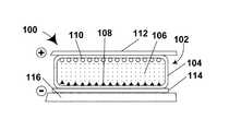
- the first dielectrophoretic display (generally designated 100 ) of the invention shown in FIGS. 1 to 3comprises an encapsulated dielectrophoretic medium (generally designated 102 ) comprising a plurality of capsules 104 (only one of which is shown in FIGS. 1 to 3 ), each of which contains a suspending liquid 106 and dispersed therein a plurality of a first type of particle 108 , which for purposes of illustration will be assumed to be black.
- the particles 108are electrophoretically mobile and may be formed of carbon black. In the following description, it will be assumed that the particles 108 are positively charged, although of course negatively charged particles could also be used if desired.
- a second type of particle 110which is electrophoretically mobile and negatively charged, and may be formed of titania.
- the triangular shape of the particles 108 , and the circular shape of the particles 110are used purely to way of illustration to enable the various types of particles to be distinguished easily in the accompanying drawings, and in no way correspond to the physical forms of the actual particles, which are typically substantially spherical.
- the display 100further comprises a common, transparent front electrode 112 , which forms a viewing surface through which an observer views the display 100 , and a plurality of discrete rear electrodes 114 , each of which defines one pixel of the display 100 (only one rear electrode 114 is shown in FIGS. 1 to 3 ).
- the front electrode 112is typically provided on a support member which also provides mechanical protection for the display 100 but for simplicity this support member is omitted from FIGS. 1 to 3 .
- FIGS. 1 to 3show only a single microcapsule forming the pixel defined by rear electrode 114 , although in practice a large number (20 or more) microcapsules are normally used for each pixel.
- the rear electrodes 114are mounted upon a substrate 116 , which contains areas of differing color, as described in more detail below with reference to FIGS. 4 to 8 .
- FIG. 1shows the display 100 with the front electrode 112 positively charged relative to the rear electrode 114 of the illustrated pixel.
- the positively charged particles 108are held electrostatically adjacent the rear electrode 114
- the negatively charged particles 110are held electrostatically against the front electrode 112 . Accordingly, an observer viewing the display 100 through the front electrode 112 sees a white pixel, since the white particles 110 are visible and hide the black particles 108 .
- FIG. 2shows the display 100 with the front electrode 112 negatively charged relative to the rear electrode 114 of the illustrated pixel.
- the positively charged particles 108are now electrostatically attracted to the negative front electrode 112
- the negatively charged particles 110are electrostatically attracted to the positive rear electrode 114 . Accordingly, the particles 108 move adjacent the front electrode 112 , and the pixel displays the black color of the particles 108 , which hide the white particles 110 .
- FIG. 3shows the display 100 after application of an alternating electric field between the front and rear electrodes 112 and 114 respectively.
- the application of the alternating electric fieldcauses dielectrophoretic movement of both types of particles 108 and 110 to the side walls of the capsule 104 , thus leaving the major portion of the area of the capsule 104 essentially transparent. Accordingly, the pixel displays the color of the substrate 116 .
- a series of short direct current voltages of alternating polarityis applied between the front and rear electrodes 112 and 114 , thereby causing the particles 108 and 110 to oscillate within the suspending liquid 106 ; this oscillation causes the particles 108 and 110 to gradually redisperse throughout the liquid 106 .
- Application of a longer direct current pulse of appropriate polaritywill then cause the pixel to assume the state shown in FIG. 1 or 2 depending upon the polarity of the longer pulse.
- the capsules 104are illustrated as being of substantially prismatic form, having a width (parallel to the planes of the electrodes) significantly greater than their height (perpendicular to these planes).
- This prismatic shape of the capsules 104is deliberate since it provides the capsules with side walls which extend essentially perpendicular to the viewing surface of the display, thus minimizing the proportion of the area of the capsule 104 which is occupied by the particles 108 and 110 in the transparent state shown in FIG. 3 .
- the capsules 104were essentially spherical, in the black state shown in FIG. 2 , the particles 108 would tend to gather in the highest part of the capsule, in a limited area centered directly above the center of the capsule.
- the color seen by the observerwould then be essentially the average of this central black area and a white or colored annulus surrounding this central area, where either the white particles 110 or the substrate 116 would be visible.
- the observerwould see a grayish color rather than a pure black, and the contrast between the two extreme optical states of the pixel would be correspondingly limited.
- the particles 108cover essentially the entire cross-section of the capsule so that no, or at least very little, white or other colored area is visible, and the contrast between the extreme optical states of the capsule is enhanced.
- the readeris referred to the aforementioned U.S. Pat. No. 6,067,185.
- the capsules 104are normally embedded within a solid binder, but this binder is omitted from FIGS. 1 to 3 for ease of illustration.
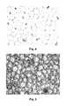
- FIGS. 4, 5 and 6 of the accompanying drawingsillustrate the white opaque, black opaque and transparent optical states of an experimental display of the present invention substantially as described above with reference to FIGS. 1 to 3 and comprising a plurality of capsules, each of which contains carbon black and white titania particles bearing charges of opposite polarity in a colorless suspending fluid.
- the displaywas prepared substantially as described in the aforementioned 2003/0137717 by encapsulating a hydrocarbon suspending fluid containing the carbon black and titania particles in a gelatin/acacia capsule wall, mixing the resultant capsules with a polymeric binder, coating the capsule/binder mixture on to an indium tin oxide (ITO) coated surface of a polymeric film to provide a single layer of capsules covering the film, and laminating the resultant film to a backplane.
- ITOindium tin oxide
- the display shown in FIGS. 4, 5 and 6was formed as a single pixel with the transparent front electrode forming the viewing surface of the display, and the backplane (actually a single rear electrode) disposed adjacent a multicolored reflector.
- FIG. 4shows the display in its first, white opaque state corresponding to that of FIG. 1 , with the white particles moved by electrophoresis and lying adjacent the viewing surface of the display, so that the white particles hide both the black particles and the multicolored reflector, and the display appears white.
- FIG. 5shows the display in its second, black opaque state corresponding to that of FIG. 2 , with the black particles moved by electrophoresis and lying adjacent the viewing surface of the display, so that the black particles hide both the white particles and the multicolored reflector, and the display appears black.
- FIG. 6shows the display in a transparent state corresponding to that of FIG.
- a display of the type shown in FIGS. 1 to 6can display three different colors, which eases the problems of building a full color electro-optic display.
- FIGS. 7 and 8illustrate the transition from the white opaque state shown in FIG. 4 to the transparent state shown in FIG. 6 ;
- FIG. 7shows the display after application of the aforementioned square wave for 10 seconds
- FIG. 8shows the display after application of the square wave for 30 seconds.
- FIGS. 6, 7 and 8show that development of the transparent state occurs gradually as more and more particles are moved to the side walls of the capsules.
- the multicolored reflectoris just becoming visible, while in FIG. 8 this reflector is more visible but much less clear than in the final transparent state shown in FIG. 6 .
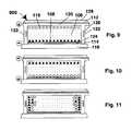
- FIGS. 9 to 11show schematic sections, similar to those of FIGS. 1 to 3 respectively, of one pixel of a microcell display (generally designated 900 ) of the present invention.
- the microcell display 900uses essentially the same dielectrophoretic medium, comprising a suspending liquid 106 with carbon black particles 108 and white titania particles suspended therein, as the encapsulated display 100 shown in FIGS. 1 to 3 ; however, the form of substrate used in the display 900 differs substantially from that of the display 100 .
- the substratecomprises a base member 120 and a plurality of side walls 122 extending perpendicular to the base member 120 and forming a plurality of microcells in which are confined the liquid 106 and the particles 108 and 110 .
- the lower faces (as illustrated in FIGS. 9 to 11 ) of the microcellsare closed by closure walls 124 , which are formed by radiation polymerization of a polymerizable species originally present in the liquid 106 ; see the aforementioned International Application Publication No. WO 02/01281, and published US Application No. 2002/0075556.
- the display 900further comprises a front electrode 112 , a rear or pixel electrode 114 and a colored substrate 116 all of which are essentially identical to the corresponding integers in FIG. 1 .
- FIGS. 9 to 11are drawn as if there is only a single microcell to the pixel defined by the electrode 114 although in practice a single pixel may comprise multiple microcells.
- the display 900also comprises auxiliary electrodes embedded within the side walls 122 and a protective layer 126 covering the front electrode 112 .
- the microcell display 900operates in a manner very similar to the encapsulated display 100 shown in FIGS. 1 to 3 .
- FIG. 9shows the display 900 with the front electrode 112 positively charged relative to the rear electrode 114 of the illustrated pixel.
- the positively charged particles 108are held electrostatically adjacent the rear electrode 114
- the negatively charged particles 110are held electrostatically against the front electrode 112 . Accordingly, an observer viewing the display 100 through the front electrode 112 sees a white pixel, since the white particles 110 are visible and hide the black particles 108 .
- FIG. 10shows the display 900 with the front electrode 112 negatively charged relative to the rear electrode 114 of the illustrated pixel.
- the positively charged particles 108are now electrostatically attracted to the negative front electrode 112
- the negatively charged particles 110are electrostatically attracted to the positive rear electrode 114 . Accordingly, the particles 108 move adjacent the front electrode 112 , and the pixel displays the black color of the particles 108 , which hide the white particles 110 .
- FIG. 11shows the display 900 after application of an alternating electric field between the front and rear electrodes 112 and 114 respectively.
- the application of the alternating electric fieldcauses dielectrophoretic movement of both types of particles 108 and 110 to the side walls of the microcell, thus leaving the major portion of the area of the microcell essentially transparent. Accordingly, the pixel displays the color of the substrate 116 .
- Redispersion of the particles 108 and 110 from the transparent state of the display 900 shown in FIG. 11may be effected in the same way as described above for the display 100 .
- the auxiliary electrodes 126are provided to assist in such redispersion.
- the auxiliary electrodesrun the full width of the display (which is assumed to be perpendicular to the plane of FIGS. 9 to 11 ), i.e., each auxiliary electrode is associated with a full row of microcells, and the auxiliary electrodes are connected to a voltage source which, when activated, applies voltages of opposed polarities to alternate auxiliary electrodes 126 .
- FIGS. 12A-12Dillustrate electronically addressable contrast media (i.e., dielectrophoretic displays) of the present invention which are addressed by electrodes disposed only on the rear surface (i.e., the surface remote from the viewing surface) of the display.
- the dielectrophoretic effectis employed to cause a species (particle) of higher dielectric constant to move to a region of higher field strength.
- a capsule 420contains a non-colored dye solvent complex 503 .
- a pair of electrodes 502are disposed adjacent the rear (non-viewing) surface of the capsule 420 .
- the complex 503is stable when no field is applied across the pair of electrodes 502 .
- an electric field 506is applied across the pair of electrodes 502 , as illustrated in FIG. 12B , the complex 503 dissociates into a colored dye component 504 and a solvent component 505 , with the dye component 504 moving away from the electrodes 502 towards a region of lower electric field.
- FIGS. 12C and 12Dillustrate electronically addressable contrast media similar to that illustrated in FIGS. 12A and 12B but using two pairs of stacked electrodes 502 , 507 in place of the single pair of electrodes 502 illustrated in FIGS. 12A and 12B .
- the presence of the two pairs of stacked electrodes 502 , 507allows for creation of a high field region in higher 506 or a lower 508 plane, thus causing a species of higher dielectric constant to migrate to a higher or lower region respectively.
- the species of higher dielectric constantis one hemisphere 440 of a bichromal sphere, this sphere having a second hemisphere 430 of lower dielectric constant than the hemisphere 440 .
- FIG. 12Cthe species of higher dielectric constant is one hemisphere 440 of a bichromal sphere, this sphere having a second hemisphere 430 of lower dielectric constant than the hemisphere 440 .
- FIGS. 12C and 12Dfurther illustrate the use of shaped material 509 , which may be dielectric or conducting materials, to shape the electric fields from the electrodes 502 , 507 .
- the present inventionneed not make use of a colored reflector behind the capsules but may be used to provide backlit displays, variable transmission windows and transparent displays; indeed, the present invention may be useful in any application where light modulation is desired.
- dielectrophoretic displaysIt is appropriate to give some consideration to the problems involved in driving dielectrophoretic displays.
- the basic physical principles of dielectrophoresisare discussed below and semi-quantitative predictions are derived from a simple model. This model also relates physical and electrical properties of the components of the dielectrophoretic medium to the strength of the dielectrophoretic force.
- ⁇ e ⁇ ( r )⁇ e ⁇ ( 0 ) + r ⁇ ⁇ ⁇ e ⁇ ( 0 ) + 1 2 ⁇ ⁇ ⁇ ⁇ ⁇ r i ⁇ r j ⁇ ⁇ 2 ⁇ ⁇ ⁇ r i ⁇ ⁇ r j + ... ( 6 )
- Equation (6)Substituting Equation (6) into Equation (5) gives:
- Equation (3)is used in the derivation of Equation (7), which shows how the various moments of the charge distribution interact with the various electric field terms.
- the monopolecouples to the electrostatic potential, the dipole to the field (gradient or first derivative of the potential), the quadrupole to the field gradient (second derivative of the potential) etc. From the expression for electrostatic energy in Equation (7), the forces and torques on charged bodies in an external field can be determined.
- the translational forceis determined by taking the negative gradient of Equation (7).
- the electrophoretic forceis the first order term in the Taylor expansion
- the dielectrophoretic forceis the second term in the same expansion, and higher order terms represent additional forces which are not relevant for purposes of the present invention.
- the first term of the expansiongives the electrophoretic force already expressed by Equation (1).
- a dipoledoes not feel a force in a uniform electric field, but rather a field gradient is required to exert force a dipole; see FIG. 13 .
- the forces F ⁇ and F + on the two parts of the dipolewould cancel to give zero net force.
- the resultant forceis the dielectrophoretic force on the dipole.
- the third term of Equation (7)shows that a quadrupole charge distribution does not experience a force in a uniform field or in a uniform field gradient, but will experience a force due to the derivative of the field gradient.
- Equation (10)shows that a dipole experiences a force in the direction of increasing field strength.
- dipolesare attracted to regions of high electric field strength.
- a charged air-gap capacitorwill attract dielectric media, the dielectric media being polarized by the electric field in the capacitor gap.
- the next step in modeling a dielectrophoretic displayis to consider the dielectrophoretic force on a polarizable particle lying within a fluid medium.
- the particletypically has no electric dipole except that induced by an external field. In such an external field, the particle is polarized, and has an induced dipole moment that can be acted on by a field gradient.
- ⁇ * pimmersed in a fluid with a complex dielectric constant ⁇ * m .
- Each complex dielectric constantis expressed in terms of the real dielectric constant, a conductivity ⁇ , and the frequency of the sinusoidally varying external field ⁇ :
- a cross-over frequencycan be defined as the frequency at which the conductive and non-conductive components of the complex dielectric function of Equation (11) are equal, and conductive and conductive and insulating regimes can be defined as follows: Conductive regime: ⁇ ( ⁇ / ⁇ ) (17A) Insulating regime: ⁇ >>( ⁇ / ⁇ ) (17B).
- FIG. 14is a graph showing the variation of the contrast function, as calculated from Equation (18), as a function of ⁇ p / ⁇ m . From FIG. 14 , it will be seen that the contrast function increases monotonically with ⁇ p / ⁇ m , and is bounded by unity.
- Equation (20)shows that the dielectrophoretic force on a conducting particle in an insulating fluid always exceeds the dielectrophoretic force on an insulating particle.
- the aforementioned E Ink and MIT patents and applicationsdisclose electrophoretic media comprising carbon black and titania particles in an insulating hydrocarbon fluid. If such media are operated in a dielectrophoretic mode, the dielectrophoretic force on the carbon black particles exceeds the dielectrophoretic force on the titania particles for otherwise similar conditions.
- E IP1 + d e d IP 1 + ⁇ IP * ⁇ e * ⁇ d e d IP ⁇ E 0 ( 21 )
- d ethe local thickness of the external phase
- d IPthe local thickness of the internal phase
- ⁇ IP * and ⁇ e *are the complex dielectric constants of the internal and external phases.
- gradients in the electric field within the internal phasearise from variations in the local fraction of external phase and the difference in dielectric constant or conductivity between the internal and external phases.
- gradients in E 2are in the plane of the substrates and point outwardly (or inwardly) along a capsule's radial direction.
- the external phase of an encapsulated electrophoretic mediumis more conductive and has a larger dielectric constant than the internal phase.
- the electric field in the internal phaseis largest in regions where the capsule is thinnest, which will be along the lateral perimeter of the capsules (i.e., the left and right hand edges of the capsules as illustrated in FIGS. 1-3 ), or in the case of tightly packed capsules, at the surfaces of contact with neighboring capsules.
- the electrophoretic particlestypically have a larger polarizability than the fluid, and so their dielectrophoretic mobility will be positive. The particles will thus be attracted to the thinnest regions of the capsules along the lateral extremes of the capsules and especially to the vertices of the capsules.
- the electrophoretic force, F epacting on the particles is typically sinusoidal: F ep ⁇ sin ⁇ t (23) and averages to zero.
- the dielectrophoretic force, F depis proportional to the square of the electric field, so its temporal variation is: F dep ⁇ sin 2 ⁇ t (24) which has a non-zero average.
- Use of a high frequency alternating voltagewill induce small amplitude oscillations due to the electrophoretic force and a sinusoidally-modulated but linearly-directed motion due to the dielectrophoretic force.
- ⁇ dep⁇ m ⁇ a 2 ⁇ Re ⁇ ⁇ K ⁇ ( ⁇ ) ⁇ 3 ⁇ ⁇ ( 28 )
- the timescale for such dielectrophoretic motioncan be estimated in the following manner.
- the gradient in the mean square electric fieldis approximately the difference in the mean square field between the capsule center and the edges, divided by the lateral radius of the capsule.
- the field at the center of the capsuleis approximately:
- this inventionprovides a variable transmission display comprising: an electrophoretic medium comprising a fluid and a plurality of electrically charged particles dispersed in the fluid, the electrophoretic medium being capable of assuming a light-transmissive state and a substantially non-light-transmissive state; at least one light-transmissive first electrode disposed adjacent the electrophoretic medium; a plurality of light-transmissive second electrodes disposed adjacent the electrophoretic medium on the side thereof remote from the first electrode(s); and voltage means for varying the potential each of the second electrodes independently of one another.
- variable transmission displays or windows of the present inventionare capable of displaying at least two optical states, namely: non-private (clear) and private, which may be a scattering state, or a white, black, or other color states.
- windows of the present inventionmay have clear and opaque states, clear and white states, clear and black states, or clear and colored states; other combinations of optical states may also be used.
- variable transmission windows of the present inventionhave two principal advantages. Firstly, such windows provide signage capabilities in addition to full area variable transmission. These signage capabilities are provided by local (pixilated) instead of global (full-area) switching to display information, including letters, graphics, images, or patterns. Such signage capability allows, useful and changing information such as name of business, opening hours, time, temperature, prices, advertizing, menus, logos, images can be displayed, and no cost is incurred by a landlord of business premises when tenants change. Such signage capability requires the use of an array of second electrodes of a size similar to that used in conventional signage, plus drivers and control electronics.
- the second electrodes used in the present windowscan be substantially larger than those in, for example, electronic book readers; whereas an electronic book reader typically has about 160 second electrodes per inch (about 6.3 per millimeter), windows of the present invention may make use of second electrodes having second electrodes about 1 ⁇ 8 inch (about 3 mm) square.
- variable transmission windowshould display an absolutely uniform optical state in both its transmissive and non-transmissive optical states.
- the human eyeis very sensitive to even minor variations in large, supposedly uniform areas of color, and in practice large variable transmission electrophoretic windows always display visible non-uniformities.
- the variable transmission windows of the present inventioncan display a simple random binary pixel pattern (“white noise”) which effectively hides display non-uniformity while providing privacy veiling and being decorative.
- FIG. 15 of the accompanying drawingsillustrates this effect.
- This Figureshows a variable transmission electrophoretic display of the present invention in which the left-hand half of the display (as illustrated) is set to a uniform gray level, whereas the right-hand half of the display is set to a random pixel pattern.
- the inconsistencies in the electrophoretic mediumcause readily visible defects in the supposedly uniform gray level on the left-hand side of the display, whereas such defects are much less visible in the random pattern on the right-hand side of the display. Accordingly, as may be seen from FIG. 15 , the present inventions allows saving costs required to achieve coating uniformity without visible mottle, streaks, or point defects.
- the present inventionallows for the retrofitting of conventional windows to form electrophoretic variable transmission windows of the invention, or for the formation of windows of the invention on any desired conventional glass substrate.
- a matrix of second electrodestypically provided with thin film transistors (TFT's) can be formed on a self-adhesive plastic film, which can then be laminated to a glass substrate.
- TFT'sthin film transistors
- the electrophoretic mediumcan them be applied by spray coating or other similar techniques over the matrix of second electrodes.
- a front plane laminatesee for example U.S. Pat. No. 6,982,178
- U.S. Pat. No. 6,982,178can be laminated to the matrix of second electrodes.
- variable transmission windows of the present inventioncosts have low initial manufacturing costs than similar liquid crystal based windows, and lower power consumption in operation.
- the present windowscan be retrofitted to existing architectural glazing, saving considerable building costs and time.
Landscapes
- Physics & Mathematics (AREA)
- Engineering & Computer Science (AREA)
- General Physics & Mathematics (AREA)
- Theoretical Computer Science (AREA)
- Nonlinear Science (AREA)
- Chemical & Material Sciences (AREA)
- Optics & Photonics (AREA)
- Computer Hardware Design (AREA)
- Nanotechnology (AREA)
- Crystallography & Structural Chemistry (AREA)
- Mathematical Physics (AREA)
- Life Sciences & Earth Sciences (AREA)
- Microelectronics & Electronic Packaging (AREA)
- Health & Medical Sciences (AREA)
- Chemical Kinetics & Catalysis (AREA)
- Electrochemistry (AREA)
- Molecular Biology (AREA)
- General Engineering & Computer Science (AREA)
- Computing Systems (AREA)
- Biophysics (AREA)
- Geometry (AREA)
- Electrochromic Elements, Electrophoresis, Or Variable Reflection Or Absorption Elements (AREA)
Abstract
Description
This application is a division of application Ser. No. 14/638,707, filed Mar. 4, 2015 (Publication No. 2015/0177589, now U.S. Pat. No. 9,664,978, issued May 30, 2017), which is a continuation of application Ser. No. 13/694,156 (Publication No. 2013/0063333, now abandoned), which is a continuation-in-part of application Ser. No. 12/549,763 (Publication No. 2010/0045592, now U.S. Pat. No. 8,305,341, issued Nov. 6, 2012), which is a continuation of application Ser. No. 11/799,377, filed May 1, 2007 (Publication No. 2008/0117495, now U.S. Pat. No. 7,583,251, issued Sep. 1, 2009), which is a continuation-in-part of application Ser. No. 10/687,166, filed Oct. 16, 2003 (Publication No. 2004/0136048, now U.S. Pat. No. 7,259,744, issued Aug. 21, 2007), which itself claims benefit of Provisional Application Ser. No. 60/419,019, filed Oct. 16, 2002. The entire disclosure of all the aforementioned applications, and of all U.S. patents and published applications mentioned below, is herein incorporated by reference.
This invention relates to electrophoretic displays, and methods for operating such displays. More specifically, this invention relates to electrophoretic displays in which solid particles and a suspending fluid are held within a cavity.
Electrophoretic displays have been the subject of intense research and development for a number of years. Such displays use a display medium comprising a plurality of electrically charged particles suspended in a fluid. Electrodes are provided adjacent the display medium so that the charged particles can be moved through the fluid by applying an electric field to the medium. In one type of such electrophoretic display, the medium comprises a single type of particle having one optical characteristic in a fluid which has a different optical characteristic. In a second type of such electrophoretic display, the medium contains two different types of particles differing in at least one optical characteristic and in electrophoretic mobility; the particles may or may not bear charges of opposite polarity. The optical characteristic which is varied is typically color visible to the human eye, but may, alternatively or in addition, be any one of more of reflectivity, retroreflectivity, luminescence, fluorescence, phosphorescence, or (in the case of displays intended for machine reading) color in the broader sense of meaning a difference in absorption or reflectance at non-visible wavelengths.
Electrophoretic displays can be divided into two main types, namely unencapsulated and encapsulated displays. In an unencapsulated electrophoretic display, the electrophoretic medium is present as a bulk liquid, typically in the form of a flat film of the liquid present between two parallel, spaced electrodes. Such unencapsulated displays typically have problems with their long-term image quality which have prevented their widespread usage. For example, particles that make up such electrophoretic displays tend to cluster and settle, resulting in inadequate service-life for these displays.
An encapsulated, electrophoretic display differs from an unencapsulated display in that the particle-containing fluid is not present as a bulk liquid but instead is confined within the walls of a large number of small capsules. Encapsulated displays typically do not suffer from the clustering and settling failure mode of traditional electrophoretic devices and provides further advantages, such as the ability to print or coat the display on a wide variety of flexible and rigid substrates.
For further details regarding encapsulated electrophoretic displays, the reader is referred to U.S. Pat. Nos. 5,930,026; 5,961,804; 6,017,584; 6,067,185; 6,118,426; 6,120,588; 6,120,839; 6,124,851; 6,130,773; 6,130,774; 6,172,798; 6,177,921; 6,232,950; 6,249,271; 6,252,564; 6,262,706; 6,262,833; 6,300,932; 6,312,304; 6,312,971; 6,323,989; 6,327,072; 6,376,828; 6,377,387; 6,392,785; 6,392,786; 6,413,790; 6,422,687; 6,445,374; 6,445,489; 6,459,418; 6,473,072; 6,480,182; 6,498,114; 6,504,524; 6,506,438; 6,512,354; 6,515,649; 6,518,949; 6,521,489; 6,531,997; 6,535,197; 6,538,801; 6,545,291; and 6,580,545; and U.S. Patent Applications Publication Nos. 2002/0019081; 2002/0021270; 2002/0053900; 2002/0060321; 2002/0063661; 2002/0063677; 2002/0090980; 2002/0106847; 2002/0113770; 2002/0130832; 2002/0131147; 2002/0145792; 2002/0171910; 2002/0180687; 2002/0180688; 2002/0185378; 2003/0011560; 2003/0011867; 2003/0011868; 2003/0020844; 2003/0025855; 2003/0034949; 2003/0038755; 2003/0053189; 2003/0076573; 2003/0096113; 2003/0102858; 2003/0132908; 2003/0137521; 2003/0137717; and 2003/0151702; and International Applications Publication Nos. WO 99/67678;WO 00/05704;WO 00/38000;WO 00/38001;WO 00/36560;WO 00/67110;WO 00/67327; WO 01/07961; and WO 01/08241. All of these patents and applications are in the name of, or assigned to, the Massachusetts Institute of Technology (MIT) or E Ink Corporation.
Many of the aforementioned patents and applications recognize that the walls surrounding the discrete microcapsules in an encapsulated electrophoretic medium could be replaced by a continuous phase, thus producing a so-called “polymer-dispersed” electrophoretic display in which the electrophoretic medium comprises a plurality of discrete droplets of an electrophoretic fluid and a continuous phase of a polymeric material, and that the discrete droplets of electrophoretic fluid within such a polymer-dispersed electrophoretic display may be regarded as capsules or microcapsules even though no discrete capsule membrane is associated with each individual droplet; see for example, U.S. Pat. No. 6,392,786, at column 6, lines 44-63. See also the aforementioned U.S. Patent Application Publication No. 2002/0131147, and the corresponding International Application PCT/US02/06393 (Publication No. WO 02/075443). Accordingly, for purposes of the present application, such polymer-dispersed electrophoretic media are regarded as sub-species of encapsulated electrophoretic media.
A related type of electrophoretic display is a so-called “microcell electrophoretic display”, sometimes also called a “microcup” electrophoretic display. In a microcell electrophoretic display, the charged particles and the suspending fluid are not encapsulated within microcapsules but instead are retained within a plurality of cavities formed within a carrier medium (or substrate), typically a polymeric film. See, for example, International Applications Publication No. WO 02/01281, and published US Application No. 2002/0075556, both assigned to Sipix Imaging, Inc.
Hereinafter, the term “microcavity electrophoretic display” will be used to cover both encapsulated and microcell electrophoretic displays.
One of the problems with electrophoretic displays is the limited range of colors which each pixel of the display can produce. The prior art describes two main types of electrophoretic media. One type comprises a single type of electrically charged particle in a colored medium. This type of medium is only capable of producing two colors at each pixel; either the color of the particles or the color of the medium is seen. The second type of medium comprises two different types of electrically charged particles in an essentially uncolored medium; the two types of particles may differ in polarity of electric charge or have charges of the same polarity but differ in electrophoretic mobility. Again, this type of medium is only capable of producing two colors at each pixel, namely the colors of the two types of particles.
One approach to expanding the limited range of colors available from conventional electrophoretic displays is to place an array of colored filters over the pixels of the display. For example, consider the effect on a display comprising white particles in a black fluid of placing an array of color filters (say red, green and blue) over the individual pixels of the display. Moving the white particles adjacent the viewing surface of a pixel covered with a red filter would color that pixel red, whereas moving the white particles of the same pixel adjacent the rear surface of the display would render the pixel black. The main problem with this approach to generating color is that the brightness of the display is limited by the pixilation of the color filter. For example, if a red color is desired, the pixels covered by red filters are set to appear red, whereas the pixels covered by green and blue filters are set to appear dark, so that only a fraction of the display surface has the desired color while the remaining portion is dark, thus limiting the brightness of any color obtained. A reflective display that was capable of three optical states (black, white and color or black, white and transparent) would significant advantages in image quality, cost and ease of manufacture.
Conventional electrophoretic displays rely upon movement of electrically charged particles in an electric field under electrostatic forces; the particles move along the lines of force of the electric field. However, it is known that objects can be moved by dielectrophoretic forces, that is to say that dipoles induced in the objects by a non-uniform electric field cause the particles to move towards regions of higher field strength. See, for example, U.S. Pat. No. 4,418,346 to Batchelder which describes an apparatus for providing a dielectrophoretic display of visual information. In this apparatus, a “bubble” of a fluid is moved through a second, immiscible fluid in a stepwise manner by applying voltages to closely spaced electrodes, the bubble being visible against a visually contrasting background. Visual information is conveyed by the position of the bubble relative to the background. The patent suggests that a simple one-dimensional display of this type might represent the level of an analog signal by the position of the bubble. However, since the movement involved is that of a bubble against a contrasting background, such an apparatus does not appear capable of displaying an arbitrary image.
It has now been realized that using a microcavity electrophoretic medium in a dielectrophoretic display greatly simplifies the problem of generating the heterogeneous electric field required by such a display, since differences between the dielectric constant and/or conductivity between the suspending fluid and the material surrounding the suspending fluid (such as a polymeric binder in which the capsules are embedded, as described in many of the aforementioned E Ink and MIT patents and publications, or the substrate in which the cavities of a microcell electrophoretic display are formed) will result in a heterogeneous electric field which can be used to move the particles within the suspending fluid against the side walls of the cavities, thereby providing the display with a substantially transparent state.
It has further been realized that a microcavity electrophoretic medium allows for the provision of auxiliary electrodes which can be used to assist the movement of particles required to provide the display with a substantially transparent state.
Variable transmission windows represent a potentially important market for electrophoretic media. As the energy performance of buildings and vehicles becomes increasingly important, electrophoretic media can be used as coatings on windows (including skylights and sunroofs) to enable the proportion of incident radiation transmitted through the windows to be electronically controlled by varying the optical state of the media. Effective implementation of such “variable-transmissivity” (“VT”) technology in buildings is expected to provide (1) reduction of unwanted heating effects during hot weather, thus reducing the amount of energy needed for cooling, the size of air conditioning plants, and peak electricity demand; (2) increased use of natural daylight, thus reducing energy used for lighting and peak electricity demand; and (3) increased occupant comfort by increasing both thermal and visual comfort. Even greater benefits would be expected to accrue in an automobile, where the ratio of glazed surface to enclosed volume is significantly larger than in a typical building. Specifically, effective implementation of VT technology in automobiles is expected to provide not only the aforementioned benefits but also (1) increased motoring safety, (2) reduced glare, (3) enhanced mirror performance (by using an electro-optic coating on the mirror), and (4) increased ability to use heads-up displays. Other potential applications of VT technology include privacy glass and glare-guards in electronic devices.
In addition to the aforementioned advantages, variable transmission windows can be used to provide privacy. Conventional (invariable) glass windows, doors, and room partitions have the advantage of admitting natural light, but the disadvantage of not providing privacy when needed. Mechanical privacy devices such as shades, for example in the form of vertical blinds, take up space, are cumbersome to use, and are often unreliable. Privacy “veiling” can be achieved by increasing the reflection, absorption, and scattering of the glass, using mirrored, tinted or frosted glass respectively. The veiling effect increases with the ratio of the light that is reflected, absorbed, or scattered by the window to the light that is transmitted through the window. Only scatter screening provides a veiling effect that is independent on the illumination conditions in- and outside the window because scatter screening blurs the view through the window, whereas reflection or absorption veiling becomes ineffective when the illumination beyond the window is high compared to that surrounding an observer outside the window.
Frosted glass in doors, room partitions, and windows is frequently used not only to provide privacy but also to display information e.g. the name and opening hours of a business that occupies the premises whose privacy is protected by the frosted glass. Frosted glass is also frequently used for decorative purposes i.e. displaying decorative patterns. However, conventional frosted glass has two major disadvantages; the privacy screening cannot be switched off when not needed, and information on the glass cannot be changed easily and without high costs when necessary, for example when the tenant of a building changes.
Liquid crystal (LC) display technology can be used instead of frosted glass for ‘variable opacity’ privacy windows, and can also display information. However, LCD windows of any useful size are very costly, and high in power consumption.
Accordingly, variable transmission-windows using electrophoretic media have been proposed; see for example U.S. Pat. Nos. 7,327,511; 7,999,787; and 7,679,814. Such electrophoretic VT windows have the advantages of low cost per area, and require power only when switching, and offer potential for in situ deposition by spray coating. However, such windows can suffer from visible non-uniformities (mottle, streaks, or point defects)) that may make them less attractive than liquid crystal-based windows despite their reduced cost and power consumption. Achieving uniformity below visible threshold of non-uniformity in electrophoretic VT windows may erase some of the cost benefits of such windows over their liquid crystal based counterparts.
The present invention provides a variable transmission electrophoretic window (or other display) which renders non-uniformities in the electrophoretic medium less visible.
Accordingly, this invention provides a dielectrophoretic display comprising:
a substrate having walls defining at least one cavity, the cavity having a viewing surface and a side wall inclined to the viewing surface;
a suspending fluid contained within the cavity;
a plurality of at least one type of particle suspended within the suspending fluid; and
means for applying to the fluid an electric field effective to cause dielectrophoretic movement of the particles to the side wall of the cavity.
This invention also provides a process for operating a dielectrophoretic display, the process comprising:
providing a substrate having walls defining at least one cavity, the cavity having a viewing surface and a side wall inclined to the viewing surface; a suspending fluid contained within the cavity; and a plurality of at least one type of particle suspended within the suspending fluid; and
applying to the fluid an electric field effective to cause dielectrophoretic movement of the particles to the side wall of the cavity.
In the dielectrophoretic display of the present invention, the suspending fluid may be substantially uncolored, and have suspended therein only a single type of particle.
At least some of the at least one type of particle may be electrically charged, and in one form of a display containing such electrically charged particles, the suspending fluid may have suspended therein a first type of particle having a first optical characteristic and a first electrophoretic mobility, and a second type of particle having a second optical characteristic different from the first optical characteristic and a second electrophoretic mobility different from the first electrophoretic mobility. The first and second electrophoretic mobilities may differ in sign, so that the first and second types of particles move in opposed directions in an electric field, and the suspending fluid may be substantially uncolored. This type of display may further comprise a backing member disposed on the opposed side of the cavity from the viewing surface, at least part of the backing member having a third optical characteristic different from the first and second optical characteristics. The backing member may comprise areas having third and fourth optical characteristics different from each other and from the first and second optical characteristics. In preferred forms of such a display, the backing member comprises areas having red, green and blue or yellow, cyan and magenta colors, and the first and second optical characteristics may comprise black and white colors.
In the dielectrophoretic display of the present invention, the cavity may have a non-circular cross-section, preferably a polygonal cross-section, as seen from the viewing surface. The at least one type of particle may be formed from an electrically conductive material, for example a metal, carbon black or a doped semiconductor.
As already indicated, in the dielectrophoretic display of the present invention, the substrate may comprises at least one capsule wall (typically a deformable wall) so that the dielectrophoretic display comprises at least one capsule. For reasons explained in the aforementioned 2003/0137717, the capsules are preferably arranged in a single layer. Alternatively, the substrate may comprise a continuous phase surrounding a plurality of discrete droplets of the suspending fluid having the at least one type of particle suspended therein (i.e., the display may be of the polymer-dispersed type), or may comprises a substantially rigid material having the at least one cavity formed therein, the substrate further comprising at least one cover member closing the at least one cavity, so that the display is of the microcell type.
In the process of the present invention, the electric field may be an alternating electric field. When the display is of the type in which at least some of the at least one type of particle are electrically charged, and the suspending fluid has suspended therein a first type of particle having a first optical characteristic and a first electrophoretic mobility, and a second type of particle having a second optical characteristic different from the first optical characteristic and a second electrophoretic mobility different from the first electrophoretic mobility, with the first and second electrophoretic mobilities differing in sign, so that the first and second types of particles move in opposed directions in an electric field, the process may further comprise:
applying an electric field of a first polarity to the cavity, thereby causing the first type of particles to approach the viewing surface and the cavity to display the first optical characteristic at the viewing surface; and
applying an electric field of a polarity opposite to the first polarity to the cavity, thereby causing the second type of particles to approach the viewing surface and the cavity to display the second optical characteristic at the viewing surface.
This invention also provides a dielectrophoretic display comprising:
a substrate having walls defining at least one cavity, the cavity having a viewing surface and a side wall inclined to the viewing surface;
a fluid contained within the cavity;
a plurality of at least one type of electrically charged particle within the fluid, the particles having a first optical characteristic;
a backing member disposed on the opposed side of the cavity from the viewing surface, at least part of the backing member having a second optical characteristic different from the first optical characteristics, the backing member being light-transmissive; and
means for applying to the substrate an electric field effective to cause dielectrophoretic movement of the particles to the side wall of the cavity.
In one form of such a dielectrophoretic display, the fluid is substantially uncolored, and has therein only a single type of particle. The cavity may have a non-circular (and preferably polygonal) cross-section as seen from the viewing surface. The single type of particle may be formed from an electrically conductive material, for example a metal or carbon black. Alternatively, the single type of particle may be formed from a doped semiconductor.
The substrate may comprise at least one capsule wall so that the dielectrophoretic display comprises at least one capsule. The display may comprise a plurality of capsules, the capsules being arranged in a single layer. Alternatively, the substrate may comprise a continuous phase surrounding a plurality of discrete droplets of the fluid having the particles therein. In another form of such a dielectrophoretic display, the substrate comprises a substantially rigid material having the at least one cavity formed therein, the substrate further comprising at least one cover member closing the at least one cavity.
The dielectrophoretic display may be arranged to have light projected on to a surface on the opposed side of the dielectrophoretic display from the viewing surface. The invention extends to a variable transmission window comprising a dielectrophoretic display of the invention.
This invention also provides a process for operating a dielectrophoretic display, the process comprising:
providing a substrate having walls defining at least one cavity, the cavity having a viewing surface and a side wall inclined to the viewing surface, a fluid contained within the cavity; and a plurality of at least one type of electrically charged particle suspended within the suspending fluid, the particles having a first optical characteristic; and a backing member disposed on the opposed side of the cavity from the viewing surface, at least part of the backing member having a second optical characteristic different from the first optical characteristic, the backing member being light-transmissive; and
applying to the substrate an electric field effective to cause dielectrophoretic movement of the particles to the side wall of the cavity.
In this process, the electric field may be an alternating electric field. The fluid may be substantially uncolored and have therein only a single type of particle. This single type of particle may be formed from an electrically conductive material, for example a metal or carbon black. Alternatively, the single type of particle may be formed from a doped semiconductor. The substrate may comprise at least one capsule wall so that the dielectrophoretic display comprises at least one capsule. The display may comprise a plurality of capsules, the capsules being arranged in a single layer. Alternatively, the substrate may comprise a continuous phase surrounding a plurality of discrete droplets of the fluid having the particles therein. In another form of such a dielectrophoretic display, the substrate comprises a substantially rigid material having the at least one cavity formed therein, the substrate further comprising at least one cover member closing the at least one cavity.
This invention also provides an electronically addressable display comprising a microencapsulated display medium including a first species having a higher dielectric constant and a second species having a lower dielectric constant; and electrodes disposed adjacent the display medium for selectively creating regions of higher and lower electric field; and wherein the first species moves toward the region of higher electric field.
In such an electronically addressable display, the display medium may comprise a bichromal microsphere having a first hemisphere and a second hemisphere differing in dielectric constants, wherein the first species of higher dielectric constant comprises the first hemisphere and the second species of lower dielectric constant comprises the second hemisphere. Alternatively, the display medium may comprise a first species of colored particles having a higher dielectric constant and a second species of colored particles having a lower dielectric constant. The first species may have a dielectric constant that is permanently higher than that of the second species. The first species may move in translational migration.
This invention also provides a process for operating a dielectrophoretic display, the process comprising:
providing a substrate having walls defining at least one cavity, the cavity having a viewing surface and a side wall inclined to the viewing surface, a fluid contained within the cavity; and a plurality of solid particles within the fluid, the particles having a dielectric constant higher than the dielectric constant of the fluid; and
applying to the substrate a non-homogeneous electric field, the electric field being greater adjacent the side wall than in the center of the cavity, thereby causing the particles to move to the side wall of the cavity.
This invention also provides a process for operating a dielectrophoretic display, the process comprising:
providing a substrate having walls defining at least one cavity, the cavity having a viewing surface and a side wall inclined to the viewing surface, a fluid contained within the cavity; and a plurality of solid particles within the fluid, the particles having a dielectric constant lower than the dielectric constant of the fluid; and
applying to the substrate a non-homogeneous electric field, the electric field being smaller adjacent the side wall than in the center of the cavity, thereby causing the particles to move to the side wall of the cavity.
This invention also provides a variable transmission display comprising:
an electrophoretic medium comprising a fluid and a plurality of electrically charged particles dispersed in the fluid, the electrophoretic medium being capable of assuming a light-transmissive state and a substantially non-light-transmissive state;
at least one light-transmissive first electrode disposed adjacent the electrophoretic medium;
a plurality of light-transmissive second electrodes disposed adjacent the electrophoretic medium on the side thereof remote from the first electrode(s); and
voltage means for varying the potential each of the second electrodes independently of one another.
In such a variable transmission display, the second electrodes and the voltage means may take the form of an active matrix backplane, with the second electrodes being arranged in a plurality of rows and a plurality of columns, and the voltage means comprising row and column electrodes connecting the second electrodes in each row and column respectively.
As already mentioned, in one aspect this invention provides a dielectrophoretic display comprising a substrate having walls defining at least one cavity, the cavity having a viewing surface and a side wall inclined to the viewing surface; a suspending fluid contained within the cavity; a plurality of at least one type of particle suspended within the suspending fluid; and means for applying to the fluid an electric field effective to cause dielectrophoretic movement of the particles to the side wall of the cavity.
References to “viewing surface” and “side wall” herein do not imply that these surfaces are perpendicular to each other, though a substantially perpendicular arrangement of the two surfaces is preferred, since when the particles are disposed adjacent the side wall of the cavity, such a perpendicular arrangement minimizes the area of the viewing surface occupied by the particles, and hence permits the maximum amount of light to pass through the cavity. The side wall or walls of the cavity also need not be planar; for example, an encapsulated display of the present invention may use capsules as described in the aforementioned U.S. Pat. No. 6,067,185 having the form of “flattened spheres” (i.e., oblate ellipsoids) with curved side walls.
In this display, it is necessary that there be a difference between the dielectric constant and/or conductivity of the suspending fluid and that of the substrate to provide the heterogeneous electric field necessary for dielectrophoresis. Desirably, this difference should be made as large as possible. It may also be advantageous to use a capsule which has a non-circular, and preferably polygonal, cross-section perpendicular to the direction of the applied electric field since sharply curved regions or corners of the capsule produce increased field heterogeneity and thus assist the dielectrophoretic movement of the particles.
Those skilled in the technology of electrophoretic displays will appreciate that both electrically neutral and electrically charged particles can be moved by dielectrophoresis, since dielectrophoretic movement is dependent upon dipoles induced in the particles by the electric field and not upon any pre-existing charge on the particles. However, it appears advantageous to use electrically charged particles in the apparatus and process of the present invention since once the particles have been moved to the side wall of the capsule by dielectrophoresis, it appears desirable to use normal electrophoretic movement of the particles to disperse them; it will be appreciated that since the heterogeneity of the electric field in an encapsulated display is due to differences between the properties of the suspending fluid on the one hand and the capsule wall and surrounding material on the other, there will normally be no way of reversing the high field and low field regions in a manner similar to that used in the Batchelder apparatus, so that if the particle movement caused by dielectrophoresis is to be reversed, some applied force other than dielectrophoresis must be used.
If electrically charged particles are used in the present apparatus and process, the particles are of course subject to both electrophoretic and dielectrophoretic forces when an electric field is applied. Typically, electrophoretic movement of particles will be much more rapid than dielectrophoretic, so that to ensure that the desired dielectrophoretic movement is not subject to interference from electrophoretic movement, it is desirable to reverse the electric field at intervals; provided the field is applied for the same amount time in each direction, the electrophoretic movements will sum to zero, since electrophoretic movement is polarity-sensitive, whereas the dielectrophoretic movements will not sum to zero since dielectrophoretic movement is polarity-independent.
The dielectrophoretic movement of the particles in the apparatus and process of the present invention is affected by the material from which the particles are formed, and the size and shape of the particles. Since dielectrophoresis depends upon the induction of dipoles within the particles, it is desirable to use particles which are highly polarizable, especially conductive particles such as metals. For example, aluminum particles may be used in the present invention. It has been observed experimentally that carbon black particles, which have a reasonably high conductivity, have substantially greater dielectrophoretic mobility than substantially non-conductive titania particles. The particles may also be formed from a doped semiconductor; the type of doping is not critical provided that the particles have sufficient conductivity, but most undoped semiconductors have too low a conductivity to have high dielectrophoretic mobility.
The induced dipole, and hence the dielectrophoretic movement of the particles, is also affected by the size and shape of the particles. Since a large particle allows greater separation between the poles of a dipole than a smaller particle, increasing the size of the particles will increase dielectrophoretic mobility, although of course the particles should not be made so large as to readily visible when they lie adjacent the side wall of the capsule. For similar reasons, elongate particles, especially needle-shaped particles, will tend to have a higher dielectrophoretic mobility than spherical particles of the same volume. Anisotropically shaped particles may also be useful in the present invention.
There are two main variations of the apparatus and process of the present invention. In the first variation, the cavity contains only a single type of particle in an uncolored suspending fluid. This capsule can be switched between an “opaque” state, in which the particles are dispersed throughout the suspending fluid, and a “transparent” state, in which the particles are moved to a side wall of the capsule so that light can pass through the uncolored suspending fluid. The transparent state need not appear transparent to a viewer; as illustrated in the drawings and as described in more detail below, a reflector or filter having a color different from that of the particles may be placed on the opposed side of the capsule from the viewing surface thereof, so that in the transparent state a viewer sees the color of the reflector or filter; in the opaque state the color of the reflector or filter is of course hidden by the dispersed particles.
In the second variation, the capsules contain two different types of particles differing in at least one optical characteristic and in electrophoretic mobility and a suspending fluid which may be colored or uncolored. This capsule can be switched among three states, namely a first opaque state, in which the first type of particles are visible, a second opaque state, in which the second type of particles are visible, and a “transparent” state, in which both types of particles are moved to a side wall of the capsule by dielectrophoresis and the color of the suspending fluid is visible; if, as will typically be the case, the suspending fluid is uncolored, the transparent state is actually transparent and may be used to display the color of a reflector or filter disposed on the opposed side of the capsule from the viewing surface thereof, as previously described.
It will be appreciated that, provided that the desired color can be seen when a display of the present invention is in a transparent state, the location of the colored material is essentially irrelevant. Thus, although reference has been made above to a reflector or filter, it is not essential that this reflector or filter be a discrete integer, and color could be provided in any convenient location. Thus, for example, the colored reflector or filter could be provided by coloring (a) the substrate itself, for example the polymeric film used in a microcell form of the present display; (b) a material associated with the substrate, for example a polymeric binder used to retain capsules in a coherent layer in an encapsulated display of the invention, or a lamination adhesive layer used to secure the dielectrophoretic layer to a backplane; or (c) the pixel electrodes or another component of a backplane used to drive the display. In principle, in an encapsulated display color could be provided by dyeing the capsule walls themselves, but this does have the disadvantage that in an opaque state of a pixel the color in the portion of the capsule adjacent the viewing surface will affect the color seen at that surface when the pixel is in an opaque state. In some cases, the resultant color shift may be acceptable, or may be minimized, for example by using particles which have a color complementary to that of the color caused by the capsule wall. In other cases, color may be provided only on the parts of the capsule wall lying on the opposed side of the capsule to the viewing surface, for example by providing a radiation-sensitive color-forming material in the capsule wall and then exposing this color-forming material to radiation effective to bring about the formation of color, this radiation being directed on to the capsule from the side of the display opposite to the viewing surface.
Color could also be provided from a source separate from the display itself. For example, if a display of the present invention is arranged to operate as a light valve and backlit by projecting light on to a surface on the opposed side of the display from the viewing surface, color could be provided by imaging an appropriate color filter on to the rear surface of the display.
Except in cases where it is essential that the colored member be light transmissive, the color may be provided either by dyes or pigments, although the latter are generally preferred since they are typically more stable against prolonged exposure to radiation, and thus tend to provide displays with longer operating lifetimes.
As already indicated, no special electrode configurations are required in the display and process of the present invention; the invention can be practiced with simple parallel electrodes on opposed sides of the cavity; for example, a multi-pixel display of the invention using at least one cavity per pixel could have the conventional electrode configuration of a single pixel electrode for each pixel on one side of the cavities and a single common electrode extending across all the pixels on the opposed side of the cavities. However, this invention does not exclude the possibility that the electrodes might be shaped to enhance the dielectrophoretic effect. It may also be useful to use so-called “z-axis adhesives” (i.e., adhesives having a substantially greater conductivity parallel to the thickness of a layer of adhesive than in the plane of this layer) between one or both of the electrodes and the cavities cf. application Ser. No. 60/319,934, filed Feb. 11, 2003, the entire disclosure of which is herein incorporated by reference. In addition, as discussed in detail below with reference to the drawings, in some embodiments of the invention it may be advantageous to provide auxiliary electrodes to assist in redispersing the particles in the suspending fluid after the particles have be driven to the side walls by dielectrophoresis.
As already mentioned, there are three principal types of dielectrophoretic displays of the present invention. The first type is the “classical” encapsulated electrophoretic type as described in the aforementioned E Ink and MIT patents and applications. In this type of display, the substrate has the form of at least one capsule wall, which is typically deformable, and formed by depositing a film-forming material around a droplet containing the suspending fluid and the dielectrophoretic particles. The second type is the polymer-dispersed electrophoretic type in which the substrate comprises a continuous phase surrounding a plurality of discrete droplets of the suspending fluid. Full details regarding the preparation of this type of display are given in the aforementioned 2002/0131147. The third type is the microcell display, in which a plurality of cavities or recesses are formed in a substrate, filled with the suspending fluid and particles and then sealed, either by lamination a cover sheet over the recesses or by polymerizing a polymerizable species also present in the suspending fluid.
The first dielectrophoretic display (generally designated100) of the invention shown inFIGS. 1 to 3 comprises an encapsulated dielectrophoretic medium (generally designated102) comprising a plurality of capsules104 (only one of which is shown inFIGS. 1 to 3 ), each of which contains a suspendingliquid 106 and dispersed therein a plurality of a first type ofparticle 108, which for purposes of illustration will be assumed to be black. Theparticles 108 are electrophoretically mobile and may be formed of carbon black. In the following description, it will be assumed that theparticles 108 are positively charged, although of course negatively charged particles could also be used if desired. Also suspended in the suspendingliquid 106 is a plurality of a second type ofparticle 110, which is electrophoretically mobile and negatively charged, and may be formed of titania. (The triangular shape of theparticles 108, and the circular shape of theparticles 110 are used purely to way of illustration to enable the various types of particles to be distinguished easily in the accompanying drawings, and in no way correspond to the physical forms of the actual particles, which are typically substantially spherical. However, we do not exclude the use of non-spherical particles in the present displays.) Thedisplay 100 further comprises a common, transparentfront electrode 112, which forms a viewing surface through which an observer views thedisplay 100, and a plurality of discreterear electrodes 114, each of which defines one pixel of the display100 (only onerear electrode 114 is shown inFIGS. 1 to 3 ). (Thefront electrode 112 is typically provided on a support member which also provides mechanical protection for thedisplay 100 but for simplicity this support member is omitted fromFIGS. 1 to 3 .) For ease of illustration and comprehension,FIGS. 1 to 3 show only a single microcapsule forming the pixel defined byrear electrode 114, although in practice a large number (20 or more) microcapsules are normally used for each pixel. Therear electrodes 114 are mounted upon asubstrate 116, which contains areas of differing color, as described in more detail below with reference toFIGS. 4 to 8 .
Typically the liquid106 is uncolored (i.e., essentially transparent), although some color may be present therein to adjust the optical properties of the various states of the display.FIG. 1 shows thedisplay 100 with thefront electrode 112 positively charged relative to therear electrode 114 of the illustrated pixel. The positively chargedparticles 108 are held electrostatically adjacent therear electrode 114, while the negatively chargedparticles 110 are held electrostatically against thefront electrode 112. Accordingly, an observer viewing thedisplay 100 through thefront electrode 112 sees a white pixel, since thewhite particles 110 are visible and hide theblack particles 108.
To redisperse theparticles FIG. 3 , a series of short direct current voltages of alternating polarity is applied between the front andrear electrodes particles liquid 106; this oscillation causes theparticles FIG. 1 or 2 depending upon the polarity of the longer pulse.
InFIGS. 1 to 3 , thecapsules 104 are illustrated as being of substantially prismatic form, having a width (parallel to the planes of the electrodes) significantly greater than their height (perpendicular to these planes). This prismatic shape of thecapsules 104 is deliberate since it provides the capsules with side walls which extend essentially perpendicular to the viewing surface of the display, thus minimizing the proportion of the area of thecapsule 104 which is occupied by theparticles FIG. 3 . Also, if thecapsules 104 were essentially spherical, in the black state shown inFIG. 2 , theparticles 108 would tend to gather in the highest part of the capsule, in a limited area centered directly above the center of the capsule. The color seen by the observer would then be essentially the average of this central black area and a white or colored annulus surrounding this central area, where either thewhite particles 110 or thesubstrate 116 would be visible. Thus, even in this supposedly black state, the observer would see a grayish color rather than a pure black, and the contrast between the two extreme optical states of the pixel would be correspondingly limited. In contrast, with the prismatic form of microcapsule shown inFIGS. 1 and 2 , theparticles 108 cover essentially the entire cross-section of the capsule so that no, or at least very little, white or other colored area is visible, and the contrast between the extreme optical states of the capsule is enhanced. For further discussion on this point, and on the desirability of achieving close-packing of the capsules within the electrophoretic layer, the reader is referred to the aforementioned U.S. Pat. No. 6,067,185. Also, as described in the aforementioned E Ink and MIT patents and applications, to provide mechanical integrity to the dielectrophoretic medium, thecapsules 104 are normally embedded within a solid binder, but this binder is omitted fromFIGS. 1 to 3 for ease of illustration.
As shown inFIGS. 9 to 11 , themicrocell display 900 operates in a manner very similar to the encapsulateddisplay 100 shown inFIGS. 1 to 3 .FIG. 9 shows thedisplay 900 with thefront electrode 112 positively charged relative to therear electrode 114 of the illustrated pixel. The positively chargedparticles 108 are held electrostatically adjacent therear electrode 114, while the negatively chargedparticles 110 are held electrostatically against thefront electrode 112. Accordingly, an observer viewing thedisplay 100 through thefront electrode 112 sees a white pixel, since thewhite particles 110 are visible and hide theblack particles 108.
Redispersion of theparticles display 900 shown inFIG. 11 may be effected in the same way as described above for thedisplay 100. However, theauxiliary electrodes 126 are provided to assist in such redispersion. The auxiliary electrodes run the full width of the display (which is assumed to be perpendicular to the plane ofFIGS. 9 to 11 ), i.e., each auxiliary electrode is associated with a full row of microcells, and the auxiliary electrodes are connected to a voltage source which, when activated, applies voltages of opposed polarities to alternateauxiliary electrodes 126. By applying a series of voltage pulses of alternating polarity to theauxiliary electrodes 126, an electric field is created in the left-right direction inFIGS. 9 to 11 , which greatly assists is redispersing all theparticles electrodes particles
InFIGS. 12A and 12B , acapsule 420 contains a non-colored dyesolvent complex 503. a pair ofelectrodes 502 are disposed adjacent the rear (non-viewing) surface of thecapsule 420. (In all ofFIGS. 12A-12D , as inFIGS. 1-3 and 9-11 , it is assumed that the display is to be viewed from above as illustrated.) The complex503 is stable when no field is applied across the pair ofelectrodes 502. However, when anelectric field 506 is applied across the pair ofelectrodes 502, as illustrated inFIG. 12B , the complex503 dissociates into acolored dye component 504 and asolvent component 505, with thedye component 504 moving away from theelectrodes 502 towards a region of lower electric field.
It will be appreciated that other electronically addressable contrast media may readily be substituted for those shown inFIGS. 12A-12D .
It will be appreciated that the present invention need not make use of a colored reflector behind the capsules but may be used to provide backlit displays, variable transmission windows and transparent displays; indeed, the present invention may be useful in any application where light modulation is desired.
It is appropriate to give some consideration to the problems involved in driving dielectrophoretic displays. The basic physical principles of dielectrophoresis are discussed below and semi-quantitative predictions are derived from a simple model. This model also relates physical and electrical properties of the components of the dielectrophoretic medium to the strength of the dielectrophoretic force.
An object of charge q in an external electric field Eeexperiences a force:
F=qEe (1)
The external field does not include the field arising from the charged object under consideration (i.e., Ee=E−Eself), since according to Newton's Laws one cannot pull oneself up by one's own bootstraps. It is advantageous to express Equation (1) in terms of potentials. The potential for force is the potential energy W
F=−∇W (2)
and the potential for the electric field is the electrostatic potential
Ee=−∇ϕe (3)
Accordingly, Equation (1) above can be re-written as:
W=qϕe (4)
For any general object with a charge density function ρ(r) there are forces beyond the electrophoretic term owing to the distributed nature of the charge distribution. To realize this, it is necessary to begin by recognizing that the total electrostatic potential energy is simply the sum of all the possible electrostatic energy terms calculated as the same manner as in Equation (4) above:
where the integral is over the charge distribution of the object under consideration. This energy can be broken up into recognizable components by expressing the electrostatic potential as a Taylor expansion about a suitable origin:
Substituting Equation (6) into Equation (5) gives:
where q is the electric monopole:
p is the electric dipole moment:
and Qijrepresents the components of the electric quadrupole tensor.
Equation (3) is used in the derivation of Equation (7), which shows how the various moments of the charge distribution interact with the various electric field terms. The monopole couples to the electrostatic potential, the dipole to the field (gradient or first derivative of the potential), the quadrupole to the field gradient (second derivative of the potential) etc. From the expression for electrostatic energy in Equation (7), the forces and torques on charged bodies in an external field can be determined. The translational force is determined by taking the negative gradient of Equation (7). The electrophoretic force is the first order term in the Taylor expansion, the dielectrophoretic force is the second term in the same expansion, and higher order terms represent additional forces which are not relevant for purposes of the present invention. The first term of the expansion gives the electrophoretic force already expressed by Equation (1). The second term is the dielectrophoretic force, FDEP, between a dipole and a field gradient:
FDEP=p·∇Ee (10)
FDEP=p·∇Ee (10)
Thus, a dipole does not feel a force in a uniform electric field, but rather a field gradient is required to exert force a dipole; seeFIG. 13 . InFIG. 13 , If the electric field were uniform, the forces F−and F+on the two parts of the dipole would cancel to give zero net force. Because the two charges that comprise the dipole are at different positions and experience different fields, the forces do not completely cancel. The resultant force is the dielectrophoretic force on the dipole. The third term of Equation (7) shows that a quadrupole charge distribution does not experience a force in a uniform field or in a uniform field gradient, but will experience a force due to the derivative of the field gradient.
Equation (10) shows that a dipole experiences a force in the direction of increasing field strength. In other words, dipoles are attracted to regions of high electric field strength. For example, a charged air-gap capacitor will attract dielectric media, the dielectric media being polarized by the electric field in the capacitor gap.
The next step in modeling a dielectrophoretic display is to consider the dielectrophoretic force on a polarizable particle lying within a fluid medium. The particle typically has no electric dipole except that induced by an external field. In such an external field, the particle is polarized, and has an induced dipole moment that can be acted on by a field gradient. Consider a particle with a complex dielectric constant ε*pimmersed in a fluid with a complex dielectric constant ε*m. Each complex dielectric constant is expressed in terms of the real dielectric constant, a conductivity σ, and the frequency of the sinusoidally varying external field ω:
An applied electric field of the form:
E=E0ejωt (12)
polarizes the fluid and the particle. The important parameter when considering dielectrophoresis is the difference between the dipole moment of the particle and the same volume of the fluid. The excess dipole moment is given by the Clausius-Mosotti relation:
p=4πεma3K(ω)E (13)
where εmis the dielectric constant of the fluid, a the radius of the particle (assumed to be spherical) and K(ω) is the difference between the complex dielectric constant of the particle (ε*p) and that of the fluid (ε*m), weighted according to the effect of field gathering:
The dielectrophoretic force on the particle, using Equation (10) and taking the real component of a complex quantity, is:
FDEP=Re{p·∇Ee}=Re{4πεma3K(ω)E·∇E} (15)
This can be transformed to give the time average dielectric force in the sinusoidal external field:
FDEP=2πεma3Re{K(ω)}∇(Erms)2 (16)
where Ermsis the root-mean-square electric field strength.
FDEP=Re{p·∇Ee}=Re{4πεma3K(ω)E·∇E} (15)
This can be transformed to give the time average dielectric force in the sinusoidal external field:
FDEP=2πεma3Re{K(ω)}∇(Erms)2 (16)
where Ermsis the root-mean-square electric field strength.
There are two major cases of interest in connection with dielectrophoretic displays, namely that of an insulating particle in an insulating fluid, and of a conducting particle in an insulating fluid, and these two cases are considered separately below.
A. Insulating Particle in an Insulating Fluid
In principle, all materials act as insulators at sufficiently high frequencies and as conductors at sufficiently low frequencies. Materials normally considered to be insulators may be conductive in the 1 MHz range, and sometimes at far lower frequencies, while materials normally considered to be conductors may act as insulators at very high frequencies, perhaps in the MHz or GHz range or above. A cross-over frequency can be defined as the frequency at which the conductive and non-conductive components of the complex dielectric function of Equation (11) are equal, and conductive and conductive and insulating regimes can be defined as follows:
Conductive regime: ω<<(σ/ε) (17A)
Insulating regime: ω>>(σ/ε) (17B).
Conductive regime: ω<<(σ/ε) (17A)
Insulating regime: ω>>(σ/ε) (17B).
When a (solid) particle is immersed in a fluid, in general the cross-over frequencies of the particle and the fluid will be different, so that there will be a frequency range where one of the particle and the fluid acts as an insulating dielectric material, whereas the other component acts as a conductor. Within the insulating regime, the contrast function defined by Equation (11) above can be approximated by:
From this Equation, it will be seen that if the particle has a dielectric constant that exceeds that of the fluid it will be attracted to high-field regions, whereas if the particle has a dielectric constant less than that of the fluid it will be attracted to low-field regions.
B. Conducting Particle in an Insulating Fluid
If, at the applied field frequency, the particle acts as a conductor, the imaginary component of its dielectric constant is much greater than the real component, and hence:
εp*≈−jσ/ω (19).
Assuming that the surrounding fluid acts as an insulator, the magnitude of the particle's dielectric constant far exceeds the magnitude of the fluid's dielectric constant, K(ω) approaches unity, and the dielectrophoretic force is given by:
FDEP=2πεma3∇(Erms)2 (20)
εp*≈−jσ/ω (19).
Assuming that the surrounding fluid acts as an insulator, the magnitude of the particle's dielectric constant far exceeds the magnitude of the fluid's dielectric constant, K(ω) approaches unity, and the dielectrophoretic force is given by:
FDEP=2πεma3∇(Erms)2 (20)
Equation (20) shows that the dielectrophoretic force on a conducting particle in an insulating fluid always exceeds the dielectrophoretic force on an insulating particle. To take one practical example, the aforementioned E Ink and MIT patents and applications disclose electrophoretic media comprising carbon black and titania particles in an insulating hydrocarbon fluid. If such media are operated in a dielectrophoretic mode, the dielectrophoretic force on the carbon black particles exceeds the dielectrophoretic force on the titania particles for otherwise similar conditions.
Finally, a simple model of the dielectrophoretic behavior of an encapsulated electrophoretic medium of the general type shown inFIGS. 1-3 will be considered. Inhomogeneities in the electrophoretic layer, for example those due to differences between the fluid and the capsule walls, induce field gradients. A full analysis of this problem would require numerical field calculations, but in order to develop a first approximation about the magnitude and direction of the field gradients in such an electrophoretic layer, we consider a very simple model for the field distribution throughout a capsule by making the approximation that the electric field divides itself locally between the external components (the capsule wall and any polymeric binder, which is typically present between the capsules and serves to bind them into a mechanically coherent layer) and the internal phase (the fluid and the particles therein) in the same manner as a vertical stack of these materials with no lateral variations in geometry. This crude approximation neglects lateral field components and is expected to be particularly poor near the vertical edges of the capsules, as illustrated inFIGS. 1-3 . Using this vertical stack model, the electric field in the internal phase is given by:
where E0is the applied voltage, V, divided by the thickness, d, of the electrophoretic layer, i.e.:
E0=V/d (22)
deis the local thickness of the external phase, dIPis the local thickness of the internal phase, εIP* and εe* are the complex dielectric constants of the internal and external phases. In this model, gradients in the electric field within the internal phase arise from variations in the local fraction of external phase and the difference in dielectric constant or conductivity between the internal and external phases. Also, gradients in E2are in the plane of the substrates and point outwardly (or inwardly) along a capsule's radial direction. Typically, the external phase of an encapsulated electrophoretic medium is more conductive and has a larger dielectric constant than the internal phase. In such a medium, the electric field in the internal phase is largest in regions where the capsule is thinnest, which will be along the lateral perimeter of the capsules (i.e., the left and right hand edges of the capsules as illustrated in
Typically, in an encapsulated electrophoretic medium, the electrophoretic particles have a larger polarizability than the fluid, and so their dielectrophoretic mobility will be positive. The particles will thus be attracted to the thinnest regions of the capsules along the lateral extremes of the capsules and especially to the vertices of the capsules.
Consider the application of an alternating voltage to the electrophoretic medium. The electrophoretic force, Fep, acting on the particles is typically sinusoidal:
Fep˜sin ωt (23)
and averages to zero. The dielectrophoretic force, Fdep, is proportional to the square of the electric field, so its temporal variation is:
Fdep˜sin2ωt (24)
which has a non-zero average. Use of a high frequency alternating voltage will induce small amplitude oscillations due to the electrophoretic force and a sinusoidally-modulated but linearly-directed motion due to the dielectrophoretic force. The total velocity of a particle is given by the sum of the electrophoretic and dielectrophoretic motions:
v=vep+vdep (25)
where
vep˜μepE0sin ωt (26)
and:
vdep˜μdep∇(Erms2)sin2ωt (27)
where μdepis the dielectrophoretic mobility, which can be derived from Equation (16) and the standard formula for the drag force, Fdrag, on a particle in a viscous fluid:
Fdrag=6πμaν (27A)
From Equations (16) and (27A):
Fdrag=6πμaν (27A)
From Equations (16) and (27A):
As mentioned above, the time-averaged migration of the particles will be toward the outer lateral edges of the capsules, and especially toward the vertices of the capsules in this direction.
The timescale for such dielectrophoretic motion can be estimated in the following manner. The gradient in the mean square electric field is approximately the difference in the mean square field between the capsule center and the edges, divided by the lateral radius of the capsule. The field at the center of the capsule is approximately:
where H is the ink thickness and hcis the height of the internal phase at capsule center. At the lateral edge of the capsule, the thickness of the internal phase goes to zero and the field at the internal phase goes to:
The gradient in the mean square field can be approximated by:
where acis the lateral radius of the capsule.
It should be noted that since practical encapsulated electrophoretic media are composites of several components, the electric field across any of the components will be a function of the electrical behavior of all the other components. For example, over short time scales, differences in dielectric constants between the various components will cause electric field lines to be bent, concentrated, or rarified in various regions. Over time scales longer than ohmic relaxation times, conductivity variations will determine these effects.
As previously mentioned, in another aspect this invention provides a variable transmission display comprising: an electrophoretic medium comprising a fluid and a plurality of electrically charged particles dispersed in the fluid, the electrophoretic medium being capable of assuming a light-transmissive state and a substantially non-light-transmissive state; at least one light-transmissive first electrode disposed adjacent the electrophoretic medium; a plurality of light-transmissive second electrodes disposed adjacent the electrophoretic medium on the side thereof remote from the first electrode(s); and voltage means for varying the potential each of the second electrodes independently of one another. The variable transmission displays or windows of the present invention are capable of displaying at least two optical states, namely: non-private (clear) and private, which may be a scattering state, or a white, black, or other color states. Thus, windows of the present invention may have clear and opaque states, clear and white states, clear and black states, or clear and colored states; other combinations of optical states may also be used.
The variable transmission windows of the present invention have two principal advantages. Firstly, such windows provide signage capabilities in addition to full area variable transmission. These signage capabilities are provided by local (pixilated) instead of global (full-area) switching to display information, including letters, graphics, images, or patterns. Such signage capability allows, useful and changing information such as name of business, opening hours, time, temperature, prices, advertizing, menus, logos, images can be displayed, and no cost is incurred by a landlord of business premises when tenants change. Such signage capability requires the use of an array of second electrodes of a size similar to that used in conventional signage, plus drivers and control electronics. However, the second electrodes used in the present windows can be substantially larger than those in, for example, electronic book readers; whereas an electronic book reader typically has about 160 second electrodes per inch (about 6.3 per millimeter), windows of the present invention may make use of second electrodes having second electrodes about ⅛ inch (about 3 mm) square.
Secondly, the decorative or informative patterns can be written on the variable transmission window to hide the non-uniformities which in practice always occur in such windows. In theory, a variable transmission window should display an absolutely uniform optical state in both its transmissive and non-transmissive optical states. The human eye is very sensitive to even minor variations in large, supposedly uniform areas of color, and in practice large variable transmission electrophoretic windows always display visible non-uniformities. The variable transmission windows of the present invention can display a simple random binary pixel pattern (“white noise”) which effectively hides display non-uniformity while providing privacy veiling and being decorative.FIG. 15 of the accompanying drawings illustrates this effect. This Figure shows a variable transmission electrophoretic display of the present invention in which the left-hand half of the display (as illustrated) is set to a uniform gray level, whereas the right-hand half of the display is set to a random pixel pattern. It will be seen fromFIG. 15 that the inconsistencies in the electrophoretic medium cause readily visible defects in the supposedly uniform gray level on the left-hand side of the display, whereas such defects are much less visible in the random pattern on the right-hand side of the display. Accordingly, as may be seen fromFIG. 15 , the present inventions allows saving costs required to achieve coating uniformity without visible mottle, streaks, or point defects.
The present invention allows for the retrofitting of conventional windows to form electrophoretic variable transmission windows of the invention, or for the formation of windows of the invention on any desired conventional glass substrate. For example, a matrix of second electrodes, typically provided with thin film transistors (TFT's) can be formed on a self-adhesive plastic film, which can then be laminated to a glass substrate. The electrophoretic medium can them be applied by spray coating or other similar techniques over the matrix of second electrodes. Alternatively, a front plane laminate (see for example U.S. Pat. No. 6,982,178) can be laminated to the matrix of second electrodes.
The variable transmission windows of the present invention costs have low initial manufacturing costs than similar liquid crystal based windows, and lower power consumption in operation. In addition, as already noted, the present windows can be retrofitted to existing architectural glazing, saving considerable building costs and time.
Those skilled in the display art will appreciate that numerous changes, improvements and modifications can be made in the preferred embodiments of the invention already described without departing from the scope of the invention. Accordingly, the whole of the foregoing description is intended to be construed in an illustrative and not in a limitative sense.
Claims (2)
1. A variable transmission display comprising:
an electrophoretic medium comprising a fluid and a plurality of electrically charged particles dispersed in the fluid, the electrophoretic medium being capable of assuming a light-transmissive state and a substantially non-light-transmissive state;
at least one light-transmissive first electrode disposed adjacent the electrophoretic medium;
a plurality of light-transmissive second electrodes disposed adjacent the electrophoretic medium on the side thereof remote from the first electrode(s), the second electrodes being arranged in a plurality of rows and a plurality of columns; and
voltage means for varying the potential of each of the second electrodes independently of one another, the voltage means comprising row and column electrodes connecting the second electrodes in each row and column respectively.
2. A variable transmission display according toclaim 1 further comprising a transistor associated with each second electrode.
Priority Applications (1)
| Application Number | Priority Date | Filing Date | Title |
|---|---|---|---|
| US15/586,760US10331005B2 (en) | 2002-10-16 | 2017-05-04 | Electrophoretic displays |
Applications Claiming Priority (7)
| Application Number | Priority Date | Filing Date | Title |
|---|---|---|---|
| US41901902P | 2002-10-16 | 2002-10-16 | |
| US10/687,166US7259744B2 (en) | 1995-07-20 | 2003-10-16 | Dielectrophoretic displays |
| US11/799,377US7583251B2 (en) | 1995-07-20 | 2007-05-01 | Dielectrophoretic displays |
| US12/549,763US8305341B2 (en) | 1995-07-20 | 2009-08-28 | Dielectrophoretic displays |
| US13/694,156US20130063333A1 (en) | 2002-10-16 | 2012-11-01 | Electrophoretic displays |
| US14/638,707US9664978B2 (en) | 2002-10-16 | 2015-03-04 | Electrophoretic displays |
| US15/586,760US10331005B2 (en) | 2002-10-16 | 2017-05-04 | Electrophoretic displays |
Related Parent Applications (1)
| Application Number | Title | Priority Date | Filing Date |
|---|---|---|---|
| US14/638,707DivisionUS9664978B2 (en) | 2002-10-16 | 2015-03-04 | Electrophoretic displays |
Publications (2)
| Publication Number | Publication Date |
|---|---|
| US20170235206A1 US20170235206A1 (en) | 2017-08-17 |
| US10331005B2true US10331005B2 (en) | 2019-06-25 |
Family
ID=47829378
Family Applications (3)
| Application Number | Title | Priority Date | Filing Date |
|---|---|---|---|
| US13/694,156AbandonedUS20130063333A1 (en) | 2002-10-16 | 2012-11-01 | Electrophoretic displays |
| US14/638,707Expired - Fee RelatedUS9664978B2 (en) | 2002-10-16 | 2015-03-04 | Electrophoretic displays |
| US15/586,760Expired - LifetimeUS10331005B2 (en) | 2002-10-16 | 2017-05-04 | Electrophoretic displays |
Family Applications Before (2)
| Application Number | Title | Priority Date | Filing Date |
|---|---|---|---|
| US13/694,156AbandonedUS20130063333A1 (en) | 2002-10-16 | 2012-11-01 | Electrophoretic displays |
| US14/638,707Expired - Fee RelatedUS9664978B2 (en) | 2002-10-16 | 2015-03-04 | Electrophoretic displays |
Country Status (1)
| Country | Link |
|---|---|
| US (3) | US20130063333A1 (en) |
Cited By (1)
| Publication number | Priority date | Publication date | Assignee | Title |
|---|---|---|---|---|
| US20190042031A1 (en)* | 2015-05-29 | 2019-02-07 | Samsung Display Co., Ltd. | Flexible display device including a flexible substrate having a bending part and a conductive pattern at least partially disposed on the bending part |
Families Citing this family (105)
| Publication number | Priority date | Publication date | Assignee | Title |
|---|---|---|---|---|
| US20130063333A1 (en) | 2002-10-16 | 2013-03-14 | E Ink Corporation | Electrophoretic displays |
| US11250794B2 (en) | 2004-07-27 | 2022-02-15 | E Ink Corporation | Methods for driving electrophoretic displays using dielectrophoretic forces |
| PL3004981T3 (en)* | 2013-05-31 | 2024-09-09 | E Ink Corporation | Solar control device |
| US10726760B2 (en) | 2013-10-07 | 2020-07-28 | E Ink California, Llc | Driving methods to produce a mixed color state for an electrophoretic display |
| TWI550332B (en) | 2013-10-07 | 2016-09-21 | 電子墨水加利福尼亞有限責任公司 | Driving methods for color display device |
| US10380931B2 (en) | 2013-10-07 | 2019-08-13 | E Ink California, Llc | Driving methods for color display device |
| EP3060960B1 (en) | 2013-10-22 | 2018-12-05 | Vlyte Innovations Limited | A wide operating temperature range electrophoretic device |
| WO2016073914A1 (en) | 2014-11-07 | 2016-05-12 | E Ink Corporation | Applications of electro-optic displays |
| JP6430021B2 (en) | 2015-01-05 | 2018-11-28 | イー インク コーポレイション | Electro-optic display and method for driving the same |
| US10197883B2 (en) | 2015-01-05 | 2019-02-05 | E Ink Corporation | Electro-optic displays, and methods for driving same |
| ES2951682T3 (en) | 2015-02-04 | 2023-10-24 | E Ink Corp | Electro-optical display elements displaying in dark mode and light mode, and related apparatus and methods |
| US10997930B2 (en) | 2015-05-27 | 2021-05-04 | E Ink Corporation | Methods and circuitry for driving display devices |
| US11087644B2 (en) | 2015-08-19 | 2021-08-10 | E Ink Corporation | Displays intended for use in architectural applications |
| CN107924100B (en) | 2015-08-31 | 2021-03-23 | 伊英克公司 | Electronically Erase Drawing Device |
| US11657774B2 (en) | 2015-09-16 | 2023-05-23 | E Ink Corporation | Apparatus and methods for driving displays |
| EP3350798B1 (en) | 2015-09-16 | 2023-07-26 | E Ink Corporation | Apparatus and methods for driving displays |
| US10803813B2 (en) | 2015-09-16 | 2020-10-13 | E Ink Corporation | Apparatus and methods for driving displays |
| EP3362853A4 (en) | 2015-10-12 | 2018-10-31 | E Ink California, LLC | Electrophoretic display device |
| US10795233B2 (en) | 2015-11-18 | 2020-10-06 | E Ink Corporation | Electro-optic displays |
| US10593272B2 (en) | 2016-03-09 | 2020-03-17 | E Ink Corporation | Drivers providing DC-balanced refresh sequences for color electrophoretic displays |
| CN113823232B (en) | 2016-03-09 | 2024-01-19 | 伊英克公司 | Method for driving electro-optic display |
| JP6599569B2 (en) | 2016-05-24 | 2019-10-30 | イー インク コーポレイション | Method for rendering an image on a display, an apparatus comprising a display device and a computing device, and a non-transitory computer storage medium |
| US10527899B2 (en) | 2016-05-31 | 2020-01-07 | E Ink Corporation | Backplanes for electro-optic displays |
| PL3583464T3 (en) | 2017-02-15 | 2023-10-02 | E Ink California, Llc | Polymer additives used in color electrophoretic display media |
| CN112259034B (en) | 2017-03-06 | 2024-04-23 | 伊英克公司 | Method and apparatus for presenting color images |
| US9995987B1 (en) | 2017-03-20 | 2018-06-12 | E Ink Corporation | Composite particles and method for making the same |
| KR102531228B1 (en) | 2017-04-04 | 2023-05-10 | 이 잉크 코포레이션 | Methods for driving electro-optic displays |
| US11404013B2 (en) | 2017-05-30 | 2022-08-02 | E Ink Corporation | Electro-optic displays with resistors for discharging remnant charges |
| KR20190133292A (en) | 2017-05-30 | 2019-12-02 | 이 잉크 코포레이션 | Electro-optic displays |
| EP3639087B1 (en)* | 2017-06-16 | 2022-11-02 | E Ink Corporation | Variable transmission electrophoretic devices |
| JP6959361B2 (en) | 2017-06-16 | 2021-11-02 | イー インク コーポレイション | An electro-optical medium containing a pigment encapsulated in a gelatin binder |
| US10921676B2 (en) | 2017-08-30 | 2021-02-16 | E Ink Corporation | Electrophoretic medium |
| US11721295B2 (en) | 2017-09-12 | 2023-08-08 | E Ink Corporation | Electro-optic displays, and methods for driving same |
| WO2019055486A1 (en) | 2017-09-12 | 2019-03-21 | E Ink Corporation | Methods for driving electro-optic displays |
| US10882042B2 (en) | 2017-10-18 | 2021-01-05 | E Ink Corporation | Digital microfluidic devices including dual substrates with thin-film transistors and capacitive sensing |
| JP2021507293A (en) | 2017-12-19 | 2021-02-22 | イー インク コーポレイション | Application of electro-optical display |
| PL3729191T3 (en) | 2017-12-22 | 2023-10-09 | E Ink Corporation | ELECTROOPTIC DISPLAYS AND METHODS OF CONTROL THEM |
| JP7001217B2 (en) | 2017-12-22 | 2022-01-19 | イー インク コーポレイション | Electrophoresis display device and electronic device |
| US11248122B2 (en) | 2017-12-30 | 2022-02-15 | E Ink Corporation | Pigments for electrophoretic displays |
| WO2019144097A1 (en) | 2018-01-22 | 2019-07-25 | E Ink Corporation | Electro-optic displays, and methods for driving same |
| US11175561B1 (en) | 2018-04-12 | 2021-11-16 | E Ink Corporation | Electrophoretic display media with network electrodes and methods of making and using the same |
| KR102609672B1 (en) | 2018-07-17 | 2023-12-05 | 이 잉크 코포레이션 | Electro-optical displays and driving methods |
| CN112470066A (en) | 2018-08-10 | 2021-03-09 | 伊英克加利福尼亚有限责任公司 | Drive waveform for switchable light collimating layer comprising a bistable electrophoretic fluid |
| US11314098B2 (en) | 2018-08-10 | 2022-04-26 | E Ink California, Llc | Switchable light-collimating layer with reflector |
| US11397366B2 (en) | 2018-08-10 | 2022-07-26 | E Ink California, Llc | Switchable light-collimating layer including bistable electrophoretic fluid |
| EP3850524A4 (en) | 2018-09-12 | 2022-04-27 | Hewlett-Packard Development Company, L.P. | PRIVACY SLIDES FOR ELECTRONIC DISPLAYS |
| US11353759B2 (en) | 2018-09-17 | 2022-06-07 | Nuclera Nucleics Ltd. | Backplanes with hexagonal and triangular electrodes |
| TWI763526B (en) | 2018-10-15 | 2022-05-01 | 美商電子墨水股份有限公司 | Method for dispensing an aqueous chemical species to a surface |
| US11754903B1 (en) | 2018-11-16 | 2023-09-12 | E Ink Corporation | Electro-optic assemblies and materials for use therein |
| CN113056703B (en) | 2018-11-30 | 2024-06-14 | 伊英克公司 | Pressure sensitive writing medium comprising electrophoretic material |
| CA3115833C (en) | 2018-11-30 | 2023-01-24 | E Ink California, Llc | Electro-optic displays and driving methods |
| KR102632666B1 (en) | 2019-02-25 | 2024-02-01 | 이 잉크 코포레이션 | Composite electrophoretic particles and variable transmission films containing composite electrophoretic particles |
| CN109765706B (en)* | 2019-03-29 | 2022-08-16 | 京东方科技集团股份有限公司 | Display device and control method thereof |
| GB201914105D0 (en) | 2019-09-30 | 2019-11-13 | Vlyte Innovations Ltd | A see-through electrophoretic device having a visible grid |
| WO2021097179A1 (en) | 2019-11-14 | 2021-05-20 | E Ink Corporation | Methods for driving electro-optic displays |
| JP2022553872A (en) | 2019-11-18 | 2022-12-26 | イー インク コーポレイション | How to drive an electro-optic display |
| JP7629031B2 (en) | 2020-05-31 | 2025-02-12 | イー インク コーポレイション | Electro-optic display and method for driving same - Patents.com |
| JP7496002B2 (en) | 2020-06-11 | 2024-06-05 | イー インク コーポレイション | Electro-optic display and method for driving same - Patents.com |
| US11846863B2 (en) | 2020-09-15 | 2023-12-19 | E Ink Corporation | Coordinated top electrode—drive electrode voltages for switching optical state of electrophoretic displays using positive and negative voltages of different magnitudes |
| WO2022060700A1 (en) | 2020-09-15 | 2022-03-24 | E Ink Corporation | Improved driving voltages for advanced color electrophoretic displays and displays with improved driving voltages |
| JP7542140B2 (en) | 2020-09-15 | 2024-08-29 | イー インク コーポレイション | Four-particle electrophoretic medium providing fast and high contrast optical state switching |
| US12181767B2 (en) | 2020-09-15 | 2024-12-31 | E Ink Corporation | Five-particle electrophoretic medium with improved black optical state |
| EP4222732A4 (en) | 2020-10-01 | 2024-09-25 | E Ink Corporation | ELECTRO-OPTICAL DISPLAY DEVICES AND METHODS OF DRIVING THEM |
| TWI860795B (en) | 2020-11-02 | 2024-11-01 | 美商電子墨水股份有限公司 | Electronic color display |
| AU2021368677B2 (en) | 2020-11-02 | 2023-12-21 | E Ink Corporation | Driving sequences to remove prior state information from color electrophoretic displays |
| WO2022094384A1 (en) | 2020-11-02 | 2022-05-05 | E Ink Corporation | Enhanced push-pull (epp) waveforms for achieving primary color sets in multi-color electrophoretic displays |
| JP7545588B2 (en) | 2020-12-08 | 2024-09-04 | イー インク コーポレイション | Method for driving an electro-optic display - Patents.com |
| KR102809890B1 (en) | 2021-02-09 | 2025-05-19 | 이 잉크 코포레이션 | Continuous waveform driving in multi-color electrophoretic displays |
| EP4388370A4 (en) | 2021-08-18 | 2025-07-02 | E Ink Corp | METHOD FOR CONTROLLING ELECTRO-OPTICAL DISPLAYS |
| WO2023043714A1 (en) | 2021-09-14 | 2023-03-23 | E Ink Corporation | Coordinated top electrode - drive electrode voltages for switching optical state of electrophoretic displays using positive and negative voltages of different magnitudes |
| US11830448B2 (en) | 2021-11-04 | 2023-11-28 | E Ink Corporation | Methods for driving electro-optic displays |
| CN118215957A (en) | 2021-11-05 | 2024-06-18 | 伊英克公司 | Dithering based on multi-primary display mask with low halation sensitivity |
| US12339559B1 (en) | 2021-12-09 | 2025-06-24 | E Ink Corporation | Electro-optic displays and methods for discharging remnant voltage using backlight |
| US12307988B2 (en) | 2021-12-22 | 2025-05-20 | E Ink Corporation | Methods for globally applying voltages to the display pixels of electro-optic displays |
| US11922893B2 (en) | 2021-12-22 | 2024-03-05 | E Ink Corporation | High voltage driving using top plane switching with zero voltage frames between driving frames |
| CN119920209B (en) | 2021-12-27 | 2025-08-26 | 伊英克公司 | Method for driving an electro-optical display |
| CN114307785B (en)* | 2021-12-30 | 2023-03-14 | 华南师范大学 | Method capable of accurately controlling electric response behavior of particles in emulsion droplets and emulsion system |
| CN118435269A (en) | 2021-12-30 | 2024-08-02 | 伊英克公司 | Method for driving electro-optic display |
| US20230213790A1 (en) | 2022-01-04 | 2023-07-06 | E Ink Corporation | Electrophoretic media comprising electrophoretic particles and a combination of charge control agents |
| WO2023164099A1 (en) | 2022-02-28 | 2023-08-31 | E Ink Corporation | Parking space management system |
| US11984088B2 (en) | 2022-04-27 | 2024-05-14 | E Ink Corporation | Color displays configured to convert RGB image data for display on advanced color electronic paper |
| KR20250034149A (en) | 2022-08-25 | 2025-03-10 | 이 잉크 코포레이션 | Transition drive mode for impulse balancing when switching between global color mode and direct update mode for electrophoretic displays |
| TW202424949A (en) | 2022-10-25 | 2024-06-16 | 美商電子墨水股份有限公司 | Methods for driving electro-optic displays |
| WO2024145318A1 (en) | 2022-12-30 | 2024-07-04 | E Ink Corporation | A variable light transmission device and a method of operation of the same |
| WO2024145324A1 (en) | 2022-12-30 | 2024-07-04 | E Ink Corporation | A variable light transmission device and a method of manufacture of the same |
| WO2024145345A1 (en) | 2022-12-30 | 2024-07-04 | E Ink Corporation | A variable light transmission device comprising electrophoretic medium having a compination of light reflective and light absorbing pigment particles |
| US12190836B2 (en) | 2023-01-27 | 2025-01-07 | E Ink Corporation | Multi-element pixel electrode circuits for electro-optic displays and methods for driving the same |
| WO2024182264A1 (en) | 2023-02-28 | 2024-09-06 | E Ink Corporation | Drive scheme for improved color gamut in color electrophoretic displays |
| US20240402562A1 (en) | 2023-06-05 | 2024-12-05 | E Ink Corporation | Color electrophoretic medium having four pigment particle system addressable by waveforms having four voltage levels |
| WO2025006440A1 (en) | 2023-06-27 | 2025-01-02 | E Ink Corporation | Time-shifted waveforms for multi-particle electrophoretic displays providing low-flash image updates |
| US12412538B2 (en) | 2023-06-27 | 2025-09-09 | E Ink Corporation | Electrophoretic device with ambient light sensor and adaptive whiteness restoring and color balancing frontlight |
| AU2024306138A1 (en) | 2023-06-27 | 2025-09-04 | E Ink Corporation | Multi-particle electrophoretic display having low-flash image updates |
| WO2025023926A1 (en) | 2023-07-24 | 2025-01-30 | E Ink Corporation | Electro-optic assemblies and materials for use therein |
| US20250053058A1 (en) | 2023-08-08 | 2025-02-13 | E Ink Corporation | Backplanes for segmented electro-optic displays and methods of manufacturing same |
| US20250118271A1 (en) | 2023-10-05 | 2025-04-10 | E Ink Corporation | Staged gate voltage control |
| US20250138382A1 (en) | 2023-10-31 | 2025-05-01 | E Ink Corporation | Reflective display and projected capacitive touch sensor with shared transparent electrode |
| US20250191547A1 (en) | 2023-12-06 | 2025-06-12 | E Ink Corporation | Method of driving a color electophoretic display to form images without dithering |
| US20250201206A1 (en) | 2023-12-15 | 2025-06-19 | E Ink Corporation | Fast response color waveforms for multiparticle electrophoretic displays |
| WO2025136446A1 (en) | 2023-12-22 | 2025-06-26 | E Ink Corporation | Five-particle electrophoretic medium with improved black optical state |
| US20250216737A1 (en) | 2024-01-02 | 2025-07-03 | E Ink Corporation | Electrophoretic media comprising a cationic charge control agent |
| US20250224645A1 (en) | 2024-01-05 | 2025-07-10 | E Ink Corporation | Electrophoretic medium comprising particles having a pigment core and a polymeric shell |
| US20250224646A1 (en) | 2024-01-08 | 2025-07-10 | E Ink Corporation | Adhesive Layer Comprising Conductive Filler Particles and a Polymeric Dispersant |
| US20250237922A1 (en) | 2024-01-19 | 2025-07-24 | E Ink Corporation | Flexible segmented electro-optic displays and methods of manufacture |
| US20250239231A1 (en) | 2024-01-20 | 2025-07-24 | E Ink Corporation | Methods for delivering low-ghosting partial updates in color electrophoretic displays |
| US20250239232A1 (en) | 2024-01-24 | 2025-07-24 | E Ink Corporation | Methods for producing full-color epaper images with low grain |
Citations (494)
| Publication number | Priority date | Publication date | Assignee | Title |
|---|---|---|---|---|
| US3036388A (en) | 1961-10-27 | 1962-05-29 | Clarence R Tate | Magnetic writing materials set |
| US3385927A (en) | 1964-08-26 | 1968-05-28 | Stromberg Carlson Corp | Display device utilizing a medium that alters the degree of refraction of light |
| US3406363A (en) | 1966-05-26 | 1968-10-15 | Clarence R. Tate | Multicolored micromagnets |
| US3460248A (en) | 1966-05-26 | 1969-08-12 | Clarence R Tate | Method for making micromagnets |
| US3560956A (en) | 1967-07-05 | 1971-02-02 | Sinnott Co | Image forming apparatus |
| US3617374A (en) | 1969-04-14 | 1971-11-02 | Ncr Co | Display device |
| US3668106A (en) | 1970-04-09 | 1972-06-06 | Matsushita Electric Industrial Co Ltd | Electrophoretic display device |
| US3689400A (en) | 1969-10-18 | 1972-09-05 | Matsushita Electric Industrial Co Ltd | Color image reproduction device |
| US3697150A (en) | 1971-01-06 | 1972-10-10 | Xerox Corp | Electro-optic systems in which an electrophoretic-like or dipolar material is dispersed throughout a liquid crystal to reduce the turn-off time |
| US3700802A (en) | 1970-12-21 | 1972-10-24 | Zenith Radio Corp | Matrix-type image display with light-guide addressing system |
| US3756693A (en) | 1970-12-21 | 1973-09-04 | Matsushita Electric Industrial Co Ltd | Electrophoretic display device |
| US3765011A (en) | 1971-06-10 | 1973-10-09 | Zenith Radio Corp | Flat panel image display |
| US3767392A (en) | 1970-04-15 | 1973-10-23 | Matsushita Electric Industrial Co Ltd | Electrophoretic light image reproduction process |
| US3792308A (en) | 1970-06-08 | 1974-02-12 | Matsushita Electric Industrial Co Ltd | Electrophoretic display device of the luminescent type |
| US3806893A (en) | 1971-07-29 | 1974-04-23 | Matsushita Electric Industrial Co Ltd | Method of electrically detecting colloidal memory |
| US3850627A (en) | 1971-01-06 | 1974-11-26 | Xerox Corp | Electrophoretic imaging method |
| US3870517A (en) | 1969-10-18 | 1975-03-11 | Matsushita Electric Industrial Co Ltd | Color image reproduction sheet employed in photoelectrophoretic imaging |
| US3892568A (en) | 1969-04-23 | 1975-07-01 | Matsushita Electric Industrial Co Ltd | Electrophoretic image reproduction process |
| US3960439A (en) | 1974-09-16 | 1976-06-01 | Xerox Corporation | Texture transformations in optically negative liquid crystals |
| US3980476A (en) | 1975-01-27 | 1976-09-14 | Xerox Corporation | Imaging system |
| DE2523763A1 (en) | 1975-05-28 | 1976-12-09 | Siemens Ag | Liquid crystal display device - has matrix of row and column conducting traces on circuit boards between which liquid crystal is held |
| US4041481A (en) | 1974-10-05 | 1977-08-09 | Matsushita Electric Industrial Co., Ltd. | Scanning apparatus for an electrophoretic matrix display panel |
| US4045327A (en) | 1974-08-28 | 1977-08-30 | Matsushita Electric Industrial Co., Ltd. | Electrophoretic matrix panel |
| US4068927A (en) | 1976-09-01 | 1978-01-17 | North American Philips Corporation | Electrophoresis display with buried lead lines |
| US4071430A (en) | 1976-12-06 | 1978-01-31 | North American Philips Corporation | Electrophoretic image display having an improved switching time |
| US4088395A (en) | 1976-05-27 | 1978-05-09 | American Cyanamid Company | Paper counter-electrode for electrochromic devices |
| US4123346A (en) | 1976-05-11 | 1978-10-31 | Thomson-Csf | Electrophoretic device |
| US4126854A (en) | 1976-05-05 | 1978-11-21 | Xerox Corporation | Twisting ball panel display |
| US4143103A (en) | 1976-05-04 | 1979-03-06 | Xerox Corporation | Method of making a twisting ball panel display |
| US4187160A (en) | 1977-11-11 | 1980-02-05 | Bbc Brown, Boveri & Company, Ltd. | Method and apparatus for operating an electrophoretic indicating element |
| US4203106A (en) | 1977-11-23 | 1980-05-13 | North American Philips Corporation | X-Y addressable electrophoretic display device with control electrode |
| US4218302A (en) | 1979-08-02 | 1980-08-19 | U.S. Philips Corporation | Electrophoretic display devices |
| US4231641A (en) | 1975-11-29 | 1980-11-04 | Ebauches S.A. | Electro-optic device |
| US4261653A (en) | 1978-05-26 | 1981-04-14 | The Bendix Corporation | Light valve including dipolar particle construction and method of manufacture |
| US4305807A (en) | 1980-03-13 | 1981-12-15 | Burroughs Corporation | Electrophoretic display device using a liquid crystal as a threshold device |
| US4330788A (en) | 1979-03-05 | 1982-05-18 | U.S. Philips Corporation | Printing device for electrophoretic recording |
| US4345249A (en) | 1979-12-25 | 1982-08-17 | Citizen Watch Company Limited | Liquid crystal display panel |
| US4368952A (en) | 1979-12-11 | 1983-01-18 | Pilot Man-Nen-Hitsu Kabushiki Kaisha | Magnetic display panel using reversal magnetism |
| US4390403A (en) | 1981-07-24 | 1983-06-28 | Batchelder J Samuel | Method and apparatus for dielectrophoretic manipulation of chemical species |
| US4402062A (en) | 1981-05-14 | 1983-08-30 | Batchelder J Samuel | Method and apparatus for dielectrophoretic storage and retrieval of information |
| US4407565A (en) | 1981-01-16 | 1983-10-04 | Research Frontiers Incorporated | Light valve suspension containing fluorocarbon liquid |
| US4411495A (en) | 1981-04-15 | 1983-10-25 | Bell Telephone Laboratories, Incorporated | Refractive index switchable display cell |
| US4418346A (en) | 1981-05-20 | 1983-11-29 | Batchelder J Samuel | Method and apparatus for providing a dielectrophoretic display of visual information |
| US4419383A (en) | 1979-12-26 | 1983-12-06 | Magnavox Government And Industrial Electronics Company | Method for individually encapsulating magnetic particles |
| US4430648A (en) | 1980-01-22 | 1984-02-07 | Citizen Watch Company Limited | Combination matrix array display and memory system |
| US4435047A (en) | 1981-09-16 | 1984-03-06 | Manchester R & D Partnership | Encapsulated liquid crystal and method |
| US4438160A (en) | 1982-01-18 | 1984-03-20 | Sony Corporation | Method of making a rotary ball display device |
| US4450440A (en) | 1981-12-24 | 1984-05-22 | U.S. Philips Corporation | Construction of an epid bar graph |
| JPS5998227A (en) | 1982-11-26 | 1984-06-06 | Sharp Corp | Pocketbook-type electronic computer |
| US4509828A (en) | 1981-02-05 | 1985-04-09 | Commissariat A L'energie Atomique | Matrix display device with multiple screen electrodes |
| US4522472A (en) | 1982-02-19 | 1985-06-11 | North American Philips Corporation | Electrophoretic image display with reduced drives and leads |
| US4598960A (en) | 1985-04-29 | 1986-07-08 | Copytele, Inc. | Methods and apparatus for connecting closely spaced large conductor arrays employing multi-conductor carrier boards |
| US4605284A (en) | 1981-09-16 | 1986-08-12 | Manchester R & D Partnership | Encapsulated liquid crystal and method |
| US4643528A (en) | 1985-03-18 | 1987-02-17 | Manchester R & D Partnership | Encapsulated liquid crystal and filler material |
| US4648956A (en) | 1984-12-31 | 1987-03-10 | North American Philips Corporation | Electrode configurations for an electrophoretic display device |
| JPS6258222A (en) | 1985-09-09 | 1987-03-13 | Ricoh Co Ltd | Matrix display device |
| US4655897A (en) | 1984-11-13 | 1987-04-07 | Copytele, Inc. | Electrophoretic display panels and associated methods |
| JPS62231930A (en) | 1986-04-02 | 1987-10-12 | Stanley Electric Co Ltd | Liquid crystal display device |
| US4703573A (en) | 1985-02-04 | 1987-11-03 | Montgomery John W | Visual and audible activated work and method of forming same |
| US4707080A (en) | 1981-09-16 | 1987-11-17 | Manchester R & D Partnership | Encapsulated liquid crystal material, apparatus and method |
| US4732830A (en) | 1984-11-13 | 1988-03-22 | Copytele, Inc. | Electrophoretic display panels and associated methods |
| US4742345A (en) | 1985-11-19 | 1988-05-03 | Copytele, Inc. | Electrophoretic display panel apparatus and methods therefor |
| US4741604A (en) | 1985-02-01 | 1988-05-03 | Kornfeld Cary D | Electrode arrays for cellular displays |
| US4746917A (en) | 1986-07-14 | 1988-05-24 | Copytele, Inc. | Method and apparatus for operating an electrophoretic display between a display and a non-display mode |
| EP0281204A2 (en) | 1987-03-06 | 1988-09-07 | Dott. Bonapace & C. S.p.A. | Method of protecting scarcely stable substances with polymeric mixture and application thereof |
| US4772820A (en) | 1986-09-11 | 1988-09-20 | Copytele, Inc. | Monolithic flat panel display apparatus |
| US4776675A (en) | 1984-06-18 | 1988-10-11 | Nissha Printing Co., Ltd. | Multicolor liquid crystal display device having printed color filters |
| US4833060A (en) | 1988-03-21 | 1989-05-23 | Eastman Kodak Company | Polymeric powders having a predetermined and controlled size and size distribution |
| US4833464A (en) | 1987-09-14 | 1989-05-23 | Copytele, Inc. | Electrophoretic information display (EPID) apparatus employing grey scale capability |
| US4835084A (en) | 1988-03-21 | 1989-05-30 | Eastman Kodak Company | Electrostatographic toner and method of producing the same |
| US4850919A (en) | 1986-09-11 | 1989-07-25 | Copytele, Inc. | Monolithic flat panel display apparatus and methods for fabrication thereof |
| US4870398A (en) | 1987-10-08 | 1989-09-26 | Tektronix, Inc. | Drive waveform for ferroelectric displays |
| US4919521A (en) | 1987-06-03 | 1990-04-24 | Nippon Sheet Glass Co., Ltd. | Electromagnetic device |
| US4947159A (en) | 1988-04-18 | 1990-08-07 | 501 Copytele, Inc. | Power supply apparatus capable of multi-mode operation for an electrophoretic display panel |
| US4947157A (en) | 1988-10-03 | 1990-08-07 | 501 Copytele, Inc. | Apparatus and methods for pulsing the electrodes of an electrophoretic display for achieving faster display operation |
| US4948232A (en) | 1983-12-16 | 1990-08-14 | Alf Lange | Device for the presentation of information with rollable plastic substrate |
| US4965131A (en) | 1988-03-21 | 1990-10-23 | Eastman Kodak Company | Colloidally stabilized suspension process |
| US4994312A (en) | 1989-12-27 | 1991-02-19 | Eastman Kodak Company | Shaped articles from orientable polymers and polymer microbeads |
| JPH0353224A (en) | 1989-07-21 | 1991-03-07 | Toyota Motor Corp | Electrophoretic display element |
| JPH03118196A (en) | 1989-09-30 | 1991-05-20 | Brother Ind Ltd | System electronic pocketbook |
| US5041824A (en) | 1989-03-02 | 1991-08-20 | Copytele, Inc. | Semitransparent electrophoretic information displays (EPID) employing mesh like electrodes |
| EP0443571A2 (en) | 1990-02-23 | 1991-08-28 | Ube Industries, Ltd. | Liquid crystal display panel |
| US5053763A (en) | 1989-05-01 | 1991-10-01 | Copytele, Inc. | Dual anode flat panel electrophoretic display apparatus |
| US5055371A (en) | 1990-05-02 | 1991-10-08 | Eastman Kodak Company | Receiver sheet for toner images |
| US5066946A (en) | 1989-07-03 | 1991-11-19 | Copytele, Inc. | Electrophoretic display panel with selective line erasure |
| US5066105A (en) | 1989-10-18 | 1991-11-19 | Ube Industries, Ltd. | Liquid crystal display device having varistor layers substantially free from cross-talk |
| US5077157A (en) | 1989-11-24 | 1991-12-31 | Copytele, Inc. | Methods of fabricating dual anode, flat panel electrophoretic displays |
| US5105185A (en) | 1989-07-12 | 1992-04-14 | Alps Electric Co., Ltd. | Display method, device for realizing same and displaying medium used therefor |
| US5109354A (en) | 1989-03-31 | 1992-04-28 | Kyocera Corporation | Electronic system pocketbook apparatus |
| US5119218A (en) | 1988-09-28 | 1992-06-02 | Ube Industries, Ltd. | Liquid crystal display device having varistor elements |
| US5128785A (en) | 1989-08-08 | 1992-07-07 | Ube Industries, Ltd. | Liquid crystal display device substantially free from cross-talk having varistor layers coupled to signal lines and picture electrodes |
| US5138472A (en) | 1991-02-11 | 1992-08-11 | Raychem Corporation | Display having light scattering centers |
| US5167508A (en) | 1989-08-21 | 1992-12-01 | Mc Taggart Stephen I | Electronic book |
| US5174882A (en) | 1991-11-25 | 1992-12-29 | Copytele, Inc. | Electrode structure for an electrophoretic display apparatus |
| US5177476A (en) | 1989-11-24 | 1993-01-05 | Copytele, Inc. | Methods of fabricating dual anode, flat panel electrophoretic displays |
| US5181016A (en) | 1991-01-15 | 1993-01-19 | The United States Of America As Represented By The United States Department Of Energy | Micro-valve pump light valve display |
| US5187609A (en) | 1991-03-27 | 1993-02-16 | Disanto Frank J | Electrophoretic display panel with semiconductor coated elements |
| US5216530A (en) | 1985-06-03 | 1993-06-01 | Taliq Corporation | Encapsulated liquid crystal having a smectic phase |
| US5216416A (en) | 1991-08-19 | 1993-06-01 | Copytele, Inc. | Electrophoretic display panel with interleaved local anode |
| US5220316A (en) | 1989-07-03 | 1993-06-15 | Benjamin Kazan | Nonlinear resistor control circuit and use in liquid crystal displays |
| US5223823A (en) | 1991-03-11 | 1993-06-29 | Copytele, Inc. | Electrophoretic display panel with plural electrically independent anode elements |
| US5223115A (en) | 1991-05-13 | 1993-06-29 | Copytele, Inc. | Electrophoretic display with single character erasure |
| US5247290A (en) | 1991-11-21 | 1993-09-21 | Copytele, Inc. | Method of operation for reducing power, increasing life and improving performance of epids |
| US5250938A (en) | 1990-12-19 | 1993-10-05 | Copytele, Inc. | Electrophoretic display panel having enhanced operation |
| US5254981A (en) | 1989-09-15 | 1993-10-19 | Copytele, Inc. | Electrophoretic display employing gray scale capability utilizing area modulation |
| US5262098A (en) | 1992-12-23 | 1993-11-16 | Xerox Corporation | Method and apparatus for fabricating bichromal balls for a twisting ball display |
| US5266937A (en) | 1991-11-25 | 1993-11-30 | Copytele, Inc. | Method for writing data to an electrophoretic display panel |
| US5270843A (en) | 1992-08-31 | 1993-12-14 | Jiansheng Wang | Directly formed polymer dispersed liquid crystal light shutter displays |
| US5276438A (en) | 1991-08-29 | 1994-01-04 | Copytele, Inc. | Electrophoretic display panel with internal mesh background screen |
| US5280280A (en) | 1991-05-24 | 1994-01-18 | Robert Hotto | DC integrating display driver employing pixel status memories |
| US5279694A (en) | 1986-12-04 | 1994-01-18 | Copytele, Inc. | Chip mounting techniques for display apparatus |
| US5293528A (en) | 1992-02-25 | 1994-03-08 | Copytele, Inc. | Electrophoretic display panel and associated methods providing single pixel erase capability |
| US5302235A (en) | 1989-05-01 | 1994-04-12 | Copytele, Inc. | Dual anode flat panel electrophoretic display apparatus |
| US5315312A (en) | 1991-05-06 | 1994-05-24 | Copytele, Inc. | Electrophoretic display panel with tapered grid insulators and associated methods |
| US5316341A (en) | 1989-03-16 | 1994-05-31 | Productive Environments, Inc. | Hypertext book attachment |
| US5345251A (en) | 1993-01-11 | 1994-09-06 | Copytele, Inc. | Electrophoretic display panel with interleaved cathode and anode |
| US5344594A (en) | 1991-10-29 | 1994-09-06 | Xerox Corporation | Method for the fabrication of multicolored balls for a twisting ball display |
| EP0618715A1 (en) | 1991-12-13 | 1994-10-05 | Kabushiki Kaisha Ace Denken | Electronic notepad |
| US5354799A (en) | 1992-11-16 | 1994-10-11 | Eastman Kodak Company | Limited coalescence process |
| US5357355A (en) | 1991-06-07 | 1994-10-18 | Nec Corporation | Double sided thin panel display unit for displaying the same image |
| US5359346A (en) | 1992-02-25 | 1994-10-25 | Copytele, Inc. | Electrophoretic display panel and associated methods for blinking displayed characters |
| US5377258A (en) | 1993-08-30 | 1994-12-27 | National Medical Research Council | Method and apparatus for an automated and interactive behavioral guidance system |
| US5383008A (en) | 1993-12-29 | 1995-01-17 | Xerox Corporation | Liquid ink electrostatic image development system |
| US5389945A (en) | 1989-11-08 | 1995-02-14 | Xerox Corporation | Writing system including paper-like digitally addressed media and addressing device therefor |
| US5390026A (en) | 1992-06-26 | 1995-02-14 | Samsung Electronics Co., Ltd. | Character editing circuit of camcorder |
| WO1995006307A1 (en) | 1993-08-26 | 1995-03-02 | Copytele, Inc. | Electrophoretic display having reduced writing time |
| US5398131A (en) | 1992-08-13 | 1995-03-14 | Hall; Dennis R. | Stereoscopic hardcopy methods |
| US5402145A (en) | 1993-02-17 | 1995-03-28 | Copytele, Inc. | Electrophoretic display panel with arc driven individual pixels |
| US5407231A (en) | 1990-04-09 | 1995-04-18 | Productive Environments, Inc. | Windowing leaf structure |
| US5411398A (en) | 1992-05-29 | 1995-05-02 | Japan Capsular Products, Inc. | Magnetic display system |
| US5412398A (en) | 1992-02-25 | 1995-05-02 | Copytele, Inc. | Electrophoretic display panel and associated methods for blinking displayed characters |
| US5411656A (en) | 1993-08-12 | 1995-05-02 | Copytele, Inc. | Gas absorption additives for electrophoretic suspensions |
| EP0659866A2 (en) | 1993-12-27 | 1995-06-28 | Matsushita Electric Industrial Co., Ltd. | Liquid-crytal panel, method of manufacturing the same, and liquid-crystal display apparatus |
| US5463491A (en) | 1991-11-01 | 1995-10-31 | Research Frontiers Incorporated | Light valve employing a film comprising an encapsulated liquid suspension, and method of making such film |
| US5463492A (en) | 1991-11-01 | 1995-10-31 | Research Frontiers Incorporated | Light modulating film of improved clarity for a light valve |
| US5467107A (en) | 1993-10-01 | 1995-11-14 | Copytele, Inc. | Electrophoretic display panel with selective character addressability |
| US5467217A (en) | 1991-11-01 | 1995-11-14 | Research Frontiers Incorporated | Light valve suspensions and films containing UV absorbers and light valves containing the same |
| US5485176A (en) | 1991-11-21 | 1996-01-16 | Kabushiki Kaisha Sega Enterprises | Information display system for electronically reading a book |
| US5484292A (en) | 1989-08-21 | 1996-01-16 | Mctaggart; Stephen I. | Apparatus for combining audio and visual indicia |
| US5488499A (en) | 1992-07-16 | 1996-01-30 | Seiko Epson Corporation | Liquid crystal display device utilizing a chiral nematic liquid crystal medium operative relative to two metastable states |
| US5508720A (en) | 1994-02-02 | 1996-04-16 | Copytele, Inc. | Portable telecommunication device with removable electrophoretic display |
| US5508068A (en) | 1989-06-17 | 1996-04-16 | Shinko Electric Works Co., Ltd. | Cholesteric liquid crystal composition, color-forming liquid crystal composite product, method for protecting liquid crystal and color-forming liquid crystal picture laminated product |
| US5512162A (en) | 1992-08-13 | 1996-04-30 | Massachusetts Institute Of Technology | Method for photo-forming small shaped metal containing articles from porous precursors |
| US5530567A (en) | 1993-06-29 | 1996-06-25 | Casio Computer Co., Ltd. | Polymer dispersed liquid crystal display device having encapsulated liquid crystal surrounded by polymer matrix liquid crystal and method of manufacturing the same |
| US5534888A (en) | 1994-02-03 | 1996-07-09 | Motorola | Electronic book |
| US5535027A (en) | 1990-11-09 | 1996-07-09 | Sharp Kabushiki Kaisha | Liquid crystal display device with a photoconductor at each intersection of a linear luminous source and a linear electrode |
| US5538430A (en) | 1994-07-26 | 1996-07-23 | Smith; B. Gary | Self-reading child's book |
| US5565885A (en) | 1990-05-16 | 1996-10-15 | Kabushiki Kaisha Toshiba | Liquid crystal display panel and liquid crystal display device |
| US5573711A (en) | 1994-05-26 | 1996-11-12 | Copytele, Inc. | Planar fluorinated dielectric suspensions for electrophoretic image displays and related methods |
| US5576867A (en) | 1990-01-09 | 1996-11-19 | Merck Patent Gesellschaft Mit Beschrankter Haftung | Liquid crystal switching elements having a parallel electric field and βo which is not 0° or 90° |
| US5580692A (en) | 1992-05-26 | 1996-12-03 | Eastman Kodak Company | Solvent extraction in limited coalescence processes |
| US5582700A (en) | 1995-10-16 | 1996-12-10 | Zikon Corporation | Electrophoretic display utilizing phase separation of liquids |
| US5594562A (en) | 1992-02-07 | 1997-01-14 | Kabushiki Kaisha Pilot | Hand-writable polymer dispersed liquid crystal board set with high resistance layer adjacent conductive layer |
| US5604027A (en) | 1995-01-03 | 1997-02-18 | Xerox Corporation | Some uses of microencapsulation for electric paper |
| US5625460A (en) | 1993-12-09 | 1997-04-29 | Eastman Kodak Company | Method and apparatus for locally switching gray dot types to reproduce an image with gray level printing |
| US5627561A (en) | 1993-09-09 | 1997-05-06 | Copytele, Inc. | Electrophoretic display panel with selective character addressability |
| US5642211A (en) | 1993-04-30 | 1997-06-24 | Sharp Kabushiki Kaisha | Liquid crystal display apparatus having a non-linear resistor connected to the pixel electrode and using a two-terminal device as a switching device |
| US5643673A (en) | 1992-06-22 | 1997-07-01 | Copytele, Inc. | Black electrophoretic particles and method of manufacture |
| US5650872A (en) | 1994-12-08 | 1997-07-22 | Research Frontiers Incorporated | Light valve containing ultrafine particles |
| US5654732A (en) | 1991-07-24 | 1997-08-05 | Canon Kabushiki Kaisha | Display apparatus |
| US5659330A (en) | 1996-05-31 | 1997-08-19 | Xerox Corporation | Electrocapillary color display sheet |
| US5675719A (en) | 1994-07-15 | 1997-10-07 | Eastman Kodak Company | Method and apparatus for parallel processing of a document image |
| US5684500A (en) | 1994-06-17 | 1997-11-04 | France Telecom | Multiplexed control active matrix display screen |
| US5684501A (en) | 1994-03-18 | 1997-11-04 | U.S. Philips Corporation | Active matrix display device and method of driving such |
| US5684365A (en) | 1994-12-14 | 1997-11-04 | Eastman Kodak Company | TFT-el display panel using organic electroluminescent media |
| US5689282A (en) | 1991-07-09 | 1997-11-18 | U.S. Philips Corporation | Display device with compensation for stray capacitance |
| US5694224A (en) | 1994-12-08 | 1997-12-02 | Eastman Kodak Company | Method and apparatus for tone adjustment correction on rendering gray level image data |
| US5699074A (en) | 1995-03-24 | 1997-12-16 | Teletransaction, Inc. | Addressing device and method for rapid video response in a bistable liquid crystal display |
| US5700608A (en) | 1995-07-31 | 1997-12-23 | Eastman Kodak Company | Process for making photographic emulsions and photographic elements and emulsions containing latent image forming units internally containing sensitizing dye |
| US5708525A (en) | 1995-12-15 | 1998-01-13 | Xerox Corporation | Applications of a transmissive twisting ball display |
| US5717283A (en) | 1996-01-03 | 1998-02-10 | Xerox Corporation | Display sheet with a plurality of hourglass shaped capsules containing marking means responsive to external fields |
| US5717515A (en) | 1995-12-15 | 1998-02-10 | Xerox Corporation | Canted electric fields for addressing a twisting ball display |
| US5717514A (en) | 1995-12-15 | 1998-02-10 | Xerox Corporation | Polychromal segmented balls for a twisting ball display |
| US5729663A (en) | 1995-12-07 | 1998-03-17 | Xerox Corporation | Method and apparatus for gray screening |
| US5731792A (en) | 1996-05-06 | 1998-03-24 | Xerox Corporation | Electrocapillary color display sheet |
| US5737115A (en) | 1995-12-15 | 1998-04-07 | Xerox Corporation | Additive color tristate light valve twisting ball display |
| US5739801A (en) | 1995-12-15 | 1998-04-14 | Xerox Corporation | Multithreshold addressing of a twisting ball display |
| US5745094A (en) | 1994-12-28 | 1998-04-28 | International Business Machines Corporation | Electrophoretic display |
| US5751266A (en) | 1990-09-11 | 1998-05-12 | Northern Telecom Limited | Co-ordinate addressing of liquid crystal cells |
| US5760761A (en) | 1995-12-15 | 1998-06-02 | Xerox Corporation | Highlight color twisting ball display |
| US5777782A (en) | 1996-12-24 | 1998-07-07 | Xerox Corporation | Auxiliary optics for a twisting ball display |
| US5783368A (en) | 1994-12-24 | 1998-07-21 | Alcatel N.V. | Method of forming conductive paths on a substrate containing depressions |
| US5798315A (en) | 1994-03-31 | 1998-08-25 | Toppan Moore Co., Ltd. | Microcapsule-containing oil-based coating liquid, ink, coated sheet, and method of preparing the same |
| US5808783A (en) | 1996-06-27 | 1998-09-15 | Xerox Corporation | High reflectance gyricon display |
| US5818556A (en) | 1996-07-24 | 1998-10-06 | Raychem Corporation | Method and apparatus for patterning encapsulated liquid crystal layers |
| US5835075A (en) | 1993-02-25 | 1998-11-10 | Seiko Epson Corporation | Method of driving a liquid crystal display device |
| US5852427A (en) | 1992-03-19 | 1998-12-22 | Tektronix, Inc. | Reducing cross talk effects in electro-optical addressing structures |
| EP0886257A1 (en) | 1997-06-19 | 1998-12-23 | Denso Corporation | Liquid crystal display device with matrix electrode structure, using an antiferroelelectric liquid crystal |
| US5866284A (en) | 1997-05-28 | 1999-02-02 | Hewlett-Packard Company | Print method and apparatus for re-writable medium |
| WO1999010870A1 (en) | 1997-08-21 | 1999-03-04 | Sharp Kabushiki Kaisha | Method of driving a bistable cholesteric liquid crystal device |
| US5892504A (en) | 1991-07-17 | 1999-04-06 | U.S. Philips Corporation | Matrix display device and its method of operation |
| US5896117A (en) | 1995-09-29 | 1999-04-20 | Samsung Electronics, Co., Ltd. | Drive circuit with reduced kickback voltage for liquid crystal display |
| US5898416A (en) | 1996-03-18 | 1999-04-27 | U.S. Philips Corporation | Display device |
| US5900192A (en) | 1998-01-09 | 1999-05-04 | Xerox Corporation | Method and apparatus for fabricating very small two-color balls for a twisting ball display |
| US5930026A (en) | 1996-10-25 | 1999-07-27 | Massachusetts Institute Of Technology | Nonemissive displays and piezoelectric power supplies therefor |
| US5933203A (en) | 1997-01-08 | 1999-08-03 | Advanced Display Systems, Inc. | Apparatus for and method of driving a cholesteric liquid crystal flat panel display |
| US5961804A (en) | 1997-03-18 | 1999-10-05 | Massachusetts Institute Of Technology | Microencapsulated electrophoretic display |
| US5963456A (en) | 1992-07-17 | 1999-10-05 | Beckman Instruments, Inc. | Method and apparatus for displaying capillary electrophoresis data |
| US5978052A (en) | 1996-07-12 | 1999-11-02 | Tektronix, Inc. | Method of operating a plasma addressed liquid crystal display panel to extend useful life of the panel |
| US6002384A (en) | 1995-08-02 | 1999-12-14 | Sharp Kabushiki Kaisha | Apparatus for driving display apparatus |
| US6017584A (en) | 1995-07-20 | 2000-01-25 | E Ink Corporation | Multi-color electrophoretic displays and materials for making the same |
| US6025896A (en) | 1997-10-09 | 2000-02-15 | Brother Kogyo Kabushiki Kaisha | Display device |
| US6034807A (en) | 1998-10-28 | 2000-03-07 | Memsolutions, Inc. | Bistable paper white direct view display |
| US6046716A (en) | 1996-12-19 | 2000-04-04 | Colorado Microdisplay, Inc. | Display system having electrode modulation to alter a state of an electro-optic layer |
| US6052106A (en) | 1994-02-25 | 2000-04-18 | Universita Degli Studi Di Roma Sapienza | Control method for a ferroelectric liquid crystal matrix panel |
| US6054071A (en) | 1998-01-28 | 2000-04-25 | Xerox Corporation | Poled electrets for gyricon-based electric-paper displays |
| US6055091A (en) | 1996-06-27 | 2000-04-25 | Xerox Corporation | Twisting-cylinder display |
| US6055180A (en) | 1997-06-17 | 2000-04-25 | Thin Film Electronics Asa | Electrically addressable passive device, method for electrical addressing of the same and uses of the device and the method |
| US6057814A (en) | 1993-05-24 | 2000-05-02 | Display Science, Inc. | Electrostatic video display drive circuitry and displays incorporating same |
| US6064410A (en) | 1998-03-03 | 2000-05-16 | Eastman Kodak Company | Printing continuous tone images on receivers having field-driven particles |
| US6064784A (en) | 1997-06-10 | 2000-05-16 | The University Of British Columbia | Electrophoretic, dual refraction frustration of total internal reflection in high efficiency variable reflectivity image displays |
| US6067185A (en) | 1997-08-28 | 2000-05-23 | E Ink Corporation | Process for creating an encapsulated electrophoretic display |
| WO2000036560A1 (en) | 1998-12-18 | 2000-06-22 | E Ink Corporation | Electronic ink display media for security and authentication |
| US6081285A (en) | 1998-04-28 | 2000-06-27 | Eastman Kodak Company | Forming images on receivers having field-driven particles and conducting layer |
| WO2000038000A1 (en) | 1998-12-22 | 2000-06-29 | E Ink Corporation | Method of manufacturing of a discrete electronic device |
| US6097531A (en) | 1998-11-25 | 2000-08-01 | Xerox Corporation | Method of making uniformly magnetized elements for a gyricon display |
| US6118426A (en) | 1995-07-20 | 2000-09-12 | E Ink Corporation | Transducers and indicators having printed displays |
| US6120839A (en) | 1995-07-20 | 2000-09-19 | E Ink Corporation | Electro-osmotic displays and materials for making the same |
| US6120588A (en) | 1996-07-19 | 2000-09-19 | E Ink Corporation | Electronically addressable microencapsulated ink and display thereof |
| US6124851A (en) | 1995-07-20 | 2000-09-26 | E Ink Corporation | Electronic book with multiple page displays |
| US6128124A (en) | 1998-10-16 | 2000-10-03 | Xerox Corporation | Additive color electric paper without registration or alignment of individual elements |
| US6130774A (en) | 1998-04-27 | 2000-10-10 | E Ink Corporation | Shutter mode microencapsulated electrophoretic display |
| US6137467A (en) | 1995-01-03 | 2000-10-24 | Xerox Corporation | Optically sensitive electric paper |
| US6144361A (en) | 1998-09-16 | 2000-11-07 | International Business Machines Corporation | Transmissive electrophoretic display with vertical electrodes |
| WO2000067110A1 (en) | 1999-05-03 | 2000-11-09 | E Ink Corporation | Display unit for electronic shelf price label system |
| US6147791A (en) | 1998-11-25 | 2000-11-14 | Xerox Corporation | Gyricon displays utilizing rotating elements and magnetic latching |
| US6154190A (en) | 1995-02-17 | 2000-11-28 | Kent State University | Dynamic drive methods and apparatus for a bistable liquid crystal display |
| US6156473A (en) | 1995-08-31 | 2000-12-05 | Eastman Kodak Company | Monodisperse spherical toner particles containing aliphatic amides or aliphatic acids |
| US6177921B1 (en) | 1997-08-28 | 2001-01-23 | E Ink Corporation | Printable electrode structures for displays |
| WO2001007961A1 (en) | 1999-07-21 | 2001-02-01 | E Ink Corporation | Use of a storage capacitor to enhance the performance of an active matrix driven electronic display |
| US6184856B1 (en) | 1998-09-16 | 2001-02-06 | International Business Machines Corporation | Transmissive electrophoretic display with laterally adjacent color cells |
| US6211998B1 (en) | 1998-11-25 | 2001-04-03 | Xerox Corporation | Magnetic unlatching and addressing of a gyricon display |
| US6211853B1 (en) | 1996-12-16 | 2001-04-03 | Ngk Insulators, Ltd. | Optical waveguide display with voltage-modulated controlled movable actuators which cause light leakage in waveguide at each display element to provide gradation in a display image |
| US6215920B1 (en) | 1997-06-10 | 2001-04-10 | The University Of British Columbia | Electrophoretic, high index and phase transition control of total internal reflection in high efficiency variable reflectivity image displays |
| US6215540B1 (en) | 1998-08-10 | 2001-04-10 | Eastman Kodak Company | Light modulating layer with different transmissive states with conductive pixel areas formed from a photosensitive layer |
| US6225971B1 (en) | 1998-09-16 | 2001-05-01 | International Business Machines Corporation | Reflective electrophoretic display with laterally adjacent color cells using an absorbing panel |
| US6232950B1 (en) | 1997-08-28 | 2001-05-15 | E Ink Corporation | Rear electrode structures for displays |
| EP1099207A1 (en) | 1998-07-22 | 2001-05-16 | E-Ink Corporation | Electronic display |
| US6239896B1 (en) | 1998-06-01 | 2001-05-29 | Canon Kabushiki Kaisha | Electrophotographic display device and driving method therefor |
| US6241921B1 (en) | 1998-05-15 | 2001-06-05 | Massachusetts Institute Of Technology | Heterogeneous display elements and methods for their fabrication |
| US6249271B1 (en) | 1995-07-20 | 2001-06-19 | E Ink Corporation | Retroreflective electrophoretic displays and materials for making the same |
| US6252564B1 (en) | 1997-08-28 | 2001-06-26 | E Ink Corporation | Tiled displays |
| US6262833B1 (en) | 1998-10-07 | 2001-07-17 | E Ink Corporation | Capsules for electrophoretic displays and methods for making the same |
| US6262706B1 (en) | 1995-07-20 | 2001-07-17 | E Ink Corporation | Retroreflective electrophoretic displays and materials for making the same |
| US6271823B1 (en) | 1998-09-16 | 2001-08-07 | International Business Machines Corporation | Reflective electrophoretic display with laterally adjacent color cells using a reflective panel |
| US6281643B1 (en) | 1990-03-05 | 2001-08-28 | Nikon Corporation | Stage apparatus |
| US20010026260A1 (en) | 2000-03-01 | 2001-10-04 | Shuji Yoneda | Liquid crystal display device |
| US6300932B1 (en) | 1997-08-28 | 2001-10-09 | E Ink Corporation | Electrophoretic displays with luminescent particles and materials for making the same |
| US6301038B1 (en) | 1997-02-06 | 2001-10-09 | University College Dublin | Electrochromic system |
| EP1145072A2 (en) | 1998-06-22 | 2001-10-17 | E-Ink Corporation | Means of addressing microencapsulated display media |
| US6312304B1 (en) | 1998-12-15 | 2001-11-06 | E Ink Corporation | Assembly of microencapsulated electronic displays |
| US6312971B1 (en) | 1999-08-31 | 2001-11-06 | E Ink Corporation | Solvent annealing process for forming a thin semiconductor film with advantageous properties |
| US6320565B1 (en) | 1999-08-17 | 2001-11-20 | Philips Electronics North America Corporation | DAC driver circuit with pixel resetting means and color electro-optic display device and system incorporating same |
| US6323989B1 (en) | 1996-07-19 | 2001-11-27 | E Ink Corporation | Electrophoretic displays using nanoparticles |
| US6327072B1 (en) | 1999-04-06 | 2001-12-04 | E Ink Corporation | Microcell electrophoretic displays |
| US6330054B1 (en) | 1998-09-30 | 2001-12-11 | Brother Kogyo Kabushiki Kaisha | Image-forming method and image-forming apparatus on recording medium including microcapsules |
| US6348908B1 (en) | 1998-09-15 | 2002-02-19 | Xerox Corporation | Ambient energy powered display |
| US6359605B1 (en) | 1998-06-12 | 2002-03-19 | U.S. Philips Corporation | Active matrix electroluminescent display devices |
| US6373461B1 (en) | 1999-01-29 | 2002-04-16 | Seiko Epson Corporation | Piezoelectric transducer and electrophoretic ink display apparatus using piezoelectric transducer |
| US6376828B1 (en) | 1998-10-07 | 2002-04-23 | E Ink Corporation | Illumination system for nonemissive electronic displays |
| US6377383B1 (en) | 1997-09-04 | 2002-04-23 | The University Of British Columbia | Optical switching by controllable frustration of total internal reflection |
| US6377387B1 (en) | 1999-04-06 | 2002-04-23 | E Ink Corporation | Methods for producing droplets for use in capsule-based electrophoretic displays |
| US6392786B1 (en) | 1999-07-01 | 2002-05-21 | E Ink Corporation | Electrophoretic medium provided with spacers |
| US20020060321A1 (en) | 2000-07-14 | 2002-05-23 | Kazlas Peter T. | Minimally- patterned, thin-film semiconductor devices for display applications |
| US6407763B1 (en) | 1999-07-21 | 2002-06-18 | Fuji Xerox Co., Ltd. | Image display medium, image-forming method and image-forming apparatus capable of repetitive writing on the image display medium |
| US6413790B1 (en) | 1999-07-21 | 2002-07-02 | E Ink Corporation | Preferred methods for producing electrical circuit elements used to control an electronic display |
| US20020090980A1 (en) | 2000-12-05 | 2002-07-11 | Wilcox Russell J. | Displays for portable electronic apparatus |
| US6421033B1 (en) | 1999-09-30 | 2002-07-16 | Innovative Technology Licensing, Llc | Current-driven emissive display addressing and fabrication scheme |
| US20020113770A1 (en) | 1998-07-08 | 2002-08-22 | Joseph M. Jacobson | Methods for achieving improved color in microencapsulated electrophoretic devices |
| US6445489B1 (en) | 1998-03-18 | 2002-09-03 | E Ink Corporation | Electrophoretic displays and systems for addressing such displays |
| US20020135861A1 (en)* | 2001-03-21 | 2002-09-26 | Kabushiki Kaisha Toshiba | Electrophoresis display device |
| US6459418B1 (en) | 1995-07-20 | 2002-10-01 | E Ink Corporation | Displays combining active and non-active inks |
| US6462837B1 (en) | 1998-03-05 | 2002-10-08 | Ricoh Company, Ltd. | Gray-scale conversion based on SIMD processor |
| US6473072B1 (en) | 1998-05-12 | 2002-10-29 | E Ink Corporation | Microencapsulated electrophoretic electrostatically-addressed media for drawing device applications |
| US6480182B2 (en) | 1997-03-18 | 2002-11-12 | Massachusetts Institute Of Technology | Printable electronic display |
| US6498114B1 (en) | 1999-04-09 | 2002-12-24 | E Ink Corporation | Method for forming a patterned semiconductor film |
| US6498674B1 (en) | 2000-04-14 | 2002-12-24 | Xerox Corporation | Rotating element sheet material with generalized containment structure |
| US20020196219A1 (en) | 2001-06-26 | 2002-12-26 | Fuji Xerox Co., Ltd. | Image display device and driving method thereof |
| US6504524B1 (en) | 2000-03-08 | 2003-01-07 | E Ink Corporation | Addressing methods for displays having zero time-average field |
| US6506438B2 (en) | 1998-12-15 | 2003-01-14 | E Ink Corporation | Method for printing of transistor arrays on plastic substrates |
| US6512354B2 (en) | 1998-07-08 | 2003-01-28 | E Ink Corporation | Method and apparatus for sensing the state of an electrophoretic display |
| US6515649B1 (en) | 1995-07-20 | 2003-02-04 | E Ink Corporation | Suspended particle displays and materials for making the same |
| US6518949B2 (en) | 1998-04-10 | 2003-02-11 | E Ink Corporation | Electronic displays using organic-based field effect transistors |
| US20030034950A1 (en)* | 2001-08-17 | 2003-02-20 | Rong-Chang Liang | Electrophoretic display with dual mode switching |
| US6531997B1 (en) | 1999-04-30 | 2003-03-11 | E Ink Corporation | Methods for addressing electrophoretic displays |
| US20030048522A1 (en) | 2001-09-13 | 2003-03-13 | Rong-Chang Liang | Three-dimensional electrophoretic displays |
| US6538801B2 (en) | 1996-07-19 | 2003-03-25 | E Ink Corporation | Electrophoretic displays using nanoparticles |
| US20030058223A1 (en) | 2001-09-21 | 2003-03-27 | Tracy James L. | Adaptable keypad and button mechanism therefor |
| US6545291B1 (en) | 1999-08-31 | 2003-04-08 | E Ink Corporation | Transistor design for use in the construction of an electronically driven display |
| US6556262B1 (en) | 2000-01-06 | 2003-04-29 | Eastman Kodak Company | Display sheet having memory using limited coalescence domains |
| US20030099027A1 (en) | 2001-09-28 | 2003-05-29 | Fuji Xerox Co., Ltd. | Display element |
| US20030102858A1 (en) | 1998-07-08 | 2003-06-05 | E Ink Corporation | Method and apparatus for determining properties of an electrophoretic display |
| US6580545B2 (en) | 2001-04-19 | 2003-06-17 | E Ink Corporation | Electrochromic-nanoparticle displays |
| US6614418B2 (en) | 1994-02-25 | 2003-09-02 | Semiconductor Energy Laboratory Co., Ltd. | Active matrix type electro-optical device and method of driving the same |
| US6633306B1 (en) | 1998-03-13 | 2003-10-14 | Siemens Aktiengesellschaft | Active matrix liquid crystal display |
| US6639578B1 (en) | 1995-07-20 | 2003-10-28 | E Ink Corporation | Flexible displays |
| US6650462B2 (en) | 2000-06-22 | 2003-11-18 | Seiko Epson Corporation | Method and circuit for driving electrophoretic display and electronic device using same |
| US6657612B2 (en) | 2000-09-21 | 2003-12-02 | Fuji Xerox Co., Ltd. | Image display medium driving method and image display device |
| US6657772B2 (en) | 2001-07-09 | 2003-12-02 | E Ink Corporation | Electro-optic display and adhesive composition for use therein |
| US6661563B2 (en) | 2000-01-31 | 2003-12-09 | Fujitsu Limited | Sheet-shaped display, sphere-like resin body, and micro-capsule |
| US6664944B1 (en) | 1995-07-20 | 2003-12-16 | E-Ink Corporation | Rear electrode structures for electrophoretic displays |
| US6672921B1 (en) | 2000-03-03 | 2004-01-06 | Sipix Imaging, Inc. | Manufacturing process for electrophoretic display |
| USD485294S1 (en) | 1998-07-22 | 2004-01-13 | E Ink Corporation | Electrode structure for an electronic display |
| US20040011651A1 (en) | 1996-01-31 | 2004-01-22 | Board Of Regents, The University Of Texas System | Method and apparatus for fractionation using conventional dielectrophoresis and field flow fractionation |
| US6693620B1 (en) | 1999-05-03 | 2004-02-17 | E Ink Corporation | Threshold addressing of electrophoretic displays |
| US6704133B2 (en) | 1998-03-18 | 2004-03-09 | E-Ink Corporation | Electro-optic display overlays and systems for addressing such displays |
| US20040051934A1 (en) | 2002-08-29 | 2004-03-18 | Fuji Xerox Co., Ltd. | Image display medium and image writing device |
| US6710540B1 (en) | 1995-07-20 | 2004-03-23 | E Ink Corporation | Electrostatically-addressable electrophoretic display |
| US6721083B2 (en) | 1996-07-19 | 2004-04-13 | E Ink Corporation | Electrophoretic displays using nanoparticles |
| US6724519B1 (en) | 1998-12-21 | 2004-04-20 | E-Ink Corporation | Protective electrodes for electrophoretic displays |
| US6727882B1 (en) | 1997-12-18 | 2004-04-27 | The Technology Partnership Plc | Method and apparatus for matrix addressing of an electrophoretic display device |
| US6727881B1 (en) | 1995-07-20 | 2004-04-27 | E Ink Corporation | Encapsulated electrophoretic displays and methods and materials for making the same |
| US6738039B2 (en) | 2000-04-13 | 2004-05-18 | Canon Kabushiki Kaisha | Electrophoretic display method and device |
| US20040105036A1 (en) | 2002-08-06 | 2004-06-03 | E Ink Corporation | Protection of electro-optic displays against thermal effects |
| US6753844B2 (en) | 2001-06-20 | 2004-06-22 | Fuji Xerox Co., Ltd. | Image display device and display drive method |
| US6753999B2 (en) | 1998-03-18 | 2004-06-22 | E Ink Corporation | Electrophoretic displays in portable devices and systems for addressing such displays |
| US20040120024A1 (en) | 2002-09-23 | 2004-06-24 | Chen Huiyong Paul | Electrophoretic displays with improved high temperature performance |
| US20040119681A1 (en) | 1998-11-02 | 2004-06-24 | E Ink Corporation | Broadcast system for electronic ink signs |
| US6762744B2 (en) | 2000-06-22 | 2004-07-13 | Seiko Epson Corporation | Method and circuit for driving electrophoretic display, electrophoretic display and electronic device using same |
| US6788449B2 (en) | 2000-03-03 | 2004-09-07 | Sipix Imaging, Inc. | Electrophoretic display and novel process for its manufacture |
| WO2004079442A1 (en) | 2003-03-06 | 2004-09-16 | Bridgestone Corporation | Production method for iamge display unit and image display unit |
| US6798470B2 (en) | 2001-03-21 | 2004-09-28 | Kabushiki Kaisha Toshiba | Electrophoresis display |
| EP1462847A1 (en) | 2001-12-10 | 2004-09-29 | Bridgestone Corporation | Image display |
| US6806995B2 (en) | 2001-10-29 | 2004-10-19 | Sipix Imaging, Inc. | Electrophoretic display with holding electrodes |
| US6816147B2 (en) | 2000-08-17 | 2004-11-09 | E Ink Corporation | Bistable electro-optic display, and method for addressing same |
| US6819471B2 (en) | 2001-08-16 | 2004-11-16 | E Ink Corporation | Light modulation by frustration of total internal reflection |
| US6822782B2 (en) | 2001-05-15 | 2004-11-23 | E Ink Corporation | Electrophoretic particles and processes for the production thereof |
| US6825970B2 (en) | 2001-09-14 | 2004-11-30 | E Ink Corporation | Methods for addressing electro-optic materials |
| US6825068B2 (en) | 2000-04-18 | 2004-11-30 | E Ink Corporation | Process for fabricating thin film transistors |
| US6825829B1 (en) | 1997-08-28 | 2004-11-30 | E Ink Corporation | Adhesive backed displays |
| EP1482354A1 (en) | 2002-03-06 | 2004-12-01 | Bridgestone Corporation | Image displaying apparatus and method |
| EP1484635A1 (en) | 2002-02-15 | 2004-12-08 | Bridgestone Corporation | Image display unit |
| WO2004107031A1 (en) | 2003-05-27 | 2004-12-09 | Bridgestone Corporation | Display drive method and image display unit |
| US20040246562A1 (en) | 2003-05-16 | 2004-12-09 | Sipix Imaging, Inc. | Passive matrix electrophoretic display driving scheme |
| US6831769B2 (en) | 2001-07-09 | 2004-12-14 | E Ink Corporation | Electro-optic display and lamination adhesive |
| US6839158B2 (en) | 1997-08-28 | 2005-01-04 | E Ink Corporation | Encapsulated electrophoretic displays having a monolayer of capsules and materials and methods for making the same |
| US6842657B1 (en) | 1999-04-09 | 2005-01-11 | E Ink Corporation | Reactive formation of dielectric layers and protection of organic layers in organic semiconductor device fabrication |
| US6842279B2 (en) | 2002-06-27 | 2005-01-11 | E Ink Corporation | Illumination system for nonemissive electronic displays |
| US6842165B2 (en) | 2000-05-26 | 2005-01-11 | Seiko Epson Corporation | Display device and recording medium |
| US20050012980A1 (en) | 2003-05-02 | 2005-01-20 | E Ink Corporation | Electrophoretic displays with controlled amounts of pigment |
| EP1500971A1 (en) | 2002-04-26 | 2005-01-26 | Bridgestone Corporation | Particle for image display and its apparatus |
| EP1501194A1 (en) | 2002-04-17 | 2005-01-26 | Bridgestone Corporation | Image display unit |
| US6859302B2 (en) | 2000-03-03 | 2005-02-22 | Sipix Imaging, Inc. | Electrophoretic display and novel process for its manufacture |
| US6865010B2 (en) | 2001-12-13 | 2005-03-08 | E Ink Corporation | Electrophoretic electronic displays with low-index films |
| US6864875B2 (en) | 1998-04-10 | 2005-03-08 | E Ink Corporation | Full color reflective display with multichromatic sub-pixels |
| US6866760B2 (en) | 1998-08-27 | 2005-03-15 | E Ink Corporation | Electrophoretic medium and process for the production thereof |
| US6870661B2 (en) | 2001-05-15 | 2005-03-22 | E Ink Corporation | Electrophoretic displays containing magnetic particles |
| US6870657B1 (en) | 1999-10-11 | 2005-03-22 | University College Dublin | Electrochromic device |
| US6885495B2 (en) | 2000-03-03 | 2005-04-26 | Sipix Imaging Inc. | Electrophoretic display with in-plane switching |
| US6897996B2 (en) | 2001-09-12 | 2005-05-24 | Canon Kabushiki Kaisha | Electrophoretic display device |
| US6900851B2 (en) | 2002-02-08 | 2005-05-31 | E Ink Corporation | Electro-optic displays and optical systems for addressing such displays |
| EP1536271A1 (en) | 2002-06-21 | 2005-06-01 | Bridgestone Corporation | Image display and method for manufacturing image display |
| US20050122306A1 (en) | 2003-10-29 | 2005-06-09 | E Ink Corporation | Electro-optic displays with single edge addressing and removable driver circuitry |
| US20050122563A1 (en) | 2003-07-24 | 2005-06-09 | E Ink Corporation | Electro-optic displays |
| EP1542067A1 (en) | 2002-07-17 | 2005-06-15 | Bridgestone Corporation | Image display |
| US6919003B2 (en) | 2000-03-23 | 2005-07-19 | Canon Kabushiki Kaisha | Apparatus and process for producing electrophoretic device |
| US20050156340A1 (en) | 2004-01-20 | 2005-07-21 | E Ink Corporation | Preparation of capsules |
| US6922276B2 (en) | 2002-12-23 | 2005-07-26 | E Ink Corporation | Flexible electro-optic displays |
| EP1577703A1 (en) | 2002-12-17 | 2005-09-21 | Bridgestone Corporation | Image display panel manufacturing method, image display device manufacturing method, and image display device |
| EP1577702A1 (en) | 2002-12-24 | 2005-09-21 | Bridgestone Corporation | Image display |
| US6950200B1 (en) | 1999-10-18 | 2005-09-27 | Minolta Co., Ltd. | Apparatus and method for re-outputting image data under different conditions depending on time passing from output of the image data |
| US6950220B2 (en) | 2002-03-18 | 2005-09-27 | E Ink Corporation | Electro-optic displays, and methods for driving same |
| US6956557B2 (en) | 2001-09-28 | 2005-10-18 | Fuji Xerox Co., Ltd. | Image display device |
| US6958848B2 (en) | 2002-05-23 | 2005-10-25 | E Ink Corporation | Capsules, materials for use therein and electrophoretic media and displays containing such capsules |
| US20050253777A1 (en) | 2004-05-12 | 2005-11-17 | E Ink Corporation | Tiled displays and methods for driving same |
| US6967640B2 (en) | 2001-07-27 | 2005-11-22 | E Ink Corporation | Microencapsulated electrophoretic display with integrated driver |
| EP1598694A1 (en) | 2003-02-25 | 2005-11-23 | Bridgestone Corporation | Image displaying panel and image display unit |
| US20050259068A1 (en) | 2001-12-10 | 2005-11-24 | Norio Nihei | Image display |
| US6982178B2 (en) | 2002-06-10 | 2006-01-03 | E Ink Corporation | Components and methods for use in electro-optic displays |
| US6987605B2 (en) | 2000-03-03 | 2006-01-17 | Sipix Imaging, Inc. | Transflective electrophoretic display |
| US6987603B2 (en) | 2003-01-31 | 2006-01-17 | E Ink Corporation | Construction of electrophoretic displays |
| WO2006015044A1 (en) | 2004-07-27 | 2006-02-09 | E Ink Corporation | Electro-optic displays |
| US7002728B2 (en) | 1997-08-28 | 2006-02-21 | E Ink Corporation | Electrophoretic particles, and processes for the production thereof |
| US7012735B2 (en) | 2003-03-27 | 2006-03-14 | E Ink Corporaiton | Electro-optic assemblies, and materials for use therein |
| US7012600B2 (en) | 1999-04-30 | 2006-03-14 | E Ink Corporation | Methods for driving bistable electro-optic displays, and apparatus for use therein |
| US7023420B2 (en) | 2000-11-29 | 2006-04-04 | E Ink Corporation | Electronic display with photo-addressing means |
| US7030854B2 (en) | 2001-03-13 | 2006-04-18 | E Ink Corporation | Apparatus for displaying drawings |
| US7030412B1 (en) | 1999-05-05 | 2006-04-18 | E Ink Corporation | Minimally-patterned semiconductor devices for display applications |
| US7034783B2 (en) | 2003-08-19 | 2006-04-25 | E Ink Corporation | Method for controlling electro-optic display |
| US7038655B2 (en) | 1999-05-03 | 2006-05-02 | E Ink Corporation | Electrophoretic ink composed of particles with field dependent mobilities |
| US7050040B2 (en) | 2002-12-18 | 2006-05-23 | Xerox Corporation | Switching of two-particle electrophoretic display media with a combination of AC and DC electric field for contrast enhancement |
| US7071913B2 (en) | 1995-07-20 | 2006-07-04 | E Ink Corporation | Retroreflective electrophoretic displays and materials for making the same |
| US7075703B2 (en) | 2004-01-16 | 2006-07-11 | E Ink Corporation | Process for sealing electro-optic displays |
| US7079305B2 (en) | 2001-03-19 | 2006-07-18 | E Ink Corporation | Electrophoretic medium and process for the production thereof |
| US7084848B2 (en) | 2000-10-31 | 2006-08-01 | Matsushita Electric Industrial Co., Ltd | Liquid crystal display device, electroluminescent display device, method of driving the devices, and method of evaluating subpixel arrangement patterns |
| US7106297B2 (en) | 2001-10-10 | 2006-09-12 | Koninklijke Philips Electronics N.V. | Color display device |
| US7110164B2 (en) | 2002-06-10 | 2006-09-19 | E Ink Corporation | Electro-optic displays, and processes for the production thereof |
| US7109968B2 (en) | 1995-07-20 | 2006-09-19 | E Ink Corporation | Non-spherical cavity electrophoretic displays and methods and materials for making the same |
| US7110163B2 (en) | 2001-07-09 | 2006-09-19 | E Ink Corporation | Electro-optic display and lamination adhesive for use therein |
| US7116318B2 (en) | 2002-04-24 | 2006-10-03 | E Ink Corporation | Backplanes for display applications, and components for use therein |
| US7119772B2 (en) | 1999-04-30 | 2006-10-10 | E Ink Corporation | Methods for driving bistable electro-optic displays, and apparatus for use therein |
| US7119759B2 (en) | 1999-05-03 | 2006-10-10 | E Ink Corporation | Machine-readable displays |
| US7167155B1 (en) | 1995-07-20 | 2007-01-23 | E Ink Corporation | Color electrophoretic displays |
| US7170670B2 (en) | 2001-04-02 | 2007-01-30 | E Ink Corporation | Electrophoretic medium and display with improved image stability |
| US7173752B2 (en) | 2003-11-05 | 2007-02-06 | E Ink Corporation | Electro-optic displays, and materials for use therein |
| US20070052757A1 (en) | 1996-07-19 | 2007-03-08 | E Ink Corporation | Electronically addressable microencapsulated ink and display thereof |
| US7190008B2 (en) | 2002-04-24 | 2007-03-13 | E Ink Corporation | Electro-optic displays, and components for use therein |
| US7193625B2 (en) | 1999-04-30 | 2007-03-20 | E Ink Corporation | Methods for driving electro-optic displays, and apparatus for use therein |
| US7202847B2 (en) | 2002-06-28 | 2007-04-10 | E Ink Corporation | Voltage modulated driver circuits for electro-optic displays |
| US7206119B2 (en) | 2003-12-31 | 2007-04-17 | E Ink Corporation | Electro-optic displays, and method for driving same |
| US20070085819A1 (en) | 2004-10-14 | 2007-04-19 | Koninklijke Philips Electronics, N.V. | Look-up tables with graylevel transition waveforms for bi-stable display |
| US20070091417A1 (en) | 2005-10-25 | 2007-04-26 | E Ink Corporation | Electrophoretic media and displays with improved binder |
| US20070103427A1 (en) | 2003-11-25 | 2007-05-10 | Koninklijke Philips Electronice N.V. | Display apparatus with a display device and a cyclic rail-stabilized method of driving the display device |
| US7223672B2 (en) | 2002-04-24 | 2007-05-29 | E Ink Corporation | Processes for forming backplanes for electro-optic displays |
| US7230750B2 (en) | 2001-05-15 | 2007-06-12 | E Ink Corporation | Electrophoretic media and processes for the production thereof |
| US7230751B2 (en) | 2005-01-26 | 2007-06-12 | E Ink Corporation | Electrophoretic displays using gaseous fluids |
| US7230604B2 (en) | 2000-09-08 | 2007-06-12 | Fuji Xerox Co., Ltd. | Display medium driving method |
| US7236291B2 (en) | 2003-04-02 | 2007-06-26 | Bridgestone Corporation | Particle use for image display media, image display panel using the particles, and image display device |
| US7236290B1 (en) | 2000-07-25 | 2007-06-26 | E Ink Corporation | Electrophoretic medium with improved stability |
| US7242513B2 (en) | 1997-08-28 | 2007-07-10 | E Ink Corporation | Encapsulated electrophoretic displays having a monolayer of capsules and materials and methods for making the same |
| US7247379B2 (en) | 1997-08-28 | 2007-07-24 | E Ink Corporation | Electrophoretic particles, and processes for the production thereof |
| US7256766B2 (en) | 1998-08-27 | 2007-08-14 | E Ink Corporation | Electrophoretic display comprising optical biasing element |
| US7259744B2 (en) | 1995-07-20 | 2007-08-21 | E Ink Corporation | Dielectrophoretic displays |
| US7283119B2 (en) | 2002-06-14 | 2007-10-16 | Canon Kabushiki Kaisha | Color electrophoretic display device |
| US7304634B2 (en) | 1995-07-20 | 2007-12-04 | E Ink Corporation | Rear electrode structures for electrophoretic displays |
| US20070285385A1 (en) | 1998-11-02 | 2007-12-13 | E Ink Corporation | Broadcast system for electronic ink signs |
| US7312916B2 (en) | 2002-08-07 | 2007-12-25 | E Ink Corporation | Electrophoretic media containing specularly reflective particles |
| US20080024482A1 (en) | 2002-06-13 | 2008-01-31 | E Ink Corporation | Methods for driving electro-optic displays |
| US20080024429A1 (en) | 2006-07-25 | 2008-01-31 | E Ink Corporation | Electrophoretic displays using gaseous fluids |
| US7327511B2 (en) | 2004-03-23 | 2008-02-05 | E Ink Corporation | Light modulators |
| US20080043318A1 (en) | 2005-10-18 | 2008-02-21 | E Ink Corporation | Color electro-optic displays, and processes for the production thereof |
| US7339715B2 (en) | 2003-03-25 | 2008-03-04 | E Ink Corporation | Processes for the production of electrophoretic displays |
| US7352353B2 (en) | 1995-07-20 | 2008-04-01 | E Ink Corporation | Electrostatically addressable electrophoretic display |
| US7365733B2 (en) | 2002-12-16 | 2008-04-29 | E Ink Corporation | Backplanes for electro-optic displays |
| US20080130092A1 (en) | 2004-03-23 | 2008-06-05 | E Ink Corporation | Light modulators |
| US20080136774A1 (en) | 2004-07-27 | 2008-06-12 | E Ink Corporation | Methods for driving electrophoretic displays using dielectrophoretic forces |
| US7388572B2 (en) | 2004-02-27 | 2008-06-17 | E Ink Corporation | Backplanes for electro-optic displays |
| US7411719B2 (en) | 1995-07-20 | 2008-08-12 | E Ink Corporation | Electrophoretic medium and process for the production thereof |
| US7420549B2 (en) | 2003-10-08 | 2008-09-02 | E Ink Corporation | Electro-wetting displays |
| US7432907B2 (en) | 2003-03-04 | 2008-10-07 | Canon Kabushiki Kaisha | Driving method of electrophoretic display device |
| US20080273132A1 (en) | 2007-05-01 | 2008-11-06 | Yu-Chen Hsu | Electronic-Ink Display Panel |
| US7453445B2 (en) | 2004-08-13 | 2008-11-18 | E Ink Corproation | Methods for driving electro-optic displays |
| US20080291129A1 (en) | 2007-05-21 | 2008-11-27 | E Ink Corporation | Methods for driving video electro-optic displays |
| US20090009852A1 (en) | 2001-05-15 | 2009-01-08 | E Ink Corporation | Electrophoretic particles and processes for the production thereof |
| US7477444B2 (en) | 2006-09-22 | 2009-01-13 | E Ink Corporation & Air Products And Chemical, Inc. | Electro-optic display and materials for use therein |
| US7492497B2 (en) | 2006-08-02 | 2009-02-17 | E Ink Corporation | Multi-layer light modulator |
| US7492339B2 (en) | 2004-03-26 | 2009-02-17 | E Ink Corporation | Methods for driving bistable electro-optic displays |
| US7525719B2 (en) | 2001-09-19 | 2009-04-28 | Bridgestone Corporation | Particles and device for displaying image |
| US7528822B2 (en) | 2001-11-20 | 2009-05-05 | E Ink Corporation | Methods for driving electro-optic displays |
| US20090122389A1 (en) | 2007-11-14 | 2009-05-14 | E Ink Corporation | Electro-optic assemblies, and adhesives and binders for use therein |
| US7535624B2 (en) | 2001-07-09 | 2009-05-19 | E Ink Corporation | Electro-optic display and materials for use therein |
| US7551346B2 (en) | 2003-11-05 | 2009-06-23 | E Ink Corporation | Electro-optic displays, and materials for use therein |
| US7554712B2 (en) | 2005-06-23 | 2009-06-30 | E Ink Corporation | Edge seals for, and processes for assembly of, electro-optic displays |
| US20090174651A1 (en) | 1995-07-20 | 2009-07-09 | E Ink Corporation | Addressing schemes for electronic displays |
| US7561324B2 (en) | 2002-09-03 | 2009-07-14 | E Ink Corporation | Electro-optic displays |
| US20090195568A1 (en) | 2003-03-31 | 2009-08-06 | E Ink Corporation | Methods for driving electro-optic displays |
| US7583427B2 (en) | 2002-06-10 | 2009-09-01 | E Ink Corporation | Components and methods for use in electro-optic displays |
| US7583251B2 (en) | 1995-07-20 | 2009-09-01 | E Ink Corporation | Dielectrophoretic displays |
| US7602374B2 (en) | 2003-09-19 | 2009-10-13 | E Ink Corporation | Methods for reducing edge effects in electro-optic displays |
| US7612760B2 (en) | 2005-02-17 | 2009-11-03 | Seiko Epson Corporation | Electrophoresis device, method of driving electrophoresis device, and electronic apparatus |
| US7649666B2 (en) | 2006-12-07 | 2010-01-19 | E Ink Corporation | Components and methods for use in electro-optic displays |
| US7649674B2 (en) | 2002-06-10 | 2010-01-19 | E Ink Corporation | Electro-optic display with edge seal |
| US7667886B2 (en) | 2007-01-22 | 2010-02-23 | E Ink Corporation | Multi-layer sheet for use in electro-optic displays |
| US7672040B2 (en) | 2003-11-05 | 2010-03-02 | E Ink Corporation | Electro-optic displays, and materials for use therein |
| US7679814B2 (en) | 2001-04-02 | 2010-03-16 | E Ink Corporation | Materials for use in electrophoretic displays |
| US7679599B2 (en) | 2005-03-04 | 2010-03-16 | Seiko Epson Corporation | Electrophoretic device, method of driving electrophoretic device, and electronic apparatus |
| US7688497B2 (en) | 2007-01-22 | 2010-03-30 | E Ink Corporation | Multi-layer sheet for use in electro-optic displays |
| US7733554B2 (en) | 2006-03-08 | 2010-06-08 | E Ink Corporation | Electro-optic displays, and materials and methods for production thereof |
| US7839564B2 (en) | 2002-09-03 | 2010-11-23 | E Ink Corporation | Components and methods for use in electro-optic displays |
| US7843621B2 (en) | 2002-06-10 | 2010-11-30 | E Ink Corporation | Components and testing methods for use in the production of electro-optic displays |
| US7843624B2 (en) | 2006-03-08 | 2010-11-30 | E Ink Corporation | Electro-optic displays, and materials and methods for production thereof |
| US7848006B2 (en) | 1995-07-20 | 2010-12-07 | E Ink Corporation | Electrophoretic displays with controlled amounts of pigment |
| US7893435B2 (en) | 2000-04-18 | 2011-02-22 | E Ink Corporation | Flexible electronic circuits and displays including a backplane comprising a patterned metal foil having a plurality of apertures extending therethrough |
| US7903319B2 (en) | 2006-07-11 | 2011-03-08 | E Ink Corporation | Electrophoretic medium and display with improved image stability |
| US7910175B2 (en) | 2003-03-25 | 2011-03-22 | E Ink Corporation | Processes for the production of electrophoretic displays |
| US7952557B2 (en) | 2001-11-20 | 2011-05-31 | E Ink Corporation | Methods and apparatus for driving electro-optic displays |
| US7952790B2 (en) | 2006-03-22 | 2011-05-31 | E Ink Corporation | Electro-optic media produced using ink jet printing |
| US7956841B2 (en) | 1995-07-20 | 2011-06-07 | E Ink Corporation | Stylus-based addressing structures for displays |
| US7999787B2 (en) | 1995-07-20 | 2011-08-16 | E Ink Corporation | Methods for driving electrophoretic displays using dielectrophoretic forces |
| US8009348B2 (en) | 1999-05-03 | 2011-08-30 | E Ink Corporation | Machine-readable displays |
| US8018640B2 (en) | 2006-07-13 | 2011-09-13 | E Ink Corporation | Particles for use in electrophoretic displays |
| US8034209B2 (en) | 2007-06-29 | 2011-10-11 | E Ink Corporation | Electro-optic displays, and materials and methods for production thereof |
| US8068090B2 (en) | 2007-06-05 | 2011-11-29 | Fuji Xerox Co., Ltd. | Image display medium, image display device, storage medium storing an image display program, and image display method |
| US8089453B2 (en) | 1995-07-20 | 2012-01-03 | E Ink Corporation | Stylus-based addressing structures for displays |
| US8106853B2 (en) | 2005-12-12 | 2012-01-31 | Nupix, LLC | Wire-based flat panel displays |
| US8115729B2 (en) | 1999-05-03 | 2012-02-14 | E Ink Corporation | Electrophoretic display element with filler particles |
| US8125501B2 (en) | 2001-11-20 | 2012-02-28 | E Ink Corporation | Voltage modulated driver circuits for electro-optic displays |
| US8129655B2 (en) | 2002-09-03 | 2012-03-06 | E Ink Corporation | Electrophoretic medium with gaseous suspending fluid |
| US8174490B2 (en) | 2003-06-30 | 2012-05-08 | E Ink Corporation | Methods for driving electrophoretic displays |
| US8177942B2 (en) | 2003-11-05 | 2012-05-15 | E Ink Corporation | Electro-optic displays, and materials for use therein |
| US8289250B2 (en) | 2004-03-31 | 2012-10-16 | E Ink Corporation | Methods for driving electro-optic displays |
| US8300006B2 (en) | 2003-10-03 | 2012-10-30 | E Ink Corporation | Electrophoretic display unit |
| US8314784B2 (en) | 2008-04-11 | 2012-11-20 | E Ink Corporation | Methods for driving electro-optic displays |
| US8319759B2 (en) | 2003-10-08 | 2012-11-27 | E Ink Corporation | Electrowetting displays |
| US8390301B2 (en) | 2006-03-08 | 2013-03-05 | E Ink Corporation | Electro-optic displays, and materials and methods for production thereof |
| US8390918B2 (en) | 2001-04-02 | 2013-03-05 | E Ink Corporation | Electrophoretic displays with controlled amounts of pigment |
| US20130063333A1 (en) | 2002-10-16 | 2013-03-14 | E Ink Corporation | Electrophoretic displays |
| US8537103B2 (en) | 2001-09-07 | 2013-09-17 | Semiconductor Energy Laboratory Co., Ltd. | Electrophoresis display device and electronic equipments using the same |
| US8558783B2 (en) | 2001-11-20 | 2013-10-15 | E Ink Corporation | Electro-optic displays with reduced remnant voltage |
| US8610988B2 (en) | 2006-03-09 | 2013-12-17 | E Ink Corporation | Electro-optic display with edge seal |
| US8928562B2 (en) | 2003-11-25 | 2015-01-06 | E Ink Corporation | Electro-optic displays, and methods for driving same |
| US9199441B2 (en) | 2007-06-28 | 2015-12-01 | E Ink Corporation | Processes for the production of electro-optic displays, and color filters for use therein |
| US20150346578A1 (en) | 2002-06-13 | 2015-12-03 | E Ink Corporation | Methods for driving electrophoretic displays using dielectrophoretic forces |
| US9412314B2 (en) | 2001-11-20 | 2016-08-09 | E Ink Corporation | Methods for driving electro-optic displays |
- 2012
- 2012-11-01USUS13/694,156patent/US20130063333A1/ennot_activeAbandoned
- 2015
- 2015-03-04USUS14/638,707patent/US9664978B2/ennot_activeExpired - Fee Related
- 2017
- 2017-05-04USUS15/586,760patent/US10331005B2/ennot_activeExpired - Lifetime
Patent Citations (576)
| Publication number | Priority date | Publication date | Assignee | Title |
|---|---|---|---|---|
| US3036388A (en) | 1961-10-27 | 1962-05-29 | Clarence R Tate | Magnetic writing materials set |
| US3385927A (en) | 1964-08-26 | 1968-05-28 | Stromberg Carlson Corp | Display device utilizing a medium that alters the degree of refraction of light |
| US3406363A (en) | 1966-05-26 | 1968-10-15 | Clarence R. Tate | Multicolored micromagnets |
| US3460248A (en) | 1966-05-26 | 1969-08-12 | Clarence R Tate | Method for making micromagnets |
| US3560956A (en) | 1967-07-05 | 1971-02-02 | Sinnott Co | Image forming apparatus |
| US3617374A (en) | 1969-04-14 | 1971-11-02 | Ncr Co | Display device |
| US3892568A (en) | 1969-04-23 | 1975-07-01 | Matsushita Electric Industrial Co Ltd | Electrophoretic image reproduction process |
| US3689400A (en) | 1969-10-18 | 1972-09-05 | Matsushita Electric Industrial Co Ltd | Color image reproduction device |
| US3870517A (en) | 1969-10-18 | 1975-03-11 | Matsushita Electric Industrial Co Ltd | Color image reproduction sheet employed in photoelectrophoretic imaging |
| US3668106A (en) | 1970-04-09 | 1972-06-06 | Matsushita Electric Industrial Co Ltd | Electrophoretic display device |
| US3767392A (en) | 1970-04-15 | 1973-10-23 | Matsushita Electric Industrial Co Ltd | Electrophoretic light image reproduction process |
| US3792308A (en) | 1970-06-08 | 1974-02-12 | Matsushita Electric Industrial Co Ltd | Electrophoretic display device of the luminescent type |
| US3756693A (en) | 1970-12-21 | 1973-09-04 | Matsushita Electric Industrial Co Ltd | Electrophoretic display device |
| US3700802A (en) | 1970-12-21 | 1972-10-24 | Zenith Radio Corp | Matrix-type image display with light-guide addressing system |
| US3850627A (en) | 1971-01-06 | 1974-11-26 | Xerox Corp | Electrophoretic imaging method |
| US3697150A (en) | 1971-01-06 | 1972-10-10 | Xerox Corp | Electro-optic systems in which an electrophoretic-like or dipolar material is dispersed throughout a liquid crystal to reduce the turn-off time |
| US3765011A (en) | 1971-06-10 | 1973-10-09 | Zenith Radio Corp | Flat panel image display |
| US3806893A (en) | 1971-07-29 | 1974-04-23 | Matsushita Electric Industrial Co Ltd | Method of electrically detecting colloidal memory |
| US4045327A (en) | 1974-08-28 | 1977-08-30 | Matsushita Electric Industrial Co., Ltd. | Electrophoretic matrix panel |
| US3960439A (en) | 1974-09-16 | 1976-06-01 | Xerox Corporation | Texture transformations in optically negative liquid crystals |
| US4041481A (en) | 1974-10-05 | 1977-08-09 | Matsushita Electric Industrial Co., Ltd. | Scanning apparatus for an electrophoretic matrix display panel |
| US3980476A (en) | 1975-01-27 | 1976-09-14 | Xerox Corporation | Imaging system |
| DE2523763A1 (en) | 1975-05-28 | 1976-12-09 | Siemens Ag | Liquid crystal display device - has matrix of row and column conducting traces on circuit boards between which liquid crystal is held |
| US4231641A (en) | 1975-11-29 | 1980-11-04 | Ebauches S.A. | Electro-optic device |
| US4143103A (en) | 1976-05-04 | 1979-03-06 | Xerox Corporation | Method of making a twisting ball panel display |
| US4126854A (en) | 1976-05-05 | 1978-11-21 | Xerox Corporation | Twisting ball panel display |
| US4123346A (en) | 1976-05-11 | 1978-10-31 | Thomson-Csf | Electrophoretic device |
| US4088395A (en) | 1976-05-27 | 1978-05-09 | American Cyanamid Company | Paper counter-electrode for electrochromic devices |
| US4068927A (en) | 1976-09-01 | 1978-01-17 | North American Philips Corporation | Electrophoresis display with buried lead lines |
| US4071430A (en) | 1976-12-06 | 1978-01-31 | North American Philips Corporation | Electrophoretic image display having an improved switching time |
| US4187160A (en) | 1977-11-11 | 1980-02-05 | Bbc Brown, Boveri & Company, Ltd. | Method and apparatus for operating an electrophoretic indicating element |
| US4203106A (en) | 1977-11-23 | 1980-05-13 | North American Philips Corporation | X-Y addressable electrophoretic display device with control electrode |
| US4261653A (en) | 1978-05-26 | 1981-04-14 | The Bendix Corporation | Light valve including dipolar particle construction and method of manufacture |
| US4330788A (en) | 1979-03-05 | 1982-05-18 | U.S. Philips Corporation | Printing device for electrophoretic recording |
| US4218302A (en) | 1979-08-02 | 1980-08-19 | U.S. Philips Corporation | Electrophoretic display devices |
| US4368952A (en) | 1979-12-11 | 1983-01-18 | Pilot Man-Nen-Hitsu Kabushiki Kaisha | Magnetic display panel using reversal magnetism |
| US4345249A (en) | 1979-12-25 | 1982-08-17 | Citizen Watch Company Limited | Liquid crystal display panel |
| US4419383A (en) | 1979-12-26 | 1983-12-06 | Magnavox Government And Industrial Electronics Company | Method for individually encapsulating magnetic particles |
| US4430648A (en) | 1980-01-22 | 1984-02-07 | Citizen Watch Company Limited | Combination matrix array display and memory system |
| US4305807A (en) | 1980-03-13 | 1981-12-15 | Burroughs Corporation | Electrophoretic display device using a liquid crystal as a threshold device |
| US4407565A (en) | 1981-01-16 | 1983-10-04 | Research Frontiers Incorporated | Light valve suspension containing fluorocarbon liquid |
| US4509828A (en) | 1981-02-05 | 1985-04-09 | Commissariat A L'energie Atomique | Matrix display device with multiple screen electrodes |
| US4411495A (en) | 1981-04-15 | 1983-10-25 | Bell Telephone Laboratories, Incorporated | Refractive index switchable display cell |
| US4402062A (en) | 1981-05-14 | 1983-08-30 | Batchelder J Samuel | Method and apparatus for dielectrophoretic storage and retrieval of information |
| US4418346A (en) | 1981-05-20 | 1983-11-29 | Batchelder J Samuel | Method and apparatus for providing a dielectrophoretic display of visual information |
| US4390403A (en) | 1981-07-24 | 1983-06-28 | Batchelder J Samuel | Method and apparatus for dielectrophoretic manipulation of chemical species |
| US4435047A (en) | 1981-09-16 | 1984-03-06 | Manchester R & D Partnership | Encapsulated liquid crystal and method |
| US4605284A (en) | 1981-09-16 | 1986-08-12 | Manchester R & D Partnership | Encapsulated liquid crystal and method |
| US4707080A (en) | 1981-09-16 | 1987-11-17 | Manchester R & D Partnership | Encapsulated liquid crystal material, apparatus and method |
| US4616903A (en) | 1981-09-16 | 1986-10-14 | Manchester R & D Partnership | Encapsulated liquid crystal and method |
| US4450440A (en) | 1981-12-24 | 1984-05-22 | U.S. Philips Corporation | Construction of an epid bar graph |
| US4438160A (en) | 1982-01-18 | 1984-03-20 | Sony Corporation | Method of making a rotary ball display device |
| US4522472A (en) | 1982-02-19 | 1985-06-11 | North American Philips Corporation | Electrophoretic image display with reduced drives and leads |
| JPS5998227A (en) | 1982-11-26 | 1984-06-06 | Sharp Corp | Pocketbook-type electronic computer |
| US4948232A (en) | 1983-12-16 | 1990-08-14 | Alf Lange | Device for the presentation of information with rollable plastic substrate |
| US4776675A (en) | 1984-06-18 | 1988-10-11 | Nissha Printing Co., Ltd. | Multicolor liquid crystal display device having printed color filters |
| US4732830A (en) | 1984-11-13 | 1988-03-22 | Copytele, Inc. | Electrophoretic display panels and associated methods |
| US4655897A (en) | 1984-11-13 | 1987-04-07 | Copytele, Inc. | Electrophoretic display panels and associated methods |
| US4648956A (en) | 1984-12-31 | 1987-03-10 | North American Philips Corporation | Electrode configurations for an electrophoretic display device |
| US4741604A (en) | 1985-02-01 | 1988-05-03 | Kornfeld Cary D | Electrode arrays for cellular displays |
| US4703573A (en) | 1985-02-04 | 1987-11-03 | Montgomery John W | Visual and audible activated work and method of forming same |
| US4643528A (en) | 1985-03-18 | 1987-02-17 | Manchester R & D Partnership | Encapsulated liquid crystal and filler material |
| US4598960A (en) | 1985-04-29 | 1986-07-08 | Copytele, Inc. | Methods and apparatus for connecting closely spaced large conductor arrays employing multi-conductor carrier boards |
| US5216530A (en) | 1985-06-03 | 1993-06-01 | Taliq Corporation | Encapsulated liquid crystal having a smectic phase |
| JPS6258222A (en) | 1985-09-09 | 1987-03-13 | Ricoh Co Ltd | Matrix display device |
| US4742345A (en) | 1985-11-19 | 1988-05-03 | Copytele, Inc. | Electrophoretic display panel apparatus and methods therefor |
| JPS62231930A (en) | 1986-04-02 | 1987-10-12 | Stanley Electric Co Ltd | Liquid crystal display device |
| US4746917A (en) | 1986-07-14 | 1988-05-24 | Copytele, Inc. | Method and apparatus for operating an electrophoretic display between a display and a non-display mode |
| US4772820A (en) | 1986-09-11 | 1988-09-20 | Copytele, Inc. | Monolithic flat panel display apparatus |
| US4850919A (en) | 1986-09-11 | 1989-07-25 | Copytele, Inc. | Monolithic flat panel display apparatus and methods for fabrication thereof |
| US5279694A (en) | 1986-12-04 | 1994-01-18 | Copytele, Inc. | Chip mounting techniques for display apparatus |
| EP0281204A2 (en) | 1987-03-06 | 1988-09-07 | Dott. Bonapace & C. S.p.A. | Method of protecting scarcely stable substances with polymeric mixture and application thereof |
| US4919521A (en) | 1987-06-03 | 1990-04-24 | Nippon Sheet Glass Co., Ltd. | Electromagnetic device |
| US4833464A (en) | 1987-09-14 | 1989-05-23 | Copytele, Inc. | Electrophoretic information display (EPID) apparatus employing grey scale capability |
| US4870398A (en) | 1987-10-08 | 1989-09-26 | Tektronix, Inc. | Drive waveform for ferroelectric displays |
| US4833060A (en) | 1988-03-21 | 1989-05-23 | Eastman Kodak Company | Polymeric powders having a predetermined and controlled size and size distribution |
| US4835084A (en) | 1988-03-21 | 1989-05-30 | Eastman Kodak Company | Electrostatographic toner and method of producing the same |
| US4965131A (en) | 1988-03-21 | 1990-10-23 | Eastman Kodak Company | Colloidally stabilized suspension process |
| US4947159A (en) | 1988-04-18 | 1990-08-07 | 501 Copytele, Inc. | Power supply apparatus capable of multi-mode operation for an electrophoretic display panel |
| US5119218A (en) | 1988-09-28 | 1992-06-02 | Ube Industries, Ltd. | Liquid crystal display device having varistor elements |
| US4947157A (en) | 1988-10-03 | 1990-08-07 | 501 Copytele, Inc. | Apparatus and methods for pulsing the electrodes of an electrophoretic display for achieving faster display operation |
| US5041824A (en) | 1989-03-02 | 1991-08-20 | Copytele, Inc. | Semitransparent electrophoretic information displays (EPID) employing mesh like electrodes |
| US5316341A (en) | 1989-03-16 | 1994-05-31 | Productive Environments, Inc. | Hypertext book attachment |
| US5109354A (en) | 1989-03-31 | 1992-04-28 | Kyocera Corporation | Electronic system pocketbook apparatus |
| US5053763A (en) | 1989-05-01 | 1991-10-01 | Copytele, Inc. | Dual anode flat panel electrophoretic display apparatus |
| US5302235A (en) | 1989-05-01 | 1994-04-12 | Copytele, Inc. | Dual anode flat panel electrophoretic display apparatus |
| US5460688A (en) | 1989-05-01 | 1995-10-24 | Copytele, Inc. | Dual anode flat panel electrophoretic display apparatus |
| US5508068A (en) | 1989-06-17 | 1996-04-16 | Shinko Electric Works Co., Ltd. | Cholesteric liquid crystal composition, color-forming liquid crystal composite product, method for protecting liquid crystal and color-forming liquid crystal picture laminated product |
| US5066946A (en) | 1989-07-03 | 1991-11-19 | Copytele, Inc. | Electrophoretic display panel with selective line erasure |
| US5220316A (en) | 1989-07-03 | 1993-06-15 | Benjamin Kazan | Nonlinear resistor control circuit and use in liquid crystal displays |
| US5105185A (en) | 1989-07-12 | 1992-04-14 | Alps Electric Co., Ltd. | Display method, device for realizing same and displaying medium used therefor |
| JPH0353224A (en) | 1989-07-21 | 1991-03-07 | Toyota Motor Corp | Electrophoretic display element |
| US5128785A (en) | 1989-08-08 | 1992-07-07 | Ube Industries, Ltd. | Liquid crystal display device substantially free from cross-talk having varistor layers coupled to signal lines and picture electrodes |
| US5167508A (en) | 1989-08-21 | 1992-12-01 | Mc Taggart Stephen I | Electronic book |
| US5484292A (en) | 1989-08-21 | 1996-01-16 | Mctaggart; Stephen I. | Apparatus for combining audio and visual indicia |
| US5254981A (en) | 1989-09-15 | 1993-10-19 | Copytele, Inc. | Electrophoretic display employing gray scale capability utilizing area modulation |
| JPH03118196A (en) | 1989-09-30 | 1991-05-20 | Brother Ind Ltd | System electronic pocketbook |
| US5066105A (en) | 1989-10-18 | 1991-11-19 | Ube Industries, Ltd. | Liquid crystal display device having varistor layers substantially free from cross-talk |
| US5389945A (en) | 1989-11-08 | 1995-02-14 | Xerox Corporation | Writing system including paper-like digitally addressed media and addressing device therefor |
| US5177476A (en) | 1989-11-24 | 1993-01-05 | Copytele, Inc. | Methods of fabricating dual anode, flat panel electrophoretic displays |
| US5077157A (en) | 1989-11-24 | 1991-12-31 | Copytele, Inc. | Methods of fabricating dual anode, flat panel electrophoretic displays |
| US4994312A (en) | 1989-12-27 | 1991-02-19 | Eastman Kodak Company | Shaped articles from orientable polymers and polymer microbeads |
| US5576867A (en) | 1990-01-09 | 1996-11-19 | Merck Patent Gesellschaft Mit Beschrankter Haftung | Liquid crystal switching elements having a parallel electric field and βo which is not 0° or 90° |
| EP0443571A2 (en) | 1990-02-23 | 1991-08-28 | Ube Industries, Ltd. | Liquid crystal display panel |
| US6281643B1 (en) | 1990-03-05 | 2001-08-28 | Nikon Corporation | Stage apparatus |
| US5407231A (en) | 1990-04-09 | 1995-04-18 | Productive Environments, Inc. | Windowing leaf structure |
| US5055371A (en) | 1990-05-02 | 1991-10-08 | Eastman Kodak Company | Receiver sheet for toner images |
| US5565885A (en) | 1990-05-16 | 1996-10-15 | Kabushiki Kaisha Toshiba | Liquid crystal display panel and liquid crystal display device |
| US5751266A (en) | 1990-09-11 | 1998-05-12 | Northern Telecom Limited | Co-ordinate addressing of liquid crystal cells |
| US5535027A (en) | 1990-11-09 | 1996-07-09 | Sharp Kabushiki Kaisha | Liquid crystal display device with a photoconductor at each intersection of a linear luminous source and a linear electrode |
| US5250938A (en) | 1990-12-19 | 1993-10-05 | Copytele, Inc. | Electrophoretic display panel having enhanced operation |
| US5181016A (en) | 1991-01-15 | 1993-01-19 | The United States Of America As Represented By The United States Department Of Energy | Micro-valve pump light valve display |
| US5138472A (en) | 1991-02-11 | 1992-08-11 | Raychem Corporation | Display having light scattering centers |
| US5223823A (en) | 1991-03-11 | 1993-06-29 | Copytele, Inc. | Electrophoretic display panel with plural electrically independent anode elements |
| US5187609A (en) | 1991-03-27 | 1993-02-16 | Disanto Frank J | Electrophoretic display panel with semiconductor coated elements |
| US5315312A (en) | 1991-05-06 | 1994-05-24 | Copytele, Inc. | Electrophoretic display panel with tapered grid insulators and associated methods |
| US5223115A (en) | 1991-05-13 | 1993-06-29 | Copytele, Inc. | Electrophoretic display with single character erasure |
| US5280280A (en) | 1991-05-24 | 1994-01-18 | Robert Hotto | DC integrating display driver employing pixel status memories |
| US5357355A (en) | 1991-06-07 | 1994-10-18 | Nec Corporation | Double sided thin panel display unit for displaying the same image |
| US5689282A (en) | 1991-07-09 | 1997-11-18 | U.S. Philips Corporation | Display device with compensation for stray capacitance |
| US5892504A (en) | 1991-07-17 | 1999-04-06 | U.S. Philips Corporation | Matrix display device and its method of operation |
| US5654732A (en) | 1991-07-24 | 1997-08-05 | Canon Kabushiki Kaisha | Display apparatus |
| US5304439A (en) | 1991-08-19 | 1994-04-19 | Copytele, Inc. | Method of making an electrophoretic display panel with interleaved local anode |
| US5216416A (en) | 1991-08-19 | 1993-06-01 | Copytele, Inc. | Electrophoretic display panel with interleaved local anode |
| US5276438A (en) | 1991-08-29 | 1994-01-04 | Copytele, Inc. | Electrophoretic display panel with internal mesh background screen |
| US5344594A (en) | 1991-10-29 | 1994-09-06 | Xerox Corporation | Method for the fabrication of multicolored balls for a twisting ball display |
| US5467217A (en) | 1991-11-01 | 1995-11-14 | Research Frontiers Incorporated | Light valve suspensions and films containing UV absorbers and light valves containing the same |
| US5463492A (en) | 1991-11-01 | 1995-10-31 | Research Frontiers Incorporated | Light modulating film of improved clarity for a light valve |
| US5463491A (en) | 1991-11-01 | 1995-10-31 | Research Frontiers Incorporated | Light valve employing a film comprising an encapsulated liquid suspension, and method of making such film |
| US5499038A (en) | 1991-11-21 | 1996-03-12 | Copytele, Inc. | Method of operation for reducing power, increasing life and improving performance of EPIDs |
| US5485176A (en) | 1991-11-21 | 1996-01-16 | Kabushiki Kaisha Sega Enterprises | Information display system for electronically reading a book |
| US5247290A (en) | 1991-11-21 | 1993-09-21 | Copytele, Inc. | Method of operation for reducing power, increasing life and improving performance of epids |
| US5174882A (en) | 1991-11-25 | 1992-12-29 | Copytele, Inc. | Electrode structure for an electrophoretic display apparatus |
| US5266937A (en) | 1991-11-25 | 1993-11-30 | Copytele, Inc. | Method for writing data to an electrophoretic display panel |
| EP0618715A1 (en) | 1991-12-13 | 1994-10-05 | Kabushiki Kaisha Ace Denken | Electronic notepad |
| US5594562A (en) | 1992-02-07 | 1997-01-14 | Kabushiki Kaisha Pilot | Hand-writable polymer dispersed liquid crystal board set with high resistance layer adjacent conductive layer |
| US5412398A (en) | 1992-02-25 | 1995-05-02 | Copytele, Inc. | Electrophoretic display panel and associated methods for blinking displayed characters |
| US5359346A (en) | 1992-02-25 | 1994-10-25 | Copytele, Inc. | Electrophoretic display panel and associated methods for blinking displayed characters |
| US5293528A (en) | 1992-02-25 | 1994-03-08 | Copytele, Inc. | Electrophoretic display panel and associated methods providing single pixel erase capability |
| US5852427A (en) | 1992-03-19 | 1998-12-22 | Tektronix, Inc. | Reducing cross talk effects in electro-optical addressing structures |
| US5580692A (en) | 1992-05-26 | 1996-12-03 | Eastman Kodak Company | Solvent extraction in limited coalescence processes |
| US5411398A (en) | 1992-05-29 | 1995-05-02 | Japan Capsular Products, Inc. | Magnetic display system |
| US5707738A (en) | 1992-06-22 | 1998-01-13 | Copytele, Inc. | Black electrophoretic particles and method of manufacture |
| US5643673A (en) | 1992-06-22 | 1997-07-01 | Copytele, Inc. | Black electrophoretic particles and method of manufacture |
| US5390026A (en) | 1992-06-26 | 1995-02-14 | Samsung Electronics Co., Ltd. | Character editing circuit of camcorder |
| US5488499A (en) | 1992-07-16 | 1996-01-30 | Seiko Epson Corporation | Liquid crystal display device utilizing a chiral nematic liquid crystal medium operative relative to two metastable states |
| US5963456A (en) | 1992-07-17 | 1999-10-05 | Beckman Instruments, Inc. | Method and apparatus for displaying capillary electrophoresis data |
| US5512162A (en) | 1992-08-13 | 1996-04-30 | Massachusetts Institute Of Technology | Method for photo-forming small shaped metal containing articles from porous precursors |
| US5398131A (en) | 1992-08-13 | 1995-03-14 | Hall; Dennis R. | Stereoscopic hardcopy methods |
| US5270843A (en) | 1992-08-31 | 1993-12-14 | Jiansheng Wang | Directly formed polymer dispersed liquid crystal light shutter displays |
| US5354799A (en) | 1992-11-16 | 1994-10-11 | Eastman Kodak Company | Limited coalescence process |
| US5262098A (en) | 1992-12-23 | 1993-11-16 | Xerox Corporation | Method and apparatus for fabricating bichromal balls for a twisting ball display |
| US5345251A (en) | 1993-01-11 | 1994-09-06 | Copytele, Inc. | Electrophoretic display panel with interleaved cathode and anode |
| US5561443A (en) | 1993-02-17 | 1996-10-01 | Copytele, Inc. | Electrophoretic display panel with arc driven individual pixels |
| US5402145A (en) | 1993-02-17 | 1995-03-28 | Copytele, Inc. | Electrophoretic display panel with arc driven individual pixels |
| US5835075A (en) | 1993-02-25 | 1998-11-10 | Seiko Epson Corporation | Method of driving a liquid crystal display device |
| US6236385B1 (en) | 1993-02-25 | 2001-05-22 | Seiko Epson Corporation | Method of driving a liquid crystal display device |
| US5642211A (en) | 1993-04-30 | 1997-06-24 | Sharp Kabushiki Kaisha | Liquid crystal display apparatus having a non-linear resistor connected to the pixel electrode and using a two-terminal device as a switching device |
| US6057814A (en) | 1993-05-24 | 2000-05-02 | Display Science, Inc. | Electrostatic video display drive circuitry and displays incorporating same |
| US5530567A (en) | 1993-06-29 | 1996-06-25 | Casio Computer Co., Ltd. | Polymer dispersed liquid crystal display device having encapsulated liquid crystal surrounded by polymer matrix liquid crystal and method of manufacturing the same |
| US5411656A (en) | 1993-08-12 | 1995-05-02 | Copytele, Inc. | Gas absorption additives for electrophoretic suspensions |
| WO1995006307A1 (en) | 1993-08-26 | 1995-03-02 | Copytele, Inc. | Electrophoretic display having reduced writing time |
| US5377258A (en) | 1993-08-30 | 1994-12-27 | National Medical Research Council | Method and apparatus for an automated and interactive behavioral guidance system |
| US5627561A (en) | 1993-09-09 | 1997-05-06 | Copytele, Inc. | Electrophoretic display panel with selective character addressability |
| US5467107A (en) | 1993-10-01 | 1995-11-14 | Copytele, Inc. | Electrophoretic display panel with selective character addressability |
| US5625460A (en) | 1993-12-09 | 1997-04-29 | Eastman Kodak Company | Method and apparatus for locally switching gray dot types to reproduce an image with gray level printing |
| EP0659866A2 (en) | 1993-12-27 | 1995-06-28 | Matsushita Electric Industrial Co., Ltd. | Liquid-crytal panel, method of manufacturing the same, and liquid-crystal display apparatus |
| US5383008A (en) | 1993-12-29 | 1995-01-17 | Xerox Corporation | Liquid ink electrostatic image development system |
| US5508720A (en) | 1994-02-02 | 1996-04-16 | Copytele, Inc. | Portable telecommunication device with removable electrophoretic display |
| US5534888A (en) | 1994-02-03 | 1996-07-09 | Motorola | Electronic book |
| US6052106A (en) | 1994-02-25 | 2000-04-18 | Universita Degli Studi Di Roma Sapienza | Control method for a ferroelectric liquid crystal matrix panel |
| US6614418B2 (en) | 1994-02-25 | 2003-09-02 | Semiconductor Energy Laboratory Co., Ltd. | Active matrix type electro-optical device and method of driving the same |
| US5684501A (en) | 1994-03-18 | 1997-11-04 | U.S. Philips Corporation | Active matrix display device and method of driving such |
| US5798315A (en) | 1994-03-31 | 1998-08-25 | Toppan Moore Co., Ltd. | Microcapsule-containing oil-based coating liquid, ink, coated sheet, and method of preparing the same |
| US5573711A (en) | 1994-05-26 | 1996-11-12 | Copytele, Inc. | Planar fluorinated dielectric suspensions for electrophoretic image displays and related methods |
| US5684500A (en) | 1994-06-17 | 1997-11-04 | France Telecom | Multiplexed control active matrix display screen |
| US5675719A (en) | 1994-07-15 | 1997-10-07 | Eastman Kodak Company | Method and apparatus for parallel processing of a document image |
| US5538430A (en) | 1994-07-26 | 1996-07-23 | Smith; B. Gary | Self-reading child's book |
| US5650872A (en) | 1994-12-08 | 1997-07-22 | Research Frontiers Incorporated | Light valve containing ultrafine particles |
| US5694224A (en) | 1994-12-08 | 1997-12-02 | Eastman Kodak Company | Method and apparatus for tone adjustment correction on rendering gray level image data |
| US5684365A (en) | 1994-12-14 | 1997-11-04 | Eastman Kodak Company | TFT-el display panel using organic electroluminescent media |
| US5783368A (en) | 1994-12-24 | 1998-07-21 | Alcatel N.V. | Method of forming conductive paths on a substrate containing depressions |
| US5745094A (en) | 1994-12-28 | 1998-04-28 | International Business Machines Corporation | Electrophoretic display |
| US5872552A (en) | 1994-12-28 | 1999-02-16 | International Business Machines Corporation | Electrophoretic display |
| US5604027A (en) | 1995-01-03 | 1997-02-18 | Xerox Corporation | Some uses of microencapsulation for electric paper |
| US6137467A (en) | 1995-01-03 | 2000-10-24 | Xerox Corporation | Optically sensitive electric paper |
| US6154190A (en) | 1995-02-17 | 2000-11-28 | Kent State University | Dynamic drive methods and apparatus for a bistable liquid crystal display |
| US5699074A (en) | 1995-03-24 | 1997-12-16 | Teletransaction, Inc. | Addressing device and method for rapid video response in a bistable liquid crystal display |
| US7352353B2 (en) | 1995-07-20 | 2008-04-01 | E Ink Corporation | Electrostatically addressable electrophoretic display |
| US7109968B2 (en) | 1995-07-20 | 2006-09-19 | E Ink Corporation | Non-spherical cavity electrophoretic displays and methods and materials for making the same |
| US7999787B2 (en) | 1995-07-20 | 2011-08-16 | E Ink Corporation | Methods for driving electrophoretic displays using dielectrophoretic forces |
| US7956841B2 (en) | 1995-07-20 | 2011-06-07 | E Ink Corporation | Stylus-based addressing structures for displays |
| US7848007B2 (en) | 1995-07-20 | 2010-12-07 | E Ink Corporation | Electrophoretic medium and process for the production thereof |
| US7848006B2 (en) | 1995-07-20 | 2010-12-07 | E Ink Corporation | Electrophoretic displays with controlled amounts of pigment |
| US8139050B2 (en) | 1995-07-20 | 2012-03-20 | E Ink Corporation | Addressing schemes for electronic displays |
| US6459418B1 (en) | 1995-07-20 | 2002-10-01 | E Ink Corporation | Displays combining active and non-active inks |
| US8305341B2 (en) | 1995-07-20 | 2012-11-06 | E Ink Corporation | Dielectrophoretic displays |
| US6262706B1 (en) | 1995-07-20 | 2001-07-17 | E Ink Corporation | Retroreflective electrophoretic displays and materials for making the same |
| US7583251B2 (en) | 1995-07-20 | 2009-09-01 | E Ink Corporation | Dielectrophoretic displays |
| US20090174651A1 (en) | 1995-07-20 | 2009-07-09 | E Ink Corporation | Addressing schemes for electronic displays |
| US6249271B1 (en) | 1995-07-20 | 2001-06-19 | E Ink Corporation | Retroreflective electrophoretic displays and materials for making the same |
| US7411719B2 (en) | 1995-07-20 | 2008-08-12 | E Ink Corporation | Electrophoretic medium and process for the production thereof |
| US6515649B1 (en) | 1995-07-20 | 2003-02-04 | E Ink Corporation | Suspended particle displays and materials for making the same |
| US7391555B2 (en) | 1995-07-20 | 2008-06-24 | E Ink Corporation | Non-spherical cavity electrophoretic displays and materials for making the same |
| US6727881B1 (en) | 1995-07-20 | 2004-04-27 | E Ink Corporation | Encapsulated electrophoretic displays and methods and materials for making the same |
| US7304634B2 (en) | 1995-07-20 | 2007-12-04 | E Ink Corporation | Rear electrode structures for electrophoretic displays |
| US7259744B2 (en) | 1995-07-20 | 2007-08-21 | E Ink Corporation | Dielectrophoretic displays |
| US6017584A (en) | 1995-07-20 | 2000-01-25 | E Ink Corporation | Multi-color electrophoretic displays and materials for making the same |
| US8384658B2 (en) | 1995-07-20 | 2013-02-26 | E Ink Corporation | Electrostatically addressable electrophoretic display |
| US6710540B1 (en) | 1995-07-20 | 2004-03-23 | E Ink Corporation | Electrostatically-addressable electrophoretic display |
| US6639578B1 (en) | 1995-07-20 | 2003-10-28 | E Ink Corporation | Flexible displays |
| US7167155B1 (en) | 1995-07-20 | 2007-01-23 | E Ink Corporation | Color electrophoretic displays |
| US8089453B2 (en) | 1995-07-20 | 2012-01-03 | E Ink Corporation | Stylus-based addressing structures for displays |
| US6124851A (en) | 1995-07-20 | 2000-09-26 | E Ink Corporation | Electronic book with multiple page displays |
| US6120839A (en) | 1995-07-20 | 2000-09-19 | E Ink Corporation | Electro-osmotic displays and materials for making the same |
| US6118426A (en) | 1995-07-20 | 2000-09-12 | E Ink Corporation | Transducers and indicators having printed displays |
| US7071913B2 (en) | 1995-07-20 | 2006-07-04 | E Ink Corporation | Retroreflective electrophoretic displays and materials for making the same |
| US6664944B1 (en) | 1995-07-20 | 2003-12-16 | E-Ink Corporation | Rear electrode structures for electrophoretic displays |
| US7106296B1 (en) | 1995-07-20 | 2006-09-12 | E Ink Corporation | Electronic book with multiple page displays |
| US6680725B1 (en) | 1995-07-20 | 2004-01-20 | E Ink Corporation | Methods of manufacturing electronically addressable displays |
| US5700608A (en) | 1995-07-31 | 1997-12-23 | Eastman Kodak Company | Process for making photographic emulsions and photographic elements and emulsions containing latent image forming units internally containing sensitizing dye |
| US6002384A (en) | 1995-08-02 | 1999-12-14 | Sharp Kabushiki Kaisha | Apparatus for driving display apparatus |
| US6156473A (en) | 1995-08-31 | 2000-12-05 | Eastman Kodak Company | Monodisperse spherical toner particles containing aliphatic amides or aliphatic acids |
| US5896117A (en) | 1995-09-29 | 1999-04-20 | Samsung Electronics, Co., Ltd. | Drive circuit with reduced kickback voltage for liquid crystal display |
| US5582700A (en) | 1995-10-16 | 1996-12-10 | Zikon Corporation | Electrophoretic display utilizing phase separation of liquids |
| US5729663A (en) | 1995-12-07 | 1998-03-17 | Xerox Corporation | Method and apparatus for gray screening |
| US5708525A (en) | 1995-12-15 | 1998-01-13 | Xerox Corporation | Applications of a transmissive twisting ball display |
| US5760761A (en) | 1995-12-15 | 1998-06-02 | Xerox Corporation | Highlight color twisting ball display |
| US5717515A (en) | 1995-12-15 | 1998-02-10 | Xerox Corporation | Canted electric fields for addressing a twisting ball display |
| US5717514A (en) | 1995-12-15 | 1998-02-10 | Xerox Corporation | Polychromal segmented balls for a twisting ball display |
| US5737115A (en) | 1995-12-15 | 1998-04-07 | Xerox Corporation | Additive color tristate light valve twisting ball display |
| US5739801A (en) | 1995-12-15 | 1998-04-14 | Xerox Corporation | Multithreshold addressing of a twisting ball display |
| US5717283A (en) | 1996-01-03 | 1998-02-10 | Xerox Corporation | Display sheet with a plurality of hourglass shaped capsules containing marking means responsive to external fields |
| US20040011651A1 (en) | 1996-01-31 | 2004-01-22 | Board Of Regents, The University Of Texas System | Method and apparatus for fractionation using conventional dielectrophoresis and field flow fractionation |
| US5898416A (en) | 1996-03-18 | 1999-04-27 | U.S. Philips Corporation | Display device |
| US5731792A (en) | 1996-05-06 | 1998-03-24 | Xerox Corporation | Electrocapillary color display sheet |
| US5659330A (en) | 1996-05-31 | 1997-08-19 | Xerox Corporation | Electrocapillary color display sheet |
| US6055091A (en) | 1996-06-27 | 2000-04-25 | Xerox Corporation | Twisting-cylinder display |
| US5808783A (en) | 1996-06-27 | 1998-09-15 | Xerox Corporation | High reflectance gyricon display |
| US5978052A (en) | 1996-07-12 | 1999-11-02 | Tektronix, Inc. | Method of operating a plasma addressed liquid crystal display panel to extend useful life of the panel |
| US20070052757A1 (en) | 1996-07-19 | 2007-03-08 | E Ink Corporation | Electronically addressable microencapsulated ink and display thereof |
| US6538801B2 (en) | 1996-07-19 | 2003-03-25 | E Ink Corporation | Electrophoretic displays using nanoparticles |
| US6120588A (en) | 1996-07-19 | 2000-09-19 | E Ink Corporation | Electronically addressable microencapsulated ink and display thereof |
| US6721083B2 (en) | 1996-07-19 | 2004-04-13 | E Ink Corporation | Electrophoretic displays using nanoparticles |
| US6323989B1 (en) | 1996-07-19 | 2001-11-27 | E Ink Corporation | Electrophoretic displays using nanoparticles |
| US6422687B1 (en) | 1996-07-19 | 2002-07-23 | E Ink Corporation | Electronically addressable microencapsulated ink and display thereof |
| US8035886B2 (en) | 1996-07-19 | 2011-10-11 | E Ink Corporation | Electronically addressable microencapsulated ink and display thereof |
| US6652075B2 (en) | 1996-07-19 | 2003-11-25 | E Ink Corporation | Electronically addressable microencapsulated ink and display thereof |
| US7148128B2 (en) | 1996-07-19 | 2006-12-12 | E Ink Corporation | Electronically addressable microencapsulated ink and display thereof |
| US5818556A (en) | 1996-07-24 | 1998-10-06 | Raychem Corporation | Method and apparatus for patterning encapsulated liquid crystal layers |
| US5930026A (en) | 1996-10-25 | 1999-07-27 | Massachusetts Institute Of Technology | Nonemissive displays and piezoelectric power supplies therefor |
| US6130773A (en) | 1996-10-25 | 2000-10-10 | Massachusetts Institute Of Technology | Nonemissive displays and piezoelectric power supplies therefor |
| US6211853B1 (en) | 1996-12-16 | 2001-04-03 | Ngk Insulators, Ltd. | Optical waveguide display with voltage-modulated controlled movable actuators which cause light leakage in waveguide at each display element to provide gradation in a display image |
| US6046716A (en) | 1996-12-19 | 2000-04-04 | Colorado Microdisplay, Inc. | Display system having electrode modulation to alter a state of an electro-optic layer |
| US5777782A (en) | 1996-12-24 | 1998-07-07 | Xerox Corporation | Auxiliary optics for a twisting ball display |
| US5933203A (en) | 1997-01-08 | 1999-08-03 | Advanced Display Systems, Inc. | Apparatus for and method of driving a cholesteric liquid crystal flat panel display |
| US6301038B1 (en) | 1997-02-06 | 2001-10-09 | University College Dublin | Electrochromic system |
| US6980196B1 (en) | 1997-03-18 | 2005-12-27 | Massachusetts Institute Of Technology | Printable electronic display |
| US6480182B2 (en) | 1997-03-18 | 2002-11-12 | Massachusetts Institute Of Technology | Printable electronic display |
| US5961804A (en) | 1997-03-18 | 1999-10-05 | Massachusetts Institute Of Technology | Microencapsulated electrophoretic display |
| US5866284A (en) | 1997-05-28 | 1999-02-02 | Hewlett-Packard Company | Print method and apparatus for re-writable medium |
| US6064784A (en) | 1997-06-10 | 2000-05-16 | The University Of British Columbia | Electrophoretic, dual refraction frustration of total internal reflection in high efficiency variable reflectivity image displays |
| US6215920B1 (en) | 1997-06-10 | 2001-04-10 | The University Of British Columbia | Electrophoretic, high index and phase transition control of total internal reflection in high efficiency variable reflectivity image displays |
| US6055180A (en) | 1997-06-17 | 2000-04-25 | Thin Film Electronics Asa | Electrically addressable passive device, method for electrical addressing of the same and uses of the device and the method |
| EP0886257A1 (en) | 1997-06-19 | 1998-12-23 | Denso Corporation | Liquid crystal display device with matrix electrode structure, using an antiferroelelectric liquid crystal |
| WO1999010870A1 (en) | 1997-08-21 | 1999-03-04 | Sharp Kabushiki Kaisha | Method of driving a bistable cholesteric liquid crystal device |
| US6535197B1 (en) | 1997-08-28 | 2003-03-18 | E Ink Corporation | Printable electrode structures for displays |
| US7247379B2 (en) | 1997-08-28 | 2007-07-24 | E Ink Corporation | Electrophoretic particles, and processes for the production thereof |
| US6839158B2 (en) | 1997-08-28 | 2005-01-04 | E Ink Corporation | Encapsulated electrophoretic displays having a monolayer of capsules and materials and methods for making the same |
| US6842167B2 (en) | 1997-08-28 | 2005-01-11 | E Ink Corporation | Rear electrode structures for displays |
| US7002728B2 (en) | 1997-08-28 | 2006-02-21 | E Ink Corporation | Electrophoretic particles, and processes for the production thereof |
| US6177921B1 (en) | 1997-08-28 | 2001-01-23 | E Ink Corporation | Printable electrode structures for displays |
| US7242513B2 (en) | 1997-08-28 | 2007-07-10 | E Ink Corporation | Encapsulated electrophoretic displays having a monolayer of capsules and materials and methods for making the same |
| US6392785B1 (en) | 1997-08-28 | 2002-05-21 | E Ink Corporation | Non-spherical cavity electrophoretic displays and materials for making the same |
| US6445374B2 (en) | 1997-08-28 | 2002-09-03 | E Ink Corporation | Rear electrode structures for displays |
| US6300932B1 (en) | 1997-08-28 | 2001-10-09 | E Ink Corporation | Electrophoretic displays with luminescent particles and materials for making the same |
| US6067185A (en) | 1997-08-28 | 2000-05-23 | E Ink Corporation | Process for creating an encapsulated electrophoretic display |
| US6252564B1 (en) | 1997-08-28 | 2001-06-26 | E Ink Corporation | Tiled displays |
| US7728811B2 (en) | 1997-08-28 | 2010-06-01 | E Ink Corporation | Adhesive backed displays |
| US6825829B1 (en) | 1997-08-28 | 2004-11-30 | E Ink Corporation | Adhesive backed displays |
| US6232950B1 (en) | 1997-08-28 | 2001-05-15 | E Ink Corporation | Rear electrode structures for displays |
| US6377383B1 (en) | 1997-09-04 | 2002-04-23 | The University Of British Columbia | Optical switching by controllable frustration of total internal reflection |
| US6025896A (en) | 1997-10-09 | 2000-02-15 | Brother Kogyo Kabushiki Kaisha | Display device |
| US6727882B1 (en) | 1997-12-18 | 2004-04-27 | The Technology Partnership Plc | Method and apparatus for matrix addressing of an electrophoretic display device |
| US5900192A (en) | 1998-01-09 | 1999-05-04 | Xerox Corporation | Method and apparatus for fabricating very small two-color balls for a twisting ball display |
| US6054071A (en) | 1998-01-28 | 2000-04-25 | Xerox Corporation | Poled electrets for gyricon-based electric-paper displays |
| US6064410A (en) | 1998-03-03 | 2000-05-16 | Eastman Kodak Company | Printing continuous tone images on receivers having field-driven particles |
| US6462837B1 (en) | 1998-03-05 | 2002-10-08 | Ricoh Company, Ltd. | Gray-scale conversion based on SIMD processor |
| US6633306B1 (en) | 1998-03-13 | 2003-10-14 | Siemens Aktiengesellschaft | Active matrix liquid crystal display |
| US6704133B2 (en) | 1998-03-18 | 2004-03-09 | E-Ink Corporation | Electro-optic display overlays and systems for addressing such displays |
| US6445489B1 (en) | 1998-03-18 | 2002-09-03 | E Ink Corporation | Electrophoretic displays and systems for addressing such displays |
| US6753999B2 (en) | 1998-03-18 | 2004-06-22 | E Ink Corporation | Electrophoretic displays in portable devices and systems for addressing such displays |
| US7075502B1 (en) | 1998-04-10 | 2006-07-11 | E Ink Corporation | Full color reflective display with multichromatic sub-pixels |
| US6864875B2 (en) | 1998-04-10 | 2005-03-08 | E Ink Corporation | Full color reflective display with multichromatic sub-pixels |
| US20080048970A1 (en) | 1998-04-10 | 2008-02-28 | E Ink Corporation | Full color reflective display with multichromatic sub-pixels |
| US8466852B2 (en) | 1998-04-10 | 2013-06-18 | E Ink Corporation | Full color reflective display with multichromatic sub-pixels |
| US6518949B2 (en) | 1998-04-10 | 2003-02-11 | E Ink Corporation | Electronic displays using organic-based field effect transistors |
| US6172798B1 (en) | 1998-04-27 | 2001-01-09 | E Ink Corporation | Shutter mode microencapsulated electrophoretic display |
| US6130774A (en) | 1998-04-27 | 2000-10-10 | E Ink Corporation | Shutter mode microencapsulated electrophoretic display |
| US6081285A (en) | 1998-04-28 | 2000-06-27 | Eastman Kodak Company | Forming images on receivers having field-driven particles and conducting layer |
| US6473072B1 (en) | 1998-05-12 | 2002-10-29 | E Ink Corporation | Microencapsulated electrophoretic electrostatically-addressed media for drawing device applications |
| US6738050B2 (en) | 1998-05-12 | 2004-05-18 | E Ink Corporation | Microencapsulated electrophoretic electrostatically addressed media for drawing device applications |
| US6241921B1 (en) | 1998-05-15 | 2001-06-05 | Massachusetts Institute Of Technology | Heterogeneous display elements and methods for their fabrication |
| US6239896B1 (en) | 1998-06-01 | 2001-05-29 | Canon Kabushiki Kaisha | Electrophotographic display device and driving method therefor |
| US6359605B1 (en) | 1998-06-12 | 2002-03-19 | U.S. Philips Corporation | Active matrix electroluminescent display devices |
| EP1145072A2 (en) | 1998-06-22 | 2001-10-17 | E-Ink Corporation | Means of addressing microencapsulated display media |
| US20020113770A1 (en) | 1998-07-08 | 2002-08-22 | Joseph M. Jacobson | Methods for achieving improved color in microencapsulated electrophoretic devices |
| US20030102858A1 (en) | 1998-07-08 | 2003-06-05 | E Ink Corporation | Method and apparatus for determining properties of an electrophoretic display |
| US6512354B2 (en) | 1998-07-08 | 2003-01-28 | E Ink Corporation | Method and apparatus for sensing the state of an electrophoretic display |
| US7667684B2 (en) | 1998-07-08 | 2010-02-23 | E Ink Corporation | Methods for achieving improved color in microencapsulated electrophoretic devices |
| US6995550B2 (en) | 1998-07-08 | 2006-02-07 | E Ink Corporation | Method and apparatus for determining properties of an electrophoretic display |
| EP1099207A1 (en) | 1998-07-22 | 2001-05-16 | E-Ink Corporation | Electronic display |
| USD485294S1 (en) | 1998-07-22 | 2004-01-13 | E Ink Corporation | Electrode structure for an electronic display |
| US6215540B1 (en) | 1998-08-10 | 2001-04-10 | Eastman Kodak Company | Light modulating layer with different transmissive states with conductive pixel areas formed from a photosensitive layer |
| US7256766B2 (en) | 1998-08-27 | 2007-08-14 | E Ink Corporation | Electrophoretic display comprising optical biasing element |
| US6866760B2 (en) | 1998-08-27 | 2005-03-15 | E Ink Corporation | Electrophoretic medium and process for the production thereof |
| US6348908B1 (en) | 1998-09-15 | 2002-02-19 | Xerox Corporation | Ambient energy powered display |
| US6225971B1 (en) | 1998-09-16 | 2001-05-01 | International Business Machines Corporation | Reflective electrophoretic display with laterally adjacent color cells using an absorbing panel |
| US6184856B1 (en) | 1998-09-16 | 2001-02-06 | International Business Machines Corporation | Transmissive electrophoretic display with laterally adjacent color cells |
| US6144361A (en) | 1998-09-16 | 2000-11-07 | International Business Machines Corporation | Transmissive electrophoretic display with vertical electrodes |
| US6271823B1 (en) | 1998-09-16 | 2001-08-07 | International Business Machines Corporation | Reflective electrophoretic display with laterally adjacent color cells using a reflective panel |
| US6330054B1 (en) | 1998-09-30 | 2001-12-11 | Brother Kogyo Kabushiki Kaisha | Image-forming method and image-forming apparatus on recording medium including microcapsules |
| US6262833B1 (en) | 1998-10-07 | 2001-07-17 | E Ink Corporation | Capsules for electrophoretic displays and methods for making the same |
| US6376828B1 (en) | 1998-10-07 | 2002-04-23 | E Ink Corporation | Illumination system for nonemissive electronic displays |
| US6128124A (en) | 1998-10-16 | 2000-10-03 | Xerox Corporation | Additive color electric paper without registration or alignment of individual elements |
| US6034807A (en) | 1998-10-28 | 2000-03-07 | Memsolutions, Inc. | Bistable paper white direct view display |
| US20070285385A1 (en) | 1998-11-02 | 2007-12-13 | E Ink Corporation | Broadcast system for electronic ink signs |
| US20040119681A1 (en) | 1998-11-02 | 2004-06-24 | E Ink Corporation | Broadcast system for electronic ink signs |
| US6147791A (en) | 1998-11-25 | 2000-11-14 | Xerox Corporation | Gyricon displays utilizing rotating elements and magnetic latching |
| US6097531A (en) | 1998-11-25 | 2000-08-01 | Xerox Corporation | Method of making uniformly magnetized elements for a gyricon display |
| US6211998B1 (en) | 1998-11-25 | 2001-04-03 | Xerox Corporation | Magnetic unlatching and addressing of a gyricon display |
| US6312304B1 (en) | 1998-12-15 | 2001-11-06 | E Ink Corporation | Assembly of microencapsulated electronic displays |
| US6506438B2 (en) | 1998-12-15 | 2003-01-14 | E Ink Corporation | Method for printing of transistor arrays on plastic substrates |
| WO2000036560A1 (en) | 1998-12-18 | 2000-06-22 | E Ink Corporation | Electronic ink display media for security and authentication |
| US6724519B1 (en) | 1998-12-21 | 2004-04-20 | E-Ink Corporation | Protective electrodes for electrophoretic displays |
| WO2000038000A1 (en) | 1998-12-22 | 2000-06-29 | E Ink Corporation | Method of manufacturing of a discrete electronic device |
| US6373461B1 (en) | 1999-01-29 | 2002-04-16 | Seiko Epson Corporation | Piezoelectric transducer and electrophoretic ink display apparatus using piezoelectric transducer |
| US6377387B1 (en) | 1999-04-06 | 2002-04-23 | E Ink Corporation | Methods for producing droplets for use in capsule-based electrophoretic displays |
| US6327072B1 (en) | 1999-04-06 | 2001-12-04 | E Ink Corporation | Microcell electrophoretic displays |
| US6498114B1 (en) | 1999-04-09 | 2002-12-24 | E Ink Corporation | Method for forming a patterned semiconductor film |
| US6842657B1 (en) | 1999-04-09 | 2005-01-11 | E Ink Corporation | Reactive formation of dielectric layers and protection of organic layers in organic semiconductor device fabrication |
| US7733335B2 (en) | 1999-04-30 | 2010-06-08 | E Ink Corporation | Methods for driving bistable electro-optic displays, and apparatus for use therein |
| US20150339983A1 (en) | 1999-04-30 | 2015-11-26 | E Ink Corporation | Methods for driving electro-optic displays, and apparatus for use therein |
| US20070091418A1 (en) | 1999-04-30 | 2007-04-26 | E Ink Corporation | Methods for driving electro-optic displays, and apparatus for use therein |
| US7312794B2 (en) | 1999-04-30 | 2007-12-25 | E Ink Corporation | Methods for driving electro-optic displays, and apparatus for use therein |
| US7193625B2 (en) | 1999-04-30 | 2007-03-20 | E Ink Corporation | Methods for driving electro-optic displays, and apparatus for use therein |
| US7688297B2 (en) | 1999-04-30 | 2010-03-30 | E Ink Corporation | Methods for driving bistable electro-optic displays, and apparatus for use therein |
| US6531997B1 (en) | 1999-04-30 | 2003-03-11 | E Ink Corporation | Methods for addressing electrophoretic displays |
| US7012600B2 (en) | 1999-04-30 | 2006-03-14 | E Ink Corporation | Methods for driving bistable electro-optic displays, and apparatus for use therein |
| US7119772B2 (en) | 1999-04-30 | 2006-10-10 | E Ink Corporation | Methods for driving bistable electro-optic displays, and apparatus for use therein |
| US7733311B2 (en) | 1999-04-30 | 2010-06-08 | E Ink Corporation | Methods for driving bistable electro-optic displays, and apparatus for use therein |
| US7038655B2 (en) | 1999-05-03 | 2006-05-02 | E Ink Corporation | Electrophoretic ink composed of particles with field dependent mobilities |
| US8009348B2 (en) | 1999-05-03 | 2011-08-30 | E Ink Corporation | Machine-readable displays |
| US6693620B1 (en) | 1999-05-03 | 2004-02-17 | E Ink Corporation | Threshold addressing of electrophoretic displays |
| US7119759B2 (en) | 1999-05-03 | 2006-10-10 | E Ink Corporation | Machine-readable displays |
| US8115729B2 (en) | 1999-05-03 | 2012-02-14 | E Ink Corporation | Electrophoretic display element with filler particles |
| WO2000067110A1 (en) | 1999-05-03 | 2000-11-09 | E Ink Corporation | Display unit for electronic shelf price label system |
| US7030412B1 (en) | 1999-05-05 | 2006-04-18 | E Ink Corporation | Minimally-patterned semiconductor devices for display applications |
| US6392786B1 (en) | 1999-07-01 | 2002-05-21 | E Ink Corporation | Electrophoretic medium provided with spacers |
| US6407763B1 (en) | 1999-07-21 | 2002-06-18 | Fuji Xerox Co., Ltd. | Image display medium, image-forming method and image-forming apparatus capable of repetitive writing on the image display medium |
| US6413790B1 (en) | 1999-07-21 | 2002-07-02 | E Ink Corporation | Preferred methods for producing electrical circuit elements used to control an electronic display |
| US7176880B2 (en) | 1999-07-21 | 2007-02-13 | E Ink Corporation | Use of a storage capacitor to enhance the performance of an active matrix driven electronic display |
| WO2001007961A1 (en) | 1999-07-21 | 2001-02-01 | E Ink Corporation | Use of a storage capacitor to enhance the performance of an active matrix driven electronic display |
| US6521489B2 (en) | 1999-07-21 | 2003-02-18 | E Ink Corporation | Preferred methods for producing electrical circuit elements used to control an electronic display |
| US7859637B2 (en) | 1999-07-21 | 2010-12-28 | E Ink Corporation | Use of a storage capacitor to enhance the performance of an active matrix driven electronic display |
| US6320565B1 (en) | 1999-08-17 | 2001-11-20 | Philips Electronics North America Corporation | DAC driver circuit with pixel resetting means and color electro-optic display device and system incorporating same |
| US6545291B1 (en) | 1999-08-31 | 2003-04-08 | E Ink Corporation | Transistor design for use in the construction of an electronically driven display |
| US6750473B2 (en) | 1999-08-31 | 2004-06-15 | E-Ink Corporation | Transistor design for use in the construction of an electronically driven display |
| US6312971B1 (en) | 1999-08-31 | 2001-11-06 | E Ink Corporation | Solvent annealing process for forming a thin semiconductor film with advantageous properties |
| US6421033B1 (en) | 1999-09-30 | 2002-07-16 | Innovative Technology Licensing, Llc | Current-driven emissive display addressing and fabrication scheme |
| US6870657B1 (en) | 1999-10-11 | 2005-03-22 | University College Dublin | Electrochromic device |
| US6950200B1 (en) | 1999-10-18 | 2005-09-27 | Minolta Co., Ltd. | Apparatus and method for re-outputting image data under different conditions depending on time passing from output of the image data |
| US6556262B1 (en) | 2000-01-06 | 2003-04-29 | Eastman Kodak Company | Display sheet having memory using limited coalescence domains |
| US6661563B2 (en) | 2000-01-31 | 2003-12-09 | Fujitsu Limited | Sheet-shaped display, sphere-like resin body, and micro-capsule |
| US20010026260A1 (en) | 2000-03-01 | 2001-10-04 | Shuji Yoneda | Liquid crystal display device |
| US6885495B2 (en) | 2000-03-03 | 2005-04-26 | Sipix Imaging Inc. | Electrophoretic display with in-plane switching |
| US6859302B2 (en) | 2000-03-03 | 2005-02-22 | Sipix Imaging, Inc. | Electrophoretic display and novel process for its manufacture |
| US6788449B2 (en) | 2000-03-03 | 2004-09-07 | Sipix Imaging, Inc. | Electrophoretic display and novel process for its manufacture |
| US6672921B1 (en) | 2000-03-03 | 2004-01-06 | Sipix Imaging, Inc. | Manufacturing process for electrophoretic display |
| US6987605B2 (en) | 2000-03-03 | 2006-01-17 | Sipix Imaging, Inc. | Transflective electrophoretic display |
| US6504524B1 (en) | 2000-03-08 | 2003-01-07 | E Ink Corporation | Addressing methods for displays having zero time-average field |
| US6919003B2 (en) | 2000-03-23 | 2005-07-19 | Canon Kabushiki Kaisha | Apparatus and process for producing electrophoretic device |
| US6738039B2 (en) | 2000-04-13 | 2004-05-18 | Canon Kabushiki Kaisha | Electrophoretic display method and device |
| US6498674B1 (en) | 2000-04-14 | 2002-12-24 | Xerox Corporation | Rotating element sheet material with generalized containment structure |
| US6825068B2 (en) | 2000-04-18 | 2004-11-30 | E Ink Corporation | Process for fabricating thin film transistors |
| US7365394B2 (en) | 2000-04-18 | 2008-04-29 | E Ink Corporation | Process for fabricating thin film transistors |
| US7893435B2 (en) | 2000-04-18 | 2011-02-22 | E Ink Corporation | Flexible electronic circuits and displays including a backplane comprising a patterned metal foil having a plurality of apertures extending therethrough |
| US6842165B2 (en) | 2000-05-26 | 2005-01-11 | Seiko Epson Corporation | Display device and recording medium |
| US6762744B2 (en) | 2000-06-22 | 2004-07-13 | Seiko Epson Corporation | Method and circuit for driving electrophoretic display, electrophoretic display and electronic device using same |
| US6650462B2 (en) | 2000-06-22 | 2003-11-18 | Seiko Epson Corporation | Method and circuit for driving electrophoretic display and electronic device using same |
| US20020060321A1 (en) | 2000-07-14 | 2002-05-23 | Kazlas Peter T. | Minimally- patterned, thin-film semiconductor devices for display applications |
| US6683333B2 (en) | 2000-07-14 | 2004-01-27 | E Ink Corporation | Fabrication of electronic circuit elements using unpatterned semiconductor layers |
| US7236290B1 (en) | 2000-07-25 | 2007-06-26 | E Ink Corporation | Electrophoretic medium with improved stability |
| US7280094B2 (en) | 2000-08-17 | 2007-10-09 | E Ink Corporation | Bistable electro-optic display, and method for addressing same |
| US6816147B2 (en) | 2000-08-17 | 2004-11-09 | E Ink Corporation | Bistable electro-optic display, and method for addressing same |
| US7230604B2 (en) | 2000-09-08 | 2007-06-12 | Fuji Xerox Co., Ltd. | Display medium driving method |
| US6657612B2 (en) | 2000-09-21 | 2003-12-02 | Fuji Xerox Co., Ltd. | Image display medium driving method and image display device |
| US7084848B2 (en) | 2000-10-31 | 2006-08-01 | Matsushita Electric Industrial Co., Ltd | Liquid crystal display device, electroluminescent display device, method of driving the devices, and method of evaluating subpixel arrangement patterns |
| US7023420B2 (en) | 2000-11-29 | 2006-04-04 | E Ink Corporation | Electronic display with photo-addressing means |
| US8064962B2 (en) | 2000-12-05 | 2011-11-22 | E Ink Corporation | Displays for portable electronic apparatus |
| US20020090980A1 (en) | 2000-12-05 | 2002-07-11 | Wilcox Russell J. | Displays for portable electronic apparatus |
| US7312784B2 (en) | 2001-03-13 | 2007-12-25 | E Ink Corporation | Apparatus for displaying drawings |
| US7705824B2 (en) | 2001-03-13 | 2010-04-27 | E Ink Corporation | Apparatus for displaying drawings |
| US7030854B2 (en) | 2001-03-13 | 2006-04-18 | E Ink Corporation | Apparatus for displaying drawings |
| US7079305B2 (en) | 2001-03-19 | 2006-07-18 | E Ink Corporation | Electrophoretic medium and process for the production thereof |
| US20020135861A1 (en)* | 2001-03-21 | 2002-09-26 | Kabushiki Kaisha Toshiba | Electrophoresis display device |
| US6798470B2 (en) | 2001-03-21 | 2004-09-28 | Kabushiki Kaisha Toshiba | Electrophoresis display |
| US7170670B2 (en) | 2001-04-02 | 2007-01-30 | E Ink Corporation | Electrophoretic medium and display with improved image stability |
| US7679814B2 (en) | 2001-04-02 | 2010-03-16 | E Ink Corporation | Materials for use in electrophoretic displays |
| US8390918B2 (en) | 2001-04-02 | 2013-03-05 | E Ink Corporation | Electrophoretic displays with controlled amounts of pigment |
| US6580545B2 (en) | 2001-04-19 | 2003-06-17 | E Ink Corporation | Electrochromic-nanoparticle displays |
| US7180649B2 (en) | 2001-04-19 | 2007-02-20 | E Ink Corporation | Electrochromic-nanoparticle displays |
| US6870661B2 (en) | 2001-05-15 | 2005-03-22 | E Ink Corporation | Electrophoretic displays containing magnetic particles |
| US7230750B2 (en) | 2001-05-15 | 2007-06-12 | E Ink Corporation | Electrophoretic media and processes for the production thereof |
| US7375875B2 (en) | 2001-05-15 | 2008-05-20 | E Ink Corporation | Electrophoretic media and processes for the production thereof |
| US6822782B2 (en) | 2001-05-15 | 2004-11-23 | E Ink Corporation | Electrophoretic particles and processes for the production thereof |
| US7532388B2 (en) | 2001-05-15 | 2009-05-12 | E Ink Corporation | Electrophoretic media and processes for the production thereof |
| US20050018273A1 (en) | 2001-05-15 | 2005-01-27 | E Ink Corporation | Electrophoretic particles and processes for the production thereof |
| US20090009852A1 (en) | 2001-05-15 | 2009-01-08 | E Ink Corporation | Electrophoretic particles and processes for the production thereof |
| US7411720B2 (en) | 2001-05-15 | 2008-08-12 | E Ink Corporation | Electrophoretic particles and processes for the production thereof |
| US6753844B2 (en) | 2001-06-20 | 2004-06-22 | Fuji Xerox Co., Ltd. | Image display device and display drive method |
| US20020196219A1 (en) | 2001-06-26 | 2002-12-26 | Fuji Xerox Co., Ltd. | Image display device and driving method thereof |
| US7110163B2 (en) | 2001-07-09 | 2006-09-19 | E Ink Corporation | Electro-optic display and lamination adhesive for use therein |
| US7535624B2 (en) | 2001-07-09 | 2009-05-19 | E Ink Corporation | Electro-optic display and materials for use therein |
| US6831769B2 (en) | 2001-07-09 | 2004-12-14 | E Ink Corporation | Electro-optic display and lamination adhesive |
| US6657772B2 (en) | 2001-07-09 | 2003-12-02 | E Ink Corporation | Electro-optic display and adhesive composition for use therein |
| US7382363B2 (en) | 2001-07-27 | 2008-06-03 | E Ink Corporation | Microencapsulated electrophoretic display with integrated driver |
| US6967640B2 (en) | 2001-07-27 | 2005-11-22 | E Ink Corporation | Microencapsulated electrophoretic display with integrated driver |
| US6819471B2 (en) | 2001-08-16 | 2004-11-16 | E Ink Corporation | Light modulation by frustration of total internal reflection |
| US20030034950A1 (en)* | 2001-08-17 | 2003-02-20 | Rong-Chang Liang | Electrophoretic display with dual mode switching |
| US8537103B2 (en) | 2001-09-07 | 2013-09-17 | Semiconductor Energy Laboratory Co., Ltd. | Electrophoresis display device and electronic equipments using the same |
| US6897996B2 (en) | 2001-09-12 | 2005-05-24 | Canon Kabushiki Kaisha | Electrophoretic display device |
| US20030048522A1 (en) | 2001-09-13 | 2003-03-13 | Rong-Chang Liang | Three-dimensional electrophoretic displays |
| US6825970B2 (en) | 2001-09-14 | 2004-11-30 | E Ink Corporation | Methods for addressing electro-optic materials |
| US7525719B2 (en) | 2001-09-19 | 2009-04-28 | Bridgestone Corporation | Particles and device for displaying image |
| US20030058223A1 (en) | 2001-09-21 | 2003-03-27 | Tracy James L. | Adaptable keypad and button mechanism therefor |
| US20030099027A1 (en) | 2001-09-28 | 2003-05-29 | Fuji Xerox Co., Ltd. | Display element |
| US6956557B2 (en) | 2001-09-28 | 2005-10-18 | Fuji Xerox Co., Ltd. | Image display device |
| US7106297B2 (en) | 2001-10-10 | 2006-09-12 | Koninklijke Philips Electronics N.V. | Color display device |
| US6806995B2 (en) | 2001-10-29 | 2004-10-19 | Sipix Imaging, Inc. | Electrophoretic display with holding electrodes |
| US7952557B2 (en) | 2001-11-20 | 2011-05-31 | E Ink Corporation | Methods and apparatus for driving electro-optic displays |
| US8125501B2 (en) | 2001-11-20 | 2012-02-28 | E Ink Corporation | Voltage modulated driver circuits for electro-optic displays |
| US9412314B2 (en) | 2001-11-20 | 2016-08-09 | E Ink Corporation | Methods for driving electro-optic displays |
| US7528822B2 (en) | 2001-11-20 | 2009-05-05 | E Ink Corporation | Methods for driving electro-optic displays |
| US8558783B2 (en) | 2001-11-20 | 2013-10-15 | E Ink Corporation | Electro-optic displays with reduced remnant voltage |
| US20050259068A1 (en) | 2001-12-10 | 2005-11-24 | Norio Nihei | Image display |
| EP1462847A1 (en) | 2001-12-10 | 2004-09-29 | Bridgestone Corporation | Image display |
| US6865010B2 (en) | 2001-12-13 | 2005-03-08 | E Ink Corporation | Electrophoretic electronic displays with low-index films |
| US6900851B2 (en) | 2002-02-08 | 2005-05-31 | E Ink Corporation | Electro-optic displays and optical systems for addressing such displays |
| EP1484635A1 (en) | 2002-02-15 | 2004-12-08 | Bridgestone Corporation | Image display unit |
| US7705823B2 (en) | 2002-02-15 | 2010-04-27 | Bridgestone Corporation | Image display unit |
| EP1482354A1 (en) | 2002-03-06 | 2004-12-01 | Bridgestone Corporation | Image displaying apparatus and method |
| US7321459B2 (en) | 2002-03-06 | 2008-01-22 | Bridgestone Corporation | Image display device and method |
| US6950220B2 (en) | 2002-03-18 | 2005-09-27 | E Ink Corporation | Electro-optic displays, and methods for driving same |
| US7787169B2 (en) | 2002-03-18 | 2010-08-31 | E Ink Corporation | Electro-optic displays, and methods for driving same |
| EP1501194A1 (en) | 2002-04-17 | 2005-01-26 | Bridgestone Corporation | Image display unit |
| US20060209008A1 (en) | 2002-04-17 | 2006-09-21 | Bridgestone Corporation | Image display device |
| US7605799B2 (en) | 2002-04-24 | 2009-10-20 | E Ink Corporation | Backplanes for display applications, and components for use therein |
| US7598173B2 (en) | 2002-04-24 | 2009-10-06 | E Ink Corporation | Electro-optic displays, and components for use therein |
| US7223672B2 (en) | 2002-04-24 | 2007-05-29 | E Ink Corporation | Processes for forming backplanes for electro-optic displays |
| US7442587B2 (en) | 2002-04-24 | 2008-10-28 | E Ink Corporation | Processes for forming backplanes for electro-optic displays |
| US7190008B2 (en) | 2002-04-24 | 2007-03-13 | E Ink Corporation | Electro-optic displays, and components for use therein |
| US7116318B2 (en) | 2002-04-24 | 2006-10-03 | E Ink Corporation | Backplanes for display applications, and components for use therein |
| US7646530B2 (en) | 2002-04-26 | 2010-01-12 | Bridgestone Corporation | Particle and device for image display |
| EP1500971A1 (en) | 2002-04-26 | 2005-01-26 | Bridgestone Corporation | Particle for image display and its apparatus |
| US7202991B2 (en) | 2002-05-23 | 2007-04-10 | E Ink Corporation | Capsules, materials for use therein and electrophoretic media and displays containing such capsules |
| US6958848B2 (en) | 2002-05-23 | 2005-10-25 | E Ink Corporation | Capsules, materials for use therein and electrophoretic media and displays containing such capsules |
| US7061663B2 (en) | 2002-05-23 | 2006-06-13 | E Ink Corporation | Capsules, materials for use therein and electrophoretic media and displays containing such capsules |
| US7843621B2 (en) | 2002-06-10 | 2010-11-30 | E Ink Corporation | Components and testing methods for use in the production of electro-optic displays |
| US7583427B2 (en) | 2002-06-10 | 2009-09-01 | E Ink Corporation | Components and methods for use in electro-optic displays |
| US7649674B2 (en) | 2002-06-10 | 2010-01-19 | E Ink Corporation | Electro-optic display with edge seal |
| US7110164B2 (en) | 2002-06-10 | 2006-09-19 | E Ink Corporation | Electro-optic displays, and processes for the production thereof |
| US6982178B2 (en) | 2002-06-10 | 2006-01-03 | E Ink Corporation | Components and methods for use in electro-optic displays |
| US7729039B2 (en) | 2002-06-10 | 2010-06-01 | E Ink Corporation | Components and methods for use in electro-optic displays |
| US7513813B2 (en) | 2002-06-10 | 2009-04-07 | E Ink Corporation | Sub-assemblies and processes for the production of electro-optic displays |
| US7443571B2 (en) | 2002-06-10 | 2008-10-28 | E Ink Corporation | Components and methods for use in electro-optic displays |
| US8482835B2 (en) | 2002-06-10 | 2013-07-09 | E Ink Corporation | Components and methods for use in electro-optic displays |
| US20090168067A1 (en) | 2002-06-10 | 2009-07-02 | E Ink Corporation | Components and methods for use in electro-optic displays |
| US7236292B2 (en) | 2002-06-10 | 2007-06-26 | E Ink Corporation | Components and methods for use in electro-optic displays |
| US20080024482A1 (en) | 2002-06-13 | 2008-01-31 | E Ink Corporation | Methods for driving electro-optic displays |
| US20150346578A1 (en) | 2002-06-13 | 2015-12-03 | E Ink Corporation | Methods for driving electrophoretic displays using dielectrophoretic forces |
| US7283119B2 (en) | 2002-06-14 | 2007-10-16 | Canon Kabushiki Kaisha | Color electrophoretic display device |
| EP1536271A1 (en) | 2002-06-21 | 2005-06-01 | Bridgestone Corporation | Image display and method for manufacturing image display |
| US20060087479A1 (en) | 2002-06-21 | 2006-04-27 | Bridgestone Corporation | Image display and method for manufacturing image display |
| US6842279B2 (en) | 2002-06-27 | 2005-01-11 | E Ink Corporation | Illumination system for nonemissive electronic displays |
| US7202847B2 (en) | 2002-06-28 | 2007-04-10 | E Ink Corporation | Voltage modulated driver circuits for electro-optic displays |
| US20060087489A1 (en) | 2002-07-17 | 2006-04-27 | Ryou Sakurai | Image display |
| EP1542067A1 (en) | 2002-07-17 | 2005-06-15 | Bridgestone Corporation | Image display |
| US20040105036A1 (en) | 2002-08-06 | 2004-06-03 | E Ink Corporation | Protection of electro-optic displays against thermal effects |
| US7312916B2 (en) | 2002-08-07 | 2007-12-25 | E Ink Corporation | Electrophoretic media containing specularly reflective particles |
| US20040051934A1 (en) | 2002-08-29 | 2004-03-18 | Fuji Xerox Co., Ltd. | Image display medium and image writing device |
| US7561324B2 (en) | 2002-09-03 | 2009-07-14 | E Ink Corporation | Electro-optic displays |
| US8129655B2 (en) | 2002-09-03 | 2012-03-06 | E Ink Corporation | Electrophoretic medium with gaseous suspending fluid |
| US7839564B2 (en) | 2002-09-03 | 2010-11-23 | E Ink Corporation | Components and methods for use in electro-optic displays |
| US20040120024A1 (en) | 2002-09-23 | 2004-06-24 | Chen Huiyong Paul | Electrophoretic displays with improved high temperature performance |
| US20130063333A1 (en) | 2002-10-16 | 2013-03-14 | E Ink Corporation | Electrophoretic displays |
| US8077141B2 (en) | 2002-12-16 | 2011-12-13 | E Ink Corporation | Backplanes for electro-optic displays |
| US7365733B2 (en) | 2002-12-16 | 2008-04-29 | E Ink Corporation | Backplanes for electro-optic displays |
| US20060231401A1 (en) | 2002-12-17 | 2006-10-19 | Ryou Sakurai | Image display panel manufacturing method, image display device manufacturing method, and image disiplay device |
| EP1577703A1 (en) | 2002-12-17 | 2005-09-21 | Bridgestone Corporation | Image display panel manufacturing method, image display device manufacturing method, and image display device |
| US7050040B2 (en) | 2002-12-18 | 2006-05-23 | Xerox Corporation | Switching of two-particle electrophoretic display media with a combination of AC and DC electric field for contrast enhancement |
| US6922276B2 (en) | 2002-12-23 | 2005-07-26 | E Ink Corporation | Flexible electro-optic displays |
| EP1577702A1 (en) | 2002-12-24 | 2005-09-21 | Bridgestone Corporation | Image display |
| US20060214906A1 (en) | 2002-12-24 | 2006-09-28 | Bridgestone Corporation | Image display |
| US6987603B2 (en) | 2003-01-31 | 2006-01-17 | E Ink Corporation | Construction of electrophoretic displays |
| US7369299B2 (en) | 2003-02-25 | 2008-05-06 | Bridgestone Corporation | Image display panel and image display device |
| EP1598694A1 (en) | 2003-02-25 | 2005-11-23 | Bridgestone Corporation | Image displaying panel and image display unit |
| US7432907B2 (en) | 2003-03-04 | 2008-10-07 | Canon Kabushiki Kaisha | Driving method of electrophoretic display device |
| WO2004079442A1 (en) | 2003-03-06 | 2004-09-16 | Bridgestone Corporation | Production method for iamge display unit and image display unit |
| US7910175B2 (en) | 2003-03-25 | 2011-03-22 | E Ink Corporation | Processes for the production of electrophoretic displays |
| US7339715B2 (en) | 2003-03-25 | 2008-03-04 | E Ink Corporation | Processes for the production of electrophoretic displays |
| US7012735B2 (en) | 2003-03-27 | 2006-03-14 | E Ink Corporaiton | Electro-optic assemblies, and materials for use therein |
| US20090195568A1 (en) | 2003-03-31 | 2009-08-06 | E Ink Corporation | Methods for driving electro-optic displays |
| US7236291B2 (en) | 2003-04-02 | 2007-06-26 | Bridgestone Corporation | Particle use for image display media, image display panel using the particles, and image display device |
| US20050012980A1 (en) | 2003-05-02 | 2005-01-20 | E Ink Corporation | Electrophoretic displays with controlled amounts of pigment |
| US20040246562A1 (en) | 2003-05-16 | 2004-12-09 | Sipix Imaging, Inc. | Passive matrix electrophoretic display driving scheme |
| WO2004107031A1 (en) | 2003-05-27 | 2004-12-09 | Bridgestone Corporation | Display drive method and image display unit |
| US8174490B2 (en) | 2003-06-30 | 2012-05-08 | E Ink Corporation | Methods for driving electrophoretic displays |
| US7636191B2 (en) | 2003-07-24 | 2009-12-22 | E Ink Corporation | Electro-optic display |
| US20050122563A1 (en) | 2003-07-24 | 2005-06-09 | E Ink Corporation | Electro-optic displays |
| US7034783B2 (en) | 2003-08-19 | 2006-04-25 | E Ink Corporation | Method for controlling electro-optic display |
| US7545358B2 (en) | 2003-08-19 | 2009-06-09 | E Ink Corporation | Methods for controlling electro-optic displays |
| US7602374B2 (en) | 2003-09-19 | 2009-10-13 | E Ink Corporation | Methods for reducing edge effects in electro-optic displays |
| US8300006B2 (en) | 2003-10-03 | 2012-10-30 | E Ink Corporation | Electrophoretic display unit |
| US8319759B2 (en) | 2003-10-08 | 2012-11-27 | E Ink Corporation | Electrowetting displays |
| US7420549B2 (en) | 2003-10-08 | 2008-09-02 | E Ink Corporation | Electro-wetting displays |
| US20050122306A1 (en) | 2003-10-29 | 2005-06-09 | E Ink Corporation | Electro-optic displays with single edge addressing and removable driver circuitry |
| US7672040B2 (en) | 2003-11-05 | 2010-03-02 | E Ink Corporation | Electro-optic displays, and materials for use therein |
| US7551346B2 (en) | 2003-11-05 | 2009-06-23 | E Ink Corporation | Electro-optic displays, and materials for use therein |
| US8177942B2 (en) | 2003-11-05 | 2012-05-15 | E Ink Corporation | Electro-optic displays, and materials for use therein |
| US7173752B2 (en) | 2003-11-05 | 2007-02-06 | E Ink Corporation | Electro-optic displays, and materials for use therein |
| US7349148B2 (en) | 2003-11-05 | 2008-03-25 | E Ink Corporation | Electro-optic displays, and materials for use therein |
| US8928562B2 (en) | 2003-11-25 | 2015-01-06 | E Ink Corporation | Electro-optic displays, and methods for driving same |
| US20070103427A1 (en) | 2003-11-25 | 2007-05-10 | Koninklijke Philips Electronice N.V. | Display apparatus with a display device and a cyclic rail-stabilized method of driving the display device |
| US7206119B2 (en) | 2003-12-31 | 2007-04-17 | E Ink Corporation | Electro-optic displays, and method for driving same |
| US7075703B2 (en) | 2004-01-16 | 2006-07-11 | E Ink Corporation | Process for sealing electro-optic displays |
| US20050156340A1 (en) | 2004-01-20 | 2005-07-21 | E Ink Corporation | Preparation of capsules |
| US7388572B2 (en) | 2004-02-27 | 2008-06-17 | E Ink Corporation | Backplanes for electro-optic displays |
| US20080130092A1 (en) | 2004-03-23 | 2008-06-05 | E Ink Corporation | Light modulators |
| US7327511B2 (en) | 2004-03-23 | 2008-02-05 | E Ink Corporation | Light modulators |
| US7492339B2 (en) | 2004-03-26 | 2009-02-17 | E Ink Corporation | Methods for driving bistable electro-optic displays |
| US8289250B2 (en) | 2004-03-31 | 2012-10-16 | E Ink Corporation | Methods for driving electro-optic displays |
| US20050253777A1 (en) | 2004-05-12 | 2005-11-17 | E Ink Corporation | Tiled displays and methods for driving same |
| US7116466B2 (en) | 2004-07-27 | 2006-10-03 | E Ink Corporation | Electro-optic displays |
| WO2006015044A1 (en) | 2004-07-27 | 2006-02-09 | E Ink Corporation | Electro-optic displays |
| US20080136774A1 (en) | 2004-07-27 | 2008-06-12 | E Ink Corporation | Methods for driving electrophoretic displays using dielectrophoretic forces |
| US7304787B2 (en) | 2004-07-27 | 2007-12-04 | E Ink Corporation | Electro-optic displays |
| US7453445B2 (en) | 2004-08-13 | 2008-11-18 | E Ink Corproation | Methods for driving electro-optic displays |
| US20070085819A1 (en) | 2004-10-14 | 2007-04-19 | Koninklijke Philips Electronics, N.V. | Look-up tables with graylevel transition waveforms for bi-stable display |
| US7230751B2 (en) | 2005-01-26 | 2007-06-12 | E Ink Corporation | Electrophoretic displays using gaseous fluids |
| US7612760B2 (en) | 2005-02-17 | 2009-11-03 | Seiko Epson Corporation | Electrophoresis device, method of driving electrophoresis device, and electronic apparatus |
| US7679599B2 (en) | 2005-03-04 | 2010-03-16 | Seiko Epson Corporation | Electrophoretic device, method of driving electrophoretic device, and electronic apparatus |
| US7554712B2 (en) | 2005-06-23 | 2009-06-30 | E Ink Corporation | Edge seals for, and processes for assembly of, electro-optic displays |
| US20080043318A1 (en) | 2005-10-18 | 2008-02-21 | E Ink Corporation | Color electro-optic displays, and processes for the production thereof |
| US20070091417A1 (en) | 2005-10-25 | 2007-04-26 | E Ink Corporation | Electrophoretic media and displays with improved binder |
| US8106853B2 (en) | 2005-12-12 | 2012-01-31 | Nupix, LLC | Wire-based flat panel displays |
| US8390301B2 (en) | 2006-03-08 | 2013-03-05 | E Ink Corporation | Electro-optic displays, and materials and methods for production thereof |
| US7843624B2 (en) | 2006-03-08 | 2010-11-30 | E Ink Corporation | Electro-optic displays, and materials and methods for production thereof |
| US7733554B2 (en) | 2006-03-08 | 2010-06-08 | E Ink Corporation | Electro-optic displays, and materials and methods for production thereof |
| US8610988B2 (en) | 2006-03-09 | 2013-12-17 | E Ink Corporation | Electro-optic display with edge seal |
| US7952790B2 (en) | 2006-03-22 | 2011-05-31 | E Ink Corporation | Electro-optic media produced using ink jet printing |
| US7903319B2 (en) | 2006-07-11 | 2011-03-08 | E Ink Corporation | Electrophoretic medium and display with improved image stability |
| US8018640B2 (en) | 2006-07-13 | 2011-09-13 | E Ink Corporation | Particles for use in electrophoretic displays |
| US20080024429A1 (en) | 2006-07-25 | 2008-01-31 | E Ink Corporation | Electrophoretic displays using gaseous fluids |
| US7492497B2 (en) | 2006-08-02 | 2009-02-17 | E Ink Corporation | Multi-layer light modulator |
| US7477444B2 (en) | 2006-09-22 | 2009-01-13 | E Ink Corporation & Air Products And Chemical, Inc. | Electro-optic display and materials for use therein |
| US7649666B2 (en) | 2006-12-07 | 2010-01-19 | E Ink Corporation | Components and methods for use in electro-optic displays |
| US7667886B2 (en) | 2007-01-22 | 2010-02-23 | E Ink Corporation | Multi-layer sheet for use in electro-optic displays |
| US7688497B2 (en) | 2007-01-22 | 2010-03-30 | E Ink Corporation | Multi-layer sheet for use in electro-optic displays |
| US20080273132A1 (en) | 2007-05-01 | 2008-11-06 | Yu-Chen Hsu | Electronic-Ink Display Panel |
| US20080291129A1 (en) | 2007-05-21 | 2008-11-27 | E Ink Corporation | Methods for driving video electro-optic displays |
| US8068090B2 (en) | 2007-06-05 | 2011-11-29 | Fuji Xerox Co., Ltd. | Image display medium, image display device, storage medium storing an image display program, and image display method |
| US9199441B2 (en) | 2007-06-28 | 2015-12-01 | E Ink Corporation | Processes for the production of electro-optic displays, and color filters for use therein |
| US8034209B2 (en) | 2007-06-29 | 2011-10-11 | E Ink Corporation | Electro-optic displays, and materials and methods for production thereof |
| US20090122389A1 (en) | 2007-11-14 | 2009-05-14 | E Ink Corporation | Electro-optic assemblies, and adhesives and binders for use therein |
| US8314784B2 (en) | 2008-04-11 | 2012-11-20 | E Ink Corporation | Methods for driving electro-optic displays |
Non-Patent Citations (99)
| Title |
|---|
| Ackerman, "E Ink of Cambridge gets start-up funding", Boston Globe, Dec. 24, 1997, p. D4 Dec. 24, 1997. |
| Amundson, K., "Electrophoretic Imaging Films for Electronic Paper Displays" in Crawford, G. ed. Flexible Flat Panel Displays, John Wiley & Sons, Ltd., Hoboken, NJ (2005) Dec. 31, 2005. |
| Amundson, K., "Electrophoretic Imaging Films for Electronic Paper Displays" in Crawford, G. ed. Flexible Flat Panel Displays, John Wiley & Sons, Ltd., Hoboken, NJ (2005). |
| Amundson, Karl, et al., "12.3: Flexible, Active-Matrix Display Constructed Using a Microencapsulated Electrophoretic Material and an Organic-Semiconductor-Based Backplane", SID 01 Digest, pp. 160-163 (Jun. 2001). |
| Amundson, Karl, et al., "12.3: Flexible, Active-Matrix Display Constructed Using a Microencapsulated Electrophoretic Material and an Organic-Semiconductor-Based Backplane", SID 01 Digest, pp. 160-163 (Jun. 2001). Jun. 30, 2001. |
| Au, J. et al., "Ultra-Thin 3.1-in. Active-Matrix Electronic Ink Display for Mobile Devices", IDW'02, pp. 223-226 (2002). |
| Au, J. et al., "Ultra-Thin 3.1-in. Active-Matrix Electronic Ink Display for Mobile Devices", IDW'02, pp. 223-226 (2002). Dec. 31, 2002. |
| Bach, U. et al., "Nanomaterials-Based Electrochromics for Paper-Quality Displays", Adv. Mater, 14(11), pp. 845-848 (2002). |
| Bach, U. et al., "Nanomaterials-Based Electrochromics for Paper-Quality Displays", Adv. Mater, vol. 14, No. 11, pp. 845-848 (Jun. 2002). Jun. 5, 2002. |
| Ballinger, Dale O., "Magnetic recording paper is erasable", Electronics, pp. 73-76 (Mar. 1, 1973). Mar. 1, 1973. |
| Blazo, Stephen F., "High Resolution Electrophoretic Display with Photoconductor Addressing", SID Digest, p. 152 (1982). Jan. 1, 1982. |
| Bohnke et al., "Polymer-Based Solid Electrochromic Cell for Matrix-Addressable Display Devices." J. Electrochem. Soc., 138, 3612 (1991) Dec. 31, 1991. |
| Bouchard, A. et al., "High-Resolution Microencapsulated Electrophoretic Display on Silicon", SID 04 Digest, pp. 651-653 (2004). |
| Bouchard, A. et al., "High-Resolution Microencapsulated Electrophoretic Display on Silicon", SID 04 Digest, pp. 651-653 (2004). Dec. 31, 2004. |
| Bryce, M.R., "Seeing through synthetic metals", Nature, vol. 335, pp. 12-13, (Sep. 1988). |
| Bryce, M.R., "Seeing through synthetic metals", Nature, vol. 335, pp. 12-13, (Sep. 1988). Sep. 1, 1988. |
| Caillot, E. et al. "Active Matrix Electrophoretic Information Display for High Performance Mobile Devices", IDMC Proceedings (2003) Dec. 31, 2003. |
| Chen, Y., et al., "A Conformable Electronic Ink Display using a Foil-Based a-Si TFT Array", SID 01 Digest, pp. 157-159 (Jun. 2001). |
| Chen, Y., et al., "A Conformable Electronic Ink Display using a Foil-Based a-Si TFT Array", SID 01 Digest, pp. 157-159 (Jun. 2001). Jun. 30, 2001. |
| Chiang, A. et al., "A High Speed Electrophoretic Matrix Display", SID 80 Digest, 114 (1980). |
| Chiang, Anne, "Reduction of Lateral Migration in Matrix Addressed Electrophoretic Display", Xerox Disclosure Journal, vol. 5, 73 (Feb. 1980). |
| Clarisse, C. et al., "Field-Effect Transistor with Diphthalocyanine Thin Film", Electric Letters, vol. 24, No. 11, p. 675 (May 26, 1988). May 26, 1988. |
| Comiskey, B., et al., "An electrophoretic ink for all-printed reflective electronic displays", Nature, 394, pp. 253-255 (1998). |
| Comiskey, B., et al., "An electrophoretic ink for all-printed reflective electronic displays", Nature, 394, pp. 253-255 (1998). Dec. 31, 1998. |
| Comiskey, B., et al., "Electrophoretic Ink: A Printable Display Material", SID 97 Digest, pp. 75-76 (1997). |
| Comiskey, B., et al., "Electrophoretic Ink: A Printable isplay Material", SID 97 Digest, pp. 75-76 (1997). Dec. 31, 1997. |
| Dalisa, A.L., "Electrophoretic Display Technology", IEEE Trans. Electron Dev., ED-24, 827 (1977) Jul. 31, 1977. |
| Dalisa, A.L., "Electrophoretic Display Technology", IEEE Trans. Electron Dev., ED-24, 827 (1977). |
| Danner, G.M. et al., "Reliability Performance for Microencapsulated Electrophoretic Displays with Simulated Active Matrix Drive", SID 03 Digest, 573 (2003) Dec. 31, 2003. |
| Danner, G.M. et al., "Reliability Performance for Microencapsulated Electrophoretic Displays with Simulated Active Matrix Drive", SID 03 Digest, 573 (2003). |
| Drzaic, P., et al., "A Printed and Rollable Bistable Electronic Display", SID 98 Digest, pp. 1131-1134 (1998). |
| Drzaic, P., et al., "A Printed and Rollable Bistable Electronic Display", SID 98 Digest, pp. 1131-1134 (1998). Dec. 31, 1998. |
| Duthaler, G., et al., "Active-Matrix Color Displays Using Electrophoretic Ink and Color Filters", SID 02 Digest, pp. 1374-1377 (2002). |
| Duthaler, G., et al., "Active-Matrix Color Displays Using Electrophoretic Ink and Color Filters", SID 02 Digest, pp. 1374-1377 (2002). Dec. 31, 2002. |
| Egashira, N. et al., "Solid electrochromic cell consisting of Lu-diphthalocyanine and lead floride", Proceedings of the SID, vol. 28/3, pp. 227-232 (1987) Jan. 1, 1987. |
| Egashira, N. et al., "Solid electrochromic cell consisting of Lu-diphthalocyanine and lead floride", Proceedings of the SID, vol. 28/3, pp. 227-232 (1987). |
| Gates, H. et al. "A5 Sized Electronic Paper Display for Document Viewing", SID 05 Digest (2005) Dec. 31, 2005. |
| Gates, H. et al. "A5 Sized Electronic Paper Display for Document Viewing", SID 05 Digest (2005). |
| Gutcho, M.H., Microcapsules and Mlcroencapsulation Techniques, Noyes Data Corp., Park Ridge NJ, (1976) Dec. 31, 1976. |
| Hatano, T. et al., "18:3: Bistable Paper-White Display Device Using Cholesteric Liquid Crystals", SID 96 Digest, 269 (1996). Jan. 1, 1996. |
| Hayes, R.A. et al., "Video-Speed Electronic Paper Based on Electrowetting", Nature, vol. 425, pp. 383-385 (Sep. 2003). |
| Henzen, A. et al., "An Electronic Ink Low Latency Drawing Tablet", SID 04 Digest, 1070 (2004) Dec. 31, 2004. |
| Henzen, A. et al., "An Electronic Ink Low Latency Drawing Tablet", SID 04 Digest, 1070 (2004). |
| Henzen, A. et al., "Development of Active Matrix Electronic Ink Displays for Handheld Devices", SID 03 Digest, 176, (2003) Dec. 31, 2003. |
| Henzen, A. et al., "Development of Active Matrix Electronic Ink Displays for Handheld Devices", SID 03 Digest, 176, (2003). |
| Henzen, A. et al., "Development of Active Matrix Electronic Ink Displays for Smart Handheld Applications", IDW'02, 227 (2002) Dec. 31, 2002. |
| Henzen, A. et al., "Development of Active Matrix Electronic Ink Displays for Smart Handheld Applications", IDW'02, 227 (2002). |
| Hosaka, Hiroshi et al., "Electromagnetic microrelays: concepts and fundamental characteristics", Sensors and Actuators A, vol. 40, pp. 41-47 (1994). Jan. 1, 1994. |
| Jacobson, J., et al., "The last book", IBM Systems J., 36, 457 (1997) Dec. 31, 1997. |
| Ji, Y. et al., "P-50: Polymer Walls in Higher-Polymer-Content Bistable Reflective Cholesteric Displays", SID 96 Digest, 611 (1996). |
| Ji, Y. et al., "P-50: Polymer Walls in Higher-Polymer-Content Bistable Reflective Cholesteric Displays", SID 96 Digest, 611 (1996). Jan. 1, 1996. |
| Jin, S. et al., "Optically Transparent, Electrically Conductive Composite Medium", Science, vol. 255, 446 (1992). |
| Jin, S. et al., "Optically Transparent, Electrically Conductive Composite Medium", Science, vol. 255, 446 (1992). Jan. 1, 1992. |
| Jo, G-R, et al., "Toner Display Based on Particle Movements", Chem. Mater, 14, pp. 664-669 (2002). |
| Jo, G-R, et al., "Toner Display Based on Particle Movements", Chem. Mater, 14, pp. 664-669 (2002). Dec. 31, 2002. |
| Johnson, M. et al., "High Quality Images on Electronic Paper Displays", SID 05 Digest, 1666 (2005) Dec. 31, 2005. |
| Johnson, M. et al., "High Quality Images on Electronic Paper Displays", SID 05 Digest, 1666 (2005). |
| Kazlas, P. et al., "Card-size Active-matrix Electronic Ink Display", Eurodisplay 2002, 259 (2002) Dec. 31, 2002. |
| Kazlas, P. et al., "Card-size Active-matrix Electronic Ink Display", Eurodisplay 2002, 259 (2002). |
| Kazlas, P., et al., "12.1 SVGA Microencapsulated Electrophoretic Active Matrix Display for Information Applicances", SID 01 Digest, pp. 152-155 (Jun. 2001). |
| Kazlas, P., et al., "12.1 SVGA Microencapsulated Electrophoretic Active Matrix Display for Information Applicances", SID 01 Digest, pp. 152-155 (Jun. 2001). Jun. 30, 2001. |
| Kitamura, T. et al., "Electrical toner movement for electronic paper-like display", Asia Display/IDW '01, pp. 1517-1520, Paper HCS1-1 (2001). |
| Kitamura, T. et al., "Electrical toner movement for electronic paper-like display", Asia Display/IDW '01, pp. 1517-1520, Paper HCS1-1 (2001). Jan. 1, 2001. |
| Kornfeld, C., A Defect-Tolerant Active-Matrix Electrophoretic Display, SID Digest, 142 (1984). |
| Kornfeld, C., A Defect-Tolerant Active-Matrix Electrophoretic Display, SID Digest, 142 (1984). Dec. 31, 1984. |
| Lee, Lawrence L., "Fabrication of Magnetic Particles Displays", Proceedings of the SID, vol. 18, 283 (1977) Jan. 1, 1977. |
| Lee, Lawrence L., "Fabrication of Magnetic Particles Displays", Proceedings of the SID, vol. 18, 283 (1977). |
| Moesner, F.M., et al., "Devices for Particle Handling by an AC Electric Field", IEEE, 1995, p. 66 Dec. 31, 1995. |
| Murau, P., "Characteristics of an X-Y Addressed Electrophoretic Image Display (EPID)", SID 84 Digest, 141 (1984). Jan. 1, 1984. |
| O'Regan, B. et al., "A Low Cost, High-efficiency Solar Cell Based on Dye-sensitized colloidal TiO2 Films", Nature, vol. 353, pp. 737-740 (Oct. 1991). |
| O'Regan, B. et al., "A Low Cost, High-efficiency Solar Cell Based on Dye-sensitized colloidal TiO2 Films", Nature, vol. 353, pp. 737-740 (Oct. 24, 1991). Oct. 24, 1991. |
| Pankove, Jacques I., "Color Reflection Type Display Panel", RCA Technical Notes, No. 535 (Mar. 1962). Mar. 1, 1962. |
| Pearlstein, Fred, "Electroless Plating", Modern Electroplating, Wiley, New York, pp. 710-747 (1976). Jan. 1, 1976. |
| Pitt, M.G., et al., "Power Consumption of Microencapsulated Electrophoretic Displays for Smart Handheld Applications", SID 02 Digest, pp. 1378-1381 (2002). |
| Pitt, M.G., et al., "Power Consumption of Microencapsulated Electrophoretic Displays for Smart Handheld Applications", SID 02 Digest, pp. 1378-1381 (2002). Dec. 31, 2002. |
| Quon, W. Stephen, "Multilevel Voltage Select (MLVS): A Novel Technique to X-Y Address an Electrophoretic Display", Correspondence, pp. 1120-1123 (1977). |
| Quon, W. Stephen, "Multilevel Voltage Select (MLVS): A Novel Technique to X-Y Address an Electrophoretic Display", Correspondence, pp. 1120-1123 (1977). Jan. 1, 1977. |
| Saitoh, M. et al., "A newly developed electrical twisting ball display", Proceedings of the SID, vol. 23(4), pp. 249-253 (1982). Jan. 1, 1982. |
| Sheridon, N.K. et al., "The Gyricon—A Twisting Ball Display", Proceedings of the SID, vol. 18, p. 289 (1977). Jan. 1, 1977. |
| Sheridon, N.K., et al., "A Photoconductor-Addressed Electrophoretic Cell for Office Data Display", SID 82 Digest, 94 (1982). Jan. 1, 1982. |
| Shiffman, R.R., et al., "An Electrophoretic Image Display with Internal NMOS Address Logic and Display Drivers," Proceedings of the SID, 1984, vol. 25, pp. 105-115 (1984). |
| Shiffman, R.R., et al., "An Electrophoretic Image Display with Internal NMOS Address Logic and Display Drivers," Proceedings of the SID, 1984, vol. 25, pp. 105-115 (1984). Dec. 31, 1984. |
| Shiwa, S. et al., "Electrophoretic Display Method Using Ionographic Technology," SID 88 Digest (1988), p. 61 Dec. 31, 1988. |
| Singer, B. et al., "An X-Y Addressable Electrophoretic Display," Proceedings of the SID, 18, 255 (1977) Dec. 31, 1977. |
| Vaz, Nuno A. et al., "Dual frequency addressing of polymer-dispersed liquid-crystal films", J. Appl. Phys., vol. 65, pp. 5043-5050 (1989). Jan. 1, 1989. |
| Vizard, Frank, "Electric Tales: Computer chips replace wood chips in the pages of 21st century books", Popular Science (1977). Jan. 1, 1977. |
| Webber, R., "Image Stability in Active-Matrix Microencapsulated Electrophoretic Displays", SID 02 Digest, pp. 126-129 (2002). |
| Webber, R., "Image Stability in Active-Matrix Microencapsulated Electrophoretic Displays", SID 02 Digest, pp. 126-129 (2002). Dec. 31, 2002. |
| Whitesides, T. et al., "Towards Video-rate Microencapsulated Dual-Particle Electrophoretic Displays", SID 04 Digest, 133 (2004) Dec. 31, 2004. |
| Wood, D., "An Electrochromic Renaissance?" Information Display, 18(3), 24 (Mar. 2002) Mar. 1, 2002. |
| Wood, D., "An Electrochromic Renaissance?" Information Display, 18(3), 24 (Mar. 2002). |
| Wrighton, Mark S. et al., "Photoelectrolysis of Water by Irradiation of Platinized n-Type Semiconducting Metal Oxides", Journal of Solid State Chemistry, 22, pp. 17-19 (1977). Mar. 11, 1977. |
| Yamaguchi, Masanori et al., "Equivalent Circuit of Ion Projection-Driven Electrophoretic Display", IEICE Transations, vol. 74, No. 12, p. 4152 (1991). |
| Yamaguchi, Masanori et al.; "Equivalent Circuit of Ion Projection-Driven Electrophoretic Display"; IEICE Transations, vol. 74, No. 12, p. 4152 (1991). Dec. 1, 1991. |
| Yamaguchi, Y. et al., "Toner display using insulative particles charged triboelectrically", Asia Display/IDW '01, pp. 1729-1730, Paper AMD4-4 (2001). |
| Yamaguchi, Y. et al., "Toner display using insulative particles charged triboelectrically", Asia Display/IDW '01, pp. 1729-1730, Paper AMD4-4 (2001). Jan. 1, 2001. |
| Yang, Y. et al., "A new architecture for polymer transistors", Nature, vol. 372, p. 344 (1994). Jan. 1, 1994. |
| Zehner, R. et al., "Drive Waveforms for Active Matrix Electrophoretic Displays", SID 03 Digest, pp. 842-845 (2003). |
| Zehner, R. et al., "Drive Waveforms for Active Matrix Electrophoretic Displays", SID 03 Digest, pp. 842-845 (2003). Dec. 31, 2003. |
Cited By (2)
| Publication number | Priority date | Publication date | Assignee | Title |
|---|---|---|---|---|
| US20190042031A1 (en)* | 2015-05-29 | 2019-02-07 | Samsung Display Co., Ltd. | Flexible display device including a flexible substrate having a bending part and a conductive pattern at least partially disposed on the bending part |
| US11009729B2 (en)* | 2015-05-29 | 2021-05-18 | Samsung Display Co., Ltd. | Flexible display device including a flexible substrate having a bending part and a conductive pattern at least partially disposed on the bending part |
Also Published As
| Publication number | Publication date |
|---|---|
| US9664978B2 (en) | 2017-05-30 |
| US20170235206A1 (en) | 2017-08-17 |
| US20150177589A1 (en) | 2015-06-25 |
| US20130063333A1 (en) | 2013-03-14 |
Similar Documents
| Publication | Publication Date | Title |
|---|---|---|
| US10331005B2 (en) | Electrophoretic displays | |
| US11733580B2 (en) | Method for driving two layer variable transmission display | |
| US7999787B2 (en) | Methods for driving electrophoretic displays using dielectrophoretic forces | |
| US20170168370A1 (en) | Methods for driving electrophoretic displays using dielectrophoretic forces | |
| US8305341B2 (en) | Dielectrophoretic displays | |
| US7259744B2 (en) | Dielectrophoretic displays | |
| EP3067744B1 (en) | Method of driving an electrophoretic display | |
| US20080130092A1 (en) | Light modulators | |
| US12248226B2 (en) | Driving methods for a variable light transmission device | |
| JP2022136260A (en) | Driving methods for variable transmission electrophoretic media |
Legal Events
| Date | Code | Title | Description |
|---|---|---|---|
| AS | Assignment | Owner name:E INK CORPORATION, MASSACHUSETTS Free format text:ASSIGNMENT OF ASSIGNORS INTEREST;ASSIGNOR:HERTEL, DIRK;REEL/FRAME:042845/0574 Effective date:20170628 | |
| STPP | Information on status: patent application and granting procedure in general | Free format text:RESPONSE TO NON-FINAL OFFICE ACTION ENTERED AND FORWARDED TO EXAMINER | |
| STPP | Information on status: patent application and granting procedure in general | Free format text:NOTICE OF ALLOWANCE MAILED -- APPLICATION RECEIVED IN OFFICE OF PUBLICATIONS | |
| STPP | Information on status: patent application and granting procedure in general | Free format text:PUBLICATIONS -- ISSUE FEE PAYMENT VERIFIED | |
| STCF | Information on status: patent grant | Free format text:PATENTED CASE | |
| MAFP | Maintenance fee payment | Free format text:PAYMENT OF MAINTENANCE FEE, 4TH YEAR, LARGE ENTITY (ORIGINAL EVENT CODE: M1551); ENTITY STATUS OF PATENT OWNER: LARGE ENTITY Year of fee payment:4 |