US10330744B2 - Magnetometer with a waveguide - Google Patents
Magnetometer with a waveguideDownload PDFInfo
- Publication number
- US10330744B2 US10330744B2US15/468,641US201715468641AUS10330744B2US 10330744 B2US10330744 B2US 10330744B2US 201715468641 AUS201715468641 AUS 201715468641AUS 10330744 B2US10330744 B2US 10330744B2
- Authority
- US
- United States
- Prior art keywords
- light
- magneto
- centers
- center material
- defect center
- Prior art date
- Legal status (The legal status is an assumption and is not a legal conclusion. Google has not performed a legal analysis and makes no representation as to the accuracy of the status listed.)
- Active, expires
Links
Images


Classifications
- G—PHYSICS
- G01—MEASURING; TESTING
- G01R—MEASURING ELECTRIC VARIABLES; MEASURING MAGNETIC VARIABLES
- G01R33/00—Arrangements or instruments for measuring magnetic variables
- G01R33/02—Measuring direction or magnitude of magnetic fields or magnetic flux
- G01R33/032—Measuring direction or magnitude of magnetic fields or magnetic flux using magneto-optic devices, e.g. Faraday or Cotton-Mouton effect
- G—PHYSICS
- G01—MEASURING; TESTING
- G01R—MEASURING ELECTRIC VARIABLES; MEASURING MAGNETIC VARIABLES
- G01R33/00—Arrangements or instruments for measuring magnetic variables
- G01R33/20—Arrangements or instruments for measuring magnetic variables involving magnetic resonance
- G01R33/24—Arrangements or instruments for measuring magnetic variables involving magnetic resonance for measuring direction or magnitude of magnetic fields or magnetic flux
- G01R33/26—Arrangements or instruments for measuring magnetic variables involving magnetic resonance for measuring direction or magnitude of magnetic fields or magnetic flux using optical pumping
- G—PHYSICS
- G02—OPTICS
- G02B—OPTICAL ELEMENTS, SYSTEMS OR APPARATUS
- G02B6/00—Light guides; Structural details of arrangements comprising light guides and other optical elements, e.g. couplings
- G02B6/0001—Light guides; Structural details of arrangements comprising light guides and other optical elements, e.g. couplings specially adapted for lighting devices or systems
- G02B6/0011—Light guides; Structural details of arrangements comprising light guides and other optical elements, e.g. couplings specially adapted for lighting devices or systems the light guides being planar or of plate-like form
- G02B6/0033—Means for improving the coupling-out of light from the light guide
- G02B6/0035—Means for improving the coupling-out of light from the light guide provided on the surface of the light guide or in the bulk of it
- G02B6/0045—Means for improving the coupling-out of light from the light guide provided on the surface of the light guide or in the bulk of it by shaping at least a portion of the light guide
- G—PHYSICS
- G02—OPTICS
- G02B—OPTICAL ELEMENTS, SYSTEMS OR APPARATUS
- G02B6/00—Light guides; Structural details of arrangements comprising light guides and other optical elements, e.g. couplings
- G02B6/0001—Light guides; Structural details of arrangements comprising light guides and other optical elements, e.g. couplings specially adapted for lighting devices or systems
- G02B6/0096—Light guides; Structural details of arrangements comprising light guides and other optical elements, e.g. couplings specially adapted for lighting devices or systems the lights guides being of the hollow type
- G—PHYSICS
- G02—OPTICS
- G02B—OPTICAL ELEMENTS, SYSTEMS OR APPARATUS
- G02B6/00—Light guides; Structural details of arrangements comprising light guides and other optical elements, e.g. couplings
- G02B6/10—Light guides; Structural details of arrangements comprising light guides and other optical elements, e.g. couplings of the optical waveguide type
Definitions
- Magneto-optical defect center materialssuch as diamonds with nitrogen vacancy centers can be used to determine an applied magnetic field by transmitting light into the diamond and measuring the responsive light that is emitted.
- the loss of light in such systemsmay be detrimental to measurements and operations.
- An illustrative magneto-optical defect center materialmay include a first portion comprising a plurality of defect centers dispersed throughout the first portion.
- the magneto-optical materialalso may include a second portion adjacent to the first portion.
- the second portionmay not contain significant defect centers.
- the second portionmay be configured to facilitate transmission of light generated by the defect centers of the first portion away from the first portion.
- Some illustrative magneto-optical defect center materialsmay include a first portion that can have a plurality of defect centers dispersed throughout the first portion.
- the materialsmay also include a second portion adjacent to the first portion.
- the second portionmay not contain defect centers.
- the second portionmay be configured to facilitate transmission of light generated by the defect centers of the first portion away from the first portion.
- Some illustrative magnetometersmay include a diamond.
- the diamondmay include a first portion and a second portion.
- the first portionmay include a plurality of nitrogen vacancy (NV) centers, and the second portion may not have substantial NV centers.
- the second portionmay be configured to facilitate transmission of light generated from the NV centers of the first portion away from the first portion.
- the magnetometermay further include a light source that may be configured to transmit light into the first portion of the diamond.
- the magnetometermay further include a photo detector configured to detect light transmitted through at least one side of the second portion of the diamond.
- the magnetometermay also include a processor operatively coupled to the photo detector. The processor may be configured to determine a strength of a magnetic field based at least in part on the light detected by the photo detector.
- Some illustrative magneto-optical defect center materialsinclude means for absorbing first light with a first frequency and transmitting second light with a second frequency.
- the materialsmay also include means for directing the second light that may be adjacent to the means for absorbing the first light and transmitting the second light.
- the means for directing the second lightmay not absorb the first light.
- the means for directing the second lightmay be configured to facilitate transmission of the second light away from the means for absorbing the first light and transmitting the second light.
- Some illustrative methodsinclude receiving, at a plurality of defect centers of a first portion of a magneto-optical defect center material, first light with a first frequency.
- the plurality of defect centersmay be dispersed throughout the first portion.
- the methodcan also include transmitting, from the plurality of defect centers, second light with a second frequency.
- the methodmay further include facilitating, via a second portion of the magneto-optical defect center material, the second light away from the first portion.
- the second portionmay be adjacent to the first portion.
- the second portionmay not contain defect centers.
- FIG. 1illustrates an NV center in a diamond lattice in accordance with some illustrative embodiments.
- FIG. 2illustrates an energy level diagram showing energy levels of spin states for an NV center in accordance with some illustrative embodiments.
- FIG. 3is a schematic diagram illustrating a NV center magnetic sensor system in accordance with some illustrative embodiments.
- FIG. 4is a graph illustrating the fluorescence as a function of an applied RF frequency of an NV center along a given direction for a zero magnetic field in accordance with some illustrative embodiments.
- FIG. 5is a graph illustrating the fluorescence as a function of an applied RF frequency for four different NV center orientations for a non-zero magnetic field in accordance with some illustrative embodiments.
- FIG. 6is a schematic diagram illustrating a magnetic field detection system in accordance with some illustrative embodiments.
- FIG. 7is a diagram illustrating possible paths of light emitted from a material with defect centers in accordance with some illustrative embodiments.
- FIG. 8Ais a diagram illustrating possible paths of light emitted from a material with defect centers and a rectangular waveguide in accordance with some illustrative embodiments.
- FIG. 8Bis a three-dimensional view of the material and rectangular waveguide of FIG. 8A in accordance with some illustrative embodiments.
- FIG. 9Ais a diagram illustrating possible paths of light emitted from a material with defect centers and an angled waveguide in accordance with some illustrative embodiments.
- FIG. 9Bis a three-dimensional view of the material and angular waveguide of FIG. 9A in accordance with some illustrative embodiments.
- FIG. 10Ais a diagram illustrating possible paths of light emitted from a material with defect centers and a three-dimensional waveguide in accordance with some illustrative embodiments.
- FIG. 10Bis a three-dimensional view of the material and a three-dimensional waveguide of FIG. 10A in accordance with some illustrative embodiments.
- FIGS. 10C-10Fare two-dimensional cross-sectional drawings of a three-dimensional waveguide in accordance with some illustrative embodiments.
- FIG. 11is a diagram illustrating a material attached to a waveguide in accordance with some illustrative embodiments.
- FIG. 12is a flow chart of a method of forming a material with a waveguide in accordance with some illustrative embodiments.
- FIG. 13is a flow chart of a method of forming a material with a waveguide in accordance with some illustrative embodiments.
- Magneto-optical defect center materialssuch as diamonds with nitrogen vacancy (NV) centers can be used to detect magnetic fields. Green light which enters a diamond structure with NV centers interacts with NV centers, and red light is emitted from the diamond. The amount of red light emitted can be used to determine the strength of the magnetic field. The efficiency and accuracy of sensors using magneto-optical defect center materials such as diamonds with NV centers (DNV sensors) is increased by transferring as much light as possible from the NV centers to the photo sensor that measures the amount of red light.
- Magneto-optical defect center materialsinclude but are not be limited to diamonds, Silicon Carbide (SiC) and other materials with nitrogen, boron, or other chemical defect centers.
- the material with the defect centersmay be formed in a shape that directs light from the defect centers towards the photo diode.
- a defect centerWhen excited by the green light photon, a defect center emits a red light photon. But, the direction that the red light photon is emitted from the defect center is not necessarily the direction that the green light photon was received. Rather, the red light photon can be emitted in any direction.
- the red photonWhen the red photon reaches the interface between the diamond and the surrounding medium, the photon may transmit through the interface or reflect back into the diamond, depending, in part, on the angle of incidence at the interface.
- the phenomenon by which the photon may reflect back into the diamondis referred to as total internal reflection (TIR).
- TIRtotal internal reflection
- the sides of the diamondcan be angled and polished to reflect red light photons towards the photo sensor.
- the NV center in a diamondcomprises a substitutional nitrogen or boron atom in a lattice site adjacent a carbon vacancy as shown in FIG. 1 .
- the NV centermay have four orientations, each corresponding to a different crystallographic orientation of the diamond lattice.
- the NV centermay exist in a neutral charge state or a negative charge state.
- the neutral charge stateuses the nomenclature NV 0
- the negative charge stateuses the nomenclature NV, which is adopted in this description.
- the NV centerhas a number of electrons, including three unpaired electrons, each one from the vacancy to a respective of the three carbon atoms adjacent to the vacancy, and a pair of electrons between the nitrogen and the vacancy.
- the NV centerwhich is in the negatively charged state, also includes an extra electron.
- the optical transitions between the ground state 3 A 2 and the excited triplet 3 Eare predominantly spin conserving, meaning that the optical transitions are between initial and final states that have the same spin.
- a photon of red lightis emitted with a photon energy corresponding to the energy difference between the energy levels of the transitions.
- the system 300includes an optical excitation source 310 , which directs optical excitation to an NV diamond material 320 with NV centers.
- the systemfurther includes an RF excitation source 330 , which provides RF radiation to the NV diamond material 320 .
- Light from the NV diamondmay be directed through an optical filter 350 to an optical detector 340 .
- the RF excitation source 330may be a microwave coil, for example.
- the optical excitation source 310may be a laser or a light emitting diode, for example, which emits light in the green, for example.
- the optical excitation source 310induces fluorescence in the red, which corresponds to an electronic transition from the excited state to the ground state.
- Light from the NV diamond material 320is directed through the optical filter 350 to filter out light in the excitation band (in the green, for example), and to pass light in the red fluorescence band, which in turn is detected by the detector 340 .
- the component B zmay be determined.
- Optical excitation schemes other than continuous wave excitationare contemplated, such as excitation schemes involving pulsed optical excitation, and pulsed RF excitation.
- pulsed excitation schemesinclude Ramsey pulse sequence, and spin echo pulse sequence.
- the excitation scheme utilized during the measurement collection processi.e., the applied optical excitation and the applied RF excitation
- the excitation schememay utilize continuous wave (CW) magnetometry, pulsed magnetometry, and variations on CW and pulsed magnetometry (e.g., pulsed RF excitation with CW optical excitation).
- pulse parameters u and Tmay be optimized using Rabi analysis and FID-Tau sweeps prior to the collection process, as described in, for example, U.S. patent application Ser. No. 15/003,590, which is incorporated by reference herein in its entirety.
- the diamond material 320will have NV centers aligned along directions of four different orientation classes.
- FIG. 5illustrates fluorescence as a function of RF frequency for the case where the diamond material 320 has NV centers aligned along directions of four different orientation classes.
- the component B z along each of the different orientationsmay be determined.
- FIG. 3illustrates an NV center magnetic sensor system 300 with NV diamond material 320 with a plurality of NV centers
- the magnetic sensor systemmay instead employ a different magneto-optical defect center material, with a plurality of magneto-optical defect centers.
- Magneto-optical defect center materialsinclude but are not be limited to diamonds, Silicon Carbide (SiC) and other materials with nitrogen, boron, or other defect centers.
- SiCSilicon Carbide
- the electronic spin state energies of the magneto-optical defect centersshift with magnetic field, and the optical response, such as fluorescence, for the different spin states is not the same for all of the different spin states.
- the magnetic fieldmay be determined based on optical excitation, and possibly RF excitation, in a corresponding way to that described above with NV diamond material.
- FIG. 6is a schematic diagram of a system 600 for a magnetic field detection system according to some embodiments.
- the system 600includes an optical excitation source 610 , which directs optical excitation to an NV diamond material 620 with NV centers, or another magneto-optical defect center material with magneto-optical defect centers.
- An RF excitation source 630provides RF radiation to the NV diamond material 620 .
- a magnetic field generator 670generates a magnetic field, which is detected at the NV diamond material 620 .
- the magnetic field generator 670may generate magnetic fields with orthogonal polarizations, for example.
- the magnetic field generator 670may include two or more magnetic field generators, such as two or more Helmholtz coils.
- the two or more magnetic field generatorsmay be configured to provide a magnetic field having a predetermined direction, each of which provide a relatively uniform magnetic field at the NV diamond material 620 .
- the predetermined directionsmay be orthogonal to one another.
- the two or more magnetic field generators of the magnetic field generator 670may be disposed at the same position, or may be separated from each other. In the case that the two or more magnetic field generators are separated from each other, the two or more magnetic field generators may be arranged in an array, such as a one-dimensional or two-dimensional array, for example.
- the system 600may be arranged to include one or more optical detection systems 605 , where each of the optical detection systems 605 includes the optical detector 640 , optical excitation source 610 , and NV diamond material 620 . Furthermore, the magnetic field generator 670 may have a relatively high power as compared to the optical detection systems 605 . In this way, the optical systems 605 may be deployed in an environment that requires a relatively lower power for the optical systems 605 , while the magnetic field generator 670 may be deployed in an environment that has a relatively high power available for the magnetic field generator 670 so as to apply a relatively strong magnetic field.
- the system 600further includes a controller 680 arranged to receive a light detection signal from the optical detector 640 and to control the optical excitation source 610 , the RF excitation source 630 , and the second magnetic field generator 675 .
- the controllermay be a single controller, or multiple controllers. For a controller including multiple controllers, each of the controllers may perform different functions, such as controlling different components of the system 600 .
- the second magnetic field generator 675may be controlled by the controller 680 via an amplifier 660 , for example.
- the RF excitation source 630may be a microwave coil, for example.
- the optical excitation source 610may be a laser or a light emitting diode, for example, which emits light in the green, for example.
- the optical excitation source 610induces fluorescence in the red from the NV diamond material 620 , where the fluorescence corresponds to an electronic transition from the excited state to the ground state.
- Light from the NV diamond material 620is directed through the optical filter 650 to filter out light in the excitation band (in the green, for example), and to pass light in the red fluorescence band, which in turn is detected by the optical detector 640 .
- the controller 680is arranged to receive a light detection signal from the optical detector 640 and to control the optical excitation source 610 , the RF excitation source 630 , and the second magnetic field generator 675 .
- the controllermay include a processor 682 and a memory 684 , in order to control the operation of the optical excitation source 610 , the RF excitation source 630 , and the second magnetic field generator 675 .
- the memory 684which may include a nontransitory computer readable medium, may store instructions to allow the operation of the optical excitation source 610 , the RF excitation source 630 , and the second magnetic field generator 675 to be controlled. That is, the controller 680 may be programmed to provide control.
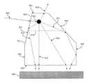
- FIG. 7illustrates a magneto-optical defect center material 720 with a defect center 715 and an optical detector 740 .
- the magneto-optical defect center material 720is a diamond material
- the defect center 715is an NV center.
- any suitable magneto-optical defect center material 720 and defect center 715can be used.
- An excitation photontravels along path 705 , enters the material 720 and excites the defect center 715 .
- the excited defect center 715emits a photon, which can be in any direction.
- Paths 710 , 711 , 712 , 713 , and 714are example paths that the emitted photon may travel. In the embodiments of FIG.
- one defect center 715is shown for illustrative purposes.
- the materialmay include multiple defect centers 715 .
- the angles and specific paths in FIG. 7are meant to be illustrative only and not meant to be limiting. In alternative embodiments, additional, fewer, and/or different elements may be used.
- the refractive index of the materialis different than the refractive index of whatever is between the material 720 and the optical detector 740 .
- the path of the emitted lightmay change direction at the interface between the material 720 and the surrounding material depending upon the angle of incidence and the differences in the refractive indexes.
- the photonmay reflect off of the surface of the material 720 .
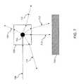
- FIG. 8Ais a diagram illustrating possible paths of light emitted from a material with defect centers and a rectangular waveguide in accordance with some illustrative embodiments.
- FIG. 8Aillustrates a material 820 with a defect center 815 and an optical detector 840 .
- the magneto-optical defect center material 820is a diamond material
- the defect center 815is an NV center.
- any suitable magneto-optical defect center material 820 and defect center 815can be used.
- Attached to the material 820is a waveguide 822 .
- An excitation photontravels along path 805 , enters the material 820 and excites the defect center 815 .
- the excited defect center 815emits a photon, which can be in any direction.
- Paths 810 , 811 , 812 , 813 , and 814are example paths that the emitted photon may travel.
- one defect center 815is shown for illustrative purposes.
- the materialmay include multiple defect centers 815 .
- the angles and specific paths in FIG. 8are meant to be illustrative only and not meant to be limiting.
- FIG. 8Bis a three-dimensional view of the material and rectangular waveguide of FIG. 8A in accordance with an illustrative embodiment. As shown in FIG. 8B , the material 820 and the waveguide 822 are a cuboid. In alternative embodiments, additional, fewer, and/or different elements may be used.
- the embodiments shown in FIG. 8Aincludes a waveguide 822 attached to the material 820 .
- the waveguide 822is a diamond, and there is no difference in refractive indexes between the waveguide 822 and the material 820 .
- the waveguide 822may be of any material with the same or similar refractive index as the material 820 . Because there is little or no difference in refractive indexes, light passing through the interface 824 does not bounce back into the material 820 or change velocity (e.g., including direction). Accordingly, because light passes freely through the interface 824 , more light is emitted from the material 820 toward the optical detector 840 than in the embodiments of FIG. 7 .
- light that hits the end face of the waveguide 822i.e., the face of the waveguide 822 facing the optical detector 840
- the material 820includes NV centers, but the waveguide 822 does not include NV centers.
- Light emitted from an NV centercan be used to excite another NV center.
- the excited NV centeremits light in any direction. Accordingly, if the waveguide 822 includes NV centers, light that passed through the interface 824 may excite an NV center in the waveguide 822 , and the NV center may emit light back towards the material 820 or in a direction that would allow the light to pass through a side surface of the waveguide 822 (e.g., as opposed to the end face of the waveguide 822 and toward the optical detector 840 ). In some instances, light may be absorbed by defects that are not NV centers, and such defects may not emit a corresponding light. In such instances, the light is not transmitted to a light sensor.
- efficiency of the waveguide 822is increased when the waveguide 822 does not include nitrogen vacancies.
- efficiency of the systemis determined by the amount of light that is emitted from the defect centers compared to the amount of light that is detected the optical detector 840 . That is, in a system with 100% efficiency, the same amount of light that is emitted by the defect centers passes through the end face of the waveguide 822 and is detected by the optical detector 840 .
- a system with the waveguide 822 that has nitrogen vacancieshas a mean efficiency of about 4.5%
- a system with the waveguide 822 that does not have nitrogen vacancieshas a mean efficiency of about 6.1%.
- FIG. 9Ais a diagram illustrating possible paths of light emitted from a material with defect centers and an angled waveguide in accordance with some illustrative embodiments.
- FIG. 9Aillustrates a material 920 with a defect center 915 and an optical detector 940 .
- the magneto-optical defect center material 920is a diamond material
- the defect center 915is an NV center.
- any suitable magneto-optical defect center material 920 and defect center 915can be used.
- the material 920 with the waveguide 922has a higher efficiency than the embodiments of FIG. 8 .
- the systemhas a mean efficiency of about 9.8%.
- the shape of the material 920 and the waveguide 922 in FIG. 9Ais two-dimensional. That is, the surfaces of the material 920 and the waveguide 922 that are orthogonal to the viewing direction of FIG. 9 are flat with each side in a plane that is parallel to one another, and each side spaced from one another.
- FIG. 9Bis a three-dimensional view of the material and angular waveguide of FIG. 9A in accordance with an illustrative embodiment.
- the material 920 and the waveguide 922are defined, in one plane, by sides 951 , 952 , 953 , 954 , 955 , and 956 .
- the angles between sides 951 and 952 , between sides 952 and 953 , between sides 953 and 954 , and between sides 956 and 951are obtuse angles (i.e., greater than 90°).
- the angles between sides 954 and 955 and between sides 955 and 956are right angles (i.e., 90°).
- the material 920 with nitrogen vacanciesdoes not extend to sides 954 , 955 , and 956 .
- any suitable shapecan be used.
- the waveguidecan include a compound parabolic concentrator (CPC).
- the waveguidecan approximate a CPC.
- FIG. 10Ais a diagram illustrating possible paths of light emitted from a material with defect centers and a three-dimensional waveguide in accordance with some illustrative embodiments.
- FIG. 10Aillustrates a material 1020 with a defect center 1015 and an optical detector 1040 .
- the magneto-optical defect center material 1020is a diamond material
- the defect center 1015is an NV center.
- any suitable magneto-optical defect center material 1020 and defect center 1015can be used.
- Attached to the material 1020is a waveguide 122 .
- An excitation photontravels along path 1005 , enters the material 1020 , and excites the defect center 1015 .
- the excited defect center 1015emits a photon, which can be in any direction.
- Paths 1010 , 1011 , 1012 , and 1013are example paths that the emitted photon may travel.
- one defect center 1015is shown for illustrative purposes.
- the materialmay include multiple defect centers 1015 .
- the angles and specific paths in FIG. 10are meant to be illustrative only and not meant to be limiting. In alternative embodiments, additional, fewer, and/or different elements may be used.
- the material 1020includes defect centers, and the waveguide 1022 is made of diamond but does not include defect centers.
- the angles formed by sides 1055 and 1056 and by sides 1056 and 1057are right angles, and the other angles formed by the other sides are obtuse angles.
- the cross-sectional shape of the material 1020 and the waveguide 1022 of FIG. 10Ais the shape of the material 1020 and the waveguide 1022 in two, orthogonal planes.
- the material 1020 and the waveguide 1022have one side 1052 , one side 1056 , two sides 1051 , two sides 1053 , two sides 1054 , two sides 1055 , two sides 1057 , and two sides 1058 .
- the three-dimensional aspectcan be seen in FIG. 10B .
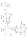
- FIGS. 10C-10Fare two-dimensional cross-sectional drawings of a three-dimensional waveguide in accordance with some illustrative embodiments.
- the three-dimensional waveguide in FIGS. 10C-10Fcan be the same waveguide as in FIGS. 10A and/or 10B .
- Dimensions 1061 , 1062 , 1063 , 1064 , 1065 , 1066 , 1067 , 1068 , 1069 , and 1070are provided as illustrative measurements in accordance with some embodiments. In alternative embodiments, any other suitable dimensions may be used.
- the dimension 1061is 2.81 mm
- the dimension 1062is 2.00 mm
- the dimension 1063is 0.60 mm
- the dimension 1064is 1.00 mm
- the dimension 1065is 3.00 mm
- the dimension 1066is 0.50 mm
- the dimension 1067is 1.17 mm
- the dimension 1068is 2.0 mm
- the dimension 1069is 0.60
- the dimension 1070is 1.75 mm.
- the three-dimensional material 1020 and waveguide 1022 of the system of FIGS. 10A-10Fhad a mean efficiency of 55.1%.
- the shape of the configuration of FIGS. 10A and 10Bcan be created using diamond shaping and polishing techniques. In some instances, the shapes of FIGS. 10A-10F can be more difficult (e.g., more steps, more sides, etc.) than other configurations (e.g., those of FIGS. 8A, 8B, 9A, and 9B ).
- the material and the waveguide of the configurations of FIGS. 8A, 8B, 9A, 9B, and 10A-10Finclude the material with the defect centers and the material without the defect centers (i.e., the waveguide).
- the material with the defect centersis synthesized via any suitable method (e.g., chemical vapor deposition), and the waveguide is synthesized onto the material with the defect centers. In alternative embodiments, the material with the defect centers is synthesized onto the waveguide.
- FIG. 11is a diagram illustrating a material attached to a waveguide in accordance with some illustrative embodiments.
- the material 1120can be fused to the waveguide 1122 .
- the material 1120 and the waveguide 1122are fused together using optical contact bonding.
- any suitable methodcan be used to fuse the material 1120 and the waveguide 1122 .
- the refractive index of the material 1120 and the waveguide 1122are the same. Accordingly, as discussed above, more of the light that is emitted from the defect centers is directed towards the optical detector 1140 with the waveguide 1122 than without.
- the waveguide 1122can be manufactured into any suitable shape.
- the waveguide 1122is a paraboloid.
- the waveguide 1122can be a compound parabolic concentrator.
- the material 1120is a cube.
- the length of the diagonal of one of the sidesis the same as the length of the diameter of the paraboloid at the end of the waveguide 1122 attached to the material 1120 .
- any other suitable shapecan be used, such as any of the shapes shown in FIGS. 8A, 8B, 9A, 9B, and 10A-10F .
- the light used to excite the corresponding defect centersis orthogonal to the respective side of the material that the light enters.
- light entering the material through the interface at an orthogonal angleis the most efficient direction to get the light into the material.
- a larger incidence anglemay be more efficient than an orthogonal angle, depending upon the polarization of the light with respect to the surface orientation.
- the lightcan enter the material at any suitable angle, even if at a less efficient angle.
- the angle of the light entering the materialcan be parallel to a plane of the respective optical detector (e.g., as in FIG. 7 ).
- Such an anglecan be chosen based on, for example, a configuration of a magnetometer system (e.g., a DNV system) or other system constraints.
- FIG. 12is a flow chart of a method of forming a material with a waveguide in accordance with an illustrative embodiment.
- additional, fewer, and/or different operationsmay be performed.
- the use of a flow chart and/or arrowsis not meant to be limiting with respect to the order or flow of operations.
- two or more operationsmay be performed simultaneously.
- a material with defect centersis synthesized.
- the materialcan be a diamond material, and the defect centers can be NV centers.
- chemical vapor depositioncan be used to create the material with defect centers.
- any suitable method for synthesizing the material with defect centerscan be used.
- a waveguideis synthesized.
- the waveguidecan be the same material as the material with the defect centers but without the defect centers (e.g., diamond material without NV centers or other defect centers).
- chemical vapor depositionis used to synthesize the waveguide onto the material with defect centers.
- chemical vapor depositioncan be used to form the material in the operation 1205 in the presence of nitrogen or other element or material, and the waveguide can be synthesized by continuing to deposit carbon on the material but without the nitrogen or other element or material.
- the material and waveguidecan be cut and polished.
- the material and waveguidecan be cut and polished into one of the shapes shown in FIGS. 8A, 8B, 9A, 9B, 10A-10F .
- the material and waveguidecan be used in a magnetometer such as a DNV sensor.
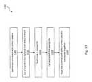
- FIG. 13is a flow chart of a method of forming a material with a waveguide in accordance with some illustrative embodiments.
- additional, fewer, and/or different operationsmay be performed.
- the use of a flow chart and/or arrowsis not meant to be limiting with respect to the order or flow of operations.
- two or more operationsmay be performed simultaneously.
- a material with defect centersis synthesized.
- the materialis diamond and the defect centers are NV centers.
- a materialcan be formed using chemical vapor deposition in the presence of nitrogen or other defect material, thereby forming a material with defect centers.
- any suitable methodcan be used to create a material with defect centers.
- the material with defect centersis cut and polished. The material with defect centers can be cut into any suitable shape, such as a cube, a cuboid, etc.
- a waveguideis synthesized.
- a material without defect centerscan be formed using any suitable method, such as chemical vapor deposition.
- the waveguidecan be cut and polished.
- the waveguidecan be cut into the shape of the waveguide 822 of FIGS. 8A and 8B , the waveguide 922 of FIGS. 9A and 9B , the waveguide 1022 of FIGS. 10A-10F , or the waveguide 1122 of FIG. 11 .
- the waveguidecan be cut into any suitable shape.
- the material with the defect centersis fused to the waveguide.
- optical contact bondingcan be used to fuse the material with the defect centers with the waveguide.
- an adhesive or other suitable bonding agentcan be used to attach the material with the defect centers to the waveguide.
- the substance used to fix the material with the defect centers to the waveguidecan have a refractive index that is the same as or similar to the refractive index of the material.
- the material and waveguidecan be used in a magnetometer such as a DNV sensor.
- any of the operations described hereincan be implemented at least in part as computer-readable instructions stored on a computer-readable memory. Upon execution of the computer-readable instructions by a processor, the computer-readable instructions can cause a node to perform the operations.
- any two components so associatedcan also be viewed as being “operably connected,” or “operably coupled,” to each other to achieve the desired functionality, and any two components capable of being so associated can also be viewed as being “operably couplable,” to each other to achieve the desired functionality.
- operably couplableinclude but are not limited to physically mateable and/or physically interacting components and/or wirelessly interactable and/or wirelessly interacting components and/or logically interacting and/or logically interactable components.
- the phrase “A or B”will be understood to include the possibilities of “A” or “B” or “A and B.” Further, unless otherwise noted, the use of the words “approximate,” “about,” “around,” “substantially,” etc., mean plus or minus ten percent.
Landscapes
- Physics & Mathematics (AREA)
- General Physics & Mathematics (AREA)
- Condensed Matter Physics & Semiconductors (AREA)
- Optics & Photonics (AREA)
- Engineering & Computer Science (AREA)
- Power Engineering (AREA)
- Optical Modulation, Optical Deflection, Nonlinear Optics, Optical Demodulation, Optical Logic Elements (AREA)
Abstract
Description
Magneto-optical defect center materials such as diamonds with nitrogen vacancy centers can be used to determine an applied magnetic field by transmitting light into the diamond and measuring the responsive light that is emitted. The loss of light in such systems may be detrimental to measurements and operations.
An illustrative magneto-optical defect center material may include a first portion comprising a plurality of defect centers dispersed throughout the first portion. The magneto-optical material also may include a second portion adjacent to the first portion. The second portion may not contain significant defect centers. The second portion may be configured to facilitate transmission of light generated by the defect centers of the first portion away from the first portion.
Some illustrative magneto-optical defect center materials may include a first portion that can have a plurality of defect centers dispersed throughout the first portion. The materials may also include a second portion adjacent to the first portion. The second portion may not contain defect centers. The second portion may be configured to facilitate transmission of light generated by the defect centers of the first portion away from the first portion.
Some illustrative magnetometers may include a diamond. The diamond may include a first portion and a second portion. The first portion may include a plurality of nitrogen vacancy (NV) centers, and the second portion may not have substantial NV centers. The second portion may be configured to facilitate transmission of light generated from the NV centers of the first portion away from the first portion. The magnetometer may further include a light source that may be configured to transmit light into the first portion of the diamond. The magnetometer may further include a photo detector configured to detect light transmitted through at least one side of the second portion of the diamond. The magnetometer may also include a processor operatively coupled to the photo detector. The processor may be configured to determine a strength of a magnetic field based at least in part on the light detected by the photo detector.
Some illustrative magneto-optical defect center materials include means for absorbing first light with a first frequency and transmitting second light with a second frequency. The materials may also include means for directing the second light that may be adjacent to the means for absorbing the first light and transmitting the second light. The means for directing the second light may not absorb the first light. The means for directing the second light may be configured to facilitate transmission of the second light away from the means for absorbing the first light and transmitting the second light.
Some illustrative methods include receiving, at a plurality of defect centers of a first portion of a magneto-optical defect center material, first light with a first frequency. The plurality of defect centers may be dispersed throughout the first portion. The method can also include transmitting, from the plurality of defect centers, second light with a second frequency. The method may further include facilitating, via a second portion of the magneto-optical defect center material, the second light away from the first portion. The second portion may be adjacent to the first portion. The second portion may not contain defect centers.
The foregoing summary is illustrative only and is not intended to be in any way limiting. In addition to the illustrative aspects, embodiments, and features described above, further aspects, embodiments, and features will become apparent by reference to the following drawings and the detailed description.
The foregoing and other features of the present disclosure will become apparent from the following description and appended claims, taken in conjunction with the accompanying drawings. Understanding that these drawings depict only several embodiments in accordance with the disclosure and are, therefore, not to be considered limiting of its scope, the disclosure will be described with additional specificity and detail through use of the accompanying drawings.
In the following detailed description, reference is made to the accompanying drawings, which form a part hereof. In the drawings, similar symbols typically identify similar components, unless context dictates otherwise. The illustrative embodiments described in the detailed description, drawings, and claims are not meant to be limiting. Other embodiments may be utilized, and other changes may be made, without departing from the spirit or scope of the subject matter presented here. It will be readily understood that the aspects of the present disclosure, as generally described herein, and illustrated in the figures, can be arranged, substituted, combined, and designed in a wide variety of different configurations, all of which are explicitly contemplated and make part of this disclosure.
Magneto-optical defect center materials such as diamonds with nitrogen vacancy (NV) centers can be used to detect magnetic fields. Green light which enters a diamond structure with NV centers interacts with NV centers, and red light is emitted from the diamond. The amount of red light emitted can be used to determine the strength of the magnetic field. The efficiency and accuracy of sensors using magneto-optical defect center materials such as diamonds with NV centers (DNV sensors) is increased by transferring as much light as possible from the NV centers to the photo sensor that measures the amount of red light. Magneto-optical defect center materials include but are not be limited to diamonds, Silicon Carbide (SiC) and other materials with nitrogen, boron, or other chemical defect centers.
In various embodiments described herein, the material with the defect centers may be formed in a shape that directs light from the defect centers towards the photo diode. When excited by the green light photon, a defect center emits a red light photon. But, the direction that the red light photon is emitted from the defect center is not necessarily the direction that the green light photon was received. Rather, the red light photon can be emitted in any direction. When the red photon reaches the interface between the diamond and the surrounding medium, the photon may transmit through the interface or reflect back into the diamond, depending, in part, on the angle of incidence at the interface. The phenomenon by which the photon may reflect back into the diamond is referred to as total internal reflection (TIR). Thus, the sides of the diamond can be angled and polished to reflect red light photons towards the photo sensor.
The NV center in a diamond comprises a substitutional nitrogen or boron atom in a lattice site adjacent a carbon vacancy as shown inFIG. 1 . The NV center may have four orientations, each corresponding to a different crystallographic orientation of the diamond lattice.
The NV center may exist in a neutral charge state or a negative charge state. Conventionally, the neutral charge state uses the nomenclature NV0, while the negative charge state uses the nomenclature NV, which is adopted in this description.
The NV center has a number of electrons, including three unpaired electrons, each one from the vacancy to a respective of the three carbon atoms adjacent to the vacancy, and a pair of electrons between the nitrogen and the vacancy. The NV center, which is in the negatively charged state, also includes an extra electron.
The NV center has rotational symmetry, and as shown inFIG. 2 , has a ground state, which is a spin triplet with3A2symmetry with one spin state ms=0, and two further spin states ms=+1, and ms=−1. In the absence of an external magnetic field, the ms=±1 energy levels are offset from the ms=0 due to spin-spin interactions, and the ms=±1 energy levels are degenerate, i.e., they have the same energy. The ms=0 spin state energy level is split from the ms=±1 energy levels by an energy of 2.87 GHz for a zero external magnetic field.
Introducing an external magnetic field with a component along the NV axis lifts the degeneracy of the ms=±1 energy levels, splitting the energy levels ms=±1 by an amount 2gμBBz, where g is the g-factor, μBis the Bohr magneton, and Bzis the component of the external magnetic field along the NV axis. This relationship is correct to a first order and inclusion of higher order corrections is a straightforward matter and will not affect the computational and logic steps in the systems and methods described below.
The NV center electronic structure further includes an excited triplet state3E with corresponding ms=0 and ms=±1 spin states. The optical transitions between the ground state3A2and the excited triplet3E are predominantly spin conserving, meaning that the optical transitions are between initial and final states that have the same spin. For a direct transition between the excited triplet3E and the ground state3A2, a photon of red light is emitted with a photon energy corresponding to the energy difference between the energy levels of the transitions.
There is, however, an alternative non-radiative decay route from the triplet3E to the ground state3A2via intermediate electron states, which are thought to be intermediate singlet states A, E with intermediate energy levels. Significantly, the transition rate from the ms=±1 spin states of the excited triplet3E to the intermediate energy levels is significantly greater than the transition rate from the ms=0 spin state of the excited triplet3E to the intermediate energy levels. The transition from the singlet states A, E to the ground state triplet3A2predominantly decays to the ms=0 spin state over the ms=±1 spins states. These features of the decay from the excited triplet3E state via the intermediate singlet states A, E to the ground state triplet3A2allows that if optical excitation is provided to the system, the optical excitation will eventually pump the NV center into the ms=0 spin state of the ground state3A2. In this way, the population of the ms=0 spin state of the ground state3A2may be “reset” to a maximum polarization determined by the decay rates from the triplet3E to the intermediate singlet states.
Another feature of the decay is that the fluorescence intensity due to optically stimulating the excited triplet3E state is less for the ms=±1 states than for the ms=0 spin state. This is so because the decay via the intermediate states does not result in a photon emitted in the fluorescence band, and because of the greater probability that the ms=±1 states of the excited triplet3E state will decay via the non-radiative decay path. The lower fluorescence intensity for the ms=±1 states than for the ms=0 spin state allows the fluorescence intensity to be used to determine the spin state. As the population of the ms=±1 states increases relative to the ms=0 spin, the overall fluorescence intensity will be reduced.
TheRF excitation source 330 may be a microwave coil, for example. TheRF excitation source 330, when emitting RF radiation with a photon energy resonant with the transition energy between ground ms=0 spin state and the ms=+1 spin state, excites a transition between those spin states. For such a resonance, the spin state cycles between ground ms=0 spin state and the ms=+1 spin state, reducing the population in the ms=0 spin state and reducing the overall fluorescence at resonances. Similarly, resonance occurs between the ms=0 spin state and the ms=−1 spin state of the ground state when the photon energy of the RF radiation emitted by the RF excitation source is the difference in energies of the ms=0 spin state and the ms=−1 spin state, or between the ms=0 spin state and the ms=+1 spin state, there is a decrease in the fluorescence intensity.
Theoptical excitation source 310 may be a laser or a light emitting diode, for example, which emits light in the green, for example. Theoptical excitation source 310 induces fluorescence in the red, which corresponds to an electronic transition from the excited state to the ground state. Light from theNV diamond material 320 is directed through theoptical filter 350 to filter out light in the excitation band (in the green, for example), and to pass light in the red fluorescence band, which in turn is detected by thedetector 340. The opticalexcitation light source 310, in addition to exciting fluorescence in thediamond material 320, also serves to reset the population of the ms=0 spin state of the ground state3A2to a maximum polarization, or other desired polarization.
For continuous wave excitation, theoptical excitation source 310 continuously pumps the NV centers, and theRF excitation source 330 sweeps across a frequency range that includes the zero splitting (when the ms=±1 spin states have the same energy) photon energy of 2.87 GHz. The fluorescence for an RF sweep corresponding to adiamond material 320 with NV centers aligned along a single direction is shown inFIG. 4 for different magnetic field components Bzalong the NV axis, where the energy splitting between the ms=−1 spin state and the ms=+1 spin state increases with Bz. Thus, the component Bzmay be determined. Optical excitation schemes other than continuous wave excitation are contemplated, such as excitation schemes involving pulsed optical excitation, and pulsed RF excitation. Examples of pulsed excitation schemes include Ramsey pulse sequence, and spin echo pulse sequence. The excitation scheme utilized during the measurement collection process (i.e., the applied optical excitation and the applied RF excitation) may be any appropriate excitation scheme. For example, the excitation scheme may utilize continuous wave (CW) magnetometry, pulsed magnetometry, and variations on CW and pulsed magnetometry (e.g., pulsed RF excitation with CW optical excitation). In cases where Ramsey pulse RF sequences are used, pulse parameters u and T may be optimized using Rabi analysis and FID-Tau sweeps prior to the collection process, as described in, for example, U.S. patent application Ser. No. 15/003,590, which is incorporated by reference herein in its entirety.
In general, thediamond material 320 will have NV centers aligned along directions of four different orientation classes.FIG. 5 illustrates fluorescence as a function of RF frequency for the case where thediamond material 320 has NV centers aligned along directions of four different orientation classes. In this case, the component Bzalong each of the different orientations may be determined. These results, along with the known orientation of crystallographic planes of a diamond lattice, allow not only the magnitude of the external magnetic field to be determined, but also the direction of the magnetic field.
WhileFIG. 3 illustrates an NV centermagnetic sensor system 300 withNV diamond material 320 with a plurality of NV centers, in general, the magnetic sensor system may instead employ a different magneto-optical defect center material, with a plurality of magneto-optical defect centers. Magneto-optical defect center materials include but are not be limited to diamonds, Silicon Carbide (SiC) and other materials with nitrogen, boron, or other defect centers. The electronic spin state energies of the magneto-optical defect centers shift with magnetic field, and the optical response, such as fluorescence, for the different spin states is not the same for all of the different spin states. In this way, the magnetic field may be determined based on optical excitation, and possibly RF excitation, in a corresponding way to that described above with NV diamond material.
Themagnetic field generator 670 may generate magnetic fields with orthogonal polarizations, for example. In this regard, themagnetic field generator 670 may include two or more magnetic field generators, such as two or more Helmholtz coils. The two or more magnetic field generators may be configured to provide a magnetic field having a predetermined direction, each of which provide a relatively uniform magnetic field at theNV diamond material 620. The predetermined directions may be orthogonal to one another. In addition, the two or more magnetic field generators of themagnetic field generator 670 may be disposed at the same position, or may be separated from each other. In the case that the two or more magnetic field generators are separated from each other, the two or more magnetic field generators may be arranged in an array, such as a one-dimensional or two-dimensional array, for example.
Thesystem 600 may be arranged to include one or moreoptical detection systems 605, where each of theoptical detection systems 605 includes theoptical detector 640,optical excitation source 610, andNV diamond material 620. Furthermore, themagnetic field generator 670 may have a relatively high power as compared to theoptical detection systems 605. In this way, theoptical systems 605 may be deployed in an environment that requires a relatively lower power for theoptical systems 605, while themagnetic field generator 670 may be deployed in an environment that has a relatively high power available for themagnetic field generator 670 so as to apply a relatively strong magnetic field.
Thesystem 600 further includes acontroller 680 arranged to receive a light detection signal from theoptical detector 640 and to control theoptical excitation source 610, theRF excitation source 630, and the second magnetic field generator675. The controller may be a single controller, or multiple controllers. For a controller including multiple controllers, each of the controllers may perform different functions, such as controlling different components of thesystem 600. The second magnetic field generator675 may be controlled by thecontroller 680 via an amplifier660, for example.
TheRF excitation source 630 may be a microwave coil, for example. TheRF excitation source 630 is controlled to emit RF radiation with a photon energy resonant with the transition energy between the ground ms=0 spin state and the ms=±1 spin states as discussed above with respect toFIG. 3 .
Theoptical excitation source 610 may be a laser or a light emitting diode, for example, which emits light in the green, for example. Theoptical excitation source 610 induces fluorescence in the red from theNV diamond material 620, where the fluorescence corresponds to an electronic transition from the excited state to the ground state. Light from theNV diamond material 620 is directed through the optical filter650 to filter out light in the excitation band (in the green, for example), and to pass light in the red fluorescence band, which in turn is detected by theoptical detector 640. The opticalexcitation light source 610, in addition to exciting fluorescence in theNV diamond material 620, also serves to reset the population of the ms=0 spin state of the ground state3A2to a maximum polarization, or other desired polarization.
Thecontroller 680 is arranged to receive a light detection signal from theoptical detector 640 and to control theoptical excitation source 610, theRF excitation source 630, and the second magnetic field generator675. The controller may include aprocessor 682 and amemory 684, in order to control the operation of theoptical excitation source 610, theRF excitation source 630, and the second magnetic field generator675. Thememory 684, which may include a nontransitory computer readable medium, may store instructions to allow the operation of theoptical excitation source 610, theRF excitation source 630, and the second magnetic field generator675 to be controlled. That is, thecontroller 680 may be programmed to provide control.
In the embodiments illustrated inFIG. 7 , there is no object between the material720 and theoptical detector 740. Thus, air or a vacuum is between the material720 and theoptical detector 740. The air or vacuum surrounds thematerial 720. In alternative embodiments, objects such as waveguides may be between the material720 and theoptical detector 740. Regardless of whether an object is between the material720 and theoptical detector 740, the refractive index of the material is different than the refractive index of whatever is between the material720 and theoptical detector 740.
In the embodiments shown inFIG. 7 in which the same material (e.g., air or a vacuum) surrounds thematerial 720 on all sides and has a different refractive index than thematerial 720, the path of the emitted light may change direction at the interface between the material720 and the surrounding material depending upon the angle of incidence and the differences in the refractive indexes. In some instances, depending upon the differences in the refractive indexes, the angle of incidence, and the surface of the interface (e.g., smooth or rough), the photon may reflect off of the surface of thematerial 720. In general, as the angle of incidence becomes more orthogonal, as the differences in the refractive indexes gets closer to zero, and as the surface of the interface is more rough, the higher the chance that the emitted photon will pass through the interface rather than reflect off of the interface. In the examples ofFIG. 7 , all ofpaths material 720 before passing through the interface. Because the emitted photon can be emitted in any three-dimensional direction, only a small fraction of the possible beam paths exit the surface of the material720 facing theoptical detector 740.
The embodiments shown inFIG. 8A includes awaveguide 822 attached to thematerial 820. In an illustrative embodiment, thewaveguide 822 is a diamond, and there is no difference in refractive indexes between thewaveguide 822 and thematerial 820. In alternative embodiments, thewaveguide 822 may be of any material with the same or similar refractive index as thematerial 820. Because there is little or no difference in refractive indexes, light passing through the interface824 does not bounce back into thematerial 820 or change velocity (e.g., including direction). Accordingly, because light passes freely through the interface824, more light is emitted from thematerial 820 toward theoptical detector 840 than in the embodiments ofFIG. 7 . That is, light emitted in a direction toward a side of the material820 that is not the interface824 may bounce back into thematerial 820 depending upon the angle of incidence, etc., as described above. Such light, therefore, has a chance to be bounced into the direction of the interface824 and toward theoptical detector 840. In general, light (e.g., via path812) that contacts a sidewall of thewaveguide 822 will be reflected back into thewaveguide 822 as opposed to transitioning outside of thewaveguide 822 because of the angle of incidence. That is, such light will generally have a low angle of incidence, thereby increasing the chance that the light will bounce back into thewaveguide 822. Similarly, light that hits the end face of the waveguide822 (i.e., the face of thewaveguide 822 facing the optical detector840) will generally have a high angle of incidence, and, therefore, a higher chance of passing through the end of thewaveguide 822 and pass onto the surface of the optical detector.
In some illustrative embodiments, thematerial 820 includes NV centers, but thewaveguide 822 does not include NV centers. Light emitted from an NV center can be used to excite another NV center. The excited NV center emits light in any direction. Accordingly, if thewaveguide 822 includes NV centers, light that passed through the interface824 may excite an NV center in thewaveguide 822, and the NV center may emit light back towards thematerial 820 or in a direction that would allow the light to pass through a side surface of the waveguide822 (e.g., as opposed to the end face of thewaveguide 822 and toward the optical detector840). In some instances, light may be absorbed by defects that are not NV centers, and such defects may not emit a corresponding light. In such instances, the light is not transmitted to a light sensor.
Accordingly, efficiency of thewaveguide 822 is increased when thewaveguide 822 does not include nitrogen vacancies. In this context, efficiency of the system is determined by the amount of light that is emitted from the defect centers compared to the amount of light that is detected theoptical detector 840. That is, in a system with 100% efficiency, the same amount of light that is emitted by the defect centers passes through the end face of thewaveguide 822 and is detected by theoptical detector 840. In an illustrative embodiment, a system with thewaveguide 822 that has nitrogen vacancies has a mean efficiency of about 4.5%, whereas a system with thewaveguide 822 that does not have nitrogen vacancies has a mean efficiency of about 6.1%.
In an illustrative embodiment, the shape of thematerial 920 and thewaveguide 922 inFIG. 9A is two-dimensional. That is, the surfaces of thematerial 920 and thewaveguide 922 that are orthogonal to the viewing direction ofFIG. 9 are flat with each side in a plane that is parallel to one another, and each side spaced from one another.FIG. 9B is a three-dimensional view of the material and angular waveguide ofFIG. 9A in accordance with an illustrative embodiment.
As shown inFIG. 9A , thematerial 920 and thewaveguide 922 are defined, in one plane, bysides sides sides sides sides sides sides sides
In an illustrative embodiment, thematerial 1020 includes defect centers, and thewaveguide 1022 is made of diamond but does not include defect centers. In an illustrative embodiment, the angles formed bysides sides material 1020 and thewaveguide 1022 ofFIG. 10A is the shape of thematerial 1020 and thewaveguide 1022 in two, orthogonal planes. That is, thematerial 1020 and thewaveguide 1022 have oneside 1052, oneside 1056, twosides 1051, twosides 1053, twosides 1054, twosides 1055, twosides 1057, and twosides 1058. The three-dimensional aspect can be seen inFIG. 10B .
In an illustrative embodiment, the three-dimensional material 1020 andwaveguide 1022 of the system ofFIGS. 10A-10F had a mean efficiency of 55.1%. The shape of the configuration ofFIGS. 10A and 10B can be created using diamond shaping and polishing techniques. In some instances, the shapes ofFIGS. 10A-10F can be more difficult (e.g., more steps, more sides, etc.) than other configurations (e.g., those ofFIGS. 8A, 8B, 9A, and 9B ). As explained above, the material and the waveguide of the configurations ofFIGS. 8A, 8B, 9A, 9B, and 10A-10F include the material with the defect centers and the material without the defect centers (i.e., the waveguide). In some embodiments, the material with the defect centers is synthesized via any suitable method (e.g., chemical vapor deposition), and the waveguide is synthesized onto the material with the defect centers. In alternative embodiments, the material with the defect centers is synthesized onto the waveguide.
In alternative embodiments, the material and the waveguide can be synthesized (or otherwise formed) independently and attached after synthesis. For example,FIG. 11 is a diagram illustrating a material attached to a waveguide in accordance with some illustrative embodiments. Thematerial 1120 can be fused to thewaveguide 1122. In an illustrative embodiment, thematerial 1120 and thewaveguide 1122 are fused together using optical contact bonding. In alternative embodiments, any suitable method can be used to fuse thematerial 1120 and thewaveguide 1122.
In an illustrative embodiment, the refractive index of thematerial 1120 and thewaveguide 1122 are the same. Accordingly, as discussed above, more of the light that is emitted from the defect centers is directed towards theoptical detector 1140 with thewaveguide 1122 than without.
In an illustrative embodiment, because thewaveguide 1122 is synthesized separately from thematerial 1120, thewaveguide 1122 can be manufactured into any suitable shape. In the embodiments shown inFIG. 11 , thewaveguide 1122 is a paraboloid. For example, thewaveguide 1122 can be a compound parabolic concentrator. In an illustrative embodiment, thematerial 1120 is a cube. In such an embodiment, the length of the diagonal of one of the sides is the same as the length of the diameter of the paraboloid at the end of thewaveguide 1122 attached to thematerial 1120. In alternative embodiments, any other suitable shape can be used, such as any of the shapes shown inFIGS. 8A, 8B, 9A, 9B, and 10A-10F .
In the embodiments ofFIGS. 7, 8A, 9A, and 10A , the light used to excite the corresponding defect centers is orthogonal to the respective side of the material that the light enters. In some instances, light entering the material through the interface at an orthogonal angle is the most efficient direction to get the light into the material. In other instances, a larger incidence angle may be more efficient than an orthogonal angle, depending upon the polarization of the light with respect to the surface orientation. In alternative embodiments, the light can enter the material at any suitable angle, even if at a less efficient angle. For example, the angle of the light entering the material can be parallel to a plane of the respective optical detector (e.g., as inFIG. 7 ). Such an angle can be chosen based on, for example, a configuration of a magnetometer system (e.g., a DNV system) or other system constraints.
In anoperation 1205, a material with defect centers is synthesized. For example, the material can be a diamond material, and the defect centers can be NV centers. In an illustrative embodiment, chemical vapor deposition can be used to create the material with defect centers. In alternative embodiments, any suitable method for synthesizing the material with defect centers can be used.
In anoperation 1210, a waveguide is synthesized. For example, the waveguide can be the same material as the material with the defect centers but without the defect centers (e.g., diamond material without NV centers or other defect centers). In an illustrative embodiment, chemical vapor deposition is used to synthesize the waveguide onto the material with defect centers. For example, chemical vapor deposition can be used to form the material in theoperation 1205 in the presence of nitrogen or other element or material, and the waveguide can be synthesized by continuing to deposit carbon on the material but without the nitrogen or other element or material.
In anoperation 1215, the material and waveguide can be cut and polished. For example, the material and waveguide can be cut and polished into one of the shapes shown inFIGS. 8A, 8B, 9A, 9B, 10A-10F . In an illustrative embodiment, after the material and waveguide is cut and polished, the material and waveguide can be used in a magnetometer such as a DNV sensor.
In anoperation 1305, a material with defect centers is synthesized. In an illustrative embodiment, the material is diamond and the defect centers are NV centers. For example, a material can be formed using chemical vapor deposition in the presence of nitrogen or other defect material, thereby forming a material with defect centers. In alternative embodiments, any suitable method can be used to create a material with defect centers. In anoperation 1310, the material with defect centers is cut and polished. The material with defect centers can be cut into any suitable shape, such as a cube, a cuboid, etc.
In anoperation 1315, a waveguide is synthesized. For example, a material without defect centers can be formed using any suitable method, such as chemical vapor deposition. In anoperation 1320, the waveguide can be cut and polished. For example, the waveguide can be cut into the shape of thewaveguide 822 ofFIGS. 8A and 8B , thewaveguide 922 ofFIGS. 9A and 9B , thewaveguide 1022 ofFIGS. 10A-10F , or thewaveguide 1122 ofFIG. 11 . In alternative embodiments, the waveguide can be cut into any suitable shape.
In anoperation 1325, the material with the defect centers is fused to the waveguide. For example, optical contact bonding can be used to fuse the material with the defect centers with the waveguide. In alternative embodiments, an adhesive or other suitable bonding agent can be used to attach the material with the defect centers to the waveguide. In such embodiments, the substance used to fix the material with the defect centers to the waveguide can have a refractive index that is the same as or similar to the refractive index of the material. In an illustrative embodiment, after the material and waveguide are fixed together, the material and waveguide can be used in a magnetometer such as a DNV sensor.
In an illustrative embodiment, any of the operations described herein can be implemented at least in part as computer-readable instructions stored on a computer-readable memory. Upon execution of the computer-readable instructions by a processor, the computer-readable instructions can cause a node to perform the operations.
The herein described subject matter sometimes illustrates different components contained within, or connected with, different other components. It is to be understood that such depicted architectures are merely exemplary, and that in fact many other architectures can be implemented which achieve the same functionality. In a conceptual sense, any arrangement of components to achieve the same functionality is effectively “associated” such that the desired functionality is achieved. Hence, any two components herein combined to achieve a particular functionality can be seen as “associated with” each other such that the desired functionality is achieved, irrespective of architectures or intermedial components. Likewise, any two components so associated can also be viewed as being “operably connected,” or “operably coupled,” to each other to achieve the desired functionality, and any two components capable of being so associated can also be viewed as being “operably couplable,” to each other to achieve the desired functionality. Specific examples of operably couplable include but are not limited to physically mateable and/or physically interacting components and/or wirelessly interactable and/or wirelessly interacting components and/or logically interacting and/or logically interactable components.
With respect to the use of substantially any plural and/or singular terms herein, those having skill in the art can translate from the plural to the singular and/or from the singular to the plural as is appropriate to the context and/or application. The various singular/plural permutations may be expressly set forth herein for sake of clarity.
It will be understood by those within the art that, in general, terms used herein, and especially in the appended claims (e.g., bodies of the appended claims) are generally intended as “open” terms (e.g., the term “including” should be interpreted as “including but not limited to,” the term “having” should be interpreted as “having at least,” the term “includes” should be interpreted as “includes but is not limited to,” etc.). It will be further understood by those within the art that if a specific number of an introduced claim recitation is intended, such an intent will be explicitly recited in the claim, and in the absence of such recitation no such intent is present. For example, as an aid to understanding, the following appended claims may contain usage of the introductory phrases “at least one” and “one or more” to introduce claim recitations. However, the use of such phrases should not be construed to imply that the introduction of a claim recitation by the indefinite articles “a” or “an” limits any particular claim containing such introduced claim recitation to inventions containing only one such recitation, even when the same claim includes the introductory phrases “one or more” or “at least one” and indefinite articles such as “a” or “an” (e.g., “a” and/or “an” should typically be interpreted to mean “at least one” or “one or more”); the same holds true for the use of definite articles used to introduce claim recitations. In addition, even if a specific number of an introduced claim recitation is explicitly recited, those skilled in the art will recognize that such recitation should typically be interpreted to mean at least the recited number (e.g., the bare recitation of “two recitations,” without other modifiers, typically means at least two recitations, or two or more recitations). Furthermore, in those instances where a convention analogous to “at least one of A, B, and C, etc.” is used, in general such a construction is intended in the sense one having skill in the art would understand the convention (e.g., “a system having at least one of A, B, and C” would include but not be limited to systems that have A alone, B alone, C alone, A and B together, A and C together, B and C together, and/or A, B, and C together, etc.). In those instances where a convention analogous to “at least one of A, B, or C, etc.” is used, in general such a construction is intended in the sense one having skill in the art would understand the convention (e.g., “a system having at least one of A, B, or C” would include but not be limited to systems that have A alone, B alone, C alone, A and B together, A and C together, B and C together, and/or A, B, and C together, etc.). It will be further understood by those within the art that virtually any disjunctive word and/or phrase presenting two or more alternative terms, whether in the description, claims, or drawings, should be understood to contemplate the possibilities of including one of the terms, either of the terms, or both terms. For example, the phrase “A or B” will be understood to include the possibilities of “A” or “B” or “A and B.” Further, unless otherwise noted, the use of the words “approximate,” “about,” “around,” “substantially,” etc., mean plus or minus ten percent.
The foregoing description of illustrative embodiments has been presented for purposes of illustration and of description. It is not intended to be exhaustive or limiting with respect to the precise form disclosed, and modifications and variations are possible in light of the above teachings or may be acquired from practice of the disclosed embodiments. It is intended that the scope of the invention be defined by the claims appended hereto and their equivalents.
Claims (29)
1. A diamond comprising:
a first portion comprising a plurality of nitrogen vacancy (NV) centers dispersed throughout the first portion; and
a second portion adjacent to the first portion, wherein the second portion does not contain NV centers, and wherein the second portion is configured to facilitate transmission of light generated by the NV centers of the first portion away from the first portion.
2. The diamond ofclaim 1 , wherein all sides of the diamond are polished.
3. The diamond ofclaim 1 , wherein the second portion is configured to facilitate transmission of the light from the first portion through a side of the second portion that is opposite the first portion.
4. The diamond ofclaim 1 , wherein the first portion of the diamond comprises a first side along a first plane, wherein the second portion of the diamond comprises a second side along a second plane, and wherein the first plane is orthogonal to the second plane.
5. The diamond ofclaim 4 , wherein light that travels through the first side excites at least a portion of the NV centers, and wherein more light emitted from the NV centers travels through the second side than any other side of the diamond.
6. The diamond ofclaim 1 , wherein the second portion comprises a first side and a second side, wherein the first side and the second side are on opposite sides of the second portion, wherein the first portion is adjacent to the second portion along the first side, wherein an outside surface of the diamond is covered by a plurality of flat surfaces, wherein one of the plurality of the flat surfaces is the second side of the second portion, and wherein more light emitted from the NV centers travels through the second side than through any other one of the plurality of flat surfaces.
7. A magneto-optical defect center material comprising:
a first portion comprising a plurality of defect centers dispersed throughout the first portion; and
a second portion adjacent to the first portion, wherein the second portion does not contain defect centers, and wherein the second portion is configured to facilitate transmission of light generated by the defect centers of the first portion away from the first portion.
8. The magneto-optical defect center material ofclaim 7 , wherein all sides of the magneto-optical defect center material are polished.
9. The magneto-optical defect center material ofclaim 7 , wherein the second portion is configured to facilitate transmission of the light from the first portion through a side of the second portion that is opposite the first portion.
10. The magneto-optical defect center material ofclaim 7 , wherein the first portion of the magneto-optical defect center material comprises a first side along a first plane, wherein the second portion of the magneto-optical defect center material comprises a second side along a second plane, and wherein the first plane is orthogonal to the second plane.
11. The magneto-optical defect center material ofclaim 10 , wherein light that travels through the first side excites at least a portion of the defect centers, and wherein more light emitted from the defect centers travels through the second side than any other side of the magneto-optical defect center material.
12. The magneto-optical defect center material ofclaim 7 , wherein the second portion comprises a first side and a second side, wherein the first side and the second side are on opposite sides of the second portion, wherein the first portion is adjacent to the second portion along the first side, wherein an outside surface of the magneto-optical defect center material is covered by a plurality of flat surfaces, wherein one of the plurality of the flat surfaces is the second side of the second portion, and wherein more light emitted from the defect centers travels through the second side than through any other one of the plurality of flat surfaces.
13. A magnetometer comprising:
a magneto-optical defect center material comprising a first portion and a second portion, wherein the first portion comprises a plurality of defect centers, wherein the second portion does not comprise defect centers, and wherein the second portion is configured to facilitate transmission of light generated at the defect centers of the first portion away from the first portion;
a light source configured to transmit light into the first portion of the magneto-optical defect center material;
a photo detector configured to detect light transmitted through at least one side of the second portion of the magneto-optical defect center material; and
a processor operatively coupled to the photo detector, wherein the processor is configured to determine a strength of a magnetic field based at least in part on the light detected by the photo detector.
14. The magnetometer ofclaim 13 , wherein all sides of the magneto-optical defect center material are polished.
15. The magnetometer ofclaim 13 , wherein the second portion of the magneto-optical defect center material is configured to facilitate transmission of the light from the first portion through a side of the second portion that is opposite the first portion.
16. The magnetometer ofclaim 13 , wherein the first portion of the magneto-optical defect center material comprises a first side along a first plane, wherein the second portion of the magneto-optical defect center material comprises a second side along a second plane, and wherein the first plane is orthogonal to the second plane.
17. The magnetometer ofclaim 16 , wherein light that travels through the first side excites at least a portion of the defect centers, and wherein more light emitted from the defect centers travels through the second side than any other side of the magneto-optical defect center material.
18. The magnetometer ofclaim 13 , wherein the second portion comprises a first side and a second side, wherein the first side and the second side are on opposite sides of the second portion, wherein the first portion is adjacent to the second portion along the first side, wherein an outside surface of the magneto-optical defect center material is covered by a plurality of flat surfaces, wherein one of the plurality of the flat surfaces is the second side of the second portion, and wherein more light emitted from the defect centers travels through the second side than through any other one of the plurality of flat surfaces.
19. The magnetometer ofclaim 13 , wherein the photo detector has a sensing surface within a plane that is parallel to a direction that the light source is configured to transmit light.
20. A magneto-optical defect center material comprising:
means for absorbing first light with a first frequency and transmitting second light with a second frequency; and
means for directing the second light that is adjacent to the means for absorbing the first light and transmitting the second light, wherein the means for directing the second light does not absorb the first light, and wherein the means for directing the second light is configured to facilitate transmission of the second light away from the means for absorbing the first light and transmitting the second light.
21. The magneto-optical defect center material ofclaim 20 , wherein all sides of the magneto-optical defect center material are polished.
22. The magneto-optical defect center material ofclaim 20 , wherein the means for directing the second light is configured to facilitate transmission of the light from the means for absorbing the first light and transmitting the second light through a side of the means for directing the second light that is opposite the means for absorbing the first light and transmitting the second light.
23. The magneto-optical defect center material ofclaim 20 , wherein the means for absorbing the first light and transmitting the second light comprises a first side along a first plane, wherein the means for directing the second light of the magneto-optical defect center material comprises a second side along a second plane, and wherein the first plane is orthogonal to the second plane.
24. The magneto-optical defect center material ofclaim 20 , wherein the means for directing the second light comprises a first side and a second side, wherein the first side and the second side are on opposite sides of the means for directing the second light, wherein the means for absorbing the first light and transmitting the second light is adjacent to the means for directing the second light along the first side, wherein an outside surface of the magneto-optical defect center material is covered by a plurality of flat surfaces, wherein one of the plurality of the flat surfaces is the second side of the means for directing the second light, and wherein more of the second light travels through the second side than through any other one of the plurality of flat surfaces.
25. A method comprising:
receiving, at a plurality of defect centers of a first portion of a magneto-optical defect center material, first light with a first frequency, wherein the plurality of defect centers are dispersed throughout the first portion;
transmitting, from the plurality of defect centers, second light with a second frequency; and
facilitating, via a second portion of the magneto-optical defect center material, the second light away from the first portion, wherein the second portion is adjacent to the first portion, wherein the second portion does not contain defect centers.
26. The method ofclaim 25 , further comprising reflecting the second light off of polished sides of the first portion, through the first portion, and into the second portion.
27. The method ofclaim 26 , further comprising transmitting the second light through a side of the second portion that is at an opposite side of the second portion from the first portion.
28. The method ofclaim 25 , further comprising:
transmitting the first light through a first side of the first portion along a first plane; and
transmitting the second light through a second side of the second portion along a second plane, wherein the first plane is orthogonal to the second plane.
29. The method ofclaim 28 , wherein more of the second light travels through the second side than any other side of the magneto-optical defect center material.
Priority Applications (4)
| Application Number | Priority Date | Filing Date | Title |
|---|---|---|---|
| US15/468,641US10330744B2 (en) | 2017-03-24 | 2017-03-24 | Magnetometer with a waveguide |
| EP17807444.9AEP3465244A4 (en) | 2016-05-31 | 2017-05-31 | Magneto-optical detecting apparatus and methods |
| PCT/US2017/035315WO2017210365A1 (en) | 2016-05-31 | 2017-05-31 | Magneto-optical detecting apparatus and methods |
| US15/610,526US10677953B2 (en) | 2016-05-31 | 2017-05-31 | Magneto-optical detecting apparatus and methods |
Applications Claiming Priority (1)
| Application Number | Priority Date | Filing Date | Title |
|---|---|---|---|
| US15/468,641US10330744B2 (en) | 2017-03-24 | 2017-03-24 | Magnetometer with a waveguide |
Related Parent Applications (1)
| Application Number | Title | Priority Date | Filing Date |
|---|---|---|---|
| US15/468,410Continuation-In-PartUS20180275224A1 (en) | 2016-05-31 | 2017-03-24 | Generation of magnetic field proxy through rf frequency dithering |
Related Child Applications (2)
| Application Number | Title | Priority Date | Filing Date |
|---|---|---|---|
| US15/382,045Continuation-In-PartUS20170343619A1 (en) | 2016-05-31 | 2016-12-16 | Two-stage optical dnv excitation |
| US15/610,526Continuation-In-PartUS10677953B2 (en) | 2016-05-31 | 2017-05-31 | Magneto-optical detecting apparatus and methods |
Publications (2)
| Publication Number | Publication Date |
|---|---|
| US20180275210A1 US20180275210A1 (en) | 2018-09-27 |
| US10330744B2true US10330744B2 (en) | 2019-06-25 |
Family
ID=63581707
Family Applications (1)
| Application Number | Title | Priority Date | Filing Date |
|---|---|---|---|
| US15/468,641Active2037-08-25US10330744B2 (en) | 2016-05-31 | 2017-03-24 | Magnetometer with a waveguide |
Country Status (1)
| Country | Link |
|---|---|
| US (1) | US10330744B2 (en) |
Cited By (11)
| Publication number | Priority date | Publication date | Assignee | Title |
|---|---|---|---|---|
| US10996407B2 (en)* | 2018-12-27 | 2021-05-04 | Sumida Corporation | Excitation light irradiation device and excitation light irradiation method |
| US11119163B2 (en) | 2019-10-30 | 2021-09-14 | Honeywell International Inc. | Quantum vector magnetometer based on nanoscale fin waveguide |
| US11199733B2 (en) | 2019-10-08 | 2021-12-14 | Honeywell International Inc. | Integrated photonics quantum vector magnetometer |
| US11531073B2 (en) | 2020-12-31 | 2022-12-20 | X Development Llc | Fiber-coupled spin defect magnetometry |
| EP4194874A1 (en)* | 2021-12-09 | 2023-06-14 | Wainvam-E | Sensor device comprising a source of fluorescence coupled to a fluorescence collector and magnetometer comprising said device |
| US11733321B2 (en) | 2019-10-02 | 2023-08-22 | X Development Llc | Magnetometry based on electron spin defects |
| US11774384B2 (en) | 2021-01-15 | 2023-10-03 | X Development Llc | Spin defect magnetometry pixel array |
| US11774526B2 (en) | 2020-09-10 | 2023-10-03 | X Development Llc | Magnetometry based on electron spin defects |
| US12099102B2 (en) | 2022-04-20 | 2024-09-24 | Honeywell International Inc. | Delivery of pump laser into probe waveguide using optical diffraction |
| US12188998B2 (en) | 2022-11-08 | 2025-01-07 | Honeywell International Inc. | Integrated photonics magnetometer based on a nonlinear diamond-containing resonator |
| US12339338B2 (en) | 2023-02-07 | 2025-06-24 | Honeywell International Inc. | Integrated photonic responsive material sensor |
Families Citing this family (5)
| Publication number | Priority date | Publication date | Assignee | Title |
|---|---|---|---|---|
| CN112748378B (en)* | 2019-10-30 | 2025-06-24 | 霍尼韦尔国际公司 | Quantum vector magnetometer based on nanoscale fin waveguide |
| EP4119938A1 (en)* | 2021-07-12 | 2023-01-18 | Wainvam-E | Sensor head and measuring device including said sensor head |
| GB202110314D0 (en)* | 2021-07-19 | 2021-09-01 | Element Six Tech Ltd | Device utilising electronic zeeman splitting |
| CN113804941B (en)* | 2021-11-22 | 2022-08-16 | 安徽省国盛量子科技有限公司 | Current measuring device and method based on diamond NV color center |
| IL302162A (en)* | 2023-04-04 | 2024-11-01 | Elta Systems Ltd | Magnetic field sensor and optical collector |
Citations (446)
| Publication number | Priority date | Publication date | Assignee | Title |
|---|---|---|---|---|
| US2746027A (en) | 1951-11-16 | 1956-05-15 | James J Murray | Flux-gap variation transducer for hydrophones, microphones, and accelerometers |
| US3359812A (en) | 1964-03-13 | 1967-12-26 | Spectra Physics | Angle adjusting mechanism for optical elements |
| US3389333A (en) | 1964-02-10 | 1968-06-18 | Sperry Rand Corp | Control system for maintaining a desired magnetic field in a given space |
| US3490032A (en) | 1966-12-08 | 1970-01-13 | Gulf Research Development Co | Method and apparatus utilizing a pair of spaced magnetometers for making magnetic surveys |
| US3514723A (en) | 1966-06-23 | 1970-05-26 | Warwick Electronics Inc | Tone control circuit comprising a single potentiometer |
| US3518531A (en) | 1968-02-23 | 1970-06-30 | Varian Associates | Transient suppressor for use in magnetometer readout circuits |
| US3621380A (en) | 1969-01-02 | 1971-11-16 | Texas Instruments Inc | Method and apparatus for seismic-magnetic prospecting |
| US3745452A (en) | 1971-02-23 | 1973-07-10 | J Osburn | Magnetic field gradient apparatus and method for detecting pipe line corrosion |
| US3899758A (en) | 1974-05-01 | 1975-08-12 | Gte International Inc | Variable inductive resonant circuit arrangement having a diamagnetic core for the UHF range |
| US4025873A (en) | 1976-08-17 | 1977-05-24 | The United States Of America As Represented By The Secretary Of The Navy | Broadband, microwave, two-stage, stagger-tuned, field effect transistor amplifier |
| US4047805A (en) | 1973-02-14 | 1977-09-13 | Canon Kabushiki Kaisha | Ripple-free dichroic mirrors |
| US4078247A (en) | 1975-02-05 | 1978-03-07 | Rca Corporation | Inverter circuit control circuit for precluding simultaneous conduction of thyristors |
| US4084215A (en) | 1977-02-25 | 1978-04-11 | The United States Of America As Represented By The Secretary Of The Navy | Strobe light having reduced electromagnetic radiation |
| US4322769A (en) | 1980-12-22 | 1982-03-30 | International Business Machines Corporation | Electric switch operation monitoring circuitry |
| US4329173A (en) | 1980-03-31 | 1982-05-11 | Carondelet Foundry Company | Alloy resistant to corrosion |
| US4359673A (en) | 1980-08-21 | 1982-11-16 | Bross Jr Augustus T | Electromagnetically actuated linear reciprocating self-timed motor |
| US4368430A (en) | 1980-08-18 | 1983-01-11 | Sanders Associates, Inc. | Fiber optic magnetic sensors |
| US4410926A (en) | 1980-10-02 | 1983-10-18 | Flowtec Ag | Arrangement for generating DC magnetic fields of alternating polarity for the magnetic-inductive flow measurement |
| US4437533A (en) | 1981-03-18 | 1984-03-20 | Firma Jungheinrich Unternehmensuerwaltung KG | System for monitoring the course and for controlling the braking of a freely movable vehicle, particularly an inductively steered vehicle, and vehicle with such a system |
| US4514083A (en) | 1981-02-03 | 1985-04-30 | Olympus Optical Company Ltd. | Distance measuring apparatus |
| US4588993A (en) | 1980-11-26 | 1986-05-13 | The United States Of America As Represented By The Secretary Of The Department Of Health And Human Services | Broadband isotropic probe system for simultaneous measurement of complex E- and H-fields |
| US4636612A (en) | 1983-04-19 | 1987-01-13 | Cyclomatic Industries, Inc. | Optical tracking device |
| US4638324A (en) | 1984-12-10 | 1987-01-20 | Hazeltine Corporation | Resistive loop angular filter |
| US4675522A (en) | 1985-10-09 | 1987-06-23 | Spectron Development Laboratories, Inc. | Fiber optic magnetic field sensor |
| WO1987004028A1 (en) | 1985-12-20 | 1987-07-02 | Pierre Misson | Magnetic transmission |
| WO1988004032A1 (en) | 1986-11-27 | 1988-06-02 | Plessey Overseas Limited | Acoustic sensor |
| US4768962A (en) | 1986-05-17 | 1988-09-06 | U.S. Philips Corporation | Feed-through connector for RF signals |
| US4818990A (en) | 1987-09-11 | 1989-04-04 | Fernandes Roosevelt A | Monitoring system for power lines and right-of-way using remotely piloted drone |
| US4820986A (en) | 1985-12-16 | 1989-04-11 | National Research Development Corporation | Inductive circuit arrangements |
| US4945305A (en) | 1986-10-09 | 1990-07-31 | Ascension Technology Corporation | Device for quantitatively measuring the relative position and orientation of two bodies in the presence of metals utilizing direct current magnetic fields |
| US4958328A (en) | 1989-07-24 | 1990-09-18 | Texaco Inc. | Marine walkaway vertical seismic profiling |
| EP0161940B1 (en) | 1984-05-17 | 1990-12-27 | Electricity Association Services Limited | Radio direction finding for locating lightening ground strikes |
| US4982158A (en) | 1988-06-23 | 1991-01-01 | Electric Power Research Institute, Inc. | Method and apparatus for magnetic detection of flaws |
| US5019721A (en) | 1989-08-18 | 1991-05-28 | Wisconsin Alumni Research Foundation | Active superconducting devices formed of thin films |
| US5038103A (en) | 1985-04-22 | 1991-08-06 | The United States Of America As Represented By The Secretary Of The Navy | Optical fiber magnetometer |
| US5113136A (en) | 1989-01-20 | 1992-05-12 | Fujitsu Limited | Gradiometer apparatus with compensation coils for measuring magnetic fields |
| US5134369A (en) | 1991-03-12 | 1992-07-28 | Hughes Aircraft Company | Three axis magnetometer sensor field alignment and registration |
| US5189368A (en) | 1976-09-24 | 1993-02-23 | Lockheed Sanders, Inc. | Magnetometer |
| US5200855A (en) | 1991-07-12 | 1993-04-06 | Optical Coating Laboratory, Inc. | Absorbing dichroic filters |
| US5210650A (en) | 1992-03-31 | 1993-05-11 | Eastman Kodak Company | Compact, passively athermalized optical assembly |
| US5245347A (en) | 1980-12-29 | 1993-09-14 | Raytheon Company | All weather tactical strike system (AWTSS) and method of operation |
| US5252912A (en) | 1989-06-28 | 1993-10-12 | William E. Merritt | System for warning aircraft pilot of potential impact with a power line and generating time-to-time impact signal |
| US5301096A (en) | 1991-09-27 | 1994-04-05 | Electric Power Research Institute | Submersible contactless power delivery system |
| US5384109A (en) | 1990-04-02 | 1995-01-24 | Nycomed Imaging As | Diagnostic magnetometry using superparamagnetic particles |
| US5396802A (en) | 1993-08-26 | 1995-03-14 | Viatran Corporation | Differential pressure transducer utilizing a variable ferrofluid keeper as an active magnetic circuit element |
| US5420549A (en) | 1994-05-13 | 1995-05-30 | The United States Of America As Represented By The Administrator Of The National Aeronautics And Space Administration | Extended linear ion trap frequency standard apparatus |
| US5425179A (en) | 1993-10-22 | 1995-06-20 | The Charles Machine Works, Inc. | Optical sensor for measuring inclination angles |
| US5427915A (en) | 1989-06-15 | 1995-06-27 | Biocircuits Corporation | Multi-optical detection system |
| WO1995033972A1 (en)* | 1994-06-02 | 1995-12-14 | Spectra-Physics Laserplane, Inc. | Laser alignment device and method using green light |
| EP0718642A1 (en) | 1994-12-20 | 1996-06-26 | De Beers Industrial Diamond Division (Proprietary) Limited | Diffractive optics |
| EP0726458A2 (en) | 1995-01-13 | 1996-08-14 | Bruker Analytische Messtechnik GmbH | Method and apparatus for measuring samples and for localizing a first substance within a surrounding second substance by means of nuclear magnetic resonance |
| US5548279A (en) | 1994-07-22 | 1996-08-20 | Mcdonnell Douglas Corporation | Method and apparatus for detecting a power line |
| US5568516A (en) | 1993-07-02 | 1996-10-22 | Phonic Ear Incorporated | Very low power cordless headset system |
| US5586069A (en) | 1994-09-30 | 1996-12-17 | Vlsi Technology, Inc. | Arithmetic logic unit with zero sum prediction |
| US5597762A (en) | 1994-09-27 | 1997-01-28 | Nonophase Diamond Technologies, Inc. | Field-enhanced diffusion using optical activation |
| US5638472A (en) | 1993-04-01 | 1997-06-10 | Optics For Research | Optical fiber and lens assembly having a movable lens and a fixed optical fiber |
| US5694375A (en) | 1996-03-22 | 1997-12-02 | The United States Of America As Represented By The Secretary Of The Navy | Ultra-broadband hydrophone |
| US5719497A (en) | 1996-05-09 | 1998-02-17 | The Regents Of The University Of California | Lensless Magneto-optic speed sensor |
| US5731996A (en) | 1996-03-05 | 1998-03-24 | Hughes Electronics | Dipole moment detector and localizer |
| US5764061A (en) | 1995-10-26 | 1998-06-09 | Kokusai Denshin Denwa Kabushiki Kaisha | Maritime apparatus for locating a buried submarine cable |
| US5818352A (en) | 1994-09-03 | 1998-10-06 | Integrated Drilling Services Limited | Well data telemetry system |
| US5846708A (en) | 1991-11-19 | 1998-12-08 | Massachusetts Institiute Of Technology | Optical and electrical methods and apparatus for molecule detection |
| US5888925A (en) | 1995-09-28 | 1999-03-30 | Alliedsignal Inc. | Hydrogen and moisture getter and absorber for sealed devices |
| US5894220A (en) | 1996-02-12 | 1999-04-13 | University Of Maryland | Apparatus for microscopic imaging of electrical and magnetic properties of room-temperature objects |
| US5907420A (en) | 1996-09-13 | 1999-05-25 | Lucent Technologies, Inc. | System and method for mitigating cross-saturation in optically amplified networks |
| US5907907A (en) | 1996-01-31 | 1999-06-01 | Kabushiki Kaisha Topcon | Laser leveling system |
| US5915061A (en) | 1996-04-05 | 1999-06-22 | Pirelli Cavi S.P.A. | Apparatus and method for housing optical components |
| US5995696A (en) | 1997-02-07 | 1999-11-30 | Hitachi Cable, Ltd. | Hollow waveguide and method of making same |
| US6042249A (en) | 1996-07-30 | 2000-03-28 | Bayer Corporation | Illuminator optical assembly for an analytical instrument and methods of alignment and manufacture |
| US6057684A (en) | 1995-10-31 | 2000-05-02 | Yoshihiro Murakami | Magnetic flaw detection apparatus using an E-shaped magnetic sensor and high-pass filter |
| US6064210A (en) | 1997-11-14 | 2000-05-16 | Cedar Bluff Group Corporation | Retrievable resistivity logging system for use in measurement while drilling |
| US6121053A (en) | 1997-12-10 | 2000-09-19 | Brookhaven Science Associates | Multiple protocol fluorometer and method |
| US6124862A (en) | 1997-06-13 | 2000-09-26 | Anivision, Inc. | Method and apparatus for generating virtual views of sporting events |
| US6130753A (en) | 1999-02-01 | 2000-10-10 | The United States Of America As Represented By The Secretary Of The Air Force | Laser optical density measurement system |
| US6144204A (en) | 1997-11-28 | 2000-11-07 | Picker Nordstar Oy | Gradient coils for magnetic resonance meeting |
| US6195231B1 (en) | 1994-05-06 | 2001-02-27 | Steven R. Sedlmayr | Thin film magnetic data transfer transducer |
| US6215303B1 (en) | 1999-06-14 | 2001-04-10 | The United States Of America As Represented By The Secretary Of The Air Force | Wire detection system |
| US6262574B1 (en) | 1999-03-12 | 2001-07-17 | The United States Of America As Represented By The Secretary Of The Navy | Sensor for measuring magnetic field strength and temperature for an electric motor |
| US6360173B1 (en) | 1999-02-22 | 2002-03-19 | Terrescan Technologies, Inc. | Geophysical exploration system and method |
| US6398155B1 (en) | 2001-01-02 | 2002-06-04 | The United States Of America As Represented By The Secretary Of The Army | Method and system for determining the pointing direction of a body in flight |
| US6433944B1 (en) | 1998-09-25 | 2002-08-13 | Fuji Photo Film Co., Ltd. | Master carrier for magnetic transfer and method for transfer |
| US6437563B1 (en) | 1997-11-21 | 2002-08-20 | Quantum Design, Inc. | Method and apparatus for making measurements of accumulations of magnetically susceptible particles combined with analytes |
| US20020144093A1 (en) | 2001-03-28 | 2002-10-03 | Ryo Inoue | Method and apparatus for restoring registers after cancelling a multi-cycle instruction |
| US6472651B1 (en) | 1999-06-18 | 2002-10-29 | Fujitsu Limited | Optical information storage device having phase compensating mechanism and polarization plane rotating mechanism |
| US6472869B1 (en) | 2001-06-18 | 2002-10-29 | United States Of America As Represented By The Secretary Of The Air Force | Diode laser-pumped magnetometer |
| US20020167306A1 (en) | 2001-03-23 | 2002-11-14 | Ivano Zalunardo | Device with a magnetic position encoder |
| US6504365B2 (en) | 2000-09-29 | 2003-01-07 | Jeol Ltd. | Magnetic force microscope |
| DE10228536A1 (en) | 2001-06-26 | 2003-01-30 | Fuji Photo Film Co Ltd | Magnetic recording medium used in magnetic disks in mini computers, personal computers, and work stations comprises a support with a non-magnetic lower layer, and a magnetic layer |
| US6518747B2 (en) | 2001-02-16 | 2003-02-11 | Quantum Design, Inc. | Method and apparatus for quantitative determination of accumulations of magnetic particles |
| US20030058346A1 (en) | 1997-04-02 | 2003-03-27 | Bechtel Jon H. | Control circuit for image array sensors |
| US6542242B1 (en) | 1999-05-10 | 2003-04-01 | University Of Washington | Mapping air contaminants using path-integrated optical remote sensing with a non-overlapping variable path length beam geometry |
| US20030076229A1 (en) | 2000-03-14 | 2003-04-24 | Roland Blanpain | Microsystem using magnetometer and inclinometer for anti-theft protection of valuables |
| US20030094942A1 (en) | 2001-11-20 | 2003-05-22 | Friend Timothy R. | Magnetometer having a dynamically adjustable bias setting and electronic vehicle compass incorporating the same |
| US20030098455A1 (en) | 2001-03-31 | 2003-05-29 | D-Wave Systems, Inc. | High sensitivity, directional dc-SQUID magnetometer |
| US6621578B1 (en) | 1999-11-26 | 2003-09-16 | Olympus Optical Co, Ltd. | Elliposometer, sample positioning mechanism, and polarization angular adjusting mechanism, used in the elliposometer |
| US6621377B2 (en) | 2000-05-02 | 2003-09-16 | Paratek Microwave, Inc. | Microstrip phase shifter |
| US6636146B1 (en) | 1996-12-10 | 2003-10-21 | Régie Autonome des Transports Parisiens | Contactless communication system for exchanging data |
| US20030235136A1 (en) | 2001-12-04 | 2003-12-25 | Mark Akselrod | Optical single-bit recording and fluorescent readout utilizing aluminum oxide single crystals |
| US20040013180A1 (en) | 2002-04-22 | 2004-01-22 | Giannakis Georgios B. | Space-time multipath coding schemes for wireless communication systems |
| US6686696B2 (en) | 2001-03-08 | 2004-02-03 | Genvac Aerospace Corporation | Magnetron with diamond coated cathode |
| US20040022179A1 (en) | 2002-04-22 | 2004-02-05 | Giannakis Georgios B. | Wireless communication system having error-control coder and linear precoder |
| US6690162B1 (en) | 1999-10-04 | 2004-02-10 | Qest Quantenelektronische Systeme | Device for high-resolution measurement of magnetic fields |
| US20040042150A1 (en) | 2000-01-27 | 2004-03-04 | Swinbanks Malcolm A. | Dynamic degaussing system |
| US20040081033A1 (en) | 2001-02-06 | 2004-04-29 | Yoel Arieli | Multiple layer optical storage device |
| US20040095133A1 (en) | 2002-11-18 | 2004-05-20 | International Business Machines Corporation | Magnetic imaging microscope test system and its application for characterization of read and write heads for magnetic recording |
| US20040109328A1 (en) | 2002-12-06 | 2004-06-10 | Chevron U.S.A. Inc. | Optical uses of diamondoid-containing materials |
| US6765487B1 (en) | 2002-10-17 | 2004-07-20 | The United States Of America As Represented By The Secretary Of The Navy | Underwater detection and deterrent system |
| US6788722B1 (en) | 2000-07-10 | 2004-09-07 | Coherent, Inc. | High power waveguide laser |
| US6809829B1 (en) | 1999-05-19 | 2004-10-26 | Matsushita Electric Industrial Co., Ltd. | Method and apparatus for evaluating aberrations of optical element and method and apparatus for adjusting optical unit and lens |
| US20040247145A1 (en) | 2003-06-03 | 2004-12-09 | Unitron Hearing Ltd. | Automatic magnetic detection in hearing aids |
| EP1505627A2 (en) | 2003-08-07 | 2005-02-09 | Matsushita Electric Industrial Co., Ltd. | Magnetron |
| US20050031840A1 (en) | 2003-08-05 | 2005-02-10 | Xerox Corporation | RF connector |
| US20050068249A1 (en) | 2003-09-27 | 2005-03-31 | Frederick Du Toit Cornelis | High gain, steerable multiple beam antenna system |
| US20050099177A1 (en) | 2003-11-06 | 2005-05-12 | Greelish Stephen J. | Dynamic magnetic anomaly compensation |
| US20050112594A1 (en) | 1999-03-15 | 2005-05-26 | Applera Corporation | Probe/mobility modifier complexes for multiplex nucleic acid detection |
| US20050130601A1 (en) | 2001-03-16 | 2005-06-16 | Vincent Palermo | Methods and apparatus for tuning in an inductive system |
| US20050126905A1 (en) | 1999-06-22 | 2005-06-16 | President And Fellows Of Harvard College | High-precision feedback control for ion sculpting of solid state features |
| US20050134257A1 (en) | 2003-12-22 | 2005-06-23 | Kurt Etherington | Combination hall effect position sensor and switch |
| US20050138330A1 (en) | 2003-12-23 | 2005-06-23 | Maxim Integrated Products, Inc. | MAXQ microcontroller |
| US20050146327A1 (en) | 1998-12-23 | 2005-07-07 | Jakab Peter D. | Magnetic resonance scanner with electromagnetic position and orientation tracking device |
| US20060012385A1 (en) | 2004-07-13 | 2006-01-19 | Credence Systems Corporation | Integration of photon emission microscope and focused ion beam |
| US20060054789A1 (en) | 2004-09-13 | 2006-03-16 | Matsushita Electric Industrial Co., Ltd | Photodetector-amplifier circuit and optical pickup device |
| US20060055584A1 (en) | 2003-11-25 | 2006-03-16 | Waite James W | Sensor fusion for model-based detection in pipe and cable locator systems |
| US20060062084A1 (en) | 2004-09-17 | 2006-03-23 | Julian Drew | Microseismic event detection and location by continuous map migration |
| US20060071709A1 (en) | 2003-12-31 | 2006-04-06 | Franco Maloberti | Switched-capacitor circuits with reduced finite-gain effect |
| EP1685597A2 (en) | 2003-11-18 | 2006-08-02 | Halliburton Energy Services, Inc. | High-temperature devices on insulator substrates |
| GB2423366A (en) | 2005-02-16 | 2006-08-23 | Cintex Ltd | Metal detector |
| US7118657B2 (en) | 1999-06-22 | 2006-10-10 | President And Fellows Of Harvard College | Pulsed ion beam control of solid state features |
| US20060247847A1 (en) | 2005-03-18 | 2006-11-02 | Carter Scott J | Navigation systems and methods for wheeled objects |
| US20060245078A1 (en) | 2005-04-28 | 2006-11-02 | Kazuteru Kawamura | Zoom optical system and image taking apparatus using the same |
| US20060255801A1 (en) | 2005-05-10 | 2006-11-16 | Ge Medical Systems Global Technology Company, Llc | Magnetic resonance imaging apparatus and magnetic resonance imaging method |
| US20060291771A1 (en) | 2005-06-24 | 2006-12-28 | Henning Braunisch | Methods and apparatus to mount a waveguide to a substrate |
| US20070004371A1 (en) | 2001-06-08 | 2007-01-04 | Sony Corporation | IC receiver to minimize tracking error |
| US7221164B1 (en) | 2006-04-25 | 2007-05-22 | Barringer Anthony R | Airborne remote sensing electric field exploration system |
| US20070120563A1 (en) | 2005-11-28 | 2007-05-31 | Ryuuzou Kawabata | Magnetic field measurement system and optical pumping magnetometer |
| GB2433737A (en) | 2002-11-21 | 2007-07-04 | Element Six Ltd | A CVD single crystal diamond material |
| US7277161B2 (en) | 2004-11-10 | 2007-10-02 | Wetenschappelijk En Technisch Onderzoekscentrum Voor Diamant | Method for discerning colorless and near colorless diamonds and arrangement for carrying out this method |
| US20070247147A1 (en) | 2001-10-25 | 2007-10-25 | Intermatix Corporation | Detection with evanescent wave probe |
| US20070273877A1 (en) | 2004-03-31 | 2007-11-29 | Yoshihiro Kawano | Examination Apparatus, Fluoroscopy Apparatus, Examination Method, And Experimental Method |
| US7307416B2 (en) | 2004-10-22 | 2007-12-11 | Delphi Technologies, Inc. | Position sensor and assembly |
| US7305869B1 (en) | 2004-04-12 | 2007-12-11 | U. S. Department Of Energy | Spin microscope based on optically detected magnetic resonance |
| US20080016677A1 (en) | 2002-01-23 | 2008-01-24 | Stereotaxis, Inc. | Rotating and pivoting magnet for magnetic navigation |
| US20080048640A1 (en) | 2006-08-18 | 2008-02-28 | Hull David M | Methods for detecting and classifying loads on AC lines |
| US7342399B1 (en) | 2006-04-17 | 2008-03-11 | The United States Of America As Represented By The Secretary Of The Navy | Magnetic anomaly sensing-based system for tracking a moving magnetic target |
| US20080078233A1 (en) | 2006-09-25 | 2008-04-03 | Larson John D | Apparatus and method for measuring an environmental condition |
| US20080089367A1 (en) | 2006-10-03 | 2008-04-17 | Kartik Srinivasan | Fiber-Coupled Solid State Microcavity Light Emitters |
| USRE40343E1 (en) | 1997-01-09 | 2008-05-27 | Cymer, Inc. | Control circuit with automatic DC offset |
| US7413011B1 (en) | 2007-12-26 | 2008-08-19 | Schlumberger Technology Corporation | Optical fiber system and method for wellhole sensing of magnetic permeability using diffraction effect of faraday rotator |
| US20080204004A1 (en) | 2007-02-23 | 2008-08-28 | General Electric Company | Coil arrangement for electromagnetic tracking method and system |
| US20080217516A1 (en) | 2004-07-22 | 2008-09-11 | Hamamatsu Photonics K.K. | Photodetector |
| US7427525B2 (en) | 2006-10-13 | 2008-09-23 | Hewlett-Packard Development Company, L.P. | Methods for coupling diamond structures to photonic devices |
| US20080239265A1 (en) | 2007-03-30 | 2008-10-02 | Asml Netherlands B.V. | Angularly resolved scatterometer, inspection method, lithographic apparatus, lithographic processing cell device manufacturing method and alignment sensor |
| US20080253264A1 (en) | 2007-04-12 | 2008-10-16 | Sanyo Electric Co., Ltd. | Optical pickup device and optical disk apparatus |
| US20080265895A1 (en) | 2007-04-30 | 2008-10-30 | Strack Kurt M | Multi-component marine electromagnetic signal acquisition cable and system |
| US20080266050A1 (en) | 2005-11-16 | 2008-10-30 | Koninklijke Philips Electronics, N.V. | Universal Rf Wireless Sensor Interface |
| US7448548B1 (en) | 2006-01-13 | 2008-11-11 | Point Six Wireless, Llc | Pulsed wireless directional object counter |
| EP1990313A1 (en) | 2007-05-10 | 2008-11-12 | INSERM (Institut National de la Santé et de la Recherche Médicale) | Method to produce light-emitting nano-particles of diamond |
| US20080279047A1 (en) | 2007-05-09 | 2008-11-13 | An Sun-Shin | System and method for underwater wireless communication |
| US20080299904A1 (en) | 2007-06-04 | 2008-12-04 | Seagate Technology Llc | Wireless communication system |
| US7471805B2 (en) | 2004-12-20 | 2008-12-30 | Central Coast Patent Agency, Inc. | Hearing aid mechanism |
| US20090001979A1 (en) | 2007-06-27 | 2009-01-01 | Hitachi High-Technologies Corporation | Magnetic field measuring apparatus |
| US20090015262A1 (en) | 2007-07-09 | 2009-01-15 | Strack Kurt M | Buoy-based marine electromagnetic signal acquisition system |
| US20090042592A1 (en) | 2007-07-06 | 2009-02-12 | Lg Electronics Inc. | Broadcast receiver and method of processing data |
| US20090060790A1 (en) | 2006-06-16 | 2009-03-05 | Murata Manufacturing Co., Ltd. | Sensor for detecting substance in liquid |
| US20090058697A1 (en) | 2005-01-25 | 2009-03-05 | Atmel Corporation | Method and system for minimizing the accumulated offset error for an analog to digital converter |
| US20090079426A1 (en) | 2007-09-25 | 2009-03-26 | General Electric Company, A New York Corporation | Electromagnetic tracking employing scalar-magnetometer |
| US20090079417A1 (en) | 2007-09-21 | 2009-03-26 | Mort Deborah K | Inductively powered power bus apparatus |
| US20090132100A1 (en) | 2005-03-18 | 2009-05-21 | Hideki Shibata | Flight Control System |
| US7543780B1 (en) | 2004-10-04 | 2009-06-09 | The United States Of America As Represented By The Secretary Of The Air Force | Unmanned air vehicle transmission line docking surveillance |
| US7546000B2 (en) | 2006-09-07 | 2009-06-09 | Hewlett-Packard Development Company, L.P. | Scalable and defect-tolerant color-center-based quantum computer architectures and methods for fabricating color-center-based quantum computer architectures |
| WO2009073736A1 (en) | 2007-12-03 | 2009-06-11 | President And Fellows Of Harvard College | Spin based magnetometer |
| US20090157331A1 (en) | 2006-02-10 | 2009-06-18 | Rijksuniversiteit Groningen | System and a method for determining one or more parameters of a source of a potential-energy field |
| US20090161264A1 (en) | 2007-10-12 | 2009-06-25 | Woelke Magnetbandtechnik Gmbh & Co. Kg | Magnetic Field Sensitive Sensor |
| US7570050B2 (en) | 2006-01-11 | 2009-08-04 | Kabushiki Kaisha Toshiba | Magnetic resonance imaging apparatus and method |
| US20090195244A1 (en) | 2005-12-09 | 2009-08-06 | Schlumberger Technology Corporation | Electromagnetic imaging method and device |
| US20090222208A1 (en) | 2005-12-29 | 2009-09-03 | Neil Speck | Magnetic Beacon Guidance System |
| US20090244857A1 (en) | 2008-03-28 | 2009-10-01 | Fujitsu Limited | Circuit device |
| US20090243616A1 (en) | 2007-04-30 | 2009-10-01 | Kjt Enterprises, Inc. | Multi-component marine electromagnetic signal acquisition method |
| US7608820B1 (en) | 2007-08-28 | 2009-10-27 | The United States Of America As Represented By The United States Department Of Energy | Spin microscope based on optically detected magnetic resonance |
| US20090277702A1 (en) | 2005-10-07 | 2009-11-12 | Toyota Jidosha Kabushiki Kaisha | Hybrid vehicle and method of controlling the same |
| US20090310650A1 (en) | 2008-06-12 | 2009-12-17 | Harris Corporation | Featureless coherent chaotic amplitude modulation |
| US20100004802A1 (en) | 2005-01-25 | 2010-01-07 | William Kress Bodin | Navigating UAVS with an on-board digital camera |
| US20100015918A1 (en) | 2008-07-18 | 2010-01-21 | Ferro Solutions, Inc. | Wireless transfer of information using magneto-electric devices |
| US20100015438A1 (en) | 2005-06-22 | 2010-01-21 | Stephen David Williams | High colour diamond layer |
| US20100045269A1 (en) | 2001-03-16 | 2010-02-25 | Lafranchise Jeffrey R | Methods and apparatus to detect location and orientation in an inductive system |
| EP2163392A1 (en) | 2008-09-10 | 2010-03-17 | OOO "Novye Energeticheskie Tehnologii" | Document security, securities and article protection method using nanodiamonds with active NV centers |
| US20100071904A1 (en) | 2008-04-18 | 2010-03-25 | Shell Oil Company | Hydrocarbon production from mines and tunnels used in treating subsurface hydrocarbon containing formations |
| US20100102820A1 (en) | 2008-10-23 | 2010-04-29 | Kjt Enterprises, Inc. | Method for determining electromagnetic survey sensor orientation |
| US20100102809A1 (en) | 2008-08-05 | 2010-04-29 | May Wayne A | Differential gradiometric magnetometer, system and method of use |
| US20100134922A1 (en) | 2008-11-28 | 2010-06-03 | Kabushiki Kaisha Toshiba | Magnetic recording head, magnetic head assembly, magnetic recording apparatus, and magnetic recording method |
| US7741936B1 (en) | 2004-09-09 | 2010-06-22 | University Of South Florida | Tunable micro electromechanical inductor |
| US20100157305A1 (en) | 2008-12-18 | 2010-06-24 | Henderson Thomas A | In-line self spacing optical sensor assembly for a printer |
| US20100188081A1 (en) | 2007-06-15 | 2010-07-29 | Technische Universitat Graz | Method and Device for Measuring Magnetic Fields |
| US20100237149A1 (en) | 2009-03-17 | 2010-09-23 | Datalogic Scanning, Inc. | Systems and methods for compensating for fixed pattern noise |
| US7805030B2 (en) | 2007-03-08 | 2010-09-28 | Hewlett-Packard Development Company, L.P. | Optical structures including selectively positioned color centers, photonic chips including same, and methods of fabricating optical structures |
| US20100271032A1 (en) | 2009-04-28 | 2010-10-28 | Kjt Enterprises, Inc. | Method of testing electric field recording of a marine electromagnetic sensor cable |
| US20100271016A1 (en) | 2009-04-24 | 2010-10-28 | Hewlett-Packard Development Company, L.P. | Microfiber Magnetometer |
| US20100277121A1 (en) | 2008-09-27 | 2010-11-04 | Hall Katherine L | Wireless energy transfer between a source and a vehicle |
| US20100321117A1 (en) | 2008-02-07 | 2010-12-23 | Lahav Gan | Device, system, and method of frequency generation using an atomic resonator |
| US20100326042A1 (en) | 2008-11-25 | 2010-12-30 | Mclean John P | Efficient RF Electromagnetic Propulsion System With Communications Capability |
| US7868702B2 (en) | 2006-09-27 | 2011-01-11 | Sharp Kabushiki Kaisha | Photoreceiver/amplifier circuit, optical pickup device, and optical disk device |
| US20110034393A1 (en) | 2007-09-25 | 2011-02-10 | Lesaffre Et Compagnie | Use of a novel natural agent in cosmetic compositions |
| US20110031969A1 (en) | 2009-08-07 | 2011-02-10 | Government Of The United States Of America, As Represented By The Secretary Of Commerce, The | Atomic magnetometer and method of sensing magnetic fields |
| US7889484B2 (en) | 2007-06-04 | 2011-02-15 | Lg Electronics Inc. | Display apparatus |
| US20110059704A1 (en) | 2009-09-10 | 2011-03-10 | Renesas Electronics Corporation | Transmitter and semiconductor integrated circuit available for it |
| US20110062957A1 (en) | 2009-09-11 | 2011-03-17 | Hewlett-Packard Development Company, L.P. | Optically integrated biosensor based on optically detected magnetic resonance |
| US20110066379A1 (en) | 2008-05-26 | 2011-03-17 | Mes Marius J | survey system for locating geophysical anomalies |
| US20110062967A1 (en) | 2008-05-28 | 2011-03-17 | Mohaupt High Voltage Gmbh | VLF Test Generator |
| US7916489B2 (en) | 2006-11-08 | 2011-03-29 | Aisin Seiki Kabushiki Kaisha | Mounting structure |
| WO2011046403A2 (en) | 2009-10-16 | 2011-04-21 | Korea Advanced Institute Of Science And Technology | Autonomous driving apparatus and method of on-line electric vehicle |
| US7932718B1 (en) | 2009-03-12 | 2011-04-26 | The United States Of America As Represented By The Secretary Of The Navy | System and method using magnetic anomaly field magnitudes for detection, localization, classification and tracking of magnetic objects |
| US20110120890A1 (en) | 2008-05-15 | 2011-05-26 | Julie Macpherson | Conductivity sensor device comprising diamond film with at least one nanopore or micorpore |
| US20110127999A1 (en) | 2009-08-14 | 2011-06-02 | Paul Lott | Pipeline inspection apparatus and method |
| US20110165862A1 (en) | 2008-11-26 | 2011-07-07 | Nationz Technologies Inc. | Rf sim card, card reader, and communication method |
| US7983812B2 (en) | 2008-08-04 | 2011-07-19 | Scott Potter & Associates, Llc | Method and apparatus for managing battery power in emergency vehicles |
| US20110176563A1 (en) | 2010-01-18 | 2011-07-21 | Ian Friel | Cvd single crystal diamond material |
| US20110175604A1 (en) | 2010-01-15 | 2011-07-21 | Vale S.A. | Stabilization system for sensors on moving platforms |
| US20110243267A1 (en) | 2010-03-31 | 2011-10-06 | Korea Electronics Technology Institute | Magnetic field communication method for managing node with low power consumption |
| JP4800896B2 (en) | 2006-10-16 | 2011-10-26 | シャープ株式会社 | Magnetic sensor element and manufacturing method thereof, magnetic head, magnetic reproducing apparatus, and magnetic reproducing method |
| US20110270078A1 (en) | 2010-04-30 | 2011-11-03 | Wagenaar Douglas J | Methods and systems of combining magnetic resonance and nuclear imaging |
| US20110279120A1 (en) | 2010-05-12 | 2011-11-17 | Suedow Gustav Goeran Mattias | Electromagnetic survey systems and methods with rotation-corrected motion compensation |
| WO2011153339A1 (en) | 2010-06-02 | 2011-12-08 | William Marsh Rice University | Magnetic particles for determining reservoir parameters |
| US20110315988A1 (en) | 2009-10-05 | 2011-12-29 | Zena Technologies, Inc. | Passivated upstanding nanostructures and methods of making the same |
| US20120016538A1 (en) | 2010-06-21 | 2012-01-19 | Waite James W | Uav power line position and load parameter estimation |
| US20120019242A1 (en) | 2008-11-04 | 2012-01-26 | The University Of Melbourne | Method and apparatus for monitoring a property of a sample |
| GB2482596A (en) | 2010-08-04 | 2012-02-08 | Uni T Stuttgart | A diamond optical element |
| US20120037803A1 (en) | 2010-08-12 | 2012-02-16 | Flir Systems, Inc. | Electromagnetic interference shield |
| US8120355B1 (en) | 2009-05-27 | 2012-02-21 | Lockheed Martin Corporation | Magnetic anomaly detector |
| US8120351B2 (en) | 2004-03-11 | 2012-02-21 | Robert Bosch Gmbh | Magnet sensor arrangement for sensing the movement of element moving in linear or rotary fashion |
| US20120044014A1 (en) | 2010-08-18 | 2012-02-23 | Volterra Semiconductor Corporation | Switching Circuits For Extracting Power From An Electric Power Source And Associated Methods |
| US8124296B1 (en) | 2010-09-30 | 2012-02-28 | Global Energy Science, LLC (California) | Thick electrode direct reaction fuel cells utilizing cross-flows and taylor vortex flows |
| US20120051996A1 (en) | 2008-07-23 | 2012-03-01 | Geoffrey Alan Scarsbrook | Diamond material |
| US20120063505A1 (en) | 2010-09-10 | 2012-03-15 | Panasonic Corporation | Power transmitter and wireless power transmission system |
| GB2483767A (en) | 2010-09-14 | 2012-03-21 | Element Six Ltd | A microfluidic cell with a diamond sensor comprising a quantum spin defect |
| US20120089299A1 (en) | 1999-12-15 | 2012-04-12 | Automotive Technologies International, Inc. | Wireless transmission system for vehicular component control and monitoring |
| US20120087449A1 (en) | 2009-12-27 | 2012-04-12 | Curtis Ling | Methods and apparatus for synchronization in multiple-channel communication systems |
| JP2012103171A (en) | 2010-11-11 | 2012-05-31 | Jeol Resonance Inc | Magnetic field measuring device |
| US20120140219A1 (en) | 2010-12-07 | 2012-06-07 | Cleary Joseph A | Monolithic Geared Optical Reflector |
| JP2012110489A (en) | 2010-11-24 | 2012-06-14 | Sumitomo Electric Ind Ltd | Magnetism measuring instrument, and method for manufacturing magnetism sensor element |
| GB2486794A (en) | 2010-12-24 | 2012-06-27 | Element Six Ltd | Dislocation engineering in single crystal synthetic diamond material |
| JP2012121748A (en) | 2010-12-07 | 2012-06-28 | Sumitomo Electric Ind Ltd | Diamond and magnetic sensor using the same |
| US20120181020A1 (en) | 2008-05-20 | 2012-07-19 | Oxane Materials, Inc. | Method Of Manufacture And The Use Of A Functional Proppant For Determination Of Subterranean Fracture Geometries |
| US20120194068A1 (en) | 2011-01-31 | 2012-08-02 | Lite-On Technology Corp. | Lamp having light sensor |
| US20120203086A1 (en) | 2010-11-05 | 2012-08-09 | Freedom Meditech, Inc. | Apparatus and method for non-invasively detecting diseases that affect structural properties in biological tissues |
| EP2495166A1 (en) | 2011-03-03 | 2012-09-05 | Asociacion de la Industria Navarra (AIN) | Aerial robotic system for the inspection of overhead power lines |
| US20120232838A1 (en) | 2009-11-24 | 2012-09-13 | Nokia Corporation | Installation of Magnetic Signal Sources for Positioning |
| US20120235634A1 (en) | 2008-09-27 | 2012-09-20 | Hall Katherine L | Wireless energy transfer with variable size resonators for medical applications |
| US20120235633A1 (en) | 2008-09-27 | 2012-09-20 | Kesler Morris P | Wireless energy transfer with variable size resonators for implanted medical devices |
| US20120245885A1 (en) | 2011-03-25 | 2012-09-27 | Sony Corporation | Positioning device, positioning method, program, and recording medium |
| US20120257683A1 (en) | 2009-12-30 | 2012-10-11 | Sony Corporation | Communications system using beamforming |
| US8294306B2 (en) | 2010-03-16 | 2012-10-23 | Indian Institute Of Technology Madras | DC capacitor balancing |
| GB2490589A (en) | 2011-05-06 | 2012-11-07 | Element Six Ltd | Diamond sensors, detectors and quantum devices |
| US20120281843A1 (en) | 2011-05-06 | 2012-11-08 | Oticon A/S | Receiver and method for retrieving an information signal from a magnetic induction signal |
| US8310251B2 (en) | 2007-01-03 | 2012-11-13 | University Of Florida Research Foundation, Inc. | System for assessing pipeline condition |
| US8311767B1 (en) | 2009-07-13 | 2012-11-13 | Lockheed Martin Corporation | Magnetic navigation system |
| GB2491936A (en) | 2011-05-24 | 2012-12-19 | Element Six Ltd | Diamond sensors and spintronic quantum devices |
| GB2493236A (en) | 2011-05-10 | 2013-01-30 | Element Six Ltd | Diamond sensors, detectors and quantum devices |
| JP2013028497A (en) | 2011-07-28 | 2013-02-07 | Sumitomo Electric Ind Ltd | Polycrystalline diamond and method for producing the same |
| US20130043863A1 (en) | 2011-08-19 | 2013-02-21 | Udo Ausserlechner | Magnetic position sensors, systems and methods |
| WO2013027074A2 (en) | 2011-08-23 | 2013-02-28 | ARACONSYS Kft. | Magnetometer, method for its operation and non-destructive material testing apparatus |
| US20130070252A1 (en) | 2011-09-21 | 2013-03-21 | Honeywell International Inc. | Systems and methods for a hollow core resonant filter |
| US8415640B2 (en) | 2010-04-19 | 2013-04-09 | President And Fellows Of Harvard College | Diamond nanowires |
| GB2495632A (en) | 2011-10-14 | 2013-04-17 | Element Six Ltd | A solid state component device for achieving multi-photon interference between quantum registers with nuclear and electron spin state coupling |
| US20130093424A1 (en) | 2011-10-18 | 2013-04-18 | Aharon Blank | System and method for electron spin resonance |
| WO2013059404A1 (en) | 2011-10-19 | 2013-04-25 | The Trustees Of Columbia University In The City Of New York | Systems and methods for deterministic emitter switch microscopy |
| EP2587232A1 (en) | 2011-10-27 | 2013-05-01 | Universität des Saarlandes | System and method for detecting mechanical vibrations |
| US20130107253A1 (en) | 2011-10-28 | 2013-05-02 | Charles M. Santori | Entanglement process |
| WO2013066446A1 (en) | 2011-08-01 | 2013-05-10 | The Trustees Of Columbia University In The City Of New York | Conjugates of nano-diamond and magnetic or metallic particles |
| WO2013066448A2 (en) | 2011-08-08 | 2013-05-10 | Battelle Memorial Institute | Polymer-sulfur composite materials for electrodes in li-s energy storage devices |
| US20130127518A1 (en) | 2011-11-18 | 2013-05-23 | Fujitsu Limited | Control circuit and electronic device |
| GB2497660A (en) | 2011-12-16 | 2013-06-19 | Element Six Ltd | Single crystal CVD synthetic diamond material |
| US8471137B2 (en) | 2011-02-22 | 2013-06-25 | Kenneth Michael ADAIR | Pickup system with a cartridge |
| WO2013093136A1 (en) | 2011-12-23 | 2013-06-27 | Universidad De Zaragoza | Device and method for sensing magnetic materials |
| US8480653B2 (en) | 2007-05-23 | 2013-07-09 | Biosense Webster, Inc. | Magnetically guided catheter with concentric needle port |
| US20130179074A1 (en) | 2012-01-11 | 2013-07-11 | Indooratlas Oy | Utilizing magnetic field based navigation |
| US20130215712A1 (en) | 2011-03-23 | 2013-08-22 | Global Geophysical Services, Inc. | Method for Assessing the Effectiveness of Modifying Transmissive Networks of Natural Reservoirs |
| US20130223805A1 (en) | 2010-11-12 | 2013-08-29 | Zhengbiao OUYANG | Photonic Crystal Magneto-Optical Circulator and Manufacturing Method Thereof |
| US8525516B2 (en) | 2007-12-11 | 2013-09-03 | Commissariat à l'énergie atomique et aux énergies alternatives | Apparatus with ambient magnetic field correction |
| US20130265782A1 (en) | 2010-12-15 | 2013-10-10 | Illinois Tool Works Inc. | Heat-sink/connector system for light emitting diode |
| US20130265042A1 (en) | 2012-04-06 | 2013-10-10 | Hitachi, Ltd. | Optical Pumping Magnetometer |
| US20130279319A1 (en) | 2011-01-21 | 2013-10-24 | Mitsubishi Electric Corporation | Optical pickup device and optical disc device |
| US8575929B1 (en) | 2011-06-20 | 2013-11-05 | The United States Of America As Represented By The Secretary Of The Navy | Magnetic anomaly surveillance system using spherical trilateration |
| US20130292472A1 (en) | 2012-05-04 | 2013-11-07 | Raytheon Bbn Technologies Corp. | Boundless reading of information bits with a single photon |
| WO2013188732A1 (en) | 2012-06-14 | 2013-12-19 | The Trustees Of Columbia University In The City Of New York | Systems and methods for precision optical imaging of electrical currents and temperature in integrated circuits |
| WO2013190329A1 (en) | 2012-06-22 | 2013-12-27 | Ucl Business Plc | Analytical method on the basis of electron spin resonance (esr) and probe|molecule |
| US20140012505A1 (en) | 2011-03-31 | 2014-01-09 | Laurentian University Of Sudbury | Multi-component electromagnetic prospecting apparatus and method of use thereof |
| US20140015522A1 (en) | 2012-07-13 | 2014-01-16 | Qualcomm Incorporated | Systems, methods, and apparatus for detection of metal objects in a predetermined space |
| WO2014011286A2 (en) | 2012-04-13 | 2014-01-16 | The Regents Of The University Of California | Gyroscopes based on nitrogen-vacancy centers in diamond |
| US20140044208A1 (en) | 2008-02-20 | 2014-02-13 | Hobbit Wave | Beamforming devices and methods |
| US20140072008A1 (en) | 2012-09-13 | 2014-03-13 | Andrei Faraon | Color centers affected by magnetic fields to produce light based on lasing |
| US20140070622A1 (en) | 2012-09-11 | 2014-03-13 | Qualcomm Incorporated | Wireless power transfer system coil arrangements and method of operation |
| US20140081592A1 (en) | 2012-09-17 | 2014-03-20 | Xsens Holding B.V. | System and Method for Magnetic Field Data Compression |
| US8704546B2 (en) | 2010-10-29 | 2014-04-22 | Fairchild Semiconductor Corporation | Method of manufacturing a SiC bipolar junction transistor and SiC bipolar junction transistor thereof |
| JP5476206B2 (en) | 2010-02-02 | 2014-04-23 | 日本電子株式会社 | Fluorescence microscope device |
| US20140126334A1 (en) | 2009-12-16 | 2014-05-08 | Shb Instruments, Inc. | Underwater acoustic navigation systems and methods |
| US20140139322A1 (en) | 2011-05-03 | 2014-05-22 | Nationz Technologies Inc. | Communication method, device, and system |
| US20140153363A1 (en) | 2012-12-04 | 2014-06-05 | Pgs Geophysical As | Systems and methods for removal of swell noise in marine electromagnetic surveys |
| US20140154792A1 (en) | 2011-07-22 | 2014-06-05 | Biosensia Patents Limited | Reader device for luminescent immunoassays |
| US20140159652A1 (en) | 2008-09-27 | 2014-06-12 | Witricity Corporation | Wireless energy transfer converters |
| JP5522606B2 (en) | 2007-03-08 | 2014-06-18 | エレメント シックス リミテッド | diamond |
| US20140166904A1 (en) | 2011-06-13 | 2014-06-19 | President And Fellows Of Harvard College | Efficient Fluorescence Detection In Solid State Spin Systems |
| US20140167759A1 (en) | 2012-12-18 | 2014-06-19 | The Regents Of The University Of California | Nmr borehole logging device and method of use |
| US20140168174A1 (en) | 2012-12-13 | 2014-06-19 | Research In Motion Limited | Stylus location utilizing multiple magnetometers |
| WO2014099110A2 (en) | 2012-10-09 | 2014-06-26 | Purdue Research Foundation | Titanium nitride based metamaterial |
| US20140180627A1 (en) | 2012-12-20 | 2014-06-26 | Qualcomm Incorporated | System, method and/or devices for applying magnetic signatures for positioning |
| US20140191752A1 (en) | 2011-06-13 | 2014-07-10 | President And Fellows Of Harvard College | Spectral Decomposition Of Composite Solid State Spin Environments Through Quantum Control of Spin Impurities |
| US20140198463A1 (en) | 2011-09-07 | 2014-07-17 | Commissariat A L'energie Atomique Et Aux Energies Alternatives | Printed circuit board and magnetic field or current sensor |
| US20140197831A1 (en) | 2011-06-13 | 2014-07-17 | President And Fellows Of Harvard College | Absorbtion-Based Detection Of Spin Impurities In Solid-State Spin Systems |
| GB2510053A (en) | 2012-12-13 | 2014-07-23 | Element Six Ltd | Synthetic diamond materials for quantum and optical applications |
| US20140210473A1 (en) | 2013-07-31 | 2014-07-31 | National Institute Of Standards And Technology | Electron spin resonance spectrometer and method for using same |
| US20140215985A1 (en) | 2013-02-07 | 2014-08-07 | Claas Selbstfahrende Erntemaschinen Gmbh | Agricultural harvesting machine |
| US8803513B2 (en) | 2007-06-27 | 2014-08-12 | Brooks Automation, Inc. | Multiple dimension position sensor |
| US20140225606A1 (en) | 2013-02-13 | 2014-08-14 | Hitachi, Ltd. | Inspection Device and Inspection Method |
| US20140247094A1 (en) | 2011-09-16 | 2014-09-04 | The Trustees Of Columbia University In The City Of New York | High-precision ghz clock generation using spin states in diamond |
| WO2014135547A1 (en) | 2013-03-06 | 2014-09-12 | Element Six N.V | Synthetic diamond optical elements |
| WO2014135544A1 (en) | 2013-03-06 | 2014-09-12 | Element Six Technologies Limited | Synthetic diamond optical elements |
| US20140264723A1 (en) | 2011-10-28 | 2014-09-18 | Di Liang | Devices including a diamond layer |
| US20140265555A1 (en) | 2013-03-15 | 2014-09-18 | Witricity Corporation | Series relayed wireless power transfer in a vehicle |
| US20140272119A1 (en) | 2013-03-14 | 2014-09-18 | Sabic Innovative Plastics Ip B.V. | Functionally graded polymer articles and methods of making same |
| US20140273826A1 (en) | 2013-03-15 | 2014-09-18 | Google Inc. | System and Method for Code Communication |
| US20140297067A1 (en) | 2012-08-02 | 2014-10-02 | Benjamin Malay | Vehicle control system |
| US8854839B2 (en) | 2010-06-29 | 2014-10-07 | I Shou University | AC-to-DC power converting device |
| JP5601183B2 (en) | 2010-12-07 | 2014-10-08 | 住友電気工業株式会社 | Diamond substrate and manufacturing method thereof |
| EP2790031A1 (en) | 2013-04-08 | 2014-10-15 | Universität Ulm | Method for the hyperpolarisation of nuclear spin in a diamond |
| US20140306707A1 (en) | 2011-11-30 | 2014-10-16 | President And Fellows Of Harvard College | Use of Nuclear Spin Impurities to Suppress Electronic Spin Fluctuations and Decoherence in Composite Solid-State Spin Systems |
| US20140327439A1 (en) | 2013-05-01 | 2014-11-06 | Massachusetts Institute Of Technology | Stable three-axis nuclear spin gyroscope |
| US8885301B1 (en) | 2014-02-19 | 2014-11-11 | Infinitum Solutions, Inc. | Magnetic write head characterization with nano-meter resolution using nitrogen vacancy color centers |
| JP2014215985A (en) | 2013-04-30 | 2014-11-17 | 日本電信電話株式会社 | Quantum computing device |
| JP2014216596A (en) | 2013-04-30 | 2014-11-17 | 日本電信電話株式会社 | Construction method of quantum bit |
| US20140340085A1 (en) | 2013-05-17 | 2014-11-20 | Massachusetts Institute Of Technology | Time-resolved magnetic sensing with electronic spins in diamond |
| US8913900B2 (en) | 2005-10-11 | 2014-12-16 | President And Fellows Of Harvard College | Method and apparatus for fault-tolerant quantum communication based on solid-state photon emitters |
| US20140368191A1 (en) | 2012-11-12 | 2014-12-18 | Valerian Goroshevskiy | Apparatus and method for metallic constructions assessment |
| WO2014210486A1 (en) | 2013-06-28 | 2014-12-31 | Dirk Robert Englund | Wide-field sensing using nitrogen vacancies |
| US20150009746A1 (en) | 2011-12-23 | 2015-01-08 | President And Fellows Of Harvard College | Solid-State Quantum Memory Based on a Nuclear Spin Coupled to an Electronic Spin |
| US8933594B2 (en) | 2008-09-27 | 2015-01-13 | Witricity Corporation | Wireless energy transfer for vehicles |
| US20150015247A1 (en) | 2008-06-23 | 2015-01-15 | The Regents Of The University Of California | Magnetic Particle Imaging Devices and Methods |
| US20150018018A1 (en) | 2013-07-12 | 2015-01-15 | Microsoft Corporation | Indoor Location-Finding using Magnetic Field Anomalies |
| US20150022404A1 (en) | 2011-03-07 | 2015-01-22 | Htc Corporation | Handheld device |
| WO2015015172A1 (en) | 2013-07-30 | 2015-02-05 | The University Of Warwick | Sensitive detector |
| EP2837930A1 (en) | 2013-08-15 | 2015-02-18 | Latvijas Universitate | Method for detecting the magnitude of a magnetic field gradient |
| US20150048822A1 (en) | 2011-06-13 | 2015-02-19 | President And Fellows Of Harvard College | Dynamic Decoupling In Solid State Spin Ensembles |
| US8963488B2 (en) | 2008-09-27 | 2015-02-24 | Witricity Corporation | Position insensitive wireless charging |
| US20150054355A1 (en) | 2012-05-03 | 2015-02-26 | Powermat Technologies Ltd. | System and method for triggering power transfer across an inductive power coupling and non resonant transmission |
| US20150061670A1 (en) | 2012-05-15 | 2015-03-05 | Schlumberger Technology Corporation | NMR Analysis of A Core Sample Employing An Open Permanent Magnet Removable from A Core Holder |
| US20150061590A1 (en) | 2010-05-19 | 2015-03-05 | Qualcomm Incorporated | Adaptive wireless energy transfer system |
| US20150128431A1 (en) | 2013-11-14 | 2015-05-14 | Voltafield Technology Corporation | Magnetic-Field Sensing Method |
| US20150153151A1 (en) | 2013-12-04 | 2015-06-04 | Google Inc. | Determining Location Using Magnetic Fields From AC Power Lines |
| JP2015518562A (en) | 2012-03-27 | 2015-07-02 | ビーイー・エアロスペース・インコーポレーテッド | Magnetic encoder system for aircraft seat actuators |
| US20150192532A1 (en) | 2014-01-08 | 2015-07-09 | Massachusetts Institute Of Technology | Methods and apparatus for optically detecting magnetic resonance |
| US20150192596A1 (en) | 2012-06-14 | 2015-07-09 | The Trustees Of Columbia University In The City Of New York | Systems and methods for detection of electric fields, ion exchange, and ph using spectral shift in diamond color centers |
| GB2522309A (en) | 2013-11-18 | 2015-07-22 | Element Six Technologies Ltd | Diamond components for quantum imaging, sensing and information processing devices |
| US9103873B1 (en) | 2013-03-01 | 2015-08-11 | Anritsu Company | Systems and methods for improved power control in millimeter wave transceivers |
| JP5764059B2 (en) | 2008-07-23 | 2015-08-12 | エレメント シックス リミテッド | Solid state material |
| US20150225052A1 (en) | 2012-07-17 | 2015-08-13 | Steve Cordell | Method and Apparatus for Precision Tracking of Approaching Magnetic-Detonated and Traditional Impact Torpedoes |
| EP2907792A1 (en) | 2012-10-12 | 2015-08-19 | Japan Science and Technology Agency | Nano-diamond particle and method for producing same, and fluorescent molecular probe and method for analyzing structure of protein |
| US20150235661A1 (en) | 2014-02-19 | 2015-08-20 | Infinitum Solutions, Inc. | Magnetic write head characterization with nano-meter resolution using nitrogen vacancy color centers |
| US20150253355A1 (en) | 2012-08-22 | 2015-09-10 | President And Fellows Of Harvard College | Nanoscale scanning sensors |
| WO2015142945A1 (en) | 2014-03-20 | 2015-09-24 | Lockheed Martin Corporation | Mapping and monitoring of hydraulic fractures using vector magnetometers |
| JP2015167176A (en) | 2014-03-04 | 2015-09-24 | 日本電信電話株式会社 | Control method of quantum memory |
| US20150269957A1 (en) | 2014-03-18 | 2015-09-24 | Seagate Technology Llc | Nitrogen-vacancy nanocrystal magnetic source sensor |
| US20150276897A1 (en) | 2012-10-25 | 2015-10-01 | Koninklijke Philips N.V. | Radio frequency (rf) birdcage coil with separately controlled ring members and rungs for use in a magnetic resonance (mr) imaging system |
| US20150288352A1 (en) | 2014-04-07 | 2015-10-08 | Lockheed Martin Corporation | Energy efficient controlled magnetic field generator circuit |
| WO2015157110A1 (en) | 2014-04-07 | 2015-10-15 | Lockheed Martin Corporation | High bit-rate magnetic communcation |
| WO2015158383A1 (en) | 2014-04-16 | 2015-10-22 | Universitaet Ulm | Sensor comprising a piezomagnetic or piezoelectric element on a diamond substrate with a colour centre |
| US20150314870A1 (en) | 2012-10-22 | 2015-11-05 | Bcb International Ltd. | Micro unmanned aerial vehicle and method of control therefor |
| US20150326030A1 (en) | 2004-09-16 | 2015-11-12 | Auckland Uniservices Limited | Inductively powered mobile sensor system |
| GB2526639A (en) | 2013-11-18 | 2015-12-02 | Element Six Technologies Ltd | Methods of fabricating synthetic diamond materials using microwave plasma activated chemical vapour deposition techniques and products obtained using said |
| JP5831947B2 (en) | 2013-01-09 | 2015-12-09 | 日本電信電話株式会社 | Magnetic field detection apparatus and magnetic field detection method |
| US20150354985A1 (en) | 2013-05-24 | 2015-12-10 | Allegro Microsystems, Llc | Magnetic Field Sensor To Detect A Magnitude Of A Magnetic Field In Any Direction |
| US20150358026A1 (en) | 2008-02-07 | 2015-12-10 | Lahav Gan | Apparatus, system, and method of frequency generation using an atomic resonator |
| WO2015193156A1 (en) | 2014-06-16 | 2015-12-23 | Element Six Technologies Limited | Synthetic diamond optical elements |
| US20150374250A1 (en) | 2014-06-26 | 2015-12-31 | Renesas Electronics Corporation | Magnetic measurement apparatus |
| US20150377987A1 (en) | 2006-01-19 | 2015-12-31 | Menon Biosensors, Inc. | Magnetic resonance system and method to detect and confirm analytes |
| US20150377865A1 (en) | 2014-06-27 | 2015-12-31 | Google Inc. | Method for using nanodiamonds to detect nearby magnetic nanoparticles |
| US20160018269A1 (en) | 2013-04-02 | 2016-01-21 | President And Fellows Of Harvard College | Nanometer Scale Quantum Thermometer |
| US20160031339A1 (en) | 2013-04-08 | 2016-02-04 | Geo-Line Co., Ltd. | Location-based electric power mediation module, electric vehicle, mediation server, and user certification socket or connector |
| US20160036529A1 (en) | 2013-03-15 | 2016-02-04 | Bae Systems Plc | Directional multiband antenna |
| US9270387B2 (en) | 2005-06-15 | 2016-02-23 | Wfs Technologies Ltd. | Mobile device with an underwater communications system and method |
| US20160054402A1 (en) | 2013-04-05 | 2016-02-25 | Research Foundation Of The City University Of New York | Method and apparatus for polarizing nuclear and electronic spins |
| US20160052789A1 (en) | 2013-03-06 | 2016-02-25 | The Trustees Of Columbia University In The City Of New York | Techniques for fabricating diamond nanostructures |
| US20160077167A1 (en) | 2014-02-19 | 2016-03-17 | Infinitum Solutions, Inc. | Integrated optical nanoscale probe |
| US9291508B1 (en) | 2013-03-13 | 2016-03-22 | Sandia Corporation | Light-pulse atom interferometric device |
| US20160097702A1 (en) | 2014-10-06 | 2016-04-07 | CNPC USA Corp. | Method of testing a polycrystalline diamond compact cutter |
| US20160113507A1 (en) | 2014-10-22 | 2016-04-28 | Parsin Haji Reza | Photoacoustic remote sensing (pars) |
| US20160131723A1 (en) | 2014-11-12 | 2016-05-12 | Seiko Epson Corporation | Magnetic field measurement method and magnetic field measurement device |
| US20160139048A1 (en) | 2014-11-14 | 2016-05-19 | Infinitum Solutions, Inc. | Photon emitter characterization using photoluminescence quenching in nitrogen vacancy color centers |
| WO2016075226A1 (en)* | 2014-11-12 | 2016-05-19 | Technische Universiteit Eindhoven | Plasmonic biosensor based on molecular conformation |
| US20160146904A1 (en) | 2014-09-25 | 2016-05-26 | Lockheed Martin Corporation | Micro-dnv device |
| US20160161583A1 (en) | 2014-12-08 | 2016-06-09 | Research Foundation Of The City University Of New York | Method for hyper-polarizing nuclear spins at arbitrary magnetic fields |
| US20160161429A1 (en) | 2011-10-19 | 2016-06-09 | The Trustees Of Columbia University In The City Of New York | Systems and methods for deterministic emitter switch microscopy |
| US9369182B2 (en) | 2008-09-27 | 2016-06-14 | Witricity Corporation | Wireless energy transfer using variable size resonators and system monitoring |
| US20160174867A1 (en) | 2014-12-17 | 2016-06-23 | Renesas Electronics Corporation | Magnetism measuring device |
| CN105738845A (en) | 2016-02-25 | 2016-07-06 | 哈尔滨医科大学 | Nanometer level three-dimension magnetic resonance molecule imaging device based on diamond NV-color center |
| WO2016118791A1 (en) | 2015-01-23 | 2016-07-28 | Lockheed Martin Corporation | Dnv magnetic field detector |
| WO2016118756A1 (en) | 2015-01-23 | 2016-07-28 | Lockheed Martin Corporation | Apparatus and method for high sensitivity magnetometry measurement and signal processing in a magnetic detection system |
| US20160214714A1 (en) | 2015-01-28 | 2016-07-28 | Lockheed Martin Corporation | In-situ power charging |
| US20160216341A1 (en) | 2015-01-23 | 2016-07-28 | Lockheed Martin Corporation | Dnv magnetic field detector |
| US20160223621A1 (en) | 2015-02-04 | 2016-08-04 | Lockheed Martin Corporation | Apparatus and method for recovery of three dimensional magnetic field from a magnetic detection system |
| WO2016122966A1 (en) | 2015-01-28 | 2016-08-04 | Lockheed Martin Corporation | Rapid high-resolution magnetic field measurements for power line inspection |
| US20160221441A1 (en) | 2008-09-27 | 2016-08-04 | Witricity Corporation | System for wireless energy distribution in a vehicle |
| US20160231394A1 (en) | 2015-02-04 | 2016-08-11 | Lockheed Martin Corporation | Apparatus and method for estimating absolute axes' orientations for a magnetic detection system |
| US20160266220A1 (en) | 2015-03-13 | 2016-09-15 | President And Fellows Of Harvard College | Magnetic sensing and imaging using interactions between surface electron spins and solid state spins |
| US20160282427A1 (en) | 2014-02-19 | 2016-09-29 | Infinitum Solutions, Inc. | Integrated optical nanoscale probe measurement of electric fields from electric charges in electronic devices |
| US20160291191A1 (en) | 2013-12-04 | 2016-10-06 | Eiichi Fukushima | Method and System for Detection of a Material within a Region of the Earth |
| US20160313408A1 (en) | 2015-04-21 | 2016-10-27 | Renesas Electronics Corporation | Magnetic measuring device |
| WO2016190909A2 (en) | 2015-01-28 | 2016-12-01 | Lockheed Martin Corporation | Magnetic navigation methods and systems utilizing power grid and communication network |
| US20160356863A1 (en) | 2014-03-20 | 2016-12-08 | Lockheed Martin Corporation | Dnv magnetic field detector |
| CN106257602A (en) | 2016-07-11 | 2016-12-28 | 东南大学 | A kind of radial direction adjusts the portable nuclear magnetic resonance detection permanent-magnet of uniform field |
| WO2017007513A1 (en) | 2015-07-08 | 2017-01-12 | Lockheed Martin Corporation | General purpose removal of geomagnetic noise |
| US20170010214A1 (en) | 2015-07-07 | 2017-01-12 | Otsuka Electronics Co., Ltd. | Optical characteristic measurement system and calibration method for optical characteristic measurement system |
| US20170010594A1 (en) | 2015-07-08 | 2017-01-12 | Lockheed Martin Corporation | Precision position encoder/sensor using nitrogen vacancy diamond |
| US20170010338A1 (en) | 2014-02-13 | 2017-01-12 | President And Fellows Of Harvard College | Optically detected magnetic resonance imaging with an electromagnetic field resonator |
| US9551763B1 (en) | 2016-01-21 | 2017-01-24 | Lockheed Martin Corporation | Diamond nitrogen vacancy sensor with common RF and magnetic fields generator |
| WO2017014807A1 (en) | 2015-07-23 | 2017-01-26 | Lockheed Martin Corporation | Improved light collection from dnv sensors |
| US20170030982A1 (en) | 2015-07-28 | 2017-02-02 | Rmit University | Sensor for measuring an external magnetic field |
| US20170038314A1 (en) | 2014-04-23 | 2017-02-09 | Hamamatsu Ohotonics K.K. | Image acquisition device and image acquisition method |
| US20170038411A1 (en) | 2015-01-14 | 2017-02-09 | Amir Yacobi | Method And System For Magnetic Resonance Imaging Using Nitrogen-Vacancy Centers |
| US9570793B2 (en) | 2014-04-15 | 2017-02-14 | Gatesair, Inc. | Directional coupler system |
| WO2017039747A1 (en) | 2015-09-04 | 2017-03-09 | Lockheed Martin Corporation | Magnetic wake detector |
| US20170075205A1 (en) | 2015-09-13 | 2017-03-16 | Apple Inc. | Integrated light pipe for optical projection |
| US20170074660A1 (en) | 2015-09-16 | 2017-03-16 | Raytheon Company | Magnetic Field Gradient Navigation Aid |
| US20170075020A1 (en) | 2015-09-16 | 2017-03-16 | Raytheon Company | Measurement of Magnetic Field Gradients |
| US20170077665A1 (en) | 2015-09-10 | 2017-03-16 | The Chinese University Of Hong Kong | Diamond maser and microwave amplifier |
| US9614589B1 (en) | 2015-12-01 | 2017-04-04 | Lockheed Martin Corporation | Communication via a magnio |
| US20170104426A1 (en) | 2003-09-05 | 2017-04-13 | Brilliant Light Power, Inc | Electrical power generation systems and methods regarding same |
| US20170146615A1 (en)* | 2015-11-20 | 2017-05-25 | Thomas Wolf | Diamond magnetometer |
| US20170199156A1 (en) | 2016-01-12 | 2017-07-13 | Lockheed Martin Corporation | Defect detector for conductive materials |
| WO2017127091A1 (en) | 2016-01-21 | 2017-07-27 | Lockheed Martin Corporation | Reduced instruction set controller for diamond nitrogen vacancy sensor |
| US20170212182A1 (en) | 2016-01-21 | 2017-07-27 | Lockheed Martin Corporation | Diamond nitrogen vacancy sensor with circuitry on diamond |
| WO2017127079A1 (en) | 2016-01-21 | 2017-07-27 | Lockheed Martin Corporation | Ac vector magnetic anomaly detection with diamond nitrogen vacancies |
| WO2017127094A1 (en) | 2016-01-21 | 2017-07-27 | Lockheed Martin Corporation | Magnetometer with light pipe |
| WO2017127096A1 (en) | 2016-01-21 | 2017-07-27 | Lockheed Martin Corporation | Diamond nitrogen vacancy sensor with dual rf sources |
| WO2017127080A1 (en) | 2016-01-21 | 2017-07-27 | Lockheed Martin Corporation | Measurement parameters for qc metrology of synthetically generated diamond with nv centers |
| WO2017127090A1 (en) | 2016-01-21 | 2017-07-27 | Lockheed Martin Corporation | Higher magnetic sensitivity through fluorescence manipulation by phonon spectrum control |
| US20170212179A1 (en) | 2016-01-21 | 2017-07-27 | Lockheed Martin Corporation | Magnetometer with a light emitting diode |
| US20170212258A1 (en) | 2016-01-21 | 2017-07-27 | Lockheed Martin Corporation | Hydrophone |
| US20170211947A1 (en) | 2016-01-21 | 2017-07-27 | Lockheed Martin Corporation | Diamond nitrogen vacancy sensed ferro-fluid hydrophone |
| US20170212183A1 (en) | 2016-01-21 | 2017-07-27 | Lockheed Martin Corporation | Method for resolving natural sensor ambiguity for dnv direction finding applications |
| US20170261629A1 (en) | 2014-12-01 | 2017-09-14 | Subvision Ab | A system and method for sea bed surveying |
| US20170343695A1 (en) | 2016-05-31 | 2017-11-30 | Lockheed Martin Corporation | Magneto-Optical Detecting Apparatus and Methods |
| US20170343619A1 (en) | 2016-05-31 | 2017-11-30 | Lockheed Martin Corporation | Two-stage optical dnv excitation |
| US20170343617A1 (en) | 2016-05-31 | 2017-11-30 | Lockheed Martin Corporation | Selected volume continuous illumination magnetometer |
| US20170343621A1 (en) | 2016-05-31 | 2017-11-30 | Lockheed Martin Corporation | Magneto-optical defect center magnetometer |
| US20180136291A1 (en) | 2016-11-08 | 2018-05-17 | Linh M. Pham | Methods and apparatus for optically detecting magnetic resonance |
| US20180275212A1 (en) | 2017-03-24 | 2018-09-27 | Lockheed Martin Corporation | Magnetic detection system with highly integrated diamond nitrogen vacancy sensor |
| US20180275209A1 (en) | 2017-03-24 | 2018-09-27 | Lockheed Martin Corporation | Standing-wave radio frequency exciter |
- 2017
- 2017-03-24USUS15/468,641patent/US10330744B2/enactiveActive
Patent Citations (540)
| Publication number | Priority date | Publication date | Assignee | Title |
|---|---|---|---|---|
| US2746027A (en) | 1951-11-16 | 1956-05-15 | James J Murray | Flux-gap variation transducer for hydrophones, microphones, and accelerometers |
| US3389333A (en) | 1964-02-10 | 1968-06-18 | Sperry Rand Corp | Control system for maintaining a desired magnetic field in a given space |
| US3359812A (en) | 1964-03-13 | 1967-12-26 | Spectra Physics | Angle adjusting mechanism for optical elements |
| US3514723A (en) | 1966-06-23 | 1970-05-26 | Warwick Electronics Inc | Tone control circuit comprising a single potentiometer |
| US3490032A (en) | 1966-12-08 | 1970-01-13 | Gulf Research Development Co | Method and apparatus utilizing a pair of spaced magnetometers for making magnetic surveys |
| US3518531A (en) | 1968-02-23 | 1970-06-30 | Varian Associates | Transient suppressor for use in magnetometer readout circuits |
| US3621380A (en) | 1969-01-02 | 1971-11-16 | Texas Instruments Inc | Method and apparatus for seismic-magnetic prospecting |
| US3745452A (en) | 1971-02-23 | 1973-07-10 | J Osburn | Magnetic field gradient apparatus and method for detecting pipe line corrosion |
| US4047805A (en) | 1973-02-14 | 1977-09-13 | Canon Kabushiki Kaisha | Ripple-free dichroic mirrors |
| US3899758A (en) | 1974-05-01 | 1975-08-12 | Gte International Inc | Variable inductive resonant circuit arrangement having a diamagnetic core for the UHF range |
| US4078247A (en) | 1975-02-05 | 1978-03-07 | Rca Corporation | Inverter circuit control circuit for precluding simultaneous conduction of thyristors |
| US4025873A (en) | 1976-08-17 | 1977-05-24 | The United States Of America As Represented By The Secretary Of The Navy | Broadband, microwave, two-stage, stagger-tuned, field effect transistor amplifier |
| US5189368A (en) | 1976-09-24 | 1993-02-23 | Lockheed Sanders, Inc. | Magnetometer |
| US4084215A (en) | 1977-02-25 | 1978-04-11 | The United States Of America As Represented By The Secretary Of The Navy | Strobe light having reduced electromagnetic radiation |
| US4329173A (en) | 1980-03-31 | 1982-05-11 | Carondelet Foundry Company | Alloy resistant to corrosion |
| US4368430A (en) | 1980-08-18 | 1983-01-11 | Sanders Associates, Inc. | Fiber optic magnetic sensors |
| US4359673A (en) | 1980-08-21 | 1982-11-16 | Bross Jr Augustus T | Electromagnetically actuated linear reciprocating self-timed motor |
| US4410926A (en) | 1980-10-02 | 1983-10-18 | Flowtec Ag | Arrangement for generating DC magnetic fields of alternating polarity for the magnetic-inductive flow measurement |
| US4588993A (en) | 1980-11-26 | 1986-05-13 | The United States Of America As Represented By The Secretary Of The Department Of Health And Human Services | Broadband isotropic probe system for simultaneous measurement of complex E- and H-fields |
| US4322769A (en) | 1980-12-22 | 1982-03-30 | International Business Machines Corporation | Electric switch operation monitoring circuitry |
| US5245347A (en) | 1980-12-29 | 1993-09-14 | Raytheon Company | All weather tactical strike system (AWTSS) and method of operation |
| US4514083A (en) | 1981-02-03 | 1985-04-30 | Olympus Optical Company Ltd. | Distance measuring apparatus |
| US4437533A (en) | 1981-03-18 | 1984-03-20 | Firma Jungheinrich Unternehmensuerwaltung KG | System for monitoring the course and for controlling the braking of a freely movable vehicle, particularly an inductively steered vehicle, and vehicle with such a system |
| US4636612A (en) | 1983-04-19 | 1987-01-13 | Cyclomatic Industries, Inc. | Optical tracking device |
| EP0161940B1 (en) | 1984-05-17 | 1990-12-27 | Electricity Association Services Limited | Radio direction finding for locating lightening ground strikes |
| US4638324A (en) | 1984-12-10 | 1987-01-20 | Hazeltine Corporation | Resistive loop angular filter |
| US5038103A (en) | 1985-04-22 | 1991-08-06 | The United States Of America As Represented By The Secretary Of The Navy | Optical fiber magnetometer |
| US4675522A (en) | 1985-10-09 | 1987-06-23 | Spectron Development Laboratories, Inc. | Fiber optic magnetic field sensor |
| US4820986A (en) | 1985-12-16 | 1989-04-11 | National Research Development Corporation | Inductive circuit arrangements |
| WO1987004028A1 (en) | 1985-12-20 | 1987-07-02 | Pierre Misson | Magnetic transmission |
| US4768962A (en) | 1986-05-17 | 1988-09-06 | U.S. Philips Corporation | Feed-through connector for RF signals |
| US4945305A (en) | 1986-10-09 | 1990-07-31 | Ascension Technology Corporation | Device for quantitatively measuring the relative position and orientation of two bodies in the presence of metals utilizing direct current magnetic fields |
| WO1988004032A1 (en) | 1986-11-27 | 1988-06-02 | Plessey Overseas Limited | Acoustic sensor |
| US4818990A (en) | 1987-09-11 | 1989-04-04 | Fernandes Roosevelt A | Monitoring system for power lines and right-of-way using remotely piloted drone |
| US4982158A (en) | 1988-06-23 | 1991-01-01 | Electric Power Research Institute, Inc. | Method and apparatus for magnetic detection of flaws |
| US5113136A (en) | 1989-01-20 | 1992-05-12 | Fujitsu Limited | Gradiometer apparatus with compensation coils for measuring magnetic fields |
| US5427915A (en) | 1989-06-15 | 1995-06-27 | Biocircuits Corporation | Multi-optical detection system |
| US5252912A (en) | 1989-06-28 | 1993-10-12 | William E. Merritt | System for warning aircraft pilot of potential impact with a power line and generating time-to-time impact signal |
| US4958328A (en) | 1989-07-24 | 1990-09-18 | Texaco Inc. | Marine walkaway vertical seismic profiling |
| US5019721A (en) | 1989-08-18 | 1991-05-28 | Wisconsin Alumni Research Foundation | Active superconducting devices formed of thin films |
| US5384109A (en) | 1990-04-02 | 1995-01-24 | Nycomed Imaging As | Diagnostic magnetometry using superparamagnetic particles |
| US5134369A (en) | 1991-03-12 | 1992-07-28 | Hughes Aircraft Company | Three axis magnetometer sensor field alignment and registration |
| US5200855A (en) | 1991-07-12 | 1993-04-06 | Optical Coating Laboratory, Inc. | Absorbing dichroic filters |
| US5301096A (en) | 1991-09-27 | 1994-04-05 | Electric Power Research Institute | Submersible contactless power delivery system |
| US5846708A (en) | 1991-11-19 | 1998-12-08 | Massachusetts Institiute Of Technology | Optical and electrical methods and apparatus for molecule detection |
| US5210650A (en) | 1992-03-31 | 1993-05-11 | Eastman Kodak Company | Compact, passively athermalized optical assembly |
| US5638472A (en) | 1993-04-01 | 1997-06-10 | Optics For Research | Optical fiber and lens assembly having a movable lens and a fixed optical fiber |
| US5568516A (en) | 1993-07-02 | 1996-10-22 | Phonic Ear Incorporated | Very low power cordless headset system |
| US5396802A (en) | 1993-08-26 | 1995-03-14 | Viatran Corporation | Differential pressure transducer utilizing a variable ferrofluid keeper as an active magnetic circuit element |
| US5425179A (en) | 1993-10-22 | 1995-06-20 | The Charles Machine Works, Inc. | Optical sensor for measuring inclination angles |
| US6195231B1 (en) | 1994-05-06 | 2001-02-27 | Steven R. Sedlmayr | Thin film magnetic data transfer transducer |
| US5420549A (en) | 1994-05-13 | 1995-05-30 | The United States Of America As Represented By The Administrator Of The National Aeronautics And Space Administration | Extended linear ion trap frequency standard apparatus |
| WO1995033972A1 (en)* | 1994-06-02 | 1995-12-14 | Spectra-Physics Laserplane, Inc. | Laser alignment device and method using green light |
| US5548279A (en) | 1994-07-22 | 1996-08-20 | Mcdonnell Douglas Corporation | Method and apparatus for detecting a power line |
| US5818352A (en) | 1994-09-03 | 1998-10-06 | Integrated Drilling Services Limited | Well data telemetry system |
| US5597762A (en) | 1994-09-27 | 1997-01-28 | Nonophase Diamond Technologies, Inc. | Field-enhanced diffusion using optical activation |
| US5586069A (en) | 1994-09-30 | 1996-12-17 | Vlsi Technology, Inc. | Arithmetic logic unit with zero sum prediction |
| EP0718642A1 (en) | 1994-12-20 | 1996-06-26 | De Beers Industrial Diamond Division (Proprietary) Limited | Diffractive optics |
| JP3782147B2 (en) | 1995-01-13 | 2006-06-07 | ブルーカー アナリチシェ メステヒニック ゲーエムベーハー | Method and apparatus for measuring gems in surrounding materials by nuclear magnetic resonance |
| DE19600241C2 (en) | 1995-01-13 | 2002-08-01 | Bruker Biospin Gmbh | Method and device for finding gemstones in a surrounding substance by means of magnetic resonance |
| EP0726458A2 (en) | 1995-01-13 | 1996-08-14 | Bruker Analytische Messtechnik GmbH | Method and apparatus for measuring samples and for localizing a first substance within a surrounding second substance by means of nuclear magnetic resonance |
| DE69608006T2 (en) | 1995-01-13 | 2001-02-15 | Bruker Analytik Gmbh | Method and device for detecting gemstones in a surrounding substance using magnetic resonance |
| US5888925A (en) | 1995-09-28 | 1999-03-30 | Alliedsignal Inc. | Hydrogen and moisture getter and absorber for sealed devices |
| US5764061A (en) | 1995-10-26 | 1998-06-09 | Kokusai Denshin Denwa Kabushiki Kaisha | Maritime apparatus for locating a buried submarine cable |
| US6057684A (en) | 1995-10-31 | 2000-05-02 | Yoshihiro Murakami | Magnetic flaw detection apparatus using an E-shaped magnetic sensor and high-pass filter |
| US5907907A (en) | 1996-01-31 | 1999-06-01 | Kabushiki Kaisha Topcon | Laser leveling system |
| US5894220A (en) | 1996-02-12 | 1999-04-13 | University Of Maryland | Apparatus for microscopic imaging of electrical and magnetic properties of room-temperature objects |
| US5731996A (en) | 1996-03-05 | 1998-03-24 | Hughes Electronics | Dipole moment detector and localizer |
| US5694375A (en) | 1996-03-22 | 1997-12-02 | The United States Of America As Represented By The Secretary Of The Navy | Ultra-broadband hydrophone |
| US5915061A (en) | 1996-04-05 | 1999-06-22 | Pirelli Cavi S.P.A. | Apparatus and method for housing optical components |
| US5719497A (en) | 1996-05-09 | 1998-02-17 | The Regents Of The University Of California | Lensless Magneto-optic speed sensor |
| US6042249A (en) | 1996-07-30 | 2000-03-28 | Bayer Corporation | Illuminator optical assembly for an analytical instrument and methods of alignment and manufacture |
| US5907420A (en) | 1996-09-13 | 1999-05-25 | Lucent Technologies, Inc. | System and method for mitigating cross-saturation in optically amplified networks |
| US6636146B1 (en) | 1996-12-10 | 2003-10-21 | Régie Autonome des Transports Parisiens | Contactless communication system for exchanging data |
| USRE40343E1 (en) | 1997-01-09 | 2008-05-27 | Cymer, Inc. | Control circuit with automatic DC offset |
| US5995696A (en) | 1997-02-07 | 1999-11-30 | Hitachi Cable, Ltd. | Hollow waveguide and method of making same |
| US20030058346A1 (en) | 1997-04-02 | 2003-03-27 | Bechtel Jon H. | Control circuit for image array sensors |
| US6124862A (en) | 1997-06-13 | 2000-09-26 | Anivision, Inc. | Method and apparatus for generating virtual views of sporting events |
| US6064210A (en) | 1997-11-14 | 2000-05-16 | Cedar Bluff Group Corporation | Retrievable resistivity logging system for use in measurement while drilling |
| US6437563B1 (en) | 1997-11-21 | 2002-08-20 | Quantum Design, Inc. | Method and apparatus for making measurements of accumulations of magnetically susceptible particles combined with analytes |
| US6144204A (en) | 1997-11-28 | 2000-11-07 | Picker Nordstar Oy | Gradient coils for magnetic resonance meeting |
| US6121053A (en) | 1997-12-10 | 2000-09-19 | Brookhaven Science Associates | Multiple protocol fluorometer and method |
| US6433944B1 (en) | 1998-09-25 | 2002-08-13 | Fuji Photo Film Co., Ltd. | Master carrier for magnetic transfer and method for transfer |
| US20050146327A1 (en) | 1998-12-23 | 2005-07-07 | Jakab Peter D. | Magnetic resonance scanner with electromagnetic position and orientation tracking device |
| US6130753A (en) | 1999-02-01 | 2000-10-10 | The United States Of America As Represented By The Secretary Of The Air Force | Laser optical density measurement system |
| US6360173B1 (en) | 1999-02-22 | 2002-03-19 | Terrescan Technologies, Inc. | Geophysical exploration system and method |
| US6262574B1 (en) | 1999-03-12 | 2001-07-17 | The United States Of America As Represented By The Secretary Of The Navy | Sensor for measuring magnetic field strength and temperature for an electric motor |
| US20050112594A1 (en) | 1999-03-15 | 2005-05-26 | Applera Corporation | Probe/mobility modifier complexes for multiplex nucleic acid detection |
| US6542242B1 (en) | 1999-05-10 | 2003-04-01 | University Of Washington | Mapping air contaminants using path-integrated optical remote sensing with a non-overlapping variable path length beam geometry |
| US6809829B1 (en) | 1999-05-19 | 2004-10-26 | Matsushita Electric Industrial Co., Ltd. | Method and apparatus for evaluating aberrations of optical element and method and apparatus for adjusting optical unit and lens |
| US6215303B1 (en) | 1999-06-14 | 2001-04-10 | The United States Of America As Represented By The Secretary Of The Air Force | Wire detection system |
| US6472651B1 (en) | 1999-06-18 | 2002-10-29 | Fujitsu Limited | Optical information storage device having phase compensating mechanism and polarization plane rotating mechanism |
| US20050126905A1 (en) | 1999-06-22 | 2005-06-16 | President And Fellows Of Harvard College | High-precision feedback control for ion sculpting of solid state features |
| US7118657B2 (en) | 1999-06-22 | 2006-10-10 | President And Fellows Of Harvard College | Pulsed ion beam control of solid state features |
| US6690162B1 (en) | 1999-10-04 | 2004-02-10 | Qest Quantenelektronische Systeme | Device for high-resolution measurement of magnetic fields |
| US6621578B1 (en) | 1999-11-26 | 2003-09-16 | Olympus Optical Co, Ltd. | Elliposometer, sample positioning mechanism, and polarization angular adjusting mechanism, used in the elliposometer |
| US20120089299A1 (en) | 1999-12-15 | 2012-04-12 | Automotive Technologies International, Inc. | Wireless transmission system for vehicular component control and monitoring |
| US20040042150A1 (en) | 2000-01-27 | 2004-03-04 | Swinbanks Malcolm A. | Dynamic degaussing system |
| US20030076229A1 (en) | 2000-03-14 | 2003-04-24 | Roland Blanpain | Microsystem using magnetometer and inclinometer for anti-theft protection of valuables |
| US6621377B2 (en) | 2000-05-02 | 2003-09-16 | Paratek Microwave, Inc. | Microstrip phase shifter |
| US6788722B1 (en) | 2000-07-10 | 2004-09-07 | Coherent, Inc. | High power waveguide laser |
| US6504365B2 (en) | 2000-09-29 | 2003-01-07 | Jeol Ltd. | Magnetic force microscope |
| US6398155B1 (en) | 2001-01-02 | 2002-06-04 | The United States Of America As Represented By The Secretary Of The Army | Method and system for determining the pointing direction of a body in flight |
| US20040081033A1 (en) | 2001-02-06 | 2004-04-29 | Yoel Arieli | Multiple layer optical storage device |
| US6518747B2 (en) | 2001-02-16 | 2003-02-11 | Quantum Design, Inc. | Method and apparatus for quantitative determination of accumulations of magnetic particles |
| US6686696B2 (en) | 2001-03-08 | 2004-02-03 | Genvac Aerospace Corporation | Magnetron with diamond coated cathode |
| US20050130601A1 (en) | 2001-03-16 | 2005-06-16 | Vincent Palermo | Methods and apparatus for tuning in an inductive system |
| US20100045269A1 (en) | 2001-03-16 | 2010-02-25 | Lafranchise Jeffrey R | Methods and apparatus to detect location and orientation in an inductive system |
| US20020167306A1 (en) | 2001-03-23 | 2002-11-14 | Ivano Zalunardo | Device with a magnetic position encoder |
| US20020144093A1 (en) | 2001-03-28 | 2002-10-03 | Ryo Inoue | Method and apparatus for restoring registers after cancelling a multi-cycle instruction |
| US20030098455A1 (en) | 2001-03-31 | 2003-05-29 | D-Wave Systems, Inc. | High sensitivity, directional dc-SQUID magnetometer |
| US20070004371A1 (en) | 2001-06-08 | 2007-01-04 | Sony Corporation | IC receiver to minimize tracking error |
| US6472869B1 (en) | 2001-06-18 | 2002-10-29 | United States Of America As Represented By The Secretary Of The Air Force | Diode laser-pumped magnetometer |
| DE10228536A1 (en) | 2001-06-26 | 2003-01-30 | Fuji Photo Film Co Ltd | Magnetic recording medium used in magnetic disks in mini computers, personal computers, and work stations comprises a support with a non-magnetic lower layer, and a magnetic layer |
| US20070247147A1 (en) | 2001-10-25 | 2007-10-25 | Intermatix Corporation | Detection with evanescent wave probe |
| US20030094942A1 (en) | 2001-11-20 | 2003-05-22 | Friend Timothy R. | Magnetometer having a dynamically adjustable bias setting and electronic vehicle compass incorporating the same |
| US20030235136A1 (en) | 2001-12-04 | 2003-12-25 | Mark Akselrod | Optical single-bit recording and fluorescent readout utilizing aluminum oxide single crystals |
| US20080016677A1 (en) | 2002-01-23 | 2008-01-24 | Stereotaxis, Inc. | Rotating and pivoting magnet for magnetic navigation |
| US20040013180A1 (en) | 2002-04-22 | 2004-01-22 | Giannakis Georgios B. | Space-time multipath coding schemes for wireless communication systems |
| US20040022179A1 (en) | 2002-04-22 | 2004-02-05 | Giannakis Georgios B. | Wireless communication system having error-control coder and linear precoder |
| US6765487B1 (en) | 2002-10-17 | 2004-07-20 | The United States Of America As Represented By The Secretary Of The Navy | Underwater detection and deterrent system |
| US20040095133A1 (en) | 2002-11-18 | 2004-05-20 | International Business Machines Corporation | Magnetic imaging microscope test system and its application for characterization of read and write heads for magnetic recording |
| GB2433737A (en) | 2002-11-21 | 2007-07-04 | Element Six Ltd | A CVD single crystal diamond material |
| US20040109328A1 (en) | 2002-12-06 | 2004-06-10 | Chevron U.S.A. Inc. | Optical uses of diamondoid-containing materials |
| US20040247145A1 (en) | 2003-06-03 | 2004-12-09 | Unitron Hearing Ltd. | Automatic magnetic detection in hearing aids |
| US20050031840A1 (en) | 2003-08-05 | 2005-02-10 | Xerox Corporation | RF connector |
| EP1505627A2 (en) | 2003-08-07 | 2005-02-09 | Matsushita Electric Industrial Co., Ltd. | Magnetron |
| US20170104426A1 (en) | 2003-09-05 | 2017-04-13 | Brilliant Light Power, Inc | Electrical power generation systems and methods regarding same |
| US20050068249A1 (en) | 2003-09-27 | 2005-03-31 | Frederick Du Toit Cornelis | High gain, steerable multiple beam antenna system |
| US20050099177A1 (en) | 2003-11-06 | 2005-05-12 | Greelish Stephen J. | Dynamic magnetic anomaly compensation |
| US7400142B2 (en) | 2003-11-06 | 2008-07-15 | Stephen John Greelish | Dynamic magnetic anomaly compensation |
| EP1685597A2 (en) | 2003-11-18 | 2006-08-02 | Halliburton Energy Services, Inc. | High-temperature devices on insulator substrates |
| US20060055584A1 (en) | 2003-11-25 | 2006-03-16 | Waite James W | Sensor fusion for model-based detection in pipe and cable locator systems |
| US20050134257A1 (en) | 2003-12-22 | 2005-06-23 | Kurt Etherington | Combination hall effect position sensor and switch |
| US20050138330A1 (en) | 2003-12-23 | 2005-06-23 | Maxim Integrated Products, Inc. | MAXQ microcontroller |
| US20060071709A1 (en) | 2003-12-31 | 2006-04-06 | Franco Maloberti | Switched-capacitor circuits with reduced finite-gain effect |
| US8120351B2 (en) | 2004-03-11 | 2012-02-21 | Robert Bosch Gmbh | Magnet sensor arrangement for sensing the movement of element moving in linear or rotary fashion |
| US20070273877A1 (en) | 2004-03-31 | 2007-11-29 | Yoshihiro Kawano | Examination Apparatus, Fluoroscopy Apparatus, Examination Method, And Experimental Method |
| US7305869B1 (en) | 2004-04-12 | 2007-12-11 | U. S. Department Of Energy | Spin microscope based on optically detected magnetic resonance |
| US20060012385A1 (en) | 2004-07-13 | 2006-01-19 | Credence Systems Corporation | Integration of photon emission microscope and focused ion beam |
| US20080217516A1 (en) | 2004-07-22 | 2008-09-11 | Hamamatsu Photonics K.K. | Photodetector |
| US7741936B1 (en) | 2004-09-09 | 2010-06-22 | University Of South Florida | Tunable micro electromechanical inductor |
| US20060054789A1 (en) | 2004-09-13 | 2006-03-16 | Matsushita Electric Industrial Co., Ltd | Photodetector-amplifier circuit and optical pickup device |
| US20150326030A1 (en) | 2004-09-16 | 2015-11-12 | Auckland Uniservices Limited | Inductively powered mobile sensor system |
| US9680338B2 (en) | 2004-09-16 | 2017-06-13 | Auckland Uniservices Limited | Inductively powered mobile sensor system |
| US20060062084A1 (en) | 2004-09-17 | 2006-03-23 | Julian Drew | Microseismic event detection and location by continuous map migration |
| US7543780B1 (en) | 2004-10-04 | 2009-06-09 | The United States Of America As Represented By The Secretary Of The Air Force | Unmanned air vehicle transmission line docking surveillance |
| US7307416B2 (en) | 2004-10-22 | 2007-12-11 | Delphi Technologies, Inc. | Position sensor and assembly |
| US7474090B2 (en) | 2004-10-22 | 2009-01-06 | Delphi Technologies, Inc. | Position sensor and assembly |
| US7277161B2 (en) | 2004-11-10 | 2007-10-02 | Wetenschappelijk En Technisch Onderzoekscentrum Voor Diamant | Method for discerning colorless and near colorless diamonds and arrangement for carrying out this method |
| US7471805B2 (en) | 2004-12-20 | 2008-12-30 | Central Coast Patent Agency, Inc. | Hearing aid mechanism |
| US20100004802A1 (en) | 2005-01-25 | 2010-01-07 | William Kress Bodin | Navigating UAVS with an on-board digital camera |
| US20090058697A1 (en) | 2005-01-25 | 2009-03-05 | Atmel Corporation | Method and system for minimizing the accumulated offset error for an analog to digital converter |
| GB2423366A (en) | 2005-02-16 | 2006-08-23 | Cintex Ltd | Metal detector |
| US20090132100A1 (en) | 2005-03-18 | 2009-05-21 | Hideki Shibata | Flight Control System |
| US20060247847A1 (en) | 2005-03-18 | 2006-11-02 | Carter Scott J | Navigation systems and methods for wheeled objects |
| US20060245078A1 (en) | 2005-04-28 | 2006-11-02 | Kazuteru Kawamura | Zoom optical system and image taking apparatus using the same |
| US20060255801A1 (en) | 2005-05-10 | 2006-11-16 | Ge Medical Systems Global Technology Company, Llc | Magnetic resonance imaging apparatus and magnetic resonance imaging method |
| US9270387B2 (en) | 2005-06-15 | 2016-02-23 | Wfs Technologies Ltd. | Mobile device with an underwater communications system and method |
| US20100015438A1 (en) | 2005-06-22 | 2010-01-21 | Stephen David Williams | High colour diamond layer |
| US20060291771A1 (en) | 2005-06-24 | 2006-12-28 | Henning Braunisch | Methods and apparatus to mount a waveguide to a substrate |
| US20090277702A1 (en) | 2005-10-07 | 2009-11-12 | Toyota Jidosha Kabushiki Kaisha | Hybrid vehicle and method of controlling the same |
| US8913900B2 (en) | 2005-10-11 | 2014-12-16 | President And Fellows Of Harvard College | Method and apparatus for fault-tolerant quantum communication based on solid-state photon emitters |
| US20080266050A1 (en) | 2005-11-16 | 2008-10-30 | Koninklijke Philips Electronics, N.V. | Universal Rf Wireless Sensor Interface |
| US20070120563A1 (en) | 2005-11-28 | 2007-05-31 | Ryuuzou Kawabata | Magnetic field measurement system and optical pumping magnetometer |
| US20090195244A1 (en) | 2005-12-09 | 2009-08-06 | Schlumberger Technology Corporation | Electromagnetic imaging method and device |
| US20090222208A1 (en) | 2005-12-29 | 2009-09-03 | Neil Speck | Magnetic Beacon Guidance System |
| US7570050B2 (en) | 2006-01-11 | 2009-08-04 | Kabushiki Kaisha Toshiba | Magnetic resonance imaging apparatus and method |
| US7448548B1 (en) | 2006-01-13 | 2008-11-11 | Point Six Wireless, Llc | Pulsed wireless directional object counter |
| US20150377987A1 (en) | 2006-01-19 | 2015-12-31 | Menon Biosensors, Inc. | Magnetic resonance system and method to detect and confirm analytes |
| US20090157331A1 (en) | 2006-02-10 | 2009-06-18 | Rijksuniversiteit Groningen | System and a method for determining one or more parameters of a source of a potential-energy field |
| US7342399B1 (en) | 2006-04-17 | 2008-03-11 | The United States Of America As Represented By The Secretary Of The Navy | Magnetic anomaly sensing-based system for tracking a moving magnetic target |
| US7221164B1 (en) | 2006-04-25 | 2007-05-22 | Barringer Anthony R | Airborne remote sensing electric field exploration system |
| US20090060790A1 (en) | 2006-06-16 | 2009-03-05 | Murata Manufacturing Co., Ltd. | Sensor for detecting substance in liquid |
| US20080048640A1 (en) | 2006-08-18 | 2008-02-28 | Hull David M | Methods for detecting and classifying loads on AC lines |
| US7546000B2 (en) | 2006-09-07 | 2009-06-09 | Hewlett-Packard Development Company, L.P. | Scalable and defect-tolerant color-center-based quantum computer architectures and methods for fabricating color-center-based quantum computer architectures |
| US20080078233A1 (en) | 2006-09-25 | 2008-04-03 | Larson John D | Apparatus and method for measuring an environmental condition |
| US7868702B2 (en) | 2006-09-27 | 2011-01-11 | Sharp Kabushiki Kaisha | Photoreceiver/amplifier circuit, optical pickup device, and optical disk device |
| US20080089367A1 (en) | 2006-10-03 | 2008-04-17 | Kartik Srinivasan | Fiber-Coupled Solid State Microcavity Light Emitters |
| US7427525B2 (en) | 2006-10-13 | 2008-09-23 | Hewlett-Packard Development Company, L.P. | Methods for coupling diamond structures to photonic devices |
| JP4800896B2 (en) | 2006-10-16 | 2011-10-26 | シャープ株式会社 | Magnetic sensor element and manufacturing method thereof, magnetic head, magnetic reproducing apparatus, and magnetic reproducing method |
| US7916489B2 (en) | 2006-11-08 | 2011-03-29 | Aisin Seiki Kabushiki Kaisha | Mounting structure |
| US8310251B2 (en) | 2007-01-03 | 2012-11-13 | University Of Florida Research Foundation, Inc. | System for assessing pipeline condition |
| US20080204004A1 (en) | 2007-02-23 | 2008-08-28 | General Electric Company | Coil arrangement for electromagnetic tracking method and system |
| JP5522606B2 (en) | 2007-03-08 | 2014-06-18 | エレメント シックス リミテッド | diamond |
| US7805030B2 (en) | 2007-03-08 | 2010-09-28 | Hewlett-Packard Development Company, L.P. | Optical structures including selectively positioned color centers, photonic chips including same, and methods of fabricating optical structures |
| US20080239265A1 (en) | 2007-03-30 | 2008-10-02 | Asml Netherlands B.V. | Angularly resolved scatterometer, inspection method, lithographic apparatus, lithographic processing cell device manufacturing method and alignment sensor |
| US20080253264A1 (en) | 2007-04-12 | 2008-10-16 | Sanyo Electric Co., Ltd. | Optical pickup device and optical disk apparatus |
| US20090243616A1 (en) | 2007-04-30 | 2009-10-01 | Kjt Enterprises, Inc. | Multi-component marine electromagnetic signal acquisition method |
| US20080265895A1 (en) | 2007-04-30 | 2008-10-30 | Strack Kurt M | Multi-component marine electromagnetic signal acquisition cable and system |
| US20080279047A1 (en) | 2007-05-09 | 2008-11-13 | An Sun-Shin | System and method for underwater wireless communication |
| EP1990313A1 (en) | 2007-05-10 | 2008-11-12 | INSERM (Institut National de la Santé et de la Recherche Médicale) | Method to produce light-emitting nano-particles of diamond |
| US8574536B2 (en) | 2007-05-10 | 2013-11-05 | Inserm (Institut National De La Sante Et De La Recherche Medicale) | Method to produce light-emitting nano-particles of diamond |
| US8480653B2 (en) | 2007-05-23 | 2013-07-09 | Biosense Webster, Inc. | Magnetically guided catheter with concentric needle port |
| US20080299904A1 (en) | 2007-06-04 | 2008-12-04 | Seagate Technology Llc | Wireless communication system |
| US7889484B2 (en) | 2007-06-04 | 2011-02-15 | Lg Electronics Inc. | Display apparatus |
| US20100188081A1 (en) | 2007-06-15 | 2010-07-29 | Technische Universitat Graz | Method and Device for Measuring Magnetic Fields |
| US8803513B2 (en) | 2007-06-27 | 2014-08-12 | Brooks Automation, Inc. | Multiple dimension position sensor |
| US20090001979A1 (en) | 2007-06-27 | 2009-01-01 | Hitachi High-Technologies Corporation | Magnetic field measuring apparatus |
| US20090042592A1 (en) | 2007-07-06 | 2009-02-12 | Lg Electronics Inc. | Broadcast receiver and method of processing data |
| US20090015262A1 (en) | 2007-07-09 | 2009-01-15 | Strack Kurt M | Buoy-based marine electromagnetic signal acquisition system |
| US7705599B2 (en) | 2007-07-09 | 2010-04-27 | Kjt Enterprises, Inc. | Buoy-based marine electromagnetic signal acquisition system |
| US7608820B1 (en) | 2007-08-28 | 2009-10-27 | The United States Of America As Represented By The United States Department Of Energy | Spin microscope based on optically detected magnetic resonance |
| US20090079417A1 (en) | 2007-09-21 | 2009-03-26 | Mort Deborah K | Inductively powered power bus apparatus |
| US20110034393A1 (en) | 2007-09-25 | 2011-02-10 | Lesaffre Et Compagnie | Use of a novel natural agent in cosmetic compositions |
| US20090079426A1 (en) | 2007-09-25 | 2009-03-26 | General Electric Company, A New York Corporation | Electromagnetic tracking employing scalar-magnetometer |
| US20090161264A1 (en) | 2007-10-12 | 2009-06-25 | Woelke Magnetbandtechnik Gmbh & Co. Kg | Magnetic Field Sensitive Sensor |
| US8022693B2 (en) | 2007-10-12 | 2011-09-20 | Woelke Magnetbandtechnik Gmbh & Co. Kg | Magnetic field sensitive sensor |
| US20100315079A1 (en) | 2007-12-03 | 2010-12-16 | President And Fellows Of Harvard College | Electronic spin based enhancement of magnetometer sensitivity |
| WO2009073736A1 (en) | 2007-12-03 | 2009-06-11 | President And Fellows Of Harvard College | Spin based magnetometer |
| US20100308813A1 (en) | 2007-12-03 | 2010-12-09 | President And Fellows Of Harvard College | High sensitivity solid state magnetometer |
| US8547090B2 (en) | 2007-12-03 | 2013-10-01 | President And Fellows Of Harvard College | Electronic spin based enhancement of magnetometer sensitivity |
| US8947080B2 (en) | 2007-12-03 | 2015-02-03 | President And Fellows Of Harvard College | High sensitivity solid state magnetometer |
| US8525516B2 (en) | 2007-12-11 | 2013-09-03 | Commissariat à l'énergie atomique et aux énergies alternatives | Apparatus with ambient magnetic field correction |
| US7413011B1 (en) | 2007-12-26 | 2008-08-19 | Schlumberger Technology Corporation | Optical fiber system and method for wellhole sensing of magnetic permeability using diffraction effect of faraday rotator |
| US20100321117A1 (en) | 2008-02-07 | 2010-12-23 | Lahav Gan | Device, system, and method of frequency generation using an atomic resonator |
| US20120326793A1 (en) | 2008-02-07 | 2012-12-27 | Lahav Gan | Device, system, and method of frequency generation using an atomic resonator |
| US20150358026A1 (en) | 2008-02-07 | 2015-12-10 | Lahav Gan | Apparatus, system, and method of frequency generation using an atomic resonator |
| US20140104008A1 (en) | 2008-02-07 | 2014-04-17 | Lahav Gan | Device, system, and method of frequency generation using an atomic resonator |
| US20140044208A1 (en) | 2008-02-20 | 2014-02-13 | Hobbit Wave | Beamforming devices and methods |
| US20090244857A1 (en) | 2008-03-28 | 2009-10-01 | Fujitsu Limited | Circuit device |
| US20100071904A1 (en) | 2008-04-18 | 2010-03-25 | Shell Oil Company | Hydrocarbon production from mines and tunnels used in treating subsurface hydrocarbon containing formations |
| US20110120890A1 (en) | 2008-05-15 | 2011-05-26 | Julie Macpherson | Conductivity sensor device comprising diamond film with at least one nanopore or micorpore |
| US20120181020A1 (en) | 2008-05-20 | 2012-07-19 | Oxane Materials, Inc. | Method Of Manufacture And The Use Of A Functional Proppant For Determination Of Subterranean Fracture Geometries |
| US20110066379A1 (en) | 2008-05-26 | 2011-03-17 | Mes Marius J | survey system for locating geophysical anomalies |
| US20110062967A1 (en) | 2008-05-28 | 2011-03-17 | Mohaupt High Voltage Gmbh | VLF Test Generator |
| US20090310650A1 (en) | 2008-06-12 | 2009-12-17 | Harris Corporation | Featureless coherent chaotic amplitude modulation |
| US20150015247A1 (en) | 2008-06-23 | 2015-01-15 | The Regents Of The University Of California | Magnetic Particle Imaging Devices and Methods |
| US20100015918A1 (en) | 2008-07-18 | 2010-01-21 | Ferro Solutions, Inc. | Wireless transfer of information using magneto-electric devices |
| US9317811B2 (en) | 2008-07-23 | 2016-04-19 | Element Six Technologies Limited | Diamond material |
| JP5536056B2 (en) | 2008-07-23 | 2014-07-02 | エレメント シックス リミテッド | Diamond material |
| JP5764059B2 (en) | 2008-07-23 | 2015-08-12 | エレメント シックス リミテッド | Solid state material |
| US20120051996A1 (en) | 2008-07-23 | 2012-03-01 | Geoffrey Alan Scarsbrook | Diamond material |
| US7983812B2 (en) | 2008-08-04 | 2011-07-19 | Scott Potter & Associates, Llc | Method and apparatus for managing battery power in emergency vehicles |
| US20100102809A1 (en) | 2008-08-05 | 2010-04-29 | May Wayne A | Differential gradiometric magnetometer, system and method of use |
| US20150303333A1 (en) | 2008-09-04 | 2015-10-22 | Zena Technologies, Inc. | Passivated upstanding nanostructures and methods of making the same |
| EP2163392A1 (en) | 2008-09-10 | 2010-03-17 | OOO "Novye Energeticheskie Tehnologii" | Document security, securities and article protection method using nanodiamonds with active NV centers |
| US20100277121A1 (en) | 2008-09-27 | 2010-11-04 | Hall Katherine L | Wireless energy transfer between a source and a vehicle |
| US8963488B2 (en) | 2008-09-27 | 2015-02-24 | Witricity Corporation | Position insensitive wireless charging |
| US20120235634A1 (en) | 2008-09-27 | 2012-09-20 | Hall Katherine L | Wireless energy transfer with variable size resonators for medical applications |
| US8933594B2 (en) | 2008-09-27 | 2015-01-13 | Witricity Corporation | Wireless energy transfer for vehicles |
| US20120235633A1 (en) | 2008-09-27 | 2012-09-20 | Kesler Morris P | Wireless energy transfer with variable size resonators for implanted medical devices |
| US9369182B2 (en) | 2008-09-27 | 2016-06-14 | Witricity Corporation | Wireless energy transfer using variable size resonators and system monitoring |
| US20160221441A1 (en) | 2008-09-27 | 2016-08-04 | Witricity Corporation | System for wireless energy distribution in a vehicle |
| US20140159652A1 (en) | 2008-09-27 | 2014-06-12 | Witricity Corporation | Wireless energy transfer converters |
| US20100102820A1 (en) | 2008-10-23 | 2010-04-29 | Kjt Enterprises, Inc. | Method for determining electromagnetic survey sensor orientation |
| US20120019242A1 (en) | 2008-11-04 | 2012-01-26 | The University Of Melbourne | Method and apparatus for monitoring a property of a sample |
| US20100326042A1 (en) | 2008-11-25 | 2010-12-30 | Mclean John P | Efficient RF Electromagnetic Propulsion System With Communications Capability |
| US20110165862A1 (en) | 2008-11-26 | 2011-07-07 | Nationz Technologies Inc. | Rf sim card, card reader, and communication method |
| US20100134922A1 (en) | 2008-11-28 | 2010-06-03 | Kabushiki Kaisha Toshiba | Magnetic recording head, magnetic head assembly, magnetic recording apparatus, and magnetic recording method |
| US20100157305A1 (en) | 2008-12-18 | 2010-06-24 | Henderson Thomas A | In-line self spacing optical sensor assembly for a printer |
| US7932718B1 (en) | 2009-03-12 | 2011-04-26 | The United States Of America As Represented By The Secretary Of The Navy | System and method using magnetic anomaly field magnitudes for detection, localization, classification and tracking of magnetic objects |
| US20100237149A1 (en) | 2009-03-17 | 2010-09-23 | Datalogic Scanning, Inc. | Systems and methods for compensating for fixed pattern noise |
| US20100271016A1 (en) | 2009-04-24 | 2010-10-28 | Hewlett-Packard Development Company, L.P. | Microfiber Magnetometer |
| US8138756B2 (en) | 2009-04-24 | 2012-03-20 | Hewlett-Packard Development Company, L.P. | Microfiber magnetometer |
| US20100271032A1 (en) | 2009-04-28 | 2010-10-28 | Kjt Enterprises, Inc. | Method of testing electric field recording of a marine electromagnetic sensor cable |
| US8120355B1 (en) | 2009-05-27 | 2012-02-21 | Lockheed Martin Corporation | Magnetic anomaly detector |
| US8311767B1 (en) | 2009-07-13 | 2012-11-13 | Lockheed Martin Corporation | Magnetic navigation system |
| US8334690B2 (en) | 2009-08-07 | 2012-12-18 | The United States of America as represented by the Secretary of Commerce, the National Institute of Standards and Technology | Atomic magnetometer and method of sensing magnetic fields |
| US20110031969A1 (en) | 2009-08-07 | 2011-02-10 | Government Of The United States Of America, As Represented By The Secretary Of Commerce, The | Atomic magnetometer and method of sensing magnetic fields |
| US20110127999A1 (en) | 2009-08-14 | 2011-06-02 | Paul Lott | Pipeline inspection apparatus and method |
| US20110059704A1 (en) | 2009-09-10 | 2011-03-10 | Renesas Electronics Corporation | Transmitter and semiconductor integrated circuit available for it |
| US20110062957A1 (en) | 2009-09-11 | 2011-03-17 | Hewlett-Packard Development Company, L.P. | Optically integrated biosensor based on optically detected magnetic resonance |
| US8193808B2 (en) | 2009-09-11 | 2012-06-05 | Hewlett-Packard Development Company, L.P. | Optically integrated biosensor based on optically detected magnetic resonance |
| US20110315988A1 (en) | 2009-10-05 | 2011-12-29 | Zena Technologies, Inc. | Passivated upstanding nanostructures and methods of making the same |
| WO2011046403A2 (en) | 2009-10-16 | 2011-04-21 | Korea Advanced Institute Of Science And Technology | Autonomous driving apparatus and method of on-line electric vehicle |
| US20120232838A1 (en) | 2009-11-24 | 2012-09-13 | Nokia Corporation | Installation of Magnetic Signal Sources for Positioning |
| US20140126334A1 (en) | 2009-12-16 | 2014-05-08 | Shb Instruments, Inc. | Underwater acoustic navigation systems and methods |
| US9645223B2 (en) | 2009-12-16 | 2017-05-09 | Shb Instruments, Inc. | Underwater acoustic navigation systems and methods |
| US20120087449A1 (en) | 2009-12-27 | 2012-04-12 | Curtis Ling | Methods and apparatus for synchronization in multiple-channel communication systems |
| US20120257683A1 (en) | 2009-12-30 | 2012-10-11 | Sony Corporation | Communications system using beamforming |
| US20110175604A1 (en) | 2010-01-15 | 2011-07-21 | Vale S.A. | Stabilization system for sensors on moving platforms |
| US20110176563A1 (en) | 2010-01-18 | 2011-07-21 | Ian Friel | Cvd single crystal diamond material |
| JP5476206B2 (en) | 2010-02-02 | 2014-04-23 | 日本電子株式会社 | Fluorescence microscope device |
| US8294306B2 (en) | 2010-03-16 | 2012-10-23 | Indian Institute Of Technology Madras | DC capacitor balancing |
| US20110243267A1 (en) | 2010-03-31 | 2011-10-06 | Korea Electronics Technology Institute | Magnetic field communication method for managing node with low power consumption |
| US8415640B2 (en) | 2010-04-19 | 2013-04-09 | President And Fellows Of Harvard College | Diamond nanowires |
| US20110270078A1 (en) | 2010-04-30 | 2011-11-03 | Wagenaar Douglas J | Methods and systems of combining magnetic resonance and nuclear imaging |
| US20110279120A1 (en) | 2010-05-12 | 2011-11-17 | Suedow Gustav Goeran Mattias | Electromagnetic survey systems and methods with rotation-corrected motion compensation |
| US20150061590A1 (en) | 2010-05-19 | 2015-03-05 | Qualcomm Incorporated | Adaptive wireless energy transfer system |
| WO2011153339A1 (en) | 2010-06-02 | 2011-12-08 | William Marsh Rice University | Magnetic particles for determining reservoir parameters |
| US20120016538A1 (en) | 2010-06-21 | 2012-01-19 | Waite James W | Uav power line position and load parameter estimation |
| US8854839B2 (en) | 2010-06-29 | 2014-10-07 | I Shou University | AC-to-DC power converting device |
| WO2012016977A2 (en) | 2010-08-04 | 2012-02-09 | Element Six Limited | A diamond optical element |
| GB2482596A (en) | 2010-08-04 | 2012-02-08 | Uni T Stuttgart | A diamond optical element |
| US20130270991A1 (en) | 2010-08-04 | 2013-10-17 | Element Six Limited | Diamond optical element |
| US20120037803A1 (en) | 2010-08-12 | 2012-02-16 | Flir Systems, Inc. | Electromagnetic interference shield |
| US20120044014A1 (en) | 2010-08-18 | 2012-02-23 | Volterra Semiconductor Corporation | Switching Circuits For Extracting Power From An Electric Power Source And Associated Methods |
| US20120063505A1 (en) | 2010-09-10 | 2012-03-15 | Panasonic Corporation | Power transmitter and wireless power transmission system |
| GB2483767A (en) | 2010-09-14 | 2012-03-21 | Element Six Ltd | A microfluidic cell with a diamond sensor comprising a quantum spin defect |
| US8124296B1 (en) | 2010-09-30 | 2012-02-28 | Global Energy Science, LLC (California) | Thick electrode direct reaction fuel cells utilizing cross-flows and taylor vortex flows |
| US8704546B2 (en) | 2010-10-29 | 2014-04-22 | Fairchild Semiconductor Corporation | Method of manufacturing a SiC bipolar junction transistor and SiC bipolar junction transistor thereof |
| US20120203086A1 (en) | 2010-11-05 | 2012-08-09 | Freedom Meditech, Inc. | Apparatus and method for non-invasively detecting diseases that affect structural properties in biological tissues |
| JP2012103171A (en) | 2010-11-11 | 2012-05-31 | Jeol Resonance Inc | Magnetic field measuring device |
| US20130223805A1 (en) | 2010-11-12 | 2013-08-29 | Zhengbiao OUYANG | Photonic Crystal Magneto-Optical Circulator and Manufacturing Method Thereof |
| JP2012110489A (en) | 2010-11-24 | 2012-06-14 | Sumitomo Electric Ind Ltd | Magnetism measuring instrument, and method for manufacturing magnetism sensor element |
| JP2012121748A (en) | 2010-12-07 | 2012-06-28 | Sumitomo Electric Ind Ltd | Diamond and magnetic sensor using the same |
| US20120140219A1 (en) | 2010-12-07 | 2012-06-07 | Cleary Joseph A | Monolithic Geared Optical Reflector |
| JP5601183B2 (en) | 2010-12-07 | 2014-10-08 | 住友電気工業株式会社 | Diamond substrate and manufacturing method thereof |
| US20130265782A1 (en) | 2010-12-15 | 2013-10-10 | Illinois Tool Works Inc. | Heat-sink/connector system for light emitting diode |
| GB2486794A (en) | 2010-12-24 | 2012-06-27 | Element Six Ltd | Dislocation engineering in single crystal synthetic diamond material |
| WO2012084750A1 (en) | 2010-12-24 | 2012-06-28 | Element Six Limited | Dislocation engineering in single crystal synthetic diamond material |
| US20130279319A1 (en) | 2011-01-21 | 2013-10-24 | Mitsubishi Electric Corporation | Optical pickup device and optical disc device |
| US20120194068A1 (en) | 2011-01-31 | 2012-08-02 | Lite-On Technology Corp. | Lamp having light sensor |
| US8471137B2 (en) | 2011-02-22 | 2013-06-25 | Kenneth Michael ADAIR | Pickup system with a cartridge |
| EP2495166A1 (en) | 2011-03-03 | 2012-09-05 | Asociacion de la Industria Navarra (AIN) | Aerial robotic system for the inspection of overhead power lines |
| US20150022404A1 (en) | 2011-03-07 | 2015-01-22 | Htc Corporation | Handheld device |
| US9442205B2 (en) | 2011-03-23 | 2016-09-13 | Global Ambient Seismic, Inc. | Method for assessing the effectiveness of modifying transmissive networks of natural reservoirs |
| US20130215712A1 (en) | 2011-03-23 | 2013-08-22 | Global Geophysical Services, Inc. | Method for Assessing the Effectiveness of Modifying Transmissive Networks of Natural Reservoirs |
| US20120245885A1 (en) | 2011-03-25 | 2012-09-27 | Sony Corporation | Positioning device, positioning method, program, and recording medium |
| US20140012505A1 (en) | 2011-03-31 | 2014-01-09 | Laurentian University Of Sudbury | Multi-component electromagnetic prospecting apparatus and method of use thereof |
| US20140139322A1 (en) | 2011-05-03 | 2014-05-22 | Nationz Technologies Inc. | Communication method, device, and system |
| EP2705179A1 (en) | 2011-05-06 | 2014-03-12 | Element Six Limited | Diamond sensors, detectors, and quantum devices |
| US20140037932A1 (en) | 2011-05-06 | 2014-02-06 | Element Six Limited | Diamond sensors, detectors, and quantum devices |
| GB2490589A (en) | 2011-05-06 | 2012-11-07 | Element Six Ltd | Diamond sensors, detectors and quantum devices |
| US20120281843A1 (en) | 2011-05-06 | 2012-11-08 | Oticon A/S | Receiver and method for retrieving an information signal from a magnetic induction signal |
| US9249526B2 (en) | 2011-05-06 | 2016-02-02 | Element Six Limited | Diamond sensors, detectors, and quantum devices |
| GB2493236A (en) | 2011-05-10 | 2013-01-30 | Element Six Ltd | Diamond sensors, detectors and quantum devices |
| EP2707523A1 (en) | 2011-05-10 | 2014-03-19 | Element Six Limited | Diamond sensors, detectors, and quantum devices |
| US8686377B2 (en) | 2011-05-10 | 2014-04-01 | Element Six Limited | Diamond sensors, detectors, and quantum devices |
| US20140061510A1 (en) | 2011-05-10 | 2014-03-06 | Element Six Limited | Diamond sensors, detectors, and quantum devices |
| US20140077231A1 (en) | 2011-05-24 | 2014-03-20 | Element Six Limited | Diamond sensors, detectors, and quantum devices |
| US8758509B2 (en) | 2011-05-24 | 2014-06-24 | Element Six Limited | Diamond sensors, detectors, and quantum devices |
| GB2491936A (en) | 2011-05-24 | 2012-12-19 | Element Six Ltd | Diamond sensors and spintronic quantum devices |
| US20140191752A1 (en) | 2011-06-13 | 2014-07-10 | President And Fellows Of Harvard College | Spectral Decomposition Of Composite Solid State Spin Environments Through Quantum Control of Spin Impurities |
| US20140166904A1 (en) | 2011-06-13 | 2014-06-19 | President And Fellows Of Harvard College | Efficient Fluorescence Detection In Solid State Spin Systems |
| US9157859B2 (en) | 2011-06-13 | 2015-10-13 | President And Fellows Of Harvard College | Efficient fluorescence detection in solid state spin systems |
| US20150048822A1 (en) | 2011-06-13 | 2015-02-19 | President And Fellows Of Harvard College | Dynamic Decoupling In Solid State Spin Ensembles |
| JP5828036B2 (en) | 2011-06-13 | 2015-12-02 | プレジデント アンド フェローズ オブ ハーバード カレッジ | Absorption-based detection of spin impurities in solid-state spin systems |
| US20140197831A1 (en) | 2011-06-13 | 2014-07-17 | President And Fellows Of Harvard College | Absorbtion-Based Detection Of Spin Impurities In Solid-State Spin Systems |
| US8575929B1 (en) | 2011-06-20 | 2013-11-05 | The United States Of America As Represented By The Secretary Of The Navy | Magnetic anomaly surveillance system using spherical trilateration |
| US20140154792A1 (en) | 2011-07-22 | 2014-06-05 | Biosensia Patents Limited | Reader device for luminescent immunoassays |
| JP2013028497A (en) | 2011-07-28 | 2013-02-07 | Sumitomo Electric Ind Ltd | Polycrystalline diamond and method for producing the same |
| EP2745360A1 (en) | 2011-08-01 | 2014-06-25 | The Trustees of Columbia University in the City of New York | Conjugates of nano-diamond and magnetic or metallic particles |
| WO2013066446A1 (en) | 2011-08-01 | 2013-05-10 | The Trustees Of Columbia University In The City Of New York | Conjugates of nano-diamond and magnetic or metallic particles |
| US20140191139A1 (en) | 2011-08-01 | 2014-07-10 | The Trustees Of Columbia University In The City Of New York | Conjugates of nano-diamond and magnetic or metallic particles |
| WO2013066448A2 (en) | 2011-08-08 | 2013-05-10 | Battelle Memorial Institute | Polymer-sulfur composite materials for electrodes in li-s energy storage devices |
| US20130043863A1 (en) | 2011-08-19 | 2013-02-21 | Udo Ausserlechner | Magnetic position sensors, systems and methods |
| WO2013027074A2 (en) | 2011-08-23 | 2013-02-28 | ARACONSYS Kft. | Magnetometer, method for its operation and non-destructive material testing apparatus |
| US20140198463A1 (en) | 2011-09-07 | 2014-07-17 | Commissariat A L'energie Atomique Et Aux Energies Alternatives | Printed circuit board and magnetic field or current sensor |
| US20140247094A1 (en) | 2011-09-16 | 2014-09-04 | The Trustees Of Columbia University In The City Of New York | High-precision ghz clock generation using spin states in diamond |
| US20130070252A1 (en) | 2011-09-21 | 2013-03-21 | Honeywell International Inc. | Systems and methods for a hollow core resonant filter |
| GB2495632A (en) | 2011-10-14 | 2013-04-17 | Element Six Ltd | A solid state component device for achieving multi-photon interference between quantum registers with nuclear and electron spin state coupling |
| US20140291490A1 (en) | 2011-10-14 | 2014-10-02 | Element Six Technologies Limited | Quantum processing device |
| US20130093424A1 (en) | 2011-10-18 | 2013-04-18 | Aharon Blank | System and method for electron spin resonance |
| US20160161429A1 (en) | 2011-10-19 | 2016-06-09 | The Trustees Of Columbia University In The City Of New York | Systems and methods for deterministic emitter switch microscopy |
| EP2769417A1 (en) | 2011-10-19 | 2014-08-27 | The Trustees of Columbia University in the City of New York | Systems and methods for deterministic emitter switch microscopy |
| WO2013059404A1 (en) | 2011-10-19 | 2013-04-25 | The Trustees Of Columbia University In The City Of New York | Systems and methods for deterministic emitter switch microscopy |
| US9632045B2 (en) | 2011-10-19 | 2017-04-25 | The Trustees Of Columbia University In The City Of New York | Systems and methods for deterministic emitter switch microscopy |
| EP2587232A1 (en) | 2011-10-27 | 2013-05-01 | Universität des Saarlandes | System and method for detecting mechanical vibrations |
| US20140264723A1 (en) | 2011-10-28 | 2014-09-18 | Di Liang | Devices including a diamond layer |
| US20130107253A1 (en) | 2011-10-28 | 2013-05-02 | Charles M. Santori | Entanglement process |
| US20130127518A1 (en) | 2011-11-18 | 2013-05-23 | Fujitsu Limited | Control circuit and electronic device |
| US20140306707A1 (en) | 2011-11-30 | 2014-10-16 | President And Fellows Of Harvard College | Use of Nuclear Spin Impurities to Suppress Electronic Spin Fluctuations and Decoherence in Composite Solid-State Spin Systems |
| US20140335339A1 (en) | 2011-12-16 | 2014-11-13 | Element Six Technologies Limited | Single crystal cvd synthetic diamond material |
| GB2497660A (en) | 2011-12-16 | 2013-06-19 | Element Six Ltd | Single crystal CVD synthetic diamond material |
| US20150009746A1 (en) | 2011-12-23 | 2015-01-08 | President And Fellows Of Harvard College | Solid-State Quantum Memory Based on a Nuclear Spin Coupled to an Electronic Spin |
| WO2013093136A1 (en) | 2011-12-23 | 2013-06-27 | Universidad De Zaragoza | Device and method for sensing magnetic materials |
| US20130179074A1 (en) | 2012-01-11 | 2013-07-11 | Indooratlas Oy | Utilizing magnetic field based navigation |
| JP2015518562A (en) | 2012-03-27 | 2015-07-02 | ビーイー・エアロスペース・インコーポレーテッド | Magnetic encoder system for aircraft seat actuators |
| US20130265042A1 (en) | 2012-04-06 | 2013-10-10 | Hitachi, Ltd. | Optical Pumping Magnetometer |
| US9689679B2 (en) | 2012-04-13 | 2017-06-27 | The Regents Of The University Of California | Gyroscopes based on nitrogen-vacancy centers in diamond |
| WO2014011286A2 (en) | 2012-04-13 | 2014-01-16 | The Regents Of The University Of California | Gyroscopes based on nitrogen-vacancy centers in diamond |
| US20150090033A1 (en) | 2012-04-13 | 2015-04-02 | The Regents Of The University Of California | Gyroscopes based on nitrogen-vacancy centers in diamond |
| GB2515226A (en) | 2012-04-13 | 2014-12-17 | Univ California | Gyroscopes based on nitrogen-vacancy centers in diamond |
| US20150054355A1 (en) | 2012-05-03 | 2015-02-26 | Powermat Technologies Ltd. | System and method for triggering power transfer across an inductive power coupling and non resonant transmission |
| US20130292472A1 (en) | 2012-05-04 | 2013-11-07 | Raytheon Bbn Technologies Corp. | Boundless reading of information bits with a single photon |
| US20150061670A1 (en) | 2012-05-15 | 2015-03-05 | Schlumberger Technology Corporation | NMR Analysis of A Core Sample Employing An Open Permanent Magnet Removable from A Core Holder |
| WO2013188732A1 (en) | 2012-06-14 | 2013-12-19 | The Trustees Of Columbia University In The City Of New York | Systems and methods for precision optical imaging of electrical currents and temperature in integrated circuits |
| US20150137793A1 (en) | 2012-06-14 | 2015-05-21 | The Trustees Of Columbia University In The City Of New York | Systems and methods for precision optical imaging of electrical currents and temperature in integrated circuits |
| US20150192596A1 (en) | 2012-06-14 | 2015-07-09 | The Trustees Of Columbia University In The City Of New York | Systems and methods for detection of electric fields, ion exchange, and ph using spectral shift in diamond color centers |
| WO2013190329A1 (en) | 2012-06-22 | 2013-12-27 | Ucl Business Plc | Analytical method on the basis of electron spin resonance (esr) and probe|molecule |
| US20140015522A1 (en) | 2012-07-13 | 2014-01-16 | Qualcomm Incorporated | Systems, methods, and apparatus for detection of metal objects in a predetermined space |
| US20150225052A1 (en) | 2012-07-17 | 2015-08-13 | Steve Cordell | Method and Apparatus for Precision Tracking of Approaching Magnetic-Detonated and Traditional Impact Torpedoes |
| US20140297067A1 (en) | 2012-08-02 | 2014-10-02 | Benjamin Malay | Vehicle control system |
| JP2015529328A (en) | 2012-08-22 | 2015-10-05 | プレジデント アンド フェローズ オブ ハーバード カレッジ | Nanoscale scanning sensor |
| US20150253355A1 (en) | 2012-08-22 | 2015-09-10 | President And Fellows Of Harvard College | Nanoscale scanning sensors |
| US20140070622A1 (en) | 2012-09-11 | 2014-03-13 | Qualcomm Incorporated | Wireless power transfer system coil arrangements and method of operation |
| US20140072008A1 (en) | 2012-09-13 | 2014-03-13 | Andrei Faraon | Color centers affected by magnetic fields to produce light based on lasing |
| US20140081592A1 (en) | 2012-09-17 | 2014-03-20 | Xsens Holding B.V. | System and Method for Magnetic Field Data Compression |
| WO2014099110A2 (en) | 2012-10-09 | 2014-06-26 | Purdue Research Foundation | Titanium nitride based metamaterial |
| EP2907792A1 (en) | 2012-10-12 | 2015-08-19 | Japan Science and Technology Agency | Nano-diamond particle and method for producing same, and fluorescent molecular probe and method for analyzing structure of protein |
| US20150314870A1 (en) | 2012-10-22 | 2015-11-05 | Bcb International Ltd. | Micro unmanned aerial vehicle and method of control therefor |
| US20150276897A1 (en) | 2012-10-25 | 2015-10-01 | Koninklijke Philips N.V. | Radio frequency (rf) birdcage coil with separately controlled ring members and rungs for use in a magnetic resonance (mr) imaging system |
| US20140368191A1 (en) | 2012-11-12 | 2014-12-18 | Valerian Goroshevskiy | Apparatus and method for metallic constructions assessment |
| US20140153363A1 (en) | 2012-12-04 | 2014-06-05 | Pgs Geophysical As | Systems and methods for removal of swell noise in marine electromagnetic surveys |
| US20150299894A1 (en) | 2012-12-13 | 2015-10-22 | Element Six Limited | Synthetic diamond materials for quantum and optical applications and methods of making the same |
| GB2510053A (en) | 2012-12-13 | 2014-07-23 | Element Six Ltd | Synthetic diamond materials for quantum and optical applications |
| US20140168174A1 (en) | 2012-12-13 | 2014-06-19 | Research In Motion Limited | Stylus location utilizing multiple magnetometers |
| US20140167759A1 (en) | 2012-12-18 | 2014-06-19 | The Regents Of The University Of California | Nmr borehole logging device and method of use |
| US20140180627A1 (en) | 2012-12-20 | 2014-06-26 | Qualcomm Incorporated | System, method and/or devices for applying magnetic signatures for positioning |
| JP5831947B2 (en) | 2013-01-09 | 2015-12-09 | 日本電信電話株式会社 | Magnetic field detection apparatus and magnetic field detection method |
| US20140215985A1 (en) | 2013-02-07 | 2014-08-07 | Claas Selbstfahrende Erntemaschinen Gmbh | Agricultural harvesting machine |
| US20140225606A1 (en) | 2013-02-13 | 2014-08-14 | Hitachi, Ltd. | Inspection Device and Inspection Method |
| US9103873B1 (en) | 2013-03-01 | 2015-08-11 | Anritsu Company | Systems and methods for improved power control in millimeter wave transceivers |
| WO2014135547A1 (en) | 2013-03-06 | 2014-09-12 | Element Six N.V | Synthetic diamond optical elements |
| US20160052789A1 (en) | 2013-03-06 | 2016-02-25 | The Trustees Of Columbia University In The City Of New York | Techniques for fabricating diamond nanostructures |
| WO2014135544A1 (en) | 2013-03-06 | 2014-09-12 | Element Six Technologies Limited | Synthetic diamond optical elements |
| US9291508B1 (en) | 2013-03-13 | 2016-03-22 | Sandia Corporation | Light-pulse atom interferometric device |
| US20140272119A1 (en) | 2013-03-14 | 2014-09-18 | Sabic Innovative Plastics Ip B.V. | Functionally graded polymer articles and methods of making same |
| US20160036529A1 (en) | 2013-03-15 | 2016-02-04 | Bae Systems Plc | Directional multiband antenna |
| US20140265555A1 (en) | 2013-03-15 | 2014-09-18 | Witricity Corporation | Series relayed wireless power transfer in a vehicle |
| US20140273826A1 (en) | 2013-03-15 | 2014-09-18 | Google Inc. | System and Method for Code Communication |
| US20160018269A1 (en) | 2013-04-02 | 2016-01-21 | President And Fellows Of Harvard College | Nanometer Scale Quantum Thermometer |
| US20160054402A1 (en) | 2013-04-05 | 2016-02-25 | Research Foundation Of The City University Of New York | Method and apparatus for polarizing nuclear and electronic spins |
| US20160061914A1 (en) | 2013-04-08 | 2016-03-03 | Universitaet Ulm | Method for the hyperpolarisation of nuclear spin in a diamond via a long-range interaction |
| WO2014166883A1 (en) | 2013-04-08 | 2014-10-16 | Universitaet Ulm | Method for the hyperpolarisation of nuclear spin in a diamond via a long-range interaction |
| EP2790031A1 (en) | 2013-04-08 | 2014-10-15 | Universität Ulm | Method for the hyperpolarisation of nuclear spin in a diamond |
| US20160031339A1 (en) | 2013-04-08 | 2016-02-04 | Geo-Line Co., Ltd. | Location-based electric power mediation module, electric vehicle, mediation server, and user certification socket or connector |
| JP2014215985A (en) | 2013-04-30 | 2014-11-17 | 日本電信電話株式会社 | Quantum computing device |
| JP2014216596A (en) | 2013-04-30 | 2014-11-17 | 日本電信電話株式会社 | Construction method of quantum bit |
| US20140327439A1 (en) | 2013-05-01 | 2014-11-06 | Massachusetts Institute Of Technology | Stable three-axis nuclear spin gyroscope |
| US20170138735A1 (en) | 2013-05-01 | 2017-05-18 | Massachusetts Institute Of Technology | Stable three-axis nuclear spin gyroscope |
| US20140340085A1 (en) | 2013-05-17 | 2014-11-20 | Massachusetts Institute Of Technology | Time-resolved magnetic sensing with electronic spins in diamond |
| US20150354985A1 (en) | 2013-05-24 | 2015-12-10 | Allegro Microsystems, Llc | Magnetic Field Sensor To Detect A Magnitude Of A Magnetic Field In Any Direction |
| WO2014210486A1 (en) | 2013-06-28 | 2014-12-31 | Dirk Robert Englund | Wide-field sensing using nitrogen vacancies |
| US20150001422A1 (en) | 2013-06-28 | 2015-01-01 | Massachusetts Institute Of Technology | Wide-field imaging using nitrogen vacancies |
| US20150018018A1 (en) | 2013-07-12 | 2015-01-15 | Microsoft Corporation | Indoor Location-Finding using Magnetic Field Anomalies |
| WO2015015172A1 (en) | 2013-07-30 | 2015-02-05 | The University Of Warwick | Sensitive detector |
| US20140210473A1 (en) | 2013-07-31 | 2014-07-31 | National Institute Of Standards And Technology | Electron spin resonance spectrometer and method for using same |
| EP2837930A1 (en) | 2013-08-15 | 2015-02-18 | Latvijas Universitate | Method for detecting the magnitude of a magnetic field gradient |
| US20150128431A1 (en) | 2013-11-14 | 2015-05-14 | Voltafield Technology Corporation | Magnetic-Field Sensing Method |
| GB2522309A (en) | 2013-11-18 | 2015-07-22 | Element Six Technologies Ltd | Diamond components for quantum imaging, sensing and information processing devices |
| US20160348277A1 (en) | 2013-11-18 | 2016-12-01 | Element Six Technologies Limited | Diamond components for quantum imaging, sensing and information processing devices |
| GB2526639A (en) | 2013-11-18 | 2015-12-02 | Element Six Technologies Ltd | Methods of fabricating synthetic diamond materials using microwave plasma activated chemical vapour deposition techniques and products obtained using said |
| US20150153151A1 (en) | 2013-12-04 | 2015-06-04 | Google Inc. | Determining Location Using Magnetic Fields From AC Power Lines |
| US20160291191A1 (en) | 2013-12-04 | 2016-10-06 | Eiichi Fukushima | Method and System for Detection of a Material within a Region of the Earth |
| US20150192532A1 (en) | 2014-01-08 | 2015-07-09 | Massachusetts Institute Of Technology | Methods and apparatus for optically detecting magnetic resonance |
| US20170010338A1 (en) | 2014-02-13 | 2017-01-12 | President And Fellows Of Harvard College | Optically detected magnetic resonance imaging with an electromagnetic field resonator |
| US9778329B2 (en) | 2014-02-19 | 2017-10-03 | Infinitum Solutions, Inc. | Integrated optical nanoscale probe measurement of electric fields from electric charges in electronic devices |
| US20160077167A1 (en) | 2014-02-19 | 2016-03-17 | Infinitum Solutions, Inc. | Integrated optical nanoscale probe |
| US20160071532A9 (en) | 2014-02-19 | 2016-03-10 | Infinitum Solutions, Inc. | Magnetic write head characterization with nano-meter resolution using nitrogen vacancy color centers |
| US9779769B2 (en) | 2014-02-19 | 2017-10-03 | Infinitum Solutions, Inc. | Integrated optical nanoscale probe |
| US8885301B1 (en) | 2014-02-19 | 2014-11-11 | Infinitum Solutions, Inc. | Magnetic write head characterization with nano-meter resolution using nitrogen vacancy color centers |
| US20160282427A1 (en) | 2014-02-19 | 2016-09-29 | Infinitum Solutions, Inc. | Integrated optical nanoscale probe measurement of electric fields from electric charges in electronic devices |
| US20150235661A1 (en) | 2014-02-19 | 2015-08-20 | Infinitum Solutions, Inc. | Magnetic write head characterization with nano-meter resolution using nitrogen vacancy color centers |
| JP2015167176A (en) | 2014-03-04 | 2015-09-24 | 日本電信電話株式会社 | Control method of quantum memory |
| US9245551B2 (en) | 2014-03-18 | 2016-01-26 | Seagate Technology Llc | Nitrogen-vacancy nanocrystal magnetic source sensor |
| US20150269957A1 (en) | 2014-03-18 | 2015-09-24 | Seagate Technology Llc | Nitrogen-vacancy nanocrystal magnetic source sensor |
| US20160356863A1 (en) | 2014-03-20 | 2016-12-08 | Lockheed Martin Corporation | Dnv magnetic field detector |
| US20150268373A1 (en) | 2014-03-20 | 2015-09-24 | Lockheed Martin Corporation | Mapping and monitoring of hydraulic fractures using vector magnetometers |
| WO2015142945A1 (en) | 2014-03-20 | 2015-09-24 | Lockheed Martin Corporation | Mapping and monitoring of hydraulic fractures using vector magnetometers |
| US20170205526A1 (en) | 2014-03-20 | 2017-07-20 | Lockheed Martin Corporation | Mapping and monitoring of hydraulic fractures using vector magnetometers |
| WO2015157290A1 (en) | 2014-04-07 | 2015-10-15 | Lockheed Martin Corporation | Energy efficient controlled magnetic field generator circuit |
| US9590601B2 (en) | 2014-04-07 | 2017-03-07 | Lockheed Martin Corporation | Energy efficient controlled magnetic field generator circuit |
| US20150326410A1 (en) | 2014-04-07 | 2015-11-12 | Lockheed Martin Corporation | High bit-rate magnetic communication |
| US20150288352A1 (en) | 2014-04-07 | 2015-10-08 | Lockheed Martin Corporation | Energy efficient controlled magnetic field generator circuit |
| WO2015157110A1 (en) | 2014-04-07 | 2015-10-15 | Lockheed Martin Corporation | High bit-rate magnetic communcation |
| US9570793B2 (en) | 2014-04-15 | 2017-02-14 | Gatesair, Inc. | Directional coupler system |
| WO2015158383A1 (en) | 2014-04-16 | 2015-10-22 | Universitaet Ulm | Sensor comprising a piezomagnetic or piezoelectric element on a diamond substrate with a colour centre |
| US20170038314A1 (en) | 2014-04-23 | 2017-02-09 | Hamamatsu Ohotonics K.K. | Image acquisition device and image acquisition method |
| WO2015193156A1 (en) | 2014-06-16 | 2015-12-23 | Element Six Technologies Limited | Synthetic diamond optical elements |
| US20150374250A1 (en) | 2014-06-26 | 2015-12-31 | Renesas Electronics Corporation | Magnetic measurement apparatus |
| US20150377865A1 (en) | 2014-06-27 | 2015-12-31 | Google Inc. | Method for using nanodiamonds to detect nearby magnetic nanoparticles |
| US20160146904A1 (en) | 2014-09-25 | 2016-05-26 | Lockheed Martin Corporation | Micro-dnv device |
| US20160097702A1 (en) | 2014-10-06 | 2016-04-07 | CNPC USA Corp. | Method of testing a polycrystalline diamond compact cutter |
| US20160113507A1 (en) | 2014-10-22 | 2016-04-28 | Parsin Haji Reza | Photoacoustic remote sensing (pars) |
| WO2016075226A1 (en)* | 2014-11-12 | 2016-05-19 | Technische Universiteit Eindhoven | Plasmonic biosensor based on molecular conformation |
| US20160131723A1 (en) | 2014-11-12 | 2016-05-12 | Seiko Epson Corporation | Magnetic field measurement method and magnetic field measurement device |
| US20160139048A1 (en) | 2014-11-14 | 2016-05-19 | Infinitum Solutions, Inc. | Photon emitter characterization using photoluminescence quenching in nitrogen vacancy color centers |
| US20170261629A1 (en) | 2014-12-01 | 2017-09-14 | Subvision Ab | A system and method for sea bed surveying |
| US20160161583A1 (en) | 2014-12-08 | 2016-06-09 | Research Foundation Of The City University Of New York | Method for hyper-polarizing nuclear spins at arbitrary magnetic fields |
| US20160174867A1 (en) | 2014-12-17 | 2016-06-23 | Renesas Electronics Corporation | Magnetism measuring device |
| US20170038411A1 (en) | 2015-01-14 | 2017-02-09 | Amir Yacobi | Method And System For Magnetic Resonance Imaging Using Nitrogen-Vacancy Centers |
| US20160216340A1 (en) | 2015-01-23 | 2016-07-28 | Lockheed Martin Corporation | Apparatus and method for high sensitivity magnetometry measurement and signal processing in a magnetic detection system |
| WO2016118756A1 (en) | 2015-01-23 | 2016-07-28 | Lockheed Martin Corporation | Apparatus and method for high sensitivity magnetometry measurement and signal processing in a magnetic detection system |
| US20170139017A1 (en) | 2015-01-23 | 2017-05-18 | Lockheed Martin Corporation | Apparatus and method for high sensitivity magnetometry measurement and signal processing in a magnetic detection system |
| US9557391B2 (en) | 2015-01-23 | 2017-01-31 | Lockheed Martin Corporation | Apparatus and method for high sensitivity magnetometry measurement and signal processing in a magnetic detection system |
| WO2016118791A1 (en) | 2015-01-23 | 2016-07-28 | Lockheed Martin Corporation | Dnv magnetic field detector |
| US20160216341A1 (en) | 2015-01-23 | 2016-07-28 | Lockheed Martin Corporation | Dnv magnetic field detector |
| WO2016190909A2 (en) | 2015-01-28 | 2016-12-01 | Lockheed Martin Corporation | Magnetic navigation methods and systems utilizing power grid and communication network |
| US20160216304A1 (en) | 2015-01-28 | 2016-07-28 | Lockheed Martin Corporation | Rapid high-resolution magnetic field measurements for power line inspection |
| WO2016122966A1 (en) | 2015-01-28 | 2016-08-04 | Lockheed Martin Corporation | Rapid high-resolution magnetic field measurements for power line inspection |
| WO2016122965A1 (en) | 2015-01-28 | 2016-08-04 | Lockheed Martin Corporation | In-situ power charging |
| US20160214714A1 (en) | 2015-01-28 | 2016-07-28 | Lockheed Martin Corporation | In-situ power charging |
| WO2016126435A1 (en) | 2015-02-04 | 2016-08-11 | Lockheed Martin Corporation | Apparatus and method for estimating absolute axes' orientations for a magnetic detection system |
| US9541610B2 (en) | 2015-02-04 | 2017-01-10 | Lockheed Martin Corporation | Apparatus and method for recovery of three dimensional magnetic field from a magnetic detection system |
| US20160231394A1 (en) | 2015-02-04 | 2016-08-11 | Lockheed Martin Corporation | Apparatus and method for estimating absolute axes' orientations for a magnetic detection system |
| WO2016126436A1 (en) | 2015-02-04 | 2016-08-11 | Lockheed Martin Corporation | Apparatus and method for recovery of three dimensional magnetic field from a magnetic detection system |
| US20160223621A1 (en) | 2015-02-04 | 2016-08-04 | Lockheed Martin Corporation | Apparatus and method for recovery of three dimensional magnetic field from a magnetic detection system |
| US9891297B2 (en) | 2015-03-13 | 2018-02-13 | President And Fellows Of Harvard College | Magnetic sensing and imaging using interactions between surface electron spins and solid state spins |
| US20160266220A1 (en) | 2015-03-13 | 2016-09-15 | President And Fellows Of Harvard College | Magnetic sensing and imaging using interactions between surface electron spins and solid state spins |
| US20160313408A1 (en) | 2015-04-21 | 2016-10-27 | Renesas Electronics Corporation | Magnetic measuring device |
| US20170010214A1 (en) | 2015-07-07 | 2017-01-12 | Otsuka Electronics Co., Ltd. | Optical characteristic measurement system and calibration method for optical characteristic measurement system |
| WO2017007514A1 (en) | 2015-07-08 | 2017-01-12 | Lockheed Martin Corporation | Precision position encoder/sensor using nitrogen vacancy diamonds |
| WO2017007513A1 (en) | 2015-07-08 | 2017-01-12 | Lockheed Martin Corporation | General purpose removal of geomagnetic noise |
| US20170010334A1 (en) | 2015-07-08 | 2017-01-12 | Lockheed Martin Corporation | General purpose removal of geomagnetic noise |
| US20170010594A1 (en) | 2015-07-08 | 2017-01-12 | Lockheed Martin Corporation | Precision position encoder/sensor using nitrogen vacancy diamond |
| US20170023487A1 (en) | 2015-07-23 | 2017-01-26 | Lockheed Martin Corporation | Light collection from dnv sensors |
| WO2017014807A1 (en) | 2015-07-23 | 2017-01-26 | Lockheed Martin Corporation | Improved light collection from dnv sensors |
| US20170030982A1 (en) | 2015-07-28 | 2017-02-02 | Rmit University | Sensor for measuring an external magnetic field |
| US20170068012A1 (en) | 2015-09-04 | 2017-03-09 | Lockheed Martin Corporation | Magnetic wake detector |
| WO2017039747A1 (en) | 2015-09-04 | 2017-03-09 | Lockheed Martin Corporation | Magnetic wake detector |
| US20170077665A1 (en) | 2015-09-10 | 2017-03-16 | The Chinese University Of Hong Kong | Diamond maser and microwave amplifier |
| US20170075205A1 (en) | 2015-09-13 | 2017-03-16 | Apple Inc. | Integrated light pipe for optical projection |
| US20170074660A1 (en) | 2015-09-16 | 2017-03-16 | Raytheon Company | Magnetic Field Gradient Navigation Aid |
| US20170075020A1 (en) | 2015-09-16 | 2017-03-16 | Raytheon Company | Measurement of Magnetic Field Gradients |
| US20170146615A1 (en)* | 2015-11-20 | 2017-05-25 | Thomas Wolf | Diamond magnetometer |
| WO2017095454A1 (en) | 2015-12-01 | 2017-06-08 | Lockheed Martin Corporation | Communication via a magnio |
| US20170207823A1 (en) | 2015-12-01 | 2017-07-20 | Lockheed Martin Corporation | Communication via a magnio |
| US9614589B1 (en) | 2015-12-01 | 2017-04-04 | Lockheed Martin Corporation | Communication via a magnio |
| US20170199156A1 (en) | 2016-01-12 | 2017-07-13 | Lockheed Martin Corporation | Defect detector for conductive materials |
| WO2017127081A1 (en) | 2016-01-21 | 2017-07-27 | Lockheed Martin Corporation | Diamond nitrogen vacancy sensor with circuitry on diamond |
| US20170212180A1 (en) | 2016-01-21 | 2017-07-27 | Lockheed Martin Corporation | Diamond nitrogen vacancy sensor with dual rf sources |
| WO2017127094A1 (en) | 2016-01-21 | 2017-07-27 | Lockheed Martin Corporation | Magnetometer with light pipe |
| WO2017127096A1 (en) | 2016-01-21 | 2017-07-27 | Lockheed Martin Corporation | Diamond nitrogen vacancy sensor with dual rf sources |
| US20170212178A1 (en) | 2016-01-21 | 2017-07-27 | Lockheed Martin Corporation | Magnetometer with light pipe |
| WO2017127080A1 (en) | 2016-01-21 | 2017-07-27 | Lockheed Martin Corporation | Measurement parameters for qc metrology of synthetically generated diamond with nv centers |
| WO2017127095A1 (en) | 2016-01-21 | 2017-07-27 | Lockheed Martin Corporation | Diamond nitrogen vacancy sensor with common rf and magnetic fields generator |
| US20170212185A1 (en) | 2016-01-21 | 2017-07-27 | Lockheed Martin Corporation | Magnetometer with a light emitting diode |
| WO2017127090A1 (en) | 2016-01-21 | 2017-07-27 | Lockheed Martin Corporation | Higher magnetic sensitivity through fluorescence manipulation by phonon spectrum control |
| US20170212182A1 (en) | 2016-01-21 | 2017-07-27 | Lockheed Martin Corporation | Diamond nitrogen vacancy sensor with circuitry on diamond |
| US20170212187A1 (en) | 2016-01-21 | 2017-07-27 | Lockheed Martin Corporation | Magneto-optical defect sensor with common rf and magnetic fields generator |
| US20170212179A1 (en) | 2016-01-21 | 2017-07-27 | Lockheed Martin Corporation | Magnetometer with a light emitting diode |
| US20170212258A1 (en) | 2016-01-21 | 2017-07-27 | Lockheed Martin Corporation | Hydrophone |
| WO2017127093A1 (en) | 2016-01-21 | 2017-07-27 | Lockheed Martin Corporation | Hydrophone |
| US20170211947A1 (en) | 2016-01-21 | 2017-07-27 | Lockheed Martin Corporation | Diamond nitrogen vacancy sensed ferro-fluid hydrophone |
| WO2017127097A1 (en) | 2016-01-21 | 2017-07-27 | Lockheed Martin Corporation | Magnetometer with a light emitting diode |
| US20170212184A1 (en) | 2016-01-21 | 2017-07-27 | Lockheed Martin Corporation | Higher magnetic sensitivity through fluorescence manipulation by phonon spectrum control |
| US20170212177A1 (en) | 2016-01-21 | 2017-07-27 | Lockheed Martin Corporation | Higher magnetic sensitivity through fluorescence manipulation by phonon spectrum control |
| WO2017127098A1 (en) | 2016-01-21 | 2017-07-27 | Lockheed Martin Corporation | Diamond nitrogen vacancy sensed ferro-fluid hydrophone |
| WO2017127079A1 (en) | 2016-01-21 | 2017-07-27 | Lockheed Martin Corporation | Ac vector magnetic anomaly detection with diamond nitrogen vacancies |
| US20170212186A1 (en) | 2016-01-21 | 2017-07-27 | Lockheed Martin Corporation | Magnetometer with light pipe |
| US20170212190A1 (en) | 2016-01-21 | 2017-07-27 | Lockheed Martin Corporation | Ac vector magnetic anomaly detection with diamond nitrogen vacancies |
| US20170212183A1 (en) | 2016-01-21 | 2017-07-27 | Lockheed Martin Corporation | Method for resolving natural sensor ambiguity for dnv direction finding applications |
| US20170212046A1 (en) | 2016-01-21 | 2017-07-27 | Lockheed Martin Corporation | Measurement parameters for qc metrology of synthetically generated diamond with nv centers |
| WO2017127085A1 (en) | 2016-01-21 | 2017-07-27 | Lockheed Martin Corporation | Method for resolving natural sensor ambiguity for dnv direction finding applications |
| US20170212181A1 (en) | 2016-01-21 | 2017-07-27 | Lockheed Martin Corporation | Reduced instruction set controller for diamond nitrogen vacancy sensor |
| US9720055B1 (en) | 2016-01-21 | 2017-08-01 | Lockheed Martin Corporation | Magnetometer with light pipe |
| WO2017127091A1 (en) | 2016-01-21 | 2017-07-27 | Lockheed Martin Corporation | Reduced instruction set controller for diamond nitrogen vacancy sensor |
| US9551763B1 (en) | 2016-01-21 | 2017-01-24 | Lockheed Martin Corporation | Diamond nitrogen vacancy sensor with common RF and magnetic fields generator |
| CN105738845A (en) | 2016-02-25 | 2016-07-06 | 哈尔滨医科大学 | Nanometer level three-dimension magnetic resonance molecule imaging device based on diamond NV-color center |
| US20170343695A1 (en) | 2016-05-31 | 2017-11-30 | Lockheed Martin Corporation | Magneto-Optical Detecting Apparatus and Methods |
| US20170343619A1 (en) | 2016-05-31 | 2017-11-30 | Lockheed Martin Corporation | Two-stage optical dnv excitation |
| US20170343617A1 (en) | 2016-05-31 | 2017-11-30 | Lockheed Martin Corporation | Selected volume continuous illumination magnetometer |
| US20170343621A1 (en) | 2016-05-31 | 2017-11-30 | Lockheed Martin Corporation | Magneto-optical defect center magnetometer |
| CN106257602A (en) | 2016-07-11 | 2016-12-28 | 东南大学 | A kind of radial direction adjusts the portable nuclear magnetic resonance detection permanent-magnet of uniform field |
| US20180136291A1 (en) | 2016-11-08 | 2018-05-17 | Linh M. Pham | Methods and apparatus for optically detecting magnetic resonance |
| US20180275212A1 (en) | 2017-03-24 | 2018-09-27 | Lockheed Martin Corporation | Magnetic detection system with highly integrated diamond nitrogen vacancy sensor |
| US20180275209A1 (en) | 2017-03-24 | 2018-09-27 | Lockheed Martin Corporation | Standing-wave radio frequency exciter |
Non-Patent Citations (402)
| Title |
|---|
| "Diamond Sensors, Detectors, and Quantum Devices' in Patent Application Approval Process," Chemicals & Chemistry, pp. 1-6, (Feb. 28, 2014), 6 pages. |
| "Findings from University of Stuttgart in physics reported," Science Letter, (Jul. 7, 2009), 2 pages. |
| "New Findings on Nitrogen from Ecole Normale Superieure Summarized (Magnetic imaging with an ensemble of nitrogen vacancy-centers in diamond)," Physics Week, pp. 1-2 (Jul. 21, 2015), 2 pages. |
| "Patent Issued for Diamond Sensors, Detectors, and Quantum Devices (U.S. Pat. No. 9,249,526)," Journal of Engineering, pp. 1-5 (Feb. 15, 2016), 5 pages. |
| "Researchers Submit Patent Application, ‘Diamond Sensors, Detectors, and Quantum Devices’, for Approval," Chemicals & Chemistry, pp. 1-7, (Apr. 11, 2014), 7 pages. |
| Acosta et al "Nitrogen-vacancy centers: physics and applications," MRS Bulletin 38(2): 127-130 (Feb. 2013), 4 pages. |
| Acosta et al., "Broadband magnetometry by infrared-absorption detection of nitrogen-vacancy ensembles in diamond," Appl. Phys. Letters 97: 174104 (Oct. 29, 2010), 4 pages. |
| Acosta et al., "Diamonds with a high density of nitrogen-vacancy centers for magnetometry applications," Physical Review B 80(115202): 1-15 (Sep. 9, 2009), 15 pages. |
| Aiello et al., "Composite-pulse magnetometry with a solid-state quantum sensor," Nature Communications 4(1419): 1-6 (Jan. 29, 2013), 6 pages. |
| Alam, "Solid-state 13C magic angle spinning NMR spectroscopy characterization of particle size structural variations in synthetic nanodiamonds," Materials Chemistry and Physics 85(2-3): 310-315 (Jun. 15, 2004), 6 pages. |
| Albrecht et al., "Coupling of nitrogen vacancy centres in nanodiamonds by means of phonons," New Journal of Physics 15(083014): 1-26 (Aug. 6, 2013) 27 pages. |
| Appel et al., "Nanoscale microwave imaging with a single electron spin in diamond," New Journal of Physics 17(112001): 1-6 (Nov. 3, 2015) 7 pages. |
| Arai et al., "Fourier magnetic imaging with nanoscale resolution and compressed sensing speed-up using electronic spins in diamond," Nature Nanotechnology 10: 859-864 (Aug. 10, 2015) 7 pages. |
| Aslam et al., "Single spin optically detected magnetic resonance with 60-90 GHz (E-band) microwave resonators," Review of Scientific Instruments 86(064704): 1-8 (Jun. 22, 2015), 9 pages. |
| Awschalom et al., "Diamond age of spintronics," Scientific American 297: 84-91 (Oct. 2007), 8 pages. |
| Babamoradi et al., "Correlation between entanglement and spin density in nitrogen-vacancy center of diamond," European Physical Journal D 65: 597-683 (Dec. 1, 2011), 7 pages. |
| Babunts et al., "Diagnostics of NV defect structure orientation in diamond using optically detected magnetic resonance with a modulated magnetic field," Technical Physics Letters 41(6): 583-586 (Jun. 2015; first published online Jul. 14, 2015), 4 pages. |
| Babunts et al., "Temperature-scanned magnetic resonance and the evidence of two-way transfer of a nitrogen nuclear spin hyperfine interaction in coupled NV-N pairs in diamond," JETP Letters 95(8): 429-432 (Jun. 27, 2012), 4 pages. |
| Bagguley et al., "Zeeman effect of acceptor states in semiconducting diamond," Journal of the Physical Society of Japan 21(Supplement): 244-248 (1966), 7 pages. |
| Balasubramanian et al., "Nanoscale imaging magnetometry with diamond spins under ambient conditions," Nature 455: 648-651 (Oct. 2, 2008), 5 pages. |
| Balmer et al., "Chemical Vapour deposition synthetic diamond: materials technology and applications," J. of Physics: Condensed Matter 21(36): 1-51 (Aug. 19, 2009), 51 pages. |
| Baranov et al., "Enormously High Concentrations of Fluorescent Nitrogen-Vacancy Centers Fabricated by Sintering of Detonation Nanodiamonds," Small 7(11): 1533-1537 (Jun. 6, 2011; first published online Apr. 26, 2011) 5 pages. |
| Barfuss et al., "Strong mechanical driving of a single electron spin," Nature Physics 11: 820-824 (Aug. 3, 2015) 6 pages. |
| Barry et al., "Optical magnetic detection of single-neuron action potentials using quantum defects in diamond," as submitted to Quantum Physics on Feb. 2, 2016, 23 pages. |
| Bennett et al., "CVD Diamond for High Power Laser Applications," SPIE 8603, High-Power Laser Materials Processing: Lasers, Beam Delivery, Diagnostics, and Applications II, 860307 (Feb. 22, 2013), 16 pages. |
| Berman & Chernobrod, "Single-spin microscope with sub-nanoscale resolution based on optically detected magnetic resonance," SPIE 7608, Quantum Sensing and Nanophotonic Devices VII, 76080Y (Jan. 23, 2010), 4 pages. |
| Berman et al. "Measurement of single electron and nuclear spin states based on optically detected magnetic resonance," J. Physics: Conf. Series 38: 167-170 (2006), 5 pages. |
| Blakley et al., "Room-temperature magnetic gradiometry with fiber-coupled nitrogen-vacancy centers in diamond," Optics Letters 40(16): 3727-3730 (Aug. 5, 2015), 4 pages. |
| Bourgeois, et al., "Photoelectric detection of electron spin resonance of nitrogen-vacancy centres in diamond," Nature Communications 6(8577): 1-8 (Oct. 21, 2015), 8 pages. |
| Brenneis, et al. "Ultrafast electronic readout of diamond nitrogen-vacancy centres coupled to graphene." Nature nanotechnology 10 2 (2015): 135-139. |
| Bucher et al, "High Resolution Magnetic Resonance Spectroscopy Using Solid-State Spins", May 25, 2017, downloaded from https://arxiv.org/ (arXiv.org >quant-ph >arXiv:1705.08887) on May 25, 2017, pp. 1-24. |
| Budker & Romalis, "Optical Magnetometry," Nature Physics 3: 227-243 (Apr. 2007), 8 pages. |
| Bui et al., "Noninvasive Fault Monitoring of Electrical Machines by Solving the Steady-State Magnetic Inverse Problem," in IEEE Transactions on Magnetics, vol. 44, No. 6, pp. 1050-1053, Jun. 24, 2008. |
| Casanova, et al., "Effect of magnetic field on phosphorus centre in diamond," Physica Status Solidi A 186(2): 291-295 (Jul. 30, 2001), 6 pages. |
| Castelletto, et al., "Frontiers in diffraction unlimited optical methods for spin manipulation, magnetic field sensing and imaging using diamond nitrogen vacancy defects," Nanophotonics 1(2): 139-153 (Nov. 2012), 15 pages. |
| Chadebec et al., "Rotor fault detection of electrical machines by low frequency magnetic stray field analysis," 2005 5th IEEE International Symposium on Diagnostics for Electric Machines, Power Electronics and Drives, Vienna, 2005, submitted Mar. 22, 2006, pp. 1-6. |
| Chapman, et al., "Anomalous saturation effects due to optical spin depolarization in nitrogen-vacancy centers in diamond nanocrystals," Physical Review B 86(045204): 1-8 (Jul. 10, 2012), 8 pages. |
| Chavez, et al. "Detecting Arctic oil spills with NMR: a feasibility study." Near Surface Geophysics 13.4 (Feb. 2015): 409-416. |
| Chen et al., "Vector magnetic field sensing by a single nitrogen vacancy center in diamond," EPL 101(67003): 1-5 (Mar. 2013), 6 pages. |
| Chernobrod et al., "Improving the sensitivity of frequency modulation spectroscopy using nanomechanical cantilevers," Applied Physics Letters 85(17): 3896-3898 (Oct. 25, 2004), 3 pages. |
| Chernobrod et al., "Spin Microscope Based on Optically Detected Magnetic Resonsance," Journal of Applied Physics 97(014903): 1-3, (2005; first published online Dec. 10, 2004), 4 pages. |
| Childress et al., "Coherent dynamics of coupled electron and nuclear spin qubits in diamond," Science 314(5797): 281-285 (Oct. 13, 2006), 6 pages. |
| Chipaux et al., "Magnetic imaging with an ensemble of nitrogen vacancy-centers in diamond," European Physical Journal D 69(166): 1-10 (Jul. 2, 2015), 10 pages. |
| Chipaux et al., "Nitrogen vacancies (NV) centers in diamond for magnetic sensors and quantum sensing," SPIE 9370, Quantum Sensing and Nanophotonic Devices XII, 937017 (Feb. 8, 2015), 6 pages. |
| Chipaux, et al., "Wide bandwidth instantaneous radio frequency spectrum analyzer based on nitrogen vacancy centers in diamond," Applied Physics Letters 107(233502): 1-5 (2015), 6 pages. |
| Clevenson et al., "Broadband magnetometry and temperature sensing with a light-trapping diamond waveguide," Nature Physics 11: 393-397 (May 2015; first published online Apr. 6, 2015) 6 pages. |
| Constable, "Geomagnetic Spectrum, Temporal." In Encyclopedia of Geomagnetism and Paleomagnetism, pp. 353-355, Springer: Dordrecht, Netherlands (2007), 3 pages. |
| Cooper et al., "Time-resolved magnetic sensing with electronic spins in diamond," Nature Communications 5:3141: 1-7 (Jan. 24, 2014), 7 pages. |
| Creedon et al., "Strong coupling between P1 diamond impurity centers and a three-dimensional lumped photonic microwave cavity," Physical Review B 91(140408R): 1-5 (Apr. 24, 2015), 5 pages. |
| Dale, et al. "Medical applications of diamond magnetometry: commercial viability." arXiv preprint arXiv:1705.01994 (May 8, 2017), pp. 1-7. |
| Davies, "Current problems in diamond: towards a quantitative understanding," Physica B 273-274: 15-13 (Dec. 15, 1999) 9 pages. |
| De Lange et al., "Single-Spin Magnetometry with Multipulse Sensing Sequences," Physical Review Letters 106(080802):1-4 (Feb. 24, 2011), 4 pages. |
| Degen, "Scanning magnetic field microscope with a diamond single-spin sensor," Applied Physics Letters 92(243111): 1 3 (Jun. 17, 2008), 3 pages. |
| Delacroix et al., "Design, manufacturing, and performance analysis of mid-infrared achromatic half-wave plates with diamond subwavelength gratings," Applied Optics 51(24): 5897-5902 (Aug. 16, 2012), 6 pages. |
| Denatale et al., "Fabrication and characterization of diamond moth eye antireflective surfaces on Ge," J. of Applied Physics 71: 1388-1393 (Mar. 1992), 8 pages. |
| Dobrovitski et al., "Quantum Control over Single Spins in Diamond," Annual Review of Condensed Matter Physics 4: 23-50 (Apr. 2013), 30 pages. |
| Doherty et al., "The nitrogen-vacancy colour centre in diamond," Physics Reports 528: 1-45 (Jul. 1, 2013), 45 pages. |
| Doherty et al., "Theory of the ground-state spin of the NV—center in diamond," Physical Review B 85(205203): 1-21 (May 3, 2012), 21 pages. |
| Doi et al., "Pure negatively charged state of the NV center in n-type diamond," Physical Review B 93(081203): 1-6 (Feb. 3, 2016), 6 pages. |
| Drake et al., "Influence of magnetic field alignment and defect concentration on nitrogen-vacancy polarization in diamond," New Journal of Physics 18(013011): 1-8 (Jan. 2016; first published on Dec. 24, 2015) 9 pages. |
| Dreau et al., "Avoiding power broadening in optically detected magnetic resonance of single NV defects for enhanced dc magnetic field sensitivity," Physical Review B 84(195204): 1-8 (Nov. 23, 2011), 8 pages. |
| Dreau et al., "High-resolution spectroscopy of single NV defects coupled with nearby 13C nuclear spins in diamond," Physical Review B 85(134107): 1-7 (Apr. 20, 2012), 7 pages. |
| Dumeige et al., "Magnetometry with nitrogen-vacancy ensembles in diamond based on infrared absorption in a doubly resonant optical cavity," Physical Review B 87(155202): 1-9 (Apr. 8, 2013), 9 pages. |
| Epstein et al., "Anisotropic interactions of a single spin and dark-spin spectroscopy in diamond," Nature Physics 1: 94 98 (Nov. 2005), 5 pages. |
| European Extended Search Report for Appl. Ser. No. 16740794.9 dated Nov. 12, 2018, 12 pages. |
| European Extended Search Report for Appl. Ser. No. 16743879.5 dated Sep. 11, 2018, 11 pages. |
| European Extended Search Report for Appl. Ser. No. 16800410.9 dated Oct. 12, 2018, 11 pages. |
| Fallah et al., "Multi-sensor approach in vessel magnetic wake imaging," Wave Motion 51(1): 60-76 (Jan. 2014), retrieved from http://www.sciencedirect.com/science/article/pii/S0165212513001133 (Aug. 21, 2016). |
| Fedotov et al., "High-resolution magnetic field imaging with a nitrogen-vacancy diamond sensor integrated with a photonic-crystal fiber," Optics Letters 41(3): 472-475 (Feb. 1, 2016; published Jan. 25, 2016), 4 pages. |
| Fedotov et al., "Photonic-crystal-fiber-coupled photoluminescence interrogation of nitrogen vacancies in diamond nanoparticles," Laser Physics Letters 9(2): 151-154 (Feb. 2012; first published online Dec. 2, 2011), 5 pages. |
| Feng & Wei, "A steady-state spectral method to fit microwave absorptions of NV centers in diamonds: application to sensitive magnetic field sensing," Measurement Science & Technology 25(105102): 1-6 (Oct. 2014; first published online Aug. 29, 2014) 7 pages. |
| Fenglian Niu, "Crack Detection of Power Line Based on Metal Magnetic Memory Non destructive", Telkomnika Indonesian Journal of Electrical Engineering, vol. 12, No. 11, Nov. 1, 2014, pp. 7764-7771. |
| Fologea, et al. "Detecting single stranded DNA with a solid state nanopore." Nano Letters 5.10 (Aug. 15, 2005): 1905-1909. |
| Freitas, et al., "Solid-State Nuclear Magnetic Resonance (NMR) Methods Applied to the Study of Carbon Materials," Chemistry and Physics of Carbon, vol. 31 (2012), 45 pages. |
| Froidurot et al., "Magnetic discretion of naval propulsion machines," in IEEE Transactions on Magnetics, vol. 38, No. 2, pp. 1185-1188, Mar. 2002. |
| Gaebel, et al. "Room-temperature coherent coupling of single spins in diamond." Nature Physics 2 6 (May 28, 2006): 408-413. |
| GB Examination Report from United Kingdom application No. GB 1618202.4 dated Jan. 10, 2017. |
| Geiselmann et al., "Fast optical modulation of the fluorescence from a single nitrogen-vacancy centre," Nature Physics 9: 785-789 (Dec. 2013; first published online Oct. 13, 2013), 5 pages. |
| Gombert & Blasi, "The Moth-Eye Effect—From Fundamentals to Commercial Exploitation," Functional Properties of Bio-Inspired Surfaces: 79-102 (Nov. 2009), 26 pages. |
| Gong et al., "Generation of Nitrogen-Vacancy Center Pairs in Bulk Diamond by Molecular Nitrogen Implantation," Chinese Physics Letters 33(2)(026105): 1-4 (Feb. 2016), 5 pages. |
| Gould et al., "An imaging magnetometer for bio-sensing based on nitrogen-vacancy centers in diamond," SPIE 8933, Frontiers in Biological Detection: From Nanosensors to Systems VI, 89330L (Mar. 18, 2014), 8 pages. |
| Gould et al., "Room-temperature detection of a single 19 nm superparamagnetic nanoparticle with an imaging magnetometer," Applied Physics Letters 105(072406): 1-4 (Aug. 19, 2014), 5 pages. |
| Gruber et al., "Scanning confocal optical microscopy and magnetic resonance on single defect centers," Science 276(5321): 2012-2014 (Jun. 27, 1997), 4 pages. |
| Haeberle et al., "Nanoscale nuclear magnetic imaging with chemical contrast," Nature Nanotechnology 10: 125-128 (Feb. 2015; first published online Jan. 5, 2015) 4 pages. |
| Haihua et al., "Design of wideband anti-reflective sub wavelength nanostructures," Infrared and Laser Engineering 40(2): 267-270 (Feb. 2011), 4 pages. |
| Halbach et al., "Design of Permanent Multipole Magnets with Oriented Rare Earth Cobalt Material", Nuclear Instruments and Methods, North Holland Publishing Co., Amsterdam, NL., vol. 169, Jan. 1, 1980, pp. 1-5, XP001032085, DOI: 10.1016/0029-554X(80) 90094-4. |
| HALBACH K: "DESIGN OF PERMANENT MULTIPOLE MAGNETS WITH ORIENTED RARE EARTH COBALT MATERIAL", NUCLEAR INSTRUMENTS AND METHODS., NORTH-HOLLAND PUBLISHING COMPANY. AMSTERDAM., NL, vol. 169, 1 January 1980 (1980-01-01), NL, pages 01 - 10, XP001032085, DOI: 10.1016/0029-554X(80)90094-4 |
| Hall et al., "Sensing of Fluctuating Nanoscale Magnetic Fields Using Nitrogen-Vacancy Centers in Diamond," Physical Review Letters 103(220802): 1-4 (Nov. 25, 2009), 4 pages. |
| Hanson et al., "Coherent Dynamics of a Single Spin Interacting with an Adjustable Spin Bath," Science 320(5874): 352-355 (Apr. 18, 2008), 5 pages. |
| Hanson et al., "Polarization and Readout of Coupled Single Spins in Diamond," Physical Review Letters 97(087601): 1 4 (Aug. 23, 2006) 4 pages. |
| Hanson et al., "Room-temperature manipulation and decoherence of a single spin in diamond," Physical Review 74(161203): 1-4 (Oct. 26, 2006), 4 pages. |
| Hanzawa et al., "Zeeman effect on the zero phonon line of the NV center in synthetic diamond," Physica B 184(1-4): 137-140 (Feb. 1993), 4 pages. |
| Heerema, et al "Graphene nanodevices for DNA sequencing." Nature nanotechnology 11.2 (Feb. 3, 2016): 127-136. |
| Hegyi & Yablonovitch, "Molecular imaging by optically detected electron spin resonance of nitrogen vacancies in nanodiamonds," Nano Letters 13(3): 1173-1178 (Mar. 2013; first published online Feb. 6, 2013), 6 pages. |
| Hegyi & Yablonovitch, "Nanodiamond molecular imaging with enhanced contrast and expanded field of view," Journal of Biomedical Optics 19(1)(011015): 1-8 (Jan. 2014), 9 pages. |
| Hilser et al., "All-optical control of the spin state in the NV- center in diamond," Physical Review B 86(125204): 1-8 (Sep. 14, 2012), 8 pages. |
| Hobbs, "Study of the Environmental and Optical Durability of AR Microstructures in Sapphire, ALON, and Diamond," SPIE 7302, Window and Dome Technologies and Materials XI, 73020J (Apr. 27, 2009), 14 pages. |
| Hodges et al., "Time-keeping with electron spin states in diamond", Dept. of Electrical Engineering and Dent of Applied Physics and Applied Mathematics, Columbia University, New York, New York 10027, Aug. 30, 2011, 13 pages. |
| Huebener et al., "ODMR of NV centers in nano-diamonds covered with N@C60," Physica Status Solidi B 245(10): 2013-2017 (Oct. 2008; first published online Sep. 8, 2008), 5 pages. |
| Huxter et al., "Vibrational and electronic dynamics of nitrogen-vacancy centres in diamond revealed by two-dimensional ultrafast spectroscopy," Nature Physics 9: 744-749 (Sep. 29, 2013), 6 pages. |
| IEEE Std 802.11 TM-2012 Wireless LAN Medium Access Control (MAC) and Physical Layer (PHY) Specifications, 1 page. |
| International Search Report and Written Opinion for PCT Appl. Ser. No. PCT/US2018/041411 dated Feb. 8, 2019, 13 pages. |
| International Search Report and Written Opinion for PCT Appl. Ser. No. PCT/US2018/041527 dated Feb. 4, 2019, 22 pages. |
| International Search Report and Written Opinion from related PCT application PCT/US2017/035315 dated Aug. 24, 2017, 7 pages. |
| International Search Report and Written Opinion of the International Searching Authority dated Apr. 1, 2016 from related PCT application PCT/US2016/014384, 12 pages. |
| International Search Report and Written Opinion of the International Searching Authority dated Apr. 11, 2016 from related PCT application PCT/US2016/014376, 12 pages. |
| International Search Report and Written Opinion of the International Searching Authority dated Apr. 11, 2016 from related PCT application PCT/US2016/014388, 14 pages. |
| International Search Report and Written Opinion of the International Searching Authority dated Apr. 11, 2016 from related PCT application PCT/US2016/014395, 15 pages. |
| International Search Report and Written Opinion of the International Searching Authority dated Apr. 4, 2017 from related PCT application PCT/US16/68366, 9 pages. |
| International Search Report and Written Opinion of the International Searching Authority dated Feb. 15, 2017 from related PCT application PCT/US2016/014390, 20 pages. |
| International Search Report and Written opinion of the International Searching Authority dated Jul. 12, 2016, from related PCT application PCT/US2016/014287, 14 pages. |
| International Search Report and Written Opinion of the International Searching Authority dated Jul. 14, 2017, from related PCT application PCT/US2017/022118, 13 pages. |
| International Search Report and Written Opinion of the International Searching Authority dated Jul. 16, 2015, from related PCT application PCT/US2015/24723, 8 pages. |
| International Search Report and Written Opinion of the International Searching Authority dated Jul. 17, 2017, from related PCT application PCT/US2017/024177, 11 pages. |
| International Search Report and Written Opinion of the International Searching Authority dated Jul. 18, 2017 from related PCT application PCT/US2017/024173, 13 pages. |
| International Search Report and Written Opinion of the International Searching Authority dated Jul. 18, 2017, from related PCT application PCT/US2017/024167, 11 pages. |
| International Search Report and Written Opinion of the International Searching Authority dated Jul. 19, 2017, from related PCT application PCT/US2017/024171, 12 pages. |
| International Search Report and Written Opinion of the International Searching Authority dated Jul. 6, 2015, from related PCT application PCT/US2015/021093, 9 pages. |
| International Search Report and Written Opinion of the International Searching Authority dated Jul. 8, 2015, from related PCT application PCT/US2015/024265, 11 pages. |
| International Search Report and Written Opinion of the International Searching Authority dated Jun. 1, 2017, from related PCT application PCT/US17/21811, 9 pages. |
| International Search Report and Written Opinion of the International Searching Authority dated Jun. 1, 2017, in related PCT application PCT/US17/22279, 20 pages. |
| International Search Report and Written Opinion of the International Searching Authority dated Jun. 10, 2016 from related PCT application PCT/US2016/014290, 11 pages. |
| International Search Report and Written Opinion of the International Searching Authority dated Jun. 15, 2017, from related PCT application PCT/US2017/024175, 10 pages. |
| International Search Report and Written Opinion of the International Searching Authority dated Jun. 15, 2017, from related PCT application PCT/US2017/024182, 21 pages. |
| International Search Report and Written Opinion of the International Searching Authority dated Jun. 2, 2016, from related PCT application PCT/US2016/014386, 14 pages. |
| International Search Report and Written Opinion of the International Searching Authority dated Jun. 2, 2016, from related PCT application PCT/US2016/014387, 13 pages. |
| International Search Report and Written Opinion of the International Searching Authority dated Jun. 22, 2017 in related PCT application PCT/US2017/024180, 10 pages. |
| International Search Report and Written Opinion of the International Searching Authority dated Jun. 5, 2017 from related PCT application PCT/US2017/024169, 11 pages. |
| International Search Report and Written Opinion of the International Searching Authority dated Jun. 5, 2017 in related PCT application PCT/US2017/024168, 7 pages. |
| International Search Report and Written Opinion of the International Searching Authority dated Jun. 5, 2017, from related PCT application PCT/US2017/024174, 8 pages. |
| International Search Report and Written Opinion of the International Searching Authority dated Jun. 6, 2016, from related PCT application PCT/US2016/014291, 13 pages. |
| International Search Report and Written Opinion of the International Searching Authority dated Jun. 6, 2017, from related PCT application PCT/2017/024165, 9 pages. |
| International Search Report and Written Opinion of the International Searching Authority dated Jun. 6, 2017, from related PCT application PCT/US2017/024172, 9 pages. |
| International Search Report and Written Opinion of the International Searching Authority dated Jun. 9, 2016 from related PCT application PCT/US2016/014333, 16 pages. |
| International Search Report and Written Opinion of the International Searching Authority dated Jun. 9, 2017, from related patent application PCT/US2017/024181, 13 pages. |
| International Search Report and Written Opinion of the International Searching Authority dated Jun. 9, 2017, from related PCT application PCT/US2017/024179, 9 pages. |
| International Search Report and Written Opinion of the International Searching Authority dated Mar. 13, 2017 from related PCT application PCT/US2016/68320, 10 pages. |
| International Search Report and Written Opinion of the International Searching Authority dated Mar. 24, 2016 from related PCT application PCT/US2016/014297, 15 pages. |
| International Search Report and Written Opinion of the International Searching Authority dated Mar. 24, 2016 from related PCT application PCT/US2016/014336, 17 pages. |
| International Search Report and Written Opinion of the International Searching Authority dated Mar. 24, 2016 from related PCT application PCT/US2016/014392, 8 pages. |
| International Search Report and Written Opinion of the International Searching Authority dated Mar. 24, 2016 from related PCT application PCT/US2016/014403, 10 pages. |
| International Search Report and Written Opinion of the International Searching Authority dated Mar. 25, 2016, from related PCT application PCT/US2016/014363, 8 pages. |
| International Search Report and Written Opinion of the International Searching Authority dated Mar. 25, 2016, from related PCT application PCT/US2016/014389, 19 pages. |
| International Search Report and Written Opinion of the International Searching Authority dated Mar. 27, 2017 from related PCT application PCT/US16/68344, 16 pages. |
| International Search Report and Written Opinion of the International Searching Authority dated Mar. 28, 2016, from related PCT application PCT/US2016/014380, 9 pages. |
| International Search Report and Written Opinion of the International Searching Authority dated Mar. 28, 2016, from related PCT application PCT/US2016/014394, 17 pages. |
| International Search Report and Written Opinion of the International Searching Authority dated Mar. 29, 2016 from related PCT application PCT/US2016/014325, 11 pages. |
| International Search Report and Written Opinion of the International Searching Authority dated Mar. 29, 2016 from related PCT application PCT/US2016/014328, 7 pages. |
| International Search Report and Written Opinion of the International Searching Authority dated Mar. 29, 2016 from related PCT application PCT/US2016/014330, 8 pages. |
| International Search Report and Written Opinion of the International Searching Authority dated Mar. 29, 2016, from related PCT application PCT/US2016/014385, 11 pages. |
| International Search Report and Written Opinion of the International Searching Authority dated Mar. 30, 2016 from related PCT application PCT/US2016/014298, 14 pages. |
| International Search Report and Written Opinion of the International Searching Authority dated Mar. 31, 2016 from related PCT application PCT/US2016/014375, 11 pages. |
| International Search Report and Written Opinion of the International Searching Authority dated Mar. 31, 2016 from related PCT application PCT/US2016/014396, 11 pages. |
| International Search Report and Written Opinion of the International Searching Authority dated Mar. 31, 2017 from related PCT application PCT/US2016/066566, 11 pages. |
| International Search Report and Written Opinion of the International Searching Authority dated May 10, 2017 from related PCT application PCT/US17/19411, 8 pages. |
| International Search Report and Written Opinion of the International Searching Authority dated May 18, 2017 from related PCT application PCT/US2017/021593, 10 pages. |
| International Search Report and Written Opinion of the International Searching Authority dated May 19, 2017, from related PCT application PCT/US17/18099, 16 pages. |
| International Search Report and Written Opinion of the International Searching Authority dated May 26, 2016 from related PCT application PCT/US2016/014331, 15 pages. |
| International Search Report and Written Opinion of the International Searching Authority dated May 3, 2017 from related PCT application PCT/US2017/018701, 8 pages. |
| International Search Report and Written Opinion of the International Searching Authority dated May 4, 2017 from related PCT application PCT/US2017/018709, 8 pages. |
| International Search Report and Written Opinion of the International Searching Authority dated May 8, 2017 from related PCT application PCT/US2017/17321, 17 pages. |
| International Search Report and Written Opinion of the International Searching Authority dated Sep. 13, 2016, from related PCT application PCT/US16/14377, 11 pages. |
| Ivady et al., "Pressure and temperature dependence of the zero-field splitting in the ground state of NV centers in diamond: A first-principles study," Physical Review B 90(235205): 1-8 (Dec. 2014), 8 pages. |
| Jarmola et al., "Temperature—and Magnetic-Field-Dependent Longitudinal Spin Relaxation in Nitrogen-Vacancy Ensembles in Diamond," Physical Review Letters 108 (197601): 1-5 (May 2012), 5 pages. |
| Jensen et al., "Light narrowing of magnetic resonances in ensembles of nitrogen-vacancy centers in diamond," Physical Review B 87(014115): 1-10 (Jan. 2013), 10 pages. |
| Karlsson et al., "Diamond micro-optics: microlenses and antireflection structures surfaces for the infrared spectral region," Optics Express 11(5): 502-507 (Mar. 10, 2003), 6 pages. |
| Keyser "Enhancing nanopore sensing with DNA nanotechnology." Nature nanotechnology 11.2 (Feb. 2016): 106-108. |
| Khan & Hemmer, "Noise limitation in nano-scale imaging," Proceedings of SPIE vol. 5842: 302-305, (Dec. 2005), 7 pages. |
| Kim et al., "Electron spin resonance shift and linewidth broadening of nitrogen-vacancy centers in diamond as a function of electron irradiation dose," Applied Physics Letters 101(082410): 1-5 (Aug. 2012), 6 pages. |
| Kim et al., "Jahn-Teller Splitting and Zeeman Effect of Acceptors in Diamond," Physica B 273-274: 647-627 (Jul. 1999), 4 pages. |
| Kim et al., "Magnetospectroscopy of acceptors in ‘blue’ diamonds," Physica B 302-301: 88-100 (Aug. 2001), 13 pages. |
| Kim et al., "Zeeman effect of electronic Raman lines of accepters in elemental semiconductors: Boron in blue diamond," Physical Review B 62(12): 8038-8052 (Sep. 2000), 15 pages. |
| King et al., "Optical polarization of 13C nuclei in diamond through nitrogen vacancy centers," Physical Review B 81(073201): 1-4 (Feb. 2010), 4 pages. |
| Kok et al., "Materials Science: Qubits in the pink," Nature 444(2): 49 (Nov. 2006), 1 page. |
| Konenko et al., "Formation of antireflective surface structures on diamond films by laser patterning," Applied Physics A 68:99-102 (Jan. 1999), 4 pages. |
| Kraus et al., "Magnetic field and temperature sensing with atomic-scale spin defects in silicon carbide," Scientific Reports 4(5303): 1-8 (Jul. 2014) 8 pages. |
| Kwon et al., "Analysis of the far field of permanent-magnet motors and effects of geometric asymmetries and unbalance in magnet design," in IEEE Transactions on Magnetics, vol. 40, No. 2, pp. 435-442, Mar. 2004. |
| Lai et al., "Influence of a static magnetic field on the photoluminescence of an ensemble of nitrogen-vacancy color centers in a diamond single-crystal," Applied Physics Letters 95, (Sep. 2009), 4 pages. |
| Lai et al., "Optically detected magnetic resonance of a single Nitrogen-Vacancy electronic spin in diamond nanocrystals," CLEO/EQEC, (Jun. 14-19, 2009), 1 page. |
| Laraoui et al., "Nitrogen-vacancy assisted magnetometry of paramagnetic centers in an individual diamond nanocrystal," Nano Letters 12: 3477-3482 (Jul. 2012), 6 pages. |
| Lazariev et al., "A nitrogen-vacancy spin based molecular structure microscope using multiplexed projection reconstruction," Scientific Reports 5(14130): 1-8 (Sep. 2015) 9 pages. |
| Le Sage et al., "Efficient photon detection from color centers in a diamond optical waveguide," Phys. Rev. B 85: 121202(R), pp. 121202-1-121202-4, (Mar. 23, 2012), 4 pages. |
| Lee et al., "Vector magnetometry based on S=3/2 electronic spins," Physical Review B 92 (115201): 1-7 (Sep. 2015), 7 pages. |
| Lesik et al., "Preferential orientation of NV defects in CVD diamond films grown on (113)-oriented substrates," Diamond and Related Materials 56: 47 53 (Jun. 2015), 7 pages. |
| Levchenko et al., "Inhomogeneous broadening of optically detected magnetic resonance of the ensembles of nitrogen-vacancy centers in diamond by interstitial carbon atoms," Applied Physics Letters 106, (Mar. 2015; published online Mar. 9, 2015), 6 pages. |
| Lili et al., "Fiber integrated diamond-based magnetometer," Applied Physics Letters 103(143105): 1-4 (Sep. 2013), 5 pages. |
| Lindsay "The promises and challenges of solid-state sequencing." Nature nanotechnology 11.2 (Feb. 2016): 109-111. |
| Liu et al., "Electron spin studies of nitrogen vacancy centers in nanodiamonds," Acta Physica Sinica 62(16) 164208: 1-5 (Aug. 2013), 5 pages. |
| Maclaurin et al., "Nanoscale magnetometry through quantum control of nitrogen-vacancy centres in rotationally diffusing nanodiamonds," New Journal of Physics 15, (Jan. 2013) 16 pages. |
| MacQuarie et al., "Mechanical spin control of nitrogen-vacancy centers in diamond," Retrieved from http://www.arxiv.org/pdf/1306.6356.pdf, pp. 1-8, (Jun. 2013), 8 pages. |
| Macs et al., "Diamond as a magnetic field calibration probe," Journal of Physics D: Applied Physics 37, (Apr. 2004; published Mar. 17, 2004), 6 pages. |
| Maertz et al., "Vector magnetic field microscopy using nitrogen vacancy centers in diamond", Applied Physics Letters 96, No. 9 Mar. 1, 2010, pp. 092504-1-092504-3. |
| Maletinsky et al., "A robust scanning diamond sensor for nanoscale imaging with single nitrogen-vacancy centres," Nature Nanotechnology 7: 320-324, (May 2012; published Apr. 15, 2012), 5 pages. |
| Mamin et al., "Multipulse Double-Quantum Magnetometry with Near-Surface Nitrogen-Vacancy Centers," Physical Review Letters 13(030803): 1-5 (Jul. 2014), 5 pages. |
| Mamin et al., "Nanoscale Nuclear Magnetic Resonance with a Nitrogen-Vacancy Spin Sensor," Science 339, (Feb. 2013), 5 pages. |
| Manson et al., "GR transition in diamond: magnetic field measurements," Journal of Physics C Solid St. Phys 13: L1005-L1009, (Nov. 1980), 6 pages. |
| Massachusetts Institute of Technology, "Wide-Field Imaging Using Nitrogen Vacancies," in Patent Application Approval Process, Physics Week: 1-5, (Jan. 20, 2015), 5 pages. |
| Matlashov, et al. "SQUIDs for magnetic resonance imaging at ultra-low magnetic field." PIERS online 5 5 (2009): 466-470. |
| Matlashov, et al. "SQUIDs vs. induction coils for ultra-low field nuclear magnetic resonance: experimental and simulation comparison." IEEE Transactions on Applied Superconductivity 21.3 (Jan. 1, 2012): 465-468. |
| Matsuda et al., "Development of a plastic diamond anvil cell for high pressure magneto-photoluminescence in pulsed high magnetic fields," International Journal of Modern Physics B 18(27-29), (Nov. 2004), 7 pages. |
| Maze et al., "Nanoscale magnetic sensing using spin qubits in diamond," Proc. SPIE 7225, Advanced Optical Concepts in Quantum Computing, Memory, and Communication II, 722509 (Feb. 2, 2009) 8 pages. |
| Maze et al., "Nanoscale magnetic sensing with an individual electronic spin in diamond," Nature Physics 455: 644-647 (Oct. 2, 2008), 5 pages. |
| Meijer et al., "Generation of single color centers by focused nitrogen implantation," Applied Physics Letters 87(261909): 1-3 (Dec. 2005), 4 pages. |
| Michaelovich et al., "Polarization Dependencies of the Nitrogen-Vacancy Center." Undergraduate Project Report, Ben-Gurion University Aug. 2015, pp. 1-9. |
| Millot et al., "High-field Zeeman and Paschen-Back effects at high pressure in oriented ruby," Physical Review B 78 (155125): 1-7 (Oct. 2008), 7 pages. |
| Moessle, et al, "SQUID detected magnetic resonance imaging in microtesla fields." Annu. Rev. Biomed. Eng. 9 (May 23, 2008): 389-413. |
| Moriyama et al., "Importance of electron-electron interactions and Zeeman splitting in single-wall carbon nanotube quantum dots," Physica E 26: 473-476 (Feb. 2005) 4 pages. |
| Mrozek et al., "Circularly polarized microwaves for magnetic resonance study in the GHz range: Application to nitrogen-vacancy in diamonds," Applied Physics Letters, pp. 1-4 (Jul. 2015), 4 pages. |
| Nagl et al., "Improving surface and defect center chemistry of fluorescent nanodiamonds for imaging purposes—a review," Analytical and Bioanalaytical Chemistry 407: 7521-7536 (Oct. 2015; published online Jul. 29, 2015), 16 pages. |
| Neumann et al., "Excited-state spectroscopy of single NV defects in diamond using optically detected magnetic resonance," New Journal of Physics 11(013017): 1-19, (Jan. 2009), 11 pages. |
| Nizovtsev & Kilin, "Optically Detected Magnetic Resonance Spectra of the 14NV-13C Spin Systems in Diamond: Analytical Theory and Experiment," Doklady of the National Academy of Sciences of Belarus, (2013), 27 pages with English machine translation. |
| Nizovtsev et al., "Modeling fluorescence of single nitrogen-vacancy defect centers in diamond," Physica B—Condensed Matter, 608-611 (Dec. 2001), 4 pages. |
| Nizovtsev et al., "Theoretical study of hyperfine interactions and optically detected magnetic resonance spectra by simulation of the C-291(NV)H-(172) diamond cluster hosting nitrogen-vacancy center," New Journal of Physics 16(083014): 1-21 (Aug. 2014), 2 pages. |
| Nobauer et al., "Smooth optimal quantum control for robust solid state spin magnetometry," Retrieved from http://www.arxiv.org/abs/1412.5051, pp. 1-12, (Dec. 2014), 12 pages. |
| Nowodzinski et al., "Nitrogen-Vacancy centers in diamond for current imaging at the redistributive layer level of Integrated Circuits," Microelectronics Reliability 55: 1549-1553 (Aug. 2015), 5 pages. |
| Nusran et al., "Optimizing phase-estimation algorithms for diamond spin magnetometry," Physical Review B 90(024422): 1-12 (Jul. 2014), 12 pages. |
| Ohashi et al., "Negatively Charged Nitrogen-Vacancy Centers in a 5 nm Thin 12C Diamond Film," Nano Letters 13: 4733-4738 (Oct. 2013), 6 pages. |
| Pelliccione, et al., Two-dimensional nanoscale imaging of gadolinium spins via scanning probe relaxometry with a single spin in diamond, Phys. Rev. Applied 2.5 (Sep. 8, 2014): 054014 pp. 1-17. |
| Plakhotnik et al., "Super-Paramagnetic Particles Chemically Bound to Luminescent Diamond : Single Nanocrystals Probed with Optically Detected Magnetic Resonance," Journal of Physical Chemistry C 119: 20119-20124 (Aug. 2015), 6 pages. |
| Polatomic. "AN/ASQ-233A Digital Magnetic Anomaly Detective Set." Retrieved May 9, 2016, from http://polatomic.com/images/DMAD_Data_Sheet_09-2009.pdf (2009), 1 page. |
| Poole, "What is GMSK Modulation—Gaussian Minimum Shift Keying." Radio-Electronics, retrieved from https://web.archive.org/web/20150403045840/http://www.radio-electronics.com/info/rf-technology-design/pm-phase-modulation/what-is-gmsk-gaussian-minimum-shift-keyingtutorial.php (Apr. 3, 2015), 4 pages. |
| Qiu et al., "Low-field NMR Measurement Procedure when SQUID Detection is Used," IEEE/CSC & ESAS European Superconductivity News Forum, No. 5, Jul. 2008. |
| Qiu, et al. "SQUID-detected NMR in Earth's magnetic field." Journal of Physics: Conference Series. vol. 97. No. 1. IOP Publishing, Mar. 2008, pp. 1-7. |
| Rabeau et al., "Implantation of labelled single nitrogen vacancy centers in diamond using 15N," Applied Physics Letters 88 (Jan. 2006), 4 pages. |
| Ramsey, et al., "Phase Shifts in the Molecular Beam Method of Separated Oscillating Fields", Physical Review, vol. 84, No. 3, Nov. 1, 1951, pp. 506-507. |
| Ranjbar et al., "Many-electron states of nitrogen-vacancy centers in diamond and spin density calculations," Physical Review B 84(165212): 1-6 (Oct. 2011), 6 pages. |
| Reynhardt, "Spin-lattice relaxation of spin-1/2 nuclei in solids containing diluted paramagnetic impurity centers. I, Zeeman polarization of nuclear spin system," Concepts in Magnetic Resonance Part A, pp. 20-35, (Sep. 2003), 16 pages. |
| Rogers et al., "Singlet levels of the NV(-) centre in diamond," New Journal of Physics 17 (Jan. 2015) 13 pages. |
| Rondin et al., "Magnetometry with nitrogen-vacancy defects in diamond," Reports on Progress in Physics 77(056503) 1-26 (May 2014), 27 pages. |
| Rondin et al., "Magnetometry with nitrogen-vacancy defects in diamond" May 22, 2014 (May 22, 2014), pp. 1 [online] http://arxiv.org/pdf/1311.5214.pdf, 29 pages. |
| Rondin et al., "Nanoscale magnetic field mapping with a single spin scanning probe magnetometer," Applied Physics Letters 100; (Apr. 2012), 6 pages. |
| Rosskopf, "Advanced quantum sensing using nitrogen vacancy centers in diamond", Dissertation, p. 91 (12 pages), XP055500261, DOI: 10.3929/ethz-b-000168296 Retrieved from the Internet: URL: https://epo.summon.serialssolutions.com/2.0.0/llnk/0/elvHCXMwY2BQsUxJMUsOMJTVVNQWwlomqZYWuolJ5qa6qaagq5BSjEzMLUG7kSOdTULczYPcTXwQHUXQqkrUWXXQ_a21WpJRpZukC26gWBhZmjEzsAJbAuaWkH1HrEqAZSlojWVyZkkqUoXhJsjA44100S3EwJSaJ8Lg5AidcFcoLAV6qDRXoRiOfDwvXaEUTAJzV1E-MEIVyllKTQYWeAmJIJLB5ppCZpwCMRmCCSRFIMHVzDXH201X (retr, 2016. |
| Sarkar et al., "Magnetic properties of graphite oxide and reduced graphene oxide," Physica E 64: 78-82 (Nov. 2014), 5 pages. |
| Scheuer et al., "Accelerated 2D magnetic resonance spectroscopy of single spins using matrix completion," Scientific Reports 5(17728): 1-8 (Dec. 2015), 8 pages. |
| Schirhagl et al., "Nitrogen-vacancy centers in diamond: Nanoscale sensors for physics and biology," Annual Review of Physical Chemistry 65: 83-105 (Jan. 2014), 26 pages. |
| Schoenfeld & Harneit, "Real time magnetic field sensing and imaging using a single spin in diamond," Physical Review Letters 106(030802): 1-4 (Jan. 2011), 4 pages. |
| Schonfeld, "Optical readout of single spins for quantum computing and magnetic sensing", Dissertation, Fachbereich Physlk der Freien Universitat Berlin, May 1, 2011, 21 Pages (relevant pages only), XP055143403. Retrieved from the Internet: URL: http://www.diss.fu-berlin.de/diss/servlets/MCRFlleNodeServleUFU Diss_derivate_00000001219 9/DIssertatIon_Slmon-choenfela_PublIcVersion-2.pdfJsessionid-89A943688E59. |
| Sedov et al., "Si-doped nano- and microcrystalline diamond films with controlled bright photoluminescence of silicon-vacancy color centers," Diamond and Related Materials 56: 23-28 (Jun. 2015; available online Apr. 18, 2015), 6 pages. |
| Shames et al., "Magnetic resonance tracking of fluorescent nanodiamond fabrication," Journal of Physics D: Applied Physics 48(155302): 1-13 (Apr. 2015; published Mar. 20, 2015) 14 pages. |
| Shao et al., "Diamond Color Center Based FM Microwave Demodulator," in Conference on Lasers and Electro-Optics, OSA Technical Digest (online) (Optical Society of America), paper JTh2A.136, (Jun. 5-10, 2016), 2 pages. |
| Sheinker et al., "Localization in 3-D Using Beacons of Low Frequency Magnetic Field" IEEE Transactions on Instrumentation and Measurement 62(12): 3194-3201 (Dec. 2013), 8 pages. |
| Simanovskaia et al., "Sidebands in optically detected magnetic resonance signals of nitrogen vacancy centers in diamond," Physical Review B 87(224106): 1-11 (Jun. 2013), 11 pages. |
| Sotoma et al., "Effective production of fluorescent nanodiamonds containing negatively-charged nitrogen-vacancy centers by ion irradiation," Diamond and Related Materials 49: 33-38 (Oct. 2014), 6 pages. |
| Soykal et al., "Quantum metrology with a single spin-3/2 defect in silicon carbide," Mesoscale and Nanoscale Physics (May 24, 2016), retrieved from https://arxiv.org/abs/1605.07628 (Sep. 22, 2016), 9 pages. |
| Steiner et al., "Universal enhancement of the optical readout fidelity of single electron spins at nitrogen-vacancy centers in diamond," Physical Review B 81(035205): 1-6 (Jan. 2010), 6 pages. |
| Steinert et al., "High-sensitivity magnetic imaging using an array of spins in diamond," Rev. Sci. Inst. 81(043705): 1-5 (Apr. 23, 2010), 5 pages. |
| Steinert et al., "Magnetic spin imaging under ambient conditions with sub-cellular resolution." Nature Comms 4:1607 (Mar. 19, 2013). |
| Stepanov et al., "High-frequency and high-field optically detected magnetic resonance of nitrogen-vacancy centers in diamond," Applied Physics Letters 106 (Feb. 2015), 5 pages. |
| Sternschulte et al., "Uniaxial stress and Zeeman splitting of the 1.681 eV optical center in a homoepitaxial CVD diamond film," Diamond and Related Materials 4: 1189-1192 (Sep. 1995), 4 pages. |
| Storteboom et al., "Lifetime investigation of single nitrogen vacancy centres in nanodiamonds," Optics Express 23(9): 11327-11333 (May 4, 2015; published Apr. 22, 2015), 7 pages. |
| Sushkov, et al "All-optical sensing of a single-molecule electron spin." Nano letters 14.11 (Nov. 7, 2013): 6443-6448. |
| Tahara et al., "Quantifying selective alignment of ensemble nitrogen-vacancy centers in (111) diamond," Applied Physics Letters 107:193110 (Nov. 2015; published online Nov. 13, 2015), 5 pages. |
| Taylor et al., "High-sensitivity diamond magnetometer with nanoscale resolution," Nature Physics 4: 810-816 (Oct. 2008), 7 pages. |
| Teeling-Smith et al., "Electron Paramagnetic Resonance of a Single NV Nanodiamond Attached to an Individual Biomolecule", Biophysical Journal 110, May 10, 2016, pp. 2044-2052. |
| Terblanche et al., "13C spin-lattice relaxation in natural diamond: Zeeman relaxation at 4.7 T and 300 K due to fixed paramagnetic nitrogen defects," Solid State Nuclear Magnetic Resonance 20: 1-22 (Aug. 2001), 22 pages. |
| Terblanche et al., "13C spin-lattice relaxation in natural diamond: Zeeman relaxation in fields of 500 to 5000 G at 300 K due to fixed paramagnetic nitrogen defects," Solid State Nuclear Magnetic Resonance 19: 107-129 (May 2001), 23 pages. |
| Tetienne et al., "Magnetic-field-dependent photodynamics of single NV defects in diamond: an application to qualitative all-optical magnetic imaging," New Journal of Physics 14(103033): 1-5 (Oct. 2012) 16 pages. |
| Tetienne, et al. "Spin relaxometry of single nitrogen-vacancy defects in diamond nanocrystals for magnetic noise sensing." Physical Review B 87.23 (Apr. 3, 2013): 235436-1-235436-5. |
| Tong et al., "A hybrid-system approach for W state and cluster state generation," Optics Communication 310: 166-172, (Jan. 2014; available online Aug. 12, 2013), 7 pages. |
| U.S. Final Office Action dated Jul. 26, 2018 from related U.S. Appl. No. 15/003,177, 14 pages. |
| U.S. Final Office Action for U.S. Appl. No. 15/003,396 dated Mar. 22, 2019, 13 pages. |
| U.S. Final Office Action for U.S. Appl. No. 15/380,691 dated Sep. 21, 2018 12 pages. |
| U.S. Final Office Action for U.S. Appl. No. 15/382,045 dated Apr. 26, 2019, 16 pages. |
| U.S. Final Office Action for U.S. Appl. No. 15/443,422 dated Mar. 7, 2019, 17 pages. |
| U.S. Final Office Action for U.S. Appl. No. 15/479,256 dated Sep. 10, 2018, 20 pages. |
| U.S. Non-Final Office Action dated Aug. 6, 2018 from related U.S. Appl. No. 15/376,244, 28 pages. |
| U.S. Non-Final Office Action dated Aug. 9, 2018 from related U.S. Appl. No. 15/003,309, 22 pages. |
| U.S. Non-Final Office Action dated Jul. 20, 2018 from related U.S. Appl. No. 15/350,303, 13 pages. |
| U.S. Non-Final Office Action dated Jul. 26, 2018 from related U.S. Appl. No. 15/380,419, 11 pages. |
| U.S. Non-Final Office Action dated Jul. 3, 2018 from related U.S. Appl. No. 15/003,396, 19 pages. |
| U.S. Non-Final Office Action for U.S. Appl. No. 15/003,177 dated Jan. 14, 2019, 15 pages. |
| U.S. Non-Final Office Action for U.S. Appl. No. 15/003,193 dated Apr. 11, 2019, 7 pages. |
| U.S. Non-Final Office Action for U.S. Appl. No. 15/003,309 dated Feb. 13, 2019, 16 pages. |
| U.S. Non-Final Office Action for U.S. Appl. No. 15/003,617 dated Feb. 26, 2019, 10 pages. |
| U.S. Non-Final Office Action for U.S. Appl. No. 15/003,670 dated Nov. 27, 2018, 14 pages. |
| U.S. Non-Final Office Action for U.S. Appl. No. 15/372,201 dated Apr. 2, 2019, 10 pages. |
| U.S. Non-Final Office Action for U.S. Appl. No. 15/372,201 dated Oct. 15, 2018, 12 pages. |
| U.S. Non-Final Office Action for U.S. Appl. No. 15/382,045 dated Dec. 31, 2018, 16 pages. |
| U.S. Non-Final Office Action for U.S. Appl. No. 15/400,794 dated Jan. 10, 2019, 6 pages. |
| U.S. Non-Final Office Action for U.S. Appl. No. 15/419,832 dated Feb. 8, 2019, 12 pages. |
| U.S. Non-Final Office Action for U.S. Appl. No. 15/440,194 dated Feb. 15, 2019, 21 pages. |
| U.S. Non-Final Office Action for U.S. Appl. No. 15/443,422 dated Oct. 2, 2018 16 pages. |
| U.S. Non-Final Office Action for U.S. Appl. No. 15/446,373 dated Apr. 19, 2019, 8 pages. |
| U.S. Non-Final Office Action for U.S. Appl. No. 15/446,373 dated Oct. 1, 2018, 13 pages. |
| U.S. Non-Final Office Action for U.S. Appl. No. 15/454,162 dated Sep. 10, 2018 13 pages. |
| U.S. Non-Final Office Action for U.S. Appl. No. 15/468,274 dated Oct. 26, 2018, 11 pages. |
| U.S. Non-Final Office Action for U.S. Appl. No. 15/468,282 dated Oct. 10, 2018, 12 pages. |
| U.S. Non-Final Office Action for U.S. Appl. No. 15/468,314 dated Mar. 28, 2019, 17 pages. |
| U.S. Non-Final Office Action for U.S. Appl. No. 15/468,356 dated Jan. 2, 2019, 10 pages. |
| U.S. Non-Final Office Action for U.S. Appl. No. 15/468,410 dated Apr. 11, 2019, 15 pages. |
| U.S. Non-Final Office Action for U.S. Appl. No. 15/468,559 dated Apr. 11, 2019, 12 pages. |
| U.S. Non-Final Office Action for U.S. Appl. No. 15/468,951 dated Dec. 13, 2018, 9 pages. |
| U.S. Non-Final Office Action for U.S. Appl. No. 15/469,374 dated Feb. 28, 2019, 14 pages. |
| U.S. Notice of Allowance dated Apr. 20, 2016, from related U.S. Appl. No. 15/003,718, 9 pages. |
| U.S. Notice of Allowance dated Aug. 11, 2017 from related U.S. Appl. No. 15/003,558, 5 pages. |
| U.S. Notice of Allowance dated Aug. 17, 2016 from related U.S. Appl. No. 15/003,718, 8 pages. |
| U.S. Notice of Allowance dated Dec. 13, 2016, from related U.S. Appl. No. 14/680,877, 8 pages. |
| U.S. Notice of Allowance dated Dec. 22, 2016, from related U.S. Appl. No. 14/659,498, 10 pages. |
| U.S. Notice of Allowance dated Feb. 14, 2017, from related U.S. Appl. No. 15/003,677, 8 pages. |
| U.S. Notice of Allowance dated Feb. 2, 2018, from related U.S. Appl. No. 15/003,292, 8 pages. |
| U.S. Notice of Allowance dated Feb. 21, 2018, from related U.S. Appl. No. 15/003,176, 9 pages. |
| U.S. Notice of Allowance dated Jul. 18, 2017 from related U.S. Appl. No. 15/003,634, 6 pages. |
| U.S. Notice of Allowance dated Jul. 18, 2018 from related U.S. Appl. No. 15/468,386, 12 pages. |
| U.S. Notice of Allowance dated Jul. 24, 2017 from related U.S. Appl. No. 15/003,088, 12 pages. |
| U.S. Notice of Allowance dated Jul. 6, 2018 from related U.S. Appl. No. 15/672,953, 11 pages. |
| U.S. Notice of Allowance dated Jun. 20, 2017, from related U.S. Appl. No. 15/204,675, 9 pages. |
| U.S. Notice of Allowance dated Jun. 27, 2018 from related U.S. Appl. No. 15/003,519, 21 pages. |
| U.S. Notice of Allowance dated Jun. 28, 2017 from related U.S. Appl. No. 15/003,256, 10 pages. |
| U.S. Notice of Allowance dated Jun. 8, 2017 from related U.S. Appl. No. 15/351,862, 7 pages. |
| U.S. Notice of Allowance dated Mar. 15, 2017 from related U.S. Appl. No. 15/351,862, 6 pages. |
| U.S. Notice of Allowance dated Mar. 29, 2016, from related U.S. Appl. No. 15/003,590, 11 pages. |
| U.S. Notice of Allowance dated May 15, 2018, from related U.S. Appl. No. 15/003,209, 7 pages. |
| U.S. Notice of Allowance dated May 16, 2018, from related U.S. Appl. No. 15/003,145, 8 pages. |
| U.S. Notice of Allowance dated May 26, 2017 from related U.S. Appl. No. 15/218,821, 7 pages. |
| U.S. Notice of Allowance dated Oct. 19, 2017, from related U.S. Appl. No. 15/179,957, 5 pages. |
| U.S. Notice of Allowance dated Oct. 23, 2017, from related U.S. Appl. No. 15/003,797, 6 pages. |
| U.S. Notice of Allowance dated Sep. 1, 2017, from related U.S. Appl. No. 14/676,740, 7 pages. |
| U.S. Notice of Allowance dated Sep. 14, 2017, from related U.S. Appl. No. 15/476,636, 10 pages. |
| U.S. Notice of Allowance dated Sep. 18, 2017, from related U.S. Appl. No. 15/003,206, 11 pages. |
| U.S. Notice of Allowance dated Sep. 26, 2017, from related U.S. Appl. No. 15/003,281, 7 pages. |
| U.S. Notice of Allowance dated Sep. 8, 2016, from related U.S. Appl. No. 15/003,298, 10 pages. |
| U.S. Notice of Allowance for U.S. Appl. No. 14/866,730 dated Aug. 15, 2018, 9 pages. |
| U.S. Notice of Allowance for U.S. Appl. No. 15/003,617 dated Apr. 30, 2019, 9 pages. |
| U.S. Notice of Allowance for U.S. Appl. No. 15/003,670 dated Feb. 1, 2019, 7 pages. |
| U.S. Notice of Allowance for U.S. Appl. No. 15/003,704 dated Nov. 2, 2018, 19 pages. |
| U.S. Notice of Allowance for U.S. Appl. No. 15/207,457 dated Mar. 6, 2019, 16 pages. |
| U.S. Notice of Allowance for U.S. Appl. No. 15/350,303 dated Dec. 26, 2018, 10 pages. |
| U.S. Notice of Allowance for U.S. Appl. No. 15/376,244 dated Feb. 21, 2019, 7 pages. |
| U.S. Notice of Allowance for U.S. Appl. No. 15/380,419 dated Feb. 26, 2019, 5 pages. |
| U.S. Notice of Allowance for U.S. Appl. No. 15/400,794 dated Apr. 25, 2019, 5 pages. |
| U.S. Notice of Allowance for U.S. Appl. No. 15/437,038 dated Mar. 21, 2019, 13 pages. |
| U.S. Notice of Allowance for U.S. Appl. No. 15/437,222 dated Mar. 25, 2019, 11 pages. |
| U.S. Notice of Allowance for U.S. Appl. No. 15/450,504 dated Dec. 13, 2018, 7 pages. |
| U.S. Notice of Allowance for U.S. Appl. No. 15/454,162 dated Jan. 17, 2019, 8 pages. |
| U.S. Notice of Allowance for U.S. Appl. No. 15/468,282 dated Feb. 19, 2019, 8 pages. |
| U.S. Notice of Allowance for U.S. Appl. No. 15/468,289 dated Oct. 17, 2018, 12 pages. |
| U.S. Notice of Allowance for U.S. Appl. No. 15/468,397 dated Dec. 12, 2018, 5 pages. |
| U.S. Notice of Allowance for U.S. Appl. No. 15/468,56 dated Apr. 22, 2019, 8 pages. |
| U.S. Notice of Allowance for U.S. Appl. No. 15/468,582 dated Mar. 21, 2019, 12 pages. |
| U.S. Notice of Allowance for U.S. Appl. No. 15/468,951 dated Mar. 28, 2019, 8 pages. |
| U.S. Notice of Allowance for U.S. Appl. No. 15/479,256 dated Feb. 4, 2019, 7 pages. |
| U.S. Office Action dated Apr. 17, 2017, from related U.S. Appl. No. 15/003,558, 12 pages. |
| U.S. Office Action dated Aug. 15, 2017 from related U.S. Appl. No. 15/003,281, 12 pages. |
| U.S. Office Action dated Aug. 24, 2016 from related U.S. Appl. No. 14/676,740, 19 pages. |
| U.S. Office Action dated Feb. 1, 2018 from related U.S. Appl. No. 15/003,577, 16 pages. |
| U.S. Office Action dated Feb. 10, 2017 from related U.S. Appl. No. 14/676,740, 20 pages. |
| U.S. Office Action dated Feb. 10, 2017, from related U.S. Appl. No. 15/003,088, 11 pages. |
| U.S. Office Action dated Feb. 16, 2017, from related U.S. Appl. No. 15/204,675, 7 pages. |
| U.S. Office Action dated Feb. 5, 2018, from related U.S. Appl. No. 15/450,504, 12 pages. |
| U.S. Office Action dated Jan. 25, 2018, from related U.S. Appl. No. 15/672,953, 28 pages. |
| U.S. Office Action dated Jan. 26, 2018, from related U.S. Appl. No. 15/003,678, 14 pages. |
| U.S. Office Action dated Jul. 27, 2017 from related U.S. Appl. No. 15/003,577, 15 pages. |
| U.S. Office Action dated Jul. 29, 2016 from related U.S. Appl. No. 14/680,877, 8 pages. |
| U.S. Office Action dated Jun. 1 2017, from related U.S. Appl. No. 15/003,797, 29 pages. |
| U.S. Office Action dated Jun. 1, 2017, from related U.S. Appl. No. 15/179,957, 29 pages. |
| U.S. Office Action dated Jun. 12, 2017 from related U.S. Appl. No. 15/003,256, 9 pages. |
| U.S. Office Action dated Jun. 12, 2017 from related U.S. Appl. No. 15/003,336, 14 pages. |
| U.S. Office Action dated Jun. 16, 2017 from related U.S. Appl. No. 15/003,678, 15 pages. |
| U.S. Office Action dated Jun. 19, 2018, from related U.S. Appl. No. 15/450,504, 12 pages. |
| U.S. Office Action dated Jun. 2, 2017, from related U.S. Appl. No. 15/476,636, 10 pages. |
| U.S. Office Action dated Mar. 1, 2017, from related U.S. Appl. No. 15/003,634, 7 pages. |
| U.S. Office Action dated Mar. 27, 2018, from related U.S. Appl. No. 15/468,386, 21 pages. |
| U.S. Office Action dated Mar. 28, 2018, from related U.S. Appl. No. 15/003,177, 12 pages. |
| U.S. Office Action dated Mar. 5, 2018, from related U.S. Appl. No. 14/866,730, 14 pages. |
| U.S. Office Action dated Mar. 8, 2018 from related U.S. Appl. No. 15/380,691, 12 pages. |
| U.S. Office Action dated Mar. 8, 2018, from related U.S. Appl. No. 15/479,256, 30 pages. |
| U.S. Office Action dated May 13, 2016, from related U.S. Appl. No. 14/676,740, 15 pages. |
| U.S. Office Action dated May 16, 2016, from related U.S. Appl. No. 15/218,821, 7 pages. |
| U.S. Office Action dated May 22, 2017, from related U.S. Appl. No. 15/003,206, 12 pages. |
| U.S. Office Action dated May 6, 2016, from related U.S. Appl. No. 14/659,498. |
| U.S. Office Action dated Nov. 2, 2016, from related U.S. Appl. No. 15/003,256, 19 pages. |
| U.S. Office Action dated Nov. 24, 2017, from related U.S. Appl. No. 15/003,145, 14 pages. |
| U.S. Office Action dated Nov. 27, 2017, from related U.S. Appl. No. 15/468,386, 28 pages. |
| U.S. Office Action dated Nov. 3, 2016, from related U.S. Appl. No. 15/204,675, 9 pages. |
| U.S. Office Action dated Oct. 14, 2016 from related U.S. Appl. No. 15/003,677, 13 pages. |
| U.S. Office Action dated Oct. 19, 2016, from related U.S. Appl. No. 15/218,821, 6 pages. |
| U.S. Office Action dated Sep. 27, 2017 from related U.S. Appl. No. 15/003,176, 8 pages. |
| U.S. Office Action dated Sep. 8, 2017, from related U.S. Appl. No. 15/003,292, 8 pages. |
| U.S. Office Action for U.S. Appl. No. 15/468,397 dated Sep. 13, 2018, 7 pages. |
| Uhlen et al., "New diamond nanofabrication process for hard x-ray zone plates," J. of Vacuum Science & Tech. B 29(6) (06FG03): 1-4 (Nov./Dec. 2011) 4 pages. |
| UK Office Action dated Jun. 8, 2018, from related application No. GB1617438.5, 3 pages. |
| Vershovskii & Dmitriev, "Combined excitation of an optically detected magnetic resonance in nitrogen-vacancy centers in diamond for precision measurment of the components of a magnetic field vector," Technical Physics Letters 41(11): 1026-1029 (Nov. 2015) 4 pages. |
| Vershovskii & Dmitriev, "Micro-scale three-component quantum magnetometer based on nitrogen-vacancy color centers in diamond crystal," Technical Physics Letters 41(4): 393-396 (Apr. 2015), 4 pages. |
| Wahlstrom et al., "Modeling Magnetic Fields Using Gaussian Processes," 2013 IEEE International Conference on Acoustics, Speech, and Signal Processing, pp. 3522-3526 (May 26-31, 2013), 5 pages. |
| Wang et al., "Optimizing ultrasensitive single electron magnetometer based on nitrogen-vacancy center in diamond," Chinese Science Bulletin, 58(24): 2920-2923, (Aug. 2013), 4 pages. |
| Webber et al., "Ab initio thermodynamics calculation of the relative concentration of NV- and NV0 defects in diamond," Physical Review B 85,(014102): 1-7 (Jan. 2012) 7 pages. |
| Wegerich, "Similarity based modeling of time synchronous averaged vibration signals for machinery health monitoring," 2004 IEEE Aerospace Conference Proceedings (IEEE Cat. No. 04TH8720), 2004, pp. 3654-3662 vol. 6. |
| Wells, et al. "Assessing graphene nanopores for sequencing DNA." Nano letters 12.8 (Jul. 10, 2012): 4117-4123. |
| Widmann et al., "Coherent control of single spins in silicon earbide at room temperature," Nature Materials, 14: 164-168 (2015) (available online Dec. 1, 2014), 5 pages. |
| Wikipedia, "Continuous phase modulation", downloaded from https://web archive.org/web/20151017015236/https://en.wikipedia.org/wiki/Continuous_phase_modulation on May 10, 2017, 8 pages. |
| Wikipedia, "Minimum-shift keying", downloaded from http://web archive.org/web/20151017175828/https://en.wikipedia.org/wiki/Minimum-shift_keying on May 10, 2017, 2 pages. |
| Wolf et al., "Subpicotesla Diamond Magnetometry," Physical Review X 5(041001): 1-10 (Oct. 2015), 10 pages. |
| Wolfe et al., "Off-resonant manipulation of spins in diamond via precessing magnetization of a proximal ferromagnet," Physical Review B 89(180406): 1-5 (May 2014), 5 pages. |
| Wysocki et al., "Modified Walsh-Hadamard sequences for DS CDMA wireless systems." Int. J. Adaptive Control and Signal Processing 16(8): 589-602 (Oct. 2002; first published online Sep. 23, 2002), 25 pages. |
| Xue & Liu, "Producing GHZ state of nitrogen-vacancy centers in cavity QED," Journal of Modern Optics 60(6-7), (Mar. 2013), 8 pages. |
| Yang & Gu, "Novel calibration techniques for high pulsed-magnetic fields using luminescence caused by photo," (with English machine translation), Journal of Huazhong University of Science and Technology, (Jun. 2007), 11 pages. |
| Yavkin et al., "Defects in Nanodiamonds: Application of High-Frequency cw and Pulse EPR, ODMR," Applied Magnetic Resonance, 45: 1035-1049 (Oct. 2014; published online Sep. 10, 2014), 15 pages. |
| Yu et al., "Bright fluorescent nanodiamonds: no photobleaching and low cytotoxicity," J. Am. Chem. Soc., 127: 17604-17605 (Nov. 25, 2005), 2 pages. |
| Zhang et al., "Laser-polarization-dependent and magnetically controlled optical bistability in diamond nitrogen-vacancy centers," Physics Letters A 377: 2621-2627 (Nov. 2013), 7 pages. |
| Zhang et al., "Laser-polarization-dependent spontaneous emission of the zero phonon line from single nitrogen-vacancy center in diamond," Chinese Physics B 24(3) (Apr. 2014), 13 pages. |
| Zhang et al., "Scalable quantum information transfer between nitrogen-vacancy-center ensembles," Annals of Physics, 355: 170-181 (Apr. 2015; available online Feb. 14, 2013), 12 pages. |
| Zhao et al., "Atomic-scale magnetometry of distant nuclear spin clusters via nitrogen-vacancy spin in diamond," Nature Nanotechnology, 5: 242-246 (Apr. 2011), 5 pages. |
Cited By (14)
| Publication number | Priority date | Publication date | Assignee | Title |
|---|---|---|---|---|
| US11754793B2 (en) | 2018-12-27 | 2023-09-12 | Sumida Corporation | Excitation light irradiation device and excitation light irradiation method |
| US11320607B2 (en) | 2018-12-27 | 2022-05-03 | Sumida Corporation | Excitation light irradiation device and excitation light irradiation method |
| US10996407B2 (en)* | 2018-12-27 | 2021-05-04 | Sumida Corporation | Excitation light irradiation device and excitation light irradiation method |
| US11733321B2 (en) | 2019-10-02 | 2023-08-22 | X Development Llc | Magnetometry based on electron spin defects |
| US11199733B2 (en) | 2019-10-08 | 2021-12-14 | Honeywell International Inc. | Integrated photonics quantum vector magnetometer |
| US11119163B2 (en) | 2019-10-30 | 2021-09-14 | Honeywell International Inc. | Quantum vector magnetometer based on nanoscale fin waveguide |
| US11774526B2 (en) | 2020-09-10 | 2023-10-03 | X Development Llc | Magnetometry based on electron spin defects |
| US11531073B2 (en) | 2020-12-31 | 2022-12-20 | X Development Llc | Fiber-coupled spin defect magnetometry |
| US11774384B2 (en) | 2021-01-15 | 2023-10-03 | X Development Llc | Spin defect magnetometry pixel array |
| WO2023104921A1 (en)* | 2021-12-09 | 2023-06-15 | Wainvam-E | Sensor device comprising a source of fluorescence coupled to a fluorescence collector and magnetometer comprising said device |
| EP4194874A1 (en)* | 2021-12-09 | 2023-06-14 | Wainvam-E | Sensor device comprising a source of fluorescence coupled to a fluorescence collector and magnetometer comprising said device |
| US12099102B2 (en) | 2022-04-20 | 2024-09-24 | Honeywell International Inc. | Delivery of pump laser into probe waveguide using optical diffraction |
| US12188998B2 (en) | 2022-11-08 | 2025-01-07 | Honeywell International Inc. | Integrated photonics magnetometer based on a nonlinear diamond-containing resonator |
| US12339338B2 (en) | 2023-02-07 | 2025-06-24 | Honeywell International Inc. | Integrated photonic responsive material sensor |
Also Published As
| Publication number | Publication date |
|---|---|
| US20180275210A1 (en) | 2018-09-27 |
Similar Documents
| Publication | Publication Date | Title |
|---|---|---|
| US10330744B2 (en) | Magnetometer with a waveguide | |
| US10088336B2 (en) | Diamond nitrogen vacancy sensed ferro-fluid hydrophone | |
| US10520558B2 (en) | Diamond nitrogen vacancy sensor with nitrogen-vacancy center diamond located between dual RF sources | |
| US20170343620A1 (en) | Magneto-optical defect center device including light pipe with optical coatings | |
| US9551763B1 (en) | Diamond nitrogen vacancy sensor with common RF and magnetic fields generator | |
| US10345396B2 (en) | Selected volume continuous illumination magnetometer | |
| US20170212183A1 (en) | Method for resolving natural sensor ambiguity for dnv direction finding applications | |
| US10338162B2 (en) | AC vector magnetic anomaly detection with diamond nitrogen vacancies | |
| US20190018087A1 (en) | Magnetometer with tubular light pipe | |
| US20190219645A1 (en) | Compact magnetometer apparatus | |
| US20170212258A1 (en) | Hydrophone | |
| US20170343619A1 (en) | Two-stage optical dnv excitation | |
| US20190018088A1 (en) | Magneto-optical defect center sensor including light pipe with focusing lens | |
| KR20170108055A (en) | Apparatus and method for high-sensitivity magnetic force measurement and signal processing in a magnetic detection system | |
| US10228429B2 (en) | Apparatus and method for resonance magneto-optical defect center material pulsed mode referencing | |
| US9829545B2 (en) | Apparatus and method for hypersensitivity detection of magnetic field | |
| US20180275225A1 (en) | Magneto-optical defect center material holder | |
| KR102274933B1 (en) | Diamond nitrogen vacancy center magnetic field sensor | |
| US20190018091A1 (en) | Magnetometer with thermally compensated bias magnet | |
| WO2018174909A1 (en) | Magnetometer with a waveguide | |
| US10379174B2 (en) | Bias magnet array for magnetometer | |
| US20180275207A1 (en) | Magneto-optical defect center sensor with vivaldi rf antenna array | |
| WO2018174915A1 (en) | Magneto-optical defect center sensor with vivaldi rf antenna array | |
| US20170343618A1 (en) | Layered rf coil for magnetometer | |
| US20180275205A1 (en) | Use of waveplates in magnetometer sensor |
Legal Events
| Date | Code | Title | Description |
|---|---|---|---|
| AS | Assignment | Owner name:LOCKHEED MARTIN CORPORATION, MARYLAND Free format text:ASSIGNMENT OF ASSIGNORS INTEREST;ASSIGNOR:LUZOD, NICHOLAS M.;REEL/FRAME:046104/0493 Effective date:20171206 | |
| STPP | Information on status: patent application and granting procedure in general | Free format text:NOTICE OF ALLOWANCE MAILED -- APPLICATION RECEIVED IN OFFICE OF PUBLICATIONS | |
| STPP | Information on status: patent application and granting procedure in general | Free format text:PUBLICATIONS -- ISSUE FEE PAYMENT VERIFIED | |
| STCF | Information on status: patent grant | Free format text:PATENTED CASE | |
| MAFP | Maintenance fee payment | Free format text:PAYMENT OF MAINTENANCE FEE, 4TH YEAR, LARGE ENTITY (ORIGINAL EVENT CODE: M1551); ENTITY STATUS OF PATENT OWNER: LARGE ENTITY Year of fee payment:4 |