US10320152B2 - Tunable laser - Google Patents
Tunable laserDownload PDFInfo
- Publication number
- US10320152B2 US10320152B2US15/938,842US201815938842AUS10320152B2US 10320152 B2US10320152 B2US 10320152B2US 201815938842 AUS201815938842 AUS 201815938842AUS 10320152 B2US10320152 B2US 10320152B2
- Authority
- US
- United States
- Prior art keywords
- mirror
- comb
- laser
- gain
- cavity
- Prior art date
- Legal status (The legal status is an assumption and is not a legal conclusion. Google has not performed a legal analysis and makes no representation as to the accuracy of the status listed.)
- Active
Links
Images


Classifications
- H—ELECTRICITY
- H01—ELECTRIC ELEMENTS
- H01S—DEVICES USING THE PROCESS OF LIGHT AMPLIFICATION BY STIMULATED EMISSION OF RADIATION [LASER] TO AMPLIFY OR GENERATE LIGHT; DEVICES USING STIMULATED EMISSION OF ELECTROMAGNETIC RADIATION IN WAVE RANGES OTHER THAN OPTICAL
- H01S5/00—Semiconductor lasers
- H01S5/10—Construction or shape of the optical resonator, e.g. extended or external cavity, coupled cavities, bent-guide, varying width, thickness or composition of the active region
- H01S5/12—Construction or shape of the optical resonator, e.g. extended or external cavity, coupled cavities, bent-guide, varying width, thickness or composition of the active region the resonator having a periodic structure, e.g. in distributed feedback [DFB] lasers
- H01S5/125—Distributed Bragg reflector [DBR] lasers
- H—ELECTRICITY
- H01—ELECTRIC ELEMENTS
- H01S—DEVICES USING THE PROCESS OF LIGHT AMPLIFICATION BY STIMULATED EMISSION OF RADIATION [LASER] TO AMPLIFY OR GENERATE LIGHT; DEVICES USING STIMULATED EMISSION OF ELECTROMAGNETIC RADIATION IN WAVE RANGES OTHER THAN OPTICAL
- H01S5/00—Semiconductor lasers
- H01S5/005—Optical components external to the laser cavity, specially adapted therefor, e.g. for homogenisation or merging of the beams or for manipulating laser pulses, e.g. pulse shaping
- H01S5/0071—Optical components external to the laser cavity, specially adapted therefor, e.g. for homogenisation or merging of the beams or for manipulating laser pulses, e.g. pulse shaping for beam steering, e.g. using a mirror outside the cavity to change the beam direction
- H—ELECTRICITY
- H01—ELECTRIC ELEMENTS
- H01S—DEVICES USING THE PROCESS OF LIGHT AMPLIFICATION BY STIMULATED EMISSION OF RADIATION [LASER] TO AMPLIFY OR GENERATE LIGHT; DEVICES USING STIMULATED EMISSION OF ELECTROMAGNETIC RADIATION IN WAVE RANGES OTHER THAN OPTICAL
- H01S5/00—Semiconductor lasers
- H01S5/06—Arrangements for controlling the laser output parameters, e.g. by operating on the active medium
- H01S5/0607—Arrangements for controlling the laser output parameters, e.g. by operating on the active medium by varying physical parameters other than the potential of the electrodes, e.g. by an electric or magnetic field, mechanical deformation, pressure, light, temperature
- H01S5/0614—Arrangements for controlling the laser output parameters, e.g. by operating on the active medium by varying physical parameters other than the potential of the electrodes, e.g. by an electric or magnetic field, mechanical deformation, pressure, light, temperature controlled by electric field, i.e. whereby an additional electric field is used to tune the bandgap, e.g. using the Stark-effect
- H—ELECTRICITY
- H01—ELECTRIC ELEMENTS
- H01S—DEVICES USING THE PROCESS OF LIGHT AMPLIFICATION BY STIMULATED EMISSION OF RADIATION [LASER] TO AMPLIFY OR GENERATE LIGHT; DEVICES USING STIMULATED EMISSION OF ELECTROMAGNETIC RADIATION IN WAVE RANGES OTHER THAN OPTICAL
- H01S5/00—Semiconductor lasers
- H01S5/06—Arrangements for controlling the laser output parameters, e.g. by operating on the active medium
- H01S5/062—Arrangements for controlling the laser output parameters, e.g. by operating on the active medium by varying the potential of the electrodes
- H01S5/0625—Arrangements for controlling the laser output parameters, e.g. by operating on the active medium by varying the potential of the electrodes in multi-section lasers
- H01S5/06255—Controlling the frequency of the radiation
- H01S5/06256—Controlling the frequency of the radiation with DBR-structure
- H—ELECTRICITY
- H01—ELECTRIC ELEMENTS
- H01S—DEVICES USING THE PROCESS OF LIGHT AMPLIFICATION BY STIMULATED EMISSION OF RADIATION [LASER] TO AMPLIFY OR GENERATE LIGHT; DEVICES USING STIMULATED EMISSION OF ELECTROMAGNETIC RADIATION IN WAVE RANGES OTHER THAN OPTICAL
- H01S5/00—Semiconductor lasers
- H01S5/10—Construction or shape of the optical resonator, e.g. extended or external cavity, coupled cavities, bent-guide, varying width, thickness or composition of the active region
- H01S5/12—Construction or shape of the optical resonator, e.g. extended or external cavity, coupled cavities, bent-guide, varying width, thickness or composition of the active region the resonator having a periodic structure, e.g. in distributed feedback [DFB] lasers
- H01S5/1234—Actively induced grating, e.g. acoustically or electrically induced
- H—ELECTRICITY
- H01—ELECTRIC ELEMENTS
- H01S—DEVICES USING THE PROCESS OF LIGHT AMPLIFICATION BY STIMULATED EMISSION OF RADIATION [LASER] TO AMPLIFY OR GENERATE LIGHT; DEVICES USING STIMULATED EMISSION OF ELECTROMAGNETIC RADIATION IN WAVE RANGES OTHER THAN OPTICAL
- H01S5/00—Semiconductor lasers
- H01S5/20—Structure or shape of the semiconductor body to guide the optical wave ; Confining structures perpendicular to the optical axis, e.g. index or gain guiding, stripe geometry, broad area lasers, gain tailoring, transverse or lateral reflectors, special cladding structures, MQW barrier reflection layers
- H01S5/22—Structure or shape of the semiconductor body to guide the optical wave ; Confining structures perpendicular to the optical axis, e.g. index or gain guiding, stripe geometry, broad area lasers, gain tailoring, transverse or lateral reflectors, special cladding structures, MQW barrier reflection layers having a ridge or stripe structure
- H01S5/2205—Structure or shape of the semiconductor body to guide the optical wave ; Confining structures perpendicular to the optical axis, e.g. index or gain guiding, stripe geometry, broad area lasers, gain tailoring, transverse or lateral reflectors, special cladding structures, MQW barrier reflection layers having a ridge or stripe structure comprising special burying or current confinement layers
- H01S5/2222—Structure or shape of the semiconductor body to guide the optical wave ; Confining structures perpendicular to the optical axis, e.g. index or gain guiding, stripe geometry, broad area lasers, gain tailoring, transverse or lateral reflectors, special cladding structures, MQW barrier reflection layers having a ridge or stripe structure comprising special burying or current confinement layers having special electric properties
- H01S5/2227—Structure or shape of the semiconductor body to guide the optical wave ; Confining structures perpendicular to the optical axis, e.g. index or gain guiding, stripe geometry, broad area lasers, gain tailoring, transverse or lateral reflectors, special cladding structures, MQW barrier reflection layers having a ridge or stripe structure comprising special burying or current confinement layers having special electric properties special thin layer sequence
- H01S5/2228—Structure or shape of the semiconductor body to guide the optical wave ; Confining structures perpendicular to the optical axis, e.g. index or gain guiding, stripe geometry, broad area lasers, gain tailoring, transverse or lateral reflectors, special cladding structures, MQW barrier reflection layers having a ridge or stripe structure comprising special burying or current confinement layers having special electric properties special thin layer sequence quantum wells
- H—ELECTRICITY
- H01—ELECTRIC ELEMENTS
- H01S—DEVICES USING THE PROCESS OF LIGHT AMPLIFICATION BY STIMULATED EMISSION OF RADIATION [LASER] TO AMPLIFY OR GENERATE LIGHT; DEVICES USING STIMULATED EMISSION OF ELECTROMAGNETIC RADIATION IN WAVE RANGES OTHER THAN OPTICAL
- H01S5/00—Semiconductor lasers
- H01S5/30—Structure or shape of the active region; Materials used for the active region
- H01S5/34—Structure or shape of the active region; Materials used for the active region comprising quantum well or superlattice structures, e.g. single quantum well [SQW] lasers, multiple quantum well [MQW] lasers or graded index separate confinement heterostructure [GRINSCH] lasers
- H—ELECTRICITY
- H01—ELECTRIC ELEMENTS
- H01S—DEVICES USING THE PROCESS OF LIGHT AMPLIFICATION BY STIMULATED EMISSION OF RADIATION [LASER] TO AMPLIFY OR GENERATE LIGHT; DEVICES USING STIMULATED EMISSION OF ELECTROMAGNETIC RADIATION IN WAVE RANGES OTHER THAN OPTICAL
- H01S5/00—Semiconductor lasers
- H01S5/04—Processes or apparatus for excitation, e.g. pumping, e.g. by electron beams
- H01S5/042—Electrical excitation ; Circuits therefor
- H01S5/0425—Electrodes, e.g. characterised by the structure
- H01S5/04254—Electrodes, e.g. characterised by the structure characterised by the shape
- H—ELECTRICITY
- H01—ELECTRIC ELEMENTS
- H01S—DEVICES USING THE PROCESS OF LIGHT AMPLIFICATION BY STIMULATED EMISSION OF RADIATION [LASER] TO AMPLIFY OR GENERATE LIGHT; DEVICES USING STIMULATED EMISSION OF ELECTROMAGNETIC RADIATION IN WAVE RANGES OTHER THAN OPTICAL
- H01S5/00—Semiconductor lasers
- H01S5/10—Construction or shape of the optical resonator, e.g. extended or external cavity, coupled cavities, bent-guide, varying width, thickness or composition of the active region
- H01S5/12—Construction or shape of the optical resonator, e.g. extended or external cavity, coupled cavities, bent-guide, varying width, thickness or composition of the active region the resonator having a periodic structure, e.g. in distributed feedback [DFB] lasers
- H01S5/1206—Construction or shape of the optical resonator, e.g. extended or external cavity, coupled cavities, bent-guide, varying width, thickness or composition of the active region the resonator having a periodic structure, e.g. in distributed feedback [DFB] lasers having a non constant or multiplicity of periods
- H01S5/1209—Sampled grating
Definitions
- Various embodiments of this applicationrelate to the field of tunable lasers.
- Tunable lasersare widely used in telecommunications, sensing, and test and measurement applications. Semiconductor tunable lasers are particularly useful for their small size and low power consumption.
- a semiconductor tunable laseris a sampled grating distributed Bragg reflector laser (SGDBR) which uses Vernier tuning of two SGDBR (sampled grating distributed Bragg reflector) mirrors.
- the sampled grating distributed Bragg reflectorscan include a plurality of distributed Bragg reflectors which cumulatively produce a comb of reflections.
- the full width half maximum and reflection strength of the combcan be tailored by various design parameters including grating burst length, number of bursts, spacing between bursts coupling coefficient etc.,
- Various other embodiments of tunable lasersinclude Y branch configurations of the above, digital supermode distributed Bragg reflectors, coupled cavity designs, and tunable grating-coupler designs.
- a tunable laser described hereincomprise a laser cavity formed between a broadband mirror and a comb reflector.
- the laser cavityincludes a gain section and an optional phase section.
- Such embodiments of a tunable lasercan achieve a wide wavelength tuning range by utilizing a Vernier effect between cavity modes of the laser cavity and the modes of the comb reflector.
- a tunable laser described hereincomprise a Y-branch laser comprising a first branch comprising a first reflector, a gain section and a comb reflector and a second branch comprising a second reflector, an optional phase section and a comb reflector.
- Wavelength tuning in the Y-branchcan be achieved by using a Vernier effect between cavity modes of the laser cavity formed by the first and the second branches and the modes of the comb reflector.
- tunable lasers described hereincomprise a laser cavity formed by a comb reflector comprising an optically active material (e.g., gain material).
- the laser cavitycan comprise lenses or other optical components within the laser cavity.
- the laser cavitycan be configured as an external cavity laser.
- tunable lasers comprising a comb reflectorcan be integrated (e.g., monolithically integrated) with additional optical components and/or devices as a photonic integrated circuit.
- various embodiments of tunable lasers comprising a comb reflectorcan be monolithically integrated with a semiconductor optical amplifier and/or a modulator (e.g., an electroabsorption modulator (EAM) or a Mach-Zehnder type modulator).
- EAMelectroabsorption modulator
- Mach-Zehnder type modulatore.g., a Mach-Zehnder type modulator
- the modulatorcan be configured for direct modulation of light from the tunable laser at bit-rates greater than or equal to about 1 Gbps, greater than or equal to about 2.5 Gbps, greater than or equal to about 10 Gbps, greater than or equal to about 40 Gbps, greater than or equal to about 100 Gbps, greater than or equal to about 256 Gbps, or values in between any of these values.
- a wavelength tunable lasercomprising a gain medium; a reflective comb mirror disposed at one side of the gain medium, the reflective comb mirror having a plurality of reflection peaks; and a broadband reflector disposed at another side of the gain medium.
- the reflective comb mirror and the broadband reflectorform a laser cavity formed having a plurality of cavity modes.
- the reflective comb mirroris configured to be electrically or thermally tuned such that at least one of the plurality of reflection peaks overlaps with one of the plurality of cavity modes to generate a laser signal.
- the reflective comb mirrorcan comprise additional gain material separate from said gain medium.
- the reflective comb mirrorcan comprise one or more sections comprising additional gain material separate from said gain medium.
- the gain mediumcan comprise the reflective comb mirror.
- a wavelength tunable lasercomprising a laser cavity formed by a reflective comb mirror and a broadband reflector.
- the reflective comb mirrorhas a plurality of reflection peaks.
- the laser cavitycomprises a gain medium.
- the laser cavityhas a plurality of cavity modes.
- the laser cavitycomprises a phase section that is configured to introduce a change in optical path of an optical signal in the laser cavity.
- the phase section and/or the reflective comb mirrorare configured to be electrically or thermally tuned such that at least one of the plurality of reflection peaks of the reflective comb mirror overlaps with one of the plurality of cavity modes to produce a laser signal.
- a wavelength tunable lasercomprising a gain region comprising a gain medium; a comb mirror disposed at one side of the gain region, the comb mirror having a plurality of reflection peaks; and a broadband mirror disposed at another side of the gain region.
- a laser cavity formed by the comb mirror and the broadband mirrorhas a plurality of cavity modes.
- the comb mirroris configured to be electrically or thermally controlled such that at least one of the plurality of reflection peaks overlaps with one of the plurality of cavity modes.
- the gain region, the comb mirror and the broadband mirrorcan be disposed on a substrate comprising at least one waveguide.
- the substratecan comprise a crystalline material.
- the gain regioncan comprise a multi-quantum well semiconductor heterojunction.
- Various embodiments of the tunable lasercan be configured as a semiconductor laser.
- the comb mirrorcan comprise one or more regions comprising gain medium.
- the one or more regions comprising gain mediumcan be separate from the gain region.
- the comb mirrorcan comprise one or more regions that are devoid of the gain medium.
- the gain regioncan comprise the comb mirror.
- the tunable lasercan further comprise a phase section configured to introduce a change in optical path of an optical signal in the laser cavity.
- the phase sectioncan be configured to be electrically or thermally controlled such that at least one of the plurality of reflection peaks overlaps with one of the plurality of cavity modes.
- two or more reflection peaks of the comb mirrorcan be accommodated in a gain bandwidth of the gain region.
- a length of the laser cavitycan be configured such that a non-integer number of cavity modes are between two consecutive reflection peaks of the comb mirror.
- the broadband mirrorcan comprise a cleaved facet.
- a wavelength tunable lasercomprising a crystalline substrate; a waveguide on the crystalline substrate; a first reflector at one end of the waveguide, a second reflector at another end of the waveguide, and a gain region in a cavity formed by the first and the second reflectors.
- the first reflectorcomprises a plurality of reflective regions and has a plurality of reflection peaks in a wavelength range.
- the second reflectorhas substantially uniform reflectivity for wavelengths in the wavelength range.
- the gain regioncomprises a gain medium.
- the gain regionhas a gain peak in the wavelength range, the gain peak having a maximum gain; and a gain bandwidth equal to a width of the gain peak at 50% of the maximum gain.
- the cavity formed by the first and the second reflectorshas a plurality of cavity modes.
- a length of the cavityis configured such that a non-integer number of cavity modes are between consecutive reflection peaks of the first reflector.
- the wavelength rangecan be between about 650 nm and about 1950 nm.
- the wavelength rangecan comprise at least one of a first range from about 1250 nm and about 1360 nm, a second range from about 1500 nm and about 1580 nm, or a third range from about 1600 nm and about 1700 nm.
- the tunable lasercan further comprise one or more electrodes configured to provide electrical current or voltage to move the reflection peaks of the first reflector with respect to the cavity modes to select a desired lasing wavelength.
- two or more reflection peaks of the first reflectorcan be within the gain bandwidth.
- the first reflectorcan be a comb mirror and the second reflector can be a broadband mirror.
- Various embodiments described hereincomprise a laser cavity formed by a broadband reflector having a spectral reflectivity curve with a bandwidth between about 20 nm and about 300 nm, a comb mirror having a plurality of reflection peaks, the bandwidth of an individual reflection peak from the plurality of reflection peaks being less than about 10 nm.
- the wavelength distance between consecutive reflection peaks of the comb mirroralso referred to as free spectral range (FSR) of the comb mirror
- FSRfree spectral range
- the laser cavitycomprises a gain region between the broadband reflector and the comb mirror.
- the laser cavityhas a plurality of cavity modes.
- the optical path lengthis configured adjust the spacing between cavity modes of the laser cavity such that a non-integer number of cavity modes are present between two consecutive reflection peaks of the comb mirror.
- two or more reflection peaks of the comb mirrorcan occur within a gain bandwidth of the laser cavity.
- the laser cavitycan comprise a phase section which can be used to change a wavelength of a laser signal output from the laser cavity.
- electrical voltage and/or electrical currentcan be applied to the phase section to change the wavelength of the laser signal output from the laser cavity.
- the phase sectioncan be heated or cooled to change the wavelength of the laser signal output from the laser cavity.
- position of the plurality of reflection peaks of the comb mirrorcan be changed to change the wavelength of the laser signal output from the laser cavity.
- the position of the plurality of reflection peaks of the comb mirrorcan be changed by applying electrical current or electrical voltage to the comb mirror.
- the laser cavity comprising the gain region, the broadband reflector and the comb mirrorcan be formed on a substrate comprising a waveguide layer.
- the substratecan be a crystalline substrate.
- the laser cavity comprising the gain region, the broadband reflector and the comb mirrorcan be monolithically integrated on a substrate comprising a waveguide layer.
- the reflective comb mirrorcan comprise additional gain material separate from the gain medium in the laser cavity.
- the reflective comb mirrorcan comprise one or more sections comprising additional gain material separate from the gain medium.
- the gain medium of the laser cavitycan comprises the reflective comb mirror.
- FIG. 1schematically illustrates an embodiment of a tunable laser comprising a comb reflector.
- FIG. 2schematically illustrates an embodiment of a tunable laser comprising a comb reflector and a free spectral range (FSR) enhancing section.
- FSRfree spectral range
- FIG. 3schematically illustrates an embodiment of a Y-branch laser comprising a comb reflector.
- FIG. 4Aschematically illustrates an embodiment of a tunable laser comprising a comb reflector with a plurality of sections comprising gain medium.
- FIG. 4Bschematically illustrates an embodiment of a mask layer showing electrical contact regions configured to provide electrical current or voltage to the different portions of the tunable laser illustrated in FIG. 4A .
- FIGS. 5A-5Eschematically illustrate tuning operation of an embodiment of a tunable laser comprising a comb reflector.
- FIGS. 6A-6Dschematically illustrate a process of mode selection in a sampled grating distributed Bragg reflector (SGDBR) laser.
- SGDBRdistributed Bragg reflector
- FIG. 7is a wavelength map generated by simulating the operation of a tunable laser comprising a comb reflector.
- FIGS. 8A-1 and 8A-2illustrate the variation in the wavelength of light output from an embodiment of a tunable laser comprising a comb reflector for different operating conditions.
- FIG. 9Aillustrates the wavelength of light output from an embodiment of a tunable laser comprising a comb reflector at different operating conditions.
- FIGS. 9B-1 and 9B-2illustrate the variation in the wavelength of light output from an embodiment of a tunable laser comprising a comb reflector at different operating conditions.
- FIG. 10is the variation in the wavelength of light output from an embodiment of a tunable laser comprising a sampled grating distributed Bragg reflector (SGDBR) laser at both ends of a laser cavity for different operating conditions.
- SGDBRsampled grating distributed Bragg reflector
- the structures, systems, and/or devices described hereinmay be embodied using a variety of techniques including techniques that may not be described herein but are known to a person having ordinary skill in the art. For purposes of comparing various embodiments, certain aspects and advantages of these embodiments are described. Not necessarily all such aspects or advantages are achieved by any particular embodiment. Thus, for example, various embodiments may be carried out in a manner that achieves or optimizes one advantage or group of advantages as taught herein without necessarily achieving other aspects or advantages as may also be taught or suggested herein. It will be understood that when an element or component is referred to herein as being “connected” or “coupled” to another element, it can be directly connected or coupled to the other element or intervening elements may be present therebetween. For clarity of description, “reflector” or “mirror” can be used interchangeably to refer to an optical element and/or a surface having a reflectivity greater than or equal to about 0.01% and less than or equal to 100% including any value in between.
- a new innovative tunable semiconductor laseris contemplated herein that offers advantages of simpler tuning mechanism as well as lower power consumption.
- Various embodiments of tunable lasers described hereincan be tuned with fewer controls (e.g., one or two controls).
- Various embodiments of the innovative tunable laser comprising a comb mirror described hereincomprise a comb mirror to define a series of selectable lasing modes each of which can be continuously tuned over a short wavelength range.
- the tunable lasercan be configured to output a laser signal having a desired wavelength by selecting a lasing mode of the comb mirror that is closest to the desired wavelength and tuning the selected mode to the desired wavelength by temperature tuning and/or electrical tuning.
- the tuning range of the innovative tunable laser comprising a comb mirrorcan be greater than or equal to about 5 nm, greater than or equal to about 10 nm, greater than or equal to about 20 nm, greater than or equal to about 50 nm, greater than or equal to about 100 nm, less than or equal to about 200 nm, less than or equal to about 300 nm, less than or equal to about 500 nm, or have any value in a range or sub-range defined by any of these values.
- the lasercomprises a gain region 102 , a broadband mirror 104 disposed at one end of the gain region 102 and a comb reflector 103 disposed at another end of the gain region 102 .
- the gain region 102can comprise an optically active material.
- the gain region 102can comprise multi-quantum well heterojunctions formed in semiconductor materials, such as, for example, III-V semiconductor materials.
- the broadband mirror 104can be a cleaved facet coated with reflective coatings, cleaved facet without any coating or any other broadband reflector.
- the broadband mirror 104is disposed at one end of a gain region 102 .
- the broadband mirror 104can be configured to reflect wavelengths in a broad spectral range substantially uniformly such that the reflectivity of the broadband mirror 104 is within ⁇ 10% of an average reflectivity for wavelengths in a wide wavelength range that extends between about 20 nm and about 500 nm.
- the spectral reflectivity (e.g., reflectivity versus wavelength) curve of the broadband mirror 104can have a bandwidth (e.g., full width at half maximum (FWHM)) of about 20 nm, about 50 nm, about 100 nm, about 200 nm, about 300 nm, about 500 nm, about 1 micron, about 3 microns, about 10 microns, or any range or combination of ranges between any of these values.
- FWHMfull width at half maximum
- the broadband mirror 104can be configured to substantially uniformly reflect wavelengths between about 300 nm and about 20 microns, between about 300 nm and about 15 microns, between about 300 nm and about 10 microns, between about 300 nm and about 7 microns, between about 300 nm and about 3.5 microns, between about 300 nm and about 1.9 microns, between about 300 nm and about 1.5 microns, between about 1.5 microns and about 1.9 microns, between about 1.3 microns and about 1.5 microns, between about 1.5 microns and about 1.7 microns between about 300 nm and about 1.3 microns, between about 300 nm and about 1.0 micron, between about 300 nm and about 980 nm, between about 300 nm and about 760 nm, between about 300 nm and about 600 nm, between about 400 nm and about 590 nm, or any wavelength range in these ranges/sub-ranges formed by any of these values.
- the broadband mirror 104can be configured to reflect between about 0.1% to about 99.9% of incident light.
- the broadband mirror 104can be configured to reflect an amount greater than about 20% of incident light, an amount greater than about 30% of incident light, an amount greater than about 40% of incident light, an amount greater than about 50% of incident light, an amount greater than about 60% of incident light, an amount greater than about 75% of incident light, an amount greater than about 85% of incident light, an amount greater than about 95% of incident light, an amount less than about 99% of incident light, or any range or combination of ranges between any of these values.
- the broadband mirror 104can be configured to provide significant reflection (e.g., between about 1%-99.9%) across the full wavelength tuning range of the tunable laser.
- the broadband mirror 104is not considered to be a sampled grating distributed Bragg reflector.
- the bandwidth of the spectral reflectivity of the broadband mirror 104can be substantially greater (e.g., greater than or equal to 10 nm, greater than or equal to 20 nm, greater than or equal to 30 nm, greater than or equal to 50 nm) than bandwidth of the spectral reflectivity of a sampled grating distributed Bragg reflector.
- the comb mirror 103can be a periodically chirped reflector or a superstructure grating or mirror. In some embodiments, the comb mirror 103 can comprise a sampled grating distributed Bragg reflector. The comb mirror 103 can have a reflectivity between about 0.01% and about 99.9% for incident light having a reflective wavelength in the operating wavelength range of the tunable laser. The comb mirror 103 has a plurality of reflection peaks in the operating wavelength range of the tunable laser. Each reflection peak can have a maximum reflection at a wavelength in the operating wavelength range of the tunable laser and a bandwidth given by the spectral width of the individual reflection peak at half the maximum reflection.
- the wavelength at which the maximum of an individual reflection peak occurscan be tuned electrically or thermally.
- the wavelength at which the maximum of an individual reflection peak occurscan be changed by changing the temperature of the comb mirror 103 or by providing an electrical current or electrical voltage to the comb mirror 103 .
- the bandwidth of an individual reflection peakcan be in a range between about 0.001 nm and about 10 nm, between about 0.01 nm and about 5 nm, between about 0.05 nm and about 4 nm, between about 0.1 nm and about 3 nm, between about 0.2 nm and about 2.5 nm, between about 0.5 nm and about 2.0 nm, between about 0.7 nm and about 1.0 nm, or any value in a range/sub-range formed by these values.
- the distance between consecution reflection peaks of the comb mirror 103is referred to as free spectral range (FSR).
- the FSRcan be between about 0.05 nm and about 50 nm, between about 0.1 nm and about 30 nm, between about 0.1 nm and about 1 nm, between about 0.2 nm and about 10 nm, between about 0.3 nm and about 15 nm, between about 0.5 nm and about 15 nm, a value in any range/sub-range formed by any of these values.
- the laser cavity formed by the comb mirror 103 and the broadband mirror 104has a plurality of cavity modes.
- the laser cavitycan be configured such that a non-integer number of cavity modes may fit into a single free spectral range (distance between two consecutive reflection peaks) of the comb mirror 103 .
- a non-integer number of cavity modesmay fit into a single free spectral range (distance between two consecutive reflection peaks) of the comb mirror 103 .
- different cavity modeswould overlap with different portions of consecutive reflection peaks of the comb mirror 103 .
- the innovative tunable lasercomprising a comb mirror, different cavity modes selected by consecutive reflection peaks of the comb mirror would not be able to simultaneously lase.
- the optical path length of the laser cavitycan be configured such that a non-integer number of cavity modes may fit into a single free spectral range (distance between two consecutive reflection peaks) of the comb mirror 103 .
- the comb mirror 103can be a sampled grating distributed Bragg reflector (SGDBR).
- the broadband mirror 104can be configured as a front or a back mirror of the laser device.
- the comb mirror 103can be configured as a front or a back mirror.
- the front mirrorhas a reflectivity configured to allow a portion of the laser signal to be output through the front mirror.
- the front mirrorcan have a reflectivity between about 0.1% and about 99%, between about 0.1% and about 60%, between about 1% and about 80%, between about 5% and about 70%, between about 10% and about 65%, between about 20% and about 60%, or any value in a range/sub-range defined by any of these values so as to allow output a portion of the laser signal through the front mirror. Other values outside this range are also possible.
- Various embodimentsmay make use of the laser signal from either end of the laser, or in some applications from both ends simultaneously.
- the wavelengths at which the reflectivity of the plurality of reflection peaks of comb mirror 103 have a maximum valuecan be tuned such as, for example by providing an electric current and/or electrical voltage through an electrical contact associated with the comb mirror 103 .
- the comb mirror 103is configured to select one or more of the cavity modes to generate a laser signal at a desired wavelength.
- tuning the comb mirror 103can result in movement of at least one of the reflection peaks across the cavity modes such that at least one of the cavity modes overlaps with the at least one of the reflection peaks.
- heater pads or liquid crystal with electrodes configured to apply voltage across the liquid crystalcan be associated with the comb mirror 103 and used to tune the FSR of the comb mirror 103 .
- Various embodiments of heater padsinclude disposing a resistive metallic strip over the comb mirror 103 , and applying an electric current through the resistive strip resulting in local heating which ultimately results in tuning of the comb mirror.
- Various parameterscan be adjusted such that the cavity modes are spaced wide enough apart to obtain a laser signal with a single mode having side mode suppression ratio (SMSR) greater than about 20 dB (e.g., about 30 dB, about 40 dB, about 50 dB, etc. or any range formed by any of these values).
- SMSRside mode suppression ratio
- the output signal from the lasercan have a SMSR between about 10 dB and about 150 dB, between about 30 dB and about 140 dB, between about 40 dB and about 120 dB, between about 50 dB and about 110 dB, between about 60 dB and about 100 dB, between about 70 dB and about 90 dB or any range or a combination of ranges between any of these value.
- the laser cavity formed by the broadband mirror 104 and the comb mirror 103can include an optional phase section 101 to help manipulate the cavity mode placement.
- the phase section 101can be configured to effect a change in the optical path length of the optical signal in the cavity.
- electrical current or an electrical voltagecan be applied to the phase section 101 through electrical contacts (e.g., in proximity to the phase section) to alter the optical path length of the optical signal in the laser cavity.
- the optical path length of the optical signal in the laser cavitycan be changed by effecting a temperature change in the phase section 101 .
- a temperature change in the phase section 101can be caused, for example, by applying an electric current through a resistive strip disposed with respect to the phase section 101 .
- the phase section 101can be disposed between the gain region 102 and the comb mirror 103 , and in some embodiments the phase section 101 can be within the gain region 102 . Other locations are also possible.
- the phase section 101is optional and in some embodiments, the phase section 101 can be omitted.
- cavity mode tuningcan be achieved either thermally (e.g., by applying an electrical current through a resistive heat strip) or through second order effects relating to carrier density or stress and strain in the gain region 102 .
- the comb mirror 103may be pumped to induce gain either optically or electrically.
- the gain region 102can be divided into two or more portions by providing additional reflectors (e.g., reflector 105 ) in the gain region 102 as shown in FIG. 2 .
- the reflector 105is placed in the phase section 101 .
- the reflector 105can be disposed in the gain region 102 .
- the reflectivity of the reflector 105can be in a range between about 1% and about 50% in the wavelength range of operation of the laser 200 .
- the reflector 105may advantageously increase the effective free spectral range (FSR) of dominant cavity modes.
- FSReffective free spectral range
- FIG. 3Yet another embodiment of the innovative tunable laser comprising a comb mirror incorporates Y-branch laser technology as shown in FIG. 3 .
- the embodiment of the tunable laser 300 depicted in FIG. 3can be configured as a dual output laser.
- the dual output lasercomprises a first waveguide comprising a single comb mirror 103 coupled to a second waveguide comprising the phase section 101 and a third waveguide comprising the gain section 102 .
- a broadband mirror 104is disposed at the ends of the second and the third waveguides opposite the comb mirror 103 as shown in FIG. 3 .
- the two broadband mirrors 104may or may not be HR (highly reflective).
- the two broadband mirrors 104can comprise high reflective coatings.
- the embodiment of the Y-branch laser 300 illustrated in FIG. 3can be modified in various ways.
- the second waveguideneed not comprise a phase section.
- the second waveguidecan comprise an additional gain region.
- the first and the second waveguidescan comprise additional gain regions.
- the first and/or the third waveguidescan comprise additional phase sections.
- the Y-branch lasercan comprise a broadband mirror 104 disposed at an end of the first waveguide and two comb mirrors 103 disposed at the ends of the second and third waveguides. In some such embodiments, the two comb mirrors 103 can be identical.
- both the comb mirrors 103can have the same reflectivity and/or the same FSR.
- the two comb mirrors 103need not be identical.
- the two comb mirrors 103can have different reflectivities and/or different FSRs.
- all of the first, second and third waveguidesmay include a gain region similar to the gain region ( 102 ). Many other variations are possible.
- the innovative tunable laser comprising a comb mirror described hereincan be designed to operate in wavelength ranges between about 600 nm and about 1900 nm, less than 600 nm, greater than 1900 nm where spontaneous emission and stimulated emission are available.
- Embodiments of the innovative tunable laser comprising a comb mirror discussed hereincan be fabricated from a variety of materials including but not limited to III-V semiconductor materials such as InP, GaAs, InGaAP, InAlAsP, GaN; erbium doped glasses; Silicon Germanium, and other laser materials.
- Embodiments of the innovative tunable laser comprising a comb mirror discussed hereincan also comprise hybrid combinations of materials, for example, by butt-coupling or wafer bonding gain material to other active or passive material.
- Various implementations of the innovative tunable laser comprising a comb mirror described hereincan be fabricated by monolithically integrating the gain region, the optional phase section, and the comb mirror on a substrate comprising a waveguide layer.
- the substratecan be a crystalline substrate.
- the substratecan comprise a semiconductor material.
- the radiation emitted from the gain region 102 when the tunable laser is not configured to lasecan have a peak with a maximum gain value and a bandwidth which is equal to the spectral width at which the gain is half the maximum gain value.
- the bandwidth of the gain peakcan be greater than the FSR of the comb mirror as shown in FIG. 5E .
- the bandwidth of the gain peakcan be wide enough to accommodate two or more reflection peaks of the comb mirror 103 .
- the bandwidth of the gain peakcan be wide enough to accommodate at least 3, at least 4, at least 5, at least 10 reflection peaks, at least 20 reflection peaks, at least 30 reflection peaks or any ranges between any of these values of the comb mirror 103 .
- the bandwidth of the gain peakcan be wide enough to accommodate at least 1 reflection peak of the comb mirror 103 .
- the gain region 102can extend into the comb mirror 103 .
- the comb mirror 103can be formed in the gain region 102 .
- the comb mirror 103can comprise an additional gain material different from the gain medium in the gain region 102 .
- the additional gain materialcan be distributed through the entire length of the comb mirror 103 or distributed in one or more sections.
- the one or more sections of the comb mirror 103can be separate from the gain region 102 as shown in FIG. 4A .
- the one or more sections of the comb mirror 103 comprising the additional gain materialcan be periodic as shown in FIG. 4A or non-periodic.
- the additional gain materialcan be the same as the material of the gain region 102 or different from the material of the gain region 102 .
- the gain region 102can comprise the comb mirror 103 .
- Including gain in the mirror regioncan advantageously reduce the FWHM of the reflection peaks of the comb mirror 103 which can advantageously allow higher selectivity between cavity modes. Reducing the FWHM of the reflection peaks of the comb mirror 103 can also result in the tunable laser having a larger tuning range with more comb peaks. The existence of more comb peaks can allow for individual cavity modes to be independently selected. In some such implementations of the tunable laser, thermal tuning can be used to tune the comb mirror 103 .
- one or more sections of the comb mirror 103can include gain medium and one or more other sections of the comb mirror 103 can be devoid of gain medium.
- a tunable laser comprising a comb mirrorcan comprise one or more sections having gain medium and one or more section without gain medium.
- the comb mirrorcan be provided with two or more electrical contacts, one or more electrical contacts for injecting current into the gain medium and one or more other contacts for injecting current into the portions of the comb mirror not including gain medium to accomplish wavelength tuning.
- FIG. 4Aillustrates an implementation of a laser comprising a comb mirror 103 with one or more sections comprising gain medium and one or more sections without gain medium.
- the comb mirror 103comprises a plurality of mirror bursts (or a plurality of spaced apart reflective regions) with gain sections provided between the mirror bursts.
- the gain mediumcan be distributed through the entire length of the comb mirror 103 .
- gain mediumis periodically introduced throughout the comb mirror 103 .
- the lasercan be provided with one or more electrical contact regions to provide electrical current or voltage to different portions of the laser.
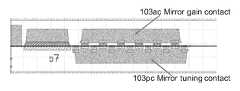
- the mask layer shown in FIG. 4Bis an example of a mask layer that can be used to fabricate portions of the laser illustrated in FIG. 4A .
- the mask layer shown in FIG. 4Bcomprises a phase contact section 101 c at left configured to provide electrical current or voltage to the phase section 101 , a gain contact section 102 c configured to provide electrical current or voltage to the gain region, and a comb mirror gain contact region 103 ac configured to provide electrical current or voltage to the optically active sections of the comb mirror 103 that comprise a gain medium and a comb mirror tuning contact region 103 pc to provide electrical current or voltage to the optically passive regions of the comb mirror 103 .
- the lengths of the gain, mirror and phase sections illustrated in FIG. 4Bmay vary and be significantly different from the example shown here. Likewise, the number of mirror bursts in the comb mirror shown in FIG. 4B may vary significantly.
- one or more heaterscan be used for wavelength tuning the laser of FIG. 4A instead of or in addition to injection current.
- Wavelength tuning in various embodiments of the innovative tunable lasercomprising a comb mirror at one end and a broadband reflector at the other end as described herein can be accomplished by moving the reflection peaks of the comb mirror to select different cavity modes of the laser.
- at least one of the reflection peaks of the comb mirrorcan be moved to select one of the cavity modes.
- at least one of the reflection peaks of the comb mirroris capable of being moved by an amount greater than or equal to the distance between consecutive reflection peaks (also referred to as free spectral range (FSR)) of the comb mirror.
- FSRfree spectral range
- wavelength tuning in implementations of a sampled grating distributed Bragg reflector (SGDBR) laser comprising two sampled grating distributed Bragg reflectors (SGDBRs) at both ends of a laser cavityis accomplished by Vernier tuning of the two sampled grating distributed Bragg reflectors.
- wavelength tuningcan be accomplished by Vernier tuning of cavity modes.
- Embodiments of the innovative tunable laser comprising a comb mirror at one end and a broadband reflector at the other end as described hereincan be tuned using two tuning controls—for example, one tuning control for a phase section and a second tuning control for a mirror section instead of three tuning controls—for example, one tuning control for a phase section and two tuning controls for mirror sections that are used to achieve wavelength tuning in implementations of a SGDBR laser comprising two sampled grating distributed Bragg reflectors (SGDBRs) at both ends of a laser cavity.
- SGDBRssampled grating distributed Bragg reflectors
- FIGS. 5A-5EThe tuning operation of an embodiment of the innovative tunable laser comprising a comb mirror contemplated here is shown in FIGS. 5A-5E .
- FIG. 5Aillustrates the cavity modes of the laser cavity of the innovative tunable laser comprising a comb mirror.
- FIG. 5Billustrates the reflection peaks of the comb mirror.
- the laser cavitycan be configured such that the spacing between the cavity modes relative to the spacing between the reflection peaks of the comb mirror can be controlled to ensure that the nearest neighbors to a selected cavity mode are significantly suppressed.
- FIGS. 5A and 5Billustrate an example of a tunable laser with laser cavity and the comb mirror configured to allow approximately 6.8 cavity modes between individual reflection peaks (or FSR) of the comb mirror.
- the bandwidth of the gain peak of the gain region of the lasercan be broad relative to the FSR of the comb mirror and can accommodate 2 or more reflectance peaks of the comb mirror within the gain bandwidth of the gain region (e.g., gain region 102 ) as shown in FIG. 5D . Accordingly, the bandwidth of the gain peak does not drive the selection between adjacent competing reflection peaks of the comb mirror.
- the tuning of the mirror and phase sectioncan in some embodiments be achieved electrically or thermally, and the gain in the laser gain section can in some embodiments be achieved electrically or through optical pumping.
- the tuning operation of the innovative tunable laser comprising a comb mirror discussed hereinis significantly different from other existing lasers (e.g., the SGDBR laser).
- wavelength tuning in various embodiments of the tunable laser comprising a comb mirror discussed hereinis accomplished by a Vernier effect between the FSR of the reflection peaks and the cavity modes.
- the cavity modes in various embodiments of the innovative tunable laser comprising a combcan be tuned over a small wavelength range by the phase section.
- the comb mirrorscan be tuned over a large wavelength. Accordingly, the mirror comb can be tuned over most of the available index tuning range, minus half a cavity mode spacing.
- Continuous tuning in the innovative tunable laser comprising a comb mirrorcan be achieved using a mirror comb with FSR that is substantially close to the index tuning range.
- the comb spacingmay be denser in a SGDBR tunable laser to allow for full tuning of one mirror comb spacing plus half the width of the comb of the other mirror.
- the wavelength maps from innovative tunable laser comprising a comb mirrorshow a constant hopping between the modes of the comb mirror, before repeating back to the first mirror comb on the next available cavity mode as depicted in FIG. 7 . This operation is different from the mode selection and tuning process of a SGDBR laser.
- the design of the innovative tunable laser comprising a comb mirroris different from a conventional SGDBR laser, with different rules pertaining to the design of the mirror, and a different set of constraints on the design of the cavity length vs the design of the mirror.
- FIGS. 6A-6Ddescribes the mode selection process for tuning in an SGDBR laser comprising two SGDBRs.
- the spacing between individual reflection peaks of the first SGDBRe.g., front SGDBR
- the second SGDBRe.g., rear SGDBR
- the two SGDBRs with slightly different spacing between individual reflection peaksare tuned to achieve wavelength tuning.
- FIGS. 6C and 6Dshow two lasing modes that would be down selected by gain spectrum or mirror strength envelope. The selection process is dominated by the interplay of two comb mirrors and their relative alignment to one another.
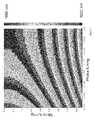
- FIG. 7A section of a tuning map generated by simulating the operation of the innovative tunable laser comprising a comb mirror discussed herein is shown in FIG. 7 below.
- the tuning map in FIG. 7is in the wavelength range between about 1620 nm and about 1680 nm
- the innovative tunable laser comprising a comb mirrorcan be designed to operate in other wavelength ranges between about 600 nm and about 1900 nm, less than 600 nm, greater than 1900 nm or in other wavelength ranges where spontaneous emission and stimulated emission are available.
- the simulation shown in FIG. 7is obtained by using a simple model based on the tuning mechanism discussed above with reference to FIGS. 5A-5E considering the interaction between the reflection peaks of the comb mirror, the cavity modes and the gain bandwidth.
- the simulationdoes not include other physical phenomena such as four wave mixing, threshold variation affecting carrier density and cavity index, the alpha parameter etc. which can affect the wavelength tuning map.
- Some designsmay exhibit “stickiness” of modes due to four wave mixing or other nonlinear or linear effects, or hysteresis in tuning due to alpha parameter, four wave mixing or other nonlinear or linear effects. In some cases the hysteresis and mode sticking effects may be useful to the stability and predicable tuning of these devices.
- the wavelength maps of such designsmay be different from the wavelength map shown in FIG. 7 .
- the wavelength mapmay be similar to the wavelength map shown in FIG. 7 .
- the existence of hysteresismay in some cases mean that direction of tuning on the map is related to wavelength accessibility.
- the simulated wavelength map shown in FIG. 7is obtained by using only two controls—tuning the phase section to tune the cavity modes and tuning the comb mirror to tune the reflection peaks. Accordingly, the wavelength map iterates repeatedly across multiple comb modes, using different cavity modes for each iteration.
- the innovative tunable laser comprising a comb mirrorcan be continuously tuned to select any wavelength in a desired operating range using one or two controls—e.g., phase section to tune the cavity modes and tuning the comb mirror to tune the reflection peaks.
- continuous tuningrefers to the ability to configure the laser to operate at any wavelength in a wavelength range by appropriate selection of laser parameters, such as, for example, current or voltage to the gain regions, current or voltage to the phase section and current or voltage to the comb mirror.
- FIGS. 8A-1, 8A-2, 9A, 9B-1 and 9B-2Some wavelength maps from early prototypes of the innovative tunable laser comprising a comb mirror are shown in FIGS. 8A-1, 8A-2, 9A, 9B-1 and 9B-2 . These wavelength maps show multiple continuous wavelength spans selected by combination of a mirror comb peak and cavity mode on the wavelength map. The interleaving of super-modes can also occur in part as a result of second order processes including thermal and nonlinear effects. Tuning continuity in these designs is in some cases compromised by mode sticking or other second order effects. These examples are included to show the presence in some embodiments of second order effects and other non-linear processes that can lead to maps useful but different from the simulated wavelength map shown in FIG. 7 .
- FIG. 8A-1is a wavelength tuning map obtained by varying the electrical current to the comb mirror and the phase section.
- the FSR of the comb mirror and the cavity modeswere configured to provide approximately 20 nm of wavelength tuning as shown in the wavelength histogram shown in FIG. 8A-2 .
- FIG. 9Ashows the spectrum of light output from an embodiment of a tunable laser comprising a comb mirror for different operating conditions. As seen from the wavelength spectra 901 , 903 , 905 , 907 , 909 , 911 and 913 , a side mode suppression ratio (SMSR) greater than about 30 dB is achieved for various operating conditions of the embodiment of the innovative tunable laser comprising a comb mirror.
- SMSRside mode suppression ratio
- FIG. 9B-1illustrates the wavelength map between 1620 nm and 1650 nm for the embodiment of the innovative tunable laser comprising a comb mirror
- FIG. 9B-2is a wavelength histogram corresponding to the wavelength map of FIG. 9B-1 .
- the different color streaks in the wavelength map shown in FIG. 9B-1correspond to non-adjacent cavity modes that are tuned continuously when selected by the mirror.
- the wavelengths of light output from the innovative tunable laser comprising a comb mirrorcycle through wavelengths that are defined primarily by spacing of the mirror comb.
- One cyclemay not result in a continuous tuning range, however, the tunable laser can be configured such that this series of comb modes can be repeated for multiple adjacent cavity modes as the mirror is further tuned and cycled through the mirror peaks.
- a continuous tuning rangecan be achieved this way if desired, as shown in FIGS. 9B-1 and 9B-2 .
- the wavelength map obtained for an embodiment of a SGDBR laser illustrated in FIG. 10is different from the wavelength map shown in FIG. 9B-1 .
- a SGDBR lasertransitions through each mirror reflection peak in sequence and the combined tuning of two mirrors, allows quasi-continuous tuning across wavelength ranges that include multiple cavity mode hops along the way.
- To achieve continuous wavelength tuning in a SGDBR laserwould require tuning the phase section of the SGDBR in addition to the combined tuning of the two mirrors.
- tuning the comb mirror and the phase sectioncan achieve continuous wavelength tuning in the innovative tunable laser comprising a comb mirror.
- the difference between the tuning mechanismsis clear in that the color of the wavelength maps of FIG. 9B-1 and FIG. 10 .
- the wavelength map for an embodiment of the tunable laser comprising a comb mirror illustrated in FIG. 9B-1repeatedly cycles from left to right, gradually changing shade, whereas the wavelength map for an embodiment of a SGDBR laser illustrated in FIG. 10 , the full tuning range is accessible within a single cycle of tuning the two mirrors with respect to each other over the entire tuning range.
- the tuning map for the implementation of the SGDBR laserhops in wavelength from cavity mode to cavity mode leaving wavelength gaps.
- the innovative tunable laser comprising a comb mirrorhas the advantage of being able to display fully continuous wavelength range, without the wavelength gaps found in the wavelength map of the implementation of the SGDBR laser.
Landscapes
- Physics & Mathematics (AREA)
- Condensed Matter Physics & Semiconductors (AREA)
- General Physics & Mathematics (AREA)
- Electromagnetism (AREA)
- Optics & Photonics (AREA)
- Acoustics & Sound (AREA)
- Geometry (AREA)
- Semiconductor Lasers (AREA)
Abstract
Description
Claims (15)
Priority Applications (3)
| Application Number | Priority Date | Filing Date | Title |
|---|---|---|---|
| US15/938,842US10320152B2 (en) | 2017-03-28 | 2018-03-28 | Tunable laser |
| US15/962,972US10355451B2 (en) | 2017-03-28 | 2018-04-25 | Laser with sampled grating distributed bragg reflector |
| US16/431,285US11251584B2 (en) | 2017-03-28 | 2019-06-04 | Tunable laser |
Applications Claiming Priority (4)
| Application Number | Priority Date | Filing Date | Title |
|---|---|---|---|
| US201762477908P | 2017-03-28 | 2017-03-28 | |
| US201762489922P | 2017-04-25 | 2017-04-25 | |
| US201762596655P | 2017-12-08 | 2017-12-08 | |
| US15/938,842US10320152B2 (en) | 2017-03-28 | 2018-03-28 | Tunable laser |
Related Child Applications (2)
| Application Number | Title | Priority Date | Filing Date |
|---|---|---|---|
| US15/962,972Continuation-In-PartUS10355451B2 (en) | 2017-03-28 | 2018-04-25 | Laser with sampled grating distributed bragg reflector |
| US16/431,285ContinuationUS11251584B2 (en) | 2017-03-28 | 2019-06-04 | Tunable laser |
Publications (2)
| Publication Number | Publication Date |
|---|---|
| US20180287342A1 US20180287342A1 (en) | 2018-10-04 |
| US10320152B2true US10320152B2 (en) | 2019-06-11 |
Family
ID=63671812
Family Applications (2)
| Application Number | Title | Priority Date | Filing Date |
|---|---|---|---|
| US15/938,842ActiveUS10320152B2 (en) | 2017-03-28 | 2018-03-28 | Tunable laser |
| US16/431,285ActiveUS11251584B2 (en) | 2017-03-28 | 2019-06-04 | Tunable laser |
Family Applications After (1)
| Application Number | Title | Priority Date | Filing Date |
|---|---|---|---|
| US16/431,285ActiveUS11251584B2 (en) | 2017-03-28 | 2019-06-04 | Tunable laser |
Country Status (1)
| Country | Link |
|---|---|
| US (2) | US10320152B2 (en) |
Cited By (5)
| Publication number | Priority date | Publication date | Assignee | Title |
|---|---|---|---|---|
| US11152764B1 (en) | 2018-11-20 | 2021-10-19 | Freedom Photonics Llc | Gratings for high power single mode laser |
| US11251584B2 (en) | 2017-03-28 | 2022-02-15 | Freedom Photonics Llc | Tunable laser |
| US11431149B1 (en) | 2019-03-22 | 2022-08-30 | Freedom Photonics Llc | Single mode laser with large optical mode size |
| US11721951B2 (en) | 2019-09-16 | 2023-08-08 | Freedom Photonics Llc | Tunable laser with active material on at least one end for monitoring performance |
| US11837838B1 (en) | 2020-01-31 | 2023-12-05 | Freedom Photonics Llc | Laser having tapered region |
Families Citing this family (2)
| Publication number | Priority date | Publication date | Assignee | Title |
|---|---|---|---|---|
| US10355451B2 (en) | 2017-03-28 | 2019-07-16 | Freedom Photonics Llc | Laser with sampled grating distributed bragg reflector |
| WO2020107315A1 (en)* | 2018-11-29 | 2020-06-04 | 华为技术有限公司 | Two-section dbr laser and monolithic integrated array light source chip |
Citations (12)
| Publication number | Priority date | Publication date | Assignee | Title |
|---|---|---|---|---|
| US4608697A (en) | 1983-04-11 | 1986-08-26 | At&T Bell Laboratories | Spectral control arrangement for coupled cavity laser |
| US4719636A (en) | 1984-08-24 | 1988-01-12 | Nec Corporation | Wavelength tunable semiconductor laser device provided with control regions |
| US4896325A (en)* | 1988-08-23 | 1990-01-23 | The Regents Of The University Of California | Multi-section tunable laser with differing multi-element mirrors |
| US5091916A (en) | 1990-09-28 | 1992-02-25 | At&T Bell Laboratories | Distributed reflector laser having improved side mode suppression |
| US5325392A (en) | 1992-03-06 | 1994-06-28 | Nippon Telegraph And Telephone Corporation | Distributed reflector and wavelength-tunable semiconductor laser |
| US20020105991A1 (en) | 1999-09-02 | 2002-08-08 | Coldren Larry A. | High-power, manufacturable sampled grating distributed bragg reflector lasers |
| US20040076199A1 (en) | 2002-08-22 | 2004-04-22 | Agility Communications, Inc. | Chirp control of integrated laser-modulators having multiple sections |
| US20040179569A1 (en)* | 2003-03-12 | 2004-09-16 | Hitachi., Ltd. | Wavelength tunable DBR laser diode |
| US7130325B2 (en)* | 2003-05-02 | 2006-10-31 | Electronics And Telecommunications Research Institute | Sampled grating distributed feedback wavelength tunable semiconductor laser integrated with sampled grating distributed Bragg reflector |
| US8401399B2 (en) | 2009-05-28 | 2013-03-19 | Freedom Photonics, Llc. | Chip-based advanced modulation format transmitter |
| US9344196B1 (en) | 2009-05-28 | 2016-05-17 | Freedom Photonics, Llc. | Integrated interferometric optical transmitter |
| US20180287343A1 (en) | 2017-03-28 | 2018-10-04 | Freedom Photonics Llc | Laser with sampled grating distributed bragg reflector |
Family Cites Families (137)
| Publication number | Priority date | Publication date | Assignee | Title |
|---|---|---|---|---|
| US3752992A (en) | 1969-05-28 | 1973-08-14 | Us Navy | Optical communication system |
| GB1500289A (en) | 1974-06-03 | 1978-02-08 | Rca Corp | Homodyne communication system |
| US3939341A (en) | 1975-04-02 | 1976-02-17 | Hughes Aircraft Company | Phase-locked optical homodyne receiver |
| US3970838A (en) | 1975-08-29 | 1976-07-20 | Hughes Aircraft Company | Dual channel phase locked optical homodyne receiver |
| US4063084A (en) | 1976-07-19 | 1977-12-13 | Hughes Aircraft Company | Dual channel optical homodyne receiver |
| US4168397A (en) | 1978-05-26 | 1979-09-18 | Gte Automatic Electric Laboratories Incorporated | 8-Phase PSK modulator |
| GB2121636B (en) | 1982-05-20 | 1986-03-05 | Standard Telephones Cables Ltd | Coherent optical receiver |
| US4622672A (en) | 1984-01-20 | 1986-11-11 | At&T Bell Laboratories | Self-stabilized semiconductor lasers |
| US4870654A (en) | 1987-05-22 | 1989-09-26 | California Laboratories, Inc. | Generation of multiply folded optical paths |
| US4893352A (en) | 1987-06-30 | 1990-01-09 | Massachusetts Institute Of Technology | Optical transmitter of modulated signals |
| JPH063511B2 (en) | 1987-10-27 | 1994-01-12 | 日本電気株式会社 | Optical heterodyne / homodyne detection method |
| US4903341A (en) | 1987-12-28 | 1990-02-20 | Mcdonnell Douglas Corporation | Semiconductor optical heterodyne detector |
| JPH01223837A (en) | 1988-03-03 | 1989-09-06 | Nec Corp | Optical multi-value transmitter |
| NL8801490A (en) | 1988-06-10 | 1990-01-02 | Philips Nv | DEVICE FOR OPTICAL HETERODYNE DETECTION AND INTEGRATED OPTICAL COMPONENT SUITABLE FOR APPLICATION IN SUCH A DEVICE. |
| US4904963A (en) | 1988-11-16 | 1990-02-27 | Mcdonnell Douglas Corporation | Staggered quadrature phase shift keyed laser modulator |
| JPH0391278A (en) | 1989-09-01 | 1991-04-16 | Nippon Telegr & Teleph Corp <Ntt> | Semiconductor laser diode |
| CA1323657C (en) | 1989-09-22 | 1993-10-26 | Mohsen Kavenrad | Optical homodyne dpsk receiver with optical amplifier |
| US5034603A (en) | 1989-11-06 | 1991-07-23 | Wilson Keith E | Integrated optics wavelength stabilization unit |
| US5007106A (en) | 1989-11-08 | 1991-04-09 | At&T Bell Laboratories | Optical Homodyne Receiver |
| US5412226A (en) | 1989-11-20 | 1995-05-02 | British Telecommunications Public Limited Company | Semi-conductor structures |
| DE69127840T2 (en) | 1990-03-01 | 1998-03-05 | Fujitsu Ltd | Optical transmitter |
| NL9001331A (en) | 1990-06-13 | 1992-01-02 | Philips Nv | DEVICE FOR OPTICAL HETERODYNE DETECTION AND OPTICAL COMPONENT SUITABLE FOR APPLICATION IN SUCH A DEVICE. |
| JPH04144320A (en) | 1990-10-05 | 1992-05-18 | Hitachi Ltd | Homodyne optical receiver |
| US5222103A (en) | 1991-01-02 | 1993-06-22 | Gte Laboratories Incorporated | Differential quadrature phase shift keying encoder for subcarrier systems |
| US5101450A (en) | 1991-01-23 | 1992-03-31 | Gte Laboratories Incorporated | Quadrature optical phase modulators for lightwave systems |
| US5088105A (en) | 1991-03-26 | 1992-02-11 | Spectra Diode Laboratories, Inc. | Optical amplifier with folded light path and laser-amplifier combination |
| CA2083219C (en) | 1991-11-19 | 1999-01-05 | Hiroshi Nishimoto | Optical transmitter having optical modulator |
| DE4212152A1 (en) | 1992-04-10 | 1993-10-14 | Sel Alcatel Ag | Tunable semiconductor laser |
| US5347608A (en) | 1992-06-30 | 1994-09-13 | Ibiden Co., Ltd. | Optical waveguide and optical waveguide device |
| US5237292A (en) | 1992-07-01 | 1993-08-17 | Space Systems/Loral | Quadrature amplitude modulation system with compensation for transmission system characteristics |
| US5351317A (en) | 1992-08-14 | 1994-09-27 | Telefonaktiebolaget L M Ericsson | Interferometric tunable optical filter |
| US5452118A (en) | 1993-04-20 | 1995-09-19 | Spire Corporation | Optical heterodyne receiver for fiber optic communications system |
| US5398256A (en) | 1993-05-10 | 1995-03-14 | The United States Of America As Represented By The United States Department Of Energy | Interferometric ring lasers and optical devices |
| US5424863A (en) | 1993-09-23 | 1995-06-13 | Ael Industries, Inc. | Dual-polarization fiber optic communications link |
| WO1995022070A1 (en) | 1994-02-11 | 1995-08-17 | Philips Electronics N.V. | Optical device with phased array |
| JPH0998155A (en) | 1995-10-03 | 1997-04-08 | Matsushita Electric Ind Co Ltd | Optical transmitter and optical transmission system using the same |
| US5654818A (en) | 1996-02-09 | 1997-08-05 | The United States Of America As Represented By The United States National Aeronautics And Space Administration | Polarization independent electro-optic modulator |
| US6020963A (en) | 1996-06-04 | 2000-02-01 | Northeastern University | Optical quadrature Interferometer |
| US5915051A (en) | 1997-01-21 | 1999-06-22 | Massascusetts Institute Of Technology | Wavelength-selective optical add/drop switch |
| JP3094950B2 (en) | 1997-05-28 | 2000-10-03 | 日本電気株式会社 | Optical transmission device and optical transmission method |
| US6205159B1 (en) | 1997-06-23 | 2001-03-20 | Newport Corporation | Discrete wavelength liquid crystal tuned external cavity diode laser |
| US6556327B1 (en) | 1997-11-06 | 2003-04-29 | Matsushita Electric Industrial Co., Ltd. | Signal converter, optical transmitter and optical fiber transmission system |
| US6452945B1 (en) | 1998-03-05 | 2002-09-17 | Kestrel Solutions, Inc. | Electrical add-drop multiplexing for optical communications networks utilizing frequency division multiplexing |
| US6271950B1 (en) | 1998-08-18 | 2001-08-07 | Lucent Technologies Inc. | Optical differential phase shift keying transmission system having multiplexing, routing and add/replace capabilities |
| DE59900216D1 (en) | 1998-10-22 | 2001-10-04 | Contraves Space Ag Zuerich | Device for the homodyne reception of optical phase-shifted signals |
| EP1087478A1 (en) | 1999-09-27 | 2001-03-28 | Nortel Networks Limited | Generation of short optical pulses using strongly complex coupled DFB lasers. |
| JP2001127377A (en) | 1999-10-28 | 2001-05-11 | Hitachi Ltd | Optical transmission device and optical transmission device |
| US6661975B1 (en) | 2000-03-10 | 2003-12-09 | Northrop Grumman Corporation | Multi-rate variable duty cycle modem for use in an optical communication system |
| CA2352113A1 (en) | 2000-07-07 | 2002-01-07 | Jds Uniphase Corporation | Optical modulator and method for polarization bit interleaving |
| JP4108254B2 (en) | 2000-07-11 | 2008-06-25 | 富士通株式会社 | Optical transmitter and optical transmission system |
| IL137732A (en)* | 2000-08-07 | 2006-12-31 | Crosslight Photonics Ltd | Characterization of multiple section semiconductor lasers |
| US6459521B1 (en) | 2000-08-28 | 2002-10-01 | Agere Systems Guardian Corp. | Electroabsorption modulator integrated distributed feedback laser transmitter |
| KR100395492B1 (en) | 2000-12-30 | 2003-08-25 | 한국전자통신연구원 | Laser device |
| US6690687B2 (en) | 2001-01-02 | 2004-02-10 | Spectrasensors, Inc. | Tunable semiconductor laser having cavity with ring resonator mirror and mach-zehnder interferometer |
| US6646747B2 (en) | 2001-05-17 | 2003-11-11 | Sioptical, Inc. | Interferometer apparatus and associated method |
| JP2003043430A (en) | 2001-05-23 | 2003-02-13 | Hitachi Ltd | Optical transmission device and method of manufacturing the same |
| US6782205B2 (en) | 2001-06-25 | 2004-08-24 | Silicon Light Machines | Method and apparatus for dynamic equalization in wavelength division multiplexing |
| US6912235B2 (en) | 2001-08-01 | 2005-06-28 | Iolon, Inc. | Apparatus and method for phase control of tunable external cavity lasers |
| US7272271B2 (en) | 2001-09-26 | 2007-09-18 | Celight, Inc. | Electro-optical integrated transmitter chip for arbitrary quadrature modulation of optical signals |
| US7209611B2 (en) | 2002-10-08 | 2007-04-24 | Infinera Corporation | Transmitter photonic integrated circuit (TxPIC) chips utilizing compact wavelength selective combiners/decombiners |
| CA2463502C (en) | 2001-10-09 | 2011-09-20 | Infinera Corporation | Digital optical network architecture |
| US7751658B2 (en) | 2001-10-09 | 2010-07-06 | Infinera Corporation | Monolithic transmitter photonic integrated circuit (TxPIC) having tunable modulated sources with feedback system for source power level or wavelength tuning |
| US7283694B2 (en) | 2001-10-09 | 2007-10-16 | Infinera Corporation | Transmitter photonic integrated circuits (TxPIC) and optical transport networks employing TxPICs |
| WO2003044913A2 (en) | 2001-11-06 | 2003-05-30 | Infinera Corporation | Optical communication module with photonic integrated circuit chip (pic) and external booster optical amplifier |
| GB2383424B (en) | 2001-11-30 | 2004-12-22 | Marconi Optical Components Ltd | Photonic integrated device |
| GB2383706B (en) | 2001-11-30 | 2005-03-30 | Marconi Optical Components Ltd | Modulation control |
| JP3914428B2 (en) | 2001-12-10 | 2007-05-16 | 株式会社日立製作所 | Optical transmitter, optical receiver |
| US7286578B2 (en) | 2002-03-04 | 2007-10-23 | Danmarks Tekniske Universitet | High-power diode laser system |
| JP2003255283A (en) | 2002-03-04 | 2003-09-10 | Opnext Japan Inc | Mach-zehnder type optical modulator |
| US6807321B2 (en) | 2002-03-11 | 2004-10-19 | Lucent Technologies Inc. | Apparatus and method for measurement and adaptive control of polarization mode dispersion in optical fiber transmission systems |
| GB0206228D0 (en) | 2002-03-16 | 2002-05-01 | Intense Photonics Ltd | Folded integrated laser modulator |
| WO2004013980A2 (en) | 2002-08-02 | 2004-02-12 | Ahura Corporation | System for amplifying optical signals |
| US7027476B2 (en) | 2002-08-09 | 2006-04-11 | California Institute Of Technology | Tunable semiconductor lasers |
| US20040105476A1 (en)* | 2002-08-19 | 2004-06-03 | Wasserbauer John G. | Planar waveguide surface emitting laser and photonic integrated circuit |
| US7406267B2 (en) | 2002-11-06 | 2008-07-29 | Finisar Corporation | Method and apparatus for transmitting a signal using thermal chirp management of a directly modulated transmitter |
| US7023601B2 (en) | 2002-12-02 | 2006-04-04 | Nortel Networks Limited | Optical E-field modulation using a Mach-Zehnder interferometer |
| US7460793B2 (en) | 2002-12-11 | 2008-12-02 | Michael George Taylor | Coherent optical detection and signal processing method and system |
| US7327022B2 (en) | 2002-12-30 | 2008-02-05 | General Electric Company | Assembly, contact and coupling interconnection for optoelectronics |
| JP4961588B2 (en) | 2003-01-28 | 2012-06-27 | ハイ キュー レーザー ゲゼルシャフト ミット ベシュレンクテル ハフツング | Laser beam guide folding device |
| KR20040081838A (en) | 2003-03-17 | 2004-09-23 | 엘지전자 주식회사 | Double-faced and polymer optical backplane and the fabrication method |
| US7212326B2 (en) | 2003-05-30 | 2007-05-01 | Jds Uniphase Corporation | Optical external modulator |
| US6978056B2 (en) | 2003-06-04 | 2005-12-20 | Covega, Inc. | Waveguide modulators having bias control with reduced temperature dependence |
| US7209664B1 (en) | 2003-06-10 | 2007-04-24 | Nortel Networks Limited | Frequency agile transmitter and receiver architecture for DWDM systems |
| US8050351B2 (en) | 2003-07-02 | 2011-11-01 | Celight, Inc. | Quadrature modulator with feedback control and optical communications system using the same |
| US7633988B2 (en) | 2003-07-31 | 2009-12-15 | Jds Uniphase Corporation | Tunable laser source with monolithically integrated interferometric optical modulator |
| JP2005077987A (en) | 2003-09-03 | 2005-03-24 | Sumitomo Osaka Cement Co Ltd | Optical modulator |
| TWI227582B (en) | 2003-11-28 | 2005-02-01 | Walsin Lihwa Corp | External cavity tunable laser system formed from MEMS corner mirror array element |
| US20050135733A1 (en) | 2003-12-19 | 2005-06-23 | Benoit Reid | Integrated optical loop mirror |
| US7257142B2 (en) | 2004-03-29 | 2007-08-14 | Intel Corporation | Semi-integrated designs for external cavity tunable lasers |
| JP2005302784A (en) | 2004-04-06 | 2005-10-27 | Matsushita Electric Ind Co Ltd | Semiconductor light emitting device and manufacturing method thereof |
| WO2005099421A2 (en)* | 2004-04-14 | 2005-10-27 | The Trustees Of Princeton University | Monolithic wavelength stabilized asymmetric laser |
| US7078981B2 (en) | 2004-07-27 | 2006-07-18 | Lucent Technologies Inc. | 16 QAM modulator and method of 16 QAM modulation |
| JP4751601B2 (en) | 2004-09-30 | 2011-08-17 | 住友大阪セメント株式会社 | Light modulator |
| US7376307B2 (en) | 2004-10-29 | 2008-05-20 | Matsushita Electric Industrial Co., Ltd | Multimode long period fiber bragg grating machined by ultrafast laser direct writing |
| EP1696527A3 (en) | 2005-02-24 | 2007-11-28 | JDS Uniphase Inc. | Low loss grating for high efficiency wavelength stabilized high power lasers |
| CA2521731A1 (en)* | 2005-05-09 | 2006-11-09 | Jian-Jun He | Wavelength switchable semiconductor laser |
| JP4466861B2 (en) | 2005-06-27 | 2010-05-26 | 横河電機株式会社 | QPSK optical modulator |
| DE602005005697T2 (en) | 2005-11-25 | 2009-04-30 | Alcatel Lucent | Fiber optic transmission system, transmitter and receiver for DQPSK modulated signals and associated stabilization method |
| JP4563944B2 (en) | 2006-01-31 | 2010-10-20 | 富士通株式会社 | Optical transmitter |
| CN101043269B (en) | 2006-03-22 | 2011-01-05 | 富士通株式会社 | I-Q quadrature modulation transmitter and its device and method for monitoring I-Q phase deviation |
| WO2007107187A1 (en) | 2006-03-23 | 2007-09-27 | Pirelli & C. S.P.A. | Integrated laser optical source with active and passive sections formed in distinct substrates |
| JP2008066849A (en) | 2006-09-05 | 2008-03-21 | Fujitsu Ltd | Optical transmitter and driving method thereof |
| US7583894B2 (en) | 2006-09-21 | 2009-09-01 | Alcatel-Lucent Usa Inc. | Interferometric operation of electroabsorption modulators |
| JP5405716B2 (en) | 2006-09-29 | 2014-02-05 | 富士通株式会社 | Optical transmitter |
| WO2008047346A2 (en) | 2006-10-17 | 2008-04-24 | Oms Displays Ltd. | Semitransparent integrated optic mirror |
| EP3133756A1 (en) | 2007-09-14 | 2017-02-22 | Semtech Corporation | High-speed serialized related components, systems and methods |
| US8238759B2 (en) | 2008-02-14 | 2012-08-07 | Infinera Corporation | High capacity transmitter implemented on a photonic integrated circuit |
| US8213799B2 (en) | 2008-02-22 | 2012-07-03 | Infinera Corporation | Optical receiver including a filter on a planar lightwave circuit |
| JP4388987B2 (en) | 2008-03-31 | 2009-12-24 | 住友大阪セメント株式会社 | Mach-Zehnder waveguide type optical modulator |
| US8168939B2 (en) | 2008-07-09 | 2012-05-01 | Luxtera, Inc. | Method and system for a light source assembly supporting direct coupling to an integrated circuit |
| US8977086B2 (en) | 2009-02-12 | 2015-03-10 | Governors Of The University Of Alberta | Tapered waveguide coupler and spectrometer |
| WO2010095018A2 (en) | 2009-02-17 | 2010-08-26 | Oclaro Technology Plc | Optical chips and devices for optical communications |
| US8368995B2 (en) | 2009-10-13 | 2013-02-05 | Skorpios Technologies, Inc. | Method and system for hybrid integration of an opto-electronic integrated circuit |
| WO2011060325A1 (en) | 2009-11-12 | 2011-05-19 | Packet Photonics, Inc. | Optical network interface module using a hardware programmable optical network interface engine |
| US7999988B2 (en) | 2009-12-30 | 2011-08-16 | Intel Corporation | Optical modulator using a dual output laser embedded in a mach zehnder interferometer |
| US8649639B2 (en) | 2010-03-04 | 2014-02-11 | Luxtera, Inc. | Method and system for waveguide mode filters |
| US9071038B2 (en) | 2010-03-31 | 2015-06-30 | Infinera Corporation | Segmented distributed feedback laser |
| JP5764875B2 (en) | 2010-06-02 | 2015-08-19 | 富士通株式会社 | Semiconductor optical device |
| WO2012019290A1 (en) | 2010-08-13 | 2012-02-16 | Genia Photonics Inc. | Tunable mode-locked laser |
| JP2012156335A (en) | 2011-01-26 | 2012-08-16 | Nippon Telegr & Teleph Corp <Ntt> | Semiconductor laser |
| JP5542071B2 (en) | 2011-01-26 | 2014-07-09 | 日本電信電話株式会社 | Optical integrated circuit |
| JP5638469B2 (en) | 2011-06-09 | 2014-12-10 | 三菱電機株式会社 | Optical modulator and optical modulation method |
| US20130016744A1 (en) | 2011-07-13 | 2013-01-17 | Oracle International Corporation | Laser source with tunable-grating-waveguide reflections |
| GB201115784D0 (en) | 2011-09-13 | 2011-10-26 | Univ Gent | Integrated photonics waveguide grating coupler |
| JP5077480B2 (en) | 2011-12-19 | 2012-11-21 | 住友大阪セメント株式会社 | Optical waveguide device |
| US9196503B2 (en) | 2012-08-23 | 2015-11-24 | Michael Xiaoxuan Yang | Methods for fabricating devices on semiconductor substrates |
| US9557478B2 (en) | 2012-08-28 | 2017-01-31 | Acacia Communications, Inc. | Electronic and optical co-packaging of coherent transceiver |
| US8831049B2 (en) | 2012-09-14 | 2014-09-09 | Laxense Inc. | Tunable optical system with hybrid integrated laser |
| KR20140077533A (en) | 2012-12-14 | 2014-06-24 | 삼성전기주식회사 | Method for manufacturing optical wiring board |
| US9755753B2 (en) | 2013-01-02 | 2017-09-05 | Oe Solutions America, Inc. | Tunable U-laser transmitter with integrated Mach-Zehnder Modulator |
| US9322996B2 (en) | 2013-03-07 | 2016-04-26 | Aurrion, Inc. | Simultaneous processing of multiple photonic device layers |
| US9726840B2 (en) | 2013-06-06 | 2017-08-08 | Acacia Communications, Inc. | Integration of electronic chips onto a photonic chip |
| US8971676B1 (en) | 2013-10-07 | 2015-03-03 | Oracle International Corporation | Hybrid-integrated photonic chip package |
| JP6319762B2 (en) | 2013-10-31 | 2018-05-09 | 日東電工株式会社 | Opto-electric hybrid board and manufacturing method thereof |
| JP6224495B2 (en) | 2014-03-19 | 2017-11-01 | 株式会社東芝 | Semiconductor laser device |
| US10320152B2 (en) | 2017-03-28 | 2019-06-11 | Freedom Photonics Llc | Tunable laser |
| US11391969B2 (en) | 2018-12-07 | 2022-07-19 | Freedom Photonics Llc | Systems and methods for wavelength monitoring |
- 2018
- 2018-03-28USUS15/938,842patent/US10320152B2/enactiveActive
- 2019
- 2019-06-04USUS16/431,285patent/US11251584B2/enactiveActive
Patent Citations (19)
| Publication number | Priority date | Publication date | Assignee | Title |
|---|---|---|---|---|
| US4608697A (en) | 1983-04-11 | 1986-08-26 | At&T Bell Laboratories | Spectral control arrangement for coupled cavity laser |
| US4719636A (en) | 1984-08-24 | 1988-01-12 | Nec Corporation | Wavelength tunable semiconductor laser device provided with control regions |
| US4896325A (en)* | 1988-08-23 | 1990-01-23 | The Regents Of The University Of California | Multi-section tunable laser with differing multi-element mirrors |
| US5091916A (en) | 1990-09-28 | 1992-02-25 | At&T Bell Laboratories | Distributed reflector laser having improved side mode suppression |
| US5325392A (en) | 1992-03-06 | 1994-06-28 | Nippon Telegraph And Telephone Corporation | Distributed reflector and wavelength-tunable semiconductor laser |
| US20020105991A1 (en) | 1999-09-02 | 2002-08-08 | Coldren Larry A. | High-power, manufacturable sampled grating distributed bragg reflector lasers |
| US20040076199A1 (en) | 2002-08-22 | 2004-04-22 | Agility Communications, Inc. | Chirp control of integrated laser-modulators having multiple sections |
| US20040179569A1 (en)* | 2003-03-12 | 2004-09-16 | Hitachi., Ltd. | Wavelength tunable DBR laser diode |
| US7130325B2 (en)* | 2003-05-02 | 2006-10-31 | Electronics And Telecommunications Research Institute | Sampled grating distributed feedback wavelength tunable semiconductor laser integrated with sampled grating distributed Bragg reflector |
| US8401399B2 (en) | 2009-05-28 | 2013-03-19 | Freedom Photonics, Llc. | Chip-based advanced modulation format transmitter |
| US8401405B2 (en) | 2009-05-28 | 2013-03-19 | Freedom Photonics, Llc. | Monolithic widely-tunable coherent receiver |
| US8712256B2 (en) | 2009-05-28 | 2014-04-29 | Freedom Photonics, Llc. | Monolithic widely-tunable coherent receiver |
| US8718486B2 (en) | 2009-05-28 | 2014-05-06 | Freedom Photonics, Llc. | Chip-based advanced modulation format transmitter |
| US9246596B2 (en) | 2009-05-28 | 2016-01-26 | Freedom Photonics, Llc. | Monolithic widely-tunable coherent receiver |
| US9270380B2 (en) | 2009-05-28 | 2016-02-23 | Freedom Photonics, Llc. | Chip-based advanced modulation format transmitter |
| US9344196B1 (en) | 2009-05-28 | 2016-05-17 | Freedom Photonics, Llc. | Integrated interferometric optical transmitter |
| US9887780B2 (en) | 2009-05-28 | 2018-02-06 | Freedom Photonics, Llc. | Chip-based advanced modulation format transmitter |
| US9941971B1 (en) | 2013-07-23 | 2018-04-10 | Freedom Photonics, Llc. | Integrated interferometric optical transmitter |
| US20180287343A1 (en) | 2017-03-28 | 2018-10-04 | Freedom Photonics Llc | Laser with sampled grating distributed bragg reflector |
Non-Patent Citations (4)
| Title |
|---|
| Arimoto, H. et al., "Wavelength-Tunable Short-Cavity DBR Laser Array With Active Distributed Bragg Reflector", Journal of Lightwave Technology, vol. 24(11):4436-4371, Nov. 2006. |
| Hofstetter, D.et al., "Single-growth-step GaAsIAlGaAs distributed Bragg reflector lasers with holographically-defined recessed gratings", Electronics Letters Oct. 27, 1994 vol. 30(22): 1858-1859. |
| Jayaraman, V. et al., "Theory, Design, and Performance of Extended Tuning Range Semiconductor Laser with Sampled Grating", IEEE J. of Quantum Electronics, 29, pp. 1824-1834, 1993. |
| Kazuhiro Komori, et. al., "Single-Mode Properties of Distributed-Reflector Lasers", IEEE Journal of Quantum Electronics, vol. 25, No. 6, Jun. 1989, pp. 1235-1244. |
Cited By (5)
| Publication number | Priority date | Publication date | Assignee | Title |
|---|---|---|---|---|
| US11251584B2 (en) | 2017-03-28 | 2022-02-15 | Freedom Photonics Llc | Tunable laser |
| US11152764B1 (en) | 2018-11-20 | 2021-10-19 | Freedom Photonics Llc | Gratings for high power single mode laser |
| US11431149B1 (en) | 2019-03-22 | 2022-08-30 | Freedom Photonics Llc | Single mode laser with large optical mode size |
| US11721951B2 (en) | 2019-09-16 | 2023-08-08 | Freedom Photonics Llc | Tunable laser with active material on at least one end for monitoring performance |
| US11837838B1 (en) | 2020-01-31 | 2023-12-05 | Freedom Photonics Llc | Laser having tapered region |
Also Published As
| Publication number | Publication date |
|---|---|
| US20190386463A1 (en) | 2019-12-19 |
| US11251584B2 (en) | 2022-02-15 |
| US20180287342A1 (en) | 2018-10-04 |
Similar Documents
| Publication | Publication Date | Title |
|---|---|---|
| US10355451B2 (en) | Laser with sampled grating distributed bragg reflector | |
| US11251584B2 (en) | Tunable laser | |
| US8559470B2 (en) | Method and system for hybrid integration of a tunable laser and a phase modulator | |
| US9209600B2 (en) | Tunable laser, a method for making, and a method for operating such a laser | |
| JP6229595B2 (en) | Modulated light source | |
| US20130235890A1 (en) | Tunable hybrid laser with carrier-induced phase control | |
| JP4954992B2 (en) | Semiconductor light reflecting element, semiconductor laser using the semiconductor light reflecting element, and optical transponder using the semiconductor laser | |
| US20090290613A1 (en) | External cavity laser assembly including external chirped exit reflector for improved linearity | |
| CN104993375A (en) | Distributed feedback laser with short cavity length | |
| WO2017092094A1 (en) | Wavelength tunable semiconductor laser | |
| US5881079A (en) | Wavelength selectable laser with inherent and single-mode stability | |
| US12224554B2 (en) | Laser having tapered region | |
| CN102074891B (en) | Semiconductor laser device and method for controlling semiconductor laser | |
| JP2002299755A (en) | Fast and broadband tunable laser | |
| US12308608B2 (en) | Semiconductor optical integrated device | |
| JP5001239B2 (en) | Semiconductor tunable laser | |
| US9153930B2 (en) | Laser light source | |
| JPH09270568A (en) | Multiple wavelength oscillation laser | |
| Fujiwara et al. | Suppression of thermal wavelength drift in super-structure grating distributed Bragg reflector (SSG-DBR) laser with thermal drift compensator | |
| US20030086449A1 (en) | Generator of short light pulses | |
| JP2018011023A (en) | Variable wavelength semiconductor laser | |
| WO2006008724A1 (en) | Method for designing a semiconductor laser with intracavity reflecting features, semiconductor laser and method of fabrication thereof | |
| US20250202198A1 (en) | Tunable reflector for a silicon photonic laser | |
| US20250096530A1 (en) | Laser with Tunable Reflector | |
| EP4525226A1 (en) | Laser with tunable reflector |
Legal Events
| Date | Code | Title | Description |
|---|---|---|---|
| FEPP | Fee payment procedure | Free format text:ENTITY STATUS SET TO UNDISCOUNTED (ORIGINAL EVENT CODE: BIG.); ENTITY STATUS OF PATENT OWNER: SMALL ENTITY | |
| FEPP | Fee payment procedure | Free format text:ENTITY STATUS SET TO SMALL (ORIGINAL EVENT CODE: SMAL); ENTITY STATUS OF PATENT OWNER: SMALL ENTITY | |
| FEPP | Fee payment procedure | Free format text:PETITION RELATED TO MAINTENANCE FEES GRANTED (ORIGINAL EVENT CODE: PTGR); ENTITY STATUS OF PATENT OWNER: SMALL ENTITY | |
| STPP | Information on status: patent application and granting procedure in general | Free format text:NOTICE OF ALLOWANCE MAILED -- APPLICATION RECEIVED IN OFFICE OF PUBLICATIONS | |
| AS | Assignment | Owner name:FREEDOM PHOTONICS LLC, CALIFORNIA Free format text:ASSIGNMENT OF ASSIGNORS INTEREST;ASSIGNOR:MORRISON, GORDON BARBOUR;REEL/FRAME:049011/0251 Effective date:20180328 | |
| STCF | Information on status: patent grant | Free format text:PATENTED CASE | |
| FEPP | Fee payment procedure | Free format text:ENTITY STATUS SET TO UNDISCOUNTED (ORIGINAL EVENT CODE: BIG.); ENTITY STATUS OF PATENT OWNER: LARGE ENTITY | |
| MAFP | Maintenance fee payment | Free format text:PAYMENT OF MAINTENANCE FEE, 4TH YEAR, LARGE ENTITY (ORIGINAL EVENT CODE: M1551); ENTITY STATUS OF PATENT OWNER: LARGE ENTITY Year of fee payment:4 | |
| AS | Assignment | Owner name:GLAS TRUST COMPANY LLC, NEW JERSEY Free format text:SECURITY INTEREST;ASSIGNORS:LIMINAR TECHNOLOGIES, INC;LUMINAR, LLC;FREEDOM PHOTONICS LLC;REEL/FRAME:069312/0713 Effective date:20240808 Owner name:GLAS TRUST COMPANY LLC, NEW JERSEY Free format text:SECURITY INTEREST;ASSIGNORS:LUMINAR TECHNOLOGIES, INC;LUMINAR , LLC;FREEDOM PHOTONICS LLC;REEL/FRAME:069312/0669 Effective date:20240808 | |
| AS | Assignment | Owner name:GLAS TRUST COMPANY LLC, NEW JERSEY Free format text:CORRECTIVE ASSIGNMENT TO CORRECT THE THE NAME OF THE FIRST CONVEYING PARTY PREVIOUSLY RECORDED AT REEL: 69312 FRAME: 713. ASSIGNOR(S) HEREBY CONFIRMS THE ASSIGNMENT;ASSIGNORS:LUMINAR TECHNOLOGIES, INC;LUMINAR , LLC;FREEDOM PHOTONICS LLC;REEL/FRAME:069990/0772 Effective date:20240808 |