US10317528B2 - Core independent ultrasonic proximity sensing peripheral - Google Patents
Core independent ultrasonic proximity sensing peripheralDownload PDFInfo
- Publication number
- US10317528B2 US10317528B2US15/447,532US201715447532AUS10317528B2US 10317528 B2US10317528 B2US 10317528B2US 201715447532 AUS201715447532 AUS 201715447532AUS 10317528 B2US10317528 B2US 10317528B2
- Authority
- US
- United States
- Prior art keywords
- ultrasonic
- proximity
- voltage value
- integration time
- dsm
- Prior art date
- Legal status (The legal status is an assumption and is not a legal conclusion. Google has not performed a legal analysis and makes no representation as to the accuracy of the status listed.)
- Active, expires
Links
- 230000002093peripheral effectEffects0.000titleclaimsabstractdescription57
- 230000010354integrationEffects0.000claimsabstractdescription54
- 238000000034methodMethods0.000claimsdescription23
- 238000001514detection methodMethods0.000claimsdescription11
- 230000006870functionEffects0.000claimsdescription10
- 238000012545processingMethods0.000claimsdescription5
- 230000008878couplingEffects0.000claimsdescription4
- 238000010168coupling processMethods0.000claimsdescription4
- 238000005859coupling reactionMethods0.000claimsdescription4
- 239000003990capacitorSubstances0.000description8
- 238000010586diagramMethods0.000description8
- 230000008569processEffects0.000description6
- 230000008859changeEffects0.000description4
- 238000009825accumulationMethods0.000description3
- 230000003111delayed effectEffects0.000description3
- 238000013461designMethods0.000description3
- 241001465754MetazoaSpecies0.000description2
- 230000005540biological transmissionEffects0.000description2
- 238000006243chemical reactionMethods0.000description2
- 201000003478cholangiolocellular carcinomaDiseases0.000description2
- 238000005516engineering processMethods0.000description2
- 230000010355oscillationEffects0.000description2
- 230000035945sensitivityEffects0.000description2
- 230000007704transitionEffects0.000description2
- 230000001960triggered effectEffects0.000description2
- 230000009471actionEffects0.000description1
- 230000008901benefitEffects0.000description1
- 230000000295complement effectEffects0.000description1
- 230000003247decreasing effectEffects0.000description1
- 230000009977dual effectEffects0.000description1
- 230000003993interactionEffects0.000description1
- 238000004519manufacturing processMethods0.000description1
- 239000000463materialSubstances0.000description1
- 238000005259measurementMethods0.000description1
- 238000012986modificationMethods0.000description1
- 230000004048modificationEffects0.000description1
- 238000012544monitoring processMethods0.000description1
- 230000000717retained effectEffects0.000description1
- 230000036962time dependentEffects0.000description1
Images


Classifications
- G—PHYSICS
- G01—MEASURING; TESTING
- G01S—RADIO DIRECTION-FINDING; RADIO NAVIGATION; DETERMINING DISTANCE OR VELOCITY BY USE OF RADIO WAVES; LOCATING OR PRESENCE-DETECTING BY USE OF THE REFLECTION OR RERADIATION OF RADIO WAVES; ANALOGOUS ARRANGEMENTS USING OTHER WAVES
- G01S15/00—Systems using the reflection or reradiation of acoustic waves, e.g. sonar systems
- G01S15/02—Systems using the reflection or reradiation of acoustic waves, e.g. sonar systems using reflection of acoustic waves
- G01S15/06—Systems determining the position data of a target
- G01S15/08—Systems for measuring distance only
- G01S15/10—Systems for measuring distance only using transmission of interrupted, pulse-modulated waves
- G—PHYSICS
- G01—MEASURING; TESTING
- G01S—RADIO DIRECTION-FINDING; RADIO NAVIGATION; DETERMINING DISTANCE OR VELOCITY BY USE OF RADIO WAVES; LOCATING OR PRESENCE-DETECTING BY USE OF THE REFLECTION OR RERADIATION OF RADIO WAVES; ANALOGOUS ARRANGEMENTS USING OTHER WAVES
- G01S15/00—Systems using the reflection or reradiation of acoustic waves, e.g. sonar systems
- G01S15/02—Systems using the reflection or reradiation of acoustic waves, e.g. sonar systems using reflection of acoustic waves
- G01S15/50—Systems of measurement, based on relative movement of the target
- G01S15/58—Velocity or trajectory determination systems; Sense-of-movement determination systems
- G—PHYSICS
- G01—MEASURING; TESTING
- G01S—RADIO DIRECTION-FINDING; RADIO NAVIGATION; DETERMINING DISTANCE OR VELOCITY BY USE OF RADIO WAVES; LOCATING OR PRESENCE-DETECTING BY USE OF THE REFLECTION OR RERADIATION OF RADIO WAVES; ANALOGOUS ARRANGEMENTS USING OTHER WAVES
- G01S7/00—Details of systems according to groups G01S13/00, G01S15/00, G01S17/00
- G01S7/52—Details of systems according to groups G01S13/00, G01S15/00, G01S17/00 of systems according to group G01S15/00
- G01S7/523—Details of pulse systems
Definitions
- the present disclosurerelates to peripheral devices in a microcontroller or system on a chip, and, in particular, to core independent peripheral devices used for a proximity sensing peripheral.
- PIRPassive Infra-Red
- a method for ultrasonic proximity sensingmay comprise the steps of: providing a microcontroller having a central processor and memory, and a plurality of core independent peripherals (CIPS) that may comprise an analog-to-digital converter (ADC), a configurable logic cell (CLC), a data signal modulator (DSM), a hardware limit timer (HLT), a fixed voltage reference (FVR), an operational amplifier (OPA), a pulse width modulation generator (PWM), and a timer counter register (TMR); coupling an ultrasonic transmitting transducer to the DSM; and coupling an ultrasonic receiving transducer to a receive OPA; generating signals from the DSM to be transmitted as ultrasonic pulses from the ultrasonic transmitting transducer; receiving reflected ultrasonic pulses with the ultrasonic receiving transducer and generating receive signals to the receive OPA; detecting the received signals with an amplitude modulation detector; integrating the detected received signals to a voltage value; comparing the voltage value to a
- the methodmay comprise the step of integrating only the detected signals within an integration time window, wherein the integration time window represents a distance range of an object.
- the start and stop times of the integration time windowmay be programmable.
- the methodmay comprise the steps of: integrating the detected signals within a plurality of different integration time windows to produce a plurality of voltage values representative of each of the different integration time windows; comparing the plurality of voltage values to a plurality of prior voltage values representative of each of the different integration time windows; and generating proximity sensed signals when any one or more of the plurality of voltage values may be different than the respective ones of the plurality of prior voltage values representative of each of the different integration time windows.
- the methodmay comprise the steps of: determining which of the integration time windows may have a proximity sensed signal; determining in time order which of the proximity sensed signals may be generated and the corresponding integration time windows thereof; and comparing in time a first proximity sensed signal associated with a first integration time window to a second proximity sensed signal associated with a second integration time window, the first integration time window represents a proximity detection of an object at a closer location and the second integration time window represents a proximity detection of the object at a farther away location; wherein if the first proximity sensed signal occurs before the second proximity sensed signal then the object may be moving away, and if the second proximity sensed signal occurs before the first proximity sensed signal then the object may be moving closer.
- the methodmay comprise the step of determining a speed of the object from the time between the first and second proximity sensed signals.
- the voltage valuemay be sampled with the ADC and stored as a digital representation thereof.
- an ultrasonic proximity sensing devicemay comprise: a microcontroller that may comprise a central processor and memory, and a plurality of core independent peripherals (CIPs) that may comprise an analog-to-digital converter (ADC), a configurable logic cell (CLC), a data signal modulator (DSM), a hardware limit timer (HLT), a fixed voltage reference (FVR), an operational amplifier (OPA), a programmable ramp generator (PRG), a pulse width modulation generator (PWM), and a timer counter register (TMR); an ultrasonic transmitting transducer coupled to the DSM; and an ultrasonic receiving transducer coupled to a receive OPA; wherein the selected CIPs may be configured to generate signals to be transmitted as ultrasonic pulses from the ultrasonic transmitting transducer, receive signals representing reflected ultrasonic pulses with the ultrasonic receiving transducer, detect the received signals, integrate the detected signals to voltage value, sample the voltage value, store the sampled voltage value as a present voltage value
- ADC
- the CIPsgenerate the ultrasonic pulse signals, receive and detect the reflected ultrasonic pulse signals and stores the present voltage value without intervention from the central processor of the microcontroller.
- logic functions of the CLCmay be selected from the group consisting of a flip-flop, a NOR gate, an NAND gate, a XNOR gate, an AND gate, an OR gate, and a XOR gate.
- the CLCcomprises at least two of the logic functions.
- an output from the DSMmay be coupled to the ultrasonic transmitting transducer;
- the PWMmay be coupled to a first input of the DSM;
- a first CLCmay be configured as a RS flip-flop and may have an output coupled to a second input of the DSM; and
- a first TMRmay have an input coupled to the output of the DSM, and an output coupled to a reset input of the first CLC; wherein a start signal may be coupled to a set input of the first CLC, whereby an ultrasonic pulse may be generated each time the start signal may be asserted and the ultrasonic pulse may have a pulse duration determined by the first TMR.
- a peak voltage detectorcoupled to an output of the receive OPA; and a voltage integrator having a first input coupled to an output of the peak voltage detector and a second input coupled to a FVR, wherein when a voltage from the peak voltage detector may be greater than a reference voltage from the FVR the voltage value increases.
- the ultrasonic pulsesmay have a pulse duration of from about 40 to about 200 cycles at 40 kHz.
- the microcontrollermay be in a single integrated circuit package.
- the ultrasonic transmitting transducermay be at least one ultrasonic transmitting transducer and the ultrasonic receiving transducer may be a plurality of ultrasonic receiving transducers.
- the at least one ultrasonic transmitting transducer and the plurality of ultrasonic receiving transducersmay be arranged in an area for best ultrasonic proximity sensing operation.
- the microcontrollermay be reconfigured into an ultrasonic ranging device after sensing proximity of the at least one object.
- certain ones of the detected reflected ultrasonic pulsesmay be integrated when occurring within an integration time window.
- start and stop times of the integration time windowmay be programmable.
- a microcontrollermay comprise: a central processing unit and memory; and configurable logic cell modules configured to provide first and second RS-flip flops, a first and second timer, a data signal modulator (DSM), an analog-to-digital converter (ADC), a first operational amplifier, a voltage reference module, and a pulse width modulation (PWM) unit; wherein the microcontroller may be configured such that a PWM signal may be fed to the DSM which generates an output PWM signal fed to an external pin and a clock input of the first timer whose output may be fed to a reset input of the first SR-flip flop which receives a start signal at its set input and provides an output signal which may be fed back to the DSM; wherein the start signal may be further fed to a reset input of the second SR-flip-flop whose output triggers the second timer controlling the ADC; and wherein the first operational amplifier may be configured as an integrator receiving an output signal from the ultrasonic receiver and
- the output signal of the first SR-flip-flopmay be fed to a one-shot timer that may set the second SR flip-flop and may hold and release operation of the integrator.
- a second operational amplifiermay be configured to amplify an output signal from the ultrasonic receiver.
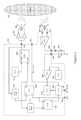
- FIG. 1illustrates a schematic block diagram of an ultrasonic ranging system comprising a microcontroller having a plurality of core independent peripheral (CIP) devices;
- CIPcore independent peripheral
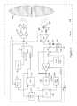
- FIG. 2illustrates a schematic block diagram of an ultrasonic proximity sensing system comprising a microcontroller having a plurality of core independent peripheral (CIP) devices, according to a specific example embodiment of this disclosure;
- CIPcore independent peripheral
- FIG. 3illustrates a schematic block diagram of a microcontroller integrated circuit package comprising the ultrasonic proximity sensing device shown in FIG. 2 ;
- FIG. 4illustrates a schematic graph of an integration process of the received ultrasonic energy, according to the teachings of this disclosure
- FIG. 5illustrates a schematic graph of an integration process of the received ultrasonic energy using a delayed and shortened integration time window, according to the teachings of this disclosure
- FIG. 6illustrates a schematic plan view of a proximity sensing peripheral coupled with a plurality of ultrasonic transducers arranged in an area, according to another specific example embodiment of this disclosure.
- FIG. 7illustrates a schematic block diagram of a microcontroller integrated circuit package comprising core independent peripherals (CIPs) and programmable interconnections thereto, according to the teachings of this disclosure.
- CIPscore independent peripherals
- Microcontrollersare systems on a chip that generally comprise a central processing unit, memory, a plurality of input/output ports, and a variety of peripheral devices.
- a variety of so called core independent peripheral (CIP) devicescan be provided such as configurable logic cells, complementary waveform/output generators, numerical controlled oscillators and programmable switch mode controllers.
- CIPcore independent peripheral
- a core independent peripheralis a peripheral device in a microcontroller that does not require support from the central processing unit (CPU) of the microcontroller for its operation, while the CPU may be used to initialize and configure such a peripheral device.
- CPUcentral processing unit
- the CPUmay be used to initialize and configure such a peripheral device.
- a CIP deviceonce such a CIP device is configured and started, for example by the CPU, it operates on its own and frees processing power of the CPU core for other tasks.
- a counteronce triggered, starts counting independently from the CPU, a direct memory access controller performs block transfers from/to memory without CPU interaction, etc.
- Using CIPsdecrease parts count, manufacturing costs, and increase reliability and versatility of a product. Many products greatly benefit from such cost savings, increased versatility and reliability.
- One such productmay be used for ultrasonic proximity sensing applications.
- a ranging functionwas implemented using a collection of core independent peripherals (CIPs) in a microcontroller.
- CIPscore independent peripherals
- a pulse width modulation (PWM) peripheralmay be used to generate a high frequency drive signal, a counter to set the duration of the PWM drive signal (pulse), and a second timer coupled to a comparator to measure the time it takes to receive back a reflection from an object of the ranging signal.
- PWMpulse width modulation
- the ranging peripheralallows the user to set a bit to start the ranging, and receive an interrupt when the ranging measurement has completed.
- Alternative aspects of the designallow time dependent return pulse detection sensitivity and/or gain adjustments.
- the aforementioned configurable ultrasonic ranging peripheraldoes not use up software overhead of a central processor in a microcontroller during operation thereof.
- the ultrasonic ranging peripheraluses on-chip resources for most of its functions and therefore requires very few external components. It's set and forget nature may be based on CIP based timers, signal generators and configurable logic cells (CLC).
- the ultrasonic proximity systemmay use an ultrasonic transmit section.
- the receive sectionmay use an integrator in place of a comparator.
- the ultrasonic energy at the receiveris averaged over time to get an acoustic finger printer for the area, e.g., room or enclosure.
- the resultmay be converted into a digital representation using an ADC and compared to a previously stored proximity signature average for the area (e.g., room or enclosure), if the present value is different from the previous proximity signature, then a proximity alarm (e.g., interrupt) may be triggered.
- a proximity alarme.g., interrupt
- any new object (car, truck, etc.) or body (people, animal, etc.) in the areawill change the acoustics thereof, specifically changing reflections and/or absorbing the ultrasonic sound, the resulting integration of acoustic energy in the receiver will change (increased or decreased).
- the integration value converted by the ADCwill be different from a previously stored integration value, thereby triggering detection of a person or new object in proximity thereto (in the area, room or enclosure).
- Such a systemmay generate 40-60 kHz sound pulses. Timing between the transmission and reception of the strongest ultrasonic energy pulse is timed. Other reflections are either too weak or too late to be measured. People tend to absorb sound rather than reflect sound. Some materials carried by people do reflect sound.
- the ultrasonic energy pulseis generated just like in an ultrasonic ranging system, e.g., commonly owned U.S. patent application Ser. No. 15/278,984.
- the timer and threshold comparatorare replaced by an integrator.
- the integratormay collect all the energy pulse returns to create an ultrasonic reflection finger print for the area.
- objectse.g., people, animals, vehicles, etc.
- the resulting ultrasonic reflection accumulationcan be compared to a stored running average.
- a microcontroller with configurable logic cell (CLC) modulesmay be used to implement such an ultrasonic proximity sensing system.
- a respective microcontroller manufactured by the assignee of the present applicationcomprising core independent peripherals as stated above may be used.
- a CLC modulemay comprise a configurable logic cell that provides, depending on its configuration, as a SR flip-flop, J-K flip-flop, D-latch, various logic gate combinations including AND, OR, XOR, etc.
- a plurality of such cellsfor example four cells, may be included within a microcontroller and the respective configurable cells can be cascaded to provide for one or more desired logic functions.
- the microcontrollermay further comprise timers, a data signal modulator (DSM) module, an operational amplifier, and PWM modules.
- DSMdata signal modulator
- FIG. 1depicted is a schematic block diagram of an ultrasonic ranging device comprising a microcontroller having a plurality of core independent peripheral (CIP) devices.
- CIPcore independent peripheral
- a microcontroller 100may comprise a plurality of core independent peripheral (CIP) devices, for example but are not limited to, the following peripherals: Data Signal Modulator (DSM) 104 , Fixed Voltage Reference (FVR) 110 , Operational Amplifier (OPA) 112 , Comparator (CMP) 114 , Hardware Limit Timers (HLT) 116 and 122 , Configurable Logic Cells (CLC) 118 and 126 , Pulse Width Modulation (PWM) Generator 120 , Capture Compare Pulse Width Modulation (CCP) 128 , and Timer Counter Register (TMR) 130 .
- DSMData Signal Modulator
- FVRFixed Voltage Reference
- OPAOperational Amplifier
- CMPComparator
- HLTHardware Limit Timers
- CLCConfigurable Logic Cells
- PWMPulse Width Modulation
- CCPCapture Compare Pulse Width Modulation
- TMRTimer Counter Register
- the CLCsmay comprise, for example but are not limited to, four modules; wherein each module may be configured as flip-flops and/or a variety of logic combinations such as NOR, NAND, XNOR, AND, OR, XOR and other gates, etc.
- a usermay select from a variety of internal and external signals to provide input signals to these modules.
- the output signalsmay be either used internally and/or coupled to external nodes (pins) 180 - 194 of the microcontroller 100 .
- Such logic core independent peripheralsallow for simple combinatorial and sequential logic functions to be added without the necessity of additional external devices.
- a start bit at input node 180triggers a SR-flip flop defined by the CLC 118 . This couples a PWM signal from the output of the PWM 120 to the carrier high (CARH) input of the DSM 104 .
- the PWM signalis passed through the DSM 104 and is coupled to an external driver 132 which drives an ultrasonic (acoustic) transmitting transducer 134 to generate a pulse of ultrasonic sound having a frequency of about 40 kHz with a pulse duration determined by the HLT/TMR 122 in combination with the CLC 118 having its Q-output coupled to the modulation (MOD) input of the DSM 104 .
- the pulse durationmay be, for example but is not limited to, from about 40 cycles to about 200 cycles of the 40 kHz frequency.
- the HLT/TMR 122is activated by a PWM signal on the output of the DSM 104 , and when it times out the SR flip-flop of the CLC 118 is reset, ending the PWM pulse from the DSM 104 .
- the high-to-low transition at the output of the SR flip-flop of the CLC 118triggers the HLT/TMR 116 configured as a one-shot timer.
- This one-shot timer(HLT/TMR 116 ) provides the necessary dead time between ultrasonic signal transmit and receive, so residual oscillations from the ultrasonic transmitting transducer 134 element do not generate a false signal during the receiver operation.
- the second SR flip-flop CLC 126When the one-shot timer (HLT/TMR 116 ) times out, the second SR flip-flop CLC 126 is set thereby enabling the timer gate TMR 130 to start counting the time it takes to detected a reflected return ultrasonic signal.
- a peak detectorcomprising diode 148 , resistor 150 and capacitor 152 ; may be coupled to an input of the CMP 114 that will cause the output of the CMP 114 to initiate a capture event to store the time count from the TMR 130 in the CCP 128 .
- This actionalso generates an interrupt 182 that notifies the program running in the central processor (not shown) of the microcontroller 100 of a receipt and capture of the time required for the round trip of the ultrasonic pulse. If no DC signal of sufficient amplitude is received at the input of the CMP 114 then a time out of the TMR 130 will trigger a fault interrupt 184 (no ultrasonic return signal received).
- the entire system except for the actual ultrasonic transducers 134 and 146 , and some external componentsmay be provided by a microcontroller comprising the above-mentioned CIP peripherals.
- a microcontrollercomprising the above-mentioned CIP peripherals.
- the diode 148 , resistor 150 , capacitor 152 , the ultrasonic transmitter driver 132 , and transmit and receive transducers 134 and 146 , respectively,are required as external components.
- the remaining componentsmay be provided by CIP peripherals of the microcontroller 100 .
- a microcontroller 200may comprise a plurality of core independent peripheral (CIP) devices, for example but are not limited to, the following peripherals: Data Signal Modulator (DSM) 104 , Fixed Voltage Reference (FVR) 210 , Operational Amplifiers (OPA) 112 and 214 , analog-to-digital converter (ADC) 238 , Hardware Limit Timers (HLT) 116 and 122 , Configurable Logic Cells (CLC) 118 and 226 , Pulse Width Modulation (PWM) Generator 120 , and Timer Counter Register (TMR) 230 .
- DSMData Signal Modulator
- FVRFixed Voltage Reference
- OPAOperational Amplifiers
- ADCanalog-to-digital converter
- HLTHardware Limit Timers
- CLCConfigurable Logic Cells
- PWMPulse Width Modulation
- TMRTimer Counter Register
- the CLCsmay comprise, for example but are not limited to, four modules; wherein each module may be configured as flip-flops and/or a variety of logic combinations such as NOR, NAND, XNOR, AND, OR, XOR and other gates, etc.
- a usermay select from a variety of internal and external signals to provide input signals to these modules.
- the output signalsmay be either used internally and/or coupled to external nodes (pins) 180 - 194 of the microcontroller 200 .
- Such logic core independent peripheralsallow for simple combinatorial and sequential logic functions to be added without the necessity of additional external devices.
- the core independent peripherals (CIPs) and exemplary interconnections thereof for an ultrasonic proximity sensing applicationare shown in FIG. 2 .
- a start bit at input node 280triggers the SR-flip flop in the CLC module 118 . This couples a PWM signal from the output of the PWM 120 to the carrier high (CARH) input of the DSM 104 .
- CARHcarrier high
- the PWM signalis passed through the DSM 104 and is coupled to an external driver 132 which drives an ultrasonic (acoustic) transmitting transducer 134 to generate a pulse of an ultrasonic sound having a frequency of about 40 kHz with a pulse duration determined by the HLT/TMR 122 in combination with the CLC 118 having its Q-output coupled to the modulation (MOD) input of the DSM 104 .
- the HLT/TMR 122is activated by a PWM signal on the output of the DSM 104 , and when it times out the SR flip-flop of the CLC 118 is reset, ending the PWM pulse from the DSM 104 .
- the high-to-low transition at the output of the SR flip-flop of the CLC 118triggers the HLT/TMR 116 configured as a one-shot timer.
- This one-shot timer(HLT/TMR 116 ) provides the necessary dead time between ultrasonic signal transmit and receive, so residual oscillations from the ultrasonic transmitting transducer 134 element do not generate a false signal during the receiver operation.
- the second SR flip-flop CLC 226is set thereby enabling the timer gate TMR 230 to start counting time for an “integration window” to take place while the reflected return ultrasonic signal(s) are received and integrated.
- an amplitude modulation (AM) diode detectorcomprising diode 148 , resistor 150 and capacitor 152 ; will provide received ultrasonic acoustic energy to a voltage integrator, comprising OPA 214 and capacitor 248 , for accumulation thereof.
- AMamplitude modulation
- the start and stop times of the integrationyou can literally specify the range from the unit over which you integrate. So basically, one can determine the finger print for a shell, for example, from 3′ to 5′ from the transducer. By measuring the finger print for multiple shells; e.g., 1-2, 2-3, 3-4, 4-5, and 5-6 feet, one can determine whether something is moving toward or away from the sensor 146 by just seeing changes move from further out to closer in, and vice versa. One can even estimate the speed of the object moving by observing time of change between shells. Approximate distance of the object may be determined from which shell (integration time window) has an object detection therein.
- the final hardware limit timer (HLT) 230When the final hardware limit timer (HLT) 230 times out, it will trigger a conversion by the ADC 238 which will convert the accumulated received ultrasonic energy into a digital value.
- This digital valuemay be coupled to a digital processor and memory 380 ( FIG. 3 ) where it may be stored and compared to a running average, if the absolute difference (+/ ⁇ ) is greater than a preset integration threshold, then a proximity event is detected, if not, then the value may be averaged into the running average and the proximity sensing process repeated.
- a microcontroller 200comprising the above-mentioned CIP peripherals. For example, as shown in FIG.
- the proximity sensing system shown in FIG. 2is immune to thermal changes in the environment. If the acoustic finger print for the area (room or enclosure) 270 changes over time, the average will still allow the capture of fast motion.
- the gated integratorallows the monitoring of different bands of proximity.
- the complete systemcan be implemented with CIPs in a microcontroller with minimal software overhead.
- the ultrasonic proximity sensing peripheralmay be adapted to be reconfigured into an ultrasonic ranging peripheral, as shown in FIG. 1 , since most of the modules and functions are substantially the same between the two peripherals. Provision could be made in the microcontroller for the comparator (CMP) 114 , CCP 128 , OPA 214 and ADC 238 to be switchably selectable as required. Wherein after the proximity sensing peripheral detects an object the microcontroller could switch to the ultrasonic ranging peripheral to obtain more detailed location information of the object detected during the proximity sensing operation.
- CMPcomparator
- FIG. 3depicted is a schematic block diagram of a microcontroller integrated circuit package comprising the ultrasonic proximity sensing device shown in FIG. 2 .
- the proximity sensing system shown in FIG. 2may be provided with a microcontroller 302 comprising an integrated circuit package and the aforementioned CIPs and further comprises a central processor and memory 380 .
- the CIPsOnce the CIPs have been configured (using configuration registers not shown) they become independent in operation from the central processor and memory 380 , and only interact therewith upon a Start input and interrupt outputs.
- Various external connection nodes (pins) 180 - 194 , 394may be provided on the microcontroller 302 integrated circuit package.
- FIG. 4depicted is a schematic graph of an integration process of the received ultrasonic energy, according to the teachings of this disclosure.
- Detected voltages from the AM detector(diode 148 and capacitor 152 ) are integrated in the integrator (OPA 214 and capacitor 248 ) during an integration window 456 starting when the integrator is released (unclamped) to begin accumulating voltage charge until the ADC 238 takes a sample of this accumulated voltage.
- a digital representation from the ADC 238 of the voltage samplemay be stored in the central processor memory 380 and compared with the digital representations of previous voltage samples.
- FIG. 5depicted is a schematic graph of an integration process of the received ultrasonic energy using a delayed and shortened integration time window, according to the teachings of this disclosure.
- the primary ultrasonic energy reflection 452 amay dominate the integrator input so a delayed and/or reduced integration window time may be used instead of integrating over the entire time of ultrasonic reflections ( FIG. 4 ).
- the reduced integration window 556only integrates ultrasonic reflections 452 d - 452 h , and will ignore ultrasonic reflections 452 a - 452 and 452 i . This may prevent overloading of the integrator.
- a delay timermay be used to hold the integrator in reset, blanking out this strong reflection.
- a second timermay trigger the ADC to set the end of the integration. Averages for different windows may be retained to get a finger print for different bands of reflections.
- the returned energyis integrated over the entire range, you must have sufficient storage to hold the full charge.
- a proximity sensing peripheral 600may be coupled to at least one transmitting transducer 134 and a plurality of receiving transducers 146 .
- the plurality of receiving transducers 146may be positioned for best reflected ultrasonic pulse reception coverage in the area 670 (room or enclosure), and the at least one transmitting transducer 134 positioned for best ultrasonic pulse transmission coverage.
- the at least one transmitting transducer 134may be centrally located and oriented to send ultrasonic pulses to the ceiling of the area 670 for reflection therefrom and reception by the plurality of receiving transducers 146 .
- An arrangement of multiple transmitting and receiver transducers 134 and 146may be advantageous for odd shaped rooms so as to eliminate dead spots therein.
- Operations of the at least one transmitting transducer 134 and the plurality of receiving transducers 146may be time division multiplexed with the proximity sensing peripheral 200 and ultrasonic reception averages calculated and stored for each different area (zones) of the room 670 .
- a microcontrollerin an integrated circuit package, comprising core independent peripherals (CIPs) and programmable interconnections thereto, according to the teachings of this disclosure.
- a microcontrollergenerally represented by the numeral 700 , may comprise an integrated circuit package 702 having external connection nodes (pins) 394 that may be used for power, ground, input, output and input/output signals.
- the CIPsas described more fully hereinabove, may have their input and output signals internally connected to other CIPs and/or to the external connection nodes 790 .
- I/O (input/output) multiplexers (or switching matrixes) 790may be programmed to interconnect desired nodes 794 to respective signal inputs and output of the CIPs.
- Interconnection multiplexers 792may be programmed to interconnect signal inputs and outputs between CIPs.
- MPLAB® Code Configurator (MCC)may be utilized to easily configure functionality of the internal (to the microcontroller integrated circuit) CIPs used in this ultrasonic ranging detection application.
- the MCCmay further be used to configure (program) internal interconnections (e.g., interconnection multiplexers 792 ) between the CIPs and/or external integrated circuit package connections (e.g., I/O multiplexers 790 ) to the CIPs.
- the MCCis a user-friendly plug-in tool for MPLAB®X IDE which generates drivers for controlling and driving peripherals of PIC® microcontrollers, based on the settings and selections made in its Graphical User Interface (GUI).
- GUIGraphical User Interface
- DS40001725MPLAB® Code Configurator User's Guide
- MPLAB® and PIC®are registered trademarks of Microchip Technology Inc., the assignee of the present patent application.
- the various CIPs used in the specific example embodiments shown hereinare further described as follows:
- the DSM peripheralis described in Microchip data sheet “Data signal Modulator”, DS39744.
- the CLC peripheralis described in Microchip data sheet “Configurable Logic Cell”, DS33949.
- the CCP (capture compare, PWM and Timer) peripheralis described in Microchip data sheet “Capture/Compare/PWM/Timer,” DS33035.
- the comparator peripheralis described in Microchip data sheet “Dual Comparator Module”, DS39710.
- the I/O portsare for example described in Microchip data sheet “I/O Ports”, DS70193.
- DACsdigital-to-analog converters
- PGAprogrammable gain amplifier
- PRGprogrammable ramp generator
- CIPscore independent peripherals
Landscapes
- Engineering & Computer Science (AREA)
- Physics & Mathematics (AREA)
- Radar, Positioning & Navigation (AREA)
- Remote Sensing (AREA)
- Computer Networks & Wireless Communication (AREA)
- General Physics & Mathematics (AREA)
- Acoustics & Sound (AREA)
- Measurement Of Velocity Or Position Using Acoustic Or Ultrasonic Waves (AREA)
Abstract
Description
Claims (24)
Priority Applications (5)
| Application Number | Priority Date | Filing Date | Title |
|---|---|---|---|
| US15/447,532US10317528B2 (en) | 2016-03-03 | 2017-03-02 | Core independent ultrasonic proximity sensing peripheral |
| CN201780003934.2ACN108351403B (en) | 2016-03-03 | 2017-03-03 | Ultrasonic Proximity Sensing Peripheral Based on Core Standalone Peripheral |
| PCT/US2017/020603WO2017152019A1 (en) | 2016-03-03 | 2017-03-03 | Core independent peripheral based ultrasonic proximity sensing peripheral |
| EP17711490.7AEP3423862B1 (en) | 2016-03-03 | 2017-03-03 | Core independent peripheral based ultrasonic proximity sensing peripheral |
| TW106107120ATW201733289A (en) | 2016-03-03 | 2017-03-03 | Core independent peripheral based ultrasonic proximity sensing peripheral |
Applications Claiming Priority (2)
| Application Number | Priority Date | Filing Date | Title |
|---|---|---|---|
| US201662302933P | 2016-03-03 | 2016-03-03 | |
| US15/447,532US10317528B2 (en) | 2016-03-03 | 2017-03-02 | Core independent ultrasonic proximity sensing peripheral |
Publications (2)
| Publication Number | Publication Date |
|---|---|
| US20170254900A1 US20170254900A1 (en) | 2017-09-07 |
| US10317528B2true US10317528B2 (en) | 2019-06-11 |
Family
ID=59724220
Family Applications (1)
| Application Number | Title | Priority Date | Filing Date |
|---|---|---|---|
| US15/447,532Active2037-09-29US10317528B2 (en) | 2016-03-03 | 2017-03-02 | Core independent ultrasonic proximity sensing peripheral |
Country Status (5)
| Country | Link |
|---|---|
| US (1) | US10317528B2 (en) |
| EP (1) | EP3423862B1 (en) |
| CN (1) | CN108351403B (en) |
| TW (1) | TW201733289A (en) |
| WO (1) | WO2017152019A1 (en) |
Cited By (1)
| Publication number | Priority date | Publication date | Assignee | Title |
|---|---|---|---|---|
| US11828885B2 (en)* | 2017-12-15 | 2023-11-28 | Cirrus Logic Inc. | Proximity sensing |
Families Citing this family (4)
| Publication number | Priority date | Publication date | Assignee | Title |
|---|---|---|---|---|
| JP7238448B2 (en)* | 2019-02-12 | 2023-03-14 | 株式会社デンソー | Ultrasonic distance detector |
| TWI701585B (en)* | 2019-07-17 | 2020-08-11 | 友達光電股份有限公司 | Ultrasonic pixel circuit and related display device |
| US10955550B1 (en)* | 2019-12-09 | 2021-03-23 | Tymphany Acoustic Technology (Huizhou) Co., Ltd. | Synchronization of motion-sensitive acoustic speakers |
| CN113504307B (en)* | 2021-09-10 | 2021-12-21 | 西南石油大学 | A multi-frequency core sound velocity measurement device |
Citations (22)
| Publication number | Priority date | Publication date | Assignee | Title |
|---|---|---|---|---|
| US3624712A (en)* | 1969-07-22 | 1971-11-30 | Automation Ind Inc | Ultrasonic pulse echo thickness-measuring device |
| US3625057A (en)* | 1967-11-01 | 1971-12-07 | Mitsubishi Electric Corp | Ultrasonic flowmeter |
| US3665443A (en)* | 1970-09-03 | 1972-05-23 | Aerospace Res | Ultrasonic intrusion alarm |
| US3688565A (en)* | 1970-09-28 | 1972-09-05 | Sonie Instr Inc | Ultrasonic thickness gauge |
| US3858438A (en)* | 1972-11-13 | 1975-01-07 | Panametrics | Ultrasonic-gaging system method and apparatus |
| US3914987A (en) | 1973-10-03 | 1975-10-28 | Krautkramer Branson | Ultrasonic measuring apparatus for determining wall thickness of a workpiece |
| US3918296A (en)* | 1972-10-10 | 1975-11-11 | Tokyo Keiki Kk | Pulse reflection type ultrasonic thickness meter |
| US4075598A (en)* | 1975-04-25 | 1978-02-21 | Tokyo Shibaura Electric Co., Ltd. | Ultrasonic wave transmitting and receiving apparatus |
| US4075883A (en)* | 1976-08-20 | 1978-02-28 | General Electric Company | Ultrasonic fan beam scanner for computerized time-of-flight tomography |
| US4290310A (en)* | 1979-07-09 | 1981-09-22 | Varian Associates, Inc. | Ultrasonic imaging system using digital control |
| US4439846A (en) | 1981-11-18 | 1984-03-27 | Polaroid Corporation | Sonar rangefinder system |
| US4451909A (en) | 1980-12-18 | 1984-05-29 | Nippon Soken, Inc. | Ultrasonic wave distance detection system |
| US4596144A (en)* | 1984-09-27 | 1986-06-24 | Canadian Corporate Management Co., Ltd. | Acoustic ranging system |
| US4853904A (en)* | 1986-09-19 | 1989-08-01 | U.S. Philips Corporation | Apparatus for examining a moving object by means of ultrasound echography |
| US5159837A (en) | 1990-02-01 | 1992-11-03 | Mitsubishi Denki K.K. | Ultrasonic wave obstacle sensor |
| US5528217A (en) | 1993-01-05 | 1996-06-18 | Adams; Christopher | Collision avoidance system for vehicles using digital logic circuitry and retro-fitting techniques |
| US6314055B1 (en) | 1998-10-16 | 2001-11-06 | Intersense, Inc. | Range measuring system |
| US20030060163A1 (en) | 2001-09-27 | 2003-03-27 | Filkins Robert John | Wireless transceiver and method for remote ultrasonic measurements |
| WO2004095056A1 (en)* | 2003-04-22 | 2004-11-04 | Koninklijke Philips Electronics N.V. | Object position estimation system, apparatus and method |
| US20060022680A1 (en) | 2003-04-28 | 2006-02-02 | Takehiko Suginouchi | Ultrasonic distance measure |
| US20090093960A1 (en)* | 2007-10-04 | 2009-04-09 | Jeffrey Scott Puhalla | Method and system for obstacle avoidance for a vehicle |
| US20090320602A1 (en)* | 2008-03-20 | 2009-12-31 | Siemens Aktiengesellschaft | Device and method for synchronization of ultrasonic transducers in a movement system |
Family Cites Families (4)
| Publication number | Priority date | Publication date | Assignee | Title |
|---|---|---|---|---|
| DE102004053686A1 (en)* | 2004-11-03 | 2006-05-04 | Essling, Mirko | Laser receiving device with improved accuracy and lower power consumption |
| DE102006029025A1 (en)* | 2006-06-14 | 2007-12-27 | Iris-Gmbh Infrared & Intelligent Sensors | Reflective object distance determining device, has two integrators connected with photoelectric unit and control input, where photoelectric unit is rectangle or square shape and exhibits specific side length |
| US8320866B2 (en)* | 2010-02-11 | 2012-11-27 | Mediatek Singapore Pte. Ltd. | Integrated circuits, communication units and methods of cancellation of intermodulation distortion |
| CN103760567B (en)* | 2014-01-27 | 2016-06-15 | 中国科学院半导体研究所 | A kind of passive imaging system with distance measurement function and distance-finding method thereof |
- 2017
- 2017-03-02USUS15/447,532patent/US10317528B2/enactiveActive
- 2017-03-03EPEP17711490.7Apatent/EP3423862B1/enactiveActive
- 2017-03-03TWTW106107120Apatent/TW201733289A/enunknown
- 2017-03-03WOPCT/US2017/020603patent/WO2017152019A1/ennot_activeCeased
- 2017-03-03CNCN201780003934.2Apatent/CN108351403B/enactiveActive
Patent Citations (23)
| Publication number | Priority date | Publication date | Assignee | Title |
|---|---|---|---|---|
| US3625057A (en)* | 1967-11-01 | 1971-12-07 | Mitsubishi Electric Corp | Ultrasonic flowmeter |
| US3624712A (en)* | 1969-07-22 | 1971-11-30 | Automation Ind Inc | Ultrasonic pulse echo thickness-measuring device |
| US3665443A (en)* | 1970-09-03 | 1972-05-23 | Aerospace Res | Ultrasonic intrusion alarm |
| US3688565A (en)* | 1970-09-28 | 1972-09-05 | Sonie Instr Inc | Ultrasonic thickness gauge |
| US3918296A (en)* | 1972-10-10 | 1975-11-11 | Tokyo Keiki Kk | Pulse reflection type ultrasonic thickness meter |
| US3858438A (en)* | 1972-11-13 | 1975-01-07 | Panametrics | Ultrasonic-gaging system method and apparatus |
| US3914987A (en) | 1973-10-03 | 1975-10-28 | Krautkramer Branson | Ultrasonic measuring apparatus for determining wall thickness of a workpiece |
| US4075598A (en)* | 1975-04-25 | 1978-02-21 | Tokyo Shibaura Electric Co., Ltd. | Ultrasonic wave transmitting and receiving apparatus |
| US4075883A (en)* | 1976-08-20 | 1978-02-28 | General Electric Company | Ultrasonic fan beam scanner for computerized time-of-flight tomography |
| US4290310A (en)* | 1979-07-09 | 1981-09-22 | Varian Associates, Inc. | Ultrasonic imaging system using digital control |
| US4451909A (en) | 1980-12-18 | 1984-05-29 | Nippon Soken, Inc. | Ultrasonic wave distance detection system |
| US4439846A (en) | 1981-11-18 | 1984-03-27 | Polaroid Corporation | Sonar rangefinder system |
| US4596144A (en)* | 1984-09-27 | 1986-06-24 | Canadian Corporate Management Co., Ltd. | Acoustic ranging system |
| US4596144B1 (en)* | 1984-09-27 | 1995-10-10 | Federal Ind Ind Group Inc | Acoustic ranging system |
| US4853904A (en)* | 1986-09-19 | 1989-08-01 | U.S. Philips Corporation | Apparatus for examining a moving object by means of ultrasound echography |
| US5159837A (en) | 1990-02-01 | 1992-11-03 | Mitsubishi Denki K.K. | Ultrasonic wave obstacle sensor |
| US5528217A (en) | 1993-01-05 | 1996-06-18 | Adams; Christopher | Collision avoidance system for vehicles using digital logic circuitry and retro-fitting techniques |
| US6314055B1 (en) | 1998-10-16 | 2001-11-06 | Intersense, Inc. | Range measuring system |
| US20030060163A1 (en) | 2001-09-27 | 2003-03-27 | Filkins Robert John | Wireless transceiver and method for remote ultrasonic measurements |
| WO2004095056A1 (en)* | 2003-04-22 | 2004-11-04 | Koninklijke Philips Electronics N.V. | Object position estimation system, apparatus and method |
| US20060022680A1 (en) | 2003-04-28 | 2006-02-02 | Takehiko Suginouchi | Ultrasonic distance measure |
| US20090093960A1 (en)* | 2007-10-04 | 2009-04-09 | Jeffrey Scott Puhalla | Method and system for obstacle avoidance for a vehicle |
| US20090320602A1 (en)* | 2008-03-20 | 2009-12-31 | Siemens Aktiengesellschaft | Device and method for synchronization of ultrasonic transducers in a movement system |
Non-Patent Citations (9)
| Title |
|---|
| Curtis, Keith, "AN1536: Ultrasonic Range Detection," Microchip Technology Incorporated, URL: http://wwl.microchip.com/downloads/en/AppNotes/00001536A.podf, 14 pages, Oct. 28, 2013. |
| International Search Report and Written Opinion, Application No. PCT/US2015/054301, 13 pages, dated Jan. 5, 2017. |
| Microchip Technology Incorporated, "MPLAB® Code Configurator User's Guide," URL: http://wwl.microchip.com/downloads/en/DeviceDoc/40001725B.pdf, 24 pages, Mar. 25, 2014. |
| Microchip Technology Incorporated, "Section 10. I/O Ports," URL: http://wwl.microchip.com/downloads/en/DeviceDoc/70193D.pdf, 14 pages, Nov. 29, 2011. |
| Microchip Technology Incorporated, "Section 19. Dual Comparator Module," URL: http://wwl.microchip.com/downloads/en/DeviceDoc/39710b.podf, 12 pages, Jan. 5, 2010. |
| Microchip Technology Incorporated, "Section 55. Data Signal Modulator (DSM)" URL: http://wwl.microchip.com/downloads/en/DeviceDoc/39744a.pdf, 16 pages, May 11, 2011. |
| Microchip Technology Incorporated, "Section 64. Capture/Compare/PWM/Timer (MCCP and SCCP)," URL: http://wwl.microchip.com/downloads/en/DeviceDoc/33035a.podf, 64 pages, © 2013. |
| Partial International Search Report and Invitation to Pay Additional Fees, Application No. PCT/US2017/020603, 11 pages, dated May 18, 2017. |
| U.S. Non-Final Office Action, U.S. Appl. No. 15/278,984, 15 pages, dated Mar. 22, 2018. |
Cited By (1)
| Publication number | Priority date | Publication date | Assignee | Title |
|---|---|---|---|---|
| US11828885B2 (en)* | 2017-12-15 | 2023-11-28 | Cirrus Logic Inc. | Proximity sensing |
Also Published As
| Publication number | Publication date |
|---|---|
| EP3423862B1 (en) | 2021-04-28 |
| CN108351403B (en) | 2023-08-25 |
| TW201733289A (en) | 2017-09-16 |
| US20170254900A1 (en) | 2017-09-07 |
| EP3423862A1 (en) | 2019-01-09 |
| WO2017152019A1 (en) | 2017-09-08 |
| CN108351403A (en) | 2018-07-31 |
Similar Documents
| Publication | Publication Date | Title |
|---|---|---|
| US10317528B2 (en) | Core independent ultrasonic proximity sensing peripheral | |
| US20110180709A1 (en) | Serial-chaining proximity sensors for gesture recognition | |
| CN106154278B (en) | Intelligent robot and sensor module and obstacle detection method for it | |
| CN110780301A (en) | Threshold Generation for Coded Ultrasonic Sensing | |
| JP2010530954A (en) | Configurable electronic controller for capacitance measurement | |
| US7911967B2 (en) | Control and monitor signal transmission system | |
| EP3356847B1 (en) | Core independent peripheral based ultrasonic ranging peripheral | |
| US9236852B2 (en) | Input capture peripheral with gating logic | |
| WO2019080004A1 (en) | Composite motion detection system and method for use thereof | |
| KR20170046221A (en) | Apparatus for controlling ultrasonic sensor and control method thereof | |
| CN102590799A (en) | Monitoring sensor having activation | |
| JPH05206824A (en) | Ultrasonic proximity switch | |
| De Angelis et al. | A flexible UWB sensor for indoor localization | |
| CN211855581U (en) | PIR motion sensor | |
| RU2090931C1 (en) | Items counting system | |
| JPS6044624B2 (en) | Ultrasonic measuring device | |
| Cholasta | S12ZVL LIN Enabled Ultrasonic Distance Measurement | |
| JP5094714B2 (en) | Device for detecting a change in capacitance, and capacitive sensor for detecting the presence of a user using this device | |
| JPS5848634Y2 (en) | Ultrasonic object detection device | |
| Damala et al. | Distance Measurement Using Ultrasonic Sensor | |
| JPS5836315B2 (en) | Chiyo-on-Papulse Eco-Shiki Butsutysonzaikenshiyutsu Cairo | |
| JPS59201557A (en) | Transmission/reception system | |
| JP2010038551A (en) | Object detection device | |
| JPS5899778A (en) | Detecting device for visitor | |
| JPS5968691A (en) | Ultrasonic object detection device |
Legal Events
| Date | Code | Title | Description |
|---|---|---|---|
| AS | Assignment | Owner name:MICROCHIP TECHNOLOGY INCORPORATED, ARIZONA Free format text:ASSIGNMENT OF ASSIGNORS INTEREST;ASSIGNORS:CURTIS, KEITH;SUMAGUE, KRISTINE ANGELICA;STRAM, ANTHONY;SIGNING DATES FROM 20170301 TO 20170302;REEL/FRAME:041439/0869 | |
| STPP | Information on status: patent application and granting procedure in general | Free format text:RESPONSE TO NON-FINAL OFFICE ACTION ENTERED AND FORWARDED TO EXAMINER | |
| STPP | Information on status: patent application and granting procedure in general | Free format text:NOTICE OF ALLOWANCE MAILED -- APPLICATION RECEIVED IN OFFICE OF PUBLICATIONS | |
| STCF | Information on status: patent grant | Free format text:PATENTED CASE | |
| AS | Assignment | Owner name:JPMORGAN CHASE BANK, N.A., AS ADMINISTRATIVE AGENT, DELAWARE Free format text:SECURITY INTEREST;ASSIGNORS:MICROCHIP TECHNOLOGY INC.;SILICON STORAGE TECHNOLOGY, INC.;ATMEL CORPORATION;AND OTHERS;REEL/FRAME:053311/0305 Effective date:20200327 | |
| AS | Assignment | Owner name:SILICON STORAGE TECHNOLOGY, INC., ARIZONA Free format text:RELEASE BY SECURED PARTY;ASSIGNOR:JPMORGAN CHASE BANK, N.A, AS ADMINISTRATIVE AGENT;REEL/FRAME:053466/0011 Effective date:20200529 Owner name:MICROSEMI CORPORATION, CALIFORNIA Free format text:RELEASE BY SECURED PARTY;ASSIGNOR:JPMORGAN CHASE BANK, N.A, AS ADMINISTRATIVE AGENT;REEL/FRAME:053466/0011 Effective date:20200529 Owner name:ATMEL CORPORATION, ARIZONA Free format text:RELEASE BY SECURED PARTY;ASSIGNOR:JPMORGAN CHASE BANK, N.A, AS ADMINISTRATIVE AGENT;REEL/FRAME:053466/0011 Effective date:20200529 Owner name:MICROCHIP TECHNOLOGY INC., ARIZONA Free format text:RELEASE BY SECURED PARTY;ASSIGNOR:JPMORGAN CHASE BANK, N.A, AS ADMINISTRATIVE AGENT;REEL/FRAME:053466/0011 Effective date:20200529 Owner name:MICROSEMI STORAGE SOLUTIONS, INC., ARIZONA Free format text:RELEASE BY SECURED PARTY;ASSIGNOR:JPMORGAN CHASE BANK, N.A, AS ADMINISTRATIVE AGENT;REEL/FRAME:053466/0011 Effective date:20200529 | |
| AS | Assignment | Owner name:JPMORGAN CHASE BANK, N.A., AS ADMINISTRATIVE AGENT, ILLINOIS Free format text:SECURITY INTEREST;ASSIGNORS:MICROCHIP TECHNOLOGY INC.;SILICON STORAGE TECHNOLOGY, INC.;ATMEL CORPORATION;AND OTHERS;REEL/FRAME:052856/0909 Effective date:20200529 Owner name:WELLS FARGO BANK, NATIONAL ASSOCIATION, MINNESOTA Free format text:SECURITY INTEREST;ASSIGNORS:MICROCHIP TECHNOLOGY INC.;SILICON STORAGE TECHNOLOGY, INC.;ATMEL CORPORATION;AND OTHERS;REEL/FRAME:053468/0705 Effective date:20200529 | |
| AS | Assignment | Owner name:WELLS FARGO BANK, NATIONAL ASSOCIATION, AS COLLATERAL AGENT, MINNESOTA Free format text:SECURITY INTEREST;ASSIGNORS:MICROCHIP TECHNOLOGY INCORPORATED;SILICON STORAGE TECHNOLOGY, INC.;ATMEL CORPORATION;AND OTHERS;REEL/FRAME:055671/0612 Effective date:20201217 | |
| AS | Assignment | Owner name:WELLS FARGO BANK, NATIONAL ASSOCIATION, AS NOTES COLLATERAL AGENT, MINNESOTA Free format text:SECURITY INTEREST;ASSIGNORS:MICROCHIP TECHNOLOGY INCORPORATED;SILICON STORAGE TECHNOLOGY, INC.;ATMEL CORPORATION;AND OTHERS;REEL/FRAME:057935/0474 Effective date:20210528 | |
| AS | Assignment | Owner name:WELLS FARGO BANK, NATIONAL ASSOCIATION, AS NOTES COLLATERAL AGENT, MINNESOTA Free format text:GRANT OF SECURITY INTEREST IN PATENT RIGHTS;ASSIGNORS:MICROCHIP TECHNOLOGY INCORPORATED;SILICON STORAGE TECHNOLOGY, INC.;ATMEL CORPORATION;AND OTHERS;REEL/FRAME:058214/0625 Effective date:20211117 | |
| AS | Assignment | Owner name:MICROSEMI STORAGE SOLUTIONS, INC., ARIZONA Free format text:RELEASE BY SECURED PARTY;ASSIGNOR:JPMORGAN CHASE BANK, N.A., AS ADMINISTRATIVE AGENT;REEL/FRAME:059263/0001 Effective date:20220218 Owner name:MICROSEMI CORPORATION, ARIZONA Free format text:RELEASE BY SECURED PARTY;ASSIGNOR:JPMORGAN CHASE BANK, N.A., AS ADMINISTRATIVE AGENT;REEL/FRAME:059263/0001 Effective date:20220218 Owner name:ATMEL CORPORATION, ARIZONA Free format text:RELEASE BY SECURED PARTY;ASSIGNOR:JPMORGAN CHASE BANK, N.A., AS ADMINISTRATIVE AGENT;REEL/FRAME:059263/0001 Effective date:20220218 Owner name:SILICON STORAGE TECHNOLOGY, INC., ARIZONA Free format text:RELEASE BY SECURED PARTY;ASSIGNOR:JPMORGAN CHASE BANK, N.A., AS ADMINISTRATIVE AGENT;REEL/FRAME:059263/0001 Effective date:20220218 Owner name:MICROCHIP TECHNOLOGY INCORPORATED, ARIZONA Free format text:RELEASE BY SECURED PARTY;ASSIGNOR:JPMORGAN CHASE BANK, N.A., AS ADMINISTRATIVE AGENT;REEL/FRAME:059263/0001 Effective date:20220218 | |
| AS | Assignment | Owner name:MICROSEMI STORAGE SOLUTIONS, INC., ARIZONA Free format text:RELEASE BY SECURED PARTY;ASSIGNOR:WELLS FARGO BANK, NATIONAL ASSOCIATION, AS NOTES COLLATERAL AGENT;REEL/FRAME:059358/0335 Effective date:20220228 Owner name:MICROSEMI CORPORATION, ARIZONA Free format text:RELEASE BY SECURED PARTY;ASSIGNOR:WELLS FARGO BANK, NATIONAL ASSOCIATION, AS NOTES COLLATERAL AGENT;REEL/FRAME:059358/0335 Effective date:20220228 Owner name:ATMEL CORPORATION, ARIZONA Free format text:RELEASE BY SECURED PARTY;ASSIGNOR:WELLS FARGO BANK, NATIONAL ASSOCIATION, AS NOTES COLLATERAL AGENT;REEL/FRAME:059358/0335 Effective date:20220228 Owner name:SILICON STORAGE TECHNOLOGY, INC., ARIZONA Free format text:RELEASE BY SECURED PARTY;ASSIGNOR:WELLS FARGO BANK, NATIONAL ASSOCIATION, AS NOTES COLLATERAL AGENT;REEL/FRAME:059358/0335 Effective date:20220228 Owner name:MICROCHIP TECHNOLOGY INCORPORATED, ARIZONA Free format text:RELEASE BY SECURED PARTY;ASSIGNOR:WELLS FARGO BANK, NATIONAL ASSOCIATION, AS NOTES COLLATERAL AGENT;REEL/FRAME:059358/0335 Effective date:20220228 | |
| AS | Assignment | Owner name:MICROSEMI STORAGE SOLUTIONS, INC., ARIZONA Free format text:RELEASE BY SECURED PARTY;ASSIGNOR:WELLS FARGO BANK, NATIONAL ASSOCIATION, AS NOTES COLLATERAL AGENT;REEL/FRAME:059863/0400 Effective date:20220228 Owner name:MICROSEMI CORPORATION, ARIZONA Free format text:RELEASE BY SECURED PARTY;ASSIGNOR:WELLS FARGO BANK, NATIONAL ASSOCIATION, AS NOTES COLLATERAL AGENT;REEL/FRAME:059863/0400 Effective date:20220228 Owner name:ATMEL CORPORATION, ARIZONA Free format text:RELEASE BY SECURED PARTY;ASSIGNOR:WELLS FARGO BANK, NATIONAL ASSOCIATION, AS NOTES COLLATERAL AGENT;REEL/FRAME:059863/0400 Effective date:20220228 Owner name:SILICON STORAGE TECHNOLOGY, INC., ARIZONA Free format text:RELEASE BY SECURED PARTY;ASSIGNOR:WELLS FARGO BANK, NATIONAL ASSOCIATION, AS NOTES COLLATERAL AGENT;REEL/FRAME:059863/0400 Effective date:20220228 Owner name:MICROCHIP TECHNOLOGY INCORPORATED, ARIZONA Free format text:RELEASE BY SECURED PARTY;ASSIGNOR:WELLS FARGO BANK, NATIONAL ASSOCIATION, AS NOTES COLLATERAL AGENT;REEL/FRAME:059863/0400 Effective date:20220228 | |
| AS | Assignment | Owner name:MICROSEMI STORAGE SOLUTIONS, INC., ARIZONA Free format text:RELEASE BY SECURED PARTY;ASSIGNOR:WELLS FARGO BANK, NATIONAL ASSOCIATION, AS NOTES COLLATERAL AGENT;REEL/FRAME:059363/0001 Effective date:20220228 Owner name:MICROSEMI CORPORATION, ARIZONA Free format text:RELEASE BY SECURED PARTY;ASSIGNOR:WELLS FARGO BANK, NATIONAL ASSOCIATION, AS NOTES COLLATERAL AGENT;REEL/FRAME:059363/0001 Effective date:20220228 Owner name:ATMEL CORPORATION, ARIZONA Free format text:RELEASE BY SECURED PARTY;ASSIGNOR:WELLS FARGO BANK, NATIONAL ASSOCIATION, AS NOTES COLLATERAL AGENT;REEL/FRAME:059363/0001 Effective date:20220228 Owner name:SILICON STORAGE TECHNOLOGY, INC., ARIZONA Free format text:RELEASE BY SECURED PARTY;ASSIGNOR:WELLS FARGO BANK, NATIONAL ASSOCIATION, AS NOTES COLLATERAL AGENT;REEL/FRAME:059363/0001 Effective date:20220228 Owner name:MICROCHIP TECHNOLOGY INCORPORATED, ARIZONA Free format text:RELEASE BY SECURED PARTY;ASSIGNOR:WELLS FARGO BANK, NATIONAL ASSOCIATION, AS NOTES COLLATERAL AGENT;REEL/FRAME:059363/0001 Effective date:20220228 | |
| AS | Assignment | Owner name:MICROSEMI STORAGE SOLUTIONS, INC., ARIZONA Free format text:RELEASE BY SECURED PARTY;ASSIGNOR:WELLS FARGO BANK, NATIONAL ASSOCIATION, AS NOTES COLLATERAL AGENT;REEL/FRAME:060894/0437 Effective date:20220228 Owner name:MICROSEMI CORPORATION, ARIZONA Free format text:RELEASE BY SECURED PARTY;ASSIGNOR:WELLS FARGO BANK, NATIONAL ASSOCIATION, AS NOTES COLLATERAL AGENT;REEL/FRAME:060894/0437 Effective date:20220228 Owner name:ATMEL CORPORATION, ARIZONA Free format text:RELEASE BY SECURED PARTY;ASSIGNOR:WELLS FARGO BANK, NATIONAL ASSOCIATION, AS NOTES COLLATERAL AGENT;REEL/FRAME:060894/0437 Effective date:20220228 Owner name:SILICON STORAGE TECHNOLOGY, INC., ARIZONA Free format text:RELEASE BY SECURED PARTY;ASSIGNOR:WELLS FARGO BANK, NATIONAL ASSOCIATION, AS NOTES COLLATERAL AGENT;REEL/FRAME:060894/0437 Effective date:20220228 Owner name:MICROCHIP TECHNOLOGY INCORPORATED, ARIZONA Free format text:RELEASE BY SECURED PARTY;ASSIGNOR:WELLS FARGO BANK, NATIONAL ASSOCIATION, AS NOTES COLLATERAL AGENT;REEL/FRAME:060894/0437 Effective date:20220228 | |
| MAFP | Maintenance fee payment | Free format text:PAYMENT OF MAINTENANCE FEE, 4TH YEAR, LARGE ENTITY (ORIGINAL EVENT CODE: M1551); ENTITY STATUS OF PATENT OWNER: LARGE ENTITY Year of fee payment:4 |