US10312217B2 - Method for low temperature bonding and bonded structure - Google Patents
Method for low temperature bonding and bonded structureDownload PDFInfo
- Publication number
- US10312217B2 US10312217B2US15/205,346US201615205346AUS10312217B2US 10312217 B2US10312217 B2US 10312217B2US 201615205346 AUS201615205346 AUS 201615205346AUS 10312217 B2US10312217 B2US 10312217B2
- Authority
- US
- United States
- Prior art keywords
- bonding
- insulating material
- nitrogen
- planarized
- terminating
- Prior art date
- Legal status (The legal status is an assumption and is not a legal conclusion. Google has not performed a legal analysis and makes no representation as to the accuracy of the status listed.)
- Expired - Fee Related
Links
Images


Classifications
- H—ELECTRICITY
- H01—ELECTRIC ELEMENTS
- H01L—SEMICONDUCTOR DEVICES NOT COVERED BY CLASS H10
- H01L21/00—Processes or apparatus adapted for the manufacture or treatment of semiconductor or solid state devices or of parts thereof
- H01L21/02—Manufacture or treatment of semiconductor devices or of parts thereof
- H01L21/04—Manufacture or treatment of semiconductor devices or of parts thereof the devices having potential barriers, e.g. a PN junction, depletion layer or carrier concentration layer
- H01L21/18—Manufacture or treatment of semiconductor devices or of parts thereof the devices having potential barriers, e.g. a PN junction, depletion layer or carrier concentration layer the devices having semiconductor bodies comprising elements of Group IV of the Periodic Table or AIIIBV compounds with or without impurities, e.g. doping materials
- H01L21/30—Treatment of semiconductor bodies using processes or apparatus not provided for in groups H01L21/20 - H01L21/26
- H01L21/302—Treatment of semiconductor bodies using processes or apparatus not provided for in groups H01L21/20 - H01L21/26 to change their surface-physical characteristics or shape, e.g. etching, polishing, cutting
- H01L21/306—Chemical or electrical treatment, e.g. electrolytic etching
- H01L21/3063—Electrolytic etching
- H—ELECTRICITY
- H01—ELECTRIC ELEMENTS
- H01L—SEMICONDUCTOR DEVICES NOT COVERED BY CLASS H10
- H01L24/00—Arrangements for connecting or disconnecting semiconductor or solid-state bodies; Methods or apparatus related thereto
- H01L24/80—Methods for connecting semiconductor or other solid state bodies using means for bonding being attached to, or being formed on, the surface to be connected
- H01L24/83—Methods for connecting semiconductor or other solid state bodies using means for bonding being attached to, or being formed on, the surface to be connected using a layer connector
- H—ELECTRICITY
- H01—ELECTRIC ELEMENTS
- H01L—SEMICONDUCTOR DEVICES NOT COVERED BY CLASS H10
- H01L21/00—Processes or apparatus adapted for the manufacture or treatment of semiconductor or solid state devices or of parts thereof
- H01L21/02—Manufacture or treatment of semiconductor devices or of parts thereof
- H01L21/02041—Cleaning
- H01L21/02057—Cleaning during device manufacture
- H01L21/0206—Cleaning during device manufacture during, before or after processing of insulating layers
- H—ELECTRICITY
- H01—ELECTRIC ELEMENTS
- H01L—SEMICONDUCTOR DEVICES NOT COVERED BY CLASS H10
- H01L21/00—Processes or apparatus adapted for the manufacture or treatment of semiconductor or solid state devices or of parts thereof
- H01L21/02—Manufacture or treatment of semiconductor devices or of parts thereof
- H01L21/04—Manufacture or treatment of semiconductor devices or of parts thereof the devices having potential barriers, e.g. a PN junction, depletion layer or carrier concentration layer
- H01L21/18—Manufacture or treatment of semiconductor devices or of parts thereof the devices having potential barriers, e.g. a PN junction, depletion layer or carrier concentration layer the devices having semiconductor bodies comprising elements of Group IV of the Periodic Table or AIIIBV compounds with or without impurities, e.g. doping materials
- H01L21/20—Deposition of semiconductor materials on a substrate, e.g. epitaxial growth solid phase epitaxy
- H01L21/2003—Deposition of semiconductor materials on a substrate, e.g. epitaxial growth solid phase epitaxy characterised by the substrate
- H01L21/2007—Bonding of semiconductor wafers to insulating substrates or to semiconducting substrates using an intermediate insulating layer
- H—ELECTRICITY
- H01—ELECTRIC ELEMENTS
- H01L—SEMICONDUCTOR DEVICES NOT COVERED BY CLASS H10
- H01L21/00—Processes or apparatus adapted for the manufacture or treatment of semiconductor or solid state devices or of parts thereof
- H01L21/02—Manufacture or treatment of semiconductor devices or of parts thereof
- H01L21/04—Manufacture or treatment of semiconductor devices or of parts thereof the devices having potential barriers, e.g. a PN junction, depletion layer or carrier concentration layer
- H01L21/18—Manufacture or treatment of semiconductor devices or of parts thereof the devices having potential barriers, e.g. a PN junction, depletion layer or carrier concentration layer the devices having semiconductor bodies comprising elements of Group IV of the Periodic Table or AIIIBV compounds with or without impurities, e.g. doping materials
- H01L21/30—Treatment of semiconductor bodies using processes or apparatus not provided for in groups H01L21/20 - H01L21/26
- H01L21/31—Treatment of semiconductor bodies using processes or apparatus not provided for in groups H01L21/20 - H01L21/26 to form insulating layers thereon, e.g. for masking or by using photolithographic techniques; After treatment of these layers; Selection of materials for these layers
- H01L21/3105—After-treatment
- H01L21/311—Etching the insulating layers by chemical or physical means
- H01L21/31105—Etching inorganic layers
- H01L21/31111—Etching inorganic layers by chemical means
- H01L21/31116—Etching inorganic layers by chemical means by dry-etching
- H—ELECTRICITY
- H01—ELECTRIC ELEMENTS
- H01L—SEMICONDUCTOR DEVICES NOT COVERED BY CLASS H10
- H01L21/00—Processes or apparatus adapted for the manufacture or treatment of semiconductor or solid state devices or of parts thereof
- H01L21/02—Manufacture or treatment of semiconductor devices or of parts thereof
- H01L21/04—Manufacture or treatment of semiconductor devices or of parts thereof the devices having potential barriers, e.g. a PN junction, depletion layer or carrier concentration layer
- H01L21/18—Manufacture or treatment of semiconductor devices or of parts thereof the devices having potential barriers, e.g. a PN junction, depletion layer or carrier concentration layer the devices having semiconductor bodies comprising elements of Group IV of the Periodic Table or AIIIBV compounds with or without impurities, e.g. doping materials
- H01L21/30—Treatment of semiconductor bodies using processes or apparatus not provided for in groups H01L21/20 - H01L21/26
- H01L21/322—Treatment of semiconductor bodies using processes or apparatus not provided for in groups H01L21/20 - H01L21/26 to modify their internal properties, e.g. to produce internal imperfections
- H—ELECTRICITY
- H01—ELECTRIC ELEMENTS
- H01L—SEMICONDUCTOR DEVICES NOT COVERED BY CLASS H10
- H01L21/00—Processes or apparatus adapted for the manufacture or treatment of semiconductor or solid state devices or of parts thereof
- H01L21/70—Manufacture or treatment of devices consisting of a plurality of solid state components formed in or on a common substrate or of parts thereof; Manufacture of integrated circuit devices or of parts thereof
- H01L21/71—Manufacture of specific parts of devices defined in group H01L21/70
- H01L21/76—Making of isolation regions between components
- H01L21/762—Dielectric regions, e.g. EPIC dielectric isolation, LOCOS; Trench refilling techniques, SOI technology, use of channel stoppers
- H01L21/7624—Dielectric regions, e.g. EPIC dielectric isolation, LOCOS; Trench refilling techniques, SOI technology, use of channel stoppers using semiconductor on insulator [SOI] technology
- H01L21/76251—Dielectric regions, e.g. EPIC dielectric isolation, LOCOS; Trench refilling techniques, SOI technology, use of channel stoppers using semiconductor on insulator [SOI] technology using bonding techniques
- H—ELECTRICITY
- H01—ELECTRIC ELEMENTS
- H01L—SEMICONDUCTOR DEVICES NOT COVERED BY CLASS H10
- H01L24/00—Arrangements for connecting or disconnecting semiconductor or solid-state bodies; Methods or apparatus related thereto
- H01L24/01—Means for bonding being attached to, or being formed on, the surface to be connected, e.g. chip-to-package, die-attach, "first-level" interconnects; Manufacturing methods related thereto
- H01L24/26—Layer connectors, e.g. plate connectors, solder or adhesive layers; Manufacturing methods related thereto
- H—ELECTRICITY
- H01—ELECTRIC ELEMENTS
- H01L—SEMICONDUCTOR DEVICES NOT COVERED BY CLASS H10
- H01L24/00—Arrangements for connecting or disconnecting semiconductor or solid-state bodies; Methods or apparatus related thereto
- H01L24/74—Apparatus for manufacturing arrangements for connecting or disconnecting semiconductor or solid-state bodies
- H01L24/75—Apparatus for connecting with bump connectors or layer connectors
- H—ELECTRICITY
- H01—ELECTRIC ELEMENTS
- H01L—SEMICONDUCTOR DEVICES NOT COVERED BY CLASS H10
- H01L25/00—Assemblies consisting of a plurality of semiconductor or other solid state devices
- H01L25/03—Assemblies consisting of a plurality of semiconductor or other solid state devices all the devices being of a type provided for in a single subclass of subclasses H10B, H10D, H10F, H10H, H10K or H10N, e.g. assemblies of rectifier diodes
- H01L25/04—Assemblies consisting of a plurality of semiconductor or other solid state devices all the devices being of a type provided for in a single subclass of subclasses H10B, H10D, H10F, H10H, H10K or H10N, e.g. assemblies of rectifier diodes the devices not having separate containers
- H01L25/065—Assemblies consisting of a plurality of semiconductor or other solid state devices all the devices being of a type provided for in a single subclass of subclasses H10B, H10D, H10F, H10H, H10K or H10N, e.g. assemblies of rectifier diodes the devices not having separate containers the devices being of a type provided for in group H10D89/00
- H01L25/0657—Stacked arrangements of devices
- H—ELECTRICITY
- H01—ELECTRIC ELEMENTS
- H01L—SEMICONDUCTOR DEVICES NOT COVERED BY CLASS H10
- H01L25/00—Assemblies consisting of a plurality of semiconductor or other solid state devices
- H01L25/50—Multistep manufacturing processes of assemblies consisting of devices, the devices being individual devices of subclass H10D or integrated devices of class H10
- H01L27/085—
- H01L29/06—
- H01L29/16—
- H—ELECTRICITY
- H10—SEMICONDUCTOR DEVICES; ELECTRIC SOLID-STATE DEVICES NOT OTHERWISE PROVIDED FOR
- H10D—INORGANIC ELECTRIC SEMICONDUCTOR DEVICES
- H10D62/00—Semiconductor bodies, or regions thereof, of devices having potential barriers
- H10D62/10—Shapes, relative sizes or dispositions of the regions of the semiconductor bodies; Shapes of the semiconductor bodies
- H—ELECTRICITY
- H10—SEMICONDUCTOR DEVICES; ELECTRIC SOLID-STATE DEVICES NOT OTHERWISE PROVIDED FOR
- H10D—INORGANIC ELECTRIC SEMICONDUCTOR DEVICES
- H10D62/00—Semiconductor bodies, or regions thereof, of devices having potential barriers
- H10D62/80—Semiconductor bodies, or regions thereof, of devices having potential barriers characterised by the materials
- H10D62/83—Semiconductor bodies, or regions thereof, of devices having potential barriers characterised by the materials being Group IV materials, e.g. B-doped Si or undoped Ge
- H—ELECTRICITY
- H10—SEMICONDUCTOR DEVICES; ELECTRIC SOLID-STATE DEVICES NOT OTHERWISE PROVIDED FOR
- H10D—INORGANIC ELECTRIC SEMICONDUCTOR DEVICES
- H10D84/00—Integrated devices formed in or on semiconductor substrates that comprise only semiconducting layers, e.g. on Si wafers or on GaAs-on-Si wafers
- H10D84/80—Integrated devices formed in or on semiconductor substrates that comprise only semiconducting layers, e.g. on Si wafers or on GaAs-on-Si wafers characterised by the integration of at least one component covered by groups H10D12/00 or H10D30/00, e.g. integration of IGFETs
- H10D84/82—Integrated devices formed in or on semiconductor substrates that comprise only semiconducting layers, e.g. on Si wafers or on GaAs-on-Si wafers characterised by the integration of at least one component covered by groups H10D12/00 or H10D30/00, e.g. integration of IGFETs of only field-effect components
- H—ELECTRICITY
- H01—ELECTRIC ELEMENTS
- H01L—SEMICONDUCTOR DEVICES NOT COVERED BY CLASS H10
- H01L2224/00—Indexing scheme for arrangements for connecting or disconnecting semiconductor or solid-state bodies and methods related thereto as covered by H01L24/00
- H01L2224/80—Methods for connecting semiconductor or other solid state bodies using means for bonding being attached to, or being formed on, the surface to be connected
- H01L2224/83—Methods for connecting semiconductor or other solid state bodies using means for bonding being attached to, or being formed on, the surface to be connected using a layer connector
- H01L2224/83009—Pre-treatment of the layer connector or the bonding area
- H01L2224/8301—Cleaning the layer connector, e.g. oxide removal step, desmearing
- H—ELECTRICITY
- H01—ELECTRIC ELEMENTS
- H01L—SEMICONDUCTOR DEVICES NOT COVERED BY CLASS H10
- H01L2224/00—Indexing scheme for arrangements for connecting or disconnecting semiconductor or solid-state bodies and methods related thereto as covered by H01L24/00
- H01L2224/80—Methods for connecting semiconductor or other solid state bodies using means for bonding being attached to, or being formed on, the surface to be connected
- H01L2224/83—Methods for connecting semiconductor or other solid state bodies using means for bonding being attached to, or being formed on, the surface to be connected using a layer connector
- H01L2224/83009—Pre-treatment of the layer connector or the bonding area
- H01L2224/8303—Reshaping the layer connector in the bonding apparatus, e.g. flattening the layer connector
- H01L2224/83031—Reshaping the layer connector in the bonding apparatus, e.g. flattening the layer connector by chemical means, e.g. etching, anodisation
- H—ELECTRICITY
- H01—ELECTRIC ELEMENTS
- H01L—SEMICONDUCTOR DEVICES NOT COVERED BY CLASS H10
- H01L2224/00—Indexing scheme for arrangements for connecting or disconnecting semiconductor or solid-state bodies and methods related thereto as covered by H01L24/00
- H01L2224/80—Methods for connecting semiconductor or other solid state bodies using means for bonding being attached to, or being formed on, the surface to be connected
- H01L2224/83—Methods for connecting semiconductor or other solid state bodies using means for bonding being attached to, or being formed on, the surface to be connected using a layer connector
- H01L2224/83053—Bonding environment
- H01L2224/8309—Vacuum
- H—ELECTRICITY
- H01—ELECTRIC ELEMENTS
- H01L—SEMICONDUCTOR DEVICES NOT COVERED BY CLASS H10
- H01L2224/00—Indexing scheme for arrangements for connecting or disconnecting semiconductor or solid-state bodies and methods related thereto as covered by H01L24/00
- H01L2224/80—Methods for connecting semiconductor or other solid state bodies using means for bonding being attached to, or being formed on, the surface to be connected
- H01L2224/83—Methods for connecting semiconductor or other solid state bodies using means for bonding being attached to, or being formed on, the surface to be connected using a layer connector
- H01L2224/83053—Bonding environment
- H01L2224/83095—Temperature settings
- H01L2224/83099—Ambient temperature
- H—ELECTRICITY
- H01—ELECTRIC ELEMENTS
- H01L—SEMICONDUCTOR DEVICES NOT COVERED BY CLASS H10
- H01L2224/00—Indexing scheme for arrangements for connecting or disconnecting semiconductor or solid-state bodies and methods related thereto as covered by H01L24/00
- H01L2224/80—Methods for connecting semiconductor or other solid state bodies using means for bonding being attached to, or being formed on, the surface to be connected
- H01L2224/83—Methods for connecting semiconductor or other solid state bodies using means for bonding being attached to, or being formed on, the surface to be connected using a layer connector
- H01L2224/8319—Arrangement of the layer connectors prior to mounting
- H—ELECTRICITY
- H01—ELECTRIC ELEMENTS
- H01L—SEMICONDUCTOR DEVICES NOT COVERED BY CLASS H10
- H01L2224/00—Indexing scheme for arrangements for connecting or disconnecting semiconductor or solid-state bodies and methods related thereto as covered by H01L24/00
- H01L2224/80—Methods for connecting semiconductor or other solid state bodies using means for bonding being attached to, or being formed on, the surface to be connected
- H01L2224/83—Methods for connecting semiconductor or other solid state bodies using means for bonding being attached to, or being formed on, the surface to be connected using a layer connector
- H01L2224/838—Bonding techniques
- H01L2224/8385—Bonding techniques using a polymer adhesive, e.g. an adhesive based on silicone, epoxy, polyimide, polyester
- H—ELECTRICITY
- H01—ELECTRIC ELEMENTS
- H01L—SEMICONDUCTOR DEVICES NOT COVERED BY CLASS H10
- H01L2224/00—Indexing scheme for arrangements for connecting or disconnecting semiconductor or solid-state bodies and methods related thereto as covered by H01L24/00
- H01L2224/80—Methods for connecting semiconductor or other solid state bodies using means for bonding being attached to, or being formed on, the surface to be connected
- H01L2224/83—Methods for connecting semiconductor or other solid state bodies using means for bonding being attached to, or being formed on, the surface to be connected using a layer connector
- H01L2224/838—Bonding techniques
- H01L2224/83894—Direct bonding, i.e. joining surfaces by means of intermolecular attracting interactions at their interfaces, e.g. covalent bonds, van der Waals forces
- H01L2224/83896—Direct bonding, i.e. joining surfaces by means of intermolecular attracting interactions at their interfaces, e.g. covalent bonds, van der Waals forces between electrically insulating surfaces, e.g. oxide or nitride layers
- H—ELECTRICITY
- H01—ELECTRIC ELEMENTS
- H01L—SEMICONDUCTOR DEVICES NOT COVERED BY CLASS H10
- H01L2224/00—Indexing scheme for arrangements for connecting or disconnecting semiconductor or solid-state bodies and methods related thereto as covered by H01L24/00
- H01L2224/80—Methods for connecting semiconductor or other solid state bodies using means for bonding being attached to, or being formed on, the surface to be connected
- H01L2224/83—Methods for connecting semiconductor or other solid state bodies using means for bonding being attached to, or being formed on, the surface to be connected using a layer connector
- H01L2224/83909—Post-treatment of the layer connector or bonding area
- H01L2224/83948—Thermal treatments, e.g. annealing, controlled cooling
- H—ELECTRICITY
- H01—ELECTRIC ELEMENTS
- H01L—SEMICONDUCTOR DEVICES NOT COVERED BY CLASS H10
- H01L2924/00—Indexing scheme for arrangements or methods for connecting or disconnecting semiconductor or solid-state bodies as covered by H01L24/00
- H—ELECTRICITY
- H01—ELECTRIC ELEMENTS
- H01L—SEMICONDUCTOR DEVICES NOT COVERED BY CLASS H10
- H01L2924/00—Indexing scheme for arrangements or methods for connecting or disconnecting semiconductor or solid-state bodies as covered by H01L24/00
- H01L2924/01—Chemical elements
- H01L2924/01005—Boron [B]
- H—ELECTRICITY
- H01—ELECTRIC ELEMENTS
- H01L—SEMICONDUCTOR DEVICES NOT COVERED BY CLASS H10
- H01L2924/00—Indexing scheme for arrangements or methods for connecting or disconnecting semiconductor or solid-state bodies as covered by H01L24/00
- H01L2924/01—Chemical elements
- H01L2924/01006—Carbon [C]
- H—ELECTRICITY
- H01—ELECTRIC ELEMENTS
- H01L—SEMICONDUCTOR DEVICES NOT COVERED BY CLASS H10
- H01L2924/00—Indexing scheme for arrangements or methods for connecting or disconnecting semiconductor or solid-state bodies as covered by H01L24/00
- H01L2924/01—Chemical elements
- H01L2924/01007—Nitrogen [N]
- H—ELECTRICITY
- H01—ELECTRIC ELEMENTS
- H01L—SEMICONDUCTOR DEVICES NOT COVERED BY CLASS H10
- H01L2924/00—Indexing scheme for arrangements or methods for connecting or disconnecting semiconductor or solid-state bodies as covered by H01L24/00
- H01L2924/01—Chemical elements
- H01L2924/01013—Aluminum [Al]
- H—ELECTRICITY
- H01—ELECTRIC ELEMENTS
- H01L—SEMICONDUCTOR DEVICES NOT COVERED BY CLASS H10
- H01L2924/00—Indexing scheme for arrangements or methods for connecting or disconnecting semiconductor or solid-state bodies as covered by H01L24/00
- H01L2924/01—Chemical elements
- H01L2924/01014—Silicon [Si]
- H—ELECTRICITY
- H01—ELECTRIC ELEMENTS
- H01L—SEMICONDUCTOR DEVICES NOT COVERED BY CLASS H10
- H01L2924/00—Indexing scheme for arrangements or methods for connecting or disconnecting semiconductor or solid-state bodies as covered by H01L24/00
- H01L2924/01—Chemical elements
- H01L2924/01015—Phosphorus [P]
- H—ELECTRICITY
- H01—ELECTRIC ELEMENTS
- H01L—SEMICONDUCTOR DEVICES NOT COVERED BY CLASS H10
- H01L2924/00—Indexing scheme for arrangements or methods for connecting or disconnecting semiconductor or solid-state bodies as covered by H01L24/00
- H01L2924/01—Chemical elements
- H01L2924/01018—Argon [Ar]
- H—ELECTRICITY
- H01—ELECTRIC ELEMENTS
- H01L—SEMICONDUCTOR DEVICES NOT COVERED BY CLASS H10
- H01L2924/00—Indexing scheme for arrangements or methods for connecting or disconnecting semiconductor or solid-state bodies as covered by H01L24/00
- H01L2924/01—Chemical elements
- H01L2924/0102—Calcium [Ca]
- H—ELECTRICITY
- H01—ELECTRIC ELEMENTS
- H01L—SEMICONDUCTOR DEVICES NOT COVERED BY CLASS H10
- H01L2924/00—Indexing scheme for arrangements or methods for connecting or disconnecting semiconductor or solid-state bodies as covered by H01L24/00
- H01L2924/01—Chemical elements
- H01L2924/01023—Vanadium [V]
- H—ELECTRICITY
- H01—ELECTRIC ELEMENTS
- H01L—SEMICONDUCTOR DEVICES NOT COVERED BY CLASS H10
- H01L2924/00—Indexing scheme for arrangements or methods for connecting or disconnecting semiconductor or solid-state bodies as covered by H01L24/00
- H01L2924/01—Chemical elements
- H01L2924/01031—Gallium [Ga]
- H—ELECTRICITY
- H01—ELECTRIC ELEMENTS
- H01L—SEMICONDUCTOR DEVICES NOT COVERED BY CLASS H10
- H01L2924/00—Indexing scheme for arrangements or methods for connecting or disconnecting semiconductor or solid-state bodies as covered by H01L24/00
- H01L2924/01—Chemical elements
- H01L2924/01033—Arsenic [As]
- H—ELECTRICITY
- H01—ELECTRIC ELEMENTS
- H01L—SEMICONDUCTOR DEVICES NOT COVERED BY CLASS H10
- H01L2924/00—Indexing scheme for arrangements or methods for connecting or disconnecting semiconductor or solid-state bodies as covered by H01L24/00
- H01L2924/01—Chemical elements
- H01L2924/01039—Yttrium [Y]
- H—ELECTRICITY
- H01—ELECTRIC ELEMENTS
- H01L—SEMICONDUCTOR DEVICES NOT COVERED BY CLASS H10
- H01L2924/00—Indexing scheme for arrangements or methods for connecting or disconnecting semiconductor or solid-state bodies as covered by H01L24/00
- H01L2924/01—Chemical elements
- H01L2924/01049—Indium [In]
- H—ELECTRICITY
- H01—ELECTRIC ELEMENTS
- H01L—SEMICONDUCTOR DEVICES NOT COVERED BY CLASS H10
- H01L2924/00—Indexing scheme for arrangements or methods for connecting or disconnecting semiconductor or solid-state bodies as covered by H01L24/00
- H01L2924/01—Chemical elements
- H01L2924/0106—Neodymium [Nd]
- H—ELECTRICITY
- H01—ELECTRIC ELEMENTS
- H01L—SEMICONDUCTOR DEVICES NOT COVERED BY CLASS H10
- H01L2924/00—Indexing scheme for arrangements or methods for connecting or disconnecting semiconductor or solid-state bodies as covered by H01L24/00
- H01L2924/01—Chemical elements
- H01L2924/01061—Promethium [Pm]
- H—ELECTRICITY
- H01—ELECTRIC ELEMENTS
- H01L—SEMICONDUCTOR DEVICES NOT COVERED BY CLASS H10
- H01L2924/00—Indexing scheme for arrangements or methods for connecting or disconnecting semiconductor or solid-state bodies as covered by H01L24/00
- H01L2924/01—Chemical elements
- H01L2924/01072—Hafnium [Hf]
- H—ELECTRICITY
- H01—ELECTRIC ELEMENTS
- H01L—SEMICONDUCTOR DEVICES NOT COVERED BY CLASS H10
- H01L2924/00—Indexing scheme for arrangements or methods for connecting or disconnecting semiconductor or solid-state bodies as covered by H01L24/00
- H01L2924/01—Chemical elements
- H01L2924/01074—Tungsten [W]
- H—ELECTRICITY
- H01—ELECTRIC ELEMENTS
- H01L—SEMICONDUCTOR DEVICES NOT COVERED BY CLASS H10
- H01L2924/00—Indexing scheme for arrangements or methods for connecting or disconnecting semiconductor or solid-state bodies as covered by H01L24/00
- H01L2924/01—Chemical elements
- H01L2924/01075—Rhenium [Re]
- H—ELECTRICITY
- H01—ELECTRIC ELEMENTS
- H01L—SEMICONDUCTOR DEVICES NOT COVERED BY CLASS H10
- H01L2924/00—Indexing scheme for arrangements or methods for connecting or disconnecting semiconductor or solid-state bodies as covered by H01L24/00
- H01L2924/01—Chemical elements
- H01L2924/01084—Polonium [Po]
- H—ELECTRICITY
- H01—ELECTRIC ELEMENTS
- H01L—SEMICONDUCTOR DEVICES NOT COVERED BY CLASS H10
- H01L2924/00—Indexing scheme for arrangements or methods for connecting or disconnecting semiconductor or solid-state bodies as covered by H01L24/00
- H01L2924/01—Chemical elements
- H01L2924/01093—Neptunium [Np]
- H—ELECTRICITY
- H01—ELECTRIC ELEMENTS
- H01L—SEMICONDUCTOR DEVICES NOT COVERED BY CLASS H10
- H01L2924/00—Indexing scheme for arrangements or methods for connecting or disconnecting semiconductor or solid-state bodies as covered by H01L24/00
- H01L2924/013—Alloys
- H01L2924/0132—Binary Alloys
- H—ELECTRICITY
- H01—ELECTRIC ELEMENTS
- H01L—SEMICONDUCTOR DEVICES NOT COVERED BY CLASS H10
- H01L2924/00—Indexing scheme for arrangements or methods for connecting or disconnecting semiconductor or solid-state bodies as covered by H01L24/00
- H01L2924/053—Oxides composed of metals from groups of the periodic table
- H01L2924/0544—14th Group
- H01L2924/05442—SiO2
- H—ELECTRICITY
- H01—ELECTRIC ELEMENTS
- H01L—SEMICONDUCTOR DEVICES NOT COVERED BY CLASS H10
- H01L2924/00—Indexing scheme for arrangements or methods for connecting or disconnecting semiconductor or solid-state bodies as covered by H01L24/00
- H01L2924/06—Polymers
- H01L2924/078—Adhesive characteristics other than chemical
- H01L2924/07802—Adhesive characteristics other than chemical not being an ohmic electrical conductor
- H—ELECTRICITY
- H01—ELECTRIC ELEMENTS
- H01L—SEMICONDUCTOR DEVICES NOT COVERED BY CLASS H10
- H01L2924/00—Indexing scheme for arrangements or methods for connecting or disconnecting semiconductor or solid-state bodies as covered by H01L24/00
- H01L2924/10—Details of semiconductor or other solid state devices to be connected
- H01L2924/102—Material of the semiconductor or solid state bodies
- H01L2924/1025—Semiconducting materials
- H01L2924/10251—Elemental semiconductors, i.e. Group IV
- H01L2924/10253—Silicon [Si]
- H—ELECTRICITY
- H01—ELECTRIC ELEMENTS
- H01L—SEMICONDUCTOR DEVICES NOT COVERED BY CLASS H10
- H01L2924/00—Indexing scheme for arrangements or methods for connecting or disconnecting semiconductor or solid-state bodies as covered by H01L24/00
- H01L2924/10—Details of semiconductor or other solid state devices to be connected
- H01L2924/102—Material of the semiconductor or solid state bodies
- H01L2924/1025—Semiconducting materials
- H01L2924/1026—Compound semiconductors
- H01L2924/1032—III-V
- H01L2924/10329—Gallium arsenide [GaAs]
- H—ELECTRICITY
- H01—ELECTRIC ELEMENTS
- H01L—SEMICONDUCTOR DEVICES NOT COVERED BY CLASS H10
- H01L2924/00—Indexing scheme for arrangements or methods for connecting or disconnecting semiconductor or solid-state bodies as covered by H01L24/00
- H01L2924/10—Details of semiconductor or other solid state devices to be connected
- H01L2924/11—Device type
- H01L2924/14—Integrated circuits
- H—ELECTRICITY
- H01—ELECTRIC ELEMENTS
- H01L—SEMICONDUCTOR DEVICES NOT COVERED BY CLASS H10
- H01L2924/00—Indexing scheme for arrangements or methods for connecting or disconnecting semiconductor or solid-state bodies as covered by H01L24/00
- H01L2924/30—Technical effects
- H01L2924/35—Mechanical effects
- H01L2924/351—Thermal stress
- H01L2924/3512—Cracking
- Y—GENERAL TAGGING OF NEW TECHNOLOGICAL DEVELOPMENTS; GENERAL TAGGING OF CROSS-SECTIONAL TECHNOLOGIES SPANNING OVER SEVERAL SECTIONS OF THE IPC; TECHNICAL SUBJECTS COVERED BY FORMER USPC CROSS-REFERENCE ART COLLECTIONS [XRACs] AND DIGESTS
- Y10—TECHNICAL SUBJECTS COVERED BY FORMER USPC
- Y10S—TECHNICAL SUBJECTS COVERED BY FORMER USPC CROSS-REFERENCE ART COLLECTIONS [XRACs] AND DIGESTS
- Y10S148/00—Metal treatment
- Y10S148/012—Bonding, e.g. electrostatic for strain gauges
- Y—GENERAL TAGGING OF NEW TECHNOLOGICAL DEVELOPMENTS; GENERAL TAGGING OF CROSS-SECTIONAL TECHNOLOGIES SPANNING OVER SEVERAL SECTIONS OF THE IPC; TECHNICAL SUBJECTS COVERED BY FORMER USPC CROSS-REFERENCE ART COLLECTIONS [XRACs] AND DIGESTS
- Y10—TECHNICAL SUBJECTS COVERED BY FORMER USPC
- Y10S—TECHNICAL SUBJECTS COVERED BY FORMER USPC CROSS-REFERENCE ART COLLECTIONS [XRACs] AND DIGESTS
- Y10S438/00—Semiconductor device manufacturing: process
- Y10S438/974—Substrate surface preparation
- Y—GENERAL TAGGING OF NEW TECHNOLOGICAL DEVELOPMENTS; GENERAL TAGGING OF CROSS-SECTIONAL TECHNOLOGIES SPANNING OVER SEVERAL SECTIONS OF THE IPC; TECHNICAL SUBJECTS COVERED BY FORMER USPC CROSS-REFERENCE ART COLLECTIONS [XRACs] AND DIGESTS
- Y10—TECHNICAL SUBJECTS COVERED BY FORMER USPC
- Y10T—TECHNICAL SUBJECTS COVERED BY FORMER US CLASSIFICATION
- Y10T156/00—Adhesive bonding and miscellaneous chemical manufacture
- Y10T156/10—Methods of surface bonding and/or assembly therefor
- Y10T156/1002—Methods of surface bonding and/or assembly therefor with permanent bending or reshaping or surface deformation of self sustaining lamina
- Y10T156/1043—Subsequent to assembly
Definitions
- the present inventionrelates to bonding of materials at room temperature and, in particular, to bonding of processed semiconductor materials, such as integrated circuit or device substrates, having activated surfaces to achieve high bonding strength adequate for subsequent fabrication and/or a desired application.
- Direct room temperature bondinggenerally produces weak van der Waals or hydrogen bonding. Annealing is typically required to convert the weak bond to a stronger chemical bond such as a covalent bond.
- Other wafer bonding techniques including anodic and fusiontypically require the application of voltage, pressure and/or annealing at elevated temperature to achieve a sufficient bond strength for subsequent fabrication and/or the desired application.
- the need to apply voltage, pressure or heathas significantly limited wafer bonding applications because these parameters can damage the materials being wafer bonded, give rise to internal stress and introduce undesirable changes in the devices or materials being bonded. Achieving a strong bond at low temperatures is also critical for bonding of thermally mismatched or thermally sensitive wafers including processed device wafers.
- Ultra high vacuum (UHV) bondingis one of the approaches to achieve a low or room temperature strong bond.
- the bonding wafersstill have to be pre-annealed at high temperatures, for instance >600° C. for silicon and 500° C. for GaAs, before cooling down to low or room temperature for bonding.
- the UHV approachdoes not generally work on commonly used materials, for example, in SiO 2 . It is further also expensive and inefficient.
- Adhesive layerscan also be used to bond device wafers to a variety of substrates and to transfer device layers at low temperatures.
- thermal and chemical instability, interface bubbles, stress and the inhomogeneous nature of adhesive layersprevent its wide application. It is thus highly desirable to achieve a strong bond at room temperature by bonding wafers in ambient without any adhesive, external pressure or applied electric field.
- a gas plasma treatment prior to bonding in ambientis known to enhance the bonding energy of bonded silicon pairs at low or room temperature. See, for example, G. L. Sun, Q.-Y. Tong, et al., J. de Physique, 49(C4), 79 (1988); G. G. Goetz, Proc. of 1st Symp. on Semicond. Wafer Bonding: Science, Technol. and Applications, The Electrochem. Soc., 92-7, 65 (1992); S. Farrens et al., J. Electroch. Soc., 142, 3950 (1995) and Amirffeiz et al, Abstracts of 5th Symp. on Semi. Wafer Bonding: Science, Tech.
- a method of bondinghaving steps of forming first and second bonding surfaces, etching the first and second bonding surfaces, and bonding together at room temperature the first and second bonding surfaces after said etching step.
- the etchingmay include etching the first and second bonding surfaces such that respective surface roughnesses of the first and second bonding surfaces after said etching are substantially the same as respective surface roughnesses before said etching.
- the surface roughnessmay be in a range of 0.1 to 3.0 nm.
- the bonding surfacesmay be the surface of a deposited insulating material, such as silicon oxide, silicon nitride or a dielectric polymer.
- the bonding surfacemay also be the surface of a silicon wafer.
- Silicon wafersusing either the surface of the wafer or a deposited material on the wafer, may be bonded together.
- the wafersmay have devices or integrated circuits formed therein.
- the devices and circuits in the wafers bonded togethermay be interconnected.
- the wafersmay have a non-planar surface or an irregular surface topology upon which a material is deposited to form the bonding surfaces.
- Forming at least one of the bonding surfacesmay include depositing a polishable material on a non-planar surface. Depositing said polishable material may include depositing one of silicon oxide, silicon nitride or a dielectric polymer.
- the bonding surfacesmay be polished using a method such as chemical-mechanical polishing. The surfaces may also be etched prior to the polishing.
- the etching stepmay also include activating the first and second bonding surfaces and forming selected bonding groups on the first and second bonding surfaces.
- Bonding groupsmay also be formed capable of forming chemical bonds at approximately room temperature, and chemical bonds may be formed between the bonding surfaces allowing bonded groups to diffuse or dissociate away from an interface of the bonding surfaces.
- the chemical bondscan increase the bonding strength between the bonding surfaces by diffusing or dissociating away said bonding groups.
- the bonding surfacesmay be immersed in a solution to form bonding surfaces terminated with desired species.
- the speciesmay comprise at least one of a silanol group, an NH 2 group, a fluorine group and an HF group.
- a monolayer of one of a desired atom and a desired moleculemay be formed on the bonding surface. Terminating the surface may include rinsing said bonding materials in an ammonia-based solution after said slightly etching.
- the ammonia-based solutionmay be ammonium hydroxide or ammonium fluoride.
- the methodmay also include exposing the bonding surfaces to one of an oxygen, argon, NH 3 and CF 4 RIE plasma process. Silicon dioxide may be deposited as to form the bonding surfaces, and etched using the RIE process.
- the etching processmay create a defective or damaged zone proximate to the bonding surfaces.
- the defective or damaged zonecan facilitate the removal of bonding by-products through diffusion or dissociation.
- the methodmay also include steps of forming first and second bonding surfaces, etching the bonding surfaces, terminating the bonding surfaces with a species allowing formation of chemical bonds at about room temperature, and bonding the bonding surfaces at about room temperature, or may include steps of forming the bonding surfaces each having a surface roughness in a range of 0.1 to 3 nm, removing material from the bonding surfaces while maintaining said surface roughness, and directly bonding the bonding surfaces at room temperature with a bonding strength of at least 500 mJ/m 2 , at least 1000 mJ/m 2 , or at least 2000 mJ/m 2 .
- the objects of the inventionmay also be achieved by a bonded device having a first material having a first etched bonding surface, and a second material having a second etched bonding surface directly bonded to the first bonding surface at room temperature having a bonding strength of at least 500 to 2000 mJ/m 2 .
- the bonding surfacesmay be being activated and terminated with a desired bonding species, and the desired species may include a monolayer of one of a desired atom and a desired molecule on said bonding surface or at least one of a silanol group, an NH 2 group, a fluorine group and an HF group.
- the bonding surfacesmay each have a defective region located proximate to said first and second bonding surfaces, respectively.
- the first materialmay include a surface of a first semiconductor wafer having devices formed therein
- the second materialmay include a surface of a second semiconductor wafer having devices formed therein.
- Devices in the wafersmay be interconnected, and the wafers may be of different technologies.
- the wafersmay also have an integrated circuit formed therein, and devices or circuits in the wafers may be interconnected.
- One of said first and second wafersmay be a device region after removing a substantial portion of a substrate of said one of said first and second wafers.
- the wafersmay have an irregular surface topology.
- the first materialmay include a first wafer containing electrical devices and having a first non-planar surface, and the first bonding surface may include a polished and etched deposited oxide layer on said first non-planar surface.
- the second materialmay include a second wafer containing electrical devices and having a second non-planar surface, and the second bonding surface may include a polished, planarized and slightly etched deposited oxide layer on the second non-planar surface.
- the first materialmay include a first wafer containing electrical devices and having a first surface with irregular topology, and the first bonding surface may include a polished, planarized and slightly etched deposited oxide layer on the first surface.
- the second materialmay include a second wafer containing electrical devices and having a second surface with irregular topology, and the second bonding surface may include a polished, planarized and slightly etched deposited oxide layer on the second surface.
- the bonded device according to the inventionmay also include a first material having a first etched and activated bonding surface terminated with a first desired bonding species, and a second material having a second etched and activated bonding surface terminated with a second desired bonding species bonded to the first bonding surface at room temperature.
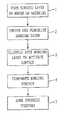
- FIG. 1is a flow chart of the method according to the invention
- FIG. 2is a flow chart of an example of the method according to the invention.
- FIGS. 3A-3Eare diagrams illustrating a first embodiment of a method according to the invention.
- FIGS. 4A-4Eare diagrams illustrating bonding according to the invention using silicon oxide
- FIGS. 5A-5Eare diagrams illustrating bonding according to the invention using silicon
- FIGS. 6A and 6Bare graphs of room temperature bonding energy versus storage time
- FIG. 7is a diagram of a bonding fixture used in the invention.
- FIG. 8is a fluorine concentration profile by SIMS (Secondary Ion Mass Spectroscopy) near the bonding interface of deposited oxide covered silicon wafers that were very slight etched by diluted HF before bonding.
- SIMSSecondary Ion Mass Spectroscopy
- Wafer 30preferably a processed semiconductor device wafer and more preferably a processed silicon device wafer, contains a device layer 31 with processed devices.
- Device layer 31may contain a number of layers and include surface regions of wafer 30 .
- the surface topography of layer 31is typically nonplanar.
- Layer 31may also represent a processed integrated circuit containing any number of layers such as active devices, interconnection, insulation, etc.
- the integrated circuitmay be fully processed, or partially processed where the remaining processing is performed after the bonding process.
- the processing after the bondingmay include full or partial substrate removal or via formation between the bonded wafers for interconnection.
- Bonding layer 32may be any solid state material or mixed materials which can be deposited or formed at low temperatures and can be polished to a sufficiently smooth surface.
- Layer 32may be an insulator, such as SiO 2 , silicon nitride, amorphous silicon formed using chemical vapor deposition (CVD) or plasma-enhanced CVD (PECVD), sputtering or by evaporation. Other materials such as polymers, semiconductors or sintered materials may also be used.
- Layer 32should have thickness greater than the surface topography of layer 31 .
- the surface 33 of layer 32is planarized and smoothed, as shown in step 2 of FIG. 1 and in FIG. 3B . It is noted that the roughness/planarity of surface 33 is exaggerated in FIG. 3A for illustrative purposes.
- This stepmay be accomplished using chemical-mechanical polishing.
- Surface 33is preferably polished to a roughness of about no more than about 3 nm and preferably no more than about 0.1 nm and be substantially planar.
- the surface roughness valuesare typically given as root-mean square (RMS) values. Also, the surface roughness may be given as mean values which are nearly the same as the RMS values.
- polishing surface 33is cleaned and dried to remove any residue from the polishing step. Polished surface 33 is preferably then rinsed with a solution.
- the bonding surfacemay also be etched prior to polishing to improve the planarity and/or surface roughness.
- the etchingcan be effective to remove high spots on the bonding surface by selective etching of the high spots using, for example, standard photolithographic techniques.
- a layer of silicon nitridecan be embedded within a silicon dioxide bonding layer 32 that can serve as an etch stop when using a solution containing HF.
- the etch stop materialmay be used to improve uniformity, reproducibility, and manufacturability.
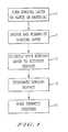
- FIG. 3Billustrates layer 32 having upper surface 34 after the polishing/planarization and cleaning steps. Surface 34 then undergoes an activation process (step 3 , FIG. 1 ).
- This activation processis an etching process and preferably a very slight etch (VSE) process.
- VSEmeans that the root-mean-square micro-roughness (RMS) of the very slightly etched surface remains at approximately the unetched value, typically ⁇ 0.5 nm and preferably in the range of 0.1 nm to 3 nm.
- RMSroot-mean-square micro-roughness
- the optimum amount of material removeddepends upon the material and the method used for removal. Typical amounts removed vary from Angstroms to a few nanometers. It is also possible to remove more material.
- VSEalso includes the breaking of bonds on the treated surfaces and can occur without significant removal of material.
- the VSEis distinct from simple modification of the surface by, for example, charging the surface with electronic charge or damaging the surface layer.
- the VSE processconsists of a gas or mixed gas (such as oxygen, argon, nitrogen, CF 4 , NH 3 ) plasma process at a specified power level for a specified time ( FIG. 3C ).
- a gas or mixed gassuch as oxygen, argon, nitrogen, CF 4 , NH 3
- the power and duration of the plasma processwill vary depending upon the materials used to obtain the desired bond energy. Examples are given below, but in general, the power and duration will be determined empirically.
- the plasma processmay be conducted in different modes. Both reactive ion etch (RIE) and plasma modes may be used, as well as an inductively-coupled plasma mode (ICP). Sputtering may also be used. Data and examples are given below in both the RIE and plasma modes.
- RIEreactive ion etch
- ICPinductively-coupled plasma mode
- the VSE processetches the surface very slightly via physical sputtering and/or chemical reaction and preferably is controlled to not degrade the surface roughness of the bonding surfaces.
- the surface roughnessmay even be improved depending upon the VSE and materials etched. Almost any gas or gas mixture that will not etch surface 34 excessively can be used for the room temperature bonding method according to the invention.
- the VSEserves to clean the surface and break bonds of the oxide on the wafer surface.
- the VSE processcan thus enhance the surface activation significantly.
- a desired bonding speciescan be used to terminated on surface 34 during the VSE by proper design of the VSE.
- a post-VSE treatmentthat activates and terminates the surface with a desired terminating species during the post-VSE process may be used.
- the desired speciesfurther preferably forms a temporary bond to the surface 34 atomic layer, effectively terminating the atomic layer, until a subsequent time that this surface can be brought together with a surface terminated by the same or another bonding species 36 as shown in FIG. 3D .
- Desired species on the surfaceswill further preferably react with each other when they are in sufficiently close proximity allowing chemical bonding between surfaces 34 and 36 at low or room temperature that is enhanced by diffusion or dissociation and diffusion of the reacted desired species away from the bonding interface.
- the post-VSE processpreferably consists of immersion in a solution containing a selected chemical to generate surface reactions that result in terminating the bonding surface 34 with desired species.
- the immersionis preferably performed immediately after the VSE process.
- the post-VSE processmay be performed in the same apparatus in which the VSE process is conducted. This is done most readily if both VSE and post-VSE processes are either dry, i.e, plasma, RIE, ICP, sputtering, etc, or wet, i.e., solution immersion.
- a desired speciespreferably consists of a monolayer or a few monolayers of atoms or molecules.
- the post-VSE processmay also consist of a plasma, RIE, or other dry process whereby appropriate gas chemistries are introduced to result in termination of the surface with the desired species.
- the post-VSE processmay also be a second VSE process.
- the termination processmay also include a cleaning process where surface contaminants are removed without VSE. In this case, a post-cleaning process similar to the post-VSE processes described above then results in a desired surface termination.
- the post-VSE or post-cleaning processmay or may not be needed to terminate surfaces with desired species if the activated surface bonds by the cleaning or VSE process are subsequently sufficiently weakly surface reconstructed and can remain sufficiently clean before bonding such that subsequent bonding with a similar surface can form a chemical bond.
- the wafersare optionally rinsed then dried.
- Two wafersare bonded by aligning them (if necessary) and bringing them together to form a bonding interface.
- a second wafer 35has been processed in the manner shown in FIG. 3C to prepare bonding surface 36 .
- the two wafersare brought together by, for example, commercially available wafer bonding equipment (not shown) to initiate bonding interface 37 ( FIG. 3E ).
- a spontaneous bondthen typically occurs at some location in the bonding interface and propagates across the wafer.
- a chemical reactionsuch as polymerization that results in chemical bonds takes place between species used to terminate surfaces 34 and 36 when the surfaces are in sufficient proximity.
- the bonding energyis defined as the specific surface energy of one of the separated surfaces at the bonding interface that is partially debonded by inserting a wedge.
- the by-products of the reactionthen diffuse away from the bonding interface to the wafer edge or are absorbed by the wafers, typically in the surrounding materials.
- the by-productsmay also be converted to other by-products that diffuse away or are absorbed by the wafers.
- the amount of covalent and/or ionic bondingmay be increased by removal of converted species resulting in further increase in bond strength.
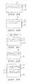
- FIGS. 4A-4Eshow surface conditions and the bonding propagation to form covalent bonds in a the case of a planar Si wafer covered with silicon oxide.
- Si wafer 40On Si wafer 40 an SiO 2 layer 41 is formed, which has been polished and planarized. Surface 42 of layer 41 is subjected to the VSE process to produce an activated surface ( FIG. 4A ).
- a second SiO 2 layer 45is formed, and surface 46 is subjected to a VSE process to activate surface 46 ( FIG. 4B ). Desired species are terminated on surface 46 and are shown as lines 43 in FIG. 4C . Either or both of a VSE and post-VSE processes are used to properly terminate surface 46 .
- surface 42may also be terminated using a post-VSE process.
- Wafer 44is brought together with wafer 40 ( FIG. 4D ) and bonds 46 begin to form.
- the bondingpropagates and by-products are removed (indicated as arrows 47 ) and chemical bonds (such as covalent) are formed, as shown in FIG. 4E .
- the bonding immediately after the RIE processmay use a special bonding fixture allowing immediate in situ bonding of the etched wafers.
- a diagram of the fixtureis shown in FIG. 7 .
- plasma chamber 75are two wafers to be bonded 70 disposed on RF electrodes 76 and 77 .
- a plasmais formed in zone 79 by the application of RF power to the electrodes via moveable vacuum RF power feedthrough 74 and by the introduction of an appropriate gas or gas mixture through gas feedthrough 73 .
- Element 71is a vacuum feedthrough for mechanical actuator (not shown) to retract retractable spacer 72 .
- Chamber 75is pumped down to a desired vacuum level via pumps (not shown) and chamber inlet 78 .
- the VSE and post-VSE or post-cleaningmay be conducted in chamber 75 .
- the mechanical spacers 72are retracted by the mechanical actuator and the wafers 70 are moved into contact with to begin the bonding process.
- the bonded wafersare then moved from the chamber into ambient or into another vacuum chamber (not shown) and stored for a desired period to allow the bonding to propagate by a wafer handling system (not shown).
- the materials of the bonding layerspreferably have an open structure so that the by-products of the polymerization reaction can be easily removed.
- the bonding species on the opposing bonding surfacesmust be able to react at room temperature to form a strong or chemical bond.
- the bond energyis sufficiently high to virtually eliminate slippage between wafers after subsequent heat treatments associated with a subsequent processing or operation when wafers have different thermal expansion coefficients. Lack of slippage is manifest by a lack of wafer bowing upon inspection after the subsequent processing or operation.
- At least one of the wafersis preferable for at least one of the wafers to be as thin as possible because a thin wafer allows compliance to accommodate a lack of perfect surface planarization and smoothness. Thinning to thickness of about 10 mils to 10 microns is effective.
- the bonded wafersare preferably stored at ambient or at low or room temperature after bonding to allow removal of species or converted species for a specified period of time depending upon the materials and species used. Twenty four hours is usually preferable. The storage time is dependent upon the type of plasma process used. Chemical bonds may be obtained more quickly, in a matter of minutes, when certain plasma processes such as an Ar plasma are used. For example, 585 mJ/m 2 bonds were obtained in immediately after bonding and over 800 mJ/m 2 were observed after 8 hours for deposited oxides etched by an Ar plasma followed by NH 4 OH dip.
- Annealing the bonded wafers during bondingmay increase the bonding strength.
- the annealing temperatureshould be below 200 EC and may be typically in the range of 75-100 EC. Storing the bonded wafers under vacuum may facilitate the removal of residual gasses from the bonding surfaces, but is not always necessary.
- All of the processes abovemay be carried out at or near room temperature.
- the wafersare bonded with sufficient strength to allow subsequent processing operations (lapping, polishing, substrate removal, chemical etching, lithography, masking, etc.). Bonding energies of approximately 500-2000 mJ/m 2 or more can be achieved (see FIG. 6A ).
- CMOS and bipolar or III-V HBT and Si CMOScomplementary metal-oxide-semiconductor
- Other elements or materialssuch as thermal spreaders, surrogate substrates, antennas, wiring layers, a pre-formed multi-layer interconnects, etc. may be bonded to produce different types of circuits or systems, as desired.
- PECVD SiO 2is deposited on a Si wafer containing devices.
- Surface 34after the plasma (such as argon, oxygen or CF 4 ) treatment, is mainly terminated by Si—OH groups due to the availability of moisture in the plasma system and in air.
- the wafersare immediately immersed in solution such as ammonium hydroxide (NH 4 OH), NH 4 F or HF for a period such as between 10 and 120 seconds.
- NH 4 OHammonium hydroxide
- NH 4 FNH 4 F
- HFa period such as between 10 and 120 seconds.
- Si—OH groupsare replaced by Si—NH2 groups according to the following substitution reaction: 2Si—OH+2NH 4 OH ⁇ 2Si—NH 2 +4HOH (1)
- Si—F groupsare terminating on the PECVD SiO 2 surface after an NH 4 F or HF immersion.
- Si—NH2:Si—OH groups or Si—NH2: Si—NH2 groups across the bonding surfacescan polymerize at room temperature in forming Si—O—Si or Si—N—N—Si (or Si—N—Si) covalent bonds: Si—NH 2 +Si—OH ⁇ Si—O—Si+NH 3 (2) Si—NH 2 +Si—NH 2 ⁇ Si—N—N—Si+2H 2 (3)
- the HF or NH 4 F dipped oxide surfacesare terminated by Si—F groups in addition to Si—OH groups. Since HF or NH 4 F solution etches silicon oxide strongly, their concentrations must be controlled to an adequately low level, and the immersion time must be sufficiently short. This is an example of a post-VSE process being a second VSE process.
- the covalent bonds across the bonding interfaceare formed due to the polymerization reaction between hydrogen bonded Si—HF or Si—OH groups: Si—HF+Si—HF ⁇ Si—F—F—Si+H 2 (4) Si—F+Si—OH ⁇ Si—O—Si+HF (5)
- FIG. 8shows the fluorine concentration profile of bonded thermal oxide covered silicon wafers that were dipped in 0.05% HF before room temperature bonding. A fluorine concentration peak is clearly seen at the bonding interface. This provides evidence of the chemical process described above where the desired species are located at the bonding interface.
- reaction (2)Since reaction (2) is reversible only at relatively high temperatures of ⁇ 500 EC, the formed siloxane bonds should not be attacked by NH 3 at lower temperatures. It is known that H 2 molecules are small and diffuse about 50 times quicker than water molecules in oxide. The existence of a damaged layer near the surface of an adequate thickness i.e. a few nm, will facilitate the diffusion or dissolution of NH 3 , and HF and hydrogen in reactions (2), (3), (4) and/or (5) in this layer and enhancement of the chemical bond. The three reactions result in a higher bonding energy of SiO 2 /SiO 2 bonded pairs at room temperature after a period of storage time to allow NH 3 or H 2 to diffuse away.
- the plasma treatmentmay create a damaged or defective area in the oxide layer near the bonding surface.
- the zoneextends for a few monolayers.
- the damaged or defective areaaids in the removal of bonding by-products. Efficient removal of the bonding by-products improves the bonding strength since the by-products can interfere with the bonding process by preventing high-strength bond from forming.
- Many different surfaces of materialsmay be smoothed and/or planarized, followed by a cleaning process, to prepare for bonding according to the invention.
- These materialscan be room temperature bonded by mating surfaces with sufficient planarity, surface smoothness, and passivation that includes cleaning, and/or VSE, activation and termination.
- Amorphous and sintered materials, non-planar integrated circuits, and silicon wafersare examples of such materials.
- Single crystalline semiconductor or insulating surfaces, such as SiO 2 or Si surfacescan also be provided with the desired surface roughness, planarity and cleanliness. Keeping the surfaces in high or ultra-high vacuum simplifies obtaining surfaces sufficiently free of contamination and atomic reconstruction to achieve the strong bonding according to the invention.
- semiconductor or insulator materialssuch as InP, GaAs, SiC, sapphire, etc.
- PECVD SiO 2may be deposited on many types of materials at low temperatures, many different combinations of materials may be bonded according to the invention at room temperature. Other materials may also be deposited as long as appropriate processes and chemical reactions are available for the VSE, surface activation, and termination.
- the methodmay also be used with silicon nitride as the bonding material.
- Silicon nitridemay be bonded to silicon nitride, or to silicon dioxide and silicon. Silicon oxide may also be bonded to silicon.
- Other types of dielectric materialsmay be bonded together including aluminum nitride and diamond-like carbon.
- the methodmay be applied to planar wafers having no devices or circuits and one wafer with devices and circuits.
- the planar wafermay be coated with a bonding layer, such as PECVD oxide or amorphous silicon, and then processed as described above to bond the two wafers.
- the planar wafermay not need to be coated with a bonding layer if it has sufficient smoothness and planarity and the proper bonding material.
- the bonding processmay be repeated with any number of wafers, materials or functional elements.
- two device or IC wafersmay be joined, followed by removing one of the exposed substrates to transfer a layer or more of devices, or just the active regions of an IC.
- the bonding according to the inventionmay be applied to joining different types of materials.
- a silicon wafercan be bonded to another silicon wafer, or bond to an oxidized silicon wafer.
- the bare silicon wafer and the oxide covered waferare immersed in HF, NH 4 F and/or NH 4 OH and bonded after drying.
- the time for the immersionshould be less than about twenty minutes for the silicon wafer covered with the thin oxide since the NH 4 OH solution etches silicon oxide. Since HF and NH 4 F etches oxides strongly, very diluted solutions, preferably in 0.01-0.2% range should be used for dipping of the silicon wafers.
- reaction (2), (3), (4) and/or (5)take place at the bonding interface between the two wafers.
- the plasma-treated wafersmay also be immersed in deionized water instead of the NH 4 OH solution.
- the silicon bondingmay be conducted with a bare silicon wafer, i.e. having a native oxide or a silicon wafer having an oxide layer formed on its surface as described above.
- a bare silicon waferi.e. having a native oxide or a silicon wafer having an oxide layer formed on its surface as described above.
- the native oxidewhich if formed on the bare silicon wafer is sputter etched, and the oxide layer formed on the silicon surface is etched.
- the final surfaceis an activated (native or formed) oxide.
- the activated oxide surfaceWhen rinsed in deionized water, the activated oxide surface is mainly terminated with Si—OH groups. Since oxide growth in oxygen plasma has been found to have less water than in normal native oxide layers, the water from the original bonding bridge and generated by the following polymerization reaction (6) can be absorbed into the plasma oxide readily.
- FIGS. 5A-5Eillustrate bonding two silicon wafers.
- Wafers 50 and 52have respective surfaces 51 and 53 with native oxides (not shown) subjected to a VSE process ( FIGS. 5A and 5B ).
- Surface 53is in FIG. 5C is shown terminated with a desired species 54 .
- the two wafersare brought together and bonds 55 begin to form ( FIG. 5D ).
- the bondingpropagates and bonding by-products, in this case H 2 gas, are removed.
- the by-products being removedare shown as arrows 56 in FIG. 5E .
- the watercan also diffuse through the thin oxide layer on the bare silicon wafer to react with silicon.
- the silicon surface underneath the oxidehas a damaged or defective zone, extending for a few monolayers, the water molecules that diffuse through the oxide layer and reach the damaged or defective zone can be converted to hydrogen at room temperature and be removed readily: Si+2H 2 O ⁇ SiO 2 +2H 2 (7)
- a relatively thick ( ⁇ 5 nm) oxide layeris formed, it will take a long period of time for the water molecules to diffuse through this thick layer.
- a thin oxide layeris left or a too narrow defective zone is formed, water that can reach the silicon surface may not react sufficiently with the silicon and convert to hydrogen. In both cases the bonding energy enhancement will be limited.
- the preferred oxygen plasma treatmentthus leaves a minimum plasma oxide thickness (e.g., about 0.1-1.0 nm) and a reasonably thick defective zone (e.g., about 0.1-0.3 nm) on the silicon surface.
- the VSE processuses wet chemicals.
- an InP wafer having a deposited silicon oxide layer, as in the first embodiment, and a device layerare bonded to a AlN substrate having a deposited oxide layer.
- both wafersare cleaned in an standard RCA cleaning solution.
- the wafersare very slightly etched using a dilute HF aqueous solution with an HF concentration preferably in the range of 0.01 to 0.2%. About a few tenths of a nm is removed and the surface smoothness is not degraded as determined by AFM (atomic force microscope) measurements.
- the wafersare spin dried and bonded in ambient air at room temperature.
- the resulting bonding energyhas been measured to reach ⁇ 700 mJ/m 2 after storage in air. After annealing this bonded pair at 75° C. the bonding energy of 1500 mJ/m 2 was obtained.
- the bonding energyhas been measured to reach silicon bulk fracture energy (about 2500 mJ/m 2 ) after annealing at 100° C. If the wafers are rinsed with deionized water after the HF dip, the bonding energy at 100° C. is reduced to 200 mJ/m 2 , that is about one tenth of that obtained without the rinse. This illustrates the preference of F to OH as a terminating species.
- the VSE processconsists of 0.1% HF etching followed by 5 min dip in 0.02% HN 4 F solution of thermally oxidized silicon wafers at room temperature after a standard cleaning process. Without rinsing in deionized water, the wafers are bonded after spin drying at room temperature. The bonding energy of the bonded pairs reaches ⁇ 1700 mJ/m after 100° C. annealing. If the wafers are rinsed in de-ionized water after the HF etching before bonding, the bonding energy of bonded pairs is only 400 mJ/m 2 , again illustrating the preference of F to OH as a terminating species.
- Dilute NH 4 Fis used in the VSE process to etch silicon oxide covered wafers in a fourth embodiment.
- concentration of the NH 4 Fshould be below 0.02% to obtain the desired bonding.
- the bonding energy of ⁇ 600 mJ/mcan be achieved at room temperature after storage.
- a fifth embodiment of the inventionis used to bond Si surfaces having a native oxide of about 1 nm in thickness.
- a VSE processusing 5 min etching in 70% HNO 3 +diluted HF (preferably 0.01 to 0.02%) is performed. Wafers are pulled out of the solution vertically with a basically hydrophobic surface. Without rinsing in water, the wafers were bonded at room temperature in air. In this process covalent bonding occurs at room temperature with measured bonding energies typically about 600 mJ/m 2 . This bonding energy is significantly increased to 1300 mJ/m 2 after annealing at 75° C. and reaches the fracture energy of bulk silicon (about 2500 mJ/m 2 ) at a temperature of 100° C.
- diluted HNO 3 with watercan be used in the solution to achieve similar results.
- the siliconis etched in the dilute HNO 3 VSE process at a rate of 0.1-0.15 nm/min and a new thick oxide 2.5-3.5 nm in thickness is formed.
- the VSE processmay consist of a dry etch that has chemical and/or physical components.
- chemical etchingmay result from SF 4 /H 2 gas mixture while physical etching may result from Ar etch.
- physical etchingmay result from Ar etch.
- chemical etchingmay use CF 4 while physical etching may use oxygen or argon gas.
- thermally stable polymer materialfor the bonding materials and bond two polymer surfaces together. Examples are polyimides or spin-on materials.
- VSEvery slight etching
- the oxide covered wafer bonding caseis similar except that a different surface termination is preferred.
- the highly reactive surface layers of oxide and silicon to allow water adsorption and conversion to hydrogenshould be formed.
- the highly reactive layerscan be a plasma thin oxide layer and a damaged silicon surface layer.
- the oxide on the silicon waferwill also have some damage. Not only O 2 plasma but also plasma of other gases (such as Ar, CF 4 ) are adequate.
- VSEsilicon surface is readily to react with moisture to form an oxide layer, and the underlying damaged silicon layer is created by VSE. Since the VSE and by-products removal methods are rather general in nature, this approach can be implemented by many means and apply to many materials.
- a first examplethree inch ⁇ 100>, 1-10 ohm-cm, boron doped silicon wafers were used.
- PECVD oxidewas deposited on some of the silicon wafers.
- thermal oxidized silicon waferswere also studied.
- the PECVD oxide thicknesswas 0.5 ⁇ m and 0.3 ⁇ m on the front side and the back side of the wafers, respectively.
- Oxideis deposited on both sides of the wafer to minimize wafer bow during polishing and improve planarization.
- a soft polishwas performed to remove about 30 nm of the oxide and to smooth the front oxide surface originally having a root mean square of the micro-roughness (RMS) of ⁇ 0.56 nm to a final ⁇ 0.18 nm.
- RMSmicro-roughness
- a modified RCA1 solutionwas used to clean the wafer surfaces followed by spin-drying.
- Two waferswere loaded into the plasma system, both wafers are placed on the RF electrode and treated in plasma in RIE mode. For comparison, some wafers were treated in plasma mode in which the wafers were put on the grounded electrode.
- An oxygen plasmawas used with a nominal flow rate of 16 scc/m.
- the RF powerwas 20-400 W (typically 80 W) at 13.56 MHz and the vacuum level was 100 mTorr.
- the oxide covered waferswere treated in plasma for times between 15 seconds to 5 minutes.
- the plasma treated silicon waferswere then dipped in an appropriate solution or rinse with de-ionized water followed by spin-drying and room temperature bonding in air. Some of the plasma treated wafers were also directly bonded in air without rinse or dipping.
- the bonding energywas measured by inserting a wedge into the interface to measure the crack length according to the equation:
- E and tware the Young's modulus and thickness for wafers one and two and tb is the thickness of a wedge inserted between the two wafers that results in a wafer separation of length L from the edge of the wafers.
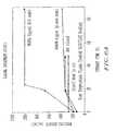
- the room temperature bonding energy as a function of storage time of bonded plasma treated oxide covered silicon wafersis shown in FIG. 6A .
- This figureshows measured room temperature bonding energy versus storage time for 4 different cases as shown.
- the resultscan be summarized as follows: (1) for dipped and bonded RIE plasma treated oxide wafers, the room temperature bonding energy increases with storage time and reaches a stable value after ⁇ 20 h in air or at low vacuum; (2) RIE mode results in higher bonding energies than plasma mode; (3) too short a plasma exposure time or too low a plasma power provides a small or negligible increase in bond energy; (4) NH 4 OH dip after plasma treatment shows a much higher increase in bonding energy than water rinse; (5) direct bonding in air after plasma treatment without dipping or rinse shows an almost constant bonding energy with time.
- the bonding energy of the directly bonded wafer pairs immediately after room temperature bondingis slightly higher than the de-ionized water rinsed or NH 4 OH dipped wafer pairs.
- FIG. 6Bshows room temperature bonding of Si and AlN wafers with PECVD oxide deposited layers. After about 100 h of storage time a bonding energy of over 2000 mJ/m 2 were observed.
- the bonding energy as a function of storage time of O 2 plasma treated thermally oxidized silicon wafer pairsis similar to wafers with PECVD oxide, although the values of the room temperature bonding energy are somewhat lower.
- the bonding energy as high as 1000 mJ/m 2was reached in the RIE mode plasma treated and NH 4 OH dipped PECVD oxide covered wafer pairs. Since the maximum bonding energy of a van der Waals bonded silicon oxide covered wafer pairs is about 200 mJ/m 2 , a large portion of the bonding energy is attributed to the formation of covalent bonds at the bonding interface at room temperature according to the above equation.
- the above processwas applied to bond processed InP wafers (600 ⁇ m thick) to AlN wafers (380 ⁇ m thick), or to bond processed Si (380 ⁇ m thick) and InP 600 ⁇ m thick) wafers, as second and third examples.
- the processed InP device wafersare covered with PECVD oxide and planarized and smoothed by chemical-mechanical polishing CMP.
- a PECVD oxide layeris also deposited on the AlN wafers and is planarized and smoothed to improve the RMS surface roughness.
- the processed Si and processed InP wafersare deposited with PECVD oxide and planarized and smoothed using CMP. After VSE similar to the example 1 bonding at room temperature, the bonded wafers are left in ambient air at room temperature.
- bonding energy1000 mJ/m 2 and 1100 mJ/m2 were achieved for the InP/Si and InP/AlN bonded pairs, respectively.
- bonding energy at room temperatureas high as 2500 mJ/m 2 has been achieved.
- These room temperature bonded plasma treated wafer pairshave sufficient bonding strength to sustain subsequent substrate lapping and etching and other typical semiconductor fabrication processes before or after substrate removal.
- the InP substrate in the room temperature bonded InP/AlN pairswas lapped with 1900# Al 2 O 3 powder from initial 600 ⁇ m thick to ⁇ 50 ⁇ m thick followed by etching in an HCl/H 3 PO 4 solution to leave about a 2.0 ⁇ m thick InP device layer on the AN or Si wafer.
- the water and etching solutiondid not penetrate into the bonding interface.
- Surfacesare sputter etched by energetic particles such as radicals, ions, photons and electrons in the plasma or RIE mode.
- the O 2 plasma under conditions that bring about the desired VSEis sputter-etching about 2 ⁇ /min of PECVD oxide as measured by a reflectance spectrometry.
- the sputter etching rateis about 0.5 ⁇ /min.
- the thickness of oxide before and after plasma treatmentwas measured by a reflectance spectrometry and averaged from 98 measured points on each wafer.
- the etching by O 2 plasmahas not only cleaned the surface by oxidation and sputtering but also broken bonds of the oxide on the wafer surfaces.
- the surface roughness of plasma treated oxide surfacesmust not be degraded by the etching process.
- AFM measurementsshow that compared with the initial surface roughness, the RMS of the O 2 plasma treated oxide wafers was ⁇ 2 ⁇ and did not change noticeably.
- the bonding energy enhancement effectis also small. Keeping other conditions unchanged when the O 2 plasma treatment was performed with plasma mode rather than RIE mode, the etching of oxide surfaces is negligible and the oxide thickness does not change.
- the final room temperature bonding energyis only 385 mJ/m 2 compared to 1000 mJ/m 2 of RIE treated wafers (see FIG. 6A ).
- CF 4 /O 2 RIEwas used to remove ⁇ 4 nm of PECVD oxide from the wafer surfaces prior to bonding.
- the bonding energy of room temperature bonded PECVD oxide covered silicon waferswas also enhanced significantly in this manner and exceeds 1000 mJ/m 2 after sufficient storage time (see also FIG. 6A ).
- An argon plasmahas also been used for the VSE with a nominal flow rate of 16 scc/m.
- the RF powerwas typically 60 W at 13.56 MHz and the vacuum level was 100 mTorr.
- the oxide covered silicon waferswere treated in plasma in RIE mode for times between 30 seconds to 2 minutes.
- the plasma treated silicon waferswere then dipped in an NH 4 OH solution followed by spin-drying and room temperature bonding in air. The bonding energy reached ⁇ 800 mJ/m 2 at room temperature after only 8 h storage in air.
Landscapes
- Engineering & Computer Science (AREA)
- Microelectronics & Electronic Packaging (AREA)
- Power Engineering (AREA)
- Computer Hardware Design (AREA)
- Manufacturing & Machinery (AREA)
- Condensed Matter Physics & Semiconductors (AREA)
- General Physics & Mathematics (AREA)
- Physics & Mathematics (AREA)
- Chemical & Material Sciences (AREA)
- Inorganic Chemistry (AREA)
- Chemical Kinetics & Catalysis (AREA)
- General Chemical & Material Sciences (AREA)
- Pressure Welding/Diffusion-Bonding (AREA)
- Mechanical Treatment Of Semiconductor (AREA)
- Drying Of Semiconductors (AREA)
- Internal Circuitry In Semiconductor Integrated Circuit Devices (AREA)
- Cleaning Or Drying Semiconductors (AREA)
Abstract
Description
2Si—OH+2NH4OH→2Si—NH2+4HOH (1)
Si—NH2+Si—OH→Si—O—Si+NH3 (2)
Si—NH2+Si—NH2→Si—N—N—Si+2H2 (3)
Si—HF+Si—HF→Si—F—F—Si+H2 (4)
Si—F+Si—OH→Si—O—Si+HF (5)
Si—OH+Si—OH→Si—O—Si+H2O (6)
Si+2H2O→SiO2+2H2 (7)
Claims (31)
Priority Applications (1)
| Application Number | Priority Date | Filing Date | Title |
|---|---|---|---|
| US15/205,346US10312217B2 (en) | 2000-02-16 | 2016-07-08 | Method for low temperature bonding and bonded structure |
Applications Claiming Priority (10)
| Application Number | Priority Date | Filing Date | Title |
|---|---|---|---|
| US09/505,283US6902987B1 (en) | 2000-02-16 | 2000-02-16 | Method for low temperature bonding and bonded structure |
| US10/913,441US7387944B2 (en) | 2000-02-16 | 2004-08-09 | Method for low temperature bonding and bonded structure |
| US11/980,664US7807549B2 (en) | 2000-02-16 | 2007-10-31 | Method for low temperature bonding and bonded structure |
| US12/720,368US7871898B2 (en) | 2000-02-16 | 2010-03-09 | Method for low temperature bonding and bonded structure |
| US12/954,740US8153505B2 (en) | 2000-02-16 | 2010-11-26 | Method for low temperature bonding and bonded structure |
| US13/341,273US20120097638A1 (en) | 2000-02-16 | 2011-12-30 | Method For Low Temperature Bonding And Bonded Structure |
| US14/197,070US9082627B2 (en) | 2000-02-16 | 2014-03-04 | Method for low temperature bonding and bonded structure |
| US14/754,111US9331149B2 (en) | 2000-02-16 | 2015-06-29 | Method for low temperature bonding and bonded structure |
| US14/957,501US9391143B2 (en) | 2000-02-16 | 2015-12-02 | Method for low temperature bonding and bonded structure |
| US15/205,346US10312217B2 (en) | 2000-02-16 | 2016-07-08 | Method for low temperature bonding and bonded structure |
Related Parent Applications (1)
| Application Number | Title | Priority Date | Filing Date |
|---|---|---|---|
| US14/957,501ContinuationUS9391143B2 (en) | 2000-02-16 | 2015-12-02 | Method for low temperature bonding and bonded structure |
Publications (2)
| Publication Number | Publication Date |
|---|---|
| US20160322328A1 US20160322328A1 (en) | 2016-11-03 |
| US10312217B2true US10312217B2 (en) | 2019-06-04 |
Family
ID=24009686
Family Applications (15)
| Application Number | Title | Priority Date | Filing Date |
|---|---|---|---|
| US09/505,283Expired - LifetimeUS6902987B1 (en) | 2000-02-16 | 2000-02-16 | Method for low temperature bonding and bonded structure |
| US10/460,418Expired - LifetimeUS7041178B2 (en) | 2000-02-16 | 2003-06-13 | Method for low temperature bonding and bonded structure |
| US10/762,318Expired - LifetimeUS7335572B2 (en) | 2000-02-16 | 2004-01-23 | Method for low temperature bonding and bonded structure |
| US10/913,441Expired - LifetimeUS7387944B2 (en) | 2000-02-16 | 2004-08-09 | Method for low temperature bonding and bonded structure |
| US11/980,415Expired - Fee RelatedUS7553744B2 (en) | 2000-02-16 | 2007-10-31 | Method for low temperature bonding and bonded structure |
| US11/980,664Expired - Fee RelatedUS7807549B2 (en) | 2000-02-16 | 2007-10-31 | Method for low temperature bonding and bonded structure |
| US12/493,957Expired - Fee RelatedUS8053329B2 (en) | 2000-02-16 | 2009-06-29 | Method for low temperature bonding and bonded structure |
| US12/720,368Expired - Fee RelatedUS7871898B2 (en) | 2000-02-16 | 2010-03-09 | Method for low temperature bonding and bonded structure |
| US12/954,740Expired - Fee RelatedUS8153505B2 (en) | 2000-02-16 | 2010-11-26 | Method for low temperature bonding and bonded structure |
| US13/341,273AbandonedUS20120097638A1 (en) | 2000-02-16 | 2011-12-30 | Method For Low Temperature Bonding And Bonded Structure |
| US14/197,056AbandonedUS20140203407A1 (en) | 2000-02-16 | 2014-03-04 | Method for low temperature bonding and bonded structure |
| US14/197,070Expired - Fee RelatedUS9082627B2 (en) | 2000-02-16 | 2014-03-04 | Method for low temperature bonding and bonded structure |
| US14/754,111Expired - Fee RelatedUS9331149B2 (en) | 2000-02-16 | 2015-06-29 | Method for low temperature bonding and bonded structure |
| US14/957,501Expired - Fee RelatedUS9391143B2 (en) | 2000-02-16 | 2015-12-02 | Method for low temperature bonding and bonded structure |
| US15/205,346Expired - Fee RelatedUS10312217B2 (en) | 2000-02-16 | 2016-07-08 | Method for low temperature bonding and bonded structure |
Family Applications Before (14)
| Application Number | Title | Priority Date | Filing Date |
|---|---|---|---|
| US09/505,283Expired - LifetimeUS6902987B1 (en) | 2000-02-16 | 2000-02-16 | Method for low temperature bonding and bonded structure |
| US10/460,418Expired - LifetimeUS7041178B2 (en) | 2000-02-16 | 2003-06-13 | Method for low temperature bonding and bonded structure |
| US10/762,318Expired - LifetimeUS7335572B2 (en) | 2000-02-16 | 2004-01-23 | Method for low temperature bonding and bonded structure |
| US10/913,441Expired - LifetimeUS7387944B2 (en) | 2000-02-16 | 2004-08-09 | Method for low temperature bonding and bonded structure |
| US11/980,415Expired - Fee RelatedUS7553744B2 (en) | 2000-02-16 | 2007-10-31 | Method for low temperature bonding and bonded structure |
| US11/980,664Expired - Fee RelatedUS7807549B2 (en) | 2000-02-16 | 2007-10-31 | Method for low temperature bonding and bonded structure |
| US12/493,957Expired - Fee RelatedUS8053329B2 (en) | 2000-02-16 | 2009-06-29 | Method for low temperature bonding and bonded structure |
| US12/720,368Expired - Fee RelatedUS7871898B2 (en) | 2000-02-16 | 2010-03-09 | Method for low temperature bonding and bonded structure |
| US12/954,740Expired - Fee RelatedUS8153505B2 (en) | 2000-02-16 | 2010-11-26 | Method for low temperature bonding and bonded structure |
| US13/341,273AbandonedUS20120097638A1 (en) | 2000-02-16 | 2011-12-30 | Method For Low Temperature Bonding And Bonded Structure |
| US14/197,056AbandonedUS20140203407A1 (en) | 2000-02-16 | 2014-03-04 | Method for low temperature bonding and bonded structure |
| US14/197,070Expired - Fee RelatedUS9082627B2 (en) | 2000-02-16 | 2014-03-04 | Method for low temperature bonding and bonded structure |
| US14/754,111Expired - Fee RelatedUS9331149B2 (en) | 2000-02-16 | 2015-06-29 | Method for low temperature bonding and bonded structure |
| US14/957,501Expired - Fee RelatedUS9391143B2 (en) | 2000-02-16 | 2015-12-02 | Method for low temperature bonding and bonded structure |
Country Status (7)
| Country | Link |
|---|---|
| US (15) | US6902987B1 (en) |
| EP (2) | EP1275142A4 (en) |
| JP (3) | JP5496439B2 (en) |
| KR (3) | KR20020081328A (en) |
| AU (1) | AU2001241447A1 (en) |
| CA (1) | CA2399282C (en) |
| WO (1) | WO2001061743A1 (en) |
Cited By (3)
| Publication number | Priority date | Publication date | Assignee | Title |
|---|---|---|---|---|
| WO2023146633A1 (en)* | 2022-01-26 | 2023-08-03 | Applied Materials, Inc. | Methods and apparatus for processing a substrate |
| WO2024193815A1 (en) | 2023-03-21 | 2024-09-26 | Ev Group E. Thallner Gmbh | Method for surface treatment of a substrate and method for bonding such a substrate to a further substrate, and a device for carrying out such methods |
| RU2835590C1 (en)* | 2024-09-12 | 2025-02-28 | Федеральное государственное автономное образовательное учреждение высшего образования "Национальный исследовательский университет "Московский институт электронной техники" | Method of silicon and glass surface preparation before anodic bonding process |
Families Citing this family (393)
| Publication number | Priority date | Publication date | Assignee | Title |
|---|---|---|---|---|
| FR2773261B1 (en) | 1997-12-30 | 2000-01-28 | Commissariat Energie Atomique | METHOD FOR THE TRANSFER OF A THIN FILM COMPRISING A STEP OF CREATING INCLUSIONS |
| US6984571B1 (en) | 1999-10-01 | 2006-01-10 | Ziptronix, Inc. | Three dimensional device integration method and integrated device |
| US6500694B1 (en) | 2000-03-22 | 2002-12-31 | Ziptronix, Inc. | Three dimensional device integration method and integrated device |
| US6902987B1 (en) | 2000-02-16 | 2005-06-07 | Ziptronix, Inc. | Method for low temperature bonding and bonded structure |
| US6563133B1 (en)* | 2000-08-09 | 2003-05-13 | Ziptronix, Inc. | Method of epitaxial-like wafer bonding at low temperature and bonded structure |
| US6939434B2 (en) | 2000-08-11 | 2005-09-06 | Applied Materials, Inc. | Externally excited torroidal plasma source with magnetic control of ion distribution |
| US6893907B2 (en)* | 2002-06-05 | 2005-05-17 | Applied Materials, Inc. | Fabrication of silicon-on-insulator structure using plasma immersion ion implantation |
| US7166524B2 (en) | 2000-08-11 | 2007-01-23 | Applied Materials, Inc. | Method for ion implanting insulator material to reduce dielectric constant |
| US7223676B2 (en) | 2002-06-05 | 2007-05-29 | Applied Materials, Inc. | Very low temperature CVD process with independently variable conformality, stress and composition of the CVD layer |
| US7294563B2 (en) | 2000-08-10 | 2007-11-13 | Applied Materials, Inc. | Semiconductor on insulator vertical transistor fabrication and doping process |
| US7137354B2 (en) | 2000-08-11 | 2006-11-21 | Applied Materials, Inc. | Plasma immersion ion implantation apparatus including a plasma source having low dissociation and low minimum plasma voltage |
| US7288491B2 (en) | 2000-08-11 | 2007-10-30 | Applied Materials, Inc. | Plasma immersion ion implantation process |
| US7183177B2 (en) | 2000-08-11 | 2007-02-27 | Applied Materials, Inc. | Silicon-on-insulator wafer transfer method using surface activation plasma immersion ion implantation for wafer-to-wafer adhesion enhancement |
| US7094670B2 (en)* | 2000-08-11 | 2006-08-22 | Applied Materials, Inc. | Plasma immersion ion implantation process |
| US7037813B2 (en) | 2000-08-11 | 2006-05-02 | Applied Materials, Inc. | Plasma immersion ion implantation process using a capacitively coupled plasma source having low dissociation and low minimum plasma voltage |
| US7303982B2 (en) | 2000-08-11 | 2007-12-04 | Applied Materials, Inc. | Plasma immersion ion implantation process using an inductively coupled plasma source having low dissociation and low minimum plasma voltage |
| US7320734B2 (en) | 2000-08-11 | 2008-01-22 | Applied Materials, Inc. | Plasma immersion ion implantation system including a plasma source having low dissociation and low minimum plasma voltage |
| US7465478B2 (en) | 2000-08-11 | 2008-12-16 | Applied Materials, Inc. | Plasma immersion ion implantation process |
| US7816188B2 (en)* | 2001-07-30 | 2010-10-19 | Sandisk 3D Llc | Process for fabricating a dielectric film using plasma oxidation |
| US6793759B2 (en) | 2001-10-09 | 2004-09-21 | Dow Corning Corporation | Method for creating adhesion during fabrication of electronic devices |
| US20030113947A1 (en)* | 2001-12-19 | 2003-06-19 | Vandentop Gilroy J. | Electrical/optical integration scheme using direct copper bonding |
| US20060127599A1 (en)* | 2002-02-12 | 2006-06-15 | Wojak Gregory J | Process and apparatus for preparing a diamond substance |
| US6822326B2 (en)* | 2002-09-25 | 2004-11-23 | Ziptronix | Wafer bonding hermetic encapsulation |
| FR2846788B1 (en) | 2002-10-30 | 2005-06-17 | PROCESS FOR PRODUCING DETACHABLE SUBSTRATES | |
| FR2847077B1 (en) | 2002-11-12 | 2006-02-17 | Soitec Silicon On Insulator | SEMICONDUCTOR COMPONENTS, PARTICULARLY OF THE MIXED SOI TYPE, AND METHOD OF MAKING SAME |
| EP1568077B1 (en)* | 2002-12-04 | 2018-07-11 | Suss MicroTec Lithography GmbH | Method for pre-treating surfaces of substrates to be bonded |
| US20040126993A1 (en)* | 2002-12-30 | 2004-07-01 | Chan Kevin K. | Low temperature fusion bonding with high surface energy using a wet chemical treatment |
| US6962835B2 (en) | 2003-02-07 | 2005-11-08 | Ziptronix, Inc. | Method for room temperature metal direct bonding |
| US7109092B2 (en) | 2003-05-19 | 2006-09-19 | Ziptronix, Inc. | Method of room temperature covalent bonding |
| FR2857953B1 (en)* | 2003-07-21 | 2006-01-13 | Commissariat Energie Atomique | STACKED STRUCTURE, AND METHOD FOR MANUFACTURING THE SAME |
| US7122481B2 (en)* | 2003-07-25 | 2006-10-17 | Intel Corporation | Sealing porous dielectrics with silane coupling reagents |
| FR2858461B1 (en)* | 2003-07-30 | 2005-11-04 | Soitec Silicon On Insulator | IMPLEMENTING A STRUCTURE COMPRISING A PROTECTIVE LAYER AGAINST CHEMICAL TREATMENTS |
| JP3980539B2 (en)* | 2003-08-29 | 2007-09-26 | 唯知 須賀 | Substrate bonding method, irradiation method, and substrate bonding apparatus |
| DE10344113A1 (en)* | 2003-09-24 | 2005-05-04 | Erich Thallner | Apparatus and method for joining wafers |
| FR2861497B1 (en) | 2003-10-28 | 2006-02-10 | Soitec Silicon On Insulator | METHOD FOR CATASTROPHIC TRANSFER OF A FINE LAYER AFTER CO-IMPLANTATION |
| US7084460B2 (en)* | 2003-11-03 | 2006-08-01 | International Business Machines Corporation | Method for fabricating SiGe-on-insulator (SGOI) and Ge-on-insulator (GOI) substrates |
| FR2863405B1 (en)* | 2003-12-08 | 2006-02-03 | Commissariat Energie Atomique | MOLECULAR BONDING OF MICROELECTRONIC COMPONENTS ON A POLYMERIC FILM |
| FR2864336B1 (en)* | 2003-12-23 | 2006-04-28 | Commissariat Energie Atomique | METHOD FOR SEALING TWO PLATES WITH FORMATION OF AN OHMIC CONTACT BETWEEN THEM |
| FR2864970B1 (en)* | 2004-01-09 | 2006-03-03 | Soitec Silicon On Insulator | SUPPORT SUBSTRATE WITH THERMAL EXPANSION COEFFICIENT DETERMINED |
| US7422384B2 (en)* | 2004-03-17 | 2008-09-09 | Hewlett-Packard Development, L.P. | System and a method for printing small print jobs |
| US7087134B2 (en)* | 2004-03-31 | 2006-08-08 | Hewlett-Packard Development Company, L.P. | System and method for direct-bonding of substrates |
| JP4411123B2 (en)* | 2004-03-31 | 2010-02-10 | 新光電気工業株式会社 | Manufacturing method of heat sink |
| CN1942281A (en)* | 2004-04-08 | 2007-04-04 | 松下电器产业株式会社 | Joining method and device therefor |
| FR2871291B1 (en)* | 2004-06-02 | 2006-12-08 | Tracit Technologies | PROCESS FOR TRANSFERRING PLATES |
| FR2872627B1 (en)* | 2004-06-30 | 2006-08-18 | Commissariat Energie Atomique | MOLECULAR ADHESION ASSEMBLY OF TWO SUBSTRATES |
| US7261793B2 (en)* | 2004-08-13 | 2007-08-28 | Hewlett-Packard Development Company, L.P. | System and method for low temperature plasma-enhanced bonding |
| JP2006080314A (en)* | 2004-09-09 | 2006-03-23 | Canon Inc | Manufacturing method of bonded substrate |
| US7262495B2 (en) | 2004-10-07 | 2007-08-28 | Hewlett-Packard Development Company, L.P. | 3D interconnect with protruding contacts |
| KR101263276B1 (en)* | 2004-10-21 | 2013-05-10 | 후지필름 디마틱스, 인크. | Sacrificial substrate for etching |
| US7563691B2 (en)* | 2004-10-29 | 2009-07-21 | Hewlett-Packard Development Company, L.P. | Method for plasma enhanced bonding and bonded structures formed by plasma enhanced bonding |
| WO2006047052A1 (en)* | 2004-10-26 | 2006-05-04 | Hewlett-Packard Development Company, L.P. | Method for plasma enhanced bonding and bonded structures formed by plasma enhanced bonding |
| US7238589B2 (en)* | 2004-11-01 | 2007-07-03 | International Business Machines Corporation | In-place bonding of microstructures |
| FR2879208B1 (en)* | 2004-12-15 | 2007-02-09 | Commissariat Energie Atomique | METHOD OF BONDING TWO FREE SURFACES, RESPECTIVELY OF FIRST AND SECOND DIFFERENT SUBSTRATES |
| FR2879183B1 (en)* | 2004-12-15 | 2007-04-27 | Atmel Grenoble Soc Par Actions | METHOD FOR THE COLLECTIVE MANUFACTURE OF MICROSTRUCTURES WITH OVERLAPPING ELEMENTS |
| US7372145B2 (en)* | 2005-02-28 | 2008-05-13 | Silverbrook Research Pty Ltd | Bonded assembly having improved adhesive bond strength |
| US7425052B2 (en)* | 2005-02-28 | 2008-09-16 | Silverbrook Research Pty Ltd | Printhead assembly having improved adhesive bond strength |
| JP2006258958A (en)* | 2005-03-15 | 2006-09-28 | Shibaura Mechatronics Corp | Substrate bonding method and substrate bonding apparatus |
| US9153645B2 (en)* | 2005-05-17 | 2015-10-06 | Taiwan Semiconductor Manufacturing Company, Ltd. | Lattice-mismatched semiconductor structures with reduced dislocation defect densities and related methods for device fabrication |
| US8324660B2 (en) | 2005-05-17 | 2012-12-04 | Taiwan Semiconductor Manufacturing Company, Ltd. | Lattice-mismatched semiconductor structures with reduced dislocation defect densities and related methods for device fabrication |
| US20070267722A1 (en)* | 2006-05-17 | 2007-11-22 | Amberwave Systems Corporation | Lattice-mismatched semiconductor structures with reduced dislocation defect densities and related methods for device fabrication |
| EP2595175B1 (en)* | 2005-05-17 | 2019-04-17 | Taiwan Semiconductor Manufacturing Company, Ltd. | Method of fabricating a lattice-mismatched semiconductor structure with reduced dislocation defect densities |
| JP2007012788A (en)* | 2005-06-29 | 2007-01-18 | Elpida Memory Inc | Manufacturing method of semiconductor device |
| FR2888402B1 (en)* | 2005-07-06 | 2007-12-21 | Commissariat Energie Atomique | METHOD FOR ASSEMBLING SUBSTRATES BY DEPOSITING A THIN OXIDE OR NITRIDE BONDING LAYER AND STRUCTURE THUS ASSEMBLED |
| FR2888663B1 (en)* | 2005-07-13 | 2008-04-18 | Soitec Silicon On Insulator | METHOD OF REDUCING THE ROUGHNESS OF A THICK LAYER OF INSULATION |
| KR101329388B1 (en)* | 2005-07-26 | 2013-11-14 | 앰버웨이브 시스템즈 코포레이션 | Solutions for integrated circuit integration of alternative active area materials |
| US7674687B2 (en)* | 2005-07-27 | 2010-03-09 | Silicon Genesis Corporation | Method and structure for fabricating multiple tiled regions onto a plate using a controlled cleaving process |
| US8217473B2 (en)* | 2005-07-29 | 2012-07-10 | Hewlett-Packard Development Company, L.P. | Micro electro-mechanical system packaging and interconnect |
| US20070023850A1 (en)* | 2005-07-30 | 2007-02-01 | Chien-Hua Chen | Bonding surfaces together via plasma treatment on both surfaces with wet treatment on only one surface |
| US7166520B1 (en) | 2005-08-08 | 2007-01-23 | Silicon Genesis Corporation | Thin handle substrate method and structure for fabricating devices using one or more films provided by a layer transfer process |
| US20070032044A1 (en)* | 2005-08-08 | 2007-02-08 | Silicon Genesis Corporation | Method and structure for fabricating devices using one or more films provided by a layer transfer process and etch back |
| US20070029043A1 (en)* | 2005-08-08 | 2007-02-08 | Silicon Genesis Corporation | Pre-made cleavable substrate method and structure of fabricating devices using one or more films provided by a layer transfer process |
| US7485968B2 (en) | 2005-08-11 | 2009-02-03 | Ziptronix, Inc. | 3D IC method and device |
| US7427554B2 (en)* | 2005-08-12 | 2008-09-23 | Silicon Genesis Corporation | Manufacturing strained silicon substrates using a backing material |
| FR2889887B1 (en) | 2005-08-16 | 2007-11-09 | Commissariat Energie Atomique | METHOD FOR DEFERING A THIN LAYER ON A SUPPORT |
| US20070048980A1 (en)* | 2005-08-24 | 2007-03-01 | International Business Machines Corporation | Method for post-rie passivation of semiconductor surfaces for epitaxial growth |
| US7638842B2 (en)* | 2005-09-07 | 2009-12-29 | Amberwave Systems Corporation | Lattice-mismatched semiconductor structures on insulators |
| FR2891281B1 (en) | 2005-09-28 | 2007-12-28 | Commissariat Energie Atomique | METHOD FOR MANUFACTURING A THIN FILM ELEMENT |
| US7601271B2 (en)* | 2005-11-28 | 2009-10-13 | S.O.I.Tec Silicon On Insulator Technologies | Process and equipment for bonding by molecular adhesion |
| US7863157B2 (en)* | 2006-03-17 | 2011-01-04 | Silicon Genesis Corporation | Method and structure for fabricating solar cells using a layer transfer process |
| US7371662B2 (en)* | 2006-03-21 | 2008-05-13 | Taiwan Semiconductor Manufacturing Company, Ltd. | Method for forming a 3D interconnect and resulting structures |
| WO2007112066A2 (en) | 2006-03-24 | 2007-10-04 | Amberwave Systems Corporation | Lattice-mismatched semiconductor structures and related methods for device fabrication |
| US7378339B2 (en)* | 2006-03-30 | 2008-05-27 | Freescale Semiconductor, Inc. | Barrier for use in 3-D integration of circuits |
| US7598153B2 (en)* | 2006-03-31 | 2009-10-06 | Silicon Genesis Corporation | Method and structure for fabricating bonded substrate structures using thermal processing to remove oxygen species |
| WO2007118121A2 (en) | 2006-04-05 | 2007-10-18 | Silicon Genesis Corporation | Method and structure for fabricating solar cells using a layer transfer process |
| US7476289B2 (en)* | 2006-06-29 | 2009-01-13 | Applied Materials, Inc. | Vacuum elastomer bonding apparatus and method |
| US8153513B2 (en)* | 2006-07-25 | 2012-04-10 | Silicon Genesis Corporation | Method and system for continuous large-area scanning implantation process |
| US8173551B2 (en) | 2006-09-07 | 2012-05-08 | Taiwan Semiconductor Manufacturing Co., Ltd. | Defect reduction using aspect ratio trapping |
| US20080070355A1 (en)* | 2006-09-18 | 2008-03-20 | Amberwave Systems Corporation | Aspect ratio trapping for mixed signal applications |
| US8138087B2 (en)* | 2006-09-18 | 2012-03-20 | Nxp B.V. | Method of manufacturing an integrated circuit |
| WO2008039495A1 (en) | 2006-09-27 | 2008-04-03 | Amberwave Systems Corporation | Tri-gate field-effect transistors formed by aspect ratio trapping |
| WO2008039534A2 (en) | 2006-09-27 | 2008-04-03 | Amberwave Systems Corporation | Quantum tunneling devices and circuits with lattice- mismatched semiconductor structures |
| US8502263B2 (en) | 2006-10-19 | 2013-08-06 | Taiwan Semiconductor Manufacturing Company, Ltd. | Light-emitter-based devices with lattice-mismatched semiconductor structures |
| FR2910179B1 (en) | 2006-12-19 | 2009-03-13 | Commissariat Energie Atomique | METHOD FOR MANUFACTURING THIN LAYERS OF GaN BY IMPLANTATION AND RECYCLING OF A STARTING SUBSTRATE |
| FR2912839B1 (en)* | 2007-02-16 | 2009-05-15 | Soitec Silicon On Insulator | IMPROVING THE QUALITY OF COLD CLEANING INTERFACE BY COLD CLEANING AND HOT COLLAGE |
| JP5433927B2 (en)* | 2007-03-14 | 2014-03-05 | 株式会社Sumco | Manufacturing method of bonded wafer |
| US8237151B2 (en) | 2009-01-09 | 2012-08-07 | Taiwan Semiconductor Manufacturing Company, Ltd. | Diode-based devices and methods for making the same |
| US8304805B2 (en) | 2009-01-09 | 2012-11-06 | Taiwan Semiconductor Manufacturing Company, Ltd. | Semiconductor diodes fabricated by aspect ratio trapping with coalesced films |
| WO2008124154A2 (en) | 2007-04-09 | 2008-10-16 | Amberwave Systems Corporation | Photovoltaics on silicon |
| US7825328B2 (en) | 2007-04-09 | 2010-11-02 | Taiwan Semiconductor Manufacturing Company, Ltd. | Nitride-based multi-junction solar cell modules and methods for making the same |
| US8329541B2 (en) | 2007-06-15 | 2012-12-11 | Taiwan Semiconductor Manufacturing Company, Ltd. | InP-based transistor fabrication |
| SG182214A1 (en)* | 2007-06-20 | 2012-07-30 | Semiconductor Energy Lab | Method of manufacturing semiconductor device |
| FR2919427B1 (en)* | 2007-07-26 | 2010-12-03 | Soitec Silicon On Insulator | STRUCTURE A RESERVOIR OF LOADS. |
| JP2010538495A (en) | 2007-09-07 | 2010-12-09 | アンバーウェーブ・システムズ・コーポレーション | Multi-junction solar cell |
| US20090206275A1 (en)* | 2007-10-03 | 2009-08-20 | Silcon Genesis Corporation | Accelerator particle beam apparatus and method for low contaminate processing |
| US7989305B2 (en)* | 2007-10-10 | 2011-08-02 | Semiconductor Energy Laboratory Co., Ltd. | Method for manufacturing SOI substrate using cluster ion |
| FR2923079B1 (en)* | 2007-10-26 | 2017-10-27 | S O I Tec Silicon On Insulator Tech | SUBSTRATES SOI WITH INSULATED FINE LAYER ENTERREE |
| JP4348454B2 (en)* | 2007-11-08 | 2009-10-21 | 三菱重工業株式会社 | Device and device manufacturing method |
| DE102007060785B4 (en)* | 2007-12-17 | 2011-12-15 | Fraunhofer-Gesellschaft zur Förderung der angewandten Forschung e.V. | Method for producing a (multi) component based on ultra-planar metal structures |
| FR2925221B1 (en)* | 2007-12-17 | 2010-02-19 | Commissariat Energie Atomique | METHOD FOR TRANSFERRING A THIN LAYER |
| DE102008011354B3 (en)* | 2008-02-27 | 2009-09-24 | Carl Zeiss Smt Ag | Method for joining two components to a composite structure by "fusion bonding" and composite structure, optical element, holding device, projection lens and projection exposure apparatus produced thereby |
| DE102008014119B4 (en)* | 2008-03-13 | 2013-11-14 | Fraunhofer-Gesellschaft zur Förderung der angewandten Forschung e.V. | A method for producing a 3-dimensional, polymeric material having shaped body, method for producing a coating of polymeric material and a 3-dimensional molded body |
| FR2931585B1 (en)* | 2008-05-26 | 2010-09-03 | Commissariat Energie Atomique | NITROGEN PLASMA SURFACE TREATMENT IN A DIRECT COLLECTION PROCESS |
| US8183667B2 (en) | 2008-06-03 | 2012-05-22 | Taiwan Semiconductor Manufacturing Co., Ltd. | Epitaxial growth of crystalline material |
| US7972938B2 (en)* | 2008-06-05 | 2011-07-05 | Ues, Inc. | Methods of splitting CdZnTe layers from CdZnTe substrates for the growth of HgCdTe |
| US8763682B2 (en)* | 2008-06-20 | 2014-07-01 | Orbital Technologies Corporation | Condensing heat exchanger with hydrophilic antimicrobial coating |
| US8274097B2 (en) | 2008-07-01 | 2012-09-25 | Taiwan Semiconductor Manufacturing Company, Ltd. | Reduction of edge effects from aspect ratio trapping |
| US8981427B2 (en) | 2008-07-15 | 2015-03-17 | Taiwan Semiconductor Manufacturing Company, Ltd. | Polishing of small composite semiconductor materials |
| KR101548173B1 (en)* | 2008-09-18 | 2015-08-31 | 삼성전자주식회사 | Temporary Wafer Temporary Bonding Method Using Silicon Direct Bonding (SDB), and Method of Manufacturing Semiconductor Device and Semiconductor Device Using the Bonding Method |
| EP2335273A4 (en) | 2008-09-19 | 2012-01-25 | Taiwan Semiconductor Mfg | FORMATION OF DEVICES BY GROWTH OF EPITAXIAL LAYERS |
| US20100072515A1 (en) | 2008-09-19 | 2010-03-25 | Amberwave Systems Corporation | Fabrication and structures of crystalline material |
| US8253211B2 (en) | 2008-09-24 | 2012-08-28 | Taiwan Semiconductor Manufacturing Company, Ltd. | Semiconductor sensor structures with reduced dislocation defect densities |
| FR2938202B1 (en)* | 2008-11-07 | 2010-12-31 | Soitec Silicon On Insulator | SURFACE TREATMENT FOR MOLECULAR ADHESION |
| US7863097B2 (en)* | 2008-11-07 | 2011-01-04 | Raytheon Company | Method of preparing detectors for oxide bonding to readout integrated chips |
| FR2942911B1 (en)* | 2009-03-09 | 2011-05-13 | Soitec Silicon On Insulator | METHOD FOR PRODUCING A HETEROSTRUCTURE WITH LOCAL ADAPTATION OF THERMAL EXPANSION COEFFICIENT |
| US8629446B2 (en) | 2009-04-02 | 2014-01-14 | Taiwan Semiconductor Manufacturing Company, Ltd. | Devices formed from a non-polar plane of a crystalline material and method of making the same |
| WO2010127320A2 (en) | 2009-04-30 | 2010-11-04 | Arizona Board of Regents, a body corporate acting for and on behalf of Arizona State University | Methods for wafer bonding, and for nucleating bonding nanophases |
| US9293622B2 (en) | 2009-05-05 | 2016-03-22 | 3M Innovative Properties Company | Re-emitting semiconductor carrier devices for use with LEDs and methods of manufacture |
| WO2011008476A1 (en) | 2009-06-30 | 2011-01-20 | 3M Innovative Properties Company | Cadmium-free re-emitting semiconductor construction |
| KR20120016261A (en) | 2009-05-05 | 2012-02-23 | 쓰리엠 이노베이티브 프로퍼티즈 컴파니 | Semiconductor devices grown on indium-containing substrates using indium depletion mechanisms |
| US8072056B2 (en)* | 2009-06-10 | 2011-12-06 | Medtronic, Inc. | Apparatus for restricting moisture ingress |
| US8172760B2 (en) | 2009-06-18 | 2012-05-08 | Medtronic, Inc. | Medical device encapsulated within bonded dies |
| FR2947098A1 (en) | 2009-06-18 | 2010-12-24 | Commissariat Energie Atomique | METHOD OF TRANSFERRING A THIN LAYER TO A TARGET SUBSTRATE HAVING A THERMAL EXPANSION COEFFICIENT DIFFERENT FROM THAT OF THE THIN LAYER |
| US8278187B2 (en)* | 2009-06-24 | 2012-10-02 | Semiconductor Energy Laboratory Co., Ltd. | Method for reprocessing semiconductor substrate by stepwise etching with at least two etching treatments |
| KR20120032487A (en)* | 2009-06-24 | 2012-04-05 | 가부시키가이샤 한도오따이 에네루기 켄큐쇼 | Method reprocessing semiconductor substrate and method for manufacturing soi substrate |
| JP5728007B2 (en) | 2009-06-30 | 2015-06-03 | スリーエム イノベイティブ プロパティズ カンパニー | Electroluminescent device with color adjustment based on current concentration |
| KR20120092549A (en) | 2009-06-30 | 2012-08-21 | 쓰리엠 이노베이티브 프로퍼티즈 컴파니 | White light electroluminescent devices with adjustable color temperature |
| FR2947481B1 (en)* | 2009-07-03 | 2011-08-26 | Commissariat Energie Atomique | SIMPLIFIED COPPER-COPPER BONDING PROCESS |
| US8669588B2 (en)* | 2009-07-06 | 2014-03-11 | Raytheon Company | Epitaxially-grown position sensitive detector |
| US8318588B2 (en)* | 2009-08-25 | 2012-11-27 | Semiconductor Energy Laboratory Co., Ltd. | Method for reprocessing semiconductor substrate, method for manufacturing reprocessed semiconductor substrate, and method for manufacturing SOI substrate |
| SG178061A1 (en)* | 2009-08-25 | 2012-03-29 | Semiconductor Energy Lab | Method for reprocessing semiconductor substrate, method for manufacturing reprocessed semiconductor substrate, and method for manufacturing soi substrate |
| KR101731809B1 (en)* | 2009-10-09 | 2017-05-02 | 가부시키가이샤 한도오따이 에네루기 켄큐쇼 | Reprocessing method of semiconductor substrate, manufacturing method of reprocessed semiconductor substrate, and manufacturing method of soi substrate |
| US20110180896A1 (en)* | 2010-01-25 | 2011-07-28 | International Business Machines Corporation | Method of producing bonded wafer structure with buried oxide/nitride layers |
| CN102742004B (en)* | 2010-02-04 | 2015-02-25 | 索泰克公司 | Bonded semiconductor structures and methods of forming same |
| US9646869B2 (en) | 2010-03-02 | 2017-05-09 | Micron Technology, Inc. | Semiconductor devices including a diode structure over a conductive strap and methods of forming such semiconductor devices |
| US8288795B2 (en) | 2010-03-02 | 2012-10-16 | Micron Technology, Inc. | Thyristor based memory cells, devices and systems including the same and methods for forming the same |
| US8507966B2 (en) | 2010-03-02 | 2013-08-13 | Micron Technology, Inc. | Semiconductor cells, arrays, devices and systems having a buried conductive line and methods for forming the same |
| US9608119B2 (en)* | 2010-03-02 | 2017-03-28 | Micron Technology, Inc. | Semiconductor-metal-on-insulator structures, methods of forming such structures, and semiconductor devices including such structures |
| US8557679B2 (en)* | 2010-06-30 | 2013-10-15 | Corning Incorporated | Oxygen plasma conversion process for preparing a surface for bonding |
| JP5517800B2 (en) | 2010-07-09 | 2014-06-11 | キヤノン株式会社 | Member for solid-state imaging device and method for manufacturing solid-state imaging device |
| FR2963159B1 (en)* | 2010-07-21 | 2018-01-19 | Soitec | METHODS OF FORMING BOUND SEMICONDUCTOR STRUCTURES, AND SEMICONDUCTOR STRUCTURES FORMED THEREFROM |
| SG177816A1 (en)* | 2010-07-15 | 2012-02-28 | Soitec Silicon On Insulator | Methods of forming bonded semiconductor structures, and semiconductor structures formed by such methods |
| US8481406B2 (en) | 2010-07-15 | 2013-07-09 | Soitec | Methods of forming bonded semiconductor structures |
| FR2963982B1 (en) | 2010-08-20 | 2012-09-28 | Soitec Silicon On Insulator | LOW TEMPERATURE BONDING PROCESS |
| US8666505B2 (en) | 2010-10-26 | 2014-03-04 | Medtronic, Inc. | Wafer-scale package including power source |
| KR101705937B1 (en)* | 2011-01-25 | 2017-02-10 | 에베 그룹 에. 탈너 게엠베하 | Method for the permanent bonding of wafers |
| CN105374667B (en)* | 2011-01-25 | 2019-01-11 | Ev 集团 E·索尔纳有限责任公司 | Method for permanent engagement chip |
| US8424388B2 (en) | 2011-01-28 | 2013-04-23 | Medtronic, Inc. | Implantable capacitive pressure sensor apparatus and methods regarding same |
| DE102011012834A1 (en)* | 2011-02-22 | 2012-08-23 | Fraunhofer-Gesellschaft zur Förderung der angewandten Forschung e.V. | Method for producing lightweight structural elements |
| US8952418B2 (en) | 2011-03-01 | 2015-02-10 | Micron Technology, Inc. | Gated bipolar junction transistors |
| US8519431B2 (en) | 2011-03-08 | 2013-08-27 | Micron Technology, Inc. | Thyristors |
| CN103477420B (en) | 2011-04-08 | 2016-11-16 | Ev集团E·索尔纳有限责任公司 | The method of permanent adhesive wafer |
| JP5980309B2 (en)* | 2011-04-08 | 2016-08-31 | エーファウ・グループ・エー・タルナー・ゲーエムベーハー | Method for permanently bonding wafers |
| US8637800B2 (en) | 2011-04-19 | 2014-01-28 | Altasens, Inc. | Image sensor with hybrid heterostructure |
| US8912017B2 (en) | 2011-05-10 | 2014-12-16 | Ostendo Technologies, Inc. | Semiconductor wafer bonding incorporating electrical and optical interconnects |
| US9123529B2 (en) | 2011-06-21 | 2015-09-01 | Semiconductor Energy Laboratory Co., Ltd. | Method for reprocessing semiconductor substrate, method for manufacturing reprocessed semiconductor substrate, and method for manufacturing SOI substrate |
| US8441087B2 (en) | 2011-07-22 | 2013-05-14 | Raytheon Company | Direct readout focal plane array |
| US9064808B2 (en) | 2011-07-25 | 2015-06-23 | Synopsys, Inc. | Integrated circuit devices having features with reduced edge curvature and methods for manufacturing the same |
| US8772848B2 (en) | 2011-07-26 | 2014-07-08 | Micron Technology, Inc. | Circuit structures, memory circuitry, and methods |
| US10115764B2 (en) | 2011-08-15 | 2018-10-30 | Raytheon Company | Multi-band position sensitive imaging arrays |
| US9540545B2 (en)* | 2011-09-02 | 2017-01-10 | Schlumberger Technology Corporation | Plasma treatment in fabricating directional drilling assemblies |
| US8609550B2 (en) | 2011-09-08 | 2013-12-17 | Synopsys, Inc. | Methods for manufacturing integrated circuit devices having features with reduced edge curvature |
| FR2981940B1 (en)* | 2011-10-26 | 2014-06-06 | Commissariat Energie Atomique | PROCESS FOR DIRECTLY BONDING A SILICON OXIDE LAYER |
| FR2981941B1 (en)* | 2011-10-26 | 2014-06-06 | Commissariat Energie Atomique | METHOD FOR DIRECTLY TREATING AND BONDING A LAYER OF MATERIAL |
| WO2013066977A1 (en) | 2011-10-31 | 2013-05-10 | Arizona Board Of Regents, A Body Corporate Of The State Of Arizona, Acting For And On Behalf Of Arizona State University | Methods for wafer bonding and for nucleating bonding nanophases using wet and steam pressurization |
| US8778737B2 (en)* | 2011-10-31 | 2014-07-15 | International Business Machines Corporation | Flattened substrate surface for substrate bonding |
| KR101870155B1 (en) | 2012-02-02 | 2018-06-25 | 삼성전자주식회사 | Via Connection Structures and Semiconductor Devices Having the Same, and methods of Fabricating the Sames |
| US10543662B2 (en) | 2012-02-08 | 2020-01-28 | Corning Incorporated | Device modified substrate article and methods for making |
| US8748885B2 (en) | 2012-02-10 | 2014-06-10 | Taiwan Semiconductor Manufacturing Company, Ltd. | Soft material wafer bonding and method of bonding |
| US10052848B2 (en)* | 2012-03-06 | 2018-08-21 | Apple Inc. | Sapphire laminates |
| US9221289B2 (en) | 2012-07-27 | 2015-12-29 | Apple Inc. | Sapphire window |
| US8735219B2 (en)* | 2012-08-30 | 2014-05-27 | Ziptronix, Inc. | Heterogeneous annealing method and device |
| WO2014052476A2 (en) | 2012-09-25 | 2014-04-03 | Arizona Board Of Regents, A Body Corporate Of The State Of Arizona, Acting For And On... | Methods for wafer bonding, and for nucleating bonding nanophases |
| US10014177B2 (en) | 2012-12-13 | 2018-07-03 | Corning Incorporated | Methods for processing electronic devices |
| US10086584B2 (en) | 2012-12-13 | 2018-10-02 | Corning Incorporated | Glass articles and methods for controlled bonding of glass sheets with carriers |
| TWI617437B (en) | 2012-12-13 | 2018-03-11 | 康寧公司 | Facilitated processing for controlling bonding between sheet and carrier |
| US9340443B2 (en) | 2012-12-13 | 2016-05-17 | Corning Incorporated | Bulk annealing of glass sheets |
| CN205159286U (en)* | 2012-12-31 | 2016-04-13 | 菲力尔系统公司 | Apparatus for wafer-level packaging of microbolometer vacuum-packaged assemblies |
| US9232672B2 (en) | 2013-01-10 | 2016-01-05 | Apple Inc. | Ceramic insert control mechanism |
| US8921992B2 (en) | 2013-03-14 | 2014-12-30 | Raytheon Company | Stacked wafer with coolant channels |
| US9678540B2 (en) | 2013-09-23 | 2017-06-13 | Apple Inc. | Electronic component embedded in ceramic material |
| US9632537B2 (en) | 2013-09-23 | 2017-04-25 | Apple Inc. | Electronic component embedded in ceramic material |
| US10510576B2 (en) | 2013-10-14 | 2019-12-17 | Corning Incorporated | Carrier-bonding methods and articles for semiconductor and interposer processing |
| KR20160083049A (en)* | 2013-11-04 | 2016-07-11 | 어플라이드 머티어리얼스, 인코포레이티드 | Adhesion improvements for oxide-silicon stack |
| US9154678B2 (en) | 2013-12-11 | 2015-10-06 | Apple Inc. | Cover glass arrangement for an electronic device |
| CN106132688B (en) | 2014-01-27 | 2020-07-14 | 康宁股份有限公司 | Article and method for controlled bonding of a sheet to a carrier |
| US9225056B2 (en) | 2014-02-12 | 2015-12-29 | Apple Inc. | Antenna on sapphire structure |
| US20150262902A1 (en) | 2014-03-12 | 2015-09-17 | Invensas Corporation | Integrated circuits protected by substrates with cavities, and methods of manufacture |
| EP3129221A1 (en)* | 2014-04-09 | 2017-02-15 | Corning Incorporated | Device modified substrate article and methods for making |
| US10078233B2 (en) | 2014-07-30 | 2018-09-18 | Hewlett Packard Enterprise Development Lp | Optical waveguide resonators |
| US10366883B2 (en) | 2014-07-30 | 2019-07-30 | Hewlett Packard Enterprise Development Lp | Hybrid multilayer device |
| US9536853B2 (en) | 2014-11-18 | 2017-01-03 | International Business Machines Corporation | Semiconductor device including built-in crack-arresting film structure |
| US11069734B2 (en) | 2014-12-11 | 2021-07-20 | Invensas Corporation | Image sensor device |
| JP2016171307A (en)* | 2015-03-10 | 2016-09-23 | 株式会社デンソー | Substrate bonding method |
| EP3297824A1 (en) | 2015-05-19 | 2018-03-28 | Corning Incorporated | Articles and methods for bonding sheets with carriers |
| JP6415391B2 (en)* | 2015-06-08 | 2018-10-31 | 東京エレクトロン株式会社 | Surface modification method, program, computer storage medium, surface modification apparatus, and bonding system |
| US9741620B2 (en) | 2015-06-24 | 2017-08-22 | Invensas Corporation | Structures and methods for reliable packages |
| KR102524620B1 (en) | 2015-06-26 | 2023-04-21 | 코닝 인코포레이티드 | Methods and articles including sheets and carriers |
| US10406634B2 (en) | 2015-07-01 | 2019-09-10 | Apple Inc. | Enhancing strength in laser cutting of ceramic components |
| US10886250B2 (en) | 2015-07-10 | 2021-01-05 | Invensas Corporation | Structures and methods for low temperature bonding using nanoparticles |
| US9953941B2 (en) | 2015-08-25 | 2018-04-24 | Invensas Bonding Technologies, Inc. | Conductive barrier direct hybrid bonding |
| CN106653675B (en)* | 2015-08-28 | 2020-07-10 | 中芯国际集成电路制造(北京)有限公司 | Method for forming shallow trench isolation structure |
| US10658177B2 (en) | 2015-09-03 | 2020-05-19 | Hewlett Packard Enterprise Development Lp | Defect-free heterogeneous substrates |
| EP3141941B1 (en)* | 2015-09-10 | 2019-11-27 | ams AG | Semiconductor device with photonic and electronic functionality and method for manufacturing a semiconductor device |
| JP6106239B2 (en)* | 2015-09-30 | 2017-03-29 | エーファウ・グループ・エー・タルナー・ゲーエムベーハー | Method for permanently bonding a wafer |
| US9496239B1 (en) | 2015-12-11 | 2016-11-15 | International Business Machines Corporation | Nitride-enriched oxide-to-oxide 3D wafer bonding |
| US9852988B2 (en) | 2015-12-18 | 2017-12-26 | Invensas Bonding Technologies, Inc. | Increased contact alignment tolerance for direct bonding |
| FR3045939B1 (en)* | 2015-12-22 | 2018-03-30 | Commissariat A L'energie Atomique Et Aux Energies Alternatives | METHOD FOR DIRECT COLLAGE BETWEEN TWO STRUCTURES |
| US10446532B2 (en) | 2016-01-13 | 2019-10-15 | Invensas Bonding Technologies, Inc. | Systems and methods for efficient transfer of semiconductor elements |
| US10586847B2 (en) | 2016-01-15 | 2020-03-10 | Hewlett Packard Enterprise Development Lp | Multilayer device |
| US10636767B2 (en)* | 2016-02-29 | 2020-04-28 | Invensas Corporation | Correction die for wafer/die stack |
| US10373830B2 (en) | 2016-03-08 | 2019-08-06 | Ostendo Technologies, Inc. | Apparatus and methods to remove unbonded areas within bonded substrates using localized electromagnetic wave annealing |
| US9673220B1 (en) | 2016-03-09 | 2017-06-06 | Globalfoundries Inc. | Chip structures with distributed wiring |
| US11088244B2 (en) | 2016-03-30 | 2021-08-10 | Hewlett Packard Enterprise Development Lp | Devices having substrates with selective airgap regions |
| US10109983B2 (en)* | 2016-04-28 | 2018-10-23 | Hewlett Packard Enterprise Development Lp | Devices with quantum dots |
| US10354975B2 (en) | 2016-05-16 | 2019-07-16 | Raytheon Company | Barrier layer for interconnects in 3D integrated device |
| US10204893B2 (en) | 2016-05-19 | 2019-02-12 | Invensas Bonding Technologies, Inc. | Stacked dies and methods for forming bonded structures |
| US9716088B1 (en) | 2016-06-30 | 2017-07-25 | International Business Machines Corporation | 3D bonded semiconductor structure with an embedded capacitor |
| US9620479B1 (en) | 2016-06-30 | 2017-04-11 | International Business Machines Corporation | 3D bonded semiconductor structure with an embedded resistor |
| US9941241B2 (en) | 2016-06-30 | 2018-04-10 | International Business Machines Corporation | Method for wafer-wafer bonding |
| US10079471B2 (en)* | 2016-07-08 | 2018-09-18 | Hewlett Packard Enterprise Development Lp | Bonding interface layer |
| TW201825623A (en) | 2016-08-30 | 2018-07-16 | 美商康寧公司 | Peptide plasma polymer for sheet bonding |
| US10020281B2 (en) | 2016-08-30 | 2018-07-10 | International Business Machines Corporation | Metal bonding pads for packaging applications |
| TWI821867B (en) | 2016-08-31 | 2023-11-11 | 美商康寧公司 | Articles of controllably bonded sheets and methods for making same |
| US10193634B2 (en) | 2016-09-19 | 2019-01-29 | Hewlett Packard Enterprise Development Lp | Optical driver circuits |
| US9640509B1 (en) | 2016-09-29 | 2017-05-02 | International Business Machines Corporation | Advanced metal-to-metal direct bonding |
| US10446487B2 (en) | 2016-09-30 | 2019-10-15 | Invensas Bonding Technologies, Inc. | Interface structures and methods for forming same |
| US10401099B2 (en) | 2016-10-05 | 2019-09-03 | Raytheon Company | Transparent heat exchanger |
| US10580735B2 (en) | 2016-10-07 | 2020-03-03 | Xcelsis Corporation | Stacked IC structure with system level wiring on multiple sides of the IC die |
| US10672663B2 (en) | 2016-10-07 | 2020-06-02 | Xcelsis Corporation | 3D chip sharing power circuit |
| US11176450B2 (en) | 2017-08-03 | 2021-11-16 | Xcelsis Corporation | Three dimensional circuit implementing machine trained network |
| US10566765B2 (en) | 2016-10-27 | 2020-02-18 | Hewlett Packard Enterprise Development Lp | Multi-wavelength semiconductor lasers |
| TWI822659B (en) | 2016-10-27 | 2023-11-21 | 美商艾德亞半導體科技有限責任公司 | Structures and methods for low temperature bonding |
| JP2020502786A (en) | 2016-12-16 | 2020-01-23 | ザ ガバメント オブ ザ ユナイテッド ステイツ オブ アメリカ,アズ リプレゼンテッド バイ ザ セクレタリー オブ ザ ネイビー | Selective oxidation of transition metal nitride layers in compound semiconductor device structures |
| JP6673183B2 (en)* | 2016-12-21 | 2020-03-25 | 株式会社Sumco | Method for manufacturing pn junction silicon wafer |
| US10002844B1 (en) | 2016-12-21 | 2018-06-19 | Invensas Bonding Technologies, Inc. | Bonded structures |
| CN117878055A (en) | 2016-12-28 | 2024-04-12 | 艾德亚半导体接合科技有限公司 | Stacking substrate processing |
| US20180182665A1 (en) | 2016-12-28 | 2018-06-28 | Invensas Bonding Technologies, Inc. | Processed Substrate |
| TWI837879B (en) | 2016-12-29 | 2024-04-01 | 美商艾德亞半導體接合科技有限公司 | Bonded structures with integrated passive component |
| US10276909B2 (en) | 2016-12-30 | 2019-04-30 | Invensas Bonding Technologies, Inc. | Structure comprising at least a first element bonded to a carrier having a closed metallic channel waveguide formed therein |
| US10168475B2 (en) | 2017-01-18 | 2019-01-01 | Juniper Networks, Inc. | Atomic layer deposition bonding for heterogeneous integration of photonics and electronics |
| US10263031B2 (en) | 2017-02-01 | 2019-04-16 | Omnivision Technologies, Inc. | Feedback capacitor and method for readout of hybrid bonded image sensors |
| US10375338B2 (en) | 2017-02-01 | 2019-08-06 | Omnivision Technologies, Inc. | Two stage amplifier readout circuit in pixel level hybrid bond image sensors |
| US9998698B1 (en) | 2017-02-01 | 2018-06-12 | Omnivision Technologies, Inc. | Circuitry and method for readout of hybrid-bonded image sensors |
| EP3580166A4 (en) | 2017-02-09 | 2020-09-02 | Invensas Bonding Technologies, Inc. | Bonded structures |
| US10217725B2 (en) | 2017-02-23 | 2019-02-26 | International Business Machines Corporation | Microstructure modulation for metal wafer-wafer bonding |
| US10141392B2 (en) | 2017-02-23 | 2018-11-27 | International Business Machines Corporation | Microstructure modulation for 3D bonded semiconductor structure with an embedded capacitor |
| US10141391B2 (en) | 2017-02-23 | 2018-11-27 | International Business Machines Corporation | Microstructure modulation for 3D bonded semiconductor containing an embedded resistor structure |
| WO2018169968A1 (en) | 2017-03-16 | 2018-09-20 | Invensas Corporation | Direct-bonded led arrays and applications |
| US10515913B2 (en) | 2017-03-17 | 2019-12-24 | Invensas Bonding Technologies, Inc. | Multi-metal contact structure |
| US10508030B2 (en) | 2017-03-21 | 2019-12-17 | Invensas Bonding Technologies, Inc. | Seal for microelectronic assembly |
| US10784191B2 (en) | 2017-03-31 | 2020-09-22 | Invensas Bonding Technologies, Inc. | Interface structures and methods for forming same |
| US10680407B2 (en) | 2017-04-10 | 2020-06-09 | Hewlett Packard Enterprise Development Lp | Multi-wavelength semiconductor comb lasers |
| US10515837B2 (en) | 2017-04-13 | 2019-12-24 | Raytheon Company | Method of wafer bonding of dissimilar thickness die |
| US10269756B2 (en) | 2017-04-21 | 2019-04-23 | Invensas Bonding Technologies, Inc. | Die processing |
| US10879212B2 (en) | 2017-05-11 | 2020-12-29 | Invensas Bonding Technologies, Inc. | Processed stacked dies |
| US10242967B2 (en) | 2017-05-16 | 2019-03-26 | Raytheon Company | Die encapsulation in oxide bonded wafer stack |
| US10446441B2 (en) | 2017-06-05 | 2019-10-15 | Invensas Corporation | Flat metal features for microelectronics applications |
| US10217720B2 (en) | 2017-06-15 | 2019-02-26 | Invensas Corporation | Multi-chip modules formed using wafer-level processing of a reconstitute wafer |
| JP7260523B2 (en) | 2017-08-18 | 2023-04-18 | コーニング インコーポレイテッド | Temporary binding using polycationic polymers |
| CN109518129B (en)* | 2017-09-18 | 2022-03-01 | 安徽精卓光显技术有限责任公司 | Preparation method of curved glass |
| US10840205B2 (en) | 2017-09-24 | 2020-11-17 | Invensas Bonding Technologies, Inc. | Chemical mechanical polishing for hybrid bonding |
| US11195748B2 (en) | 2017-09-27 | 2021-12-07 | Invensas Corporation | Interconnect structures and methods for forming same |
| US10396521B2 (en) | 2017-09-29 | 2019-08-27 | Hewlett Packard Enterprise Development Lp | Laser |
| US11031285B2 (en) | 2017-10-06 | 2021-06-08 | Invensas Bonding Technologies, Inc. | Diffusion barrier collar for interconnects |
| WO2019083729A1 (en)* | 2017-10-23 | 2019-05-02 | Trustees Of Boston University | Enhanced thermal transport across interfaces |
| US11331692B2 (en) | 2017-12-15 | 2022-05-17 | Corning Incorporated | Methods for treating a substrate and method for making articles comprising bonded sheets |
| US11380597B2 (en) | 2017-12-22 | 2022-07-05 | Invensas Bonding Technologies, Inc. | Bonded structures |
| US10923408B2 (en) | 2017-12-22 | 2021-02-16 | Invensas Bonding Technologies, Inc. | Cavity packages |
| US10727219B2 (en) | 2018-02-15 | 2020-07-28 | Invensas Bonding Technologies, Inc. | Techniques for processing devices |
| US11169326B2 (en) | 2018-02-26 | 2021-11-09 | Invensas Bonding Technologies, Inc. | Integrated optical waveguides, direct-bonded waveguide interface joints, optical routing and interconnects |
| US10847419B2 (en) | 2018-03-14 | 2020-11-24 | Raytheon Company | Stress compensation and relief in bonded wafers |
| US11256004B2 (en) | 2018-03-20 | 2022-02-22 | Invensas Bonding Technologies, Inc. | Direct-bonded lamination for improved image clarity in optical devices |
| US10991804B2 (en) | 2018-03-29 | 2021-04-27 | Xcelsis Corporation | Transistor level interconnection methodologies utilizing 3D interconnects |
| US11062915B2 (en) | 2018-03-29 | 2021-07-13 | Taiwan Semiconductor Manufacturing Company, Ltd. | Redistribution structures for semiconductor packages and methods of forming the same |
| US11056348B2 (en) | 2018-04-05 | 2021-07-06 | Invensas Bonding Technologies, Inc. | Bonding surfaces for microelectronics |
| US11244916B2 (en) | 2018-04-11 | 2022-02-08 | Invensas Bonding Technologies, Inc. | Low temperature bonded structures |
| US10790262B2 (en) | 2018-04-11 | 2020-09-29 | Invensas Bonding Technologies, Inc. | Low temperature bonded structures |
| US10964664B2 (en) | 2018-04-20 | 2021-03-30 | Invensas Bonding Technologies, Inc. | DBI to Si bonding for simplified handle wafer |
| US10381801B1 (en) | 2018-04-26 | 2019-08-13 | Hewlett Packard Enterprise Development Lp | Device including structure over airgap |
| US10319696B1 (en) | 2018-05-10 | 2019-06-11 | Micron Technology, Inc. | Methods for fabricating 3D semiconductor device packages, resulting packages and systems incorporating such packages |
| US11004757B2 (en) | 2018-05-14 | 2021-05-11 | Invensas Bonding Technologies, Inc. | Bonded structures |
| US11139402B2 (en) | 2018-05-14 | 2021-10-05 | Synopsys, Inc. | Crystal orientation engineering to achieve consistent nanowire shapes |
| US11276676B2 (en) | 2018-05-15 | 2022-03-15 | Invensas Bonding Technologies, Inc. | Stacked devices and methods of fabrication |
| US10923413B2 (en) | 2018-05-30 | 2021-02-16 | Xcelsis Corporation | Hard IP blocks with physically bidirectional passageways |
| KR20210009426A (en) | 2018-06-13 | 2021-01-26 | 인벤사스 본딩 테크놀로지스 인코포레이티드 | TV as a pad |
| US11393779B2 (en) | 2018-06-13 | 2022-07-19 | Invensas Bonding Technologies, Inc. | Large metal pads over TSV |
| US10910344B2 (en) | 2018-06-22 | 2021-02-02 | Xcelsis Corporation | Systems and methods for releveled bump planes for chiplets |
| WO2020010056A1 (en) | 2018-07-03 | 2020-01-09 | Invensas Bonding Technologies, Inc. | Techniques for joining dissimilar materials in microelectronics |
| JP6986105B2 (en)* | 2018-07-05 | 2021-12-22 | エーファウ・グループ・エー・タルナー・ゲーエムベーハー | Permanent bonding method of wafer |
| JP7258992B2 (en)* | 2018-07-05 | 2023-04-17 | エーファウ・グループ・エー・タルナー・ゲーエムベーハー | Wafer permanent bonding method |
| US11158606B2 (en) | 2018-07-06 | 2021-10-26 | Invensas Bonding Technologies, Inc. | Molded direct bonded and interconnected stack |
| US11462419B2 (en) | 2018-07-06 | 2022-10-04 | Invensas Bonding Technologies, Inc. | Microelectronic assemblies |
| US12406959B2 (en) | 2018-07-26 | 2025-09-02 | Adeia Semiconductor Bonding Technologies Inc. | Post CMP processing for hybrid bonding |
| US10700094B2 (en)* | 2018-08-08 | 2020-06-30 | Xcelsis Corporation | Device disaggregation for improved performance |
| US11515291B2 (en) | 2018-08-28 | 2022-11-29 | Adeia Semiconductor Inc. | Integrated voltage regulator and passive components |
| US20200075533A1 (en) | 2018-08-29 | 2020-03-05 | Invensas Bonding Technologies, Inc. | Bond enhancement in microelectronics by trapping contaminants and arresting cracks during direct-bonding processes |
| US11011494B2 (en) | 2018-08-31 | 2021-05-18 | Invensas Bonding Technologies, Inc. | Layer structures for making direct metal-to-metal bonds at low temperatures in microelectronics |
| US20210265300A1 (en) | 2018-08-31 | 2021-08-26 | Bondtech Co., Ltd. | Bonding system and bonding method |
| CN109461695A (en)* | 2018-10-11 | 2019-03-12 | 德淮半导体有限公司 | A kind of wafer bonding method |
| US11158573B2 (en) | 2018-10-22 | 2021-10-26 | Invensas Bonding Technologies, Inc. | Interconnect structures |
| CN109411340A (en)* | 2018-10-31 | 2019-03-01 | 德淮半导体有限公司 | Wafer bonding method |
| CN109786229B (en)* | 2018-12-05 | 2021-07-02 | 中北大学 | A wafer bonding method and a corresponding method for preparing a heterogeneous substrate |
| US11244920B2 (en) | 2018-12-18 | 2022-02-08 | Invensas Bonding Technologies, Inc. | Method and structures for low temperature device bonding |
| CN113330557A (en) | 2019-01-14 | 2021-08-31 | 伊文萨思粘合技术公司 | Bonding structure |
| US11387202B2 (en) | 2019-03-01 | 2022-07-12 | Invensas Llc | Nanowire bonding interconnect for fine-pitch microelectronics |
| US11901281B2 (en) | 2019-03-11 | 2024-02-13 | Adeia Semiconductor Bonding Technologies Inc. | Bonded structures with integrated passive component |
| US10854578B2 (en) | 2019-03-29 | 2020-12-01 | Invensas Corporation | Diffused bitline replacement in stacked wafer memory |
| US11610846B2 (en)* | 2019-04-12 | 2023-03-21 | Adeia Semiconductor Bonding Technologies Inc. | Protective elements for bonded structures including an obstructive element |
| US11205625B2 (en) | 2019-04-12 | 2021-12-21 | Invensas Bonding Technologies, Inc. | Wafer-level bonding of obstructive elements |
| US11373963B2 (en) | 2019-04-12 | 2022-06-28 | Invensas Bonding Technologies, Inc. | Protective elements for bonded structures |
| US11355404B2 (en) | 2019-04-22 | 2022-06-07 | Invensas Bonding Technologies, Inc. | Mitigating surface damage of probe pads in preparation for direct bonding of a substrate |
| US11264458B2 (en) | 2019-05-20 | 2022-03-01 | Synopsys, Inc. | Crystal orientation engineering to achieve consistent nanowire shapes |
| US11385278B2 (en) | 2019-05-23 | 2022-07-12 | Invensas Bonding Technologies, Inc. | Security circuitry for bonded structures |
| US10886168B2 (en) | 2019-06-04 | 2021-01-05 | International Business Machines Corporation | Surface modified dielectric refill structure |
| US12374641B2 (en) | 2019-06-12 | 2025-07-29 | Adeia Semiconductor Bonding Technologies Inc. | Sealed bonded structures and methods for forming the same |
| US11296053B2 (en) | 2019-06-26 | 2022-04-05 | Invensas Bonding Technologies, Inc. | Direct bonded stack structures for increased reliability and improved yield in microelectronics |
| US10971472B2 (en)* | 2019-07-09 | 2021-04-06 | Mikro Mesa Technology Co., Ltd. | Method of liquid assisted bonding |
| US11443981B2 (en)* | 2019-08-16 | 2022-09-13 | Taiwan Semiconductor Manufacturing Company, Ltd. | Bonding method of package components and bonding apparatus |
| US12080672B2 (en) | 2019-09-26 | 2024-09-03 | Adeia Semiconductor Bonding Technologies Inc. | Direct gang bonding methods including directly bonding first element to second element to form bonded structure without adhesive |
| US12113054B2 (en) | 2019-10-21 | 2024-10-08 | Adeia Semiconductor Technologies Llc | Non-volatile dynamic random access memory |
| CN110767541A (en)* | 2019-10-28 | 2020-02-07 | 苏师大半导体材料与设备研究院(邳州)有限公司 | Wafer bonding method |
| US11862602B2 (en) | 2019-11-07 | 2024-01-02 | Adeia Semiconductor Technologies Llc | Scalable architecture for reduced cycles across SOC |
| EP4064330A4 (en) | 2019-11-21 | 2023-08-09 | Bondtech Co., Ltd. | Component mounting system, component feeder, and component mounting method |
| US11762200B2 (en) | 2019-12-17 | 2023-09-19 | Adeia Semiconductor Bonding Technologies Inc. | Bonded optical devices |
| US11876076B2 (en) | 2019-12-20 | 2024-01-16 | Adeia Semiconductor Technologies Llc | Apparatus for non-volatile random access memory stacks |
| US11721653B2 (en) | 2019-12-23 | 2023-08-08 | Adeia Semiconductor Bonding Technologies Inc. | Circuitry for electrical redundancy in bonded structures |
| CN115088068A (en) | 2019-12-23 | 2022-09-20 | 伊文萨思粘合技术公司 | Electrical redundancy for bonded structures |
| US11854879B2 (en) | 2020-02-26 | 2023-12-26 | Raytheon Company | Cu3Sn via metallization in electrical devices for low-temperature 3D-integration |
| WO2021188846A1 (en) | 2020-03-19 | 2021-09-23 | Invensas Bonding Technologies, Inc. | Dimension compensation control for directly bonded structures |
| US11742314B2 (en) | 2020-03-31 | 2023-08-29 | Adeia Semiconductor Bonding Technologies Inc. | Reliable hybrid bonded apparatus |
| KR102771078B1 (en) | 2020-04-20 | 2025-02-19 | 삼성전자주식회사 | Semiconductor device |
| CN113594014B (en)* | 2020-04-30 | 2024-04-12 | 中微半导体设备(上海)股份有限公司 | Component, plasma reaction device, and component processing method |
| WO2021236361A1 (en) | 2020-05-19 | 2021-11-25 | Invensas Bonding Technologies, Inc. | Laterally unconfined structure |
| US11631647B2 (en) | 2020-06-30 | 2023-04-18 | Adeia Semiconductor Bonding Technologies Inc. | Integrated device packages with integrated device die and dummy element |
| US11764177B2 (en) | 2020-09-04 | 2023-09-19 | Adeia Semiconductor Bonding Technologies Inc. | Bonded structure with interconnect structure |
| US11728273B2 (en) | 2020-09-04 | 2023-08-15 | Adeia Semiconductor Bonding Technologies Inc. | Bonded structure with interconnect structure |
| US11264357B1 (en) | 2020-10-20 | 2022-03-01 | Invensas Corporation | Mixed exposure for large die |
| KR20230097121A (en) | 2020-10-29 | 2023-06-30 | 아데이아 세미컨덕터 본딩 테크놀로지스 인코포레이티드 | Direct bonding method and structure |
| TW202236439A (en)* | 2020-10-29 | 2022-09-16 | 美商英帆薩斯邦德科技有限公司 | Direct bonding methods and structures |
| DE102020131832A1 (en) | 2020-12-01 | 2022-06-02 | Universität Kassel, Körperschaft des öffentlichen Rechts | Process for the manufacture of casting molds or casting cores |
| WO2022131066A1 (en)* | 2020-12-18 | 2022-06-23 | Agc株式会社 | Joined body, and method and apparatus for manufacturing joined body |
| JP2024501017A (en) | 2020-12-28 | 2024-01-10 | アデイア セミコンダクター ボンディング テクノロジーズ インコーポレイテッド | Structure with through-substrate via and method for forming the same |
| KR20230125309A (en) | 2020-12-28 | 2023-08-29 | 아데이아 세미컨덕터 본딩 테크놀로지스 인코포레이티드 | Structures having through-substrate vias and methods for forming the same |
| JP2024501559A (en) | 2020-12-30 | 2024-01-12 | アデイア セミコンダクター ボンディング テクノロジーズ インコーポレイテッド | Structures with conductive features and methods of forming the same |
| DE102021200230A1 (en) | 2021-01-13 | 2022-07-14 | Robert Bosch Gesellschaft mit beschränkter Haftung | Low temperature bonding method, substrate assembly |
| KR20230153446A (en) | 2021-03-03 | 2023-11-06 | 아데이아 세미컨덕터 본딩 테크놀로지스 인코포레이티드 | Contact structure for direct coupling |
| WO2022212596A1 (en) | 2021-03-31 | 2022-10-06 | Invensas Bonding Technologies, Inc. | Direct bonding methods and structures |
| JP2024515032A (en) | 2021-03-31 | 2024-04-04 | アデイア セミコンダクター ボンディング テクノロジーズ インコーポレイテッド | Direct bonding and peeling of carriers |
| KR20240036698A (en) | 2021-08-02 | 2024-03-20 | 아데이아 세미컨덕터 본딩 테크놀로지스 인코포레이티드 | Protective semiconductor elements for combined structures |
| US20230066395A1 (en)* | 2021-08-27 | 2023-03-02 | Micron Technology, Inc. | Systems and methods for direct bonding in semiconductor die manufacturing |
| US20230140107A1 (en)* | 2021-10-28 | 2023-05-04 | Adeia Semiconductor Bonding Technologies Inc. | Direct bonding methods and structures |
| CN114920469B (en)* | 2022-06-01 | 2024-04-30 | 北方夜视技术股份有限公司 | Bonding method of borosilicate glass |
| CN114920468B (en)* | 2022-06-01 | 2023-12-05 | 北方夜视技术股份有限公司 | Borosilicate glass hydrophilic bonding method |
| CN114988723A (en)* | 2022-06-01 | 2022-09-02 | 北方夜视技术股份有限公司 | A water glass-based optical light-transmitting element bonding method |
| CN114975501A (en)* | 2022-07-28 | 2022-08-30 | 晶芯成(北京)科技有限公司 | Wafer bonding method and method for forming backside illuminated image sensor |
| US12191233B2 (en) | 2022-07-28 | 2025-01-07 | Adeia Semiconductor Bonding Technologies Inc. | Embedded cooling systems and methods of manufacturing embedded cooling systems |
| US20240105674A1 (en)* | 2022-09-07 | 2024-03-28 | Adeia Semiconductor Bonding Technologies Inc. | Bonded structure and method of forming same |
| US20240175123A1 (en)* | 2022-11-29 | 2024-05-30 | Phononics Ltd | Fusion bonding of diamond using thermal SiO2 |
| WO2024138186A1 (en) | 2022-12-23 | 2024-06-27 | Adeia Semiconductor Bonding Technologies Inc. | Embedded cooling systems for advanced device packaging |
| KR20250130348A (en) | 2022-12-29 | 2025-09-01 | 아데이아 세미컨덕터 본딩 테크놀로지스 인코포레이티드 | Embedded cooling assembly for advanced device packaging and method for manufacturing the same |
| KR20250130375A (en) | 2022-12-31 | 2025-09-01 | 아데이아 세미컨덕터 본딩 테크놀로지스 인코포레이티드 | Embedded liquid cooling technology |
| US12341083B2 (en) | 2023-02-08 | 2025-06-24 | Adeia Semiconductor Bonding Technologies Inc. | Electronic device cooling structures bonded to semiconductor elements |
| CN116092953B (en)* | 2023-03-07 | 2023-07-18 | 天津中科晶禾电子科技有限责任公司 | Wafer bonding device and method and composite substrate assembly |
| TW202516697A (en) | 2023-03-31 | 2025-04-16 | 美商艾德亞半導體接合科技有限公司 | Integrated cooling assemblies including backside power/ground delivery and methods of manufacturing the same |
| US20240387323A1 (en) | 2023-05-17 | 2024-11-21 | Adeia Semiconductor Bonding Technologies Inc. | Integrated cooling assemblies including signal redistribution and methods of manufacturing the same |
| US12191234B2 (en) | 2023-05-17 | 2025-01-07 | Adeia Semiconductor Bonding Technologies Inc. | Integrated cooling assemblies for advanced device packaging and methods of manufacturing the same |
| WO2025072548A2 (en) | 2023-09-29 | 2025-04-03 | Adeia Semiconductor Bonding Technologies Inc. | Stacked quantum dot sensors and methods of forming the same |
| WO2025101787A1 (en) | 2023-11-08 | 2025-05-15 | Adeia Semiconductor Bonding Technologies Inc. | See-through led displays and methods related thereto |
| US12283490B1 (en) | 2023-12-21 | 2025-04-22 | Adeia Semiconductor Bonding Technologies Inc. | Integrated cooling assemblies for advanced device packaging and methods of manufacturing the same |
| US20250210585A1 (en)* | 2023-12-22 | 2025-06-26 | Adeia Semiconductor Bonding Technologies Inc. | Direct bonding of semiconductor elements |
| US12368087B2 (en) | 2023-12-26 | 2025-07-22 | Adeia Semiconductor Bonding Technologies Inc. | Embedded cooling systems for advanced device packaging and methods of manufacturing the same |
| WO2025144749A1 (en) | 2023-12-27 | 2025-07-03 | Adeia Semiconductor Bonding Technologies Inc. | Display devices using reconstituted substrates and methods of forming the same |
| FR3159042A1 (en)* | 2024-02-07 | 2025-08-08 | Soitec | Direct bonding process between two substrates |
| WO2025140983A1 (en)* | 2023-12-29 | 2025-07-03 | Soitec | Method for directly bonding two substrates |
| WO2025141060A1 (en)* | 2023-12-29 | 2025-07-03 | Soitec | Method for directly bonding two substrates |
| FR3159043A1 (en)* | 2024-02-07 | 2025-08-08 | Soitec | Direct bonding process between two substrates |
| US12322677B1 (en) | 2024-02-07 | 2025-06-03 | Adeia Semiconductor Bonding Technologies Inc. | Fluid channel geometry optimizations to improve cooling efficiency |
| WO2025199204A1 (en) | 2024-03-22 | 2025-09-25 | Adeia Semiconductor Bonding Technologies Inc. | Passive optical elements for covering for defective pixels in displays and methods related thereto |
| US12336141B1 (en) | 2024-03-29 | 2025-06-17 | Adeia Semiconductor Bonding Technologies Inc. | Cold plate cavity designs for improved thermal performance |
| US12176264B1 (en) | 2024-03-29 | 2024-12-24 | Adeia Semiconductor Bonding Technologies Inc. | Manifold designs for embedded liquid cooling in a package |
| US12266545B1 (en) | 2024-05-24 | 2025-04-01 | Adeia Semiconductor Bonding Technologies Inc. | Structures and methods for integrated cold plate in XPUs and memory |
| CN119876870A (en)* | 2024-07-02 | 2025-04-25 | 武汉理工大学 | SiC/InP heterogeneous wafer bonding method based on magnetron sputtering amorphous silicon |
| US12412808B1 (en) | 2024-12-20 | 2025-09-09 | Adeia Semiconductor Bonding Technologies Inc. | Cold plate and manifold integration for high reliability |
Citations (211)
| Publication number | Priority date | Publication date | Assignee | Title |
|---|---|---|---|---|
| US3423823A (en) | 1965-10-18 | 1969-01-28 | Hewlett Packard Co | Method for making thin diaphragms |
| US3488834A (en) | 1965-10-20 | 1970-01-13 | Texas Instruments Inc | Microelectronic circuit formed in an insulating substrate and method of making same |
| US3508980A (en) | 1967-07-26 | 1970-04-28 | Motorola Inc | Method of fabricating an integrated circuit structure with dielectric isolation |
| US3534467A (en) | 1966-10-28 | 1970-10-20 | Siemens Ag | Method of producing a semiconductor structural component including a galvanomagnetically resistive semiconductor crystal |
| US3579391A (en) | 1967-01-05 | 1971-05-18 | Trw Inc | Method of producing dielectric isolation for monolithic circuit |
| US3587166A (en) | 1965-02-26 | 1971-06-28 | Texas Instruments Inc | Insulated isolation techniques in integrated circuits |
| US3602981A (en) | 1967-05-13 | 1971-09-07 | Philips Corp | Method of manufacturing a semiconductor device and semiconductor device obtained by carrying out said method |
| US3607466A (en) | 1967-11-22 | 1971-09-21 | Sony Corp | Method of making semiconductor wafer |
| US3640807A (en) | 1969-07-04 | 1972-02-08 | Philips Corp | Method of manufacturing a semiconductor device and semiconductor device manufactured by said method |
| US3647581A (en) | 1968-07-11 | 1972-03-07 | Itt | Manufacture of semiconductor devices |
| US3888708A (en) | 1972-02-17 | 1975-06-10 | Kensall D Wise | Method for forming regions of predetermined thickness in silicon |
| JPS54116888A (en) | 1978-03-03 | 1979-09-11 | Hitachi Ltd | Manufacture of dielectric separate substrate |
| JPS54155770A (en) | 1978-05-29 | 1979-12-08 | Nec Corp | Manufacture of semiconductor device |
| US4416054A (en) | 1980-07-01 | 1983-11-22 | Westinghouse Electric Corp. | Method of batch-fabricating flip-chip bonded dual integrated circuit arrays |
| JPS60167439A (en) | 1984-02-10 | 1985-08-30 | Nec Corp | Manufacture of complementary dielectric isolation substrate |
| US4612083A (en) | 1984-07-20 | 1986-09-16 | Nec Corporation | Process of fabricating three-dimensional semiconductor device |
| US4617160A (en) | 1984-11-23 | 1986-10-14 | Irvine Sensors Corporation | Method for fabricating modules comprising uniformly stacked, aligned circuit-carrying layers |
| EP0209173A1 (en) | 1985-06-20 | 1987-01-21 | Koninklijke Philips Electronics N.V. | Method of manufacturing semiconductor devices comprising the mechanical connection of two bodies |
| JPS6231138A (en) | 1985-08-02 | 1987-02-10 | Nec Corp | Dielectric isolation semiconductor integrated circuit device |
| US4649630A (en) | 1985-04-01 | 1987-03-17 | Motorola, Inc. | Process for dielectrically isolated semiconductor structure |
| US4700466A (en) | 1985-02-08 | 1987-10-20 | Kabushiki Kaisha Toshiba | Method of manufacturing semiconductor device wherein silicon substrates are bonded together |
| US4754544A (en) | 1985-01-30 | 1988-07-05 | Energy Conversion Devices, Inc. | Extremely lightweight, flexible semiconductor device arrays |
| JPS63237408A (en) | 1987-03-26 | 1988-10-03 | Sumitomo Metal Mining Co Ltd | Substrate for semiconductor devices |
| JPS63246841A (en) | 1987-04-02 | 1988-10-13 | Toshiba Corp | Dielectric separation method for silicon crystals |
| US4829018A (en) | 1986-06-27 | 1989-05-09 | Wahlstrom Sven E | Multilevel integrated circuits employing fused oxide layers |
| JPH01259546A (en) | 1988-04-08 | 1989-10-17 | Fujitsu Ltd | Manufacture of semiconductor device |
| US4935386A (en) | 1987-02-26 | 1990-06-19 | Kabushiki Kaisha Toshiba | Method of manufacturing semiconductor device including substrate bonding and outdiffusion by thermal heating |
| US4939101A (en) | 1988-09-06 | 1990-07-03 | General Electric Company | Method of making direct bonded wafers having a void free interface |
| JPH02177435A (en) | 1988-12-28 | 1990-07-10 | Sony Corp | Manufacture of semiconductor substrate |
| US4962879A (en) | 1988-12-19 | 1990-10-16 | Duke University | Method for bubble-free bonding of silicon wafers |
| US4963505A (en) | 1987-10-27 | 1990-10-16 | Nippondenso Co., Ltd. | Semiconductor device and method of manufacturing same |
| US4970175A (en) | 1988-08-09 | 1990-11-13 | U.S. Philips Corporation | Method of manufacturing a semiconductor device using SEG and a transitory substrate |
| US4978421A (en) | 1989-11-13 | 1990-12-18 | International Business Machines Corporation | Monolithic silicon membrane device fabrication process |
| US4992149A (en) | 1989-07-20 | 1991-02-12 | Recytec S.A. | Process for the simultaneous recovery of manganese dioxide and zinc |
| JPH0370155A (en) | 1989-08-10 | 1991-03-26 | Oki Electric Ind Co Ltd | Manufacture of dielectric separating type semiconductor device |
| US5007071A (en) | 1988-10-14 | 1991-04-09 | Shin-Etsu Handotai Co., Ltd. | Method of inspecting bonded wafers |
| JPH03101128A (en) | 1989-09-13 | 1991-04-25 | Casio Comput Co Ltd | Manufacture of semiconductor chip |
| US5013471A (en) | 1988-06-03 | 1991-05-07 | Matsushita Electric Industrial Co., Ltd. | Magnetic fluid, method for producing it and magnetic seal means using the same |
| US5024723A (en) | 1990-05-07 | 1991-06-18 | Goesele Ulrich M | Method of producing a thin silicon on insulator layer by wafer bonding and chemical thinning |
| US5034343A (en) | 1990-03-08 | 1991-07-23 | Harris Corporation | Manufacturing ultra-thin wafer using a handle wafer |
| US5070026A (en) | 1989-06-26 | 1991-12-03 | Spire Corporation | Process of making a ferroelectric electronic component and product |
| US5071792A (en) | 1990-11-05 | 1991-12-10 | Harris Corporation | Process for forming extremely thin integrated circuit dice |
| US5081061A (en) | 1990-02-23 | 1992-01-14 | Harris Corporation | Manufacturing ultra-thin dielectrically isolated wafers |
| US5087585A (en) | 1989-07-11 | 1992-02-11 | Nec Corporation | Method of stacking semiconductor substrates for fabrication of three-dimensional integrated circuit |
| US5089431A (en) | 1989-10-23 | 1992-02-18 | U.S. Philips Corporation | Method of manufacturing a semiconductor device including a static induction transistor |
| US5121706A (en) | 1987-10-16 | 1992-06-16 | The Curators Of The University Of Missouri | Apparatus for applying a composite insulative coating to a substrate |
| US5162251A (en) | 1991-03-18 | 1992-11-10 | Hughes Danbury Optical Systems, Inc. | Method for making thinned charge-coupled devices |
| US5183783A (en) | 1990-12-28 | 1993-02-02 | Shin-Etsu Handotai Co., Ltd | Method for production of dielectric-separation substrate |
| US5196375A (en) | 1987-07-24 | 1993-03-23 | Kabushiki Kaisha Toshiba | Method for manufacturing bonded semiconductor body |
| US5207864A (en) | 1991-12-30 | 1993-05-04 | Bell Communications Research | Low-temperature fusion of dissimilar semiconductors |
| US5234860A (en) | 1992-03-19 | 1993-08-10 | Eastman Kodak Company | Thinning of imaging device processed wafers |
| US5236118A (en) | 1992-05-12 | 1993-08-17 | The Regents Of The University Of California | Aligned wafer bonding |
| US5238875A (en) | 1990-09-06 | 1993-08-24 | Shin-Etsu Handotai Co., Ltd. | Method of producing a bonded wafer |
| US5266511A (en) | 1991-10-02 | 1993-11-30 | Fujitsu Limited | Process for manufacturing three dimensional IC's |
| US5266824A (en) | 1991-03-15 | 1993-11-30 | Shin-Etsu Handotai Co., Ltd. | SOI semiconductor substrate |
| US5270261A (en) | 1991-09-13 | 1993-12-14 | International Business Machines Corporation | Three dimensional multichip package methods of fabrication |
| US5270259A (en) | 1988-06-21 | 1993-12-14 | Hitachi, Ltd. | Method for fabricating an insulating film from a silicone resin using O.sub. |
| US5272104A (en) | 1993-03-11 | 1993-12-21 | Harris Corporation | Bonded wafer process incorporating diamond insulator |
| US5284707A (en) | 1990-12-25 | 1994-02-08 | Matsushita Electric Industrial Co., Ltd. | Anti-contaminating adsorbed film covalently bonded to a substrate surface through -Si- groups |
| US5321301A (en) | 1992-04-08 | 1994-06-14 | Nec Corporation | Semiconductor device |
| US5324566A (en) | 1991-01-23 | 1994-06-28 | Matsushita Electric Industrial Co., Ltd. | Water and oil repelling film having surface irregularities and method of manufacturing the same |
| US5324687A (en) | 1992-10-16 | 1994-06-28 | General Electric Company | Method for thinning of integrated circuit chips for lightweight packaged electronic systems |
| US5354695A (en) | 1992-04-08 | 1994-10-11 | Leedy Glenn J | Membrane dielectric isolation IC fabrication |
| JPH06302486A (en) | 1993-02-16 | 1994-10-28 | Nippondenso Co Ltd | Method and device for directly bonding two material |
| US5362659A (en) | 1994-04-25 | 1994-11-08 | The United States Of America As Represented By The Secretary Of The Navy | Method for fabricating vertical bipolar junction transistors in silicon bonded to an insulator |
| US5376579A (en) | 1993-07-02 | 1994-12-27 | The United States Of America As Represented By The Secretary Of The Air Force | Schemes to form silicon-on-diamond structure |
| US5380681A (en) | 1994-03-21 | 1995-01-10 | United Microelectronics Corporation | Three-dimensional multichip package and methods of fabricating |
| US5383993A (en) | 1989-09-01 | 1995-01-24 | Nippon Soken Inc. | Method of bonding semiconductor substrates |
| US5407856A (en) | 1991-05-08 | 1995-04-18 | Fraunhofer Gesellschaft Zur Forderung Der Angewandten Forschung | Direct substrate bonding |
| US5413955A (en) | 1993-12-21 | 1995-05-09 | Delco Electronics Corporation | Method of bonding silicon wafers at temperatures below 500 degrees centigrade for sensor applications |
| US5413952A (en) | 1994-02-02 | 1995-05-09 | Motorola, Inc. | Direct wafer bonded structure method of making |
| US5420449A (en) | 1992-04-17 | 1995-05-30 | Rohm Co., Ltd. | Capacitor for a semiconductor device |
| US5422302A (en) | 1986-06-30 | 1995-06-06 | Canon Kk | Method for producing a three-dimensional semiconductor device |
| US5427638A (en) | 1992-06-04 | 1995-06-27 | Alliedsignal Inc. | Low temperature reaction bonding |
| US5432729A (en) | 1993-04-23 | 1995-07-11 | Irvine Sensors Corporation | Electronic module comprising a stack of IC chips each interacting with an IC chip secured to the stack |
| US5441591A (en) | 1993-06-07 | 1995-08-15 | The United States Of America As Represented By The Secretary Of The Navy | Silicon to sapphire bond |
| US5441911A (en) | 1993-02-22 | 1995-08-15 | Texas Instruments Incorporated | Silicon carbide wafer bonded to a silicon wafer |
| US5451547A (en) | 1991-08-26 | 1995-09-19 | Nippondenso Co., Ltd. | Method of manufacturing semiconductor substrate |
| JPH07249749A (en) | 1994-03-11 | 1995-09-26 | Canon Inc | Method for manufacturing SOI substrate |
| US5459104A (en) | 1993-01-18 | 1995-10-17 | Mitsubishi Materials Silicon Corporation | Process for production of semiconductor substrate |
| US5460659A (en) | 1993-12-10 | 1995-10-24 | Spectrolab, Inc. | Concentrating photovoltaic module and fabrication method |
| US5485540A (en) | 1992-11-16 | 1996-01-16 | Matsushita Electric Industrial Co., Ltd. | Optical waveguide device bonded through direct bonding and a method for fabricating the same |
| US5489554A (en) | 1992-07-21 | 1996-02-06 | Hughes Aircraft Company | Method of making a 3-dimensional circuit assembly having electrical contacts that extend through the IC layer |
| JPH0845699A (en) | 1994-05-24 | 1996-02-16 | Sony Corp | Plasma control method and plasma processing device |
| US5497033A (en) | 1993-02-08 | 1996-03-05 | Martin Marietta Corporation | Embedded substrate for integrated circuit modules |
| US5503704A (en) | 1993-01-06 | 1996-04-02 | The Regents Of The University Of California | Nitrogen based low temperature direct bonding |
| WO1996013060A1 (en) | 1994-10-24 | 1996-05-02 | Daimler-Benz Aktiengesellschaft | Method for directly connecting flat bodies and articles produced according to said method from said flat bodies |
| US5514235A (en) | 1993-06-29 | 1996-05-07 | Shin-Etsu Handotai Co., Ltd. | Method of making bonded wafers |
| US5516727A (en) | 1993-04-19 | 1996-05-14 | International Business Machines Corporation | Method for encapsulating light emitting diodes |
| US5517754A (en) | 1994-06-02 | 1996-05-21 | International Business Machines Corporation | Fabrication processes for monolithic electronic modules |
| US5523602A (en) | 1993-09-06 | 1996-06-04 | Hitachi, Ltd. | Multi-layered structure having single crystalline semiconductor film formed on insulator |
| US5534465A (en) | 1995-01-10 | 1996-07-09 | At&T Corp. | Method for making multichip circuits using active semiconductor substrates |
| JPH08195334A (en) | 1994-11-17 | 1996-07-30 | Canon Inc | Silicon substrate bonding method |
| US5543648A (en) | 1992-01-31 | 1996-08-06 | Canon Kabushiki Kaisha | Semiconductor member and semiconductor device having a substrate with a hydrogenated surface |
| US5546494A (en) | 1992-07-08 | 1996-08-13 | Matsushita Electric Industrial Co., Ltd. | Optical waveguide device and manufacturing method of the same |
| US5548178A (en) | 1992-07-08 | 1996-08-20 | Matsushita Electric Industrial Co., Ltd. | Piezoelectric vibrator and manufacturing method thereof |
| US5547896A (en) | 1995-02-13 | 1996-08-20 | Harris Corporation | Direct etch for thin film resistor using a hard mask |
| JPH08213548A (en) | 1994-09-22 | 1996-08-20 | Fraunhofer Ges | Method for manufacturing three-dimensional integrated circuit |
| US5561303A (en) | 1991-11-07 | 1996-10-01 | Harris Corporation | Silicon on diamond circuit structure |
| US5567657A (en) | 1995-12-04 | 1996-10-22 | General Electric Company | Fabrication and structures of two-sided molded circuit modules with flexible interconnect layers |
| US5569620A (en) | 1992-09-03 | 1996-10-29 | Harris Corporation | Bonded wafer processing with metal silicidation |
| US5580407A (en) | 1993-07-13 | 1996-12-03 | U.S. Philips Corporation | Method of bonding two objects, at least one of which comprises organic materials |
| US5591678A (en) | 1993-01-19 | 1997-01-07 | He Holdings, Inc. | Process of manufacturing a microelectric device using a removable support substrate and etch-stop |
| JPH0982588A (en) | 1995-09-12 | 1997-03-28 | Denso Corp | Direct bonding method for nitride and direct bonded object |
| US5627106A (en) | 1994-05-06 | 1997-05-06 | United Microelectronics Corporation | Trench method for three dimensional chip connecting during IC fabrication |
| US5647932A (en) | 1993-05-18 | 1997-07-15 | Matsushita Electric Industrial Co., Ltd. | Method of processing a piezoelectric device |
| US5650353A (en) | 1992-09-29 | 1997-07-22 | Shin-Etsu Handotai Co., Ltd. | Method for production of SOI substrate |
| US5652436A (en) | 1995-08-14 | 1997-07-29 | Kobe Steel Usa Inc. | Smooth diamond based mesa structures |
| US5653019A (en) | 1995-08-31 | 1997-08-05 | Regents Of The University Of California | Repairable chip bonding/interconnect process |
| US5659192A (en) | 1993-06-30 | 1997-08-19 | Honeywell Inc. | SOI substrate fabrication |
| US5661316A (en) | 1994-01-18 | 1997-08-26 | Hewlett-Packard Company | Method for bonding compound semiconductor wafers to create an ohmic interface |
| US5661901A (en) | 1995-07-10 | 1997-09-02 | Micron Technology, Inc. | Method for mounting and electrically interconnecting semiconductor dice |
| US5668057A (en) | 1991-03-13 | 1997-09-16 | Matsushita Electric Industrial Co., Ltd. | Methods of manufacture for electronic components having high-frequency elements |
| US5666706A (en) | 1993-06-10 | 1997-09-16 | Matsushita Electric Industrial Co., Ltd. | Method of manufacturing a piezoelectric acoustic wave device |
| US5673478A (en) | 1995-04-28 | 1997-10-07 | Texas Instruments Incorporated | Method of forming an electronic device having I/O reroute |
| US5698471A (en) | 1995-05-08 | 1997-12-16 | Matsushita Electric Industrial Co., Ltd. | Method of manufacturing a composite substrate and a piezoelectric device using the substrate |
| WO1998013860A1 (en) | 1996-09-26 | 1998-04-02 | Fraunhofer-Gesellschaft zur Förderung der angewandten Forschung e.V. | Process for joining inorganic substrates in a permanent manner |
| JPH1092702A (en) | 1996-09-18 | 1998-04-10 | Agency Of Ind Science & Technol | Method for normal-temperature junction of silicon wafer |
| US5741733A (en) | 1994-01-14 | 1998-04-21 | Siemens Aktiengesellschaft | Method for the production of a three-dimensional circuit arrangement |
| US5747857A (en) | 1991-03-13 | 1998-05-05 | Matsushita Electric Industrial Co., Ltd. | Electronic components having high-frequency elements and methods of manufacture therefor |
| US5753536A (en) | 1994-08-29 | 1998-05-19 | Matsushita Electric Industrial Co., Ltd. | Semiconductor device and associated fabrication method |
| US5753529A (en) | 1994-05-05 | 1998-05-19 | Siliconix Incorporated | Surface mount and flip chip technology for total integrated circuit isolation |
| US5755914A (en) | 1992-08-25 | 1998-05-26 | Canon Kabushiki Kaisha | Method for bonding semiconductor substrates |
| US5759753A (en) | 1995-07-19 | 1998-06-02 | Matsushita Electric Industrial Co., Ltd. | Piezoelectric device and method of manufacturing the same |
| US5760478A (en) | 1996-08-20 | 1998-06-02 | International Business Machines Corporation | Clock skew minimization system and method for integrated circuits |
| US5763318A (en) | 1995-08-03 | 1998-06-09 | International Business Machines Corporation | Method of making a machine structures fabricated of mutiple microstructure layers |
| US5766984A (en) | 1994-09-22 | 1998-06-16 | Fraunhofer-Gesellschaft Zur Foerderung Der Angewandten Forschung | Method of making a vertical integrated circuit |
| US5771555A (en) | 1993-11-01 | 1998-06-30 | Matsushita Electric Industrial Co., Ltd. | Method for producing an electronic component using direct bonding |
| US5783477A (en) | 1996-09-20 | 1998-07-21 | Hewlett-Packard Company | Method for bonding compounds semiconductor wafers to create an ohmic interface |
| US5793115A (en) | 1993-09-30 | 1998-08-11 | Kopin Corporation | Three dimensional processor using transferred thin film circuits |
| JPH10223495A (en) | 1997-02-04 | 1998-08-21 | Nippon Telegr & Teleph Corp <Ntt> | Semiconductor device having flexible structure and method of manufacturing the same |
| US5804086A (en) | 1994-01-26 | 1998-09-08 | Commissariat A L'energie Atomique | Structure having cavities and process for producing such a structure |
| US5807783A (en) | 1996-10-07 | 1998-09-15 | Harris Corporation | Surface mount die by handle replacement |
| US5821665A (en) | 1995-05-08 | 1998-10-13 | Matsushita Electric Industrial Co., Ltd. | Surface acoustic wave device and method of manufacture |
| WO1998045130A1 (en) | 1997-04-04 | 1998-10-15 | Leedy Glenn J | Three dimensional structure memory |
| US5841197A (en) | 1994-11-18 | 1998-11-24 | Adamic, Jr.; Fred W. | Inverted dielectric isolation process |
| US5849627A (en) | 1990-02-07 | 1998-12-15 | Harris Corporation | Bonded wafer processing with oxidative bonding |
| US5851894A (en) | 1995-05-05 | 1998-12-22 | Fraunhofer-Gesellschaft Zur Foerderung Der Angewandten Forschung E.V. | Method of vertically integrating microelectronic systems |
| US5858876A (en) | 1996-04-01 | 1999-01-12 | Chartered Semiconductor Manufacturing, Ltd. | Simultaneous deposit and etch method for forming a void-free and gap-filling insulator layer upon a patterned substrate layer |
| US5866942A (en) | 1995-04-28 | 1999-02-02 | Nec Corporation | Metal base package for a semiconductor device |
| US5872025A (en) | 1995-07-26 | 1999-02-16 | International Business Machines Corporation | Method for stacked three dimensional device manufacture |
| US5877070A (en) | 1997-05-31 | 1999-03-02 | Max-Planck Society | Method for the transfer of thin layers of monocrystalline material to a desirable substrate |
| US5876497A (en) | 1995-12-12 | 1999-03-02 | Canon Kabushiki Kaisha | Fabrication process and fabrication apparatus of SOI substrate |
| US5877516A (en) | 1998-03-20 | 1999-03-02 | The United States Of America As Represented By The Secretary Of The Army | Bonding of silicon carbide directly to a semiconductor substrate by using silicon to silicon bonding |
| US5877034A (en) | 1994-09-22 | 1999-03-02 | Fraunhofer Gesellschaft Zur Foerderung Der Angwandten Forschung E.V. | Method of making a three-dimensional integrated circuit |
| US5880010A (en) | 1994-07-12 | 1999-03-09 | Sun Microsystems, Inc. | Ultrathin electronics |
| US5889302A (en) | 1997-04-21 | 1999-03-30 | Advanced Micro Devices, Inc. | Multilayer floating gate field effect transistor structure for use in integrated circuit devices |
| EP0905767A1 (en) | 1997-09-26 | 1999-03-31 | Shin-Etsu Handotai Company Limited | Method of fabricating an SOI wafer and SOI wafer fabricated thereby |
| US5903018A (en) | 1993-05-20 | 1999-05-11 | Nec Corporation | Bipolar transistor including a compound semiconductor |
| US5902118A (en) | 1994-07-05 | 1999-05-11 | Siemens Aktiengesellschaft | Method for production of a three-dimensional circuit arrangement |
| US5915193A (en) | 1995-05-18 | 1999-06-22 | Tong; Qin-Yi | Method for the cleaning and direct bonding of solids |
| US5920142A (en) | 1996-03-08 | 1999-07-06 | Matsushita Electric Industrial Co., Ltd. | Electronic part and a method of production thereof |
| EP0933810A1 (en) | 1998-01-30 | 1999-08-04 | Canon Kabushiki Kaisha | Process of reclamation of SOI substrate and reproduced substrate |
| US5936280A (en) | 1997-04-21 | 1999-08-10 | Advanced Micro Devices, Inc. | Multilayer quadruple gate field effect transistor structure for use in integrated circuit devices |
| WO1999046809A1 (en) | 1998-03-09 | 1999-09-16 | Harris Corporation | Devices formable by low temperature direct bonding |
| US5966622A (en) | 1997-10-08 | 1999-10-12 | Lucent Technologies Inc. | Process for bonding crystalline substrates with different crystal lattices |
| US5980770A (en) | 1998-04-16 | 1999-11-09 | Siemens Aktiengesellschaft | Removal of post-RIE polymer on Al/Cu metal line |
| US5990472A (en) | 1997-09-29 | 1999-11-23 | Mcnc | Microelectronic radiation detectors for detecting and emitting radiation signals |
| US5990562A (en) | 1997-02-25 | 1999-11-23 | International Business Machines Corporation | Semiconductor devices having backside probing capability |
| KR19990083518A (en) | 1998-04-28 | 1999-11-25 | 데구사-휠스 악티엔게젤샤프트 | Process for joining two solid bodies and the resultant structural element |
| US6004865A (en) | 1993-09-06 | 1999-12-21 | Hitachi, Ltd. | Method of fabricating multi-layered structure having single crystalline semiconductor film formed on insulator |
| US6004866A (en) | 1996-03-18 | 1999-12-21 | Shin-Etsu Handotai, Co., Ltd. | Method for manufacturing bonded wafer and bonded wafer manufactured thereby |
| US6018211A (en) | 1993-04-28 | 2000-01-25 | Matsushita Electric Industrial Co., Ltd. | Surface acoustic wave device and method of manufacturing the same |
| US6048752A (en) | 1993-04-30 | 2000-04-11 | The United States Of America As Represented By The Secretary Of The Air Force | Density improvement for planar hybrid wafer scale integration |
| US6054371A (en) | 1997-09-29 | 2000-04-25 | Kabushiki Kaisha Toshiba | Method of manufacturing a semiconductor device by detachably mounting substrates to a holder board |
| TW389965B (en) | 1998-12-31 | 2000-05-11 | San Fu Chemical Co Ltd | Method for improving reliability of a gate oxide layer by NF3 annealing |
| US6071761A (en) | 1997-03-18 | 2000-06-06 | Jacobs; Richard L. | Method for encapsulated integrated circuits |
| US6087760A (en) | 1997-04-21 | 2000-07-11 | Matsushita Electric Industrial Co., Ltd. | Ultrasonic transmitter-receiver |
| US6087719A (en) | 1997-04-25 | 2000-07-11 | Kabushiki Kaisha Toshiba | Chip for multi-chip semiconductor device and method of manufacturing the same |
| US6097096A (en) | 1997-07-11 | 2000-08-01 | Advanced Micro Devices | Metal attachment method and structure for attaching substrates at low temperatures |
| US6103009A (en) | 1995-12-12 | 2000-08-15 | Canon Kabushiki Kaisha | Fabrication process for a SOI substrate |
| US6120917A (en) | 1993-12-06 | 2000-09-19 | Matsushita Electric Industrial Co., Ltd. | Hybrid magnetic substrate and method for producing the same |
| US6136691A (en) | 1998-05-26 | 2000-10-24 | Taiwan Semiconductor Manufacturing Corporation | In situ plasma clean for tungsten etching back |
| US6143628A (en) | 1997-03-27 | 2000-11-07 | Canon Kabushiki Kaisha | Semiconductor substrate and method of manufacturing the same |
| US6146992A (en) | 1995-11-22 | 2000-11-14 | Siemens Aktiengesellschaft | Vertically integrated semiconductor component and method of producing the same |
| US6153495A (en) | 1998-03-09 | 2000-11-28 | Intersil Corporation | Advanced methods for making semiconductor devices by low temperature direct bonding |
| US6153445A (en) | 1997-02-19 | 2000-11-28 | Semiconductor Energy Laboratory Co., Ltd. | Method of manufacturing semiconductor device |
| US6156624A (en) | 1996-04-08 | 2000-12-05 | Canon Kabushiki Kaisha | Method for production of SOI substrate by pasting and SOI substrate |
| US6165817A (en) | 1998-03-30 | 2000-12-26 | Micron Technology, Inc. | Method of bonding a flexible polymer tape to a substrate to reduce stresses on the electrical connections |
| US6180496B1 (en) | 1997-08-29 | 2001-01-30 | Silicon Genesis Corporation | In situ plasma wafer bonding method |
| US6194323B1 (en) | 1998-12-16 | 2001-02-27 | Lucent Technologies Inc. | Deep sub-micron metal etch with in-situ hard mask etch |
| US6198159B1 (en) | 1997-03-28 | 2001-03-06 | Ube Industries, Ltd. | Bonded wafer, process for producing same and substrate |
| US6197663B1 (en) | 1999-12-07 | 2001-03-06 | Lucent Technologies Inc. | Process for fabricating integrated circuit devices having thin film transistors |
| WO2001026137A2 (en) | 1999-10-01 | 2001-04-12 | Ziptronix, Inc. | Three dimensional device integration method and integrated device |
| US6236141B1 (en) | 1998-12-14 | 2001-05-22 | Matsushita Electric Industrial Co., Ltd. | Surface acoustic wave element |
| US6242324B1 (en) | 1999-08-10 | 2001-06-05 | The United States Of America As Represented By The Secretary Of The Navy | Method for fabricating singe crystal materials over CMOS devices |
| US6246068B1 (en) | 1995-10-06 | 2001-06-12 | Canon Kabushiki Kaisha | Semiconductor article with porous structure |
| US6255731B1 (en) | 1997-07-30 | 2001-07-03 | Canon Kabushiki Kaisha | SOI bonding structure |
| US6255899B1 (en) | 1999-09-01 | 2001-07-03 | International Business Machines Corporation | Method and apparatus for increasing interchip communications rates |
| US6270202B1 (en) | 1997-04-24 | 2001-08-07 | Matsushita Electric Industrial Co., Ltd. | Liquid jetting apparatus having a piezoelectric drive element directly bonded to a casing |
| US6274892B1 (en) | 1998-03-09 | 2001-08-14 | Intersil Americas Inc. | Devices formable by low temperature direct bonding |
| WO2001061743A1 (en) | 2000-02-16 | 2001-08-23 | Ziptronix, Inc. | Method for low temperature bonding and bonded structure |
| US6284085B1 (en) | 1997-04-03 | 2001-09-04 | The Board Of Trustees Of The Leland Stanford Junior University | Ultra precision and reliable bonding method |
| EP1130647A2 (en) | 2000-02-29 | 2001-09-05 | George Halkias | Procedure for the wafer scale integration of gallium arsenide based optoelectronic devices with silicon based integrated circuits |
| US6316332B1 (en) | 1998-11-30 | 2001-11-13 | Lo Yu-Hwa | Method for joining wafers at a low temperature and low stress |
| US6323108B1 (en) | 1999-07-27 | 2001-11-27 | The United States Of America As Represented By The Secretary Of The Navy | Fabrication ultra-thin bonded semiconductor layers |
| US6328796B1 (en) | 1999-02-01 | 2001-12-11 | The United States Of America As Represented By The Secretary Of The Navy | Single-crystal material on non-single-crystalline substrate |
| US6448174B1 (en) | 1998-03-26 | 2002-09-10 | Fraunhofer-Gesellschaft Zur Forderung Der Angewandten Forschung E. V. | Wiring method for producing a vertical, integrated circuit structure and vertical, integrated circuit structure |
| US20020164839A1 (en) | 2000-03-22 | 2002-11-07 | Ziptronix | Three dimensional device integration method and integrated device |
| US20030057423A1 (en) | 1998-03-02 | 2003-03-27 | Tatsuya Shimoda | Three-dimensional device |
| US6563224B2 (en) | 1997-04-04 | 2003-05-13 | Elm Technology Corporation | Three dimensional structure integrated circuit |
| US6562647B2 (en) | 1999-09-13 | 2003-05-13 | Vishay Intertechnology, Inc. | Chip scale surface mount package for semiconductor device and process of fabricating the same |
| US6613678B1 (en) | 1998-05-15 | 2003-09-02 | Canon Kabushiki Kaisha | Process for manufacturing a semiconductor substrate as well as a semiconductor thin film, and multilayer structure |
| WO2004071700A2 (en) | 2003-02-07 | 2004-08-26 | Ziptronix, Inc. | Room temperature metal direct bonding |
| WO2006111533A1 (en) | 2005-04-22 | 2006-10-26 | S.O.I.Tec Silicon On Insulator Technologies | A method of bonding two wafers made out of materials selected from semiconductor materials |
| US8841002B2 (en) | 2003-05-19 | 2014-09-23 | Ziptronix, Inc. | Method of room temperature covalent bonding |
| US9171756B2 (en) | 2005-08-11 | 2015-10-27 | Ziptronix, Inc. | 3D IC method and device |
| US9184125B2 (en) | 2012-08-30 | 2015-11-10 | Ziptronix, Inc. | Heterogeneous annealing method and device |
| US9496239B1 (en) | 2015-12-11 | 2016-11-15 | International Business Machines Corporation | Nitride-enriched oxide-to-oxide 3D wafer bonding |
| US20170062366A1 (en) | 2015-08-25 | 2017-03-02 | Ziptronix, Inc. | Conductive barrier direct hybrid bonding |
| US20170179029A1 (en) | 2015-12-18 | 2017-06-22 | Ziptronix, Inc. | Increased contact alignment tolerance for direct bonding |
Family Cites Families (9)
| Publication number | Priority date | Publication date | Assignee | Title |
|---|---|---|---|---|
| US4649930A (en)* | 1981-03-06 | 1987-03-17 | Siemens Gammasonics, Inc. | Apparatus for beat buffering techniques varified by arrhythmias detection for stopaction frames of cardiac function |
| JPS623113A (en) | 1985-06-28 | 1987-01-09 | Nissan Motor Co Ltd | multi-cylinder internal combustion engine |
| US4992847A (en) | 1988-06-06 | 1991-02-12 | Regents Of The University Of California | Thin-film chip-to-substrate interconnect and methods for making same |
| JP3134391B2 (en)* | 1991-09-19 | 2001-02-13 | 株式会社デンソー | Silicon substrate bonding method |
| US5910669A (en) | 1992-07-24 | 1999-06-08 | Siliconix Incorporated | Field effect Trench transistor having lightly doped epitaxial region on the surface portion thereof |
| US6326248B1 (en)* | 1994-06-02 | 2001-12-04 | Semiconductor Energy Laboratory Co., Ltd. | Process for fabricating semiconductor device |
| NL1000100C2 (en)* | 1995-04-10 | 1996-10-11 | Pacques Bv | A settling device for a liquid, gas, and particulate material contains fluid, as well as a cleaning device and a method for cleaning waste water provided with this. |
| US5669057A (en)* | 1995-10-03 | 1997-09-16 | Xerox Corporation | Reproduction machine having a tandem automatic document handler |
| JP3604026B2 (en)* | 1997-02-27 | 2004-12-22 | 三菱住友シリコン株式会社 | Manufacturing method of bonded silicon substrate |
- 2000
- 2000-02-16USUS09/505,283patent/US6902987B1/ennot_activeExpired - Lifetime
- 2001
- 2001-02-15JPJP2001560438Apatent/JP5496439B2/ennot_activeExpired - Lifetime
- 2001-02-15EPEP01912694Apatent/EP1275142A4/ennot_activeWithdrawn
- 2001-02-15WOPCT/US2001/003683patent/WO2001061743A1/enactiveApplication Filing
- 2001-02-15KRKR1020027010561Apatent/KR20020081328A/ennot_activeCeased
- 2001-02-15CACA2399282Apatent/CA2399282C/ennot_activeExpired - Fee Related
- 2001-02-15KRKR1020117015751Apatent/KR101298859B1/ennot_activeExpired - Lifetime
- 2001-02-15EPEP10185999Apatent/EP2287896A2/ennot_activeWithdrawn
- 2001-02-15AUAU2001241447Apatent/AU2001241447A1/ennot_activeAbandoned
- 2001-02-15KRKR1020097011631Apatent/KR20090077981A/ennot_activeCeased
- 2003
- 2003-06-13USUS10/460,418patent/US7041178B2/ennot_activeExpired - Lifetime
- 2004
- 2004-01-23USUS10/762,318patent/US7335572B2/ennot_activeExpired - Lifetime
- 2004-08-09USUS10/913,441patent/US7387944B2/ennot_activeExpired - Lifetime
- 2007
- 2007-10-31USUS11/980,415patent/US7553744B2/ennot_activeExpired - Fee Related
- 2007-10-31USUS11/980,664patent/US7807549B2/ennot_activeExpired - Fee Related
- 2009
- 2009-06-29USUS12/493,957patent/US8053329B2/ennot_activeExpired - Fee Related
- 2010
- 2010-03-09USUS12/720,368patent/US7871898B2/ennot_activeExpired - Fee Related
- 2010-11-26USUS12/954,740patent/US8153505B2/ennot_activeExpired - Fee Related
- 2011
- 2011-12-30USUS13/341,273patent/US20120097638A1/ennot_activeAbandoned
- 2012
- 2012-05-08JPJP2012107053Apatent/JP5902030B2/ennot_activeExpired - Lifetime
- 2013
- 2013-07-08JPJP2013143038Apatent/JP5864481B2/ennot_activeExpired - Fee Related
- 2014
- 2014-03-04USUS14/197,056patent/US20140203407A1/ennot_activeAbandoned
- 2014-03-04USUS14/197,070patent/US9082627B2/ennot_activeExpired - Fee Related
- 2015
- 2015-06-29USUS14/754,111patent/US9331149B2/ennot_activeExpired - Fee Related
- 2015-12-02USUS14/957,501patent/US9391143B2/ennot_activeExpired - Fee Related
- 2016
- 2016-07-08USUS15/205,346patent/US10312217B2/ennot_activeExpired - Fee Related
Patent Citations (251)
| Publication number | Priority date | Publication date | Assignee | Title |
|---|---|---|---|---|
| US3587166A (en) | 1965-02-26 | 1971-06-28 | Texas Instruments Inc | Insulated isolation techniques in integrated circuits |
| US3423823A (en) | 1965-10-18 | 1969-01-28 | Hewlett Packard Co | Method for making thin diaphragms |
| US3488834A (en) | 1965-10-20 | 1970-01-13 | Texas Instruments Inc | Microelectronic circuit formed in an insulating substrate and method of making same |
| US3534467A (en) | 1966-10-28 | 1970-10-20 | Siemens Ag | Method of producing a semiconductor structural component including a galvanomagnetically resistive semiconductor crystal |
| US3579391A (en) | 1967-01-05 | 1971-05-18 | Trw Inc | Method of producing dielectric isolation for monolithic circuit |
| US3602981A (en) | 1967-05-13 | 1971-09-07 | Philips Corp | Method of manufacturing a semiconductor device and semiconductor device obtained by carrying out said method |
| US3508980A (en) | 1967-07-26 | 1970-04-28 | Motorola Inc | Method of fabricating an integrated circuit structure with dielectric isolation |
| US3607466A (en) | 1967-11-22 | 1971-09-21 | Sony Corp | Method of making semiconductor wafer |
| US3647581A (en) | 1968-07-11 | 1972-03-07 | Itt | Manufacture of semiconductor devices |
| US3640807A (en) | 1969-07-04 | 1972-02-08 | Philips Corp | Method of manufacturing a semiconductor device and semiconductor device manufactured by said method |
| US3888708A (en) | 1972-02-17 | 1975-06-10 | Kensall D Wise | Method for forming regions of predetermined thickness in silicon |
| JPS54116888A (en) | 1978-03-03 | 1979-09-11 | Hitachi Ltd | Manufacture of dielectric separate substrate |
| JPS54155770A (en) | 1978-05-29 | 1979-12-08 | Nec Corp | Manufacture of semiconductor device |
| US4416054A (en) | 1980-07-01 | 1983-11-22 | Westinghouse Electric Corp. | Method of batch-fabricating flip-chip bonded dual integrated circuit arrays |
| JPS60167439A (en) | 1984-02-10 | 1985-08-30 | Nec Corp | Manufacture of complementary dielectric isolation substrate |
| US4612083A (en) | 1984-07-20 | 1986-09-16 | Nec Corporation | Process of fabricating three-dimensional semiconductor device |
| US4617160A (en) | 1984-11-23 | 1986-10-14 | Irvine Sensors Corporation | Method for fabricating modules comprising uniformly stacked, aligned circuit-carrying layers |
| US4754544A (en) | 1985-01-30 | 1988-07-05 | Energy Conversion Devices, Inc. | Extremely lightweight, flexible semiconductor device arrays |
| US4700466A (en) | 1985-02-08 | 1987-10-20 | Kabushiki Kaisha Toshiba | Method of manufacturing semiconductor device wherein silicon substrates are bonded together |
| US4649630A (en) | 1985-04-01 | 1987-03-17 | Motorola, Inc. | Process for dielectrically isolated semiconductor structure |
| EP0209173A1 (en) | 1985-06-20 | 1987-01-21 | Koninklijke Philips Electronics N.V. | Method of manufacturing semiconductor devices comprising the mechanical connection of two bodies |
| US4983251A (en) | 1985-06-20 | 1991-01-08 | U.S. Philips Corporation | Method of manufacturing semiconductor devices |
| JPS6231138A (en) | 1985-08-02 | 1987-02-10 | Nec Corp | Dielectric isolation semiconductor integrated circuit device |
| US4829018A (en) | 1986-06-27 | 1989-05-09 | Wahlstrom Sven E | Multilevel integrated circuits employing fused oxide layers |
| US5422302A (en) | 1986-06-30 | 1995-06-06 | Canon Kk | Method for producing a three-dimensional semiconductor device |
| US4935386A (en) | 1987-02-26 | 1990-06-19 | Kabushiki Kaisha Toshiba | Method of manufacturing semiconductor device including substrate bonding and outdiffusion by thermal heating |
| JPS63237408A (en) | 1987-03-26 | 1988-10-03 | Sumitomo Metal Mining Co Ltd | Substrate for semiconductor devices |
| JPS63246841A (en) | 1987-04-02 | 1988-10-13 | Toshiba Corp | Dielectric separation method for silicon crystals |
| US5196375A (en) | 1987-07-24 | 1993-03-23 | Kabushiki Kaisha Toshiba | Method for manufacturing bonded semiconductor body |
| US5121706A (en) | 1987-10-16 | 1992-06-16 | The Curators Of The University Of Missouri | Apparatus for applying a composite insulative coating to a substrate |
| US4963505A (en) | 1987-10-27 | 1990-10-16 | Nippondenso Co., Ltd. | Semiconductor device and method of manufacturing same |
| JPH01259546A (en) | 1988-04-08 | 1989-10-17 | Fujitsu Ltd | Manufacture of semiconductor device |
| US5013471A (en) | 1988-06-03 | 1991-05-07 | Matsushita Electric Industrial Co., Ltd. | Magnetic fluid, method for producing it and magnetic seal means using the same |
| US5270259A (en) | 1988-06-21 | 1993-12-14 | Hitachi, Ltd. | Method for fabricating an insulating film from a silicone resin using O.sub. |
| US4970175A (en) | 1988-08-09 | 1990-11-13 | U.S. Philips Corporation | Method of manufacturing a semiconductor device using SEG and a transitory substrate |
| US4939101A (en) | 1988-09-06 | 1990-07-03 | General Electric Company | Method of making direct bonded wafers having a void free interface |
| US5007071A (en) | 1988-10-14 | 1991-04-09 | Shin-Etsu Handotai Co., Ltd. | Method of inspecting bonded wafers |
| US4962879A (en) | 1988-12-19 | 1990-10-16 | Duke University | Method for bubble-free bonding of silicon wafers |
| JPH02177435A (en) | 1988-12-28 | 1990-07-10 | Sony Corp | Manufacture of semiconductor substrate |
| US5070026A (en) | 1989-06-26 | 1991-12-03 | Spire Corporation | Process of making a ferroelectric electronic component and product |
| US5087585A (en) | 1989-07-11 | 1992-02-11 | Nec Corporation | Method of stacking semiconductor substrates for fabrication of three-dimensional integrated circuit |
| US4992149A (en) | 1989-07-20 | 1991-02-12 | Recytec S.A. | Process for the simultaneous recovery of manganese dioxide and zinc |
| JPH0370155A (en) | 1989-08-10 | 1991-03-26 | Oki Electric Ind Co Ltd | Manufacture of dielectric separating type semiconductor device |
| US5383993A (en) | 1989-09-01 | 1995-01-24 | Nippon Soken Inc. | Method of bonding semiconductor substrates |
| JPH03101128A (en) | 1989-09-13 | 1991-04-25 | Casio Comput Co Ltd | Manufacture of semiconductor chip |
| US5089431A (en) | 1989-10-23 | 1992-02-18 | U.S. Philips Corporation | Method of manufacturing a semiconductor device including a static induction transistor |
| US4978421A (en) | 1989-11-13 | 1990-12-18 | International Business Machines Corporation | Monolithic silicon membrane device fabrication process |
| US5849627A (en) | 1990-02-07 | 1998-12-15 | Harris Corporation | Bonded wafer processing with oxidative bonding |
| US5081061A (en) | 1990-02-23 | 1992-01-14 | Harris Corporation | Manufacturing ultra-thin dielectrically isolated wafers |
| US5034343A (en) | 1990-03-08 | 1991-07-23 | Harris Corporation | Manufacturing ultra-thin wafer using a handle wafer |
| US5024723A (en) | 1990-05-07 | 1991-06-18 | Goesele Ulrich M | Method of producing a thin silicon on insulator layer by wafer bonding and chemical thinning |
| US5238875A (en) | 1990-09-06 | 1993-08-24 | Shin-Etsu Handotai Co., Ltd. | Method of producing a bonded wafer |
| US5071792A (en) | 1990-11-05 | 1991-12-10 | Harris Corporation | Process for forming extremely thin integrated circuit dice |
| US5284707A (en) | 1990-12-25 | 1994-02-08 | Matsushita Electric Industrial Co., Ltd. | Anti-contaminating adsorbed film covalently bonded to a substrate surface through -Si- groups |
| US5183783A (en) | 1990-12-28 | 1993-02-02 | Shin-Etsu Handotai Co., Ltd | Method for production of dielectric-separation substrate |
| US5437894A (en) | 1991-01-23 | 1995-08-01 | Matsushita Electric Industrial Co., Ltd. | Method of manufacturing a water- and oil-repelling film having surface irregularities |
| US5324566A (en) | 1991-01-23 | 1994-06-28 | Matsushita Electric Industrial Co., Ltd. | Water and oil repelling film having surface irregularities and method of manufacturing the same |
| US5747857A (en) | 1991-03-13 | 1998-05-05 | Matsushita Electric Industrial Co., Ltd. | Electronic components having high-frequency elements and methods of manufacture therefor |
| US5668057A (en) | 1991-03-13 | 1997-09-16 | Matsushita Electric Industrial Co., Ltd. | Methods of manufacture for electronic components having high-frequency elements |
| US5266824A (en) | 1991-03-15 | 1993-11-30 | Shin-Etsu Handotai Co., Ltd. | SOI semiconductor substrate |
| US5162251A (en) | 1991-03-18 | 1992-11-10 | Hughes Danbury Optical Systems, Inc. | Method for making thinned charge-coupled devices |
| US5407856A (en) | 1991-05-08 | 1995-04-18 | Fraunhofer Gesellschaft Zur Forderung Der Angewandten Forschung | Direct substrate bonding |
| US5451547A (en) | 1991-08-26 | 1995-09-19 | Nippondenso Co., Ltd. | Method of manufacturing semiconductor substrate |
| US5270261A (en) | 1991-09-13 | 1993-12-14 | International Business Machines Corporation | Three dimensional multichip package methods of fabrication |
| US5266511A (en) | 1991-10-02 | 1993-11-30 | Fujitsu Limited | Process for manufacturing three dimensional IC's |
| US5561303A (en) | 1991-11-07 | 1996-10-01 | Harris Corporation | Silicon on diamond circuit structure |
| US5207864A (en) | 1991-12-30 | 1993-05-04 | Bell Communications Research | Low-temperature fusion of dissimilar semiconductors |
| US5543648A (en) | 1992-01-31 | 1996-08-06 | Canon Kabushiki Kaisha | Semiconductor member and semiconductor device having a substrate with a hydrogenated surface |
| US5234860A (en) | 1992-03-19 | 1993-08-10 | Eastman Kodak Company | Thinning of imaging device processed wafers |
| US5354695A (en) | 1992-04-08 | 1994-10-11 | Leedy Glenn J | Membrane dielectric isolation IC fabrication |
| US5869354A (en) | 1992-04-08 | 1999-02-09 | Elm Technology Corporation | Method of making dielectrically isolated integrated circuit |
| US5321301A (en) | 1992-04-08 | 1994-06-14 | Nec Corporation | Semiconductor device |
| US5420449A (en) | 1992-04-17 | 1995-05-30 | Rohm Co., Ltd. | Capacitor for a semiconductor device |
| US5236118A (en) | 1992-05-12 | 1993-08-17 | The Regents Of The University Of California | Aligned wafer bonding |
| US5427638A (en) | 1992-06-04 | 1995-06-27 | Alliedsignal Inc. | Low temperature reaction bonding |
| US5546494A (en) | 1992-07-08 | 1996-08-13 | Matsushita Electric Industrial Co., Ltd. | Optical waveguide device and manufacturing method of the same |
| US5548178A (en) | 1992-07-08 | 1996-08-20 | Matsushita Electric Industrial Co., Ltd. | Piezoelectric vibrator and manufacturing method thereof |
| US5489554A (en) | 1992-07-21 | 1996-02-06 | Hughes Aircraft Company | Method of making a 3-dimensional circuit assembly having electrical contacts that extend through the IC layer |
| US5755914A (en) | 1992-08-25 | 1998-05-26 | Canon Kabushiki Kaisha | Method for bonding semiconductor substrates |
| US5569620A (en) | 1992-09-03 | 1996-10-29 | Harris Corporation | Bonded wafer processing with metal silicidation |
| US5650353A (en) | 1992-09-29 | 1997-07-22 | Shin-Etsu Handotai Co., Ltd. | Method for production of SOI substrate |
| US5324687A (en) | 1992-10-16 | 1994-06-28 | General Electric Company | Method for thinning of integrated circuit chips for lightweight packaged electronic systems |
| US5785874A (en) | 1992-11-16 | 1998-07-28 | Matsushita Electric Industrial Co., Ltd. | Optical waveguide device bonded through direct bonding and a method for fabricating the same |
| US5485540A (en) | 1992-11-16 | 1996-01-16 | Matsushita Electric Industrial Co., Ltd. | Optical waveguide device bonded through direct bonding and a method for fabricating the same |
| US5503704A (en) | 1993-01-06 | 1996-04-02 | The Regents Of The University Of California | Nitrogen based low temperature direct bonding |
| US5459104A (en) | 1993-01-18 | 1995-10-17 | Mitsubishi Materials Silicon Corporation | Process for production of semiconductor substrate |
| US5591678A (en) | 1993-01-19 | 1997-01-07 | He Holdings, Inc. | Process of manufacturing a microelectric device using a removable support substrate and etch-stop |
| US5497033A (en) | 1993-02-08 | 1996-03-05 | Martin Marietta Corporation | Embedded substrate for integrated circuit modules |
| US5421953A (en) | 1993-02-16 | 1995-06-06 | Nippondenso Co., Ltd. | Method and apparatus for direct bonding two bodies |
| JPH06302486A (en) | 1993-02-16 | 1994-10-28 | Nippondenso Co Ltd | Method and device for directly bonding two material |
| US5441911A (en) | 1993-02-22 | 1995-08-15 | Texas Instruments Incorporated | Silicon carbide wafer bonded to a silicon wafer |
| US5272104A (en) | 1993-03-11 | 1993-12-21 | Harris Corporation | Bonded wafer process incorporating diamond insulator |
| US5516727A (en) | 1993-04-19 | 1996-05-14 | International Business Machines Corporation | Method for encapsulating light emitting diodes |
| US5432729A (en) | 1993-04-23 | 1995-07-11 | Irvine Sensors Corporation | Electronic module comprising a stack of IC chips each interacting with an IC chip secured to the stack |
| US6018211A (en) | 1993-04-28 | 2000-01-25 | Matsushita Electric Industrial Co., Ltd. | Surface acoustic wave device and method of manufacturing the same |
| US6048752A (en) | 1993-04-30 | 2000-04-11 | The United States Of America As Represented By The Secretary Of The Air Force | Density improvement for planar hybrid wafer scale integration |
| US5647932A (en) | 1993-05-18 | 1997-07-15 | Matsushita Electric Industrial Co., Ltd. | Method of processing a piezoelectric device |
| US5903018A (en) | 1993-05-20 | 1999-05-11 | Nec Corporation | Bipolar transistor including a compound semiconductor |
| US5441591A (en) | 1993-06-07 | 1995-08-15 | The United States Of America As Represented By The Secretary Of The Navy | Silicon to sapphire bond |
| US5666706A (en) | 1993-06-10 | 1997-09-16 | Matsushita Electric Industrial Co., Ltd. | Method of manufacturing a piezoelectric acoustic wave device |
| US5514235A (en) | 1993-06-29 | 1996-05-07 | Shin-Etsu Handotai Co., Ltd. | Method of making bonded wafers |
| US5659192A (en) | 1993-06-30 | 1997-08-19 | Honeywell Inc. | SOI substrate fabrication |
| US5376579A (en) | 1993-07-02 | 1994-12-27 | The United States Of America As Represented By The Secretary Of The Air Force | Schemes to form silicon-on-diamond structure |
| US5580407A (en) | 1993-07-13 | 1996-12-03 | U.S. Philips Corporation | Method of bonding two objects, at least one of which comprises organic materials |
| US6004865A (en) | 1993-09-06 | 1999-12-21 | Hitachi, Ltd. | Method of fabricating multi-layered structure having single crystalline semiconductor film formed on insulator |
| US6313012B1 (en) | 1993-09-06 | 2001-11-06 | Hitachi, Ltd. | Method of fabricating multi-layered structure having single crystalline semiconductor film formed on insulator |
| US5523602A (en) | 1993-09-06 | 1996-06-04 | Hitachi, Ltd. | Multi-layered structure having single crystalline semiconductor film formed on insulator |
| US5793115A (en) | 1993-09-30 | 1998-08-11 | Kopin Corporation | Three dimensional processor using transferred thin film circuits |
| US5771555A (en) | 1993-11-01 | 1998-06-30 | Matsushita Electric Industrial Co., Ltd. | Method for producing an electronic component using direct bonding |
| US6120917A (en) | 1993-12-06 | 2000-09-19 | Matsushita Electric Industrial Co., Ltd. | Hybrid magnetic substrate and method for producing the same |
| US5460659A (en) | 1993-12-10 | 1995-10-24 | Spectrolab, Inc. | Concentrating photovoltaic module and fabrication method |
| US5413955A (en) | 1993-12-21 | 1995-05-09 | Delco Electronics Corporation | Method of bonding silicon wafers at temperatures below 500 degrees centigrade for sensor applications |
| US5741733A (en) | 1994-01-14 | 1998-04-21 | Siemens Aktiengesellschaft | Method for the production of a three-dimensional circuit arrangement |
| US5661316A (en) | 1994-01-18 | 1997-08-26 | Hewlett-Packard Company | Method for bonding compound semiconductor wafers to create an ohmic interface |
| US5804086A (en) | 1994-01-26 | 1998-09-08 | Commissariat A L'energie Atomique | Structure having cavities and process for producing such a structure |
| US5413952A (en) | 1994-02-02 | 1995-05-09 | Motorola, Inc. | Direct wafer bonded structure method of making |
| JPH07249749A (en) | 1994-03-11 | 1995-09-26 | Canon Inc | Method for manufacturing SOI substrate |
| US5380681A (en) | 1994-03-21 | 1995-01-10 | United Microelectronics Corporation | Three-dimensional multichip package and methods of fabricating |
| US5362659A (en) | 1994-04-25 | 1994-11-08 | The United States Of America As Represented By The Secretary Of The Navy | Method for fabricating vertical bipolar junction transistors in silicon bonded to an insulator |
| US5753529A (en) | 1994-05-05 | 1998-05-19 | Siliconix Incorporated | Surface mount and flip chip technology for total integrated circuit isolation |
| US5627106A (en) | 1994-05-06 | 1997-05-06 | United Microelectronics Corporation | Trench method for three dimensional chip connecting during IC fabrication |
| JPH0845699A (en) | 1994-05-24 | 1996-02-16 | Sony Corp | Plasma control method and plasma processing device |
| US5517754A (en) | 1994-06-02 | 1996-05-21 | International Business Machines Corporation | Fabrication processes for monolithic electronic modules |
| US5902118A (en) | 1994-07-05 | 1999-05-11 | Siemens Aktiengesellschaft | Method for production of a three-dimensional circuit arrangement |
| US5880010A (en) | 1994-07-12 | 1999-03-09 | Sun Microsystems, Inc. | Ultrathin electronics |
| US5753536A (en) | 1994-08-29 | 1998-05-19 | Matsushita Electric Industrial Co., Ltd. | Semiconductor device and associated fabrication method |
| US5877034A (en) | 1994-09-22 | 1999-03-02 | Fraunhofer Gesellschaft Zur Foerderung Der Angwandten Forschung E.V. | Method of making a three-dimensional integrated circuit |
| US5563084A (en) | 1994-09-22 | 1996-10-08 | Fraunhofer-Gesellschaft zur F orderung der angewandten Forschung e.V. | Method of making a three-dimensional integrated circuit |
| US5766984A (en) | 1994-09-22 | 1998-06-16 | Fraunhofer-Gesellschaft Zur Foerderung Der Angewandten Forschung | Method of making a vertical integrated circuit |
| JPH08213548A (en) | 1994-09-22 | 1996-08-20 | Fraunhofer Ges | Method for manufacturing three-dimensional integrated circuit |
| WO1996013060A1 (en) | 1994-10-24 | 1996-05-02 | Daimler-Benz Aktiengesellschaft | Method for directly connecting flat bodies and articles produced according to said method from said flat bodies |
| JPH08195334A (en) | 1994-11-17 | 1996-07-30 | Canon Inc | Silicon substrate bonding method |
| US5841197A (en) | 1994-11-18 | 1998-11-24 | Adamic, Jr.; Fred W. | Inverted dielectric isolation process |
| US5534465A (en) | 1995-01-10 | 1996-07-09 | At&T Corp. | Method for making multichip circuits using active semiconductor substrates |
| US5547896A (en) | 1995-02-13 | 1996-08-20 | Harris Corporation | Direct etch for thin film resistor using a hard mask |
| US5673478A (en) | 1995-04-28 | 1997-10-07 | Texas Instruments Incorporated | Method of forming an electronic device having I/O reroute |
| US5866942A (en) | 1995-04-28 | 1999-02-02 | Nec Corporation | Metal base package for a semiconductor device |
| US5851894A (en) | 1995-05-05 | 1998-12-22 | Fraunhofer-Gesellschaft Zur Foerderung Der Angewandten Forschung E.V. | Method of vertically integrating microelectronic systems |
| US5991989A (en) | 1995-05-08 | 1999-11-30 | Matsushita Electric Industrial Co., Ltd. | Method of manufacture of surface acoustic wave device |
| US5698471A (en) | 1995-05-08 | 1997-12-16 | Matsushita Electric Industrial Co., Ltd. | Method of manufacturing a composite substrate and a piezoelectric device using the substrate |
| US5821665A (en) | 1995-05-08 | 1998-10-13 | Matsushita Electric Industrial Co., Ltd. | Surface acoustic wave device and method of manufacture |
| US5910699A (en) | 1995-05-08 | 1999-06-08 | Matsushita Electric Industrial Co., Ltd. | Method of manufacturing a composite substrate and a piezoelectric device using the substrate |
| US5915193A (en) | 1995-05-18 | 1999-06-22 | Tong; Qin-Yi | Method for the cleaning and direct bonding of solids |
| US5661901A (en) | 1995-07-10 | 1997-09-02 | Micron Technology, Inc. | Method for mounting and electrically interconnecting semiconductor dice |
| US5759753A (en) | 1995-07-19 | 1998-06-02 | Matsushita Electric Industrial Co., Ltd. | Piezoelectric device and method of manufacturing the same |
| US5982010A (en) | 1995-07-19 | 1999-11-09 | Matsushita Electric Industrial Co., Ltd. | Piezoelectric device and method of manufacturing the same |
| US5872025A (en) | 1995-07-26 | 1999-02-16 | International Business Machines Corporation | Method for stacked three dimensional device manufacture |
| US5763318A (en) | 1995-08-03 | 1998-06-09 | International Business Machines Corporation | Method of making a machine structures fabricated of mutiple microstructure layers |
| US5672240A (en) | 1995-08-14 | 1997-09-30 | Kobe Steel Usa Inc. | Methods for forming smooth diamond-based mesa structures |
| US5652436A (en) | 1995-08-14 | 1997-07-29 | Kobe Steel Usa Inc. | Smooth diamond based mesa structures |
| US5653019A (en) | 1995-08-31 | 1997-08-05 | Regents Of The University Of California | Repairable chip bonding/interconnect process |
| US5904860A (en) | 1995-09-12 | 1999-05-18 | Nippondenso Co., Ltd. | Method for direct bonding nitride bodies |
| JPH0982588A (en) | 1995-09-12 | 1997-03-28 | Denso Corp | Direct bonding method for nitride and direct bonded object |
| US6246068B1 (en) | 1995-10-06 | 2001-06-12 | Canon Kabushiki Kaisha | Semiconductor article with porous structure |
| US6146992A (en) | 1995-11-22 | 2000-11-14 | Siemens Aktiengesellschaft | Vertically integrated semiconductor component and method of producing the same |
| US5567657A (en) | 1995-12-04 | 1996-10-22 | General Electric Company | Fabrication and structures of two-sided molded circuit modules with flexible interconnect layers |
| US6103009A (en) | 1995-12-12 | 2000-08-15 | Canon Kabushiki Kaisha | Fabrication process for a SOI substrate |
| US5876497A (en) | 1995-12-12 | 1999-03-02 | Canon Kabushiki Kaisha | Fabrication process and fabrication apparatus of SOI substrate |
| US6154940A (en) | 1996-03-08 | 2000-12-05 | Matsushita Electric Industrial Co., Ltd. | Electronic part and a method of production thereof |
| US5920142A (en) | 1996-03-08 | 1999-07-06 | Matsushita Electric Industrial Co., Ltd. | Electronic part and a method of production thereof |
| US6004866A (en) | 1996-03-18 | 1999-12-21 | Shin-Etsu Handotai, Co., Ltd. | Method for manufacturing bonded wafer and bonded wafer manufactured thereby |
| US5858876A (en) | 1996-04-01 | 1999-01-12 | Chartered Semiconductor Manufacturing, Ltd. | Simultaneous deposit and etch method for forming a void-free and gap-filling insulator layer upon a patterned substrate layer |
| US6156624A (en) | 1996-04-08 | 2000-12-05 | Canon Kabushiki Kaisha | Method for production of SOI substrate by pasting and SOI substrate |
| US5760478A (en) | 1996-08-20 | 1998-06-02 | International Business Machines Corporation | Clock skew minimization system and method for integrated circuits |
| JPH1092702A (en) | 1996-09-18 | 1998-04-10 | Agency Of Ind Science & Technol | Method for normal-temperature junction of silicon wafer |
| US5783477A (en) | 1996-09-20 | 1998-07-21 | Hewlett-Packard Company | Method for bonding compounds semiconductor wafers to create an ohmic interface |
| US6328841B1 (en) | 1996-09-26 | 2001-12-11 | Fraunhofer-Gesellschaft Zur Foerderungdder Angewandten Forschung, E.V. | Process for joining inorganic substrates in a permanent manner |
| WO1998013860A1 (en) | 1996-09-26 | 1998-04-02 | Fraunhofer-Gesellschaft zur Förderung der angewandten Forschung e.V. | Process for joining inorganic substrates in a permanent manner |
| US5807783A (en) | 1996-10-07 | 1998-09-15 | Harris Corporation | Surface mount die by handle replacement |
| JPH10223495A (en) | 1997-02-04 | 1998-08-21 | Nippon Telegr & Teleph Corp <Ntt> | Semiconductor device having flexible structure and method of manufacturing the same |
| US6153445A (en) | 1997-02-19 | 2000-11-28 | Semiconductor Energy Laboratory Co., Ltd. | Method of manufacturing semiconductor device |
| US5990562A (en) | 1997-02-25 | 1999-11-23 | International Business Machines Corporation | Semiconductor devices having backside probing capability |
| US6071761A (en) | 1997-03-18 | 2000-06-06 | Jacobs; Richard L. | Method for encapsulated integrated circuits |
| US6143628A (en) | 1997-03-27 | 2000-11-07 | Canon Kabushiki Kaisha | Semiconductor substrate and method of manufacturing the same |
| US6198159B1 (en) | 1997-03-28 | 2001-03-06 | Ube Industries, Ltd. | Bonded wafer, process for producing same and substrate |
| US6284085B1 (en) | 1997-04-03 | 2001-09-04 | The Board Of Trustees Of The Leland Stanford Junior University | Ultra precision and reliable bonding method |
| US5915167A (en) | 1997-04-04 | 1999-06-22 | Elm Technology Corporation | Three dimensional structure memory |
| US6563224B2 (en) | 1997-04-04 | 2003-05-13 | Elm Technology Corporation | Three dimensional structure integrated circuit |
| WO1998045130A1 (en) | 1997-04-04 | 1998-10-15 | Leedy Glenn J | Three dimensional structure memory |
| US6133640A (en) | 1997-04-04 | 2000-10-17 | Elm Technology Corporation | Three-dimensional structure memory |
| US5936280A (en) | 1997-04-21 | 1999-08-10 | Advanced Micro Devices, Inc. | Multilayer quadruple gate field effect transistor structure for use in integrated circuit devices |
| US6087760A (en) | 1997-04-21 | 2000-07-11 | Matsushita Electric Industrial Co., Ltd. | Ultrasonic transmitter-receiver |
| US5889302A (en) | 1997-04-21 | 1999-03-30 | Advanced Micro Devices, Inc. | Multilayer floating gate field effect transistor structure for use in integrated circuit devices |
| US6270202B1 (en) | 1997-04-24 | 2001-08-07 | Matsushita Electric Industrial Co., Ltd. | Liquid jetting apparatus having a piezoelectric drive element directly bonded to a casing |
| US6087719A (en) | 1997-04-25 | 2000-07-11 | Kabushiki Kaisha Toshiba | Chip for multi-chip semiconductor device and method of manufacturing the same |
| US5877070A (en) | 1997-05-31 | 1999-03-02 | Max-Planck Society | Method for the transfer of thin layers of monocrystalline material to a desirable substrate |
| US6097096A (en) | 1997-07-11 | 2000-08-01 | Advanced Micro Devices | Metal attachment method and structure for attaching substrates at low temperatures |
| US6255731B1 (en) | 1997-07-30 | 2001-07-03 | Canon Kabushiki Kaisha | SOI bonding structure |
| US6180496B1 (en) | 1997-08-29 | 2001-01-30 | Silicon Genesis Corporation | In situ plasma wafer bonding method |
| EP0905767A1 (en) | 1997-09-26 | 1999-03-31 | Shin-Etsu Handotai Company Limited | Method of fabricating an SOI wafer and SOI wafer fabricated thereby |
| US6054371A (en) | 1997-09-29 | 2000-04-25 | Kabushiki Kaisha Toshiba | Method of manufacturing a semiconductor device by detachably mounting substrates to a holder board |
| US5990472A (en) | 1997-09-29 | 1999-11-23 | Mcnc | Microelectronic radiation detectors for detecting and emitting radiation signals |
| US5966622A (en) | 1997-10-08 | 1999-10-12 | Lucent Technologies Inc. | Process for bonding crystalline substrates with different crystal lattices |
| EP0933810A1 (en) | 1998-01-30 | 1999-08-04 | Canon Kabushiki Kaisha | Process of reclamation of SOI substrate and reproduced substrate |
| US20030057423A1 (en) | 1998-03-02 | 2003-03-27 | Tatsuya Shimoda | Three-dimensional device |
| US6274892B1 (en) | 1998-03-09 | 2001-08-14 | Intersil Americas Inc. | Devices formable by low temperature direct bonding |
| US6153495A (en) | 1998-03-09 | 2000-11-28 | Intersil Corporation | Advanced methods for making semiconductor devices by low temperature direct bonding |
| WO1999046809A1 (en) | 1998-03-09 | 1999-09-16 | Harris Corporation | Devices formable by low temperature direct bonding |
| US5877516A (en) | 1998-03-20 | 1999-03-02 | The United States Of America As Represented By The Secretary Of The Army | Bonding of silicon carbide directly to a semiconductor substrate by using silicon to silicon bonding |
| US6448174B1 (en) | 1998-03-26 | 2002-09-10 | Fraunhofer-Gesellschaft Zur Forderung Der Angewandten Forschung E. V. | Wiring method for producing a vertical, integrated circuit structure and vertical, integrated circuit structure |
| US6165817A (en) | 1998-03-30 | 2000-12-26 | Micron Technology, Inc. | Method of bonding a flexible polymer tape to a substrate to reduce stresses on the electrical connections |
| US5980770A (en) | 1998-04-16 | 1999-11-09 | Siemens Aktiengesellschaft | Removal of post-RIE polymer on Al/Cu metal line |
| KR19990083518A (en) | 1998-04-28 | 1999-11-25 | 데구사-휠스 악티엔게젤샤프트 | Process for joining two solid bodies and the resultant structural element |
| US6190778B1 (en) | 1998-04-28 | 2001-02-20 | Degussa-Huls Aktiengesellschaft | Process for joining two solid bodies and the resultant structural element |
| JPH11335631A (en) | 1998-04-28 | 1999-12-07 | Degussa Huels Ag | Method for bonding two solids to each other and structural material |
| US6613678B1 (en) | 1998-05-15 | 2003-09-02 | Canon Kabushiki Kaisha | Process for manufacturing a semiconductor substrate as well as a semiconductor thin film, and multilayer structure |
| US6136691A (en) | 1998-05-26 | 2000-10-24 | Taiwan Semiconductor Manufacturing Corporation | In situ plasma clean for tungsten etching back |
| US6316332B1 (en) | 1998-11-30 | 2001-11-13 | Lo Yu-Hwa | Method for joining wafers at a low temperature and low stress |
| US6236141B1 (en) | 1998-12-14 | 2001-05-22 | Matsushita Electric Industrial Co., Ltd. | Surface acoustic wave element |
| US6194323B1 (en) | 1998-12-16 | 2001-02-27 | Lucent Technologies Inc. | Deep sub-micron metal etch with in-situ hard mask etch |
| TW389965B (en) | 1998-12-31 | 2000-05-11 | San Fu Chemical Co Ltd | Method for improving reliability of a gate oxide layer by NF3 annealing |
| US6328796B1 (en) | 1999-02-01 | 2001-12-11 | The United States Of America As Represented By The Secretary Of The Navy | Single-crystal material on non-single-crystalline substrate |
| US6323108B1 (en) | 1999-07-27 | 2001-11-27 | The United States Of America As Represented By The Secretary Of The Navy | Fabrication ultra-thin bonded semiconductor layers |
| US6242324B1 (en) | 1999-08-10 | 2001-06-05 | The United States Of America As Represented By The Secretary Of The Navy | Method for fabricating singe crystal materials over CMOS devices |
| US6255899B1 (en) | 1999-09-01 | 2001-07-03 | International Business Machines Corporation | Method and apparatus for increasing interchip communications rates |
| US6562647B2 (en) | 1999-09-13 | 2003-05-13 | Vishay Intertechnology, Inc. | Chip scale surface mount package for semiconductor device and process of fabricating the same |
| US20020094661A1 (en) | 1999-10-01 | 2002-07-18 | Ziptronix | Three dimensional device intergration method and intergrated device |
| WO2001026137A2 (en) | 1999-10-01 | 2001-04-12 | Ziptronix, Inc. | Three dimensional device integration method and integrated device |
| US20060292744A1 (en) | 1999-10-01 | 2006-12-28 | Ziptronix | Three dimensional device integration method and integrated device |
| US20020173120A1 (en) | 1999-10-01 | 2002-11-21 | Ziptronix | Three dimensional device integration method and integrated device |
| US7126212B2 (en) | 1999-10-01 | 2006-10-24 | Ziptronix, Inc. | Three dimensional device integration method and integrated device |
| US6905557B2 (en) | 1999-10-01 | 2005-06-14 | Ziptronix, Inc. | Three dimensional integrated device |
| US6197663B1 (en) | 1999-12-07 | 2001-03-06 | Lucent Technologies Inc. | Process for fabricating integrated circuit devices having thin film transistors |
| US7553744B2 (en) | 2000-02-16 | 2009-06-30 | Ziptronix, Inc. | Method for low temperature bonding and bonded structure |
| US7041178B2 (en) | 2000-02-16 | 2006-05-09 | Ziptronix, Inc. | Method for low temperature bonding and bonded structure |
| JP2003523627A (en) | 2000-02-16 | 2003-08-05 | ジプトロニクス・インコーポレイテッド | Low temperature bonding method and bonding composition |
| WO2001061743A1 (en) | 2000-02-16 | 2001-08-23 | Ziptronix, Inc. | Method for low temperature bonding and bonded structure |
| US8153505B2 (en) | 2000-02-16 | 2012-04-10 | Ziptronix, Inc. | Method for low temperature bonding and bonded structure |
| US20030211705A1 (en) | 2000-02-16 | 2003-11-13 | Ziptronix, Inc. | Method for low temperature bonding and bonded structure |
| US20040152282A1 (en) | 2000-02-16 | 2004-08-05 | Ziptronix, Inc. | Method for low temperature bonding and bonded structure |
| US20090263953A1 (en) | 2000-02-16 | 2009-10-22 | Ziptronix, Inc. | Method for low temperature bonding and bonded structure |
| CA2399282A1 (en) | 2000-02-16 | 2001-08-23 | Ziptronix, Inc. | Method for low temperature bonding and bonded structure |
| US7335572B2 (en) | 2000-02-16 | 2008-02-26 | Ziptronix, Inc. | Method for low temperature bonding and bonded structure |
| EP1130647A2 (en) | 2000-02-29 | 2001-09-05 | George Halkias | Procedure for the wafer scale integration of gallium arsenide based optoelectronic devices with silicon based integrated circuits |
| US6500694B1 (en) | 2000-03-22 | 2002-12-31 | Ziptronix, Inc. | Three dimensional device integration method and integrated device |
| US6627531B2 (en) | 2000-03-22 | 2003-09-30 | Ziptronix, Inc. | Three dimensional device integration method and integrated device |
| US20030119279A1 (en) | 2000-03-22 | 2003-06-26 | Ziptronix | Three dimensional device integration method and integrated device |
| US6864585B2 (en) | 2000-03-22 | 2005-03-08 | Ziptronix, Inc. | Three dimensional device integration method and integrated device |
| US20020164839A1 (en) | 2000-03-22 | 2002-11-07 | Ziptronix | Three dimensional device integration method and integrated device |
| US7037755B2 (en) | 2000-03-22 | 2006-05-02 | Ziptronix, Inc. | Three dimensional device integration method and integrated device |
| WO2004071700A2 (en) | 2003-02-07 | 2004-08-26 | Ziptronix, Inc. | Room temperature metal direct bonding |
| JP2006517344A (en) | 2003-02-07 | 2006-07-20 | ジプトロニクス・インコーポレイテッド | Room temperature metal direct bonding |
| US9385024B2 (en) | 2003-02-07 | 2016-07-05 | Ziptronix, Inc. | Room temperature metal direct bonding |
| US8841002B2 (en) | 2003-05-19 | 2014-09-23 | Ziptronix, Inc. | Method of room temperature covalent bonding |
| JP2008535230A (en) | 2005-04-22 | 2008-08-28 | エス. オー. アイ. テック シリコン オン インシュレーター テクノロジーズ | Method for bonding two wafers made of a material selected from semiconductor materials |
| WO2006111533A1 (en) | 2005-04-22 | 2006-10-26 | S.O.I.Tec Silicon On Insulator Technologies | A method of bonding two wafers made out of materials selected from semiconductor materials |
| US9171756B2 (en) | 2005-08-11 | 2015-10-27 | Ziptronix, Inc. | 3D IC method and device |
| US9184125B2 (en) | 2012-08-30 | 2015-11-10 | Ziptronix, Inc. | Heterogeneous annealing method and device |
| US20170062366A1 (en) | 2015-08-25 | 2017-03-02 | Ziptronix, Inc. | Conductive barrier direct hybrid bonding |
| US9496239B1 (en) | 2015-12-11 | 2016-11-15 | International Business Machines Corporation | Nitride-enriched oxide-to-oxide 3D wafer bonding |
| US20170179029A1 (en) | 2015-12-18 | 2017-06-22 | Ziptronix, Inc. | Increased contact alignment tolerance for direct bonding |
Non-Patent Citations (326)
| Title |
|---|
| "Deliberate Design for Assuring Adequate Thermal Oxide Sidewall at the Corners of Trenches", IBM Technical Disclosure Bulletin, Jul. 1991, pp. 261-262. |
| "Fabrication on Planar Arrays of Semiconductor Chips Separated by Insulating Barriers," IBM Technical Disclosure Bulletin, Apr. 1965, p. 1103. |
| "Metal Oxide Circuits on Silicon Membranes", IBM Technical Disclosure Bulletin, Oct. 1979, p. 2079. |
| "Smart Cut: A Promising New SOI Material Technology", M. Bruel et al.; Proceedings 1995 IEEE Int'l SOI Conference, Oct. 1995, pp. 178-179. |
| "Wafer Bonding With Stress-Free Trench Isolation", IBM Technical Disclosure Bulletin, Jul. 1991, pp. 304-305. |
| A. Li, "Systematic Low Temperature Bonding and its Application to the Hydrogen Ion Cut Process and Three—Dimensional Structures," (1999). |
| Abe et al., "Bonded SOI wafers with various substrates for IC fabrication," Proceedings of the Second International Symposium on Semiconductor Wafer Bonding: Science, Technology and Applications, The Electrochemical Society Proceedings, vol. 93-29 (1993), pp. 32-42. |
| Abe, Takao et al., "Silicon Wafer Bonding Mechanism for Silicon-on-Insulator Structures," Jpn. J. Appl. Phys., Dec. 1990, vol. 29, No. 12, pp. L2311-L2314. |
| Agarwal, B. et al., "A 227-GHz fmax Transferred-Substrate Heterojunction Bipolar Transistor", IEEE Electron Device Letters, May 1997, vol. 18, No. 5, pp. 228-231. |
| Akatsu, T. et al., "GaAs Wafer Bonding by Atomic Hydrogen Surface Cleaning", Journal of Applied Physics, Dec. 15, 1999, vol. 86, No. 12, pp. 7146-7150. |
| Amirfeiz et al., "Formation of silicon structures by plasma activated wafer bonding," Electrochemical Society Proceedings: Semiconductor Wafer Bonding: Science, Technology, and Applications V, vol. 99-35, (1999), pp. 29-39. |
| Amirfeiz et al., "Formation of silicon structures by plasma activated wafer bonding," vol. 99-2, Abstract No. 963, 1999 Joint Int'l Meeting of the Electrochecm. Soc'y, Dec. 16, 1999. |
| Amirfeiz et al., "Formation of Silicon Structures by Plasma Activated Wafer Bonding", Proceedings of the 5.sup.th Semiconductor Wafer Bonding Symposium, Oct. 1999, 11 pages. |
| Amirfeiz et al., "Formation of silicon structures by plasma-activated wafer bonding," Journal of the Electrochemical Society, 2000, vol. 147, No. 7, pp. 2693-2698. |
| Anthony, B. et al., "In situ Cleaning of Silicon Substrate Surfaces by Remote Plasma-Excited Hydrogen" J. Vac. Sci. Technol. B7, 621-626 (Jul./Aug. 1989), American Vacuum Society 1989. |
| Arnold, Emil, "Silicon-on-insulator devices for high voltage and power IC applications," Proceedings of the Second International Symposium on Semiconductor Wafer Bonding: Science, Technology and Applications, The Electrochemical Society Proceedings, vol. 93-29 (1993), pp. 161-175. |
| Arora, B.M. et al., "Reactive Ion-Etching-Induced Damage in Silicon Using SF6 Gas Mixtures," J. Vac. Sci. Technol., Jul./Aug. 1987, vol. B5, No. 4, pp. 876-882. |
| Aspar, B. et al., "Basic Mechanisms Involved in the Smart-Cut.RTM. Process," Microelectronic Engineering, 1997, vol. 36, pp. 233-240. |
| Aspar, B. et al., "Smart-Cut Process Using Metallic Bonding Application to Transfer of Si, GaAs, InP thin films", Electronics Letters, Jun. 10, 1999, vol. 35, No. 12 pp. 1024-1025. |
| Auberton-Herve, et al., "Silicon on Insulator Wafers Using the Smart Cut.RTM. Technology", Proceedings of the Eighth International Symposium on Silicon Materials Science and Technology, Silicon Materials Science and Technology, 1998, vol. 2, Electrochemical Society Proceedings, vol. 98-1, pp. 1341-1360. |
| Bagdahn, J. et al., "Characterization of Directly Bonded Silicon Wafers by Means of the Double Cantilever Crack Opening Method", Proceedings of the Fourth International Symposium on Semiconductor Wafer Bonding: Science, Technology, and Applications, 1998, Proceedings vol. 97-36, pp. 291-298. |
| Baumgart et al., "Evaluation of Wafer Bonding and Etch Back for Soi Technology" Philips J. Res., vol. 49, No. 1/2 (1995) 91-124. |
| Bayraktaroglu, Burhan et al., "Very High-Power-Density CW Operation of GaAs/AlGaAs Microwave Heterojunction Bipolar Transistors," IEEE Electron Device Letters, Oct. 1993, vol. 14, No. 10, pp. 493-495. |
| Beitman et al., "Bonded SOI in a bipolar IC without trench isolation," Proceedings of the Second International Symposium on Semiconductor Wafer Bonding: Science, Technology and Applications, The Electrochemical Society Proceedings, vol. 93-29 (1993), pp. 144-151. |
| Bengtsson, S. et al., "Low Temperature Bonding," International Conference on Compliant & Alternative Substrate Technology, Meeting Program & Abstract Book, Sep. 29-23, p. 10. |
| Bengtsson, Stefan et al., "Room Temperature Wafer Bonding of Silicon Oxidized Silicon, and Crystalline Quartz," Journal of Electronic Materials, 2000, vol. 29, No. 7, pp. 909-915. |
| Bengtsson, Stefan et al., "The Influence of Wafer Dimensions on the Contact Wave Velocity in Silicon Wafer Bonding," 69 Applied Physics Letters 3381 (1996). |
| Bergman, K. et al., "Donor-Hydrogen Complexes in Passivated Silicon," Physical Review B, Feb. 15, 1988, vol. 37, No. 5, pp. 2770-2773. |
| Bertagnolli, E. et al., "Interchip Via Technology Three-Dimensional Metallization for Vertically Integrated Circuits," Electrochemical Society Proceedings, (2000), vol. 97-36, pp. 509-520. |
| Berthold, A. et al., "Wafer-to-Wafer Fusion Bonding of Oxidized Silicon to Silicon at Low Temperatures," Sensors and Actuators, 1998, vol. A68, pp. 410-413. |
| Bhattacharya, U. et al., "Transferred Substrate Schottky-Collector Heterojunction Bipolar Transistors: First Results and Scaling Laws for High fmax," IEEE Electron Device Letters, Aug. 1995, vol. 16, No. 8, pp. 357-359. |
| Biermann et al., "Direct Bonding: From an Optical Technology to a Broad Research Topic" Special Issue on Direct Bonding, Philips J. Res., vol. 49, p. 1-10, 1995. |
| Bjeletich, Peter et al., "Electrical Characterization of Plasma Bonded SOI," Proceedings of the Fourth International Symposium on Semiconductor Wafer Bonding: Science, Technology, and Applications, 1999, Proceedings vol. 97-36, pp. 349-357. |
| Bollmann et al., Three Dimensional Metallization for Vertically Integrated Circuits, 1997 Materials for Advanced Metallization MAM '97 Abstracts Booklet 94. |
| Booth et al., "Full three dimensional microcircuit integration techniques using wafer bonding," Proceedings of the Second International Symposium on Semiconductor Wafer Bonding: Science, Technology and Applications, The Electrochemical Society Proceedings, vol. 93-29 (1993), pp. 293-302. |
| Booth, D.E. et al., "Backside Imaging CCD Using Bonded and Etched Back Silicon on Epoxy," 97-36 Electrochemical Society Proceedings 584 (1998). |
| Borenstein, Jeffrey T. et al., "Kinetic Model for Hydrogen Reactions in Boron-Doped Silicon," J. Appl. Phys., Mar. 15, 1993, vol. 73, No. 6, pp. 2751-2754. |
| Bower, R.W. et al., "Aligned Wafer Bonding: A Key to Three Dimensional Microstructures," J. Electronic Materials, May 1991, vol. 20, Issue 5, pp. 383-387. |
| Bower, Robert W. et al., "Design Considerations of a Digital Pressure Sensor Array," 1991 International Conference on SolidState Sensors and Actuators, 1991. Digest of Technical Papers, Transducers, pp. 312-314. |
| Bower, Robert W. et al., "Low Temperature S3N4 Direct Bonding," Applied Physics Letters, (1993), vol. 62, pp. 3485-3487. |
| Bruel, M., "Silicon on Insulator Material Technology," Electronics Letters, Jul. 6, 1995, vol. 31, No. 14, pp. 1201-1202. |
| Brugger et al., "High-precision aligned silicon wafer bonding for a micromachined AFM sensor," Proceedings of the Second International Symposium on Semiconductor Wafer Bonding: Science, Technology and Applications, The Electrochemical Society Proceedings, vol. 93-29 (1993), pp. 363-372. |
| Burke, Barry E. et al., "Soft-X-Ray CCD Imagers for AXAF," IEEE Transactions on Electron Devices, Oct. 1997, vol. 44, Issue 10, pp. 1633-1642. |
| Cha et al., "Design considerations for wafer bonding of dissimilar materials," Proceedings of the Second International Symposium on Semiconductor Wafer Bonding: Science, Technology and Applications, The Electrochemical Society Proceedings, vol. 93-29 (1993), pp. 257-266. |
| Christel et al., "Silicon fusion bonding: An important tool for the design of micromechanical silicon devices," Proceedings of the Second International Symposium on Semiconductor Wafer Bonding: Science, Technology and Applications, The Electrochemical Society Proceedings, vol. 93-29 (1993), pp. 327-339. |
| Chu, W.K. et al., "Distribution of Irradiation Damage in Silicon Bombarded with Hydrogen," Physical Review B, Nov. 1, 1977, vol. 16, No. 9, pp. 3851-3859. |
| Ciarlo, D., "High- and low-temperature bonding techniques for microstructures," Proceedings of the Second International Symposium on Semiconductor Wafer Bonding: Science, Technology and Applications, The Electrochemical Society Proceedings, vol. 93-29 (1993), pp. 313-326. |
| Ciarlo, Dino R., "High- and Low-Temperature Bonding Techniques for Microstructures," Proceedings of the Second International Symposium on Semiconductor Wafer Bonding: Science, Technology, and Applications, Proceedings vol. 93-29, May 1993, pp. 313-326. |
| Dekker, R. et al., "An Ultra Low-Power RF Bipolar Technology on Glass," IEDM Technical Digest, Dec. 7-10, 1997, vol. 97, pp. 921-923. |
| Den Besten, C. et al., "Polymer Bonding of Micro-Machined Silicon Structures," IEEE Micro Electro Mechanical Systems, Feb. 4-7, 1992, pp. 104-109. |
| Denteneer, P.J.H. et al., "Microscopic Structure of the Hydrogen-Boron Complex in Crystalline Silicon," Physical Review B, May 15, 1989, vol. 39, No. 15, pp. 10809-10824. |
| Desmond et al., "Low-Temperature Atmospheric Silicon-Silicon Wafer Bonding for Power Electronic Applications," 97-36 Electrochemical Society Proceedings 459 (1998). |
| Desmond et al., "The effects of process-induced defects on the chemical selectivity of highly-doped boron etchstops," Proceedings of the Second International Symposium on Semiconductor Wafer Bonding: Science, Technology and Applications, The Electrochemical Society Proceedings, vol. 93-29 (1993), pp. 423-432. |
| Di Cioccio, L. et al., "Silicon Carbide on Insulator Formation Using the Smart Cut Process", Electronics Letters, Jun. 6, 1996, vol. 32, No. 12, pp. 1144-1147. |
| Duncan, T.M. et al., "Study of Fluorine in Silicate Glass With19 F Nuclear Magnetic Resonance Spectroscopy," J. Appl. Phys., Jul. 1, 1986, vol. 60, No. 1, pp. 130-136. |
| Eda et al., "Quartz crystal on silicon technique using direct bonding," Proceedings of the Second International Symposium on Semiconductor Wafer Bonding: Science, Technology and Applications, The Electrochemical Society Proceedings, vol. 93-29 (1993), pp. 373-381. |
| Egloff et al., "Evaluation of Strain Sources in Bond and Etchback Silicon-on-Insulator" Philips J. Res. 49 (1995) pp. 125-138. |
| Eom, C. B. et al., "Fabrication of Double Sided YBa2Cu3O7 Thin Films on 2 Inch Diameter LaAlO3 Wafers by Direct Wafer Bonding," IEEE Transactions on Applied Superconductivity, Jun. 1997, vol. 7, Issue 2, pp. 1244-1248. |
| EP 01 92 0489; European Search Report; dated Jun. 6, 2003, 4 pages. |
| Esashi, "Complex micromechanical structures by low temperature bonding," Proceedings of the Second International Symposium on Semiconductor Wafer Bonding: Science, Technology and Applications, The Electrochemical Society Proceedings, vol. 93-29 (1993), pp. 348-362. |
| Farrens et al., "Analysis of bond characteristics in Si direct-bonded materials," Proceedings of the Second International Symposium on Semiconductor Wafer Bonding: Science, Technology and Applications, The Electrochemical Society Proceedings, vol. 93-29 (1993), pp. 81-95. |
| Farrens et al., "Chemical free room temperature wafer to wafer direct bonding," J. Electrochem. Soc., The Electrochemical Society, Inc., Nov. 1995, vol. 142, No. 11. pp. 3949-3955. |
| Farrens et al., "Chemical Free Room Temperature Wafer to Wafer Direct Bonding", J. Electrochem. Soc., vol. 142, No. 11, Nov. 1995, pp. 3949-3955. |
| Farrens et al., "Chemical free wafer bonding of silicon to glass and sapphire," Electrochemical Society Proceedings vol. 95-7, 1995, pp. 72-77. |
| Farrens, S. N. et al., "A Kinetics Study of the Bond Strength of Direct Bonded Wafers," J. Electrochemical Society, Nov. 1994, vol. 141, No. 11, pp. 3225-3230. |
| Farrens, S., "Low Temperature Wafer Bonding," Electromechanical Society Proceedings, 1997, vol. 97-36, pp. 425-436. |
| Feijóo et al, "BE-SOI with etch stop layers grown by RTCVD," Proceedings of the Second International Symposium on Semiconductor Wafer Bonding: Science, Technology and Applications, The Electrochemical Society Proceedings, vol. 93-29 (1993), pp. 267-279. |
| Feijoó, Diego et al., "Silicon Wafer Bonding Studied by Infrared Absorption Spectroscopy," Applied Physics Letters, (1994), vol. 65, pp. 2548-2550. |
| Feindt et al., "A complementary bipolar process on bonded wafers," Proceedings of the Second International Symposium on Semiconductor Wafer Bonding: Science, Technology and Applications, The Electrochemical Society Proceedings, vol. 93-29 (1993), pp. 189-196. |
| Field, Leslie A. et al., "Fusing Silicon Wafers with Low Melting Temperature Glass," Sensors and Actuators, 1990, vol. A21-A23, pp. 935-938. |
| First Office Action (English translation) dated Oct. 6, 2015, issued in Japanese Patent Application No. 2012-107053, 7 pages. |
| Folta et al., "Low-temperature wafer bonding of surfaces using a reactive sputtered oxide," Proceedings of the Second International Symposium on Semiconductor Wafer Bonding: Science, Technology and Applications, The Electrochemical Society Proceedings, vol. 93-29 (1993), pp. 107-113. |
| Fromm et al., Interaction of Oxygen and Nitrogen With Clean Transition Metal Surfaces, Surface Science 74 (1978) pp. 259-275. |
| Fujino, S. et al., "Silicon Wafer Direct Bonding Through the Amorphous Layer," Jpn. J. Appl. Phys., Oct. 15, 1995, vol. 34, No. 10B, 1 page. |
| Furukawa et al., "Si wafer direct-bonding technique," Toshiba Ceramics Research and Development Center, 1991, pp. 790-793. |
| Gan, Qing, "Surface activation enhanced low temperature silicon wafer bonding," Dissertation submitted in partial fulfillment of the requirements for the degree of Doctor of Philosophy, Department of Mechanical Engineering and Materials Science, Duke University, Aug. 4, 2000, 192 pages. |
| Garofalini, Stephen H., "Atomistic structure and dynamic behavior of silica surfaces," Proceedings of the Second International Symposium on Semiconductor Wafer Bonding: Science, Technology and Applications, The Electrochemical Society Proceedings, vol. 93-29 (1993), pp. 57-70. |
| Gassel et al., "SIMOX and wafer bonding: Combination of competitors complements one another," Proceedings of the Second International Symposium on Semiconductor Wafer Bonding: Science, Technology and Applications, The Electrochemical Society Proceedings, vol. 93-29 (1993), pp. 433-442. |
| Gillis, Peter P. et al., "Double-Cantilever Cleavage Mode of Crack Propagation," Journal of Applied Physics, Mar. 1964, vol. 35, No. 3 (Part I), pp. 647-658. |
| Goetz, "Generalized Reactive Bonding," Proceedings of the 1.sup.st Semiconductor Wafer Bonding Symposium, 1991, pp. 65-73. |
| Gösele et al., "Semiconductor Wafer Bonding: A flexible approach to materials combinations in microelectronics; micromechanics and optoelectronics," IEEE, 1997, pp. 23-32. |
| Gösele et al., "Silicon layer transfer by wafer bonding," Proceedings of the Second International Symposium on Semiconductor Wafer Bonding: Science, Technology and Applications, The Electrochemical Society Proceedings, vol. 93-29 (1993), pp. 395-409. |
| Gösele, U. et al., "Fundamental Issues in Wafer Bonding", J. Vac, Sci. Technol. A 17(4), Jul./Aug. 1999, American Vacuum Society, pp. 1145-1152. |
| Gösele, U. et al., "History and Future of Semiconductor Wafer Bonding," Solid State Phenomena, (1996), vol. 47-48, pp. 33-44. |
| Gösele, U. et al., "Self-Propagating Room-Temperature Silicon Wafer Bonding in Ultrahigh Vacuum," Appl. Phys. Lett., Dec. 11, 1995, vol. 67, No. 24, pp. 3614-3616. |
| Gösele, U. et al., "Semiconductor Wafer Bonding, a Flexible Approach to Materials Combinations in Microelectronics, Micromechanics and Optoelectronics", 1997 IEEE, pp. 23-32. |
| Gösele, U. et al., "Semiconductor Wafer Bonding", Annu. Rev. Mater. Sci., Aug. 1998, vol. 28, pp. 215-241. |
| Gösele, U. et al., "Wafer Bonding for Microsystems Technologies", Sensors and Actuators 74, 1999 Elsevier Science S.A, 1999, pp. 161-168. |
| Graf, D. et al., "Reaction of Water with Hydrofluoric Acid Treated Silicon (111) and (100) Surfaces," J. Vac. Sci. Technol., May/Jun. 1989, A7(3), pp. 808-813. |
| Grundner, M. et al., "Investigations on Hydrophilic and Hydrophobic Silicon (100) Wafer Surfaces by X-Ray Photoelectron and High-Resolution Electron Energy Loss-Spectroscopy," Appl. Phys. A, 1986, vol. 39, pp. 73-82. |
| Grupen-Shemansky, M.E. et al., "Stress in GaAs Bonded to Si", Proceedings of 1st International Symposium on Semiconductor Wafer Bonding: Science, Technology and Applications, vol. 92-7, The Electrochemical Society, Pennington, NJ, 1992, pp. 132-145. |
| Gui et al., "The effect of surface roughness on direct wafer bonding," Journal of Applied Physics, May 15, 1999, vol. 85, No. 10, pp. 7448-7454. |
| Gui, C. et al., "Present and Future Role of Chemical Mechanical Polishing in Wafer Bonding", Journal of the Electrochemical Society, Jun. 1998, vol. 145, No. 6, pp. 2198-2204. |
| Gupta, P. et al., "Hydrogen Desorption Kinetics From Monohydride and Dihydride Species on Silicon Surfaces," Physical Review B, May 15, 1988, vol. 37, No. 14, pp. 8234-8243. |
| Haisma et al., "Diversity and Feasibility of Direct Bonding: A Survey of a Dedicated Optical Technology", Applied Optics, 33, pp. 1154-1169 (Mar. 1994). |
| Haisma et al., "Non-Silicon Applications of Direct Bonding" Philips J. Res. 49 (1995) pp. 151-163. |
| Haisma et al., "Silicon-Wafer Fabrication and (Potential) Applications of Direct-Bonded Silicon", Philips J. Res. 49 (1995) pp. 65-89. |
| Haisma et al., "Surface Preparation and Phenomenological Aspects of Direct Bonding", Philips J. Res. 49 (1995) pp. 23-46. |
| Haisma, J. "Direct Bonding in Patent Literature," Philips Journal of Research, vol. 49, No. 1/2 (1995), pp. 165-170. |
| Haisma, J. et al.; "Silicon-on-Insulator Wafer Bonding-Wafer Thinning"; Japanese J. Appl. Phys, 1989, vol. 28, No. 8; pp. 1426-1443. |
| Haisma, J., "Direct Bonding: Retrospect and Outlook", Philips Journal of Research, vol. 49, No. 1/2 (1995), pp. 171-177. |
| Haisma, Jan et al., "Frameworks for Direct Bonding", Philips J. Res. 49 (1995) pp. 11-21. |
| Harendt et al., "Bonded-wafer SOI smart power circuits in automotive applications," Proceedings of the Second International Symposium on Semiconductor Wafer Bonding: Science, Technology and Applications, The Electrochemical Society Proceedings, vol. 93-29 (1993), pp. 129-143. |
| Harendt, C. et al., "Vertical Polysilicon Interconnects by Aligned Wafer Bonding," Electrochemical Society Proceedings vol. 97-36, (1998), pp. 501-508. |
| Hattangady, S. V. et al.,"In situ Cleaning of GaAs Surface Using Hydrogen Dissociated With a Remote Noble-Gas Discharge," J. Appl. Phys., Aug. 1990, 68(3), pp. 1233-1236. |
| Henttinen, K. et al., "Mechanically Induced Si Layer Transfer in Hydrogen-Implanted Si Wafers," Applied Physics Letters, Apr. 24, 2000, vol. 76, No. 17, pp. 2370-2372. |
| Hess, G. et al., "Evolution of Subsurface Hydrogen From Boron-Doped Si(100)," Appl. Phys. Lett., Oct. 13, 1997, vol. 71, No. 15, pp. 2184-2186. |
| Hill, Darrell et al., "Novel HBT with Reduced Thermal Impedance," IEEE Microwave and Guided Wave Letters, Nov. 1995, vol. 5, No. 11, pp. 373-375. |
| Hobart, K.D. et al., "Characterization of SI pn Junctions Fabricated by Direct Wafer Bonding in Ultra-High Vacuum," Applied Physics Letters, Mar. 2, 1998, vol. 72, No. 9, pp. 1095-1097. |
| Hobart, K.D. et al., "Fabrication of a Double-Side IGBT by Very Low Temperature Wafer Bonding," 1999 Proceedings of the 11th International Symposium on Power Semiconductor Devices and Ics, IEEE, (1999), pp. 45-48. |
| Hochbauer, et al., "Hydrogen Blister Depth in Boron and Hydrogen Coimplanted N-Type Silicon," Appl. Phys. Lett., Dec. 20, 1999, vol. 75, No. 25, pp. 3938-3940. |
| Horning et al., "Wafer-to-wafer bond characterization by defect decoration etching," Proceedings of the Second International Symposium on Semiconductor Wafer Bonding: Science, Technology and Applications, The Electrochemical Society Proceedings, vol. 93-29 (1993), pp. 199-206. |
| Huang, Alex Q., "Analysis of the Inductive Turn-Off of Double Gate MOS Controlled Thyristors", IEEE Transactions on Electron Devices, Jun. 1996, vol. 43, No. 6, pp. 1029-1032. |
| Huang, Qing-An et al., "Biased-Voltage Controlled Thinning for Bonded Silicon-On-Insulator Wafers," Applied Physics Letters, May 29, 1995, vol. 66, pp. 2990-2991. |
| Hughes, Donald L., "Silicon-silicon direct wafer bonding," Proceedings of the Second International Symposium on Semiconductor Wafer Bonding: Science, Technology and Applications, The Electrochemical Society Proceedings, vol. 93-29 (1993), pp. 17-31. |
| Imthum, George P. et al., "Bonded Silicon-on-Sapphire Wafers and Devices," J. Appl. Phys., Sep. 15, 1992, vol. 72, No. 6, pp. 2526-2527. |
| International Conference on Compliant & Alternative Substrate Technology, Meeting Program & Abstract Book, Sep. 19-23, 1999 Disney's Boardwalk Inn, Lake Buena Vista, FL total of 6 pages. |
| Ismail, M. S. et al., "One-Step Direct Bonding Process of Low Temperature Si3N4 and TiN Technology," 1993 Proceedings of the 7th International Conference on Solid State Sensors and Actuators, (1993), pp. 188-193. |
| Ismail, M.S. et al., "Digital Pressure-Switch Array with Aligned Silicon Fusion Bonding," J. Micromechanics and Microengineering, (1991), vol. 1, No. 4, pp. 231-236. |
| Itoh et al., "Room temperature vacuum sealing surface activated bonding method," Jun. 8-12, 2003, IEEE, pp. 1828-1831. |
| Iyer et al., "Ultra thin silicon-on insulator using epitaxial etch stops," Proceedings of the Second International Symposium on Semiconductor Wafer Bonding: Science, Technology and Applications, The Electrochemical Society Proceedings, vol. 93-29 (1993), pp. 3-16. |
| Jalaguier, E. et al., "Transfer of 3 in GaAs Film on Silicon Substrate by Proton Implantation Process", Electronic Letters, Feb. 19, 1998, vol. 34, No. 4 pp. 408-409. |
| Jalaguier, E. et al., Transfer of Thin InP Films onto Silicon Substrate by Proton Implantation Process, 11th Int. Conf. on Indium Phosphide and Related Materials, May 16-20, IEEE 1999, pp. 26-27. |
| Japanese Office Action dated May 29, 2012, in Patent Application No. 2001-560438 (with English Translation). |
| Jensen, J.F. et al., "A 3.2-GHz Second-Order Delta-Sigma Modulator Implemented in InP HBT Technology," IEEE Journal of Solid-Stated Circuits, Oct. 1995, vol. 30, No. 10, pp. 1119-1127. |
| Jiao et al., "Silicon direct bonding at low temperature near the boiling point of water," Proceedings of the Second International Symposium on Semiconductor Wafer Bonding: Science, Technology and Applications, The Electrochemical Society Proceedings, vol. 93-29 (1993), pp. 280-282. |
| Jiao, Jiwei et al., "Low-Temperature Silicon Direct Bonding and Interface Behaviours", Sensors and Actuators, 1995, vol. A50, pp. 117-120. |
| Johann Steinkirchner et al., "Silicon Wafer Bonding via Designed Monolayers," 7 Advanced Materials 7, 662 (1995). |
| John L. Vossen et al., Thin Film Processes II, Academic Press (1991) (excerpts). |
| John L. Vossen et al., Thin Film Processes, Academic Press (1978) (excerpts). |
| Judge, John S., "A Study of the Dissolution of SiO2 in Acidic Fluoride Solutions", J. Electrochem. Soc.: Solid State Science, Nov. 1971, vol. 118, No. 11, pp. 1772-1775. |
| Kanda, Yozo et al., "The Mechanism of Field-Assisted Silicon-Glass Bonding", Sensors and Actuators, 1990, vol. A21-A23, pp. 939-943. |
| Kasi, R. et al., "Chemistry of Fluorine in the Oxidation of Silicon," Appl. Phys. Lett., Jun. 24, 1991, vol. 58, No. 25, pp. 2975-2977. |
| Kawai et al, "Structure of the interface of a bonded wafer," Proceedings of the Second International Symposium on Semiconductor Wafer Bonding: Science, Technology and Applications, The Electrochemical Society Proceedings, vol. 93-29 (1993), pp. 216-224. |
| Kazor, A. et al., "Fluorine Enhanced Oxidation of Silicon at Low Temperatures," Appl. Phys. Lett., Sep. 19, 1994, vol. 65, No. 12, pp. 1572-1574. |
| Khanh, N.Q. et al., "Nondestructive Detection of Microvoids at the interface of Direct Bonded Silicon Wafers by Scanning Infrared Microscopy," J. Electrochem. Soc., Jul. 1995, vol. 142, No. 7, pp. 2425-2429. |
| Kim et al., "Effects of B Doping on Hydrogen Desorption from Si(001) During Gas-Source Molecular-Beam Epitaxy From Si2 H6 and B2 H6," Appl. Phys. Lett., Dec. 16, 1996, vol. 69, No. 25, pp. 3869-3871. |
| Kissinger, Gudrun et al., "Void-Free Silicon-Wafer-Bond Strengthening in the 200-400° C. Range," Sensors and Actuators A: Physical, Mar. 1993, vol. 36, Issue 2, pp. 149-156. |
| Klem, J.F. et al., "Characterization of Thin AlGaAs/InGaAS/GaAs Quantum-Well Structure Bonded Directly to SiO2/Si and Glass Substrates," J. Appl. Phys., 66(1), Jul. 1989, pp. 459-462. |
| Ko, W.H., et al., "Bonding Techniques for Microsensors," Micromachining and Micropackaging of Transducers, 1985, pp. 41-61. |
| Ko, Wen Hsiung et al., "Development of a Miniature Pressure Transducer for Biomedical Applications," IEEE Transactions on Electron Devices, Dec. 1979, vol. ED-26, No. 12, pp. 1896-1905. |
| Köhler, J. et al., "Weibull Fracture Probability for Silicon Wafer Bond Evaluation," J. Electrochemical Society, (2000), vol. 147, Issue 12, pp. 4683-4687. |
| Korean Office Action dated Dec. 28, 2011, in Patent Application No. 10-2011-7015751 (with English-language translation). |
| Korean Office Action dated Nov. 27, 2012 in Patent Application No. 10-2011-7015751 (with English translation). |
| Kouvatsos et al., "Silicon-Fluorine Bonding and Fluorine Profiling in SiO2 Films Grown by NF3-Enhanced Oxidation," Appl. Phys. Lett., Aug. 17, 1992, vol. 61, No. 7, pp. 780-782. |
| Krauter, G. et al., "Low Temperature Silicon Direct Bonding for Application in Micromechanics: Bonding Energies for Different Combinations of Oxides", Sensors and Actuators A 70, (1998), pp. 271-275. |
| Ku et al., "Low Stress Tungsten Absorber for X-Ray Masks", Microelectronic Engineering, vol. 11, No. 1-4, Apr. 1990, pp. 303-308. |
| Kub et al., "Electrical Characteristics of Low Temperature Direct Silicon-Silicon Bonding for Power Device Applications," Electrochemical Society Proceedings vol. 97-36, (1998), pp. 466-472. |
| Kub, F.J. et al., "A Double-Side IGBT by Low Temperature Wafer Bonding," The 1999 Joint International Meeting, Oct. 17-22, 1999, vol. 99-2, Abstract No. 1031, 1 page. |
| Kub, F.J. et al., "Single-Crystal Ferroelectric Microwave Capacitor Fabricated by Separation by Hydrogen Implantation", Electronics Letters, Mar. 18, 1999, vol. 35, No. 6, pp. 477-478. |
| Kurahashi et al., "Sensors Utilizing Si Wafer Direct Bonding at Low Temperature," 1991 Proceedings of the 2nd International Symposium on Micro Machine and Human Science 173, 173. |
| Lasky, J.B. et al., "Silicon-on-Insulator (SOI) by Bonding and Etch-Back," IEDM Technical Digest, Dec. 1-4, 1985, vol. 85, pp. 684-687. |
| Lasky, J.B., "Wafer Bonding for Silicon-on-Insulator Technologies," Appl. Phys. Lett., Jan. 6, 1986, vol. 48, No. 1. |
| Lee, Hyeokjae et al., "A New Leakage Component Caused by the Interaction of Residual Stress and the Relative Position of Poly-Si Gate at Isolation Edge", IEDM Technical Digest, Dec. 10-13, 1995, vol. 95-683, pp. 28.2.1-28.2.4. |
| Lee, Q. et al., "A > 400 GHz fmax Transferred-Substrate Heterojunction Bipolar Transistor IC Technology," IEEE Electron Device Letters, Mar. 1998, vol. 19, No. 3, pp. 77-79. |
| Lee, Q. et al., "Submicron Transferred-Substrate Heterojunction Bipolar Transistors," IEEE Electron Device Letters, Aug. 1999, vol. 20, No. 8, pp. 396-398. |
| Lehmann et al., "Bubble-Free Wafer Bonding of GaAs and InP on Silicon in a Microcleanroom", Jpn. J. Appl. Phys., 28, pp. 2141-2143 (Dec. 1989). |
| Li et al., "Low temperature direct bonding using pressure and temperature," SPIE, (1997), vol. 3184, pp. 124-127. |
| Li, Y. Albert et al., "Surface Roughness of Hydrogen Ion Cut Low Temperature Bonded Thin Film Layers," Jpn. J. Appl. Phys., Jan. 2000, vol. 39, Part 1, No. 1, pp. 275-276. |
| Ling et al., "Influence of bonding temperature on the electrical properties of Si/Si02 interfaces in bonded silicon-on-insulator-wafers" Proceedings of the Second International Symposium on Semiconductor Wafer Bonding: Science, Technology and Applications, The Electrochemical Society Proceedings, vol. 93-29 (1993), pp. 453-462. |
| Liu, William et al., "Current Gain Collapse in Mircowave Multifinger Heterojunction Bipolar Transistors Operated at Very High Power Densities", IEEE Transactions on Electron Devices, Nov. 1993, vol. 40, No. 11, pp. 1917-1927. |
| Ljungberg et al., "Buried silicide layers in silicon using wafer bonding with cobalt as interfacial layer," Proceedings of the Second International Symposium on Semiconductor Wafer Bonding: Science, Technology and Applications, The Electrochemical Society Proceedings, vol. 93-29 (1993), pp. 249-256. |
| Ljungberg et al., "Spontaneity of hydrophobic Si—Si bonding and properties of the bonded interfaces," Proceedings of the Second International Symposium on Semiconductor Wafer Bonding: Science, Technology and Applications, The Electrochemical Society Proceedings, vol. 93-29 (1993), pp. 473-482. |
| Ljungberg, Karin et al., "Improved Direct Bonding of Si and SiO2 Surfaces by Cleaning in H2SO4:H2O2:HF," Applied Physics Letters, Jul. 31, 1995vol. 67, No. 5, pp. 650-652. |
| Ljungberg, Karin et al., "Modification of Silicon Surfaces with H2SO4 :H2O2 :HF and HNO3 :HF for Wafer Bonding Applications," Electrochemical Society Proceedings, 1996, vol. 95-7, pp. 163-173. |
| Ljungberg, Karin et al., "Spontaneous Bonding of Hydrophobic Silicon Surfaces," Appl. Phys. Lett., Mar. 22, 1993, vol. 62, No. 12, pp. 1362-1364. |
| Lo, Y.H. et al., "Wafer Bonding Technology and its Optoelectronic Applications," SPIE proc., vol. 3006, pp. 26-35, 1997. |
| Lu, Shi-Ji et al., "A New Silicon Micromachining Method Using SOI/SDB Technology," Sensors and Actuators A: Physical, Apr. 1990, vol. 23, Issues 1-3, pp. 961-963. |
| Lusson et al., "Hydrogen Configurations and Stability in Amorphous Sputtered Silicon," J. Appl. Phys., Apr. 1, 1997, vol. 81, No. 7, pp. 3073-3080. |
| Macary et al, "Influence of the wafer cleaning on the electrical properties of Si—Si bonded wafers," Proceedings of the Second International Symposium on Semiconductor Wafer Bonding: Science, Technology and Applications, The Electrochemical Society Proceedings, vol. 93-29 (1993), pp. 463-472. |
| Mack, S. et al., "Analysis of Bonding-Related Gas Enclosure in Micromachined Cavities Sealed by Silicon Wafer Bonding," J. Electrochem. Soc., Mar. 1997, vol. 144, No. 3, pp. 1106-1111. |
| Mahan, A.H. et al., "Characterization of Microvoids in device-quality Hydrogenated Amorphous Silicon by Small-Angle X-Ray Scattering and Infrared Measurements," Physical Review B., Dec. 15, 1989, vol. 40, No. 17, pp. 12024-12027. |
| Maszara et al., "Role of Surface Morphology in Wafer Bonding", J. Appl. Phys. 69(1) (Jan. 1991) pp. 257-260. |
| Maszara, W.P. et al., "Bonding of Silicon Wafers for Silicon-on-Insulator", J. Appl. Phys., Nov. 15, 1988, vol. 64, No. 10, pp. 4943-4950. |
| Maszara, W.P., "Silicon-on-Insulator by Wafer Bonding: a Review," J. Electrochem. Soc., Jan. 1991, vol. 138, No. 1, pp. 341-347. |
| Matsumoto, Satoshi et al., "Thin-Film Quasi-SOI Power MOSFET Fabricated by Reversed Silicon Wafer Direct Bonding," IEEE Transactions on Electron Devices, Jan. 1998, vol. 45, Issue 1, pp. 105-109. |
| McLachlan et al., "A bonded wafer bipolar process in manufacturing," Proceedings of the Second International Symposium on Semiconductor Wafer Bonding: Science, Technology and Applications, The Electrochemical Society Proceedings, vol. 93-29 (1993), pp. 43-54. |
| McQuaid, S.A. et al., "Passivation, Structural Modification, and Etching of Amorphous Silicon in Hydrogen Plasmas," J. Appl. Phys., Jun. 1, 1997, vol. 81, No. 11, pp. 7612-7618. |
| Messoussi, Rochdi et al., "Improvement of Rinsing Efficiency After Sulfuric Acid Hydrogen Peroxide Mixture (H2 SO4/H2 O2) by HF Addition," Jpn. J. Appl. Phys., 1996, vol. 35, Part 1, No. 4A, pp. 1989-1992. |
| Meyerson, Bernard S. et al., "Bistable Conditions for Low-Temperature Silicon Epitaxy," Appl. Phys. Lett., Sep. 3, 1990, vol. 57, No. 10, pp. 1034-1036. |
| Michalske et al., "Closure and Repropagation of Healed Cracks in Silicate Glass," Journal of American Ceramic Society, 1985, vol. 68 pp. 586-590. |
| Mitani et al, "Investigation of the N-type inversion layer induced at the bottom of P-type active silicon layers in bonded SOI wafers," Proceedings of the Second International Symposium on Semiconductor Wafer Bonding: Science, Technology and Applications, The Electrochemical Society Proceedings, vol. 93-29 (1993), pp. 443-452. |
| Mitani, Kiyoshi et al., "A New Evaluation Method of Silicon Wafer Bonding Interfaces and Bonding Strength by KOH Etching", Jpn. J. Appl. Phys., Apr. 1992, vol. 31, Part 1, No. 4, pp. 969-974. |
| Mitani, Kiyoshi et al., "Causes and Prevention of Temperature-Dependent Bubbles in Silicon Wafer Bonding", Jpn. J. Appl. Phys., Apr. 1991, vol. 30, No. 4, pp. 615-622. |
| Mitani, Kiyoshi, "Wafer Bonding: Studies of Interface Bubbles and Electrical Characterization," Department of Electrical Engineering, Duke University, 1991. |
| Morita, M. et al., "Fluorine-Enhanced Thermal Oxidation of Silicon in the Presence of NF3," Appl. Phys. Lett., Dec. 15, 1984, vol. 45, No. 12, pp. 1312-1314. |
| Mumola et al., "Plasma-thinned silicon-on-insulator bonded wafers," Proceedings of the Second International Symposium on Semiconductor Wafer Bonding: Science, Technology and Applications, The Electrochemical Society Proceedings, vol. 93-29 (1993), pp. 410-422. |
| Nakamura et al., "Giga-Bit DRAM Cells with Low Capacitance and Low Resistance Bit-Lines on Buries MOSFET's and Capacitors by Using Bonded SOI Technology-Reversed-Stacked-Capacitor (RSTC) Cell—", IEDM Technical Digest, Dec. 10-13, 1995, vol. 95, pp. 889-892. |
| Nakanishi et al., "Studies on SiO2—SiO2 bonding with hydrofluoric acid—room temperature and low stress bonding technique for MEMS—" 1998 IEEE, pp. 609-614. |
| Nakanishi et al., "Studies on SiO2—SiO2 Bonding with Hydrofluoric Acid-Room Temperature and Low Stress Bonding Techniquie for MEMS—", IEEE 1998, pp. 609-614. |
| Nielsen, Henry et al., "Some Illumination on the Mechanism of SiO2 Etching in HF Solutions," J. Electrochem. Soc.: Solid-State Science and Technology, Mar. 1983, vol. 130, No. 3, pp. 708-711. |
| Nishioka, Yasushiro et al., "Dielectric Characteristics of Fluorinated Ultradry SiO2," Appl. Phys. Lett., Mar. 20, 1999, vol. 54, No. 12, pp. 1127-1129. |
| Nishizawa et al., "An advanced dielectric isolation structure for SOI-CMOS/BiCMOS VLSIs," Proceedings of the Second International Symposium on Semiconductor Wafer Bonding: Science, Technology and Applications, The Electrochemical Society Proceedings, vol. 93-29 (1993), pp. 176-188. |
| Niwano et al., "Morphology of Hydrofluoric Acid and Ammonium Fluoride-Treated Silicon Surfaces Studied by Surface Infrared Spectroscopy," J. Appl. Phys., Jun. 1, 1992, vol. 71, No. 11, pp. 5646-5649. |
| No Author, "C.M.O.S. Devices Fabricated on Buried SiO2 Layers Formed by Oxygen Implantation into Silicon", Electronics Letters, Aug. 31, 1978, vol. 14, No. 18, pp. 593-594. |
| Notice of Opposition with Duplicate Opposition, Japan Opposition No. 2016-700986 dated Nov. 11, 2016, for Japanese Patent No. 5902030, 1 page. |
| Notice of Opposition, Japan Opposition No. 2016-700747 dated Sep. 16, 2016, for Japanese Patent No. 5864481, 1 page. |
| Oberlin, David W., "A New Air-Isolation Process for Monolithic Integrated Circuits," IEEE Transactions on Electron Devices, Jun. 1970, vol. 17, Issue 6, pp. 485-487. |
| Office Action dated Aug. 19, 2014 in Japanese Patent Application No. 2012-107053 (with English language translation). |
| Office Action dated Dec. 17, 2013, in Japanese Patent Application 2012-107053 (English Translation Only). |
| Office Action dated Jan. 8, 2013 in Japanese Patent Application No. 2001-560438 (English language translation only). |
| Office Action dated May 13, 2014 in Japanese Patent Application No. 2013-143038 with English language translation. |
| Office Action dated Oct. 15, 2013 in Japanese patent Application No. 2001-560438 with English language translation. |
| Ohmi, Tadahiro et al., "VLSI Interconnects for Ultra High Speed Signal Propagation," Proceedings Fifth International IEEE VLSI Multilevel Interconnection Conference, Jun. 13-14, 1988, pp. 261-267. |
| Pasquariello, Donato et al., "Mesa-Spacers: Enabling Nondestructive Measurement of Surface Energy in Room Temperature Wafer Bonding," Journal of the Electrochemical Society, 2000, vol. 147, No. 6, pp. 2343-2346. |
| Pasquariello, Donato et al., "Oxidation and Induced Damage in Oxygen Plasma in Situ Wafer Bonding," Journal of the Electrochemical Society, 2000, vol. 147, No. 7, pp. 2699-2703. |
| Pearton, S.J. et al., "Hydrogen in Crystalline Semiconductors," Appl. Phys. A, 1987, vol. 43, pp. 153-195. |
| Petersen et al., "Silicon fusion bonding for pressure sensors," in Technol. Dig. IEEE Solid State Sens.& Actuators Workshop, Hilton Head, SC, 1988, pp. 144-147. |
| Petzold, M. et al., "Interface Strength Characterization of Bonded Wafers" Proceedings of the Third International Symposium on Semiconductor Wafer Bonding: Physics and Applications Proceedings, 1995, vol. 95-7, pp. 380-389. |
| Plössl et al., "Covalent Silicon Bonding at Room Temperature in Ultrahigh Vacuum," Mat. Res. Soc. Symp. Proc., 1998, vol. 483, pp. 141-146. |
| Plössl, A. et al., "Wafer Direct Bonding: Tailoring Adhesion Between Brittle Materials," Materials Science & Engineering, Mar. 10, 1999, vol. R25, Nos. 1-2, pp. 1-88. |
| Plössl, Andreas et al., "The Interface of Silicon Sampled Joined at Room Temperature by Wafer Direct Bonding in Ultrahigh Vacuum", Proceedings of the Eighth International Symposium on Silicon Materials Science and Technology, vol. 2, pp. 1361-1372, 1998. |
| Pourahmadi, Farzad et al., "Variable-Flow Micro-Valve Structure Fabricated with Silicon Fusion Bonding," IEEE Solid-State Sensor and Actuator Workshop: Technical Digest, Jun. 4-7, 1990, pp. 144-147. |
| Quenzer, H. J. et al., "Low Temperature Wafer Bonding for Micromechanical Applications," 1992 Micro Electro Mechanical Systems, 1992, MEMS '92, pp. 49-55. |
| Rabinovich, Eliezer M. et al., "Retention of Fluorine in Silica Gels and Glass," J. Am. Ceram. Soc., 1989, vol. 72, No. 7, pp. 1229-1232. |
| Rayleigh, L., "A Study of Glass Surfaces in Optical Contact", Proceedings of the Royal Society of London, Series A—Mathematical and Physical Sciences, Sep. 1, 1936, vol. 156, pp. 326-349. |
| Reiche et al., "Characterization of interfaces of directly bonded silicon wafers: A comparative study of secondary ion mass spectroscopy multiple internal reflection spectroscopy, and transmission electron microscopy," Jpn. J. Appl. Phys., vol. 35 (1996), pp. 2102-2107, Part 1, No. 4A, Apr. 1996. |
| Reiche et al., "The Effect of a Plasma Pretreatment of the Si/Si Bonding Behavior", Proceedings of the Fourth International Symposium on Semiconductor Wafer Bonding: Science and Technology and Applications, the Electrochemical Society, Pennington, NJ 1998, pp. 437-444. |
| Reiche et al., "The effect of a plasma pretreatment on the Si/Si bonding behaviouir," Electrochemical Society Proceedings, 1998, vol. 97-36, pp. 437-444. |
| Ricardo D'Agostino, "Plasma Etching of Si and SiO2 in SF6-O2 mixtures," 52(1) J. Appl. Phys. 162 (1981). |
| Robb et al., "High temperature lateral dopant diffusion in WSi2, TiSi2 and TiN films," Proceedings of the Second International Symposium on Semiconductor Wafer Bonding: Science, Technology and Applications, The Electrochemical Society, Proceedings vol. 93-29 (1993), pp. 230-239. |
| Roberds et al., "Low temperature , in situ, plasma activated wafer bonding," Electrochecmical Society Proceedings, 1997, vol. 97-36, pp. 598-606. |
| Roberds et al., "Low temperature silicon direct bonding," Department of Mechanical, Aeronautical, and Materials Engineering, University of California, Davis, 1997, pp. 240-248. |
| Roberds, B.E. et al., "Low Temperature, in Situ, Plasma Activated Wafer Bonding," Electrochemical Society Proceedings, 1997, vol. 97-36, pp. 598-606. |
| Roberds, B.E. et al., "Wafer Bonding of GaAS, InP, and Si Annealed Without Hydrogen for Advanced Device Technologies," Electrochemical Society Proceedings, 1997, vol. 97-36, pp. 592-597. |
| Ross, R.C., et al., "Physical Microstructure in Device-Quality Hydrogenated Amorphous Silicon," Journal of Non-Crystalline Solids, 1984, vol. 66, pp. 81-86. |
| Rouse et al, "Application of 150 mm bonded wafer technology to a power asic process," Proceedings of the Second International Symposium on Semiconductor Wafer Bonding: Science, Technology and Applications, The Electrochemical Society Proceedings, vol. 93-29 (1993), pp. 283-292. |
| Sailer et al., "Creating 3D Circuits Using Transferred Films," IEEE Circuits and Devices, Nov. 1997, vol. 13, Issue 6, pp. 27-30. |
| Saitoh et al., "Characterization of directly bonded silicon-on-insulator structures using spectroscopic ellipsometry," Proceedings of the Second International Symposium on Semiconductor Wafer Bonding: Science, Technology and Applications, The Electrochemical Society Proceedings, vol. 93-29 (1993), pp. 207-215. |
| Sakaguchi et al., Extremely High Selective Etching of Porous Si for Single Etch-Stop Bond-and-Etch-Back Silicon-on-Insulator, Jpn. J. Appl. Phys., vol. 34 (1995), pp. 842-847. |
| Sakakibara et al., "A wafer bonded—SOI bipolar transistor," Proceedings of the Second International Symposium on Semiconductor Wafer Bonding: Science, Technology and Applications, The Electrochemical Society Proceedings, vol. 93-29 (1993), pp. 152-160. |
| Samsung Electronics Co., LTD. and Samsung Electronics America, Inc. v. Invensas Bonding Technologies, Inc., Petition for Inter Partes Review of U.S. Pat. No. 7,553,744, dated Oct. 1, 2018, pp. 1-74, (Petition - 7553744 - IPR2019-00001). |
| Samsung Electronics Co., LTD. and Samsung Electronics America, Inc. v. Invensas Bonding Technologies, Inc., Petition for Inter Partes Review of U.S. Pat. No. 7,807,549, dated Oct. 1, 2018, pp. 1-48, (Petition - 7807549 - IPR2019-00005). |
| Samsung Electronics Co., LTD. and Samsung Electronics America, Inc. v. Invensas Bonding Technologies, Inc., Petition for Inter Partes Review of U.S. Pat. No. 7,807,549, dated Oct. 1, 2018, pp. 1-69, (Petition - 7807549 - IPR2019-00004). |
| Samsung Electronics Co., LTD. and Samsung Electronics America, Inc. v. Invensas Bonding Technologies, Inc., Petition for Inter Partes Review of U.S. Pat. No. 7,871,898, dated Oct. 1, 2018, pp. 1-82, (Petition - 7871898 - IPR2019-00006). |
| Samsung Electronics Co., LTD. and Samsung Electronics America, Inc. v. Invensas Bonding Technologies, Inc., Petition for Inter Partes Review of U.S. Pat. No. 8,153,505, dated Oct. 2, 2018, pp. 1-59, (Petition - 8153505 - IPR2019-00022). |
| Samsung Electronics Co., LTD. and Samsung Electronics America, Inc. v. Invensas Bonding Technologies, Inc., Petition for Inter Partes Review of U.S. Pat. No. 8,153,505, dated Oct. 2, 2018, pp. 1-67, (Petition - 8153505 - IPR2019-00023). |
| Samsung Electronics Co., LTD. and Samsung Electronics America, Inc. v. Invensas Bonding Technologies, Inc., Petition for Inter Partes Review of U.S. Pat. No. 9,391,143, dated Oct. 2, 2018, pp. 1-65, (IPR2019-00020_143_1_IPR_Petition)(Part 1). |
| Samsung Electronics Co., LTD. and Samsung Electronics America, Inc. v. Invensas Bonding Technologies, Inc., Petition for Inter Partes Review of U.S. Pat. No. 9,391,143, dated Oct. 2, 2018, pp. 1-83, (IPR2019-00021_143_11_IPR_Petition)(Part 2). |
| Samsung Electronics Co., LTD. and Samsung Electronics America, Inc. v. Invensas Bonding Technologies, Inc., Petition for Inter Partes Review of U.S. Pat. No. 9,431,368, dated Oct. 1, 2018, pp. 1-84, (IPR2019-00007_368_IPR_Petition). |
| Schmidt, Martin A., "Wafer-To-Wafer Bonding for Microstructure Formation," Proceedings of the IEEE, Aug. 1998, vol. 86, No. 8, pp. 1575-1586. |
| Schulze, S. et al., "Investigation of Bonded Silicon-Silicon-Interfaces Using Scanning Acoustic Microscopy", Proceedings of the Second International Symposium on Microstructures and Microfabricated Systems, Proceedings vol. 95-27, 1995, pp. 309-318. |
| Schumacher, Andreas et al., "The Bonding Energies of Oxidized Silicon Wafers for Micromechanical Applications at Moderate Temperatures," Electrochemical Society Proceedings vol. 97-36, (1998), pp. 155-162. |
| Shajii et al., "A backside contact technology for a wafer-bonded liquid shear-stress sensor," Proceedings of the Second International Symposium on Semiconductor Wafer Bonding: Science, Technology and Applications, The Electrochemical Society Proceedings, vol. 93-29 (1993), pp. 340-347. |
| Shimbo, M. et al., "Silicon-to-Silicon Direct Bonding Method," J. Appl. Phys., Oct. 15, 1986, vol. 60, No. 8, pp. 2987-2989. |
| Söderbärg et al., "Formation of heat sinks using bonding and etch back technique in combination with diamond deposition," Proceedings of the Second International Symposium on Semiconductor Wafer Bonding: Science, Technology and Applications, The Electrochemical Society Proceedings, vol. 93-29 (1993), pp. 382-391. |
| Sooriakumar et al, "Thermal mismatch strain in anodically bonded silicon and glass," Proceedings of the Second International Symposium on Semiconductor Wafer Bonding: Science, Technology and Applications, The Electrochemical Society Proceedings, vol. 93-29 (1993), pp. 225-229. |
| Spierings, G.A.C.M. et al., "Direct Bonding of Organic Polymeric Materials", Philips J. Res. 49 (1995) pp. 139-149. |
| Spierings, G.A.C.M. et al., "Diversity and Interfacial Phenomena in Direct Bonding," Proceedings of the First International Symposium on Semiconductor Wafer Bonding. Science, Technology, and Applications, 1992, Proceedings vol. 92-7, pp. 18-32. |
| Spierings, G.A.C.M. et al., "Surface-Related Phenomena in the Direct Bonding of Silicon and Fused-Silica Wafer Pairs," Philips Journal of Research, 1995, vol. 49, No. 1/2, pp. 47-53. |
| Stanchina, W.E. et al., "An InP-Based HBT FAB for High-Speed Digital, Analog, Mixed-Signal, and Optoelectronic Ics," IEEE Gallium Arsenide Integrated Circuit Symposium, Technical Digest 1995, Oct. 29-Nov. 1, 1995, pp. 31-34. |
| Stanley, Timothy, "Revenue sensitivity to yield and starting wafer cost in SOI SRAM production," Proceedings of the Second International Symposium on Semiconductor Wafer Bonding: Science, Technology and Applications, The Electrochemical Society Proceedings, vol. 93-29 (1993), pp. 303-309. |
| Stengl, R. et al., "A Model for the Silicon Wafer Bonding Process", Jpn. J. Appl. Phys., Oct. 1989, vol. 28, No. 10, pp. 1735-1741. |
| Stengl, R. et al., "Bubble-Free Silicon Wafer Bonding in a NonCleanroom Environment," Jpn. J. Appl. Phys., Dec. 1988, vol. 29, No. 12, pp. L2311-L2314. |
| Suga, T., "Room-temperature bonding on metals and ceramics," Proceedings of the Second International Symposium on Semiconductor Wafer Bonding: Science, Technology and Applications, The Electrochemical Society Proceedings, vol. 93-29 (1993), pp. 71-80. |
| Sun et al., "Cool Plasma Activated Surface in Silicon Wafer Direct Bonding Technology," Journal De Physique, Sep. 1988, vol. 49, No. C4, pp. C4-79-C4-82. |
| Sunada, Takeshi et al., "The Role of Fluorine Termination in the Chemical Stability of HF-Treated Si Surfaces," Jpn, J. Appl. Phys., Dec. 1990, vol. 29, No. 12, pp. L2408-L2410. |
| Suzuki et al., "SiN Membrane Masks for X-Ray Lithography", Journal of Vacuum Science and Technology, vol. 20, No. 2, Feb. 1982, pp. 191-194. |
| Takagi et al, "Low temperature direct bonding of silicon and silicon dioxide by the surface activation method," Transducers 1997, 1997 Int. Conf. on Solid State Sensors and Actuators, Jun. 16-19, 1997, pp. 657-660. |
| Takagi et al., "Effect of surface roughness on room-temperature wafer bonding by Ar beam surface activation," Jpn. J. Appl. Phys., vol. 37, No. 7, Jul. 1998, pp. 4197-4203. |
| Takagi et al., "Pressureless silicon direct bonding at room temperature by argon beam etching," IEEJ Transactions on Sensors and Micromachines, vol. 117, No. 8, 1997, pp. 420-425. |
| Takagi et al., "Wafer-scale room-temperature bonding between silicon and ceramic wafers by means of argon-beam surface activation," 2001, IEEE, p. 60-63. |
| Takagi, H. et al., "Room Temperature Silicon Wafer Direct Bonding in Vacuum by Ar Beam Irradiation," Micro Electron Mechanical Systems, 1997. MEMS '97, Proceedings, IEEE., Tenth Annual International Workshop on pp. 191-196, Jan. 23-30, 1997. |
| Takagi, H. et al., "Surface Activated Bonding of Silicon Wafers at Room Temperature," Appl. Phys. Lett., Apr. 15, 1996, vol. 68, No. 16, pp. 2222-2224. |
| Takagi, H. et al., "Transmission Electron Microscope observations of Si/Si Interface Bonded at Room Temperature by Ar Beam Surface Activation," Jpn. J. Appl. Phys., Mar. 1999, vol. 28, Part 1, No. 3A, pp. 1589-1594. |
| Takagi, Hideki et al., "Low-Temperature Direct Bonding of Silicon and Silicon Dioxide by the Surface Activation Method", Sensors and Actuators A, Oct. 1, 1998, vol. 70, No. 1-2, pp. 164-170. |
| Takagi, Hideki et al., "Room-Temperature Bonding of Lithium Niobate and Silicon Wafers by Argon-Beam Surface Activation," Appl. Phys. Lett., Apr. 19, 1999, vol. 74, No. 16, pp. 2387-2389. |
| Takizawa, Ritsuo et al., "Ultraclean Technique for Silicon Wafer Surfaces with HNO3-HF Systems," Jpn. J. Appl. Phys., Nov. 1998, vol. 27, No. 11, pp. L2210-L2212. |
| Tong et al., "A "smarter-cut" approach to low temperature silicon layer transfer," Appl. Phys. Lett. Jan. 5, 1998, vol. 72, No. 1, pp. 49-51. |
| Tong et al., "Fabrication of Ultrathin SOI by SIMOX Wafer Bonding (SWB)," Journal of Electronic Materials, 1993, vol. 22, No. 7, pp. 763-768. |
| Tong et al., "Hydrophobic silicon wafer bonding," Appl. Phys. Lett., Jan. 31, 1994, vol. 64, No. 5, pp. 625-627. |
| Tong et al., "Low temperature InP layer transfer," Electronics Letters, Feb. 18, 1999, vol. 35, No. 4, pp. 341-342. |
| Tong et al., "Low temperature wafer direct bonding," Proceedings of the Second International Symposium on Semiconductor Wafer Bonding: Science, Technology and Applications, The Electrochemical Society Proceedings, vol. 93-29 (1993), pp. 96-106. |
| Tong et al., "Materials with a Buried C60 Layer Produced by Direct Wafer Bonding," J. Electrochem. Soc., Oct. 1994, vol. 141, No. 10, pp. 137-138. |
| Tong et al., "Ultrathin single-crystalline silicon on quartz (SOQ) by 150 C wafer bonding," Sensors and Actuators A: Physical, May 15, 1995, vol. 48, Issue 2, pp. 117-123. |
| Tong et al., "Wafer bonding and layer splitting for microsystems," Advanced Materials, 1999, vol. 11, No. 17, pp. 1409-1425. |
| Tong, Q.-Y. et al, "The Role of Surface Chemistry in Bonding of Standard Silicon Wafers," J. Electrochem, Soc., vol. 144, No. 1, pp. 384-389 (Jan. 1997). |
| Tong, Q.-Y. et al., "A "Smarter-Cut" Approach to Low Temperature Silicon Layer Transfer," Appl. Phys. Lett., Jan. 5, 1998, vol. 72, No. 1, pp. 49-51. |
| Tong, Q.-Y. et al., "A Model of Low-Temperature Wafer Bonding and its Applications," J. Electrochem. Soc., May 1996, vol. 143, No. 5, pp. 1773-1779. |
| Tong, Q.-Y. et al., "Beyond "Smart-Cut.RTM.": Recent Advances in Layer Transfer for Material Integration," MRS Bulletin, Dec. 1998, pp. 40-44. |
| Tong, Q.-Y. et al., "Diffusion and Oxide Viscous Flow Mechanism in SDB Process and Silicon Wafer Rapid Thermal Bonding," Electronic Letters, May 1990, vol. 26, Issue 11, pp. 697-699. |
| Tong, Q.-Y. et al., "Feasibility Study of VLSI Device Layer Transfer by CMP PETEOS Direct Bonding," Proceedings 1996 IEEE International SOI Conference, Oct. 1996, pp. 36 and 37. |
| Tong, Q.-Y. et al., "Hydrophobic Silicon Wafer Bonding," Jan. 31, Appl. Phys. Lett., 1994, vol. 64, No. 5, pp. 625-627. |
| Tong, Q.-Y. et al., "IOS—A New Type of Materials Combination for System-on-a Chip Preparation," 1999 IEEE International SOI Conference, Oct. 1999, pp. 104-105. |
| Tong, Q.-Y. et al., "Layer Splitting Process in Hydrogen-Implanted Si, Ge, SiC, and Diamond Substrates," Appl. Phys. Lett., Mar. 17, 1997, vol. 70, No. 11, pp. 1390-1392. |
| Tong, Q.-Y. et al., "Low Temperature InP Layer Transfer," Electronics Letters, Feb. 18, 1999, vol. 35, No. 4, pp. 341-342. |
| Tong, Q.-Y. et al., "Low Temperature Si Layer Splitting," 1997 Proceedings, 1997 IEEE International SOI Conference, pp. 126-127. |
| Tong, Q.-Y. et al., "Low Vacuum Wafer Bonding", Electrochemical and Solid-State Letters, 1998, vol. 1, No. 1, pp. 52-53. |
| Tong, Q.-Y. et al., "Semiconductor Wafer Bonding: Recent Developments", Materials Chemistry and Physics, 1994, vol. 37, pp. 101-127. |
| Tong, Q.-Y. et al., "Silicon Carbide Wafer Bonding," J. Electrochemical Society, Jan. 1995, vol. 142, No. 1, pp. 232-236. |
| Tong, Q.-Y. et al., "Thickness Considerations in Direct Silicon Wafer Bonding," J. Electrochemical Society, 142.11, (1995), pp. 3975-3979. |
| Tong, Q.-Y. et al., "Transfer of Semiconductor and Oxide Films by Wafer Bonding and Layer Cutting," J. Electronic Materials, (2000), vol. 29, No. 7, pp. 928-933. |
| Tong, Q.-Y. et al., "Wafer Bonding and Layer Splitting for Microsystems", Advanced Materials, 1999, vol. 11, No. 17, pp. 1409-1425. |
| Tong, Q.-Y. et al., "Wafer Bonding of Si With Dissimilar Materials," Solid State and Integrated Circuit Technology, (1995), pp. 524-526. |
| Tong, Q.-Y. et al., Semiconductor Wafer Bonding Science and Technology, John Wiley & Sons, Inc., 1999. |
| Tong, Q.-Y., "Room Temperature Silicon and SiO2 Covalent Bonding in Ambient," Dec. 10, 1999, 9 pages. |
| Tong, Qin-Yi, "Low Temperature Wafer Direct Bonding", Journal of Microelectromechanical Systems, IEEE 1994, vol. 3, No. 1, Mar. 1994, pp. 29-35. |
| Trimble et al., "Evaluation of Polycrystalline Silicon Membranes on Fused Silica for X-Ray Lithography Masks", Journal of Vacuum Science and Technology B (Microelectronics Processing Phenomena), vol. 7, No. 6, Nov./Dec. 1989, pp. 1675-1679. |
| TSMC Answer to Second Amended Complaint, filed Aug. 27, 2012, pp. 1-80. |
| U.S. Appl. No. 15/159,649, filed May 19, 2016, Uzoh et al. |
| U.S. Appl. No. 15/379,942, filed Dec. 15, 2016, Enquist et al. |
| U.S. Appl. No. 15/387,385, filed Dec. 21, 2016, Wang et al. |
| U.S. Appl. No. 15/389,157, filed Dec. 22, 2016, Uzoh et al. |
| U.S. Appl. No. 15/395,197, filed Dec. 30, 2016, Huang et al. |
| U.S. Appl. No. 15/426,942, filed Feb. 7, 2017, DeLaCruz et al. |
| Vanderwater et al, "High-Brightness AlGaInP Light Emitting Diodes," Proc. IEEE, Nov. 1997, vol. 85, No. 11, pp. 1752-1764. |
| Von Keudell, A. et al., "Evidence for Atomic H Insertion Into Strained Si—Si Bonds in the Amorphous Hydrogenated Silicon Subsurface From in Situ Infrared Spectroscopy," Appl. Phys. Lett., Dec. 29, 1997, vol. 71, No. 26, pp. 3832-3834. |
| Watt, V.H.C. et al., "Low Temperature Direct Bonding on Nonhydrophilic Surfaces," Electronic Letters, Apr. 29, 1994, vol. 30, Issue 9, pp. 693-695. |
| Weldon et al., "Physics and chemistry of silicon wafer bonding investigated by infrared absorption spectroscopy," Journal of Vacuum Science & Technology B, Jul./Aug. 1996, vol. 14, No. 4, pp. 3095-3106. |
| Weldon, M.K. et al., "Mechanistic Studies of Silicon Wafer Bonding and Layer Exfoliation", Proceedings of the Fourth International Symposium on Semiconductor Wafer Bonding: Science, Technology, and Applications, 1998, Proceedings vol. 97-36, pp. 229-248. |
| Williams et al., "Mobile Fluoride Ions in SiO2", Journal of Applied Physics, Feb. 1975, vol. 46, No. 2, pp. 695-698. |
| Wright, Peter J. et al., "The Effect of Fluorine in Silicon Dioxide Gate Dielectrics," IEEE Transactions on Electron Devices, May 1989, vol. 36, No. 5, pp. 879-889. |
| Xu et al., "Novel Two-Step SDB Technology for High-Performance Thin-Film SOI/MOSFET Applications," Electronics Letters, Mar. 6, 1989, vol. 25, No. 6, pp. 394-395. |
| Xu et al., "Silicon on Quartz by Solid-State Diffusion Bonding (SSDB) Technology," Electronics Letters, May 26, 1988, vol. 24, No. 11 pp. 691-692. |
| Y. Li et al., "Systematic Low Temperature Silicon Bonding Using Pressure and Temperature," 1998 Jpn. J. Appl. Phys. 37 (1998) ("Li"). |
| Yallup, Kevin, "Analog CMOS circuits on thick film SOI," Proceedings of the Second International Symposium on Semiconductor Wafer Bonding: Science, Technology and Applications, The Electrochemical Society Proceedings, vol. 93-29 (1993), pp. 117-128. |
| Yamahata, Shoji et al., "Over-220-GHz-fT-AND-fmax InP/InGaAs Double-Heterojunction Bipolar Transistors with a New Hexagonal Shaped Emitter," IEEE Gallium Arsenide Integrated Circuit Symposium, Oct. 29-Nov. 1, 1995, Technical Digest 1995, pp. 163-166. |
| Yokoi, Hideki et al., "Analysis of GaInAsP Surfaces by Contact-Angle Measurement for Wafer Direct Bonding with Garnet Crystals," Japanese J. Applied Physics, (1999), vol. 38, Part 1, No. 8, pp. 4780. |
| Yoshimaru, M. et al., "Interaction Between Water and Fluorine-Doped Silicon Oxide Films Deposited by Plasma-Enhanced Chemical Vapor Deposition," J. Vac. Sci. Technol. A, Nov./Dec. 1997, vol. 15, No. 6, pp. 2915-2922. |
| Zhou, Y. et al., "Electrical Properties of Wafer-Bonded GaAs/Si Heterojunctions", Appl. Phys. Lett., vol. 73, No. 16, 1998 American Institute of Physics, pp. 2337-2339. |
| Zhu et al., "Wafer Bonding Technology and its Applications in Optoelectronic Devices and Materials," IEEE Journal of Selected Topics in Quantum Electronics, vol. 3, No. 3, Jun. 1997 pp. 927-936. |
| Ziptronix, Inc. v. Ominvision Technologies, Defendant TSMC's Answer and Affirmative Defenses to Ziptronix First Amended Complaint, Case No. 4:10-cv-05525-SBA, Document 49, filed May 4, 2011, pp. 1-45. |
| Ziptronix, Inc. v. Omnivision Technologies, Complaint for Patent Infringement, Case 4:10-cv-05525-SBA, Document 48, filed May 4, 2011, pp. 1-29. |
| Ziptronix, Inc. v. Omnivision Technologies, Complaint for Patent Infringement, Case No. 4:10-cv-05525-SBA Document 1, filed Dec. 16, 2010, pp. 1-17. |
| Ziptronix, Inc. v. Omnvision Technologies, Inc., Defendants' Third Supplemental Consolidated Invalidity Contentions Under Patent Local Rule 3-3, Case No. 4:10-cv-05525-SBA, filed Jun. 14, 2013, pp. 1-5379, (submitted in multiple parts). |
| Zucker et al., "Application of Oxygen Plasma Processing to Silicon Direct Bonding", Sensors and Actuators A, 36 (1993), pp. 227-231. |
Cited By (4)
| Publication number | Priority date | Publication date | Assignee | Title |
|---|---|---|---|---|
| WO2023146633A1 (en)* | 2022-01-26 | 2023-08-03 | Applied Materials, Inc. | Methods and apparatus for processing a substrate |
| US12020992B2 (en) | 2022-01-26 | 2024-06-25 | Applied Materials, Inc. | Methods and apparatus for processing a substrate |
| WO2024193815A1 (en) | 2023-03-21 | 2024-09-26 | Ev Group E. Thallner Gmbh | Method for surface treatment of a substrate and method for bonding such a substrate to a further substrate, and a device for carrying out such methods |
| RU2835590C1 (en)* | 2024-09-12 | 2025-02-28 | Федеральное государственное автономное образовательное учреждение высшего образования "Национальный исследовательский университет "Московский институт электронной техники" | Method of silicon and glass surface preparation before anodic bonding process |
Also Published As
Similar Documents
| Publication | Publication Date | Title |
|---|---|---|
| US10312217B2 (en) | Method for low temperature bonding and bonded structure | |
| JP5571227B2 (en) | Room temperature covalent bonding method | |
| JP6887811B2 (en) | Room temperature metal direct bonding |
Legal Events
| Date | Code | Title | Description |
|---|---|---|---|
| AS | Assignment | Owner name:INVENSAS BONDING TECHNOLOGIES, INC., CALIFORNIA Free format text:CHANGE OF NAME;ASSIGNOR:ZIPTRONIX , INC.;REEL/FRAME:043029/0657 Effective date:20170526 | |
| AS | Assignment | Owner name:RESEARCH TRIANGLE INSTITUTE, NORTH CAROLINA Free format text:ASSIGNMENT OF ASSIGNORS INTEREST;ASSIGNORS:TONG, QIN-YI;FOUNTAIN, GAIUS GILLMAN, JR.;ENQUIST, PAUL M.;SIGNING DATES FROM 20000306 TO 20000309;REEL/FRAME:043094/0108 Owner name:ZIPTRONIX, INC., CALIFORNIA Free format text:ASSIGNMENT OF ASSIGNORS INTEREST;ASSIGNOR:RESEARCH TRIANGLE INSTITUTE;REEL/FRAME:043094/0084 Effective date:20001026 | |
| STPP | Information on status: patent application and granting procedure in general | Free format text:NOTICE OF ALLOWANCE MAILED -- APPLICATION RECEIVED IN OFFICE OF PUBLICATIONS | |
| STCF | Information on status: patent grant | Free format text:PATENTED CASE | |
| FEPP | Fee payment procedure | Free format text:MAINTENANCE FEE REMINDER MAILED (ORIGINAL EVENT CODE: REM.); ENTITY STATUS OF PATENT OWNER: LARGE ENTITY | |
| LAPS | Lapse for failure to pay maintenance fees | Free format text:PATENT EXPIRED FOR FAILURE TO PAY MAINTENANCE FEES (ORIGINAL EVENT CODE: EXP.); ENTITY STATUS OF PATENT OWNER: LARGE ENTITY | |
| STCH | Information on status: patent discontinuation | Free format text:PATENT EXPIRED DUE TO NONPAYMENT OF MAINTENANCE FEES UNDER 37 CFR 1.362 | |
| FP | Lapsed due to failure to pay maintenance fee | Effective date:20230604 |