US10310674B2 - Optical touch screen system using radiation pattern sensing and method therefor - Google Patents
Optical touch screen system using radiation pattern sensing and method thereforDownload PDFInfo
- Publication number
- US10310674B2 US10310674B2US14/806,388US201514806388AUS10310674B2US 10310674 B2US10310674 B2US 10310674B2US 201514806388 AUS201514806388 AUS 201514806388AUS 10310674 B2US10310674 B2US 10310674B2
- Authority
- US
- United States
- Prior art keywords
- fibers
- touch screen
- photodetectors
- screen system
- photoemitters
- Prior art date
- Legal status (The legal status is an assumption and is not a legal conclusion. Google has not performed a legal analysis and makes no representation as to the accuracy of the status listed.)
- Expired - Fee Related, expires
Links
Images


Classifications
- G—PHYSICS
- G06—COMPUTING OR CALCULATING; COUNTING
- G06F—ELECTRIC DIGITAL DATA PROCESSING
- G06F3/00—Input arrangements for transferring data to be processed into a form capable of being handled by the computer; Output arrangements for transferring data from processing unit to output unit, e.g. interface arrangements
- G06F3/01—Input arrangements or combined input and output arrangements for interaction between user and computer
- G06F3/03—Arrangements for converting the position or the displacement of a member into a coded form
- G06F3/041—Digitisers, e.g. for touch screens or touch pads, characterised by the transducing means
- G06F3/042—Digitisers, e.g. for touch screens or touch pads, characterised by the transducing means by opto-electronic means
- G06F3/0421—Digitisers, e.g. for touch screens or touch pads, characterised by the transducing means by opto-electronic means by interrupting or reflecting a light beam, e.g. optical touch-screen
- G—PHYSICS
- G06—COMPUTING OR CALCULATING; COUNTING
- G06F—ELECTRIC DIGITAL DATA PROCESSING
- G06F3/00—Input arrangements for transferring data to be processed into a form capable of being handled by the computer; Output arrangements for transferring data from processing unit to output unit, e.g. interface arrangements
- G06F3/01—Input arrangements or combined input and output arrangements for interaction between user and computer
- G06F3/03—Arrangements for converting the position or the displacement of a member into a coded form
- G06F3/041—Digitisers, e.g. for touch screens or touch pads, characterised by the transducing means
- G06F3/0412—Digitisers structurally integrated in a display
Definitions
- the present disclosurerelates generally to touch screens, and more particularly to optical touch screen systems.
- Touch screensare input devices that are useful in a variety of computer-based products, including cell phones, personal data assistants (PDAs), electronic books, point of sale terminals, and the like. Touch screens are usually formed with thin, transparent films that overlay a display so that the user can interact intuitively with objects and scenes on the display.
- Capacitive touch screenshave become the most popular due to their low cost, relative accuracy, and ability to detect multiple touches. Capacitive touch screens work by detecting small changes in capacitance due to the user's finger touching or being in close proximity to the screen. However because they rely on small changes in capacitance, capacitive touch screens are sensitive to false touch detections cause by, e.g., dust, water, etc. as well as to electromagnetic interference (EMI). Moreover it is difficult to discriminate between actual touches and objects such as fingers being in close proximity to the screen. In addition, capacitive touch screens cannot readily be scaled up in size because the signal discrimination becomes too low.
- EMIelectromagnetic interference
- FIG. 1illustrates in partial block diagram and partial top view a capacitive touch screen system known in the prior art
- FIG. 2illustrates in partial block diagram and partial perspective view an optical touch screen system according to various embodiments
- FIG. 3illustrates a top view of an optical touch screen system according to a first particular embodiment
- FIG. 4illustrates a top view of an optical touch screen system according to a second particular embodiment
- FIG. 5illustrates in partial block diagram and partial perspective view an optical touch screen system according to a third particular embodiment
- FIG. 6illustrates in partial block diagram and partial side view an optical touch screen system according to a fourth particular embodiment
- FIG. 7illustrates in partial block diagram and partial perspective view an optical touch screen system according to a fifth particular embodiment.
- FIG. 8illustrates a side view of an optical touch screen system using a hybrid display and optical sensor according to a sixth particular embodiment.
- FIG. 9illustrates a side view of an optical touch screen system using a hybrid display and optical sensor according to a seventh particular embodiment.
- An optical touch screen system as disclosed in some embodiments presented hereinrelies on the property that light transmitted through an enclosure will exhibit a standing wave interference pattern that can be perturbed by a nearby object such as a finger, stylus, etc.
- a nearby objectsuch as a finger, stylus, etc.
- touchescan be detected by comparing a pattern subsequently measured with the pattern in the untouched condition, and using a perturbation in the standing wave pattern to locate the position of the touch.
- an optical touch screen systemincludes a semiconductor body forming a hybrid display and image sensor that includes an array of display pixels interspersed with an array of image sensor pixels, and a control circuit.
- the control circuitdrives one or more display pixels with a first pattern and measures a second pattern using the image sensor pixels.
- the control circuitanalyzes the second pattern to detect a size and position of an object, such as a finger or a stylus, and to selectively detect a touch location in response to the second pattern.
- the optical touch screen systemalso includes a spatial light modulator overlying a surface of the hybrid display and image sensor.
- the spatial light modulatoris a diffraction grating
- the control circuitmeasures a position of the object by activating a display pixel and measuring reflected light in a plurality of adjacent image sensor pixels.
- the optical touch screen systemactivates multiple display pixels and uses the spatial light modulator to create a hologram of a nearby object.
- FIG. 1illustrates in partial block diagram and partial top view a capacitive touch screen system 100 known in the prior art.
- Capacitive touch screen system 100includes generally a touch screen 110 , a driver 120 , a receiver 130 , a processor 140 , and a display 150 .
- Touch screen 110is a rectangular transparent screen having vertical conductors overlying and crossing horizontal conductors, with intersections thereof representing potential touch locations.
- Processor 140has an output coupled to an input of driver 120 to control driver 120 to provide signals to the horizontal conductors.
- Receiver 130has inputs connected to the vertical conductors to detect capacitance changes and provide the measurements to processor 140 .
- Display 150is underneath touch screen 110 such that a user can interact intuitively with objects or images on display 150 .
- driver 120can use the capacitance in the horizontal conductors to form an oscillator whose frequency is determined by the capacitance.
- Receiver 130measures the frequency on the vertical conductors and detects a touch by sensing a difference in oscillation frequency compared to an untouched condition.
- Processor 140detects a touch at the row and column corresponding to the detected frequency deviation. Other ways of measuring changes in capacitance are also possible.
- capacitive touch screen system 100is low cost and reasonably reliable, the small capacitance between the conductors can also be disturbed by other objects besides the human finger, such as water drops. Also EMI can cause false detections. Moreover capacitive touch screen system 100 has difficulty in distinguishing near touches from actual touches so that it can be hyper-sensitive.
- FIG. 2illustrates in partial block diagram and partial perspective view an optical touch screen system 200 according to various embodiments.
- Optical touch screen system 200includes generally an optically transmissive medium 202 , light sources 212 and 222 , optical detectors 232 and 242 , and a control circuit 250 .
- Optically transmissive medium 202is a generally transparent thin film formed by known organic or inorganic materials.
- optically transmissive medium 202can be formed with TiO 2 , which has a relatively high index of refraction of about 2.6.
- Optically transmissive medium 202has a first side 210 , a second side 220 , a third side 230 , and a fourth side 240 .
- Light source 212is positioned at or near first side 210 for emitting light from first side 210 toward third side 230 .
- Light source 222is positioned at or near second side 220 for emitting light from second side 220 toward fourth side 240 .
- Light sources 212 and 222are any suitable optical emitters which may emit partially or substantially coherent light. Examples of light sources 212 and 222 will be described below. In one particular embodiment, light sources 212 and 222 emit light at different wavelengths.
- Optical detector 232is a set of photodetectors arranged along third side 230 .
- Each such photodetectorcan be a single image sensor pixel or an array of image sensor pixels.
- the photodetectorscan also be arranged in a plane underneath optically transmissive medium 202 .
- optical detector 242is a similar set of photodetectors arranged along fourth side 240 .
- Control circuit 250includes a driver 252 , a receiver 254 , and a controller 256 .
- Driver 252has an input, and outputs connected to each of light sources 212 and 222 for providing activation signals thereto.
- Receiver 254has inputs connected to optical detectors 232 and 243 , and an output.
- Controller 256has an input connected to the output of receiver 254 , and an output connected to the input of driver 252 .
- optical detectors 232 and 242each include horizontal charge coupled devices (CCDs) for capturing and transferring the signals received by each photodetector in sequence to receiver 254 , and receiver 254 includes amplifiers and analog-to-digital converters (ADCs) to convert the signal provided by each CCD into digital signals representative of received light intensity for further processing.
- CCDshorizontal charge coupled devices
- ADCsanalog-to-digital converters
- optical detectors 232 and 242can be implemented with active pixel sensors using complementary metal oxide semiconductor (CMOS) technology.
- CMOScomplementary metal oxide semiconductor
- optical touch screen system 200relies on light sources 212 and 222 to establish standing wave patterns in optically transmissive medium 202 .
- Optical detectors 232 and 242are capable of detecting the standing wave patterns along sides 230 and 240 , respectively.
- optical touch screen system 200also relies on the fact that a touch, such as a finger in close proximity to the top surface of optically transmissive medium 202 , perturbs the standing wave pattern.
- Controller 256uses light sources 212 and 222 to determine a first standing wave pattern in an untouched condition, and then a second standing wave pattern in a touched condition. Controller 256 determines a touch location in response to a difference between the first and second standing wave patterns. Note that controller 256 may infer the touch location using a complex transform between the pattern and the location.
- optical touch screen system 200provides several improvements over the capacitive touch approach.
- the detection of the standing wave patternscan be performed with pre-existing elements, allowing low cost implementation.
- FIG. 3illustrates a top view of an optical touch screen system 300 according to a first particular embodiment.
- optically transmissive medium 202is formed with a set of discrete fibers including a first set of horizontal fibers 304 and a second set of vertical fibers 306 .
- Each of the fiberscan be formed with any suitable optically transmissive material, such as TiO 2 .
- light sources 212 and 222provide polarized light, such that some light escapes.
- a touchsuch as touch area 310 , affects the amplitude of signals received by optical detectors 232 and 242 .
- a touch represented by touch area 310 above optical touch screen 300will cause a perturbation in the fibers, and a correlation can be found between the horizontal and vertical position and shape of the perturbation with detected signals in optical detectors 232 and 242 .
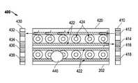
- FIG. 4illustrates a top view of an optical touch screen system 400 according to a second particular embodiment.
- Optical touch screen system 400includes optically transmissive medium 202 in which a representative portion 420 is shown in FIG. 4 .
- Portion 420includes a set of fibers 422 extending horizontally with sets of circular cavities 424 between every other pair of fibers 422 .
- Each of the fibers and circular cavitiescan be formed with any suitable optically transmissive material, such as TiO 2 .
- On a right sideis a linear array of detectors 410
- on a left sideis a linear array of detectors 430 .
- Each linear array of detectorsincludes display pixels interspersed with image sensor pixels with gaps corresponding to the spaces between adjacent fibers 422 .
- Linear array of detectors 410includes a photoemitter 412 , a photodetector 414 , a photoemitter 416 , and a photodetector 418 .
- Linear array of detectors 430includes a photodetector 432 , a photoemitter 434 , a photodetector 436 , and a photoemitter 438 .
- photoemitter 412is on a right side and photodetector 432 on a left side of a first fiber
- photoemitter 434is on a left side
- photodetector 414is on a right side of a second fiber, and so on.
- Circular cavities 424act to partially couple light from one fiber into an adjacent fiber such that the intensity of the incident light is split by circular cavities 424 into forward and backward components.
- the intensity of the forward and backward componentschanges from emitter to detector due to the coupling of light into different numbers of circular cavities. This characteristic allows a touch above the array at a particular position to perturb the forward and backward components in a way that can be detected and correlated to touch position.
- Touch 440perturbs the forward component sensed by detector 436 as well as the backward component sensed by photodetector 418 .
- the perturbationcan be sensed by comparison with the forward and backward signals from the unperturbed fibers.
- an optical touch screen systemusing portion 420 , another layer with fibers extending orthogonally to fibers 422 will overlie or underlie portion 420 .
- Control circuit 250will use measurements from this additional layer to determine X and Y coordinates of touch 440 .
- an optical touch screen systemincludes a single layer with fibers extending in only one direction, and uses the forward and backward components to detect not only the rows affected by touch 440 but also the position along the rows. However this other embodiment does not produce as accurate a touch location as an optical touch screen system that uses two orthogonal layers.
- FIG. 5illustrates in partial block diagram and partial perspective view an optical touch screen system 500 according to a third particular embodiment.
- Optical touch screen system 500includes optically transmissive medium 202 overlying a display layer 520 .
- Display layer 520includes edge rows of pixels 530 and 540 extending beyond the edges of optically transmissive medium 202 .
- Edge row of pixels 530includes a red pixel 532 and a green pixel 534 that are used as light sources.
- Optical touch screen system 500repurposes normal display pixels in edge rows to operate as light sources for establishing the standing wave patterns in optically transmissive medium 202 .
- the red and green lightis emitted by pixels 532 and 534 generally in an upward direction but is redirected through optically transmissive medium 202 parallel to the plane of display layer 520 by prism elements 550 and 560 , respectively.
- the red and green lightcreate standing wave patterns that can be measured in the untouched condition, and differences between the measurement in the untouched condition and current measurements can be used to detect touch locations.
- edge pixelsallows flexible operation at low cost by re-purposing a portion of the existing display array. It also allows various modulation modes for more accurate touch detection, including temporal encoding, wavelength encoding, spatial encoding (the prism elements can collect light from several LEDs), and polarization encoding. If there are multiple polarizations, pulse timings, and/or wavelength ranges of light sources along with pixels that can distinguish among them, then multiple somewhat independent perturbation patterns can be computed. Thus multiple determinations of position can be made, leading to a more robust overall touch position determination. In particular, if the timing or polarizations are interleaved (e.g., odd light sources have one state, and even light sources another), crosstalk can be reduced, improving resolution.
- the timing or polarizationsare interleaved (e.g., odd light sources have one state, and even light sources another), crosstalk can be reduced, improving resolution.
- FIG. 6illustrates in partial block diagram and partial perspective view an optical touch screen system 600 according to a fourth particular embodiment.
- Optical touch screen system 600includes optically transmissive medium 202 overlying a display plane 610 .
- Optically transmissive medium 202includes a first side 210 and a second side 220 and adjacent light sources 212 and 222 .
- Display plane 610includes a main display area 612 as well as a sensor array 614 near third side 230 and a sensor array 616 near fourth side 640 .
- Optical touch screen system 600uses sensor arrays 614 and 616 instead of 232 and 242 based on the fact that the standing wave pattern in optically transmissive medium 202 will reflect a certain pattern onto display plane 610 that will also be perturbed by a touch. While losing some sensitivity compared to an optical touch screen system using sensors along the edges, it can be manufactured easily and cheaply and so will be appropriate for many applications.
- FIG. 7illustrates in partial block diagram and partial perspective view an optical touch screen system 700 using a hybrid display and optical sensor 710 according to a fifth particular embodiment.
- Optical touch screen system 700includes a semiconductor substrate 720 forming hybrid display and optical sensor 710 connected to control circuit 250 .
- Hybrid display and optical sensor 710includes an array of display pixels shown as shaded blocks such as representative display pixels 712 , 714 , and 716 intermixed in a checkerboard pattern with an array of image sensor pixels shown as clear blocks such as representative image sensor pixel 718 .
- Hybrid display and optical sensor 710includes semiconductor substrate 720 and a color filter array 730 .
- each pixelis formed with a PN junction diode, in which image sensor pixels use reverse biased diodes such as exemplary diode 722 and display pixels use forward biased diodes such as exemplary diode 724 .
- Color filter array 730overlies semiconductor substrate 720 and creates green, red, and blue display pixels such as green display pixels 712 , a red display pixel 714 , and a blue display pixel 716 arranged generally in a modified Bayer pattern.
- the modified Bayer patternincludes green, red, and blue display pixels in the ratio of 2:1:1 like a conventional Bayer filter, but is modified to include an array of image sensor pixels with an image sensor pixel in between each pair of adjacent display pixels. Like the display pixels, the image sensor pixels use a color filter array in a modified Bayer pattern.
- image sensor pixelsare typically smaller than display pixels, in optical touch screen system 700 they are made the same size for ease of manufacturing.
- each image sensor pixelcan be implemented with an array of smaller image sensors.
- Control circuit 250activates the array of display pixels and captures an image using the array of image sensor pixels to determine the position of an object such as a finger or stylus from the surface.
- the positionincludes the planar coordinates as well as the distance from the surface of the hybrid display and image sensor.
- Control circuit 250intelligently measures this distance by measuring the intensity of reflected light near an object at neighboring image sensor pixels such that it can accurately discriminate between touches and near touches.
- Semiconductor substrate 720 and color filter array 730are inexpensive to manufacture and optical touch screen system 700 does not need a separate optically transmissive layer, but control circuit 250 needs additional processing capability to locate objects and to measure the position of the objects based on the reflected light pattern and intensity.
- Hybrid display and optical sensor 710can also be used with other elements to form optical touch screen systems that provide various advantages compared to capacitive touch screens. Two such examples will now be explained.
- FIG. 8illustrates a side view of an optical touch screen system 800 using a hybrid display and optical sensor 810 according to a sixth particular embodiment.
- Optical touch screen system 800includes hybrid display and optical sensor 810 and a spatial light modulator in the form of a grating 820 overlying but separated from hybrid display and optical sensor 810 .
- Hybrid display and optical sensor 810includes an array of display pixels interspersed with an array of image sensor pixels, and is constructed similarly to hybrid display and optical sensor 710 of FIG. 7 .
- hybrid display and optical sensor 810includes an exemplary blue display pixel 812 and exemplary adjacent blue image sensor pixels 814 and 816 .
- Grating 820is a diffraction grating with a periodic structure that splits and diffracts light into several beams or “grating orders”, which represent maxima of intensity of the diffracted light. Shown in FIG. 8 is a main beam 830 corresponding to grating order 0, a beam 831 displaced to the right by a predetermined angle and having a grating order of +1, and a set of beams 840 displaced to the left including a beam 841 having a grating order of ⁇ 1, a beam 842 having a grating order of ⁇ 2, a beam 843 having a grating order of ⁇ 3, a beam 844 having a grating order of ⁇ 4, and a beam 845 having a grating order of ⁇ 5.
- grating 820is useful in easily and accurately measuring the position.
- FIG. 9illustrates a side view of an optical touch screen system 900 using a hybrid display and optical sensor 910 according to a seventh particular embodiment.
- Optical touch screen system 900includes a spatial light modulator 920 overlying but separated from hybrid display and optical sensor 910 .
- Hybrid display and optical sensor 910again includes a semiconductor body having an array of display pixels interspersed with an array of image sensor pixels and an overlying color filter array, and is constructed similarly to hybrid display and optical sensor 710 of FIG. 7 .
- each display pixelemits coherent or partially coherent light.
- control circuit 250causes hybrid display and optical sensor 910 to activate many pixels, such as blue pixels 911 - 914 shown in FIG. 9 , at the same time, each pixel emitting coherent or partially coherent light.
- Spatial light modulator 920refracts, redirects, and phase matches light from multiple coherent display pixels to form a free space three-dimensional standing wave pattern, i.e. a hologram, of the nearby object.
- the hologramcan then be detected by the array of image sensor pixels such as exemplary image sensor pixel 915 to analyze the object to determine the shape of the object and the distance of the object from the surface of optical touch screen system 900 .
- Optical touch screen system 900can use different types of spatial light modulators, including liquid crystal display (LCD), acousto-optic, and electro-optic modulators.
- LCD modulatorsare the slowest of the three but are well-known and have been extensively developed for consumer electronic applications. Acousto-optic and electro-optic modulators are faster but less well developed.
- the underlying hybrid display and image sensoris able to more accurately and efficiently develop position information of the nearby object, simplifying the processing task of control circuit 250 .
Landscapes
- Engineering & Computer Science (AREA)
- General Engineering & Computer Science (AREA)
- Theoretical Computer Science (AREA)
- Human Computer Interaction (AREA)
- Physics & Mathematics (AREA)
- General Physics & Mathematics (AREA)
- Position Input By Displaying (AREA)
Abstract
Description
Claims (3)
Priority Applications (3)
| Application Number | Priority Date | Filing Date | Title |
|---|---|---|---|
| US14/806,388US10310674B2 (en) | 2015-07-22 | 2015-07-22 | Optical touch screen system using radiation pattern sensing and method therefor |
| CN201620774476.5UCN206421354U (en) | 2015-07-22 | 2016-07-21 | Touch-screen and optical touch screen systems |
| US16/385,127US10877604B2 (en) | 2015-07-22 | 2019-04-16 | Optical touch screen system using radiation pattern sensing and method therefor |
Applications Claiming Priority (1)
| Application Number | Priority Date | Filing Date | Title |
|---|---|---|---|
| US14/806,388US10310674B2 (en) | 2015-07-22 | 2015-07-22 | Optical touch screen system using radiation pattern sensing and method therefor |
Related Child Applications (1)
| Application Number | Title | Priority Date | Filing Date |
|---|---|---|---|
| US16/385,127DivisionUS10877604B2 (en) | 2015-07-22 | 2019-04-16 | Optical touch screen system using radiation pattern sensing and method therefor |
Publications (2)
| Publication Number | Publication Date |
|---|---|
| US20170024083A1 US20170024083A1 (en) | 2017-01-26 |
| US10310674B2true US10310674B2 (en) | 2019-06-04 |
Family
ID=57837849
Family Applications (2)
| Application Number | Title | Priority Date | Filing Date |
|---|---|---|---|
| US14/806,388Expired - Fee RelatedUS10310674B2 (en) | 2015-07-22 | 2015-07-22 | Optical touch screen system using radiation pattern sensing and method therefor |
| US16/385,127ActiveUS10877604B2 (en) | 2015-07-22 | 2019-04-16 | Optical touch screen system using radiation pattern sensing and method therefor |
Family Applications After (1)
| Application Number | Title | Priority Date | Filing Date |
|---|---|---|---|
| US16/385,127ActiveUS10877604B2 (en) | 2015-07-22 | 2019-04-16 | Optical touch screen system using radiation pattern sensing and method therefor |
Country Status (2)
| Country | Link |
|---|---|
| US (2) | US10310674B2 (en) |
| CN (1) | CN206421354U (en) |
Cited By (1)
| Publication number | Priority date | Publication date | Assignee | Title |
|---|---|---|---|---|
| US11231809B2 (en)* | 2017-07-11 | 2022-01-25 | Hewlett-Packard Development Company, L.P. | Touch input detection |
Families Citing this family (7)
| Publication number | Priority date | Publication date | Assignee | Title |
|---|---|---|---|---|
| US10043050B2 (en)* | 2016-03-07 | 2018-08-07 | Microsoft Technology Licensing, Llc | Image sensing with a display |
| TWI599801B (en)* | 2016-07-26 | 2017-09-21 | Au Optronics Corp | Image sensing device and optical film thereof |
| CN107505980B (en)* | 2017-08-16 | 2019-10-22 | 江苏集萃有机光电技术研究所有限公司 | Display screen and electronic equipment |
| CN109975299B (en)* | 2017-12-27 | 2022-03-25 | 群光电子股份有限公司 | Luminescent source detection system and method |
| CN109032431A (en)* | 2018-07-13 | 2018-12-18 | 业成科技(成都)有限公司 | It can define the optical touch control apparatus and its method of nib color |
| EP3599541B1 (en)* | 2018-07-26 | 2023-12-13 | University of Vienna | Optical waveguide light emitter and touchscreen |
| US12189902B2 (en)* | 2023-01-18 | 2025-01-07 | Apple Inc. | Photo-sensing enabled display for touch detection with customized photodiode and light emitting diode component level angular response |
Citations (12)
| Publication number | Priority date | Publication date | Assignee | Title |
|---|---|---|---|---|
| US6538644B1 (en)* | 1999-11-19 | 2003-03-25 | Fujitsu Takamisawa Component Ltd. | Touch panel |
| US20040120684A1 (en)* | 2002-08-09 | 2004-06-24 | Akira Ishibashi | Optical waveguide, optical waveguide apparatus, optomechanical apparatus, detecting apparatus, information processing apparatus, input apparatus, key-input apparatus, and fiber structure |
| US20100097348A1 (en)* | 2008-10-16 | 2010-04-22 | Inha Industry Partnership Institute | Touch screen tool |
| US20100156848A1 (en)* | 2008-12-24 | 2010-06-24 | Fuji Xerox Co., Ltd. | Optical waveguide, optical waveguide type touch panel and method of manufacturing the optical waveguide |
| US20110122091A1 (en)* | 2009-11-25 | 2011-05-26 | King Jeffrey S | Methods and apparatus for sensing touch events on a display |
| US20130127790A1 (en)* | 2011-07-13 | 2013-05-23 | Flatfrog Laboratories Ab | Touch-sensing display panel |
| US8541856B2 (en) | 2010-12-08 | 2013-09-24 | Omnivision Technologies, Inc. | Optical touch-screen imager |
| US20130314368A1 (en)* | 2012-05-24 | 2013-11-28 | Corning Incorporated | Waveguide-based touch system employing interference effects |
| US20140035836A1 (en)* | 2012-08-06 | 2014-02-06 | Qualcomm Mems Technologies, Inc. | Channel waveguide system for sensing touch and/or gesture |
| US8780087B2 (en) | 2009-12-11 | 2014-07-15 | Sung-han Kim | Optical touch screen |
| US20150091875A1 (en)* | 2012-10-04 | 2015-04-02 | Corning Incorporated | Pressure sensing touch systems and methods |
| US20160342282A1 (en)* | 2014-01-16 | 2016-11-24 | Flatfrog Laboratories Ab | Touch-sensing quantum dot lcd panel |
Family Cites Families (20)
| Publication number | Priority date | Publication date | Assignee | Title |
|---|---|---|---|---|
| US20020001110A1 (en)* | 1987-09-11 | 2002-01-03 | Michael H. Metz | Holographic light panels and flat panel display systems and method and apparatus for making same |
| US7034866B1 (en) | 2000-11-22 | 2006-04-25 | Koninklijke Philips Electronics N.V. | Combined display-camera for an image processing system |
| US20040140973A1 (en)* | 2003-01-16 | 2004-07-22 | Zanaty Farouk M. | System and method of a video capture monitor concurrently displaying and capturing video images |
| US20050008052A1 (en)* | 2003-07-01 | 2005-01-13 | Ryoji Nomura | Light-emitting device |
| US7359564B2 (en)* | 2004-10-29 | 2008-04-15 | Microsoft Corporation | Method and system for cancellation of ambient light using light frequency |
| CN101211246B (en)* | 2006-12-26 | 2010-06-23 | 乐金显示有限公司 | organic light emitting diode panel and touch screen system including the same |
| US8736587B2 (en)* | 2008-07-10 | 2014-05-27 | Semiconductor Energy Laboratory Co., Ltd. | Semiconductor device |
| US20100060611A1 (en)* | 2008-09-05 | 2010-03-11 | Sony Ericsson Mobile Communication Ab | Touch display with switchable infrared illumination for touch position determination and methods thereof |
| US8076207B2 (en)* | 2009-07-14 | 2011-12-13 | United Microelectronics Corp. | Gate structure and method of making the same |
| WO2011019971A2 (en)* | 2009-08-14 | 2011-02-17 | Arizona Board Of Regents, For And On Behalf Of Arizona State University | Method and system for aligning color filter array |
| WO2011060097A2 (en)* | 2009-11-10 | 2011-05-19 | California Institute Of Technology | Acoustic assisted phase conjugate optical tomography |
| US20110248960A1 (en)* | 2010-04-08 | 2011-10-13 | Qualcomm Mems Technologies, Inc. | Holographic touchscreen |
| JP2012247910A (en)* | 2011-05-26 | 2012-12-13 | Sony Corp | Three-dimensional interactive display |
| JP2013024788A (en)* | 2011-07-25 | 2013-02-04 | Renesas Electronics Corp | Semiconductor integrated circuit, scan flip-flop, and method for testing semiconductor integrated circuit |
| US9223442B2 (en)* | 2013-01-10 | 2015-12-29 | Samsung Display Co., Ltd. | Proximity and touch sensing surface for integration with a display |
| US9280214B2 (en)* | 2013-07-02 | 2016-03-08 | Blackberry Limited | Method and apparatus for motion sensing of a handheld device relative to a stylus |
| US20150083917A1 (en)* | 2013-09-23 | 2015-03-26 | Qualcomm Incorporated | Infrared light director for gesture or scene sensing fsc display |
| US9804316B2 (en)* | 2013-12-20 | 2017-10-31 | Apple Inc. | Display having backlight with narrowband collimated light sources |
| US9836165B2 (en)* | 2014-05-16 | 2017-12-05 | Apple Inc. | Integrated silicon-OLED display and touch sensor panel |
| JP6415160B2 (en)* | 2014-07-29 | 2018-10-31 | キヤノン株式会社 | Printing apparatus, control method for the apparatus, and program |
- 2015
- 2015-07-22USUS14/806,388patent/US10310674B2/ennot_activeExpired - Fee Related
- 2016
- 2016-07-21CNCN201620774476.5Upatent/CN206421354U/ennot_activeExpired - Fee Related
- 2019
- 2019-04-16USUS16/385,127patent/US10877604B2/enactiveActive
Patent Citations (12)
| Publication number | Priority date | Publication date | Assignee | Title |
|---|---|---|---|---|
| US6538644B1 (en)* | 1999-11-19 | 2003-03-25 | Fujitsu Takamisawa Component Ltd. | Touch panel |
| US20040120684A1 (en)* | 2002-08-09 | 2004-06-24 | Akira Ishibashi | Optical waveguide, optical waveguide apparatus, optomechanical apparatus, detecting apparatus, information processing apparatus, input apparatus, key-input apparatus, and fiber structure |
| US20100097348A1 (en)* | 2008-10-16 | 2010-04-22 | Inha Industry Partnership Institute | Touch screen tool |
| US20100156848A1 (en)* | 2008-12-24 | 2010-06-24 | Fuji Xerox Co., Ltd. | Optical waveguide, optical waveguide type touch panel and method of manufacturing the optical waveguide |
| US20110122091A1 (en)* | 2009-11-25 | 2011-05-26 | King Jeffrey S | Methods and apparatus for sensing touch events on a display |
| US8780087B2 (en) | 2009-12-11 | 2014-07-15 | Sung-han Kim | Optical touch screen |
| US8541856B2 (en) | 2010-12-08 | 2013-09-24 | Omnivision Technologies, Inc. | Optical touch-screen imager |
| US20130127790A1 (en)* | 2011-07-13 | 2013-05-23 | Flatfrog Laboratories Ab | Touch-sensing display panel |
| US20130314368A1 (en)* | 2012-05-24 | 2013-11-28 | Corning Incorporated | Waveguide-based touch system employing interference effects |
| US20140035836A1 (en)* | 2012-08-06 | 2014-02-06 | Qualcomm Mems Technologies, Inc. | Channel waveguide system for sensing touch and/or gesture |
| US20150091875A1 (en)* | 2012-10-04 | 2015-04-02 | Corning Incorporated | Pressure sensing touch systems and methods |
| US20160342282A1 (en)* | 2014-01-16 | 2016-11-24 | Flatfrog Laboratories Ab | Touch-sensing quantum dot lcd panel |
Non-Patent Citations (1)
| Title |
|---|
| G. Wernicke et al., "Liquid crystal display as spatial light modulator for diffractive optical elements and the reconstruction of digital holograms," Proceedings of SPIE, vol. 4596, 2001, pp. 182-190. |
Cited By (1)
| Publication number | Priority date | Publication date | Assignee | Title |
|---|---|---|---|---|
| US11231809B2 (en)* | 2017-07-11 | 2022-01-25 | Hewlett-Packard Development Company, L.P. | Touch input detection |
Also Published As
| Publication number | Publication date |
|---|---|
| US10877604B2 (en) | 2020-12-29 |
| CN206421354U (en) | 2017-08-18 |
| US20170024083A1 (en) | 2017-01-26 |
| US20190243511A1 (en) | 2019-08-08 |
Similar Documents
| Publication | Publication Date | Title |
|---|---|---|
| US10877604B2 (en) | Optical touch screen system using radiation pattern sensing and method therefor | |
| US10698529B2 (en) | Integrating capacitive sensing with an optical sensor | |
| CN108496180B (en) | Optical fingerprint sensor under display | |
| US20100295821A1 (en) | Optical touch panel | |
| US8035625B2 (en) | Touch screen | |
| US8803846B2 (en) | Method for detecting touch and optical touch sensing system | |
| JP2018081710A (en) | Ultrasonic touch sensor with display monitor | |
| WO2020062781A1 (en) | Method for detecting biometric information, biometric sensor, and display apparatus | |
| KR20160034358A (en) | Light guide panel including diffraction gratings | |
| US20110122099A1 (en) | Multiple-input touch panel and method for gesture recognition | |
| KR101910607B1 (en) | Detecting Multitouch Events in an Optical Touch-Sensitive Device using Touch Event Templates | |
| CN102073418A (en) | Coordinate positioning method and equipment | |
| TWI460638B (en) | Light guide plate touch device | |
| WO2018024161A1 (en) | Sensor and display device | |
| JP2010287225A (en) | Touch input device | |
| CN108962959A (en) | A kind of organic light emitting display panel and display device | |
| CN108664854A (en) | Fingerprint imaging module and electronic equipment | |
| US20120319988A1 (en) | System and method for sensor device signaling using a polarity reset interval | |
| JP2006323521A (en) | Non-contact type input device | |
| TWI525511B (en) | Light guide plate optical touch device | |
| KR20120066381A (en) | Optical touch screen panel | |
| US8878820B2 (en) | Optical touch module | |
| US8896553B1 (en) | Hybrid sensor module | |
| US11756330B2 (en) | Biometric sensor, display apparatus, and method for detecting biometric information | |
| TW201621592A (en) | Optical touch device of light guide plate |
Legal Events
| Date | Code | Title | Description |
|---|---|---|---|
| AS | Assignment | Owner name:SEMICONDUCTOR COMPONENTS INDUSTRIES, LLC, ARIZONA Free format text:ASSIGNMENT OF ASSIGNORS INTEREST;ASSIGNORS:LENCHENKOV, VICTOR A.;KEELAN, BRIAN WILLIAM;REEL/FRAME:036576/0487 Effective date:20150714 | |
| AS | Assignment | Owner name:SEMICONDUCTOR COMPONENTS INDUSTRIES, LLC, ARIZONA Free format text:ASSIGNMENT OF ASSIGNORS INTEREST;ASSIGNOR:GILTON, TERRY;REEL/FRAME:037678/0323 Effective date:20160126 | |
| AS | Assignment | Owner name:DEUTSCHE BANK AG NEW YORK BRANCH, NEW YORK Free format text:SECURITY INTEREST;ASSIGNOR:SEMICONDUCTOR COMPONENTS INDUSTRIES, LLC;REEL/FRAME:038620/0087 Effective date:20160415 | |
| AS | Assignment | Owner name:DEUTSCHE BANK AG NEW YORK BRANCH, AS COLLATERAL AGENT, NEW YORK Free format text:CORRECTIVE ASSIGNMENT TO CORRECT THE INCORRECT PATENT NUMBER 5859768 AND TO RECITE COLLATERAL AGENT ROLE OF RECEIVING PARTY IN THE SECURITY INTEREST PREVIOUSLY RECORDED ON REEL 038620 FRAME 0087. ASSIGNOR(S) HEREBY CONFIRMS THE SECURITY INTEREST;ASSIGNOR:SEMICONDUCTOR COMPONENTS INDUSTRIES, LLC;REEL/FRAME:039853/0001 Effective date:20160415 Owner name:DEUTSCHE BANK AG NEW YORK BRANCH, AS COLLATERAL AG Free format text:CORRECTIVE ASSIGNMENT TO CORRECT THE INCORRECT PATENT NUMBER 5859768 AND TO RECITE COLLATERAL AGENT ROLE OF RECEIVING PARTY IN THE SECURITY INTEREST PREVIOUSLY RECORDED ON REEL 038620 FRAME 0087. ASSIGNOR(S) HEREBY CONFIRMS THE SECURITY INTEREST;ASSIGNOR:SEMICONDUCTOR COMPONENTS INDUSTRIES, LLC;REEL/FRAME:039853/0001 Effective date:20160415 | |
| STPP | Information on status: patent application and granting procedure in general | Free format text:NOTICE OF ALLOWANCE MAILED -- APPLICATION RECEIVED IN OFFICE OF PUBLICATIONS | |
| STPP | Information on status: patent application and granting procedure in general | Free format text:PUBLICATIONS -- ISSUE FEE PAYMENT VERIFIED | |
| STCF | Information on status: patent grant | Free format text:PATENTED CASE | |
| FEPP | Fee payment procedure | Free format text:MAINTENANCE FEE REMINDER MAILED (ORIGINAL EVENT CODE: REM.); ENTITY STATUS OF PATENT OWNER: LARGE ENTITY | |
| AS | Assignment | Owner name:FAIRCHILD SEMICONDUCTOR CORPORATION, ARIZONA Free format text:RELEASE OF SECURITY INTEREST IN PATENTS RECORDED AT REEL 038620, FRAME 0087;ASSIGNOR:DEUTSCHE BANK AG NEW YORK BRANCH, AS COLLATERAL AGENT;REEL/FRAME:064070/0001 Effective date:20230622 Owner name:SEMICONDUCTOR COMPONENTS INDUSTRIES, LLC, ARIZONA Free format text:RELEASE OF SECURITY INTEREST IN PATENTS RECORDED AT REEL 038620, FRAME 0087;ASSIGNOR:DEUTSCHE BANK AG NEW YORK BRANCH, AS COLLATERAL AGENT;REEL/FRAME:064070/0001 Effective date:20230622 | |
| LAPS | Lapse for failure to pay maintenance fees | Free format text:PATENT EXPIRED FOR FAILURE TO PAY MAINTENANCE FEES (ORIGINAL EVENT CODE: EXP.); ENTITY STATUS OF PATENT OWNER: LARGE ENTITY | |
| STCH | Information on status: patent discontinuation | Free format text:PATENT EXPIRED DUE TO NONPAYMENT OF MAINTENANCE FEES UNDER 37 CFR 1.362 | |
| FP | Lapsed due to failure to pay maintenance fee | Effective date:20230604 |