US10299368B2 - Surface integrated waveguides and circuit structures therefor - Google Patents
Surface integrated waveguides and circuit structures thereforDownload PDFInfo
- Publication number
- US10299368B2 US10299368B2US15/387,278US201615387278AUS10299368B2US 10299368 B2US10299368 B2US 10299368B2US 201615387278 AUS201615387278 AUS 201615387278AUS 10299368 B2US10299368 B2US 10299368B2
- Authority
- US
- United States
- Prior art keywords
- circuit structure
- wire bond
- conductive layer
- bond wires
- signal
- Prior art date
- Legal status (The legal status is an assumption and is not a legal conclusion. Google has not performed a legal analysis and makes no representation as to the accuracy of the status listed.)
- Active
Links
- 238000004377microelectronicMethods0.000claimsabstractdescription36
- 239000000758substrateSubstances0.000claimsdescription24
- 230000005670electromagnetic radiationEffects0.000claimsdescription8
- 238000000034methodMethods0.000abstractdescription13
- 239000010410layerSubstances0.000description84
- 239000002184metalSubstances0.000description18
- 229910052751metalInorganic materials0.000description18
- 238000010586diagramMethods0.000description11
- 238000005553drillingMethods0.000description9
- 239000011295pitchSubstances0.000description9
- 238000000465mouldingMethods0.000description7
- 239000004065semiconductorSubstances0.000description6
- 239000004020conductorSubstances0.000description3
- 230000015572biosynthetic processEffects0.000description2
- 238000004891communicationMethods0.000description2
- 230000008021depositionEffects0.000description2
- 239000003989dielectric materialSubstances0.000description2
- 238000005538encapsulationMethods0.000description2
- 239000000463materialSubstances0.000description2
- 230000000644propagated effectEffects0.000description2
- 230000001902propagating effectEffects0.000description2
- RYGMFSIKBFXOCR-UHFFFAOYSA-NCopperChemical compound[Cu]RYGMFSIKBFXOCR-UHFFFAOYSA-N0.000description1
- 230000000712assemblyEffects0.000description1
- 238000000429assemblyMethods0.000description1
- 230000005540biological transmissionEffects0.000description1
- 239000003990capacitorSubstances0.000description1
- 150000001875compoundsChemical class0.000description1
- 229910052802copperInorganic materials0.000description1
- 239000010949copperSubstances0.000description1
- 230000008878couplingEffects0.000description1
- 238000010168coupling processMethods0.000description1
- 238000005859coupling reactionMethods0.000description1
- 230000005672electromagnetic fieldEffects0.000description1
- 239000011888foilSubstances0.000description1
- 230000001939inductive effectEffects0.000description1
- 238000001746injection mouldingMethods0.000description1
- 239000007787solidSubstances0.000description1
- 238000012358sourcingMethods0.000description1
- 238000001228spectrumMethods0.000description1
- 230000001629suppressionEffects0.000description1
- 239000002344surface layerSubstances0.000description1
- 229910000859α-FeInorganic materials0.000description1
Images


Classifications
- H—ELECTRICITY
- H05—ELECTRIC TECHNIQUES NOT OTHERWISE PROVIDED FOR
- H05K—PRINTED CIRCUITS; CASINGS OR CONSTRUCTIONAL DETAILS OF ELECTRIC APPARATUS; MANUFACTURE OF ASSEMBLAGES OF ELECTRICAL COMPONENTS
- H05K1/00—Printed circuits
- H05K1/02—Details
- H05K1/0213—Electrical arrangements not otherwise provided for
- H05K1/0216—Reduction of cross-talk, noise or electromagnetic interference
- H05K1/0228—Compensation of cross-talk by a mutually correlated lay-out of printed circuit traces, e.g. for compensation of cross-talk in mounted connectors
- H—ELECTRICITY
- H01—ELECTRIC ELEMENTS
- H01P—WAVEGUIDES; RESONATORS, LINES, OR OTHER DEVICES OF THE WAVEGUIDE TYPE
- H01P1/00—Auxiliary devices
- H01P1/20—Frequency-selective devices, e.g. filters
- H01P1/207—Hollow waveguide filters
- H—ELECTRICITY
- H01—ELECTRIC ELEMENTS
- H01P—WAVEGUIDES; RESONATORS, LINES, OR OTHER DEVICES OF THE WAVEGUIDE TYPE
- H01P1/00—Auxiliary devices
- H01P1/20—Frequency-selective devices, e.g. filters
- H01P1/207—Hollow waveguide filters
- H01P1/208—Cascaded cavities; Cascaded resonators inside a hollow waveguide structure
- H01P1/2088—Integrated in a substrate
- H—ELECTRICITY
- H01—ELECTRIC ELEMENTS
- H01P—WAVEGUIDES; RESONATORS, LINES, OR OTHER DEVICES OF THE WAVEGUIDE TYPE
- H01P3/00—Waveguides; Transmission lines of the waveguide type
- H01P3/12—Hollow waveguides
- H01P3/121—Hollow waveguides integrated in a substrate
- H—ELECTRICITY
- H05—ELECTRIC TECHNIQUES NOT OTHERWISE PROVIDED FOR
- H05K—PRINTED CIRCUITS; CASINGS OR CONSTRUCTIONAL DETAILS OF ELECTRIC APPARATUS; MANUFACTURE OF ASSEMBLAGES OF ELECTRICAL COMPONENTS
- H05K1/00—Printed circuits
- H05K1/02—Details
- H05K1/0274—Optical details, e.g. printed circuits comprising integral optical means
- H—ELECTRICITY
- H05—ELECTRIC TECHNIQUES NOT OTHERWISE PROVIDED FOR
- H05K—PRINTED CIRCUITS; CASINGS OR CONSTRUCTIONAL DETAILS OF ELECTRIC APPARATUS; MANUFACTURE OF ASSEMBLAGES OF ELECTRICAL COMPONENTS
- H05K3/00—Apparatus or processes for manufacturing printed circuits
- H05K3/30—Assembling printed circuits with electric components, e.g. with resistor
- H—ELECTRICITY
- H01—ELECTRIC ELEMENTS
- H01L—SEMICONDUCTOR DEVICES NOT COVERED BY CLASS H10
- H01L2224/00—Indexing scheme for arrangements for connecting or disconnecting semiconductor or solid-state bodies and methods related thereto as covered by H01L24/00
- H01L2224/01—Means for bonding being attached to, or being formed on, the surface to be connected, e.g. chip-to-package, die-attach, "first-level" interconnects; Manufacturing methods related thereto
- H01L2224/42—Wire connectors; Manufacturing methods related thereto
- H01L2224/47—Structure, shape, material or disposition of the wire connectors after the connecting process
- H01L2224/48—Structure, shape, material or disposition of the wire connectors after the connecting process of an individual wire connector
- H01L2224/4805—Shape
- H01L2224/4809—Loop shape
- H01L2224/48091—Arched
- H—ELECTRICITY
- H01—ELECTRIC ELEMENTS
- H01L—SEMICONDUCTOR DEVICES NOT COVERED BY CLASS H10
- H01L2224/00—Indexing scheme for arrangements for connecting or disconnecting semiconductor or solid-state bodies and methods related thereto as covered by H01L24/00
- H01L2224/01—Means for bonding being attached to, or being formed on, the surface to be connected, e.g. chip-to-package, die-attach, "first-level" interconnects; Manufacturing methods related thereto
- H01L2224/42—Wire connectors; Manufacturing methods related thereto
- H01L2224/47—Structure, shape, material or disposition of the wire connectors after the connecting process
- H01L2224/48—Structure, shape, material or disposition of the wire connectors after the connecting process of an individual wire connector
- H01L2224/481—Disposition
- H01L2224/48151—Connecting between a semiconductor or solid-state body and an item not being a semiconductor or solid-state body, e.g. chip-to-substrate, chip-to-passive
- H01L2224/48221—Connecting between a semiconductor or solid-state body and an item not being a semiconductor or solid-state body, e.g. chip-to-substrate, chip-to-passive the body and the item being stacked
- H01L2224/48225—Connecting between a semiconductor or solid-state body and an item not being a semiconductor or solid-state body, e.g. chip-to-substrate, chip-to-passive the body and the item being stacked the item being non-metallic, e.g. insulating substrate with or without metallisation
- H01L2224/48227—Connecting between a semiconductor or solid-state body and an item not being a semiconductor or solid-state body, e.g. chip-to-substrate, chip-to-passive the body and the item being stacked the item being non-metallic, e.g. insulating substrate with or without metallisation connecting the wire to a bond pad of the item
- H—ELECTRICITY
- H01—ELECTRIC ELEMENTS
- H01L—SEMICONDUCTOR DEVICES NOT COVERED BY CLASS H10
- H01L2924/00—Indexing scheme for arrangements or methods for connecting or disconnecting semiconductor or solid-state bodies as covered by H01L24/00
- H01L2924/0001—Technical content checked by a classifier
- H01L2924/00014—Technical content checked by a classifier the subject-matter covered by the group, the symbol of which is combined with the symbol of this group, being disclosed without further technical details
- H—ELECTRICITY
- H01—ELECTRIC ELEMENTS
- H01P—WAVEGUIDES; RESONATORS, LINES, OR OTHER DEVICES OF THE WAVEGUIDE TYPE
- H01P1/00—Auxiliary devices
- H01P1/32—Non-reciprocal transmission devices
- H01P1/38—Circulators
- H01P1/383—Junction circulators, e.g. Y-circulators
- H01P1/39—Hollow waveguide circulators
- H—ELECTRICITY
- H01—ELECTRIC ELEMENTS
- H01P—WAVEGUIDES; RESONATORS, LINES, OR OTHER DEVICES OF THE WAVEGUIDE TYPE
- H01P11/00—Apparatus or processes specially adapted for manufacturing waveguides or resonators, lines, or other devices of the waveguide type
- H01P11/001—Manufacturing waveguides or transmission lines of the waveguide type
- H01P11/002—Manufacturing hollow waveguides
- H—ELECTRICITY
- H01—ELECTRIC ELEMENTS
- H01P—WAVEGUIDES; RESONATORS, LINES, OR OTHER DEVICES OF THE WAVEGUIDE TYPE
- H01P5/00—Coupling devices of the waveguide type
- H01P5/12—Coupling devices having more than two ports
- H01P5/16—Conjugate devices, i.e. devices having at least one port decoupled from one other port
- H01P5/19—Conjugate devices, i.e. devices having at least one port decoupled from one other port of the junction type
- H—ELECTRICITY
- H01—ELECTRIC ELEMENTS
- H01P—WAVEGUIDES; RESONATORS, LINES, OR OTHER DEVICES OF THE WAVEGUIDE TYPE
- H01P7/00—Resonators of the waveguide type
- H01P7/06—Cavity resonators
- H01P7/065—Cavity resonators integrated in a substrate
- H—ELECTRICITY
- H01—ELECTRIC ELEMENTS
- H01Q—ANTENNAS, i.e. RADIO AERIALS
- H01Q13/00—Waveguide horns or mouths; Slot antennas; Leaky-waveguide antennas; Equivalent structures causing radiation along the transmission path of a guided wave
- H01Q13/10—Resonant slot antennas
- H01Q13/18—Resonant slot antennas the slot being backed by, or formed in boundary wall of, a resonant cavity ; Open cavity antennas
- H—ELECTRICITY
- H05—ELECTRIC TECHNIQUES NOT OTHERWISE PROVIDED FOR
- H05K—PRINTED CIRCUITS; CASINGS OR CONSTRUCTIONAL DETAILS OF ELECTRIC APPARATUS; MANUFACTURE OF ASSEMBLAGES OF ELECTRICAL COMPONENTS
- H05K2201/00—Indexing scheme relating to printed circuits covered by H05K1/00
- H05K2201/10—Details of components or other objects attached to or integrated in a printed circuit board
- H05K2201/10227—Other objects, e.g. metallic pieces
- H05K2201/10287—Metal wires as connectors or conductors
Definitions
- the following descriptionrelates to microelectronic devices. More particularly, the following description relates to a circuit structure, such as a waveguide or cavity, having spaced-apart wire bond wires for at least one side thereof.
- substrate-integrated waveguidesare formed by laser drilling holes in a dielectric substrate, including a printed circuit board, down to a lower metal layer. Such holes are filled with a metal to form metal posts, and an upper metal layer is formed over upper ends of such metal posts and on a presently exposed upper surface of such dielectric substrate to form an SIW.
- metal post-to-metal post spacing or pitchis limited to laser drilling spacings, which conventionally such pitch is at a minimum 350 microns.
- Photolithographic semiconductor processingmay be used to form such metal posts with sub-350 micron pitches; however, photolithographic semiconductor processing is substantially more costly than laser drilling.
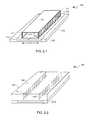
- FIG. 1-1is a line drawing of a front perspective view illustratively depicting an exemplary in-process microelectronic device.
- FIG. 1-2is a line drawing of a front perspective view illustratively depicting another exemplary in-process microelectronic device.
- FIG. 2-1is a line drawing of a front perspective view illustratively depicting the exemplary microelectronic device of FIG. 1-1 with an upper conductive layer.
- FIG. 2-2is a line drawing of a front perspective view illustratively depicting the example microelectronic device of FIG. 2-1 with a signal guide dielectric layer.
- FIG. 2-3is a line drawing of a front perspective view illustratively depicting the example microelectronic device of FIG. 2-2 with an upper conductive layer.
- FIG. 3is a block diagram illustratively depicting a cross-sectional view of an exemplary system-integrated package (“SiP”) having an upper surface integrated waveguide circuit structure for a microelectronic device.
- SiPsystem-integrated package
- FIG. 4is a block diagram illustratively depicting a top plan view of the example SiP of FIG. 3 .
- FIGS. 5 through 10are respective block diagrams illustratively depicting respective top-down views of corresponding exemplary microelectronic devices having a signal guide circuit structure formed with wire bond wires.
- FIG. 11is a block diagram illustratively depicting an exemplary amplifier system having a plurality of signal guide circuit structures.
- FIG. 12is a flow diagram illustratively depicting an exemplary process flow for forming a microelectronic device for having a signal guide circuit structure.
- SIWsSubstrate-Integrated Waveguides
- SIWsuse laser drilled holes in a printed circuit board (“PCB”) or other substrate, which are filled with a metal or other conductor to form metal posts or bars of a waveguide. Such metal posts may interconnect upper and lower conductive plates of an SIW.
- spacings between laser drilled holes of an SIWmay conventionally only be as small as approximately 350 microns (0.35 millimeters (“mm”)). This limits applications for such conventional SIWs to frequencies having wavelengths approximately equal to or greater than 3.5 millimeters (i.e., approximately 10 ⁇ 0.35 mm).
- a photolithographic semiconductor processmay be used to form metal posts, namely plated or filled vias, with narrower spacings than approximately 350 microns.
- photolithographic semiconductor processingis substantially more expensive than laser drilling.
- forming a signal guide circuit structure as described in additional detail below by using wire bond wiresallows for use of higher frequencies than that of conventional laser drill SIWs without the high cost of photolithographic semiconductor processing.
- signal guide circuit structuresmay be formed for higher frequencies than laser drilling and at less cost than photolithographic semiconductor processing.
- wire bond wiringmay be used as a replacement for laser drilling with respect to both cost and pitch.
- wire bond wiringcan allow the top/bottom surface layers for signal routing, which is not capable for conventional SIWs that route only in internal layers of a package substrate or PCB.
- an apparatusrelates generally to a microelectronic device.
- a first conductive layeris for providing a lower interior surface of a circuit structure.
- a plurality of wire bond wiresare interconnected to the lower interior surface of the first conductive layer and spaced apart from one another for providing at least one side of the circuit structure.
- a second conductive layeris for providing an upper interior surface of the circuit structure.
- the upper interior surface and lower interior surface, which may be opposite one another,are spaced apart from one another by the plurality of wire bond wires.
- the plurality of wire bond wiresare interconnected to the upper interior surface of the second conductive layer.
- the plurality of wire bond wires, the first conductive layer and the second conductive layerin combination define at least one opening in the at least one side for a signal port of the circuit structure.
- a methodrelates generally to forming a microelectronic device.
- a first conductive layeris obtained for providing a lower interior surface of a circuit structure.
- a plurality of wire bond wiresare interconnected to the lower interior surface of the first conductive layer and spaced apart from one another for providing at least one side of the circuit structure.
- a second conductive layeris formed for providing an upper interior surface of the circuit structure.
- the upper interior surface and lower interior surface, which may be opposite one another,are spaced apart from one another by the plurality of wire bond wires.
- the plurality of wire bond wiresare interconnected to the upper interior surface of the second conductive layer.
- the plurality of wire bond wires, the first conductive layer and the second conductive layerin combination define at least one opening in the at least one side for a signal port of the circuit structure.
- FIG. 1-1is a line drawing of a front perspective view illustratively depicting an exemplary in-process microelectronic device 100 .
- Microelectronic device 100may include a substrate 102 having a conductive layer 101 .
- Conductive layer 101may generally have a thickness t.
- Substrate 102may be formed of a semiconductive or dielectric material.
- Conductive layer 101may be a conductive strip on an upper surface 103 of a substrate 102 , or conductive layer 101 may be a conductive strip wholly or partially recessed in an upper surface 103 of a substrate 102 .
- Conductive layer 101may have a thickness, t, which may be one or more plated and/or deposited layers, a foil layer, a printed layer, an ink stamped layer, a vapor deposited layer or a combination thereof or the like for forming a metal or other conductive layer 101 .
- Thickness tcan be 1 or 2 or several microns, with generally thicker conductive layers providing better electrical performance.
- a lower interior surface 104 of a circuit structure 110may be at least a portion, if not all, of an upper surface 105 of conductive layer 101 .
- Conductive layer 101may have attached to upper surface 105 thereof a plurality of spaced apart wire bond wires 108 for providing at least one side of circuit structure 110 .
- Such at least one sidemay provide an interior sidewall surface 116 , one and/or all interior sides, of circuit structure 110 .
- a first and a second plurality of spaced apart wire bond wires 108form two spaced apart rows 106 and 107 of wire bond wires 108 .
- Rows 106 and 107are spaced apart by a distance w, which may be in a range may vary from application to application, but is generally at least greater than a half wavelength ( ⁇ /2) with respect to wavelength ⁇ of a signal input.
- Row 106may provide a first interior sidewall surface 116 of circuit structure 110
- row 107may provide a second interior sidewall surface 116 of circuit structure 110 opposite such first interior sidewall surface.
- Lower ends 112 of wire bond wires 108may be ball, stitch or other types of wire bond wire bonds for physical-mechanical attachment to upper surface 105 to define a lower interior surface. Tips or upper ends 111 of wire bond wires 108 may be physically-mechanically attached to another conductive layer, as described below in additional detail.
- Wire bond wires 108 of a plurality thereof, such as rows 106 and 107 for example,may be spaced apart from one another on center a distance d. Distance d may be approximately 1/10 or smaller fraction of a wavelength ⁇ of a signal to be propagated in an interior region 117 defined by circuit structure 110 , such as for millimeter or smaller wavelengths, as described below in additional detail.
- circuit structure 110may be a signal guide circuit structure, such as for a signal waveguide or signal cavity for a wavelength in the electromagnetic spectrum for example.
- circuit structure 110is a waveguide for electromagnetic signals, as described below in additional detail.
- lightis technically an electromagnetic signal, circuit structure 110 is not for propagation of light.
- other circuit structuresmay be implemented using at least one set of a plurality of spaced apart wire bond wires 108 , such as for circuit structure 110 a cavity as illustratively depicted in the line drawing of FIG. 1-2 having a front perspective view illustratively depicting another exemplary in-process microelectronic device 100 .
- rectilinear circuit structuresare illustratively depicted for purposes of clarity by way of example, rectilinear, non-rectilinear, or a combination thereof types of circuit structures may be used.
- a signal ingress end 118 of interior region 117has a width w 1 and a height h 1
- a signal egress end 119 of interior region 117has a width w 2 and a height h 2 , where w 1 and w 2 are equal to one another and where h 1 and h 2 are equal to one another.
- either or both w 1 and w 2 or h 1 and h 2may be unequal to one another, such as for a horn circuit structure 110 for example.
- a first set of wire bond wires 108 , optionally a second set of wire bond wires 108 , conductive layer 101 , and another conductive layer (described below) in combinationmay define a first opening 118 , and optionally a second opening 119 , for at least one opening in at least one side for first signal port 118 , and optionally a second signal port 119 , respectively, of a circuit structure 110 .
- a plurality of wire bond wires 108may be interconnected to a lower interior surface 104 of a lower or first conductive layer 101 and spaced apart from one another by a distance d for providing at least one side of a circuit structure 110 to define at least one opening 114 for a cavity, which includes a waveguide having at least two openings, in at least one side, which includes a waveguide having at least two sides.
- Such at least one openingmay be for one or more electromagnetic signals with wavelengths in a range of approximately 0.5 to 1.5 mm for suppressing at least one of one or more forms of crosstalk, electromagnetic interference and/or electromagnetic radiation (hereinafter, electromagnetic interference and/or electromagnetic radiation is collectively and singly referred to as “electromagnetic radiation”) with wavelengths longer than 1.5 mm, and certainly suppressing wavelengths longer than 3.5 mm as may be associated with laser drilled spacings.
- electromagnetic interference and/or electromagnetic radiationis collectively and singly referred to as “electromagnetic radiation”
- such at least one openingmay be for one or more electromagnetic signals with wavelengths in a range of approximately 0.5 to 3.0 mm or 1.5 to 3.0 mm for suppressing at least one of crosstalk and/or electromagnetic radiation with wavelengths longer than 3.0 mm, and certainly suppressing wavelengths longer than 3.5 mm as may be associated with laser drilled spacings.
- wire bond wires 108may additionally be used to supplant use of laser drilled and filled metal posts for longer wavelengths.
- an uSIW circuit structure 110may have wire bond wires 108 on a pitch for electromagnetic signals with wavelengths in a range of approximately 3 to 15 mm for suppressing at least one of crosstalk and/or electromagnetic radiation with wavelengths longer than 15 mm.
- a waveguide circuit structure 110 with a dielectric for electromagnetic wave propagationis generally described below, though other types of circuit structures may be used in accordance with the description herein.
- an electromagnetic waveguide circuit structure 110may be thought of as an “upper-Surface Integrated Waveguide” or “uSIW” so as to distinguish from a conventional SIW.
- FIG. 2-1is a line drawing of a front perspective view illustratively depicting the exemplary microelectronic device 100 of FIG. 1-1 with an upper conductive layer 121 .
- FIG. 1-1 through 2-1microelectronic device 100 of FIG. 2-1 is further described.
- a metal or other electrically conductive layer (“cover”) 121may be mechanically coupled to upper ends 111 for electrical conductivity.
- Cover 121may provide another conductive layer for waveguide circuit structure 110 for providing an upper interior surface 122 on an underside of cover 121 .
- Cover 121is spaced apart from conductive layer 101 by heights of wire bond wires 108 , so upper interior surface 122 is spaced apart from lower interior surface 104 .
- Upper ends 111 of wire bond wires 108are interconnect to upper interior surface 122 .
- Upper interior surface 122 for defining an interior region 117 of waveguide circuit structure 110may be directly opposite lower interior surface 104 ; however, in another implementation wire bond wires 108 may be slanted so upper interior surface 122 and lower interior surface 104 are not directly opposite one another, though portions respectively thereof may be directly opposite one another.
- wire bond wires 108 , conductive layer 101 and cover 121 in combinationmay define at least one signal path opening 114 into interior region 117 in at least one side provided by such wire bond wires 108 for a signal port of a circuit structure 110 .
- Upper and lower interior surfaces 122 and 104may be interconnected to upper and lower ends 111 and 112 of wire bond wires 108 , respectively, of such interior surfaces, where such wire bond wires 108 provide interior sidewall surfaces 116 , for defining an interior region 117 .
- Wire bond wires 108may be used to interconnect for purposes of electrical conductivity upper and lower conductive surfaces, as well as provide interior sidewall surfaces 116 for forming a waveguide circuit structure 110 having bars, as opposed to solid walls, for defining sidewalls for openings 118 and 119 . Again, spacings between wire bond wires 108 may be narrow with respect to a wavelength of a propagated signal.
- bonded wire bond wires 108may have on center spacings, or pitch, from one another in a range of approximately 50 to 150 microns (0.050 to 0.150 mm) on narrow-spacings end of a wire bonding pitch range.
- bonded wire bond wires 108may be used for waveguide circuit structures 110 for signal wavelengths less than approximately 1.5 mm, such as in a range of approximately 500 to 1500 microns (i.e., 0.5 to 1.5 mm) for example.
- Spacing greater than 150 microns, including those in a range of approximately 150 to 300 microns,may likewise be used with wire bond wires 108 .
- spacings greater than approximately 350 micronsmay be used with wire bond wires 108 .
- Investment in wire bond toolingis not limited to applications for only frequencies higher than conventional laser drilling tooling, but may likewise displace laser drilling tooling for frequencies with wavelengths greater than approximately 3.5 mm.
- wire bond wires 108may have a smaller pitch than laser drilled holes, either or both openings for a signal ingress end 118 of a width w 1 and a signal egress end 119 of interior region 117 of a width w 2 may be less than a minimum pitch of laser drilled holes.
- Width w 1 and/or w 2may be in a range of approximately 50 to 150 microns for having a narrow strip line interface thereto or therefrom for a circuit structure 110 with wire bond wires 108 .
- larger valuesmay be used, such as in a range of approximately 150 to 300 microns for width w 1 and/or w 2 with corresponding strip line interfaces for a circuit structure 110 with wire bond wires 108 .
- Widths of ingress and/or egress openings of circuit structure 110may be narrowly tailored for higher frequencies, so as to suppress frequencies with longer wavelengths from a wire bond wire 108 signal guide circuit structure 110 .
- a wavelength of approximately 3 mm for approximately a 10 GHz signal or higher frequencymay be allowed to pass into and/or out of a waveguide circuit structure 110 , while lower frequencies may be filtered out by such waveguide circuit structure 110 .
- wire bond wires 108may be an ability to form a circuit structure on an upper surface of a substrate without having to introduce another dielectric layer, as air may be used as a waveguide dielectric.
- waveguidesmay occupy a substantial amount of surface area or volume of a substrate of an SIW, multiple layers may have to be introduced for an SIW to have adequate space for circuitry other than waveguides. This may increase overall thickness of an SIW product, which may preclude use in some thin profile packages.
- wire bond wires 108may be attached to an upper surface of a substrate having a conductive layer 101 , layers of such substrate below such conductive layer 101 may not be affected by imposition of conductive layer 101 .
- Conductive layer 101is conventionally coupled to an earth ground or other zero potential sink.
- wire bond wires 108may be more closely spaced than laser drilled and filled holes, such wire bond wires 108 coupled to upper and lower conductive layers, such as upper and lower conductive plates for example, may form an electromagnetic and/or radio frequency interference cage. Shielding from external interference may be provided to a signal in a circuit structure 110 , and/or shielding from a signal in a circuit structure 110 may be provided to limit generation of external interference escaping from circuit structure 110 .
- FIG. 2-2is a line drawing of a front perspective view illustratively depicting the example microelectronic device 100 of FIG. 2-1 with a signal guide, such as a waveguide, dielectric layer.
- FIG. 2-3is a line drawing of a front perspective view illustratively depicting the example microelectronic device 100 of FIG. 2-2 with an upper conductive layer. With simultaneous reference to FIG. 1-1 through 2-3 , microelectronic device 100 of FIGS. 2-2 and 2-3 is further described.
- Upper ends 111 of wire bond wires 108may or may not extend in whole or in part above an upper surface 124 of a dielectric layer 123 . Upper ends 111 may have a slanted portion extending above a cylindrical shaft portion of wires of wire bond wires 108 . Wire bond wires 108 may be of a bond via array, namely bond via array wires.
- Dielectric layer 123may be formed over wire bond wires 108 and surfaces 103 - 105 .
- Dielectric layer 123may be a molding or encapsulating layer of a molding or encapsulation material, respectively.
- dielectric layer 123may be formed by injection molding using a mold assist film to leave upper ends 111 , in whole or in part, exposed after forming such a molding layer. Whether a dielectric layer 123 is implemented or not, such dielectric layer 123 may be above an upper surface of a substrate in contrast to a conventional SIW.
- Circuit structure 110such as a waveguide for propagating an electromagnetic signal, may have air or generally a gas, or no dielectric medium at all (i.e., space or a vacuum), for propagating an electromagnetic signal.
- a cover 121may be formed on and/or above an upper surface 124 of dielectric layer 123 for interconnection with upper ends 111 .
- a metal or other electrically conductive materialmay be plated, printed, deposited or otherwise formed on upper surface 124 for forming cover 121 while simultaneously interconnecting upper ends 111 with such cover 121 .
- Cover 121in addition to being over an interior region 117 corresponding to interior surface 104 , overlaps upper ends 111 .
- cover 121may extend beyond upper ends 111 of wire bond wires, same or similarly to optionally having conductive layer 101 extend beyond interior surface 104 as generally indicated by upper surface 105 .
- cover 121may have an extension portion 138 , such as an eave or overhang, which is outside of interior region 117 and extends beyond a sidewall defined by at least one plurality of wire bond wires 108 of such interior region 117 .
- extension portion 138 of conductive cover 121may be laterally extend away from such a sidewall by an amount in a range of approximately 0.5*h 1 to h 1 .
- Extension portion 138may suppress “leakage” of electromagnetic field and reduce emission loss of signal.
- a longer extension portion 138may generally provide enhanced suppression of leakage.
- FIG. 3is a block diagram illustratively depicting a cross-sectional view of an exemplary system-integrated package (“SiP”) 130 having a uSIW circuit structure 110 , such as previously described, for a microelectronic device 100 .
- Substrate 102may include a plurality of layers 131 - 1 through 131 -N for forming conductive lines or traces. Respectively located between pairs of such plurality of layers 131 - 1 through 131 -N may be a plurality of inter-dielectric layers 132 - 1 through 132 -N.
- substrate 102may be a multi-layer PCB formed of FR4 with copper traces or other form of substrate.
- SiP 130is further described.
- a molding layer 123may be formed covering in whole or in part one or more of microelectronic components 133 .
- a cover 121may be formed for uSIW circuit structure 110 , which formation of cover 121 may optionally be followed by formation of a capping molding or encapsulation layer 135 over such cover 121 and an upper surface 124 of molding layer 123 .
- FIG. 4is a block diagram illustratively depicting a top plan view of the example SiP 130 of FIG. 3 .
- SiP 130may have many microelectronic components, which for purposes of clarity are as generalized as blocks of microelectronic components 133 , coupled to an upper surface of a substrate 102 .
- Two of such microelectronic components 133may be for communication of an RF signal 136 from one to the other.
- a uSIW circuit structure 110may be coupled at one end to RF circuit 133 - 3 and at the other end to RF circuit 133 - 4 for communicating such RF signal 136 . While an example signal path and waveguide path therefor is illustratively depicted for purposes of clarity, it should be understood that another type of signal path and/or waveguide path may be used.
- curved cornersmay be used as illustratively indicated with dashed lines 137 .
- an RF signal 136is described another type of electromagnetic waveguide signal, such as a millimeter-wave or microwave signal for an electromagnetic signal for example, may be used.
- a high-frequency RF signal 136passes between many different microelectronic components 133 .
- a uSIW circuit structure 110may be used.
- RF signal 136may have narrow bands at high frequencies making use of a uSIW circuit structure 110 desirable. Because a uSIW circuit structure 110 may be formed on a surface of substrate 102 , no additional internal routing layer or layers need be added to substrate 102 .
- FIGS. 5 through 10are respective block diagrams illustratively depicting respective top-down views of corresponding exemplary microelectronic devices 100 having a signal guide circuit structure 110 formed with wire bond wires 108 . Each of FIGS. 5 through 10 is further described with simultaneous reference to FIGS. 1-1 through 4 .
- microelectronic device 100includes a uSIW circuit structure 110 , as previously, described, but additionally with one or more conductive structures 141 of same or different shapes from one another.
- Conductive structures 141may be located in interior region 117 , namely in a signal conduit or cavity of a circuit structure 110 generally between rows 116 and 117 .
- One or more of conductive structures 141may be formed with wire bond wires 108 and/or by forming conductive vias in a dielectric layer 123 . With respect to the latter, holes may be formed for interconnection of conductive vias as conductive structures to interior surface 104 for mechanical coupling therewith for electrical conductivity. A metal or other conductive material may be plated or otherwise deposited into such holes for forming conductive vias for conductive structures. This deposition may be a same deposition used to form cover 121 .
- addition of conductive structures 141 in interior region 117is for having interior conductive structures 141 couple lower interior surface 104 and upper interior surface 122 of interior region 117 for electrical conductivity to provide an inductive post filter.
- addition of conductive structures 141 in interior region 117is for having interior conductive structures 141 couple lower interior surface 104 and upper interior surface 122 of interior region 117 for electrical conductivity to provide an iris-coupled filter circuit structure 110 .
- wire bond wires 108are used to form a Y-shaped structure.
- a T-shaped or other shaped structuremay be formed.
- a splitter as in FIG. 7-1 or a coupler as in FIG. 7-2 as generally indicated by signal arrows 149 bymay be implemented as a Y-shaped or T-shaped circuit structure 110 .
- a first set 146 of wire bond wires 108is for a first outer side of such a Y-shaped or T-shaped circuit structure 110
- a second set of wire bond wires 147is for a second outer side of such a Y-shaped or T-shaped circuit structure 110 opposite such first side outer side
- a third set 148 of wire bond wires 108is for a first inner side and a second inner side respectively opposite such first outer side and second outer side.
- a ferrite disk 142 and metalized transforms 143may be formed in interior region 117 to provide a circulator circuit structure 110 as in FIG. 7-3 .
- a circuit structure 110may be implemented for a positive feedback oscillator or other oscillator or a resonator for a microelectronic device 100 .
- conductive lines 144such as strip lines for example, may be provided to ports of circuit structure 110 .
- a circuit structure 110may be implemented for a cavity-backed active oscillator antenna or other antenna for a microelectronic device 100 .
- conductive lines 144may be provided to a port of circuit structure 110 .
- a circuit structure 110may be implemented for a tunable cavity for a microelectronic device 100 .
- conductive lines 144may be provided to ports of circuit structure 110
- one or more tuning elements 145may be located in an internal region 117 of a tunable cavity circuit structure 110 .
- Either upper or lower ends of conductive structures 141may be spaced apart from either upper or lower interior surfaces, namely not shorted to either an upper or a lower conductive layer, for a transmitter or a receiver.
- a set of interior wire bond wires used for conductive structures 141may be interconnected to a lower interior surface 104 between rows 106 and 107 and may be shorter than outer wire bond wires 108 used to provide rows 106 and 107 .
- Such set of interior wire bond wires used for conductive structures 141may be completely covered with a dielectric layer 123 , including upper ends thereof, so as not to come in direct contact with cover 121 .
- holes for conductive structures 141may not reach down to lower interior surface 104 , leaving a portion of dielectric layer 123 between bottoms of such holes and lower interior surface 104 .
- FIG. 11is a block diagram illustratively depicting an exemplary amplifier system 150 having a plurality of signal guide circuit structures 110 , namely circuit structure 110 - 1 and 110 - 2 in this example.
- FIG. 11is further described with simultaneous reference to FIGS. 1-1 through 11 .
- An input signal 151is provided, such as by a strip line for example, to an ingress or input end or port of a uSIW circuit structure 110 - 1 .
- An input matching network 152may be coupled to an output or egress end or port of circuit structure 110 - 1 , such as with a strip line or other signal conductive medium.
- An active N-port or multi-port circuit 153may be coupled to input matching network 152 to receive a signal therefrom.
- An output matching network 154may be coupled to multi-port circuit 153 to receive a signal therefrom.
- Another uSIW circuit structure 110 - 2may be coupled at an input or ingress port or end thereof to receive a signal from output matching network 154 , such as via a strip line or other signal conductive medium.
- An output or egress end or port of circuit structure 110 - 2may be coupled, such as with a strip line or other signal conductive medium, for sourcing an output signal 155 therefrom.
- Output signal 155may be an amplified version of input signal 151 , as amplifier system 150 may be an amplifier with a uSIW input and output.
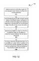
- FIG. 12is a flow diagram illustratively depicting an exemplary process flow 160 for forming a microelectronic device 100 for having a circuit structure 110 , as previously described.
- FIG. 12is further described with simultaneous reference to FIGS. 1-1 through 12 .
- a first conductive layer 101may be obtained for providing a lower interior surface 104 of a circuit structure 110 .
- a plurality of wire bond wires 108may be interconnected to an upper surface 105 of first conductive layer 101 , namely lower interior surface 104 of circuit structure 110 .
- Such plurality of wire bond wires 108may be spaced apart from one another by a distance d for providing at least one side of a circuit structure 110 .
- a dielectric layer 123may be deposited on upper surface 105 of first conductive layer 101 for providing a dielectric signal medium for circuit structure 110 .
- dielectric materialsthat are commonly used for dielectric signal mediums include mold compounds, such as a G770 material for example.
- a second or upper conductive layernamely cover 121
- cover 121may be formed for providing an upper interior surface 122 of circuit structure 110 opposite lower interior surface 104 .
- Cover 121may be interconnected to upper ends 111 of such a plurality of wire bond wires 108 .
Landscapes
- Engineering & Computer Science (AREA)
- Microelectronics & Electronic Packaging (AREA)
- Manufacturing & Machinery (AREA)
- Physics & Mathematics (AREA)
- Electromagnetism (AREA)
- Waveguides (AREA)
- Optical Integrated Circuits (AREA)
Abstract
Description
Claims (12)
Priority Applications (3)
| Application Number | Priority Date | Filing Date | Title |
|---|---|---|---|
| US15/387,278US10299368B2 (en) | 2016-12-21 | 2016-12-21 | Surface integrated waveguides and circuit structures therefor |
| PCT/US2017/064437WO2018118393A1 (en) | 2016-12-21 | 2017-12-04 | Surface integrated waveguides and circuit structures therefor |
| EP17882348.0AEP3560026A4 (en) | 2016-12-21 | 2017-12-04 | Surface integrated waveguides and circuit structures therefor |
Applications Claiming Priority (1)
| Application Number | Priority Date | Filing Date | Title |
|---|---|---|---|
| US15/387,278US10299368B2 (en) | 2016-12-21 | 2016-12-21 | Surface integrated waveguides and circuit structures therefor |
Publications (2)
| Publication Number | Publication Date |
|---|---|
| US20180177041A1 US20180177041A1 (en) | 2018-06-21 |
| US10299368B2true US10299368B2 (en) | 2019-05-21 |
Family
ID=62562867
Family Applications (1)
| Application Number | Title | Priority Date | Filing Date |
|---|---|---|---|
| US15/387,278ActiveUS10299368B2 (en) | 2016-12-21 | 2016-12-21 | Surface integrated waveguides and circuit structures therefor |
Country Status (3)
| Country | Link |
|---|---|
| US (1) | US10299368B2 (en) |
| EP (1) | EP3560026A4 (en) |
| WO (1) | WO2018118393A1 (en) |
Cited By (4)
| Publication number | Priority date | Publication date | Assignee | Title |
|---|---|---|---|---|
| US20200014118A1 (en)* | 2018-07-06 | 2020-01-09 | City University Of Hong Kong | Waveguide fed open slot antenna |
| US10879616B2 (en)* | 2018-08-30 | 2020-12-29 | University Of Electronic Science And Technology Of China | Shared-aperture antenna |
| US20210265723A1 (en)* | 2018-07-24 | 2021-08-26 | Samsung Electronics Co., Ltd. | Antenna device |
| US20220349987A1 (en)* | 2021-04-29 | 2022-11-03 | Veoneer Us, Inc. | Platformed post arrays for waveguides and related sensor assemblies |
Families Citing this family (9)
| Publication number | Priority date | Publication date | Assignee | Title |
|---|---|---|---|---|
| CN110931962B (en)* | 2018-09-20 | 2021-08-24 | 佛山市南海微波通讯设备有限公司 | High-isolation low-profile dual-polarized antenna applied to WLAN |
| CN109361043A (en)* | 2018-10-25 | 2019-02-19 | 北京无线电测量研究所 | Ka wave band substrate integrated waveguide isolator |
| CN109462000B (en)* | 2018-11-06 | 2020-10-09 | 上海航天计算机技术研究所 | Multi-layer substrate integrated waveguide third-order filtering power divider |
| CN110277621A (en)* | 2019-06-22 | 2019-09-24 | 南京理工大学 | Filter power splitter based on substrate integrated waveguide |
| US10856408B1 (en) | 2019-07-03 | 2020-12-01 | City University Of Hong Kong | Substrate-integrated device and method for making the same |
| JP6905608B2 (en)* | 2019-07-12 | 2021-07-21 | 株式会社フジクラ | Post wall waveguide and filter module |
| CN111293439B (en)* | 2019-12-30 | 2022-08-16 | 扬州船用电子仪器研究所(中国船舶重工集团公司第七二三研究所) | Millimeter wave low sidelobe waveguide slot array antenna |
| CN112086717B (en)* | 2020-09-07 | 2021-08-06 | 郑州宇林电子科技有限公司 | Capacitive patch loaded dual-mode substrate integrated waveguide band-pass filter |
| US20230352841A1 (en)* | 2022-05-02 | 2023-11-02 | Texas Instruments Incorporated | Wireless system package |
Citations (794)
| Publication number | Priority date | Publication date | Assignee | Title |
|---|---|---|---|---|
| US2230663A (en) | 1940-01-18 | 1941-02-04 | Alden Milton | Electric contact and wire assembly mechanism |
| US3289452A (en) | 1963-07-23 | 1966-12-06 | Siemens Ag | Method and device for bonding a contact wire to a semiconductor member |
| US3358897A (en) | 1964-03-31 | 1967-12-19 | Tempress Res Co | Electric lead wire bonding tools |
| US3430835A (en) | 1966-06-07 | 1969-03-04 | Westinghouse Electric Corp | Wire bonding apparatus for microelectronic components |
| US3623649A (en) | 1969-06-09 | 1971-11-30 | Gen Motors Corp | Wedge bonding tool for the attachment of semiconductor leads |
| US3795037A (en) | 1970-05-05 | 1974-03-05 | Int Computers Ltd | Electrical connector devices |
| US3900153A (en) | 1972-06-13 | 1975-08-19 | Licentia Gmbh | Formation of solder layers |
| JPS5150661A (en) | 1974-10-30 | 1976-05-04 | Hitachi Ltd | |
| US4067104A (en) | 1977-02-24 | 1978-01-10 | Rockwell International Corporation | Method of fabricating an array of flexible metallic interconnects for coupling microelectronics components |
| US4072816A (en) | 1976-12-13 | 1978-02-07 | International Business Machines Corporation | Integrated circuit package |
| US4213556A (en) | 1978-10-02 | 1980-07-22 | General Motors Corporation | Method and apparatus to detect automatic wire bonder failure |
| US4327860A (en) | 1980-01-03 | 1982-05-04 | Kulicke And Soffa Ind. Inc. | Method of making slack free wire interconnections |
| US4422568A (en) | 1981-01-12 | 1983-12-27 | Kulicke And Soffa Industries, Inc. | Method of making constant bonding wire tail lengths |
| US4437604A (en) | 1982-03-15 | 1984-03-20 | Kulicke & Soffa Industries, Inc. | Method of making fine wire interconnections |
| JPS59189069A (en) | 1983-04-12 | 1984-10-26 | Alps Electric Co Ltd | Device and method for coating solder on terminal |
| JPS61125062A (en) | 1984-11-22 | 1986-06-12 | Hitachi Ltd | Method and device for attaching pin |
| US4604644A (en) | 1985-01-28 | 1986-08-05 | International Business Machines Corporation | Solder interconnection structure for joining semiconductor devices to substrates that have improved fatigue life, and process for making |
| US4642889A (en) | 1985-04-29 | 1987-02-17 | Amp Incorporated | Compliant interconnection and method therefor |
| US4667267A (en) | 1985-01-22 | 1987-05-19 | Rogers Corporation | Decoupling capacitor for pin grid array package |
| JPS62158338A (en) | 1985-12-28 | 1987-07-14 | Tanaka Denshi Kogyo Kk | semiconductor equipment |
| US4695870A (en) | 1986-03-27 | 1987-09-22 | Hughes Aircraft Company | Inverted chip carrier |
| JPS62226307A (en) | 1986-03-28 | 1987-10-05 | Toshiba Corp | robot equipment |
| US4716049A (en) | 1985-12-20 | 1987-12-29 | Hughes Aircraft Company | Compressive pedestal for microminiature connections |
| US4725692A (en) | 1985-05-24 | 1988-02-16 | Hitachi, Ltd. | Electronic device and lead frame used thereon |
| US4771930A (en) | 1986-06-30 | 1988-09-20 | Kulicke And Soffa Industries Inc. | Apparatus for supplying uniform tail lengths |
| US4793814A (en) | 1986-07-21 | 1988-12-27 | Rogers Corporation | Electrical circuit board interconnect |
| JPS6412769A (en) | 1987-07-07 | 1989-01-17 | Sony Corp | Correction circuit for image distortion |
| US4804132A (en) | 1987-08-28 | 1989-02-14 | Difrancesco Louis | Method for cold bonding |
| JPS6471162A (en) | 1987-09-11 | 1989-03-16 | Hitachi Ltd | Semiconductor device |
| JPH01118364A (en) | 1987-10-30 | 1989-05-10 | Fujitsu Ltd | Preliminary solder dipping method |
| US4845354A (en) | 1988-03-08 | 1989-07-04 | International Business Machines Corporation | Process control for laser wire bonding |
| US4867267A (en) | 1987-10-14 | 1989-09-19 | Industrial Research Products, Inc. | Hearing aid transducer |
| US4902600A (en) | 1986-10-14 | 1990-02-20 | Fuji Photo Film Co., Ltd. | Light-sensitive material comprising light-sensitive layer provided on support wherein the light-sensitive layer and support have specified pH values |
| US4924353A (en) | 1985-12-20 | 1990-05-08 | Hughes Aircraft Company | Connector system for coupling to an integrated circuit chip |
| US4925083A (en) | 1987-02-06 | 1990-05-15 | Emhart Deutschland Gmbh | Ball bonding method and apparatus for performing the method |
| US4955523A (en) | 1986-12-17 | 1990-09-11 | Raychem Corporation | Interconnection of electronic components |
| US4975079A (en) | 1990-02-23 | 1990-12-04 | International Business Machines Corp. | Connector assembly for chip testing |
| US4982265A (en) | 1987-06-24 | 1991-01-01 | Hitachi, Ltd. | Semiconductor integrated circuit device and method of manufacturing the same |
| US4998885A (en) | 1989-10-27 | 1991-03-12 | International Business Machines Corporation | Elastomeric area array interposer |
| US4999472A (en) | 1990-03-12 | 1991-03-12 | Neinast James E | Electric arc system for ablating a surface coating |
| US5067007A (en) | 1988-06-13 | 1991-11-19 | Hitachi, Ltd. | Semiconductor device having leads for mounting to a surface of a printed circuit board |
| US5067382A (en) | 1990-11-02 | 1991-11-26 | Cray Computer Corporation | Method and apparatus for notching a lead wire attached to an IC chip to facilitate severing the wire |
| US5083697A (en) | 1990-02-14 | 1992-01-28 | Difrancesco Louis | Particle-enhanced joining of metal surfaces |
| US5095187A (en) | 1989-12-20 | 1992-03-10 | Raychem Corporation | Weakening wire supplied through a wire bonder |
| US5133495A (en) | 1991-08-12 | 1992-07-28 | International Business Machines Corporation | Method of bonding flexible circuit to circuitized substrate to provide electrical connection therebetween |
| US5138438A (en) | 1987-06-24 | 1992-08-11 | Akita Electronics Co. Ltd. | Lead connections means for stacked tab packaged IC chips |
| US5148265A (en) | 1990-09-24 | 1992-09-15 | Ist Associates, Inc. | Semiconductor chip assemblies with fan-in leads |
| US5148266A (en) | 1990-09-24 | 1992-09-15 | Ist Associates, Inc. | Semiconductor chip assemblies having interposer and flexible lead |
| JPH04346436A (en) | 1991-05-24 | 1992-12-02 | Fujitsu Ltd | Bump manufacturing method and bump manufacturing equipment |
| US5186381A (en) | 1991-04-16 | 1993-02-16 | Samsung Electronics, Co., Ltd. | Semiconductor chip bonding process |
| US5189505A (en) | 1989-11-08 | 1993-02-23 | Hewlett-Packard Company | Flexible attachment flip-chip assembly |
| US5196726A (en) | 1990-01-23 | 1993-03-23 | Sumitomo Electric Industries, Ltd. | Substrate for packaging a semiconductor device having particular terminal and bump structure |
| US5203075A (en) | 1991-08-12 | 1993-04-20 | Inernational Business Machines | Method of bonding flexible circuit to cicuitized substrate to provide electrical connection therebetween using different solders |
| US5214308A (en) | 1990-01-23 | 1993-05-25 | Sumitomo Electric Industries, Ltd. | Substrate for packaging a semiconductor device |
| US5220489A (en) | 1991-10-11 | 1993-06-15 | Motorola, Inc. | Multicomponent integrated circuit package |
| US5222014A (en) | 1992-03-02 | 1993-06-22 | Motorola, Inc. | Three-dimensional multi-chip pad array carrier |
| US5238173A (en) | 1991-12-04 | 1993-08-24 | Kaijo Corporation | Wire bonding misattachment detection apparatus and that detection method in a wire bonder |
| US5241456A (en) | 1990-07-02 | 1993-08-31 | General Electric Company | Compact high density interconnect structure |
| US5241454A (en) | 1992-01-22 | 1993-08-31 | International Business Machines Corporation | Mutlilayered flexible circuit package |
| US5316788A (en) | 1991-07-26 | 1994-05-31 | International Business Machines Corporation | Applying solder to high density substrates |
| US5340771A (en) | 1993-03-18 | 1994-08-23 | Lsi Logic Corporation | Techniques for providing high I/O count connections to semiconductor dies |
| US5346118A (en) | 1993-09-28 | 1994-09-13 | At&T Bell Laboratories | Surface mount solder assembly of leadless integrated circuit packages to substrates |
| JPH06268101A (en) | 1993-03-17 | 1994-09-22 | Hitachi Ltd | Semiconductor device and manufacturing method thereof, electronic device, lead frame and mounting substrate |
| JPH06268015A (en) | 1993-03-10 | 1994-09-22 | Nec Corp | Integrated circuit |
| JPH06333931A (en) | 1993-05-20 | 1994-12-02 | Nippondenso Co Ltd | Manufacture of fine electrode of semiconductor device |
| US5371654A (en) | 1992-10-19 | 1994-12-06 | International Business Machines Corporation | Three dimensional high performance interconnection package |
| US5397997A (en) | 1991-08-23 | 1995-03-14 | Nchip, Inc. | Burn-in technologies for unpackaged integrated circuits |
| JPH07122787A (en) | 1993-09-06 | 1995-05-12 | Sharp Corp | Structure of chip component type LED and manufacturing method thereof |
| US5438224A (en) | 1992-04-23 | 1995-08-01 | Motorola, Inc. | Integrated circuit package having a face-to-face IC chip arrangement |
| US5455390A (en) | 1994-02-01 | 1995-10-03 | Tessera, Inc. | Microelectronics unit mounting with multiple lead bonding |
| US5468995A (en) | 1994-07-05 | 1995-11-21 | Motorola, Inc. | Semiconductor device having compliant columnar electrical connections |
| US5476211A (en) | 1993-11-16 | 1995-12-19 | Form Factor, Inc. | Method of manufacturing electrical contacts, using a sacrificial member |
| US5494667A (en) | 1992-06-04 | 1996-02-27 | Kabushiki Kaisha Hayahibara | Topically applied hair restorer containing pine extract |
| US5495667A (en) | 1994-11-07 | 1996-03-05 | Micron Technology, Inc. | Method for forming contact pins for semiconductor dice and interconnects |
| US5518964A (en) | 1994-07-07 | 1996-05-21 | Tessera, Inc. | Microelectronic mounting with multiple lead deformation and bonding |
| WO1996015458A1 (en) | 1994-11-15 | 1996-05-23 | Formfactor, Inc. | Probe card assembly and kit, and methods of using same |
| US5536909A (en) | 1992-07-24 | 1996-07-16 | Tessera, Inc. | Semiconductor connection components and methods with releasable lead support |
| US5541567A (en) | 1994-10-17 | 1996-07-30 | International Business Machines Corporation | Coaxial vias in an electronic substrate |
| US5571428A (en) | 1992-01-17 | 1996-11-05 | Hitachi, Ltd. | Semiconductor leadframe and its production method and plastic encapsulated semiconductor device |
| US5578869A (en) | 1994-03-29 | 1996-11-26 | Olin Corporation | Components for housing an integrated circuit device |
| US5615824A (en) | 1994-06-07 | 1997-04-01 | Tessera, Inc. | Soldering with resilient contacts |
| JPH09505439A (en) | 1993-11-16 | 1997-05-27 | フォームファクター・インコーポレイテッド | Contact structure, interposer, semiconductor assembly and method for interconnection |
| US5656550A (en) | 1994-08-24 | 1997-08-12 | Fujitsu Limited | Method of producing a semicondutor device having a lead portion with outer connecting terminal |
| US5659952A (en) | 1994-09-20 | 1997-08-26 | Tessera, Inc. | Method of fabricating compliant interface for semiconductor chip |
| US5679977A (en) | 1990-09-24 | 1997-10-21 | Tessera, Inc. | Semiconductor chip assemblies, methods of making same and components for same |
| US5688716A (en) | 1994-07-07 | 1997-11-18 | Tessera, Inc. | Fan-out semiconductor chip assembly |
| US5718361A (en) | 1995-11-21 | 1998-02-17 | International Business Machines Corporation | Apparatus and method for forming mold for metallic material |
| JPH1065054A (en) | 1996-06-20 | 1998-03-06 | Lg Semicon Co Ltd | Chip size semiconductor package and its manufacturing method |
| US5726493A (en) | 1994-06-13 | 1998-03-10 | Fujitsu Limited | Semiconductor device and semiconductor device unit having ball-grid-array type package structure |
| US5731709A (en) | 1996-01-26 | 1998-03-24 | Motorola, Inc. | Method for testing a ball grid array semiconductor device and a device for such testing |
| US5736780A (en) | 1995-11-07 | 1998-04-07 | Shinko Electric Industries Co., Ltd. | Semiconductor device having circuit pattern along outer periphery of sealing resin and related processes |
| US5736785A (en) | 1996-12-20 | 1998-04-07 | Industrial Technology Research Institute | Semiconductor package for improving the capability of spreading heat |
| JPH10135221A (en) | 1996-10-29 | 1998-05-22 | Taiyo Yuden Co Ltd | Bump-forming method |
| JPH10135220A (en) | 1996-10-29 | 1998-05-22 | Taiyo Yuden Co Ltd | Bump-forming method |
| US5766987A (en) | 1995-09-22 | 1998-06-16 | Tessera, Inc. | Microelectronic encapsulation methods and equipment |
| US5802699A (en) | 1994-06-07 | 1998-09-08 | Tessera, Inc. | Methods of assembling microelectronic assembly with socket for engaging bump leads |
| US5811982A (en) | 1995-11-27 | 1998-09-22 | International Business Machines Corporation | High density cantilevered probe for electronic devices |
| US5831836A (en) | 1992-01-30 | 1998-11-03 | Lsi Logic | Power plane for semiconductor device |
| US5830389A (en) | 1990-02-09 | 1998-11-03 | Toranaga Technologies, Inc. | Electrically conductive compositions and methods for the preparation and use thereof |
| US5839191A (en) | 1997-01-24 | 1998-11-24 | Unisys Corporation | Vibrating template method of placing solder balls on the I/O pads of an integrated circuit package |
| US5854507A (en) | 1998-07-21 | 1998-12-29 | Hewlett-Packard Company | Multiple chip assembly |
| US5874781A (en) | 1995-08-16 | 1999-02-23 | Micron Technology, Inc. | Angularly offset stacked die multichip device and method of manufacture |
| JPH1174295A (en) | 1997-08-29 | 1999-03-16 | Citizen Electron Co Ltd | Method for packaging electronic circuit |
| US5898991A (en) | 1997-01-16 | 1999-05-04 | International Business Machines Corporation | Methods of fabrication of coaxial vias and magnetic devices |
| JPH11135663A (en) | 1997-10-28 | 1999-05-21 | Nec Kyushu Ltd | Molded bga type semiconductor device and manufacture thereof |
| JPH11145323A (en) | 1997-11-05 | 1999-05-28 | Shinko Electric Ind Co Ltd | Semiconductor device and manufacturing method therefor |
| US5908317A (en) | 1996-03-11 | 1999-06-01 | Anam Semiconductor Inc. | Method of forming chip bumps of bump chip scale semiconductor package |
| EP0920058A2 (en) | 1997-11-25 | 1999-06-02 | Matsushita Electric Industrial Co., Ltd. | Circuit component built-in module and method for producing the same |
| US5912505A (en) | 1995-11-07 | 1999-06-15 | Sumitomo Metal (Smi) Electronics Devices, Inc. | Semiconductor package and semiconductor device |
| US5948533A (en) | 1990-02-09 | 1999-09-07 | Ormet Corporation | Vertically interconnected electronic assemblies and compositions useful therefor |
| US5953624A (en) | 1997-01-13 | 1999-09-14 | Kabushiki Kaisha Shinkawa | Bump forming method |
| JPH11251350A (en) | 1998-02-27 | 1999-09-17 | Fuji Xerox Co Ltd | Method and apparatus for forming bump |
| JPH11260856A (en) | 1998-03-11 | 1999-09-24 | Matsushita Electron Corp | Semiconductor device and its manufacture and mounting structure of the device |
| US5973391A (en) | 1997-12-11 | 1999-10-26 | Read-Rite Corporation | Interposer with embedded circuitry and method for using the same to package microelectronic units |
| US5971253A (en) | 1995-07-31 | 1999-10-26 | Tessera, Inc. | Microelectronic component mounting with deformable shell terminals |
| US5977640A (en) | 1998-06-26 | 1999-11-02 | International Business Machines Corporation | Highly integrated chip-on-chip packaging |
| US5977618A (en) | 1992-07-24 | 1999-11-02 | Tessera, Inc. | Semiconductor connection components and methods with releasable lead support |
| JPH11317476A (en) | 1997-10-02 | 1999-11-16 | Internatl Business Mach Corp <Ibm> | Angled flying lead wire bonding process |
| US5989936A (en) | 1994-07-07 | 1999-11-23 | Tessera, Inc. | Microelectronic assembly fabrication with terminal formation from a conductive layer |
| US5994152A (en) | 1996-02-21 | 1999-11-30 | Formfactor, Inc. | Fabricating interconnects and tips using sacrificial substrates |
| US6000126A (en) | 1996-03-29 | 1999-12-14 | General Dynamics Information Systems, Inc. | Method and apparatus for connecting area grid arrays to printed wire board |
| US6002168A (en) | 1997-11-25 | 1999-12-14 | Tessera, Inc. | Microelectronic component with rigid interposer |
| US6032359A (en) | 1997-08-21 | 2000-03-07 | Carroll; Keith C. | Method of manufacturing a female electrical connector in a single layer flexible polymeric dielectric film substrate |
| US6038136A (en) | 1997-10-29 | 2000-03-14 | Hestia Technologies, Inc. | Chip package with molded underfill |
| US6052287A (en) | 1997-12-09 | 2000-04-18 | Sandia Corporation | Silicon ball grid array chip carrier |
| US6054756A (en) | 1992-07-24 | 2000-04-25 | Tessera, Inc. | Connection components with frangible leads and bus |
| US6054337A (en) | 1996-12-13 | 2000-04-25 | Tessera, Inc. | Method of making a compliant multichip package |
| US6077380A (en) | 1995-06-30 | 2000-06-20 | Microfab Technologies, Inc. | Method of forming an adhesive connection |
| US6117694A (en) | 1994-07-07 | 2000-09-12 | Tessera, Inc. | Flexible lead structures and methods of making same |
| KR100265563B1 (en) | 1998-06-29 | 2000-09-15 | 김영환 | Ball grid array package and fabricating method thereof |
| US6121676A (en) | 1996-12-13 | 2000-09-19 | Tessera, Inc. | Stacked microelectronic assembly and method therefor |
| US6124546A (en) | 1997-12-03 | 2000-09-26 | Advanced Micro Devices, Inc. | Integrated circuit chip package and method of making the same |
| US6133072A (en) | 1996-12-13 | 2000-10-17 | Tessera, Inc. | Microelectronic connector with planar elastomer sockets |
| US6145733A (en) | 1996-05-07 | 2000-11-14 | Herbert Streckfuss Gmbh | Process for soldering electronic components to a printed circuit board |
| JP2000323516A (en) | 1999-05-14 | 2000-11-24 | Fujitsu Ltd | Wiring board manufacturing method, wiring board and semiconductor device |
| US6157080A (en) | 1997-11-06 | 2000-12-05 | Sharp Kabushiki Kaisha | Semiconductor device using a chip scale package |
| US6158647A (en) | 1998-09-29 | 2000-12-12 | Micron Technology, Inc. | Concave face wire bond capillary |
| US6164523A (en) | 1998-07-01 | 2000-12-26 | Semiconductor Components Industries, Llc | Electronic component and method of manufacture |
| US6168965B1 (en) | 1999-08-12 | 2001-01-02 | Tower Semiconductor Ltd. | Method for making backside illuminated image sensor |
| US6177636B1 (en) | 1994-12-29 | 2001-01-23 | Tessera, Inc. | Connection components with posts |
| US6180881B1 (en) | 1998-05-05 | 2001-01-30 | Harlan Ruben Isaak | Chip stack and method of making same |
| US6194250B1 (en) | 1998-09-14 | 2001-02-27 | Motorola, Inc. | Low-profile microelectronic package |
| US6202297B1 (en) | 1995-08-28 | 2001-03-20 | Tessera, Inc. | Socket for engaging bump leads on a microelectronic device and methods therefor |
| US6208024B1 (en) | 1996-12-12 | 2001-03-27 | Tessera, Inc. | Microelectronic mounting with multiple lead deformation using restraining straps |
| US6206273B1 (en) | 1999-02-17 | 2001-03-27 | International Business Machines Corporation | Structures and processes to create a desired probetip contact geometry on a wafer test probe |
| US6211572B1 (en) | 1995-10-31 | 2001-04-03 | Tessera, Inc. | Semiconductor chip package with fan-in leads |
| US6211574B1 (en) | 1999-04-16 | 2001-04-03 | Advanced Semiconductor Engineering Inc. | Semiconductor package with wire protection and method therefor |
| US6225688B1 (en) | 1997-12-11 | 2001-05-01 | Tessera, Inc. | Stacked microelectronic assembly and method therefor |
| US6238949B1 (en) | 1999-06-18 | 2001-05-29 | National Semiconductor Corporation | Method and apparatus for forming a plastic chip on chip package module |
| KR20010061849A (en) | 1999-12-29 | 2001-07-07 | 박종섭 | Wafer level package |
| US6258625B1 (en) | 1999-05-18 | 2001-07-10 | International Business Machines Corporation | Method of interconnecting electronic components using a plurality of conductive studs |
| US6260264B1 (en) | 1997-12-08 | 2001-07-17 | 3M Innovative Properties Company | Methods for making z-axis electrical connections |
| US6262482B1 (en) | 1998-02-03 | 2001-07-17 | Oki Electric Industry Co., Ltd. | Semiconductor device |
| JP2001196407A (en) | 2000-01-14 | 2001-07-19 | Seiko Instruments Inc | Semiconductor device and method of forming the same |
| US6268662B1 (en) | 1998-10-14 | 2001-07-31 | Texas Instruments Incorporated | Wire bonded flip-chip assembly of semiconductor devices |
| US6295729B1 (en) | 1992-10-19 | 2001-10-02 | International Business Machines Corporation | Angled flying lead wire bonding process |
| US6303997B1 (en) | 1998-04-08 | 2001-10-16 | Anam Semiconductor, Inc. | Thin, stackable semiconductor packages |
| KR20010094894A (en) | 2000-04-07 | 2001-11-03 | 마이클 디. 오브라이언 | Semiconductor package and its manufacturing method |
| US6316838B1 (en) | 1999-10-29 | 2001-11-13 | Fujitsu Limited | Semiconductor device |
| US20010042925A1 (en) | 1998-05-12 | 2001-11-22 | Noriaki Yamamoto | Wire bonding method and apparatus, and semiconductor device |
| JP2001326236A (en) | 2000-05-12 | 2001-11-22 | Nec Kyushu Ltd | Manufacturing method of semiconductor device |
| US6329224B1 (en) | 1998-04-28 | 2001-12-11 | Tessera, Inc. | Encapsulation of microelectronic assemblies |
| US6332270B2 (en) | 1998-11-23 | 2001-12-25 | International Business Machines Corporation | Method of making high density integral test probe |
| WO2002013256A1 (en) | 2000-08-08 | 2002-02-14 | Telefonaktiebolaget Lm Ericsson (Publ) | Method of securing solder balls and any components fixed to one and the same side of a substrate |
| JP2002050871A (en) | 2000-08-02 | 2002-02-15 | Casio Comput Co Ltd | Build-up circuit board and method of manufacturing the same |
| US6358627B2 (en) | 1999-04-03 | 2002-03-19 | International Business Machines Corporation | Rolling ball connector |
| US6362525B1 (en) | 1999-11-09 | 2002-03-26 | Cypress Semiconductor Corp. | Circuit structure including a passive element formed within a grid array substrate and method for making the same |
| US6376769B1 (en) | 1999-05-18 | 2002-04-23 | Amerasia International Technology, Inc. | High-density electronic package, and method for making same |
| US6388333B1 (en) | 1999-11-30 | 2002-05-14 | Fujitsu Limited | Semiconductor device having protruding electrodes higher than a sealed portion |
| US6395199B1 (en) | 2000-06-07 | 2002-05-28 | Graftech Inc. | Process for providing increased conductivity to a material |
| US6399426B1 (en) | 1998-07-21 | 2002-06-04 | Miguel Albert Capote | Semiconductor flip-chip package and method for the fabrication thereof |
| US6407448B2 (en) | 1998-05-30 | 2002-06-18 | Hyundai Electronics Industries Co., Inc. | Stackable ball grid array semiconductor package and fabrication method thereof |
| US6407456B1 (en) | 1996-02-20 | 2002-06-18 | Micron Technology, Inc. | Multi-chip device utilizing a flip chip and wire bond assembly |
| US6410431B2 (en) | 1998-04-07 | 2002-06-25 | International Business Machines Corporation | Through-chip conductors for low inductance chip-to-chip integration and off-chip connections |
| US6413850B1 (en) | 1999-11-18 | 2002-07-02 | Hitachi, Ltd. | Method of forming bumps |
| KR20020058216A (en) | 2000-12-29 | 2002-07-12 | 마이클 디. 오브라이언 | Stacked semiconductor package and its manufacturing method |
| US20020125556A1 (en) | 2001-03-09 | 2002-09-12 | Oh Kwang Seok | Stacking structure of semiconductor chips and semiconductor package using it |
| US6458411B1 (en) | 2001-01-17 | 2002-10-01 | Aralight, Inc. | Method of making a mechanically compliant bump |
| JP2002289769A (en) | 2001-03-26 | 2002-10-04 | Matsushita Electric Ind Co Ltd | Stacked semiconductor device and method of manufacturing the same |
| US6469373B2 (en) | 2000-05-15 | 2002-10-22 | Kabushiki Kaisha Toshiba | Semiconductor apparatus with improved thermal and mechanical characteristic under-fill layer and manufacturing method therefor |
| US6469260B2 (en) | 2000-02-28 | 2002-10-22 | Shinko Electric Industries Co., Ltd. | Wiring boards, semiconductor devices and their production processes |
| US6472743B2 (en) | 2001-02-22 | 2002-10-29 | Siliconware Precision Industries, Co., Ltd. | Semiconductor package with heat dissipating structure |
| US6476503B1 (en) | 1999-08-12 | 2002-11-05 | Fujitsu Limited | Semiconductor device having columnar electrode and method of manufacturing same |
| US6476583B2 (en) | 2000-07-21 | 2002-11-05 | Jomahip, Llc | Automatic battery charging system for a battery back-up DC power supply |
| US6476506B1 (en) | 2001-09-28 | 2002-11-05 | Motorola, Inc. | Packaged semiconductor with multiple rows of bond pads and method therefor |
| US20020171152A1 (en) | 2001-05-18 | 2002-11-21 | Nec Corporation | Flip-chip-type semiconductor device and manufacturing method thereof |
| US6486545B1 (en) | 2001-07-26 | 2002-11-26 | Amkor Technology, Inc. | Pre-drilled ball grid array package |
| US6489182B2 (en) | 1999-03-09 | 2002-12-03 | Hynix Semiconductur, Inc. | Method of fabricating a wire arrayed chip size package |
| US6489676B2 (en) | 2000-12-04 | 2002-12-03 | Fujitsu Limited | Semiconductor device having an interconnecting post formed on an interposer within a sealing resin |
| US6495914B1 (en) | 1997-08-19 | 2002-12-17 | Hitachi, Ltd. | Multi-chip module structure having conductive blocks to provide electrical connection between conductors on first and second sides of a conductive base substrate |
| US20030006494A1 (en) | 2001-07-03 | 2003-01-09 | Lee Sang Ho | Thin profile stackable semiconductor package and method for manufacturing |
| US6507104B2 (en) | 2000-09-07 | 2003-01-14 | Siliconware Precision Industries Co., Ltd. | Semiconductor package with embedded heat-dissipating device |
| US6509639B1 (en) | 2001-07-27 | 2003-01-21 | Charles W. C. Lin | Three-dimensional stacked semiconductor package |
| US6515355B1 (en) | 1998-09-02 | 2003-02-04 | Micron Technology, Inc. | Passivation layer for packaged integrated circuits |
| US6514847B1 (en) | 1997-11-28 | 2003-02-04 | Sony Corporation | Method for making a semiconductor device |
| US6522018B1 (en) | 2000-05-16 | 2003-02-18 | Micron Technology, Inc. | Ball grid array chip packages having improved testing and stacking characteristics |
| US6531784B1 (en) | 2000-06-02 | 2003-03-11 | Amkor Technology, Inc. | Semiconductor package with spacer strips |
| US20030048108A1 (en) | 1993-04-30 | 2003-03-13 | Beaman Brian Samuel | Structural design and processes to control probe position accuracy in a wafer test probe assembly |
| US20030057544A1 (en) | 2001-09-13 | 2003-03-27 | Nathan Richard J. | Integrated assembly protocol |
| US6545228B2 (en) | 2000-09-05 | 2003-04-08 | Seiko Epson Corporation | Semiconductor device with a plurality of stacked boards and method of making |
| US6550666B2 (en) | 2001-08-21 | 2003-04-22 | Advanpack Solutions Pte Ltd | Method for forming a flip chip on leadframe semiconductor package |
| JP2003122611A (en) | 2001-10-11 | 2003-04-25 | Oki Electric Ind Co Ltd | Data providing method and server device |
| US6555918B2 (en) | 1997-09-29 | 2003-04-29 | Hitachi, Ltd. | Stacked semiconductor device including improved lead frame arrangement |
| US6560117B2 (en) | 2000-06-28 | 2003-05-06 | Micron Technology, Inc. | Packaged microelectronic die assemblies and methods of manufacture |
| US6563205B1 (en) | 1995-08-16 | 2003-05-13 | Micron Technology, Inc. | Angularly offset and recessed stacked die multichip device and method of manufacture |
| US6563217B2 (en) | 1998-06-30 | 2003-05-13 | Micron Technology, Inc. | Module assembly for stacked BGA packages |
| US20030094666A1 (en) | 2001-11-16 | 2003-05-22 | R-Tec Corporation | Interposer |
| US6573458B1 (en) | 1998-09-07 | 2003-06-03 | Ngk Spark Plug Co., Ltd. | Printed circuit board |
| US6578754B1 (en) | 2000-04-27 | 2003-06-17 | Advanpack Solutions Pte. Ltd. | Pillar connections for semiconductor chips and method of manufacture |
| JP2003174124A (en) | 2001-12-04 | 2003-06-20 | Sainekkusu:Kk | Method for forming external electrode of semiconductor device |
| US6581283B2 (en) | 1999-12-02 | 2003-06-24 | Kabushiki Kaisha Shinkawa | Method for forming pin-form wires and the like |
| US6581276B2 (en) | 2000-04-04 | 2003-06-24 | Amerasia International Technology, Inc. | Fine-pitch flexible connector, and method for making same |
| JP2003197668A (en) | 2001-12-10 | 2003-07-11 | Senmao Koochii Kofun Yugenkoshi | Bonding wire for semiconductor package and manufacturing method thereof |
| US20030162378A1 (en) | 2001-12-28 | 2003-08-28 | Seiko Epson Corporation | Bonding method and bonding apparatus |
| US6624653B1 (en) | 2000-08-28 | 2003-09-23 | Micron Technology, Inc. | Method and system for wafer level testing and burning-in semiconductor components |
| US6630730B2 (en) | 2000-04-28 | 2003-10-07 | Micron Technology, Inc. | Semiconductor device assemblies including interposers with dams protruding therefrom |
| US6639303B2 (en) | 1996-10-29 | 2003-10-28 | Tru-Si Technolgies, Inc. | Integrated circuits and methods for their fabrication |
| JP2003307897A (en) | 2001-10-16 | 2003-10-31 | Hokushin Ind Inc | Conductive blade |
| JP2003318327A (en) | 2002-04-22 | 2003-11-07 | Mitsui Chemicals Inc | Printed wiring board and stacked package |
| US6647310B1 (en) | 2000-05-30 | 2003-11-11 | Advanced Micro Devices, Inc. | Temperature control of an integrated circuit |
| US6650013B2 (en) | 2001-08-29 | 2003-11-18 | Micron Technology, Inc. | Method of manufacturing wire bonded microelectronic device assemblies |
| US6653170B1 (en) | 2001-02-06 | 2003-11-25 | Charles W. C. Lin | Semiconductor chip assembly with elongated wire ball bonded to chip and electrolessly plated to support circuit |
| US6684007B2 (en) | 1998-10-09 | 2004-01-27 | Fujitsu Limited | Optical coupling structures and the fabrication processes |
| JP2004031754A (en) | 2002-06-27 | 2004-01-29 | Oki Electric Ind Co Ltd | Laminated multi-chip package, method of manufacturing chip constituting the same, and wire bonding method |
| US6686268B2 (en) | 1998-04-06 | 2004-02-03 | Micron Technology, Inc. | Method of forming overmolded chip scale package and resulting product |
| US6687988B1 (en) | 1999-10-20 | 2004-02-10 | Kabushiki Kaisha Shinkawa | Method for forming pin-form wires and the like |
| JP2004047702A (en) | 2002-07-11 | 2004-02-12 | Toshiba Corp | Semiconductor device stack module |
| JP2004048048A (en) | 2003-09-16 | 2004-02-12 | Oki Electric Ind Co Ltd | Semiconductor device and method of manufacturing the same |
| US6696305B2 (en) | 2002-01-23 | 2004-02-24 | Via Technologies, Inc. | Metal post manufacturing method |
| US20040041757A1 (en) | 2002-09-04 | 2004-03-04 | Ming-Hsiang Yang | Light emitting diode display module with high heat-dispersion and the substrate thereof |
| US6720783B2 (en) | 1999-06-25 | 2004-04-13 | Enplas Corporation | IC socket and spring means of IC socket |
| US6730544B1 (en) | 1999-12-20 | 2004-05-04 | Amkor Technology, Inc. | Stackable semiconductor package and method for manufacturing same |
| US6733711B2 (en) | 2000-09-01 | 2004-05-11 | General Electric Company | Plastic packaging of LED arrays |
| US6734539B2 (en) | 2000-12-27 | 2004-05-11 | Lucent Technologies Inc. | Stacked module package |
| US6734542B2 (en) | 2000-12-27 | 2004-05-11 | Matsushita Electric Industrial Co., Ltd. | Component built-in module and method for producing the same |
| US6741085B1 (en) | 1993-11-16 | 2004-05-25 | Formfactor, Inc. | Contact carriers (tiles) for populating larger substrates with spring contacts |
| US6740981B2 (en) | 2000-03-27 | 2004-05-25 | Kabushiki Kaisha, Toshiba | Semiconductor device including memory unit and semiconductor module including memory units |
| US6740980B2 (en) | 2002-07-04 | 2004-05-25 | Renesas Technology Corp. | Semiconductor device |
| US6746894B2 (en) | 2001-03-30 | 2004-06-08 | Micron Technology, Inc. | Ball grid array interposer, packages and methods |
| JP2004172157A (en) | 2002-11-15 | 2004-06-17 | Shinko Electric Ind Co Ltd | Semiconductor package and package stack semiconductor device |
| US6754407B2 (en) | 2001-06-26 | 2004-06-22 | Intel Corporation | Flip-chip package integrating optical and electrical devices and coupling to a waveguide on a board |
| US6756663B2 (en) | 1997-09-16 | 2004-06-29 | Matsushita Electric Industrial Co., Ltd. | Semiconductor device including wiring board with three dimensional wiring pattern |
| US6756252B2 (en) | 2002-07-17 | 2004-06-29 | Texas Instrument Incorporated | Multilayer laser trim interconnect method |
| US6759738B1 (en) | 1995-08-02 | 2004-07-06 | International Business Machines Corporation | Systems interconnected by bumps of joining material |
| US6762078B2 (en) | 1999-05-20 | 2004-07-13 | Amkor Technology, Inc. | Semiconductor package having semiconductor chip within central aperture of substrate |
| JP2004200316A (en) | 2002-12-17 | 2004-07-15 | Shinko Electric Ind Co Ltd | Semiconductor device |
| US6765287B1 (en) | 2001-07-27 | 2004-07-20 | Charles W. C. Lin | Three-dimensional stacked semiconductor package |
| US6774317B2 (en) | 1994-12-29 | 2004-08-10 | Tessera, Inc. | Connection components with posts |
| US6774494B2 (en) | 2001-03-22 | 2004-08-10 | Renesas Technology Corp. | Semiconductor device and manufacturing method thereof |
| US6774473B1 (en) | 1999-07-30 | 2004-08-10 | Ming-Tung Shen | Semiconductor chip module |
| US6774467B2 (en) | 2000-03-24 | 2004-08-10 | Shinko Electric Industries Co., Ltd | Semiconductor device and process of production of same |
| US6777787B2 (en) | 2000-03-28 | 2004-08-17 | Rohm Co., Ltd. | Semiconductor device with warp preventing board joined thereto |
| US6778406B2 (en) | 1993-11-16 | 2004-08-17 | Formfactor, Inc. | Resilient contact structures for interconnecting electronic devices |
| US6780746B2 (en) | 2000-06-02 | 2004-08-24 | Micron Technology, Inc. | Method for fabricating a chip scale package using wafer level processing and devices resulting therefrom |
| US6787926B2 (en) | 2001-09-05 | 2004-09-07 | Taiwan Semiconductor Manufacturing Co., Ltd | Wire stitch bond on an integrated circuit bond pad and method of making the same |
| WO2004077525A2 (en) | 2003-02-25 | 2004-09-10 | Tessera, Inc. | Ball grid array with bumps |
| US6790757B1 (en) | 1999-12-20 | 2004-09-14 | Agere Systems Inc. | Wire bonding method for copper interconnects in semiconductor devices |
| US6800941B2 (en) | 2001-12-31 | 2004-10-05 | Megic Corporation | Integrated chip package structure using ceramic substrate and method of manufacturing the same |
| JP2004281514A (en) | 2003-03-13 | 2004-10-07 | Denso Corp | Wire bonding method |
| US6812575B2 (en) | 2000-08-29 | 2004-11-02 | Nec Corporation | Semiconductor device |
| US6815257B2 (en) | 2002-03-18 | 2004-11-09 | Samsung Electro-Mechanics Co., Ltd. | Chip scale package and method of fabricating the same |
| JP2004319892A (en) | 2003-04-18 | 2004-11-11 | Renesas Technology Corp | Manufacturing method of semiconductor device |
| JP2004327855A (en) | 2003-04-25 | 2004-11-18 | Nec Electronics Corp | Semiconductor device and its manufacturing method |
| JP2004327856A (en) | 2003-04-25 | 2004-11-18 | North:Kk | Method for manufacturing wiring circuit board and method for manufacturing semiconductor integrated circuit device using the wiring circuit board |
| US6825552B2 (en) | 2001-05-09 | 2004-11-30 | Tessera, Inc. | Connection components with anisotropic conductive material interconnection |
| JP2004343030A (en) | 2003-03-31 | 2004-12-02 | North:Kk | Wiring circuit board, manufacturing method thereof, circuit module provided with this wiring circuit board |
| US6828668B2 (en) | 1994-07-07 | 2004-12-07 | Tessera, Inc. | Flexible lead structures and methods of making same |
| US6828665B2 (en) | 2002-10-18 | 2004-12-07 | Siliconware Precision Industries Co., Ltd. | Module device of stacked semiconductor packages and method for fabricating the same |
| US20040262728A1 (en) | 2003-06-30 | 2004-12-30 | Sterrett Terry L. | Modular device assemblies |
| JP2005011874A (en) | 2003-06-17 | 2005-01-13 | Matsushita Electric Ind Co Ltd | Semiconductor built-in module and manufacturing method thereof |
| US6844619B2 (en) | 2000-12-01 | 2005-01-18 | Nec Corporation | Compact semiconductor device capable of mounting a plurality of semiconductor chips with high density and method of manufacturing the same |
| JP2005033141A (en) | 2003-07-11 | 2005-02-03 | Sony Corp | Semiconductor device, its manufacturing method, false wafer, its manufacturing method, and packaging structure of semiconductor device |
| US6856235B2 (en) | 1996-04-18 | 2005-02-15 | Tessera, Inc. | Methods for manufacturing resistors using a sacrificial layer |
| US6864166B1 (en) | 2001-08-29 | 2005-03-08 | Micron Technology, Inc. | Method of manufacturing wire bonded microelectronic device assemblies |
| US6867499B1 (en) | 1999-09-30 | 2005-03-15 | Skyworks Solutions, Inc. | Semiconductor packaging |
| US20050062492A1 (en) | 2001-08-03 | 2005-03-24 | Beaman Brian Samuel | High density integrated circuit apparatus, test probe and methods of use thereof |
| US6874910B2 (en) | 2001-04-12 | 2005-04-05 | Matsushita Electric Works, Ltd. | Light source device using LED, and method of producing same |
| JP2005093551A (en) | 2003-09-12 | 2005-04-07 | Genusion:Kk | Package structure of semiconductor device, and packaging method |
| US20050082664A1 (en) | 2003-10-16 | 2005-04-21 | Elpida Memory, Inc. | Stacked semiconductor device and semiconductor chip control method |
| US20050095835A1 (en) | 2003-09-26 | 2005-05-05 | Tessera, Inc. | Structure and method of making capped chips having vertical interconnects |
| US6897565B2 (en) | 2001-10-09 | 2005-05-24 | Tessera, Inc. | Stacked packages |
| US6900530B1 (en) | 2003-12-29 | 2005-05-31 | Ramtek Technology, Inc. | Stacked IC |
| JP2005142378A (en) | 2003-11-07 | 2005-06-02 | North:Kk | Method for manufacturing member for wiring circuit |
| US6902869B2 (en) | 1997-11-12 | 2005-06-07 | International Business Machines Corporation | Manufacturing methods for printed circuit boards |
| US6902950B2 (en) | 2000-10-18 | 2005-06-07 | Intel Corporation | Method to protect an encapsulated die package during back grinding with a solder metallization layer and devices formed thereby |
| US6906408B2 (en) | 2000-07-12 | 2005-06-14 | Micron Technology, Inc. | Assemblies and packages including die-to-die connections |
| US6909181B2 (en) | 2001-11-16 | 2005-06-21 | Fujitsu Limited | Light signal processing system |
| US6908785B2 (en) | 2001-12-06 | 2005-06-21 | Samsung Electronics Co., Ltd. | Multi-chip package (MCP) with a conductive bar and method for manufacturing the same |
| JP2005175019A (en) | 2003-12-08 | 2005-06-30 | Sharp Corp | Semiconductor device and stacked semiconductor device |
| JP2005183923A (en) | 2003-11-28 | 2005-07-07 | Matsushita Electric Ind Co Ltd | Semiconductor device and manufacturing method thereof |
| JP2005183880A (en) | 2003-12-24 | 2005-07-07 | Fujikura Ltd | SUBSTRATE FOR MULTILAYER WIRING BOARD, DOUBLE WIRE WIRING BOARD AND METHOD FOR PRODUCING THEM |
| US6917098B1 (en) | 2003-12-29 | 2005-07-12 | Texas Instruments Incorporated | Three-level leadframe for no-lead packages |
| CN1641832A (en) | 2004-01-14 | 2005-07-20 | 株式会社东芝 | Semiconductor device and manufacturing method for the same |
| US20050161814A1 (en) | 2002-12-27 | 2005-07-28 | Fujitsu Limited | Method for forming bumps, semiconductor device and method for manufacturing same, substrate processing apparatus, and semiconductor manufacturing apparatus |
| US20050176233A1 (en) | 2002-11-15 | 2005-08-11 | Rajeev Joshi | Wafer-level chip scale package and method for fabricating and using the same |
| US20050173807A1 (en) | 2004-02-05 | 2005-08-11 | Jianbai Zhu | High density vertically stacked semiconductor device |
| US6930256B1 (en) | 2002-05-01 | 2005-08-16 | Amkor Technology, Inc. | Integrated circuit substrate having laser-embedded conductive patterns and method therefor |
| US6933598B2 (en) | 2002-10-08 | 2005-08-23 | Chippac, Inc. | Semiconductor stacked multi-package module having inverted second package and electrically shielded first package |
| US6933608B2 (en) | 2002-11-21 | 2005-08-23 | Kaijo Corporation | Wire loop, semiconductor device having same, wire bonding method and wire bonding apparatus |
| US6939723B2 (en) | 1999-08-25 | 2005-09-06 | Micron Technology, Inc. | Method of forming haze-free BST films |
| US6946380B2 (en) | 2002-02-19 | 2005-09-20 | Seiko Epson Corporation | Method for forming bump, semiconductor element having bumps and method of manufacturing the same, semiconductor device and method of manufacturing the same, circuit board, and electronic equipment |
| US6951773B2 (en) | 2002-11-07 | 2005-10-04 | Via Technologies, Inc. | Chip packaging structure and manufacturing process thereof |
| JP2005302765A (en) | 2004-04-06 | 2005-10-27 | Seiko Epson Corp | SEMICONDUCTOR DEVICE, ITS MANUFACTURING METHOD, AND ELECTRONIC DEVICE |
| US6962282B2 (en) | 2002-03-09 | 2005-11-08 | Fujitsu Limited | System for providing an open-cavity low profile encapsulated semiconductor package |
| US6962864B1 (en) | 2004-05-26 | 2005-11-08 | National Chung Cheng University | Wire-bonding method for chips with copper interconnects by introducing a thin layer |
| TW200539406A (en) | 2004-05-31 | 2005-12-01 | Via Tech Inc | Circuit carrier and manufacturing process thereof |
| US6977440B2 (en) | 2001-10-09 | 2005-12-20 | Tessera, Inc. | Stacked packages |
| US6979599B2 (en) | 2001-01-10 | 2005-12-27 | Silverbrook Research Pty Ltd | Chip with molded cap array |
| US6987032B1 (en) | 2002-07-19 | 2006-01-17 | Asat Ltd. | Ball grid array package and process for manufacturing same |
| US6989122B1 (en) | 2002-10-17 | 2006-01-24 | National Semiconductor Corporation | Techniques for manufacturing flash-free contacts on a semiconductor package |
| US7009297B1 (en) | 2000-10-13 | 2006-03-07 | Bridge Semiconductor Corporation | Semiconductor chip assembly with embedded metal particle |
| US7017794B2 (en) | 2003-01-14 | 2006-03-28 | Seiko Epson Corporation | Wire bonding method and wire bonding apparatus |
| US7021521B2 (en) | 1998-10-28 | 2006-04-04 | International Business Machines Corporation | Bump connection and method and apparatus for forming said connection |
| JP2006108588A (en) | 2004-10-08 | 2006-04-20 | Oki Electric Ind Co Ltd | Manufacturing method for semiconductor device |
| US20060087013A1 (en) | 2004-10-21 | 2006-04-27 | Etron Technology, Inc. | Stacked multiple integrated circuit die package assembly |
| US7045884B2 (en) | 2002-10-04 | 2006-05-16 | International Rectifier Corporation | Semiconductor device package |
| WO2006050691A2 (en) | 2004-11-02 | 2006-05-18 | Imasys Ag | Laying device, contacting device, advancing system, laying and contacting unit, production system, method for the production and a transponder unit |
| US7051915B2 (en) | 2002-08-29 | 2006-05-30 | Rohm Co., Ltd. | Capillary for wire bonding and method of wire bonding using it |
| US7053485B2 (en) | 2002-08-16 | 2006-05-30 | Tessera, Inc. | Microelectronic packages with self-aligning features |
| US7052935B2 (en) | 2003-02-26 | 2006-05-30 | Advanced Semiconductor Engineering, Inc. | Flip-chip package and fabricating process thereof |
| US7061079B2 (en) | 2003-11-17 | 2006-06-13 | Advanced Semiconductor Engineering, Inc. | Chip package structure and manufacturing method thereof |
| KR20060064291A (en) | 2004-12-08 | 2006-06-13 | 삼성전자주식회사 | Memory card and its manufacturing method |
| US7071028B2 (en) | 2001-07-31 | 2006-07-04 | Sony Corporation | Semiconductor device and its manufacturing method |
| US7071547B2 (en) | 2002-09-11 | 2006-07-04 | Tessera, Inc. | Assemblies having stacked semiconductor chips and methods of making same |
| JP2006186086A (en) | 2004-12-27 | 2006-07-13 | Itoo:Kk | Method for soldering printed circuit board and guide plate for preventing bridge |
| US7078822B2 (en) | 2002-06-25 | 2006-07-18 | Intel Corporation | Microelectronic device interconnects |
| US7078788B2 (en) | 2000-08-16 | 2006-07-18 | Intel Corporation | Microelectronic substrates with integrated devices |
| US7095105B2 (en) | 2004-03-23 | 2006-08-22 | Texas Instruments Incorporated | Vertically stacked semiconductor device |
| US7112520B2 (en) | 2002-03-04 | 2006-09-26 | Micron Technology, Inc. | Semiconductor die packages with recessed interconnecting structures and methods for assembling the same |
| US20060216868A1 (en) | 2005-03-25 | 2006-09-28 | Advanced Semiconductor Engineering Inc. | Package structure and fabrication thereof |
| US7115986B2 (en) | 2001-05-02 | 2006-10-03 | Micron Technology, Inc. | Flexible ball grid array chip scale packages |
| US7119427B2 (en) | 2003-11-13 | 2006-10-10 | Samsung Electronics Ltd., Co. | Stacked BGA packages |
| US7121891B2 (en) | 2002-03-20 | 2006-10-17 | Gabe Cherian | Interposer |
| US20060255449A1 (en) | 2005-05-12 | 2006-11-16 | Yonggill Lee | Lid used in package structure and the package structure having the same |
| US7138722B2 (en) | 1996-12-04 | 2006-11-21 | Renesas Technology Corp. | Semiconductor device |
| CN1877824A (en) | 2005-06-10 | 2006-12-13 | 夏普株式会社 | Semiconductor device, stacked semiconductor device, and manufacturing method for semiconductor device |
| US20070010086A1 (en) | 2005-07-06 | 2007-01-11 | Delta Electronics, Inc. | Circuit board with a through hole wire and manufacturing method thereof |
| US7176559B2 (en) | 2002-08-16 | 2007-02-13 | Via Technologies, Inc. | Integrated circuit package with a balanced-part structure |
| US7176043B2 (en) | 2003-12-30 | 2007-02-13 | Tessera, Inc. | Microelectronic packages and methods therefor |
| US7176506B2 (en) | 2001-08-28 | 2007-02-13 | Tessera, Inc. | High frequency chip packages with connecting elements |
| US7187072B2 (en) | 1994-03-18 | 2007-03-06 | Hitachi Chemical Company, Ltd. | Fabrication process of semiconductor package and semiconductor package |
| US7190061B2 (en) | 2003-01-03 | 2007-03-13 | Samsung Electronics Co., Ltd. | stack package made of chip scale packages |
| US7198987B1 (en) | 2004-03-04 | 2007-04-03 | Skyworks Solutions, Inc. | Overmolded semiconductor package with an integrated EMI and RFI shield |
| US7198980B2 (en) | 2002-06-27 | 2007-04-03 | Micron Technology, Inc. | Methods for assembling multiple semiconductor devices |
| US20070080360A1 (en) | 2005-10-06 | 2007-04-12 | Url Mirsky | Microelectronic interconnect substrate and packaging techniques |
| US7205670B2 (en) | 2002-08-30 | 2007-04-17 | Kabushiki Kaisha Toshiba | Semiconductor device and manufacturing method therefor |
| US7215033B2 (en) | 2003-11-19 | 2007-05-08 | Samsung Electronics Co., Ltd. | Wafer level stack structure for system-in-package and method thereof |
| US7216794B2 (en) | 2005-06-09 | 2007-05-15 | Texas Instruments Incorporated | Bond capillary design for ribbon wire bonding |
| JP2007123595A (en) | 2005-10-28 | 2007-05-17 | Nec Corp | Semiconductor device and its mounting structure |
| TW200721327A (en) | 2005-07-26 | 2007-06-01 | Nec Electronics Corp | Semiconductor device and method of manufacturing the same |
| US7227095B2 (en) | 2003-08-06 | 2007-06-05 | Micron Technology, Inc. | Wire bonders and methods of wire-bonding |
| KR20070058680A (en) | 2004-09-28 | 2007-06-08 | 프리스케일 세미컨덕터, 인크. | Method of forming semiconductor package and its structure |
| US7229906B2 (en) | 2002-09-19 | 2007-06-12 | Kulicke And Soffa Industries, Inc. | Method and apparatus for forming bumps for semiconductor interconnections using a wire bonding machine |
| US7233057B2 (en) | 2004-05-28 | 2007-06-19 | Nokia Corporation | Integrated circuit package with optimized mold shape |
| US7242081B1 (en) | 2006-04-24 | 2007-07-10 | Advanced Semiconductor Engineering Inc. | Stacked package structure |
| US20070164457A1 (en) | 2006-01-19 | 2007-07-19 | Elpida Memory Inc. | Semiconductor package, substrate with conductive post, stacked type semiconductor device, manufacturing method of semiconductor package and manufacturing method of stacked type semiconductor device |
| US7246431B2 (en) | 2002-09-06 | 2007-07-24 | Tessera, Inc. | Methods of making microelectronic packages including folded substrates |
| US7256069B2 (en) | 1999-06-28 | 2007-08-14 | Micron Technology, Inc. | Wafer-level package and methods of fabricating |
| US20070190747A1 (en) | 2006-01-23 | 2007-08-16 | Tessera Technologies Hungary Kft. | Wafer level packaging to lidded chips |
| JP2007208159A (en) | 2006-02-06 | 2007-08-16 | Hitachi Ltd | Semiconductor device |
| US7259445B2 (en) | 2002-09-30 | 2007-08-21 | Advanced Interconnect Technologies Limited | Thermal enhanced package for block mold assembly |
| US7262506B2 (en) | 2001-06-21 | 2007-08-28 | Micron Technology, Inc. | Stacked mass storage flash memory package |
| WO2007101251A2 (en) | 2006-02-28 | 2007-09-07 | Micron Technology, Inc. | Microelectronic devices, stacked microelectronic devices, and methods for manufacturing such devices |
| US7268421B1 (en) | 2004-11-10 | 2007-09-11 | Bridge Semiconductor Corporation | Semiconductor chip assembly with welded metal pillar that includes enlarged ball bond |
| JP2007234845A (en) | 2006-03-01 | 2007-09-13 | Nec Corp | Semiconductor device |
| US7276785B2 (en) | 2002-03-07 | 2007-10-02 | Infineon Technologies Ag | Electronic module, panel having electronic modules which are to be divided up, and process for the production thereof |
| US7276799B2 (en) | 2003-08-26 | 2007-10-02 | Samsung Electronics Co., Ltd. | Chip stack package and manufacturing method thereof |
| WO2007116544A1 (en) | 2006-04-10 | 2007-10-18 | Murata Manufacturing Co., Ltd. | Composite substrate and method of manufacturing composite substrate |
| US7287322B2 (en) | 1998-12-02 | 2007-10-30 | Formfactor, Inc. | Lithographic contact elements |
| JP2007287922A (en) | 2006-04-17 | 2007-11-01 | Elpida Memory Inc | Multilayer semiconductor device and manufacturing method thereof |
| US7290448B2 (en) | 2004-09-10 | 2007-11-06 | Yamaha Corporation | Physical quantity sensor, lead frame, and manufacturing method therefor |
| US7294928B2 (en) | 2002-09-06 | 2007-11-13 | Tessera, Inc. | Components, methods and assemblies for stacked packages |
| US7294920B2 (en) | 2004-07-23 | 2007-11-13 | Industrial Technology Research Institute | Wafer-leveled chip packaging structure and method thereof |
| US7298033B2 (en) | 2003-06-30 | 2007-11-20 | Samsung Electronics Co., Ltd. | Stack type ball grid array package and method for manufacturing the same |
| US7301770B2 (en) | 2004-12-10 | 2007-11-27 | International Business Machines Corporation | Cooling apparatus, cooled electronic module, and methods of fabrication thereof employing thermally conductive, wire-bonded pin fins |
| US7307348B2 (en) | 2005-12-07 | 2007-12-11 | Micron Technology, Inc. | Semiconductor components having through wire interconnects (TWI) |
| US20070290325A1 (en) | 2006-06-16 | 2007-12-20 | Lite-On Semiconductor Corporation | Surface mounting structure and packaging method thereof |
| JP2007335464A (en) | 2006-06-12 | 2007-12-27 | Nec Corp | Wiring board provided with metal post, semiconductor device, semiconductor device module, and manufacturing method therefor |
| US20080006942A1 (en) | 2006-07-06 | 2008-01-10 | Samsung Electro-Mechanics Co., Ltd. | Bottom substrate of package on package and manufacturing method thereof |
| US7321164B2 (en) | 2005-08-15 | 2008-01-22 | Phoenix Precision Technology Corporation | Stack structure with semiconductor chip embedded in carrier |
| US20080017968A1 (en) | 2006-07-18 | 2008-01-24 | Samsung Electronics Co., Ltd. | Stack type semiconductor package and method of fabricating the same |
| US7323767B2 (en) | 2002-04-25 | 2008-01-29 | Micron Technology, Inc. | Standoffs for centralizing internals in packaging process |
| US20080023805A1 (en) | 2006-07-26 | 2008-01-31 | Texas Instruments Incorporated | Array-Processed Stacked Semiconductor Packages |
| US7327038B2 (en) | 2004-12-27 | 2008-02-05 | Samsung Electronics Co., Ltd. | Semiconductor device package |
| JP2008034534A (en) | 2006-07-27 | 2008-02-14 | Shinko Electric Ind Co Ltd | Stack package structure and unitized package used in manufacturing it, and manufacturing method for them |
| US20080042265A1 (en) | 2006-08-15 | 2008-02-21 | Merilo Leo A | Chip scale module package in bga semiconductor package |
| KR20080020069A (en) | 2006-08-30 | 2008-03-05 | 삼성전자주식회사 | Semiconductor package and manufacturing method |
| US20080054434A1 (en) | 2006-08-31 | 2008-03-06 | Jae Myun Kim | Semiconductor stack package for optimal packaging of components having interconnections |
| US7342803B2 (en) | 1999-09-02 | 2008-03-11 | Ibiden Co., Ltd. | Printed circuit board and method of manufacturing printed circuit board |
| US7344917B2 (en) | 2005-11-30 | 2008-03-18 | Freescale Semiconductor, Inc. | Method for packaging a semiconductor device |
| US7345361B2 (en) | 2003-12-04 | 2008-03-18 | Intel Corporation | Stackable integrated circuit packaging |
| US20080073769A1 (en) | 2006-09-27 | 2008-03-27 | Yen-Yi Wu | Semiconductor package and semiconductor device |
| US7355289B2 (en) | 2005-07-29 | 2008-04-08 | Freescale Semiconductor, Inc. | Packaged integrated circuit with enhanced thermal dissipation |
| US7365416B2 (en) | 2004-12-16 | 2008-04-29 | Matsushita Electric Industrial Co., Ltd. | Multi-level semiconductor module and method for fabricating the same |
| US7368924B2 (en) | 1993-04-30 | 2008-05-06 | International Business Machines Corporation | Probe structure having a plurality of discrete insulated probe tips projecting from a support surface, apparatus for use thereof and methods of fabrication thereof |
| US20080105984A1 (en) | 2006-11-03 | 2008-05-08 | Samsung Electronics Co., Ltd. | Semiconductor chip stack package with reinforcing member for preventing package warpage connected to substrate |
| US7371676B2 (en) | 2005-04-08 | 2008-05-13 | Micron Technology, Inc. | Method for fabricating semiconductor components with through wire interconnects |
| US7372151B1 (en) | 2003-09-12 | 2008-05-13 | Asat Ltd. | Ball grid array package and process for manufacturing same |
| US7378726B2 (en) | 2005-12-28 | 2008-05-27 | Intel Corporation | Stacked packages with interconnecting pins |
| WO2008065896A1 (en) | 2006-11-28 | 2008-06-05 | Kyushu Institute Of Technology | Method for manufacturing semiconductor device having dual-face electrode structure and semiconductor device manufactured by the method |
| US7390700B2 (en) | 2006-04-07 | 2008-06-24 | Texas Instruments Incorporated | Packaged system of semiconductor chips having a semiconductor interposer |
| US7391105B2 (en) | 2003-08-28 | 2008-06-24 | Samsung Electronics Co., Ltd. | Unit semiconductor chip and multi chip package with center bonding pads and methods for manufacturing the same |
| US7391121B2 (en) | 2005-02-10 | 2008-06-24 | Infineon Technologies Ag | Semiconductor device with a number of bonding leads and method for producing the same |
| US20080156518A1 (en) | 2007-01-03 | 2008-07-03 | Tessera, Inc. | Alignment and cutting of microelectronic substrates |
| US20080164595A1 (en) | 2007-01-09 | 2008-07-10 | Advanced Semiconductor Engineering, Inc. | Stackable semiconductor package and the method for making the same |
| US20080169548A1 (en) | 2007-01-16 | 2008-07-17 | Samsung Electronics Co., Ltd | Semiconductor package having a semiconductor chip in a substrate and method of fabricating the same |
| JP2008166439A (en) | 2006-12-27 | 2008-07-17 | Spansion Llc | Semiconductor device and manufacturing method thereof |
| JP2008171938A (en) | 2007-01-10 | 2008-07-24 | Fujitsu Ltd | Semiconductor device and its manufacturing method |
| US20080217708A1 (en) | 2007-03-09 | 2008-09-11 | Skyworks Solutions, Inc. | Integrated passive cap in a system-in-package |
| US7425758B2 (en) | 2006-08-28 | 2008-09-16 | Micron Technology, Inc. | Metal core foldover package structures |
| JP2008235378A (en) | 2007-03-16 | 2008-10-02 | Nec Corp | Wiring board with metal post, semiconductor device and their manufacturing methods |
| WO2008120755A1 (en) | 2007-03-30 | 2008-10-09 | Nec Corporation | Circuit board incorporating functional element, method for manufacturing the circuit board, and electronic device |
| US20080246126A1 (en) | 2007-04-04 | 2008-10-09 | Freescale Semiconductor, Inc. | Stacked and shielded die packages with interconnects |
| JP2008251794A (en) | 2007-03-30 | 2008-10-16 | Aoi Electronics Co Ltd | Semiconductor device and manufacturing method of semiconductor device |
| KR20080094251A (en) | 2007-04-19 | 2008-10-23 | 삼성전자주식회사 | Wafer level package and manufacturing method thereof |
| KR100865125B1 (en) | 2007-06-12 | 2008-10-24 | 삼성전기주식회사 | Semiconductor package and manufacturing method |
| JP2008277362A (en) | 2007-04-26 | 2008-11-13 | Spansion Llc | Semiconductor device, and manufacturing method thereof |
| US20080280393A1 (en) | 2007-05-09 | 2008-11-13 | Taiwan Semiconductor Manufacturing Co., Ltd. | Methods for forming package structures |
| US7453157B2 (en) | 2004-06-25 | 2008-11-18 | Tessera, Inc. | Microelectronic packages and methods therefor |
| US20080284045A1 (en) | 2007-05-18 | 2008-11-20 | Texas Instruments Incorporated | Method for Fabricating Array-Molded Package-On-Package |
| US7456091B2 (en) | 2005-05-20 | 2008-11-25 | Renesas Technology Corp. | Semiconductor device and method of manufacturing the same |
| US7456495B2 (en) | 2003-12-19 | 2008-11-25 | Infineon Technologies Ag | Semiconductor module with a semiconductor stack, and methods for its production |
| US7462936B2 (en) | 2003-10-06 | 2008-12-09 | Tessera, Inc. | Formation of circuitry with modification of feature height |
| US20080303153A1 (en) | 2007-06-11 | 2008-12-11 | Shinko Electric Industries Co., Ltd. | Semiconductor device, manufacturing method thereof, and semiconductor device product |
| US20080308305A1 (en) | 2007-06-15 | 2008-12-18 | Ngk Spark Plug Co., Ltd. | Wiring substrate with reinforcing member |
| US20090008796A1 (en) | 2006-12-29 | 2009-01-08 | United Test And Assembly Center Ltd. | Copper on organic solderability preservative (osp) interconnect |
| JP2009004650A (en) | 2007-06-22 | 2009-01-08 | Oki Electric Ind Co Ltd | Semiconductor device and manufacturing method thereof |
| US7476962B2 (en) | 2005-03-04 | 2009-01-13 | Samsung Electronics Co., Ltd. | Stack semiconductor package formed by multiple molding and method of manufacturing the same |
| US7476608B2 (en) | 2005-07-14 | 2009-01-13 | Hewlett-Packard Development Company, L.P. | Electrically connecting substrate with electrical device |
| US20090014876A1 (en) | 2007-07-13 | 2009-01-15 | Samsung Electronics Co., Ltd. | Wafer level stacked package having via contact in encapsulation portion and manufacturing method thereof |
| US7485969B2 (en) | 2005-09-01 | 2009-02-03 | Micron Technology, Inc. | Stacked microelectronic devices and methods for manufacturing microelectronic devices |
| US7485562B2 (en) | 2002-08-27 | 2009-02-03 | Micron Technology, Inc. | Method of making multichip wafer level packages and computing systems incorporating same |
| US20090032913A1 (en) | 2003-02-27 | 2009-02-05 | Tessera, Inc. | Component and assemblies with ends offset downwardly |
| JP2009506553A (en) | 2005-08-31 | 2009-02-12 | マイクロン テクノロジー, インク. | Microelectronic device package, stacked microelectronic device package, and method of manufacturing microelectronic device |
| US7495644B2 (en) | 2003-12-26 | 2009-02-24 | Semiconductor Energy Laboratory Co., Ltd. | Display device and method for manufacturing display device |
| US7495179B2 (en) | 2003-10-06 | 2009-02-24 | Tessera, Inc. | Components with posts and pads |
| JP2009508324A (en) | 2005-08-19 | 2009-02-26 | マイクロン テクノロジー, インク. | Microelectronic device, stacked microelectronic device, and method of manufacturing microelectronic device |
| JP2009044110A (en) | 2007-08-13 | 2009-02-26 | Elpida Memory Inc | Semiconductor device and its manufacturing method |
| KR100886100B1 (en) | 2007-11-29 | 2009-02-27 | 앰코 테크놀로지 코리아 주식회사 | Semiconductor package and manufacturing method thereof |
| US7504284B2 (en) | 2005-08-26 | 2009-03-17 | Micron Technology, Inc. | Microelectronic device packages, stacked microelectronic device packages, and methods for manufacturing microelectronic devices |
| US7504716B2 (en) | 2005-10-26 | 2009-03-17 | Texas Instruments Incorporated | Structure and method of molded QFN device suitable for miniaturization, multiple rows and stacking |
| US20090072924A1 (en) | 2006-03-09 | 2009-03-19 | Kyocera Corporation | Waveguide Forming Apparatus, Dielectric Waveguide Forming Apparatus, Pin Structure, and High Frequency Circuit |
| JP2009064966A (en) | 2007-09-06 | 2009-03-26 | Shinko Electric Ind Co Ltd | Multilayer wiring board and manufacturing method thereof, and semiconductor device |
| US20090085185A1 (en) | 2007-10-01 | 2009-04-02 | Samsung Electronics Co., Ltd. | Stack-type semiconductor package, method of forming the same and electronic system including the same |
| US20090091009A1 (en) | 2007-10-03 | 2009-04-09 | Corisis David J | Stackable integrated circuit package |
| US7517733B2 (en) | 2007-03-22 | 2009-04-14 | Stats Chippac, Ltd. | Leadframe design for QFN package with top terminal leads |
| CN101409241A (en) | 2007-10-09 | 2009-04-15 | 英飞凌科技股份有限公司 | Semiconductor chip package, semiconductor chip assembly and method of manufacturing device |
| US20090102063A1 (en) | 2007-10-22 | 2009-04-23 | Siliconware Precision Industries Co., Ltd. | Semiconductor package and method for fabricating the same |
| JP2009088254A (en) | 2007-09-28 | 2009-04-23 | Toshiba Corp | Electronic component package and method of manufacturing electronic component package |
| US7527505B2 (en) | 2006-08-03 | 2009-05-05 | Alps Electric Co., Ltd. | Semiconductor device contact resistant to deterioration due to heat and method for manufacturing contact |
| US7528474B2 (en) | 2005-05-31 | 2009-05-05 | Stats Chippac Ltd. | Stacked semiconductor package assembly having hollowed substrate |
| US7535090B2 (en) | 2003-12-26 | 2009-05-19 | Kabuhsiki Kaisha Toshiba | LSI package provided with interface module |
| US20090127686A1 (en) | 2007-11-21 | 2009-05-21 | Advanced Chip Engineering Technology Inc. | Stacking die package structure for semiconductor devices and method of the same |
| JP2009111384A (en) | 2007-10-26 | 2009-05-21 | 3D Plus | Method for vertical interconnection of 3d electronic modules using via |
| US7537962B2 (en) | 2006-12-22 | 2009-05-26 | Stats Chippac Ltd. | Method of fabricating a shielded stacked integrated circuit package system |
| CN101449375A (en) | 2006-06-29 | 2009-06-03 | 英特尔公司 | A device, a system and a method applied to the connection without leads in the encapsulation of an integrate circuit |
| US20090140415A1 (en) | 2007-11-29 | 2009-06-04 | Ibiden Co., Ltd | Combination substrate |
| US7550836B2 (en) | 2006-10-27 | 2009-06-23 | Advanced Semiconductor Engineering, Inc. | Structure of package on package and method for fabricating the same |
| US20090166664A1 (en) | 2007-12-28 | 2009-07-02 | Samsung Electro-Mechanics Co., Ltd. | High power light emitting diode package and manufacturing method thereof |
| US20090166873A1 (en) | 2007-12-27 | 2009-07-02 | Advanced Chip Engineering Technology Inc. | Inter-connecting structure for semiconductor device package and method of the same |
| US7560360B2 (en) | 2006-08-30 | 2009-07-14 | International Business Machines Corporation | Methods for enhancing trench capacitance and trench capacitor |
| US7564116B2 (en) | 2005-03-02 | 2009-07-21 | Samsung Electro-Mechanics Co., Ltd. | Printed circuit board with embedded capacitors therein and manufacturing process thereof |
| TW200933760A (en) | 2007-08-16 | 2009-08-01 | Micron Technology Inc | Microelectronic die packages with leadframes, including leadframe-based interposer for stacked die packages, and associated systems and methods |
| US20090194829A1 (en) | 2008-01-31 | 2009-08-06 | Shine Chung | MEMS Packaging Including Integrated Circuit Dies |
| WO2009096950A1 (en) | 2008-01-30 | 2009-08-06 | Kulicke And Soffa Industries, Inc. | Wire loop and method of forming the wire loop |
| US7576415B2 (en) | 2007-06-15 | 2009-08-18 | Advanced Semiconductor Engineering, Inc. | EMI shielded semiconductor package |
| US7582963B2 (en) | 2005-03-29 | 2009-09-01 | Texas Instruments Incorporated | Vertically integrated system-in-a-package |
| US7589394B2 (en) | 2007-04-10 | 2009-09-15 | Ibiden Co., Ltd. | Interposer |
| US7592638B2 (en) | 2005-10-19 | 2009-09-22 | Lg Innotek Co., Ltd. | Light emitting diode package |
| US7595548B2 (en) | 2004-10-08 | 2009-09-29 | Yamaha Corporation | Physical quantity sensor and manufacturing method therefor |
| US20090256229A1 (en) | 2005-11-16 | 2009-10-15 | Sharp Kabushiki Kaisha | Semiconductor Package, Method for Manufacturing the Same, Semiconductor Module, and Electronic Device |
| US7605479B2 (en) | 2001-08-22 | 2009-10-20 | Tessera, Inc. | Stacked chip assembly with encapsulant layer |
| US7612638B2 (en) | 2006-07-14 | 2009-11-03 | Taiwan Semiconductor Manufacturing Co., Ltd. | Waveguides in integrated circuits |
| JP2009260132A (en) | 2008-04-18 | 2009-11-05 | Oki Semiconductor Co Ltd | Method for manufacturing semiconductor device |
| US7621436B2 (en) | 2005-11-14 | 2009-11-24 | Kabushiki Kaisha Shinkawa | Wire bonding method |
| US7625781B2 (en) | 2005-02-15 | 2009-12-01 | Infineon Technologies Ag | Semiconductor device having a plastic housing and external connections and method for producing the same |
| KR20090123680A (en) | 2008-05-28 | 2009-12-02 | 주식회사 하이닉스반도체 | Laminated Semiconductor Packages |
| US7629695B2 (en) | 2004-05-20 | 2009-12-08 | Kabushiki Kaisha Toshiba | Stacked electronic component and manufacturing method thereof |
| US7633765B1 (en) | 2004-03-23 | 2009-12-15 | Amkor Technology, Inc. | Semiconductor package including a top-surface metal layer for implementing circuit features |
| US7633154B2 (en) | 2006-02-13 | 2009-12-15 | Industrial Technology Research Institute | Encapsulation and methods thereof |
| WO2009158098A2 (en) | 2008-06-03 | 2009-12-30 | Intel Corporation | Package on package using a bump-less build up layer (bbul) package |
| US7646102B2 (en) | 2000-02-16 | 2010-01-12 | Micron Technology, Inc. | Wafer level pre-packaged flip chip systems |
| WO2010014103A1 (en) | 2008-07-31 | 2010-02-04 | Skyworks Solutions, Inc. | Semiconductor package with integrated interference shielding and method of manufacture therof |
| US7659617B2 (en) | 2006-11-30 | 2010-02-09 | Tessera, Inc. | Substrate for a flexible microelectronic assembly and a method of fabricating thereof |
| US7659612B2 (en) | 2006-04-24 | 2010-02-09 | Micron Technology, Inc. | Semiconductor components having encapsulated through wire interconnects (TWI) |
| US20100032822A1 (en) | 2008-08-07 | 2010-02-11 | Advanced Semiconductor Engineering, Inc. | Chip package structure |
| US7663226B2 (en) | 2007-09-28 | 2010-02-16 | Samsung Electro-Mechanics Co., Ltd. | Heat-releasing printed circuit board and semiconductor chip package |
| US20100044860A1 (en) | 2008-08-21 | 2010-02-25 | Tessera Interconnect Materials, Inc. | Microelectronic substrate or element having conductive pads and metal posts joined thereto using bond layer |
| US7670940B2 (en) | 2004-10-18 | 2010-03-02 | Fujitsu Limited | Plating method, semiconductor device fabrication method and circuit board fabrication method |
| US7675152B2 (en) | 2005-09-01 | 2010-03-09 | Texas Instruments Incorporated | Package-on-package semiconductor assembly |
| CN101675516A (en) | 2007-03-05 | 2010-03-17 | 泰塞拉公司 | Has the chip that is connected to the rear side contact of front side contact by via hole |
| US7683482B2 (en) | 1999-01-29 | 2010-03-23 | Panasonic Corporation | Electronic component unit |
| US7682960B2 (en) | 2007-06-04 | 2010-03-23 | Advanced Semiconductor Engineering, Inc. | Method of fabricating a wafer structure having a pad and a first protection layer and a second protection layer |
| US7683460B2 (en) | 2006-09-22 | 2010-03-23 | Infineon Technologies Ag | Module with a shielding and/or heat dissipating element |
| KR20100033012A (en) | 2008-09-19 | 2010-03-29 | 주식회사 하이닉스반도체 | Semiconductor package and stacked semiconductor package having the same |
| US20100078795A1 (en) | 2005-07-01 | 2010-04-01 | Koninklijke Philips Electronics, N.V. | Electronic device |
| US7692931B2 (en) | 2006-07-17 | 2010-04-06 | Micron Technology, Inc. | Microelectronic packages with leadframes, including leadframes configured for stacked die packages, and associated systems and methods |
| US7696631B2 (en) | 2007-12-10 | 2010-04-13 | International Business Machines Corporation | Wire bonding personalization and discrete component attachment on wirebond pads |
| WO2010041630A1 (en) | 2008-10-10 | 2010-04-15 | 日本電気株式会社 | Semiconductor device and method for manufacturing same |
| US7706144B2 (en) | 2007-12-17 | 2010-04-27 | Lynch Thomas W | Heat dissipation system and related method |
| US7709968B2 (en) | 2003-12-30 | 2010-05-04 | Tessera, Inc. | Micro pin grid array with pin motion isolation |
| JP2010103129A (en) | 2008-10-21 | 2010-05-06 | Panasonic Corp | Multilayer semiconductor device and electronic apparatus |
| US7719122B2 (en) | 2007-01-11 | 2010-05-18 | Taiwan Semiconductor Manufacturing Co., Ltd. | System-in-package packaging for minimizing bond wire contamination and yield loss |
| KR20100062315A (en) | 2008-12-02 | 2010-06-10 | 앰코 테크놀로지 코리아 주식회사 | Semiconductor package and fabricating method thereof |
| US7737545B2 (en) | 2003-09-24 | 2010-06-15 | Interconnect Portfolio Llc | Multi-surface IC packaging structures and methods for their manufacture |
| TW201023277A (en) | 2008-07-18 | 2010-06-16 | United Test & Assembly Ct Lt | Packaging structural member |
| JP2010135671A (en) | 2008-12-08 | 2010-06-17 | Panasonic Corp | Semiconductor equipment and method of manufacturing the same |
| US7750483B1 (en) | 2004-11-10 | 2010-07-06 | Bridge Semiconductor Corporation | Semiconductor chip assembly with welded metal pillar and enlarged plated contact terminal |
| US7759782B2 (en) | 2006-04-07 | 2010-07-20 | Tessera, Inc. | Substrate for a microelectronic package and method of fabricating thereof |
| US20100193937A1 (en) | 2009-01-30 | 2010-08-05 | Sanyo Electric Co., Ltd. | Semiconductor module |
| US20100200981A1 (en) | 2009-02-09 | 2010-08-12 | Advanced Semiconductor Engineering, Inc. | Semiconductor package and method of manufacturing the same |
| US7777328B2 (en) | 2006-01-27 | 2010-08-17 | Ibiden Co., Ltd. | Substrate and multilayer circuit board |
| US7777351B1 (en) | 2007-10-01 | 2010-08-17 | Amkor Technology, Inc. | Thin stacked interposer package |
| US7777238B2 (en) | 2004-09-07 | 2010-08-17 | Hitachi Aic Inc. | Chip-type light emitting device and wiring substrate for the same |
| US7781877B2 (en) | 2007-08-07 | 2010-08-24 | Micron Technology, Inc. | Packaged integrated circuit devices with through-body conductive vias, and methods of making same |
| US7780064B2 (en) | 2006-06-02 | 2010-08-24 | Asm Technology Singapore Pte Ltd | Wire bonding method for forming low-loop profiles |
| JP2010192928A (en) | 1999-08-12 | 2010-09-02 | Fujitsu Semiconductor Ltd | Semiconductor device, and method of manufacturing the same |
| JP2010199528A (en) | 2009-01-27 | 2010-09-09 | Tatsuta System Electronics Kk | Bonding wire |
| WO2010101163A1 (en) | 2009-03-04 | 2010-09-10 | 日本電気株式会社 | Substrate with built-in functional element, and electronic device using the substrate |
| US7795717B2 (en) | 2003-05-07 | 2010-09-14 | Infineon Technologies Ag | Electronic component embedded within a plastic compound and including copper columns within the plastic compound extending between upper and lower rewiring layers, and system carrier and panel for producing an electronic component |
| DE102009001461A1 (en) | 2009-03-11 | 2010-09-16 | Robert Bosch Gmbh | Method for producing an electronic assembly |
| JP2010206007A (en) | 2009-03-04 | 2010-09-16 | Nec Corp | Semiconductor device and method of manufacturing the same |
| EP2234158A1 (en) | 2009-03-25 | 2010-09-29 | LSI Corporation | A three-dimensional electronics package |
| US7807512B2 (en) | 2008-03-21 | 2010-10-05 | Samsung Electronics Co., Ltd. | Semiconductor packages and methods of fabricating the same |
| US7808439B2 (en) | 2007-09-07 | 2010-10-05 | University Of Tennessee Reserch Foundation | Substrate integrated waveguide antenna array |
| US20100258955A1 (en) | 2009-04-14 | 2010-10-14 | Nec Electronics Corporation | Semiconductor device and method of manufacturing the same |
| US7815323B2 (en) | 2005-05-04 | 2010-10-19 | Lang-Mekra North America, Llc | Mirror stabilizer arm connector assembly |
| US20100289142A1 (en) | 2009-05-15 | 2010-11-18 | Il Kwon Shim | Integrated circuit packaging system with coin bonded interconnects and method of manufacture thereof |
| US7838334B2 (en) | 2008-12-01 | 2010-11-23 | Advanced Semiconductor Engineering, Inc. | Package-on-package device, semiconductor package and method for manufacturing the same |
| US7842541B1 (en) | 2008-09-24 | 2010-11-30 | Amkor Technology, Inc. | Ultra thin package and fabrication method |
| US7851259B2 (en) | 2007-08-31 | 2010-12-14 | Samsung Electronics Co., Ltd. | Stack-type semiconductor package, method of forming the same and electronic system including the same |
| US20100314748A1 (en) | 2009-06-15 | 2010-12-16 | Kun Yuan Technology Co., Ltd. | Chip packaging method and structure thereof |
| US7855462B2 (en) | 2007-07-09 | 2010-12-21 | Micron Technology, Inc. | Packaged semiconductor assemblies and methods for manufacturing such assemblies |
| US7855464B2 (en) | 2008-07-10 | 2010-12-21 | Mitsubishi Electric Corporation | Semiconductor device having a semiconductor chip and resin sealing portion |
| US7859033B2 (en) | 2008-07-09 | 2010-12-28 | Eastman Kodak Company | Wafer level processing for backside illuminated sensors |
| US7857190B2 (en) | 2005-12-28 | 2010-12-28 | Kabushiki Kaisha Shinkawa | Wire bonding apparatus, record medium storing bonding control program, and bonding method |
| US20100327419A1 (en) | 2009-06-26 | 2010-12-30 | Sriram Muthukumar | Stacked-chip packages in package-on-package apparatus, methods of assembling same, and systems containing same |
| US7872335B2 (en) | 2007-06-08 | 2011-01-18 | Broadcom Corporation | Lead frame-BGA package with enhanced thermal performance and I/O counts |
| US7880290B2 (en) | 2006-12-29 | 2011-02-01 | Samsung Electronics Co., Ltd. | Flip-chip packages allowing reduced size without electrical shorts and methods of manufacturing the same |
| US20110042699A1 (en) | 2009-08-24 | 2011-02-24 | Samsung Electro-Mechanics Co., Ltd, | Substrate for light emitting diode package and light emitting diode package having the same |
| US7898083B2 (en) | 2008-12-17 | 2011-03-01 | Texas Instruments Incorporated | Method for low stress flip-chip assembly of fine-pitch semiconductor devices |
| US7901989B2 (en) | 2006-10-10 | 2011-03-08 | Tessera, Inc. | Reconstituted wafer level stacking |
| US7902644B2 (en) | 2007-12-07 | 2011-03-08 | Stats Chippac Ltd. | Integrated circuit package system for electromagnetic isolation |
| US7902652B2 (en) | 2006-09-26 | 2011-03-08 | Samsung Electronics Co., Ltd. | Semiconductor package and semiconductor system in package using the same |
| US7911805B2 (en) | 2007-06-29 | 2011-03-22 | Tessera, Inc. | Multilayer wiring element having pin interface |
| US7910385B2 (en) | 2006-05-12 | 2011-03-22 | Micron Technology, Inc. | Method of fabricating microelectronic devices |
| US20110068478A1 (en) | 2009-03-26 | 2011-03-24 | Reza Argenty Pagaila | Integrated circuit packaging system with package stacking and method of manufacture thereof |
| US7919871B2 (en) | 2008-03-21 | 2011-04-05 | Stats Chippac Ltd. | Integrated circuit package system for stackable devices |
| US7923295B2 (en) | 2007-12-26 | 2011-04-12 | Stats Chippac, Ltd. | Semiconductor device and method of forming the device using sacrificial carrier |
| US7923304B2 (en) | 2009-09-10 | 2011-04-12 | Stats Chippac Ltd. | Integrated circuit packaging system with conductive pillars and method of manufacture thereof |
| US7928552B1 (en) | 2010-03-12 | 2011-04-19 | Stats Chippac Ltd. | Integrated circuit packaging system with multi-tier conductive interconnects and method of manufacture thereof |
| US7932170B1 (en) | 2008-06-23 | 2011-04-26 | Amkor Technology, Inc. | Flip chip bump structure and fabrication method |
| US7934313B1 (en) | 2009-12-28 | 2011-05-03 | Siliconware Precision Industries Co., Ltd. | Package structure fabrication method |
| US7939934B2 (en) | 2005-03-16 | 2011-05-10 | Tessera, Inc. | Microelectronic packages and methods therefor |
| US7944034B2 (en) | 2007-06-22 | 2011-05-17 | Texas Instruments Incorporated | Array molded package-on-package having redistribution lines |
| US7956456B2 (en) | 2008-02-27 | 2011-06-07 | Texas Instruments Incorporated | Thermal interface material design for enhanced thermal performance and improved package structural integrity |
| US7960843B2 (en) | 2008-06-27 | 2011-06-14 | Qimonda Ag | Chip arrangement and method of manufacturing a chip arrangement |
| US7964956B1 (en) | 2007-12-10 | 2011-06-21 | Oracle America, Inc. | Circuit packaging and connectivity |
| US7967062B2 (en) | 2006-06-16 | 2011-06-28 | International Business Machines Corporation | Thermally conductive composite interface, cooled electronic assemblies employing the same, and methods of fabrication thereof |
| US20110157834A1 (en) | 2009-12-25 | 2011-06-30 | Hsiang-Hua Wang | Heat/electricity discrete metal core-chip on board module |
| US7974099B2 (en) | 2007-11-19 | 2011-07-05 | Nexxus Lighting, Inc. | Apparatus and methods for thermal management of light emitting diodes |
| US7990711B1 (en) | 2010-02-24 | 2011-08-02 | International Business Machines Corporation | Double-face heat removal of vertically integrated chip-stacks utilizing combined symmetric silicon carrier fluid cavity and micro-channel cold plate |
| US7994622B2 (en) | 2007-04-16 | 2011-08-09 | Tessera, Inc. | Microelectronic packages having cavities for receiving microelectric elements |
| US8004093B2 (en) | 2008-08-01 | 2011-08-23 | Stats Chippac Ltd. | Integrated circuit package stacking system |
| US8004074B2 (en) | 2007-04-13 | 2011-08-23 | Nec Corporation | Semiconductor device and fabrication method |
| JP2011166051A (en) | 2010-02-15 | 2011-08-25 | Panasonic Corp | Semiconductor device and method of manufacturing the same |
| US8008121B2 (en) | 2009-11-04 | 2011-08-30 | Stats Chippac, Ltd. | Semiconductor package and method of mounting semiconductor die to opposite sides of TSV substrate |
| US20110209908A1 (en) | 2009-08-06 | 2011-09-01 | Advanced Chip Engineering Technology Inc. | Conductor package structure and method of the same |
| US8012797B2 (en) | 2009-01-07 | 2011-09-06 | Advanced Semiconductor Engineering, Inc. | Method for forming stackable semiconductor device packages including openings with conductive bumps of specified geometries |
| US20110215472A1 (en) | 2008-06-30 | 2011-09-08 | Qualcomm Incorporated | Through Silicon via Bridge Interconnect |
| US8018033B2 (en) | 2007-01-31 | 2011-09-13 | Fujitsu Semiconductor Limited | Semiconductor device and manufacturing method of the same |
| US8018065B2 (en) | 2008-02-28 | 2011-09-13 | Atmel Corporation | Wafer-level integrated circuit package with top and bottom side electrical connections |
| US8021907B2 (en) | 2008-06-09 | 2011-09-20 | Stats Chippac, Ltd. | Method and apparatus for thermally enhanced semiconductor package |
| US8020290B2 (en) | 2009-06-14 | 2011-09-20 | Jayna Sheats | Processes for IC fabrication |
| US8035213B2 (en) | 2007-10-22 | 2011-10-11 | Advanced Semiconductor Engineering, Inc. | Chip package structure and method of manufacturing the same |
| US8039960B2 (en) | 2007-09-21 | 2011-10-18 | Stats Chippac, Ltd. | Solder bump with inner core pillar in semiconductor package |
| US8039970B2 (en) | 2007-01-31 | 2011-10-18 | Kabushiki Kaisha Toshiba | Stacked semiconductor device and method of manufacturing the same |
| US8039316B2 (en) | 2009-04-14 | 2011-10-18 | Stats Chippac Ltd. | Integrated circuit packaging system with stacked integrated circuit and heat spreader with openings and method of manufacture thereof |
| US8048479B2 (en) | 2006-08-01 | 2011-11-01 | Qimonda Ag | Method for placing material onto a target board by means of a transfer board |
| US8053814B2 (en) | 2009-04-08 | 2011-11-08 | International Business Machines Corporation | On-chip embedded thermal antenna for chip cooling |
| US8053906B2 (en) | 2008-07-11 | 2011-11-08 | Advanced Semiconductor Engineering, Inc. | Semiconductor package and method for processing and bonding a wire |
| US8053879B2 (en) | 2008-09-01 | 2011-11-08 | Hynix Semiconductor Inc. | Stacked semiconductor package and method for fabricating the same |
| US8058101B2 (en) | 2005-12-23 | 2011-11-15 | Tessera, Inc. | Microelectronic packages and methods therefor |
| US8063475B2 (en) | 2008-09-26 | 2011-11-22 | Stats Chippac Ltd. | Semiconductor package system with through silicon via interposer |
| US8071470B2 (en) | 2008-10-23 | 2011-12-06 | Carsem (M) Sdn. Bhd. | Wafer level package using stud bump coated with solder |
| US8071431B2 (en) | 2004-03-04 | 2011-12-06 | Skyworks Solutions, Inc. | Overmolded semiconductor package with a wirebond cage for EMI shielding |
| US8076765B2 (en) | 2009-01-07 | 2011-12-13 | Advanced Semiconductor Engineering, Inc. | Stackable semiconductor device packages including openings partially exposing connecting elements, conductive bumps, or conductive conductors |
| US8080445B1 (en) | 2010-09-07 | 2011-12-20 | Stats Chippac, Ltd. | Semiconductor device and method of forming WLP with semiconductor die embedded within penetrable encapsulant between TSV interposers |
| US20120001336A1 (en) | 2010-07-02 | 2012-01-05 | Texas Instruments Incorporated | Corrosion-resistant copper-to-aluminum bonds |
| US8092734B2 (en) | 2004-05-13 | 2012-01-10 | Aptina Imaging Corporation | Covers for microelectronic imagers and methods for wafer-level packaging of microelectronics imagers |
| CN102324418A (en) | 2011-08-09 | 2012-01-18 | 日月光半导体制造股份有限公司 | Semiconductor element packaging structure and manufacturing method thereof |
| US8106498B2 (en) | 2009-03-05 | 2012-01-31 | Stats Chippac Ltd. | Integrated circuit packaging system with a dual board-on-chip structure and method of manufacture thereof |
| US8115283B1 (en) | 2009-07-14 | 2012-02-14 | Amkor Technology, Inc. | Reversible top/bottom MEMS package |
| US8120186B2 (en) | 2008-02-15 | 2012-02-21 | Qimonda Ag | Integrated circuit and method |
| US8119516B2 (en) | 2007-11-14 | 2012-02-21 | Tessera Interconnect Materials, Inc. | Bump structure formed from using removable mandrel |
| US8120054B2 (en) | 2007-09-04 | 2012-02-21 | Seoul Semiconductor Co., Ltd. | Light emitting diode package having heat dissipating slugs |
| US20120063090A1 (en) | 2010-09-09 | 2012-03-15 | Taiwan Semiconductor Manufacturing Company, Ltd. | Cooling mechanism for stacked die package and method of manufacturing the same |
| US8143710B2 (en) | 2008-11-06 | 2012-03-27 | Samsung Electronics Co., Ltd. | Wafer-level chip-on-chip package, package on package, and methods of manufacturing the same |
| US8143141B2 (en) | 2004-11-12 | 2012-03-27 | Hamamatsu Photonics K.K. | Laser beam machining method and semiconductor chip |
| US20120080787A1 (en) | 2010-10-05 | 2012-04-05 | Qualcomm Incorporated | Electronic Package and Method of Making an Electronic Package |
| US20120086111A1 (en) | 2010-10-12 | 2012-04-12 | Elpida Memory, Inc. | Semiconductor device |
| US8158888B2 (en) | 2008-07-03 | 2012-04-17 | Advanced Semiconductor Engineering, Inc. | Circuit substrate and method of fabricating the same and chip package structure |
| US8169065B2 (en) | 2009-12-22 | 2012-05-01 | Epic Technologies, Inc. | Stackable circuit structures and methods of fabrication thereof |
| US8174119B2 (en) | 2006-11-10 | 2012-05-08 | Stats Chippac, Ltd. | Semiconductor package with embedded die |
| US8183682B2 (en) | 2005-11-01 | 2012-05-22 | Nxp B.V. | Methods of packaging a semiconductor die and package formed by the methods |
| US8183684B2 (en) | 2007-03-23 | 2012-05-22 | Semiconductor Components Industries, Llc | Semiconductor device and method of manufacturing the same |
| US20120126431A1 (en) | 2010-11-24 | 2012-05-24 | Samsung Electronics Co., Ltd. | Semiconductor package |
| WO2012067177A1 (en) | 2010-11-17 | 2012-05-24 | 株式会社フジクラ | Wiring board and method for producing same |
| US8193034B2 (en) | 2006-11-10 | 2012-06-05 | Stats Chippac, Ltd. | Semiconductor device and method of forming vertical interconnect structure using stud bumps |
| US8194411B2 (en) | 2009-03-31 | 2012-06-05 | Hong Kong Applied Science and Technology Research Institute Co. Ltd | Electronic package with stacked modules with channels passing through metal layers of the modules |
| US8198716B2 (en) | 2007-03-26 | 2012-06-12 | Intel Corporation | Die backside wire bond technology for single or stacked die package |
| US20120153444A1 (en) | 2009-06-18 | 2012-06-21 | Rohm Co., Ltd | Semiconductor device |
| US8207604B2 (en) | 2003-12-30 | 2012-06-26 | Tessera, Inc. | Microelectronic package comprising offset conductive posts on compliant layer |
| US8213184B2 (en) | 2006-08-04 | 2012-07-03 | International Business Machines Corporation | Method of testing using a temporary chip attach carrier |
| KR20120075855A (en) | 2010-12-29 | 2012-07-09 | 앰코 테크놀로지 코리아 주식회사 | Semiconductor package structure and method of manufacturing the same |
| US8217502B2 (en) | 2010-06-08 | 2012-07-10 | Stats Chippac Ltd. | Integrated circuit packaging system with multipart conductive pillars and method of manufacture thereof |
| US20120184116A1 (en) | 2011-01-18 | 2012-07-19 | Tyco Electronics Corporation | Interposer |
| US8225982B2 (en) | 2007-10-04 | 2012-07-24 | Texas Instruments Incorporated | Dual capillary IC wirebonding |
| US8237257B2 (en) | 2008-09-25 | 2012-08-07 | King Dragon International Inc. | Substrate structure with die embedded inside and dual build-up layers over both side surfaces and method of the same |
| US8258015B2 (en) | 2008-02-22 | 2012-09-04 | Stats Chippac Ltd. | Integrated circuit package system with penetrable film adhesive |
| US8258010B2 (en) | 2009-03-17 | 2012-09-04 | Stats Chippac, Ltd. | Making a semiconductor device having conductive through organic vias |
| US8264091B2 (en) | 2009-09-21 | 2012-09-11 | Stats Chippac Ltd. | Integrated circuit packaging system with encapsulated via and method of manufacture thereof |
| US8263435B2 (en) | 2010-10-28 | 2012-09-11 | Stats Chippac, Ltd. | Semiconductor device and method of stacking semiconductor die in mold laser package interconnected by bumps and conductive vias |
| US8278746B2 (en) | 2010-04-02 | 2012-10-02 | Advanced Semiconductor Engineering, Inc. | Semiconductor device packages including connecting elements |
| US8288854B2 (en) | 2010-05-19 | 2012-10-16 | Advanced Semiconductor Engineering, Inc. | Semiconductor package and method for making the same |
| US8293580B2 (en) | 2010-03-24 | 2012-10-23 | Samsung Electronics Co., Ltd. | Method of forming package-on-package and device related thereto |
| US8299368B2 (en) | 2007-12-25 | 2012-10-30 | Invensas Corporation | Interconnection element for electric circuits |
| US8304900B2 (en) | 2010-08-11 | 2012-11-06 | Stats Chippac Ltd. | Integrated circuit packaging system with stacked lead and method of manufacture thereof |
| US8314492B2 (en) | 2009-07-30 | 2012-11-20 | Lapis Semiconductor Co., Ltd. | Semiconductor package and package-on-package semiconductor device |
| US8315060B2 (en) | 2008-03-31 | 2012-11-20 | Murata Manufacturing Co., Ltd. | Electronic component module and method of manufacturing the electronic component module |
| US8324633B2 (en) | 2007-11-08 | 2012-12-04 | Photonstar Led Limited | Ultra high thermal performance packaging for optoelectronics devices |
| US8330272B2 (en) | 2010-07-08 | 2012-12-11 | Tessera, Inc. | Microelectronic packages with dual or multiple-etched flip-chip connectors |
| TW201250979A (en) | 2011-05-03 | 2012-12-16 | Tessera Inc | Package-on-package assembly with wire bonds to encapsulation surface |
| US20130001797A1 (en) | 2011-06-28 | 2013-01-03 | Choi Yun-Seok | Package on package using through substrate vias |
| US8349735B2 (en) | 2010-09-22 | 2013-01-08 | Stats Chippac, Ltd. | Semiconductor device and method of forming conductive TSV with insulating annular ring |
| US8354297B2 (en) | 2010-09-03 | 2013-01-15 | Stats Chippac, Ltd. | Semiconductor device and method of forming different height conductive pillars to electrically interconnect stacked laterally offset semiconductor die |
| US8362620B2 (en) | 2009-08-28 | 2013-01-29 | Stmicroelectronics S.R.L. | Electronic devices with extended metallization layer on a passivation layer |
| US8372741B1 (en) | 2012-02-24 | 2013-02-12 | Invensas Corporation | Method for package-on-package assembly with wire bonds to encapsulation surface |
| US20130040423A1 (en) | 2011-08-10 | 2013-02-14 | Taiwan Semiconductor Manufacturing Company, Ltd. | Method of Multi-Chip Wafer Level Packaging |
| US20130049218A1 (en) | 2011-08-31 | 2013-02-28 | Zhiwei Gong | Semiconductor device packaging having pre-encapsulation through via formation |
| US8390117B2 (en) | 2007-12-11 | 2013-03-05 | Panasonic Corporation | Semiconductor device and method of manufacturing the same |
| US8390108B2 (en) | 2009-12-16 | 2013-03-05 | Stats Chippac Ltd. | Integrated circuit packaging system with stacking interconnect and method of manufacture thereof |
| US8395259B2 (en) | 2006-08-08 | 2013-03-12 | Samsung Electronics Co., Ltd. | Multi-chip package having a stacked plurality of different sized semiconductor chips, and method of manufacturing the same |
| US8404520B1 (en) | 2011-10-17 | 2013-03-26 | Invensas Corporation | Package-on-package assembly with wire bond vias |
| US8409922B2 (en) | 2010-09-14 | 2013-04-02 | Stats Chippac, Ltd. | Semiconductor device and method of forming leadframe interposer over semiconductor die and TSV substrate for vertical electrical interconnect |
| US8415704B2 (en) | 2010-09-22 | 2013-04-09 | Ut-Battelle, Llc | Close-packed array of light emitting devices |
| US20130087915A1 (en) | 2011-10-10 | 2013-04-11 | Conexant Systems, Inc. | Copper Stud Bump Wafer Level Package |
| US8419442B2 (en) | 2010-07-20 | 2013-04-16 | Shinko Electric Industries Co., Ltd. | Socket and method of fabricating the same |
| US8435899B2 (en) | 2002-12-13 | 2013-05-07 | Canon Kabushiki Kaisha | Method for producing columnar structured material |
| WO2013065895A1 (en) | 2011-11-03 | 2013-05-10 | 주식회사 네패스 | Method for manufacturing a fanout semiconductor package using a lead frame, and semiconductor package and package-on-package for same |
| US20130153646A1 (en) | 2011-12-14 | 2013-06-20 | Yuan Ze University | Method for suppressing kirkendall voids formation at the interface between solder and copper pad |
| US8476770B2 (en) | 2011-07-07 | 2013-07-02 | Taiwan Semiconductor Manufacturing Company, Ltd. | Apparatus and methods for forming through vias |
| US8476115B2 (en) | 2011-05-03 | 2013-07-02 | Stats Chippac, Ltd. | Semiconductor device and method of mounting cover to semiconductor die and interposer with adhesive material |
| US8482111B2 (en) | 2010-07-19 | 2013-07-09 | Tessera, Inc. | Stackable molded microelectronic packages |
| US8487421B2 (en) | 2011-08-01 | 2013-07-16 | Tessera, Inc. | Microelectronic package with stacked microelectronic elements and method for manufacture thereof |
| US8492201B2 (en) | 2008-05-27 | 2013-07-23 | Stats Chippac, Ltd. | Semiconductor device and method of forming through vias with reflowed conductive material |
| US8502387B2 (en) | 2010-12-09 | 2013-08-06 | Stats Chippac Ltd. | Integrated circuit packaging system with vertical interconnection and method of manufacture thereof |
| US20130200524A1 (en) | 2012-02-03 | 2013-08-08 | Samsung Electronics Co., Ltd. | Package-on-package type semiconductor packages and methods for fabricating the same |
| US8508045B2 (en) | 2011-03-03 | 2013-08-13 | Broadcom Corporation | Package 3D interconnection and method of making same |
| US8507297B2 (en) | 2008-08-06 | 2013-08-13 | Spatial Photonics, Inc. | Packaging and testing of multiple MEMS devices on a wafer |
| US8518746B2 (en) | 2010-09-02 | 2013-08-27 | Stats Chippac, Ltd. | Semiconductor device and method of forming TSV semiconductor wafer with embedded semiconductor die |
| US8525318B1 (en) | 2010-11-10 | 2013-09-03 | Amkor Technology, Inc. | Semiconductor device and fabricating method thereof |
| US8525214B2 (en) | 2008-03-25 | 2013-09-03 | Bridge Semiconductor Corporation | Semiconductor chip assembly with post/base heat spreader with thermal via |
| US8525314B2 (en) | 2004-11-03 | 2013-09-03 | Tessera, Inc. | Stacked packaging improvements |
| US20130234317A1 (en) | 2012-03-09 | 2013-09-12 | Taiwan Semiconductor Manufacturing Company, Ltd. | Packaging Methods and Packaged Semiconductor Devices |
| US20130256847A1 (en) | 2012-04-02 | 2013-10-03 | Samsung Electronics Co., Ltd. | Semiconductor devices including electromagnetic interference shield |
| US8552556B1 (en) | 2011-11-22 | 2013-10-08 | Amkor Technology, Inc. | Wafer level fan out package |
| US20130265732A1 (en) | 2012-04-04 | 2013-10-10 | Texas Instruments Incorporated | Interchip communication using a dielectric waveguide |
| US8558379B2 (en) | 2007-09-28 | 2013-10-15 | Tessera, Inc. | Flip chip interconnection with double post |
| US8558392B2 (en) | 2010-05-14 | 2013-10-15 | Stats Chippac, Ltd. | Semiconductor device and method of forming interconnect structure and mounting semiconductor die in recessed encapsulant |
| US8564141B2 (en) | 2010-05-06 | 2013-10-22 | SK Hynix Inc. | Chip unit and stack package having the same |
| US8580607B2 (en) | 2010-07-27 | 2013-11-12 | Tessera, Inc. | Microelectronic packages with nanoparticle joining |
| US8598717B2 (en) | 2006-12-27 | 2013-12-03 | Spansion Llc | Semiconductor device and method for manufacturing the same |
| US20130323409A1 (en) | 2012-05-31 | 2013-12-05 | Skyworks Solutions, Inc. | Systems and methods for controlling electromagnetic interference for integrated circuit modules |
| US20130328178A1 (en) | 2006-05-12 | 2013-12-12 | Infineon Technologies Ag | Shielding device |
| US8618646B2 (en) | 2010-10-12 | 2013-12-31 | Headway Technologies, Inc. | Layered chip package and method of manufacturing same |
| US8618659B2 (en) | 2011-05-03 | 2013-12-31 | Tessera, Inc. | Package-on-package assembly with wire bonds to encapsulation surface |
| US8624374B2 (en) | 2010-04-02 | 2014-01-07 | Advanced Semiconductor Engineering, Inc. | Semiconductor device packages with fan-out and with connecting elements for stacking and manufacturing methods thereof |
| US8633059B2 (en) | 2011-05-11 | 2014-01-21 | Stats Chippac Ltd. | Integrated circuit packaging system with interconnect and method of manufacture thereof |
| US8637991B2 (en) | 2010-11-15 | 2014-01-28 | Tessera, Inc. | Microelectronic package with terminals on dielectric mass |
| US8642393B1 (en) | 2012-08-08 | 2014-02-04 | Taiwan Semiconductor Manufacturing Company, Ltd. | Package on package devices and methods of forming same |
| US20140035892A1 (en) | 2012-08-03 | 2014-02-06 | Qualcomm Mems Technologies, Inc. | Incorporation of passives and fine pitch through via for package on package |
| US8646508B2 (en) | 2010-10-27 | 2014-02-11 | Towa Seiko Co., Ltd. | Label peeling machine |
| US8653676B2 (en) | 2011-10-04 | 2014-02-18 | Samsung Electronics Co., Ltd. | Semiconductor package and method of manufacturing the same |
| US8653626B2 (en) | 2012-07-18 | 2014-02-18 | Taiwan Semiconductor Manufacturing Company, Ltd. | Package structures including a capacitor and methods of forming the same |
| US8653668B2 (en) | 2010-02-03 | 2014-02-18 | Nippon Steel & Sumikin Materials Co., Ltd. | Copper bonding wire for semiconductor device and bonding structure thereof |
| US8664780B2 (en) | 2011-08-31 | 2014-03-04 | Samsung Electronics Co., Ltd. | Semiconductor package having plural semiconductor chips and method of forming the same |
| US8669646B2 (en) | 2011-05-31 | 2014-03-11 | Broadcom Corporation | Apparatus and method for grounding an IC package lid for EMI reduction |
| US8670261B2 (en) | 2011-10-03 | 2014-03-11 | Invensas Corporation | Stub minimization using duplicate sets of signal terminals |
| US8680684B2 (en) | 2012-01-09 | 2014-03-25 | Invensas Corporation | Stackable microelectronic package structures |
| US8680677B2 (en) | 2004-11-04 | 2014-03-25 | Nxp B.V. | Carbon nanotube-based conductive connections for integrated circuit devices |
| US8680662B2 (en) | 2008-06-16 | 2014-03-25 | Tessera, Inc. | Wafer level edge stacking |
| US8686570B2 (en) | 2012-01-20 | 2014-04-01 | Taiwan Semiconductor Manufacturing Company, Ltd. | Multi-dimensional integrated circuit structures and methods of forming the same |
| US8685792B2 (en) | 2007-03-03 | 2014-04-01 | Stats Chippac Ltd. | Integrated circuit package system with interposer |
| US8697492B2 (en) | 2010-11-02 | 2014-04-15 | Tessera, Inc. | No flow underfill |
| US20140103527A1 (en) | 2012-03-23 | 2014-04-17 | Stats Chippac, Ltd. | Semiconductor Device and Method of Forming a POP Device with Embedded Vertical Interconnect Units |
| US20140124949A1 (en) | 2012-11-06 | 2014-05-08 | Jong Sik Paek | Semiconductor device and method of manufacturing semiconductor device |
| US8729714B1 (en) | 2012-12-31 | 2014-05-20 | Intel Mobile Communications GmbH | Flip-chip wafer level package and methods thereof |
| US8742597B2 (en) | 2012-06-29 | 2014-06-03 | Intel Corporation | Package substrates with multiple dice |
| US8742576B2 (en) | 2012-02-15 | 2014-06-03 | Oracle International Corporation | Maintaining alignment in a multi-chip module using a compressible structure |
| US20140175657A1 (en) | 2012-12-21 | 2014-06-26 | Mihir A. Oka | Methods to improve laser mark contrast on die backside film in embedded die packages |
| US8766436B2 (en) | 2011-03-01 | 2014-07-01 | Lsi Corporation | Moisture barrier for a wire bond |
| US8772817B2 (en) | 2010-12-22 | 2014-07-08 | Cree, Inc. | Electronic device submounts including substrates with thermally conductive vias |
| WO2014107301A1 (en) | 2012-12-20 | 2014-07-10 | Invensas Corporation | Structure for microelectronic packaging with encapsulated bond elements |
| US8785245B2 (en) | 2010-07-15 | 2014-07-22 | Samsung Electronics Co., Ltd. | Method of manufacturing stack type semiconductor package |
| US8791575B2 (en) | 2010-07-23 | 2014-07-29 | Tessera, Inc. | Microelectronic elements having metallic pads overlying vias |
| US8791580B2 (en) | 2011-12-30 | 2014-07-29 | Samsung Electronics Co., Ltd. | Integrated circuit packages having redistribution structures |
| US8796135B2 (en) | 2010-07-23 | 2014-08-05 | Tessera, Inc. | Microelectronic elements with rear contacts connected with via first or via middle structures |
| US8796846B2 (en) | 2008-12-12 | 2014-08-05 | Stats Chippac, Ltd. | Semiconductor device with a vertical interconnect structure for 3-D FO-WLCSP |
| US8802494B2 (en) | 2009-08-04 | 2014-08-12 | Amkor Technology Korea, Inc. | Method of fabricating a semiconductor device having an interposer |
| US20140225248A1 (en) | 2013-02-13 | 2014-08-14 | Qualcomm Incorporated | Power distribution and thermal solution for direct stacked integrated circuits |
| US8811055B2 (en) | 2011-09-19 | 2014-08-19 | Samsung Electronics Co., Ltd. | Semiconductor memory device |
| US8810031B2 (en) | 2005-10-26 | 2014-08-19 | Industrial Technology Research Institute | Wafer-to-wafer stack with supporting pedestal |
| US8816404B2 (en) | 2011-09-16 | 2014-08-26 | Stats Chippac, Ltd. | Semiconductor device and method of forming stacked semiconductor die and conductive interconnect structure through an encapsulant |
| US8816505B2 (en) | 2011-07-29 | 2014-08-26 | Tessera, Inc. | Low stress vias |
| US20140239490A1 (en) | 2013-02-26 | 2014-08-28 | Unimicron Technology Corporation | Packaging substrate and fabrication method thereof |
| US20140239479A1 (en) | 2013-02-26 | 2014-08-28 | Paul R Start | Microelectronic package including an encapsulated heat spreader |
| US8836140B2 (en) | 2010-10-12 | 2014-09-16 | Peking University | Three-dimensional vertically interconnected structure |
| US8836147B2 (en) | 2010-10-01 | 2014-09-16 | Nippon Steel & Sumikin Materials Co., Ltd. | Bonding structure of multilayer copper bonding wire |
| US8835228B2 (en) | 2012-05-22 | 2014-09-16 | Invensas Corporation | Substrate-less stackable package with wire-bond interconnect |
| US8841765B2 (en) | 2011-04-22 | 2014-09-23 | Tessera, Inc. | Multi-chip module with stacked face-down connected dies |
| US8847376B2 (en) | 2010-07-23 | 2014-09-30 | Tessera, Inc. | Microelectronic elements with post-assembly planarization |
| US8853558B2 (en) | 2010-12-10 | 2014-10-07 | Tessera, Inc. | Interconnect structure |
| US20140308907A1 (en) | 2013-04-16 | 2014-10-16 | Skyworks Solutions, Inc. | Apparatus and methods related to ground paths implemented with surface mount devices |
| US20140312503A1 (en) | 2013-04-23 | 2014-10-23 | ByoungRim SEO | Semiconductor packages and methods of fabricating the same |
| US8884416B2 (en) | 2010-07-26 | 2014-11-11 | Samsung Electronics Co., Ltd. | Semiconductor apparatus having through vias configured to isolate power supplied to a memory chip from data signals supplied to the memory chip |
| US8893380B2 (en) | 2008-12-05 | 2014-11-25 | Samsung Electro-Mechanics Co., Ltd. | Method of manufacturing a chip embedded printed circuit board |
| US8907500B2 (en) | 2013-02-04 | 2014-12-09 | Invensas Corporation | Multi-die wirebond packages with elongated windows |
| US8912651B2 (en) | 2011-11-30 | 2014-12-16 | Taiwan Semiconductor Manufacturing Company, Ltd. | Package-on-package (PoP) structure including stud bulbs and method |
| US8916781B2 (en) | 2011-11-15 | 2014-12-23 | Invensas Corporation | Cavities containing multi-wiring structures and devices |
| US8922005B2 (en) | 2012-04-11 | 2014-12-30 | Taiwan Semiconductor Manufacturing Company, Ltd. | Methods and apparatus for package on package devices with reversed stud bump through via interconnections |
| US8923004B2 (en) | 2008-07-31 | 2014-12-30 | Micron Technology, Inc. | Microelectronic packages with small footprints and associated methods of manufacturing |
| US8937309B2 (en) | 2011-08-08 | 2015-01-20 | Micron Technology, Inc. | Semiconductor die assemblies, semiconductor devices including same, and methods of fabrication |
| US8940636B2 (en) | 2008-03-27 | 2015-01-27 | STATS ChipPAC, Ltc. | Through hole vias at saw streets including protrusions or recesses for interconnection |
| US8940630B2 (en) | 2013-02-01 | 2015-01-27 | Invensas Corporation | Method of making wire bond vias and microelectronic package having wire bond vias |
| US8948712B2 (en) | 2012-05-31 | 2015-02-03 | Skyworks Solutions, Inc. | Via density and placement in radio frequency shielding applications |
| US8946757B2 (en) | 2012-02-17 | 2015-02-03 | Invensas Corporation | Heat spreading substrate with embedded interconnects |
| US20150044823A1 (en) | 2013-08-08 | 2015-02-12 | Invensas Corporation | Microelectronic package with integrated bearing surfaces |
| US20150048471A1 (en) | 2012-03-02 | 2015-02-19 | Robert Bosch Gmbh | Semiconductor module having an integrated waveguide for radar signals |
| US8963339B2 (en) | 2012-10-08 | 2015-02-24 | Qualcomm Incorporated | Stacked multi-chip integrated circuit package |
| US8970049B2 (en) | 2003-12-17 | 2015-03-03 | Chippac, Inc. | Multiple chip package module having inverted package stacked over die |
| US8975726B2 (en) | 2012-10-11 | 2015-03-10 | Taiwan Semiconductor Manufacturing Company, Ltd. | POP structures and methods of forming the same |
| US8981559B2 (en) | 2012-06-25 | 2015-03-17 | Taiwan Semiconductor Manufacturing Company, Ltd. | Package on package devices and methods of packaging semiconductor dies |
| US8978247B2 (en) | 2012-05-22 | 2015-03-17 | Invensas Corporation | TSV fabrication using a removable handling structure |
| US20150076714A1 (en) | 2013-09-16 | 2015-03-19 | Invensas Corporation | Microelectronic element with bond elements to encapsulation surface |
| US8988895B2 (en) | 2011-08-23 | 2015-03-24 | Tessera, Inc. | Interconnection elements with encased interconnects |
| US8987132B2 (en) | 2012-08-30 | 2015-03-24 | International Business Machines Corporation | Double solder bumps on substrates for low temperature flip chip bonding |
| US8993376B2 (en) | 2010-08-16 | 2015-03-31 | Stats Chippac, Ltd. | Semiconductor device and method of forming wafer-level multi-row etched leadframe with base leads and embedded semiconductor die |
| US9006031B2 (en) | 2011-06-23 | 2015-04-14 | Stats Chippac, Ltd. | Semiconductor device and method of forming EWLB package with standoff conductive layer over encapsulant bumps |
| US9012263B1 (en) | 2013-10-31 | 2015-04-21 | Freescale Semiconductor, Inc. | Method for treating a bond pad of a package substrate |
| US20150130054A1 (en) | 2013-11-13 | 2015-05-14 | Amkor Technology, Inc. | Semiconductor package structure and manufacturing method thereof |
| US9082763B2 (en) | 2012-03-15 | 2015-07-14 | Taiwan Semiconductor Manufacturing Company, Ltd. | Joint structure for substrates and methods of forming |
| US20150206865A1 (en) | 2014-01-17 | 2015-07-23 | Taiwan Semiconductor Manufacturing Company, Ltd. | Integrated Circuit Package and Methods of Forming Same |
| US9105552B2 (en) | 2011-10-31 | 2015-08-11 | Taiwan Semiconductor Manufacturing Company, Ltd. | Package on package devices and methods of packaging semiconductor dies |
| US9117811B2 (en) | 2011-06-13 | 2015-08-25 | Tessera, Inc. | Flip chip assembly and process with sintering material on metal bumps |
| US9128123B2 (en) | 2011-06-03 | 2015-09-08 | Taiwan Semiconductor Manufacturing Company, Ltd. | Interposer test structures and methods |
| US9136254B2 (en) | 2013-02-01 | 2015-09-15 | Invensas Corporation | Microelectronic package having wire bond vias and stiffening layer |
| US9142586B2 (en) | 2009-02-24 | 2015-09-22 | Taiwan Semiconductor Manufacturing Company, Ltd. | Pad design for backside illuminated image sensor |
| US9167710B2 (en) | 2013-08-07 | 2015-10-20 | Invensas Corporation | Embedded packaging with preformed vias |
| US9171790B2 (en) | 2012-05-30 | 2015-10-27 | Taiwan Semiconductor Manufacturing Company, Ltd. | Package on package devices and methods of packaging semiconductor dies |
| US9177832B2 (en) | 2011-09-16 | 2015-11-03 | Stats Chippac, Ltd. | Semiconductor device and method of forming a reconfigured stackable wafer level package with vertical interconnect |
| US9196586B2 (en) | 2014-02-13 | 2015-11-24 | Taiwan Semiconductor Manufacturing Company, Ltd. | Semiconductor package including an embedded surface mount device and method of forming the same |
| US9196588B2 (en) | 2011-11-04 | 2015-11-24 | Invensas Corporation | EMI shield |
| US20150340305A1 (en) | 2014-05-20 | 2015-11-26 | Freescale Semiconductor, Inc. | Stacked die package with redistribution layer |
| US9209081B2 (en) | 2013-02-21 | 2015-12-08 | Freescale Semiconductor, Inc. | Semiconductor grid array package |
| US9224647B2 (en) | 2010-09-24 | 2015-12-29 | Stats Chippac, Ltd. | Semiconductor device and method of forming TSV interposer with semiconductor die and build-up interconnect structure on opposing surfaces of the interposer |
| US20150380376A1 (en) | 2014-06-25 | 2015-12-31 | Varughese Mathew | Surface finish for wirebonding |
| US9258922B2 (en) | 2012-01-18 | 2016-02-09 | Taiwan Semiconductor Manufacturing Company, Ltd. | PoP structures including through-assembly via modules |
| US9263394B2 (en) | 2013-11-22 | 2016-02-16 | Invensas Corporation | Multiple bond via arrays of different wire heights on a same substrate |
| US9299670B2 (en) | 2013-03-14 | 2016-03-29 | Freescale Semiconductor, Inc. | Stacked microelectronic packages having sidewall conductors and methods for the fabrication thereof |
| US9318452B2 (en) | 2014-03-21 | 2016-04-19 | Taiwan Semiconductor Manufacturing Company, Ltd. | Semiconductor packages and methods of forming the same |
| US9324696B2 (en) | 2013-08-29 | 2016-04-26 | Samsung Electronics Co., Ltd. | Package-on-package devices, methods of fabricating the same, and semiconductor packages |
| US9330945B2 (en) | 2007-09-18 | 2016-05-03 | Stats Chippac Ltd. | Integrated circuit package system with multi-chip module |
| US9349706B2 (en) | 2012-02-24 | 2016-05-24 | Invensas Corporation | Method for package-on-package assembly with wire bonds to encapsulation surface |
| US9362161B2 (en) | 2014-03-20 | 2016-06-07 | Stats Chippac, Ltd. | Semiconductor device and method of forming 3D dual side die embedded build-up semiconductor package |
| US9378982B2 (en) | 2013-01-31 | 2016-06-28 | Taiwan Semiconductor Manufacturing Company, Ltd. | Die package with openings surrounding end-portions of through package vias (TPVs) and package on package (PoP) using the die package |
| US9379078B2 (en) | 2013-11-07 | 2016-06-28 | Taiwan Semiconductor Manufacturing Company, Ltd. | 3D die stacking structure with fine pitches |
| US9379074B2 (en) | 2013-11-22 | 2016-06-28 | Invensas Corporation | Die stacks with one or more bond via arrays of wire bond wires and with one or more arrays of bump interconnects |
| US20160200566A1 (en) | 2013-06-28 | 2016-07-14 | Intel IP Corporation | Microelectromechanical system (mems) on application specific integrated circuit (asic) |
| US9401338B2 (en) | 2012-11-29 | 2016-07-26 | Freescale Semiconductor, Inc. | Electronic devices with embedded die interconnect structures, and methods of manufacture thereof |
| US20160225692A1 (en) | 2015-02-04 | 2016-08-04 | Amkor Technology, Inc. | Semiconductor package and fabricating method thereof |
| US9412661B2 (en) | 2012-11-21 | 2016-08-09 | Taiwan Semiconductor Manufacturing Company, Ltd. | Method for forming package-on-package structure |
| US9418971B2 (en) | 2012-11-08 | 2016-08-16 | Taiwan Semiconductor Manufacturing Company, Ltd. | Package-on-package structure including a thermal isolation material and method of forming the same |
| US9437459B2 (en) | 2014-05-01 | 2016-09-06 | Freescale Semiconductor, Inc. | Aluminum clad copper structure of an electronic component package and a method of making an electronic component package with an aluminum clad copper structure |
| US9443797B2 (en) | 2012-09-14 | 2016-09-13 | STATS ChipPAC Pte. Ltd. | Semiconductor device having wire studs as vertical interconnect in FO-WLP |
| US9449941B2 (en) | 2011-07-07 | 2016-09-20 | Taiwan Semiconductor Manufacturing Company, Ltd. | Connecting function chips to a package to form package-on-package |
| US9461025B2 (en) | 2013-03-12 | 2016-10-04 | Taiwan Semiconductor Manfacturing Company, Ltd. | Electric magnetic shielding structure in packages |
| US9496152B2 (en) | 2010-03-12 | 2016-11-15 | STATS ChipPAC Pte. Ltd. | Carrier system with multi-tier conductive posts and method of manufacture thereof |
| US9502390B2 (en) | 2012-08-03 | 2016-11-22 | Invensas Corporation | BVA interposer |
| US9508622B2 (en) | 2011-04-28 | 2016-11-29 | Freescale Semiconductor, Inc. | Method for protecting copper wire bonds on aluminum pads of a semiconductor device from corrosion |
| US9559088B2 (en) | 2010-12-22 | 2017-01-31 | Intel Corporation | Multi-chip package having a substrate with a plurality of vertically embedded die and a process of forming the same |
| US9583456B2 (en) | 2013-11-22 | 2017-02-28 | Invensas Corporation | Multiple bond via arrays of different wire heights on a same substrate |
| US20170117231A1 (en) | 2015-10-12 | 2017-04-27 | Invensas Corporation | Wire bond wires for interference shielding |
| US9735084B2 (en) | 2014-12-11 | 2017-08-15 | Invensas Corporation | Bond via array for thermal conductivity |
Family Cites Families (4)
| Publication number | Priority date | Publication date | Assignee | Title |
|---|---|---|---|---|
| US8669834B2 (en)* | 2008-03-18 | 2014-03-11 | Shi Cheng | Substrate integrated waveguide |
| CN101621149B (en)* | 2008-07-01 | 2013-01-16 | 电子科技大学 | Method for designing microwave and millimeter-wave spatial power synthesis amplifier |
| CN101924110B (en)* | 2010-04-22 | 2015-04-29 | 复旦大学 | SOI (Silicon On Insulator) transistor structure of body contact and preparation method thereof |
| CN105932379A (en)* | 2016-06-17 | 2016-09-07 | 中国电子科技集团公司第十研究所 | SIW (substrate integrated waveguide) filter with ports on different planes |
- 2016
- 2016-12-21USUS15/387,278patent/US10299368B2/enactiveActive
- 2017
- 2017-12-04WOPCT/US2017/064437patent/WO2018118393A1/ennot_activeCeased
- 2017-12-04EPEP17882348.0Apatent/EP3560026A4/ennot_activeWithdrawn
Patent Citations (951)
| Publication number | Priority date | Publication date | Assignee | Title |
|---|---|---|---|---|
| US2230663A (en) | 1940-01-18 | 1941-02-04 | Alden Milton | Electric contact and wire assembly mechanism |
| US3289452A (en) | 1963-07-23 | 1966-12-06 | Siemens Ag | Method and device for bonding a contact wire to a semiconductor member |
| US3358897A (en) | 1964-03-31 | 1967-12-19 | Tempress Res Co | Electric lead wire bonding tools |
| US3430835A (en) | 1966-06-07 | 1969-03-04 | Westinghouse Electric Corp | Wire bonding apparatus for microelectronic components |
| US3623649A (en) | 1969-06-09 | 1971-11-30 | Gen Motors Corp | Wedge bonding tool for the attachment of semiconductor leads |
| US3795037A (en) | 1970-05-05 | 1974-03-05 | Int Computers Ltd | Electrical connector devices |
| US3900153A (en) | 1972-06-13 | 1975-08-19 | Licentia Gmbh | Formation of solder layers |
| JPS5150661A (en) | 1974-10-30 | 1976-05-04 | Hitachi Ltd | |
| US4072816A (en) | 1976-12-13 | 1978-02-07 | International Business Machines Corporation | Integrated circuit package |
| US4067104A (en) | 1977-02-24 | 1978-01-10 | Rockwell International Corporation | Method of fabricating an array of flexible metallic interconnects for coupling microelectronics components |
| US4213556A (en) | 1978-10-02 | 1980-07-22 | General Motors Corporation | Method and apparatus to detect automatic wire bonder failure |
| US4327860A (en) | 1980-01-03 | 1982-05-04 | Kulicke And Soffa Ind. Inc. | Method of making slack free wire interconnections |
| US4422568A (en) | 1981-01-12 | 1983-12-27 | Kulicke And Soffa Industries, Inc. | Method of making constant bonding wire tail lengths |
| US4437604A (en) | 1982-03-15 | 1984-03-20 | Kulicke & Soffa Industries, Inc. | Method of making fine wire interconnections |
| JPS59189069A (en) | 1983-04-12 | 1984-10-26 | Alps Electric Co Ltd | Device and method for coating solder on terminal |
| JPS61125062A (en) | 1984-11-22 | 1986-06-12 | Hitachi Ltd | Method and device for attaching pin |
| US4667267A (en) | 1985-01-22 | 1987-05-19 | Rogers Corporation | Decoupling capacitor for pin grid array package |
| US4604644A (en) | 1985-01-28 | 1986-08-05 | International Business Machines Corporation | Solder interconnection structure for joining semiconductor devices to substrates that have improved fatigue life, and process for making |
| US4642889A (en) | 1985-04-29 | 1987-02-17 | Amp Incorporated | Compliant interconnection and method therefor |
| US4725692A (en) | 1985-05-24 | 1988-02-16 | Hitachi, Ltd. | Electronic device and lead frame used thereon |
| US4716049A (en) | 1985-12-20 | 1987-12-29 | Hughes Aircraft Company | Compressive pedestal for microminiature connections |
| US4924353A (en) | 1985-12-20 | 1990-05-08 | Hughes Aircraft Company | Connector system for coupling to an integrated circuit chip |
| JPS62158338A (en) | 1985-12-28 | 1987-07-14 | Tanaka Denshi Kogyo Kk | semiconductor equipment |
| US4695870A (en) | 1986-03-27 | 1987-09-22 | Hughes Aircraft Company | Inverted chip carrier |
| JPS62226307A (en) | 1986-03-28 | 1987-10-05 | Toshiba Corp | robot equipment |
| US4771930A (en) | 1986-06-30 | 1988-09-20 | Kulicke And Soffa Industries Inc. | Apparatus for supplying uniform tail lengths |
| US4793814A (en) | 1986-07-21 | 1988-12-27 | Rogers Corporation | Electrical circuit board interconnect |
| US4902600A (en) | 1986-10-14 | 1990-02-20 | Fuji Photo Film Co., Ltd. | Light-sensitive material comprising light-sensitive layer provided on support wherein the light-sensitive layer and support have specified pH values |
| US4955523A (en) | 1986-12-17 | 1990-09-11 | Raychem Corporation | Interconnection of electronic components |
| US4925083A (en) | 1987-02-06 | 1990-05-15 | Emhart Deutschland Gmbh | Ball bonding method and apparatus for performing the method |
| US5138438A (en) | 1987-06-24 | 1992-08-11 | Akita Electronics Co. Ltd. | Lead connections means for stacked tab packaged IC chips |
| US4982265A (en) | 1987-06-24 | 1991-01-01 | Hitachi, Ltd. | Semiconductor integrated circuit device and method of manufacturing the same |
| JPS6412769A (en) | 1987-07-07 | 1989-01-17 | Sony Corp | Correction circuit for image distortion |
| US4804132A (en) | 1987-08-28 | 1989-02-14 | Difrancesco Louis | Method for cold bonding |
| JPS6471162A (en) | 1987-09-11 | 1989-03-16 | Hitachi Ltd | Semiconductor device |
| US4867267A (en) | 1987-10-14 | 1989-09-19 | Industrial Research Products, Inc. | Hearing aid transducer |
| JPH01118364A (en) | 1987-10-30 | 1989-05-10 | Fujitsu Ltd | Preliminary solder dipping method |
| US4845354A (en) | 1988-03-08 | 1989-07-04 | International Business Machines Corporation | Process control for laser wire bonding |
| US5067007A (en) | 1988-06-13 | 1991-11-19 | Hitachi, Ltd. | Semiconductor device having leads for mounting to a surface of a printed circuit board |
| US4998885A (en) | 1989-10-27 | 1991-03-12 | International Business Machines Corporation | Elastomeric area array interposer |
| US5189505A (en) | 1989-11-08 | 1993-02-23 | Hewlett-Packard Company | Flexible attachment flip-chip assembly |
| US5095187A (en) | 1989-12-20 | 1992-03-10 | Raychem Corporation | Weakening wire supplied through a wire bonder |
| US5214308A (en) | 1990-01-23 | 1993-05-25 | Sumitomo Electric Industries, Ltd. | Substrate for packaging a semiconductor device |
| US5196726A (en) | 1990-01-23 | 1993-03-23 | Sumitomo Electric Industries, Ltd. | Substrate for packaging a semiconductor device having particular terminal and bump structure |
| US5948533A (en) | 1990-02-09 | 1999-09-07 | Ormet Corporation | Vertically interconnected electronic assemblies and compositions useful therefor |
| US5830389A (en) | 1990-02-09 | 1998-11-03 | Toranaga Technologies, Inc. | Electrically conductive compositions and methods for the preparation and use thereof |
| US5083697A (en) | 1990-02-14 | 1992-01-28 | Difrancesco Louis | Particle-enhanced joining of metal surfaces |
| US4975079A (en) | 1990-02-23 | 1990-12-04 | International Business Machines Corp. | Connector assembly for chip testing |
| US4999472A (en) | 1990-03-12 | 1991-03-12 | Neinast James E | Electric arc system for ablating a surface coating |
| US5241456A (en) | 1990-07-02 | 1993-08-31 | General Electric Company | Compact high density interconnect structure |
| US5148266A (en) | 1990-09-24 | 1992-09-15 | Ist Associates, Inc. | Semiconductor chip assemblies having interposer and flexible lead |
| US5679977A (en) | 1990-09-24 | 1997-10-21 | Tessera, Inc. | Semiconductor chip assemblies, methods of making same and components for same |
| US5148265A (en) | 1990-09-24 | 1992-09-15 | Ist Associates, Inc. | Semiconductor chip assemblies with fan-in leads |
| US5067382A (en) | 1990-11-02 | 1991-11-26 | Cray Computer Corporation | Method and apparatus for notching a lead wire attached to an IC chip to facilitate severing the wire |
| US5186381A (en) | 1991-04-16 | 1993-02-16 | Samsung Electronics, Co., Ltd. | Semiconductor chip bonding process |
| JPH04346436A (en) | 1991-05-24 | 1992-12-02 | Fujitsu Ltd | Bump manufacturing method and bump manufacturing equipment |
| US5316788A (en) | 1991-07-26 | 1994-05-31 | International Business Machines Corporation | Applying solder to high density substrates |
| US5133495A (en) | 1991-08-12 | 1992-07-28 | International Business Machines Corporation | Method of bonding flexible circuit to circuitized substrate to provide electrical connection therebetween |
| US5203075A (en) | 1991-08-12 | 1993-04-20 | Inernational Business Machines | Method of bonding flexible circuit to cicuitized substrate to provide electrical connection therebetween using different solders |
| US5397997A (en) | 1991-08-23 | 1995-03-14 | Nchip, Inc. | Burn-in technologies for unpackaged integrated circuits |
| US5220489A (en) | 1991-10-11 | 1993-06-15 | Motorola, Inc. | Multicomponent integrated circuit package |
| US5238173A (en) | 1991-12-04 | 1993-08-24 | Kaijo Corporation | Wire bonding misattachment detection apparatus and that detection method in a wire bonder |
| US5571428A (en) | 1992-01-17 | 1996-11-05 | Hitachi, Ltd. | Semiconductor leadframe and its production method and plastic encapsulated semiconductor device |
| US5241454A (en) | 1992-01-22 | 1993-08-31 | International Business Machines Corporation | Mutlilayered flexible circuit package |
| US5831836A (en) | 1992-01-30 | 1998-11-03 | Lsi Logic | Power plane for semiconductor device |
| US5222014A (en) | 1992-03-02 | 1993-06-22 | Motorola, Inc. | Three-dimensional multi-chip pad array carrier |
| US5438224A (en) | 1992-04-23 | 1995-08-01 | Motorola, Inc. | Integrated circuit package having a face-to-face IC chip arrangement |
| US5494667A (en) | 1992-06-04 | 1996-02-27 | Kabushiki Kaisha Hayahibara | Topically applied hair restorer containing pine extract |
| US6054756A (en) | 1992-07-24 | 2000-04-25 | Tessera, Inc. | Connection components with frangible leads and bus |
| US5977618A (en) | 1992-07-24 | 1999-11-02 | Tessera, Inc. | Semiconductor connection components and methods with releasable lead support |
| US5787581A (en) | 1992-07-24 | 1998-08-04 | Tessera, Inc. | Methods of making semiconductor connection components with releasable load support |
| US5536909A (en) | 1992-07-24 | 1996-07-16 | Tessera, Inc. | Semiconductor connection components and methods with releasable lead support |
| US20080117612A1 (en) | 1992-10-19 | 2008-05-22 | International Business Machines Corporation | High density integrated circuit apparatus, test probe and methods of use thereof |
| US20080112147A1 (en) | 1992-10-19 | 2008-05-15 | International Business Machines Corporation | High density integrated circuit apparatus, test probe and methods of use thereof |
| US20080116915A1 (en) | 1992-10-19 | 2008-05-22 | International Business Machines Corporation | High density integrated circuit apparatus, test probe and methods of use thereof |
| US20080121879A1 (en) | 1992-10-19 | 2008-05-29 | Brian Samuel Beaman | High density integrated circuit apparatus, test probe and methods of use thereof |
| US5531022A (en) | 1992-10-19 | 1996-07-02 | International Business Machines Corporation | Method of forming a three dimensional high performance interconnection package |
| US20080100317A1 (en) | 1992-10-19 | 2008-05-01 | International Business Machines Corporation | High density integrated circuit apparatus, test probe and methods of use thereof |
| US20080129319A1 (en) | 1992-10-19 | 2008-06-05 | International Business Machines Corporation | High density integrated circuit apparatus, test probe and methods of use thereof |
| US20080100316A1 (en) | 1992-10-19 | 2008-05-01 | International Business Machines Corporation | High density integrated circuit apparatus, test probe and methods of use thereof |
| US20080047741A1 (en) | 1992-10-19 | 2008-02-28 | International Business Machines Corporation | High density integrated circuit apparatus, test probe and methods of use thereof |
| US20080100318A1 (en) | 1992-10-19 | 2008-05-01 | International Business Machines Corporation | High density integrated circuit apparatus, test probe and methods of use thereof |
| US20080048690A1 (en) | 1992-10-19 | 2008-02-28 | International Business Machines Corporation | High density integrated circuit apparatus, test probe and methods of use thereof |
| US20080100324A1 (en) | 1992-10-19 | 2008-05-01 | International Business Machines Corporation | High density integrated circuit apparatus, test probe and methods of use thereof |
| US20080112144A1 (en) | 1992-10-19 | 2008-05-15 | International Business Machines Corporation | High density integrated circuit apparatus, test probe and methods of use thereof |
| US20080132094A1 (en) | 1992-10-19 | 2008-06-05 | International Business Machines Corporation | High density integrated circuit apparatus, test probe and methods of use thereof |
| US20080129320A1 (en) | 1992-10-19 | 2008-06-05 | International Business Machines Corporation | High density integrated circuit apparatus, test probe and methods of use thereof |
| US20080048691A1 (en) | 1992-10-19 | 2008-02-28 | International Business Machines Corporation | High density integrated circuit apparatus, test probe and methods of use thereof |
| US20080117611A1 (en) | 1992-10-19 | 2008-05-22 | International Business Machines Corporation | High density integrated circuit apparatus, test probe and methods of use thereof |
| US20080116914A1 (en) | 1992-10-19 | 2008-05-22 | International Business Machines Corporation | High density integrated circuit apparatus, test probe and methods of use thereof |
| US20080116912A1 (en) | 1992-10-19 | 2008-05-22 | International Business Machines Corporation | High density integrated circuit apparatus, test probe and methods of use thereof |
| US20080048697A1 (en) | 1992-10-19 | 2008-02-28 | International Business Machines Corporation | High density integrated circuit apparatus, test probe and methods of use thereof |
| US7495342B2 (en) | 1992-10-19 | 2009-02-24 | International Business Machines Corporation | Angled flying lead wire bonding process |
| US20090128176A1 (en) | 1992-10-19 | 2009-05-21 | Brian Samuel Beaman | High density integrated circuit apparatus, test probe and methods of use thereof |
| US7538565B1 (en) | 1992-10-19 | 2009-05-26 | International Business Machines Corporation | High density integrated circuit apparatus, test probe and methods of use thereof |
| US20090189288A1 (en) | 1992-10-19 | 2009-07-30 | Brian Samuel Beaman | Angled flying lead wire bonding process |
| US6526655B2 (en) | 1992-10-19 | 2003-03-04 | International Business Machines Corporation | Angled flying lead wire bonding process |
| US20090315579A1 (en) | 1992-10-19 | 2009-12-24 | International Business Machines Corporation | High density integrated circuit apparatus, test probe and methods of use thereof |
| US5371654A (en) | 1992-10-19 | 1994-12-06 | International Business Machines Corporation | Three dimensional high performance interconnection package |
| US20080116913A1 (en) | 1992-10-19 | 2008-05-22 | International Business Machines Corporation | High density integrated circuit apparatus, test probe and methods of use thereof |
| US20080106283A1 (en) | 1992-10-19 | 2008-05-08 | International Business Machines Corporation | High density integrated circuit apparatus, test probe and methods of use thereof |
| US20070271781A9 (en) | 1992-10-19 | 2007-11-29 | Beaman Brian S | High density integrated circuit apparatus, test probe and methods of use thereof |
| US5821763A (en) | 1992-10-19 | 1998-10-13 | International Business Machines Corporation | Test probe for high density integrated circuits, methods of fabrication thereof and methods of use thereof |
| US20080117613A1 (en) | 1992-10-19 | 2008-05-22 | International Business Machines Corporation | High density integrated circuit apparatus, test probe and methods of use thereof |
| US20080106282A1 (en) | 1992-10-19 | 2008-05-08 | International Business Machines Corporation | High density integrated circuit apparatus, test probe and methods of use thereof |
| US20080116916A1 (en) | 1992-10-19 | 2008-05-22 | International Business Machines Corporation | High density integrated circuit apparatus, test probe and methods of use thereof |
| US6708403B2 (en) | 1992-10-19 | 2004-03-23 | International Business Machines Corporation | Angled flying lead wire bonding process |
| US20080112145A1 (en) | 1992-10-19 | 2008-05-15 | International Business Machines Corporation | High density integrated circuit apparatus, test probe and methods of use thereof |
| US5635846A (en) | 1992-10-19 | 1997-06-03 | International Business Machines Corporation | Test probe having elongated conductor embedded in an elostomeric material which is mounted on a space transformer |
| US20080123310A1 (en) | 1992-10-19 | 2008-05-29 | International Business Machines Corporation | High density integrated circuit apparatus, test probe and methods of use thereof |
| US20080106281A1 (en) | 1992-10-19 | 2008-05-08 | International Business Machines Corporation | High density integrated circuit apparatus, test probe and methods of use thereof |
| US20080112149A1 (en) | 1992-10-19 | 2008-05-15 | International Business Machines Corporation | High density integrated circuit apparatus, test probe and methods of use thereof |
| US20020014004A1 (en) | 1992-10-19 | 2002-02-07 | Beaman Brian Samuel | High density integrated circuit apparatus, test probe and methods of use thereof |
| US6334247B1 (en) | 1992-10-19 | 2002-01-01 | International Business Machines Corporation | High density integrated circuit apparatus, test probe and methods of use thereof |
| US20080111569A1 (en) | 1992-10-19 | 2008-05-15 | International Business Machines Corporation | High density integrated circuit apparatus, test probe and methods of use thereof |
| US20080106291A1 (en) | 1992-10-19 | 2008-05-08 | Beaman Brian S | High density integrated circuit apparatus, test probe and methods of use thereof |
| US20080112148A1 (en) | 1992-10-19 | 2008-05-15 | International Business Machines Corporation | High density integrated circuit apparatus, test probe and methods of use thereof |
| US20080106285A1 (en) | 1992-10-19 | 2008-05-08 | International Business Machines Corporation | High density integrated circuit apparatus, test probe and methods of use thereof |
| US20080106872A1 (en) | 1992-10-19 | 2008-05-08 | International Business Machines Corporation | High density integrated circuit apparatus, test probe and methods of use thereof |
| US20080111570A1 (en) | 1992-10-19 | 2008-05-15 | International Business Machines Corporation | High density integrated circuit apparatus, test probe and methods of use thereof |
| US20080111568A1 (en) | 1992-10-19 | 2008-05-15 | International Business Machines Corporation | High density integrated circuit apparatus, test probe and methods of use thereof |
| US6295729B1 (en) | 1992-10-19 | 2001-10-02 | International Business Machines Corporation | Angled flying lead wire bonding process |
| US6300780B1 (en) | 1992-10-19 | 2001-10-09 | International Business Machines Corporation | High density integrated circuit apparatus, test probe and methods of use thereof |
| US20080106284A1 (en) | 1992-10-19 | 2008-05-08 | International Business Machines Corporation | High density integrated circuit apparatus, test probe and methods of use thereof |
| US20080112146A1 (en) | 1992-10-19 | 2008-05-15 | International Business Machines Corporation | High density integrated circuit apparatus, test probe and methods of use thereof |
| JPH06268015A (en) | 1993-03-10 | 1994-09-22 | Nec Corp | Integrated circuit |
| US5608265A (en) | 1993-03-17 | 1997-03-04 | Hitachi, Ltd. | Encapsulated semiconductor device package having holes for electrically conductive material |
| JPH06268101A (en) | 1993-03-17 | 1994-09-22 | Hitachi Ltd | Semiconductor device and manufacturing method thereof, electronic device, lead frame and mounting substrate |
| US5340771A (en) | 1993-03-18 | 1994-08-23 | Lsi Logic Corporation | Techniques for providing high I/O count connections to semiconductor dies |
| US7368924B2 (en) | 1993-04-30 | 2008-05-06 | International Business Machines Corporation | Probe structure having a plurality of discrete insulated probe tips projecting from a support surface, apparatus for use thereof and methods of fabrication thereof |
| US20030048108A1 (en) | 1993-04-30 | 2003-03-13 | Beaman Brian Samuel | Structural design and processes to control probe position accuracy in a wafer test probe assembly |
| JPH06333931A (en) | 1993-05-20 | 1994-12-02 | Nippondenso Co Ltd | Manufacture of fine electrode of semiconductor device |
| JPH07122787A (en) | 1993-09-06 | 1995-05-12 | Sharp Corp | Structure of chip component type LED and manufacturing method thereof |
| US5346118A (en) | 1993-09-28 | 1994-09-13 | At&T Bell Laboratories | Surface mount solder assembly of leadless integrated circuit packages to substrates |
| US5476211A (en) | 1993-11-16 | 1995-12-19 | Form Factor, Inc. | Method of manufacturing electrical contacts, using a sacrificial member |
| US6778406B2 (en) | 1993-11-16 | 2004-08-17 | Formfactor, Inc. | Resilient contact structures for interconnecting electronic devices |
| JPH09505439A (en) | 1993-11-16 | 1997-05-27 | フォームファクター・インコーポレイテッド | Contact structure, interposer, semiconductor assembly and method for interconnection |
| US7225538B2 (en) | 1993-11-16 | 2007-06-05 | Formfactor, Inc. | Resilient contact structures formed and then attached to a substrate |
| US6215670B1 (en) | 1993-11-16 | 2001-04-10 | Formfactor, Inc. | Method for manufacturing raised electrical contact pattern of controlled geometry |
| US6741085B1 (en) | 1993-11-16 | 2004-05-25 | Formfactor, Inc. | Contact carriers (tiles) for populating larger substrates with spring contacts |
| US5455390A (en) | 1994-02-01 | 1995-10-03 | Tessera, Inc. | Microelectronics unit mounting with multiple lead bonding |
| US7187072B2 (en) | 1994-03-18 | 2007-03-06 | Hitachi Chemical Company, Ltd. | Fabrication process of semiconductor package and semiconductor package |
| US5578869A (en) | 1994-03-29 | 1996-11-26 | Olin Corporation | Components for housing an integrated circuit device |
| US5802699A (en) | 1994-06-07 | 1998-09-08 | Tessera, Inc. | Methods of assembling microelectronic assembly with socket for engaging bump leads |
| US5615824A (en) | 1994-06-07 | 1997-04-01 | Tessera, Inc. | Soldering with resilient contacts |
| US5980270A (en) | 1994-06-07 | 1999-11-09 | Tessera, Inc. | Soldering with resilient contacts |
| US5726493A (en) | 1994-06-13 | 1998-03-10 | Fujitsu Limited | Semiconductor device and semiconductor device unit having ball-grid-array type package structure |
| US5468995A (en) | 1994-07-05 | 1995-11-21 | Motorola, Inc. | Semiconductor device having compliant columnar electrical connections |
| US6117694A (en) | 1994-07-07 | 2000-09-12 | Tessera, Inc. | Flexible lead structures and methods of making same |
| US5801441A (en) | 1994-07-07 | 1998-09-01 | Tessera, Inc. | Microelectronic mounting with multiple lead deformation and bonding |
| US5989936A (en) | 1994-07-07 | 1999-11-23 | Tessera, Inc. | Microelectronic assembly fabrication with terminal formation from a conductive layer |
| US5518964A (en) | 1994-07-07 | 1996-05-21 | Tessera, Inc. | Microelectronic mounting with multiple lead deformation and bonding |
| US5688716A (en) | 1994-07-07 | 1997-11-18 | Tessera, Inc. | Fan-out semiconductor chip assembly |
| US6828668B2 (en) | 1994-07-07 | 2004-12-07 | Tessera, Inc. | Flexible lead structures and methods of making same |
| US6194291B1 (en) | 1994-07-07 | 2001-02-27 | Tessera, Inc. | Microelectronic assemblies with multiple leads |
| US5656550A (en) | 1994-08-24 | 1997-08-12 | Fujitsu Limited | Method of producing a semicondutor device having a lead portion with outer connecting terminal |
| US5659952A (en) | 1994-09-20 | 1997-08-26 | Tessera, Inc. | Method of fabricating compliant interface for semiconductor chip |
| US5541567A (en) | 1994-10-17 | 1996-07-30 | International Business Machines Corporation | Coaxial vias in an electronic substrate |
| US5495667A (en) | 1994-11-07 | 1996-03-05 | Micron Technology, Inc. | Method for forming contact pins for semiconductor dice and interconnects |
| WO1996015458A1 (en) | 1994-11-15 | 1996-05-23 | Formfactor, Inc. | Probe card assembly and kit, and methods of using same |
| JP3157134B2 (en) | 1994-11-15 | 2001-04-16 | フォームファクター,インコーポレイテッド | Mounting electronic components on circuit boards |
| US6774317B2 (en) | 1994-12-29 | 2004-08-10 | Tessera, Inc. | Connection components with posts |
| US6177636B1 (en) | 1994-12-29 | 2001-01-23 | Tessera, Inc. | Connection components with posts |
| US6077380A (en) | 1995-06-30 | 2000-06-20 | Microfab Technologies, Inc. | Method of forming an adhesive connection |
| US5971253A (en) | 1995-07-31 | 1999-10-26 | Tessera, Inc. | Microelectronic component mounting with deformable shell terminals |
| US6759738B1 (en) | 1995-08-02 | 2004-07-06 | International Business Machines Corporation | Systems interconnected by bumps of joining material |
| US6563205B1 (en) | 1995-08-16 | 2003-05-13 | Micron Technology, Inc. | Angularly offset and recessed stacked die multichip device and method of manufacture |
| US5874781A (en) | 1995-08-16 | 1999-02-23 | Micron Technology, Inc. | Angularly offset stacked die multichip device and method of manufacture |
| US6202297B1 (en) | 1995-08-28 | 2001-03-20 | Tessera, Inc. | Socket for engaging bump leads on a microelectronic device and methods therefor |
| US5766987A (en) | 1995-09-22 | 1998-06-16 | Tessera, Inc. | Microelectronic encapsulation methods and equipment |
| US6211572B1 (en) | 1995-10-31 | 2001-04-03 | Tessera, Inc. | Semiconductor chip package with fan-in leads |
| US5912505A (en) | 1995-11-07 | 1999-06-15 | Sumitomo Metal (Smi) Electronics Devices, Inc. | Semiconductor package and semiconductor device |
| US5736780A (en) | 1995-11-07 | 1998-04-07 | Shinko Electric Industries Co., Ltd. | Semiconductor device having circuit pattern along outer periphery of sealing resin and related processes |
| US5718361A (en) | 1995-11-21 | 1998-02-17 | International Business Machines Corporation | Apparatus and method for forming mold for metallic material |
| US5811982A (en) | 1995-11-27 | 1998-09-22 | International Business Machines Corporation | High density cantilevered probe for electronic devices |
| US5731709A (en) | 1996-01-26 | 1998-03-24 | Motorola, Inc. | Method for testing a ball grid array semiconductor device and a device for such testing |
| US6407456B1 (en) | 1996-02-20 | 2002-06-18 | Micron Technology, Inc. | Multi-chip device utilizing a flip chip and wire bond assembly |
| US5994152A (en) | 1996-02-21 | 1999-11-30 | Formfactor, Inc. | Fabricating interconnects and tips using sacrificial substrates |
| US5908317A (en) | 1996-03-11 | 1999-06-01 | Anam Semiconductor Inc. | Method of forming chip bumps of bump chip scale semiconductor package |
| US6000126A (en) | 1996-03-29 | 1999-12-14 | General Dynamics Information Systems, Inc. | Method and apparatus for connecting area grid arrays to printed wire board |
| US6856235B2 (en) | 1996-04-18 | 2005-02-15 | Tessera, Inc. | Methods for manufacturing resistors using a sacrificial layer |
| US6145733A (en) | 1996-05-07 | 2000-11-14 | Herbert Streckfuss Gmbh | Process for soldering electronic components to a printed circuit board |
| JPH1065054A (en) | 1996-06-20 | 1998-03-06 | Lg Semicon Co Ltd | Chip size semiconductor package and its manufacturing method |
| JPH10135220A (en) | 1996-10-29 | 1998-05-22 | Taiyo Yuden Co Ltd | Bump-forming method |
| JPH10135221A (en) | 1996-10-29 | 1998-05-22 | Taiyo Yuden Co Ltd | Bump-forming method |
| US6639303B2 (en) | 1996-10-29 | 2003-10-28 | Tru-Si Technolgies, Inc. | Integrated circuits and methods for their fabrication |
| US7138722B2 (en) | 1996-12-04 | 2006-11-21 | Renesas Technology Corp. | Semiconductor device |
| US6362520B2 (en) | 1996-12-12 | 2002-03-26 | Tessera, Inc. | Microelectronic mounting with multiple lead deformation using restraining straps |
| US6208024B1 (en) | 1996-12-12 | 2001-03-27 | Tessera, Inc. | Microelectronic mounting with multiple lead deformation using restraining straps |
| US6054337A (en) | 1996-12-13 | 2000-04-25 | Tessera, Inc. | Method of making a compliant multichip package |
| US6121676A (en) | 1996-12-13 | 2000-09-19 | Tessera, Inc. | Stacked microelectronic assembly and method therefor |
| US6313528B1 (en) | 1996-12-13 | 2001-11-06 | Tessera, Inc. | Compliant multichip package |
| US6133072A (en) | 1996-12-13 | 2000-10-17 | Tessera, Inc. | Microelectronic connector with planar elastomer sockets |
| US6699730B2 (en) | 1996-12-13 | 2004-03-02 | Tessers, Inc. | Stacked microelectronic assembly and method therefor |
| US5736785A (en) | 1996-12-20 | 1998-04-07 | Industrial Technology Research Institute | Semiconductor package for improving the capability of spreading heat |
| US5953624A (en) | 1997-01-13 | 1999-09-14 | Kabushiki Kaisha Shinkawa | Bump forming method |
| US5898991A (en) | 1997-01-16 | 1999-05-04 | International Business Machines Corporation | Methods of fabrication of coaxial vias and magnetic devices |
| US5839191A (en) | 1997-01-24 | 1998-11-24 | Unisys Corporation | Vibrating template method of placing solder balls on the I/O pads of an integrated circuit package |
| US6495914B1 (en) | 1997-08-19 | 2002-12-17 | Hitachi, Ltd. | Multi-chip module structure having conductive blocks to provide electrical connection between conductors on first and second sides of a conductive base substrate |
| US6032359A (en) | 1997-08-21 | 2000-03-07 | Carroll; Keith C. | Method of manufacturing a female electrical connector in a single layer flexible polymeric dielectric film substrate |
| JPH1174295A (en) | 1997-08-29 | 1999-03-16 | Citizen Electron Co Ltd | Method for packaging electronic circuit |
| US6756663B2 (en) | 1997-09-16 | 2004-06-29 | Matsushita Electric Industrial Co., Ltd. | Semiconductor device including wiring board with three dimensional wiring pattern |
| US6555918B2 (en) | 1997-09-29 | 2003-04-29 | Hitachi, Ltd. | Stacked semiconductor device including improved lead frame arrangement |
| JPH11317476A (en) | 1997-10-02 | 1999-11-16 | Internatl Business Mach Corp <Ibm> | Angled flying lead wire bonding process |
| US6218728B1 (en) | 1997-10-28 | 2001-04-17 | Nec Corporation | Mold-BGA-type semiconductor device and method for making the same |
| JPH11135663A (en) | 1997-10-28 | 1999-05-21 | Nec Kyushu Ltd | Molded bga type semiconductor device and manufacture thereof |
| US6038136A (en) | 1997-10-29 | 2000-03-14 | Hestia Technologies, Inc. | Chip package with molded underfill |
| JPH11145323A (en) | 1997-11-05 | 1999-05-28 | Shinko Electric Ind Co Ltd | Semiconductor device and manufacturing method therefor |
| US6157080A (en) | 1997-11-06 | 2000-12-05 | Sharp Kabushiki Kaisha | Semiconductor device using a chip scale package |
| US6902869B2 (en) | 1997-11-12 | 2005-06-07 | International Business Machines Corporation | Manufacturing methods for printed circuit boards |
| EP0920058A2 (en) | 1997-11-25 | 1999-06-02 | Matsushita Electric Industrial Co., Ltd. | Circuit component built-in module and method for producing the same |
| US6002168A (en) | 1997-11-25 | 1999-12-14 | Tessera, Inc. | Microelectronic component with rigid interposer |
| US6514847B1 (en) | 1997-11-28 | 2003-02-04 | Sony Corporation | Method for making a semiconductor device |
| US6124546A (en) | 1997-12-03 | 2000-09-26 | Advanced Micro Devices, Inc. | Integrated circuit chip package and method of making the same |
| US6260264B1 (en) | 1997-12-08 | 2001-07-17 | 3M Innovative Properties Company | Methods for making z-axis electrical connections |
| US7170185B1 (en) | 1997-12-08 | 2007-01-30 | 3M Innovative Properties Company | Solvent assisted burnishing of pre-underfilled solder bumped wafers for flipchip bonding |
| US6052287A (en) | 1997-12-09 | 2000-04-18 | Sandia Corporation | Silicon ball grid array chip carrier |
| US5973391A (en) | 1997-12-11 | 1999-10-26 | Read-Rite Corporation | Interposer with embedded circuitry and method for using the same to package microelectronic units |
| US6225688B1 (en) | 1997-12-11 | 2001-05-01 | Tessera, Inc. | Stacked microelectronic assembly and method therefor |
| US6262482B1 (en) | 1998-02-03 | 2001-07-17 | Oki Electric Industry Co., Ltd. | Semiconductor device |
| JPH11251350A (en) | 1998-02-27 | 1999-09-17 | Fuji Xerox Co Ltd | Method and apparatus for forming bump |
| JPH11260856A (en) | 1998-03-11 | 1999-09-24 | Matsushita Electron Corp | Semiconductor device and its manufacture and mounting structure of the device |
| US6686268B2 (en) | 1998-04-06 | 2004-02-03 | Micron Technology, Inc. | Method of forming overmolded chip scale package and resulting product |
| US6410431B2 (en) | 1998-04-07 | 2002-06-25 | International Business Machines Corporation | Through-chip conductors for low inductance chip-to-chip integration and off-chip connections |
| US6303997B1 (en) | 1998-04-08 | 2001-10-16 | Anam Semiconductor, Inc. | Thin, stackable semiconductor packages |
| US6329224B1 (en) | 1998-04-28 | 2001-12-11 | Tessera, Inc. | Encapsulation of microelectronic assemblies |
| US6180881B1 (en) | 1998-05-05 | 2001-01-30 | Harlan Ruben Isaak | Chip stack and method of making same |
| US20010042925A1 (en) | 1998-05-12 | 2001-11-22 | Noriaki Yamamoto | Wire bonding method and apparatus, and semiconductor device |
| US6407448B2 (en) | 1998-05-30 | 2002-06-18 | Hyundai Electronics Industries Co., Inc. | Stackable ball grid array semiconductor package and fabrication method thereof |
| JP2000156461A (en) | 1998-06-26 | 2000-06-06 | Internatl Business Mach Corp <Ibm> | High-integration chip-on-chip packaging |
| US5977640A (en) | 1998-06-26 | 1999-11-02 | International Business Machines Corporation | Highly integrated chip-on-chip packaging |
| KR100265563B1 (en) | 1998-06-29 | 2000-09-15 | 김영환 | Ball grid array package and fabricating method thereof |
| US6563217B2 (en) | 1998-06-30 | 2003-05-13 | Micron Technology, Inc. | Module assembly for stacked BGA packages |
| US6164523A (en) | 1998-07-01 | 2000-12-26 | Semiconductor Components Industries, Llc | Electronic component and method of manufacture |
| US6399426B1 (en) | 1998-07-21 | 2002-06-04 | Miguel Albert Capote | Semiconductor flip-chip package and method for the fabrication thereof |
| US5854507A (en) | 1998-07-21 | 1998-12-29 | Hewlett-Packard Company | Multiple chip assembly |
| US6515355B1 (en) | 1998-09-02 | 2003-02-04 | Micron Technology, Inc. | Passivation layer for packaged integrated circuits |
| US6573458B1 (en) | 1998-09-07 | 2003-06-03 | Ngk Spark Plug Co., Ltd. | Printed circuit board |
| US6194250B1 (en) | 1998-09-14 | 2001-02-27 | Motorola, Inc. | Low-profile microelectronic package |
| US7677429B2 (en) | 1998-09-29 | 2010-03-16 | Micron Technology, Inc. | Concave face wire bond capillary and method |
| US6158647A (en) | 1998-09-29 | 2000-12-12 | Micron Technology, Inc. | Concave face wire bond capillary |
| US7416107B2 (en) | 1998-09-29 | 2008-08-26 | Micron Technology, Inc. | Concave face wire bond capillary and method |
| US6439450B1 (en) | 1998-09-29 | 2002-08-27 | Micron Technology, Inc. | Concave face wire bond capillary |
| US6684007B2 (en) | 1998-10-09 | 2004-01-27 | Fujitsu Limited | Optical coupling structures and the fabrication processes |
| US6268662B1 (en) | 1998-10-14 | 2001-07-31 | Texas Instruments Incorporated | Wire bonded flip-chip assembly of semiconductor devices |
| US7021521B2 (en) | 1998-10-28 | 2006-04-04 | International Business Machines Corporation | Bump connection and method and apparatus for forming said connection |
| US6332270B2 (en) | 1998-11-23 | 2001-12-25 | International Business Machines Corporation | Method of making high density integral test probe |
| US7287322B2 (en) | 1998-12-02 | 2007-10-30 | Formfactor, Inc. | Lithographic contact elements |
| US7683482B2 (en) | 1999-01-29 | 2010-03-23 | Panasonic Corporation | Electronic component unit |
| US6206273B1 (en) | 1999-02-17 | 2001-03-27 | International Business Machines Corporation | Structures and processes to create a desired probetip contact geometry on a wafer test probe |
| US6489182B2 (en) | 1999-03-09 | 2002-12-03 | Hynix Semiconductur, Inc. | Method of fabricating a wire arrayed chip size package |
| US6358627B2 (en) | 1999-04-03 | 2002-03-19 | International Business Machines Corporation | Rolling ball connector |
| US6211574B1 (en) | 1999-04-16 | 2001-04-03 | Advanced Semiconductor Engineering Inc. | Semiconductor package with wire protection and method therefor |
| JP2000323516A (en) | 1999-05-14 | 2000-11-24 | Fujitsu Ltd | Wiring board manufacturing method, wiring board and semiconductor device |
| US6376769B1 (en) | 1999-05-18 | 2002-04-23 | Amerasia International Technology, Inc. | High-density electronic package, and method for making same |
| US6258625B1 (en) | 1999-05-18 | 2001-07-10 | International Business Machines Corporation | Method of interconnecting electronic components using a plurality of conductive studs |
| CN1352804A (en) | 1999-05-18 | 2002-06-05 | 阿梅拉西亚国际技术公司 | High-density electronic package and method for making same |
| US6762078B2 (en) | 1999-05-20 | 2004-07-13 | Amkor Technology, Inc. | Semiconductor package having semiconductor chip within central aperture of substrate |
| US6238949B1 (en) | 1999-06-18 | 2001-05-29 | National Semiconductor Corporation | Method and apparatus for forming a plastic chip on chip package module |
| US6720783B2 (en) | 1999-06-25 | 2004-04-13 | Enplas Corporation | IC socket and spring means of IC socket |
| US7256069B2 (en) | 1999-06-28 | 2007-08-14 | Micron Technology, Inc. | Wafer-level package and methods of fabricating |
| US6774473B1 (en) | 1999-07-30 | 2004-08-10 | Ming-Tung Shen | Semiconductor chip module |
| US6168965B1 (en) | 1999-08-12 | 2001-01-02 | Tower Semiconductor Ltd. | Method for making backside illuminated image sensor |
| JP2010192928A (en) | 1999-08-12 | 2010-09-02 | Fujitsu Semiconductor Ltd | Semiconductor device, and method of manufacturing the same |
| US6476503B1 (en) | 1999-08-12 | 2002-11-05 | Fujitsu Limited | Semiconductor device having columnar electrode and method of manufacturing same |
| US6939723B2 (en) | 1999-08-25 | 2005-09-06 | Micron Technology, Inc. | Method of forming haze-free BST films |
| US7342803B2 (en) | 1999-09-02 | 2008-03-11 | Ibiden Co., Ltd. | Printed circuit board and method of manufacturing printed circuit board |
| US6867499B1 (en) | 1999-09-30 | 2005-03-15 | Skyworks Solutions, Inc. | Semiconductor packaging |
| US6687988B1 (en) | 1999-10-20 | 2004-02-10 | Kabushiki Kaisha Shinkawa | Method for forming pin-form wires and the like |
| US6316838B1 (en) | 1999-10-29 | 2001-11-13 | Fujitsu Limited | Semiconductor device |
| US6362525B1 (en) | 1999-11-09 | 2002-03-26 | Cypress Semiconductor Corp. | Circuit structure including a passive element formed within a grid array substrate and method for making the same |
| US6413850B1 (en) | 1999-11-18 | 2002-07-02 | Hitachi, Ltd. | Method of forming bumps |
| US6388333B1 (en) | 1999-11-30 | 2002-05-14 | Fujitsu Limited | Semiconductor device having protruding electrodes higher than a sealed portion |
| US6581283B2 (en) | 1999-12-02 | 2003-06-24 | Kabushiki Kaisha Shinkawa | Method for forming pin-form wires and the like |
| US6730544B1 (en) | 1999-12-20 | 2004-05-04 | Amkor Technology, Inc. | Stackable semiconductor package and method for manufacturing same |
| US6790757B1 (en) | 1999-12-20 | 2004-09-14 | Agere Systems Inc. | Wire bonding method for copper interconnects in semiconductor devices |
| KR20010061849A (en) | 1999-12-29 | 2001-07-07 | 박종섭 | Wafer level package |
| JP2001196407A (en) | 2000-01-14 | 2001-07-19 | Seiko Instruments Inc | Semiconductor device and method of forming the same |
| US7646102B2 (en) | 2000-02-16 | 2010-01-12 | Micron Technology, Inc. | Wafer level pre-packaged flip chip systems |
| US6469260B2 (en) | 2000-02-28 | 2002-10-22 | Shinko Electric Industries Co., Ltd. | Wiring boards, semiconductor devices and their production processes |
| US6774467B2 (en) | 2000-03-24 | 2004-08-10 | Shinko Electric Industries Co., Ltd | Semiconductor device and process of production of same |
| US6740981B2 (en) | 2000-03-27 | 2004-05-25 | Kabushiki Kaisha, Toshiba | Semiconductor device including memory unit and semiconductor module including memory units |
| US6777787B2 (en) | 2000-03-28 | 2004-08-17 | Rohm Co., Ltd. | Semiconductor device with warp preventing board joined thereto |
| US6581276B2 (en) | 2000-04-04 | 2003-06-24 | Amerasia International Technology, Inc. | Fine-pitch flexible connector, and method for making same |
| KR20010094894A (en) | 2000-04-07 | 2001-11-03 | 마이클 디. 오브라이언 | Semiconductor package and its manufacturing method |
| US6578754B1 (en) | 2000-04-27 | 2003-06-17 | Advanpack Solutions Pte. Ltd. | Pillar connections for semiconductor chips and method of manufacture |
| US6630730B2 (en) | 2000-04-28 | 2003-10-07 | Micron Technology, Inc. | Semiconductor device assemblies including interposers with dams protruding therefrom |
| JP2001326236A (en) | 2000-05-12 | 2001-11-22 | Nec Kyushu Ltd | Manufacturing method of semiconductor device |
| US6469373B2 (en) | 2000-05-15 | 2002-10-22 | Kabushiki Kaisha Toshiba | Semiconductor apparatus with improved thermal and mechanical characteristic under-fill layer and manufacturing method therefor |
| US6522018B1 (en) | 2000-05-16 | 2003-02-18 | Micron Technology, Inc. | Ball grid array chip packages having improved testing and stacking characteristics |
| US6693363B2 (en) | 2000-05-16 | 2004-02-17 | Micron Technology, Inc. | Ball grid array chip packages having improved testing and stacking characteristics |
| US6647310B1 (en) | 2000-05-30 | 2003-11-11 | Advanced Micro Devices, Inc. | Temperature control of an integrated circuit |
| US6780746B2 (en) | 2000-06-02 | 2004-08-24 | Micron Technology, Inc. | Method for fabricating a chip scale package using wafer level processing and devices resulting therefrom |
| US6531784B1 (en) | 2000-06-02 | 2003-03-11 | Amkor Technology, Inc. | Semiconductor package with spacer strips |
| US6395199B1 (en) | 2000-06-07 | 2002-05-28 | Graftech Inc. | Process for providing increased conductivity to a material |
| US6560117B2 (en) | 2000-06-28 | 2003-05-06 | Micron Technology, Inc. | Packaged microelectronic die assemblies and methods of manufacture |
| US6906408B2 (en) | 2000-07-12 | 2005-06-14 | Micron Technology, Inc. | Assemblies and packages including die-to-die connections |
| US6476583B2 (en) | 2000-07-21 | 2002-11-05 | Jomahip, Llc | Automatic battery charging system for a battery back-up DC power supply |
| JP2002050871A (en) | 2000-08-02 | 2002-02-15 | Casio Comput Co Ltd | Build-up circuit board and method of manufacturing the same |
| WO2002013256A1 (en) | 2000-08-08 | 2002-02-14 | Telefonaktiebolaget Lm Ericsson (Publ) | Method of securing solder balls and any components fixed to one and the same side of a substrate |
| US7078788B2 (en) | 2000-08-16 | 2006-07-18 | Intel Corporation | Microelectronic substrates with integrated devices |
| US6624653B1 (en) | 2000-08-28 | 2003-09-23 | Micron Technology, Inc. | Method and system for wafer level testing and burning-in semiconductor components |
| US6812575B2 (en) | 2000-08-29 | 2004-11-02 | Nec Corporation | Semiconductor device |
| US6733711B2 (en) | 2000-09-01 | 2004-05-11 | General Electric Company | Plastic packaging of LED arrays |
| US6545228B2 (en) | 2000-09-05 | 2003-04-08 | Seiko Epson Corporation | Semiconductor device with a plurality of stacked boards and method of making |
| US6507104B2 (en) | 2000-09-07 | 2003-01-14 | Siliconware Precision Industries Co., Ltd. | Semiconductor package with embedded heat-dissipating device |
| US7009297B1 (en) | 2000-10-13 | 2006-03-07 | Bridge Semiconductor Corporation | Semiconductor chip assembly with embedded metal particle |
| US7067911B1 (en) | 2000-10-13 | 2006-06-27 | Bridge Semiconductor Corporation | Three-dimensional stacked semiconductor package with metal pillar in encapsulant aperture |
| US7071573B1 (en) | 2000-10-13 | 2006-07-04 | Bridge Semiconductor Corporation | Semiconductor chip assembly with welded metal pillar |
| US6902950B2 (en) | 2000-10-18 | 2005-06-07 | Intel Corporation | Method to protect an encapsulated die package during back grinding with a solder metallization layer and devices formed thereby |
| US6844619B2 (en) | 2000-12-01 | 2005-01-18 | Nec Corporation | Compact semiconductor device capable of mounting a plurality of semiconductor chips with high density and method of manufacturing the same |
| US6489676B2 (en) | 2000-12-04 | 2002-12-03 | Fujitsu Limited | Semiconductor device having an interconnecting post formed on an interposer within a sealing resin |
| US6734542B2 (en) | 2000-12-27 | 2004-05-11 | Matsushita Electric Industrial Co., Ltd. | Component built-in module and method for producing the same |
| US6734539B2 (en) | 2000-12-27 | 2004-05-11 | Lucent Technologies Inc. | Stacked module package |
| KR20020058216A (en) | 2000-12-29 | 2002-07-12 | 마이클 디. 오브라이언 | Stacked semiconductor package and its manufacturing method |
| KR100393102B1 (en) | 2000-12-29 | 2003-07-31 | 앰코 테크놀로지 코리아 주식회사 | Stacked semiconductor package |
| US6979599B2 (en) | 2001-01-10 | 2005-12-27 | Silverbrook Research Pty Ltd | Chip with molded cap array |
| US6458411B1 (en) | 2001-01-17 | 2002-10-01 | Aralight, Inc. | Method of making a mechanically compliant bump |
| US6653170B1 (en) | 2001-02-06 | 2003-11-25 | Charles W. C. Lin | Semiconductor chip assembly with elongated wire ball bonded to chip and electrolessly plated to support circuit |
| US6472743B2 (en) | 2001-02-22 | 2002-10-29 | Siliconware Precision Industries, Co., Ltd. | Semiconductor package with heat dissipating structure |
| US20020125556A1 (en) | 2001-03-09 | 2002-09-12 | Oh Kwang Seok | Stacking structure of semiconductor chips and semiconductor package using it |
| US6774494B2 (en) | 2001-03-22 | 2004-08-10 | Renesas Technology Corp. | Semiconductor device and manufacturing method thereof |
| JP2002289769A (en) | 2001-03-26 | 2002-10-04 | Matsushita Electric Ind Co Ltd | Stacked semiconductor device and method of manufacturing the same |
| US6746894B2 (en) | 2001-03-30 | 2004-06-08 | Micron Technology, Inc. | Ball grid array interposer, packages and methods |
| US6874910B2 (en) | 2001-04-12 | 2005-04-05 | Matsushita Electric Works, Ltd. | Light source device using LED, and method of producing same |
| US7115986B2 (en) | 2001-05-02 | 2006-10-03 | Micron Technology, Inc. | Flexible ball grid array chip scale packages |
| US6825552B2 (en) | 2001-05-09 | 2004-11-30 | Tessera, Inc. | Connection components with anisotropic conductive material interconnection |
| US20020171152A1 (en) | 2001-05-18 | 2002-11-21 | Nec Corporation | Flip-chip-type semiconductor device and manufacturing method thereof |
| US7262506B2 (en) | 2001-06-21 | 2007-08-28 | Micron Technology, Inc. | Stacked mass storage flash memory package |
| US6754407B2 (en) | 2001-06-26 | 2004-06-22 | Intel Corporation | Flip-chip package integrating optical and electrical devices and coupling to a waveguide on a board |
| US20030006494A1 (en) | 2001-07-03 | 2003-01-09 | Lee Sang Ho | Thin profile stackable semiconductor package and method for manufacturing |
| US6486545B1 (en) | 2001-07-26 | 2002-11-26 | Amkor Technology, Inc. | Pre-drilled ball grid array package |
| US6509639B1 (en) | 2001-07-27 | 2003-01-21 | Charles W. C. Lin | Three-dimensional stacked semiconductor package |
| US6765287B1 (en) | 2001-07-27 | 2004-07-20 | Charles W. C. Lin | Three-dimensional stacked semiconductor package |
| US7071028B2 (en) | 2001-07-31 | 2006-07-04 | Sony Corporation | Semiconductor device and its manufacturing method |
| US20050062492A1 (en) | 2001-08-03 | 2005-03-24 | Beaman Brian Samuel | High density integrated circuit apparatus, test probe and methods of use thereof |
| US6550666B2 (en) | 2001-08-21 | 2003-04-22 | Advanpack Solutions Pte Ltd | Method for forming a flip chip on leadframe semiconductor package |
| US7605479B2 (en) | 2001-08-22 | 2009-10-20 | Tessera, Inc. | Stacked chip assembly with encapsulant layer |
| US7176506B2 (en) | 2001-08-28 | 2007-02-13 | Tessera, Inc. | High frequency chip packages with connecting elements |
| US6650013B2 (en) | 2001-08-29 | 2003-11-18 | Micron Technology, Inc. | Method of manufacturing wire bonded microelectronic device assemblies |
| US6864166B1 (en) | 2001-08-29 | 2005-03-08 | Micron Technology, Inc. | Method of manufacturing wire bonded microelectronic device assemblies |
| US6787926B2 (en) | 2001-09-05 | 2004-09-07 | Taiwan Semiconductor Manufacturing Co., Ltd | Wire stitch bond on an integrated circuit bond pad and method of making the same |
| US20030057544A1 (en) | 2001-09-13 | 2003-03-27 | Nathan Richard J. | Integrated assembly protocol |
| US6476506B1 (en) | 2001-09-28 | 2002-11-05 | Motorola, Inc. | Packaged semiconductor with multiple rows of bond pads and method therefor |
| US6897565B2 (en) | 2001-10-09 | 2005-05-24 | Tessera, Inc. | Stacked packages |
| US6977440B2 (en) | 2001-10-09 | 2005-12-20 | Tessera, Inc. | Stacked packages |
| JP2003122611A (en) | 2001-10-11 | 2003-04-25 | Oki Electric Ind Co Ltd | Data providing method and server device |
| JP2003307897A (en) | 2001-10-16 | 2003-10-31 | Hokushin Ind Inc | Conductive blade |
| EP1449414A1 (en) | 2001-11-16 | 2004-08-25 | R-Tec Corporation | Interposer |
| US20050017369A1 (en) | 2001-11-16 | 2005-01-27 | Gary Clayton | Interposer |
| US6909181B2 (en) | 2001-11-16 | 2005-06-21 | Fujitsu Limited | Light signal processing system |
| US20030094666A1 (en) | 2001-11-16 | 2003-05-22 | R-Tec Corporation | Interposer |
| WO2003045123A1 (en) | 2001-11-16 | 2003-05-30 | R-Tec Corporation | Interposer |
| JP2003174124A (en) | 2001-12-04 | 2003-06-20 | Sainekkusu:Kk | Method for forming external electrode of semiconductor device |
| US6908785B2 (en) | 2001-12-06 | 2005-06-21 | Samsung Electronics Co., Ltd. | Multi-chip package (MCP) with a conductive bar and method for manufacturing the same |
| JP2003197668A (en) | 2001-12-10 | 2003-07-11 | Senmao Koochii Kofun Yugenkoshi | Bonding wire for semiconductor package and manufacturing method thereof |
| US20030162378A1 (en) | 2001-12-28 | 2003-08-28 | Seiko Epson Corporation | Bonding method and bonding apparatus |
| US6800941B2 (en) | 2001-12-31 | 2004-10-05 | Megic Corporation | Integrated chip package structure using ceramic substrate and method of manufacturing the same |
| US6696305B2 (en) | 2002-01-23 | 2004-02-24 | Via Technologies, Inc. | Metal post manufacturing method |
| US6946380B2 (en) | 2002-02-19 | 2005-09-20 | Seiko Epson Corporation | Method for forming bump, semiconductor element having bumps and method of manufacturing the same, semiconductor device and method of manufacturing the same, circuit board, and electronic equipment |
| US7112520B2 (en) | 2002-03-04 | 2006-09-26 | Micron Technology, Inc. | Semiconductor die packages with recessed interconnecting structures and methods for assembling the same |
| US7276785B2 (en) | 2002-03-07 | 2007-10-02 | Infineon Technologies Ag | Electronic module, panel having electronic modules which are to be divided up, and process for the production thereof |
| US6962282B2 (en) | 2002-03-09 | 2005-11-08 | Fujitsu Limited | System for providing an open-cavity low profile encapsulated semiconductor package |
| US6815257B2 (en) | 2002-03-18 | 2004-11-09 | Samsung Electro-Mechanics Co., Ltd. | Chip scale package and method of fabricating the same |
| US7121891B2 (en) | 2002-03-20 | 2006-10-17 | Gabe Cherian | Interposer |
| JP2003318327A (en) | 2002-04-22 | 2003-11-07 | Mitsui Chemicals Inc | Printed wiring board and stacked package |
| US7323767B2 (en) | 2002-04-25 | 2008-01-29 | Micron Technology, Inc. | Standoffs for centralizing internals in packaging process |
| US7185426B1 (en) | 2002-05-01 | 2007-03-06 | Amkor Technology, Inc. | Method of manufacturing a semiconductor package |
| US6930256B1 (en) | 2002-05-01 | 2005-08-16 | Amkor Technology, Inc. | Integrated circuit substrate having laser-embedded conductive patterns and method therefor |
| US7671457B1 (en) | 2002-05-01 | 2010-03-02 | Amkor Technology, Inc. | Semiconductor package including top-surface terminals for mounting another semiconductor package |
| US7078822B2 (en) | 2002-06-25 | 2006-07-18 | Intel Corporation | Microelectronic device interconnects |
| US6777797B2 (en) | 2002-06-27 | 2004-08-17 | Oki Electric Industry. Co., Ltd. | Stacked multi-chip package, process for fabrication of chip structuring package, and process for wire-bonding |
| JP2004031754A (en) | 2002-06-27 | 2004-01-29 | Oki Electric Ind Co Ltd | Laminated multi-chip package, method of manufacturing chip constituting the same, and wire bonding method |
| US7198980B2 (en) | 2002-06-27 | 2007-04-03 | Micron Technology, Inc. | Methods for assembling multiple semiconductor devices |
| US6740980B2 (en) | 2002-07-04 | 2004-05-25 | Renesas Technology Corp. | Semiconductor device |
| JP2004047702A (en) | 2002-07-11 | 2004-02-12 | Toshiba Corp | Semiconductor device stack module |
| US6756252B2 (en) | 2002-07-17 | 2004-06-29 | Texas Instrument Incorporated | Multilayer laser trim interconnect method |
| US6987032B1 (en) | 2002-07-19 | 2006-01-17 | Asat Ltd. | Ball grid array package and process for manufacturing same |
| US7176559B2 (en) | 2002-08-16 | 2007-02-13 | Via Technologies, Inc. | Integrated circuit package with a balanced-part structure |
| US7053485B2 (en) | 2002-08-16 | 2006-05-30 | Tessera, Inc. | Microelectronic packages with self-aligning features |
| US7485562B2 (en) | 2002-08-27 | 2009-02-03 | Micron Technology, Inc. | Method of making multichip wafer level packages and computing systems incorporating same |
| US7051915B2 (en) | 2002-08-29 | 2006-05-30 | Rohm Co., Ltd. | Capillary for wire bonding and method of wire bonding using it |
| US7205670B2 (en) | 2002-08-30 | 2007-04-17 | Kabushiki Kaisha Toshiba | Semiconductor device and manufacturing method therefor |
| US20040041757A1 (en) | 2002-09-04 | 2004-03-04 | Ming-Hsiang Yang | Light emitting diode display module with high heat-dispersion and the substrate thereof |
| US7246431B2 (en) | 2002-09-06 | 2007-07-24 | Tessera, Inc. | Methods of making microelectronic packages including folded substrates |
| US7294928B2 (en) | 2002-09-06 | 2007-11-13 | Tessera, Inc. | Components, methods and assemblies for stacked packages |
| US7071547B2 (en) | 2002-09-11 | 2006-07-04 | Tessera, Inc. | Assemblies having stacked semiconductor chips and methods of making same |
| US7229906B2 (en) | 2002-09-19 | 2007-06-12 | Kulicke And Soffa Industries, Inc. | Method and apparatus for forming bumps for semiconductor interconnections using a wire bonding machine |
| US7259445B2 (en) | 2002-09-30 | 2007-08-21 | Advanced Interconnect Technologies Limited | Thermal enhanced package for block mold assembly |
| US7045884B2 (en) | 2002-10-04 | 2006-05-16 | International Rectifier Corporation | Semiconductor device package |
| US6933598B2 (en) | 2002-10-08 | 2005-08-23 | Chippac, Inc. | Semiconductor stacked multi-package module having inverted second package and electrically shielded first package |
| US7053477B2 (en) | 2002-10-08 | 2006-05-30 | Chippac, Inc. | Semiconductor multi-package module having inverted bump chip carrier second package |
| US6989122B1 (en) | 2002-10-17 | 2006-01-24 | National Semiconductor Corporation | Techniques for manufacturing flash-free contacts on a semiconductor package |
| US6828665B2 (en) | 2002-10-18 | 2004-12-07 | Siliconware Precision Industries Co., Ltd. | Module device of stacked semiconductor packages and method for fabricating the same |
| US6951773B2 (en) | 2002-11-07 | 2005-10-04 | Via Technologies, Inc. | Chip packaging structure and manufacturing process thereof |
| JP2004172157A (en) | 2002-11-15 | 2004-06-17 | Shinko Electric Ind Co Ltd | Semiconductor package and package stack semiconductor device |
| US20050176233A1 (en) | 2002-11-15 | 2005-08-11 | Rajeev Joshi | Wafer-level chip scale package and method for fabricating and using the same |
| US6933608B2 (en) | 2002-11-21 | 2005-08-23 | Kaijo Corporation | Wire loop, semiconductor device having same, wire bonding method and wire bonding apparatus |
| US7262124B2 (en) | 2002-11-21 | 2007-08-28 | Kaijo Corporation | Wire loop, semiconductor device having same, wire bonding method and wire bonding apparatus |
| US8435899B2 (en) | 2002-12-13 | 2013-05-07 | Canon Kabushiki Kaisha | Method for producing columnar structured material |
| JP2004200316A (en) | 2002-12-17 | 2004-07-15 | Shinko Electric Ind Co Ltd | Semiconductor device |
| US20050161814A1 (en) | 2002-12-27 | 2005-07-28 | Fujitsu Limited | Method for forming bumps, semiconductor device and method for manufacturing same, substrate processing apparatus, and semiconductor manufacturing apparatus |
| US7190061B2 (en) | 2003-01-03 | 2007-03-13 | Samsung Electronics Co., Ltd. | stack package made of chip scale packages |
| US7017794B2 (en) | 2003-01-14 | 2006-03-28 | Seiko Epson Corporation | Wire bonding method and wire bonding apparatus |
| WO2004077525A2 (en) | 2003-02-25 | 2004-09-10 | Tessera, Inc. | Ball grid array with bumps |
| US7052935B2 (en) | 2003-02-26 | 2006-05-30 | Advanced Semiconductor Engineering, Inc. | Flip-chip package and fabricating process thereof |
| US20090032913A1 (en) | 2003-02-27 | 2009-02-05 | Tessera, Inc. | Component and assemblies with ends offset downwardly |
| JP2004281514A (en) | 2003-03-13 | 2004-10-07 | Denso Corp | Wire bonding method |
| JP2004343030A (en) | 2003-03-31 | 2004-12-02 | North:Kk | Wiring circuit board, manufacturing method thereof, circuit module provided with this wiring circuit board |
| JP2004319892A (en) | 2003-04-18 | 2004-11-11 | Renesas Technology Corp | Manufacturing method of semiconductor device |
| JP2004327856A (en) | 2003-04-25 | 2004-11-18 | North:Kk | Method for manufacturing wiring circuit board and method for manufacturing semiconductor integrated circuit device using the wiring circuit board |
| JP2004327855A (en) | 2003-04-25 | 2004-11-18 | Nec Electronics Corp | Semiconductor device and its manufacturing method |
| US7795717B2 (en) | 2003-05-07 | 2010-09-14 | Infineon Technologies Ag | Electronic component embedded within a plastic compound and including copper columns within the plastic compound extending between upper and lower rewiring layers, and system carrier and panel for producing an electronic component |
| JP2005011874A (en) | 2003-06-17 | 2005-01-13 | Matsushita Electric Ind Co Ltd | Semiconductor built-in module and manufacturing method thereof |
| US20040262728A1 (en) | 2003-06-30 | 2004-12-30 | Sterrett Terry L. | Modular device assemblies |
| US7298033B2 (en) | 2003-06-30 | 2007-11-20 | Samsung Electronics Co., Ltd. | Stack type ball grid array package and method for manufacturing the same |
| JP2005033141A (en) | 2003-07-11 | 2005-02-03 | Sony Corp | Semiconductor device, its manufacturing method, false wafer, its manufacturing method, and packaging structure of semiconductor device |
| US7227095B2 (en) | 2003-08-06 | 2007-06-05 | Micron Technology, Inc. | Wire bonders and methods of wire-bonding |
| US7977597B2 (en) | 2003-08-06 | 2011-07-12 | Micron Technology, Inc. | Wire bonders and methods of wire-bonding |
| US7276799B2 (en) | 2003-08-26 | 2007-10-02 | Samsung Electronics Co., Ltd. | Chip stack package and manufacturing method thereof |
| US7391105B2 (en) | 2003-08-28 | 2008-06-24 | Samsung Electronics Co., Ltd. | Unit semiconductor chip and multi chip package with center bonding pads and methods for manufacturing the same |
| JP2005093551A (en) | 2003-09-12 | 2005-04-07 | Genusion:Kk | Package structure of semiconductor device, and packaging method |
| US7372151B1 (en) | 2003-09-12 | 2008-05-13 | Asat Ltd. | Ball grid array package and process for manufacturing same |
| JP2004048048A (en) | 2003-09-16 | 2004-02-12 | Oki Electric Ind Co Ltd | Semiconductor device and method of manufacturing the same |
| US7737545B2 (en) | 2003-09-24 | 2010-06-15 | Interconnect Portfolio Llc | Multi-surface IC packaging structures and methods for their manufacture |
| US20050095835A1 (en) | 2003-09-26 | 2005-05-05 | Tessera, Inc. | Structure and method of making capped chips having vertical interconnects |
| US7462936B2 (en) | 2003-10-06 | 2008-12-09 | Tessera, Inc. | Formation of circuitry with modification of feature height |
| US7495179B2 (en) | 2003-10-06 | 2009-02-24 | Tessera, Inc. | Components with posts and pads |
| US20050082664A1 (en) | 2003-10-16 | 2005-04-21 | Elpida Memory, Inc. | Stacked semiconductor device and semiconductor chip control method |
| JP2005142378A (en) | 2003-11-07 | 2005-06-02 | North:Kk | Method for manufacturing member for wiring circuit |
| US7119427B2 (en) | 2003-11-13 | 2006-10-10 | Samsung Electronics Ltd., Co. | Stacked BGA packages |
| US7061079B2 (en) | 2003-11-17 | 2006-06-13 | Advanced Semiconductor Engineering, Inc. | Chip package structure and manufacturing method thereof |
| US7215033B2 (en) | 2003-11-19 | 2007-05-08 | Samsung Electronics Co., Ltd. | Wafer level stack structure for system-in-package and method thereof |
| JP2005183923A (en) | 2003-11-28 | 2005-07-07 | Matsushita Electric Ind Co Ltd | Semiconductor device and manufacturing method thereof |
| US7345361B2 (en) | 2003-12-04 | 2008-03-18 | Intel Corporation | Stackable integrated circuit packaging |
| JP2005175019A (en) | 2003-12-08 | 2005-06-30 | Sharp Corp | Semiconductor device and stacked semiconductor device |
| US8970049B2 (en) | 2003-12-17 | 2015-03-03 | Chippac, Inc. | Multiple chip package module having inverted package stacked over die |
| US7456495B2 (en) | 2003-12-19 | 2008-11-25 | Infineon Technologies Ag | Semiconductor module with a semiconductor stack, and methods for its production |
| JP2005183880A (en) | 2003-12-24 | 2005-07-07 | Fujikura Ltd | SUBSTRATE FOR MULTILAYER WIRING BOARD, DOUBLE WIRE WIRING BOARD AND METHOD FOR PRODUCING THEM |
| US7495644B2 (en) | 2003-12-26 | 2009-02-24 | Semiconductor Energy Laboratory Co., Ltd. | Display device and method for manufacturing display device |
| US7535090B2 (en) | 2003-12-26 | 2009-05-19 | Kabuhsiki Kaisha Toshiba | LSI package provided with interface module |
| US6917098B1 (en) | 2003-12-29 | 2005-07-12 | Texas Instruments Incorporated | Three-level leadframe for no-lead packages |
| US6900530B1 (en) | 2003-12-29 | 2005-05-31 | Ramtek Technology, Inc. | Stacked IC |
| US8207604B2 (en) | 2003-12-30 | 2012-06-26 | Tessera, Inc. | Microelectronic package comprising offset conductive posts on compliant layer |
| US7176043B2 (en) | 2003-12-30 | 2007-02-13 | Tessera, Inc. | Microelectronic packages and methods therefor |
| US7709968B2 (en) | 2003-12-30 | 2010-05-04 | Tessera, Inc. | Micro pin grid array with pin motion isolation |
| JP2005203497A (en) | 2004-01-14 | 2005-07-28 | Toshiba Corp | Semiconductor device and manufacturing method thereof |
| US7061097B2 (en) | 2004-01-14 | 2006-06-13 | Kabushiki Kaisha Toshiba | Semiconductor device and manufacturing method for the same |
| CN1641832A (en) | 2004-01-14 | 2005-07-20 | 株式会社东芝 | Semiconductor device and manufacturing method for the same |
| US20050173807A1 (en) | 2004-02-05 | 2005-08-11 | Jianbai Zhu | High density vertically stacked semiconductor device |
| US8071431B2 (en) | 2004-03-04 | 2011-12-06 | Skyworks Solutions, Inc. | Overmolded semiconductor package with a wirebond cage for EMI shielding |
| US7198987B1 (en) | 2004-03-04 | 2007-04-03 | Skyworks Solutions, Inc. | Overmolded semiconductor package with an integrated EMI and RFI shield |
| US8399972B2 (en) | 2004-03-04 | 2013-03-19 | Skyworks Solutions, Inc. | Overmolded semiconductor package with a wirebond cage for EMI shielding |
| US7633765B1 (en) | 2004-03-23 | 2009-12-15 | Amkor Technology, Inc. | Semiconductor package including a top-surface metal layer for implementing circuit features |
| US7095105B2 (en) | 2004-03-23 | 2006-08-22 | Texas Instruments Incorporated | Vertically stacked semiconductor device |
| JP2005302765A (en) | 2004-04-06 | 2005-10-27 | Seiko Epson Corp | SEMICONDUCTOR DEVICE, ITS MANUFACTURING METHOD, AND ELECTRONIC DEVICE |
| US8092734B2 (en) | 2004-05-13 | 2012-01-10 | Aptina Imaging Corporation | Covers for microelectronic imagers and methods for wafer-level packaging of microelectronics imagers |
| US7629695B2 (en) | 2004-05-20 | 2009-12-08 | Kabushiki Kaisha Toshiba | Stacked electronic component and manufacturing method thereof |
| US6962864B1 (en) | 2004-05-26 | 2005-11-08 | National Chung Cheng University | Wire-bonding method for chips with copper interconnects by introducing a thin layer |
| US7233057B2 (en) | 2004-05-28 | 2007-06-19 | Nokia Corporation | Integrated circuit package with optimized mold shape |
| TW200539406A (en) | 2004-05-31 | 2005-12-01 | Via Tech Inc | Circuit carrier and manufacturing process thereof |
| US7453157B2 (en) | 2004-06-25 | 2008-11-18 | Tessera, Inc. | Microelectronic packages and methods therefor |
| US7294920B2 (en) | 2004-07-23 | 2007-11-13 | Industrial Technology Research Institute | Wafer-leveled chip packaging structure and method thereof |
| US7777238B2 (en) | 2004-09-07 | 2010-08-17 | Hitachi Aic Inc. | Chip-type light emitting device and wiring substrate for the same |
| US7290448B2 (en) | 2004-09-10 | 2007-11-06 | Yamaha Corporation | Physical quantity sensor, lead frame, and manufacturing method therefor |
| KR20070058680A (en) | 2004-09-28 | 2007-06-08 | 프리스케일 세미컨덕터, 인크. | Method of forming semiconductor package and its structure |
| US8138584B2 (en) | 2004-09-28 | 2012-03-20 | Freescale Semiconductor, Inc. | Method of forming a semiconductor package and structure thereof |
| US7595548B2 (en) | 2004-10-08 | 2009-09-29 | Yamaha Corporation | Physical quantity sensor and manufacturing method therefor |
| JP2006108588A (en) | 2004-10-08 | 2006-04-20 | Oki Electric Ind Co Ltd | Manufacturing method for semiconductor device |
| US7670940B2 (en) | 2004-10-18 | 2010-03-02 | Fujitsu Limited | Plating method, semiconductor device fabrication method and circuit board fabrication method |
| US20060087013A1 (en) | 2004-10-21 | 2006-04-27 | Etron Technology, Inc. | Stacked multiple integrated circuit die package assembly |
| WO2006050691A2 (en) | 2004-11-02 | 2006-05-18 | Imasys Ag | Laying device, contacting device, advancing system, laying and contacting unit, production system, method for the production and a transponder unit |
| US9153562B2 (en) | 2004-11-03 | 2015-10-06 | Tessera, Inc. | Stacked packaging improvements |
| US8525314B2 (en) | 2004-11-03 | 2013-09-03 | Tessera, Inc. | Stacked packaging improvements |
| US8927337B2 (en) | 2004-11-03 | 2015-01-06 | Tessera, Inc. | Stacked packaging improvements |
| US8680677B2 (en) | 2004-11-04 | 2014-03-25 | Nxp B.V. | Carbon nanotube-based conductive connections for integrated circuit devices |
| US7750483B1 (en) | 2004-11-10 | 2010-07-06 | Bridge Semiconductor Corporation | Semiconductor chip assembly with welded metal pillar and enlarged plated contact terminal |
| US7268421B1 (en) | 2004-11-10 | 2007-09-11 | Bridge Semiconductor Corporation | Semiconductor chip assembly with welded metal pillar that includes enlarged ball bond |
| US8143141B2 (en) | 2004-11-12 | 2012-03-27 | Hamamatsu Photonics K.K. | Laser beam machining method and semiconductor chip |
| KR20060064291A (en) | 2004-12-08 | 2006-06-13 | 삼성전자주식회사 | Memory card and its manufacturing method |
| US7850087B2 (en) | 2004-12-08 | 2010-12-14 | Samsung Electronics Co. Ltd. | Semiconductor device and method of manufacturing the same |
| US7301770B2 (en) | 2004-12-10 | 2007-11-27 | International Business Machines Corporation | Cooling apparatus, cooled electronic module, and methods of fabrication thereof employing thermally conductive, wire-bonded pin fins |
| US7365416B2 (en) | 2004-12-16 | 2008-04-29 | Matsushita Electric Industrial Co., Ltd. | Multi-level semiconductor module and method for fabricating the same |
| US7327038B2 (en) | 2004-12-27 | 2008-02-05 | Samsung Electronics Co., Ltd. | Semiconductor device package |
| JP2006186086A (en) | 2004-12-27 | 2006-07-13 | Itoo:Kk | Method for soldering printed circuit board and guide plate for preventing bridge |
| US7391121B2 (en) | 2005-02-10 | 2008-06-24 | Infineon Technologies Ag | Semiconductor device with a number of bonding leads and method for producing the same |
| US7625781B2 (en) | 2005-02-15 | 2009-12-01 | Infineon Technologies Ag | Semiconductor device having a plastic housing and external connections and method for producing the same |
| US7564116B2 (en) | 2005-03-02 | 2009-07-21 | Samsung Electro-Mechanics Co., Ltd. | Printed circuit board with embedded capacitors therein and manufacturing process thereof |
| US7476962B2 (en) | 2005-03-04 | 2009-01-13 | Samsung Electronics Co., Ltd. | Stack semiconductor package formed by multiple molding and method of manufacturing the same |
| US7939934B2 (en) | 2005-03-16 | 2011-05-10 | Tessera, Inc. | Microelectronic packages and methods therefor |
| US20060216868A1 (en) | 2005-03-25 | 2006-09-28 | Advanced Semiconductor Engineering Inc. | Package structure and fabrication thereof |
| US7582963B2 (en) | 2005-03-29 | 2009-09-01 | Texas Instruments Incorporated | Vertically integrated system-in-a-package |
| US7371676B2 (en) | 2005-04-08 | 2008-05-13 | Micron Technology, Inc. | Method for fabricating semiconductor components with through wire interconnects |
| US7682962B2 (en) | 2005-04-08 | 2010-03-23 | Micron Technology, Inc. | Method for fabricating stacked semiconductor components with through wire interconnects |
| US7919846B2 (en) | 2005-04-08 | 2011-04-05 | Micron Technology, Inc. | Stacked semiconductor component having through wire interconnect |
| US7757385B2 (en) | 2005-04-08 | 2010-07-20 | Micron Technology, Inc. | System for fabricating semiconductor components with through wire interconnects |
| US7728443B2 (en) | 2005-04-08 | 2010-06-01 | Micron Technology, Inc. | Semiconductor components with through wire interconnects |
| US7815323B2 (en) | 2005-05-04 | 2010-10-19 | Lang-Mekra North America, Llc | Mirror stabilizer arm connector assembly |
| US20060255449A1 (en) | 2005-05-12 | 2006-11-16 | Yonggill Lee | Lid used in package structure and the package structure having the same |
| US7456091B2 (en) | 2005-05-20 | 2008-11-25 | Renesas Technology Corp. | Semiconductor device and method of manufacturing the same |
| US7528474B2 (en) | 2005-05-31 | 2009-05-05 | Stats Chippac Ltd. | Stacked semiconductor package assembly having hollowed substrate |
| US7216794B2 (en) | 2005-06-09 | 2007-05-15 | Texas Instruments Incorporated | Bond capillary design for ribbon wire bonding |
| US7578422B2 (en) | 2005-06-09 | 2009-08-25 | Texas Instruments Incorporated | Bond capillary design for ribbon wire bonding |
| CN1877824A (en) | 2005-06-10 | 2006-12-13 | 夏普株式会社 | Semiconductor device, stacked semiconductor device, and manufacturing method for semiconductor device |
| US7723839B2 (en) | 2005-06-10 | 2010-05-25 | Sharp Kabushiki Kaisha | Semiconductor device, stacked semiconductor device, and manufacturing method for semiconductor device |
| US20100078795A1 (en) | 2005-07-01 | 2010-04-01 | Koninklijke Philips Electronics, N.V. | Electronic device |
| US20070010086A1 (en) | 2005-07-06 | 2007-01-11 | Delta Electronics, Inc. | Circuit board with a through hole wire and manufacturing method thereof |
| US7576439B2 (en) | 2005-07-14 | 2009-08-18 | Hewlett-Packard Development Company, L.P. | Electrically connecting substrate with electrical device |
| US7476608B2 (en) | 2005-07-14 | 2009-01-13 | Hewlett-Packard Development Company, L.P. | Electrically connecting substrate with electrical device |
| TW200721327A (en) | 2005-07-26 | 2007-06-01 | Nec Electronics Corp | Semiconductor device and method of manufacturing the same |
| US7800233B2 (en) | 2005-07-26 | 2010-09-21 | Nec Electronics Corporation | Semiconductor device and method of manufacturing the same |
| US7355289B2 (en) | 2005-07-29 | 2008-04-08 | Freescale Semiconductor, Inc. | Packaged integrated circuit with enhanced thermal dissipation |
| US7321164B2 (en) | 2005-08-15 | 2008-01-22 | Phoenix Precision Technology Corporation | Stack structure with semiconductor chip embedded in carrier |
| JP2009508324A (en) | 2005-08-19 | 2009-02-26 | マイクロン テクノロジー, インク. | Microelectronic device, stacked microelectronic device, and method of manufacturing microelectronic device |
| US7504284B2 (en) | 2005-08-26 | 2009-03-17 | Micron Technology, Inc. | Microelectronic device packages, stacked microelectronic device packages, and methods for manufacturing microelectronic devices |
| JP2009506553A (en) | 2005-08-31 | 2009-02-12 | マイクロン テクノロジー, インク. | Microelectronic device package, stacked microelectronic device package, and method of manufacturing microelectronic device |
| US7485969B2 (en) | 2005-09-01 | 2009-02-03 | Micron Technology, Inc. | Stacked microelectronic devices and methods for manufacturing microelectronic devices |
| US7675152B2 (en) | 2005-09-01 | 2010-03-09 | Texas Instruments Incorporated | Package-on-package semiconductor assembly |
| US20070080360A1 (en) | 2005-10-06 | 2007-04-12 | Url Mirsky | Microelectronic interconnect substrate and packaging techniques |
| US7592638B2 (en) | 2005-10-19 | 2009-09-22 | Lg Innotek Co., Ltd. | Light emitting diode package |
| US8810031B2 (en) | 2005-10-26 | 2014-08-19 | Industrial Technology Research Institute | Wafer-to-wafer stack with supporting pedestal |
| US7504716B2 (en) | 2005-10-26 | 2009-03-17 | Texas Instruments Incorporated | Structure and method of molded QFN device suitable for miniaturization, multiple rows and stacking |
| JP2007123595A (en) | 2005-10-28 | 2007-05-17 | Nec Corp | Semiconductor device and its mounting structure |
| US8183682B2 (en) | 2005-11-01 | 2012-05-22 | Nxp B.V. | Methods of packaging a semiconductor die and package formed by the methods |
| US7621436B2 (en) | 2005-11-14 | 2009-11-24 | Kabushiki Kaisha Shinkawa | Wire bonding method |
| US20090256229A1 (en) | 2005-11-16 | 2009-10-15 | Sharp Kabushiki Kaisha | Semiconductor Package, Method for Manufacturing the Same, Semiconductor Module, and Electronic Device |
| US7344917B2 (en) | 2005-11-30 | 2008-03-18 | Freescale Semiconductor, Inc. | Method for packaging a semiconductor device |
| US7307348B2 (en) | 2005-12-07 | 2007-12-11 | Micron Technology, Inc. | Semiconductor components having through wire interconnects (TWI) |
| US8058101B2 (en) | 2005-12-23 | 2011-11-15 | Tessera, Inc. | Microelectronic packages and methods therefor |
| US8093697B2 (en) | 2005-12-23 | 2012-01-10 | Tessera, Inc. | Microelectronic packages and methods therefor |
| US8728865B2 (en) | 2005-12-23 | 2014-05-20 | Tessera, Inc. | Microelectronic packages and methods therefor |
| US7857190B2 (en) | 2005-12-28 | 2010-12-28 | Kabushiki Kaisha Shinkawa | Wire bonding apparatus, record medium storing bonding control program, and bonding method |
| US7378726B2 (en) | 2005-12-28 | 2008-05-27 | Intel Corporation | Stacked packages with interconnecting pins |
| JP2007194436A (en) | 2006-01-19 | 2007-08-02 | Elpida Memory Inc | Semiconductor package, substrate with conductive post, stacked semiconductor device, manufacturing method of semiconductor package, and manufacturing method of stacked semiconductor device |
| US20070164457A1 (en) | 2006-01-19 | 2007-07-19 | Elpida Memory Inc. | Semiconductor package, substrate with conductive post, stacked type semiconductor device, manufacturing method of semiconductor package and manufacturing method of stacked type semiconductor device |
| US20070190747A1 (en) | 2006-01-23 | 2007-08-16 | Tessera Technologies Hungary Kft. | Wafer level packaging to lidded chips |
| US7777328B2 (en) | 2006-01-27 | 2010-08-17 | Ibiden Co., Ltd. | Substrate and multilayer circuit board |
| JP2007208159A (en) | 2006-02-06 | 2007-08-16 | Hitachi Ltd | Semiconductor device |
| US7671459B2 (en) | 2006-02-08 | 2010-03-02 | Micron Technologies, Inc. | Microelectronic devices, stacked microelectronic devices, and methods for manufacturing such devices |
| US7633154B2 (en) | 2006-02-13 | 2009-12-15 | Industrial Technology Research Institute | Encapsulation and methods thereof |
| WO2007101251A2 (en) | 2006-02-28 | 2007-09-07 | Micron Technology, Inc. | Microelectronic devices, stacked microelectronic devices, and methods for manufacturing such devices |
| JP2009528706A (en) | 2006-02-28 | 2009-08-06 | マイクロン テクノロジー, インク. | Microelectronic device, stacked microelectronic device, and method of manufacturing such device |
| US8450839B2 (en) | 2006-02-28 | 2013-05-28 | Micron Technology, Inc. | Microelectronic devices, stacked microelectronic devices, and methods for manufacturing such devices |
| JP2007234845A (en) | 2006-03-01 | 2007-09-13 | Nec Corp | Semiconductor device |
| US7876180B2 (en) | 2006-03-09 | 2011-01-25 | Kyocera Corporation | Waveguide forming apparatus, dielectric waveguide forming apparatus, pin structure, and high frequency circuit |
| US20090072924A1 (en) | 2006-03-09 | 2009-03-19 | Kyocera Corporation | Waveguide Forming Apparatus, Dielectric Waveguide Forming Apparatus, Pin Structure, and High Frequency Circuit |
| US7759782B2 (en) | 2006-04-07 | 2010-07-20 | Tessera, Inc. | Substrate for a microelectronic package and method of fabricating thereof |
| US8071424B2 (en) | 2006-04-07 | 2011-12-06 | Tessera, Inc. | Substrate for a microelectronic package and method of fabricating thereof |
| US7390700B2 (en) | 2006-04-07 | 2008-06-24 | Texas Instruments Incorporated | Packaged system of semiconductor chips having a semiconductor interposer |
| WO2007116544A1 (en) | 2006-04-10 | 2007-10-18 | Murata Manufacturing Co., Ltd. | Composite substrate and method of manufacturing composite substrate |
| JP2007287922A (en) | 2006-04-17 | 2007-11-01 | Elpida Memory Inc | Multilayer semiconductor device and manufacturing method thereof |
| TW200810079A (en) | 2006-04-17 | 2008-02-16 | Elpida Memory Inc | Stacked semiconductor device and fabrication method for same |
| US7808093B2 (en) | 2006-04-17 | 2010-10-05 | Elpida Memory, Inc. | Stacked semiconductor device |
| US7242081B1 (en) | 2006-04-24 | 2007-07-10 | Advanced Semiconductor Engineering Inc. | Stacked package structure |
| US7659612B2 (en) | 2006-04-24 | 2010-02-09 | Micron Technology, Inc. | Semiconductor components having encapsulated through wire interconnects (TWI) |
| US20070254406A1 (en) | 2006-04-24 | 2007-11-01 | Advanced Semiconductor Engineering Inc. | Method for manufacturing stacked package structure |
| US20130328178A1 (en) | 2006-05-12 | 2013-12-12 | Infineon Technologies Ag | Shielding device |
| US7910385B2 (en) | 2006-05-12 | 2011-03-22 | Micron Technology, Inc. | Method of fabricating microelectronic devices |
| US7780064B2 (en) | 2006-06-02 | 2010-08-24 | Asm Technology Singapore Pte Ltd | Wire bonding method for forming low-loop profiles |
| JP2007335464A (en) | 2006-06-12 | 2007-12-27 | Nec Corp | Wiring board provided with metal post, semiconductor device, semiconductor device module, and manufacturing method therefor |
| US7967062B2 (en) | 2006-06-16 | 2011-06-28 | International Business Machines Corporation | Thermally conductive composite interface, cooled electronic assemblies employing the same, and methods of fabrication thereof |
| US20070290325A1 (en) | 2006-06-16 | 2007-12-20 | Lite-On Semiconductor Corporation | Surface mounting structure and packaging method thereof |
| US8084867B2 (en) | 2006-06-29 | 2011-12-27 | Intel Corporation | Apparatus, system, and method for wireless connection in integrated circuit packages |
| CN101449375A (en) | 2006-06-29 | 2009-06-03 | 英特尔公司 | A device, a system and a method applied to the connection without leads in the encapsulation of an integrate circuit |
| US20080006942A1 (en) | 2006-07-06 | 2008-01-10 | Samsung Electro-Mechanics Co., Ltd. | Bottom substrate of package on package and manufacturing method thereof |
| US7612638B2 (en) | 2006-07-14 | 2009-11-03 | Taiwan Semiconductor Manufacturing Co., Ltd. | Waveguides in integrated circuits |
| US7692931B2 (en) | 2006-07-17 | 2010-04-06 | Micron Technology, Inc. | Microelectronic packages with leadframes, including leadframes configured for stacked die packages, and associated systems and methods |
| US20080017968A1 (en) | 2006-07-18 | 2008-01-24 | Samsung Electronics Co., Ltd. | Stack type semiconductor package and method of fabricating the same |
| US7892889B2 (en) | 2006-07-26 | 2011-02-22 | Texas Instruments Incorporated | Array-processed stacked semiconductor packages |
| US20080023805A1 (en) | 2006-07-26 | 2008-01-31 | Texas Instruments Incorporated | Array-Processed Stacked Semiconductor Packages |
| JP2008034534A (en) | 2006-07-27 | 2008-02-14 | Shinko Electric Ind Co Ltd | Stack package structure and unitized package used in manufacturing it, and manufacturing method for them |
| US8048479B2 (en) | 2006-08-01 | 2011-11-01 | Qimonda Ag | Method for placing material onto a target board by means of a transfer board |
| US7527505B2 (en) | 2006-08-03 | 2009-05-05 | Alps Electric Co., Ltd. | Semiconductor device contact resistant to deterioration due to heat and method for manufacturing contact |
| US8213184B2 (en) | 2006-08-04 | 2012-07-03 | International Business Machines Corporation | Method of testing using a temporary chip attach carrier |
| US8395259B2 (en) | 2006-08-08 | 2013-03-12 | Samsung Electronics Co., Ltd. | Multi-chip package having a stacked plurality of different sized semiconductor chips, and method of manufacturing the same |
| US20080042265A1 (en) | 2006-08-15 | 2008-02-21 | Merilo Leo A | Chip scale module package in bga semiconductor package |
| US7425758B2 (en) | 2006-08-28 | 2008-09-16 | Micron Technology, Inc. | Metal core foldover package structures |
| KR20080020069A (en) | 2006-08-30 | 2008-03-05 | 삼성전자주식회사 | Semiconductor package and manufacturing method |
| US7560360B2 (en) | 2006-08-30 | 2009-07-14 | International Business Machines Corporation | Methods for enhancing trench capacitance and trench capacitor |
| US20080054434A1 (en) | 2006-08-31 | 2008-03-06 | Jae Myun Kim | Semiconductor stack package for optimal packaging of components having interconnections |
| US7683460B2 (en) | 2006-09-22 | 2010-03-23 | Infineon Technologies Ag | Module with a shielding and/or heat dissipating element |
| US7902652B2 (en) | 2006-09-26 | 2011-03-08 | Samsung Electronics Co., Ltd. | Semiconductor package and semiconductor system in package using the same |
| US20080073769A1 (en) | 2006-09-27 | 2008-03-27 | Yen-Yi Wu | Semiconductor package and semiconductor device |
| US7642133B2 (en) | 2006-09-27 | 2010-01-05 | Advanced Semiconductor Engineering, Inc. | Method of making a semiconductor package and method of making a semiconductor device |
| US7901989B2 (en) | 2006-10-10 | 2011-03-08 | Tessera, Inc. | Reconstituted wafer level stacking |
| US7550836B2 (en) | 2006-10-27 | 2009-06-23 | Advanced Semiconductor Engineering, Inc. | Structure of package on package and method for fabricating the same |
| US20080105984A1 (en) | 2006-11-03 | 2008-05-08 | Samsung Electronics Co., Ltd. | Semiconductor chip stack package with reinforcing member for preventing package warpage connected to substrate |
| US8174119B2 (en) | 2006-11-10 | 2012-05-08 | Stats Chippac, Ltd. | Semiconductor package with embedded die |
| US8193034B2 (en) | 2006-11-10 | 2012-06-05 | Stats Chippac, Ltd. | Semiconductor device and method of forming vertical interconnect structure using stud bumps |
| US8017452B2 (en) | 2006-11-28 | 2011-09-13 | Kyushu Institute Of Technology | Method of manufacturing semiconductor device with electrode for external connection and semiconductor device obtained by means of said method |
| WO2008065896A1 (en) | 2006-11-28 | 2008-06-05 | Kyushu Institute Of Technology | Method for manufacturing semiconductor device having dual-face electrode structure and semiconductor device manufactured by the method |
| US7659617B2 (en) | 2006-11-30 | 2010-02-09 | Tessera, Inc. | Substrate for a flexible microelectronic assembly and a method of fabricating thereof |
| US7537962B2 (en) | 2006-12-22 | 2009-05-26 | Stats Chippac Ltd. | Method of fabricating a shielded stacked integrated circuit package system |
| US8598717B2 (en) | 2006-12-27 | 2013-12-03 | Spansion Llc | Semiconductor device and method for manufacturing the same |
| JP2008166439A (en) | 2006-12-27 | 2008-07-17 | Spansion Llc | Semiconductor device and manufacturing method thereof |
| US20090008796A1 (en) | 2006-12-29 | 2009-01-08 | United Test And Assembly Center Ltd. | Copper on organic solderability preservative (osp) interconnect |
| US7880290B2 (en) | 2006-12-29 | 2011-02-01 | Samsung Electronics Co., Ltd. | Flip-chip packages allowing reduced size without electrical shorts and methods of manufacturing the same |
| US20080156518A1 (en) | 2007-01-03 | 2008-07-03 | Tessera, Inc. | Alignment and cutting of microelectronic substrates |
| US20080164595A1 (en) | 2007-01-09 | 2008-07-10 | Advanced Semiconductor Engineering, Inc. | Stackable semiconductor package and the method for making the same |
| JP2008171938A (en) | 2007-01-10 | 2008-07-24 | Fujitsu Ltd | Semiconductor device and its manufacturing method |
| US7719122B2 (en) | 2007-01-11 | 2010-05-18 | Taiwan Semiconductor Manufacturing Co., Ltd. | System-in-package packaging for minimizing bond wire contamination and yield loss |
| US20080169548A1 (en) | 2007-01-16 | 2008-07-17 | Samsung Electronics Co., Ltd | Semiconductor package having a semiconductor chip in a substrate and method of fabricating the same |
| US8039970B2 (en) | 2007-01-31 | 2011-10-18 | Kabushiki Kaisha Toshiba | Stacked semiconductor device and method of manufacturing the same |
| US8018033B2 (en) | 2007-01-31 | 2011-09-13 | Fujitsu Semiconductor Limited | Semiconductor device and manufacturing method of the same |
| US8685792B2 (en) | 2007-03-03 | 2014-04-01 | Stats Chippac Ltd. | Integrated circuit package system with interposer |
| CN101675516A (en) | 2007-03-05 | 2010-03-17 | 泰塞拉公司 | Has the chip that is connected to the rear side contact of front side contact by via hole |
| US20080217708A1 (en) | 2007-03-09 | 2008-09-11 | Skyworks Solutions, Inc. | Integrated passive cap in a system-in-package |
| JP2008235378A (en) | 2007-03-16 | 2008-10-02 | Nec Corp | Wiring board with metal post, semiconductor device and their manufacturing methods |
| US7517733B2 (en) | 2007-03-22 | 2009-04-14 | Stats Chippac, Ltd. | Leadframe design for QFN package with top terminal leads |
| US8183684B2 (en) | 2007-03-23 | 2012-05-22 | Semiconductor Components Industries, Llc | Semiconductor device and method of manufacturing the same |
| US8198716B2 (en) | 2007-03-26 | 2012-06-12 | Intel Corporation | Die backside wire bond technology for single or stacked die package |
| JP2008251794A (en) | 2007-03-30 | 2008-10-16 | Aoi Electronics Co Ltd | Semiconductor device and manufacturing method of semiconductor device |
| WO2008120755A1 (en) | 2007-03-30 | 2008-10-09 | Nec Corporation | Circuit board incorporating functional element, method for manufacturing the circuit board, and electronic device |
| US20080246126A1 (en) | 2007-04-04 | 2008-10-09 | Freescale Semiconductor, Inc. | Stacked and shielded die packages with interconnects |
| US7589394B2 (en) | 2007-04-10 | 2009-09-15 | Ibiden Co., Ltd. | Interposer |
| US8004074B2 (en) | 2007-04-13 | 2011-08-23 | Nec Corporation | Semiconductor device and fabrication method |
| US7994622B2 (en) | 2007-04-16 | 2011-08-09 | Tessera, Inc. | Microelectronic packages having cavities for receiving microelectric elements |
| KR20080094251A (en) | 2007-04-19 | 2008-10-23 | 삼성전자주식회사 | Wafer level package and manufacturing method thereof |
| US9418940B2 (en) | 2007-04-26 | 2016-08-16 | Cypress Semiconductor Corporation | Structures and methods for stack type semiconductor packaging |
| JP2008277362A (en) | 2007-04-26 | 2008-11-13 | Spansion Llc | Semiconductor device, and manufacturing method thereof |
| US20080280393A1 (en) | 2007-05-09 | 2008-11-13 | Taiwan Semiconductor Manufacturing Co., Ltd. | Methods for forming package structures |
| US20080284045A1 (en) | 2007-05-18 | 2008-11-20 | Texas Instruments Incorporated | Method for Fabricating Array-Molded Package-On-Package |
| US7682960B2 (en) | 2007-06-04 | 2010-03-23 | Advanced Semiconductor Engineering, Inc. | Method of fabricating a wafer structure having a pad and a first protection layer and a second protection layer |
| US7872335B2 (en) | 2007-06-08 | 2011-01-18 | Broadcom Corporation | Lead frame-BGA package with enhanced thermal performance and I/O counts |
| TW200849551A (en) | 2007-06-11 | 2008-12-16 | Shinko Electric Ind Co | Semiconductor device, manufacturing method thereof, and semiconductor device product |
| JP2008306128A (en) | 2007-06-11 | 2008-12-18 | Shinko Electric Ind Co Ltd | Semiconductor device and its production process |
| US20080303153A1 (en) | 2007-06-11 | 2008-12-11 | Shinko Electric Industries Co., Ltd. | Semiconductor device, manufacturing method thereof, and semiconductor device product |
| US8017437B2 (en) | 2007-06-12 | 2011-09-13 | Samsung Electro—Mechanics Co., Ltd. | Method for manufacturing a semiconductor package |
| KR100865125B1 (en) | 2007-06-12 | 2008-10-24 | 삼성전기주식회사 | Semiconductor package and manufacturing method |
| US7576415B2 (en) | 2007-06-15 | 2009-08-18 | Advanced Semiconductor Engineering, Inc. | EMI shielded semiconductor package |
| US20080308305A1 (en) | 2007-06-15 | 2008-12-18 | Ngk Spark Plug Co., Ltd. | Wiring substrate with reinforcing member |
| US7944034B2 (en) | 2007-06-22 | 2011-05-17 | Texas Instruments Incorporated | Array molded package-on-package having redistribution lines |
| JP2009004650A (en) | 2007-06-22 | 2009-01-08 | Oki Electric Ind Co Ltd | Semiconductor device and manufacturing method thereof |
| US7911805B2 (en) | 2007-06-29 | 2011-03-22 | Tessera, Inc. | Multilayer wiring element having pin interface |
| US7855462B2 (en) | 2007-07-09 | 2010-12-21 | Micron Technology, Inc. | Packaged semiconductor assemblies and methods for manufacturing such assemblies |
| US20090014876A1 (en) | 2007-07-13 | 2009-01-15 | Samsung Electronics Co., Ltd. | Wafer level stacked package having via contact in encapsulation portion and manufacturing method thereof |
| US7781877B2 (en) | 2007-08-07 | 2010-08-24 | Micron Technology, Inc. | Packaged integrated circuit devices with through-body conductive vias, and methods of making same |
| US8723307B2 (en) | 2007-08-07 | 2014-05-13 | Micron Technology, Inc. | Packaged integrated circuit devices with through-body conductive vias, and methods of making same |
| US8076770B2 (en) | 2007-08-13 | 2011-12-13 | Elpida Memory, Inc. | Semiconductor device including a first land on the wiring substrate and a second land on the sealing portion |
| JP2009044110A (en) | 2007-08-13 | 2009-02-26 | Elpida Memory Inc | Semiconductor device and its manufacturing method |
| TW200933760A (en) | 2007-08-16 | 2009-08-01 | Micron Technology Inc | Microelectronic die packages with leadframes, including leadframe-based interposer for stacked die packages, and associated systems and methods |
| US7851259B2 (en) | 2007-08-31 | 2010-12-14 | Samsung Electronics Co., Ltd. | Stack-type semiconductor package, method of forming the same and electronic system including the same |
| US8120054B2 (en) | 2007-09-04 | 2012-02-21 | Seoul Semiconductor Co., Ltd. | Light emitting diode package having heat dissipating slugs |
| JP2009064966A (en) | 2007-09-06 | 2009-03-26 | Shinko Electric Ind Co Ltd | Multilayer wiring board and manufacturing method thereof, and semiconductor device |
| US7808439B2 (en) | 2007-09-07 | 2010-10-05 | University Of Tennessee Reserch Foundation | Substrate integrated waveguide antenna array |
| US9330945B2 (en) | 2007-09-18 | 2016-05-03 | Stats Chippac Ltd. | Integrated circuit package system with multi-chip module |
| US8039960B2 (en) | 2007-09-21 | 2011-10-18 | Stats Chippac, Ltd. | Solder bump with inner core pillar in semiconductor package |
| US7663226B2 (en) | 2007-09-28 | 2010-02-16 | Samsung Electro-Mechanics Co., Ltd. | Heat-releasing printed circuit board and semiconductor chip package |
| JP2009088254A (en) | 2007-09-28 | 2009-04-23 | Toshiba Corp | Electronic component package and method of manufacturing electronic component package |
| US8558379B2 (en) | 2007-09-28 | 2013-10-15 | Tessera, Inc. | Flip chip interconnection with double post |
| US8846521B2 (en) | 2007-09-28 | 2014-09-30 | Kabushiki Kaisha Toshiba | Method for manufacturing an electronic component package and electronic component package |
| US20090085185A1 (en) | 2007-10-01 | 2009-04-02 | Samsung Electronics Co., Ltd. | Stack-type semiconductor package, method of forming the same and electronic system including the same |
| US8319338B1 (en) | 2007-10-01 | 2012-11-27 | Amkor Technology, Inc. | Thin stacked interposer package |
| US7777351B1 (en) | 2007-10-01 | 2010-08-17 | Amkor Technology, Inc. | Thin stacked interposer package |
| KR20090033605A (en) | 2007-10-01 | 2009-04-06 | 삼성전자주식회사 | Multilayer semiconductor package, method for forming the same and electronic device having same |
| US20090091009A1 (en) | 2007-10-03 | 2009-04-09 | Corisis David J | Stackable integrated circuit package |
| US8225982B2 (en) | 2007-10-04 | 2012-07-24 | Texas Instruments Incorporated | Dual capillary IC wirebonding |
| CN101409241A (en) | 2007-10-09 | 2009-04-15 | 英飞凌科技股份有限公司 | Semiconductor chip package, semiconductor chip assembly and method of manufacturing device |
| US7834464B2 (en) | 2007-10-09 | 2010-11-16 | Infineon Technologies Ag | Semiconductor chip package, semiconductor chip assembly, and method for fabricating a device |
| US20090102063A1 (en) | 2007-10-22 | 2009-04-23 | Siliconware Precision Industries Co., Ltd. | Semiconductor package and method for fabricating the same |
| US8035213B2 (en) | 2007-10-22 | 2011-10-11 | Advanced Semiconductor Engineering, Inc. | Chip package structure and method of manufacturing the same |
| JP2009111384A (en) | 2007-10-26 | 2009-05-21 | 3D Plus | Method for vertical interconnection of 3d electronic modules using via |
| US8567051B2 (en) | 2007-10-26 | 2013-10-29 | 3D Plus | Process for the vertical interconnection of 3D electronic modules by vias |
| US8324633B2 (en) | 2007-11-08 | 2012-12-04 | Photonstar Led Limited | Ultra high thermal performance packaging for optoelectronics devices |
| US8119516B2 (en) | 2007-11-14 | 2012-02-21 | Tessera Interconnect Materials, Inc. | Bump structure formed from using removable mandrel |
| US7974099B2 (en) | 2007-11-19 | 2011-07-05 | Nexxus Lighting, Inc. | Apparatus and methods for thermal management of light emitting diodes |
| US20090127686A1 (en) | 2007-11-21 | 2009-05-21 | Advanced Chip Engineering Technology Inc. | Stacking die package structure for semiconductor devices and method of the same |
| KR100886100B1 (en) | 2007-11-29 | 2009-02-27 | 앰코 테크놀로지 코리아 주식회사 | Semiconductor package and manufacturing method thereof |
| US20090140415A1 (en) | 2007-11-29 | 2009-06-04 | Ibiden Co., Ltd | Combination substrate |
| US7902644B2 (en) | 2007-12-07 | 2011-03-08 | Stats Chippac Ltd. | Integrated circuit package system for electromagnetic isolation |
| US7964956B1 (en) | 2007-12-10 | 2011-06-21 | Oracle America, Inc. | Circuit packaging and connectivity |
| US7696631B2 (en) | 2007-12-10 | 2010-04-13 | International Business Machines Corporation | Wire bonding personalization and discrete component attachment on wirebond pads |
| US8390117B2 (en) | 2007-12-11 | 2013-03-05 | Panasonic Corporation | Semiconductor device and method of manufacturing the same |
| US7706144B2 (en) | 2007-12-17 | 2010-04-27 | Lynch Thomas W | Heat dissipation system and related method |
| US8299368B2 (en) | 2007-12-25 | 2012-10-30 | Invensas Corporation | Interconnection element for electric circuits |
| US7923295B2 (en) | 2007-12-26 | 2011-04-12 | Stats Chippac, Ltd. | Semiconductor device and method of forming the device using sacrificial carrier |
| US20090166873A1 (en) | 2007-12-27 | 2009-07-02 | Advanced Chip Engineering Technology Inc. | Inter-connecting structure for semiconductor device package and method of the same |
| US20090166664A1 (en) | 2007-12-28 | 2009-07-02 | Samsung Electro-Mechanics Co., Ltd. | High power light emitting diode package and manufacturing method thereof |
| WO2009096950A1 (en) | 2008-01-30 | 2009-08-06 | Kulicke And Soffa Industries, Inc. | Wire loop and method of forming the wire loop |
| US20090194829A1 (en) | 2008-01-31 | 2009-08-06 | Shine Chung | MEMS Packaging Including Integrated Circuit Dies |
| US8120186B2 (en) | 2008-02-15 | 2012-02-21 | Qimonda Ag | Integrated circuit and method |
| US8258015B2 (en) | 2008-02-22 | 2012-09-04 | Stats Chippac Ltd. | Integrated circuit package system with penetrable film adhesive |
| US7956456B2 (en) | 2008-02-27 | 2011-06-07 | Texas Instruments Incorporated | Thermal interface material design for enhanced thermal performance and improved package structural integrity |
| US8018065B2 (en) | 2008-02-28 | 2011-09-13 | Atmel Corporation | Wafer-level integrated circuit package with top and bottom side electrical connections |
| US7807512B2 (en) | 2008-03-21 | 2010-10-05 | Samsung Electronics Co., Ltd. | Semiconductor packages and methods of fabricating the same |
| US7919871B2 (en) | 2008-03-21 | 2011-04-05 | Stats Chippac Ltd. | Integrated circuit package system for stackable devices |
| US8525214B2 (en) | 2008-03-25 | 2013-09-03 | Bridge Semiconductor Corporation | Semiconductor chip assembly with post/base heat spreader with thermal via |
| US8940636B2 (en) | 2008-03-27 | 2015-01-27 | STATS ChipPAC, Ltc. | Through hole vias at saw streets including protrusions or recesses for interconnection |
| US8315060B2 (en) | 2008-03-31 | 2012-11-20 | Murata Manufacturing Co., Ltd. | Electronic component module and method of manufacturing the electronic component module |
| JP2009260132A (en) | 2008-04-18 | 2009-11-05 | Oki Semiconductor Co Ltd | Method for manufacturing semiconductor device |
| US8492201B2 (en) | 2008-05-27 | 2013-07-23 | Stats Chippac, Ltd. | Semiconductor device and method of forming through vias with reflowed conductive material |
| KR20090123680A (en) | 2008-05-28 | 2009-12-02 | 주식회사 하이닉스반도체 | Laminated Semiconductor Packages |
| WO2009158098A2 (en) | 2008-06-03 | 2009-12-30 | Intel Corporation | Package on package using a bump-less build up layer (bbul) package |
| JP2011514015A (en) | 2008-06-03 | 2011-04-28 | インテル コーポレイション | Package on package using bumpless build-up layer (BBUL) |
| US8021907B2 (en) | 2008-06-09 | 2011-09-20 | Stats Chippac, Ltd. | Method and apparatus for thermally enhanced semiconductor package |
| US8680662B2 (en) | 2008-06-16 | 2014-03-25 | Tessera, Inc. | Wafer level edge stacking |
| US7932170B1 (en) | 2008-06-23 | 2011-04-26 | Amkor Technology, Inc. | Flip chip bump structure and fabrication method |
| US7960843B2 (en) | 2008-06-27 | 2011-06-14 | Qimonda Ag | Chip arrangement and method of manufacturing a chip arrangement |
| US20110215472A1 (en) | 2008-06-30 | 2011-09-08 | Qualcomm Incorporated | Through Silicon via Bridge Interconnect |
| US8158888B2 (en) | 2008-07-03 | 2012-04-17 | Advanced Semiconductor Engineering, Inc. | Circuit substrate and method of fabricating the same and chip package structure |
| US7859033B2 (en) | 2008-07-09 | 2010-12-28 | Eastman Kodak Company | Wafer level processing for backside illuminated sensors |
| US7855464B2 (en) | 2008-07-10 | 2010-12-21 | Mitsubishi Electric Corporation | Semiconductor device having a semiconductor chip and resin sealing portion |
| US8053906B2 (en) | 2008-07-11 | 2011-11-08 | Advanced Semiconductor Engineering, Inc. | Semiconductor package and method for processing and bonding a wire |
| TW201023277A (en) | 2008-07-18 | 2010-06-16 | United Test & Assembly Ct Lt | Packaging structural member |
| WO2010014103A1 (en) | 2008-07-31 | 2010-02-04 | Skyworks Solutions, Inc. | Semiconductor package with integrated interference shielding and method of manufacture therof |
| US8923004B2 (en) | 2008-07-31 | 2014-12-30 | Micron Technology, Inc. | Microelectronic packages with small footprints and associated methods of manufacturing |
| US8004093B2 (en) | 2008-08-01 | 2011-08-23 | Stats Chippac Ltd. | Integrated circuit package stacking system |
| US8507297B2 (en) | 2008-08-06 | 2013-08-13 | Spatial Photonics, Inc. | Packaging and testing of multiple MEMS devices on a wafer |
| US20100032822A1 (en) | 2008-08-07 | 2010-02-11 | Advanced Semiconductor Engineering, Inc. | Chip package structure |
| US20100044860A1 (en) | 2008-08-21 | 2010-02-25 | Tessera Interconnect Materials, Inc. | Microelectronic substrate or element having conductive pads and metal posts joined thereto using bond layer |
| US8053879B2 (en) | 2008-09-01 | 2011-11-08 | Hynix Semiconductor Inc. | Stacked semiconductor package and method for fabricating the same |
| KR20100033012A (en) | 2008-09-19 | 2010-03-29 | 주식회사 하이닉스반도체 | Semiconductor package and stacked semiconductor package having the same |
| US7842541B1 (en) | 2008-09-24 | 2010-11-30 | Amkor Technology, Inc. | Ultra thin package and fabrication method |
| US8237257B2 (en) | 2008-09-25 | 2012-08-07 | King Dragon International Inc. | Substrate structure with die embedded inside and dual build-up layers over both side surfaces and method of the same |
| US8063475B2 (en) | 2008-09-26 | 2011-11-22 | Stats Chippac Ltd. | Semiconductor package system with through silicon via interposer |
| WO2010041630A1 (en) | 2008-10-10 | 2010-04-15 | 日本電気株式会社 | Semiconductor device and method for manufacturing same |
| US8569892B2 (en) | 2008-10-10 | 2013-10-29 | Nec Corporation | Semiconductor device and manufacturing method thereof |
| JP2010103129A (en) | 2008-10-21 | 2010-05-06 | Panasonic Corp | Multilayer semiconductor device and electronic apparatus |
| US8269335B2 (en) | 2008-10-21 | 2012-09-18 | Panasonic Corporation | Multilayer semiconductor device and electronic equipment |
| US20120043655A1 (en) | 2008-10-23 | 2012-02-23 | Carsem (M) Sdn. Bhd. | Wafer-level package using stud bump coated with solder |
| US8071470B2 (en) | 2008-10-23 | 2011-12-06 | Carsem (M) Sdn. Bhd. | Wafer level package using stud bump coated with solder |
| US8143710B2 (en) | 2008-11-06 | 2012-03-27 | Samsung Electronics Co., Ltd. | Wafer-level chip-on-chip package, package on package, and methods of manufacturing the same |
| US7838334B2 (en) | 2008-12-01 | 2010-11-23 | Advanced Semiconductor Engineering, Inc. | Package-on-package device, semiconductor package and method for manufacturing the same |
| KR20100062315A (en) | 2008-12-02 | 2010-06-10 | 앰코 테크놀로지 코리아 주식회사 | Semiconductor package and fabricating method thereof |
| KR101011863B1 (en) | 2008-12-02 | 2011-01-31 | 앰코 테크놀로지 코리아 주식회사 | Semiconductor package and manufacturing method thereof |
| US8893380B2 (en) | 2008-12-05 | 2014-11-25 | Samsung Electro-Mechanics Co., Ltd. | Method of manufacturing a chip embedded printed circuit board |
| JP2010135671A (en) | 2008-12-08 | 2010-06-17 | Panasonic Corp | Semiconductor equipment and method of manufacturing the same |
| US8796846B2 (en) | 2008-12-12 | 2014-08-05 | Stats Chippac, Ltd. | Semiconductor device with a vertical interconnect structure for 3-D FO-WLCSP |
| US7898083B2 (en) | 2008-12-17 | 2011-03-01 | Texas Instruments Incorporated | Method for low stress flip-chip assembly of fine-pitch semiconductor devices |
| US8012797B2 (en) | 2009-01-07 | 2011-09-06 | Advanced Semiconductor Engineering, Inc. | Method for forming stackable semiconductor device packages including openings with conductive bumps of specified geometries |
| US8076765B2 (en) | 2009-01-07 | 2011-12-13 | Advanced Semiconductor Engineering, Inc. | Stackable semiconductor device packages including openings partially exposing connecting elements, conductive bumps, or conductive conductors |
| JP2010199528A (en) | 2009-01-27 | 2010-09-09 | Tatsuta System Electronics Kk | Bonding wire |
| CN101819959A (en) | 2009-01-30 | 2010-09-01 | 三洋电机株式会社 | Semiconductor module and portable set |
| US20100193937A1 (en) | 2009-01-30 | 2010-08-05 | Sanyo Electric Co., Ltd. | Semiconductor module |
| US20100200981A1 (en) | 2009-02-09 | 2010-08-12 | Advanced Semiconductor Engineering, Inc. | Semiconductor package and method of manufacturing the same |
| US9142586B2 (en) | 2009-02-24 | 2015-09-22 | Taiwan Semiconductor Manufacturing Company, Ltd. | Pad design for backside illuminated image sensor |
| JP2010206007A (en) | 2009-03-04 | 2010-09-16 | Nec Corp | Semiconductor device and method of manufacturing the same |
| WO2010101163A1 (en) | 2009-03-04 | 2010-09-10 | 日本電気株式会社 | Substrate with built-in functional element, and electronic device using the substrate |
| US8106498B2 (en) | 2009-03-05 | 2012-01-31 | Stats Chippac Ltd. | Integrated circuit packaging system with a dual board-on-chip structure and method of manufacture thereof |
| DE102009001461A1 (en) | 2009-03-11 | 2010-09-16 | Robert Bosch Gmbh | Method for producing an electronic assembly |
| US8520396B2 (en) | 2009-03-11 | 2013-08-27 | Robert Bosch Gmbh | Method for producing an electronic module |
| US8258010B2 (en) | 2009-03-17 | 2012-09-04 | Stats Chippac, Ltd. | Making a semiconductor device having conductive through organic vias |
| EP2234158A1 (en) | 2009-03-25 | 2010-09-29 | LSI Corporation | A three-dimensional electronics package |
| US20110068478A1 (en) | 2009-03-26 | 2011-03-24 | Reza Argenty Pagaila | Integrated circuit packaging system with package stacking and method of manufacture thereof |
| US8194411B2 (en) | 2009-03-31 | 2012-06-05 | Hong Kong Applied Science and Technology Research Institute Co. Ltd | Electronic package with stacked modules with channels passing through metal layers of the modules |
| US8053814B2 (en) | 2009-04-08 | 2011-11-08 | International Business Machines Corporation | On-chip embedded thermal antenna for chip cooling |
| US20100258955A1 (en) | 2009-04-14 | 2010-10-14 | Nec Electronics Corporation | Semiconductor device and method of manufacturing the same |
| US8039316B2 (en) | 2009-04-14 | 2011-10-18 | Stats Chippac Ltd. | Integrated circuit packaging system with stacked integrated circuit and heat spreader with openings and method of manufacture thereof |
| US20100289142A1 (en) | 2009-05-15 | 2010-11-18 | Il Kwon Shim | Integrated circuit packaging system with coin bonded interconnects and method of manufacture thereof |
| US8020290B2 (en) | 2009-06-14 | 2011-09-20 | Jayna Sheats | Processes for IC fabrication |
| US20100314748A1 (en) | 2009-06-15 | 2010-12-16 | Kun Yuan Technology Co., Ltd. | Chip packaging method and structure thereof |
| US20120153444A1 (en) | 2009-06-18 | 2012-06-21 | Rohm Co., Ltd | Semiconductor device |
| US20100327419A1 (en) | 2009-06-26 | 2010-12-30 | Sriram Muthukumar | Stacked-chip packages in package-on-package apparatus, methods of assembling same, and systems containing same |
| US8115283B1 (en) | 2009-07-14 | 2012-02-14 | Amkor Technology, Inc. | Reversible top/bottom MEMS package |
| US8314492B2 (en) | 2009-07-30 | 2012-11-20 | Lapis Semiconductor Co., Ltd. | Semiconductor package and package-on-package semiconductor device |
| US8802494B2 (en) | 2009-08-04 | 2014-08-12 | Amkor Technology Korea, Inc. | Method of fabricating a semiconductor device having an interposer |
| US20110209908A1 (en) | 2009-08-06 | 2011-09-01 | Advanced Chip Engineering Technology Inc. | Conductor package structure and method of the same |
| US20110042699A1 (en) | 2009-08-24 | 2011-02-24 | Samsung Electro-Mechanics Co., Ltd, | Substrate for light emitting diode package and light emitting diode package having the same |
| US8362620B2 (en) | 2009-08-28 | 2013-01-29 | Stmicroelectronics S.R.L. | Electronic devices with extended metallization layer on a passivation layer |
| US7923304B2 (en) | 2009-09-10 | 2011-04-12 | Stats Chippac Ltd. | Integrated circuit packaging system with conductive pillars and method of manufacture thereof |
| US8232141B2 (en) | 2009-09-10 | 2012-07-31 | Stats Chippac Ltd. | Integrated circuit packaging system with conductive pillars and method of manufacture thereof |
| US8264091B2 (en) | 2009-09-21 | 2012-09-11 | Stats Chippac Ltd. | Integrated circuit packaging system with encapsulated via and method of manufacture thereof |
| US8008121B2 (en) | 2009-11-04 | 2011-08-30 | Stats Chippac, Ltd. | Semiconductor package and method of mounting semiconductor die to opposite sides of TSV substrate |
| US8390108B2 (en) | 2009-12-16 | 2013-03-05 | Stats Chippac Ltd. | Integrated circuit packaging system with stacking interconnect and method of manufacture thereof |
| US8169065B2 (en) | 2009-12-22 | 2012-05-01 | Epic Technologies, Inc. | Stackable circuit structures and methods of fabrication thereof |
| US20110157834A1 (en) | 2009-12-25 | 2011-06-30 | Hsiang-Hua Wang | Heat/electricity discrete metal core-chip on board module |
| US7934313B1 (en) | 2009-12-28 | 2011-05-03 | Siliconware Precision Industries Co., Ltd. | Package structure fabrication method |
| US8653668B2 (en) | 2010-02-03 | 2014-02-18 | Nippon Steel & Sumikin Materials Co., Ltd. | Copper bonding wire for semiconductor device and bonding structure thereof |
| JP2011166051A (en) | 2010-02-15 | 2011-08-25 | Panasonic Corp | Semiconductor device and method of manufacturing the same |
| US7990711B1 (en) | 2010-02-24 | 2011-08-02 | International Business Machines Corporation | Double-face heat removal of vertically integrated chip-stacks utilizing combined symmetric silicon carrier fluid cavity and micro-channel cold plate |
| US7928552B1 (en) | 2010-03-12 | 2011-04-19 | Stats Chippac Ltd. | Integrated circuit packaging system with multi-tier conductive interconnects and method of manufacture thereof |
| US8318539B2 (en) | 2010-03-12 | 2012-11-27 | Stats Chippac Ltd. | Method of manufacture of integrated circuit packaging system with multi-tier conductive interconnects |
| US9496152B2 (en) | 2010-03-12 | 2016-11-15 | STATS ChipPAC Pte. Ltd. | Carrier system with multi-tier conductive posts and method of manufacture thereof |
| US8293580B2 (en) | 2010-03-24 | 2012-10-23 | Samsung Electronics Co., Ltd. | Method of forming package-on-package and device related thereto |
| US8624374B2 (en) | 2010-04-02 | 2014-01-07 | Advanced Semiconductor Engineering, Inc. | Semiconductor device packages with fan-out and with connecting elements for stacking and manufacturing methods thereof |
| US8278746B2 (en) | 2010-04-02 | 2012-10-02 | Advanced Semiconductor Engineering, Inc. | Semiconductor device packages including connecting elements |
| US8564141B2 (en) | 2010-05-06 | 2013-10-22 | SK Hynix Inc. | Chip unit and stack package having the same |
| US8558392B2 (en) | 2010-05-14 | 2013-10-15 | Stats Chippac, Ltd. | Semiconductor device and method of forming interconnect structure and mounting semiconductor die in recessed encapsulant |
| US8288854B2 (en) | 2010-05-19 | 2012-10-16 | Advanced Semiconductor Engineering, Inc. | Semiconductor package and method for making the same |
| US8217502B2 (en) | 2010-06-08 | 2012-07-10 | Stats Chippac Ltd. | Integrated circuit packaging system with multipart conductive pillars and method of manufacture thereof |
| US20120001336A1 (en) | 2010-07-02 | 2012-01-05 | Texas Instruments Incorporated | Corrosion-resistant copper-to-aluminum bonds |
| US8330272B2 (en) | 2010-07-08 | 2012-12-11 | Tessera, Inc. | Microelectronic packages with dual or multiple-etched flip-chip connectors |
| US8785245B2 (en) | 2010-07-15 | 2014-07-22 | Samsung Electronics Co., Ltd. | Method of manufacturing stack type semiconductor package |
| US9123664B2 (en) | 2010-07-19 | 2015-09-01 | Tessera, Inc. | Stackable molded microelectronic packages |
| US8907466B2 (en) | 2010-07-19 | 2014-12-09 | Tessera, Inc. | Stackable molded microelectronic packages |
| US8482111B2 (en) | 2010-07-19 | 2013-07-09 | Tessera, Inc. | Stackable molded microelectronic packages |
| US9570382B2 (en) | 2010-07-19 | 2017-02-14 | Tessera, Inc. | Stackable molded microelectronic packages |
| US8419442B2 (en) | 2010-07-20 | 2013-04-16 | Shinko Electric Industries Co., Ltd. | Socket and method of fabricating the same |
| US8791575B2 (en) | 2010-07-23 | 2014-07-29 | Tessera, Inc. | Microelectronic elements having metallic pads overlying vias |
| US8796135B2 (en) | 2010-07-23 | 2014-08-05 | Tessera, Inc. | Microelectronic elements with rear contacts connected with via first or via middle structures |
| US8847376B2 (en) | 2010-07-23 | 2014-09-30 | Tessera, Inc. | Microelectronic elements with post-assembly planarization |
| US8884416B2 (en) | 2010-07-26 | 2014-11-11 | Samsung Electronics Co., Ltd. | Semiconductor apparatus having through vias configured to isolate power supplied to a memory chip from data signals supplied to the memory chip |
| US8580607B2 (en) | 2010-07-27 | 2013-11-12 | Tessera, Inc. | Microelectronic packages with nanoparticle joining |
| US8304900B2 (en) | 2010-08-11 | 2012-11-06 | Stats Chippac Ltd. | Integrated circuit packaging system with stacked lead and method of manufacture thereof |
| US8993376B2 (en) | 2010-08-16 | 2015-03-31 | Stats Chippac, Ltd. | Semiconductor device and method of forming wafer-level multi-row etched leadframe with base leads and embedded semiconductor die |
| US8518746B2 (en) | 2010-09-02 | 2013-08-27 | Stats Chippac, Ltd. | Semiconductor device and method of forming TSV semiconductor wafer with embedded semiconductor die |
| US8354297B2 (en) | 2010-09-03 | 2013-01-15 | Stats Chippac, Ltd. | Semiconductor device and method of forming different height conductive pillars to electrically interconnect stacked laterally offset semiconductor die |
| US9054095B2 (en) | 2010-09-07 | 2015-06-09 | Stats Chippac, Ltd. | Semiconductor device and method of forming WLP with semiconductor die embedded within penetrable encapsulant between TSV interposers |
| US8080445B1 (en) | 2010-09-07 | 2011-12-20 | Stats Chippac, Ltd. | Semiconductor device and method of forming WLP with semiconductor die embedded within penetrable encapsulant between TSV interposers |
| US20120063090A1 (en) | 2010-09-09 | 2012-03-15 | Taiwan Semiconductor Manufacturing Company, Ltd. | Cooling mechanism for stacked die package and method of manufacturing the same |
| US8409922B2 (en) | 2010-09-14 | 2013-04-02 | Stats Chippac, Ltd. | Semiconductor device and method of forming leadframe interposer over semiconductor die and TSV substrate for vertical electrical interconnect |
| US8349735B2 (en) | 2010-09-22 | 2013-01-08 | Stats Chippac, Ltd. | Semiconductor device and method of forming conductive TSV with insulating annular ring |
| US8415704B2 (en) | 2010-09-22 | 2013-04-09 | Ut-Battelle, Llc | Close-packed array of light emitting devices |
| US9224647B2 (en) | 2010-09-24 | 2015-12-29 | Stats Chippac, Ltd. | Semiconductor device and method of forming TSV interposer with semiconductor die and build-up interconnect structure on opposing surfaces of the interposer |
| US8836147B2 (en) | 2010-10-01 | 2014-09-16 | Nippon Steel & Sumikin Materials Co., Ltd. | Bonding structure of multilayer copper bonding wire |
| US20120080787A1 (en) | 2010-10-05 | 2012-04-05 | Qualcomm Incorporated | Electronic Package and Method of Making an Electronic Package |
| US20120086111A1 (en) | 2010-10-12 | 2012-04-12 | Elpida Memory, Inc. | Semiconductor device |
| US8618646B2 (en) | 2010-10-12 | 2013-12-31 | Headway Technologies, Inc. | Layered chip package and method of manufacturing same |
| US8836140B2 (en) | 2010-10-12 | 2014-09-16 | Peking University | Three-dimensional vertically interconnected structure |
| US8646508B2 (en) | 2010-10-27 | 2014-02-11 | Towa Seiko Co., Ltd. | Label peeling machine |
| US8263435B2 (en) | 2010-10-28 | 2012-09-11 | Stats Chippac, Ltd. | Semiconductor device and method of stacking semiconductor die in mold laser package interconnected by bumps and conductive vias |
| US8697492B2 (en) | 2010-11-02 | 2014-04-15 | Tessera, Inc. | No flow underfill |
| US8525318B1 (en) | 2010-11-10 | 2013-09-03 | Amkor Technology, Inc. | Semiconductor device and fabricating method thereof |
| US8637991B2 (en) | 2010-11-15 | 2014-01-28 | Tessera, Inc. | Microelectronic package with terminals on dielectric mass |
| US8659164B2 (en) | 2010-11-15 | 2014-02-25 | Tessera, Inc. | Microelectronic package with terminals on dielectric mass |
| WO2012067177A1 (en) | 2010-11-17 | 2012-05-24 | 株式会社フジクラ | Wiring board and method for producing same |
| US20120126431A1 (en) | 2010-11-24 | 2012-05-24 | Samsung Electronics Co., Ltd. | Semiconductor package |
| US8502387B2 (en) | 2010-12-09 | 2013-08-06 | Stats Chippac Ltd. | Integrated circuit packaging system with vertical interconnection and method of manufacture thereof |
| US8853558B2 (en) | 2010-12-10 | 2014-10-07 | Tessera, Inc. | Interconnect structure |
| US9559088B2 (en) | 2010-12-22 | 2017-01-31 | Intel Corporation | Multi-chip package having a substrate with a plurality of vertically embedded die and a process of forming the same |
| US8772817B2 (en) | 2010-12-22 | 2014-07-08 | Cree, Inc. | Electronic device submounts including substrates with thermally conductive vias |
| KR101215271B1 (en) | 2010-12-29 | 2012-12-26 | 앰코 테크놀로지 코리아 주식회사 | Semiconductor package structure and method of manufacturing the same |
| KR20120075855A (en) | 2010-12-29 | 2012-07-09 | 앰코 테크놀로지 코리아 주식회사 | Semiconductor package structure and method of manufacturing the same |
| US20120184116A1 (en) | 2011-01-18 | 2012-07-19 | Tyco Electronics Corporation | Interposer |
| US8766436B2 (en) | 2011-03-01 | 2014-07-01 | Lsi Corporation | Moisture barrier for a wire bond |
| US8508045B2 (en) | 2011-03-03 | 2013-08-13 | Broadcom Corporation | Package 3D interconnection and method of making same |
| US8841765B2 (en) | 2011-04-22 | 2014-09-23 | Tessera, Inc. | Multi-chip module with stacked face-down connected dies |
| US9508622B2 (en) | 2011-04-28 | 2016-11-29 | Freescale Semiconductor, Inc. | Method for protecting copper wire bonds on aluminum pads of a semiconductor device from corrosion |
| TW201250979A (en) | 2011-05-03 | 2012-12-16 | Tessera Inc | Package-on-package assembly with wire bonds to encapsulation surface |
| US9093435B2 (en) | 2011-05-03 | 2015-07-28 | Tessera, Inc. | Package-on-package assembly with wire bonds to encapsulation surface |
| US8476115B2 (en) | 2011-05-03 | 2013-07-02 | Stats Chippac, Ltd. | Semiconductor device and method of mounting cover to semiconductor die and interposer with adhesive material |
| US8618659B2 (en) | 2011-05-03 | 2013-12-31 | Tessera, Inc. | Package-on-package assembly with wire bonds to encapsulation surface |
| US9224717B2 (en) | 2011-05-03 | 2015-12-29 | Tessera, Inc. | Package-on-package assembly with wire bonds to encapsulation surface |
| US8633059B2 (en) | 2011-05-11 | 2014-01-21 | Stats Chippac Ltd. | Integrated circuit packaging system with interconnect and method of manufacture thereof |
| US8669646B2 (en) | 2011-05-31 | 2014-03-11 | Broadcom Corporation | Apparatus and method for grounding an IC package lid for EMI reduction |
| US9128123B2 (en) | 2011-06-03 | 2015-09-08 | Taiwan Semiconductor Manufacturing Company, Ltd. | Interposer test structures and methods |
| US9117811B2 (en) | 2011-06-13 | 2015-08-25 | Tessera, Inc. | Flip chip assembly and process with sintering material on metal bumps |
| US9006031B2 (en) | 2011-06-23 | 2015-04-14 | Stats Chippac, Ltd. | Semiconductor device and method of forming EWLB package with standoff conductive layer over encapsulant bumps |
| US20130001797A1 (en) | 2011-06-28 | 2013-01-03 | Choi Yun-Seok | Package on package using through substrate vias |
| US8476770B2 (en) | 2011-07-07 | 2013-07-02 | Taiwan Semiconductor Manufacturing Company, Ltd. | Apparatus and methods for forming through vias |
| US9449941B2 (en) | 2011-07-07 | 2016-09-20 | Taiwan Semiconductor Manufacturing Company, Ltd. | Connecting function chips to a package to form package-on-package |
| US8816505B2 (en) | 2011-07-29 | 2014-08-26 | Tessera, Inc. | Low stress vias |
| US8487421B2 (en) | 2011-08-01 | 2013-07-16 | Tessera, Inc. | Microelectronic package with stacked microelectronic elements and method for manufacture thereof |
| US8937309B2 (en) | 2011-08-08 | 2015-01-20 | Micron Technology, Inc. | Semiconductor die assemblies, semiconductor devices including same, and methods of fabrication |
| CN102324418A (en) | 2011-08-09 | 2012-01-18 | 日月光半导体制造股份有限公司 | Semiconductor element packaging structure and manufacturing method thereof |
| US20130040423A1 (en) | 2011-08-10 | 2013-02-14 | Taiwan Semiconductor Manufacturing Company, Ltd. | Method of Multi-Chip Wafer Level Packaging |
| US8988895B2 (en) | 2011-08-23 | 2015-03-24 | Tessera, Inc. | Interconnection elements with encased interconnects |
| US20130049218A1 (en) | 2011-08-31 | 2013-02-28 | Zhiwei Gong | Semiconductor device packaging having pre-encapsulation through via formation |
| US8664780B2 (en) | 2011-08-31 | 2014-03-04 | Samsung Electronics Co., Ltd. | Semiconductor package having plural semiconductor chips and method of forming the same |
| US8816404B2 (en) | 2011-09-16 | 2014-08-26 | Stats Chippac, Ltd. | Semiconductor device and method of forming stacked semiconductor die and conductive interconnect structure through an encapsulant |
| US9177832B2 (en) | 2011-09-16 | 2015-11-03 | Stats Chippac, Ltd. | Semiconductor device and method of forming a reconfigured stackable wafer level package with vertical interconnect |
| US8811055B2 (en) | 2011-09-19 | 2014-08-19 | Samsung Electronics Co., Ltd. | Semiconductor memory device |
| US8670261B2 (en) | 2011-10-03 | 2014-03-11 | Invensas Corporation | Stub minimization using duplicate sets of signal terminals |
| US8653676B2 (en) | 2011-10-04 | 2014-02-18 | Samsung Electronics Co., Ltd. | Semiconductor package and method of manufacturing the same |
| US20130087915A1 (en) | 2011-10-10 | 2013-04-11 | Conexant Systems, Inc. | Copper Stud Bump Wafer Level Package |
| US9041227B2 (en) | 2011-10-17 | 2015-05-26 | Invensas Corporation | Package-on-package assembly with wire bond vias |
| US8404520B1 (en) | 2011-10-17 | 2013-03-26 | Invensas Corporation | Package-on-package assembly with wire bond vias |
| WO2013059181A1 (en) | 2011-10-17 | 2013-04-25 | Invensas Corporation | Package-on-package assembly with wire bond vias |
| US8836136B2 (en) | 2011-10-17 | 2014-09-16 | Invensas Corporation | Package-on-package assembly with wire bond vias |
| US9105483B2 (en) | 2011-10-17 | 2015-08-11 | Invensas Corporation | Package-on-package assembly with wire bond vias |
| US9105552B2 (en) | 2011-10-31 | 2015-08-11 | Taiwan Semiconductor Manufacturing Company, Ltd. | Package on package devices and methods of packaging semiconductor dies |
| WO2013065895A1 (en) | 2011-11-03 | 2013-05-10 | 주식회사 네패스 | Method for manufacturing a fanout semiconductor package using a lead frame, and semiconductor package and package-on-package for same |
| KR20130048810A (en) | 2011-11-03 | 2013-05-13 | 주식회사 네패스 | Method of manufacturing fan-out semiconductor package using lead frame, semiconductor package thereof, and package on package thereof |
| US9196588B2 (en) | 2011-11-04 | 2015-11-24 | Invensas Corporation | EMI shield |
| US8916781B2 (en) | 2011-11-15 | 2014-12-23 | Invensas Corporation | Cavities containing multi-wiring structures and devices |
| US9214434B1 (en) | 2011-11-22 | 2015-12-15 | Amkor Technology, Inc. | Fan-out semiconductor package |
| US8552556B1 (en) | 2011-11-22 | 2013-10-08 | Amkor Technology, Inc. | Wafer level fan out package |
| US8912651B2 (en) | 2011-11-30 | 2014-12-16 | Taiwan Semiconductor Manufacturing Company, Ltd. | Package-on-package (PoP) structure including stud bulbs and method |
| US20130153646A1 (en) | 2011-12-14 | 2013-06-20 | Yuan Ze University | Method for suppressing kirkendall voids formation at the interface between solder and copper pad |
| US8791580B2 (en) | 2011-12-30 | 2014-07-29 | Samsung Electronics Co., Ltd. | Integrated circuit packages having redistribution structures |
| US8680684B2 (en) | 2012-01-09 | 2014-03-25 | Invensas Corporation | Stackable microelectronic package structures |
| US9258922B2 (en) | 2012-01-18 | 2016-02-09 | Taiwan Semiconductor Manufacturing Company, Ltd. | PoP structures including through-assembly via modules |
| US8686570B2 (en) | 2012-01-20 | 2014-04-01 | Taiwan Semiconductor Manufacturing Company, Ltd. | Multi-dimensional integrated circuit structures and methods of forming the same |
| US20130200524A1 (en) | 2012-02-03 | 2013-08-08 | Samsung Electronics Co., Ltd. | Package-on-package type semiconductor packages and methods for fabricating the same |
| US8742576B2 (en) | 2012-02-15 | 2014-06-03 | Oracle International Corporation | Maintaining alignment in a multi-chip module using a compressible structure |
| US8946757B2 (en) | 2012-02-17 | 2015-02-03 | Invensas Corporation | Heat spreading substrate with embedded interconnects |
| US9349706B2 (en) | 2012-02-24 | 2016-05-24 | Invensas Corporation | Method for package-on-package assembly with wire bonds to encapsulation surface |
| US8772152B2 (en) | 2012-02-24 | 2014-07-08 | Invensas Corporation | Method for package-on-package assembly with wire bonds to encapsulation surface |
| US8372741B1 (en) | 2012-02-24 | 2013-02-12 | Invensas Corporation | Method for package-on-package assembly with wire bonds to encapsulation surface |
| US20150048471A1 (en) | 2012-03-02 | 2015-02-19 | Robert Bosch Gmbh | Semiconductor module having an integrated waveguide for radar signals |
| US9318449B2 (en) | 2012-03-02 | 2016-04-19 | Robert Bosch Gmbh | Semiconductor module having an integrated waveguide for radar signals |
| US20130234317A1 (en) | 2012-03-09 | 2013-09-12 | Taiwan Semiconductor Manufacturing Company, Ltd. | Packaging Methods and Packaged Semiconductor Devices |
| US9082763B2 (en) | 2012-03-15 | 2015-07-14 | Taiwan Semiconductor Manufacturing Company, Ltd. | Joint structure for substrates and methods of forming |
| US20140103527A1 (en) | 2012-03-23 | 2014-04-17 | Stats Chippac, Ltd. | Semiconductor Device and Method of Forming a POP Device with Embedded Vertical Interconnect Units |
| US20130256847A1 (en) | 2012-04-02 | 2013-10-03 | Samsung Electronics Co., Ltd. | Semiconductor devices including electromagnetic interference shield |
| US20130265732A1 (en) | 2012-04-04 | 2013-10-10 | Texas Instruments Incorporated | Interchip communication using a dielectric waveguide |
| US9405064B2 (en) | 2012-04-04 | 2016-08-02 | Texas Instruments Incorporated | Microstrip line of different widths, ground planes of different distances |
| US8922005B2 (en) | 2012-04-11 | 2014-12-30 | Taiwan Semiconductor Manufacturing Company, Ltd. | Methods and apparatus for package on package devices with reversed stud bump through via interconnections |
| KR20150012285A (en) | 2012-05-22 | 2015-02-03 | 인벤사스 코포레이션 | Substrate-less stackable package with wire-bond interconnect |
| US8978247B2 (en) | 2012-05-22 | 2015-03-17 | Invensas Corporation | TSV fabrication using a removable handling structure |
| US8835228B2 (en) | 2012-05-22 | 2014-09-16 | Invensas Corporation | Substrate-less stackable package with wire-bond interconnect |
| US9263413B2 (en) | 2012-05-22 | 2016-02-16 | Invensas Corporation | Substrate-less stackable package with wire-bond interconnect |
| US9171790B2 (en) | 2012-05-30 | 2015-10-27 | Taiwan Semiconductor Manufacturing Company, Ltd. | Package on package devices and methods of packaging semiconductor dies |
| US20160043813A1 (en) | 2012-05-31 | 2016-02-11 | Skyworks Solutions, Inc. | Via density in radio frequency shielding applications |
| US20130323409A1 (en) | 2012-05-31 | 2013-12-05 | Skyworks Solutions, Inc. | Systems and methods for controlling electromagnetic interference for integrated circuit modules |
| US8948712B2 (en) | 2012-05-31 | 2015-02-03 | Skyworks Solutions, Inc. | Via density and placement in radio frequency shielding applications |
| US8981559B2 (en) | 2012-06-25 | 2015-03-17 | Taiwan Semiconductor Manufacturing Company, Ltd. | Package on package devices and methods of packaging semiconductor dies |
| US8742597B2 (en) | 2012-06-29 | 2014-06-03 | Intel Corporation | Package substrates with multiple dice |
| US8653626B2 (en) | 2012-07-18 | 2014-02-18 | Taiwan Semiconductor Manufacturing Company, Ltd. | Package structures including a capacitor and methods of forming the same |
| US20140035892A1 (en) | 2012-08-03 | 2014-02-06 | Qualcomm Mems Technologies, Inc. | Incorporation of passives and fine pitch through via for package on package |
| US9502390B2 (en) | 2012-08-03 | 2016-11-22 | Invensas Corporation | BVA interposer |
| US8642393B1 (en) | 2012-08-08 | 2014-02-04 | Taiwan Semiconductor Manufacturing Company, Ltd. | Package on package devices and methods of forming same |
| US8987132B2 (en) | 2012-08-30 | 2015-03-24 | International Business Machines Corporation | Double solder bumps on substrates for low temperature flip chip bonding |
| US9443797B2 (en) | 2012-09-14 | 2016-09-13 | STATS ChipPAC Pte. Ltd. | Semiconductor device having wire studs as vertical interconnect in FO-WLP |
| US8963339B2 (en) | 2012-10-08 | 2015-02-24 | Qualcomm Incorporated | Stacked multi-chip integrated circuit package |
| US8975726B2 (en) | 2012-10-11 | 2015-03-10 | Taiwan Semiconductor Manufacturing Company, Ltd. | POP structures and methods of forming the same |
| US20140124949A1 (en) | 2012-11-06 | 2014-05-08 | Jong Sik Paek | Semiconductor device and method of manufacturing semiconductor device |
| US9418971B2 (en) | 2012-11-08 | 2016-08-16 | Taiwan Semiconductor Manufacturing Company, Ltd. | Package-on-package structure including a thermal isolation material and method of forming the same |
| US9412661B2 (en) | 2012-11-21 | 2016-08-09 | Taiwan Semiconductor Manufacturing Company, Ltd. | Method for forming package-on-package structure |
| US9401338B2 (en) | 2012-11-29 | 2016-07-26 | Freescale Semiconductor, Inc. | Electronic devices with embedded die interconnect structures, and methods of manufacture thereof |
| US9095074B2 (en) | 2012-12-20 | 2015-07-28 | Invensas Corporation | Structure for microelectronic packaging with bond elements to encapsulation surface |
| WO2014107301A1 (en) | 2012-12-20 | 2014-07-10 | Invensas Corporation | Structure for microelectronic packaging with encapsulated bond elements |
| US8878353B2 (en) | 2012-12-20 | 2014-11-04 | Invensas Corporation | Structure for microelectronic packaging with bond elements to encapsulation surface |
| US20140175657A1 (en) | 2012-12-21 | 2014-06-26 | Mihir A. Oka | Methods to improve laser mark contrast on die backside film in embedded die packages |
| US8729714B1 (en) | 2012-12-31 | 2014-05-20 | Intel Mobile Communications GmbH | Flip-chip wafer level package and methods thereof |
| US9378982B2 (en) | 2013-01-31 | 2016-06-28 | Taiwan Semiconductor Manufacturing Company, Ltd. | Die package with openings surrounding end-portions of through package vias (TPVs) and package on package (PoP) using the die package |
| US20170229432A1 (en) | 2013-01-31 | 2017-08-10 | Taiwan Semiconductor Manufacturing Company, Ltd. | Die package with Openings Surrounding End-portions of Through Package Vias (TPVs) and Package on Package (PoP) Using the Die Package |
| US9136254B2 (en) | 2013-02-01 | 2015-09-15 | Invensas Corporation | Microelectronic package having wire bond vias and stiffening layer |
| US9601454B2 (en) | 2013-02-01 | 2017-03-21 | Invensas Corporation | Method of forming a component having wire bonds and a stiffening layer |
| US8940630B2 (en) | 2013-02-01 | 2015-01-27 | Invensas Corporation | Method of making wire bond vias and microelectronic package having wire bond vias |
| US8907500B2 (en) | 2013-02-04 | 2014-12-09 | Invensas Corporation | Multi-die wirebond packages with elongated windows |
| US20140225248A1 (en) | 2013-02-13 | 2014-08-14 | Qualcomm Incorporated | Power distribution and thermal solution for direct stacked integrated circuits |
| US9209081B2 (en) | 2013-02-21 | 2015-12-08 | Freescale Semiconductor, Inc. | Semiconductor grid array package |
| US20140239479A1 (en) | 2013-02-26 | 2014-08-28 | Paul R Start | Microelectronic package including an encapsulated heat spreader |
| US20140239490A1 (en) | 2013-02-26 | 2014-08-28 | Unimicron Technology Corporation | Packaging substrate and fabrication method thereof |
| US9461025B2 (en) | 2013-03-12 | 2016-10-04 | Taiwan Semiconductor Manfacturing Company, Ltd. | Electric magnetic shielding structure in packages |
| US9299670B2 (en) | 2013-03-14 | 2016-03-29 | Freescale Semiconductor, Inc. | Stacked microelectronic packages having sidewall conductors and methods for the fabrication thereof |
| US20140308907A1 (en) | 2013-04-16 | 2014-10-16 | Skyworks Solutions, Inc. | Apparatus and methods related to ground paths implemented with surface mount devices |
| US20140312503A1 (en) | 2013-04-23 | 2014-10-23 | ByoungRim SEO | Semiconductor packages and methods of fabricating the same |
| US20160200566A1 (en) | 2013-06-28 | 2016-07-14 | Intel IP Corporation | Microelectromechanical system (mems) on application specific integrated circuit (asic) |
| TWI605558B (en) | 2013-08-07 | 2017-11-11 | 英凡薩斯公司 | Embedded packaging with preformed vias |
| US9167710B2 (en) | 2013-08-07 | 2015-10-20 | Invensas Corporation | Embedded packaging with preformed vias |
| US20150044823A1 (en) | 2013-08-08 | 2015-02-12 | Invensas Corporation | Microelectronic package with integrated bearing surfaces |
| US9324696B2 (en) | 2013-08-29 | 2016-04-26 | Samsung Electronics Co., Ltd. | Package-on-package devices, methods of fabricating the same, and semiconductor packages |
| US20150076714A1 (en) | 2013-09-16 | 2015-03-19 | Invensas Corporation | Microelectronic element with bond elements to encapsulation surface |
| US9012263B1 (en) | 2013-10-31 | 2015-04-21 | Freescale Semiconductor, Inc. | Method for treating a bond pad of a package substrate |
| US9379078B2 (en) | 2013-11-07 | 2016-06-28 | Taiwan Semiconductor Manufacturing Company, Ltd. | 3D die stacking structure with fine pitches |
| US20150130054A1 (en) | 2013-11-13 | 2015-05-14 | Amkor Technology, Inc. | Semiconductor package structure and manufacturing method thereof |
| US9583456B2 (en) | 2013-11-22 | 2017-02-28 | Invensas Corporation | Multiple bond via arrays of different wire heights on a same substrate |
| US9263394B2 (en) | 2013-11-22 | 2016-02-16 | Invensas Corporation | Multiple bond via arrays of different wire heights on a same substrate |
| US9379074B2 (en) | 2013-11-22 | 2016-06-28 | Invensas Corporation | Die stacks with one or more bond via arrays of wire bond wires and with one or more arrays of bump interconnects |
| US20150206865A1 (en) | 2014-01-17 | 2015-07-23 | Taiwan Semiconductor Manufacturing Company, Ltd. | Integrated Circuit Package and Methods of Forming Same |
| US9196586B2 (en) | 2014-02-13 | 2015-11-24 | Taiwan Semiconductor Manufacturing Company, Ltd. | Semiconductor package including an embedded surface mount device and method of forming the same |
| US9362161B2 (en) | 2014-03-20 | 2016-06-07 | Stats Chippac, Ltd. | Semiconductor device and method of forming 3D dual side die embedded build-up semiconductor package |
| US9318452B2 (en) | 2014-03-21 | 2016-04-19 | Taiwan Semiconductor Manufacturing Company, Ltd. | Semiconductor packages and methods of forming the same |
| US9437459B2 (en) | 2014-05-01 | 2016-09-06 | Freescale Semiconductor, Inc. | Aluminum clad copper structure of an electronic component package and a method of making an electronic component package with an aluminum clad copper structure |
| US20150340305A1 (en) | 2014-05-20 | 2015-11-26 | Freescale Semiconductor, Inc. | Stacked die package with redistribution layer |
| US20150380376A1 (en) | 2014-06-25 | 2015-12-31 | Varughese Mathew | Surface finish for wirebonding |
| US9735084B2 (en) | 2014-12-11 | 2017-08-15 | Invensas Corporation | Bond via array for thermal conductivity |
| US20160225692A1 (en) | 2015-02-04 | 2016-08-04 | Amkor Technology, Inc. | Semiconductor package and fabricating method thereof |
| US20170117231A1 (en) | 2015-10-12 | 2017-04-27 | Invensas Corporation | Wire bond wires for interference shielding |
Non-Patent Citations (73)
| Title |
|---|
| "Wafer Level Stack—WDoD", [online] [Retrieved Aug. 5, 2010] Retrieved from internet: <http://www.3d-plus.com/techno-wafer-level-stack-wdod.php>, 2 pages. |
| Bang, U.S. Appl. No. 10/656,534, filed Sep. 5, 2003. |
| Brochure, "High Performance BVA PoP Package for Mobile Systems," Invensas Corporation, May 2013, 20 pages. |
| Brochure, "Invensas BVA PoP for Mobile Computing: 100+ GB/s BVA PoP," Invensas Corporation, c. 2012, 2 pages. |
| Brochure, "Invensas BVA PoP for Mobile Computing: Ultra High IO Without TSVs," Invensas Corporation, Jun. 26, 2012, 4 pages. |
| Campos et al., "System in Package Solutions Using Fan-Out Wafer Level Packaging Technology," SEMI Networking Day, Jun. 27, 2013, 31 pages. |
| Chinese Office Action for Application No. 201180022247.8 dated Apr. 14, 2015. |
| Chinese Office Action for Application No. 201180022247.8 dated Sep. 16, 2014. |
| Chinese Office Action for Application No. 201310264264.3 dated May 12, 2015. |
| Chinese Office Action Search Report for Application No. 2014800551784 dated Jan. 23, 2018. |
| EE Times Asia "3D Plus Wafer Level Stack" [online] [Retrieved Aug. 5, 2010] Retrieved from internet: <http://www.eetasia.com/ART_8800428222_280300_NT_DEC52276.htm>, 2 pages. |
| European Search Report for Appln. No. EP12712792, dated Feb. 27, 2018, 2 pages. |
| Extended European Search Report for Appln. No. EP13162975, dated Sep. 5, 2013. |
| Ghaffarian Ph.D., Reza et al., "Evaluation Methodology Guidance for Stack Packages," Jet Propulsion Laboratory, California Institute of Technology, Pasadena, CA, NASA, Oct. 2009, 44 pages. |
| IBM et al., "Method of Producing Thin-Film Wirings with Vias," IBM Technical Disclosure Bulletin, Apr. 1, 1989, IBM Corp., (Thornwood), US-ISSN 0018-8689, vol. 31, No. 11, pp. 209-210, https://priorart.ip.com. |
| International Search Report and Written Opinion for Appln. No. PCT/US2011/024143, dated Jan. 17, 2012. |
| International Search Report and Written Opinion for Appln. No. PCT/US2011/024143, dated Sep. 14, 2011. |
| International Search Report and Written Opinion for Appln. No. PCT/US2011/044342, dated May 7, 2012. |
| International Search Report and Written Opinion for Appln. No. PCT/US2011/044346, dated May 11, 2012. |
| International Search Report and Written Opinion for Appln. No. PCT/US2011/060551, dated Apr. 18, 2012. |
| International Search Report and Written Opinion for Appln. No. PCT/US2012/060402, dated Apr. 2, 2013. |
| International Search Report and Written Opinion for Appln. No. PCT/US2013/026126, dated Jul. 25, 2013. |
| International Search Report and Written Opinion for Appln. No. PCT/US2013/041981, dated Nov. 13, 2013. |
| International Search Report and Written Opinion for Appln. No. PCT/US2013/052883, dated Oct. 21, 2013. |
| International Search Report and Written Opinion for Appln. No. PCT/US2013/053437, dated Nov. 25, 2013. |
| International Search Report and Written Opinion for Appln. No. PCT/US2013/075672, dated Apr. 22, 2014. |
| International Search Report and Written Opinion for Appln. No. PCT/US2014/014181, dated Jun. 13, 2014. |
| International Search Report and Written Opinion for Appln. No. PCT/US2014/050125, dated Feb. 4, 2015. |
| International Search Report and Written Opinion for Appln. No. PCT/US2014/050148, dated Feb. 9, 2015. |
| International Search Report and Written Opinion for Appln. No. PCT/US2014/055695, dated Dec. 15, 2015. |
| International Search Report and Written Opinion for Appln. No. PCT/US2014/055695, dated Mar. 20, 2015. |
| International Search Report and Written Opinion for Appln. No. PCT/US2015/011715, dated Apr. 20, 2015. |
| International Search Report and Written Opinion for Appln. No. PCT/US2015/032679, dated Nov. 11, 2015. |
| International Search Report and Written Opinion for Appln. No. PCT/US2016/056402, dated Jan. 31, 2017. |
| International Search Report and Written Opinion for Appln. No. PCT/US2016/056526, dated Jan. 20, 2017. |
| International Search Report and Written Opinion for Appln. No. PCT/US2016/068297, dated Apr. 17, 2017. |
| International Search Report and Written Opinion for Appln. No. PCT/US2017/064437, dated Mar. 29, 2018. |
| International Search Report and Written Opinion for co-pending PCT Application No. PCT/US2017/064437, filed Dec. 4, 2017, dated Mar. 29, 2018, 14 pages. |
| International Search Report for Appln. No. PCT/US2005/039716, dated Apr. 5, 2006. |
| Japanese Office Action for Appln. No. 2013-509325, dated Oct. 18, 2013. |
| Japanese Office Action for Appln. No. 2013-520776, dated Apr. 21, 2015. |
| Japanese Office Action for Appln. No. 2013-520777, dated May 22, 2015. |
| Jin, Yonggang et al., "STM 3D-IC Package and 3D eWLB Development," STMicroelectronics Singapore/STMicroelectronics France, May 21, 2010. |
| Kim et al., "Application of Through Mold Via (TMV) as PoP Base Package," 2008, 6 pages. |
| Korean Office Action for Appn. 10-2011-0041843, dated Jun. 20, 2011. |
| Korean Office Action for Appn. 2014-7025992, dated Feb. 5, 2015. |
| Korean Search Report KR10-2010-0113271, dated Jan. 12, 2011. |
| Korean Search Report KR10-2011-0041843, dated Feb. 24, 2011. |
| MEISER S.: "KLEIN UND KOMPLEX.", ELEKTRONIK, W E K A FACHZEITSCHRIFTEN-VERLAG GMBH, DE, vol. 41., no. 01., 7 January 1992 (1992-01-07), DE, pages 72 - 77., XP000277326, ISSN: 0013-5658 |
| Meiser, S., "Klein Und Komplex," Elektronik Irl Press Ltd, DE, vol. 41, No. 1, Jan. 7, 1992 (Jan. 7, 1992) pp. 72-77, XP000277326, [ISR Appln. No. PCT/US2012/060402, dated Feb. 21, 2013 provides concise stmt. of relevance). |
| Neo-Manhattan Technology, A Novel HDI Manufacturing Process, "High-Density Interconnects for Advanced Flex Substrates and 3-D Package Stacking," IPC Flex & Chips Symposium, Tempe, AZ, Feb. 11-12, 2003. |
| North Corporation, Processed intra-Layer Interconnection Material for PWBs [Etched Copper Bump with Copper Foil], NMBITM, Version 2001.6. |
| NTK HTCC Package General Design Guide, Communication Media Components Group, NGK Spark Plug Co., Ltd., Komaki, Aichi, Japan, Apr. 2010, 32 pages. |
| Partial International Search Report for Appln. No. PCT/US2012/060402, dated Feb. 21, 2013. |
| Partial International Search Report for Appln. No. PCT/US2013/026126, dated Jun. 17, 2013. |
| Partial International Search Report for Appln. No. PCT/US2013/075672, dated Mar. 12, 2014. |
| Partial International Search Report for Appln. No. PCT/US2014/014181, dated May 8, 2014. |
| Partial International Search Report for Appln. No. PCT/US2015/032679, dated Sep. 4, 2015. |
| Partial International Search Report for Appln. No. PCT/US2015/033004, dated Sep. 9, 2015. |
| Partial International Search Report from Invitation to Pay Additional Fees for Appln. No. PCT/US2012/028738, dated Jun. 6, 2012. |
| Redistributed Chip Package (RCP) Technology, Freescale Semiconductor, 2005, 6 pages. |
| Taiwan Office Action for 100125521, dated Dec. 20, 2013. |
| Taiwan Office Action for 100125522, dated Jan. 27, 2014. |
| Taiwan Office Action for 100138311, dated Jun. 27, 2014. |
| Taiwan Office Action for 100140428, dated Jan. 26, 2015. |
| Taiwan Office Action for 100141695, dated Mar. 19, 2014. |
| Taiwan Office Action for 102106326, dated Sep. 8, 2015. |
| Taiwan Office Action for 103103350, dated Mar. 21, 2016. |
| Taiwan Search Report for 105128420, dated Sep. 26, 2017. |
| U.S. Appl. No. 13/477,532, mailed May 22, 2012. |
| U.S. Office Action for U.S. Appl. No. 12/769,930, dated May 5, 2011. |
| Written Opinion for Appln. No. PCT/US2014/050125, dated Jul. 15, 2015. |
| Yoon, PhD, Seung Wook, "Next Generation Wafer Level Packaging Solution for 3D Integration," May 2010, STATS ChipPAC Ltd. |
Cited By (7)
| Publication number | Priority date | Publication date | Assignee | Title |
|---|---|---|---|---|
| US20200014118A1 (en)* | 2018-07-06 | 2020-01-09 | City University Of Hong Kong | Waveguide fed open slot antenna |
| US10854991B2 (en)* | 2018-07-06 | 2020-12-01 | City University Of Hong Kong | Waveguide fed open slot antenna |
| US20210265723A1 (en)* | 2018-07-24 | 2021-08-26 | Samsung Electronics Co., Ltd. | Antenna device |
| US11482776B2 (en)* | 2018-07-24 | 2022-10-25 | Samsung Electronics Co., Ltd. | Antenna device |
| US10879616B2 (en)* | 2018-08-30 | 2020-12-29 | University Of Electronic Science And Technology Of China | Shared-aperture antenna |
| US20220349987A1 (en)* | 2021-04-29 | 2022-11-03 | Veoneer Us, Inc. | Platformed post arrays for waveguides and related sensor assemblies |
| US11914067B2 (en)* | 2021-04-29 | 2024-02-27 | Veoneer Us, Llc | Platformed post arrays for waveguides and related sensor assemblies |
Also Published As
| Publication number | Publication date |
|---|---|
| WO2018118393A1 (en) | 2018-06-28 |
| EP3560026A1 (en) | 2019-10-30 |
| US20180177041A1 (en) | 2018-06-21 |
| EP3560026A4 (en) | 2020-08-19 |
Similar Documents
| Publication | Publication Date | Title |
|---|---|---|
| US10299368B2 (en) | Surface integrated waveguides and circuit structures therefor | |
| US7612638B2 (en) | Waveguides in integrated circuits | |
| EP3780259B1 (en) | Transition structure and multilayer transition structure for millimeter wave | |
| US20100182105A1 (en) | Impedance-controlled coplanar waveguide system for the three-dimensional distribution of high-bandwidth signals | |
| US20130076570A1 (en) | Rf module | |
| US10056669B2 (en) | Transmission line | |
| US9577310B2 (en) | Semiconductor package and semiconductor package mounting structure | |
| JP4081284B2 (en) | High frequency integrated circuit module | |
| US6489679B2 (en) | High-frequency package | |
| US8022784B2 (en) | Planar transmission line-to-waveguide transition apparatus having an embedded bent stub | |
| US6727777B2 (en) | Apparatus and method for angled coaxial to planar structure broadband transition | |
| US7349196B2 (en) | Composite distributed dielectric structure | |
| US8049319B2 (en) | Ultra wideband system-on-package | |
| CN112397477B (en) | Millimeter wave chip packaging system | |
| JP5728101B1 (en) | MMIC integrated circuit module | |
| JPH11340701A (en) | Connection structure of high-frequency transmission line | |
| CN113056092B (en) | Wiring substrate | |
| US20210135329A1 (en) | Implementation of inductive posts in an siw structure and production of a generic filter | |
| US8589832B2 (en) | On chip shielding structure for integrated circuits or devices on a substrate and method of shielding | |
| US11837565B2 (en) | Devices including coax-like electrical connections and methods for manufacturing thereof | |
| JP7745769B2 (en) | High frequency module for radar sensor | |
| US12389543B2 (en) | Wiring board, package for containing electronic component, electronic device, and electronic module | |
| US20240213185A1 (en) | System, electronic device and package with vertical to horizontal substrate integrated waveguide transition and horizontal grounded coplanar waveguide transition | |
| JP4885618B2 (en) | Electronic device having mounting structure of high-frequency circuit chip |
Legal Events
| Date | Code | Title | Description |
|---|---|---|---|
| AS | Assignment | Owner name:INVENSAS CORPORATION, CALIFORNIA Free format text:ASSIGNMENT OF ASSIGNORS INTEREST;ASSIGNORS:HUANG, SHAOWU;DELACRUZ, JAVIER A.;REEL/FRAME:041164/0130 Effective date:20161219 | |
| STPP | Information on status: patent application and granting procedure in general | Free format text:NOTICE OF ALLOWANCE MAILED -- APPLICATION RECEIVED IN OFFICE OF PUBLICATIONS | |
| STPP | Information on status: patent application and granting procedure in general | Free format text:PUBLICATIONS -- ISSUE FEE PAYMENT VERIFIED | |
| STCF | Information on status: patent grant | Free format text:PATENTED CASE | |
| AS | Assignment | Owner name:BANK OF AMERICA, N.A., NORTH CAROLINA Free format text:SECURITY INTEREST;ASSIGNORS:ROVI SOLUTIONS CORPORATION;ROVI TECHNOLOGIES CORPORATION;ROVI GUIDES, INC.;AND OTHERS;REEL/FRAME:053468/0001 Effective date:20200601 | |
| MAFP | Maintenance fee payment | Free format text:PAYMENT OF MAINTENANCE FEE, 4TH YEAR, LARGE ENTITY (ORIGINAL EVENT CODE: M1551); ENTITY STATUS OF PATENT OWNER: LARGE ENTITY Year of fee payment:4 |