US10278294B2 - Glass device housings - Google Patents
Glass device housingsDownload PDFInfo
- Publication number
- US10278294B2 US10278294B2US15/653,171US201715653171AUS10278294B2US 10278294 B2US10278294 B2US 10278294B2US 201715653171 AUS201715653171 AUS 201715653171AUS 10278294 B2US10278294 B2US 10278294B2
- Authority
- US
- United States
- Prior art keywords
- glass
- housing
- structures
- housing structure
- display
- Prior art date
- Legal status (The legal status is an assumption and is not a legal conclusion. Google has not performed a legal analysis and makes no representation as to the accuracy of the status listed.)
- Active
Links
Images


Classifications
- H05K5/0004—
- H—ELECTRICITY
- H05—ELECTRIC TECHNIQUES NOT OTHERWISE PROVIDED FOR
- H05K—PRINTED CIRCUITS; CASINGS OR CONSTRUCTIONAL DETAILS OF ELECTRIC APPARATUS; MANUFACTURE OF ASSEMBLAGES OF ELECTRICAL COMPONENTS
- H05K5/00—Casings, cabinets or drawers for electric apparatus
- H05K5/0017—Casings, cabinets or drawers for electric apparatus with operator interface units
- H05K5/0018—Casings, cabinets or drawers for electric apparatus with operator interface units having an electronic display
- B—PERFORMING OPERATIONS; TRANSPORTING
- B24—GRINDING; POLISHING
- B24B—MACHINES, DEVICES, OR PROCESSES FOR GRINDING OR POLISHING; DRESSING OR CONDITIONING OF ABRADING SURFACES; FEEDING OF GRINDING, POLISHING, OR LAPPING AGENTS
- B24B7/00—Machines or devices designed for grinding plane surfaces on work, including polishing plane glass surfaces; Accessories therefor
- B24B7/20—Machines or devices designed for grinding plane surfaces on work, including polishing plane glass surfaces; Accessories therefor characterised by a special design with respect to properties of the material of non-metallic articles to be ground
- B24B7/22—Machines or devices designed for grinding plane surfaces on work, including polishing plane glass surfaces; Accessories therefor characterised by a special design with respect to properties of the material of non-metallic articles to be ground for grinding inorganic material, e.g. stone, ceramics, porcelain
- B24B7/24—Machines or devices designed for grinding plane surfaces on work, including polishing plane glass surfaces; Accessories therefor characterised by a special design with respect to properties of the material of non-metallic articles to be ground for grinding inorganic material, e.g. stone, ceramics, porcelain for grinding or polishing glass
- B24B7/241—Methods
- B—PERFORMING OPERATIONS; TRANSPORTING
- B24—GRINDING; POLISHING
- B24B—MACHINES, DEVICES, OR PROCESSES FOR GRINDING OR POLISHING; DRESSING OR CONDITIONING OF ABRADING SURFACES; FEEDING OF GRINDING, POLISHING, OR LAPPING AGENTS
- B24B7/00—Machines or devices designed for grinding plane surfaces on work, including polishing plane glass surfaces; Accessories therefor
- B24B7/20—Machines or devices designed for grinding plane surfaces on work, including polishing plane glass surfaces; Accessories therefor characterised by a special design with respect to properties of the material of non-metallic articles to be ground
- B24B7/22—Machines or devices designed for grinding plane surfaces on work, including polishing plane glass surfaces; Accessories therefor characterised by a special design with respect to properties of the material of non-metallic articles to be ground for grinding inorganic material, e.g. stone, ceramics, porcelain
- B24B7/24—Machines or devices designed for grinding plane surfaces on work, including polishing plane glass surfaces; Accessories therefor characterised by a special design with respect to properties of the material of non-metallic articles to be ground for grinding inorganic material, e.g. stone, ceramics, porcelain for grinding or polishing glass
- B24B7/242—Machines or devices designed for grinding plane surfaces on work, including polishing plane glass surfaces; Accessories therefor characterised by a special design with respect to properties of the material of non-metallic articles to be ground for grinding inorganic material, e.g. stone, ceramics, porcelain for grinding or polishing glass for plate glass
- C—CHEMISTRY; METALLURGY
- C03—GLASS; MINERAL OR SLAG WOOL
- C03B—MANUFACTURE, SHAPING, OR SUPPLEMENTARY PROCESSES
- C03B23/00—Re-forming shaped glass
- C03B23/20—Uniting glass pieces by fusing without substantial reshaping
- C03B23/24—Making hollow glass sheets or bricks
- C03B23/245—Hollow glass sheets
- G—PHYSICS
- G06—COMPUTING OR CALCULATING; COUNTING
- G06F—ELECTRIC DIGITAL DATA PROCESSING
- G06F3/00—Input arrangements for transferring data to be processed into a form capable of being handled by the computer; Output arrangements for transferring data from processing unit to output unit, e.g. interface arrangements
- G06F3/01—Input arrangements or combined input and output arrangements for interaction between user and computer
- G06F3/03—Arrangements for converting the position or the displacement of a member into a coded form
- G06F3/041—Digitisers, e.g. for touch screens or touch pads, characterised by the transducing means
- G06F3/0412—Digitisers structurally integrated in a display
- G—PHYSICS
- G06—COMPUTING OR CALCULATING; COUNTING
- G06F—ELECTRIC DIGITAL DATA PROCESSING
- G06F3/00—Input arrangements for transferring data to be processed into a form capable of being handled by the computer; Output arrangements for transferring data from processing unit to output unit, e.g. interface arrangements
- G06F3/01—Input arrangements or combined input and output arrangements for interaction between user and computer
- G06F3/03—Arrangements for converting the position or the displacement of a member into a coded form
- G06F3/041—Digitisers, e.g. for touch screens or touch pads, characterised by the transducing means
- G06F3/044—Digitisers, e.g. for touch screens or touch pads, characterised by the transducing means by capacitive means
- G—PHYSICS
- G06—COMPUTING OR CALCULATING; COUNTING
- G06F—ELECTRIC DIGITAL DATA PROCESSING
- G06F3/00—Input arrangements for transferring data to be processed into a form capable of being handled by the computer; Output arrangements for transferring data from processing unit to output unit, e.g. interface arrangements
- G06F3/01—Input arrangements or combined input and output arrangements for interaction between user and computer
- G06F3/03—Arrangements for converting the position or the displacement of a member into a coded form
- G06F3/041—Digitisers, e.g. for touch screens or touch pads, characterised by the transducing means
- G06F3/045—Digitisers, e.g. for touch screens or touch pads, characterised by the transducing means using resistive elements, e.g. a single continuous surface or two parallel surfaces put in contact
- H—ELECTRICITY
- H04—ELECTRIC COMMUNICATION TECHNIQUE
- H04M—TELEPHONIC COMMUNICATION
- H04M1/00—Substation equipment, e.g. for use by subscribers
- H04M1/02—Constructional features of telephone sets
- H04M1/0202—Portable telephone sets, e.g. cordless phones, mobile phones or bar type handsets
- H04M1/026—Details of the structure or mounting of specific components
- H04M1/0266—Details of the structure or mounting of specific components for a display module assembly
- H—ELECTRICITY
- H05—ELECTRIC TECHNIQUES NOT OTHERWISE PROVIDED FOR
- H05K—PRINTED CIRCUITS; CASINGS OR CONSTRUCTIONAL DETAILS OF ELECTRIC APPARATUS; MANUFACTURE OF ASSEMBLAGES OF ELECTRICAL COMPONENTS
- H05K5/00—Casings, cabinets or drawers for electric apparatus
- H05K5/0017—Casings, cabinets or drawers for electric apparatus with operator interface units
- H—ELECTRICITY
- H05—ELECTRIC TECHNIQUES NOT OTHERWISE PROVIDED FOR
- H05K—PRINTED CIRCUITS; CASINGS OR CONSTRUCTIONAL DETAILS OF ELECTRIC APPARATUS; MANUFACTURE OF ASSEMBLAGES OF ELECTRICAL COMPONENTS
- H05K5/00—Casings, cabinets or drawers for electric apparatus
- H05K5/02—Details
- H—ELECTRICITY
- H05—ELECTRIC TECHNIQUES NOT OTHERWISE PROVIDED FOR
- H05K—PRINTED CIRCUITS; CASINGS OR CONSTRUCTIONAL DETAILS OF ELECTRIC APPARATUS; MANUFACTURE OF ASSEMBLAGES OF ELECTRICAL COMPONENTS
- H05K5/00—Casings, cabinets or drawers for electric apparatus
- H05K5/02—Details
- H05K5/0217—Mechanical details of casings
- H05K5/0234—Feet; Stands; Pedestals, e.g. wheels for moving casing on floor
- H—ELECTRICITY
- H05—ELECTRIC TECHNIQUES NOT OTHERWISE PROVIDED FOR
- H05K—PRINTED CIRCUITS; CASINGS OR CONSTRUCTIONAL DETAILS OF ELECTRIC APPARATUS; MANUFACTURE OF ASSEMBLAGES OF ELECTRICAL COMPONENTS
- H05K5/00—Casings, cabinets or drawers for electric apparatus
- H05K5/10—Casings, cabinets or drawers for electric apparatus comprising several parts forming a closed casing
- H—ELECTRICITY
- H04—ELECTRIC COMMUNICATION TECHNIQUE
- H04M—TELEPHONIC COMMUNICATION
- H04M1/00—Substation equipment, e.g. for use by subscribers
- H04M1/02—Constructional features of telephone sets
- H04M1/0202—Portable telephone sets, e.g. cordless phones, mobile phones or bar type handsets
- H04M1/026—Details of the structure or mounting of specific components
- H04M1/0266—Details of the structure or mounting of specific components for a display module assembly
- H04M1/0268—Details of the structure or mounting of specific components for a display module assembly including a flexible display panel
- H04M1/0269—Details of the structure or mounting of specific components for a display module assembly including a flexible display panel mounted in a fixed curved configuration, e.g. display curved around the edges of the telephone housing
Definitions
- Thisrelates to electronic devices and, more particularly, to glass structures for electronic devices.
- Electronic devicessuch as cellular telephones, handheld computers, and portable music players often include housings with glass members.
- a device with a displaymay have a glass cover that serves as a protective layer.
- a rear housing surfacemay be formed from a layer of glass.
- device housing structuressuch as cover glass layers and housing surfaces from structures that are sufficiently strong to prevent damage during accidental impact events.
- portable devicesthat are subject to drop events from structures that are able to withstand the forces involved in a typical drop event without incurring excessive damage.
- Glass strength and device aestheticscan sometimes be enhanced by using sufficiently thick glass layers. However, the size and weight of a device should not be excessive. If care is not taken, modifications that are made to ensure that a device has glass structures that are sufficiently strong, will make the device heavy and bulky.
- An electronic devicemay have a glass housing structures.
- the glass housing structuresmay be used to cover a display and other internal electronic device components.
- the glass housing structuresmay cover a front face of an electronic device and, if desired, may cover additional device surfaces.
- the glass housing structuremay have multiple glass pieces that are joined using a glass fusing process.
- a peripheral glass membermay be fused along the edge of a planar glass member to enhance the thickness of the edge.
- a rounded edge featuremay be formed by machining the thickened edge.
- Raised fused glass featuresmay surround openings in the planar glass member.
- Raised support structure ribsmay be formed by fusing glass structures to the planar glass member.
- planar glass membersmay be fused together to form a five-sided box in which electronic components may be mounted. Display structures and other internal components may be slid into place between opposing glass sides of the box.
- Opaque masking material and colored glassmay be used to create portions of the glass housing structures that hide internal device components from view.
- FIG. 1is a perspective view of an illustrative electronic device with a display and a supporting stand in accordance with an embodiment of the present invention.
- FIG. 2is a perspective view of an illustrative electronic device such as a tablet computer in accordance with an embodiment of the present invention.
- FIG. 3is a perspective view of an illustrative electronic device such as a media player in accordance with an embodiment of the present invention.
- FIG. 4is a perspective view of an illustrative portable electronic device such as a cellular telephone or other handheld device in accordance with an embodiment of the present invention.
- FIG. 5is a cross-sectional side view of an illustrative electronic device having a display formed from display structures that are received within a recess in covering glass structures in accordance with an embodiment of the present invention.
- FIG. 6is a cross-sectional side view of an illustrative electronic device having glass structures with thickened peripheral edges and a central recess that have been mounted to a curved rear housing in accordance with an embodiment of the present invention.
- FIG. 7is a cross-sectional side view of an illustrative electronic device having glass structures with thickened peripheral edges and a central recess that have been mounted to mating rear glass housing structures in accordance with an embodiment of the present invention.
- FIG. 8is a cross-sectional side view of an illustrative electronic device having glass structures with thickened peripheral edges and a central recess that have been mounted mating rear glass housing structures using an interposed housing member in accordance with an embodiment of the present invention.
- FIG. 9shows equipment and operations involved in forming glass electronic device housing structures in accordance with an embodiment of the present invention.
- FIG. 10is a perspective view of an illustrative corner portion of a glass device housing structure in accordance with an embodiment of the present invention.
- FIG. 11is a perspective interior view of an illustrative planar glass housing member with support structures that have been implemented by fusing ribs of glass to the planar glass housing member in accordance with an embodiment of the present invention.
- FIG. 12is a perspective interior view of an illustrative planar glass housing member with raised fused glass structures that surround a speaker port opening and a button opening in the planar glass housing member in accordance with an embodiment of the present invention.
- FIG. 13is a cross-sectional side view of an illustrative device showing how glass housing structures in the device may be provided with raised fused glass portions on an exterior surface surrounding an opening for a button in accordance with an embodiment of the present invention.
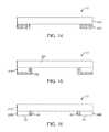
- FIG. 14is a cross-sectional side view of glass structures formed from by fusing a colored peripheral glass member to an edge portion of a planar glass member in accordance with an embodiment of the present invention.
- FIG. 15is a cross-sectional side view of glass structures formed from by fusing a peripheral glass member to an edge portion of a planar glass member and covering the bottom and inner surfaces of the peripheral glass member with an opaque masking material in accordance with an embodiment of the present invention.
- FIG. 16is a cross-sectional side view of glass structures formed from by fusing a peripheral glass member to an edge portion of a planar glass member and covering the inner surface of the peripheral glass member with an opaque masking material in accordance with an embodiment of the present invention.
- FIG. 17is a cross-sectional side view of glass structures formed from by fusing a colored peripheral glass member to an edge portion of a colored planar glass member in accordance with an embodiment of the present invention.
- FIG. 18is a cross-sectional side view of glass structures formed from by fusing a peripheral glass member to an edge portion of a planar glass member and coating the interior surface of the glass structures with an opaque masking material in accordance with an embodiment of the present invention.
- FIG. 19is a diagram showing how glass electronic device housing structures may be provided with a rounded edge and a laminated flexible display structure in accordance with an embodiment of the present invention.
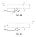
- FIG. 20is a cross-sectional side view of glass structures formed from by fusing a peripheral glass member with an angled edge to a planar glass member in accordance with an embodiment of the present invention.
- FIG. 21is a cross-sectional side view of glass structures formed from by fusing a peripheral glass member with a curved edge to a planar glass member in accordance with an embodiment of the present invention.
- FIG. 22is a diagram showing how an extruded glass structures for an electronic device housing may be provided with a fused end cap in accordance with an embodiment of the present invention.
- FIG. 23is a diagram showing how glass housing structures formed from a five-sided box of fused glass members may be provided with internal components in accordance with an embodiment of the present invention.
- FIG. 24is a diagram showing how internal components may be slid into a cavity within glass housing structures formed from a five-sided box of fused glass members in accordance with an embodiment of the present invention.
- FIG. 25is a cross-sectional side view of illustrative five-sided box glass fused glass structures that have been provided with internal components and a rounded edge in accordance with an embodiment of the present invention.
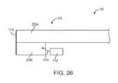
- FIG. 26is a cross-sectional side view of glass structures formed by fusing a peripheral glass member to a planar glass member and configured to be illuminated along an edge using a light source in accordance with an embodiment of the present invention.
- FIG. 27is a flow chart of illustrative steps involved in forming glass housing structures in accordance with an embodiment of the present invention.
- Glass structureswhich may sometimes be referred to as glass housing structures, may be used to provide a protective transparent covering for a display or other optical component, may be used to form a housing sidewall, may be used to form other housing structures such as a rear housing wall or other housing structures, may be used to form raised features such as raised ribs that serve as support structures for a sheet of glass or other glass structures, or may otherwise be used in forming structures in an electronic device.
- FIG. 1An example of an electronic device that may have glass housing structures is shown in FIG. 1 .
- electronic device 10has a stand such as stand 12 on which main unit 14 has been mounted.
- Main unit 14may include a display such as display 16 and a rear housing such as rear housing 18 (as an example).
- Device 10may be a monitor, a monitor with an integrated computer, a television, or other electronic equipment.
- Housing 18may be formed from metal, plastic, glass, ceramic, carbon-fiber composite material or other fiber-based composite materials, other materials, or combinations of these materials.
- Display 16may be covered with glass structures 20 .
- Glass structures 20may serve as a glass front housing structure for device 10 .
- Glass structures 20may be transparent so that display 16 may be viewed by a user of device 10 through glass structures 20 .
- Display 16may include display structures with image pixels formed from light-emitting diodes (LEDs), organic LEDs (OLEDs), plasma cells, electrowetting pixels, electrophoretic pixels, liquid crystal display (LCD) components, or other suitable image pixel structures.
- Touch sensor electrodesmay be included in display 16 to provide display 16 with touch sensing capabilities (e.g., display 16 may be a touch screen) or display 16 may be touch insensitive.
- device 10is a portable device such as a tablet computer, gaming device, navigation device, etc.
- Display 16may be mounted in housing 18 .
- Display 16may be covered with a display cover layer formed from glass structures 20 . Openings may be formed in glass structures 20 to accommodate components such as button 22 .
- FIG. 3is a perspective view of electronic device 10 in a configuration in which the electronic device housing has been formed from glass structures 20 that surround internal device components.
- End face 20 ′ of device 10may also be formed from glass (as an example) and may include openings for audio jack 28 , switch 30 , and digital connector port 32 (as examples).
- Display 16may be used to display images on one or more sides of device 10 .
- the portion of glass structures 20 of FIG. 3 that overlap display 16may be transparent, so that the images displayed by display 16 may be visible by a user of device 10 through glass structures 20 .
- the rear surface of glass structures 20may be transparent or may be colored (as examples).
- device 10has been provided with upper and lower glass layers 20 .
- Housing structure 38e.g., a layer of glass, ceramic, plastic, fiber-based composite, other material, or combination of these materials
- Structures 20 and optional structure 38may form a housing for device 10 .
- Display 16may be mounted behind upper glass layer 20 (e.g., on the front face of device 10 ). Openings in glass structures 20 may be used to accommodate buttons such as button 34 and other components (e.g., a speaker aligned with speaker port 36 ).
- FIGS. 1, 2, 3, and 4are merely illustrative. Any suitable electronic equipment may be provided with glass housing structures, if desired.
- FIG. 5is a cross-sectional side view of electronic device 10 in a configuration in which glass housing structure 20 has been used to form a cover glass layer over display structures 40 .
- Display structures 40may be used to form display 16 .
- Display structures 40may include a number of layers of material. These layers may include, for example, layers of glass, layers of plastic, and layers of adhesive.
- a liquid crystal displaymay have layers of polarizer, light diffusing elements, light guides for backlight structures, and a liquid crystal layer.
- An organic light-emitting diode (OLED) displaymay have organic materials that are used in producing light.
- An array of circuit componentssuch as a thin-film transistor (TFT) array may be used to drive the image pixels in a display. This array of circuitry may be formed on a substrate material such as glass or polymer.
- the substrate layer on which the thin-film transistors and/or other circuitry for the display are formedmay sometimes referred to as a TFT substrate or transistor substrate.
- Glass housing structures 20may be mounted to housing structures 18 (e.g., housing structures formed from metal, glass, plastic, fiber-based composites, etc.). Internal components may be mounted within the housing of electronic device 10 .
- device 10may include a printed circuit such as printed circuit 42 .
- Printed circuit 42may be a rigid printed circuit board (e.g., a fiberglass-filled epoxy board), a flexible printed circuit (“flex circuit”) formed from a flexible sheet of polyimide or other polymer layer, or may formed using other dielectric substrate materials.
- Components 44such as switches, connectors, discrete circuit elements such as capacitors, resistors, and inductors, integrated circuits, and other electronic devices may be mounted to substrate 42 .
- Display structures 40may be coupled to circuitry on substrates such as substrate 42 using communications path 46 (e.g., a flex circuit cable or other suitable path).
- center portion 48 of glass structures 20may have a thickness T 1 that is smaller than edge thickness T 2 .
- the smaller size of thickness T 1may create a recessed portion 50 .
- Recess 50 in center portion 48may have a rectangular shape or other suitable shape and may be configured to receive internal components in device 10 such as display structures 40 .
- the larger size of edge thickness T 2 relative to center thickness T 1may help strengthen glass structure 20 along its periphery to prevent damage in the event of an impact event.
- the larger size of the edges of glass structures 20may also improve device aesthetics.
- Glass structures 20may have a rectangular periphery (e.g., glass structures 20 may be formed from structures such as a planar sheet having a rectangular outline when viewed from above) and center portion 48 may form a rectangular recess within center of glass structures 20 .
- thickened edge portions 49may form a rectangular ring that runs around the periphery of glass structure 20 .
- glass structure 20may have other shapes (e.g., oval, circular, square, shapes with curved edges and/or straight edges, etc.).
- the thickened edge portions of glass structures 20may also be provided along only part of the edges of glass structures 20 , rather than the entire periphery of glass structures 20 .
- Housing structures such as structures 20 and 18may be joined using interposed layers of adhesive, using fasteners, using interlocking engagement features such as snaps, or using other suitable attachment mechanisms.
- glass structures 20e.g., the upper portion of the device housing
- lower housing 18e.g., metal, glass, plastic, ceramic, fiber-based composites, etc.
- a display or other structuresmay be mounted under the recessed portion of glass structures 20
- Internal components 44may be mounted in the interior of the device.
- FIG. 7is an example in which device 10 has been provide with two substantially similar glass housing structures 20 .
- Structures 20may, as an example, have rectangular shapes with thinner (recessed) center regions 48 and thickened edges 49 .
- One or more displays and other internal componentsmay be provided in device 10 of FIG. 7 .
- device 10may have a housing member such as housing sidewall structure 18 that is interposed between upper and lower glass housing structures 20 .
- Structure 18may be formed from metal, glass, ceramic, plastic, fiber-based composite material, other materials, or a combination of these materials.
- Upper and lower glass housing structures 20 in FIGS. 7 and 8may have recessed portions (e.g., rectangular recesses), as described in connection with FIG. 5 . Display structures and other internal device components may be received within the recesses of structures 20 of FIGS. 7 and 8 .
- Device structures such as glass structures 20may be formed from multiple pieces of glass that are fused together.
- Glass structuresmay, for example, be heated to an elevated temperature (e.g., about 800° C.) that is above the glass fusion temperature and that is below the glass working temperature. Using a metal die or other glass fusing tool, the heated glass pieces may be pressed together. Glass structures that are fused together using this type of approach may have invisible or barely visible joint lines (i.e., the fused glass joints that are formed when fusing a first glass member to a second glass member may be invisible or barely visible to the naked eye).
- FIG. 9Illustrative operations and equipment involved in forming glass structures 20 with recessed portion are shown in FIG. 9 .
- glass structures 20such as planar glass member 20 A may be formed and polished using polishing tool 56 .
- polishing tool 56may be used to perform mechanical and/or chemical polishing processes.
- Glass structures 20 Amay be formed from a glass sheet with a rectangular shape, a shape with curved edges, a shape with straight edges, or a shape with a combination of curved and straight edges.
- additional glass structuresmay be fused to glass structures 20 A using heated press (fusing tool) 62 .
- upper press member 64may be moved downwards in direction 66 while lower press member 68 is moved upwards in direction 70 to press glass structures 20 A and glass structures 20 B together.
- the temperature of glass structures 20 A and 20 Bmay be maintained at an elevated temperature of about 800° C. (e.g., a temperature above the fusion temperature of the glass and below the working temperature of the glass). This forms glass fusion bond 72 between structures 20 A and 20 B and fuses structures 20 A and 20 B together to form glass structures 20 .
- Glass structures 20 Bmay, for example, be a peripheral glass member having the shape of a rectangular ring that runs around the periphery of a rectangular version of glass structure 20 A or may be a glass member that runs around part of the periphery of glass structure 20 A (as examples).
- the glass structures that are formed by fusing structures 20 B to structures 20 Amay have an edge thickness T 2 and a thinner central region of thickness T 1 , as described in connection with FIG. 5 (as an example).
- glass structures 20 A and/or 20 Bmay have other shapes (e.g., to form additional glass thickness around an opening in glass structure 20 A, to form ribs or other supporting structures on glass structures 20 A, to form a peripheral thickened edge portion around a non-rectangular piece of glass, etc.).
- glass structures 20may be strengthened.
- glass structures 20may be strengthened using chemical strengthening tool 74 .
- Chemical strengthening tool 74may be used to immerse glass structures 20 in a bath containing potassium nitrate (as an example).
- Glass structures 20may be free of glass frit at fusion joints 72 , which may promote compatibility with chemical strengthening treatments. Heat-based tempering operations may also be performed to strengthen glass structures 20 , if desired.
- glass structures 20may have polished upper surface 58 , polished lower surface 60 , recessed central region 48 of thickness T 1 , and thickened edge regions 49 of thickness T 2 (T 2 >T 1 ). Glass structures 20 may then be assembled into device 10 . For example, glass structures 20 may be attached to additional glass structures (using glass fusing, using adhesive, using fasteners, using mating engagement structures, etc.) and/or non-glass housing structures.
- glass structures 20may be mounted to housing structures 18 . Because of the use of the glass fusing process of FIG. 9 to join glass structures 20 B to glass structures 20 A, fusion joint 72 between structures 20 A and 20 B may be invisible or nearly invisible to the naked eye of the user of device 10 , thereby enhancing device aesthetics.
- the enhanced thickness T 2 of the edge portion of glass structures 20(in the example of FIG. 10 ) may help improve the resistance of glass structures 20 to damage due to an impact event.
- glass structures 20 Bmay be fused to glass structures 20 A in other patterns.
- glass structures 20 B that have the shape of strengthening support ribsmay be fused across the center of the surface of glass structures 20 A, as shown in FIG. 11 .
- Strengthening features formed from structures 20 Bmay have the shape of a cross (as shown in the example of FIG. 11 ), may have a T shape, may have a central arm with multiple branches, or may have any other suitable pattern.
- the strengthening structure pattern formed by glass structures 20 B on structures 20 A of FIG. 11is merely illustrative.
- FIG. 12is an interior perspective view of illustrative glass structures 20 that have been provided with openings such as button opening 78 (e.g., for button 34 of FIG. 4 ) and speaker port opening 76 (e.g., for speaker port 36 of FIG. 4 ).
- glass structures 20 Bmay be used to locally thicken glass structures 20 A in the vicinity of one or more openings in glass structures 20 A.
- Glass structures 20 Bmay, for example, form raised rings or other raised structures that surround openings 36 and 34 to provided additional structural support for glass structures 20 A in the vicinity of openings 36 and 34 .
- FIG. 13is an illustrative cross-sectional side view of device 10 in a configuration in which glass structures 20 have been provided with external features by fusing glass structures 20 B to exterior surface 58 of glass structures 20 A.
- glass structures 20 Bhave been used to create a raised feature such as a circular ring on the surface of glass structures 20 A that surrounds button 34 .
- Light source 80may optionally be used to provide illumination for the raised ring formed by structures 20 B. If desired, raised features may be formed elsewhere on surface 58 of glass structures 20 A (e.g., surrounding speaker port 36 , in a particular location on a touch screen, around the rectangular peripheral edge of display 16 and device 10 , etc.).
- Glass structures 20may be formed from clear glass, glass with a colored tint (e.g., a blue tint, red tint, green tint, etc.), black glass, gray glass, or glass of other colors. As shown in FIG. 14 , glass structures 20 A and 20 B may be formed from glass of different colors. For example, glass structures 20 A may be formed from clear glass and glass structures 20 B may be formed from black glass or non-clear glass of another color. The amount of color in structures 20 B may be sufficient to render structures 20 B dark or opaque in appearance or may allow structures 20 B to remain transparent. The use of a color for structures 20 B that is not clear may help hide interior device components from view through the edge of structures 20 .
- a colored tinte.g., a blue tint, red tint, green tint, etc.
- internal device structuresmay also be hidden from view by providing structures 20 B with a layer of opaque masking material 82 .
- Material 82may be black ink, white ink, colored ink, or other opaque substances (as an example).
- FIG. 16shows how opaque masking material 82 may be formed on the inner edges of glass structures 20 B. This may allow surfaces 84 of structures 20 B to remain uncovered so that surfaces 84 may be attached to device structures using adhesive (as an example).
- FIG. 17is a cross-sectional side view of glass structures 20 in a configuration in which glass structures 20 A and glass structures 20 B have both been formed from non-clear glass (e.g., black glass, gray glass, blue glass, green glass, other colored glass, etc.).
- non-clear glasse.g., black glass, gray glass, blue glass, green glass, other colored glass, etc.
- glass structures 20have been provided with a layer of opaque masking material 82 (e.g., black ink, white ink, colored ink, or other opaque substance) that covers lower surface 60 of glass structures 20 A and lower surfaces 84 of glass structures 20 B.
- opaque masking material 82e.g., black ink, white ink, colored ink, or other opaque substance
- FIG. 19Illustrative operations involved in forming glass structures 20 with a recessed portion and curved features such as rounded edges are shown in FIG. 19 .
- a portion of glass structures 20such as polished planar glass member 20 A may be fused with glass structures 20 B by moving structures 20 A in direction 66 while moving structures 20 B in direction 70 while applying heat in fusing tool (heated press) 62 .
- tool 92e.g., a machining tool, grinding tool, polishing tool and/or other equipment for machining and polishing structures 20
- tool 92may be used in removing excess glass along curved surfaces 86 and 88 , thereby rounding the edges of glass structures 20 .
- Glass strengthening equipmentsuch as chemical strengthening tool 74 may be used to strengthen glass structures 20 following formation of curved surfaces 86 and 88 .
- display structures 40may be laminated to glass structures 20 using lamination tool 90 .
- display 16may be laminated to lower planar polished surface 60 and curved interior surface 88 of glass structures 20 using adhesive.
- Display structures 40may be formed using a substrate that is sufficiently flexible to allow display structures 40 to conform to the curved shape of surface 88 .
- Display structures 40may be for example, flexible structures for a flexible liquid crystal display, flexible electrowetting display structures, flexible electrophoretic display structures, or flexible organic light-emitting diode display structures (as examples).
- glass structures 20 Bmay be provided with angled (beveled) inner edge surface 94 .
- Surface 94may be coated with an optional opaque masking material such as layer 82 .
- the non-zero angle that is made by surface 94 with respect to surface normal 96 of planar lower surface 60 of planar glass member 20 Amay help improve the strength of glass structures 20 .
- the inner edge of glass structures 20 Bhas been provided with a planar surface (i.e., surface 94 is flat).
- a planar surfacei.e., surface 94 is flat.
- FIG. 21An illustrative arrangement in which the inner edge of glass structures 20 B has been provided with a curved surface (curved surface 94 ) is shown in FIG. 21 .
- FIG. 22shows how glass structures 20 may be formed from extruded glass structures such as extruded hollow-rod-shaped glass structure 200 and associated cap structures such as end cap glass structure 20 D.
- Glass structures 200 and 20 Dmay be formed using glass extruding and machining tools such as tools 100 .
- Fusing tool 62may be used to fuse structures 200 and 20 D together.
- electronic componentmay be housed within the interior of extruded glass structures 20 D.
- Fused caps 200may be used to enclose these internal components within the interior of device 10 .
- FIG. 23shows how internal electronic device components 102 may be inserted into glass structures 20 E and, if desired, may be covered with fused end cap 20 F.
- Structures 20 Emay be formed by fusing together five glass members to form a five-sided box with a lower face that is open to receive components 102 .
- the five-sided boxmay be formed from a first pair of opposing planar structures (e.g., front and rear sheets of glass), a second pair of opposing planar structures (e.g., opposing left and right sheets or strips of glass), and a fifth planar sheet (or strip) of glass such as end cap layer 20 F that have been fused together using fused joints.
- An air gapmay be formed between opposing glass walls in box-shaped glass structures 20 E.
- Ribs or other strengthening structuressuch as structures 20 B of FIG. 11 may be formed on one, two, three, four, or more than four of the surfaces of the five-sided box-shaped glass structures 20 E of FIG. 23 .
- Components 102may be inserted into the interior of structures 20 E (e.g., in the gap formed between the opposing front and rear sheets and between the opposing right and left sheets of glass).
- Components 102may include, for example, display structures 40 for forming display 16 and other components (see, e.g., components 44 of FIG. 5 ).
- Glass structures 20 Emay be formed from sheets of glass that are fused together using fusing equipment such as fusing tool 62 ( FIGS. 9 and 22 ).
- Glass structures 20 Fmay be attached to glass structures 20 E using glass fusing techniques, using adhesive, or using other attachment mechanisms.
- FIG. 24is a side view of glass structures 20 E showing how internal components 102 may be slid into the interior of glass structure 20 E in direction 106 through end face opening 104 in glass structures 20 E. If desired, machining techniques such as the curved edge machining techniques described in connection with FIG. 19 may be used in creating curved surfaces on glass structures 20 E (see, e.g., rounded edge surfaces 108 of glass structures 20 of device 10 in FIG. 25 ).
- edge 116 of glass structures 20may be provided with a roughened surface that helps to scatter and diffuse light.
- Device 10may be provided with a light-emitting diode or other internal light source 112 .
- Light source 112may produce light 114 that strikes roughened edge surface 116 of glass structures 20 .
- Light 114may illuminate the exposed exterior edge of glass structures 20 . Some or all of the peripheral edge portions of glass structures 20 may be illuminated in this way.
- FIG. 27is a flow chart of illustrative steps that may be used in forming glass structures 20 .
- glass structuressuch as glass structures 20 A and 20 B may be polished using polishing equipment 56 .
- fusing equipment 62may be used to fuse two or more glass structures together.
- glass structures 20 A and 20 Bmay be fused together to form glass structures 20 or the five sides of the five-sided-box glass structures of FIGS. 23 and 24 may be fused together.
- machining and polishing operationsmay be formed at step 122 .
- a thickened edge portion (of thickness T 2 ) of glass structures 20may be machined and polished to form a rounded edge for glass structures 20 , as shown in FIG. 19 .
- machining operations to form a rounded edge structure on glass structures 20may be performed during the operations of step 118 (e.g., using machining and polishing equipment).
- glass structures 20may be strengthened using heat and/or chemical treatment.
- glass structures 20may be strengthened by applying a chemical bath to glass structures 20 using chemical strengthening tool 74 .
- glass structures 20may be assembled with other housing structures to form electronic device 10 .
- Glass structures 20may, for example, be attached to glass or non-glass housing structures 18 or other structures to form device 10 .
- Internal componentssuch as a display, integrated circuits, and other components may be mounted within the glass structures and other structures for the housing of device 10 .
Landscapes
- Engineering & Computer Science (AREA)
- Chemical & Material Sciences (AREA)
- General Engineering & Computer Science (AREA)
- Theoretical Computer Science (AREA)
- Mechanical Engineering (AREA)
- Inorganic Chemistry (AREA)
- Ceramic Engineering (AREA)
- Microelectronics & Electronic Packaging (AREA)
- Physics & Mathematics (AREA)
- General Physics & Mathematics (AREA)
- Human Computer Interaction (AREA)
- Organic Chemistry (AREA)
- Materials Engineering (AREA)
- Signal Processing (AREA)
- Devices For Indicating Variable Information By Combining Individual Elements (AREA)
- Casings For Electric Apparatus (AREA)
Abstract
Description
This application is a continuation patent application of U.S. patent application Ser. No. 14/819,110, filed Aug. 5, 2015 and titled “Glass Device Housing,” which is a continuation patent application of U.S. patent application Ser. No. 14/295,110, filed Jun. 3, 2014 and titled “Fused Glass Device Housings,” now U.S. Pat. No. 9,125,298, which is a continuation patent application of U.S. patent application Ser. No. 13/358,389, filed Jan. 25, 2012 and titled “Fused Glass Device Housings,” now U.S. Pat. No. 8,773,848, the disclosures of which are hereby incorporated herein by reference in their entireties.
This relates to electronic devices and, more particularly, to glass structures for electronic devices.
Electronic devices such as cellular telephones, handheld computers, and portable music players often include housings with glass members. For example, a device with a display may have a glass cover that serves as a protective layer. In some devices, a rear housing surface may be formed from a layer of glass.
To ensure satisfactory robustness, it is generally desirable to form device housing structures such as cover glass layers and housing surfaces from structures that are sufficiently strong to prevent damage during accidental impact events. For example, it is generally desirable to form portable devices that are subject to drop events from structures that are able to withstand the forces involved in a typical drop event without incurring excessive damage.
Glass strength and device aesthetics can sometimes be enhanced by using sufficiently thick glass layers. However, the size and weight of a device should not be excessive. If care is not taken, modifications that are made to ensure that a device has glass structures that are sufficiently strong, will make the device heavy and bulky.
It would therefore be desirable to be able to provide improved glass structures for electronic devices.
An electronic device may have a glass housing structures. The glass housing structures may be used to cover a display and other internal electronic device components. The glass housing structures may cover a front face of an electronic device and, if desired, may cover additional device surfaces.
The glass housing structure may have multiple glass pieces that are joined using a glass fusing process. A peripheral glass member may be fused along the edge of a planar glass member to enhance the thickness of the edge. A rounded edge feature may be formed by machining the thickened edge. Raised fused glass features may surround openings in the planar glass member. Raised support structure ribs may be formed by fusing glass structures to the planar glass member.
Multiple planar glass members may be fused together to form a five-sided box in which electronic components may be mounted. Display structures and other internal components may be slid into place between opposing glass sides of the box.
Opaque masking material and colored glass may be used to create portions of the glass housing structures that hide internal device components from view.
Further features of the invention, its nature and various advantages will be more apparent from the accompanying drawings and the following detailed description of the preferred embodiments.
Electronic devices such as computers, handheld devices, computer monitors, televisions, cellular telephones, media players, and other equipment may have displays and other components that are covered with glass structures. The glass structures, which may sometimes be referred to as glass housing structures, may be used to provide a protective transparent covering for a display or other optical component, may be used to form a housing sidewall, may be used to form other housing structures such as a rear housing wall or other housing structures, may be used to form raised features such as raised ribs that serve as support structures for a sheet of glass or other glass structures, or may otherwise be used in forming structures in an electronic device.
An example of an electronic device that may have glass housing structures is shown inFIG. 1 . In the example ofFIG. 1 ,electronic device 10 has a stand such asstand 12 on whichmain unit 14 has been mounted.Main unit 14 may include a display such asdisplay 16 and a rear housing such as rear housing18 (as an example).Device 10 may be a monitor, a monitor with an integrated computer, a television, or other electronic equipment.
In the illustrative example ofFIG. 2 ,device 10 is a portable device such as a tablet computer, gaming device, navigation device, etc.Display 16 may be mounted inhousing 18.Display 16 may be covered with a display cover layer formed fromglass structures 20. Openings may be formed inglass structures 20 to accommodate components such as button22.
In the illustrative example ofFIG. 4 ,device 10 has been provided with upper and lower glass layers20. Housing structure38 (e.g., a layer of glass, ceramic, plastic, fiber-based composite, other material, or combination of these materials) may optionally be interposed between upper andlower glass structures 20.Structures 20 andoptional structure 38 may form a housing fordevice 10.Display 16 may be mounted behind upper glass layer20 (e.g., on the front face of device10). Openings inglass structures 20 may be used to accommodate buttons such asbutton 34 and other components (e.g., a speaker aligned with speaker port36).
The illustrative device configurations ofFIGS. 1, 2, 3, and 4 are merely illustrative. Any suitable electronic equipment may be provided with glass housing structures, if desired.
To help maximize the interior volume indevice 10 and reduce the size and weight ofglass structures 20,center portion 48 ofglass structures 20 may have a thickness T1 that is smaller than edge thickness T2. The smaller size of thickness T1 may create a recessedportion 50.Recess 50 incenter portion 48 may have a rectangular shape or other suitable shape and may be configured to receive internal components indevice 10 such asdisplay structures 40. The larger size of edge thickness T2 relative to center thickness T1 may help strengthenglass structure 20 along its periphery to prevent damage in the event of an impact event. The larger size of the edges ofglass structures 20 may also improve device aesthetics.
Housing structures such asstructures
In the illustrative example ofFIG. 6 , glass structures20 (e.g., the upper portion of the device housing) may have a planarexterior surface 52 and lower housing18 (e.g., metal, glass, plastic, ceramic, fiber-based composites, etc.) may be have acurved exterior surface 54. A display or other structures may be mounted under the recessed portion ofglass structures 20.Internal components 44 may be mounted in the interior of the device.
As shown inFIG. 8 ,device 10 may have a housing member such ashousing sidewall structure 18 that is interposed between upper and lowerglass housing structures 20.Structure 18 may be formed from metal, glass, ceramic, plastic, fiber-based composite material, other materials, or a combination of these materials. Upper and lowerglass housing structures 20 inFIGS. 7 and 8 may have recessed portions (e.g., rectangular recesses), as described in connection withFIG. 5 . Display structures and other internal device components may be received within the recesses ofstructures 20 ofFIGS. 7 and 8 .
Device structures such asglass structures 20 may be formed from multiple pieces of glass that are fused together. Glass structures may, for example, be heated to an elevated temperature (e.g., about 800° C.) that is above the glass fusion temperature and that is below the glass working temperature. Using a metal die or other glass fusing tool, the heated glass pieces may be pressed together. Glass structures that are fused together using this type of approach may have invisible or barely visible joint lines (i.e., the fused glass joints that are formed when fusing a first glass member to a second glass member may be invisible or barely visible to the naked eye).
Illustrative operations and equipment involved in formingglass structures 20 with recessed portion are shown inFIG. 9 .
Initially, a portion ofglass structures 20 such asplanar glass member 20A may be formed and polished usingpolishing tool 56. For example, bothupper surface 58 andlower surface 60 ofglass structures 20A may be polished usingtool 56.Polishing tool 56 may be used to perform mechanical and/or chemical polishing processes.Glass structures 20A may be formed from a glass sheet with a rectangular shape, a shape with curved edges, a shape with straight edges, or a shape with a combination of curved and straight edges.
Following polishing operations withtool 56, additional glass structures may be fused toglass structures 20A using heated press (fusing tool)62. In particular,upper press member 64 may be moved downwards indirection 66 whilelower press member 68 is moved upwards indirection 70 to pressglass structures 20A andglass structures 20B together. During pressing, the temperature ofglass structures glass fusion bond 72 betweenstructures structures glass structures 20.
Becauselower surface 60 ofglass structures 20A was polished bytool 56, this surface may remain polished following fusion ofglass structures 20B toglass structures 20A.
Following formation ofglass structures 20 usingglass fusing tool 62,glass structures 20 may be strengthened. For example,glass structures 20 may be strengthened usingchemical strengthening tool 74.Chemical strengthening tool 74 may be used to immerseglass structures 20 in a bath containing potassium nitrate (as an example).Glass structures 20 may be free of glass frit atfusion joints 72, which may promote compatibility with chemical strengthening treatments. Heat-based tempering operations may also be performed to strengthenglass structures 20, if desired.
Following strengthening ofglass structures 20 withchemical strengthening tool 74,glass structures 20 may have polishedupper surface 58, polishedlower surface 60, recessedcentral region 48 of thickness T1, and thickenededge regions 49 of thickness T2 (T2>T1).Glass structures 20 may then be assembled intodevice 10. For example,glass structures 20 may be attached to additional glass structures (using glass fusing, using adhesive, using fasteners, using mating engagement structures, etc.) and/or non-glass housing structures.
As shown inFIG. 10 , for example,glass structures 20 may be mounted tohousing structures 18. Because of the use of the glass fusing process ofFIG. 9 to joinglass structures 20B toglass structures 20A, fusion joint72 betweenstructures device 10, thereby enhancing device aesthetics. The enhanced thickness T2 of the edge portion of glass structures20 (in the example ofFIG. 10 ) may help improve the resistance ofglass structures 20 to damage due to an impact event.
If desired,glass structures 20B may be fused toglass structures 20A in other patterns. For example,glass structures 20B that have the shape of strengthening support ribs may be fused across the center of the surface ofglass structures 20A, as shown inFIG. 11 . Strengthening features formed fromstructures 20B may have the shape of a cross (as shown in the example ofFIG. 11 ), may have a T shape, may have a central arm with multiple branches, or may have any other suitable pattern. The strengthening structure pattern formed byglass structures 20B onstructures 20A ofFIG. 11 is merely illustrative.
As shown inFIG. 15 , internal device structures may also be hidden from view by providingstructures 20B with a layer ofopaque masking material 82.Material 82 may be black ink, white ink, colored ink, or other opaque substances (as an example).
In theFIG. 18 example,glass structures 20 have been provided with a layer of opaque masking material82 (e.g., black ink, white ink, colored ink, or other opaque substance) that coverslower surface 60 ofglass structures 20A andlower surfaces 84 ofglass structures 20B.
Illustrative operations involved in formingglass structures 20 with a recessed portion and curved features such as rounded edges are shown inFIG. 19 .
As shown inFIG. 19 , a portion ofglass structures 20 such as polishedplanar glass member 20A may be fused withglass structures 20B by movingstructures 20A indirection 66 while movingstructures 20B indirection 70 while applying heat in fusing tool (heated press)62.
After fusingstructures tool 62, tool92 (e.g., a machining tool, grinding tool, polishing tool and/or other equipment for machining and polishing structures20) may be used in removing excess glass alongcurved surfaces glass structures 20.
Glass strengthening equipment such aschemical strengthening tool 74 may be used to strengthenglass structures 20 following formation ofcurved surfaces
If desired, display structures40 (FIG. 5 ) may be laminated toglass structures 20 usinglamination tool 90. For example,display 16 may be laminated to lower planarpolished surface 60 and curvedinterior surface 88 ofglass structures 20 using adhesive.Display structures 40 may be formed using a substrate that is sufficiently flexible to allowdisplay structures 40 to conform to the curved shape ofsurface 88.Display structures 40 may be for example, flexible structures for a flexible liquid crystal display, flexible electrowetting display structures, flexible electrophoretic display structures, or flexible organic light-emitting diode display structures (as examples).
As shown inFIG. 20 ,glass structures 20B may be provided with angled (beveled) inner edge surface94. Surface94 may be coated with an optional opaque masking material such aslayer 82. The non-zero angle that is made by surface94 with respect to surface normal96 of planarlower surface 60 ofplanar glass member 20A may help improve the strength ofglass structures 20.
In theFIG. 20 configuration, the inner edge ofglass structures 20B has been provided with a planar surface (i.e., surface94 is flat). An illustrative arrangement in which the inner edge ofglass structures 20B has been provided with a curved surface (curved surface94) is shown inFIG. 21 .
As shown inFIG. 26 ,edge 116 ofglass structures 20 may be provided with a roughened surface that helps to scatter and diffuse light.Device 10 may be provided with a light-emitting diode or other internallight source 112.Light source 112 may produce light114 that strikes roughenededge surface 116 ofglass structures 20.Light 114 may illuminate the exposed exterior edge ofglass structures 20. Some or all of the peripheral edge portions ofglass structures 20 may be illuminated in this way.
Atstep 118, glass structures such asglass structures polishing equipment 56.
Atstep 120, fusingequipment 62 may be used to fuse two or more glass structures together. For example,glass structures glass structures 20 or the five sides of the five-sided-box glass structures ofFIGS. 23 and 24 may be fused together.
If desired, additional machining and polishing operations may be formed atstep 122. For example, a thickened edge portion (of thickness T2) ofglass structures 20 may be machined and polished to form a rounded edge forglass structures 20, as shown inFIG. 19 . If desired, machining operations to form a rounded edge structure onglass structures 20 may be performed during the operations of step118 (e.g., using machining and polishing equipment).
Atstep 124,glass structures 20 may be strengthened using heat and/or chemical treatment. For example,glass structures 20 may be strengthened by applying a chemical bath toglass structures 20 usingchemical strengthening tool 74.
Atstep 126,glass structures 20 may be assembled with other housing structures to formelectronic device 10.Glass structures 20 may, for example, be attached to glass ornon-glass housing structures 18 or other structures to formdevice 10. Internal components such as a display, integrated circuits, and other components may be mounted within the glass structures and other structures for the housing ofdevice 10.
The foregoing is merely illustrative of the principles of this invention and various modifications can be made by those skilled in the art without departing from the scope and spirit of the invention.
Claims (20)
1. A housing for an electronic device, comprising:
a first housing structure defining a first exterior portion of a sidewall that is formed from a glass material, the first housing structure having a first thickness at an inner portion and a second thickness at a peripheral portion surrounding the inner portion, the first thickness being less than the second thickness; and
a second housing structure coupled to the first housing structure, the second housing structure defining a second exterior portion of the sidewall coplanar with the first exterior portion of the sidewall, the first and second housing structures defining an interior volume for receiving a display that is visible through the first housing structure.
2. The housing defined inclaim 1 , wherein the first housing structure defines a recess that is configured to receive at least a portion of the display.
3. The housing defined inclaim 2 , wherein the display is visible through the inner portion of the first housing structure.
4. The housing defined inclaim 2 , wherein a touch sensor is positioned adjacent to an inner surface of the recess of the first housing structure.
5. The housing defined inclaim 1 , wherein:
the housing further comprises an intermediate structure defining a third exterior portion of the sidewall;
the intermediate structure is positioned at least partially between the first housing structure and the second housing structure; and
the intermediate structure is coplanar with the first and second exterior portions of the sidewall.
6. The housing defined inclaim 1 , wherein the peripheral portion comprises non-clear glass.
7. The housing defined inclaim 1 , wherein the peripheral portion defines a rounded external edge.
8. The housing defined inclaim 1 , wherein the peripheral portion defines an inner surface that is curved.
9. The housing defined inclaim 1 , wherein:
the peripheral portion defines an inner surface; and
an opaque masking material is positioned over at least a portion of the inner surface.
10. The housing defined inclaim 1 , wherein:
the first housing structure comprises a base glass layer and one or more glass rib support structures; and
the one or more glass rib support structures are fused to the base glass layer.
11. An electronic device, comprising:
a display; and
a housing enclosing the display and comprising:
a first housing structure defining a first portion of an exterior sidewall formed from a glass material and a recess within an inner portion surrounded by a peripheral portion, the display viewable through the inner portion of the first housing structure; and
a second housing structure coupled to the first housing structure and defining a second portion of the exterior sidewall that is coplanar with the first portion of the exterior sidewall, and
internal electrical components positioned within a cavity defined between the second housing structure and the first housing structure.
12. The electronic device ofclaim 11 , wherein
the display comprises a touch sensor that is operable through the inner portion of the first housing structure.
13. The electronic device ofclaim 11 , wherein:
the first housing structure has a first thickness at the inner portion:
the first housing structure has a second thickness at the peripheral portion; and
the first thickness is less than the second thickness.
14. The electronic device ofclaim 11 , wherein the second housing structure comprises a metal material.
15. The electronic device ofclaim 11 , wherein the recess of the first housing structure defines a curved interior surface.
16. The electronic device ofclaim 15 , wherein:
the display is a flexible display; and
the flexible display is secured adjacent the curved interior surface.
17. A housing, comprising:
a glass housing structure having a recess at a central portion of the glass housing structure, the glass housing structure defining a first portion of an exterior sidewall that includes exposed glass material;
a base structure coupled to the glass housing structure having a second portion of the exterior sidewall that is coplanar with the first portion of the exterior sidewall; and
a display positioned within a cavity defined between the base structure and the glass housing structure.
18. The housing defined inclaim 17 , wherein:
the glass housing structure has a thickness of T1 at the central portion and a thickness of T2 at a peripheral portion of the glass housing structure, the thickness of T1 being less than the thickness of T2.
19. The housing defined inclaim 17 , wherein:
the glass housing structure is formed from a base glass layer and a peripheral glass layer; and
the peripheral glass layer is fused to the base glass layer.
20. The housing defined inclaim 17 , wherein the display is positioned adjacent a portion of the recess of the glass housing structure.
Priority Applications (7)
| Application Number | Priority Date | Filing Date | Title |
|---|---|---|---|
| US15/653,171US10278294B2 (en) | 2012-01-25 | 2017-07-18 | Glass device housings |
| US16/138,933US10512176B2 (en) | 2012-01-25 | 2018-09-21 | Glass device housings |
| US16/692,798US10842031B2 (en) | 2012-01-25 | 2019-11-22 | Glass device housings |
| US17/033,151US11260489B2 (en) | 2012-01-25 | 2020-09-25 | Glass device housings |
| US17/668,860US11612975B2 (en) | 2012-01-25 | 2022-02-10 | Glass device housings |
| US18/123,863US12083649B2 (en) | 2012-01-25 | 2023-03-20 | Glass device housings |
| US18/816,749US20240416475A1 (en) | 2012-01-25 | 2024-08-27 | Glass device housings |
Applications Claiming Priority (4)
| Application Number | Priority Date | Filing Date | Title |
|---|---|---|---|
| US13/358,389US8773848B2 (en) | 2012-01-25 | 2012-01-25 | Fused glass device housings |
| US14/295,110US9125298B2 (en) | 2012-01-25 | 2014-06-03 | Fused glass device housings |
| US14/819,110US9756739B2 (en) | 2012-01-25 | 2015-08-05 | Glass device housing |
| US15/653,171US10278294B2 (en) | 2012-01-25 | 2017-07-18 | Glass device housings |
Related Parent Applications (1)
| Application Number | Title | Priority Date | Filing Date |
|---|---|---|---|
| US14/819,110ContinuationUS9756739B2 (en) | 2012-01-25 | 2015-08-05 | Glass device housing |
Related Child Applications (1)
| Application Number | Title | Priority Date | Filing Date |
|---|---|---|---|
| US16/138,933ContinuationUS10512176B2 (en) | 2012-01-25 | 2018-09-21 | Glass device housings |
Publications (2)
| Publication Number | Publication Date |
|---|---|
| US20170318686A1 US20170318686A1 (en) | 2017-11-02 |
| US10278294B2true US10278294B2 (en) | 2019-04-30 |
Family
ID=47679035
Family Applications (10)
| Application Number | Title | Priority Date | Filing Date |
|---|---|---|---|
| US13/358,389Active2032-07-14US8773848B2 (en) | 2012-01-25 | 2012-01-25 | Fused glass device housings |
| US14/295,110ActiveUS9125298B2 (en) | 2012-01-25 | 2014-06-03 | Fused glass device housings |
| US14/819,110ActiveUS9756739B2 (en) | 2012-01-25 | 2015-08-05 | Glass device housing |
| US15/653,171ActiveUS10278294B2 (en) | 2012-01-25 | 2017-07-18 | Glass device housings |
| US16/138,933ActiveUS10512176B2 (en) | 2012-01-25 | 2018-09-21 | Glass device housings |
| US16/692,798ActiveUS10842031B2 (en) | 2012-01-25 | 2019-11-22 | Glass device housings |
| US17/033,151ActiveUS11260489B2 (en) | 2012-01-25 | 2020-09-25 | Glass device housings |
| US17/668,860ActiveUS11612975B2 (en) | 2012-01-25 | 2022-02-10 | Glass device housings |
| US18/123,863ActiveUS12083649B2 (en) | 2012-01-25 | 2023-03-20 | Glass device housings |
| US18/816,749PendingUS20240416475A1 (en) | 2012-01-25 | 2024-08-27 | Glass device housings |
Family Applications Before (3)
| Application Number | Title | Priority Date | Filing Date |
|---|---|---|---|
| US13/358,389Active2032-07-14US8773848B2 (en) | 2012-01-25 | 2012-01-25 | Fused glass device housings |
| US14/295,110ActiveUS9125298B2 (en) | 2012-01-25 | 2014-06-03 | Fused glass device housings |
| US14/819,110ActiveUS9756739B2 (en) | 2012-01-25 | 2015-08-05 | Glass device housing |
Family Applications After (6)
| Application Number | Title | Priority Date | Filing Date |
|---|---|---|---|
| US16/138,933ActiveUS10512176B2 (en) | 2012-01-25 | 2018-09-21 | Glass device housings |
| US16/692,798ActiveUS10842031B2 (en) | 2012-01-25 | 2019-11-22 | Glass device housings |
| US17/033,151ActiveUS11260489B2 (en) | 2012-01-25 | 2020-09-25 | Glass device housings |
| US17/668,860ActiveUS11612975B2 (en) | 2012-01-25 | 2022-02-10 | Glass device housings |
| US18/123,863ActiveUS12083649B2 (en) | 2012-01-25 | 2023-03-20 | Glass device housings |
| US18/816,749PendingUS20240416475A1 (en) | 2012-01-25 | 2024-08-27 | Glass device housings |
Country Status (8)
| Country | Link |
|---|---|
| US (10) | US8773848B2 (en) |
| EP (2) | EP2807125B1 (en) |
| JP (1) | JP6099674B2 (en) |
| KR (9) | KR101913708B1 (en) |
| CN (2) | CN104220389B (en) |
| AU (1) | AU2013212582B2 (en) |
| TW (2) | TWI529145B (en) |
| WO (1) | WO2013112433A2 (en) |
Families Citing this family (134)
| Publication number | Priority date | Publication date | Assignee | Title |
|---|---|---|---|---|
| US12185512B2 (en) | 2007-11-16 | 2024-12-31 | Manufacturing Resources International, Inc. | Electronic display assembly with thermal management |
| US8654302B2 (en) | 2008-03-03 | 2014-02-18 | Manufacturing Resources International, Inc. | Heat exchanger for an electronic display |
| US9573346B2 (en) | 2008-05-21 | 2017-02-21 | Manufacturing Resources International, Inc. | Photoinitiated optical adhesive and method for using same |
| US8824140B2 (en)* | 2010-09-17 | 2014-09-02 | Apple Inc. | Glass enclosure |
| US8773848B2 (en)* | 2012-01-25 | 2014-07-08 | Apple Inc. | Fused glass device housings |
| KR101346083B1 (en)* | 2012-04-26 | 2013-12-31 | 엘지디스플레이 주식회사 | Display Device |
| US9110525B2 (en)* | 2012-06-28 | 2015-08-18 | Blackberry Limited | Touch-sensitive display and method |
| US9439315B2 (en) | 2012-06-29 | 2016-09-06 | Samsung Display Co., Ltd. | Display device, and method and apparatus for manufacturing the same |
| KR20140002470A (en) | 2012-06-29 | 2014-01-08 | 삼성디스플레이 주식회사 | Display device, manufacturing method of the same and manufacturing device of the same |
| US9288294B2 (en)* | 2012-10-19 | 2016-03-15 | Htc Corporation | Handheld electronic device and method for assembling display panel thereof |
| US20150086048A1 (en)* | 2013-09-20 | 2015-03-26 | Corning Incorporated | Acoustic panels and planar structures |
| KR102102314B1 (en)* | 2013-12-16 | 2020-04-20 | 엘지디스플레이 주식회사 | Curved Cover Plate and Curved Display Device and method of manufacturing the same |
| US10069952B2 (en)* | 2014-02-13 | 2018-09-04 | Magna Mirrors Of America, Inc. | Cover glass for mobile device |
| CN104023099B (en)* | 2014-06-20 | 2017-04-12 | 蓝思科技股份有限公司 | Mobile phone curved glass panel and forming method thereof |
| KR200488235Y1 (en)* | 2014-08-27 | 2018-12-31 | 애플 인크. | Sapphire cover for electronic devices |
| KR20160028595A (en)* | 2014-09-03 | 2016-03-14 | 삼성디스플레이 주식회사 | Cover window, method for manufacturing the same and display device comprising the same |
| CN105528101A (en)* | 2014-10-21 | 2016-04-27 | 宸鸿科技(厦门)有限公司 | A touch control panel and a three-dimensional cover plate structure therefor |
| US10702882B2 (en) | 2014-10-30 | 2020-07-07 | Corning Incorporated | Method and system for the selective coating of an interior surface |
| US10589500B2 (en) | 2015-02-27 | 2020-03-17 | Corning Incorporated | Customized and selective decoration of internal tube-like surfaces using pre-printed films with splinter resistant property |
| US10296049B2 (en)* | 2015-07-15 | 2019-05-21 | Dell Products L.P. | Carbon fiber/ceramic chassis |
| US20170066108A1 (en)* | 2015-09-03 | 2017-03-09 | Apple Inc. | Forming a smooth matte surface of a ceramic material |
| US10429892B1 (en)* | 2016-01-12 | 2019-10-01 | Apple Inc. | Electronic devices with thin display housings |
| WO2017131854A1 (en)* | 2016-01-26 | 2017-08-03 | Google Inc. | Glass enclosures for electronic devices |
| CN206164608U (en)* | 2016-05-10 | 2017-05-10 | 华为技术有限公司 | Panel and terminal of terminal shell, terminal shell |
| US10231346B2 (en)* | 2016-05-27 | 2019-03-12 | Lg Electronics Inc. | Display device |
| KR102718781B1 (en)* | 2016-05-27 | 2024-10-18 | 엘지전자 주식회사 | Display device |
| US11419231B1 (en) | 2016-09-22 | 2022-08-16 | Apple Inc. | Forming glass covers for electronic devices |
| US11565506B2 (en) | 2016-09-23 | 2023-01-31 | Apple Inc. | Thermoformed cover glass for an electronic device |
| US11535551B2 (en)* | 2016-09-23 | 2022-12-27 | Apple Inc. | Thermoformed cover glass for an electronic device |
| US10800141B2 (en) | 2016-09-23 | 2020-10-13 | Apple Inc. | Electronic device having a glass component with crack hindering internal stress regions |
| US10870261B2 (en)* | 2016-11-04 | 2020-12-22 | Apple Inc. | Structured glass for an electronic device |
| KR102612078B1 (en) | 2016-11-22 | 2023-12-11 | 삼성디스플레이 주식회사 | Flat panel display device having display areas with the appearance of rounded corners |
| CN106746540A (en)* | 2017-01-05 | 2017-05-31 | 东莞华清光学科技有限公司 | A kind of complex-curved shell and preparation method thereof |
| US11678445B2 (en) | 2017-01-25 | 2023-06-13 | Apple Inc. | Spatial composites |
| EP4589618A3 (en) | 2017-03-29 | 2025-10-15 | Apple Inc. | Device having integrated interface system |
| US10485113B2 (en) | 2017-04-27 | 2019-11-19 | Manufacturing Resources International, Inc. | Field serviceable and replaceable display |
| KR102524831B1 (en)* | 2017-06-19 | 2023-04-24 | 삼성전자주식회사 | electronic device including window |
| US10556823B2 (en)* | 2017-06-20 | 2020-02-11 | Apple Inc. | Interior coatings for glass structures in electronic devices |
| USD826936S1 (en) | 2017-06-23 | 2018-08-28 | Nanolumens Acquisition, Inc. | Five sided light emitting display |
| US10775889B1 (en) | 2017-07-21 | 2020-09-15 | Apple Inc. | Enclosure with locally-flexible regions |
| US10292286B2 (en) | 2017-07-31 | 2019-05-14 | Apple Inc. | Patterned glass layers in electronic devices |
| US10996713B2 (en)* | 2017-08-07 | 2021-05-04 | Apple Inc. | Portable electronic device |
| US10866615B1 (en) | 2017-08-16 | 2020-12-15 | Apple Inc. | Electronic devices with two-stage displays |
| EP3450408A1 (en)* | 2017-09-01 | 2019-03-06 | LIBBEY GLASS Inc. | Glass tile and method of making the same |
| US10969526B2 (en)* | 2017-09-08 | 2021-04-06 | Apple Inc. | Coatings for transparent substrates in electronic devices |
| US10690986B2 (en) | 2017-09-13 | 2020-06-23 | Apple Inc. | Electronic devices having electrically adjustable optical shutters |
| WO2019067772A1 (en) | 2017-09-29 | 2019-04-04 | Mikael Silvanto | Multi-part device enclosure |
| US10924836B1 (en)* | 2017-09-29 | 2021-02-16 | Apple Inc. | Techniques for improving glass earcup drop performance |
| US10611666B2 (en) | 2017-12-01 | 2020-04-07 | Apple Inc. | Controlled crystallization of glass ceramics for electronic devices |
| US11066322B2 (en) | 2017-12-01 | 2021-07-20 | Apple Inc. | Selectively heat-treated glass-ceramic for an electronic device |
| CN108108049A (en)* | 2017-12-06 | 2018-06-01 | 北京小米移动软件有限公司 | Electronic equipment |
| TWI636306B (en)* | 2017-12-08 | 2018-09-21 | 致伸科技股份有限公司 | Portable electronic device |
| WO2019114475A1 (en)* | 2017-12-12 | 2019-06-20 | Oppo广东移动通信有限公司 | Mobile terminal and its display screen assembly thereof |
| WO2019192702A1 (en) | 2018-04-05 | 2019-10-10 | Huawei Technologies Co., Ltd. | Glass housing structure for an electronic device |
| CN110385627A (en)* | 2018-04-18 | 2019-10-29 | 南昌欧菲光学技术有限公司 | Panel and preparation method thereof |
| CN110390880A (en)* | 2018-04-18 | 2019-10-29 | 南昌欧菲光学技术有限公司 | Panel and its manufacture craft |
| CN110385626A (en)* | 2018-04-18 | 2019-10-29 | 南昌欧菲光学技术有限公司 | Panel and preparation method thereof |
| CN108630110B (en)* | 2018-04-24 | 2020-06-23 | 广州国显科技有限公司 | Display screen, manufacturing method thereof and display device |
| WO2019212507A1 (en)* | 2018-04-30 | 2019-11-07 | Hewlett-Packard Development Company, L.P. | Electronic device housings with reinforcing structures |
| CN108529856A (en)* | 2018-05-25 | 2018-09-14 | Oppo广东移动通信有限公司 | Housing, electronic device, and method for manufacturing housing |
| CN111356979B (en) | 2018-05-25 | 2023-12-29 | 苹果公司 | Portable computer with dynamic display interface |
| CN108769316B (en)* | 2018-05-25 | 2020-05-12 | Oppo广东移动通信有限公司 | Housing, electronic device, and method for manufacturing housing |
| CN108675618B (en)* | 2018-06-06 | 2021-06-25 | 三砥新材(深圳)有限公司 | Manufacturing method of mobile terminal glass rear cover |
| US10602626B2 (en) | 2018-07-30 | 2020-03-24 | Manufacturing Resources International, Inc. | Housing assembly for an integrated display unit |
| CN109108462A (en)* | 2018-08-02 | 2019-01-01 | 瑞声光电科技(常州)有限公司 | Microphone device and its assembly method |
| US11175769B2 (en) | 2018-08-16 | 2021-11-16 | Apple Inc. | Electronic device with glass enclosure |
| US11133572B2 (en) | 2018-08-30 | 2021-09-28 | Apple Inc. | Electronic device with segmented housing having molded splits |
| US11258163B2 (en) | 2018-08-30 | 2022-02-22 | Apple Inc. | Housing and antenna architecture for mobile device |
| US11189909B2 (en) | 2018-08-30 | 2021-11-30 | Apple Inc. | Housing and antenna architecture for mobile device |
| US10705570B2 (en) | 2018-08-30 | 2020-07-07 | Apple Inc. | Electronic device housing with integrated antenna |
| CN110875968A (en)* | 2018-09-04 | 2020-03-10 | 北京小米移动软件有限公司 | Terminal device |
| US11630485B2 (en)* | 2018-09-10 | 2023-04-18 | Apple Inc. | Housing structures and input-output devices for electronic devices |
| US10791207B2 (en)* | 2018-09-14 | 2020-09-29 | Apple Inc. | Method and apparatus for attaching display to enclosure |
| US11420900B2 (en) | 2018-09-26 | 2022-08-23 | Apple Inc. | Localized control of bulk material properties |
| KR20200057392A (en) | 2018-11-16 | 2020-05-26 | (주)대호테크 | A transparent cover mounted on a flexible display, Manufacturing method of the transparent cover and a portable terminal equipped with the transparent cover |
| US11096317B2 (en) | 2019-02-26 | 2021-08-17 | Manufacturing Resources International, Inc. | Display assembly with loopback cooling |
| KR102068685B1 (en)* | 2019-03-11 | 2020-01-21 | (주)유티아이 | Flexible Cover Window |
| CN109814672B (en)* | 2019-03-20 | 2024-09-13 | 中国兵器工业计算机应用技术研究所 | Reinforcing display control terminal |
| US10795413B1 (en) | 2019-04-03 | 2020-10-06 | Manufacturing Resources International, Inc. | Electronic display assembly with a channel for ambient air in an access panel |
| KR102150392B1 (en)* | 2019-04-15 | 2020-09-02 | (주)유티아이 | Visibility Improvement Flexible Cover Window |
| CN114399012B (en) | 2019-04-17 | 2024-08-06 | 苹果公司 | Wireless locatable tag |
| US11680010B2 (en) | 2019-07-09 | 2023-06-20 | Apple Inc. | Evaluation of transparent components for electronic devices |
| US11448801B2 (en) | 2019-07-30 | 2022-09-20 | Apple Inc. | Textured glass layers in electronic devices |
| US11269374B2 (en)* | 2019-09-11 | 2022-03-08 | Apple Inc. | Electronic device with a cover assembly having an adhesion layer |
| CN110728909A (en)* | 2019-09-29 | 2020-01-24 | 联想(北京)有限公司 | Electronic device and method for attaching to screen |
| US12304171B2 (en)* | 2019-12-03 | 2025-05-20 | Huawei Technologies Co., Ltd. | Three-dimensional, seamless and colored cover for an electronic device |
| US12009576B2 (en) | 2019-12-03 | 2024-06-11 | Apple Inc. | Handheld electronic device |
| CN113352474B (en)* | 2020-03-03 | 2023-01-03 | Oppo广东移动通信有限公司 | Preparation method of transparent cover plate, wearable device, assembly method and display module |
| US11460892B2 (en) | 2020-03-28 | 2022-10-04 | Apple Inc. | Glass cover member for an electronic device enclosure |
| CN115955798A (en) | 2020-03-28 | 2023-04-11 | 苹果公司 | Glass cover member for housing of electronic equipment |
| WO2021231221A1 (en) | 2020-05-13 | 2021-11-18 | Apple Inc. | Wearable electronic device with glass shell |
| US11666273B2 (en) | 2020-05-20 | 2023-06-06 | Apple Inc. | Electronic device enclosure including a glass ceramic region |
| WO2021241765A1 (en) | 2020-05-25 | 2021-12-02 | 엘지전자 주식회사 | Method for manufacturing rear cover glass, and flexible display device |
| US11304317B2 (en)* | 2020-06-19 | 2022-04-12 | Motorola Mobility Llc | Unitary pre-formed fascia spanning at least two sides of an electronic device housing and corresponding methods and devices |
| US11477923B2 (en) | 2020-10-02 | 2022-10-18 | Manufacturing Resources International, Inc. | Field customizable airflow system for a communications box |
| US11778757B2 (en) | 2020-10-23 | 2023-10-03 | Manufacturing Resources International, Inc. | Display assemblies incorporating electric vehicle charging equipment |
| US20230398680A1 (en)* | 2020-11-06 | 2023-12-14 | The Texas A&M University System | Methods and systems for controlling end effectors |
| WO2022133133A1 (en) | 2020-12-17 | 2022-06-23 | Apple Inc. | Forming of glass components for portable electronic devices |
| WO2022133136A1 (en) | 2020-12-17 | 2022-06-23 | Apple Inc. | Fluid forming a glass component for a portable electronic device |
| US11945048B2 (en) | 2020-12-23 | 2024-04-02 | Apple Inc. | Laser-based cutting of transparent components for an electronic device |
| US12041738B2 (en) | 2021-01-13 | 2024-07-16 | Apple Inc. | Electronic devices with durable folding displays |
| WO2022174006A1 (en) | 2021-02-12 | 2022-08-18 | Manufacturing Resourcesinternational, Inc | Display assembly using structural adhesive |
| WO2022266404A1 (en) | 2021-06-18 | 2022-12-22 | Corning Incorporated | Colored glass articles having improved mechanical durability |
| US12378152B2 (en) | 2021-06-18 | 2025-08-05 | Corning Incorporated | Colored glass articles having improved mechanical durability |
| US12054422B2 (en) | 2021-06-18 | 2024-08-06 | Corning Incorporated | Colored glass articles having improved mechanical durability |
| US11597674B2 (en) | 2021-06-18 | 2023-03-07 | Corning Incorporated | Colored glass articles having improved mechanical durability |
| US11634354B2 (en) | 2021-06-18 | 2023-04-25 | Corning Incorporated | Colored glass articles having improved mechanical durability |
| US12304858B2 (en) | 2021-06-18 | 2025-05-20 | Corning Incorporated | Colored glass articles having improved mechanical durability |
| US11802072B2 (en) | 2021-06-18 | 2023-10-31 | Corning Incorporated | Gold containing silicate glass |
| US11560329B1 (en) | 2021-10-04 | 2023-01-24 | Corning Incorporated | Colored glass articles having improved mechanical durability |
| US11966263B2 (en) | 2021-07-28 | 2024-04-23 | Manufacturing Resources International, Inc. | Display assemblies for providing compressive forces at electronic display layers |
| US12408312B2 (en) | 2021-07-28 | 2025-09-02 | Manufacturing Resources International, Inc. | Display assemblies with vents |
| US11744054B2 (en) | 2021-08-23 | 2023-08-29 | Manufacturing Resources International, Inc. | Fan unit for providing improved airflow within display assemblies |
| US11762231B2 (en) | 2021-08-23 | 2023-09-19 | Manufacturing Resources International, Inc. | Display assemblies inducing turbulent flow |
| US11919393B2 (en) | 2021-08-23 | 2024-03-05 | Manufacturing Resources International, Inc. | Display assemblies inducing relatively turbulent flow and integrating electric vehicle charging equipment |
| US12126847B2 (en) | 2021-09-13 | 2024-10-22 | Apple Inc. | Rendering for electronic devices |
| CN113800753A (en)* | 2021-09-22 | 2021-12-17 | Oppo广东移动通信有限公司 | Electronic device, glass case and preparation method thereof |
| US11968813B2 (en) | 2021-11-23 | 2024-04-23 | Manufacturing Resources International, Inc. | Display assembly with divided interior space |
| US12240782B2 (en) | 2022-05-31 | 2025-03-04 | Corning Incorporated | Ion exchangeable yellow glass articles |
| US12010813B2 (en) | 2022-07-22 | 2024-06-11 | Manufacturing Resources International, Inc. | Self-contained electronic display assembly, mounting structure and methods for the same |
| US12072561B2 (en) | 2022-07-22 | 2024-08-27 | Manufacturing Resources International, Inc. | Self-contained electronic display assembly, mounting structure and methods for the same |
| US12035486B1 (en) | 2022-07-25 | 2024-07-09 | Manufacturing Resources International, Inc. | Electronic display assembly with fabric panel communications box |
| USD1029939S1 (en) | 2022-08-31 | 2024-06-04 | Manufacturing Resources International, Inc. | Electronic display unit |
| US11997808B2 (en) | 2022-08-31 | 2024-05-28 | Manufacturing Resources International, Inc. | Display assembly with unobstructed zone |
| US12039894B2 (en) | 2022-08-31 | 2024-07-16 | Manufacturing Resources International, Inc. | Display assembly with unobstructed zone |
| US12106687B2 (en) | 2022-08-31 | 2024-10-01 | Manufacturing Resources International, Inc. | Display assembly with unobstructed zone |
| US20240231440A9 (en)* | 2022-10-24 | 2024-07-11 | Corning Incorporated | Elastic bilinear structure for impact force mitigation |
| USD1030873S1 (en) | 2023-03-02 | 2024-06-11 | Manufacturing Resources International, Inc. | Electronic display unit |
| USD1029778S1 (en) | 2023-06-02 | 2024-06-04 | Manufacturing Resources International, Inc. | Electronic display assembly structure |
| USD1030691S1 (en) | 2023-06-02 | 2024-06-11 | Manufacturing Resources International, Inc. | Electronic display assembly structure |
| USD1070843S1 (en) | 2023-07-17 | 2025-04-15 | Manufacturing Resources International, Inc. | Electronic display assembly |
| US12350730B1 (en) | 2023-12-27 | 2025-07-08 | Manufacturing Resources International, Inc. | Bending mandril comprising ultra high molecular weight material, related bending machines, systems, and methods |
| USD1066280S1 (en) | 2024-09-12 | 2025-03-11 | Manufacturing Resources International, Inc. | Electronic display assembly |
| USD1076846S1 (en) | 2024-09-12 | 2025-05-27 | Manufacturing Resources International, Inc. | Electronic display assembly |
Citations (316)
| Publication number | Priority date | Publication date | Assignee | Title |
|---|---|---|---|---|
| US3415637A (en) | 1967-06-14 | 1968-12-10 | Saint Gobain Corp | Strengthening glass sheets by ion exchange |
| US3441398A (en) | 1964-08-10 | 1969-04-29 | Ppg Industries Inc | Method of removing ion from salt bath by ion exchange regeneration |
| US3467508A (en) | 1965-07-09 | 1969-09-16 | Pilkington Brothers Ltd | Float glass surface modification process |
| US3498773A (en) | 1966-02-23 | 1970-03-03 | Owens Illinois Inc | Method of strengthening glass by ion exchange |
| AT283630B (en) | 1967-04-28 | 1970-08-10 | Glaverbel | Method and device for the production of bent and toughened glass sheets |
| US3558415A (en) | 1969-01-13 | 1971-01-26 | Ppg Industries Inc | Glass window having a compressively stressed outer glass sheet |
| US3607172A (en) | 1968-11-01 | 1971-09-21 | Brockway Glass Co Inc | Tripotassium phosphate treatment for strengthening glass |
| US3619240A (en) | 1967-04-25 | 1971-11-09 | Glaverbel | Mechanically strengthening articles made of vitreous or ceramic materials |
| US3626723A (en) | 1967-04-28 | 1971-12-14 | Glaverbel | Production of chemically strengthened curved glass bodies |
| DE1771268A1 (en) | 1967-04-28 | 1971-12-23 | Glaverbel | Method and device for bending glass |
| US3652244A (en) | 1967-04-27 | 1972-03-28 | Glaverbel | Chemical treatments for modifying physical properties of various materials |
| JPS486925U (en) | 1971-06-08 | 1973-01-26 | ||
| US3753840A (en) | 1970-01-19 | 1973-08-21 | Glaverbel | Fabrication of curved glass sheets |
| GB1346747A (en) | 1971-07-28 | 1974-02-13 | Saint Gobain | Method for strengthening glass by ion exchange |
| US3798013A (en) | 1971-04-26 | 1974-03-19 | Nippon Sheet Glass Co Ltd | Double ion exchange method for strengthening glass articles |
| US3843472A (en) | 1971-05-21 | 1974-10-22 | Glaverbel | Method of strengthening an edge of a glass article and article with strengthened edge |
| US3857689A (en) | 1971-12-28 | 1974-12-31 | Nippon Selfoc Co Ltd | Ion exchange process for manufacturing integrated optical circuits |
| US3951707A (en) | 1973-04-02 | 1976-04-20 | Kulite Semiconductor Products, Inc. | Method for fabricating glass-backed transducers and glass-backed structures |
| JPS5231757A (en) | 1975-09-05 | 1977-03-10 | Hitachi Ltd | Manufacturing method of liquid crystal display element |
| US4015045A (en) | 1974-01-09 | 1977-03-29 | Ppg Industries, Inc. | Chemical strengthening of glass |
| US4119760A (en) | 1975-08-15 | 1978-10-10 | Ppg Industries, Inc. | Chemical strengthening of glass |
| US4156755A (en) | 1978-04-19 | 1979-05-29 | Ppg Industries, Inc. | Lithium containing ion exchange strengthened glass |
| US4165228A (en) | 1977-05-26 | 1979-08-21 | Agency Of Industrial Science And Technology | Process and apparatus for heat treating edge of plate glass |
| US4178082A (en) | 1976-12-18 | 1979-12-11 | Carl Zeiss-Stiftung | Hardened circular spectacle-lens element and method of making the same |
| JPS5531944A (en) | 1978-08-29 | 1980-03-06 | Toshiba Corp | Surface stress measuring unit for wind cooled tempered glass |
| JPS5567529A (en) | 1978-11-10 | 1980-05-21 | Asahi Glass Co Ltd | Glass article strengthening method |
| US4212919A (en) | 1979-06-28 | 1980-07-15 | Corning Glass Works | Strengthened polychromatic glasses |
| JPS5595645A (en) | 1979-01-17 | 1980-07-21 | Seiko Instr & Electronics Ltd | Tempering treatment method for inorganic glass |
| JPS55136979A (en) | 1979-04-13 | 1980-10-25 | Seiko Instr & Electronics Ltd | Digital watch with curved surface |
| JPS55144450A (en) | 1979-04-23 | 1980-11-11 | Seiko Instr & Electronics Ltd | Reinforcing treatment of inorganic glass for watch |
| US4346601A (en) | 1980-08-18 | 1982-08-31 | The Post Office | Testing glass fibres |
| US4353649A (en) | 1979-07-06 | 1982-10-12 | Tokyo Shibaura Denki Kabushiki Kaisha | Apparatus for surface stress measurement of glass coating and transparent plastic product |
| DE3212612A1 (en) | 1982-04-05 | 1983-10-13 | Schott Glaswerke, 6500 Mainz | Chemically curable watch glass of high Knoop hardness |
| US4425810A (en) | 1981-11-05 | 1984-01-17 | Chevron Research Company | Apparatus for physical properties measurements at high temperatures and pressures |
| JPS5913638A (en) | 1982-07-08 | 1984-01-24 | Matsushita Electronics Corp | Method and apparatus for manufacturing box-shaped cover glass |
| JPS5937451A (en) | 1982-05-27 | 1984-02-29 | イ−ドウエス | Method and device for automatically inspecting vessel |
| JPS6066696A (en) | 1983-09-20 | 1985-04-16 | Toshiba Corp | Stepping motor control method |
| JPS6197147A (en) | 1984-10-16 | 1986-05-15 | Seiko Epson Corp | high strength glass |
| US4646722A (en) | 1984-12-10 | 1987-03-03 | Opielab, Inc. | Protective endoscope sheath and method of installing same |
| JPS6360129A (en) | 1986-08-28 | 1988-03-16 | Central Glass Co Ltd | Method for chemically tempering glass |
| US4733973A (en) | 1986-05-12 | 1988-03-29 | American Glass Research, Inc. | Method and apparatus for testing glassware |
| JPS63222234A (en) | 1987-03-11 | 1988-09-16 | Mitsubishi Heavy Ind Ltd | Strain/stress measuring film |
| US4842629A (en) | 1986-12-01 | 1989-06-27 | Siemens Aktiengesellschaft | Method for producing buried regions of raised refractive index in a glass member by ion exchange |
| US4844724A (en) | 1984-11-29 | 1989-07-04 | Hoya Corporation | Method of adjusting refractive index distribution lenses |
| US4846868A (en) | 1986-09-05 | 1989-07-11 | Central Glass Company, Limited | Chemically strengthened glass article and method of producing same |
| US4849002A (en) | 1987-10-27 | 1989-07-18 | Kigre, Inc. | Ion-exchangeable germanate method for strengthened germanate glass articles |
| US4872896A (en) | 1988-05-27 | 1989-10-10 | Alfred University | Process for strengthening glass |
| US4911743A (en) | 1986-05-29 | 1990-03-27 | Hughes Aircraft Company | Glass structure strengthening by etching |
| US4937129A (en) | 1988-01-06 | 1990-06-26 | Semiconductor Energy Laboratory Co., Ltd. | Thin film pattern structure formed on a glass substrate |
| US4957364A (en) | 1989-04-18 | 1990-09-18 | Hughes Aircraft Company | Helical bend proof testing of optical fibers |
| US4959548A (en) | 1989-05-02 | 1990-09-25 | The United States Of America As Represented By The United States Department Of Energy | Neutron apparatus for measuring strain in composites |
| US4983197A (en) | 1988-08-09 | 1991-01-08 | Froning Edilbert A K | Method for producing waveguides in a glass substrate by ion exchange |
| US4986130A (en) | 1989-10-19 | 1991-01-22 | Engelhaupt Darell E | Apparatus and method for monitoring stress as a coating is applied |
| US5041173A (en) | 1985-03-25 | 1991-08-20 | Kabushiki Kaisha Toshiba | Lapping tools |
| US5104435A (en) | 1985-03-05 | 1992-04-14 | Nippon Sheet Glass Co., Ltd. | Method of making a plate microlens |
| US5129934A (en) | 1990-12-24 | 1992-07-14 | Ford Motor Company | Method and apparatus for bending glass sheets |
| US5157746A (en) | 1990-06-08 | 1992-10-20 | Brother Kogyo Kabushiki Kaisha | Optical waveguide array including two-dimensional lens and its manufacturing method |
| US5160523A (en) | 1990-07-10 | 1992-11-03 | Oy Nokia Ab | Method of producing optical waveguides by an ion exchange technique on a glass substrate |
| JPH0532431A (en) | 1991-05-20 | 1993-02-09 | Hoya Corp | Glass for chemical reinforcement |
| JPH05249422A (en) | 1992-03-06 | 1993-09-28 | Casio Comput Co Ltd | Liquid crystal display device manufacturing method |
| US5254149A (en) | 1992-04-06 | 1993-10-19 | Ford Motor Company | Process for determining the quality of temper of a glass sheet using a laser beam |
| US5269888A (en) | 1990-04-19 | 1993-12-14 | Cselt - Centro Studi E Laboratori Telecomunicazioni S.P.A. | Method of fabricating integrated optical devices by means of field-assisted ion exchange |
| US5281303A (en) | 1991-09-27 | 1994-01-25 | Corning Incorporated | Process for manufacturing integrated optical components using silicon mask |
| JPH06242260A (en) | 1993-02-12 | 1994-09-02 | Kyocera Corp | Cover glass for watches |
| US5369267A (en) | 1993-05-18 | 1994-11-29 | Intevac, Inc. | Microchannel image intensifier tube with novel sealing feature |
| JPH0750144A (en) | 1993-08-04 | 1995-02-21 | Nec Kagoshima Ltd | Fluorescent character display tube |
| US5411563A (en) | 1993-06-25 | 1995-05-02 | Industrial Technology Research Institute | Strengthening of multilayer ceramic/glass articles |
| US5437193A (en) | 1994-03-22 | 1995-08-01 | The United States Of America As Represented By The United States Department Of Energy | Method and apparatus for testing microfilaments |
| US5445871A (en) | 1990-10-30 | 1995-08-29 | Kansai Paint Co., Ltd. | Surface-modified plastic plate |
| US5483261A (en) | 1992-02-14 | 1996-01-09 | Itu Research, Inc. | Graphical input controller and method with rear screen image detection |
| US5488204A (en) | 1992-06-08 | 1996-01-30 | Synaptics, Incorporated | Paintbrush stylus for capacitive touch sensor pad |
| US5525138A (en) | 1994-05-26 | 1996-06-11 | Ford Motor Company | Determination of tensile membrane stress and compressive layer thickness in tempered glass using a CO2 laser beam |
| JPH0973072A (en) | 1995-03-01 | 1997-03-18 | Canon Inc | Display device |
| US5625154A (en) | 1993-12-24 | 1997-04-29 | Ngk Ceramics Europe S.A. | Method and apparatus for testing ceramic specimens by simultaneous application of mechanical and thermal stresses |
| JPH09507206A (en) | 1994-10-13 | 1997-07-22 | サン−ゴバン ビトラージュ ソシエテ アノニム | Tempered glass base material |
| US5654057A (en) | 1994-12-28 | 1997-08-05 | Hoya Corporation | Sheet glass flattening method, method of manufacturing glass substrate for an information recording disk using flattened glass, method of manufacturing a magnetic recording disk using glass substrate, and magnetic recording medium |
| JPH09312245A (en) | 1996-05-21 | 1997-12-02 | Hoya Corp | Thin-film-deposited substrate and manufacture thereof |
| US5733622A (en) | 1995-06-07 | 1998-03-31 | International Business Machines Corporation | Edge strengthened substrate of a data storage disk and method for fabricating same |
| US5766493A (en) | 1995-07-06 | 1998-06-16 | Lg Electronics Inc. | Method of fabricating a liquid crystal display substrate |
| US5816225A (en) | 1996-05-14 | 1998-10-06 | I.A.T. Technologies Limited | Device for the treatment of engine and heating fuels obtained from mineral oil or from plants |
| US5825352A (en) | 1996-01-04 | 1998-10-20 | Logitech, Inc. | Multiple fingers contact sensing method for emulating mouse buttons and mouse operations on a touch sensor pad |
| US5826601A (en) | 1995-03-30 | 1998-10-27 | Dainippon Screen Mfg., Co. | Treating liquid replacing method, substrate treating method and substrate treating apparatus |
| US5835079A (en) | 1996-06-13 | 1998-11-10 | International Business Machines Corporation | Virtual pointing device for touchscreens |
| US5880411A (en) | 1992-06-08 | 1999-03-09 | Synaptics, Incorporated | Object position detector with edge motion feature and gesture recognition |
| US5930047A (en) | 1995-04-21 | 1999-07-27 | Xelux Holding Ag | Anti-glare device |
| US5953094A (en) | 1997-04-04 | 1999-09-14 | Sanyo Electric Co., Ltd. | Liquid crystal display device |
| US5985014A (en) | 1996-10-01 | 1999-11-16 | Minolta Co., Ltd. | Ink for ink-jet recording containing specified glycol derivatives |
| US6050870A (en) | 1994-12-09 | 2000-04-18 | Seiko Instruments, Inc. | Display device and method of manufacturing the same |
| JP2000163031A (en) | 1998-11-25 | 2000-06-16 | Seiko Epson Corp | Portable information devices and information storage media |
| WO2000047529A1 (en) | 1999-02-12 | 2000-08-17 | The Pennsylvania State University | Strengthening, crack arrest and multiple cracking in brittle materials using residual stresses |
| US6114039A (en) | 1996-02-07 | 2000-09-05 | Saint Gobain Vitrage | Process for treating glass substrates |
| US6120908A (en) | 1997-09-08 | 2000-09-19 | Elf Atochem North America, Inc. | Strengthening flat glass by edge coating |
| EP1038663A2 (en) | 1999-03-26 | 2000-09-27 | Agfa-Gevaert N.V. | Method of making an electronic module comprising a glass laminate |
| CN1277090A (en) | 1999-06-14 | 2000-12-20 | 康宁股份有限公司 | Method for finishing glass plate edge |
| US6166915A (en) | 1996-01-11 | 2000-12-26 | Micron Technology, Inc. | Electronic circuits and circuit boards |
| US6188391B1 (en) | 1998-07-09 | 2001-02-13 | Synaptics, Inc. | Two-layer capacitive touchpad and method of making same |
| JP2001083887A (en) | 1999-09-10 | 2001-03-30 | Nec Eng Ltd | Mounting structure of liquid crystal display device |
| US6245313B1 (en) | 1998-05-19 | 2001-06-12 | Toshiba Machine Co., Ltd. | Process for manufacturing a product of glassy carbon |
| US6287674B1 (en) | 1997-10-24 | 2001-09-11 | Agfa-Gevaert | Laminate comprising a thin borosilicate glass substrate as a constituting layer |
| US6307590B1 (en) | 1997-01-30 | 2001-10-23 | Fuji Photo Film Co., Ltd. | Cooled CCD camera |
| US6310610B1 (en) | 1997-12-04 | 2001-10-30 | Nortel Networks Limited | Intelligent touch display |
| CN1322339A (en) | 1999-09-27 | 2001-11-14 | 时至准钟表股份有限公司 | Method for driving color liquid crystal display panel and method for control of display of time piece |
| US6323846B1 (en) | 1998-01-26 | 2001-11-27 | University Of Delaware | Method and apparatus for integrating manual input |
| US6327011B2 (en) | 1997-10-20 | 2001-12-04 | Lg Electronics, Inc. | Liquid crystal display device having thin glass substrate on which protective layer formed and method of making the same |
| JP2002003895A (en) | 2000-06-26 | 2002-01-09 | Lion Hygiene Kk | Solid detergent and its manufacturing method |
| US6350664B1 (en) | 1999-09-02 | 2002-02-26 | Matsushita Electric Industrial Co., Ltd. | Semiconductor device and method of manufacturing the same |
| US6393180B1 (en) | 1997-10-07 | 2002-05-21 | Jds Fitel Inc. | Providing a refractive index change in an ion diffused material |
| WO2002042838A1 (en) | 2000-11-27 | 2002-05-30 | Seamless Display Limited | Visual display screen arrangement |
| JP2002160932A (en) | 2000-11-17 | 2002-06-04 | Sony Corp | Method of producing glass substrate, glass substrate, and electronic device having the glass plate |
| US20020105793A1 (en) | 2000-12-12 | 2002-08-08 | Masaharu Oda | Surface lighting device |
| US6437867B2 (en) | 1996-12-04 | 2002-08-20 | The Research Foundation Of The City University Of New York | Performing selected optical measurements with optical coherence domain reflectometry |
| CN1369449A (en) | 2002-03-26 | 2002-09-18 | 中国建筑材料科学研究院 | Process for over-all strengthening of glass |
| US20020155302A1 (en) | 2001-04-19 | 2002-10-24 | Smith Novis W. | Method for preparing laminated safety glass |
| US20020157199A1 (en) | 2000-05-19 | 2002-10-31 | International Business Machines Corporation | Lanthanide oxide dissolution from glass surface |
| JP2002342033A (en) | 2001-05-21 | 2002-11-29 | Sony Corp | Non-contact type user input device |
| JP2003502257A (en) | 1999-06-15 | 2003-01-21 | ホヤ・コリア・カンパニー・リミテッド | Cover glass for flat panel display device and manufacturing method thereof |
| US20030024274A1 (en) | 2001-08-06 | 2003-02-06 | Cho Doo Hee | Method of manufacturing a planar waveguide using ion exchange method |
| US6521862B1 (en) | 2001-10-09 | 2003-02-18 | International Business Machines Corporation | Apparatus and method for improving chamfer quality of disk edge surfaces with laser treatment |
| US20030057183A1 (en) | 2001-09-21 | 2003-03-27 | Cho Gyu Sn | Method of fabricating thin liquid crystal display device |
| US20030077453A1 (en) | 2001-10-18 | 2003-04-24 | Hitoshi Oaku | Display device substrate and display device formed therewith |
| JP2003146705A (en) | 2001-11-09 | 2003-05-21 | Nippon Sheet Glass Co Ltd | Method for chemically strengthened glass substrate for information recording medium |
| US6621542B1 (en) | 1999-10-29 | 2003-09-16 | Seiko Epson Corporation | Electro-optic panel, device, and apparatus having a mark on a planarized layer on an irregular surface |
| US20030234771A1 (en) | 2002-06-21 | 2003-12-25 | Mulligan Roger C. | Capacitive touch sensor architecture with unique sensor bar addressing |
| US6690387B2 (en) | 2001-12-28 | 2004-02-10 | Koninklijke Philips Electronics N.V. | Touch-screen image scrolling system and method |
| WO2004014109A1 (en) | 2002-07-31 | 2004-02-12 | Nippon Sheet Glass Co., Ltd. | Sealing plate for electroluminecense element and mother glass substrate for taking a large number of sealing plates |
| JP2004094256A (en) | 2002-09-03 | 2004-03-25 | Samsung Electronics Co Ltd | Flat panel display |
| US6718612B2 (en) | 1999-08-04 | 2004-04-13 | Asahi Glass Company, Ltd. | Method for manufacturing a magnetic disk comprising a glass substrate using a protective layer over a glass workpiece |
| US20040119701A1 (en) | 2002-12-19 | 2004-06-24 | Mulligan Roger C. | Lattice touch-sensing system |
| US20040137828A1 (en) | 2002-07-17 | 2004-07-15 | Hoya Corporation | Glass substrate for a mask blank, method of producing a glass substrate for a mask blank, mask blank, method of producing the mask blank, transfer mask, and method of producing a transfer mask |
| WO2004061806A1 (en) | 2002-12-27 | 2004-07-22 | Semiconductor Energy Laboratory Co., Ltd. | Display and electronic device |
| US20040142118A1 (en) | 2003-01-10 | 2004-07-22 | Nec Corporation | Flexible electronic device and production method of the same |
| US20040163414A1 (en) | 2003-02-20 | 2004-08-26 | Hoya Corporation | Method of processing a glass substrate for a magnetic disk and method of manufacturing the glass substrate |
| JP2004259402A (en) | 2003-02-27 | 2004-09-16 | Hoya Corp | Manufacturing method of glass substrate for magnetic disk and manufacturing method of magnetic disk |
| US6810688B1 (en) | 1999-11-22 | 2004-11-02 | Saint-Gobain Glass France | Method for treating glass substrates and glass substrates for the producing of display screens |
| JP2004339019A (en) | 2003-05-16 | 2004-12-02 | Asahi Glass Co Ltd | Tempered glass member and vacuum envelope for display using the same |
| DE10322350A1 (en) | 2003-05-17 | 2004-12-09 | Schott Ag | Production of optical device comprises coating first region of substrate with coating having first layer with exchange atoms, removing substrate material from second region, and exchanging substrate ions with exchange ions |
| WO2004106253A1 (en) | 2003-05-28 | 2004-12-09 | Central Glass Company, Limited | Chemically reinforced glass and method for production thereof |
| US20050105071A1 (en) | 2003-06-03 | 2005-05-19 | Fusao Ishii | Methods for patterning substrates having arbitrary and unexpected dimensional changes |
| JP2005140901A (en) | 2003-11-05 | 2005-06-02 | Nippon Sheet Glass Co Ltd | Filter glass substrate and its manufacturing method |
| JP2005156766A (en) | 2003-11-25 | 2005-06-16 | Nec Corp | Display system and electronic apparatus using same |
| JP2005162549A (en) | 2003-12-03 | 2005-06-23 | Toshiba Ceramics Co Ltd | Silica glass crucible |
| US20050135724A1 (en) | 2003-12-19 | 2005-06-23 | Henry Helvajian | Integrated glass ceramic systems |
| US6936741B2 (en) | 2003-06-30 | 2005-08-30 | Bayer Materialscience Ag | Process for working up the waste water obtained in the preparation of dinitrotoluene |
| US20050193772A1 (en) | 2004-03-05 | 2005-09-08 | Davidson Ronald A. | Closed cassette and method for heat treating glass sheets |
| US6955971B2 (en) | 2002-11-12 | 2005-10-18 | S.O.I.Tec Silicon On Insulator Technologies S.A. | Semiconductor structure and methods for fabricating same |
| EP1592073A1 (en) | 2004-04-30 | 2005-11-02 | Kabushiki Kaisha Toyota Jidoshokki | Method for thinning substrates of EL devices |
| US20050259438A1 (en) | 2003-02-21 | 2005-11-24 | Minebea Co., Ltd. | Spread illuminating apparatus with light conductive plate having polygonal configuration |
| US20050285991A1 (en) | 2004-06-28 | 2005-12-29 | Kabushiki Kaisha Toshiba | Liquid crystal display device protection structure for electronic equipment |
| KR20060005920A (en) | 2004-07-14 | 2006-01-18 | 삼성코닝 주식회사 | Manufacturing Method of Glass Panel |
| US20060026521A1 (en) | 2004-07-30 | 2006-02-02 | Apple Computer, Inc. | Gestures for touch sensitive input devices |
| US6996324B2 (en) | 2001-09-19 | 2006-02-07 | Matsushita Electric Industrial Co., Ltd. | Optical waveguide and method for fabricating the same |
| US7012700B2 (en) | 2002-06-17 | 2006-03-14 | Zygo Corporation | Interferometric optical systems having simultaneously scanned optical path length and focus |
| US20060055936A1 (en) | 2004-09-10 | 2006-03-16 | The General Hospital Corporation | System and method for optical coherence imaging |
| US7013709B2 (en) | 2002-01-31 | 2006-03-21 | Symyx Technologies, Inc. | High throughput preparation and analysis of plastically shaped material samples |
| US7015894B2 (en) | 2001-09-28 | 2006-03-21 | Ricoh Company, Ltd. | Information input and output system, method, storage medium, and carrier wave |
| US20060063351A1 (en) | 2004-09-10 | 2006-03-23 | Versatilis Llc | Method of making a microelectronic and/or optoelectronic circuitry sheet |
| US20060070694A1 (en) | 2000-05-03 | 2006-04-06 | Saint-Gobain Glass France | Laminated glazing material |
| US20060097991A1 (en) | 2004-05-06 | 2006-05-11 | Apple Computer, Inc. | Multipoint touchscreen |
| US7070837B2 (en) | 2001-08-08 | 2006-07-04 | Mark Ross | Screen protector |
| US20060197753A1 (en) | 2005-03-04 | 2006-09-07 | Hotelling Steven P | Multi-functional hand-held device |
| US20060227331A1 (en) | 2005-04-06 | 2006-10-12 | Frank Vollmer | Method and apparatus for measuring and monitoring optical properties based on a ring-resonator |
| US20060238695A1 (en) | 2005-04-26 | 2006-10-26 | Sharp Kabushiki Kaisha | Display device and method for manufacturing the same |
| US20060250559A1 (en) | 2003-07-03 | 2006-11-09 | Bocko Peter L | Glass product for use in ultra-thin glass display applications |
| US20060268528A1 (en) | 2004-07-02 | 2006-11-30 | Apple Computer, Inc. | Handheld computing device |
| US20060292822A1 (en) | 2005-06-27 | 2006-12-28 | Ya-Hong Xie | Method for producing dislocation-free strained crystalline films |
| US20070003796A1 (en) | 2005-06-03 | 2007-01-04 | Hoya Corporation | Method for manufacturing magnetic disk glass substrate and method for manufacturing magnetic disk |
| US20070013822A1 (en) | 2005-07-15 | 2007-01-18 | Toshiba Matsushita Display Technology Co., Ltd | Display device and method of manufacturing the same |
| US7166531B1 (en) | 2005-01-31 | 2007-01-23 | Novellus Systems, Inc. | VLSI fabrication processes for introducing pores into dielectric materials |
| US20070029519A1 (en) | 2001-08-24 | 2007-02-08 | Hirohisa Kikuyama | Surface treating solution for fine processing of glass base plate having a plurality of components |
| US20070030436A1 (en) | 2005-08-05 | 2007-02-08 | Seiko Epson Corporation | Liquid crystal device, electro-optical device, projector, and micro-device |
| US20070039353A1 (en) | 2003-09-29 | 2007-02-22 | Naohiro Kamiya | Chemical strengthening treatment method of magnetic disk glass substrate |
| US20070046200A1 (en) | 2005-08-31 | 2007-03-01 | Chung-Lin Fu | Plasma display panel and manufacturing method of barrier ribs thereof |
| US20070063876A1 (en) | 2005-08-24 | 2007-03-22 | Wong Alex K | Multiple sensing element touch sensor |
| JP2007099557A (en) | 2005-10-04 | 2007-04-19 | Nippon Electric Glass Co Ltd | Tempered glass article and method for producing the same |
| US20070089827A1 (en) | 2004-06-01 | 2007-04-26 | Asahi Glass Co., Ltd. | Method for producing an optical element |
| US20070122542A1 (en) | 2003-07-03 | 2007-05-31 | Donnelly Corporation | Method of manufacturing a touch screen |
| US20070132737A1 (en) | 2005-12-09 | 2007-06-14 | Mulligan Roger C | Systems and methods for determining touch location |
| WO2007089054A1 (en) | 2006-01-31 | 2007-08-09 | Optron-Tec Co., Ltd. | Protective glass complex and method of manufacturing the same |
| US20070196578A1 (en) | 2006-10-10 | 2007-08-23 | Michael Karp | Method and system for coating |
| US20070236618A1 (en) | 2006-03-31 | 2007-10-11 | 3M Innovative Properties Company | Touch Screen Having Reduced Visibility Transparent Conductor Pattern |
| JP2008001590A (en) | 2006-05-25 | 2008-01-10 | Nippon Electric Glass Co Ltd | Tempered glass and method for producing the same |
| JP2008007360A (en) | 2006-06-28 | 2008-01-17 | Optrex Corp | Mother glass substrate, glass substrate and method for manufacturing the glass substrate |
| US20080026260A1 (en) | 2006-07-03 | 2008-01-31 | Hideki Kawai | Method for fabricating a glass substrate, magnetic disk, and method for fabricating the same |
| JP2008063166A (en) | 2006-09-05 | 2008-03-21 | Casio Comput Co Ltd | Method for reducing deformation of workpiece, method for machining workpiece, and method for manufacturing reactor |
| JP2008066126A (en) | 2006-09-07 | 2008-03-21 | Pentax Corp | Sealing member and organic electroluminescence element |
| US20080074028A1 (en) | 2002-09-03 | 2008-03-27 | Helmars Ozolins | Bezel-less electronic display |
| WO2008044694A1 (en) | 2006-10-10 | 2008-04-17 | Nippon Electric Glass Co., Ltd. | Reinforced glass substrate |
| US20080094716A1 (en) | 2004-09-10 | 2008-04-24 | Toshihiko Ushiro | Transmission-Type Display Panel and Method of Manufacturing the Same |
| US20080135175A1 (en) | 2005-08-09 | 2008-06-12 | Asahi Glass Company, Limited | Thin plate glass laminate and process for producing display device using thin plate glass laminate |
| CN101206314A (en) | 2006-12-19 | 2008-06-25 | 蔡孟廷 | Touch panel display device, touch panel unit manufacturing method, and glass grinder for manufacturing touch panel unit |
| US20080158181A1 (en) | 2007-01-03 | 2008-07-03 | Apple Computer, Inc. | Double-sided touch sensitive panel and flex circuit bonding |
| JP2008192194A (en) | 2007-01-31 | 2008-08-21 | Hoya Corp | Manufacturing method of glass substrate for magnetic disk, manufacturing method of magnetic disk, magnetic disk and manufacturing system of glass substrate for magnetic disk |
| US20080202167A1 (en) | 2007-02-23 | 2008-08-28 | Nicholas Dominic Cavallaro | Thermal edge finishing |
| JP2008195602A (en) | 2007-01-16 | 2008-08-28 | Nippon Electric Glass Co Ltd | Method for manufacturing tempered glass substrate and tempered glass substrate |
| CN101267509A (en) | 2008-04-28 | 2008-09-17 | 刘圣平 | A bluetooth TV receiving device and its method |
| JP2008216938A (en) | 2007-03-08 | 2008-09-18 | Epson Imaging Devices Corp | Electrooptical device, electronic equipment, and manufacturing method of electrooptical device |
| US20080230177A1 (en) | 2007-03-19 | 2008-09-25 | White Electronic Designs Corp. | Enhanced liquid crystal display system and methods |
| US20080243321A1 (en) | 2005-02-11 | 2008-10-02 | Econtrols, Inc. | Event sensor |
| US20080258603A1 (en) | 2005-12-22 | 2008-10-23 | Shinoda Plasma Co., Ltd. | Color display device |
| US20080261057A1 (en) | 2007-04-20 | 2008-10-23 | White Electronic Designs Corp. | Bezelless display system |
| US20080264176A1 (en) | 2007-04-30 | 2008-10-30 | Snecma | Method of making an alumina deposit on a substrate covered in sic |
| US20080286548A1 (en) | 2007-05-18 | 2008-11-20 | Adam James Ellison | Down-drawable, chemically strengthened glass for cover plate |
| US7461564B2 (en) | 2006-10-04 | 2008-12-09 | Corning Incorporated | Method and apparatus for proof testing a sheet of brittle material |
| JP2008306149A (en) | 2007-07-24 | 2008-12-18 | Hoya Candeo Optronics株式会社 | Wafer support glass |
| WO2009003029A2 (en) | 2007-06-25 | 2008-12-31 | Brewer Science Inc. | High-temperature spin-on temporary bonding compositions |
| EP2025556A2 (en) | 2007-08-07 | 2009-02-18 | Murakami Corporation | Image pickup device-equipped rear view mirror |
| US20090046240A1 (en) | 2007-08-16 | 2009-02-19 | Brian Bolton | Methods and Systems for Strengthening LCD Modules |
| US20090067141A1 (en) | 2007-09-04 | 2009-03-12 | Apple Inc. | Assembly of a handheld electronic device |
| EP2036867A1 (en) | 2006-06-08 | 2009-03-18 | Hoya Corporation | Glass for use as substrate for information recording medium, substrate for information recording medium, information recording medium, and their production methods |
| US20090091551A1 (en) | 2007-10-04 | 2009-04-09 | Apple Inc. | Single-layer touch-sensitive display |
| US20090096937A1 (en) | 2007-08-16 | 2009-04-16 | Bauer Frederick T | Vehicle Rearview Assembly Including a Display for Displaying Video Captured by a Camera and User Instructions |
| US20090153729A1 (en) | 2007-12-17 | 2009-06-18 | Jari Hiltunen | Reflowable Camera Module With Integrated Flash |
| CN101465892A (en) | 2007-12-19 | 2009-06-24 | 深圳富泰宏精密工业有限公司 | Pick-up head protective cover structure |
| WO2009078406A1 (en) | 2007-12-18 | 2009-06-25 | Hoya Corporation | Cover glass for portable terminal, method for manufacturing cover glass for portable terminal, and portable terminal apparatus |
| US20090162703A1 (en) | 2006-10-16 | 2009-06-25 | Konica Minolta | Glass Substrate for Information Recording Medium, and Method of Manufacturing Glass Substrate for Magnetic Recording Medium and Information Recording Medium |
| US7558054B1 (en) | 2008-01-03 | 2009-07-07 | Apple Inc. | Display window securing system |
| US20090197048A1 (en) | 2008-02-05 | 2009-08-06 | Jaymin Amin | Damage resistant glass article for use as a cover plate in electronic devices |
| US20090202808A1 (en) | 2008-02-08 | 2009-08-13 | Gregory Scott Glaesemann | Damage resistant chemically-toughened protective cover glass |
| WO2009102326A1 (en) | 2008-02-13 | 2009-08-20 | Hewlett-Packard Development Company, L.P. | Reinforced display devices |
| CN101523275A (en) | 2006-10-17 | 2009-09-02 | 精工电子有限公司 | Display device |
| US20090220761A1 (en) | 2008-02-29 | 2009-09-03 | Matthew John Dejneka | Ion exchanged, fast cooled glasses |
| JP2009230341A (en) | 2008-03-21 | 2009-10-08 | Epson Imaging Devices Corp | Input device, electro-optical device, and electronic appliance |
| JP2009234856A (en) | 2008-03-27 | 2009-10-15 | Hoya Corp | Glass base material and method for manufacturing the same |
| US20090257189A1 (en) | 2008-04-11 | 2009-10-15 | Wang Erik L | Portable electronic device housing structures |
| WO2009125133A2 (en) | 2008-03-27 | 2009-10-15 | Saint-Gobain Glass France | Method of manufacturing flat optical elements, and elements obtained |
| US7626807B2 (en) | 2007-01-17 | 2009-12-01 | Askey Computer Corp. | Display device capable of protecting a display panel |
| US20090294420A1 (en) | 2008-05-30 | 2009-12-03 | Anatoli Anatolyevich Abramov | Laser Cutting of Glass Along A Predetermined Line |
| US20090324939A1 (en) | 2008-06-27 | 2009-12-31 | Feinstein Casey J | Method for Fabricating Thin Sheets of Glass |
| US20090324899A1 (en) | 2008-06-30 | 2009-12-31 | Feinstein Casey J | Full perimeter chemical strengthening of substrates |
| WO2010005578A1 (en) | 2008-07-11 | 2010-01-14 | Corning Incorporated | Glass with compressive surface for consumer applications |
| WO2010014163A1 (en) | 2008-07-29 | 2010-02-04 | Corning Incorporated | Dual stage ion exchange for chemical strengthening of glass |
| US20100035038A1 (en) | 2008-08-08 | 2010-02-11 | Barefoot Kristen L | Strengthened glass articles and methods of making |
| TW201007521A (en) | 2008-08-12 | 2010-02-16 | Cando Corp | Cover lens with touch-sensing function and method for fabricating the same |
| WO2010019829A1 (en) | 2008-08-13 | 2010-02-18 | Robert Stancel | Impact resistant thin-glass solar modules |
| US20100053632A1 (en) | 2004-11-12 | 2010-03-04 | Medeikon Corporation | Single Trace Multi-Channel Low Coherence Interferometric Sensor |
| US20100062284A1 (en) | 2006-12-04 | 2010-03-11 | Toru Watanabe | Method of manufacturing glass substrate for recording medium, glass substrate for recording medium, recording medium and holding jig |
| JP2010060908A (en) | 2008-09-04 | 2010-03-18 | Panasonic Corp | Video display device |
| US20100119846A1 (en) | 2007-03-02 | 2010-05-13 | Masahiro Sawada | Reinforced plate glass and method for manufacturing the same |
| JP2010116276A (en) | 2008-11-11 | 2010-05-27 | Nippon Electric Glass Co Ltd | Tempered glass substrate and producing method of the same |
| US20100137031A1 (en) | 2008-12-01 | 2010-06-03 | Research In Motion Limited | Portable electronic device and method of controlling same |
| EP2196870A1 (en) | 2007-09-26 | 2010-06-16 | Citizen Holdings Co., Ltd. | Cover glass for watch |
| US20100154992A1 (en) | 2008-12-22 | 2010-06-24 | Feinstein Casey J | Layer-Specific Energy Distribution Delamination |
| US20100167059A1 (en) | 2008-12-26 | 2010-07-01 | Kazuaki Hashimoto | Glass substrate and method for manufacturing the same |
| US20100171920A1 (en) | 2007-06-22 | 2010-07-08 | Tomohiro Nishiyama | Display device and method for producing the same |
| US20100179044A1 (en) | 2007-09-03 | 2010-07-15 | Saint- Gobain Glass France | Glass substrate with refractive index gradient and manufacturing process of same |
| WO2010080988A2 (en) | 2009-01-09 | 2010-07-15 | Apple Inc. | A method for fabricating thin touch sensor panels |
| US20100206008A1 (en) | 2009-02-19 | 2010-08-19 | Harvey Daniel R | Method of separating strengthened glass |
| US20100216514A1 (en) | 2009-02-25 | 2010-08-26 | Embarq Holdings Company, Llc | Multi-directional display communication devices, systems, and methods |
| US20100215862A1 (en) | 2009-02-26 | 2010-08-26 | Sinue Gomez | Method for forming an opal glass |
| JP2010195600A (en) | 2009-02-23 | 2010-09-09 | Nishiyama Stainless Chemical Kk | Methods for manufacturing glass substrate for electronic device and electronic device |
| US20100224767A1 (en) | 2009-03-04 | 2010-09-09 | Tdk Corporation | Photodetector, method for manufacturing the same, and photodetection system |
| WO2010101961A2 (en) | 2009-03-02 | 2010-09-10 | Apple Inc. | Techniques for strengthening glass covers for portable electronic devices |
| JP2010237493A (en) | 2009-03-31 | 2010-10-21 | Toshiba Mobile Display Co Ltd | Liquid crystal display |
| US20100265188A1 (en) | 2009-04-20 | 2010-10-21 | Shih Chang Chang | Touch actuated sensor configuration integrated with an oled structure |
| US20100279067A1 (en) | 2009-04-30 | 2010-11-04 | Robert Sabia | Glass sheet having enhanced edge strength |
| US20100285275A1 (en) | 2009-05-06 | 2010-11-11 | Adra Smith Baca | Fingerprint-resistant glass substrates |
| US20100315570A1 (en) | 2009-06-11 | 2010-12-16 | Mathew Dinesh C | Portable computer display structures |
| US20100321305A1 (en) | 2009-06-18 | 2010-12-23 | Shih Chang Chang | Driving an oled display structure integrated with a touch sensor configuration |
| US7872644B2 (en) | 2005-12-01 | 2011-01-18 | Lg Display Co., Ltd. | Aging pad and flat panel display device having the same |
| US20110012873A1 (en) | 2009-07-15 | 2011-01-20 | Prest Christopher D | Display modules |
| US20110019354A1 (en) | 2009-03-02 | 2011-01-27 | Christopher Prest | Techniques for Strengthening Glass Covers for Portable Electronic Devices |
| JP2011032124A (en) | 2009-07-31 | 2011-02-17 | Bridgestone Plant Engineering Co Ltd | Processing apparatus for thin sheet glass |
| US20110063550A1 (en) | 2009-09-11 | 2011-03-17 | Gettemy Shawn R | Electronic device display structures with alignment features |
| US20110067447A1 (en) | 2010-08-18 | 2011-03-24 | Stephen Paul Zadesky | Enhanced Strengthening of Glass |
| KR20110030919A (en) | 2009-09-18 | 2011-03-24 | 엘지전자 주식회사 | Handheld terminal |
| US20110072856A1 (en) | 2009-09-30 | 2011-03-31 | Andrew Davidson | Pre-Processing Techniques to Produce Complex Edges Using a Glass Slumping Process |
| WO2011041484A1 (en) | 2009-09-30 | 2011-04-07 | Apple Inc. | Techniques for strengthening glass covers for portable electronic devices |
| US20110102346A1 (en) | 2009-10-30 | 2011-05-05 | Orsley Timothy J | Methods and apparatus for providing touch sensitive displays |
| US20110113828A1 (en) | 2008-04-25 | 2011-05-19 | Hamamatsu Photonics K.K. | Process for fusing glass |
| US20110159321A1 (en) | 2009-12-29 | 2011-06-30 | Hoya Corporation | Glass substrate for magnetic disk and manufacturing method thereof |
| US20110164372A1 (en) | 2010-01-06 | 2011-07-07 | Apple Inc. | Display module |
| CN102131357A (en) | 2010-02-02 | 2011-07-20 | 苹果公司 | Hand-held device shell |
| US20110182084A1 (en) | 2008-09-29 | 2011-07-28 | Andrew Michael Tomlinson | Light guide device |
| US20110186345A1 (en) | 2010-02-02 | 2011-08-04 | David Pakula | Offset Control for Assemblying an Electronic Device Housing |
| US20110188846A1 (en) | 2008-04-25 | 2011-08-04 | Osram Opto Semiconductors Gmbh | Illumination Unit |
| JP2011158799A (en) | 2010-02-03 | 2011-08-18 | Sony Corp | Electro-optical device and electronic device |
| US8013834B2 (en) | 2005-08-04 | 2011-09-06 | Lg Electronics Inc. | Display apparatus and mobile communication terminal having the same |
| US20110248152A1 (en) | 2010-04-13 | 2011-10-13 | Silicon Laboratories, Inc. | Apparatus and Circuit with a Multi-Directional Arrangement of Optical Elements |
| US20110255250A1 (en) | 2010-04-19 | 2011-10-20 | Richard Hung Minh Dinh | Printed circuit board components for electronic devices |
| US20110255000A1 (en) | 2010-04-19 | 2011-10-20 | Trent Weber | Camera alignment and mounting structures |
| US20110267833A1 (en) | 2008-10-27 | 2011-11-03 | Saint-Gobain Glass France | Light-emitting diode module for a vehicle, and productions |
| JP2011231009A (en) | 2011-08-12 | 2011-11-17 | Hoya Corp | Glass substrate of cover glass for portable equipment |
| US20110279383A1 (en) | 2010-05-14 | 2011-11-17 | Wilson Stephen S | Touch Screen Shield |
| US20110300908A1 (en) | 2010-06-04 | 2011-12-08 | Silvio Grespan | Thin Glass for Touch Panel Sensors and Methods Therefor |
| US20120018323A1 (en) | 2010-07-20 | 2012-01-26 | Otter Products, Llc | Flash Isolation for Device Covers |
| WO2012015960A2 (en) | 2010-07-30 | 2012-02-02 | Apple Inc. | Electronic device having selectively strengthened cover glass |
| US8110268B2 (en) | 2006-11-03 | 2012-02-07 | Skinit, Inc. | Adhesive cover for consumer devices |
| US8111248B2 (en) | 2008-09-12 | 2012-02-07 | Lg Display Co., Ltd. | Liquid crystal display device and method of manufacturing thereof |
| US20120069517A1 (en)* | 2010-09-17 | 2012-03-22 | Apple Inc. | Glass enclosure |
| US20120099113A1 (en) | 2008-11-05 | 2012-04-26 | The General Hospital Corporation | System and method for providing full jones matrix-based analysis to determine non-depolarizing polarization parameters using optical frequency domain imaging |
| US20120105400A1 (en) | 2010-10-29 | 2012-05-03 | Mathew Dinesh C | Camera lens structures and display structures for electronic devices |
| US20120118628A1 (en) | 2010-11-11 | 2012-05-17 | David Pakula | Insert Molding Around Glass Members for Portable Electronic Devices |
| US20120136259A1 (en) | 2006-06-05 | 2012-05-31 | Volcano Corporation | Polarization-sensitive spectral interferometry |
| US20120135195A1 (en) | 2010-11-30 | 2012-05-31 | Gregory Scott Glaesemann | Methods for separating glass articles from strengthened glass substrate sheets |
| US20120151760A1 (en) | 2010-12-15 | 2012-06-21 | Sony Ericsson Mobile Communications Ab | Non-planar display glass for mobile device |
| CN102591576A (en) | 2011-12-27 | 2012-07-18 | 华为终端有限公司 | Handheld device and touch response method |
| US20120188743A1 (en) | 2010-05-14 | 2012-07-26 | Wilson Stephen S | Touch screen shield |
| US20120196071A1 (en) | 2011-02-01 | 2012-08-02 | Cornejo Ivan A | Strengthened glass substrate sheets and methods for fabricating glass panels from glass substrate sheets |
| TW201235744A (en) | 2010-11-22 | 2012-09-01 | 3M Innovative Properties Co | Electronic display including an obscuring layer and method of making same |
| US20120236526A1 (en) | 2011-03-16 | 2012-09-20 | Weber Douglas J | Strengthening variable thickness glass |
| US20120236477A1 (en) | 2011-03-16 | 2012-09-20 | Weber Douglas J | Electronic device having selectively strengthened glass |
| US20120281381A1 (en) | 2011-05-04 | 2012-11-08 | Sanford Emery A | Housing for Portable Electronic Device with Reduced Border Region |
| US8312743B2 (en) | 2005-05-18 | 2012-11-20 | City University Of Hong Kong | Method for fabricating buried ion-exchanged waveguides using field-assisted annealing |
| US20120328843A1 (en) | 2011-06-24 | 2012-12-27 | Cleary Thomas M | Light-weight hybrid glass laminates |
| US8393175B2 (en) | 2010-08-26 | 2013-03-12 | Corning Incorporated | Methods for extracting strengthened glass substrates from glass sheets |
| US20130071601A1 (en) | 2011-09-16 | 2013-03-21 | Amazon Technologies, Inc. | Cover glass for electronic devices |
| US20130083506A1 (en) | 2011-09-29 | 2013-04-04 | Derek W. Wright | Multi-layer transparent structures for electronic device housings |
| US20130182259A1 (en) | 2009-12-01 | 2013-07-18 | Mark Brezinski | System and method for calibrated spectral domain optical coherence tomography and low coherence interferometry |
| WO2013106242A2 (en) | 2012-01-10 | 2013-07-18 | Apple Inc. | Integrated camera window |
| US20130188366A1 (en) | 2012-01-25 | 2013-07-25 | Peter Russell-Clarke | Fused Glass Device Housings |
| US20130213565A1 (en) | 2009-04-28 | 2013-08-22 | Cheil Industries Inc. | Flexible substrate for display panel and manufacturing method thereof |
| EP2635540A1 (en) | 2010-11-04 | 2013-09-11 | Apple Inc. | Enhanced strengthening of glass |
| JP2013537723A (en) | 2010-08-26 | 2013-10-03 | コーニング インコーポレイテッド | Glass interposer panel and method of manufacturing the same |
| US8611077B2 (en)* | 2010-08-27 | 2013-12-17 | Apple Inc. | Electronic devices with component mounting structures |
| US20150077624A1 (en)* | 2013-09-16 | 2015-03-19 | Apple Inc. | Electronic Device Having A Flexible Printed Circuit Biasing Structure |
| US20150331444A1 (en)* | 2011-09-30 | 2015-11-19 | Apple Inc. | Electronic Devices With Cover Layers Mounted to Displays |
Family Cites Families (34)
| Publication number | Priority date | Publication date | Assignee | Title |
|---|---|---|---|---|
| JPS486925B1 (en) | 1966-08-31 | 1973-03-01 | ||
| JPS486925Y1 (en) | 1970-08-18 | 1973-02-22 | ||
| JPS5231757Y2 (en) | 1972-01-26 | 1977-07-19 | ||
| JPS5531944Y2 (en) | 1975-07-23 | 1980-07-30 | ||
| JPS5937451B2 (en) | 1977-05-04 | 1984-09-10 | 株式会社東芝 | Surface stress measuring device for chemically strengthened glass |
| JPS5567529U (en) | 1978-11-02 | 1980-05-09 | ||
| JPS5822688Y2 (en) | 1978-12-22 | 1983-05-14 | 東芝テック株式会社 | vacuum cleaner |
| JPS6333394Y2 (en) | 1979-04-03 | 1988-09-06 | ||
| JPS5653208A (en) | 1979-10-01 | 1981-05-12 | Kanebo Ltd | Composite acrylic fiber and its production |
| JPH0532431Y2 (en) | 1987-08-25 | 1993-08-19 | ||
| JP2765288B2 (en) | 1991-07-19 | 1998-06-11 | 日本電気株式会社 | Strength evaluation method |
| JPH1114975A (en)* | 1997-06-20 | 1999-01-22 | Sharp Corp | Manufacturing method of liquid crystal display device |
| JP2004292247A (en) | 2003-03-27 | 2004-10-21 | Fujikura Ltd | Glass substrate bonding method |
| JP2005112676A (en)* | 2003-10-08 | 2005-04-28 | Nippon Sheet Glass Co Ltd | Method for producing el element seal plate and el element seal plate produced thereby |
| FR2871651A1 (en)* | 2004-06-09 | 2005-12-16 | Thomson Licensing Sa | GLASS HOOD AND ENCAPSULATION BOX FOR ELECTRONIC COMPONENTS WITH SUCH HOOD |
| US7200008B1 (en)* | 2004-07-01 | 2007-04-03 | Bhugra Kern S | Multi-depth drive enclosure |
| CN1322339C (en) | 2005-06-08 | 2007-06-20 | 中国科学院上海光学精密机械研究所 | High diffraction efficiency quartz transmission grating with 532 nm wavelength |
| US7405988B2 (en)* | 2005-09-26 | 2008-07-29 | Silicon Storage Technology, Inc. | Method and apparatus for systematic and random variation and mismatch compensation for multilevel flash memory operation |
| US7583507B2 (en)* | 2006-03-31 | 2009-09-01 | Spectra Logic Corporation | High density array system having multiple storage units with active movable media drawers |
| KR100816382B1 (en) | 2006-07-20 | 2008-03-27 | 고려개발 주식회사 | Isostatic Permeable Concrete Reinforced Stone Pile |
| KR101310757B1 (en)* | 2007-03-16 | 2013-09-25 | 엘지전자 주식회사 | Mobile terminal |
| US7911387B2 (en)* | 2007-06-21 | 2011-03-22 | Apple Inc. | Handheld electronic device antennas |
| US7876274B2 (en)* | 2007-06-21 | 2011-01-25 | Apple Inc. | Wireless handheld electronic device |
| US8049845B2 (en)* | 2007-09-06 | 2011-11-01 | Entire Technology Co., Ltd. | Optical diffusion device |
| KR101441920B1 (en)* | 2007-12-24 | 2014-09-19 | 엘지전자 주식회사 | Portable terminal |
| US8417298B2 (en)* | 2008-04-01 | 2013-04-09 | Apple Inc. | Mounting structures for portable electronic devices |
| JP2010064943A (en) | 2008-09-12 | 2010-03-25 | Olympus Corp | Method for producing glass substrate and apparatus for reinforcing glass substrate |
| GB0823407D0 (en)* | 2008-12-23 | 2009-01-28 | Nexan Technologies Ltd | Apparatus for storing data |
| AU2011212982B9 (en)* | 2010-02-02 | 2014-10-02 | Apple Inc. | Enhanced chemical strengthening glass of covers for portable electronic devices |
| US9119293B2 (en)* | 2010-03-18 | 2015-08-25 | Nokia Technologies Oy | Housing for a portable electronic device |
| US20120313884A1 (en)* | 2011-06-10 | 2012-12-13 | Ping-Wen Huang | Cover glass structure and fabrication method thereof and touch-sensitive display device |
| US9864403B2 (en)* | 2011-12-02 | 2018-01-09 | Apple Inc. | Electronic devices with structural glass members |
| JP6066696B2 (en) | 2012-12-03 | 2017-01-25 | 三菱電機株式会社 | Scroll fluid machinery |
| US11480999B2 (en)* | 2017-12-15 | 2022-10-25 | Google Llc | Mobile communication device cover glass |
- 2012
- 2012-01-25USUS13/358,389patent/US8773848B2/enactiveActive
- 2013
- 2013-01-22KRKR1020177023702Apatent/KR101913708B1/enactiveActive
- 2013-01-22WOPCT/US2013/022464patent/WO2013112433A2/enactiveApplication Filing
- 2013-01-22KRKR1020147021917Apatent/KR101651956B1/enactiveActive
- 2013-01-22CNCN201380015902.6Apatent/CN104220389B/enactiveActive
- 2013-01-22AUAU2013212582Apatent/AU2013212582B2/enactiveActive
- 2013-01-22KRKR1020207032022Apatent/KR102357858B1/enactiveActive
- 2013-01-22KRKR1020187030912Apatent/KR102051313B1/enactiveActive
- 2013-01-22CNCN201710301359.6Apatent/CN107263236B/enactiveActive
- 2013-01-22KRKR1020197035006Apatent/KR102177653B1/enactiveActive
- 2013-01-22KRKR1020237020267Apatent/KR102771510B1/enactiveActive
- 2013-01-22KRKR1020257005235Apatent/KR20250026893A/enactivePending
- 2013-01-22JPJP2014554769Apatent/JP6099674B2/enactiveActive
- 2013-01-22KRKR1020167022987Apatent/KR101773735B1/enactiveActive
- 2013-01-22KRKR1020227003024Apatent/KR102546133B1/enactiveActive
- 2013-01-22EPEP13703214.0Apatent/EP2807125B1/enactiveActive
- 2013-01-22EPEP19196823.9Apatent/EP3597611B1/enactiveActive
- 2013-01-24TWTW102102718Apatent/TWI529145B/ennot_activeIP Right Cessation
- 2013-01-24TWTW105106546Apatent/TWI634085B/ennot_activeIP Right Cessation
- 2014
- 2014-06-03USUS14/295,110patent/US9125298B2/enactiveActive
- 2015
- 2015-08-05USUS14/819,110patent/US9756739B2/enactiveActive
- 2017
- 2017-07-18USUS15/653,171patent/US10278294B2/enactiveActive
- 2018
- 2018-09-21USUS16/138,933patent/US10512176B2/enactiveActive
- 2019
- 2019-11-22USUS16/692,798patent/US10842031B2/enactiveActive
- 2020
- 2020-09-25USUS17/033,151patent/US11260489B2/enactiveActive
- 2022
- 2022-02-10USUS17/668,860patent/US11612975B2/enactiveActive
- 2023
- 2023-03-20USUS18/123,863patent/US12083649B2/enactiveActive
- 2024
- 2024-08-27USUS18/816,749patent/US20240416475A1/enactivePending
Patent Citations (358)
| Publication number | Priority date | Publication date | Assignee | Title |
|---|---|---|---|---|
| US3441398A (en) | 1964-08-10 | 1969-04-29 | Ppg Industries Inc | Method of removing ion from salt bath by ion exchange regeneration |
| US3467508A (en) | 1965-07-09 | 1969-09-16 | Pilkington Brothers Ltd | Float glass surface modification process |
| US3498773A (en) | 1966-02-23 | 1970-03-03 | Owens Illinois Inc | Method of strengthening glass by ion exchange |
| US3619240A (en) | 1967-04-25 | 1971-11-09 | Glaverbel | Mechanically strengthening articles made of vitreous or ceramic materials |
| US3652244A (en) | 1967-04-27 | 1972-03-28 | Glaverbel | Chemical treatments for modifying physical properties of various materials |
| AT283630B (en) | 1967-04-28 | 1970-08-10 | Glaverbel | Method and device for the production of bent and toughened glass sheets |
| US3626723A (en) | 1967-04-28 | 1971-12-14 | Glaverbel | Production of chemically strengthened curved glass bodies |
| DE1771268A1 (en) | 1967-04-28 | 1971-12-23 | Glaverbel | Method and device for bending glass |
| US3415637A (en) | 1967-06-14 | 1968-12-10 | Saint Gobain Corp | Strengthening glass sheets by ion exchange |
| US3607172A (en) | 1968-11-01 | 1971-09-21 | Brockway Glass Co Inc | Tripotassium phosphate treatment for strengthening glass |
| US3558415A (en) | 1969-01-13 | 1971-01-26 | Ppg Industries Inc | Glass window having a compressively stressed outer glass sheet |
| US3753840A (en) | 1970-01-19 | 1973-08-21 | Glaverbel | Fabrication of curved glass sheets |
| US3798013A (en) | 1971-04-26 | 1974-03-19 | Nippon Sheet Glass Co Ltd | Double ion exchange method for strengthening glass articles |
| US3843472A (en) | 1971-05-21 | 1974-10-22 | Glaverbel | Method of strengthening an edge of a glass article and article with strengthened edge |
| JPS486925U (en) | 1971-06-08 | 1973-01-26 | ||
| GB1346747A (en) | 1971-07-28 | 1974-02-13 | Saint Gobain | Method for strengthening glass by ion exchange |
| US3857689A (en) | 1971-12-28 | 1974-12-31 | Nippon Selfoc Co Ltd | Ion exchange process for manufacturing integrated optical circuits |
| US3951707A (en) | 1973-04-02 | 1976-04-20 | Kulite Semiconductor Products, Inc. | Method for fabricating glass-backed transducers and glass-backed structures |
| US4015045A (en) | 1974-01-09 | 1977-03-29 | Ppg Industries, Inc. | Chemical strengthening of glass |
| US4119760A (en) | 1975-08-15 | 1978-10-10 | Ppg Industries, Inc. | Chemical strengthening of glass |
| JPS5231757A (en) | 1975-09-05 | 1977-03-10 | Hitachi Ltd | Manufacturing method of liquid crystal display element |
| US4178082A (en) | 1976-12-18 | 1979-12-11 | Carl Zeiss-Stiftung | Hardened circular spectacle-lens element and method of making the same |
| US4165228A (en) | 1977-05-26 | 1979-08-21 | Agency Of Industrial Science And Technology | Process and apparatus for heat treating edge of plate glass |
| US4156755A (en) | 1978-04-19 | 1979-05-29 | Ppg Industries, Inc. | Lithium containing ion exchange strengthened glass |
| JPS5531944A (en) | 1978-08-29 | 1980-03-06 | Toshiba Corp | Surface stress measuring unit for wind cooled tempered glass |
| JPS5567529A (en) | 1978-11-10 | 1980-05-21 | Asahi Glass Co Ltd | Glass article strengthening method |
| JPS5595645A (en) | 1979-01-17 | 1980-07-21 | Seiko Instr & Electronics Ltd | Tempering treatment method for inorganic glass |
| JPS55136979A (en) | 1979-04-13 | 1980-10-25 | Seiko Instr & Electronics Ltd | Digital watch with curved surface |
| JPS55144450A (en) | 1979-04-23 | 1980-11-11 | Seiko Instr & Electronics Ltd | Reinforcing treatment of inorganic glass for watch |
| US4212919A (en) | 1979-06-28 | 1980-07-15 | Corning Glass Works | Strengthened polychromatic glasses |
| US4353649A (en) | 1979-07-06 | 1982-10-12 | Tokyo Shibaura Denki Kabushiki Kaisha | Apparatus for surface stress measurement of glass coating and transparent plastic product |
| US4346601A (en) | 1980-08-18 | 1982-08-31 | The Post Office | Testing glass fibres |
| US4425810A (en) | 1981-11-05 | 1984-01-17 | Chevron Research Company | Apparatus for physical properties measurements at high temperatures and pressures |
| DE3212612A1 (en) | 1982-04-05 | 1983-10-13 | Schott Glaswerke, 6500 Mainz | Chemically curable watch glass of high Knoop hardness |
| JPS5937451A (en) | 1982-05-27 | 1984-02-29 | イ−ドウエス | Method and device for automatically inspecting vessel |
| JPS5913638A (en) | 1982-07-08 | 1984-01-24 | Matsushita Electronics Corp | Method and apparatus for manufacturing box-shaped cover glass |
| JPS6066696A (en) | 1983-09-20 | 1985-04-16 | Toshiba Corp | Stepping motor control method |
| JPS6197147A (en) | 1984-10-16 | 1986-05-15 | Seiko Epson Corp | high strength glass |
| US4844724A (en) | 1984-11-29 | 1989-07-04 | Hoya Corporation | Method of adjusting refractive index distribution lenses |
| US4646722A (en) | 1984-12-10 | 1987-03-03 | Opielab, Inc. | Protective endoscope sheath and method of installing same |
| US5104435A (en) | 1985-03-05 | 1992-04-14 | Nippon Sheet Glass Co., Ltd. | Method of making a plate microlens |
| US5041173A (en) | 1985-03-25 | 1991-08-20 | Kabushiki Kaisha Toshiba | Lapping tools |
| US4733973A (en) | 1986-05-12 | 1988-03-29 | American Glass Research, Inc. | Method and apparatus for testing glassware |
| US4911743A (en) | 1986-05-29 | 1990-03-27 | Hughes Aircraft Company | Glass structure strengthening by etching |
| JPS6360129A (en) | 1986-08-28 | 1988-03-16 | Central Glass Co Ltd | Method for chemically tempering glass |
| US4846868A (en) | 1986-09-05 | 1989-07-11 | Central Glass Company, Limited | Chemically strengthened glass article and method of producing same |
| US4842629A (en) | 1986-12-01 | 1989-06-27 | Siemens Aktiengesellschaft | Method for producing buried regions of raised refractive index in a glass member by ion exchange |
| JPS63222234A (en) | 1987-03-11 | 1988-09-16 | Mitsubishi Heavy Ind Ltd | Strain/stress measuring film |
| US4849002A (en) | 1987-10-27 | 1989-07-18 | Kigre, Inc. | Ion-exchangeable germanate method for strengthened germanate glass articles |
| US4937129A (en) | 1988-01-06 | 1990-06-26 | Semiconductor Energy Laboratory Co., Ltd. | Thin film pattern structure formed on a glass substrate |
| US4872896A (en) | 1988-05-27 | 1989-10-10 | Alfred University | Process for strengthening glass |
| US4983197A (en) | 1988-08-09 | 1991-01-08 | Froning Edilbert A K | Method for producing waveguides in a glass substrate by ion exchange |
| US4957364A (en) | 1989-04-18 | 1990-09-18 | Hughes Aircraft Company | Helical bend proof testing of optical fibers |
| US4959548A (en) | 1989-05-02 | 1990-09-25 | The United States Of America As Represented By The United States Department Of Energy | Neutron apparatus for measuring strain in composites |
| US4986130A (en) | 1989-10-19 | 1991-01-22 | Engelhaupt Darell E | Apparatus and method for monitoring stress as a coating is applied |
| US5269888A (en) | 1990-04-19 | 1993-12-14 | Cselt - Centro Studi E Laboratori Telecomunicazioni S.P.A. | Method of fabricating integrated optical devices by means of field-assisted ion exchange |
| US5157746A (en) | 1990-06-08 | 1992-10-20 | Brother Kogyo Kabushiki Kaisha | Optical waveguide array including two-dimensional lens and its manufacturing method |
| US5160523A (en) | 1990-07-10 | 1992-11-03 | Oy Nokia Ab | Method of producing optical waveguides by an ion exchange technique on a glass substrate |
| US5445871A (en) | 1990-10-30 | 1995-08-29 | Kansai Paint Co., Ltd. | Surface-modified plastic plate |
| US5129934A (en) | 1990-12-24 | 1992-07-14 | Ford Motor Company | Method and apparatus for bending glass sheets |
| JPH0532431A (en) | 1991-05-20 | 1993-02-09 | Hoya Corp | Glass for chemical reinforcement |
| US5281303A (en) | 1991-09-27 | 1994-01-25 | Corning Incorporated | Process for manufacturing integrated optical components using silicon mask |
| US5483261A (en) | 1992-02-14 | 1996-01-09 | Itu Research, Inc. | Graphical input controller and method with rear screen image detection |
| JPH05249422A (en) | 1992-03-06 | 1993-09-28 | Casio Comput Co Ltd | Liquid crystal display device manufacturing method |
| US5254149A (en) | 1992-04-06 | 1993-10-19 | Ford Motor Company | Process for determining the quality of temper of a glass sheet using a laser beam |
| US5880411A (en) | 1992-06-08 | 1999-03-09 | Synaptics, Incorporated | Object position detector with edge motion feature and gesture recognition |
| US5488204A (en) | 1992-06-08 | 1996-01-30 | Synaptics, Incorporated | Paintbrush stylus for capacitive touch sensor pad |
| JPH06242260A (en) | 1993-02-12 | 1994-09-02 | Kyocera Corp | Cover glass for watches |
| US5369267A (en) | 1993-05-18 | 1994-11-29 | Intevac, Inc. | Microchannel image intensifier tube with novel sealing feature |
| US5411563A (en) | 1993-06-25 | 1995-05-02 | Industrial Technology Research Institute | Strengthening of multilayer ceramic/glass articles |
| JPH0750144A (en) | 1993-08-04 | 1995-02-21 | Nec Kagoshima Ltd | Fluorescent character display tube |
| US5625154A (en) | 1993-12-24 | 1997-04-29 | Ngk Ceramics Europe S.A. | Method and apparatus for testing ceramic specimens by simultaneous application of mechanical and thermal stresses |
| US5437193A (en) | 1994-03-22 | 1995-08-01 | The United States Of America As Represented By The United States Department Of Energy | Method and apparatus for testing microfilaments |
| US5525138A (en) | 1994-05-26 | 1996-06-11 | Ford Motor Company | Determination of tensile membrane stress and compressive layer thickness in tempered glass using a CO2 laser beam |
| US5780371A (en) | 1994-10-13 | 1998-07-14 | Saint-Gobain Vitrage S.A. | Reinforced glass substrate |
| JPH09507206A (en) | 1994-10-13 | 1997-07-22 | サン−ゴバン ビトラージュ ソシエテ アノニム | Tempered glass base material |
| US6050870A (en) | 1994-12-09 | 2000-04-18 | Seiko Instruments, Inc. | Display device and method of manufacturing the same |
| US5725625A (en) | 1994-12-28 | 1998-03-10 | Hoya Corporation | Method of manufacturing a magnetic recording disk using glass substrate |
| US5654057A (en) | 1994-12-28 | 1997-08-05 | Hoya Corporation | Sheet glass flattening method, method of manufacturing glass substrate for an information recording disk using flattened glass, method of manufacturing a magnetic recording disk using glass substrate, and magnetic recording medium |
| JPH0973072A (en) | 1995-03-01 | 1997-03-18 | Canon Inc | Display device |
| US5826601A (en) | 1995-03-30 | 1998-10-27 | Dainippon Screen Mfg., Co. | Treating liquid replacing method, substrate treating method and substrate treating apparatus |
| US5930047A (en) | 1995-04-21 | 1999-07-27 | Xelux Holding Ag | Anti-glare device |
| US5733622A (en) | 1995-06-07 | 1998-03-31 | International Business Machines Corporation | Edge strengthened substrate of a data storage disk and method for fabricating same |
| US5766493A (en) | 1995-07-06 | 1998-06-16 | Lg Electronics Inc. | Method of fabricating a liquid crystal display substrate |
| US5825352A (en) | 1996-01-04 | 1998-10-20 | Logitech, Inc. | Multiple fingers contact sensing method for emulating mouse buttons and mouse operations on a touch sensor pad |
| US6166915A (en) | 1996-01-11 | 2000-12-26 | Micron Technology, Inc. | Electronic circuits and circuit boards |
| US6114039A (en) | 1996-02-07 | 2000-09-05 | Saint Gobain Vitrage | Process for treating glass substrates |
| US5816225A (en) | 1996-05-14 | 1998-10-06 | I.A.T. Technologies Limited | Device for the treatment of engine and heating fuels obtained from mineral oil or from plants |
| JPH09312245A (en) | 1996-05-21 | 1997-12-02 | Hoya Corp | Thin-film-deposited substrate and manufacture thereof |
| US5835079A (en) | 1996-06-13 | 1998-11-10 | International Business Machines Corporation | Virtual pointing device for touchscreens |
| US5985014A (en) | 1996-10-01 | 1999-11-16 | Minolta Co., Ltd. | Ink for ink-jet recording containing specified glycol derivatives |
| US6437867B2 (en) | 1996-12-04 | 2002-08-20 | The Research Foundation Of The City University Of New York | Performing selected optical measurements with optical coherence domain reflectometry |
| US6307590B1 (en) | 1997-01-30 | 2001-10-23 | Fuji Photo Film Co., Ltd. | Cooled CCD camera |
| US5953094A (en) | 1997-04-04 | 1999-09-14 | Sanyo Electric Co., Ltd. | Liquid crystal display device |
| US6120908A (en) | 1997-09-08 | 2000-09-19 | Elf Atochem North America, Inc. | Strengthening flat glass by edge coating |
| US6393180B1 (en) | 1997-10-07 | 2002-05-21 | Jds Fitel Inc. | Providing a refractive index change in an ion diffused material |
| US6327011B2 (en) | 1997-10-20 | 2001-12-04 | Lg Electronics, Inc. | Liquid crystal display device having thin glass substrate on which protective layer formed and method of making the same |
| US6287674B1 (en) | 1997-10-24 | 2001-09-11 | Agfa-Gevaert | Laminate comprising a thin borosilicate glass substrate as a constituting layer |
| US6310610B1 (en) | 1997-12-04 | 2001-10-30 | Nortel Networks Limited | Intelligent touch display |
| US6323846B1 (en) | 1998-01-26 | 2001-11-27 | University Of Delaware | Method and apparatus for integrating manual input |
| US6245313B1 (en) | 1998-05-19 | 2001-06-12 | Toshiba Machine Co., Ltd. | Process for manufacturing a product of glassy carbon |
| US6188391B1 (en) | 1998-07-09 | 2001-02-13 | Synaptics, Inc. | Two-layer capacitive touchpad and method of making same |
| JP2000163031A (en) | 1998-11-25 | 2000-06-16 | Seiko Epson Corp | Portable information devices and information storage media |
| WO2000047529A1 (en) | 1999-02-12 | 2000-08-17 | The Pennsylvania State University | Strengthening, crack arrest and multiple cracking in brittle materials using residual stresses |
| US6516634B1 (en) | 1999-02-12 | 2003-02-11 | The Penn State Research Foundation | Strengthening, crack arrest and multiple cracking in brittle materials using residual stresses |
| EP1038663A2 (en) | 1999-03-26 | 2000-09-27 | Agfa-Gevaert N.V. | Method of making an electronic module comprising a glass laminate |
| CN1277090A (en) | 1999-06-14 | 2000-12-20 | 康宁股份有限公司 | Method for finishing glass plate edge |
| US6325704B1 (en) | 1999-06-14 | 2001-12-04 | Corning Incorporated | Method for finishing edges of glass sheets |
| US20020035853A1 (en) | 1999-06-14 | 2002-03-28 | Corning Incorporated | Method for finishing edges of glass sheets |
| JP2003502257A (en) | 1999-06-15 | 2003-01-21 | ホヤ・コリア・カンパニー・リミテッド | Cover glass for flat panel display device and manufacturing method thereof |
| US6718612B2 (en) | 1999-08-04 | 2004-04-13 | Asahi Glass Company, Ltd. | Method for manufacturing a magnetic disk comprising a glass substrate using a protective layer over a glass workpiece |
| US6350664B1 (en) | 1999-09-02 | 2002-02-26 | Matsushita Electric Industrial Co., Ltd. | Semiconductor device and method of manufacturing the same |
| JP2001083887A (en) | 1999-09-10 | 2001-03-30 | Nec Eng Ltd | Mounting structure of liquid crystal display device |
| US6429840B1 (en) | 1999-09-27 | 2002-08-06 | Citizen Watch Co., Ltd. | Method of driving color liquid crystal display panel and method of controlling display of timepiece |
| CN1322339A (en) | 1999-09-27 | 2001-11-14 | 时至准钟表股份有限公司 | Method for driving color liquid crystal display panel and method for control of display of time piece |
| US6621542B1 (en) | 1999-10-29 | 2003-09-16 | Seiko Epson Corporation | Electro-optic panel, device, and apparatus having a mark on a planarized layer on an irregular surface |
| US6810688B1 (en) | 1999-11-22 | 2004-11-02 | Saint-Gobain Glass France | Method for treating glass substrates and glass substrates for the producing of display screens |
| US20060070694A1 (en) | 2000-05-03 | 2006-04-06 | Saint-Gobain Glass France | Laminated glazing material |
| US20020157199A1 (en) | 2000-05-19 | 2002-10-31 | International Business Machines Corporation | Lanthanide oxide dissolution from glass surface |
| JP2002003895A (en) | 2000-06-26 | 2002-01-09 | Lion Hygiene Kk | Solid detergent and its manufacturing method |
| JP2002160932A (en) | 2000-11-17 | 2002-06-04 | Sony Corp | Method of producing glass substrate, glass substrate, and electronic device having the glass plate |
| WO2002042838A1 (en) | 2000-11-27 | 2002-05-30 | Seamless Display Limited | Visual display screen arrangement |
| US20040051944A1 (en) | 2000-11-27 | 2004-03-18 | Stark Bernard Harry | Visual display screen arrangement |
| US20020105793A1 (en) | 2000-12-12 | 2002-08-08 | Masaharu Oda | Surface lighting device |
| US20020155302A1 (en) | 2001-04-19 | 2002-10-24 | Smith Novis W. | Method for preparing laminated safety glass |
| JP2002342033A (en) | 2001-05-21 | 2002-11-29 | Sony Corp | Non-contact type user input device |
| US6769274B2 (en) | 2001-08-06 | 2004-08-03 | Electronics And Telecommunications Research Institute | Method of manufacturing a planar waveguide using ion exchange method |
| US20030024274A1 (en) | 2001-08-06 | 2003-02-06 | Cho Doo Hee | Method of manufacturing a planar waveguide using ion exchange method |
| US7070837B2 (en) | 2001-08-08 | 2006-07-04 | Mark Ross | Screen protector |
| US20070029519A1 (en) | 2001-08-24 | 2007-02-08 | Hirohisa Kikuyama | Surface treating solution for fine processing of glass base plate having a plurality of components |
| US6996324B2 (en) | 2001-09-19 | 2006-02-07 | Matsushita Electric Industrial Co., Ltd. | Optical waveguide and method for fabricating the same |
| US20030057183A1 (en) | 2001-09-21 | 2003-03-27 | Cho Gyu Sn | Method of fabricating thin liquid crystal display device |
| US7015894B2 (en) | 2001-09-28 | 2006-03-21 | Ricoh Company, Ltd. | Information input and output system, method, storage medium, and carrier wave |
| US6521862B1 (en) | 2001-10-09 | 2003-02-18 | International Business Machines Corporation | Apparatus and method for improving chamfer quality of disk edge surfaces with laser treatment |
| US20030077453A1 (en) | 2001-10-18 | 2003-04-24 | Hitoshi Oaku | Display device substrate and display device formed therewith |
| JP2003146705A (en) | 2001-11-09 | 2003-05-21 | Nippon Sheet Glass Co Ltd | Method for chemically strengthened glass substrate for information recording medium |
| US6690387B2 (en) | 2001-12-28 | 2004-02-10 | Koninklijke Philips Electronics N.V. | Touch-screen image scrolling system and method |
| US7184064B2 (en) | 2001-12-28 | 2007-02-27 | Koninklijke Philips Electronics N.V. | Touch-screen image scrolling system and method |
| US7013709B2 (en) | 2002-01-31 | 2006-03-21 | Symyx Technologies, Inc. | High throughput preparation and analysis of plastically shaped material samples |
| CN1369449A (en) | 2002-03-26 | 2002-09-18 | 中国建筑材料科学研究院 | Process for over-all strengthening of glass |
| US7012700B2 (en) | 2002-06-17 | 2006-03-14 | Zygo Corporation | Interferometric optical systems having simultaneously scanned optical path length and focus |
| US20030234771A1 (en) | 2002-06-21 | 2003-12-25 | Mulligan Roger C. | Capacitive touch sensor architecture with unique sensor bar addressing |
| US20040137828A1 (en) | 2002-07-17 | 2004-07-15 | Hoya Corporation | Glass substrate for a mask blank, method of producing a glass substrate for a mask blank, mask blank, method of producing the mask blank, transfer mask, and method of producing a transfer mask |
| WO2004014109A1 (en) | 2002-07-31 | 2004-02-12 | Nippon Sheet Glass Co., Ltd. | Sealing plate for electroluminecense element and mother glass substrate for taking a large number of sealing plates |
| US20080074028A1 (en) | 2002-09-03 | 2008-03-27 | Helmars Ozolins | Bezel-less electronic display |
| JP2004094256A (en) | 2002-09-03 | 2004-03-25 | Samsung Electronics Co Ltd | Flat panel display |
| US6955971B2 (en) | 2002-11-12 | 2005-10-18 | S.O.I.Tec Silicon On Insulator Technologies S.A. | Semiconductor structure and methods for fabricating same |
| US20040119701A1 (en) | 2002-12-19 | 2004-06-24 | Mulligan Roger C. | Lattice touch-sensing system |
| WO2004061806A1 (en) | 2002-12-27 | 2004-07-22 | Semiconductor Energy Laboratory Co., Ltd. | Display and electronic device |
| CN101025502A (en) | 2003-01-10 | 2007-08-29 | 日本电气株式会社 | Production method of flexible electronic device |
| US20040142118A1 (en) | 2003-01-10 | 2004-07-22 | Nec Corporation | Flexible electronic device and production method of the same |
| US20040163414A1 (en) | 2003-02-20 | 2004-08-26 | Hoya Corporation | Method of processing a glass substrate for a magnetic disk and method of manufacturing the glass substrate |
| US20050259438A1 (en) | 2003-02-21 | 2005-11-24 | Minebea Co., Ltd. | Spread illuminating apparatus with light conductive plate having polygonal configuration |
| JP2004259402A (en) | 2003-02-27 | 2004-09-16 | Hoya Corp | Manufacturing method of glass substrate for magnetic disk and manufacturing method of magnetic disk |
| JP2004339019A (en) | 2003-05-16 | 2004-12-02 | Asahi Glass Co Ltd | Tempered glass member and vacuum envelope for display using the same |
| DE10322350A1 (en) | 2003-05-17 | 2004-12-09 | Schott Ag | Production of optical device comprises coating first region of substrate with coating having first layer with exchange atoms, removing substrate material from second region, and exchanging substrate ions with exchange ions |
| US20050058423A1 (en) | 2003-05-17 | 2005-03-17 | Schott Glas | Optical device, and process for producing it |
| WO2004106253A1 (en) | 2003-05-28 | 2004-12-09 | Central Glass Company, Limited | Chemically reinforced glass and method for production thereof |
| US20050105071A1 (en) | 2003-06-03 | 2005-05-19 | Fusao Ishii | Methods for patterning substrates having arbitrary and unexpected dimensional changes |
| US6936741B2 (en) | 2003-06-30 | 2005-08-30 | Bayer Materialscience Ag | Process for working up the waste water obtained in the preparation of dinitrotoluene |
| US20060250559A1 (en) | 2003-07-03 | 2006-11-09 | Bocko Peter L | Glass product for use in ultra-thin glass display applications |
| US20070122542A1 (en) | 2003-07-03 | 2007-05-31 | Donnelly Corporation | Method of manufacturing a touch screen |
| US20070039353A1 (en) | 2003-09-29 | 2007-02-22 | Naohiro Kamiya | Chemical strengthening treatment method of magnetic disk glass substrate |
| JP2005140901A (en) | 2003-11-05 | 2005-06-02 | Nippon Sheet Glass Co Ltd | Filter glass substrate and its manufacturing method |
| JP2005156766A (en) | 2003-11-25 | 2005-06-16 | Nec Corp | Display system and electronic apparatus using same |
| JP2005162549A (en) | 2003-12-03 | 2005-06-23 | Toshiba Ceramics Co Ltd | Silica glass crucible |
| US20050135724A1 (en) | 2003-12-19 | 2005-06-23 | Henry Helvajian | Integrated glass ceramic systems |
| US20050193772A1 (en) | 2004-03-05 | 2005-09-08 | Davidson Ronald A. | Closed cassette and method for heat treating glass sheets |
| US20050245165A1 (en) | 2004-04-30 | 2005-11-03 | Masayuki Harada | Method for thinning substrate of EL device |
| CN1694589A (en) | 2004-04-30 | 2005-11-09 | 株式会社丰田自动织机 | Method for thinning substrate of EL device |
| EP1592073A1 (en) | 2004-04-30 | 2005-11-02 | Kabushiki Kaisha Toyota Jidoshokki | Method for thinning substrates of EL devices |
| US20060097991A1 (en) | 2004-05-06 | 2006-05-11 | Apple Computer, Inc. | Multipoint touchscreen |
| US7663607B2 (en) | 2004-05-06 | 2010-02-16 | Apple Inc. | Multipoint touchscreen |
| US20070089827A1 (en) | 2004-06-01 | 2007-04-26 | Asahi Glass Co., Ltd. | Method for producing an optical element |
| US20050285991A1 (en) | 2004-06-28 | 2005-12-29 | Kabushiki Kaisha Toshiba | Liquid crystal display device protection structure for electronic equipment |
| US20060268528A1 (en) | 2004-07-02 | 2006-11-30 | Apple Computer, Inc. | Handheld computing device |
| KR20060005920A (en) | 2004-07-14 | 2006-01-18 | 삼성코닝 주식회사 | Manufacturing Method of Glass Panel |
| US20060026521A1 (en) | 2004-07-30 | 2006-02-02 | Apple Computer, Inc. | Gestures for touch sensitive input devices |
| US20080094716A1 (en) | 2004-09-10 | 2008-04-24 | Toshihiko Ushiro | Transmission-Type Display Panel and Method of Manufacturing the Same |
| US20060063351A1 (en) | 2004-09-10 | 2006-03-23 | Versatilis Llc | Method of making a microelectronic and/or optoelectronic circuitry sheet |
| US20060055936A1 (en) | 2004-09-10 | 2006-03-16 | The General Hospital Corporation | System and method for optical coherence imaging |
| US20100053632A1 (en) | 2004-11-12 | 2010-03-04 | Medeikon Corporation | Single Trace Multi-Channel Low Coherence Interferometric Sensor |
| US7166531B1 (en) | 2005-01-31 | 2007-01-23 | Novellus Systems, Inc. | VLSI fabrication processes for introducing pores into dielectric materials |
| US20080243321A1 (en) | 2005-02-11 | 2008-10-02 | Econtrols, Inc. | Event sensor |
| US20060197753A1 (en) | 2005-03-04 | 2006-09-07 | Hotelling Steven P | Multi-functional hand-held device |
| US20060227331A1 (en) | 2005-04-06 | 2006-10-12 | Frank Vollmer | Method and apparatus for measuring and monitoring optical properties based on a ring-resonator |
| US20060238695A1 (en) | 2005-04-26 | 2006-10-26 | Sharp Kabushiki Kaisha | Display device and method for manufacturing the same |
| US8312743B2 (en) | 2005-05-18 | 2012-11-20 | City University Of Hong Kong | Method for fabricating buried ion-exchanged waveguides using field-assisted annealing |
| US20070003796A1 (en) | 2005-06-03 | 2007-01-04 | Hoya Corporation | Method for manufacturing magnetic disk glass substrate and method for manufacturing magnetic disk |
| US20060292822A1 (en) | 2005-06-27 | 2006-12-28 | Ya-Hong Xie | Method for producing dislocation-free strained crystalline films |
| US20070013822A1 (en) | 2005-07-15 | 2007-01-18 | Toshiba Matsushita Display Technology Co., Ltd | Display device and method of manufacturing the same |
| US8013834B2 (en) | 2005-08-04 | 2011-09-06 | Lg Electronics Inc. | Display apparatus and mobile communication terminal having the same |
| US20070030436A1 (en) | 2005-08-05 | 2007-02-08 | Seiko Epson Corporation | Liquid crystal device, electro-optical device, projector, and micro-device |
| US20080135175A1 (en) | 2005-08-09 | 2008-06-12 | Asahi Glass Company, Limited | Thin plate glass laminate and process for producing display device using thin plate glass laminate |
| US20070063876A1 (en) | 2005-08-24 | 2007-03-22 | Wong Alex K | Multiple sensing element touch sensor |
| US20070046200A1 (en) | 2005-08-31 | 2007-03-01 | Chung-Lin Fu | Plasma display panel and manufacturing method of barrier ribs thereof |
| JP2007099557A (en) | 2005-10-04 | 2007-04-19 | Nippon Electric Glass Co Ltd | Tempered glass article and method for producing the same |
| US7872644B2 (en) | 2005-12-01 | 2011-01-18 | Lg Display Co., Ltd. | Aging pad and flat panel display device having the same |
| US20070132737A1 (en) | 2005-12-09 | 2007-06-14 | Mulligan Roger C | Systems and methods for determining touch location |
| US20080258603A1 (en) | 2005-12-22 | 2008-10-23 | Shinoda Plasma Co., Ltd. | Color display device |
| WO2007089054A1 (en) | 2006-01-31 | 2007-08-09 | Optron-Tec Co., Ltd. | Protective glass complex and method of manufacturing the same |
| US20070236618A1 (en) | 2006-03-31 | 2007-10-11 | 3M Innovative Properties Company | Touch Screen Having Reduced Visibility Transparent Conductor Pattern |
| JP2008001590A (en) | 2006-05-25 | 2008-01-10 | Nippon Electric Glass Co Ltd | Tempered glass and method for producing the same |
| US20120136259A1 (en) | 2006-06-05 | 2012-05-31 | Volcano Corporation | Polarization-sensitive spectral interferometry |
| EP2036867A1 (en) | 2006-06-08 | 2009-03-18 | Hoya Corporation | Glass for use as substrate for information recording medium, substrate for information recording medium, information recording medium, and their production methods |
| JP2008007360A (en) | 2006-06-28 | 2008-01-17 | Optrex Corp | Mother glass substrate, glass substrate and method for manufacturing the glass substrate |
| US20080026260A1 (en) | 2006-07-03 | 2008-01-31 | Hideki Kawai | Method for fabricating a glass substrate, magnetic disk, and method for fabricating the same |
| JP2008063166A (en) | 2006-09-05 | 2008-03-21 | Casio Comput Co Ltd | Method for reducing deformation of workpiece, method for machining workpiece, and method for manufacturing reactor |
| JP2008066126A (en) | 2006-09-07 | 2008-03-21 | Pentax Corp | Sealing member and organic electroluminescence element |
| US7461564B2 (en) | 2006-10-04 | 2008-12-09 | Corning Incorporated | Method and apparatus for proof testing a sheet of brittle material |
| EP2075237A1 (en) | 2006-10-10 | 2009-07-01 | Nippon Electric Glass Co., Ltd. | Reinforced glass substrate |
| WO2008044694A1 (en) | 2006-10-10 | 2008-04-17 | Nippon Electric Glass Co., Ltd. | Reinforced glass substrate |
| US20070196578A1 (en) | 2006-10-10 | 2007-08-23 | Michael Karp | Method and system for coating |
| US20090162703A1 (en) | 2006-10-16 | 2009-06-25 | Konica Minolta | Glass Substrate for Information Recording Medium, and Method of Manufacturing Glass Substrate for Magnetic Recording Medium and Information Recording Medium |
| CN101523275A (en) | 2006-10-17 | 2009-09-02 | 精工电子有限公司 | Display device |
| US20100296027A1 (en) | 2006-10-17 | 2010-11-25 | Tsutomu Matsuhira | Display device |
| US8110268B2 (en) | 2006-11-03 | 2012-02-07 | Skinit, Inc. | Adhesive cover for consumer devices |
| US20100062284A1 (en) | 2006-12-04 | 2010-03-11 | Toru Watanabe | Method of manufacturing glass substrate for recording medium, glass substrate for recording medium, recording medium and holding jig |
| CN101206314A (en) | 2006-12-19 | 2008-06-25 | 蔡孟廷 | Touch panel display device, touch panel unit manufacturing method, and glass grinder for manufacturing touch panel unit |
| US20080158181A1 (en) | 2007-01-03 | 2008-07-03 | Apple Computer, Inc. | Double-sided touch sensitive panel and flex circuit bonding |
| JP2008195602A (en) | 2007-01-16 | 2008-08-28 | Nippon Electric Glass Co Ltd | Method for manufacturing tempered glass substrate and tempered glass substrate |
| US7626807B2 (en) | 2007-01-17 | 2009-12-01 | Askey Computer Corp. | Display device capable of protecting a display panel |
| JP2008192194A (en) | 2007-01-31 | 2008-08-21 | Hoya Corp | Manufacturing method of glass substrate for magnetic disk, manufacturing method of magnetic disk, magnetic disk and manufacturing system of glass substrate for magnetic disk |
| US20080202167A1 (en) | 2007-02-23 | 2008-08-28 | Nicholas Dominic Cavallaro | Thermal edge finishing |
| US20100119846A1 (en) | 2007-03-02 | 2010-05-13 | Masahiro Sawada | Reinforced plate glass and method for manufacturing the same |
| JP2008216938A (en) | 2007-03-08 | 2008-09-18 | Epson Imaging Devices Corp | Electrooptical device, electronic equipment, and manufacturing method of electrooptical device |
| US20080230177A1 (en) | 2007-03-19 | 2008-09-25 | White Electronic Designs Corp. | Enhanced liquid crystal display system and methods |
| US20080261057A1 (en) | 2007-04-20 | 2008-10-23 | White Electronic Designs Corp. | Bezelless display system |
| US20080264176A1 (en) | 2007-04-30 | 2008-10-30 | Snecma | Method of making an alumina deposit on a substrate covered in sic |
| WO2008143999A1 (en) | 2007-05-18 | 2008-11-27 | Corning Incorporated | Down-drawable, chemically strengthened glass for cover plate |
| US20080286548A1 (en) | 2007-05-18 | 2008-11-20 | Adam James Ellison | Down-drawable, chemically strengthened glass for cover plate |
| KR20100019526A (en) | 2007-05-18 | 2010-02-18 | 코닝 인코포레이티드 | Down-drawable, chemically strengthened glass for cover plate |
| US20100171920A1 (en) | 2007-06-22 | 2010-07-08 | Tomohiro Nishiyama | Display device and method for producing the same |
| WO2009003029A2 (en) | 2007-06-25 | 2008-12-31 | Brewer Science Inc. | High-temperature spin-on temporary bonding compositions |
| JP2008306149A (en) | 2007-07-24 | 2008-12-18 | Hoya Candeo Optronics株式会社 | Wafer support glass |
| EP2025556A2 (en) | 2007-08-07 | 2009-02-18 | Murakami Corporation | Image pickup device-equipped rear view mirror |
| US20090096937A1 (en) | 2007-08-16 | 2009-04-16 | Bauer Frederick T | Vehicle Rearview Assembly Including a Display for Displaying Video Captured by a Camera and User Instructions |
| US20090046240A1 (en) | 2007-08-16 | 2009-02-19 | Brian Bolton | Methods and Systems for Strengthening LCD Modules |
| US20100179044A1 (en) | 2007-09-03 | 2010-07-15 | Saint- Gobain Glass France | Glass substrate with refractive index gradient and manufacturing process of same |
| US20090067141A1 (en) | 2007-09-04 | 2009-03-12 | Apple Inc. | Assembly of a handheld electronic device |
| EP2196870A1 (en) | 2007-09-26 | 2010-06-16 | Citizen Holdings Co., Ltd. | Cover glass for watch |
| US20090091551A1 (en) | 2007-10-04 | 2009-04-09 | Apple Inc. | Single-layer touch-sensitive display |
| US20090153729A1 (en) | 2007-12-17 | 2009-06-18 | Jari Hiltunen | Reflowable Camera Module With Integrated Flash |
| EP2233447A1 (en) | 2007-12-18 | 2010-09-29 | Hoya Corporation | Cover glass for portable terminal, method for manufacturing cover glass for portable terminal, and portable terminal apparatus |
| WO2009078406A1 (en) | 2007-12-18 | 2009-06-25 | Hoya Corporation | Cover glass for portable terminal, method for manufacturing cover glass for portable terminal, and portable terminal apparatus |
| US20110003619A1 (en) | 2007-12-18 | 2011-01-06 | Hoya Corporation | Cover glass for mobile terminals, manufacturing method of the same and mobile terminal device |
| CN101465892A (en) | 2007-12-19 | 2009-06-24 | 深圳富泰宏精密工业有限公司 | Pick-up head protective cover structure |
| US7558054B1 (en) | 2008-01-03 | 2009-07-07 | Apple Inc. | Display window securing system |
| US20090197048A1 (en) | 2008-02-05 | 2009-08-06 | Jaymin Amin | Damage resistant glass article for use as a cover plate in electronic devices |
| WO2009099615A1 (en) | 2008-02-05 | 2009-08-13 | Corning Incorporated | Damage resistant glass article for use as a cover plate in electronic devices |
| US20090202808A1 (en) | 2008-02-08 | 2009-08-13 | Gregory Scott Glaesemann | Damage resistant chemically-toughened protective cover glass |
| WO2009102326A1 (en) | 2008-02-13 | 2009-08-20 | Hewlett-Packard Development Company, L.P. | Reinforced display devices |
| US20090220761A1 (en) | 2008-02-29 | 2009-09-03 | Matthew John Dejneka | Ion exchanged, fast cooled glasses |
| JP2009230341A (en) | 2008-03-21 | 2009-10-08 | Epson Imaging Devices Corp | Input device, electro-optical device, and electronic appliance |
| US20110199687A1 (en) | 2008-03-27 | 2011-08-18 | Saint-Gobain Glass France | Process for the manufacture of flat optical elements and elements thus obtained |
| JP2009234856A (en) | 2008-03-27 | 2009-10-15 | Hoya Corp | Glass base material and method for manufacturing the same |
| WO2009125133A2 (en) | 2008-03-27 | 2009-10-15 | Saint-Gobain Glass France | Method of manufacturing flat optical elements, and elements obtained |
| US20090257189A1 (en) | 2008-04-11 | 2009-10-15 | Wang Erik L | Portable electronic device housing structures |
| US20110113828A1 (en) | 2008-04-25 | 2011-05-19 | Hamamatsu Photonics K.K. | Process for fusing glass |
| US20110188846A1 (en) | 2008-04-25 | 2011-08-04 | Osram Opto Semiconductors Gmbh | Illumination Unit |
| CN101267509A (en) | 2008-04-28 | 2008-09-17 | 刘圣平 | A bluetooth TV receiving device and its method |
| US20090294420A1 (en) | 2008-05-30 | 2009-12-03 | Anatoli Anatolyevich Abramov | Laser Cutting of Glass Along A Predetermined Line |
| US8673163B2 (en) | 2008-06-27 | 2014-03-18 | Apple Inc. | Method for fabricating thin sheets of glass |
| US20090324939A1 (en) | 2008-06-27 | 2009-12-31 | Feinstein Casey J | Method for Fabricating Thin Sheets of Glass |
| US7810355B2 (en) | 2008-06-30 | 2010-10-12 | Apple Inc. | Full perimeter chemical strengthening of substrates |
| US20090324899A1 (en) | 2008-06-30 | 2009-12-31 | Feinstein Casey J | Full perimeter chemical strengthening of substrates |
| WO2010005578A1 (en) | 2008-07-11 | 2010-01-14 | Corning Incorporated | Glass with compressive surface for consumer applications |
| JP2011527661A (en) | 2008-07-11 | 2011-11-04 | コーニング インコーポレイテッド | Glass with compression surface for consumer use |
| US20100009154A1 (en) | 2008-07-11 | 2010-01-14 | Douglas Clippinger Allan | Glass with compressive surface for consumer applications |
| WO2010014163A1 (en) | 2008-07-29 | 2010-02-04 | Corning Incorporated | Dual stage ion exchange for chemical strengthening of glass |
| US20100028607A1 (en) | 2008-07-29 | 2010-02-04 | Christopher Morton Lee | Dual stage ion exchange for chemical strengthening of glass |
| US20100035038A1 (en) | 2008-08-08 | 2010-02-11 | Barefoot Kristen L | Strengthened glass articles and methods of making |
| US20120202040A1 (en) | 2008-08-08 | 2012-08-09 | Barefoot Kristen L | Strengthened glass articles and methods of making |
| TW201007521A (en) | 2008-08-12 | 2010-02-16 | Cando Corp | Cover lens with touch-sensing function and method for fabricating the same |
| WO2010019829A1 (en) | 2008-08-13 | 2010-02-18 | Robert Stancel | Impact resistant thin-glass solar modules |
| JP2010060908A (en) | 2008-09-04 | 2010-03-18 | Panasonic Corp | Video display device |
| US8111248B2 (en) | 2008-09-12 | 2012-02-07 | Lg Display Co., Ltd. | Liquid crystal display device and method of manufacturing thereof |
| US20110182084A1 (en) | 2008-09-29 | 2011-07-28 | Andrew Michael Tomlinson | Light guide device |
| US20110267833A1 (en) | 2008-10-27 | 2011-11-03 | Saint-Gobain Glass France | Light-emitting diode module for a vehicle, and productions |
| US20120099113A1 (en) | 2008-11-05 | 2012-04-26 | The General Hospital Corporation | System and method for providing full jones matrix-based analysis to determine non-depolarizing polarization parameters using optical frequency domain imaging |
| JP2010116276A (en) | 2008-11-11 | 2010-05-27 | Nippon Electric Glass Co Ltd | Tempered glass substrate and producing method of the same |
| US20100137031A1 (en) | 2008-12-01 | 2010-06-03 | Research In Motion Limited | Portable electronic device and method of controlling same |
| US20100154992A1 (en) | 2008-12-22 | 2010-06-24 | Feinstein Casey J | Layer-Specific Energy Distribution Delamination |
| US20100167059A1 (en) | 2008-12-26 | 2010-07-01 | Kazuaki Hashimoto | Glass substrate and method for manufacturing the same |
| US7918019B2 (en) | 2009-01-09 | 2011-04-05 | Apple Inc. | Method for fabricating thin touch sensor panels |
| WO2010080988A2 (en) | 2009-01-09 | 2010-07-15 | Apple Inc. | A method for fabricating thin touch sensor panels |
| US20110030209A1 (en) | 2009-01-09 | 2011-02-10 | Shih Chang Chang | Method for fabricating thin touch sensor panels |
| US20100206008A1 (en) | 2009-02-19 | 2010-08-19 | Harvey Daniel R | Method of separating strengthened glass |
| JP2010195600A (en) | 2009-02-23 | 2010-09-09 | Nishiyama Stainless Chemical Kk | Methods for manufacturing glass substrate for electronic device and electronic device |
| US20100216514A1 (en) | 2009-02-25 | 2010-08-26 | Embarq Holdings Company, Llc | Multi-directional display communication devices, systems, and methods |
| US20100215862A1 (en) | 2009-02-26 | 2010-08-26 | Sinue Gomez | Method for forming an opal glass |
| US20110019123A1 (en) | 2009-03-02 | 2011-01-27 | Christopher Prest | Techniques for Strengthening Glass Covers for Portable Electronic Devices |
| WO2010101961A2 (en) | 2009-03-02 | 2010-09-10 | Apple Inc. | Techniques for strengthening glass covers for portable electronic devices |
| US20110019354A1 (en) | 2009-03-02 | 2011-01-27 | Christopher Prest | Techniques for Strengthening Glass Covers for Portable Electronic Devices |
| US20100224767A1 (en) | 2009-03-04 | 2010-09-09 | Tdk Corporation | Photodetector, method for manufacturing the same, and photodetection system |
| JP2010237493A (en) | 2009-03-31 | 2010-10-21 | Toshiba Mobile Display Co Ltd | Liquid crystal display |
| US20100265188A1 (en) | 2009-04-20 | 2010-10-21 | Shih Chang Chang | Touch actuated sensor configuration integrated with an oled structure |
| US20130213565A1 (en) | 2009-04-28 | 2013-08-22 | Cheil Industries Inc. | Flexible substrate for display panel and manufacturing method thereof |
| US20100279067A1 (en) | 2009-04-30 | 2010-11-04 | Robert Sabia | Glass sheet having enhanced edge strength |
| US20100285275A1 (en) | 2009-05-06 | 2010-11-11 | Adra Smith Baca | Fingerprint-resistant glass substrates |
| US20100315570A1 (en) | 2009-06-11 | 2010-12-16 | Mathew Dinesh C | Portable computer display structures |
| US20120020002A1 (en)* | 2009-06-11 | 2012-01-26 | Mathew Dinesh C | Portable computer display structures |
| US20100321305A1 (en) | 2009-06-18 | 2010-12-23 | Shih Chang Chang | Driving an oled display structure integrated with a touch sensor configuration |
| US20110012873A1 (en) | 2009-07-15 | 2011-01-20 | Prest Christopher D | Display modules |
| WO2011008433A1 (en) | 2009-07-15 | 2011-01-20 | Apple Inc. | Display modules |
| JP2011032124A (en) | 2009-07-31 | 2011-02-17 | Bridgestone Plant Engineering Co Ltd | Processing apparatus for thin sheet glass |
| US20110063550A1 (en) | 2009-09-11 | 2011-03-17 | Gettemy Shawn R | Electronic device display structures with alignment features |
| KR20110030919A (en) | 2009-09-18 | 2011-03-24 | 엘지전자 주식회사 | Handheld terminal |
| WO2011041484A1 (en) | 2009-09-30 | 2011-04-07 | Apple Inc. | Techniques for strengthening glass covers for portable electronic devices |
| US20110072856A1 (en) | 2009-09-30 | 2011-03-31 | Andrew Davidson | Pre-Processing Techniques to Produce Complex Edges Using a Glass Slumping Process |
| EP2483216A1 (en) | 2009-09-30 | 2012-08-08 | Apple Inc. | Techniques for strengthening glass covers for portable electronic devices |
| US20110102346A1 (en) | 2009-10-30 | 2011-05-05 | Orsley Timothy J | Methods and apparatus for providing touch sensitive displays |
| US20130182259A1 (en) | 2009-12-01 | 2013-07-18 | Mark Brezinski | System and method for calibrated spectral domain optical coherence tomography and low coherence interferometry |
| US20110159321A1 (en) | 2009-12-29 | 2011-06-30 | Hoya Corporation | Glass substrate for magnetic disk and manufacturing method thereof |
| US20110164372A1 (en) | 2010-01-06 | 2011-07-07 | Apple Inc. | Display module |
| US20110186345A1 (en) | 2010-02-02 | 2011-08-04 | David Pakula | Offset Control for Assemblying an Electronic Device Housing |
| US8551283B2 (en)* | 2010-02-02 | 2013-10-08 | Apple Inc. | Offset control for assembling an electronic device housing |
| TW201129284A (en) | 2010-02-02 | 2011-08-16 | Apple Inc | Portable electronic device housing with outer glass surfaces |
| CN102131357A (en) | 2010-02-02 | 2011-07-20 | 苹果公司 | Hand-held device shell |
| JP2011158799A (en) | 2010-02-03 | 2011-08-18 | Sony Corp | Electro-optical device and electronic device |
| US20110248152A1 (en) | 2010-04-13 | 2011-10-13 | Silicon Laboratories, Inc. | Apparatus and Circuit with a Multi-Directional Arrangement of Optical Elements |
| US20110255000A1 (en) | 2010-04-19 | 2011-10-20 | Trent Weber | Camera alignment and mounting structures |
| US20110255250A1 (en) | 2010-04-19 | 2011-10-20 | Richard Hung Minh Dinh | Printed circuit board components for electronic devices |
| US20110279383A1 (en) | 2010-05-14 | 2011-11-17 | Wilson Stephen S | Touch Screen Shield |
| US20120188743A1 (en) | 2010-05-14 | 2012-07-26 | Wilson Stephen S | Touch screen shield |
| US20110300908A1 (en) | 2010-06-04 | 2011-12-08 | Silvio Grespan | Thin Glass for Touch Panel Sensors and Methods Therefor |
| US20120018323A1 (en) | 2010-07-20 | 2012-01-26 | Otter Products, Llc | Flash Isolation for Device Covers |
| US20120027399A1 (en) | 2010-07-30 | 2012-02-02 | Yeates Kyle H | Electronic Device Having Selectively Strengthening Glass Cover Glass |
| WO2012015960A2 (en) | 2010-07-30 | 2012-02-02 | Apple Inc. | Electronic device having selectively strengthened cover glass |
| US20110067447A1 (en) | 2010-08-18 | 2011-03-24 | Stephen Paul Zadesky | Enhanced Strengthening of Glass |
| US8393175B2 (en) | 2010-08-26 | 2013-03-12 | Corning Incorporated | Methods for extracting strengthened glass substrates from glass sheets |
| JP2013537723A (en) | 2010-08-26 | 2013-10-03 | コーニング インコーポレイテッド | Glass interposer panel and method of manufacturing the same |
| US8611077B2 (en)* | 2010-08-27 | 2013-12-17 | Apple Inc. | Electronic devices with component mounting structures |
| US8824140B2 (en) | 2010-09-17 | 2014-09-02 | Apple Inc. | Glass enclosure |
| US20120069517A1 (en)* | 2010-09-17 | 2012-03-22 | Apple Inc. | Glass enclosure |
| US20120105400A1 (en) | 2010-10-29 | 2012-05-03 | Mathew Dinesh C | Camera lens structures and display structures for electronic devices |
| EP2635540A1 (en) | 2010-11-04 | 2013-09-11 | Apple Inc. | Enhanced strengthening of glass |
| US20120118628A1 (en) | 2010-11-11 | 2012-05-17 | David Pakula | Insert Molding Around Glass Members for Portable Electronic Devices |
| TW201235744A (en) | 2010-11-22 | 2012-09-01 | 3M Innovative Properties Co | Electronic display including an obscuring layer and method of making same |
| US20120135195A1 (en) | 2010-11-30 | 2012-05-31 | Gregory Scott Glaesemann | Methods for separating glass articles from strengthened glass substrate sheets |
| US20120151760A1 (en) | 2010-12-15 | 2012-06-21 | Sony Ericsson Mobile Communications Ab | Non-planar display glass for mobile device |
| US20120196071A1 (en) | 2011-02-01 | 2012-08-02 | Cornejo Ivan A | Strengthened glass substrate sheets and methods for fabricating glass panels from glass substrate sheets |
| WO2012106280A1 (en) | 2011-02-01 | 2012-08-09 | Corning Incorporated | Strengthened glass substrate sheets and methods for fabricating glass panels from glass substrate sheets |
| US20120236526A1 (en) | 2011-03-16 | 2012-09-20 | Weber Douglas J | Strengthening variable thickness glass |
| US20120236477A1 (en) | 2011-03-16 | 2012-09-20 | Weber Douglas J | Electronic device having selectively strengthened glass |
| US20120281381A1 (en) | 2011-05-04 | 2012-11-08 | Sanford Emery A | Housing for Portable Electronic Device with Reduced Border Region |
| US20120328843A1 (en) | 2011-06-24 | 2012-12-27 | Cleary Thomas M | Light-weight hybrid glass laminates |
| JP2011231009A (en) | 2011-08-12 | 2011-11-17 | Hoya Corp | Glass substrate of cover glass for portable equipment |
| US20130071601A1 (en) | 2011-09-16 | 2013-03-21 | Amazon Technologies, Inc. | Cover glass for electronic devices |
| US20130083506A1 (en) | 2011-09-29 | 2013-04-04 | Derek W. Wright | Multi-layer transparent structures for electronic device housings |
| US20150331444A1 (en)* | 2011-09-30 | 2015-11-19 | Apple Inc. | Electronic Devices With Cover Layers Mounted to Displays |
| CN102591576A (en) | 2011-12-27 | 2012-07-18 | 华为终端有限公司 | Handheld device and touch response method |
| US8684613B2 (en) | 2012-01-10 | 2014-04-01 | Apple Inc. | Integrated camera window |
| US20140176779A1 (en) | 2012-01-10 | 2014-06-26 | Apple Inc. | Integrated camera window |
| WO2013106242A2 (en) | 2012-01-10 | 2013-07-18 | Apple Inc. | Integrated camera window |
| US9125298B2 (en)* | 2012-01-25 | 2015-09-01 | Apple Inc. | Fused glass device housings |
| US20130188366A1 (en) | 2012-01-25 | 2013-07-25 | Peter Russell-Clarke | Fused Glass Device Housings |
| US20150077624A1 (en)* | 2013-09-16 | 2015-03-19 | Apple Inc. | Electronic Device Having A Flexible Printed Circuit Biasing Structure |
Non-Patent Citations (16)
| Title |
|---|
| "iPhone 4", Wikipedia, Jan. 4, 2012, 17 pgs. |
| "Toward Making Smart Phone Touch-Screens More Glare and Smudge Resistant", e! Science News, http://eciencenews.com/articles/2009/08/19toward.making.smart.phone.touch.screens.more.glare.and.smudge.resistant, Aug. 19, 2009, 1 pg. |
| Aben "Laboratory of Photoelasticity", Institute of Cybernetics at TTU, www.ioc.ee/res/photo.html, Oct. 5, 2000. |
| Arun K. Varshneya, Chemical Strengthening of Glass: Lessons Learned and Yet to be Learned International Journal of Applied Glass Science, 2010, 1, 2, pp. 131-142. |
| Chemically Strengthened Glass, Wikipedia, Apr. 19, 2009, http://en/wikipedia.org/w/index.php?title=Chemically.sub.--strengthened.s- ub.--glass&oldid=284794988. |
| Forooghian et al., Investigative Ophthalmology & Visual Science; Oct. 2008, vol. 49, No. 10. |
| Karlsson et al., "The Technology of Chemical Glass Strengthening-a review", Apr. 2010, Glass Technology, European Journal of Glass Science and Technology A., vol. 51, No. 2, pp. 41-54. |
| Karlsson et al., "The Technology of Chemical Glass Strengthening—a review", Apr. 2010, Glass Technology, European Journal of Glass Science and Technology A., vol. 51, No. 2, pp. 41-54. |
| Lee et al., "A Multi-Touch Three Dimensional Touch-Sensitive Tablet", Proceedings of CHI: ACM Conference on Human Factors in Computing Systems, Apr. 1985, pp. 21-25. |
| Mehrl et al., "Designer's Noticebook: Proximity Detection IR LED and Optical Crosstalk", http://ams.com/eng/content/view/download/145137, Aug. 1, 2011, 5 pages. |
| Ohkuma, "Development of a Manufacturing Process of a Thin, Lightweight LCD Cell", Department of Cell Process Development, IBM, Japan, Section 13.4, 2000. |
| Rubine, "Combining Gestures and Direct Manipulation", CHI'92, May 1992, pp. 659-660. |
| Rubine, "The Automatic Recognition of Gestures", CMU-CS-91-202, Submitted in Partial Fulfillment of the Requirements of the Degree of Doctor of Philosophy in Computer Science at Carnegie Mellon University, Dec. 1991, 285 pages. |
| Saxer et al., "High-Speed Fiber-Based Polarization-Sensitive Optical Coherence Tomography of in vivo Human Skin," Optics Letters, vol. 25, No. 18, pp. 1355-1357, Sep. 15, 2000. |
| Westerman, "Hand Tracking, Finger Identification and Chronic Manipulation of a Multi-Touch Surface", A Dissertation Submitted to the Faculty of the University of Delaware in Partial Fulfillment of the Requirements for the degree of Doctor of Philosophy in Electrical Engineering, Spring 1999, 364 pages. |
| Wikipedia: "Iphone 4", www.wikipedia.org, retrieved Oct. 31, 2011, 15 pgs. |
Also Published As
Similar Documents
| Publication | Publication Date | Title |
|---|---|---|
| US12083649B2 (en) | Glass device housings | |
| HK1202520B (en) | Fused glass device housings |
Legal Events
| Date | Code | Title | Description |
|---|---|---|---|
| STPP | Information on status: patent application and granting procedure in general | Free format text:PUBLICATIONS -- ISSUE FEE PAYMENT VERIFIED | |
| STCF | Information on status: patent grant | Free format text:PATENTED CASE | |
| MAFP | Maintenance fee payment | Free format text:PAYMENT OF MAINTENANCE FEE, 4TH YEAR, LARGE ENTITY (ORIGINAL EVENT CODE: M1551); ENTITY STATUS OF PATENT OWNER: LARGE ENTITY Year of fee payment:4 |