US10269970B2 - Gradient ternary or quaternary multiple-gate transistor - Google Patents
Gradient ternary or quaternary multiple-gate transistorDownload PDFInfo
- Publication number
- US10269970B2 US10269970B2US15/707,922US201715707922AUS10269970B2US 10269970 B2US10269970 B2US 10269970B2US 201715707922 AUS201715707922 AUS 201715707922AUS 10269970 B2US10269970 B2US 10269970B2
- Authority
- US
- United States
- Prior art keywords
- epitaxy
- lattice constant
- layer
- integrated circuit
- circuit structure
- Prior art date
- Legal status (The legal status is an assumption and is not a legal conclusion. Google has not performed a legal analysis and makes no representation as to the accuracy of the status listed.)
- Active, expires
Links
Images


Classifications
- H—ELECTRICITY
- H10—SEMICONDUCTOR DEVICES; ELECTRIC SOLID-STATE DEVICES NOT OTHERWISE PROVIDED FOR
- H10D—INORGANIC ELECTRIC SEMICONDUCTOR DEVICES
- H10D30/00—Field-effect transistors [FET]
- H10D30/01—Manufacture or treatment
- H10D30/021—Manufacture or treatment of FETs having insulated gates [IGFET]
- H10D30/024—Manufacture or treatment of FETs having insulated gates [IGFET] of fin field-effect transistors [FinFET]
- H01L29/7851—
- H01L29/66795—
- H—ELECTRICITY
- H10—SEMICONDUCTOR DEVICES; ELECTRIC SOLID-STATE DEVICES NOT OTHERWISE PROVIDED FOR
- H10D—INORGANIC ELECTRIC SEMICONDUCTOR DEVICES
- H10D30/00—Field-effect transistors [FET]
- H10D30/60—Insulated-gate field-effect transistors [IGFET]
- H10D30/62—Fin field-effect transistors [FinFET]
- H10D30/6211—Fin field-effect transistors [FinFET] having fin-shaped semiconductor bodies integral with the bulk semiconductor substrates
Definitions
- an integrated circuit structureincludes a semiconductor substrate; insulation regions over the semiconductor substrate; and an epitaxy region over the semiconductor substrate and having at least a portion in a space between the insulation regions.
- the epitaxy regionincludes a III-V compound semiconductor material.
- the epitaxy regionalso includes a lower portion and an upper portion over the lower portion.
- the lower portion and the semiconductor substratehave a first lattice mismatch.
- the upper portion and the semiconductor substratehave a second lattice mismatch different from the first lattice mismatch.
- the advantageous features of the present inventioninclude improved performance in MOS transistors including improved drive currents, reduced leakage currents, and high on-to-off current ratios.
- Semiconductor material 22may have a continuously changed composition, which may be achieved, for example, by continuously adjusting the flow rate of indium-containing gases such as trimethyl indium (TMIn), and/or gallium-containing gases such as trimethyl gallium (TMGa).
- the composition of semiconductor material 22may also be layered, with substantially abrupt composition changes from layer to layer.
- the resulting composition in semiconductor material 22(either continuously changed or layered) is referred to as a gradient composition.
- high-bandgap semiconductor layer 26is epitaxially grown.
- fin 24has bandgap EgA
- high-bandgap semiconductor layer 26has bandgap EgB greater than bandgap EgA.
- bandgap EgBis greater than bandgap EgA by about 0.1 eV, although greater or lower bandgap differences may also apply.
- Conduction band EcA of fin 24may also be lower than the conduction band EcB of high-bandgap semiconductor layer 26 .
- conduction band EcAis lower than conduction band EcB by about 0.1 eV, although greater or lower conduction band differences may also apply.
- FIG. 5may be used to form a fin field-effect transistor (FinFET).
- FIG. 6further illustrates the formation of gate dielectric 30 and gate electrode 34 .
- Gate dielectric 30may be formed of commonly used dielectric materials such as silicon oxide, silicon nitride, oxynitrides, multi-layers thereof, and combinations thereof. Gate dielectric 30 may also be formed of high-k dielectric materials.
- FinFET 100(which may be an n-type FinFET) is shown in FIG. 7 .
- FinFET 100includes source region 44 , drain region 46 , and fin 24 therebetween.
- FinFET 100may be an NFET, and source region 44 and drain region 46 are n-type regions doped with an n-type impurity, for example, by implantations.
- FinFET 100may be a PFET, and source region 44 and drain region 46 are p-type regions doped with a p-type impurity.
- fin 24 and the portion of high-bandgap semiconductor layer 26 on opposite sidewalls of fin 24form a quantum well.
- the quantum effectis partially affected by the thickness T of fin 24 (see FIG. 6 ), which thickness is equal to spacing S in FIG. 2 .
- the carrier mobilityis high because of the low bandgap EgA, and hence the on-current Ion of the respective FinFET 100 is high.
Landscapes
- Insulated Gate Type Field-Effect Transistor (AREA)
Abstract
Description
This application is a continuation application of U.S. patent application Ser. No. 12/616,068, filed Nov. 10, 2009, entitled “Gradient Ternary or Quaternary Multiple-Gate Transistor,” which claims the benefit of U.S. Provisional Application No. 61/182,550 filed on May 29, 2009, entitled “Gradient Ternary or Quaternary Multiple-Gate Transistor,” which applications are hereby incorporated herein by reference.
This application relates to commonly-assigned U.S. Provisional Patent Application Ser. No. 61/165,803, filed Apr. 1, 2009, and entitled “High-Mobility Multiple-Gate Transistor with Improved On-to-Off Current Ratio,” which application is hereby incorporated herein by reference.
This invention relates generally to integrated circuit devices, and more particularly to fin field-effect transistors (FinFETs) and methods for forming the same.
The speeds of metal-oxide-semiconductor (MOS) transistors are closely related to the drive currents of the MOS transistors, which drive currents are further closely related to the mobility of charges. For example, NMOS transistors have high drive currents when the electron mobility in their channel regions is high, while PMOS transistors have high drive currents when the hole mobility in their channel regions is high.
Compound semiconductor materials of group III and group V elements (referred to as III-V compound semiconductors hereinafter) are good candidates for forming NMOS devices due to their high electron mobility. In addition, germanium is a commonly known semiconductor material, and the electron mobility and hole mobility of germanium are greater than that of silicon, which is the most commonly used semiconductor material in the formation of integrated circuits. Hence, germanium is also an excellent material for forming integrated circuits. Therefore, III-V based and germanium-based transistors have been recently explored.
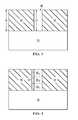
A challenge faced by the semiconductor industry, however, is that although the MOS transistors formed on III-V compound semiconductors or germanium have high drive currents, the leakage currents of these MOS transistors are also high. This is partially caused by the low bandgap and the high dielectric constants of the III-V compound semiconductors and germanium. For example,FIG. 1 illustrates the comparison of bandgaps and dielectric constants of germanium, commonly used III-V compound semiconductors, and other semiconductor materials such as group IV materials.FIG. 1 reveals that the bandgaps of germanium and some commonly used III-V compound semiconductors are small. Therefore, the respective MOS transistors suffer from high band-to-band leakage currents between their gates and source/drain regions. The high dielectric constants of these materials further worsen the leakage currents. As a result, the on/off current ratios (Ion/Ioff) of III-V based MOS transistors and germanium-based MOS transistors are relatively low.
In accordance with one aspect of the present invention, an integrated circuit structure includes a semiconductor substrate; insulation regions over the semiconductor substrate; and an epitaxy region over the semiconductor substrate and having at least a portion in a space between the insulation regions. The epitaxy region includes a III-V compound semiconductor material. The epitaxy region also includes a lower portion and an upper portion over the lower portion. The lower portion and the semiconductor substrate have a first lattice mismatch. The upper portion and the semiconductor substrate have a second lattice mismatch different from the first lattice mismatch.
Other embodiments are also disclosed.
The advantageous features of the present invention include improved performance in MOS transistors including improved drive currents, reduced leakage currents, and high on-to-off current ratios.
For a more complete understanding of the present invention, and the advantages thereof, reference is now made to the following descriptions taken in conjunction with the accompanying drawings, in which:
The making and using of the embodiments of the present invention are discussed in detail below. It should be appreciated, however, that the embodiments provide many applicable inventive concepts that can be embodied in a wide variety of specific contexts. The specific embodiments discussed are merely illustrative of specific ways to make and use the invention, and do not limit the scope of the invention.
Novel fin field-effect transistors (FinFETs) and the method of forming the same are presented. The intermediate stages of manufacturing embodiments of the present invention are illustrated. The variations and the operation of the embodiments are discussed. Throughout the various views and illustrative embodiments of the present invention, like reference numbers are used to designate like elements.
Next, as shown inFIG. 3 , the portion ofsubstrate 10 between opposite sidewalls ofinsulation regions 14 is recessed to formopening 18. Recessing depth D1 may be substantially equal to or less than thickness D2 ofinsulation regions 14.
InFIG. 4 ,semiconductor material 22 is epitaxially grown in opening18.Semiconductor material 22 may include a material with a high electron mobility such as a III-V compound semiconductor material, which may include, but is not limited to, GaAs, InP, GaN, InGaAs, InAlAs, GaSb, AlSb, AlAs, AlP, GaP, combinations thereof, and multi-layers thereof. In an embodiment,semiconductor material 22 includes a gradient composition, with the compositions of lower portions gradually changed to the desirable composition of upper portions. Also, the bottom portion ofsemiconductor material 22 may have a lattice constant closer to the lattice constant ofsubstrate 10, while the lattice constant mismatch betweensemiconductor material 22 andsubstrate 10 gradually increases from the bottom to the top ofsemiconductor material 22. In an exemplary embodiment, as schematically illustrated inFIG. 4 , thebottom portion 221is formed of GaAs, whilesubstrate 10 is formed of silicon. The lattice constant of GaAs is greater than that of silicon, with the lattice constant mismatch between GaAs and silicon being about 4 percent. Thetop portion 223ofsemiconductor material 22 may be formed of InGaAs with a composition between that of In0.5Ga0.47As and that of In0.7Ga0.3As. If formed of In0.5Ga0.47As, the lattice constant oftop portion 223is greater than that of silicon by about 8 percent. The middle portions ofsemiconductor material 22 have compositions between the composition ofbottom portion 221and the composition oftop portion 223. Accordingly, the middle portions ofsemiconductor material 22 have lattice constants between the lattice constant ofbottom portion 221and the lattice constant oftop portion 223. For example, inmiddle portion 222, the indium percentage increased from bottom to top, with a portion of anexemplary middle portion 222having a composition In0.2Ga0.8As.
In alternative embodiments,bottom portion 221is formed of germanium, and InGaAs is formed on germanium, with the percentage of indium in InGaAs gradually increasing from lower portions to upper portions, until the desirable composition such as In0.5Ga0.47As, In0.7Ga0.3As, or a composition therebetween is achieved intop portion 223.
In the resulting structure,top portion 223ofsemiconductor material 22 is formed of a high-mobility III-V compound semiconductor material, which is at least a ternary material including three group III and group V elements. Alternatively, the high-mobility III-V compound semiconductor material further includes an additional group III and group V element to form a quaternary material such as InGaAlAs, InGaAlN, InPAsGa, and the like.
Referring toFIG. 5 , the upper portions ofinsulation regions 14 are selectively etched, while bottom portions are left un-etched. As a result,semiconductor material 22 has a portion standing above the bottom portions ofinsulation regions 14, thus formingfin 24.
Next, as shown inFIG. 6 , high-bandgap semiconductor layer 26 is epitaxially grown. In an embodiment,fin 24 has bandgap EgA, while high-bandgap semiconductor layer 26 has bandgap EgB greater than bandgap EgA. In an exemplary embodiment, bandgap EgB is greater than bandgap EgA by about 0.1 eV, although greater or lower bandgap differences may also apply. Conduction band EcA offin 24 may also be lower than the conduction band EcB of high-bandgap semiconductor layer 26. In an exemplary embodiment, conduction band EcA is lower than conduction band EcB by about 0.1 eV, although greater or lower conduction band differences may also apply. The appropriate materials of high-bandgap semiconductor layer 26 may be selected by comparing the bandgaps of the available semiconductor materials with high electron mobilities, which may include, but are not limited to, silicon, germanium, GaAs, InP, GaN, InGaAs, InAlAs, GaSb, AlSb, AlAs, AlP, GaP, and the like. In an exemplary embodiment, high-bandgap semiconductor layer 26 comprises GaAs.
The structure shown inFIG. 5 may be used to form a fin field-effect transistor (FinFET).FIG. 6 further illustrates the formation ofgate dielectric 30 andgate electrode 34.Gate dielectric 30 may be formed of commonly used dielectric materials such as silicon oxide, silicon nitride, oxynitrides, multi-layers thereof, and combinations thereof.Gate dielectric 30 may also be formed of high-k dielectric materials. The exemplary high-k materials may have k values greater than about 4.0, or even greater than about 7.0, and may include aluminum-containing dielectrics such as Al2O3, HfAlO, HfAlON, AlZrO, Hf-containing materials such as HfO2, HfSiOx, HfAlOx, HfZrSiOx, HfSiON, and/or other materials such as LaAlO3and ZrO2.Gate electrode 34 may be formed of doped polysilicon, metals, metal nitrides, metal silicides, and the like. The bottom ends ofgate dielectric 30 andgate electrode 34 may contact the top surface ofinsulation regions 14.
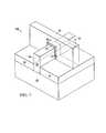
After the formation ofgate dielectric 30 andgate electrode 34, source and drain regions may be formed. A perspective view of resulting FinFET100 (which may be an n-type FinFET) is shown inFIG. 7 .FinFET 100 includessource region 44,drain region 46, andfin 24 therebetween.FinFET 100 may be an NFET, andsource region 44 and drainregion 46 are n-type regions doped with an n-type impurity, for example, by implantations. Alternatively,FinFET 100 may be a PFET, andsource region 44 and drainregion 46 are p-type regions doped with a p-type impurity.
InFinFET 100, with bandgap EgA offin 24 being lower than bandgap EgB of high-bandgap semiconductor layer 26,fin 24 and the portion of high-bandgap semiconductor layer 26 on opposite sidewalls of fin24 (refer toFIG. 6 ) form a quantum well. The quantum effect is partially affected by the thickness T of fin24 (seeFIG. 6 ), which thickness is equal to spacing S inFIG. 2 . When a non-zero gate voltage is applied togate electrode 34, due to the quantum confinement effect, electrons tend to flow throughfin 24. Accordingly, the carrier mobility is high because of the low bandgap EgA, and hence the on-current Ion of therespective FinFET 100 is high. On the other hand, whenFinFET 100 is turned off with the gate voltage being zero volts, electrons tend to flow through the high-bandgap semiconductor layers26. Accordingly, the carrier mobility is low due to the high bandgap EgB, and hence the off-current (leakage current) Ioff of therespective FinFET 100 is low.FinFET 100 thus has a high on/off current ratio.
InFIG. 9 ,mask layer 50 is patterned, for example by etching, and hence opening18 are generated.Semiconductor substrate 10 is exposed throughopening 18. In this embodiment, the remaining portions ofmask layer 50 act asinsulation region 14 and have substantially the same function asinsulation region 14 as shown inFIGS. 2-6 . The remaining steps of this embodiment are substantially the same as the steps illustrated inFIGS. 3-6 , and hence are not repeated herein.
The embodiments of the present invention provide low-cost processes for growing high-mobility and low defect III-V compound semiconductor materials by gradually adjusting compositions of the III-V compound semiconductor materials. The transistors formed on the III-V compound semiconductor materials may have increased Ion/Ioff ratios due to the use of small bandgap channels and large bandgap leakage paths.
Although the present invention and its advantages have been described in detail, it should be understood that various changes, substitutions and alterations can be made herein without departing from the spirit and scope of the invention as defined by the appended claims. Moreover, the scope of the present application is not intended to be limited to the particular embodiments of the process, machine, manufacture, and composition of matter, means, methods and steps described in the specification. As one of ordinary skill in the art will readily appreciate from the disclosure of the present invention, processes, machines, manufacture, compositions of matter, means, methods, or steps, presently existing or later to be developed, that perform substantially the same function or achieve substantially the same result as the corresponding embodiments described herein may be utilized according to the present invention. Accordingly, the appended claims are intended to include within their scope such processes, machines, manufacture, compositions of matter, means, methods, or steps. In addition, each claim constitutes a separate embodiment, and the combination of various claims and embodiments are within the scope of the invention.
Claims (20)
1. An integrated circuit structure comprising:
a semiconductor substrate having a first lattice constant;
insulation regions on the semiconductor substrate and having sidewalls facing each other;
an epitaxy region comprising a III-V compound semiconductor material over the semiconductor substrate, the epitaxy regions having sidewalls adjoining the sidewalls of the insulation regions, wherein the epitaxy region further comprises:
a fin protruding above the insulation regions and having a second lattice constant different from the first lattice constant; and
a gradient epitaxy region between the fin and the semiconductor substrate, wherein the gradient epitaxy region has a third lattice constant between the first lattice constant and the second lattice constant, and wherein sidewalls of the fin are substantially vertically aligned to sidewalls of the gradient epitaxy region; and
a high-bandgap semiconductor layer on a top surface and the sidewalls of the fin, wherein the high-bandgap semiconductor layer has a bandgap greater than a bandgap of the fin.
2. The integrated circuit structure ofclaim 1 further comprising:
a gate dielectric on the high-bandgap semiconductor layer;
a gate electrode over the gate dielectric; and
a source region and a drain region on opposite ends of the fin, wherein each of the fin and the high-bandgap semiconductor layer extends from the source region to the drain region.
3. The integrated circuit structure ofclaim 1 , wherein a bottom surface of the high-bandgap semiconductor layer contacts the insulation regions.
4. The integrated circuit structure ofclaim 1 , wherein the fin is formed of a ternary III-V compound semiconductor material.
5. The integrated circuit structure ofclaim 1 , wherein the fin is formed of a quaternary III-V compound semiconductor material.
6. The integrated circuit structure ofclaim 1 , wherein the gradient epitaxy region has a gradient lattice constant, with lower portions of the gradient epitaxy region having smaller lattice constants than lattice constants of upper portions of the gradient epitaxy region.
7. The integrated circuit structure ofclaim 1 , further comprising a III-V compound semiconductor material layer interposed between the gradient epitaxy region and the semiconductor substrate, the III-V compound semiconductor material layer having a fourth lattice constant, the fourth lattice constant being between the first lattice constant and a lattice constant of the gradient epitaxy region at an interface between the III-V compound semiconductor material layer and the gradient epitaxy region.
8. The integrated circuit structure ofclaim 7 , wherein the III-V compound semiconductor material layer comprises GaAs.
9. An integrated circuit structure comprising:
a semiconductor substrate having a first lattice constant;
a first epitaxy region above the semiconductor substrate, the first epitaxy region having a gradient composition such that a concentration of a first element increases as the first epitaxy region extends away from the semiconductor substrate, a first end of the first epitaxy region closest to the semiconductor substrate having a lattice constant closer to the first lattice constant than a lattice constant of a second end of the first epitaxy region, the second end being opposite the first end;
insulation regions on opposing sides of the first epitaxy region, the insulation regions extending above a lower surface of the first epitaxy region, the first epitaxy region extending above the insulation regions forming a fin; and
a high-bandgap semiconductor layer on a top surface and sidewalls of the fin, wherein the high-bandgap semiconductor layer has a bandgap greater than a bandgap of the first epitaxy region.
10. The integrated circuit structure ofclaim 9 , further comprising a second epitaxy region interposed between the first epitaxy region and the semiconductor substrate.
11. The integrated circuit structure ofclaim 10 , wherein the second epitaxy region comprises germanium.
12. The integrated circuit structure ofclaim 10 , wherein the first epitaxy region comprises InGaAs, wherein a percentage of indium increases as the first epitaxy region extends away from the semiconductor substrate.
13. The integrated circuit structure ofclaim 11 , wherein the high-bandgap semiconductor layer is GaAs.
14. The integrated circuit structure ofclaim 9 , wherein the first epitaxy region contacts the semiconductor substrate.
15. An integrated circuit structure comprising:
a semiconductor substrate having a first lattice constant;
a first epitaxy layer over the semiconductor substrate, the first epitaxy layer having a second lattice constant;
a second epitaxy layer over the first epitaxy layer, the second epitaxy layer having a third lattice constant, the second epitaxy layer having a gradient composition, the second lattice constant being between the first lattice constant and the third lattice constant; and
isolation regions on opposing sides of the first epitaxy layer, an upper surface of the isolation regions extending higher than an interface between the first epitaxy layer and the second epitaxy layer.
16. The integrated circuit structure ofclaim 15 , wherein the first epitaxy layer is GaAs or Ge.
17. The integrated circuit structure ofclaim 16 , wherein the second epitaxy layer is InGaAs, wherein a concentration of indium increases as the second epitaxy layer extends away from the semiconductor substrate.
18. The integrated circuit structure ofclaim 15 , further comprising a high-bandgap semiconductor layer on a top surface and sidewalls of the second epitaxy layer, wherein the high-bandgap semiconductor layer has a bandgap greater than a bandgap of the second epitaxy layer.
19. The integrated circuit structure ofclaim 15 , wherein a lattice constant of the second epitaxy layer distal from the semiconductor substrate is 8% greater than a lattice constant of the semiconductor substrate.
20. The integrated circuit structure ofclaim 19 , wherein the second lattice constant is 4% greater than the first lattice constant.
Priority Applications (1)
| Application Number | Priority Date | Filing Date | Title |
|---|---|---|---|
| US15/707,922US10269970B2 (en) | 2009-05-29 | 2017-09-18 | Gradient ternary or quaternary multiple-gate transistor |
Applications Claiming Priority (3)
| Application Number | Priority Date | Filing Date | Title |
|---|---|---|---|
| US18255009P | 2009-05-29 | 2009-05-29 | |
| US12/616,068US9768305B2 (en) | 2009-05-29 | 2009-11-10 | Gradient ternary or quaternary multiple-gate transistor |
| US15/707,922US10269970B2 (en) | 2009-05-29 | 2017-09-18 | Gradient ternary or quaternary multiple-gate transistor |
Related Parent Applications (1)
| Application Number | Title | Priority Date | Filing Date |
|---|---|---|---|
| US12/616,068ContinuationUS9768305B2 (en) | 2009-05-29 | 2009-11-10 | Gradient ternary or quaternary multiple-gate transistor |
Publications (2)
| Publication Number | Publication Date |
|---|---|
| US20180006156A1 US20180006156A1 (en) | 2018-01-04 |
| US10269970B2true US10269970B2 (en) | 2019-04-23 |
Family
ID=43219244
Family Applications (2)
| Application Number | Title | Priority Date | Filing Date |
|---|---|---|---|
| US12/616,068Active2032-08-14US9768305B2 (en) | 2009-05-29 | 2009-11-10 | Gradient ternary or quaternary multiple-gate transistor |
| US15/707,922Active2029-11-20US10269970B2 (en) | 2009-05-29 | 2017-09-18 | Gradient ternary or quaternary multiple-gate transistor |
Family Applications Before (1)
| Application Number | Title | Priority Date | Filing Date |
|---|---|---|---|
| US12/616,068Active2032-08-14US9768305B2 (en) | 2009-05-29 | 2009-11-10 | Gradient ternary or quaternary multiple-gate transistor |
Country Status (5)
| Country | Link |
|---|---|
| US (2) | US9768305B2 (en) |
| JP (1) | JP5341020B2 (en) |
| KR (1) | KR101226827B1 (en) |
| CN (1) | CN101924105B (en) |
| TW (1) | TWI440182B (en) |
Families Citing this family (67)
| Publication number | Priority date | Publication date | Assignee | Title |
|---|---|---|---|---|
| CN101853882B (en) | 2009-04-01 | 2016-03-23 | 台湾积体电路制造股份有限公司 | There is the high-mobility multiple-gate transistor of the switch current ratio of improvement |
| US8816391B2 (en) | 2009-04-01 | 2014-08-26 | Taiwan Semiconductor Manufacturing Company, Ltd. | Source/drain engineering of devices with high-mobility channels |
| US8455860B2 (en) | 2009-04-30 | 2013-06-04 | Taiwan Semiconductor Manufacturing Company, Ltd. | Reducing source/drain resistance of III-V based transistors |
| US9768305B2 (en) | 2009-05-29 | 2017-09-19 | Taiwan Semiconductor Manufacturing Company, Ltd. | Gradient ternary or quaternary multiple-gate transistor |
| US8617976B2 (en) | 2009-06-01 | 2013-12-31 | Taiwan Semiconductor Manufacturing Company, Ltd. | Source/drain re-growth for manufacturing III-V based transistors |
| US8629478B2 (en)* | 2009-07-31 | 2014-01-14 | Taiwan Semiconductor Manufacturing Company, Ltd. | Fin structure for high mobility multiple-gate transistor |
| US8344425B2 (en)* | 2009-12-30 | 2013-01-01 | Intel Corporation | Multi-gate III-V quantum well structures |
| US8455929B2 (en) | 2010-06-30 | 2013-06-04 | Taiwan Semiconductor Manufacturing Company, Ltd. | Formation of III-V based devices on semiconductor substrates |
| US8890207B2 (en) | 2011-09-06 | 2014-11-18 | Taiwan Semiconductor Manufacturing Company, Ltd. | FinFET design controlling channel thickness |
| CN103000524B (en)* | 2011-09-13 | 2016-03-23 | 中芯国际集成电路制造(上海)有限公司 | Fin FET and manufacture method thereof |
| US9099388B2 (en)* | 2011-10-21 | 2015-08-04 | Taiwan Semiconductor Manufacturing Company, Ltd. | III-V multi-channel FinFETs |
| KR101805634B1 (en)* | 2011-11-15 | 2017-12-08 | 삼성전자 주식회사 | Semiconductor device comprising III-V group barrier and method of manufacturing the same |
| US9406518B2 (en)* | 2011-11-18 | 2016-08-02 | Taiwan Semiconductor Manufacturing Company, Ltd. | (110) surface orientation for reducing fermi-level-pinning between high-K dielectric and group III-V compound semiconductor substrate |
| KR101608494B1 (en) | 2011-12-19 | 2016-04-01 | 인텔 코포레이션 | Group iii-n transistors for system on chip(soc) architecture integrating power management and radio frequency circuits |
| KR101700213B1 (en)* | 2011-12-21 | 2017-01-26 | 인텔 코포레이션 | Methods for forming fins for metal oxide semiconductor device structures |
| US8486770B1 (en)* | 2011-12-30 | 2013-07-16 | Taiwan Semiconductor Manufacturing Company, Ltd. | Method of forming CMOS FinFET device |
| US8742509B2 (en)* | 2012-03-01 | 2014-06-03 | Taiwan Semiconductor Manufacturing Company, Ltd. | Apparatus and method for FinFETs |
| US8836016B2 (en) | 2012-03-08 | 2014-09-16 | Taiwan Semiconductor Manufacturing Company, Ltd. | Semiconductor structures and methods with high mobility and high energy bandgap materials |
| US9142400B1 (en) | 2012-07-17 | 2015-09-22 | Stc.Unm | Method of making a heteroepitaxial layer on a seed area |
| US9728464B2 (en) | 2012-07-27 | 2017-08-08 | Intel Corporation | Self-aligned 3-D epitaxial structures for MOS device fabrication |
| EP2709156A3 (en)* | 2012-09-14 | 2014-04-23 | Imec | Band engineered semiconductor device and method for manufacturing thereof |
| US8716751B2 (en) | 2012-09-28 | 2014-05-06 | Intel Corporation | Methods of containing defects for non-silicon device engineering |
| US8723225B2 (en)* | 2012-10-04 | 2014-05-13 | Taiwan Semiconductor Manufacturing Company, Ltd. | Guard rings on fin structures |
| EP2717316B1 (en)* | 2012-10-05 | 2019-08-14 | IMEC vzw | Method for producing strained germanium fin structures |
| CN103811344B (en)* | 2012-11-09 | 2016-08-10 | 中国科学院微电子研究所 | Semiconductor device and method for manufacturing the same |
| US8847324B2 (en)* | 2012-12-17 | 2014-09-30 | Synopsys, Inc. | Increasing ION /IOFF ratio in FinFETs and nano-wires |
| US8896101B2 (en) | 2012-12-21 | 2014-11-25 | Intel Corporation | Nonplanar III-N transistors with compositionally graded semiconductor channels |
| US9362386B2 (en)* | 2013-02-27 | 2016-06-07 | Taiwan Semiconductor Manufacturing Company, Ltd. | FETs and methods for forming the same |
| EP2775528B1 (en)* | 2013-03-05 | 2019-07-17 | IMEC vzw | Passivated III-V or Ge fin-shaped field effect transistor |
| US9385198B2 (en) | 2013-03-12 | 2016-07-05 | Taiwan Semiconductor Manufacturing Company, Ltd. | Heterostructures for semiconductor devices and methods of forming the same |
| US9312344B2 (en) | 2013-03-13 | 2016-04-12 | Taiwan Semiconductor Manufacturing Company, Ltd. | Methods for forming semiconductor materials in STI trenches |
| CN105164809B (en) | 2013-06-26 | 2018-07-24 | 美商新思科技有限公司 | FinFETs with heterojunction and improved channel control |
| KR102098900B1 (en)* | 2013-06-28 | 2020-04-08 | 인텔 코포레이션 | Making a defect free fin based device in lateral epitaxy overgrowth region |
| CN104282565B (en)* | 2013-07-03 | 2017-08-25 | 中芯国际集成电路制造(上海)有限公司 | Fin formula field effect transistor and forming method thereof |
| WO2015047353A1 (en)* | 2013-09-27 | 2015-04-02 | Intel Corporation | Methods to achieve high mobility in cladded iii-v channel materials |
| CN105493251A (en)* | 2013-09-27 | 2016-04-13 | 英特尔公司 | Non-planar semiconductor device with multi-layer flexible substrate |
| EP3050092A4 (en) | 2013-09-27 | 2017-05-03 | Intel Corporation | Non-silicon device heterolayers on patterned silicon substrate for cmos by combination of selective and conformal epitaxy |
| KR102138871B1 (en) | 2013-09-27 | 2020-07-28 | 인텔 코포레이션 | Semiconductor device having group iii-v material active region and graded gate dielectric |
| CN104766867A (en)* | 2014-01-03 | 2015-07-08 | 中国科学院微电子研究所 | Semiconductor device and method for manufacturing the same |
| US9865688B2 (en) | 2014-03-14 | 2018-01-09 | International Business Machines Corporation | Device isolation using preferential oxidation of the bulk substrate |
| EP3123521A4 (en) | 2014-03-27 | 2017-10-25 | Intel Corporation | Confined epitaxial regions for semiconductor devices and methods of fabricating semiconductor devices having confined epitaxial regions |
| KR102175767B1 (en)* | 2014-05-02 | 2020-11-06 | 삼성전자주식회사 | Method Of Forming a finFET and Integrated Circuit Device |
| JP6428789B2 (en)* | 2014-06-24 | 2018-11-28 | インテル・コーポレーション | Integrated circuits, complementary metal oxide semiconductor (CMOS) devices, computing systems, and methods |
| US9293523B2 (en)* | 2014-06-24 | 2016-03-22 | Applied Materials, Inc. | Method of forming III-V channel |
| US9263555B2 (en)* | 2014-07-03 | 2016-02-16 | Globalfoundries Inc. | Methods of forming a channel region for a semiconductor device by performing a triple cladding process |
| CN105448985B (en)* | 2014-08-14 | 2018-12-11 | 中国科学院微电子研究所 | Semiconductor device and method for manufacturing the same |
| WO2016043769A1 (en)* | 2014-09-19 | 2016-03-24 | Intel Corporation | Apparatus and methods to create an indium gallium arsenide active channel having indium rich surfaces |
| WO2016043770A1 (en)* | 2014-09-19 | 2016-03-24 | Intel Corporation | Apparatus and methods to create a buffer to reduce leakage in microelectronic transistors |
| US10497814B2 (en) | 2014-12-23 | 2019-12-03 | Intel Corporation | III-V semiconductor alloys for use in the subfin of non-planar semiconductor devices and methods of forming the same |
| US9520466B2 (en) | 2015-03-16 | 2016-12-13 | Taiwan Semiconductor Manufacturing Company, Ltd. | Vertical gate-all-around field effect transistors and methods of forming same |
| KR102372167B1 (en)* | 2015-04-24 | 2022-03-07 | 삼성전자주식회사 | Semiconductor device |
| KR102454077B1 (en) | 2015-06-23 | 2022-10-14 | 인텔 코포레이션 | Indium-Rich NMS Transistor Channels |
| KR102427071B1 (en) | 2015-06-24 | 2022-08-01 | 인텔 코포레이션 | Sub-Fin Sidewall Passivation in Alternate Channel FinFETs |
| EP3353810A4 (en) | 2015-09-25 | 2019-05-01 | Intel Corporation | PASSIVATION OF TRANSISTOR CHANNEL ZONE INTERFACES |
| CN106611787A (en)* | 2015-10-26 | 2017-05-03 | 联华电子股份有限公司 | Semiconductor structure and manufacturing method thereof |
| US20170236841A1 (en)* | 2016-02-11 | 2017-08-17 | Qualcomm Incorporated | Fin with an epitaxial cladding layer |
| WO2017146676A1 (en)* | 2016-02-22 | 2017-08-31 | Intel Corporation | Apparatus and methods to create an active channel having indium rich side and bottom surfaces |
| CN107154355B (en)* | 2016-03-03 | 2020-04-10 | 上海新昇半导体科技有限公司 | Fin-shaped field effect transistor and preparation method thereof |
| CN107154429B (en)* | 2016-03-03 | 2020-04-10 | 上海新昇半导体科技有限公司 | Fin-shaped field effect transistor and preparation method thereof |
| US10475930B2 (en) | 2016-08-17 | 2019-11-12 | Samsung Electronics Co., Ltd. | Method of forming crystalline oxides on III-V materials |
| US10529832B2 (en)* | 2016-12-19 | 2020-01-07 | International Business Machines Corporation | Shallow, abrupt and highly activated tin extension implant junction |
| JP7038497B2 (en)* | 2017-07-07 | 2022-03-18 | 東京エレクトロン株式会社 | Manufacturing method of electrostatic chuck |
| RU2737136C2 (en)* | 2017-07-13 | 2020-11-25 | Интел Корпорейшн | Manufacturing of defects-free device based on a rib in the area of transverse epitaxial growth |
| KR102396978B1 (en) | 2018-11-16 | 2022-05-11 | 삼성전자주식회사 | Semiconductor device |
| KR102747249B1 (en) | 2020-07-17 | 2025-01-02 | 삼성전자주식회사 | Semiconductor devices |
| KR20220068283A (en) | 2020-11-18 | 2022-05-26 | 삼성전자주식회사 | Semiconductor device |
| US11855209B2 (en) | 2020-12-07 | 2023-12-26 | Samsung Electronics Co., Ltd. | Semiconductor device |
Citations (91)
| Publication number | Priority date | Publication date | Assignee | Title |
|---|---|---|---|---|
| US5055890A (en) | 1990-01-25 | 1991-10-08 | The United States Of America As Represented By The United States Department Of Energy | Nonvolatile semiconductor memory having three dimension charge confinement |
| US5621227A (en) | 1995-07-18 | 1997-04-15 | Discovery Semiconductors, Inc. | Method and apparatus for monolithic optoelectronic integrated circuit using selective epitaxy |
| EP0921575A2 (en) | 1997-12-03 | 1999-06-09 | Matsushita Electric Industrial Co., Ltd. | Semiconductor device comprising a heterostructure MIS field-effect transistor having a strained channel layer |
| US6121153A (en) | 1994-08-29 | 2000-09-19 | Fujitsu Limited | Semiconductor device having a regrowth crystal region |
| CN1289149A (en) | 1999-03-12 | 2001-03-28 | 国际商业机器公司 | High-speed composite p channel si/siGe heterogeneous structure of field-effect devices |
| US6218685B1 (en) | 1998-01-08 | 2001-04-17 | Matsushita Electronics Corporation | Semiconductor device and method for fabricating the same |
| US20020042189A1 (en) | 2000-10-10 | 2002-04-11 | Kazuyasu Tanaka | Manufacturing method of semiconductor chip with adhesive agent |
| US6399970B2 (en) | 1996-09-17 | 2002-06-04 | Matsushita Electric Industrial Co., Ltd. | FET having a Si/SiGeC heterojunction channel |
| US6475890B1 (en) | 2001-02-12 | 2002-11-05 | Advanced Micro Devices, Inc. | Fabrication of a field effect transistor with an upside down T-shaped semiconductor pillar in SOI technology |
| US6475869B1 (en) | 2001-02-26 | 2002-11-05 | Advanced Micro Devices, Inc. | Method of forming a double gate transistor having an epitaxial silicon/germanium channel region |
| US6512252B1 (en) | 1999-11-15 | 2003-01-28 | Matsushita Electric Industrial Co., Ltd. | Semiconductor device |
| US6558478B1 (en) | 1999-10-06 | 2003-05-06 | Ebara Corporation | Method of and apparatus for cleaning substrate |
| US20030178677A1 (en) | 2002-03-19 | 2003-09-25 | International Business Machines Corporation | Strained fin fets structure and method |
| US6654604B2 (en) | 2000-11-21 | 2003-11-25 | Matsushita Electric Industrial Co. Ltd. | Equipment for communication system |
| US6706571B1 (en) | 2002-10-22 | 2004-03-16 | Advanced Micro Devices, Inc. | Method for forming multiple structures in a semiconductor device |
| US20040104404A1 (en) | 2002-11-26 | 2004-06-03 | Nec Compound Semiconductor Devices, Ltd. | Heterojunction field effect type semiconductor device having high gate turn-on voltage and low on-resistance and its manufacturing method |
| US6762483B1 (en) | 2003-01-23 | 2004-07-13 | Advanced Micro Devices, Inc. | Narrow fin FinFET |
| US20040173812A1 (en) | 2003-03-07 | 2004-09-09 | Amberwave Systems Corporation | Shallow trench isolation process |
| US20040251479A1 (en) | 2003-06-16 | 2004-12-16 | Matsushita Electric Industrial Co., Ltd. | Semiconductor device and method for fabricating the same |
| US20040256647A1 (en) | 2003-06-23 | 2004-12-23 | Sharp Laboratories Of America Inc. | Strained silicon finFET device |
| JP2005005646A (en) | 2003-06-16 | 2005-01-06 | Nippon Telegr & Teleph Corp <Ntt> | Semiconductor device |
| US20050029542A1 (en) | 1998-08-12 | 2005-02-10 | Hiroshi Mizutani | Semiconductor switches and switching circuits for microwave |
| US6858478B2 (en) | 2002-08-23 | 2005-02-22 | Intel Corporation | Tri-gate devices and methods of fabrication |
| JP2005051241A (en) | 2003-07-25 | 2005-02-24 | Interuniv Micro Electronica Centrum Vzw | Multilayer gate semiconductor device and manufacturing method thereof |
| JP2005062219A (en) | 2003-08-08 | 2005-03-10 | Nikon Corp | Optical member switching device and microscope using the same |
| US6867433B2 (en) | 2003-04-30 | 2005-03-15 | Taiwan Semiconductor Manufacturing Company, Ltd. | Semiconductor-on-insulator chip incorporating strained-channel partially-depleted, fully-depleted, and multiple-gate transistors |
| US20050093154A1 (en) | 2003-07-25 | 2005-05-05 | Interuniversitair Microelektronica Centrum (Imec Vzw) | Multiple gate semiconductor device and method for forming same |
| US20050104137A1 (en) | 2002-08-12 | 2005-05-19 | Carl Faulkner | Insulated gate field-effect transistor having III-VI source/drain layer(s) |
| US20050136622A1 (en) | 2003-12-18 | 2005-06-23 | Mulligan Rose A. | Methods and apparatus for laser dicing |
| US20050153490A1 (en) | 2003-12-16 | 2005-07-14 | Jae-Man Yoon | Method of forming fin field effect transistor |
| US20050158913A1 (en) | 2004-01-19 | 2005-07-21 | Fuji Photo Film Co., Ltd. | Solid state imaging apparatus and its manufacturing method |
| US20050186742A1 (en) | 2004-02-24 | 2005-08-25 | Chang-Woo Oh | Vertical channel fin field-effect transistors having increased source/drain contact area and methods for fabricating the same |
| US20050205934A1 (en) | 2002-06-07 | 2005-09-22 | Amberwave Systems Corporation | Strained germanium-on-insulator device structures |
| US20050217707A1 (en) | 1998-03-13 | 2005-10-06 | Aegerter Brian K | Selective processing of microelectronic workpiece surfaces |
| US20060057856A1 (en) | 2004-09-09 | 2006-03-16 | Toshiba Ceramics Co., Ltd. | Manufacturing method for strained silicon wafer |
| US20060076625A1 (en) | 2004-09-25 | 2006-04-13 | Lee Sung-Young | Field effect transistors having a strained silicon channel and methods of fabricating same |
| US7042009B2 (en) | 2004-06-30 | 2006-05-09 | Intel Corporation | High mobility tri-gate devices and methods of fabrication |
| US20060148182A1 (en) | 2005-01-03 | 2006-07-06 | Suman Datta | Quantum well transistor using high dielectric constant dielectric layer |
| US20060211220A1 (en) | 2003-05-12 | 2006-09-21 | Tokyo Seimitsu Co., Ltd. | Method and device or dividing plate-like member |
| US20060275988A1 (en) | 2005-06-03 | 2006-12-07 | Atsushi Yagishita | Semiconductor device and method of fabricating the same |
| TWI269358B (en) | 2004-03-31 | 2006-12-21 | Intel Corp | A bulk non-planar transistor having strained enhanced mobility and methods of fabrication |
| US20060292887A1 (en) | 2005-06-24 | 2006-12-28 | Seiko Epson Corporation | Manufacturing method for a semiconductor device |
| US20060292719A1 (en) | 2005-05-17 | 2006-12-28 | Amberwave Systems Corporation | Lattice-mismatched semiconductor structures with reduced dislocation defect densities and related methods for device fabrication |
| US7190050B2 (en) | 2005-07-01 | 2007-03-13 | Synopsys, Inc. | Integrated circuit on corrugated substrate |
| WO2007046150A1 (en) | 2005-10-21 | 2007-04-26 | Fujitsu Limited | Fin type semiconductor device and method for manufacturing same |
| US20070102763A1 (en) | 2003-09-24 | 2007-05-10 | Yee-Chia Yeo | Multiple-gate transistors formed on bulk substrates |
| US20070122954A1 (en) | 2005-07-01 | 2007-05-31 | Synopsys, Inc. | Sequential Selective Epitaxial Growth |
| US20070122953A1 (en) | 2005-07-01 | 2007-05-31 | Synopsys, Inc. | Enhanced Segmented Channel MOS Transistor with High-Permittivity Dielectric Isolation Material |
| US20070120156A1 (en) | 2005-07-01 | 2007-05-31 | Synopsys, Inc. | Enhanced Segmented Channel MOS Transistor with Multi Layer Regions |
| US20070128782A1 (en) | 2005-07-01 | 2007-06-07 | Synopsys, Inc. | Enhanced Segmented Channel MOS Transistor with Narrowed Base Regions |
| US7247887B2 (en) | 2005-07-01 | 2007-07-24 | Synopsys, Inc. | Segmented channel MOS transistor |
| US7265008B2 (en) | 2005-07-01 | 2007-09-04 | Synopsys, Inc. | Method of IC production using corrugated substrate |
| US20070238281A1 (en) | 2006-03-28 | 2007-10-11 | Hudait Mantu K | Depositing polar materials on non-polar semiconductor substrates |
| US20070243703A1 (en) | 2006-04-14 | 2007-10-18 | Aonex Technololgies, Inc. | Processes and structures for epitaxial growth on laminate substrates |
| JP2008508725A (en) | 2004-07-28 | 2008-03-21 | マイクロン テクノロジー, インク. | Memory device, transistor, memory cell and manufacturing method thereof |
| US7348225B2 (en) | 2005-10-27 | 2008-03-25 | International Business Machines Corporation | Structure and method of fabricating FINFET with buried channel |
| US20080105899A1 (en) | 2006-11-03 | 2008-05-08 | Samsung Electronics Co., Ltd. | Semiconductor device with epitaxially grown layer and fabrication method |
| US20080135879A1 (en) | 2004-06-22 | 2008-06-12 | Samsung Electronics Co., Ltd. | Method of fabricating cmos transistor and cmos transistor fabricated thereby |
| US20080141040A1 (en) | 2006-12-08 | 2008-06-12 | Microsoft Corporation | Secure data protection during disasters |
| JP2008141040A (en) | 2006-12-04 | 2008-06-19 | Nec Corp | Field effect transistor and method of manufacturing the same |
| JP2008160131A (en) | 2006-12-22 | 2008-07-10 | Interuniv Micro Electronica Centrum Vzw | Field effect transistor element and manufacturing method thereof |
| US20080185691A1 (en) | 2007-02-01 | 2008-08-07 | Kangguo Cheng | Fin Pin Diode |
| US20080237655A1 (en) | 2007-03-29 | 2008-10-02 | Kabushiki Kaisha Toshiba | Semiconductor apparatus and method for manufacturing same |
| US20080258243A1 (en) | 2007-04-20 | 2008-10-23 | Masayuki Kuroda | Field effect transistor |
| US20080258176A1 (en) | 2007-04-18 | 2008-10-23 | Yeong-Chang Chou | Antimonide-based compound semiconductor with titanium tungsten stack |
| US20080296632A1 (en) | 2007-05-30 | 2008-12-04 | Synopsys, Inc. | Stress-Enhanced Performance Of A FinFet Using Surface/Channel Orientations And Strained Capping Layers |
| US20080315310A1 (en) | 2007-06-19 | 2008-12-25 | Willy Rachmady | High k dielectric materials integrated into multi-gate transistor structures |
| US20090001415A1 (en) | 2007-06-30 | 2009-01-01 | Nick Lindert | Multi-gate transistor with strained body |
| US20090079014A1 (en) | 2007-09-26 | 2009-03-26 | Sandford Justin S | Transistors with high-k dielectric spacer liner to mitigate lateral oxide encroachment |
| US20090095984A1 (en) | 2005-11-30 | 2009-04-16 | Brask Justin K | Dielectric interface for group iii-v semiconductor device |
| JP2009105163A (en) | 2007-10-22 | 2009-05-14 | Toshiba Corp | Semiconductor device |
| US20090194790A1 (en) | 2008-01-11 | 2009-08-06 | Yoshihiro Sato | Field effect transister and process for producing the same |
| US20090242990A1 (en) | 2008-03-28 | 2009-10-01 | Kabushiki Kaisha Toshiba | Semiconductor device and manufacturing method of same |
| US20090267113A1 (en) | 2005-09-08 | 2009-10-29 | Nissan Motor Co., Ltd. | Semiconductor device and method of manufacturing the same |
| US20090272965A1 (en) | 2008-04-30 | 2009-11-05 | Willy Rachmady | Selective High-K dielectric film deposition for semiconductor device |
| US7683436B2 (en) | 2006-04-28 | 2010-03-23 | Kabushiki Kaisha Toshiba | Semiconductor device having a pole-shaped portion and method of fabricating the same |
| US20100252816A1 (en) | 2009-04-01 | 2010-10-07 | Taiwan Semiconductor Manufacturing Company, Ltd. | High-Mobility Multiple-Gate Transistor with Improved On-to-Off Current Ratio |
| US20100252862A1 (en) | 2009-04-01 | 2010-10-07 | Chih-Hsin Ko | Source/Drain Engineering of Devices with High-Mobility Channels |
| US20100276668A1 (en) | 2009-04-30 | 2010-11-04 | Chih-Hsin Ko | Reducing Source/Drain Resistance of III-V Based Transistors |
| US20100301392A1 (en) | 2009-06-01 | 2010-12-02 | Chih-Hsin Ko | Source/Drain Re-Growth for Manufacturing III-V Based Transistors |
| US20100301390A1 (en) | 2009-05-29 | 2010-12-02 | Chih-Hsin Ko | Gradient Ternary or Quaternary Multiple-Gate Transistor |
| US7883991B1 (en) | 2010-02-18 | 2011-02-08 | Taiwan Semiconductor Manufacturing Company, Ltd. | Temporary carrier bonding and detaching processes |
| US7928426B2 (en) | 2007-03-27 | 2011-04-19 | Intel Corporation | Forming a non-planar transistor having a quantum well channel |
| US7936040B2 (en) | 2008-10-26 | 2011-05-03 | Koucheng Wu | Schottky barrier quantum well resonant tunneling transistor |
| US8058692B2 (en) | 2008-12-29 | 2011-11-15 | Taiwan Semiconductor Manufacturing Company, Ltd. | Multiple-gate transistors with reverse T-shaped fins |
| CN102244503A (en) | 2010-05-11 | 2011-11-16 | 台湾积体电路制造股份有限公司 | Method, apparatus and circuit for correcting resistor-capacitor filter |
| US20120001239A1 (en) | 2010-06-30 | 2012-01-05 | Taiwan Semiconductor Manufacturing Company, Ltd. | Formation of III-V Based Devices on Semiconductor Substrates |
| US8174073B2 (en) | 2007-05-30 | 2012-05-08 | Taiwan Semiconductor Manufacturing Co., Ltd. | Integrated circuit structures with multiple FinFETs |
| US8357927B2 (en) | 2010-03-09 | 2013-01-22 | Hynix Semiconductor Inc. | Semiconductor device and method for manufacturing the same |
| US8440542B2 (en) | 2010-10-11 | 2013-05-14 | Monolithic 3D Inc. | Semiconductor device and structure |
| US8575596B2 (en) | 2009-12-23 | 2013-11-05 | Intel Corporation | Non-planar germanium quantum well devices |
Family Cites Families (5)
| Publication number | Priority date | Publication date | Assignee | Title |
|---|---|---|---|---|
| US6803631B2 (en)* | 2003-01-23 | 2004-10-12 | Advanced Micro Devices, Inc. | Strained channel finfet |
| US6921982B2 (en)* | 2003-07-21 | 2005-07-26 | International Business Machines Corporation | FET channel having a strained lattice structure along multiple surfaces |
| US7198995B2 (en)* | 2003-12-12 | 2007-04-03 | International Business Machines Corporation | Strained finFETs and method of manufacture |
| US8946811B2 (en)* | 2006-07-10 | 2015-02-03 | Taiwan Semiconductor Manufacturing Company, Ltd. | Body-tied, strained-channel multi-gate device and methods of manufacturing same |
| CN100557815C (en)* | 2008-03-24 | 2009-11-04 | 西安电子科技大学 | InAlN/GaN Heterojunction Enhanced High Electron Mobility Transistor Structure and Fabrication Method |
- 2009
- 2009-11-10USUS12/616,068patent/US9768305B2/enactiveActive
- 2010
- 2010-05-10KRKR1020100043489Apatent/KR101226827B1/enactiveActive
- 2010-05-21JPJP2010116844Apatent/JP5341020B2/enactiveActive
- 2010-05-28TWTW099117137Apatent/TWI440182B/enactive
- 2010-05-28CNCN2010101944290Apatent/CN101924105B/enactiveActive
- 2017
- 2017-09-18USUS15/707,922patent/US10269970B2/enactiveActive
Patent Citations (139)
| Publication number | Priority date | Publication date | Assignee | Title |
|---|---|---|---|---|
| US5055890A (en) | 1990-01-25 | 1991-10-08 | The United States Of America As Represented By The United States Department Of Energy | Nonvolatile semiconductor memory having three dimension charge confinement |
| US6121153A (en) | 1994-08-29 | 2000-09-19 | Fujitsu Limited | Semiconductor device having a regrowth crystal region |
| US5621227A (en) | 1995-07-18 | 1997-04-15 | Discovery Semiconductors, Inc. | Method and apparatus for monolithic optoelectronic integrated circuit using selective epitaxy |
| US6399970B2 (en) | 1996-09-17 | 2002-06-04 | Matsushita Electric Industrial Co., Ltd. | FET having a Si/SiGeC heterojunction channel |
| US6472685B2 (en) | 1997-12-03 | 2002-10-29 | Matsushita Electric Industrial Co., Ltd. | Semiconductor device |
| EP0921575A2 (en) | 1997-12-03 | 1999-06-09 | Matsushita Electric Industrial Co., Ltd. | Semiconductor device comprising a heterostructure MIS field-effect transistor having a strained channel layer |
| US6218685B1 (en) | 1998-01-08 | 2001-04-17 | Matsushita Electronics Corporation | Semiconductor device and method for fabricating the same |
| US20050217707A1 (en) | 1998-03-13 | 2005-10-06 | Aegerter Brian K | Selective processing of microelectronic workpiece surfaces |
| US20050029542A1 (en) | 1998-08-12 | 2005-02-10 | Hiroshi Mizutani | Semiconductor switches and switching circuits for microwave |
| CN1289149A (en) | 1999-03-12 | 2001-03-28 | 国际商业机器公司 | High-speed composite p channel si/siGe heterogeneous structure of field-effect devices |
| US6350993B1 (en) | 1999-03-12 | 2002-02-26 | International Business Machines Corporation | High speed composite p-channel Si/SiGe heterostructure for field effect devices |
| US6558478B1 (en) | 1999-10-06 | 2003-05-06 | Ebara Corporation | Method of and apparatus for cleaning substrate |
| US6512252B1 (en) | 1999-11-15 | 2003-01-28 | Matsushita Electric Industrial Co., Ltd. | Semiconductor device |
| US20020042189A1 (en) | 2000-10-10 | 2002-04-11 | Kazuyasu Tanaka | Manufacturing method of semiconductor chip with adhesive agent |
| US6654604B2 (en) | 2000-11-21 | 2003-11-25 | Matsushita Electric Industrial Co. Ltd. | Equipment for communication system |
| US6475890B1 (en) | 2001-02-12 | 2002-11-05 | Advanced Micro Devices, Inc. | Fabrication of a field effect transistor with an upside down T-shaped semiconductor pillar in SOI technology |
| US6475869B1 (en) | 2001-02-26 | 2002-11-05 | Advanced Micro Devices, Inc. | Method of forming a double gate transistor having an epitaxial silicon/germanium channel region |
| US20030178677A1 (en) | 2002-03-19 | 2003-09-25 | International Business Machines Corporation | Strained fin fets structure and method |
| US6635909B2 (en) | 2002-03-19 | 2003-10-21 | International Business Machines Corporation | Strained fin FETs structure and method |
| TW580771B (en) | 2002-03-19 | 2004-03-21 | Ibm | Strained fin FETs structure and method |
| AU2003223306A1 (en) | 2002-03-19 | 2003-10-08 | International Business Machines Corporation | Strained fin fets structure and method |
| JP2005521258A (en) | 2002-03-19 | 2005-07-14 | インターナショナル・ビジネス・マシーンズ・コーポレーション | Strained FinFET Structure and Method |
| WO2003081640A2 (en) | 2002-03-19 | 2003-10-02 | International Business Machines Corporation | Strained fin fets structure and method |
| EP1488462B1 (en) | 2002-03-19 | 2011-02-09 | International Business Machines Corporation | Strained fin fets structure and method |
| US20050205934A1 (en) | 2002-06-07 | 2005-09-22 | Amberwave Systems Corporation | Strained germanium-on-insulator device structures |
| US20050104137A1 (en) | 2002-08-12 | 2005-05-19 | Carl Faulkner | Insulated gate field-effect transistor having III-VI source/drain layer(s) |
| US7382021B2 (en) | 2002-08-12 | 2008-06-03 | Acorn Technologies, Inc. | Insulated gate field-effect transistor having III-VI source/drain layer(s) |
| US6858478B2 (en) | 2002-08-23 | 2005-02-22 | Intel Corporation | Tri-gate devices and methods of fabrication |
| US6706571B1 (en) | 2002-10-22 | 2004-03-16 | Advanced Micro Devices, Inc. | Method for forming multiple structures in a semiconductor device |
| US20040104404A1 (en) | 2002-11-26 | 2004-06-03 | Nec Compound Semiconductor Devices, Ltd. | Heterojunction field effect type semiconductor device having high gate turn-on voltage and low on-resistance and its manufacturing method |
| US6762483B1 (en) | 2003-01-23 | 2004-07-13 | Advanced Micro Devices, Inc. | Narrow fin FinFET |
| US20040197975A1 (en) | 2003-01-23 | 2004-10-07 | Zoran Krivokapic | Narrow fin finfet |
| US6921963B2 (en) | 2003-01-23 | 2005-07-26 | Advanced Micro Devices, Inc | Narrow fin FinFET |
| JP2006516820A (en) | 2003-01-23 | 2006-07-06 | アドバンスト・マイクロ・ディバイシズ・インコーポレイテッド | Method for forming fin FET with narrow fin structure |
| US20040173812A1 (en) | 2003-03-07 | 2004-09-09 | Amberwave Systems Corporation | Shallow trench isolation process |
| US6960781B2 (en) | 2003-03-07 | 2005-11-01 | Amberwave Systems Corporation | Shallow trench isolation process |
| JP2006521026A (en) | 2003-03-07 | 2006-09-14 | アンバーウェーブ システムズ コーポレイション | Shallow trench isolation process |
| US6867433B2 (en) | 2003-04-30 | 2005-03-15 | Taiwan Semiconductor Manufacturing Company, Ltd. | Semiconductor-on-insulator chip incorporating strained-channel partially-depleted, fully-depleted, and multiple-gate transistors |
| US20060211220A1 (en) | 2003-05-12 | 2006-09-21 | Tokyo Seimitsu Co., Ltd. | Method and device or dividing plate-like member |
| JP2005005633A (en) | 2003-06-16 | 2005-01-06 | Matsushita Electric Ind Co Ltd | Semiconductor device and manufacturing method thereof |
| US20040251479A1 (en) | 2003-06-16 | 2004-12-16 | Matsushita Electric Industrial Co., Ltd. | Semiconductor device and method for fabricating the same |
| CN1574399A (en) | 2003-06-16 | 2005-02-02 | 松下电器产业株式会社 | Semiconductor device and manufacturing method thereof |
| US7205615B2 (en) | 2003-06-16 | 2007-04-17 | Matsushita Electric Industrial Co., Ltd. | Semiconductor device having internal stress film |
| JP2005005646A (en) | 2003-06-16 | 2005-01-06 | Nippon Telegr & Teleph Corp <Ntt> | Semiconductor device |
| US7045401B2 (en) | 2003-06-23 | 2006-05-16 | Sharp Laboratories Of America, Inc. | Strained silicon finFET device |
| US20040256647A1 (en) | 2003-06-23 | 2004-12-23 | Sharp Laboratories Of America Inc. | Strained silicon finFET device |
| JP2005019970A (en) | 2003-06-23 | 2005-01-20 | Sharp Corp | Strained silicon fin FET device |
| JP2005051241A (en) | 2003-07-25 | 2005-02-24 | Interuniv Micro Electronica Centrum Vzw | Multilayer gate semiconductor device and manufacturing method thereof |
| US20050093154A1 (en) | 2003-07-25 | 2005-05-05 | Interuniversitair Microelektronica Centrum (Imec Vzw) | Multiple gate semiconductor device and method for forming same |
| JP2005062219A (en) | 2003-08-08 | 2005-03-10 | Nikon Corp | Optical member switching device and microscope using the same |
| US20070102763A1 (en) | 2003-09-24 | 2007-05-10 | Yee-Chia Yeo | Multiple-gate transistors formed on bulk substrates |
| US7863674B2 (en) | 2003-09-24 | 2011-01-04 | Taiwan Semiconductor Manufacturing Company, Ltd. | Multiple-gate transistors formed on bulk substrates |
| US20050153490A1 (en) | 2003-12-16 | 2005-07-14 | Jae-Man Yoon | Method of forming fin field effect transistor |
| US20050136622A1 (en) | 2003-12-18 | 2005-06-23 | Mulligan Rose A. | Methods and apparatus for laser dicing |
| US20050158913A1 (en) | 2004-01-19 | 2005-07-21 | Fuji Photo Film Co., Ltd. | Solid state imaging apparatus and its manufacturing method |
| US20050186742A1 (en) | 2004-02-24 | 2005-08-25 | Chang-Woo Oh | Vertical channel fin field-effect transistors having increased source/drain contact area and methods for fabricating the same |
| US7154118B2 (en) | 2004-03-31 | 2006-12-26 | Intel Corporation | Bulk non-planar transistor having strained enhanced mobility and methods of fabrication |
| TWI269358B (en) | 2004-03-31 | 2006-12-21 | Intel Corp | A bulk non-planar transistor having strained enhanced mobility and methods of fabrication |
| US20080135879A1 (en) | 2004-06-22 | 2008-06-12 | Samsung Electronics Co., Ltd. | Method of fabricating cmos transistor and cmos transistor fabricated thereby |
| US7042009B2 (en) | 2004-06-30 | 2006-05-09 | Intel Corporation | High mobility tri-gate devices and methods of fabrication |
| US7598134B2 (en) | 2004-07-28 | 2009-10-06 | Micron Technology, Inc. | Memory device forming methods |
| JP2008508725A (en) | 2004-07-28 | 2008-03-21 | マイクロン テクノロジー, インク. | Memory device, transistor, memory cell and manufacturing method thereof |
| US20060057856A1 (en) | 2004-09-09 | 2006-03-16 | Toshiba Ceramics Co., Ltd. | Manufacturing method for strained silicon wafer |
| US7250357B2 (en) | 2004-09-09 | 2007-07-31 | Toshiba Ceramics Co., Ltd. | Manufacturing method for strained silicon wafer |
| US20060076625A1 (en) | 2004-09-25 | 2006-04-13 | Lee Sung-Young | Field effect transistors having a strained silicon channel and methods of fabricating same |
| US20060148182A1 (en) | 2005-01-03 | 2006-07-06 | Suman Datta | Quantum well transistor using high dielectric constant dielectric layer |
| KR20070088817A (en) | 2005-01-03 | 2007-08-29 | 인텔 코오퍼레이션 | Quantum Well Transistors Using High Dielectric Constant Dielectric Layers |
| US20060292719A1 (en) | 2005-05-17 | 2006-12-28 | Amberwave Systems Corporation | Lattice-mismatched semiconductor structures with reduced dislocation defect densities and related methods for device fabrication |
| JP2008546181A (en) | 2005-05-17 | 2008-12-18 | アンバーウェーブ システムズ コーポレイション | Lattice-mismatched semiconductor structure with low dislocation defect density and related device manufacturing method |
| US20060275988A1 (en) | 2005-06-03 | 2006-12-07 | Atsushi Yagishita | Semiconductor device and method of fabricating the same |
| US20060292887A1 (en) | 2005-06-24 | 2006-12-28 | Seiko Epson Corporation | Manufacturing method for a semiconductor device |
| US20070132053A1 (en) | 2005-07-01 | 2007-06-14 | Synopsys Inc. | Integrated Circuit On Corrugated Substrate |
| US7508031B2 (en) | 2005-07-01 | 2009-03-24 | Synopsys, Inc. | Enhanced segmented channel MOS transistor with narrowed base regions |
| US20070122954A1 (en) | 2005-07-01 | 2007-05-31 | Synopsys, Inc. | Sequential Selective Epitaxial Growth |
| US7960232B2 (en) | 2005-07-01 | 2011-06-14 | Synopsys, Inc. | Methods of designing an integrated circuit on corrugated substrate |
| US7247887B2 (en) | 2005-07-01 | 2007-07-24 | Synopsys, Inc. | Segmented channel MOS transistor |
| US7265008B2 (en) | 2005-07-01 | 2007-09-04 | Synopsys, Inc. | Method of IC production using corrugated substrate |
| US20090181477A1 (en) | 2005-07-01 | 2009-07-16 | Synopsys, Inc. | Integrated Circuit On Corrugated Substrate |
| US20070128782A1 (en) | 2005-07-01 | 2007-06-07 | Synopsys, Inc. | Enhanced Segmented Channel MOS Transistor with Narrowed Base Regions |
| US20070120156A1 (en) | 2005-07-01 | 2007-05-31 | Synopsys, Inc. | Enhanced Segmented Channel MOS Transistor with Multi Layer Regions |
| US7807523B2 (en) | 2005-07-01 | 2010-10-05 | Synopsys, Inc. | Sequential selective epitaxial growth |
| US7528465B2 (en) | 2005-07-01 | 2009-05-05 | Synopsys, Inc. | Integrated circuit on corrugated substrate |
| US7605449B2 (en) | 2005-07-01 | 2009-10-20 | Synopsys, Inc. | Enhanced segmented channel MOS transistor with high-permittivity dielectric isolation material |
| US20070122953A1 (en) | 2005-07-01 | 2007-05-31 | Synopsys, Inc. | Enhanced Segmented Channel MOS Transistor with High-Permittivity Dielectric Isolation Material |
| US20080290470A1 (en) | 2005-07-01 | 2008-11-27 | Synopsys, Inc. | Integrated Circuit On Corrugated Substrate |
| US7190050B2 (en) | 2005-07-01 | 2007-03-13 | Synopsys, Inc. | Integrated circuit on corrugated substrate |
| US20090267113A1 (en) | 2005-09-08 | 2009-10-29 | Nissan Motor Co., Ltd. | Semiconductor device and method of manufacturing the same |
| WO2007046150A1 (en) | 2005-10-21 | 2007-04-26 | Fujitsu Limited | Fin type semiconductor device and method for manufacturing same |
| US7348225B2 (en) | 2005-10-27 | 2008-03-25 | International Business Machines Corporation | Structure and method of fabricating FINFET with buried channel |
| US20090095984A1 (en) | 2005-11-30 | 2009-04-16 | Brask Justin K | Dielectric interface for group iii-v semiconductor device |
| US7989280B2 (en) | 2005-11-30 | 2011-08-02 | Intel Corporation | Dielectric interface for group III-V semiconductor device |
| US20070238281A1 (en) | 2006-03-28 | 2007-10-11 | Hudait Mantu K | Depositing polar materials on non-polar semiconductor substrates |
| US20070243703A1 (en) | 2006-04-14 | 2007-10-18 | Aonex Technololgies, Inc. | Processes and structures for epitaxial growth on laminate substrates |
| US7683436B2 (en) | 2006-04-28 | 2010-03-23 | Kabushiki Kaisha Toshiba | Semiconductor device having a pole-shaped portion and method of fabricating the same |
| US20080105899A1 (en) | 2006-11-03 | 2008-05-08 | Samsung Electronics Co., Ltd. | Semiconductor device with epitaxially grown layer and fabrication method |
| JP2008141040A (en) | 2006-12-04 | 2008-06-19 | Nec Corp | Field effect transistor and method of manufacturing the same |
| US20080141040A1 (en) | 2006-12-08 | 2008-06-12 | Microsoft Corporation | Secure data protection during disasters |
| US20080169485A1 (en) | 2006-12-22 | 2008-07-17 | Interuniversitair Microelektronica Centrum (Imec) Vzw | Field effect transistor device and method of producing the same |
| JP2008160131A (en) | 2006-12-22 | 2008-07-10 | Interuniv Micro Electronica Centrum Vzw | Field effect transistor element and manufacturing method thereof |
| US7560784B2 (en) | 2007-02-01 | 2009-07-14 | International Business Machines Corporation | Fin PIN diode |
| US20080185691A1 (en) | 2007-02-01 | 2008-08-07 | Kangguo Cheng | Fin Pin Diode |
| US7928426B2 (en) | 2007-03-27 | 2011-04-19 | Intel Corporation | Forming a non-planar transistor having a quantum well channel |
| US8237153B2 (en) | 2007-03-27 | 2012-08-07 | Intel Corporation | Forming a non-planar transistor having a quantum well channel |
| US20080237655A1 (en) | 2007-03-29 | 2008-10-02 | Kabushiki Kaisha Toshiba | Semiconductor apparatus and method for manufacturing same |
| US20080258176A1 (en) | 2007-04-18 | 2008-10-23 | Yeong-Chang Chou | Antimonide-based compound semiconductor with titanium tungsten stack |
| US7956383B2 (en) | 2007-04-20 | 2011-06-07 | Panasonic Corporation | Field effect transistor |
| US20080258243A1 (en) | 2007-04-20 | 2008-10-23 | Masayuki Kuroda | Field effect transistor |
| JP2008270521A (en) | 2007-04-20 | 2008-11-06 | Matsushita Electric Ind Co Ltd | Field effect transistor |
| US8174073B2 (en) | 2007-05-30 | 2012-05-08 | Taiwan Semiconductor Manufacturing Co., Ltd. | Integrated circuit structures with multiple FinFETs |
| US7939862B2 (en) | 2007-05-30 | 2011-05-10 | Synopsys, Inc. | Stress-enhanced performance of a FinFet using surface/channel orientations and strained capping layers |
| US20080296632A1 (en) | 2007-05-30 | 2008-12-04 | Synopsys, Inc. | Stress-Enhanced Performance Of A FinFet Using Surface/Channel Orientations And Strained Capping Layers |
| US20080315310A1 (en) | 2007-06-19 | 2008-12-25 | Willy Rachmady | High k dielectric materials integrated into multi-gate transistor structures |
| US20090001415A1 (en) | 2007-06-30 | 2009-01-01 | Nick Lindert | Multi-gate transistor with strained body |
| US20090079014A1 (en) | 2007-09-26 | 2009-03-26 | Sandford Justin S | Transistors with high-k dielectric spacer liner to mitigate lateral oxide encroachment |
| US7768079B2 (en) | 2007-09-26 | 2010-08-03 | Intel Corporation | Transistors with high-k dielectric spacer liner to mitigate lateral oxide encroachement |
| JP2009105163A (en) | 2007-10-22 | 2009-05-14 | Toshiba Corp | Semiconductor device |
| US20090194790A1 (en) | 2008-01-11 | 2009-08-06 | Yoshihiro Sato | Field effect transister and process for producing the same |
| US8399926B2 (en) | 2008-03-28 | 2013-03-19 | Kabushiki Kaisha Toshiba | Semiconductor device and manufacturing method of same |
| US20090242990A1 (en) | 2008-03-28 | 2009-10-01 | Kabushiki Kaisha Toshiba | Semiconductor device and manufacturing method of same |
| US8076231B2 (en) | 2008-03-28 | 2011-12-13 | Kabushiki Kaisha Toshiba | Semiconductor device and manufacturing method of same |
| US7670894B2 (en) | 2008-04-30 | 2010-03-02 | Intel Corporation | Selective high-k dielectric film deposition for semiconductor device |
| US20090272965A1 (en) | 2008-04-30 | 2009-11-05 | Willy Rachmady | Selective High-K dielectric film deposition for semiconductor device |
| US7936040B2 (en) | 2008-10-26 | 2011-05-03 | Koucheng Wu | Schottky barrier quantum well resonant tunneling transistor |
| US8058692B2 (en) | 2008-12-29 | 2011-11-15 | Taiwan Semiconductor Manufacturing Company, Ltd. | Multiple-gate transistors with reverse T-shaped fins |
| US20100252862A1 (en) | 2009-04-01 | 2010-10-07 | Chih-Hsin Ko | Source/Drain Engineering of Devices with High-Mobility Channels |
| US20100252816A1 (en) | 2009-04-01 | 2010-10-07 | Taiwan Semiconductor Manufacturing Company, Ltd. | High-Mobility Multiple-Gate Transistor with Improved On-to-Off Current Ratio |
| US20140134815A1 (en) | 2009-04-01 | 2014-05-15 | Taiwan Semiconductor Manufacturing Company, Ltd. | High-Mobility Multiple-Gate Transistor with Improved On-to-Off Current Ratio |
| US8674408B2 (en) | 2009-04-30 | 2014-03-18 | Taiwan Semiconductor Manufacturing Company, Ltd. | Reducing source/drain resistance of III-V based transistors |
| US20100276668A1 (en) | 2009-04-30 | 2010-11-04 | Chih-Hsin Ko | Reducing Source/Drain Resistance of III-V Based Transistors |
| US20100301390A1 (en) | 2009-05-29 | 2010-12-02 | Chih-Hsin Ko | Gradient Ternary or Quaternary Multiple-Gate Transistor |
| US20100301392A1 (en) | 2009-06-01 | 2010-12-02 | Chih-Hsin Ko | Source/Drain Re-Growth for Manufacturing III-V Based Transistors |
| US20140070276A1 (en) | 2009-06-01 | 2014-03-13 | Taiwan Semiconductor Manufacturing Company, Ltd. | Source/Drain Re-Growth for Manufacturing III-V Based Transistors |
| US8575596B2 (en) | 2009-12-23 | 2013-11-05 | Intel Corporation | Non-planar germanium quantum well devices |
| US7883991B1 (en) | 2010-02-18 | 2011-02-08 | Taiwan Semiconductor Manufacturing Company, Ltd. | Temporary carrier bonding and detaching processes |
| US8357927B2 (en) | 2010-03-09 | 2013-01-22 | Hynix Semiconductor Inc. | Semiconductor device and method for manufacturing the same |
| CN102244503A (en) | 2010-05-11 | 2011-11-16 | 台湾积体电路制造股份有限公司 | Method, apparatus and circuit for correcting resistor-capacitor filter |
| US8314652B2 (en) | 2010-05-11 | 2012-11-20 | Taiwan Semiconductor Manufacturing Co., Ltd. | System and method for RC calibration using phase and frequency |
| US20120001239A1 (en) | 2010-06-30 | 2012-01-05 | Taiwan Semiconductor Manufacturing Company, Ltd. | Formation of III-V Based Devices on Semiconductor Substrates |
| US8440542B2 (en) | 2010-10-11 | 2013-05-14 | Monolithic 3D Inc. | Semiconductor device and structure |
Non-Patent Citations (16)
| Title |
|---|
| Chuang, R.W. et al., Gallium nitride metal-semiconductor-metal photodetectors prepared on silicon substrates; Journal of Applied Physics, vol. 102, 2007, pp. 073110-1 073110-4. |
| Chui, C.O. et al., Germanium n-type shallow junction activation dependences Applied Physics Letters, vol. 87, 2005, pp. 091901-1 091909-3. |
| Datta, S. et al., Ultrahigh-Speed 0.5 V Supply Voltage In0.7Ga0.3As Quantum-Well Transistors on Silicon Substrate IEEE Electron Device Letters, vol. 28, No. 8, Aug. 2007, pp. 685-687. |
| Iwakami, S. et al., AlGaN/GaN Heterostructure Field-Effect Transistors (HFETs) on Si Substrates for Large-Current Operation Japanese Journal of Applied Physics, vol. 43, No. 7A, 2004, pp. L831-L833. |
| Jackson, S.L. et al., Silicon Doping of InP, GaAs, In0.53Ga0.47As and In0.49Ga0.51P Grown by Gas Source and Metalorganic Molecular Beam Epitaxy Using a SiBr4 Vapor Source IEEE, Conference Proceedings, Sixth International Conference on Indium Phosphide and Related Materials, Mar. 27-31, 1994, pp. 57-60. |
| Krishnamohan, T. et al., High-Mobility Low Band-To-Band-Tunneling Strained-Germanium Double-Gate Heterostructure FETs: Simulations IEEE Transactions on Electron Devices, vol. 53, No. 5, May 2006, pp. 1000-1009. |
| Merriam-Webster OnLine definition of portion. No Date. |
| Merriam-Webster OnLine definition of region. No Date. |
| Posselt, M. et al., P implantation into preamorphized germanium and subsequent annealing: Solid phase epitaxial regrowth, P diffusion, and activation Journal of Vacuum Science Technology, vol. 26, Jan./Feb. 2008, pp. 430-434. |
| Satta, A., Diffusion, activation, and regrowth behavior of high dose P implants in Ge Applied Physics Letters, vol. 88, 2006, pp. 162118-1 162118-3. |
| Satta, A., P implantation doping of Ge: Diffusion, activation, and recrystallization Journal of Vacuum Science Technology, vol. 24, Jan./Feb. 2006, pp. 494-498. |
| Shin, C.-F. et al., Blue, Green, and White InGaN Light-Emitting Diodes Grown on Si Japanese Journal of Applied Physics, vol. 44, No. 4, 2005, pp. L140-L143. |
| Taiwan Office Action for TW Application No. 10220743250, dated Jun. 2013, 6 pages. |
| Vanamu, G. et al., Growth of high-quality GaAs on Ge/Si1-xGex on nanostructured silicon substrates Applied Physics Letters, vol. 88, 2006, pp. 251909-1 251909-3. |
| Vurgaftman, I. et al., Band parameters for III-V compound semiconductors and their alloys Journal of Applied Physics, vol. 89, No. 11, Jun. 1, 2001, pp. 5815-5875. |
| Yamane, Y. et al., Selective Formation of Ohmic Contacts to n-GaAs IEEE, Electronics Letters, vol. 23, No. 8, Apr. 9, 1987, pp. 382-383. |
Also Published As
| Publication number | Publication date |
|---|---|
| JP5341020B2 (en) | 2013-11-13 |
| CN101924105B (en) | 2012-12-19 |
| US20100301390A1 (en) | 2010-12-02 |
| US20180006156A1 (en) | 2018-01-04 |
| JP2010278435A (en) | 2010-12-09 |
| CN101924105A (en) | 2010-12-22 |
| US9768305B2 (en) | 2017-09-19 |
| KR101226827B1 (en) | 2013-01-25 |
| TWI440182B (en) | 2014-06-01 |
| TW201104866A (en) | 2011-02-01 |
| KR20100129146A (en) | 2010-12-08 |
Similar Documents
| Publication | Publication Date | Title |
|---|---|---|
| US10269970B2 (en) | Gradient ternary or quaternary multiple-gate transistor | |
| US10109748B2 (en) | High-mobility multiple-gate transistor with improved on-to-off current ratio | |
| US10164023B2 (en) | FinFETs with strained well regions | |
| US9698060B2 (en) | Germanium FinFETs with metal gates and stressors | |
| US8816391B2 (en) | Source/drain engineering of devices with high-mobility channels | |
| US9741800B2 (en) | III-V multi-channel FinFETs | |
| US8604518B2 (en) | Split-channel transistor and methods for forming the same | |
| US8354695B2 (en) | Tunnel field-effect transistor with narrow band-gap channel and strong gate coupling | |
| US9853026B2 (en) | FinFET device and fabrication method thereof | |
| US9748142B2 (en) | FinFETs with strained well regions | |
| US8723223B2 (en) | Hybrid Fin field-effect transistors | |
| US20180226499A1 (en) | Semiconductor device with low band-to-band tunneling | |
| KR102131902B1 (en) | Tunneling field effect transistor and fabrication methods of the same |
Legal Events
| Date | Code | Title | Description |
|---|---|---|---|
| FEPP | Fee payment procedure | Free format text:ENTITY STATUS SET TO UNDISCOUNTED (ORIGINAL EVENT CODE: BIG.); ENTITY STATUS OF PATENT OWNER: LARGE ENTITY | |
| STPP | Information on status: patent application and granting procedure in general | Free format text:PUBLICATIONS -- ISSUE FEE PAYMENT VERIFIED | |
| STCF | Information on status: patent grant | Free format text:PATENTED CASE | |
| MAFP | Maintenance fee payment | Free format text:PAYMENT OF MAINTENANCE FEE, 4TH YEAR, LARGE ENTITY (ORIGINAL EVENT CODE: M1551); ENTITY STATUS OF PATENT OWNER: LARGE ENTITY Year of fee payment:4 |