US10268000B2 - Optical assemblies with managed connectivity - Google Patents
Optical assemblies with managed connectivityDownload PDFInfo
- Publication number
- US10268000B2 US10268000B2US15/722,648US201715722648AUS10268000B2US 10268000 B2US10268000 B2US 10268000B2US 201715722648 AUS201715722648 AUS 201715722648AUS 10268000 B2US10268000 B2US 10268000B2
- Authority
- US
- United States
- Prior art keywords
- adapter block
- adapter
- circuit board
- cover
- ports
- Prior art date
- Legal status (The legal status is an assumption and is not a legal conclusion. Google has not performed a legal analysis and makes no representation as to the accuracy of the status listed.)
- Expired - Fee Related
Links
Images


Classifications
- G—PHYSICS
- G02—OPTICS
- G02B—OPTICAL ELEMENTS, SYSTEMS OR APPARATUS
- G02B6/00—Light guides; Structural details of arrangements comprising light guides and other optical elements, e.g. couplings
- G02B6/24—Coupling light guides
- G02B6/36—Mechanical coupling means
- G02B6/38—Mechanical coupling means having fibre to fibre mating means
- G02B6/3807—Dismountable connectors, i.e. comprising plugs
- G02B6/3873—Connectors using guide surfaces for aligning ferrule ends, e.g. tubes, sleeves, V-grooves, rods, pins, balls
- G02B6/3874—Connectors using guide surfaces for aligning ferrule ends, e.g. tubes, sleeves, V-grooves, rods, pins, balls using tubes, sleeves to align ferrules
- G02B6/3878—Connectors using guide surfaces for aligning ferrule ends, e.g. tubes, sleeves, V-grooves, rods, pins, balls using tubes, sleeves to align ferrules comprising a plurality of ferrules, branching and break-out means
- G02B6/3879—Linking of individual connector plugs to an overconnector, e.g. using clamps, clips, common housings comprising several individual connector plugs
- G—PHYSICS
- G02—OPTICS
- G02B—OPTICAL ELEMENTS, SYSTEMS OR APPARATUS
- G02B6/00—Light guides; Structural details of arrangements comprising light guides and other optical elements, e.g. couplings
- G02B6/24—Coupling light guides
- G02B6/36—Mechanical coupling means
- G02B6/38—Mechanical coupling means having fibre to fibre mating means
- G02B6/3807—Dismountable connectors, i.e. comprising plugs
- G02B6/381—Dismountable connectors, i.e. comprising plugs of the ferrule type, e.g. fibre ends embedded in ferrules, connecting a pair of fibres
- G02B6/3817—Dismountable connectors, i.e. comprising plugs of the ferrule type, e.g. fibre ends embedded in ferrules, connecting a pair of fibres containing optical and electrical conductors
- G—PHYSICS
- G02—OPTICS
- G02B—OPTICAL ELEMENTS, SYSTEMS OR APPARATUS
- G02B6/00—Light guides; Structural details of arrangements comprising light guides and other optical elements, e.g. couplings
- G02B6/24—Coupling light guides
- G02B6/36—Mechanical coupling means
- G02B6/38—Mechanical coupling means having fibre to fibre mating means
- G02B6/3807—Dismountable connectors, i.e. comprising plugs
- G02B6/381—Dismountable connectors, i.e. comprising plugs of the ferrule type, e.g. fibre ends embedded in ferrules, connecting a pair of fibres
- G02B6/3825—Dismountable connectors, i.e. comprising plugs of the ferrule type, e.g. fibre ends embedded in ferrules, connecting a pair of fibres with an intermediate part, e.g. adapter, receptacle, linking two plugs
- G—PHYSICS
- G02—OPTICS
- G02B—OPTICAL ELEMENTS, SYSTEMS OR APPARATUS
- G02B6/00—Light guides; Structural details of arrangements comprising light guides and other optical elements, e.g. couplings
- G02B6/24—Coupling light guides
- G02B6/36—Mechanical coupling means
- G02B6/38—Mechanical coupling means having fibre to fibre mating means
- G02B6/3807—Dismountable connectors, i.e. comprising plugs
- G02B6/3895—Dismountable connectors, i.e. comprising plugs identification of connection, e.g. right plug to the right socket or full engagement of the mating parts
- G—PHYSICS
- G02—OPTICS
- G02B—OPTICAL ELEMENTS, SYSTEMS OR APPARATUS
- G02B6/00—Light guides; Structural details of arrangements comprising light guides and other optical elements, e.g. couplings
- G02B6/24—Coupling light guides
- G02B6/42—Coupling light guides with opto-electronic elements
- G02B6/4201—Packages, e.g. shape, construction, internal or external details
- G02B6/4256—Details of housings
- G02B6/426—Details of housings mounting, engaging or coupling of the package to a board, a frame or a panel
- G02B6/4261—Packages with mounting structures to be pluggable or detachable, e.g. having latches or rails
- G—PHYSICS
- G02—OPTICS
- G02B—OPTICAL ELEMENTS, SYSTEMS OR APPARATUS
- G02B6/00—Light guides; Structural details of arrangements comprising light guides and other optical elements, e.g. couplings
- G02B6/24—Coupling light guides
- G02B6/42—Coupling light guides with opto-electronic elements
- G02B6/4201—Packages, e.g. shape, construction, internal or external details
- G02B6/4274—Electrical aspects
- G02B6/428—Electrical aspects containing printed circuit boards [PCB]
- G—PHYSICS
- G02—OPTICS
- G02B—OPTICAL ELEMENTS, SYSTEMS OR APPARATUS
- G02B6/00—Light guides; Structural details of arrangements comprising light guides and other optical elements, e.g. couplings
- G02B6/44—Mechanical structures for providing tensile strength and external protection for fibres, e.g. optical transmission cables
- G02B6/4439—Auxiliary devices
- G02B6/444—Systems or boxes with surplus lengths
- G02B6/4452—Distribution frames
- G02B6/44526—Panels or rackmounts covering a whole width of the frame or rack
- G—PHYSICS
- G02—OPTICS
- G02B—OPTICAL ELEMENTS, SYSTEMS OR APPARATUS
- G02B6/00—Light guides; Structural details of arrangements comprising light guides and other optical elements, e.g. couplings
- G02B6/44—Mechanical structures for providing tensile strength and external protection for fibres, e.g. optical transmission cables
- G02B6/4439—Auxiliary devices
- G02B6/444—Systems or boxes with surplus lengths
- G02B6/4452—Distribution frames
- G—PHYSICS
- G02—OPTICS
- G02B—OPTICAL ELEMENTS, SYSTEMS OR APPARATUS
- G02B6/00—Light guides; Structural details of arrangements comprising light guides and other optical elements, e.g. couplings
- G02B6/44—Mechanical structures for providing tensile strength and external protection for fibres, e.g. optical transmission cables
- G02B6/4439—Auxiliary devices
- G02B6/444—Systems or boxes with surplus lengths
- G02B6/44528—Patch-cords; Connector arrangements in the system or in the box
- H—ELECTRICITY
- H01—ELECTRIC ELEMENTS
- H01R—ELECTRICALLY-CONDUCTIVE CONNECTIONS; STRUCTURAL ASSOCIATIONS OF A PLURALITY OF MUTUALLY-INSULATED ELECTRICAL CONNECTING ELEMENTS; COUPLING DEVICES; CURRENT COLLECTORS
- H01R12/00—Structural associations of a plurality of mutually-insulated electrical connecting elements, specially adapted for printed circuits, e.g. printed circuit boards [PCB], flat or ribbon cables, or like generally planar structures, e.g. terminal strips, terminal blocks; Coupling devices specially adapted for printed circuits, flat or ribbon cables, or like generally planar structures; Terminals specially adapted for contact with, or insertion into, printed circuits, flat or ribbon cables, or like generally planar structures
- H01R12/70—Coupling devices
- H01R12/71—Coupling devices for rigid printing circuits or like structures
- H01R12/72—Coupling devices for rigid printing circuits or like structures coupling with the edge of the rigid printed circuits or like structures
- H01R12/722—Coupling devices for rigid printing circuits or like structures coupling with the edge of the rigid printed circuits or like structures coupling devices mounted on the edge of the printed circuits
- H01R12/728—Coupling devices without an insulating housing provided on the edge of the PCB
- H—ELECTRICITY
- H01—ELECTRIC ELEMENTS
- H01R—ELECTRICALLY-CONDUCTIVE CONNECTIONS; STRUCTURAL ASSOCIATIONS OF A PLURALITY OF MUTUALLY-INSULATED ELECTRICAL CONNECTING ELEMENTS; COUPLING DEVICES; CURRENT COLLECTORS
- H01R24/00—Two-part coupling devices, or either of their cooperating parts, characterised by their overall structure
- H01R24/60—Contacts spaced along planar side wall transverse to longitudinal axis of engagement
- H01R24/62—Sliding engagements with one side only, e.g. modular jack coupling devices
- H01R24/64—Sliding engagements with one side only, e.g. modular jack coupling devices for high frequency, e.g. RJ 45
- Y—GENERAL TAGGING OF NEW TECHNOLOGICAL DEVELOPMENTS; GENERAL TAGGING OF CROSS-SECTIONAL TECHNOLOGIES SPANNING OVER SEVERAL SECTIONS OF THE IPC; TECHNICAL SUBJECTS COVERED BY FORMER USPC CROSS-REFERENCE ART COLLECTIONS [XRACs] AND DIGESTS
- Y10—TECHNICAL SUBJECTS COVERED BY FORMER USPC
- Y10T—TECHNICAL SUBJECTS COVERED BY FORMER US CLASSIFICATION
- Y10T29/00—Metal working
- Y10T29/49—Method of mechanical manufacture
- Y10T29/49826—Assembling or joining
Definitions
- communications devicescan be used for switching, cross-connecting, and interconnecting communications signal transmission paths in a communications network. Some such communications devices are installed in one or more equipment racks to permit organized, high-density installations to be achieved in limited space available for equipment.
- Communications devicescan be organized into communications networks, which typically include numerous logical communication links between various items of equipment. Often a single logical communication link is implemented using several pieces of physical communication media.
- a logical communication link between a computer and an inter-networking devicesuch as a hub or router can be implemented as follows. A first cable connects the computer to a jack mounted in a wall. A second cable connects the wall-mounted jack to a port of a patch panel, and a third cable connects the inter-networking device to another port of a patch panel. A “patch cord” cross connects the two together.
- a single logical communication linkis often implemented using several segments of physical communication media.
- NMSNetwork management systems
- NMS systemsare typically aware of logical communication links that exist in a communications network, but typically do not have information about the specific physical layer media (e.g., the communications devices, cables, couplers, etc.) that are used to implement the logical communication links. Indeed, NMS systems typically do not have the ability to display or otherwise provide information about how logical communication links are implemented at the physical layer level.
- the present disclosurerelates to communications connector assemblies and connector arrangements that provide physical layer management capabilities.
- the disclosurerelates to fiber optic connector assemblies and connector arrangements.
- an optical adapter block assemblyincludes an adapter block, a circuit board arrangement, and a cover.
- the adapter blockdefines ports and apertures associated with the ports.
- Contact assembliescan be disposed in the apertures of the adapter block so that portions of each contact assembly extend into an interior of the adapter block.
- the circuit board arrangementhas a first side including circuit board components and a second side configured to seat on the adapter block. The second side also is configured to electrically connect to the contact assemblies disposed in the apertures of the adapter block.
- the coveris configured to seat on the first side of the circuit board arrangement. The cover is attached to the adapter block so that the circuit board arrangement is held to the adapter block by the cover.
- the coveris latched to the adapter block. In certain examples, the cover is heat staked to the adapter block.
- an optical adapter block assemblyincludes a first adapter block, a second adapter block, and a connecting member that couples to a first side of the first adapter block and to a second side of the second adapter block to hold the first and second adapter blocks together as a unit.
- the first adapter blockdefines front ports at a front of the first adapter block and a rear ports at a rear of the first adapter block.
- the top of the first adapter blockdefines an aperture for each port of the first adapter block.
- the second adapter blockdefines front ports at a front of the second adapter block and rear ports at a rear of the second adapter block.
- the top of the second adapter blockdefines an aperture for each port of the second adapter block.
- an optical adapter block assemblyincludes an adapter block, a circuit board arrangement, and a cover that is heat staked to the adapter block.
- the adapter blockdefines front and rear ports.
- the adapter blockalso defines apertures at a top of the adapter block with each aperture being associated with one of the front ports or rear ports.
- the adapter blockalso includes heat stakes extending upwardly from the top of the adapter block.
- the circuit board arrangementdefines openings through which the heat stakes pass when the circuit board arrangement is disposed on the adapter block.
- the coverincludes a top plate from which wells extend downwardly.
- the wellsdefine through-holes and counter-bores through which the heat stakes extend when the cover is mounted to the adapter block. A tip of each heat stake is configured to be melted into the counter-bore of the respective well to secure the cover plate and the circuit board arrangement to the adapter block.
- the heat stakesare positioned adjacent the apertures in the adapter block to hold the circuit board securely to the adapter block in the location of the apertures.
- Contact assembliescan be mounted in the apertures. Positioning the heat stakes at the apertures inhibits movement of the circuit board away from the adapter at the apertures that may otherwise be caused by deflection of the contact assemblies within the apertures.
- inventive aspectscan relate to individual features and to combinations of features. It is to be understood that both the forgoing general description and the following detailed description are exemplary and explanatory only and are not restrictive of the broad inventive concepts upon which the embodiments disclosed herein are based.
- FIG. 1is a schematic diagram showing two optical connectors with physical layer storage inserted at an optical adapter having media reading interfaces to access the physical layer storage of the connectors;
- FIG. 2is a perspective view of an example optical connector having physical layer storage aligned with an example contact assembly suitable for implementing a media reading interface;
- FIG. 3is a side elevational view of FIG. 2 ;
- FIG. 4is a perspective view of the example optical connector of FIG. 2 interacting with the contact assembly of FIG. 2 ;
- FIG. 5is a side elevational view of FIG. 4 ;
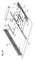
- FIG. 6is a front perspective view of a first example adapter block assembly including adapter blocks, a joining member, a circuit board, and a cover;
- FIG. 7shows the components of the first adapter block assembly of FIG. 6 exploded outwardly from each other;
- FIG. 8is a cross-sectional view of the first adapter block assembly of FIG. 6 ;
- FIG. 9is a front perspective view of the first adapter block assembly of FIG. 6 with the cover removed;
- FIG. 10is a side elevational view of the first adapter block assembly of FIG. 9 ;
- FIG. 11is a front perspective view of an example adapter block suitable for use with the first adapter block assembly of FIG. 6 ;
- FIG. 12is a top plan view of the adapter block of FIG. 11 ;
- FIG. 13is a bottom plan view of the adapter block of FIG. 11 ;
- FIG. 14is a perspective view of an example joining member suitable for use with the first adapter block assembly of FIG. 6 ;
- FIG. 15is a bottom plan view of the joining member of FIG. 14 ;
- FIG. 16is a top plan view of the joining member of FIG. 14 ;
- FIG. 17is a cross-sectional view of the joining member taken along the 17-17 line of FIG. 16 ;
- FIG. 18is a bottom perspective view of contact assemblies mounted to an example circuit board suitable for use with the first adapter block assembly of FIG. 6 ;
- FIG. 19is a perspective view showing the adapter block assembly of FIG. 6 exploded upwardly from an example tray;
- FIG. 20is a perspective view showing the adapter block assembly of FIG. 6 mounted to the tray of FIG. 19 ;
- FIG. 21is a front perspective view of a second example adapter block assembly including adapter blocks, a joining member, a circuit board, and multiple cover pieces;
- FIG. 22is a bottom perspective view of the adapter block assembly of FIG. 21 ;
- FIG. 23shows the components of the first adapter block assembly of FIG. 21 exploded outwardly from each other;
- FIG. 24is a front perspective view of an example adapter block suitable for use with the first adapter block assembly of FIG. 21 ;
- FIG. 25is a side elevational view of the first adapter block assembly of FIG. 21 ;
- FIGS. 26-29illustrate an example cover piece suitable for use with the first adapter block assembly of FIG. 21 ;
- FIGS. 30-31are perspective views of an example joining member suitable for use with the first adapter block assembly of FIG. 21 ;
- FIG. 32is a top plan view of the joining member of FIG. 30 ;
- FIG. 33is a bottom plan view of the joining member of FIG. 30 ;
- FIGS. 34-35are perspective views of an intermediate cover piece suitable for use with the first adapter block assembly of FIG. 21 ;
- FIG. 36is an exploded view of a third example adapter block assembly including a cover heat staked to an adapter block to sandwich a circuit board therebetween;
- FIG. 37is a cross-sectional view of the third example adapter block assembly of FIG. 36 with the components assembled together;
- FIG. 38is a top perspective view of a fourth example adapter block assembly including an adapter block, a circuit board, and a cover;
- FIG. 39shows the components of the fourth adapter block assembly of FIG. 38 exploded outwardly from each other;
- FIGS. 40-42illustrate an example adapter block suitable for use in the fourth adapter block assembly of FIG. 38 ;
- FIG. 43is a bottom perspective view of contact assemblies mounted to a circuit board suitable for use in the fourth adapter block assembly of FIG. 38 ;
- FIGS. 44-45illustrate one example cover suitable for use in the fourth adapter block assembly of FIG. 38 ;
- FIG. 46illustrates an example tray arrangement including another example tray to which any of the adapter block assemblies disclosed herein can be mounted;
- FIG. 47is a perspective view of another adapter block assembly
- FIG. 48is a front view of the adapter block assembly of FIG. 47 with part of a forward shroud being visible;
- FIG. 49is a bottom plan view of the adapter block assembly of FIG. 47 ;
- FIG. 50is a bottom perspective view of the adapter block assembly of FIG. 47 with the circuit board and contact assemblies exploded away from the adapter blocks of the adapter block assembly;
- FIGS. 51-55illustrate steps when latching the cover pieces to the adapter block assembly of FIG. 47 ;
- FIG. 56is a perspective view of an optical adapter block exploded away from a joining member coupled to another optical adapter block.
- media segmentsconnect equipment of the communications network.
- media segmentsinclude optical cables, electrical cables, and hybrid cables. This disclosure will focus on optical media segments.
- the media segmentsmay be terminated with optical plug connectors, media converters, or other optical termination components.
- FIG. 1is a schematic diagram of one example connection system 100 including an adapter block assembly (e.g., optical adapters, electrical sockets, wireless readers, etc.) 110 at which communications signals from a first media segment (e.g., an optical fiber, an electrical conductor, a wireless transceiver, etc.) 122 pass to another media segment 132 .
- a first media segmente.g., an optical fiber, an electrical conductor, a wireless transceiver, etc.
- the media segments 122 , 132are terminated by connector arrangements 120 , 130 , respectively.
- the example adapter block assembly 110connects segments of optical communications media in an optical network. In other implementations, however, the adapter block assembly 110 can connect electrical segments, wireless segments, or some combination thereof.
- the adapter block assembly 110includes a fiber optic adapter defining at least one connection opening 111 having a first port end 112 and a second port end 114 .
- a sleeve (e.g., a split sleeve) 103is arranged within the connection opening 111 of the adapter 110 between the first and second port ends 112 , 114 .
- Each port end 112 , 114is configured to receive a connector arrangement 120 .
- Each fiber connector arrangement 120 , 130includes a ferrule 124 , 134 through which optical signals from the optical fiber 122 , 132 , respectively, pass.
- the ferrules 124 , 134are held and aligned by a sleeve 103 to allow optical signals to pass between the ferrules 124 , 134 .
- the aligned ferrules 124 , 134 of the connector arrangements 120 , 130create an optical path along which the communication signals may be carried.
- the communications networkis coupled to or incorporates a data management system that provides physical layer information (PLI) functionality as well as physical layer management (PLM) functionality.
- PLIphysical layer information
- PLMphysical layer management
- PLAI functionalityrefers to the ability of a physical component or system to identify or otherwise associate physical layer information with some or all of the physical components used to implement the physical layer of the communications network.
- PLM functionalityrefers to the ability of a component or system to manipulate or to enable others to manipulate the physical components used to implement the physical layer of the communications network (e.g., to track what is connected to each component, to trace connections that are made using the components, or to provide visual indications to a user at a selected component).
- physical layer informationrefers to information about the identity, attributes, and/or status of the physical components used to implement the physical layer of the communications network.
- Physical layer information of the communications networkcan include media information, device information, and location information.
- Media informationrefers to physical layer information pertaining to cables, plugs, connectors, and other such physical media.
- Non-limiting examples of media informationinclude a part number, a serial number, a plug type, a conductor type, a cable length, cable polarity, a cable pass-through capacity, a date of manufacture, a manufacturing lot number, the color or shape of the plug connector, an insertion count, and testing or performance information.
- Device informationrefers to physical layer information pertaining to the communications panels, inter-networking devices, media converters, computers, servers, wall outlets, and other physical communications devices to which the media segments attach.
- Location informationrefers to physical layer information pertaining to a physical layout of a building or buildings in which the network is deployed.
- one or more of the components (e.g., media segments, equipment, etc.) of the communications networkare configured to store physical layer information pertaining to the component as will be disclosed in more detail herein.
- Some componentsinclude media reading interfaces that are configured to read stored physical layer information from the components. The physical layer information obtained by the media reading interface may be communicated over the network for processing and/or storage.
- the adapter block assembly 110 of FIG. 1can be configured to collect physical layer information from the connector arrangements 120 , 130 terminating one or more of the media segments 122 , 132 .
- the first connector arrangement 120may include a storage device 125 that is configured to store physical layer information pertaining to the segment of physical communications media 122 and/or to the first connector arrangement 120 .
- the connector arrangement 130also includes a storage device 135 that is configured to store information pertaining to the second connector arrangement 130 and/or to the second optic cable 132 terminated thereby.
- each of the storage devices 125 , 135is implemented using an EEPROM (e.g., a PCB surface-mount EEPROM). In other implementations, the storage devices 125 , 135 are implemented using other non-volatile memory device. Each storage device 125 , 135 is arranged and configured so that it does not interfere or interact with the communications signals communicated over the media segments 122 , 132 .
- the adapter 110is coupled to at least a first media reading interface 116 . In certain implementations, the adapter 110 also is coupled to at least a second media interface 118 . In certain implementations, the adapter 110 is coupled to multiple media reading interfaces. In an example, the adapter 110 includes a media reading interface for each port end defined by the adapter 110 . In another example, the adapter 110 includes a media reading interface for each connection opening 111 defined by the adapter 110 . In other implementations, the adapter 110 can include any desired number of media reading interfaces 116 , 118 .
- At least the first media reading interface 116is mounted to a printed circuit board 115 .
- the printed circuit board 115also can include the second media reading interface 118 .
- the printed circuit board 115 of the adapter 110can be communicatively connected to one or more programmable processors and/or to one or more network interfaces (see data line 119 of FIG. 1 ).
- the network interfacemay be configured to send the physical layer information to a physical layer data management network. Examples of data management networks can be found in U.S. Provisional Application No. 61/760,816, filed Feb. 5, 2013, and titled “Systems and Methods for Associating Location Information with a Communication Sub-Assembly Housed within a Communication Assembly,” the disclosures of which are hereby incorporated herein by reference.
- the first media reading interface 116is configured to enable reading (e.g., by an electronic processor) of the information stored in the storage device 125 .
- the information read from the first connector arrangement 120can be transferred through the printed circuit board 115 to the physical layer data management network.
- the second media reading interface 118is configured to enable reading (e.g., by an electronic processor) of the information stored in the storage device 135 .
- the information read from the second connector arrangement 130can be transferred through the printed circuit board 115 or another circuit board to the physical layer data management network.
- the storage devices 125 , 135 and the media reading interfaces 116 , 118each include at least three (3) leads—a power lead, a ground lead, and a data lead.
- the three leads of the storage devices 125 , 135come into electrical contact with three (3) corresponding leads of the media reading interfaces 116 , 118 when the corresponding media segment is inserted in the corresponding port.
- a two-line interfaceis used with a simple charge pump.
- additional leadscan be provided (e.g., for potential future applications).
- the storage devices 125 , 135 and the media reading interfaces 116 , 118may each include four (4) leads, five (5) leads, six (6) leads, etc.
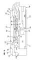
- FIGS. 2-5illustrate one example optical connector 150 suitable for implementing any of the connector arrangements 120 , 130 of FIG. 1 .
- the optical connector 150includes a connector body 151 including a latch 153 or other securement feature that enables the connector 150 to be secured to an adapter port.
- the optical connector 150includes a contact region 152 at which one or more electrical contacts 154 can be coupled to the connector body 151 .
- the contacts 154can be laid on a circuit board that is mounted to or within the body 151 .
- the contacts 154are electrically coupled to a memory or storage device that holds physical layer information pertaining to the connector 150 and/or to an optical fiber terminated by the connector 150 .
- the contact assembly 160includes a body 161 that holds one or more electrical contacts 162 together.
- Each of the contacts 162includes a contact section 163 at which the contact 162 physically touches (e.g., presses against, swipes along, etc.) one of the contacts 154 at the connector contact region 152 when the connector 150 is brought into contact with the contact assembly 160 (see FIG. 5 ).
- the contact sections 163may touch the connector contacts 154 when the connector 150 is plugged into a corresponding port end of an optical adapter.
- engagement with the connector contacts 154causes the contact sections 163 of the contact assembly contacts 162 to deflect towards the body 161 (see FIG. 5 ).
- the contact assembly 160includes a sensing contact 166 that extends outwardly from the body 161 .
- a first of the contacts 162includes an extension 164 that aligns with the sensing contact 166 .
- the extension 164is spaced from the sensing contact 166 ( FIG. 3 ).
- the contact sections 163 of the contact assembly contacts 162deflect towards the body 161
- the extension 164deflects towards the sensing contact 166 .
- a first contact area 165 on the extension 164touches (e.g., presses against, swipes along, etc.) a second contact area 167 on the sensing contact 166 ( FIG. 5 ), thereby shorting the first contact 162 and the sensing contact 166 together.
- An electronic processor or other portion of the data management networkdetermines when the contacts 162 , 166 short together to identify when a connector 150 has been inserted into an adapter port.
- the contact assembly body 161is configured to be secured at an aperture defined in an adapter block. In other implementations, the contact assembly body 161 is configured to be secured to a circuit board or other surface.
- the body 161can include one or more pegs 168 that extend outwardly from the body 161 to be received in apertures defined in the surface. In the example shown, the body 161 defines two pegs 168 extending away from the contact sections 163 .
- the contact assembly body 161defines a tapered section 169 that accommodates deflection of the contacts 162 (e.g., when an optical connector 150 engages the contact assembly 160 .
- contact assembly 160suitable for use as contact assembly 160 are shown and described in U.S. Provisional Application No. 61/843,752, filed Jul. 8, 2013, and titled “Optical Assemblies with Managed Connectivity,” the disclosure of which is hereby incorporated herein by reference.
- one or more contact assemblies 160can be mounted to an adapter block assembly.
- FIGS. 6-45illustrate various example implementations of connector assemblies suitable for receiving the contact assemblies 160 .
- Each adapter block assemblyincludes at least a first adapter block, at least a first circuit board, and at least a first cover.
- One or more contact assemblies 160are disposed between the first adapter block and the first circuit board.
- the first circuit boardholds the contact assemblies 160 to the first adapter block.
- the first coverholds the first circuit board to the first adapter block.
- the first coveris mounted to the first circuit board.
- Certain type of connector assembliescan include multiple adapter blocks coupled together using a joining member.
- Certain type of connector assembliescan include multiple circuit boards held together by a single cover or multiple covers mounted to a single circuit board.
- FIGS. 6-20illustrate a first example adapter block assembly 200 suitable for implementing the adapter block assembly 110 of FIG. 1 .
- the adapter block assembly 200has a front 201 , a rear 202 , a top 203 , a bottom 204 , a first side 205 , and a second side 206 .
- a periphery 207 of the adapter block assembly 200 defined by the front 201 , rear 202 , and sides 205 , 206defines a staggered configuration.
- Ports 212 for receiving optical connectors (e.g., optical connectors 150 ) along insertion axes A ( FIG. 11 )are provided at the front 201 and rear 202 of the adapter block assembly 200 .
- adjacent ports 212are staggered forwardly/rearwardly relative to each other. In the example shown, adjacent pairs of ports 212 are staggered forwardly/rearwardly relative to each other. The staggering of the ports 212 enhances access to individual connectors 150 plugged into the ports 212 .
- the adapter block assembly 200includes a first adapter block 210 A, a second adapter block 210 B, a joining member 220 , a circuit board 230 , and a cover 240 .
- the joining member 220couples the first and second adapter blocks 210 A, 210 B together.
- the circuit board 230couples to the joined first and second adapter blocks 210 A, 210 B.
- Contact assemblies 160 and circuit board components 234are mounted to the circuit board 230 .
- the contact assemblies 160face towards the adapter blocks 210 A, 210 B.
- the cover 240extends over at least some of the components 234 of the circuit board 230 .
- FIG. 8is a cross-sectional view of the adapter block assembly 200 taken along the insertion axis A of one of the ports 212 .
- a first optical connector 150is shown plugged into the right port 212 and the left port 212 is shown empty.
- a ferrule of the optical connector 150is held at a sleeve 208 disposed between the left and right ports 212 .
- the sleeve 208is configured to align and hold ferrules of connectors 150 inserted at opposite ports 212 .
- the latch arm 153 of the connector 150latches or otherwise secures to an interior of the adapter block 210 .
- a contact assembly 160is disposed between the adapter block 210 and the circuit board 230 .
- a right contact assembly 160corresponds with the right port 212 and a left contact assembly 160 corresponds with the left port 212 .
- Contacts 162 of the contact assembly 160extend through apertures 215 in the adapter block 210 .
- the contacts 162are positioned and oriented so that the contact sections 163 align with the contact region 152 of optical connectors 150 received at corresponding ports 212 .
- Pegs 168extend into the circuit board 230 .
- the circuit board 230is mounted flush with the adapter block 210 .
- the circuit board 230can be mounted within a recessed area 214 of the adapter block 210 between end sections 218 (e.g., see FIGS. 9 and 10 ).
- the periphery of the circuit board 230is recessed inwardly relative to the ports 212 .
- the adapter block 210defines front and rear curved sections 216 that extend downwardly from the end sections 218 and outwardly to define the front and rear ports 212 .
- the circuit board 230has a bottom surface 232 that seats on the recessed section 214 and a top surface 231 that lies about level with the top of the end sections 218 .
- components 234 mounted to the first surface 231 of the board 230extend upwardly past the top of the end sections 218 .
- the cover 240extends over the first surface 231 of the circuit board 230 .
- the cover 240has a top surface 241 that faces away from the circuit board 231 and a bottom surface 242 that faces towards the circuit board 232 .
- the cover 240(e.g., the second surface 242 ) seats on the first surface 231 .
- a periphery of the cover 240seats on the end sections 218 .
- a hollow section of the cover 240 defined by a raised second surface 242extends over the first surface 231 of the circuit board 230 to accommodate the board components 234 .
- the periphery of the cover 240seats on only portions of the end sections 218 .
- the periphery of the cover 240can be recessed inwardly from the ports 212 to enhance access to the ports 212 .
- the periphery of the cover 240can be recessed inwardly from the front and rear curved portions 216 .
- the cover 240can define ramped or tapered sections 245 at the front and rear of the cover 240 . The tapered sections 245 further enhance access to the ports 212 by reducing the material that might otherwise block finger access to the ports 212 when the cover 240 is mounted to the adapter block 210 .
- FIGS. 11-12illustrate one example adapter block 210 suitable for use in the adapter block assembly 200 .
- the adapter block 210includes a block body 211 that defines a plurality of front and rear ports 212 .
- the front ports 212align with the rear ports 212 .
- the front ports 212form a lateral row that extends along a common (e.g., horizontal) axis.
- the rear ports 212also form a lateral row that extends along a common (e.g., horizontal) axis.
- the top of the adapter block 210defines the recessed area 214 between a front end section 218 and a rear end section 218 .
- Apertures 215are defined in the recessed area 214 and extend into a hollow interior of the adapter block 210 .
- the front ports 212are located generally flush relative to each other. In other implementations, however, a perimeter of the adapter block 210 can have a staggered configuration so that some of the front ports 212 are offset forwardly/rearwardly along the insertion axes relative to others of the front ports 212 . In one example, adjacent front ports 212 are forwardly/rearwardly offset from each other. In the example shown, sections of the adapter block 210 are forwardly/rearwardly offset from each other. For example, a first section 213 A of the adapter block 210 is offset rearwardly relative to a second section 213 B of the adapter block 210 (see FIG. 11 ). In certain implementations, each section 213 A, 213 B defines at least one of the front ports 212 and one of the rear ports 212 . In an example, each section 213 A, 213 B defines two each of the front and rear ports 212 .
- each adapter block 210is configured to be coupled to one or more adapter blocks 210 and/or to be coupled to a tray, blade, drawer, tray, or other such structure (hereinafter “tray”).
- each adapter block 210includes an engagement member 217 that extends outwardly from at least one side 205 , 206 of the adapter block 210 .
- an engagement member 217extends outwardly from both sides 205 , 206 of the adapter block 210 .
- the engagement member 217has a T-shaped profile when viewed from above or below the adapter block 210 .
- the engagement member 217can have a first portion 217 a extending outwardly from the side 205 , 206 of the adapter block 210 and a second portion 217 b extending generally orthogonally across the first portion 217 a ( FIG. 12 ).
- a stop member 219also extends outwardly from opposite sides 205 , 206 of the adapter block 210 .
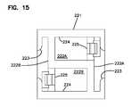
- two or more adapter blocks 210can be coupled together using a joining member 220 .
- the joining member 220includes a body 221 defining one or more interior cavities 222 that are sized to receive the engagement members 217 of the adapter blocks 210 .
- the joining member 220includes a first interior cavity 222 A that is separated from a second interior cavity 222 B.
- two cavities 222are formed at opposite sides of the joining member 220 to hold two adapter blocks 210 together end-to-end.
- each interior cavity 222 A, 222 Bextends along two adjacent sides of the joining member to form an L-shape.
- Each cavity 222is accessible through an open bottom of the joining member 220 ( FIG. 15 ), a respective aperture 224 defined in a top of the joining member 220 ( FIG. 16 ), and a respective slot 223 ( FIG. 14 ) defined in one of the sides of the joining member body 221 .
- the slots 223 of the joining member 220are sized to enable an adapter block engagement member 217 to enter one of the cavities 222 (see FIG. 13 ).
- the engagement member 217can be slid into the cavity 222 through the open bottom of the joining member 220 with the first portion 217 a of engagement member 217 passing through the slot 223 .
- the second portion 217 b of the engagement member 217abuts against the body 221 to hold the adapter block 210 laterally relative to the joining member 220 (see FIG. 13 ).
- a latching hook 225extends downwardly within each of the cavities 222 of the joining member 220 .
- a first latching hook 225 Aextends downwardly within cavity 222 A and a second latching hook 225 B extends downwardly within cavity 222 B.
- Each latching hook 225 A, 225 Bdefines a shoulder 226 facing towards the top of the joining member 220 .
- Each latching hook 225 A, 225 Bis configured to deflect laterally within the cavity 222 A, 222 B.
- the section portion 217 b of the engagement member 217pushes against the latching hook 225 to cause deflection of the latching hook 225 away from the slot 223 .
- the latching hook 225snaps over the section portion 217 b of the engagement member 217 to hold the engagement member 217 within the cavity 222 (see FIG. 13 ).
- FIG. 18illustrates an example circuit board arrangement suitable for use with the adapter block assembly 200 .
- the example circuit board arrangementincludes a circuit board 230 having contact assemblies 160 mounted to a second surface 232 .
- a perimeter 233 of the circuit board 230has a staggered configuration so that some of the contact assemblies 160 are mounted further forwardly/rearwardly relative to others of the contact assemblies 160 .
- the staggered configuration of the circuit board 230generally aligns with the staggered configuration of the adapter blocks 210 .
- the circuit board 230 shown in FIG. 18is configured to couple to two different adapter blocks 210 .
- the circuit board 230includes an intermediate portion 236 sized to extend over a joining member 220 coupling together two adapter blocks 210 .
- a circuit board connector 235extends downwardly from the second surface 232 of the circuit board 230 at the intermediate portion 236 .
- the circuit board connector 235is configured to electrically connect the circuit board 230 (e.g., and hence components 234 and contacts 160 on the circuit board 230 ) to a second circuit board or other electrical circuit as will be disclosed in more detail herein.
- the joining member 220is sized to accommodate passage of the circuit board connector 235 between the adapter blocks 210 and within the periphery 233 of the circuit board 230 .
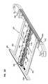
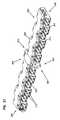
- FIGS. 19 and 20illustrate mounting the adapter block assembly 200 to an example tray 250 .
- the tray 250is configured to receive at least one adapter block assembly 200 .
- the tray 250also is configured to manage optical fibers/cables routed to the ports 212 of the adapter block assembly 200 .
- the tray 250includes cross-members 253 extending between two side rails 251 , 252 .
- a mounting rail 254extends between the cross-members 253 .
- latching fingers 256extend upwardly from the mounting rail 254 .
- the latching fingers 256are configured to engage the adapter block assembly 200 (e.g., the joining member 220 ) to further secure the adapter block assembly 200 to the tray 250 .
- two latching fingers 256face in opposite directions towards the side rails 251 , 252 .
- the latching fingers 256extend upwardly through the cavities 222 defined in the joining member 220 and through the apertures 224 defined at the top of the joining member 220 to latch over the top of the joining member 220 .
- the latching members 256latch over shoulders defined within the joining member 220 .
- another type of adapter block assembly securement structurecan be disposed at the mounting rail 254 .
- Mounting structures 255are provided at the inner sides of the side rails 251 , 252 . In certain implementations, the mounting structures 255 are laterally aligned. The mounting structures 255 are configured to receive the engagement members 217 of the adapter blocks 217 . For example, the mounting structures 255 receive the engagement members 217 extending outwardly from the sides 205 , 206 of the adapter block assembly 200 . In an example, each mounting structures 255 defines a T-shaped cavity having an open top through which an engagement member 217 can slide. Each mounting structures 255 also includes a shelf on which the engagement member 217 can seat.
- the tray 250is moveable (e.g., slideable, pivotal, etc.) relative to a rack, cabinet, or other mounting structure.
- exterior surfaces of the side rails 251 , 252can include guides 258 that interact with guides on the holding structure.
- the tray 250includes cable management guides 259 that form routing paths for optical fibers/cables routed onto the tray 250 .
- the management guides 259may aid in managing the optical fibers/cables during movement of the tray 250 .
- the tray 250provides an electrical connection between the adapter block assembly 200 and a data management network.
- an electrical circuite.g., a second circuit board
- the mounting rail 254 and/or one or more of the cross-members 253can define a pocket or channel sized to fit the circuit board (e.g., see FIG. 46 ).
- the circuit boardincludes connectors (e.g., pin receptacles) configured to receive the circuit board connectors 235 of the printed circuit board 230 within the adapter block assembly 200 .
- the circuit boardextends over the mounting rail 254 and over at least part of one of the cross-members 253 towards an aperture in the second side rail 252 through which the circuit board can connect to a chassis electrical circuit (e.g., backplane, cable, etc.).
- a chassis electrical circuite.g., backplane, cable, etc.
- an electrical cablee.g., a flexible cable
- an electrical cablecan extend from the chassis electrical circuit, through the aperture in the second side rail 252 , extend across at least part of the cross-members 253 , and connect to the second circuit board.
- a covercan be positioned over the cross-member channel to protect the flex circuit.
- the covercan be latched (e.g., using latches 256 ) other otherwise secured to the cross-member 253 .
- the chassis electrical circuitincludes a local processor to manage the data obtained from the adapter block assembly 200 .
- the chassis electrical circuitincludes a data port through which the data can be carried to a data management network.
- FIGS. 21-35illustrate a second example adapter block assembly 300 suitable for implementing the adapter block assembly 110 of FIG. 1 .
- the adapter block assembly 300has a front 301 , a rear 302 , a top 303 , a bottom 304 , a first side 305 , and a second side 306 .
- a periphery 307 of the adapter block assembly 300 defined by the front 301 , rear 302 , and sides 305 , 306defines a staggered configuration.
- Ports 312 for receiving optical connectors (e.g., optical connectors 150 ) along insertion axesare provided at the front 301 and rear 302 of the second adapter block assembly 300 .
- adjacent ports 312are staggered forwardly/rearwardly relative to each other. In the example shown, adjacent pairs of ports 312 are staggered forwardly/rearwardly relative to each other. The staggering of the ports 312 enhances access to individual connectors 150 plugged into the ports 312 .
- the adapter block assembly 300includes a first adapter block 310 A, a second adapter block 310 B, a joining member 320 , a circuit board 330 , a first cover 340 A, a second cover 340 B, and an intermediate cover 350 .
- the joining member 320couples the first and second adapter blocks 310 A, 310 B together.
- the circuit board 330seats on the joined first and second adapter blocks 310 A, 310 B.
- the first and second covers 340 A, 340 Bare disposed over the circuit board 330 and couples to the adapter blocks 310 A, 310 B as will be disclosed in more detail herein.
- the intermediate cover 350extends over an intermediate portion 336 of the circuit board 330 between the first and second covers 340 A, 340 B.
- the covers 340 A, 340 B, 350can be formed as a single piece.
- the circuit board 330can be separated into multiple pieces.
- Contact assemblies 160 and circuit board components 334are mounted to the circuit board 330 .
- the components 334can be mounted to a first side 331 of the circuit board 330 and the contact assemblies 160 can be mounted to a second side 332 of the circuit board 330 .
- the contact assemblies 160face towards the adapter blocks 310 A, 310 B when the circuit board 330 is disposed between the adapter blocks 310 and the covers 340 .
- the covers 340 A, 340 Bextends over at least some of the components 334 of the circuit board 330 .
- the covers 340 A, 340 Bare secured to the adapter blocks 310 A, 310 B, thereby holding the circuit board 330 therebetween.
- FIGS. 24 and 25illustrate one example adapter block 310 suitable for use as adapter blocks 310 A, 310 B.
- the example adapter block 310includes an adapter body 311 defining one or more front ports 312 and one or more rear ports 312 .
- Each front port 312aligns with one of the rear ports 312 .
- the front ports 312form a lateral row that extends along a common (e.g., horizontal) axis.
- the rear ports 312also form a lateral row that extends along a common (e.g., horizontal) axis.
- the front ports 312are located generally flush relative to each other. In other implementations, however, a perimeter of the adapter block 310 can have a staggered configuration so that some of the front ports 312 are offset forwardly/rearwardly along the insertion axes relative to others of the front ports 312 . In one example, adjacent front ports 312 are forwardly/rearwardly offset from each other. In the example shown, sections of the adapter block 310 are forwardly/rearwardly offset from each other. For example, a first section 313 A of the adapter block 310 is offset rearwardly relative to an adjacent second section 313 B of the adapter block 310 (see FIG. 24 ). In certain implementations, each section 313 A, 313 B defines at least one of the front ports 312 and one of the rear ports 312 . In an example, each section 313 A, 313 B defines two each of the front and rear ports 312 .
- the top of the adapter block 310defines the recessed area 314 between a front end section 318 and a rear end section 318 .
- the recessed area 314enables the circuit board 330 to be flush mounted with the adapter block 310 .
- a circuit board 330 mounted in the recessed area 314would lie flush with a top of the front and rear end sections 318 .
- Apertures 315are defined in the recessed area 314 and extend into a hollow interior of the adapter block 310 .
- the contact assemblies 160 of the circuit board 330extend through the apertures 310 when the circuit board 330 is disposed at the recessed area 314 .
- the adapter block 310defines front and rear curved sections 316 that extend downwardly from the end sections 318 and outwardly to define the front and rear ports 312 .
- the adapter block 310is configured to latch to the cover 340 .
- the adapter block 310can include latch arms 361 that extend upwardly from a top of the adapter block 310 .
- the latch arms 361include latch hooks 362 that extend outwardly from the latch arms 361 .
- a front latch arm 361 and a rear latch arm 361extend upwardly at each section 313 of the adapter block 310 (see FIG. 24 ).
- a greater or fewer number of latch arms 361may extend upwardly from the adapter block 310 .
- FIGS. 26-29illustrate an example cover 340 that is configured to receive the latch arms 361 to secure the cover 340 to the adapter block 310 .
- the example cover 340has a first surface 341 facing away from the adapter block 310 , a second surface 342 facing towards the adapter block 310 , and a perimeter 343 extending between the first and second surfaces 341 , 342 .
- the cover 340is sized so that the perimeter 343 is recessed inwardly from a perimeter of the adapter block 310 to enhance access to the ports 312 (and connectors inserted therein) of the adapter block 310 .
- the cover 340defines tapered or chamfered edges 344 extending between the first surface 341 and the perimeter 343 .
- the cover 340also defines through-openings 347 that extend through the first and second surfaces 341 , 342 of the cover 340 .
- the through-openings 347are wider than the latch arms 361 .
- the cover 340also defines platforms 348 adjacent the through-openings 347 .
- each through-opening 347includes a first portion 347 a that is sized to enable the entire latch arm 361 to pass therethrough without deflecting the latch arm 361 .
- the through-openings 347also define second portions 347 b adjacent the platforms 348 .
- the second portions 347 bare too small to enable the latch hooks 362 of the latch arms 361 to pass therethrough.
- the latch arms 361are inserted through the first portions 347 a of the through-openings 347 .
- the cover 340is laterally moved so that the platforms 348 are disposed beneath the latch hooks 362 of the arms 361 .
- the platforms 348inhibit passage of the latch arms 361 back through the through-openings 347 . Friction and the contact force between the latch hooks 362 and the platforms 348 inhibits a return lateral movement of the cover 340 to align the latch hooks 362 with the first through-opening portions 347 a.
- the second surface 342 of the cover 340defines recesses 346 that extend through the perimeter 343 of the cover 340 .
- the recesses 346accommodate LEDs or other light indicators mounted to the circuit board 330 . Light from the indicators can shine through the recesses 346 in the perimeter to identify a section of the adapter block 310 .
- the cover 340can define a recess 346 for each port 312 of the adapter block 310 . In such implementations, the recesses 346 align with the respective port 312 identified by the corresponding indicator.
- each adapter block 310is configured to be coupled to one or more adapter blocks 310 and/or to be coupled to a tray (e.g., tray 250 of FIGS. 19-20 ), or other such structure.
- each adapter block 310includes an engagement member 317 that extends outwardly from at least one side 305 , 306 of the adapter block 310 .
- an engagement member 317extends outwardly from both sides 305 , 306 of the adapter block 310 .
- the engagement member 317has an H-shaped profile when viewed from the side 305 , 306 the adapter block 310 .
- the engagement member 317can have a two L-shaped flanges 317 a extending outwardly from the side 305 , 306 of the adapter block 310 ; a shelf 317 b extending between the flanges 317 a , and a ramp or tapered section 317 c extending inwardly from the shelf 317 b towards the side 305 , 306 of the adapter block 310 .
- the L-shaped flanges 317 aface forwardly and rearwardly of the adapter block 310 (see FIG. 24 ).
- a stop member 319also extends outwardly from opposite sides 305 , 306 of the adapter block 310 .
- the joining member 320includes a body 321 defining an open bottom leading to a generally hollow interior.
- the joining body 321also defines openings 322 at the first and second ends of the body 321 that lead to the hollow interior.
- the top of the joining body 321is configured to enable the intermediate portion 336 of the circuit board 330 to extend thereover.
- the body 321defines an aperture 327 through which a circuit board connector 335 can pass (e.g., see FIG. 22 ) to enable connection between the circuit board 330 and an electrical circuit disposed beneath the adapter blocks 310 .
- Sidewalls of the body 321define one or more receiving slots 323 that are sized to receive the engagement members 317 of the adapter blocks 310 .
- the joining member 320includes a first receiving slot 323 A at a first sidewall of the joining member 320 and a second receiving slot 323 B at an opposite sidewall of the joining member 320 .
- the joining member 320holds two adapter blocks 310 together end-to-end (see FIGS. 21 and 22 ).
- Each receiving slot 323extends through a top and corresponding side of the joining member 320 .
- the slots 323are sized to enable an adapter block engagement member 317 (e.g., the flanges 317 a ) to enter the slot 323 through the top of the joining member 320 .
- the joining member 320also includes a latching arm 324 that extends upwardly within one or more of the receiving slots 323 .
- the latching arm 324includes a latching hook 325 that extends outwardly from the arm 324 .
- the ramp 317 c of the engagement member 317cams against the latching hook 325 to deflect the arm 324 inwardly until the latching hook 325 clears the shelf 317 b .
- the arm 324returns to its initial position so that the latching hook 325 catches on the shelf 317 b .
- the latching arm 324inhibits the adapter block 310 from being slid out of engagement with the joining member 320 .
- opposite sides of the joining member 320each define a second slot 326 adjacent the receiving slot 323 .
- the second slot 326does not extend fully through the side of the joining member 320 .
- the second slot 326is sized to receive the stop member 319 when the adapter block engagement member 317 is slid into the receiving slot 323 . Interaction between the second slot 326 and the stop member 319 inhibits the adapter block 310 from sliding all the way through the joining member 320 .
- the joining body 321also includes protrusions 329 that extend outwardly from the body 321 adjacent the receiving slots 323 .
- the protrusions 329can be disposed beneath the receiving slots 323 at the sidewalls.
- the adapter blocks 310may seat on the protrusions 329 to inhibit movement of the adapter blocks 310 past the joining member 320 .
- the joining member 320includes a retention member 328 disposed at each of the first and second open ends of the body 321 .
- each retention member 328can be formed at a top of the body 321 and face out towards the respective end opening 322 .
- the retention member 328can be inwardly recessed into the top of the body 321 relative to the open end of the body 321 .
- FIGS. 34-35illustrate one example intermediate cover 350 that is configured to mount over the intermediate portion 336 of the circuit board 330 .
- the intermediate cover 350is configured to couple to the joining member 320 .
- the intermediate cover 350includes a body 351 from which two latching arms 352 extend downwardly at opposite ends. Each latching arm 352 includes a latching hook 353 that is configured to snap-fit, latch, or otherwise secure to the retention member 328 at one end of the joining member body 321 .
- the intermediate cover 350defines a hollow interior or recessed inner surface that accommodates any components 334 mounted to the intermediate portion 336 of the circuit board 330 .
- the intermediate cover 350fits between, but does not couple to the first and second covers 340 A, 340 B (see FIG. 21 ). In other implementations, the intermediate cover 350 can be coupled to the first and second covers 340 A, 340 B.
- FIGS. 36-37illustrate a third example adapter block assembly 400 including an adapter block 410 , a circuit board 430 , and a cover 440 .
- each of these three componentsis formed from as a single-piece unit. In other implementations, however, any of these components could be formed from multiple pieces (e.g., multiple adapter blocks with joining members, multiple circuit boards, multiple cover pieces, etc.).
- the adapter block assembly 400can be configured to mount to a tray (e.g., tray 250 of FIGS. 19 and 20 ), or other structure.
- the adapter block 410includes a body 411 defining a plurality of front and rear connector ports 412 .
- the adapter body 411includes some sections 413 that are offset forwardly or rearwardly relative to other sections 413 .
- a first section 413 A shown in FIG. 36is offset forwardly relative to a second section 413 B.
- the ports 412 of the adapter block 310may be flush.
- the adapter block body 411has a first group of ports 412 at a first side, a second group of ports 412 at a second side, and an intermediate portion 414 that separates the first and second groups.
- the intermediate portion 414does not define ports 412 .
- a top of the adapter block 410defines apertures 415 at which contact assemblies 160 can be mounted.
- a contact assembly 160is disposed at each port 412 .
- a contact assembly 160can be disposed at alternate ports 412 and/or at the ports 412 on only the front or rear of the adapter block 410 .
- Heat stakes 416extend upwardly from the top of the adapter block 410 .
- a front heat stake 416 and a rear heat stake 416extend upwardly at each section 413 of the adapter block 410 except for the intermediate portion 414 .
- the adapter block 410can include any desired number of heat stakes 416 .
- the circuit board 430includes a board body 431 on which electrical components 432 can be mounted.
- the circuit board body 431also is configured to electrically couple to the contact assemblies 160 (e.g., via contact pads).
- the board body 431defines openings 433 through which the heat stakes 416 extend when the circuit board 430 is seated on the adapter block 410 .
- the cover 440is configured to extend over the circuit board 430 and to attach to the adapter block 410 .
- the cover 440includes a top plate 441 from which tabs 442 extend downwardly.
- the tabs 442are configured to seat on the circuit board 430 .
- the tabs 442are configured to seat on the board body 431 (see FIG. 37 ).
- the tabs 442can be configured to seat on components 432 of the circuit board 430 .
- the tabs 442raise the top plate 441 sufficiently far off the circuit board 430 to accommodate the circuit board components 432 beneath the top plate 441 .
- the cover 440defines through-holes 443 that extend through the top plate 441 of the cover 440 .
- the through-holes 443are defined through wells 444 extending downwardly from the top plate 441 .
- the through-holes 443are sized to accommodate passage of the heat stakes 416 of the adapter blocks 410 when the circuit board 430 and cover 440 are mounted to the adapter block 410 .
- the wells 444define counter-bores 445 leading to the exterior surface of the top plate 441 .
- the counter-bores 445are frustro-conical portions of the through-hole 443 that taper away from the heat stakes 416 .
- the heat stakes 416are sized to extend beyond the top plate 441 of the cover 440 .
- the tips of the heat stakes 416are melted.
- the melted heat stakes 416at least partially fill the counter-bores 445 .
- the melted heat stakes 416are generally flush with the exterior surface of the cover top plate 441 .
- the melted heat stakes 416can be recessed inwardly or can protrude outwardly from the cover top plate 441 .
- the melted heat stake material filling the counter-bores 445does not fit through the wells 444 , thereby inhibiting removal of the cover 440 from the adapter block 410 .
- the melted materialmay have a frustro-conical shape or other shape having a maximum cross-dimension that is greater than an internal cross-dimension of the well 444 .
- the melted heat stake materialfuses or otherwise bonds to the material forming the cover 440 to inhibit removal of the cover 440 from the adapter block 410 .
- the heat stakes 416are positioned adjacent the contact assemblies 160 (e.g., adjacent the apertures 415 ) mounted to the adapter block 410 . Accordingly, the bond between the cover 440 and the adapter block 410 is strongest near the contact assemblies 160 . These bonds facilitate holding the cover 440 and hence the circuit board 430 against the adapter block 410 despite any deflection of the contact assembly 160 (e.g., the sensing contact 166 ) against the circuit board 430 . Maintaining the position of the circuit board 430 even during deflection of the contact assembly 160 enhances the connection between the electrical contacts 162 of the contact assembly 160 and contact pads on the circuit board 430 .
- FIGS. 38-45illustrate a fourth example adapter block assembly 500 suitable for implementing the adapter block assembly 110 of FIG. 1 .
- the adapter block assembly 500has a front 501 , a rear 502 , a top 503 , a bottom 504 , a first side 505 , and a second side 506 .
- a periphery 507 of the adapter block assembly 500 defined by the front 501 , rear 502 , and sides 505 , 506defines a staggered configuration.
- Ports 512 for receiving optical connectors (e.g., optical connectors 150 ) along insertion axesare provided at the front 501 and rear 502 of the second adapter block assembly 500 .
- adjacent ports 512are staggered forwardly/rearwardly relative to each other. In the example shown, adjacent pairs of ports 512 are staggered forwardly/rearwardly relative to each other. The staggering of the ports 512 enhances access to individual connectors 150 plugged into the ports 512 .
- the fourth example adapter block assembly 500includes an adapter block 510 , a circuit board 530 , and a cover 540 .
- each of these three components 510 , 530 , 540is formed from as a single-piece unit. In other implementations, however, any of these components 510 , 530 , 540 could be formed from multiple pieces (e.g., multiple adapter blocks with joining members, multiple circuit boards, multiple cover pieces, etc.).
- the adapter block 510includes a body 511 defining a plurality of front and rear connector ports 512 .
- the adapter body 511includes some sections 513 that are offset forwardly or rearwardly relative to other sections 513 .
- a first section 513 A shown in FIG. 40is offset forwardly relative to a second section 513 B.
- the ports 512 of the adapter block 510may be flush.
- the adapter block body 511has a first group of ports 512 at a first side, a second group of ports 512 at a second side, and an intermediate portion 514 that separates the first and second groups.
- the intermediate portion 514does not define ports 512 .
- a top of the adapter block 510defines apertures 515 at which contact assemblies 160 can be mounted.
- a contact assembly 160is disposed at each port 512 .
- a contact assembly 160can be disposed at alternate ports 512 and/or at the ports 512 on only the front or rear of the adapter block 510 .
- Heat stakes 516extend upwardly from the top of the adapter block 510 .
- a front heat stake 516 and a rear heat stake 516extend upwardly at each section 513 of the adapter block 510 except for the intermediate portion 514 .
- the adapter block 510can include any desired number of heat stakes 516 .
- the adapter block 510can be configured to mount to a tray (e.g., tray 250 of FIGS. 19 and 20 ), or other structure.
- sides 505 , 506 of the adapter block 510include engagement members 517 that extend outwardly from the adapter body 511 .
- the engagement members 517can be configured to fit into slots defined in the tray.
- the adapter block 510also can include stop members 519 that also are configured to interact with retention structures on the tray.
- the intermediate portion 514 of the adapter block 510can include inward protrusions 508 that are configured to engage latch arms (e.g., latch arms 256 of FIG. 19 ) to secure the adapter block 510 to the tray.
- the circuit board 530includes a board body 531 on which electrical components 532 can be mounted.
- the circuit board body 531also is configured to electrically couple to the contact assemblies 160 (e.g., via contact pads).
- the board body 531defines openings through which the heat stakes 516 extend when the circuit board 530 is seated on the adapter block 510 .
- the board body 531also includes an intermediate portion 534 that is configured to extend over the intermediate portion 514 of the adapter block 510 .
- a circuit board connector 535can extend downwardly from the circuit board body 531 and through an aperture 518 defined in the intermediate portion 514 of the adapter block 510 to connect to an electrical circuit disposed beneath the adapter block 510 .
- the cover 540is configured to extend over the circuit board 530 and to attach to the adapter block 510 .
- the cover 540includes a top plate 541 from which sidewalls 542 extend downwardly.
- the sidewalls 542are configured to seat on the circuit board 430 .
- the sidewalls 542are configured to seat on the board body 530 .
- the sidewalls 542can be configured to seat on components 532 of the circuit board 430 .
- the sidewalls 542raise the top plate 541 sufficiently far off the circuit board 530 to accommodate the circuit board components 532 beneath the top plate 541 .
- tabs 547also extend downwardly from the top plate 541 to hold the top plate 541 off the circuit board 530 .
- the sidewalls 542define apertures 546 that lead to a hollow interior of the cover 540 .
- the apertures 546enable light from indicators (e.g., LEDs) mounted to the circuit board 530 to shine through and indicate an adapter port 512 .
- the cover 540defines through-holes 543 that extend through the top plate 541 .
- the through-holes 543are defined through wells 544 extending downwardly from the top plate 541 (see FIG. 45 ).
- the through-holes 543are sized to accommodate passage of the heat stakes 516 of the adapter blocks 510 when the circuit board 530 and cover 540 are mounted to the adapter block 510 .
- the wells 544define counter-bores 545 ( FIG. 44 ) leading to the exterior surface of the top plate 541 .
- the counter-bores 545are frustro-conical portions of the through-hole 543 that taper away from the heat stakes 516 .
- the heat stakes 516are sized to extend beyond the top plate 541 of the cover 540 .
- the tips of the heat stakes 516are melted.
- the melted tipsat least partially fill the counter-bores 545 .
- the melted heat stakes 516are generally flush with the exterior surface of the cover top plate 541 .
- the melted heat stakes 516can be recessed inwardly or can protrude outwardly from the cover top plate 541 .
- the melted heat stake material filling the counter-bores 545does not fit through the wells 544 , thereby inhibiting removal of the cover 540 from the adapter block 510 .
- the melted materialmay have a frustro-conical shape or other shape having a maximum cross-dimension that is greater than an internal cross-dimension of the well 544 .
- the melted heat stake materialfuses or otherwise bonds to the material forming the cover 540 to inhibit removal of the cover 540 from the adapter block 510 .
- some of the adapter block assemblies disclosed abovehave heights of no more than 13 mm including the adapters, the contact assemblies, the circuit board assemblies, and any cover assembly or housing assembly.
- some of the adapter block assemblieshave heights of no more than 12.75 mm.
- Certain of the adapter block assemblieshave heights of no more than 12.5 mm.
- certain of the adapter block assemblieshave heights of no more than 12.55 mm.
- the adapter assemblies by themselvescan have heights of no more than 9.5 mm.
- certain of the adapter block assemblies by themselvescan have heights of no more than 9.35 mm.
- the adapter assemblies by themselvescan have heights of no more than 9 mm.
- the adapter assemblies by themselvescan have heights of no more than 8.5 mm.
- the adapter assemblies by themselvescan have heights of no more than 8 mm.
- FIG. 46illustrates an example tray arrangement 600 including another example tray 610 to which any of the adapter block assemblies disclosed herein can be mounted.
- a circuit board arrangement 620is configured to mount to the tray 610 .
- the circuit board arrangement 620is configured to communicate with components (e.g., a controller) of the circuit board arrangement of the adapter block assembly mounted to the tray 610 .
- the tray 610is configured to be slideably mounted to a side plane 640 .
- a flexible cable 630 or other electrical circuitconnects the circuit board arrangement 620 of the tray 610 to an electrical circuit or local processor located at or connected to the side plane 640 .
- the tray 610also can be configured to manage optical fibers routed to the ports of the adapter block assembly mounted to the tray 610 .
- the tray 610includes cross-members 613 extending between two side rails 611 , 612 .
- a mounting rail 614extends between the cross-members 613 .
- mounting members 616extend upwardly from the mounting rail 614 .
- the mounting members 616are configured to engage an adapter block assembly to further secure the adapter block assembly to the tray 610 .
- Mounting structures 615also are provided at the inner sides of the side rails 611 , 612 . In certain implementations, the mounting structures 615 are laterally aligned with each other and with the mounting members 616 .
- the mounting rail 614defines a pocket 617 at which the circuit board 620 can be mounted.
- Connection members 622are mounted to the circuit board 620 in alignment with circuit board contact members of the adapter block assembly to be mounted to the tray 610 .
- the circuit board 620also includes a connection member 625 at a cross-member 613 .
- at least part of the cross-member 613can also define part of the pocket 617 .
- At least a portion 632 of the flexible cable 630can be routed through the second side rail 612 , through the pocket 617 along the cross-member 613 , to the connection member 625 of the circuit board 620 .
- a cover 618can be mounted to the cross-member 613 to cover (e.g., protect) the flexible cable portion 632 .
- the side plane 640defines one or more guide slots 642 along which the tray 610 can slide. For example, one of the side rails 611 , 612 of the tray 610 can slide along one of the guide slots 642 .
- the flexible cable 630includes an intermediate length 634 that extends between the side rail 612 of the tray 610 and the side plane 640 . The intermediate length 634 is folded back on itself to accommodate movement of the tray 610 relative to the side plane 640 .
- FIGS. 47-55illustrate a fifth example adapter block assembly 700 suitable for implementing the adapter block assembly 110 of FIG. 1 .
- the adapter block assembly 700has a front 701 , a rear 702 , a top 703 , a bottom 704 , a first side 705 , and a second side 706 .
- a periphery 707 of the adapter block assembly 700 defined by the front 701 , rear 702 , and sides 705 , 706defines a staggered configuration.
- Ports 712 for receiving optical connectors (e.g., optical connectors 150 ) along insertion axesare provided at the front 701 and rear 702 of the second adapter block assembly 700 .
- adjacent ports 712are staggered forwardly/rearwardly relative to each other. In the example shown, adjacent pairs of ports 712 are staggered forwardly/rearwardly relative to each other. The staggering of the ports 712 enhances access to individual connectors 150 plugged into the ports 712 .
- the fifth example adapter block assembly 700includes at least one adapter block arrangement 710 , a circuit board 730 ( FIG. 50 ), and a cover arrangement 740 .
- the adapter block arrangement 710includes a first adapter block 710 A, a second adapter block 710 B, and a joining member 720 .
- the joining member 720couples the first and second adapter blocks 710 A, 710 B together.
- the adapter block arrangement 710can be formed as a single piece.
- the circuit board 730seats on the adapter block arrangement 710 so that a first surface 731 faces away from the adapter block arrangement 710 and a second surface 732 faces towards the adapter block arrangement 710 (see FIG. 50 ).
- the circuit board 730 shown in FIG. 50includes an intermediate portion 736 sized to extend over the joining member 720 coupling together the adapter blocks 710 A, 710 B.
- a circuit board connector 735( FIG. 50 ) extends downwardly from the second surface 732 of the circuit board 730 at the intermediate portion 736 .
- the circuit board connector 735is configured to electrically connect the circuit board 730 (e.g., and hence contacts 160 mating with the circuit board 730 ) to a data processing network (e.g., via another circuit board or flex circuit) as will be disclosed in more detail herein.
- the joining member 720is sized to accommodate passage of the circuit board connector 735 therethrough.
- the joining member 720includes a shroud 727 through which pins of the connector 735 extend.
- the shroud 727inhibits damage (e.g., bending, breaking, etc.) to the pins when the adapter block arrangement 710 is being mounted to the tray arrangement 600 or other mounting surface.
- the joining member 720includes two shrouds 727 (e.g., a forward shroud and a rearward shroud).
- the shrouds 727accommodate multiple connectors on the tray 610 .
- the pin connector 735extends through the forward shroud 727 and into a first of two female connectors on the tray 610 and a second of the female connectors is received in the rearward shroud 727 .
- the adapter block assembly 700is rotated 180° relative to the tray 610 so that the pin connector 735 extends through the forward shroud 727 and into the second female connector on the tray 610 and the first female connector is received in the rearward shroud 727 .
- the cover arrangement 740includes a first cover 740 A, a second cover 740 B, and an intermediate cover 750 .
- the first and second covers 740 A, 740 Bare disposed over the circuit board 730 and coupled to the adapter blocks 710 A, 710 B as will be disclosed in more detail herein.
- the intermediate cover 750extends over an intermediate portion 736 ( FIG. 50 ) of the circuit board 730 between the first and second covers 740 A, 740 B.
- the covers 740 A, 740 B, 750can be formed as a single piece.
- the circuit board 730can be separated into multiple pieces.
- FIG. 56illustrates an example first adapter block 710 A, an example second adapter block 710 B, and an example joining member 720 .
- a top of each adapter block 710 A, 710 Bdefines apertures 715 at which contact assemblies 160 can be mounted. Each aperture 715 aligns with one of the ports 712 .
- a contact assembly 160is disposed at each port 712 . In other implementations, a contact assembly 160 can be disposed at alternate ports 712 and/or at the ports 712 on only the front or rear of the adapter block arrangement 710 .
- the second surface 732 of the circuit board 730includes contact pads that align with the contact assemblies 160 for electrical communication therewith.
- the cover arrangement 740is configured to latch to the adapter block arrangement 710 .
- the adapter block arrangement 710can include latch arms 761 ( FIGS. 51 and 56 ) that extend upwardly from a top of the adapter blocks 710 A, 710 B.
- the latch arms 761include latch hooks 762 that extend outwardly from the latch arms 761 ( FIGS. 51 and 56 ).
- a latch arm 761extends upwardly at each port 712 of the adapter block 710 arrangement.
- a greater or fewer number of latch arms 761may extend upwardly from the adapter block arrangement 710 .
- the cover 740that is configured to receive the latch arms 761 to secure the cover 740 to the adapter block arrangement 710 .
- the cover 740also defines through-openings 747 that extend through the cover 740 .
- Each through-opening 747includes a first portion and a second portion. The first portion is sized to enable the latch hook 762 of the latch arm 761 to pass therethrough. The second portion is sized to inhibit passage of the latch hook 762 therethrough.
- the cover 740also defines a platform 748 adjacent the second portion of each through-openings 747 .
- the first cover piece 740 Ais mounted to the first adapter block 710 A by pressing the first cover piece 740 A onto the first adapter block 710 A (see FIG. 51 ).
- the latch arms 761 (including the latch hooks 762 ) of the block 710 Apass through the first portions of the through-openings 747 of the first cover piece 740 A (see FIG. 52 ).
- the first cover piece 740 Ais then slid in a first direction D 1 ( FIG. 52 ) so that the through-openings 747 move laterally relative to the latch arms 761 until the latch hooks 762 are disposed over the platforms 748 (see 740 A of FIG. 53 ).
- the latch arms 761are deflected when passing through the first portions of the through-openings 747 and return to normal positions upon entering the second portions of the through-openings 747 .
- the second cover piece 740 Bis mounted to the second adapter block 710 B using the same process, but sliding the second cover piece 740 B in a second direction D 2 that is opposite the first direction D 1 (see FIG. 54 ).
- the intermediate cover 750is positioned over the circuit board 730 between the first and second cover pieces 740 A, 740 B ( FIG. 55 ).
- the intermediate cover 750inhibits movement of the cover pieces 740 A, 740 B that would otherwise align the latch arms 761 with the through-openings 748 . Accordingly, the intermediate cover 750 inhibits removal of the cover pieces 740 A, 740 B from the adapter block arrangement 710 .
- the intermediate cover 750includes a body 751 defining latching slots 752 that align with latch arms 722 on the joining member 720 .
- the latch arms 722snap into the latching slots 752 when the intermediate cover 750 is positioned over the intermediate portion 736 of the circuit board, which seats on the joining member 720 .
- the intermediate cover 750can otherwise be coupled to the adapter block 710 .
- each adapter block assembly 700is configured to be coupled to a tray (e.g., tray 250 of FIGS. 19-20 ), or other such structure.
- each adapter block assembly 700includes an engagement member 717 that extends outwardly from at least one side 705 , 706 of the adapter block 710 ( FIG. 48 ).
- an engagement member 717extends outwardly from both sides 705 , 706 of the adapter block 710 .
- the engagement member 717has an H-shaped profile when viewed from the side 705 , 706 the adapter block arrangement 710 .
- the engagement member 717can have a two L-shaped flanges extending outwardly from the side 705 , 706 of the adapter block 710 ; a shelf extending between the flanges, and a ramp or tapered section extending inwardly from the shelf towards the side 705 , 706 .
- the joining member 720includes latch fingers 725 configured to latch to the engagement members 717 of adapter blocks 710 .
- a joining member 720may have a first latch finger that hooks to the engagement member at a first side 705 of a first adapter block 710 A and a second latch finger 725 that hooks to the engagement member 717 at a second side 706 of a second adapter block 710 B.
- the joining member 720couples the adapter blocks 710 A, 710 B together so that front ports 712 of the adapter blocks 710 A, 710 B extend along a common plane.
Landscapes
- Physics & Mathematics (AREA)
- General Physics & Mathematics (AREA)
- Optics & Photonics (AREA)
- Engineering & Computer Science (AREA)
- Microelectronics & Electronic Packaging (AREA)
- Mechanical Coupling Of Light Guides (AREA)
- Light Guides In General And Applications Therefor (AREA)
- Optical Couplings Of Light Guides (AREA)
- Photovoltaic Devices (AREA)
- Connector Housings Or Holding Contact Members (AREA)
Abstract
Description
Claims (20)
Priority Applications (5)
| Application Number | Priority Date | Filing Date | Title |
|---|---|---|---|
| US15/722,648US10268000B2 (en) | 2013-02-05 | 2017-10-02 | Optical assemblies with managed connectivity |
| US16/388,983US10746943B2 (en) | 2013-02-05 | 2019-04-19 | Optical assemblies with managed connectivity |
| US16/995,219US11327248B2 (en) | 2013-02-05 | 2020-08-17 | Optical assemblies with managed connectivity |
| US17/739,985US11867952B2 (en) | 2013-02-05 | 2022-05-09 | Optical assemblies with managed connectivity |
| US18/545,191US20240118502A1 (en) | 2013-02-05 | 2023-12-19 | Optical assemblies with managed connectivity |
Applications Claiming Priority (5)
| Application Number | Priority Date | Filing Date | Title |
|---|---|---|---|
| US201361761034P | 2013-02-05 | 2013-02-05 | |
| US201361843718P | 2013-07-08 | 2013-07-08 | |
| US14/169,912US9285552B2 (en) | 2013-02-05 | 2014-01-31 | Optical assemblies with managed connectivity |
| US15/065,338US9778424B2 (en) | 2013-02-05 | 2016-03-09 | Optical assemblies with managed connectivity |
| US15/722,648US10268000B2 (en) | 2013-02-05 | 2017-10-02 | Optical assemblies with managed connectivity |
Related Parent Applications (1)
| Application Number | Title | Priority Date | Filing Date |
|---|---|---|---|
| US15/065,338ContinuationUS9778424B2 (en) | 2013-02-05 | 2016-03-09 | Optical assemblies with managed connectivity |
Related Child Applications (1)
| Application Number | Title | Priority Date | Filing Date |
|---|---|---|---|
| US16/388,983ContinuationUS10746943B2 (en) | 2013-02-05 | 2019-04-19 | Optical assemblies with managed connectivity |
Publications (2)
| Publication Number | Publication Date |
|---|---|
| US20180120518A1 US20180120518A1 (en) | 2018-05-03 |
| US10268000B2true US10268000B2 (en) | 2019-04-23 |
Family
ID=51259283
Family Applications (7)
| Application Number | Title | Priority Date | Filing Date |
|---|---|---|---|
| US14/169,912Expired - Fee RelatedUS9285552B2 (en) | 2013-02-05 | 2014-01-31 | Optical assemblies with managed connectivity |
| US15/065,338ActiveUS9778424B2 (en) | 2013-02-05 | 2016-03-09 | Optical assemblies with managed connectivity |
| US15/722,648Expired - Fee RelatedUS10268000B2 (en) | 2013-02-05 | 2017-10-02 | Optical assemblies with managed connectivity |
| US16/388,983Expired - Fee RelatedUS10746943B2 (en) | 2013-02-05 | 2019-04-19 | Optical assemblies with managed connectivity |
| US16/995,219ActiveUS11327248B2 (en) | 2013-02-05 | 2020-08-17 | Optical assemblies with managed connectivity |
| US17/739,985ActiveUS11867952B2 (en) | 2013-02-05 | 2022-05-09 | Optical assemblies with managed connectivity |
| US18/545,191PendingUS20240118502A1 (en) | 2013-02-05 | 2023-12-19 | Optical assemblies with managed connectivity |
Family Applications Before (2)
| Application Number | Title | Priority Date | Filing Date |
|---|---|---|---|
| US14/169,912Expired - Fee RelatedUS9285552B2 (en) | 2013-02-05 | 2014-01-31 | Optical assemblies with managed connectivity |
| US15/065,338ActiveUS9778424B2 (en) | 2013-02-05 | 2016-03-09 | Optical assemblies with managed connectivity |
Family Applications After (4)
| Application Number | Title | Priority Date | Filing Date |
|---|---|---|---|
| US16/388,983Expired - Fee RelatedUS10746943B2 (en) | 2013-02-05 | 2019-04-19 | Optical assemblies with managed connectivity |
| US16/995,219ActiveUS11327248B2 (en) | 2013-02-05 | 2020-08-17 | Optical assemblies with managed connectivity |
| US17/739,985ActiveUS11867952B2 (en) | 2013-02-05 | 2022-05-09 | Optical assemblies with managed connectivity |
| US18/545,191PendingUS20240118502A1 (en) | 2013-02-05 | 2023-12-19 | Optical assemblies with managed connectivity |
Country Status (10)
| Country | Link |
|---|---|
| US (7) | US9285552B2 (en) |
| EP (2) | EP3730983A1 (en) |
| JP (1) | JP2016513275A (en) |
| KR (1) | KR20150132107A (en) |
| CN (1) | CN104969107B (en) |
| AU (1) | AU2014215062A1 (en) |
| BR (1) | BR112015017589A2 (en) |
| CL (1) | CL2015002179A1 (en) |
| MX (1) | MX2015009915A (en) |
| WO (1) | WO2014124004A1 (en) |
Cited By (1)
| Publication number | Priority date | Publication date | Assignee | Title |
|---|---|---|---|---|
| US20190346632A1 (en)* | 2013-02-05 | 2019-11-14 | Commscope Technologies Llc | Optical assemblies with managed connectivity |
Families Citing this family (33)
| Publication number | Priority date | Publication date | Assignee | Title |
|---|---|---|---|---|
| WO2011047288A1 (en) | 2009-10-16 | 2011-04-21 | Adc Telecommunications, Inc. | Managed connectivity in fiber optic systems and methods thereof |
| WO2011100634A2 (en) | 2010-02-12 | 2011-08-18 | Adc Telecommunications, Inc. | Managed fiber connectivity systems |
| US9128262B2 (en) | 2013-02-05 | 2015-09-08 | Adc Telecommunications, Inc. | Slidable telecommunications tray with cable slack management |
| US9423570B2 (en) | 2013-02-05 | 2016-08-23 | Commscope Technologies Llc | Optical assemblies with managed connectivity |
| US9379501B2 (en) | 2013-02-05 | 2016-06-28 | Commscope Technologies Llc | Optical assemblies with managed connectivity |
| US10203465B2 (en) | 2014-04-25 | 2019-02-12 | Commscope Technologies Llc | Managed connectivity in cable spool assemblies |
| CN106575024B (en) | 2014-06-23 | 2019-07-09 | Adc电信公司 | Undercarriage system with blades |
| WO2016012295A1 (en) | 2014-07-22 | 2016-01-28 | Tyco Electronics Raychem Bvba | Door hinge mechanism for telecommunicatons panel |
| EP3192274A4 (en) | 2014-09-11 | 2018-05-16 | ADC Telecommunications, Inc. | Door hinge mechanism for telecommunications panel |
| WO2016094292A1 (en)* | 2014-12-09 | 2016-06-16 | Commscope Technologies Llc | Releasable connection interface for a fiber optic component holder |
| TWI518393B (en)* | 2015-02-24 | 2016-01-21 | 楊沐晨 | One-piece optical fiber adapter capable of switching connection polarity of optical fiber connectors |
| EP3329346A4 (en) | 2015-07-29 | 2019-06-12 | Commscope Technologies LLC | CHASSIS SYSTEMS FOR BLADE SERVERS |
| AU2016354633A1 (en)* | 2015-11-13 | 2018-04-26 | CommScope Connectivity Belgium BVBA | Fiber optic connection system |
| WO2017184501A1 (en) | 2016-04-19 | 2017-10-26 | Commscope, Inc. Of North Carolina | Door assembly for a telecommunications chassis with a combination hinge structure |
| ES2851948T3 (en) | 2016-04-19 | 2021-09-09 | Commscope Inc North Carolina | Telecom rack with slide out trays |
| WO2018045232A1 (en)* | 2016-08-31 | 2018-03-08 | Commscope Technologies Llc | Connection modules with removable electronics unit |
| WO2018057615A1 (en)* | 2016-09-21 | 2018-03-29 | Commscope Technologies Llc | Adapter block assembly |
| US10101542B2 (en) | 2016-09-27 | 2018-10-16 | Commscope Technologies Llc | Managed connectivity systems |
| US10185100B2 (en)* | 2017-01-30 | 2019-01-22 | Senko Advanced Components, Inc | Modular connector and adapter assembly using a removable anchor device |
| US10871619B2 (en)* | 2017-01-30 | 2020-12-22 | Senko Advanced Components, Inc. | Cassette assembly for a plural of fiber optic receptacles |
| US10895697B2 (en)* | 2017-04-14 | 2021-01-19 | Hewlett Packard Enterprise Development Lp | Optical adapters |
| US11226453B2 (en) | 2017-08-09 | 2022-01-18 | Commscope Technologies Llc | Board mounted active component assembly |
| DE102017130750A1 (en)* | 2017-12-20 | 2019-06-27 | Reichle & De-Massari Ag | connector system |
| US10164375B1 (en)* | 2018-04-29 | 2018-12-25 | Cheng Uei Precision Industry Co., Ltd. | Plug connector |
| JP7084263B2 (en)* | 2018-09-14 | 2022-06-14 | 三和電気工業株式会社 | Optical connector plug connection detection mechanism |
| US11703651B2 (en) | 2018-11-02 | 2023-07-18 | Go!Foton Holdings, Inc. | Cable termination assembly with disengagement prevention structures |
| US11962955B2 (en) | 2018-11-20 | 2024-04-16 | Commscope Technologies Llc | Port occupancy detection for high density panels |
| US11531170B2 (en) | 2018-11-28 | 2022-12-20 | Go!Foton Holdings, Inc. | Intelligent patch panel |
| US12078859B2 (en) | 2019-01-14 | 2024-09-03 | Commscope Technologies Llc | Equipment panel with termination region |
| EP3991527A4 (en)* | 2019-06-28 | 2023-09-27 | CommScope Technologies LLC | Bladed panel system and components therefore |
| CN113178720A (en)* | 2021-04-20 | 2021-07-27 | 杭州耀芯科技有限公司 | Pluggable free space photoelectric hybrid connector |
| CN116577878A (en)* | 2023-05-06 | 2023-08-11 | 惠州市飞博康实业有限公司 | A multi-gang adapter suitable for high-density assembly |
| EP4475344A1 (en)* | 2023-06-05 | 2024-12-11 | Magna Electronics Sweden AB | Connector and electronic assembly |
Citations (184)
| Publication number | Priority date | Publication date | Assignee | Title |
|---|---|---|---|---|
| US3243761A (en) | 1963-10-08 | 1966-03-29 | Burndy Corp | Contact locking connector |
| USRE26692E (en) | 1967-09-07 | 1969-10-14 | Contact for direct reception of printed circuit board | |
| US3954320A (en) | 1973-07-06 | 1976-05-04 | Western Electric Company, Inc. | Electrical connecting devices for terminating cords |
| US4127317A (en) | 1976-07-06 | 1978-11-28 | Bunker Ramo Corporation | Electrical connectors which may be shortened to provide fewer contacts |
| US4737120A (en) | 1986-11-12 | 1988-04-12 | Amp Incorporated | Electrical connector with low insertion force and overstress protection |
| US4953194A (en) | 1989-09-22 | 1990-08-28 | Network Devices, Incorporated | Automated documentation system for a communications network |
| US4968929A (en) | 1987-04-18 | 1990-11-06 | Heidelberger Druckmaschinen Ag | Plug connector coding system for electric cables |
| US5041005A (en) | 1991-02-10 | 1991-08-20 | Amp Incorporated | Low profile cam-in SIMM socket |
| US5052940A (en) | 1990-05-11 | 1991-10-01 | Rit-Rad Interconnection Technologies Ltd. | Hermaphroditic self-shorting electrical connector |
| US5064381A (en) | 1991-03-04 | 1991-11-12 | Lin Yu Chuan | Electric connecting device |
| US5107075A (en) | 1989-08-11 | 1992-04-21 | North States Industries, Inc. | Slidable safety cover for electrical outlets |
| US5107532A (en) | 1989-09-22 | 1992-04-21 | Cable Management International, Inc. | Automated documentation system for a communications network |
| US5161988A (en) | 1991-02-13 | 1992-11-10 | Rit Technologies Ltd. | Patching panel |
| US5166970A (en) | 1991-06-10 | 1992-11-24 | Ward Timothy K | Multi-conductor identifier with voice communication capability |
| US5199895A (en) | 1992-02-04 | 1993-04-06 | Chang Lien Ker | Low insertion force, self-locking connecting apparatus for electrically connecting memory modules to a printed circuit board |
| US5222164A (en) | 1992-08-27 | 1993-06-22 | International Business Machines Corporation | Electrically isolated optical connector identification system |
| US5265187A (en) | 1992-10-28 | 1993-11-23 | Northern Telecom Limited | Distribution frame and optical connector holder combination |
| US5305405A (en) | 1993-02-25 | 1994-04-19 | Adc Telecommunications, Inc. | Patch cord |
| US5353367A (en) | 1993-11-29 | 1994-10-04 | Northern Telecom Limited | Distribution frame and optical connector holder combination |
| US5394503A (en) | 1993-10-08 | 1995-02-28 | Data Switch Corporation | Optical fiber connection monitoring apparatus, patch panel control system and method of using same |
| US5393249A (en) | 1993-06-30 | 1995-02-28 | Adc Telecommunications, Inc. | Rear cross connect DSX system |
| US5413494A (en) | 1992-10-05 | 1995-05-09 | Adc Telecommunications, Inc. | Jack module assembly |
| US5418334A (en) | 1993-08-04 | 1995-05-23 | Williams; Kenyon D. | Relative position tracer lamp indicator |
| US5419717A (en) | 1994-08-15 | 1995-05-30 | The Whitaker Corporation | Hybrid connector between optics and edge card |
| US5448675A (en) | 1994-06-09 | 1995-09-05 | At&T Ipm Corp. | Telecommunications distribution frame with tracing |
| US5467062A (en) | 1992-04-02 | 1995-11-14 | Adc Telecommunications, Inc. | Miniature coax jack module |
| US5470251A (en) | 1993-09-24 | 1995-11-28 | Molex Incorporated | Connector engagement detecting device |
| US5473715A (en) | 1994-05-03 | 1995-12-05 | Methode Electronics, Inc. | Hybrid fiber optic/electrical connector |
| US5483467A (en) | 1992-06-10 | 1996-01-09 | Rit Technologies, Ltd. | Patching panel scanner |
| US5579425A (en) | 1995-08-30 | 1996-11-26 | Lucent Technologies Inc. | Anti-snag duplex connector |
| US5674085A (en) | 1996-05-24 | 1997-10-07 | The Whitaker Corporation | Electrical connector with switch |
| US5685741A (en) | 1996-06-27 | 1997-11-11 | Adc Telecommunications, Inc. | On demand plug-in jack card and monitor frame |
| US5712942A (en) | 1996-05-13 | 1998-01-27 | Lucent Technologies Inc. | Optical communications system having distributed intelligence |
| US5800192A (en) | 1996-08-30 | 1998-09-01 | Berg Technology, Inc. | Receptacle with integral sensor device |
| US5821510A (en) | 1994-12-22 | 1998-10-13 | Lucent Technologies Inc. | Labeling and tracing system for jumper used in an exchange |
| US5854824A (en) | 1994-09-04 | 1998-12-29 | Rit Technologies Ltd. | Connectivity scanner |
| US5871368A (en) | 1996-11-19 | 1999-02-16 | Intel Corporation | Bus connector |
| US5910776A (en) | 1994-10-24 | 1999-06-08 | Id Technologies, Inc. | Method and apparatus for identifying locating or monitoring equipment or other objects |
| US6002331A (en) | 1998-07-20 | 1999-12-14 | Laor; Herzel | Method and apparatus for identifying and tracking connections of communication lines |
| US6095851A (en) | 1997-11-17 | 2000-08-01 | Xircom, Inc. | Status indicator for electronic device |
| US6116961A (en) | 1998-11-12 | 2000-09-12 | Adc Telecommunications, Inc. | Jack assembly |
| WO2000065696A1 (en) | 1999-04-23 | 2000-11-02 | The Whitaker Corporation | Receptacle connector with plug differentiation member |
| US6222975B1 (en) | 1998-12-11 | 2001-04-24 | Lucent Technologies, Inc. | System and method for detecting and reporting the use of optical fibers in fiber optic cables |
| US6222908B1 (en) | 1999-09-23 | 2001-04-24 | Avaya Technology Corp. | Method and device for identifying a specific patch cord connector as it is introduced into, or removed from, a telecommunications patch system |
| US6227911B1 (en) | 1998-09-09 | 2001-05-08 | Amphenol Corporation | RJ contact/filter modules and multiport filter connector utilizing such modules |
| US6234830B1 (en) | 1999-02-10 | 2001-05-22 | Avaya Technology Corp. | Tracing interface module for patch cords in a telecommunications system |
| US6238235B1 (en) | 1999-05-10 | 2001-05-29 | Rit Technologies Ltd. | Cable organizer |
| US6280231B1 (en) | 1998-07-24 | 2001-08-28 | Krone Aktiengesellschaft | Electrical connector |
| US6285293B1 (en) | 1999-02-10 | 2001-09-04 | Avaya Technology Corp. | System and method for addressing and tracing patch cords in a dedicated telecommunications system |
| US6300877B1 (en) | 2000-03-10 | 2001-10-09 | Adc Telecommunications, Inc. | DSX baytracer illuminator |
| US6330148B1 (en) | 1999-01-13 | 2001-12-11 | Lg. Philips Lcd Co., Ltd. | Flat panel display module for computer |
| US6330307B1 (en) | 1999-02-10 | 2001-12-11 | Avaya Technology Corp. | Display panel overlay structure and method for tracing interface modules in a telecommunications patch system |
| US20020008613A1 (en) | 2000-02-11 | 2002-01-24 | Nathan John F. | Electrical connector for vehicle wiring |
| US6350148B1 (en) | 1999-02-10 | 2002-02-26 | Avaya Technology Corp. | Method and device for detecting the presence of a patch cord connector in a telecommunications patch system |
| US6364694B1 (en) | 2001-01-19 | 2002-04-02 | M M E Corporation | Modular communications socket |
| EP1199586A2 (en) | 2000-10-18 | 2002-04-24 | Lucent Technologies Inc. | Optical fiber cable tracing system |
| WO2002047215A1 (en) | 2000-12-06 | 2002-06-13 | Barkey, Volker | Electrical device |
| US6409392B1 (en) | 1999-10-19 | 2002-06-25 | Fitel Usa Corp. | Duplex clip for clipping two optical fiber simplex connectors together to form a duplex connector |
| US20020081076A1 (en) | 2000-12-27 | 2002-06-27 | Lampert Norman R. | Optical connector receptacle having switching capability |
| US6421322B1 (en) | 1997-11-17 | 2002-07-16 | Adc Telecommunications, Inc. | System and method for electronically identifying connections of a cross-connect system |
| US6424710B1 (en) | 1999-02-10 | 2002-07-23 | Avaya Technology Corp. | Method and device for detecting the presence of a patch cord connector in a telecommunications patch system using passive detection sensors |
| US6422895B1 (en) | 2001-04-17 | 2002-07-23 | M M E Corporation | Receptacle for telephone plug and wide-band cable plug |
| US6437894B1 (en) | 1998-12-11 | 2002-08-20 | Fitel Usa Corp. | Fiber distribution shelf assembly for a fiber administration system having integral line tracing capabilities |
| EP1237024A1 (en) | 2001-02-15 | 2002-09-04 | FITEL USA CORPORATION (a Delaware Corporation) | Optical connector receptacle having electrical switching capability |
| USD466479S1 (en) | 2000-05-25 | 2002-12-03 | Krone Gmbh | RJ style plug |
| US6499861B1 (en) | 1999-09-23 | 2002-12-31 | Avaya Technology Corp. | Illuminated patch cord connector ports for use in a telecommunications patch closet having patch cord tracing capabilities |
| US20030031423A1 (en) | 2001-04-11 | 2003-02-13 | Adc Telecommunications, Inc. | Fiber optic adapter with attenuator and method |
| US6522737B1 (en) | 1999-02-10 | 2003-02-18 | Avaya Technology Corp. | System and method of operation for a telecommunications patch system |
| US6574586B1 (en) | 1999-04-06 | 2003-06-03 | Itracs Corporation | System for monitoring connection pattern of data ports |
| US6612856B1 (en) | 2001-12-17 | 2003-09-02 | 3Com Corporation | Apparatus and methods for preventing cable-discharge damage to electronic equipment |
| US6626697B1 (en) | 2002-11-07 | 2003-09-30 | Tyco Electronics Corp. | Network connection sensing assembly |
| US6684179B1 (en) | 1999-04-06 | 2004-01-27 | Itracs Corporation | System for monitoring connection pattern of data ports |
| US20040052498A1 (en) | 2002-09-13 | 2004-03-18 | Colombo Bruce A. | Adapter systems for dynamically updating information related to a network and methods for developing the adapter systems |
| US20040052471A1 (en) | 2002-09-13 | 2004-03-18 | Fitel Usa Corp. | Connector systems for dynamically updating information related to a network and methods for developing the connector systems |
| DE10244304B3 (en) | 2002-09-23 | 2004-03-18 | Data-Complex E.K. | Arrangement for monitoring patch panels at distributor points in data networks has patch cables that can be plugged into connections in patch fields with plugs, each fitted with a transponder |
| US6743044B2 (en) | 2002-08-14 | 2004-06-01 | Adc Telecommunications, Inc. | Cross-connect jumper assembly having tracer lamp |
| JP2004165089A (en) | 2002-11-15 | 2004-06-10 | Tokyo Tsushinki Kogyo Kk | Wiring device |
| US6793408B2 (en) | 2002-12-31 | 2004-09-21 | Intel Corporation | Module interface with optical and electrical interconnects |
| US6802735B2 (en) | 2002-06-18 | 2004-10-12 | Tyco Electronics Corporation | Receptacle and plug interconnect module with integral sensor contacts |
| EP1467232A1 (en) | 2002-01-15 | 2004-10-13 | Tokyo Communication Equipment Mfg. Co., Ltd. | Optical connector having memory function |
| US6808116B1 (en) | 2002-05-29 | 2004-10-26 | At&T Corp. | Fiber jumpers with data storage method and apparatus |
| US6811446B1 (en) | 2003-10-08 | 2004-11-02 | Speed Thch Corp. | Combination connector shell |
| US6814624B2 (en) | 2002-11-22 | 2004-11-09 | Adc Telecommunications, Inc. | Telecommunications jack assembly |
| US20040240807A1 (en) | 2001-05-30 | 2004-12-02 | Franz-Friedrich Frohlich | Optical distribution device and light waveguide connector cable |
| US6850685B2 (en) | 2002-03-27 | 2005-02-01 | Adc Telecommunications, Inc. | Termination panel with pivoting bulkhead and cable management |
| US20050165710A1 (en) | 2002-02-18 | 2005-07-28 | Unocon Llc C/O Noam Ribon | Network-info device |
| US6932517B2 (en) | 2000-10-27 | 2005-08-23 | Ethicon Endo-Surgery, Inc. | Connector incorporating a contact pad surface on a plane parallel to a longitudinal axis |
| US6939168B2 (en) | 2001-07-06 | 2005-09-06 | Fci Americas Technology, Inc. | Universal serial bus electrical connector |
| USD510068S1 (en) | 2002-03-11 | 2005-09-27 | Rit Technologies Ltd | Patch panel for communication equipment |
| US6961675B2 (en) | 2000-03-14 | 2005-11-01 | Itracs Corporation | System for monitoring connection pattern of data ports |
| US20050249477A1 (en) | 2004-05-04 | 2005-11-10 | Mark Parrish | Optical fiber connectors with identification circuits and distribution terminals that communicate therewith |
| US6971895B2 (en) | 2002-11-15 | 2005-12-06 | Tokyo Communication Equipment Mfg Co., Ltd. | Connector adapter with memory function unit |
| US6976867B2 (en) | 2002-11-07 | 2005-12-20 | Tyco Electronics Amp Espana, S.A. | Network connection sensing assembly |
| US20060009061A1 (en) | 2004-06-29 | 2006-01-12 | Machado Russell L | Universal connector assembly and method of manufacturing |
| DE102004033940A1 (en) | 2004-07-14 | 2006-02-16 | Tkm Telekommunikation Und Elektronik Gmbh | Connector identification system for identifying multi-pole plug-in connectors for data-transmission cables in panels with manifold sockets has detectors/LEDs assigned to individual sockets |
| EP1662287A1 (en) | 2004-10-27 | 2006-05-31 | Panduit Corporation | Fiber optic industrial connector |
| US20060141871A1 (en) | 2004-12-28 | 2006-06-29 | Yazaki Corporation | Connector |
| US7073953B2 (en) | 2001-08-31 | 2006-07-11 | Amphenol Corporation | Modular fiber optic connection system |
| US7077710B2 (en) | 2001-03-21 | 2006-07-18 | Rit Technologies Ltd. | Patch panel |
| US20060160395A1 (en) | 2004-12-21 | 2006-07-20 | Commscope Solutions Properties, Llc | Methods, systems and computer program products for connecting and monitoring network equipment in a telecommunications system |
| US7081808B2 (en) | 2002-09-13 | 2006-07-25 | Fitel Usa Corp. | Self-registration systems and methods for dynamically updating information related to a network |
| US7088880B1 (en) | 2003-12-24 | 2006-08-08 | Lockheed Martin Corporation | Optical fiber coupling and inline fault monitor device and method |
| US20060193591A1 (en) | 2003-12-23 | 2006-08-31 | Adc Telecommunications, Inc. | High density optical fiber distribution frame with modules |
| US7112090B2 (en) | 2003-05-14 | 2006-09-26 | Panduit Corp. | High density keystone jack patch panel |
| US20060228086A1 (en) | 2005-03-31 | 2006-10-12 | Matthew Holmberg | Adapter block including connector storage |
| US7153142B2 (en) | 2002-11-11 | 2006-12-26 | Rit Technologies Ltd. | Retrofit kit for interconnect cabling system |
| US7165728B2 (en) | 2004-04-02 | 2007-01-23 | Stratos International, Inc. | Radio frequency identification for transfer of component information in fiber optic testing |
| US7193422B2 (en) | 2004-01-20 | 2007-03-20 | The Siemon Company | Patch panel system |
| US7207819B2 (en) | 2005-09-09 | 2007-04-24 | Hon Hai Precision Ind. Co., Ltd. | Electrical connector with a detective switch |
| US20070116411A1 (en) | 2005-11-18 | 2007-05-24 | Mark Benton | Transceiver/fiber optic connector adaptor with patch cord id reading capability |
| US7234944B2 (en) | 2005-08-26 | 2007-06-26 | Panduit Corp. | Patch field documentation and revision systems |
| US7241157B2 (en) | 2004-04-09 | 2007-07-10 | Hon Hai Precision Ind. Co., Ltd. | Modular jack with a detective switch |
| US20070237470A1 (en) | 2006-04-10 | 2007-10-11 | Aronson Lewis B | Active optical cable with electrical connector |
| US20070254529A1 (en) | 2006-04-26 | 2007-11-01 | Tyco Electronics Corporation | Electrical connector having contact plates |
| US7297018B2 (en) | 2004-11-03 | 2007-11-20 | Panduit Corp. | Method and apparatus for patch panel patch cord documentation and revision |
| US7300214B2 (en) | 2003-10-09 | 2007-11-27 | Electronics And Telecommunications Research Institute | Optical module interfacing device and ethernet system using the same |
| US7312715B2 (en) | 2003-07-31 | 2007-12-25 | Rit Technologies Ltd. | Management of large scale cabling systems |
| US7315224B2 (en) | 2001-08-23 | 2008-01-01 | Rit Technologies Ltd. | High data rate interconnecting device |
| USD559186S1 (en) | 2004-09-20 | 2008-01-08 | Rit Technologies Ltd. | High-density patch panel |
| US7352289B1 (en) | 2003-09-11 | 2008-04-01 | Sun Microsystems, Inc. | System and method for detecting the connection state of a network cable connector |
| US7356208B2 (en) | 2006-05-03 | 2008-04-08 | Biolase Technology, Inc. | Fiber detector apparatus and related methods |
| US20080090454A1 (en) | 2006-10-10 | 2008-04-17 | Adc Telecommunications, Inc. | Upgradeable patch panel |
| US20080090450A1 (en) | 2004-12-22 | 2008-04-17 | Matsushita Electric Works, Ltd. | Optical And Eletrical Compound Connector |
| US20080100456A1 (en) | 2006-10-31 | 2008-05-01 | Downie John D | System for mapping connections using RFID function |
| US20080100467A1 (en) | 2006-10-31 | 2008-05-01 | Downie John D | Radio frequency identification of component connections |
| US7370106B2 (en) | 2000-11-22 | 2008-05-06 | Panduit Corp. | Network revision system with local system ports |
| US7384300B1 (en) | 1999-12-22 | 2008-06-10 | Xerox Corporation | Method and apparatus for a connection sensing apparatus |
| US7396245B2 (en) | 2006-10-13 | 2008-07-08 | Cheng Uei Precision Industry Co., Ltd. | Memory card connector |
| US20080175550A1 (en) | 2007-01-19 | 2008-07-24 | Hutch Coburn | Fiber optic adapter cassette and panel |
| US20080175532A1 (en) | 2007-01-16 | 2008-07-24 | Reichle & De-Massari Ag | Plug connector system and protective device for optical plug connectors |
| US7458517B2 (en) | 2004-04-02 | 2008-12-02 | Stratos International, Inc. | Radio frequency identification of a connector by a patch panel or other similar structure |
| US20090034911A1 (en) | 2007-08-01 | 2009-02-05 | Ortronics, Inc. | Positional differentiating connector assembly |
| US7490996B2 (en) | 2006-08-16 | 2009-02-17 | Sigmund Sommer | Electro-optical plug and receptacle |
| US7497709B1 (en) | 2007-09-12 | 2009-03-03 | Hon Hai Precision Ind. Co., Ltd. | Electrical connector with switch device |
| US7519000B2 (en) | 2002-01-30 | 2009-04-14 | Panduit Corp. | Systems and methods for managing a network |
| US20090097846A1 (en) | 2006-12-14 | 2009-04-16 | David Robert Kozischek | RFID Systems and Methods for Optical Fiber Network Deployment and Maintenance |
| US7534137B2 (en) | 2006-02-14 | 2009-05-19 | Panduit Corp. | Method and apparatus for patch panel patch cord documentation and revision |
| US7552872B2 (en) | 2006-06-21 | 2009-06-30 | Opnext Japan, Inc. | Reader/writer, optical transceiver module, and cable system |
| US20090166404A1 (en) | 2008-01-02 | 2009-07-02 | Commscope, Inc. Of North Carolina | Intelligent MPO-to-MPO Patch Panels Having Connectivity Tracking Capabilities and Related Methods |
| US7563116B2 (en) | 2007-09-22 | 2009-07-21 | Hon Hai Precision Ind. Co., Ltd. | Electrical connector with switching terminals |
| US7570861B2 (en) | 2007-01-19 | 2009-08-04 | Adc Telecommunications, Inc. | Adapter panel with lateral sliding adapter arrays |
| US7575454B1 (en) | 2008-06-05 | 2009-08-18 | Taiko Denki Co., Ltd. | Receptacle and mounting structure thereof |
| US7588470B2 (en) | 2007-09-18 | 2009-09-15 | Hon Hai Precision Ind. Co., Ltd. | Electrical connector with an improved detecting pin |
| US20090232455A1 (en) | 2008-03-04 | 2009-09-17 | Ponharith Pon Nhep | Multi-port adapter block |
| US7591667B2 (en) | 2005-03-04 | 2009-09-22 | Tyco Electronics Amp Espana Sa | Network connection sensing assembly |
| US7607926B2 (en) | 2008-03-14 | 2009-10-27 | Advanced Connectek Inc. | Connector with a switch terminal |
| US7635280B1 (en) | 2008-07-30 | 2009-12-22 | Apple Inc. | Type A USB receptacle with plug detection |
| WO2010001400A1 (en) | 2008-07-02 | 2010-01-07 | Rit Technologies Ltd. | System and method for monitoring physical layer connectivity |
| US7648377B2 (en) | 2007-07-31 | 2010-01-19 | Japan Aviation Electronics Industry, Limited | Connector having connection detecting means which is elastically deformable |
| CN101650457A (en) | 2009-08-31 | 2010-02-17 | 华为技术有限公司 | Optical fiber distribution module, optical fiber plug and optical fiber distribution frame |
| US20100048064A1 (en) | 2008-08-19 | 2010-02-25 | John Peng | Network jack and processing method for the same |
| US7682174B2 (en) | 2007-08-28 | 2010-03-23 | Hon Hai Precision Ind. Co., Ltd. | Electrical card connector |
| US7722370B2 (en) | 2007-12-28 | 2010-05-25 | Asustek Computer Inc. | Socket with detection functions |
| US7727026B2 (en) | 2007-10-12 | 2010-06-01 | Hon Hai Precision Ind. Co., Ltd. | Electrical connector with a pair of improved detecting pins |
| WO2010081186A1 (en) | 2009-01-19 | 2010-07-22 | Adc Gmbh | Telecommunications connector |
| US20100211664A1 (en) | 2009-02-13 | 2010-08-19 | Adc Telecommunications, Inc. | Aggregation of physical layer information related to a network |
| US7798832B2 (en) | 2007-09-03 | 2010-09-21 | Hon Hai Precision Ind. Co., Ltd | Electrical connector with a pair of improved detacting pins |
| US7811119B2 (en) | 2005-11-18 | 2010-10-12 | Panduit Corp. | Smart cable provisioning for a patch cord management system |
| WO2010121639A1 (en) | 2009-04-22 | 2010-10-28 | Adc Gmbh | Method and arrangement for identifying at least one object |
| US20100303421A1 (en) | 2009-06-02 | 2010-12-02 | Hon Hai Precision Industry Co., Ltd. | Connector with improved fastening structures for fastening two tongues thereof together |
| US7867017B1 (en) | 2009-11-20 | 2011-01-11 | U.D. Electronic Corp. | Connector insertion sensing structure |
| US7869426B2 (en) | 2006-03-22 | 2011-01-11 | Adc Gmbh | Intelligent patching system and method |
| US7872738B2 (en) | 2005-08-22 | 2011-01-18 | Tyco Electronics Subsea Communications Llc | System and method for monitoring an optical communication system |
| US20110043371A1 (en) | 2009-08-21 | 2011-02-24 | Michael German | Systems, Equipment and Methods for Automatically Tracking Cable Connections and for Identifying Work Area Devices and Related Methods of Operating Communications Networks |
| US20110085774A1 (en) | 2009-10-13 | 2011-04-14 | Leviton Manufacturing Co., Inc. | Fiber optic adapter plates with integrated fiber optic adapters |
| US20110092100A1 (en) | 2009-10-16 | 2011-04-21 | Adc Telecommunications, Inc. | Managed connectivity in electrical systems and methods thereof |
| US20110115494A1 (en) | 2009-10-19 | 2011-05-19 | Adc Telecommunications | Managed electrical connectivity systems |
| US20110116748A1 (en) | 2009-10-16 | 2011-05-19 | Adc Telecommunications, Inc. | Managed connectivity in fiber optic systems and methods thereof |
| US20110222819A1 (en) | 2010-02-12 | 2011-09-15 | John Anderson | Managed fiber connectivity systems |
| US20120003877A1 (en) | 2010-07-02 | 2012-01-05 | Baudouin Bareel | Communication assembly comprising a plug connector and a jack assembly provided to be connected |
| US8157582B2 (en) | 2009-04-02 | 2012-04-17 | The Siemon Company | Telecommunications patch panel |
| US20120133524A1 (en) | 2010-02-12 | 2012-05-31 | Chad Anderson | Communications bladed panel systems |
| US20120168521A1 (en) | 2010-05-06 | 2012-07-05 | Corning Incorporated | Radio frequency identification (rfid) in communication connections, including fiber optic components |
| US20120208401A1 (en) | 2010-10-22 | 2012-08-16 | Adc Telecommunications, Inc. | Plug contact arrangement and the manufacture thereof |
| US8282425B2 (en) | 2009-08-25 | 2012-10-09 | Tyco Electronics Corporation | Electrical connectors having open-ended conductors |
| US8287316B2 (en) | 2009-08-25 | 2012-10-16 | Tyco Electronics Corporation | Electrical connector with separable contacts |
| US20120322310A1 (en) | 2011-04-15 | 2012-12-20 | Chris Taylor | Managed electrical connectivity systems |
| WO2014009344A1 (en) | 2012-07-11 | 2014-01-16 | Tyco Electronics Uk Ltd. | Slidable fibre optic module comprising a rail with electrical contacts |
| US20140023328A1 (en) | 2012-07-11 | 2014-01-23 | Tyco Electronics Uk Ltd | Indicating communications components via illumination |
| US20140219615A1 (en) | 2013-02-05 | 2014-08-07 | Adc Telecommunications, Inc. | Optical assemblies with managed connectivity |
| US20140220794A1 (en) | 2013-02-05 | 2014-08-07 | Tyco Electronics Uk Ltd. | Optical assemblies with managed connectivity |
| US20140241691A1 (en) | 2013-02-27 | 2014-08-28 | Adc Telecommunications, Inc. | Slidable fiber optic connection module with cable slack management |
| US9128262B2 (en) | 2013-02-05 | 2015-09-08 | Adc Telecommunications, Inc. | Slidable telecommunications tray with cable slack management |
| US9285552B2 (en)* | 2013-02-05 | 2016-03-15 | Commscope Technologies Llc | Optical assemblies with managed connectivity |
Family Cites Families (3)
| Publication number | Priority date | Publication date | Assignee | Title |
|---|---|---|---|---|
| WO2012149020A2 (en)* | 2011-04-25 | 2012-11-01 | Adc Telecommunications, Inc. | Rack and chassis for fiber optic sliding adapter modules |
| US9075203B2 (en) | 2012-01-17 | 2015-07-07 | Adc Telecommunications, Inc. | Fiber optic adapter block |
| CN202600189U (en)* | 2012-05-31 | 2012-12-12 | 泰科电子(上海)有限公司 | Adapter assembly and connector assembly |
- 2014
- 2014-01-31USUS14/169,912patent/US9285552B2/ennot_activeExpired - Fee Related
- 2014-02-05CNCN201480007551.9Apatent/CN104969107B/ennot_activeExpired - Fee Related
- 2014-02-05KRKR1020157022020Apatent/KR20150132107A/ennot_activeWithdrawn
- 2014-02-05MXMX2015009915Apatent/MX2015009915A/ennot_activeApplication Discontinuation
- 2014-02-05EPEP20173538.8Apatent/EP3730983A1/ennot_activeWithdrawn
- 2014-02-05JPJP2015556253Apatent/JP2016513275A/enactivePending
- 2014-02-05WOPCT/US2014/014870patent/WO2014124004A1/enactiveApplication Filing
- 2014-02-05EPEP14749636.8Apatent/EP2954358B1/enactiveActive
- 2014-02-05BRBR112015017589Apatent/BR112015017589A2/ennot_activeIP Right Cessation
- 2014-02-05AUAU2014215062Apatent/AU2014215062A1/ennot_activeAbandoned
- 2015
- 2015-08-04CLCL2015002179Apatent/CL2015002179A1/enunknown
- 2016
- 2016-03-09USUS15/065,338patent/US9778424B2/enactiveActive
- 2017
- 2017-10-02USUS15/722,648patent/US10268000B2/ennot_activeExpired - Fee Related
- 2019
- 2019-04-19USUS16/388,983patent/US10746943B2/ennot_activeExpired - Fee Related
- 2020
- 2020-08-17USUS16/995,219patent/US11327248B2/enactiveActive
- 2022
- 2022-05-09USUS17/739,985patent/US11867952B2/enactiveActive
- 2023
- 2023-12-19USUS18/545,191patent/US20240118502A1/enactivePending
Patent Citations (214)
| Publication number | Priority date | Publication date | Assignee | Title |
|---|---|---|---|---|
| US3243761A (en) | 1963-10-08 | 1966-03-29 | Burndy Corp | Contact locking connector |
| USRE26692E (en) | 1967-09-07 | 1969-10-14 | Contact for direct reception of printed circuit board | |
| US3954320A (en) | 1973-07-06 | 1976-05-04 | Western Electric Company, Inc. | Electrical connecting devices for terminating cords |
| US4127317A (en) | 1976-07-06 | 1978-11-28 | Bunker Ramo Corporation | Electrical connectors which may be shortened to provide fewer contacts |
| US4737120A (en) | 1986-11-12 | 1988-04-12 | Amp Incorporated | Electrical connector with low insertion force and overstress protection |
| US4968929A (en) | 1987-04-18 | 1990-11-06 | Heidelberger Druckmaschinen Ag | Plug connector coding system for electric cables |
| US5107075A (en) | 1989-08-11 | 1992-04-21 | North States Industries, Inc. | Slidable safety cover for electrical outlets |
| US5107532A (en) | 1989-09-22 | 1992-04-21 | Cable Management International, Inc. | Automated documentation system for a communications network |
| US4953194A (en) | 1989-09-22 | 1990-08-28 | Network Devices, Incorporated | Automated documentation system for a communications network |
| US5052940A (en) | 1990-05-11 | 1991-10-01 | Rit-Rad Interconnection Technologies Ltd. | Hermaphroditic self-shorting electrical connector |
| US5041005A (en) | 1991-02-10 | 1991-08-20 | Amp Incorporated | Low profile cam-in SIMM socket |
| US5161988A (en) | 1991-02-13 | 1992-11-10 | Rit Technologies Ltd. | Patching panel |
| US5064381A (en) | 1991-03-04 | 1991-11-12 | Lin Yu Chuan | Electric connecting device |
| US5166970A (en) | 1991-06-10 | 1992-11-24 | Ward Timothy K | Multi-conductor identifier with voice communication capability |
| US5199895A (en) | 1992-02-04 | 1993-04-06 | Chang Lien Ker | Low insertion force, self-locking connecting apparatus for electrically connecting memory modules to a printed circuit board |
| US5467062A (en) | 1992-04-02 | 1995-11-14 | Adc Telecommunications, Inc. | Miniature coax jack module |
| US5483467A (en) | 1992-06-10 | 1996-01-09 | Rit Technologies, Ltd. | Patching panel scanner |
| US5222164A (en) | 1992-08-27 | 1993-06-22 | International Business Machines Corporation | Electrically isolated optical connector identification system |
| US5413494A (en) | 1992-10-05 | 1995-05-09 | Adc Telecommunications, Inc. | Jack module assembly |
| US5265187A (en) | 1992-10-28 | 1993-11-23 | Northern Telecom Limited | Distribution frame and optical connector holder combination |
| US5305405A (en) | 1993-02-25 | 1994-04-19 | Adc Telecommunications, Inc. | Patch cord |
| US5393249A (en) | 1993-06-30 | 1995-02-28 | Adc Telecommunications, Inc. | Rear cross connect DSX system |
| US5418334A (en) | 1993-08-04 | 1995-05-23 | Williams; Kenyon D. | Relative position tracer lamp indicator |
| US5470251A (en) | 1993-09-24 | 1995-11-28 | Molex Incorporated | Connector engagement detecting device |
| US5394503A (en) | 1993-10-08 | 1995-02-28 | Data Switch Corporation | Optical fiber connection monitoring apparatus, patch panel control system and method of using same |
| US5353367A (en) | 1993-11-29 | 1994-10-04 | Northern Telecom Limited | Distribution frame and optical connector holder combination |
| US5473715A (en) | 1994-05-03 | 1995-12-05 | Methode Electronics, Inc. | Hybrid fiber optic/electrical connector |
| US5448675A (en) | 1994-06-09 | 1995-09-05 | At&T Ipm Corp. | Telecommunications distribution frame with tracing |
| US5419717A (en) | 1994-08-15 | 1995-05-30 | The Whitaker Corporation | Hybrid connector between optics and edge card |
| US5854824A (en) | 1994-09-04 | 1998-12-29 | Rit Technologies Ltd. | Connectivity scanner |
| US5910776A (en) | 1994-10-24 | 1999-06-08 | Id Technologies, Inc. | Method and apparatus for identifying locating or monitoring equipment or other objects |
| US5821510A (en) | 1994-12-22 | 1998-10-13 | Lucent Technologies Inc. | Labeling and tracing system for jumper used in an exchange |
| US5579425A (en) | 1995-08-30 | 1996-11-26 | Lucent Technologies Inc. | Anti-snag duplex connector |
| US5712942A (en) | 1996-05-13 | 1998-01-27 | Lucent Technologies Inc. | Optical communications system having distributed intelligence |
| US5674085A (en) | 1996-05-24 | 1997-10-07 | The Whitaker Corporation | Electrical connector with switch |
| US5685741A (en) | 1996-06-27 | 1997-11-11 | Adc Telecommunications, Inc. | On demand plug-in jack card and monitor frame |
| US5800192A (en) | 1996-08-30 | 1998-09-01 | Berg Technology, Inc. | Receptacle with integral sensor device |
| US6095837A (en) | 1996-08-30 | 2000-08-01 | Berg Technology, Inc. | Electrical connector with integral sensor device |
| US5871368A (en) | 1996-11-19 | 1999-02-16 | Intel Corporation | Bus connector |
| US6421322B1 (en) | 1997-11-17 | 2002-07-16 | Adc Telecommunications, Inc. | System and method for electronically identifying connections of a cross-connect system |
| US6095851A (en) | 1997-11-17 | 2000-08-01 | Xircom, Inc. | Status indicator for electronic device |
| US6002331A (en) | 1998-07-20 | 1999-12-14 | Laor; Herzel | Method and apparatus for identifying and tracking connections of communication lines |
| US6280231B1 (en) | 1998-07-24 | 2001-08-28 | Krone Aktiengesellschaft | Electrical connector |
| US6227911B1 (en) | 1998-09-09 | 2001-05-08 | Amphenol Corporation | RJ contact/filter modules and multiport filter connector utilizing such modules |
| US6116961A (en) | 1998-11-12 | 2000-09-12 | Adc Telecommunications, Inc. | Jack assembly |
| US6222975B1 (en) | 1998-12-11 | 2001-04-24 | Lucent Technologies, Inc. | System and method for detecting and reporting the use of optical fibers in fiber optic cables |
| US6437894B1 (en) | 1998-12-11 | 2002-08-20 | Fitel Usa Corp. | Fiber distribution shelf assembly for a fiber administration system having integral line tracing capabilities |
| US6330148B1 (en) | 1999-01-13 | 2001-12-11 | Lg. Philips Lcd Co., Ltd. | Flat panel display module for computer |
| US6424710B1 (en) | 1999-02-10 | 2002-07-23 | Avaya Technology Corp. | Method and device for detecting the presence of a patch cord connector in a telecommunications patch system using passive detection sensors |
| US6350148B1 (en) | 1999-02-10 | 2002-02-26 | Avaya Technology Corp. | Method and device for detecting the presence of a patch cord connector in a telecommunications patch system |
| US6234830B1 (en) | 1999-02-10 | 2001-05-22 | Avaya Technology Corp. | Tracing interface module for patch cords in a telecommunications system |
| US6285293B1 (en) | 1999-02-10 | 2001-09-04 | Avaya Technology Corp. | System and method for addressing and tracing patch cords in a dedicated telecommunications system |
| US6330307B1 (en) | 1999-02-10 | 2001-12-11 | Avaya Technology Corp. | Display panel overlay structure and method for tracing interface modules in a telecommunications patch system |
| US6522737B1 (en) | 1999-02-10 | 2003-02-18 | Avaya Technology Corp. | System and method of operation for a telecommunications patch system |
| US6725177B2 (en) | 1999-04-06 | 2004-04-20 | Itracs Corporation | System for monitoring connection pattern of data ports |
| US6574586B1 (en) | 1999-04-06 | 2003-06-03 | Itracs Corporation | System for monitoring connection pattern of data ports |
| US6684179B1 (en) | 1999-04-06 | 2004-01-27 | Itracs Corporation | System for monitoring connection pattern of data ports |
| WO2000065696A1 (en) | 1999-04-23 | 2000-11-02 | The Whitaker Corporation | Receptacle connector with plug differentiation member |
| US6238235B1 (en) | 1999-05-10 | 2001-05-29 | Rit Technologies Ltd. | Cable organizer |
| US6499861B1 (en) | 1999-09-23 | 2002-12-31 | Avaya Technology Corp. | Illuminated patch cord connector ports for use in a telecommunications patch closet having patch cord tracing capabilities |
| US6222908B1 (en) | 1999-09-23 | 2001-04-24 | Avaya Technology Corp. | Method and device for identifying a specific patch cord connector as it is introduced into, or removed from, a telecommunications patch system |
| US6409392B1 (en) | 1999-10-19 | 2002-06-25 | Fitel Usa Corp. | Duplex clip for clipping two optical fiber simplex connectors together to form a duplex connector |
| US7814240B2 (en) | 1999-12-22 | 2010-10-12 | Xerox Corporation | Method and apparatus for a connection sensing apparatus |
| US7384300B1 (en) | 1999-12-22 | 2008-06-10 | Xerox Corporation | Method and apparatus for a connection sensing apparatus |
| US20020008613A1 (en) | 2000-02-11 | 2002-01-24 | Nathan John F. | Electrical connector for vehicle wiring |
| US6636152B2 (en) | 2000-03-10 | 2003-10-21 | Adc Telecommunications, Inc. | DSX illuminator |
| US6300877B1 (en) | 2000-03-10 | 2001-10-09 | Adc Telecommunications, Inc. | DSX baytracer illuminator |
| US6961675B2 (en) | 2000-03-14 | 2005-11-01 | Itracs Corporation | System for monitoring connection pattern of data ports |
| USD466479S1 (en) | 2000-05-25 | 2002-12-03 | Krone Gmbh | RJ style plug |
| US6456768B1 (en) | 2000-10-18 | 2002-09-24 | Fitel Usa Corp. | Optical fiber cable tracing system |
| EP1199586A2 (en) | 2000-10-18 | 2002-04-24 | Lucent Technologies Inc. | Optical fiber cable tracing system |
| US6932517B2 (en) | 2000-10-27 | 2005-08-23 | Ethicon Endo-Surgery, Inc. | Connector incorporating a contact pad surface on a plane parallel to a longitudinal axis |
| US7370106B2 (en) | 2000-11-22 | 2008-05-06 | Panduit Corp. | Network revision system with local system ports |
| WO2002047215A1 (en) | 2000-12-06 | 2002-06-13 | Barkey, Volker | Electrical device |
| US6511231B2 (en) | 2000-12-27 | 2003-01-28 | Fitel Usa Corp. | Optical connector receptacle having switching capability |
| US6554484B2 (en) | 2000-12-27 | 2003-04-29 | Fitel Usa Corp. | Optical connector receptacle having switching capability |
| US20020081076A1 (en) | 2000-12-27 | 2002-06-27 | Lampert Norman R. | Optical connector receptacle having switching capability |
| US6364694B1 (en) | 2001-01-19 | 2002-04-02 | M M E Corporation | Modular communications socket |
| EP1237024A1 (en) | 2001-02-15 | 2002-09-04 | FITEL USA CORPORATION (a Delaware Corporation) | Optical connector receptacle having electrical switching capability |
| US7077710B2 (en) | 2001-03-21 | 2006-07-18 | Rit Technologies Ltd. | Patch panel |
| US20030031423A1 (en) | 2001-04-11 | 2003-02-13 | Adc Telecommunications, Inc. | Fiber optic adapter with attenuator and method |
| US6422895B1 (en) | 2001-04-17 | 2002-07-23 | M M E Corporation | Receptacle for telephone plug and wide-band cable plug |
| US20040240807A1 (en) | 2001-05-30 | 2004-12-02 | Franz-Friedrich Frohlich | Optical distribution device and light waveguide connector cable |
| US6939168B2 (en) | 2001-07-06 | 2005-09-06 | Fci Americas Technology, Inc. | Universal serial bus electrical connector |
| US7315224B2 (en) | 2001-08-23 | 2008-01-01 | Rit Technologies Ltd. | High data rate interconnecting device |
| US7073953B2 (en) | 2001-08-31 | 2006-07-11 | Amphenol Corporation | Modular fiber optic connection system |
| US6612856B1 (en) | 2001-12-17 | 2003-09-02 | 3Com Corporation | Apparatus and methods for preventing cable-discharge damage to electronic equipment |
| US7210858B2 (en) | 2002-01-15 | 2007-05-01 | Tokyo Communications Equipment Co., Ltd. | Optical connector with memory function |
| EP1467232A1 (en) | 2002-01-15 | 2004-10-13 | Tokyo Communication Equipment Mfg. Co., Ltd. | Optical connector having memory function |
| US7519000B2 (en) | 2002-01-30 | 2009-04-14 | Panduit Corp. | Systems and methods for managing a network |
| US20050165710A1 (en) | 2002-02-18 | 2005-07-28 | Unocon Llc C/O Noam Ribon | Network-info device |
| USD510068S1 (en) | 2002-03-11 | 2005-09-27 | Rit Technologies Ltd | Patch panel for communication equipment |
| US6850685B2 (en) | 2002-03-27 | 2005-02-01 | Adc Telecommunications, Inc. | Termination panel with pivoting bulkhead and cable management |
| US6808116B1 (en) | 2002-05-29 | 2004-10-26 | At&T Corp. | Fiber jumpers with data storage method and apparatus |
| US6802735B2 (en) | 2002-06-18 | 2004-10-12 | Tyco Electronics Corporation | Receptacle and plug interconnect module with integral sensor contacts |
| US6905363B2 (en) | 2002-08-14 | 2005-06-14 | Adc Telecommunications, Inc. | Cross-connect jumper assembly having tracer lamp |
| US6743044B2 (en) | 2002-08-14 | 2004-06-01 | Adc Telecommunications, Inc. | Cross-connect jumper assembly having tracer lamp |
| US6898368B2 (en) | 2002-09-13 | 2005-05-24 | Fitel Usa Corp. | Adapter systems for dynamically updating information related to a network and methods for developing the adapter systems |
| US20040052498A1 (en) | 2002-09-13 | 2004-03-18 | Colombo Bruce A. | Adapter systems for dynamically updating information related to a network and methods for developing the adapter systems |
| US7081808B2 (en) | 2002-09-13 | 2006-07-25 | Fitel Usa Corp. | Self-registration systems and methods for dynamically updating information related to a network |
| US20040052471A1 (en) | 2002-09-13 | 2004-03-18 | Fitel Usa Corp. | Connector systems for dynamically updating information related to a network and methods for developing the connector systems |
| CA2499803A1 (en) | 2002-09-23 | 2004-04-08 | Data-Complex E.K. | Arrangement for monitoring patch panels at distributor points in data networks |
| DE10244304B3 (en) | 2002-09-23 | 2004-03-18 | Data-Complex E.K. | Arrangement for monitoring patch panels at distributor points in data networks has patch cables that can be plugged into connections in patch fields with plugs, each fitted with a transponder |
| US6626697B1 (en) | 2002-11-07 | 2003-09-30 | Tyco Electronics Corp. | Network connection sensing assembly |
| US6976867B2 (en) | 2002-11-07 | 2005-12-20 | Tyco Electronics Amp Espana, S.A. | Network connection sensing assembly |
| US7153142B2 (en) | 2002-11-11 | 2006-12-26 | Rit Technologies Ltd. | Retrofit kit for interconnect cabling system |
| US6971895B2 (en) | 2002-11-15 | 2005-12-06 | Tokyo Communication Equipment Mfg Co., Ltd. | Connector adapter with memory function unit |
| JP2004165089A (en) | 2002-11-15 | 2004-06-10 | Tokyo Tsushinki Kogyo Kk | Wiring device |
| US20040117515A1 (en) | 2002-11-15 | 2004-06-17 | Masuyuki Sago | Distributing system |
| US6814624B2 (en) | 2002-11-22 | 2004-11-09 | Adc Telecommunications, Inc. | Telecommunications jack assembly |
| US6793408B2 (en) | 2002-12-31 | 2004-09-21 | Intel Corporation | Module interface with optical and electrical interconnects |
| US7112090B2 (en) | 2003-05-14 | 2006-09-26 | Panduit Corp. | High density keystone jack patch panel |
| US7312715B2 (en) | 2003-07-31 | 2007-12-25 | Rit Technologies Ltd. | Management of large scale cabling systems |
| US7352289B1 (en) | 2003-09-11 | 2008-04-01 | Sun Microsystems, Inc. | System and method for detecting the connection state of a network cable connector |
| US6811446B1 (en) | 2003-10-08 | 2004-11-02 | Speed Thch Corp. | Combination connector shell |
| US7300214B2 (en) | 2003-10-09 | 2007-11-27 | Electronics And Telecommunications Research Institute | Optical module interfacing device and ethernet system using the same |
| US20060193591A1 (en) | 2003-12-23 | 2006-08-31 | Adc Telecommunications, Inc. | High density optical fiber distribution frame with modules |
| US7088880B1 (en) | 2003-12-24 | 2006-08-08 | Lockheed Martin Corporation | Optical fiber coupling and inline fault monitor device and method |
| US7193422B2 (en) | 2004-01-20 | 2007-03-20 | The Siemon Company | Patch panel system |
| US7165728B2 (en) | 2004-04-02 | 2007-01-23 | Stratos International, Inc. | Radio frequency identification for transfer of component information in fiber optic testing |
| US7458517B2 (en) | 2004-04-02 | 2008-12-02 | Stratos International, Inc. | Radio frequency identification of a connector by a patch panel or other similar structure |
| US7241157B2 (en) | 2004-04-09 | 2007-07-10 | Hon Hai Precision Ind. Co., Ltd. | Modular jack with a detective switch |
| US7123810B2 (en) | 2004-05-04 | 2006-10-17 | Bellsouth Intellectual Property Corporation | Optical fiber connectors with identification circuits and distribution terminals that communicate therewith |
| US20050249477A1 (en) | 2004-05-04 | 2005-11-10 | Mark Parrish | Optical fiber connectors with identification circuits and distribution terminals that communicate therewith |
| US20060009061A1 (en) | 2004-06-29 | 2006-01-12 | Machado Russell L | Universal connector assembly and method of manufacturing |
| DE102004033940A1 (en) | 2004-07-14 | 2006-02-16 | Tkm Telekommunikation Und Elektronik Gmbh | Connector identification system for identifying multi-pole plug-in connectors for data-transmission cables in panels with manifold sockets has detectors/LEDs assigned to individual sockets |
| USD559186S1 (en) | 2004-09-20 | 2008-01-08 | Rit Technologies Ltd. | High-density patch panel |
| EP1662287A1 (en) | 2004-10-27 | 2006-05-31 | Panduit Corporation | Fiber optic industrial connector |
| US7297018B2 (en) | 2004-11-03 | 2007-11-20 | Panduit Corp. | Method and apparatus for patch panel patch cord documentation and revision |
| US20060160395A1 (en) | 2004-12-21 | 2006-07-20 | Commscope Solutions Properties, Llc | Methods, systems and computer program products for connecting and monitoring network equipment in a telecommunications system |
| US20080090450A1 (en) | 2004-12-22 | 2008-04-17 | Matsushita Electric Works, Ltd. | Optical And Eletrical Compound Connector |
| US20060141871A1 (en) | 2004-12-28 | 2006-06-29 | Yazaki Corporation | Connector |
| US7591667B2 (en) | 2005-03-04 | 2009-09-22 | Tyco Electronics Amp Espana Sa | Network connection sensing assembly |
| US20060228086A1 (en) | 2005-03-31 | 2006-10-12 | Matthew Holmberg | Adapter block including connector storage |
| US7872738B2 (en) | 2005-08-22 | 2011-01-18 | Tyco Electronics Subsea Communications Llc | System and method for monitoring an optical communication system |
| US7234944B2 (en) | 2005-08-26 | 2007-06-26 | Panduit Corp. | Patch field documentation and revision systems |
| US7207819B2 (en) | 2005-09-09 | 2007-04-24 | Hon Hai Precision Ind. Co., Ltd. | Electrical connector with a detective switch |
| US20070116411A1 (en) | 2005-11-18 | 2007-05-24 | Mark Benton | Transceiver/fiber optic connector adaptor with patch cord id reading capability |
| WO2007061490A2 (en) | 2005-11-18 | 2007-05-31 | Stratos International, Inc. | Transceiver/fiber optic connector adaptor with patch cord id reading capability |
| US7226217B1 (en) | 2005-11-18 | 2007-06-05 | Stratos International, Inc. | Transceiver/fiber optic connector adaptor with patch cord ID reading capability |
| US7811119B2 (en) | 2005-11-18 | 2010-10-12 | Panduit Corp. | Smart cable provisioning for a patch cord management system |
| US7534137B2 (en) | 2006-02-14 | 2009-05-19 | Panduit Corp. | Method and apparatus for patch panel patch cord documentation and revision |
| US7869426B2 (en) | 2006-03-22 | 2011-01-11 | Adc Gmbh | Intelligent patching system and method |
| US20070237470A1 (en) | 2006-04-10 | 2007-10-11 | Aronson Lewis B | Active optical cable with electrical connector |
| US20070254529A1 (en) | 2006-04-26 | 2007-11-01 | Tyco Electronics Corporation | Electrical connector having contact plates |
| US7356208B2 (en) | 2006-05-03 | 2008-04-08 | Biolase Technology, Inc. | Fiber detector apparatus and related methods |
| US7552872B2 (en) | 2006-06-21 | 2009-06-30 | Opnext Japan, Inc. | Reader/writer, optical transceiver module, and cable system |
| US7490996B2 (en) | 2006-08-16 | 2009-02-17 | Sigmund Sommer | Electro-optical plug and receptacle |
| US20080090454A1 (en) | 2006-10-10 | 2008-04-17 | Adc Telecommunications, Inc. | Upgradeable patch panel |
| US20090215310A1 (en) | 2006-10-10 | 2009-08-27 | Adc Gmbh | Upgradeable telecommunications patch panel and method of upgrading same |
| US7479032B2 (en) | 2006-10-10 | 2009-01-20 | Adc Gmbh | Upgradeable telecommunications patch panel and method of upgrading same |
| US7396245B2 (en) | 2006-10-13 | 2008-07-08 | Cheng Uei Precision Industry Co., Ltd. | Memory card connector |
| US20080100456A1 (en) | 2006-10-31 | 2008-05-01 | Downie John D | System for mapping connections using RFID function |
| US20080100467A1 (en) | 2006-10-31 | 2008-05-01 | Downie John D | Radio frequency identification of component connections |
| US20090097846A1 (en) | 2006-12-14 | 2009-04-16 | David Robert Kozischek | RFID Systems and Methods for Optical Fiber Network Deployment and Maintenance |
| US20080175532A1 (en) | 2007-01-16 | 2008-07-24 | Reichle & De-Massari Ag | Plug connector system and protective device for optical plug connectors |
| US20080175550A1 (en) | 2007-01-19 | 2008-07-24 | Hutch Coburn | Fiber optic adapter cassette and panel |
| US7570861B2 (en) | 2007-01-19 | 2009-08-04 | Adc Telecommunications, Inc. | Adapter panel with lateral sliding adapter arrays |
| US7648377B2 (en) | 2007-07-31 | 2010-01-19 | Japan Aviation Electronics Industry, Limited | Connector having connection detecting means which is elastically deformable |
| US20090034911A1 (en) | 2007-08-01 | 2009-02-05 | Ortronics, Inc. | Positional differentiating connector assembly |
| US7682174B2 (en) | 2007-08-28 | 2010-03-23 | Hon Hai Precision Ind. Co., Ltd. | Electrical card connector |
| US7798832B2 (en) | 2007-09-03 | 2010-09-21 | Hon Hai Precision Ind. Co., Ltd | Electrical connector with a pair of improved detacting pins |
| US7497709B1 (en) | 2007-09-12 | 2009-03-03 | Hon Hai Precision Ind. Co., Ltd. | Electrical connector with switch device |
| US7588470B2 (en) | 2007-09-18 | 2009-09-15 | Hon Hai Precision Ind. Co., Ltd. | Electrical connector with an improved detecting pin |
| US7563116B2 (en) | 2007-09-22 | 2009-07-21 | Hon Hai Precision Ind. Co., Ltd. | Electrical connector with switching terminals |
| US7727026B2 (en) | 2007-10-12 | 2010-06-01 | Hon Hai Precision Ind. Co., Ltd. | Electrical connector with a pair of improved detecting pins |
| US7722370B2 (en) | 2007-12-28 | 2010-05-25 | Asustek Computer Inc. | Socket with detection functions |
| US20090166404A1 (en) | 2008-01-02 | 2009-07-02 | Commscope, Inc. Of North Carolina | Intelligent MPO-to-MPO Patch Panels Having Connectivity Tracking Capabilities and Related Methods |
| US20130071084A1 (en) | 2008-03-04 | 2013-03-21 | Adc Telecommunications, Inc. | Multi-port adapter block |
| US20090232455A1 (en) | 2008-03-04 | 2009-09-17 | Ponharith Pon Nhep | Multi-port adapter block |
| US7607926B2 (en) | 2008-03-14 | 2009-10-27 | Advanced Connectek Inc. | Connector with a switch terminal |
| US7575454B1 (en) | 2008-06-05 | 2009-08-18 | Taiko Denki Co., Ltd. | Receptacle and mounting structure thereof |
| WO2010001400A1 (en) | 2008-07-02 | 2010-01-07 | Rit Technologies Ltd. | System and method for monitoring physical layer connectivity |
| US7635280B1 (en) | 2008-07-30 | 2009-12-22 | Apple Inc. | Type A USB receptacle with plug detection |
| US7880475B2 (en) | 2008-07-30 | 2011-02-01 | Apple Inc. | Type A USB receptacle with plug detection |
| US20100048064A1 (en) | 2008-08-19 | 2010-02-25 | John Peng | Network jack and processing method for the same |
| US7785154B2 (en) | 2008-08-19 | 2010-08-31 | John Peng | Network jack and processing method for the same |
| WO2010081186A1 (en) | 2009-01-19 | 2010-07-22 | Adc Gmbh | Telecommunications connector |
| US20120021636A1 (en) | 2009-01-19 | 2012-01-26 | Adc Gmbh | Telecommunications connector |
| US20100211665A1 (en) | 2009-02-13 | 2010-08-19 | Adc Telecommunications, Inc. | Network management systems for use with physical layer information |
| US20100211697A1 (en) | 2009-02-13 | 2010-08-19 | Adc Telecommunications, Inc. | Managed connectivity devices, systems, and methods |
| US20100211664A1 (en) | 2009-02-13 | 2010-08-19 | Adc Telecommunications, Inc. | Aggregation of physical layer information related to a network |
| US20100215049A1 (en) | 2009-02-13 | 2010-08-26 | Adc Telecommunications, Inc. | Inter-networking devices for use with physical layer information |
| US8157582B2 (en) | 2009-04-02 | 2012-04-17 | The Siemon Company | Telecommunications patch panel |
| WO2010121639A1 (en) | 2009-04-22 | 2010-10-28 | Adc Gmbh | Method and arrangement for identifying at least one object |
| US20100303421A1 (en) | 2009-06-02 | 2010-12-02 | Hon Hai Precision Industry Co., Ltd. | Connector with improved fastening structures for fastening two tongues thereof together |
| US20110043371A1 (en) | 2009-08-21 | 2011-02-24 | Michael German | Systems, Equipment and Methods for Automatically Tracking Cable Connections and for Identifying Work Area Devices and Related Methods of Operating Communications Networks |
| US8282425B2 (en) | 2009-08-25 | 2012-10-09 | Tyco Electronics Corporation | Electrical connectors having open-ended conductors |
| US8287316B2 (en) | 2009-08-25 | 2012-10-16 | Tyco Electronics Corporation | Electrical connector with separable contacts |
| CN101650457A (en) | 2009-08-31 | 2010-02-17 | 华为技术有限公司 | Optical fiber distribution module, optical fiber plug and optical fiber distribution frame |
| US20110085774A1 (en) | 2009-10-13 | 2011-04-14 | Leviton Manufacturing Co., Inc. | Fiber optic adapter plates with integrated fiber optic adapters |
| US8596882B2 (en) | 2009-10-16 | 2013-12-03 | Adc Telecommunications, Inc. | Managed connectivity in fiber optic systems and methods thereof |
| US20110116748A1 (en) | 2009-10-16 | 2011-05-19 | Adc Telecommunications, Inc. | Managed connectivity in fiber optic systems and methods thereof |
| US20110092100A1 (en) | 2009-10-16 | 2011-04-21 | Adc Telecommunications, Inc. | Managed connectivity in electrical systems and methods thereof |
| US20110115494A1 (en) | 2009-10-19 | 2011-05-19 | Adc Telecommunications | Managed electrical connectivity systems |
| US7867017B1 (en) | 2009-11-20 | 2011-01-11 | U.D. Electronic Corp. | Connector insertion sensing structure |
| US20120133524A1 (en) | 2010-02-12 | 2012-05-31 | Chad Anderson | Communications bladed panel systems |
| US8690593B2 (en) | 2010-02-12 | 2014-04-08 | Adc Telecommunications, Inc. | Managed fiber connectivity systems |
| US20110255829A1 (en) | 2010-02-12 | 2011-10-20 | John Anderson | Managed fiber connectivity systems |
| US20110235979A1 (en) | 2010-02-12 | 2011-09-29 | John Anderson | Managed fiber connectivity systems |
| US20110222819A1 (en) | 2010-02-12 | 2011-09-15 | John Anderson | Managed fiber connectivity systems |
| US20140286610A1 (en) | 2010-02-12 | 2014-09-25 | Adc Telecommunications, Inc. | Managed fiber connectivity systems |
| US20120168521A1 (en) | 2010-05-06 | 2012-07-05 | Corning Incorporated | Radio frequency identification (rfid) in communication connections, including fiber optic components |
| US20120003877A1 (en) | 2010-07-02 | 2012-01-05 | Baudouin Bareel | Communication assembly comprising a plug connector and a jack assembly provided to be connected |
| US20120208401A1 (en) | 2010-10-22 | 2012-08-16 | Adc Telecommunications, Inc. | Plug contact arrangement and the manufacture thereof |
| US20120322310A1 (en) | 2011-04-15 | 2012-12-20 | Chris Taylor | Managed electrical connectivity systems |
| US20140023328A1 (en) | 2012-07-11 | 2014-01-23 | Tyco Electronics Uk Ltd | Indicating communications components via illumination |
| WO2014009344A1 (en) | 2012-07-11 | 2014-01-16 | Tyco Electronics Uk Ltd. | Slidable fibre optic module comprising a rail with electrical contacts |
| US20140219615A1 (en) | 2013-02-05 | 2014-08-07 | Adc Telecommunications, Inc. | Optical assemblies with managed connectivity |
| US20140220794A1 (en) | 2013-02-05 | 2014-08-07 | Tyco Electronics Uk Ltd. | Optical assemblies with managed connectivity |
| US9128262B2 (en) | 2013-02-05 | 2015-09-08 | Adc Telecommunications, Inc. | Slidable telecommunications tray with cable slack management |
| US9285552B2 (en)* | 2013-02-05 | 2016-03-15 | Commscope Technologies Llc | Optical assemblies with managed connectivity |
| US9778424B2 (en)* | 2013-02-05 | 2017-10-03 | Commscope Technologies Llc | Optical assemblies with managed connectivity |
| US20140241691A1 (en) | 2013-02-27 | 2014-08-28 | Adc Telecommunications, Inc. | Slidable fiber optic connection module with cable slack management |
Non-Patent Citations (13)
| Title |
|---|
| Avaya's Enhanced SYSTIMAX® iPatch System Enables IT Managers to Optimise Network Efficiency and Cut Downtime, Press Release, May 20, 2003, obtained from http://www.avaya.com/usa/about-avaya/newsroom/news-releases/2003/pr-030520 on Jan. 7, 2009. |
| Avaya's Enhanced SYSTIMAX® iPatch System Enables IT Managers to Optimise Network Efficiency and Cut Downtime, Press Release, May 9, 2003, obtained from http://www.avaya.com/usa/about-avaya/newsroom/news-releases/2003/pr-030509 on Jan. 7, 2009. |
| European Search Report for Application No. 14749636.8 dated Jul. 26, 2016. |
| European Search Report for Application No. 14749636.8 dated Nov. 29, 2016. |
| FOCIS 10—Fiber Optic Connector Intermateability Standard—Type LC, TIA/EIA-604-10A, 38 pages (Mar. 2002). |
| Intelligent patching systems carving out a ‘large’ niche, Cabling Installation & Maintenance, vol. 12, Issue 7, Jul. 2004 (5 pages). |
| intelliMAC: The intelligent way to make Moves, Adds or Changes! NORDX/CDT © 2003 (6 pages). |
| International Search Report and Written Opinion for PCT/US2014/014870 dated May 19, 2014. |
| iTRACS Physical Layer Manager FAQ, obtained on Jun. 11, 2008 from http://www.itracs.com/products/physical-layer-manager-faqs.html (6 pages). |
| Meredith, L., "Managers missing point of intelligent patching," Daa Center News, Jun. 21, 2005, obtained Dec. 2, 2008 from http://searchdatacenter.techtarget.com/news/article/0,289142,sid80_gcil09999,00.html. |
| Ohtsuki, F. et al., "Design of Optical Connectors with ID Modules," Electronics and Communications in Japan, Part 1, vol. 77, No. 2, pp. 94-105 (Feb. 1994). |
| SYSTIMAX® iPatch System Wins Platinum Network of the Year Award, Press Release, Jan. 30, 2003, obtained from http://www.avaya.com/usa/about-avaya/newsroom/news-releases/2003/pr-030130a on Jan. 7, 2009. |
| TrueNet; TFP Series Rack Mount Fiber Panels, Spec Sheet; May 2008; 8 pages. |
Cited By (5)
| Publication number | Priority date | Publication date | Assignee | Title |
|---|---|---|---|---|
| US20190346632A1 (en)* | 2013-02-05 | 2019-11-14 | Commscope Technologies Llc | Optical assemblies with managed connectivity |
| US10746943B2 (en)* | 2013-02-05 | 2020-08-18 | Commscope Technologies Llc | Optical assemblies with managed connectivity |
| US11327248B2 (en) | 2013-02-05 | 2022-05-10 | Commscope Technologies Llc | Optical assemblies with managed connectivity |
| US20220334324A1 (en)* | 2013-02-05 | 2022-10-20 | Commscope Technologies Llc | Optical assemblies with managed connectivity |
| US11867952B2 (en)* | 2013-02-05 | 2024-01-09 | Commscope Technologies Llc | Optical assemblies with managed connectivity |
Also Published As
| Publication number | Publication date |
|---|---|
| US11327248B2 (en) | 2022-05-10 |
| JP2016513275A (en) | 2016-05-12 |
| US9285552B2 (en) | 2016-03-15 |
| EP2954358A4 (en) | 2016-12-28 |
| US20190346632A1 (en) | 2019-11-14 |
| MX2015009915A (en) | 2015-09-25 |
| US10746943B2 (en) | 2020-08-18 |
| CN104969107B (en) | 2017-10-03 |
| WO2014124004A1 (en) | 2014-08-14 |
| EP2954358B1 (en) | 2020-05-13 |
| CL2015002179A1 (en) | 2016-04-22 |
| US11867952B2 (en) | 2024-01-09 |
| US20140219614A1 (en) | 2014-08-07 |
| EP2954358A1 (en) | 2015-12-16 |
| US9778424B2 (en) | 2017-10-03 |
| AU2014215062A1 (en) | 2015-08-06 |
| US20240118502A1 (en) | 2024-04-11 |
| KR20150132107A (en) | 2015-11-25 |
| US20180120518A1 (en) | 2018-05-03 |
| CN104969107A (en) | 2015-10-07 |
| EP3730983A1 (en) | 2020-10-28 |
| US20160187594A1 (en) | 2016-06-30 |
| BR112015017589A2 (en) | 2017-07-11 |
| US20220334324A1 (en) | 2022-10-20 |
| US20210033801A1 (en) | 2021-02-04 |
Similar Documents
| Publication | Publication Date | Title |
|---|---|---|
| US11867952B2 (en) | Optical assemblies with managed connectivity | |
| US9735523B2 (en) | Optical assemblies with managed connectivity | |
| US12306444B2 (en) | Managed fiber connectivity systems | |
| US10574008B2 (en) | Managed electrical connectivity systems | |
| US9437990B2 (en) | Managed electrical connectivity systems | |
| US10101542B2 (en) | Managed connectivity systems | |
| US9798096B2 (en) | Managed fiber connectivity systems | |
| WO2018045232A1 (en) | Connection modules with removable electronics unit | |
| HK1182455B (en) | Managed fiber connectivity systems |
Legal Events
| Date | Code | Title | Description |
|---|---|---|---|
| FEPP | Fee payment procedure | Free format text:ENTITY STATUS SET TO UNDISCOUNTED (ORIGINAL EVENT CODE: BIG.); ENTITY STATUS OF PATENT OWNER: LARGE ENTITY | |
| STPP | Information on status: patent application and granting procedure in general | Free format text:PUBLICATIONS -- ISSUE FEE PAYMENT VERIFIED | |
| STCF | Information on status: patent grant | Free format text:PATENTED CASE | |
| AS | Assignment | Owner name:WILMINGTON TRUST, NATIONAL ASSOCIATION, AS COLLATE Free format text:PATENT SECURITY AGREEMENT;ASSIGNOR:COMMSCOPE TECHNOLOGIES LLC;REEL/FRAME:049892/0051 Effective date:20190404 Owner name:JPMORGAN CHASE BANK, N.A., NEW YORK Free format text:TERM LOAN SECURITY AGREEMENT;ASSIGNORS:COMMSCOPE, INC. OF NORTH CAROLINA;COMMSCOPE TECHNOLOGIES LLC;ARRIS ENTERPRISES LLC;AND OTHERS;REEL/FRAME:049905/0504 Effective date:20190404 Owner name:JPMORGAN CHASE BANK, N.A., NEW YORK Free format text:ABL SECURITY AGREEMENT;ASSIGNORS:COMMSCOPE, INC. OF NORTH CAROLINA;COMMSCOPE TECHNOLOGIES LLC;ARRIS ENTERPRISES LLC;AND OTHERS;REEL/FRAME:049892/0396 Effective date:20190404 Owner name:WILMINGTON TRUST, NATIONAL ASSOCIATION, AS COLLATERAL AGENT, CONNECTICUT Free format text:PATENT SECURITY AGREEMENT;ASSIGNOR:COMMSCOPE TECHNOLOGIES LLC;REEL/FRAME:049892/0051 Effective date:20190404 | |
| AS | Assignment | Owner name:WILMINGTON TRUST, DELAWARE Free format text:SECURITY INTEREST;ASSIGNORS:ARRIS SOLUTIONS, INC.;ARRIS ENTERPRISES LLC;COMMSCOPE TECHNOLOGIES LLC;AND OTHERS;REEL/FRAME:060752/0001 Effective date:20211115 | |
| FEPP | Fee payment procedure | Free format text:MAINTENANCE FEE REMINDER MAILED (ORIGINAL EVENT CODE: REM.); ENTITY STATUS OF PATENT OWNER: LARGE ENTITY | |
| LAPS | Lapse for failure to pay maintenance fees | Free format text:PATENT EXPIRED FOR FAILURE TO PAY MAINTENANCE FEES (ORIGINAL EVENT CODE: EXP.); ENTITY STATUS OF PATENT OWNER: LARGE ENTITY | |
| STCH | Information on status: patent discontinuation | Free format text:PATENT EXPIRED DUE TO NONPAYMENT OF MAINTENANCE FEES UNDER 37 CFR 1.362 | |
| FP | Lapsed due to failure to pay maintenance fee | Effective date:20230423 | |
| AS | Assignment | Owner name:RUCKUS WIRELESS, LLC (F/K/A RUCKUS WIRELESS, INC.), NORTH CAROLINA Free format text:RELEASE OF SECURITY INTEREST AT REEL/FRAME 049905/0504;ASSIGNOR:JPMORGAN CHASE BANK, N.A., AS COLLATERAL AGENT;REEL/FRAME:071477/0255 Effective date:20241217 Owner name:COMMSCOPE TECHNOLOGIES LLC, NORTH CAROLINA Free format text:RELEASE OF SECURITY INTEREST AT REEL/FRAME 049905/0504;ASSIGNOR:JPMORGAN CHASE BANK, N.A., AS COLLATERAL AGENT;REEL/FRAME:071477/0255 Effective date:20241217 Owner name:COMMSCOPE, INC. OF NORTH CAROLINA, NORTH CAROLINA Free format text:RELEASE OF SECURITY INTEREST AT REEL/FRAME 049905/0504;ASSIGNOR:JPMORGAN CHASE BANK, N.A., AS COLLATERAL AGENT;REEL/FRAME:071477/0255 Effective date:20241217 Owner name:ARRIS SOLUTIONS, INC., NORTH CAROLINA Free format text:RELEASE OF SECURITY INTEREST AT REEL/FRAME 049905/0504;ASSIGNOR:JPMORGAN CHASE BANK, N.A., AS COLLATERAL AGENT;REEL/FRAME:071477/0255 Effective date:20241217 Owner name:ARRIS TECHNOLOGY, INC., NORTH CAROLINA Free format text:RELEASE OF SECURITY INTEREST AT REEL/FRAME 049905/0504;ASSIGNOR:JPMORGAN CHASE BANK, N.A., AS COLLATERAL AGENT;REEL/FRAME:071477/0255 Effective date:20241217 Owner name:ARRIS ENTERPRISES LLC (F/K/A ARRIS ENTERPRISES, INC.), NORTH CAROLINA Free format text:RELEASE OF SECURITY INTEREST AT REEL/FRAME 049905/0504;ASSIGNOR:JPMORGAN CHASE BANK, N.A., AS COLLATERAL AGENT;REEL/FRAME:071477/0255 Effective date:20241217 |