US10262734B2 - Memory cells, memory cell programming methods, memory cell reading methods, memory cell operating methods, and memory devices - Google Patents
Memory cells, memory cell programming methods, memory cell reading methods, memory cell operating methods, and memory devicesDownload PDFInfo
- Publication number
- US10262734B2 US10262734B2US15/798,166US201715798166AUS10262734B2US 10262734 B2US10262734 B2US 10262734B2US 201715798166 AUS201715798166 AUS 201715798166AUS 10262734 B2US10262734 B2US 10262734B2
- Authority
- US
- United States
- Prior art keywords
- memory element
- memory
- current
- diode
- voltage
- Prior art date
- Legal status (The legal status is an assumption and is not a legal conclusion. Google has not performed a legal analysis and makes no representation as to the accuracy of the status listed.)
- Expired - Fee Related
Links
- 230000015654memoryEffects0.000titleclaimsabstractdescription314
- 238000000034methodMethods0.000titleclaimsabstractdescription26
- 238000011017operating methodMethods0.000titleabstractdescription4
- 239000000463materialSubstances0.000description33
- 238000010586diagramMethods0.000description9
- 230000015556catabolic processEffects0.000description4
- 229920000642polymerPolymers0.000description3
- 229910005866GeSeInorganic materials0.000description2
- 229910002269La1–xCaxMnO3Inorganic materials0.000description2
- 150000004770chalcogenidesChemical class0.000description2
- 230000003247decreasing effectEffects0.000description2
- 238000005259measurementMethods0.000description2
- 229910044991metal oxideInorganic materials0.000description2
- 150000004706metal oxidesChemical class0.000description2
- ZKATWMILCYLAPD-UHFFFAOYSA-Nniobium pentoxideChemical compoundO=[Nb](=O)O[Nb](=O)=OZKATWMILCYLAPD-UHFFFAOYSA-N0.000description2
- 229910052709silverInorganic materials0.000description2
- HZNVUJQVZSTENZ-UHFFFAOYSA-N2,3-dichloro-5,6-dicyano-1,4-benzoquinoneChemical compoundClC1=C(Cl)C(=O)C(C#N)=C(C#N)C1=OHZNVUJQVZSTENZ-UHFFFAOYSA-N0.000description1
- SNLFYGIUTYKKOE-UHFFFAOYSA-N4-n,4-n-bis(4-aminophenyl)benzene-1,4-diamineChemical compoundC1=CC(N)=CC=C1N(C=1C=CC(N)=CC=1)C1=CC=C(N)C=C1SNLFYGIUTYKKOE-UHFFFAOYSA-N0.000description1
- 229910016411CuxOInorganic materials0.000description1
- 229910005829GeSInorganic materials0.000description1
- 229910002370SrTiO3Inorganic materials0.000description1
- 229910010252TiO3Inorganic materials0.000description1
- 229910003087TiOxInorganic materials0.000description1
- -1WOxInorganic materials0.000description1
- 229910003134ZrOxInorganic materials0.000description1
- PNEYBMLMFCGWSK-UHFFFAOYSA-Naluminium oxideInorganic materials[O-2].[O-2].[O-2].[Al+3].[Al+3]PNEYBMLMFCGWSK-UHFFFAOYSA-N0.000description1
- 229910002113barium titanateInorganic materials0.000description1
- 229910052593corundumInorganic materials0.000description1
- 230000007423decreaseEffects0.000description1
- GNBHRKFJIUUOQI-UHFFFAOYSA-NfluoresceinChemical compoundO1C(=O)C2=CC=CC=C2C21C1=CC=C(O)C=C1OC1=CC(O)=CC=C21GNBHRKFJIUUOQI-UHFFFAOYSA-N0.000description1
- 229910000473manganese(VI) oxideInorganic materials0.000description1
- 230000002085persistent effectEffects0.000description1
- 229910014031strontium zirconium oxideInorganic materials0.000description1
- PBCFLUZVCVVTBY-UHFFFAOYSA-Ntantalum pentoxideInorganic materialsO=[Ta](=O)O[Ta](=O)=OPBCFLUZVCVVTBY-UHFFFAOYSA-N0.000description1
- HLLICFJUWSZHRJ-UHFFFAOYSA-NtioxidazoleChemical compoundCCCOC1=CC=C2N=C(NC(=O)OC)SC2=C1HLLICFJUWSZHRJ-UHFFFAOYSA-N0.000description1
- 229910001845yogo sapphireInorganic materials0.000description1
Images


Classifications
- G—PHYSICS
- G11—INFORMATION STORAGE
- G11C—STATIC STORES
- G11C13/00—Digital stores characterised by the use of storage elements not covered by groups G11C11/00, G11C23/00, or G11C25/00
- G11C13/0002—Digital stores characterised by the use of storage elements not covered by groups G11C11/00, G11C23/00, or G11C25/00 using resistive RAM [RRAM] elements
- G11C13/0021—Auxiliary circuits
- G11C13/0069—Writing or programming circuits or methods
- G—PHYSICS
- G11—INFORMATION STORAGE
- G11C—STATIC STORES
- G11C13/00—Digital stores characterised by the use of storage elements not covered by groups G11C11/00, G11C23/00, or G11C25/00
- G11C13/0002—Digital stores characterised by the use of storage elements not covered by groups G11C11/00, G11C23/00, or G11C25/00 using resistive RAM [RRAM] elements
- G11C13/0021—Auxiliary circuits
- G11C13/003—Cell access
- G—PHYSICS
- G11—INFORMATION STORAGE
- G11C—STATIC STORES
- G11C13/00—Digital stores characterised by the use of storage elements not covered by groups G11C11/00, G11C23/00, or G11C25/00
- G11C13/0002—Digital stores characterised by the use of storage elements not covered by groups G11C11/00, G11C23/00, or G11C25/00 using resistive RAM [RRAM] elements
- G11C13/0021—Auxiliary circuits
- G11C13/004—Reading or sensing circuits or methods
- G—PHYSICS
- G11—INFORMATION STORAGE
- G11C—STATIC STORES
- G11C13/00—Digital stores characterised by the use of storage elements not covered by groups G11C11/00, G11C23/00, or G11C25/00
- G11C13/0002—Digital stores characterised by the use of storage elements not covered by groups G11C11/00, G11C23/00, or G11C25/00 using resistive RAM [RRAM] elements
- G11C13/0021—Auxiliary circuits
- G11C13/0069—Writing or programming circuits or methods
- G11C2013/0073—Write using bi-directional cell biasing
- G—PHYSICS
- G11—INFORMATION STORAGE
- G11C—STATIC STORES
- G11C13/00—Digital stores characterised by the use of storage elements not covered by groups G11C11/00, G11C23/00, or G11C25/00
- G11C13/0002—Digital stores characterised by the use of storage elements not covered by groups G11C11/00, G11C23/00, or G11C25/00 using resistive RAM [RRAM] elements
- G11C13/0021—Auxiliary circuits
- G11C13/0069—Writing or programming circuits or methods
- G11C2013/009—Write using potential difference applied between cell electrodes
- G—PHYSICS
- G11—INFORMATION STORAGE
- G11C—STATIC STORES
- G11C2213/00—Indexing scheme relating to G11C13/00 for features not covered by this group
- G11C2213/70—Resistive array aspects
- G11C2213/72—Array wherein the access device being a diode
- G—PHYSICS
- G11—INFORMATION STORAGE
- G11C—STATIC STORES
- G11C2213/00—Indexing scheme relating to G11C13/00 for features not covered by this group
- G11C2213/70—Resistive array aspects
- G11C2213/74—Array wherein each memory cell has more than one access device
Definitions
- Embodiments disclosed hereinpertain to memory cells, memory cell programming methods, memory cell reading methods, memory cell operating methods, and memory devices.
- Resistive random access memoriesmay use a material capable of being configured in one of two different resistive states to store information. When configured in one of the resistive states, the material may have a high resistance to electrical current. In contrast, when configured in the other resistive state, the material may have a low resistance to electrical current.
- the resistive state in which the material is configuredmay be changed using electrical signals. For example, if the material is in a high-resistance state, the material may be configured to be in a low-resistance state by applying a voltage across the material.
- the resistive statemay be persistent. For example, once configured in a resistive state, the material may stay in the resistive state even if neither a current nor a voltage is applied to the material. Furthermore, the configuration of the material may be repeatedly changed from the high resistance state to the low resistance state or from the low resistance state to the high resistance state.
- FIG. 1is a chart illustrating voltage/current relationships.
- FIG. 2is chart illustrating other voltage/current relationships.
- FIG. 3is a schematic diagram of a memory cell.
- FIG. 4is a schematic diagram of a memory device.
- FIG. 5is a schematic diagram of a memory device illustrating a current.
- FIG. 6is a schematic diagram of a memory device illustrating another current.
- Embodiments of the inventionencompass memory cell operating methods, memory cell programming methods, memory cell reading methods, memory cells, and memory devices. Example embodiments of such methods, memory cells, and memory devices are described with reference to FIGS. 1-6 .
- Random access memoriesmay use resistive states of a memory element to store one or more bits of information.
- a memory element capable of being configured in either a high-resistance state or a low-resistance statemay store one bit of information by associating a bit value of “1” with the low-resistance state and a bit value of “0” with the high-resistance state.
- a bit value of “1”may be associated with the high-resistance state and a bit value of “0” may be associated with the low-resistance state.
- the memory elementmay include a bipolar memory material.
- a positive voltage applied across the bipolar memory materialmay change the configuration of the bipolar memory material from a high-resistance state to a low-resistance state.
- a negative voltage applied across the bipolar memory materialmay change the configuration of the bipolar memory material from a low-resistance state to a high-resistance state.
- a negative voltage applied across the bipolar memory materialmay change the configuration of the bipolar memory material from a high-resistance state to a low-resistance state and a positive voltage applied across the bipolar memory material may change the configuration of the bipolar memory material from a low-resistance state to a high-resistance.
- a bipolar memory materialmay be configured in a first resistive state using a voltage having a first polarity and may be configured in a second resistive state using a voltage having a polarity opposite that of the first polarity.
- bipolar memory materialexamples include ionic conducting chalcogenides, binary metal oxides, perovskite oxides, colossal magnetoresistives, and polymers.
- Example ionic conducting chalcogenides that may be used as bipolar memory materialinclude GeS, GeSe and Ag or Cu-doped GeS and GeSe.
- Example binary metal oxides that may be used as bipolar memory materialinclude HfO x , Nb 2 O 5 , Al 2 O 3 , WOx, Ta 2 O 5 , TiO x , ZrO x , Cu x O, and Ni x O.
- Example ionic perovskite oxides that may be used as bipolar memory materialinclude doped or undoped SrTiO 3 , SrZrO 3 , BaTiO 3 .
- Example colossal magnetoresistives that may be used as bipolar memory materialinclude Pr 1-x Ca x MnO 3 (PCMO), La 1-x Ca x MnO 3 (LCMO), and Ba 1-x Sr x TiO 3 .
- Example polymers that may be used as bipolar memory materialinclude Bengala Rose, AlQ 3 Ag, Cu-TCNQ, DDQ, TAPA, and fluorescine-based polymers. Of course, other materials may be used as bipolar memory material. The materials listed above are provided by way of example rather than as an exhaustive list of bipolar memory material.
- a chart 100depicts one example of a relationship 102 between voltages applied to a memory element initially in a high-resistance state and currents through the memory element resulting from the voltages.
- the memory elementmay comprise one or more of the bipolar memory materials described above.
- Chart 100illustrates that as voltages applied to the memory element increase from ⁇ 0.6 V to 0.2 V, no current, or a negligible amount of current, for example less than 1 micro amp, flows through the memory element. However, at a voltage substantially equal to a turn-on voltage 104 , the memory element begins conducting current. As the voltage across the memory element is increased beyond turn-on voltage 104 , the amount of current conducted by the memory element increases with the voltage without current clamping. The flattening of the current with voltage depicted in FIG. 1 results from current clamping of a measurement circuit.
- chart 100illustrates a change in the resistive state of the memory element.
- the memory elementis in a high-resistance state as evidenced by the fact that the memory element does not conduct current or conducts a negligible amount of current when voltages smaller than the turn-on voltage are applied to the memory element.
- the memory elementmay have a resistance of about or above 10 9 ohms.
- the memory elementconfigures itself in a low-resistance state as evidenced by the fact that the memory element begins conducting current.
- the memory elementmay be highly conductive and have a resistance of about a few thousand ohms.
- a chart 200depicts one example of a relationship 202 between voltages applied to a memory element initially in the low-resistance state described above and currents running through the memory element resulting from the voltages.
- Chart 200illustrates that currents resulting from voltages greater than about 0.25 V are substantially the same, which results from current clamping of a measurement circuit. Without the current clamping, the current increases with voltage. As the voltage is decreased below about 0.25 V, the current through the memory element accordingly decreases. As the voltage applied across the memory element becomes negative, the current through the memory element is also negative. However, when the voltage applied across the memory element is substantially equal to a turn-off voltage 204 , the amount of current through the memory element is substantially zero. As the voltage is further decreased below the turn-off voltage, the current through the memory element remains substantially zero.
- chart 200illustrates a change in resistive state of the memory element.
- the memory elementis in the low-resistance state as evidenced by the fact that the memory element conducts current when voltages greater than turn-off voltage 204 are applied to the memory element.
- the memory elementconfigures itself in the high-resistance state described above as evidenced by the fact that the memory element stops conducting current or conducts only a negligible amount of current.
- the memory elementmay remain in the high-resistance state as long as a voltage greater than or equal to turn-on voltage 104 is not applied to the memory element.
- the memory elementmay remain in the high-resistance state even if no voltage is applied to the memory element. Accordingly, the high-resistance state of the memory element may be described as non-volatile since the high-resistance state might not change over time as long as a voltage greater than or equal to turn-on voltage 104 is not applied to the memory element.
- the memory elementmay remain in the low-resistance state as long as a voltage less than or equal to turn-off voltage 204 is not applied to the memory element.
- the memory elementmay remain in the low-resistance state even if no voltage is applied to the memory element.
- the low-resistance state of the memory elementmay also be described as non-volatile since the low-resistance state might not change over time as long as a voltage less than or equal to turn-off voltage 204 is not applied to the memory element.
- the memory elementmay be used to store one bit information.
- a memory elementmay represent a bit value of “0” when configured in the high-resistance state and may represent a bit value of “1” when configured in the low-resistance state.
- the resistive state of the memory elementmay be repeatedly changed over time. Accordingly, the memory element may be in the high-resistance state representing a bit value of “0” at one moment in time and the memory element may be in a low-resistance state representing a bit value of “1” at another moment in time.
- the representation of bit value with resistance statescan be the opposite of that described above.
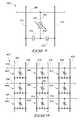
- Memory cell 300includes a memory element 302 having electrodes 306 and 304 .
- Memory element 302may comprise a bipolar memory material such as one or more of the bipolar memory materials discussed above.
- Memory cell 300also includes a wordline 308 and two bitlines 314 and 316 .
- Electrode 304 of memory element 302is connected to a wordline 308 .
- Bitline 314may be selectively electrically connected to memory element 302 .
- a diode 310may be connected to bitline 314 and to electrode 306 .
- diode 310When diode 310 is forward biased (e.g., forward biased beyond a cut-in voltage of diode 310 ), diode 310 may conduct current from bitline 314 to memory element 302 , thereby electrically connecting bitline 314 to memory element 302 .
- diode 310when diode 310 is not forward biased (e.g., when diode 310 is reverse biased), diode 310 may hinder current from flowing from memory element 302 to bitline 314 or from bitline 314 to memory element 302 so that memory element 302 is not electrically connected to bitline 314 .
- bitline 316may be selectively electrically connected to memory element 302 .
- a diode 312may be connected to bitline 316 and to electrode 306 .
- diode 312When diode 312 is forward biased (e.g., forward biased beyond a cut-in voltage of diode 312 ), diode 312 may conduct current from memory element 302 to bitline 316 thereby electrically connecting memory element 302 to bitline 316 .
- diode 312when diode 312 is not forward biased (e.g., when diode 312 is reverse biased), diode 312 may hinder current from flowing from bitline 316 to memory element 302 or from memory element 302 to bitline 316 so that memory element 302 is not electrically connected to bitline 316 .
- a memory cellmay comprise one or more devices that selectively electrically connect a memory element to a first bitline and/or a second bitline instead of diodes.
- memory element 300may use a first transistor in place of diode 310 and a second transistor in place of diode 312 . When turned on, the first transistor may allow current to flow between bitline 314 and memory element 302 , electrically connecting bitline 314 and memory element 302 . When turned off, the first transistor may hinder current from flowing between bitline 314 and memory element 302 thereby electrically disconnecting bitline 314 and memory element 302 .
- the second transistormay selectively electrically connect memory element 302 to bitline 316 .
- Devices other than diodes or transistorsmay alternatively be used to selectively electrically connect memory element 302 to bitlines 314 and 316 .
- Memory cell 300may store a bit of information via a resistive state of memory element 302 .
- the bitmay have a value of “0” or a value of “1.”
- the value of the bit stored by memory cell 300may be “0” and if memory element 302 is in a low-resistance state, the value of the bit stored by memory cell 300 may be “1.”
- a convention in which a high-resistance state represents a bit value of “1” and a low-resistance state represents a bit value of “0”may alternatively be used.
- a read operationmay be used to determine a value of a bit stored by memory cell 300 .
- a first positive voltagemay be applied between wordline 308 and bitline 316 so that wordline 308 is at a higher potential than bitline 316 and so that diode 312 is forward biased.
- the first positive voltagemay be greater than a cut-in voltage of diode 312 but less than a sum of the cut-in voltage of diode 312 and the turn-off voltage (which was described above in relation to FIG. 2 ) of memory element 302 so that the resistive state of memory element 302 is not altered.
- a second positive voltagemay be simultaneously applied between wordline 308 and bitline 314 so that wordline 308 is at a higher potential than bitline 314 and so that diode 310 is reverse biased.
- the second voltagemay be lower than a breakdown voltage of diode 310 .
- the first voltage and the second voltagemay be substantially the same voltage.
- memory element 302If memory element 302 is configured in a low-resistance state, current may flow from wordline 308 through memory element 302 and forward-biased diode 312 to bitline 316 . Based on the current, a memory device comprising memory cell 300 may determine that memory element 302 is in a low-resistance state and therefore the value stored by memory cell 300 is a “1.” For example, the memory device may compare the current on bitline 316 with a reference current or the memory device may use the current on bitline 316 to create a voltage and may then compare the voltage with a reference voltage.
- memory element 302may hinder current from flowing from wordline 308 through memory element 302 and forward-biased diode 312 to bitline 316 .
- memory element 302may restrict an amount of current flowing from wordline 308 through memory element 302 and forward-biased diode 312 to bitline 316 to a negligible amount of current that may be clearly distinguished from an amount of current allowed to flow when memory element 302 is in the low-resistance state.
- the memory device comprising memory cell 300may determine that memory element 302 is in the high-resistance state and therefore the value stored by memory cell 300 is a “0.”
- a first positive voltagemay be applied between bitline 314 and wordline 308 so that bitline 314 is at a higher potential than wordline 308 and so that diode 310 is forward biased.
- the first positive voltagemay be greater than the cut-in voltage of diode 310 but less than a sum of the cut-in voltage of diode 310 and the turn-on voltage (which was described above in relation to FIG. 1 ) of memory element 302 so that the resistive state of memory element 302 is not altered.
- a second positive voltagemay simultaneously be applied between bitline 316 and wordline 308 so that bitline 316 is at a higher potential than wordline 308 and so that diode 312 is reverse biased.
- the second voltagemay be lower than a breakdown voltage of diode 312 .
- the first voltage and the second voltagemay be substantially the same voltage.
- memory element 302If memory element 302 is configured in a low-resistance state, current may flow from bitline 314 through forward-biased diode 310 and memory element 302 to wordline 308 . Based on the current on wordline 308 , a memory device comprising memory cell 300 may determine that memory element 302 is in a low-resistance state and therefore the value stored by memory cell 300 is a “1.”
- memory element 302may hinder current from flowing from bitline 314 through forward-biased diode 310 and memory element 302 to wordline 308 .
- memory element 302may restrict an amount of current flowing from bitline 314 through forward-biased diode 310 and memory element 302 to wordline 308 to a negligible amount that may be clearly distinguished from an amount of current allowed to flow when memory element 302 is in the low-resistance state.
- the memory device comprising memory cell 300may determine that memory element 302 is in the high-resistance state and therefore the value stored by memory cell 300 is a “0.”
- a bit valuemay be written to memory cell 300 .
- a first positive voltagemay be applied between bitline 314 and wordline 308 so that bitline 314 is at a higher potential than wordline 308 and so that diode 310 is forward biased.
- the first positive voltagemay be greater than a sum of the cut-in voltage of diode 310 and the turn-on voltage of memory element 302 . If memory element 302 is in a high-resistance state, the first voltage (or a current resulting from the first voltage) may re-configure memory element 302 to be in a low-resistance state.
- memory element 302may remain in the low-resistance state. Consequently, due to the first voltage, memory element 302 may be configured in a low-resistance state corresponding with a bit value of “1.”
- a second positive voltagemay be applied simultaneously with the first voltage.
- the second positive voltagemay be applied between bitline 316 and wordline 308 so that bitline 316 is at a higher potential than wordline 308 and so that diode 312 is reverse biased.
- the second voltagemay hinder current from flowing from bitline 314 to bitline 316 .
- the second voltagemay be lower than a breakdown voltage of diode 312 .
- the first voltagemay result from a first voltage pulse and the second voltage may result from a second voltage pulse.
- the first voltage and the second voltagemay be substantially the same voltage.
- a bit value of “0”may be written to memory cell 300 .
- a first positive voltagemay be applied between wordline 308 and bitline 316 so that wordline 308 is at a higher potential than bitline 316 and so that diode 312 is forward biased.
- the first positive voltagemay be greater than a sum of the cut-in voltage of diode 312 and the turn-off voltage of memory element 302 . If memory element 302 is in a low-resistance state, the first voltage (or a current resulting from the first voltage) may re-configure memory element 302 to be in a high-resistance state.
- memory element 302may remain in the high-resistance state. Consequently, due to the first voltage, memory element 302 may be configured in a high-resistance state corresponding with a bit value of “0.”
- a second positive voltagemay be applied simultaneously with the first voltage.
- the second positive voltagemay be applied between wordline 308 and bitline 314 so that wordline 308 is at a higher potential than bitline 314 and so that diode 310 is reverse biased.
- the second voltagemay hinder current from flowing from bitline 316 to bitline 314 .
- the second voltagemay be lower than a breakdown voltage of diode 310 .
- the first voltagemay result from a first voltage pulse and the second voltage may result from a second voltage pulse.
- the first voltage and the second voltagemay be substantially the same voltage.
- the methods of writing a “0” and writing a “1” to memory cell 300may be repeatedly used so that memory cell 300 stores different bit values over time.
- memory element 302may be re-written using these methods millions of times without damaging memory element 302 . Since memory element 302 may remain in a resistive state without a voltage or current being applied to memory element 302 as was discussed above in relation to FIG. 1 , memory element 302 may be said to preserve a bit value in a non-volatile manner. Accordingly, memory cell 300 may store a bit of information without having to be frequently refreshed or memory cell 300 may be refreshed at a rate lower than a rate used to refresh a volatile memory cell.
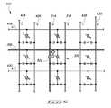
- the memory deviceincludes memory cell 300 as well as additional memory cells 402 , 404 , 406 , 408 , 410 , 412 , 414 , and 416 .
- the memory devicemay store a plurality of bits. For example, the memory device may store one bit in each memory cell of the memory device.
- the memory cells of the memory devicemay be arranged to share bitlines and wordlines.
- memory cells 402 , 408 , and 412share wordline 418 ; memory cells 404 , 300 , and 414 share wordline 308 ; and memory cells 406 , 410 , and 416 share wordline 420 .
- memory cells 402 , 404 , and 406share bitlines 424 and 426 ; memory cells 408 , 300 , and 410 share bitlines 314 and 316 ; and memory cells 412 , 414 , and 416 share bitlines 428 and 430 .
- FIG. 5a schematic diagram 500 illustrating a configuration of the memory device of FIG. 4 is illustrated.
- the configurationmay be used to write a bit value of “1” to memory cell 300 or to read a bit of information from memory cell 300 .
- a first positive voltageis applied across bitline 314 and wordline 308 .
- a second positive voltageis applied across bitline 316 and wordline 308 . Consequently, a current may flow from bitline 314 through memory cell 300 to wordline 308 as illustrated by arrow 502 and as was described above in relation to FIG. 3 .
- the first voltageis greater than a sum of the cut-in voltage of diode 310 and the turn-on voltage of memory element 302 , a “1” may be written to memory cell 300 as was described above in relation to FIG. 3 .
- the memory devicemay determine the value of a bit stored by memory cell 300 based on a current flowing from bitline 314 to wordline 308 as was described above in relation to FIG. 3 .
- bitlines and wordlines of the memory devicemay be configured with particular voltages.
- bitlines 314 and 316may be at a higher potential than wordline 308 . Since memory cells 408 and 410 are also connected to bitlines 314 and 316 , wordlines 418 and 420 may be configured to be at substantially the same potential as bitlines 314 and 316 to hinder current from flowing from bitline 314 and/or bitline 316 to wordline 418 and/or wordline 420 .
- bitlines 424 and 428may be configured to be at substantially the same potential as wordline 308 to hinder current from flowing from bitline 424 to wordline 308 via memory cell 404 and to hinder current from flowing from bitline 428 to wordline 308 via memory cell 414 .
- bitlines 426 and 430may be configured at a higher potential than wordline 308 so that current is hindered from flowing from bitline 426 through memory cell 404 to wordline 308 and from bitline 430 through memory cell 414 to wordline 308 .
- bitlines 424 and 426 and wordlines 418 and 420may be configured with voltages causing the diodes of memory cells 402 and 406 to be reverse biased.
- bitlines 428 and 430 and wordlines 418 and 420may be configured with voltages causing the diodes of memory cells 412 and 416 to be reverse biased.
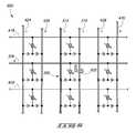
- FIG. 6a schematic diagram 600 illustrating a configuration of the memory device of FIG. 4 is illustrated.
- the configurationmay be used to write a bit value of “0” to memory cell 300 or to read a bit of information from memory cell 300 .
- a first positive voltageis applied across wordline 308 and bitline 316 .
- a second positive voltageis applied across wordline 308 and bitline 314 . Consequently, a current may flow from wordline 308 through memory cell 300 to bitline 316 as indicated by arrow 602 and as was described above in relation to FIG. 3 .
- the first voltageis greater than a sum of the cut-in voltage of diode 312 and the turn-off voltage of memory element 302 , a “0” may be written to memory cell 300 as was described above in relation to FIG. 3 .
- the memory devicemay determine the value of a bit stored by memory cell 300 based on a current flowing from wordline 308 to bitline 316 as was described above in relation to FIG. 3 .
- bitlines and wordlines of the memory devicemay be configured with particular voltages.
- bitlines 314 and 316may be at a lower potential than wordline 308 . Since memory cells 408 and 410 are also connected to bitlines 314 and 316 , wordlines 418 and 420 may be configured to be at substantially the same potential as bitlines 314 and 316 to hinder current from flowing from wordline 418 and/or wordline 420 to bitline 314 and/or bitline 316 .
- bitlines 426 and 430may be configured to be at substantially the same potential as wordline 308 to hinder current from flowing from wordline 308 to bitline 426 via memory cell 404 and to hinder current from flowing from wordline 308 to bitline 430 via memory cell 414 .
- bitlines 424 and 428may be configured at a lower potential than wordline 308 so that current is hindered from flowing from bitline 424 to wordline 308 through memory cell 404 and from bitline 428 to wordline 308 through memory cell 414 .
- bitlines 424 and 428may be configured at the same potential as wordlines 418 and 420 to hinder current from flowing through left-hand diodes of memory cells 402 , 406 , 412 , and 416 .
- bitlines 426 and 430 and wordlines 418 and 420may be configured to reverse bias right-hand diodes of memory cells 402 , 406 , 412 , and 416 .
- memory element 302is configured so that memory element 302 changes to a low-resistance state when a voltage greater than the turn-on voltage of memory element 302 is applied between electrodes 306 and 304 so that electrode 306 is at a higher potential than electrode 304 .
- memory element 302changes to a high-resistance state when a voltage greater than the turn-off voltage of memory element 302 is applied across electrodes 304 and 306 so that electrode 304 is at a higher potential than electrode 306 .
- memory element 302may be reversed so that memory element 302 changes to a high-resistance state when a voltage greater than the turn-off voltage of memory element 302 is applied between electrodes 306 and 304 so that electrode 306 is at a higher potential than electrode 304 .
- memory element 302may change to a low-resistance state when a voltage greater than the turn-on voltage of memory element 302 is applied across electrodes 304 and 306 so that electrode 304 is at a higher potential than electrode 306 .
- memory devicesmay be constructed based on an understanding that the high-resistance state of memory element 302 corresponds to a bit value of “1” and that the low-resistance state of memory element 302 corresponds to a bit value of “0” without changing the principles of writing and reading memory cell 300 .
- a memory elementhaving a high resistance state and a low resistance state.
- a memory elementmay be configurable in more than two different resistive states.
- Such a memory elementmay store more than one bit of information and may be used in a memory cell such as memory cell 300 .
- Each of a plurality of different programming voltagesmay correspond to a different one of a plurality of different resistive states of the memory element.
- the methods of programming memory cell 300 described abovemay be adapted to program a memory element having more than one resistive state by applying one of the plurality of programming voltages to the memory element in order to configure the memory element in the resistive state corresponding to the applied programming voltage. Furthermore, the methods of reading memory cell 300 described above may be adapted to read the memory element by comparing a current resulting from a voltage applied to the memory element to a plurality of different reference currents to determine in which of the plurality of different resistive states the memory cell is configured.
Landscapes
- Semiconductor Memories (AREA)
- Mram Or Spin Memory Techniques (AREA)
- Read Only Memory (AREA)
Abstract
Description
This application is a continuation of and claims priority to U.S. patent application Ser. No. 15/084,191, filed Mar. 29, 2016, which is a continuation of and claims priority to U.S. patent application Ser. No. 13/292,680, filed Nov. 9, 2011, now U.S. Pat. No. 9,343,145, issued May 17, 2016, which is a continuation of and claims priority to U.S. patent application Ser. No. 12/833,810, filed Jul. 9, 2010, now U.S. Pat. No. 8,154,906, issued Apr. 10, 2012, and which is a continuation of and claims priority to U.S. patent application Ser. No. 12/014,232, filed Jan. 15, 2008, now U.S. Pat. No. 7,768,812, issued Aug. 3, 2010, the teachings of which are incorporated herein by reference.
Embodiments disclosed herein pertain to memory cells, memory cell programming methods, memory cell reading methods, memory cell operating methods, and memory devices.
Resistive random access memories may use a material capable of being configured in one of two different resistive states to store information. When configured in one of the resistive states, the material may have a high resistance to electrical current. In contrast, when configured in the other resistive state, the material may have a low resistance to electrical current. The resistive state in which the material is configured may be changed using electrical signals. For example, if the material is in a high-resistance state, the material may be configured to be in a low-resistance state by applying a voltage across the material.
The resistive state may be persistent. For example, once configured in a resistive state, the material may stay in the resistive state even if neither a current nor a voltage is applied to the material. Furthermore, the configuration of the material may be repeatedly changed from the high resistance state to the low resistance state or from the low resistance state to the high resistance state.
Embodiments of the invention encompass memory cell operating methods, memory cell programming methods, memory cell reading methods, memory cells, and memory devices. Example embodiments of such methods, memory cells, and memory devices are described with reference toFIGS. 1-6 .
Random access memories may use resistive states of a memory element to store one or more bits of information. For example, a memory element capable of being configured in either a high-resistance state or a low-resistance state may store one bit of information by associating a bit value of “1” with the low-resistance state and a bit value of “0” with the high-resistance state. Alternatively, a bit value of “1” may be associated with the high-resistance state and a bit value of “0” may be associated with the low-resistance state.
The memory element may include a bipolar memory material. A positive voltage applied across the bipolar memory material may change the configuration of the bipolar memory material from a high-resistance state to a low-resistance state. Furthermore, a negative voltage applied across the bipolar memory material may change the configuration of the bipolar memory material from a low-resistance state to a high-resistance state.
Alternatively, a negative voltage applied across the bipolar memory material may change the configuration of the bipolar memory material from a high-resistance state to a low-resistance state and a positive voltage applied across the bipolar memory material may change the configuration of the bipolar memory material from a low-resistance state to a high-resistance. Accordingly, a bipolar memory material may be configured in a first resistive state using a voltage having a first polarity and may be configured in a second resistive state using a voltage having a polarity opposite that of the first polarity.
Examples of bipolar memory material include ionic conducting chalcogenides, binary metal oxides, perovskite oxides, colossal magnetoresistives, and polymers. Example ionic conducting chalcogenides that may be used as bipolar memory material include GeS, GeSe and Ag or Cu-doped GeS and GeSe. Example binary metal oxides that may be used as bipolar memory material include HfOx, Nb2O5, Al2O3, WOx, Ta2O5, TiOx, ZrOx, CuxO, and NixO. Example ionic perovskite oxides that may be used as bipolar memory material include doped or undoped SrTiO3, SrZrO3, BaTiO3.
Example colossal magnetoresistives that may be used as bipolar memory material include Pr1-xCaxMnO3(PCMO), La1-xCaxMnO3(LCMO), and Ba1-xSrxTiO3. Example polymers that may be used as bipolar memory material include Bengala Rose, AlQ3Ag, Cu-TCNQ, DDQ, TAPA, and fluorescine-based polymers. Of course, other materials may be used as bipolar memory material. The materials listed above are provided by way of example rather than as an exhaustive list of bipolar memory material.
Referring toFIG. 1 , achart 100 depicts one example of arelationship 102 between voltages applied to a memory element initially in a high-resistance state and currents through the memory element resulting from the voltages. The memory element may comprise one or more of the bipolar memory materials described above.Chart 100 illustrates that as voltages applied to the memory element increase from −0.6 V to 0.2 V, no current, or a negligible amount of current, for example less than 1 micro amp, flows through the memory element. However, at a voltage substantially equal to a turn-onvoltage 104, the memory element begins conducting current. As the voltage across the memory element is increased beyond turn-onvoltage 104, the amount of current conducted by the memory element increases with the voltage without current clamping. The flattening of the current with voltage depicted inFIG. 1 results from current clamping of a measurement circuit.
Thus,chart 100 illustrates a change in the resistive state of the memory element. Initially, the memory element is in a high-resistance state as evidenced by the fact that the memory element does not conduct current or conducts a negligible amount of current when voltages smaller than the turn-on voltage are applied to the memory element. In this high-resistance state, the memory element may have a resistance of about or above 109ohms. However, once a voltage greater than or equal to turn-onvoltage 104 is applied to the memory element, the memory element configures itself in a low-resistance state as evidenced by the fact that the memory element begins conducting current. In this low-resistance state, the memory element may be highly conductive and have a resistance of about a few thousand ohms.
Referring toFIG. 2 , achart 200 depicts one example of arelationship 202 between voltages applied to a memory element initially in the low-resistance state described above and currents running through the memory element resulting from the voltages.Chart 200 illustrates that currents resulting from voltages greater than about 0.25 V are substantially the same, which results from current clamping of a measurement circuit. Without the current clamping, the current increases with voltage. As the voltage is decreased below about 0.25 V, the current through the memory element accordingly decreases. As the voltage applied across the memory element becomes negative, the current through the memory element is also negative. However, when the voltage applied across the memory element is substantially equal to a turn-offvoltage 204, the amount of current through the memory element is substantially zero. As the voltage is further decreased below the turn-off voltage, the current through the memory element remains substantially zero.
Thus,chart 200 illustrates a change in resistive state of the memory element. Initially, the memory element is in the low-resistance state as evidenced by the fact that the memory element conducts current when voltages greater than turn-offvoltage 204 are applied to the memory element. However, once a voltage less than or equal to turn-offvoltage 204 is applied to the memory element, the memory element configures itself in the high-resistance state described above as evidenced by the fact that the memory element stops conducting current or conducts only a negligible amount of current.
In some cases, once configured in the high-resistance state, the memory element may remain in the high-resistance state as long as a voltage greater than or equal to turn-onvoltage 104 is not applied to the memory element. The memory element may remain in the high-resistance state even if no voltage is applied to the memory element. Accordingly, the high-resistance state of the memory element may be described as non-volatile since the high-resistance state might not change over time as long as a voltage greater than or equal to turn-onvoltage 104 is not applied to the memory element.
Similarly, in some cases, once configured in the low-resistance state, the memory element may remain in the low-resistance state as long as a voltage less than or equal to turn-offvoltage 204 is not applied to the memory element. In fact, the memory element may remain in the low-resistance state even if no voltage is applied to the memory element. Accordingly, the low-resistance state of the memory element may also be described as non-volatile since the low-resistance state might not change over time as long as a voltage less than or equal to turn-offvoltage 204 is not applied to the memory element.
Since the high-resistance state and the low-resistance state may be non-volatile, the memory element may be used to store one bit information. For example, a memory element may represent a bit value of “0” when configured in the high-resistance state and may represent a bit value of “1” when configured in the low-resistance state. Furthermore, the resistive state of the memory element may be repeatedly changed over time. Accordingly, the memory element may be in the high-resistance state representing a bit value of “0” at one moment in time and the memory element may be in a low-resistance state representing a bit value of “1” at another moment in time. Similarly, the representation of bit value with resistance states can be the opposite of that described above.
Referring toFIG. 3 , amemory cell 300 is illustrated.Memory cell 300 includes amemory element 302 havingelectrodes Memory element 302 may comprise a bipolar memory material such as one or more of the bipolar memory materials discussed above.Memory cell 300 also includes awordline 308 and twobitlines Electrode 304 ofmemory element 302 is connected to awordline 308.
Similarly,bitline 316 may be selectively electrically connected tomemory element 302. For example, adiode 312 may be connected to bitline316 and toelectrode 306. Whendiode 312 is forward biased (e.g., forward biased beyond a cut-in voltage of diode312),diode 312 may conduct current frommemory element 302 to bitline316 thereby electrically connectingmemory element 302 tobitline 316. In contrast, whendiode 312 is not forward biased (e.g., whendiode 312 is reverse biased),diode 312 may hinder current from flowing frombitline 316 tomemory element 302 or frommemory element 302 to bitline316 so thatmemory element 302 is not electrically connected tobitline 316.
In some configurations, a memory cell may comprise one or more devices that selectively electrically connect a memory element to a first bitline and/or a second bitline instead of diodes. For example, in one configuration,memory element 300 may use a first transistor in place ofdiode 310 and a second transistor in place ofdiode 312. When turned on, the first transistor may allow current to flow betweenbitline 314 andmemory element 302, electrically connectingbitline 314 andmemory element 302. When turned off, the first transistor may hinder current from flowing betweenbitline 314 andmemory element 302 thereby electrically disconnectingbitline 314 andmemory element 302.
Similarly, the second transistor may selectively electrically connectmemory element 302 tobitline 316. Devices other than diodes or transistors may alternatively be used to selectively electrically connectmemory element 302 to bitlines314 and316.
A read operation may be used to determine a value of a bit stored bymemory cell 300. According to one read operation, a first positive voltage may be applied betweenwordline 308 andbitline 316 so thatwordline 308 is at a higher potential thanbitline 316 and so thatdiode 312 is forward biased. The first positive voltage may be greater than a cut-in voltage ofdiode 312 but less than a sum of the cut-in voltage ofdiode 312 and the turn-off voltage (which was described above in relation toFIG. 2 ) ofmemory element 302 so that the resistive state ofmemory element 302 is not altered. A second positive voltage may be simultaneously applied betweenwordline 308 andbitline 314 so thatwordline 308 is at a higher potential thanbitline 314 and so thatdiode 310 is reverse biased. The second voltage may be lower than a breakdown voltage ofdiode 310. In some cases, the first voltage and the second voltage may be substantially the same voltage.
Ifmemory element 302 is configured in a low-resistance state, current may flow fromwordline 308 throughmemory element 302 and forward-biaseddiode 312 tobitline 316. Based on the current, a memory device comprisingmemory cell 300 may determine thatmemory element 302 is in a low-resistance state and therefore the value stored bymemory cell 300 is a “1.” For example, the memory device may compare the current onbitline 316 with a reference current or the memory device may use the current onbitline 316 to create a voltage and may then compare the voltage with a reference voltage.
In contrast, ifmemory element 302 is configured in a high-resistance state,memory element 302 may hinder current from flowing fromwordline 308 throughmemory element 302 and forward-biaseddiode 312 tobitline 316. Alternatively,memory element 302 may restrict an amount of current flowing fromwordline 308 throughmemory element 302 and forward-biaseddiode 312 to bitline316 to a negligible amount of current that may be clearly distinguished from an amount of current allowed to flow whenmemory element 302 is in the low-resistance state. Based on the lack of current, or the very small amount of current, the memory device comprisingmemory cell 300 may determine thatmemory element 302 is in the high-resistance state and therefore the value stored bymemory cell 300 is a “0.”
Another method of readingmemory cell 300 may alternatively be used. According to this method, a first positive voltage may be applied betweenbitline 314 andwordline 308 so thatbitline 314 is at a higher potential thanwordline 308 and so thatdiode 310 is forward biased. The first positive voltage may be greater than the cut-in voltage ofdiode 310 but less than a sum of the cut-in voltage ofdiode 310 and the turn-on voltage (which was described above in relation toFIG. 1 ) ofmemory element 302 so that the resistive state ofmemory element 302 is not altered. A second positive voltage may simultaneously be applied betweenbitline 316 andwordline 308 so thatbitline 316 is at a higher potential thanwordline 308 and so thatdiode 312 is reverse biased. The second voltage may be lower than a breakdown voltage ofdiode 312. In some cases, the first voltage and the second voltage may be substantially the same voltage.
Ifmemory element 302 is configured in a low-resistance state, current may flow frombitline 314 through forward-biaseddiode 310 andmemory element 302 towordline 308. Based on the current onwordline 308, a memory device comprisingmemory cell 300 may determine thatmemory element 302 is in a low-resistance state and therefore the value stored bymemory cell 300 is a “1.”
In contrast, ifmemory element 302 is configured in a high-resistance state,memory element 302 may hinder current from flowing frombitline 314 through forward-biaseddiode 310 andmemory element 302 towordline 308. Alternatively,memory element 302 may restrict an amount of current flowing frombitline 314 through forward-biaseddiode 310 andmemory element 302 to wordline308 to a negligible amount that may be clearly distinguished from an amount of current allowed to flow whenmemory element 302 is in the low-resistance state. Based on the lack of current, or the very small amount of current, the memory device comprisingmemory cell 300 may determine thatmemory element 302 is in the high-resistance state and therefore the value stored bymemory cell 300 is a “0.”
In addition to reading a bit value frommemory cell 300, a bit value may be written tomemory cell 300. To write a bit value of “1” tomemory cell 300, a first positive voltage may be applied betweenbitline 314 andwordline 308 so thatbitline 314 is at a higher potential thanwordline 308 and so thatdiode 310 is forward biased. The first positive voltage may be greater than a sum of the cut-in voltage ofdiode 310 and the turn-on voltage ofmemory element 302. Ifmemory element 302 is in a high-resistance state, the first voltage (or a current resulting from the first voltage) may re-configurememory element 302 to be in a low-resistance state. Ifmemory element 302 is already in a low-resistance state,memory element 302 may remain in the low-resistance state. Consequently, due to the first voltage,memory element 302 may be configured in a low-resistance state corresponding with a bit value of “1.”
A second positive voltage may be applied simultaneously with the first voltage. The second positive voltage may be applied betweenbitline 316 andwordline 308 so thatbitline 316 is at a higher potential thanwordline 308 and so thatdiode 312 is reverse biased. The second voltage may hinder current from flowing frombitline 314 tobitline 316. The second voltage may be lower than a breakdown voltage ofdiode 312.
The first voltage may result from a first voltage pulse and the second voltage may result from a second voltage pulse. In some cases, the first voltage and the second voltage may be substantially the same voltage.
Alternatively, a bit value of “0” may be written tomemory cell 300. To write a bit value of “0” tomemory cell 300, a first positive voltage may be applied betweenwordline 308 andbitline 316 so thatwordline 308 is at a higher potential thanbitline 316 and so thatdiode 312 is forward biased. The first positive voltage may be greater than a sum of the cut-in voltage ofdiode 312 and the turn-off voltage ofmemory element 302. Ifmemory element 302 is in a low-resistance state, the first voltage (or a current resulting from the first voltage) may re-configurememory element 302 to be in a high-resistance state. Ifmemory element 302 is already in a high-resistance state,memory element 302 may remain in the high-resistance state. Consequently, due to the first voltage,memory element 302 may be configured in a high-resistance state corresponding with a bit value of “0.”
A second positive voltage may be applied simultaneously with the first voltage. The second positive voltage may be applied betweenwordline 308 andbitline 314 so thatwordline 308 is at a higher potential thanbitline 314 and so thatdiode 310 is reverse biased. The second voltage may hinder current from flowing frombitline 316 tobitline 314. The second voltage may be lower than a breakdown voltage ofdiode 310.
The first voltage may result from a first voltage pulse and the second voltage may result from a second voltage pulse. In some cases, the first voltage and the second voltage may be substantially the same voltage.
The methods of writing a “0” and writing a “1” tomemory cell 300 may be repeatedly used so thatmemory cell 300 stores different bit values over time. In some cases,memory element 302 may be re-written using these methods millions of times without damagingmemory element 302. Sincememory element 302 may remain in a resistive state without a voltage or current being applied tomemory element 302 as was discussed above in relation toFIG. 1 ,memory element 302 may be said to preserve a bit value in a non-volatile manner. Accordingly,memory cell 300 may store a bit of information without having to be frequently refreshed ormemory cell 300 may be refreshed at a rate lower than a rate used to refresh a volatile memory cell.
Referring toFIG. 4 , a schematic diagram400 of a portion of a memory device is illustrated. The memory device includesmemory cell 300 as well asadditional memory cells
The memory cells of the memory device may be arranged to share bitlines and wordlines. In diagram400,memory cells share wordline 418;memory cells share wordline 308; andmemory cells share wordline 420. Furthermore, in diagram400,memory cells memory cells memory cells
Referring toFIG. 5 , a schematic diagram500 illustrating a configuration of the memory device ofFIG. 4 is illustrated. The configuration may be used to write a bit value of “1” tomemory cell 300 or to read a bit of information frommemory cell 300. According to the configuration, a first positive voltage is applied acrossbitline 314 andwordline 308. A second positive voltage is applied acrossbitline 316 andwordline 308. Consequently, a current may flow frombitline 314 throughmemory cell 300 to wordline308 as illustrated byarrow 502 and as was described above in relation toFIG. 3 . If the first voltage is greater than a sum of the cut-in voltage ofdiode 310 and the turn-on voltage ofmemory element 302, a “1” may be written tomemory cell 300 as was described above in relation toFIG. 3 .
Alternatively, if the first voltage is greater than the cut-in voltage ofdiode 310 but less than a sum of the cut-in voltage of the diode and the turn-on voltage ofmemory element 302, the memory device may determine the value of a bit stored bymemory cell 300 based on a current flowing frombitline 314 to wordline308 as was described above in relation toFIG. 3 .
It may be desirable to ensure that values stored bymemory cells memory cell 300. To avoid disturbances, bitlines and wordlines of the memory device may be configured with particular voltages.
For example, when writing a “1” intomemory cell 300,bitlines wordline 308. Sincememory cells wordlines bitlines bitline 314 and/orbitline 316 to wordline418 and/orwordline 420.
Furthermore, it may be desirable to hinder currents from flowing frommemory cells wordline 308 so that a current onwordline 308 may be correctly attributed tomemory cell 300. To do so,bitlines wordline 308 to hinder current from flowing frombitline 424 to wordline308 viamemory cell 404 and to hinder current from flowing frombitline 428 to wordline308 viamemory cell 414. In addition, bitlines426 and430 may be configured at a higher potential thanwordline 308 so that current is hindered from flowing frombitline 426 throughmemory cell 404 to wordline308 and frombitline 430 throughmemory cell 414 towordline 308.
Other memory cells not connected to either wordline308 or bitlines314 and316 (i.e.,memory cells memory cells bitlines memory cells
Referring toFIG. 6 , a schematic diagram600 illustrating a configuration of the memory device ofFIG. 4 is illustrated. The configuration may be used to write a bit value of “0” tomemory cell 300 or to read a bit of information frommemory cell 300. According to the configuration, a first positive voltage is applied acrosswordline 308 andbitline 316. A second positive voltage is applied acrosswordline 308 andbitline 314. Consequently, a current may flow fromwordline 308 throughmemory cell 300 to bitline316 as indicated byarrow 602 and as was described above in relation toFIG. 3 . If the first voltage is greater than a sum of the cut-in voltage ofdiode 312 and the turn-off voltage ofmemory element 302, a “0” may be written tomemory cell 300 as was described above in relation toFIG. 3 .
Alternatively, if the first voltage is greater than the cut-in voltage ofdiode 312 but less than a sum of the cut-in voltage of diode and the turn-off voltage ofmemory element 302, the memory device may determine the value of a bit stored bymemory cell 300 based on a current flowing fromwordline 308 to bitline316 as was described above in relation toFIG. 3 .
It may be desirable to ensure that values stored bymemory cells memory cell 300. To avoid disturbances, bitlines and wordlines of the memory device may be configured with particular voltages.
For example, when writing a “0” intomemory cell 300,bitlines wordline 308. Sincememory cells wordlines bitlines wordline 418 and/orwordline 420 tobitline 314 and/orbitline 316.
Furthermore, it may be desirable to hinder currents from flowing fromwordline 308 intomemory cells bitlines wordline 308 to hinder current from flowing fromwordline 308 to bitline426 viamemory cell 404 and to hinder current from flowing fromwordline 308 to bitline430 viamemory cell 414. In addition, bitlines424 and428 may be configured at a lower potential thanwordline 308 so that current is hindered from flowing frombitline 424 to wordline308 throughmemory cell 404 and frombitline 428 to wordline308 throughmemory cell 414.
Other memory cells not connected to either wordline308 or bitlines314 and316 (i.e.,memory cells FIG. 6 . For example, bitlines424 and428 may be configured at the same potential aswordlines memory cells bitlines memory cells
The above discussion has assumed thatmemory element 302 is configured so thatmemory element 302 changes to a low-resistance state when a voltage greater than the turn-on voltage ofmemory element 302 is applied betweenelectrodes electrode 306 is at a higher potential thanelectrode 304. Similarly, the above discussion has assumed thatmemory element 302 changes to a high-resistance state when a voltage greater than the turn-off voltage ofmemory element 302 is applied acrosselectrodes electrode 304 is at a higher potential thanelectrode 306.
However,memory element 302 may be reversed so thatmemory element 302 changes to a high-resistance state when a voltage greater than the turn-off voltage ofmemory element 302 is applied betweenelectrodes electrode 306 is at a higher potential thanelectrode 304. In this configuration,memory element 302 may change to a low-resistance state when a voltage greater than the turn-on voltage ofmemory element 302 is applied acrosselectrodes electrode 304 is at a higher potential thanelectrode 306.
Furthermore, the above discussion has assumed that a high-resistance state ofmemory element 302 corresponds to a bit value of “0” and that a low-resistance state ofmemory element 302 corresponds to a bit value of “1.” However, as was mentioned above, memory devices may be constructed based on an understanding that the high-resistance state ofmemory element 302 corresponds to a bit value of “1” and that the low-resistance state ofmemory element 302 corresponds to a bit value of “0” without changing the principles of writing and readingmemory cell 300.
The above discussion has referred to a memory element having a high resistance state and a low resistance state. However, in some embodiments of the invention, a memory element may be configurable in more than two different resistive states. Such a memory element may store more than one bit of information and may be used in a memory cell such asmemory cell 300. Each of a plurality of different programming voltages may correspond to a different one of a plurality of different resistive states of the memory element.
The methods ofprogramming memory cell 300 described above may be adapted to program a memory element having more than one resistive state by applying one of the plurality of programming voltages to the memory element in order to configure the memory element in the resistive state corresponding to the applied programming voltage. Furthermore, the methods ofreading memory cell 300 described above may be adapted to read the memory element by comparing a current resulting from a voltage applied to the memory element to a plurality of different reference currents to determine in which of the plurality of different resistive states the memory cell is configured.
In compliance with the statute, the subject matter disclosed herein has been described in language more or less specific as to structural and methodical features. It is to be understood, however, that the claims are not limited to the specific features shown and described, since the means herein disclosed comprise example embodiments. The claims are thus to be afforded full scope as literally worded, and to be appropriately interpreted in accordance with the doctrine of equivalents.
Claims (23)
1. A memory device comprising:
a memory element configured to have a plurality of different electrical resistances in a plurality of different memory states;
circuitry configured to conduct a first current through the memory element at a first moment in time to program the memory element in a first of the memory states having a first of the electrical resistances and to conduct a second current through the memory element at a second moment in time to program the memory element in a second of the memory states having a second of the electrical resistances which is different than the first electrical resistance; and
wherein the first and second currents are conducted in opposite directions through the memory element.
2. The device ofclaim 1 wherein the memory element has a plurality of electrodes and the first current is conducted from a first node to one of the electrodes and the second current is conducted from the one of the electrodes to a second node.
3. The device ofclaim 2 wherein the first node is a first bitline and the second node is a second bitline.
4. The device ofclaim 3 wherein another of the electrodes is coupled with a wordline.
5. The device ofclaim 1 wherein the memory element comprises a plurality of electrodes, and the circuitry comprises a first diode and a second diode which are coupled with a first of the electrodes.
6. The device ofclaim 5 wherein the first diode conducts the first current and the second diode conducts the second current.
7. The device ofclaim 6 wherein the first diode prevents conduction of the second current and the second diode prevents conduction of the first current.
8. The device ofclaim 5 wherein a cathode of the first diode and an anode of the second diode are individually coupled with the first electrode.
9. A memory device comprising:
a memory element comprising a plurality of electrodes and wherein the memory element is configured to have a plurality of different electrical resistances in respective ones of a plurality of different memory states at a plurality of moments in time;
a wordline coupled with a first of the electrodes;
a plurality of bitlines coupled with a second of the electrodes;
circuitry configured to cause conduction of current through the memory element between the wordline and a first of the bitlines and prevent current from flowing to a second of the bitlines during an application of a voltage to the wordline; and
wherein the current conducted through the memory element is indicative of the electrical resistances and corresponding memory states of the memory element at the different moments in time.
10. The device ofclaim 9 wherein the first and second bitlines are provided at the same voltage during conduction of the current through the memory element.
11. The device ofclaim 10 wherein the circuitry comprises a plurality of diodes individually coupled with a respective one of the first and second bitlines and the memory element.
12. The device ofclaim 11 wherein a cathode of a first of the diodes and an anode of a second of the diodes are individually coupled with the second electrode.
13. A memory cell operational method comprising:
first conducting a first current from a first electrode through a memory element to a second electrode at a first moment in time, wherein the memory element has a plurality of different electrical resistances corresponding to a plurality of different memory states;
providing the memory element in a first of the memory states having a first of the electrical resistances as a result of the first conducting;
second conducting a second current from the second electrode through the memory element to the first electrode at a second moment in time; and
providing the memory element in a second of the memory states having a second of the electrical resistances as a result of the second conducting.
14. The method ofclaim 13 wherein the first conducting comprises conducting the first current from a first node to one of the electrodes and the second conducting comprises conducting the second current from the one of the electrodes to a second node.
15. The method ofclaim 14 wherein the first node is a first bitline and the second node is a second bitline.
16. The method ofclaim 15 wherein another of the electrodes is coupled with a wordline.
17. The method ofclaim 13 wherein the first conducting comprises conducting using a first diode and the second conducting comprises conducting using a second diode.
18. The method ofclaim 17 further comprising preventing conduction of the second current using the first diode and preventing conduction of the first current using the second diode.
19. A memory cell operational method comprising:
applying a voltage to a wordline;
conducting a current through a memory element which is coupled with the wordline to a first bitline as a result of the applying the voltage to the wordline, wherein the memory element has a plurality of different electrical resistances corresponding to a plurality of different memory states at a plurality of different moments in time;
preventing the current from flowing through the memory element to a second bit line as a result of the applying the voltage to the wordline; and
using the current conducted to the first bitline to determine the electrical resistance and corresponding one of the different memory states of the memory element at one of the moments in time.
20. The method ofclaim 19 further comprising providing the first and second bitlines at the same voltage during the conducting the current through the memory element.
21. The method ofclaim 19 wherein the conducting comprises conducting the current using a first diode.
22. The method ofclaim 21 wherein the preventing comprises preventing using a second diode.
23. The method ofclaim 22 wherein a cathode of the first diode and an anode of the second diode are individually coupled with an electrode of the memory element.
Priority Applications (4)
| Application Number | Priority Date | Filing Date | Title |
|---|---|---|---|
| US15/798,166US10262734B2 (en) | 2008-01-15 | 2017-10-30 | Memory cells, memory cell programming methods, memory cell reading methods, memory cell operating methods, and memory devices |
| US16/384,557US10790020B2 (en) | 2008-01-15 | 2019-04-15 | Memory cells, memory cell programming methods, memory cell reading methods, memory cell operating methods, and memory devices |
| US17/031,454US11393530B2 (en) | 2008-01-15 | 2020-09-24 | Memory cells, memory cell programming methods, memory cell reading methods, memory cell operating methods, and memory devices |
| US17/867,359US20220351775A1 (en) | 2008-01-15 | 2022-07-18 | Memory Cells, Memory Cell Programming Methods, Memory Cell Reading Methods, Memory Cell Operating Methods, and Memory Devices |
Applications Claiming Priority (5)
| Application Number | Priority Date | Filing Date | Title |
|---|---|---|---|
| US12/014,232US7768812B2 (en) | 2008-01-15 | 2008-01-15 | Memory cells, memory cell programming methods, memory cell reading methods, memory cell operating methods, and memory devices |
| US12/833,810US8154906B2 (en) | 2008-01-15 | 2010-07-09 | Memory cells, memory cell programming methods, memory cell reading methods, memory cell operating methods, and memory devices |
| US13/292,680US9343145B2 (en) | 2008-01-15 | 2011-11-09 | Memory cells, memory cell programming methods, memory cell reading methods, memory cell operating methods, and memory devices |
| US15/084,191US9805792B2 (en) | 2008-01-15 | 2016-03-29 | Memory cells, memory cell programming methods, memory cell reading methods, memory cell operating methods, and memory devices |
| US15/798,166US10262734B2 (en) | 2008-01-15 | 2017-10-30 | Memory cells, memory cell programming methods, memory cell reading methods, memory cell operating methods, and memory devices |
Related Parent Applications (1)
| Application Number | Title | Priority Date | Filing Date |
|---|---|---|---|
| US15/084,191ContinuationUS9805792B2 (en) | 2008-01-15 | 2016-03-29 | Memory cells, memory cell programming methods, memory cell reading methods, memory cell operating methods, and memory devices |
Related Child Applications (1)
| Application Number | Title | Priority Date | Filing Date |
|---|---|---|---|
| US16/384,557ContinuationUS10790020B2 (en) | 2008-01-15 | 2019-04-15 | Memory cells, memory cell programming methods, memory cell reading methods, memory cell operating methods, and memory devices |
Publications (2)
| Publication Number | Publication Date |
|---|---|
| US20180068724A1 US20180068724A1 (en) | 2018-03-08 |
| US10262734B2true US10262734B2 (en) | 2019-04-16 |
Family
ID=40850479
Family Applications (8)
| Application Number | Title | Priority Date | Filing Date |
|---|---|---|---|
| US12/014,232Active2028-08-20US7768812B2 (en) | 2008-01-15 | 2008-01-15 | Memory cells, memory cell programming methods, memory cell reading methods, memory cell operating methods, and memory devices |
| US12/833,810Expired - Fee RelatedUS8154906B2 (en) | 2008-01-15 | 2010-07-09 | Memory cells, memory cell programming methods, memory cell reading methods, memory cell operating methods, and memory devices |
| US13/292,680Expired - Fee RelatedUS9343145B2 (en) | 2008-01-15 | 2011-11-09 | Memory cells, memory cell programming methods, memory cell reading methods, memory cell operating methods, and memory devices |
| US15/084,191ActiveUS9805792B2 (en) | 2008-01-15 | 2016-03-29 | Memory cells, memory cell programming methods, memory cell reading methods, memory cell operating methods, and memory devices |
| US15/798,166Expired - Fee RelatedUS10262734B2 (en) | 2008-01-15 | 2017-10-30 | Memory cells, memory cell programming methods, memory cell reading methods, memory cell operating methods, and memory devices |
| US16/384,557Expired - Fee RelatedUS10790020B2 (en) | 2008-01-15 | 2019-04-15 | Memory cells, memory cell programming methods, memory cell reading methods, memory cell operating methods, and memory devices |
| US17/031,454ActiveUS11393530B2 (en) | 2008-01-15 | 2020-09-24 | Memory cells, memory cell programming methods, memory cell reading methods, memory cell operating methods, and memory devices |
| US17/867,359AbandonedUS20220351775A1 (en) | 2008-01-15 | 2022-07-18 | Memory Cells, Memory Cell Programming Methods, Memory Cell Reading Methods, Memory Cell Operating Methods, and Memory Devices |
Family Applications Before (4)
| Application Number | Title | Priority Date | Filing Date |
|---|---|---|---|
| US12/014,232Active2028-08-20US7768812B2 (en) | 2008-01-15 | 2008-01-15 | Memory cells, memory cell programming methods, memory cell reading methods, memory cell operating methods, and memory devices |
| US12/833,810Expired - Fee RelatedUS8154906B2 (en) | 2008-01-15 | 2010-07-09 | Memory cells, memory cell programming methods, memory cell reading methods, memory cell operating methods, and memory devices |
| US13/292,680Expired - Fee RelatedUS9343145B2 (en) | 2008-01-15 | 2011-11-09 | Memory cells, memory cell programming methods, memory cell reading methods, memory cell operating methods, and memory devices |
| US15/084,191ActiveUS9805792B2 (en) | 2008-01-15 | 2016-03-29 | Memory cells, memory cell programming methods, memory cell reading methods, memory cell operating methods, and memory devices |
Family Applications After (3)
| Application Number | Title | Priority Date | Filing Date |
|---|---|---|---|
| US16/384,557Expired - Fee RelatedUS10790020B2 (en) | 2008-01-15 | 2019-04-15 | Memory cells, memory cell programming methods, memory cell reading methods, memory cell operating methods, and memory devices |
| US17/031,454ActiveUS11393530B2 (en) | 2008-01-15 | 2020-09-24 | Memory cells, memory cell programming methods, memory cell reading methods, memory cell operating methods, and memory devices |
| US17/867,359AbandonedUS20220351775A1 (en) | 2008-01-15 | 2022-07-18 | Memory Cells, Memory Cell Programming Methods, Memory Cell Reading Methods, Memory Cell Operating Methods, and Memory Devices |
Country Status (6)
| Country | Link |
|---|---|
| US (8) | US7768812B2 (en) |
| EP (3) | EP2243138B1 (en) |
| KR (1) | KR101136639B1 (en) |
| CN (1) | CN101911201B (en) |
| TW (1) | TWI420531B (en) |
| WO (1) | WO2009091445A1 (en) |
Families Citing this family (30)
| Publication number | Priority date | Publication date | Assignee | Title |
|---|---|---|---|---|
| US7768812B2 (en) | 2008-01-15 | 2010-08-03 | Micron Technology, Inc. | Memory cells, memory cell programming methods, memory cell reading methods, memory cell operating methods, and memory devices |
| US8034655B2 (en) | 2008-04-08 | 2011-10-11 | Micron Technology, Inc. | Non-volatile resistive oxide memory cells, non-volatile resistive oxide memory arrays, and methods of forming non-volatile resistive oxide memory cells and memory arrays |
| US8211743B2 (en)* | 2008-05-02 | 2012-07-03 | Micron Technology, Inc. | Methods of forming non-volatile memory cells having multi-resistive state material between conductive electrodes |
| US8134137B2 (en)* | 2008-06-18 | 2012-03-13 | Micron Technology, Inc. | Memory device constructions, memory cell forming methods, and semiconductor construction forming methods |
| US9343665B2 (en) | 2008-07-02 | 2016-05-17 | Micron Technology, Inc. | Methods of forming a non-volatile resistive oxide memory cell and methods of forming a non-volatile resistive oxide memory array |
| US8014185B2 (en)* | 2008-07-09 | 2011-09-06 | Sandisk 3D Llc | Multiple series passive element matrix cell for three-dimensional arrays |
| US7733685B2 (en)* | 2008-07-09 | 2010-06-08 | Sandisk 3D Llc | Cross point memory cell with distributed diodes and method of making same |
| US7923812B2 (en)* | 2008-12-19 | 2011-04-12 | Sandisk 3D Llc | Quad memory cell and method of making same |
| US7910407B2 (en) | 2008-12-19 | 2011-03-22 | Sandisk 3D Llc | Quad memory cell and method of making same |
| US8461566B2 (en) | 2009-11-02 | 2013-06-11 | Micron Technology, Inc. | Methods, structures and devices for increasing memory density |
| US8427859B2 (en) | 2010-04-22 | 2013-04-23 | Micron Technology, Inc. | Arrays of vertically stacked tiers of non-volatile cross point memory cells, methods of forming arrays of vertically stacked tiers of non-volatile cross point memory cells, and methods of reading a data value stored by an array of vertically stacked tiers of non-volatile cross point memory cells |
| US8411477B2 (en) | 2010-04-22 | 2013-04-02 | Micron Technology, Inc. | Arrays of vertically stacked tiers of non-volatile cross point memory cells, methods of forming arrays of vertically stacked tiers of non-volatile cross point memory cells, and methods of reading a data value stored by an array of vertically stacked tiers of non-volatile cross point memory cells |
| US8289763B2 (en) | 2010-06-07 | 2012-10-16 | Micron Technology, Inc. | Memory arrays |
| US8351242B2 (en) | 2010-09-29 | 2013-01-08 | Micron Technology, Inc. | Electronic devices, memory devices and memory arrays |
| US8759809B2 (en) | 2010-10-21 | 2014-06-24 | Micron Technology, Inc. | Integrated circuitry comprising nonvolatile memory cells having platelike electrode and ion conductive material layer |
| US8796661B2 (en) | 2010-11-01 | 2014-08-05 | Micron Technology, Inc. | Nonvolatile memory cells and methods of forming nonvolatile memory cell |
| US8526213B2 (en) | 2010-11-01 | 2013-09-03 | Micron Technology, Inc. | Memory cells, methods of programming memory cells, and methods of forming memory cells |
| US8502185B2 (en)* | 2011-05-31 | 2013-08-06 | Crossbar, Inc. | Switching device having a non-linear element |
| US9454997B2 (en) | 2010-12-02 | 2016-09-27 | Micron Technology, Inc. | Array of nonvolatile memory cells having at least five memory cells per unit cell, having a plurality of the unit cells which individually comprise three elevational regions of programmable material, and/or having a continuous volume having a combination of a plurality of vertically oriented memory cells and a plurality of horizontally oriented memory cells; array of vertically stacked tiers of nonvolatile memory cells |
| US8431458B2 (en) | 2010-12-27 | 2013-04-30 | Micron Technology, Inc. | Methods of forming a nonvolatile memory cell and methods of forming an array of nonvolatile memory cells |
| US8791447B2 (en) | 2011-01-20 | 2014-07-29 | Micron Technology, Inc. | Arrays of nonvolatile memory cells and methods of forming arrays of nonvolatile memory cells |
| US8488365B2 (en) | 2011-02-24 | 2013-07-16 | Micron Technology, Inc. | Memory cells |
| US8537592B2 (en) | 2011-04-15 | 2013-09-17 | Micron Technology, Inc. | Arrays of nonvolatile memory cells and methods of forming arrays of nonvolatile memory cells |
| JP2013069928A (en)* | 2011-09-22 | 2013-04-18 | Toshiba Corp | Nonvolatile semiconductor storage device |
| US9514814B1 (en)* | 2015-08-13 | 2016-12-06 | Arm Ltd. | Memory write driver, method and system |
| US10739186B2 (en)* | 2017-11-20 | 2020-08-11 | Samsung Electronics Co., Ltd. | Bi-directional weight cell |
| CN110619907B (en)* | 2019-08-28 | 2021-06-04 | 中国科学院上海微系统与信息技术研究所 | Synaptic circuit, synaptic array and data processing method based on synaptic circuit |
| JP2021047937A (en)* | 2019-09-17 | 2021-03-25 | キオクシア株式会社 | Semiconductor storage device |
| RU2744246C1 (en)* | 2019-12-10 | 2021-03-04 | Федеральное государственное автономное образовательное учреждение высшего образования "Национальный исследовательский Нижегородский государственный университет им. Н.И. Лобачевского" | Device for switching memristor |
| RU2737794C1 (en)* | 2019-12-10 | 2020-12-03 | Федеральное государственное автономное образовательное учреждение высшего образования "Национальный исследовательский Нижегородский государственный университет им. Н.И. Лобачевского" | Method to control operation of memristor and device for implementation thereof |
Citations (281)
| Publication number | Priority date | Publication date | Assignee | Title |
|---|---|---|---|---|
| GB1266513A (en) | 1969-05-19 | 1972-03-08 | ||
| EP0117045A2 (en) | 1983-01-18 | 1984-08-29 | OIS Optical Imaging Systems, Inc. | Liquid crystal flat panel display |
| US4715685A (en) | 1985-03-04 | 1987-12-29 | Energy Conversion Devices, Inc. | Liquid crystal display having potential source in a diode ring |
| US4964080A (en) | 1990-03-09 | 1990-10-16 | Intel Corporation | Three-dimensional memory cell with integral select transistor |
| US5049970A (en) | 1987-11-17 | 1991-09-17 | Sharp Kabushiki Kaisha | High resistive element |
| US5122476A (en) | 1991-01-28 | 1992-06-16 | Micron Technology, Inc. | Double DRAM cell |
| US6034882A (en) | 1998-11-16 | 2000-03-07 | Matrix Semiconductor, Inc. | Vertically stacked field programmable nonvolatile memory and method of fabrication |
| US6218696B1 (en) | 1999-06-07 | 2001-04-17 | Infineon Technologies North America Corp. | Layout and wiring scheme for memory cells with vertical transistors |
| US20020018355A1 (en) | 1998-11-16 | 2002-02-14 | Johnson Mark G. | Vertically stacked field programmable nonvolatile memory and method of fabrication |
| US20020034117A1 (en) | 2000-09-19 | 2002-03-21 | Takeshi Okazawa | Non-volatile semiconductor memory device with magnetic memory cell array |
| US20020079524A1 (en) | 2000-12-26 | 2002-06-27 | Charles Dennison | Lower electrode isolation in a double-wide trench |
| US20020098676A1 (en) | 2001-01-24 | 2002-07-25 | Ning Xian J. | Metal hard mask for ild rie processing of semiconductor memory devices to prevent oxidation of conductive lines |
| US6432767B2 (en) | 1995-12-05 | 2002-08-13 | Hitachi, Ltd. | Method of fabricating semiconductor device |
| US20020196695A1 (en) | 2001-05-30 | 2002-12-26 | Stmicroelectronics S.R.L. | Column multiplexer for semiconductor memories |
| US20030031047A1 (en) | 2001-08-09 | 2003-02-13 | Anthony Thomas C. | One-time programmable unit memory cell based on vertically oriented fuse and diode and one-time programmable memory using the same |
| US6524867B2 (en) | 2000-12-28 | 2003-02-25 | Micron Technology, Inc. | Method for forming platinum-rhodium stack as an oxygen barrier |
| US20030086313A1 (en) | 2001-11-07 | 2003-05-08 | Yoshiaki Asao | Magnetic memory device using SOI substrate and method of manufacturing the same |
| KR20030048421A (en) | 2000-11-01 | 2003-06-19 | 가가쿠 기쥬츠 신코 지교단 | Point contact array, not circuit, and electronic circuit comprising the same |
| US20030174570A1 (en) | 2002-03-12 | 2003-09-18 | Mitsubishi Denki Kabushiki Kaisha | Semiconductor memory device having potential control circuit |
| US20030185049A1 (en) | 2002-04-02 | 2003-10-02 | Peter Fricke | Cubic memory array |
| US20030218929A1 (en) | 2002-05-24 | 2003-11-27 | Heiko Fibranz | Circuit configuration having a flow controller, integrated memory device, and test configuration having such a circuit configuration |
| US20030218902A1 (en) | 2002-05-22 | 2003-11-27 | Perner Frederick A. | Triple sample sensing for magnetic random access memory (MRAM) with series diodes |
| US20030223283A1 (en) | 2002-04-03 | 2003-12-04 | Mitsubishi Denki Kabushiki Kaisha | Magnetic memory device |
| US20040002186A1 (en) | 2002-06-27 | 2004-01-01 | Vyvoda Michael A. | Electrically isolated pillars in active devices |
| US6693821B2 (en) | 2001-06-28 | 2004-02-17 | Sharp Laboratories Of America, Inc. | Low cross-talk electrically programmable resistance cross point memory |
| US20040100835A1 (en) | 2002-11-27 | 2004-05-27 | Nec Corporation | Magnetic memory cell and magnetic random access memory using the same |
| US20040108528A1 (en) | 2001-06-28 | 2004-06-10 | Sharp Laboratories Of America, Inc. | Cross-point resistor memory array and method of fabrication |
| US6753562B1 (en) | 2003-03-27 | 2004-06-22 | Sharp Laboratories Of America, Inc. | Spin transistor magnetic random access memory device |
| US6753561B1 (en) | 2002-08-02 | 2004-06-22 | Unity Semiconductor Corporation | Cross point memory array using multiple thin films |
| US20040124407A1 (en) | 2000-02-11 | 2004-07-01 | Kozicki Michael N. | Scalable programmable structure, an array including the structure, and methods of forming the same |
| US6778421B2 (en) | 2002-03-14 | 2004-08-17 | Hewlett-Packard Development Company, Lp. | Memory device array having a pair of magnetic bits sharing a common conductor line |
| US6785159B2 (en) | 2002-08-29 | 2004-08-31 | Micron Technology, Inc. | Combination etch stop and in situ resistor in a magnetoresistive memory and methods for fabricating same |
| US20040188714A1 (en) | 2003-03-31 | 2004-09-30 | Scheuerlein Roy E. | Three-dimensional memory device incorporating segmented bit line memory array |
| US6806531B1 (en) | 2003-04-07 | 2004-10-19 | Silicon Storage Technology, Inc. | Non-volatile floating gate memory cell with floating gates formed in cavities, and array thereof, and method of formation |
| US20040245547A1 (en) | 2003-06-03 | 2004-12-09 | Hitachi Global Storage Technologies B.V. | Ultra low-cost solid-state memory |
| US6834008B2 (en) | 2002-08-02 | 2004-12-21 | Unity Semiconductor Corporation | Cross point memory array using multiple modes of operation |
| US20050001257A1 (en) | 2003-02-14 | 2005-01-06 | Till Schloesser | Method of fabricating and architecture for vertical transistor cells and transistor-controlled memory cells |
| KR20050008353A (en) | 2003-07-15 | 2005-01-21 | 현대자동차주식회사 | Knocking sensor mounting position determining method |
| US20050032100A1 (en) | 2003-06-24 | 2005-02-10 | California Institute Of Technology | Electrochemical method and resulting structures for attaching molecular and biomolecular structures to semiconductor micro and nanostructures |
| US20050054119A1 (en) | 2003-09-05 | 2005-03-10 | Sharp Laboratories Of America, Inc. | Buffered-layer memory cell |
| CN1624803A (en) | 2003-12-05 | 2005-06-08 | 株式会社瑞萨科技 | Semiconductor integrated circuit device |
| US20050122771A1 (en) | 2003-12-05 | 2005-06-09 | Bomy Chen | Memory device and method of operating same |
| JP2005175457A (en) | 2003-12-08 | 2005-06-30 | Sharp Corp | RRAM memory cell electrode |
| US20050161747A1 (en) | 2004-01-26 | 2005-07-28 | Hsiang-Lan Lung | Thin film phase-change memory |
| US20050174835A1 (en) | 2004-02-06 | 2005-08-11 | Unity Semiconductor Corporation | Multi-resistive state element with reactive metal |
| US6930324B2 (en) | 2002-12-31 | 2005-08-16 | Infineon Technologies Ag | Device architecture and process for improved vertical memory arrays |
| US20050180248A1 (en) | 2003-03-31 | 2005-08-18 | Scheuerlein Roy E. | Word line arrangement having multi-layer word line segments for three-dimensional memory array |
| US6940113B2 (en) | 2001-06-28 | 2005-09-06 | Sharp Laboratories Of America, Inc. | Trench isolated cross-point memory array |
| US6946702B2 (en) | 2003-06-03 | 2005-09-20 | Winbond Electronics Corp. | Resistance random access memory |
| US20050205943A1 (en) | 2004-03-17 | 2005-09-22 | Sanyo Electric Co., Ltd. | Memory and method of fabricating the same |
| US6950369B2 (en) | 2001-02-06 | 2005-09-27 | Mitsubishi Denki Kabushiki Kaisha | Magnetic memory device capable of passing bidirectional currents through the bit lines |
| US6955992B2 (en) | 2003-09-30 | 2005-10-18 | Sharp Laboratories Of America, Inc. | One mask PT/PCMO/PT stack etching process for RRAM applications |
| US6958273B2 (en) | 2003-03-21 | 2005-10-25 | Silicon Storage Technology, Inc. | Self-aligned method of forming a semiconductor memory array of floating gate memory cells with buried floating gate, pointed floating gate and pointed channel region, and a memory array made thereby |
| US6961258B2 (en) | 2001-06-30 | 2005-11-01 | Ovonyx, Inc. | Pore structure for programmable device |
| US20050250281A1 (en) | 2004-04-26 | 2005-11-10 | Infineon Technologies Ag | Method for manufacturing resistively switching memory devices |
| US6970375B2 (en) | 2002-08-02 | 2005-11-29 | Unity Semiconductor Corporation | Providing a reference voltage to a cross point memory array |
| US20050275003A1 (en) | 2004-06-10 | 2005-12-15 | Sharp Kabushiki Kaisha | Crosspoint structure semiconductor memory device, and manufacturing method thereof |
| US20050275042A1 (en) | 2004-06-10 | 2005-12-15 | Samsung Electronics Co., Ltd. | Semiconductor device including a field effect transistor and method of forming thereof |
| US20050287741A1 (en) | 2004-06-28 | 2005-12-29 | Yi Ding | Nonvolatile memory fabrication methods in which a dielectric layer underlying a floating gate layer is spaced from an edge of an isolation trench and/or an edge of the floating gate layer |
| US6985374B2 (en) | 2003-01-17 | 2006-01-10 | Seiko Epson Corporation | Ferroelectric memory device |
| JP2006032729A (en) | 2004-07-16 | 2006-02-02 | Matsushita Electric Ind Co Ltd | Nonvolatile memory and manufacturing method thereof |
| US20060027893A1 (en) | 2004-07-09 | 2006-02-09 | International Business Machines Corporation | Field-enhanced programmable resistance memory cell |
| JP2006040981A (en) | 2004-07-22 | 2006-02-09 | Sharp Corp | High density SOI crosspoint memory array and method for manufacturing the same |
| US20060035451A1 (en) | 2003-05-20 | 2006-02-16 | Sharp Laboratories Of America, Inc. | High-density SOI cross-point memory fabricating method |
| US7002197B2 (en) | 2004-01-23 | 2006-02-21 | Hewlett-Packard Development Company, L.P. | Cross point resistive memory array |
| US7005350B2 (en) | 2002-12-31 | 2006-02-28 | Matrix Semiconductor, Inc. | Method for fabricating programmable memory array structures incorporating series-connected transistor strings |
| US20060046509A1 (en) | 2004-08-31 | 2006-03-02 | Samsung Electronics Co., Ltd. | Method of forming a phase change memory device having a small area of contact |
| US7009278B2 (en) | 2003-11-24 | 2006-03-07 | Sharp Laboratories Of America, Inc. | 3d rram |
| US20060062049A1 (en) | 2004-09-17 | 2006-03-23 | Seok-Heon Lee | Methods for programming user data and confirmation information in nonvolatile memory devices |
| US7029925B2 (en) | 2002-01-31 | 2006-04-18 | Texas Instruments Incorporated | FeRAM capacitor stack etch |
| US7035141B1 (en) | 2004-11-17 | 2006-04-25 | Spansion Llc | Diode array architecture for addressing nanoscale resistive memory arrays |
| US20060099813A1 (en) | 2004-10-21 | 2006-05-11 | Sharp Laboratories Of America, Inc. | Chemical mechanical polish of PCMO thin films for RRAM applications |
| US20060097238A1 (en) | 2002-07-26 | 2006-05-11 | Laurent Breuil | Non-volatile memory element and production method thereof and storage memory arrangement |
| US7046550B1 (en) | 2005-01-18 | 2006-05-16 | International Business Machines Corporation | Cross-point memory architecture with improved selectivity |
| US7050316B1 (en) | 2004-03-09 | 2006-05-23 | Silicon Storage Technology, Inc. | Differential non-volatile content addressable memory cell and array using phase changing resistor storage elements |
| US20060110878A1 (en) | 2004-11-22 | 2006-05-25 | Macronix International Co., Ltd. | Side wall active pin memory and manufacturing method |
| US7067862B2 (en) | 2002-08-02 | 2006-06-27 | Unity Semiconductor Corporation | Conductive memory device with conductive oxide electrodes |
| US20060160304A1 (en) | 2005-01-19 | 2006-07-20 | Sharp Laboratories Of America, Inc. | Non-volatile memory resistor cell with nanotip electrode |
| US20060171200A1 (en) | 2004-02-06 | 2006-08-03 | Unity Semiconductor Corporation | Memory using mixed valence conductive oxides |
| US20060170027A1 (en) | 2005-01-31 | 2006-08-03 | Samsung Electronics Co., Ltd. | Nonvolatile memory device made of resistance material and method of fabricating the same |
| US20060181920A1 (en) | 2005-02-09 | 2006-08-17 | Klaus-Dieter Ufert | Resistive memory element with shortened erase time |
| US7098438B1 (en) | 2003-11-19 | 2006-08-29 | Raytheon Company | Method and apparatus for resetting a high speed latch circuit |
| US20060215445A1 (en) | 2005-03-28 | 2006-09-28 | In-Gyu Baek | Magneto-resistive memory cells and devices having asymmetrical contacts and methods of fabrication therefor |
| JP2006267411A (en) | 2005-03-23 | 2006-10-05 | Victor Co Of Japan Ltd | Liquid crystal display device and liquid crystal display method |
| US20060258089A1 (en) | 2005-05-10 | 2006-11-16 | Chen Chung-Zen | FLASH memory device and method of manufacture |
| US7149108B2 (en) | 2002-08-02 | 2006-12-12 | Unity Semiconductor Corporation | Memory array of a non-volatile RAM |
| US20060284157A1 (en) | 2005-06-17 | 2006-12-21 | Macronix International Co., Ltd. | Thin film plate phase change RAM circuit and manufacturing method |
| US20060284242A1 (en) | 2005-06-07 | 2006-12-21 | Jo Sang-Youn | Non-volatile memory device having floating gate and methods forming the same |
| US20060286709A1 (en) | 2005-06-17 | 2006-12-21 | Macronix International Co., Ltd. | Manufacturing methods for thin film fuse phase change ram |
| US20070010082A1 (en) | 2005-07-05 | 2007-01-11 | Cay-Uwe Pinnow | Structure and method for manufacturing phase change memories with particular switching characteristics |
| US20070015330A1 (en) | 2005-07-18 | 2007-01-18 | Sharp Laboratories Of America, Inc. | Metal/semiconductor/metal (MSM) back-to-back Schottky diode |
| US7167387B2 (en) | 2003-10-23 | 2007-01-23 | Matsushita Electric Industrial Co., Ltd. | Variable resistance element, method of manufacturing the element, memory containing the element, and method of driving the memory |
| US20070019923A1 (en) | 2005-07-22 | 2007-01-25 | Teruo Sasagawa | Support structure for MEMS device and methods therefor |
| US20070034848A1 (en) | 2005-08-15 | 2007-02-15 | Micron Technology, Inc. | Reproducible resistance variable insulating memory devices and methods for forming same |
| US7180160B2 (en) | 2004-07-30 | 2007-02-20 | Infineon Technologies Ag | MRAM storage device |
| US20070041235A1 (en) | 2005-08-17 | 2007-02-22 | Sharp Kabushiki Kaisha | Semiconductor storage device |
| US20070045615A1 (en) | 2005-08-31 | 2007-03-01 | Samsung Electronics Co., Ltd. | Non-volatile organic resistance random access memory device and method of manufacturing the same |
| US20070048990A1 (en) | 2005-08-30 | 2007-03-01 | Sharp Laboratories Of America, Inc. | Method of buffer layer formation for RRAM thin film deposition |
| US7187201B1 (en) | 2004-06-24 | 2007-03-06 | Xilinx, Inc. | Programmable logic device suitable for implementation in molecular electronics |
| US7193267B2 (en) | 2001-06-28 | 2007-03-20 | Sharp Laboratories Of America, Inc. | Cross-point resistor memory array |
| US20070086235A1 (en) | 2005-10-18 | 2007-04-19 | Du-Eung Kim | Phase-change memory device and method of fabricating the same |
| US20070109835A1 (en) | 2005-11-17 | 2007-05-17 | Sharp Laboratories Of America, Inc. | Cross-point RRAM memory array having low bit line crosstalk |
| US20070120124A1 (en) | 2005-11-30 | 2007-05-31 | I-Wei Chen | Resistance-switching oxide thin film devices |
| US20070123039A1 (en) | 2004-11-03 | 2007-05-31 | Elkins Patricia C | Electroless plating of metal caps for chalcogenide-based memory devices |
| US20070121369A1 (en) | 2004-05-27 | 2007-05-31 | Thomas Happ | Resistive memory cell arrangement and a semiconductor memory including the same |
| EP1796103A2 (en) | 2005-12-12 | 2007-06-13 | Hitachi Global Storage Technologies Netherlands B.V. | Unpolar resistance random access memory (pram) device and vertically stacked architecture |
| US20070165434A1 (en) | 2006-01-19 | 2007-07-19 | Samsung Electronics Co., Ltd. | Resistive RAM having at least one varistor and methods of operating the same |
| US7247876B2 (en) | 2000-06-30 | 2007-07-24 | Intel Corporation | Three dimensional programmable device and method for fabricating the same |
| CN101005113A (en) | 2005-12-27 | 2007-07-25 | 旺宏电子股份有限公司 | Method for forming self-aligned thermally isolated cells in variable resistance memory arrays |
| US20070173019A1 (en) | 2006-01-09 | 2007-07-26 | Macronix International Co., Ltd. | Programmable Resistive Ram and Manufacturing Method |
| US20070171706A1 (en) | 2006-01-25 | 2007-07-26 | Elpida Memory, Inc. | Semiconductor memory device |
| US20070176261A1 (en) | 2006-01-30 | 2007-08-02 | Macronix International Co., Ltd. | Vertical Side Wall Active Pin Structures in a Phase Change Memory and Manufacturing Methods |
| CN101034732A (en) | 2006-03-10 | 2007-09-12 | 三星电子株式会社 | Resistance random memory device |
| US20070210348A1 (en) | 2005-12-23 | 2007-09-13 | Song Jongheui | Phase-change memory device and methods of fabricating the same |
| US7273791B2 (en) | 2000-11-09 | 2007-09-25 | Micron Technology, Inc. | Methods for forming a conductive structure using oxygen diffusion through one metal layer to oxidize a second metal layer |
| US20070224770A1 (en) | 2006-03-25 | 2007-09-27 | Makoto Nagashima | Systems and methods for fabricating self-aligned memory cell |
| US20070231988A1 (en) | 2006-03-09 | 2007-10-04 | Samsung Electronics Co., Ltd. | Method of fabricating nanowire memory device and system of controlling nanowire formation used in the same |
| CN101051670A (en) | 2007-04-19 | 2007-10-10 | 复旦大学 | Preparing method for RRAM to avoid forming phenomenon using CuxO as storage medium |
| US20070246795A1 (en) | 2006-04-20 | 2007-10-25 | Micron Technology, Inc. | Dual depth shallow trench isolation and methods to form same |
| US20070257257A1 (en) | 2006-02-20 | 2007-11-08 | Samsung Electronics Co., Ltd. | Nonvolatile memory device including amorphous alloy metal oxide layer and method of manufacturing the same |
| US20070268742A1 (en) | 2006-05-18 | 2007-11-22 | Micron Technology, Inc. | Memory Architecture and Cell Design Employing Two Access Transistors |
| US20070268739A1 (en) | 2006-03-08 | 2007-11-22 | Samsung Electronics Co., Ltd. | Nanowire memory device and method of manufacturing the same |
| KR20070111840A (en) | 2006-05-19 | 2007-11-22 | 삼성전자주식회사 | Nonvolatile Memory Device Using Oxygen-deficient Metal Oxide and Manufacturing Method Thereof |
| US20070269683A1 (en) | 2005-11-30 | 2007-11-22 | The Trustees Of The University Of Pennyslvani | Non-volatile resistance-switching oxide thin film devices |
| US20070278578A1 (en) | 2005-02-18 | 2007-12-06 | Fujitsu Limited | Memory cell array, method of producing the same, and semiconductor memory device using the same |
| US20070285965A1 (en) | 2007-06-11 | 2007-12-13 | Kabushiki Kaisha Toshiba | Resistance change memory device |
| KR20070118865A (en) | 2006-06-13 | 2007-12-18 | 광주과학기술원 | Non-volatile Memory, Manufacturing Method and Device Thereof |
| US20070295950A1 (en) | 2006-06-27 | 2007-12-27 | Samsung Electronics Co., Ltd. | Variable resistance random access memory device and a method of fabricating the same |
| US20080001172A1 (en) | 2006-06-30 | 2008-01-03 | Karg Siegfried F | Nonvolatile programmable resistor memory cell |
| US20080008642A1 (en) | 2004-08-24 | 2008-01-10 | Osaka University | Process For Producing Aluminum Nitride Crystal And Aluminum Nitride Crystal Obtained Thereby |
| WO2008003620A2 (en) | 2006-07-04 | 2008-01-10 | Basf Se | Electrochemical production of sterically hindered amines |
| US20080013363A1 (en) | 2006-06-27 | 2008-01-17 | Samsung Electronics Co., Ltd | Operation method of nonvolatile memory device induced by pulse voltage |
| US20080012064A1 (en) | 2006-04-21 | 2008-01-17 | Samsung Electronics Co., Ltd. | Nonvolatile memory device and methods of operating and fabricating the same |
| US20080014750A1 (en) | 2006-07-14 | 2008-01-17 | Makoto Nagashima | Systems and methods for fabricating self-aligned memory cell |
| US7323349B2 (en) | 2005-05-02 | 2008-01-29 | Sharp Laboratories Of America, Inc. | Self-aligned cross point resistor memory array |
| US20080026547A1 (en) | 2006-07-27 | 2008-01-31 | Samsung Electronics Co. Ltd. | Method of forming poly-si pattern, diode having poly-si pattern, multi-layer cross point resistive memory device having poly-si pattern, and method of manufacturing the diode and the memory device |
| WO2008013086A1 (en) | 2006-07-27 | 2008-01-31 | Panasonic Corporation | Nonvolatile semiconductor storage device and method for manufacturing same |
| US20080029842A1 (en) | 2006-08-02 | 2008-02-07 | Ralf Symanczyk | CBRAM cell and CBRAM array, and method of operating thereof |
| US20080029754A1 (en) | 2006-08-01 | 2008-02-07 | Samsung Electronics Co., Ltd. | Variable resistance non-volatile memory devices including a uniformly narrow contact layer and methods of manufacturing same |
| US20080036508A1 (en) | 2004-12-27 | 2008-02-14 | Nec Corporation | Switching Element, Switching Element Drive Method and Fabrication Method, Reconfigurable Logic Integrated Circuit, and Memory Element |
| US7335906B2 (en) | 2003-04-03 | 2008-02-26 | Kabushiki Kaisha Toshiba | Phase change memory device |
| US20080048165A1 (en) | 2006-07-24 | 2008-02-28 | Seiko Epson Corporation | Variable resistance element and resistance variable type memory device |
| US20080049487A1 (en) | 2006-08-22 | 2008-02-28 | Sharp Kabushiki Kaisha | Semiconductor memory device |
| WO2008029446A1 (en) | 2006-09-05 | 2008-03-13 | Fujitsu Limited | Writing method of nonvolatile semiconductor storage apparatus |
| US20080062740A1 (en) | 2006-08-28 | 2008-03-13 | In-Gyu Baek | Methods of programming a resistive memory device |
| US20080070409A1 (en) | 2006-09-18 | 2008-03-20 | Park Wan-Jae | Method of Fabricating Interconnections of Microelectronic Device Using Dual Damascene Process |
| US20080073635A1 (en) | 2006-09-21 | 2008-03-27 | Masahiro Kiyotoshi | Semiconductor Memory and Method of Manufacturing the Same |
| US20080078985A1 (en) | 2006-09-29 | 2008-04-03 | Rene Meyer | Electrochemical memory with internal boundary |
| US20080080229A1 (en) | 2006-10-02 | 2008-04-03 | Byung-Gil Choi | Variable resistive memory wordline switch |
| US20080089105A1 (en) | 2006-10-02 | 2008-04-17 | Yu-Hwan Ro | Variable Resistance Memory Device and Method of Manufacturing the Same |
| US20080093591A1 (en) | 2006-10-18 | 2008-04-24 | Samsung Electronics Co., Ltd | Storage nodes, phase change memory devices, and methods of manufacturing the same |
| US20080102278A1 (en) | 2006-10-27 | 2008-05-01 | Franz Kreupl | Carbon filament memory and method for fabrication |
| US20080099753A1 (en) | 2006-10-31 | 2008-05-01 | Samsung Electronics Co., Ltd. | Phase change memory devices having dual lower electrodes and methods of fabricating the same |
| US20080106925A1 (en) | 2006-11-08 | 2008-05-08 | Symetrix Corporation | Correlated electron memory |
| US20080105862A1 (en) | 2005-06-17 | 2008-05-08 | Macronix International Co., Ltd. | Thin film fuse phase change ram and manufacturing method |
| US20080123390A1 (en) | 2006-11-28 | 2008-05-29 | Kim Won-Joo | Non-volatile memory device and method of fabricating the same |
| US7388775B2 (en) | 2005-03-30 | 2008-06-17 | Ovonyx, Inc. | Detecting switching of access elements of phase change memory cells |
| US7393785B2 (en) | 1998-08-26 | 2008-07-01 | Micron Technology, Inc. | Methods and apparatus for forming rhodium-containing layers |
| US20080157257A1 (en) | 2005-05-09 | 2008-07-03 | Nantero, Inc. | Nonvolatile nanotube diodes and nonvolatile nanotube blocks and systems using same and methods of making same |
| US20080175031A1 (en) | 2007-01-23 | 2008-07-24 | Samsung Electronics Co., Ltd. | Memory cell of a resistive semiconductor memory device, a resistive semiconductor memory device having a three-dimensional stack structure, and related methods |
| US20080175032A1 (en) | 2007-01-23 | 2008-07-24 | Kabushiki Kaisha Toshiba | Semiconductor memory and method for manufacturing the same |
| US7405967B2 (en) | 1998-12-04 | 2008-07-29 | Axon Technologies Corporation | Microelectronic programmable device and methods of forming and programming the same |
| US20080185687A1 (en) | 2007-02-07 | 2008-08-07 | Industry-University Cooperation Foundation Hanyang University | Memory device and method for fabricating the same |
| US20080185571A1 (en) | 2007-02-01 | 2008-08-07 | Thomas Happ | Resistive memory including buried word lines |
| JP2008192995A (en) | 2007-02-07 | 2008-08-21 | Matsushita Electric Ind Co Ltd | RESISTANCE CHANGE ELEMENT, ITS MANUFACTURING METHOD, AND RESISTANCE CHANGE TYPE MEMORY USING THE SAME |
| CN101256831A (en) | 2007-01-30 | 2008-09-03 | 三星电子株式会社 | Memory device including multi-bit memory cells having magnetoresistive memory elements and related methods |
| US20080212361A1 (en) | 2005-05-09 | 2008-09-04 | Nantero, Inc. | Nonvolatile nanotube diodes and nonvolatile nanotube blocks and systems using same and methods of making same |
| US20080232160A1 (en) | 2007-02-27 | 2008-09-25 | International Business Machines Corporation | Rectifying element for a crosspoint based memory array architecture |
| US20080247219A1 (en) | 2007-04-04 | 2008-10-09 | Samsung Electronics Co., Ltd. | Resistive Random Access Memory Devices Including Sidewall Resistive Layers and Related Methods |
| US20080251779A1 (en) | 2007-04-11 | 2008-10-16 | Infineon Technologies Ag | Apparatus of memory array using finfets |
| US20080259672A1 (en) | 2007-04-17 | 2008-10-23 | Macronix International Co., Ltd. | 4f2 self align side wall active phase change memory |
| US20080258126A1 (en) | 2007-04-17 | 2008-10-23 | Macronix International Co., Ltd. | Memory Cell Sidewall Contacting Side Electrode |
| US7459715B2 (en) | 2003-04-03 | 2008-12-02 | Kabushiki Kaisha Toshiba | Resistance change memory device |
| US20080303014A1 (en) | 2005-12-20 | 2008-12-11 | Nxp B.V. | Vertical Phase Change Memory Cell and Methods For Manufacturing Thereof |
| US20090014706A1 (en) | 2007-07-13 | 2009-01-15 | Macronix International Co., Ltd. | 4f2 self align fin bottom electrodes fet drive phase change memory |
| US20090014707A1 (en) | 2006-10-20 | 2009-01-15 | Wei Lu | Non-volatile solid state resistive switching devices |
| CN101350360A (en) | 2008-08-29 | 2009-01-21 | 中国科学院上海微系统与信息技术研究所 | A three-dimensional stack non-phase-change resistance switching memory device and its manufacturing method |
| US20090026436A1 (en) | 2007-07-25 | 2009-01-29 | Yoon-Jong Song | Phase change memory devices and methods of forming the same |
| US20090059644A1 (en) | 2007-08-29 | 2009-03-05 | Elpida Memory, Inc. | Semiconductor memory device having vertical transistors |
| US20090057640A1 (en) | 2007-09-04 | 2009-03-05 | Industrial Technology Research Institute | Phase-change memory element |
| US20090072217A1 (en) | 2007-09-17 | 2009-03-19 | Ulrich Klostermann | Integrated Circuits; Methods for Manufacturing an Integrated Circuit and Memory Module |
| US20090085121A1 (en) | 2007-09-28 | 2009-04-02 | Human Park | Condensed Memory Cell Structure Using a FinFET |
| JP2009081251A (en) | 2007-09-26 | 2009-04-16 | Panasonic Corp | Resistance change element, manufacturing method thereof, and resistance change type memory |
| US20090097295A1 (en) | 2005-12-16 | 2009-04-16 | Hidenori Morimoto | Nonvolatile Semiconductor Memory Device |
| US7538338B2 (en) | 2004-09-03 | 2009-05-26 | Unity Semiconductor Corporation | Memory using variable tunnel barrier widths |
| US20090141547A1 (en) | 2007-11-29 | 2009-06-04 | Samsung Electronics Co., Ltd. | Non-volatile memory devices and methods of fabricating and using the same |
| US7544987B2 (en) | 2000-08-30 | 2009-06-09 | Micron Technology, Inc. | High-k dielectric materials and processes for manufacturing them |
| US7557424B2 (en) | 2007-01-03 | 2009-07-07 | International Business Machines Corporation | Reversible electric fuse and antifuse structures for semiconductor devices |
| US20090173930A1 (en) | 2008-01-09 | 2009-07-09 | Sony Corporation | Memory element and memory device |
| US7560815B1 (en) | 1998-08-27 | 2009-07-14 | Micron Technology, Inc. | Device structures including ruthenium silicide diffusion barrier layers |
| US20090180309A1 (en) | 2008-01-15 | 2009-07-16 | Jun Liu | Memory Cells, Memory Cell Programming Methods, Memory Cell Reading Methods, Memory Cell Operating Methods, and Memory Devices |
| JP2009163867A (en) | 2007-06-01 | 2009-07-23 | Panasonic Corp | Resistance change type memory |
| US7570511B2 (en) | 2006-11-10 | 2009-08-04 | Samsung Electronics Co., Ltd. | Semiconductor memory device having a three-dimensional cell array structure |
| US20090207681A1 (en) | 2008-02-19 | 2009-08-20 | Micron Technology, Inc. | Systems and devices including local data lines and methods of using, making, and operating the same |
| US20090207647A1 (en) | 2008-02-14 | 2009-08-20 | Kabushiki Kaisha Toshiba | Nonvolatile semiconductor storage device and data writing method therefor |
| US20090218557A1 (en) | 2008-03-03 | 2009-09-03 | Elpida Memory, Inc. | Phase change memory device and fabrication method thereof |
| US20090218558A1 (en) | 2008-02-28 | 2009-09-03 | Jun-Beom Park | Semiconductor device and method of forming the same |
| CN101546602A (en) | 2008-03-27 | 2009-09-30 | 三星电子株式会社 | Nonvolatile memory device using variable resistance element |
| US20090250681A1 (en) | 2008-04-08 | 2009-10-08 | John Smythe | Non-Volatile Resistive Oxide Memory Cells, Non-Volatile Resistive Oxide Memory Arrays, And Methods Of Forming Non-Volatile Resistive Oxide Memory Cells And Memory Arrays |
| KR20090108804A (en) | 2008-04-14 | 2009-10-19 | 윤진수 | Food manufacturing method containing kimchi powder |
| US20090261343A1 (en) | 2002-12-19 | 2009-10-22 | Sandisk 3D Llc | High-density nonvolatile memory and methods of making the same |
| WO2009127187A2 (en) | 2008-04-15 | 2009-10-22 | Technische Universität Dresden | Apparatus and method for producing switchable temporary magnetism in oxidic materials by means of electrical fields |
| US20090261314A1 (en) | 2008-04-16 | 2009-10-22 | Samsung Electronics Co., Ltd. | Non-volatile memory device and method of fabricating the same |
| US20090268532A1 (en) | 2008-04-28 | 2009-10-29 | Qimonda Ag | Systems and Methods for Writing to a Memory |
| US20090267047A1 (en) | 2008-04-28 | 2009-10-29 | Hitachi, Ltd. | Semiconductor memory device and manufacturing method thereof |
| US20090272959A1 (en) | 2008-05-01 | 2009-11-05 | Prashant Phatak | Non-Volatile Resistive-Switching Memories |
| US20090273087A1 (en) | 2008-05-01 | 2009-11-05 | Wayne French | Closed-loop sputtering controlled to enhance electrical characteristics in deposited layer |
| US20090272960A1 (en) | 2008-05-02 | 2009-11-05 | Bhaskar Srinivasan | Non-Volatile Resistive Oxide Memory Cells, and Methods Of Forming Non-Volatile Resistive Oxide Memory Cells |
| US20090272962A1 (en) | 2008-05-01 | 2009-11-05 | Pragati Kumar | Reduction of forming voltage in semiconductor devices |
| US20090272961A1 (en) | 2008-05-01 | 2009-11-05 | Michael Miller | Surface treatment to improve resistive-switching characteristics |
| US20090278109A1 (en) | 2008-05-10 | 2009-11-12 | Prashant Phatak | Confinement techniques for non-volatile resistive-switching memories |
| US20090303780A1 (en) | 2008-06-09 | 2009-12-10 | Qimonda Ag | Integrated circuit including an array of diodes coupled to a layer of resistance changing material |
| US20090317540A1 (en) | 2008-06-18 | 2009-12-24 | Gurtej Sandhu | Methods Of Forming A Non-Volatile Resistive Oxide Memory Array |
| US20090316467A1 (en) | 2008-06-18 | 2009-12-24 | Jun Liu | Memory Device Constructions, Memory Cell Forming Methods, and Semiconductor Construction Forming Methods |
| US20090316474A1 (en) | 2008-06-23 | 2009-12-24 | Samsung Electronics Co., Ltd. | Phase change memory |
| US20090315090A1 (en) | 2008-06-23 | 2009-12-24 | Rolf Weis | Isolation Trenches with Conductive Plates |
| US7639523B2 (en) | 2006-11-08 | 2009-12-29 | Symetrix Corporation | Stabilized resistive switching memory |
| US20090321878A1 (en) | 2008-06-26 | 2009-12-31 | Koo June-Mo | Non-volatile memory device and method of fabricating the same |
| US20090323385A1 (en) | 2008-06-30 | 2009-12-31 | ScanDisk 3D LLC | Method for fabricating high density pillar structures by double patterning using positive photoresist |
| US20100003782A1 (en) | 2008-07-02 | 2010-01-07 | Nishant Sinha | Methods Of Forming A Non-Volatile Resistive Oxide Memory Cell And Methods Of Forming A Non-Volatile Resistive Oxide Memory Array |
| JP2010009669A (en) | 2008-06-26 | 2010-01-14 | Toshiba Corp | Semiconductor memory device |
| US20100046273A1 (en) | 2007-06-22 | 2010-02-25 | Panasonic Corporation | Resistance change nonvolatile memory device |
| US20100061132A1 (en) | 2006-12-07 | 2010-03-11 | Yoshihisa Fujisaki | Semiconductor storage device |
| US20100065836A1 (en) | 2008-09-18 | 2010-03-18 | Hynix Semiconductor Inc. | Resistive memory device and method of fabricating the same |
| US20100072452A1 (en) | 2008-09-19 | 2010-03-25 | Samsung Electronics Co., Ltd. | Non-volatile memory device |
| US7687793B2 (en) | 2001-05-11 | 2010-03-30 | Micron Technology, Inc. | Resistance variable memory cells |
| US20100084741A1 (en) | 2008-10-08 | 2010-04-08 | Dieter Andres | Integrated Circuit |
| US20100085798A1 (en) | 2008-10-08 | 2010-04-08 | The Regents Of The University Of Michigan | Silicon-based nanoscale resistive device with adjustable resistance |
| US7696077B2 (en) | 2006-07-14 | 2010-04-13 | Micron Technology, Inc. | Bottom electrode contacts for semiconductor devices and methods of forming same |
| US20100090187A1 (en) | 2008-10-13 | 2010-04-15 | Samsung Electronics Co.,Ltd | Resistive memory device |
| US20100110759A1 (en) | 2008-11-03 | 2010-05-06 | Seagate Technology Llc | Programmable resistive memory cell with filament placement structure |
| US20100123542A1 (en) | 2008-11-18 | 2010-05-20 | Seagate Technology Llc | Nano-dimensional non-volatile memory cells |
| US7727908B2 (en) | 2006-08-03 | 2010-06-01 | Micron Technology, Inc. | Deposition of ZrA1ON films |
| US20100135061A1 (en) | 2008-12-02 | 2010-06-03 | Shaoping Li | Non-Volatile Memory Cell with Ferroelectric Layer Configurations |
| US20100140578A1 (en) | 2008-12-05 | 2010-06-10 | Seagate Technology Llc | Non volatile memory cells including a composite solid electrolyte layer |
| WO2010068221A1 (en) | 2008-12-12 | 2010-06-17 | Hewlett-Packard Development Company, L.P. | Memristive device |
| US20100157658A1 (en) | 2008-12-19 | 2010-06-24 | Unity Semiconductor Corporation | Conductive metal oxide structures in non-volatile re-writable memory devices |
| US20100163820A1 (en) | 2008-12-26 | 2010-07-01 | Min Seok Son | Phase change memory device having a reduced contact area and method for manufacturing the same |
| US20100163829A1 (en) | 2008-12-30 | 2010-07-01 | Industrial Technology Research Institute | Conductive bridging random access memory device and method of manufacturing the same |
| US7751163B2 (en) | 2006-09-29 | 2010-07-06 | Qimonda Ag | Electric device protection circuit and method for protecting an electric device |
| KR20100078808A (en) | 2008-12-30 | 2010-07-08 | 삼성전자주식회사 | Resistive memory device |
| US20100176368A1 (en) | 2009-01-14 | 2010-07-15 | Ko Nikka | Method of manufacturing semiconductor memory device, and semiconductor memory device |
| US20100178729A1 (en) | 2009-01-13 | 2010-07-15 | Yoon Hongsik | Resistance-Type Random Access Memory Device Having Three-Dimensional Bit Line and Word Line Patterning |
| WO2010082928A1 (en) | 2009-01-15 | 2010-07-22 | Hewlett-Packard Development Company, L.P. | Silicon-based memristive device |
| WO2010082922A1 (en) | 2009-01-13 | 2010-07-22 | Hewlett-Packard Development Company, L.P. | Memristor having a triangular shaped electrode |
| WO2010082923A2 (en) | 2009-01-13 | 2010-07-22 | Hewlett-Packard Development Company, L.P. | Programmable bipolar electronic device |
| WO2010085241A1 (en) | 2009-01-20 | 2010-07-29 | Hewlett-Packard Development Company, L.P. | Multilayer memristive devices |
| US20100195371A1 (en) | 2007-08-06 | 2010-08-05 | Sony Corporation | Memory element and memory device |
| US20100193758A1 (en) | 2009-01-30 | 2010-08-05 | Seagate Technology Llc | Programmable metallization memory cell with planarized silver electrode |
| US20100193762A1 (en) | 2009-02-03 | 2010-08-05 | Nanya Technology Corp. | Non-volatile memory cell and fabrication method thereof |
| WO2010087854A1 (en) | 2009-01-30 | 2010-08-05 | Hewlett-Packard Development Company, L.P. | Memristive transistor memory |
| US20100193761A1 (en) | 2009-01-30 | 2010-08-05 | Seagate Technology Llc | Programmable metallization memory cell with layered solid electrolyte structure |
| US7772580B2 (en) | 2007-08-10 | 2010-08-10 | Qimonda Ag | Integrated circuit having a cell with a resistivity changing layer |
| US7777215B2 (en) | 2007-07-20 | 2010-08-17 | Macronix International Co., Ltd. | Resistive memory structure with buffer layer |
| JP2010192646A (en) | 2009-02-18 | 2010-09-02 | Toshiba Corp | Semiconductor device and method of manufacturing the same |
| JP2010192569A (en) | 2009-02-17 | 2010-09-02 | Toshiba Corp | Nonvolatile semiconductor memory device and method for manufacturing the same |
| WO2010101340A1 (en) | 2009-03-05 | 2010-09-10 | 광주과학기술원 | Resistance change memory device with three-dimensional structure, and device array, electronic product and manufacturing method therefor |
| US20100232200A1 (en) | 2009-03-10 | 2010-09-16 | Shepard Daniel R | Vertical switch three-dimensional memory array |
| US20100237442A1 (en) | 2009-03-19 | 2010-09-23 | International Business Machines Corporation | Selectively self-assembling oxygen diffusion barrier |
| US20100243983A1 (en) | 2009-03-31 | 2010-09-30 | Tony Chiang | Controlled localized defect paths for resistive memories |
| US20100243980A1 (en) | 2009-03-25 | 2010-09-30 | Kabushiki Kaisha Toshiba | Nonvolatile memory device and method for manufacturing nonvolatile memory device |
| US20100259960A1 (en) | 2009-04-08 | 2010-10-14 | George Samachisa | Three-Dimensional Array of Re-Programmable Non-Volatile Memory Elements Having Vertical Bit Lines |
| US20100259961A1 (en) | 2009-04-08 | 2010-10-14 | Luca Fasoli | Three-Dimensional Array of Re-Programmable Non-Volatile Memory Elements Having Vertical Bit Lines and a Double-Global-Bit-Line Architecture |
| US20100258782A1 (en) | 2009-04-10 | 2010-10-14 | Ronald John Kuse | Resistive-switching memory elements having improved switching characteristics |
| US20100259962A1 (en) | 2009-04-08 | 2010-10-14 | Tianhong Yan | Three-Dimensional Array of Re-Programmable Non-Volatile Memory Elements Having Vertical Bit Lines and a Single-Sided Word Line Architecture |
| JP2010263211A (en) | 2009-05-04 | 2010-11-18 | Samsung Electronics Co Ltd | Multilayer memory device |
| US7948764B2 (en) | 2004-09-24 | 2011-05-24 | Oberthur Technologies | Method for mounting an electronic component on a preferably soft support, and resulting electronic entity, such as a passport |
| US20110171836A1 (en) | 2007-02-21 | 2011-07-14 | Air Liquide Electronics U.S. Lp | Methods for forming a ruthenium-based film on a substrate |
| US20110193044A1 (en) | 2010-02-08 | 2011-08-11 | Micron Technology, Inc. | Resistive memory and methods of processing resistive memory |
| US8021897B2 (en) | 2009-02-19 | 2011-09-20 | Micron Technology, Inc. | Methods of fabricating a cross point memory array |
| US20110261606A1 (en) | 2010-04-22 | 2011-10-27 | Sandhu Gurtej S | Arrays Of Vertically Stacked Tiers Of Non-Volatile Cross Point Memory Cells, Methods Of Forming Arrays Of Vertically Stacked Tiers Of Non-Volatile Cross Point Memory Cells, And Methods Of Reading A Data Value Stored By An Array Of Vertically Stacked Tiers Of Non-Volatile Cross Point Memory Cells |
| US20110261607A1 (en) | 2010-04-22 | 2011-10-27 | Micron Technology, Inc. | Arrays Of Vertically Stacked Tiers Of Non-Volatile Cross Point Memory Cells, Methods Of Forming Arrays Of Vertically Stacked Tiers Of Non-Volatile Cross Point Memory Cells, And Methods Of Reading A Data Value Stored By An Array Of Vertically Stacked Tiers Of Non-Volatile Cross Point Memory Cells |
| US8094477B2 (en) | 2008-07-30 | 2012-01-10 | Kabushiki Kaisha Toshiba | Resistance change semiconductor storage device |
| US8098520B2 (en) | 2008-04-25 | 2012-01-17 | Seagate Technology Llc | Storage device including a memory cell having multiple memory layers |
| US20120140542A1 (en) | 2010-12-02 | 2012-06-07 | Jun Liu | Arrays of Nonvolatile Memory Cells |
| US20120147648A1 (en) | 2010-12-14 | 2012-06-14 | Scheuerlein Roy E | Three dimensional non-volatile storage with dual gate selection of vertical bit lines |
| US20120164798A1 (en) | 2010-12-27 | 2012-06-28 | Sills Scott E | Methods of forming a nonvolatile memory cell and methods of forming an array of nonvolatile memory cells |
| US20120187363A1 (en) | 2011-01-20 | 2012-07-26 | Liu Zengtao T | Arrays Of Nonvolatile Memory Cells And Methods Of Forming Arrays Of Nonvolatile Memory Cells |
| US20120248399A1 (en) | 2009-12-17 | 2012-10-04 | Yoshitaka Sasago | Semiconductor storage device and method for manufacturing same |
| US8355274B2 (en) | 2008-09-19 | 2013-01-15 | Panasonic Corporation | Current steering element, storage element, storage device, and method for manufacturing current steering element |
| US8537592B2 (en) | 2011-04-15 | 2013-09-17 | Micron Technology, Inc. | Arrays of nonvolatile memory cells and methods of forming arrays of nonvolatile memory cells |
Family Cites Families (17)
| Publication number | Priority date | Publication date | Assignee | Title |
|---|---|---|---|---|
| CN1459398A (en) | 2002-05-21 | 2003-12-03 | 日本精工股份有限公司 | Steering wheel column device |
| US6917539B2 (en)* | 2002-08-02 | 2005-07-12 | Unity Semiconductor Corporation | High-density NVRAM |
| US7050346B2 (en)* | 2003-07-29 | 2006-05-23 | Kabushiki Kaisha Toshiba | Non-volatile semiconductor memory device and electric device with the same |
| KR20070028604A (en) | 2004-06-30 | 2007-03-12 | 코닌클리즈케 필립스 일렉트로닉스 엔.브이. | Electrical apparatus having a layer of conductive material contacted by nanowires and manufacturing method thereof |
| US20060002330A1 (en) | 2004-07-01 | 2006-01-05 | Lila Madour | Method and system for providing network access to protocol for carrying authentication for network access (PANA) mobile terminals and point-to-point protocol (PPP) mobile terminals packet data network |
| FR2882828B1 (en)* | 2005-03-03 | 2007-04-06 | Saint Gobain | METHOD FOR SUPPLYING AN ELECTROCOMMANDABLE DEVICE HAVING VARIABLE OPTICAL AND / OR ENERGY PROPERTIES |
| US7167397B2 (en)* | 2005-06-21 | 2007-01-23 | Intel Corporation | Apparatus and method for programming a memory array |
| PL204873B1 (en) | 2005-12-15 | 2010-02-26 | Wagony & Sacute Widnica Spo & | Mechanism of the hinged unloading traps in railway wagons |
| JP2007213639A (en)* | 2006-02-07 | 2007-08-23 | Renesas Technology Corp | Nonvolatile semiconductor memory |
| EP2168298B1 (en) | 2007-01-04 | 2022-03-09 | Nokia Technologies Oy | Apparatus, methods and computer program products providing a common signaling entry for a modular control channel structure |
| JP2009168867A (en) | 2008-01-11 | 2009-07-30 | Hitachi Displays Ltd | Display device |
| US7969776B2 (en) | 2008-04-03 | 2011-06-28 | Micron Technology, Inc. | Data cells with drivers and methods of making and operating the same |
| CN102026154B (en) | 2009-09-23 | 2014-11-05 | 中兴通讯股份有限公司 | Media modifying method and system |
| US8578317B2 (en) | 2009-10-30 | 2013-11-05 | Synopsys, Inc. | Routing method for flip chip package and apparatus using the same |
| JP5254462B2 (en) | 2009-11-16 | 2013-08-07 | 株式会社上原Otec研究所 | Plastic processing equipment |
| CN101703051B (en) | 2009-12-03 | 2012-10-17 | 湖南化工研究院 | Insecticidal composition containing cyanogen insect amide and molosultap and application thereof |
| EP2601710B1 (en) | 2010-08-09 | 2018-02-21 | CK Technologies, Inc. | Cable / harness test connector |
- 2008
- 2008-01-15USUS12/014,232patent/US7768812B2/enactiveActive
- 2008-11-21EPEP08870757.5Apatent/EP2243138B1/ennot_activeNot-in-force
- 2008-11-21CNCN200880124714.6Apatent/CN101911201B/ennot_activeExpired - Fee Related
- 2008-11-21KRKR1020107015584Apatent/KR101136639B1/ennot_activeExpired - Fee Related
- 2008-11-21WOPCT/US2008/084422patent/WO2009091445A1/enactiveApplication Filing
- 2008-11-21EPEP21186092.9Apatent/EP3926632A3/ennot_activeWithdrawn
- 2008-11-21EPEP14171745.4Apatent/EP2787507B1/enactiveActive
- 2008-12-05TWTW097147549Apatent/TWI420531B/ennot_activeIP Right Cessation
- 2010
- 2010-07-09USUS12/833,810patent/US8154906B2/ennot_activeExpired - Fee Related
- 2011
- 2011-11-09USUS13/292,680patent/US9343145B2/ennot_activeExpired - Fee Related
- 2016
- 2016-03-29USUS15/084,191patent/US9805792B2/enactiveActive
- 2017
- 2017-10-30USUS15/798,166patent/US10262734B2/ennot_activeExpired - Fee Related
- 2019
- 2019-04-15USUS16/384,557patent/US10790020B2/ennot_activeExpired - Fee Related
- 2020
- 2020-09-24USUS17/031,454patent/US11393530B2/enactiveActive
- 2022
- 2022-07-18USUS17/867,359patent/US20220351775A1/ennot_activeAbandoned
Patent Citations (381)
| Publication number | Priority date | Publication date | Assignee | Title |
|---|---|---|---|---|
| GB1266513A (en) | 1969-05-19 | 1972-03-08 | ||
| EP0117045A2 (en) | 1983-01-18 | 1984-08-29 | OIS Optical Imaging Systems, Inc. | Liquid crystal flat panel display |
| US4715685A (en) | 1985-03-04 | 1987-12-29 | Energy Conversion Devices, Inc. | Liquid crystal display having potential source in a diode ring |
| US5049970A (en) | 1987-11-17 | 1991-09-17 | Sharp Kabushiki Kaisha | High resistive element |
| US4964080A (en) | 1990-03-09 | 1990-10-16 | Intel Corporation | Three-dimensional memory cell with integral select transistor |
| US5122476A (en) | 1991-01-28 | 1992-06-16 | Micron Technology, Inc. | Double DRAM cell |
| US6432767B2 (en) | 1995-12-05 | 2002-08-13 | Hitachi, Ltd. | Method of fabricating semiconductor device |
| US7393785B2 (en) | 1998-08-26 | 2008-07-01 | Micron Technology, Inc. | Methods and apparatus for forming rhodium-containing layers |
| US7560815B1 (en) | 1998-08-27 | 2009-07-14 | Micron Technology, Inc. | Device structures including ruthenium silicide diffusion barrier layers |
| US6034882A (en) | 1998-11-16 | 2000-03-07 | Matrix Semiconductor, Inc. | Vertically stacked field programmable nonvolatile memory and method of fabrication |
| CN1339159A (en) | 1998-11-16 | 2002-03-06 | 矩阵半导体公司 | Vertical stack field programmable nonvolatile memory and method of manufacture |
| US20020018355A1 (en) | 1998-11-16 | 2002-02-14 | Johnson Mark G. | Vertically stacked field programmable nonvolatile memory and method of fabrication |
| US7405967B2 (en) | 1998-12-04 | 2008-07-29 | Axon Technologies Corporation | Microelectronic programmable device and methods of forming and programming the same |
| US6218696B1 (en) | 1999-06-07 | 2001-04-17 | Infineon Technologies North America Corp. | Layout and wiring scheme for memory cells with vertical transistors |
| US20040124407A1 (en) | 2000-02-11 | 2004-07-01 | Kozicki Michael N. | Scalable programmable structure, an array including the structure, and methods of forming the same |
| US7247876B2 (en) | 2000-06-30 | 2007-07-24 | Intel Corporation | Three dimensional programmable device and method for fabricating the same |
| US7544987B2 (en) | 2000-08-30 | 2009-06-09 | Micron Technology, Inc. | High-k dielectric materials and processes for manufacturing them |
| US20020034117A1 (en) | 2000-09-19 | 2002-03-21 | Takeshi Okazawa | Non-volatile semiconductor memory device with magnetic memory cell array |
| US20050243844A1 (en) | 2000-11-01 | 2005-11-03 | Japan Science And Technology Corporation | Point contact array, not circuit, and electronic circuit using the same |
| KR20030048421A (en) | 2000-11-01 | 2003-06-19 | 가가쿠 기쥬츠 신코 지교단 | Point contact array, not circuit, and electronic circuit comprising the same |
| US20030174042A1 (en) | 2000-11-01 | 2003-09-18 | Masakazu Aono | Point contact array, not circuit, and electronic circuit comprising the same |
| US7473982B2 (en) | 2000-11-01 | 2009-01-06 | Japan Science And Technology Agency | Point contact array, not circuit, and electronic circuit comprising the same |
| US7525410B2 (en) | 2000-11-01 | 2009-04-28 | Japan Science And Technology Agency | Point contact array, not circuit, and electronic circuit using the same |
| US20050014325A1 (en) | 2000-11-01 | 2005-01-20 | Japan Science And Technology Corporation | Point contact array, not circuit, and electronic circuit comprising the same |
| KR100751736B1 (en) | 2000-11-01 | 2007-08-27 | 도꾸리쯔교세이호징 가가꾸 기쥬쯔 신꼬 기꼬 | Point contact array, not circuit, and electronic circuit using the same |
| US7026911B2 (en) | 2000-11-01 | 2006-04-11 | Japan Science And Technology Corporation | Point contact array, not circuit, and electronic circuit comprising the same |
| US7273791B2 (en) | 2000-11-09 | 2007-09-25 | Micron Technology, Inc. | Methods for forming a conductive structure using oxygen diffusion through one metal layer to oxidize a second metal layer |
| US20020079524A1 (en) | 2000-12-26 | 2002-06-27 | Charles Dennison | Lower electrode isolation in a double-wide trench |
| US6524867B2 (en) | 2000-12-28 | 2003-02-25 | Micron Technology, Inc. | Method for forming platinum-rhodium stack as an oxygen barrier |
| US20020098676A1 (en) | 2001-01-24 | 2002-07-25 | Ning Xian J. | Metal hard mask for ild rie processing of semiconductor memory devices to prevent oxidation of conductive lines |
| US6950369B2 (en) | 2001-02-06 | 2005-09-27 | Mitsubishi Denki Kabushiki Kaisha | Magnetic memory device capable of passing bidirectional currents through the bit lines |
| US7687793B2 (en) | 2001-05-11 | 2010-03-30 | Micron Technology, Inc. | Resistance variable memory cells |
| US20020196695A1 (en) | 2001-05-30 | 2002-12-26 | Stmicroelectronics S.R.L. | Column multiplexer for semiconductor memories |
| US6552952B2 (en) | 2001-05-30 | 2003-04-22 | Stmicroelectronics S.R.L. | Column multiplexer for semiconductor memories |
| US20040108528A1 (en) | 2001-06-28 | 2004-06-10 | Sharp Laboratories Of America, Inc. | Cross-point resistor memory array and method of fabrication |
| US6693821B2 (en) | 2001-06-28 | 2004-02-17 | Sharp Laboratories Of America, Inc. | Low cross-talk electrically programmable resistance cross point memory |
| US7193267B2 (en) | 2001-06-28 | 2007-03-20 | Sharp Laboratories Of America, Inc. | Cross-point resistor memory array |
| US6905937B2 (en) | 2001-06-28 | 2005-06-14 | Sharp Laboratories Of America, Inc. | Methods of fabricating a cross-point resistor memory array |
| US6940113B2 (en) | 2001-06-28 | 2005-09-06 | Sharp Laboratories Of America, Inc. | Trench isolated cross-point memory array |
| US6972211B2 (en) | 2001-06-28 | 2005-12-06 | Sharp Laboratories Of America, Inc. | Method of fabricating trench isolated cross-point memory array |
| US6961258B2 (en) | 2001-06-30 | 2005-11-01 | Ovonyx, Inc. | Pore structure for programmable device |
| US20030031047A1 (en) | 2001-08-09 | 2003-02-13 | Anthony Thomas C. | One-time programmable unit memory cell based on vertically oriented fuse and diode and one-time programmable memory using the same |
| US20030086313A1 (en) | 2001-11-07 | 2003-05-08 | Yoshiaki Asao | Magnetic memory device using SOI substrate and method of manufacturing the same |
| US20060023498A1 (en) | 2001-11-07 | 2006-02-02 | Yoshiaki Asao | Magnetic memory device using SOI substrate and method of manufacturing the same |
| US7029925B2 (en) | 2002-01-31 | 2006-04-18 | Texas Instruments Incorporated | FeRAM capacitor stack etch |
| US20030174570A1 (en) | 2002-03-12 | 2003-09-18 | Mitsubishi Denki Kabushiki Kaisha | Semiconductor memory device having potential control circuit |
| CN1444284A (en) | 2002-03-12 | 2003-09-24 | 三菱电机株式会社 | Semiconductor storage with electric potential control circuit |
| US6717881B2 (en) | 2002-03-12 | 2004-04-06 | Renesas Technology Corp. | Semiconductor memory device having potential control circuit |
| US6778421B2 (en) | 2002-03-14 | 2004-08-17 | Hewlett-Packard Development Company, Lp. | Memory device array having a pair of magnetic bits sharing a common conductor line |
| US20030185049A1 (en) | 2002-04-02 | 2003-10-02 | Peter Fricke | Cubic memory array |
| US6687147B2 (en) | 2002-04-02 | 2004-02-03 | Hewlett-Packard Development Company, L.P. | Cubic memory array with diagonal select lines |
| US20030223283A1 (en) | 2002-04-03 | 2003-12-04 | Mitsubishi Denki Kabushiki Kaisha | Magnetic memory device |
| CN1459792A (en) | 2002-05-22 | 2003-12-03 | 惠普公司 | Triple sampling readout of magnetic RAM having series diode |
| US20030218902A1 (en) | 2002-05-22 | 2003-11-27 | Perner Frederick A. | Triple sample sensing for magnetic random access memory (MRAM) with series diodes |
| US6757188B2 (en) | 2002-05-22 | 2004-06-29 | Hewlett-Packard Development Company, L.P. | Triple sample sensing for magnetic random access memory (MRAM) with series diodes |
| US20040090841A1 (en) | 2002-05-22 | 2004-05-13 | Perner Frederick A. | Triple sample sensing for magnetic random access memory (MRAM) with series diodes |
| US6873544B2 (en) | 2002-05-22 | 2005-03-29 | Hewlett-Packard Company, L.P. | Triple sample sensing for magnetic random access memory (MRAM) with series diodes |
| US20030218929A1 (en) | 2002-05-24 | 2003-11-27 | Heiko Fibranz | Circuit configuration having a flow controller, integrated memory device, and test configuration having such a circuit configuration |
| US6693846B2 (en) | 2002-05-24 | 2004-02-17 | Infineon Technologies Ag | Command controller for an integrated circuit memory device and test circuitry thereof |
| US20040002186A1 (en) | 2002-06-27 | 2004-01-01 | Vyvoda Michael A. | Electrically isolated pillars in active devices |
| US20060097238A1 (en) | 2002-07-26 | 2006-05-11 | Laurent Breuil | Non-volatile memory element and production method thereof and storage memory arrangement |
| US7149108B2 (en) | 2002-08-02 | 2006-12-12 | Unity Semiconductor Corporation | Memory array of a non-volatile RAM |
| US6753561B1 (en) | 2002-08-02 | 2004-06-22 | Unity Semiconductor Corporation | Cross point memory array using multiple thin films |
| US6834008B2 (en) | 2002-08-02 | 2004-12-21 | Unity Semiconductor Corporation | Cross point memory array using multiple modes of operation |
| US7067862B2 (en) | 2002-08-02 | 2006-06-27 | Unity Semiconductor Corporation | Conductive memory device with conductive oxide electrodes |
| US6970375B2 (en) | 2002-08-02 | 2005-11-29 | Unity Semiconductor Corporation | Providing a reference voltage to a cross point memory array |
| US6785159B2 (en) | 2002-08-29 | 2004-08-31 | Micron Technology, Inc. | Combination etch stop and in situ resistor in a magnetoresistive memory and methods for fabricating same |
| US20040100835A1 (en) | 2002-11-27 | 2004-05-27 | Nec Corporation | Magnetic memory cell and magnetic random access memory using the same |
| US20090261343A1 (en) | 2002-12-19 | 2009-10-22 | Sandisk 3D Llc | High-density nonvolatile memory and methods of making the same |
| US6930324B2 (en) | 2002-12-31 | 2005-08-16 | Infineon Technologies Ag | Device architecture and process for improved vertical memory arrays |
| US7005350B2 (en) | 2002-12-31 | 2006-02-28 | Matrix Semiconductor, Inc. | Method for fabricating programmable memory array structures incorporating series-connected transistor strings |
| US6985374B2 (en) | 2003-01-17 | 2006-01-10 | Seiko Epson Corporation | Ferroelectric memory device |
| US7109544B2 (en) | 2003-02-14 | 2006-09-19 | Infineon Technologies Ag | Architecture for vertical transistor cells and transistor-controlled memory cells |
| US20050001257A1 (en) | 2003-02-14 | 2005-01-06 | Till Schloesser | Method of fabricating and architecture for vertical transistor cells and transistor-controlled memory cells |
| US6958273B2 (en) | 2003-03-21 | 2005-10-25 | Silicon Storage Technology, Inc. | Self-aligned method of forming a semiconductor memory array of floating gate memory cells with buried floating gate, pointed floating gate and pointed channel region, and a memory array made thereby |
| US6753562B1 (en) | 2003-03-27 | 2004-06-22 | Sharp Laboratories Of America, Inc. | Spin transistor magnetic random access memory device |
| US7233024B2 (en) | 2003-03-31 | 2007-06-19 | Sandisk 3D Llc | Three-dimensional memory device incorporating segmented bit line memory array |
| US20040188714A1 (en) | 2003-03-31 | 2004-09-30 | Scheuerlein Roy E. | Three-dimensional memory device incorporating segmented bit line memory array |
| US20050180248A1 (en) | 2003-03-31 | 2005-08-18 | Scheuerlein Roy E. | Word line arrangement having multi-layer word line segments for three-dimensional memory array |
| US7335906B2 (en) | 2003-04-03 | 2008-02-26 | Kabushiki Kaisha Toshiba | Phase change memory device |
| US7459715B2 (en) | 2003-04-03 | 2008-12-02 | Kabushiki Kaisha Toshiba | Resistance change memory device |
| US6806531B1 (en) | 2003-04-07 | 2004-10-19 | Silicon Storage Technology, Inc. | Non-volatile floating gate memory cell with floating gates formed in cavities, and array thereof, and method of formation |
| US20060035451A1 (en) | 2003-05-20 | 2006-02-16 | Sharp Laboratories Of America, Inc. | High-density SOI cross-point memory fabricating method |
| US20040245547A1 (en) | 2003-06-03 | 2004-12-09 | Hitachi Global Storage Technologies B.V. | Ultra low-cost solid-state memory |
| US6946702B2 (en) | 2003-06-03 | 2005-09-20 | Winbond Electronics Corp. | Resistance random access memory |
| US20050032100A1 (en) | 2003-06-24 | 2005-02-10 | California Institute Of Technology | Electrochemical method and resulting structures for attaching molecular and biomolecular structures to semiconductor micro and nanostructures |
| KR20050008353A (en) | 2003-07-15 | 2005-01-21 | 현대자동차주식회사 | Knocking sensor mounting position determining method |
| US7029924B2 (en) | 2003-09-05 | 2006-04-18 | Sharp Laboratories Of America, Inc. | Buffered-layer memory cell |
| US20050054119A1 (en) | 2003-09-05 | 2005-03-10 | Sharp Laboratories Of America, Inc. | Buffered-layer memory cell |
| US6955992B2 (en) | 2003-09-30 | 2005-10-18 | Sharp Laboratories Of America, Inc. | One mask PT/PCMO/PT stack etching process for RRAM applications |
| US7167387B2 (en) | 2003-10-23 | 2007-01-23 | Matsushita Electric Industrial Co., Ltd. | Variable resistance element, method of manufacturing the element, memory containing the element, and method of driving the memory |
| US7098438B1 (en) | 2003-11-19 | 2006-08-29 | Raytheon Company | Method and apparatus for resetting a high speed latch circuit |
| US7009278B2 (en) | 2003-11-24 | 2006-03-07 | Sharp Laboratories Of America, Inc. | 3d rram |
| US20050122771A1 (en) | 2003-12-05 | 2005-06-09 | Bomy Chen | Memory device and method of operating same |
| US20060274593A1 (en) | 2003-12-05 | 2006-12-07 | Renesas Technology Corp. | Semiconductor integrated circuit device |
| US20050128799A1 (en) | 2003-12-05 | 2005-06-16 | Renesas Technology Corp. | Semiconductor integrated circuit device |
| US7123535B2 (en) | 2003-12-05 | 2006-10-17 | Renesas Technology Corp. | Semiconductor integrated circuit device |
| US7489552B2 (en) | 2003-12-05 | 2009-02-10 | Renesas Technology Corp. | Semiconductor integrated circuit device |
| CN1624803A (en) | 2003-12-05 | 2005-06-08 | 株式会社瑞萨科技 | Semiconductor integrated circuit device |
| JP2005175457A (en) | 2003-12-08 | 2005-06-30 | Sharp Corp | RRAM memory cell electrode |
| US7002197B2 (en) | 2004-01-23 | 2006-02-21 | Hewlett-Packard Development Company, L.P. | Cross point resistive memory array |
| US20060258079A1 (en) | 2004-01-26 | 2006-11-16 | Hsiang-Lan Lung | Thin film phase-change memory |
| US20050161747A1 (en) | 2004-01-26 | 2005-07-28 | Hsiang-Lan Lung | Thin film phase-change memory |
| US20070258279A1 (en) | 2004-01-26 | 2007-11-08 | Macronix International Co., Ltd. | Thin film phase-change memory |
| US20060171200A1 (en) | 2004-02-06 | 2006-08-03 | Unity Semiconductor Corporation | Memory using mixed valence conductive oxides |
| US20050174835A1 (en) | 2004-02-06 | 2005-08-11 | Unity Semiconductor Corporation | Multi-resistive state element with reactive metal |
| US20100157657A1 (en) | 2004-02-06 | 2010-06-24 | Unity Semiconductor Corporation | Multi-resistive state memory device with conductive oxide electrodes |
| US7050316B1 (en) | 2004-03-09 | 2006-05-23 | Silicon Storage Technology, Inc. | Differential non-volatile content addressable memory cell and array using phase changing resistor storage elements |
| US20050269646A1 (en) | 2004-03-17 | 2005-12-08 | Sanyo Electric Co., Ltd | Memory |
| US20050205943A1 (en) | 2004-03-17 | 2005-09-22 | Sanyo Electric Co., Ltd. | Memory and method of fabricating the same |
| US20050250281A1 (en) | 2004-04-26 | 2005-11-10 | Infineon Technologies Ag | Method for manufacturing resistively switching memory devices |
| US20070121369A1 (en) | 2004-05-27 | 2007-05-31 | Thomas Happ | Resistive memory cell arrangement and a semiconductor memory including the same |
| JP2005353779A (en) | 2004-06-10 | 2005-12-22 | Sharp Corp | Semiconductor memory device having cross-point structure and manufacturing method thereof |
| US7687840B2 (en) | 2004-06-10 | 2010-03-30 | Sharp Kabushiki Kaisha | Crosspoint structure semiconductor memory device, and manufacturing method thereof |
| US20050275003A1 (en) | 2004-06-10 | 2005-12-15 | Sharp Kabushiki Kaisha | Crosspoint structure semiconductor memory device, and manufacturing method thereof |
| US20050275042A1 (en) | 2004-06-10 | 2005-12-15 | Samsung Electronics Co., Ltd. | Semiconductor device including a field effect transistor and method of forming thereof |
| US7187201B1 (en) | 2004-06-24 | 2007-03-06 | Xilinx, Inc. | Programmable logic device suitable for implementation in molecular electronics |
| US20050287741A1 (en) | 2004-06-28 | 2005-12-29 | Yi Ding | Nonvolatile memory fabrication methods in which a dielectric layer underlying a floating gate layer is spaced from an edge of an isolation trench and/or an edge of the floating gate layer |
| US20060027893A1 (en) | 2004-07-09 | 2006-02-09 | International Business Machines Corporation | Field-enhanced programmable resistance memory cell |
| JP2006032729A (en) | 2004-07-16 | 2006-02-02 | Matsushita Electric Ind Co Ltd | Nonvolatile memory and manufacturing method thereof |
| JP2006040981A (en) | 2004-07-22 | 2006-02-09 | Sharp Corp | High density SOI crosspoint memory array and method for manufacturing the same |
| US7180160B2 (en) | 2004-07-30 | 2007-02-20 | Infineon Technologies Ag | MRAM storage device |
| US20080008642A1 (en) | 2004-08-24 | 2008-01-10 | Osaka University | Process For Producing Aluminum Nitride Crystal And Aluminum Nitride Crystal Obtained Thereby |
| JP2006074028A (en) | 2004-08-31 | 2006-03-16 | Samsung Electronics Co Ltd | Method for manufacturing phase change memory element having small contacts |
| US7465675B2 (en) | 2004-08-31 | 2008-12-16 | Samsung Electronics Co., Ltd. | Method of forming a phase change memory device having a small area of contact |
| US20060046509A1 (en) | 2004-08-31 | 2006-03-02 | Samsung Electronics Co., Ltd. | Method of forming a phase change memory device having a small area of contact |
| US7538338B2 (en) | 2004-09-03 | 2009-05-26 | Unity Semiconductor Corporation | Memory using variable tunnel barrier widths |
| US7085167B2 (en) | 2004-09-17 | 2006-08-01 | Samsung Electronics Co., Ltd. | Methods for programming user data and confirmation information in nonvolatile memory devices |
| US20060062049A1 (en) | 2004-09-17 | 2006-03-23 | Seok-Heon Lee | Methods for programming user data and confirmation information in nonvolatile memory devices |
| US7948764B2 (en) | 2004-09-24 | 2011-05-24 | Oberthur Technologies | Method for mounting an electronic component on a preferably soft support, and resulting electronic entity, such as a passport |
| JP2006121044A (en) | 2004-10-21 | 2006-05-11 | Sharp Corp | Chemical mechanical polishing of PCMO thin film in RRAM equipment |
| US7205238B2 (en) | 2004-10-21 | 2007-04-17 | Sharp Laboratories Of America, Inc. | Chemical mechanical polish of PCMO thin films for RRAM applications |
| US20060099813A1 (en) | 2004-10-21 | 2006-05-11 | Sharp Laboratories Of America, Inc. | Chemical mechanical polish of PCMO thin films for RRAM applications |
| US20070123039A1 (en) | 2004-11-03 | 2007-05-31 | Elkins Patricia C | Electroless plating of metal caps for chalcogenide-based memory devices |
| US20060104111A1 (en) | 2004-11-17 | 2006-05-18 | Spansion Llc | Diode array architecture for addressing nanoscale resistive memory arrays |
| US7035141B1 (en) | 2004-11-17 | 2006-04-25 | Spansion Llc | Diode array architecture for addressing nanoscale resistive memory arrays |
| US20060110878A1 (en) | 2004-11-22 | 2006-05-25 | Macronix International Co., Ltd. | Side wall active pin memory and manufacturing method |
| US20080036508A1 (en) | 2004-12-27 | 2008-02-14 | Nec Corporation | Switching Element, Switching Element Drive Method and Fabrication Method, Reconfigurable Logic Integrated Circuit, and Memory Element |
| US7046550B1 (en) | 2005-01-18 | 2006-05-16 | International Business Machines Corporation | Cross-point memory architecture with improved selectivity |
| US20070167008A1 (en) | 2005-01-19 | 2007-07-19 | Sharp Laboratories Of America, Inc. | Nanotip electrode non-volatile memory resistor cell |
| US20060160304A1 (en) | 2005-01-19 | 2006-07-20 | Sharp Laboratories Of America, Inc. | Non-volatile memory resistor cell with nanotip electrode |
| US20060170027A1 (en) | 2005-01-31 | 2006-08-03 | Samsung Electronics Co., Ltd. | Nonvolatile memory device made of resistance material and method of fabricating the same |
| KR20060087882A (en) | 2005-01-31 | 2006-08-03 | 삼성전자주식회사 | Nonvolatile Memory Device Using Resistor and Manufacturing Method Thereof |
| US20060181920A1 (en) | 2005-02-09 | 2006-08-17 | Klaus-Dieter Ufert | Resistive memory element with shortened erase time |
| US20070278578A1 (en) | 2005-02-18 | 2007-12-06 | Fujitsu Limited | Memory cell array, method of producing the same, and semiconductor memory device using the same |
| US7671417B2 (en) | 2005-02-18 | 2010-03-02 | Fujitsu Microelectronics Limited | Memory cell array, method of producing the same, and semiconductor memory device using the same |
| JP2006267411A (en) | 2005-03-23 | 2006-10-05 | Victor Co Of Japan Ltd | Liquid crystal display device and liquid crystal display method |
| US20100044666A1 (en) | 2005-03-28 | 2010-02-25 | Samsung Electronics Co., Ltd. | Resistive memory cells and devices having asymmetrical contacts |
| US20060215445A1 (en) | 2005-03-28 | 2006-09-28 | In-Gyu Baek | Magneto-resistive memory cells and devices having asymmetrical contacts and methods of fabrication therefor |
| US7388775B2 (en) | 2005-03-30 | 2008-06-17 | Ovonyx, Inc. | Detecting switching of access elements of phase change memory cells |
| US7323349B2 (en) | 2005-05-02 | 2008-01-29 | Sharp Laboratories Of America, Inc. | Self-aligned cross point resistor memory array |
| US20080212361A1 (en) | 2005-05-09 | 2008-09-04 | Nantero, Inc. | Nonvolatile nanotube diodes and nonvolatile nanotube blocks and systems using same and methods of making same |
| US20080157257A1 (en) | 2005-05-09 | 2008-07-03 | Nantero, Inc. | Nonvolatile nanotube diodes and nonvolatile nanotube blocks and systems using same and methods of making same |
| US20060258089A1 (en) | 2005-05-10 | 2006-11-16 | Chen Chung-Zen | FLASH memory device and method of manufacture |
| US20060284242A1 (en) | 2005-06-07 | 2006-12-21 | Jo Sang-Youn | Non-volatile memory device having floating gate and methods forming the same |
| US20060284157A1 (en) | 2005-06-17 | 2006-12-21 | Macronix International Co., Ltd. | Thin film plate phase change RAM circuit and manufacturing method |
| US20060286709A1 (en) | 2005-06-17 | 2006-12-21 | Macronix International Co., Ltd. | Manufacturing methods for thin film fuse phase change ram |
| US20080105862A1 (en) | 2005-06-17 | 2008-05-08 | Macronix International Co., Ltd. | Thin film fuse phase change ram and manufacturing method |
| US20070010082A1 (en) | 2005-07-05 | 2007-01-11 | Cay-Uwe Pinnow | Structure and method for manufacturing phase change memories with particular switching characteristics |
| US20070015330A1 (en) | 2005-07-18 | 2007-01-18 | Sharp Laboratories Of America, Inc. | Metal/semiconductor/metal (MSM) back-to-back Schottky diode |
| US20070019923A1 (en) | 2005-07-22 | 2007-01-25 | Teruo Sasagawa | Support structure for MEMS device and methods therefor |
| US7679812B2 (en) | 2005-07-22 | 2010-03-16 | Qualcomm Mems Technologies Inc. | Support structure for MEMS device and methods therefor |
| US20070034848A1 (en) | 2005-08-15 | 2007-02-15 | Micron Technology, Inc. | Reproducible resistance variable insulating memory devices and methods for forming same |
| US20070041235A1 (en) | 2005-08-17 | 2007-02-22 | Sharp Kabushiki Kaisha | Semiconductor storage device |
| US20070048990A1 (en) | 2005-08-30 | 2007-03-01 | Sharp Laboratories Of America, Inc. | Method of buffer layer formation for RRAM thin film deposition |
| US20070045615A1 (en) | 2005-08-31 | 2007-03-01 | Samsung Electronics Co., Ltd. | Non-volatile organic resistance random access memory device and method of manufacturing the same |
| US20070086235A1 (en) | 2005-10-18 | 2007-04-19 | Du-Eung Kim | Phase-change memory device and method of fabricating the same |
| US20070109835A1 (en) | 2005-11-17 | 2007-05-17 | Sharp Laboratories Of America, Inc. | Cross-point RRAM memory array having low bit line crosstalk |
| US7236389B2 (en) | 2005-11-17 | 2007-06-26 | Sharp Laboratories Of America, Inc. | Cross-point RRAM memory array having low bit line crosstalk |
| US20070269683A1 (en) | 2005-11-30 | 2007-11-22 | The Trustees Of The University Of Pennyslvani | Non-volatile resistance-switching oxide thin film devices |
| US20070120124A1 (en) | 2005-11-30 | 2007-05-31 | I-Wei Chen | Resistance-switching oxide thin film devices |
| US8106375B2 (en) | 2005-11-30 | 2012-01-31 | The Trustees Of The University Of Pennsylvania | Resistance-switching memory based on semiconductor composition of perovskite conductor doped perovskite insulator |
| US7666526B2 (en) | 2005-11-30 | 2010-02-23 | The Trustees Of The University Of Pennsylvania | Non-volatile resistance-switching oxide thin film devices |
| EP1796103A2 (en) | 2005-12-12 | 2007-06-13 | Hitachi Global Storage Technologies Netherlands B.V. | Unpolar resistance random access memory (pram) device and vertically stacked architecture |
| US20070132049A1 (en) | 2005-12-12 | 2007-06-14 | Stipe Barry C | Unipolar resistance random access memory (RRAM) device and vertically stacked architecture |
| US20090097295A1 (en) | 2005-12-16 | 2009-04-16 | Hidenori Morimoto | Nonvolatile Semiconductor Memory Device |
| US20080303014A1 (en) | 2005-12-20 | 2008-12-11 | Nxp B.V. | Vertical Phase Change Memory Cell and Methods For Manufacturing Thereof |
| US20070210348A1 (en) | 2005-12-23 | 2007-09-13 | Song Jongheui | Phase-change memory device and methods of fabricating the same |
| CN101005113A (en) | 2005-12-27 | 2007-07-25 | 旺宏电子股份有限公司 | Method for forming self-aligned thermally isolated cells in variable resistance memory arrays |
| US20070173019A1 (en) | 2006-01-09 | 2007-07-26 | Macronix International Co., Ltd. | Programmable Resistive Ram and Manufacturing Method |
| US20070165434A1 (en) | 2006-01-19 | 2007-07-19 | Samsung Electronics Co., Ltd. | Resistive RAM having at least one varistor and methods of operating the same |
| US20070171706A1 (en) | 2006-01-25 | 2007-07-26 | Elpida Memory, Inc. | Semiconductor memory device |
| US20070176261A1 (en) | 2006-01-30 | 2007-08-02 | Macronix International Co., Ltd. | Vertical Side Wall Active Pin Structures in a Phase Change Memory and Manufacturing Methods |
| US20070257257A1 (en) | 2006-02-20 | 2007-11-08 | Samsung Electronics Co., Ltd. | Nonvolatile memory device including amorphous alloy metal oxide layer and method of manufacturing the same |
| US20070268739A1 (en) | 2006-03-08 | 2007-11-22 | Samsung Electronics Co., Ltd. | Nanowire memory device and method of manufacturing the same |
| US20070231988A1 (en) | 2006-03-09 | 2007-10-04 | Samsung Electronics Co., Ltd. | Method of fabricating nanowire memory device and system of controlling nanowire formation used in the same |
| CN101034732A (en) | 2006-03-10 | 2007-09-12 | 三星电子株式会社 | Resistance random memory device |
| US20070224770A1 (en) | 2006-03-25 | 2007-09-27 | Makoto Nagashima | Systems and methods for fabricating self-aligned memory cell |
| US20070246795A1 (en) | 2006-04-20 | 2007-10-25 | Micron Technology, Inc. | Dual depth shallow trench isolation and methods to form same |
| US20080012064A1 (en) | 2006-04-21 | 2008-01-17 | Samsung Electronics Co., Ltd. | Nonvolatile memory device and methods of operating and fabricating the same |
| US20070268742A1 (en) | 2006-05-18 | 2007-11-22 | Micron Technology, Inc. | Memory Architecture and Cell Design Employing Two Access Transistors |
| US20100008163A1 (en) | 2006-05-18 | 2010-01-14 | Micron Technology, Inc. | Memory architecture and cell design employing two access transistors |
| US20130021836A1 (en) | 2006-05-18 | 2013-01-24 | Jun Liu | Memory architecture and cell design employing two access transistors |
| US20140247640A1 (en) | 2006-05-18 | 2014-09-04 | Micron Technology, Inc. | Memory architecture and cell design employing two access transistors |
| US20110059576A1 (en) | 2006-05-19 | 2011-03-10 | Cho Sung-Il | Nonvolatile memory devices including oxygen-deficient metal oxide layers and methods of manufacturing the same |
| US8043926B2 (en) | 2006-05-19 | 2011-10-25 | Samsung Electronics Co., Ltd. | Nonvolatile memory devices including oxygen-deficient metal oxide layers and methods of manufacturing the same |
| US20070267675A1 (en) | 2006-05-19 | 2007-11-22 | Samsung Electronics Co., Ltd. | Nonvolatile memory devices including oxygen-deficient metal oxide layers and methods of manufacturing the same |
| US7842991B2 (en) | 2006-05-19 | 2010-11-30 | Samsung Electronics Co., Ltd. | Nonvolatile memory devices including oxygen-deficient metal oxide layers and methods of manufacturing the same |
| KR20070111840A (en) | 2006-05-19 | 2007-11-22 | 삼성전자주식회사 | Nonvolatile Memory Device Using Oxygen-deficient Metal Oxide and Manufacturing Method Thereof |
| KR20070118865A (en) | 2006-06-13 | 2007-12-18 | 광주과학기술원 | Non-volatile Memory, Manufacturing Method and Device Thereof |
| US20070295950A1 (en) | 2006-06-27 | 2007-12-27 | Samsung Electronics Co., Ltd. | Variable resistance random access memory device and a method of fabricating the same |
| US20080013363A1 (en) | 2006-06-27 | 2008-01-17 | Samsung Electronics Co., Ltd | Operation method of nonvolatile memory device induced by pulse voltage |
| US20080001172A1 (en) | 2006-06-30 | 2008-01-03 | Karg Siegfried F | Nonvolatile programmable resistor memory cell |
| WO2008003620A2 (en) | 2006-07-04 | 2008-01-10 | Basf Se | Electrochemical production of sterically hindered amines |
| US7696077B2 (en) | 2006-07-14 | 2010-04-13 | Micron Technology, Inc. | Bottom electrode contacts for semiconductor devices and methods of forming same |
| US20080014750A1 (en) | 2006-07-14 | 2008-01-17 | Makoto Nagashima | Systems and methods for fabricating self-aligned memory cell |
| US20080048165A1 (en) | 2006-07-24 | 2008-02-28 | Seiko Epson Corporation | Variable resistance element and resistance variable type memory device |
| WO2008013086A1 (en) | 2006-07-27 | 2008-01-31 | Panasonic Corporation | Nonvolatile semiconductor storage device and method for manufacturing same |
| US20080026547A1 (en) | 2006-07-27 | 2008-01-31 | Samsung Electronics Co. Ltd. | Method of forming poly-si pattern, diode having poly-si pattern, multi-layer cross point resistive memory device having poly-si pattern, and method of manufacturing the diode and the memory device |
| US7807995B2 (en) | 2006-07-27 | 2010-10-05 | Panasonic Corporation | Nonvolatile semiconductor memory apparatus and manufacturing method thereof |
| US20080029754A1 (en) | 2006-08-01 | 2008-02-07 | Samsung Electronics Co., Ltd. | Variable resistance non-volatile memory devices including a uniformly narrow contact layer and methods of manufacturing same |
| US20080029842A1 (en) | 2006-08-02 | 2008-02-07 | Ralf Symanczyk | CBRAM cell and CBRAM array, and method of operating thereof |
| US7727908B2 (en) | 2006-08-03 | 2010-06-01 | Micron Technology, Inc. | Deposition of ZrA1ON films |
| US20080049487A1 (en) | 2006-08-22 | 2008-02-28 | Sharp Kabushiki Kaisha | Semiconductor memory device |
| US20080062740A1 (en) | 2006-08-28 | 2008-03-13 | In-Gyu Baek | Methods of programming a resistive memory device |
| WO2008029446A1 (en) | 2006-09-05 | 2008-03-13 | Fujitsu Limited | Writing method of nonvolatile semiconductor storage apparatus |
| US20090168495A1 (en) | 2006-09-05 | 2009-07-02 | Fujitsu Limited | Semiconductor memory device and method of writing into semiconductor memory device |
| US7898839B2 (en) | 2006-09-05 | 2011-03-01 | Fujitsu Limited | Semiconductor memory device and method of writing into semiconductor memory device |
| US20080070409A1 (en) | 2006-09-18 | 2008-03-20 | Park Wan-Jae | Method of Fabricating Interconnections of Microelectronic Device Using Dual Damascene Process |
| US20080073635A1 (en) | 2006-09-21 | 2008-03-27 | Masahiro Kiyotoshi | Semiconductor Memory and Method of Manufacturing the Same |
| US20080078985A1 (en) | 2006-09-29 | 2008-04-03 | Rene Meyer | Electrochemical memory with internal boundary |
| US7751163B2 (en) | 2006-09-29 | 2010-07-06 | Qimonda Ag | Electric device protection circuit and method for protecting an electric device |
| US20080080229A1 (en) | 2006-10-02 | 2008-04-03 | Byung-Gil Choi | Variable resistive memory wordline switch |
| US20080089105A1 (en) | 2006-10-02 | 2008-04-17 | Yu-Hwan Ro | Variable Resistance Memory Device and Method of Manufacturing the Same |
| US20080093591A1 (en) | 2006-10-18 | 2008-04-24 | Samsung Electronics Co., Ltd | Storage nodes, phase change memory devices, and methods of manufacturing the same |
| US20090014707A1 (en) | 2006-10-20 | 2009-01-15 | Wei Lu | Non-volatile solid state resistive switching devices |
| US20080102278A1 (en) | 2006-10-27 | 2008-05-01 | Franz Kreupl | Carbon filament memory and method for fabrication |
| US20080099753A1 (en) | 2006-10-31 | 2008-05-01 | Samsung Electronics Co., Ltd. | Phase change memory devices having dual lower electrodes and methods of fabricating the same |
| US7639523B2 (en) | 2006-11-08 | 2009-12-29 | Symetrix Corporation | Stabilized resistive switching memory |
| US20080106925A1 (en) | 2006-11-08 | 2008-05-08 | Symetrix Corporation | Correlated electron memory |
| US7570511B2 (en) | 2006-11-10 | 2009-08-04 | Samsung Electronics Co., Ltd. | Semiconductor memory device having a three-dimensional cell array structure |
| US7700935B2 (en) | 2006-11-28 | 2010-04-20 | Samsung Electronics Co., Ltd. | Non-volatile memory device and method of fabricating the same |
| US20080123390A1 (en) | 2006-11-28 | 2008-05-29 | Kim Won-Joo | Non-volatile memory device and method of fabricating the same |
| JP2008135744A (en) | 2006-11-28 | 2008-06-12 | Samsung Electronics Co Ltd | Nonvolatile memory device and manufacturing method thereof |
| US7864568B2 (en) | 2006-12-07 | 2011-01-04 | Renesas Electronics Corporation | Semiconductor storage device |
| US20100061132A1 (en) | 2006-12-07 | 2010-03-11 | Yoshihisa Fujisaki | Semiconductor storage device |
| US7557424B2 (en) | 2007-01-03 | 2009-07-07 | International Business Machines Corporation | Reversible electric fuse and antifuse structures for semiconductor devices |
| US20080175031A1 (en) | 2007-01-23 | 2008-07-24 | Samsung Electronics Co., Ltd. | Memory cell of a resistive semiconductor memory device, a resistive semiconductor memory device having a three-dimensional stack structure, and related methods |
| US20080175032A1 (en) | 2007-01-23 | 2008-07-24 | Kabushiki Kaisha Toshiba | Semiconductor memory and method for manufacturing the same |
| CN101256831A (en) | 2007-01-30 | 2008-09-03 | 三星电子株式会社 | Memory device including multi-bit memory cells having magnetoresistive memory elements and related methods |
| US7952914B2 (en) | 2007-01-30 | 2011-05-31 | Samsung Electronics Co., Ltd. | Memory devices including multi-bit memory cells having magnetic and resistive memory elements and related methods |
| US20080185571A1 (en) | 2007-02-01 | 2008-08-07 | Thomas Happ | Resistive memory including buried word lines |
| JP2008192995A (en) | 2007-02-07 | 2008-08-21 | Matsushita Electric Ind Co Ltd | RESISTANCE CHANGE ELEMENT, ITS MANUFACTURING METHOD, AND RESISTANCE CHANGE TYPE MEMORY USING THE SAME |
| US20080185687A1 (en) | 2007-02-07 | 2008-08-07 | Industry-University Cooperation Foundation Hanyang University | Memory device and method for fabricating the same |
| US20110171836A1 (en) | 2007-02-21 | 2011-07-14 | Air Liquide Electronics U.S. Lp | Methods for forming a ruthenium-based film on a substrate |
| US20080232160A1 (en) | 2007-02-27 | 2008-09-25 | International Business Machines Corporation | Rectifying element for a crosspoint based memory array architecture |
| US20080247219A1 (en) | 2007-04-04 | 2008-10-09 | Samsung Electronics Co., Ltd. | Resistive Random Access Memory Devices Including Sidewall Resistive Layers and Related Methods |
| US20080251779A1 (en) | 2007-04-11 | 2008-10-16 | Infineon Technologies Ag | Apparatus of memory array using finfets |
| US20080259672A1 (en) | 2007-04-17 | 2008-10-23 | Macronix International Co., Ltd. | 4f2 self align side wall active phase change memory |
| US20080258126A1 (en) | 2007-04-17 | 2008-10-23 | Macronix International Co., Ltd. | Memory Cell Sidewall Contacting Side Electrode |
| US7755076B2 (en) | 2007-04-17 | 2010-07-13 | Macronix International Co., Ltd. | 4F2 self align side wall active phase change memory |
| CN101051670A (en) | 2007-04-19 | 2007-10-10 | 复旦大学 | Preparing method for RRAM to avoid forming phenomenon using CuxO as storage medium |
| US20110249486A1 (en) | 2007-06-01 | 2011-10-13 | Panasonic Corporation | Resistance variable memory apparatus |
| JP2009163867A (en) | 2007-06-01 | 2009-07-23 | Panasonic Corp | Resistance change type memory |
| US20100172171A1 (en) | 2007-06-01 | 2010-07-08 | Ryotaro Azuma | Resistance variable memory apparatus |
| US7990754B2 (en) | 2007-06-01 | 2011-08-02 | Panasonic Corporation | Resistance variable memory apparatus |
| US8154909B2 (en) | 2007-06-01 | 2012-04-10 | Panasonic Corporation | Resistance variable memory apparatus |
| US7459716B2 (en) | 2007-06-11 | 2008-12-02 | Kabushiki Kaisha Toshiba | Resistance change memory device |
| US20070285965A1 (en) | 2007-06-11 | 2007-12-13 | Kabushiki Kaisha Toshiba | Resistance change memory device |
| US20100046273A1 (en) | 2007-06-22 | 2010-02-25 | Panasonic Corporation | Resistance change nonvolatile memory device |
| US20090014706A1 (en) | 2007-07-13 | 2009-01-15 | Macronix International Co., Ltd. | 4f2 self align fin bottom electrodes fet drive phase change memory |
| US7777215B2 (en) | 2007-07-20 | 2010-08-17 | Macronix International Co., Ltd. | Resistive memory structure with buffer layer |
| US20090026436A1 (en) | 2007-07-25 | 2009-01-29 | Yoon-Jong Song | Phase change memory devices and methods of forming the same |
| US20100195371A1 (en) | 2007-08-06 | 2010-08-05 | Sony Corporation | Memory element and memory device |
| US7772580B2 (en) | 2007-08-10 | 2010-08-10 | Qimonda Ag | Integrated circuit having a cell with a resistivity changing layer |
| US20090059644A1 (en) | 2007-08-29 | 2009-03-05 | Elpida Memory, Inc. | Semiconductor memory device having vertical transistors |
| US20090057640A1 (en) | 2007-09-04 | 2009-03-05 | Industrial Technology Research Institute | Phase-change memory element |
| US7838861B2 (en) | 2007-09-17 | 2010-11-23 | Qimonda Ag | Integrated circuits; methods for manufacturing an integrated circuit and memory module |
| US20090072217A1 (en) | 2007-09-17 | 2009-03-19 | Ulrich Klostermann | Integrated Circuits; Methods for Manufacturing an Integrated Circuit and Memory Module |
| JP2009081251A (en) | 2007-09-26 | 2009-04-16 | Panasonic Corp | Resistance change element, manufacturing method thereof, and resistance change type memory |
| US20090085121A1 (en) | 2007-09-28 | 2009-04-02 | Human Park | Condensed Memory Cell Structure Using a FinFET |
| US20090141547A1 (en) | 2007-11-29 | 2009-06-04 | Samsung Electronics Co., Ltd. | Non-volatile memory devices and methods of fabricating and using the same |
| US20090173930A1 (en) | 2008-01-09 | 2009-07-09 | Sony Corporation | Memory element and memory device |
| US9805792B2 (en)* | 2008-01-15 | 2017-10-31 | Micron Technology, Inc. | Memory cells, memory cell programming methods, memory cell reading methods, memory cell operating methods, and memory devices |
| US7768812B2 (en)* | 2008-01-15 | 2010-08-03 | Micron Technology, Inc. | Memory cells, memory cell programming methods, memory cell reading methods, memory cell operating methods, and memory devices |
| US20090180309A1 (en) | 2008-01-15 | 2009-07-16 | Jun Liu | Memory Cells, Memory Cell Programming Methods, Memory Cell Reading Methods, Memory Cell Operating Methods, and Memory Devices |
| US8154908B2 (en) | 2008-02-14 | 2012-04-10 | Kabushiki Kaisha Toshiba | Nonvolatile semiconductor storage device and data writing method therefor |
| US20090207647A1 (en) | 2008-02-14 | 2009-08-20 | Kabushiki Kaisha Toshiba | Nonvolatile semiconductor storage device and data writing method therefor |
| US7907436B2 (en) | 2008-02-14 | 2011-03-15 | Kabushiki Kaisha Toshiba | Nonvolatile semiconductor storage device and data writing method therefor |
| US20110128775A1 (en) | 2008-02-14 | 2011-06-02 | Kabushiki Kaisha Toshiba | Nonvolatile semiconductor storage device and data writing method therefor |
| US20090207681A1 (en) | 2008-02-19 | 2009-08-20 | Micron Technology, Inc. | Systems and devices including local data lines and methods of using, making, and operating the same |
| US20090218558A1 (en) | 2008-02-28 | 2009-09-03 | Jun-Beom Park | Semiconductor device and method of forming the same |
| US20090218557A1 (en) | 2008-03-03 | 2009-09-03 | Elpida Memory, Inc. | Phase change memory device and fabrication method thereof |
| CN101546602A (en) | 2008-03-27 | 2009-09-30 | 三星电子株式会社 | Nonvolatile memory device using variable resistance element |
| US8034655B2 (en) | 2008-04-08 | 2011-10-11 | Micron Technology, Inc. | Non-volatile resistive oxide memory cells, non-volatile resistive oxide memory arrays, and methods of forming non-volatile resistive oxide memory cells and memory arrays |
| US20090250681A1 (en) | 2008-04-08 | 2009-10-08 | John Smythe | Non-Volatile Resistive Oxide Memory Cells, Non-Volatile Resistive Oxide Memory Arrays, And Methods Of Forming Non-Volatile Resistive Oxide Memory Cells And Memory Arrays |
| KR20090108804A (en) | 2008-04-14 | 2009-10-19 | 윤진수 | Food manufacturing method containing kimchi powder |
| WO2009127187A2 (en) | 2008-04-15 | 2009-10-22 | Technische Universität Dresden | Apparatus and method for producing switchable temporary magnetism in oxidic materials by means of electrical fields |
| US20090261314A1 (en) | 2008-04-16 | 2009-10-22 | Samsung Electronics Co., Ltd. | Non-volatile memory device and method of fabricating the same |
| US7910909B2 (en) | 2008-04-16 | 2011-03-22 | Samsung Electronics Co., Ltd. | Non-volatile memory device and method of fabricating the same |
| US8098520B2 (en) | 2008-04-25 | 2012-01-17 | Seagate Technology Llc | Storage device including a memory cell having multiple memory layers |
| US20090268532A1 (en) | 2008-04-28 | 2009-10-29 | Qimonda Ag | Systems and Methods for Writing to a Memory |
| US20090267047A1 (en) | 2008-04-28 | 2009-10-29 | Hitachi, Ltd. | Semiconductor memory device and manufacturing method thereof |
| US20090272961A1 (en) | 2008-05-01 | 2009-11-05 | Michael Miller | Surface treatment to improve resistive-switching characteristics |
| US20090272959A1 (en) | 2008-05-01 | 2009-11-05 | Prashant Phatak | Non-Volatile Resistive-Switching Memories |
| US20090273087A1 (en) | 2008-05-01 | 2009-11-05 | Wayne French | Closed-loop sputtering controlled to enhance electrical characteristics in deposited layer |
| US20090272962A1 (en) | 2008-05-01 | 2009-11-05 | Pragati Kumar | Reduction of forming voltage in semiconductor devices |
| US20090272960A1 (en) | 2008-05-02 | 2009-11-05 | Bhaskar Srinivasan | Non-Volatile Resistive Oxide Memory Cells, and Methods Of Forming Non-Volatile Resistive Oxide Memory Cells |
| US20090278109A1 (en) | 2008-05-10 | 2009-11-12 | Prashant Phatak | Confinement techniques for non-volatile resistive-switching memories |
| US20090303780A1 (en) | 2008-06-09 | 2009-12-10 | Qimonda Ag | Integrated circuit including an array of diodes coupled to a layer of resistance changing material |
| US8114468B2 (en) | 2008-06-18 | 2012-02-14 | Boise Technology, Inc. | Methods of forming a non-volatile resistive oxide memory array |
| US20090317540A1 (en) | 2008-06-18 | 2009-12-24 | Gurtej Sandhu | Methods Of Forming A Non-Volatile Resistive Oxide Memory Array |
| US20090316467A1 (en) | 2008-06-18 | 2009-12-24 | Jun Liu | Memory Device Constructions, Memory Cell Forming Methods, and Semiconductor Construction Forming Methods |
| US20090316474A1 (en) | 2008-06-23 | 2009-12-24 | Samsung Electronics Co., Ltd. | Phase change memory |
| US20090315090A1 (en) | 2008-06-23 | 2009-12-24 | Rolf Weis | Isolation Trenches with Conductive Plates |
| JP2010009669A (en) | 2008-06-26 | 2010-01-14 | Toshiba Corp | Semiconductor memory device |
| US20110205783A1 (en) | 2008-06-26 | 2011-08-25 | Kabushiki Kaisha Toshiba | Semiconductor memory device |
| US8124968B2 (en) | 2008-06-26 | 2012-02-28 | Samsung Electronics Co., Ltd. | Non-volatile memory device |
| US20090321878A1 (en) | 2008-06-26 | 2009-12-31 | Koo June-Mo | Non-volatile memory device and method of fabricating the same |
| US8295077B2 (en) | 2008-06-26 | 2012-10-23 | Kabushiki Kaisha Toshiba | Semiconductor memory device |
| US20120119180A1 (en) | 2008-06-26 | 2012-05-17 | Koo June-Mo | Non-volatile memory device and method of fabricating the same |
| JP2010010688A (en) | 2008-06-26 | 2010-01-14 | Samsung Electronics Co Ltd | Non-volatile memory element, and method of manufacturing the same |
| US20090323385A1 (en) | 2008-06-30 | 2009-12-31 | ScanDisk 3D LLC | Method for fabricating high density pillar structures by double patterning using positive photoresist |
| US20100003782A1 (en) | 2008-07-02 | 2010-01-07 | Nishant Sinha | Methods Of Forming A Non-Volatile Resistive Oxide Memory Cell And Methods Of Forming A Non-Volatile Resistive Oxide Memory Array |
| US8094477B2 (en) | 2008-07-30 | 2012-01-10 | Kabushiki Kaisha Toshiba | Resistance change semiconductor storage device |
| CN101350360A (en) | 2008-08-29 | 2009-01-21 | 中国科学院上海微系统与信息技术研究所 | A three-dimensional stack non-phase-change resistance switching memory device and its manufacturing method |
| US20100065836A1 (en) | 2008-09-18 | 2010-03-18 | Hynix Semiconductor Inc. | Resistive memory device and method of fabricating the same |
| US20100072452A1 (en) | 2008-09-19 | 2010-03-25 | Samsung Electronics Co., Ltd. | Non-volatile memory device |
| US8355274B2 (en) | 2008-09-19 | 2013-01-15 | Panasonic Corporation | Current steering element, storage element, storage device, and method for manufacturing current steering element |
| US20100084741A1 (en) | 2008-10-08 | 2010-04-08 | Dieter Andres | Integrated Circuit |
| US20100085798A1 (en) | 2008-10-08 | 2010-04-08 | The Regents Of The University Of Michigan | Silicon-based nanoscale resistive device with adjustable resistance |
| US20100090187A1 (en) | 2008-10-13 | 2010-04-15 | Samsung Electronics Co.,Ltd | Resistive memory device |
| US20100110759A1 (en) | 2008-11-03 | 2010-05-06 | Seagate Technology Llc | Programmable resistive memory cell with filament placement structure |
| US20100123542A1 (en) | 2008-11-18 | 2010-05-20 | Seagate Technology Llc | Nano-dimensional non-volatile memory cells |
| US20100135061A1 (en) | 2008-12-02 | 2010-06-03 | Shaoping Li | Non-Volatile Memory Cell with Ferroelectric Layer Configurations |
| US20100140578A1 (en) | 2008-12-05 | 2010-06-10 | Seagate Technology Llc | Non volatile memory cells including a composite solid electrolyte layer |
| WO2010068221A1 (en) | 2008-12-12 | 2010-06-17 | Hewlett-Packard Development Company, L.P. | Memristive device |
| US20100157658A1 (en) | 2008-12-19 | 2010-06-24 | Unity Semiconductor Corporation | Conductive metal oxide structures in non-volatile re-writable memory devices |
| US20100163820A1 (en) | 2008-12-26 | 2010-07-01 | Min Seok Son | Phase change memory device having a reduced contact area and method for manufacturing the same |
| US20100163829A1 (en) | 2008-12-30 | 2010-07-01 | Industrial Technology Research Institute | Conductive bridging random access memory device and method of manufacturing the same |
| KR20100078808A (en) | 2008-12-30 | 2010-07-08 | 삼성전자주식회사 | Resistive memory device |
| US20100178729A1 (en) | 2009-01-13 | 2010-07-15 | Yoon Hongsik | Resistance-Type Random Access Memory Device Having Three-Dimensional Bit Line and Word Line Patterning |
| WO2010082922A1 (en) | 2009-01-13 | 2010-07-22 | Hewlett-Packard Development Company, L.P. | Memristor having a triangular shaped electrode |
| KR20100083402A (en) | 2009-01-13 | 2010-07-22 | 삼성전자주식회사 | Resistive random access memory device and method for fabricating the same |
| CN101840995A (en) | 2009-01-13 | 2010-09-22 | 三星电子株式会社 | Resistive random access memory and manufacturing method thereof |
| WO2010082923A2 (en) | 2009-01-13 | 2010-07-22 | Hewlett-Packard Development Company, L.P. | Programmable bipolar electronic device |
| US20100176368A1 (en) | 2009-01-14 | 2010-07-15 | Ko Nikka | Method of manufacturing semiconductor memory device, and semiconductor memory device |
| WO2010082928A1 (en) | 2009-01-15 | 2010-07-22 | Hewlett-Packard Development Company, L.P. | Silicon-based memristive device |
| WO2010085241A1 (en) | 2009-01-20 | 2010-07-29 | Hewlett-Packard Development Company, L.P. | Multilayer memristive devices |
| US20100193761A1 (en) | 2009-01-30 | 2010-08-05 | Seagate Technology Llc | Programmable metallization memory cell with layered solid electrolyte structure |
| WO2010087854A1 (en) | 2009-01-30 | 2010-08-05 | Hewlett-Packard Development Company, L.P. | Memristive transistor memory |
| US20100193758A1 (en) | 2009-01-30 | 2010-08-05 | Seagate Technology Llc | Programmable metallization memory cell with planarized silver electrode |
| US20100193762A1 (en) | 2009-02-03 | 2010-08-05 | Nanya Technology Corp. | Non-volatile memory cell and fabrication method thereof |
| JP2010192569A (en) | 2009-02-17 | 2010-09-02 | Toshiba Corp | Nonvolatile semiconductor memory device and method for manufacturing the same |
| US8436414B2 (en) | 2009-02-17 | 2013-05-07 | Kabushiki Kaisha Toshiba | Non-volatile semiconductor stacked memory device having two semiconductor pillars in a through hole and method for manufacturing same |
| US7799672B2 (en) | 2009-02-18 | 2010-09-21 | Kabushiki Kaisha Toshiba | Semiconductor device and method for manufacturing same |
| JP2010192646A (en) | 2009-02-18 | 2010-09-02 | Toshiba Corp | Semiconductor device and method of manufacturing the same |
| US8021897B2 (en) | 2009-02-19 | 2011-09-20 | Micron Technology, Inc. | Methods of fabricating a cross point memory array |
| US20110309322A1 (en) | 2009-03-05 | 2011-12-22 | Gwangju Institute Of Science And Technology | Resistance change memory device with three-dimensional structure, and device array, electronic product and manufacturing method therefor |
| WO2010101340A1 (en) | 2009-03-05 | 2010-09-10 | 광주과학기술원 | Resistance change memory device with three-dimensional structure, and device array, electronic product and manufacturing method therefor |
| US20100232200A1 (en) | 2009-03-10 | 2010-09-16 | Shepard Daniel R | Vertical switch three-dimensional memory array |
| US20100237442A1 (en) | 2009-03-19 | 2010-09-23 | International Business Machines Corporation | Selectively self-assembling oxygen diffusion barrier |
| US20100243980A1 (en) | 2009-03-25 | 2010-09-30 | Kabushiki Kaisha Toshiba | Nonvolatile memory device and method for manufacturing nonvolatile memory device |
| JP2010232214A (en) | 2009-03-25 | 2010-10-14 | Toshiba Corp | Nonvolatile memory device and method of manufacturing nonvolatile memory device |
| US8536556B2 (en) | 2009-03-25 | 2013-09-17 | Kabushiki Kaisha Toshiba | Nonvolatile memory device and method for manufacturing nonvolatile memory device |
| US20100243983A1 (en) | 2009-03-31 | 2010-09-30 | Tony Chiang | Controlled localized defect paths for resistive memories |
| US20100259961A1 (en) | 2009-04-08 | 2010-10-14 | Luca Fasoli | Three-Dimensional Array of Re-Programmable Non-Volatile Memory Elements Having Vertical Bit Lines and a Double-Global-Bit-Line Architecture |
| WO2010117911A2 (en) | 2009-04-08 | 2010-10-14 | Sandisk 3D Llc | Three-dimensional array of re-programmable non-volatile memory elements having vertical bit lines |
| US20100259962A1 (en) | 2009-04-08 | 2010-10-14 | Tianhong Yan | Three-Dimensional Array of Re-Programmable Non-Volatile Memory Elements Having Vertical Bit Lines and a Single-Sided Word Line Architecture |
| US20100259960A1 (en) | 2009-04-08 | 2010-10-14 | George Samachisa | Three-Dimensional Array of Re-Programmable Non-Volatile Memory Elements Having Vertical Bit Lines |
| US20100258782A1 (en) | 2009-04-10 | 2010-10-14 | Ronald John Kuse | Resistive-switching memory elements having improved switching characteristics |
| US8611121B2 (en) | 2009-05-04 | 2013-12-17 | Samsung Electronics Co., Ltd. | Stacked memory devices |
| JP2010263211A (en) | 2009-05-04 | 2010-11-18 | Samsung Electronics Co Ltd | Multilayer memory device |
| US20120248399A1 (en) | 2009-12-17 | 2012-10-04 | Yoshitaka Sasago | Semiconductor storage device and method for manufacturing same |
| US20110193044A1 (en) | 2010-02-08 | 2011-08-11 | Micron Technology, Inc. | Resistive memory and methods of processing resistive memory |
| US8048755B2 (en) | 2010-02-08 | 2011-11-01 | Micron Technology, Inc. | Resistive memory and methods of processing resistive memory |
| US20110261606A1 (en) | 2010-04-22 | 2011-10-27 | Sandhu Gurtej S | Arrays Of Vertically Stacked Tiers Of Non-Volatile Cross Point Memory Cells, Methods Of Forming Arrays Of Vertically Stacked Tiers Of Non-Volatile Cross Point Memory Cells, And Methods Of Reading A Data Value Stored By An Array Of Vertically Stacked Tiers Of Non-Volatile Cross Point Memory Cells |
| US8411477B2 (en) | 2010-04-22 | 2013-04-02 | Micron Technology, Inc. | Arrays of vertically stacked tiers of non-volatile cross point memory cells, methods of forming arrays of vertically stacked tiers of non-volatile cross point memory cells, and methods of reading a data value stored by an array of vertically stacked tiers of non-volatile cross point memory cells |
| US8427859B2 (en) | 2010-04-22 | 2013-04-23 | Micron Technology, Inc. | Arrays of vertically stacked tiers of non-volatile cross point memory cells, methods of forming arrays of vertically stacked tiers of non-volatile cross point memory cells, and methods of reading a data value stored by an array of vertically stacked tiers of non-volatile cross point memory cells |
| US8743589B2 (en) | 2010-04-22 | 2014-06-03 | Micron Technology, Inc. | Arrays of vertically stacked tiers of non-volatile cross point memory cells and methods of reading a data value stored by an array of vertically stacked tiers of non-volatile cross point memory cells |
| US20110261607A1 (en) | 2010-04-22 | 2011-10-27 | Micron Technology, Inc. | Arrays Of Vertically Stacked Tiers Of Non-Volatile Cross Point Memory Cells, Methods Of Forming Arrays Of Vertically Stacked Tiers Of Non-Volatile Cross Point Memory Cells, And Methods Of Reading A Data Value Stored By An Array Of Vertically Stacked Tiers Of Non-Volatile Cross Point Memory Cells |
| US8542513B2 (en) | 2010-04-22 | 2013-09-24 | Micron Technology, Inc. | Arrays of vertically stacked tiers of non-volatile cross point memory cells, methods of forming arrays of vertically stacked tiers of non-volatile cross point memory cells, and methods of reading a data value stored by an array of vertically stacked tiers of non-volatile cross point memory cells |
| US20120140542A1 (en) | 2010-12-02 | 2012-06-07 | Jun Liu | Arrays of Nonvolatile Memory Cells |
| US20120147648A1 (en) | 2010-12-14 | 2012-06-14 | Scheuerlein Roy E | Three dimensional non-volatile storage with dual gate selection of vertical bit lines |
| US8431458B2 (en) | 2010-12-27 | 2013-04-30 | Micron Technology, Inc. | Methods of forming a nonvolatile memory cell and methods of forming an array of nonvolatile memory cells |
| US8652909B2 (en) | 2010-12-27 | 2014-02-18 | Micron Technology, Inc. | Methods of forming a nonvolatile memory cell and methods of forming an array of nonvolatile memory cells array of nonvolatile memory cells |
| US20120164798A1 (en) | 2010-12-27 | 2012-06-28 | Sills Scott E | Methods of forming a nonvolatile memory cell and methods of forming an array of nonvolatile memory cells |
| US8791447B2 (en) | 2011-01-20 | 2014-07-29 | Micron Technology, Inc. | Arrays of nonvolatile memory cells and methods of forming arrays of nonvolatile memory cells |
| US20120187363A1 (en) | 2011-01-20 | 2012-07-26 | Liu Zengtao T | Arrays Of Nonvolatile Memory Cells And Methods Of Forming Arrays Of Nonvolatile Memory Cells |
| US8537592B2 (en) | 2011-04-15 | 2013-09-17 | Micron Technology, Inc. | Arrays of nonvolatile memory cells and methods of forming arrays of nonvolatile memory cells |
| US8854863B2 (en) | 2011-04-15 | 2014-10-07 | Micron Technology, Inc. | Arrays of nonvolatile memory cells and methods of forming arrays of nonvolatile memory cells |
Non-Patent Citations (35)
| Title |
|---|
| Baek et al., "Multi-Layer Cross-Point Binary Oxide Resistive Memory (OxRRAM) for Post-NAND Storage Application", IEEE 2005, United States, 4 pages. |
| Bedeschi et al., "A Bipolar-Selected Phase Change Memory Featuring Multi-Level Cell Storage", IEEE Journal of Solid-State Circuits vol. 44, No. 1, Jan. 2009, United States, pp. 217-227. |
| Chen et al., "Non-Volatile Resistive Switching for Advanced Memory Applications", IEEE, 2005, United States, 4 pages. |
| Chen et al., "Perovskite RRAM Devices with Metal/Insulator/PCMO/Metal Heterostructures", IEEE, 2005, United States, pp. 125-128. |
| Choi et al., "Defect Structure and Electrical Properties of Single-Crystal Ba0.03SR0.9TiO3", Journal of the American Ceramic Society vol. 71, No. 4, 1988, United Kingdom, pp. 201-205. |
| Courtade et al., "Microstructure and Resistance Switching in NiO Binary Oxide Films Obtained from Ni Oxidation", IEEE, 2006, United States, pp. 94-99. |
| Higaki et al., "Effects of Gas Phase Absorption into Si Substrates on Plasma Doping Process", IEEE 33rd Conference on European Solid-State Device Research , Sep. 16-18, 2003, Portugal, 4 pages. |
| Ho et al., "A Highly Reliable Self-Aligned Graded Oxide WOx Resistance Memory: Conduction Mechanisms and Reliability"IEEE 2007 Symposium on VLSI Technology Digest of Technical Papers, Kyoto, pp. 228-229. |
| Hosoi et al., "High Speed Unipolar Switching Resistance RAM (RRAM) Technology", IEEE International Electron Devices Meeting, Dec. 2006, United States, 4 pages. |
| Hudgens et al., "Overview of Phase-Change Chalcogenide Nonvolatile Memory Technology", MRS Bulletin, Nov. 2004, United States, pp. 829-832. |
| Ignatiev et al., "Resistance Non-volatile Memory-RRAM", Materials Research Society Symposium Proceedings vol. 997, 2007, United States, 9 pages. |
| Karg et al., "Nanoscale Resistive Memory Device using SrTiO3 Films", IEEE, 2007, United States, pp. 68-70. |
| Kau et al., "A Stackable Cross Point Phase Change Memory", IEEE, 2009, United States, pp. 27.1.1-27.1.4. |
| Komori et al., "Disturbless Flash Memory due to High Boost Efficiency on BiCS Structure and Optimal Memory Film Stack for Ultra High Density Storage Device", IEEE International Electron Devices Meeting, Dec. 15-17, 2008, United States, pp. 851-854. |
| Kooji et al., "Photoselective Metal Deposition on Amorphous Silicon p-i-n Solar Cells", Electrochemical Society Letters, Journal of the Electrochemical Society vol. 44, No. 10, Oct. 1997, United States, pp. L271-272. |
| Kozicki et al., "Non-Volatile Memory Based on Solid Electrolytes", IEEE Non-Volatile Memory Technology Symposium, Nov. 15-17, 2004, United States, 8 pages. |
| Kozicki, "Memory Devices Based on Solid Electrolytes", Materials Research Society Symposium Proceedings vol. 997, 2007, United States, 10 pages. |
| Lee et al., "2-Stack 1D-1R Cross-Point Structure with Oxide Diodes as Switch Elements for High Density Resistance RAM Appilcations", IEEE, 2007, United States, pp. 771-774. |
| Lee et al., "Resistance Switching of Al Doped ZnO for Non Volatile Memory Applications", IEEE 21st Non-Volatile Semiconductor Memory Workshop, 2006, United States, 2 pages. |
| Lin et al., "Effect of Top Electrode Material on Resistive Switching Properties of ZrO2 Film Memory Devices", IEEE Electron Device Letters vol. 28, No. 5, May 2007, United States, pp. 366-368. |
| Meyer et al., "Oxide Dual-Layer Memory Element for Scalable Non-Volatile Cross-Point Memory Technology", IEEE, 2008, United States, 5 pages. |
| Miyashita et al., "A Novel Bit-Line Process using Poly-Si Masked Dual-Damascene (PMDD) for 0.13 μm DRAMs and Beyond", IEEE, 2000, United States, pp. 15.4.1-15.4.4. |
| Muller et al., "Emerging Non-Volatile Memory Technologies", IEEE, 2003, United States, pp. 37-44. |
| Oh et al., "Full Integration of Highly Manufacturable 512Mb PRAM based 90nm Technology", IEEE, 2006, United States, 4 pages. |
| Pein et al., "Performance of the 3-D Pencil Flash EPROM Cell and Memory Array", IEEE Transaction on Electron Devices vol. 42, No. 11, Nov. 1995, United States, pp. 1982-1991. |
| Pellizzer et al., "A 90nm Phase Change Memory Technology for Stand-Alone Non-Volatile Memory Applications", IEEE Symposium on VLSI Technology 2008 Digest of Technical Papers, United States, 2 pages. Abstract Only. |
| Pirovano et al., "Self-Aligned μ Trench Phase-Change Memory Cell Architecture for 90nm Technology and Beyond", IEEE 37th European Solid State Device Research Conference, Sep. 11-13, 2007. Munich, 1 page. Abstract Only. |
| Scheck et al., "Selective Metal Electrodeposition Through Doping Modulation of Semiconductor Surfaces", Applied Physics Letters vol. 86, 2005, United States, 3 pages. |
| Wikipedia, Despotuli et al., "Programmable Metallization Cell", Dec. 11, 2007, Place of Publication: Internet, pp. 1-4. |
| Wikipedia; "Programmable Metallization Cell", Dec. 11, 2007; Downloaded Dec. 13, 2011; http://en.wikipedia.org/wiki/Programmable_metallization_cell. 4 pages. |
| Wuttig, "Phase-Change Materials: Towards a Universal Memory?", Nature Materials vol. 4, Apr. 2005, United Kingdon, pp. 265-266. |
| Xing et al., "Characterization of AlGaN/GaN p-n Diodes with Selectively Regrown n-AlGaN by Metal-Organic Chemical-Vapor Deposition and its Application to GaN-Based Bipolar Transistors", Journal of Applied Physics vol. 91, 2005, United States, 4 pages. |
| Yih et al., "SiC/Si Heterojunction Diodes Fabricated by Self-Selective and by Blanket Rapid Thermal Chemical Vapor Deposition", IEEE Transactions on Electron Devices vol. 41, No. 3, Mar. 1994, United States, pp. 281-287. |
| Yoon et al., "Vertical Cross-Point Resistance Change Memory for Ultra-High Density Non-Volatile Memory Applications", IEEE Symposium on VLSI Technology Digest of Technical Papers, Jun. 16-18, 2009, United States, pp. 26-27. |
| Yu et al., "Structure Effects on Resistive Switching of Al/TiOx/A1 Devices for RRAM Applications" IEEE Electron Device Letters vol. 29, No. 4, Apr. 2008, United States, pp. 331-333. |
Also Published As
| Publication number | Publication date |
|---|---|
| US11393530B2 (en) | 2022-07-19 |
| US20190244664A1 (en) | 2019-08-08 |
| US20090180309A1 (en) | 2009-07-16 |
| EP3926632A3 (en) | 2022-03-09 |
| US9343145B2 (en) | 2016-05-17 |
| US9805792B2 (en) | 2017-10-31 |
| KR101136639B1 (en) | 2012-04-18 |
| US20120057391A1 (en) | 2012-03-08 |
| US20210005259A1 (en) | 2021-01-07 |
| TWI420531B (en) | 2013-12-21 |
| TW200931433A (en) | 2009-07-16 |
| WO2009091445A1 (en) | 2009-07-23 |
| CN101911201B (en) | 2016-04-27 |
| US20220351775A1 (en) | 2022-11-03 |
| KR20100103585A (en) | 2010-09-27 |
| US20160211019A1 (en) | 2016-07-21 |
| EP2787507B1 (en) | 2022-01-19 |
| EP2243138B1 (en) | 2014-06-11 |
| US10790020B2 (en) | 2020-09-29 |
| EP2243138A1 (en) | 2010-10-27 |
| EP2787507A3 (en) | 2015-04-29 |
| US20100271863A1 (en) | 2010-10-28 |
| US20180068724A1 (en) | 2018-03-08 |
| EP3926632A2 (en) | 2021-12-22 |
| US7768812B2 (en) | 2010-08-03 |
| EP2787507A2 (en) | 2014-10-08 |
| US8154906B2 (en) | 2012-04-10 |
| CN101911201A (en) | 2010-12-08 |
| EP2243138A4 (en) | 2011-05-25 |
Similar Documents
| Publication | Publication Date | Title |
|---|---|---|
| US11393530B2 (en) | Memory cells, memory cell programming methods, memory cell reading methods, memory cell operating methods, and memory devices | |
| JP4251576B2 (en) | Nonvolatile semiconductor memory device | |
| US8139392B2 (en) | Nonvolatile semiconductor memory device and writing method of the same | |
| US9013911B2 (en) | Memory array architecture with two-terminal memory cells | |
| US9047939B2 (en) | Circuit for concurrent read operation and method therefor | |
| US6917539B2 (en) | High-density NVRAM | |
| US8514607B2 (en) | Semiconductor memory device | |
| JPWO2006137111A1 (en) | Nonvolatile semiconductor memory device and writing method thereof | |
| WO2006077747A1 (en) | Nonvolatile semiconductor storage device | |
| KR20150024434A (en) | Resistance-change memory | |
| US10490276B2 (en) | Non-volatile storage device and driving method | |
| US20060109316A1 (en) | Storage and semiconductor device | |
| JP2014063549A (en) | Semiconductor storage device |
Legal Events
| Date | Code | Title | Description |
|---|---|---|---|
| FEPP | Fee payment procedure | Free format text:ENTITY STATUS SET TO UNDISCOUNTED (ORIGINAL EVENT CODE: BIG.); ENTITY STATUS OF PATENT OWNER: LARGE ENTITY | |
| STCF | Information on status: patent grant | Free format text:PATENTED CASE | |
| FEPP | Fee payment procedure | Free format text:MAINTENANCE FEE REMINDER MAILED (ORIGINAL EVENT CODE: REM.); ENTITY STATUS OF PATENT OWNER: LARGE ENTITY | |
| LAPS | Lapse for failure to pay maintenance fees | Free format text:PATENT EXPIRED FOR FAILURE TO PAY MAINTENANCE FEES (ORIGINAL EVENT CODE: EXP.); ENTITY STATUS OF PATENT OWNER: LARGE ENTITY | |
| STCH | Information on status: patent discontinuation | Free format text:PATENT EXPIRED DUE TO NONPAYMENT OF MAINTENANCE FEES UNDER 37 CFR 1.362 | |
| FP | Lapsed due to failure to pay maintenance fee | Effective date:20230416 |