US10256137B2 - Self-aligned trench isolation in integrated circuits - Google Patents
Self-aligned trench isolation in integrated circuitsDownload PDFInfo
- Publication number
- US10256137B2 US10256137B2US15/802,721US201715802721AUS10256137B2US 10256137 B2US10256137 B2US 10256137B2US 201715802721 AUS201715802721 AUS 201715802721AUS 10256137 B2US10256137 B2US 10256137B2
- Authority
- US
- United States
- Prior art keywords
- layer
- substrate
- trench
- gate
- devices
- Prior art date
- Legal status (The legal status is an assumption and is not a legal conclusion. Google has not performed a legal analysis and makes no representation as to the accuracy of the status listed.)
- Active
Links
Images


Classifications
- H—ELECTRICITY
- H01—ELECTRIC ELEMENTS
- H01L—SEMICONDUCTOR DEVICES NOT COVERED BY CLASS H10
- H01L21/00—Processes or apparatus adapted for the manufacture or treatment of semiconductor or solid state devices or of parts thereof
- H01L21/70—Manufacture or treatment of devices consisting of a plurality of solid state components formed in or on a common substrate or of parts thereof; Manufacture of integrated circuit devices or of parts thereof
- H01L21/71—Manufacture of specific parts of devices defined in group H01L21/70
- H01L21/76—Making of isolation regions between components
- H01L21/762—Dielectric regions, e.g. EPIC dielectric isolation, LOCOS; Trench refilling techniques, SOI technology, use of channel stoppers
- H01L21/76224—Dielectric regions, e.g. EPIC dielectric isolation, LOCOS; Trench refilling techniques, SOI technology, use of channel stoppers using trench refilling with dielectric materials
- H01L21/76237—Dielectric regions, e.g. EPIC dielectric isolation, LOCOS; Trench refilling techniques, SOI technology, use of channel stoppers using trench refilling with dielectric materials introducing impurities in trench side or bottom walls, e.g. for forming channel stoppers or alter isolation behavior
- H—ELECTRICITY
- H01—ELECTRIC ELEMENTS
- H01L—SEMICONDUCTOR DEVICES NOT COVERED BY CLASS H10
- H01L21/00—Processes or apparatus adapted for the manufacture or treatment of semiconductor or solid state devices or of parts thereof
- H01L21/70—Manufacture or treatment of devices consisting of a plurality of solid state components formed in or on a common substrate or of parts thereof; Manufacture of integrated circuit devices or of parts thereof
- H01L21/71—Manufacture of specific parts of devices defined in group H01L21/70
- H01L21/76—Making of isolation regions between components
- H01L21/762—Dielectric regions, e.g. EPIC dielectric isolation, LOCOS; Trench refilling techniques, SOI technology, use of channel stoppers
- H01L21/76224—Dielectric regions, e.g. EPIC dielectric isolation, LOCOS; Trench refilling techniques, SOI technology, use of channel stoppers using trench refilling with dielectric materials
- H01L21/8234—
- H01L21/823481—
- H01L29/0638—
- H01L29/0653—
- H01L29/66484—
- H01L29/66537—
- H01L29/66825—
- H01L29/66833—
- H01L29/7881—
- H01L29/792—
- H—ELECTRICITY
- H10—SEMICONDUCTOR DEVICES; ELECTRIC SOLID-STATE DEVICES NOT OTHERWISE PROVIDED FOR
- H10D—INORGANIC ELECTRIC SEMICONDUCTOR DEVICES
- H10D30/00—Field-effect transistors [FET]
- H10D30/01—Manufacture or treatment
- H10D30/021—Manufacture or treatment of FETs having insulated gates [IGFET]
- H10D30/0217—Manufacture or treatment of FETs having insulated gates [IGFET] forming self-aligned punch-through stoppers or threshold implants under gate regions
- H—ELECTRICITY
- H10—SEMICONDUCTOR DEVICES; ELECTRIC SOLID-STATE DEVICES NOT OTHERWISE PROVIDED FOR
- H10D—INORGANIC ELECTRIC SEMICONDUCTOR DEVICES
- H10D30/00—Field-effect transistors [FET]
- H10D30/01—Manufacture or treatment
- H10D30/021—Manufacture or treatment of FETs having insulated gates [IGFET]
- H10D30/023—Manufacture or treatment of FETs having insulated gates [IGFET] having multiple independently-addressable gate electrodes influencing the same channel
- H—ELECTRICITY
- H10—SEMICONDUCTOR DEVICES; ELECTRIC SOLID-STATE DEVICES NOT OTHERWISE PROVIDED FOR
- H10D—INORGANIC ELECTRIC SEMICONDUCTOR DEVICES
- H10D30/00—Field-effect transistors [FET]
- H10D30/01—Manufacture or treatment
- H10D30/021—Manufacture or treatment of FETs having insulated gates [IGFET]
- H10D30/0411—Manufacture or treatment of FETs having insulated gates [IGFET] of FETs having floating gates
- H—ELECTRICITY
- H10—SEMICONDUCTOR DEVICES; ELECTRIC SOLID-STATE DEVICES NOT OTHERWISE PROVIDED FOR
- H10D—INORGANIC ELECTRIC SEMICONDUCTOR DEVICES
- H10D30/00—Field-effect transistors [FET]
- H10D30/01—Manufacture or treatment
- H10D30/021—Manufacture or treatment of FETs having insulated gates [IGFET]
- H10D30/0413—Manufacture or treatment of FETs having insulated gates [IGFET] of FETs having charge-trapping gate insulators, e.g. MNOS transistors
- H—ELECTRICITY
- H10—SEMICONDUCTOR DEVICES; ELECTRIC SOLID-STATE DEVICES NOT OTHERWISE PROVIDED FOR
- H10D—INORGANIC ELECTRIC SEMICONDUCTOR DEVICES
- H10D30/00—Field-effect transistors [FET]
- H10D30/60—Insulated-gate field-effect transistors [IGFET]
- H10D30/68—Floating-gate IGFETs
- H10D30/681—Floating-gate IGFETs having only two programming levels
- H—ELECTRICITY
- H10—SEMICONDUCTOR DEVICES; ELECTRIC SOLID-STATE DEVICES NOT OTHERWISE PROVIDED FOR
- H10D—INORGANIC ELECTRIC SEMICONDUCTOR DEVICES
- H10D30/00—Field-effect transistors [FET]
- H10D30/60—Insulated-gate field-effect transistors [IGFET]
- H10D30/69—IGFETs having charge trapping gate insulators, e.g. MNOS transistors
- H—ELECTRICITY
- H10—SEMICONDUCTOR DEVICES; ELECTRIC SOLID-STATE DEVICES NOT OTHERWISE PROVIDED FOR
- H10D—INORGANIC ELECTRIC SEMICONDUCTOR DEVICES
- H10D62/00—Semiconductor bodies, or regions thereof, of devices having potential barriers
- H10D62/10—Shapes, relative sizes or dispositions of the regions of the semiconductor bodies; Shapes of the semiconductor bodies
- H10D62/102—Constructional design considerations for preventing surface leakage or controlling electric field concentration
- H10D62/112—Constructional design considerations for preventing surface leakage or controlling electric field concentration for preventing surface leakage due to surface inversion layers, e.g. by using channel stoppers
- H—ELECTRICITY
- H10—SEMICONDUCTOR DEVICES; ELECTRIC SOLID-STATE DEVICES NOT OTHERWISE PROVIDED FOR
- H10D—INORGANIC ELECTRIC SEMICONDUCTOR DEVICES
- H10D62/00—Semiconductor bodies, or regions thereof, of devices having potential barriers
- H10D62/10—Shapes, relative sizes or dispositions of the regions of the semiconductor bodies; Shapes of the semiconductor bodies
- H10D62/113—Isolations within a component, i.e. internal isolations
- H10D62/115—Dielectric isolations, e.g. air gaps
- H10D62/116—Dielectric isolations, e.g. air gaps adjoining the input or output regions of field-effect devices, e.g. adjoining source or drain regions
- H—ELECTRICITY
- H10—SEMICONDUCTOR DEVICES; ELECTRIC SOLID-STATE DEVICES NOT OTHERWISE PROVIDED FOR
- H10D—INORGANIC ELECTRIC SEMICONDUCTOR DEVICES
- H10D84/00—Integrated devices formed in or on semiconductor substrates that comprise only semiconducting layers, e.g. on Si wafers or on GaAs-on-Si wafers
- H10D84/01—Manufacture or treatment
- H10D84/0123—Integrating together multiple components covered by H10D12/00 or H10D30/00, e.g. integrating multiple IGBTs
- H10D84/0126—Integrating together multiple components covered by H10D12/00 or H10D30/00, e.g. integrating multiple IGBTs the components including insulated gates, e.g. IGFETs
- H10D84/0151—Manufacturing their isolation regions
- H—ELECTRICITY
- H10—SEMICONDUCTOR DEVICES; ELECTRIC SOLID-STATE DEVICES NOT OTHERWISE PROVIDED FOR
- H10D—INORGANIC ELECTRIC SEMICONDUCTOR DEVICES
- H10D84/00—Integrated devices formed in or on semiconductor substrates that comprise only semiconducting layers, e.g. on Si wafers or on GaAs-on-Si wafers
- H10D84/01—Manufacture or treatment
- H10D84/02—Manufacture or treatment characterised by using material-based technologies
- H10D84/03—Manufacture or treatment characterised by using material-based technologies using Group IV technology, e.g. silicon technology or silicon-carbide [SiC] technology
- H10D84/038—Manufacture or treatment characterised by using material-based technologies using Group IV technology, e.g. silicon technology or silicon-carbide [SiC] technology using silicon technology, e.g. SiGe
- H01L27/11521—
- H01L27/11568—
- H—ELECTRICITY
- H10—SEMICONDUCTOR DEVICES; ELECTRIC SOLID-STATE DEVICES NOT OTHERWISE PROVIDED FOR
- H10B—ELECTRONIC MEMORY DEVICES
- H10B41/00—Electrically erasable-and-programmable ROM [EEPROM] devices comprising floating gates
- H10B41/30—Electrically erasable-and-programmable ROM [EEPROM] devices comprising floating gates characterised by the memory core region
- H—ELECTRICITY
- H10—SEMICONDUCTOR DEVICES; ELECTRIC SOLID-STATE DEVICES NOT OTHERWISE PROVIDED FOR
- H10B—ELECTRONIC MEMORY DEVICES
- H10B43/00—EEPROM devices comprising charge-trapping gate insulators
- H10B43/30—EEPROM devices comprising charge-trapping gate insulators characterised by the memory core region
Definitions
- the present applicationrelates to the fabrication of trenches buried in substrates of integrated circuits.
- an integrated circuitincludes a substrate, a first device and a second device.
- Each of the first and second devicesinclude a gate structure.
- the ICfurther includes a trench in the substrate self-aligned between the gate structures of the first and second devices.
- the trenchcomprises a first filled portion having a dielectric material and a second filled portion having a conductive material.
- the first filled portionis configured to form a buried trench isolation between the first and second devices.
- a method for fabricating an integrated circuitincludes defining an area on a substrate between a first and second gate structure, where defining an area comprises patterning the first and second gate structure on a top surface of the substrate.
- the methodfurther includes forming spacers on the first and second gate structures and forming a self-aligned trench in the defined area.
- the self-aligned trenchcomprises a first and second portion with the second portion comprising an open end of the trench.
- the methodfurther includes filling the first portion with a dielectric material and the second portion with a conductive material.
- a method for fabricating an ICincludes defining an area on a substrate between a first and second partial gate structure, where defining an area comprises patterning the first and second partial gate structure on a top surface of the substrate.
- the methodfarther includes forming a self-aligned trench in a substrate between the first and second partial gate structure.
- the self-aligned trenchincludes a first portion filled with a dielectric material and a second portion filled with a conductive material.
- FIG. 1illustrates a cross-sectional view of an IC, according o a first embodiment.
- FIG. 2illustrates a cross-sectional view of an IC, according to a second embodiment.
- FIG. 3illustrates a cross-sectional view of an IC, according to a third embodiment.
- FIG. 4illustrates a cross-sectional view of an IC, according to a fourth embodiment.
- FIGS. 5A-5Hillustrate cross-sectional views of an IC including a buried trench at select stages of its fabrication process, according to an embodiment.
- FIGS. 6A-6Lillustrate cross-sectional views of an IC including a self-aligned trench at select stages of its fabrication process, according to an embodiment.
- FIGS. 7A-7Fillustrate cross-sectional views of an IC including a self-aligned trench at select stages of its fabrication process, according to another embodiment.
- FIG. 8illustrates a cross-sectional view of a partially fabricated IC including a buried trench, according to an embodiment.
- FIG. 9illustrates a cross-sectional view of a partially fabricated IC, according to an embodiment.
- FIG. 10illustrates a flowchart for a method of fabricating an IC, according to a first embodiment.
- etchor “etching” or “etch-back” generally describes a fabrication process of patterning a material, such that at least a portion of the material remains after the etch is completed.
- the process of etching a semiconductor materialinvolves the steps of patterning a masking layer (e.g., photoresist or a hard mask) over the semiconductor material, subsequently removing areas of the semiconductor material that are no longer protected by the mask layer, and optionally removing remaining portions of the mask layer.
- the removing stepis conducted using an “etchant” that has a “selectivity” that is higher to the semiconductor material than to the mask layer.
- etchingmay also refer to a process that does not use a mask, but still leaves behind at least a portion of the material after the etch process is complete.
- etchingwhen etching a material, at least a portion of the material remains behind after the process is completed. In contrast, when removing a material, substantially all of the material is removed in the process. However, in other embodiments, ‘removing’ may incorporate etching.
- the term “selectivity” between two materialsis described as the ratio between the etch rates of the two materials under the same etching conditions. For example, an etchant with a selectivity of 3:1 to the semiconductor material over the mask layer means that the etchant removes the semiconductor material at a rate three times faster than that at which it removes the mask layer.
- the terms “deposit” or “dispose”describe the act of applying a layer of material to the substrate. Such terms are meant to describe any possible layer-forming technique including, but not limited to, thermal growth, sputtering, evaporation, chemical vapor deposition, epitaxial growth, atomic layer deposition, electroplating, etc.
- the term “substrate”describes a material onto which subsequent material layers are added.
- the substrateitself may be patterned and materials added on top of it may also be patterned, or may remain without patterning.
- “substrate”may be any of a wide array of semiconductor materials such as silicon, germanium, gallium arsenide, indium phosphide, etc.
- the substratemay be electrically non-conductive such as a glass or sapphire wafer.
- the term “substantially perpendicular,” in reference to a topographical feature's sidewall,generally describes a sidewall disposed at an angle ranging between about 85 degrees and 90 degrees with respect to the substrate.
- the term “substantially in contact”means the elements or structures n substantial contact can be in physical contact with each other with only a slight separation from each other.
- devices fabricated in and/or on the substratemay be in several regions of the substrate, and these regions may not be mutually exclusive. That is, in some embodiments, portions of one or more regions may overlap.
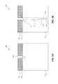
- FIG. 1illustrates a cross-sectional view of an IC 100 according to an embodiment.
- IC 100may include a substrate 106 , devices 108 , and a trench 130 in an example.
- Devices 108 as shown in FIG. 1include only two devices 108 a and 108 b for the sake of simplicity. However, as would be understood by a person of skilled in the art based on the description herein, devices 108 may include any number of devices.
- Substrate 106may be a silicon (Si) substrate implanted with p-type carriers to be a p-type Si substrate, according to an example embodiment.
- the p-type carriersmay be provided by p-type materials, such as, but not limited to, boron.
- substrate 106may be a p-type well formed in an n-type Si substrate or well (not shown).
- N-type Si substrateare formed implanted with n-type carriers that are provided by n-type materials, such as, but not limited to, phosphorus.
- devices 108 a and 108 bmay each represent a field-effect transistor (FET) including doped regions 112 and 114 and a gate structure 110 .
- FETfield-effect transistor
- Devices 108 a and 108 bmay be similar in structure and function.
- devices 108 a and 108 bmay be two distinct devices.
- Doped region 112may be used as a source/drain region, and similarly, doped region 114 may also be used as a source/drain region. It is understood by a skilled artisan that the source and drain regions of devices 108 a and 108 b may be interchangeable and are named based on voltage values applied to doped regions 112 and 114 .
- doped regions 112 and 114are n-type in this example, they may also be p-type regions when substrate 106 is n-type Si or an n-type well formed in a p-type Si substrate. Further, doped regions 112 and 114 may be formed, for example, using ion implantation to dope substrate 106 with n-type carriers using n-type materials, such as, but not limited to, arsenic. The n-type carrier concentration in doped regions 112 and 114 may be higher than the p-type carrier concentrations of substrate 106 to form heavily doped regions. Generally, doping a material with a comparatively large doping concentration of carriers equal or greater than 10 19 /cm 3 , refers to a doping that is high or heavy.
- gate structure 110may be positioned on a top surface 106 a of substrate 106 between doped regions 112 and 114 and in substantial contact with at least a portion of doped region 112 and doped region 114 .
- Gate structure 110may include a gate layer 116 and a gate dielectric layer 118 .
- Gate layer 116may be disposed over gate dielectric layer 118 and gate dielectric layer 118 may be disposed over substrate 106 .
- the material used to form gate layer 116may be, for example, doped polysilicon, metal, or any combination thereof and the material for forming gate dielectric layer 118 may be, for example, thermal oxide, nitride layer, high-k dielectric,or any combination thereof.
- Gate structure 110comprises a vertical dimension 111 that is a sum of a vertical dimension 111 a of gate layer 116 and a vertical dimension 111 b of gate dielectric layer 118 .
- applying a first potential to gate structure 110 and a second potential that is lower than the first potential to doped region 112may cause the n-type carriers below the gate structure 110 to form a channel region (not shown) between doped regions 112 and 114 .
- a third potential that is higher than the second potentialis applied to doped region 114
- the n-type carriers accumulated in the channel regionmay allow a current to flow from doped region 114 to doped region 112 . This current is typically referred to as the drain current.
- Devices 108may comprise a depletion region that is depleted of free carriers in a channel region in an example embodiment (not shown). If a positive voltage is applied to doped region 114 , the depletion region can spread in channel region from doped region 114 to doped region 112 . If the depletion region reaches doped region 112 , then “punchthrough” may occur. In such instance, gate structure 110 may no longer be able to control the drain current from doped region 114 to doped region 112 .
- pocket implants 122may be formed to prevent punchthrough in devices 108 .
- pocket implants 122may hinder the depletion region from reaching doped region 112 when the depletion region extends through channel region.
- Pocket implants 122may be doped with, for example, boron atom s.
- Devices 108may further include spacers 126 above doped regions 112 and 114 and in substantial contact with respective first and second sides 110 a and 110 b of the gate structure 110 in accordance to an example embodiment.
- Spacers 126may be formed using a dielectric material, such as silicon nitride or silicon oxide, though any suitable insulating material may be used.
- trench 130may be positioned in substrate 106 between devices 108 a and 108 b. While trench 130 is shown in FIG. 1 to comprise a vertical cross-section having a trapezoidal perimeter, in alternate embodiments trench 130 may comprise vertical cross-sections having any geometric shaped perimeters (e.g. rectangular). Trench 130 may comprise a first portion 130 a, a second portion 130 b, an open end 130 c, and a closed end 130 d. In an example, first portion 130 a may comprise a vertical dimension of about 100 nm-400 nm and second portion 130 b may comprise a vertical dimension of about 100 nm or less.
- First portion 130 amay be filled with a dielectric material to form a first filled portion 132 of trench 130 and second portion 130 b may be filled with a conductive material to form a second filled portion 134 of trench 130 .
- the dielectric material filling first portion 130 amay be, for example, oxide or nitride and the conductive material filling second portion 130 b may be, for example, single-crystalline silicon, amorphous silicon (“a-Si”) or polycrystalline silicon (“polySi”), silicon germanium (SiGe), metal silicides, or metal.
- first filled portion 132may form a buried trench isolation within substrate 106 between devices 108 a and 108 b.
- first and second filled portions 132 and 134may be formed such that top surface 132 a of first filled portion 132 is in substantial contact with bottom surface 134 b of second filled portion 134 , and bottom surface 132 b of first filled portion 132 is in substantial contact with substrate 106 . While top surface 134 a of second filled portion 134 is illustrated in FIG. 1 to be coplanar with top surface 106 a of substrate 106 , it should be understood that top surface 134 a may be raised or lowered with respect to top surface 106 a depending on application of IC 100 by the user In an embodiment, first filled portion 132 or a part thereof may be in substantial contact with doped region 114 of device 108 a and doped region 112 of device 108 b.
- second filled portion 134 or a part thereofmay be in substantial contact with doped region 114 of device 108 a and doped region 112 of device 108 b and provide a conductive path between doped region 114 of device 108 a and doped region 112 of device 108 a.
- first filled portion 132may provide electrical isolation between the electronic processes of devices 108 a and 108 b within substrate 106 , according to an embodiment.
- IC 100is shown in FIG. 1 as including only one arrangement of trench 130 interposed between adjacent devices 108 a and 108 b for the sake of simplicity. However, as would be understood by a person of skilled in the art based on the description herein, IC 100 may include any number of such arrangements with devices and trenches similar to devices 108 and trench 130 , respectively. In addition, IC 100 may include other devices and functional units that are not shown for the sake of simplicity.
- FIG. 2illustrates a cross-sectional view of an IC 200 according to an embodiment.
- IC 200is similar to IC 100 as described above. Therefore, only differences between IC 100 and 200 are described herein.
- IC 200comprises a trench 130 that may be self-aligned between adjacent devices 108 a and 108 b according to an embodiment.
- the self-aligned placement of trench 130may be defined by a spacing 236 formed between spacers 126 b and 126 c on top surface 106 a of substrate 106 . In such instance, a lateral dimension of open end 130 c of trench 130 may be equal to spacing 236 .
- the self-aligned placement of trench 130may be defined by a spacing formed between gate structures 110 of devices 108 on top surface 106 a (not shown).
- the term “self-aligned”refers to formation of trench 130 that may be aligned between two features (e.g.
- the self-aligned placement of trench 130may allow devices 108 in IC 200 to be more closely spaced on substrate 106 than those in IC 100 .
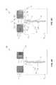
- FIG. 3illustrates a cross-sectional view of an IC 300 according to an embodiment.
- IC 300may include a substrate 106 , devices 308 , and a trench 130 .
- IC 300is similar to IC 100 as described above, only differences between IC 100 and 300 are described herein.
- devices 308 a and 308 bmay each comprise a gate structure 310 disposed on top surface 106 a of substrate 106 between doped regions 112 and 114 and in substantial contact with at least a portion of doped region 112 and doped region 114 .
- Gate structure 310may include a gate layer 116 and a stack of layers 318 .
- Stack of layers 318may comprise a charge storing layer 318 b interposed between a first dielectric layer 318 a and a second dielectric layer 318 c.
- First dielectric layer 318 amay be disposed over and in substantial contact with top surface 106 a of substrate 106 .
- Charge storing layer 318 bmay be disposed over and in substantial contact with first dielectric layer 318 b
- Second dielectric layer 318 cmay be disposed over and in substantial contact with charge storing layer 318 b.
- First and second dielectric layers 318 a and 318 cmay each comprise an oxide layer such as, but not limited to silicon dioxide.
- second dielectric layer 318 emay include a stack of dielectric layers (not shown) comprising, for example, a nitride layer interposed between oxide layers.
- Charge storing layer 318 bmay include, for example, a charge-trapping nitride layer such as, but not limited to, silicon nitride layer, silicon-rich nitride layer, or any layer that includes, but is not limited to, silicon, oxygen, and nitrogen, in various stoichiometries.
- a charge-trapping nitride layersuch as, but not limited to, silicon nitride layer, silicon-rich nitride layer, or any layer that includes, but is not limited to, silicon, oxygen, and nitrogen, in various stoichiometries.
- a three layer stack arrangement of such dielectric layersis referred to as an “oxide, nitride, oxide (ONO) stack,” or simply as “ONO layers.”
- charge storing layer 318 bmay include a polySi layer.
- Such a polySi charge storing layer 318 bmay be used as a floating gate with gate layer 116 used as a control gate in devices 308 , according to an embodiment. Generally, such devices are referred as floating gate devices. It should be understood that the relative thickness of gate layer 116 , charge storing layer 318 b and first and second dielectric layers 318 a and 318 b presented herein are for illustrative purposes only and not necessarily drawn to scale in FIG. 3 .
- IC 300may represent an analog or digital memory device and devices 308 may represent memory cells.
- each device of devices 308may be programmed as follows.
- Charge storing layer 318 bmay be programmed to the charged program level by applying a potential to doped region 114 (functioning as the drain) and a potential to gate structure 310 , while doped region 112 may function as the source source of electrons).
- a potentialmay also be applied to doped region 112 .
- the potential applied to gate structure 310 and doped regions 112 and 114may generate a vertical electric field through charge storing layer 318 b and first and second dielectric layers 318 a and 318 c, At the same time, a lateral electric field along the length of channel from doped region 112 to doped region 114 may be generated.
- channelmay invert such that electrons are drawn off doped region 112 and caused to accelerate toward doped region 114 .
- the electronsgain energy and upon attaining enough energy, the electrons are able to jump over the potential barrier of first dielectric layer 318 a and into charge storing layer 318 b where the electrons may be stored in this layer.
- first filled portion 132may provide electrical isolation within substrate 106 between devices 308 a and 308 b , according to an embodiment.
- FIG. 4illustrates a cross-sectional view of an IC 400 according to an embodiment.
- IC 400is similar to IC 300 as described above. Therefore, only differences between IC 300 and 400 are described herein.
- Trench 130may be self-aligned between adjacent devices 308 a and 308 b according to an embodiment.
- the self-aligned placement of trench 130may be defined by a spacing 236 formed between spacers 126 b and 126 con top surface 106 a of substrate 106 in an example. In such instance, a lateral dimension of open end 130 c of trench 130 may be equal to a spacing 236 .
- the self-aligned placement of trench 130may be defined by a spacing formed between gate structures 310 of devices 308 on top surface 106 a (not shown).
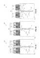
- FIGS. 5A-5Hillustrate an example fabrication process for forming IC 100 shown in FIG. 1 , according to an embodiment.
- FIG. 5Aillustrates a cross-sectional view of a partially fabricated IC 100 after formation of a trench etch area 542 on top surface 106 a of substrate 106 , according to an embodiment.
- Trench etch area 542may be formed by patterning of a first hard mask layer 538 and a second hard mask layer 540 on substrate 106 , as shown in FIG. 5A .
- Patterning of first and second hard mask layers 538 and 540may be performed by standard photolithography and etching processes.
- First hard mask layer 538may be disposed on top surface 106 a of substrate 106 , for example, by growing a thermal oxide such as silicon oxide directly from substrate 106 using thermal oxidation.
- Second hard mask layer 540may be disposed on first hard mask layer 538 , for example, by depositing a layer of nitride such as silicon nitride using conventional deposition methods such as, but not limited to, chemical vapor deposition (CVD) or atomic layer deposition (ALD).
- CVDchemical vapor deposition
- ALDatomic layer deposition
- the relative thickness of first and second hard mask layers 538 and 540 formed with respect to each othermay be equal or different, according to various embodiments.
- FIG. 5Billustrates a cross-sectional view of a partially fabricated IC 100 after formation of trench 130 in trench etch area 542 as described previously with reference to FIG. 5A , according to an embodiment.
- the patterned first and second hard mask layers 538 and 540may assist in guiding the formation of trench 130 in trench etch area 542 .
- Trench 130may be formed by any conventional etching methods suitable for etching the material of substrate 106 . For example, a dry etch process such as, but not limited to, reactive ion etching (RIE) may be performed to remove the material of substrate 106 for the formation of trench 130 , according to an embodiment.
- RIEreactive ion etching
- the etching processmay be performed to selectively etch the material of substrate 106 in trench etch area 542 without significant etching or removal of first and second hard mask layers 538 and 540 .
- This selective etchingmay be done by employing an etchant that has higher selectivity to the material of substrate 106 than the materials of first and second hard mask layers 538 and 540 .
- FIGS. 5C-5Dillustrate cross-sectional views of partially fabricated IC 100 during formation of first filled portion 132 of trench 130 , according to an embodiment.
- the formation of first filled portion 132may comprise a filling process followed by an etch back process.
- the filling processmay be performed by depositing a layer 544 of dielectric material over the partially fabricated IC 100 of FIG. 5B such that at least both first and second portions 130 a and 130 b of trench may be filled, as shown in FIG. 5C .
- the deposition of layer 544may be performed using any conventional deposition methods suitable for dielectric materials. For example, dielectric materials such as silicon oxide or silicon nitride may be deposited for layer 544 using a CVD or an ALD process.
- first filled portion 132may be followed by removal of second hard mask layer 540 by using any conventional etching method.
- FIGS. 5E-5Fillustrate a cross-sectional view of a partially fabricated IC 100 during formation of second filled portion 134 of trench 130 , according to an embodiment.
- the formation of second filled portion 134may comprise a filling process followed by an etch-back process.
- the filling processmay be performed by depositing a layer 546 of conductive material over the partially fabricated IC 100 of FIG. 5D such that at least second portion 130 b of trench 130 may be filled, as shown in FIG. 5E .
- the deposition of layer 546may be performed using any conventional methods suitable for metals or metal suicides such as, but not limited to, sputtering, thermal evaporation or CVD.
- a-Si or polySimay be deposited for layer 546 using conventional deposition methods.
- an etch-back processmay be performed to remove layer 546 from all areas except for second portion 130 b.
- the etch-back processmay be performed until top surface 134 a of second filled portion 134 may be coplanar ( FIG. 5F ) or raised higher or lower (not shown) with respect to top surface 106 a of substrate 106 .
- the formation of second filled portion 134may be followed by removal of first hard mask layer 538 by using any conventional etching method.
- the filling processmay be performed by growing an epitaxial layer (not shown) from sidewalls 131 a and 131 b of trench 130 in second portion 130 b after the formation of first filled portion 132 .
- This growthmay be performed selectively in second portion 130 b as all other areas on substrate 106 are protected by first hard mask layer 538 or first filled portion 132 . Due to such selective growth to forty second filled portion 134 , the etch-back process may be eliminated.
- the epitaxial layer in second portion 130 bmay be doped in-situ or by ion implantation to improve electrical conductivity of second filled portion 134 .
- FIG. 5Gillustrates a cross-sectional view of a partially fabricated IC 100 after formation of gate structures 110 , according to an embodiment. It should be understood that formation of only two gate structures illustrated herein are for the sake of simplicity and not intended to be limiting.
- the formation of gate structures 110may comprise a formation of gate dielectric layer 118 on the entire top surface 106 a of substrate 106 followed by a formation of gate layer 116 on the entire surface of gate dielectric layer 118 .
- Gate dielectric layer 118may be formed by growing, for example, silicon oxide directly from substrate 106 using thermal oxidation, assuming substrate 106 to be Si in this embodiment.
- gate dielectric layer 118may be formed by depositing silicon oxide, high-k dielectric, other dielectric material, or any combination thereof using a chemical vapor deposition process.
- Gate layer 116may be formed by depositing a metal layer, a polySi layer, or any combination thereof using deposition methods such as the ones mentioned above for deposition of metal and polySi. This formation of gate dielectric layer 118 and gate layer 116 may be followed by a patterning and an etching process to define gate structures 110 , as shown in FIG. 5G .
- the patterning processmay be performed by standard photolithography process and the etching process may be performed by dry etch methods such as the ones mentioned above.
- FIG. 5Hillustrates a cross-sectional view of a fabricated IC 100 (as shown in FIG. 1 ) after formation of doped regions 112 and 114 , pocket implants 122 , and spacers 126 , according to an embodiment.
- Doped regions 112 and 114may be formed by an ion implantation method. The ion implantation method may be carried out, for example, using n-type dopants such as arsenic or phosphorous.
- pocket implants 122Prior to or subsequent to doped region formation, pocket implants 122 may be formed. Pocket implants 122 may be implanted using an ion implantation process at an angle into substrate 106 to form the pocket implants at a deeper region below gate structures 110 than doped regions 112 and 114 , as shown in FIG.
- spacers 126may be formed. Spacers 126 may be a dielectric material such as silicon oxide or silicon nitride.
- the formation of spacers 126may involve first depositing a dielectric material over the partially formed IC 100 of FIG. 5G or after the formation of doped regions 112 and 114 such that it covers at least the gate structures 110 .
- the depositionmay be carried out by, for example, using a CVD process. This deposition process may be followed by defining spacers 126 as shown in FIG. 5H by patterning the deposited dielectric material for spacers using standard photolithography and etching processes.
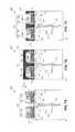
- FIGS. 6A-6Lillustrate an example fabrication process for forming IC 200 including self-aligned trench shown in FIG. 2 , according to an embodiment.
- FIG. 6Aillustrates a cross-sectional view of a partially fabricated IC 200 after formation of gate structures 110 and hard mask layers 648 , according to an embodiment.
- the formation of gate structures 110 and hard mask layers 648may comprise a formation of gate dielectric layer 118 on the entire top surface 106 a of substrate 106 , followed by a formation of gate layer 116 on the entire surface of gate dielectric layer 118 , and a subsequent deposition of hard mask layer 648 on the entire surface of gate layer 116 .
- Gate dielectric layer 118may be formed by growing, for example, silicon oxide directly from substrate 106 using thermal oxidation, assuming substrate 106 to be Si in this embodiment.
- gate dielectric layer 118may be formed by depositing silicon oxide, high-k dielectric, other dielectric material, or any combination thereof using a chemical vapor deposition process.
- Gate layer 116may be formed by depositing a metal layer, a polySi layer, or any combination thereof using deposition methods such as the ones mentioned above for deposition of metal and polySi.
- the deposition of hard mask layer 648may involve depositing a dielectric material such as, but not limited to, silicon oxide or silicon nitride, for example, using a CVD process.
- This formation of gate dielectric layer 118 , gate layer 116 , hard mask layer 648may be followed by a patterning and an etching process to define gate structures 110 and hard mask layers 648 , as shown in FIG. 6A .
- the patterning processmay be performed by standard photolithography process and the etching process may be performed by dry etch methods such as the ones mentioned above.
- spacers 650may be formed along sidewalk 110 a and 110 b of gate structures 110 as shown in FIG. 6B .
- the material for spacers 650may be dielectric materials such as, but not limited to, silicon oxide or silicon nitride.
- Hard mask layers 648 and spacers 650may act as masking layers for gate structures 110 to prevent damage to gate structures 110 during subsequent fabrication processes.
- gate structures 110 along with spacers 650may act as a patterned masking layer on substrate 106 to define a trench etch area 642 between spacers adjacent spacers 650 b and 650 c, as shown in FIG. 6B .
- This trench etch area 642may be used for a self-aligned formation of trench 130 , as shown in FIG. 6C , according to an embodiment.
- the term “self-aligned”refers to formation of trench 130 that may be aligned between two features (e.g. spacers 650 b and 650 c ) of IC 200 without performing any additional steps for the alignment of trench 130 .
- the material of substrate 106 from trench etch area 642may be removed by any conventional etching methods suitable for etching the material of substrate 106 .
- a dry etch processsuch as, but not limited to, reactive ion etching (RIE) may be performed to remove the material of substrate 106 for the self-aligned formation of trench 130 , according to an embodiment.
- the etching processmay be performed to selectively etch the material of substrate 106 in trench etch area 642 without etching or removal of hard mask layer 648 and spacers 650 .
- This selective etchingmay be clone by employing an etchant that has higher selectivity to the material of substrate 106 than the materials of hard mask layer 648 and spacers 650 .
- FIGS. 6D-6Fillustrate cross-sectional views of a partially fabricated IC 200 during formation of first filled portion 132 of trench 130 , according to an embodiment.
- This formationmay involve an etching process, a subsequent filling process followed by an etch-back process.
- the etching processinvolves partial etching of spacers 650 .
- This partial etchingmay create a wider spacing between spacers 650 b and 650 c relative to a spacing between sidewalls 131 a and 131 b of trench 130 for better control of the subsequent filling process, as shown in FIG. 6D .
- the filling processmay involve deposition of a layer 654 of dielectric material over the partially fabricated IC 200 of FIG.
- the dielectric material of layer 654may be, for example, silicon oxide or silicon nitride. This deposition may be carried out by any conventional deposition process suitable for dielectric materials such as CVD or ALD. It will be appreciated that the preceding step of widening the spacing between spacers 650 b and 650 c may help to reduce the high aspect ratio of the filling area 633 between spacers 650 b and 650 c and trench sidewalls 131 a and 131 b.
- Reducing the high aspect ratio of filling area 633may prevent pinch off from occurring between spacers 650 b and 650 c during the deposition process before the entire trench 130 may be filled.
- the filling processmay then be followed by an etch-back process to remove the deposited layer 654 of dielectric material from at least the second portion 130 b of trench 130 , as shown in FIG. 6F .
- the etch-back processmay be carried out by dry etch methods like the ones mentioned above.
- first filled portion 132may be formed as illustrated in FIGS. 6G-6I , according to an embodiment.
- This approachmay also be arranged to have wider spacing between spacers 650 b and 650 c relative to spacing between sidewalls 131 a and 131 b of trench 130 for better control of the subsequent filling process.
- the spacing between sidewalls 131 a and 131 b of trench 130may be reduced by a coating process prior to the filling process, according to an embodiment.
- the formation of first filled portion 132 in this approachmay involve a coating process, a subsequent filling process followed by an etch-back process. The filling process (as shown in FIG. 6H ) and etch-back process (as shown in FIG.
- the coating processmay involve coating sidewalls 131 a and 131 b of trench 130 with a thin film 656 (“liner 656 ”) of dielectric material such as, but not limited to, silicon oxide or silicon nitride, as shown in FIG. 6G .
- the material for liner 656may be the same material that is used in a subsequent filling process for forming first filled portion 132 , according to an embodiment.
- the coating processmay be carried out by a deposition process suitable for depositing thin films such as, but not limited to ALD. Alternately, assuming substrate 106 to be Si in an embodiment, the coating process may be carried out by growing silicon oxide directly from sidewalls 131 a and 131 b using a thermal oxidation process.
- FIGS. 6J-6Killustrate cross-sectional views of a partially fabricated IC 200 during formation of second filled portion 134 of trench 130 , according to an embodiment.
- This formation methodis similar to the method described above with reference to FIG. 5E-5F .
- hard mask layers 648 and spacers 650may be removed by any conventional etching processes.
- doped regions 112 and 114 , pocket implants 122 , and spacers 126may be formed to yield IC 200 as shown in FIG. 6L .
- the methods of forming doped regions 112 and 114 , pocket implants 122 , and spacer 126are similar to the ones described above with reference to FIG. 5H .
- doped regions 112 and 114 and pocket implants 122may be formed after formation of gate structures 110 as described above with reference to FIG. 6A .
- the fabrication processmay involve forming partial gate structures 710 and hard mask layers 648 (as shown in FIG. 7A ) instead of gate structures 110 and hard mask layers 648 , as shown in FIG. 6A .
- Partial gate structures 710may comprise gate dielectric layers 118 and gate layers 716 .
- Gate layers 716may be similar to gate layers 116 of gate structures 110 , except for having vertical dimensions smaller than vertical dimensions of gate layers 116 .
- the partial gate structures 710 with shorter vertical dimensions than gate structures 110may reduce the high aspect ratio of filling area 633 .
- the shorter partial gate structures 710may further help to control the filling process and avoid pinch off from occurring as discussed above with reference to FIGS. 6D and 6G .
- IC 200may be fabricated using the method described with reference to FIGS. 6B-6L , except for the removal of hard mask layers 648 , as illustrated in FIG. 7A . Additional processes, such as, but not limited to, the processes illustrated in FIGS. 7B-7F may be performed on IC 200 of FIG. 7A to obtain complete gate structures 770 (as shown in FIG. 7F ). Gate structures 770 may include vertical dimensions equal to vertical dimensions of gate structures 110 , as shown in FIG. 6A .
- FIG. 7Billustrates a deposition of a dielectric layer 760 such that it covers all features and exposed regions on substrate 106 , according to an embodiment.
- the dielectric material of layer 760may be, for example, silicon oxide or silicon nitride. This deposition may be carried out by any conventional deposition process suitable for dielectric materials such as CVD or ALD.
- a chemical mechanical polishing (CMP) processmay be performed to at least expose top surfaces 648 a of hard mask layers 648 , as illustrated in FIG. 7C .
- hard mask layers 648may be selectively etched without significant etching or removal of underlying gate layers 716 , as shown in FIG. 7D .
- the selective etchingmay be done by, for example, an RIE process.
- the etching processmay be followed by a deposition process of layer 765 and a removal process to form additional gate layers 717 of FIG. 7F .
- Layer 765may be formed by depositing a metal layer, a polySi layer, or any combination thereof using deposition methods such as the ones mentioned above for deposition of metal and polySi.
- the removal process following the deposition of layer 765may be performed by, for example, an etch back process, a CMP process, or a patterning process using standard photolithography and etching process, as described above. Formation of additional gate layers 717 may yield complete gate structures 770 .
- IC 300may be manufactured using a fabrication process similar to the example fabrication process described above for IC 100 with reference to FIGS. 5A-5H . Therefore, only the differences between the example fabrication processes of IC 100 and IC 300 are illustrated in FIG. 8 and discussed below.
- gate structures 310may be fabricated, according to an embodiment.
- the formation of gate structures 310may comprise formation of stack of layers 318 on substrate 106 followed by formation of gate layers 116 on stack of layers 318 .
- a first dielectric layer 318 amay be deposited on entire top surface 106 a of substrate 106 followed by deposition of a charge storing layer 318 b on entire surface of first dielectric layer 318 a, and subsequent deposition of a second dielectric layer 318 c on entire surface of charge storing layer 318 b.
- First and second dielectric layers 318 a and 318 c and charge storing layer 318 bmay be formed using conventional deposition processes such as, but not limited to, CVD and ALD.
- first dielectric layer 318 amay be formed by growing, for example, silicon oxide directly from substrate 106 using thermal oxidation, assuming substrate 106 to be Si in this embodiment.
- second dielectric layer 318 cmay be formed by growing, for example an oxide layer from a top surface 319 (as shown in FIG. 8 ) of charge storing layer 318 b, assuming charge storing layer 318 b to be a nitride layer, using any conventional oxidation process suitable for nitride materials.
- Gate layer 116may be formed by depositing a metal or polySi layer using deposition methods such as the ones mentioned above for deposition of metal and polySi. This formation of stack of layers 318 and gate layer 116 may be followed by a patterning and an etching process to define gate structures 310 , as shown in FIG. 8 .
- the patterning processmay be performed by standard photolithography process and the etching process may be performed by dry etch methods such as the ones mentioned above.
- IC 400may be manufactured using a fabrication process similar to the example fabrication process described above for IC 200 with reference to FIGS. 6A-6L . Therefore, only the differences between the example fabrication processes of IC 200 and IC 400 are illustrated in FIG. 9 and discussed below.
- gate structures 310 and hard mask layers 648may be fabricated on substrate 106 as shown in FIG. 9 , prior to the formation of spacers 650 as described with reference to FIG. 6B .
- the method for fabricating gate structures 310 and hard mask layers 648is similar to the example method described above with reference to FIG. 8 .
- IC 400may be manufactured using a fabrication process similar to the example fabrication process described above for IC 200 with reference to FIGS. 7A-7F .
- the difference between this example fabrication process of IC 200 and IC 400may be the formation of stack of layers 318 in IC 400 (as method described above with reference to FIG. 8 ) instead of gate dielectric layer 118 .
- FIG. 10illustrates a flowchart for a method of fabricating IC 100 shown in FIG. 1 , according to an embodiment. Solely for illustrative purposes, the steps illustrated in FIG. 10 will be described with reference to example fabrication process illustrated in FIGS. 5A-5H .
- trench etch area 542may be defined by patterning of a first hard mask layer 538 and a second hard mask layer 540 on substrate 106 , as shown in FIG. 5A .
- Patterning of first and second hard mask layers 538 and 540may be performed by standard photolithography and etching processes.
- First hard mask layer 538may be disposed on top surface 106 a of substrate 106 , for example, by growing a thermal oxide such as silicon oxide directly from substrate 106 using thermal oxidation.
- Second hard mask layer 540may be disposed on first hard mask layer 540 , for example, by depositing a layer of nitride such as silicon nitride using, for example, chemical vapor deposition (CVD) or atomic layer deposition (ALD) method.
- CVDchemical vapor deposition
- ALDatomic layer deposition
- trench 130may be formed in trench etch area 542 , as shown in FIG. 5B , by a dry etch process such as, but not limited to, reactive ion etching (RIE) to remove the material of substrate 106 , according to an embodiment.
- RIEreactive ion etching
- the etching processmay be performed to selectively etch the material of substrate 106 in trench etch area 542 without significant etching or removal of first and second hard mask layers 538 and 540 .
- first portion 130 a of trench 130may be filled to form first filled portion 132 by depositing a layer 544 of dielectric material such as silicon oxide or silicon nitride followed by an etch-back process to remove layer 544 from all areas except for first portion 130 a, as described above with reference to FIGS. SC and SD.
- the deposition of layer 544may be performed using, for example, a CVD or an ALD process.
- second portion 130 b of trench 130may be filled to form second filled portion 134 by depositing a layer 546 of conductive material such as metals or metal silicides followed by an etch-back process to remove layer 546 from all areas except for second portion 130 b, as described above with reference to FIGS. 5E and 5F .
- the deposition of layer 546may be performed using, for example, sputtering, thermal evaporation or CVD process.
- a-Si or polySimay be deposited for layer 546 using conventional deposition methods.
- gate structures 110may be formed ( FIG. 5G ).
- the formation of gate structures 110may involve a deposition of gate dielectric layer 118 on the entire top surface 106 a of substrate 106 followed by a deposition of gate layer 116 on the entire surface of gate dielectric layer 118 .
- Gate dielectric layer 118may be formed by depositing silicon oxide, high-k dielectric, other dielectric material, or any combination thereof using a chemical vapor deposition process.
- Gate layer 116may be formed by depositing a metal layer, a polySi layer, or any combination thereof using deposition methods such as the ones mentioned above for deposition of metal and polySi.
- gate dielectric layer 118 and gate layer 116may be followed by a patterning and an etching process to define gate structures 110 , as shown in FIG. 5G .
- the patterning processmay be performed by standard photolithography process and the etching process may be performed by dry etch methods such as the ones mentioned above.
- doped regions 112 and 114 , pocket implants 122 , and spacers 126may be formed ( FIG. 5H ).
- Doped regions 112 and 114may be formed by an ion implantation method.
- pocket implants 122may be formed in step 1070 using an ion implantation process at an angle into substrate 106 to form the pocket implants at a deeper region below gate structures 110 than doped regions 112 and 114 , as shown in FIG. 5H .
- spacers 126may be formed in step 1080 as described above with reference FIG. 5H .
- the above method 1000may additionally or alternatively include any of the steps or sub-steps described above with respect to FIGS. 5A-5H , as well as any of their modifications. Further, the above description of the example method 1000 should not be construed to limit the description of IC 100 described above.
Landscapes
- Engineering & Computer Science (AREA)
- Physics & Mathematics (AREA)
- Condensed Matter Physics & Semiconductors (AREA)
- General Physics & Mathematics (AREA)
- Manufacturing & Machinery (AREA)
- Computer Hardware Design (AREA)
- Microelectronics & Electronic Packaging (AREA)
- Power Engineering (AREA)
- Element Separation (AREA)
- Metal-Oxide And Bipolar Metal-Oxide Semiconductor Integrated Circuits (AREA)
Abstract
Description
Claims (3)
Priority Applications (1)
| Application Number | Priority Date | Filing Date | Title |
|---|---|---|---|
| US15/802,721US10256137B2 (en) | 2013-10-08 | 2017-11-03 | Self-aligned trench isolation in integrated circuits |
Applications Claiming Priority (3)
| Application Number | Priority Date | Filing Date | Title |
|---|---|---|---|
| US14/048,863US9437470B2 (en) | 2013-10-08 | 2013-10-08 | Self-aligned trench isolation in integrated circuits |
| US15/191,882US9831114B1 (en) | 2013-10-08 | 2016-06-24 | Self-aligned trench isolation in integrated circuits |
| US15/802,721US10256137B2 (en) | 2013-10-08 | 2017-11-03 | Self-aligned trench isolation in integrated circuits |
Related Parent Applications (1)
| Application Number | Title | Priority Date | Filing Date |
|---|---|---|---|
| US15/191,882ContinuationUS9831114B1 (en) | 2013-10-08 | 2016-06-24 | Self-aligned trench isolation in integrated circuits |
Publications (2)
| Publication Number | Publication Date |
|---|---|
| US20180166323A1 US20180166323A1 (en) | 2018-06-14 |
| US10256137B2true US10256137B2 (en) | 2019-04-09 |
Family
ID=52776290
Family Applications (3)
| Application Number | Title | Priority Date | Filing Date |
|---|---|---|---|
| US14/048,863ActiveUS9437470B2 (en) | 2013-10-08 | 2013-10-08 | Self-aligned trench isolation in integrated circuits |
| US15/191,882ActiveUS9831114B1 (en) | 2013-10-08 | 2016-06-24 | Self-aligned trench isolation in integrated circuits |
| US15/802,721ActiveUS10256137B2 (en) | 2013-10-08 | 2017-11-03 | Self-aligned trench isolation in integrated circuits |
Family Applications Before (2)
| Application Number | Title | Priority Date | Filing Date |
|---|---|---|---|
| US14/048,863ActiveUS9437470B2 (en) | 2013-10-08 | 2013-10-08 | Self-aligned trench isolation in integrated circuits |
| US15/191,882ActiveUS9831114B1 (en) | 2013-10-08 | 2016-06-24 | Self-aligned trench isolation in integrated circuits |
Country Status (1)
| Country | Link |
|---|---|
| US (3) | US9437470B2 (en) |
Families Citing this family (6)
| Publication number | Priority date | Publication date | Assignee | Title |
|---|---|---|---|---|
| US9437470B2 (en) | 2013-10-08 | 2016-09-06 | Cypress Semiconductor Corporation | Self-aligned trench isolation in integrated circuits |
| US9252026B2 (en)* | 2014-03-12 | 2016-02-02 | Cypress Semiconductor Corporation | Buried trench isolation in integrated circuits |
| US9960074B2 (en)* | 2016-06-30 | 2018-05-01 | Taiwan Semiconductor Manufacturing Company, Ltd. | Integrated bi-layer STI deposition |
| US11164794B2 (en)* | 2019-08-04 | 2021-11-02 | Globalfoundries U.S. Inc. | Semiconductor structures in a wide gate pitch region of semiconductor devices |
| US11670661B2 (en)* | 2019-12-20 | 2023-06-06 | Samsung Electronics Co., Ltd. | Image sensor and method of fabricating same |
| TWI812572B (en)* | 2021-07-20 | 2023-08-11 | 力晶積成電子製造股份有限公司 | Semiconductor device |
Citations (76)
| Publication number | Priority date | Publication date | Assignee | Title |
|---|---|---|---|---|
| US4918027A (en) | 1985-03-05 | 1990-04-17 | Matsushita Electric Industrial Co., Ltd. | Method of fabricating semiconductor device |
| US4939567A (en) | 1987-12-21 | 1990-07-03 | Ibm Corporation | Trench interconnect for CMOS diffusion regions |
| US4980306A (en) | 1987-11-11 | 1990-12-25 | Seiko Instruments Inc. | Method of making a CMOS device with trench isolation device |
| US5349224A (en) | 1993-06-30 | 1994-09-20 | Purdue Research Foundation | Integrable MOS and IGBT devices having trench gate structure |
| US5573969A (en) | 1994-01-19 | 1996-11-12 | Hyundai Electronics Industries Co., Ltd. | Method for fabrication of CMOS devices having minimized drain contact area |
| US5851881A (en) | 1997-10-06 | 1998-12-22 | Taiwan Semiconductor Manufacturing Company, Ltd. | Method of making monos flash memory for multi-level logic |
| US6051868A (en) | 1996-11-15 | 2000-04-18 | Nec Corporation | Semiconductor device |
| US6091129A (en) | 1996-06-19 | 2000-07-18 | Cypress Semiconductor Corporation | Self-aligned trench isolated structure |
| US6090661A (en) | 1998-03-19 | 2000-07-18 | Lsi Logic Corporation | Formation of novel DRAM cell capacitors by integration of capacitors with isolation trench sidewalls |
| US6177699B1 (en) | 1998-03-19 | 2001-01-23 | Lsi Logic Corporation | DRAM cell having a verticle transistor and a capacitor formed on the sidewalls of a trench isolation |
| US6268637B1 (en) | 1998-10-22 | 2001-07-31 | Advanced Micro Devices, Inc. | Method of making air gap isolation by making a lateral EPI bridge for low K isolation advanced CMOS fabrication |
| US6285066B1 (en) | 1995-04-06 | 2001-09-04 | Motorola, Inc. | Semiconductor device having field isolation |
| US20010035561A1 (en) | 2000-03-24 | 2001-11-01 | Franz Hirler | Semiconductor configuration |
| US6344399B1 (en) | 1997-04-25 | 2002-02-05 | Wendell P. Noble | Method of forming conductive lines and method of forming a conductive grid |
| US20020030223A1 (en)* | 2000-06-30 | 2002-03-14 | Kazuhito Narita | Semiconductor device and method of manufacturing the same |
| US20020048886A1 (en) | 1997-01-29 | 2002-04-25 | Fujitsu Limited | Semiconductor device and method for fabricating the same |
| US6420749B1 (en) | 2000-06-23 | 2002-07-16 | International Business Machines Corporation | Trench field shield in trench isolation |
| US20030089961A1 (en) | 2001-11-13 | 2003-05-15 | Joerg Vollrath | STI leakage reduction |
| US6570217B1 (en) | 1998-04-24 | 2003-05-27 | Kabushiki Kaisha Toshiba | Semiconductor device and method of manufacturing the same |
| US20030124803A1 (en) | 2001-12-10 | 2003-07-03 | Naoki Ueda | Non-volatile semiconductor memory and process of fabricating the same |
| US20030216032A1 (en) | 2002-05-17 | 2003-11-20 | Hasan Nejad | Method for forming MRAM bit having a bottom sense layer utilizing electroless plating |
| US6720638B2 (en) | 2002-06-21 | 2004-04-13 | Micron Technology, Inc. | Semiconductor constructions, and methods of forming semiconductor constructions |
| US20040129995A1 (en) | 2003-01-02 | 2004-07-08 | Yee-Chia Yeo | Semiconductor chip with gate dielectrics for high-performance and low-leakage applications |
| US20040173844A1 (en) | 2003-03-05 | 2004-09-09 | Advanced Analogic Technologies, Inc. Advanced Analogic Technologies (Hongkong) Limited | Trench power MOSFET with planarized gate bus |
| US20050006706A1 (en) | 2003-07-09 | 2005-01-13 | Semiconductor Components Industries, Llc. | Symmetrical high frequency SCR structure and method |
| US6898851B2 (en) | 2003-02-21 | 2005-05-31 | Renesas Technology Corp. | Electronic device manufacturing method |
| US20050186748A1 (en) | 2004-01-22 | 2005-08-25 | Kabushiki Kaisha Toshiba | Method of manufacturing semiconductor device |
| US20050253183A1 (en) | 2004-04-22 | 2005-11-17 | Kabushiki Kaisha Toshiba | Non-volatile semiconductor memory device and method of fabricating the same |
| US20050258463A1 (en) | 2004-05-18 | 2005-11-24 | Kabushiki Kaisha Toshiba | Non-volatile semiconductor memory device and process of manufacturing the same |
| US6998694B2 (en) | 2003-08-05 | 2006-02-14 | Shye-Lin Wu | High switching speed two mask Schottky diode with high field breakdown |
| US7009273B2 (en) | 2002-09-19 | 2006-03-07 | Kabushiki Kaisha Toshiba | Semiconductor device with a cavity therein and a method of manufacturing the same |
| US7019365B2 (en) | 2001-12-27 | 2006-03-28 | Kabushiki Kaisha Toshiba | Semiconductor device formed in semiconductor layer arranged on substrate with one of insulating film and cavity interposed between the substrate and the semiconductor layer |
| US7019364B1 (en) | 1999-08-31 | 2006-03-28 | Kabushiki Kaisha Toshiba | Semiconductor substrate having pillars within a closed empty space |
| US20060138549A1 (en) | 2004-12-29 | 2006-06-29 | Ko Kwang Y | High-voltage transistor and fabricating method thereof |
| US20060148177A1 (en)* | 2004-12-31 | 2006-07-06 | Dongbuanam Semiconductor Inc. | Method for forming split gate flash nonvolatile memory devices |
| US20060231883A1 (en)* | 2004-12-28 | 2006-10-19 | Hiroyuki Nansei | Semiconductor device |
| US20060246657A1 (en)* | 2005-05-02 | 2006-11-02 | Samsung Electronics Co., Ltd. | Method of forming an insulation layer structure and method of manufacturing a semiconductor device using the same |
| US20070161187A1 (en)* | 2005-12-28 | 2007-07-12 | Hynix Semiconductor Inc. | Method of manufacturing flash memory device |
| US20080003749A1 (en) | 2006-06-29 | 2008-01-03 | Hynix Semiconductor Inc. | Method Of Manufacturing A Flash Memory Device |
| US20080017929A1 (en) | 2006-07-24 | 2008-01-24 | Hynix Semiconductor Inc. | Semiconductor device having a compressed device isolation structure |
| US20080029817A1 (en) | 2006-07-17 | 2008-02-07 | Stmicroelectronics S.R.L | Process for manufacturing a semiconductor wafer having SOI-insulated wells and semiconductor wafer thereby manufactured |
| US7335944B2 (en) | 2001-09-07 | 2008-02-26 | Power Integrations, Inc. | High-voltage vertical transistor with a multi-gradient drain doping profile |
| US7372086B2 (en) | 2003-05-07 | 2008-05-13 | Kabushiki Kaisha Toshiba | Semiconductor device including MOSFET and isolation region for isolating the MOSFET |
| US20080224234A1 (en) | 2007-03-16 | 2008-09-18 | Seiko Epson Corporation | Method for manufacturing semiconductor device and semiconductor device |
| US20090029523A1 (en) | 2007-07-25 | 2009-01-29 | Hynix Semiconductor Inc. | Method of Fabricating Flash Memory Device |
| US20090159987A1 (en) | 2007-12-20 | 2009-06-25 | Tae Kyung Oh | Semiconductor device for reducing interference between adjoining gates and method for manufacturing the same |
| US20090162989A1 (en) | 2007-12-21 | 2009-06-25 | Samsung Electronics Co. Ltd. | Methods of manufacturing a semiconductor device using a layer suspended across a trench |
| US20090170282A1 (en) | 2007-12-28 | 2009-07-02 | Cha Deok Dong | Method of Forming Isolation Layer in Semiconductor Device |
| US20090218619A1 (en)* | 2008-03-02 | 2009-09-03 | Alpha & Omega Semiconductor, Ltd | Self-aligned slotted accumulation-mode field effect transistor (AccuFET) structure and method |
| US20090230456A1 (en)* | 2008-03-12 | 2009-09-17 | Yoon Young-Bae | Semiconductor device |
| US20090321794A1 (en) | 2006-09-07 | 2009-12-31 | International Business Machines Corporation | Cmos devices incorporating hybrid orientation technology (hot) with embedded connectors |
| US20100047994A1 (en)* | 2008-08-21 | 2010-02-25 | Zhong Dong | Fabrication of integrated circuits with isolation trenches |
| US7704854B2 (en)* | 2008-05-06 | 2010-04-27 | International Business Machines Corporation | Method for fabricating semiconductor device having conductive liner for rad hard total dose immunity |
| US7741143B2 (en) | 2005-01-06 | 2010-06-22 | Samsung Electronics Co., Ltd. | Image sensor having 3-dimensional transfer transistor and its method of manufacture |
| US20100163992A1 (en) | 2008-12-31 | 2010-07-01 | Kim Mi-Young | Semiconductor device and method for fabricating the same |
| US7767528B2 (en) | 2003-06-12 | 2010-08-03 | Infineon Technologies Ag | Field effect transistor and fabrication method |
| US20110039383A1 (en) | 2009-08-14 | 2011-02-17 | Alpha & Omega Semiconductor, Inc. | Shielded gate trench MOSFET device and fabrication |
| US20110127650A1 (en) | 2009-11-30 | 2011-06-02 | Imec | Method of Manufacturing a Semiconductor Device and Semiconductor Devices Resulting Therefrom |
| US20110159659A1 (en) | 2009-12-31 | 2011-06-30 | Chiu Tzuyin | Novel Manufacturing Approach for Collector and N Type Buried Layer Of Bipolar Transistor |
| US20110198700A1 (en) | 2010-02-16 | 2011-08-18 | Samsung Electronics Co., Ltd. | Semiconductor devices with peripheral region insertion patterns and methods of fabricating the same |
| US20110227191A1 (en) | 2010-03-19 | 2011-09-22 | Disney Donald R | Silicon-on-insulator devices with buried depletion shield layer |
| US20120205777A1 (en) | 2011-02-14 | 2012-08-16 | Lee Sang-Hyun | Semiconductor device and method for fabricating the same |
| US20130095636A1 (en) | 2011-10-18 | 2013-04-18 | Stmicroelectronics (Crolles 2) Sas | Process for producing at least one deep trench isolation |
| US20130234279A1 (en) | 2012-03-07 | 2013-09-12 | Samsung Electronics Co., Ltd. | Semiconductor device with buried word line structures and method of manufacturing the same |
| US20130322189A1 (en) | 2012-06-01 | 2013-12-05 | United Michroelectronics Corp. | Semiconductor element and operating method thereof |
| US20140011334A1 (en) | 2012-07-04 | 2014-01-09 | SK Hynix Inc. | Semiconductor device with vertical channel transistor and method for fabricating the same |
| US20150008530A1 (en) | 2013-07-05 | 2015-01-08 | Samsung Electronics Co., Ltd. | Semiconductor device and method of forming the same |
| US20150014807A1 (en) | 2013-07-10 | 2015-01-15 | Taiwan Semiconductor Manufacturing Company, Ltd. | Method of forming a shallow trench isolation structure |
| US8975684B2 (en) | 2012-07-18 | 2015-03-10 | Samsung Electronics Co., Ltd. | Methods of forming non-volatile memory devices having air gaps |
| US20150099342A1 (en) | 2013-10-04 | 2015-04-09 | Taiwan Semiconductor Manufacturing Company, Ltd. | Mechanism of Forming a Trench Structure |
| US20150097224A1 (en) | 2013-10-08 | 2015-04-09 | Spansion Llc | Buried trench isolation in integrated circuits |
| US20150097245A1 (en) | 2013-10-08 | 2015-04-09 | Spansion Llc | Self-aligned trench isolation in integrated circuits |
| US20150179734A1 (en) | 2013-12-19 | 2015-06-25 | Globalfoundries Singapore Pte. Ltd. | Integrated circuits with a buried n layer and methods for producing such integrated circuits |
| US9159791B2 (en) | 2012-06-06 | 2015-10-13 | United Microelectronics Corp. | Semiconductor device comprising a conductive region |
| US9219115B2 (en) | 2013-10-11 | 2015-12-22 | Taiwan Semiconductor Manufacturing Company, Ltd. | Forming conductive STI liners for FinFETS |
| US20160043217A1 (en) | 2014-08-07 | 2016-02-11 | Texas Instruments Incorporated | Methods and Apparatus for LDMOS Devices with Cascaded Resurf Implants and Double Buffers |
- 2013
- 2013-10-08USUS14/048,863patent/US9437470B2/enactiveActive
- 2016
- 2016-06-24USUS15/191,882patent/US9831114B1/enactiveActive
- 2017
- 2017-11-03USUS15/802,721patent/US10256137B2/enactiveActive
Patent Citations (83)
| Publication number | Priority date | Publication date | Assignee | Title |
|---|---|---|---|---|
| US4918027A (en) | 1985-03-05 | 1990-04-17 | Matsushita Electric Industrial Co., Ltd. | Method of fabricating semiconductor device |
| US4980306A (en) | 1987-11-11 | 1990-12-25 | Seiko Instruments Inc. | Method of making a CMOS device with trench isolation device |
| US4939567A (en) | 1987-12-21 | 1990-07-03 | Ibm Corporation | Trench interconnect for CMOS diffusion regions |
| US5349224A (en) | 1993-06-30 | 1994-09-20 | Purdue Research Foundation | Integrable MOS and IGBT devices having trench gate structure |
| US5573969A (en) | 1994-01-19 | 1996-11-12 | Hyundai Electronics Industries Co., Ltd. | Method for fabrication of CMOS devices having minimized drain contact area |
| US6285066B1 (en) | 1995-04-06 | 2001-09-04 | Motorola, Inc. | Semiconductor device having field isolation |
| US6091129A (en) | 1996-06-19 | 2000-07-18 | Cypress Semiconductor Corporation | Self-aligned trench isolated structure |
| US6051868A (en) | 1996-11-15 | 2000-04-18 | Nec Corporation | Semiconductor device |
| US20020048886A1 (en) | 1997-01-29 | 2002-04-25 | Fujitsu Limited | Semiconductor device and method for fabricating the same |
| US6348366B2 (en) | 1997-04-25 | 2002-02-19 | Micron Technology, Inc. | Method of forming conductive lines |
| US6344399B1 (en) | 1997-04-25 | 2002-02-05 | Wendell P. Noble | Method of forming conductive lines and method of forming a conductive grid |
| US6884687B2 (en) | 1997-04-25 | 2005-04-26 | Micron Technology, Inc. | Semiconductor processing methods of forming integrated circuitry, forming conductive lines, forming a conductive grid, forming a conductive network, forming an electrical interconnection to a node location, forming an electrical interconnection with a transistor source/drain region, and integrated circuitry |
| US5851881A (en) | 1997-10-06 | 1998-12-22 | Taiwan Semiconductor Manufacturing Company, Ltd. | Method of making monos flash memory for multi-level logic |
| US6090661A (en) | 1998-03-19 | 2000-07-18 | Lsi Logic Corporation | Formation of novel DRAM cell capacitors by integration of capacitors with isolation trench sidewalls |
| US6177699B1 (en) | 1998-03-19 | 2001-01-23 | Lsi Logic Corporation | DRAM cell having a verticle transistor and a capacitor formed on the sidewalls of a trench isolation |
| US6570217B1 (en) | 1998-04-24 | 2003-05-27 | Kabushiki Kaisha Toshiba | Semiconductor device and method of manufacturing the same |
| US6268637B1 (en) | 1998-10-22 | 2001-07-31 | Advanced Micro Devices, Inc. | Method of making air gap isolation by making a lateral EPI bridge for low K isolation advanced CMOS fabrication |
| US7019364B1 (en) | 1999-08-31 | 2006-03-28 | Kabushiki Kaisha Toshiba | Semiconductor substrate having pillars within a closed empty space |
| US7507634B2 (en) | 1999-08-31 | 2009-03-24 | Kabushiki Kaisha Toshiba | Method for fabricating a localize SOI in bulk silicon substrate including changing first trenches formed in the substrate into unclosed empty space by applying heat treatment |
| US7235456B2 (en) | 1999-08-31 | 2007-06-26 | Kabushiki Kaisha Toshiba | Method of making empty space in silicon |
| US20010035561A1 (en) | 2000-03-24 | 2001-11-01 | Franz Hirler | Semiconductor configuration |
| US6420749B1 (en) | 2000-06-23 | 2002-07-16 | International Business Machines Corporation | Trench field shield in trench isolation |
| US20020030223A1 (en)* | 2000-06-30 | 2002-03-14 | Kazuhito Narita | Semiconductor device and method of manufacturing the same |
| US7335944B2 (en) | 2001-09-07 | 2008-02-26 | Power Integrations, Inc. | High-voltage vertical transistor with a multi-gradient drain doping profile |
| US20030089961A1 (en) | 2001-11-13 | 2003-05-15 | Joerg Vollrath | STI leakage reduction |
| US20030124803A1 (en) | 2001-12-10 | 2003-07-03 | Naoki Ueda | Non-volatile semiconductor memory and process of fabricating the same |
| US7420249B2 (en) | 2001-12-27 | 2008-09-02 | Kabushiki Kaisha Toshiba | Semiconductor device formed in semiconductor layer arranged on substrate with one of insulating film and cavity interposed between the substrate and the semiconductor layer |
| US7019365B2 (en) | 2001-12-27 | 2006-03-28 | Kabushiki Kaisha Toshiba | Semiconductor device formed in semiconductor layer arranged on substrate with one of insulating film and cavity interposed between the substrate and the semiconductor layer |
| US20030216032A1 (en) | 2002-05-17 | 2003-11-20 | Hasan Nejad | Method for forming MRAM bit having a bottom sense layer utilizing electroless plating |
| US6720638B2 (en) | 2002-06-21 | 2004-04-13 | Micron Technology, Inc. | Semiconductor constructions, and methods of forming semiconductor constructions |
| US7145215B2 (en) | 2002-09-19 | 2006-12-05 | Kabushiki Kaisha Toshiba | Semiconductor device with a cavity therein and a method of manufacturing the same |
| US7009273B2 (en) | 2002-09-19 | 2006-03-07 | Kabushiki Kaisha Toshiba | Semiconductor device with a cavity therein and a method of manufacturing the same |
| US20040129995A1 (en) | 2003-01-02 | 2004-07-08 | Yee-Chia Yeo | Semiconductor chip with gate dielectrics for high-performance and low-leakage applications |
| US6898851B2 (en) | 2003-02-21 | 2005-05-31 | Renesas Technology Corp. | Electronic device manufacturing method |
| US20040173844A1 (en) | 2003-03-05 | 2004-09-09 | Advanced Analogic Technologies, Inc. Advanced Analogic Technologies (Hongkong) Limited | Trench power MOSFET with planarized gate bus |
| US7372086B2 (en) | 2003-05-07 | 2008-05-13 | Kabushiki Kaisha Toshiba | Semiconductor device including MOSFET and isolation region for isolating the MOSFET |
| US7767528B2 (en) | 2003-06-12 | 2010-08-03 | Infineon Technologies Ag | Field effect transistor and fabrication method |
| US20050006706A1 (en) | 2003-07-09 | 2005-01-13 | Semiconductor Components Industries, Llc. | Symmetrical high frequency SCR structure and method |
| US6998694B2 (en) | 2003-08-05 | 2006-02-14 | Shye-Lin Wu | High switching speed two mask Schottky diode with high field breakdown |
| US20050186748A1 (en) | 2004-01-22 | 2005-08-25 | Kabushiki Kaisha Toshiba | Method of manufacturing semiconductor device |
| US20050253183A1 (en) | 2004-04-22 | 2005-11-17 | Kabushiki Kaisha Toshiba | Non-volatile semiconductor memory device and method of fabricating the same |
| US20050258463A1 (en) | 2004-05-18 | 2005-11-24 | Kabushiki Kaisha Toshiba | Non-volatile semiconductor memory device and process of manufacturing the same |
| US20060231883A1 (en)* | 2004-12-28 | 2006-10-19 | Hiroyuki Nansei | Semiconductor device |
| US20060138549A1 (en) | 2004-12-29 | 2006-06-29 | Ko Kwang Y | High-voltage transistor and fabricating method thereof |
| US20060148177A1 (en)* | 2004-12-31 | 2006-07-06 | Dongbuanam Semiconductor Inc. | Method for forming split gate flash nonvolatile memory devices |
| US7741143B2 (en) | 2005-01-06 | 2010-06-22 | Samsung Electronics Co., Ltd. | Image sensor having 3-dimensional transfer transistor and its method of manufacture |
| US20060246657A1 (en)* | 2005-05-02 | 2006-11-02 | Samsung Electronics Co., Ltd. | Method of forming an insulation layer structure and method of manufacturing a semiconductor device using the same |
| US20070161187A1 (en)* | 2005-12-28 | 2007-07-12 | Hynix Semiconductor Inc. | Method of manufacturing flash memory device |
| US20080003749A1 (en) | 2006-06-29 | 2008-01-03 | Hynix Semiconductor Inc. | Method Of Manufacturing A Flash Memory Device |
| US20080029817A1 (en) | 2006-07-17 | 2008-02-07 | Stmicroelectronics S.R.L | Process for manufacturing a semiconductor wafer having SOI-insulated wells and semiconductor wafer thereby manufactured |
| US20080017929A1 (en) | 2006-07-24 | 2008-01-24 | Hynix Semiconductor Inc. | Semiconductor device having a compressed device isolation structure |
| US20090321794A1 (en) | 2006-09-07 | 2009-12-31 | International Business Machines Corporation | Cmos devices incorporating hybrid orientation technology (hot) with embedded connectors |
| US20080224234A1 (en) | 2007-03-16 | 2008-09-18 | Seiko Epson Corporation | Method for manufacturing semiconductor device and semiconductor device |
| US20090029523A1 (en) | 2007-07-25 | 2009-01-29 | Hynix Semiconductor Inc. | Method of Fabricating Flash Memory Device |
| US20090159987A1 (en) | 2007-12-20 | 2009-06-25 | Tae Kyung Oh | Semiconductor device for reducing interference between adjoining gates and method for manufacturing the same |
| US20090162989A1 (en) | 2007-12-21 | 2009-06-25 | Samsung Electronics Co. Ltd. | Methods of manufacturing a semiconductor device using a layer suspended across a trench |
| US20090170282A1 (en) | 2007-12-28 | 2009-07-02 | Cha Deok Dong | Method of Forming Isolation Layer in Semiconductor Device |
| US20090218619A1 (en)* | 2008-03-02 | 2009-09-03 | Alpha & Omega Semiconductor, Ltd | Self-aligned slotted accumulation-mode field effect transistor (AccuFET) structure and method |
| US20090230456A1 (en)* | 2008-03-12 | 2009-09-17 | Yoon Young-Bae | Semiconductor device |
| US7704854B2 (en)* | 2008-05-06 | 2010-04-27 | International Business Machines Corporation | Method for fabricating semiconductor device having conductive liner for rad hard total dose immunity |
| US20100047994A1 (en)* | 2008-08-21 | 2010-02-25 | Zhong Dong | Fabrication of integrated circuits with isolation trenches |
| US20100163992A1 (en) | 2008-12-31 | 2010-07-01 | Kim Mi-Young | Semiconductor device and method for fabricating the same |
| US20110039383A1 (en) | 2009-08-14 | 2011-02-17 | Alpha & Omega Semiconductor, Inc. | Shielded gate trench MOSFET device and fabrication |
| US20110127650A1 (en) | 2009-11-30 | 2011-06-02 | Imec | Method of Manufacturing a Semiconductor Device and Semiconductor Devices Resulting Therefrom |
| US20110159659A1 (en) | 2009-12-31 | 2011-06-30 | Chiu Tzuyin | Novel Manufacturing Approach for Collector and N Type Buried Layer Of Bipolar Transistor |
| US20110198700A1 (en) | 2010-02-16 | 2011-08-18 | Samsung Electronics Co., Ltd. | Semiconductor devices with peripheral region insertion patterns and methods of fabricating the same |
| US20110227191A1 (en) | 2010-03-19 | 2011-09-22 | Disney Donald R | Silicon-on-insulator devices with buried depletion shield layer |
| US20120205777A1 (en) | 2011-02-14 | 2012-08-16 | Lee Sang-Hyun | Semiconductor device and method for fabricating the same |
| US20130095636A1 (en) | 2011-10-18 | 2013-04-18 | Stmicroelectronics (Crolles 2) Sas | Process for producing at least one deep trench isolation |
| US20130234279A1 (en) | 2012-03-07 | 2013-09-12 | Samsung Electronics Co., Ltd. | Semiconductor device with buried word line structures and method of manufacturing the same |
| US20130322189A1 (en) | 2012-06-01 | 2013-12-05 | United Michroelectronics Corp. | Semiconductor element and operating method thereof |
| US9159791B2 (en) | 2012-06-06 | 2015-10-13 | United Microelectronics Corp. | Semiconductor device comprising a conductive region |
| US20140011334A1 (en) | 2012-07-04 | 2014-01-09 | SK Hynix Inc. | Semiconductor device with vertical channel transistor and method for fabricating the same |
| US8975684B2 (en) | 2012-07-18 | 2015-03-10 | Samsung Electronics Co., Ltd. | Methods of forming non-volatile memory devices having air gaps |
| US20150008530A1 (en) | 2013-07-05 | 2015-01-08 | Samsung Electronics Co., Ltd. | Semiconductor device and method of forming the same |
| US20150014807A1 (en) | 2013-07-10 | 2015-01-15 | Taiwan Semiconductor Manufacturing Company, Ltd. | Method of forming a shallow trench isolation structure |
| US20150099342A1 (en) | 2013-10-04 | 2015-04-09 | Taiwan Semiconductor Manufacturing Company, Ltd. | Mechanism of Forming a Trench Structure |
| US20150097224A1 (en) | 2013-10-08 | 2015-04-09 | Spansion Llc | Buried trench isolation in integrated circuits |
| US20150097245A1 (en) | 2013-10-08 | 2015-04-09 | Spansion Llc | Self-aligned trench isolation in integrated circuits |
| US9437470B2 (en) | 2013-10-08 | 2016-09-06 | Cypress Semiconductor Corporation | Self-aligned trench isolation in integrated circuits |
| US9219115B2 (en) | 2013-10-11 | 2015-12-22 | Taiwan Semiconductor Manufacturing Company, Ltd. | Forming conductive STI liners for FinFETS |
| US20150179734A1 (en) | 2013-12-19 | 2015-06-25 | Globalfoundries Singapore Pte. Ltd. | Integrated circuits with a buried n layer and methods for producing such integrated circuits |
| US20160043217A1 (en) | 2014-08-07 | 2016-02-11 | Texas Instruments Incorporated | Methods and Apparatus for LDMOS Devices with Cascaded Resurf Implants and Double Buffers |
Non-Patent Citations (30)
| Title |
|---|
| Sato, T. et al., "SON (Silicon on Nothing) MOSFET using ESS (Empty Space in Silicon) technique for SoC applications," Electron Devices Meeting, 2001. IEDM '01. Technical Digest. International, IEEE, United States (2001); 4 pages. |
| USPTO Advisory Action for U.S. Appl. No. 14/048,527 dated Jun. 15, 2016; 3 pages. |
| USPTO Advisory Action for U.S. Appl. No. 14/048,527 dated Sep. 16, 2015; 6 pages. |
| USPTO Advisory Action for U.S. Appl. No. 14/048,863 dated Oct. 22, 2015; 3 pages. |
| USPTO Advisory Action for U.S. Appl. No. 15/012,644 dated Apr. 11, 2017; 2 pages. |
| USPTO Advisory Action for U.S. Appl. No. 15/012,644 dated Sep. 29, 2017; 5 pages. |
| USPTO Applicant Initiated Interview Summary for U.S. Appl. No. 14/048,527 dated Sep. 16, 2015; 3 page. |
| USPTO Final Rejection for U.S. Appl. No. 14/048,527 dated Jul. 7, 2015; 15 pages. |
| USPTO Final Rejection for U.S. Appl. No. 14/048,527 dated Mar. 28, 2016; 11 pages. |
| USPTO Final Rejection for U.S. Appl. No. 14/048,527 dated Nov. 28, 2016; 19 pages. |
| USPTO Final Rejection for U.S. Appl. No. 14/0848,863 dated Aug. 11, 2015; 11 pages. |
| USPTO Final Rejection for U.S. Appl. No. 15/012,644 dated Jan. 30, 2017; 8 pages. |
| USPTO Final Rejection for U.S. Appl. No. 15/012,644 dated Jul. 27, 2017; 12 pages. |
| USPTO Non-Final Rejection for U.S. Appl. No. 14/048,527 dated Aug. 18, 2016; 17 pages. |
| USPTO Non-Final Rejection for U.S. Appl. No. 14/048,527 dated Jan. 22, 2015; 11 pages. |
| USPTO Non-Final Rejection for U.S. Appl. No. 14/048,527 dated Nov. 16, 2015; 12 pages. |
| USPTO Non-Final Rejection for U.S. Appl. No. 14/048,863 dated Mar. 30, 2015; 9 pages. |
| USPTO Non-Final Rejection for U.S. Appl. No. 14/207,303 dated Jul. 8, 2015; 6 pages. |
| USPTO Non-Final Rejection for U.S. Appl. No. 15/012,644 dated Apr. 27, 2018; 13 pages. |
| USPTO Non-Final Rejection for U.S. Appl. No. 15/012,644 dated May 19, 2017; 9 pages. |
| USPTO Non-Final Rejection for U.S. Appl. No. 15/012,644 dated Oct. 11, 2016; 8 pages. |
| USPTO Notice of Allowance for U.S. Appl. No. 14/048,863 dated Jan. 15, 2016; 9 pages. |
| USPTO Notice of Allowance for U.S. Appl. No. 14/048,863 dated May 6, 2016; 9 pages. |
| USPTO Notice of Allowance for U.S. Appl. No. 14/207,303 dated Sep. 24, 2015; 7 pages. |
| USPTO Notice of Allowance for U.S. Appl. No. 15/191,882 dated Jul. 6, 2017; 13 pages. |
| USPTO Notice of Allowance for U.S. Appl. No. 15/191,882 dated Mar. 1, 2017; 12 pages. |
| USPTO Notice of Allowance for U.S. Appl. No. 15/191,882 dated Oct. 3, 2016; 13 pages. |
| USPTO Notice of Requirement for Restriction/Election for U.S. Appl. No. 14/207,303 dated Mar. 31, 2015; 6 pages. |
| USPTO Requirement for Restriction/Election for U.S. Appl. No. 14/048,527 dated Sep. 5, 2014; 7 pages. |
| USPTO Requirement for Restriction/Election for U.S. Appl. No. 14/048,863 dated Nov. 13, 2014; 9 pages. |
Also Published As
| Publication number | Publication date |
|---|---|
| US9437470B2 (en) | 2016-09-06 |
| US20180166323A1 (en) | 2018-06-14 |
| US20150097245A1 (en) | 2015-04-09 |
| US9831114B1 (en) | 2017-11-28 |
Similar Documents
| Publication | Publication Date | Title |
|---|---|---|
| US10256137B2 (en) | Self-aligned trench isolation in integrated circuits | |
| US11031297B2 (en) | Multiple gate length vertical field-effect-transistors | |
| US10741698B2 (en) | Semi-floating gate FET | |
| US7811886B2 (en) | Split-gate thin film storage NVM cell with reduced load-up/trap-up effects | |
| US12114503B2 (en) | Integrated chip including a tunnel dielectric layer which has different thicknesses over a protrusion region of a substrate | |
| US11688784B2 (en) | Transistor layout to reduce kink effect | |
| US7579243B2 (en) | Split gate memory cell method | |
| CN103824860B (en) | Method for manufacturing memory cell, method for manufacturing memory cell arrangement, and memory cell | |
| US20110163369A1 (en) | Surrounding stacked gate multi-gate fet structure nonvolatile memory device | |
| CN103872132A (en) | Metal-oxide-semiconductor transistor (MOS) and method of fabricating same | |
| US7265011B2 (en) | Method of manufacturing a transistor | |
| EP1507294A2 (en) | Semiconductor device with surrounding gate | |
| US20090315100A1 (en) | Method of manufacturing semiconductur device | |
| CN111883537B (en) | Technological method of embedded mirror image bit SONOS memory | |
| CN111883536B (en) | Technological method of embedded mirror image bit SONOS memory | |
| US20150097224A1 (en) | Buried trench isolation in integrated circuits | |
| US20190198611A1 (en) | Buried Trench Isolation in Integrated Circuits | |
| US10644016B2 (en) | Charge-trapping memory device | |
| CN105304718A (en) | Semiconductor device including charged dopant source layer and method of fabricating the same | |
| CN119342857A (en) | Semiconductor device, manufacturing method thereof and electronic device | |
| KR20060062791A (en) | Nonvolatile Memory Device and Manufacturing Method Thereof | |
| KR20060000349A (en) | Method of manufacturing transistor of semiconductor device | |
| KR19990084310A (en) | Ipyrom transistor and manufacturing method thereof | |
| WO2004061976A1 (en) | Method of forming a semiconductor device in a semiconductor layer and structure thereof |
Legal Events
| Date | Code | Title | Description |
|---|---|---|---|
| FEPP | Fee payment procedure | Free format text:ENTITY STATUS SET TO UNDISCOUNTED (ORIGINAL EVENT CODE: BIG.); ENTITY STATUS OF PATENT OWNER: LARGE ENTITY | |
| AS | Assignment | Owner name:SPANSION LLC, CALIFORNIA Free format text:ASSIGNMENT OF ASSIGNORS INTEREST;ASSIGNORS:LU, CHING-HUANG;XUE, LEI;OHTSUKA, KENICHI;AND OTHERS;SIGNING DATES FROM 20130912 TO 20130916;REEL/FRAME:044267/0517 | |
| AS | Assignment | Owner name:CYPRESS SEMICONDUCTOR CORPORATION, CALIFORNIA Free format text:ASSIGNMENT OF ASSIGNORS INTEREST;ASSIGNOR:SPANSION LLC;REEL/FRAME:044720/0792 Effective date:20150601 | |
| STCF | Information on status: patent grant | Free format text:PATENTED CASE | |
| AS | Assignment | Owner name:MUFG UNION BANK, N.A., CALIFORNIA Free format text:SECURITY INTEREST;ASSIGNOR:CYPRESS SEMICONDUCTOR CORPORATION;REEL/FRAME:049917/0093 Effective date:20190731 | |
| AS | Assignment | Owner name:SPANSION LLC, CALIFORNIA Free format text:RELEASE BY SECURED PARTY;ASSIGNOR:MUFG UNION BANK, N.A.;REEL/FRAME:059410/0438 Effective date:20200416 Owner name:CYPRESS SEMICONDUCTOR CORPORATION, CALIFORNIA Free format text:RELEASE BY SECURED PARTY;ASSIGNOR:MUFG UNION BANK, N.A.;REEL/FRAME:059410/0438 Effective date:20200416 | |
| AS | Assignment | Owner name:INFINEON TECHNOLOGIES LLC, CALIFORNIA Free format text:ASSIGNMENT OF ASSIGNORS INTEREST;ASSIGNOR:CYPRESS SEMICONDUCTOR CORPORATION;REEL/FRAME:059721/0467 Effective date:20200315 | |
| MAFP | Maintenance fee payment | Free format text:PAYMENT OF MAINTENANCE FEE, 4TH YEAR, LARGE ENTITY (ORIGINAL EVENT CODE: M1551); ENTITY STATUS OF PATENT OWNER: LARGE ENTITY Year of fee payment:4 |