US10244188B2 - Biometric imaging devices and associated methods - Google Patents
Biometric imaging devices and associated methodsDownload PDFInfo
- Publication number
- US10244188B2 US10244188B2US14/864,592US201514864592AUS10244188B2US 10244188 B2US10244188 B2US 10244188B2US 201514864592 AUS201514864592 AUS 201514864592AUS 10244188 B2US10244188 B2US 10244188B2
- Authority
- US
- United States
- Prior art keywords
- individual
- electromagnetic radiation
- imager
- imager device
- wavelength
- Prior art date
- Legal status (The legal status is an assumption and is not a legal conclusion. Google has not performed a legal analysis and makes no representation as to the accuracy of the status listed.)
- Active
Links
Images


Classifications
- G—PHYSICS
- G06—COMPUTING OR CALCULATING; COUNTING
- G06V—IMAGE OR VIDEO RECOGNITION OR UNDERSTANDING
- G06V40/00—Recognition of biometric, human-related or animal-related patterns in image or video data
- G06V40/10—Human or animal bodies, e.g. vehicle occupants or pedestrians; Body parts, e.g. hands
- G06V40/18—Eye characteristics, e.g. of the iris
- G06V40/19—Sensors therefor
- H—ELECTRICITY
- H04—ELECTRIC COMMUNICATION TECHNIQUE
- H04N—PICTORIAL COMMUNICATION, e.g. TELEVISION
- H04N5/00—Details of television systems
- H04N5/30—Transforming light or analogous information into electric information
- H04N5/33—Transforming infrared radiation
- G06K9/00604—
- H—ELECTRICITY
- H04—ELECTRIC COMMUNICATION TECHNIQUE
- H04N—PICTORIAL COMMUNICATION, e.g. TELEVISION
- H04N23/00—Cameras or camera modules comprising electronic image sensors; Control thereof
- H04N23/20—Cameras or camera modules comprising electronic image sensors; Control thereof for generating image signals from infrared radiation only
- H—ELECTRICITY
- H04—ELECTRIC COMMUNICATION TECHNIQUE
- H04N—PICTORIAL COMMUNICATION, e.g. TELEVISION
- H04N7/00—Television systems
- H04N7/18—Closed-circuit television [CCTV] systems, i.e. systems in which the video signal is not broadcast
- H04N7/183—Closed-circuit television [CCTV] systems, i.e. systems in which the video signal is not broadcast for receiving images from a single remote source
Definitions
- Biometricsis the study of signatures of a biological origin that can uniquely identify individuals. Biometric technology has increased in interest in recent years, and can be classified in two groups, cooperative identification and non-cooperative identification.
- Cooperative biometric identification methodsobtain biometric readings with the individual's knowledge, and typically detect biological signatures such as finger prints, palm prints, and iris scans.
- Non-cooperative biometric identification methodsobtain biometric readings without the person's knowledge, and typically detect facial, speech, and thermal signatures of an individual. This disclosure focuses on devices and methods that can detect various biometric signatures of both cooperative and non-cooperative individuals, through the use of imaging devices.
- Facial and iris detectionare some of the more common signatures used by security applications for identifying individuals. These methods of detection involve two independent steps, an enrollment phase where biometric data is collected and stored in a database and a query step, where unknown biometric data is compared to the database to identify the individual. In both of these steps, a camera can be used to collect and capture the images of the individual's face or iris. The images are processed using algorithms that deconstruct the image into a collection of mathematical vectors which, in aggregate, constitute a unique signature of that individual.
- CMOS imagersDigital imaging devices are often utilized to collect such image data.
- CCDscharge-coupled devices
- CMOScomplementary metal-oxide-semiconductor
- FSIfront side illumination
- electromagnetic radiationis incident upon the semiconductor surface containing the CMOS devices and circuits.
- Backside illumination CMOS imagershave also been used, and in many designs electromagnetic radiation is incident on the semiconductor surface opposite the CMOS devices and circuits.
- pigmentation of the skin and/or iriscan affect the ability to collect robust data, both in the enrollment phase as well as in the future query phase.
- the pigmentationcan mask or hide the unique structural elements that define the values of the signature mathematical vectors.
- a system for identifying an individualcan include a light source capable of emitting electromagnetic radiation having at least one wavelength of from about 700 nm to about 1200 nm, and an imager device positioned to receive the electromagnetic radiation upon reflection from an individual to generate an electronic representation of the individual.
- the systemcan also include an image processing module functionally coupled to the imager device to receive the electronic representation. The image processing module processes the electronic representation into an individual representation having at least one substantially unique identification trait.
- the imager devicecan include a semiconductor device layer having a thickness of less than about 10 microns, at least two doped regions forming a junction, and a textured region positioned to interact with the electromagnetic radiation.
- the imaging devicehas an external quantum efficiency of at least about 33% for electromagnetic radiation having at least one wavelength of greater than 800 nm.
- the light sourcecan be an active light source.
- the light sourcemay be a passive light source or in other words ambient light from the surroundings.
- the active light sourcecan be two or more active light sources each emitting infrared electromagnetic radiation at distinct peak emission wavelengths.
- the two or more active light sourcescan emit infrared electromagnetic radiation at about 850 nm and about 940 nm.
- the two or more active light sourcescan emit infrared electromagnetic radiation at about 850 nm and about 1060 nm.
- the semiconductor device layer used in the imager devicecan include any useful semiconductor material.
- the semiconductor device layercan be comprised of silicon.
- a silicon-based imager device having device layer with a thickness less than about 10 micronscan have a response time of from about 0.1 ms to about 1 ms and an external quantum efficiency of at least about 33% for electromagnetic radiation having at least one wavelength of greater than 800 nm.
- the response timecan be from about 0.1 ms to about 16 ms.
- a silicon-based imager device having a semiconductor device layer with a thickness less than about 10 micronscan have a response time of from about 0.1 ms to about 1 ms and an external quantum efficiency of at least about 11% for electromagnetic radiation having at least one wavelength of greater than 940 nm.
- the imager deviceis capable of capturing the electronic representation with sufficient detail to identify the at least one substantially unique identification trait using electromagnetic radiation emitted from the active light source having at least one wavelength of from about 700 nm to about 1200 nm and having a scene radiance impinging on the individual at 3 meters that is at least 0.1 mW/mm 2 .
- the imager deviceis capable of capturing the electronic representation with sufficient detail to identify the at least one substantially unique identification trait using electromagnetic radiation emitted from the active light source having at least one wavelength of from about 800 nm to about 1000 nm and having a scene radiance impinging on the individual at 3 meters that is from about 1.0 mW/mm 2 to about 100 mW/mm 2 .
- the imager devicecan operate on an electronic global shutter to capture the electronic representation.
- the systemcan include an analysis module functionally coupled to the image processing module, wherein the analysis module is operable to compare the at least one substantially unique identification trait with a known identification trait to facilitate identification of the individual.
- systemcan include an automatic pan and zoom module operable to move at least one of the light source or the imager device in order to track the individual.
- the imager devicecan include at least two imager devices.
- the at least two imager devicesincludes a first imager device positioned and operable to generate a facial electronic representation of the individual and a second imager device positioned and operable to generate an iris electronic representation of the individual.
- the systemcan include an automatic pan and zoom module operable to move at least one of the light source or the imager device and a process module to analyze the facial electronic representation and provide the pan and zoom module coordinates for the face and iris.
- the systemcan be configured to be concealed from the individual being identified.
- the systemcan be concealed from the individual behind an infrared transparent medium that is visually opaque.
- the infrared transparent mediumcan be a plane of glass or plastic being at least partially coated with an infrared transparent paint or other infrared transparent medium.
- metal particlescan be impregnated into at least a portion of the infrared transparent medium.
- quantum dotsmay be disposed on the infrared transparent medium such that infrared light is transmitted through the medium and visible light is filtered.
- the systemcan be activated by a trigger from the individual, whether the individual has knowledge of the trigger or not.
- the triggercan be a transistor or sensor integrated in the system that is capable of activating the system. Such triggers can be a thermal sensor, motion sensor, photosensor and other like sensors.
- the systemcan also be designed to be of a small size.
- the light source, the imager device, and the image processing modulecan collectively have a size of less than about 160 cubic centimeters.
- the light source, the imager device, and the image processing modulecan collectively have a size of less than about 16 cubic centimeters.
- the imager devicecan have an optical format of about 1/7 inches.
- the present systems and devicescan be utilized in a variety of other systems, devices, and situations.
- the present systemcan be integrated into an electronic device.
- any electronic deviceis contemplated, non-limiting examples can include a mobile smart phone, a cellular phone, a laptop computer, a tablet computer, other personal electronic devices and the like.
- Various situationsare also contemplated wherein such integration can be useful.
- such an electronic devicecan provide positive identification of an individual in order to unlock the electronic device.
- positive identification of the individualcan be used to verify the individual in a financial transaction.
- the positive identificationcan be used to determine citizenship of the individual or to verify passport or license status.
- the present disclosureadditionally provides methods of identifying an individual.
- a methodcan include emitting infrared electromagnetic radiation having at least one wavelength of from about 700 nm to about 1200 nm toward the individual, receiving the infrared electromagnetic radiation reflected from the individual into an imager device to generate an electronic representation of the individual, processing the electronic representation into an individual representation having at least one substantially unique identification trait, and using the at least one substantially unique identification trait to identify the individual.
- the imager devicecan include a semiconductor device layer having a thickness of less than about 10 microns, at least two doped regions forming a junction, and a textured region positioned to interact with the electromagnetic radiation.
- the imaging devicecan have an external quantum efficiency of at least about 33% for electromagnetic radiation having at least one wavelength of greater than 800 nm.
- the at least one substantially unique identification traitcan include an electronic representation of an iris of the individual sufficient to identify the individual.
- the electronic representation of the iriscan be captured by the imager device at a distance of from about 0.5 meters to about 15 meters from the individual.
- the electronic representation of the iriscan be captured by the imager device at a distance of from about 2 meters to about 10 meters from the individual.
- the electronic representation of the iriscan be captured at a distance of greater than 2 meters from the imager device to the individual using the infrared electromagnetic radiation having a wavelength of at least 940 nm and an intensity that is below 10,000 mW/mm 2 /steradian.
- emitting infrared electromagnetic radiationcan further include emitting infrared electromagnetic radiation from at least two active light sources, each emitting at distinct peak emission wavelengths.
- electronic representations from each active light sourcecan be processed into individual representations each having at least one substantially unique identification trait, and each individual representation can then be compared with one another to verify identification results of the individual.
- capturing the electronic representation by the imager devicecan be accomplished by a global electronic shutter mechanism.
- the global electronic shuttercan be operated with an integration time of from about 0.1 ms to about 1 ms.
- the individualcan be moving with respect to the imager device and the integration time is sufficient to capture the electronic representation with sufficient detail to identify the at least one substantially unique identification trait.
- the methodcan include comparing the at least one substantially unique identification trait with a known identification trait to facilitate identification of the individual.
- known identification traitsare contemplated, non-limiting examples of which can include facial features, iris features, thermal signatures, and the like, including combinations thereof.
- comparing the at least one substantially unique identification traitfurther includes comparing the at least one substantially unique identification trait against a plurality of known identification traits.
- the individual representationcan be a facial representation
- the facial representationcan be analyzed to locate a specific facial feature and the imager device can be panned and/or zoomed to image the specific facial feature or iris feature.
- the methodcan include moving the emitted infrared electromagnetic radiation and/or the imager device relative to movements of the individual in order to track the individual during receiving of the infrared electromagnetic radiation.
- the methodcan further include receiving the electronic representation, selecting a portion of the electronic representation, zooming the imager device to substantially correspond to the portion of the electronic representation and generating a secondary electronic representation of the individual, and processing the secondary electronic representation into a secondary individual representation having at least one substantially unique identification trait.
- an electronic device having an integrated user authorization systemwherein the user authorization system includes an imager device including a semiconductor device layer having a thickness of less than about 10 microns, at least two doped regions forming a junction, and a textured region positioned to interact with the electromagnetic radiation, wherein the imaging device has an external quantum efficiency of at least about 33% for electromagnetic radiation having at least one wavelength of greater than 800 nm.
- the imager deviceis positioned to capture an electronic representation of an identification trait of a user of the device, wherein the imager device is operable to at least periodically capture the electronic representation.
- the systemcan further include a storage register operable to store a known identification trait of an authorized user, and an analysis module electrically coupled to the imager device and the storage register, the analysis module being operable to compare the electronic representation of the identification trait to the known identification trait to verify that the user is the authorized user.
- the systemcan further include a light source operable to emit electromagnetic radiation having at least one wavelength of from about 700 nm to about 1200 nm toward the user.
- the analysis module and the imager devicecan be integrated monolithically together separate from the CPU of the electronic device. It should be noted that the analysis module can be physically separate from the imager device and operate independently from the CPU of the electronic device.
- the imager devicecan be operable to continuously verify the user is the authorized user.
- the systemcan include a switch to toggle the imager device between infrared light capture and visible light capture modes.
- switchesare contemplated herein, for example, a transistor, an infrared or color filter and others know by those skilled in the art.
- FIG. 1is a representation of a system for identifying an individual in accordance with one aspect of the present disclosure.
- FIG. 2is a schematic view of an imager device in accordance with another aspect of the present disclosure.
- FIG. 3is a graphical representation of the absorption characteristics of a fast (or thin) photodetector device based on standard silicon compared to the absorption characteristics of a photodetecting device based on silicon but having a textured region in accordance with another aspect of the present disclosure.
- FIG. 4is a schematic view of a photosensitive device in accordance with another aspect of the present disclosure.
- FIG. 5is a schematic view of a photosensitive array device in accordance with another aspect of the present disclosure.
- FIG. 6is a schematic diagram of a six transistor imager in accordance with another aspect of the present disclosure.
- FIG. 7 ais a photograph showing an iris captured with an photoimager having a rolling shutter in accordance with another aspect of the present disclosure.
- FIG. 7 bis a photograph showing an iris captured with an photoimager having a global shutter in accordance with another aspect of the present disclosure.
- FIG. 8is an illustration of a time of flight measurement in accordance with another aspect of the present disclosure.
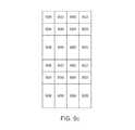
- FIG. 9 ais a schematic view of a pixel configuration for a photoimager array in accordance with another aspect of the present disclosure.
- FIG. 9 bis a schematic view of a pixel configuration for a photoimager array in accordance with another aspect of the present disclosure.
- FIG. 9 cis a schematic view of a pixel configuration for a photoimager array in accordance with another aspect of the present disclosure.
- FIG. 10is a schematic diagram of an eleven transistor imager in accordance with another aspect of the present disclosure.
- FIG. 11is a schematic view of a photosensitive device comprising a bolometer in accordance with another aspect of the present disclosure.
- FIG. 12is a representation of an integrated system for identifying an individual in accordance with one aspect of the present disclosure.
- FIG. 13is a flow diagram of a method in accordance with another aspect of the present disclosure.
- QEquantum efficiency
- EQEquantum efficiency
- electromagnetic radiationand “light” can be used interchangeably, and can represent wavelengths across a broad range, including visible wavelengths (approximately 350 nm to 800 nm) and non-visible wavelengths (longer than about 800 nm or shorter than 350 nm).
- the infrared spectrumis often described as including a near infrared portion of the spectrum including wavelengths of approximately 800 to 1300 nm, a short wave infrared portion of the spectrum including wavelengths of approximately 1300 nm to 3 micrometers, and a mid to long wave infrared (or thermal infrared) portion of the spectrum including wavelengths greater than about 3 micrometers up to about 30 micrometers.
- infraredportions of the electromagnetic spectrum unless otherwise noted.
- response timerefers to the rise time or fall time of a detector device.
- “rise time”is the time difference between the 10% point and the 90% point of the peak amplitude output on the leading edge of the electrical signal generated by the interaction of light with the device.
- “Fall time”is measured as the time difference between the 90% point and the 10% point of the trailing edge of the electrical signal.
- fall timecan be referred to as the decay time.
- shutter speedrefers to the time duration of a camera's shutter remain open while an image is captured.
- the shutter speeddirectly proportional to the exposure time, i.e. the duration of light reaching the image sensor.
- the shutter speedcontrols the amount of light that reaches the photosensitive imager.
- the slower the shutter speedthe longer the exposure time.
- Shutter speedsare commonly expressed in seconds and fractions of seconds. For example, 4, 2, 1, 1 ⁇ 2, 1 ⁇ 4, 1 ⁇ 8, 1/15, 1/30, 1/60, 1/125, 1/250, 1/500, 1/1000, 1/2000, 1/4000, 1/8000.
- each speed incrementhalves the amount of light incident upon the imager.
- the term “textured region”refers to a surface having a topology with nano- to micron-sized surface variations.
- a surface topologycan be formed by any appropriate technique, including, without limitation, irradiation of a laser pulse or laser pulses, chemical etching, lithographic patterning, interference of multiple simultaneous laser pulses, reactive ion etching, and the like. While the characteristics of such a surface can be variable depending on the materials and techniques employed, in one aspect such a surface can be several hundred nanometers thick and made up of nanocrystallites (e.g. from about 10 to about 50 nanometers) and nanopores. In another aspect, such a surface can include micron-sized structures (e.g. about 0.5 ⁇ m to about 60 ⁇ m). In yet another aspect, the surface can include nano-sized and/or micron-sized structures from about 5 nm and about 500 ⁇ m. It should be mentioned that the textured region can be ordered or disordered.
- surface modifyingand “surface modification” refer to the altering of a surface of a semiconductor material using a variety of surface modification techniques.
- Non-limiting examples of such techniquesinclude plasma etching, reactive ion etching, porous silicon etching, lasing, chemical etching (e.g. anisotropic etching, isotropic etching), nanoimprinting, material deposition, selective epitaxial growth, and the like, including combinations thereof.
- surface modificationcan include processes using primarily laser radiation or laser radiation in combination with a dopant, whereby the laser radiation facilitates the incorporation of the dopant into a surface of the semiconductor material.
- surface modificationincludes doping of a substrate such as a semiconductor material.
- target regionrefers to an area of a substrate that is intended to be doped or surface modified.
- the target region of the substratecan vary as the surface modifying process progresses. For example, after a first target region is doped or surface modified, a second target region may be selected on the same substrate.
- fluencerefers to the amount of energy from a single pulse of laser radiation that passes through a unit area. In other words, “fluence” can be described as the energy surface density of one laser pulse.
- detectionrefers to the sensing, absorption, and/or collection of electromagnetic radiation.
- scene radiancerefers to the areal density of light impinging on a known area or scene.
- the term “substantially”refers to the complete or nearly complete extent or degree of an action, characteristic, property, state, structure, item, or result.
- an object that is “substantially” enclosedwould mean that the object is either completely enclosed or nearly completely enclosed.
- the exact allowable degree of deviation from absolute completenessmay in some cases depend on the specific context. However, generally speaking the nearness of completion will be so as to have the same overall result as if absolute and total completion were obtained.
- the use of “substantially”is equally applicable when used in a negative connotation to refer to the complete or near complete lack of an action, characteristic, property, state, structure, item, or result.
- compositions that is “substantially free of” particleswould either completely lack particles, or so nearly completely lack particles that the effect would be the same as if it completely lacked particles.
- a composition that is “substantially free of” an ingredient or elementmay still actually contain such item as long as there is no measurable effect thereof.
- the term “about”is used to provide flexibility to a numerical range endpoint by providing that a given value may be “a little above” or “a little below” the endpoint.
- Securityhas generally become a top priority for many businesses, communities, governments, and the like.
- One key component in establishing effective securityis the rapid identification of individuals. For example, implementation of biometric scanning procedures in major thoroughfares such as airports, major cities, and the like can facilitate the identification and tracking of individuals for the safety of the populace as well as, in some cases, the safety of the individual being identified and tracked.
- a systemcan be utilized to identify abducted or runaway children. In other cases, fugitives and suspected criminals can be located and apprehended.
- systemscan be useful for identifying authorized users and allowing access for authorized users for financial transactions, personal electronic devices that can reduce the incidence of voter fraud, financial fraud, other forms of identity theft, and the like.
- a biometric imaging devicecapturing light wavelengths in the range of 800 nm to 1300 nm can be used.
- pigmentationis substantially transparent, and therefore electromagnetic photons pass freely through the pigment and reflect off of structural elements of interest for the identification.
- near infrared electromagnetic photonspass through the iris pigment and reflect off of iris ligament structures.
- the present disclosureprovides an efficient biometric device that can operate in low light conditions with good signal to noise ratio and high quantum efficiencies in the visible and infrared (IR) spectrum.
- IRvisible and infrared
- the present systemcan image the textured patterns of the iris, remove existing light variations, and reduce pattern interference from corneal reflections, thereby capturing more precise iris information.
- a system for identifying an individualcan include at least one active light source 102 capable of emitting electromagnetic radiation 104 having at least one wavelength of from about 700 nm to about 1200 nm and an imager device 106 positioned to receive the electromagnetic radiation upon reflection 108 from an individual 110 to generate an electronic representation of the individual.
- An image processing module 112can be functionally coupled to the imager device 106 to receive the electronic representation.
- the image processing module 112functions to process the electronic representation, using known algorithms to those skilled in the art, into an individual representation having at least one substantially unique identification trait. This substantially unique identification trait is used to identify the individual 110 . Additionally, it is noted that such a system can be utilized in cooperative as well as non-cooperative identification situations.
- FIG. 2shows one exemplary embodiment of an imager device that is capable of operation in low light conditions with good signal to noise ratio and high quantum efficiencies in the visible and IR light spectrum.
- the imager device 200can include a semiconductor device layer 202 having a device layer with a thickness of less than about 10 microns, at least two doped regions 204 , 206 forming a junction, and a textured region 208 positioned to interact with incoming electromagnetic radiation 210 .
- the first and second doped regionscan be distinct from one another, contacting one another, overlapping one another, etc.
- an intrinsic regioncan be located at least partially between the first and second doped regions.
- the semiconductor device layercan be less than about 50 microns thick. Additionally, in some aspects the semiconductor device layer can be disposed on a bulk semiconductor layer or semiconductor support layer.
- the textured region 208is shown located on a side of the semiconductor device layer 202 that is opposite to the first doped region 204 and the second doped region 206 .
- electromagnetic radiation that passes through the semiconductor device layer 202 to contact the textured region 208can be reflected back through the semiconductor device layer, thus effectively increasing the absorption path length of the semiconductor material.
- the textured regioncan be associated with an entire surface of the semiconductor material or only a portion thereof. Additionally, in some aspects the textured region can be specifically positioned to maximize the absorption path length of the semiconductor material. In other aspects, a third doping can be included near the textured region to improve the collection of carriers generated near the textured region.
- the imager devicecan have a semiconductor device layer with a thickness of less than about 10 microns and an external quantum efficiency of at least about 33% for electromagnetic radiation having at least one wavelength of greater than 800 nm.
- the imager devicecan have a response time of from about 0.1 ms to about 1 ms and an external quantum efficiency of at least about 33% for electromagnetic radiation having at least one wavelength greater than about 800 nm.
- the response timecan be from about 0.1 ms to about 16 ms.
- Other thicknesses of device layersare additionally contemplated. In one aspect, for example, the device layer thickness can be less than 50 microns. In another aspect, the device layer thickness can be less than 5 microns.
- the device layer thicknesscan be less than 1 micron.
- a lower limit for thickness of the device layercan be any thickness that allows functionality of the device. In one aspect, however, the device layer can be at least 10 nm thick. In another aspect, the device layer can be at least 100 nm thick. In yet another aspect, the device layer can be at least 500 nm thick.
- the imager devicecan have an external quantum efficiency of at least about 23% for electromagnetic radiation having at least one wavelength greater than about 850 nm. In yet another aspect, the imager device can have an external quantum efficiency of at least about 11% for electromagnetic radiation having at least one wavelength greater than about 940 nm. In another aspect, the imager device can have a response time of from about 0.1 ms to about 1 ms and an external quantum efficiency of at least about 11% for electromagnetic radiation having at least one wavelength greater than about 940 nm.
- the imager devicecan have an external quantum efficiency of at least about 46% for electromagnetic radiation having at least one wavelength of greater than 800 nm.
- the imager devicecan have a response time of from about 0.1 ms to about 1 ms and an external quantum efficiency of at least about 46% for electromagnetic radiation having at least one wavelength greater than about 800 nm.
- the imager devicecan have a semiconductor device layer having a thickness of less than 10 microns, and the imager can have an external quantum efficiency of at least about 32% for electromagnetic radiation having at least one wavelength greater than about 850 nm.
- the imager devicecan have a semiconductor device layer having a thickness of less than 10 microns, and the imager can have an external quantum efficiency of at least 50% or at least 60% for electromagnetic radiation having at least one wavelength greater than about 850 nm. In yet another aspect, the imager device can have an external quantum efficiency of at least about 15% for electromagnetic radiation having at least one wavelength greater than about 940 nm. In another aspect, the imager device can have a response time of from about 0.1 ms to about 1 ms and an external quantum efficiency of at least about 15% for electromagnetic radiation having at least one wavelength greater than about 940 nm. Further details regarding such photosensitive devices have been described in U.S. application Ser. No. 13/164,630, filed on Jun. 20, 2011, which is incorporated herein by reference in its entirety.
- the textured region 208can be positioned on a side of the semiconductor device layer 202 opposite the incoming electromagnetic radiation 210 as shown.
- the textured regioncan also be positioned on a side of the semiconductor device layer adjacent the incoming electromagnetic radiation (not shown). In other words, in this case the electromagnetic radiation would contact the textured region prior to passing into the semiconductor device layer. Additionally, it is contemplated that the textured region can be positioned on both an opposite side and an adjacent side of the semiconductor device layer.
- the present imaging devicecan be utilized to capture an electronic representation that is capable of being used to identify an individual at short distances as well as long distances.
- the devicecan capture the electronic representation at short distances such as, for example, from about 2 cm or less to about 10 cm, or up to 50 cm, or up to 0.5 m.
- the devicecan also capture the electronic representation at from short distances to long distances such as, for example, up to 1 m, up to 3 m, up to 6 m, up to 10 m, or up to 15 m or more.
- the semiconductor utilized to construct the imagercan be any useful semiconductor material from which such an imager can be made having the properties described herein.
- the semiconductor device layeris silicon.
- silicon photo detectorshave limited detectability of IR wavelengths of light, particularly for thin film silicon devices.
- Traditional silicon materialsrequire substantial absorption depths in order to detect photons having wavelengths longer than about 700 nm. While visible light can be readily absorbed in the first few microns of a silicon layer, absorption of longer wavelengths (e.g. 900 nm) in silicon at a thin wafer depth (e.g. approximately 100 ⁇ m) is poor if at all.
- the present imager devicescan increase the electromagnetic radiation absorption range of silicon, thus allowing the absorption of visible and IR light even at shallow depths and in silicon thin films.
- the textured region 208can increase the absorption, increase the external quantum efficiency, and decrease response times, particularly in the infrared wavelengths.
- Such unique and novel devicescan allow for fast shutter speeds thereby capturing images of moving objects in the visible and infrared spectrums.
- Such an increased sensitivity in a silicon-based devicecan thus reduce processing cost of photodetectors, reduce the power needed in light sources, increase the depth resolution in 3D types imaging, and improve the biometric measurements of an individual.
- FIG. 3shows an absorption/responsivity graph where the dashed line 302 represents the absorption characteristics of a photodiode based on a traditional standard fast silicon device, and the solid line 304 represents the absorption characteristics of a silicon-based photodiode device but including a textured region.
- the absorption of a standard fast silicon imager in the infraredi.e. the 800 nm to 1200 nm region
- an imageris a collection of multiple photodiodes.
- the present systemcan include optics for increasing the capture distance between the device and the individual
- the imager device having the textured regionallows the system to function at low IR light intensity levels even at such long distances. This reduces energy expenditure and thermal management issues, as well as potentially decreasing side effects that can result from high intensity IR light.
- the imager devicecan capture the electronic representation of an individual with sufficient detail to identify a substantially unique identification trait using electromagnetic radiation emitted from the active light source having at least one wavelength of from about 700 nm to about 1200 nm and having a scene radiance impinging on the individual at 3 meters that is at least 0.1 mW/mm 2 .
- the imager devicecan capture the electronic representation of an individual with sufficient detail to identify a substantially unique identification trait using electromagnetic radiation emitted from the active light source having at least one wavelength of from about 800 nm to about 1000 nm and having a scene radiance impinging on the individual at 3 meters that is from about 0.1 mW/mm 2 to about 100 mW/mm 2 .
- the imager devicecan capture the electronic representation of an individual with sufficient detail to identify a substantially unique identification trait using electromagnetic radiation emitted from the active light source having at least one wavelength of from about 800 nm to about 1000 nm and having a scene radiance impinging on the individual at 3 meters that is from about 1 mW/mm 2 to about 10 mW/mm 2 .
- the electromagnetic radiationhaving a wavelength of at least 940 nm and should have optical power below the eye damage threshold of 10,000 mW/mm 2 /steradian. It should be noted that in one aspect the substantially unique identification trait is an iris pattern of the individual.
- the thickness of the silicon material in the devicecan dictate the responsivity and response time.
- Standard silicon devicesneed to be thick, i.e. greater than 100 ⁇ m in order to detect wavelengths in the infrared spectrum, and such detection with thick devices results in a slow response and high dark current.
- the textured regionis positioned to interact with electromagnetic radiation to increase the absorption of infrared light in a device, thereby improving the infrared responsivity while allowing for fast operation.
- Diffuse scattering and reflectioncan result in increased path lengths for absorption, particularly if combined with total internal reflection, resulting in large improvements of responsivity in the infrared for silicon photodiodes, photodetectors, photodiode arrays, imagers, and the like.
- thinner silicon materialscan be used to absorb electromagnetic radiation up into the infrared regions.
- One advantage of thinner silicon material devicesis that charge carriers are more quickly swept from the device, thus decreasing the response time. Conversely, thick silicon material devices sweep charge carriers therefrom more slowly, at least in part due to diffusion.
- the silicon device layercan be of any thickness that allows electromagnetic radiation detection and conversion functionality, and thus any such thickness of silicon device layer is considered to be within the present scope.
- thin silicon layer materialscan be particularly beneficial in decreasing the response time and/or the capacitance of the device.
- charge carrierscan be more quickly swept from thinner silicon material layers as compared to thicker silicon material layers. The thinner the silicon, the less material the electron/holes have to traverse in order to be collected, and the lower the probability of a generated charge carrier encountering a defect that could trap or slow the collection of the carrier.
- one objective to implementing a fast photo responseis to utilize a thin silicon material for the semiconductor device layer of the imager.
- Such a devicecan be nearly depleted of charge carriers by the built in potential of the photodiode and any applied bias to provide for a fast collection of the photo generated carriers by drift in an electric field.
- Charge carriers remaining in any undepleted region of the photodiodeare collected by diffusion transport, which is slower than drift transport. For this reason, it can be desirable to have the thickness of any region where diffusion may dominate to be much thinner than the depleted drift regions.
- silicon materials having the proper dopingprovides a depletion region of about 10 ⁇ m with no applied bias. As such, in some aspects it can be useful to utilize a silicon material layer having a thickness of less than about 100 ⁇ m, less than about 10 ⁇ m or less than about 5 ⁇ m.
- the silicon materialcan have a thickness and substrate doping concentration such that an applied bias generates an electrical field sufficient for saturation velocity of the charge carriers. It should be noted that operating a photodiode, as disclosed herein, at a zero bias can result in low noise but at a longer response time. When bias is applied however, the dark current is increased, resulting in higher noise, but with a decreased response time. The increased dark current can be compensated if the incident radiation signal is strong. The amount of dark current increase can be minimized, however, with a thinner device layer.
- the semiconductor device layerin general can be of any thickness that allows electromagnetic radiation detection and conversion functionality, and thus any such thickness of semiconductor material is considered to be within the present scope.
- the textured regionincreases the efficiency of the device such that the semiconductor device layer can be thinner than has previously been possible. Decreasing the thickness of the semiconductor device layer reduces the amount of semiconductor material required to make such a device.
- the semiconductor device layerhas a thickness of from about 500 nm to about 50 ⁇ m.
- the semiconductor device layerhas a thickness of less than or equal to about 100 ⁇ m.
- the semiconductor device layerhas a thickness of from about 500 nm to about 20 ⁇ m.
- the semiconductor device layerhas a thickness of from about 500 nm to about 10 ⁇ m. In a further aspect, the semiconductor device layer can have a thickness of from about 500 nm to about 50 ⁇ m. In yet a further aspect, the semiconductor device layer can have a thickness of from about 500 nm to about 2 ⁇ m. In other aspect the semiconductor device layer can have a thickness of less than 10 microns, 5 microns, or 1 microns.
- a silicon semiconductor device layerhas a thickness of from about 100 nm to about 100 ⁇ m. In another aspect, the silicon material has a thickness of from about 0.5 ⁇ m to about 50 ⁇ m. In yet another aspect, the silicon material has a thickness of from about 5 ⁇ m to about 10 ⁇ m. In a further aspect, the silicon material has a thickness of from about 1 ⁇ m to about 5 ⁇ m.
- the response time of a photosensitive imaging deviceis limited by the transit time of the photo generated carriers across the thickness of the device layer.
- the RC time constant of the load resistance, (R) and the capacitance (C) of the entire electronic device structurecan be kept less than this transit time by using small load resistors and keeping the capacitance of the photodiodes small by limiting the doping density of the silicon material and area of the photodiodes.
- photodiodes doped at 10 15 /cm 3can have a capacitance that may be 10 nF/cm 2 without any applied bias.
- Small area photodiodes with 50 ohm load resistorscan have very fast RC time constants.
- the response timeis bound by an upper limit of 2 ⁇ s.
- the devices of the present disclosureincrease the absorption path length of silicon materials by increasing the absorption path length for longer wavelengths as compared to traditional silicon devices.
- the absorption depth in silicon photodetectorsis the depth into silicon at which the radiation intensity is reduced to about 36% of the value at the surface of the silicon material.
- the increased absorption path lengthresults in an apparent reduction in the absorption depth, or a reduced apparent or effective absorption depth.
- the effective absorption depth of siliconcan be reduced such that longer wavelengths can be absorbed at depths of less than or equal to about 100 ⁇ m.
- the response timecan be decreased using thinner semiconductor materials.
- the resultant upper response time limitis about 20 ns.
- the responsivitycan be on the order 10% or 0.3 Ampere/Watt.
- an imager devicehas a response time of from about 0.1 ms to about 1 ms.
- an imager devicehas a responsivity of from about 0.4 A/W to about 0.55 A/W for at least one wavelength of from about 800 nm to about 1200 nm relative to standard silicon.
- an imager devicehas a responsivity of from about 0.1 A/W to about 0.55 A/W for at least one wavelength of from about 1000 nm to about 1200 nm relative to standard silicon.
- the optoelectronic devicehas an increased external quantum efficiency of at least 10% for at least one wavelength of from about 550 nm to about 1200 nm relative to a silicon device with comparable thickness and response time.
- photosensitive imaging devicescan exhibit lower levels of dark current as compared to traditional devices. Although a variety of reasons are possible, one exemplary reason may be that a thinner silicon material layer can have fewer crystalline defects responsible for the generation of dark current.
- the dark current of an photosensing imaging device during operationis from about 100 pA/cm 2 to about 10 nA/cm 2 .
- the maximum dark current of an imaging device during operationis less than about 1 nA/cm 2 .
- imager devicesprovide, among other things, enhanced response in the infrared light portion of the optical spectrum and improved response and quantum efficiency in converting electromagnetic radiation to electrical signals.
- high quantum efficiencies and increase response timescan be obtained in the infrared for devices thinner than about 100 ⁇ m.
- the sensitivity and responseare higher than that found in thicker devices at infrared wavelengths.
- Non-limiting examples of such semiconductor materialscan include group IV materials, compounds and alloys comprised of materials from groups II and VI, compounds and alloys comprised of materials from groups III and V, and combinations thereof. More specifically, exemplary group IV materials can include silicon, carbon (e.g. diamond), germanium, and combinations thereof. Various exemplary combinations of group IV materials can include silicon carbide (SiC) and silicon germanium (SiGe). Exemplary silicon materials, for example, can include amorphous silicon (a-Si), microcrystalline silicon, multicrystalline silicon, and monocrystalline silicon, as well as other crystal types. In another aspect, the semiconductor material can include at least one of silicon, carbon, germanium, aluminum nitride, gallium nitride, indium gallium arsenide, aluminum gallium arsenide, and combinations thereof.
- Exemplary combinations of group II-VI materialscan include cadmium selenide (CdSe), cadmium sulfide (CdS), cadmium telluride (CdTe), zinc oxide (ZnO), zinc selenide (ZnSe), zinc sulfide (ZnS), zinc telluride (ZnTe), cadmium zinc telluride (CdZnTe, CZT), mercury cadmium telluride (HgCdTe), mercury zinc telluride (HgZnTe), mercury zinc selenide (HgZnSe), and combinations thereof.
- CdSecadmium selenide
- CdScadmium sulfide
- CdTecadmium telluride
- ZnOzinc oxide
- ZnSezinc selenide
- ZnSzinc sulfide
- ZnTezinc telluride
- CdZnTecadmium zinc telluride
- Exemplary combinations of group III-V materialscan include aluminum antimonide (AlSb), aluminum arsenide (AlAs), aluminum nitride (AlN), aluminum phosphide (AlP), boron nitride (BN), boron phosphide (BP), boron arsenide (BAs), gallium antimonide (GaSb), gallium arsenide (GaAs), gallium nitride (GaN), gallium phosphide (GaP), indium antimonide (InSb), indium arsenide (InAs), indium nitride (InN), indium phosphide (InP), aluminum gallium arsenide (AlGaAs, Al x Ga 1-x As), indium gallium arsenide (InGaAs, In x Ga 1-x As), indium gallium phosphide (InGaP), aluminum indium arsenide (AlInAs), aluminum in
- the semiconductor materialis monocrystalline.
- the semiconductor materialis multicrystalline.
- the semiconductor materialis microcrystalline. It is also contemplated that the semiconductor material can be amorphous. Specific nonlimiting examples include amorphous silicon or amorphous selenium.
- the semiconductor materials of the present disclosurecan also be made using a variety of manufacturing processes. In some cases the manufacturing procedures can affect the efficiency of the device, and may be taken into account in achieving a desired result. Exemplary manufacturing processes can include Czochralski (Cz) processes, magnetic Czochralski (mCz) processes, Float Zone (FZ) processes, epitaxial growth or deposition processes, and the like. It is contemplated that the semiconductor materials used in the present invention can be a combination of monocrystalline material with epitaxially grown layers formed thereon.
- dopant materialsare contemplated for the formation of the multiple doped regions, the textured region, or any other doped portion of the imager device, and any such dopant that can be used in such processes is considered to be within the present scope. It should be noted that the particular dopant utilized can vary depending on the material being doped, as well as the intended use of the resulting material.
- a dopantcan be either electron donating or hole donating.
- dopantscan include S, F, B, P, N, As, Se, Te, Ge, Ar, Ga, In, Sb, and combinations thereof.
- the scope of dopantsshould include, not only the dopants themselves, but also materials in forms that deliver such dopants (i.e. dopant carriers).
- S dopantsincludes not only S, but also any material capable being used to dope S into the target region, such as, for example, H 2 S, SF 6 , SO 2 , and the like, including combinations thereof.
- the dopantcan be S.
- Sulfurcan be present at an ion dosage level of between about 5 ⁇ 10 14 and about 1 ⁇ 10 16 ions/cm 2 .
- fluorine-containing compoundscan include ClF 3 , PF 5 , F 2 SF 6 , BF 3 , GeF 4 , WF 6 , SiF 4 , HF, CF 4 , CHF 3 , CH 2 F 2 , CH 3 F, C 2 F 6 , C 2 HF 5 , C 3 F 8 , C 4 F 8 , NF 3 , and the like, including combinations thereof.
- Non-limiting examples of boron-containing compoundscan include B(CH 3 ) 3 , BF 3 , BCl 3 , BN, C 2 B 10 H 12 , borosilica, B 2 H 6 , and the like, including combinations thereof.
- Non-limiting examples of phosphorous-containing compoundscan include PF 5 , PH 3 , and the like, including combinations thereof.
- Non-limiting examples of chlorine-containing compoundscan include Cl 2 , SiH 2 Cl 2 , HCl, SiCl 4 , and the like, including combinations thereof.
- Dopantscan also include arsenic-containing compounds such as AsH 3 and the like, as well as antimony-containing compounds. Additionally, dopant materials can include mixtures or combinations across dopant groups, i.e.
- the dopant materialcan have a density that is greater than air.
- the dopant materialcan include Se, H 2 S, SF 6 , or mixtures thereof.
- the dopantcan be SF 6 and can have a predetermined concentration range of about 5.0>10 ⁇ 8 mol/cm 3 to about 5.0 ⁇ 10 ⁇ 4 mol/cm 3 .
- SF 6 gasis a good carrier for the incorporation of sulfur into the semiconductor material via a laser process without significant adverse effects on the silicon material.
- dopantscan also be liquid solutions of n-type or p-type dopant materials dissolved in a solution such as water, alcohol, or an acid or basic solution. Dopants can also be solid materials applied as a powder or as a suspension dried onto the wafer.
- the first doped region and the second doped regioncan be doped with an electron donating or hole donating species to cause the regions to become more positive or negative in polarity as compared to each other and/or the semiconductor device layer.
- either doped regioncan be p-doped.
- either doped regioncan be n-doped.
- the first doped regioncan be negative in polarity and the second doped region can be positive in polarity by doping with p+ and n ⁇ dopants.
- variations of n( ⁇ ), n( ⁇ ), n(+), n(++), p( ⁇ ), p( ⁇ ), p(+), or p(++) type doping of the regionscan be used.
- the semiconductor materialcan be doped in addition to the first and second doped regions.
- the semiconductor materialcan be doped to have a doping polarity that is different from one or more of the first and second doped regions, or the semiconductor material can be doped to have a doping polarity that is the same as one or more of the first and second doped regions.
- the semiconductor materialcan be doped to be p-type and one or more of the first and second doped regions can be n-type.
- the semiconductor materialcan be doped to be n-type and one or more of the first and second doped regions can be p-type. In one aspect, at least one of the first or second doped regions has a surface area of from about 0.1 ⁇ m 2 to about 32 ⁇ m 2 .
- the textured regioncan function to diffuse electromagnetic radiation, to redirect electromagnetic radiation, and to absorb electromagnetic radiation, thus increasing the QE of the device.
- the textured regioncan include surface features to increase the effective absorption length of the silicon material.
- the surface featurescan be cones, pyramids, pillars, protrusions, micro lenses, quantum dots, inverted features and the like.
- Factorssuch as manipulating the feature sizes, dimensions, material type, dopant profiles, texture location, etc. can allow the diffusing region to be tunable for a specific wavelength.
- tuning the devicecan allow specific wavelengths or ranges of wavelengths to be absorbed.
- tuning the devicecan allow specific wavelengths or ranges of wavelengths to be reduced or eliminated via filtering.
- a textured regioncan allow a silicon material to experience multiple passes of incident electromagnetic radiation within the device, particularly at longer wavelengths (i.e. infrared). Such internal reflection increases the effective absorption length to be greater than the thickness of the semiconductor device layer. This increase in absorption length increases the quantum efficiency of the device, leading to an improved signal to noise ratio.
- the textured regioncan be associated with the surface nearest the impinging electromagnetic radiation, or the textured region can be associated with a surface opposite in relation to impinging electromagnetic radiation, thereby allowing the radiation to pass through the silicon material before it hits the textured region.
- the textured regioncan be doped. In one aspect, the textured region can be doped to the same or similar doping polarity as the silicon device layer so as to provide a doped contact region on the backside of the device.
- the textured regioncan be formed by various techniques, including lasing, chemical etching (e.g. anisotropic etching, isotropic etching), nanoimprinting, additional material deposition, reactive ion etching, and the like.
- One effective method of producing a textured regionis through laser processing. Such laser processing allows discrete locations of the semiconductor device layer to be textured.
- a variety of techniques of laser processing to form a textured regionare contemplated, and any technique capable of forming such a region should be considered to be within the present scope.
- Laser treatment or processingcan allow, among other things, enhanced absorption properties and thus increased electromagnetic radiation focusing and detection.
- a target region of the silicon materialcan be irradiated with laser radiation to form a textured region.
- Examples of such processinghave been described in further detail in U.S. Pat. Nos. 7,057,256, 7,354,792 and 7,442,629, which are incorporated herein by reference in their entireties.
- a surface of a semiconductor materialsuch as silicon is irradiated with laser radiation to form a textured or surface modified region.
- Such laser processingcan occur with or without a dopant material.
- the lasercan be directed through a dopant carrier and onto the silicon surface. In this way, dopant from the dopant carrier is introduced into a target region of the silicon material.
- the target regiontypically has a textured surface that increases the surface area of the laser treated region and increases the probability of radiation absorption via the mechanisms described herein.
- such a target regionis a substantially textured surface including micron-sized and/or nano-sized surface features that have been generated by the laser texturing.
- irradiating the surface of the silicon materialincludes exposing the laser radiation to a dopant such that irradiation incorporates the dopant into the semiconductor.
- dopant materialsare known in the art, and are discussed in more detail herein. It is also understood that in some aspects such laser processing can occur in an environment that does not substantially dope the silicon material (e.g. an argon atmosphere).
- the surface of the silicon material that forms the textured regionis chemically and/or structurally altered by the laser treatment, which may, in some aspects, result in the formation of surface features appearing as nanostructures, microstructures, and/or patterned areas on the surface and, if a dopant is used, the incorporation of such dopants into the semiconductor material.
- such featurescan be on the order of 50 nm to 20 ⁇ m in size and can assist in the absorption of electromagnetic radiation.
- the textured surfacecan increase the probability of incident radiation being absorbed by the silicon material.
- At least a portion of the textured region and/or the semiconductor materialcan be doped with a dopant to generate a back surface field.
- a back surface fieldcan function to repel generated charge carriers from the backside of the device and toward the junction to improve collection efficiency and speed.
- the addition of a back surface fieldcan increase charge carrier collection and depletion.
- the presence of a back surface fieldalso acts to suppress dark current contribution from the surface of a device.
- a reverse biascan be applied across the electrical contacts associated with the imager.
- Such a reverse biascan function to decrease the response time of the device by more quickly sweeping charge carriers from the silicon material. Accordingly, for those situations whereby a bias is used, any bias voltage capable of sweeping charge carriers from the silicon material is considered to be within the present scope.
- the reverse biasis from about 0.001 V to about 20 V. In another aspect, the reverse bias is from about 0.001 V to about 10 V. In yet another aspect, the reverse bias is from about 0.001 V to about 5 V. In a further aspect, the reverse bias is from about 0.001 V to about 3 V.
- the reverse biasis from about 3 V to about 5 V.
- the reverse biascan be absent, or in other words, 0 V is applied across the first and second contacts.
- the charge carrierscan be depleted from the silicon material by the junction potential created by the first and second doped regions.
- a semiconductor device layer 402can have a first doped region 404 , a second doped region 406 , and a textured region 408 on an opposing surface to the doped regions.
- An antireflective layer 410can be coupled to the semiconductor device layer 402 on the opposite surface as the textured layer 408 .
- the antireflective layer 410can be on the same side of the semiconductor device layer 402 as the textured region (not shown).
- a lenscan be optically coupled to the semiconductor device layer and positioned to focus incident electromagnetic radiation into the semiconductor device layer.
- a photodiode arrayis provided as the imager device.
- Such an arraycan include a semiconductor device layer having an incident light surface, at least two photodiodes in the semiconductor device layer, where each photodiode includes a first doped region and a second doped region forming a junction, and a textured region coupled to the semiconductor device layer and positioned to interact with electromagnetic radiation.
- the textured regioncan be a single textured region or multiple textured regions.
- the photodiode arrayhas a response time of from about 0.1 ms to about 1 ms and an external quantum efficiency of at least 33% for electromagnetic radiation having at least one wavelength greater than about 800 nm.
- the photodiode arraycan have a pixel count, or also commonly known as the pixel resolution equal to or greater than about 320 ⁇ 280. In another embodiment the pixel resolution is greater than 1 MP (megapixel), greater than 5 MP, greater than 15 MP and even greater than 25 MP.
- a semiconductor device layer 502can include at least two photodiodes 504 each having a first doped region 506 and a second doped region 508 .
- a textured region 510can be positioned to interact with electromagnetic radiation.
- FIG. 5shows a separate textured region for each photodiode. In some aspects, however, a single textured region can be used to increase the absorption path lengths of multiple photodiodes in the array.
- an isolation structure 512can be positioned between the photodiodes to electrically and/or optically isolate the photodiodes from one another.
- the photodiode arraycan be electronically coupled to electronic circuitry to process the signals generated by each photodiode.
- Non-limiting examples of such componentscan include a carrier wafer, electrical contacts, an antireflective layer, a dielectric layer, circuitry layer, a via(s), a transfer gate, an infrared filter, a color filter array (CFA), an infrared cut filter, an isolation feature, and the like. Additionally, such devices can have light absorbing properties and elements as has been disclosed in U.S. patent application Ser. No. 12/885,158, filed on Sep. 17, 2010 which is incorporated by reference in its entirety. It is further understood that the imager can be a CMOS (Complementary Metal Oxide Semiconductor) imaging sensor or a CCD (Charge Coupled Device).
- CMOSComplementary Metal Oxide Semiconductor
- CCDCharge Coupled Device
- Imager devicecan include a number of transistors per pixel depending on the desired design of the device.
- an imager devicecan include at least three transistors.
- an imaging devicecan have four, five, or six or more transistors.
- FIG. 6shows an exemplary schematic for a six-transistor (6-T) architecture that will allow global shutter operation according to one aspect of the present disclosure.
- the imagercan include a photodiode (PD), a global reset (Global_RST), a global transfer gate (Global_TX), a storage node, a transfer gate (TX 1 ), reset (RST), source follower (SF), floating diffusion (FD), row select transistor (RS), power supply (Vaapix) and voltage out (Vout). Due to the use of extra transfer gate and storage node, correlated-double-sampling (CDS) is allowed. Therefore, the read noise should be able to match typical CMOS 4T pixels.
- CDScorrelated-double-sampling
- FIGS. 7 a - bshow images of the iris of a subject captured by an IR sensitive imager device.
- FIG. 7 aan image of an iris captured using a rolling shutter is somewhat distorted due to movements during capture. These distortions may affect identification of the individual.
- FIG. 7 bshows an image of an iris captured using a global shutter that is a more defined and does not show such distortion.
- the global shutteroperates by electronically activating all pixels at precisely the same time, allowing them to integrate the light from the scene at the same time and then stop the integration at the same time. This eliminates rolling shutter distortion.
- the global shutter imagewas taken under the same conditions as the rolling shutter.
- the biometric systemcan include a three dimensional (3D) photosensing imager.
- 3D-type imagercan be useful to image surface details of an individual for identification, such as facial features, body features, stride or body position features, and the like.
- Time-of-flight (TOF)is one technique developed for use in radar and LIDAR (Light Detection and Ranging) systems to provide depth information that can be utilized for such 3D imaging.
- LIDARLight Detection and Ranging
- the basic principle of TOFinvolves sending a signal to an object and measuring a property of the returned signal from a target. The measured property is used to determine the TOF. Distance to the target is therefore derived by multiplication of half the TOF and the velocity of the signal.
- FIG. 8illustrates a TOF measurement with a target having multiple surfaces that are separated spatially. Equation (III) can be used to measure the distance to a target where d is the distance to the target and c is the speed of light.
- a TOF measurementcan utilize a modulated LED light pulse and measure the phase delay between emitted light and received light. Based on the phase delay and the LED pulse width, the TOF can be derived.
- the TOF conceptcan be utilized in both CMOS and CCD sensors to obtain depth information from each pixel in order to capture an image used for identification of an individual.
- a 3D pixelsuch as a TOF 3D pixel with enhanced infrared response can improve depth accuracy, which in turn can show facial features in a three dimensional scale.
- a photoimager arraycan include at least one 3D infrared detecting pixel and at least one visible light detecting pixel arranged monolithically in relation to each other.
- FIGS. 9 a - cshow non-limiting example configurations of pixel arrangements of such arrays.
- FIG. 9 ashows one example of a pixel array arrangement having a red pixel 902 , a blue pixel 904 , and a green pixel 906 .
- FIG. 9 bthe pixel arrangement shown includes an imager as described in FIG. 9 a and three arrays of a red pixel, a blue pixel, and two green pixels. Essentially, one TOF pixel replaces one quadrant of a RGGB pixel design. In this configuration, the addition of several green pixels allows for the capture of more green wavelengths that is needed for green color sensitivity need for the human eye, while at the same time capturing the infrared light for depth perception. It should be noted that the present scope should not be limited by the number or arrangements of pixel arrays, and that any number and/or arrangement is included in the present scope.
- FIG. 9 cshows another arrangement of pixels according to yet another aspect.
- the TOF pixelcan have an on-pixel optical narrow band pass filter.
- the narrow band pass filter designcan match the modulated light source (either LED or laser) emission spectrum and may significantly reduce unwanted ambient light that can further increase the signal to noise ratio of modulated IR light.
- Another benefit of increased infrared QEis the possibility of high frame rate operation for high speed 3D image capture.
- An integrated IR cut filtercan allow a high quality visible image with high fidelity color rendering. Integrating an infrared cut filter onto the sensor chip can also reduce the total system cost of a camera module (due to the removal of typical IR filter glass) and reduce module profile (good for mobile applications). This can be utilized with TOF pixels and non-TOF pixels.
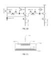
- FIG. 10shows an exemplary schematic of a 3D TOF pixel according to one aspect of the present disclosure.
- the 3D TOF pixelcan have 11 transistors for accomplishing the depth measurement of the target.
- the 3D pixelcan include a photodiode (PD), a global reset (Global_RST), a first global transfer gate (Global_TX 1 ), a first storage node, a first transfer gate (TX 1 ), a first reset (RST 1 ), a first source follower (SF 1 ), a first floating diffusion (FD 1 ), a first row select transistor (RS 1 ), a second global transfer gate (Global_TX 2 ), a second storage node, a second transfer gate (TX 2 ), a second reset (RST 2 ), a second source follower (SF 2 ), a second floating diffusion (FD 2 ), a second row select transistor (RS 2 ), power supply (Vaapix) and voltage out (Vout).
- Other transistorscan be included in the 3D
- thermal imagingcan be utilized for identification of an individual or a group of individuals exhibiting thermal-related characteristics.
- an imagercan include a silicon device layer 1102 having a first doped region 1104 and a second doped region 1106 forming at least one junction.
- the first and second doped regionscan be distinct from one another, contacting one another, overlapping one another, etc.
- an intrinsic regioncan be located at least partially between the first and second doped regions.
- the devicecan also include a textured region 1108 coupled to the silicon device layer 1102 and positioned to interact with incoming electromagnetic radiation 1110 .
- the textured region 1108is located on a side of the silicon device layer 1102 that is opposite to the first doped region 1104 and the second doped region 1106 .
- the textured region 1108can be associated with an entire surface of the silicon material or only a portion thereof.
- a thermal sensing layer 1112such as a bolometer or microbolometer, can be coupled to the silicon device layer 1102 .
- a cavity or voidis disposed between the thermal sensing layer and the silicon material (not shown). Further details relating to such a device can be found in U.S. Pat. No. 7,847,253, which is incorporated by reference in its entirety.
- Such a device as shown in FIG. 11can have the benefits of measuring facial and/or iris features as well as the thermal signature or feature of an individual.
- the system for identifying an individualcan include a light source that is either a passive light source (e.g. sunlight, ambient room lighting) or an active light source (e.g. an LED or lightbulb) that is capable of emitting IR light.
- the systemcan utilize any source of light that can be beneficially used to identify an individual.
- the light sourceis an active light source.
- Active light sourcesare well known in the art that are capable of emitting light, particularly in the IR spectrum. Such active light sources can be continuous or pulsed, where the pulses can be synchronized with light capture at the imaging device. While various light wavelengths can be emitted and utilized to identify an individual, IR light in the range of from about 700 nm to about 1200 nm can be particularly useful.
- the active light sourcecan be two or more active light sources each emitting infrared electromagnetic radiation at distinct peak emission wavelengths. While any distinct wavelength emissions within the IR range can be utilized, non-limiting examples include 850 nm, 940 nm, 1064 nm, and the like.
- the two or more active light sourcescan interact with the same imager device, either simultaneously or with an offset duty cycle. Such configurations can be useful for independent capture of one or more unique features of the individual for redundant identification. This redundant identification can help insure accurate authorization or identification of the individual.
- the two or more active light sourcescan each interact with a different imager device.
- the system including the imager device and the light sourcecan be in a fixed position. This may be useful in situations, for example, where the environment facilitates individuals walking directly toward the imager device.
- a fixed position imager devicecan be associated with a zoom lens to allow zooming along a fixed viewing axis.
- itcan be beneficial to allow movement of the imager device and/or the light source.
- a system capable of panning and/or tilting and zoomingcan track an individual during the identification process. It is noted that for purposes of the present disclosure, panning includes movement of a device in any direction.
- a systemcan include a pan and zoom module.
- Such a moduleallows the system to locate a feature of the individual, such as the iris, zoom in on that feature to optimize the imager device (e.g. camera) and/or light source angle to capture an electronic representation for identification purposes.
- a movement systemcan be manually or automatically operated.
- the identification systemcan include at least two imager devices.
- the imager devicescan be mounted together in a manner that allows dependent or independent movement.
- the imager devicescan be utilized to each capture an identification feature of an individual for redundant identification testing.
- each imagercan capture an independent image using the same or different light sources and compare the identification results.
- the two or more imagerscan function together to capture the electronic representation of the individual.
- the systemcan include a first imager device positioned and operable to generate a facial electronic representation of the individual and a second imager device positioned and operable to generate an iris electronic representation of the individual.
- the systemcan also include an image processing circuit that finds the location of the eye from the facial electronic representation and then providing that location to circuit that controls the pan, tilt and zoom functions.
- the systemcan also include an analysis module functionally coupled to the imager device to compare the substantially unique identification trait with a known identification trait to facilitate identification of the individual.
- the analysis modulecan obtain known data regarding the identity of an individual from a source such as a database and compare this known data to the electronic representation being captured by the imager device.
- Various algorithmsare known that can analyze the image to define the biometric boundaries/measurements and convert the biometric measurements to a unique code. The unique code can then be stored in the database to be used for comparison to make positive identification of the individual.
- Such an algorithmhas been described for iris detection in U.S. Pat. Nos. 4,641,349 and 5,291,560, which are incorporated by reference in their entirety.
- the image processing module and the analysis modulecan be the same or different modules. It is understood that the system described herein can be utilized with any of the identification algorithm.
- the systemcan utilize an automatic pan and zoom module to move at least one of the imager device or the light source and a process module to analyze a facial electronic representation.
- the process modulecan provide pan and zoom module coordinates for the face and iris for further zooming, movement, and image capture.
- the present systemscan be sized to suit a variety of applications. This is further facilitated by the potential thin film design and the increased sensitivity of the imager devices to IR light and the corresponding decrease in the intensity of IR emission, thus allowing reduction in the size of the light source.
- the light source, the imager device, and the image processing modulecollectively have a size of less than about 160 cubic centimeters.
- the light source, the imager device, and the image processing modulecollectively have a size of less than about 16 cubic centimeters.
- the imager devicecan have an optical format of about 1/7 inches.
- the systemcan be activated by a trigger from the individual, whether the individual has knowledge of the trigger or not.
- the triggercan be a transistor or sensor integrated in the system that is capable of activating the system.
- Such triggerscan be a thermal sensor, motion sensor, photosensor and other like sensors.
- the systems according to aspects of the present disclosurecan additionally be designed to be concealed from an individual being identified. It should be noted, that other systems that incorporate imager devices having enhanced QE for electromagnetic radiation having wavelengths in the range of about 800 nm to about 1200 nm can also be concealed from an individual by a transparent IR medium as described herein.
- the increased responsivity or enhanced QE of the present imager devicescan allow an IR light signal to be reflected off of an individual and captured behind an optically opaque but IR transparent surface, medium, or material.
- an imager devicecan be located behind an IR transparent material such as glass or plastic being at least partially coated with an infrared transparent paint or other IR transparent medium substrate.
- the IR transparent mediumis visually opaque.
- metal particlescan be impregnated into at least a portion of the infrared transparent medium.
- quantum dotsmay be disposed on a portion of the IR transparent medium such that the IR light is transmitted through the medium while other light is filtered out.
- the IR transparent materialcan be any material that allows the transmission of IR light.
- the IR light sourcecan be directed toward the individual to be identified from either side of the IR transparent material. Reflections of the IR light source are then captured by the imager device for identity processing. It is noted that the concealment of an IR imager in such a manner can be utilized in association with any method or technique using an IR imaging system, and should not be limited to identification of an individual.
- the system disclosed hereincan consume small amount of power from the electronic device. In one aspect, the system can use less than 5 watts, less than 3 watts and even less than 1 watt of power.
- the identification systemcan be integrated into an electronic device.
- Non-limiting examples of such devicescan include mobile smart phones, cellular phones, laptop computers, desktop computers, tablet computers, ATMs, and the like.
- positive identification of the individualis operable to unlock the electronic device.
- the electronic devicestores an encrypted authorized user's facial and iris identification trait in a storage registry and an individual's identification traits are captured by an authorization system incorporated into the electronic device.
- the authorization systemcan compare the individual's identification trait with the stored authorized user's identification trait for positive identification. This aspect is beneficial for verifying an individual in a financial or legal transaction or any other transaction that requires identification and/or signature.
- ATM financial transactionsmay include a user authorization system where the encrypted authorized user's identification trait is stored on an ATM debit card, such that the ATM device can compare the individual's identification trait with the authorized user trait stored on the card for a positive identification.
- a similar systemcan be utilized for credit cards or any other item of commerce.
- a financial transactionmay be accomplished via a cell phone device where the authorization system is continuously verifying the authorized user during the duration of the financial transaction via a front side or cameo imaging devices incorporated into the cell phone.
- the imager devicecan include a switch such that the user can toggle between infrared light capture and visible light capture modes.
- an electronic devicecan include an integrated user authorization system 1200 that can be configured to continuously verify and authorize a user.
- a systemcan include an imager device 1202 including a semiconductor device layer having a thickness of less than about 10 microns, at least two doped regions forming a junction, and a textured region positioned to interact with the electromagnetic radiation, wherein the imaging device has an external quantum efficiency of at least about 33% for electromagnetic radiation having at least one wavelength of greater than 800 nm, where the imager device is positioned to capture an electronic representation of an identification trait of a user of the device. The imager device at least periodically captures an electronic representation of the user.
- the systemcan also include a storage register 1206 operable to store a known identification trait of an authorized user and an analysis module 1208 electrically coupled to the imager device and the storage register, where the analysis module is operable to use algorithms to generated an electronic representation and compare the electronic representation of the identification trait to the known identification trait to verify that the user is the authorized user.
- the systemcan include a light source operable to emit electromagnetic radiation having at least one wavelength of from about 700 nm to about 1200 nm toward the user.
- a second imager device 1204can be incorporated into the system.
- the second imager devicecan be an IR enhanced imaging device configured to detect electromagnetic radiation having a wavelength in the range of about 800 nm to about 1200 nm.
- the second imager devicecan be configured to exclusively track an individual iris, face or both.
- the second imager devicecan be configured to detect visible light and can be cameo type imager.
- a trigger 1210e.g. motion sensor
- a switch 1212can optionally be incorporated in the user authorization system allowing the system to be activated and toggled between a first imager device and a second imager device.
- a first or second imager devicecan include a lens or optic element for assisting in the capturing the electronic representation of an individual.
- One technique for doing soincludes monolithically integrating the analysis module and the imager device together on the same semiconductor device layer and separate from the CPU of the electronic device. In this way the authorization system functions independently from the CPU of the electronic device.
- the authorization systemcan include a toggle to switch the imager device between IR light capture and visible light capture.
- the imagercan switch between authorizing the user and capturing visible light images.
- Such encryptioncan protect an authorized user from identity theft or unauthorized use of an electronic device.
- a method of identifying an individualcan include emitting infrared electromagnetic radiation having at least one wavelength of from about 700 nm to about 1200 nm toward the individual 1302 , receiving the infrared electromagnetic radiation reflected from the individual into an imager device to generate an electronic representation of the individual 1304 , processing the electronic representation into an individual representation having at least one substantially unique identification trait 1306 , and using the at least one substantially unique identification trait to identify the individual 1308 .
- the imager deviceincludes a semiconductor device layer, at least two doped regions forming a junction, and a textured region positioned to interact with the electromagnetic radiation, wherein the imaging device has an external quantum efficiency of at least about 30% for electromagnetic radiation having at least one wavelength of greater than 800 nm.
- identification traitscan be utilized to identify an individual, and any identification trait capable of being utilized for such identification is considered to be within the present scope.
- identification traitsinclude facial features, iris patterns, body posture, gait, thermal images, and the like.
- the substantially unique identification traitcan include an electronic representation of an iris sufficient to identify the individual.
- the enhanced responsivity of the present systemcan facilitate the capture of an electronic representation of the iris across a wide range of distances.
- the electronic representation of the iriscan be captured by the imager device at a distance of from about 0.5 m to about 15 m from the individual.
- the electronic representation of the iriscan be captured by the imager device at a distance of from about 2 m to about 10 m from the individual. In a further aspect, the electronic representation of the iris can be captured at a distance of greater than 2 m from the imager device to the individual using the infrared electromagnetic radiation at an intensity that is below 10,000 mW/mm2/steradians.
Landscapes
- Engineering & Computer Science (AREA)
- Multimedia (AREA)
- Signal Processing (AREA)
- Human Computer Interaction (AREA)
- General Health & Medical Sciences (AREA)
- Ophthalmology & Optometry (AREA)
- Health & Medical Sciences (AREA)
- Physics & Mathematics (AREA)
- General Physics & Mathematics (AREA)
- Theoretical Computer Science (AREA)
- Transforming Light Signals Into Electric Signals (AREA)
- Solid State Image Pick-Up Elements (AREA)
- Measurement Of The Respiration, Hearing Ability, Form, And Blood Characteristics Of Living Organisms (AREA)
- Image Input (AREA)
- Image Analysis (AREA)
Abstract
Description
The present application claims benefit of U.S. Patent Application bearing the Ser. No. 13/549,107, filed on Jul. 13, 2012, entitled “Biometric Imaging Devices and Associated Methods”, which claims benefit of U.S. Provisional Application bearing the Ser. No. 61/507,488, entitled “Biometric Imaging Devices and Associated Methods”, filed on Jul. 13, 2011, which is incorporated herein by reference.
Biometrics is the study of signatures of a biological origin that can uniquely identify individuals. Biometric technology has increased in interest in recent years, and can be classified in two groups, cooperative identification and non-cooperative identification. Cooperative biometric identification methods obtain biometric readings with the individual's knowledge, and typically detect biological signatures such as finger prints, palm prints, and iris scans. Non-cooperative biometric identification methods obtain biometric readings without the person's knowledge, and typically detect facial, speech, and thermal signatures of an individual. This disclosure focuses on devices and methods that can detect various biometric signatures of both cooperative and non-cooperative individuals, through the use of imaging devices.
Facial and iris detection are some of the more common signatures used by security applications for identifying individuals. These methods of detection involve two independent steps, an enrollment phase where biometric data is collected and stored in a database and a query step, where unknown biometric data is compared to the database to identify the individual. In both of these steps, a camera can be used to collect and capture the images of the individual's face or iris. The images are processed using algorithms that deconstruct the image into a collection of mathematical vectors which, in aggregate, constitute a unique signature of that individual.
Digital imaging devices are often utilized to collect such image data. For example, charge-coupled devices (CCDs) are widely used in digital imaging, and have been later improved upon by complementary metal-oxide-semiconductor (CMOS) imagers having improved performance. Many traditional CMOS imagers utilize front side illumination (FSI). In such cases, electromagnetic radiation is incident upon the semiconductor surface containing the CMOS devices and circuits. Backside illumination CMOS imagers have also been used, and in many designs electromagnetic radiation is incident on the semiconductor surface opposite the CMOS devices and circuits.
As a major caveat to biometric signature acquisition, however, pigmentation of the skin and/or iris can affect the ability to collect robust data, both in the enrollment phase as well as in the future query phase. The pigmentation can mask or hide the unique structural elements that define the values of the signature mathematical vectors.
The present disclosure provides systems, devices, and methods for identifying an individual in both cooperative and non-cooperative situations. In one aspect, for example, a system for identifying an individual can include a light source capable of emitting electromagnetic radiation having at least one wavelength of from about 700 nm to about 1200 nm, and an imager device positioned to receive the electromagnetic radiation upon reflection from an individual to generate an electronic representation of the individual. The system can also include an image processing module functionally coupled to the imager device to receive the electronic representation. The image processing module processes the electronic representation into an individual representation having at least one substantially unique identification trait. The imager device can include a semiconductor device layer having a thickness of less than about 10 microns, at least two doped regions forming a junction, and a textured region positioned to interact with the electromagnetic radiation. The imaging device has an external quantum efficiency of at least about 33% for electromagnetic radiation having at least one wavelength of greater than 800 nm.
Various light sources are contemplated, and any light source capable of delivering electromagnetic radiation within the ranges utilized by the present devices and systems is considered to be within the present scope. In one aspect, for example, the light source can be an active light source. In yet another aspect, the light source may be a passive light source or in other words ambient light from the surroundings. In another aspect, the active light source can be two or more active light sources each emitting infrared electromagnetic radiation at distinct peak emission wavelengths. In one specific aspect, the two or more active light sources can emit infrared electromagnetic radiation at about 850 nm and about 940 nm. In another aspect the two or more active light sources can emit infrared electromagnetic radiation at about 850 nm and about 1060 nm.
The semiconductor device layer used in the imager device can include any useful semiconductor material. In one aspect, however, the semiconductor device layer can be comprised of silicon. In one specific aspect, a silicon-based imager device having device layer with a thickness less than about 10 microns can have a response time of from about 0.1 ms to about 1 ms and an external quantum efficiency of at least about 33% for electromagnetic radiation having at least one wavelength of greater than 800 nm. In another aspect, the response time can be from about 0.1 ms to about 16 ms. In yet another specific aspect, a silicon-based imager device having a semiconductor device layer with a thickness less than about 10 microns can have a response time of from about 0.1 ms to about 1 ms and an external quantum efficiency of at least about 11% for electromagnetic radiation having at least one wavelength of greater than 940 nm.
In another aspect, the imager device is capable of capturing the electronic representation with sufficient detail to identify the at least one substantially unique identification trait using electromagnetic radiation emitted from the active light source having at least one wavelength of from about 700 nm to about 1200 nm and having a scene radiance impinging on the individual at 3 meters that is at least 0.1 mW/mm2. In yet another aspect, the imager device is capable of capturing the electronic representation with sufficient detail to identify the at least one substantially unique identification trait using electromagnetic radiation emitted from the active light source having at least one wavelength of from about 800 nm to about 1000 nm and having a scene radiance impinging on the individual at 3 meters that is from about 1.0 mW/mm2to about 100 mW/mm2. In a further aspect, the imager device can operate on an electronic global shutter to capture the electronic representation.
In yet another aspect, the system can include an analysis module functionally coupled to the image processing module, wherein the analysis module is operable to compare the at least one substantially unique identification trait with a known identification trait to facilitate identification of the individual.
In a further aspect, the system can include an automatic pan and zoom module operable to move at least one of the light source or the imager device in order to track the individual.
In some aspects, the imager device can include at least two imager devices. In one specific aspect, the at least two imager devices includes a first imager device positioned and operable to generate a facial electronic representation of the individual and a second imager device positioned and operable to generate an iris electronic representation of the individual. In another specific aspect, the system can include an automatic pan and zoom module operable to move at least one of the light source or the imager device and a process module to analyze the facial electronic representation and provide the pan and zoom module coordinates for the face and iris.
In some aspects, the system can be configured to be concealed from the individual being identified. In one aspect, for example, the system can be concealed from the individual behind an infrared transparent medium that is visually opaque. The infrared transparent medium can be a plane of glass or plastic being at least partially coated with an infrared transparent paint or other infrared transparent medium. In one aspect metal particles can be impregnated into at least a portion of the infrared transparent medium. In yet another aspect, quantum dots may be disposed on the infrared transparent medium such that infrared light is transmitted through the medium and visible light is filtered. In another aspect, the system can be activated by a trigger from the individual, whether the individual has knowledge of the trigger or not. The trigger can be a transistor or sensor integrated in the system that is capable of activating the system. Such triggers can be a thermal sensor, motion sensor, photosensor and other like sensors.
The system can also be designed to be of a small size. For example, in one aspect the light source, the imager device, and the image processing module can collectively have a size of less than about 160 cubic centimeters. In another aspect, the light source, the imager device, and the image processing module can collectively have a size of less than about 16 cubic centimeters. In yet another aspect, the imager device can have an optical format of about 1/7 inches.
It is also contemplated that the present systems and devices can be utilized in a variety of other systems, devices, and situations. For example, in one aspect the present system can be integrated into an electronic device. While any electronic device is contemplated, non-limiting examples can include a mobile smart phone, a cellular phone, a laptop computer, a tablet computer, other personal electronic devices and the like. Various situations are also contemplated wherein such integration can be useful. For example, in one aspect such an electronic device can provide positive identification of an individual in order to unlock the electronic device. In another aspect, positive identification of the individual can be used to verify the individual in a financial transaction. In another aspect, the positive identification can be used to determine citizenship of the individual or to verify passport or license status.
The present disclosure additionally provides methods of identifying an individual. In one aspect, such a method can include emitting infrared electromagnetic radiation having at least one wavelength of from about 700 nm to about 1200 nm toward the individual, receiving the infrared electromagnetic radiation reflected from the individual into an imager device to generate an electronic representation of the individual, processing the electronic representation into an individual representation having at least one substantially unique identification trait, and using the at least one substantially unique identification trait to identify the individual. The imager device can include a semiconductor device layer having a thickness of less than about 10 microns, at least two doped regions forming a junction, and a textured region positioned to interact with the electromagnetic radiation. The imaging device can have an external quantum efficiency of at least about 33% for electromagnetic radiation having at least one wavelength of greater than 800 nm.
In one specific aspect, the at least one substantially unique identification trait can include an electronic representation of an iris of the individual sufficient to identify the individual. In one specific aspect, the electronic representation of the iris can be captured by the imager device at a distance of from about 0.5 meters to about 15 meters from the individual. In yet another specific aspect, the electronic representation of the iris can be captured by the imager device at a distance of from about 2 meters to about 10 meters from the individual. In a further specific aspect, the electronic representation of the iris can be captured at a distance of greater than 2 meters from the imager device to the individual using the infrared electromagnetic radiation having a wavelength of at least 940 nm and an intensity that is below 10,000 mW/mm2/steradian.
In yet another aspect, emitting infrared electromagnetic radiation can further include emitting infrared electromagnetic radiation from at least two active light sources, each emitting at distinct peak emission wavelengths. In such cases, electronic representations from each active light source can be processed into individual representations each having at least one substantially unique identification trait, and each individual representation can then be compared with one another to verify identification results of the individual.
In one aspect, capturing the electronic representation by the imager device can be accomplished by a global electronic shutter mechanism. In one specific aspect, the global electronic shutter can be operated with an integration time of from about 0.1 ms to about 1 ms. In another specific aspect, the individual can be moving with respect to the imager device and the integration time is sufficient to capture the electronic representation with sufficient detail to identify the at least one substantially unique identification trait.
In another aspect, the method can include comparing the at least one substantially unique identification trait with a known identification trait to facilitate identification of the individual. A variety of known identification traits are contemplated, non-limiting examples of which can include facial features, iris features, thermal signatures, and the like, including combinations thereof. Furthermore, in one aspect comparing the at least one substantially unique identification trait further includes comparing the at least one substantially unique identification trait against a plurality of known identification traits.
In yet another aspect, the individual representation can be a facial representation, and the facial representation can be analyzed to locate a specific facial feature and the imager device can be panned and/or zoomed to image the specific facial feature or iris feature.
In a further aspect, the method can include moving the emitted infrared electromagnetic radiation and/or the imager device relative to movements of the individual in order to track the individual during receiving of the infrared electromagnetic radiation.
In yet another aspect, the method can further include receiving the electronic representation, selecting a portion of the electronic representation, zooming the imager device to substantially correspond to the portion of the electronic representation and generating a secondary electronic representation of the individual, and processing the secondary electronic representation into a secondary individual representation having at least one substantially unique identification trait.
In a further aspect, an electronic device having an integrated user authorization system is provided, wherein the user authorization system includes an imager device including a semiconductor device layer having a thickness of less than about 10 microns, at least two doped regions forming a junction, and a textured region positioned to interact with the electromagnetic radiation, wherein the imaging device has an external quantum efficiency of at least about 33% for electromagnetic radiation having at least one wavelength of greater than 800 nm. The imager device is positioned to capture an electronic representation of an identification trait of a user of the device, wherein the imager device is operable to at least periodically capture the electronic representation. The system can further include a storage register operable to store a known identification trait of an authorized user, and an analysis module electrically coupled to the imager device and the storage register, the analysis module being operable to compare the electronic representation of the identification trait to the known identification trait to verify that the user is the authorized user. In another aspect, the system can further include a light source operable to emit electromagnetic radiation having at least one wavelength of from about 700 nm to about 1200 nm toward the user. In yet another aspect, the analysis module and the imager device can be integrated monolithically together separate from the CPU of the electronic device. It should be noted that the analysis module can be physically separate from the imager device and operate independently from the CPU of the electronic device. In a further aspect, the imager device can be operable to continuously verify the user is the authorized user. In yet a further aspect, the system can include a switch to toggle the imager device between infrared light capture and visible light capture modes. Various switches are contemplated herein, for example, a transistor, an infrared or color filter and others know by those skilled in the art.
For a fuller understanding of the nature and advantage of the present invention, reference is being made to the following detailed description of preferred embodiments and in connection with the accompanying drawings, in which:
Before the present disclosure is described herein, it is to be understood that this disclosure is not limited to the particular structures, process steps, or materials disclosed herein, but is extended to equivalents thereof as would be recognized by those ordinarily skilled in the relevant arts. It should also be understood that terminology employed herein is used for the purpose of describing particular embodiments only and is not intended to be limiting.
The following terminology will be used in accordance with the definitions set forth below.
It should be noted that, as used in this specification and the appended claims, the singular forms “a,” and, “the” include plural referents unless the context clearly dictates otherwise. Thus, for example, reference to “a dopant” includes one or more of such dopants and reference to “the layer” includes reference to one or more of such layers.
As used herein, “quantum efficiency” (QE) is defined as the percentage of photons incident on an optoelectronic device that are converted into electrons. External QE (EQE) is defined as the current obtained outside of the device per incoming photon. As such, EQE therefore depends on both the absorption of photons and the collection of charges. The EQE is lower than the QE due to recombination effects and optical losses (e.g. transmission and reflection losses).
As used herein, the terms “electromagnetic radiation” and “light” can be used interchangeably, and can represent wavelengths across a broad range, including visible wavelengths (approximately 350 nm to 800 nm) and non-visible wavelengths (longer than about 800 nm or shorter than 350 nm). The infrared spectrum is often described as including a near infrared portion of the spectrum including wavelengths of approximately 800 to 1300 nm, a short wave infrared portion of the spectrum including wavelengths of approximately 1300 nm to 3 micrometers, and a mid to long wave infrared (or thermal infrared) portion of the spectrum including wavelengths greater than about 3 micrometers up to about 30 micrometers. These are generally and collectively referred to herein as “infrared” portions of the electromagnetic spectrum unless otherwise noted.
As used herein, “response time” refers to the rise time or fall time of a detector device. In one aspect, “rise time” is the time difference between the 10% point and the 90% point of the peak amplitude output on the leading edge of the electrical signal generated by the interaction of light with the device. “Fall time” is measured as the time difference between the 90% point and the 10% point of the trailing edge of the electrical signal. In some aspects, fall time can be referred to as the decay time.
As used herein, “shutter speed” refers to the time duration of a camera's shutter remain open while an image is captured. The shutter speed directly proportional to the exposure time, i.e. the duration of light reaching the image sensor. In other words, the shutter speed controls the amount of light that reaches the photosensitive imager. The slower the shutter speed, the longer the exposure time. Shutter speeds are commonly expressed in seconds and fractions of seconds. For example, 4, 2, 1, ½, ¼, ⅛, 1/15, 1/30, 1/60, 1/125, 1/250, 1/500, 1/1000, 1/2000, 1/4000, 1/8000. Notably, each speed increment halves the amount of light incident upon the imager.
As used herein, the term “textured region” refers to a surface having a topology with nano- to micron-sized surface variations. Such a surface topology can be formed by any appropriate technique, including, without limitation, irradiation of a laser pulse or laser pulses, chemical etching, lithographic patterning, interference of multiple simultaneous laser pulses, reactive ion etching, and the like. While the characteristics of such a surface can be variable depending on the materials and techniques employed, in one aspect such a surface can be several hundred nanometers thick and made up of nanocrystallites (e.g. from about 10 to about 50 nanometers) and nanopores. In another aspect, such a surface can include micron-sized structures (e.g. about 0.5 μm to about 60 μm). In yet another aspect, the surface can include nano-sized and/or micron-sized structures from about 5 nm and about 500 μm. It should be mentioned that the textured region can be ordered or disordered.
As used herein, the terms “surface modifying” and “surface modification” refer to the altering of a surface of a semiconductor material using a variety of surface modification techniques. Non-limiting examples of such techniques include plasma etching, reactive ion etching, porous silicon etching, lasing, chemical etching (e.g. anisotropic etching, isotropic etching), nanoimprinting, material deposition, selective epitaxial growth, and the like, including combinations thereof. In one specific aspect, surface modification can include processes using primarily laser radiation or laser radiation in combination with a dopant, whereby the laser radiation facilitates the incorporation of the dopant into a surface of the semiconductor material. Accordingly, in one aspect surface modification includes doping of a substrate such as a semiconductor material.
As used herein, the term “target region” refers to an area of a substrate that is intended to be doped or surface modified. The target region of the substrate can vary as the surface modifying process progresses. For example, after a first target region is doped or surface modified, a second target region may be selected on the same substrate.
As used herein, the term “fluence” refers to the amount of energy from a single pulse of laser radiation that passes through a unit area. In other words, “fluence” can be described as the energy surface density of one laser pulse.
As used herein, the term “detection” refers to the sensing, absorption, and/or collection of electromagnetic radiation.
As used herein, the term “scene radiance” refers to the areal density of light impinging on a known area or scene.
As used herein, the term “substantially” refers to the complete or nearly complete extent or degree of an action, characteristic, property, state, structure, item, or result. For example, an object that is “substantially” enclosed would mean that the object is either completely enclosed or nearly completely enclosed. The exact allowable degree of deviation from absolute completeness may in some cases depend on the specific context. However, generally speaking the nearness of completion will be so as to have the same overall result as if absolute and total completion were obtained. The use of “substantially” is equally applicable when used in a negative connotation to refer to the complete or near complete lack of an action, characteristic, property, state, structure, item, or result. For example, a composition that is “substantially free of” particles would either completely lack particles, or so nearly completely lack particles that the effect would be the same as if it completely lacked particles. In other words, a composition that is “substantially free of” an ingredient or element may still actually contain such item as long as there is no measurable effect thereof.
As used herein, the term “about” is used to provide flexibility to a numerical range endpoint by providing that a given value may be “a little above” or “a little below” the endpoint.
As used herein, a plurality of items, structural elements, compositional elements, and/or materials may be presented in a common list for convenience. However, these lists should be construed as though each member of the list is individually identified as a separate and unique member. Thus, no individual member of such list should be construed as a de facto equivalent of any other member of the same list solely based on their presentation in a common group without indications to the contrary.
Concentrations, amounts, and other numerical data may be expressed or presented herein in a range format. It is to be understood that such a range format is used merely for convenience and brevity and thus should be interpreted flexibly to include not only the numerical values explicitly recited as the limits of the range, but also to include all the individual numerical values or sub-ranges encompassed within that range as if each numerical value and sub-range is explicitly recited. As an illustration, a numerical range of “about 1 to about 5” should be interpreted to include not only the explicitly recited values of about 1 to about 5, but also include individual values and sub-ranges within the indicated range. Thus, included in this numerical range are individual values such as 2, 3, and 4 and sub-ranges such as from 1-3, from 2-4, and from 3-5, etc., as well as 1, 2, 3, 4, and 5, individually.
This same principle applies to ranges reciting only one numerical value as a minimum or a maximum. Furthermore, such an interpretation should apply regardless of the breadth of the range or the characteristics being described.
The Disclosure
Security has generally become a top priority for many businesses, communities, governments, and the like. One key component in establishing effective security is the rapid identification of individuals. For example, implementation of biometric scanning procedures in major thoroughfares such as airports, major cities, and the like can facilitate the identification and tracking of individuals for the safety of the populace as well as, in some cases, the safety of the individual being identified and tracked. As one example, such a system can be utilized to identify abducted or runaway children. In other cases, fugitives and suspected criminals can be located and apprehended. Also, such systems can be useful for identifying authorized users and allowing access for authorized users for financial transactions, personal electronic devices that can reduce the incidence of voter fraud, financial fraud, other forms of identity theft, and the like.
As has been described, one problem inherent to biometric systems imaging facial and ocular features is interference due to pigmentation. To avoid this potential interference, a biometric imaging device capturing light wavelengths in the range of 800 nm to 1300 nm can be used. For electromagnetic radiation in this wavelength range pigmentation is substantially transparent, and therefore electromagnetic photons pass freely through the pigment and reflect off of structural elements of interest for the identification. In the eye, for example, near infrared electromagnetic photons pass through the iris pigment and reflect off of iris ligament structures.
Conventional imagers, however, including both CCDs and CMOS image sensors, are based on silicon photodetectors and have very low sensitivity to near infrared light in the wavelength range of interest. As such, in many cases these systems are limited to applications where the low sensitivity and image capture speed limitations are not an issue. When attempting to capture an iris signature from a distance and/or with a short integration time, IR light needs to be greatly increased in intensity to compensate for the poor IR sensitivity of traditional imagers. High intensity IR can be damaging to ocular tissue and potentially may cause other negative side effects.
The present disclosure provides an efficient biometric device that can operate in low light conditions with good signal to noise ratio and high quantum efficiencies in the visible and infrared (IR) spectrum. Using an IR light source, as opposed to purely visible light, the present system can image the textured patterns of the iris, remove existing light variations, and reduce pattern interference from corneal reflections, thereby capturing more precise iris information.
In one aspect, as is shown inFIG. 1 for example, a system for identifying an individual can include at least one activelight source 102 capable of emittingelectromagnetic radiation 104 having at least one wavelength of from about 700 nm to about 1200 nm and animager device 106 positioned to receive the electromagnetic radiation uponreflection 108 from an individual110 to generate an electronic representation of the individual. Animage processing module 112 can be functionally coupled to theimager device 106 to receive the electronic representation. Theimage processing module 112 functions to process the electronic representation, using known algorithms to those skilled in the art, into an individual representation having at least one substantially unique identification trait. This substantially unique identification trait is used to identify the individual110. Additionally, it is noted that such a system can be utilized in cooperative as well as non-cooperative identification situations.
Thetextured region 208 is shown located on a side of thesemiconductor device layer 202 that is opposite to the firstdoped region 204 and the seconddoped region 206. In this case, electromagnetic radiation that passes through thesemiconductor device layer 202 to contact thetextured region 208 can be reflected back through the semiconductor device layer, thus effectively increasing the absorption path length of the semiconductor material. The textured region can be associated with an entire surface of the semiconductor material or only a portion thereof. Additionally, in some aspects the textured region can be specifically positioned to maximize the absorption path length of the semiconductor material. In other aspects, a third doping can be included near the textured region to improve the collection of carriers generated near the textured region.
The imager device can have a semiconductor device layer with a thickness of less than about 10 microns and an external quantum efficiency of at least about 33% for electromagnetic radiation having at least one wavelength of greater than 800 nm. In another aspect, the imager device can have a response time of from about 0.1 ms to about 1 ms and an external quantum efficiency of at least about 33% for electromagnetic radiation having at least one wavelength greater than about 800 nm. In another aspect, the response time can be from about 0.1 ms to about 16 ms. Other thicknesses of device layers are additionally contemplated. In one aspect, for example, the device layer thickness can be less than 50 microns. In another aspect, the device layer thickness can be less than 5 microns. In yet another aspect, the device layer thickness can be less than 1 micron. A lower limit for thickness of the device layer can be any thickness that allows functionality of the device. In one aspect, however, the device layer can be at least 10 nm thick. In another aspect, the device layer can be at least 100 nm thick. In yet another aspect, the device layer can be at least 500 nm thick. Additionally, in another aspect, the imager device can have an external quantum efficiency of at least about 23% for electromagnetic radiation having at least one wavelength greater than about 850 nm. In yet another aspect, the imager device can have an external quantum efficiency of at least about 11% for electromagnetic radiation having at least one wavelength greater than about 940 nm. In another aspect, the imager device can have a response time of from about 0.1 ms to about 1 ms and an external quantum efficiency of at least about 11% for electromagnetic radiation having at least one wavelength greater than about 940 nm.
In yet another aspect, the imager device can have an external quantum efficiency of at least about 46% for electromagnetic radiation having at least one wavelength of greater than 800 nm. In another aspect, the imager device can have a response time of from about 0.1 ms to about 1 ms and an external quantum efficiency of at least about 46% for electromagnetic radiation having at least one wavelength greater than about 800 nm. Additionally, in another aspect, the imager device can have a semiconductor device layer having a thickness of less than 10 microns, and the imager can have an external quantum efficiency of at least about 32% for electromagnetic radiation having at least one wavelength greater than about 850 nm. In still another aspect, the imager device can have a semiconductor device layer having a thickness of less than 10 microns, and the imager can have an external quantum efficiency of at least 50% or at least 60% for electromagnetic radiation having at least one wavelength greater than about 850 nm. In yet another aspect, the imager device can have an external quantum efficiency of at least about 15% for electromagnetic radiation having at least one wavelength greater than about 940 nm. In another aspect, the imager device can have a response time of from about 0.1 ms to about 1 ms and an external quantum efficiency of at least about 15% for electromagnetic radiation having at least one wavelength greater than about 940 nm. Further details regarding such photosensitive devices have been described in U.S. application Ser. No. 13/164,630, filed on Jun. 20, 2011, which is incorporated herein by reference in its entirety.
It should be noted that, while the device shown inFIG. 2 has a frontside illuminated architecture, backside illuminated architectures are also contemplated and are considered to be within the present scope. Additionally, whether frontside illuminated or backside illuminated, thetextured region 208 can be positioned on a side of thesemiconductor device layer 202 opposite the incomingelectromagnetic radiation 210 as shown. The textured region can also be positioned on a side of the semiconductor device layer adjacent the incoming electromagnetic radiation (not shown). In other words, in this case the electromagnetic radiation would contact the textured region prior to passing into the semiconductor device layer. Additionally, it is contemplated that the textured region can be positioned on both an opposite side and an adjacent side of the semiconductor device layer.
The present imaging device can be utilized to capture an electronic representation that is capable of being used to identify an individual at short distances as well as long distances. The device can capture the electronic representation at short distances such as, for example, from about 2 cm or less to about 10 cm, or up to 50 cm, or up to 0.5 m. The device can also capture the electronic representation at from short distances to long distances such as, for example, up to 1 m, up to 3 m, up to 6 m, up to 10 m, or up to 15 m or more.
The semiconductor utilized to construct the imager can be any useful semiconductor material from which such an imager can be made having the properties described herein. In one aspect, however, the semiconductor device layer is silicon. It is noted, however, that silicon photo detectors have limited detectability of IR wavelengths of light, particularly for thin film silicon devices. Traditional silicon materials require substantial absorption depths in order to detect photons having wavelengths longer than about 700 nm. While visible light can be readily absorbed in the first few microns of a silicon layer, absorption of longer wavelengths (e.g. 900 nm) in silicon at a thin wafer depth (e.g. approximately 100 μm) is poor if at all. The present imager devices can increase the electromagnetic radiation absorption range of silicon, thus allowing the absorption of visible and IR light even at shallow depths and in silicon thin films.
Returning toFIG. 2 , for example, thetextured region 208 can increase the absorption, increase the external quantum efficiency, and decrease response times, particularly in the infrared wavelengths. Such unique and novel devices can allow for fast shutter speeds thereby capturing images of moving objects in the visible and infrared spectrums. Such an increased sensitivity in a silicon-based device can thus reduce processing cost of photodetectors, reduce the power needed in light sources, increase the depth resolution in 3D types imaging, and improve the biometric measurements of an individual.
While it is contemplated that the present system can include optics for increasing the capture distance between the device and the individual, the imager device having the textured region allows the system to function at low IR light intensity levels even at such long distances. This reduces energy expenditure and thermal management issues, as well as potentially decreasing side effects that can result from high intensity IR light. In one aspect, for example, the imager device can capture the electronic representation of an individual with sufficient detail to identify a substantially unique identification trait using electromagnetic radiation emitted from the active light source having at least one wavelength of from about 700 nm to about 1200 nm and having a scene radiance impinging on the individual at 3 meters that is at least 0.1 mW/mm2. In another aspect, the imager device can capture the electronic representation of an individual with sufficient detail to identify a substantially unique identification trait using electromagnetic radiation emitted from the active light source having at least one wavelength of from about 800 nm to about 1000 nm and having a scene radiance impinging on the individual at 3 meters that is from about 0.1 mW/mm2to about 100 mW/mm2. In another aspect the imager device can capture the electronic representation of an individual with sufficient detail to identify a substantially unique identification trait using electromagnetic radiation emitted from the active light source having at least one wavelength of from about 800 nm to about 1000 nm and having a scene radiance impinging on the individual at 3 meters that is from about 1 mW/mm2to about 10 mW/mm2. In yet another aspect, at distances of greater than 2 meters the electromagnetic radiation having a wavelength of at least 940 nm and should have optical power below the eye damage threshold of 10,000 mW/mm2/steradian. It should be noted that in one aspect the substantially unique identification trait is an iris pattern of the individual.
As has been described, in some aspects the thickness of the silicon material in the device can dictate the responsivity and response time. Standard silicon devices need to be thick, i.e. greater than 100 μm in order to detect wavelengths in the infrared spectrum, and such detection with thick devices results in a slow response and high dark current. The textured region is positioned to interact with electromagnetic radiation to increase the absorption of infrared light in a device, thereby improving the infrared responsivity while allowing for fast operation. Diffuse scattering and reflection can result in increased path lengths for absorption, particularly if combined with total internal reflection, resulting in large improvements of responsivity in the infrared for silicon photodiodes, photodetectors, photodiode arrays, imagers, and the like. Because of the increased path lengths for absorption, thinner silicon materials can be used to absorb electromagnetic radiation up into the infrared regions. One advantage of thinner silicon material devices is that charge carriers are more quickly swept from the device, thus decreasing the response time. Conversely, thick silicon material devices sweep charge carriers therefrom more slowly, at least in part due to diffusion.
It is noted, however, that the silicon device layer can be of any thickness that allows electromagnetic radiation detection and conversion functionality, and thus any such thickness of silicon device layer is considered to be within the present scope. With that being said, thin silicon layer materials can be particularly beneficial in decreasing the response time and/or the capacitance of the device. As has been described, charge carriers can be more quickly swept from thinner silicon material layers as compared to thicker silicon material layers. The thinner the silicon, the less material the electron/holes have to traverse in order to be collected, and the lower the probability of a generated charge carrier encountering a defect that could trap or slow the collection of the carrier. Thus one objective to implementing a fast photo response is to utilize a thin silicon material for the semiconductor device layer of the imager. Such a device can be nearly depleted of charge carriers by the built in potential of the photodiode and any applied bias to provide for a fast collection of the photo generated carriers by drift in an electric field. Charge carriers remaining in any undepleted region of the photodiode are collected by diffusion transport, which is slower than drift transport. For this reason, it can be desirable to have the thickness of any region where diffusion may dominate to be much thinner than the depleted drift regions. In silicon materials having the proper doping provides a depletion region of about 10 μm with no applied bias. As such, in some aspects it can be useful to utilize a silicon material layer having a thickness of less than about 100 μm, less than about 10 μm or less than about 5 μm. In another aspect, the silicon material can have a thickness and substrate doping concentration such that an applied bias generates an electrical field sufficient for saturation velocity of the charge carriers. It should be noted that operating a photodiode, as disclosed herein, at a zero bias can result in low noise but at a longer response time. When bias is applied however, the dark current is increased, resulting in higher noise, but with a decreased response time. The increased dark current can be compensated if the incident radiation signal is strong. The amount of dark current increase can be minimized, however, with a thinner device layer.
The semiconductor device layer in general can be of any thickness that allows electromagnetic radiation detection and conversion functionality, and thus any such thickness of semiconductor material is considered to be within the present scope. In some aspects, the textured region increases the efficiency of the device such that the semiconductor device layer can be thinner than has previously been possible. Decreasing the thickness of the semiconductor device layer reduces the amount of semiconductor material required to make such a device. In one aspect, for example, the semiconductor device layer has a thickness of from about 500 nm to about 50 μm. In another aspect, the semiconductor device layer has a thickness of less than or equal to about 100 μm. In yet another aspect, the semiconductor device layer has a thickness of from about 500 nm to about 20 μm. In another aspect, the semiconductor device layer has a thickness of from about 500 nm to about 10 μm. In a further aspect, the semiconductor device layer can have a thickness of from about 500 nm to about 50 μm. In yet a further aspect, the semiconductor device layer can have a thickness of from about 500 nm to about 2 μm. In other aspect the semiconductor device layer can have a thickness of less than 10 microns, 5 microns, or 1 microns.
In one aspect a silicon semiconductor device layer has a thickness of from about 100 nm to about 100 μm. In another aspect, the silicon material has a thickness of from about 0.5 μm to about 50 μm. In yet another aspect, the silicon material has a thickness of from about 5 μm to about 10 μm. In a further aspect, the silicon material has a thickness of from about 1 μm to about 5 μm.
As has been described, the response time of a photosensitive imaging device is limited by the transit time of the photo generated carriers across the thickness of the device layer. As further explanation, the RC time constant of the load resistance, (R) and the capacitance (C) of the entire electronic device structure can be kept less than this transit time by using small load resistors and keeping the capacitance of the photodiodes small by limiting the doping density of the silicon material and area of the photodiodes. For example, photodiodes doped at 1015/cm3can have a capacitance that may be 10 nF/cm2without any applied bias. Small area photodiodes with 50 ohm load resistors can have very fast RC time constants. A photodiode with an area of 0.01 cm2can have a RC time constant of 0.5 nanoseconds. Given that the response time will be limited by the maximum charge carrier transit time across the photodiode, then diffusion rates can place an upper limit on the response time for photodiodes of different thickness. For example, if the photodiodes have a thickness of less than d=100 μm, then the diffusion transit time can be calculated by Equation (II) below, where D is the diffusion coefficient for electrons.
The response time is bound by an upper limit of 2 μs. For light having a wavelength of about 900 nm, only about 35% is absorbed in the first pass or a device thinner than 100 μm and approximately 30% is reflected at the first surface, thereby giving a responsivity on the order 10% or 0.1 A/W. The responsivity, R, can be increased at least five fold by using multiple internal reflections to achieve a value of R=0.5 A/W.
Thus, the devices of the present disclosure increase the absorption path length of silicon materials by increasing the absorption path length for longer wavelengths as compared to traditional silicon devices. The absorption depth in silicon photodetectors is the depth into silicon at which the radiation intensity is reduced to about 36% of the value at the surface of the silicon material. The increased absorption path length results in an apparent reduction in the absorption depth, or a reduced apparent or effective absorption depth. For example, the effective absorption depth of silicon can be reduced such that longer wavelengths can be absorbed at depths of less than or equal to about 100 μm. By increasing the absorption path length, such devices are able to absorb longer wavelengths (e.g. >1000 nm for silicon) within a thin semiconductor material. In addition to decreasing the effective absorption depth, the response time can be decreased using thinner semiconductor materials.
In one aspect, a photodiode can have a thickness of less than about d=10 μm. Using equation (I) above, the resultant upper response time limit is about 20 ns. For light having a wavelength of about 700 nm with about 33% absorbed in the first pass and about 30% being reflected at the first surface, the responsivity can be on the order 10% or 0.3 Ampere/Watt. The responsivity, R, can be increased at least two fold by using multiple internal reflections as described herein to achieve a value of R=0.6 A/W.
In one aspect, for example, an imager device has a response time of from about 0.1 ms to about 1 ms. In another aspect, an imager device has a responsivity of from about 0.4 A/W to about 0.55 A/W for at least one wavelength of from about 800 nm to about 1200 nm relative to standard silicon. In yet another aspect, an imager device has a responsivity of from about 0.1 A/W to about 0.55 A/W for at least one wavelength of from about 1000 nm to about 1200 nm relative to standard silicon. In another aspect, the optoelectronic device has an increased external quantum efficiency of at least 10% for at least one wavelength of from about 550 nm to about 1200 nm relative to a silicon device with comparable thickness and response time.
As has been described, photosensitive imaging devices according to aspects of the present disclosure can exhibit lower levels of dark current as compared to traditional devices. Although a variety of reasons are possible, one exemplary reason may be that a thinner silicon material layer can have fewer crystalline defects responsible for the generation of dark current. In one aspect, for example, the dark current of an photosensing imaging device during operation is from about 100 pA/cm2to about 10 nA/cm2. In another aspect, the maximum dark current of an imaging device during operation is less than about 1 nA/cm2.
Accordingly, imager devices according to aspects of the present disclosure provide, among other things, enhanced response in the infrared light portion of the optical spectrum and improved response and quantum efficiency in converting electromagnetic radiation to electrical signals. As such, high quantum efficiencies and increase response times can be obtained in the infrared for devices thinner than about 100 μm. In other words, the sensitivity and response are higher than that found in thicker devices at infrared wavelengths.
In addition to silicon, other semiconductor materials are contemplated for use in the imager devices of the present disclosure. Non-limiting examples of such semiconductor materials can include group IV materials, compounds and alloys comprised of materials from groups II and VI, compounds and alloys comprised of materials from groups III and V, and combinations thereof. More specifically, exemplary group IV materials can include silicon, carbon (e.g. diamond), germanium, and combinations thereof. Various exemplary combinations of group IV materials can include silicon carbide (SiC) and silicon germanium (SiGe). Exemplary silicon materials, for example, can include amorphous silicon (a-Si), microcrystalline silicon, multicrystalline silicon, and monocrystalline silicon, as well as other crystal types. In another aspect, the semiconductor material can include at least one of silicon, carbon, germanium, aluminum nitride, gallium nitride, indium gallium arsenide, aluminum gallium arsenide, and combinations thereof.
Exemplary combinations of group II-VI materials can include cadmium selenide (CdSe), cadmium sulfide (CdS), cadmium telluride (CdTe), zinc oxide (ZnO), zinc selenide (ZnSe), zinc sulfide (ZnS), zinc telluride (ZnTe), cadmium zinc telluride (CdZnTe, CZT), mercury cadmium telluride (HgCdTe), mercury zinc telluride (HgZnTe), mercury zinc selenide (HgZnSe), and combinations thereof.
Exemplary combinations of group III-V materials can include aluminum antimonide (AlSb), aluminum arsenide (AlAs), aluminum nitride (AlN), aluminum phosphide (AlP), boron nitride (BN), boron phosphide (BP), boron arsenide (BAs), gallium antimonide (GaSb), gallium arsenide (GaAs), gallium nitride (GaN), gallium phosphide (GaP), indium antimonide (InSb), indium arsenide (InAs), indium nitride (InN), indium phosphide (InP), aluminum gallium arsenide (AlGaAs, AlxGa1-xAs), indium gallium arsenide (InGaAs, InxGa1-xAs), indium gallium phosphide (InGaP), aluminum indium arsenide (AlInAs), aluminum indium antimonide (AlInSb), gallium arsenide nitride (GaAsN), gallium arsenide phosphide (GaAsP), aluminum gallium nitride (AlGaN), aluminum gallium phosphide (AlGaP), indium gallium nitride (InGaN), indium arsenide antimonide (InAsSb), indium gallium antimonide (InGaSb), aluminum gallium indium phosphide (AlGaInP), aluminum gallium arsenide phosphide (AlGaAsP), indium gallium arsenide phosphide (InGaAsP), aluminum indium arsenide phosphide (AlInAsP), aluminum gallium arsenide nitride (AlGaAsN), indium gallium arsenide nitride (InGaAsN), indium aluminum arsenide nitride (InAlAsN), gallium arsenide antimonide nitride (GaAsSbN), gallium indium nitride arsenide antimonide (GaInNAsSb), gallium indium arsenide antimonide phosphide (GaInAsSbP), and combinations thereof.
Additionally, various types of semiconductor materials are contemplated, and any such material that can be incorporated into an electromagnetic radiation detection device is considered to be within the present scope. In one aspect, for example, the semiconductor material is monocrystalline. In another aspect, the semiconductor material is multicrystalline. In yet another aspect, the semiconductor material is microcrystalline. It is also contemplated that the semiconductor material can be amorphous. Specific nonlimiting examples include amorphous silicon or amorphous selenium.
The semiconductor materials of the present disclosure can also be made using a variety of manufacturing processes. In some cases the manufacturing procedures can affect the efficiency of the device, and may be taken into account in achieving a desired result. Exemplary manufacturing processes can include Czochralski (Cz) processes, magnetic Czochralski (mCz) processes, Float Zone (FZ) processes, epitaxial growth or deposition processes, and the like. It is contemplated that the semiconductor materials used in the present invention can be a combination of monocrystalline material with epitaxially grown layers formed thereon.
A variety of dopant materials are contemplated for the formation of the multiple doped regions, the textured region, or any other doped portion of the imager device, and any such dopant that can be used in such processes is considered to be within the present scope. It should be noted that the particular dopant utilized can vary depending on the material being doped, as well as the intended use of the resulting material.
A dopant can be either electron donating or hole donating. In one aspect, non-limiting examples of dopants can include S, F, B, P, N, As, Se, Te, Ge, Ar, Ga, In, Sb, and combinations thereof. It should be noted that the scope of dopants should include, not only the dopants themselves, but also materials in forms that deliver such dopants (i.e. dopant carriers). For example, S dopants includes not only S, but also any material capable being used to dope S into the target region, such as, for example, H2S, SF6, SO2, and the like, including combinations thereof. In one specific aspect, the dopant can be S. Sulfur can be present at an ion dosage level of between about 5×10¹⁴and about 1×10¹⁶ions/cm2. Non-limiting examples of fluorine-containing compounds can include ClF3, PF5, F2SF6, BF3, GeF4, WF6, SiF4, HF, CF4, CHF3, CH2F2, CH3F, C2F6, C2HF5, C3F8, C4F8, NF3, and the like, including combinations thereof. Non-limiting examples of boron-containing compounds can include B(CH3)3, BF3, BCl3, BN, C2B10H12, borosilica, B2H6, and the like, including combinations thereof. Non-limiting examples of phosphorous-containing compounds can include PF5, PH3, and the like, including combinations thereof. Non-limiting examples of chlorine-containing compounds can include Cl2, SiH2Cl2, HCl, SiCl4, and the like, including combinations thereof. Dopants can also include arsenic-containing compounds such as AsH3and the like, as well as antimony-containing compounds. Additionally, dopant materials can include mixtures or combinations across dopant groups, i.e. a sulfur-containing compound mixed with a chlorine-containing compound. In one aspect, the dopant material can have a density that is greater than air. In one specific aspect, the dopant material can include Se, H2S, SF6, or mixtures thereof. In yet another specific aspect, the dopant can be SF6and can have a predetermined concentration range of about 5.0>10−8mol/cm3to about 5.0×10⁻⁴mol/cm3. SF6gas is a good carrier for the incorporation of sulfur into the semiconductor material via a laser process without significant adverse effects on the silicon material. Additionally, it is noted that dopants can also be liquid solutions of n-type or p-type dopant materials dissolved in a solution such as water, alcohol, or an acid or basic solution. Dopants can also be solid materials applied as a powder or as a suspension dried onto the wafer.
Accordingly, the first doped region and the second doped region can be doped with an electron donating or hole donating species to cause the regions to become more positive or negative in polarity as compared to each other and/or the semiconductor device layer. In one aspect, for example, either doped region can be p-doped. In another aspect, either doped region can be n-doped. In one aspect, for example, the first doped region can be negative in polarity and the second doped region can be positive in polarity by doping with p+ and n− dopants. In some aspects, variations of n(−−), n(−), n(+), n(++), p(−−), p(−), p(+), or p(++) type doping of the regions can be used. Additionally, in some aspects the semiconductor material can be doped in addition to the first and second doped regions. The semiconductor material can be doped to have a doping polarity that is different from one or more of the first and second doped regions, or the semiconductor material can be doped to have a doping polarity that is the same as one or more of the first and second doped regions. In one specific aspect, the semiconductor material can be doped to be p-type and one or more of the first and second doped regions can be n-type. In another specific aspect, the semiconductor material can be doped to be n-type and one or more of the first and second doped regions can be p-type. In one aspect, at least one of the first or second doped regions has a surface area of from about 0.1 μm2to about 32 μm2.
As has been described, the textured region can function to diffuse electromagnetic radiation, to redirect electromagnetic radiation, and to absorb electromagnetic radiation, thus increasing the QE of the device. The textured region can include surface features to increase the effective absorption length of the silicon material. The surface features can be cones, pyramids, pillars, protrusions, micro lenses, quantum dots, inverted features and the like. Factors such as manipulating the feature sizes, dimensions, material type, dopant profiles, texture location, etc. can allow the diffusing region to be tunable for a specific wavelength. In one aspect, tuning the device can allow specific wavelengths or ranges of wavelengths to be absorbed. In another aspect, tuning the device can allow specific wavelengths or ranges of wavelengths to be reduced or eliminated via filtering.
As has been described, a textured region according to aspects of the present disclosure can allow a silicon material to experience multiple passes of incident electromagnetic radiation within the device, particularly at longer wavelengths (i.e. infrared). Such internal reflection increases the effective absorption length to be greater than the thickness of the semiconductor device layer. This increase in absorption length increases the quantum efficiency of the device, leading to an improved signal to noise ratio. The textured region can be associated with the surface nearest the impinging electromagnetic radiation, or the textured region can be associated with a surface opposite in relation to impinging electromagnetic radiation, thereby allowing the radiation to pass through the silicon material before it hits the textured region. Additionally, the textured region can be doped. In one aspect, the textured region can be doped to the same or similar doping polarity as the silicon device layer so as to provide a doped contact region on the backside of the device.
The textured region can be formed by various techniques, including lasing, chemical etching (e.g. anisotropic etching, isotropic etching), nanoimprinting, additional material deposition, reactive ion etching, and the like. One effective method of producing a textured region is through laser processing. Such laser processing allows discrete locations of the semiconductor device layer to be textured. A variety of techniques of laser processing to form a textured region are contemplated, and any technique capable of forming such a region should be considered to be within the present scope. Laser treatment or processing can allow, among other things, enhanced absorption properties and thus increased electromagnetic radiation focusing and detection.
In one aspect, for example, a target region of the silicon material can be irradiated with laser radiation to form a textured region. Examples of such processing have been described in further detail in U.S. Pat. Nos. 7,057,256, 7,354,792 and 7,442,629, which are incorporated herein by reference in their entireties. Briefly, a surface of a semiconductor material such as silicon is irradiated with laser radiation to form a textured or surface modified region. Such laser processing can occur with or without a dopant material. In those aspects whereby a dopant is used, the laser can be directed through a dopant carrier and onto the silicon surface. In this way, dopant from the dopant carrier is introduced into a target region of the silicon material. Such a region incorporated into a silicon material can have various benefits in accordance with aspects of the present disclosure. For example, the target region typically has a textured surface that increases the surface area of the laser treated region and increases the probability of radiation absorption via the mechanisms described herein. In one aspect, such a target region is a substantially textured surface including micron-sized and/or nano-sized surface features that have been generated by the laser texturing. In another aspect, irradiating the surface of the silicon material includes exposing the laser radiation to a dopant such that irradiation incorporates the dopant into the semiconductor. Various dopant materials are known in the art, and are discussed in more detail herein. It is also understood that in some aspects such laser processing can occur in an environment that does not substantially dope the silicon material (e.g. an argon atmosphere).
Thus the surface of the silicon material that forms the textured region is chemically and/or structurally altered by the laser treatment, which may, in some aspects, result in the formation of surface features appearing as nanostructures, microstructures, and/or patterned areas on the surface and, if a dopant is used, the incorporation of such dopants into the semiconductor material. In some aspects, such features can be on the order of 50 nm to 20 μm in size and can assist in the absorption of electromagnetic radiation. In other words, the textured surface can increase the probability of incident radiation being absorbed by the silicon material.
In another aspect, at least a portion of the textured region and/or the semiconductor material can be doped with a dopant to generate a back surface field. A back surface field can function to repel generated charge carriers from the backside of the device and toward the junction to improve collection efficiency and speed. The addition of a back surface field can increase charge carrier collection and depletion. The presence of a back surface field also acts to suppress dark current contribution from the surface of a device.
While the imager device can operate in the absence of a bias at high speeds, in one aspect a reverse bias can be applied across the electrical contacts associated with the imager. Such a reverse bias can function to decrease the response time of the device by more quickly sweeping charge carriers from the silicon material. Accordingly, for those situations whereby a bias is used, any bias voltage capable of sweeping charge carriers from the silicon material is considered to be within the present scope. In one aspect, for example, the reverse bias is from about 0.001 V to about 20 V. In another aspect, the reverse bias is from about 0.001 V to about 10 V. In yet another aspect, the reverse bias is from about 0.001 V to about 5 V. In a further aspect, the reverse bias is from about 0.001 V to about 3 V. In yet a further aspect, the reverse bias is from about 3 V to about 5 V. In some aspects, the reverse bias can be absent, or in other words, 0 V is applied across the first and second contacts. In such cases, the charge carriers can be depleted from the silicon material by the junction potential created by the first and second doped regions.
In another aspect, as is shown inFIG. 4 , asemiconductor device layer 402 can have a firstdoped region 404, a second doped region406, and atextured region 408 on an opposing surface to the doped regions. Anantireflective layer 410 can be coupled to thesemiconductor device layer 402 on the opposite surface as thetextured layer 408. In some aspects, theantireflective layer 410 can be on the same side of thesemiconductor device layer 402 as the textured region (not shown). Furthermore, in some aspects a lens can be optically coupled to the semiconductor device layer and positioned to focus incident electromagnetic radiation into the semiconductor device layer.
In another aspect of the present disclosure, a photodiode array is provided as the imager device. Such an array can include a semiconductor device layer having an incident light surface, at least two photodiodes in the semiconductor device layer, where each photodiode includes a first doped region and a second doped region forming a junction, and a textured region coupled to the semiconductor device layer and positioned to interact with electromagnetic radiation. The textured region can be a single textured region or multiple textured regions. Additionally, the photodiode array has a response time of from about 0.1 ms to about 1 ms and an external quantum efficiency of at least 33% for electromagnetic radiation having at least one wavelength greater than about 800 nm. The photodiode array can have a pixel count, or also commonly known as the pixel resolution equal to or greater than about 320×280. In another embodiment the pixel resolution is greater than 1 MP (megapixel), greater than 5 MP, greater than 15 MP and even greater than 25 MP.
As is shown inFIG. 5 , for example, asemiconductor device layer 502 can include at least twophotodiodes 504 each having a firstdoped region 506 and a seconddoped region 508. Atextured region 510 can be positioned to interact with electromagnetic radiation.FIG. 5 shows a separate textured region for each photodiode. In some aspects, however, a single textured region can be used to increase the absorption path lengths of multiple photodiodes in the array. Furthermore, anisolation structure 512 can be positioned between the photodiodes to electrically and/or optically isolate the photodiodes from one another. In another aspect, the photodiode array can be electronically coupled to electronic circuitry to process the signals generated by each photodiode.
Various imager configurations and components are contemplated, and any such should be considered to be within the present scope. Non-limiting examples of such components can include a carrier wafer, electrical contacts, an antireflective layer, a dielectric layer, circuitry layer, a via(s), a transfer gate, an infrared filter, a color filter array (CFA), an infrared cut filter, an isolation feature, and the like. Additionally, such devices can have light absorbing properties and elements as has been disclosed in U.S. patent application Ser. No. 12/885,158, filed on Sep. 17, 2010 which is incorporated by reference in its entirety. It is further understood that the imager can be a CMOS (Complementary Metal Oxide Semiconductor) imaging sensor or a CCD (Charge Coupled Device).
Imager device can include a number of transistors per pixel depending on the desired design of the device. In one aspect, for example, an imager device can include at least three transistors. In other aspects, an imaging device can have four, five, or six or more transistors. For example,FIG. 6 shows an exemplary schematic for a six-transistor (6-T) architecture that will allow global shutter operation according to one aspect of the present disclosure. The imager can include a photodiode (PD), a global reset (Global_RST), a global transfer gate (Global_TX), a storage node, a transfer gate (TX1), reset (RST), source follower (SF), floating diffusion (FD), row select transistor (RS), power supply (Vaapix) and voltage out (Vout). Due to the use of extra transfer gate and storage node, correlated-double-sampling (CDS) is allowed. Therefore, the read noise should be able to match typical CMOS 4T pixels.
While a rolling shutter is considered to be within the present scope, the use of a global shutter can be beneficial for use in the present devices and systems. For example,FIGS. 7a-b show images of the iris of a subject captured by an IR sensitive imager device. As can be seen inFIG. 7a , an image of an iris captured using a rolling shutter is somewhat distorted due to movements during capture. These distortions may affect identification of the individual.FIG. 7b , on the other hand, shows an image of an iris captured using a global shutter that is a more defined and does not show such distortion. The global shutter operates by electronically activating all pixels at precisely the same time, allowing them to integrate the light from the scene at the same time and then stop the integration at the same time. This eliminates rolling shutter distortion. The global shutter image was taken under the same conditions as the rolling shutter. Thus, it would be advantages to utilize a global shutter with the photoimaging device to obtain undistorted images, particularly if the subject is in motion.
In another aspect of the present disclosure, the biometric system can include a three dimensional (3D) photosensing imager. Such a 3D-type imager can be useful to image surface details of an individual for identification, such as facial features, body features, stride or body position features, and the like. Time-of-flight (TOF) is one technique developed for use in radar and LIDAR (Light Detection and Ranging) systems to provide depth information that can be utilized for such 3D imaging. The basic principle of TOF involves sending a signal to an object and measuring a property of the returned signal from a target. The measured property is used to determine the TOF. Distance to the target is therefore derived by multiplication of half the TOF and the velocity of the signal.
By measuring the time (e.g. TOF) it takes for light emitted from a
As one example, a 3D pixel, such as a TOF 3D pixel with enhanced infrared response can improve depth accuracy, which in turn can show facial features in a three dimensional scale. In one aspect, a photoimager array can include at least one 3D infrared detecting pixel and at least one visible light detecting pixel arranged monolithically in relation to each other.FIGS. 9a-c show non-limiting example configurations of pixel arrangements of such arrays.FIG. 9a shows one example of a pixel array arrangement having ared pixel 902, ablue pixel 904, and agreen pixel 906. Additionally, two 3D TOFpixels 908 having enhanced responsivity or detectability in the IR regions of the light spectrum are included. The combination of two 3D pixels allows for better depth perception. InFIG. 9b , the pixel arrangement shown includes an imager as described inFIG. 9a and three arrays of a red pixel, a blue pixel, and two green pixels. Essentially, one TOF pixel replaces one quadrant of a RGGB pixel design. In this configuration, the addition of several green pixels allows for the capture of more green wavelengths that is needed for green color sensitivity need for the human eye, while at the same time capturing the infrared light for depth perception. It should be noted that the present scope should not be limited by the number or arrangements of pixel arrays, and that any number and/or arrangement is included in the present scope.FIG. 9c shows another arrangement of pixels according to yet another aspect.
In some aspects, the TOF pixel can have an on-pixel optical narrow band pass filter. The narrow band pass filter design can match the modulated light source (either LED or laser) emission spectrum and may significantly reduce unwanted ambient light that can further increase the signal to noise ratio of modulated IR light. Another benefit of increased infrared QE is the possibility of high frame rate operation for high speed 3D image capture. An integrated IR cut filter can allow a high quality visible image with high fidelity color rendering. Integrating an infrared cut filter onto the sensor chip can also reduce the total system cost of a camera module (due to the removal of typical IR filter glass) and reduce module profile (good for mobile applications). This can be utilized with TOF pixels and non-TOF pixels.
In another aspect, thermal imaging can be utilized for identification of an individual or a group of individuals exhibiting thermal-related characteristics. As is shown inFIG. 11 for example, such an imager can include asilicon device layer 1102 having a firstdoped region 1104 and a seconddoped region 1106 forming at least one junction. Numerous configurations are contemplated, and any type of junction configuration is considered to be within the present scope. For example, the first and second doped regions can be distinct from one another, contacting one another, overlapping one another, etc. In some cases, an intrinsic region can be located at least partially between the first and second doped regions. The device can also include atextured region 1108 coupled to thesilicon device layer 1102 and positioned to interact with incomingelectromagnetic radiation 1110. In this case, thetextured region 1108 is located on a side of thesilicon device layer 1102 that is opposite to the firstdoped region 1104 and the seconddoped region 1106. Thetextured region 1108 can be associated with an entire surface of the silicon material or only a portion thereof. Further athermal sensing layer 1112, such as a bolometer or microbolometer, can be coupled to thesilicon device layer 1102. In one aspect, a cavity or void is disposed between the thermal sensing layer and the silicon material (not shown). Further details relating to such a device can be found in U.S. Pat. No. 7,847,253, which is incorporated by reference in its entirety. Such a device as shown inFIG. 11 can have the benefits of measuring facial and/or iris features as well as the thermal signature or feature of an individual.
As has been described, the system for identifying an individual can include a light source that is either a passive light source (e.g. sunlight, ambient room lighting) or an active light source (e.g. an LED or lightbulb) that is capable of emitting IR light. The system can utilize any source of light that can be beneficially used to identify an individual. As such, in one aspect the light source is an active light source. Active light sources are well known in the art that are capable of emitting light, particularly in the IR spectrum. Such active light sources can be continuous or pulsed, where the pulses can be synchronized with light capture at the imaging device. While various light wavelengths can be emitted and utilized to identify an individual, IR light in the range of from about 700 nm to about 1200 nm can be particularly useful. Additionally, in some aspects the active light source can be two or more active light sources each emitting infrared electromagnetic radiation at distinct peak emission wavelengths. While any distinct wavelength emissions within the IR range can be utilized, non-limiting examples include 850 nm, 940 nm, 1064 nm, and the like. In some aspects, the two or more active light sources can interact with the same imager device, either simultaneously or with an offset duty cycle. Such configurations can be useful for independent capture of one or more unique features of the individual for redundant identification. This redundant identification can help insure accurate authorization or identification of the individual. In other aspects, the two or more active light sources can each interact with a different imager device.
In some aspects, the system including the imager device and the light source can be in a fixed position. This may be useful in situations, for example, where the environment facilitates individuals walking directly toward the imager device. In some cases, a fixed position imager device can be associated with a zoom lens to allow zooming along a fixed viewing axis. In other aspects, it can be beneficial to allow movement of the imager device and/or the light source. Thus, a system capable of panning and/or tilting and zooming can track an individual during the identification process. It is noted that for purposes of the present disclosure, panning includes movement of a device in any direction. For example, in one aspect a system can include a pan and zoom module. Such a module allows the system to locate a feature of the individual, such as the iris, zoom in on that feature to optimize the imager device (e.g. camera) and/or light source angle to capture an electronic representation for identification purposes. Such a movement system can be manually or automatically operated.
In one specific aspect, the identification system can include at least two imager devices. The imager devices can be mounted together in a manner that allows dependent or independent movement. In one aspect, the imager devices can be utilized to each capture an identification feature of an individual for redundant identification testing. For example, each imager can capture an independent image using the same or different light sources and compare the identification results. In other aspects, the two or more imagers can function together to capture the electronic representation of the individual. For example, in one aspect, the system can include a first imager device positioned and operable to generate a facial electronic representation of the individual and a second imager device positioned and operable to generate an iris electronic representation of the individual. In such a configuration, the system can also include an image processing circuit that finds the location of the eye from the facial electronic representation and then providing that location to circuit that controls the pan, tilt and zoom functions.
The system can also include an analysis module functionally coupled to the imager device to compare the substantially unique identification trait with a known identification trait to facilitate identification of the individual. For example, the analysis module can obtain known data regarding the identity of an individual from a source such as a database and compare this known data to the electronic representation being captured by the imager device. Various algorithms are known that can analyze the image to define the biometric boundaries/measurements and convert the biometric measurements to a unique code. The unique code can then be stored in the database to be used for comparison to make positive identification of the individual. Such an algorithm has been described for iris detection in U.S. Pat. Nos. 4,641,349 and 5,291,560, which are incorporated by reference in their entirety. It should be noted that the image processing module and the analysis module can be the same or different modules. It is understood that the system described herein can be utilized with any of the identification algorithm.
In another aspect, the system can utilize an automatic pan and zoom module to move at least one of the imager device or the light source and a process module to analyze a facial electronic representation. The process module can provide pan and zoom module coordinates for the face and iris for further zooming, movement, and image capture.
Furthermore, it is noted that in various aspects the present systems can be sized to suit a variety of applications. This is further facilitated by the potential thin film design and the increased sensitivity of the imager devices to IR light and the corresponding decrease in the intensity of IR emission, thus allowing reduction in the size of the light source. In one aspect, for example, the light source, the imager device, and the image processing module collectively have a size of less than about 160 cubic centimeters. In yet another aspect, the light source, the imager device, and the image processing module collectively have a size of less than about 16 cubic centimeters. In yet another aspect, the imager device can have an optical format of about 1/7 inches.
In another aspect, the system can be activated by a trigger from the individual, whether the individual has knowledge of the trigger or not. The trigger can be a transistor or sensor integrated in the system that is capable of activating the system. Such triggers can be a thermal sensor, motion sensor, photosensor and other like sensors.
The systems according to aspects of the present disclosure can additionally be designed to be concealed from an individual being identified. It should be noted, that other systems that incorporate imager devices having enhanced QE for electromagnetic radiation having wavelengths in the range of about 800 nm to about 1200 nm can also be concealed from an individual by a transparent IR medium as described herein. The increased responsivity or enhanced QE of the present imager devices can allow an IR light signal to be reflected off of an individual and captured behind an optically opaque but IR transparent surface, medium, or material. For example, an imager device can be located behind an IR transparent material such as glass or plastic being at least partially coated with an infrared transparent paint or other IR transparent medium substrate. In some aspects, the IR transparent medium is visually opaque. In one aspect, metal particles can be impregnated into at least a portion of the infrared transparent medium. In yet another aspect, quantum dots may be disposed on a portion of the IR transparent medium such that the IR light is transmitted through the medium while other light is filtered out. The IR transparent material can be any material that allows the transmission of IR light. The IR light source can be directed toward the individual to be identified from either side of the IR transparent material. Reflections of the IR light source are then captured by the imager device for identity processing. It is noted that the concealment of an IR imager in such a manner can be utilized in association with any method or technique using an IR imaging system, and should not be limited to identification of an individual. It is also noted that, in addition to locating the imager behind an IR transparent material, concealment can also be accomplished through the obscured placement of an IR imager having a small footprint. Given the small footprint and the desired electronic devices, the system disclosed herein can consume small amount of power from the electronic device. In one aspect, the system can use less than 5 watts, less than 3 watts and even less than 1 watt of power.
In other aspects, the identification system can be integrated into an electronic device. Non-limiting examples of such devices can include mobile smart phones, cellular phones, laptop computers, desktop computers, tablet computers, ATMs, and the like. In one specific aspect, positive identification of the individual is operable to unlock the electronic device. In this example, the electronic device stores an encrypted authorized user's facial and iris identification trait in a storage registry and an individual's identification traits are captured by an authorization system incorporated into the electronic device. The authorization system can compare the individual's identification trait with the stored authorized user's identification trait for positive identification. This aspect is beneficial for verifying an individual in a financial or legal transaction or any other transaction that requires identification and/or signature. It is contemplated herein, that ATM financial transactions may include a user authorization system where the encrypted authorized user's identification trait is stored on an ATM debit card, such that the ATM device can compare the individual's identification trait with the authorized user trait stored on the card for a positive identification. A similar system can be utilized for credit cards or any other item of commerce.
In another example, a financial transaction may be accomplished via a cell phone device where the authorization system is continuously verifying the authorized user during the duration of the financial transaction via a front side or cameo imaging devices incorporated into the cell phone. Furthermore, in a cell phone embodiment, the imager device can include a switch such that the user can toggle between infrared light capture and visible light capture modes.
InFIG. 12 , an electronic device can include an integrateduser authorization system 1200 that can be configured to continuously verify and authorize a user. Such a system can include animager device 1202 including a semiconductor device layer having a thickness of less than about 10 microns, at least two doped regions forming a junction, and a textured region positioned to interact with the electromagnetic radiation, wherein the imaging device has an external quantum efficiency of at least about 33% for electromagnetic radiation having at least one wavelength of greater than 800 nm, where the imager device is positioned to capture an electronic representation of an identification trait of a user of the device. The imager device at least periodically captures an electronic representation of the user. The system can also include astorage register 1206 operable to store a known identification trait of an authorized user and ananalysis module 1208 electrically coupled to the imager device and the storage register, where the analysis module is operable to use algorithms to generated an electronic representation and compare the electronic representation of the identification trait to the known identification trait to verify that the user is the authorized user. Thus an authorized user can continuously use the device while an unauthorized user will be precluded from doing so. In one aspect, the system can include a light source operable to emit electromagnetic radiation having at least one wavelength of from about 700 nm to about 1200 nm toward the user.
In another aspect, asecond imager device 1204 can be incorporated into the system. The second imager device can be an IR enhanced imaging device configured to detect electromagnetic radiation having a wavelength in the range of about 800 nm to about 1200 nm. The second imager device can be configured to exclusively track an individual iris, face or both. In another aspect the second imager device can be configured to detect visible light and can be cameo type imager. In another embodiment, a trigger1210 (e.g. motion sensor) and aswitch 1212 can optionally be incorporated in the user authorization system allowing the system to be activated and toggled between a first imager device and a second imager device. Furthermore, a first or second imager device can include a lens or optic element for assisting in the capturing the electronic representation of an individual.
Given the continuous nature of the user authorization system, it can be beneficial to separate the authorization system from the processing system of the electronic device in order to decrease CPU load. One technique for doing so includes monolithically integrating the analysis module and the imager device together on the same semiconductor device layer and separate from the CPU of the electronic device. In this way the authorization system functions independently from the CPU of the electronic device.
Furthermore, in some aspects the authorization system can include a toggle to switch the imager device between IR light capture and visible light capture. As such, the imager can switch between authorizing the user and capturing visible light images.
Furthermore, it can be beneficial to encrypt the known identification trait for security reasons. Such encryption can protect an authorized user from identity theft or unauthorized use of an electronic device.
In another aspect of the present disclosure, a method of identifying an individual is provided. As is shown inFIG. 13 , such a method can include emitting infrared electromagnetic radiation having at least one wavelength of from about 700 nm to about 1200 nm toward the individual1302, receiving the infrared electromagnetic radiation reflected from the individual into an imager device to generate an electronic representation of the individual1304, processing the electronic representation into an individual representation having at least one substantiallyunique identification trait 1306, and using the at least one substantially unique identification trait to identify the individual1308. The imager device includes a semiconductor device layer, at least two doped regions forming a junction, and a textured region positioned to interact with the electromagnetic radiation, wherein the imaging device has an external quantum efficiency of at least about 30% for electromagnetic radiation having at least one wavelength of greater than 800 nm.
A variety of identification traits can be utilized to identify an individual, and any identification trait capable of being utilized for such identification is considered to be within the present scope. Non-limiting examples of such identification traits include facial features, iris patterns, body posture, gait, thermal images, and the like. In one specific aspect, the substantially unique identification trait can include an electronic representation of an iris sufficient to identify the individual. As has been described, the enhanced responsivity of the present system can facilitate the capture of an electronic representation of the iris across a wide range of distances. In one aspect, for example, the electronic representation of the iris can be captured by the imager device at a distance of from about 0.5 m to about 15 m from the individual. In another aspect, the electronic representation of the iris can be captured by the imager device at a distance of from about 2 m to about 10 m from the individual. In a further aspect, the electronic representation of the iris can be captured at a distance of greater than 2 m from the imager device to the individual using the infrared electromagnetic radiation at an intensity that is below 10,000 mW/mm2/steradians.
Of course, it is to be understood that the above-described arrangements are only illustrative of the application of the principles of the present disclosure. Numerous modifications and alternative arrangements may be devised by those skilled in the art without departing from the spirit and scope of the present disclosure and the appended claims are intended to cover such modifications and arrangements. Thus, while the present disclosure has been described above with particularity and detail in connection with what is presently deemed to be the most practical embodiments of the disclosure, it will be apparent to those of ordinary skill in the art that numerous modifications, including, but not limited to, variations in size, materials, shape, form, function and manner of operation, assembly and use may be made without departing from the principles and concepts set forth herein.
Claims (24)
1. A system for identifying an individual, comprising:
an active light source capable of emitting electromagnetic radiation having at least one wavelength of from about 800 nanometers (nm) to about 1200 nm;
an imager device positioned to receive the electromagnetic radiation upon reflection from an individual to generate an electronic representation of the individual, the imager device comprising:
at least one infrared light detecting pixel having a silicon semiconductor device layer exhibiting a thickness of less than about 10 microns, the semiconductor device layer comprising at least two doped regions forming a junction and a textured region having a topology comprising a plurality of nanostructures or microstructures formed by one of lasing and chemical etching, the textured region being positioned to interact with the electromagnetic radiation so as to increase the path length within the semiconductor device layer, wherein the imager device has a quantum efficiency of at least about 33% for electromagnetic radiation having at least one wavelength of greater than 800 nm and a responsivity in a range from about 0.1 Amps/Watt (A/W) to about 0.55 A/W for at least one wavelength in a range from about 1000 nm to about 1200 nm, wherein the at least one infrared light detecting pixel further comprises a thermal sensing layer disposed on a side of the semiconductor device layer opposite the incoming electromagnetic radiation for capturing thermal images of the individual; and
at least one visible light detecting pixel configured to detect at least one wavelength in the range of from about 350 nm to about 800 nm for capturing visible light images of the individual; and
an image processing module functionally coupled to the imager device and operable to receive the electronic representation, wherein the image processing module is operable to process the electronic representation into an individual representation having at least one substantially unique identification trait.
2. The system ofclaim 1 , wherein the semiconductor device layer is coupled to a bulk semiconductor.
3. The system ofclaim 1 , wherein the active light source is two or more active light sources each emitting infrared electromagnetic radiation at distinct peak emission wavelengths.
4. The system ofclaim 3 , wherein the two or more active light sources emit infrared electromagnetic radiation at about 850 nm and about 940 nm.
5. The system ofclaim 1 , wherein the imager device is capable of capturing the electronic representation with sufficient detail to identify the at least one substantially unique identification trait using electromagnetic radiation emitted from the active light source having at least one wavelength of from about 800 nm to about 1200 nm and having a scene radiance impinging on the individual at 3 meters that is at least 0.1 milliWatts/millimeter squared (mW/mm2).
6. The system ofclaim 1 , wherein the imager device is silicon-based and has a response time of from about 0.1 millisecond (ms) to about 1 ms and a quantum efficiency of at least about 33% for electromagnetic radiation having at least one wavelength of greater than 800 nm.
7. The system ofclaim 1 , wherein the imager device is silicon-based and has a response time of from about 0.1 millisecond (ms) to about 1 ms and a quantum efficiency of at least about 11% for electromagnetic radiation having at least one wavelength of greater than 940 nm.
8. The system ofclaim 1 , further comprising an analysis module functionally coupled to the image processing module, wherein the analysis module is operable to compare the at least one substantially unique identification trait with a known identification trait to facilitate identification of the individual.
9. The system ofclaim 1 , further comprising an automatic pan and zoom module operable to move at least one of the light source or the imager device in order to track the individual.
10. The system ofclaim 1 , wherein the imager device includes at least two imager devices.
11. The system ofclaim 10 , wherein the at least two imager devices includes a first imager device positioned and operable to generate a facial electronic representation of the individual and a second imager device positioned and operable to generate an iris electronic representation of the individual.
12. The system ofclaim 11 , further comprising:
an automatic pan and zoom module operable to move at least one of the active light source or the imager device; and
a process module to analyze the facial electronic representation and provide the pan and zoom module coordinates for the face and iris.
13. The system ofclaim 12 , wherein the system is concealed behind an infrared transparent and optically opaque medium from the individual.
14. The system ofclaim 1 , wherein the light source, the imager device, and the image processing module collectively has a size of less than about 160 cubic centimeters.
15. The system ofclaim 1 , further comprising an electronic device into which the system is integrated, wherein the electronic device includes at least one of a mobile smart phone, a cellular phone, a laptop computer, and a tablet computer.
16. The system ofclaim 15 , wherein positive identification of the individual is operable to verify the individual in a financial transaction.
17. A method of identifying an individual, comprising:
emitting infrared electromagnetic radiation having at least one wavelength of from about 800 nanometers (nm) to about 1200 nm toward the individual;
receiving the infrared electromagnetic radiation reflected from the individual into an imager device to generate an electronic representation of the individual, the imager device comprising:
at least one infrared light detecting pixel having a silicon semiconductor device layer exhibiting a thickness of less than about 10 microns, the semiconductor device layer comprising at least two doped regions forming a junction and a textured region having a topology comprising a plurality of nanostructures or microstructures formed by one of lasing and chemical etching, the textured region being positioned to interact with the electromagnetic radiation so as to increase the path length within the semiconductor device layer, wherein the imager device has a quantum efficiency of at least about 33% for electromagnetic radiation having at least one wavelength of greater than 800 nm and a responsivity in a range from about 0.1 Amps/Watt (A/W) to about 0.55 A/W for at least one wavelength in a range from about 1000 nm to about 1200 nm, wherein the at least one infrared light detecting pixel further comprises a thermal sensing layer disposed on a side of the semiconductor device layer opposite the incoming electromagnetic radiation for capturing thermal images of the individual; and
at least one visible light detecting pixel configured to detect at least one wavelength in the range of from about 350 nm to about 800 nm for capturing visible light images of the individual;
processing the electronic representation into an individual representation having at least one substantially unique identification trait; and
using the at least one substantially unique identification trait to identify the individual.
18. The method ofclaim 17 , wherein the at least one substantially unique identification trait includes an electronic representation of an iris sufficient to identify the individual.
19. The method ofclaim 18 , wherein the electronic representation of the iris is captured by the imager device at a distance of from about 0.5 meter (m) to about 15 m from the individual.
20. The method ofclaim 17 , wherein emitting infrared electromagnetic radiation further includes emitting infrared electromagnetic radiation from at least two active light sources each emitting at distinct peak emission wavelengths.
21. The method ofclaim 20 , wherein electronic representations from each active light source are processed into individual representations each having at least one substantially unique identification trait, and wherein each individual representation is compared to verify identification results of the individual.
22. The method ofclaim 17 , further comprising moving the emitted infrared electromagnetic radiation and the imager device relative to movements of the individual in order to track the individual during receiving of the infrared electromagnetic radiation.
23. The system ofclaim 1 , wherein the imager device has a quantum efficiency of at least about 46% for electromagnetic radiation having at least one wavelength of greater than 800 nm.
24. The method ofclaim 17 , wherein the imager device has a quantum efficiency of at least about 46% for electromagnetic radiation having at least one wavelength of greater than 800 nm.
Priority Applications (2)
| Application Number | Priority Date | Filing Date | Title |
|---|---|---|---|
| US14/864,592US10244188B2 (en) | 2011-07-13 | 2015-09-24 | Biometric imaging devices and associated methods |
| US16/363,764US20190222778A1 (en) | 2011-07-13 | 2019-03-25 | Biometric imaging devices and associated methods |
Applications Claiming Priority (3)
| Application Number | Priority Date | Filing Date | Title |
|---|---|---|---|
| US201161507488P | 2011-07-13 | 2011-07-13 | |
| US13/549,107US20130016203A1 (en) | 2011-07-13 | 2012-07-13 | Biometric imaging devices and associated methods |
| US14/864,592US10244188B2 (en) | 2011-07-13 | 2015-09-24 | Biometric imaging devices and associated methods |
Related Parent Applications (1)
| Application Number | Title | Priority Date | Filing Date |
|---|---|---|---|
| US13/549,107ContinuationUS20130016203A1 (en) | 2011-07-13 | 2012-07-13 | Biometric imaging devices and associated methods |
Related Child Applications (1)
| Application Number | Title | Priority Date | Filing Date |
|---|---|---|---|
| US16/363,764ContinuationUS20190222778A1 (en) | 2011-07-13 | 2019-03-25 | Biometric imaging devices and associated methods |
Publications (2)
| Publication Number | Publication Date |
|---|---|
| US20160119555A1 US20160119555A1 (en) | 2016-04-28 |
| US10244188B2true US10244188B2 (en) | 2019-03-26 |
Family
ID=47506957
Family Applications (3)
| Application Number | Title | Priority Date | Filing Date |
|---|---|---|---|
| US13/549,107AbandonedUS20130016203A1 (en) | 2011-07-13 | 2012-07-13 | Biometric imaging devices and associated methods |
| US14/864,592ActiveUS10244188B2 (en) | 2011-07-13 | 2015-09-24 | Biometric imaging devices and associated methods |
| US16/363,764AbandonedUS20190222778A1 (en) | 2011-07-13 | 2019-03-25 | Biometric imaging devices and associated methods |
Family Applications Before (1)
| Application Number | Title | Priority Date | Filing Date |
|---|---|---|---|
| US13/549,107AbandonedUS20130016203A1 (en) | 2011-07-13 | 2012-07-13 | Biometric imaging devices and associated methods |
Family Applications After (1)
| Application Number | Title | Priority Date | Filing Date |
|---|---|---|---|
| US16/363,764AbandonedUS20190222778A1 (en) | 2011-07-13 | 2019-03-25 | Biometric imaging devices and associated methods |
Country Status (5)
| Country | Link |
|---|---|
| US (3) | US20130016203A1 (en) |
| EP (1) | EP2732402A2 (en) |
| JP (1) | JP2014525091A (en) |
| CN (1) | CN103946867A (en) |
| WO (1) | WO2013010127A2 (en) |
Cited By (4)
| Publication number | Priority date | Publication date | Assignee | Title |
|---|---|---|---|---|
| US10741399B2 (en) | 2004-09-24 | 2020-08-11 | President And Fellows Of Harvard College | Femtosecond laser-induced formation of submicrometer spikes on a semiconductor substrate |
| US20210377481A1 (en)* | 2020-05-28 | 2021-12-02 | Taiwan Semiconductor Manufacturing Company Limited | Multi-function transfer gate electrode for a photodetector and methods of operating the same |
| US11226402B2 (en)* | 2016-06-09 | 2022-01-18 | Ams Sensors Singapore Pte. Ltd. | Optical ranging systems including optical cross-talk reducing features |
| US11488999B2 (en)* | 2020-01-06 | 2022-11-01 | Qualcomm Incorporated | Active depth sensing image sensor |
Families Citing this family (23)
| Publication number | Priority date | Publication date | Assignee | Title |
|---|---|---|---|---|
| US9773169B1 (en)* | 2012-11-06 | 2017-09-26 | Cross Match Technologies, Inc. | System for capturing a biometric image in high ambient light environments |
| US9557222B2 (en)* | 2013-03-15 | 2017-01-31 | Robert Bosch Gmbh | Portable device with temperature sensing |
| US9893227B2 (en)* | 2013-05-24 | 2018-02-13 | The United States Of America As Represented By The Secretary Of The Army | Enhanced deep ultraviolet photodetector and method thereof |
| JP6594620B2 (en)* | 2013-12-20 | 2019-10-23 | パナソニック インテレクチュアル プロパティ コーポレーション オブ アメリカ | Optical brain function measuring device |
| DE102014103010A1 (en)* | 2014-03-06 | 2015-09-10 | Skidata Ag | digital camera |
| KR101608316B1 (en)* | 2014-05-08 | 2016-04-01 | 아이리텍 잉크 | An Acquisition apparatus and method of Iris image in outdoors and/or indoors |
| US10097780B2 (en)* | 2014-06-05 | 2018-10-09 | Invisage Technologies, Inc. | Sensors and systems for the capture of scenes and events in space and time |
| KR101645084B1 (en)* | 2014-06-10 | 2016-08-02 | 아이리텍 잉크 | Hand attached -type wearable device for iris recognition in outdoors and/or indoors |
| US9582879B2 (en)* | 2014-10-20 | 2017-02-28 | Microsoft Technology Licensing, Llc | Facial skin mask generation for heart rate detection |
| WO2016135934A1 (en)* | 2015-02-26 | 2016-09-01 | 富士通株式会社 | Electronic apparatus and living body authentication program |
| US9654712B2 (en)* | 2015-10-07 | 2017-05-16 | Semiconductor Components Industries, Llc | Pixels with a global shutter and high dynamic range |
| CN108605101B (en) | 2016-01-25 | 2021-07-06 | 肖特玻璃科技(苏州)有限公司 | System for optical detection of parameters |
| EP3519850B1 (en)* | 2016-09-30 | 2024-10-30 | Magic Leap, Inc. | Projector with spatial light modulation |
| US10582095B2 (en) | 2016-10-14 | 2020-03-03 | MP High Tech Solutions Pty Ltd | Imaging apparatuses and enclosures |
| US11765323B2 (en) | 2017-05-26 | 2023-09-19 | Calumino Pty Ltd. | Apparatus and method of location determination in a thermal imaging system |
| KR102472629B1 (en)* | 2017-10-23 | 2022-11-30 | 삼성전자주식회사 | Image sensor for detecting infrared multi-band and electronic device using the same |
| US11625473B2 (en) | 2018-02-14 | 2023-04-11 | Samsung Electronics Co., Ltd. | Method and apparatus with selective combined authentication |
| US10598936B1 (en)* | 2018-04-23 | 2020-03-24 | Facebook Technologies, Llc | Multi-mode active pixel sensor |
| US11526793B2 (en)* | 2018-10-04 | 2022-12-13 | Intel Corporation | Quantum state imaging for memory optimization |
| US11373425B2 (en) | 2020-06-02 | 2022-06-28 | The Nielsen Company (U.S.), Llc | Methods and apparatus for monitoring an audience of media based on thermal imaging |
| US11553247B2 (en)* | 2020-08-20 | 2023-01-10 | The Nielsen Company (Us), Llc | Methods and apparatus to determine an audience composition based on thermal imaging and facial recognition |
| US11595723B2 (en) | 2020-08-20 | 2023-02-28 | The Nielsen Company (Us), Llc | Methods and apparatus to determine an audience composition based on voice recognition |
| US11763591B2 (en) | 2020-08-20 | 2023-09-19 | The Nielsen Company (Us), Llc | Methods and apparatus to determine an audience composition based on voice recognition, thermal imaging, and facial recognition |
Citations (718)
| Publication number | Priority date | Publication date | Assignee | Title |
|---|---|---|---|---|
| US3487223A (en) | 1968-07-10 | 1969-12-30 | Us Air Force | Multiple internal reflection structure in a silicon detector which is obtained by sandblasting |
| US3922571A (en) | 1974-06-12 | 1975-11-25 | Bell Telephone Labor Inc | Semiconductor voltage transformer |
| US3973994A (en) | 1974-03-11 | 1976-08-10 | Rca Corporation | Solar cell with grooved surface |
| US3994012A (en) | 1975-05-07 | 1976-11-23 | The Regents Of The University Of Minnesota | Photovoltaic semi-conductor devices |
| US4017887A (en) | 1972-07-25 | 1977-04-12 | The United States Of America As Represented By The Secretary Of The Air Force | Method and means for passivation and isolation in semiconductor devices |
| US4105955A (en) | 1976-03-11 | 1978-08-08 | Nippon Electric Co., Ltd. | Heterostructure laser having a stripe region defined in an active layer by a difference in impurity |
| US4149174A (en) | 1976-03-24 | 1979-04-10 | U.S. Philips Corporation | Majority charge carrier bipolar diode with fully depleted barrier region at zero bias |
| US4176365A (en) | 1978-05-08 | 1979-11-27 | Sperry Rand Corporation | Josephson tunnel junction device with hydrogenated amorphous silicon, germanium or silicon-germanium alloy tunneling barrier |
| US4181538A (en) | 1978-09-26 | 1980-01-01 | The United States Of America As Represented By The United States Department Of Energy | Method for making defect-free zone by laser-annealing of doped silicon |
| GB2030766A (en) | 1978-09-02 | 1980-04-10 | Plessey Co Ltd | Laser treatment of semiconductor material |
| US4201450A (en) | 1978-04-03 | 1980-05-06 | Polaroid Corporation | Rigid electro-optic device using a transparent ferroelectric ceramic element |
| US4242149A (en) | 1979-07-31 | 1980-12-30 | The United States Of America As Represented By The Secretary Of The Army | Method of making photodetectors using ion implantation and laser annealing |
| US4253882A (en) | 1980-02-15 | 1981-03-03 | University Of Delaware | Multiple gap photovoltaic device |
| US4277793A (en) | 1979-07-16 | 1981-07-07 | Rca Corporation | Photodiode having enhanced long wavelength response |
| US4322571A (en) | 1980-07-17 | 1982-03-30 | The Boeing Company | Solar cells and methods for manufacture thereof |
| JPS5771188A (en) | 1980-10-21 | 1982-05-01 | Mitsubishi Electric Corp | Amorphous solar cell |
| US4343832A (en) | 1980-10-02 | 1982-08-10 | Motorola, Inc. | Semiconductor devices by laser enhanced diffusion |
| US4346164A (en) | 1980-10-06 | 1982-08-24 | Werner Tabarelli | Photolithographic method for the manufacture of integrated circuits |
| JPS57173966A (en) | 1981-04-20 | 1982-10-26 | Fuji Photo Film Co Ltd | Solid state image pickup device |
| US4419533A (en) | 1982-03-03 | 1983-12-06 | Energy Conversion Devices, Inc. | Photovoltaic device having incident radiation directing means for total internal reflection |
| US4452826A (en) | 1980-11-24 | 1984-06-05 | Hughes Aircraft Company | Use of polysilicon for smoothing of liquid crystal MOS displays |
| US4493942A (en) | 1983-01-18 | 1985-01-15 | Exxon Research And Engineering Co. | Solar cell with two-dimensional reflecting diffraction grating |
| US4514582A (en) | 1982-09-17 | 1985-04-30 | Exxon Research And Engineering Co. | Optical absorption enhancement in amorphous silicon deposited on rough substrate |
| AU3666484A (en) | 1983-12-23 | 1985-06-27 | Unisearch Limited | Laser grooved solar cell |
| US4536608A (en) | 1983-04-25 | 1985-08-20 | Exxon Research And Engineering Co. | Solar cell with two-dimensional hexagonal reflecting diffraction grating |
| US4546945A (en) | 1981-04-30 | 1985-10-15 | Sea Co Services Limited | Freight-carrying platforms |
| US4568960A (en) | 1980-10-23 | 1986-02-04 | Rockwell International Corporation | Blocked impurity band detectors |
| US4593303A (en) | 1981-07-10 | 1986-06-03 | Fairchild Camera & Instrument Corporation | Self-aligned antiblooming structure for charge-coupled devices |
| US4593313A (en) | 1983-09-05 | 1986-06-03 | Olympus Optical Co., Ltd. | Endoscope |
| US4617593A (en) | 1984-08-07 | 1986-10-14 | Texas Instruments Incorporated | Visible and near infrared imaging system |
| US4630082A (en) | 1979-03-12 | 1986-12-16 | Clarion Co., Ltd. | Semiconductor device with multi-electrode construction equivalent to variable capacitance diode |
| US4648936A (en) | 1985-10-11 | 1987-03-10 | The United States Of America As Represented By The United States Department Of Energy | Dopant type and/or concentration selective dry photochemical etching of semiconductor materials |
| US4663188A (en) | 1982-09-27 | 1987-05-05 | Rca Corporation | Method for making a photodetector with enhanced light absorption |
| US4672206A (en)* | 1984-09-25 | 1987-06-09 | Matsushita Electric Works, Ltd. | Passive infrared detector |
| US4673770A (en) | 1985-10-21 | 1987-06-16 | Joseph Mandelkorn | Glass sealed silicon membrane solar cell |
| US4679068A (en) | 1985-07-25 | 1987-07-07 | General Electric Company | Composite visible/thermal-infrared imaging system |
| US4703996A (en) | 1984-08-24 | 1987-11-03 | American Telephone And Telegraph Company, At&T Bell Laboratories | Integrated optical device having integral photodetector |
| US4723086A (en) | 1986-10-07 | 1988-02-02 | Micronix Corporation | Coarse and fine motion positioning mechanism |
| JPS63116421A (en) | 1986-11-05 | 1988-05-20 | Mitsubishi Electric Corp | Manufacturing method of semiconductor device |
| US4751571A (en) | 1987-07-29 | 1988-06-14 | General Electric Company | Composite visible/thermal-infrared imaging apparatus |
| US4773944A (en) | 1987-09-08 | 1988-09-27 | Energy Conversion Devices, Inc. | Large area, low voltage, high current photovoltaic modules and method of fabricating same |
| US4775425A (en) | 1987-07-27 | 1988-10-04 | Energy Conversion Devices, Inc. | P and n-type microcrystalline semiconductor alloy material including band gap widening elements, devices utilizing same |
| US4777490A (en) | 1986-04-22 | 1988-10-11 | General Electric Company | Monolithic antenna with integral pin diode tuning |
| US4829013A (en) | 1983-01-12 | 1989-05-09 | Semiconductor Energy Laboratory Co., Ltd. | Semiconductor photoelectric conversion device, light-transparent substrate therefor and their manufacturing methods |
| US4838952A (en) | 1988-04-29 | 1989-06-13 | Spectrolab, Inc. | Controlled reflectance solar cell |
| US4883962A (en) | 1979-07-30 | 1989-11-28 | The Secretary Of State For Defence In Her Britannic Majesty's Government Of The United Kingdom Of Great Britain And Northern Ireland | Thermal imaging devices |
| US4887255A (en) | 1986-08-25 | 1989-12-12 | Canon Kabushiki Kaisha | Integrated optical head |
| US4886958A (en) | 1988-03-25 | 1989-12-12 | Texas Instruments Incorporated | Autofocus system for scanning laser inspector or writer |
| US4894526A (en) | 1987-01-15 | 1990-01-16 | American Telephone And Telegraph Company, At&T Bell Laboratories | Infrared-radiation detector device |
| US4910568A (en) | 1986-05-26 | 1990-03-20 | Fujitsu Limited | Image sensor |
| US4910588A (en) | 1983-10-13 | 1990-03-20 | Canon Kabushiki Kaisha | Image pick-up apparatus with high resolution and anti-bloom characteristics |
| JPH02152226A (en) | 1988-12-02 | 1990-06-12 | Fujitsu Ltd | Manufacturing method of semiconductor device |
| JPH02237026A (en) | 1989-03-09 | 1990-09-19 | Sony Corp | Manufacture of semiconductor device |
| US4964134A (en) | 1987-02-18 | 1990-10-16 | British Telecommunications Public Limited Company | Semiconductor laser structures |
| US4965784A (en) | 1988-05-31 | 1990-10-23 | Sandia Corporation | Method and apparatus for bistable optical information storage for erasable optical disks |
| US4968372A (en) | 1988-08-12 | 1990-11-06 | Licentia Patent-Verwaltungs-Gmbh | Method of producing a flexible carrier substrate |
| US4999308A (en) | 1987-11-09 | 1991-03-12 | Fuji Electric Co., Ltd. | Method of making thin film solar cell array |
| US5021854A (en) | 1987-12-03 | 1991-06-04 | Xsirius Photonics, Inc. | Silicon avalanche photodiode array |
| US5021100A (en) | 1989-03-10 | 1991-06-04 | Mitsubishi Denki Kabushiki Kaisha | Tandem solar cell |
| JPH03183037A (en) | 1989-12-11 | 1991-08-09 | Nec Corp | Optical memory medium |
| WO1991014284A1 (en) | 1990-03-06 | 1991-09-19 | Unisearch Limited | Schottky junction charge coupled device |
| US5081049A (en) | 1988-07-18 | 1992-01-14 | Unisearch Limited | Sculpted solar cell surfaces |
| US5080725A (en) | 1987-12-17 | 1992-01-14 | Unisearch Limited | Optical properties of solar cells using tilted geometrical features |
| US5089437A (en) | 1989-10-17 | 1992-02-18 | Mitsubishi Denki Kabushiki Kaisha | Semiconductor laser manufacturing method |
| EP0473439A2 (en) | 1990-08-31 | 1992-03-04 | Cooper Industries, Inc. | Electronic switch comprising a photosensitive semiconductor |
| US5100478A (en) | 1989-12-01 | 1992-03-31 | Mitsubishi Denki Kabushiki Kaisha | Solar cell |
| US5114876A (en) | 1990-12-07 | 1992-05-19 | The United States Of America As Represented By The United States Department Of Energy | Selective epitaxy using the gild process |
| US5127964A (en) | 1981-11-04 | 1992-07-07 | Kanegafuchi Kagaku Kogyo Kabushiki Kaisha | Flexible photovoltaic device |
| JPH04318970A (en) | 1991-04-17 | 1992-11-10 | Mitsubishi Electric Corp | Manufacture of photosensor |
| US5164324A (en) | 1990-03-29 | 1992-11-17 | The United States Of America As Represented By The Secretary Of The Navy | Laser texturing |
| US5182231A (en) | 1988-04-07 | 1993-01-26 | Hitachi, Ltd. | Method for modifying wiring of semiconductor device |
| US5208822A (en) | 1990-07-19 | 1993-05-04 | Kokusai Denshin Denwa Co., Ltd. | Semiconductor element having opposite signs of α parameter |
| US5223043A (en) | 1991-02-11 | 1993-06-29 | The United States Of America As Represented By The United States Department Of Energy | Current-matched high-efficiency, multijunction monolithic solar cells |
| US5234790A (en) | 1991-03-04 | 1993-08-10 | E. I. Du Pont De Nemours And Company | Peel-apart photosensitive element |
| US5236863A (en) | 1992-06-01 | 1993-08-17 | National Semiconductor Corporation | Isolation process for VLSI |
| US5244817A (en) | 1992-08-03 | 1993-09-14 | Eastman Kodak Company | Method of making backside illuminated image sensors |
| EP0566156A1 (en) | 1992-04-17 | 1993-10-20 | Terumo Kabushiki Kaisha | Infrared sensor and method for production thereof |
| US5296045A (en) | 1992-09-04 | 1994-03-22 | United Solar Systems Corporation | Composite back reflector for photovoltaic device |
| JPH06104414A (en) | 1992-09-18 | 1994-04-15 | Toshiba Corp | Solid-state imaging device |
| US5309275A (en) | 1990-06-21 | 1994-05-03 | Canon Kabushiki Kaisha | Semiconductor optical amplifying apparatus |
| US5322988A (en) | 1990-03-29 | 1994-06-21 | The United States Of America As Represented By The Secretary Of The Navy | Laser texturing |
| JPH06244444A (en) | 1993-02-18 | 1994-09-02 | Hitachi Ltd | Light confining structure and light receiving element using the same |
| US5346850A (en) | 1992-10-29 | 1994-09-13 | Regents Of The University Of California | Crystallization and doping of amorphous silicon on low temperature plastic |
| JPH06267868A (en) | 1993-03-16 | 1994-09-22 | Fuji Electric Co Ltd | Formation of silicon oxide semiconductor film |
| JPH06275641A (en) | 1993-03-22 | 1994-09-30 | Semiconductor Energy Lab Co Ltd | Method of forming thin film transistor |
| US5351446A (en) | 1991-10-15 | 1994-10-04 | Wacker-Chemtronic Gesellschaft fur Elecktronik-Grundstoffe mbH | Method and apparatus for the rotary sawing of brittle and hard materials |
| US5370747A (en) | 1991-11-25 | 1994-12-06 | Sanyo Electric Co., Ltd. | Photovoltaic device |
| US5373182A (en) | 1993-01-12 | 1994-12-13 | Santa Barbara Research Center | Integrated IR and visible detector |
| US5381431A (en) | 1993-08-13 | 1995-01-10 | Massachusetts Institute Of Technology | Picosecond Q-switched microlasers |
| US5383217A (en) | 1989-05-09 | 1995-01-17 | Nikon Corporation | Exposure apparatus with laser source requiring new gas introduction |
| US5390201A (en) | 1992-12-04 | 1995-02-14 | Fuji Xerox Co., Ltd. | Self-frequency-doubler laser element |
| JPH0774240A (en) | 1993-06-15 | 1995-03-17 | Nec Corp | Semiconductor device |
| US5410168A (en) | 1991-11-06 | 1995-04-25 | Mitsubishi Denki Kabushiki Kaisha | Infrared imaging device |
| US5413100A (en) | 1991-07-17 | 1995-05-09 | Effets Biologiques Exercice | Non-invasive method for the in vivo determination of the oxygen saturation rate of arterial blood, and device for carrying out the method |
| JPH07183484A (en) | 1993-09-24 | 1995-07-21 | Fr Telecom | Monolithic integrated structure, manufacturing method thereof, and monolithic integrated heterodyne receiver circuit |
| JPH07235658A (en) | 1994-02-22 | 1995-09-05 | Sony Corp | Solid-state imaging device and method for forming sensor structure thereof |
| US5449626A (en) | 1991-12-27 | 1995-09-12 | Hezel; Rudolf | Method for manufacture of a solar cell |
| US5454347A (en) | 1992-07-03 | 1995-10-03 | Agency Of Industrial Science & Technology | Laser-beam annealing apparatus |
| US5502329A (en) | 1992-01-31 | 1996-03-26 | Sgs-Thomson Microelectronics S.A. | Protection component for automobile circuit |
| US5507881A (en) | 1991-09-30 | 1996-04-16 | Fuji Electric Co., Ltd. | Thin-film solar cell and method of manufacturing same |
| US5523570A (en) | 1994-07-15 | 1996-06-04 | Loral Infrared & Imaging Systems, Inc. | Double direct injection dual band sensor readout input circuit |
| US5559361A (en) | 1993-04-13 | 1996-09-24 | Sgs-Thomson Microelectronics S.A. | Monolithic diode assay |
| US5569615A (en) | 1992-10-30 | 1996-10-29 | Semiconductor Energy Laboratory Co., Ltd. | Method for forming a flash memory by forming shallow and deep regions adjacent the gate |
| US5569624A (en) | 1995-06-05 | 1996-10-29 | Regents Of The University Of California | Method for shallow junction formation |
| US5578858A (en) | 1992-10-13 | 1996-11-26 | Fraunhofer-Gesellschaft Zur Foerderung Der Angewandten Forschung E.V. | Infrared radiation absorption device |
| US5580615A (en) | 1983-12-27 | 1996-12-03 | Kabushiki Kaisha Toshiba | Method of forming a conductive film on an insulating region of a substrate |
| US5583704A (en) | 1991-10-31 | 1996-12-10 | Asahi Kogaku Kogyo Kabushiki Kaisha | Surface reflecting mirror having a surface reflecting multilayer film |
| US5589704A (en) | 1995-01-27 | 1996-12-31 | Lucent Technologies Inc. | Article comprising a Si-based photodetector |
| US5589008A (en) | 1993-10-11 | 1996-12-31 | Universite De Neuchatel | Photovoltaic cell and method for fabrication of said cell |
| US5597621A (en) | 1995-12-01 | 1997-01-28 | University Of Florida | Method of manufacturing photoluminescing semiconductor material using lasers |
| US5600130A (en) | 1994-06-17 | 1997-02-04 | The Regents Of The University Of Colorado | Two-dimensional optoelectronic array module |
| US5627081A (en) | 1994-11-29 | 1997-05-06 | Midwest Research Institute | Method for processing silicon solar cells |
| US5635089A (en) | 1993-07-13 | 1997-06-03 | University Of Florida | Ceramic, metal and composite materials having increased surface area |
| JPH09148594A (en) | 1995-11-27 | 1997-06-06 | Sanyo Electric Co Ltd | Photovoltaic element and its manufacture |
| US5640013A (en) | 1995-04-07 | 1997-06-17 | Mitsubishi Denki Kabushiki Kaisha | Infrared sensor having a heat sensitive semiconductor portion that detects and absorbs infrared rays |
| US5641362A (en) | 1995-11-22 | 1997-06-24 | Ebara Solar, Inc. | Structure and fabrication process for an aluminum alloy junction self-aligned back contact silicon solar cell |
| US5641969A (en) | 1996-03-28 | 1997-06-24 | Applied Materials, Inc. | Ion implantation apparatus |
| JPH09298308A (en) | 1996-04-30 | 1997-11-18 | Sharp Corp | Light receiving element and manufacturing method thereof |
| US5705413A (en) | 1995-10-12 | 1998-01-06 | U.S. Philips Corporation | Method of manufacturing an electronic device using thermally stable mask |
| US5705828A (en) | 1991-08-10 | 1998-01-06 | Sanyo Electric Co., Ltd. | Photovoltaic device |
| US5708486A (en) | 1995-09-14 | 1998-01-13 | Canon Kabushiki Kaisha | LCD having a shading layer exhibiting a different reflection characteristic from reflection electrodes |
| US5710442A (en) | 1995-02-03 | 1998-01-20 | Hitachi, Ltd. | Semiconductor device and method of manufacturing same |
| US5714404A (en) | 1993-11-18 | 1998-02-03 | Regents Of The University Of California | Fabrication of polycrystalline thin films by pulsed laser processing |
| US5731213A (en) | 1992-07-28 | 1998-03-24 | Kabushiki Kaisha Toshiba | Semiconductor light receiving device and method of manufacturing the same |
| US5751005A (en) | 1996-12-20 | 1998-05-12 | Raytheon Company | Low-crosstalk column differencing circuit architecture for integrated two-color focal plane arrays |
| US5758644A (en) | 1995-06-07 | 1998-06-02 | Masimo Corporation | Manual and automatic probe calibration |
| US5766127A (en) | 1996-04-15 | 1998-06-16 | Ohmeda Inc. | Method and apparatus for improved photoplethysmographic perfusion-index monitoring |
| US5766964A (en) | 1994-09-09 | 1998-06-16 | Georgia Tech Research Corporation | Processes for producing low cost, high efficiency silicon solar cells |
| US5773820A (en) | 1995-06-12 | 1998-06-30 | Motorola, Inc. | Rotary position sensor with reference and grey scales |
| US5779631A (en) | 1988-11-02 | 1998-07-14 | Non-Invasive Technology, Inc. | Spectrophotometer for measuring the metabolic condition of a subject |
| US5781392A (en) | 1997-05-12 | 1998-07-14 | Tii Industries, Inc. | Balanced overvoltage protector for a dual-wire system |
| US5792280A (en) | 1994-05-09 | 1998-08-11 | Sandia Corporation | Method for fabricating silicon cells |
| US5802091A (en) | 1996-11-27 | 1998-09-01 | Lucent Technologies Inc. | Tantalum-aluminum oxide coatings for semiconductor devices |
| US5808350A (en) | 1997-01-03 | 1998-09-15 | Raytheon Company | Integrated IR, visible and NIR sensor and methods of fabricating same |
| US5859446A (en) | 1996-02-28 | 1999-01-12 | Hitachi, Ltd. | Diode and power converting apparatus |
| US5861639A (en) | 1994-11-25 | 1999-01-19 | Sgs-Thomson Microelectronics S.A. | Breakover-triggered dipole component having a controlled sensitivity |
| US5871826A (en) | 1996-05-30 | 1999-02-16 | Xerox Corporation | Proximity laser doping technique for electronic materials |
| JPH1177348A (en) | 1997-08-29 | 1999-03-23 | Canon Inc | Welding method and photovoltaic element |
| JPH1197724A (en) | 1997-09-25 | 1999-04-09 | Citizen Watch Co Ltd | Solar cell and its manufacture |
| US5898672A (en) | 1994-11-11 | 1999-04-27 | Nokia Telecommunications Oy | Overload prevention in a telecommunication network node |
| US5918140A (en) | 1997-06-16 | 1999-06-29 | The Regents Of The University Of California | Deposition of dopant impurities and pulsed energy drive-in |
| US5923071A (en) | 1992-06-12 | 1999-07-13 | Seiko Instruments Inc. | Semiconductor device having a semiconductor film of low oxygen concentration |
| US5935320A (en) | 1996-09-12 | 1999-08-10 | Wacker Siltronic Gesellschaft Fur Halbleitermaterialien Ag | Process for producing silicon semiconductor wafers with low defect density |
| US5943584A (en) | 1996-11-22 | 1999-08-24 | Samsung Electronics Co., Ltd. | Annealing methods of doping electrode surfaces using dopant gases |
| US5942789A (en) | 1996-07-30 | 1999-08-24 | Nec Corporation | Photodetector and method for fabricating same |
| US5963790A (en) | 1992-07-22 | 1999-10-05 | Mitsubshiki Denki Kabushiki Kaisha | Method of producing thin film solar cell |
| US5977603A (en) | 1995-12-18 | 1999-11-02 | Mitsubishi Denki Kabushiki Kaisha | Infrared detector and fabrication method thereof |
| US5977515A (en) | 1994-10-05 | 1999-11-02 | Hitachi, Ltd. | Underwater laser processing device including chamber with partitioning wall |
| US5995606A (en) | 1995-03-13 | 1999-11-30 | At&T Corp. | Client-server architecture using internet and public switched networks |
| US6019796A (en) | 1997-09-10 | 2000-02-01 | Xerox Corporation | Method of manufacturing a thin film transistor with reduced parasitic capacitance and reduced feed-through voltage |
| US6048588A (en) | 1988-07-08 | 2000-04-11 | Cauldron Limited Partnership | Method for enhancing chemisorption of material |
| US6049058A (en) | 1998-12-15 | 2000-04-11 | Lsp Technologies, Inc. | Laser peening process and apparatus with uniform pressure pulse confinement |
| DE19838439C1 (en) | 1998-08-24 | 2000-04-27 | Fraunhofer Ges Forschung | Vertically integrated thin film photodiode, for photodetector used e.g. in optical data storage and transmission, is produced by thinning and reflective coating of a photodiode substrate bonded to a temporary substrate |
| US6072117A (en) | 1996-02-27 | 2000-06-06 | Canon Kabushiki Kaisha | Photovoltaic device provided with an opaque substrate having a specific irregular surface structure |
| US6071796A (en) | 1998-10-30 | 2000-06-06 | Sharp Laboratories Of America, Inc. | Method of controlling oxygen incorporation during crystallization of silicon film by excimer laser anneal in air ambient |
| JP2000164914A (en) | 1998-09-10 | 2000-06-16 | Electrowatt Technol Innov Ag | Photosensitive semiconductor device, photosensitive semiconductor device, photosensitive circuit, and method for controlling flame using photosensitive semiconductor device or photosensitive semiconductor device |
| US6080988A (en) | 1996-12-20 | 2000-06-27 | Nikon Corporation | Optically readable radiation-displacement-conversion devices and methods, and image-rendering apparatus and methods employing same |
| US6082858A (en)* | 1998-04-29 | 2000-07-04 | Carnegie Mellon University | Apparatus and method of monitoring a subject's eyes using two different wavelengths of light |
| US6097031A (en) | 1997-07-25 | 2000-08-01 | Honeywell Inc. | Dual bandwith bolometer |
| US6107618A (en) | 1997-07-14 | 2000-08-22 | California Institute Of Technology | Integrated infrared and visible image sensors |
| US6106689A (en) | 1997-01-20 | 2000-08-22 | Canon Kabushiki Kaisha | Process for forming zinc oxide film and processes for producing semiconductor device substrate and photo-electricity generating device using the film |
| US6111300A (en) | 1998-12-01 | 2000-08-29 | Agilent Technologies | Multiple color detection elevated pin photo diode active pixel sensor |
| US6117499A (en) | 1997-04-09 | 2000-09-12 | Komag, Inc. | Micro-texture media made by polishing of a selectively irradiated surface |
| US6121130A (en) | 1998-11-16 | 2000-09-19 | Chartered Semiconductor Manufacturing Ltd. | Laser curing of spin-on dielectric thin films |
| US6128379A (en) | 1997-12-03 | 2000-10-03 | Telcordia Technologies, Inc. | Intelligent data peripheral systems and methods |
| US6131512A (en) | 1998-02-03 | 2000-10-17 | Agfa-Gevaert, N.V. | Printing master comprising strain gauges |
| US6131511A (en) | 1996-06-14 | 2000-10-17 | Matsushita Electric Industrial Co., Ltd. | Screen printing method and screen printing apparatus |
| US6147297A (en) | 1995-06-21 | 2000-11-14 | Fraunhofer Gesellschaft Zur Foerderung Der Angewandten Forschung E.V. | Solar cell having an emitter provided with a surface texture and a process for the fabrication thereof |
| US6160833A (en) | 1998-05-06 | 2000-12-12 | Xerox Corporation | Blue vertical cavity surface emitting laser |
| US6168965B1 (en) | 1999-08-12 | 2001-01-02 | Tower Semiconductor Ltd. | Method for making backside illuminated image sensor |
| JP2001007381A (en) | 1999-06-24 | 2001-01-12 | Nippon Hoso Kyokai <Nhk> | Photoelectric conversion film and manufacturing method thereof |
| US6194722B1 (en) | 1997-03-28 | 2001-02-27 | Interuniversitair Micro-Elektronica Centrum, Imec, Vzw | Method of fabrication of an infrared radiation detector and infrared detector device |
| US6204506B1 (en) | 1997-06-05 | 2001-03-20 | Hamamatsu Photonics K.K. | Back illuminated photodetector and method of fabricating the same |
| WO2001031842A2 (en) | 1999-10-26 | 2001-05-03 | Telefonaktiebolaget Lm Ericsson (Publ) | System and method for improved resource management in an integrated telecommunications network having a packet-switched network portion and a circuit-switched network portion |
| US6229192B1 (en) | 1998-01-27 | 2001-05-08 | Ois Optical Imaging Systems, Inc. | Image sensor or LCD including switching pin diodes |
| WO2001035601A1 (en) | 1999-11-10 | 2001-05-17 | Rainfinity, Inc. | Distributed traffic controlling system and method for network data |
| US6242291B1 (en) | 1996-12-12 | 2001-06-05 | Semiconductor Energy Laboratory Co., Ltd. | Laser annealing method and laser annealing device |
| US6252256B1 (en) | 1992-12-04 | 2001-06-26 | Stmicroelectronics, Inc. | Overvoltage protection circuit |
| KR20010061058A (en) | 1999-12-28 | 2001-07-07 | 박종섭 | Method for manufacturing image sensor |
| JP2001189478A (en) | 1999-12-28 | 2001-07-10 | Sanyo Electric Co Ltd | Semiconductor device and manufacturing method thereof |
| US6272768B1 (en) | 1999-11-12 | 2001-08-14 | Michael J. Danese | Apparatus for treating an object using ultra-violet light |
| US20010017344A1 (en) | 1999-07-20 | 2001-08-30 | Aebi Verle W. | Electron bombarded passive pixel sensor imaging |
| US6290713B1 (en) | 1999-08-24 | 2001-09-18 | Thomas A. Russell | Flexible illuminators for phototherapy |
| US6291302B1 (en) | 2000-01-14 | 2001-09-18 | Advanced Micro Devices, Inc. | Selective laser anneal process using highly reflective aluminum mask |
| US20010022768A1 (en) | 2000-02-22 | 2001-09-20 | Shinichi Takahashi | Optical pickup apparatus and laser diode chip |
| US6313901B1 (en) | 1999-09-01 | 2001-11-06 | National Semiconductor Corporation | Liquid crystal display fabrication process using a final rapid thermal anneal |
| US6320296B1 (en) | 1997-10-06 | 2001-11-20 | Sumitomo Electric Industries, Ltd. | Diamond wafer, method of estimating a diamond wafer and diamond surface acoustic wave device |
| US20010044266A1 (en) | 2000-05-16 | 2001-11-22 | Seiji Katsuoka | Polishing apparatus |
| US20010044175A1 (en) | 1999-04-13 | 2001-11-22 | Howard Ted Barrett | Micro heating of selective regions |
| US20010044251A1 (en) | 2000-05-17 | 2001-11-22 | Cho Young-Rae | Cathode structure for field emission device and method of fabricating the same |
| US6327022B1 (en) | 1997-01-27 | 2001-12-04 | Nikon Corporation | Projection exposure method and apparatus |
| JP2001339057A (en) | 2000-05-30 | 2001-12-07 | Mitsumasa Koyanagi | Manufacturing method of three-dimensional image processing device |
| US6331885B1 (en) | 1997-09-19 | 2001-12-18 | Nikon Corporation | Stage apparatus, scanning type exposure apparatus, and device produced with the same |
| US6331445B1 (en) | 1999-05-07 | 2001-12-18 | National Research Council Of Canada | Phototonic device with strain-induced three dimensional growth morphology |
| US6333485B1 (en) | 1998-12-11 | 2001-12-25 | International Business Machines Corporation | Method for minimizing sample damage during the ablation of material using a focused ultrashort pulsed beam |
| US6340281B1 (en) | 1998-04-16 | 2002-01-22 | Matsushita Electric Industrial Co., Ltd. | Method and apparatus for positioning a disk-shaped object |
| JP2002043594A (en) | 2000-07-21 | 2002-02-08 | Sharp Corp | Light transmission type thin film solar cell module |
| US20020020893A1 (en) | 1995-06-22 | 2002-02-21 | Andre Lhorte | Monolithic assembly of semiconductor components including a fast diode |
| US20020024618A1 (en) | 2000-08-31 | 2002-02-28 | Nec Corporation | Field sequential display of color video picture with color breakup prevention |
| US20020034845A1 (en) | 2000-09-18 | 2002-03-21 | Takashi Fujimura | Method of forming polycrystalline semiconductor film |
| US6372611B1 (en) | 1997-01-24 | 2002-04-16 | Nec Corporation | Semiconductor manufacturing method including gettering of metal impurities |
| US6372591B1 (en) | 1997-12-03 | 2002-04-16 | Nec Corporation | Fabrication method of semiconductor device using ion implantation |
| US6372536B1 (en) | 1997-07-09 | 2002-04-16 | Osram Opto Semiconductors & Co. Ohg | II-VI semiconductor component having at least one junction between a layer containing Se and a layer containing BeTe, and process for producing the junction |
| US6379979B1 (en) | 1998-07-06 | 2002-04-30 | Intel Corporation | Method of making infrared and visible light detector |
| JP2002134640A (en) | 2000-10-11 | 2002-05-10 | United Test Center Inc | Thin photosensitive semiconductor device |
| US20020056845A1 (en) | 2000-11-14 | 2002-05-16 | Yasuhiro Iguchi | Semiconductor photodiode and an optical receiver |
| US20020060322A1 (en) | 2000-11-20 | 2002-05-23 | Hiroshi Tanabe | Thin film transistor having high mobility and high on-current and method for manufacturing the same |
| WO2002041363A2 (en) | 2000-11-16 | 2002-05-23 | Solarflex Technologies, Inc. | System and methods for laser assisted deposition |
| US20020079290A1 (en) | 1998-03-18 | 2002-06-27 | Konstantin Holdermann | Etching solution for wet chemical pyramidal texture etching of silicon surfaces |
| JP2002190386A (en) | 2000-12-20 | 2002-07-05 | Daicel Chem Ind Ltd | Material for organic electroluminescence element and method for producing the same |
| US6420706B1 (en) | 1999-01-08 | 2002-07-16 | Sarnoff Corporation | Optical detectors using nulling for high linearity and large dynamic range |
| US6429036B1 (en) | 1999-01-14 | 2002-08-06 | Micron Technology, Inc. | Backside illumination of CMOS image sensor |
| US6429037B1 (en) | 1998-06-29 | 2002-08-06 | Unisearch Limited | Self aligning method for forming a selective emitter and metallization in a solar cell |
| US20020117699A1 (en) | 2001-02-12 | 2002-08-29 | Roy Francois | High-capacitance photodiode |
| US20020126333A1 (en) | 1999-12-17 | 2002-09-12 | Hideo Hosono | Production method and device for hologram |
| US6457478B1 (en) | 1999-11-12 | 2002-10-01 | Michael J. Danese | Method for treating an object using ultra-violet light |
| US6465860B2 (en) | 1998-09-01 | 2002-10-15 | Kabushiki Kaisha Toshiba | Multi-wavelength semiconductor image sensor and method of manufacturing the same |
| US20020148964A1 (en) | 2001-04-13 | 2002-10-17 | Mcnc | Electromagnetic radiation detectors having a micromachined electrostatic chopper device |
| US6475839B2 (en) | 1993-11-05 | 2002-11-05 | Semiconductor Energy Laboratory Co., Ltd. | Manufacturing of TFT device by backside laser irradiation |
| US6479093B2 (en) | 2000-08-29 | 2002-11-12 | International Business Machines Corporation | Composite laminate circuit structure and methods of interconnecting the same |
| US6483116B1 (en) | 2000-04-25 | 2002-11-19 | Innovative Technology Licensing, Llc | High performance ultraviolet imager for operation at room temperature |
| US6483929B1 (en) | 2000-06-08 | 2002-11-19 | Tarian Llc | Method and apparatus for histological and physiological biometric operation and authentication |
| US6486522B1 (en) | 1999-09-28 | 2002-11-26 | Pictos Technologies, Inc. | Light sensing system with high pixel fill factor |
| US20020176650A1 (en) | 2001-02-12 | 2002-11-28 | Yiping Zhao | Ultrafast all-optical switch using carbon nanotube polymer composites |
| US20020182769A1 (en) | 2001-01-29 | 2002-12-05 | Xoptix, Inc. | Transparent solar cell and method of fabrication |
| US6493567B1 (en) | 1997-10-14 | 2002-12-10 | Transonic Systems, Inc. | Single light sensor optical probe for monitoring blood parameters and cardiovascular measurements |
| US6498336B1 (en) | 2000-11-15 | 2002-12-24 | Pixim, Inc. | Integrated light sensors with back reflectors for increased quantum efficiency |
| US6500690B1 (en) | 1999-10-27 | 2002-12-31 | Kaneka Corporation | Method of producing a thin-film photovoltaic device |
| US6504178B2 (en) | 1999-07-02 | 2003-01-07 | Digirad Corporation | Indirect back surface contact to semiconductor devices |
| US20030016708A1 (en) | 2001-06-07 | 2003-01-23 | Hans-Stephan Albrecht | Chirp compensation method and apparatus |
| FR2827707A1 (en) | 2001-07-20 | 2003-01-24 | Fr De Detecteurs Infrarouges S | METHOD FOR PRODUCING A BOLOMETRIC DETECTOR AND DETECTOR CARRIED OUT ACCORDING TO THIS METHOD |
| US20030024269A1 (en) | 2001-05-30 | 2003-02-06 | Shepard Chester L. | System and method for glass processing and temperature sensing |
| US20030029495A1 (en) | 2001-05-25 | 2003-02-13 | President And Fellows Of Harvard College | Systems and methods for light absorption and field emission using microstructured silicon |
| US20030030083A1 (en) | 1998-06-27 | 2003-02-13 | Hyundai Electronics Industries Co., Ltd. | Photodiode having a plurality of PN injections and image sensor having the same |
| JP2003058269A (en) | 2001-08-09 | 2003-02-28 | Mitsubishi Heavy Ind Ltd | Individual authentication system |
| US20030045074A1 (en) | 2001-08-29 | 2003-03-06 | Cindy Seibel | Method for semiconductor gate doping |
| US20030045092A1 (en) | 2001-09-05 | 2003-03-06 | Dong Suk Shin | Method of fabricating a semiconductor device having reduced contact resistance |
| US20030057357A1 (en) | 1999-12-29 | 2003-03-27 | Uppal Jack S. | Method of fabricating image sensors using a thin film photodiode above active CMOS circuitry |
| JP2003104121A (en) | 2001-09-27 | 2003-04-09 | Matsushita Electric Ind Co Ltd | Rear view display device |
| US6562705B1 (en) | 1999-10-26 | 2003-05-13 | Kabushiki Kaisha Toshiba | Method and apparatus for manufacturing semiconductor element |
| JP2003163360A (en) | 2000-12-07 | 2003-06-06 | Seiko Epson Corp | Photoelectric conversion element |
| US6580053B1 (en) | 2000-08-31 | 2003-06-17 | Sharp Laboratories Of America, Inc. | Apparatus to control the amount of oxygen incorporated into polycrystalline silicon film during excimer laser processing of silicon films |
| US20030111106A1 (en) | 2001-08-24 | 2003-06-19 | Yasue Nagano | Stacked photoelectric conversion device |
| US6583936B1 (en) | 2002-03-11 | 2003-06-24 | Eastman Kodak Company | Patterned roller for the micro-replication of complex lenses |
| US6586318B1 (en) | 1999-12-28 | 2003-07-01 | Xerox Corporation | Thin phosphorus nitride film as an N-type doping source used in laser doping technology |
| US20030132449A1 (en) | 2000-01-28 | 2003-07-17 | Hideo Hosono | Light emitting diode and semiconductor laser |
| US6597025B2 (en) | 2001-03-15 | 2003-07-22 | Koninklijke Philips Electronics N.V. | Light sensitive semiconductor component |
| WO2003059390A1 (en) | 2002-01-16 | 2003-07-24 | Dong Wha Pharm. Ind. Co., Ltd. | Oral mucoadhesive film |
| US6607927B2 (en) | 2001-09-28 | 2003-08-19 | Agere Systems, Inc. | Method and apparatus for monitoring in-line copper contamination |
| JP2003258285A (en) | 2002-02-27 | 2003-09-12 | Sharp Corp | Method for producing surface uneven structure and solar cell |
| US6624049B1 (en) | 1996-07-08 | 2003-09-23 | Semiconductor Energy Laboratory Co., Ltd. | Semiconductor device and method of manufacturing the same |
| EP1347670A1 (en) | 2000-12-20 | 2003-09-24 | Daicel Chemical Industries, Ltd. | Material for organic electroluminescence device and its manufacturing method |
| US20030183270A1 (en) | 2000-08-31 | 2003-10-02 | Fritz Falk | Multicrystalline laser-crystallized silicon thin layer solar cell deposited on a glass substrate |
| US6639253B2 (en) | 2001-04-07 | 2003-10-28 | Bourns Limited | Overvoltage protection device |
| US20030210332A1 (en) | 2002-05-08 | 2003-11-13 | Frame Wayne W. | One chip, low light level color camera |
| US20030213515A1 (en) | 1998-02-26 | 2003-11-20 | Canon Kabushiki Kaisha | Stacked photovoltaic device |
| US20030214595A1 (en) | 2002-05-20 | 2003-11-20 | Keiji Mabuchi | Solid-state image pickup device |
| US6653554B2 (en) | 2001-03-15 | 2003-11-25 | Canon Kabushiki Kaisha | Thin film polycrystalline solar cells and methods of forming same |
| US20030228883A1 (en) | 2002-04-15 | 2003-12-11 | Takashi Kusakari | Information device |
| US6667528B2 (en) | 2002-01-03 | 2003-12-23 | International Business Machines Corporation | Semiconductor-on-insulator lateral p-i-n photodetector with a reflecting mirror and backside contact and method for forming the same |
| US6677655B2 (en) | 2000-08-04 | 2004-01-13 | Amberwave Systems Corporation | Silicon wafer with embedded optoelectronic material for monolithic OEIC |
| US20040014307A1 (en) | 2002-07-19 | 2004-01-22 | Shin Dong Suk | Method for fabricating semiconductor device |
| US20040016886A1 (en) | 2002-07-25 | 2004-01-29 | General Electric Company | Flexible imager and digital imaging method |
| US6689209B2 (en) | 2000-11-03 | 2004-02-10 | Memc Electronic Materials, Inc. | Process for preparing low defect density silicon using high growth rates |
| US6690968B2 (en) | 1999-12-29 | 2004-02-10 | Ge Medical Systems Information Technologies, Inc. | Method of and apparatus for identifying a portion of a waveform representing a physiological event |
| JP2004047682A (en) | 2002-07-11 | 2004-02-12 | Toshiba Corp | Solid-state imaging device |
| US20040041168A1 (en) | 2002-08-29 | 2004-03-04 | Hembree David R | Test insert with electrostatic discharge structures and associated methods |
| US20040046224A1 (en) | 2000-04-10 | 2004-03-11 | Pierre Rossel | Schottky-diode semiconductor device |
| US20040077117A1 (en) | 2002-10-18 | 2004-04-22 | Xiaoyi Ding | Feedthrough design and method for a hermetically sealed microdevice |
| US20040080638A1 (en) | 2002-10-23 | 2004-04-29 | Won-Ho Lee | CMOS image sensor including photodiodes having different depth accordong to wavelength of light |
| US6734455B2 (en) | 2001-03-15 | 2004-05-11 | Micron Technology, Inc. | Agglomeration elimination for metal sputter deposition of chalcogenides |
| US20040112426A1 (en) | 2002-12-11 | 2004-06-17 | Sharp Kabushiki Kaisha | Solar cell and method of manufacturing the same |
| US6753585B1 (en) | 2002-12-05 | 2004-06-22 | National Semiconductor Corporation | Vertical color photo-detector with increased sensitivity and compatible video interface |
| CN1507075A (en) | 2002-12-10 | 2004-06-23 | 北京力诺桑普光伏高科技有限公司 | Surface structure of monocrystalline silicon solar cell and its making process |
| US6756104B2 (en) | 1998-04-21 | 2004-06-29 | Lsp Technologies, Inc. | Surface finishes on laser rods and slabs for laser peening systems |
| US6759262B2 (en) | 2001-12-18 | 2004-07-06 | Agilent Technologies, Inc. | Image sensor with pixel isolation system and manufacturing method therefor |
| US20040130020A1 (en) | 2002-12-27 | 2004-07-08 | Semiconductor Energy Laboratory Co., Ltd. | Semiconductor device and manufacturing method thereof |
| US20040161868A1 (en) | 2003-02-19 | 2004-08-19 | Hong Sungkwon (Chris) | CMOS image sensor and method of fabrication |
| US20040169834A1 (en) | 2002-11-18 | 2004-09-02 | Infineon Technologies Ag | Optical device for use with a lithography method |
| JP2004273886A (en) | 2003-03-11 | 2004-09-30 | Hitachi Cable Ltd | Crystal thin film semiconductor device and photovoltaic device |
| JP2004273887A (en) | 2003-03-11 | 2004-09-30 | Hitachi Cable Ltd | Crystal thin film semiconductor device and solar cell element |
| US6800541B2 (en) | 1999-07-22 | 2004-10-05 | Nec Corporation | Pulse laser irradiation method for forming a semiconductor thin film |
| US6801799B2 (en) | 2000-10-05 | 2004-10-05 | Cybro Medical, Ltd. | Pulse oximeter and method of operation |
| US6803555B1 (en) | 2001-09-07 | 2004-10-12 | Indigo Systems Corporation | Two-stage auto-zero amplifier circuit for electro-optical arrays |
| US6815685B2 (en) | 1999-12-22 | 2004-11-09 | Photonfocus Ag | Photodetector and method for detecting radiation |
| US20040222187A1 (en) | 2003-05-02 | 2004-11-11 | Kun-Chih Lin | Method of fabricating polysilicon film by excimer laser crystallization process |
| US6822313B2 (en) | 2001-03-27 | 2004-11-23 | Kabushiki Kaisha Toshiba | Diode |
| US6825057B1 (en) | 1997-11-25 | 2004-11-30 | Robert Bosch Gmbh | Thermal membrane sensor and method for the production thereof |
| US20040252931A1 (en) | 2001-11-15 | 2004-12-16 | Marc Belleville | Multilayer monolithic electronic device and method for producing such a device |
| US20040256561A1 (en) | 2003-06-17 | 2004-12-23 | Allyson Beuhler | Wide band light sensing pixel array |
| US20050032249A1 (en) | 2000-03-21 | 2005-02-10 | Im James S. | Surface planarization of thin silicon films during and after processing by the sequential lateral solidification method |
| US20050040440A1 (en) | 2003-08-20 | 2005-02-24 | Sony Corporation | Photo-electric converting device and its driving method, and its manufacturing method, solid-state image pickup device and its driving method and its manufacturing method |
| US6864156B1 (en) | 2003-04-04 | 2005-03-08 | Xilinx, Inc. | Semiconductor wafer with well contacts on back side |
| US6864190B2 (en) | 2002-10-17 | 2005-03-08 | National Research Council Of Canada | Laser chemical fabrication of nanostructures |
| US20050051822A1 (en) | 2003-09-04 | 2005-03-10 | Manning Homer M. | Support for vertically oriented capacitors during the formation of a semiconductor device |
| US6867806B1 (en) | 1999-11-04 | 2005-03-15 | Taiwan Advanced Sensors Corporation | Interlace overlap pixel design for high sensitivity CMOS image sensors |
| US20050062041A1 (en) | 2003-09-24 | 2005-03-24 | Sanyo Electric Co., Ltd. | Photovoltaic cell and method of fabricating the same |
| US20050063566A1 (en)* | 2001-10-17 | 2005-03-24 | Beek Gary A . Van | Face imaging system for recordal and automated identity confirmation |
| WO2005029599A2 (en) | 2003-09-24 | 2005-03-31 | Matsushita Electric Works, Ltd. | Semiconductor light-emitting device and its manufacturing method |
| US6876003B1 (en) | 1999-04-15 | 2005-04-05 | Sumitomo Electric Industries, Ltd. | Semiconductor light-emitting device, method of manufacturing transparent conductor film and method of manufacturing compound semiconductor light-emitting device |
| US20050088634A1 (en) | 2002-03-15 | 2005-04-28 | Nikon Corporation | Exposure system and device production process |
| KR20050039273A (en) | 2003-10-24 | 2005-04-29 | 준 신 이 | Module integrated solar cell and method for manufacturing the same |
| US20050093100A1 (en) | 2003-11-03 | 2005-05-05 | International Business Machines Corporation | Method for fabricating SiGe-on-insulator (SGOI) and Ge-on-insulator (GOI) substrates |
| CN1614789A (en) | 2004-09-30 | 2005-05-11 | 无锡尚德太阳能电力有限公司 | Method for preparing polycrystalline silicon suede |
| US20050101160A1 (en) | 2003-11-12 | 2005-05-12 | Diwakar Garg | Silicon thin film transistors and solar cells on plastic substrates |
| US20050101100A1 (en) | 2003-11-06 | 2005-05-12 | General Electric Company | Integrated devices with optical and electrical isolation and method for making |
| US6897118B1 (en) | 2004-02-11 | 2005-05-24 | Chartered Semiconductor Manufacturing Ltd. | Method of multiple pulse laser annealing to activate ultra-shallow junctions |
| US6900839B1 (en) | 2000-09-29 | 2005-05-31 | Rockwell Science Center, Llc | High gain detector amplifier with enhanced dynamic range for single photon read-out of photodetectors |
| US6907135B2 (en) | 1997-03-03 | 2005-06-14 | British Telecommunications Public Limited Company | Security check provision |
| US20050127401A1 (en)* | 2001-05-25 | 2005-06-16 | President & Fellows Of Harvard Coll | Silicon-based visible and near-infrared optoelectric devices |
| US20050134698A1 (en) | 2003-12-18 | 2005-06-23 | Schroeder Dale W. | Color image sensor with imaging elements imaging on respective regions of sensor elements |
| US6911375B2 (en) | 2003-06-02 | 2005-06-28 | International Business Machines Corporation | Method of fabricating silicon devices on sapphire with wafer bonding at low temperature |
| US20050150542A1 (en) | 2004-01-13 | 2005-07-14 | Arun Madan | Stable Three-Terminal and Four-Terminal Solar Cells and Solar Cell Panels Using Thin-Film Silicon Technology |
| US6919587B2 (en) | 2001-12-21 | 2005-07-19 | Stmicroelectronics S.A. | Low-capacitance bidirectional protection device |
| US20050158969A1 (en) | 2001-04-11 | 2005-07-21 | Memc Electronic Materials, Inc. | Control of thermal donor formation in high resistivity CZ silicon |
| US6923625B2 (en) | 2002-01-07 | 2005-08-02 | Integrated Sensing Systems, Inc. | Method of forming a reactive material and article formed thereby |
| US6927432B2 (en) | 2003-08-13 | 2005-08-09 | Motorola, Inc. | Vertically integrated photosensor for CMOS imagers |
| US20050184353A1 (en) | 2004-02-20 | 2005-08-25 | Chandra Mouli | Reduced crosstalk sensor and method of formation |
| US20050184291A1 (en) | 2004-02-20 | 2005-08-25 | Cole Bryan G. | Isolation structures for preventing photons and carriers from reaching active areas and methods of formation |
| US20050211996A1 (en) | 2003-10-14 | 2005-09-29 | Sanjay Krishna | Intersubband detector with avalanche multiplier region |
| US20050227390A1 (en) | 2004-04-13 | 2005-10-13 | Max Shtein | Method of fabricating an optoelectronic device having a bulk heterojunction |
| US20050226287A1 (en) | 2004-03-31 | 2005-10-13 | Imra America, Inc. | Femtosecond laser processing system with process parameters, controls and feedback |
| US20050227457A1 (en) | 2001-03-22 | 2005-10-13 | Takaharu Kondo | Method of forming silicon-based thin film, silicon-based thin film, and photovoltaic element |
| US6984816B2 (en) | 2003-08-13 | 2006-01-10 | Motorola, Inc. | Vertically integrated photosensor for CMOS imagers |
| US20060006482A1 (en) | 2002-07-16 | 2006-01-12 | Stmicroelectronics N.V. | Tfa image sensor with stability-optimized photodiode |
| US20060011954A1 (en) | 2004-07-16 | 2006-01-19 | Tetsuzo Ueda | Semiconductor photodetecting device and method of manufacturing the same |
| US20060011955A1 (en) | 2004-07-19 | 2006-01-19 | Baggenstoss William J | Pixel cell having a grated interface |
| JP2006033493A (en) | 2004-07-16 | 2006-02-02 | Matsushita Electric Ind Co Ltd | Imaging device |
| EP1630871A1 (en) | 2003-11-10 | 2006-03-01 | Matsushita Electric Industrial Co., Ltd. | An imaging device and an imaging method |
| KR20060020400A (en) | 2004-08-31 | 2006-03-06 | 매그나칩 반도체 유한회사 | Manufacturing method of CMOS image sensor with reduced light loss |
| US7008854B2 (en) | 2003-05-21 | 2006-03-07 | Micron Technology, Inc. | Silicon oxycarbide substrates for bonded silicon on insulator |
| US20060060848A1 (en) | 2004-09-23 | 2006-03-23 | Chih-Hsiung Chang | Semiconductor device and method of fabricating a ltps film |
| US20060071254A1 (en) | 2004-09-28 | 2006-04-06 | Rhodes Howard E | High dynamic range image sensor |
| US20060079062A1 (en) | 2004-09-24 | 2006-04-13 | President & Fellows Of Harvard College | Femtosecond laser-induced formation of submicrometer spikes on a semiconductor substrate |
| WO2006043690A1 (en) | 2004-10-20 | 2006-04-27 | Semiconductor Energy Laboratory Co., Ltd. | Laser irradiation method, laser irradiation apparatus and method for manufacturing semiconductor device |
| US20060086956A1 (en) | 2004-10-20 | 2006-04-27 | Masakazu Furukawa | Solid-state imaging device |
| US7041525B2 (en) | 2001-08-06 | 2006-05-09 | International Business Machines Corporation | Three-dimensional island pixel photo-sensor |
| US20060097172A1 (en)* | 2004-11-09 | 2006-05-11 | Samsung Electronics Co., Ltd. | Imaging apparatus, medium, and method using infrared rays with image discrimination |
| US20060102901A1 (en) | 2004-11-18 | 2006-05-18 | The Trustees Of Columbia University In The City Of New York | Systems and methods for creating crystallographic-orientation controlled poly-Silicon films |
| KR20060052278A (en) | 2004-10-28 | 2006-05-19 | 소니 가부시끼 가이샤 | Solid-state image sensor, its manufacturing method, semiconductor device, and its manufacturing method |
| WO2006054758A1 (en) | 2004-11-18 | 2006-05-26 | Semiconductor Energy Laboratory Co., Ltd. | Semiconductor device and manufacturing method of the same |
| JP2006147991A (en) | 2004-11-24 | 2006-06-08 | Canon Inc | Solid-state imaging device and optical apparatus having the same |
| US20060118781A1 (en) | 2004-12-03 | 2006-06-08 | Omnivision Technologies, Inc. | Image sensor and pixel having a polysilicon layer over the photodiode |
| US20060121680A1 (en) | 2004-12-03 | 2006-06-08 | Semiconductor Energy Laboratory Co., Ltd. | Semiconductor device and manufacturing method thereof |
| US20060128087A1 (en)* | 2000-11-09 | 2006-06-15 | Canesta, Inc. | Methods and devices for improved charge management for three-dimensional and color sensing |
| US20060132633A1 (en) | 2004-12-16 | 2006-06-22 | Samsung Electronics Co., Ltd. | CMOS image sensors having pixel arrays with uniform light sensitivity |
| JP2006173381A (en) | 2004-12-16 | 2006-06-29 | Toyota Motor Corp | Photovoltaic element |
| US20060138396A1 (en) | 2004-12-29 | 2006-06-29 | Industrial Technology Research Institute | Quantum-dot infrared photodetector |
| US20060145148A1 (en) | 2005-01-05 | 2006-07-06 | Katsura Hirai | Method for forming organic semiconductor layer and organic thin film transistor |
| US20060145176A1 (en) | 2004-12-30 | 2006-07-06 | Dongbuanam Semiconductor Inc. | CMOS image sensor and fabricating method thereof |
| US7075079B2 (en) | 2001-06-27 | 2006-07-11 | Wood Roland A | Sensor for dual wavelength bands |
| US20060160343A1 (en) | 2005-01-20 | 2006-07-20 | Chong Yung F | Laser activation of implanted contact plug for memory bitline fabrication |
| US20060166475A1 (en) | 2003-03-10 | 2006-07-27 | Siegfried Mantl | Method for the production of stree-relaxed layer structure on a non-lattice adapted substrate and utilization of said layer system in electronic and/or optoelectronic components |
| TW200627675A (en) | 2004-09-23 | 2006-08-01 | Lumileds Lighting Llc | Growth of Ⅲ-nitride light-emitting devices on textured substrates |
| JP2006210701A (en) | 2005-01-28 | 2006-08-10 | Sanyo Electric Co Ltd | Solid-state imaging device and manufacturing method thereof |
| US20060175529A1 (en) | 2003-11-06 | 2006-08-10 | Harmon Eric S | Large-area detector |
| WO2006086014A2 (en) | 2004-09-24 | 2006-08-17 | President And Fellows Of Harvard College | Method for manufacturing of silicon-based detektors having laser-microstructured sulfur-doped surface layers |
| US20060181627A1 (en) | 2005-01-06 | 2006-08-17 | Recon/Optical, Inc. | Hybrid infrared detector array and CMOS readout integrated circuit with improved dynamic range |
| US20060180885A1 (en) | 2005-02-14 | 2006-08-17 | Omnivision Technologies, Inc. | Image sensor using deep trench isolation |
| US7109517B2 (en) | 2001-11-16 | 2006-09-19 | Zaidi Saleem H | Method of making an enhanced optical absorption and radiation tolerance in thin-film solar cells and photodetectors |
| US20060210122A1 (en)* | 2005-03-16 | 2006-09-21 | Dixon Cleveland | System and method for eyeball surface topography as a biometric discriminator |
| US7112545B1 (en) | 1999-09-10 | 2006-09-26 | The Board Of Trustees Of The University Of Arkansas | Passivation of material using ultra-fast pulsed laser |
| US20060214121A1 (en) | 2003-10-29 | 2006-09-28 | Olaf Schrey | Distance sensor and method for detecting a distance |
| JP2006261372A (en) | 2005-03-17 | 2006-09-28 | Sony Corp | Solid-state imaging device, manufacturing method of solid-state imaging device, and image photographing apparatus |
| US20060228897A1 (en) | 2005-04-08 | 2006-10-12 | Timans Paul J | Rapid thermal processing using energy transfer layers |
| US7126212B2 (en) | 1999-10-01 | 2006-10-24 | Ziptronix, Inc. | Three dimensional device integration method and integrated device |
| US20060238632A1 (en) | 2005-04-26 | 2006-10-26 | Micron Technology, Inc. | Rolling shutter for prevention of blooming |
| US20060244090A1 (en) | 2005-04-11 | 2006-11-02 | Stmicroelectronics S.A. | Method for fabricating an integrated circuit comprising a photodiode and corresponding integrated circuit |
| US7132724B1 (en) | 2000-09-25 | 2006-11-07 | Foveon, Inc. | Complete-charge-transfer vertical color filter detector |
| US20060257140A1 (en) | 2003-02-07 | 2006-11-16 | Ulrich Seger | Device and method for generating images |
| US20060255340A1 (en) | 2005-05-12 | 2006-11-16 | Venkatesan Manivannan | Surface passivated photovoltaic devices |
| US20070035879A1 (en) | 2003-12-29 | 2007-02-15 | Sherwood Information Partners, Inc. | Disk-drive system supporting massively parallel video streams and method |
| US20070035849A1 (en) | 2005-08-11 | 2007-02-15 | Jin Li | Method and apparatus providing graded-index microlenses |
| US20070051876A1 (en) | 2005-02-25 | 2007-03-08 | Hirofumi Sumi | Imager |
| US20070052050A1 (en) | 2005-09-07 | 2007-03-08 | Bart Dierickx | Backside thinned image sensor with integrated lens stack |
| US20070063219A1 (en) | 2003-04-21 | 2007-03-22 | Yissum Research Development Company Of The Hebrew University Of Jerusalem | Voltage tunable integrated infrared imager |
| US20070076481A1 (en) | 2005-10-03 | 2007-04-05 | Rockwell Scientific Licensing, Llc | Multimode focal plane array with electrically isolated commons for independent sub-array biasing |
| US7202102B2 (en) | 2001-11-27 | 2007-04-10 | Jds Uniphase Corporation | Doped absorption for enhanced responsivity for high speed photodiodes |
| US7211214B2 (en) | 2000-07-18 | 2007-05-01 | Princeton University | Laser assisted direct imprint lithography |
| US7211501B2 (en) | 2002-12-12 | 2007-05-01 | Intel Corporation | Method and apparatus for laser annealing |
| US20070103580A1 (en) | 2005-11-10 | 2007-05-10 | Goro Noto | Image capturing apparatus |
| US20070102709A1 (en) | 2003-05-20 | 2007-05-10 | On International, Inc. | P-type group ii-vi semiconductor compounds |
| JP2007122237A (en) | 2005-10-26 | 2007-05-17 | Mitsubishi Electric Corp | Imaging device for forgery determination and personal identification device |
| US20070115554A1 (en) | 2005-11-22 | 2007-05-24 | Breitung Eric M | Antireflective surfaces, methods of manufacture thereof and articles comprising the same |
| US20070123005A1 (en) | 2005-09-27 | 2007-05-31 | Semiconductor Energy Laboratory Co., Ltd. | Film formation apparatus, method for forming film, and method for manufacturing photoelectric conversion device |
| US20070125951A1 (en) | 2005-11-08 | 2007-06-07 | General Atomics | Apparatus and methods for use in flash detection |
| US20070131275A1 (en) | 2005-12-13 | 2007-06-14 | The Boeing Company | Multijunction solar cell with bonded transparent conductive interlayer |
| US20070138590A1 (en) | 2005-12-15 | 2007-06-21 | Micron Technology, Inc. | Light sensor having undulating features for CMOS imager |
| US7235812B2 (en) | 2004-09-13 | 2007-06-26 | International Business Machines Corporation | Method of creating defect free high Ge content (>25%) SiGe-on-insulator (SGOI) substrates using wafer bonding techniques |
| JP2007165909A (en) | 2005-12-16 | 2007-06-28 | Icemos Technology Corp | Manufacturing method of backlit photodiode and backlit photo diode auto |
| US20070145505A1 (en) | 2005-12-28 | 2007-06-28 | Dongbu Electronics Co., Ltd. | Image sensor and method for manufacturing the same |
| JP2007180643A (en) | 2005-12-27 | 2007-07-12 | Sony Corp | Switching device, signal transmission circuit device, and switching method |
| JP2007180642A (en) | 2005-12-27 | 2007-07-12 | Swcc Showa Device Technology Co Ltd | High definition image serial data transmission apparatus |
| US7247527B2 (en) | 2003-07-31 | 2007-07-24 | Semiconductor Energy Laboratory Co., Ltd. | Method for manufacturing semiconductor device, and laser irradiation apparatus |
| US7247812B2 (en) | 2002-11-22 | 2007-07-24 | Au Optronics Corporation | Laser annealing apparatus |
| US7256102B2 (en) | 2003-10-30 | 2007-08-14 | Nec Corporation | Manufacturing method of thin film device substrate |
| US20070187670A1 (en) | 2006-02-16 | 2007-08-16 | International Business Machines Corporation | Opto-thermal annealing mask and method |
| US20070189583A1 (en)* | 2006-02-13 | 2007-08-16 | Smart Wireless Corporation | Infrared face authenticating apparatus, and portable terminal and security apparatus including the same |
| US20070194356A1 (en) | 2006-01-31 | 2007-08-23 | Chang-Rok Moon | Image sensor having improved sensitivity and decreased crosstalk and method of fabricating same |
| US20070194401A1 (en) | 2006-02-22 | 2007-08-23 | Youichi Nagai | Photodetector |
| US20070195056A1 (en) | 2006-02-17 | 2007-08-23 | Beverly Lloyd | Optical device for producing a virtual image |
| US20070200940A1 (en) | 2006-02-28 | 2007-08-30 | Gruhlke Russell W | Vertical tri-color sensor |
| US20070201859A1 (en) | 2006-02-24 | 2007-08-30 | Logitech Europe S.A. | Method and system for use of 3D sensors in an image capture device |
| US7271445B2 (en) | 2003-05-21 | 2007-09-18 | Micron Technology, Inc. | Ultra-thin semiconductors bonded on glass substrates |
| US7271835B2 (en) | 2002-09-18 | 2007-09-18 | Sony Corporation | Solid-state image pickup device and device driving control method for solid-state image pickup |
| JP2007258684A (en) | 2006-02-24 | 2007-10-04 | Sony Corp | Solid-state imaging device, manufacturing method thereof, and camera |
| CN101053065A (en) | 2004-07-26 | 2007-10-10 | 于尔根·H·维尔纳 | Laser doping of solids with a linearly focused laser beam and fabrication of solar cell emitters based on the method |
| US20070235827A1 (en) | 2006-04-07 | 2007-10-11 | Micron Technology, Inc. | Method and apparatus providing isolation well for increasing shutter efficiency in global storage pixels |
| US20070237504A1 (en) | 2006-04-11 | 2007-10-11 | Nec Electronics Corporation | Solid state imaging device |
| US20070243701A1 (en) | 2006-04-14 | 2007-10-18 | Takayuki Ito | Semiconductor device fabrication method using ultra-rapid thermal annealing |
| US7285482B2 (en) | 2004-01-09 | 2007-10-23 | Matsushita Electric Industrial Co., Ltd. | Method for producing solid-state imaging device |
| US20070247414A1 (en) | 2006-04-21 | 2007-10-25 | Cree, Inc. | Solid state luminaires for general illumination |
| US20070262366A1 (en) | 2004-09-11 | 2007-11-15 | Samsung Electronics Co,. Ltd. | Cmos image sensor and method of manufacturing same |
| JP2007305675A (en) | 2006-05-09 | 2007-11-22 | Sony Corp | Solid-state imaging device, imaging device |
| US20070290283A1 (en) | 2005-12-29 | 2007-12-20 | Sang-Wook Park | Solar cell and manufacturing method thereof |
| US20070293056A1 (en) | 2004-04-28 | 2007-12-20 | Emd Corporation | Surface Modification Method for Solid Sample, Impurity Activation Method, and Method for Manufacturing Semiconductor Device |
| US20070296060A1 (en) | 2004-08-06 | 2007-12-27 | Keiichiro Tanabe | Method for Forming P-Type Semiconductor Region, and Semiconductor Element |
| US20070298533A1 (en) | 2006-06-26 | 2007-12-27 | Micron Technology, Inc. | Method and apparatus providing imager pixel array with grating structure and imager device containing the same |
| US7314832B2 (en) | 2002-10-03 | 2008-01-01 | Pan Jit Americas, Inc. | Low temperature texturing layer to enhance adhesion of subsequent layers |
| US7315014B2 (en) | 2005-08-30 | 2008-01-01 | Micron Technology, Inc. | Image sensors with optical trench |
| EP1873840A1 (en) | 2006-06-30 | 2008-01-02 | General Electric Company | Photovoltaic device which includes all-back-contact configuration; and related fabrication processes |
| US20080002863A1 (en)* | 2004-12-07 | 2008-01-03 | Aoptix Technologies, Inc. | Iris imaging using reflection from the eye |
| US20080020555A1 (en) | 2006-07-21 | 2008-01-24 | Semiconductor Energy Laboratory Co., Ltd. | Method for manufacturing semiconductor device |
| US20080036022A1 (en) | 2006-08-11 | 2008-02-14 | Sung-Ho Hwang | Image sensor and method of manufacturing the same |
| KR20080014301A (en) | 2006-08-10 | 2008-02-14 | 삼성전자주식회사 | Back-illumination type CMOS image sensor including a deep trench device isolation film and a method of manufacturing the same |
| US20080044943A1 (en)* | 2001-05-25 | 2008-02-21 | President & Fellows Of Harvard | Manufacture of silicon-based devices having disordered sulfur-doped surface layers |
| US20080076240A1 (en) | 2006-09-22 | 2008-03-27 | Commissariat A L'energie Atomique | Method for producing doped regions in a substrate, and photovoltaic cell |
| US7358498B2 (en) | 2003-08-04 | 2008-04-15 | Technest Holdings, Inc. | System and a method for a smart surveillance system |
| TW200818529A (en) | 2006-08-31 | 2008-04-16 | Newsouth Innovations Pty Ltd | Thin-film diode structure using a sacrificial doped dielectric layer |
| JP2008099158A (en) | 2006-10-16 | 2008-04-24 | Sony Corp | Solid-state imaging apparatus, method of driving solid-state imaging apparatus and imaging apparatus |
| KR100825808B1 (en) | 2007-02-26 | 2008-04-29 | 삼성전자주식회사 | Image sensor of back lighting structure and manufacturing method of image sensor |
| US20080099804A1 (en) | 2006-10-26 | 2008-05-01 | Omnivision Technologies, Inc. | Image sensor having curved micro-mirrors over the sensing photodiode and method for fabricating |
| US20080121805A1 (en) | 2006-11-04 | 2008-05-29 | Tweet Douglas J | Ge short wavelength infrared imager |
| US20080121280A1 (en) | 2005-05-17 | 2008-05-29 | Interuniversitair Microelektronica Centrum (Imec) Vzw | Method for the production of photovoltaic cells |
| US20080135099A1 (en) | 2004-02-19 | 2008-06-12 | Dong Yu | Solution-based fabrication of photovoltaic cell |
| US20080142686A1 (en) | 2006-12-15 | 2008-06-19 | Yasutaka Konno | Solid-state imaging element, photo-detector and authentication system using the photo-detector |
| US20080170173A1 (en) | 2007-01-11 | 2008-07-17 | Samsung Electronics Co., Ltd. | Compact backlight assembly capable of adjusting light color level |
| JP2008167004A (en) | 2006-12-27 | 2008-07-17 | Sony Corp | Solid-state imaging device, driving method of solid-state imaging device, and imaging device |
| US20080173620A1 (en) | 2005-09-26 | 2008-07-24 | Ultratech, Inc. | Apparatuses and methods for irradiating a substrate to avoid substrate edge damage |
| US20080174685A1 (en) | 2007-01-22 | 2008-07-24 | Omnivision Technologies, Inc. | Image sensors with blooming reduction mechanisms |
| US20080178932A1 (en) | 2006-11-02 | 2008-07-31 | Guardian Industries Corp. | Front electrode including transparent conductive coating on patterned glass substrate for use in photovoltaic device and method of making same |
| WO2008091242A2 (en) | 2005-12-21 | 2008-07-31 | Uva Patent Foundation | Systems and methods of laser texturing and crystallization of material surfaces |
| US20080179762A1 (en) | 2007-01-25 | 2008-07-31 | Au Optronics Corporation | Layered structure with laser-induced aggregation silicon nano-dots in a silicon-rich dielectric layer, and applications of the same |
| CN101241923A (en) | 2007-02-08 | 2008-08-13 | 台湾积体电路制造股份有限公司 | Image sensor semiconductor device |
| JP2008187003A (en) | 2007-01-30 | 2008-08-14 | Fujitsu Ltd | Infrared detector |
| US20080191310A1 (en) | 2007-02-12 | 2008-08-14 | Weng-Jin Wu | By-product removal for wafer bonding process |
| US20080192132A1 (en) | 2007-02-09 | 2008-08-14 | Gentex Corporation | Imaging device |
| US7413909B2 (en) | 1993-05-28 | 2008-08-19 | Baylor College Of Medicine | Method and apparatus for desorption and ionization of analytes |
| US20080198251A1 (en) | 2007-02-15 | 2008-08-21 | Micron Technology, Inc. | Method, apparatus, and system providing multiple pixel integration periods |
| WO2008099524A1 (en) | 2007-02-16 | 2008-08-21 | Mitsubishi Heavy Industries, Ltd. | Photoelectric converter and method for fabricating the same |
| US20080202576A1 (en) | 2007-02-16 | 2008-08-28 | Henry Hieslmair | Solar cell structures, photovoltaic panels and corresponding processes |
| US20080213936A1 (en) | 2007-01-23 | 2008-09-04 | Sharp Kabushiki Kaisha | Alignment mark forming method, alignment method, semiconductor device manufacturing method, and solid-state image capturing apparatus manufacturing method |
| US7425471B2 (en) | 2004-06-18 | 2008-09-16 | Electro Scientific Industries, Inc. | Semiconductor structure processing using multiple laser beam spots spaced on-axis with cross-axis offset |
| US20080223436A1 (en) | 2007-03-15 | 2008-09-18 | Guardian Industries Corp. | Back reflector for use in photovoltaic device |
| US20080242005A1 (en) | 2007-03-26 | 2008-10-02 | Semiconductor Energy Laboratory Co., Ltd. | Method for manufacturing semiconductor device |
| US7432148B2 (en) | 2005-08-31 | 2008-10-07 | Micron Technology, Inc. | Shallow trench isolation by atomic-level silicon reconstruction |
| US20080251812A1 (en) | 2007-04-16 | 2008-10-16 | Woo Sik Yoo | Heteroepitaxial Crystal Quality Improvement |
| US20080257409A1 (en) | 2007-04-09 | 2008-10-23 | Amberwave Systems Corporation | Photovoltaics on silicon |
| US20080266434A1 (en) | 2004-04-12 | 2008-10-30 | Shigetoshi Sugawa | Solid-State Imaging Device, Optical Sensor and Method of Operating Solid-State Imaging Device |
| US20080266435A1 (en) | 2005-02-11 | 2008-10-30 | Gennadiy Agranov | Method and apparatus for dark current and hot pixel reduction in active pixel image sensors |
| US7446359B2 (en) | 2004-06-28 | 2008-11-04 | Samsung Electronics Co., Ltd. | Image sensor integrated circuit devices including a photo absorption layer |
| US7446807B2 (en) | 2004-12-03 | 2008-11-04 | Micron Technology, Inc. | Imager pixel with capacitance for boosting reset voltage |
| KR20080097709A (en) | 2007-05-03 | 2008-11-06 | 동부일렉트로닉스 주식회사 | Image sensor and manufacturing method thereof |
| US20080281174A1 (en) | 2006-06-16 | 2008-11-13 | Thomas Dietiker | System and method for a non-invasive medical sensor |
| JP2008283219A (en) | 2008-08-14 | 2008-11-20 | Toshiba Corp | Optical device |
| WO2008145097A2 (en) | 2007-05-25 | 2008-12-04 | Fraunhofer-Gesellschaft zur Förderung der angewandten Forschung e.V. | Photosensitive semiconductor component |
| JP2008294698A (en) | 2007-05-24 | 2008-12-04 | Sony Corp | Solid-state imaging device, signal processing device and signal processing method for solid-state imaging device, and imaging device |
| US20080303932A1 (en) | 2007-06-11 | 2008-12-11 | Taiwan Semiconductor Manufacturing Company, Ltd | Isolation structure for image sensor device |
| US20080309913A1 (en) | 2007-06-14 | 2008-12-18 | James John Fallon | Systems and methods for laser radar imaging for the blind and visually impaired |
| US20090002528A1 (en) | 2007-06-29 | 2009-01-01 | Sohei Manabe | High dynamic range sensor with blooming drain |
| US20090009596A1 (en) | 2006-02-13 | 2009-01-08 | Max-Viz, Inc | System for and method of synchronous acquisition of pulsed source light in performance of monitoring aircraft flight operation |
| US20090014056A1 (en) | 2007-07-09 | 2009-01-15 | Energy Related Devices, Inc. | Micro concentrators elastically coupled with spherical photovoltaic cells |
| US7482532B2 (en) | 2005-01-19 | 2009-01-27 | Massachusetts Institute Of Technology | Light trapping in thin film solar cells using textured photonic crystal |
| US20090027640A1 (en) | 2007-07-24 | 2009-01-29 | Nikon Corporation | Movable body drive method and movable body drive system, pattern formation method and apparatus, exposure method and apparatus, position control method and position control system, and device manufacturing method |
| JP2009021479A (en) | 2007-07-13 | 2009-01-29 | Omron Corp | CIS solar cell and manufacturing method thereof |
| US20090036783A1 (en) | 2007-07-30 | 2009-02-05 | Sony Corporation | Biometric image pickup apparatus |
| US20090038669A1 (en) | 2006-09-20 | 2009-02-12 | Translucent Photonics, Inc. | Thin Film Solar Cell III |
| US20090039397A1 (en) | 2007-08-09 | 2009-02-12 | Micromedia Technology Corp. | Image sensor structure |
| US7498650B2 (en) | 2007-03-08 | 2009-03-03 | Teledyne Licensing, Llc | Backside illuminated CMOS image sensor with pinned photodiode |
| US20090056797A1 (en) | 2007-08-28 | 2009-03-05 | Blue Square Energy Incorporated | Photovoltaic Thin-Film Solar Cell and Method Of Making The Same |
| US20090057536A1 (en) | 2007-08-28 | 2009-03-05 | Matsushita Electric Industrial Co., Ltd. | Image sensor and electromagnetic radiation imaging device |
| US20090065051A1 (en) | 2007-09-11 | 2009-03-12 | Silicon China (Hk) Limited | Method and structure for hydrogenation of silicon substrates with shaped covers |
| US7504325B2 (en) | 2002-11-05 | 2009-03-17 | Semiconductor Energy Laboratory Co., Ltd. | Laser doping processing method and method for manufacturing semiconductor device |
| US20090078316A1 (en) | 2007-09-24 | 2009-03-26 | Qualcomm Incorporated | Interferometric photovoltaic cell |
| CN101404307A (en) | 2008-10-29 | 2009-04-08 | 中山大学 | Production method for polycrystalline silicon solar cell texture surface |
| US20090090988A1 (en) | 2007-10-03 | 2009-04-09 | Sony Corporation | Solid state imaging device, method of manufacturing the same, and imaging apparatus |
| US20090095887A1 (en) | 2007-10-10 | 2009-04-16 | Valeri Saveliev | Avalanche pixel sensors and related methods |
| US20090097290A1 (en) | 2007-03-14 | 2009-04-16 | Sriram Chandrasekaran | Isolated Power Converter |
| US20090096049A1 (en) | 2007-05-07 | 2009-04-16 | Sony Corporation | Solid state imaging device, method of manufacturing the same, and imaging apparatus |
| US7521737B2 (en) | 2002-09-19 | 2009-04-21 | Quantum Semiconductor Llc | Light-sensing device |
| US20090101197A1 (en) | 2005-05-11 | 2009-04-23 | Mitsubishi Electric Corporation | Solar Battery and Production Method Thereof |
| US20090109305A1 (en) | 2007-10-31 | 2009-04-30 | Tiejun Dai | One-step black level calibration for image sensors |
| CN101423942A (en) | 2008-11-13 | 2009-05-06 | 蒋冬 | Alkali etch solution and method for preparing monocrystalline silicon pile fabrics |
| US20090114630A1 (en) | 2007-11-05 | 2009-05-07 | Hawryluk Andrew M | Minimization of surface reflectivity variations |
| US7542085B2 (en) | 2003-11-26 | 2009-06-02 | Aptina Imaging Corporation | Image sensor with a capacitive storage node linked to transfer gate |
| US20090142879A1 (en) | 2007-11-30 | 2009-06-04 | Semiconductor Energy Laboratory Co., Ltd. | Method of manufacturing photoelectric conversion device |
| US7547616B2 (en) | 2005-06-01 | 2009-06-16 | International Business Machines Corporation | Laser processing method for trench-edge-defect-free solid phase epitaxy in confined geometrics |
| US20090151785A1 (en) | 2007-12-12 | 2009-06-18 | Soshchin Naum | Solar cell and its spectrum converter |
| EP2073270A2 (en) | 2007-12-18 | 2009-06-24 | Sony Corporation | Solid-state imaging device and camera |
| CN101465361A (en) | 2007-12-18 | 2009-06-24 | 台湾积体电路制造股份有限公司 | Isolation structure of image sensor element |
| US20090160983A1 (en) | 2007-12-19 | 2009-06-25 | Micron Technology, Inc. | Method and apparatus providing light traps for optical crosstalk reduction |
| CN101478013A (en) | 2008-12-30 | 2009-07-08 | 无锡尚德太阳能电力有限公司 | Method for producing solar cell silicon wafer suede by reactive ion etching and solar cell produced thereby |
| JP2009152569A (en) | 2007-11-30 | 2009-07-09 | Semiconductor Energy Lab Co Ltd | Method for manufacturing photoelectric conversion device |
| US7560750B2 (en) | 2003-06-26 | 2009-07-14 | Kyocera Corporation | Solar cell device |
| US20090180010A1 (en) | 2008-01-14 | 2009-07-16 | Adkisson James W | Low lag transfer gate device |
| US20090179199A1 (en) | 2004-11-10 | 2009-07-16 | Canon Kabushiki Kaisha | Field effect transistor with amorphous oxide layer containing microcrystals |
| US7569503B2 (en) | 2004-11-24 | 2009-08-04 | Nanosys, Inc. | Contact doping and annealing systems and processes for nanowire thin films |
| US20090194671A1 (en) | 2008-01-31 | 2009-08-06 | Omnivision Technologies, Inc. | Image sensor reflector |
| US20090200631A1 (en) | 2008-02-08 | 2009-08-13 | Omnivision Technologies, Inc. | Backside illuminated imaging sensor with light attenuating layer |
| WO2009100023A2 (en) | 2008-02-01 | 2009-08-13 | President & Fellows Of Harvard College | A multijunction photovoltaic device |
| US20090200626A1 (en) | 2008-02-08 | 2009-08-13 | Omnivision Technologies Inc. | Backside illuminated imaging sensor with vertical pixel sensor |
| US20090200625A1 (en) | 2008-02-08 | 2009-08-13 | Omnivision Technologies, Inc. | Backside illuminated image sensor having deep light reflective trenches |
| US20090200586A1 (en) | 2008-02-08 | 2009-08-13 | Omnivision Technologies, Inc. | Backside illuminated imaging sensor with silicide light reflecting layer |
| US20090200454A1 (en) | 2008-01-10 | 2009-08-13 | Stmicroelectronics S.A. | Pixel circuit for global electronic shutter |
| US20090206237A1 (en) | 2004-01-24 | 2009-08-20 | Shannon John M | Phototransistor |
| US20090211627A1 (en) | 2008-02-25 | 2009-08-27 | Suniva, Inc. | Solar cell having crystalline silicon p-n homojunction and amorphous silicon heterojunctions for surface passivation |
| US20090213883A1 (en) | 2008-02-27 | 2009-08-27 | President & Fellows Of Harvard College | Laser-induced structuring of substrate surfaces |
| US7582515B2 (en) | 2007-01-18 | 2009-09-01 | Applied Materials, Inc. | Multi-junction solar cells and methods and apparatuses for forming the same |
| US20090218493A1 (en) | 2008-02-29 | 2009-09-03 | Mccaffrey Nathaniel J | Wide spectral range hybrid image detector |
| US7586601B2 (en) | 2005-06-14 | 2009-09-08 | Ebstein Steven M | Applications of laser-processed substrate for molecular diagnostics |
| US20090227061A1 (en) | 2008-03-05 | 2009-09-10 | Nicholas Bateman | Establishing a high phosphorus concentration in solar cells |
| US20090223561A1 (en) | 2008-02-19 | 2009-09-10 | Lg Electronics Inc. | Method of etching asymmetric wafer, solar cell including the asymmetrically etched wafer, and method of manufacturing the same |
| US7592593B2 (en) | 2006-07-26 | 2009-09-22 | Northrop Grumman Corporation | Multi-band focal plane array |
| US7595213B2 (en) | 2005-12-15 | 2009-09-29 | Samsung Electronics Co., Ltd. | Semiconductor devices, CMOS image sensors, and methods of manufacturing same |
| US20090242019A1 (en) | 2007-12-19 | 2009-10-01 | Silexos, Inc | Method to create high efficiency, low cost polysilicon or microcrystalline solar cell on flexible substrates using multilayer high speed inkjet printing and, rapid annealing and light trapping |
| US20090242933A1 (en) | 2008-03-28 | 2009-10-01 | Jds Uniphase Corporation | Semiconductor Photodiode And Method Of Manufacture Thereof |
| US20090242032A1 (en) | 2008-03-28 | 2009-10-01 | Semiconductor Energy Laboratory Co., Ltd. | Photoelectric conversion device and method for manufacturing the same |
| US20090256156A1 (en) | 2008-04-09 | 2009-10-15 | E-Phocus, Inc | Hybrid imaging sensor with approximately equal potential photodiodes |
| US20090256226A1 (en) | 2008-04-09 | 2009-10-15 | Sony Corporation | Solid-state imaging device, production method thereof, and electronic device |
| US7605064B2 (en) | 2000-02-29 | 2009-10-20 | Agere Systems Inc. | Selective laser annealing of semiconductor material |
| US7605397B2 (en) | 2005-08-17 | 2009-10-20 | Digirad Corporation | Capacitive bypass |
| US20090261255A1 (en) | 2004-12-21 | 2009-10-22 | Hitachi Metals, Ltd. | Fluorescent material, a method of manufacturing the fluorescent material, a radiation detector using the fluorescent material, and an X-ray CT scanner |
| JP2009253683A (en) | 2008-04-07 | 2009-10-29 | Konica Minolta Holdings Inc | Photosensor |
| US7615808B2 (en) | 2004-09-17 | 2009-11-10 | California Institute Of Technology | Structure for implementation of back-illuminated CMOS or CCD imagers |
| US20090278967A1 (en) | 2008-05-09 | 2009-11-12 | Sony Corporation | Solid-state image pickup device and electronic apparatus |
| US7619269B2 (en) | 2003-03-19 | 2009-11-17 | Fujitsu Microelectronics Limited | Semiconductor device, manufacturing process thereof and imaging device |
| US7618839B2 (en) | 2003-07-02 | 2009-11-17 | Aptina Imaging Corporation | Pinned photodiode structure and method of formation |
| US20090283807A1 (en) | 2008-05-14 | 2009-11-19 | International Business Machines Corporation | Anti-Reflection Structures For CMOS Image Sensors |
| US20090294787A1 (en) | 2008-06-02 | 2009-12-03 | Mitsubishi Electric Corporation | Optical semiconductor device |
| US7629582B2 (en) | 2006-10-24 | 2009-12-08 | Raytheon Company | Dual band imager with visible or SWIR detectors combined with uncooled LWIR detectors |
| US7629234B2 (en) | 2004-06-18 | 2009-12-08 | Electro Scientific Industries, Inc. | Semiconductor structure processing using multiple laterally spaced laser beam spots with joint velocity profiling |
| WO2009147085A1 (en) | 2008-06-06 | 2009-12-10 | Robert Bosch Gmbh | Multispectral sensor |
| US20090308457A1 (en) | 2008-06-12 | 2009-12-17 | Smith David D | Trench Process And Structure For Backside Contact Solar Cells With Polysilicon Doped Regions |
| US20090308450A1 (en) | 2008-06-11 | 2009-12-17 | Solar Implant Technologies Inc. | Solar cell fabrication with faceting and ion implantation |
| US20100000597A1 (en) | 2008-07-01 | 2010-01-07 | Peter John Cousins | Front Contact Solar Cell With Formed Electrically Conducting Layers On the Front Side And Backside |
| US7649156B2 (en) | 2003-11-27 | 2010-01-19 | Samsung Mobile Display Co., Ltd. | Laser annealing apparatus for processing semiconductor devices in inline manner |
| US7648851B2 (en) | 2006-03-06 | 2010-01-19 | Taiwan Semiconductor Manufacturing Company, Ltd. | Method of fabricating backside illuminated image sensor |
| US20100013593A1 (en) | 2008-07-16 | 2010-01-21 | IP Filepoint, LLC A Delaware LLC | Biometric authentication and verification |
| US20100013036A1 (en) | 2008-07-16 | 2010-01-21 | Carey James E | Thin Sacrificial Masking Films for Protecting Semiconductors From Pulsed Laser Process |
| US20100013039A1 (en) | 2008-07-21 | 2010-01-21 | Omnivision Technologies, Inc. | Backside-illuminated imaging sensor including backside passivation |
| CN101634027A (en) | 2009-08-26 | 2010-01-27 | 北京市太阳能研究所有限公司 | Method for preparing monocrystal silicon textured surface |
| CN101634026A (en) | 2009-08-26 | 2010-01-27 | 北京市太阳能研究所有限公司 | Corrosive liquid for preparing monocrystal silicon textured surface and method thereof |
| US20100024871A1 (en) | 2008-07-31 | 2010-02-04 | Min-Seok Oh | Photovoltaic device and method of manufacturing the same |
| US20100032008A1 (en) | 2006-12-11 | 2010-02-11 | Lumenz Llc | Zinc oxide multi-junction photovoltaic cells and optoelectronic devices |
| US20100037952A1 (en) | 2008-08-18 | 2010-02-18 | Semiconductor Manufacturing International (Shanghai) Corporation | Selective Emitter Solar Cell and Fabrication Method Thereof |
| US20100038523A1 (en) | 2008-02-12 | 2010-02-18 | Omnivision Technologies, Inc. | Image sensor with buried self aligned focusing element |
| US20100040981A1 (en) | 2007-02-05 | 2010-02-18 | Palo Alto Research Center Incorporated | Tuning Optical Cavities |
| US20100038542A1 (en) | 2008-08-15 | 2010-02-18 | Sionyx, Inc. | Wideband Semiconducting Light Detector |
| US20100044552A1 (en) | 2008-08-19 | 2010-02-25 | Lockheed Martin Corporation | Automatic simultaneous dual gain readout integrated circuit using threshold voltage shifts of mosfet bulk to source potential |
| US20100053382A1 (en) | 2006-12-26 | 2010-03-04 | Nikon Corporation | Image processing device for correcting signal irregularity, calibration method,imaging device, image processing program, and image processing method |
| US20100052088A1 (en) | 2008-09-03 | 2010-03-04 | Sionyx, Inc. | High sensitivity photodetectors, imaging arrays, and high efficiency photovoltaic devices produced using ion implantation and femtosecond laser irradiation |
| US20100051809A1 (en) | 2008-09-02 | 2010-03-04 | Princeton Lightwave, Inc. | Monolithic Dual Band Imager |
| US20100055887A1 (en) | 2008-09-03 | 2010-03-04 | IP Photonics Corporation | Laser Diffusion Fabrication of Solar Cells |
| KR20100026463A (en) | 2008-08-29 | 2010-03-10 | 엘지전자 주식회사 | Method for manufacturing solar cell |
| US20100059385A1 (en) | 2008-09-06 | 2010-03-11 | Delin Li | Methods for fabricating thin film solar cells |
| US20100059803A1 (en) | 2008-09-05 | 2010-03-11 | Commissariat A L'energie Atomique | Light reflecting cmos image sensor |
| US20100074396A1 (en) | 2008-07-07 | 2010-03-25 | Siemens Medical Solutions Usa, Inc. | Medical imaging with black silicon photodetector |
| US20100072349A1 (en) | 2008-09-22 | 2010-03-25 | Kenton Veeder | Response-enhanced monolithic-hybrid pixel |
| WO2010033127A1 (en) | 2008-09-22 | 2010-03-25 | Sionyx, Inc. | Response-enhanced monolithic-hybrid pixel |
| US7687740B2 (en) | 2004-06-18 | 2010-03-30 | Electro Scientific Industries, Inc. | Semiconductor structure processing using multiple laterally spaced laser beam spots delivering multiple blows |
| US20100084009A1 (en) | 2007-03-16 | 2010-04-08 | Bp Corporation North America Inc. | Solar Cells |
| US20100083997A1 (en) | 2008-10-02 | 2010-04-08 | International Business Machines Corporation | QUANTUM WELL GaP/Si TANDEM PHOTOVOLTAIC CELLS |
| US20100096718A1 (en) | 2008-10-21 | 2010-04-22 | Jaroslav Hynecek | Backside illuminated image sensor |
| US20100097609A1 (en) | 2006-11-30 | 2010-04-22 | Arndt Jaeger | Radiation Detector |
| US20100102206A1 (en) | 2008-10-27 | 2010-04-29 | Stmicroelectronics S.A. | Near infrared/color image sensor |
| US20100102366A1 (en) | 2008-10-24 | 2010-04-29 | Jong-Jan Lee | Integrated Infrared and Color CMOS Imager Sensor |
| US20100109060A1 (en) | 2008-11-06 | 2010-05-06 | Omnivision Technologies Inc. | Image sensor with backside photodiode implant |
| US20100108864A1 (en) | 2008-10-30 | 2010-05-06 | Sony Corporation | Solid-state imaging device, manufacturing method of the same, and imaging apparatus |
| US20100117181A1 (en) | 2008-11-13 | 2010-05-13 | Samsung Electronics Co., Ltd. | Semiconductor package and method of manufacturing the same |
| US20100116312A1 (en) | 2004-06-24 | 2010-05-13 | The Trustees Of Princeton University | Solar cells |
| US20100118172A1 (en) | 2008-11-13 | 2010-05-13 | Mccarten John P | Image sensors having gratings for color separation |
| US20100128937A1 (en) | 2008-11-24 | 2010-05-27 | Electronics And Telecommunications Research Institute | Multi-image acquisition apparatus |
| US20100128161A1 (en) | 2008-11-21 | 2010-05-27 | Sony Corporation | Solid-state imaging device, method for manufacturing solid-state imaging device, and imaging apparatus |
| US7728274B2 (en) | 2007-03-30 | 2010-06-01 | Subrahmanyam Pilla | Imaging system with negative electron affinity photocathode |
| US20100133635A1 (en) | 2008-11-28 | 2010-06-03 | Samsung Electronics Co., Ltd. | image sensor and image sensing system including the same |
| US7731665B2 (en) | 2005-09-07 | 2010-06-08 | Lg Electronics, Inc. | Apparatus and method for measuring biological information |
| US20100140768A1 (en) | 2008-12-10 | 2010-06-10 | Zafiropoulo Arthur W | Systems and processes for forming three-dimensional circuits |
| US20100143744A1 (en) | 2007-03-09 | 2010-06-10 | University Of Virginia Patent Foundation | Systems and Methods of Laser Texturing of Material Surfaces and their Applications |
| US20100140733A1 (en) | 2008-12-05 | 2010-06-10 | Samsung Electronics Co., Ltd. | Back-side illuminated image sensor |
| US20100147383A1 (en) | 2008-12-17 | 2010-06-17 | Carey James E | Method and apparatus for laser-processing a semiconductor photovoltaic apparatus |
| US7741666B2 (en) | 2008-02-08 | 2010-06-22 | Omnivision Technologies, Inc. | Backside illuminated imaging sensor with backside P+ doped layer |
| US7745901B1 (en) | 2009-01-29 | 2010-06-29 | Sionyx, Inc. | Highly-depleted laser doped semiconductor volume |
| US20100171948A1 (en) | 2006-06-14 | 2010-07-08 | President And Fellows Of Harvard College | Metalized semiconductor substrates for raman spectroscopy |
| US7763913B2 (en) | 2006-12-12 | 2010-07-27 | Aptina Imaging Corporation | Imaging method, apparatus, and system providing improved imager quantum efficiency |
| US20100190292A1 (en) | 2003-08-14 | 2010-07-29 | University Of Johannesburg | Method for the preparation of group ib-iiia-via quaternary or higher alloy semiconductor films |
| US7772028B2 (en) | 2004-12-23 | 2010-08-10 | International Business Machines Corporation | CMOS imager with Cu wiring and method of eliminating high reflectivity interfaces therefrom |
| US20100201834A1 (en) | 2009-02-10 | 2010-08-12 | Sony Corporation | Solid-state imaging device, method of manufacturing the same, and electronic apparatus |
| US20100200658A1 (en)* | 2009-02-11 | 2010-08-12 | Datalogic Scanning, Inc. | High-resolution optical code imaging using a color imager |
| US20100213582A9 (en) | 2003-02-18 | 2010-08-26 | Couillard James G | Glass-based soi structures |
| CN101818348A (en) | 2010-04-02 | 2010-09-01 | 浙江大学 | Method for preparing texture of monocrystalline-silicon solar cell by one-step process |
| US20100224229A1 (en) | 2009-03-09 | 2010-09-09 | Pralle Martin U | Multi-junction semiconductor photovoltaic apparatus and methods |
| US20100240169A1 (en) | 2009-03-19 | 2010-09-23 | Tswin Creeks Technologies, Inc. | Method to make electrical contact to a bonded face of a photovoltaic cell |
| US20100245647A1 (en) | 2009-03-24 | 2010-09-30 | Sony Corporation | Solid-state imaging device, driving method of solid-state imaging device, and electronic apparatus |
| US20100258176A1 (en) | 2009-06-04 | 2010-10-14 | Juwan Kang | Solar cell and method of manufacturing the same |
| KR20100118864A (en) | 2009-04-29 | 2010-11-08 | 주식회사 효성 | A fabricating method of buried contact solar cell |
| US7828983B2 (en) | 2001-11-29 | 2010-11-09 | Transform Solar Pty Ltd | Semiconductor texturing process |
| US20100289885A1 (en) | 2007-10-04 | 2010-11-18 | Yuesheng Lu | Combined RGB and IR Imaging Sensor |
| US20100290668A1 (en)* | 2006-09-15 | 2010-11-18 | Friedman Marc D | Long distance multimodal biometric system and method |
| US20100300505A1 (en) | 2009-05-26 | 2010-12-02 | Chen Yung T | Multiple junction photovolatic devices and process for making the same |
| US20100300507A1 (en) | 2009-06-02 | 2010-12-02 | Sierra Solar Power, Inc. | High efficiency low cost crystalline-si thin film solar module |
| US7847326B2 (en) | 2007-06-29 | 2010-12-07 | Park Sung-Hyung | Backside illuminated image sensor |
| JP2010278472A (en) | 2010-08-30 | 2010-12-09 | Sony Corp | Method of manufacturing solid-state imaging device |
| US20100313932A1 (en) | 2007-12-19 | 2010-12-16 | Oerlikon Solar Ip Ag, Trubbach | Method for obtaining high performance thin film devices deposited on highly textured substrates |
| US7855406B2 (en) | 2006-07-13 | 2010-12-21 | Kabushiki Kaisha Toshiba | Solid-state imaging device and method of manufacturing the same |
| US20110003424A1 (en) | 2005-12-21 | 2011-01-06 | Denis De Ceuster | Back Side Contact Solar Cell Structures And Fabrication Processes |
| WO2011003871A1 (en) | 2009-07-07 | 2011-01-13 | International Business Machines Corporation | A temperature control device for optoelectronic devices |
| US7875498B2 (en) | 2006-06-30 | 2011-01-25 | Fairchild Semiconductor Corporation | Chip module for complete power train |
| CN201725796U (en) | 2010-06-01 | 2011-01-26 | 格科微电子(上海)有限公司 | CMOS image sensor with back illumination |
| US20110019050A1 (en) | 2008-02-28 | 2011-01-27 | Hirofumi Yamashita | Solid-state imaging device and manufacturing method thereof |
| US20110025842A1 (en) | 2009-02-18 | 2011-02-03 | King Martin T | Automatically capturing information, such as capturing information using a document-aware device |
| US7897942B1 (en) | 2007-12-20 | 2011-03-01 | Kla-Tencor Corporation | Dynamic tracking of wafer motion and distortion during lithography |
| US20110056544A1 (en) | 2009-09-04 | 2011-03-10 | Lg Electronics Inc. | Solar cell |
| US7910964B2 (en) | 2005-08-30 | 2011-03-22 | National University Corporation Shizuoka University | Semiconductor range-finding element and solid-state imaging device |
| WO2011035188A2 (en) | 2009-09-17 | 2011-03-24 | Sionyx, Inc. | Photosensitive imaging devices and associated methods |
| US20110073976A1 (en) | 2009-09-30 | 2011-03-31 | Stmicroelectronics S.A. | Back-side image sensor |
| US7923801B2 (en) | 2007-04-18 | 2011-04-12 | Invisage Technologies, Inc. | Materials, systems and methods for optoelectronic devices |
| US20110095387A1 (en) | 2009-10-22 | 2011-04-28 | James Carey | Semiconductor devices having an enhanced absorption region and associated methods |
| US7935941B2 (en) | 2004-06-18 | 2011-05-03 | Electro Scientific Industries, Inc. | Semiconductor structure processing using multiple laser beam spots spaced on-axis on non-adjacent structures |
| US20110104850A1 (en) | 2007-11-19 | 2011-05-05 | Weidman Timothy W | Solar cell contact formation process using a patterned etchant material |
| JP2011091128A (en) | 2009-10-21 | 2011-05-06 | Canon Inc | Solid-state image pickup element |
| US20110127567A1 (en) | 2008-06-02 | 2011-06-02 | Korea University Industrial & Academic Collaboration Foundation | Supporting substrate for preparing semiconductor light-emitting device and semiconductor light-emitting device using supporting substrates |
| US20110150304A1 (en) | 2009-12-21 | 2011-06-23 | Tadayuki Abe | Personal authentication apparatus and mobile communication terminal |
| KR20110079323A (en) | 2009-12-31 | 2011-07-07 | 주식회사 동부하이텍 | Image sensor and its manufacturing method |
| US8008205B2 (en) | 2006-03-08 | 2011-08-30 | Sharp Kabushiki Kaisha | Methods for producing a semiconductor device having planarization films |
| US8013411B2 (en) | 2005-03-07 | 2011-09-06 | Micron Technology, Inc. | Method and structure to reduce optical crosstalk in a solid state imager |
| US20110220971A1 (en) | 2009-09-17 | 2011-09-15 | Sionyx, Inc. | Photosensitive imaging devices and associated methods |
| WO2011119618A2 (en) | 2010-03-24 | 2011-09-29 | Sionyx, Inc. | Devices having enhanced electromagnetic radiation detection and associated methods |
| US20110241152A1 (en) | 2010-04-02 | 2011-10-06 | Taiwan Semiconductor Manufacturing Company, Ltd. | Sensor element isolation in a backside illuminated image sensor |
| US20110241148A1 (en) | 2010-03-31 | 2011-10-06 | Sony Corporation | Solid-state imaging device, method of manufacturing the same, and electronic equipment |
| US8035343B2 (en) | 2007-10-15 | 2011-10-11 | Black & Decker Inc. | Method for balancing cells in a battery pack |
| US20110251478A1 (en) | 2007-08-10 | 2011-10-13 | Koninklijke Philips Electronics N.V. | Motion detection in medical systems |
| US20110260059A1 (en) | 2010-04-21 | 2011-10-27 | Sionyx, Inc. | Photosensitive imaging devices and associated methods |
| US20110266644A1 (en) | 2009-02-24 | 2011-11-03 | Hamamatsu Photonics K.K. | Semiconductor photodetection element |
| US20110292380A1 (en)* | 2009-02-17 | 2011-12-01 | Canesta, Inc. | CMOS three-dimensional image sensor detectors having reduced inter-gate capacitance, and enhanced modulation contrast |
| CN102270646A (en) | 2010-06-01 | 2011-12-07 | 格科微电子(上海)有限公司 | Backside illuminated CMOS imaging sensor |
| US8076746B2 (en) | 2009-06-26 | 2011-12-13 | Omnivision Technologies, Inc. | Back-illuminated image sensors having both frontside and backside photodetectors |
| US20110303999A1 (en) | 2009-02-24 | 2011-12-15 | Hamamatsu Photonics K.K. | Semiconductor light-detecting element |
| US8088219B2 (en) | 2006-07-27 | 2012-01-03 | Siltronic Ag | Monocrystalline semiconductor wafer comprising defect-reduced regions and method for producing it |
| US20120001841A1 (en) | 2010-06-30 | 2012-01-05 | Jeff Gokingco | Identifying ambient light type and illuminance compensation using a plurality of photodetectors |
| US8093559B1 (en) | 2008-12-02 | 2012-01-10 | Hrl Laboratories, Llc | Methods and apparatus for three-color infrared sensors |
| US20120024363A1 (en) | 2010-08-02 | 2012-02-02 | Von Ardenne Anlagentechnik Gmbh | Thin film solar cell and method for producing it |
| US20120025199A1 (en) | 2010-07-27 | 2012-02-02 | Taiwan Semiconductor Manufacturing Company, Ltd | Image Sensor with Deep Trench Isolation Structure |
| USRE43169E1 (en) | 1998-10-15 | 2012-02-07 | Masimo Corporation | Universal modular pulse oximeter probe for use with reusable and disposable patient attachment devices |
| US20120038811A1 (en) | 2008-04-23 | 2012-02-16 | International Business Machines Corporation | Methods for enhancing quality of pixel sensor image frames for global shutter imaging |
| US20120043637A1 (en) | 2002-12-18 | 2012-02-23 | Infrared Newco, Inc. | Image sensor comprising isolated germanium photodetectors integrated with a silicon substrate and silicon circuitry |
| US20120049242A1 (en) | 2009-04-21 | 2012-03-01 | The Silanna Group Pty Ltd | Optoelectronic device with lateral pin or pin junction |
| WO2012027290A1 (en) | 2010-08-23 | 2012-03-01 | Red. Com, Inc. | High dynamic range video |
| US20120049306A1 (en) | 2010-08-31 | 2012-03-01 | Sony Corporation | Solid-state imaging element, method of manufacturing the same, solid-state imaging apparatus, and imaging apparatus |
| US20120080733A1 (en) | 2010-09-30 | 2012-04-05 | Doan Hung Q | Photodetector isolation in image sensors |
| US20120111396A1 (en) | 2010-05-04 | 2012-05-10 | Sionyx, Inc. | Photovoltaic Devices and Associated Methods |
| US20120153128A1 (en) | 2010-12-21 | 2012-06-21 | Stmicroelectronics Sa | Image sensor with reduced optical crosstalk |
| US20120153127A1 (en) | 2010-12-21 | 2012-06-21 | Stmicroelectronics Sa | Image sensor with reduced crosstalk |
| US8207051B2 (en) | 2009-04-28 | 2012-06-26 | Sionyx, Inc. | Semiconductor surface modification |
| US20120171804A1 (en) | 2004-11-30 | 2012-07-05 | Solexel, Inc. | Patterning of silicon oxide layers using pulsed laser ablation |
| US20120188431A1 (en) | 2011-01-26 | 2012-07-26 | Sony Corporation | Solid-state image pickup device, method of manufacturing solid-state image pickup device, and electronic apparatus |
| US20120187190A1 (en) | 2005-03-11 | 2012-07-26 | Hand Held Products, Inc. | Image reader having image sensor array |
| US8247259B2 (en) | 2007-12-20 | 2012-08-21 | Osram Opto Semiconductors Gmbh | Method for the production of an optoelectronic component using thin-film technology |
| US20120217602A1 (en) | 2011-02-25 | 2012-08-30 | Sony Corporation | Solid-state imaging device, manufacturing method thereof, and electronic apparatus |
| US8259293B2 (en) | 2007-03-15 | 2012-09-04 | Johns Hopkins University | Deep submicron and nano CMOS single photon photodetector pixel with event based circuits for readout data-rate reduction communication system |
| US20120222396A1 (en) | 2011-03-04 | 2012-09-06 | Rolls-Royce Deutschland Ltd & Co Kg | Jet engine device with a bypass duct |
| WO2012117931A1 (en) | 2011-03-02 | 2012-09-07 | ソニー株式会社 | Solid state imaging device and fabrication method therefor, and electronic instrument |
| US20120228473A1 (en) | 2011-03-10 | 2012-09-13 | Sony Corporation | Solid-state imaging device, method of manufacturing solid-state imaging device, and imaging apparatus |
| US8268403B2 (en) | 2004-05-11 | 2012-09-18 | Jsr Corporation | Method for forming organic silica film, organic silica film, wiring structure, semiconductor device, and composition for film formation |
| EP2509107A1 (en) | 2010-06-01 | 2012-10-10 | Boly Media Communications (Shenzhen) Co., Ltd | Multispectral photosensitive device |
| JP2012212349A (en) | 2011-03-31 | 2012-11-01 | Hitachi Solutions Ltd | Biometric authentication device |
| US20120274744A1 (en) | 2011-04-26 | 2012-11-01 | Aptina Imaging Corporation | Structured light imaging system |
| US20120291859A1 (en) | 2011-05-17 | 2012-11-22 | Christopher Vineis | Multi-Junction Semiconductor Photovoltaic Apparatus and Methods |
| US20120300037A1 (en) | 2010-02-03 | 2012-11-29 | Battelle Memorial Institute | Three-dimensional imaging system using a single lens system |
| US20120305063A1 (en) | 2009-12-09 | 2012-12-06 | Solexel, Inc. | High-efficiency photovoltaic back-contact solar cell structures and manufacturing methods using thin planar semiconductor absorbers |
| US20120313205A1 (en) | 2011-06-10 | 2012-12-13 | Homayoon Haddad | Photosensitive Imagers Having Defined Textures for Light Trapping and Associated Methods |
| US20120312304A1 (en) | 2005-01-12 | 2012-12-13 | Resmed Limited | Reinforcing member for a patient interface |
| US20120313204A1 (en) | 2011-06-09 | 2012-12-13 | Homayoon Haddad | Process Module for Increasing the Response of Backside Illuminated Photosensitive Imagers and Associated Methods |
| WO2012174752A1 (en) | 2011-06-24 | 2012-12-27 | 博立码杰通讯(深圳)有限公司 | Multi scene depth photo sensitive device, system thereof, scene depth expanding method, and optical imaging system |
| US20120326008A1 (en) | 2010-12-21 | 2012-12-27 | Sionyx, Inc. | Photodetecting imager devices having correlated double sampling and associated methods |
| US20130001553A1 (en) | 2010-12-21 | 2013-01-03 | Sionyx, Inc. | Semiconductor devices having reduced substrate damage and associated methods |
| US8355545B2 (en) | 2007-04-10 | 2013-01-15 | Lumidigm, Inc. | Biometric detection using spatial, temporal, and/or spectral techniques |
| US20130020468A1 (en) | 2011-07-19 | 2013-01-24 | Sony Corporation | Solid-state imaging device, manufacturing method of solid-state imaging device, manufacturing method of semiconductor device, semiconductor device, and electronic device |
| US20130026531A1 (en) | 2011-02-11 | 2013-01-31 | Seoul Opto Device Co., Ltd. | Non-polar light emitting diode having photonic crystal structure and method of fabricating the same |
| US20130082343A1 (en) | 2011-10-04 | 2013-04-04 | Canon Kabushiki Kaisha | Photoelectric conversion device, method of manufacturing the same and photoelectric conversion system |
| US8445950B2 (en) | 2009-12-28 | 2013-05-21 | Kabushiki Kaisha Toshiba | Solid-state imaging device |
| US20130135439A1 (en) | 2011-11-29 | 2013-05-30 | Fujitsu Limited | Stereoscopic image generating device and stereoscopic image generating method |
| US8470619B2 (en) | 2008-12-17 | 2013-06-25 | Palo Alto Research Center Incorporated | Selective decomposition of nitride semiconductors to enhance LED light extraction |
| US20130168792A1 (en) | 2011-09-16 | 2013-07-04 | Sionyx, Inc. | Three Dimensional Architecture Semiconductor Devices and Associated Methods |
| US20130168803A1 (en) | 2011-09-16 | 2013-07-04 | Sionyx, Inc. | Semiconductor-On-Insulator Devices and Associated Methods |
| US20130200251A1 (en) | 2012-02-07 | 2013-08-08 | Aptina Imaging Corporation | Imaging sensors with optical cavity pixels |
| US20130207214A1 (en) | 2011-09-16 | 2013-08-15 | Sionyx, Inc. | Integrated Visible and Infrared Imager Devices and Associated Methods |
| US20130207212A1 (en) | 2012-02-09 | 2013-08-15 | Omnivision Technologies, Inc. | Lateral light shield in backside illuminated imaging sensors |
| US8530264B2 (en) | 2010-08-02 | 2013-09-10 | Imec | Methods for manufacturing arrays for CMOS imagers |
| US8564087B2 (en) | 2009-02-25 | 2013-10-22 | Hamamatsu Photonics K.K. | Photodiode manufacturing method and photodiodes |
| US20130285130A1 (en) | 2012-04-25 | 2013-10-31 | Taiwan Semiconductor Manufacturing Company, Ltd. | Backside illuminated image sensor with negatively charged layer |
| US8604405B2 (en) | 2009-03-31 | 2013-12-10 | Taiwan Semiconductor Manufacturing Company, Ltd. | Backside illuminated image sensor device with refractive index dependent layer thicknesses and method of forming the same |
| US8603902B2 (en) | 2008-01-31 | 2013-12-10 | President And Fellows Of Harvard College | Engineering flat surfaces on materials doped via pulsed laser irradiation |
| US8649568B2 (en) | 2007-07-20 | 2014-02-11 | Sony Corporation | Vein authentication apparatus, imaging apparatus for vein authentication, and vein illuminating method |
| US8729678B2 (en) | 2011-10-21 | 2014-05-20 | Samsung Electronics Co., Ltd. | Image sensor for stabilizing a black level |
| US8742528B2 (en) | 2009-02-24 | 2014-06-03 | Hamamatsu Photonics K.K. | Photodiode and photodiode array |
| US20140198240A1 (en) | 2013-01-11 | 2014-07-17 | Digimarc Corporation | Next generation imaging methods and systems |
| US20140247378A1 (en) | 2013-03-01 | 2014-09-04 | Apple Inc. | Exposure control for image sensors |
| US8884226B2 (en) | 2010-01-25 | 2014-11-11 | Hamamatsu Photonics K.K. | OCT device |
| US20140352779A1 (en) | 2012-01-18 | 2014-12-04 | Wostec. Inc. | Arrangements with pyramidal features having at least one nanostructured surface and methods of making and using |
| US8906670B2 (en) | 2009-09-11 | 2014-12-09 | Pacific Bioscience Of California, Inc. | Zero-mode waveguides with non-reflecting walls |
| US20140374868A1 (en) | 2013-06-20 | 2014-12-25 | Samsung Electronics Co., Ltd. | Image sensor and method of manufacturing the same |
| US20150076468A1 (en) | 2012-04-13 | 2015-03-19 | Asahi Kasei E-Materials Corporation | Light extraction product for semiconductor light emitting device and light emitting device |
| US9190551B2 (en) | 2009-02-24 | 2015-11-17 | Hamamatsu Photonics K.K. | Photodiode and photodiode array |
| US9478572B2 (en) | 2011-02-24 | 2016-10-25 | Sony Corporation | Solid-state imaging device, manufacturing method thereof, and electronic apparatus |
| US9559215B1 (en) | 2015-12-23 | 2017-01-31 | Intel Corporation | Method and apparatus for making p-channel thin film transistors for OLED and LED active matrix flat panel displays |
| US20170141258A1 (en) | 2011-11-14 | 2017-05-18 | Hypersolar, Inc. | Methods for manufacturing photoelectrosynthetically active heterostructures |
| US9659984B2 (en) | 2011-09-16 | 2017-05-23 | Sony Corporation | Solid-state image sensor including a photoelectric conversion element, a charge conversion element, and a light shielding element, method for producing the same solid-state image sensor, and electronic apparatus including the same solid-state image sensor |
| US9673250B2 (en) | 2013-06-29 | 2017-06-06 | Sionyx, Llc | Shallow trench textured regions and associated methods |
Family Cites Families (5)
| Publication number | Priority date | Publication date | Assignee | Title |
|---|---|---|---|---|
| JP2001024936A (en)* | 1999-07-09 | 2001-01-26 | Matsushita Electric Ind Co Ltd | Image capture device |
| JP2001257927A (en)* | 2000-03-09 | 2001-09-21 | Technosonic:Kk | Object tracking device |
| JP2005339425A (en)* | 2004-05-31 | 2005-12-08 | Sanyo Electric Co Ltd | Personal identification device |
| JP4308220B2 (en)* | 2006-04-24 | 2009-08-05 | 富士通株式会社 | Personal recognition device |
| JPWO2009016846A1 (en)* | 2007-08-02 | 2010-10-14 | パナソニック株式会社 | Iris authentication device and iris authentication system |
- 2012
- 2012-07-13WOPCT/US2012/046768patent/WO2013010127A2/enactiveApplication Filing
- 2012-07-13EPEP12810820.6Apatent/EP2732402A2/ennot_activeWithdrawn
- 2012-07-13CNCN201280044408.8Apatent/CN103946867A/enactivePending
- 2012-07-13USUS13/549,107patent/US20130016203A1/ennot_activeAbandoned
- 2012-07-13JPJP2014520387Apatent/JP2014525091A/enactivePending
- 2015
- 2015-09-24USUS14/864,592patent/US10244188B2/enactiveActive
- 2019
- 2019-03-25USUS16/363,764patent/US20190222778A1/ennot_activeAbandoned
Patent Citations (788)
| Publication number | Priority date | Publication date | Assignee | Title |
|---|---|---|---|---|
| US3487223A (en) | 1968-07-10 | 1969-12-30 | Us Air Force | Multiple internal reflection structure in a silicon detector which is obtained by sandblasting |
| US4017887A (en) | 1972-07-25 | 1977-04-12 | The United States Of America As Represented By The Secretary Of The Air Force | Method and means for passivation and isolation in semiconductor devices |
| US3973994A (en) | 1974-03-11 | 1976-08-10 | Rca Corporation | Solar cell with grooved surface |
| US3922571A (en) | 1974-06-12 | 1975-11-25 | Bell Telephone Labor Inc | Semiconductor voltage transformer |
| US3994012A (en) | 1975-05-07 | 1976-11-23 | The Regents Of The University Of Minnesota | Photovoltaic semi-conductor devices |
| US4105955A (en) | 1976-03-11 | 1978-08-08 | Nippon Electric Co., Ltd. | Heterostructure laser having a stripe region defined in an active layer by a difference in impurity |
| US4149174A (en) | 1976-03-24 | 1979-04-10 | U.S. Philips Corporation | Majority charge carrier bipolar diode with fully depleted barrier region at zero bias |
| US4201450A (en) | 1978-04-03 | 1980-05-06 | Polaroid Corporation | Rigid electro-optic device using a transparent ferroelectric ceramic element |
| US4176365A (en) | 1978-05-08 | 1979-11-27 | Sperry Rand Corporation | Josephson tunnel junction device with hydrogenated amorphous silicon, germanium or silicon-germanium alloy tunneling barrier |
| GB2030766A (en) | 1978-09-02 | 1980-04-10 | Plessey Co Ltd | Laser treatment of semiconductor material |
| US4181538A (en) | 1978-09-26 | 1980-01-01 | The United States Of America As Represented By The United States Department Of Energy | Method for making defect-free zone by laser-annealing of doped silicon |
| US4630082A (en) | 1979-03-12 | 1986-12-16 | Clarion Co., Ltd. | Semiconductor device with multi-electrode construction equivalent to variable capacitance diode |
| US4277793A (en) | 1979-07-16 | 1981-07-07 | Rca Corporation | Photodiode having enhanced long wavelength response |
| US4883962A (en) | 1979-07-30 | 1989-11-28 | The Secretary Of State For Defence In Her Britannic Majesty's Government Of The United Kingdom Of Great Britain And Northern Ireland | Thermal imaging devices |
| US4242149A (en) | 1979-07-31 | 1980-12-30 | The United States Of America As Represented By The Secretary Of The Army | Method of making photodetectors using ion implantation and laser annealing |
| US4253882A (en) | 1980-02-15 | 1981-03-03 | University Of Delaware | Multiple gap photovoltaic device |
| US4322571A (en) | 1980-07-17 | 1982-03-30 | The Boeing Company | Solar cells and methods for manufacture thereof |
| US4343832A (en) | 1980-10-02 | 1982-08-10 | Motorola, Inc. | Semiconductor devices by laser enhanced diffusion |
| US4346164A (en) | 1980-10-06 | 1982-08-24 | Werner Tabarelli | Photolithographic method for the manufacture of integrated circuits |
| JPS5771188A (en) | 1980-10-21 | 1982-05-01 | Mitsubishi Electric Corp | Amorphous solar cell |
| US4568960A (en) | 1980-10-23 | 1986-02-04 | Rockwell International Corporation | Blocked impurity band detectors |
| US4452826A (en) | 1980-11-24 | 1984-06-05 | Hughes Aircraft Company | Use of polysilicon for smoothing of liquid crystal MOS displays |
| JPS57173966A (en) | 1981-04-20 | 1982-10-26 | Fuji Photo Film Co Ltd | Solid state image pickup device |
| US4546945A (en) | 1981-04-30 | 1985-10-15 | Sea Co Services Limited | Freight-carrying platforms |
| US4593303A (en) | 1981-07-10 | 1986-06-03 | Fairchild Camera & Instrument Corporation | Self-aligned antiblooming structure for charge-coupled devices |
| US5127964A (en) | 1981-11-04 | 1992-07-07 | Kanegafuchi Kagaku Kogyo Kabushiki Kaisha | Flexible photovoltaic device |
| US4419533A (en) | 1982-03-03 | 1983-12-06 | Energy Conversion Devices, Inc. | Photovoltaic device having incident radiation directing means for total internal reflection |
| US4514582A (en) | 1982-09-17 | 1985-04-30 | Exxon Research And Engineering Co. | Optical absorption enhancement in amorphous silicon deposited on rough substrate |
| US4663188A (en) | 1982-09-27 | 1987-05-05 | Rca Corporation | Method for making a photodetector with enhanced light absorption |
| US4829013A (en) | 1983-01-12 | 1989-05-09 | Semiconductor Energy Laboratory Co., Ltd. | Semiconductor photoelectric conversion device, light-transparent substrate therefor and their manufacturing methods |
| US4493942A (en) | 1983-01-18 | 1985-01-15 | Exxon Research And Engineering Co. | Solar cell with two-dimensional reflecting diffraction grating |
| US4536608A (en) | 1983-04-25 | 1985-08-20 | Exxon Research And Engineering Co. | Solar cell with two-dimensional hexagonal reflecting diffraction grating |
| US4593313A (en) | 1983-09-05 | 1986-06-03 | Olympus Optical Co., Ltd. | Endoscope |
| US4910588A (en) | 1983-10-13 | 1990-03-20 | Canon Kabushiki Kaisha | Image pick-up apparatus with high resolution and anti-bloom characteristics |
| AU3666484A (en) | 1983-12-23 | 1985-06-27 | Unisearch Limited | Laser grooved solar cell |
| US5580615A (en) | 1983-12-27 | 1996-12-03 | Kabushiki Kaisha Toshiba | Method of forming a conductive film on an insulating region of a substrate |
| US4617593A (en) | 1984-08-07 | 1986-10-14 | Texas Instruments Incorporated | Visible and near infrared imaging system |
| US4703996A (en) | 1984-08-24 | 1987-11-03 | American Telephone And Telegraph Company, At&T Bell Laboratories | Integrated optical device having integral photodetector |
| US4672206A (en)* | 1984-09-25 | 1987-06-09 | Matsushita Electric Works, Ltd. | Passive infrared detector |
| US4679068A (en) | 1985-07-25 | 1987-07-07 | General Electric Company | Composite visible/thermal-infrared imaging system |
| US4648936A (en) | 1985-10-11 | 1987-03-10 | The United States Of America As Represented By The United States Department Of Energy | Dopant type and/or concentration selective dry photochemical etching of semiconductor materials |
| US4673770A (en) | 1985-10-21 | 1987-06-16 | Joseph Mandelkorn | Glass sealed silicon membrane solar cell |
| US4777490A (en) | 1986-04-22 | 1988-10-11 | General Electric Company | Monolithic antenna with integral pin diode tuning |
| US4910568A (en) | 1986-05-26 | 1990-03-20 | Fujitsu Limited | Image sensor |
| US4887255A (en) | 1986-08-25 | 1989-12-12 | Canon Kabushiki Kaisha | Integrated optical head |
| US4723086A (en) | 1986-10-07 | 1988-02-02 | Micronix Corporation | Coarse and fine motion positioning mechanism |
| JPS63116421A (en) | 1986-11-05 | 1988-05-20 | Mitsubishi Electric Corp | Manufacturing method of semiconductor device |
| US4894526A (en) | 1987-01-15 | 1990-01-16 | American Telephone And Telegraph Company, At&T Bell Laboratories | Infrared-radiation detector device |
| US4964134A (en) | 1987-02-18 | 1990-10-16 | British Telecommunications Public Limited Company | Semiconductor laser structures |
| US4775425A (en) | 1987-07-27 | 1988-10-04 | Energy Conversion Devices, Inc. | P and n-type microcrystalline semiconductor alloy material including band gap widening elements, devices utilizing same |
| US4751571A (en) | 1987-07-29 | 1988-06-14 | General Electric Company | Composite visible/thermal-infrared imaging apparatus |
| US4773944A (en) | 1987-09-08 | 1988-09-27 | Energy Conversion Devices, Inc. | Large area, low voltage, high current photovoltaic modules and method of fabricating same |
| US4999308A (en) | 1987-11-09 | 1991-03-12 | Fuji Electric Co., Ltd. | Method of making thin film solar cell array |
| US5021854A (en) | 1987-12-03 | 1991-06-04 | Xsirius Photonics, Inc. | Silicon avalanche photodiode array |
| US5080725A (en) | 1987-12-17 | 1992-01-14 | Unisearch Limited | Optical properties of solar cells using tilted geometrical features |
| US4886958A (en) | 1988-03-25 | 1989-12-12 | Texas Instruments Incorporated | Autofocus system for scanning laser inspector or writer |
| US5182231A (en) | 1988-04-07 | 1993-01-26 | Hitachi, Ltd. | Method for modifying wiring of semiconductor device |
| US4838952A (en) | 1988-04-29 | 1989-06-13 | Spectrolab, Inc. | Controlled reflectance solar cell |
| US4965784A (en) | 1988-05-31 | 1990-10-23 | Sandia Corporation | Method and apparatus for bistable optical information storage for erasable optical disks |
| US6048588A (en) | 1988-07-08 | 2000-04-11 | Cauldron Limited Partnership | Method for enhancing chemisorption of material |
| US5081049A (en) | 1988-07-18 | 1992-01-14 | Unisearch Limited | Sculpted solar cell surfaces |
| US4968372A (en) | 1988-08-12 | 1990-11-06 | Licentia Patent-Verwaltungs-Gmbh | Method of producing a flexible carrier substrate |
| US5779631A (en) | 1988-11-02 | 1998-07-14 | Non-Invasive Technology, Inc. | Spectrophotometer for measuring the metabolic condition of a subject |
| JPH02152226A (en) | 1988-12-02 | 1990-06-12 | Fujitsu Ltd | Manufacturing method of semiconductor device |
| JPH02237026A (en) | 1989-03-09 | 1990-09-19 | Sony Corp | Manufacture of semiconductor device |
| US5021100A (en) | 1989-03-10 | 1991-06-04 | Mitsubishi Denki Kabushiki Kaisha | Tandem solar cell |
| US5383217A (en) | 1989-05-09 | 1995-01-17 | Nikon Corporation | Exposure apparatus with laser source requiring new gas introduction |
| US5089437A (en) | 1989-10-17 | 1992-02-18 | Mitsubishi Denki Kabushiki Kaisha | Semiconductor laser manufacturing method |
| US5100478A (en) | 1989-12-01 | 1992-03-31 | Mitsubishi Denki Kabushiki Kaisha | Solar cell |
| JPH03183037A (en) | 1989-12-11 | 1991-08-09 | Nec Corp | Optical memory medium |
| WO1991014284A1 (en) | 1990-03-06 | 1991-09-19 | Unisearch Limited | Schottky junction charge coupled device |
| US5164324A (en) | 1990-03-29 | 1992-11-17 | The United States Of America As Represented By The Secretary Of The Navy | Laser texturing |
| US5322988A (en) | 1990-03-29 | 1994-06-21 | The United States Of America As Represented By The Secretary Of The Navy | Laser texturing |
| US5309275A (en) | 1990-06-21 | 1994-05-03 | Canon Kabushiki Kaisha | Semiconductor optical amplifying apparatus |
| US5208822A (en) | 1990-07-19 | 1993-05-04 | Kokusai Denshin Denwa Co., Ltd. | Semiconductor element having opposite signs of α parameter |
| EP0473439A2 (en) | 1990-08-31 | 1992-03-04 | Cooper Industries, Inc. | Electronic switch comprising a photosensitive semiconductor |
| US5114876A (en) | 1990-12-07 | 1992-05-19 | The United States Of America As Represented By The United States Department Of Energy | Selective epitaxy using the gild process |
| US5223043A (en) | 1991-02-11 | 1993-06-29 | The United States Of America As Represented By The United States Department Of Energy | Current-matched high-efficiency, multijunction monolithic solar cells |
| US5234790A (en) | 1991-03-04 | 1993-08-10 | E. I. Du Pont De Nemours And Company | Peel-apart photosensitive element |
| JPH04318970A (en) | 1991-04-17 | 1992-11-10 | Mitsubishi Electric Corp | Manufacture of photosensor |
| US5413100A (en) | 1991-07-17 | 1995-05-09 | Effets Biologiques Exercice | Non-invasive method for the in vivo determination of the oxygen saturation rate of arterial blood, and device for carrying out the method |
| US5705828A (en) | 1991-08-10 | 1998-01-06 | Sanyo Electric Co., Ltd. | Photovoltaic device |
| US5507881A (en) | 1991-09-30 | 1996-04-16 | Fuji Electric Co., Ltd. | Thin-film solar cell and method of manufacturing same |
| US5351446A (en) | 1991-10-15 | 1994-10-04 | Wacker-Chemtronic Gesellschaft fur Elecktronik-Grundstoffe mbH | Method and apparatus for the rotary sawing of brittle and hard materials |
| US5583704A (en) | 1991-10-31 | 1996-12-10 | Asahi Kogaku Kogyo Kabushiki Kaisha | Surface reflecting mirror having a surface reflecting multilayer film |
| US5410168A (en) | 1991-11-06 | 1995-04-25 | Mitsubishi Denki Kabushiki Kaisha | Infrared imaging device |
| US5370747A (en) | 1991-11-25 | 1994-12-06 | Sanyo Electric Co., Ltd. | Photovoltaic device |
| US5449626A (en) | 1991-12-27 | 1995-09-12 | Hezel; Rudolf | Method for manufacture of a solar cell |
| US5502329A (en) | 1992-01-31 | 1996-03-26 | Sgs-Thomson Microelectronics S.A. | Protection component for automobile circuit |
| EP0566156A1 (en) | 1992-04-17 | 1993-10-20 | Terumo Kabushiki Kaisha | Infrared sensor and method for production thereof |
| US5236863A (en) | 1992-06-01 | 1993-08-17 | National Semiconductor Corporation | Isolation process for VLSI |
| US5923071A (en) | 1992-06-12 | 1999-07-13 | Seiko Instruments Inc. | Semiconductor device having a semiconductor film of low oxygen concentration |
| US5454347A (en) | 1992-07-03 | 1995-10-03 | Agency Of Industrial Science & Technology | Laser-beam annealing apparatus |
| US5963790A (en) | 1992-07-22 | 1999-10-05 | Mitsubshiki Denki Kabushiki Kaisha | Method of producing thin film solar cell |
| US5731213A (en) | 1992-07-28 | 1998-03-24 | Kabushiki Kaisha Toshiba | Semiconductor light receiving device and method of manufacturing the same |
| US5244817A (en) | 1992-08-03 | 1993-09-14 | Eastman Kodak Company | Method of making backside illuminated image sensors |
| US5296045A (en) | 1992-09-04 | 1994-03-22 | United Solar Systems Corporation | Composite back reflector for photovoltaic device |
| JPH06104414A (en) | 1992-09-18 | 1994-04-15 | Toshiba Corp | Solid-state imaging device |
| US5578858A (en) | 1992-10-13 | 1996-11-26 | Fraunhofer-Gesellschaft Zur Foerderung Der Angewandten Forschung E.V. | Infrared radiation absorption device |
| US5346850A (en) | 1992-10-29 | 1994-09-13 | Regents Of The University Of California | Crystallization and doping of amorphous silicon on low temperature plastic |
| US20030025156A1 (en) | 1992-10-30 | 2003-02-06 | Semiconductor Energy Laboratory Co., Ltd. | Laser processing method, method for forming a flash memory, insulated gate semiconductor device and method for forming the same |
| US5569615A (en) | 1992-10-30 | 1996-10-29 | Semiconductor Energy Laboratory Co., Ltd. | Method for forming a flash memory by forming shallow and deep regions adjacent the gate |
| US6252256B1 (en) | 1992-12-04 | 2001-06-26 | Stmicroelectronics, Inc. | Overvoltage protection circuit |
| US5390201A (en) | 1992-12-04 | 1995-02-14 | Fuji Xerox Co., Ltd. | Self-frequency-doubler laser element |
| US5373182A (en) | 1993-01-12 | 1994-12-13 | Santa Barbara Research Center | Integrated IR and visible detector |
| JPH06244444A (en) | 1993-02-18 | 1994-09-02 | Hitachi Ltd | Light confining structure and light receiving element using the same |
| JPH06267868A (en) | 1993-03-16 | 1994-09-22 | Fuji Electric Co Ltd | Formation of silicon oxide semiconductor film |
| JPH06275641A (en) | 1993-03-22 | 1994-09-30 | Semiconductor Energy Lab Co Ltd | Method of forming thin film transistor |
| US5559361A (en) | 1993-04-13 | 1996-09-24 | Sgs-Thomson Microelectronics S.A. | Monolithic diode assay |
| US7413909B2 (en) | 1993-05-28 | 2008-08-19 | Baylor College Of Medicine | Method and apparatus for desorption and ionization of analytes |
| JPH0774240A (en) | 1993-06-15 | 1995-03-17 | Nec Corp | Semiconductor device |
| US5635089A (en) | 1993-07-13 | 1997-06-03 | University Of Florida | Ceramic, metal and composite materials having increased surface area |
| US5381431A (en) | 1993-08-13 | 1995-01-10 | Massachusetts Institute Of Technology | Picosecond Q-switched microlasers |
| JPH07183484A (en) | 1993-09-24 | 1995-07-21 | Fr Telecom | Monolithic integrated structure, manufacturing method thereof, and monolithic integrated heterodyne receiver circuit |
| US5727096A (en) | 1993-09-24 | 1998-03-10 | France Telecom | Process for making a monolithic integrated structure incorporating opto-electronic components and structure made in this way |
| US5589008A (en) | 1993-10-11 | 1996-12-31 | Universite De Neuchatel | Photovoltaic cell and method for fabrication of said cell |
| US6475839B2 (en) | 1993-11-05 | 2002-11-05 | Semiconductor Energy Laboratory Co., Ltd. | Manufacturing of TFT device by backside laser irradiation |
| US5714404A (en) | 1993-11-18 | 1998-02-03 | Regents Of The University Of California | Fabrication of polycrystalline thin films by pulsed laser processing |
| JPH07235658A (en) | 1994-02-22 | 1995-09-05 | Sony Corp | Solid-state imaging device and method for forming sensor structure thereof |
| US5792280A (en) | 1994-05-09 | 1998-08-11 | Sandia Corporation | Method for fabricating silicon cells |
| US5600130A (en) | 1994-06-17 | 1997-02-04 | The Regents Of The University Of Colorado | Two-dimensional optoelectronic array module |
| US5523570A (en) | 1994-07-15 | 1996-06-04 | Loral Infrared & Imaging Systems, Inc. | Double direct injection dual band sensor readout input circuit |
| US5766964A (en) | 1994-09-09 | 1998-06-16 | Georgia Tech Research Corporation | Processes for producing low cost, high efficiency silicon solar cells |
| US5977515A (en) | 1994-10-05 | 1999-11-02 | Hitachi, Ltd. | Underwater laser processing device including chamber with partitioning wall |
| US5898672A (en) | 1994-11-11 | 1999-04-27 | Nokia Telecommunications Oy | Overload prevention in a telecommunication network node |
| US5861639A (en) | 1994-11-25 | 1999-01-19 | Sgs-Thomson Microelectronics S.A. | Breakover-triggered dipole component having a controlled sensitivity |
| US5627081A (en) | 1994-11-29 | 1997-05-06 | Midwest Research Institute | Method for processing silicon solar cells |
| US5589704A (en) | 1995-01-27 | 1996-12-31 | Lucent Technologies Inc. | Article comprising a Si-based photodetector |
| US5710442A (en) | 1995-02-03 | 1998-01-20 | Hitachi, Ltd. | Semiconductor device and method of manufacturing same |
| US5995606A (en) | 1995-03-13 | 1999-11-30 | At&T Corp. | Client-server architecture using internet and public switched networks |
| US5640013A (en) | 1995-04-07 | 1997-06-17 | Mitsubishi Denki Kabushiki Kaisha | Infrared sensor having a heat sensitive semiconductor portion that detects and absorbs infrared rays |
| US5569624A (en) | 1995-06-05 | 1996-10-29 | Regents Of The University Of California | Method for shallow junction formation |
| US5758644A (en) | 1995-06-07 | 1998-06-02 | Masimo Corporation | Manual and automatic probe calibration |
| US5773820A (en) | 1995-06-12 | 1998-06-30 | Motorola, Inc. | Rotary position sensor with reference and grey scales |
| US6147297A (en) | 1995-06-21 | 2000-11-14 | Fraunhofer Gesellschaft Zur Foerderung Der Angewandten Forschung E.V. | Solar cell having an emitter provided with a surface texture and a process for the fabrication thereof |
| US20020020893A1 (en) | 1995-06-22 | 2002-02-21 | Andre Lhorte | Monolithic assembly of semiconductor components including a fast diode |
| US5708486A (en) | 1995-09-14 | 1998-01-13 | Canon Kabushiki Kaisha | LCD having a shading layer exhibiting a different reflection characteristic from reflection electrodes |
| US5705413A (en) | 1995-10-12 | 1998-01-06 | U.S. Philips Corporation | Method of manufacturing an electronic device using thermally stable mask |
| US5641362A (en) | 1995-11-22 | 1997-06-24 | Ebara Solar, Inc. | Structure and fabrication process for an aluminum alloy junction self-aligned back contact silicon solar cell |
| JPH09148594A (en) | 1995-11-27 | 1997-06-06 | Sanyo Electric Co Ltd | Photovoltaic element and its manufacture |
| US5597621A (en) | 1995-12-01 | 1997-01-28 | University Of Florida | Method of manufacturing photoluminescing semiconductor material using lasers |
| US5977603A (en) | 1995-12-18 | 1999-11-02 | Mitsubishi Denki Kabushiki Kaisha | Infrared detector and fabrication method thereof |
| US6072117A (en) | 1996-02-27 | 2000-06-06 | Canon Kabushiki Kaisha | Photovoltaic device provided with an opaque substrate having a specific irregular surface structure |
| US5859446A (en) | 1996-02-28 | 1999-01-12 | Hitachi, Ltd. | Diode and power converting apparatus |
| US5641969A (en) | 1996-03-28 | 1997-06-24 | Applied Materials, Inc. | Ion implantation apparatus |
| US5766127A (en) | 1996-04-15 | 1998-06-16 | Ohmeda Inc. | Method and apparatus for improved photoplethysmographic perfusion-index monitoring |
| JPH09298308A (en) | 1996-04-30 | 1997-11-18 | Sharp Corp | Light receiving element and manufacturing method thereof |
| US5871826A (en) | 1996-05-30 | 1999-02-16 | Xerox Corporation | Proximity laser doping technique for electronic materials |
| US6131511A (en) | 1996-06-14 | 2000-10-17 | Matsushita Electric Industrial Co., Ltd. | Screen printing method and screen printing apparatus |
| US6624049B1 (en) | 1996-07-08 | 2003-09-23 | Semiconductor Energy Laboratory Co., Ltd. | Semiconductor device and method of manufacturing the same |
| US5942789A (en) | 1996-07-30 | 1999-08-24 | Nec Corporation | Photodetector and method for fabricating same |
| US5935320A (en) | 1996-09-12 | 1999-08-10 | Wacker Siltronic Gesellschaft Fur Halbleitermaterialien Ag | Process for producing silicon semiconductor wafers with low defect density |
| US5943584A (en) | 1996-11-22 | 1999-08-24 | Samsung Electronics Co., Ltd. | Annealing methods of doping electrode surfaces using dopant gases |
| US5802091A (en) | 1996-11-27 | 1998-09-01 | Lucent Technologies Inc. | Tantalum-aluminum oxide coatings for semiconductor devices |
| US6242291B1 (en) | 1996-12-12 | 2001-06-05 | Semiconductor Energy Laboratory Co., Ltd. | Laser annealing method and laser annealing device |
| US5751005A (en) | 1996-12-20 | 1998-05-12 | Raytheon Company | Low-crosstalk column differencing circuit architecture for integrated two-color focal plane arrays |
| US6080988A (en) | 1996-12-20 | 2000-06-27 | Nikon Corporation | Optically readable radiation-displacement-conversion devices and methods, and image-rendering apparatus and methods employing same |
| US5808350A (en) | 1997-01-03 | 1998-09-15 | Raytheon Company | Integrated IR, visible and NIR sensor and methods of fabricating same |
| US6106689A (en) | 1997-01-20 | 2000-08-22 | Canon Kabushiki Kaisha | Process for forming zinc oxide film and processes for producing semiconductor device substrate and photo-electricity generating device using the film |
| US6372611B1 (en) | 1997-01-24 | 2002-04-16 | Nec Corporation | Semiconductor manufacturing method including gettering of metal impurities |
| US6327022B1 (en) | 1997-01-27 | 2001-12-04 | Nikon Corporation | Projection exposure method and apparatus |
| US6907135B2 (en) | 1997-03-03 | 2005-06-14 | British Telecommunications Public Limited Company | Security check provision |
| US6194722B1 (en) | 1997-03-28 | 2001-02-27 | Interuniversitair Micro-Elektronica Centrum, Imec, Vzw | Method of fabrication of an infrared radiation detector and infrared detector device |
| US6117499A (en) | 1997-04-09 | 2000-09-12 | Komag, Inc. | Micro-texture media made by polishing of a selectively irradiated surface |
| US5781392A (en) | 1997-05-12 | 1998-07-14 | Tii Industries, Inc. | Balanced overvoltage protector for a dual-wire system |
| US6204506B1 (en) | 1997-06-05 | 2001-03-20 | Hamamatsu Photonics K.K. | Back illuminated photodetector and method of fabricating the same |
| US5918140A (en) | 1997-06-16 | 1999-06-29 | The Regents Of The University Of California | Deposition of dopant impurities and pulsed energy drive-in |
| US6372536B1 (en) | 1997-07-09 | 2002-04-16 | Osram Opto Semiconductors & Co. Ohg | II-VI semiconductor component having at least one junction between a layer containing Se and a layer containing BeTe, and process for producing the junction |
| US6107618A (en) | 1997-07-14 | 2000-08-22 | California Institute Of Technology | Integrated infrared and visible image sensors |
| US6097031A (en) | 1997-07-25 | 2000-08-01 | Honeywell Inc. | Dual bandwith bolometer |
| JPH1177348A (en) | 1997-08-29 | 1999-03-23 | Canon Inc | Welding method and photovoltaic element |
| US6019796A (en) | 1997-09-10 | 2000-02-01 | Xerox Corporation | Method of manufacturing a thin film transistor with reduced parasitic capacitance and reduced feed-through voltage |
| US6331885B1 (en) | 1997-09-19 | 2001-12-18 | Nikon Corporation | Stage apparatus, scanning type exposure apparatus, and device produced with the same |
| JPH1197724A (en) | 1997-09-25 | 1999-04-09 | Citizen Watch Co Ltd | Solar cell and its manufacture |
| US6320296B1 (en) | 1997-10-06 | 2001-11-20 | Sumitomo Electric Industries, Ltd. | Diamond wafer, method of estimating a diamond wafer and diamond surface acoustic wave device |
| US6493567B1 (en) | 1997-10-14 | 2002-12-10 | Transonic Systems, Inc. | Single light sensor optical probe for monitoring blood parameters and cardiovascular measurements |
| US6825057B1 (en) | 1997-11-25 | 2004-11-30 | Robert Bosch Gmbh | Thermal membrane sensor and method for the production thereof |
| US6128379A (en) | 1997-12-03 | 2000-10-03 | Telcordia Technologies, Inc. | Intelligent data peripheral systems and methods |
| US6372591B1 (en) | 1997-12-03 | 2002-04-16 | Nec Corporation | Fabrication method of semiconductor device using ion implantation |
| US6229192B1 (en) | 1998-01-27 | 2001-05-08 | Ois Optical Imaging Systems, Inc. | Image sensor or LCD including switching pin diodes |
| US6131512A (en) | 1998-02-03 | 2000-10-17 | Agfa-Gevaert, N.V. | Printing master comprising strain gauges |
| US20030213515A1 (en) | 1998-02-26 | 2003-11-20 | Canon Kabushiki Kaisha | Stacked photovoltaic device |
| US20020079290A1 (en) | 1998-03-18 | 2002-06-27 | Konstantin Holdermann | Etching solution for wet chemical pyramidal texture etching of silicon surfaces |
| US6340281B1 (en) | 1998-04-16 | 2002-01-22 | Matsushita Electric Industrial Co., Ltd. | Method and apparatus for positioning a disk-shaped object |
| US6756104B2 (en) | 1998-04-21 | 2004-06-29 | Lsp Technologies, Inc. | Surface finishes on laser rods and slabs for laser peening systems |
| US6082858A (en)* | 1998-04-29 | 2000-07-04 | Carnegie Mellon University | Apparatus and method of monitoring a subject's eyes using two different wavelengths of light |
| US6160833A (en) | 1998-05-06 | 2000-12-12 | Xerox Corporation | Blue vertical cavity surface emitting laser |
| US20030030083A1 (en) | 1998-06-27 | 2003-02-13 | Hyundai Electronics Industries Co., Ltd. | Photodiode having a plurality of PN injections and image sensor having the same |
| US6429037B1 (en) | 1998-06-29 | 2002-08-06 | Unisearch Limited | Self aligning method for forming a selective emitter and metallization in a solar cell |
| US6379979B1 (en) | 1998-07-06 | 2002-04-30 | Intel Corporation | Method of making infrared and visible light detector |
| DE19838439C1 (en) | 1998-08-24 | 2000-04-27 | Fraunhofer Ges Forschung | Vertically integrated thin film photodiode, for photodetector used e.g. in optical data storage and transmission, is produced by thinning and reflective coating of a photodiode substrate bonded to a temporary substrate |
| US6790701B2 (en) | 1998-09-01 | 2004-09-14 | Kabushiki Kaisha Toshiba | Method of manufacturing a multi-wavelength semiconductor image sensor |
| US6465860B2 (en) | 1998-09-01 | 2002-10-15 | Kabushiki Kaisha Toshiba | Multi-wavelength semiconductor image sensor and method of manufacturing the same |
| JP2000164914A (en) | 1998-09-10 | 2000-06-16 | Electrowatt Technol Innov Ag | Photosensitive semiconductor device, photosensitive semiconductor device, photosensitive circuit, and method for controlling flame using photosensitive semiconductor device or photosensitive semiconductor device |
| USRE43169E1 (en) | 1998-10-15 | 2012-02-07 | Masimo Corporation | Universal modular pulse oximeter probe for use with reusable and disposable patient attachment devices |
| US6071796A (en) | 1998-10-30 | 2000-06-06 | Sharp Laboratories Of America, Inc. | Method of controlling oxygen incorporation during crystallization of silicon film by excimer laser anneal in air ambient |
| US6121130A (en) | 1998-11-16 | 2000-09-19 | Chartered Semiconductor Manufacturing Ltd. | Laser curing of spin-on dielectric thin films |
| US6111300A (en) | 1998-12-01 | 2000-08-29 | Agilent Technologies | Multiple color detection elevated pin photo diode active pixel sensor |
| US6333485B1 (en) | 1998-12-11 | 2001-12-25 | International Business Machines Corporation | Method for minimizing sample damage during the ablation of material using a focused ultrashort pulsed beam |
| US6049058A (en) | 1998-12-15 | 2000-04-11 | Lsp Technologies, Inc. | Laser peening process and apparatus with uniform pressure pulse confinement |
| US6420706B1 (en) | 1999-01-08 | 2002-07-16 | Sarnoff Corporation | Optical detectors using nulling for high linearity and large dynamic range |
| US6429036B1 (en) | 1999-01-14 | 2002-08-06 | Micron Technology, Inc. | Backside illumination of CMOS image sensor |
| US20010044175A1 (en) | 1999-04-13 | 2001-11-22 | Howard Ted Barrett | Micro heating of selective regions |
| US6876003B1 (en) | 1999-04-15 | 2005-04-05 | Sumitomo Electric Industries, Ltd. | Semiconductor light-emitting device, method of manufacturing transparent conductor film and method of manufacturing compound semiconductor light-emitting device |
| US6331445B1 (en) | 1999-05-07 | 2001-12-18 | National Research Council Of Canada | Phototonic device with strain-induced three dimensional growth morphology |
| JP2001007381A (en) | 1999-06-24 | 2001-01-12 | Nippon Hoso Kyokai <Nhk> | Photoelectric conversion film and manufacturing method thereof |
| US6504178B2 (en) | 1999-07-02 | 2003-01-07 | Digirad Corporation | Indirect back surface contact to semiconductor devices |
| US20010017344A1 (en) | 1999-07-20 | 2001-08-30 | Aebi Verle W. | Electron bombarded passive pixel sensor imaging |
| US6800541B2 (en) | 1999-07-22 | 2004-10-05 | Nec Corporation | Pulse laser irradiation method for forming a semiconductor thin film |
| US6168965B1 (en) | 1999-08-12 | 2001-01-02 | Tower Semiconductor Ltd. | Method for making backside illuminated image sensor |
| US6290713B1 (en) | 1999-08-24 | 2001-09-18 | Thomas A. Russell | Flexible illuminators for phototherapy |
| US6313901B1 (en) | 1999-09-01 | 2001-11-06 | National Semiconductor Corporation | Liquid crystal display fabrication process using a final rapid thermal anneal |
| US7112545B1 (en) | 1999-09-10 | 2006-09-26 | The Board Of Trustees Of The University Of Arkansas | Passivation of material using ultra-fast pulsed laser |
| US6486522B1 (en) | 1999-09-28 | 2002-11-26 | Pictos Technologies, Inc. | Light sensing system with high pixel fill factor |
| US7126212B2 (en) | 1999-10-01 | 2006-10-24 | Ziptronix, Inc. | Three dimensional device integration method and integrated device |
| WO2001031842A2 (en) | 1999-10-26 | 2001-05-03 | Telefonaktiebolaget Lm Ericsson (Publ) | System and method for improved resource management in an integrated telecommunications network having a packet-switched network portion and a circuit-switched network portion |
| US6562705B1 (en) | 1999-10-26 | 2003-05-13 | Kabushiki Kaisha Toshiba | Method and apparatus for manufacturing semiconductor element |
| US6500690B1 (en) | 1999-10-27 | 2002-12-31 | Kaneka Corporation | Method of producing a thin-film photovoltaic device |
| US6867806B1 (en) | 1999-11-04 | 2005-03-15 | Taiwan Advanced Sensors Corporation | Interlace overlap pixel design for high sensitivity CMOS image sensors |
| WO2001035601A1 (en) | 1999-11-10 | 2001-05-17 | Rainfinity, Inc. | Distributed traffic controlling system and method for network data |
| US6457478B1 (en) | 1999-11-12 | 2002-10-01 | Michael J. Danese | Method for treating an object using ultra-violet light |
| US6272768B1 (en) | 1999-11-12 | 2001-08-14 | Michael J. Danese | Apparatus for treating an object using ultra-violet light |
| US20020126333A1 (en) | 1999-12-17 | 2002-09-12 | Hideo Hosono | Production method and device for hologram |
| US6815685B2 (en) | 1999-12-22 | 2004-11-09 | Photonfocus Ag | Photodetector and method for detecting radiation |
| US6586318B1 (en) | 1999-12-28 | 2003-07-01 | Xerox Corporation | Thin phosphorus nitride film as an N-type doping source used in laser doping technology |
| JP2001189478A (en) | 1999-12-28 | 2001-07-10 | Sanyo Electric Co Ltd | Semiconductor device and manufacturing method thereof |
| US6818535B2 (en) | 1999-12-28 | 2004-11-16 | Xerox Corporation | Thin phosphorus nitride film as an n-type doping source used in a laser doping technology |
| KR20010061058A (en) | 1999-12-28 | 2001-07-07 | 박종섭 | Method for manufacturing image sensor |
| US20030057357A1 (en) | 1999-12-29 | 2003-03-27 | Uppal Jack S. | Method of fabricating image sensors using a thin film photodiode above active CMOS circuitry |
| US6690968B2 (en) | 1999-12-29 | 2004-02-10 | Ge Medical Systems Information Technologies, Inc. | Method of and apparatus for identifying a portion of a waveform representing a physiological event |
| US6291302B1 (en) | 2000-01-14 | 2001-09-18 | Advanced Micro Devices, Inc. | Selective laser anneal process using highly reflective aluminum mask |
| US20030132449A1 (en) | 2000-01-28 | 2003-07-17 | Hideo Hosono | Light emitting diode and semiconductor laser |
| US20010022768A1 (en) | 2000-02-22 | 2001-09-20 | Shinichi Takahashi | Optical pickup apparatus and laser diode chip |
| US7605064B2 (en) | 2000-02-29 | 2009-10-20 | Agere Systems Inc. | Selective laser annealing of semiconductor material |
| US20050032249A1 (en) | 2000-03-21 | 2005-02-10 | Im James S. | Surface planarization of thin silicon films during and after processing by the sequential lateral solidification method |
| US20040046224A1 (en) | 2000-04-10 | 2004-03-11 | Pierre Rossel | Schottky-diode semiconductor device |
| US6483116B1 (en) | 2000-04-25 | 2002-11-19 | Innovative Technology Licensing, Llc | High performance ultraviolet imager for operation at room temperature |
| US20010044266A1 (en) | 2000-05-16 | 2001-11-22 | Seiji Katsuoka | Polishing apparatus |
| US20010044251A1 (en) | 2000-05-17 | 2001-11-22 | Cho Young-Rae | Cathode structure for field emission device and method of fabricating the same |
| JP2001339057A (en) | 2000-05-30 | 2001-12-07 | Mitsumasa Koyanagi | Manufacturing method of three-dimensional image processing device |
| US6483929B1 (en) | 2000-06-08 | 2002-11-19 | Tarian Llc | Method and apparatus for histological and physiological biometric operation and authentication |
| US7211214B2 (en) | 2000-07-18 | 2007-05-01 | Princeton University | Laser assisted direct imprint lithography |
| JP2002043594A (en) | 2000-07-21 | 2002-02-08 | Sharp Corp | Light transmission type thin film solar cell module |
| US6677655B2 (en) | 2000-08-04 | 2004-01-13 | Amberwave Systems Corporation | Silicon wafer with embedded optoelectronic material for monolithic OEIC |
| US6479093B2 (en) | 2000-08-29 | 2002-11-12 | International Business Machines Corporation | Composite laminate circuit structure and methods of interconnecting the same |
| US6580053B1 (en) | 2000-08-31 | 2003-06-17 | Sharp Laboratories Of America, Inc. | Apparatus to control the amount of oxygen incorporated into polycrystalline silicon film during excimer laser processing of silicon films |
| US20030183270A1 (en) | 2000-08-31 | 2003-10-02 | Fritz Falk | Multicrystalline laser-crystallized silicon thin layer solar cell deposited on a glass substrate |
| US7091411B2 (en) | 2000-08-31 | 2006-08-15 | Institut Fur Physikalische Hochtechnologie E.V. | Multicrystalline laser-crystallized silicon thin layer solar cell deposited on a glass substrate and method of producing |
| US20020024618A1 (en) | 2000-08-31 | 2002-02-28 | Nec Corporation | Field sequential display of color video picture with color breakup prevention |
| US20020034845A1 (en) | 2000-09-18 | 2002-03-21 | Takashi Fujimura | Method of forming polycrystalline semiconductor film |
| US6486046B2 (en) | 2000-09-18 | 2002-11-26 | Kabushiki Kaisha Toshiba | Method of forming polycrystalline semiconductor film |
| US7132724B1 (en) | 2000-09-25 | 2006-11-07 | Foveon, Inc. | Complete-charge-transfer vertical color filter detector |
| US6900839B1 (en) | 2000-09-29 | 2005-05-31 | Rockwell Science Center, Llc | High gain detector amplifier with enhanced dynamic range for single photon read-out of photodetectors |
| US6801799B2 (en) | 2000-10-05 | 2004-10-05 | Cybro Medical, Ltd. | Pulse oximeter and method of operation |
| JP2002134640A (en) | 2000-10-11 | 2002-05-10 | United Test Center Inc | Thin photosensitive semiconductor device |
| US6689209B2 (en) | 2000-11-03 | 2004-02-10 | Memc Electronic Materials, Inc. | Process for preparing low defect density silicon using high growth rates |
| US20060128087A1 (en)* | 2000-11-09 | 2006-06-15 | Canesta, Inc. | Methods and devices for improved charge management for three-dimensional and color sensing |
| US20020056845A1 (en) | 2000-11-14 | 2002-05-16 | Yasuhiro Iguchi | Semiconductor photodiode and an optical receiver |
| US6683326B2 (en) | 2000-11-14 | 2004-01-27 | Sumitomo Electric Industries, Ltd. | Semiconductor photodiode and an optical receiver |
| US6498336B1 (en) | 2000-11-15 | 2002-12-24 | Pixim, Inc. | Integrated light sensors with back reflectors for increased quantum efficiency |
| WO2002041363A2 (en) | 2000-11-16 | 2002-05-23 | Solarflex Technologies, Inc. | System and methods for laser assisted deposition |
| US20020060322A1 (en) | 2000-11-20 | 2002-05-23 | Hiroshi Tanabe | Thin film transistor having high mobility and high on-current and method for manufacturing the same |
| JP2003163360A (en) | 2000-12-07 | 2003-06-06 | Seiko Epson Corp | Photoelectric conversion element |
| EP1347670A1 (en) | 2000-12-20 | 2003-09-24 | Daicel Chemical Industries, Ltd. | Material for organic electroluminescence device and its manufacturing method |
| JP2002190386A (en) | 2000-12-20 | 2002-07-05 | Daicel Chem Ind Ltd | Material for organic electroluminescence element and method for producing the same |
| US20020182769A1 (en) | 2001-01-29 | 2002-12-05 | Xoptix, Inc. | Transparent solar cell and method of fabrication |
| US20020117699A1 (en) | 2001-02-12 | 2002-08-29 | Roy Francois | High-capacitance photodiode |
| US20020176650A1 (en) | 2001-02-12 | 2002-11-28 | Yiping Zhao | Ultrafast all-optical switch using carbon nanotube polymer composites |
| US6677656B2 (en) | 2001-02-12 | 2004-01-13 | Stmicroelectronics S.A. | High-capacitance photodiode |
| US6597025B2 (en) | 2001-03-15 | 2003-07-22 | Koninklijke Philips Electronics N.V. | Light sensitive semiconductor component |
| US6653554B2 (en) | 2001-03-15 | 2003-11-25 | Canon Kabushiki Kaisha | Thin film polycrystalline solar cells and methods of forming same |
| US6734455B2 (en) | 2001-03-15 | 2004-05-11 | Micron Technology, Inc. | Agglomeration elimination for metal sputter deposition of chalcogenides |
| US20050227457A1 (en) | 2001-03-22 | 2005-10-13 | Takaharu Kondo | Method of forming silicon-based thin film, silicon-based thin film, and photovoltaic element |
| US6822313B2 (en) | 2001-03-27 | 2004-11-23 | Kabushiki Kaisha Toshiba | Diode |
| US6639253B2 (en) | 2001-04-07 | 2003-10-28 | Bourns Limited | Overvoltage protection device |
| US20050158969A1 (en) | 2001-04-11 | 2005-07-21 | Memc Electronic Materials, Inc. | Control of thermal donor formation in high resistivity CZ silicon |
| US20020148964A1 (en) | 2001-04-13 | 2002-10-17 | Mcnc | Electromagnetic radiation detectors having a micromachined electrostatic chopper device |
| US20060231914A1 (en) | 2001-05-25 | 2006-10-19 | President & Fellows Of Harvard College | Silicon-based visible and near-infrared optoelectric devices |
| US7884439B2 (en) | 2001-05-25 | 2011-02-08 | President And Fellows Of Harvard College | Silicon-based visible and near-infrared optoelectric devices |
| US20090174026A1 (en) | 2001-05-25 | 2009-07-09 | President And Fellows Of Harvard College | Silicon-based visible and near-infrared optoelectric devices |
| US7781856B2 (en) | 2001-05-25 | 2010-08-24 | President And Fellows Of Harvard College | Silicon-based visible and near-infrared optoelectric devices |
| US9276143B2 (en) | 2001-05-25 | 2016-03-01 | President And Fellows Of Harvard College | Silicon-based visible and near-infrared optoelectric devices |
| US20080258604A1 (en) | 2001-05-25 | 2008-10-23 | President And Fellows Of Harvard College | Systems and methods for light absorption and field emission using microstructured silicon |
| US7390689B2 (en) | 2001-05-25 | 2008-06-24 | President And Fellows Of Harvard College | Systems and methods for light absorption and field emission using microstructured silicon |
| US20090146240A1 (en) | 2001-05-25 | 2009-06-11 | President And Fellows Of Harvard College | Silicon-based visible and near-infrared optoelectric devices |
| US20050127401A1 (en)* | 2001-05-25 | 2005-06-16 | President & Fellows Of Harvard Coll | Silicon-based visible and near-infrared optoelectric devices |
| US7057256B2 (en) | 2001-05-25 | 2006-06-06 | President & Fellows Of Harvard College | Silicon-based visible and near-infrared optoelectric devices |
| US7354792B2 (en) | 2001-05-25 | 2008-04-08 | President And Fellows Of Harvard College | Manufacture of silicon-based devices having disordered sulfur-doped surface layers |
| US20080044943A1 (en)* | 2001-05-25 | 2008-02-21 | President & Fellows Of Harvard | Manufacture of silicon-based devices having disordered sulfur-doped surface layers |
| US20030029495A1 (en) | 2001-05-25 | 2003-02-13 | President And Fellows Of Harvard College | Systems and methods for light absorption and field emission using microstructured silicon |
| US20120024364A1 (en) | 2001-05-25 | 2012-02-02 | President And Fellows Of Harvard College | Silicon-based visible and near-infrared optoelectric devices |
| US7504702B2 (en) | 2001-05-25 | 2009-03-17 | President & Fellows Of Harvard College | Silicon-based visible and near-infrared optoelectric devices |
| US8080467B2 (en) | 2001-05-25 | 2011-12-20 | President And Fellows Of Harvard College | Silicon-based visible and near-infrared optoelectric devices |
| US20030024269A1 (en) | 2001-05-30 | 2003-02-06 | Shepard Chester L. | System and method for glass processing and temperature sensing |
| US6796144B2 (en) | 2001-05-30 | 2004-09-28 | Battelle Memorial Institute | System and method for glass processing and temperature sensing |
| US20030016708A1 (en) | 2001-06-07 | 2003-01-23 | Hans-Stephan Albrecht | Chirp compensation method and apparatus |
| US7075079B2 (en) | 2001-06-27 | 2006-07-11 | Wood Roland A | Sensor for dual wavelength bands |
| FR2827707A1 (en) | 2001-07-20 | 2003-01-24 | Fr De Detecteurs Infrarouges S | METHOD FOR PRODUCING A BOLOMETRIC DETECTOR AND DETECTOR CARRIED OUT ACCORDING TO THIS METHOD |
| US7041525B2 (en) | 2001-08-06 | 2006-05-09 | International Business Machines Corporation | Three-dimensional island pixel photo-sensor |
| JP2003058269A (en) | 2001-08-09 | 2003-02-28 | Mitsubishi Heavy Ind Ltd | Individual authentication system |
| US20030111106A1 (en) | 2001-08-24 | 2003-06-19 | Yasue Nagano | Stacked photoelectric conversion device |
| US20030045074A1 (en) | 2001-08-29 | 2003-03-06 | Cindy Seibel | Method for semiconductor gate doping |
| US20030045092A1 (en) | 2001-09-05 | 2003-03-06 | Dong Suk Shin | Method of fabricating a semiconductor device having reduced contact resistance |
| US6803555B1 (en) | 2001-09-07 | 2004-10-12 | Indigo Systems Corporation | Two-stage auto-zero amplifier circuit for electro-optical arrays |
| JP2003104121A (en) | 2001-09-27 | 2003-04-09 | Matsushita Electric Ind Co Ltd | Rear view display device |
| US6607927B2 (en) | 2001-09-28 | 2003-08-19 | Agere Systems, Inc. | Method and apparatus for monitoring in-line copper contamination |
| US20050063566A1 (en)* | 2001-10-17 | 2005-03-24 | Beek Gary A . Van | Face imaging system for recordal and automated identity confirmation |
| US20040252931A1 (en) | 2001-11-15 | 2004-12-16 | Marc Belleville | Multilayer monolithic electronic device and method for producing such a device |
| US7109517B2 (en) | 2001-11-16 | 2006-09-19 | Zaidi Saleem H | Method of making an enhanced optical absorption and radiation tolerance in thin-film solar cells and photodetectors |
| US7202102B2 (en) | 2001-11-27 | 2007-04-10 | Jds Uniphase Corporation | Doped absorption for enhanced responsivity for high speed photodiodes |
| US7828983B2 (en) | 2001-11-29 | 2010-11-09 | Transform Solar Pty Ltd | Semiconductor texturing process |
| US6759262B2 (en) | 2001-12-18 | 2004-07-06 | Agilent Technologies, Inc. | Image sensor with pixel isolation system and manufacturing method therefor |
| US6919587B2 (en) | 2001-12-21 | 2005-07-19 | Stmicroelectronics S.A. | Low-capacitance bidirectional protection device |
| US6667528B2 (en) | 2002-01-03 | 2003-12-23 | International Business Machines Corporation | Semiconductor-on-insulator lateral p-i-n photodetector with a reflecting mirror and backside contact and method for forming the same |
| US6923625B2 (en) | 2002-01-07 | 2005-08-02 | Integrated Sensing Systems, Inc. | Method of forming a reactive material and article formed thereby |
| WO2003059390A1 (en) | 2002-01-16 | 2003-07-24 | Dong Wha Pharm. Ind. Co., Ltd. | Oral mucoadhesive film |
| JP2003258285A (en) | 2002-02-27 | 2003-09-12 | Sharp Corp | Method for producing surface uneven structure and solar cell |
| US6583936B1 (en) | 2002-03-11 | 2003-06-24 | Eastman Kodak Company | Patterned roller for the micro-replication of complex lenses |
| US20050088634A1 (en) | 2002-03-15 | 2005-04-28 | Nikon Corporation | Exposure system and device production process |
| US20030228883A1 (en) | 2002-04-15 | 2003-12-11 | Takashi Kusakari | Information device |
| US20030210332A1 (en) | 2002-05-08 | 2003-11-13 | Frame Wayne W. | One chip, low light level color camera |
| US20030214595A1 (en) | 2002-05-20 | 2003-11-20 | Keiji Mabuchi | Solid-state image pickup device |
| JP2004047682A (en) | 2002-07-11 | 2004-02-12 | Toshiba Corp | Solid-state imaging device |
| US20060006482A1 (en) | 2002-07-16 | 2006-01-12 | Stmicroelectronics N.V. | Tfa image sensor with stability-optimized photodiode |
| US20040014307A1 (en) | 2002-07-19 | 2004-01-22 | Shin Dong Suk | Method for fabricating semiconductor device |
| US20040016886A1 (en) | 2002-07-25 | 2004-01-29 | General Electric Company | Flexible imager and digital imaging method |
| US20040041168A1 (en) | 2002-08-29 | 2004-03-04 | Hembree David R | Test insert with electrostatic discharge structures and associated methods |
| US7271835B2 (en) | 2002-09-18 | 2007-09-18 | Sony Corporation | Solid-state image pickup device and device driving control method for solid-state image pickup |
| US7521737B2 (en) | 2002-09-19 | 2009-04-21 | Quantum Semiconductor Llc | Light-sensing device |
| US7314832B2 (en) | 2002-10-03 | 2008-01-01 | Pan Jit Americas, Inc. | Low temperature texturing layer to enhance adhesion of subsequent layers |
| US6864190B2 (en) | 2002-10-17 | 2005-03-08 | National Research Council Of Canada | Laser chemical fabrication of nanostructures |
| US20040077117A1 (en) | 2002-10-18 | 2004-04-22 | Xiaoyi Ding | Feedthrough design and method for a hermetically sealed microdevice |
| US20040080638A1 (en) | 2002-10-23 | 2004-04-29 | Won-Ho Lee | CMOS image sensor including photodiodes having different depth accordong to wavelength of light |
| US7504325B2 (en) | 2002-11-05 | 2009-03-17 | Semiconductor Energy Laboratory Co., Ltd. | Laser doping processing method and method for manufacturing semiconductor device |
| US20040169834A1 (en) | 2002-11-18 | 2004-09-02 | Infineon Technologies Ag | Optical device for use with a lithography method |
| US7247812B2 (en) | 2002-11-22 | 2007-07-24 | Au Optronics Corporation | Laser annealing apparatus |
| US6753585B1 (en) | 2002-12-05 | 2004-06-22 | National Semiconductor Corporation | Vertical color photo-detector with increased sensitivity and compatible video interface |
| CN1507075A (en) | 2002-12-10 | 2004-06-23 | 北京力诺桑普光伏高科技有限公司 | Surface structure of monocrystalline silicon solar cell and its making process |
| US20040112426A1 (en) | 2002-12-11 | 2004-06-17 | Sharp Kabushiki Kaisha | Solar cell and method of manufacturing the same |
| US7211501B2 (en) | 2002-12-12 | 2007-05-01 | Intel Corporation | Method and apparatus for laser annealing |
| US20120043637A1 (en) | 2002-12-18 | 2012-02-23 | Infrared Newco, Inc. | Image sensor comprising isolated germanium photodetectors integrated with a silicon substrate and silicon circuitry |
| US20040130020A1 (en) | 2002-12-27 | 2004-07-08 | Semiconductor Energy Laboratory Co., Ltd. | Semiconductor device and manufacturing method thereof |
| US20060257140A1 (en) | 2003-02-07 | 2006-11-16 | Ulrich Seger | Device and method for generating images |
| US20100213582A9 (en) | 2003-02-18 | 2010-08-26 | Couillard James G | Glass-based soi structures |
| US20040161868A1 (en) | 2003-02-19 | 2004-08-19 | Hong Sungkwon (Chris) | CMOS image sensor and method of fabrication |
| US20090050944A1 (en) | 2003-02-19 | 2009-02-26 | Hong Sungkwon Chris | CMOS image sensor and method of fabrication |
| US20060166475A1 (en) | 2003-03-10 | 2006-07-27 | Siegfried Mantl | Method for the production of stree-relaxed layer structure on a non-lattice adapted substrate and utilization of said layer system in electronic and/or optoelectronic components |
| JP2004273887A (en) | 2003-03-11 | 2004-09-30 | Hitachi Cable Ltd | Crystal thin film semiconductor device and solar cell element |
| JP2004273886A (en) | 2003-03-11 | 2004-09-30 | Hitachi Cable Ltd | Crystal thin film semiconductor device and photovoltaic device |
| US7619269B2 (en) | 2003-03-19 | 2009-11-17 | Fujitsu Microelectronics Limited | Semiconductor device, manufacturing process thereof and imaging device |
| US6864156B1 (en) | 2003-04-04 | 2005-03-08 | Xilinx, Inc. | Semiconductor wafer with well contacts on back side |
| US20070063219A1 (en) | 2003-04-21 | 2007-03-22 | Yissum Research Development Company Of The Hebrew University Of Jerusalem | Voltage tunable integrated infrared imager |
| US20040222187A1 (en) | 2003-05-02 | 2004-11-11 | Kun-Chih Lin | Method of fabricating polysilicon film by excimer laser crystallization process |
| US20070102709A1 (en) | 2003-05-20 | 2007-05-10 | On International, Inc. | P-type group ii-vi semiconductor compounds |
| US7271445B2 (en) | 2003-05-21 | 2007-09-18 | Micron Technology, Inc. | Ultra-thin semiconductors bonded on glass substrates |
| US7008854B2 (en) | 2003-05-21 | 2006-03-07 | Micron Technology, Inc. | Silicon oxycarbide substrates for bonded silicon on insulator |
| US7528463B2 (en) | 2003-05-21 | 2009-05-05 | Micron Technolgy, Inc. | Semiconductor on insulator structure |
| US6911375B2 (en) | 2003-06-02 | 2005-06-28 | International Business Machines Corporation | Method of fabricating silicon devices on sapphire with wafer bonding at low temperature |
| US20040256561A1 (en) | 2003-06-17 | 2004-12-23 | Allyson Beuhler | Wide band light sensing pixel array |
| US7560750B2 (en) | 2003-06-26 | 2009-07-14 | Kyocera Corporation | Solar cell device |
| US7618839B2 (en) | 2003-07-02 | 2009-11-17 | Aptina Imaging Corporation | Pinned photodiode structure and method of formation |
| US7247527B2 (en) | 2003-07-31 | 2007-07-24 | Semiconductor Energy Laboratory Co., Ltd. | Method for manufacturing semiconductor device, and laser irradiation apparatus |
| US7358498B2 (en) | 2003-08-04 | 2008-04-15 | Technest Holdings, Inc. | System and a method for a smart surveillance system |
| US6984816B2 (en) | 2003-08-13 | 2006-01-10 | Motorola, Inc. | Vertically integrated photosensor for CMOS imagers |
| US6927432B2 (en) | 2003-08-13 | 2005-08-09 | Motorola, Inc. | Vertically integrated photosensor for CMOS imagers |
| US20100190292A1 (en) | 2003-08-14 | 2010-07-29 | University Of Johannesburg | Method for the preparation of group ib-iiia-via quaternary or higher alloy semiconductor films |
| US7511750B2 (en) | 2003-08-20 | 2009-03-31 | Sony Corporation | Photo-electric converting device and its driving method, and its manufacturing method, solid-state image pickup device and its driving method and its manufacturing method |
| US20050040440A1 (en) | 2003-08-20 | 2005-02-24 | Sony Corporation | Photo-electric converting device and its driving method, and its manufacturing method, solid-state image pickup device and its driving method and its manufacturing method |
| US20050051822A1 (en) | 2003-09-04 | 2005-03-10 | Manning Homer M. | Support for vertically oriented capacitors during the formation of a semiconductor device |
| US20060231853A1 (en) | 2003-09-24 | 2006-10-19 | Matsushita Electric Works, Ltd | Semiconductor light-emitting device and its manufacturing method |
| WO2005029599A2 (en) | 2003-09-24 | 2005-03-31 | Matsushita Electric Works, Ltd. | Semiconductor light-emitting device and its manufacturing method |
| US20050062041A1 (en) | 2003-09-24 | 2005-03-24 | Sanyo Electric Co., Ltd. | Photovoltaic cell and method of fabricating the same |
| US20050211996A1 (en) | 2003-10-14 | 2005-09-29 | Sanjay Krishna | Intersubband detector with avalanche multiplier region |
| KR20050039273A (en) | 2003-10-24 | 2005-04-29 | 준 신 이 | Module integrated solar cell and method for manufacturing the same |
| US20060214121A1 (en) | 2003-10-29 | 2006-09-28 | Olaf Schrey | Distance sensor and method for detecting a distance |
| US7256102B2 (en) | 2003-10-30 | 2007-08-14 | Nec Corporation | Manufacturing method of thin film device substrate |
| US20050093100A1 (en) | 2003-11-03 | 2005-05-05 | International Business Machines Corporation | Method for fabricating SiGe-on-insulator (SGOI) and Ge-on-insulator (GOI) substrates |
| US20060175529A1 (en) | 2003-11-06 | 2006-08-10 | Harmon Eric S | Large-area detector |
| US20050101100A1 (en) | 2003-11-06 | 2005-05-12 | General Electric Company | Integrated devices with optical and electrical isolation and method for making |
| EP1630871A1 (en) | 2003-11-10 | 2006-03-01 | Matsushita Electric Industrial Co., Ltd. | An imaging device and an imaging method |
| US20050101160A1 (en) | 2003-11-12 | 2005-05-12 | Diwakar Garg | Silicon thin film transistors and solar cells on plastic substrates |
| US7542085B2 (en) | 2003-11-26 | 2009-06-02 | Aptina Imaging Corporation | Image sensor with a capacitive storage node linked to transfer gate |
| US7649156B2 (en) | 2003-11-27 | 2010-01-19 | Samsung Mobile Display Co., Ltd. | Laser annealing apparatus for processing semiconductor devices in inline manner |
| US20050134698A1 (en) | 2003-12-18 | 2005-06-23 | Schroeder Dale W. | Color image sensor with imaging elements imaging on respective regions of sensor elements |
| US20070035879A1 (en) | 2003-12-29 | 2007-02-15 | Sherwood Information Partners, Inc. | Disk-drive system supporting massively parallel video streams and method |
| US7285482B2 (en) | 2004-01-09 | 2007-10-23 | Matsushita Electric Industrial Co., Ltd. | Method for producing solid-state imaging device |
| US20050150542A1 (en) | 2004-01-13 | 2005-07-14 | Arun Madan | Stable Three-Terminal and Four-Terminal Solar Cells and Solar Cell Panels Using Thin-Film Silicon Technology |
| US20090206237A1 (en) | 2004-01-24 | 2009-08-20 | Shannon John M | Phototransistor |
| US6897118B1 (en) | 2004-02-11 | 2005-05-24 | Chartered Semiconductor Manufacturing Ltd. | Method of multiple pulse laser annealing to activate ultra-shallow junctions |
| US20080135099A1 (en) | 2004-02-19 | 2008-06-12 | Dong Yu | Solution-based fabrication of photovoltaic cell |
| US20050184353A1 (en) | 2004-02-20 | 2005-08-25 | Chandra Mouli | Reduced crosstalk sensor and method of formation |
| US20050184291A1 (en) | 2004-02-20 | 2005-08-25 | Cole Bryan G. | Isolation structures for preventing photons and carriers from reaching active areas and methods of formation |
| US20050226287A1 (en) | 2004-03-31 | 2005-10-13 | Imra America, Inc. | Femtosecond laser processing system with process parameters, controls and feedback |
| US20080266434A1 (en) | 2004-04-12 | 2008-10-30 | Shigetoshi Sugawa | Solid-State Imaging Device, Optical Sensor and Method of Operating Solid-State Imaging Device |
| US20050227390A1 (en) | 2004-04-13 | 2005-10-13 | Max Shtein | Method of fabricating an optoelectronic device having a bulk heterojunction |
| US20070293056A1 (en) | 2004-04-28 | 2007-12-20 | Emd Corporation | Surface Modification Method for Solid Sample, Impurity Activation Method, and Method for Manufacturing Semiconductor Device |
| US8268403B2 (en) | 2004-05-11 | 2012-09-18 | Jsr Corporation | Method for forming organic silica film, organic silica film, wiring structure, semiconductor device, and composition for film formation |
| US7629234B2 (en) | 2004-06-18 | 2009-12-08 | Electro Scientific Industries, Inc. | Semiconductor structure processing using multiple laterally spaced laser beam spots with joint velocity profiling |
| US7687740B2 (en) | 2004-06-18 | 2010-03-30 | Electro Scientific Industries, Inc. | Semiconductor structure processing using multiple laterally spaced laser beam spots delivering multiple blows |
| US7935941B2 (en) | 2004-06-18 | 2011-05-03 | Electro Scientific Industries, Inc. | Semiconductor structure processing using multiple laser beam spots spaced on-axis on non-adjacent structures |
| US7425471B2 (en) | 2004-06-18 | 2008-09-16 | Electro Scientific Industries, Inc. | Semiconductor structure processing using multiple laser beam spots spaced on-axis with cross-axis offset |
| US20100116312A1 (en) | 2004-06-24 | 2010-05-13 | The Trustees Of Princeton University | Solar cells |
| US7446359B2 (en) | 2004-06-28 | 2008-11-04 | Samsung Electronics Co., Ltd. | Image sensor integrated circuit devices including a photo absorption layer |
| US20060011954A1 (en) | 2004-07-16 | 2006-01-19 | Tetsuzo Ueda | Semiconductor photodetecting device and method of manufacturing the same |
| JP2006033493A (en) | 2004-07-16 | 2006-02-02 | Matsushita Electric Ind Co Ltd | Imaging device |
| US20060011955A1 (en) | 2004-07-19 | 2006-01-19 | Baggenstoss William J | Pixel cell having a grated interface |
| CN101053065A (en) | 2004-07-26 | 2007-10-10 | 于尔根·H·维尔纳 | Laser doping of solids with a linearly focused laser beam and fabrication of solar cell emitters based on the method |
| US20080026550A1 (en) | 2004-07-26 | 2008-01-31 | Werner Jurgen H | Laser doping of solid bodies using a linear-focussed laser beam and production of solar-cell emitters based on said method |
| US20070296060A1 (en) | 2004-08-06 | 2007-12-27 | Keiichiro Tanabe | Method for Forming P-Type Semiconductor Region, and Semiconductor Element |
| KR20060020400A (en) | 2004-08-31 | 2006-03-06 | 매그나칩 반도체 유한회사 | Manufacturing method of CMOS image sensor with reduced light loss |
| US20070262366A1 (en) | 2004-09-11 | 2007-11-15 | Samsung Electronics Co,. Ltd. | Cmos image sensor and method of manufacturing same |
| US7235812B2 (en) | 2004-09-13 | 2007-06-26 | International Business Machines Corporation | Method of creating defect free high Ge content (>25%) SiGe-on-insulator (SGOI) substrates using wafer bonding techniques |
| US7615808B2 (en) | 2004-09-17 | 2009-11-10 | California Institute Of Technology | Structure for implementation of back-illuminated CMOS or CCD imagers |
| TW200627675A (en) | 2004-09-23 | 2006-08-01 | Lumileds Lighting Llc | Growth of Ⅲ-nitride light-emitting devices on textured substrates |
| US20060060848A1 (en) | 2004-09-23 | 2006-03-23 | Chih-Hsiung Chang | Semiconductor device and method of fabricating a ltps film |
| US7884446B2 (en) | 2004-09-24 | 2011-02-08 | President & Fellows Of Harvard College | Femtosecond laser-induced formation of submicrometer spikes on a semiconductor substrate |
| US20060079062A1 (en) | 2004-09-24 | 2006-04-13 | President & Fellows Of Harvard College | Femtosecond laser-induced formation of submicrometer spikes on a semiconductor substrate |
| WO2006086014A2 (en) | 2004-09-24 | 2006-08-17 | President And Fellows Of Harvard College | Method for manufacturing of silicon-based detektors having laser-microstructured sulfur-doped surface layers |
| US7442629B2 (en) | 2004-09-24 | 2008-10-28 | President & Fellows Of Harvard College | Femtosecond laser-induced formation of submicrometer spikes on a semiconductor substrate |
| US20060071254A1 (en) | 2004-09-28 | 2006-04-06 | Rhodes Howard E | High dynamic range image sensor |
| CN1614789A (en) | 2004-09-30 | 2005-05-11 | 无锡尚德太阳能电力有限公司 | Method for preparing polycrystalline silicon suede |
| WO2006043690A1 (en) | 2004-10-20 | 2006-04-27 | Semiconductor Energy Laboratory Co., Ltd. | Laser irradiation method, laser irradiation apparatus and method for manufacturing semiconductor device |
| US20060086956A1 (en) | 2004-10-20 | 2006-04-27 | Masakazu Furukawa | Solid-state imaging device |
| US20070178672A1 (en) | 2004-10-20 | 2007-08-02 | Semiconductor Energy Laboratory Co., Ltd. | Laser irradiation method, laser irradiation apparatus and method for manufacturing semiconductor device |
| KR20060052278A (en) | 2004-10-28 | 2006-05-19 | 소니 가부시끼 가이샤 | Solid-state image sensor, its manufacturing method, semiconductor device, and its manufacturing method |
| US8030726B2 (en) | 2004-10-28 | 2011-10-04 | Sony Corporation | Solid-state image sensor and method for manufacturing thereof as well as semiconductor device and method for manufacturing thereof |
| US20060097172A1 (en)* | 2004-11-09 | 2006-05-11 | Samsung Electronics Co., Ltd. | Imaging apparatus, medium, and method using infrared rays with image discrimination |
| US20090179199A1 (en) | 2004-11-10 | 2009-07-16 | Canon Kabushiki Kaisha | Field effect transistor with amorphous oxide layer containing microcrystals |
| WO2006054758A1 (en) | 2004-11-18 | 2006-05-26 | Semiconductor Energy Laboratory Co., Ltd. | Semiconductor device and manufacturing method of the same |
| US20060102901A1 (en) | 2004-11-18 | 2006-05-18 | The Trustees Of Columbia University In The City Of New York | Systems and methods for creating crystallographic-orientation controlled poly-Silicon films |
| US7569503B2 (en) | 2004-11-24 | 2009-08-04 | Nanosys, Inc. | Contact doping and annealing systems and processes for nanowire thin films |
| JP2006147991A (en) | 2004-11-24 | 2006-06-08 | Canon Inc | Solid-state imaging device and optical apparatus having the same |
| US20120171804A1 (en) | 2004-11-30 | 2012-07-05 | Solexel, Inc. | Patterning of silicon oxide layers using pulsed laser ablation |
| US7446807B2 (en) | 2004-12-03 | 2008-11-04 | Micron Technology, Inc. | Imager pixel with capacitance for boosting reset voltage |
| US20060118781A1 (en) | 2004-12-03 | 2006-06-08 | Omnivision Technologies, Inc. | Image sensor and pixel having a polysilicon layer over the photodiode |
| US20060121680A1 (en) | 2004-12-03 | 2006-06-08 | Semiconductor Energy Laboratory Co., Ltd. | Semiconductor device and manufacturing method thereof |
| US20080002863A1 (en)* | 2004-12-07 | 2008-01-03 | Aoptix Technologies, Inc. | Iris imaging using reflection from the eye |
| JP2006173381A (en) | 2004-12-16 | 2006-06-29 | Toyota Motor Corp | Photovoltaic element |
| US20060132633A1 (en) | 2004-12-16 | 2006-06-22 | Samsung Electronics Co., Ltd. | CMOS image sensors having pixel arrays with uniform light sensitivity |
| US20090261255A1 (en) | 2004-12-21 | 2009-10-22 | Hitachi Metals, Ltd. | Fluorescent material, a method of manufacturing the fluorescent material, a radiation detector using the fluorescent material, and an X-ray CT scanner |
| US7772028B2 (en) | 2004-12-23 | 2010-08-10 | International Business Machines Corporation | CMOS imager with Cu wiring and method of eliminating high reflectivity interfaces therefrom |
| US20060138396A1 (en) | 2004-12-29 | 2006-06-29 | Industrial Technology Research Institute | Quantum-dot infrared photodetector |
| US20060145176A1 (en) | 2004-12-30 | 2006-07-06 | Dongbuanam Semiconductor Inc. | CMOS image sensor and fabricating method thereof |
| US20060145148A1 (en) | 2005-01-05 | 2006-07-06 | Katsura Hirai | Method for forming organic semiconductor layer and organic thin film transistor |
| US7551059B2 (en) | 2005-01-06 | 2009-06-23 | Goodrich Corporation | Hybrid infrared detector array and CMOS readout integrated circuit with improved dynamic range |
| US20060181627A1 (en) | 2005-01-06 | 2006-08-17 | Recon/Optical, Inc. | Hybrid infrared detector array and CMOS readout integrated circuit with improved dynamic range |
| US20120312304A1 (en) | 2005-01-12 | 2012-12-13 | Resmed Limited | Reinforcing member for a patient interface |
| US7482532B2 (en) | 2005-01-19 | 2009-01-27 | Massachusetts Institute Of Technology | Light trapping in thin film solar cells using textured photonic crystal |
| US20060160343A1 (en) | 2005-01-20 | 2006-07-20 | Chong Yung F | Laser activation of implanted contact plug for memory bitline fabrication |
| JP2006210701A (en) | 2005-01-28 | 2006-08-10 | Sanyo Electric Co Ltd | Solid-state imaging device and manufacturing method thereof |
| US20080266435A1 (en) | 2005-02-11 | 2008-10-30 | Gennadiy Agranov | Method and apparatus for dark current and hot pixel reduction in active pixel image sensors |
| US20060180885A1 (en) | 2005-02-14 | 2006-08-17 | Omnivision Technologies, Inc. | Image sensor using deep trench isolation |
| US20070051876A1 (en) | 2005-02-25 | 2007-03-08 | Hirofumi Sumi | Imager |
| US8013411B2 (en) | 2005-03-07 | 2011-09-06 | Micron Technology, Inc. | Method and structure to reduce optical crosstalk in a solid state imager |
| US20120187190A1 (en) | 2005-03-11 | 2012-07-26 | Hand Held Products, Inc. | Image reader having image sensor array |
| US20060210122A1 (en)* | 2005-03-16 | 2006-09-21 | Dixon Cleveland | System and method for eyeball surface topography as a biometric discriminator |
| JP2006261372A (en) | 2005-03-17 | 2006-09-28 | Sony Corp | Solid-state imaging device, manufacturing method of solid-state imaging device, and image photographing apparatus |
| US20060228897A1 (en) | 2005-04-08 | 2006-10-12 | Timans Paul J | Rapid thermal processing using energy transfer layers |
| US20060244090A1 (en) | 2005-04-11 | 2006-11-02 | Stmicroelectronics S.A. | Method for fabricating an integrated circuit comprising a photodiode and corresponding integrated circuit |
| US20060238632A1 (en) | 2005-04-26 | 2006-10-26 | Micron Technology, Inc. | Rolling shutter for prevention of blooming |
| US20090101197A1 (en) | 2005-05-11 | 2009-04-23 | Mitsubishi Electric Corporation | Solar Battery and Production Method Thereof |
| US7375378B2 (en) | 2005-05-12 | 2008-05-20 | General Electric Company | Surface passivated photovoltaic devices |
| US20060255340A1 (en) | 2005-05-12 | 2006-11-16 | Venkatesan Manivannan | Surface passivated photovoltaic devices |
| US20080121280A1 (en) | 2005-05-17 | 2008-05-29 | Interuniversitair Microelektronica Centrum (Imec) Vzw | Method for the production of photovoltaic cells |
| US7547616B2 (en) | 2005-06-01 | 2009-06-16 | International Business Machines Corporation | Laser processing method for trench-edge-defect-free solid phase epitaxy in confined geometrics |
| US7586601B2 (en) | 2005-06-14 | 2009-09-08 | Ebstein Steven M | Applications of laser-processed substrate for molecular diagnostics |
| US20070035849A1 (en) | 2005-08-11 | 2007-02-15 | Jin Li | Method and apparatus providing graded-index microlenses |
| US7564631B2 (en) | 2005-08-11 | 2009-07-21 | Aptina Imaging Corporation | Method and apparatus providing graded-index microlenses |
| US7605397B2 (en) | 2005-08-17 | 2009-10-20 | Digirad Corporation | Capacitive bypass |
| US7910964B2 (en) | 2005-08-30 | 2011-03-22 | National University Corporation Shizuoka University | Semiconductor range-finding element and solid-state imaging device |
| US7315014B2 (en) | 2005-08-30 | 2008-01-01 | Micron Technology, Inc. | Image sensors with optical trench |
| US7432148B2 (en) | 2005-08-31 | 2008-10-07 | Micron Technology, Inc. | Shallow trench isolation by atomic-level silicon reconstruction |
| US7731665B2 (en) | 2005-09-07 | 2010-06-08 | Lg Electronics, Inc. | Apparatus and method for measuring biological information |
| US20070052050A1 (en) | 2005-09-07 | 2007-03-08 | Bart Dierickx | Backside thinned image sensor with integrated lens stack |
| US20080173620A1 (en) | 2005-09-26 | 2008-07-24 | Ultratech, Inc. | Apparatuses and methods for irradiating a substrate to avoid substrate edge damage |
| US20070123005A1 (en) | 2005-09-27 | 2007-05-31 | Semiconductor Energy Laboratory Co., Ltd. | Film formation apparatus, method for forming film, and method for manufacturing photoelectric conversion device |
| US20070076481A1 (en) | 2005-10-03 | 2007-04-05 | Rockwell Scientific Licensing, Llc | Multimode focal plane array with electrically isolated commons for independent sub-array biasing |
| JP2007122237A (en) | 2005-10-26 | 2007-05-17 | Mitsubishi Electric Corp | Imaging device for forgery determination and personal identification device |
| US20070125951A1 (en) | 2005-11-08 | 2007-06-07 | General Atomics | Apparatus and methods for use in flash detection |
| US20070103580A1 (en) | 2005-11-10 | 2007-05-10 | Goro Noto | Image capturing apparatus |
| US20070115554A1 (en) | 2005-11-22 | 2007-05-24 | Breitung Eric M | Antireflective surfaces, methods of manufacture thereof and articles comprising the same |
| US20070131275A1 (en) | 2005-12-13 | 2007-06-14 | The Boeing Company | Multijunction solar cell with bonded transparent conductive interlayer |
| US7456452B2 (en) | 2005-12-15 | 2008-11-25 | Micron Technology, Inc. | Light sensor having undulating features for CMOS imager |
| US7595213B2 (en) | 2005-12-15 | 2009-09-29 | Samsung Electronics Co., Ltd. | Semiconductor devices, CMOS image sensors, and methods of manufacturing same |
| US20070138590A1 (en) | 2005-12-15 | 2007-06-21 | Micron Technology, Inc. | Light sensor having undulating features for CMOS imager |
| JP2007165909A (en) | 2005-12-16 | 2007-06-28 | Icemos Technology Corp | Manufacturing method of backlit photodiode and backlit photo diode auto |
| US20110003424A1 (en) | 2005-12-21 | 2011-01-06 | Denis De Ceuster | Back Side Contact Solar Cell Structures And Fabrication Processes |
| US20100219506A1 (en) | 2005-12-21 | 2010-09-02 | University Of Virginia Patent Foundation | Systems and Methods of Laser Texturing and Crystallization of Material Surfaces |
| WO2008091242A2 (en) | 2005-12-21 | 2008-07-31 | Uva Patent Foundation | Systems and methods of laser texturing and crystallization of material surfaces |
| JP2007180643A (en) | 2005-12-27 | 2007-07-12 | Sony Corp | Switching device, signal transmission circuit device, and switching method |
| JP2007180642A (en) | 2005-12-27 | 2007-07-12 | Swcc Showa Device Technology Co Ltd | High definition image serial data transmission apparatus |
| US20070145505A1 (en) | 2005-12-28 | 2007-06-28 | Dongbu Electronics Co., Ltd. | Image sensor and method for manufacturing the same |
| US20070290283A1 (en) | 2005-12-29 | 2007-12-20 | Sang-Wook Park | Solar cell and manufacturing method thereof |
| US20070194356A1 (en) | 2006-01-31 | 2007-08-23 | Chang-Rok Moon | Image sensor having improved sensitivity and decreased crosstalk and method of fabricating same |
| US20090009596A1 (en) | 2006-02-13 | 2009-01-08 | Max-Viz, Inc | System for and method of synchronous acquisition of pulsed source light in performance of monitoring aircraft flight operation |
| US7705879B2 (en) | 2006-02-13 | 2010-04-27 | Max-Viz, Inc. | System for and method of synchronous acquisition of pulsed source light in performance of monitoring aircraft flight operation |
| US20070189583A1 (en)* | 2006-02-13 | 2007-08-16 | Smart Wireless Corporation | Infrared face authenticating apparatus, and portable terminal and security apparatus including the same |
| US20070187670A1 (en) | 2006-02-16 | 2007-08-16 | International Business Machines Corporation | Opto-thermal annealing mask and method |
| US20070195056A1 (en) | 2006-02-17 | 2007-08-23 | Beverly Lloyd | Optical device for producing a virtual image |
| US20070194401A1 (en) | 2006-02-22 | 2007-08-23 | Youichi Nagai | Photodetector |
| US20120147241A1 (en) | 2006-02-24 | 2012-06-14 | Sony Corporation | Solid-state imaging device, method for producing same, and camera |
| US20070201859A1 (en) | 2006-02-24 | 2007-08-30 | Logitech Europe S.A. | Method and system for use of 3D sensors in an image capture device |
| JP2007258684A (en) | 2006-02-24 | 2007-10-04 | Sony Corp | Solid-state imaging device, manufacturing method thereof, and camera |
| US20070200940A1 (en) | 2006-02-28 | 2007-08-30 | Gruhlke Russell W | Vertical tri-color sensor |
| US7648851B2 (en) | 2006-03-06 | 2010-01-19 | Taiwan Semiconductor Manufacturing Company, Ltd. | Method of fabricating backside illuminated image sensor |
| US8008205B2 (en) | 2006-03-08 | 2011-08-30 | Sharp Kabushiki Kaisha | Methods for producing a semiconductor device having planarization films |
| US20070235827A1 (en) | 2006-04-07 | 2007-10-11 | Micron Technology, Inc. | Method and apparatus providing isolation well for increasing shutter efficiency in global storage pixels |
| US20070237504A1 (en) | 2006-04-11 | 2007-10-11 | Nec Electronics Corporation | Solid state imaging device |
| US20070243701A1 (en) | 2006-04-14 | 2007-10-18 | Takayuki Ito | Semiconductor device fabrication method using ultra-rapid thermal annealing |
| US20070247414A1 (en) | 2006-04-21 | 2007-10-25 | Cree, Inc. | Solid state luminaires for general illumination |
| JP2007305675A (en) | 2006-05-09 | 2007-11-22 | Sony Corp | Solid-state imaging device, imaging device |
| US7800684B2 (en) | 2006-05-09 | 2010-09-21 | Sony Corporation | Solid-state image pickup device and image pickup apparatus with a low reflective film on the substrate |
| US20100171948A1 (en) | 2006-06-14 | 2010-07-08 | President And Fellows Of Harvard College | Metalized semiconductor substrates for raman spectroscopy |
| US20080281174A1 (en) | 2006-06-16 | 2008-11-13 | Thomas Dietiker | System and method for a non-invasive medical sensor |
| US20070298533A1 (en) | 2006-06-26 | 2007-12-27 | Micron Technology, Inc. | Method and apparatus providing imager pixel array with grating structure and imager device containing the same |
| EP1873840A1 (en) | 2006-06-30 | 2008-01-02 | General Electric Company | Photovoltaic device which includes all-back-contact configuration; and related fabrication processes |
| US7875498B2 (en) | 2006-06-30 | 2011-01-25 | Fairchild Semiconductor Corporation | Chip module for complete power train |
| US7855406B2 (en) | 2006-07-13 | 2010-12-21 | Kabushiki Kaisha Toshiba | Solid-state imaging device and method of manufacturing the same |
| US20080020555A1 (en) | 2006-07-21 | 2008-01-24 | Semiconductor Energy Laboratory Co., Ltd. | Method for manufacturing semiconductor device |
| US7592593B2 (en) | 2006-07-26 | 2009-09-22 | Northrop Grumman Corporation | Multi-band focal plane array |
| US8088219B2 (en) | 2006-07-27 | 2012-01-03 | Siltronic Ag | Monocrystalline semiconductor wafer comprising defect-reduced regions and method for producing it |
| KR20080014301A (en) | 2006-08-10 | 2008-02-14 | 삼성전자주식회사 | Back-illumination type CMOS image sensor including a deep trench device isolation film and a method of manufacturing the same |
| US20080036022A1 (en) | 2006-08-11 | 2008-02-14 | Sung-Ho Hwang | Image sensor and method of manufacturing the same |
| TW200818529A (en) | 2006-08-31 | 2008-04-16 | Newsouth Innovations Pty Ltd | Thin-film diode structure using a sacrificial doped dielectric layer |
| US20100290668A1 (en)* | 2006-09-15 | 2010-11-18 | Friedman Marc D | Long distance multimodal biometric system and method |
| US20090038669A1 (en) | 2006-09-20 | 2009-02-12 | Translucent Photonics, Inc. | Thin Film Solar Cell III |
| US20080076240A1 (en) | 2006-09-22 | 2008-03-27 | Commissariat A L'energie Atomique | Method for producing doped regions in a substrate, and photovoltaic cell |
| JP2008099158A (en) | 2006-10-16 | 2008-04-24 | Sony Corp | Solid-state imaging apparatus, method of driving solid-state imaging apparatus and imaging apparatus |
| US7629582B2 (en) | 2006-10-24 | 2009-12-08 | Raytheon Company | Dual band imager with visible or SWIR detectors combined with uncooled LWIR detectors |
| US20110140221A1 (en) | 2006-10-26 | 2011-06-16 | Omnivision Technologies, Inc. | Image sensor having curved micro-mirrors over the sensing photodiode and method for fabricating |
| US20080099804A1 (en) | 2006-10-26 | 2008-05-01 | Omnivision Technologies, Inc. | Image sensor having curved micro-mirrors over the sensing photodiode and method for fabricating |
| US20080178932A1 (en) | 2006-11-02 | 2008-07-31 | Guardian Industries Corp. | Front electrode including transparent conductive coating on patterned glass substrate for use in photovoltaic device and method of making same |
| US20080121805A1 (en) | 2006-11-04 | 2008-05-29 | Tweet Douglas J | Ge short wavelength infrared imager |
| US20100097609A1 (en) | 2006-11-30 | 2010-04-22 | Arndt Jaeger | Radiation Detector |
| US20100032008A1 (en) | 2006-12-11 | 2010-02-11 | Lumenz Llc | Zinc oxide multi-junction photovoltaic cells and optoelectronic devices |
| US7763913B2 (en) | 2006-12-12 | 2010-07-27 | Aptina Imaging Corporation | Imaging method, apparatus, and system providing improved imager quantum efficiency |
| US20080142686A1 (en) | 2006-12-15 | 2008-06-19 | Yasutaka Konno | Solid-state imaging element, photo-detector and authentication system using the photo-detector |
| US20100053382A1 (en) | 2006-12-26 | 2010-03-04 | Nikon Corporation | Image processing device for correcting signal irregularity, calibration method,imaging device, image processing program, and image processing method |
| JP2008167004A (en) | 2006-12-27 | 2008-07-17 | Sony Corp | Solid-state imaging device, driving method of solid-state imaging device, and imaging device |
| US20090273695A1 (en) | 2006-12-27 | 2009-11-05 | Sony Corporation | Solid-state image pickup apparatus, drive method for the solid-state image pickup apparatus, and image pickup apparatus |
| US20080170173A1 (en) | 2007-01-11 | 2008-07-17 | Samsung Electronics Co., Ltd. | Compact backlight assembly capable of adjusting light color level |
| US7582515B2 (en) | 2007-01-18 | 2009-09-01 | Applied Materials, Inc. | Multi-junction solar cells and methods and apparatuses for forming the same |
| US20080174685A1 (en) | 2007-01-22 | 2008-07-24 | Omnivision Technologies, Inc. | Image sensors with blooming reduction mechanisms |
| US20080213936A1 (en) | 2007-01-23 | 2008-09-04 | Sharp Kabushiki Kaisha | Alignment mark forming method, alignment method, semiconductor device manufacturing method, and solid-state image capturing apparatus manufacturing method |
| US20080179762A1 (en) | 2007-01-25 | 2008-07-31 | Au Optronics Corporation | Layered structure with laser-induced aggregation silicon nano-dots in a silicon-rich dielectric layer, and applications of the same |
| JP2008187003A (en) | 2007-01-30 | 2008-08-14 | Fujitsu Ltd | Infrared detector |
| US20100040981A1 (en) | 2007-02-05 | 2010-02-18 | Palo Alto Research Center Incorporated | Tuning Optical Cavities |
| US20080191296A1 (en) | 2007-02-08 | 2008-08-14 | Taiwan Semiconductor Manufacturing Company, Ltd. | Optical Transmission Improvement On Multi-Dielectric Structure In Advance CMOS Imager |
| CN101241923A (en) | 2007-02-08 | 2008-08-13 | 台湾积体电路制造股份有限公司 | Image sensor semiconductor device |
| US20080192132A1 (en) | 2007-02-09 | 2008-08-14 | Gentex Corporation | Imaging device |
| US20080191310A1 (en) | 2007-02-12 | 2008-08-14 | Weng-Jin Wu | By-product removal for wafer bonding process |
| US20080198251A1 (en) | 2007-02-15 | 2008-08-21 | Micron Technology, Inc. | Method, apparatus, and system providing multiple pixel integration periods |
| WO2008099524A1 (en) | 2007-02-16 | 2008-08-21 | Mitsubishi Heavy Industries, Ltd. | Photoelectric converter and method for fabricating the same |
| US20080202576A1 (en) | 2007-02-16 | 2008-08-28 | Henry Hieslmair | Solar cell structures, photovoltaic panels and corresponding processes |
| US20080196761A1 (en) | 2007-02-16 | 2008-08-21 | Mitsubishi Heavy Industries, Ltd | Photovoltaic device and process for producing same |
| KR100825808B1 (en) | 2007-02-26 | 2008-04-29 | 삼성전자주식회사 | Image sensor of back lighting structure and manufacturing method of image sensor |
| US8164126B2 (en) | 2007-02-26 | 2012-04-24 | Samsung Electronics Co., Ltd. | CMOS image sensors including backside illumination structure |
| US7498650B2 (en) | 2007-03-08 | 2009-03-03 | Teledyne Licensing, Llc | Backside illuminated CMOS image sensor with pinned photodiode |
| US20100143744A1 (en) | 2007-03-09 | 2010-06-10 | University Of Virginia Patent Foundation | Systems and Methods of Laser Texturing of Material Surfaces and their Applications |
| US20090097290A1 (en) | 2007-03-14 | 2009-04-16 | Sriram Chandrasekaran | Isolated Power Converter |
| US20080223436A1 (en) | 2007-03-15 | 2008-09-18 | Guardian Industries Corp. | Back reflector for use in photovoltaic device |
| US8259293B2 (en) | 2007-03-15 | 2012-09-04 | Johns Hopkins University | Deep submicron and nano CMOS single photon photodetector pixel with event based circuits for readout data-rate reduction communication system |
| US20100084009A1 (en) | 2007-03-16 | 2010-04-08 | Bp Corporation North America Inc. | Solar Cells |
| US20080242005A1 (en) | 2007-03-26 | 2008-10-02 | Semiconductor Energy Laboratory Co., Ltd. | Method for manufacturing semiconductor device |
| US7728274B2 (en) | 2007-03-30 | 2010-06-01 | Subrahmanyam Pilla | Imaging system with negative electron affinity photocathode |
| US20080257409A1 (en) | 2007-04-09 | 2008-10-23 | Amberwave Systems Corporation | Photovoltaics on silicon |
| US8355545B2 (en) | 2007-04-10 | 2013-01-15 | Lumidigm, Inc. | Biometric detection using spatial, temporal, and/or spectral techniques |
| US20080251812A1 (en) | 2007-04-16 | 2008-10-16 | Woo Sik Yoo | Heteroepitaxial Crystal Quality Improvement |
| US7923801B2 (en) | 2007-04-18 | 2011-04-12 | Invisage Technologies, Inc. | Materials, systems and methods for optoelectronic devices |
| KR20080097709A (en) | 2007-05-03 | 2008-11-06 | 동부일렉트로닉스 주식회사 | Image sensor and manufacturing method thereof |
| US20090096049A1 (en) | 2007-05-07 | 2009-04-16 | Sony Corporation | Solid state imaging device, method of manufacturing the same, and imaging apparatus |
| JP2008294698A (en) | 2007-05-24 | 2008-12-04 | Sony Corp | Solid-state imaging device, signal processing device and signal processing method for solid-state imaging device, and imaging device |
| US8456546B2 (en) | 2007-05-24 | 2013-06-04 | Sony Corporation | Solid-state imaging device, signal processing device and signal processing method for solid-state imaging device, and imaging apparatus |
| WO2008145097A2 (en) | 2007-05-25 | 2008-12-04 | Fraunhofer-Gesellschaft zur Förderung der angewandten Forschung e.V. | Photosensitive semiconductor component |
| US20080303932A1 (en) | 2007-06-11 | 2008-12-11 | Taiwan Semiconductor Manufacturing Company, Ltd | Isolation structure for image sensor device |
| US20080309913A1 (en) | 2007-06-14 | 2008-12-18 | James John Fallon | Systems and methods for laser radar imaging for the blind and visually impaired |
| US20090002528A1 (en) | 2007-06-29 | 2009-01-01 | Sohei Manabe | High dynamic range sensor with blooming drain |
| US7847326B2 (en) | 2007-06-29 | 2010-12-07 | Park Sung-Hyung | Backside illuminated image sensor |
| US20090014056A1 (en) | 2007-07-09 | 2009-01-15 | Energy Related Devices, Inc. | Micro concentrators elastically coupled with spherical photovoltaic cells |
| JP2009021479A (en) | 2007-07-13 | 2009-01-29 | Omron Corp | CIS solar cell and manufacturing method thereof |
| US8649568B2 (en) | 2007-07-20 | 2014-02-11 | Sony Corporation | Vein authentication apparatus, imaging apparatus for vein authentication, and vein illuminating method |
| US20090027640A1 (en) | 2007-07-24 | 2009-01-29 | Nikon Corporation | Movable body drive method and movable body drive system, pattern formation method and apparatus, exposure method and apparatus, position control method and position control system, and device manufacturing method |
| US20090036783A1 (en) | 2007-07-30 | 2009-02-05 | Sony Corporation | Biometric image pickup apparatus |
| US20090039397A1 (en) | 2007-08-09 | 2009-02-12 | Micromedia Technology Corp. | Image sensor structure |
| US20110251478A1 (en) | 2007-08-10 | 2011-10-13 | Koninklijke Philips Electronics N.V. | Motion detection in medical systems |
| US20090057536A1 (en) | 2007-08-28 | 2009-03-05 | Matsushita Electric Industrial Co., Ltd. | Image sensor and electromagnetic radiation imaging device |
| US20090056797A1 (en) | 2007-08-28 | 2009-03-05 | Blue Square Energy Incorporated | Photovoltaic Thin-Film Solar Cell and Method Of Making The Same |
| US20090065051A1 (en) | 2007-09-11 | 2009-03-12 | Silicon China (Hk) Limited | Method and structure for hydrogenation of silicon substrates with shaped covers |
| US20090078316A1 (en) | 2007-09-24 | 2009-03-26 | Qualcomm Incorporated | Interferometric photovoltaic cell |
| US20090090988A1 (en) | 2007-10-03 | 2009-04-09 | Sony Corporation | Solid state imaging device, method of manufacturing the same, and imaging apparatus |
| US20100289885A1 (en) | 2007-10-04 | 2010-11-18 | Yuesheng Lu | Combined RGB and IR Imaging Sensor |
| US20090095887A1 (en) | 2007-10-10 | 2009-04-16 | Valeri Saveliev | Avalanche pixel sensors and related methods |
| US8035343B2 (en) | 2007-10-15 | 2011-10-11 | Black & Decker Inc. | Method for balancing cells in a battery pack |
| US20090109305A1 (en) | 2007-10-31 | 2009-04-30 | Tiejun Dai | One-step black level calibration for image sensors |
| US20090114630A1 (en) | 2007-11-05 | 2009-05-07 | Hawryluk Andrew M | Minimization of surface reflectivity variations |
| US20110104850A1 (en) | 2007-11-19 | 2011-05-05 | Weidman Timothy W | Solar cell contact formation process using a patterned etchant material |
| US20090142879A1 (en) | 2007-11-30 | 2009-06-04 | Semiconductor Energy Laboratory Co., Ltd. | Method of manufacturing photoelectric conversion device |
| JP2009152569A (en) | 2007-11-30 | 2009-07-09 | Semiconductor Energy Lab Co Ltd | Method for manufacturing photoelectric conversion device |
| US20090151785A1 (en) | 2007-12-12 | 2009-06-18 | Soshchin Naum | Solar cell and its spectrum converter |
| EP2073270A2 (en) | 2007-12-18 | 2009-06-24 | Sony Corporation | Solid-state imaging device and camera |
| CN101465361A (en) | 2007-12-18 | 2009-06-24 | 台湾积体电路制造股份有限公司 | Isolation structure of image sensor element |
| US20100313932A1 (en) | 2007-12-19 | 2010-12-16 | Oerlikon Solar Ip Ag, Trubbach | Method for obtaining high performance thin film devices deposited on highly textured substrates |
| US20090160983A1 (en) | 2007-12-19 | 2009-06-25 | Micron Technology, Inc. | Method and apparatus providing light traps for optical crosstalk reduction |
| US20090242019A1 (en) | 2007-12-19 | 2009-10-01 | Silexos, Inc | Method to create high efficiency, low cost polysilicon or microcrystalline solar cell on flexible substrates using multilayer high speed inkjet printing and, rapid annealing and light trapping |
| US7880168B2 (en) | 2007-12-19 | 2011-02-01 | Aptina Imaging Corporation | Method and apparatus providing light traps for optical crosstalk reduction |
| US8247259B2 (en) | 2007-12-20 | 2012-08-21 | Osram Opto Semiconductors Gmbh | Method for the production of an optoelectronic component using thin-film technology |
| US7897942B1 (en) | 2007-12-20 | 2011-03-01 | Kla-Tencor Corporation | Dynamic tracking of wafer motion and distortion during lithography |
| US20090200454A1 (en) | 2008-01-10 | 2009-08-13 | Stmicroelectronics S.A. | Pixel circuit for global electronic shutter |
| US20090180010A1 (en) | 2008-01-14 | 2009-07-16 | Adkisson James W | Low lag transfer gate device |
| US20090194671A1 (en) | 2008-01-31 | 2009-08-06 | Omnivision Technologies, Inc. | Image sensor reflector |
| US8603902B2 (en) | 2008-01-31 | 2013-12-10 | President And Fellows Of Harvard College | Engineering flat surfaces on materials doped via pulsed laser irradiation |
| WO2009100023A2 (en) | 2008-02-01 | 2009-08-13 | President & Fellows Of Harvard College | A multijunction photovoltaic device |
| US7741666B2 (en) | 2008-02-08 | 2010-06-22 | Omnivision Technologies, Inc. | Backside illuminated imaging sensor with backside P+ doped layer |
| US20090200626A1 (en) | 2008-02-08 | 2009-08-13 | Omnivision Technologies Inc. | Backside illuminated imaging sensor with vertical pixel sensor |
| US20090200625A1 (en) | 2008-02-08 | 2009-08-13 | Omnivision Technologies, Inc. | Backside illuminated image sensor having deep light reflective trenches |
| US20090200631A1 (en) | 2008-02-08 | 2009-08-13 | Omnivision Technologies, Inc. | Backside illuminated imaging sensor with light attenuating layer |
| US20090200586A1 (en) | 2008-02-08 | 2009-08-13 | Omnivision Technologies, Inc. | Backside illuminated imaging sensor with silicide light reflecting layer |
| US7800192B2 (en) | 2008-02-08 | 2010-09-21 | Omnivision Technologies, Inc. | Backside illuminated image sensor having deep light reflective trenches |
| US20100038523A1 (en) | 2008-02-12 | 2010-02-18 | Omnivision Technologies, Inc. | Image sensor with buried self aligned focusing element |
| US20090223561A1 (en) | 2008-02-19 | 2009-09-10 | Lg Electronics Inc. | Method of etching asymmetric wafer, solar cell including the asymmetrically etched wafer, and method of manufacturing the same |
| US20090211627A1 (en) | 2008-02-25 | 2009-08-27 | Suniva, Inc. | Solar cell having crystalline silicon p-n homojunction and amorphous silicon heterojunctions for surface passivation |
| US7816220B2 (en) | 2008-02-27 | 2010-10-19 | President & Fellows Of Harvard College | Laser-induced structuring of substrate surfaces |
| US20090213883A1 (en) | 2008-02-27 | 2009-08-27 | President & Fellows Of Harvard College | Laser-induced structuring of substrate surfaces |
| US20110019050A1 (en) | 2008-02-28 | 2011-01-27 | Hirofumi Yamashita | Solid-state imaging device and manufacturing method thereof |
| US20090218493A1 (en) | 2008-02-29 | 2009-09-03 | Mccaffrey Nathaniel J | Wide spectral range hybrid image detector |
| US8058615B2 (en) | 2008-02-29 | 2011-11-15 | Sionyx, Inc. | Wide spectral range hybrid image detector |
| US20090227061A1 (en) | 2008-03-05 | 2009-09-10 | Nicholas Bateman | Establishing a high phosphorus concentration in solar cells |
| US20090242933A1 (en) | 2008-03-28 | 2009-10-01 | Jds Uniphase Corporation | Semiconductor Photodiode And Method Of Manufacture Thereof |
| US20090242032A1 (en) | 2008-03-28 | 2009-10-01 | Semiconductor Energy Laboratory Co., Ltd. | Photoelectric conversion device and method for manufacturing the same |
| JP2009253683A (en) | 2008-04-07 | 2009-10-29 | Konica Minolta Holdings Inc | Photosensor |
| US20090256156A1 (en) | 2008-04-09 | 2009-10-15 | E-Phocus, Inc | Hybrid imaging sensor with approximately equal potential photodiodes |
| US20090256226A1 (en) | 2008-04-09 | 2009-10-15 | Sony Corporation | Solid-state imaging device, production method thereof, and electronic device |
| US20120038811A1 (en) | 2008-04-23 | 2012-02-16 | International Business Machines Corporation | Methods for enhancing quality of pixel sensor image frames for global shutter imaging |
| US20090278967A1 (en) | 2008-05-09 | 2009-11-12 | Sony Corporation | Solid-state image pickup device and electronic apparatus |
| US20100264473A1 (en) | 2008-05-14 | 2010-10-21 | International Business Machines Corporation | Anti-reflection structures for cmos image sensors |
| US20090283807A1 (en) | 2008-05-14 | 2009-11-19 | International Business Machines Corporation | Anti-Reflection Structures For CMOS Image Sensors |
| US20110127567A1 (en) | 2008-06-02 | 2011-06-02 | Korea University Industrial & Academic Collaboration Foundation | Supporting substrate for preparing semiconductor light-emitting device and semiconductor light-emitting device using supporting substrates |
| US20090294787A1 (en) | 2008-06-02 | 2009-12-03 | Mitsubishi Electric Corporation | Optical semiconductor device |
| US20110194100A1 (en)* | 2008-06-06 | 2011-08-11 | Michael Thiel | Multispectral sensor |
| WO2009147085A1 (en) | 2008-06-06 | 2009-12-10 | Robert Bosch Gmbh | Multispectral sensor |
| US20090308450A1 (en) | 2008-06-11 | 2009-12-17 | Solar Implant Technologies Inc. | Solar cell fabrication with faceting and ion implantation |
| US20090308457A1 (en) | 2008-06-12 | 2009-12-17 | Smith David D | Trench Process And Structure For Backside Contact Solar Cells With Polysilicon Doped Regions |
| US20100000597A1 (en) | 2008-07-01 | 2010-01-07 | Peter John Cousins | Front Contact Solar Cell With Formed Electrically Conducting Layers On the Front Side And Backside |
| US20100074396A1 (en) | 2008-07-07 | 2010-03-25 | Siemens Medical Solutions Usa, Inc. | Medical imaging with black silicon photodetector |
| US20100013036A1 (en) | 2008-07-16 | 2010-01-21 | Carey James E | Thin Sacrificial Masking Films for Protecting Semiconductors From Pulsed Laser Process |
| US20100013593A1 (en) | 2008-07-16 | 2010-01-21 | IP Filepoint, LLC A Delaware LLC | Biometric authentication and verification |
| US20100013039A1 (en) | 2008-07-21 | 2010-01-21 | Omnivision Technologies, Inc. | Backside-illuminated imaging sensor including backside passivation |
| US20100024871A1 (en) | 2008-07-31 | 2010-02-04 | Min-Seok Oh | Photovoltaic device and method of manufacturing the same |
| JP2008283219A (en) | 2008-08-14 | 2008-11-20 | Toshiba Corp | Optical device |
| US20100038542A1 (en) | 2008-08-15 | 2010-02-18 | Sionyx, Inc. | Wideband Semiconducting Light Detector |
| US7847253B2 (en) | 2008-08-15 | 2010-12-07 | Sionyx, Inc. | Wideband semiconducting light detector |
| US20100037952A1 (en) | 2008-08-18 | 2010-02-18 | Semiconductor Manufacturing International (Shanghai) Corporation | Selective Emitter Solar Cell and Fabrication Method Thereof |
| US20100044552A1 (en) | 2008-08-19 | 2010-02-25 | Lockheed Martin Corporation | Automatic simultaneous dual gain readout integrated circuit using threshold voltage shifts of mosfet bulk to source potential |
| KR20100026463A (en) | 2008-08-29 | 2010-03-10 | 엘지전자 주식회사 | Method for manufacturing solar cell |
| US20100051809A1 (en) | 2008-09-02 | 2010-03-04 | Princeton Lightwave, Inc. | Monolithic Dual Band Imager |
| US20100055887A1 (en) | 2008-09-03 | 2010-03-04 | IP Photonics Corporation | Laser Diffusion Fabrication of Solar Cells |
| US20100052088A1 (en) | 2008-09-03 | 2010-03-04 | Sionyx, Inc. | High sensitivity photodetectors, imaging arrays, and high efficiency photovoltaic devices produced using ion implantation and femtosecond laser irradiation |
| US20100059803A1 (en) | 2008-09-05 | 2010-03-11 | Commissariat A L'energie Atomique | Light reflecting cmos image sensor |
| US20100059385A1 (en) | 2008-09-06 | 2010-03-11 | Delin Li | Methods for fabricating thin film solar cells |
| WO2010033127A1 (en) | 2008-09-22 | 2010-03-25 | Sionyx, Inc. | Response-enhanced monolithic-hybrid pixel |
| US7968834B2 (en) | 2008-09-22 | 2011-06-28 | Sionyx, Inc. | Response-enhanced monolithic-hybrid pixel |
| US20100072349A1 (en) | 2008-09-22 | 2010-03-25 | Kenton Veeder | Response-enhanced monolithic-hybrid pixel |
| US8288702B2 (en) | 2008-09-22 | 2012-10-16 | Sionyx, Inc. | Response-enhanced monolithic-hybrid pixel |
| US20100083997A1 (en) | 2008-10-02 | 2010-04-08 | International Business Machines Corporation | QUANTUM WELL GaP/Si TANDEM PHOTOVOLTAIC CELLS |
| US20100096718A1 (en) | 2008-10-21 | 2010-04-22 | Jaroslav Hynecek | Backside illuminated image sensor |
| US20100102366A1 (en) | 2008-10-24 | 2010-04-29 | Jong-Jan Lee | Integrated Infrared and Color CMOS Imager Sensor |
| US20100102206A1 (en) | 2008-10-27 | 2010-04-29 | Stmicroelectronics S.A. | Near infrared/color image sensor |
| CN101404307A (en) | 2008-10-29 | 2009-04-08 | 中山大学 | Production method for polycrystalline silicon solar cell texture surface |
| US20100108864A1 (en) | 2008-10-30 | 2010-05-06 | Sony Corporation | Solid-state imaging device, manufacturing method of the same, and imaging apparatus |
| US20100109060A1 (en) | 2008-11-06 | 2010-05-06 | Omnivision Technologies Inc. | Image sensor with backside photodiode implant |
| US20100117181A1 (en) | 2008-11-13 | 2010-05-13 | Samsung Electronics Co., Ltd. | Semiconductor package and method of manufacturing the same |
| US20100118172A1 (en) | 2008-11-13 | 2010-05-13 | Mccarten John P | Image sensors having gratings for color separation |
| CN101423942A (en) | 2008-11-13 | 2009-05-06 | 蒋冬 | Alkali etch solution and method for preparing monocrystalline silicon pile fabrics |
| US9064762B2 (en) | 2008-11-21 | 2015-06-23 | Sony Corporation | Solid-state imaging device, method for manufacturing solid-state imaging device, and imaging apparatus |
| US20100128161A1 (en) | 2008-11-21 | 2010-05-27 | Sony Corporation | Solid-state imaging device, method for manufacturing solid-state imaging device, and imaging apparatus |
| US20100128937A1 (en) | 2008-11-24 | 2010-05-27 | Electronics And Telecommunications Research Institute | Multi-image acquisition apparatus |
| US20100133635A1 (en) | 2008-11-28 | 2010-06-03 | Samsung Electronics Co., Ltd. | image sensor and image sensing system including the same |
| US8093559B1 (en) | 2008-12-02 | 2012-01-10 | Hrl Laboratories, Llc | Methods and apparatus for three-color infrared sensors |
| US20100140733A1 (en) | 2008-12-05 | 2010-06-10 | Samsung Electronics Co., Ltd. | Back-side illuminated image sensor |
| US20100140768A1 (en) | 2008-12-10 | 2010-06-10 | Zafiropoulo Arthur W | Systems and processes for forming three-dimensional circuits |
| US20100147383A1 (en) | 2008-12-17 | 2010-06-17 | Carey James E | Method and apparatus for laser-processing a semiconductor photovoltaic apparatus |
| US8470619B2 (en) | 2008-12-17 | 2013-06-25 | Palo Alto Research Center Incorporated | Selective decomposition of nitride semiconductors to enhance LED light extraction |
| CN101478013A (en) | 2008-12-30 | 2009-07-08 | 无锡尚德太阳能电力有限公司 | Method for producing solar cell silicon wafer suede by reactive ion etching and solar cell produced thereby |
| US7745901B1 (en) | 2009-01-29 | 2010-06-29 | Sionyx, Inc. | Highly-depleted laser doped semiconductor volume |
| US8928784B2 (en) | 2009-02-10 | 2015-01-06 | Sony Corporation | Solid-state imaging device, method of manufacturing the same, and electronic apparatus |
| US20100201834A1 (en) | 2009-02-10 | 2010-08-12 | Sony Corporation | Solid-state imaging device, method of manufacturing the same, and electronic apparatus |
| US20100200658A1 (en)* | 2009-02-11 | 2010-08-12 | Datalogic Scanning, Inc. | High-resolution optical code imaging using a color imager |
| US20110292380A1 (en)* | 2009-02-17 | 2011-12-01 | Canesta, Inc. | CMOS three-dimensional image sensor detectors having reduced inter-gate capacitance, and enhanced modulation contrast |
| US20110025842A1 (en) | 2009-02-18 | 2011-02-03 | King Martin T | Automatically capturing information, such as capturing information using a document-aware device |
| US8916945B2 (en) | 2009-02-24 | 2014-12-23 | Hamamatsu Photonics K.K. | Semiconductor light-detecting element |
| US20110266644A1 (en) | 2009-02-24 | 2011-11-03 | Hamamatsu Photonics K.K. | Semiconductor photodetection element |
| US8994135B2 (en) | 2009-02-24 | 2015-03-31 | Hamamatsu Photonics K.K. | Photodiode and photodiode array |
| US9419159B2 (en) | 2009-02-24 | 2016-08-16 | Hamamatsu Photonics K.K. | Semiconductor light-detecting element |
| US20110303999A1 (en) | 2009-02-24 | 2011-12-15 | Hamamatsu Photonics K.K. | Semiconductor light-detecting element |
| US9190551B2 (en) | 2009-02-24 | 2015-11-17 | Hamamatsu Photonics K.K. | Photodiode and photodiode array |
| US8629485B2 (en) | 2009-02-24 | 2014-01-14 | Hamamatsu Photonics K.K. | Semiconductor photodetection element |
| US8742528B2 (en) | 2009-02-24 | 2014-06-03 | Hamamatsu Photonics K.K. | Photodiode and photodiode array |
| US8564087B2 (en) | 2009-02-25 | 2013-10-22 | Hamamatsu Photonics K.K. | Photodiode manufacturing method and photodiodes |
| US20100224229A1 (en) | 2009-03-09 | 2010-09-09 | Pralle Martin U | Multi-junction semiconductor photovoltaic apparatus and methods |
| US20100240169A1 (en) | 2009-03-19 | 2010-09-23 | Tswin Creeks Technologies, Inc. | Method to make electrical contact to a bonded face of a photovoltaic cell |
| US20100245647A1 (en) | 2009-03-24 | 2010-09-30 | Sony Corporation | Solid-state imaging device, driving method of solid-state imaging device, and electronic apparatus |
| US8604405B2 (en) | 2009-03-31 | 2013-12-10 | Taiwan Semiconductor Manufacturing Company, Ltd. | Backside illuminated image sensor device with refractive index dependent layer thicknesses and method of forming the same |
| US20120049242A1 (en) | 2009-04-21 | 2012-03-01 | The Silanna Group Pty Ltd | Optoelectronic device with lateral pin or pin junction |
| US8207051B2 (en) | 2009-04-28 | 2012-06-26 | Sionyx, Inc. | Semiconductor surface modification |
| KR20100118864A (en) | 2009-04-29 | 2010-11-08 | 주식회사 효성 | A fabricating method of buried contact solar cell |
| US20100300505A1 (en) | 2009-05-26 | 2010-12-02 | Chen Yung T | Multiple junction photovolatic devices and process for making the same |
| US20100300507A1 (en) | 2009-06-02 | 2010-12-02 | Sierra Solar Power, Inc. | High efficiency low cost crystalline-si thin film solar module |
| US20100258176A1 (en) | 2009-06-04 | 2010-10-14 | Juwan Kang | Solar cell and method of manufacturing the same |
| US8076746B2 (en) | 2009-06-26 | 2011-12-13 | Omnivision Technologies, Inc. | Back-illuminated image sensors having both frontside and backside photodetectors |
| WO2011003871A1 (en) | 2009-07-07 | 2011-01-13 | International Business Machines Corporation | A temperature control device for optoelectronic devices |
| CN101634027A (en) | 2009-08-26 | 2010-01-27 | 北京市太阳能研究所有限公司 | Method for preparing monocrystal silicon textured surface |
| CN101634026A (en) | 2009-08-26 | 2010-01-27 | 北京市太阳能研究所有限公司 | Corrosive liquid for preparing monocrystal silicon textured surface and method thereof |
| US20110056544A1 (en) | 2009-09-04 | 2011-03-10 | Lg Electronics Inc. | Solar cell |
| US8906670B2 (en) | 2009-09-11 | 2014-12-09 | Pacific Bioscience Of California, Inc. | Zero-mode waveguides with non-reflecting walls |
| US8476681B2 (en) | 2009-09-17 | 2013-07-02 | Sionyx, Inc. | Photosensitive imaging devices and associated methods |
| US8680591B2 (en) | 2009-09-17 | 2014-03-25 | Sionyx, Inc. | Photosensitive imaging devices and associated methods |
| US20110227138A1 (en)* | 2009-09-17 | 2011-09-22 | Homayoon Haddad | Photosensitive Imaging Devices And Associated Methods |
| US20110220971A1 (en) | 2009-09-17 | 2011-09-15 | Sionyx, Inc. | Photosensitive imaging devices and associated methods |
| WO2011035188A2 (en) | 2009-09-17 | 2011-03-24 | Sionyx, Inc. | Photosensitive imaging devices and associated methods |
| US20110073976A1 (en) | 2009-09-30 | 2011-03-31 | Stmicroelectronics S.A. | Back-side image sensor |
| JP2011091128A (en) | 2009-10-21 | 2011-05-06 | Canon Inc | Solid-state image pickup element |
| US20110095387A1 (en) | 2009-10-22 | 2011-04-28 | James Carey | Semiconductor devices having an enhanced absorption region and associated methods |
| US20120305063A1 (en) | 2009-12-09 | 2012-12-06 | Solexel, Inc. | High-efficiency photovoltaic back-contact solar cell structures and manufacturing methods using thin planar semiconductor absorbers |
| US20110150304A1 (en) | 2009-12-21 | 2011-06-23 | Tadayuki Abe | Personal authentication apparatus and mobile communication terminal |
| US8445950B2 (en) | 2009-12-28 | 2013-05-21 | Kabushiki Kaisha Toshiba | Solid-state imaging device |
| KR20110079323A (en) | 2009-12-31 | 2011-07-07 | 주식회사 동부하이텍 | Image sensor and its manufacturing method |
| US8884226B2 (en) | 2010-01-25 | 2014-11-11 | Hamamatsu Photonics K.K. | OCT device |
| US20120300037A1 (en) | 2010-02-03 | 2012-11-29 | Battelle Memorial Institute | Three-dimensional imaging system using a single lens system |
| WO2011119618A2 (en) | 2010-03-24 | 2011-09-29 | Sionyx, Inc. | Devices having enhanced electromagnetic radiation detection and associated methods |
| US20110241148A1 (en) | 2010-03-31 | 2011-10-06 | Sony Corporation | Solid-state imaging device, method of manufacturing the same, and electronic equipment |
| US8445985B2 (en) | 2010-03-31 | 2013-05-21 | Sony Corporation | Solid-state imaging device, method of manufacturing the same, and electronic equipment |
| CN101818348A (en) | 2010-04-02 | 2010-09-01 | 浙江大学 | Method for preparing texture of monocrystalline-silicon solar cell by one-step process |
| US20110241152A1 (en) | 2010-04-02 | 2011-10-06 | Taiwan Semiconductor Manufacturing Company, Ltd. | Sensor element isolation in a backside illuminated image sensor |
| US20110260059A1 (en) | 2010-04-21 | 2011-10-27 | Sionyx, Inc. | Photosensitive imaging devices and associated methods |
| US20120111396A1 (en) | 2010-05-04 | 2012-05-10 | Sionyx, Inc. | Photovoltaic Devices and Associated Methods |
| US9184204B2 (en) | 2010-06-01 | 2015-11-10 | Boly Media Communications (Shenzhen) Co., Ltd. | Multi-spectrum photosensitive device |
| CN201725796U (en) | 2010-06-01 | 2011-01-26 | 格科微电子(上海)有限公司 | CMOS image sensor with back illumination |
| CN102270646A (en) | 2010-06-01 | 2011-12-07 | 格科微电子(上海)有限公司 | Backside illuminated CMOS imaging sensor |
| EP2509107A1 (en) | 2010-06-01 | 2012-10-10 | Boly Media Communications (Shenzhen) Co., Ltd | Multispectral photosensitive device |
| US20120001841A1 (en) | 2010-06-30 | 2012-01-05 | Jeff Gokingco | Identifying ambient light type and illuminance compensation using a plurality of photodetectors |
| US20120025199A1 (en) | 2010-07-27 | 2012-02-02 | Taiwan Semiconductor Manufacturing Company, Ltd | Image Sensor with Deep Trench Isolation Structure |
| US20120024363A1 (en) | 2010-08-02 | 2012-02-02 | Von Ardenne Anlagentechnik Gmbh | Thin film solar cell and method for producing it |
| US8530264B2 (en) | 2010-08-02 | 2013-09-10 | Imec | Methods for manufacturing arrays for CMOS imagers |
| WO2012027290A1 (en) | 2010-08-23 | 2012-03-01 | Red. Com, Inc. | High dynamic range video |
| JP2010278472A (en) | 2010-08-30 | 2010-12-09 | Sony Corp | Method of manufacturing solid-state imaging device |
| US20120049306A1 (en) | 2010-08-31 | 2012-03-01 | Sony Corporation | Solid-state imaging element, method of manufacturing the same, solid-state imaging apparatus, and imaging apparatus |
| JP2012054321A (en) | 2010-08-31 | 2012-03-15 | Sony Corp | Solid state image sensor and method of manufacturing the same, and solid state image pick-up device and image pick-up device |
| US20120080733A1 (en) | 2010-09-30 | 2012-04-05 | Doan Hung Q | Photodetector isolation in image sensors |
| US8698272B2 (en) | 2010-12-21 | 2014-04-15 | Sionyx, Inc. | Semiconductor devices having reduced substrate damage and associated methods |
| US20120153128A1 (en) | 2010-12-21 | 2012-06-21 | Stmicroelectronics Sa | Image sensor with reduced optical crosstalk |
| US20130001553A1 (en) | 2010-12-21 | 2013-01-03 | Sionyx, Inc. | Semiconductor devices having reduced substrate damage and associated methods |
| US20120326008A1 (en) | 2010-12-21 | 2012-12-27 | Sionyx, Inc. | Photodetecting imager devices having correlated double sampling and associated methods |
| US20120153127A1 (en) | 2010-12-21 | 2012-06-21 | Stmicroelectronics Sa | Image sensor with reduced crosstalk |
| US20120188431A1 (en) | 2011-01-26 | 2012-07-26 | Sony Corporation | Solid-state image pickup device, method of manufacturing solid-state image pickup device, and electronic apparatus |
| US20130026531A1 (en) | 2011-02-11 | 2013-01-31 | Seoul Opto Device Co., Ltd. | Non-polar light emitting diode having photonic crystal structure and method of fabricating the same |
| US9478572B2 (en) | 2011-02-24 | 2016-10-25 | Sony Corporation | Solid-state imaging device, manufacturing method thereof, and electronic apparatus |
| US20120217602A1 (en) | 2011-02-25 | 2012-08-30 | Sony Corporation | Solid-state imaging device, manufacturing method thereof, and electronic apparatus |
| WO2012117931A1 (en) | 2011-03-02 | 2012-09-07 | ソニー株式会社 | Solid state imaging device and fabrication method therefor, and electronic instrument |
| US20140054662A1 (en) | 2011-03-02 | 2014-02-27 | Sony Corporation | Solid-state imaging device, manufacturing method of solid-state imaging device, and electronic device |
| US20120222396A1 (en) | 2011-03-04 | 2012-09-06 | Rolls-Royce Deutschland Ltd & Co Kg | Jet engine device with a bypass duct |
| US20120228473A1 (en) | 2011-03-10 | 2012-09-13 | Sony Corporation | Solid-state imaging device, method of manufacturing solid-state imaging device, and imaging apparatus |
| JP2012212349A (en) | 2011-03-31 | 2012-11-01 | Hitachi Solutions Ltd | Biometric authentication device |
| US20120274744A1 (en) | 2011-04-26 | 2012-11-01 | Aptina Imaging Corporation | Structured light imaging system |
| US20120291859A1 (en) | 2011-05-17 | 2012-11-22 | Christopher Vineis | Multi-Junction Semiconductor Photovoltaic Apparatus and Methods |
| US20120313204A1 (en) | 2011-06-09 | 2012-12-13 | Homayoon Haddad | Process Module for Increasing the Response of Backside Illuminated Photosensitive Imagers and Associated Methods |
| US20120313205A1 (en) | 2011-06-10 | 2012-12-13 | Homayoon Haddad | Photosensitive Imagers Having Defined Textures for Light Trapping and Associated Methods |
| US9369641B2 (en) | 2011-06-24 | 2016-06-14 | Boly Media Communications (Shenzhen) Co., Ltd | Multi-depth-of-field light-sensing device, and system and method for use thereof having plural light-sensing pixel layers sense light signals with different wavelength bands from different distances |
| WO2012174752A1 (en) | 2011-06-24 | 2012-12-27 | 博立码杰通讯(深圳)有限公司 | Multi scene depth photo sensitive device, system thereof, scene depth expanding method, and optical imaging system |
| US20130020468A1 (en) | 2011-07-19 | 2013-01-24 | Sony Corporation | Solid-state imaging device, manufacturing method of solid-state imaging device, manufacturing method of semiconductor device, semiconductor device, and electronic device |
| US20130207214A1 (en) | 2011-09-16 | 2013-08-15 | Sionyx, Inc. | Integrated Visible and Infrared Imager Devices and Associated Methods |
| US20130168803A1 (en) | 2011-09-16 | 2013-07-04 | Sionyx, Inc. | Semiconductor-On-Insulator Devices and Associated Methods |
| US20170244920A1 (en) | 2011-09-16 | 2017-08-24 | Sony Corporation | Solid-state image sensor, method for producing solid-state image sensor, and electronic apparatus |
| US9659984B2 (en) | 2011-09-16 | 2017-05-23 | Sony Corporation | Solid-state image sensor including a photoelectric conversion element, a charge conversion element, and a light shielding element, method for producing the same solid-state image sensor, and electronic apparatus including the same solid-state image sensor |
| US20130168792A1 (en) | 2011-09-16 | 2013-07-04 | Sionyx, Inc. | Three Dimensional Architecture Semiconductor Devices and Associated Methods |
| US20130082343A1 (en) | 2011-10-04 | 2013-04-04 | Canon Kabushiki Kaisha | Photoelectric conversion device, method of manufacturing the same and photoelectric conversion system |
| US8729678B2 (en) | 2011-10-21 | 2014-05-20 | Samsung Electronics Co., Ltd. | Image sensor for stabilizing a black level |
| US20170141258A1 (en) | 2011-11-14 | 2017-05-18 | Hypersolar, Inc. | Methods for manufacturing photoelectrosynthetically active heterostructures |
| US20130135439A1 (en) | 2011-11-29 | 2013-05-30 | Fujitsu Limited | Stereoscopic image generating device and stereoscopic image generating method |
| US20140352779A1 (en) | 2012-01-18 | 2014-12-04 | Wostec. Inc. | Arrangements with pyramidal features having at least one nanostructured surface and methods of making and using |
| US20130200251A1 (en) | 2012-02-07 | 2013-08-08 | Aptina Imaging Corporation | Imaging sensors with optical cavity pixels |
| US20130207212A1 (en) | 2012-02-09 | 2013-08-15 | Omnivision Technologies, Inc. | Lateral light shield in backside illuminated imaging sensors |
| US20150076468A1 (en) | 2012-04-13 | 2015-03-19 | Asahi Kasei E-Materials Corporation | Light extraction product for semiconductor light emitting device and light emitting device |
| US20130285130A1 (en) | 2012-04-25 | 2013-10-31 | Taiwan Semiconductor Manufacturing Company, Ltd. | Backside illuminated image sensor with negatively charged layer |
| US20140198240A1 (en) | 2013-01-11 | 2014-07-17 | Digimarc Corporation | Next generation imaging methods and systems |
| US20140247378A1 (en) | 2013-03-01 | 2014-09-04 | Apple Inc. | Exposure control for image sensors |
| US20140374868A1 (en) | 2013-06-20 | 2014-12-25 | Samsung Electronics Co., Ltd. | Image sensor and method of manufacturing the same |
| US9673250B2 (en) | 2013-06-29 | 2017-06-06 | Sionyx, Llc | Shallow trench textured regions and associated methods |
| US9559215B1 (en) | 2015-12-23 | 2017-01-31 | Intel Corporation | Method and apparatus for making p-channel thin film transistors for OLED and LED active matrix flat panel displays |
Non-Patent Citations (253)
| Title |
|---|
| "Infrared Absorption by Sulfur-Doped Silicon formed by Femtosecond Laser Irradiation"; Springer Berline/Heidelberg, vol. 79, Nov. 2004. |
| "Masimo Rainbow SET Pulse CO-Oximetry," 2010, Masimo Corporation, Irvine, California, http://www.masimo.com/Rainbow/about.htm. |
| A. Arndt, J.F. Allison, J.G. Haynos, and A. Meulenberg, Jr., "Optical Properties of the COMSAT Non-reflective Cell," 11th IEEE Photovoltaic Spec. Conf., p. 40, 1975. |
| Aberle, Progress with polycrystalline silicon thin-film solar cells on glass at UNSW. Journal of Crystal Growth 287,386-390 (2006). |
| Agranov, et al., Pixel continues to shrink . . . Small Pixels for Novel CMOS Image Sensors, 4 pages. |
| Amoruso et al., Emission of nanoparticles during ultrashort laser irradiation of silicon targets. Europhysics Letters 67, 404-410 (2004). |
| Arango et al., Charge transfer in photovoltaics consisting of interpenetrating networks of conjugated polymer and TiO2 nanoparticles. Applied Physics Letters 74, 1698-1700 (1999). |
| Asom et al., Interstitial Defect Reactions in Silicon; Appl. Phys. Lett.; Jul. 27, 1987; pp. 256-258; vol. 51(4); American Institute of Physics. |
| Beek et al., Efficient hybrid solar cells from zinc oxide nanoparticles and a conjugated polymer. Advanced Materials 16, 1009-1013 (2004). |
| Bentini et al., Surface doping of semiconductors by pulsed-laser irradiation in reactive atmosphere. Applied Physics A: Materials Science & Processing. 1988;45(4):317-324. |
| Berger, Michael; Moth Eyes Inspire Self-Cleaning Antireflection Nanotechnology Coatings; 2008; 3 pages; Nanowerk LLC. |
| Berger, O., Inns, D. and Aberle, A.E. "Commercial White Paint as Back Surface Reflector for Thin-Film Solar Cells", Solar Energy Materials & Solar Cells, vol. 91, pp. 1215-1221,2007. |
| Bernhard, C.G., "Structural and Functional Adaptation in a Visual System" Endevor vol. 26, pp. 79-84, May 1967. |
| Betta et al.; Si-PIN X-Ray Detector Technology; Nuclear Instruments and Methods in Physics Research; 1997; pp. 344-348; vol. A, No. 395; Elsevier Science B.V. |
| Blood et al., Electrical Characterization of Semiconductors. Reports on Progress in Physics 41, 157-257 (1978). |
| Boden, S.A. et al.; Nanoimprinting for Antireflective Moth-Eye Surfaces; 4 pages; 2008. |
| Bogue: "From bolometers to beetles: the development of the thermal imaging sensors;" sensor Review; 2007; pp. 278-281; Emerald Group Publishing Limited (ISSN 0260-2288). |
| Borghesi et al.; "Oxygen Precipitation in Silicon," J. Appl. Phys., v. 77(9), pp. 4169-4244 (May 1, 1995). |
| Born, M. and E.Wolf, "Princip les of Optics, 7th Ed.", Cambridge University Press, 1999, pp. 246-255. |
| Bouhdata, A. et al. "Modeling of the Spectral Response of Pin Photodetectors Impact of Exposed Zone Thickness, Surface Recombination Velocity and Trap Concentration", Microelectronics Reliability 44, pp. 223-228 (2004). |
| Brieger,S., O.Dubbers, S.Fricker, A.Manzke, C.Pfahler, A.Plettl, and P.Zlemann, "An Approach for the Fabrication of Hexagonally Ordered Arrays of Cylindrical Nanoholes in Crystalline and Amorphous Silicon Based on the Self-Organization of Polymer Micelles", Nanotechnology, vol. 17, pp. 4991-4994, 2006, doi:10.1088/0957-4884/17/19/036. |
| Brus, Luminescence of Silicon Materials-Chains, Sheets, Nanoclystals, Nanowires, Microcrystals, and Porous Silicon. Journal of Physical Chemistry 98,3575-3581 (1994). |
| Bucksbaum et al., Rapid Melting and Regrowth Velocities in Silicon Heated by Ultraviolet Picosecond Laser-Pulses, Physical Review Letters 53, 182-185 (1984). |
| Bulgakov et al., Silicon clusters produced by femtosecond laser ablation: non-thermal emission and gas-phase condensation. Applied Physics AMaterials Science & Processing 79, 1591-1594 (2004). |
| Buttgen, B.; "Demodulation Pixel Based on Static Drift Fields"; IEEE Transactions on Electron Devices, vol. 53, No. 11, Nov. 2006. |
| Byung Jun Park et al, Jpn. J. Appl. Phys. 46 2454, 2007, 5 pages. |
| Campbell et al., Light Trapping Properties of Pyramidally Textured Surfaces. Journal of Applied Physics 62, 243-249 (1987). |
| Campbell, Stephen A., "The Science and Engineering of Microeletronic Fabrication, 2nd Ed.", Oxford University Press, 2001, pp. 406-411. |
| Carey et al, "High Sensitivity Silicon-Based VIS/NIR Photodetectors", CLEO 2004 (San Francisco, CA 2004) pp. 1-2 cited by other. |
| Carey et al. "High Sensitivity Silicon-Based VISNIR Photodetectors" CLEO 2004 (San Francisco CA 2003) 1-2. |
| Carey et al., "Femtosecond-Laser-Assisted Microstructuring of Silicon Surfaces", Optics and Photonics News, 2003. 14, 32-36. |
| Carey et al., In-situ doping of silicon using the gas immersion laser doping (GILD) process. Applied Surface Science. vol. 43, Issues 1-4, Dec. 2, 1989, pp. 325-332. |
| Carey et al., Visible and near-infared responsivity of femtosecondlaser microstrnctured silicon photodiodes. Opt. Lett. 2005;30: 1773- 5. |
| Carey, et al. "Femtosecond Laser-Assisted Microstructuring of Silicon for Novel Detector, Sensing and Display Technologies", LEOS 2003, 481-482, Tuscon, AR. |
| Carey, et al. "Femtosecond Laser-Assisted Microstructuring of Silicon for Novel Detector, Sensing and Display Technologies", LEOS; 2002, 97-98, Glasgos, Scotland, 2002. |
| Carey, et al., "Fabrication of Micrometer-Sized Conical Field Emitters Using Femtosecond Laser-Assisted Etching of Silicon," Proc. IVMC 2001, 75-76, UC Davis, Davis, CA. |
| Carey, et al., "Field Emission from Silicon. Microstructures Formed by Femtosecond Laser Assisted Etching," Proc. CLEO 2001 (Baltimore, MD 2001) 555-557. |
| Carey, et al., "High Sensitivity Silicon-Based VIS/NIR Photodetectors", Optical Society of America (2003) 1-2. |
| Carey, Femtosecond-laser microstructuring of silicon for novel optoelectronic devices. Thesis. The Division of Engineering and Applied Sciences. Harvard University. Cambridge, MA. Jul. 2004 162 pages. |
| Carey, III; "Femtosecond-laser Microstructuring of Silicon for Novel Optoelectronic Devices"; Harvard University, Jul. 2004; (Thesis). |
| Carey, P.G. et al., "In-situ Doping of Silicon Using Gas Immersion Laser Doping (GILD) Process," Appl. Surf. Sci. 43, 325-332 (1989). |
| Chang, S.W., V.P.Chuang, S.T.Boles, and C.V.Thompson, "Metal-Catalyzed Etching of Vertically Aligned Polysilicon and Amorphous Silicon Nanowire Arrays by Etching Direction Confinement", Advanced Functional Materials, vol. 20, No. 24, pp. 4364-4370, 2010. |
| Chen, Q. et al.; Broadband moth-eye antireflection coatings fabricated by low-cost nanoimprinting; Applied Physics Letters 94; pp. 263118-1-263118-3; 2009; American Institute of Physics. |
| Chiang, Wen Jen et al., "Silicon Nanocrystal-Based Photosensor on Low-Temperature Polycrystalline-Silicone Panels", Applied Physics Letters, 2007, 51120-1-51120-3, Ltt. 91, American Inst. of Physics, Melville, NY. |
| Chichkiv, B.N. et al, "Femtosecond, picosecond and nanosecond laser ablation of solids" Appl. Phys. A 63, 109-115; 1996. |
| Chien et al, "Pulse Width Effect in Ultrafast Laser Processing of Materials," Applied Physics A, 2005, 1257-1263, 81, Springer Berlin, Heidelberg, Germany. |
| Choubey et al., On Evolution of CMOS Image Sensors, Proceedings of the 8th International Conference on Sensing Technology, Sep. 2-4, 2014, Liverpool, UK, pages. |
| Cifre, Polycrystalline Silicon Films Obtained by Hot-Wire Chemical-Vapor-Deposition. Applied Physics aMaterials Science & Processing 59, 645-651 (1994). |
| Cilingiroglu et al., "An evaluation of MOS Interface-Trap Charge Pump as and Ultralow Constant-Current Generator," IEEE Journal of Solid-State Circuit, 2003, vol. 38, No. 1, Jan. 2003, 71-83. |
| Clapham, P.B. et al, "Reduction of Lens Reflexion by the Moth Eye Principle" Nature, vol. 244. Aug. 1973, pp. 281-282. |
| Cmosis; "Global Shutter Image Sensors for Machine Vision Application"; Image Sensors Europe 2010, Mar. 23-25, 2010; .COPYRGT. copyright 2010. |
| Contreras et al., Progress toward 20% efficiency in Cu(In,Ca)Se-2 polycrystalline thin-film solar cells. Progress in Photovoltaics 7, 311-316 (1999). |
| Cotter, Jeffrey E.; Optical intensity of light in layers of silicon with rear diffuse reflectors; Journal of Applied Physics; Jul. 1, 1998; pp. 618-624; vol. 84, No. 1; American Institute of Physics. |
| Crouch et al., "Comparison of Structure and Properties of Femtosecond and Nanosecond Laser-Structured Silicon" Appl. Phys. Lett., 2004, 84,1850-1852. |
| Crouch et al., "Infrared Absorption by Sulfur-Doped Silicon Formed by Femtosecond Laser Irradiation", Appl. Phys. A, 2004, 79, 1635-1641. |
| Cuadra et al., Present status of intermediate band solar cell research. Thin Solid Films 451-52, 593-599 (2004). |
| Curtins et al., High-Rate Deposition of Amorphous Hydrogenated Silicon-Effect of Plasma Excitation-Frequency. Electronics Letters 23, 228-230 (1987). |
| Delley et al., Quantum Confinement in Si Nanocrystals. Physical Review B 47, 1397-1400 (1993). |
| Despeisse, et al.; "Thin Film Silicon Solar Cell on Highly Textured Substrates for High Conversion Efficiency"; 2004. |
| Detection of X-ray and Gamma-ray Photons Using Silicon Diodes; Dec. 2000; Detection Technology, Inc.; Micropolis, Finland. |
| Dewan, Rahul et al.; Light Trapping in Thin-Film Silicon Solar Cells with Submicron Surface Texture; Optics Express; vol. 17, No. 25; Dec. 7, 2009; Optical Society of America. |
| Deych et al.; Advances in Computed Tomography and Digital Mammography; Power Point; Nov. 18, 2008; Analogic Corp.; Peabody, MA. |
| Dobie, et al.; "Minimization of reflected light in photovoltaic modules"; Mar. 1, 2009. |
| Dobrzanski, L.A. et al.; Laser Surface Treatment of Multicrystalline Silicon for Enhancing Optical Properties; Journal of Materials Processing Technology; p. 291-296; 2007; Elsevier B.V. |
| Dolgaev et al., "Formation of Conical Microstructures Upon Laser Evaporation of Solids", Appl. Phys. A, 2001, 73, 177-181. |
| Duerinckx, et al.; "Optical Path Length Enhancement for >13% Screenprinted Thin Film Silicon Solar Cells"; 2006. |
| Dulinski, Wojciech et al.; Tests of backside illumincated monolithic CMOS pixel sensor in an HPD set-up; Nuclear Instruments and methods in Physics Research; Apr. 19, 2005; pp. 274-280; Elsevier B.V. |
| English translation of Japanese Office Action in corresponding JP Application No. 2014-520387 dated Jul. 26, 2016 (6 pages). |
| Extended European Search Report in corresponding EP Application No. 14740538.5 dated Aug. 12, 2016 (11 pages). |
| Fontaine, A Review of the 1.4 μm Pixel Generation, Technology Analysis Group Chipworks Inc., 2011, 4 pages. |
| Fontaine, Ray, A Survey of Enabling Technologies in Successful Consumer Digital Imaging Products (Part 3: Pixel Isolation Structures), http://www.techinsights.com, Jul. 24, 2017, 13 pages. |
| Forbes, L. and M.Y. Louie, "Backside Nanoscale Texturing to Improve IR Response of Silicon Photodetectors and Solar Cells," Nanotech, vol. 2, pp. 9-12, Jun. 2010. |
| Forbes; "Texturing, reflectivity, diffuse scattering and light trapping in silicon solar cells"; 2012. |
| Fowlkes et al., "Surface Microstructuring and Long-Range Ordering of Silicon Nanoparticles", Appl. Phys. Lett., 2002, 80 (20), 3799-3801. |
| Gibbons, J., "Ion Implantation in Semiconductors—Part II; Damage Production and Annealing", Proceedings of the IEEE vol. 60, No. 9 pp. 1062-1096. Jun. 1972. |
| Gjessing, J. et al.; 2D back-side diffraction grating for impored light trapping in thin silicon solar cells; Optics Express; vol. 18, No. 6; pp. 5481-5495; Mar. 15, 2010; Optical Society of America. |
| Gjessing, J. et al.; 2D blazed grating for light trapping in thin silicon solar cells; 3 pages; 2010; Optical Society of America. |
| Glezer et al., Ultrafast-laser driven micro-explosions in transparent materials. Applied Physics Letters 71, 882-884 ( 1997). |
| Gloeckler et al. Band-Gap Grading in Cu(In,Ga)Se2 Solar Cells, Journal of Physics and Chemistry of Solids; 2005; pp. 189-194; vol. 66. |
| Glover et al., Probing paiticle synthesis during femtosecond laser ablation: initial phase transition kinetics. Applied Physics B Lasers and Optics 78, 995-1000 (2004). |
| Glover, Hydrodynamics of particle formation following femtosecond laser ablation. Journal of the Optical Society of America B-Optical Physics 20, 125-131 (2003). |
| Goetzberger, et al.; "Solar Energy Materials & Solar Cells"; vol. 92 (2008) pp. 1570-1578. |
| Goetzbergeret al., Crystalline Silicon Solar Cells (ed.), Chapter 6, High Efficiency Solar Cells. New York: John Wiley & Sons Ltd, 1994. |
| Green, Recent developments in photovoltaics. Solar Energy 76, 3-8 (2004). |
| Greenham et al., Charge sepai⋅ation and transport in conjugatedpolymerjsemiconductor-nanocrystal composites studied by photoluminescence quenching and photoconductivity. Physical Review B 54, 17628-17637 (1996). |
| Halls et al., Efficient Photodiodes from Interpenelsating Polymer Networks. Nature 376, 498-500 (1995). |
| Han et al., "Evaluation of a Small Negative Transfer Gate Bias on the Performance of 4T CMOS Image Sensor Pixels," 2007 International Image Sensor Workshop, 238-240, Ogunquit, Maine. |
| Hansen, Henri et al. "The Black Silicon Method: A Universal Method for determining the Parameter Setting of a Fluorine-Based Reactive Ion Etcher in Depp Silicon Trench Etching With Profile Control", J. Micromedch. Microeng. 5 (1'995) pp. 115-120. |
| Haug, et al.; "Light Trapping effects in thin film silicon solar cells"; 2009. |
| Heisterkamp et al., Pulse energy dependence of subcellular dissection by femtosecond laser pulses. Optics Express 13, 3690-3696 (2005). |
| Her et al., "Microstructuring of Silicon with Femtosecond Laser Pulses," Applied Physics Letters, 1998, 1673-1675, vol. 73, No. 12, American Institute of Physics. |
| Her et al., "Novel Conical Microstructures Created in Silicon With Femtosecond Laser Pulses", CLEO 1998, 511-512, San Francisco, CA. |
| Her, et al., "Femtosecond laser-induced formation of spikes on silicon," Applied Physics A, 2000, 70, 383-385. |
| Hermann, S. et al.; Impact of Surface Topography and Laser Pulse Duration for Laser Ablation of Solar Cell Front Side Passivating SiNx Layers; Journal of Applied Physics; vol. 108, No. 11; pp. 114514-1-114514-8; 2010; American Institute of Physics. |
| Herny, Limiting Efficiencies of Ideal Single and Multiple Energy Gap Terrestrial Solar-Cells. Journal of Applied Physics 51, 4494-4500 (1980). |
| High—Performance Technologies for Advanced Biomedical Applications; .COPYRGT. 2004Brochure; pp. 1-46; PerkinElmerOptoelectronics. |
| Holland; Fabrication of Detectors and Transistors on High-Resistivity Silicon; Nuclear Instruments and Methods in Physics Research, vol. A275, pp. 537-541 (1989). |
| Hong et al., "Cryogenic processed metal-semiconductor-metal (MSM) photodetectors on MBE grown ZnSe,", 1999, IEEE Transactions on Electron Devices, vol. 46, No. 6, pp. 1127-1134. |
| Hsieh et al., "Focal-Plane-Arrays and CMOS Readout Techniques of Infrared Imaging Systems," IEE Transactions on Circuits and Systems for Video Technology, 1997, vol. 7, No. 4, Aug. 1997, 594-605. |
| http://electroiq.com/insights-from-leading-edge/2016/09/iftle-303-sony-introduces-ziptronix-dbi-technology-in-samsung-galaxy-s7, "Omnivision was the first to sample BSI in 2007 but costs were too high and adoption was thus very low", (2016). |
| http://joseph-tang.blogspot.com/2017/, Oshiyama et al. , Near-infrared Sensitivity Enhancement of a Back-illuminated Complementary Metal Oxide Semiconductor Image Sensor with a Pyramid Surface for Diffraction Structure, (2017). |
| https://blogs.yahoo.co.jp/miyabiman_now/25628945.html. |
| Hu et al., "Solar Cells from Basic to Advanced Systems," McGraw Hill Book Co., 1983, 39, New York, New York. |
| Huang et al., "A uniform 290 nm periodic Square Strcuture on ZnO Fabricated by Two-Beam Femtosecond Laser Ablation," Nanotechnolgoy, 8 pp. 1-6 (2007). |
| Huang et al., "Microstructured Silicon Photodetector", Jul. 2006, Applied Physics Letters, vol. 89, Iss. 3, pp. 1-3.* |
| Huang, et al.; "Key Technique for texturing a uniform pyramid structure with a layer of silicon nitride on monocrystalline silicon wafer" Applied Surface Science; 2013 pp. 245-249. |
| Huang, et al.; "Microstructured silicon photodetector"; Applied Physics Letters 89, 033506; 2006 American Institute of Physics; 2006. |
| Hüpkes, J. et al.; Light Scattering and Trapping in Different Thin Film Photovoltaic Devices; 24th European Photovoltaic Solar Energy Conference, Hamburg, Germany (Sep. 21-25, 2009); pp. 2766-2769. |
| Igalson et al. Defect States in the CIGS Solar cells by Photocapacitance and Deep Level Optical Spectroscopy; Bulletin of the Polish Academy of Sciences Technical Sciences; 2005; pp. 157-161; vol. 53(2). |
| IMEC, 3D Integrated Image Sensors for Smart Imaging Systems, Piet De Moor, 2010, 32 pages. |
| Itonaga et al., "Extremely-low-noise CMOS Image Sensor with high saturation capacity," 2011 International Electron Devices Meeting, Washington, DC, 2011, pp. 8.1.1-8.1.4. |
| Jansen, H. et al., "The Black Silicon Method: a universal method for determining the parameter setting of a flourine-based reactive ion etcher in deep silicon trench etching with profile control",J. Micromech. Microeng. vol. 5, 1995 pp. 115-120. |
| Job et al., "Doping of Oxidized Float Zone Silincon by Thermal Donors—A low Thermal Budget Doping Method for Device Applications?" Mat. Res. Soc. Symp. Pro.; v. 719, F9.5.1-F9.5.6 (2002). |
| Joy, T. et al.; Development of a Production-Ready, Back-Illuminated CMOS Image Sensor with Small Pixels; Electron Devices Meeting; pp. 1007-1010; 2007; IEEE. |
| Juntunen et al.; Advanced Photodiode Detector for Medical CT Imaging: Design and Performance; 2007; pp. 2730-2735; IEEE. |
| Keppner et al., Passivation Properties of Amorphous and Microcrystalline Silicon Layers Deposited by Vhf-Gd for Crystalline Silicon Solar-Cells. Solar Energy Materials and Solar Cells 34, 201-209 (1994). |
| Kim et al.; "Strong Sub-Band-Gap Infrared Absorption in Silicon Supersaturated with Sulfur"; 2006 Appl. Phys. Lett. 88, 241902-1-241902-3. |
| Kitamura et al., "Suppression of crosstalk by using backside deep trench isolation for 1.12μm backside illuminated CMOS image sensor," 2012 International Electron Devices Meeting, San Francisco, CA, 2012, pp. 24.2.1-24.2.4. |
| Koh et al., "Simple nanostructuring on silicon surfaceby means of focused beam patterning and wet etching", Applied Surface Science, 2000 pp. 599-603. |
| Kolasinski et al., "Laser Assisted and Wet Chemical Etching of Silicon Nanostructures," J. Vac. Sci. Technol., A 24(4), Jul./Aug. 2006, 1474-1479. |
| Konstantatos et al., "Engineering the Temproal Response of Photoconductive Photodetectors via Selective Introduction of Surface Trap States," Nano Letters, v. 8(5), pp. 1446-1450 (Apr. 2, 2008). |
| Konstantatos et al., "PbS Colloidal Quantum Dot Photoconductive Photodetectors: Transport, Traps, and Gain," Appl. Phys. Lett., v. 91, pp. 173505-1-173505-3 (Oct. 23, 2007). |
| Korean Intellectual Property Office (KIPO), CMOS Image Sensor, KIPO, 2004, 29 pages. |
| Kray, D. et al.; Laser-doped Silicon Soalr Cells by Laser Chemical Processing (LCP) exceeding 20% Efficiency; 33rd IEEE Photovoltaic Specialist Conference; 3 pages; May 2008; IEEE. |
| Kroning et al.; X-ray Imaging Systems for NDT and General Applications; 2002; Fraunhofer Institute for Nondestructive Testing; Saarbrucken and Dresden, Germany. |
| Kryski; A High Speed 4 Megapixel Digital CMOS Sensor; 2007 International Image Sensor Workshop; Jun. 6-10, 2007. |
| Lee et al., SNR Performance Comparison of 1.4μm Pixel : FSI, Light-guide, and BSI, 2011, 3 pages. |
| Li et al., "Gettering in High Resistive Float Zone Silicon Wafers," Transaction on Nuclear Science, vol. 36(1), pp. 290-294 (Feb. 1, 1989). |
| Li, "Design and Simulation of an Uncooled Double-Cantilever Microbolometer with the Potential for .about.mK NETD," 2004, Sensors and Actuators A, 351-359, vol. 112, Elsevier B.V. |
| Li, Hongsong et al.; An experimental study of the correlation between surface roughness and light scattering for rough metallic surfaces; Advanced Characterization Techniques for Optics, Semiconductors, and Nanotechnologies II; 2005; pp. 25780V-1-25780V-15; vol. 5878; SPIE Bellingham, WA. |
| Lin, A. et al.; Optimization of Random Diffraction Gratings in Thin-Film Solar Cells Using Genetic Algorithms; 2007; 1 page; SSEL Annual Report. |
| Low Dose Technologies; Power Point. |
| Luque et al., Increasing the efficiency of ideal solar cells by photon induced transitions at intermediate levels. Physical Review Letters 78, 5014-5017 (1997). |
| Madzharov, et al.; "Light trapping in thin-firm silicon solar cells for superstrate and substrate configuration" Abstract #1614, 218.sup.th ECS Meeting .COPYRGT. 2010 the Electrochemical Society. |
| Marti et al., Limiting efficiencies for photovoltaic energy conversion in multigap systems. Solar Energy Materials and Solar Cells 43, 203-222 (1996). |
| Mateus; C.F.R. et al.; Ultrabroadband Mirror Using Low-Index Cladded Subwavelength Grating; Photonics Technology Letters; vol. 16, Issue No. 2; pp. 518-520; Feb. 2004; IEEE. |
| Matsuno, Shigeru et al.; Advanced Technologies for High Efficiency Photovoltaic Systems; Mitsubishi Electric Advance; vol. 122; pp. 17-19; Jun. 2008. |
| Meier et al., Recent progress in micromorph solar cells. Journal of Non-Crystalline Solids 230, 1250-1256 (1998). |
| Meier etal., Complete Microclystalline P-1-N. SolarCell-Crystalline or Amorphous Cell Behavior. Applied Physics Letters 65, 860-862 (1994). |
| Meynants, et al.; "Backside illuminated global shutter COMOS image sensors"; 2011 International Image Sensor Workshop; Jun. 11, 2011. |
| Minoglou et al., "Reduction of Electrical Crosstalk in Hybrid Backside Illuminated CMOS Imagers using Deep Trench Isolation," 2008 International Interconnect Technology Conference, Burlingame, CA, USA, 2008, pp. 129-131. |
| Mo et al., Sulfm point defects in crystalline and amorphous silicon. Physical Review B 70 (2004). |
| Moloney, A.M. et al.; Novel Black Silicon PIN Photodiodes; 8 pages; Jan. 25, 2006; SPIE. |
| Moon et al. Selective emitter using porous silicon for crystalline silicon solar cells. Solar Energy Materials & Solar Cells, v. 93, pp. 846-850 (2009). |
| Morneault, K. et al., "ISDN Q.921-User Adaptation Layer," Network Working Group, Request for Comments: 3057, The Internet Society, pp. 1-66, (2001). |
| Morneault, K. et al., "SS7 MTP2-User Adaptation Layer," Network Working Group, Internet Draft, The Internet Engineering Task Force, pp. 1-94, (Feb. 2001). |
| Moses; Nuclear Medical Imaging—Techniques and Challenges; Power Point; Feb. 9, 2005; Lawrence Berkeley National Laboratory Department of Functional Imaging. |
| Munck, Generic building blocks for 3D integration and their application on hybrid CMOS image sensors, Katholieke Universiteit Leuven, Kapeldreef 75—B-3001 Heverlee, Sep. 2008, 328 pages. |
| Munday, J.N. et al.; Large Integrated Absorption Enhancement in Plasmonic Solar Cells by Combining Metallic Gratings and Antireflection Coatings; Nano Letters; vol. 11, No. 6; pp. 2195-2201; Oct. 14, 2010; American Chemical Society. |
| Murkin, JM and Arangol, M, "Near Infrared spectroscopy as an index of rain and tissue oxygenation," Bri. J. of Anathesia (BJA/PGA Supplement):13-i13 (2009). |
| Myers et al., Enhancing nearinfrared avalanche photodiode performance by femtosecond laser microstructuring. Applied Optics 45, 8825-8831 (2006). |
| Myers, Richard et al., "Enhancing Near-IR Avalanche Photodiodes Performance by Femtosecond Laser Microstructuring" Harvard Dept. of Physics. |
| Nauka et al., "New Intrinsic Gettering Process in Silicon Based on Interactions of Silicon Interstitials," J. App. Phys., vol. 60(2), pp. 615-621, Jul. 15, 1986. |
| Nauka et al., Intrinsic Gettering in Oxygen-Free Silicon; App. Phys. Lett., vol. 46(7), Apr. 4, 1985. |
| Nayak et al, "Semiconductor Laesr Crystallization of a--Si:H," SPIE Digital Library, 2003, 277-380, vol. 4977, Bellingham, Washington. 2003. |
| Nayak et al, "Semiconductor Laser Crystallization of a--Si:H on Conducting Tin-Oxide-Coated Glass for Solar Cell and Display Applications," Applied Physics A, 2005, 1077-1080, 80, Springer Berlin, Heidelberg, Germany. |
| Nayak et al, "Ultrafast-Laser-Assisted Chemical Restructuring of Silicon and Germanium Surfaces," Applied Surface Science, 2007, 6580-6583, vol. 253, Issue 15, Elsevier B.V. |
| Nayak et al.; "Femtosecond Laser-Induced Micro-Structuring of Thin a-Si:H Films", Material Research Society Symposium proceeedings; vol. 850; Nov. 28-Dec. 2, 2004; pp. MM1.8.1-MM 1.8.5. |
| Nayak, B.K. et al.; Ultrafast Laser Textured Silicon Solar Cells; Mater. Res. Soc. Symp. Proc.; vol. 1123; 6 pages; 2009; Materials Research Society. |
| Nayak, et al.; "Efficient light trapping in silicon solar cells by ultrafast-laser-induced self-assembled micro/nano structures"; Progress in Photovoltaics: Research and Applications; 2011. |
| Nirmal et al., Lwninescence photophysics in semiconductor nanocrystals. Accounts of Chemical Research 32. 407-414 (1999). |
| Oden, et al.; "Optical and Infrared Detection Using Microcantilevers;" SPIE Digital Library on Oct. 13, 2010; vol. 2744; 10 pages. |
| Ohring, Milton."The Materials of Science of Thin Films"; pp. 176-179; Academic Press, 1992. |
| Ong et al., "Framework Architecture for Signaling Transport," Network Working Group, Request for Comments: 2719, The Internet Society, pp. 1-24, (Oct. 1999). |
| O'Regan et al., A Low-Cost, High-Efficiency Solar-Cell Based on DyeSensitized Colloidal Tio2 Films. Nature 353, 737-740 (1991). |
| Pain, Bedabrata; "A Back-Illuminated Megapixel CMOS Image Sensor"; http://hdl.handle.net/2014/39312; May 1, 2005. |
| Pain, Bedabrata; Backside Illumination Technology for SOI-CMOS Image Sensors; 2009 IISW Symposium on Backside Illujination of Solid-State Image Sensors, Bergen Norway; Jun. 25, 2009; pp. 1-23. |
| Palm et al. CIGSSe Thin Film PB Modules: From Fundamental Investigators to Advanced Performance and Stability; Thin Solid Films; 2004; pp. 544-551; vol. 451-2. |
| Park et al., "Deep Trench Isolation for Crosstalk Suppression in Active Pixel Sensors with 1.7μm Pixel Pitch", in Japanese Journal of Applied Physics, vol. 46, No. 4B, pp. 2454-5457, 2007. |
| Pavesi, Optical gain in silicon nanocrystals. Nature 408, 440-444 (2000). |
| Payne, D.N.R. et al.; Characterization of Experimental Textured ZnO:Al Films for Thin Film Solar Cell Applications and Comparison with Commercial and Plasmonic Alternatives; Photovoltaic Specialists Conference (PVSC); pp. 1560-1564; 2010; IEEE. |
| Pedraza et al., "Silicon Microcolumn Arrays Grown by Nanosecond Pulsed-Excimer Laser Irradiation", Appl. Phys. Lett., 1999, 74 (16), 2322-2324, American Institute of Physics. |
| Pedraza et al., "Surface Nanostructuring of Silicon", Appl. Phys. A, 2003, 77, 277-284. |
| Rao, et al., Monolithic and Fully-Hybrid Backside Illuminated CMOS Imagers for Smart Sensing, IMEC, Kapeldreef 75, B-3001 Leuven, Belgium, 4 pages. |
| Rashkeev et al., "Hydrogen passivation and Activation of Oxygen Complexes in Silicon," American Institute of Physics, vol. 78(11), pp. 1571-1573 (Mar. 12, 2001). |
| Rath et al., Limited influence of grain boundary defects in hot-wire CVD polysilicon films on solar cell performance. Journal of Noncrystalline Solids 230, 1277-1281 (1998). |
| Reber et al., Crystalline silicon thin-film solar cellsrecent results at Fraunhofer ISE, Solar Energy 77, 865-875 (2004). |
| Russell, et al.; "Nanosecond Eximer Laser Processing for Novel Microelectronic Fabrication"; Nanosecond Excimer Laser Processing; 6 pages; 1989. |
| Russell, Ramirez and Kelley, "Nanosecond Excimer Laser Processing for Novel Microelectronic Devices," US Navy, SPAWAR, San Diego, Techical Report, 2003. |
| Russell, Ramirez, Kelley, "Nanosecond Excimer Laser Processing for Novel Microelectronic Fabrication," SSC Pacific Technical Reports , pp. 228-233, 2003, vol. 4, US Navy. |
| Sai, H. et al.; Enhancement of Light Trapping in Thin-Film Hydrogenated Microcrystalline Si Solar Cells Using Back Reflectors with Self-Ordered Dimple Pattern; Applied Physics Letters; vol. 93; 2008; American Institute of Physics. |
| Sanchez et al., "Dynamics of the Hydrodynamical Growth of Columns on Silicon Exposed to ArF Excimer-Laser Irradiation", Appl. Phys. A, 66, 83-86 (1998). |
| Sanchez et al., "Whiskerlike Structure Growth on Silicon Exposed to ArF Excimer Laser Irradiation", Appl. Phys. Lett., 1996, 69 (5), 620-622. |
| Sarnet et al., Laser doping for microelectronics and microtechnology. Proc.of SPIE vol. 5448 pp. 669-680. |
| Sarnet et al.; "Femtosecond laser for black silicon and photovoltaic cells"; Feb. 21, 2008, Proc. of SPIE; vol. 6881; pp. 1-15. |
| Schaffer et al., Micromachining bulk glass by use offemtosecond laser pulses with nanojoule energy. Optics Letters 26, 93-95(2001). |
| Schuppler et al., Size, Shape, and Composition of Luminescent Species in Oxidized Si Nanocrystals and H-Passivated Porous Si. Physical Review B 52, 4910-4925 (1995). |
| Senoussaoui, N. et al.; Thin-Film Solar Cells with Periodic Grating Coupler; Thin Solid Films; pp. 397-401; 2003; Elsevier B.V. |
| Serpenguzel et al., "Temperature Dependence of Photluminescence in Non-Crystalline Silicon", Photonics West (San Jose, CA, 2004) 454-462. |
| Serpenguzel et al., "Temperature Dependence of Photoluminescence in Non-Crystalline Silicon", Photonics West (San Jose, CA, 2004) 454-462. |
| Seto, Electrical Properties of Polyclystalline Silicon Films. Jomnal of Applied Physics 46, 5247-5254 (1975). |
| Shali et al., Thin-film silicon solar cell technology. Progress in Photovoltaics 12, 113-142 (2004). |
| Sheehy et al., Chalcogen doping of silicon via intense femtosecondlaser irradiation. Materials Science and Engineering B-Solid State Materials for Advanced Technology 137, 289-294 (2007). |
| Sheehy et al., Role of the Background Gas in the Morphology and Optical Properties of Laser-Microstructured Silicon. Chem Mater. 2005; 17(14):3582-6. |
| Shen et al., "Femtosecond laser-induced formation of submicrometer spikes on silicon in water", Appllied Physics Letter, vol. 85(23 ), p. 5694 (2004). |
| Shen et al., "Formation of Regular Arrays of Silicon Micorspikes by Femotsecond Laser Irradiation Through a Mask", Appl. Phys. Lett., 82, 1715-1717 (2003). |
| Shockley et al., Detailed Balance Limit ofEfficiency of p-n. Junction Solar Cells. Journal of Applied Physics 32,510-519 (1961). |
| Sidebottom, G. et al., "SS7 MTP3-User Adaptation Layer (M3UA)," Network Working Group, Internet Draft, The Internet Engineering Task Force, pp. 1-128, (Feb. 2001). |
| Sipe et al., Laser-Induced Periodic Surface-Structure .1. Theory. Physical Review B 27, 1141-1154 (1983). |
| Slaoui et al., Advanced inorganic materials for photovoltaics. Mrs Bulletin 32, 211-218 (2007). |
| Solar Energy Research Institute, "Basic Photovoltaic Principles and Methods," Van Nostrand Reinhold Co., NY 1984, pp. 45-47 and 138-142. |
| Solhusvik, J. et al. "A 1280x960 3.75um pixel CMOS imager with Triple Exposure HDR," Proc. of 2009 International Image Sensor Workshop, Bergen, Norway, Jun. 22-28, 2009. |
| Staebler et al., Stability of N-I-P. Amorphous-Silicon Solar-Cells. Applied Physics Letters 39, 733-735 (1981). |
| Stalmans et al. Porous silicon in crystalline silicon solar cells: a review and the effect on the internal quantum efficiency. Progress in Photovoltaics 6 233-246 (1998). |
| Stewart, R. et al. "Stream Control Transmission Protocol", Network Working Group, pp. 1-134 (Oct. 2000). |
| STMicroelctronics, BSI—technical challenges, IISW-2009, Bergen. Jun. 25, 2009, 37 pages. |
| Stocks et al., Texturing ofpolycrystalline silicon. Solar Energy Materials and Solar Cells 40, 33-42 (1996). |
| Stone et al.; The X-ray Sensitivity of Amorphous Selenium for Mammography;.Am. Assoc. Phys. Med.; Mar. 2002; pp. 319-324; vol. 29 No. 3; Am. Assoc. Phys. Med. |
| Stupca et al., Enhancement of polycrystalline silicon solar cells using ultrathin films of silicon nanoparticle. Applied Physics Letters 91, 063107 (2007). |
| Svrcek et al., Ex situ prepared Si nanocrystals embedded in silica glass: Formation and characterization. Journal of Applied Physics 95, 3158-3163 (2004). |
| Svrcek et al., Silicon nanocrystals as light converter for solar cells. Thin Solid Films 451-52, 384-388 (2004). |
| Szlufcik, J. et al.; Simple Integral Screenprinting process for selective emitter polycrystalline silicon solar cells; Applied Physics Letters; vol. 59, No. 13; Sep. 23, 1991; American Institute of Physics. |
| Tabbal et al., "Formation of Single Crystal Sulfur Supersaturated Silicon Based Junctions by Pulsed Laser Melting". 2007, J. Vac. Sci. Technol. B25(6), 1847-1852. |
| Takayanagi, et al.; "A 600.times.600 Pixel, 500, fps CMOS Image Sensor with a 4.4 jum Pinned Photodiode 5-Transistor Global Shutter Pixel"; 2007 International Image Sensor Workshop; Jun. 6-10, 2007. |
| Tiwari et al., A silicon nanocrystals based memo1y. Applied Physics Letters 68, 1377-1379 (1996). |
| Torres et al., Device grade microcrystalline silicon owing to reduced oxygen contamination, Applied Physics Letters 69, 1373-1375 (1996). |
| Tournier, et al., Pixel-to-Pixel isolation by Deep Trench technology, STMicroelectronics, 850, rue Jean Monnet—F-38926 Crolles Cedex—France, 2011, 4 pages. |
| Tournier, et al., Pixel-to-Pixel isolation by Deep Trench technology: Application to CMOS Image Sensor, https://www.researchgate.net/publication/268300742, 2011, 5 pages. |
| Tower, John R. et al.; Large Format Backside Illuminated CCD Imager for Space Surveillance; IEEE Transactions on Electron Devices, vol. 50, No. 1; Jan. 2003; pp. 218-224. |
| Tull et al., Formation of silicon nanoparticles and web-like aggregates by femtosecond laser ablation in a background gas. Applied Physics a-Materials Science & Processing 83, 341-346 (2006). |
| Tull et al., Silicon surface morphologies after femtosecond laser irradiation, Mrs Bulletin 31, 626-633 (2006). |
| Tull; "Femtosecond Laser Ablation of Silicon: Nanoparticles, Doping and Photovotaics"; Harvard University, Jun. 2007 (Thesis). |
| Uehara et al., "A High-Sensitive Digital Photosensor Using MOS Interface-Trap Charge Pumping," IEICE Electronics Express, 2004, vol. 1, No. 18, 556-561. |
| van der Zel, L. "SF6 and the Environment," EPRI, Nov. 2003. |
| Vigue, F. et al. "Visible-blind Ultraviolet Photodetectors based on ZnMgBeSe" Journal of Electronic Materials, vol. 30, No. 6, pp. 4190-4192 (2001). |
| Wilson et al., Quantum Confinement in Size-Selected, Surface-Oxidized Silicon Nanocrystals. Science 262, 1242-1244 (1993). |
| Wilson, "Depth Distributions of Sulfur Implanted Into Silicon as a Function of Ion energy, Ion Fluence, and Anneal Temperature," 1984, Appl. Phys. 55(10, 3490-3494. |
| Winderbaum, S. et al.; Reactive ion etching (RIE) as a method for texturing polycrystalline silicon solar cells; Solar Energy Materials and Solar Cells; 1997; pp. 239-248; Elsevier Science B.V. |
| Wronski, Electronic Properties of Amorphous Silicon in Solar-Cell Operation leee Transactions on Electron Devices 24, 351-357 (1977). |
| Wu et al., "13.9%—efficient CdTe polycrystalline thin-film solar cells with an infrared transmission of˜so%", Progress in Photovoltaics 14, 471-483 (2006). |
| Wu et al., "Black Silicon: A New Light Absorber," APS Centennial Meeting (Mar. 23, 1999). |
| Wu et al., "Black Silicon" Harvard UPS 1999. |
| Wu et al., "Femtosecond laser-gas-solid interactions," Thesis presented to the Department of Physics at Harvard University, pp. 1-113, 126-136, Aug. 2000. |
| Wu et al., "Visible Luminescence From Silicon Surfaces Microstructured in Air". Appl. Phys. Lett., vol. 81, No. 11, 1999-2001 (2002). |
| Wu, et al "Near-Unity Below-Band-Gap Absorption by Microstructured Silicon," 2001, Applied Physics Letters, 1850-1852, vol. 78, No. 13, American Institute of Physics. |
| Xiong , Y., et al, "Depth from focusing and defocusing", Computer Vision and Pattern Recognition, 1993. Proceedings CVPR '93., 1993 IEEE , Los Alamitos, CA, USA.IEEE Comput. Soc, Jun. 15, 1993 (Jun. 15, 1993), pp. 68-73. |
| Xu, Y., et al, "Infrared Detection Using Thermally Isolated Diode," Sensors and Actuators A, Elsevier Sequoia S.A., 1993, vol. 36, 209-217, Lausanne, Switzerland. |
| Yablonovitch, et al.; "Intensity Enhancement in Textured Optical Sheets for Solar Cells"; .COPYRGT. 1982 IEEE. |
| Yamamoto, K. et al.; NIR Sensitivity Enhancement by Laser Treatment for Si Detectors; Nuclear Instruments and Methods in Physics Research A; pp. 520-523; Mar. 31, 2010; Elsevier. |
| Yan, B.; Light Trapping Effect from Randomized Textures of Ag/ZnO Back Reflector on Hyrdrogenated Amorphous and Nanocrystalline Silicon Based Solar Cells; Thin Film Solar Technology II; vol. 7771; 2010; SPIE. |
| Yasutomi, et al.; "Two-Stage Charge Transfer Pixel Using Pinned Diodes for Low-Noise Global Shutter Imaging"; 2009 International Image Sensor Workshop; Mar. 28, 2009. |
| Yaung et al., "High performance 300mm backside illumination technology for continuous pixel shrinkage," 2011 International Electron Devices Meeting, Washington, DC, 2011, pp. 8.2.1-8.2.4. |
| Younkin et al., "Infrared Absorption by Conical Silicon Microstructures Made in a Variety of Background Gases Using Femtosecond-Laser Pulses", J. Appl. Phys., 93, 2626-2629 (2003). |
| Younkin, "Surface Studies and Microstructure Fabrication Using Femtosecond Laser Pulses," Thesis presented to the Division of Engineering & Applied sciences at Harvard University (Aug. 2001). |
| Younkin, R. et al. "Infrared absorption by conical silicon microstrnctures made in a variety of background gases using femtosecond-laserpulses," Proc. CLEO 2001 (Baltimore, MD, 2001) p. 556. |
| Yu et al., Polymer Photovoltaic CellsEnhanced Efficiencies Via a Network oflnternal Donor-Acceptor Heterojunctions. Science 270, 1789-1791 (1995). |
| Yuan, et al.; "Efficient black silicon solar cell with a density-graded nanoporous surface: Optical properties, performance limitations, and design rules"; American Institute of Physics; Applied Physics Letters 95. 1230501 (2009) 3 pages. |
| Zaidi, S.H. et al.; Diffraction Grating Structures in Solar Cells; Photovoltaic Specialists Conference, 2000; 4 pages; Sep. 2000; IEEE. |
| Zhang et al, "Ultra-Shallow P+-Junction Formation in Silicon by Excimer Laser Doping: a Heat and Mass Transfer Perspective," Int. J. Heat Mass Transfer, 1996, 3835-3844, vol. 39, No. 18, Elsevier Science Ltd., Great Britain. |
| Zhao et al., 19.8% efficient "honeycomb" textured multicrystalline and 24.4% monocrystalline silicon solar cells. Applied Physics Letters 73, 1991-1993 (1998). |
| Zhong, S. et al. "Excellent Light Trapping in Ultrathin Solar Cells," AFM-Journal, May 2016 pp. 1-11. |
| Zhu et al., "Evolution of Silicon Surface Microstructures by Picosecond and Femtosecond Laser Irradiations," Applied Surface Science, 2005, 102-108, Elsevie, Amsterdam, NL.Ultra-Shallow P+-Junction Formation in Silicon by Excimer Laser Doping: a Heat and Mass Transfer Perspective, Int. J. Heat Mass Transfer, 1996, 3835-3844, vol. 39, No. 18, Elsevier Science Ltd., Great Britain. |
| Ziou et al., "Depth from defocus using the hermite transform", Image Processing, 1998. ICIP 98. Intl. Conference on Chicago, IL. Oct. 1998 pp. 958-962. |
Cited By (5)
| Publication number | Priority date | Publication date | Assignee | Title |
|---|---|---|---|---|
| US10741399B2 (en) | 2004-09-24 | 2020-08-11 | President And Fellows Of Harvard College | Femtosecond laser-induced formation of submicrometer spikes on a semiconductor substrate |
| US11226402B2 (en)* | 2016-06-09 | 2022-01-18 | Ams Sensors Singapore Pte. Ltd. | Optical ranging systems including optical cross-talk reducing features |
| US11488999B2 (en)* | 2020-01-06 | 2022-11-01 | Qualcomm Incorporated | Active depth sensing image sensor |
| US20210377481A1 (en)* | 2020-05-28 | 2021-12-02 | Taiwan Semiconductor Manufacturing Company Limited | Multi-function transfer gate electrode for a photodetector and methods of operating the same |
| US11258971B2 (en)* | 2020-05-28 | 2022-02-22 | Taiwan Semiconductor Manufacturing Company Limited | Multi-function transfer gate electrode for a photodetector and methods of operating the same |
Also Published As
| Publication number | Publication date |
|---|---|
| US20160119555A1 (en) | 2016-04-28 |
| JP2014525091A (en) | 2014-09-25 |
| WO2013010127A2 (en) | 2013-01-17 |
| US20190222778A1 (en) | 2019-07-18 |
| WO2013010127A3 (en) | 2013-07-11 |
| US20130016203A1 (en) | 2013-01-17 |
| CN103946867A (en) | 2014-07-23 |
| EP2732402A2 (en) | 2014-05-21 |
Similar Documents
| Publication | Publication Date | Title |
|---|---|---|
| US10244188B2 (en) | Biometric imaging devices and associated methods | |
| US20150356351A1 (en) | Biometric Imaging Devices and Associated Methods | |
| KR20150129675A (en) | Biometric imaging devices and associated methods | |
| US12080694B2 (en) | Photosensitive imaging devices and associated methods | |
| US10484855B2 (en) | Process module for increasing the response of backside illuminated photosensitive imagers and associated methods | |
| US8698084B2 (en) | Three dimensional sensors, systems, and associated methods | |
| US9673243B2 (en) | Photosensitive imaging devices and associated methods | |
| US8476681B2 (en) | Photosensitive imaging devices and associated methods | |
| US20120313205A1 (en) | Photosensitive Imagers Having Defined Textures for Light Trapping and Associated Methods | |
| EP2583312A2 (en) | High speed photosensitive devices and associated methods |
Legal Events
| Date | Code | Title | Description |
|---|---|---|---|
| AS | Assignment | Owner name:SIONYX, INC., MASSACHUSETTS Free format text:ASSIGNMENT OF ASSIGNORS INTEREST;ASSIGNORS:SAYLOR, STEPHEN D.;PRALLE, MARTIN U.;REEL/FRAME:037346/0697 Effective date:20120907 | |
| AS | Assignment | Owner name:SIONYX, LLC, MASSACHUSETTS Free format text:CHANGE OF NAME;ASSIGNOR:SIONYX, INC.;REEL/FRAME:037449/0544 Effective date:20150802 | |
| STCF | Information on status: patent grant | Free format text:PATENTED CASE | |
| MAFP | Maintenance fee payment | Free format text:PAYMENT OF MAINTENANCE FEE, 4TH YEAR, LARGE ENTITY (ORIGINAL EVENT CODE: M1551); ENTITY STATUS OF PATENT OWNER: LARGE ENTITY Year of fee payment:4 |