US10234336B2 - Ring oscillators for temperature detection in wideband supply noise environments - Google Patents
Ring oscillators for temperature detection in wideband supply noise environmentsDownload PDFInfo
- Publication number
- US10234336B2 US10234336B2US14/867,734US201514867734AUS10234336B2US 10234336 B2US10234336 B2US 10234336B2US 201514867734 AUS201514867734 AUS 201514867734AUS 10234336 B2US10234336 B2US 10234336B2
- Authority
- US
- United States
- Prior art keywords
- ring oscillator
- frequency
- divider
- signal
- temperature
- Prior art date
- Legal status (The legal status is an assumption and is not a legal conclusion. Google has not performed a legal analysis and makes no representation as to the accuracy of the status listed.)
- Active, expires
Links
Images


Classifications
- G—PHYSICS
- G01—MEASURING; TESTING
- G01K—MEASURING TEMPERATURE; MEASURING QUANTITY OF HEAT; THERMALLY-SENSITIVE ELEMENTS NOT OTHERWISE PROVIDED FOR
- G01K7/00—Measuring temperature based on the use of electric or magnetic elements directly sensitive to heat ; Power supply therefor, e.g. using thermoelectric elements
- G01K7/32—Measuring temperature based on the use of electric or magnetic elements directly sensitive to heat ; Power supply therefor, e.g. using thermoelectric elements using change of resonant frequency of a crystal
- G—PHYSICS
- G01—MEASURING; TESTING
- G01K—MEASURING TEMPERATURE; MEASURING QUANTITY OF HEAT; THERMALLY-SENSITIVE ELEMENTS NOT OTHERWISE PROVIDED FOR
- G01K7/00—Measuring temperature based on the use of electric or magnetic elements directly sensitive to heat ; Power supply therefor, e.g. using thermoelectric elements
- G01K7/34—Measuring temperature based on the use of electric or magnetic elements directly sensitive to heat ; Power supply therefor, e.g. using thermoelectric elements using capacitative elements
- G01K7/346—Measuring temperature based on the use of electric or magnetic elements directly sensitive to heat ; Power supply therefor, e.g. using thermoelectric elements using capacitative elements for measuring temperature based on the time delay of a signal through a series of logical ports
- H—ELECTRICITY
- H03—ELECTRONIC CIRCUITRY
- H03K—PULSE TECHNIQUE
- H03K3/00—Circuits for generating electric pulses; Monostable, bistable or multistable circuits
- H03K3/02—Generators characterised by the type of circuit or by the means used for producing pulses
- H03K3/027—Generators characterised by the type of circuit or by the means used for producing pulses by the use of logic circuits, with internal or external positive feedback
- H03K3/03—Astable circuits
- H03K3/0315—Ring oscillators
Definitions
- a ring oscillatormay include an odd number of inverters that are configured to generate an oscillating output signal that oscillates between two voltage levels.
- the invertersmay be chained together such that the output of one of the inverters is connected to the input of another of the inverters. Under the fundamental law of oscillation, the chain of inverters may provide a loop gain higher than one and total phase shift of 180 degrees in order to generate oscillating output signal.
- Ring oscillatorsmay be used in a system where a frequency of the oscillating output signal can be used to determine a process-voltage-temperature characteristic of the system.
- a ring oscillatormay be used as a process detector. Due to imperfections in the fabrication process, transistors of a same type that are located in different areas of a same die, or located on different dies may have different speeds. After fabrication, dies may be tested and categorized as typical, fast, or slow in order to further calibrate the dies so that their components operate at desired speeds. A frequency of the ring oscillator output signal may be used to identify a die or a particular set of transistors on the die may as being in the typical, fast, or slow category.
- a ring oscillatormay be used as a temperature detector that detects an operating temperature of a system.
- An approximately linear relationshipmay exist between the frequency of the ring oscillator output signal and temperature. Based on the relationship, a change in the frequency may indicate a change in the temperature of the system.
- the frequency of the ring oscillator output signalmay also be affected by noise in a system, such as noise on a supply voltage line.
- noisein a system
- the greater the amplitude of the noisethe greater that the frequency of the ring oscillator output signal may vary. If the noise amplitude is too large, then the variation of the frequency due to the noise may mask the variation of the frequency due to a change in temperature. In other words, if the noise is too large, then the ring oscillator may generate its output signal at a frequency that does not accurately reflect the operating temperature of the system. As such, it may be desirable to reduce the impact that noise has on the ring oscillator so that the ring oscillator may generate its output signal at a frequency that most accurately reflects the operating temperature of the system.
- FIG. 1is a block diagram of an example electronic temperature identification system.
- FIG. 2is a block diagram of another example temperature identification system.
- FIG. 3is a block diagram of a non-volatile memory system in which temperature sensing circuitry of either FIG. 1 or 2 may be implemented.
- FIG. 4is a flow chart of an example method of detecting an operating temperature of a system using a ring oscillator.
- FIG. 5is a flow chart of another example of detecting an operating temperature of a system using a ring oscillator.
- a temperature identification systemmay include a temperature measurement module and temperature sensing circuitry.
- the temperature sensing circuitrymay include a ring oscillator circuit configured to generate a ring oscillator signal.
- the temperature sensing circuitrymay also include a divider configured to: receive the ring oscillator signal from the ring oscillator circuit; divide a frequency of the ring oscillator signal by a divider value to generate a divider signal; and output the divider signal to the temperature measurement module.
- the temperature measurement modulemay be configured to determine an operating temperature of the ring oscillator circuit based on the divider signal.
- a method of identifying an operating temperaturemay be performed.
- the methodmay include generating, with a ring oscillator circuit, a ring oscillator signal; dividing, with a frequency divider circuit, a frequency of the ring oscillator signal by a divider value to generate a divider signal; and identifying, with a temperature measurement module, an operating temperature of the ring oscillator based on a frequency of the divider signal.
- a regulatormay generate a regulated voltage based on a supply voltage, and output the regulated voltage to the ring oscillator circuit.
- the ring oscillator circuitmay generate the ring oscillator signal based on the regulated voltage.
- the regulatormay be associated with an open loop unity gain frequency, and the divider value may be based on the open loop unity gain frequency.
- the divider valuemay be based on a ratio of a frequency of the ring oscillator signal and the open loop unity gain frequency.
- the divider valuemay be based on a predetermined frequency of the ring oscillator signal, a predetermined frequency of a noise component of a supply voltage, and a predetermined number of times to average cycles of the noise component occurring at the predetermined frequency.
- the divider valuemay be in a range between 100 and 1000.
- the ring oscillatormay be powered by a supply voltage from a host device.
- a peak magnitude of the noise componentmay be within about ten to thirty percent of a direct current (DC) level of the supply voltage.
- the temperature measurement modulemay determine the operating temperature based on a frequency of the divider signal.
- a chain of invertersmay be powered with a regulated voltage to generate the ring oscillator signal.
- a chain of invertersmay be powered with a supply voltage from a host device.
- FIGS. 1 and 2show example temperature identification systems that sense and measure a temperature using a ring oscillator in the presence of a noisy supply voltage.
- FIG. 3shows an example non-volatile memory system in which the temperature identification systems may be implemented.
- FIGS. 4 and 5show example methods of detecting an operating temperature of a system using a ring oscillator.
- an example electronic temperature identification system 100may include temperature sensing circuitry 102 and a temperature measurement module 104 .
- the temperature sensing circuitry 102may be configured to sense its temperature and/or its surrounding temperature while operating (referred to herein as its operating temperature). The temperature sensing circuitry 102 may do so by generating a signal having a frequency that is indicative of the operating temperature.
- the temperature measurement module 104may be configured to receive the electrical signal from the temperature sensing circuitry 102 , identify the frequency of the electrical signal, and calculate or measure the operating temperature based on the identified frequency.
- the temperature sensing circuitry 102may include a ring oscillator circuit 106 and a divider circuit 108 .
- the ring oscillator 106may include a chain of Q inverters (INV) 110 , where Q is an odd integer of three or greater. By being chained together, the output of one of the inverters 110 may be connected to the input of another of the inverters 110 .
- a feedback loop 112may connect an output 114 of the last or Qth inverter 110 (Q) with an input 116 of the first or initial inverter 110 ( 1 ).
- a supply line 118may supply a supply voltage VCC to the inverters 110 to power the inverters 110 .
- the inverters 110may also be connected to a ground reference voltage VSS.
- the chain of inverters 110may have a loop gain that is greater than one and a phase shift between the output 114 and the input 116 of 180 degrees, and as a result, may generate a ring oscillator signal having a frequency f OSC upon receipt of the supply voltage VCC.
- the frequency f OSC of the ring oscillator signalmay have an approximately linear relationship with the operating temperature of the ring oscillator 106 .
- the ring oscillator frequency f OSCmay decrease.
- the ring oscillator frequency f OSCmay decrease 0.4 Megahertz (MHz) per 10 degrees Celsius increase in operating temperature. Due to the relationship between the operating temperature and the ring oscillator frequency f OSC , the operating temperature may be determined by identifying the ring oscillator frequency f OSC , and a change in the operating temperature may be determined by identifying a change in the ring oscillator frequency f OSC .
- the supply voltage VCCmay be noisy—i.e., the peak level of the noise may be within a range of about 10-30 percent of the direct current (DC) level of the supply voltage VCC.
- a noisy supply voltage VCC having a DC level of 3.3 Volts (V)may carry a noise component that varies in a range of plus/minus 1 V.
- the noisemay also occur over a wide range of frequencies, such as from 1 Hertz (Hz) up to 100 Megahertz (MHz) or even higher than 100 MHz, including frequencies in Gigahertz (GHz). Such noise may be referred to as wideband noise.
- the ring oscillator frequency f OSCmay change due to variations in the noisy supply voltage VCC.
- a frequency value of the ring oscillator frequency f OSCmay overlap for different operating temperatures.
- the ring oscillator frequency f OSCmay not provide or reflect an accurate indication of the operating temperature since at least part of a detected variation in the ring oscillator frequency f OSC may be due to variations in the noise of the supply voltage VCC.
- the ring oscillator frequency f OSCmay provide an accurate indication of the operating temperature despite the noise on the supply voltage line 118 .
- An output 120 of the ring oscillator 106may be connected at a node connecting an output of one inverter and an input of a next inverter in the chain. Via the output 120 , the ring oscillator signal may be sent to the frequency divider circuit 108 , which may be configured to divide the frequency of the ring oscillator signal by a divider value N to generate a divider signal.
- the noise component of the supply voltage VCCmay have an average or mean value of zero. As such, dividing the frequency of the ring oscillator signal may average cycles of the noise of the supply voltage VCC, which may absorb the impact the noise component of the supply voltage VCC has on the frequency of the divider signal generated by the frequency divider circuit 108 .
- the divider signalmay have a lower or reduced frequency variation compared to the frequency variation of the ring oscillator signal due to the noise of the supply voltage VCC. Due to the lower or reduced frequency variation, the frequency and/or changes in the frequency of the divider signal may more accurately indicate the operating temperature and/or changes in the operating temperature of the temperature sensing circuitry 102 compared to the frequency and/or frequency changes of the ring oscillator signal.
- the divider value Nmay be chosen so that at a minimum, two cycles of the noise at a determined frequency are averaged due to the frequency division. In some example implementations, ten cycles of noise at the determined frequency are averaged. In addition or alternatively, the divider value N may be based on the ring oscillator frequency f OSC , a determined frequency of the noise, and the number of cycles of the noise to be averaged at that determined frequency. As an example, a divider value of 500 may allow the frequency divider circuit 108 to average ten noise cycles for a ring oscillator frequency f OSC of 50 MHz and a noise frequency of 1 MHz. In addition or alternatively, the divider value N may be in a range of about 100 to 1,000.
- the divider signal generated by the frequency divider circuit 108may be sent to the temperature measurement module 104 .
- the temperature measurement modulemay be configured to identify the frequency of the divider signal and/or change in frequency from a prior identified frequency, and then determine an operating temperature corresponding to the identified frequency and/or a change in operating temperature corresponding to a change in frequency from the prior identified frequency.
- the temperature measurement module 104may include a counter module that is configured to determine the frequency of the divider signal.
- the counter modulemay use an external, accurate known reference frequency, such as one generated by a host system or based on a host clock and/or one generated from a crystal module.
- the temperature measurement module 104may be configured to determine the operating temperature in a predetermined number of degree increments, such as ten-degree increments for example. A frequency or a range of frequencies may correspond to each of the temperature increments. When the temperature measurement module 104 identifies a frequency of the divider signal, the temperature measurement module 104 may then determine to which of the temperature increments the identified frequency corresponds.
- the divider signalmay still have some frequency variation due to noise of the supply voltage VCC.
- the frequency variationmay be small enough such that at any point in time during operation, the frequency of the divider signal does not correspond to a temperature increment other than the one that correctly indicates or corresponds to the true operating temperature of the temperature sensing circuitry.
- the temperature module 104may be hardware or a combination of hardware and software.
- each modulemay include an application specific integrated circuit (ASIC), a field programmable gate array (FPGA), a circuit, a digital logic circuit, an analog circuit, a combination of discrete circuits, gates, or any other type of hardware or combination thereof.
- the temperature measurement module 104may include memory hardware that comprises instructions executable with a processor or processor circuitry to implement one or more of the features of the temperature measurement module 104 . When the temperature measurement module 104 includes the portion of the memory that comprises instructions executable with the processor, the temperature measurement module 104 may or may not include the processor.
- the temperature measurement module 104may just be the portion of the memory that comprises instructions executable with the processor to implement the features of the corresponding module without the temperature measurement module 104 including any other hardware. Because the temperature measurement module 104 includes at least some hardware even when the included hardware comprises software, the temperature measurement module 104 may be interchangeably referred to as a hardware module.
- another example electronic temperature identification system 200may include temperature measurement circuitry 202 in communication with a temperature measurement module 204 .
- the temperature measurement module 204may be the same and/or operate in the same way as the temperature measurement module 104 shown and described with reference to FIG. 1 .
- the temperature sensing circuitry 202 of FIG. 2may include a ring oscillator 206 that includes a chain of Q inverters 210 ( 1 ) to 210 (Q) that generates and outputs a ring oscillator signal to a frequency divider circuit 208 via an output 220 .
- the frequency divider circuit 208may be the same and/or operate the same way as the frequency divider circuit 108 of FIG. 1 .
- the temperature measurement circuitry 202may further include a regulator 222 that is configured to generate a regulated voltage V_REG.
- the regulator 222may be configured to receive a supply voltage VCC on a supply line 218 , and use the supply voltage VCC to generate the regulated voltage V_REG.
- the regulator 222may be configured to generate the regulated voltage V_REG with a power supply rejection (PSR) such that the peak magnitude of the noise component of the regulated voltage V_REG is much lower than the peak magnitude of the noise component of the supply voltage VCC.
- PSRpower supply rejection
- the regulated voltage V_REGmay be supplied to the inverters 210 ( 1 ) to 210 (Q) of the ring oscillator 206 to power the inverters 210 ( 1 ) to 210 (Q) instead of the supply voltage VCC. Because the regulated voltage V_REG has a lower noise component than the supply voltage VCC, the frequency f OSC of the ring oscillator signal generated by the ring oscillator 206 may be less affected by the noise of the regulated voltage V_REG than if the inverters 210 ( 1 ) to 210 (Q) were powered by the supply voltage VCC.
- the divider circuit 208 in combination with the regulator 222may operate in conjunction with the ring oscillator 206 to generate a divider signal having a frequency that depends less on the noise of the supply voltage VCC than the frequency of the divider signal generated in FIG. 1 , which is generated without the use of a regulator to power the ring oscillator 106 .
- the regulator 222may be desirable for the regulator 222 to generate the regulated voltage V_REG with a PSR that is at or better than a threshold PSR.
- the threshold PSRmay be a PSR that yields a predetermined maximum acceptable peak magnitude of noise of the regulated voltage V_REG on which the ring oscillator frequency f OSC may depend.
- An example threshold PSRmay be 30 decibels (dB).
- the regulator 222may be configured to generate the regulated voltage V_REG with a PSR that is at or better than the threshold PSR only up to a certain frequency. This frequency, which may be referred to as an open loop unity gain frequency f unity , may be the frequency above which the regulator 222 generates the regulated voltage V_REG with a PSR that is worse than the threshold PSR.
- the regulator 222may be configured to generate the regulated voltage V_REG with a PSR at or better than the threshold PSR for noise having a frequency that is less than the open loop unity gain frequency f unity , and generate the regulated voltage V_REG with a PSR that is worse than the threshold PSR for noise having a frequency that is greater than the open loop unity gain frequency f unity .
- the regulator 222alone may not be able to sufficiently or desirably reduce the impact that the noise component of the supply voltage VCC has on the ring oscillator 206 for frequencies above the open loop unity gain frequency f unity .
- the frequency divider circuit 208may be included to reduce the impact for noise occurring at frequencies greater than the open loop unity gain frequency f unity .
- the divider value N of the frequency divider circuit 208may be set so that the frequency divider circuit 208 averages two or more cycles of noise occurring at the open loop unity gain frequency f unity or higher.
- the divider value Nmay depend on the open loop unity gain frequency f unity , and in particular on a ratio of a predetermined ring oscillator frequency f OSC to the open loop unity gain frequency f unity .
- the predetermined ring oscillator frequency f OSCmay correspond to a predetermined or selected operating temperature.
- the predetermined ring oscillator f OSCmay be a maximum one of a plurality of frequencies corresponding to a plurality of operating temperatures, where the maximum frequency corresponds to a minimum operating temperature.
- An example minimum operating temperaturemay be ⁇ 40 degrees Celsius, although other minimum operating temperatures may be used.
- the divider value Nmay be greater than the ratio multiplied by a number of cycles of noise occurring at a predetermined frequency (e.g., the open loop unity gain frequency f unity or higher) to be averaged.
- a predetermined frequencye.g., the open loop unity gain frequency f unity or higher
- the regulator 222may be configured to sufficiently reduce the peak magnitude of the noise for frequencies lower than the open loop unity gain frequency f unity
- the frequency divider circuit 208may be configured to sufficiently reduce the peak magnitude of the noise for frequencies higher than the open loop unity gain frequency f unity .
- FIG. 3shows a block diagram of a non-volatile memory system 300 that includes temperature sensing circuitry 302 and a temperature measurement module 304 .
- the temperature sensing circuitry 302may be configured as either of the temperature sensing circuitries 102 or 202 of FIG. 1 or 2 , respectively.
- the temperature measurement module 304may be configured as either of the temperature measurement modules 104 or 204 of FIG. 1 or 2 , respectively.
- the non-volatile memory system 300may be configured to be connected to and/or in communication with a host system 306 .
- the host system 306may be any electronic system or device that is configured to communicate and/or operate with the non-volatile memory system 300 .
- the non-volatile memory system 300may include non-volatile memory 308 , which may include a plurality of non-volatile memory elements or cells, each configured to store one or more bits of data.
- the non-volatile memory elements or cellsmay be any suitable non-volatile memory cells, such as NAND flash memory cells and/or NOR flash memory cells in a two dimensional and/or three dimensional configuration.
- the memory cellsmay take the form of solid-state (e.g., flash) memory cells and can be one-time programmable, few-time programmable, or many-time programmable.
- the non-volatile memory system 300may also include core logic circuitry 310 that performs memory management functions for the storage of data in the non-volatile memory 308 .
- Example memory management functionsmay include, but not limited to, communicating with the host system 306 , including receiving, handling, and responding to host requests or commands, such as read, write, erase, and status requests/commands received from the host system 306 ; formatting the non-volatile memory 308 to ensure it is operating properly; mapping out bad memory cells; allocating spare cells to be substituted for future failed cells; and transitioning the non-volatile memory system 300 between different states, operation modes, and/or power consumption modes.
- the host system 306may communicate with the core logic circuitry 310 .
- the eMMC system 104may include a memory interface (I/F) 312 that provides an interface between the core logic circuitry 310 and the non-volatile memory 308 .
- the core logic circuitry 310may be configured to communicate data and commands with the non-volatile memory 308 via the memory interface 312 to store data in and/or read data from the non-volatile memory 308 .
- the non-volatile memory system 300may also include a host interface 314 to communicate with the host system 306 .
- the host interface 314may be coupled to a communications bus 316 on which the interface 314 sends and receives signals to and from the host system 306 .
- the host interface 314may include driver circuitry configured to generate the signals, such as by pulling up to a high level and pulling down to a low level voltages on the lines of the communications bus 316 .
- the communications bus 316may include a host clock line CLK HOST on which the host system 306 may send a host clock signal to the non-volatile memory system 300 ; an N-number of data lines DAT[N:0] on which the host system 306 and the non-volatile memory system 300 may communicate data signals with each other; and a command line CMD on which the host system 306 and the non-volatile memory system 300 may communicate command signals and responses with each other.
- the data signalsmay include data that the host system 306 wants stored in or read from the non-volatile memory system 300 .
- Command signals sent from the host system 306may instruct or request that the non-volatile memory system 300 perform some action, such as perform an operation, transition into a certain state, or respond with requested information, as examples.
- the response signals sent from the non-volatile memory system 300may acknowledge receipt of the command signals, indicate that the instructed/action is performed, or include the requested information, as examples.
- the host clock signalmay set the frequency of the communications bus 316 and/or control the data flow by providing the times and/or rates at which the clock and data signals may be sampled by the non-volatile system 300 .
- the non-volatile memory system 300may also include analog circuitry 318 that provides a plurality of regulator supply voltages to the core logic circuitry 310 , including a core supply voltage.
- the analog circuitry 318may provide a base clock signal CLK BASE , one or more process-voltage-temperature (PVT) signals, and a core voltage stabilization signal VDD_CORE_OK indicating whether the core supply voltage is at a stable level.
- the core logic circuitry 108may send one or more control signals to the analog circuitry 116 to configure, program, enable, and/or disable various components of the analog circuitry 116 .
- the temperature sensing circuitry 302may be part of the analog circuitry 318
- the temperature measurement module 304may be part of the core logic circuitry 310 .
- the divider signal generated and output by the temperature sensing circuitry 302may be one of the PVT signals output by the analog circuitry 318 to the core logic circuitry 310 .
- the temperature measurement module 304may determine the frequency of the divider signal to measure the operating temperature of the temperature sensing circuitry 302 , as described above with reference FIGS. 1 and 2 .
- the operating temperature sensed by the temperature sensing circuitry 302may also be indicative of the operating temperature of the analog circuitry 318 and/or the non-volatile memory system 300 as a whole.
- the core logic circuitry 310may use the measured temperature to control and/or adjust the operating temperature.
- the operating temperaturemay correspond to and/or be affected by the frequency of the base clock CLK BASE . The higher the frequency of the base clock CLK BASE , the higher the operating temperature, and vice versa.
- the control logic circuitry 310may determine whether the operating temperature is at a desired level, or should be decreased or increased. Based on the determination, the core logic circuitry 310 may output one of the control signals to the analog circuitry 318 to have the analog circuitry 318 either maintain the frequency of the base clock CLK BASE , or increase or decrease the frequency in order to achieve a desired operating temperature.
- the core logic circuitry 310may output one of the control signals to the analog circuitry 318 to have the analog circuitry 318 lower the frequency of the base clock signal CLK BASE in order to lower the operating temperature.
- the host system 306may supply a supply voltage VCC on a supply line 320 to power components of the non-volatile memory system 300 , including the temperature sensing circuitry 302 .
- the supply voltage VCCmay be sent to the inverters of the ring oscillator circuitry to power the ring oscillators.
- the supply voltage VCCmay be sent to a regulator rather than to the ring oscillator.
- the core logic circuitry 310may be configured to enable and disable the temperature sensing circuitry 302 .
- One of the control signals output by the core logic circuitry 310may be an enable signal that is used to enable and disable the temperature sensing circuitry 302 .
- the first or initial inverter of the ring oscillatormay include a NAND gate.
- One of the inputs of the NAND gatemay be configured to receive the output of the last inverter, as described above.
- Another input of the NAND gatemay be configured to receive the enable signal from the core logic circuitry.
- the temperature sensing circuitry 302 and the temperature measurement module 304are shown as being components of the analog circuitry 318 and the core logic circuitry 310 , respectively, in other example configurations, the temperature sensing circuitry 302 may be a component of the non-volatile memory system 300 that is separate from the analog circuitry 318 and/or the temperature measurement module 304 may be a component of the non-volatile memory system 300 that is separate from the core logic circuitry 310 . In other configurations, at least some of the temperature measurement module 304 may be part of the analog circuitry 318 .
- the temperature measurement module 304may include a counter module to determine the frequency the divider signal. The counter module may be implemented as part of the analog circuitry 318 , and the output of the counter module may be sent to the core logic circuitry 310 , where another portion of the temperature measurement module 304 may use the determined frequency to measure the temperature.
- non-volatile memory systemsmay include the temperature sensing circuitry 302 but not the temperature measurement module 304 .
- the temperature measurement modulemay be external to the non-volatile memory system.
- the temperature measurement modulemay be part of the host system 306 and/or part of test bench or test setup.
- the temperature measurement module 304may include an oscilloscope that may be configured to receive the divider signal and measure the frequency of the divider signal.
- the temperature measurement module 304may be part of the non-volatile memory system 300 , and the non-volatile memory system 300 may be configured to also send the divider signal to a second temperature measurement module that is external to the non-volatile memory system.
- the non-volatile memory systemmay include a test pin that an external temperature measurement module may be connected to in order to receive the divider signal.
- Various configurations of the temperature sensing circuitry 302 and the temperature measurement module 304 as they may be implemented with a non-volatile memory system 300may be possible.
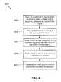
- FIG. 4is a flow chart of an example method 400 of detecting an operating temperature of a system using a ring oscillator.
- a chain of inverters of a ring oscillatormay receive and be powered by a supply voltage.
- the chain of invertersmay generate a ring oscillator signal having an associated frequency.
- the ring oscillator signalmay be sent to a frequency divider circuit.
- the frequency divider circuitmay receive the ring oscillator signal and divide the frequency of the ring oscillator signal by a divider value to generate a divider signal.
- the divider valuemay be set so that at least two cycles of noise of the supply voltage at a determined frequency is averaged. As a result, the frequency of the divider signal may be less dependent on the noise of the supply voltage than the frequency of the ring oscillator signal.
- the divider signalmay be sent to a temperature measurement module.
- the temperature measurement modulemay identify the frequency of the divider signal, and in response determine an operating temperature of the ring oscillator, which may be indicative of the operating temperature of the system.
- FIG. 5is a flow chart of another example method 500 of detecting an operating temperature of a system using a ring oscillator.
- a regulatormay receive a supply voltage.
- the regulatormay generate a regulated voltage with an associated power supply rejection (PSR).
- PSRpower supply rejection
- the amount of PSRmay vary over a range of frequencies. For example, the PSR with which the regulated voltage may be at or higher than a threshold PSR for frequencies below an open loop unity gain frequency of the regulator, and lower than the threshold PSR for frequencies above the open loop unity gain frequency.
- the regulatormay send the regulated voltage to a ring oscillator.
- a chain of inverters of the ring oscillatormay receive and be powered by the regulated voltage. In response to receiving the supply voltage, the chain of inverters may generate a ring oscillator signal having an associated frequency.
- the ring oscillator signalmay be sent to a frequency divider circuit.
- the frequency divider circuitmay receive the ring oscillator signal and divide the frequency of the ring oscillator signal by a divider value to generate a divider signal. The divider value may be set so that at least two cycles of noise of the supply voltage at a determined frequency is averaged.
- the divider valuemay be based on a ratio of a frequency of the ring oscillator signal to the open loop unity gain frequency of the regulator.
- the divider signalmay be sent to a temperature measurement module.
- the temperature measurement modulemay identify the frequency of the divider signal, and in response determine an operating temperature of the ring oscillator, which may be indicative of the operating temperature of the system.
Landscapes
- Physics & Mathematics (AREA)
- General Physics & Mathematics (AREA)
- Chemical & Material Sciences (AREA)
- Crystallography & Structural Chemistry (AREA)
- Engineering & Computer Science (AREA)
- Power Engineering (AREA)
- Oscillators With Electromechanical Resonators (AREA)
- Nonlinear Science (AREA)
Abstract
Description
Claims (12)
Priority Applications (3)
| Application Number | Priority Date | Filing Date | Title |
|---|---|---|---|
| CN201680035344.3ACN107771273B (en) | 2015-08-06 | 2016-06-09 | Ring oscillator for temperature detection in broadband supply noise environments |
| PCT/US2016/036584WO2017023418A1 (en) | 2015-08-06 | 2016-06-09 | Ring oscillators for temperature detection in wideband supply noise environments |
| TW105120833ATW201709669A (en) | 2015-08-06 | 2016-06-30 | Ring oscillators for temperature detection in wideband supply noise environments |
Applications Claiming Priority (2)
| Application Number | Priority Date | Filing Date | Title |
|---|---|---|---|
| IN4097CH2015 | 2015-08-06 | ||
| IN4097/CHE/2015 | 2015-08-06 |
Publications (2)
| Publication Number | Publication Date |
|---|---|
| US20170038264A1 US20170038264A1 (en) | 2017-02-09 |
| US10234336B2true US10234336B2 (en) | 2019-03-19 |
Family
ID=58052449
Family Applications (1)
| Application Number | Title | Priority Date | Filing Date |
|---|---|---|---|
| US14/867,734Active2037-03-01US10234336B2 (en) | 2015-08-06 | 2015-09-28 | Ring oscillators for temperature detection in wideband supply noise environments |
Country Status (3)
| Country | Link |
|---|---|
| US (1) | US10234336B2 (en) |
| CN (1) | CN107771273B (en) |
| TW (1) | TW201709669A (en) |
Families Citing this family (97)
| Publication number | Priority date | Publication date | Assignee | Title |
|---|---|---|---|---|
| US11907484B2 (en) | 2015-06-22 | 2024-02-20 | Sigmasense, Llc. | Function and orientation identification for input/output (I/O) operative touch sensor device (TSD) |
| US11397492B2 (en) | 2015-06-22 | 2022-07-26 | Sigmasense, Llc. | Enhanced mutual capacitance touch screen display with shape detection and methods for use therewith |
| US10664098B2 (en) | 2015-06-22 | 2020-05-26 | Sigmasense, Llc. | Channel driver circuit |
| CN106716314B (en) | 2015-07-06 | 2020-02-28 | 3轴数据有限责任公司 | Pen system with internal pressure inclined rotation |
| US12181352B2 (en) | 2021-06-03 | 2024-12-31 | Sigmasense, Llc. | Insole XYZ force detection system |
| US12226674B2 (en) | 2016-08-18 | 2025-02-18 | Sigmasense, Llc. | Power harvesting in a foot force detection system |
| US12225979B2 (en) | 2016-08-18 | 2025-02-18 | Sigmasense, Llc. | Variable sampling rate within a foot force detection system |
| US12194344B2 (en) | 2016-08-18 | 2025-01-14 | Sigmasense, Llc. | Plurality of layers of pressure sensors within a foot force detection system |
| US12121773B2 (en) | 2016-08-18 | 2024-10-22 | Sigmasense, Llc. | Personal athlete monitoring system |
| US12207703B2 (en) | 2016-08-18 | 2025-01-28 | Sigmasense, Llc. | Shoe to shoe communication within a foot force detection system |
| CN106875878B (en)* | 2017-02-27 | 2020-04-14 | 京东方科技集团股份有限公司 | Temperature detection circuit, display panel and display device |
| US10838530B2 (en) | 2017-09-15 | 2020-11-17 | Sigmasense, Llc. | Touchscreen display with concurrent touch and display operations |
| US12282058B2 (en) | 2017-11-23 | 2025-04-22 | Proteantecs Ltd. | Integrated circuit pad failure detection |
| TWI648528B (en)* | 2017-11-23 | 2019-01-21 | 財團法人工業技術研究院 | Resistive gas sensor and gas sensing method thereof |
| US11740281B2 (en) | 2018-01-08 | 2023-08-29 | Proteantecs Ltd. | Integrated circuit degradation estimation and time-of-failure prediction using workload and margin sensing |
| TWI828676B (en) | 2018-04-16 | 2024-01-11 | 以色列商普騰泰克斯有限公司 | Methods for integrated circuit profiling and anomaly detection and relevant computer program products |
| EP3811246A4 (en) | 2018-06-19 | 2022-03-23 | Proteantecs Ltd. | EFFICIENT INTEGRATED CIRCUIT SIMULATION AND TEST |
| US10554215B1 (en) | 2019-03-26 | 2020-02-04 | Sigmasense, Llc. | Analog to digital conversion circuit with very narrow bandpass digital filtering |
| US10895867B2 (en) | 2018-08-27 | 2021-01-19 | Sigmasense, Llc. | Analog world interfacing for automated systems |
| US11003205B2 (en) | 2019-02-04 | 2021-05-11 | Sigmasense, Llc. | Receive analog to digital circuit of a low voltage drive circuit data communication system |
| US12007421B2 (en) | 2018-08-27 | 2024-06-11 | Sigmasense, Llc. | Load sensing circuit employing sink and sense configuration |
| US11635396B2 (en) | 2018-08-27 | 2023-04-25 | Sigmasense, Llc. | Sensing device with drive sense circuit and particle sensor and methods for use therewith |
| US11550426B2 (en) | 2018-08-27 | 2023-01-10 | Sigmasense, Llc. | Sensor monitoring system |
| US11644860B2 (en) | 2018-08-27 | 2023-05-09 | Sigmasense, Llc. | Configuring a programmable drive sense unit |
| US11099032B2 (en) | 2018-08-27 | 2021-08-24 | Sigmasense, Llc. | Drive sense circuit with drive-sense line |
| US11914812B2 (en) | 2018-08-27 | 2024-02-27 | Sigmasense, Llc. | Current reference operative drive-sense circuit (DSC) |
| US11822358B2 (en) | 2018-08-27 | 2023-11-21 | Sigmasense, Llc. | Drive-sense circuit to determine effects of different electrical characteristics on load |
| US11429226B2 (en) | 2018-08-27 | 2022-08-30 | Sigmasense, Llc. | Analog-digital drive sense circuit |
| US10845985B2 (en) | 2018-09-14 | 2020-11-24 | Sigmasense, Llc. | Identification in touch systems |
| US11875005B2 (en) | 2018-09-14 | 2024-01-16 | Sigmasense, Llc. | Touch screen display with touchless indications and methods for use therewith |
| US11899867B2 (en) | 2018-09-14 | 2024-02-13 | Sigmasense, Llc. | Touch screen display with touchless gestures and methods for use therewith |
| US10908718B2 (en) | 2018-09-14 | 2021-02-02 | Sigmasense, Llc. | Large touch screen display with integrated electrodes |
| US11372510B2 (en) | 2018-11-02 | 2022-06-28 | Sigmasense, Llc. | Multi-conductor touch system |
| US10935585B2 (en) | 2018-11-19 | 2021-03-02 | Sigmasense, Llc. | Drive sense circuit with transient suppression |
| US10852857B2 (en) | 2018-11-19 | 2020-12-01 | Sigmasense, Llc. | Frequency diverse e-pen for touch sensor and e-pen systems |
| FR3089628A1 (en) | 2018-12-11 | 2020-06-12 | Commissariat A L'energie Atomique Et Aux Energies Alternatives | Temperature sensor |
| US10996728B2 (en) | 2019-01-04 | 2021-05-04 | Sigmasense, Llc. | Power supply signal conditioning system based on drive-sense circuit (DSC) processing |
| CN109450411B (en)* | 2019-01-04 | 2022-10-11 | 京东方科技集团股份有限公司 | Latch and driving method thereof and chip |
| US10831690B2 (en) | 2019-01-14 | 2020-11-10 | Sigmasense, Llc. | Channel allocation among low voltage drive circuits |
| US10915483B2 (en) | 2019-01-14 | 2021-02-09 | Sigmasense, Llc. | Low voltage drive circuit with variable oscillating characteristics and methods for use therewith |
| US11061082B2 (en) | 2019-03-18 | 2021-07-13 | Sigmasense, Llc. | Single line hall effect sensor drive and sense |
| US10671034B1 (en) | 2019-03-18 | 2020-06-02 | Sigmasense, Llc. | Motor drive input adaptation with in-line drive-sense circuit |
| US12046214B2 (en) | 2019-03-22 | 2024-07-23 | Sigmasense, Llc. | Display controller with row enable based on drive settle detection |
| US11029782B2 (en) | 2019-05-03 | 2021-06-08 | Sigmasense, Llc. | Light emitting diode (LED) touch display circuit |
| US10756578B1 (en) | 2019-05-31 | 2020-08-25 | Sigmasense, Llc. | Wireless power transfer with in-line sensing and control |
| US11131714B2 (en) | 2019-05-31 | 2021-09-28 | Sigmasense, Llc. | Battery monitoring and characterization during charging |
| US11056930B2 (en) | 2019-05-31 | 2021-07-06 | Sigmasense, Llc. | Wireless power transfer and communications |
| US11216133B2 (en) | 2019-06-10 | 2022-01-04 | Sigmasense, Llc. | Device for use with a touch screen |
| US11126297B2 (en) | 2019-06-10 | 2021-09-21 | Sigmasense, Llc. | Electronic pen with ring-back and other functionalities |
| US11018654B1 (en)* | 2019-06-11 | 2021-05-25 | Marvell Asia Pte, Ltd. | Temperature sensor with reduced power supply voltage sensitivity |
| US20220268644A1 (en)* | 2019-07-29 | 2022-08-25 | Proteantecs Ltd. | On-die thermal sensing network for integrated circuits |
| US11555687B2 (en) | 2019-08-08 | 2023-01-17 | Sigmasense, Llc. | Capacitive imaging glove |
| US10976837B2 (en) | 2019-08-20 | 2021-04-13 | Sigmasense, Llc. | User input passive device for use with an interactive display device |
| US10908641B1 (en) | 2019-10-09 | 2021-02-02 | Sigmasense, Llc. | Display generated data transmission from user device to touchscreen via user |
| US11221980B2 (en) | 2019-10-31 | 2022-01-11 | Sigmasense, Llc. | Low voltage drive circuit operable to convey data via a bus |
| US10862492B1 (en) | 2019-11-08 | 2020-12-08 | Sigmasense, Llc. | Current operative analog to digital converter (ADC) |
| US11709189B2 (en) | 2019-11-08 | 2023-07-25 | Sigmasense, Llc. | Two-element high accuracy impedance sensing circuit with increased signal to noise ratio (SNR) |
| US11190205B2 (en) | 2019-11-08 | 2021-11-30 | Sigmasense, Llc. | Single-ended direct interface dual DAC feedback photo-diode sensor |
| US11133811B2 (en) | 2019-11-08 | 2021-09-28 | Sigmasense, Llc. | High resolution analog to digital converter (ADC) with improved bandwidth |
| US12352713B2 (en) | 2019-12-30 | 2025-07-08 | Sigmasense, Llc. | Organic and/or inorganic material test system using differential drive-sense circuits |
| US11935397B2 (en) | 2019-12-30 | 2024-03-19 | Sigmasense, Llc. | Organic and inorganic test system |
| US11216109B2 (en) | 2020-01-07 | 2022-01-04 | Sigmasense, Llc. | Drive-sense control for extended sensor panels |
| US11221704B2 (en) | 2020-02-05 | 2022-01-11 | Sigmasense, Llc. | Screen-to-screen communication via touch sense elements |
| US11079888B1 (en) | 2020-02-18 | 2021-08-03 | Sigmasense, Llc. | Sensitivity region of interest processing (ROIP) for input/output (I/O) operative touch sensor device (TSD) |
| US11144160B1 (en) | 2020-03-30 | 2021-10-12 | Sigmasense, Llc. | Three-dimensional data reduction method and system |
| US11182038B2 (en) | 2020-04-08 | 2021-11-23 | Sigmasense, Llc. | Encoded data pattern touchscreen sensing system |
| EP4139697A4 (en) | 2020-04-20 | 2024-05-22 | Proteantecs Ltd. | MONITORING THE CONNECTION BETWEEN CHIPS |
| US11340995B2 (en) | 2020-05-21 | 2022-05-24 | Sigmasense, Llc. | Integrated circuit with programmable input/output module |
| US11439812B2 (en) | 2020-06-03 | 2022-09-13 | Sigmasense, Llc. | Array operative to perform distributed/patterned sensing and/or stimulation across patient bodily section |
| US11504535B2 (en) | 2020-06-03 | 2022-11-22 | Sigmasense, Llc. | Pacemaker operative to deliver impulses of pace signal and sense cardiac response via single conductor of pacemaker lead |
| WO2022009199A1 (en) | 2020-07-06 | 2022-01-13 | Proteantecs Ltd. | Integrated circuit margin measurement for structural testing |
| US11304002B2 (en) | 2020-08-12 | 2022-04-12 | Sigmasense, Llc. | Single transducer audio in/out device |
| CN114544016A (en)* | 2020-11-24 | 2022-05-27 | 平头哥(上海)半导体技术有限公司 | System on chip, temperature measurement unit, related apparatus and method |
| US11374587B1 (en) | 2021-02-25 | 2022-06-28 | Sigmasense, Llc. | Batteryless wireless sensor system |
| US20220334180A1 (en)* | 2021-04-20 | 2022-10-20 | Tektronix, Inc. | Real-equivalent-time flash array digitizer oscilloscope architecture |
| US11989378B2 (en) | 2021-04-23 | 2024-05-21 | Sigmasense, Llc. | Passive pen with variable capacitor for pressure indication |
| US11575850B2 (en) | 2021-05-28 | 2023-02-07 | Sigmasense, Llc. | Imaging device with drive-sense circuit(s) and methods for use therewith |
| US11575851B2 (en) | 2021-05-28 | 2023-02-07 | Sigmasense, Llc. | Handheld communication device with drive-sense circuit based imaging array and methods for use therewith |
| US12085618B2 (en) | 2021-06-01 | 2024-09-10 | Sigmasense, Llc. | Battery serving network with multiple loads with individual voltage sensing at each load |
| US12373070B2 (en) | 2021-06-28 | 2025-07-29 | Sigmasense, Llc. | System for detecting and validating multiuser interaction with interface elements via signaling through users bodies |
| US12360641B2 (en) | 2021-06-28 | 2025-07-15 | Sigmasense, Llc. | System for detecting and validating multiuser interaction with interface elements via perimeter sensors |
| US11679678B2 (en) | 2021-06-28 | 2023-06-20 | Sigmasense, Llc. | Vehicle system for detecting and visually conveying vehicle button interaction |
| US11733818B2 (en) | 2021-07-19 | 2023-08-22 | Sigmasense, Llc. | Identifying capacitively coupled devices |
| US11556298B1 (en) | 2021-07-30 | 2023-01-17 | Sigmasense, Llc | Generation and communication of user notation data via an interactive display device |
| US11592874B1 (en) | 2021-08-04 | 2023-02-28 | Sigmasense, Llc. | Touch sensing in a flexible/foldable touch screen display |
| US11797139B2 (en) | 2021-09-21 | 2023-10-24 | Sigmasense, Llc. | Fingerprint scanning device incorporating drive-sense circuitry |
| US11435864B1 (en) | 2021-09-28 | 2022-09-06 | Sigmasense, Llc. | Differential touch screen display |
| US11709563B2 (en) | 2021-10-26 | 2023-07-25 | Sigmasense, Llc. | Touch-based device with interlaced electrode grids |
| US12271550B2 (en) | 2022-04-28 | 2025-04-08 | Sigmasense, Llc. | Multi-frequency character transmission and detection |
| US12360630B2 (en) | 2022-06-03 | 2025-07-15 | Sigmasense, Llc. | Touch sensor device with differentiated priority sensing region |
| US11740752B1 (en) | 2022-07-13 | 2023-08-29 | Sigmasense, Llc. | Device with signal generator |
| US12175039B2 (en) | 2022-07-13 | 2024-12-24 | Sigmasense, Llc. | Touch icon offset based on touch data samples |
| US12050740B2 (en) | 2022-11-29 | 2024-07-30 | Sigmasense, Llc. | Passive device with compressible pressure assembly for Z-direction capacitance detection |
| US12013800B1 (en) | 2023-02-08 | 2024-06-18 | Proteantecs Ltd. | Die-to-die and chip-to-chip connectivity monitoring |
| US12352807B2 (en)* | 2023-04-03 | 2025-07-08 | Avago Technologies International Sales Pte. Limited | Ultra-compact and micropower circuit to monitor process, voltage, and temperature with high accuracy |
| US12135852B1 (en) | 2023-04-28 | 2024-11-05 | Sigmasense, Llc. | Spatial filtering a touch signal of a touch screen display |
| US12123908B1 (en) | 2023-09-12 | 2024-10-22 | Proteantecs Ltd. | Loopback testing of integrated circuits |
Citations (3)
| Publication number | Priority date | Publication date | Assignee | Title |
|---|---|---|---|---|
| US20070081575A1 (en) | 2005-10-07 | 2007-04-12 | Advanced Micro Devices, Inc. | Method and apparatus for temperature sensing in integrated circuits |
| US7619486B1 (en) | 2007-03-07 | 2009-11-17 | Xilinx, Inc. | Method for detecting and compensating for temperature effects |
| US7804372B2 (en) | 2006-06-09 | 2010-09-28 | Fujitsu Limited | Ring oscillator for temperature sensor, temperature sensor circuit, and semiconductor device having the same |
Family Cites Families (15)
| Publication number | Priority date | Publication date | Assignee | Title |
|---|---|---|---|---|
| JP2004146866A (en)* | 2002-10-21 | 2004-05-20 | Denso Corp | Oscillator circuit |
| US7629856B2 (en)* | 2006-10-27 | 2009-12-08 | Infineon Technologies Ag | Delay stage, ring oscillator, PLL-circuit and method |
| US7605668B2 (en)* | 2006-12-12 | 2009-10-20 | Intel Corporation | Delay stage with controllably variable capacitive load |
| JP5117823B2 (en)* | 2007-11-13 | 2013-01-16 | 日本電波工業株式会社 | Highly stable oscillator with temperature chamber |
| CN201222719Y (en)* | 2008-05-27 | 2009-04-15 | 上海复旦微电子股份有限公司 | High-precision ring oscillator |
| CN101741352A (en)* | 2008-11-10 | 2010-06-16 | 北京芯技佳易微电子科技有限公司 | Oscillator of which frequency is changed along with temperature |
| CN101769798B (en)* | 2009-01-06 | 2011-12-14 | 比亚迪股份有限公司 | Temperature detection system |
| CN102118160B (en)* | 2009-12-30 | 2013-10-23 | 意法半导体研发(深圳)有限公司 | Circuit and method for generating clock signal |
| CN102118159B (en)* | 2009-12-30 | 2013-06-05 | 意法半导体研发(深圳)有限公司 | Circuit and method for generating clock signal |
| CN103021451B (en)* | 2011-09-22 | 2016-03-30 | 复旦大学 | A kind of multi-step temperature based on threshold voltage adjustments controls self-refresh memory device and method thereof |
| US9065459B1 (en)* | 2013-03-14 | 2015-06-23 | Integrated Device Technology, Inc. | Clock generation circuits using jitter attenuation control circuits with dynamic range shifting |
| US9756699B2 (en)* | 2013-08-30 | 2017-09-05 | Avago Technologies General Ip (Singapore) Pte. Ltd | Low-power data acquisition system and sensor interface |
| CN103441760A (en)* | 2013-09-10 | 2013-12-11 | 灿芯半导体(上海)有限公司 | High-precision annular oscillator, and frequency calibration circuit and method thereof |
| CN203492007U (en)* | 2013-09-10 | 2014-03-19 | 灿芯半导体(上海)有限公司 | High-precision ring oscillator and frequency calibration circuit thereof |
| CN104753496A (en)* | 2015-04-09 | 2015-07-01 | 西安电子科技大学 | Frequency band self-tuning three-level complex band-pass filter |
- 2015
- 2015-09-28USUS14/867,734patent/US10234336B2/enactiveActive
- 2016
- 2016-06-09CNCN201680035344.3Apatent/CN107771273B/enactiveActive
- 2016-06-30TWTW105120833Apatent/TW201709669A/enunknown
Patent Citations (4)
| Publication number | Priority date | Publication date | Assignee | Title |
|---|---|---|---|---|
| US20070081575A1 (en) | 2005-10-07 | 2007-04-12 | Advanced Micro Devices, Inc. | Method and apparatus for temperature sensing in integrated circuits |
| US7455450B2 (en)* | 2005-10-07 | 2008-11-25 | Advanced Micro Devices, Inc. | Method and apparatus for temperature sensing in integrated circuits |
| US7804372B2 (en) | 2006-06-09 | 2010-09-28 | Fujitsu Limited | Ring oscillator for temperature sensor, temperature sensor circuit, and semiconductor device having the same |
| US7619486B1 (en) | 2007-03-07 | 2009-11-17 | Xilinx, Inc. | Method for detecting and compensating for temperature effects |
Non-Patent Citations (1)
| Title |
|---|
| International Search Report and Written Opinion for corresponding application No. PCT/US2016/036584 dated Aug. 16, 2016 (10 pages). |
Also Published As
| Publication number | Publication date |
|---|---|
| TW201709669A (en) | 2017-03-01 |
| CN107771273B (en) | 2020-07-21 |
| CN107771273A (en) | 2018-03-06 |
| US20170038264A1 (en) | 2017-02-09 |
Similar Documents
| Publication | Publication Date | Title |
|---|---|---|
| US10234336B2 (en) | Ring oscillators for temperature detection in wideband supply noise environments | |
| US10365318B2 (en) | Testing and setting performance parameters in a semiconductor device and method therefor | |
| US8659962B2 (en) | Semiconductor device, semiconductor system having the same and operating method thereof | |
| EP2958231A1 (en) | Semiconductor integrated circuit device with crystal resonator and manufacturing method of electronic device using the same | |
| US10840896B2 (en) | Digital measurement circuit and memory system using the same | |
| KR20220131979A (en) | Calibration circuits, memories and calibration methods | |
| US7804371B2 (en) | Systems, modules, chips, circuits and methods with delay trim value updates on power-up | |
| EP1858163B1 (en) | Oscillator circuit generating oscillating signal having stable cycle | |
| EP2128736B1 (en) | Electronic circuit device | |
| KR100845773B1 (en) | Power-up signal trip point measuring circuit of semiconductor memory device and power-up signal trip point level measuring method using same | |
| KR102666336B1 (en) | Clock generation circuit, memory and clock duty cycle calibration method | |
| WO2017023418A1 (en) | Ring oscillators for temperature detection in wideband supply noise environments | |
| JP5190767B2 (en) | MONITOR CIRCUIT AND RESOURCE CONTROL METHOD | |
| KR102718902B1 (en) | Memory | |
| US8581641B2 (en) | Power-up signal generation circuit | |
| KR102355437B1 (en) | Semiconductor apparatus including clock generation circuit and semiconductor system | |
| CN114420191B (en) | Memory device | |
| CN106297897B (en) | Memory cell and test method thereof | |
| TWI494946B (en) | Dll system in memory device with wide frequency application and method for dynamically changing power supply of delay line in dll system in memory device with frequency application | |
| US11428718B2 (en) | Semiconductor device |
Legal Events
| Date | Code | Title | Description |
|---|---|---|---|
| AS | Assignment | Owner name:SANDISK TECHNOLOGIES INC., TEXAS Free format text:ASSIGNMENT OF ASSIGNORS INTEREST;ASSIGNORS:ODEDARA, BHAVIN;THIMMAIAH, JAYANTH MYSORE;REEL/FRAME:036672/0384 Effective date:20150928 | |
| AS | Assignment | Owner name:SANDISK TECHNOLOGIES LLC, TEXAS Free format text:CHANGE OF NAME;ASSIGNOR:SANDISK TECHNOLOGIES INC;REEL/FRAME:038812/0954 Effective date:20160516 | |
| STCF | Information on status: patent grant | Free format text:PATENTED CASE | |
| MAFP | Maintenance fee payment | Free format text:PAYMENT OF MAINTENANCE FEE, 4TH YEAR, LARGE ENTITY (ORIGINAL EVENT CODE: M1551); ENTITY STATUS OF PATENT OWNER: LARGE ENTITY Year of fee payment:4 | |
| AS | Assignment | Owner name:SANDISK TECHNOLOGIES, INC., CALIFORNIA Free format text:ASSIGNMENT OF ASSIGNORS INTEREST;ASSIGNOR:SANDISK TECHNOLOGIES LLC;REEL/FRAME:069796/0423 Effective date:20241227 | |
| AS | Assignment | Owner name:SANDISK TECHNOLOGIES, INC., CALIFORNIA Free format text:PARTIAL RELEASE OF SECURITY INTERESTS;ASSIGNOR:JPMORGAN CHASE BANK, N.A., AS AGENT;REEL/FRAME:071382/0001 Effective date:20250424 Owner name:JPMORGAN CHASE BANK, N.A., AS COLLATERAL AGENT, ILLINOIS Free format text:SECURITY AGREEMENT;ASSIGNOR:SANDISK TECHNOLOGIES, INC.;REEL/FRAME:071050/0001 Effective date:20250424 |