US10211146B2 - Air gap over transistor gate and related method - Google Patents
Air gap over transistor gate and related methodDownload PDFInfo
- Publication number
- US10211146B2 US10211146B2US15/152,794US201615152794AUS10211146B2US 10211146 B2US10211146 B2US 10211146B2US 201615152794 AUS201615152794 AUS 201615152794AUS 10211146 B2US10211146 B2US 10211146B2
- Authority
- US
- United States
- Prior art keywords
- layer
- air gap
- dielectric
- metal
- interconnect
- Prior art date
- Legal status (The legal status is an assumption and is not a legal conclusion. Google has not performed a legal analysis and makes no representation as to the accuracy of the status listed.)
- Active
Links
Images


Classifications
- H—ELECTRICITY
- H01—ELECTRIC ELEMENTS
- H01L—SEMICONDUCTOR DEVICES NOT COVERED BY CLASS H10
- H01L23/00—Details of semiconductor or other solid state devices
- H01L23/52—Arrangements for conducting electric current within the device in operation from one component to another, i.e. interconnections, e.g. wires, lead frames
- H01L23/522—Arrangements for conducting electric current within the device in operation from one component to another, i.e. interconnections, e.g. wires, lead frames including external interconnections consisting of a multilayer structure of conductive and insulating layers inseparably formed on the semiconductor body
- H01L23/5222—Capacitive arrangements or effects of, or between wiring layers
- H—ELECTRICITY
- H01—ELECTRIC ELEMENTS
- H01L—SEMICONDUCTOR DEVICES NOT COVERED BY CLASS H10
- H01L21/00—Processes or apparatus adapted for the manufacture or treatment of semiconductor or solid state devices or of parts thereof
- H01L21/70—Manufacture or treatment of devices consisting of a plurality of solid state components formed in or on a common substrate or of parts thereof; Manufacture of integrated circuit devices or of parts thereof
- H01L21/71—Manufacture of specific parts of devices defined in group H01L21/70
- H01L21/768—Applying interconnections to be used for carrying current between separate components within a device comprising conductors and dielectrics
- H01L21/76801—Applying interconnections to be used for carrying current between separate components within a device comprising conductors and dielectrics characterised by the formation and the after-treatment of the dielectrics, e.g. smoothing
- H01L21/7682—Applying interconnections to be used for carrying current between separate components within a device comprising conductors and dielectrics characterised by the formation and the after-treatment of the dielectrics, e.g. smoothing the dielectric comprising air gaps
- H—ELECTRICITY
- H01—ELECTRIC ELEMENTS
- H01L—SEMICONDUCTOR DEVICES NOT COVERED BY CLASS H10
- H01L23/00—Details of semiconductor or other solid state devices
- H01L23/48—Arrangements for conducting electric current to or from the solid state body in operation, e.g. leads, terminal arrangements ; Selection of materials therefor
- H01L23/482—Arrangements for conducting electric current to or from the solid state body in operation, e.g. leads, terminal arrangements ; Selection of materials therefor consisting of lead-in layers inseparably applied to the semiconductor body (electrodes)
- H01L23/4821—Bridge structure with air gap
- H01L27/1203—
- H—ELECTRICITY
- H10—SEMICONDUCTOR DEVICES; ELECTRIC SOLID-STATE DEVICES NOT OTHERWISE PROVIDED FOR
- H10D—INORGANIC ELECTRIC SEMICONDUCTOR DEVICES
- H10D30/00—Field-effect transistors [FET]
- H10D30/01—Manufacture or treatment
- H10D30/021—Manufacture or treatment of FETs having insulated gates [IGFET]
- H—ELECTRICITY
- H10—SEMICONDUCTOR DEVICES; ELECTRIC SOLID-STATE DEVICES NOT OTHERWISE PROVIDED FOR
- H10D—INORGANIC ELECTRIC SEMICONDUCTOR DEVICES
- H10D30/00—Field-effect transistors [FET]
- H10D30/60—Insulated-gate field-effect transistors [IGFET]
- H—ELECTRICITY
- H10—SEMICONDUCTOR DEVICES; ELECTRIC SOLID-STATE DEVICES NOT OTHERWISE PROVIDED FOR
- H10D—INORGANIC ELECTRIC SEMICONDUCTOR DEVICES
- H10D86/00—Integrated devices formed in or on insulating or conducting substrates, e.g. formed in silicon-on-insulator [SOI] substrates or on stainless steel or glass substrates
- H10D86/201—Integrated devices formed in or on insulating or conducting substrates, e.g. formed in silicon-on-insulator [SOI] substrates or on stainless steel or glass substrates the substrates comprising an insulating layer on a semiconductor body, e.g. SOI
- H—ELECTRICITY
- H01—ELECTRIC ELEMENTS
- H01L—SEMICONDUCTOR DEVICES NOT COVERED BY CLASS H10
- H01L23/00—Details of semiconductor or other solid state devices
- H01L23/48—Arrangements for conducting electric current to or from the solid state body in operation, e.g. leads, terminal arrangements ; Selection of materials therefor
- H01L23/482—Arrangements for conducting electric current to or from the solid state body in operation, e.g. leads, terminal arrangements ; Selection of materials therefor consisting of lead-in layers inseparably applied to the semiconductor body (electrodes)
- H01L23/485—Arrangements for conducting electric current to or from the solid state body in operation, e.g. leads, terminal arrangements ; Selection of materials therefor consisting of lead-in layers inseparably applied to the semiconductor body (electrodes) consisting of layered constructions comprising conductive layers and insulating layers, e.g. planar contacts
- H—ELECTRICITY
- H01—ELECTRIC ELEMENTS
- H01L—SEMICONDUCTOR DEVICES NOT COVERED BY CLASS H10
- H01L23/00—Details of semiconductor or other solid state devices
- H01L23/52—Arrangements for conducting electric current within the device in operation from one component to another, i.e. interconnections, e.g. wires, lead frames
- H01L23/522—Arrangements for conducting electric current within the device in operation from one component to another, i.e. interconnections, e.g. wires, lead frames including external interconnections consisting of a multilayer structure of conductive and insulating layers inseparably formed on the semiconductor body
- H01L23/5226—Via connections in a multilevel interconnection structure
- H—ELECTRICITY
- H01—ELECTRIC ELEMENTS
- H01L—SEMICONDUCTOR DEVICES NOT COVERED BY CLASS H10
- H01L23/00—Details of semiconductor or other solid state devices
- H01L23/52—Arrangements for conducting electric current within the device in operation from one component to another, i.e. interconnections, e.g. wires, lead frames
- H01L23/522—Arrangements for conducting electric current within the device in operation from one component to another, i.e. interconnections, e.g. wires, lead frames including external interconnections consisting of a multilayer structure of conductive and insulating layers inseparably formed on the semiconductor body
- H01L23/532—Arrangements for conducting electric current within the device in operation from one component to another, i.e. interconnections, e.g. wires, lead frames including external interconnections consisting of a multilayer structure of conductive and insulating layers inseparably formed on the semiconductor body characterised by the materials
- H01L23/53204—Conductive materials
- H01L23/53209—Conductive materials based on metals, e.g. alloys, metal silicides
- H01L23/53214—Conductive materials based on metals, e.g. alloys, metal silicides the principal metal being aluminium
- H01L23/53223—Additional layers associated with aluminium layers, e.g. adhesion, barrier, cladding layers
- H—ELECTRICITY
- H01—ELECTRIC ELEMENTS
- H01L—SEMICONDUCTOR DEVICES NOT COVERED BY CLASS H10
- H01L23/00—Details of semiconductor or other solid state devices
- H01L23/52—Arrangements for conducting electric current within the device in operation from one component to another, i.e. interconnections, e.g. wires, lead frames
- H01L23/522—Arrangements for conducting electric current within the device in operation from one component to another, i.e. interconnections, e.g. wires, lead frames including external interconnections consisting of a multilayer structure of conductive and insulating layers inseparably formed on the semiconductor body
- H01L23/532—Arrangements for conducting electric current within the device in operation from one component to another, i.e. interconnections, e.g. wires, lead frames including external interconnections consisting of a multilayer structure of conductive and insulating layers inseparably formed on the semiconductor body characterised by the materials
- H01L23/53204—Conductive materials
- H01L23/53209—Conductive materials based on metals, e.g. alloys, metal silicides
- H01L23/53228—Conductive materials based on metals, e.g. alloys, metal silicides the principal metal being copper
- H01L23/53238—Additional layers associated with copper layers, e.g. adhesion, barrier, cladding layers
- H—ELECTRICITY
- H01—ELECTRIC ELEMENTS
- H01L—SEMICONDUCTOR DEVICES NOT COVERED BY CLASS H10
- H01L23/00—Details of semiconductor or other solid state devices
- H01L23/52—Arrangements for conducting electric current within the device in operation from one component to another, i.e. interconnections, e.g. wires, lead frames
- H01L23/522—Arrangements for conducting electric current within the device in operation from one component to another, i.e. interconnections, e.g. wires, lead frames including external interconnections consisting of a multilayer structure of conductive and insulating layers inseparably formed on the semiconductor body
- H01L23/532—Arrangements for conducting electric current within the device in operation from one component to another, i.e. interconnections, e.g. wires, lead frames including external interconnections consisting of a multilayer structure of conductive and insulating layers inseparably formed on the semiconductor body characterised by the materials
- H01L23/5329—Insulating materials
- H01L23/53295—Stacked insulating layers
Definitions
- the present disclosurerelates to semiconductor devices, and more specifically, to an air gap over a transistor gate and method of forming the same.
- the air gapreduces off-state capacitance (C off ) in applications such as radio frequency switches in semiconductor-on-insulator (SOI) substrates.
- SOIsemiconductor-on-insulator
- Radio frequency (RF) switchesare widely used in telecommunications equipment such as smartphones to route high frequency telecommunications signals through transmission paths.
- RF switchesare commonly used in smartphones to allow use with different digital wireless technology standards used in different geographies.
- Current RF switchesare generally fabricated using semiconductor-on-insulator (SOI) substrates.
- SOI substratestypically use a layered silicon-insulator-silicon substrate in place of a more conventional silicon substrate (bulk substrate).
- SOI-based devicesdiffer from conventional silicon-built devices in that the silicon junction is above an electrical insulator, typically silicon dioxide or (less commonly) sapphire.
- R onwhich is the resistance of the switch when power is switched on
- C offoff-state capacitance
- R onis preferred to be as low as possible when the RF switch is on to reduce the power consumption
- C offshould be minimized to reduce undesired coupling noise.
- lowering either R on or C offresults in the opposite effect in the other parameter.
- a first aspect of the disclosureis directed to a method of forming an air gap for a semiconductor device, the method comprising: forming an air gap mask exposing a portion of an interconnect layer over a device layer, the device layer including a transistor gate therein; etching an opening through the interconnect layer using the air gap mask above the transistor gate, the opening exposing sidewalls of a dielectric of the interconnect layer; removing the air gap mask; recessing the exposed sidewalls of the dielectric of the interconnect layer in the opening; and forming an air gap over the transistor gate by depositing an air gap capping layer to seal the opening at a surface of the interconnect layer.
- a second aspect of the disclosureincludes a semiconductor device, comprising: a transistor gate in a device layer; an interconnect layer over the device layer; and an air gap extending through the interconnect layer above the transistor gate.
- a third aspect of the disclosurerelated to a radio frequency semiconductor-on-insulator (RFSOI) switch, comprising: a transistor gate in a semiconductor-on-insulator (SOI) layer of an SOI substrate; an interconnect layer over the SOI layer, the interconnect layer including a local interconnect layer over the SOI layer and a first metal layer over the local interconnect layer; and an air gap extending through a dielectric of the interconnect layer above the transistor gate.
- RFSOIradio frequency semiconductor-on-insulator
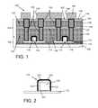
- FIG. 1shows a cross-sectional view of embodiments of a method according to the disclosure.
- FIG. 2shows an enlarged cross-sectional view of an illustrative transistor gate.
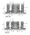
- FIGS. 3A-Eshow cross-sectional views of etching an opening according to embodiments of a method of the disclosure.
- FIG. 4shows a cross-sectional view of removing an air gap mask according to embodiments of the disclosure.
- FIGS. 5-7show plan views of embodiments of a structure partially through a method according to the disclosure.
- FIG. 8A-Cshow cross-sectional views of recessing an opening according to embodiments of the disclosure.
- FIG. 9shows an enlarged cross-sectional view of a detail per the FIG. 8B embodiment.
- FIG. 10shows a cross-sectional view of a method and a semiconductor device such as a radio frequency SOI switch with an air gap over a transistor gate thereof according to embodiments of the disclosure.
- FIGS. 11 and 12shows cross-sectional views of alternative methods and alternative semiconductor devices with an air gap over a transistor gate thereof according to embodiments of the disclosure.
- the present disclosurerelates to methods of forming semiconductor devices including an air gap over a transistor gate for reducing the capacitance between the transistor gate and adjacent wires, contacts, and vias used to contact the source and drain of the transistor.
- This capacitance reductionmay decrease the off-state capacitance of the transistor when it is used in in such applications as radio frequency (RF) switches in semiconductor-on-insulator (SOI) substrates or bulk (non-SOI) substrates.
- RFradio frequency
- SOIsemiconductor-on-insulator
- non-SOIbulk
- FIG. 1a cross-sectional view of a first process of a method of forming an air gap for a semiconductor device according to embodiments of the disclosure is illustrated.
- FIG. 1shows a semiconductor device 100 after formation of a device layer 102 and an interconnect layer 104 .
- Device layer 102is illustrated as including a semiconductor-on-insulator (SOI) substrate 106 including a semiconductor substrate 108 with an insulator layer 110 thereover and a semiconductor-on-insulator (SOI) layer 112 thereover.
- SOIsemiconductor-on-insulator
- a portion or entire semiconductor substrate 108 and/or SOI layer 112may be strained.
- SOI layer 112may be strained.
- SOI layer 112may be segmented by shallow trench isolations (STI) 114 .
- Insulator layer 110may include any appropriate dielectric material for the application desired, e.g., silicon oxide (SiO x ) or (less commonly) sapphire. Insulator layer 110 and/or STI 114 may also include the same material, such as silicon dioxide or any other interlayer dielectric material described herein.
- Device layer 102also includes a number of transistors 116 formed therein.
- Each transistor 116may include any now known or later developed transistor structure such as doped source/drain regions (not labeled) in SOI layer 112 having a transistor gate 118 thereover and therebetween.
- FIG. 2shows an enlarged cross-sectional view of an illustrative transistor gate 118 .
- Each transistor gate 118may include, among other structures, a body 120 of polysilicon or a metal gate conductor (commonly referred to collectively as “PC”), spacers 122 about body 120 , a gate dielectric 124 under body 120 , a silicide layer 125 over body 120 (i.e., a silicon-metal alloy), and an etch stop layer 126 over silicide layer 125 and/or spacers 122 .
- PCmetal gate conductor
- Spacers 122may include any now known or later developed spacer material such as silicon nitride (Si 3 N 4 ), and gate dielectric 124 may include any now known or later developed gate dielectric material such as: hafnium silicate (HfSiO), hafnium oxide (HfO 2 ), zirconium silicate (ZrSiO x ), zirconium oxide (ZrO 2 ), silicon oxide (SiO 2 ), silicon nitride (Si 3 N 4 ), silicon oxynitride (SiON), high-k material or any combination of these materials.
- Etch stop layer 126may include any now known or later developed etch stop material such as silicon nitride.
- Silicide layer 125may include any now known or later developed silicide material, e.g., titanium, nickel, cobalt, etc. As understood, each transistor gate 118 may run into, out of, or across the page as illustrated.
- interconnect layer 104may include a number of layers including a contact or local interconnect layer 130 (commonly referred to as a contact area (CA) layer) and a first metal layer 132 .
- Each layer 130 , 132may include an interlayer dielectric (ILD) layer 134 , 136 , respectively.
- ILDinterlayer dielectric
- ILD layers 134 , 136may include may but are not limited to: silicon nitride (Si 3 N 4 ), silicon oxide (SiO 2 ), fluorinated SiO 2 (FSG), hydrogenated silicon oxycarbide (SiCOH), porous SiCOH, boro-phospho-silicate glass (BPSG), silsesquioxanes, carbon (C) doped oxides (i.e., organosilicates) that include atoms of silicon (Si), carbon (C), oxygen (O), and/or hydrogen (H), thermosetting polyarylene ethers, SiLK (a polyarylene ether available from Dow Chemical Corporation), a spin-on silicon-carbon containing polymer material available from JSR Corporation, other low dielectric constant ( ⁇ 3.9) material, or layers thereof.
- SiLKa polyarylene ether available from Dow Chemical Corporation
- spin-on silicon-carbon containing polymer materialavailable from JSR Corporation, other low dielectric constant ( ⁇ 3.9) material, or layers thereof.
- Each layer 130 , 132may also include a respective cap layer 138 , 140 at an upper surface thereof.
- Each cap layer 138 , 140may include one or more layers, for example, a silicon oxide layer 142 and an etch stop layer 144 , formed from silicon nitride (nitride), silicon carbo nitride (SiCN), etc., as known in the art.
- silicon nitridenitride
- SiCNsilicon carbo nitride
- various other forms of cap layersmay also be employed.
- cap layers 138 , 140are illustrated as identical, they can be different materials, thicknesses, etc.
- a number of contacts 150may extend through ILD layer 134 of contact or local interconnect layer 130 (hereafter “local interconnect layer 130 ”) to various parts of device layer 102 .
- contacts 150extend to source/drain regions of transistors 116 .
- each contact 150may include a conductor such as aluminum or copper, within a refractory metal liner of ruthenium; however, other refractory metals such as tantalum (Ta), titanium (Ti), tungsten (W), iridium (Ir), rhodium (Rh) and platinum (Pt), etc., or mixtures of thereof, may also be employed.
- contacts 150extend mostly vertically within semiconductor device 100 to connect conductors in layers thereof, i.e., vertically on page as illustrated.
- First metal layer 132may include a number of metal wires 152 therein. Each metal wire 152 may use the same materials as listed for contacts 150 .
- metal wires 152extend mostly horizontally or laterally in a layer within semiconductor device 100 to connect contacts 150 therein, i.e., into, out of, or across a page as illustrated.
- first metal layer 132may include a metal wire 152 extending laterally parallel to transistor gate 118 in device layer 102 , i.e., vertically above but parallel to transistor gate 118 .
- Semiconductor device 100as illustrated in FIG.
- contacts 150 and wires 152are shown in FIG. 1 as single damascene levels, they could be formed using as dual damascene levels containing refractory metal lined copper or tungsten, as known in the art.
- Depositingmay include any now known or later developed techniques appropriate for the material to be deposited including but not limited to, for example: chemical vapor deposition (CVD), low-pressure CVD (LPCVD), plasma-enhanced CVD (PECVD), semi-atmosphere CVD (SACVD) and high density plasma CVD (HDPCVD), rapid thermal CVD (RTCVD), ultra-high vacuum CVD (UHVCVD), limited reaction processing CVD (LRPCVD), metalorganic CVD (MOCVD), sputtering deposition, ion beam deposition, electron beam deposition, laser assisted deposition, thermal oxidation, thermal nitridation, spin-on methods, physical vapor deposition (PVD), atomic layer deposition (ALD), chemical oxidation, molecular beam epitaxy (MBE), plating, evaporation.
- CVDchemical vapor deposition
- LPCVDlow-pressure CVD
- PECVDplasma-enhanced CVD
- SACVDsemi-
- FIG. 1also shows forming an air gap mask 160 exposing a portion 162 of interconnect layer 104 over device layer 102 .
- Mask 160may be formed, for example, post first metal layer 132 damascene planarization, e.g., via chemical mechanical polishing (CMP), and may include any now known or later developed masking material.
- CMPchemical mechanical polishing
- Mask 160is patterned and etched in a conventional fashion to create openings 164 therein.
- transistor gate 118 widthis approximately 200 nm and openings 164 in air gap mask 160 may have a size of approximately 0.16 micrometers (um) to 0.24 um, and in particular, 0.2 um. These widths could scale with larger and smaller channel transistor width or with larger or smaller contact 150 and wire 152 width.
- FIGS. 3A-Eshow etching an opening 166 through interconnect layer 104 using air gap mask 160 above transistor gate 118 . Opening 166 exposes sidewalls 170 of a dielectric 134 , 136 of interconnect layer 104 .
- Etchinggenerally refers to the removal of material from a substrate (or structures formed on the substrate), and is often performed with a mask in place so that material may selectively be removed from certain areas of the substrate, while leaving the material unaffected, in other areas of the substrate. There are generally two categories of etching, (i) wet etch, and (ii) dry etch.
- wet etchis performed with a solvent (such as an acid or a base) which may be chosen for its ability to selectively dissolve a given material (such as oxide), while, leaving another material (such as polysilicon or nitride) relatively intact.
- a solventsuch as an acid or a base
- a wet etchwill generally etch a homogeneous material (e.g., oxide) isotopically, but a wet etch may also etch single-crystal materials (e.g. silicon wafers) anisotopically.
- Dry etchmay be performed using a plasma. Plasma systems can operate in several modes by adjusting the parameters of the plasma.
- etchingproduces energetic free radicals, neutrally charged, that react at the surface of the wafer. Since neutral particles attack the wafer from all angles, this process is isotopic. Ion milling, or sputter etching, bombards the wafer with energetic ions of noble gases which approach the wafer approximately from one direction, and therefore this process is highly anisotopic.
- Reactive-ion etchingRIE
- the etching(indicated by arrows in FIG. 3A only) may include a RIE.
- opening 166may extend above transistor gate 118 to a number of different depths.
- etching opening 166may cease when: opening 166 meets or extends to etch stop layer 126 ( FIG. 3A ); recesses etch stop layer 126 ( FIG. 3B ); removes (extends beyond) etch stop layer 126 exposing silicide layer 125 ( FIG. 3C ); exposes body 120 ( FIG. 3D ), e.g., if silicide layer 125 is not present or has been removed entirely; or does not expose etch stop layer 126 by not extending through dielectric layer 134 above gate 118 ( FIG. 3E ). Accordingly, the etching of FIGS. 3A-E can be controlled to select the extent of exposure of an upper surface 168 of transistor gate 118 .
- FIG. 4shows the semiconductor device after removing air gap mask 160 (on the FIG. 3B embodiment only for brevity).
- Air gap mask 160FIGS. 3A-E ) may be removed using any now known or later developed resist strip, in-situ or ex-situ.
- FIGS. 5-7show plan or top views of embodiments of the structure after FIG. 4 processing, i.e., partially through the methods according to the disclosure.
- FIGS. 5-7illustrate example layouts of openings 166 , and hence, air gaps 188 ( FIG. 10 ) to be formed thereby, as will be described herein.
- the cross-sections of FIGS. 5-7are taken through dielectric 134 in FIG. 4 .
- FIGS. 5-7show SOI layer 112 (active area) having gates 118 formed thereover with contacts 150 extending from gate 118 and SOI layer 112 .
- Metal wires 152are shown coupling certain contacts 150 over SOI layer 112 . As illustrated metal wires 152 run parallel to certain gates, labeled 118 A.
- openings 166can take a variety of forms.
- openings 166are etched as laterally elongate openings above transistor gate 118 . That is, rather than simple vertical openings, openings 166 have a length, e.g., just short of a transistor gate 118 that they parallel.
- a portion of opening 166may be etched in a laterally disposed T-shape 174 , i.e., in a T-shape laid out horizontally in the plane of the page.
- openings 166do not expose contacts 150 or metal wires 152 , i.e., some of dielectric 134 , 136 ( FIG.
- openings 166 through interconnect layer 104may be designed such that they are narrower adjacent to contacts 150 (or subsequently formed vias 194 ( FIGS. 10-12 )) to reduce the likelihood of contact 150 intersecting air gap 188 ( FIG. 10 ). That is, opening 166 may be narrower (width W 2 ) laterally adjacent a contact 150 (or vias 194 ( FIGS. 10-12 )) and wider (width W 1 ) laterally between contacts 150 (or vias 194 ( FIGS. 10-12 )) to reduce the likelihood of contact 150 (or via 194 ) being exposed by air gap 188 , which would allow filling of air gap 188 with a conductor.
- air gap 188may have the same layout, i.e., as shown in FIG. 6 , with a first width W 1 laterally adjacent a contact 150 (or via 194 ) and a second width W 2 wider than first width W 1 laterally between contacts 150 (or vias 194 ).
- the variable widthcan occur in local interconnect layer 130 and/or first metal layer 132 and/or subsequent layers 190 ( FIGS. 10-12 ). That is, air gap 188 would have a similar width variation regardless of whether viewed through local interconnect layer 130 , first metal layer 132 or a subsequent air gap capping layer 190 ( FIGS. 10-12 ).
- FIG. 10-12In FIG.
- openings 166may be etched as many, not necessarily elongated, disconnected openings.
- some of openings 166 in FIG. 7are designed not to be adjacent to contact 150 (or subsequently formed vias 194 (FIGS. 10-12)) to reduce the likelihood of contact 150 or via 194 intersecting air gap 188 ( FIGS. 8A-C ), which would allow filling of air gap 188 with a conductor.
- Selecting amongst the various lengths of opening 166 shown in FIGS. 5-7one can eventually establish air gaps 188 ( FIG. 10 ) that will optimally reduce on-resistance and off-capacitance of a semiconductor device 200 ( FIG.
- Air gap openings 166may also be formed with different widths, as shown in FIG. 6 . Air gap opening 166 width may be reduced in width, for example, near contacts 150 or vias 194 to reduce the likelihood of the air gap 188 intersecting the contacts or vias, due to misalignment.
- FIGS. 8A-Cshow an optional recessing of exposed sidewalls 170 of dielectric 134 , 136 of interconnect layer 104 in opening 166 .
- recessing sidewalls 170acts to enlarge opening 166 and thus air gaps 188 ( FIG. 10 ), reducing the effective dielectric constant of interconnect layer 104 while leaving the air gap top opening to be sealed in the next process step narrower than the air gap itself.
- silicon oxide filmsare used for local interconnect and first metal layers 130 , 132 and silicon nitride is used for cap layer(s) 138 , 140 , then a hydrofluoric acid (HF) wet etch could be used for this recess (indicated by arrows in FIG.
- HFhydrofluoric acid
- FIG. 9shows that opening widths BB and CC are wider than air gap top opening AA.
- the recessingmay include, for example, a wet etch as described elsewhere herein. In one embodiment, shown in FIGS.
- recessing exposed sidewalls 170 of dielectric 134 , 136 of interconnect layer 104 in opening 166may expose an edge 180 , 182 of at least one of the local interconnect cap layer 130 and first metal cap layer 132 in opening 166 .
- edges 182assist in closing opening 166 to form an air gap, e.g., by facilitating the pinching off of opening 166 .
- recessing at this stagecan also be used to further deepen opening 166 .
- recessingoccurred after air gap mask removal 160 in FIG. 4 , but with the FIG. 3E embodiment in which dielectric layer 134 remains above transistor gate 118 , recessing as shown in FIGS. 8A-C can further deepen opening 166 to any of the depths shown in FIGS. 3A-E .
- recessingmay extend opening 166 thereto ( FIG. 8A , left side).
- recessingcould extend opening 166 to recess etch stop layer 126 ( FIG.
- FIG. 10shows forming an air gap 188 over transistor gate 118 by depositing an air gap capping layer 190 to seal opening 166 ( FIG. 9 ) at a surface of interconnect layer 104 .
- air gap 188is vertically aligned with transistor gate 118 , although perfect alignment is not necessary in all cases.
- Air gap capping layer 190may include any dielectric material capable of sealing opening 166 and acting as an ILD for a first via layer (not shown) to be formed therein.
- air gap capping layer 190may include chemical vapor deposited (CVD) dielectric.
- CVDchemical vapor deposited
- air gap capping layer 190may include a plasma-enhanced chemical vapor deposition (PECVD) silane oxide.
- PECVDplasma-enhanced chemical vapor deposition
- PECVD silane oxidemay be chosen because it has very poor step coverage, resulting in a larger air gap volume.
- air gap capping layer 190may include a thin silicon nitride layer with an ILD oxide, such as a PECVD TEOS-based, PVD, or similar oxide (individual layers not shown for clarity).
- Edges 182 of first metal cap layer 140 ( FIG. 1 ) of first metal layer 132act to pinch opening 166 to assist in closing air gap 188 .
- Air gap 188does not expose any contact 150 or metal wire 152 , i.e., dielectric 134 , 136 of interconnect layer 104 about air gap 188 covers any conductive wire 152 in first metal layer 132 or any conductive contact 150 in local interconnect layer 130 .
- Air gap 188may have any of the lateral layouts of opening 166 , as shown in FIGS. 5-7 .
- first metal layer 132may include a metal wire 152 ( FIG. 10 ) extending laterally parallel to transistor gate 118 (see FIGS. 5-7 ) in device layer 102 .
- air gap 188vertically extends above and below metal wire 152 , i.e., below dielectric 136 of first metal layer 132 and above metal wire 152 in cap layer 190 . Most notably, air gap 188 extends above an upper surface of first metal layer 132 . As also shown in FIG.
- air gap 188may vertically extend only partially into air gap capping layer 190 so that layer 190 can act as a first via layer ILD with minimal interference from air gap 188 .
- Vias 194 to another metal layermay be formed in air gap capping layer 190 , using any conventional or later developed technique.
- a thin layer 192 of air gap capping layer 190may selectively cover transistor gate 118 in opening 116 , thus providing additional control over the extent to which transistor gate 118 is exposed to air gap 188 .
- Air gap capping layer 190seals opening 166 regardless of the lateral layout it takes from FIGS.
- opening 166can be controlled to avoid exposing thereof by subsequently formed vias 194 , thus preventing via 194 conductor from entering air gap 188 .
- FIGS. 11 and 12Alternative air gap embodiments are shown in FIGS. 11 and 12 .
- FIG. 11shows an air gap 288 which has a shallower etch depth ( FIGS. 3A-E ) to avoid touching transistor gate 118 .
- FIG. 12shows an air gap 388 which had the recess etch shown in FIGS. 8A-C reduced or eliminated. This structure has a smaller air gap 388 than shown in FIG. 11 but avoids exposing the dielectrics of local interconnect layer 130 and first metal layer 132 to the etchant.
- semiconductor device 200may include transistor gate 118 in device layer 102 .
- Transistor gate 118may include body 120 , silicide layer 125 over body 120 , and etch stop layer 126 over silicide layer 125 .
- Transistor 116can take the form of any now known or later developed complementary metal-oxide semiconductor (CMOS) field effect transistor (FET).
- CMOScomplementary metal-oxide semiconductor
- FETfield effect transistor
- Semiconductor device 200can also include interconnect layer 104 over device layer 102 .
- Interconnect layer 104may include one or more interconnect layers, for example, local interconnect layer 130 and first metal layer 132 .
- Semiconductor device 200also includes air gap 188 extending through interconnect layer 104 above transistor gate 118 .
- the extent to which transistor gate 118 , i.e., upper surface 168 thereof, is exposed and/or what part of gate 118 is exposed to air gap 188can be controlled through the etching, recessing and capping processes.
- air gap 188can be formed with any embodiment of opening 166 provided. That is, air gap 188 may meet or extend to etch stop layer 126 (left side of FIG. 10 ); extend into etch stop layer 126 (see FIGS.
- an air gapmay contact dielectric such as dielectric layer 134 or thin layer 192 of cap layer 190 , contact etch top layer 126 (either full or recessed), contact silicide layer 125 or contact body 120 of transistor gate 118 .
- dielectric 134 , 136 of interconnect layer 104 about air gap 188covers any conductor, e.g., any conductive wire 152 in first metal layer 132 or any conductive contact 150 in local interconnect layer 130 .
- Edges 180 and/or 182 of at least one of local interconnect cap layer(s) 138 and first metal cap layer(s) 140may extend into air gap 188 . As shown in FIG.
- first metal cap layer 140may have a width AA in the air gap (where opening 166 is positioned in FIG. 9 ) that is less than a width BB of the air gap (where opening 166 is positioned in FIG. 9 ) in dielectric 136 of first metal layer 132 below first metal cap layer 140 .
- edges 182 of first metal cap layer 140act to pinch off dielectric 190 , allowing for a lesser amount of dielectric 190 to seal opening 166 .
- etch stop layer 126 of transistor gate 118may be recessed ( FIGS. 4 and 8 ).
- air gap 188may have a height-to-width ratio greater than approximately 3 to 1, e.g., 4 to 1.
- air gap 188may have a width of approximately 1-2 um, and a height of approximately 8-10 um.
- air gap 188may be laterally elongated or T-shaped-like opening 166 used to form it.
- semiconductor device 200can be used to form a variety of devices such as a radio frequency semiconductor-on-insulator (RFSOI) switch, a low amplitude amplifier, a power amplifier, etc.
- RFSOIradio frequency semiconductor-on-insulator
- Use of air gap 188 , 288 or 388 over transistor gate 118 according to the various embodiments of the disclosureprovides a mechanism to reduce off-capacitance and on-resistance of any device using it by controlling one of the main contributors of intrinsic FET capacitance: the effective dielectric constant of local interconnect layer 130 and first metal layer 132 .
- an off-capacitance reduction of between approximately 15-60%was observed, with an effective dielectric constant of interconnect layer 104 lowered from approximately 4 to 2 using air gap 188 , 288 or 388 .
- the method as described aboveis used in the fabrication of integrated circuit chips.
- the resulting integrated circuit chipscan be distributed by the fabricator in raw wafer form (that is, as a single wafer that has multiple unpackaged chips), as a bare die, or in a packaged form.
- the chipis mounted in a single chip package (such as a plastic carrier, with leads that are affixed to a motherboard or other higher level carrier) or in a multichip package (such as a ceramic carrier that has either or both surface interconnections or buried interconnections).
- the chipis then integrated with other chips, discrete circuit elements, and/or other signal processing devices as part of either (a) an intermediate product, such as a motherboard, or (b) an end product.
- the end productcan be any product that includes integrated circuit chips, ranging from toys and other low-end applications to advanced computer products having a display, a keyboard or other input device, and a central processor.
- Approximating languagemay be applied to modify any quantitative representation that could permissibly vary without resulting in a change in the basic function to which it is related. Accordingly, a value modified by a term or terms, such as “about”, “approximately” and “substantially”, are not to be limited to the precise value specified. In at least some instances, the approximating language may correspond to the precision of an instrument for measuring the value.
- range limitationsmay be combined and/or interchanged, such ranges are identified and include all the sub-ranges contained therein unless context or language indicates otherwise. “Approximately” as applied to a particular value of a range applies to both values, and unless otherwise dependent on the precision of the instrument measuring the value, may indicate +/ ⁇ 10% of the stated value(s).
Landscapes
- Engineering & Computer Science (AREA)
- Physics & Mathematics (AREA)
- Condensed Matter Physics & Semiconductors (AREA)
- General Physics & Mathematics (AREA)
- Computer Hardware Design (AREA)
- Microelectronics & Electronic Packaging (AREA)
- Power Engineering (AREA)
- Manufacturing & Machinery (AREA)
- Internal Circuitry In Semiconductor Integrated Circuit Devices (AREA)
- Geometry (AREA)
Abstract
Description
Claims (18)
Priority Applications (5)
| Application Number | Priority Date | Filing Date | Title |
|---|---|---|---|
| US15/152,794US10211146B2 (en) | 2016-05-12 | 2016-05-12 | Air gap over transistor gate and related method |
| TW106110114ATWI637480B (en) | 2016-05-12 | 2017-03-27 | Air gap above the gate of the transistor and related methods |
| DE102017207777.8ADE102017207777B4 (en) | 2016-05-12 | 2017-05-09 | Air gap across transistor gate and corresponding RFSOI switch |
| DE102017012436.1ADE102017012436B4 (en) | 2016-05-12 | 2017-05-09 | semiconductor device and RFSOI switch |
| CN201710333396.5ACN107424968B (en) | 2016-05-12 | 2017-05-12 | Air gap over transistor gate and related methods |
Applications Claiming Priority (1)
| Application Number | Priority Date | Filing Date | Title |
|---|---|---|---|
| US15/152,794US10211146B2 (en) | 2016-05-12 | 2016-05-12 | Air gap over transistor gate and related method |
Publications (2)
| Publication Number | Publication Date |
|---|---|
| US20170330832A1 US20170330832A1 (en) | 2017-11-16 |
| US10211146B2true US10211146B2 (en) | 2019-02-19 |
Family
ID=60163377
Family Applications (1)
| Application Number | Title | Priority Date | Filing Date |
|---|---|---|---|
| US15/152,794ActiveUS10211146B2 (en) | 2016-05-12 | 2016-05-12 | Air gap over transistor gate and related method |
Country Status (4)
| Country | Link |
|---|---|
| US (1) | US10211146B2 (en) |
| CN (1) | CN107424968B (en) |
| DE (2) | DE102017207777B4 (en) |
| TW (1) | TWI637480B (en) |
Cited By (14)
| Publication number | Priority date | Publication date | Assignee | Title |
|---|---|---|---|---|
| US20180277479A1 (en)* | 2015-10-16 | 2018-09-27 | Sony Corporation | Semiconductor device and method for manufacturing semiconductor device |
| US11205609B2 (en) | 2020-02-03 | 2021-12-21 | United Microelectronics Corp. | Semiconductor structure with an air gap |
| US11270945B2 (en) | 2020-06-12 | 2022-03-08 | United Microelectronics Corp. | Semiconductor device |
| US11289368B2 (en)* | 2020-04-27 | 2022-03-29 | United Microelectronics Corp. | Semiconductor device and method for fabricating semiconductor device |
| US11335638B2 (en) | 2020-04-15 | 2022-05-17 | Taiwan Semiconductor Manufacturing Co., Ltd. | Reducing RC delay in semiconductor devices |
| US20220181199A1 (en)* | 2020-04-27 | 2022-06-09 | United Microelectronics Corp. | Semiconductor device and method for fabricating semiconductor device |
| US11545548B1 (en) | 2021-06-29 | 2023-01-03 | Globalfoundries U.S. Inc. | Gate contacts with airgap isolation |
| US11862693B2 (en) | 2020-08-24 | 2024-01-02 | Globalfoundries Singapore Pte. Ltd. | Semiconductor devices including a drain captive structure having an air gap and methods of forming the same |
| US20240063126A1 (en)* | 2022-08-17 | 2024-02-22 | Taiwan Semiconductor Manufacturing Company, Ltd. | Semiconductor device structure and methods of forming the same |
| US12142519B2 (en) | 2022-04-22 | 2024-11-12 | United Microelectronics Corp. | Etch stop detection structure and etch stop detection method |
| US12191351B1 (en) | 2024-05-14 | 2025-01-07 | Globalfoundries Singapore Pte. Ltd. | Laterally-diffused metal-oxide-semiconductor devices with an air gap |
| FR3152913A1 (en) | 2023-09-11 | 2025-03-14 | Centre National De La Recherche Scientifique | Method for producing MOSFET transistors integrating air cavities for reducing capacitive coupling in radiofrequency regime |
| US12324148B2 (en) | 2020-12-24 | 2025-06-03 | Changxin Memory Technologies, Inc. | Method for forming semiconductor structure and a semiconductor |
| US12341058B2 (en) | 2022-02-04 | 2025-06-24 | Globalfoundries Singapore Pte. Ltd. | Air gap through at least two metal layers |
Families Citing this family (21)
| Publication number | Priority date | Publication date | Assignee | Title |
|---|---|---|---|---|
| US10157778B2 (en) | 2016-05-31 | 2018-12-18 | Taiwan Semiconductor Manufacturing Co., Ltd. | Semiconductor structure and manufacturing method thereof |
| US11152254B2 (en)* | 2016-12-28 | 2021-10-19 | Intel Corporation | Pitch quartered three-dimensional air gaps |
| CN109545735B (en)* | 2017-09-22 | 2022-01-28 | 蓝枪半导体有限责任公司 | Metal internal connection structure and its making method |
| KR102598117B1 (en)* | 2018-05-25 | 2023-11-02 | 주식회사 디비하이텍 | Rf switch device with an air-gap and method of manufacturing the same |
| US10854506B2 (en)* | 2018-09-27 | 2020-12-01 | Taiwan Semiconductor Manufacturing Co., Ltd. | Semiconductor device and manufacturing method thereof |
| JP2020053569A (en)* | 2018-09-27 | 2020-04-02 | ソニーセミコンダクタソリューションズ株式会社 | Semiconductor device, solid-state imaging device, and method of manufacturing semiconductor device |
| US10796949B2 (en) | 2018-10-19 | 2020-10-06 | International Business Machines Corporation | Airgap vias in electrical interconnects |
| US20200194459A1 (en)* | 2018-12-18 | 2020-06-18 | Vanguard International Semiconductor Corporation | Semiconductor devices and methods for fabricating the same |
| US10840128B2 (en)* | 2019-01-14 | 2020-11-17 | Tower Semiconductors Ltd. | Semiconductor device having a radio frequency circuit and a method for manufacturing the semiconductor device |
| CN110148583B (en)* | 2019-05-14 | 2021-06-18 | 上海华虹宏力半导体制造有限公司 | Method for forming metal interconnection structure |
| US11417749B2 (en)* | 2019-06-14 | 2022-08-16 | Taiwan Semiconductor Manufacturing Company Limited | Semiconductor arrangement with airgap and method of forming |
| TWI890676B (en)* | 2019-06-20 | 2025-07-21 | 日商索尼半導體解決方案公司 | Semiconductor device and method for manufacturing semiconductor device |
| US11024592B2 (en)* | 2019-10-18 | 2021-06-01 | Nanya Technology Corporation | Semiconductor device with spacer over sidewall of bonding pad and method for preparing the same |
| US11127678B2 (en)* | 2019-12-10 | 2021-09-21 | Globalfoundries U.S. Inc. | Dual dielectric layer for closing seam in air gap structure |
| US11183456B2 (en) | 2020-01-15 | 2021-11-23 | Micron Technology, Inc. | Memory arrays and methods used in forming a memory array |
| US11557510B2 (en) | 2020-07-30 | 2023-01-17 | Taiwan Semiconductor Manufacturing Co., Ltd. | Spacers for semiconductor devices including backside power rails |
| US12142562B2 (en) | 2021-06-22 | 2024-11-12 | International Business Machines Corporation | Subtractive metal etch with improved isolation for BEOL interconnect and cross point |
| US12137553B2 (en)* | 2021-08-05 | 2024-11-05 | Micron Technology, Inc. | Memory array and method used in forming a memory array |
| US20230411208A1 (en)* | 2022-06-21 | 2023-12-21 | Globalfoundries Singapore Pte. Ltd. | Air gap with inverted t-shaped lower portion extending through at least one metal layer, and related method |
| CN115763363A (en)* | 2022-10-18 | 2023-03-07 | 武汉新芯集成电路制造有限公司 | Semiconductor device and method for fabricating the same |
| CN118712179A (en)* | 2023-03-27 | 2024-09-27 | 华为技术有限公司 | Adapter plate and preparation method thereof, chip packaging structure, and electronic equipment |
Citations (23)
| Publication number | Priority date | Publication date | Assignee | Title |
|---|---|---|---|---|
| DE4239319A1 (en) | 1992-11-23 | 1993-04-08 | Ignaz Prof Dr Eisele | Hybrid manufacture of air gap and gate of Suspended Gate FET without using spacers producing gate separately from base structure, with air gap height based on height difference of channel and field isolators |
| DE4333875A1 (en) | 1993-10-05 | 1995-04-06 | Zenko Dipl Ing Gergintschew | Semiconductor gas sensor based on a capacitive controlled field effect transistor (CCFET) |
| US5914519A (en) | 1997-07-26 | 1999-06-22 | United Microelectronics Corp. | Air-gap spacer of a metal-oxide-semiconductor device |
| US6165890A (en) | 1997-01-21 | 2000-12-26 | Georgia Tech Research Corporation | Fabrication of a semiconductor device with air gaps for ultra-low capacitance interconnections |
| US6211561B1 (en) | 1998-11-16 | 2001-04-03 | Conexant Systems, Inc. | Interconnect structure and method employing air gaps between metal lines and between metal layers |
| US6316347B1 (en) | 2000-12-18 | 2001-11-13 | United Microelectronics Corp. | Air gap semiconductor structure and method of manufacture |
| US6917109B2 (en) | 2002-11-15 | 2005-07-12 | United Micorelectronics, Corp. | Air gap structure and formation method for reducing undesired capacitive coupling between interconnects in an integrated circuit device |
| US6984577B1 (en) | 2000-09-20 | 2006-01-10 | Newport Fab, Llc | Damascene interconnect structure and fabrication method having air gaps between metal lines and metal layers |
| US7138329B2 (en) | 2002-11-15 | 2006-11-21 | United Microelectronics Corporation | Air gap for tungsten/aluminum plug applications |
| US20080020488A1 (en)* | 2006-07-18 | 2008-01-24 | International Business Machines Corporation | Semiconductor integrated circuit devices having high-Q wafer backside inductors and methods of fabricating same |
| US7449407B2 (en) | 2002-11-15 | 2008-11-11 | United Microelectronics Corporation | Air gap for dual damascene applications |
| US20080308898A1 (en)* | 2004-01-22 | 2008-12-18 | Zvonimir Gabric | Plasma Excited Chemical Vapor Deposition Method Silicon/Oxygen/Nitrogen-Containing-Material and Layered Assembly |
| US7553756B2 (en) | 2005-11-16 | 2009-06-30 | Hitachi, Ltd. | Process for producing semiconductor integrated circuit device |
| US20100301489A1 (en) | 2009-05-29 | 2010-12-02 | Robert Seidel | Microstructure device including a metallization structure with self-aligned air gaps formed based on a sacrificial material |
| US20110018091A1 (en)* | 2009-07-24 | 2011-01-27 | International Business Machines Corporation | Fuse link structures using film stress for programming and methods of manufacture |
| US20110193230A1 (en)* | 2010-02-05 | 2011-08-11 | International Business Machines Corporation | Formation of air gap with protection of metal lines |
| US20120037962A1 (en)* | 2010-08-11 | 2012-02-16 | International Business Machines Corporation | Semiconductor structure having a contact-level air gap within the interlayer dielectrics above a semiconductor device and a method of forming the semiconductor structure using a self-assembly approach |
| US20120058639A1 (en) | 2010-09-07 | 2012-03-08 | Jae-Hwang Sim | Semiconductor devices and methods of fabricating the same |
| US8232653B2 (en) | 2009-03-26 | 2012-07-31 | Samsung Electronics Co., Ltd. | Wiring structures |
| US8298911B2 (en) | 2009-03-26 | 2012-10-30 | Samsung Electronics Co., Ltd. | Methods of forming wiring structures |
| US8350300B2 (en) | 2009-06-08 | 2013-01-08 | Canon Kabushiki Kaisha | Semiconductor device having air gaps in multilayer wiring structure |
| US20150262929A1 (en) | 2014-03-12 | 2015-09-17 | Taiwan Semiconductor Manufacturing Co., Ltd. | Air-gap scheme for beol process |
| US20160141240A1 (en)* | 2014-04-18 | 2016-05-19 | Sony Corporation | Field-effect transistor, method of manufacturing the same, and radio-frequency device |
Family Cites Families (1)
| Publication number | Priority date | Publication date | Assignee | Title |
|---|---|---|---|---|
| DE10335101B4 (en) | 2003-07-31 | 2010-02-04 | Advanced Micro Devices, Inc., Sunnyvale | A method of making a polysilicon line having a metal silicide region that enables linewidth reduction |
- 2016
- 2016-05-12USUS15/152,794patent/US10211146B2/enactiveActive
- 2017
- 2017-03-27TWTW106110114Apatent/TWI637480B/ennot_activeIP Right Cessation
- 2017-05-09DEDE102017207777.8Apatent/DE102017207777B4/enactiveActive
- 2017-05-09DEDE102017012436.1Apatent/DE102017012436B4/enactiveActive
- 2017-05-12CNCN201710333396.5Apatent/CN107424968B/enactiveActive
Patent Citations (25)
| Publication number | Priority date | Publication date | Assignee | Title |
|---|---|---|---|---|
| DE4239319A1 (en) | 1992-11-23 | 1993-04-08 | Ignaz Prof Dr Eisele | Hybrid manufacture of air gap and gate of Suspended Gate FET without using spacers producing gate separately from base structure, with air gap height based on height difference of channel and field isolators |
| DE4333875A1 (en) | 1993-10-05 | 1995-04-06 | Zenko Dipl Ing Gergintschew | Semiconductor gas sensor based on a capacitive controlled field effect transistor (CCFET) |
| US6165890A (en) | 1997-01-21 | 2000-12-26 | Georgia Tech Research Corporation | Fabrication of a semiconductor device with air gaps for ultra-low capacitance interconnections |
| US5914519A (en) | 1997-07-26 | 1999-06-22 | United Microelectronics Corp. | Air-gap spacer of a metal-oxide-semiconductor device |
| US6211561B1 (en) | 1998-11-16 | 2001-04-03 | Conexant Systems, Inc. | Interconnect structure and method employing air gaps between metal lines and between metal layers |
| US6984577B1 (en) | 2000-09-20 | 2006-01-10 | Newport Fab, Llc | Damascene interconnect structure and fabrication method having air gaps between metal lines and metal layers |
| US6316347B1 (en) | 2000-12-18 | 2001-11-13 | United Microelectronics Corp. | Air gap semiconductor structure and method of manufacture |
| US6917109B2 (en) | 2002-11-15 | 2005-07-12 | United Micorelectronics, Corp. | Air gap structure and formation method for reducing undesired capacitive coupling between interconnects in an integrated circuit device |
| US7138329B2 (en) | 2002-11-15 | 2006-11-21 | United Microelectronics Corporation | Air gap for tungsten/aluminum plug applications |
| US7449407B2 (en) | 2002-11-15 | 2008-11-11 | United Microelectronics Corporation | Air gap for dual damascene applications |
| US20080308898A1 (en)* | 2004-01-22 | 2008-12-18 | Zvonimir Gabric | Plasma Excited Chemical Vapor Deposition Method Silicon/Oxygen/Nitrogen-Containing-Material and Layered Assembly |
| US7553756B2 (en) | 2005-11-16 | 2009-06-30 | Hitachi, Ltd. | Process for producing semiconductor integrated circuit device |
| US20080020488A1 (en)* | 2006-07-18 | 2008-01-24 | International Business Machines Corporation | Semiconductor integrated circuit devices having high-Q wafer backside inductors and methods of fabricating same |
| US8232653B2 (en) | 2009-03-26 | 2012-07-31 | Samsung Electronics Co., Ltd. | Wiring structures |
| US8298911B2 (en) | 2009-03-26 | 2012-10-30 | Samsung Electronics Co., Ltd. | Methods of forming wiring structures |
| US20100301489A1 (en) | 2009-05-29 | 2010-12-02 | Robert Seidel | Microstructure device including a metallization structure with self-aligned air gaps formed based on a sacrificial material |
| US8350300B2 (en) | 2009-06-08 | 2013-01-08 | Canon Kabushiki Kaisha | Semiconductor device having air gaps in multilayer wiring structure |
| US20110018091A1 (en)* | 2009-07-24 | 2011-01-27 | International Business Machines Corporation | Fuse link structures using film stress for programming and methods of manufacture |
| US20110193230A1 (en)* | 2010-02-05 | 2011-08-11 | International Business Machines Corporation | Formation of air gap with protection of metal lines |
| US8232618B2 (en) | 2010-08-11 | 2012-07-31 | International Business Machines Corporation | Semiconductor structure having a contact-level air gap within the interlayer dielectrics above a semiconductor device and a method of forming the semiconductor structure using a self-assembly approach |
| US20120037962A1 (en)* | 2010-08-11 | 2012-02-16 | International Business Machines Corporation | Semiconductor structure having a contact-level air gap within the interlayer dielectrics above a semiconductor device and a method of forming the semiconductor structure using a self-assembly approach |
| US20120058639A1 (en) | 2010-09-07 | 2012-03-08 | Jae-Hwang Sim | Semiconductor devices and methods of fabricating the same |
| US20150262929A1 (en) | 2014-03-12 | 2015-09-17 | Taiwan Semiconductor Manufacturing Co., Ltd. | Air-gap scheme for beol process |
| US20160141240A1 (en)* | 2014-04-18 | 2016-05-19 | Sony Corporation | Field-effect transistor, method of manufacturing the same, and radio-frequency device |
| US9659865B2 (en) | 2014-04-18 | 2017-05-23 | Sony Corporation | Field-effect transistor, method of manufacturing the same, and radio-frequency device |
Non-Patent Citations (1)
| Title |
|---|
| U.S. Appl. No. 15/152,797, Notice of Allowance dated Jun. 26, 2018, 8 pages. |
Cited By (20)
| Publication number | Priority date | Publication date | Assignee | Title |
|---|---|---|---|---|
| US10879165B2 (en)* | 2015-10-16 | 2020-12-29 | Sony Corporation | Semiconductor device and method for manufacturing semiconductor device with low-permittivity layers |
| US20180277479A1 (en)* | 2015-10-16 | 2018-09-27 | Sony Corporation | Semiconductor device and method for manufacturing semiconductor device |
| US11848253B2 (en) | 2020-02-03 | 2023-12-19 | United Microelectronics Corp. | Semiconductor structure with an air gap |
| US11205609B2 (en) | 2020-02-03 | 2021-12-21 | United Microelectronics Corp. | Semiconductor structure with an air gap |
| US12230574B2 (en) | 2020-04-15 | 2025-02-18 | Taiwan Semiconductor Manufacturing Co., Ltd. | Reducing RC delay in semiconductor devices |
| US11804439B2 (en) | 2020-04-15 | 2023-10-31 | Taiwan Semiconductor Manufacturing Co., Ltd. | Reducing RC delay in semiconductor devices |
| US11335638B2 (en) | 2020-04-15 | 2022-05-17 | Taiwan Semiconductor Manufacturing Co., Ltd. | Reducing RC delay in semiconductor devices |
| US20220181199A1 (en)* | 2020-04-27 | 2022-06-09 | United Microelectronics Corp. | Semiconductor device and method for fabricating semiconductor device |
| US11289368B2 (en)* | 2020-04-27 | 2022-03-29 | United Microelectronics Corp. | Semiconductor device and method for fabricating semiconductor device |
| US12112981B2 (en)* | 2020-04-27 | 2024-10-08 | United Microelectronics Corp. | Semiconductor device and method for fabricating semiconductor device |
| US11270945B2 (en) | 2020-06-12 | 2022-03-08 | United Microelectronics Corp. | Semiconductor device |
| US11862693B2 (en) | 2020-08-24 | 2024-01-02 | Globalfoundries Singapore Pte. Ltd. | Semiconductor devices including a drain captive structure having an air gap and methods of forming the same |
| US12324148B2 (en) | 2020-12-24 | 2025-06-03 | Changxin Memory Technologies, Inc. | Method for forming semiconductor structure and a semiconductor |
| US11545548B1 (en) | 2021-06-29 | 2023-01-03 | Globalfoundries U.S. Inc. | Gate contacts with airgap isolation |
| US12341058B2 (en) | 2022-02-04 | 2025-06-24 | Globalfoundries Singapore Pte. Ltd. | Air gap through at least two metal layers |
| US12142519B2 (en) | 2022-04-22 | 2024-11-12 | United Microelectronics Corp. | Etch stop detection structure and etch stop detection method |
| US20240063126A1 (en)* | 2022-08-17 | 2024-02-22 | Taiwan Semiconductor Manufacturing Company, Ltd. | Semiconductor device structure and methods of forming the same |
| WO2025056260A1 (en) | 2023-09-11 | 2025-03-20 | Centre National De La Recherche Scientifique | Method for producing mosfet transistors incorporating air cavities to reduce capacitive coupling in radiofrequency regime |
| FR3152913A1 (en) | 2023-09-11 | 2025-03-14 | Centre National De La Recherche Scientifique | Method for producing MOSFET transistors integrating air cavities for reducing capacitive coupling in radiofrequency regime |
| US12191351B1 (en) | 2024-05-14 | 2025-01-07 | Globalfoundries Singapore Pte. Ltd. | Laterally-diffused metal-oxide-semiconductor devices with an air gap |
Also Published As
| Publication number | Publication date |
|---|---|
| TWI637480B (en) | 2018-10-01 |
| DE102017207777B4 (en) | 2023-03-30 |
| CN107424968A (en) | 2017-12-01 |
| DE102017207777A1 (en) | 2017-11-16 |
| US20170330832A1 (en) | 2017-11-16 |
| DE102017012436B4 (en) | 2025-02-13 |
| CN107424968B (en) | 2020-03-13 |
| TW201806126A (en) | 2018-02-16 |
Similar Documents
| Publication | Publication Date | Title |
|---|---|---|
| US10211146B2 (en) | Air gap over transistor gate and related method | |
| US10157777B2 (en) | Air gap over transistor gate and related method | |
| US11705396B2 (en) | Method to form air gap structure with dual dielectric layer | |
| US11610965B2 (en) | Gate cut isolation including air gap, integrated circuit including same and related method | |
| US11482456B2 (en) | Forming two portion spacer after metal gate and contact formation, and related IC structure | |
| US10049985B2 (en) | Contact line having insulating spacer therein and method of forming same | |
| US10090169B1 (en) | Methods of forming integrated circuit structures including opening filled with insulator in metal gate | |
| US10950506B2 (en) | Forming single and double diffusion breaks | |
| KR20250117604A (en) | Air gap through at least two metal layers, and related method | |
| US10090204B1 (en) | Vertical FINFET structure and methods of forming same | |
| US10825811B2 (en) | Gate cut first isolation formation with contact forming process mask protection | |
| US10991689B2 (en) | Additional spacer for self-aligned contact for only high voltage FinFETs | |
| US20240413162A1 (en) | Cavity with bottom having dielectric layer portion over gate body without etch stop layer and related method | |
| US20230411208A1 (en) | Air gap with inverted t-shaped lower portion extending through at least one metal layer, and related method | |
| US20250038047A1 (en) | Cavity with negative sloped sidewall over gate and related method | |
| US10910276B1 (en) | STI structure with liner along lower portion of longitudinal sides of active region, and related FET and method | |
| US20240021475A1 (en) | Semiconductor structure and methods for manufacturing the same | |
| US10707206B2 (en) | Gate cut isolation formed as layer against sidewall of dummy gate mandrel |
Legal Events
| Date | Code | Title | Description |
|---|---|---|---|
| AS | Assignment | Owner name:GLOBALFOUNDRIES INC., CAYMAN ISLANDS Free format text:ASSIGNMENT OF ASSIGNORS INTEREST;ASSIGNORS:HE, ZHONG-XIANG;JAFFE, MARK D.;WOLF, RANDY L.;AND OTHERS;SIGNING DATES FROM 20160510 TO 20160512;REEL/FRAME:038563/0219 | |
| AS | Assignment | Owner name:WILMINGTON TRUST, NATIONAL ASSOCIATION, DELAWARE Free format text:SECURITY AGREEMENT;ASSIGNOR:GLOBALFOUNDRIES INC.;REEL/FRAME:049490/0001 Effective date:20181127 | |
| STCF | Information on status: patent grant | Free format text:PATENTED CASE | |
| AS | Assignment | Owner name:GLOBALFOUNDRIES U.S. INC., CALIFORNIA Free format text:ASSIGNMENT OF ASSIGNORS INTEREST;ASSIGNOR:GLOBALFOUNDRIES INC.;REEL/FRAME:054633/0001 Effective date:20201022 | |
| AS | Assignment | Owner name:GLOBALFOUNDRIES INC., CAYMAN ISLANDS Free format text:RELEASE BY SECURED PARTY;ASSIGNOR:WILMINGTON TRUST, NATIONAL ASSOCIATION;REEL/FRAME:054636/0001 Effective date:20201117 | |
| AS | Assignment | Owner name:GLOBALFOUNDRIES U.S. INC., NEW YORK Free format text:RELEASE BY SECURED PARTY;ASSIGNOR:WILMINGTON TRUST, NATIONAL ASSOCIATION;REEL/FRAME:056987/0001 Effective date:20201117 | |
| MAFP | Maintenance fee payment | Free format text:PAYMENT OF MAINTENANCE FEE, 4TH YEAR, LARGE ENTITY (ORIGINAL EVENT CODE: M1551); ENTITY STATUS OF PATENT OWNER: LARGE ENTITY Year of fee payment:4 |