US10210911B2 - Apparatuses and methods for performing logical operations using sensing circuitry in a memory device - Google Patents
Apparatuses and methods for performing logical operations using sensing circuitry in a memory deviceDownload PDFInfo
- Publication number
- US10210911B2 US10210911B2US15/692,003US201715692003AUS10210911B2US 10210911 B2US10210911 B2US 10210911B2US 201715692003 AUS201715692003 AUS 201715692003AUS 10210911 B2US10210911 B2US 10210911B2
- Authority
- US
- United States
- Prior art keywords
- latch
- sense amplifier
- coupled
- data value
- row
- Prior art date
- Legal status (The legal status is an assumption and is not a legal conclusion. Google has not performed a legal analysis and makes no representation as to the accuracy of the status listed.)
- Active
Links
- 238000000034methodMethods0.000titleclaimsabstractdescription19
- 230000000295complement effectEffects0.000claimsabstractdescription128
- 230000003213activating effectEffects0.000claimsdescription34
- 238000012545processingMethods0.000claimsdescription26
- 238000012546transferMethods0.000claimsdescription10
- 230000004913activationEffects0.000claimsdescription5
- 238000010586diagramMethods0.000description67
- 230000006870functionEffects0.000description49
- 238000002955isolationMethods0.000description44
- 238000011067equilibrationMethods0.000description34
- 230000008878couplingEffects0.000description19
- 238000010168coupling processMethods0.000description19
- 238000005859coupling reactionMethods0.000description19
- 239000013641positive controlSubstances0.000description17
- 239000003990capacitorSubstances0.000description16
- 238000010304firingMethods0.000description16
- 239000013642negative controlSubstances0.000description15
- 238000013459approachMethods0.000description9
- 230000006399behaviorEffects0.000description8
- 230000000977initiatory effectEffects0.000description7
- 230000003068static effectEffects0.000description7
- 230000008901benefitEffects0.000description5
- 230000003028elevating effectEffects0.000description5
- 238000003491arrayMethods0.000description3
- 230000008859changeEffects0.000description3
- 238000005265energy consumptionMethods0.000description3
- 238000007599dischargingMethods0.000description2
- 238000007667floatingMethods0.000description2
- 239000004065semiconductorSubstances0.000description2
- 230000006978adaptationEffects0.000description1
- 230000003321amplificationEffects0.000description1
- 238000004891communicationMethods0.000description1
- 230000001186cumulative effectEffects0.000description1
- 230000001066destructive effectEffects0.000description1
- 230000003116impacting effectEffects0.000description1
- 230000004048modificationEffects0.000description1
- 238000012986modificationMethods0.000description1
- 238000010899nucleationMethods0.000description1
- 238000003199nucleic acid amplification methodMethods0.000description1
- 230000002085persistent effectEffects0.000description1
- 230000008569processEffects0.000description1
- 238000000926separation methodMethods0.000description1
- 238000012163sequencing techniqueMethods0.000description1
- 230000001360synchronised effectEffects0.000description1
Images


Classifications
- G—PHYSICS
- G11—INFORMATION STORAGE
- G11C—STATIC STORES
- G11C7/00—Arrangements for writing information into, or reading information out from, a digital store
- G—PHYSICS
- G11—INFORMATION STORAGE
- G11C—STATIC STORES
- G11C11/00—Digital stores characterised by the use of particular electric or magnetic storage elements; Storage elements therefor
- G11C11/21—Digital stores characterised by the use of particular electric or magnetic storage elements; Storage elements therefor using electric elements
- G11C11/34—Digital stores characterised by the use of particular electric or magnetic storage elements; Storage elements therefor using electric elements using semiconductor devices
- G11C11/40—Digital stores characterised by the use of particular electric or magnetic storage elements; Storage elements therefor using electric elements using semiconductor devices using transistors
- G11C11/401—Digital stores characterised by the use of particular electric or magnetic storage elements; Storage elements therefor using electric elements using semiconductor devices using transistors forming cells needing refreshing or charge regeneration, i.e. dynamic cells
- G11C11/4063—Auxiliary circuits, e.g. for addressing, decoding, driving, writing, sensing or timing
- G11C11/407—Auxiliary circuits, e.g. for addressing, decoding, driving, writing, sensing or timing for memory cells of the field-effect type
- G11C11/409—Read-write [R-W] circuits
- G11C11/4091—Sense or sense/refresh amplifiers, or associated sense circuitry, e.g. for coupled bit-line precharging, equalising or isolating
- G—PHYSICS
- G11—INFORMATION STORAGE
- G11C—STATIC STORES
- G11C11/00—Digital stores characterised by the use of particular electric or magnetic storage elements; Storage elements therefor
- G11C11/21—Digital stores characterised by the use of particular electric or magnetic storage elements; Storage elements therefor using electric elements
- G11C11/34—Digital stores characterised by the use of particular electric or magnetic storage elements; Storage elements therefor using electric elements using semiconductor devices
- G11C11/40—Digital stores characterised by the use of particular electric or magnetic storage elements; Storage elements therefor using electric elements using semiconductor devices using transistors
- G11C11/401—Digital stores characterised by the use of particular electric or magnetic storage elements; Storage elements therefor using electric elements using semiconductor devices using transistors forming cells needing refreshing or charge regeneration, i.e. dynamic cells
- G11C11/4063—Auxiliary circuits, e.g. for addressing, decoding, driving, writing, sensing or timing
- G11C11/407—Auxiliary circuits, e.g. for addressing, decoding, driving, writing, sensing or timing for memory cells of the field-effect type
- G11C11/409—Read-write [R-W] circuits
- G11C11/4093—Input/output [I/O] data interface arrangements, e.g. data buffers
- G—PHYSICS
- G11—INFORMATION STORAGE
- G11C—STATIC STORES
- G11C7/00—Arrangements for writing information into, or reading information out from, a digital store
- G11C7/10—Input/output [I/O] data interface arrangements, e.g. I/O data control circuits, I/O data buffers
- G—PHYSICS
- G11—INFORMATION STORAGE
- G11C—STATIC STORES
- G11C7/00—Arrangements for writing information into, or reading information out from, a digital store
- G11C7/10—Input/output [I/O] data interface arrangements, e.g. I/O data control circuits, I/O data buffers
- G11C7/1006—Data managing, e.g. manipulating data before writing or reading out, data bus switches or control circuits therefor
- G11C7/1012—Data reordering during input/output, e.g. crossbars, layers of multiplexers, shifting or rotating
- G—PHYSICS
- G11—INFORMATION STORAGE
- G11C—STATIC STORES
- G11C11/00—Digital stores characterised by the use of particular electric or magnetic storage elements; Storage elements therefor
- G11C11/02—Digital stores characterised by the use of particular electric or magnetic storage elements; Storage elements therefor using magnetic elements
- G11C11/16—Digital stores characterised by the use of particular electric or magnetic storage elements; Storage elements therefor using magnetic elements using elements in which the storage effect is based on magnetic spin effect
- G11C11/165—Auxiliary circuits
- G11C11/1673—Reading or sensing circuits or methods
- G—PHYSICS
- G11—INFORMATION STORAGE
- G11C—STATIC STORES
- G11C7/00—Arrangements for writing information into, or reading information out from, a digital store
- G11C7/06—Sense amplifiers; Associated circuits, e.g. timing or triggering circuits
- G11C7/065—Differential amplifiers of latching type
Definitions
- the present disclosurerelates generally to semiconductor memory and methods, and more particularly, to apparatuses and methods related to performing logical operations using sensing circuitry.
- Memory devicesare typically provided as internal, semiconductor, integrated circuits in computers or other electronic systems. There are many different types of memory including volatile and non-volatile memory. Volatile memory can require power to maintain its data (e.g., host data, error data, etc.) and includes random access memory (RAM), dynamic random access memory (DRAM), static random access memory (SRAM), synchronous dynamic random access memory (SDRAM), and thyristor random access memory (TRAM), among others.
- RAMrandom access memory
- DRAMdynamic random access memory
- SRAMstatic random access memory
- SDRAMsynchronous dynamic random access memory
- TAMthyristor random access memory
- Non-volatile memorycan provide persistent data by retaining stored data when not powered and can include NAND flash memory, NOR flash memory, and resistance variable memory such as phase change random access memory (PCRAM), resistive random access memory (RRAM), and magnetoresistive random access memory (MRAM), such as spin torque transfer random access memory (STT RAM), among others.
- PCRAMphase change random access memory
- RRAMresistive random access memory
- MRAMmagnetoresistive random access memory
- STT RAMspin torque transfer random access memory
- a processorcan comprise a number of functional units such as arithmetic logic unit (ALU) circuitry, floating point unit (FPU) circuitry, and/or a combinatorial logic block, for example, which can be used to execute instructions by performing logical operations such as AND, OR, NOT, NAND, NOR, and XOR, and invert (e.g., inversion) logical operations on data (e.g., one or more operands).
- ALUarithmetic logic unit
- FPUfloating point unit
- combinatorial logic blockfor example, which can be used to execute instructions by performing logical operations such as AND, OR, NOT, NAND, NOR, and XOR, and invert (e.g., inversion) logical operations on data (e.g., one or more operands).
- FUCfunctional unit circuitry
- FUCmay be used to perform arithmetic operations such as addition, subtraction, multiplication, and/or division on operands via a number of logical operations.
- a number of components in an electronic systemmay be involved in providing instructions to the FUC for execution.
- the instructionsmay be generated, for instance, by a processing resource such as a controller and/or host processor.
- Datae.g., the operands on which the instructions will be executed
- the instructions and/or datamay be retrieved from the memory array and sequenced and/or buffered before the FUC begins to execute instructions on the data.
- intermediate results of the instructions and/or datamay also be sequenced and/or buffered.
- the processing resourcesmay be external to the memory array, and data is accessed via a bus between the processing resources and the memory array to execute a set of instructions.
- Processing performancemay be improved in a processor-in-memory (PIM) device, in which a processor may be implemented internal and/or near to a memory (e.g., directly on a same chip as the memory array), which may conserve time and power in processing.
- PIM devicesmay have various drawbacks such as an increased chip size.
- such PIM devicesmay still consume undesirable amounts of power in association with performing logical operations (e.g., compute functions).
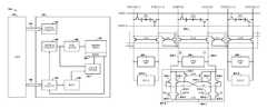
- FIG. 1is a block diagram of an apparatus in the form of a computing system including a memory device in accordance with a number of embodiments of the present disclosure.
- FIG. 2is a schematic diagram illustrating sensing circuitry in accordance with a number of embodiments of the present disclosure.
- FIG. 3illustrates a timing diagram associated with performing a number of logical operations using sensing circuitry in accordance with a number of embodiments of the present disclosure.
- FIG. 4illustrates a timing diagram associated with performing a number of logical operations using sensing circuitry in accordance with a number of embodiments of the present disclosure.
- FIG. 5is a schematic diagram illustrating a portion of sensing circuitry in accordance with a number of embodiments of the present disclosure.
- FIG. 6is a schematic diagram illustrating sensing circuitry in accordance with a number of embodiments of the present disclosure.
- FIG. 7is a schematic diagram illustrating sensing circuitry in accordance with a number of embodiments of the present disclosure.
- FIG. 8is a schematic diagram illustrating sensing circuitry in accordance with a number of embodiments of the present disclosure.
- FIG. 9is a schematic diagram illustrating sensing circuitry in accordance with a number of embodiments of the present disclosure.
- FIG. 10illustrates a timing diagram associated with performing a number of logical operations using sensing circuitry in accordance with a number of embodiments of the present disclosure.
- FIG. 11illustrates a timing diagram associated with performing a number of logical operations using sensing circuitry in accordance with a number of embodiments of the present disclosure.
- FIG. 12is a schematic diagram illustrating sensing circuitry in accordance with a number of embodiments of the present disclosure.
- FIG. 13is a schematic diagram illustrating sensing circuitry in accordance with a number of embodiments of the present disclosure.
- FIG. 14illustrates a timing diagram associated with performing a number of logical operations using sensing circuitry in accordance with a number of embodiments of the present disclosure.
- FIG. 15illustrates a timing diagram associated with performing a number of logical operations using sensing circuitry in accordance with a number of embodiments of the present disclosure.
- FIG. 16illustrates a timing diagram associated with performing a number of logical operations using sensing circuitry in accordance with a number of embodiments of the present disclosure.
- FIG. 17illustrates a timing diagram associated with performing a number of logical operations using sensing circuitry in accordance with a number of embodiments of the present disclosure.
- FIG. 18is a schematic diagram illustrating sensing circuitry in accordance with a number of embodiments of the present disclosure.
- the present disclosureincludes apparatuses and methods related to performing logical operations using sensing circuitry.
- An example apparatuscomprises an array of memory cells and sensing circuitry coupled to the array.
- the sensing circuitryincludes a sense amplifier coupled to a pair of complementary sense lines, and a compute component coupled to the sense amplifier.
- the compute componentincludes a dynamic latch.
- the sensing circuitryis configured to perform a logical operation and initially store the result in the sense amplifier.
- a number of embodiments of the present disclosurecan provide improved parallelism and/or reduced power consumption in association with performing compute functions as compared to previous systems such as previous PIM systems and systems having an external processor (e.g., a processing resource located external from a memory array, such as on a separate integrated circuit chip).
- a number of embodimentscan provide for performing fully complete compute functions such as integer add, subtract, multiply, divide, and CAM (content addressable memory) functions without transferring data out of the memory array and sensing circuitry via a bus (e.g., data bus, address bus, control bus), for instance.
- Such compute functionscan involve performing a number of logical operations (e.g., logical functions such as AND, OR, NOT, NOR, NAND, XOR, etc.).
- performing logical operationscan include performing a number of non-Boolean logic operations such as copy, compare, destroy, etc.
- datamay be transferred from the array and sensing circuitry (e.g., via a bus comprising input/output (I/O) lines) to a processing resource such as a processor, microprocessor, and/or compute engine, which may comprise ALU circuitry and/or other functional unit circuitry configured to perform the appropriate logical operations.
- a processing resourcesuch as a processor, microprocessor, and/or compute engine, which may comprise ALU circuitry and/or other functional unit circuitry configured to perform the appropriate logical operations.
- transferring data from a memory array and sensing circuitry to such processing resource(s)can involve significant power consumption.
- a sense linewhich may be referred to herein as a digit line or data line
- I/O linese.g., local I/O lines
- the circuitry of the processing resource(s)may not conform to pitch rules associated with a memory array.
- the cells of a memory arraymay have a 4F 2 or 6F 2 cell size, where “F” is a feature size corresponding to the cells.
- the devicese.g., logic gates
- ALU circuitry of previous PIM systemsmay not be capable of being formed on pitch with the memory cells, which can affect chip size and/or memory density, for example.
- a number of embodiments of the present disclosureinclude sensing circuitry formed on pitch with memory cells of the array and capable of performing compute functions such as those described herein below.
- FIG. 1is a block diagram of an apparatus in the form of a computing system 100 including a memory device 120 in accordance with a number of embodiments of the present disclosure.
- a memory device 120a memory array 130 , and/or sensing circuitry 150 might also be separately considered an “apparatus.”
- System 100includes a host 110 coupled (e.g., connected) to memory device 120 , which includes a memory array 130 .
- Host 110can be a host system such as a personal laptop computer, a desktop computer, a digital camera, a smart phone, or a memory card reader, among various other types of hosts.
- Host 110can include a system motherboard and/or backplane and can include a number of processing resources (e.g., one or more processors, microprocessors, or some other type of controlling circuitry).
- the system 100can include separate integrated circuits or both the host 110 and the memory device 120 can be on the same integrated circuit.
- the system 100can be, for instance, a server system and/or a high performance computing (HPC) system and/or a portion thereof.
- HPChigh performance computing
- FIG. 1illustrates a system having a Von Neumann architecture
- embodiments of the present disclosurecan be implemented in non-Von Neumann architectures (e.g., a Turing machine), which may not include one or more components (e.g., CPU, ALU, etc.) often associated with a Von Neumann architecture.
- non-Von Neumann architecturese.g., a Turing machine
- componentse.g., CPU, ALU, etc.
- the memory array 130can be a DRAM array, SRAM array, STT RAM array, PCRAM array, TRAM array, RRAM array, NAND flash array, and/or NOR flash array, for instance.
- the array 130can comprise memory cells arranged in rows coupled by access lines (which may be referred to herein as word lines or select lines) and columns coupled by sense lines. Although a single array 130 is shown in FIG. 1 , embodiments are not so limited. For instance, memory device 120 may include a number of arrays 130 (e.g., a number of banks of DRAM cells). An example DRAM array is described in association with FIG. 2 .
- the memory device 120includes address circuitry 142 to latch address signals provided over an I/O bus 156 (e.g., a data bus) through I/O circuitry 144 . Address signals are received and decoded by a row decoder 146 and a column decoder 152 to access the memory array 130 . Data can be read from memory array 130 by sensing voltage and/or current changes on the data lines using sensing circuitry 150 . The sensing circuitry 150 can read and latch a page (e.g., row) of data from the memory array 130 .
- the I/O circuitry 144can be used for bi-directional data communication with host 110 over the I/O bus 156 .
- the write circuitry 148is used to write data to the memory array 130 .
- Control circuitry 140decodes signals provided by control bus 154 from the host 110 . These signals can include chip enable signals, write enable signals, and address latch signals that are used to control operations performed on the memory array 130 , including data read, data write, and data erase operations. In various embodiments, the control circuitry 140 is responsible for executing instructions from the host 110 .
- the control circuitry 140can be a state machine, a sequencer, or some other type of controller.
- the sensing circuitry 150can comprise a number of sense amplifiers (e.g., sense amplifier 206 shown in FIG. 2 or sense amplifier 506 shown in FIG. 5 ) and a number of compute components (e.g., compute component 231 - 1 shown in FIG. 2 ), which can be used to perform logical operations (e.g., on data associated with complementary data lines).
- the sense amplifiercan comprise a static latch, for example, which can be referred to herein as the primary latch.
- the compute component 231 - 1can comprise a dynamic and/or static latch, for example, which can be referred to herein as the secondary latch, and which can serve as, and be referred to as, an accumulator.
- the sensing circuitry(e.g., 150 ) can be used to perform logical operations using data stored in array 130 as inputs and store the results of the logical operations back to the array 130 without transferring data via a sense line address access (e.g., without firing a column decode signal).
- various compute functionscan be performed using, and within, sensing circuitry 150 rather than (or in association with) being performed by processing resources external to the sensing circuitry (e.g., by a processor associated with host 110 and/or other processing circuitry, such as ALU circuitry, located on device 120 (e.g., on control circuitry 140 or elsewhere)).
- data associated with an operandwould be read from memory via sensing circuitry and provided to external ALU circuitry via I/O lines (e.g., via local I/O lines and/or global I/O lines).
- the external ALU circuitrycould include a number of registers and would perform compute functions using the operands, and the result would be transferred back to the array via the I/O lines.
- sensing circuitrye.g., 150
- sensing circuitryis configured to perform logical operations on data stored in memory (e.g., array 130 ) and store the result back to the memory without enabling an I/O line (e.g., a local I/O line) coupled to the sensing circuitry, which can be formed on pitch with the memory cells of the array.
- Enabling an I/O linecan include enabling (e.g., turning on) a transistor having a gate coupled to a decode signal (e.g., a column decode signal) and a source/drain coupled to the I/O line.
- decode signale.g., a column decode signal
- the sensing circuitrye.g., 150
- the sensing circuitrycan be used to perform logical operations without enabling column decode lines of the array; however, the local I/O line(s) may be enabled in order to transfer a result to a suitable location other than back to the array (e.g., to an external register).
- circuitry external to array 130 and sensing circuitry 150is not needed to perform compute functions as the sensing circuitry 150 can perform the appropriate logical operations to perform such compute functions without the use of an external processing resource. Therefore, the sensing circuitry 150 may be used to compliment and/or to replace, at least to some extent, such an external processing resource (or at least the bandwidth of such an external processing resource). However, in a number of embodiments, the sensing circuitry 150 may be used to perform logical operations (e.g., to execute instructions) in addition to logical operations performed by an external processing resource (e.g., host 110 ). For instance, host 110 and/or sensing circuitry 150 may be limited to performing only certain logical operations and/or a certain number of logical operations.
- FIG. 2is a schematic diagram illustrating sensing circuitry in accordance with a number of embodiments of the present disclosure.
- a memory cellcomprises a storage element (e.g., capacitor) and an access device (e.g., transistor).
- transistor 202 - 1 and capacitor 203 - 1comprises a memory cell
- transistor 202 - 2 and capacitor 203 - 2comprises a memory cell
- the memory array 230is a DRAM array of 1T1C (one transistor one capacitor) memory cells.
- the memory cellsmay be destructive read memory cells (e.g., reading the data stored in the cell destroys the data such that the data originally stored in the cell is refreshed after being read).
- the cells of the memory array 230are arranged in rows coupled by word lines 204 -X (Row X), 204 -Y (Row Y), etc., and columns coupled by pairs of complementary data lines DIGIT(n ⁇ 1)/DIGIT(n ⁇ 1)_, DIGIT(n)/DIGIT(n)_, DIGIT(n+1)/DIGIT(n+1)_.
- the individual data lines corresponding to each pair of complementary data linescan also be referred to as data lines 205 - 1 (D) and 205 - 2 (D_) respectively.
- FIG. 2Although only three pair of complementary data lines are shown in FIG. 2 , embodiments of the present disclosure are not so limited, and an array of memory cells can include additional columns of memory cells and/or data lines (e.g., 4,096, 8,192, 16,384, etc.).
- Memory cellscan be coupled to different data lines and/or word lines.
- a first source/drain region of a transistor 202 - 1can be coupled to data line 205 - 1 (D)
- a second source/drain region of transistor 202 - 1can be coupled to capacitor 203 - 1
- a gate of a transistor 202 - 1can be coupled to word line 204 -X.
- a first source/drain region of a transistor 202 - 2can be coupled to data line 205 - 2 (D_)
- a second source/drain region of transistor 202 - 2can be coupled to capacitor 203 - 2
- a gate of a transistor 202 - 2can be coupled to word line 204 -Y.
- the cell plateas shown in FIG. 2 , can be coupled to each of capacitors 203 - 1 and 203 - 2 .
- the cell platecan be a common node to which a reference voltage (e.g., ground) can be applied in various memory array configurations.
- a reference voltagee.g., ground
- the memory array 230is coupled to sensing circuitry 250 in accordance with a number of embodiments of the present disclosure.
- the sensing circuitry 250comprises a sense amplifier 206 and a compute component 231 - 1 corresponding to respective columns of memory cells (e.g., coupled to respective pairs of complementary data lines).
- the sensing circuitry 250can correspond to sensing circuitry 150 shown in FIG. 1 , for example.
- the sense amplifier 206can be a sense amplifier such as sense amplifier 506 described below in association with FIG. 5 .
- the sense amplifier 206can be operated to determine a data value (e.g., logic state) stored in a selected memory cell.
- the sense amplifier 206can comprise a cross coupled latch, which can be referred to herein as a primary latch.
- Embodimentsare not limited to the example sense amplifier 206 .
- the sense amplifier 206can be current-mode sense amplifier and/or single-ended sense amplifier (e.g., sense amplifier coupled to one data line).
- embodiments of the present disclosureare not limited to a folded data line architecture such as that shown in FIG. 2 .
- the sensing circuitrye.g., sense amplifier 206 and compute component 231
- the sensing circuitrycan be operated to perform a logical operation using a dynamic latch of the compute component 231 - 1 and store the result in the sense amplifier 206 without transferring data from the sensing circuitry via an I/O line (e.g., without performing a data line address access via activation of a column decode signal, for instance).
- a dynamic latchrefers to a latch that relies on capacitance of transistors (e.g., gates) or other structures to maintain a particular data state stored as voltages on output nodes.
- a dynamic latchcan be set/reset by selectively charging/discharging the capacitance. As such, the data state stored as voltages on the output nodes of the dynamic latch may remain valid only for a certain period of time.
- a latch other than a dynamic latche.g., a static latch such as a cross-coupled latch
- a dynamic latchcan operate faster, consume less power, and/or be of smaller physical size compared to a static latch.
- a dynamic latchis used in an accumulator in performing logical operations in association with a sense amplifier (“sense amp”).
- the sense amplifier and accumulatorare configured to have a result of the logical operation be initially stored in the sense amp.
- a data value(which may, or may not, be used in the logical operation) can remain unchanged in the accumulator. Benefits of having a logical operation result initially stored in a sense amplifier rather than the accumulator are discussed further below.
- logical operationse.g., Boolean logical functions involving data values
- Boolean logic functionsare used in many higher level functions. Consequently, speed and/or power efficiencies that can be realized with improved logical operations, which can translate into speed and/or power efficiencies of higher order functionalities.
- Described hereinare apparatuses and methods for performing logical operations without transferring data via an input/output (I/O) line and/or without transferring data to a control component external to the array.
- I/Oinput/output
- the apparatuses and methods for performing the logical operationsmay not require amplification of a sense line (e.g., data line, digit line, bit line) pair.
- the sense amplifier 206 and the compute component 231 - 1can be coupled to the array 230 via shift circuitry 223 .
- the shift circuitry 223comprises a pair of isolation devices 221 - 1 and 221 - 2 (e.g., isolation transistors 221 - 1 and 221 - 2 ) coupled to data lines 205 - 1 (D) and 205 - 2 (D_), respectively).
- the isolation transistors 221 - 1 and 221 - 2are coupled to a control signal 222 (NORM) that, when activated, enables (e.g., turns on) the isolation transistors 221 - 1 and 221 - 2 to couple the corresponding sense amplifier 206 and compute component 231 - 1 to a corresponding column of memory cells (e.g., to a corresponding pair of complementary data lines 205 - 1 (D) and 205 - 2 (D_)).
- NCMcontrol signal 222
- conduction of isolation transistors 221 - 1 and 221 - 2can be referred to as a “normal” configuration of the shift circuitry 223 .
- the shift circuitry 223includes another (e.g., a second) pair of isolation devices (e.g., transistors 221 - 3 and 221 - 4 ) coupled to a complementary control signal 219 (SHIFT), which can be activated, for example, when NORM is deactivated.
- a complementary control signal 219SHIFT
- the isolation transistors 221 - 3 and 221 - 4can be operated (e.g., via control signal 219 ) such that a particular sense amplifier 206 and compute component 231 - 1 are coupled to a different pair of complementary data lines (e.g., a pair of complementary data lines different than the pair of complementary data lines to which isolation transistors 221 - 1 and 221 - 2 couple the particular sense amplifier 206 and compute component 231 ), or can couple a particular sense amplifier 206 and compute component 231 - 1 to another memory array (and isolate the particular sense amplifier 206 and compute component 231 - 1 from a first memory array).
- the shift circuitry 223can be arranged as a portion of (e.g., within) the sense amplifier 206 , for instance.
- the shift circuitry 223 shown in FIG. 2includes isolation transistors 221 - 1 and 221 - 2 used to couple particular sensing circuitry 250 (e.g., a particular sense amplifier 206 and corresponding compute component 231 ) to a particular pair of complementary data lines 205 - 1 (D) and 205 - 2 (D_) (e.g., DIGIT(n) and DIGIT(n)_) and isolation transistors 221 - 3 and 221 - 4 are arranged to couple the particular sensing circuitry 250 to an adjacent pair of complementary data lines in one particular direction (e.g., adjacent data lines DIGIT(n+1) and DIGIT(n+1)_ shown to the right in FIG. 2 ), embodiments of the present disclosure are not so limited.
- shift circuitrycan include isolation transistors 221 - 1 and 221 - 2 used to couple particular sensing circuitry to a particular pair of complementary data lines (e.g., DIGIT(n) and DIGIT(n)_ and isolation transistors 221 - 3 and 221 - 4 arranged so as to be used to couple the particular sensing circuitry to an adjacent pair of complementary data lines in another particular direction (e.g., adjacent data lines DIGIT(n ⁇ 1) and DIGIT(n ⁇ 1)_ shown to the left in FIG. 2 ).
- isolation transistors 221 - 1 and 221 - 2used to couple particular sensing circuitry to a particular pair of complementary data lines (e.g., DIGIT(n) and DIGIT(n)_ and isolation transistors 221 - 3 and 221 - 4 arranged so as to be used to couple the particular sensing circuitry to an adjacent pair of complementary data lines in another particular direction (e.g., adjacent data lines DIGIT(n ⁇ 1) and DIGIT(n ⁇ 1)_ shown
- Embodiments of the present disclosureare not limited to the configuration of shift circuitry 223 shown in FIG. 2 . Also, embodiments of the present disclosure can be configured as otherwise shown in FIG. 2 but without the shift circuitry 223 . That is, shift circuitry 223 is optional. In a number of embodiments, shift circuitry such as that shown in FIG. 2 can be operated (e.g., in conjunction with sense amplifiers 206 and compute components 231 ) in association with performing compute functions such as adding and subtracting functions without transferring data out of the sensing circuitry 250 via an I/O line (e.g., local I/O line 201 (IO/IO_)), for instance.
- I/O linee.g., local I/O line 201 (IO/IO_)
- each column of memory cellscan be coupled to a column decode line that can be enabled to transfer, via local I/O line 201 , a data value from a corresponding sense amplifier 206 and/or compute component 231 - 1 to a control component external to the array such as an external processing resource (e.g., host processor and/or other functional unit circuitry).
- the column decode linecan be coupled to a column decoder (e.g., column decoder 152 shown in FIG. 1 ).
- dataneed not be transferred via such I/O lines (e.g., I/O line 201 ) to perform logical operations in accordance with embodiments of the present disclosure.
- shift circuitrysuch as that shown in FIG. 2 can be operated (e.g., in conjunction with sense amplifiers 206 and compute components 231 ) in performing compute functions such as adding and subtracting functions without transferring data to a control component external to the array, for instance.
- the compute component 231 - 1includes eight transistors (e.g., four transistors per complementary data line). The transistors are formed on pitch with the sense amplifier 206 and with the memory cells of the array 230 .
- the compute component 231 - 1comprises a dynamic latch that can be referred to as a secondary latch, which can operate as (e.g., serve as) an accumulator in performing logical operations. As such, the secondary latch of the compute component 231 - 1 may be referred to as the accumulator of the compute component 231 - 1 .
- the compute component 231 - 1is coupled to the sense amplifier 206 via the data lines 205 - 1 (D) and D_ 205 - 2 as shown in FIG. 2 .
- the transistors of compute component 231 - 1are all n-channel transistors (e.g., NMOS transistors); however, embodiments are not so limited.
- the compute component 231 - 1includes a first pass transistor 207 - 1 having a first source/drain region directly coupled (e.g., connected) to data line 205 - 1 (D), which is also directly coupled to a first source/drain region of a load transistor 218 - 2 and a first source/drain region of an invert transistor 214 - 2 .
- “directly coupled”intends coupled without an intervening component.
- a second pass transistor 207 - 2has a first source/drain region directly coupled to data line 205 - 2 , which is also directly coupled to a first source/drain region of a load transistor 218 - 1 and a first source/drain region of an invert transistor 214 - 1 .
- load transistors 218 - 1 and 218 - 2are commonly coupled together and to a LOAD control signal.
- a second source/drain region of load transistor 218 - 1is directly coupled to a gate of transistor 209 - 1 (e.g., “dynamic latch transistor”) at a common node of the latch (e.g., node S 1 of the dynamic latch).
- a second source/drain region of load transistor 218 - 2is directly coupled to a gate of transistor 209 - 2 at the complementary common node of the latch (e.g., node S 2 of the dynamic latch).
- a second source/drain region of inverting transistor 214 - 1is directly coupled to a first source/drain region of transistor 209 - 1 and to a second source/drain region of pass transistor 207 - 1 .
- a second source/drain region of inverting transistor 214 - 2is directly coupled to a first source/drain region of transistor 209 - 2 and to a second source/drain region of pass transistor 207 - 2 .
- a second source/drain region of transistors 209 - 1 and 209 - 2are commonly coupled to a reference signal (e.g., ground (GND)).
- a gate of pass transistor 207 - 1is coupled to a control signal AND.
- a gate of pass transistor 207 - 2is coupled to a control signal OR.
- a gate of invert transistor 214 - 1is coupled to a control signal ORinv.
- a gate of invert transistor 214 - 2is coupled to a control signal ANDinv.
- the dynamic latch of compute component 231 - 1 shown in FIG. 2can operate as an accumulator (and may be referred to as such) storing data dynamically on nodes S 1 and S 2 .
- Activating the LOAD control signalenables load transistors 218 - 1 and 218 - 2 (e.g., causes them to conduct) and thereby loads complementary data onto nodes S 1 and S 2 , when load transistors 218 - 1 and 218 - 2 are conducting (e.g., enabled via the LOAD control signal).
- the voltage on data line 205 - 2 (D_)is coupled to node S 1 and the voltage on data line 205 - 1 (D) is coupled to node S 2 .
- the LOAD control signalcan be elevated to a voltage greater than V DD to pass a full V DD level to nodes S 1 /S 2 .
- elevating the LOAD control signal to a voltage greater than V DDis optional, and functionality of the circuit shown in FIG. 2 is not contingent on the LOAD control signal being elevated to a voltage greater than V DD .
- the sensing circuitry 250is configured to perform logical operations on data values stored in the array of memory cells with the result (e.g., resultant data value) being stored (e.g., residing) in the sense amplifier (e.g., 206 ).
- the logical operationse.g., AND, OR, etc.
- the logical operationscan be performed on data values stored in cells coupled to different access lines (e.g., Row X and Row Y) and to one or more pairs of complementary data lines (e.g., 205 - 1 and 205 - 2 ).
- sensing circuitry 250to perform AND, OR, and NOT (e.g., invert) operations is described further below, as is operation of the shift circuitry 223 to accomplish a SHIFT between pairs of complementary data lines. While operations are described below involving one or two data values, logical operations involving a plurality of data values can be accomplished without having to transfer data to an external arithmetic logic unit (ALU) or other processing resource outside of the sensing circuitry 250 , which may only operate on 32/64/128 bits at a time.
- ALUarithmetic logic unit
- logical operations involving 16K ANDs/ORs of 32-bit data valuescan be implemented utilizing the sensing circuitry associated with a plurality of data lines without transferring data out of the sensing circuitry.
- sensing circuitry of FIG. 2is described below and summarized in Table 1 below.
- Initially storing the result of a particular logical operation in the sense amplifier(e.g., in a primary latch of sense amplifier 206 ) can provide improved versatility as compared to previous approaches in which the result may initially reside in a secondary latch (e.g., accumulator) of a compute component (e.g., 231 - 1 ), and then be subsequently transferred to the sense amp, for instance.
- a secondary latche.g., accumulator
- compute componente.g., 231 - 1
- Initially storing the result of a particular operation in the sense amplifieris advantageous because, for instance, the result can be written to a row (of the array of memory cells) or back into the accumulator without performing a precharge cycle (e.g., on the complementary data lines 205 - 1 (D) and/or 205 - 2 (D_)).
- a precharge cyclecan involve precharging complementary data lines to a predetermined voltage level (e.g., V DD /2) before/after performing an operation using the complementary data lines. Reducing the number of precharge cycles can increase the speed of and/or reduce the power associated with performing various operations.
- the sensing circuitry shown in FIG. 2consumes power for only one of the four possible data combinations shown in Table 2 below. For instance, if an AND is performed on a data value residing in the accumulator of the compute component (e.g., 231 - 1 ) and a data value stored in a memory cell coupled to a particular access line (e.g., Row X), then current (e.g., about 60 mA) is drawn only for the situation in which the accumulator stores a “0” and the memory cell stores a “1,” as shown in Table 2.
- currente.g., about 60 mA
- an equilibrate operationPrior to performing a logical operation, an equilibrate operation can occur such that the complementary data lines D and D — are shorted together at an equilibration voltage (e.g., V DD /2), as is described in detail with respect to sense amplifier 506 illustrated in FIG. 5 .
- An initial operation phase associated with performing an AND or an OR operation on a first data value and a second data value stored in memory cells coupled to different access lines (e.g., 204 -X and 204 -Y)can include loading the first data value into the accumulator of compute component 231 - 1 .
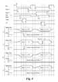
- FIG. 3illustrates a timing diagram associated with performing a number of logical operations using sensing circuitry in accordance with a number of embodiments of the present disclosure.
- FIG. 3illustrates a timing diagram associated with initiating an AND logical operation after starting to load the second operand (e.g., Row Y data value) into the sense amplifier.
- FIG. 3illustrates the sense amplifier and accumulator signals for various combinations of first and second operand data values.
- FIG. 3shows the respective sense amplifier and accumulator signals corresponding to each combination of Row X data value and Row Y data value in each set.
- the particular timing diagram signalsare discussed below with respect to the pseudo code associated with an AND operation of the circuit shown in FIG. 2 .
- pseudo code associated with loadinge.g., copying
- a first data value stored in a cell coupled to row 204 -X into the accumulatorcan be summarized as follows:
- “Deactivate EQ”indicates that an equilibration signal (EQ signal shown in FIG. 3 ) corresponding to the sense amplifier 206 is disabled at t 1 as shown in FIG. 3 (e.g., such that the complementary data lines (e.g., 205 - 1 (D) and 205 - 2 (D_) are no longer shorted to V DD /2).
- a selected rowe.g., ROW X
- is enablede.g., selected, opened such as by activating a signal to select a particular row
- the access transistorWhen the voltage signal applied to ROW X reaches the threshold voltage (Vt) of the access transistor (e.g., 202 - 2 ) corresponding to the selected cell, the access transistor turns on and couples the data line (e.g., 205 - 2 (D_)) to the selected cell (e.g., to capacitor 203 - 2 ) which creates a differential voltage signal between the data lines.
- Vtthreshold voltage
- “Fire Sense Amps”indicates that the sense amplifier 206 is enabled to set the primary latch and subsequently disabled. For example, as shown at t 3 in FIG. 3 , the ACT positive control signal (e.g., 590 shown in FIG. 5 ) goes high and the RnIF negative control signal (e.g., 528 shown in FIG.
- V DDvoltage corresponding to a logic 1 or a voltage (e.g., GND) corresponding to a logic 0 being on data line 205 - 1 (D) (and the voltage corresponding to the other logic state being on complementary data line 205 - 2 (D_)).
- the sensed data valueis stored in the primary latch of sense amplifier 206 .
- the primary energy consumptionoccurs in charging the data lines (e.g., 205 - 1 (D) or 205 - 2 (D_)) from the equilibration voltage V DD /2 to the rail voltage V DD .
- the four sets of possible Sense amplifier and Accumulator signals illustrated in FIG. 3shows the behavior of signals on data lines D and D_.
- the Row X data valueis stored in the primary latch of the sense amp.
- FIG. 2shows that the memory cell including storage element 202 - 2 , corresponding to Row X, is coupled to the complementary data line D_, while the memory cell including storage element 202 - 1 , corresponding to Row Y, is coupled to data line D.
- FIG. 3shows that the memory cell including storage element 202 - 2 , corresponding to Row X, is coupled to the complementary data line D_, while the memory cell including storage element 202 - 1 , corresponding to Row Y, is coupled to data line D.
- the charge stored in memory cell 202 - 2(corresponding to Row X) corresponding to a “0” data value causes the voltage on data line D — (to which memory cell 202 - 2 is coupled) to go high and the charge stored in memory cell 202 - 2 corresponding to a “1” data value causes the voltage on data line D — to go low, which is opposite correspondence between data states and charge stored in memory cell 202 - 2 , corresponding to Row Y, that is coupled to data line D.
- Activate LOADindicates that the LOAD control signal goes high as shown at t 4 in FIG. 3 , causing load transistors 218 - 1 and 218 - 2 to conduct.
- activating the LOAD control signalenables the dynamic latch (e.g., secondary latch in the accumulator) of the compute component 23 - 1 .
- the sensed data value stored in the sense amplifier 206is transferred (e.g., copied) to the dynamic latch so as to be dynamically stored on nodes S 1 and S 2 . As shown for each of the four sets of possible Sense amplifier and Accumulator signals illustrated in FIG.
- the behavior at S 1 and S 2 of the dynamic latch of the Accumulatorindicates the secondary latch is loaded with the Row X data value.
- Deactivate LOADindicates that the LOAD control signal goes back low as shown at t 5 in FIG. 3 to cause the load transistors 218 - 1 and 218 - 2 to stop conducting and thereby isolate the dynamic latch from the complementary data lines.
- the data valueremains dynamically stored in dynamic latch of the accumulator at nodes S 1 and S 2 .
- the selected row(e.g., ROW X) is disabled (e.g., deselected, closed such as by deactivating a select signal for a particular row) as indicated by “Close Row X” and indicated at t 6 in FIG. 3 , which can be accomplished by the access transistor turning off to decouple the selected cell from the corresponding data line.
- the data linescan be precharged as indicated by the “Precharge” in the pseudo code above.
- a precharge of the data linescan be accomplished by an equilibrate operation, as described above and shown in FIG. 3 by the EQ signal going high at t 7 .
- the equilibrate operationcauses the voltage on data lines D and D — to each return to V DD /2. Equilibration can occur, for instance, prior to a memory cell sensing operation or the logical operations (described below).
- a subsequent operation phase associated with performing the AND or the OR operation on the first data value (now stored in the sense amplifier 206 and the dynamic latch of the accumulator 231 - 1 ) and the second data value (stored in a memory cell 202 - 1 coupled to Row Y 204 -Y)includes performing particular steps which depend on the whether an AND or an OR is to be performed.
- Examples of pseudo code associated with “ANDing” and “ORing” the data value residing in the accumulator (e.g., the first data value stored in the memory cell 202 - 2 coupled to Row X 204 -X) and the second data value (e.g., the data value stored in the memory cell 202 - 1 coupled to Row Y 204 -Y)are summarized below.
- Example pseudo code associated with “ANDing” the data valuescan include:
- Deactivate EQindicates that an equilibration signal corresponding to the sense amplifier 206 is disabled (e.g., such that the complementary data lines 205 - 1 (D) and 205 - 2 (D_) are no longer shorted to V DD /2), which is illustrated in FIG. 3 at t 9 .
- a selected rowe.g., ROW Y
- Open Row Yis enabled as indicated in the pseudo code above by “Open Row Y” and shown in FIG. 3 at t 9 .
- the access transistorWhen the voltage signal applied to ROW Y reaches the threshold voltage (Vt) of the access transistor (e.g., 202 - 1 ) corresponding to the selected cell, the access transistor turns on and couples the data line (e.g., D — 205 - 1 ) to the selected cell (e.g., to capacitor 203 - 1 ) which creates a differential voltage signal between the data lines.
- Vtthreshold voltage
- “Fire Sense Amps”indicates that the sense amplifier 206 is enabled to amplify the differential signal between 205-1 (D) and 205 - 2 (D_), resulting in a voltage (e.g., V DD ) corresponding to a logic 1 or a voltage (e.g., GND) corresponding to a logic 0 being on data line 205 - 1 (D) (and the voltage corresponding to the other logic state being on complementary data line 205 - 2 (D_)).
- the ACT positive control signale.g., 590 shown in FIG.
- the sensed data value from memory cell 202 - 1is stored in the primary latch of sense amplifier 206 , as previously described.
- the dynamic latchstill corresponds to the data value from memory cell 202 - 2 since the dynamic latch is unchanged.
- “Close Row Y”indicates that the selected row (e.g., ROW Y) can be disabled if it is not desired to store the result of the AND logical operation back in the memory cell corresponding to Row Y.
- FIG. 3shows that Row Y is left open such that the result of the logical operation can be stored back in the memory cell corresponding to Row Y. Isolating the memory cell corresponding to Row Y can be accomplished by the access transistor turning off to decouple the selected cell 202 - 1 from the data line 205 - 1 (D).
- “Activate AND” in the pseudo code aboveindicates that the AND control signal goes high as shown in FIG. 3 at t 11 , causing pass transistor 207 - 1 to conduct. In this manner, activating the AND control signal causes the value of the function (e.g., Row X AND Row Y) to be written to the sense amp.
- the functione.g., Row X AND Row Y
- the dynamic latch of the accumulator 231 - 1contains a “0” (i.e., a voltage corresponding to a “0” on node S 2 and a voltage corresponding to a “1” on node S 1 )
- the sense amplifier datais written to a “0” (regardless of the data value previously stored in the sense amp) since the voltage corresponding to a “1” on node S 1 causes transistor 209 - 1 to conduct thereby coupling the sense amplifier 206 to ground through transistor 209 - 1 , pass transistor 207 - 1 and data line 205 - 1 (D).
- the result of the AND operationdepends on the data value stored in the sense amplifier 206 (e.g., from Row Y).
- the result of the AND operationshould be a “1” if the data value stored in the sense amplifier 206 (e.g., from Row Y) is also a “1,” but the result of the AND operation should be a “0” if the data value stored in the sense amplifier 206 (e.g., from Row Y) is also a “0.”
- the sensing circuitry 231 - 1is configured such that if the dynamic latch of the accumulator contains a “1” (i.e., a voltage corresponding to a “1” on node S 2 and a voltage corresponding to a “0” on node S 1 ), transistor 209 - 1 does not conduct, the sense amplifier is not coupled to ground (as described above), and the data value previously stored in the sense amplifier 206 remains unchanged (e.
- “Deactivate AND” in the pseudo code aboveindicates that the AND control signal goes low as shown at t 12 in FIG. 3 , causing pass transistor 207 - 1 to stop conducting to isolate the sense amplifier 206 (and data line 205 - 1 (D)) from ground. If not previously done, Row Y can be closed (as shown at t 13 in FIG. 3 ) and the sense amplifier can be disabled (as shown at t 14 in FIG. 3 by the ACT positive control signal going low and the RnIF negative control signal goes high). With the data lines isolated, “Precharge” in the pseudo code above can cause a precharge of the data lines by an equilibrate operation, as described previously (e.g., commencing at t 14 shown in FIG. 3 ).
- FIG. 3shows, in the alternative, the behavior of voltage signals on the data lines (e.g., 205 - 1 (D) and 205 - 2 (D_) shown in FIG. 2 ) coupled to the sense amplifier (e.g., 206 shown in FIG. 2 ) and the behavior of voltage signals on nodes S 1 and S 1 of the dynamic latch of the compute component (e.g., 231 - 1 shown in FIG. 2 ) for an AND logical operation involving each of the possible combination of operands (e.g., Row X/Row Y data values 00, 10, 01, and 11).
- the data linese.g., 205 - 1 (D) and 205 - 2 (D_) shown in FIG. 2
- the sense amplifiere.g., 206 shown in FIG. 2
- nodes S 1 and S 1 of the dynamic latch of the compute componente.g., 231 - 1 shown in FIG. 2
- AND logical operationinvolving each of the possible combination of operands (
- timing diagrams illustrated in FIG. 3 and the pseudo code described aboveindicate initiating the AND logical operation after starting to load the second operand (e.g., Row Y data value) into the sense amplifier
- the circuit shown in FIG. 2can be successfully operated by initiating the AND logical operation before starting to load the second operand (e.g., Row Y data value) into the sense amplifier, the details of which are described below and illustrated with respect to FIGS. 9, 10, and 11 .
- FIG. 4illustrates a timing diagram associated with performing a number of logical operations using sensing circuitry in accordance with a number of embodiments of the present disclosure.
- FIG. 4illustrates a timing diagram associated with initiating an OR logical operation after starting to load the second operand (e.g., Row Y data value) into the sense amplifier.
- FIG. 4illustrates the sense amplifier and accumulator signals for various combinations of first and second operand data values. The particular timing diagram signals are discussed below with respect to the pseudo code associated with an AND logical operation of the circuit shown in FIG. 2 .
- a subsequent operation phasecan alternately be associated with performing the OR operation on the first data value (now stored in the sense amplifier 206 and the dynamic latch of the accumulator 231 - 1 ) and the second data value (stored in a memory cell 202 - 1 coupled to Row Y 204 -Y).
- the operations to load the Row X data into the sense amplifier and accumulator that were previously described with respect to times t 1 -t 7 shown in FIG. 3are not repeated with respect to FIG. 4 .
- Example pseudo code associated with “ORing” the data valuescan include:
- the “Deactivate EQ”(shown at t 8 in FIG. 4 ), “Open Row Y” (shown at t 9 in FIG. 4 ), “Fire Sense Amps” (shown at t 10 in FIG. 4 ), and “Close Row Y” (shown at t 13 in FIG. 4 , and which may occur prior to initiating the particular logical function control signal), shown in the pseudo code above indicate the same functionality as previously described with respect to the AND operation pseudo code.
- Activate ORin the pseudo code above indicates that the OR control signal goes high as shown at t 11 in FIG. 4 , which causes pass transistor 207 - 2 to conduct. In this manner, activating the OR control signal causes the value of the function (e.g., Row X OR Row Y) to be written to the sense amp.
- the dynamic latch of the accumulatorcontains a “0” (i.e., a voltage corresponding to a “0” on node S 2 and a voltage corresponding to a “1” on node S 1 ), then the result of the OR operation depends on the data value stored in the sense amplifier 206 (e.g., from Row Y).
- the result of the OR operationshould be a “1” if the data value stored in the sense amplifier 206 (e.g., from Row Y) is a “1,” but the result of the OR operation should be a “0” if the data value stored in the sense amplifier 206 (e.g., from Row Y) is also a “0.”
- the sensing circuitry 231 - 1is configured such that if the dynamic latch of the accumulator contains a “0,” with the voltage corresponding to a “0” on node S 2 , transistor 209 - 2 is off and does not conduct (and pass transistor 207 - 1 is also off since the AND control signal is not asserted) so the sense amplifier 206 is not coupled to ground (either side), and the data value previously stored in the sense amplifier 206 remains unchanged (e.g., Row Y data value such that the OR operation result is a “1” if the Row Y data value is a “1” and the OR operation result is a “0” if the Row
- the dynamic latch of the accumulatorcontains a “1” (i.e., a voltage corresponding to a “1” on node S 2 and a voltage corresponding to a “0” on node S 1 ), transistor 209 - 2 does conduct (as does pass transistor 207 - 2 since the OR control signal is asserted), and the sense amplifier 206 input coupled to data line 205 - 2 (D_) is coupled to ground since the voltage corresponding to a “1” on node S 2 causes transistor 209 - 2 to conduct along with pass transistor 207 - 2 (which also conducts since the OR control signal is asserted).
- a “1”i.e., a voltage corresponding to a “1” on node S 2 and a voltage corresponding to a “0” on node S 1
- FIG. 4shows, in the alternative, the behavior of voltage signals on the data lines (e.g., 205 - 1 (D) and 205 - 2 (D_) shown in FIG. 2 ) coupled to the sense amplifier (e.g., 206 shown in FIG. 2 ) and the behavior of voltage signals on nodes S 1 and S 2 of the dynamic latch of the compute component (e.g., 231 - 1 shown in FIG. 2 ) for an OR logical operation involving each of the possible combination of operands (e.g., Row X/Row Y data values 00, 10, 01, and 11).
- “Deactivate OR” in the pseudo code aboveindicates that the OR control signal goes low as shown at t 12 in FIG. 4 , causing pass transistor 207 - 2 to stop conducting to isolate the sense amplifier 206 (and data line D 205 - 2 ) from ground. If not previously done, Row Y can be closed (as shown at t 13 in FIG. 4 ) and the sense amplifier can be disabled (as shown at t 14 in FIG. 4 by the ACT positive control signal going low and the RnIF negative control signal going high). With the data lines isolated, “Precharge” in the pseudo code above can cause a precharge of the data lines by an equilibrate operation, as described previously and shown at t 14 in FIG. 4 .
- the sensing circuitry illustrated in FIG. 2can provide additional logical operations flexibility as follows.
- the logical operationscan be changed from ⁇ Row X AND Row Y ⁇ to ⁇ ⁇ Row X AND Row Y ⁇ (where “ ⁇ Row X” indicates an opposite of the Row X data value, e.g., NOT Row X) and can be changed from ⁇ Row X OR Row Y ⁇ to ⁇ ⁇ Row X OR Row Y ⁇ .
- the ANDinv control signalcan be asserted instead of the AND control signal
- the ORInv control signalcan be asserted instead of the OR control signal.
- Activating the ORinv control signalcauses transistor 214 - 1 to conduct and activating the ANDinv control signal causes transistor 214 - 2 to conduct.
- asserting the appropriate inverted control signalcan flip the sense amplifier and cause the result initially stored in the sense amplifier 206 to be that of the AND operation using inverted Row X and true Row Y data values or that of the OR operation using the inverted Row X and true Row Y data values.
- a true or compliment version of one data valuecan be used in the accumulator to perform the logical operation (e.g., AND, OR), for example, by loading a data value to be inverted first and a data value that is not to be inverted second.
- the sensing circuitry shown in FIG. 2can perform a NOT (e.g., invert) operation by putting the non-inverted data value into the dynamic latch of the accumulator and using that data to invert the data value in the sense amplifier 206 .
- a NOTe.g., invert
- activating the ORinv control signalcauses transistor 214 - 1 to conduct and activating the ANDinv control signal causes transistor 214 - 2 to conduct.
- the ORinv and/or ANDinv control signalsare used in implementing the NOT function, as described further below:
- the “Deactivate EQ,” “Open Row X,” “Fire Sense Amps,” “Activate LOAD,” and “Deactivate LOAD” shown in the pseudo code aboveindicate the same functionality as the same operations in the pseudo code for the “Copy Row X into the Accumulator” initial operation phase described above prior to pseudo code for the AND operation and OR operation.
- a compliment version of the data value in the dynamic latch of the accumulatorcan be placed on the data line and thus transferred to the sense amplifier 206 by enabling and disabling the invert transistors (e.g., ANDinv and/or ORinv).
- the sensing circuitry 250 shown in FIG. 2initially stores the result of the AND, OR, and NOT logical operations in the sense amplifier 206 (e.g., on the sense amplifier nodes), these logical operation results can be communicated easily and quickly to any open row, any row opened after the logical operation is complete, and/or into the dynamic latch of the accumulator 231 - 1 .
- the sense amplifier 206 and sequencing for the AND, OR, and/or NOT logical operationscan also be interchanged by appropriate activation of the AND, OR, ANDinv, and/or ORinv control signals (and operation of corresponding transistors having a gate coupled to the particular control signal) before the sense amplifier 206 fires.
- the sense amplifier 206can be pre-seeded with a data value from the dynamic latch of the accumulator to reduce overall current utilized because the sense amps 206 are not at full rail voltages (e.g., supply voltage or ground/reference voltage) when accumulator function is copied to the sense amplifier 206 .
- An operation sequence with a pre-seeded sense amplifier 206either forces one of the data lines to the reference voltage (leaving the complementary data line at V DD /2, or leaves the complementary data lines unchanged.
- the sense amplifier 206pulls the respective data lines to full rails when the sense amplifier 206 fires. Using this sequence of operations will overwrite data in an open Row.
- a SHIFT operationcan be accomplished by multiplexing (“muxing”) two neighboring data line complementary pairs using a traditional DRAM isolation (ISO) scheme.
- the shift circuitry 223can be used for shifting data values stored in memory cells coupled to a particular pair of complementary data lines to the sensing circuitry 250 (e.g., sense amplifier 206 ) corresponding to a different pair of complementary data lines (e.g., such as a sense amplifier 206 corresponding to a left or right adjacent pair of complementary data lines.
- a sense amplifier 206corresponds to the pair of complementary data lines to which the sense amplifier is coupled when isolation transistors 221 - 1 and 221 - 2 are conducting.
- the SHIFT operations(right or left) do not pre-copy the Row X data value into the accumulator. Operations to shift right Row X can be summarized as follows:
- “Deactivate Norm and Activate Shift”indicates that a NORM control signal goes low causing isolation transistors 221 - 1 and 221 - 2 of the shift circuitry 223 to not conduct (e.g., isolate the sense amplifier from the corresponding pair of complementary data lines).
- the SHIFT control signalgoes high causing isolation transistors 221 - 3 and 221 - 4 to conduct, thereby coupling the sense amplifier 206 to the left adjacent pair of complementary data lines (e.g., on the memory array side of non-conducting isolation transistors 221 - 1 and 221 - 2 for the left adjacent pair of complementary data lines).
- the “Deactivate EQ,” “Open Row X,” and “Fire Sense Amps” shown in the pseudo code aboveindicate the same functionality as the same operations in the pseudo code for the “Copy Row X into the Accumulator” initial operation phase described above prior to pseudo code for the AND operation and OR operation. After these operations, the Row X data value for the memory cell coupled to the left adjacent pair of complementary data lines is shifted right and stored in the sense amplifier 206 .
- “Activate Norm and Deactivate Shift”indicates that a NORM control signal goes high causing isolation transistors 221 - 1 and 221 - 2 of the shift circuitry 223 to conduct (e.g., coupling the sense amplifier to the corresponding pair of complementary data lines), and the SHIFT control signal goes low causing isolation transistors 221 - 3 and 221 - 4 to not conduct and isolating the sense amplifier 206 from the left adjacent pair of complementary data lines (e.g., on the memory array side of non-conducting isolation transistors 221 - 1 and 221 - 2 for the left adjacent pair of complementary data lines). Since Row X is still open, the Row X data value that has been shifted right is transferred to Row X of the corresponding pair of complementary data lines through isolation transistors 221 - 1 and 221 - 2 .
- the selected row(e.g., ROW X) is disabled as indicated by “Close Row X” in the pseudo code above, which can be accomplished by the access transistor turning off to decouple the selected cell from the corresponding data line.
- the data linescan be precharged as indicated by the “Precharge” in the pseudo code above. A precharge of the data lines can be accomplished by an equilibrate operation, as described above.
- “Activate Norm and Deactivate Shift”indicates that a NORM control signal goes high causing isolation transistors 221 - 1 and 221 - 2 of the shift circuitry 223 to conduct, and the SHIFT control signal goes low causing isolation transistors 221 - 3 and 221 - 4 to not conduct.
- This configurationcouples the sense amplifier 206 to a corresponding pair of complementary data lines and isolates the sense amplifier from the right adjacent pair of complementary data lines.
- the “Deactivate EQ,” “Open Row X,” and “Fire Sense Amps” shown in the pseudo code aboveindicate the same functionality as the same operations in the pseudo code for the “Copy Row X into the Accumulator” initial operation phase described above prior to pseudo code for the AND operation and OR operation. After these operations, the Row X data value for the memory cell coupled to the pair of complementary data lines corresponding to the sense circuitry 250 is stored in the sense amplifier 206 .
- “Deactivate Norm and Activate Shift”indicates that a NORM control signal goes low causing isolation transistors 221 - 1 and 221 - 2 of the shift circuitry 223 to not conduct (e.g., isolate the sense amplifier from the corresponding pair of complementary data lines), and the SHIFT control signal goes high causing isolation transistors 221 - 3 and 221 - 4 to conduct coupling the sense amplifier to the left adjacent pair of complementary data lines (e.g., on the memory array side of non-conducting isolation transistors 221 - 1 and 221 - 2 for the left adjacent pair of complementary data lines. Since Row X is still open, the Row X data value that has been shifted left is transferred to Row X of the left adjacent pair of complementary data lines.
- the selected row(e.g., ROW X) is disabled as indicated by “Close Row X,” which can be accomplished by the access transistor turning off to decouple the selected cell from the corresponding data line.
- the data linescan be precharged as indicated by the “Precharge” in the pseudo code above. A precharge of the data lines can be accomplished by an equilibrate operation, as described above.
- general computingcan be enabled in a memory array core of a processor-in-memory (PIM) device such as a DRAM one transistor per memory cell (e.g., 1T1C) configuration at 6F ⁇ 2 or 4F ⁇ 2 memory cell sizes, for example.
- PIMprocessor-in-memory
- the advantage of the apparatuses and methods described hereinis not realized in terms of single instruction speed, but rather the cumulative speed that can be achieved by an entire bank of data being computed in parallel without ever transferring data out of the memory array (e.g., DRAM) or firing a column decode. In other words, data transfer time can be eliminated.
- apparatus of the present disclosurecan perform ANDs or ORs simultaneously using data values in memory cells coupled to a data line (e.g., a column of 16K memory cells).
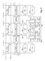
- FIG. 5is a schematic diagram illustrating a portion of sensing circuitry in accordance with a number of embodiments of the present disclosure.
- the sensing circuitry shown in FIG. 5comprises a sense amplifier 506 and a compute component 533 .
- the compute component 533can have various architectures such as those described above in association with FIG. 2 and as those described below in association with FIGS. 6-9, 12, 13, and 18 .
- the compute componentcomprises an accumulator having an associated dynamic latch, for instance.
- a sense amplifier(e.g., 506 ) can comprise a number of transistors formed on pitch with the transistors of the corresponding compute component (e.g., 533 ) and/or the memory cells of an array (e.g., array 230 shown in FIG. 2 ) to which they are coupled, which may conform to a particular feature size (e.g., 4F 2 , 6F 2 , etc.).
- the sense amplifier 506can, in conjunction with the compute component 533 , be operated to perform various logical operations using data from an array as input.
- the result of a logical operationcan be stored back to the array without transferring the data via a data line address access (e.g., without firing a column decode signal such that data is transferred to circuitry external from the array and sensing circuitry via local I/O lines).
- a number of embodiments of the present disclosurecan enable performing logical operations and compute functions associated therewith using less power than various previous approaches.
- a number of embodimentscan enable an increased parallel processing capability as compared to previous approaches.
- the circuitry corresponding to sense amplifier 506comprises a latch 515 including four transistors coupled to a pair of complementary data lines D 505 - 1 and D — 505 - 2 .
- the latch 515can be a cross coupled latch (e.g., gates of a pair of transistors, such as n-channel transistors (e.g., NMOS transistors) 527 - 1 and 527 - 2 are cross coupled with the gates of another pair of transistors, such as p-channel transistors (e.g., PMOS transistors) 529 - 1 and 529 - 2 ).
- the cross coupled latch 415comprising transistors 527 - 1 , 527 - 2 , 529 - 1 , and 529 - 2 can be referred to as a primary latch.
- the voltages or currents on the respective data lines D and D —can be provided to the respective latch inputs 533 - 1 and 533 - 2 of the cross coupled latch 515 (e.g., the input of the secondary latch).
- the latch input 533 - 1is coupled to a first source/drain region of transistors 527 - 1 and 529 - 1 as well as to the gates of transistors 527 - 2 and 529 - 2 .
- the latch input 533 - 2can be coupled to a first source/drain region of transistors 527 - 2 and 529 - 2 as well as to the gates of transistors 527 - 1 and 529 - 1 .
- the compute component 533e.g., accumulator
- a second source/drain region of transistor 527 - 1 and 527 - 2is commonly coupled to a negative control signal 528 (RnIF).
- a second source/drain region of transistors 529 - 1 and 529 - 2is commonly coupled to a positive control signal 590 (ACT).
- the ACT signal 590can be a supply voltage (e.g., V DD ) and the RnIF signal can be a reference voltage (e.g., ground).
- Activating signals 528 and 590enables the cross coupled latch 515 .
- the enabled cross coupled latch 515operates to amplify a differential voltage between latch input 533 - 1 (e.g., first common node) and latch input 533 - 2 (e.g., second common node) such that latch input 533 - 1 is driven to one of the ACT signal voltage and the RnIF signal voltage (e.g., to one of V DD and ground), and latch input 533 - 2 is driven to the other of the ACT signal voltage and the RnIF signal voltage.
- latch input 533 - 1e.g., first common node
- latch input 533 - 2e.g., second common node
- the sense amplifier 506can also include circuitry configured to equilibrate the data lines D and D — (e.g., in association with preparing the sense amplifier for a sensing operation).
- the equilibration circuitrycomprises a transistor 524 having a first source/drain region coupled to a first source/drain region of transistor 525 - 1 and data line D 505 - 1 .
- a second source/drain region of transistor 524can be coupled to a first source/drain region of transistor 525 - 2 and data line D — 505 - 2 .
- a gate of transistor 524can be coupled to gates of transistors 525 - 1 and 525 - 2 .
- the second source drain regions of transistors 525 - 1 and 525 - 2are coupled to an equilibration voltage 538 (e.g., V DD /2), which can be equal to V DD /2, where V DD is a supply voltage associated with the array.
- the gates of transistors 524 , 525 - 1 , and 525 - 2can be coupled to control signal 525 (EQ).
- EQcontrol signal 525
- activating EQenables the transistors 524 , 525 - 1 , and 525 - 2 , which effectively shorts data line D to data line D — such that the data lines D and D — are equilibrated to equilibration voltage V DD /2.
- a number of logical operationscan be performed using the sense amplifier, and storing the result in the compute component (e.g., accumulator).
- FIG. 6is a schematic diagram illustrating sensing circuitry in accordance with a number of embodiments of the present disclosure.
- the circuit illustrated in FIG. 6is similar to the circuit illustrated in FIG. 2 but with an alternative compute component 631 - 2 configuration having a modified invert implementation, as shown in FIG. 6 (and described below).
- the circuit illustrated in FIG. 6can have a sense amplifier 606 coupled between data lines D 605 - 1 and D — 605 - 2 , and can have shift circuitry 623 coupled intermediate within and between different pairs of data lines D 605 - 1 and D — 605 - 2 , for example.
- the circuitry corresponding to compute component 631 - 2implements a latch (e.g., a secondary latch) that includes eight transistors.
- the compute component 631 - 2can operate as/be, for example, an accumulator.
- the compute component 631 - 2can be coupled to each of the data lines D 605 - 1 and D — 605 - 2 as shown in FIG. 6 .
- the transistors of compute component 631 - 2can all be n-channel transistors (e.g., NMOS transistors), for example.
- the voltages or currents on the respective data lines D 605 - 1 and D — 605 - 2can be communicated to the respective inputs of the compute component 631 - 2 (e.g., inputs of the secondary latch).
- data line D 605 - 1can be coupled to a first source/drain region of a first pass transistor 607 - 1 as well as to a first source/drain region of load transistor 618 - 2 and invert transistor 636 - 1 .
- Data line D — 605 - 2can be coupled to a first source/drain region of pass transistor 607 - 2 as well as to a first source/drain region of load transistor 618 - 1 and invert transistor 636 - 2 .
- load transistor 618 - 1 and 618 - 2can be commonly coupled to a LOAD control signal.
- a second source/drain region of load transistor 618 - 1can be directly coupled to a gate of transistor 609 - 1 , the gate of transistor 609 - 1 being referred to as node S 1 .
- a second source/drain region of load transistor 618 - 2can be directly coupled to a gate of transistor 609 - 2 , the gate of transistor 609 - 2 being referred to as node S 2 .
- a second source/drain region of inverting transistor 636 - 1can be directly coupled to a gate of transistor 609 - 1 and a second source/drain region of load transistor 618 - 1 .
- a second source/drain region of inverting transistor 636 - 2can be directly coupled to a gate of transistor 609 - 2 and a second source/drain region of load transistor 618 - 2 .
- a second source/drain region of transistors 609 - 1 and 609 - 2can be commonly coupled to a negative reference signal control line 691 - 1 providing a reference signal (e.g., ground (GND)).
- a gate of pass transistor 607 - 1can be coupled to a control signal AND.
- a gate of pass transistor 607 - 2can be coupled to a control signal OR.
- a gate of invert transistor 636 - 1can be coupled to a control signal LOADinv.
- a gate of invert transistor 636 - 2can also be coupled to the control signal LOADinv.
- the circuit shown in FIG. 6stores accumulator data dynamically on nodes S 1 and S 2 .
- Activating the LOAD control signalcauses load transistors 618 - 1 and 618 - 2 to conduct, and thereby load complementary data onto nodes S 1 and S 2 .
- the data value corresponding to data line D — 605 - 2is loaded onto node S 1 and the data value corresponding to data line D 605 - 1 is loaded onto node S 2 .
- the LOAD control signalcan be elevated to a voltage greater than V DD to pass a full V DD level to S 1 /S 2 .
- elevating the LOAD control signal to a voltage greater than V DDis optional, and functionality of the circuit shown in FIG. 6 is not contingent on the LOAD control signal being elevated to a voltage greater than V DD .
- the circuit illustrated in FIG. 6is a modification of the circuit illustrated in FIG. 2 with respect to the configuration of the accumulator transistors. According to various embodiments of the present disclosure, the circuit of FIG. 6 can be operated to load a true or compliment data value into the accumulator, rather than loading a true data value into the accumulator and subsequently selecting to use the true or compliment data value while performing operations to implement logical operations, as described with respect to the circuit illustrated in FIG. 2 .
- the NOT (e.g., invert) functioncan be accomplished using the circuit illustrated in FIG. 6 by first loading the inverse data value into the accumulator directly, which can be subsequently used without further operations to invert it.
- FIG. 7is a schematic diagram illustrating sensing circuitry in accordance with a number of embodiments of the present disclosure.
- the circuit illustrated in FIG. 7is similar to the circuit illustrated in FIG. 6 but with an alternative compute component 731 - 3 configuration having a modified invert implementation, as explicitly shown in FIG. 7 (and described below).
- load transistors 718 - 1 and 718 - 2can correspond to load transistors 618 - 1 and 618 - 2 shown in FIG. 6
- transistor 707 - 1(with gate coupled to the AND control signal) can correspond to transistor 607 - 1 shown in FIG. 6
- transistor 707 - 2(with gate coupled to the OR control signal) can correspond to transistor 607 - 1 shown in FIG. 6
- transistor 709 - 1(with gate being node S 1 ) can correspond to transistor 609 - 1 shown in FIG. 6
- transistor 709 - 2(with gate being node S 2 ) can correspond to transistor 609 - 1 shown in FIG. 6 .
- the compute component 731 - 3 shown in FIG. 7is different from the compute component 631 - 3 shown in FIG. 6 by not including invert transistors (e.g., 636 - 1 and 636 - 2 shown in FIG. 6 ). Therefore, the connections of other circuit elements to the invert transistors as described with respect to FIG. 6 do not exist with respect to the compute component 731 - 3 shown in FIG. 7 . Eliminating the two invert transistors from the circuit shown in FIG. 7 compared to the circuit shown in FIG. 6 (e.g., eliminating invert transistors 636 - 1 and 636 - 2 shown in FIG. 6 ) can result in an approximately four percent (4%) smaller die size.
- invert transistorse.g., 636 - 1 and 636 - 2 shown in FIG. 6
- the second source/drain region of transistors 709 - 1 and 709 - 2are commonly coupled to a different reference signal indicated on FIG. 7 as “INVGND,” which represents an elevated reference voltage (e.g., approximately 3.0 V) having a potential elevated to a voltage greater than a ground reference voltage (e.g., GND shown in FIG. 6 ).
- IVGNDan elevated reference voltage
- GNDground reference voltage
- the elevated reference voltagecan be higher, or lower, than 3.0 V, as long as the magnitude of the elevated reference voltage is greater than ground (e.g., about 0.0 V).
- the elevated reference voltagecan be configured with the capability to switch between a low reference voltage (e.g., ground) and an elevated reference voltage.
- the sense amplifier 706 coupled between data lines 705 - 1 (D) and 705 - 2 (D_)is precharged (e.g., “readied”) for a sense operation.
- the INVGND signal 791 - 2is then switched from a low reference voltage (e.g., ground) to an elevated reference voltage, which produces a voltage separation on the complementary data lines that can be loaded into and distinguished by the sense amp.
- FIG. 8is a schematic diagram illustrating sensing circuitry in accordance with a number of embodiments of the present disclosure.
- the circuit illustrated in FIG. 8is similar to the circuit illustrated in FIG. 7 but with an alternative compute component 831 - 4 configuration having a modified invert implementation, as explicitly shown in FIG. 8 (and described below).
- load transistors 818 - 1 and 818 - 2can correspond to load transistors 718 - 1 and 718 - 2 shown in FIG. 7
- transistor 807 - 1(with gate coupled to the AND control signal) can correspond to transistor 707 - 1 shown in FIG. 7
- transistor 807 - 2(with gate coupled to the OR control signal) can correspond to transistor 707 - 1 shown in FIG. 7
- transistor 809 - 1(with gate being node S 1 ) can correspond to transistor 709 - 1 shown in FIG. 7
- transistor 809 - 2(with gate being node S 2 ) can correspond to transistor 709 - 1 shown in FIG. 7
- the compute component 831 - 4does not include invert transistors (e.g., 636 - 1 and 636 - 2 shown in FIG. 6 ).
- the negative reference signal control line 891 - 1 in the compute component 831 - 4does not provide an elevated reference voltage and is not configured to switch from a low reference voltage to an elevated reference voltage. Rather, the negative reference signal control line 891 - 1 in the compute component 831 - 4 provides a reference signal (e.g., ground (GND)) as was described with respect to negative reference signal control line 691 - 1 shown in FIG. 6 .
- a reference signale.g., ground (GND)
- the shift circuitry 823 - 1 shown in the circuit illustrated in FIG. 8is configured differently than the shift circuitry 723 shown in the circuit illustrated in FIG. 7 (shift circuitry configuration is described with respect to FIG. 2 ).
- the isolation transistors 821 - 1 and 821 - 2 having respective gates commonly coupled to the NORM control signal, and isolation transistors 821 - 3 and 821 - 4 having respective gates commonly coupled to the SHIFT control signal 819are arranged in shift circuitry 823 - 1 in the same manner described for isolation transistors 221 - 1 , 221 - 2 , 221 - 3 , and 221 - 4 shown in FIG. 2 .
- the NORM and SHIFT control signalsoperate as described with respect to FIG. 2 .
- shift circuitry 823 - 1 shown in FIG. 8includes an additional a pair of invert transistors (e.g., 837 - 1 and 837 - 2 ) in addition to the isolation transistors 221 - 1 , 221 - 2 , 221 - 3 , and 221 - 4 shown in, and described with respect to, FIG. 2 .
- a first source/drain region of invert transistor 837 - 1is directly coupled to data line D — 805 - 2 and a second source/drain region of invert transistor 837 - 1 is directly coupled to data line D 805 - 1 .
- a first source/drain region of invert transistor 837 - 2is directly coupled to data line D 805 - 1 and a second source/drain region of invert transistor 837 - 2 is directly coupled to data line D — 805 - 2 .
- Respective gates of invert transistors 837 - 1 and 837 - 2are commonly coupled to an invert (INV) control signal.
- the NOT logical operationcan be accomplished by multiplexing (“muxing”) data lines through the shift circuitry 823 - 1 (e.g., at the isolation gate level).
- the invert transistors 837 - 1 and 837 - 2are arranged to communicate the data value corresponding to the voltage from one of the complementary data lines on a memory array side of the shift circuitry 823 - 1 to the other one of the complementary data lines on a sensing circuitry side of the shift circuitry 823 - 1 when the INV control signal is activated.
- data line D — 805 - 2is coupled to data line D 805 - 1 through invert transistor 837 - 1
- data line D 805 - 1is coupled to data line D — 805 - 2 through invert transistor 837 - 2 .
- an inverted data valuecan be loaded into the sense amplifier 806 and/or the accumulator 831 - 4 .
- the isolation transistors 821 - 1 , 821 - 2 , 821 - 3 , and 821 - 4 , together with the invert transistors 837 - 1 and 837 - 2 ,can be operated as a 3-to-1 multiplexor in the shift circuitry 823 - 1 to accomplish the SHIFT and invert functions. That is, one of 3 data lines (e.g., adjacent right data lines, adjacent left data lines, or opposite data lines of a complementary pair) can be coupled to the output of the shift circuitry 823 - 1 that is coupled to data line D 805 - 1 and D — 805 - 2 .
- 3 data linese.g., adjacent right data lines, adjacent left data lines, or opposite data lines of a complementary pair
- FIG. 9is a schematic diagram illustrating sensing circuitry in accordance with a number of embodiments of the present disclosure.
- the circuit illustrated in FIG. 9is similar to the circuit illustrated in FIG. 2 but with an alternative compute component 931 - 5 configuration having a modified invert implementation, as explicitly shown in FIG. 9 (and described below).
- the circuitry corresponding to compute component 931 - 5implements a dynamic latch, which can be referred to herein as a secondary latch.
- the secondary latch of the compute component 931 - 5can serve as an accumulator.
- the compute component 931 - 5can be referred to herein as an accumulator.
- the compute component 931 - 5can be coupled to each of the data lines D 905 - 1 and D — 905 - 2 as shown in FIG. 9 .
- the transistors of compute component 931 - 5can all be n-channel transistors (e.g., NMOS transistors), for example.
- data line D 905 - 1can be coupled to a first source/drain region of transistors 916 - 1 and 939 - 1 , as well as to a first source/drain region of load transistor 918 - 1 .
- Data line D — 905 - 2can be coupled to a first source/drain region of transistors 916 - 2 and 939 - 2 , as well as to a first source/drain region of load transistor 918 - 2 .
- load transistor 918 - 1 and 918 - 2can be commonly coupled to a LOAD control signal.
- a second source/drain region of load transistor 918 - 1can be directly coupled to the gates of transistors 916 - 1 and 939 - 2 .
- a second source/drain region of load transistor 918 - 2can be directly coupled to the gates of transistors 916 - 2 and 939 - 1 .
- a second source/drain region of transistor 916 - 1can be directly coupled to a first source/drain region of pull-down transistor 914 - 1 .
- a second source/drain region of transistor 939 - 1can be directly coupled to a first source/drain region of pull-down transistor 907 - 1 .
- a second source/drain region of transistor 916 - 2can be directly coupled to a first source/drain region of pull-down transistor 914 - 2 .
- a second source/drain region of transistor 939 - 2can be directly coupled to a first source/drain region of pull-down transistor 907 - 2 .
- a second source/drain region of each of pull-down transistors 907 - 1 , 907 - 2 , 914 - 1 , and 914 - 2can be commonly directly coupled to a reference voltage 991 - 1 (e.g., ground (GND)).
- a gate of pull-down transistor 907 - 1can be coupled to an AND control signal line
- a gate of pull-down transistor 914 - 1can be coupled to an ANDinv control signal line 913 - 1
- a gate of pull-down transistor 914 - 2can be coupled to an ORinv control signal line 913 - 2
- a gate of pull-down transistor 907 - 2can be coupled to an OR control signal line.
- the gate of transistor 939 - 1can be referred to as node S 1
- the gate of transistor 939 - 2can be referred to as node S 2
- the circuit shown in FIG. 9stores accumulator data dynamically on nodes S 1 and S 2 .
- Activating the LOAD control signalcauses load transistors 918 - 1 and 918 - 2 to conduct, and thereby load complementary data onto nodes S 1 and S 2 .
- the LOAD control signalcan be elevated to a voltage greater than V DD to pass a full V DD level to S 1 /S 2 .
- elevating the LOAD control signal to a voltage greater than V DDis optional, and functionality of the circuit shown in FIG. 9 is not contingent on the LOAD control signal being elevated to a voltage greater than V DD .
- the configuration of compute component 931 - 5 shown in FIG. 9includes two (2) additional transistors than the configuration of compute component 231 - 1 shown in FIG. 2 .
- the configuration of compute component 931 - 5 shown in FIG. 9has the benefit of balancing the sense amplifier for functionality when the pull-down transistors 907 - 1 , 907 - 2 , 914 - 1 , and 914 - 2 are conducting before the sense amplifier 906 is fired (e.g., during pre-seeding of the sense amplifier 906 ).
- firing the sense amplifier 906refers to enabling the sense amplifier 906 to set the primary latch and subsequently disabling the sense amplifier 906 to retain the set primary latch.
- full rail voltagese.g., V DD , GND
- Inverting transistors that pull-down a respective data line in performing certain logical operationsincluding transistor 916 - 1 (having a gate coupled to S 2 of the dynamic latch) in series with transistor 914 - 1 (having a gate coupled to an ANDinv control signal line 913 - 1 ), and transistor 916 - 2 (having a gate coupled to S 1 of the dynamic latch) in series with transistor 914 - 2 (having a gate coupled to an ORinv control signal line 913 - 2 ) can operate to pull one of the data lines 905 - 1 or 905 - 2 to a ground reference potential so as to invert a first operand of a logical operation.
- the logical operationscan be changed from ⁇ Row X AND Row Y ⁇ to ⁇ ⁇ Row X AND Row Y ⁇ (where “ ⁇ Row X” indicates an opposite of the Row X data value, e.g., NOT Row X) and can be changed from ⁇ Row X OR Row Y ⁇ to ⁇ ⁇ Row X OR Row Y ⁇ .
- the ANDinv control signalcan be asserted instead of the AND control signal
- the ORInv control signalcan be asserted instead of the OR control signal.
- Activating the ORinv control signalcauses transistor 914 - 1 to conduct and activating the ANDinv control signal causes transistor 914 - 2 to conduct.
- asserting the appropriate inverted control signalcan flip the sense amplifier and cause the result initially stored in the sense amplifier 906 to be that of the AND operation using inverted Row X and true Row Y data values or that of the OR operation using the inverted Row X and true Row Y data values.
- a true or compliment version of one data valuecan be used in the accumulator to perform the logical operation (e.g., AND, OR), for example, by loading a data value to be inverted first and a data value that is not to be inverted second.
- FIG. 10illustrates a timing diagram associated with performing a number of logical operations using sensing circuitry in accordance with a number of embodiments of the present disclosure.
- FIG. 10illustrates a timing diagram associated with initiating an AND logical operation before starting to load the second operand (e.g., Row Y data value) into the sense amplifier.
- FIG. 10illustrates the sense amplifier and accumulator signals for various combinations of first and second operand data values.
- FIG. 10shows the respective sense amplifier and accumulator signals corresponding to each combination of Row X data value and Row Y data value in each set. The particular timing diagram signals are discussed below with respect to the pseudo code associated with an AND operation of the circuit shown in FIG. 9 .
- Operations to load data (e.g., Row X) into the accumulator 931 - 5are the same as described with respect to the accumulator 231 - 1 for the circuit shown and described with respect to FIG. 2 and the timing diagram illustrated in FIG. 3 (e.g., operations at times t 1 through t 7 ).
- the data valuee.g., Row X
- example operations to AND Row X with Row Ycan be summarized as follows:
- “Deactivate EQ” shown at T 8 in FIG. 10 and “Open Row Y” shown at t 9 in FIG. 10are the same as described above with respect to FIG. 2 and the timing diagram illustrated in FIG. 3 implementing an AND operation.
- the sense amps 906are fired at t 10 after Row Y is opened as shown in FIG. 10 .
- the “Activate AND” in the pseudo code aboveoccurs before firing the sense amps with respect to the sensing circuitry illustrated in FIG. 9 . That is, t 11 occurs before t 10 , as illustrated in FIG. 10 .
- the “Activate AND” in the pseudo code aboveindicates that the AND control signal goes high as shown at t 11 in FIG. 10 , causing pull-down transistor 907 - 1 to conduct.
- the “Activate AND” in the pseudo codecan also occur prior to, or simultaneous with, opening Row Y and result in the correct result being stored in the sense amps when subsequently fired.
- “Deactivate AND”occurs after the sense amps are fired
- “Deactivate AND”can occur in proximity to (e.g., just before, at the same time, or just after) the sense amps firing since the “Activate AND” operation has already begun to appropriately modify the voltages present on the data lines D and D — from the equilibrate voltage (e.g., V DD /2), which firing the sense amplifier drives the voltage on the data lines D and D — to the respective rails.
- activating the AND control signalcauses the value of the function (e.g., Row X AND Row Y) to be reflected on the data lines D and D — and written to the sense amplifier 906 when it fires thereafter.
- the dynamic latch of the accumulator 931 - 5contains a “0” (i.e., a voltage corresponding to a “0” on node S 2 (which is coupled to data line D through load transistor 918 - 1 ) and a voltage corresponding to a “1” on node S 1 )
- the sense amplifier datais written to a “0” (regardless of the Row Y data value initially indicated the on the data lines 905 - 1 (D) and 905 - 2 (D_)).
- the voltage corresponding to a “1” on node S 1is applied to the gate of transistor 939 - 1 , which causes transistor 939 - 1 to conduct thereby coupling the sense amplifier 1306 to ground through transistor 939 - 1 , pull-down transistor 907 - 1 (conducting due to the AND control signal being high), and data line D 905 - 1 .
- the result of the AND operationdepends on the data value stored in Row Y.
- the result of the AND operationshould be a “1” if the data value stored in Row Y is a “1,” but the result of the AND operation should be a “0” if the data value stored in Row Y is a “0.”
- the sensing circuitry 931 - 5is configured such that if the dynamic latch of the accumulator contains a “1” (i.e., a voltage corresponding to a “1” on node S 2 and a voltage corresponding to a “0” on node S 1 ), the Row Y data value on the data lines 905 - 1 (D) and 905 - 2 (D_) is sensed normally.
- Transistor 939 - 1does not conduct, and although transistor 907 - 1 is conducting due to the AND control signal applied to the gate of transistor 907 - 1 , the sense amplifier 906 is not coupled to ground through data line 905 - 1 , and the data value previously stored in the sense amplifier 906 remains unchanged (e.g., Row X data value so the AND operation result is a “1” if the Row Y data value is a “1” and the AND operation result is a “0” if the Row Y data value is a “0”).
- the sense amplifier 906is also not coupled to ground via data line 905 - 2 since transistor 907 - 2 is not conducting (even though transistor 939 - 2 is conducting due to a “1” on node S 2 ). This AND operation leaves the data value in the accumulator unchanged (e.g., from Row X).
- “Fire Sense Amps” in the pseudo code aboveindicates that the sense amplifier 906 is enabled to amplify the differential signal between D 905 - 1 and D — 905 - 2 , resulting in a voltage (e.g., V DD ) corresponding to a logic 1 or a voltage (e.g., GND) corresponding to a logic 0 being on data line D 905 - 1 (and the voltage corresponding to the other logic state being on complementary data line D — 905 - 2 ).
- V DDvoltage
- GNDvoltage
- the dynamic latchstill corresponds to the data value from memory cell coupled to Row X since the dynamic latch is unchanged. However, since Row Y is open the result of the AND function is also written to Row Y. Alternatively, Row Y can be first copied to a resultant Row (and the Resultant Row left open) before this function is performed.
- FIG. 10shows, in the alternative, the behavior of voltage signals on the data lines (e.g., 905 - 1 (D) and 905 - 2 (D_) shown in FIG. 9 ) coupled to the sense amplifier (e.g., 906 shown in FIG. 9 ) and the behavior of voltage signals on nodes S 1 and S 2 of the dynamic latch of the compute component (e.g., 931 - 5 shown in FIG. 9 ) for an AND logical operation involving each of the possible combination of operands (e.g., Row X/Row Y data values 00, 10, 01, and 11).
- the sense amplifiere.g., 906 shown in FIG. 9
- nodes S 1 and S 2 of the dynamic latch of the compute componente.g., 931 - 5 shown in FIG. 9
- “Close Row Y”indicates that the selected row (e.g., Row Y) is disabled, which can be accomplished by the access transistor turning off to decouple the selected cell from the data line D 905 - 1 . Once the selected Row Y is closed and the memory cell is isolated.
- “Deactivate AND” in the pseudo code aboveindicates that the AND control signal goes low, causing pull-down transistor 907 - 1 to stop conducting and isolate the sense amplifier 906 (and data line D 905 - 1 ) from ground (regardless of the data value stored in the dynamic latch, which may cause transistor 939 - 1 to be conducting).
- “Precharge” in the pseudo code abovecan cause a precharge of the data lines by an equilibrate operation, as described previously.
- FIG. 11illustrates a timing diagram associated with performing a number of logical operations using sensing circuitry in accordance with a number of embodiments of the present disclosure.
- a subsequent operation phasecan alternately be associated with performing the OR operation on the first data value (e.g., Row X data value stored in the sense amplifier 906 and the dynamic latch of the accumulator 931 - 5 ) and the second data value (e.g., Row Y data value stored in a memory cell)).
- FIG. 11illustrates a timing diagram associated with initiating an OR logical operation before starting to load the second operand (e.g., Row Y data value) into the sense amplifier.
- FIG. 11illustrates the sense amplifier and accumulator signals for various combinations of first and second operand data values. The particular timing diagram signals are discussed below with respect to the pseudo code associated with an AND logical operation of the circuit shown in FIG. 9 .
- a selected row for the second operand of the OR logical operation(e.g., ROW Y) is enabled as indicated in the pseudo code above by “Open Row Y” and shown in FIG. 11 at t 9 .
- Vtthreshold voltage
- the “Activate OR” in the pseudo code aboveindicates that the OR control signal goes high as shown at t 11 in FIG. 11 , causing pull-down transistor 907 - 2 to conduct. This operation leaves the data in sense amplifier and the accumulator unchanged. If the accumulator contains a “0” (Row X data) (i.e., a voltage corresponding to a “0” on node S 2 and a voltage corresponding to a “1” on node S 1 ), the pull-down transistor is conducting (by the OR control signal being high) but the complementary data line (D_) is not pulled-down because transistor 939 - 2 is off and the sense amplifier data remains unchanged (Row X data) until Row Y is opened.
- a “0”Row X data
- the accumulatorcontains a “1” (Row X data) (i.e., a voltage corresponding to a “1” on node S 2 and a voltage corresponding to a “0” on node S 1 ), the complementary data line (D_) is pulled-down because the pull-down transistor is conducting (by the OR control signal being high) and transistor 939 - 2 is conducting (by the S 2 voltage being high) so the sense amplifier data remains unchanged (Row X data) for the time being.
- a “1”Row X data
- FIG. 9shows the sensing circuitry shown in FIG. 9 to force the sense amplifier to a “1” if the accumulator contains a “1” (Row X data) when the “Activate OR” occurs and configured to sense the Row Y data value normally if the accumulator contains a “0” (Row X data) when the “Activate OR” occurs whether the Row Y memory cell is coupled to the data lines before, simultaneously to, or after the “Activate OR” occurs.
- FIG. 11shows the “Activate OR” occurring prior to firing the sense amps.
- the complementary data line (D_)is pulled-down by the compute component 931 - 5 (as described above) and the sense amplifier data of a “1” remains unchanged regardless of the Row Y data (e.g., memory cell charge cannot overcome the pull-down).
- the complementary data line (D_)is not pulled-down by the compute component 931 - 5 (as described above), and if the Row Y data is also a “0” the sense amplifier data remains unchanged by the Row Y data.
- the complementary data line (D_)is not pulled-down by the compute component 931 - 5 (as described above), and if the Row Y data is also a “1” the sense amplifier data is written to a “1” based on the Row Y data. Opening Row Y leaves the data in the accumulator unchanged.
- “Fire Sense Amps” in the pseudo code aboveindicates that the sense amplifier 906 is enabled to amplify the differential signal between D 905 - 1 and D 905 - 2 , resulting in a voltage (e.g., V DD ) corresponding to a logic 1 or a voltage (e.g., GND) corresponding to a logic 0 being on data line D 905 - 1 (and the voltage corresponding to the other logic state being on complementary data line D — 905 - 2 ). That is, firing the sense amps drives the voltages on the data lines to the rails.
- V DDvoltage e.g., V DD
- GNDvoltage e.g., GND
- Firing the sense ampsresults in the sense amplifier being written to the value of the function (e.g., Row X OR Row Y), which may overwrite the data value from Row X previously stored in the sense amp. Since Row Y is open, the result of the OR function is also written to Row Y. Alternatively, Row Y can be first copied to a resultant Row (and the Resultant Row left open) before this function is performed.
- the dynamic latchstill corresponds to the data value from memory cell coupled to Row X since the dynamic latch is unchanged.
- the “Deactivate OR” in the pseudo code aboveindicates that the OR control signal goes low as shown at t 12 in FIG. 11 , causing pull-down transistor 907 - 2 to not conduct and terminating pull-down of the complementary data line (D_) if previously pulled-down.
- “Close Row Y” in the pseudo code aboveindicates that the memory cell coupled to Row Y is isolated from the data line (D), and with the data lines isolated, “Precharge” in the pseudo code above indicates a precharge of the data lines by an equilibrate operation, as described previously.
- Row Ycan be opened before the logical operation control signal is activated (e.g., OR control signal goes high), Row Y can be closed before the OR control signal is deactivated, the OR control signal can be deactivated in proximity to the sense amplifier firing, and/or the OR control signal can be deactivated after the sense amplifier firing is complete.
- “Activate OR”can occur after the sense amplifier firing, as described with respect to FIGS. 2 and 4 .
- FIG. 12is a schematic diagram illustrating sensing circuitry in accordance with a number of embodiments of the present disclosure.
- the circuit illustrated in FIG. 12is similar to the circuit illustrated in FIG. 9 .
- Compute component 1231 - 5can correspond to compute component 931 - 5 .
- the configuration shown in FIG. 12includes a shift circuitry 1257 that is different in location and internal configuration from shift circuitry 923 shown in FIG. 9 .
- the shift circuitry 1257 illustrated in FIG. 12does not include isolation transistors in the complementary data lines to divide the complementary data lines into two portions.
- Shift circuitry 1257can be located and/or connections from the shift circuitry 1257 to the respective complementary data lines between the sense amplifier and the accumulator (whereas the shift circuitry 923 shown in FIG. 9 was located between the sense amplifier and the array of memory cells).
- the shift circuitry 1257can be configured to selectively couple a plurality of data lines directly to the nodes of a dynamic latch of compute component 1231 - 5 .
- compute component 1231 - 5can otherwise be configured the same as compute component 931 - 5 illustrated and described with respect to FIG. 9 .
- the shift circuitry 1257can include transistor(s) coupled between adjacent data lines and a node (e.g., S 1 , S 2 ) of a dynamic latch coupled through load transistors to in the compute component 1231 - 5 to data lines associated with the compute component 1231 - 5 .
- shift circuitry 1257can include a transistors coupled between a data line of a pair of complementary data lines to one of the nodes of a dynamic latch of an adjacent accumulator such that when the transistor is made to conduct a data value on the data line is loaded onto the node of the dynamic latch of an adjacent accumulator, as shown in FIG. 12 .
- shift circuitry 1257can include four shift transistors.
- Shift transistor 1258 - 1can be arranged between data line DIGIT(n) and node S 2 of a dynamic latch of the accumulator to the left of the compute component 1231 - 5 .
- Shift transistor 1258 - 2can be arranged between data line DIGIT(n)_ and node S 1 of a dynamic latch of the accumulator to the left of the compute component 1231 - 5 .
- Shift transistor 1258 - 3can be arranged between data line DIGIT(n ⁇ 1)_ and node S 1 of a dynamic latch of the compute component 1231 - 5 .
- Shift transistor 1258 - 4can be arranged between data line DIGIT(n ⁇ 1) and node S 2 of a dynamic latch of the compute component 1231 - 5 .
- Gates of pairs of shift transistors of the shift circuitry 1257 that are respectively coupled to data lines of a pair of complementary data linescan be commonly coupled to a SHIFT control signal that is operated to control when a shift occurs by causing the shift transistors to conduct.
- the change in configuration and location of the shift 1257alters the SHIFT function by the circuit illustrated in FIG. 12 (compared to the SHIFT function implemented by the circuit illustrated in FIG. 9 ).
- the circuit illustrated in FIG. 12can accomplish a SHIFT right by loading the dynamic latch of the accumulator with data values from the sense amplifier 1206 to the left, and can accomplish a SHIFT left by loading the dynamic latch of the accumulator with data values from the sense amplifier 1206 to the right.
- the configuration illustrated in FIG. 12effectively implements a 3-to-1 multiplexer for loading data values into the dynamic latch of the compute component 1231 - 5 (e.g., to S 1 and S 2 ).
- Data valuescan be loaded into the dynamic latch of the compute component 1231 - 5 from the sense amplifier 1206 to the left, from the sense amplifier 1206 to the right, of from the sense amplifier 1206 associated with (i.e., hardwired to) the particular compute component 1231 - 5 .
- the shift transistors of the shift circuitry 1257can be transistors rated for a lower voltage than the isolation transistors of shift circuitry 923 shown in FIG. 9 .
- the isolation transistors (e.g., used for NORM and SHIFT operations) of shift circuitry 923should be rated to switch between a reference voltage (e.g., ground) and an elevated voltage (e.g., 3 V, which is elevated with respect to the supply voltage of the memory array).
- the shift transistors of the shift circuitry 1257can be rated to switch between a reference voltage (e.g., ground) and a supply voltage (e.g., V DD ), thus saving power by implementing the SHIFT function using the shift circuitry 1257 configuration provided in the circuit illustrated in FIG. 12 .
- the configuration illustrated in FIG. 12can also operate faster than the configuration illustrated in FIG. 9 because a Row cycle is not required to accomplish the SHIFT function.
- FIG. 13is a schematic diagram illustrating sensing circuitry 1350 in accordance with a number of embodiments of the present disclosure.
- a memory cellcomprises a storage element (e.g., capacitor) and an access device (e.g., transistor).
- transistor 1302 - 1 and capacitor 1303 - 1comprises a memory cell
- transistor 1302 - 2 and capacitor 1303 - 2comprises a memory cell, etc.
- the cells of the memory array 1330are arranged in rows coupled by word lines 1304 -X (Row X), 1304 -Y (Row Y), etc., and columns coupled by pairs of complementary data lines DIGIT(n ⁇ 1)/DIGIT(n ⁇ 1)_, DIGIT(n)/DIGIT(n)_, DIGIT(n+1)/DIGIT(n+1)_.
- Shift circuitry 1323is configured to include isolation transistors 1321 - 1 and 1321 - 2 coupled to a control signal 1322 (NORM) that, when activated, enables (e.g., turns on) the isolation transistors 1321 - 1 and 1321 - 2 to couple the corresponding sense amplifier 1306 and compute component 1331 to a corresponding column of memory cells (e.g., to a corresponding pair of complementary data lines 1305 - 1 (D) and 1305 - 2 (D_)).
- NCMcontrol signal 1322
- Shift circuitry 1323is further configured to include isolation transistors 1321 - 3 and 1321 - 4 coupled to a complementary control signal 1319 (SHIFT) that, when activated (e.g., when NORM is deactivated), couples a particular sense amplifier 1306 and compute component 1331 to a different pair of complementary data lines (e.g., a pair of complementary data lines different than the pair of complementary data lines to which isolation transistors 1321 - 1 and 1321 - 2 couple the particular sense amplifier 1306 and compute component 1331 ).
- SHIFTcomplementary control signal 1319
- the circuit illustrated in FIG. 13is similar to the circuit illustrated in FIG. 9 but with an alternative compute component 1331 - 6 configuration including a cross-coupled latch.
- the dynamic latch and/or static latch of the compute component 1331 - 6can be collectively referred to herein as a secondary latch, which can serve as an accumulator.
- the compute component 1331 - 6can operate as and/or be referred to herein as an accumulator.
- Data line D 1305 - 1(e.g., on a sensing circuitry 1350 side of the shift circuitry 1323 which can correspond to shift circuitry 923 in FIG. 9 ) can correspond to data line D 905 - 1 shown in FIG.
- data line D — 1305 - 2(e.g., on a sensing circuitry 1350 side of the shift circuitry 1323 ) can correspond to data line D — 905 - 2 shown in FIG. 9
- sense amplifier 1306can correspond to sense amplifier 906 shown in FIG. 9
- Compute component 1331 - 6can correspond to compute component 231 - 1 shown in FIG. 2 .
- the configuration and components of compute component 1331 - 6 shown in FIG. 13is similar to the configuration and components of compute component 931 - 5 shown in FIG. 9 with the exception that a latch 1364 is added to the S 1 and S 2 dynamic nodes.
- the configuration of compute component 1331 - 6 shown in FIG. 13shows a first input 1317 - 1 of latch 1364 being directly coupled to node S 2 (one source/drain region of load/pass transistor 1318 - 1 is also directly coupled to node S 2 as shown and described with respect to FIG.
- Compute component 1331 - 6can have feedback gain with latch 1364 .
- addition of latch 1364can provide additional stability to the data value stored in the accumulator.
- the addition of latch 1364 in compute component 1331 - 6can improve soft error performance over that of the sensing circuitry illustrated in FIG. 9 .
- the sensing circuitry 1350 shown in FIG. 13can be operated as the sensing circuitry illustrated in FIG. 9 , in both pre-sensing (e.g., sense amps fired before logical operation control signal active) and post-sensing (e.g., sense amps fired after logical operation control signal active) modes with a result of a logical operation being initially stored in the sense amp.
- the accumulator and sense amplifier of the sensing circuitry 1350 shown in FIG. 13can also be operated as described with respect to the timing diagrams illustrated in FIG. 14-17 below, with a result of the logical operation being initially stored in the latch of the accumulator.
- the latch 1364can be controllably enabled by coupling to an active negative control signal line 1312 - 1 (GND/ACCUMB) and an active positive control signal line 1312 - 2 (V DD /ACCUM) rather than be configured to be continuously enabled by coupling to ground and V DD .
- load/pass transistors 1308 - 1 and 1308 - 2can each having a gate coupled to one of a LOAD control signal or a PASSD/PASSDB control signal.
- the gates of load/pass transistors 1318 - 1 and 1318 - 2can be commonly coupled to a LOAD control signal.
- transistors 1318 - 1 and 1318 - 2can be load transistors.
- activating the LOAD control signalcauses the load transistors to conduct, and thereby load complementary data onto nodes S 1 and S 2 .
- the LOAD control signalcan be elevated to a voltage greater than V DD to pass a full V DD level to S 1 /S 2 .
- elevating the LOAD control signal to a voltage greater than V DDis optional, and functionality of the circuit shown in FIG. 13 is not contingent on the LOAD control signal being elevated to a voltage greater than V DD .
- the gate of load/pass transistor 1318 - 1can be coupled to a PASSD control signal
- the gate of load/pass transistor 1318 - 2can be coupled to a PASSDb control signal.
- transistors 1318 - 1 and 1318 - 2can be pass transistors. Pass transistors can be operated differently (e.g., at different times and/or under different voltage/current conditions) than load transistors. As such, the configuration of pass transistors can be different than the configuration of load transistors.
- Load transistorsare constructed to handle loading associated with coupling data lines to the local dynamic nodes S 1 and S 2 , for example.
- Pass transistorsare constructed to handle heavier loading associated with coupling data lines to an adjacent accumulator (e.g., through the shift circuitry 1323 , as shown in FIG. 13 ).
- load/pass transistors 1318 - 1 and 1318 - 2can be configured to accommodate the heavier loading corresponding to a pass transistor but be coupled and operated as a load transistor.
- Transistors 1318 - 1 and 1318 - 2 configured as pass transistorscan also be utilized as load transistors. However, transistors 1318 - 1 and 1318 - 2 configured as load transistors may not be capable of being utilized as pass transistors.
- the compute component 1331 - 6can comprise a number of transistors formed on pitch with the transistors of the corresponding memory cells of an array (e.g., array 230 shown in FIG. 2 ) to which they are coupled, which may conform to a particular feature size (e.g., 4F 2 , 6F 2 , etc.).
- latch 1364includes four transistors 1308 - 1 , 1308 - 2 , 1309 - 1 , and 1309 - 2 coupled to a pair of complementary data lines D 1305 - 1 and D — 1305 - 2 through load/pass transistors 1318 - 1 and 1318 - 2 .
- the latch 1364can be a cross coupled latch (e.g., gates of a pair of transistors, such as n-channel transistors (e.g., NMOS transistors) 1309 - 1 and 1309 - 2 are cross coupled with the gates of another pair of transistors, such as p-channel transistors (e.g., PMOS transistors) 1308 - 1 and 1308 - 2 ).
- the cross coupled latch 1364can be referred to as a static latch.
- the voltages or currents on the respective data lines D and D —can be provided to the respective latch inputs 1317 - 1 and 1317 - 2 of the cross coupled latch 1364 (e.g., the input of the secondary latch).
- the latch input 1317 - 1is coupled to a first source/drain region of transistors 1308 - 1 and 1309 - 1 as well as to the gates of transistors 1308 - 2 and 1309 - 2 .
- the latch input 1317 - 2can be coupled to a first source/drain region of transistors 1308 - 2 and 1309 - 2 as well as to the gates of transistors 1308 - 1 and 1309 - 1 .
- a second source/drain region of transistor 1309 - 1 and 1309 - 2is commonly coupled to an active negative control signal line 1312 - 1 (e.g., ground (GND) or ACCUMB control signal similar to control signal RnIF shown in FIG. 5 with respect to the primary latch).
- a second source/drain region of transistors 1308 - 1 and 1308 - 2is commonly coupled to an active positive control signal line 1312 - 2 (e.g., V DD or ACCUM control signal similar to control signal ACT shown in FIG. 5 with respect to the primary latch).
- the active positive control signal 1312 - 2can provide a supply voltage (e.g., V DD ) and the active negative control signal 1312 - 1 can be a reference voltage (e.g., ground) to enable the cross coupled latch 1364 .
- the second source/drain region of transistors 1308 - 1 and 1308 - 2are commonly coupled directly to the supply voltage (e.g., V DD ), and the second source/drain region of transistor 1309 - 1 and 1309 - 2 are commonly coupled directly to the reference voltage (e.g., ground) so as to continuously enable latch 1364 .
- the enabled cross coupled latch 1364operates to amplify a differential voltage between latch input 1317 - 1 (e.g., first common node) and latch input 1317 - 2 (e.g., second common node) such that latch input 1317 - 1 is driven to either the activated positive control signal voltage (e.g., V DD ) or the activated negative control signal voltage (e.g., ground), and latch input 1317 - 2 is driven to the other of the activated positive control signal voltage (e.g., V DD ) or the activated negative control signal voltage (e.g., ground).
- the activated positive control signal voltagee.g., V DD
- the activated negative control signal voltagee.g., ground
- One source/drain region of each of transistors 1307 - 1 , 1307 - 2 , 1314 - 1 , and 1314 - 2can be commonly coupled together to a reference voltage location 1391 - 1 (e.g., ground (GND)) so as to be configured as pull-down transistors.
- a reference voltage location 1391 - 1e.g., ground (GND)
- Inverting transistors that pull-down a respective data line in performing certain logical operationsincluding transistor 1316 - 1 (having a gate coupled to S 2 of the dynamic latch and latch 1364 ) in series with transistor 1314 - 1 (having a gate coupled to an ANDinv control signal line 1313 - 1 ), and transistor 1316 - 2 (having a gate coupled to S 1 of the dynamic latch and latch 1364 ) in series with transistor 1314 - 2 (having a gate coupled to an ANDinv control signal line 1313 - 2 ) can operate as described with respect to corresponding transistors shown in FIG. 9 (e.g., transistor 1316 - 1 shown in FIG. 13 corresponds to transistor 916 - 1 shown in FIG. 9 , etc.).
- FIG. 14illustrates a timing diagram associated with performing a number of logical operations using sensing circuitry in accordance with a number of embodiments of the present disclosure.
- the timing diagram shown in FIG. 14illustrates signals (e.g., voltage signals) associated with performing a first operation phase of a logical operation (e.g., an R-input logical operation) using the sensing circuitry illustrated in FIG. 13 .
- the first operation phase described with respect to FIG. 14can be a first operation phase of an AND, NAND, OR, or NOR operation, for instance.
- Performing the operation phase illustrated in FIG. 14can involve consuming significantly less energy (e.g., about half) than previous processing approaches that may involve providing a full swing between voltage rails (e.g., between a supply and ground).
- the voltage rails corresponding to complementary logic valuesare a supply voltage (V DD ) and a reference voltage (e.g., ground (GND)).
- V DDsupply voltage
- GNDground
- an equilibrationcan occur such that the complementary data lines D and D — are shorted together at an equilibration voltage (V DD /2), as previously described.
- the first operation phase of a logical operation described belowinvolves loading a first operand of the logical operation into the accumulator.
- the time referencese.g., t 1 , etc.
- the time references shown in FIG. 14do not necessarily represent a same absolute or relative time as similar time references in other timing diagrams.
- the equilibration signal 1426is deactivated, and then a selected row is enabled (e.g., the row corresponding to a memory cell whose data value is to be sensed and used as a first input).
- Signal 1404 - 0represents the voltage signal applied to the selected row (e.g., Row Y 204 -Y shown in FIG. 2 ).
- row signal 1404 - 0reaches the threshold voltage (Vt) of the access transistor (e.g., 202 - 1 shown in FIG. 2 ) corresponding to the selected cell, the access transistor turns on and couples the data line D to the selected memory cell (e.g., to the capacitor 203 - 1 shown in FIG.
- the cellis a 1T1C DRAM cell
- a differential voltage signalbetween the data lines D and D — (e.g., as indicated by signals 1405 - 1 and 1405 - 2 on the data lines, respectively) between times t 2 and t 3 .
- the voltage of the selected cellis represented by signal 1403 . Due to conservation of energy, creating the differential signal between data lines D and D — (e.g., by coupling the cell to data line D) does not consume energy, since the energy associated with activating/deactivating the row signal 1404 - 0 can be amortized over the plurality of memory cells coupled to the row.
- the sense amplifier(e.g., 1306 shown in FIG. 13 ) is enabled (e.g., a positive control signal 1431 (e.g., corresponding to ACT 590 shown in FIG. 5 ) goes high and the negative control signal 1428 (e.g., corresponding to RnIF 528 shown in FIG. 5 ) goes low), which amplifies the differential signal between data lines D and D_, resulting in a voltage (e.g., V DD ) corresponding to a logic “1” or a voltage (e.g., ground) corresponding to a logic “0” being on data line D (and the other voltage being on complementary data line DJ, such that the sensed data value is stored in the primary latch of sense amplifier 1306 .
- a positive control signal 1431e.g., corresponding to ACT 590 shown in FIG. 5
- the negative control signal 1428e.g., corresponding to RnIF 528 shown in FIG. 5
- the primary energy consumptionoccurs in charging the data line D ( 1305 - 1 ) from the equilibration voltage V DD /2 to the rail voltage V DD .
- FIG. 14shows, in example, the data line voltages 1405 - 1 and 1405 - 2 that correspond to a logic “1” being on data line D.
- the primary latch of sense amplifier 1306can be coupled to the complementary data lines D and D — through respective pass transistors (not shown in FIG. 5 but in a similar configuration as the manner in which latch 1364 is coupled to the data lines D and D — through pass transistors 1318 - 1 and 1318 - 2 shown in FIG. 13 ).
- the Passd control signal 1411controls one pass transistor.
- the Passdb control signalcontrols the other pass transistor, and here the Passdb control signal can behave here the same as the Passd control signal.
- the pass transistors(if present) can be enabled (e.g., via respective Passd and Passdb control signals 1411 applied to control lines coupled to the respective gates of the pass transistors going high).
- the accumulator positive control signal 1412 - 1e.g., Accumb
- the accumulator positive control signal 1412 - 2e.g., Accum
- the accumulator control signals ACCUMB 1412 - 1 and ACCUM 1412 - 2may remain activated for subsequent operation phases.
- activating the control signals ACCUMB 1412 - 1 and ACCUM 1412 - 2enables the secondary latch (e.g., accumulator) of compute component 1331 - 6 shown in FIG. 13 .
- the sensed data value stored in sense amplifier 1306is transferred (e.g., copied) to the secondary latch, including the dynamic latch and latch 1364 .
- the Passd control signal 1411goes low thereby turning off the pass transistors (if present).
- the accumulator control signals ACCUMB 1412 - 1 and ACCUM 1412 - 2remain activated, an accumulated result is stored (e.g., latched) in the secondary latches (e.g., accumulator).
- the row signal 1404 - 0is deactivated, and the array sense amps are disabled at time t 8 (e.g., sense amplifier control signals 1428 and 1431 are deactivated).
- the data lines D and D —are equilibrated (e.g., equilibration signal 1426 is activated), as illustrated by data line voltage signals 1405 - 1 and 1405 - 2 moving from their respective rail values to the equilibration voltage (V DD /2).
- the equilibrationconsumes little energy due to the law of conservation of energy.
- equilibrationcan involve shorting the complementary data lines D and D — together at an equilibration voltage, which is V DD /2, in this example. Equilibration can occur, for instance, prior to a memory cell sensing operation.
- FIGS. 15 and 16respectively illustrate timing diagrams associated with performing a number of logical operations using sensing circuitry in accordance with a number of embodiments of the present disclosure.
- Timing diagrams shown in FIGS. 15 and 16illustrate signals (e.g., voltage signals) associated with performing a number of intermediate operation phases of a logical operation (e.g., an R-input logical operation).
- a logical operatione.g., an R-input logical operation
- FIG. 15corresponds to a number of intermediate operation phases of an R-input NAND operation or an R-input AND operation
- timing diagram shown in FIG. 16corresponds to a number of intermediate operation phases of an R-input NOR operation or an R-input OR operation.
- performing an AND or NAND operationcan include performing the operation phase shown in FIG.
- performing an OR or NOR operationcan include performing the operation phase shown and described with respect to FIG. 16 one or more times subsequent to an initial operation phase such as that described with respect to FIG. 14 .
- equilibrationis deactivated (e.g., the equilibration signal 1526 / 1626 is deactivated), and then a selected row is enabled (e.g., the row corresponding to a memory cell whose data value is to be sensed and used as an input such as a second input, third input, etc.).
- Signal 1504 - 1 / 1604 - 1represents the voltage signal applied to the selected row (e.g., Row Y 204 -Y shown in FIG. 2 ).
- row signal 1504 - 1reaches the threshold voltage (Vt) of the access transistor (e.g., 202 - 1 shown in FIG.
- the access transistorturns on and couples the data line D to the selected memory cell (e.g., to the capacitor 203 - 1 if the cell is a 1T1C DRAM cell), which creates a differential voltage signal between the data lines D and D — (e.g., as indicated by signals 1505 - 1 / 1605 - 1 and 1505 - 2 / 1605 - 2 , respectively) between times t 2 and t 3 .
- the voltage of the selected cellis represented by signal 1503 / 1603 .
- the sense amplifier(e.g., 1306 shown in FIG. 13 ) is enabled (e.g., a positive control signal 1590 / 1690 , which can correspond to ACT 533 shown in FIG. 5 , goes high, and the negative control signal 1528 / 1628 , which can correspond to RnIF 528 shown in FIG. 5 , goes low), which amplifies the differential signal between D and D_, resulting in a voltage (e.g., V DD ) corresponding to a logic 1 or a voltage (e.g., ground) corresponding to a logic 0 being on data line D (and the other voltage being on complementary data line DJ, such that the sensed data value is stored in the primary latch of sense amplifier 1306 .
- the primary energy consumptionoccurs in charging the data line D ( 1305 - 1 ) from the equilibration voltage V DD /2 to the rail voltage V DD .
- control signal 1511 - 1 (Passd) shown in FIGS. 15 and 1611-2 (Passdb) shown in FIG. 16is activated (e.g., only one of pass transistors (if present) is enabled), depending on the particular logic operation.
- control signal 1511 - 1 (Passd)is activated at time t 4 to turn on the pass transistor coupling the primary latch to data line D and the Passdb control signal remains deactivated leaving the pass transistor coupling the primary latch to data line D — turned off.
- control signal 1611 - 2(Passdb) is activated at time t 4 to turn on the pass transistor coupling the primary latch to data line D — and control signal Passd remains deactivated leaving the pass transistor coupling the primary latch to data line D turned off.
- the accumulator control signals 1412 - 1 (Accumb) and 1412 - 2 (Accum)were activated during the initial operation phase described with respect to FIG. 14 , and they remain activated during the intermediate operation phase(s).
- activating only Passdresults in accumulating the data value corresponding to the voltage signal 1505 - 1 shown in FIG. 15 corresponding to data line D.
- activating only Passdbresults in accumulating the data value corresponding to the voltage signal 1605 - 2 corresponding to data line D_.
- the secondary latchretains its stored first selected memory cell data value (e.g., a logic “1” or a logic “0”).
- the secondary latchis serving as a zeroes (0s) accumulator.
- the Passd signal 1511 - 1e.g., for AND/NAND
- the Passdb signal 1611 - 2e.g., for OR/NOR
- the selected rowis disabled (e.g., at time t 6 )
- the sense amplifieris disabled (e.g., at time t 7 )
- equilibration occurse.g., at time t 8 ).
- An intermediate operation phasesuch as that illustrated in FIG. 15 or 16 can be repeated in order to accumulate results from a number of additional rows. As an example, the sequence of timing diagram illustrated in FIGS.
- the intermediate phase shown in FIG. 16can occur 9 times to provide 9 inputs of the 10-input logical operation, with the tenth input being determined during the initial operation phase (e.g., as described with respect to FIG. 14 ).
- FIG. 17illustrates a timing diagram associated with performing a number of logical operations using sensing circuitry in accordance with a number of embodiments of the present disclosure.
- the timing diagram illustrated in FIG. 17shows signals (e.g., voltage signals) associated with performing a last operation phase of a logical operation (e.g., an R-input logical operation).
- a logical operatione.g., an R-input logical operation
- the timing diagram illustrated in FIG. 17corresponds to a last operation phase of an R-input AND operation or an R-input OR operation.
- performing a last operation phase of an R-inputcan include performing the operation phase shown in FIG. 17 subsequent to a number of iterations of the intermediate operation phase(s) described in association with FIGS. 15 and/or 16 .
- Table 3 shown belowindicates the Figures corresponding to the sequence of operation phases associated with performing a number of R-input logical operations in accordance with a number of embodiments described herein.
- FIG. 14FIG. 15 FIG. 16 FIG. 17 AND First phase R-1 Last phase iterations NAND First phase R-1 iterations OR First phase R-1 Last phase iterations NOR First phase R-1 iterations
- a NAND operationcan be implemented, for example, by storing the result of the R ⁇ 1 iterations for an AND operation in the sense amplifier, then inverting the sense amplifier before conducting the last operation phase to store the result (described below).
- a NOR operationcan be implemented, for example, by storing the result of the R ⁇ 1 iterations for an OR operation in the sense amplifier, then inverting the sense amplifier before conducting the last operation phase to store the result (described below).
- the last operation phase illustrated in the timing diagram of FIG. 17is described in association with storing a result of an R-input logical operation to a row of the array (e.g., array 230 shown in FIG. 2 ).
- the resultcan be stored to a suitable location other than back to the array (e.g., to an external register associated with a controller and/or host processor, to a memory array of a different memory device, etc., via I/O lines).
- Activating the Passd control signal 1711 (and Passdb signal)transfers the accumulated output stored in the secondary latch of compute component 1331 - 6 shown in FIG. 13 to the primary latch of sense amplifier 1306 .
- Passd control signal 1711and Passdb signal
- Activating the Passd control signal 1711transfers the accumulated output stored in the secondary latch of compute component 1331 - 6 shown in FIG. 13 to the primary latch of sense amplifier 1306 .
- the initial operation phasese.g., the first operation phase illustrated in FIG. 14 and one or more iterations of the intermediate operation phase illustrated in FIG.
- the primary latch of sense amplifier 1306is then enabled (e.g., a positive control signal 1731 (e.g., corresponding to ACT 590 shown in FIG. 5 ) goes high and the negative control signal 1728 (e.g., corresponding to RnIF 528 shown in FIG. 5 ) goes low), which amplifies the differential signal between data lines D and D such that the data line D now carries the ANDed result of the respective input data values as determined from the memory cells sensed during the prior operation phases.
- data line Dwill be at ground if any of the input data values are a logic “0” and data line D will be at V DD if all of the input data values are a logic “1.”
- any of the memory cells sensed in the prior operation phasese.g., the first operation phase of FIG. 14 and one or more iterations of the intermediate operation phase shown in FIG. 16
- the data line Dwill carry a voltage corresponding to logic “0” (e.g., ground) and data line D will carry a voltage corresponding to logic “1” (e.g., V DD ).
- the result of the R-input AND or OR logical operationscan then be stored back to a memory cell of array 230 shown in FIG. 2 .
- the result of the R-input logical operationis stored to a memory cell coupled to the last row opened (e.g., row of the last logical operation operand).
- Storing the result of the logical operation to a memory cellsimply involves enabling the associated row access transistor by enabling the particular row.
- the capacitor of the memory cellwill be driven to a voltage corresponding to the data value on the data line D (e.g., logic “1” or logic “0”), which essentially overwrites whatever data value was previously stored in the selected memory cell.
- the selected memory cellcan be a same memory cell that stored a data value used as an input for the logical operation.
- the result of the logical operationcan be stored back to a memory cell that stored an operand of the logical operation.
- the timing diagram illustrated in FIG. 17show, at time t 3 , the positive control signal 1731 and the negative control signal 1728 being deactivated (e.g., signal 1731 goes high and signal 1728 goes low) to deactivate the sense amplifier 1306 shown in FIG. 13 .
- the Passd control signal 1711 (and Passdb signal) that was activated at time t 2is deactivated.
- the sense amplifier 1306 shown in FIG. 13may be enabled subsequent to time t 4 (e.g., after he Passd control signal 1711 (and Passdb signal) are deactivated).
- a selected rowis enabled (e.g., by row enabling signal 1704 going high, which drives the capacitor of the selected cell to the voltage corresponding to the logic value stored in the accumulator.
- the selected rowis disabled.
- the sense amplifier 1306 shown in FIG. 13is disabled (e.g., positive control signal 1728 and negative control signal 1731 are deactivated), and at time t 8 equilibration occurs (e.g., signal 1726 is activated and the voltages on the complementary data lines 1705 - 1 (D) and 1705 - 2 (D_) are brought to the equilibration voltage).
- the NAND and NOR operationscan also involve a last operation phase of an R-input that is stored back to a memory cell of array 230 using control signals to operate the sensing circuitry illustrated in FIG. 13 .
- FIG. 18is a schematic diagram illustrating sensing circuitry in accordance with a number of embodiments of the present disclosure.
- the circuit illustrated in FIG. 18is similar to the circuit illustrated in FIG. 13 but with an alternative configuration having a modified shift implementation, as explicitly shown in FIG. 18 (and described below).
- the circuit shown in FIG. 18can include a similar or different embodiment of the configuration of the compute component 1831 - 7 as that shown and described with respect to compute component 1331 - 6 shown in FIG. 13 .
- the configuration of the compute component 1831 - 7is the same as that provided with respect to compute component 1331 - 6 in FIG. 13 .
- the compute component 1831 - 7can include load/pass transistors 1818 - 1 and 1818 - 2 , each having a gate coupled to one of a LOAD control signal or a PASSD/PASSDB control signal.
- activating the LOAD control signalcauses the load transistors to conduct, and thereby load complementary data onto nodes S 1 and S 2 .
- the LOAD control signalcan be elevated to a voltage greater than V DD to pass a full V DD level to S 1 /S 2 .
- elevating the LOAD control signal to a voltage greater than V DDis optional, and functionality of the circuit shown in FIG. 9 is not contingent on the LOAD control signal being elevated to a voltage greater than V DD .
- the compute component 1831 - 7can alternatively have a transistor 1818 - 1 having a gate coupled to a PASSD control signal, and the compute component 1831 - 7 can have a transistor 1818 - 2 having a gate coupled to a PASSDb control signal.
- transistors 1818 - 1 and 1818 - 2can be pass transistors. Pass transistors can be operated differently (e.g., at different times and/or under different voltage/current conditions) than load transistors. As such, the configuration of pass transistors can be different than the configuration of load transistors.
- Load transistorsare constructed to handle loading associated with coupling data lines to the local dynamic nodes S 1 and S 2 , for example.
- Pass transistorsare constructed to handle loading associated with coupling data lines to an adjacent accumulator (e.g., through the shift circuitry 1868 - 1 , as shown in FIG. 18 ).
- the circuit shown in FIG. 18does not include a shift circuitry corresponding to shift circuitry 1323 shown in FIG. 13 .
- the circuit shown in FIG. 18does include shift circuitry (e.g., 1868 - 1 , 1868 - 2 ) comprising one pair of isolation transistors.
- the shift circuitry 1868 - 1 and 1868 - 2can each include a single pair of shift transistors (e.g., 1869 - 1 and 1869 - 2 , 1869 - 3 and 1869 - 4 ).
- the circuit illustrated in FIG. 18accomplishes a SHIFT function by using the latch of the accumulator and the latch of the sense amplifier in a master-slave configuration.
- SHIFT operations(right or left) do not pre-copy the Row X data value into the accumulator. Operations to shift right a Row X data value can be summarized as follows:
- the “Activate Shift” shown in the pseudo code aboveindicates that the SHIFT control signal goes high, which causes the shift transistors (e.g., 1869 - 1 and 1869 - 2 , 1869 - 3 and 1869 - 4 ) to conduct to couple an adjacent pair of complementary data lines to the dynamic latch (and cross-coupled latch) of the accumulator and the sense amplifier 1806 .
- the pair of complementary data lines corresponding to the compute component 1831 - 7(e.g., D 1805 - 1 and D — 1805 - 2 ) are isolated from compute component 1831 - 7 because transistors 1818 - 1 and 1818 - 2 are not conducting.
- the “Deactivate Shift” shown in the pseudo code aboveindicates that the SHIFT control signal goes low, which causes the shift transistors (e.g., 1869 - 1 and 1869 - 2 , 1869 - 3 and 1869 - 4 ) to stop conducting and isolate the left adjacent pair of complementary data lines from compute component 1831 - 7 .
- the shift transistorse.g., 1869 - 1 and 1869 - 2 , 1869 - 3 and 1869 - 4
- the “Equilibrate (EQ) data lines” shown in the pseudo code aboveindicates that the pairs of complementary data lines can be equilibrated in a same manner as described previously for “Precharge” pseudo code operations.
- the “Deactivate EQ” shown in the pseudo code aboveindicates that the equilibration signal corresponding to the sense amplifier 1806 is disabled (e.g., such that the complementary data lines D 1805 - 1 and D — 1805 - 2 are no longer shorted to V DD /2), as described previously.
- the data value stored in the dynamic latch (and cross-coupled latch) of the accumulatorcan be copied to the sense amplifier 1806 .
- the “Activate Passd and Passdb” shown in the pseudo code aboveindicates that the PASSD and PASSDb control signals go high, which causes transistors 1818 - 1 and 1818 - 2 to conduct, which couples the dynamic latch (and cross-coupled latch) of the accumulator to the pair of complementary data lines D 1805 - 1 and D_ 1805 - 2 . This places the data value stored in the dynamic latch (and cross-coupled latch) of the accumulator on the pair of complementary data lines D 1805 - 1 and D — 1805 - 2 .
- the “Fire Sense Amps” shown in the pseudo code aboveindicates that the data value on the pair of complementary data lines D 1805 - 1 and D — 1805 - 2 is stored in the sense amplifier 1806 , as previously described.
- the “Deactivate Passd and Passdb” shown in the pseudo code aboveindicates that the PASSD and PASSDb control signals go low, which causes transistors 1818 - 1 and 1818 - 2 to stop conducting and isolates the dynamic latch (and cross-coupled latch) of the accumulator from the pair of complementary data lines D 1805 - 1 and D — 1805 - 2 and the sense amplifier 1806 .
- the “Activate Passd and Passdb” shown in the pseudo code aboveindicates that the PASSD and PASSDb control signals go high, which causes transistors 1818 - 1 and 1818 - 2 to conduct, thereby coupling the dynamic latch (and cross-coupled latch) of the accumulator to the pair of complementary data lines D 1805 - 1 and D — 1805 - 2 (having the Row X data value thereon). This operation places the Row X data value in the dynamic latch (and cross-coupled latch) of the accumulator from the pair of complementary data lines D 1805 - 1 and D — 1805 - 2 .
- the “Equilibrate (EQ) data lines” shown in the pseudo code aboveindicates that the pairs of complementary data lines can be equilibrated in a same manner as described previously for “Precharge” pseudo code operations.
- the “Deactivate EQ” shown in the pseudo code aboveindicates that the equilibration signal corresponding to the sense amplifier 1806 is disabled (e.g., such that the complementary data lines D 1805 - 1 and D — 1805 - 2 are no longer shorted to V DD /2), as described previously.
- the “Activate Shift” shown in the pseudo code aboveindicates that the SHIFT control signal goes high, which causes the shift transistors (e.g., 1869 - 1 and 1869 - 2 , 1869 - 3 and 1869 - 4 ) to conduct coupling a right adjacent pair of complementary data lines to the dynamic latch (and cross-coupled latch) of the accumulator and the sense amplifier 1806 .
- the pair of complementary data lines corresponding to the compute component 1831 - 7(e.g., D 1805 - 1 and D — 1805 - 2 ) are isolated from compute component 1831 - 7 because transistors 1818 - 1 and 1818 - 2 are not conducting.
- the “Fire Sense Amps” shown in the pseudo code aboveindicates that the data value on the right adjacent pair of complementary data lines is stored in the sense amplifier 1806 , in a manner previously described for storing a data value in a sense amp.
- the “Deactivate Shift” shown in the pseudo code aboveindicates that the SHIFT control signal goes low, which causes the shift transistors (e.g., 1869 - 1 and 1869 - 2 , 1869 - 3 and 1869 - 4 ) to stop conducting and isolate the right adjacent pair of complementary data lines from compute component 1831 - 7 .
- the shift transistorse.g., 1869 - 1 and 1869 - 2 , 1869 - 3 and 1869 - 4
- the “Deactivate Shift” shown in the pseudo code aboveindicates that the SHIFT control signal goes low, which causes the shift transistors (e.g., 1869 - 1 and 1869 - 2 , 1869 - 3 and 1869 - 4 ) to stop conducting and isolate the right adjacent pair of complementary data lines from compute component 1831 - 7 and sense amplifier 1806 .
- the shift transistorse.g., 1869 - 1 and 1869 - 2 , 1869 - 3 and 1869 - 4
- the above-described shift cycleis faster than previously-described shift cycles since a Row cycle can be eliminated. Power can be reduced because a Row is not opened; thus, there is no associated charging and discharging of the memory cells. Power can also be reduced from the circuit configuration shown in FIG. 13 with a shift circuitry 1323 because an elevated voltage (e.g., 3.0 V) is applied to the isolation transistors of the shift circuitry (e.g., 221 - 1 , 221 - 2 , 221 - 3 , 221 - 4 shown in FIG. 2 ), whereas V DD (e.g., 1.2 V) is utilized in implementing SHIFT functionality using the circuit illustrated in FIG. 18 .
- an elevated voltagee.g., 3.0 V
- V DDe.g., 1.2 V
- sensing circuitrysense amps, compute component, dynamic latches, isolation devices, and/or shift circuitry
- embodiments of the present disclosureare not limited to those combinations explicitly recited herein.
- Other combinations and configurations of the sensing circuitry, sense amps, compute component, dynamic latches, isolation devices, and/or shift circuitry disclosed hereinare expressly included within the scope of this disclosure.
Landscapes
- Engineering & Computer Science (AREA)
- Microelectronics & Electronic Packaging (AREA)
- Computer Hardware Design (AREA)
- Dram (AREA)
- Static Random-Access Memory (AREA)
Abstract
Description
| TABLE 1 | ||||
| Operation | Accumulator | Sense Amp | ||
| AND | Unchanged | Result | ||
| OR | Unchanged | Result | ||
| NOT | Unchanged | Result | ||
| SHIFT | Unchanged | Shifted Data | ||
| TABLE 2 | |||||
| Accumulator | Row | AND | |||
| 0 | 0 | 0 | 0 | ||
| 0 | 1 | 0 | Approx. 60 | ||
| 1 | 0 | 0 | 0 | ||
| 1 | 1 | 1 | 0 | ||
- Deactivate EQ
- Open Row X
- Fire Sense Amps (after which Row X data resides in the sense amps)
- Activate LOAD (sense amplifier data (Row X) is transferred to nodes S1 and S2 of the Accumulator and resides there dynamically)
- Deactivate LOAD
- Close Row X
- Precharge
- The result of the logic operation, in the next operation, will be placed on the sense amp, which will overwrite any row that is open.
- Even when Row Y is closed, the sense amplifier still contains the Row Y data value.
- This results in the sense amplifier being written to the value of the function (e.g., Row X AND Row Y)
- If the accumulator contains a “0” (i.e., a voltage corresponding to a “0” on node S2 and a voltage corresponding to a “1” on node S1), the sense amplifier data is written to a “0”
- If the accumulator contains a “1” (i.e., a voltage corresponding to a “1” on node S2 and a voltage corresponding to a “0” on node S1), the sense amplifier data remains unchanged (Row Y data)
- This operation leaves the data in the accumulator unchanged.
- When Row Y is closed, the sense amplifier still contains the Row Y data value.
- This results in the sense amplifier being written to the value of the function (e.g., Row X OR Row Y), which may overwrite the data value from Row Y previously stored in the sense amplifier as follows:
- If the accumulator contains a “0” (i.e., a voltage corresponding to a “0” on node S2 and a voltage corresponding to a “1” on node S1), the sense amplifier data remains unchanged (Row Y data)
- If the accumulator contains a “1” (i.e., a voltage corresponding to a “1” on node S2 and a voltage corresponding to a “0” on node S1), the sense amplifier data is written to a “1”
- This operation leaves the data in the accumulator unchanged.
- Deactivate EQ
- Open Row X
- Fire Sense Amps (after which Row X data resides in the sense amps)
- Activate LOAD (sense amplifier data (Row X) is transferred to nodes S1 and S2 of the Accumulator and resides there dynamically
- Deactivate LOAD
- Activate ANDinv and ORinv (which puts the compliment data value on the data lines)
- This results in the data value in the sense amplifier being inverted (e.g., the sense amplifier latch is flipped)
- This operation leaves the data in the accumulator unchanged
- Deactivate ANDinv and ORinv
- Close Row X
- Precharge
- Sense amplifier data (shifted left Row X) is transferred to Row X
- This results in the sense amplifier being written with AND result data:
- If the accumulator contains a “0” (i.e., a voltage corresponding to a “0” on node S2 and a voltage corresponding to a “1” on node S1), then the sense amplifier data are forced to a “0”
- If the accumulator contains a “1” (i.e., a voltage corresponding to a “1” on node S2 and a voltage corresponding to a “0” on node S1), then the sense amplifier data remains unchanged and will sense what is contained in Row Y
- This operation leaves the data in the accumulator unchanged.
- This results in the sense amplifier being written with AND result data:
- Result of AND function resides in the sense amp
- Result of the AND function is also written to Row Y (Row Y is open). Alternatively, Row Y can be first copied to the resultant Row before this function is performed.
- This modifies the voltage on the data lines from the equilibrate voltage based on the Row Y data value.
- This results in the sense amplifier being written to the value of the function (e.g., Row X OR Row Y). This operation leaves the data in the accumulator unchanged.
- Drives the voltages on the data lines to the rails
- Result of OR function resides in the sense amp
- Result of the OR function is also written to Row Y (Row Y is open—alternatively, Row Y can be first copied to the resultant Row before this function is performed)
| TABLE 3 | ||||
| Operation | FIG. 14 | FIG. 15 | FIG. 16 | FIG. 17 |
| AND | First phase | R-1 | Last phase | |
| iterations | ||||
| NAND | First phase | R-1 | ||
| iterations | ||||
| OR | First phase | R-1 | Last phase | |
| iterations | ||||
| NOR | First phase | R-1 | ||
| iterations | ||||
- Sense amplifier data is written into the accumulator one to the right.
- Sense amplifier data is written into the accumulator
Claims (19)
Priority Applications (2)
| Application Number | Priority Date | Filing Date | Title |
|---|---|---|---|
| US15/692,003US10210911B2 (en) | 2014-06-05 | 2017-08-31 | Apparatuses and methods for performing logical operations using sensing circuitry in a memory device |
| US16/277,472US10734038B2 (en) | 2014-06-05 | 2019-02-15 | Apparatuses and methods for performing logical operations using sensing circuitry |
Applications Claiming Priority (3)
| Application Number | Priority Date | Filing Date | Title |
|---|---|---|---|
| US201462008023P | 2014-06-05 | 2014-06-05 | |
| US14/725,956US9786335B2 (en) | 2014-06-05 | 2015-05-29 | Apparatuses and methods for performing logical operations using sensing circuitry |
| US15/692,003US10210911B2 (en) | 2014-06-05 | 2017-08-31 | Apparatuses and methods for performing logical operations using sensing circuitry in a memory device |
Related Parent Applications (1)
| Application Number | Title | Priority Date | Filing Date |
|---|---|---|---|
| US14/725,956ContinuationUS9786335B2 (en) | 2014-06-05 | 2015-05-29 | Apparatuses and methods for performing logical operations using sensing circuitry |
Related Child Applications (1)
| Application Number | Title | Priority Date | Filing Date |
|---|---|---|---|
| US16/277,472ContinuationUS10734038B2 (en) | 2014-06-05 | 2019-02-15 | Apparatuses and methods for performing logical operations using sensing circuitry |
Publications (2)
| Publication Number | Publication Date |
|---|---|
| US20170365299A1 US20170365299A1 (en) | 2017-12-21 |
| US10210911B2true US10210911B2 (en) | 2019-02-19 |
Family
ID=54767233
Family Applications (3)
| Application Number | Title | Priority Date | Filing Date |
|---|---|---|---|
| US14/725,956ActiveUS9786335B2 (en) | 2014-06-05 | 2015-05-29 | Apparatuses and methods for performing logical operations using sensing circuitry |
| US15/692,003ActiveUS10210911B2 (en) | 2014-06-05 | 2017-08-31 | Apparatuses and methods for performing logical operations using sensing circuitry in a memory device |
| US16/277,472ActiveUS10734038B2 (en) | 2014-06-05 | 2019-02-15 | Apparatuses and methods for performing logical operations using sensing circuitry |
Family Applications Before (1)
| Application Number | Title | Priority Date | Filing Date |
|---|---|---|---|
| US14/725,956ActiveUS9786335B2 (en) | 2014-06-05 | 2015-05-29 | Apparatuses and methods for performing logical operations using sensing circuitry |
Family Applications After (1)
| Application Number | Title | Priority Date | Filing Date |
|---|---|---|---|
| US16/277,472ActiveUS10734038B2 (en) | 2014-06-05 | 2019-02-15 | Apparatuses and methods for performing logical operations using sensing circuitry |
Country Status (3)
| Country | Link |
|---|---|
| US (3) | US9786335B2 (en) |
| TW (1) | TWI570741B (en) |
| WO (1) | WO2015187532A1 (en) |
Families Citing this family (102)
| Publication number | Priority date | Publication date | Assignee | Title |
|---|---|---|---|---|
| US9940026B2 (en) | 2014-10-03 | 2018-04-10 | Micron Technology, Inc. | Multidimensional contiguous memory allocation |
| US10032493B2 (en) | 2015-01-07 | 2018-07-24 | Micron Technology, Inc. | Longest element length determination in memory |
| US10061590B2 (en) | 2015-01-07 | 2018-08-28 | Micron Technology, Inc. | Generating and executing a control flow |
| US10365851B2 (en) | 2015-03-12 | 2019-07-30 | Micron Technology, Inc. | Apparatuses and methods for data movement |
| US10140104B2 (en) | 2015-04-14 | 2018-11-27 | Micron Technology, Inc. | Target architecture determination |
| US9959923B2 (en) | 2015-04-16 | 2018-05-01 | Micron Technology, Inc. | Apparatuses and methods to reverse data stored in memory |
| US9704541B2 (en) | 2015-06-12 | 2017-07-11 | Micron Technology, Inc. | Simulating access lines |
| US9905276B2 (en) | 2015-12-21 | 2018-02-27 | Micron Technology, Inc. | Control of sensing components in association with performing operations |
| US9952925B2 (en)* | 2016-01-06 | 2018-04-24 | Micron Technology, Inc. | Error code calculation on sensing circuitry |
| US10048888B2 (en) | 2016-02-10 | 2018-08-14 | Micron Technology, Inc. | Apparatuses and methods for partitioned parallel data movement |
| US9892767B2 (en) | 2016-02-12 | 2018-02-13 | Micron Technology, Inc. | Data gathering in memory |
| US9971541B2 (en) | 2016-02-17 | 2018-05-15 | Micron Technology, Inc. | Apparatuses and methods for data movement |
| US9899070B2 (en) | 2016-02-19 | 2018-02-20 | Micron Technology, Inc. | Modified decode for corner turn |
| US10956439B2 (en) | 2016-02-19 | 2021-03-23 | Micron Technology, Inc. | Data transfer with a bit vector operation device |
| US9697876B1 (en) | 2016-03-01 | 2017-07-04 | Micron Technology, Inc. | Vertical bit vector shift in memory |
| US10262721B2 (en) | 2016-03-10 | 2019-04-16 | Micron Technology, Inc. | Apparatuses and methods for cache invalidate |
| US9997232B2 (en)* | 2016-03-10 | 2018-06-12 | Micron Technology, Inc. | Processing in memory (PIM) capable memory device having sensing circuitry performing logic operations |
| US10379772B2 (en) | 2016-03-16 | 2019-08-13 | Micron Technology, Inc. | Apparatuses and methods for operations using compressed and decompressed data |
| US9910637B2 (en) | 2016-03-17 | 2018-03-06 | Micron Technology, Inc. | Signed division in memory |
| US10388393B2 (en) | 2016-03-22 | 2019-08-20 | Micron Technology, Inc. | Apparatus and methods for debugging on a host and memory device |
| US10120740B2 (en) | 2016-03-22 | 2018-11-06 | Micron Technology, Inc. | Apparatus and methods for debugging on a memory device |
| US11074988B2 (en) | 2016-03-22 | 2021-07-27 | Micron Technology, Inc. | Apparatus and methods for debugging on a host and memory device |
| US10977033B2 (en) | 2016-03-25 | 2021-04-13 | Micron Technology, Inc. | Mask patterns generated in memory from seed vectors |
| US10474581B2 (en) | 2016-03-25 | 2019-11-12 | Micron Technology, Inc. | Apparatuses and methods for cache operations |
| US10074416B2 (en) | 2016-03-28 | 2018-09-11 | Micron Technology, Inc. | Apparatuses and methods for data movement |
| US10430244B2 (en) | 2016-03-28 | 2019-10-01 | Micron Technology, Inc. | Apparatuses and methods to determine timing of operations |
| US10453502B2 (en) | 2016-04-04 | 2019-10-22 | Micron Technology, Inc. | Memory bank power coordination including concurrently performing a memory operation in a selected number of memory regions |
| US10607665B2 (en) | 2016-04-07 | 2020-03-31 | Micron Technology, Inc. | Span mask generation |
| US9818459B2 (en) | 2016-04-19 | 2017-11-14 | Micron Technology, Inc. | Invert operations using sensing circuitry |
| US10153008B2 (en) | 2016-04-20 | 2018-12-11 | Micron Technology, Inc. | Apparatuses and methods for performing corner turn operations using sensing circuitry |
| US9659605B1 (en) | 2016-04-20 | 2017-05-23 | Micron Technology, Inc. | Apparatuses and methods for performing corner turn operations using sensing circuitry |
| US10042608B2 (en) | 2016-05-11 | 2018-08-07 | Micron Technology, Inc. | Signed division in memory |
| US9659610B1 (en) | 2016-05-18 | 2017-05-23 | Micron Technology, Inc. | Apparatuses and methods for shifting data |
| US10049707B2 (en) | 2016-06-03 | 2018-08-14 | Micron Technology, Inc. | Shifting data |
| US10387046B2 (en) | 2016-06-22 | 2019-08-20 | Micron Technology, Inc. | Bank to bank data transfer |
| US10037785B2 (en) | 2016-07-08 | 2018-07-31 | Micron Technology, Inc. | Scan chain operation in sensing circuitry |
| US10388360B2 (en) | 2016-07-19 | 2019-08-20 | Micron Technology, Inc. | Utilization of data stored in an edge section of an array |
| US10387299B2 (en) | 2016-07-20 | 2019-08-20 | Micron Technology, Inc. | Apparatuses and methods for transferring data |
| US10733089B2 (en) | 2016-07-20 | 2020-08-04 | Micron Technology, Inc. | Apparatuses and methods for write address tracking |
| US9972367B2 (en) | 2016-07-21 | 2018-05-15 | Micron Technology, Inc. | Shifting data in sensing circuitry |
| US9767864B1 (en) | 2016-07-21 | 2017-09-19 | Micron Technology, Inc. | Apparatuses and methods for storing a data value in a sensing circuitry element |
| US10303632B2 (en) | 2016-07-26 | 2019-05-28 | Micron Technology, Inc. | Accessing status information |
| US10468087B2 (en) | 2016-07-28 | 2019-11-05 | Micron Technology, Inc. | Apparatuses and methods for operations in a self-refresh state |
| US9990181B2 (en) | 2016-08-03 | 2018-06-05 | Micron Technology, Inc. | Apparatuses and methods for random number generation |
| US11029951B2 (en) | 2016-08-15 | 2021-06-08 | Micron Technology, Inc. | Smallest or largest value element determination |
| US10606587B2 (en) | 2016-08-24 | 2020-03-31 | Micron Technology, Inc. | Apparatus and methods related to microcode instructions indicating instruction types |
| US10466928B2 (en) | 2016-09-15 | 2019-11-05 | Micron Technology, Inc. | Updating a register in memory |
| US10387058B2 (en) | 2016-09-29 | 2019-08-20 | Micron Technology, Inc. | Apparatuses and methods to change data category values |
| US10014034B2 (en)* | 2016-10-06 | 2018-07-03 | Micron Technology, Inc. | Shifting data in sensing circuitry |
| US10529409B2 (en) | 2016-10-13 | 2020-01-07 | Micron Technology, Inc. | Apparatuses and methods to perform logical operations using sensing circuitry |
| US9805772B1 (en) | 2016-10-20 | 2017-10-31 | Micron Technology, Inc. | Apparatuses and methods to selectively perform logical operations |
| CN207637499U (en) | 2016-11-08 | 2018-07-20 | 美光科技公司 | The equipment for being used to form the computation module above memory cell array |
| US10423353B2 (en) | 2016-11-11 | 2019-09-24 | Micron Technology, Inc. | Apparatuses and methods for memory alignment |
| US9761300B1 (en) | 2016-11-22 | 2017-09-12 | Micron Technology, Inc. | Data shift apparatuses and methods |
| US10402340B2 (en) | 2017-02-21 | 2019-09-03 | Micron Technology, Inc. | Memory array page table walk |
| US10403352B2 (en) | 2017-02-22 | 2019-09-03 | Micron Technology, Inc. | Apparatuses and methods for compute in data path |
| US10268389B2 (en) | 2017-02-22 | 2019-04-23 | Micron Technology, Inc. | Apparatuses and methods for in-memory operations |
| US10838899B2 (en)* | 2017-03-21 | 2020-11-17 | Micron Technology, Inc. | Apparatuses and methods for in-memory data switching networks |
| US11222260B2 (en) | 2017-03-22 | 2022-01-11 | Micron Technology, Inc. | Apparatuses and methods for operating neural networks |
| US10185674B2 (en) | 2017-03-22 | 2019-01-22 | Micron Technology, Inc. | Apparatus and methods for in data path compute operations |
| US10049721B1 (en) | 2017-03-27 | 2018-08-14 | Micron Technology, Inc. | Apparatuses and methods for in-memory operations |
| US10147467B2 (en) | 2017-04-17 | 2018-12-04 | Micron Technology, Inc. | Element value comparison in memory |
| US10043570B1 (en) | 2017-04-17 | 2018-08-07 | Micron Technology, Inc. | Signed element compare in memory |
| US9997212B1 (en) | 2017-04-24 | 2018-06-12 | Micron Technology, Inc. | Accessing data in memory |
| US10942843B2 (en) | 2017-04-25 | 2021-03-09 | Micron Technology, Inc. | Storing data elements of different lengths in respective adjacent rows or columns according to memory shapes |
| US10236038B2 (en) | 2017-05-15 | 2019-03-19 | Micron Technology, Inc. | Bank to bank data transfer |
| US10068664B1 (en) | 2017-05-19 | 2018-09-04 | Micron Technology, Inc. | Column repair in memory |
| US10013197B1 (en) | 2017-06-01 | 2018-07-03 | Micron Technology, Inc. | Shift skip |
| US10152271B1 (en) | 2017-06-07 | 2018-12-11 | Micron Technology, Inc. | Data replication |
| US10262701B2 (en) | 2017-06-07 | 2019-04-16 | Micron Technology, Inc. | Data transfer between subarrays in memory |
| US10318168B2 (en) | 2017-06-19 | 2019-06-11 | Micron Technology, Inc. | Apparatuses and methods for simultaneous in data path compute operations |
| US10162005B1 (en) | 2017-08-09 | 2018-12-25 | Micron Technology, Inc. | Scan chain operations |
| US10534553B2 (en) | 2017-08-30 | 2020-01-14 | Micron Technology, Inc. | Memory array accessibility |
| US10402165B2 (en)* | 2017-08-30 | 2019-09-03 | Gsi Technology Inc. | Concurrent multi-bit adder |
| US10741239B2 (en) | 2017-08-31 | 2020-08-11 | Micron Technology, Inc. | Processing in memory device including a row address strobe manager |
| US10416927B2 (en) | 2017-08-31 | 2019-09-17 | Micron Technology, Inc. | Processing in memory |
| US10346092B2 (en) | 2017-08-31 | 2019-07-09 | Micron Technology, Inc. | Apparatuses and methods for in-memory operations using timing circuitry |
| US10409739B2 (en) | 2017-10-24 | 2019-09-10 | Micron Technology, Inc. | Command selection policy |
| US10522210B2 (en) | 2017-12-14 | 2019-12-31 | Micron Technology, Inc. | Apparatuses and methods for subarray addressing |
| US10332586B1 (en) | 2017-12-19 | 2019-06-25 | Micron Technology, Inc. | Apparatuses and methods for subrow addressing |
| US10614875B2 (en) | 2018-01-30 | 2020-04-07 | Micron Technology, Inc. | Logical operations using memory cells |
| US10437557B2 (en) | 2018-01-31 | 2019-10-08 | Micron Technology, Inc. | Determination of a match between data values stored by several arrays |
| US11194477B2 (en) | 2018-01-31 | 2021-12-07 | Micron Technology, Inc. | Determination of a match between data values stored by three or more arrays |
| US10725696B2 (en) | 2018-04-12 | 2020-07-28 | Micron Technology, Inc. | Command selection policy with read priority |
| US10440341B1 (en) | 2018-06-07 | 2019-10-08 | Micron Technology, Inc. | Image processor formed in an array of memory cells |
| US10877752B2 (en) | 2018-09-28 | 2020-12-29 | Intel Corporation | Techniques for current-sensing circuit design for compute-in-memory |
| US11048434B2 (en)* | 2018-09-28 | 2021-06-29 | Intel Corporation | Compute in memory circuits with time-to-digital computation |
| US11175915B2 (en) | 2018-10-10 | 2021-11-16 | Micron Technology, Inc. | Vector registers implemented in memory |
| US10769071B2 (en) | 2018-10-10 | 2020-09-08 | Micron Technology, Inc. | Coherent memory access |
| US10483978B1 (en) | 2018-10-16 | 2019-11-19 | Micron Technology, Inc. | Memory device processing |
| US11184446B2 (en) | 2018-12-05 | 2021-11-23 | Micron Technology, Inc. | Methods and apparatus for incentivizing participation in fog networks |
| US12118056B2 (en) | 2019-05-03 | 2024-10-15 | Micron Technology, Inc. | Methods and apparatus for performing matrix transformations within a memory array |
| US10867655B1 (en) | 2019-07-08 | 2020-12-15 | Micron Technology, Inc. | Methods and apparatus for dynamically adjusting performance of partitioned memory |
| US11360768B2 (en) | 2019-08-14 | 2022-06-14 | Micron Technolgy, Inc. | Bit string operations in memory |
| US11829729B2 (en) | 2019-09-05 | 2023-11-28 | Micron Technology, Inc. | Spatiotemporal fused-multiply-add, and related systems, methods and devices |
| US11934824B2 (en)* | 2019-09-05 | 2024-03-19 | Micron Technology, Inc. | Methods for performing processing-in-memory operations, and related memory devices and systems |
| US11449577B2 (en) | 2019-11-20 | 2022-09-20 | Micron Technology, Inc. | Methods and apparatus for performing video processing matrix operations within a memory array |
| US11853385B2 (en) | 2019-12-05 | 2023-12-26 | Micron Technology, Inc. | Methods and apparatus for performing diversity matrix operations within a memory array |
| US12217784B2 (en)* | 2020-03-19 | 2025-02-04 | Rambus Inc. | Boosted writeback voltage |
| US11537861B2 (en) | 2020-06-23 | 2022-12-27 | Micron Technology, Inc. | Methods of performing processing-in-memory operations, and related devices and systems |
| US11227641B1 (en) | 2020-07-21 | 2022-01-18 | Micron Technology, Inc. | Arithmetic operations in memory |
| US11862287B2 (en)* | 2021-08-06 | 2024-01-02 | Macronix International Co., Ltd. | Managing page buffer circuits in memory devices |
Citations (261)
| Publication number | Priority date | Publication date | Assignee | Title |
|---|---|---|---|---|
| US4380046A (en) | 1979-05-21 | 1983-04-12 | Nasa | Massively parallel processor computer |
| US4435792A (en) | 1982-06-30 | 1984-03-06 | Sun Microsystems, Inc. | Raster memory manipulation apparatus |
| US4435793A (en) | 1979-07-26 | 1984-03-06 | Tokyo Shibaura Denki Kabushiki Kaisha | Semiconductor memory device with dummy word line/sense amplifier activation |
| EP0214718A2 (en) | 1985-07-22 | 1987-03-18 | Alliant Computer Systems Corporation | Digital computer |
| US4727474A (en) | 1983-02-18 | 1988-02-23 | Loral Corporation | Staging memory for massively parallel processor |
| US4843264A (en) | 1987-11-25 | 1989-06-27 | Visic, Inc. | Dynamic sense amplifier for CMOS static RAM |
| US4958378A (en) | 1989-04-26 | 1990-09-18 | Sun Microsystems, Inc. | Method and apparatus for detecting changes in raster data |
| US4977542A (en) | 1988-08-30 | 1990-12-11 | Mitsubishi Denki Kabushiki Kaisha | Dynamic semiconductor memory device of a twisted bit line system having improved reliability of readout |
| US5023838A (en) | 1988-12-02 | 1991-06-11 | Ncr Corporation | Random access memory device with integral logic capability |
| US5034636A (en) | 1990-06-04 | 1991-07-23 | Motorola, Inc. | Sense amplifier with an integral logic function |
| US5201039A (en) | 1987-09-30 | 1993-04-06 | Mitsubishi Denki Kabushiki Kaisha | Multiple address-space data processor with addressable register and context switching |
| US5210850A (en) | 1990-06-15 | 1993-05-11 | Compaq Computer Corporation | Memory address space determination using programmable limit registers with single-ended comparators |
| US5253308A (en) | 1989-06-21 | 1993-10-12 | Amber Engineering, Inc. | Massively parallel digital image data processor using pixel-mapped input/output and relative indexed addressing |
| US5276643A (en) | 1988-08-11 | 1994-01-04 | Siemens Aktiengesellschaft | Integrated semiconductor circuit |
| US5325519A (en) | 1991-10-18 | 1994-06-28 | Texas Microsystems, Inc. | Fault tolerant computer with archival rollback capabilities |
| US5367488A (en) | 1992-03-18 | 1994-11-22 | Goldstar Electron Co., Ltd. | DRAM having bidirectional global bit lines |
| US5379257A (en) | 1990-11-16 | 1995-01-03 | Mitsubishi Denki Kabushiki Kaisha | Semiconductor integrated circuit device having a memory and an operational unit integrated therein |
| US5386379A (en) | 1992-01-03 | 1995-01-31 | France Telecom, Establissement Autonome De Droit Public | Memory cell for associative memory |
| US5398213A (en) | 1992-10-08 | 1995-03-14 | Samsung Electronics Co., Ltd. | Access time speed-up circuit for a semiconductor memory device |
| US5440482A (en) | 1993-03-25 | 1995-08-08 | Taligent, Inc. | Forward and reverse Boyer-Moore string searching of multilingual text having a defined collation order |
| US5446690A (en) | 1993-08-10 | 1995-08-29 | Hitachi, Ltd. | Semiconductor nonvolatile memory device |
| US5473576A (en) | 1993-07-27 | 1995-12-05 | Nec Corporation | Dynamic random access memory device with low-power consumption column selector |
| US5481500A (en) | 1994-07-22 | 1996-01-02 | International Business Machines Corporation | Precharged bit decoder and sense amplifier with integrated latch usable in pipelined memories |
| US5485373A (en) | 1993-03-25 | 1996-01-16 | Taligent, Inc. | Language-sensitive text searching system with modified Boyer-Moore process |
| JPH0831168A (en) | 1994-07-13 | 1996-02-02 | Hitachi Ltd | Semiconductor memory device |
| US5506811A (en) | 1993-04-20 | 1996-04-09 | Micron Technology Inc. | Dynamic memory with isolated digit lines |
| US5615404A (en) | 1994-10-31 | 1997-03-25 | Intel Corporation | System having independently addressable bus interfaces coupled to serially connected multi-ported signal distributors generating and maintaining frame based polling schedule favoring isochronous peripherals |
| US5638128A (en) | 1994-11-08 | 1997-06-10 | General Instrument Corporation Of Delaware | Pixel interpolation filters for video decompression processor |
| US5638317A (en) | 1990-08-22 | 1997-06-10 | Texas Instruments Incorporated | Hierarchical DRAM array with grouped I/O lines and high speed sensing circuit |
| US5654936A (en) | 1995-05-25 | 1997-08-05 | Samsung Electronics Co., Ltd. | Control circuit and method for controlling a data line switching circuit in a semiconductor memory device |
| US5678021A (en) | 1992-08-25 | 1997-10-14 | Texas Instruments Incorporated | Apparatus and method for a memory unit with a processor integrated therein |
| US5724291A (en) | 1995-11-30 | 1998-03-03 | Nec Corporation | Semiconductor memory device with reduced chip area |
| US5724366A (en) | 1995-05-16 | 1998-03-03 | Mitsubishi Denki Kabushiki Kaisha | Semiconductor memory device |
| US5751987A (en) | 1990-03-16 | 1998-05-12 | Texas Instruments Incorporated | Distributed processing memory chip with embedded logic having both data memory and broadcast memory |
| US5787458A (en) | 1995-08-31 | 1998-07-28 | Nec Corporation | Content addressable memory of a simple construction capable of retrieving a variable word length data |
| US5854636A (en) | 1994-04-11 | 1998-12-29 | Hitachi, Ltd. | Semiconductor IC with a plurality of processing circuits which receive parallel data via a parallel data transfer circuit |
| US5867429A (en) | 1997-11-19 | 1999-02-02 | Sandisk Corporation | High density non-volatile flash memory without adverse effects of electric field coupling between adjacent floating gates |
| US5870504A (en) | 1996-02-29 | 1999-02-09 | International Business Machines Corporation | High speed outline smoothing method and apparatus including the operation of shifting bits of the current, preceding, and succeeding lines left and right |
| US5915084A (en) | 1996-09-30 | 1999-06-22 | Advanced Micro Devices, Inc. | Scannable sense amplifier circuit |
| US5935263A (en) | 1997-07-01 | 1999-08-10 | Micron Technology, Inc. | Method and apparatus for memory array compressed data testing |
| US5986942A (en) | 1998-01-20 | 1999-11-16 | Nec Corporation | Semiconductor memory device |
| US5991209A (en) | 1997-04-11 | 1999-11-23 | Raytheon Company | Split sense amplifier and staging buffer for wide memory architecture |
| US5991785A (en) | 1997-11-13 | 1999-11-23 | Lucent Technologies Inc. | Determining an extremum value and its index in an array using a dual-accumulation processor |
| US6005799A (en) | 1998-08-06 | 1999-12-21 | Silicon Aquarius | Methods and circuits for single-memory dynamic cell multivalue data storage |
| US6009020A (en) | 1998-03-13 | 1999-12-28 | Nec Corporation | Semiconductor memory device having dynamic data amplifier circuit capable of reducing power dissipation |
| US6092186A (en) | 1996-05-07 | 2000-07-18 | Lucent Technologies Inc. | Apparatus and method for aborting un-needed instruction fetches in a digital microprocessor device |
| US6122211A (en) | 1993-04-20 | 2000-09-19 | Micron Technology, Inc. | Fast, low power, write scheme for memory circuits using pulsed off isolation device |
| US6125071A (en) | 1998-04-22 | 2000-09-26 | Kabushiki Kaisha Toshiba | Semiconductor memory device with high data read rate |
| US6134164A (en) | 1999-04-22 | 2000-10-17 | International Business Machines Corp. | Sensing circuit for a memory cell array |
| US6147514A (en) | 1997-12-11 | 2000-11-14 | Kabushiki Kaisha Toshiba | Sense amplifier circuit |
| US6151244A (en) | 1998-03-17 | 2000-11-21 | Mitsubishi Denki Kabushiki Kaisha | Dynamic semiconductor memory device |
| US6157578A (en) | 1999-07-15 | 2000-12-05 | Stmicroelectronics, Inc. | Method and apparatus for accessing a memory device |
| US6163862A (en) | 1997-12-01 | 2000-12-19 | International Business Machines Corporation | On-chip test circuit for evaluating an on-chip signal using an external test signal |
| US6166942A (en) | 1998-08-21 | 2000-12-26 | Micron Technology, Inc. | Embedded DRAM architecture with local data drivers and programmable number of data read and data write lines |
| US6172918B1 (en) | 1998-12-08 | 2001-01-09 | Mitsubishi Denki Kabushiki Kaisha | Semiconductor memory device allowing high-speed operation of internal data buses |
| US6175514B1 (en) | 1999-01-15 | 2001-01-16 | Fast-Chip, Inc. | Content addressable memory device |
| US6181698B1 (en) | 1997-07-09 | 2001-01-30 | Yoichi Hariguchi | Network routing table using content addressable memory |
| US6208544B1 (en) | 1999-09-09 | 2001-03-27 | Harris Corporation | Content addressable memory cell providing simultaneous read and compare capability |
| US6226215B1 (en) | 1998-12-30 | 2001-05-01 | Hyundai Electronics Industries Co., Ltd. | Semiconductor memory device having reduced data access time and improve speed |
| US20010007112A1 (en) | 1997-07-02 | 2001-07-05 | Porterfield A. Kent | System for implementing a graphic address remapping table as a virtual register file in system memory |
| US20010008492A1 (en) | 2000-01-18 | 2001-07-19 | Fujitsu Limited | Semiconductor memory and method for controlling the same |
| US20010010057A1 (en) | 1997-06-24 | 2001-07-26 | Matsushita Electronics Corporation | Semiconductor integrated circuit, computer system, data processor and data processing method |
| WO2001065359A2 (en) | 2000-02-29 | 2001-09-07 | Peter Petrov | Method and apparatus for building a memory image |
| US6301153B1 (en) | 1997-04-30 | 2001-10-09 | Kabushiki Kaisha Toshiba | Nonvolatile semiconductor memory device |
| US6301164B1 (en) | 2000-08-25 | 2001-10-09 | Micron Technology, Inc. | Antifuse method to repair columns in a prefetched output memory architecture |
| US20010028584A1 (en) | 2000-03-28 | 2001-10-11 | Kabushiki Kaisha Toshiba | Semiconductor memory device having replacing defective columns with redundant columns |
| US6304477B1 (en) | 2001-01-31 | 2001-10-16 | Motorola, Inc. | Content addressable magnetic random access memory |
| US20010043089A1 (en) | 1999-05-26 | 2001-11-22 | Leonard Forbes | Dram sense amplifier for low voltages |
| US6389507B1 (en) | 1999-01-15 | 2002-05-14 | Gigabus, Inc. | Memory device search system and method |
| US20020059355A1 (en) | 1995-08-31 | 2002-05-16 | Intel Corporation | Method and apparatus for performing multiply-add operations on packed data |
| US6418498B1 (en) | 1999-12-30 | 2002-07-09 | Intel Corporation | Integrated system management memory for system management interrupt handler independent of BIOS and operating system |
| US6466499B1 (en) | 2000-07-11 | 2002-10-15 | Micron Technology, Inc. | DRAM sense amplifier having pre-charged transistor body nodes |
| US6510098B1 (en) | 1997-05-28 | 2003-01-21 | Cirrus Logic, Inc. | Method and apparatus for transferring data in a dual port memory |
| US6563754B1 (en) | 2001-02-08 | 2003-05-13 | Integrated Device Technology, Inc. | DRAM circuit with separate refresh memory |
| US6578058B1 (en) | 1999-10-06 | 2003-06-10 | Agilent Technologies, Inc. | System and method for comparing values from target systems |
| US20030167426A1 (en) | 2001-12-20 | 2003-09-04 | Richard Slobodnik | Method and apparatus for memory self testing |
| US20030222879A1 (en) | 2002-04-09 | 2003-12-04 | University Of Rochester | Multiplier-based processor-in-memory architectures for image and graphics processing |
| US20040073592A1 (en) | 2002-06-10 | 2004-04-15 | International Business Machines Corporation | Sense-amp based adder with source follower evaluation tree |
| US20040073773A1 (en) | 2002-02-06 | 2004-04-15 | Victor Demjanenko | Vector processor architecture and methods performed therein |
| US6731542B1 (en) | 2002-12-05 | 2004-05-04 | Advanced Micro Devices, Inc. | Circuit for accurate memory read operations |
| US20040085840A1 (en) | 2001-08-29 | 2004-05-06 | Micron Technology, Inc. | High voltage low power sensing device for flash memory |
| US20040095826A1 (en) | 2002-11-19 | 2004-05-20 | Frederick Perner | System and method for sensing memory cells of an array of memory cells |
| US6754746B1 (en) | 1994-07-05 | 2004-06-22 | Monolithic System Technology, Inc. | Memory array with read/write methods |
| US6768679B1 (en) | 2003-02-10 | 2004-07-27 | Advanced Micro Devices, Inc. | Selection circuit for accurate memory read operations |
| US20040154002A1 (en) | 2003-02-04 | 2004-08-05 | Ball Michael S. | System & method of linking separately compiled simulations |
| US20040205289A1 (en) | 2003-04-11 | 2004-10-14 | Sujaya Srinivasan | Reclaiming blocks in a block-alterable memory |
| US6807614B2 (en) | 2001-07-19 | 2004-10-19 | Shine C. Chung | Method and apparatus for using smart memories in computing |
| US6816422B2 (en) | 2002-05-13 | 2004-11-09 | Renesas Technology Corp. | Semiconductor memory device having multi-bit testing function |
| US6819612B1 (en) | 2003-03-13 | 2004-11-16 | Advanced Micro Devices, Inc. | Apparatus and method for a sense amplifier circuit that samples and holds a reference voltage |
| US20040240251A1 (en) | 2003-05-27 | 2004-12-02 | Rohm Co., Ltd. | Memory device with function to perform operation, and method of performing operation and storage |
| US20050015557A1 (en) | 2002-12-27 | 2005-01-20 | Chih-Hung Wang | Nonvolatile memory unit with specific cache |
| US20050078514A1 (en) | 2003-09-30 | 2005-04-14 | Scheuerlein Roy E. | Multiple twin cell non-volatile memory array and logic block structure and method therefor |
| US20050097417A1 (en) | 2003-11-04 | 2005-05-05 | Agrawal Ghasi R. | Novel bisr mode to test the redundant elements and regular functional memory to avoid test escapes |
| US6894549B2 (en) | 2001-02-21 | 2005-05-17 | Ramtron International Corporation | Ferroelectric non-volatile logic elements |
| US6943579B1 (en) | 2002-12-20 | 2005-09-13 | Altera Corporation | Variable fixed multipliers using memory blocks |
| US6948056B1 (en) | 2000-09-28 | 2005-09-20 | Intel Corporation | Maintaining even and odd array pointers to extreme values by searching and comparing multiple elements concurrently where a pointer is adjusted after processing to account for a number of pipeline stages |
| US6950898B2 (en) | 2000-08-31 | 2005-09-27 | Micron Technology, Inc. | Data amplifier having reduced data lines and/or higher data rates |
| US6950771B1 (en) | 2003-12-09 | 2005-09-27 | Xilinx, Inc. | Correlation of electrical test data with physical defect data |
| US6956770B2 (en) | 2003-09-17 | 2005-10-18 | Sandisk Corporation | Non-volatile memory and method with bit line compensation dependent on neighboring operating modes |
| US6961272B2 (en) | 2002-02-15 | 2005-11-01 | Micron Technology, Inc. | Physically alternating sense amplifier activation |
| US6965648B1 (en) | 2000-05-04 | 2005-11-15 | Sun Microsystems, Inc. | Source synchronous link integrity validation |
| US6985394B2 (en) | 2002-12-05 | 2006-01-10 | Samsung Electronics Co., Ltd | Integrated circuit devices including input/output line pairs and precharge circuits and related memory devices |
| US6987693B2 (en) | 2002-09-24 | 2006-01-17 | Sandisk Corporation | Non-volatile memory and method with reduced neighboring field errors |
| US20060047937A1 (en) | 2004-08-30 | 2006-03-02 | Ati Technologies Inc. | SIMD processor and addressing method |
| US7020017B2 (en) | 2004-04-06 | 2006-03-28 | Sandisk Corporation | Variable programming of non-volatile memory |
| US20060069849A1 (en) | 2004-09-30 | 2006-03-30 | Rudelic John C | Methods and apparatus to update information in a memory |
| US7028170B2 (en) | 2000-03-08 | 2006-04-11 | Sun Microsystems, Inc. | Processing architecture having a compare capability |
| US7045834B2 (en) | 1997-08-22 | 2006-05-16 | Micron Technology, Inc. | Memory cell arrays |
| US7054178B1 (en) | 2002-09-06 | 2006-05-30 | Etron Technology, Inc. | Datapath architecture for high area efficiency |
| US7061817B2 (en) | 2004-06-30 | 2006-06-13 | Micron Technology, Inc. | Data path having grounded precharge operation and test compression capability |
| US20060149804A1 (en) | 2004-11-30 | 2006-07-06 | International Business Machines Corporation | Multiply-sum dot product instruction with mask and splat |
| US20060146623A1 (en) | 2000-02-04 | 2006-07-06 | Renesas Technology Corp. | Semiconductor device |
| US7079407B1 (en) | 2002-10-18 | 2006-07-18 | Netlogic Microsystems, Inc. | Content addressable memory (CAM) device including match line sensing |
| US20060181917A1 (en) | 2005-01-28 | 2006-08-17 | Kang Hee-Bok | Semiconductor memory device for low voltage |
| US20060215432A1 (en) | 2005-03-28 | 2006-09-28 | Wickeraad John A | TCAM BIST with redundancy |
| US20060225072A1 (en) | 2004-05-18 | 2006-10-05 | Oracle International Corporation | Packaging multiple groups of read-only files of an application's components into multiple shared libraries |
| US20060291282A1 (en) | 2004-05-07 | 2006-12-28 | Zhizheng Liu | Flash memory cell and methods for programming and erasing |
| US7173857B2 (en) | 2002-05-23 | 2007-02-06 | Renesas Technology Corp. | Nonvolatile semiconductor memory device capable of uniformly inputting/outputting data |
| US7187585B2 (en) | 2005-04-05 | 2007-03-06 | Sandisk Corporation | Read operation for non-volatile storage that includes compensation for coupling |
| US7196928B2 (en) | 2005-04-05 | 2007-03-27 | Sandisk Corporation | Compensating for coupling during read operations of non-volatile memory |
| US20070171747A1 (en) | 2006-01-23 | 2007-07-26 | Freescale Semiconductor, Inc. | Memory and method for sensing data in a memory using complementary sensing scheme |
| US20070180006A1 (en) | 2006-01-31 | 2007-08-02 | Renesas Technology Corp. | Parallel operational processing device |
| US20070180184A1 (en) | 2005-12-13 | 2007-08-02 | Mototada Sakashita | Semiconductor device and control method therefor |
| US7260672B2 (en) | 2001-09-07 | 2007-08-21 | Intel Corporation | Using data stored in a destructive-read memory |
| US7260565B2 (en) | 2000-03-09 | 2007-08-21 | Broadcom Corporation | Method and apparatus for high speed table search |
| US20070195602A1 (en) | 2004-12-23 | 2007-08-23 | Yupin Fong | Reducing floating gate to floating gate coupling effect |
| US20070285131A1 (en) | 2006-04-28 | 2007-12-13 | Young-Soo Sohn | Sense amplifier circuit and sense amplifier-based flip-flop having the same |
| US20070285979A1 (en) | 2004-03-10 | 2007-12-13 | Altera Corporation | Dynamic ram storage techniques |
| US20070291532A1 (en) | 2004-02-23 | 2007-12-20 | Renesas Technology Corp. | Semiconductor integrated circuit device and magnetic memory device capable of maintaining data integrity |
| US20080025073A1 (en) | 2006-07-14 | 2008-01-31 | Igor Arsovski | Self-Referenced Match-Line Sense Amplifier For Content Addressable Memories |
| US20080037333A1 (en) | 2006-04-17 | 2008-02-14 | Kyoung Ho Kim | Memory device with separate read and write gate voltage controls |
| US20080052711A1 (en) | 1998-09-09 | 2008-02-28 | Microsoft Corporation | Highly componentized system architecture with loadable virtual memory manager |
| US7372715B2 (en) | 2006-06-14 | 2008-05-13 | Micron Technology, Inc. | Architecture and method for NAND flash memory |
| US20080137388A1 (en) | 2006-12-08 | 2008-06-12 | Krishnan Rengarajan S | Novel match mismatch emulation scheme for an addressed location in a cam |
| US20080165601A1 (en) | 2007-01-05 | 2008-07-10 | International Business Machines Corporation | eDRAM HIERARCHICAL DIFFERENTIAL SENSE AMP |
| US7400532B2 (en) | 2006-02-16 | 2008-07-15 | Micron Technology, Inc. | Programming method to reduce gate coupling interference for non-volatile memory |
| US20080178053A1 (en) | 2004-01-29 | 2008-07-24 | Gorman Kevin W | Hybrid built-in self test (bist) architecture for embedded memory arrays and an associated method |
| US7406494B2 (en) | 2002-05-14 | 2008-07-29 | Texas Instruments Incorporated | Method of generating a cycle-efficient bit-reverse index array for a wireless communication system |
| US20080215937A1 (en) | 2004-01-29 | 2008-09-04 | International Business Machines Corporation | Remote bist for high speed test and redundancy calculation |
| US7447720B2 (en) | 2003-04-23 | 2008-11-04 | Micron Technology, Inc. | Method for finding global extrema of a set of bytes distributed across an array of parallel processing elements |
| US7454451B2 (en) | 2003-04-23 | 2008-11-18 | Micron Technology, Inc. | Method for finding local extrema of a set of values for a parallel processing element |
| US7457181B2 (en) | 2005-11-17 | 2008-11-25 | Samsung Electronics Co., Ltd. | Memory device and method of operating the same |
| EP2026209A2 (en) | 2007-08-14 | 2009-02-18 | Dell Products, L.P. | System and method for using a memory mapping function to map memory defects |
| US20090067218A1 (en) | 2007-09-06 | 2009-03-12 | Philippe Graber | Sense amplifier circuitry for integrated circuit having memory cell array, and method of operating same |
| US7535769B2 (en) | 2005-06-20 | 2009-05-19 | Sandisk Corporation | Time-dependent compensation currents in non-volatile memory read operations |
| US7546438B2 (en) | 2001-07-19 | 2009-06-09 | Chung Shine C | Algorithm mapping, specialized instructions and architecture features for smart memory computing |
| US20090154273A1 (en) | 2007-12-17 | 2009-06-18 | Stmicroelectronics Sa | Memory including a performance test circuit |
| US20090154238A1 (en) | 2007-07-25 | 2009-06-18 | Micron Technology, Inc. | Programming multilevel cell memory arrays |
| US7562198B2 (en) | 2004-06-09 | 2009-07-14 | Renesas Technology Corp. | Semiconductor device and semiconductor signal processing apparatus |
| US7574466B2 (en) | 2003-04-23 | 2009-08-11 | Micron Technology, Inc. | Method for finding global extrema of a set of shorts distributed across an array of parallel processing elements |
| US20090254697A1 (en) | 2008-04-02 | 2009-10-08 | Zikbit Ltd. | Memory with embedded associative section for computations |
| US7602647B2 (en) | 2006-07-20 | 2009-10-13 | Sandisk Corporation | System that compensates for coupling based on sensing a neighbor using coupling |
| JP2009259193A (en) | 2008-02-20 | 2009-11-05 | Renesas Technology Corp | Semiconductor signal processor |
| US7663928B2 (en) | 2007-10-09 | 2010-02-16 | Ememory Technology Inc. | Sense amplifier circuit having current mirror architecture |
| US20100067296A1 (en) | 2006-07-20 | 2010-03-18 | Yan Li | Compensating for coupling during programming |
| US7685365B2 (en) | 2004-09-30 | 2010-03-23 | Intel Corporation | Transactional memory execution utilizing virtual memory |
| US7692466B2 (en) | 2006-08-18 | 2010-04-06 | Ati Technologies Ulc | Sense amplifier based flip-flop |
| US20100091582A1 (en) | 2008-10-09 | 2010-04-15 | Micron Technology, Inc. | Architecture and method for memory programming |
| US7752417B2 (en) | 2006-06-05 | 2010-07-06 | Oracle America, Inc. | Dynamic selection of memory virtualization techniques |
| US20100172190A1 (en) | 2007-09-18 | 2010-07-08 | Zikbit, Inc. | Processor Arrays Made of Standard Memory Cells |
| WO2010079451A1 (en) | 2009-01-08 | 2010-07-15 | Zikbit Ltd. | Memory with smaller, faster, and/or less complex storage cells |
| US20100210076A1 (en) | 2003-04-29 | 2010-08-19 | Infineon Technologies Ag | Memory circuit arrangement and method for the production thereof |
| US20100226183A1 (en) | 2007-03-07 | 2010-09-09 | Mosaid Technologies Incorporated | Partial block erase architecture for flash memory |
| US7796453B2 (en) | 2007-06-29 | 2010-09-14 | Elpida Memory, Inc. | Semiconductor device |
| US7805587B1 (en) | 2006-11-01 | 2010-09-28 | Nvidia Corporation | Memory addressing controlled by PTE fields |
| US7808854B2 (en) | 2008-02-19 | 2010-10-05 | Kabushiki Kaisha Toshiba | Systems and methods for data transfers between memory cells |
| US7827372B2 (en) | 2003-09-04 | 2010-11-02 | Nxp B.V. | Intergrated circuit and a method of cache remapping |
| KR20100134235A (en) | 2009-06-15 | 2010-12-23 | 삼성전자주식회사 | Semiconductor memory device |
| US20100332895A1 (en) | 2009-06-30 | 2010-12-30 | Gurkirat Billing | Non-volatile memory to store memory remap information |
| US20100329069A1 (en)* | 2009-06-26 | 2010-12-30 | Fujitsu Limited | Semiconductor memory device |
| US7869273B2 (en) | 2007-09-04 | 2011-01-11 | Sandisk Corporation | Reducing the impact of interference during programming |
| US20110032778A1 (en)* | 2009-08-06 | 2011-02-10 | Kabushiki Kaisha Toshiba | Semiconductor memory device |
| US7898864B2 (en) | 2009-06-24 | 2011-03-01 | Sandisk Corporation | Read operation for memory with compensation for coupling based on write-erase cycles |
| US20110051523A1 (en) | 2009-09-02 | 2011-03-03 | Micron Technology, Inc. | Small unit internal verify read in a memory device |
| US20110063919A1 (en) | 2009-09-14 | 2011-03-17 | Micron Technology, Inc. | Memory kink checking |
| US7924628B2 (en) | 2007-11-14 | 2011-04-12 | Spansion Israel Ltd | Operation of a non-volatile memory array |
| US20110093662A1 (en) | 2009-10-21 | 2011-04-21 | Micron Technology, Inc. | Memory having internal processors and data communication methods in memory |
| US7937535B2 (en) | 2007-02-22 | 2011-05-03 | Arm Limited | Managing cache coherency in a data processing apparatus |
| US20110103151A1 (en) | 2009-11-03 | 2011-05-05 | Samsung Electronics Co., Ltd. | Methods of Programming Semiconductor Memory Devices |
| US20110119467A1 (en) | 2009-11-13 | 2011-05-19 | Nec Laboratories America, Inc. | Massively parallel, smart memory based accelerator |
| US20110122695A1 (en) | 2009-11-24 | 2011-05-26 | Yan Li | Programming memory with bit line floating to reduce channel-to-floating gate coupling |
| US7957206B2 (en) | 2008-04-04 | 2011-06-07 | Micron Technology, Inc. | Read circuitry for an integrated circuit having memory cells and/or a memory cell array, and method of operating same |
| US20110140741A1 (en) | 1999-10-19 | 2011-06-16 | Zerbe Jared L | Integrating receiver with precharge circuitry |
| US7979667B2 (en) | 2007-12-10 | 2011-07-12 | Spansion Llc | Memory array search engine |
| CN102141905A (en) | 2010-01-29 | 2011-08-03 | 上海芯豪微电子有限公司 | Processor system structure |
| US7996749B2 (en) | 2007-07-03 | 2011-08-09 | Altera Corporation | Signal loss detector for high-speed serial interface of a programmable logic device |
| US20110219260A1 (en) | 2007-01-22 | 2011-09-08 | Micron Technology, Inc. | Defective memory block remapping method and system, and memory device and processor-based system using same |
| US8042082B2 (en) | 2007-09-12 | 2011-10-18 | Neal Solomon | Three dimensional memory in a system on a chip |
| US8045391B2 (en) | 2007-06-07 | 2011-10-25 | Sandisk Technologies Inc. | Non-volatile memory and method with improved sensing having bit-line lockout control |
| US20110267883A1 (en) | 2010-05-03 | 2011-11-03 | Peter Wung Lee | Dram-like nvm memory array and sense amplifier design for high temperature and high endurance operation |
| US8059438B2 (en) | 2009-08-28 | 2011-11-15 | International Business Machines Corporation | Content addressable memory array programmed to perform logic operations |
| US20110317496A1 (en) | 2010-06-23 | 2011-12-29 | International Business Machines Corporation | Jam latch for latching memory array output data |
| US20120005397A1 (en) | 2010-07-02 | 2012-01-05 | Hynix Semiconductor Inc. | Sense amplifier and semiconductor apparatus including the same |
| US8095825B2 (en) | 2006-01-16 | 2012-01-10 | Renesas Electronics Corporation | Error correction method with instruction level rollback |
| US20120017039A1 (en) | 2010-07-16 | 2012-01-19 | Plx Technology, Inc. | Caching using virtual memory |
| US20120023281A1 (en) | 1993-09-17 | 2012-01-26 | Shumpei Kawasaki | Single-chip microcomputer |
| US8117462B2 (en) | 2000-08-21 | 2012-02-14 | United States Postal Service | Delivery point validation system |
| US8164942B2 (en) | 2010-02-01 | 2012-04-24 | International Business Machines Corporation | High performance eDRAM sense amplifier |
| US20120120705A1 (en) | 2010-11-11 | 2012-05-17 | Elpida Memory, Inc. | Semiconductor device having bit lines and local i/o lines |
| US20120134216A1 (en) | 2006-06-26 | 2012-05-31 | Micron Technology, Inc. | Integrated circuit having memory array including ecc and column redundancy, and method of operating same |
| US20120134225A1 (en) | 2010-11-29 | 2012-05-31 | Chow Daniel C | Sense amplifier latch with integrated test data multiplexer |
| US20120140540A1 (en) | 2009-07-16 | 2012-06-07 | Agam Oren | Charge sharing in a tcam array |
| US8213248B2 (en) | 2009-03-06 | 2012-07-03 | Samsung Electronics Co., Ltd. | Semiconductor memory device having improved local input/output line precharge scheme |
| US8223568B2 (en) | 2008-12-19 | 2012-07-17 | Samsung Electronics Co., Ltd. | Semiconductor memory device adopting improved local input/output line precharging scheme |
| US20120182798A1 (en) | 2000-03-08 | 2012-07-19 | Kabushiki Kaisha Toshiba | Non-Volatile Semiconductor Memory |
| US20120195146A1 (en) | 2011-02-01 | 2012-08-02 | Jun In-Woo | Local sense amplifier circuit and semiconductor memory device including the same |
| US20120198310A1 (en) | 2010-09-28 | 2012-08-02 | Texas Instruments Incorporated | Configurable source based/requestor based error detection and correction for soft errors in multi-level cache memory to minimize cpu interrupt service routines |
| US8238173B2 (en) | 2009-07-16 | 2012-08-07 | Zikbit Ltd | Using storage cells to perform computation |
| US20120246380A1 (en) | 2009-10-21 | 2012-09-27 | Avidan Akerib | Neighborhood operations for parallel processing |
| US8279683B2 (en) | 2004-07-15 | 2012-10-02 | Micron Technology, Inc. | Digit line comparison circuits |
| US20120265964A1 (en) | 2011-02-22 | 2012-10-18 | Renesas Electronics Corporation | Data processing device and data processing method thereof |
| US20120281486A1 (en) | 2008-08-18 | 2012-11-08 | Elpida Memory, Inc | Semiconductor memory device and method with auxiliary i/o line assist circuit and functionality |
| US20120303627A1 (en) | 2011-05-23 | 2012-11-29 | Kimberly Keeton | Responding to a query in a data processing system |
| US8332367B2 (en) | 2010-10-20 | 2012-12-11 | International Business Machines Corporation | Parallel data redundancy removal |
| US8339824B2 (en) | 2008-07-02 | 2012-12-25 | Cooke Laurence H | Nearest neighbor serial content addressable memory |
| US8339883B2 (en) | 2009-11-18 | 2012-12-25 | Samsung Electronics Co., Ltd. | Semiconductor memory device |
| US8347154B2 (en) | 2010-09-21 | 2013-01-01 | International Business Machines Corporation | Use of hashing function to distinguish random and repeat errors in a memory system |
| US8351292B2 (en) | 2010-01-15 | 2013-01-08 | Elpida Memory, Inc. | Semiconductor device and data processing system |
| US8356144B2 (en) | 2005-02-10 | 2013-01-15 | Richard Hessel | Vector processor system |
| US20130061006A1 (en) | 2011-09-01 | 2013-03-07 | Elpida Memory, Inc. | Data mask encoding in data bit inversion scheme |
| US8417921B2 (en) | 2008-08-15 | 2013-04-09 | Apple Inc. | Running-min and running-max instructions for processing vectors using a base value from a key element of an input vector |
| US20130107623A1 (en) | 2011-11-01 | 2013-05-02 | Micron Technology, Inc. | Memory cell sensing |
| WO2013062596A1 (en) | 2011-10-28 | 2013-05-02 | Hewlett-Packard Development Company, L.P. | Row shifting shiftable memory |
| US20130117541A1 (en) | 2011-11-04 | 2013-05-09 | Jack Hilaire Choquette | Speculative execution and rollback |
| KR20130049421A (en) | 2011-11-04 | 2013-05-14 | 에스케이하이닉스 주식회사 | Semiconductor memory apparatus and test circuit therefor |
| US20130124783A1 (en) | 2011-11-14 | 2013-05-16 | Samsung Electronics Co., Ltd. | Method of operating nonvolatile memory devices storing randomized data generated by copyback operation |
| US20130132702A1 (en) | 2011-11-22 | 2013-05-23 | Mips Technologies, Inc. | Processor with Kernel Mode Access to User Space Virtual Addresses |
| US20130138646A1 (en) | 2010-04-27 | 2013-05-30 | Emin Gun Sirer | System and methods for mapping and searching objects in multidimensional space |
| WO2013081588A1 (en) | 2011-11-30 | 2013-06-06 | Intel Corporation | Instruction and logic to provide vector horizontal compare functionality |
| US8462532B1 (en) | 2010-08-31 | 2013-06-11 | Netlogic Microsystems, Inc. | Fast quaternary content addressable memory cell |
| US20130163362A1 (en) | 2011-12-22 | 2013-06-27 | SK Hynix Inc. | Precharge circuit and non-volatile memory device |
| WO2013095592A1 (en) | 2011-12-22 | 2013-06-27 | Intel Corporation | Apparatus and method for vector compute and accumulate |
| US20130173888A1 (en) | 1998-08-24 | 2013-07-04 | Microunity Systems Engineering, Inc. | Processor for Executing Wide Operand Operations Using a Control Register and a Results Register |
| US8484276B2 (en) | 2009-03-18 | 2013-07-09 | International Business Machines Corporation | Processing array data on SIMD multi-core processor architectures |
| US8495438B2 (en) | 2007-12-28 | 2013-07-23 | Texas Instruments Incorporated | Technique for memory imprint reliability improvement |
| US8503250B2 (en) | 2000-07-07 | 2013-08-06 | Mosaid Technologies Incorporated | High speed DRAM architecture with uniform access latency |
| US20130205114A1 (en) | 2006-12-06 | 2013-08-08 | Fusion-Io | Object-based memory storage |
| US20130219112A1 (en) | 2007-10-19 | 2013-08-22 | Virident Systems Inc. | Managing memory systems containing components with asymmetric characteristics |
| US20130227361A1 (en) | 2009-06-30 | 2013-08-29 | Micro Technology, Inc. | Hardwired remapped memory |
| US8526239B2 (en) | 2010-04-29 | 2013-09-03 | Hynix Semiconductor Inc. | Semiconductor memory device and method of operating the same |
| US8533245B1 (en) | 2010-03-03 | 2013-09-10 | Altera Corporation | Multipliers with a reduced number of memory blocks |
| US8555037B2 (en) | 2008-08-15 | 2013-10-08 | Apple Inc. | Processing vectors using wrapping minima and maxima instructions in the macroscalar architecture |
| US20130283122A1 (en) | 2009-10-15 | 2013-10-24 | Apple Inc. | Error Correction Coding Over Multiple Memory Pages |
| US20130286705A1 (en) | 2012-04-26 | 2013-10-31 | David B. Grover | Low power content addressable memory hitline precharge and sensing circuit |
| US8599613B2 (en) | 2011-03-29 | 2013-12-03 | Kabushiki Kaisha Toshiba | Nonvolatile semiconductor memory |
| US20130326154A1 (en) | 2012-05-31 | 2013-12-05 | Samsung Electronics Co., Ltd. | Cache system optimized for cache miss detection |
| US8605015B2 (en) | 2009-12-23 | 2013-12-10 | Syndiant, Inc. | Spatial light modulator with masking-comparators |
| US20130332707A1 (en) | 2012-06-07 | 2013-12-12 | Intel Corporation | Speed up big-number multiplication using single instruction multiple data (simd) architectures |
| US8625376B2 (en) | 2010-11-02 | 2014-01-07 | Hynix Semiconductor Inc. | Semiconductor memory device and method of operation the same |
| US8650232B2 (en) | 2009-10-26 | 2014-02-11 | Via Technologies, Inc. | System and method for determination of a horizontal minimum of digital values |
| US20140185395A1 (en) | 2013-01-03 | 2014-07-03 | Seong-young Seo | Methods of copying a page in a memory device and methods of managing pages in a memory system |
| US20140215185A1 (en) | 2013-01-29 | 2014-07-31 | Atmel Norway | Fetching instructions of a loop routine |
| US20140250279A1 (en) | 2013-03-04 | 2014-09-04 | Micron Technology, Inc. | Apparatuses and methods for performing logical operations using sensing circuitry |
| US20140344934A1 (en) | 2013-05-17 | 2014-11-20 | Hewlett-Packard Development Company, L.P. | Bloom filter with memory element |
| US8964496B2 (en) | 2013-07-26 | 2015-02-24 | Micron Technology, Inc. | Apparatuses and methods for performing compare operations using sensing circuitry |
| US8971124B1 (en) | 2013-08-08 | 2015-03-03 | Micron Technology, Inc. | Apparatuses and methods for performing logical operations using sensing circuitry |
| US9015390B2 (en) | 2003-04-25 | 2015-04-21 | Micron Technology, Inc. | Active memory data compression system and method |
| US20150134713A1 (en) | 2013-11-08 | 2015-05-14 | Micron Technology, Inc. | Divsion operations for memory |
| US9165023B2 (en) | 2011-01-31 | 2015-10-20 | Freescale Semiconductor, Inc. | Integrated circuit device and method for determining an index of an extreme value within an array of values |
| US20150325272A1 (en) | 2014-05-08 | 2015-11-12 | Richard C. Murphy | In-memory lightweight coherency |
| US20150324290A1 (en) | 2014-05-08 | 2015-11-12 | John Leidel | Hybrid memory cube system interconnect directory-based cache coherence methodology |
Family Cites Families (4)
| Publication number | Priority date | Publication date | Assignee | Title |
|---|---|---|---|---|
| US7848142B2 (en)* | 2007-10-31 | 2010-12-07 | Micron Technology, Inc. | Fractional bits in memory cells |
| KR101679358B1 (en)* | 2009-08-14 | 2016-11-24 | 삼성전자 주식회사 | Flash memory device, program method and read method for the same |
| US9019785B2 (en)* | 2013-09-19 | 2015-04-28 | Micron Technology, Inc. | Data shifting via a number of isolation devices |
| EP3214718B1 (en) | 2016-03-01 | 2019-12-04 | Siemens Aktiengesellschaft | Method and system for operating a self-sufficient energy supply network |
- 2015
- 2015-05-29USUS14/725,956patent/US9786335B2/enactiveActive
- 2015-06-01WOPCT/US2015/033477patent/WO2015187532A1/enactiveApplication Filing
- 2015-06-05TWTW104118423Apatent/TWI570741B/enactive
- 2017
- 2017-08-31USUS15/692,003patent/US10210911B2/enactiveActive
- 2019
- 2019-02-15USUS16/277,472patent/US10734038B2/enactiveActive
Patent Citations (274)
| Publication number | Priority date | Publication date | Assignee | Title |
|---|---|---|---|---|
| US4380046A (en) | 1979-05-21 | 1983-04-12 | Nasa | Massively parallel processor computer |
| US4435793A (en) | 1979-07-26 | 1984-03-06 | Tokyo Shibaura Denki Kabushiki Kaisha | Semiconductor memory device with dummy word line/sense amplifier activation |
| US4435792A (en) | 1982-06-30 | 1984-03-06 | Sun Microsystems, Inc. | Raster memory manipulation apparatus |
| US4727474A (en) | 1983-02-18 | 1988-02-23 | Loral Corporation | Staging memory for massively parallel processor |
| EP0214718A2 (en) | 1985-07-22 | 1987-03-18 | Alliant Computer Systems Corporation | Digital computer |
| US5201039A (en) | 1987-09-30 | 1993-04-06 | Mitsubishi Denki Kabushiki Kaisha | Multiple address-space data processor with addressable register and context switching |
| US4843264A (en) | 1987-11-25 | 1989-06-27 | Visic, Inc. | Dynamic sense amplifier for CMOS static RAM |
| US5276643A (en) | 1988-08-11 | 1994-01-04 | Siemens Aktiengesellschaft | Integrated semiconductor circuit |
| US4977542A (en) | 1988-08-30 | 1990-12-11 | Mitsubishi Denki Kabushiki Kaisha | Dynamic semiconductor memory device of a twisted bit line system having improved reliability of readout |
| US5023838A (en) | 1988-12-02 | 1991-06-11 | Ncr Corporation | Random access memory device with integral logic capability |
| US4958378A (en) | 1989-04-26 | 1990-09-18 | Sun Microsystems, Inc. | Method and apparatus for detecting changes in raster data |
| US5253308A (en) | 1989-06-21 | 1993-10-12 | Amber Engineering, Inc. | Massively parallel digital image data processor using pixel-mapped input/output and relative indexed addressing |
| US5751987A (en) | 1990-03-16 | 1998-05-12 | Texas Instruments Incorporated | Distributed processing memory chip with embedded logic having both data memory and broadcast memory |
| US5034636A (en) | 1990-06-04 | 1991-07-23 | Motorola, Inc. | Sense amplifier with an integral logic function |
| US5210850A (en) | 1990-06-15 | 1993-05-11 | Compaq Computer Corporation | Memory address space determination using programmable limit registers with single-ended comparators |
| US5638317A (en) | 1990-08-22 | 1997-06-10 | Texas Instruments Incorporated | Hierarchical DRAM array with grouped I/O lines and high speed sensing circuit |
| US5379257A (en) | 1990-11-16 | 1995-01-03 | Mitsubishi Denki Kabushiki Kaisha | Semiconductor integrated circuit device having a memory and an operational unit integrated therein |
| US5325519A (en) | 1991-10-18 | 1994-06-28 | Texas Microsystems, Inc. | Fault tolerant computer with archival rollback capabilities |
| US5386379A (en) | 1992-01-03 | 1995-01-31 | France Telecom, Establissement Autonome De Droit Public | Memory cell for associative memory |
| US5367488A (en) | 1992-03-18 | 1994-11-22 | Goldstar Electron Co., Ltd. | DRAM having bidirectional global bit lines |
| US5678021A (en) | 1992-08-25 | 1997-10-14 | Texas Instruments Incorporated | Apparatus and method for a memory unit with a processor integrated therein |
| US5398213A (en) | 1992-10-08 | 1995-03-14 | Samsung Electronics Co., Ltd. | Access time speed-up circuit for a semiconductor memory device |
| US5440482A (en) | 1993-03-25 | 1995-08-08 | Taligent, Inc. | Forward and reverse Boyer-Moore string searching of multilingual text having a defined collation order |
| US5485373A (en) | 1993-03-25 | 1996-01-16 | Taligent, Inc. | Language-sensitive text searching system with modified Boyer-Moore process |
| US5506811A (en) | 1993-04-20 | 1996-04-09 | Micron Technology Inc. | Dynamic memory with isolated digit lines |
| US6122211A (en) | 1993-04-20 | 2000-09-19 | Micron Technology, Inc. | Fast, low power, write scheme for memory circuits using pulsed off isolation device |
| US5473576A (en) | 1993-07-27 | 1995-12-05 | Nec Corporation | Dynamic random access memory device with low-power consumption column selector |
| US5446690A (en) | 1993-08-10 | 1995-08-29 | Hitachi, Ltd. | Semiconductor nonvolatile memory device |
| US20120023281A1 (en) | 1993-09-17 | 2012-01-26 | Shumpei Kawasaki | Single-chip microcomputer |
| US5854636A (en) | 1994-04-11 | 1998-12-29 | Hitachi, Ltd. | Semiconductor IC with a plurality of processing circuits which receive parallel data via a parallel data transfer circuit |
| US6754746B1 (en) | 1994-07-05 | 2004-06-22 | Monolithic System Technology, Inc. | Memory array with read/write methods |
| JPH0831168A (en) | 1994-07-13 | 1996-02-02 | Hitachi Ltd | Semiconductor memory device |
| US5481500A (en) | 1994-07-22 | 1996-01-02 | International Business Machines Corporation | Precharged bit decoder and sense amplifier with integrated latch usable in pipelined memories |
| US5615404A (en) | 1994-10-31 | 1997-03-25 | Intel Corporation | System having independently addressable bus interfaces coupled to serially connected multi-ported signal distributors generating and maintaining frame based polling schedule favoring isochronous peripherals |
| US5638128A (en) | 1994-11-08 | 1997-06-10 | General Instrument Corporation Of Delaware | Pixel interpolation filters for video decompression processor |
| US5724366A (en) | 1995-05-16 | 1998-03-03 | Mitsubishi Denki Kabushiki Kaisha | Semiconductor memory device |
| US5654936A (en) | 1995-05-25 | 1997-08-05 | Samsung Electronics Co., Ltd. | Control circuit and method for controlling a data line switching circuit in a semiconductor memory device |
| US5787458A (en) | 1995-08-31 | 1998-07-28 | Nec Corporation | Content addressable memory of a simple construction capable of retrieving a variable word length data |
| US20020059355A1 (en) | 1995-08-31 | 2002-05-16 | Intel Corporation | Method and apparatus for performing multiply-add operations on packed data |
| US5724291A (en) | 1995-11-30 | 1998-03-03 | Nec Corporation | Semiconductor memory device with reduced chip area |
| KR100211482B1 (en) | 1995-11-30 | 1999-08-02 | 가네꼬 히사시 | Semiconductor memory device with reduced chip area |
| US5870504A (en) | 1996-02-29 | 1999-02-09 | International Business Machines Corporation | High speed outline smoothing method and apparatus including the operation of shifting bits of the current, preceding, and succeeding lines left and right |
| US6092186A (en) | 1996-05-07 | 2000-07-18 | Lucent Technologies Inc. | Apparatus and method for aborting un-needed instruction fetches in a digital microprocessor device |
| US5915084A (en) | 1996-09-30 | 1999-06-22 | Advanced Micro Devices, Inc. | Scannable sense amplifier circuit |
| US5991209A (en) | 1997-04-11 | 1999-11-23 | Raytheon Company | Split sense amplifier and staging buffer for wide memory architecture |
| US6301153B1 (en) | 1997-04-30 | 2001-10-09 | Kabushiki Kaisha Toshiba | Nonvolatile semiconductor memory device |
| US6510098B1 (en) | 1997-05-28 | 2003-01-21 | Cirrus Logic, Inc. | Method and apparatus for transferring data in a dual port memory |
| US20010010057A1 (en) | 1997-06-24 | 2001-07-26 | Matsushita Electronics Corporation | Semiconductor integrated circuit, computer system, data processor and data processing method |
| US5935263A (en) | 1997-07-01 | 1999-08-10 | Micron Technology, Inc. | Method and apparatus for memory array compressed data testing |
| US20010007112A1 (en) | 1997-07-02 | 2001-07-05 | Porterfield A. Kent | System for implementing a graphic address remapping table as a virtual register file in system memory |
| US6181698B1 (en) | 1997-07-09 | 2001-01-30 | Yoichi Hariguchi | Network routing table using content addressable memory |
| US7045834B2 (en) | 1997-08-22 | 2006-05-16 | Micron Technology, Inc. | Memory cell arrays |
| US5991785A (en) | 1997-11-13 | 1999-11-23 | Lucent Technologies Inc. | Determining an extremum value and its index in an array using a dual-accumulation processor |
| US5867429A (en) | 1997-11-19 | 1999-02-02 | Sandisk Corporation | High density non-volatile flash memory without adverse effects of electric field coupling between adjacent floating gates |
| US6163862A (en) | 1997-12-01 | 2000-12-19 | International Business Machines Corporation | On-chip test circuit for evaluating an on-chip signal using an external test signal |
| US6147514A (en) | 1997-12-11 | 2000-11-14 | Kabushiki Kaisha Toshiba | Sense amplifier circuit |
| US5986942A (en) | 1998-01-20 | 1999-11-16 | Nec Corporation | Semiconductor memory device |
| US6009020A (en) | 1998-03-13 | 1999-12-28 | Nec Corporation | Semiconductor memory device having dynamic data amplifier circuit capable of reducing power dissipation |
| US6151244A (en) | 1998-03-17 | 2000-11-21 | Mitsubishi Denki Kabushiki Kaisha | Dynamic semiconductor memory device |
| US6125071A (en) | 1998-04-22 | 2000-09-26 | Kabushiki Kaisha Toshiba | Semiconductor memory device with high data read rate |
| US6005799A (en) | 1998-08-06 | 1999-12-21 | Silicon Aquarius | Methods and circuits for single-memory dynamic cell multivalue data storage |
| US6166942A (en) | 1998-08-21 | 2000-12-26 | Micron Technology, Inc. | Embedded DRAM architecture with local data drivers and programmable number of data read and data write lines |
| US20130173888A1 (en) | 1998-08-24 | 2013-07-04 | Microunity Systems Engineering, Inc. | Processor for Executing Wide Operand Operations Using a Control Register and a Results Register |
| US20080052711A1 (en) | 1998-09-09 | 2008-02-28 | Microsoft Corporation | Highly componentized system architecture with loadable virtual memory manager |
| US6172918B1 (en) | 1998-12-08 | 2001-01-09 | Mitsubishi Denki Kabushiki Kaisha | Semiconductor memory device allowing high-speed operation of internal data buses |
| US6226215B1 (en) | 1998-12-30 | 2001-05-01 | Hyundai Electronics Industries Co., Ltd. | Semiconductor memory device having reduced data access time and improve speed |
| US6389507B1 (en) | 1999-01-15 | 2002-05-14 | Gigabus, Inc. | Memory device search system and method |
| US6175514B1 (en) | 1999-01-15 | 2001-01-16 | Fast-Chip, Inc. | Content addressable memory device |
| US6134164A (en) | 1999-04-22 | 2000-10-17 | International Business Machines Corp. | Sensing circuit for a memory cell array |
| US20010043089A1 (en) | 1999-05-26 | 2001-11-22 | Leonard Forbes | Dram sense amplifier for low voltages |
| US6157578A (en) | 1999-07-15 | 2000-12-05 | Stmicroelectronics, Inc. | Method and apparatus for accessing a memory device |
| US6208544B1 (en) | 1999-09-09 | 2001-03-27 | Harris Corporation | Content addressable memory cell providing simultaneous read and compare capability |
| US6578058B1 (en) | 1999-10-06 | 2003-06-10 | Agilent Technologies, Inc. | System and method for comparing values from target systems |
| US20110140741A1 (en) | 1999-10-19 | 2011-06-16 | Zerbe Jared L | Integrating receiver with precharge circuitry |
| US6418498B1 (en) | 1999-12-30 | 2002-07-09 | Intel Corporation | Integrated system management memory for system management interrupt handler independent of BIOS and operating system |
| US20010008492A1 (en) | 2000-01-18 | 2001-07-19 | Fujitsu Limited | Semiconductor memory and method for controlling the same |
| US20060146623A1 (en) | 2000-02-04 | 2006-07-06 | Renesas Technology Corp. | Semiconductor device |
| WO2001065359A2 (en) | 2000-02-29 | 2001-09-07 | Peter Petrov | Method and apparatus for building a memory image |
| US7028170B2 (en) | 2000-03-08 | 2006-04-11 | Sun Microsystems, Inc. | Processing architecture having a compare capability |
| US20120182798A1 (en) | 2000-03-08 | 2012-07-19 | Kabushiki Kaisha Toshiba | Non-Volatile Semiconductor Memory |
| US7260565B2 (en) | 2000-03-09 | 2007-08-21 | Broadcom Corporation | Method and apparatus for high speed table search |
| US20010028584A1 (en) | 2000-03-28 | 2001-10-11 | Kabushiki Kaisha Toshiba | Semiconductor memory device having replacing defective columns with redundant columns |
| US6965648B1 (en) | 2000-05-04 | 2005-11-15 | Sun Microsystems, Inc. | Source synchronous link integrity validation |
| US8503250B2 (en) | 2000-07-07 | 2013-08-06 | Mosaid Technologies Incorporated | High speed DRAM architecture with uniform access latency |
| US6466499B1 (en) | 2000-07-11 | 2002-10-15 | Micron Technology, Inc. | DRAM sense amplifier having pre-charged transistor body nodes |
| US8117462B2 (en) | 2000-08-21 | 2012-02-14 | United States Postal Service | Delivery point validation system |
| US6301164B1 (en) | 2000-08-25 | 2001-10-09 | Micron Technology, Inc. | Antifuse method to repair columns in a prefetched output memory architecture |
| US6950898B2 (en) | 2000-08-31 | 2005-09-27 | Micron Technology, Inc. | Data amplifier having reduced data lines and/or higher data rates |
| US6948056B1 (en) | 2000-09-28 | 2005-09-20 | Intel Corporation | Maintaining even and odd array pointers to extreme values by searching and comparing multiple elements concurrently where a pointer is adjusted after processing to account for a number of pipeline stages |
| US6304477B1 (en) | 2001-01-31 | 2001-10-16 | Motorola, Inc. | Content addressable magnetic random access memory |
| US6563754B1 (en) | 2001-02-08 | 2003-05-13 | Integrated Device Technology, Inc. | DRAM circuit with separate refresh memory |
| US6894549B2 (en) | 2001-02-21 | 2005-05-17 | Ramtron International Corporation | Ferroelectric non-volatile logic elements |
| US6807614B2 (en) | 2001-07-19 | 2004-10-19 | Shine C. Chung | Method and apparatus for using smart memories in computing |
| US7546438B2 (en) | 2001-07-19 | 2009-06-09 | Chung Shine C | Algorithm mapping, specialized instructions and architecture features for smart memory computing |
| US20040085840A1 (en) | 2001-08-29 | 2004-05-06 | Micron Technology, Inc. | High voltage low power sensing device for flash memory |
| US7260672B2 (en) | 2001-09-07 | 2007-08-21 | Intel Corporation | Using data stored in a destructive-read memory |
| US20030167426A1 (en) | 2001-12-20 | 2003-09-04 | Richard Slobodnik | Method and apparatus for memory self testing |
| US20040073773A1 (en) | 2002-02-06 | 2004-04-15 | Victor Demjanenko | Vector processor architecture and methods performed therein |
| US6961272B2 (en) | 2002-02-15 | 2005-11-01 | Micron Technology, Inc. | Physically alternating sense amplifier activation |
| US20030222879A1 (en) | 2002-04-09 | 2003-12-04 | University Of Rochester | Multiplier-based processor-in-memory architectures for image and graphics processing |
| US6816422B2 (en) | 2002-05-13 | 2004-11-09 | Renesas Technology Corp. | Semiconductor memory device having multi-bit testing function |
| US7406494B2 (en) | 2002-05-14 | 2008-07-29 | Texas Instruments Incorporated | Method of generating a cycle-efficient bit-reverse index array for a wireless communication system |
| US7173857B2 (en) | 2002-05-23 | 2007-02-06 | Renesas Technology Corp. | Nonvolatile semiconductor memory device capable of uniformly inputting/outputting data |
| US20040073592A1 (en) | 2002-06-10 | 2004-04-15 | International Business Machines Corporation | Sense-amp based adder with source follower evaluation tree |
| US7054178B1 (en) | 2002-09-06 | 2006-05-30 | Etron Technology, Inc. | Datapath architecture for high area efficiency |
| US6987693B2 (en) | 2002-09-24 | 2006-01-17 | Sandisk Corporation | Non-volatile memory and method with reduced neighboring field errors |
| US7079407B1 (en) | 2002-10-18 | 2006-07-18 | Netlogic Microsystems, Inc. | Content addressable memory (CAM) device including match line sensing |
| US20040095826A1 (en) | 2002-11-19 | 2004-05-20 | Frederick Perner | System and method for sensing memory cells of an array of memory cells |
| US6985394B2 (en) | 2002-12-05 | 2006-01-10 | Samsung Electronics Co., Ltd | Integrated circuit devices including input/output line pairs and precharge circuits and related memory devices |
| US6731542B1 (en) | 2002-12-05 | 2004-05-04 | Advanced Micro Devices, Inc. | Circuit for accurate memory read operations |
| US6943579B1 (en) | 2002-12-20 | 2005-09-13 | Altera Corporation | Variable fixed multipliers using memory blocks |
| US20050015557A1 (en) | 2002-12-27 | 2005-01-20 | Chih-Hung Wang | Nonvolatile memory unit with specific cache |
| US20040154002A1 (en) | 2003-02-04 | 2004-08-05 | Ball Michael S. | System & method of linking separately compiled simulations |
| US6768679B1 (en) | 2003-02-10 | 2004-07-27 | Advanced Micro Devices, Inc. | Selection circuit for accurate memory read operations |
| US6819612B1 (en) | 2003-03-13 | 2004-11-16 | Advanced Micro Devices, Inc. | Apparatus and method for a sense amplifier circuit that samples and holds a reference voltage |
| US20040205289A1 (en) | 2003-04-11 | 2004-10-14 | Sujaya Srinivasan | Reclaiming blocks in a block-alterable memory |
| US7574466B2 (en) | 2003-04-23 | 2009-08-11 | Micron Technology, Inc. | Method for finding global extrema of a set of shorts distributed across an array of parallel processing elements |
| US7447720B2 (en) | 2003-04-23 | 2008-11-04 | Micron Technology, Inc. | Method for finding global extrema of a set of bytes distributed across an array of parallel processing elements |
| US7454451B2 (en) | 2003-04-23 | 2008-11-18 | Micron Technology, Inc. | Method for finding local extrema of a set of values for a parallel processing element |
| US9015390B2 (en) | 2003-04-25 | 2015-04-21 | Micron Technology, Inc. | Active memory data compression system and method |
| US20100210076A1 (en) | 2003-04-29 | 2010-08-19 | Infineon Technologies Ag | Memory circuit arrangement and method for the production thereof |
| US20040240251A1 (en) | 2003-05-27 | 2004-12-02 | Rohm Co., Ltd. | Memory device with function to perform operation, and method of performing operation and storage |
| US7827372B2 (en) | 2003-09-04 | 2010-11-02 | Nxp B.V. | Intergrated circuit and a method of cache remapping |
| US6956770B2 (en) | 2003-09-17 | 2005-10-18 | Sandisk Corporation | Non-volatile memory and method with bit line compensation dependent on neighboring operating modes |
| US20050078514A1 (en) | 2003-09-30 | 2005-04-14 | Scheuerlein Roy E. | Multiple twin cell non-volatile memory array and logic block structure and method therefor |
| US20050097417A1 (en) | 2003-11-04 | 2005-05-05 | Agrawal Ghasi R. | Novel bisr mode to test the redundant elements and regular functional memory to avoid test escapes |
| US6950771B1 (en) | 2003-12-09 | 2005-09-27 | Xilinx, Inc. | Correlation of electrical test data with physical defect data |
| US20080178053A1 (en) | 2004-01-29 | 2008-07-24 | Gorman Kevin W | Hybrid built-in self test (bist) architecture for embedded memory arrays and an associated method |
| US20080215937A1 (en) | 2004-01-29 | 2008-09-04 | International Business Machines Corporation | Remote bist for high speed test and redundancy calculation |
| US20070291532A1 (en) | 2004-02-23 | 2007-12-20 | Renesas Technology Corp. | Semiconductor integrated circuit device and magnetic memory device capable of maintaining data integrity |
| US20070285979A1 (en) | 2004-03-10 | 2007-12-13 | Altera Corporation | Dynamic ram storage techniques |
| US7020017B2 (en) | 2004-04-06 | 2006-03-28 | Sandisk Corporation | Variable programming of non-volatile memory |
| US20060291282A1 (en) | 2004-05-07 | 2006-12-28 | Zhizheng Liu | Flash memory cell and methods for programming and erasing |
| US20060225072A1 (en) | 2004-05-18 | 2006-10-05 | Oracle International Corporation | Packaging multiple groups of read-only files of an application's components into multiple shared libraries |
| US7791962B2 (en) | 2004-06-09 | 2010-09-07 | Renesas Technology Corp. | Semiconductor device and semiconductor signal processing apparatus |
| US7562198B2 (en) | 2004-06-09 | 2009-07-14 | Renesas Technology Corp. | Semiconductor device and semiconductor signal processing apparatus |
| US20100308858A1 (en) | 2004-06-09 | 2010-12-09 | Renesas Technology Corp. | Semiconductor device and semiconductor signal processing apparatus |
| US7061817B2 (en) | 2004-06-30 | 2006-06-13 | Micron Technology, Inc. | Data path having grounded precharge operation and test compression capability |
| US20130003467A1 (en) | 2004-07-15 | 2013-01-03 | Micron Technology, Inc. | Digit line comparison circuits |
| US8279683B2 (en) | 2004-07-15 | 2012-10-02 | Micron Technology, Inc. | Digit line comparison circuits |
| US20060047937A1 (en) | 2004-08-30 | 2006-03-02 | Ati Technologies Inc. | SIMD processor and addressing method |
| US7685365B2 (en) | 2004-09-30 | 2010-03-23 | Intel Corporation | Transactional memory execution utilizing virtual memory |
| US20060069849A1 (en) | 2004-09-30 | 2006-03-30 | Rudelic John C | Methods and apparatus to update information in a memory |
| US20060149804A1 (en) | 2004-11-30 | 2006-07-06 | International Business Machines Corporation | Multiply-sum dot product instruction with mask and splat |
| US20070195602A1 (en) | 2004-12-23 | 2007-08-23 | Yupin Fong | Reducing floating gate to floating gate coupling effect |
| US20060181917A1 (en) | 2005-01-28 | 2006-08-17 | Kang Hee-Bok | Semiconductor memory device for low voltage |
| US8356144B2 (en) | 2005-02-10 | 2013-01-15 | Richard Hessel | Vector processor system |
| US20060215432A1 (en) | 2005-03-28 | 2006-09-28 | Wickeraad John A | TCAM BIST with redundancy |
| US20070103986A1 (en) | 2005-04-05 | 2007-05-10 | Jian Chen | Compensating for coupling during read operations of non-volatile memory |
| US7187585B2 (en) | 2005-04-05 | 2007-03-06 | Sandisk Corporation | Read operation for non-volatile storage that includes compensation for coupling |
| US7196928B2 (en) | 2005-04-05 | 2007-03-27 | Sandisk Corporation | Compensating for coupling during read operations of non-volatile memory |
| US7535769B2 (en) | 2005-06-20 | 2009-05-19 | Sandisk Corporation | Time-dependent compensation currents in non-volatile memory read operations |
| US7457181B2 (en) | 2005-11-17 | 2008-11-25 | Samsung Electronics Co., Ltd. | Memory device and method of operating the same |
| US20070180184A1 (en) | 2005-12-13 | 2007-08-02 | Mototada Sakashita | Semiconductor device and control method therefor |
| US8095825B2 (en) | 2006-01-16 | 2012-01-10 | Renesas Electronics Corporation | Error correction method with instruction level rollback |
| US20070171747A1 (en) | 2006-01-23 | 2007-07-26 | Freescale Semiconductor, Inc. | Memory and method for sensing data in a memory using complementary sensing scheme |
| US20070180006A1 (en) | 2006-01-31 | 2007-08-02 | Renesas Technology Corp. | Parallel operational processing device |
| US7400532B2 (en) | 2006-02-16 | 2008-07-15 | Micron Technology, Inc. | Programming method to reduce gate coupling interference for non-volatile memory |
| US20080037333A1 (en) | 2006-04-17 | 2008-02-14 | Kyoung Ho Kim | Memory device with separate read and write gate voltage controls |
| US20070285131A1 (en) | 2006-04-28 | 2007-12-13 | Young-Soo Sohn | Sense amplifier circuit and sense amplifier-based flip-flop having the same |
| US7752417B2 (en) | 2006-06-05 | 2010-07-06 | Oracle America, Inc. | Dynamic selection of memory virtualization techniques |
| US7372715B2 (en) | 2006-06-14 | 2008-05-13 | Micron Technology, Inc. | Architecture and method for NAND flash memory |
| US20120134216A1 (en) | 2006-06-26 | 2012-05-31 | Micron Technology, Inc. | Integrated circuit having memory array including ecc and column redundancy, and method of operating same |
| US20080025073A1 (en) | 2006-07-14 | 2008-01-31 | Igor Arsovski | Self-Referenced Match-Line Sense Amplifier For Content Addressable Memories |
| US20100067296A1 (en) | 2006-07-20 | 2010-03-18 | Yan Li | Compensating for coupling during programming |
| US7602647B2 (en) | 2006-07-20 | 2009-10-13 | Sandisk Corporation | System that compensates for coupling based on sensing a neighbor using coupling |
| US7692466B2 (en) | 2006-08-18 | 2010-04-06 | Ati Technologies Ulc | Sense amplifier based flip-flop |
| US7805587B1 (en) | 2006-11-01 | 2010-09-28 | Nvidia Corporation | Memory addressing controlled by PTE fields |
| US20130205114A1 (en) | 2006-12-06 | 2013-08-08 | Fusion-Io | Object-based memory storage |
| US20080137388A1 (en) | 2006-12-08 | 2008-06-12 | Krishnan Rengarajan S | Novel match mismatch emulation scheme for an addressed location in a cam |
| US20080165601A1 (en) | 2007-01-05 | 2008-07-10 | International Business Machines Corporation | eDRAM HIERARCHICAL DIFFERENTIAL SENSE AMP |
| US20110219260A1 (en) | 2007-01-22 | 2011-09-08 | Micron Technology, Inc. | Defective memory block remapping method and system, and memory device and processor-based system using same |
| US7937535B2 (en) | 2007-02-22 | 2011-05-03 | Arm Limited | Managing cache coherency in a data processing apparatus |
| US20100226183A1 (en) | 2007-03-07 | 2010-09-09 | Mosaid Technologies Incorporated | Partial block erase architecture for flash memory |
| US8045391B2 (en) | 2007-06-07 | 2011-10-25 | Sandisk Technologies Inc. | Non-volatile memory and method with improved sensing having bit-line lockout control |
| US7796453B2 (en) | 2007-06-29 | 2010-09-14 | Elpida Memory, Inc. | Semiconductor device |
| US7996749B2 (en) | 2007-07-03 | 2011-08-09 | Altera Corporation | Signal loss detector for high-speed serial interface of a programmable logic device |
| US20090154238A1 (en) | 2007-07-25 | 2009-06-18 | Micron Technology, Inc. | Programming multilevel cell memory arrays |
| EP2026209A2 (en) | 2007-08-14 | 2009-02-18 | Dell Products, L.P. | System and method for using a memory mapping function to map memory defects |
| US7869273B2 (en) | 2007-09-04 | 2011-01-11 | Sandisk Corporation | Reducing the impact of interference during programming |
| US20090067218A1 (en) | 2007-09-06 | 2009-03-12 | Philippe Graber | Sense amplifier circuitry for integrated circuit having memory cell array, and method of operating same |
| US8042082B2 (en) | 2007-09-12 | 2011-10-18 | Neal Solomon | Three dimensional memory in a system on a chip |
| US20100172190A1 (en) | 2007-09-18 | 2010-07-08 | Zikbit, Inc. | Processor Arrays Made of Standard Memory Cells |
| US7663928B2 (en) | 2007-10-09 | 2010-02-16 | Ememory Technology Inc. | Sense amplifier circuit having current mirror architecture |
| US20130219112A1 (en) | 2007-10-19 | 2013-08-22 | Virident Systems Inc. | Managing memory systems containing components with asymmetric characteristics |
| US7924628B2 (en) | 2007-11-14 | 2011-04-12 | Spansion Israel Ltd | Operation of a non-volatile memory array |
| US7979667B2 (en) | 2007-12-10 | 2011-07-12 | Spansion Llc | Memory array search engine |
| US20090154273A1 (en) | 2007-12-17 | 2009-06-18 | Stmicroelectronics Sa | Memory including a performance test circuit |
| US8495438B2 (en) | 2007-12-28 | 2013-07-23 | Texas Instruments Incorporated | Technique for memory imprint reliability improvement |
| US7808854B2 (en) | 2008-02-19 | 2010-10-05 | Kabushiki Kaisha Toshiba | Systems and methods for data transfers between memory cells |
| JP2009259193A (en) | 2008-02-20 | 2009-11-05 | Renesas Technology Corp | Semiconductor signal processor |
| US8274841B2 (en) | 2008-02-20 | 2012-09-25 | Renesas Electronics Corporation | Semiconductor signal processing device |
| US20090254697A1 (en) | 2008-04-02 | 2009-10-08 | Zikbit Ltd. | Memory with embedded associative section for computations |
| US7957206B2 (en) | 2008-04-04 | 2011-06-07 | Micron Technology, Inc. | Read circuitry for an integrated circuit having memory cells and/or a memory cell array, and method of operating same |
| US8339824B2 (en) | 2008-07-02 | 2012-12-25 | Cooke Laurence H | Nearest neighbor serial content addressable memory |
| US8417921B2 (en) | 2008-08-15 | 2013-04-09 | Apple Inc. | Running-min and running-max instructions for processing vectors using a base value from a key element of an input vector |
| US8555037B2 (en) | 2008-08-15 | 2013-10-08 | Apple Inc. | Processing vectors using wrapping minima and maxima instructions in the macroscalar architecture |
| US20120281486A1 (en) | 2008-08-18 | 2012-11-08 | Elpida Memory, Inc | Semiconductor memory device and method with auxiliary i/o line assist circuit and functionality |
| US20100091582A1 (en) | 2008-10-09 | 2010-04-15 | Micron Technology, Inc. | Architecture and method for memory programming |
| US8223568B2 (en) | 2008-12-19 | 2012-07-17 | Samsung Electronics Co., Ltd. | Semiconductor memory device adopting improved local input/output line precharging scheme |
| WO2010079451A1 (en) | 2009-01-08 | 2010-07-15 | Zikbit Ltd. | Memory with smaller, faster, and/or less complex storage cells |
| US8213248B2 (en) | 2009-03-06 | 2012-07-03 | Samsung Electronics Co., Ltd. | Semiconductor memory device having improved local input/output line precharge scheme |
| US8484276B2 (en) | 2009-03-18 | 2013-07-09 | International Business Machines Corporation | Processing array data on SIMD multi-core processor architectures |
| KR20100134235A (en) | 2009-06-15 | 2010-12-23 | 삼성전자주식회사 | Semiconductor memory device |
| US8208328B2 (en) | 2009-06-15 | 2012-06-26 | Samsung Electronics Co., Ltd. | Semiconductor memory device |
| US7898864B2 (en) | 2009-06-24 | 2011-03-01 | Sandisk Corporation | Read operation for memory with compensation for coupling based on write-erase cycles |
| US20100329069A1 (en)* | 2009-06-26 | 2010-12-30 | Fujitsu Limited | Semiconductor memory device |
| US20130227361A1 (en) | 2009-06-30 | 2013-08-29 | Micro Technology, Inc. | Hardwired remapped memory |
| US20100332895A1 (en) | 2009-06-30 | 2010-12-30 | Gurkirat Billing | Non-volatile memory to store memory remap information |
| US8238173B2 (en) | 2009-07-16 | 2012-08-07 | Zikbit Ltd | Using storage cells to perform computation |
| US20120140540A1 (en) | 2009-07-16 | 2012-06-07 | Agam Oren | Charge sharing in a tcam array |
| US8310884B2 (en) | 2009-08-06 | 2012-11-13 | Kabushiki Kaisha Toshiba | Semiconductor memory device |
| US20110032778A1 (en)* | 2009-08-06 | 2011-02-10 | Kabushiki Kaisha Toshiba | Semiconductor memory device |
| US8059438B2 (en) | 2009-08-28 | 2011-11-15 | International Business Machines Corporation | Content addressable memory array programmed to perform logic operations |
| US20110051523A1 (en) | 2009-09-02 | 2011-03-03 | Micron Technology, Inc. | Small unit internal verify read in a memory device |
| US20110063919A1 (en) | 2009-09-14 | 2011-03-17 | Micron Technology, Inc. | Memory kink checking |
| US20130283122A1 (en) | 2009-10-15 | 2013-10-24 | Apple Inc. | Error Correction Coding Over Multiple Memory Pages |
| US20110093662A1 (en) | 2009-10-21 | 2011-04-21 | Micron Technology, Inc. | Memory having internal processors and data communication methods in memory |
| US20120246380A1 (en) | 2009-10-21 | 2012-09-27 | Avidan Akerib | Neighborhood operations for parallel processing |
| US8650232B2 (en) | 2009-10-26 | 2014-02-11 | Via Technologies, Inc. | System and method for determination of a horizontal minimum of digital values |
| US20110103151A1 (en) | 2009-11-03 | 2011-05-05 | Samsung Electronics Co., Ltd. | Methods of Programming Semiconductor Memory Devices |
| US20110119467A1 (en) | 2009-11-13 | 2011-05-19 | Nec Laboratories America, Inc. | Massively parallel, smart memory based accelerator |
| US8339883B2 (en) | 2009-11-18 | 2012-12-25 | Samsung Electronics Co., Ltd. | Semiconductor memory device |
| US20110122695A1 (en) | 2009-11-24 | 2011-05-26 | Yan Li | Programming memory with bit line floating to reduce channel-to-floating gate coupling |
| US8605015B2 (en) | 2009-12-23 | 2013-12-10 | Syndiant, Inc. | Spatial light modulator with masking-comparators |
| US8351292B2 (en) | 2010-01-15 | 2013-01-08 | Elpida Memory, Inc. | Semiconductor device and data processing system |
| CN102141905A (en) | 2010-01-29 | 2011-08-03 | 上海芯豪微电子有限公司 | Processor system structure |
| US9047193B2 (en) | 2010-01-29 | 2015-06-02 | Shanghai Xin Hao Micro Electronics Co. Ltd. | Processor-cache system and method |
| US8164942B2 (en) | 2010-02-01 | 2012-04-24 | International Business Machines Corporation | High performance eDRAM sense amplifier |
| US8533245B1 (en) | 2010-03-03 | 2013-09-10 | Altera Corporation | Multipliers with a reduced number of memory blocks |
| US20130138646A1 (en) | 2010-04-27 | 2013-05-30 | Emin Gun Sirer | System and methods for mapping and searching objects in multidimensional space |
| US8526239B2 (en) | 2010-04-29 | 2013-09-03 | Hynix Semiconductor Inc. | Semiconductor memory device and method of operating the same |
| US20110267883A1 (en) | 2010-05-03 | 2011-11-03 | Peter Wung Lee | Dram-like nvm memory array and sense amplifier design for high temperature and high endurance operation |
| US20110317496A1 (en) | 2010-06-23 | 2011-12-29 | International Business Machines Corporation | Jam latch for latching memory array output data |
| US20120005397A1 (en) | 2010-07-02 | 2012-01-05 | Hynix Semiconductor Inc. | Sense amplifier and semiconductor apparatus including the same |
| US20120017039A1 (en) | 2010-07-16 | 2012-01-19 | Plx Technology, Inc. | Caching using virtual memory |
| US8462532B1 (en) | 2010-08-31 | 2013-06-11 | Netlogic Microsystems, Inc. | Fast quaternary content addressable memory cell |
| US8347154B2 (en) | 2010-09-21 | 2013-01-01 | International Business Machines Corporation | Use of hashing function to distinguish random and repeat errors in a memory system |
| US20120198310A1 (en) | 2010-09-28 | 2012-08-02 | Texas Instruments Incorporated | Configurable source based/requestor based error detection and correction for soft errors in multi-level cache memory to minimize cpu interrupt service routines |
| US8332367B2 (en) | 2010-10-20 | 2012-12-11 | International Business Machines Corporation | Parallel data redundancy removal |
| US8625376B2 (en) | 2010-11-02 | 2014-01-07 | Hynix Semiconductor Inc. | Semiconductor memory device and method of operation the same |
| US20120120705A1 (en) | 2010-11-11 | 2012-05-17 | Elpida Memory, Inc. | Semiconductor device having bit lines and local i/o lines |
| US20120134225A1 (en) | 2010-11-29 | 2012-05-31 | Chow Daniel C | Sense amplifier latch with integrated test data multiplexer |
| US20120134226A1 (en) | 2010-11-29 | 2012-05-31 | Chow Daniel C | Sense amplifier and sense amplifier latch having common control |
| US9165023B2 (en) | 2011-01-31 | 2015-10-20 | Freescale Semiconductor, Inc. | Integrated circuit device and method for determining an index of an extreme value within an array of values |
| US20120195146A1 (en) | 2011-02-01 | 2012-08-02 | Jun In-Woo | Local sense amplifier circuit and semiconductor memory device including the same |
| US8644101B2 (en) | 2011-02-01 | 2014-02-04 | Samsung Electronics Co., Ltd. | Local sense amplifier circuit and semiconductor memory device including the same |
| US20120265964A1 (en) | 2011-02-22 | 2012-10-18 | Renesas Electronics Corporation | Data processing device and data processing method thereof |
| US8599613B2 (en) | 2011-03-29 | 2013-12-03 | Kabushiki Kaisha Toshiba | Nonvolatile semiconductor memory |
| US20120303627A1 (en) | 2011-05-23 | 2012-11-29 | Kimberly Keeton | Responding to a query in a data processing system |
| US20130061006A1 (en) | 2011-09-01 | 2013-03-07 | Elpida Memory, Inc. | Data mask encoding in data bit inversion scheme |
| US20140247673A1 (en)* | 2011-10-28 | 2014-09-04 | Naveen Muralimanohar | Row shifting shiftable memory |
| WO2013062596A1 (en) | 2011-10-28 | 2013-05-02 | Hewlett-Packard Development Company, L.P. | Row shifting shiftable memory |
| US20130107623A1 (en) | 2011-11-01 | 2013-05-02 | Micron Technology, Inc. | Memory cell sensing |
| US20130117541A1 (en) | 2011-11-04 | 2013-05-09 | Jack Hilaire Choquette | Speculative execution and rollback |
| KR20130049421A (en) | 2011-11-04 | 2013-05-14 | 에스케이하이닉스 주식회사 | Semiconductor memory apparatus and test circuit therefor |
| US8873272B2 (en) | 2011-11-04 | 2014-10-28 | SK Hynix Inc. | Semiconductor memory apparatus and test circuit therefor |
| US20130124783A1 (en) | 2011-11-14 | 2013-05-16 | Samsung Electronics Co., Ltd. | Method of operating nonvolatile memory devices storing randomized data generated by copyback operation |
| US20130132702A1 (en) | 2011-11-22 | 2013-05-23 | Mips Technologies, Inc. | Processor with Kernel Mode Access to User Space Virtual Addresses |
| WO2013081588A1 (en) | 2011-11-30 | 2013-06-06 | Intel Corporation | Instruction and logic to provide vector horizontal compare functionality |
| US20130163362A1 (en) | 2011-12-22 | 2013-06-27 | SK Hynix Inc. | Precharge circuit and non-volatile memory device |
| WO2013095592A1 (en) | 2011-12-22 | 2013-06-27 | Intel Corporation | Apparatus and method for vector compute and accumulate |
| US20130286705A1 (en) | 2012-04-26 | 2013-10-31 | David B. Grover | Low power content addressable memory hitline precharge and sensing circuit |
| US20130326154A1 (en) | 2012-05-31 | 2013-12-05 | Samsung Electronics Co., Ltd. | Cache system optimized for cache miss detection |
| US20130332707A1 (en) | 2012-06-07 | 2013-12-12 | Intel Corporation | Speed up big-number multiplication using single instruction multiple data (simd) architectures |
| US20140185395A1 (en) | 2013-01-03 | 2014-07-03 | Seong-young Seo | Methods of copying a page in a memory device and methods of managing pages in a memory system |
| US20140215185A1 (en) | 2013-01-29 | 2014-07-31 | Atmel Norway | Fetching instructions of a loop routine |
| US20140250279A1 (en) | 2013-03-04 | 2014-09-04 | Micron Technology, Inc. | Apparatuses and methods for performing logical operations using sensing circuitry |
| US20140344934A1 (en) | 2013-05-17 | 2014-11-20 | Hewlett-Packard Development Company, L.P. | Bloom filter with memory element |
| US8964496B2 (en) | 2013-07-26 | 2015-02-24 | Micron Technology, Inc. | Apparatuses and methods for performing compare operations using sensing circuitry |
| US8971124B1 (en) | 2013-08-08 | 2015-03-03 | Micron Technology, Inc. | Apparatuses and methods for performing logical operations using sensing circuitry |
| US20150134713A1 (en) | 2013-11-08 | 2015-05-14 | Micron Technology, Inc. | Divsion operations for memory |
| US20150325272A1 (en) | 2014-05-08 | 2015-11-12 | Richard C. Murphy | In-memory lightweight coherency |
| US20150324290A1 (en) | 2014-05-08 | 2015-11-12 | John Leidel | Hybrid memory cube system interconnect directory-based cache coherence methodology |
Non-Patent Citations (19)
| Title |
|---|
| "4.9.3 MINLOC and MAXLOC", Jun. 12, 1995, (5pgs.), Message Passing Interface Forum 1.1, retrieved from http://www.mpi-forum.org/docs/mpi-1.1/mpi-11-html/node79.html. |
| Adibi, et al., "Processing-In-Memory Technology for Knowledge Discovery Algorithms," Jun. 25, 2006, (10 pgs.), Proceeding of the Second International Workshop on Data Management on New Hardware, retrieved from: http://www.cs.cmu.edu/˜damon2006/pdf/adibi06inmemory.pdf. |
| Boyd et al., "On the General Applicability of Instruction-Set Randomization", Jul.-Sep. 2010, (14 pgs.), vol. 7, Issue 3, IEEE Transactions on Dependable and Secure Computing. |
| Debnath, Biplob, Bloomflash: Bloom Filter on Flash-Based Storage, 2011 31st Annual Conference on Distributed Computing Systems, Jun. 20-24, 2011, 10 pgs. |
| Derby, et al., "A High-Performance Embedded DSP Core with Novel SIMD Features", Apr. 6-10, 2003, (4 pgs), vol. 2, pp. 301-304, 2003 IEEE International Conference on Accoustics, Speech, and Signal Processing. |
| Draper, et al, "The Architecture of the DIVA Processing-In-Memory Chip," Jun. 22-26, 2002, (12 pgs.), ICS '02, retrieved from: http://www.isi.edu/˜draper/papers/ics02.pdf. |
| Dybdahl, et al., "Destructive-Read in Embedded DRAM, Impact on Power Consumption," Apr. 2006, (10 pgs.), vol. 2, Issue 2, Journal of Embedded Computing-Issues in embedded single-chip multicore architectures. |
| Elliot, et al., "Computational RAM: Implementing Processors in Memory", Jan.-Mar. 1999, (10 pgs.), vol. 16, Issue 1, IEEE Design and Test of Computers Magazine. |
| International Search Report and Written Opinion for PCT Application No. PCT/US2013/043702, dated Sep. 26, 2013, (11 pgs.). |
| Kogge, et al., "Processing in Memory: Chips to Petaflops," May 23, 1997, (8 pgs.), retrieved from: http://www.cs.ucf.edu/courses/cda5106/summer02/papers/kogge97PIM.pdf. |
| Office Action for related Taiwan Patent Application No. 104118423, dated Aug. 22, 2016, 10 pages. |
| Pagiamtzis, et al., "Content-Addressable Memory (CAM) Circuits and Architectures: A Tutorial and Survey", Mar. 2006, (16 pgs.), vol. 41, No. 3, IEEE Journal of Solid-State Circuits. |
| Pagiamtzis, Kostas, "Content-Addressable Memory Introduction", Jun. 25, 2007, (6 pgs.), retrieved from: http://www.pagiamtzis.com/cam/camintro. |
| Stojmenovic, "Multiplicative Circulant Networks Topological Properties and Communication Algorithms", (25 pgs.), Discrete Applied Mathematics 77 (1997) 281-305. |
| U.S. Appl. No. 13/449,082, entitled, "Methods and Apparatus for Pattern Matching," filed Apr. 17, 2012, (37 pgs.). |
| U.S. Appl. No. 13/743,686, entitled, "Weighted Search and Compare in a Memory Device," filed Jan. 17, 2013, (25 pgs.). |
| U.S. Appl. No. 13/774,553, entitled, "Neural Network in a Memory Device," filed Feb. 22, 2013, (63 pgs.). |
| U.S. Appl. No. 13/774,636, entitled, "Memory As a Programmable Logic Device," filed Feb. 22, 2013, (30 pgs.). |
| U.S. Appl. No. 13/796,189, entitled, "Performing Complex Arithmetic Functions in a Memory Device," filed Mar. 12, 2013, (23 pgs.). |
Also Published As
| Publication number | Publication date |
|---|---|
| US20170365299A1 (en) | 2017-12-21 |
| US10734038B2 (en) | 2020-08-04 |
| TWI570741B (en) | 2017-02-11 |
| TW201611028A (en) | 2016-03-16 |
| US9786335B2 (en) | 2017-10-10 |
| US20190180796A1 (en) | 2019-06-13 |
| US20150357024A1 (en) | 2015-12-10 |
| WO2015187532A1 (en) | 2015-12-10 |
Similar Documents
| Publication | Publication Date | Title |
|---|---|---|
| US10734038B2 (en) | Apparatuses and methods for performing logical operations using sensing circuitry | |
| US20210407562A1 (en) | Performing logical operations using sensing circuitry | |
| US10522211B2 (en) | Performing logical operations using sensing circuitry | |
| US11393531B2 (en) | Apparatuses and methods for comparing data patterns in memory | |
| US10453499B2 (en) | Apparatuses and methods for performing an in-place inversion using sensing circuitry | |
| US11355178B2 (en) | Apparatuses and methods for performing an exclusive or operation using sensing circuitry | |
| US9947376B2 (en) | Vertical bit vector shift in memory | |
| US10090041B2 (en) | Performing logical operations using sensing circuitry | |
| US9847110B2 (en) | Apparatuses and methods for storing a data value in multiple columns of an array corresponding to digits of a vector | |
| US10242721B2 (en) | Shifting data in sensing circuitry |
Legal Events
| Date | Code | Title | Description |
|---|---|---|---|
| AS | Assignment | Owner name:MICRON TECHNOLOGY, INC., IDAHO Free format text:ASSIGNMENT OF ASSIGNORS INTEREST;ASSIGNORS:HUSH, GLEN E.;MANNING, TROY A.;REEL/FRAME:043460/0844 Effective date:20150528 | |
| FEPP | Fee payment procedure | Free format text:ENTITY STATUS SET TO UNDISCOUNTED (ORIGINAL EVENT CODE: BIG.); ENTITY STATUS OF PATENT OWNER: LARGE ENTITY | |
| AS | Assignment | Owner name:U.S. BANK NATIONAL ASSOCIATION, AS COLLATERAL AGENT, MINNESOTA Free format text:SUPPLEMENT NO. 6 TO PATENT SECURITY AGREEMENT;ASSIGNOR:MICRON TECHNOLOGY, INC.;REEL/FRAME:044348/0253 Effective date:20171023 Owner name:MORGAN STANLEY SENIOR FUNDING, INC., AS COLLATERAL AGENT, MARYLAND Free format text:SUPPLEMENT NO. 6 TO PATENT SECURITY AGREEMENT;ASSIGNOR:MICRON TECHNOLOGY, INC.;REEL/FRAME:044653/0333 Effective date:20171023 Owner name:U.S. BANK NATIONAL ASSOCIATION, AS COLLATERAL AGEN Free format text:SUPPLEMENT NO. 6 TO PATENT SECURITY AGREEMENT;ASSIGNOR:MICRON TECHNOLOGY, INC.;REEL/FRAME:044348/0253 Effective date:20171023 Owner name:MORGAN STANLEY SENIOR FUNDING, INC., AS COLLATERAL Free format text:SUPPLEMENT NO. 6 TO PATENT SECURITY AGREEMENT;ASSIGNOR:MICRON TECHNOLOGY, INC.;REEL/FRAME:044653/0333 Effective date:20171023 | |
| AS | Assignment | Owner name:JPMORGAN CHASE BANK, N.A., AS COLLATERAL AGENT, ILLINOIS Free format text:SECURITY INTEREST;ASSIGNORS:MICRON TECHNOLOGY, INC.;MICRON SEMICONDUCTOR PRODUCTS, INC.;REEL/FRAME:047540/0001 Effective date:20180703 Owner name:JPMORGAN CHASE BANK, N.A., AS COLLATERAL AGENT, IL Free format text:SECURITY INTEREST;ASSIGNORS:MICRON TECHNOLOGY, INC.;MICRON SEMICONDUCTOR PRODUCTS, INC.;REEL/FRAME:047540/0001 Effective date:20180703 | |
| AS | Assignment | Owner name:MICRON TECHNOLOGY, INC., IDAHO Free format text:RELEASE BY SECURED PARTY;ASSIGNOR:U.S. BANK NATIONAL ASSOCIATION, AS AGENT;REEL/FRAME:046597/0333 Effective date:20180629 | |
| STCF | Information on status: patent grant | Free format text:PATENTED CASE | |
| AS | Assignment | Owner name:MICRON TECHNOLOGY, INC., CALIFORNIA Free format text:RELEASE BY SECURED PARTY;ASSIGNOR:MORGAN STANLEY SENIOR FUNDING, INC., AS COLLATERAL AGENT;REEL/FRAME:050709/0838 Effective date:20190731 | |
| AS | Assignment | Owner name:MICRON TECHNOLOGY, INC., IDAHO Free format text:RELEASE BY SECURED PARTY;ASSIGNOR:JPMORGAN CHASE BANK, N.A., AS COLLATERAL AGENT;REEL/FRAME:051028/0001 Effective date:20190731 Owner name:MICRON SEMICONDUCTOR PRODUCTS, INC., IDAHO Free format text:RELEASE BY SECURED PARTY;ASSIGNOR:JPMORGAN CHASE BANK, N.A., AS COLLATERAL AGENT;REEL/FRAME:051028/0001 Effective date:20190731 | |
| MAFP | Maintenance fee payment | Free format text:PAYMENT OF MAINTENANCE FEE, 4TH YEAR, LARGE ENTITY (ORIGINAL EVENT CODE: M1551); ENTITY STATUS OF PATENT OWNER: LARGE ENTITY Year of fee payment:4 |