US10193458B2 - Start-up controller for a power converter - Google Patents
Start-up controller for a power converterDownload PDFInfo
- Publication number
- US10193458B2 US10193458B2US15/812,850US201715812850AUS10193458B2US 10193458 B2US10193458 B2US 10193458B2US 201715812850 AUS201715812850 AUS 201715812850AUS 10193458 B2US10193458 B2US 10193458B2
- Authority
- US
- United States
- Prior art keywords
- controller
- voltage
- coupled
- external
- power
- Prior art date
- Legal status (The legal status is an assumption and is not a legal conclusion. Google has not performed a legal analysis and makes no representation as to the accuracy of the status listed.)
- Active
Links
- 238000000034methodMethods0.000claimsdescription36
- 239000003990capacitorSubstances0.000claimsdescription33
- 238000001514detection methodMethods0.000claimsdescription13
- 230000008859changeEffects0.000claimsdescription10
- 230000008878couplingEffects0.000claimsdescription9
- 238000010168coupling processMethods0.000claimsdescription9
- 238000005859coupling reactionMethods0.000claimsdescription9
- 238000005259measurementMethods0.000claimsdescription2
- 238000002955isolationMethods0.000abstractdescription19
- 238000013461designMethods0.000abstractdescription7
- 230000004888barrier functionEffects0.000abstract2
- 238000004804windingMethods0.000description47
- 238000010586diagramMethods0.000description8
- 230000001105regulatory effectEffects0.000description5
- 230000015556catabolic processEffects0.000description4
- 230000001276controlling effectEffects0.000description4
- 238000012544monitoring processMethods0.000description2
- 238000012546transferMethods0.000description2
- 230000001419dependent effectEffects0.000description1
- 230000008713feedback mechanismEffects0.000description1
- 230000005669field effectEffects0.000description1
- 230000005415magnetizationEffects0.000description1
- 229910044991metal oxideInorganic materials0.000description1
- 150000004706metal oxidesChemical class0.000description1
- 238000012986modificationMethods0.000description1
- 230000004048modificationEffects0.000description1
- 230000003287optical effectEffects0.000description1
- 230000001681protective effectEffects0.000description1
- 239000004065semiconductorSubstances0.000description1
- 230000001131transforming effectEffects0.000description1
Images


Classifications
- H—ELECTRICITY
- H02—GENERATION; CONVERSION OR DISTRIBUTION OF ELECTRIC POWER
- H02M—APPARATUS FOR CONVERSION BETWEEN AC AND AC, BETWEEN AC AND DC, OR BETWEEN DC AND DC, AND FOR USE WITH MAINS OR SIMILAR POWER SUPPLY SYSTEMS; CONVERSION OF DC OR AC INPUT POWER INTO SURGE OUTPUT POWER; CONTROL OR REGULATION THEREOF
- H02M3/00—Conversion of DC power input into DC power output
- H02M3/22—Conversion of DC power input into DC power output with intermediate conversion into AC
- H02M3/24—Conversion of DC power input into DC power output with intermediate conversion into AC by static converters
- H02M3/28—Conversion of DC power input into DC power output with intermediate conversion into AC by static converters using discharge tubes with control electrode or semiconductor devices with control electrode to produce the intermediate AC
- H02M3/325—Conversion of DC power input into DC power output with intermediate conversion into AC by static converters using discharge tubes with control electrode or semiconductor devices with control electrode to produce the intermediate AC using devices of a triode or a transistor type requiring continuous application of a control signal
- H02M3/335—Conversion of DC power input into DC power output with intermediate conversion into AC by static converters using discharge tubes with control electrode or semiconductor devices with control electrode to produce the intermediate AC using devices of a triode or a transistor type requiring continuous application of a control signal using semiconductor devices only
- H02M3/33538—Conversion of DC power input into DC power output with intermediate conversion into AC by static converters using discharge tubes with control electrode or semiconductor devices with control electrode to produce the intermediate AC using devices of a triode or a transistor type requiring continuous application of a control signal using semiconductor devices only of the forward type
- H02M3/33546—Conversion of DC power input into DC power output with intermediate conversion into AC by static converters using discharge tubes with control electrode or semiconductor devices with control electrode to produce the intermediate AC using devices of a triode or a transistor type requiring continuous application of a control signal using semiconductor devices only of the forward type with automatic control of the output voltage or current
- H—ELECTRICITY
- H02—GENERATION; CONVERSION OR DISTRIBUTION OF ELECTRIC POWER
- H02M—APPARATUS FOR CONVERSION BETWEEN AC AND AC, BETWEEN AC AND DC, OR BETWEEN DC AND DC, AND FOR USE WITH MAINS OR SIMILAR POWER SUPPLY SYSTEMS; CONVERSION OF DC OR AC INPUT POWER INTO SURGE OUTPUT POWER; CONTROL OR REGULATION THEREOF
- H02M1/00—Details of apparatus for conversion
- H02M1/36—Means for starting or stopping converters
- H—ELECTRICITY
- H02—GENERATION; CONVERSION OR DISTRIBUTION OF ELECTRIC POWER
- H02M—APPARATUS FOR CONVERSION BETWEEN AC AND AC, BETWEEN AC AND DC, OR BETWEEN DC AND DC, AND FOR USE WITH MAINS OR SIMILAR POWER SUPPLY SYSTEMS; CONVERSION OF DC OR AC INPUT POWER INTO SURGE OUTPUT POWER; CONTROL OR REGULATION THEREOF
- H02M3/00—Conversion of DC power input into DC power output
- H02M3/22—Conversion of DC power input into DC power output with intermediate conversion into AC
- H02M3/24—Conversion of DC power input into DC power output with intermediate conversion into AC by static converters
- H02M3/28—Conversion of DC power input into DC power output with intermediate conversion into AC by static converters using discharge tubes with control electrode or semiconductor devices with control electrode to produce the intermediate AC
- H02M3/325—Conversion of DC power input into DC power output with intermediate conversion into AC by static converters using discharge tubes with control electrode or semiconductor devices with control electrode to produce the intermediate AC using devices of a triode or a transistor type requiring continuous application of a control signal
- H02M3/335—Conversion of DC power input into DC power output with intermediate conversion into AC by static converters using discharge tubes with control electrode or semiconductor devices with control electrode to produce the intermediate AC using devices of a triode or a transistor type requiring continuous application of a control signal using semiconductor devices only
- H02M3/33507—Conversion of DC power input into DC power output with intermediate conversion into AC by static converters using discharge tubes with control electrode or semiconductor devices with control electrode to produce the intermediate AC using devices of a triode or a transistor type requiring continuous application of a control signal using semiconductor devices only with automatic control of the output voltage or current, e.g. flyback converters
- H02M3/33523—Conversion of DC power input into DC power output with intermediate conversion into AC by static converters using discharge tubes with control electrode or semiconductor devices with control electrode to produce the intermediate AC using devices of a triode or a transistor type requiring continuous application of a control signal using semiconductor devices only with automatic control of the output voltage or current, e.g. flyback converters with galvanic isolation between input and output of both the power stage and the feedback loop
Definitions
- the present disclosurerelates to power converters, and, in particular, to start-up controller methods and apparatus for DC-to-DC and AC-to-DC power converters.
- FIG. 3illustrates a schematic diagram of a prior art flyback converter.
- Transformer T 1is shown having a primary-side bias winding 302 . This is used to bias the Primary-Side Controller device 301 via its VDD port.
- the voltage at VDDis cross-regulated to the output voltage Vo via transformer coupling. Therefore it is possible to regulate the voltage at Vo by a controller 301 monitoring the voltage at its VDD port.
- Voltage reference 304is a device that provides a precision reference (Vo is compared to that precision reference), a voltage error amplifier (with its compensation components for stability) and a driver for driving an optical isolation coupler (optocoupler) 303 .
- the controller 301also contains a precision reference and voltage amplifier, but these circuits are not utilized when the additional feedback path is included.
- the optocoupler 303is driven linearly. Therefore the current transfer ratio (CTR) of the optocoupler 303 is an issue. CTR adds gain to the additional feedback path. This gain can vary from device to device, and a device's CTR can change as it ages.
- the controller 301is located on the primary-side of the flyback converter 300 .
- the secondary-side of the flyback converter 300is where the load (application) is coupled.
- the application device(not shown) contains a microprocessor with its capability of programmability.
- the controller 301is isolated from the benefits that programming can provide for more sophisticated flyback converter control techniques.
- the power MOSFET switch Q 1is an external device
- resistor R 6is an external resistor that scales the voltage analogous to current through the MOSFET switch Q 1 and is used by the controller 301 for current sensing.
- a method for starting up a power convertermay comprise the steps of: applying a first DC voltage to a start-up controller; turning on and off a power switch with the start-up controller, wherein the first DC voltage and the power switch may be coupled to a primary winding of a transformer, whereby an AC voltage may be produced on a secondary winding of the transformer; rectifying the AC voltage from the secondary winding of the transformer with a second rectifier to provide a second DC voltage for powering a secondary-side controller and a load; and transferring control of the power switch from the start-up controller to the secondary-side controller when the second DC voltage may be at a desired voltage value.
- the start-up controllermay be initially powered directly from the first DC voltage and then from a tertiary winding of the transformer.
- the step of turning on and off the power switch with the start-up controllermay comprise the steps of: turning on the power switch until a maximum current through the primary winding of the transformer may be reached; and thereafter turning off the power switch for a fixed time period.
- the fixed time periodmay be determined by a capacitance value of a capacitor coupled to the start-up controller.
- decoupling the load from the second DC voltage until requested to couple the load to the second DC voltagemay be coupled to the second DC voltage after the secondary-side controller starts controlling the power switch.
- preventing an overvoltage of the second DC voltagemay be provided by coupling a voltage shunt thereacross.
- the voltage shuntmay be a Zener diode having a breakdown voltage higher than a desired value for the second DC voltage.
- the step of transferring control of the power switch from the start-up controller to the secondary-side controllermay comprise the steps of: sending PWM signals from the secondary-side controller to the start-up controller when the second DC voltage may be at the desired voltage value; detecting the PWM signals from the secondary-side controller with the start-up controller; and turning on and off the power switch with the detected PWM signals from the secondary-side controller.
- the second DC voltagemay be regulated by the secondary-side controller after the start-up controller detects the PWM signals from the secondary-side controller.
- the step of controlling the power switchfurther comprises the steps of: turning on and off the power switch at a low frequency with the start-up controller to conserve power; and turning on and off the power switch at a higher frequency with the secondary-side controller.
- the step of sending PWM signals from the secondary-side controller to the start-up controllerfurther comprises the step of sending PWM signals through a voltage isolation circuit.
- the voltage isolation circuitmay be an optical-coupler.
- the voltage isolation circuitmay be a pulse transformer.
- the AC-to-DC power convertermay comprise an AC-to-DC flyback power converter.
- the AC-to-DC power convertermay comprise an AC-to-DC forward power converter.
- the start-up controllermay protect a power switch driver from under and over voltages.
- the step of limiting a maximum allowable transformer primary winding currentmay be proved with the start-up controller.
- the step of preventing the flyback power converter from going into too deep a continuous conduction modemay be provided with a current-sense comparator, whereby the flyback power converter may be protected from an over-current fault.
- the methodmay comprise the steps of: providing bias voltage to the start-up controller from a primary-side tertiary winding of the transformer, wherein the bias voltage may be coupled to the second DC voltage and provides voltage feedback thereof; detecting an overvoltage condition from the bias voltage when the secondary side controller fails to properly operate; and locking out the start-up controller when the overvoltage condition may be detected.
- providing initial bias for the secondary-side controller from an active clamp circuit until a bias from a tertiary winding of an output filter inductormay be established.
- applying AC power to a first rectifier for providing the first DC voltageapplying AC power to a first rectifier for providing the first DC voltage.
- a power convertermay comprise: a start-up controller coupled to a first DC voltage; a transformer having primary and secondary windings, wherein the transformer primary winding may be coupled to the first DC voltage; a current measurement circuit for measuring current through the primary winding of the transformer and providing the measured primary winding current to the start-up controller; a power switch coupled to the transformer primary, and coupled to and controlled by the start-up controller; a secondary-side rectifier coupled to the transformer secondary winding for providing a second DC voltage; a secondary-side controller coupled to the start-up controller and the secondary-side rectifier; wherein when the start-up controller receives the first DC voltage it start to control the power switch on and off whereby a current flows through the transformer primary, an AC voltage develops across the transformer secondary winding, a DC voltage from the secondary side rectifier powers up the secondary-side controller, and the secondary-side controller takes over control of the power switch from the start-up controller when the second DC voltage reaches a desired voltage level.
- the power convertermay comprise a flyback power converter.
- the power convertermay comprise a forward power converter.
- a switching post regulatormay be coupled between the secondary side rectifier and a load, wherein the switching post regulator may be controlled by the secondary-side controller.
- the power switchmay be a power metal oxide semiconductor field effect transistor (MOSFET).
- the secondary-side controllermay be coupled to and control the start-up controller through an isolation circuit.
- the isolation circuitmay be an optocoupler.
- the isolation circuitmay be a pulse transformer.
- a fixed off time circuitmay be provided for keeping the power switch off for a certain time period after the start-up controller has turned off the power switch.
- the certain time periodmay be determined by a capacitance value of a capacitor coupled to the fixed off time circuit.
- an AC-to-DC rectifier and filteradapted for coupling to an AC power source and used to provide the first DC voltage.
- a microcontroller integrated circuitmay comprise the power converter.
- a start-up controllermay comprise: a high voltage regulator having an input and an output; internal bias voltage circuits coupled to the high voltage regulator output; under and over voltage lockout circuits coupled to the high voltage regulator output; a current regulator; logic circuits for generating pulse width modulation (PWM) control signals; a fixed off time circuit coupled to the logic circuits; a power driver coupled to the logic circuits and providing PWM control signals for control of an external power switch; an external gate command detection circuit coupled to the logic circuits and adapted to receive an external PWM control signal, wherein when the external PWM control signal may be detected the external gate command detection circuit causes control of the external power switch to change from the logic circuits to the external PWM control signal; and first and second voltage comparators having outputs coupled to the internal current regulator and inputs coupled to a current sense input.
- PWMpulse width modulation
- a blanking circuitmay be coupled between the current sense input and the first and second voltage comparator inputs.
- the fixed off time circuit time periodmay be determined by a capacitance value of a capacitor.
- FIG. 1illustrates a schematic block diagram of a flyback power converter comprising a primary-side start-up technique, according to a specific example embodiment of this disclosure
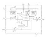
- FIG. 2illustrates a schematic block diagram of a start-up controller, according to specific example embodiments of this disclosure
- FIG. 3illustrates a schematic diagram of a prior art flyback converter
- FIG. 4illustrates a schematic block diagram of a forward power converter comprising a primary-side start-up technique, according to another specific example embodiment of this disclosure.
- a power convertermay comprise a start-up controller and a secondary-side controller, wherein the start-up controller is utilized to send power to the secondary-side controller when power (voltage) is first applied to the primary side of the power converter.
- ICintegrated circuit
- the start-up controlleris specifically designed for starting up a power converter, wherein the start-up controller is located on the primary-side of the power converter and a secondary-side controller is located on an electrically isolated, secondary-side of the power converter (transformer).
- the start-up controllermay have two modes of operation: 1) start-up controller operates as an open loop current regulator, and 2) the start-up controller receiving external PWM commands from the secondary-side controller for control of the power switch.
- the open loop current regulator modethe start-up controller is initially powered directly from a DC source voltage, e.g., battery or rectified AC line.
- the secondary-side controllerWhen the power converter's output charges to a sufficient voltage level the secondary-side controller will activate and take control of the power switch from the start-up controller. As the power converter powers up the start-up controller may receive bias from a primary-side tertiary winding of the transformer. Because the output power is only a small fraction of the power converter's rated power, wherein the output voltage may easily be protected against over-voltage by simple voltage shunt techniques, such as a power Zener diode, if the secondary-side controller fails to operate.
- the start-up controllerWhen the start-up controller receives external PWM commands (signals) from the secondary-side controller, the start-up controller switches to an external PWM commands mode when the external PWM commands from the secondary-side controller are detected. Wherein the ON and OFF times of the power switch are determined by the secondary-side controller such that the power converter can deliver its rated power or the power necessary to regulate the output voltage to the load. In normal operation the secondary-side controller regulates the output voltage to the load from the power converter. The secondary-side controller may connect the load to the power converter (either via a switch, or via a switching post regulator).
- PWM commands from the secondary-side controllerare sent to the start-up controller via an isolation circuit, e.g., an optocoupler or a pulse transformer.
- the isolation circuitis not required to operate linearly thereby alleviating problems caused by the optocoupler's current transfer ratio (CTR) issues if linear control was used.
- CTRcurrent transfer ratio
- the secondary-side controllermay make use of microprocessor resources located in the load (application) that the power converter is powering such that sophisticated power converter control techniques may be employed.
- start-up controllerIf the start-up controller ceases receiving external PWM commands it will revert back to its open loop current regulator mode. In either mode the start-up controller protects the power switch driver from under and over voltages.
- the start-up controllerlimits the maximum allowable transformer primary current.
- the start-up controllermay be used to start-up either a flyback power converter or a forward power converter. When used in a flyback power converter application the start-up controller has some additional features such as, for example but not limited to, an additional current-sense comparator that prevents the flyback power converter from entering too deeply into a continuous conduction mode of operation, thereby protecting the output of the flyback power converter from an over-current fault condition.
- the voltage from the transformer's primary-side tertiary winding, used to bias the start-up controller,may be coupled to the output voltage of the flyback converter. Therefore the voltage on the tertiary winding can be used as an output voltage feedback mechanism that can be used by the start-up controller's over-voltage lockout (OVLO) circuit as an additional level of over-voltage protection if the secondary-side controller fails to operate properly.
- OVLOover-voltage lockout
- the forward converter designmay require the following: A linear regulator may be required between the output of the transformer's primary-side tertiary winding and the bias input to the start-up controller. This is due to the fact that the tertiary winding is coupled to the rectified AC voltage and not the converter's output voltage.
- the forward converter's transformer's reset windingis located on the power converter's secondary side, and is actively clamped to provide a transformer reset.
- the active clampmay be designed to provide the initial bias for the secondary-side controller until the main source of bias for the secondary-side controller is established from the tertiary winding of the forward converter's output filter inductor.
- a flyback power convertermay comprise a primary side power rectifier and filters 104 coupled to an AC line power source 102 , a start-up controller 106 , a capacitor 107 , a transformer 122 , MOSFET switch 116 , a current sensing resistor 124 , a bias voltage rectifier 114 , a power rectifier 135 , a Zener diode 130 , a secondary-side controller 118 , a switching post regulator 120 , and an isolation circuit 108 .
- the flyback power converter 100provides regulated voltage to an application load 128 after start-up.
- the AC line power source 102may be in a universal range of from about 85 to 265 volts alternating current (AC) at a frequency of from about 47 Hz to about 63 Hz. It is contemplated and within the scope of this disclosure that the embodiments disclosed herein may be adapted for other voltages and frequencies.
- a DC sourcemay be used instead of using the primary side power rectifier and filters 104 coupled to an AC source.
- V_LinkDC voltage
- the start-up controller 106becomes active when the voltage, V_Link, reaches a sufficient voltage for proper operation thereof. Once activated the start-up controller 106 starts driving the MOSFET switch 116 from its gate node (output pin). The start-up controller 106 controls the switching of the MOSFET switch 116 in an open-loop manner based upon regulation of the peak current through the MOSFET switch 116 .
- a voltageis developed across resistor 124 in series with the MOSFET switch 116 and primary of the transformer 122 that is proportional to the peak current therethrough. This voltage is coupled to the C/S (current sense) input of the start-up controller 106 which senses it and adjusts the on time of the MOSFET switch 116 to limit the peak current to a certain design value.
- An internal linear regulator(see FIG. 2 , regulator 230 ) in the start-up controller 106 , whose input is the DC voltage, V_Link, regulates a voltage, V DD , usable by the internal circuits of the start-up converter 106 .
- V DDis the peak voltage at the gate node of the start-up controller 106 .
- the internal linear regulatorsupplies V DD for operation of the start-up controller 106 , but once a DC voltage is provided from a primary-side tertiary winding of the transformer 122 through the power diode 114 this internal linear regulator stops supplying current to the internal circuits of the start-up controller 106 . This allows internal thermal dissipation in the start-up controller 106 to be reduced.
- the transformer 122also provides bias voltage, V-Bias, via diode 114 .
- V-Biasmay be cross-regulated to the start-up controller 106 by transformer coupling.
- the winding turns ratio of the transformer 122is such that V_Bias is higher than the output voltage set point of the internal linear voltage regulator 230 ( FIG. 2 ) of the start-up controller 106 , thereby effectively shutting off this internal linear voltage regulator 230 and reducing the internal thermal dissipation of thereof.
- V_BulkOnce V_Bulk has risen to its design voltage the secondary-side controller 118 will control the switching post regulator 120 to provide V_Out to the application load 128 , thereby power loading the flyback converter 100 .
- the start-up controller 106may comprise a high voltage regulator 230 , internal bias voltage circuits 232 , a first voltage comparator 234 , a second voltage comparator 238 , a fixed blanking time circuit 240 , internal current regulator and logic circuits 236 , an external gate command detection circuit 242 , a signal buffer 244 , a switch 246 controlled by the logic circuits 236 , a MOSFET driver 248 , a fixed off-time timer 250 , and over and under voltage lockout circuits 252 .
- V IN inputis coupled to a voltage provided from the bridge rectifier and filters 104 ( FIG. 1 ) and is used as an input voltage to the high voltage regulator 230 dependent upon the AC line voltage 102 .
- the high voltage regulator 230may be a linear regulator that provides a lower voltage V DD for powering the MOSFET driver 248 and other internal bias voltages (bias circuits 232 ).
- V DDmay also be provided from an external source (e.g., V_Bias from the transformer 122 ( FIG. 1 ) such that the internal high voltage regulator 230 may turn off, thereby saving internal power dissipation within the start-up controller 106 .
- the voltage V DDmay be monitored by the over and under voltage lockout circuits 252 to protect the circuits within the start-up controller 106 from out of design specification voltages.
- Internal biases and voltage referencesmay be provided by the internal bias voltage circuits 232 which may receive its input operating voltage from the high voltage regulator 230 or an external source for V DD , e.g., transformer 122 .
- Gate drive commands to the gate driver 248may be switched between two sources using switch 246 that may be controlled by the logic circuits 236 .
- the first sourcemay be the internal current regulator and logic circuits 236
- the secondmay be from an external source coupled to the PWM input and internally buffered by the signal buffer 244 .
- the MOSFET currentis the same as the primary current of transformer.
- the logic circuits 236start the fixed blanking time circuit 240 that then momentarily blanks the signal at the current sense (C/S) node from reaching the internal current regulator and logic circuits 236 so that the internal current regulator therein may ignore the initial turn-on current spike through the MOSFET switch 116 .
- the first comparator 234 and the second comparator 238monitor the voltage at the current sense (C/S) input.
- the first comparator 234monitors the voltage at the C/S node for a brief time interval after the blanking time period of the fixed blanking time circuit 240 has finished. If the voltage at the C/S node exceeds a first voltage reference (V REF1 ) during this brief time interval then the gate drive is terminated.
- the second comparator 238sets the maximum voltage allowed (current through the MOSFET switch 116 ) at the current sense (C/S) input. If the voltage at the current sense (C/S) input is greater than a second voltage reference (V REF2 ) then the gate drive is also terminated. When the gate drive is terminated it remains off for a time period determined by the fixed off-time circuit 250 . This off time period may be externally selected by the capacitance value of a capacitor 107 at the T OFF node of the start-up controller 106 .
- PWMpulse width modulation
- the ground nodeis the circuit ground or common point for the circuits in the start-up controller 106 . This ground node may provide a return point for both the PWM drive current to the external MOSFET switch 116 and for bias return currents of the voltages at the V IN and V DD nodes.
- the start-up controller 106is not a primary-side power supply controller that can linearly regulate the output of a flyback power converter via transformer coupling. It does not duplicate the precision reference and voltage error amplifier of a secondary-side controller 118 .
- the start-up controller 106basically has two modes of operation: In the first mode, during start-up of the flyback power converter 100 , it performs as an open-loop current regulator that drives the MOSFET switch 116 until the secondary-side controller 118 takes control (command) of the PWM signals that drive the MOSFET switch 116 . In the second mode, once the secondary-side controller 118 is fully operational, it starts sending PWM signal commands to the start-up controller 106 through the isolation circuit 108 .
- the secondary-side controller 118may be either an analog controller or a digital controller (or an analog/digital hybrid). Very sophisticated control methods may be used by the secondary-side controller 118 , as long as the output of these control methods provides a PWM signal (which is typical).
- the secondary-side controller 118may communicate with the application load 128 (which loads the flyback power converter 100 via switching post regulator 120 ) for additional control sophistication.
- the open-loop current regulatorcomprising the start-up controller 106 , is designed to operate the flyback power converter 100 in a highly discontinuous mode of operation that provides a small amount of start-up power to a secondary winding of the transformer 122 whereby an output capacitor 126 is charged up and supplies operating voltage to the secondary-side controller 118 .
- the ON time(driving the external MOSFET switch 116 on) is typically determined by the amount of time it takes the PWM signal at the C/S node of the start-up controller 106 to ramp from zero volts to the V REF2 voltage of the second comparator 238 .
- the OFF time(driving the external MOSFET switch 116 off) may be determined by the fixed time-off timer 250 .
- the time duration of the fixed time-off timer 250may be determined by the value of a capacitor 107 coupled to the T OFF node of the start-up controller 106 . For example, a flyback converter rated for 20 watts of power can be made to deliver approximately one (1) watt of output power using the open-loop current regulator techniques and a long enough OFF time set by the capacitor 107 coupled to the T OFF node.
- switch 246changes the input to the gate driver 248 from the internal current regulator and logic circuits 236 to the external source (from the PWM node via signal buffer 244 ). This allows the secondary-side controller 118 to drive the flyback converter 112 at the proper frequency and PWM duty cycle to achieve rated output power and output voltage regulation.
- the start-up controller 106is simply a primary-side biased gate driver. However, the start-up controller 106 still provides the current protection afforded by the first and second voltage comparators 234 and 238 .
- switch 246will change back to the position where it gets its commands from the internal current regulator and logic circuits 236 where the OFF time is set by the fixed time-off timer 250 . Wherein the switch 246 cannot change position back to receiving commands via the signal buffer 244 until the end of the time period set by the fixed off-time timer 250 .
- switch 246When the external PWM signal from the secondary-side controller 118 via the isolation circuit 108 ceases (remaining in either a high state or a low state) (no longer being detected by the external gate command detection circuit 242 ) for a time period exceeding 250 ⁇ s, switch 246 will change back to the position where it gets its commands from the internal current regulator and logic circuits 236 .
- the over and under voltage lockout circuits 252ensure that the peak voltage at the gate node is within the proper range for the external power MOSFET switch 116 of the flyback converter 112 .
- the under-voltage lockout (UVLO) circuitensures enough voltage is available to properly enhance the gate of the MOSFET 116 .
- the over-voltage lockout (OVLO) circuitensures that the voltage does not exceed the typical gate voltage ratings of the power MOSFET 116 .
- the OVLO circuit 252also provides another important function: It must protect from a failure of the secondary-side controller 118 to start up and regulate. If the secondary-side controller 118 does not take command, the start-up controller 106 will continue to charge the output capacitor 126 until it reaches the over-voltage threshold.
- This voltage on the output capacitor 126is reflected back to the V DD node of the start-up controller 106 via the transformer 122 winding coupling and will trip the OVLO circuit in the start-up controller 106 .
- the MOSFET driver 248 outputwill be inhibited.
- the OVLO circuit 252may have, for example but is not limited to, a two (2) volt hysteresis band. Therefore gating of the MOSFET switch 116 is halted until the voltage at the V DD node of the start-up controller 106 decays below the lower limit of OVLO circuit's 252 hysteresis band.
- a power Zener diode 130(or some other form of active shunt regulator) may be placed across the output of the transformer 122 (e.g., across capacitor 126 ). Since the output power of the flyback power converter 100 can be set low by choosing a long OFF time with the capacitor 107 on the T OFF node of the start-up controller 106 , wherein the output of the transformer 122 via rectifier 135 can be reasonably protected against over-voltage by using a power Zener diode 130 shunted across the DC output therefrom.
- a forward power convertermay comprise a primary side power rectifier and filters 404 coupled to an AC line power source 402 , a start-up controller 106 , a capacitor 107 , a regulator 430 , a MOSFET switch 416 , a resistor 424 for current sensing, a bias voltage rectifier 414 , a transformer 422 , a secondary-side controller 418 , power rectifiers 435 and 436 , an active clamp circuit 440 , a current sense transformer 445 , an inductor 450 , a diode 455 , a clamp Zener diode 465 , a switch 460 , an isolation circuit 408 , and an application load 428 .
- a DC sourcemay be used instead of using the primary side power rectifier and filters 404 coupled to an AC line power source 402 , a start-up controller 106 , a capacitor 107 , a regulator 430 , a MOSFET switch 416 , a resistor 424 for current sensing
- the transformer 422may comprise four (4) windings: 1) a primary winding coupled to V_Link, 2) a secondary winding coupled to power rectifiers 435 and 436 , 3) a reset winding coupled to the active clamp circuit 440 , and 4) a tertiary winding coupled to rectifier 414 .
- the AC line 402may be in a universal range of from about 85 to 265 volts alternating current (AC) at a frequency of from about 47 Hz to about 63 Hz. It is contemplated and within the scope of this disclosure that the embodiments disclosed herein may be adapted for other voltages and frequencies.
- AC line power source 102is applied to the primary side power rectifier and filters 404 , a DC voltage, V_Link, results.
- This DC voltage, V_Linkis coupled to a primary winding of transformer 422 and the V IN input of the start-up controller 106 .
- the start-up controller 106is initially biased by V_Link (via its V IN node) upon application of the AC Line power source 402 .
- the start-up controller 106becomes active when the voltage, V_Link, reaches a sufficient voltage for proper operation thereof. Once so biased, the start-up controller 106 gates MOSFET switch 416 on and off.
- the start-up controller 106provides open-loop regulation of the current through the primary winding of transformer 422 by monitoring the voltage developed across the current sense resistor 424 coupled to its C/S node.
- the active clamp circuit 440clamps the reset winding voltage by the Zener diode on the gate of the PNP transistor thereof.
- the Zener diode on the collector of the PNP transistorclamps the voltage V CCS .
- V CCSis the bias voltage for the secondary-side controller 418 .
- Magnetization energy from the reset of transformer 422may be used to help bias the secondary-side controller 418 .
- MOSFET switch 416is gated off current flows through the tertiary winding of inductor 450 coupled to diode 455 . This also allows energy to flow to provide voltage V CCS . Once the forward power converter 400 is operational current flowing via diode 455 to the voltage V CCS will be the main source of operating power for the secondary-side controller 418 .
- the secondary-side controller 418can send gating commands to the start-up controller 106 via the isolation circuit 408 . Now the gating of the MOSFET switch 416 is controlled by the secondary-side controller 418 . The secondary-side controller 418 may then regulate the voltage V_OUT, close the switch 460 , and apply power to the application load 428 .
- the power delivered to the outputis set to be low with a selected value capacitor 107 coupled to the T OFF node (port) of the start-up controller 106 (see FIG. 2 ).
- the Zener diode on the collector of the PNP transistor of the active clamp circuit 440clamps the voltage on V CCS and protects the secondary-side controller 418 from over-voltage. Components across the output of the forward converter 400 may be protected by Zener diode 465 . Both of these Zener diodes act as protective shunt regulators.
- Comparator 234 shown in FIG. 2is not needed in the forward power converter 400 design. Its purpose is to keep the flyback power converter 100 from entering into a continuous conduction mode of operation. However, the main winding of inductor 450 of a forward power converter 400 is typically kept in a continuous conduction mode.
- a power Zener diode 130 / 465may be placed in parallel with capacitor 126 / 426 , wherein the cathode of the Zener diode 130 / 465 is coupled to the positive side of capacitor 126 / 426 and the anode of the Zener diode 130 / 465 may be coupled to the negative side of capacitor 126 / 426 .
- the Zener diode 130 / 465is shunted across the output of the flyback power converter 100 or forward power converter 400 .
- the Zener diode 130 / 465 breakdown voltageis higher than a normal voltage output on the capacitor 126 / 426 .
- Zener diode 130 / 465will dissipate the output power of the flyback or forward power converters 100 or 400 , respectively, determined by the capacitance value of the capacitor 107 at the T OFF pin of the start-up controller 106 .
- the Zener diode 130 / 465should be rated for at least that power dissipation. It is contemplated and within the scope of this disclosure, that the function of the Zener diode 130 / 465 may be replaced by active circuitry that performs this shunt clamp function. This is typically done if a more accurate breakdown voltage is required.
- a purpose of the start-up controller 106is to start-up a power converter 100 / 400 by having an open loop-current regulator with a short ON time (the MOSFET switch 116 / 416 is gated ON) and a very long OFF time (the OFF time is determine by the capacitor value placed on the T-off node of the start-up controller 106 in FIG. 2 ).
- a power converter 100 / 400 rated for powers ranging from about 20 watts to 60 wattsmay have a start-up power of about one (1) watt.
- one (1) watt of powermay be delivered to the secondary to charge up the converter's output capacitor 126 / 426 and start up the secondary-side controller 118 / 418 .
- the secondary-side controller 118 / 418would start up in time to prevent the output capacitor 126 / 426 from over-charging (over-voltage).
- the open loop start-up controller 106will continue to charge the output capacitor 126 / 426 (its open loop, meaning it gets no voltage feedback). So it's necessary to clamp the voltage across the output capacitor 126 / 426 to a voltage somewhere around 125% of the normal rated output voltage for protection.
- Zener diode 130 / 465With the appropriate breakdown voltage. This Zener diode 130 / 465 needs to be rated to handle the start-up power. For example, a Zener diode rated for two (2) watts will easily handle the (1) watt start-up power. A power converter 100 / 400 with a failed secondary-side controller 118 / 418 will remain in this Zener-clamped state until the AC line power source 102 / 402 is removed. For a forward converter 400 , this is the only way to protect against overvoltage if the secondary-side controller 418 fails to start.
- the start-up controller's 106 OVLO lockout circuits 252may also be employed to prevent over-voltage in the event of a failure of the secondary-side controller 118 .
- the Zener 130 clampprovides an additional level of protection.
Landscapes
- Engineering & Computer Science (AREA)
- Power Engineering (AREA)
- Dc-Dc Converters (AREA)
Abstract
Description
Claims (13)
Priority Applications (1)
| Application Number | Priority Date | Filing Date | Title |
|---|---|---|---|
| US15/812,850US10193458B2 (en) | 2014-11-20 | 2017-11-14 | Start-up controller for a power converter |
Applications Claiming Priority (3)
| Application Number | Priority Date | Filing Date | Title |
|---|---|---|---|
| US201462082317P | 2014-11-20 | 2014-11-20 | |
| US14/945,729US9819274B2 (en) | 2014-11-20 | 2015-11-19 | Start-up controller for a power converter |
| US15/812,850US10193458B2 (en) | 2014-11-20 | 2017-11-14 | Start-up controller for a power converter |
Related Parent Applications (1)
| Application Number | Title | Priority Date | Filing Date |
|---|---|---|---|
| US14/945,729DivisionUS9819274B2 (en) | 2014-11-20 | 2015-11-19 | Start-up controller for a power converter |
Publications (2)
| Publication Number | Publication Date |
|---|---|
| US20180109197A1 US20180109197A1 (en) | 2018-04-19 |
| US10193458B2true US10193458B2 (en) | 2019-01-29 |
Family
ID=56011209
Family Applications (2)
| Application Number | Title | Priority Date | Filing Date |
|---|---|---|---|
| US14/945,729ActiveUS9819274B2 (en) | 2014-11-20 | 2015-11-19 | Start-up controller for a power converter |
| US15/812,850ActiveUS10193458B2 (en) | 2014-11-20 | 2017-11-14 | Start-up controller for a power converter |
Family Applications Before (1)
| Application Number | Title | Priority Date | Filing Date |
|---|---|---|---|
| US14/945,729ActiveUS9819274B2 (en) | 2014-11-20 | 2015-11-19 | Start-up controller for a power converter |
Country Status (7)
| Country | Link |
|---|---|
| US (2) | US9819274B2 (en) |
| EP (1) | EP3221955B1 (en) |
| JP (1) | JP2017536076A (en) |
| KR (1) | KR20170086531A (en) |
| CN (2) | CN110601524B (en) |
| TW (1) | TW201630319A (en) |
| WO (1) | WO2016081803A1 (en) |
Cited By (3)
| Publication number | Priority date | Publication date | Assignee | Title |
|---|---|---|---|---|
| EP4429094A1 (en)* | 2023-03-10 | 2024-09-11 | Infineon Technologies Austria AG | Power converter controller, power converter and methods of operating a power converter |
| US12375000B2 (en)* | 2023-02-20 | 2025-07-29 | Cypress Semiconductor Corporation | Implementing power factor correction with single-stage flyback converters operating with a fixed switching frequency |
| US12438452B2 (en)* | 2023-02-20 | 2025-10-07 | Cypress Semiconductor Corporation | Implementing power factor correction with single-stage flyback converters operating with a variable switching frequency |
Families Citing this family (49)
| Publication number | Priority date | Publication date | Assignee | Title |
|---|---|---|---|---|
| DE102014200865A1 (en)* | 2014-01-17 | 2015-07-23 | Osram Gmbh | Circuit arrangement for operating light sources |
| US9479065B2 (en)* | 2014-10-17 | 2016-10-25 | Power Integrations, Inc. | Controller supply terminal boosting |
| US9712045B2 (en)* | 2014-11-17 | 2017-07-18 | Infineon Technologies Austria Ag | System and method for a startup cell circuit |
| US9819274B2 (en)* | 2014-11-20 | 2017-11-14 | Microchip Technology Incorporated | Start-up controller for a power converter |
| US10277130B2 (en) | 2015-06-01 | 2019-04-30 | Microchip Technolgoy Incorporated | Primary-side start-up method and circuit arrangement for a series-parallel resonant power converter |
| US9912243B2 (en) | 2015-06-01 | 2018-03-06 | Microchip Technology Incorporated | Reducing power in a power converter when in a standby mode |
| US9705408B2 (en) | 2015-08-21 | 2017-07-11 | Microchip Technology Incorporated | Power converter with sleep/wake mode |
| US20170117813A1 (en)* | 2015-10-21 | 2017-04-27 | Quanta Computer Inc. | Method and system for testing a power supply unit |
| US10541617B2 (en)* | 2016-06-02 | 2020-01-21 | Semiconductor Components Industries, Llc | Overload protection for power converter |
| US10903746B2 (en)* | 2016-08-05 | 2021-01-26 | Texas Instruments Incorporated | Load dependent in-rush current control with fault detection across Iso-barrier |
| US10355603B2 (en)* | 2016-08-17 | 2019-07-16 | Semiconductor Components Industries, Llc | Control circuit for power converter with isolated or non-isolated feedback |
| US10090769B2 (en) | 2016-11-29 | 2018-10-02 | Texas Instruments Incorporated | Isolated high frequency DC/DC switching regulator |
| CN110073584B (en)* | 2017-01-12 | 2022-06-14 | 戴泺格半导体股份有限公司 | Hybrid secondary side regulation |
| US10355602B2 (en)* | 2017-01-18 | 2019-07-16 | Analog Devices Global | Fault suppression or recovery for isolated conversion |
| JP2018129952A (en)* | 2017-02-09 | 2018-08-16 | オムロンオートモーティブエレクトロニクス株式会社 | Power conversion device |
| JP6717220B2 (en)* | 2017-02-09 | 2020-07-01 | オムロン株式会社 | Power converter |
| JP6876482B2 (en)* | 2017-03-29 | 2021-05-26 | Fdk株式会社 | Insulated switching power supply |
| US10211744B2 (en)* | 2017-05-15 | 2019-02-19 | Stmicroelectronics S.R.L. | Secondary side current mode control for a converter |
| US10761111B2 (en) | 2017-05-25 | 2020-09-01 | Texas Instruments Incorporated | System and method for control of automated test equipment contactor |
| US10236777B2 (en)* | 2017-08-09 | 2019-03-19 | L3 Cincinnati Electronics Corporation | Magnetically isolated feedback circuits and regulated power supplies incorporating the same |
| US10193457B1 (en) | 2017-09-15 | 2019-01-29 | Abb Schweiz Ag | System and method for starting up a high density isolated DC-to-DC power converter |
| US10320301B2 (en) | 2017-09-15 | 2019-06-11 | Semiconductor Components Industries, Llc | Power converter responsive to device connection status |
| US10622908B2 (en) | 2017-09-19 | 2020-04-14 | Texas Instruments Incorporated | Isolated DC-DC converter |
| US10432102B2 (en) | 2017-09-22 | 2019-10-01 | Texas Instruments Incorporated | Isolated phase shifted DC to DC converter with secondary side regulation and sense coil to reconstruct primary phase |
| US10170985B1 (en)* | 2017-12-06 | 2019-01-01 | National Chung Shan Institute Of Science And Technology | Apparatus for current estimation of DC/DC converter and DC/DC converter assembly |
| US10320283B1 (en) | 2018-01-26 | 2019-06-11 | Universal Lighting Technologies, Inc. | Resonant converter with pre-charging circuit for startup protection |
| CN110247554B (en)* | 2018-03-09 | 2020-09-11 | 台达电子工业股份有限公司 | Conversion device and control method thereof |
| US10574129B2 (en)* | 2018-05-04 | 2020-02-25 | Raytheon Company | System and method for adaptively controlling a reconfigurable power converter |
| TWI657250B (en)* | 2018-05-24 | 2019-04-21 | 產晶積體電路股份有限公司 | Current detection method |
| US10707746B1 (en) | 2018-05-31 | 2020-07-07 | Universal Lighting Technologies, Inc. | Power converter with independent multiplier input for PFC circuit |
| TWI669586B (en)* | 2018-11-15 | 2019-08-21 | 康舒科技股份有限公司 | Primary side integrated circuit module of power supply |
| US10797613B1 (en)* | 2019-04-05 | 2020-10-06 | Advanced Energy Industries, Inc. | Power supply system with actively switched bus capacitor |
| CN110198118A (en)* | 2019-05-17 | 2019-09-03 | 许继电源有限公司 | A kind of auxiliary electric source actuating apparatus and a kind of accessory power supply |
| US10951107B2 (en)* | 2019-06-27 | 2021-03-16 | Cypress Semiconductor Corporation | Communicating fault indications between primary and secondary controllers in a secondary-controlled flyback converter |
| US10756644B1 (en)* | 2019-08-22 | 2020-08-25 | Cypress Semiconductor Corporation | Controlled gate-source voltage N-channel field effect transistor (NFET) gate driver |
| US11114945B2 (en)* | 2019-08-22 | 2021-09-07 | Cypress Semiconductor Corporation | Secondary-controlled active clamp implementation for improved efficiency |
| CN110855156B (en)* | 2019-12-10 | 2021-04-16 | 格力博(江苏)股份有限公司 | Flyback switching power supply |
| US11165352B2 (en) | 2020-01-16 | 2021-11-02 | L3 Cincinnati Electronics Corporation | Capacitively isolated feedback circuits and regulated power supplies incorporating the same |
| CN113285602B (en)* | 2020-02-19 | 2024-08-27 | 万国半导体(开曼)股份有限公司 | Flyback converter with fixed on time and control method |
| TWI762896B (en)* | 2020-04-01 | 2022-05-01 | 宏碁股份有限公司 | Power supply device for eliminating malfunction of over current protection |
| US11418031B2 (en)* | 2020-05-08 | 2022-08-16 | Raytheon Company | Actively-controlled power transformer and method for controlling |
| TWI726758B (en)* | 2020-07-01 | 2021-05-01 | 宏碁股份有限公司 | Power supply device for eliminating ringing effect |
| CN112134453B (en)* | 2020-09-08 | 2021-10-29 | 台达电子企业管理(上海)有限公司 | Startup control method and system, peak voltage detection circuit and method |
| EP3993249A1 (en)* | 2020-10-28 | 2022-05-04 | NXP USA, Inc. | Advanced power supply to insure safe behavior of an inverter application |
| US11711023B2 (en)* | 2021-05-14 | 2023-07-25 | Queen's University At Kingston | Methods and circuits for sensing isolated power converter output voltage across the isolation barrier |
| US11853088B2 (en)* | 2021-09-08 | 2023-12-26 | International Business Machines Corporation | Linking separate eFuse and ORING controllers for output overvoltage protection in redundant power converters |
| US11804777B2 (en) | 2021-10-08 | 2023-10-31 | Infineon Technologies Austria Ag | Power supply and emulated current mode control |
| TWI806684B (en)* | 2022-07-04 | 2023-06-21 | 宏碁股份有限公司 | Power supply device |
| US12261560B2 (en) | 2023-05-03 | 2025-03-25 | Raytheon Company | Active harmonic filter and reactive power control system for naval ship power systems |
Citations (77)
| Publication number | Priority date | Publication date | Assignee | Title |
|---|---|---|---|---|
| US4967332A (en)* | 1990-02-26 | 1990-10-30 | General Electric Company | HVIC primary side power supply controller including full-bridge/half-bridge driver |
| US5301095A (en) | 1991-10-01 | 1994-04-05 | Origin Electric Company, Limited | High power factor AC/DC converter |
| EP0618665A2 (en) | 1993-03-31 | 1994-10-05 | Thomson Consumer Electronics, Inc. | Feedback limited duty cycle switched mode power supply |
| US5498995A (en)* | 1993-03-17 | 1996-03-12 | National Semiconductor Corporation | Short circuit frequency shift circuit for switching regulators |
| US5757627A (en) | 1996-05-01 | 1998-05-26 | Compaq Computer Corporation | Isolated power conversion with master controller in secondary |
| US6188276B1 (en)* | 1998-09-21 | 2001-02-13 | Anastasios V. Simopoulos | Power amplifier |
| US20010043479A1 (en)* | 2000-03-27 | 2001-11-22 | Tamiji Nagai | Power supply apparatus |
| US20020006045A1 (en) | 1999-07-27 | 2002-01-17 | Toshihito Shirai | Power supply unit |
| US20020125867A1 (en) | 2001-03-09 | 2002-09-12 | Samsung Electronics Co., Ltd. | Power supply control apparatus and method thereof |
| US6456511B1 (en)* | 2000-02-17 | 2002-09-24 | Tyco Electronics Corporation | Start-up circuit for flyback converter having secondary pulse width modulation |
| US6490177B1 (en) | 1998-10-05 | 2002-12-03 | Salvador Figueroa | Resonant power converter with primary-side tuning and zero-current switching |
| US6504267B1 (en) | 2001-12-14 | 2003-01-07 | Koninklijke Philips Electronics N.V. | Flyback power converter with secondary-side control and primary-side soft switching |
| US20070133234A1 (en)* | 2005-12-07 | 2007-06-14 | Active-Semi International Inc. | System and method for a primary feedback switched mode power supply |
| US20070252563A1 (en)* | 2006-04-26 | 2007-11-01 | Mitsumi Electric Co. Ltd. | Multi-ouput type DC/DC converter |
| US20080259655A1 (en) | 2007-04-19 | 2008-10-23 | Da-Chun Wei | Switching-mode power converter and pulse-width-modulation control circuit with primary-side feedback control |
| US20080265133A1 (en) | 2007-04-30 | 2008-10-30 | Sawtell Carl K | Power Supply Control Circuit with Optical Feedback |
| DE102008027054A1 (en) | 2007-07-02 | 2009-01-08 | Fuji Electric Device Technology Co., Ltd. | Switching power supply device |
| US20090261790A1 (en) | 2008-04-22 | 2009-10-22 | Douglas Paul Arduini | Synchronous rectifier post regulator |
| US20090273324A1 (en)* | 2004-12-21 | 2009-11-05 | Rohm Co., Ltd. | Switching regulator |
| US20090295346A1 (en)* | 2008-05-29 | 2009-12-03 | Power Integrations, Inc. | Method and apparatus for implementing an unregulated dormant mode in a power converter |
| US20090295349A1 (en)* | 2008-05-30 | 2009-12-03 | Active-Semi, Inc. | Constant current and voltage controller in a three-pin package with dual-use switch pin |
| CN101651426A (en) | 2009-09-10 | 2010-02-17 | 广州金升阳科技有限公司 | Self-starting control power converter of output terminal |
| US20100194198A1 (en)* | 2009-02-05 | 2010-08-05 | Power Integrations, Inc. | Method and apparatus for implementing an unregulated dormant mode with an event counter in a power converter |
| US20100208500A1 (en)* | 2009-02-19 | 2010-08-19 | Iwatt Inc. | Detecting Light Load Conditions and Improving Light Load Efficiency in a Switching Power Converter |
| US20100308875A1 (en) | 2008-03-03 | 2010-12-09 | Thomson Licensing | Switchable load for initializing an output voltage of a power supply |
| US20100327761A1 (en) | 2009-06-30 | 2010-12-30 | Microsemi Corporation | Integrated backlight control system |
| US20110019446A1 (en)* | 2009-07-22 | 2011-01-27 | Bcd Semiconductor Manufacturing Limited | Method and apparatus for a switching mode power supply |
| US20110032732A1 (en) | 2009-08-04 | 2011-02-10 | Ta-Ching Hsu | Secondary side post regulator of flyback power converter with multile outputs |
| US20110075448A1 (en) | 2009-09-30 | 2011-03-31 | Melanson John L | Switching power converter controller with direct current transformer sensing |
| US20110103104A1 (en)* | 2009-10-30 | 2011-05-05 | Intersil Americas Inc. | Bias and discharge system for low power loss start up and input capacitance discharge |
| US20110164437A1 (en) | 2010-01-07 | 2011-07-07 | Texas Instruments Incorporated | LLC Soft Start By Operation Mode Switching |
| US20110211370A1 (en) | 2010-03-01 | 2011-09-01 | Texas Instruments Incorporated | Systems and Methods of Resonant DC/DC Conversion |
| US20110305043A1 (en)* | 2010-06-11 | 2011-12-15 | Murata Manufacturing Co., Ltd. | Isolated switching power supply apparatus |
| CN102361402A (en) | 2011-10-21 | 2012-02-22 | 广州金升阳科技有限公司 | Switching power supply circuit |
| US20120099345A1 (en) | 2010-10-25 | 2012-04-26 | Analog Devices, Inc. | Soft-start control system and method for an isolated dc-dc converter with secondary controller |
| US20120139342A1 (en)* | 2010-12-06 | 2012-06-07 | Power Integrations, Inc. | Method and apparatus for implementing an unregulated dormant mode with output reset in a power converter |
| US20120139477A1 (en) | 2010-12-03 | 2012-06-07 | Motorola, Inc. | Power supply circuit having lowidle power dissipation |
| US20120230069A1 (en) | 2011-03-11 | 2012-09-13 | Ren-Huei Tzeng | Startup control circuit with acceleration startup function and method for operating the same |
| US20120243271A1 (en)* | 2011-03-25 | 2012-09-27 | Berghegger Ralf Schroeder Genannt | Power Converter with Reduced Power Dissipation |
| US20120262953A1 (en) | 2011-04-12 | 2012-10-18 | Flextronics Ap, Llc | Multi-phase resonant converter |
| US20120280642A1 (en)* | 2011-05-04 | 2012-11-08 | Ying-Chen Lin | Start-up Circuit and Motor Driving IC |
| US20120294048A1 (en) | 2009-06-17 | 2012-11-22 | Power Systems Technologies, Ltd. | Start-Up Circuit for a Power Adapter |
| US20130016535A1 (en) | 2011-07-12 | 2013-01-17 | Power Systems Technologies, Ltd. | Controller for a Power Converter and Method of Operating the Same |
| US20130155728A1 (en) | 2011-12-14 | 2013-06-20 | Cirrus Logic, Inc. | Isolation of Secondary Transformer Winding Current During Auxiliary Power Supply Generation |
| US20130194020A1 (en) | 2012-01-31 | 2013-08-01 | Macronix International Co., Ltd. | Level shifting circuit |
| US20130223108A1 (en)* | 2012-02-28 | 2013-08-29 | Silergy Semiconductor Technology (Hangzhou) Ltd | Constant voltage constant current controller and control method thereof |
| US20130229829A1 (en) | 2012-03-01 | 2013-09-05 | Infineon Technologies Ag | Multi-Mode Operation and Control of a Resonant Converter |
| US20130236203A1 (en) | 2012-03-09 | 2013-09-12 | Canon Kabushiki Kaisha | Power supply device and image forming apparatus |
| US20130301308A1 (en) | 2011-01-26 | 2013-11-14 | Murata Manufacturing Co., Ltd. | Switching power supply device |
| US20130300384A1 (en)* | 2012-05-08 | 2013-11-14 | Chengdu Monolithic Power Systems Co., Ltd. | Isolated switching mode power supply and the method thereof |
| US20140028095A1 (en) | 2012-07-25 | 2014-01-30 | Cirrus Logic, Inc. | Acceleration of output energy provision for a load during start-up of a switching power converter |
| US20140140107A1 (en) | 2012-11-16 | 2014-05-22 | Noveltek Semiconductor Corp. | Isolated power converter, inverting type shunt regulator, and operating method thereof |
| US20140160810A1 (en) | 2012-12-11 | 2014-06-12 | Iwatt Inc. | Digital Communication Link Between Secondary Side and Primary Side of Switching Power Converter |
| EP2775602A2 (en) | 2013-03-08 | 2014-09-10 | Power Integrations, Inc. | Techniques for controlling a power converter using multiple controllers |
| US20140253225A1 (en)* | 2013-03-10 | 2014-09-11 | Microchip Technology Incorporated | Method and Apparatus for Generating Regulated Isolation Supply Voltage |
| US20140254215A1 (en) | 2011-08-29 | 2014-09-11 | Power Systems Technologies Ltd. | Controller for a power converter and method of operating the same |
| US20140253227A1 (en)* | 2013-03-10 | 2014-09-11 | Microchip Technology Incorporated | Integrated High Voltage Isolation Using Low Value Capacitors |
| US20140313790A1 (en) | 2013-04-23 | 2014-10-23 | Virginia Tech Intellectual Properties, Inc. | Optimal Trajectory Control for LLC Resonant Converter for Soft Start-Up |
| US20140313794A1 (en)* | 2013-02-25 | 2014-10-23 | Rohm Co., Ltd. | Power delivery device and start-up method, ac adapter and electronic apparatus |
| US20140321170A1 (en)* | 2013-04-30 | 2014-10-30 | Texas Instruments Incorporated | Integrated primary startup bias and mosfet driver |
| US20140369086A1 (en) | 2013-06-14 | 2014-12-18 | Canon Kabushiki Kaisha | Power supply apparatus and image forming apparatus |
| US20150016152A1 (en) | 2013-07-12 | 2015-01-15 | Canon Kabushiki Kaisha | Power supply apparatus and image forming apparatus |
| US20150023063A1 (en) | 2012-03-08 | 2015-01-22 | Massachusetts Institute Of Technology | Resonant Power Converters Using Impedance Control Networks And Related Techniques |
| US20150091544A1 (en)* | 2013-09-30 | 2015-04-02 | Micrel, Inc. | Timer based pfm exit control method for a boost regulator |
| US20150124488A1 (en) | 2013-11-07 | 2015-05-07 | Futurewei Technologies, Inc. | Startup Method and System for Resonant Converters |
| US20150280584A1 (en) | 2014-04-01 | 2015-10-01 | Infineon Technologies Austria Ag | System and Method for a Switched-Mode Power Supply |
| US20150280573A1 (en) | 2014-04-01 | 2015-10-01 | Infineon Technologies Austria Ag | System and Method for a Switched-Mode Power Supply |
| US20160079878A1 (en) | 2014-09-12 | 2016-03-17 | Alpha And Omega Semiconductor (Cayman) Ltd. | Constant on time (cot) control in isolated converter |
| US20160087541A1 (en)* | 2014-09-23 | 2016-03-24 | Analog Devices Global | Minimum duty cycle control for active snubber |
| US9331583B2 (en)* | 2012-12-24 | 2016-05-03 | Chengdu Monolithic Power Systems Co., Ltd. | Switch mode power supply, control circuit and associated control method |
| US20160141951A1 (en)* | 2014-11-17 | 2016-05-19 | Infineon Technologies Austria Ag | System and Method for a Startup Cell Circuit |
| US20160149504A1 (en)* | 2014-11-20 | 2016-05-26 | Microchip Technology Incorporated | Start-up controller for a power converter |
| US20160190938A1 (en)* | 2014-12-31 | 2016-06-30 | Bcd Semiconductor Manufacturing Co., Ltd. | Switching mode power supply with selectable constant-voltage cpmstamt-current control |
| US20160226239A1 (en)* | 2015-02-02 | 2016-08-04 | On-Bright Electronics (Shanghai) Co., Ltd. | System and Method Providing Reliable Over Current Protection for Power Converter |
| US20160352231A1 (en)* | 2015-06-01 | 2016-12-01 | Microchip Technology Incorporated | Primary-Side Start-Up Method And Circuit Arrangement For A Series-Parallel Resonant Power Converter |
| US20160352237A1 (en)* | 2015-06-01 | 2016-12-01 | Microchip Technology Incorporated | Reducing power in a power converter when in a standby mode |
| US20170054376A1 (en)* | 2015-08-21 | 2017-02-23 | Microchip Technology Incorporated | Power Converter With Sleep/Wake Mode |
Family Cites Families (7)
| Publication number | Priority date | Publication date | Assignee | Title |
|---|---|---|---|---|
| JPH069591Y2 (en)* | 1987-08-25 | 1994-03-09 | シャープ株式会社 | Switching Regulator |
| JP2004140896A (en)* | 2002-10-16 | 2004-05-13 | Toshiba Corp | Power converter |
| EP2077608B1 (en)* | 2008-01-02 | 2016-11-30 | Infineon Technologies Austria AG | Drive circuit for a switch in a switching converter |
| US8125799B2 (en)* | 2009-10-23 | 2012-02-28 | Bcd Semiconductor Manufacturing Limited | Control circuits and methods for switching mode power supplies |
| EP2553798B1 (en)* | 2010-03-30 | 2014-12-03 | Telefonaktiebolaget L M Ericsson (publ) | Switched mode power supply with voltage regulator |
| JP5986839B2 (en)* | 2012-07-27 | 2016-09-06 | ローム株式会社 | DC / DC converter and control circuit thereof, power supply using the same, power adapter, and electronic device |
| US20150280576A1 (en)* | 2014-03-26 | 2015-10-01 | Infineon Technologies Austria Ag | System and Method for a Switched Mode Power Supply |
- 2015
- 2015-11-19USUS14/945,729patent/US9819274B2/enactiveActive
- 2015-11-20EPEP15805037.7Apatent/EP3221955B1/enactiveActive
- 2015-11-20TWTW104138609Apatent/TW201630319A/enunknown
- 2015-11-20CNCN201910796806.9Apatent/CN110601524B/enactiveActive
- 2015-11-20WOPCT/US2015/061769patent/WO2016081803A1/enactiveIP Right Grant
- 2015-11-20JPJP2017526867Apatent/JP2017536076A/enactivePending
- 2015-11-20KRKR1020177014436Apatent/KR20170086531A/ennot_activeWithdrawn
- 2015-11-20CNCN201580062068.5Apatent/CN107112889B/enactiveActive
- 2017
- 2017-11-14USUS15/812,850patent/US10193458B2/enactiveActive
Patent Citations (80)
| Publication number | Priority date | Publication date | Assignee | Title |
|---|---|---|---|---|
| US4967332A (en)* | 1990-02-26 | 1990-10-30 | General Electric Company | HVIC primary side power supply controller including full-bridge/half-bridge driver |
| US5301095A (en) | 1991-10-01 | 1994-04-05 | Origin Electric Company, Limited | High power factor AC/DC converter |
| US5498995A (en)* | 1993-03-17 | 1996-03-12 | National Semiconductor Corporation | Short circuit frequency shift circuit for switching regulators |
| EP0618665A2 (en) | 1993-03-31 | 1994-10-05 | Thomson Consumer Electronics, Inc. | Feedback limited duty cycle switched mode power supply |
| US5757627A (en) | 1996-05-01 | 1998-05-26 | Compaq Computer Corporation | Isolated power conversion with master controller in secondary |
| US6188276B1 (en)* | 1998-09-21 | 2001-02-13 | Anastasios V. Simopoulos | Power amplifier |
| US6490177B1 (en) | 1998-10-05 | 2002-12-03 | Salvador Figueroa | Resonant power converter with primary-side tuning and zero-current switching |
| US20020006045A1 (en) | 1999-07-27 | 2002-01-17 | Toshihito Shirai | Power supply unit |
| US6456511B1 (en)* | 2000-02-17 | 2002-09-24 | Tyco Electronics Corporation | Start-up circuit for flyback converter having secondary pulse width modulation |
| US20010043479A1 (en)* | 2000-03-27 | 2001-11-22 | Tamiji Nagai | Power supply apparatus |
| US20020125867A1 (en) | 2001-03-09 | 2002-09-12 | Samsung Electronics Co., Ltd. | Power supply control apparatus and method thereof |
| US6504267B1 (en) | 2001-12-14 | 2003-01-07 | Koninklijke Philips Electronics N.V. | Flyback power converter with secondary-side control and primary-side soft switching |
| US20090273324A1 (en)* | 2004-12-21 | 2009-11-05 | Rohm Co., Ltd. | Switching regulator |
| US20070133234A1 (en)* | 2005-12-07 | 2007-06-14 | Active-Semi International Inc. | System and method for a primary feedback switched mode power supply |
| US20070252563A1 (en)* | 2006-04-26 | 2007-11-01 | Mitsumi Electric Co. Ltd. | Multi-ouput type DC/DC converter |
| US20080259655A1 (en) | 2007-04-19 | 2008-10-23 | Da-Chun Wei | Switching-mode power converter and pulse-width-modulation control circuit with primary-side feedback control |
| US20080265133A1 (en) | 2007-04-30 | 2008-10-30 | Sawtell Carl K | Power Supply Control Circuit with Optical Feedback |
| US7746672B2 (en)* | 2007-07-02 | 2010-06-29 | Fuji Electric Device Technology Co., Ltd. | Switching power supply apparatus |
| US20090010027A1 (en) | 2007-07-02 | 2009-01-08 | Fuji Electric Device Technology Co., Ltd. | Switching power supply apparatus |
| DE102008027054A1 (en) | 2007-07-02 | 2009-01-08 | Fuji Electric Device Technology Co., Ltd. | Switching power supply device |
| US20100308875A1 (en) | 2008-03-03 | 2010-12-09 | Thomson Licensing | Switchable load for initializing an output voltage of a power supply |
| US20090261790A1 (en) | 2008-04-22 | 2009-10-22 | Douglas Paul Arduini | Synchronous rectifier post regulator |
| US20090295346A1 (en)* | 2008-05-29 | 2009-12-03 | Power Integrations, Inc. | Method and apparatus for implementing an unregulated dormant mode in a power converter |
| US20090295349A1 (en)* | 2008-05-30 | 2009-12-03 | Active-Semi, Inc. | Constant current and voltage controller in a three-pin package with dual-use switch pin |
| US20100194198A1 (en)* | 2009-02-05 | 2010-08-05 | Power Integrations, Inc. | Method and apparatus for implementing an unregulated dormant mode with an event counter in a power converter |
| US20100208500A1 (en)* | 2009-02-19 | 2010-08-19 | Iwatt Inc. | Detecting Light Load Conditions and Improving Light Load Efficiency in a Switching Power Converter |
| US20120294048A1 (en) | 2009-06-17 | 2012-11-22 | Power Systems Technologies, Ltd. | Start-Up Circuit for a Power Adapter |
| US20100327761A1 (en) | 2009-06-30 | 2010-12-30 | Microsemi Corporation | Integrated backlight control system |
| US20110019446A1 (en)* | 2009-07-22 | 2011-01-27 | Bcd Semiconductor Manufacturing Limited | Method and apparatus for a switching mode power supply |
| US20110032732A1 (en) | 2009-08-04 | 2011-02-10 | Ta-Ching Hsu | Secondary side post regulator of flyback power converter with multile outputs |
| CN101651426A (en) | 2009-09-10 | 2010-02-17 | 广州金升阳科技有限公司 | Self-starting control power converter of output terminal |
| US20110075448A1 (en) | 2009-09-30 | 2011-03-31 | Melanson John L | Switching power converter controller with direct current transformer sensing |
| US20110103104A1 (en)* | 2009-10-30 | 2011-05-05 | Intersil Americas Inc. | Bias and discharge system for low power loss start up and input capacitance discharge |
| US20110164437A1 (en) | 2010-01-07 | 2011-07-07 | Texas Instruments Incorporated | LLC Soft Start By Operation Mode Switching |
| US20110211370A1 (en) | 2010-03-01 | 2011-09-01 | Texas Instruments Incorporated | Systems and Methods of Resonant DC/DC Conversion |
| US20110305043A1 (en)* | 2010-06-11 | 2011-12-15 | Murata Manufacturing Co., Ltd. | Isolated switching power supply apparatus |
| US20120099345A1 (en) | 2010-10-25 | 2012-04-26 | Analog Devices, Inc. | Soft-start control system and method for an isolated dc-dc converter with secondary controller |
| US20120139477A1 (en) | 2010-12-03 | 2012-06-07 | Motorola, Inc. | Power supply circuit having lowidle power dissipation |
| US20120139342A1 (en)* | 2010-12-06 | 2012-06-07 | Power Integrations, Inc. | Method and apparatus for implementing an unregulated dormant mode with output reset in a power converter |
| US20130301308A1 (en) | 2011-01-26 | 2013-11-14 | Murata Manufacturing Co., Ltd. | Switching power supply device |
| US20120230069A1 (en) | 2011-03-11 | 2012-09-13 | Ren-Huei Tzeng | Startup control circuit with acceleration startup function and method for operating the same |
| US20120243271A1 (en)* | 2011-03-25 | 2012-09-27 | Berghegger Ralf Schroeder Genannt | Power Converter with Reduced Power Dissipation |
| US20120262953A1 (en) | 2011-04-12 | 2012-10-18 | Flextronics Ap, Llc | Multi-phase resonant converter |
| US20120280642A1 (en)* | 2011-05-04 | 2012-11-08 | Ying-Chen Lin | Start-up Circuit and Motor Driving IC |
| US20130016535A1 (en) | 2011-07-12 | 2013-01-17 | Power Systems Technologies, Ltd. | Controller for a Power Converter and Method of Operating the Same |
| US20140254215A1 (en) | 2011-08-29 | 2014-09-11 | Power Systems Technologies Ltd. | Controller for a power converter and method of operating the same |
| CN102361402A (en) | 2011-10-21 | 2012-02-22 | 广州金升阳科技有限公司 | Switching power supply circuit |
| US20130155728A1 (en) | 2011-12-14 | 2013-06-20 | Cirrus Logic, Inc. | Isolation of Secondary Transformer Winding Current During Auxiliary Power Supply Generation |
| US20130194020A1 (en) | 2012-01-31 | 2013-08-01 | Macronix International Co., Ltd. | Level shifting circuit |
| US20130223108A1 (en)* | 2012-02-28 | 2013-08-29 | Silergy Semiconductor Technology (Hangzhou) Ltd | Constant voltage constant current controller and control method thereof |
| US20130229829A1 (en) | 2012-03-01 | 2013-09-05 | Infineon Technologies Ag | Multi-Mode Operation and Control of a Resonant Converter |
| US20150023063A1 (en) | 2012-03-08 | 2015-01-22 | Massachusetts Institute Of Technology | Resonant Power Converters Using Impedance Control Networks And Related Techniques |
| US20130236203A1 (en) | 2012-03-09 | 2013-09-12 | Canon Kabushiki Kaisha | Power supply device and image forming apparatus |
| US20130300384A1 (en)* | 2012-05-08 | 2013-11-14 | Chengdu Monolithic Power Systems Co., Ltd. | Isolated switching mode power supply and the method thereof |
| US20140028095A1 (en) | 2012-07-25 | 2014-01-30 | Cirrus Logic, Inc. | Acceleration of output energy provision for a load during start-up of a switching power converter |
| US20140140107A1 (en) | 2012-11-16 | 2014-05-22 | Noveltek Semiconductor Corp. | Isolated power converter, inverting type shunt regulator, and operating method thereof |
| US20140160810A1 (en) | 2012-12-11 | 2014-06-12 | Iwatt Inc. | Digital Communication Link Between Secondary Side and Primary Side of Switching Power Converter |
| US9331583B2 (en)* | 2012-12-24 | 2016-05-03 | Chengdu Monolithic Power Systems Co., Ltd. | Switch mode power supply, control circuit and associated control method |
| US20140313794A1 (en)* | 2013-02-25 | 2014-10-23 | Rohm Co., Ltd. | Power delivery device and start-up method, ac adapter and electronic apparatus |
| EP2775602A2 (en) | 2013-03-08 | 2014-09-10 | Power Integrations, Inc. | Techniques for controlling a power converter using multiple controllers |
| US20140254214A1 (en) | 2013-03-08 | 2014-09-11 | Power Integrations, Inc. | Techniques for controlling a power converter using multiple controllers |
| US20140253225A1 (en)* | 2013-03-10 | 2014-09-11 | Microchip Technology Incorporated | Method and Apparatus for Generating Regulated Isolation Supply Voltage |
| US20140253227A1 (en)* | 2013-03-10 | 2014-09-11 | Microchip Technology Incorporated | Integrated High Voltage Isolation Using Low Value Capacitors |
| US20140313790A1 (en) | 2013-04-23 | 2014-10-23 | Virginia Tech Intellectual Properties, Inc. | Optimal Trajectory Control for LLC Resonant Converter for Soft Start-Up |
| US20140321170A1 (en)* | 2013-04-30 | 2014-10-30 | Texas Instruments Incorporated | Integrated primary startup bias and mosfet driver |
| US20140369086A1 (en) | 2013-06-14 | 2014-12-18 | Canon Kabushiki Kaisha | Power supply apparatus and image forming apparatus |
| US20150016152A1 (en) | 2013-07-12 | 2015-01-15 | Canon Kabushiki Kaisha | Power supply apparatus and image forming apparatus |
| US20150091544A1 (en)* | 2013-09-30 | 2015-04-02 | Micrel, Inc. | Timer based pfm exit control method for a boost regulator |
| US20150124488A1 (en) | 2013-11-07 | 2015-05-07 | Futurewei Technologies, Inc. | Startup Method and System for Resonant Converters |
| US20150280584A1 (en) | 2014-04-01 | 2015-10-01 | Infineon Technologies Austria Ag | System and Method for a Switched-Mode Power Supply |
| US20150280573A1 (en) | 2014-04-01 | 2015-10-01 | Infineon Technologies Austria Ag | System and Method for a Switched-Mode Power Supply |
| US20160079878A1 (en) | 2014-09-12 | 2016-03-17 | Alpha And Omega Semiconductor (Cayman) Ltd. | Constant on time (cot) control in isolated converter |
| US20160087541A1 (en)* | 2014-09-23 | 2016-03-24 | Analog Devices Global | Minimum duty cycle control for active snubber |
| US20160141951A1 (en)* | 2014-11-17 | 2016-05-19 | Infineon Technologies Austria Ag | System and Method for a Startup Cell Circuit |
| US20160149504A1 (en)* | 2014-11-20 | 2016-05-26 | Microchip Technology Incorporated | Start-up controller for a power converter |
| US20160190938A1 (en)* | 2014-12-31 | 2016-06-30 | Bcd Semiconductor Manufacturing Co., Ltd. | Switching mode power supply with selectable constant-voltage cpmstamt-current control |
| US20160226239A1 (en)* | 2015-02-02 | 2016-08-04 | On-Bright Electronics (Shanghai) Co., Ltd. | System and Method Providing Reliable Over Current Protection for Power Converter |
| US20160352231A1 (en)* | 2015-06-01 | 2016-12-01 | Microchip Technology Incorporated | Primary-Side Start-Up Method And Circuit Arrangement For A Series-Parallel Resonant Power Converter |
| US20160352237A1 (en)* | 2015-06-01 | 2016-12-01 | Microchip Technology Incorporated | Reducing power in a power converter when in a standby mode |
| US20170054376A1 (en)* | 2015-08-21 | 2017-02-23 | Microchip Technology Incorporated | Power Converter With Sleep/Wake Mode |
Non-Patent Citations (15)
| Title |
|---|
| "IEEE 802.3af PD with Current Mode Switching Regulator," Freescale Semiconductor, Document No. MC34670, URL: http://www.nxp.com/files/analog/doc/data_sheet/MC34670.pdf, 24 pages, Dec. 31, 2006. |
| Chinese Office Action, Application No. 201580062068.5, 5 pages, dated Dec. 5, 2018. |
| DE 102008027054 A1, U.S. Pat. No. 7,746,672 B2. |
| European Office Action, Application No. 16732045.6, 7 pages, dated Oct. 2, 2018. |
| International Search Report and Written Opinion, Application No. PCT/US2015/061769, 13 pages, dated Mar. 11, 2016. |
| International Search Report and Written Opinion, Application No. PCT/US2016/035139, 13 pages, dated Aug. 30, 2016. |
| International Search Report and Written Opinion, Application No. PCT/US2016/035149, 13 pages, dated Sep. 9, 2016. |
| International Search Report and Written Opinion, Application No. PCT/US2016/047949, 16 pages, dated Nov. 8, 2016. |
| Microchip Technology Incorporated, "HV9910C: Universal High-Brightness LED Driver," URL: http://ww1.microchip.com/downloads/en/DeviceDoc/20005323A.pdf, 18 pages, Mar. 25, 2014. |
| On Semiconductor, "NCP1249A/B + NCP4355B: Very Low No-Load Power Consumption Flyback Converter with Peak Power Excursion Evaluation Board User's Manual," XP055312861, URL: http://www.onsemi.com/pub/Collateral/EVBUM2221-D.pdf, 30 pages, Apr. 30, 2014. |
| U.S. Appl. No. 15/168,390, 23 pages, filed May 31, 2016. |
| U.S. Non-Final Office Action, U.S. Appl. No. 14/945,729, 36 pages, dated Mar. 29, 2017. |
| U.S. Non-Final Office Action, U.S. Appl. No. 15/168,390, 32 pages, dated Jul. 27, 2017. |
| U.S. Non-Final Office Action, U.S. Appl. No. 15/168,569, 22 pages, dated Jul. 20, 2018. |
| U.S. Notice of Allowance, U.S. Appl. No. 15/241,993, 22 pages, dated Apr. 5, 2017. |
Cited By (3)
| Publication number | Priority date | Publication date | Assignee | Title |
|---|---|---|---|---|
| US12375000B2 (en)* | 2023-02-20 | 2025-07-29 | Cypress Semiconductor Corporation | Implementing power factor correction with single-stage flyback converters operating with a fixed switching frequency |
| US12438452B2 (en)* | 2023-02-20 | 2025-10-07 | Cypress Semiconductor Corporation | Implementing power factor correction with single-stage flyback converters operating with a variable switching frequency |
| EP4429094A1 (en)* | 2023-03-10 | 2024-09-11 | Infineon Technologies Austria AG | Power converter controller, power converter and methods of operating a power converter |
Also Published As
| Publication number | Publication date |
|---|---|
| KR20170086531A (en) | 2017-07-26 |
| US9819274B2 (en) | 2017-11-14 |
| CN107112889A (en) | 2017-08-29 |
| TW201630319A (en) | 2016-08-16 |
| EP3221955B1 (en) | 2025-07-23 |
| US20180109197A1 (en) | 2018-04-19 |
| EP3221955A1 (en) | 2017-09-27 |
| WO2016081803A1 (en) | 2016-05-26 |
| JP2017536076A (en) | 2017-11-30 |
| US20160149504A1 (en) | 2016-05-26 |
| CN110601524B (en) | 2021-10-22 |
| CN107112889B (en) | 2019-09-24 |
| CN110601524A (en) | 2019-12-20 |
Similar Documents
| Publication | Publication Date | Title |
|---|---|---|
| US10193458B2 (en) | Start-up controller for a power converter | |
| US10277130B2 (en) | Primary-side start-up method and circuit arrangement for a series-parallel resonant power converter | |
| US9705408B2 (en) | Power converter with sleep/wake mode | |
| EP3304720B1 (en) | Reducing power in a power converter when in a standby mode | |
| US6980444B2 (en) | Switching power supply | |
| US6381151B1 (en) | High efficiency switching controller | |
| US9948175B2 (en) | Soft-start control system and method for an isolated DC-DC converter with secondary controller | |
| US8964421B2 (en) | Powering a synchronous rectifier controller | |
| JP7108173B2 (en) | Switching power supply and DC power supply | |
| US6972971B2 (en) | Pulse width modulation signal generator and switching mode power supply including the same | |
| TWI414142B (en) | Power supply control method and system therefor | |
| JP2017536076A5 (en) | ||
| US20110255315A1 (en) | Switching power supply device | |
| US9444347B2 (en) | Switched mode power supply with a simplified start-up supply | |
| US10615681B2 (en) | Switching power supply circuit | |
| US9337714B2 (en) | Power converter with fast discharge circuit | |
| US10483864B1 (en) | Method for detecting short circuit conditions in frequency control loop components | |
| KR101220775B1 (en) | Switching mode power supply(SMPS) having over current protection | |
| KR200444228Y1 (en) | Switched-Mode Power Supplies with Overvoltage Protection | |
| US20160149480A1 (en) | Power supply with low voltage protection and method of operating the same | |
| JPH11187659A (en) | Multi-output switching power supply | |
| KR20090082017A (en) | Overvoltage Protection Circuit | |
| KR20140092163A (en) | The power supply device and the method for supplying power |
Legal Events
| Date | Code | Title | Description |
|---|---|---|---|
| FEPP | Fee payment procedure | Free format text:ENTITY STATUS SET TO UNDISCOUNTED (ORIGINAL EVENT CODE: BIG.); ENTITY STATUS OF PATENT OWNER: LARGE ENTITY | |
| AS | Assignment | Owner name:MICROCHIP TECHNOLOGY INCORPORATED, ARIZONA Free format text:ASSIGNMENT OF ASSIGNORS INTEREST;ASSIGNOR:QUIGLEY, THOMAS;REEL/FRAME:044814/0268 Effective date:20171201 | |
| STCF | Information on status: patent grant | Free format text:PATENTED CASE | |
| AS | Assignment | Owner name:JPMORGAN CHASE BANK, N.A., AS ADMINISTRATIVE AGENT, DELAWARE Free format text:SECURITY INTEREST;ASSIGNORS:MICROCHIP TECHNOLOGY INC.;SILICON STORAGE TECHNOLOGY, INC.;ATMEL CORPORATION;AND OTHERS;REEL/FRAME:053311/0305 Effective date:20200327 | |
| AS | Assignment | Owner name:MICROSEMI CORPORATION, CALIFORNIA Free format text:RELEASE BY SECURED PARTY;ASSIGNOR:JPMORGAN CHASE BANK, N.A, AS ADMINISTRATIVE AGENT;REEL/FRAME:053466/0011 Effective date:20200529 Owner name:MICROSEMI STORAGE SOLUTIONS, INC., ARIZONA Free format text:RELEASE BY SECURED PARTY;ASSIGNOR:JPMORGAN CHASE BANK, N.A, AS ADMINISTRATIVE AGENT;REEL/FRAME:053466/0011 Effective date:20200529 Owner name:SILICON STORAGE TECHNOLOGY, INC., ARIZONA Free format text:RELEASE BY SECURED PARTY;ASSIGNOR:JPMORGAN CHASE BANK, N.A, AS ADMINISTRATIVE AGENT;REEL/FRAME:053466/0011 Effective date:20200529 Owner name:ATMEL CORPORATION, ARIZONA Free format text:RELEASE BY SECURED PARTY;ASSIGNOR:JPMORGAN CHASE BANK, N.A, AS ADMINISTRATIVE AGENT;REEL/FRAME:053466/0011 Effective date:20200529 Owner name:MICROCHIP TECHNOLOGY INC., ARIZONA Free format text:RELEASE BY SECURED PARTY;ASSIGNOR:JPMORGAN CHASE BANK, N.A, AS ADMINISTRATIVE AGENT;REEL/FRAME:053466/0011 Effective date:20200529 | |
| AS | Assignment | Owner name:WELLS FARGO BANK, NATIONAL ASSOCIATION, MINNESOTA Free format text:SECURITY INTEREST;ASSIGNORS:MICROCHIP TECHNOLOGY INC.;SILICON STORAGE TECHNOLOGY, INC.;ATMEL CORPORATION;AND OTHERS;REEL/FRAME:053468/0705 Effective date:20200529 | |
| AS | Assignment | Owner name:WELLS FARGO BANK, NATIONAL ASSOCIATION, AS COLLATERAL AGENT, MINNESOTA Free format text:SECURITY INTEREST;ASSIGNORS:MICROCHIP TECHNOLOGY INCORPORATED;SILICON STORAGE TECHNOLOGY, INC.;ATMEL CORPORATION;AND OTHERS;REEL/FRAME:055671/0612 Effective date:20201217 | |
| AS | Assignment | Owner name:WELLS FARGO BANK, NATIONAL ASSOCIATION, AS NOTES COLLATERAL AGENT, MINNESOTA Free format text:SECURITY INTEREST;ASSIGNORS:MICROCHIP TECHNOLOGY INCORPORATED;SILICON STORAGE TECHNOLOGY, INC.;ATMEL CORPORATION;AND OTHERS;REEL/FRAME:057935/0474 Effective date:20210528 | |
| AS | Assignment | Owner name:MICROSEMI STORAGE SOLUTIONS, INC., ARIZONA Free format text:RELEASE BY SECURED PARTY;ASSIGNOR:WELLS FARGO BANK, NATIONAL ASSOCIATION, AS NOTES COLLATERAL AGENT;REEL/FRAME:059863/0400 Effective date:20220228 Owner name:MICROSEMI CORPORATION, ARIZONA Free format text:RELEASE BY SECURED PARTY;ASSIGNOR:WELLS FARGO BANK, NATIONAL ASSOCIATION, AS NOTES COLLATERAL AGENT;REEL/FRAME:059863/0400 Effective date:20220228 Owner name:ATMEL CORPORATION, ARIZONA Free format text:RELEASE BY SECURED PARTY;ASSIGNOR:WELLS FARGO BANK, NATIONAL ASSOCIATION, AS NOTES COLLATERAL AGENT;REEL/FRAME:059863/0400 Effective date:20220228 Owner name:SILICON STORAGE TECHNOLOGY, INC., ARIZONA Free format text:RELEASE BY SECURED PARTY;ASSIGNOR:WELLS FARGO BANK, NATIONAL ASSOCIATION, AS NOTES COLLATERAL AGENT;REEL/FRAME:059863/0400 Effective date:20220228 Owner name:MICROCHIP TECHNOLOGY INCORPORATED, ARIZONA Free format text:RELEASE BY SECURED PARTY;ASSIGNOR:WELLS FARGO BANK, NATIONAL ASSOCIATION, AS NOTES COLLATERAL AGENT;REEL/FRAME:059863/0400 Effective date:20220228 | |
| AS | Assignment | Owner name:MICROSEMI STORAGE SOLUTIONS, INC., ARIZONA Free format text:RELEASE BY SECURED PARTY;ASSIGNOR:WELLS FARGO BANK, NATIONAL ASSOCIATION, AS NOTES COLLATERAL AGENT;REEL/FRAME:059363/0001 Effective date:20220228 Owner name:MICROSEMI CORPORATION, ARIZONA Free format text:RELEASE BY SECURED PARTY;ASSIGNOR:WELLS FARGO BANK, NATIONAL ASSOCIATION, AS NOTES COLLATERAL AGENT;REEL/FRAME:059363/0001 Effective date:20220228 Owner name:ATMEL CORPORATION, ARIZONA Free format text:RELEASE BY SECURED PARTY;ASSIGNOR:WELLS FARGO BANK, NATIONAL ASSOCIATION, AS NOTES COLLATERAL AGENT;REEL/FRAME:059363/0001 Effective date:20220228 Owner name:SILICON STORAGE TECHNOLOGY, INC., ARIZONA Free format text:RELEASE BY SECURED PARTY;ASSIGNOR:WELLS FARGO BANK, NATIONAL ASSOCIATION, AS NOTES COLLATERAL AGENT;REEL/FRAME:059363/0001 Effective date:20220228 Owner name:MICROCHIP TECHNOLOGY INCORPORATED, ARIZONA Free format text:RELEASE BY SECURED PARTY;ASSIGNOR:WELLS FARGO BANK, NATIONAL ASSOCIATION, AS NOTES COLLATERAL AGENT;REEL/FRAME:059363/0001 Effective date:20220228 | |
| AS | Assignment | Owner name:MICROSEMI STORAGE SOLUTIONS, INC., ARIZONA Free format text:RELEASE BY SECURED PARTY;ASSIGNOR:WELLS FARGO BANK, NATIONAL ASSOCIATION, AS NOTES COLLATERAL AGENT;REEL/FRAME:060894/0437 Effective date:20220228 Owner name:MICROSEMI CORPORATION, ARIZONA Free format text:RELEASE BY SECURED PARTY;ASSIGNOR:WELLS FARGO BANK, NATIONAL ASSOCIATION, AS NOTES COLLATERAL AGENT;REEL/FRAME:060894/0437 Effective date:20220228 Owner name:ATMEL CORPORATION, ARIZONA Free format text:RELEASE BY SECURED PARTY;ASSIGNOR:WELLS FARGO BANK, NATIONAL ASSOCIATION, AS NOTES COLLATERAL AGENT;REEL/FRAME:060894/0437 Effective date:20220228 Owner name:SILICON STORAGE TECHNOLOGY, INC., ARIZONA Free format text:RELEASE BY SECURED PARTY;ASSIGNOR:WELLS FARGO BANK, NATIONAL ASSOCIATION, AS NOTES COLLATERAL AGENT;REEL/FRAME:060894/0437 Effective date:20220228 Owner name:MICROCHIP TECHNOLOGY INCORPORATED, ARIZONA Free format text:RELEASE BY SECURED PARTY;ASSIGNOR:WELLS FARGO BANK, NATIONAL ASSOCIATION, AS NOTES COLLATERAL AGENT;REEL/FRAME:060894/0437 Effective date:20220228 | |
| MAFP | Maintenance fee payment | Free format text:PAYMENT OF MAINTENANCE FEE, 4TH YEAR, LARGE ENTITY (ORIGINAL EVENT CODE: M1551); ENTITY STATUS OF PATENT OWNER: LARGE ENTITY Year of fee payment:4 |