US10186644B2 - Self-aligned floating mirror for contact vias - Google Patents
Self-aligned floating mirror for contact viasDownload PDFInfo
- Publication number
- US10186644B2 US10186644B2US14/860,483US201514860483AUS10186644B2US 10186644 B2US10186644 B2US 10186644B2US 201514860483 AUS201514860483 AUS 201514860483AUS 10186644 B2US10186644 B2US 10186644B2
- Authority
- US
- United States
- Prior art keywords
- layer
- led
- layers
- mirror
- led chip
- Prior art date
- Legal status (The legal status is an assumption and is not a legal conclusion. Google has not performed a legal analysis and makes no representation as to the accuracy of the status listed.)
- Active
Links
Images


Classifications
- H—ELECTRICITY
- H10—SEMICONDUCTOR DEVICES; ELECTRIC SOLID-STATE DEVICES NOT OTHERWISE PROVIDED FOR
- H10H—INORGANIC LIGHT-EMITTING SEMICONDUCTOR DEVICES HAVING POTENTIAL BARRIERS
- H10H20/00—Individual inorganic light-emitting semiconductor devices having potential barriers, e.g. light-emitting diodes [LED]
- H10H20/80—Constructional details
- H10H20/85—Packages
- H10H20/855—Optical field-shaping means, e.g. lenses
- H10H20/856—Reflecting means
- H01L33/60—
- H—ELECTRICITY
- H01—ELECTRIC ELEMENTS
- H01L—SEMICONDUCTOR DEVICES NOT COVERED BY CLASS H10
- H01L25/00—Assemblies consisting of a plurality of semiconductor or other solid state devices
- H01L25/03—Assemblies consisting of a plurality of semiconductor or other solid state devices all the devices being of a type provided for in a single subclass of subclasses H10B, H10D, H10F, H10H, H10K or H10N, e.g. assemblies of rectifier diodes
- H01L25/04—Assemblies consisting of a plurality of semiconductor or other solid state devices all the devices being of a type provided for in a single subclass of subclasses H10B, H10D, H10F, H10H, H10K or H10N, e.g. assemblies of rectifier diodes the devices not having separate containers
- H01L25/075—Assemblies consisting of a plurality of semiconductor or other solid state devices all the devices being of a type provided for in a single subclass of subclasses H10B, H10D, H10F, H10H, H10K or H10N, e.g. assemblies of rectifier diodes the devices not having separate containers the devices being of a type provided for in group H10H20/00
- H01L25/0753—Assemblies consisting of a plurality of semiconductor or other solid state devices all the devices being of a type provided for in a single subclass of subclasses H10B, H10D, H10F, H10H, H10K or H10N, e.g. assemblies of rectifier diodes the devices not having separate containers the devices being of a type provided for in group H10H20/00 the devices being arranged next to each other
- H01L27/15—
- H01L27/156—
- H01L33/08—
- H01L33/382—
- H01L33/405—
- H01L33/46—
- H01L33/62—
- H—ELECTRICITY
- H10—SEMICONDUCTOR DEVICES; ELECTRIC SOLID-STATE DEVICES NOT OTHERWISE PROVIDED FOR
- H10H—INORGANIC LIGHT-EMITTING SEMICONDUCTOR DEVICES HAVING POTENTIAL BARRIERS
- H10H20/00—Individual inorganic light-emitting semiconductor devices having potential barriers, e.g. light-emitting diodes [LED]
- H10H20/80—Constructional details
- H10H20/81—Bodies
- H10H20/813—Bodies having a plurality of light-emitting regions, e.g. multi-junction LEDs or light-emitting devices having photoluminescent regions within the bodies
- H—ELECTRICITY
- H10—SEMICONDUCTOR DEVICES; ELECTRIC SOLID-STATE DEVICES NOT OTHERWISE PROVIDED FOR
- H10H—INORGANIC LIGHT-EMITTING SEMICONDUCTOR DEVICES HAVING POTENTIAL BARRIERS
- H10H20/00—Individual inorganic light-emitting semiconductor devices having potential barriers, e.g. light-emitting diodes [LED]
- H10H20/80—Constructional details
- H10H20/83—Electrodes
- H10H20/831—Electrodes characterised by their shape
- H10H20/8312—Electrodes characterised by their shape extending at least partially through the bodies
- H—ELECTRICITY
- H10—SEMICONDUCTOR DEVICES; ELECTRIC SOLID-STATE DEVICES NOT OTHERWISE PROVIDED FOR
- H10H—INORGANIC LIGHT-EMITTING SEMICONDUCTOR DEVICES HAVING POTENTIAL BARRIERS
- H10H20/00—Individual inorganic light-emitting semiconductor devices having potential barriers, e.g. light-emitting diodes [LED]
- H10H20/80—Constructional details
- H10H20/83—Electrodes
- H10H20/832—Electrodes characterised by their material
- H10H20/835—Reflective materials
- H—ELECTRICITY
- H10—SEMICONDUCTOR DEVICES; ELECTRIC SOLID-STATE DEVICES NOT OTHERWISE PROVIDED FOR
- H10H—INORGANIC LIGHT-EMITTING SEMICONDUCTOR DEVICES HAVING POTENTIAL BARRIERS
- H10H20/00—Individual inorganic light-emitting semiconductor devices having potential barriers, e.g. light-emitting diodes [LED]
- H10H20/80—Constructional details
- H10H20/84—Coatings, e.g. passivation layers or antireflective coatings
- H10H20/841—Reflective coatings, e.g. dielectric Bragg reflectors
- H—ELECTRICITY
- H10—SEMICONDUCTOR DEVICES; ELECTRIC SOLID-STATE DEVICES NOT OTHERWISE PROVIDED FOR
- H10H—INORGANIC LIGHT-EMITTING SEMICONDUCTOR DEVICES HAVING POTENTIAL BARRIERS
- H10H20/00—Individual inorganic light-emitting semiconductor devices having potential barriers, e.g. light-emitting diodes [LED]
- H10H20/80—Constructional details
- H10H20/85—Packages
- H10H20/857—Interconnections, e.g. lead-frames, bond wires or solder balls
- H—ELECTRICITY
- H10—SEMICONDUCTOR DEVICES; ELECTRIC SOLID-STATE DEVICES NOT OTHERWISE PROVIDED FOR
- H10H—INORGANIC LIGHT-EMITTING SEMICONDUCTOR DEVICES HAVING POTENTIAL BARRIERS
- H10H29/00—Integrated devices, or assemblies of multiple devices, comprising at least one light-emitting semiconductor element covered by group H10H20/00
- H10H29/10—Integrated devices comprising at least one light-emitting semiconductor component covered by group H10H20/00
- H10H29/14—Integrated devices comprising at least one light-emitting semiconductor component covered by group H10H20/00 comprising multiple light-emitting semiconductor components
- H10H29/142—Two-dimensional arrangements, e.g. asymmetric LED layout
- H—ELECTRICITY
- H01—ELECTRIC ELEMENTS
- H01L—SEMICONDUCTOR DEVICES NOT COVERED BY CLASS H10
- H01L2224/00—Indexing scheme for arrangements for connecting or disconnecting semiconductor or solid-state bodies and methods related thereto as covered by H01L24/00
- H01L2224/01—Means for bonding being attached to, or being formed on, the surface to be connected, e.g. chip-to-package, die-attach, "first-level" interconnects; Manufacturing methods related thereto
- H01L2224/26—Layer connectors, e.g. plate connectors, solder or adhesive layers; Manufacturing methods related thereto
- H01L2224/31—Structure, shape, material or disposition of the layer connectors after the connecting process
- H01L2224/32—Structure, shape, material or disposition of the layer connectors after the connecting process of an individual layer connector
- H01L2224/321—Disposition
- H01L2224/32151—Disposition the layer connector connecting between a semiconductor or solid-state body and an item not being a semiconductor or solid-state body, e.g. chip-to-substrate, chip-to-passive
- H01L2224/32221—Disposition the layer connector connecting between a semiconductor or solid-state body and an item not being a semiconductor or solid-state body, e.g. chip-to-substrate, chip-to-passive the body and the item being stacked
- H01L2224/32245—Disposition the layer connector connecting between a semiconductor or solid-state body and an item not being a semiconductor or solid-state body, e.g. chip-to-substrate, chip-to-passive the body and the item being stacked the item being metallic
- H01L2224/32257—Disposition the layer connector connecting between a semiconductor or solid-state body and an item not being a semiconductor or solid-state body, e.g. chip-to-substrate, chip-to-passive the body and the item being stacked the item being metallic the layer connector connecting to a bonding area disposed in a recess of the surface of the item
- H—ELECTRICITY
- H01—ELECTRIC ELEMENTS
- H01L—SEMICONDUCTOR DEVICES NOT COVERED BY CLASS H10
- H01L2224/00—Indexing scheme for arrangements for connecting or disconnecting semiconductor or solid-state bodies and methods related thereto as covered by H01L24/00
- H01L2224/01—Means for bonding being attached to, or being formed on, the surface to be connected, e.g. chip-to-package, die-attach, "first-level" interconnects; Manufacturing methods related thereto
- H01L2224/42—Wire connectors; Manufacturing methods related thereto
- H01L2224/44—Structure, shape, material or disposition of the wire connectors prior to the connecting process
- H01L2224/45—Structure, shape, material or disposition of the wire connectors prior to the connecting process of an individual wire connector
- H01L2224/45001—Core members of the connector
- H01L2224/4501—Shape
- H01L2224/45012—Cross-sectional shape
- H01L2224/45015—Cross-sectional shape being circular
- H—ELECTRICITY
- H01—ELECTRIC ELEMENTS
- H01L—SEMICONDUCTOR DEVICES NOT COVERED BY CLASS H10
- H01L2224/00—Indexing scheme for arrangements for connecting or disconnecting semiconductor or solid-state bodies and methods related thereto as covered by H01L24/00
- H01L2224/01—Means for bonding being attached to, or being formed on, the surface to be connected, e.g. chip-to-package, die-attach, "first-level" interconnects; Manufacturing methods related thereto
- H01L2224/42—Wire connectors; Manufacturing methods related thereto
- H01L2224/44—Structure, shape, material or disposition of the wire connectors prior to the connecting process
- H01L2224/45—Structure, shape, material or disposition of the wire connectors prior to the connecting process of an individual wire connector
- H01L2224/45001—Core members of the connector
- H01L2224/45099—Material
- H—ELECTRICITY
- H01—ELECTRIC ELEMENTS
- H01L—SEMICONDUCTOR DEVICES NOT COVERED BY CLASS H10
- H01L2224/00—Indexing scheme for arrangements for connecting or disconnecting semiconductor or solid-state bodies and methods related thereto as covered by H01L24/00
- H01L2224/01—Means for bonding being attached to, or being formed on, the surface to be connected, e.g. chip-to-package, die-attach, "first-level" interconnects; Manufacturing methods related thereto
- H01L2224/42—Wire connectors; Manufacturing methods related thereto
- H01L2224/47—Structure, shape, material or disposition of the wire connectors after the connecting process
- H01L2224/48—Structure, shape, material or disposition of the wire connectors after the connecting process of an individual wire connector
- H01L2224/4805—Shape
- H01L2224/4809—Loop shape
- H01L2224/48091—Arched
- H—ELECTRICITY
- H01—ELECTRIC ELEMENTS
- H01L—SEMICONDUCTOR DEVICES NOT COVERED BY CLASS H10
- H01L2224/00—Indexing scheme for arrangements for connecting or disconnecting semiconductor or solid-state bodies and methods related thereto as covered by H01L24/00
- H01L2224/01—Means for bonding being attached to, or being formed on, the surface to be connected, e.g. chip-to-package, die-attach, "first-level" interconnects; Manufacturing methods related thereto
- H01L2224/42—Wire connectors; Manufacturing methods related thereto
- H01L2224/47—Structure, shape, material or disposition of the wire connectors after the connecting process
- H01L2224/48—Structure, shape, material or disposition of the wire connectors after the connecting process of an individual wire connector
- H01L2224/481—Disposition
- H01L2224/48151—Connecting between a semiconductor or solid-state body and an item not being a semiconductor or solid-state body, e.g. chip-to-substrate, chip-to-passive
- H01L2224/48221—Connecting between a semiconductor or solid-state body and an item not being a semiconductor or solid-state body, e.g. chip-to-substrate, chip-to-passive the body and the item being stacked
- H01L2224/48245—Connecting between a semiconductor or solid-state body and an item not being a semiconductor or solid-state body, e.g. chip-to-substrate, chip-to-passive the body and the item being stacked the item being metallic
- H01L2224/48247—Connecting between a semiconductor or solid-state body and an item not being a semiconductor or solid-state body, e.g. chip-to-substrate, chip-to-passive the body and the item being stacked the item being metallic connecting the wire to a bond pad of the item
- H—ELECTRICITY
- H01—ELECTRIC ELEMENTS
- H01L—SEMICONDUCTOR DEVICES NOT COVERED BY CLASS H10
- H01L2224/00—Indexing scheme for arrangements for connecting or disconnecting semiconductor or solid-state bodies and methods related thereto as covered by H01L24/00
- H01L2224/73—Means for bonding being of different types provided for in two or more of groups H01L2224/10, H01L2224/18, H01L2224/26, H01L2224/34, H01L2224/42, H01L2224/50, H01L2224/63, H01L2224/71
- H01L2224/732—Location after the connecting process
- H01L2224/73251—Location after the connecting process on different surfaces
- H01L2224/73265—Layer and wire connectors
- H—ELECTRICITY
- H01—ELECTRIC ELEMENTS
- H01L—SEMICONDUCTOR DEVICES NOT COVERED BY CLASS H10
- H01L2924/00—Indexing scheme for arrangements or methods for connecting or disconnecting semiconductor or solid-state bodies as covered by H01L24/00
- H—ELECTRICITY
- H01—ELECTRIC ELEMENTS
- H01L—SEMICONDUCTOR DEVICES NOT COVERED BY CLASS H10
- H01L2924/00—Indexing scheme for arrangements or methods for connecting or disconnecting semiconductor or solid-state bodies as covered by H01L24/00
- H01L2924/0001—Technical content checked by a classifier
- H01L2924/00012—Relevant to the scope of the group, the symbol of which is combined with the symbol of this group
- H—ELECTRICITY
- H01—ELECTRIC ELEMENTS
- H01L—SEMICONDUCTOR DEVICES NOT COVERED BY CLASS H10
- H01L2924/00—Indexing scheme for arrangements or methods for connecting or disconnecting semiconductor or solid-state bodies as covered by H01L24/00
- H01L2924/0001—Technical content checked by a classifier
- H01L2924/00014—Technical content checked by a classifier the subject-matter covered by the group, the symbol of which is combined with the symbol of this group, being disclosed without further technical details
- H—ELECTRICITY
- H01—ELECTRIC ELEMENTS
- H01L—SEMICONDUCTOR DEVICES NOT COVERED BY CLASS H10
- H01L2924/00—Indexing scheme for arrangements or methods for connecting or disconnecting semiconductor or solid-state bodies as covered by H01L24/00
- H01L2924/15—Details of package parts other than the semiconductor or other solid state devices to be connected
- H01L2924/181—Encapsulation
- H—ELECTRICITY
- H01—ELECTRIC ELEMENTS
- H01L—SEMICONDUCTOR DEVICES NOT COVERED BY CLASS H10
- H01L2924/00—Indexing scheme for arrangements or methods for connecting or disconnecting semiconductor or solid-state bodies as covered by H01L24/00
- H01L2924/20—Parameters
- H01L2924/207—Diameter ranges
- H01L2933/0016—
- H01L2933/0025—
- H01L2933/0058—
- H01L2933/0066—
- H—ELECTRICITY
- H10—SEMICONDUCTOR DEVICES; ELECTRIC SOLID-STATE DEVICES NOT OTHERWISE PROVIDED FOR
- H10H—INORGANIC LIGHT-EMITTING SEMICONDUCTOR DEVICES HAVING POTENTIAL BARRIERS
- H10H20/00—Individual inorganic light-emitting semiconductor devices having potential barriers, e.g. light-emitting diodes [LED]
- H10H20/01—Manufacture or treatment
- H10H20/032—Manufacture or treatment of electrodes
- H—ELECTRICITY
- H10—SEMICONDUCTOR DEVICES; ELECTRIC SOLID-STATE DEVICES NOT OTHERWISE PROVIDED FOR
- H10H—INORGANIC LIGHT-EMITTING SEMICONDUCTOR DEVICES HAVING POTENTIAL BARRIERS
- H10H20/00—Individual inorganic light-emitting semiconductor devices having potential barriers, e.g. light-emitting diodes [LED]
- H10H20/01—Manufacture or treatment
- H10H20/034—Manufacture or treatment of coatings
- H—ELECTRICITY
- H10—SEMICONDUCTOR DEVICES; ELECTRIC SOLID-STATE DEVICES NOT OTHERWISE PROVIDED FOR
- H10H—INORGANIC LIGHT-EMITTING SEMICONDUCTOR DEVICES HAVING POTENTIAL BARRIERS
- H10H20/00—Individual inorganic light-emitting semiconductor devices having potential barriers, e.g. light-emitting diodes [LED]
- H10H20/01—Manufacture or treatment
- H10H20/036—Manufacture or treatment of packages
- H10H20/0363—Manufacture or treatment of packages of optical field-shaping means
- H—ELECTRICITY
- H10—SEMICONDUCTOR DEVICES; ELECTRIC SOLID-STATE DEVICES NOT OTHERWISE PROVIDED FOR
- H10H—INORGANIC LIGHT-EMITTING SEMICONDUCTOR DEVICES HAVING POTENTIAL BARRIERS
- H10H20/00—Individual inorganic light-emitting semiconductor devices having potential barriers, e.g. light-emitting diodes [LED]
- H10H20/01—Manufacture or treatment
- H10H20/036—Manufacture or treatment of packages
- H10H20/0364—Manufacture or treatment of packages of interconnections
Definitions
- LEDlight emitting diode
- LEDLight emitting diodes
- LEDLight emitting diodes
- LEDsare solid state devices that convert electric energy to light, and generally comprise one or more active layers of semiconductor material sandwiched between oppositely doped layers. When a bias is applied across the doped layers, holes and electrons are injected into the active layer where they recombine to generate light. Light is emitted from the active layer and from all surfaces of the LED.
- TIRtotal internal reflection
- Some LEDshave relatively low light extraction efficiencies because of the high index of refraction of the substrate compared to the index of refraction for the surrounding material (e.g. epoxy). This difference results in a small escape cone from which light rays from the active area can transmit from the substrate into the epoxy and ultimately escape from the LED package.
- Light that does not escapecan be absorbed in the semiconductor material or at surfaces that reflect the light.
- Another way to increase light extraction efficiencyis to provide reflective surfaces that reflect light so that it contributes to useful emission from the LED chip or LED package.
- a single LED chip 12is mounted on a reflective cup 13 by means of a solder bond or conductive epoxy.
- One or more wire bonds 11connect the ohmic contacts of the LED chip 12 to leads 15 A and/or 15 B, which may be attached to or integral with the reflective cup 13 .
- the reflective cupmay be filled with an encapsulant material 16 which may contain a wavelength conversion material such as a phosphor. Light emitted by the LED at a first wavelength may be absorbed by the phosphor, which may responsively emit light at a second wavelength.
- a clear protective resin 14which may be molded in the shape of a lens to collimate the light emitted from the LED chip 12 . While the reflective cup 13 may direct light in an upward direction, optical losses may occur when the light is reflected. Some light may be absorbed by the reflector cup due to the less than 100% reflectivity of practical reflector surfaces. Some metals can have less than 95% reflectivity in the wavelength range of interest.
- FIG. 2shows another conventional LED package 20 that may be more suited for high power operations that can generate more heat.
- one or more LED chips 22are mounted onto a carrier such as a printed circuit board (PCB) carrier, substrate or submount 23 .
- a reflector 24can be included on the submount 23 that surrounds the LED chip(s) 22 and reflects light emitted by the LED chips 22 away from the package 20 .
- Different reflectorscan be used such as metal reflectors, omni-directional reflectors (ODRs), and distributed Bragg reflectors (DBRs).
- the reflector 24can also provide mechanical protection to the LED chips 22 .
- One or more wirebond connections 11are made between ohmic contacts on the LED chips 22 and electrical traces 25 A, 25 B on the submount 23 .
- the mounted LED chips 22are then covered with an encapsulant 26 , which may provide environmental and mechanical protection to the chips while also acting as a lens.
- the metal reflector 24is typically attached to the carrier by means of a solder or epoxy bond.
- FIGS. 1 and 2are arranged to reflect light that escapes from the LED. LEDs have also been developed having internal reflective surfaces to reflect light internal to the LEDs.
- FIG. 3shows a schematic of an LED chip 30 with an LED 32 mounted on a submount 34 by a metal bond layer 36 .
- the LEDfurther comprises a p-contact/reflector 38 between the LED 32 and the metal bond 36 , with the reflector 38 typically comprising a metal such as silver (Ag).
- This arrangementis utilized in commercially available LEDs such as those from Cree® Inc., available under the EZBrightTM family of LEDs.
- the reflector 38can reflect light emitted from the LED chip toward the submount back toward the LED's primary emitting surface.
- the reflectoralso reflects TIR light back toward the LED's primary emitting surface. Like the metal reflectors above, reflector 38 reflects less than 100% of light and in some cases less than 95%.
- the reflectivity of a metal film on a semiconductor layermay be calculated from the materials' optical constants using thin film design software such as TFCalcTM from Software Spectra, Inc. (www.sspectra.com).
- TFCalcTMfrom Software Spectra, Inc. (www.sspectra.com).
- U.S. Pat. No. 7,915,629, also assigned to Cree Inc. and fully incorporated herein by reference,further discloses a higher efficiency LED having a composite high reflectivity layer integral to the LED for improving emission efficiency.
- the light extraction and external quantum efficiencyis strongly affected by the reflectivity of the mirror.
- the reflectivityis dominated by the properties of the Ag, which is >90% reflective.
- a metal barrier layer 42that encompasses the edges of the mirror, with the barrier layer 42 provided to prevent Ag migration during operation.
- the metal barrier layer 42has much lower reflectivity than the mirror (e.g.
- FIG. 5depicts another LED chip 50 in the EZ family of Cree, Inc. lights, with the chip 50 comprising a mirror 52 disposed below an active region 54 .
- a barrier layer 56is provided that borders mirror 52 as well as extending outside the periphery of the mirror. Those portions of the metal barrier layer extending beyond the edges of the mirror 52 can likewise absorb some of the light emitted from the LED(s) and impact the overall emitting efficiency of the chip.
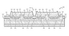
- FIG. 6depicts a monolithic LED chip comprising a plurality of sub-LEDs and a plurality of contact vias 62 .
- Portions of barrier layers 64as represented by the dark circles at the peripheries of the vias 62 , are exposed and illustrate the dimming effect that can result from such exposure of underling layers, such as the barrier layer.
- the effectcan be very pronounced when comparing the efficiency of large, single-junction chips to multi-junction chips of the same footprint. This is because the smaller the junction is relative to the barrier layer exposed at the mirror periphery, the more severe the impact is on the overall emission efficiency of the device. For example, a 16-junction, 1.4 mm LED chip can be approximately 10% dimmer than a single-junction 1.4 mm chip.
- dark metalshaving light absorptive and/or low reflective properties as interconnect layer material within and around the edges of the via 62 .
- Interconnect layerscan be utilized to connect adjacent junctions or sub-LEDs.
- the dark metalsinclude such metals such as Titanium (Ti), Nickel (Ni), Tungsten (W), and a Titanium Tungsten alloy (TiW) and are utilized as interconnect layer material due to their resistance to electromigration; however, like the barrier layers 64 above, the dark metal interconnect layers exhibit a dimming effect that negatively affects LED chip light output.
- LED chipscomprising self-aligned mirror layers that are floating, for example, by being substantially electrically isolated by an insulating material.
- These floating self-aligned mirror layersare configured with contact vias and can be positioned such that they extend from a position substantially near the edge of the contact vias or from a position directly at the edge of the vias.
- the mirror layersare substantially surrounded by an insulating material except for a portion of the mirror layer that contacts the edge of the contact vias.
- These mirror layerscan eliminate or mitigate the dark circle dimming effect around the vias of an LED device caused by portions of underlying material layers, such as the barrier layers and interconnect layers discussed above, without the need of achieving a tolerance distance.
- These mirror layerscan also self-align with the vias during device fabrication and therefore eliminate or mitigate the need for precision alignment during the fabrication process.
- the self-aligned floating mirror layers disclosed hereinare useful in any LED device having one or more contact vias, including single-junction devices, these mirror layers are particularly useful in multiple junction LED chips utilizing interconnect layers, for example, monolithic LED chips having a plurality of active areas on a substrate/submount (“submount”) that can be interconnected in series; although, it is understood that other embodiments can have active regions interconnected in parallel or in a series parallel combination.
- the active areascan be arranged in close proximity such that space between adjacent ones of the active areas is substantially not visible when the emitter is emitting, thereby allowing the LED chip to emit light similar to that of a filament.
- LEDscan also be improved by reducing the light-absorbing effects of materials, such as barrier layers, adjacent to the mirror(s).
- materialssuch as barrier layers, adjacent to the mirror(s).
- Some embodimentsare described below as having active regions arranged linearly, but it is understood that the LED chips according to the present invention can be arranged in many different shapes with their active regions arranged in many different locations and patterns in relation to one another. Some of the different shapes include different polygon shapes like triangle, square, rectangle, pentagon, etc.
- Some embodiments of the present inventioncan be arranged to provide for improved reliability under high power or high current operation. Some of these embodiments can have layer structures or composition that help minimize or eliminate electromigration during high power LED chip operation.
- Some embodiments of a monolithic LED chip, according to the present inventioncomprises a plurality of active regions, with an electrically conductive interconnect element connecting at least two of the active regions.
- the interconnect elementcan comprises a material and/or structure that resists electromigration.
- an LED chipcomprises a first active region comprising two oppositely doped layers and an active layer therebetween, at least one electrical connection via providing a path for electrical connection to one of the oppositely doped layers, and a floating mirror layer extending substantially from a position near the edge of the electrical connection via.
- an LED chipcomprises a plurality of active regions physically separated from one another, with each active region comprising two oppositely doped layers and an active layer therebetween.
- the LED chipfurther comprises at least one interconnect layer connecting one of the doped layers of one active structure with an oppositely doped layer of another active structure, wherein at least a portion of the interconnect layer is in an electrical connection via.
- the electrical connection viaprovides a path for electrical connection to one of the active structures in said plurality.
- the LEDfurther comprises a floating mirror layer extending from a position substantially near the edge of the electrical connection via.
- a method of fabricating an electrical connection via with a self-aligned floating mirror layer for an LED chipcomprises the steps of depositing a first insulating material on a semiconductor based active structure. The next step involves depositing a mirror layer on the first insulating material. Then the next step involves depositing a second insulating material on the mirror layer. The subsequent step involves depositing a photoresist mask on the second insulating layer, leaving at least one portion of the surface of said second insulating layer unmasked. The final step involves etching through the at least one unmasked portion to said semiconductor based active structure, creating an electrical connection via to a portion of the semiconductor based active structure.
- FIG. 1is a sectional view of a prior art LED package
- FIG. 2is a sectional view of another prior art LED package
- FIG. 3a sectional view of another embodiment of a prior art LED chip
- FIG. 4is a sectional view of a prior art LED chip according to the present invention.
- FIG. 5is a sectional view of a prior art LED chip according to the present invention.
- FIG. 6is a top view of a prior art monolithic LED chip according to the present invention.
- FIG. 7is a sectional view of one embodiment of an LED chip according to the present invention.
- FIG. 8is a sectional view of another embodiment of an LED chip according to the present invention.
- FIG. 9is a sectional view of another embodiment of an LED chip according to the present invention.
- FIG. 10is a top view of a monolithic LED chip according to the present invention.
- FIG. 11is a sectional view of another embodiment of an LED chip according to the present invention.
- FIG. 12is a sectional view of another embodiment of an LED chip according to the present invention.
- FIG. 13is a top view of one embodiment of an LED chip according to the present invention.
- FIG. 14is a top view of another embodiment of an LED chip according to the present invention.
- FIG. 15is a top view of still another embodiment of an LED chip according to the present invention.
- FIG. 16is a sectional view of one embodiment of a monolithic LED chip according to the present invention.
- FIG. 17is a sectional view of the LED chip shown in FIG. 16 at an intermediate manufacturing step
- FIG. 18is a sectional view of another LED chip according to the present invention at an intermediate manufacturing step
- FIG. 19is another sectional view of the LED chip shown in FIG. 18 ;
- FIG. 20is a sectional view of another embodiment of a monolithic LED chip according to the present invention.
- FIG. 21is a sectional view of the LED chip in FIG. 20 showing flow of an electrical signal
- FIG. 22is a sectional view of another embodiment of a monolithic LED chip according to the present invention.
- FIG. 23is a sectional view of the LED chip in FIG. 22 showing flow of an electrical signal
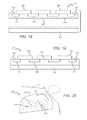
- FIG. 24is a plan view of an monolithic emitter according to the present invention.
- FIG. 25is a front view of one embodiment of a car headlight according to the present invention.
- FIG. 26is a sectional view of another embodiment of a monolithic LED chip according to the present invention.
- FIG. 27is a sectional view of the LED chip in FIG. 26 showing flow of an electrical signal
- FIG. 28is a top view of the another embodiment of a monolithic LED chip according to the present invention showing flow of an electrical signal
- FIG. 29is a sectional view of one embodiment of an interconnection metal layer according to the present invention.
- FIG. 30is a front sectional view of still another embodiment of an LED chip incorporating features of the present invention.
- FIG. 31is a front sectional view of a portion of an LED chip undergoing a first step of a method for the formation of a contact via and a self-aligned floating mirror layer incorporating features of the present invention
- FIG. 32is a front sectional view of a portion of an LED chip undergoing a second step of a method for the formation of a contact via and a self-aligned floating mirror layer incorporating features of the present invention
- FIG. 33is a front sectional view of a portion of an LED chip undergoing a third step of a method for the formation of a contact via and a self-aligned floating mirror layer incorporating features of the present invention
- FIG. 34is a front sectional view of a portion of an LED chip undergoing a fourth step of a method for the formation of a contact via and a self-aligned floating mirror layer incorporating features of the present invention
- FIG. 35is a front sectional view of a portion of an LED chip undergoing a fifth step of a method for the formation of a contact via and a self-aligned floating mirror layer incorporating features of the present invention.
- FIG. 36is a front sectional view of still a further embodiment of an LED chip incorporating features of the present invention showing an example current flow through the LED chip.
- Embodiments incorporating features of the present inventioninclude reflective layers, such as floating mirror layers that self-align with an electrical contact via during device fabrication. This can eliminate the need for precise placement of the mirror layer during device fabrication.
- the self-aligned floating mirror layersare floating, and thus substantially surrounding by electrically insulating material, these mirror layers do not need to be designed at a tolerance distance from the edges of the via, which typically arises due to concerns with causing a device short and subsequent malfunction. This increases the mirror area and eliminates lower light reflection in the proximity of electrical connection vias.
- the self-aligned floating mirror layercan be formed simultaneously or near simultaneously with an electrical connection via.
- the mirror layeris deposited on a semiconductor active structure such that it is between two layers of insulating material.
- a photoresist mask defining an etch areais then deposited on the topmost insulating layer, which in turn is on the mirror layer.
- the unmasked portion of the layersis then etched through to the semiconductor active structure so that the electrical connection can be made to it. This process is shown in greater detail with reference to FIGS. 31-35 herein.
- LED chip structuresare provided to enhance the overall emission characteristics of LEDs.
- the emission characteristics of LED chip structures having mirror reflectivityare generally enhanced by limiting the amount of dark or substantially non-reflective barrier material around the periphery of highly reflective mirror components.
- the light extraction and EQEis strongly affected by the reflective characteristics of the mirror. For example, in a mirror comprised of Ni/Ag, the reflectivity is dominated by the properties of the Ag and is believed to be around 90% reflective.
- This high reflectivitycan be counteracted by a barrier layer, which is used to prevent Ag migration during operation of the LED chip at high temperatures and/or in humid conditions.
- the barrier layerif allowed to extend substantially beyond the periphery of the mirror, can significantly adversely affect the reflectivity of the mirror since it generally has a reflectivity of 50% or lower and can absorb many of the photons that would otherwise be exiting and emitting from the chip.
- barrier layersare provided that are patterned smaller than the mirror layers they are protecting.
- the barrier layersare preferably no longer wrapping around the edges of the mirror, and thus are not exposed to light trapped within the GaN active region.
- the amount of the barrier that is exposedis minimized such that at least 40% of the mirror periphery is free from the barrier layer and its associated adverse effects.
- at least 50% of the mirror peripheryis free from the barrier layer, while in other embodiments at least 60% is free from the barrier layer.
- LED chips structureshaving a plurality of active areas/portions/regions (“regions”) that can be provided on a submount having internal and integral electrical interconnects to connect the LEDs in different series connections.
- the active regionscan be distinct from each other, with each having its own set of oppositely doped layers and active layer not otherwise connected to same layers in the other active regions.
- the submountcan also have a barrier layer that does not extend beyond the edge of or wrap around the portions of the mirror layer, with the portion being particularly below the primary emission area of the active regions. This can help minimize the light that might be absorbed during operation, thereby increasing the overall emission efficiency of the active regions.
- the submounts internal electrical connectionscan be particularly arranged to allow for interconnection of the active regions so that each is relatively close to the adjacent ones of the active regions.
- the small space between the active regionsreduces or eliminates dark spots between the active regions so that the LEDs appear as a continuous light source. This arrangement allows for monolithic LEDs that give the appearance of a conventional filament light source, while at the same time maximizing the emission area of the LED chips to increase overall brightness.
- Some embodiments of LED chips according to the present inventionhave a plurality of active areas regions on a submount and buried electrical interconnects that can present certain reliability problems, particularly under high power operation.
- the buried electrical interconnectscan experience electromigration of certain layers or materials during operation, which can lead to degradation and eventual failure of the device.
- One layer that can experience electromigrationis the buried electrical interconnect.
- some embodiments of the present inventioncan be arranged to reduce, minimize or eliminate this electromigration.
- Some embodimentscan have layers structure that allow for the use of materials for the current carrying layer that resist electromigration.
- Still other embodimentscan have current carrying layers made of multiple layers with the outermost of the layers having lower tendency to electromigrate.
- Still other embodimentsprovide layers as an alloy of materials that also helps minimize electromigration.
- first, second, etc.may be used herein to describe various elements, components, regions, and/or sections, these elements, components, regions, and/or sections should not be limited by these terms. These terms are only used to distinguish one element, component, region, or section from another element, component, region, or section. Thus, a first element, component, region, or section discussed below could be termed a second element, component, regions, or section without departing from the teachings of the present invention.
- Embodiments of the inventionare described herein with reference to cross-sectional view illustrations that are schematic illustrations of embodiments of the invention. As such, the actual thickness of components can be different, and variations from the shapes of the illustrations as a result, for example, of manufacturing techniques and/or tolerances are expected. Embodiments of the invention should not be construed as limited to the particular shapes of the regions illustrated herein but are to include deviations in shapes that result, for example, from manufacturing. A region illustrated or described as square or rectangular will typically have rounded or curved features due to normal manufacturing tolerances. Thus, the regions illustrated in the figures are schematic in nature and their shapes are not intended to illustrate the precise shape of a region of a device and are not intended to limit the scope of the invention.
- first elementwhen a first element is referred to as being “between,” “sandwiched,” or “sandwiched between,” two or more other elements, the first element can be directly between the two or more other elements or intervening elements may also be present between the two or more other elements.
- first layerif a first layer is “between” or “sandwiched between” a second and third layer, the first layer can be directly between the second and third layers with no intervening elements or the first layer can be adjacent to one or more additional layers with the first layer and these additional layers all between the second and third layers.
- LED chipIn order to use an LED chip in a circuit or other like arrangement, it is known to enclose an LED chip in a package to provide environmental and/or mechanical protection, color selection, light focusing and the like. It is understood that the term “LED” can be used herein to refer to an LED chip, LED component, and LED package interchangeably. An LED package can also include electrical leads, contacts or traces for electrically connecting the LED package to an external circuit.
- LEDscan have many different semiconductor layers arranged in different ways and can emit different colors.
- the layers of the LEDscan be fabricated using known processes, with a suitable process being fabrication using metal organic chemical vapor deposition (MOCVD).
- MOCVDmetal organic chemical vapor deposition
- the layers of the LED chipsgenerally comprise an active layer/region sandwiched between first and second oppositely doped epitaxial layers, all of which are formed successively on a growth substrate or wafer. LED chips formed on a wafer can be singulated and used in different application, such as mounting in a package. It is understood that the growth substrate/wafer can remain as part of the final singulated LED or the growth substrate can be fully or partially removed.
- the active regioncan comprise single quantum well (SQW), multiple quantum well (MQW), double heterostructure or super lattice structures.
- the active region and doped layersmay be fabricated from different material systems, with one such system being Group-III nitride based material systems.
- Group-III nitridesrefer to those semiconductor compounds formed between nitrogen and the elements in the Group III of the periodic table, usually aluminum (Al), gallium (Ga), and indium (In).
- AlGaNaluminum gallium nitride
- AlInGaNaluminum indium gallium nitride
- the doped layersare gallium nitride (GaN) and the active region is InGaN.
- the doped layersmay be AlGaN, aluminum gallium arsenide (AlGaAs) or aluminum gallium indium arsenide phosphide (AlGaInAsP) or aluminum indium gallium phosphide (AlInGaP) or zinc oxide (ZnO).
- AlGaAsaluminum gallium arsenide
- AlGaInAsPaluminum gallium indium arsenide phosphide
- AlInGaPaluminum indium gallium phosphide
- ZnOzinc oxide
- the growth substrate/wafercan be made of many materials such as silicon, glass, sapphire, silicon carbide, aluminum nitride (AlN), gallium nitride (GaN), with a suitable substrate being a 4H polytype of silicon carbide, although other silicon carbide polytypes can also be used including 3C, 6H and 15R polytypes. Silicon carbide has certain advantages, such as a closer crystal lattice match to Group III nitrides than sapphire and results in Group III nitride films of higher quality.
- Silicon carbidealso has a very high thermal conductivity so that the total output power of Group-III nitride devices on silicon carbide is not limited by the thermal dissipation of the substrate (as may be the case with some devices formed on sapphire).
- SiC substratesare available from Cree Research, Inc., of Durham, N.C. and methods for producing them are set forth in the scientific literature as well as in a U.S. Pat. Nos. Re. 34,861; 4,946,547; and 5,200,022.
- LEDscan also comprise additional features such as conductive current spreading structures, current spreading layers, and wire bond pads, all of which can be made of known materials deposited using known methods. Some or all of the LEDs can be coated with one or more phosphors, with the phosphors absorbing at least some of the LED light and emitting a different wavelength of light such that the LED emits a combination of light from the LED and the phosphor. LED chips can be coated with a phosphor using many different methods, with one suitable method being described in U.S. patent application Ser. Nos. 11/656,759 and 11/899,790, both entitled “Wafer Level Phosphor Coating Method and Devices Fabricated Utilizing Method”, and both of which are incorporated herein by reference.
- the LEDscan be coated using other methods such as electrophoretic deposition (EPD), with a suitable EPD method described in U.S. patent application Ser. No. 11/473,089 entitled “Close Loop Electrophoretic Deposition of Semiconductor Devices”, which is also incorporated herein by reference.
- EPDelectrophoretic deposition
- LEDsmay have vertical or lateral geometry as is known in the art.
- Those comprising a vertical geometrymay have a first contact on a substrate and a second contact on a p-type layer.
- An electrical signal applied to the first contactspreads into the n-type layer and a signal applied to the second contact spreads into a p-type layer.
- a thin semitransparenttypically covers some or the entire p-type layer.
- the second contactcan include such a layer, which is typically a metal such as platinum (Pt) or a transparent conductive oxide such as indium tin oxide (ITO).
- Ptplatinum
- ITOindium tin oxide
- LEDsmay also comprise a lateral geometry, wherein both contacts are on the top of the LEDs.
- a portion of the p-type layer and active regionis removed, such as by etching, to expose a contact mesa on the n-type layer.
- a second lateral n-type contactis provided on the mesa of the n-type layer.
- the contactscan comprise known materials deposited using known deposition techniques.
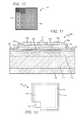
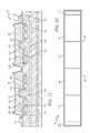
- FIG. 7shows one possible embodiment of a LED chip 100 according to the present invention.
- LED chip 100generally comprises a GaN active region 102 , a Ni/Ag-based mirror contact 104 , a metal barrier 106 , an insulator 108 , and a reflective metal 110 .
- the structure depicted in FIG. 7is intentionally simplified for illustrative purposes, and it is understood that a chip according to the present invention could include additional components as discussed above or below in more detail and/or as is well known in the art, and could likewise include other suitable materials as discussed above or below in more detail.
- additional layers and elementscan also be incorporated, including but not limited to buffer, nucleation, contact and current spreading layers as well as light extraction layers and elements.
- the oppositely doped layerscan comprise multiple layers and sub-layers, and well as supper lattice structures and inter layers.
- the active regioncan comprise single quantum well (SQW), multiple quantum well (MQW), double heterostructure or super lattice structures.
- SQWsingle quantum well
- MQWmultiple quantum well
- the order of the layerscan be different and in the embodiment shown, the first or bottom epitaxial layer can be an n-type doped layer and the second or top epitaxial layer can be a p-type doped layer, although in other embodiments the first layer can be p-type doped and the second layer n-type doped.
- Embodiments where the p-type layer is the bottom layertypically correspond with LEDs that are flip-chip mounted on a submount.
- the top layercan be the growth substrate, and in different embodiments all or a portion of the growth substrate can be removed. In those embodiments where the growth substrate is removed, the n-type doped layer is exposed as the top surface. In still other embodiments portions of the growth substrate can be left and in some embodiments can be shaped or textured to enhance light extraction.
- Each of the LEDs in the chips discussed hereincan have first and second contacts, and in the embodiment shown in FIG. 7 , the LED has lateral geometry. As such, the LED can be contacted from one side or surface of the LED, instead of top and bottom surfaces as is the case for vertical geometry.
- the first and second contactscan comprise many different materials such as gold (Au), copper (Cu) nickel (Ni), indium (In), aluminum (Al), silver (Ag), or combinations thereof.
- Still other embodimentscan comprise conducting oxides and transparent conducting oxides such as indium tin oxide, nickel oxide, zinc oxide, cadmium tin oxide, titanium tungsten nickel, indium oxide, tin oxide, magnesium oxide, ZnGa 2 O 4 , ZnO 2 /Sb, Ga 2 O 3 /Sn, AgInO 2 /Sn, In 2 O 3 /Zn, CuAlO 2 , LaCuOS, CuGaO 2 and SrCu 2 O 2 .
- the choice of material usedcan depend on the location of the contacts as well as the desired electrical characteristics such as transparency, junction resistivity and sheet resistance.
- Some embodiments of LED chips according to the present inventioncan have other features, and Group-III nitride based LEDs, for example, can have other features to assist in spreading current from the contacts. This is particularly applicable to spreading current into p-type Group-III nitrides and the current spreading structure can comprise thin semitransparent current spreading layer covering some or the entire p-type layer. These layers can comprise different materials including but not limited to a metal such as platinum (Pt) or a transparent conductive oxide such as indium tin oxide (ITO).
- Ptplatinum
- ITOindium tin oxide
- Submountscan be formed of many different materials such as silicon, ceramic, alumina, aluminum nitride, silicon carbide, sapphire, or a polymeric material such as polymide and polyester etc.
- the submountcan include a highly reflective material, such as reflective ceramics, dielectrics or metal reflectors like silver, to enhance light extraction from the component.
- the submountcan comprise a printed circuit board (PCB), or any other suitable material, such as T-Clad thermal clad insulated substrate material, available from The Bergquist Company of Chanhassen, Minn.
- PCBprinted circuit board
- different PCB typescan be used such as standard FR-4 metal core PCB, or any other type of printed circuit board.
- the barrier layer 106does not wrap around the edges of the mirror 104 as it does in the prior art. Instead, the barrier layer 106 is patterned smaller than the mirror 104 such that it is not exposed to the light emitted toward the mirror or trapped inside the GaN region 102 . In some embodiment, most of the barrier 106 may be removed in at least one embodiment so long as the insulator 108 fulfills the duties of the barrier 106 . The areas of the mirror 104 no longer bordered by the barrier 106 are instead surrounded by insulator 108 , with the insulator being crucial for preventing Ag migration from the mirror 104 .
- the insulator 108preferably has high density, high bond strength, low moisture permeability, and high resistance to metal ion diffusion. Additionally, the interface between the insulator 108 and the GaN region 102 is critical, as a weak interface can lead to Ag migration despite having an insulator 108 of high quality. Moreover, the insulator 108 may be optically transparent, and helps space the reflective metal layer 110 from the mirror 104 .
- a reflective metal layer 110may also be disposed such that it forms a composite barrier with the insulator and preferably has significantly higher reflectivity than the metal barrier 106 . Any light incident on the composite barrier at high angles may experience total internal reflection at the GaN/insulator interface due to the refractive index difference, while low angle light may get reflected off the bottom reflective layer 110 .
- the reflective layer 110preferably consists of a high reflectivity metal such as Al or Ag, although it is understood that other suitable materials may also be used.
- the reflectivity of the composite barriermay be greater than 80%, or alternatively may be greater than 90%.
- the insulator 108may have low optical absorption and a low refractive index in order for the composite barrier to be highly reflective. Since the optical and reliability requirements of the insulator 108 may be at odds with one another, the insulator may comprise two or more distinct layers (not shown).
- the insulator 108may comprise a thin layer having properties optimized to prevent Ag migration in places where it is in contact with the mirror 104 and the GaN region 102 , and the insulator 108 may comprise a second, thicker layer having a low index of refraction in between the reflective metal 110 and the thin layer. As such, total internal reflection can occur at the interface between the thin and thick insulator layers, provided the thicker layer is at least a few optical wavelengths thick.
- a suitable thickness for the thick insulator layermay be between 0.5-1 m.
- the insulator 108may comprise three distinct layers, such as the first two as discussed above and a third layer in between the thick layer and the reflective metal layer 110 , with the third layer being optimized for good adhesion to the reflective metal layer 110 .
- a composite barriermay comprise more than three insulator layers, in which reflectivity of the composite barrier is further increased by alternating high and low refractive index insulator materials.
- the insulator 108may be comprised of many different suitable materials, including an oxide, nitride, or oxynitride of elements Si or Al.
- the first layermay be comprised of an oxide or oxynitride of Ti or Ta, while the second, thicker layer may be comprised of a low refractive index material such as SiO 2 .
- the materialsmay be the same as a two-layer insulator, with the third layer adjacent the reflective metal layer 110 comprised of SiN. While these materials fit the requirements for single or multiple layer insulators as discussed above, it is understood that other suitable materials may also be used and contemplated in the context of the present invention.
- FIG. 8depicts another embodiment of a LED chip 120 according to the present invention.
- the chip 120may comprise all the components as discussed with chip 100 .
- LED chip 120comprises a GaN region 122 , an Ag-based mirror 124 , a metal barrier 126 , an insulator 128 , and a reflective metal layer 130 .
- FIG. 8further depicts a p-contact being connected to a location outside the junction through a via connection 132 .
- the mirror 124may also serve as the p-contact for the LED.
- the metal barrier 126may go outside the periphery of the mirror 124 and the GaN region 122 junction.
- This sectioncan then be coupled to the via connection 132 , so that an electrical signal applied to the mirror 124 conducts through the via 132 to the extending portion (illustrated by the crosshatched portion 127 of the barrier 126 ) and to the GaN region. If the section of the metal barrier 126 extending outside the periphery of the mirror 124 is sufficiently small and narrow compared to the overall length of the mirror's periphery, then the poor reflectivity of the barrier 126 will have a negligible impact on light extraction. In one embodiment, the width of the barrier 126 portion 127 outside the mirror 124 periphery is ⁇ 20 ⁇ m or less.
- FIG. 9depicts another embodiment of a LED chip 140 according to the present invention, with chip 140 being a multi-junction chip. Providing such a multi-junction chip is one way to get an array of LEDs having high output on higher voltages.
- the chip 140may comprise all the components as discussed with chip 100 .
- LED chip 140comprises GaN regions 142 , Ag-based mirrors 144 , metal barriers 146 , an insulator 148 , and a reflective metal layer 150 .
- FIG. 9further depicts a p-contact being connected to the n-contact 154 of an adjacent junction.
- the mirror 144may also serve as the p-contact for the LED.
- the metal barrier 146may go outside the periphery of the mirror 144 and the GaN region 142 junction. If the section 147 of the metal barrier 146 extending outside the periphery of the mirror 144 is sufficiently small and narrow compared to the overall length of the mirror's periphery, then the poor reflectivity of the barrier 146 will have a negligible impact on light extraction. Furthermore, the portion 147 of the metal barrier 146 may also be used to form a wire bond for connecting the p-contact to a package terminal.
- the metal barrier 146does not have to cover a majority of the underside of the mirror 144 as depicted in the figures.
- the mirror 144may be substantially eliminated, and can be in contact with the mirror 144 in only a small section sufficient to form a good electrical contact.
- LED chip 140further comprises passivation layers 152 , with the characteristics of passivation layers well known in the art.
- the passivation layers 152may be comprised of SiN, which is a suitable material for providing moisture resistance to the chip. However, it is understood that other appropriate materials may be used, such as SiO 2 . SiO 2 is not as moisture resistant as SiN.
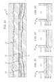
- FIG. 10depicts a monolithic LED chip comprising a plurality of LEDs and a plurality of contact vias 162 as is discussed in more detail below with respect to FIG. 12 .
- FIG. 10depicts a monolithic LED chip comprising a plurality of LEDs and a plurality of contact vias 162 as is discussed in more detail below with respect to FIG. 12 .
- the dark circles in FIG. 6 caused by the exposed portion of barrier layers 64have been virtually eliminated in FIG. 10 .
- the barrier layers in FIG. 10(not viewable from this perspective), have been made smaller than the mirror layers, and are thus not exposed and/or are minimally exposed at the periphery of said mirrors. Due to the reduction of the exposed barrier layers, any dimming effects of the barrier layers are substantially reduced and/or eliminated.
- FIG. 11depicts another embodiment of a LED chip 200 according to the present invention.
- the chip 200may comprise all the components as discussed with chip 100 .
- FIG. 11may further include a roughened n-GaN layer 202 , a p-GaN layer 204 , a mirror layer 206 (which may also serve as the p-contact for the LED), a barrier layer 208 , a dielectric barrier layer 210 , a bond metal layer 212 , a carrier layer 214 , a AuSn layer 216 , passivation layers 218 , 220 (with layer 220 at least partially roughened), and n-contacts 222 , 224 on the roughened GaN layer.
- the roughened layershelp with light extraction.
- the barrier layer 208 in FIG. 11is sized smaller than the mirror 206 . As discussed above, such sizing of the barrier layer helps eliminate many of the light-absorbing effects inherent in layer 208 , which in turn improves the overall emission and efficiency of the LED chip 200 .
- the characteristics of barrier layer 208may allow it to act as a current spreading layer as well as a barrier for Ag migration and/or a protective layer for mirror 206 , such that bond metal layer 212 is isolated from mirror 206 and thus does not dissolve into mirror 206 .
- Bond metal layer 212may be at least partially comprised of tin, which may otherwise dissolve into the mirror 206 but for the barrier 208 . Bond metal layer 212 may further be reflective, although it may not be as highly reflective as mirror 206 .
- Passivation layers 218are disposed on the sidewalls of the active region, providing sidewall passivation as is well known in the art. Passivation layers 218 may be comprised of SiN, which exhibits favorable moisture resistive characteristics. However, it is understood that other suitable materials are also contemplated. Passivation layer 220 may also be disposed over the device as shown to provide physical protection to the underlying components. Passivation layer 220 may be comprised of SiO 2 , but it is understood that other suitable passivation materials are also contemplated.
- the dielectric barrier layer 210is provided, at least in part, to protect/isolate the mirror 206 and portions of barrier 208 from the bond metal layer 212 .
- the dielectric layermay be transparent, and/or may comprise different dielectric materials such as SiN, SiO 2 , Si, Ge, MgOx, MgNx, ZnO, SiNx, SiOx, alloys or combinations thereof.
- the dielectric layer 210may also extend further under barrier 208 as depicted by the crosshatched sections under barrier 208 .
- FIG. 12depicts another embodiment of a LED chip 230 according to the present invention.
- the chip 230may comprise some or all of the components as discussed with the other chip embodiments.
- the biggest difference between chip 230 and the other chip embodimentsis that n-contact vias are provided as shown in FIG. 12 , with the vias not shown in FIG. 13 for ease of illustration.
- the viasallow for the removal of the n-contact metal on the topside of the device and the n-contact is essentially embedded within the device and electrically accessibly from the bottom of the chip. With less topside metal to block light emission, improved brightness can be realized.
- the barrier metal outside the periphery of the mirroris eliminated and/or substantially reduced, which further contributes to the emission efficiency of the device.
- the vias according to the present inventioncan be formed using conventional methods, such as etching to form the openings for the vias and photolithographic processes for forming the via.
- the viastake only a fraction of the area on the LED chip that would be needed for a wire bond pad. By using one or more vias in place of a wire bond pad, less of the active area is removed and fewer emission blocking metal for contacts is located on the topside of the device. This leaves more LED active area for light emission, thereby increasing the overall efficiency of the LED chip.
- different embodimentscan have more than one via and the vias can be in many different locations. In those embodiments having multiple vias, the vias can have different shapes and sizes and can extend to different depths in the LED. It is also understood that different embodiments can also comprise vias used in place of the first wire bond pad.
- FIG. 12may further include a roughened n-GaN layer 232 , p-GaN layers 234 , mirror layers 236 (which may also serve as the p-contact for the LED), barrier layers 238 , passivation layers 240 , 241 , an n-contact 242 , barrier layer 244 , a bond metal layer 246 , a carrier layer 248 , AuSn layer 250 , and passivation layer 252 .
- the roughened layersassist with improved light extraction of the device.
- the barrier layers 238are sized such that they are smaller than the mirror layers 236 and/or are prevented from extending beyond 40% or more of the periphery of the mirrors 236 .
- the barrier layers 238may be further provided to form a contact at the topside of the device for the p-contact integral to at least a portion of mirrors 236 .
- the barrier layers 238may help spread current laterally through the device since the mirrors 236 may be too thin to effectively spread current.
- the barrier layer 244may be provided as a protective layer for n-contact 242 , such that bond metal layer 246 is isolated from n-contact 242 and thus does not dissolve into or otherwise adversely react with n-contact 242 .
- Barrier layer 244may be comprised of TiW/Pt, although it is understood that other suitable materials are contemplated. In some embodiments, barrier layer 244 may not be necessary depending on the material make-up of the n-contact 242 and bond metal layer 246 .
- the n-contactmay be comprised of a variety of suitable materials, with preferred materials being reflective to further enhance the light emission of the device. As such, n-contact 242 may be comprised of Al, Ag, or other reflective materials. Bond metal layer 246 may further be reflective.
- Passivation layers 241are disposed on the sidewalls of the active region, providing sidewall passivation as is well known in the art.
- Passivation layers 240 , 241may be comprised of SiN, which exhibits favorable moisture resistive characteristics. However, it is understood that other suitable materials are also contemplated.
- Passivation layer 252may also be disposed over the device as shown to provide physical protection to the underlying components.
- Passivation layer 252may be comprised of SiO 2 , but it is understood that other suitable passivation materials are also contemplated.
- FIG. 13is a top view of the LED chip 230 shown in FIG. 12 , with FIG. 13 showing the n-type layer 234 and the outer edge of the mirror 236 below the n-type layer and in phantom.
- FIG. 13also shows the outer edges of the barrier layer 238 with the areas not exposed shown in phantom as further described below. The remaining layers, vias and inner edges of the barrier layer and mirror layers are not shown for ease of illustration.
- a portion of the barrier layer 238may serve as the p-type contact at the topside of the device.
- a portion of the barrier layercan be exposed for contacting and in the embodiment shown the LED chip layers can be removed above a portion of the barrier layer.
- the layers above the barrier layer 238can be etched to the barrier layer 238 , thereby forming an exposed barrier layer region 260 .
- the exposed region 260can be in many different locations and can have many different shapes, with the embodiment shown being at a corner of the LED chip 230 .
- Exposing the barrier layer in this mannerprovides advantages such as ease of contacting, but can also present the danger of moisture or contaminants entering the LED layers along the surfaces or edges in the exposed region 260 . This moisture or contaminants can negatively impact the lifetime and reliability of an LED chip.
- steps or transitionscan be included as part of the barrier layer that can inhibit or eliminate the amount of moisture or contaminants that can enter the LED chip.
- the steps or transitioncan take many different shapes and sizes. Different LED chips can have different numbers of steps or transitions and they can be included in different locations on the barrier layer. In still other embodiments, steps or transitions can be included in other layers.
- FIG. 14shows another embodiment of an LED chip 270 that is similar to the LED chip 230 shown in FIGS. 12 and 13 .
- the LED chip 270has an n-type layer 234 , mirror layer 236 and barrier layer 272 , with the other layers and features not shown for ease of illustration.
- N-type layer 234 and mirror layer 236are similar to those in LED chip 230 as shown in FIG. 13 .
- Barrier layer 272is also similar to barrier layer 236 in FIG. 13 and can be contacted through the exposed region 274 .
- the barrier layer 272has two steps 276 along the edge of the barrier layer 272 that help reduce or eliminate moisture or contaminants that can enter the LED chip 270 along the edge of the barrier layer 272 .
- the exposed area of the barrier layerresults in a portion of the barrier layer being uncovered such that it may absorb some LED chip light.
- the amount of exposed barriercan be minimized to minimize the impact of the light absorption, with the periphery of the mirror being free of the barrier layer in the percentages described above.
- the exposed portion of the barrier layercan be less than 20% of the overall barrier layer surface. In still other embodiments it can be less than 10%, while in other embodiments it can be less than 5%.
- the barrier layercan have many different shapes and can be arranged in different locations relative to the other layers of the LED chips according to the present invention.
- FIG. 15shows another embodiment of an LED chip 280 according to the present invention that is similar to the LED chip 270 , and shows an n-type layer 234 and mirror layer 236 .
- the barrier layer 282extends beyond that mirror layer 236 along two edges of the mirror layer 236 , and the barrier layer can extend beyond the mirror layers in different locations of LED chips.
- the exposed portions of the barrier layerscan be relatively thin to reduce the light absorbing surfaces. In some embodiments more than 75% of the exposed edges can be less than 3 microns wide. In other embodiments 90% can have this width, while in other embodiments 100% of the exposed edges can have this width. The exposed width for these percentages can also be different in other embodiments, such as less than 4 microns or less than 2 microns.
- the present inventioncan be used in many different lighting applications, and in particular those using a small sized high output light source. Some of these include, but are not limited to, general illumination, outdoor lighting, flashlights, white LEDs, street lights, architectural lights, home and office lighting, display lighting and backlighting.
- LED chipscan be arranged in many different ways and can be used in many different applications according to the present invention.
- Some of these LED chipscan comprise one or more active regions that can be interconnected in different ways, with some embodiments comprising a plurality of active regions on the same submount and interconnected to form high luminous flux emitters operating from relatively high voltages.
- the active regionscan be coupled together in a linear fashion to provide a light source similar to a filament source.
- the active regionscan be formed as a wafer and then mounted (e.g. flip-chip mounted) on the submount.
- the submountcan comprise internal electrical interconnects and insulation layers to allow for serial interconnection of LEDs without the need for external interconnects such as wire bonds.
- the wafer with the active regionscan comprise internal interconnections and/or insulation layers for interconnection.
- the spaces or streetscan be formed in the wafer to form the individual active regions.
- the active region and submount combinationcan be further processed by dividing or dicing the desired number of active regions. For example, an active region and submount combination with four linearly arranged active regions could be separated from the wafer active region and submount combination. Contacts can then be formed on the LED chip for applying an electrical signal to the LED chip during operation.
- the desired group of active regionscan be separated from the active region wafer and then mounted on the submount.
- a linear arrangement of four active regionscan be separated from the active region wafer and then mounted (e.g. flip-chip mounted) to a submount appropriately sized and arranged to accept the four active regions.
- individual active regionscan be mounted on submount.
- the monolithic LED chipsare described herein with reference to series connections, but it is understood that the active regions can be interconnected in different series and parallel combinations.
- the different embodiments of the present inventioncan be arranged in many different ways with many different features.
- Some embodimentscan comprise barrier layers as described above, with the barrier layer in some embodiments not extending, or minimally extending, beyond the edge of the mirror as described above in certain areas (e.g. below the emission area of the active region). This can help minimize the amount of light absorbed by the barrier layer, thereby increasing overall emission efficiency.
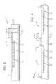
- FIG. 16is a sectional view of one embodiment of a monolithic LED chip 300 according to the present invention.
- the LED chip 300can comprise many different features and layers, most of which are not shown for ease of description.
- the LED chip 300comprises a plurality of emitting active regions 302 mounted on submount 304 .
- the active regionscan be mounted on the submount in wafer form or portion of the wafer comprising a group of active regions.
- individual active regionscan be mounted to the submount 304 .
- the individual active regionscan be separated on the submount 304 by known methods such as etching, cutting or dicing.
- the side surfaces of the resulting active regionscan be angled or shaped, and the distance between adjacent active regions is relatively small.
- the distancecan be 15 microns ( ⁇ ) or less or less, while in other embodiments it can be 10 ⁇ or less. In still other embodiments, it can be 5 ⁇ or less, and in other embodiment is can be up or less.
- Some embodimentscan also have a space in the range of 1 to 0.05 ⁇ .
- the spacecan have different percentage of a width of the active regions with some embodiments having a space that is approximately 15% or less of an active region width, while in other embodiments the space can be approximately 10% or less.
- the spacecan be 5% or less of a width, while other embodiments can have a space that is 2.5% or less of a width.
- Other embodimentscan have a space that is 1.5% or less of a width, with some embodiments having a space that is approximately 1.1% of an active region width.
- the submount 304can also contain integral and internal electrical interconnects 306 arranged to connect the active regions in series. In some embodiments this can comprise a number of vias and electrically conductive paths or layers coupled together in different ways to provide the desired interconnect scheme.
- the LED chip 300can also comprise first and second contact pads 308 , 310 for applying an electrical signal to the LED chip 300 .
- the first contact 308can be either a p-contact or an n-contact, with the second contact 310 being the other of the p-contact and n-contact.
- the LED chip 300also comprise contact interconnects 312 for conducting an electrical signal from the first contact pad 308 to the first of the active regions 302 , and for conducting an electrical signal from the last of the active regions 302 to the second contact pad 310 .
- the arrangementallows for an electrical signal to be applied to the LED chip 300 across the first and second contacts 308 , 310 .
- the LED chip 300can also comprise one or more insulating layers 314 to electrically insulate the active regions 302 and interconnects 306 , 312 from any conductive elements below the insulating layer 314 . In some embodiments, other insulating layers can be included such that at least a portion of the interconnects 306 , 312 are surrounded by insulating materials, with those portions buried in the insulating material.
- the LED chip 300can also comprise a substrate 316 and bonding layer 318 for adhesion between the substrate 316 and the layers above the substrate 316 .
- the LED chip 300can operate from an electrical signal that is approximately equal to the sum of the junction voltages of the active regions 302 . Other factors contribute to the operating voltage, with the voltage generally scaling with the number of junctions.
- each of the active regions 302can have a junction voltage of approximately 3V, such that the electrical signal applied to the active regions can be approximately equal to 3 times the number of active regions.
- the LED chipcan have four active regions so that the LED chip operates from an approximate 12V electrical signal.
- FIG. 17shows the LED chip 300 at an intermediate manufacturing step where in some embodiments the active regions can be formed separately from the submount 304 , with the submount having buried interconnects 306 , 312 , insulating layer(s) 314 and contacts 308 , 310 .
- the active regions 302can then be mounted to the submount in contact with interconnects 306 , 312 .
- the active regions 302can then have spaces formed between adjacent ones of the active regions, with the spaces formed either before or after mounting on the submount 304 .
- FIGS. 18 and 19show another embodiment of a monolithic LED chip 320 having many of the same features as LED chip 300 .
- the active regions 302are formed with interconnects 306 , 312 , insulating layer(s) 314 and contacts 308 , 310 .
- the interconnects 306 , 312are buried in or surrounded by insulating material to electrically isolate them from other features in the LED chip 320 .
- This structurecan then mounted to a separate substrate and bonding layer structure 322 to form the monolithic LED chips 320 with serially interconnected active regions.
- FIG. 20shows another embodiment of a monolithic LED chip 350 according to the present invention comprising two interconnected active regions 352 , but it understood that other monolithic LED chips can comprise many different numbers of interconnected active regions.
- the active regions 352can have lateral geometry and can be flip-chip mounted on a submount 354 that can have many different features and can be made of many different layers and materials.
- the active regions 352can be made from many different material systems, with the embodiment shown being from a Group-III nitride material system.
- the active regions 352can comprise an active structure 356 , for example, a GaN active structure having a p-type layer 358 , n-type layer 360 and an active layer 362 .
- Some embodiments of the active regionscan also comprise a growth substrate that can be many different materials such as silicon carbide or sapphire, and can be shaped or textured to enhance light extraction such as the substrate shaping utilized in commercially available DA line of LEDs from Cree, Inc.
- the substratecan be removed and the n-type layer 360 can be shaped or textured to enhance light extraction.
- the active regions 352can also comprises a current spreading layer 364 that is on the p-type layer 358 such that when the active regions 352 are mounted on the submount 354 , the LED current spreading layer 364 is between the active structure 356 and the submount 354 .
- the current spreading layer 364can comprise many different materials and is typically a transparent conductive oxide such as indium tin oxide (ITO) or a metal such as platinum (Pt), although other materials can also be used.
- ITOindium tin oxide
- Ptplatinum
- the current spreading layer 364can have many different thicknesses, with the present invention having a thickness small enough to minimize absorption of light from the active structure that passes through the current spreading layer.
- Some embodiments of the current spreading layer 364comprise ITO having thicknesses less than 1000 angstroms ( ⁇ ), while other embodiments can have a thickness less than 700 ⁇ . Still other embodiments can have a thickness less than 500 ⁇ . Still other embodiments can have a thickness in the range of 50 to 300 ⁇ , with some of these embodiments having current spreading layer 364 with a thickness of approximately 200 ⁇ .
- the current spreading layer 364 as well as the reflective layers described belowcan be deposited using known methods. It is understood that in embodiments where current spreading is not a concern, the active regions can be provided without a current spreading layer.
- a low index of refraction (IR) reflective layer 366can be arranged on the current spreading layer 364 , with current spreading layer 364 between the reflective layer 366 and active structure 356 .
- the reflective layer 366can comprise many different materials and preferably comprises a material that presents an IR step between the materials comprising the active structure 356 . Stated differently, the reflective layer 366 should have an IR that is smaller than the active structure to promote TIR of active structure light emitting toward the reflective layer 366 . Light that experiences TIR can be reflected without experiencing absorption or loss, and TIR allows for the efficient reflection of active structure light so that it can contribute to useful or desired active region emission.
- This type of reflective layercan be an improvement over devices that rely on metal layers to reflect light where the light can experience loss with each reflection. This can reduce the overall LED chip emission efficiency.
- the reflective layer 366can comprise a dielectric, with some embodiments comprising SiO 2 . It is understood that other dielectric materials can be used such as SiN, Si, Ge, MgOx, MgNx, ZnO, SiNx, SiOx, AlN, and alloys or combinations thereof.
- Some Group III nitride materials such as GaNcan have an IR of approximately 2.4, and SiO 2 has an IR of approximately 1.46.
- Embodiments with an active LED structure 356 comprising GaN and that also comprises a SiO 2 reflective layercan have a sufficient IR step between the two to allow for efficient TIR of light at the junction between the two.
- the reflective layer 366can have different thicknesses depending on the type of material, with some embodiments having a thickness of at least 0.2 microns ( ⁇ m). In some of these embodiments it can have a thickness in the range of 0.2 to 0.7 ⁇ m, while in some of these embodiments it can be approximately 0.5 ⁇ m thick.
- the reflective layer 366As light experiences TIR at the junction with the reflective layer 366 an evanescent wave with exponentially decaying intensity can extend into the reflective layer 366 . This wave is most intense within approximately one third of the light wavelength from the junction (about 0.3 um for 450 nm light in SiO2). If the reflective layer 366 is too thin, such that significant intensity remains in the evanescent wave at the interface between the first reflective layer 366 and the second reflective layer 368 , a portion of the light can reach the second reflective layer 368 . This in turn can reduce the TIR reflection at the first interface. For this reason, in some embodiments the reflective layer 366 should have a thickness of at least 0.3 um.
- a metal reflective layer (i.e. second reflective layer) 368 and adhesion layer 370are included on the reflective layer 366 , with the adhesion layer 370 sandwiched between and providing adhesion between the metal layer 368 and reflective layer 366 .
- the metal layer 368is arranged to reflect light that does not experience TIR at the junction with the reflective layer 366 and passes through the reflective layer 366 .
- the metal layer 368can comprise many different materials such as Ag, Au, Al, or combinations thereof, with the present invention being Ag.
- the adhesion layer 370can have many different thicknesses from just a few A to thousands of A. In some embodiments it can be less than 100 ⁇ , while in other embodiments it can be less than 50 ⁇ . In some of these embodiments it can be approximately 20 ⁇ thick. The thickness of the adhesion layer 370 and the material used should minimize the absorption of light passing to minimize losses of light reflecting off the metal layer 368 .
- the active regions 352can further comprise reflective layer holes 372 that can pass through the adhesion layer 370 and the reflective layer 366 , to the current spreading layer 364 .
- the holes 372can then be filled when the metal layer 368 is deposited with the metal layer material forming vias 374 to the current spreading layer 364 .
- the vias 374can provide a conductive path through the reflective layer 368 , between the p-contact and the current spreading layer 364 .
- the holes 372can be formed using many known processes such as conventional etching processes or mechanical processes such as micro drilling.
- the holes 372can have many different shapes and sizes, with the holes 372 in the embodiment shown having angled or curved side surfaces and a circular cross-section with a diameter of less than 20 ⁇ m. In some embodiments, the holes 372 can have a diameter of approximately 8 ⁇ m, with others having a diameter down to 1 ⁇ m. Adjacent holes 372 can be less than 100 ⁇ m apart, with the embodiment shown having a spacing of 30 ⁇ m spacing from edge to edge. In still other embodiments, the holes can have a spacing of as low as 10 ⁇ m or less.
- the holes 372can have cross-section with different shapes such as square, rectangular, oval, hexagon, pentagon, etc. In other embodiments the holes are not uniform size and shapes and there can be different or non-uniform spaces between adjacent holes.
- different structurescan be used to provide a conductive path between the p-contact and the current spreading layer.
- an interconnected gridcan be formed through the reflective layer 368 , with a conductive material then being deposited in the grid to form the conductive path through the composite layer.
- the gridcan take many different forms, with portions of the grid interconnecting at different angles in different embodiments.
- An electrical signal applied to the gridcan spread throughout and along the interconnected portions.
- a gridcan be used in combination with holes, while other embodiments can provide other conductive paths.
- one or more conductive pathscan run outside the LED chip's active layer such as along a side surface of the LED chip.
- the active regions 352can also comprise a barrier layer 376 on the metal layer 368 to prevent migration of the metal layer material to other layers. Preventing this migration helps the LED chips 352 maintain efficient operation through their lifetime.
- An active structure hole 378can be included passing through the barrier layer 376 , metal layer 368 , adhesion layer 370 , reflective layer 366 , and p-type layer 358 , to expose the n-type layer 360 .
- a passivation layer 380is included on the barrier layer 376 and the side surfaces of the active structure hole 378 .
- the passivation layer 380protects and provides electrical insulation between the contacts and the layers below as described in more detail below.
- the passivation layer 380can comprise many different materials, such as a dielectric material.
- the barrier layer 376does not extend beyond the edge of the metal layer 368 around the active structure hole 378 . This reduces the amount of light absorbing barrier layer material that would absorb LED light, thereby increasing the overall emission efficiency of the LED chip 350 .
- the barrier layer 376can extend beyond the edge of the active region 352 and can be exposed at a mesa on the passivation layer 380 adjacent the LED. This exposed portion can be used for contacting the serially interconnected active regions 352 .
- a p-contact pad 382can be deposited on the passivation barrier layer 376 , with the p-contact 382 providing an electrical signal that can pass to the p-type layer 358 .
- An electrical signal applied to the p-contactpasses through the barrier layer 376 , the metal layer 368 , the vias 374 , and to the current spreading layer 364 through which it is spread to the p-type layer 358 .
- An n-contact 384can be formed on the n-type layer 360 and a conductive n-type layer vias 388 can be formed through the passivation layer 380 and between the n-type contact 384 and an interconnection metal layer 386 .
- the interconnection metal layer 386is arranged to conduct an electrical signal between adjacent ones of the LED chips 352 to interconnect them in series.
- the interconnection metal layer 386can have breaks along its length to facilitate this serial interconnection and can be made of many electrically conductive materials, such as those described herein.
- the metal layer 386can be formed as part of the submount 354 using known methods, are can be formed with the active regions.
- the interconnection layercan have many different shapes and thicknesses. In some embodiments it can comprise a substantially continuous layer with breaks, while in other embodiment it can comprise conductive traces.
- the p-contact 382 , the n-contact 384 , interconnection metal layer 386 , and n-type vias 388can comprise many different materials such as Au, copper (Cu) nickel (Ni), indium (In), aluminum (Al), silver (Ag), tin (Sn), platinum (Pt) or combinations thereof.
- theycan comprise conducting oxides and transparent conducting oxides such as ITO, nickel oxide, zinc oxide, cadmium tin oxide, indium oxide, tin oxide, magnesium oxide, ZnGa 2 O 4 , ZnO 2 /Sb, Ga 2 O 3 /Sn, AgInO 2 /Sn, In 2 O 3 /Zn, CuAlO 2 , LaCuOS, CuGaO 2 and SrCu 2 O 2 .
- conducting oxides and transparent conducting oxidessuch as ITO, nickel oxide, zinc oxide, cadmium tin oxide, indium oxide, tin oxide, magnesium oxide, ZnGa 2 O 4 , ZnO 2 /Sb, Ga 2 O 3 /Sn, AgInO 2 /Sn, In 2 O 3 /Zn, CuAlO 2 , LaCuOS, CuGaO 2 and SrCu 2 O 2 .
- the choice of material usedcan depend on the location of these features as well as the desired electrical characteristics such as transparency, junction resistivity
- the growth substrate for active regions 352has been removed, and the top surface of the n-type layer is textured for light extraction.
- the active regions 352are flip-chip mounted to a substrate 390 that can provide mechanical stability.
- the substrate 390can be made of many different materials, with a suitable material being silicon.
- the blanket mirror 384can be made of many different materials, with a suitable material being Al. The blanket mirror 384 helps to reflect LED light that escapes reflection by the reflective layer 366 and the metal layer 368 , such as light that passes through the active structure hole 378 .
- the reflective layer 366 and the metal layer 368are arranged between the active region's active structure 356 and the substrate 390 so that light emitted by the active structure 356 toward the substrate 390 can be reflected back to contribute to useful LED light emission. This reduces the amount of light that can be absorbed by structures such as the substrate 390 , with the embodiments according to present invention promoting reflection by TIR instead of reflection off metal layers, to further reduce light loss due to absorption.
- the submount 354also comprises a isolation layer 396 arranged on the blanket mirror 394 such that it provides electrical isolation between the blanket mirror 394 and all elements above the blanket mirror 394 , such as the interconnection metal 386 .
- This isolationallows for electrical signals to be conducted between adjacent ones of the active regions without being shorted to the blanket mirror 394 or other features below the blanket mirror 394 .
- the isolation layer 396can be made of many different materials, with the preferred material being made of an electrically insulating material such as a dielectric.
- the combination of the isolation layer 396 and passivation layer 380results in the interconnection metal 386 being buried and/or surrounded by electrically insulating materials. This internal isolation of the electrical paths within the LED chip 350 provides for reliable and efficient interconnection and operation of the active regions 352 .
- an electrical signalis applied to the p-type layer 358 in the first of the active regions connected in series, at the p-type contact pad 382 .
- a p-type conductive vias 398is included between the interconnection metal layer 386 and the barrier layer 376 of the active region. The electrical signal at the vias 398 passes through the barrier layer 376 and to the current spreading layer 364 and to the p-type layer 358 .
- n-contact pad 400is formed on a mesa on the passivation layer 380 adjacent the active region 352 .
- An n-pad via 402is formed between the n-contact pad 400 and the interconnection metal layer to conduct a signal from the n-type layer 360 in the last of the LED chips 352 to the n-contact pad 400 .
- the emitter 350can also comprise a passivation or protection layer 406 on the side surfaces of the active structure 356 and covering the top surface of the submount 354 around the p-contact pad 382 and the n-contact pad 400 .
- FIG. 21shows the LED chip 350 during operation with an electrical signal following a path through the emitter 350 as shown by arrows 404 .
- An electrical signalis applied to the p-contact pad 382 and is conducted through the barrier layer 376 , metal layer 368 , and current spreading layer 364 , to the p-type layer 358 .
- the signalthen passes through to the n-type layer 360 where it passes through to the n-contact 384 and the n-type vias 388 .
- the signalthen conducts along the interconnection metal layer where it passes into the first of the p-type vias 398 .
- the signalis then conducted to the p-type layer 358 in the second active region 352 , where it passes into the n-type layer 360 , n-contact 384 and n-type vias 388 .
- the signalthen passes on to the next of the active regions 352 connected in series and this continues until the last of the active regions 352 .
- the electrical signal at the n-type vias 388passes into the interconnection metal layer 386 and to the n-pad vias 402 , where it is conducted to the n-contact pad 400 .
- This type of interconnection and current flowallows for a high voltage LED chip light source formed monolithically on a submount.
- the LED chip 350 shown in FIGS. 20 and 21comprises a lateral geometry in that electrical signals can be applied to the LED chip 350 at p-contact 382 and n-contact pad 400 accessible from the top surface of the LED chip.
- the LED chip 350can comprise different contact geometries and arrangements.
- FIGS. 22 and 23show another embodiment of an LED chip 450 according to the present invention having many of the same features as the LED chip 350 , but having internal conductive features to provide a vertical geometry chip.
- the LED chipdoes not have an n-contact pad on its top surface, but instead a substrate via 452 that passes from the interconnection metal layer 386 , down and through the insulation layer 396 , to the layers below.
- the substrate vias 452can extend to the blanket mirror 452 .
- An electrical signal applied to the substrate 390would conduct to the substrate via 452 .
- the substrate via 452can pass further through the different layers.
- the substrate vias 452can pass through the substrate 390 so that it is accessible at the bottom of the LED chip 450 .
- One or more contact layers or padscan also be included on the bottom of the LED for making electrical contact.
- an electrical signalpasses through the LED chip 450 as shown by arrows 454 , and has much the same path as that shown for LED chip 350 in FIG. 21 .
- An electrical signalis applied to the p-contact pad 382 and is conducted through the barrier layer 376 , metal layer 368 , and current spreading layer 364 , to the p-type layer 358 .
- the signalthen passes through to the n-type layer 360 where it passes through to the n-contact 384 and the n-type vias 388 .
- the signalthen conducts along the interconnection metal layer 386 where it passes into the first of the p-type vias 398 .
- the signalis then conducted to the p-type layer 358 in the second active region 352 , where it passes into the n-type layer 360 , n-contact 384 and n-type vias 388 .
- the signalthen passes on to the next of the active regions 352 connected in series and this continues until the last of the active regions 352 .
- the electrical signal at the n-type vias 388passes into the interconnection metal layer 386 and to the substrate vias where it passes to the substrate 390 .
- FIG. 24shows one embodiment of a monolithic LED chip 500 according to the present invention that comprises four active regions 502 arranged on a single submount 504 .
- the LED chip 500can have many different shapes and sizes, with the emitter shown having a rectangular shape.
- Each of the active regions 502can also have a generally rectangular footprint, with a small space 506 formed between adjacent ones of the active regions 502 .
- the space 506is shown as being in a straight line, but it is understood that the space can have curves or can be squiggly.
- the space 506can be formed using known methods such as different etch or cut methods.
- a p-contact pad 508is arranged at one end of the emitter 500 and the n-contact pad 510 is arranged at the opposite end. A signal applied to the p-contact pad conducts through the device to the n-contact as described above.
- the different embodiments of the devices described hereincan have many advantages.
- the rectangular embodimentcan be sized to mimic the emission of a filament in a convention light source.
- a high voltage light sourcecan be provided that is compatible with many conventional lighting applications.
- the emitter 450has four active regions each having a 3 volt junction. This results in the LED chip 450 comprising a 12 volt light source. Different numbers of LEDs can result in emitters that operate from different voltages. For example, a similarly arranged emitter with six active regions comprises a 24 volt light source.
- the space between adjacent active regionscan be minimized. This minimizes or eliminates the undesirable dark spaces between adjacent ones of the active regions, giving the emitter the appearance of a continuous filament.
- FIG. 25shows one embodiment of a car headlight 550 according to the present invention having a housing 552 , with an opening having a light transmitting cover/lens 554 .
- the headlighthas one or more monolithic LED chips 556 mounted in the housing so that light from LED chips emits out the housing opening through the lens/cover.
- Many different monolithic LED chipscan be used with many different numbers of active regions, with some embodiments using a four active region monolithic LED chip operating from a 12v electrical signal
- the integral nature of the interconnection metal layerscan present certain problems during operation.
- the interconnection metal layers 386 in a high voltage chipfunction as current carrying layers while also being a reflective layer.
- the layer 386should comprise a good current conductor that is also reflective so that it does not absorb LED light.
- Different materialscan comprise both these properties, such as Al or Ag.
- One potential problemis that some of these interconnection metal layers made of these materials can experience electromigration under high current operation that can cause degradation in performance and can ultimately lead to failure of the device.
- this electromigrationcan cause voids in the interconnecting layer that can degrade performance of the LED chip. These voids that can then result in current conducting hot spots, which can accelerate electromigration. Continued electromigration can eventually lead to open circuits in the interconnect layer and failure of the LED chip.
- some embodiments according to the present inventioncan have layer structures or interconnection metal layers made of certain materials, with both helping to reduce or eliminate this interconnection metal layer electromigration. This can result in more reliable devices where failures under high power operation are mitigated. These LED chips can experience longer lifetimes and improved performance throughout their lifetime.
- the present inventioncan be applied to many different LED chips operating from different power densities.
- the LED chipscan operate with power density up to 3 watts per square millimeter (W/mm 2 ).
- Other embodimentscan operate with even higher power density up to 10 W/mm 2 , while still other embodiments can operate with power density in excess of 10 W/mm 2 .
- the embodiments according to the present inventioncan reliably operate at high temperature, with some embodiments capable of reliable operation at junction temperatures up to 85° C. Other embodiments according to the present invention can reliably operate at junction temperatures up to 125° C., while other embodiments can reliably operate at junction temperatures up to 200° C. Still other embodiments can reliably operate at junction temperatures high than 200° C.
- Chip size rangescan be defined in terms of the area of the chip and some embodiments can have chip area of up to 1 mm 2 . Other embodiments can have chip area up to 6 mm 2 , while other embodiments can have larger chip areas.
- FIG. 26shows another embodiment of an LED chip 600 according to the present invention having an interconnection metal layer arranged to reduce or eliminate high power performance degradation and failure due to electromigration.
- the interconnection metal layer's functions of reflector and electrical conductorcan be separated into different layers. This allows for an interconnection metal layer that efficiently conducts electrical signals, but also has high resistance to electromigration. This high resistance to electromigration results in little to no electromigration and reduces or eliminates the electromigration related failures described above. Some conductive materials with high resistance to electromigration may have lower reflectivity, which can cause these layers to absorb LED chip light and lower overall LED chip emission efficiency.
- these LED chip embodimentscan also have reflective/reflector layers or features that are separate from the conductive interconnect layer and are arranged to reflect light that might otherwise be absorbed by the less reflective interconnection metal layer. This reflected light can contribute to over LED chip emission to provide for efficient overall LED chip emission efficiency.
- the LED chip 600has many of the same or similar features and the LED chips shown in FIGS. 20-23 and described above, and for these features the same reference numbers are used. It is understood that these same or similar features can be arranged in the same way and can comprise the same materials with the same or similar dimensions as those described above.
- the LED chip 600comprises active regions 352 on a submount 354 , with the active regions comprising active structures 356 with p-type layer 358 , n-type layer 360 and active layer 362 .
- a current spreading layer (or p-contact layer) 364is included on the p-type layer, and a first low index of refraction reflective layer 366 is included on the current spreading layer 364 .
- Reflective layer holes 372are included through the first reflective layer with vias 374 formed through the first from reflective layer 366 from the second reflective layer material.
- An electrical signal carried by the second reflective layer 368passes through the first reflective layer 366 along vias 374 and to the current spreading layer 364 .
- a barrier layer 376can be included on the second reflective layer 368 to help prevent electromigration of the second reflective layer material to other layers. This also helps maintain reliable and efficient operation of the LED chip 600 .
- An active structure hole 378can be included passing through the barrier layer 376 , metal layer 368 , adhesion layer 370 , reflective layer 366 , and p-type layer 358 , to expose the n-type layer 360 .
- a passivation layer 380is included on the barrier layer 376 and the side surfaces of the active structure hole 378 .
- the barrier layer 376can extend beyond the edge of the active region 352 and can be exposed at a mesa on the passivation layer 380 for a p-contact pad 382 to be deposited on the passivation barrier layer 376 .
- An n-contact 384can be formed on the n-type layer 360 in the active structure holes 378 and a conductive n-type layer vias 388 can be formed through the passivation layer 380 and between the n-type contact 384 and an interconnecting metal layer 386 .
- An n-contact pad 400is included in electrical contact with the interconnecting metal layer 386 , and in the embodiment shown is included on a via plug that is on or in electrical contact with the interconnecting metal layer 386 . All of the above layers can be on an insulation layer 396 , with some LED chips according to the present invention also having some or all of the additional layers described above.
- the reflective and conducting characteristics or functions of the interconnection metal layer 386are provided with different layers or materials.
- the interconnecting metal layer 386retains its conductivity characteristics, but can be made of a material that resists electromigration. These materials can be less reflective and can absorb LED light emitting toward the interconnection metal layer 386 . This can ultimately result in reduced emission efficiency for the LED chip 600 .
- additional layers or featurescan be included that provide the reflectivity characteristics or functions in areas where the interconnecting metal layer 386 is exposed to light from the LED chip's active regions 352 . This prevents the light reaching the interconnecting metal layer where a portion of it can be absorbed, and also reflects the light so it can contribute to use emission from the LED chip.
- additional reflective layerscan be included in many different locations in the LED chip 600 .
- a third reflective layer 602can be included that is embedded in the LED chip 600 in areas below the active regions 352 and above the interconnection metal layer 386 .
- the third reflective layer 602can be below the streets 604 , and can be included around the outside edges of the active regions 352 .
- These edge portions of the third reflective layer 602can be in the layers below the active regions 352 and extending out from beyond the edges of the active regions 352 . At least a portion can be below and extending beyond the area covered by the p-contact pad 382 , with another portion of the second reflector layer 506 extending out from the edge of the n-contact pad 400 .
- the third reflective layer 602can be in different locations in the layer structure of the LED chip 600 .
- the third reflective layer 602can be embedded in the passivation layer 380 and is electrically isolated from other layers of the LED chip 600 . That is, the third reflective layer 602 does not carry electrical signals during operation of the LED chip 600 , but are instead provided only for the reflective characteristics.
- the reflector layersare located in the areas where the less reflective interconnection metal layer 386 would be visible or where LED light might otherwise be able to reach the interconnection metal layer 386 where some of it may be absorbed.
- Portions of the third reflective layer 602 that are below the street 604reflect LED light that would otherwise continue on to the interconnection metal layer 386 between the active regions 352 .
- Portions of the third reflective layer 602 around the edge of the active regions 352similarly reflect light that would otherwise reach the interconnecting metal layer 386 beyond the edges of the active regions 352 .
- the third reflective layer 602can be made of many different reflective materials, with some embodiments comprising reflective metals such as Ag, Au, Al or combinations thereof in mixture/alloy or in a stack of different layers of different materials.
- the third reflective layercan comprise Al or can comprise Al with an adhesion material such as Ti with third reflective layer 602 comprising and Al/Ti stack.
- the third reflective layer 602can also be deposited using known methods, as described above.
- the third reflective layer 602can comprise non-metallic materials, such as dielectric materials that can be arranged as one or multiply layered reflectors such as distributed Bragg reflectors (DBRs).
- DBRsdistributed Bragg reflectors
- the interconnection metal layer 386can comprise any of the many materials described above, either alone or in combination. In this embodiment, less reflective materials can be used that resist electromigration, with the preferred materials comprising broad band reflectors. In some embodiments, the conductive interconnection metal layer 386 can comprise different materials that can provide for good adhesion to surrounding layers, barriers to surrounding layers and for conduction of an electrical signal.
- the interconnection metal layer 386can comprise an adhesion and/or diffusion layers sandwiching a current conduction layer. These arrangements are particularly applicable to high current LED chip operation with the interconnection metal layer 386 carry elevated current levels.
- the barrier and or adhesion layerscan comprise materials such as Ti, TiW and Pt either alone or in combination.
- a stack of layer having different materialscan serve as an adhesion/barrier layer with the stack in one embodiment comprising alternating layers of materials.
- the adhesion/barrier stackcan comprise TiW_Pt_TiW_Pt_TiW_Pt_TiW, etc., with the underscore showing transition between layers. This stack can comprise different number of Ti/W pairs and can have different thicknesses. It is understood that in other embodiments this stack can comprise other materials in different layer combinations.
- the interconnection metal layercan also comprise different materials for the electrical conductive layer, such as Ni, Au, Ag and Cu, either alone or combination. It is also understood that the layers in different embodiments can have different thicknesses.
- the 4 krefers to a thickness of approximately 4000 angstroms for conductive material, although other thicknesses can also be used such as less than 3000 angstroms or greater than 5000 angstroms.
- the TiW layeralso serves as a barrier layer against diffusion (conductive material out or other materials in) and also serves as a current conductor, although it is a less efficient conductor than the electrical conductive layer.
- inventionscan also comprise interconnection metal layers with fewer or more layers, with some embodiments being provided without an adhesion/barrier stack. Instead, these embodiments can comprise only a conductive layer with barrier.
- One such embodimentcan comprise Ni_TiW, with the Ni layer having different thicknesses such as approximately 4000 angstroms, although other thicknesses can also be used.
- interconnection metal layerscan comprise different layers performing the same or similar functions as described above, but may not include an adhesion/barrier stack.
- These layerscan comprise a layer of material with some embodiments using Ti, Pt or TiW of different thickness with different electrically conductive layers.
- Some embodiments of these layerscan comprise Ti_Ni_TiW with the Ni layer having thicknesses in the range of 50-500 angstroms or more.
- other interconnection metal layer embodimentscan comprise many different layers arranged in different ways. For example, one embodiment can comprise TiPdNi_4kAu_TiW.
- FIGS. 27 and 28show the electrical path through the LED chip 600 during operation, with the electrical signal following a path through the emitter that is similar to the LED chip 350 shown in FIG. 21 .
- the active regions 352can be arranged in many different ways and as shown in FIG. 24 , they can arranged in a linearly.
- the active regions 352are arranged in a square with an electrical path 610 in FIGS. 27 and 28 showing current flowing between the active regions 352 , with active regions 352 being serially connected such that the electrical signal conducts around the LED chip. This is only one of the ways that current can flow through LED chips according to the present invention. Although only two and four active regions 352 are shown in FIGS.
- LED chips according to the present inventioncan have many more active regions, and in those embodiments, the signal then passes on to the next of the active regions 352 connected in series and this continues until the last of the active regions 352 .
- the active regionscan be coupled together in different series and parallel interconnections.
- the steps aboveare generally repeated for each of the second through until the last of the active regions 352 .
- the signalis conducted to the p-type layer 358 in the last active region 352 , where it passes into the n-type layer 360 , n-contact 384 and n-type vias 388 .
- the signalis then conducted to the n-contact pad 400 .
- the third reflective layer 602is electrically isolated from the other current carrying layers in the LED chip 600 , but in other embodiments the reflective layer 602 can be in electrical contact with one or more layers and can be arranged to carry current during operation.
- some embodimentscan comprise an interconnection metal layer 386 comprising alternating layers of different materials with different properties.
- the interconnect layercan comprise a first layer 620 that is an efficient electrical conductor but may be susceptible to electromigration.
- the first layer 620can also efficiently reflect LED chip light.
- a second layer 622can be included that is less reflective but has higher resistance to electromigration than the first layer.
- the second layerscan have reflective properties so that the interconnection metal layer is reflects LED chip light.
- the interconnection metal layer 386can comprise alternating first and second layers 620 , 622 that can alternately exhibit the properties of high reflectivity and resistance to electromigration. In different embodiments, there can be different numbers of these alternating layers with one embodiment comprising one or more conductive and highly reflective layers sandwiched between layers that are resistant to electromigration.
- the multilayer arrangementcan comprise any of the different materials described above including metals and dielectrics, or combinations thereof.
- Some embodimentscan comprising at least a first layer that comprises a metal such as an Au for efficient electrical conductivity. This first layer can be sandwiched between layers to resist electromigration such as any of the materials discussed above, including Al, Ti, TiW and Pt.
- Different embodimentscan have a plurality of alternating layers, with some embodiments having Al layers as the bottommost and topmost layers.
- the conductive interconnect layer 386can comprise a high reflectivity material that includes an alloying materials to increase the resistance to electromigration. Many of the above materials can be used in the layer, with some embodiments comprising Al with various amounts of alloying materials such as copper, silicon, scandium or other possible alloying elements.
- the layercan be fabricated using known methods described above.
- alloying materialcan be included in the conductive interconnect layer in different concentrations, with some embodiments having alloying materials in the range of 1-20%. In still other embodiments the concentration of alloying materials can be in the range of 1-10%. In still other embodiments the concentration of alloying material can be approximately 1-5%.
- the embodiments according to the present inventioncan be used with many different LEDs or LED chips having different architecture and layer arrangements beyond those described above.
- the embodiments aboveare discussed with structures where the growth substrate can be removed as part of the fabrication process, with these embodiments having active structures mounted on a submount.
- the interconnecting layersare part of the LED chip and are primarily in the submount.
- dielectricscan be used for isolating the current flow on both sides of the chip.
- the present inventioncan also be used in LED chip embodiments where the growth substrate is not removed, with some of these embodiments having a shaped or textured substrate to enhance light extraction.
- One embodiment of LED chip according to the present inventioncan comprise an architecture similar to those commercially available from Cree Inc., under its DA family of LED chips.
- the growth substratecan be made of different materials such as silicon carbide (SiC), sapphire, gallium nitride (GaN) or others. These types of chips are generally described in U.S. patent application Ser. No. 12/463,709 to Donofrio et al., entitled “Semiconductor Light Emitting Diodes Having Reflective Structures and Methods of Fabricating Same,” which is incorporated herein by reference.
- the DA type chipis not fabricated on a submount. Instead, the active region or regions are on a growth substrate and the chip is flipped over for attachment to a component that has interconnect features. In some of these embodiments the active region can be between the interconnect element and the growth substrate. In some of these embodiments the growth substrate can be the primary emission surface and with the active region or regions between the substrate and component. Some of these structures can comprise entirely or partially oblique facets on one or more surfaces of the chip.
- FIG. 30shows a front sectional view of an LED chip 700 comprising a semiconductor active region 702 , a contact via 704 , a reflective layer 706 (in this embodiment shown as a floating mirror layer), an additional mirror reflector layer 708 , and an electrical connection material 710 , a portion of which is in the contact via 704 .
- a reflective layersuch as a self-aligned floating mirror layer.
- the floating mirror layer 706can extend from the edge of the contact via 704 and therefore can eliminate or mitigate dark regions around the contact via 704 that would otherwise be present due to a spatial gap necessitated by a tolerance distance.
- a tolerance distance between theis typically required to prevent shorting, for example, in devices with mirror layers carrying a current and/or is present due to manufacturing and device fabrication tolerances. It is understood that while the present disclosure describes mirror layers aligned with the edge of a via or substantially near the edge of a via, it is understood that in some embodiments, the mirror layers are proximate or adjacent to the via but are surrounded by an insulating material in the device in open space.
- FIG. 31shows the first step of the process, showing a portion of an LED chip 800 in which a contact via is to be formed.
- the LED chip 800comprises a semiconductor layer 802 .
- the portion of the LED chip 800 in which the via is to be formedis prepared for a fabrication process by multiple additional layers being deposited on the semiconductor layer 802 .
- Any suitable fabrication process that allows for the removal of the various layerscan be used with this method, for example, etching, cutting, machining, sawing, grinding, dicing or drilling. In the embodiment shown, an etching process is utilized.
- a first insulating layer 804is deposited on the semiconductor layer 802 .
- a mirror layer 806is deposited on the first insulating layer.
- a second insulating layer 808can be deposited on the mirror layer 806 . Accordingly, the mirror layer 806 can be positioned between the first insulating layer 804 and the second insulating layer 808 .
- a photoresist mask 810can be deposited on the second insulating layer and is configured to define the area for the formation of the electrical via.
- the semiconductor layer 802corresponds to a device active region of the LED chip 800 , and as mentioned above, can comprise two oppositely doped layers, for example, an n-type layer and a p-type layer, with an active region therebetween. Also as discussed above, the semiconductor layer 802 can comprise many suitable semiconductor-based materials. In the embodiment shown, the semiconductor layer 802 comprises GaN. In the embodiment shown, a via can be formed through one of the oppositely doped layers to allow for electrical contacting of the other layer.
- the first insulating layer 804 and the second insulating layer 808can comprise the same material and/or thickness or can comprise difference materials and/or thicknesses.
- the insulating layers 804 , 808can comprise any suitable electrically insulating material, for example, any ceramic material or an oxide, such as silicon dioxide, or any of the materials discussed above in reference to the insulator layer 108 described herein.
- the insulating layerscomprise silicon nitride, with the first insulating layer 804 comprising 2500 ⁇ thick silicon nitride layer and the second insulating layer 806 comprising 5000 ⁇ thick silicon nitride layer.
- the reflective layer 806can comprise any suitable mirror material, for example, various reflective metallic materials, dielectric-based materials, multiple-layer materials, and/or any of the materials described herein for use in a reflective layer, including omni-directional reflectors (ODRs), and distributed Bragg reflectors (DBRs).
- ODRsomni-directional reflectors
- DBRsdistributed Bragg reflectors
- the reflective layer 806comprises aluminum.
- the reflective layer 806can function as the primary mirror layer for the LED chip 800 or can be configured to be a secondary reflector in the device to provide additional reflection around the vias, where traditional mirror layers would be insufficient due to the tolerance issues as described above.
- the photoresist mask 810is deposited on the second insulating layer 808 and is configured to define an unmasked area 812 of the LED chip 800 in which the contact via will be formed.
- photoresist materialsfor etching processes is known and is therefore only briefly described herein. Such materials can be easily applied, patterned and removed without negatively affecting underlying layers.
- FIG. 32shows the LED chip 800 comprising the semiconductor layer 802 , the first insulating layer 804 , the mirror layer 806 , the second insulating layer 808 and the photoresist mask 810 .
- Etching of semiconductor and insulating materialsis known in the art and only briefly described herein. Any suitable etch can be utilized, with the preferred process being an etching process that selectively removes the material that the second insulating layer 808 comprises without significantly affecting the underlying mirror layer 806 .
- a reactive ion etching processis utilized to remove the portion of the silicon nitride second insulating layer 808 that is in the unmasked area 812 of the LED chip 800 , therefore exposing the mirror layer 806 .
- various chemical wet or dry etch processesare utilized.
- FIG. 33shows the LED chip 800 comprising the semiconductor layer 802 , the first insulating layer 804 , the mirror layer 806 , the second insulating layer 808 and the photoresist mask 810 .
- the portion of the mirror layer exposed in the unmasked area 812 of the LED chip 800is etched away, exposing the underlying first insulating layer 804 .
- the etching process used for this third step of etching the mirror layer 806can be the same process as used for the second step of etching the second insulating layer 808 or can be a different etching process.
- the preferred etching processwould be an etching process that selectively etches the material that the mirror layer 806 comprises, while not significantly affecting the underlying first insulating layer.
- a chemical etching processwhich is slower than the process utilized to etch the second insulating layer 808 is utilized to remove the portion of the mirror layer 806 that is in the unmasked area 812 of the LED chip 800 , therefore exposing the first insulating layer 804 .
- FIG. 34shows the LED chip 800 comprising the semiconductor layer 802 , the first insulating layer 804 , the mirror layer 806 , the second insulating layer 808 and the photoresist mask 810 .
- the portion of the first insulating layer 804 that is exposed in the unmasked area 812 of the LED chip 800is etched away, exposing the underlying semiconductor layer 802 .
- the etching process used for this fourth step of etching the first insulating layer 804can be the same process as used for the second step of etching the second insulating layer 808 (as is the case in the embodiment shown) or can be a different etching process.
- the preferred etching processwould be an etching process that selectively etches the material that the first insulating layer 804 comprises, while not significantly affecting the underlying semiconductor layer 802 .
- This fourth stepcreates a via 850 to a portion of the semiconductor layer 802 .
- the semiconductor layer 802can be further etched, for example, using a different etching process that selectively etches the material that the semiconductor layer 802 comprises, to facilitate access to a particular portion of the semiconductor layer 802 , for example, a particular doped layer, such as the n-doped or p-doped layer.
- an electrical contact 854can be deposited in the via 850 as shown in FIG. 35 .
- FIG. 35shows the LED chip 800 comprising the semiconductor layer 802 , the first insulating layer 804 , the mirror layer 806 , the second insulating layer 808 and the photoresist mask 810 .
- an electrical contact 854is deposited in the via 850 to make contact to the semiconductor layer 802 .
- this process of creating a contact viaresults in a mirror layer 806 extending from a position substantially near the edge of the via 850 and therefore substantially near the edge of the contact 854 deposited in the via.
- the mirror layer 806extends directly from an edge of the via 850 itself and can physically touch the contact 854 .
- the mirror layer 806substantially surrounds or completely surrounds the via 850 .
- the mirror layer 806is substantially near an edge of the via 850 .
- the mirror layer 806physically and/or electrically contacts the contact and/or conductive material within the contact via.
- At least one additional layeris between the mirror layer 806 and the via 850 and/or conductive material within the via 850 .
- additional layersinclude, for example, an additional device layer and/or dielectric layer.
- the mirror layer 806is a floating mirror layer and is electrically isolated by the first and second insulating layers 804 , 808 . Accordingly, the mirror layer 806 can extend completely to the edge of the via 850 without causing an electrical short.
- the pattern of the mirror layer 806is substantially aligned with the pattern of the via. Furthermore, as the mirror layer is floating and electrically isolated from any underlying interconnect layers of the device, device malfunction due to shorts caused by a mirror layer interacting with other features such as interconnect layers are eliminated.
- etching processis described herein, and is a convenient method for forming a self-aligned floating mirror layer and contact via, any process that can etch away, drill through, machine away, laser away or otherwise remove layers is within the scope of the present disclosure, provided the process is precise enough to perform the steps described above with reference to FIGS. 31-35 .
- FIG. 36shows an LED chip 900 , similar to the LED chip 600 in FIG. 27 , but further incorporating a self-aligned floating mirror layer 902 that extends from a position substantially near the conductive n-type layer vias 388 .
- the LED chip 900 in FIG. 36comprises active regions 352 , each of which comprises a p-type layer 358 , an n-type layer 360 , and an active layer 362 therebetween, and which are separated by streets 604 . Also like the LED chip 600 in FIG. 27 , the LED chip 900 in FIG.
- 36further comprises a p-contact pad 382 , a barrier layer 376 , a first reflective layer 366 , a second reflective layer 368 , a current spreading layer 364 , an n-type contact 384 , conductive n-type layer vias 388 , an electrical path 610 , p-type vias 398 , interconnect layers 386 , an insulation layer 396 , an n-contact pad 400 , an n-pad via 402 , and a third reflective layer 602 .
- FIG. 36shows an electrical signal following a path through the emitter 900 as shown by arrows 404 .
- An electrical signalis applied to the p-contact pad 382 and is conducted through the barrier layer 376 , second reflective layer 368 , and current spreading layer 364 , to the p-type layer 358 .
- the signalthen passes through to the n-type layer 360 where it passes through to the n-contact 384 and the n-type vias 388 .
- the signalthen conducts along the interconnection metal layer where it passes into the first of the p-type vias 398 .
- the signalis then conducted to the p-type layer 358 in the second active region 352 , where it passes into the n-type layer 360 , n-contact 384 and n-type vias 388 .
- the signalthen passes on to the next of the active regions 352 connected in series and this continues until the last of the active regions 352 .
- the electrical signal at the n-type vias 388passes into the interconnection metal layer 386 and to the n-pad vias 402 , where it is conducted to the n-contact pad 400 .
- This type of interconnection and current flowallows for a high voltage LED chip light source formed monolithically on a submount.
- the top semiconductor layeris depicted as the n-doped layer and the bottom semiconductor layer is depicted as the p-doped layer, it is understood that in some embodiments, the p-doped layer is the topmost semiconductor layer and the n-doped layer is the bottommost semiconductor layer. It is also understood that while the self-aligned floating mirror layer is shown near the edge of the n-type vias, in some embodiments, the self-aligned floating mirror layer can be substantially near p-type vias.
- the mirror layer 902is floating. It is not utilized to carry the current 402 such as other reflective layers are, for example, the second reflective layer 368 , and therefore can contact the edges of the n-type vias 388 and the interconnect material therein without causing a short.
- the self-aligned floating mirror layer 902can be at least partially within the insulation layer 808 , and in some embodiments, the self-aligned floating mirror layer 902 can be substantially surrounded by the insulation layer 808 . In some embodiments, the self-aligned floating mirror layer 902 is surrounded by the insulation layer 808 except for a portion of the self-aligned floating mirror layer 902 that contacts the edge of the n-type layer vias 388 . In some embodiments, the self-aligned floating mirror layer 902 can be completely surrounded by the insulation layer 808 .
Landscapes
- Engineering & Computer Science (AREA)
- Power Engineering (AREA)
- Microelectronics & Electronic Packaging (AREA)
- Physics & Mathematics (AREA)
- Condensed Matter Physics & Semiconductors (AREA)
- General Physics & Mathematics (AREA)
- Computer Hardware Design (AREA)
- Led Devices (AREA)
- Led Device Packages (AREA)
Abstract
Description
Claims (16)
Priority Applications (3)
| Application Number | Priority Date | Filing Date | Title |
|---|---|---|---|
| US14/860,483US10186644B2 (en) | 2011-06-24 | 2015-09-21 | Self-aligned floating mirror for contact vias |
| PCT/US2016/048069WO2017052886A1 (en) | 2011-06-24 | 2016-08-22 | Self-aligned floating mirror for contact vias |
| DE112016004262.0TDE112016004262T5 (en) | 2011-06-24 | 2016-08-22 | Self-aligning free-floating mirror for vias |
Applications Claiming Priority (4)
| Application Number | Priority Date | Filing Date | Title |
|---|---|---|---|
| US13/168,689US8686429B2 (en) | 2011-06-24 | 2011-06-24 | LED structure with enhanced mirror reflectivity |
| US14/050,001US9728676B2 (en) | 2011-06-24 | 2013-10-09 | High voltage monolithic LED chip |
| US14/699,302US10243121B2 (en) | 2011-06-24 | 2015-04-29 | High voltage monolithic LED chip with improved reliability |
| US14/860,483US10186644B2 (en) | 2011-06-24 | 2015-09-21 | Self-aligned floating mirror for contact vias |
Related Parent Applications (2)
| Application Number | Title | Priority Date | Filing Date |
|---|---|---|---|
| US14/699,302ContinuationUS10243121B2 (en) | 2011-06-24 | 2015-04-29 | High voltage monolithic LED chip with improved reliability |
| US14/699,302Continuation-In-PartUS10243121B2 (en) | 2011-06-24 | 2015-04-29 | High voltage monolithic LED chip with improved reliability |
Publications (3)
| Publication Number | Publication Date |
|---|---|
| US20160087173A1 US20160087173A1 (en) | 2016-03-24 |
| US20170179350A9 US20170179350A9 (en) | 2017-06-22 |
| US10186644B2true US10186644B2 (en) | 2019-01-22 |
Family
ID=54007161
Family Applications (5)
| Application Number | Title | Priority Date | Filing Date |
|---|---|---|---|
| US14/699,302ActiveUS10243121B2 (en) | 2011-06-24 | 2015-04-29 | High voltage monolithic LED chip with improved reliability |
| US14/860,483ActiveUS10186644B2 (en) | 2011-06-24 | 2015-09-21 | Self-aligned floating mirror for contact vias |
| US16/290,084ActiveUS10957830B2 (en) | 2011-06-24 | 2019-03-01 | High voltage monolithic LED chip with improved reliability |
| US16/944,356Active2031-12-28US11588083B2 (en) | 2011-06-24 | 2020-07-31 | High voltage monolithic LED chip with improved reliability |
| US18/155,556ActiveUS11843083B2 (en) | 2011-06-24 | 2023-01-17 | High voltage monolithic LED chip with improved reliability |
Family Applications Before (1)
| Application Number | Title | Priority Date | Filing Date |
|---|---|---|---|
| US14/699,302ActiveUS10243121B2 (en) | 2011-06-24 | 2015-04-29 | High voltage monolithic LED chip with improved reliability |
Family Applications After (3)
| Application Number | Title | Priority Date | Filing Date |
|---|---|---|---|
| US16/290,084ActiveUS10957830B2 (en) | 2011-06-24 | 2019-03-01 | High voltage monolithic LED chip with improved reliability |
| US16/944,356Active2031-12-28US11588083B2 (en) | 2011-06-24 | 2020-07-31 | High voltage monolithic LED chip with improved reliability |
| US18/155,556ActiveUS11843083B2 (en) | 2011-06-24 | 2023-01-17 | High voltage monolithic LED chip with improved reliability |
Country Status (3)
| Country | Link |
|---|---|
| US (5) | US10243121B2 (en) |
| DE (1) | DE112016004262T5 (en) |
| WO (1) | WO2017052886A1 (en) |
Families Citing this family (25)
| Publication number | Priority date | Publication date | Assignee | Title |
|---|---|---|---|---|
| US10243121B2 (en) | 2011-06-24 | 2019-03-26 | Cree, Inc. | High voltage monolithic LED chip with improved reliability |
| US9653643B2 (en) | 2012-04-09 | 2017-05-16 | Cree, Inc. | Wafer level packaging of light emitting diodes (LEDs) |
| DE102013100818B4 (en)* | 2013-01-28 | 2023-07-27 | OSRAM Opto Semiconductors Gesellschaft mit beschränkter Haftung | Optoelectronic semiconductor chip and method for producing an optoelectronic semiconductor chip |
| DE102014202424A1 (en)* | 2014-02-11 | 2015-08-13 | Osram Opto Semiconductors Gmbh | Optoelectronic component with a reflective layer sequence and method for generating a reflective layer sequence |
| US10403792B2 (en) | 2016-03-07 | 2019-09-03 | Rayvio Corporation | Package for ultraviolet emitting devices |
| US20180006203A1 (en)* | 2016-07-01 | 2018-01-04 | Rayvio Corporation | Ultraviolet emitting device |
| EP3491679B1 (en) | 2016-07-26 | 2023-02-22 | CreeLED, Inc. | Light emitting diodes, components and related methods |
| JP6824501B2 (en)* | 2017-02-08 | 2021-02-03 | ウシオ電機株式会社 | Semiconductor light emitting device |
| DE102018107667A1 (en)* | 2018-03-15 | 2019-09-19 | Osram Opto Semiconductors Gmbh | OPTOELECTRONIC SEMICONDUCTOR CHIP |
| US11799058B2 (en) | 2018-03-15 | 2023-10-24 | Osram Oled Gmbh | Optoelectronic semiconductor chip |
| US11121298B2 (en) | 2018-05-25 | 2021-09-14 | Creeled, Inc. | Light-emitting diode packages with individually controllable light-emitting diode chips |
| US11233183B2 (en) | 2018-08-31 | 2022-01-25 | Creeled, Inc. | Light-emitting diodes, light-emitting diode arrays and related devices |
| US11335833B2 (en) | 2018-08-31 | 2022-05-17 | Creeled, Inc. | Light-emitting diodes, light-emitting diode arrays and related devices |
| EP3882988A4 (en)* | 2018-11-13 | 2022-06-29 | Xiamen San'an Optoelectronics Technology Co., Ltd. | Light-emitting diode |
| US11101411B2 (en)* | 2019-06-26 | 2021-08-24 | Creeled, Inc. | Solid-state light emitting devices including light emitting diodes in package structures |
| JP7011185B2 (en)* | 2019-07-23 | 2022-01-26 | 日亜化学工業株式会社 | Luminescent device |
| CN110416243B (en)* | 2019-07-26 | 2021-11-12 | 成都辰显光电有限公司 | Display panel and manufacturing method thereof |
| KR20220048467A (en) | 2019-08-20 | 2022-04-19 | 서울바이오시스 주식회사 | Light emitting element for display and display device having same |
| US11482566B2 (en)* | 2019-08-20 | 2022-10-25 | Seoul Viosys Co., Ltd. | Light emitting device for display and display apparatus having the same |
| CN112510043B (en)* | 2020-12-01 | 2022-09-20 | 华中科技大学 | A kind of deep ultraviolet LED integrated chip and preparation method thereof |
| US20220384395A1 (en)* | 2021-05-27 | 2022-12-01 | Meta Platforms Technologies, Llc | High reflectivity wide bonding pad electrodes |
| CN113345993B (en)* | 2021-05-31 | 2022-11-22 | 厦门市三安光电科技有限公司 | Light emitting diode and preparation method thereof |
| US12438103B2 (en) | 2022-04-29 | 2025-10-07 | Wolfspeed, Inc. | Transistor including a discontinuous barrier layer |
| TWI887662B (en)* | 2022-06-01 | 2025-06-21 | 美商科銳Led公司 | Contact structures in light-emitting diode chips for reduced voiding of bonding metals |
| TWI867543B (en)* | 2022-06-01 | 2024-12-21 | 美商科銳Led公司 | Passivation structures for light-emitting diode chips |
Citations (174)
| Publication number | Priority date | Publication date | Assignee | Title |
|---|---|---|---|---|
| US1393573A (en) | 1920-10-21 | 1921-10-11 | John A Ritter | Headlamp |
| US1880399A (en) | 1930-03-17 | 1932-10-04 | Benjamin Electric Mfg Co | Floodlight |
| US2214600A (en) | 1937-12-30 | 1940-09-10 | Westinghouse Electric & Mfg Co | Lighting unit |
| US2961927A (en) | 1955-10-04 | 1960-11-29 | Brevets Aero Mecaniques | Rocket launching systems |
| US2981827A (en) | 1956-12-24 | 1961-04-25 | Ernest R Orsatti | Light-reflecting lens |
| US3395272A (en) | 1966-08-15 | 1968-07-30 | Thomas H. Nieholl | Apparatus for controlling light rays |
| US4420800A (en) | 1980-12-22 | 1983-12-13 | General Electric Company | Reflector lamp with shaped reflector and lens |
| EP0236950A2 (en) | 1986-03-07 | 1987-09-16 | E.I. Du Pont De Nemours And Company | Adhesion promotion in photoresist lamination and processing |
| US4946547A (en) | 1989-10-13 | 1990-08-07 | Cree Research, Inc. | Method of preparing silicon carbide surfaces for crystal growth |
| US5018157A (en) | 1990-01-30 | 1991-05-21 | At&T Bell Laboratories | Vertical cavity semiconductor lasers |
| US5200022A (en) | 1990-10-03 | 1993-04-06 | Cree Research, Inc. | Method of improving mechanically prepared substrate surfaces of alpha silicon carbide for deposition of beta silicon carbide thereon and resulting product |
| JPH0645649A (en) | 1992-07-24 | 1994-02-18 | Omron Corp | A semiconductor light emitting element, and an optical detection device, an optical information processing device, and a light emitting device using the light emitting element. |
| JPH06268252A (en) | 1993-03-12 | 1994-09-22 | Sharp Corp | Semiconductor light-emitting device |
| USRE34861E (en) | 1987-10-26 | 1995-02-14 | North Carolina State University | Sublimation of silicon carbide to produce large, device quality single crystals of silicon carbide |
| US5768339A (en) | 1995-10-13 | 1998-06-16 | O'hara; David B. | Collimator for x-ray spectroscopy |
| US5912915A (en) | 1997-05-19 | 1999-06-15 | Coherent, Inc. | Ultrafast laser with multiply-folded resonant cavity |
| WO2000034709A1 (en) | 1998-12-09 | 2000-06-15 | Rensselaer Polytechnic Institute | Led lamp with reflector and multicolor adjuster |
| US6076948A (en) | 1998-10-28 | 2000-06-20 | K. W. Muth Company, Inc. | Electromagnetic radiation emitting or receiving assembly |
| US6111276A (en) | 1996-09-05 | 2000-08-29 | Astro Power, Inc. | Semiconductor device structures incorporating "buried" mirrors and/or "buried" metal electrodes and a process for their fabrication |
| US6409361B1 (en) | 1999-03-19 | 2002-06-25 | Patlite Corporation | Light-emitting diode indicator lamp |
| US6454439B1 (en) | 2000-06-16 | 2002-09-24 | Itc Incorporated | Method for manufacturing a light assembly from interchangeable components with different characteristics |
| US6459713B2 (en) | 1995-12-18 | 2002-10-01 | Picolight Incorporated | Conductive element with lateral oxidation barrier |
| US20030025212A1 (en) | 2001-05-09 | 2003-02-06 | Bhat Jerome Chandra | Semiconductor LED flip-chip with high reflectivity dielectric coating on the mesa |
| US6558032B2 (en) | 2000-08-25 | 2003-05-06 | Stanley Electric Co., Ltd. | LED lighting equipment for vehicle |
| US6585397B1 (en) | 2000-01-20 | 2003-07-01 | Fujitsu General Limited | Reflector for a projection light source |
| US6603151B2 (en) | 2001-03-15 | 2003-08-05 | Opto Tech Corporation | Method and structure for packaging a high efficiency electro-optics device |
| US6643305B2 (en) | 2000-04-07 | 2003-11-04 | The United States Of America As Represented By The Secretary Of The Navy | Optical pumping injection cavity for optically pumped devices |
| US20030210550A1 (en) | 2001-03-27 | 2003-11-13 | Tetsuo Matsuba | Bulb-type lamp and manufacturing method for the bulb-type lamp |
| US6657236B1 (en) | 1999-12-03 | 2003-12-02 | Cree Lighting Company | Enhanced light extraction in LEDs through the use of internal and external optical elements |
| US20040085463A1 (en) | 2002-11-06 | 2004-05-06 | Manish Sharma | Imaging system with non-volatile memory |
| TW595689U (en) | 2003-05-16 | 2004-06-21 | Dung-Ching Jou | Light source module system |
| US6758582B1 (en) | 2003-03-19 | 2004-07-06 | Elumina Technology Incorporation | LED lighting device |
| US20040155565A1 (en) | 2003-02-06 | 2004-08-12 | Holder Ronald G. | Method and apparatus for the efficient collection and distribution of light for illumination |
| US6784462B2 (en) | 2001-12-13 | 2004-08-31 | Rensselaer Polytechnic Institute | Light-emitting diode with planar omni-directional reflector |
| US6797987B2 (en) | 2002-03-04 | 2004-09-28 | United Epitaxy Co., Ltd. | High efficiency light emitting diode and method of making the same |
| US6812502B1 (en) | 1999-11-04 | 2004-11-02 | Uni Light Technology Incorporation | Flip-chip light-emitting device |
| US20040217362A1 (en) | 2001-02-01 | 2004-11-04 | Slater David B | Light emitting diodes including pedestals |
| US6817737B2 (en) | 2000-10-20 | 2004-11-16 | Morpheous Technologies, Llc | Light projector |
| US6840652B1 (en) | 2001-07-31 | 2005-01-11 | Hi-Lite Safety Systems, L.C. | Lighting enhanced by magnified reflective surfaces |
| US6851834B2 (en) | 2001-12-21 | 2005-02-08 | Joseph A. Leysath | Light emitting diode lamp having parabolic reflector and diffuser |
| US20050063061A1 (en) | 2003-08-12 | 2005-03-24 | Grawert Felix Jan | Process for fabrication of high reflectors by reversal of layer sequence and application thereof |
| WO2005066539A1 (en) | 2003-12-23 | 2005-07-21 | Engel Hartmut S | Built-in illuminator |
| JP2005197289A (en) | 2003-12-26 | 2005-07-21 | Nichia Chem Ind Ltd | Nitride semiconductor light emitting device and manufacturing method thereof |
| US20050168994A1 (en) | 2004-02-03 | 2005-08-04 | Illumitech Inc. | Back-reflecting LED light source |
| WO2005078338A1 (en) | 2004-02-17 | 2005-08-25 | Kelly William M | A utility lamp |
| US20050211993A1 (en) | 2002-01-28 | 2005-09-29 | Masahiko Sano | Opposed terminal structure having a nitride semiconductor element |
| US20050225222A1 (en) | 2004-04-09 | 2005-10-13 | Joseph Mazzochette | Light emitting diode arrays with improved light extraction |
| US20050242358A1 (en) | 2004-04-29 | 2005-11-03 | Chung-Cheng Tu | Light emitting diode and method of the same |
| TWM281297U (en) | 2005-06-28 | 2005-11-21 | Tyntek Corp | High-power LED chip |
| WO2005117152A1 (en) | 2004-05-18 | 2005-12-08 | Cree, Inc. | Method for fabricating group iii nitride devices and devices fabricated using method |
| US6986594B2 (en) | 2002-04-18 | 2006-01-17 | Valeo Wischersystem Gmbh | Lighting device for motor vehicles |
| US6995402B2 (en) | 2003-10-03 | 2006-02-07 | Lumileds Lighting, U.S., Llc | Integrated reflector cup for a light emitting device mount |
| DE102004040277A1 (en) | 2004-06-30 | 2006-02-09 | Osram Opto Semiconductors Gmbh | A reflective layer system having a plurality of layers for application to a III / V compound semiconductor material |
| US20060039009A1 (en) | 2004-08-23 | 2006-02-23 | Palo Alto Research Center Incorporated | Chip-size wavelength detector |
| US20060060874A1 (en) | 2004-09-22 | 2006-03-23 | Edmond John A | High efficiency group III nitride LED with lenticular surface |
| US20060076568A1 (en) | 2004-10-12 | 2006-04-13 | Cree, Inc. | Side-emitting optical coupling device |
| US20060163586A1 (en) | 2005-01-24 | 2006-07-27 | Cree, Inc. | LED with current confinement structure and surface roughening |
| US20060163589A1 (en) | 2005-01-21 | 2006-07-27 | Zhaoyang Fan | Heterogeneous integrated high voltage DC/AC light emitter |
| WO2006092697A1 (en) | 2005-03-01 | 2006-09-08 | Hd Developments (Proprietary) Limited | A lamp using a light emitting diode (led) as a light source |
| CN1841183A (en) | 2005-03-30 | 2006-10-04 | 三星电子株式会社 | Illumination unit and image projection device using the same |
| US7121690B1 (en) | 2004-02-26 | 2006-10-17 | Advanced Optical Technologies, Llc | Constructive occlusion with a transmissive component |
| US20060273335A1 (en) | 2004-07-12 | 2006-12-07 | Hirokazu Asahara | Semiconductor light emitting device |
| US20060274805A1 (en) | 2004-06-07 | 2006-12-07 | Song Yoon K | High thermal conductivity vertical cavity surface emitting laser (VCSEL) |
| US20060278885A1 (en) | 2005-06-14 | 2006-12-14 | Industrial Technology Research Institute | LED wafer-level chip scale packaging |
| EP1750310A2 (en) | 2005-08-03 | 2007-02-07 | Samsung Electro-Mechanics Co., Ltd. | Omni-directional reflector and light emitting diode adopting the same |
| US20070057270A1 (en) | 2005-09-09 | 2007-03-15 | Bour David P | GaN laser with refractory metal ELOG masks for intracavity contact |
| US20070057273A1 (en) | 2001-10-26 | 2007-03-15 | Yoo Myung C | Diode having vertical structure and method of manufacturing the same |
| US7213940B1 (en) | 2005-12-21 | 2007-05-08 | Led Lighting Fixtures, Inc. | Lighting device and lighting method |
| US20070139923A1 (en) | 2005-12-21 | 2007-06-21 | Led Lighting Fixtures, Inc. | Lighting device |
| US20070145380A1 (en) | 2006-05-19 | 2007-06-28 | Shum Frank T | Low optical loss electrode structures for LEDs |
| US20070158668A1 (en) | 2005-08-25 | 2007-07-12 | Cree, Inc. | Close loop electrophoretic deposition of semiconductor devices |
| US20070217193A1 (en) | 2006-03-17 | 2007-09-20 | Industrial Technology Research Institute | Reflective illumination device |
| US20070217200A1 (en) | 2006-03-17 | 2007-09-20 | Chien-Cheng Yang | Bendable solid state planar light source structure, flexible substrate therefor, and manufacturing method thereof |
| WO2007115040A2 (en) | 2006-03-31 | 2007-10-11 | 3M Innovative Properties Company | Wide angle mirror system |
| US20070236626A1 (en)* | 2006-04-10 | 2007-10-11 | Nobuyuki Koganezawa | Liquid Crystal Display Device |
| WO2007121739A2 (en) | 2006-04-25 | 2007-11-01 | Osram Opto Semiconductors Gmbh | Optoelectronic semiconductor component |
| WO2007130536A2 (en) | 2006-05-05 | 2007-11-15 | Cree Led Lighting Solutions, Inc. | Lighting device |
| CN101103467A (en) | 2004-07-27 | 2008-01-09 | 克里公司 | Light emitting device with reflective bond pad and method of manufacturing light emitting device with reflective bond pad |
| TW200805717A (en) | 2006-06-27 | 2008-01-16 | Cree Inc | Efficient emitting LED package and method for efficiently emitting light |
| CN201007449Y (en) | 2007-02-06 | 2008-01-16 | 诸建平 | Lamp with LED as light source |
| US7321126B2 (en) | 2001-08-10 | 2008-01-22 | Carl Zeiss Smt Ag | Collector with fastening devices for fastening mirror shells |
| US20080035949A1 (en) | 2006-08-11 | 2008-02-14 | Sharp Kabushiki Kaisha | Nitride semiconductor light emitting device and method of manufacturing the same |
| US7339965B2 (en) | 2004-04-07 | 2008-03-04 | Innolume Gmbh | Optoelectronic device based on an antiwaveguiding cavity |
| US20080061304A1 (en) | 2006-09-07 | 2008-03-13 | Hong Kong Applied Science and Technology Research Institute Company Limited | Semiconductor light emitting device |
| US20080123341A1 (en) | 2006-11-28 | 2008-05-29 | Primo Lite Co., Ltd | Led lamp structure |
| US20080144688A1 (en) | 2006-09-06 | 2008-06-19 | Palo Alto Research Center Incorporated | Light emitting devices with an electrically active top reflector contact |
| KR100843426B1 (en) | 2007-07-23 | 2008-07-03 | 삼성전기주식회사 | Semiconductor light emitting device |
| DE102007003282A1 (en) | 2007-01-23 | 2008-07-24 | Osram Opto Semiconductors Gmbh | LED chip |
| WO2008089324A2 (en) | 2007-01-17 | 2008-07-24 | Lighting Science Group Corporation | Folded light path led array collimation optic |
| US20080173884A1 (en) | 2007-01-22 | 2008-07-24 | Cree, Inc. | Wafer level phosphor coating method and devices fabricated utilizing method |
| US20080179611A1 (en) | 2007-01-22 | 2008-07-31 | Cree, Inc. | Wafer level phosphor coating method and devices fabricated utilizing method |
| US20080185609A1 (en) | 2007-02-05 | 2008-08-07 | Kabushiki Kaisha Toyota Chuo Kenkyusho | Electrode and group III nitride-based compound semiconductor light-emitting device having the electrode |
| US20080191233A1 (en) | 2007-02-13 | 2008-08-14 | Epistar Corporation | Light-emitting diode and method for manufacturing the same |
| TW200834991A (en) | 2006-11-15 | 2008-08-16 | Univ California | Standing transparent mirrorless light emitting diode |
| WO2008107654A1 (en) | 2007-03-02 | 2008-09-12 | Photonstar Led Limited | Vertical light emitting diodes |
| US20080265268A1 (en) | 2005-08-30 | 2008-10-30 | Osram Opto Semiconductors Gmbh | Optoelectronic Component |
| US20080272391A1 (en) | 2007-03-30 | 2008-11-06 | Pawan Kapur | Silicon compatible integrated light communicator |
| WO2008149250A1 (en) | 2007-06-04 | 2008-12-11 | Koninklijke Philips Electronics N.V. | Color-tunable illumination system, lamp and luminaire |
| US20080310158A1 (en) | 2007-06-18 | 2008-12-18 | Xicato, Inc. | Solid State Illumination Device |
| US20090029495A1 (en) | 2007-07-25 | 2009-01-29 | Jinmin Li | Fabrication Method of GaN Power LEDs with Electrodes Formed by Composite Optical Coatings |
| US20090039371A1 (en) | 2007-08-09 | 2009-02-12 | Kyung Jun Kim | Semiconductor light emitting device and light emitting apparatus having the same |
| US20090050908A1 (en) | 2005-01-10 | 2009-02-26 | Cree, Inc. | Solid state lighting component |
| US20090103293A1 (en) | 2007-10-17 | 2009-04-23 | Xicato, Inc. | Illumination Device with Light Emitting Diodes and Moveable Light Adjustment Member |
| WO2009056927A1 (en) | 2007-10-29 | 2009-05-07 | Ansorg Gmbh | Lamp with a combination of reflectors |
| US20090121241A1 (en) | 2007-11-14 | 2009-05-14 | Cree, Inc. | Wire bond free wafer level LED |
| US20090152583A1 (en) | 2007-12-14 | 2009-06-18 | Chao-Min Chen | Light-emitting diode device and manufacturing method thereof |
| US20090161356A1 (en) | 2007-05-30 | 2009-06-25 | Cree Led Lighting Solutions, Inc. | Lighting device and method of lighting |
| US20090161367A1 (en)* | 2007-12-21 | 2009-06-25 | Vanden Eynden James G | Luminaire reflector |
| DE102008005497A1 (en) | 2008-01-22 | 2009-07-23 | Osram Opto Semiconductors Gmbh | Optoelectronic component and method for producing an optoelectronic component and a wafer |
| US20090213591A1 (en) | 2005-03-29 | 2009-08-27 | Kyocera Corporation | Reflective Member, Light-Emitting Device Using Same and Illuminating Device |
| US20090231856A1 (en) | 2008-03-13 | 2009-09-17 | Fraen Corporation | Reflective variable spot size lighting devices and systems |
| US7607808B2 (en) | 2004-06-16 | 2009-10-27 | Continental Automotive Systems Us, Inc. | Instrument panel housing with light diffuser |
| DE102008035900A1 (en) | 2008-04-30 | 2009-11-05 | Osram Opto Semiconductors Gmbh | LED chip |
| US20090283779A1 (en) | 2007-06-14 | 2009-11-19 | Cree, Inc. | Light source with near field mixing |
| US20090283787A1 (en) | 2007-11-14 | 2009-11-19 | Matthew Donofrio | Semiconductor light emitting diodes having reflective structures and methods of fabricating same |
| US7622746B1 (en) | 2006-03-17 | 2009-11-24 | Bridgelux, Inc. | Highly reflective mounting arrangement for LEDs |
| US20090323334A1 (en) | 2008-06-25 | 2009-12-31 | Cree, Inc. | Solid state linear array modules for general illumination |
| US20100001299A1 (en) | 2008-07-01 | 2010-01-07 | Advanced Optoelectronic Technology, Inc. | Light emitting diode illuminating apparatus with same-type light emitting diodes |
| US20100012962A1 (en) | 2008-07-17 | 2010-01-21 | Advanced Optoelectronic Technology Inc. | Light emitting diode and fabrication thereof |
| US20100029023A1 (en) | 2008-07-24 | 2010-02-04 | Koninklijke Philips Electronics N.V. | Controlling edge emission in package-free led die |
| US20100033655A1 (en) | 2007-04-16 | 2010-02-11 | Tatsuya Nakamoto | Display apparatus, driving apparatus of display apparatus, and electronic device |
| US20100038659A1 (en) | 2008-08-18 | 2010-02-18 | Ding-Yuan Chen | Omnidirectional Reflector |
| US20100051995A1 (en) | 2008-08-28 | 2010-03-04 | Kabushiki Kaisha Toshiba | Method for manufacturing semiconductor light emitting apparatus and semiconductor light emitting apparatus |
| US20100059785A1 (en) | 2008-09-05 | 2010-03-11 | Advanced Optoelectronic Technology Inc. | Light emitting device and method of fabricating the same |
| WO2010029475A1 (en) | 2008-09-12 | 2010-03-18 | Koninklijke Philips Electronics N.V. | Luminaire and illumination system |
| US20100065881A1 (en) | 2008-09-16 | 2010-03-18 | Samsung Electronics Co., Ltd. | Light-emitting element capable of increasing amount of light emitted, light-emitting device including the same, and method of manufacturing light-emitting element and light-emitting device |
| US20100078656A1 (en)* | 2008-09-30 | 2010-04-01 | Seoul Opto Device Co., Ltd. | Light emitting device and method of fabricating the same |
| JP2010087282A (en) | 2008-09-30 | 2010-04-15 | Panasonic Electric Works Co Ltd | Semiconductor light emitting element |
| US20100103678A1 (en) | 2008-10-24 | 2010-04-29 | Cree Led Lighting Solutions, Inc. | Lighting device, heat transfer structure and heat transfer element |
| US20100117111A1 (en) | 2007-04-26 | 2010-05-13 | Stefan Illek | Optoelectronic Component and Method for the Manufacture of a Plurality of Optoelectronic Components |
| US20100117099A1 (en) | 2008-11-07 | 2010-05-13 | Jacob Chi Wing Leung | Multi-chip light emitting diode modules |
| US20100140635A1 (en) | 2008-12-08 | 2010-06-10 | Cree, Inc. | Composite high reflectivity layer |
| US20100140636A1 (en) | 2008-12-08 | 2010-06-10 | Matthew Donofrio | Light Emitting Diode with Improved Light Extraction |
| US20100151604A1 (en)* | 2008-12-17 | 2010-06-17 | Seoul Semiconductor Co., Ltd. | Light emitting diode having plurality of light emitting cells and method of fabricating the same |
| US20100155746A1 (en) | 2009-04-06 | 2010-06-24 | Cree, Inc. | High voltage low current surface-emitting led |
| US20100158437A1 (en) | 2007-03-27 | 2010-06-24 | Raymond George Decorby | Channel assemblies |
| US20100163887A1 (en) | 2008-12-31 | 2010-07-01 | Seoul Opto Device Co., Ltd. | Light emitting device having a plurality of non-polar light emitting cells and a method of fabricating the same |
| US20100163900A1 (en)* | 2008-12-31 | 2010-07-01 | Seoul Opto Device Co., Ltd. | Light emitting device having plurality of non-polar light emitting cells and method of fabricating the same |
| US20100171135A1 (en) | 2007-04-26 | 2010-07-08 | Karl Engl | Optoelectronic Semiconductor Body and Method for Producing the Same |
| US20100170035A1 (en) | 2009-01-07 | 2010-07-08 | Kik Sr Paul S | Shower base apparatus |
| US20100171094A1 (en) | 2009-01-05 | 2010-07-08 | Epistar Corporation | Light-emitting semiconductor apparatus |
| US7795623B2 (en) | 2004-06-30 | 2010-09-14 | Cree, Inc. | Light emitting devices having current reducing structures and methods of forming light emitting devices having current reducing structures |
| US20100252840A1 (en) | 2009-04-06 | 2010-10-07 | Cree, Inc. | High voltage low current surface emitting led |
| US7821023B2 (en) | 2005-01-10 | 2010-10-26 | Cree, Inc. | Solid state lighting component |
| US20100279737A1 (en) | 2009-04-22 | 2010-11-04 | Vodafone Holding Gmbh | Mobile phone device with several sim cards |
| EP2259345A1 (en) | 2008-03-26 | 2010-12-08 | Panasonic Electric Works Co., Ltd | Semiconductor light emitting element and illuminating apparatus using the same |
| US20100308354A1 (en) | 2009-06-09 | 2010-12-09 | Koninklijke Philips Electronics N.V. | Led with remote phosphor layer and reflective submount |
| WO2010151600A1 (en) | 2009-06-27 | 2010-12-29 | Michael Tischler | High efficiency leds and led lamps |
| US20100327295A1 (en) | 2009-06-24 | 2010-12-30 | Paragon Semiconductor Lighting Technology Co., Ltd | Led package structure with external cutting chamfer and method for manufacturing the same |
| US20110001412A1 (en) | 2008-02-21 | 2011-01-06 | Schock Metallwerk Gmbh | Drawer Guide |
| US20110001148A1 (en) | 2009-07-06 | 2011-01-06 | Zhuo Sun | Thin flat solid state light source module |
| US20110001422A1 (en) | 2002-08-30 | 2011-01-06 | Lumination Llc | Light emitting diode component |
| US20110025190A1 (en) | 2008-03-21 | 2011-02-03 | Koninklijke Philips Electronics N.V. | Luminous device |
| US20110044027A1 (en) | 2009-08-19 | 2011-02-24 | AmTRAN TECHNOLOGY Co. Ltd | Backlight module and display device |
| US20110049546A1 (en) | 2009-09-02 | 2011-03-03 | Cree, Inc. | high reflectivity mirrors and method for making same |
| WO2011031098A2 (en) | 2009-09-10 | 2011-03-17 | 주식회사 에피밸리 | Semiconductor light emitting device |
| US20110075423A1 (en) | 2009-09-25 | 2011-03-31 | Cree Led Lighting Solutions, Inc. | Lighting device with position-retaining element |
| US20110084294A1 (en) | 2007-11-14 | 2011-04-14 | Cree, Inc. | High voltage wire bond free leds |
| WO2011071100A1 (en) | 2009-12-11 | 2011-06-16 | 昭和電工株式会社 | Semiconductor light emitting element, light emitting device using semiconductor light emitting element, and electronic apparatus |
| US20110156064A1 (en)* | 2009-12-31 | 2011-06-30 | Seoul Opto Device Co., Ltd. | Light emitting device and method of fabricating the same |
| US20110182073A1 (en) | 2006-11-30 | 2011-07-28 | Toshiba Lighting & Technology Corporation | Illumination device with semiconductor light-emitting elements |
| EP2369650A2 (en) | 2010-03-22 | 2011-09-28 | LG Innotek Co., Ltd. | Light emitting device having a dielectric reflector |
| US20110266568A1 (en) | 2010-04-29 | 2011-11-03 | Philips Lumileds Lighting Company, Llc | Light emitting device with trenches and a top contact |
| US20120025244A1 (en) | 2010-07-28 | 2012-02-02 | Seoul Opto Device Co., Ltd. | Light emitting diode having distributed bragg reflector |
| US20120074441A1 (en)* | 2010-09-24 | 2012-03-29 | Seoul Semiconductor Co., Ltd. | Wafer-level light emitting diode package and method of fabricating the same |
| US20120086026A1 (en) | 2008-02-29 | 2012-04-12 | Karl Engl | Optoelectronic Semiconductor Body and Method for the Production Thereof |
| US8212273B2 (en) | 2007-07-19 | 2012-07-03 | Photonstar Led Limited | Vertical LED with conductive vias |
| US20120280263A1 (en) | 2011-03-24 | 2012-11-08 | Cree, Inc. | Composite high reflectivity layer |
| US8431423B2 (en) | 2009-07-16 | 2013-04-30 | Koninklijke Philips Electronics N.V. | Reflective substrate for LEDS |
| US8492785B2 (en) | 2011-02-09 | 2013-07-23 | Toyoda Gosei Co., Ltd. | Semiconductor light-emitting element and semiconductor light-emitting device |
| US20140167065A1 (en) | 2011-06-24 | 2014-06-19 | Cree, Inc. | Led structure with enhanced mirror reflectivity |
| US20140217439A1 (en) | 2012-01-13 | 2014-08-07 | Semicon Light Co., Ltd. | Semiconductor Light Emitting Device |
| US20140312373A1 (en) | 2013-04-23 | 2014-10-23 | Cree, Inc. | Light emitting diodes having group iii nitride surface features defined by a mask and crystal planes |
| US20150200230A1 (en) | 2012-08-07 | 2015-07-16 | Seoul Viosys Co., Ltd. | Wafer level light-emitting diode array and method for manufacturing same |
Family Cites Families (59)
| Publication number | Priority date | Publication date | Assignee | Title |
|---|---|---|---|---|
| US2981927A (en) | 1946-04-04 | 1961-04-25 | Vaughn G Mckenney | Underwater sound transmitter |
| US4420600A (en) | 1982-12-17 | 1983-12-13 | American Cyanamid Company | Polyurethane elastomers from hindered aliphatic diisocyanates |
| US5955747A (en) | 1996-07-25 | 1999-09-21 | Oki Electric Industry Co., Ltd. | High-density light-emitting-diode array utilizing a plurality of isolation channels |
| US7014336B1 (en) | 1999-11-18 | 2006-03-21 | Color Kinetics Incorporated | Systems and methods for generating and modulating illumination conditions |
| US6414801B1 (en) | 1999-01-14 | 2002-07-02 | Truck-Lite Co., Inc. | Catadioptric light emitting diode assembly |
| JP2000353330A (en) | 1999-06-11 | 2000-12-19 | Sony Corp | Objective lens driving device |
| JP2001053341A (en) | 1999-08-09 | 2001-02-23 | Kazuo Kobayashi | Surface-emitting display |
| JP2002176226A (en) | 2000-09-22 | 2002-06-21 | Toshiba Corp | Optical element and manufacturing method thereof |
| US7339955B2 (en) | 2000-09-25 | 2008-03-04 | Pulse-Link, Inc. | TDMA communication method and apparatus using cyclic spreading codes |
| US6740906B2 (en) | 2001-07-23 | 2004-05-25 | Cree, Inc. | Light emitting diodes including modifications for submount bonding |
| KR100959683B1 (en)* | 2001-12-28 | 2010-05-26 | 엘지디스플레이 주식회사 | Reflective Liquid Crystal Display and Manufacturing Method Thereof |
| EP1467414A4 (en) | 2001-12-29 | 2007-07-11 | Hangzhou Fuyang Xinying Dianzi | A led and led lamp |
| US7573931B2 (en) | 2002-01-09 | 2009-08-11 | Avago Technologies General Ip (Singapore) Pte. Ltd. | Vertical-cavity surface-emitting laser including a supported airgap distributed bragg reflector |
| US6793372B2 (en) | 2002-09-03 | 2004-09-21 | Guide Corporation | Multiple reflector indirect light source lamp |
| JP2006527917A (en) | 2003-06-19 | 2006-12-07 | ファイアーコムス・リミテッド | Light emitting device |
| US20080106893A1 (en) | 2004-07-02 | 2008-05-08 | S. C. Johnson & Son, Inc. | Lamp and bulb for illumination and ambiance lighting |
| JP4191096B2 (en) | 2003-07-18 | 2008-12-03 | Tdk株式会社 | Method for processing workpiece including magnetic material and method for manufacturing magnetic recording medium |
| TWI233475B (en) | 2004-01-20 | 2005-06-01 | Jau-Tang Lin | Lighting device with increased brightness |
| JP4800591B2 (en) | 2004-05-26 | 2011-10-26 | オリンパス株式会社 | Shooting system |
| US20060097385A1 (en) | 2004-10-25 | 2006-05-11 | Negley Gerald H | Solid metal block semiconductor light emitting device mounting substrates and packages including cavities and heat sinks, and methods of packaging same |
| JP4416668B2 (en) | 2005-01-14 | 2010-02-17 | キヤノン株式会社 | Solid-state imaging device, control method thereof, and camera |
| US7758223B2 (en) | 2005-04-08 | 2010-07-20 | Toshiba Lighting & Technology Corporation | Lamp having outer shell to radiate heat of light source |
| US20070194137A1 (en) | 2006-02-17 | 2007-08-23 | Watts Water Technologies, Inc. | Thermostatic mixing valve |
| JP5048960B2 (en) | 2006-03-20 | 2012-10-17 | パナソニック株式会社 | Semiconductor light emitting device |
| JP4353211B2 (en) | 2006-07-11 | 2009-10-28 | 株式会社日立製作所 | Controller with built-in communication function |
| TWI440210B (en) | 2007-01-22 | 2014-06-01 | Cree Inc | Illumination device using external interconnection array of light-emitting device and manufacturing method thereof |
| CN101755165A (en) | 2007-06-05 | 2010-06-23 | 皇家飞利浦电子股份有限公司 | Illuminator, collimater and spotlight |
| JP5199623B2 (en) | 2007-08-28 | 2013-05-15 | パナソニック株式会社 | Light emitting device |
| USD581556S1 (en) | 2007-10-19 | 2008-11-25 | Koninklijke Philips Electronics N.V. | Solid state lighting spot |
| US9461201B2 (en) | 2007-11-14 | 2016-10-04 | Cree, Inc. | Light emitting diode dielectric mirror |
| US8337029B2 (en) | 2008-01-17 | 2012-12-25 | Intematix Corporation | Light emitting device with phosphor wavelength conversion |
| TW200938768A (en) | 2008-01-22 | 2009-09-16 | Koninkl Philips Electronics Nv | Illumination device with LED and a transmissive support comprising a luminescent material |
| WO2009100160A1 (en) | 2008-02-06 | 2009-08-13 | C. Crane Company, Inc. | Light emitting diode lighting device |
| KR100988041B1 (en) | 2008-05-15 | 2010-10-18 | 주식회사 에피밸리 | Semiconductor light emitting device |
| US8212469B2 (en) | 2010-02-01 | 2012-07-03 | Abl Ip Holding Llc | Lamp using solid state source and doped semiconductor nanophosphor |
| US20090322800A1 (en) | 2008-06-25 | 2009-12-31 | Dolby Laboratories Licensing Corporation | Method and apparatus in various embodiments for hdr implementation in display devices |
| US20100279437A1 (en) | 2009-05-01 | 2010-11-04 | Koninklijke Philips Electronics N.V. | Controlling edge emission in package-free led die |
| KR100901180B1 (en) | 2008-10-13 | 2009-06-04 | 현대통신 주식회사 | Heat dissipation member with variable heat dissipation path and LED emitting lamp |
| US7922366B2 (en) | 2008-11-07 | 2011-04-12 | Chia-Mao Li | LED light source with light refractor and reflector |
| JP4808244B2 (en) | 2008-12-09 | 2011-11-02 | スタンレー電気株式会社 | Semiconductor light emitting device and manufacturing method thereof |
| US7600882B1 (en) | 2009-01-20 | 2009-10-13 | Lednovation, Inc. | High efficiency incandescent bulb replacement lamp |
| JP5333758B2 (en) | 2009-02-27 | 2013-11-06 | 東芝ライテック株式会社 | Lighting device and lighting fixture |
| TWI485878B (en) | 2009-04-01 | 2015-05-21 | Lite On Technology Corp | Method for forming a lens structure of a light-emitting diode and related structure |
| US20110049545A1 (en) | 2009-09-02 | 2011-03-03 | Koninklijke Philips Electronics N.V. | Led package with phosphor plate and reflective substrate |
| EP2299468A1 (en) | 2009-09-20 | 2011-03-23 | Universiteit Antwerpen | Methods and systems for using phase plates |
| US9103507B2 (en) | 2009-10-02 | 2015-08-11 | GE Lighting Solutions, LLC | LED lamp with uniform omnidirectional light intensity output |
| KR101662010B1 (en) | 2010-05-20 | 2016-10-05 | 엘지이노텍 주식회사 | Light Emitting Device |
| CN102347431A (en) | 2010-08-05 | 2012-02-08 | 展晶科技(深圳)有限公司 | Semiconductor light emitting diode component |
| KR101198010B1 (en) | 2011-04-15 | 2012-11-07 | 서강대학교산학협력단 | Method and system of controlling data transfer rate for upward vertical handover in overlayed network environment |
| US9728676B2 (en) | 2011-06-24 | 2017-08-08 | Cree, Inc. | High voltage monolithic LED chip |
| US10243121B2 (en)* | 2011-06-24 | 2019-03-26 | Cree, Inc. | High voltage monolithic LED chip with improved reliability |
| JP5849480B2 (en) | 2011-07-13 | 2016-01-27 | 株式会社Jvcケンウッド | earphone |
| JP5662277B2 (en) | 2011-08-08 | 2015-01-28 | 株式会社東芝 | Semiconductor light emitting device and light emitting module |
| KR101887942B1 (en) | 2012-05-07 | 2018-08-14 | 삼성전자주식회사 | Light emitting device |
| US9266646B2 (en) | 2012-09-07 | 2016-02-23 | Dixie Consumer Products Llc | Cutlery utensil dispensing package |
| JP2014216470A (en)* | 2013-04-25 | 2014-11-17 | スタンレー電気株式会社 | Semiconductor light-emitting element |
| WO2015054029A1 (en)* | 2013-10-09 | 2015-04-16 | Cree, Inc. | High voltage monolithic led chip |
| JP6106120B2 (en) | 2014-03-27 | 2017-03-29 | 株式会社東芝 | Semiconductor light emitting device |
| US10658546B2 (en) | 2015-01-21 | 2020-05-19 | Cree, Inc. | High efficiency LEDs and methods of manufacturing |
- 2015
- 2015-04-29USUS14/699,302patent/US10243121B2/enactiveActive
- 2015-09-21USUS14/860,483patent/US10186644B2/enactiveActive
- 2016
- 2016-08-22WOPCT/US2016/048069patent/WO2017052886A1/ennot_activeCeased
- 2016-08-22DEDE112016004262.0Tpatent/DE112016004262T5/enactivePending
- 2019
- 2019-03-01USUS16/290,084patent/US10957830B2/enactiveActive
- 2020
- 2020-07-31USUS16/944,356patent/US11588083B2/enactiveActive
- 2023
- 2023-01-17USUS18/155,556patent/US11843083B2/enactiveActive
Patent Citations (197)
| Publication number | Priority date | Publication date | Assignee | Title |
|---|---|---|---|---|
| US1393573A (en) | 1920-10-21 | 1921-10-11 | John A Ritter | Headlamp |
| US1880399A (en) | 1930-03-17 | 1932-10-04 | Benjamin Electric Mfg Co | Floodlight |
| US2214600A (en) | 1937-12-30 | 1940-09-10 | Westinghouse Electric & Mfg Co | Lighting unit |
| US2961927A (en) | 1955-10-04 | 1960-11-29 | Brevets Aero Mecaniques | Rocket launching systems |
| US2981827A (en) | 1956-12-24 | 1961-04-25 | Ernest R Orsatti | Light-reflecting lens |
| US3395272A (en) | 1966-08-15 | 1968-07-30 | Thomas H. Nieholl | Apparatus for controlling light rays |
| US4420800A (en) | 1980-12-22 | 1983-12-13 | General Electric Company | Reflector lamp with shaped reflector and lens |
| EP0236950A2 (en) | 1986-03-07 | 1987-09-16 | E.I. Du Pont De Nemours And Company | Adhesion promotion in photoresist lamination and processing |
| USRE34861E (en) | 1987-10-26 | 1995-02-14 | North Carolina State University | Sublimation of silicon carbide to produce large, device quality single crystals of silicon carbide |
| US4946547A (en) | 1989-10-13 | 1990-08-07 | Cree Research, Inc. | Method of preparing silicon carbide surfaces for crystal growth |
| US5018157A (en) | 1990-01-30 | 1991-05-21 | At&T Bell Laboratories | Vertical cavity semiconductor lasers |
| US5200022A (en) | 1990-10-03 | 1993-04-06 | Cree Research, Inc. | Method of improving mechanically prepared substrate surfaces of alpha silicon carbide for deposition of beta silicon carbide thereon and resulting product |
| JPH0645649A (en) | 1992-07-24 | 1994-02-18 | Omron Corp | A semiconductor light emitting element, and an optical detection device, an optical information processing device, and a light emitting device using the light emitting element. |
| JPH06268252A (en) | 1993-03-12 | 1994-09-22 | Sharp Corp | Semiconductor light-emitting device |
| US5768339A (en) | 1995-10-13 | 1998-06-16 | O'hara; David B. | Collimator for x-ray spectroscopy |
| US6459713B2 (en) | 1995-12-18 | 2002-10-01 | Picolight Incorporated | Conductive element with lateral oxidation barrier |
| US6111276A (en) | 1996-09-05 | 2000-08-29 | Astro Power, Inc. | Semiconductor device structures incorporating "buried" mirrors and/or "buried" metal electrodes and a process for their fabrication |
| US5912915A (en) | 1997-05-19 | 1999-06-15 | Coherent, Inc. | Ultrafast laser with multiply-folded resonant cavity |
| US6055261A (en) | 1997-05-19 | 2000-04-25 | Coherent, Inc. | Ultrafast laser with multiply-folded resonant cavity |
| US6076948A (en) | 1998-10-28 | 2000-06-20 | K. W. Muth Company, Inc. | Electromagnetic radiation emitting or receiving assembly |
| WO2000034709A1 (en) | 1998-12-09 | 2000-06-15 | Rensselaer Polytechnic Institute | Led lamp with reflector and multicolor adjuster |
| US6149283A (en) | 1998-12-09 | 2000-11-21 | Rensselaer Polytechnic Institute (Rpi) | LED lamp with reflector and multicolor adjuster |
| US6409361B1 (en) | 1999-03-19 | 2002-06-25 | Patlite Corporation | Light-emitting diode indicator lamp |
| US6812502B1 (en) | 1999-11-04 | 2004-11-02 | Uni Light Technology Incorporation | Flip-chip light-emitting device |
| US6657236B1 (en) | 1999-12-03 | 2003-12-02 | Cree Lighting Company | Enhanced light extraction in LEDs through the use of internal and external optical elements |
| US6585397B1 (en) | 2000-01-20 | 2003-07-01 | Fujitsu General Limited | Reflector for a projection light source |
| US6643305B2 (en) | 2000-04-07 | 2003-11-04 | The United States Of America As Represented By The Secretary Of The Navy | Optical pumping injection cavity for optically pumped devices |
| US6454439B1 (en) | 2000-06-16 | 2002-09-24 | Itc Incorporated | Method for manufacturing a light assembly from interchangeable components with different characteristics |
| US6558032B2 (en) | 2000-08-25 | 2003-05-06 | Stanley Electric Co., Ltd. | LED lighting equipment for vehicle |
| US6817737B2 (en) | 2000-10-20 | 2004-11-16 | Morpheous Technologies, Llc | Light projector |
| US20040217362A1 (en) | 2001-02-01 | 2004-11-04 | Slater David B | Light emitting diodes including pedestals |
| US6603151B2 (en) | 2001-03-15 | 2003-08-05 | Opto Tech Corporation | Method and structure for packaging a high efficiency electro-optics device |
| US20030210550A1 (en) | 2001-03-27 | 2003-11-13 | Tetsuo Matsuba | Bulb-type lamp and manufacturing method for the bulb-type lamp |
| US6793373B2 (en) | 2001-03-27 | 2004-09-21 | Matsushita Electric Industrial Co., Ltd. | Bulb-type lamp and manufacturing method for the bulb-type lamp |
| US20030025212A1 (en) | 2001-05-09 | 2003-02-06 | Bhat Jerome Chandra | Semiconductor LED flip-chip with high reflectivity dielectric coating on the mesa |
| US6840652B1 (en) | 2001-07-31 | 2005-01-11 | Hi-Lite Safety Systems, L.C. | Lighting enhanced by magnified reflective surfaces |
| US7321126B2 (en) | 2001-08-10 | 2008-01-22 | Carl Zeiss Smt Ag | Collector with fastening devices for fastening mirror shells |
| US20070057273A1 (en) | 2001-10-26 | 2007-03-15 | Yoo Myung C | Diode having vertical structure and method of manufacturing the same |
| US6784462B2 (en) | 2001-12-13 | 2004-08-31 | Rensselaer Polytechnic Institute | Light-emitting diode with planar omni-directional reflector |
| US6851834B2 (en) | 2001-12-21 | 2005-02-08 | Joseph A. Leysath | Light emitting diode lamp having parabolic reflector and diffuser |
| US20050211993A1 (en) | 2002-01-28 | 2005-09-29 | Masahiko Sano | Opposed terminal structure having a nitride semiconductor element |
| US6797987B2 (en) | 2002-03-04 | 2004-09-28 | United Epitaxy Co., Ltd. | High efficiency light emitting diode and method of making the same |
| US6986594B2 (en) | 2002-04-18 | 2006-01-17 | Valeo Wischersystem Gmbh | Lighting device for motor vehicles |
| US20110001422A1 (en) | 2002-08-30 | 2011-01-06 | Lumination Llc | Light emitting diode component |
| US20040085463A1 (en) | 2002-11-06 | 2004-05-06 | Manish Sharma | Imaging system with non-volatile memory |
| US20040155565A1 (en) | 2003-02-06 | 2004-08-12 | Holder Ronald G. | Method and apparatus for the efficient collection and distribution of light for illumination |
| US6758582B1 (en) | 2003-03-19 | 2004-07-06 | Elumina Technology Incorporation | LED lighting device |
| TW595689U (en) | 2003-05-16 | 2004-06-21 | Dung-Ching Jou | Light source module system |
| US20050063061A1 (en) | 2003-08-12 | 2005-03-24 | Grawert Felix Jan | Process for fabrication of high reflectors by reversal of layer sequence and application thereof |
| US6995402B2 (en) | 2003-10-03 | 2006-02-07 | Lumileds Lighting, U.S., Llc | Integrated reflector cup for a light emitting device mount |
| WO2005066539A1 (en) | 2003-12-23 | 2005-07-21 | Engel Hartmut S | Built-in illuminator |
| JP2005197289A (en) | 2003-12-26 | 2005-07-21 | Nichia Chem Ind Ltd | Nitride semiconductor light emitting device and manufacturing method thereof |
| US20050168994A1 (en) | 2004-02-03 | 2005-08-04 | Illumitech Inc. | Back-reflecting LED light source |
| WO2005078338A1 (en) | 2004-02-17 | 2005-08-25 | Kelly William M | A utility lamp |
| US7121690B1 (en) | 2004-02-26 | 2006-10-17 | Advanced Optical Technologies, Llc | Constructive occlusion with a transmissive component |
| US7339965B2 (en) | 2004-04-07 | 2008-03-04 | Innolume Gmbh | Optoelectronic device based on an antiwaveguiding cavity |
| US20050225222A1 (en) | 2004-04-09 | 2005-10-13 | Joseph Mazzochette | Light emitting diode arrays with improved light extraction |
| US20050242358A1 (en) | 2004-04-29 | 2005-11-03 | Chung-Cheng Tu | Light emitting diode and method of the same |
| US7332365B2 (en) | 2004-05-18 | 2008-02-19 | Cree, Inc. | Method for fabricating group-III nitride devices and devices fabricated using method |
| US20060049411A1 (en) | 2004-05-18 | 2006-03-09 | Cree, Inc. | Method for fabricating group-III nitride devices and devices fabricated using method |
| WO2005117152A1 (en) | 2004-05-18 | 2005-12-08 | Cree, Inc. | Method for fabricating group iii nitride devices and devices fabricated using method |
| CN1957481A (en) | 2004-05-18 | 2007-05-02 | 美商克立股份有限公司 | Method for manufacturing group-III nitride device and device manufactured using the method |
| US20060274805A1 (en) | 2004-06-07 | 2006-12-07 | Song Yoon K | High thermal conductivity vertical cavity surface emitting laser (VCSEL) |
| US7607808B2 (en) | 2004-06-16 | 2009-10-27 | Continental Automotive Systems Us, Inc. | Instrument panel housing with light diffuser |
| DE102004040277A1 (en) | 2004-06-30 | 2006-02-09 | Osram Opto Semiconductors Gmbh | A reflective layer system having a plurality of layers for application to a III / V compound semiconductor material |
| US7795623B2 (en) | 2004-06-30 | 2010-09-14 | Cree, Inc. | Light emitting devices having current reducing structures and methods of forming light emitting devices having current reducing structures |
| US20060273335A1 (en) | 2004-07-12 | 2006-12-07 | Hirokazu Asahara | Semiconductor light emitting device |
| CN101103467A (en) | 2004-07-27 | 2008-01-09 | 克里公司 | Light emitting device with reflective bond pad and method of manufacturing light emitting device with reflective bond pad |
| US20060039009A1 (en) | 2004-08-23 | 2006-02-23 | Palo Alto Research Center Incorporated | Chip-size wavelength detector |
| US20060060874A1 (en) | 2004-09-22 | 2006-03-23 | Edmond John A | High efficiency group III nitride LED with lenticular surface |
| US20060076568A1 (en) | 2004-10-12 | 2006-04-13 | Cree, Inc. | Side-emitting optical coupling device |
| US7821023B2 (en) | 2005-01-10 | 2010-10-26 | Cree, Inc. | Solid state lighting component |
| US20090050908A1 (en) | 2005-01-10 | 2009-02-26 | Cree, Inc. | Solid state lighting component |
| US7221044B2 (en) | 2005-01-21 | 2007-05-22 | Ac Led Lighting, L.L.C. | Heterogeneous integrated high voltage DC/AC light emitter |
| US20060163589A1 (en) | 2005-01-21 | 2006-07-27 | Zhaoyang Fan | Heterogeneous integrated high voltage DC/AC light emitter |
| US20060163586A1 (en) | 2005-01-24 | 2006-07-27 | Cree, Inc. | LED with current confinement structure and surface roughening |
| US7784977B2 (en) | 2005-03-01 | 2010-08-31 | Hd Developments (Proprietary) Limited | Lamp using a light emitting diode (LED) as a light source |
| US20100165633A1 (en) | 2005-03-01 | 2010-07-01 | Hd Developments (Proprietary) Limited | Lamp Using a Light Emitting Diode (LED) as a Light Source |
| WO2006092697A1 (en) | 2005-03-01 | 2006-09-08 | Hd Developments (Proprietary) Limited | A lamp using a light emitting diode (led) as a light source |
| US20090213591A1 (en) | 2005-03-29 | 2009-08-27 | Kyocera Corporation | Reflective Member, Light-Emitting Device Using Same and Illuminating Device |
| CN1841183A (en) | 2005-03-30 | 2006-10-04 | 三星电子株式会社 | Illumination unit and image projection device using the same |
| US20060278885A1 (en) | 2005-06-14 | 2006-12-14 | Industrial Technology Research Institute | LED wafer-level chip scale packaging |
| TWM281297U (en) | 2005-06-28 | 2005-11-21 | Tyntek Corp | High-power LED chip |
| EP1750310A2 (en) | 2005-08-03 | 2007-02-07 | Samsung Electro-Mechanics Co., Ltd. | Omni-directional reflector and light emitting diode adopting the same |
| US20070158668A1 (en) | 2005-08-25 | 2007-07-12 | Cree, Inc. | Close loop electrophoretic deposition of semiconductor devices |
| US20080265268A1 (en) | 2005-08-30 | 2008-10-30 | Osram Opto Semiconductors Gmbh | Optoelectronic Component |
| US7638810B2 (en) | 2005-09-09 | 2009-12-29 | Avago Technologies Ecbu Ip (Singapore) Pte. Ltd. | GaN laser with refractory metal ELOG masks for intracavity contact |
| US20070057270A1 (en) | 2005-09-09 | 2007-03-15 | Bour David P | GaN laser with refractory metal ELOG masks for intracavity contact |
| US7213940B1 (en) | 2005-12-21 | 2007-05-08 | Led Lighting Fixtures, Inc. | Lighting device and lighting method |
| US20070139923A1 (en) | 2005-12-21 | 2007-06-21 | Led Lighting Fixtures, Inc. | Lighting device |
| CN101460779A (en) | 2005-12-21 | 2009-06-17 | 科锐Led照明技术公司 | Lighting device |
| US20070217193A1 (en) | 2006-03-17 | 2007-09-20 | Industrial Technology Research Institute | Reflective illumination device |
| US20070217200A1 (en) | 2006-03-17 | 2007-09-20 | Chien-Cheng Yang | Bendable solid state planar light source structure, flexible substrate therefor, and manufacturing method thereof |
| US7622746B1 (en) | 2006-03-17 | 2009-11-24 | Bridgelux, Inc. | Highly reflective mounting arrangement for LEDs |
| US8324652B1 (en) | 2006-03-17 | 2012-12-04 | Bridgelux, Inc. | Highly reflective mounting arrangement for LEDs |
| WO2007115040A2 (en) | 2006-03-31 | 2007-10-11 | 3M Innovative Properties Company | Wide angle mirror system |
| US20070236626A1 (en)* | 2006-04-10 | 2007-10-11 | Nobuyuki Koganezawa | Liquid Crystal Display Device |
| WO2007121739A2 (en) | 2006-04-25 | 2007-11-01 | Osram Opto Semiconductors Gmbh | Optoelectronic semiconductor component |
| CN101449100A (en) | 2006-05-05 | 2009-06-03 | 科锐Led照明科技公司 | Lighting device |
| WO2007130536A2 (en) | 2006-05-05 | 2007-11-15 | Cree Led Lighting Solutions, Inc. | Lighting device |
| US7573074B2 (en) | 2006-05-19 | 2009-08-11 | Bridgelux, Inc. | LED electrode |
| US20070145380A1 (en) | 2006-05-19 | 2007-06-28 | Shum Frank T | Low optical loss electrode structures for LEDs |
| TW200805717A (en) | 2006-06-27 | 2008-01-16 | Cree Inc | Efficient emitting LED package and method for efficiently emitting light |
| US20080035949A1 (en) | 2006-08-11 | 2008-02-14 | Sharp Kabushiki Kaisha | Nitride semiconductor light emitting device and method of manufacturing the same |
| US20080144688A1 (en) | 2006-09-06 | 2008-06-19 | Palo Alto Research Center Incorporated | Light emitting devices with an electrically active top reflector contact |
| US20080061304A1 (en) | 2006-09-07 | 2008-03-13 | Hong Kong Applied Science and Technology Research Institute Company Limited | Semiconductor light emitting device |
| TW200834991A (en) | 2006-11-15 | 2008-08-16 | Univ California | Standing transparent mirrorless light emitting diode |
| US20080123341A1 (en) | 2006-11-28 | 2008-05-29 | Primo Lite Co., Ltd | Led lamp structure |
| US20110182073A1 (en) | 2006-11-30 | 2011-07-28 | Toshiba Lighting & Technology Corporation | Illumination device with semiconductor light-emitting elements |
| US20100039822A1 (en) | 2007-01-17 | 2010-02-18 | Lighting Science Group Corporation | Folded light path led array collimation optic |
| WO2008089324A3 (en) | 2007-01-17 | 2008-10-23 | Lamina Lighting Inc | Folded light path led array collimation optic |
| WO2008089324A2 (en) | 2007-01-17 | 2008-07-24 | Lighting Science Group Corporation | Folded light path led array collimation optic |
| US20080179611A1 (en) | 2007-01-22 | 2008-07-31 | Cree, Inc. | Wafer level phosphor coating method and devices fabricated utilizing method |
| US20080173884A1 (en) | 2007-01-22 | 2008-07-24 | Cree, Inc. | Wafer level phosphor coating method and devices fabricated utilizing method |
| DE102007003282A1 (en) | 2007-01-23 | 2008-07-24 | Osram Opto Semiconductors Gmbh | LED chip |
| US20080185609A1 (en) | 2007-02-05 | 2008-08-07 | Kabushiki Kaisha Toyota Chuo Kenkyusho | Electrode and group III nitride-based compound semiconductor light-emitting device having the electrode |
| CN201007449Y (en) | 2007-02-06 | 2008-01-16 | 诸建平 | Lamp with LED as light source |
| US20080191233A1 (en) | 2007-02-13 | 2008-08-14 | Epistar Corporation | Light-emitting diode and method for manufacturing the same |
| WO2008107654A1 (en) | 2007-03-02 | 2008-09-12 | Photonstar Led Limited | Vertical light emitting diodes |
| US20100158437A1 (en) | 2007-03-27 | 2010-06-24 | Raymond George Decorby | Channel assemblies |
| US20080272391A1 (en) | 2007-03-30 | 2008-11-06 | Pawan Kapur | Silicon compatible integrated light communicator |
| US20100033655A1 (en) | 2007-04-16 | 2010-02-11 | Tatsuya Nakamoto | Display apparatus, driving apparatus of display apparatus, and electronic device |
| US20100171135A1 (en) | 2007-04-26 | 2010-07-08 | Karl Engl | Optoelectronic Semiconductor Body and Method for Producing the Same |
| US20100117111A1 (en) | 2007-04-26 | 2010-05-13 | Stefan Illek | Optoelectronic Component and Method for the Manufacture of a Plurality of Optoelectronic Components |
| US20090161356A1 (en) | 2007-05-30 | 2009-06-25 | Cree Led Lighting Solutions, Inc. | Lighting device and method of lighting |
| WO2008149250A1 (en) | 2007-06-04 | 2008-12-11 | Koninklijke Philips Electronics N.V. | Color-tunable illumination system, lamp and luminaire |
| US20090283779A1 (en) | 2007-06-14 | 2009-11-19 | Cree, Inc. | Light source with near field mixing |
| US20080310158A1 (en) | 2007-06-18 | 2008-12-18 | Xicato, Inc. | Solid State Illumination Device |
| US8212273B2 (en) | 2007-07-19 | 2012-07-03 | Photonstar Led Limited | Vertical LED with conductive vias |
| US20090026478A1 (en) | 2007-07-23 | 2009-01-29 | Samsung Electro-Mechanics Co., Ltd. | Semiconductor light emitting device |
| KR100843426B1 (en) | 2007-07-23 | 2008-07-03 | 삼성전기주식회사 | Semiconductor light emitting device |
| US20090029495A1 (en) | 2007-07-25 | 2009-01-29 | Jinmin Li | Fabrication Method of GaN Power LEDs with Electrodes Formed by Composite Optical Coatings |
| US20090039371A1 (en) | 2007-08-09 | 2009-02-12 | Kyung Jun Kim | Semiconductor light emitting device and light emitting apparatus having the same |
| US20090103293A1 (en) | 2007-10-17 | 2009-04-23 | Xicato, Inc. | Illumination Device with Light Emitting Diodes and Moveable Light Adjustment Member |
| WO2009056927A1 (en) | 2007-10-29 | 2009-05-07 | Ansorg Gmbh | Lamp with a combination of reflectors |
| US20090283787A1 (en) | 2007-11-14 | 2009-11-19 | Matthew Donofrio | Semiconductor light emitting diodes having reflective structures and methods of fabricating same |
| US20110084294A1 (en) | 2007-11-14 | 2011-04-14 | Cree, Inc. | High voltage wire bond free leds |
| US8368100B2 (en) | 2007-11-14 | 2013-02-05 | Cree, Inc. | Semiconductor light emitting diodes having reflective structures and methods of fabricating same |
| US20090121241A1 (en) | 2007-11-14 | 2009-05-14 | Cree, Inc. | Wire bond free wafer level LED |
| US20090152583A1 (en) | 2007-12-14 | 2009-06-18 | Chao-Min Chen | Light-emitting diode device and manufacturing method thereof |
| US20090161367A1 (en)* | 2007-12-21 | 2009-06-25 | Vanden Eynden James G | Luminaire reflector |
| DE102008005497A1 (en) | 2008-01-22 | 2009-07-23 | Osram Opto Semiconductors Gmbh | Optoelectronic component and method for producing an optoelectronic component and a wafer |
| US20110001412A1 (en) | 2008-02-21 | 2011-01-06 | Schock Metallwerk Gmbh | Drawer Guide |
| US20120086026A1 (en) | 2008-02-29 | 2012-04-12 | Karl Engl | Optoelectronic Semiconductor Body and Method for the Production Thereof |
| US20090231856A1 (en) | 2008-03-13 | 2009-09-17 | Fraen Corporation | Reflective variable spot size lighting devices and systems |
| US8118451B2 (en) | 2008-03-13 | 2012-02-21 | Fraen Corporation | Reflective variable spot size lighting devices and systems |
| US20110025190A1 (en) | 2008-03-21 | 2011-02-03 | Koninklijke Philips Electronics N.V. | Luminous device |
| EP2259345A1 (en) | 2008-03-26 | 2010-12-08 | Panasonic Electric Works Co., Ltd | Semiconductor light emitting element and illuminating apparatus using the same |
| DE102008035900A1 (en) | 2008-04-30 | 2009-11-05 | Osram Opto Semiconductors Gmbh | LED chip |
| US20090323334A1 (en) | 2008-06-25 | 2009-12-31 | Cree, Inc. | Solid state linear array modules for general illumination |
| US20100001299A1 (en) | 2008-07-01 | 2010-01-07 | Advanced Optoelectronic Technology, Inc. | Light emitting diode illuminating apparatus with same-type light emitting diodes |
| US20100012962A1 (en) | 2008-07-17 | 2010-01-21 | Advanced Optoelectronic Technology Inc. | Light emitting diode and fabrication thereof |
| US20100029023A1 (en) | 2008-07-24 | 2010-02-04 | Koninklijke Philips Electronics N.V. | Controlling edge emission in package-free led die |
| US20100038659A1 (en) | 2008-08-18 | 2010-02-18 | Ding-Yuan Chen | Omnidirectional Reflector |
| US20100051995A1 (en) | 2008-08-28 | 2010-03-04 | Kabushiki Kaisha Toshiba | Method for manufacturing semiconductor light emitting apparatus and semiconductor light emitting apparatus |
| US20100059785A1 (en) | 2008-09-05 | 2010-03-11 | Advanced Optoelectronic Technology Inc. | Light emitting device and method of fabricating the same |
| WO2010029475A1 (en) | 2008-09-12 | 2010-03-18 | Koninklijke Philips Electronics N.V. | Luminaire and illumination system |
| US20100065881A1 (en) | 2008-09-16 | 2010-03-18 | Samsung Electronics Co., Ltd. | Light-emitting element capable of increasing amount of light emitted, light-emitting device including the same, and method of manufacturing light-emitting element and light-emitting device |
| US20100078656A1 (en)* | 2008-09-30 | 2010-04-01 | Seoul Opto Device Co., Ltd. | Light emitting device and method of fabricating the same |
| JP2010087282A (en) | 2008-09-30 | 2010-04-15 | Panasonic Electric Works Co Ltd | Semiconductor light emitting element |
| US20100103678A1 (en) | 2008-10-24 | 2010-04-29 | Cree Led Lighting Solutions, Inc. | Lighting device, heat transfer structure and heat transfer element |
| US8791471B2 (en) | 2008-11-07 | 2014-07-29 | Cree Hong Kong Limited | Multi-chip light emitting diode modules |
| US20100117099A1 (en) | 2008-11-07 | 2010-05-13 | Jacob Chi Wing Leung | Multi-chip light emitting diode modules |
| US20100140636A1 (en) | 2008-12-08 | 2010-06-10 | Matthew Donofrio | Light Emitting Diode with Improved Light Extraction |
| US7915629B2 (en) | 2008-12-08 | 2011-03-29 | Cree, Inc. | Composite high reflectivity layer |
| US20100140635A1 (en) | 2008-12-08 | 2010-06-10 | Cree, Inc. | Composite high reflectivity layer |
| US20100151604A1 (en)* | 2008-12-17 | 2010-06-17 | Seoul Semiconductor Co., Ltd. | Light emitting diode having plurality of light emitting cells and method of fabricating the same |
| US20100163900A1 (en)* | 2008-12-31 | 2010-07-01 | Seoul Opto Device Co., Ltd. | Light emitting device having plurality of non-polar light emitting cells and method of fabricating the same |
| US20100163887A1 (en) | 2008-12-31 | 2010-07-01 | Seoul Opto Device Co., Ltd. | Light emitting device having a plurality of non-polar light emitting cells and a method of fabricating the same |
| US20100171094A1 (en) | 2009-01-05 | 2010-07-08 | Epistar Corporation | Light-emitting semiconductor apparatus |
| US20100170035A1 (en) | 2009-01-07 | 2010-07-08 | Kik Sr Paul S | Shower base apparatus |
| US7985970B2 (en) | 2009-04-06 | 2011-07-26 | Cree, Inc. | High voltage low current surface-emitting LED |
| US20100252840A1 (en) | 2009-04-06 | 2010-10-07 | Cree, Inc. | High voltage low current surface emitting led |
| US20100155746A1 (en) | 2009-04-06 | 2010-06-24 | Cree, Inc. | High voltage low current surface-emitting led |
| US20100279737A1 (en) | 2009-04-22 | 2010-11-04 | Vodafone Holding Gmbh | Mobile phone device with several sim cards |
| US20100308354A1 (en) | 2009-06-09 | 2010-12-09 | Koninklijke Philips Electronics N.V. | Led with remote phosphor layer and reflective submount |
| US20100327295A1 (en) | 2009-06-24 | 2010-12-30 | Paragon Semiconductor Lighting Technology Co., Ltd | Led package structure with external cutting chamfer and method for manufacturing the same |
| WO2010151600A1 (en) | 2009-06-27 | 2010-12-29 | Michael Tischler | High efficiency leds and led lamps |
| US20110001148A1 (en) | 2009-07-06 | 2011-01-06 | Zhuo Sun | Thin flat solid state light source module |
| US8431423B2 (en) | 2009-07-16 | 2013-04-30 | Koninklijke Philips Electronics N.V. | Reflective substrate for LEDS |
| US8235541B2 (en) | 2009-08-19 | 2012-08-07 | Amtran Technology Co., Ltd. | Backlight module and display device |
| US20110044027A1 (en) | 2009-08-19 | 2011-02-24 | AmTRAN TECHNOLOGY Co. Ltd | Backlight module and display device |
| US20110049546A1 (en) | 2009-09-02 | 2011-03-03 | Cree, Inc. | high reflectivity mirrors and method for making same |
| WO2011031098A2 (en) | 2009-09-10 | 2011-03-17 | 주식회사 에피밸리 | Semiconductor light emitting device |
| US20110075423A1 (en) | 2009-09-25 | 2011-03-31 | Cree Led Lighting Solutions, Inc. | Lighting device with position-retaining element |
| WO2011071100A1 (en) | 2009-12-11 | 2011-06-16 | 昭和電工株式会社 | Semiconductor light emitting element, light emitting device using semiconductor light emitting element, and electronic apparatus |
| US20110156064A1 (en)* | 2009-12-31 | 2011-06-30 | Seoul Opto Device Co., Ltd. | Light emitting device and method of fabricating the same |
| EP2369650A2 (en) | 2010-03-22 | 2011-09-28 | LG Innotek Co., Ltd. | Light emitting device having a dielectric reflector |
| US20110266568A1 (en) | 2010-04-29 | 2011-11-03 | Philips Lumileds Lighting Company, Llc | Light emitting device with trenches and a top contact |
| US20120025244A1 (en) | 2010-07-28 | 2012-02-02 | Seoul Opto Device Co., Ltd. | Light emitting diode having distributed bragg reflector |
| US20120074441A1 (en)* | 2010-09-24 | 2012-03-29 | Seoul Semiconductor Co., Ltd. | Wafer-level light emitting diode package and method of fabricating the same |
| US8492785B2 (en) | 2011-02-09 | 2013-07-23 | Toyoda Gosei Co., Ltd. | Semiconductor light-emitting element and semiconductor light-emitting device |
| US20120280263A1 (en) | 2011-03-24 | 2012-11-08 | Cree, Inc. | Composite high reflectivity layer |
| US20140167065A1 (en) | 2011-06-24 | 2014-06-19 | Cree, Inc. | Led structure with enhanced mirror reflectivity |
| US20140217439A1 (en) | 2012-01-13 | 2014-08-07 | Semicon Light Co., Ltd. | Semiconductor Light Emitting Device |
| US20150200230A1 (en) | 2012-08-07 | 2015-07-16 | Seoul Viosys Co., Ltd. | Wafer level light-emitting diode array and method for manufacturing same |
| US20140312373A1 (en) | 2013-04-23 | 2014-10-23 | Cree, Inc. | Light emitting diodes having group iii nitride surface features defined by a mask and crystal planes |
Non-Patent Citations (143)
| Title |
|---|
| "Handbook of Optical Constants of Solids", edited by E. Palik, Academic Press, 1st edition, Nov. 11, 1997. |
| Certificate of Invention from Chinese Patent appl. No. 200980149205.2. dated Dec. 16. 2015. |
| Chinese Grant Decision for Application No. 201080023107.8; Dated Jan. 12, 2017. |
| Chinese Notification of Reexamination for Application No. 2011800470694; dated Jan. 3, 2018. |
| Chinese Office Action for Application No. 2014800322484 ; dated Jun. 2, 2017. |
| Comments on the Written Opinion and Amendment from European Patent Appl. No. 14733925.3, dated Jan. 14, 2016. |
| Comments on the Written Opinion and Amendment of the Application from European Patent Appl. No. 12723543.0, dated Feb. 21, 2014. |
| Communication from European Appl. No. 13709035.3-1551, dated Oct. 15, 2014. |
| Cree EZ1000 LED Data Sheet, 2007 Cree's EZBright LEDs. |
| Cree EZ400 LED Data Sheet, 2007 Cree's EZBright, LEDs. |
| Cree EZ700 LED Data Sheet, 2007 Cree's EZBright LEDs. |
| Cree EZBright290 LED Data Sheet, 2007 Cree's EZBright LEDs. |
| Decision of Patent Grant from Japanese Patent Appl. No. 2011-539526, dated Oct. 22, 2013. |
| Dom LED Downlighting, Lithonia Lighting: an Acuity Brands, Company, www.lithonia.com, © 2009. |
| Ecos, Lighting the Next Generation, gothan: a division of Acuity Brands Lighting Inc., © 2008. |
| European Examination Report from European Patent Appl. No. 10 725 524.2-1757, dated Nov. 3, 2014. |
| Examination from European Patent Appl. No. 09836676.8, dated Oct. 26. 2015. |
| Examination from European Patent Appl. No. 10 725 524.2-1757, dated Feb. 3. 2016. |
| Examination Report from European Appl. No. 10 725 524.2-1757, dated Jun. 19, 2015. |
| Examination Report from European Patent Appl. No. 10 774 320.5, dated Jan. 8. 2016. |
| Examination Report from European Patent Appl. No. 10774320.5-1757, dated Sep. 5, 2014. |
| Examiner's Report from European Patent Appl. No. 10 774 320.5-1757, dated Feb. 10, 2015. |
| Final Office Action from U.S. Appl. No. 12/553,025, dated Dec. 31, 2013. |
| First Office Action and Search Report from Chinese Patent Appl. No. 2009-801492053, dated Jun. 20, 2014. |
| First Office Action from Chinese Patent Appl. No. 2012800412299, dated Dec. 16. 2015. |
| First Office Action from Chinese Patent Application No. 2009-801492034, dated Jun. 24, 2014. |
| First Office Action from Japanese Patent Appl. No. 201180047069.4, dated: Dec. 18, 2013. |
| Foreign Office Action for Chinese Application No. 201180047069.4; dated Mar. 2, 2017. |
| Foreign Office Action for European Application No. 09836676.8; dated Jul. 21, 2016. |
| Foreign Office Action for European Application No. 10725524.2; dated Jan. 19, 2017. |
| Foreign Office Action for European Application No. 9801584.5; dated Feb. 9, 2017. |
| Huang et al. High-Performance GaN-Based Vertical-Injection Light-Emitting Diodes with TiO2-Sio2 Ohnidirectiona1 Reflector and n-GaN Roughness. IEEE Photonics Technology Letters, vol. 19, No. 8, Apr. 15, 2007, pp. 565-567. |
| Huang, et al., "High-Performance GaN-Based Vertical-Injection Light-Emitting Diodes With TiO2-SiO2 Omnidriectional Reflector and n-GaN Roughness", IEEE Photonics Technology Letters, vol. 19, No. 8, Apr. 15, 2007. |
| International Preliminary Report on Patentability from Appl. No. PCT/US2013/028684, dated Sep. 18, 2014. |
| International Preliminary Report on Patentability from Application No. PCT/US09/66938, dated Apr. 3, 2012. |
| International Search Report and Written Opinion for Application No. PCT/US2012/034564, dated Sep. 5, 2012. |
| International Search Report and Written Opinion for counterpart Application No. PCT/US2009/066938 dated Aug. 30, 2010. |
| International Search Report and Written Opinion for PCT Application No. PCT/US2010/002827 dated May 2, 2011 (1). |
| International Search Report and Written Opinion for PCT Application No. PCT/US2011/001394 dated Nov. 3, 2011. |
| International Search Report and Written Opinion from PCT Application No. PCT/US2013/028684, dated May 28, 2013. |
| International Search Report and Written Opinion from PCT/US2014/058896, dated Dec. 22, 2014. |
| J.-Q Xi, et al., "Optical Thin-film Materials with Low Refractive Index for Broadband Elimination of Fresnel Reflection", Nature Photonics, Nature Publishing Group, UK, vol. 1, No. 3, Mar. 1, 2007, pp. 176-179, XP002590687. |
| Jong Kyu kim, et al., "GaInN Light-emitting Diodes with RuO2/SiO2/Ag Omni-directional Reflector", Applied Physics Letters, AIP, American Institute of Physics, Nelville, NY, US, vol. 84, No. 22, May 31, 2004, pp. 4508-4510, XP012061652. |
| J--Q. XI ET AL.: "Optical thin-film materials with low refractive index for broadband elimination of Fresnel reflection", NATURE PHOTONICS, NATURE PUBLISHING GROUP, UK, vol. 1, no. 3, 1 March 2007 (2007-03-01), UK, pages 176 - 179, XP002590687, ISSN: 1749-4885, DOI: 10.1038/NPHOTON.2007.26 |
| KIM JONG KYU, GESSMANN THOMAS, LUO HONG, SCHUBERT E. FRED: "GaInN light-emitting diodes with RuO2/SiO2/Ag omni-directional reflector", APPLIED PHYSICS LETTERS, A I P PUBLISHING LLC, US, vol. 84, no. 22, 31 May 2004 (2004-05-31), US, pages 4508 - 4510, XP012061652, ISSN: 0003-6951, DOI: 10.1063/1.1757634 |
| Lin, et al., "Enhancement of InGaN-CaN Indium-Tin-Oxide Flip-Chip Light-Emitting Diodes with TiO2-SiO2 Multilayer Stack Omnidirectional Reflector", IEEE Photonics Technology Letters, vol. 18, No. 19, Oct. 1, 2006. |
| Margalit et al. "64o C Continuous-Wave Operation of 1.5-um Vertical Cavity Laser", 1997, IEEE Journal od Selected Topics in Quantum Electronics, vol. 3, pp. 359-365. |
| Notice of Allowance for Application No. 099121883; dated Jun. 2, 2016. |
| Notice of Allowance for European Application No. 10774320.5; dated Oct. 27, 2016. |
| Notice of Allowance for Korean Application No. 10-2011-7015872; dated Sep. 29, 2016. |
| Notice of Allowance from Chinese Patent Appl. No. 200980149203.4, dated Dec. 4. 2015. |
| Notice of Allowance from Taiwanese Patent Appl. No. 099110005, dated Jul. 20, 2015. |
| Notice of Issuance from Chinese Patent Application No. 200981149205.3. dated Sep. 24, 2015. |
| Notice of Reasons for Rejection from Japanese Patent Appl. No. 2011-539526, dated Jun. 25, 2013 First Office Action and Search Report from Chinese Patent Appl. No. 201080023107.8, dated Jul. 12, 2013. |
| Notification of Reexamination from Chinese Patent appl. No. 201080023107.8, dated Dec. 2, 2015. |
| Office Action and Search Report from Taiwanese Patent Appl. No. 10420278720, dated Mar. 9, 2015. |
| Office Action and Search Report from Taiwanese Patent Appl. No. 10421191660, dated Sep. 2. 2015. |
| Office Action for Korean Application No. 10-2011-7015872; dated May 26, 2016. |
| Office Action for Taiwan Application No. 099136758; dated Oct. 12, 2016. |
| Office Action for U.S. Appl. No. 14/050,001; dated Dec. 21, 2016. |
| Office Action for U.S. Appl. No. 14/602,040; dated Mar. 2, 2017. |
| Office Action for U.S. Appl. No. 14/602,040; dated Oct. 4, 2017. |
| Office Action for U.S. Appl. No. 14/699,302; dated Jul. 28, 2016. |
| Office Action for U.S. Appl. No. 14/699,302; dated Jun. 16, 2017. |
| Office Action for U.S. Appl. No. 14/699,302; dated May 31, 2018. |
| Office Action for U.S. Appl. No. 14/699,302; dated Nov. 2, 2017. |
| Office Action from Chinese Patent Appl. No. 200980149205.3, dated Mar. 11, 2015. |
| Office Action from Chinese Patent appl. No. 201180047069.4, dated Dec. 24, 2015. |
| Office Action from Taiwanese Patent Appl. No. 099110005, dated Mar. 23, 2015. |
| Office Action from Taiwanese Patent Appl. No. 099110005, dated Mar. 26, 2015. |
| Office Action from Taiwanese Patent Appl. No. 099136758, dated Oct. 26. 2015. |
| Office Action from U.S. Appl. No. 12/329,722, dated: Oct. 27, 2010. |
| Office Action from U.S. Appl. No. 12/418,796, dated: Jul. 20, 2011. |
| Office Action from U.S. Appl. No. 12/553,025, dated Jan. 13, 2015. |
| Office Action from U.S. Appl. No. 12/553,025, dated Jun. 19, 2013. |
| Office Action from U.S. Appl. No. 12/553,025, dated May 29, 2015. |
| Office Action from U.S. Appl. No. 12/553,025, dated Nov. 10, 2015. |
| Office Action from U.S. Appl. No. 12/606,377, dated Apr. 9, 2014. |
| Office Action from U.S. Appl. No. 12/606,377, dated Mar. 2, 2015. |
| Office Action from U.S. Appl. No. 12/606,377, dated Nov. 26, 2012. |
| Office Action from U.S. Appl. No. 12/606,377, dated Sep. 18, 2015. |
| Office Action from U.S. Appl. No. 12/606,377, dated Sep. 3, 2014. |
| Office Action from U.S. Appl. No. 12/757,179, dated Jul. 15, 2014. |
| Office Action from U.S. Appl. No. 12/757,179, dated Mar. 11, 2014. |
| Office Action from U.S. Appl. No. 12/855,500, dated Dec. 4, 2013. |
| Office Action from U.S. Appl. No. 12/855,500, dated May 31, 2013. |
| Office Action from U.S. Appl. No. 13/028,946, dated Oct. 28, 2014. |
| Office Action from U.S. Appl. No. 13/071,349, dated Jan. 17, 2013. |
| Office Action from U.S. Appl. No. 13/071,349, dated May 28, 2013. |
| Office Action from U.S. Appl. No. 13/168,689, dated Jun. 28, 2013. |
| Office Action from U.S. Appl. No. 13/370,696, dated Aug. 27, 2014. |
| Office Action from U.S. Appl. No. 13/415,626, dated Feb. 28, 2013. |
| Office Action from U.S. Appl. No. 13/909,927, dated Apr. 2, 2014. |
| Office Action from U.S. Appl. No. 13/909,927, dated Apr. 23, 2015. |
| Office Action from U.S. Appl. No. 13/909,927, dated Aug. 8, 2014. |
| Office Action from U.S. Appl. No. 13/909,927, dated Nov. 6, 2014. |
| Office Action from U.S. Appl. No. 14/050,001, dated Jul. 30, 2015. |
| Office Action from U.S. Appl. No. 14/050,001: dated Jan. 29, 2016. |
| Office Action from U.S. Appl. No. 14/050,001; dated Jun. 23, 2016. |
| Office Action from U.S. Appl. No. 14/185,589, dated Feb. 19, 2015. |
| Office Action from U.S. Appl. No. 14/185,589, dated Jul. 28, 2015. |
| Office Action from U.S. Appl. No. 14/219,916, dated Jun. 17, 2015. |
| Office Action from U.S. Appl. No. 14/219,916, dated Mar. 6, 2015. |
| Office Action from U.S. Appl. No. 14/219,916, dated Oct. 29, 2014. |
| Office Action from U.S. Appl. No. 14/699,302; dated Apr. 5, 2016. |
| Office Action Summary from Korean Patent Appl. No. 10-2011-7015872, dated Nov. 6, 2015. |
| Office from Patent U.S. Appl. No. 12/757,179, dated Dec. 31, 2012. |
| QING-TAO XU, KANG LI, FAN-MIN KONG, QIAN LIU: "Enhancing extraction efficiency from GaN-based LED by using an omni-directional reflector and photonic crystal", OPTOELECTRONICS LETTERS, TIANJIN UNIVERSITY OF TECHNOLOGY, CO-PUBLISHED WITH SPRINGER-VERLAG GMBH, vol. 5, no. 6, 1 November 2009 (2009-11-01), pages 405 - 408, XP055063309, ISSN: 16731905, DOI: 10.1007/s11801-009-9119-2 |
| Raoufi et al. Surface characterization and microstructure of ITO thin films at different annealing temperatures. Applied Surface Science 253 (2007), pp. 9085-9090. |
| Rejection Decision Chinese Patent Appl. No. 201080023107.8, dated Mar. 19, 2015. |
| Renaissance Lighting brochure, © 2010. |
| Response to OA from U.S. Appl. No. 12/606,377, filed Feb. 22, 2013. |
| Response to OA from U.S. Appl. No. 12/606,377, filed Oct. 23, 2014. |
| Response to OA from U.S. Appl. No. 12/757,179, filed Apr. 23, 2013. |
| Response to OA from U.S. Appl. No. 12/855,500, filed Sep. 3, 2013. |
| Response to OA from U.S. Appl. No. 13/028,946, filed Dec. 15, 2014. |
| Response to OA from U.S. Appl. No. 13/071,349, filed Apr. 10, 2013. |
| Response to OA from U.S. Appl. No. 13/071,349, filed Jul. 18, 2013. |
| Response to OA from U.S. Appl. No. 13/415,626, filed Apr. 17, 2013. |
| Sanchez et al. Ion and electron beam assisted growth of nanometric SimOn structures for near field microscopy. Review of Scientific Instruments. vol. 73, #11, 2002, pp. 3901-3907. |
| Schnitzer et al. "30% External Quantum Efficiency From Surface Textured, Thin-Film Light-Emitting Diodes," Applied Physics Letters, Oct. 18, 1993, vol. 64, No. 16, pp. 2174-2176. |
| Search Report from Japanese Patent Appl. No. 201180047069.4, dated: Dec. 18, 2013. |
| Search Report from Taiwanese Appl. No. 099121883, dated Oct. 2, 2014. |
| Second OA from Chinese Patent Appl. No. 201080023107.8, dated Mar. 7, 2014. |
| Second Office Action from Chinese Patent Appl. No. 2009801492034, dated Jan. 6, 2015. |
| Second Office Action from Chinese Patent Appl. No. 2011800470694, dated Aug. 6, 2014. |
| Streubel, et al, "High Brightness AlGaInP Light-Emitting Diodes," IEEE Journal on Selected Topics in Quantum Electronics, vol. 8, No. 2, Mar./Apr. 2002, pp. 321-332. |
| Su, et al., "Nitride-Based LED's with n-GaN Current Spreading Layers", 2005, IEEE Electron Devices Letters, vol. 26, No, 12, pp 891-893; Dec. 2005. |
| T-Clad Thermal Substrates Overview from the Berquist Company; www.begquestcompany.com. |
| Third Office Action from Chinese Appl. No. 200980149203.4, dated Jul. 3, 2015. |
| Third Office Action from Chinese Appl. No. 201080023107.8, dated Sep. 29, 2014. |
| Third Office Action from Chinese Appl. No. 2011800470694, dated Apr. 29, 2015. |
| U.S. Appl. No. 11/473,089, filed Jun. 21, 2006, Tarsa, et al. |
| U.S. Appl. No. 11/656,759, filed Jan. 22, 2007, Chitnis, et al. |
| U.S. Appl. No. 11/899,790, filed Sep. 7, 2007, Chitnis, et al. |
| U.S. Appl. No. 12/463,709, filed May 11, 2009, Donofrio, et al. |
| U.S. Appl. No. 13/168,689, filed Jun. 24, 2011, Bergman et al. |
| U.S. Appl. No. 13/868,361, filed Apr. 23, 2013, Donofrio et al. |
| U.S. Appl. No. 14/602,040, filed Jan. 21, 2015, Donofrio et al. |
| Windisch et al. "Impact of Texture-Enhanced Transmission on High-Efficiency Surface-Textured Light-Emitting Diodes," Applied Physics Letters, vol. 79, No. 15, Oct. 2001, pp. 2315-2317. |
| Windisch et al. "Light-Extraction Mechanisms in High-Efficiency Surface-Textured Light-Emitting Diodes," IEEE Journal on Selected Topics in Quantum Electronics, vol. 8, No. 2, Mar./Apr. 2002, pp. 248-255. |
| Xu Qing-tao et al., "Enhancing Extraction Efficiency from GaN-based LED by Using an Omni-directional Reflector and Photonic Crystal", Optoelectronics Letters, vol. 5, No. 6, Nov. 1, 2009, pp. 405-408, XP055063309. |
| Y.S. Zhao, et al., "Efficiency Enhancement of InGaN/GaN Light-Emitting Diodes with a Back-Surface distributed Bragg Reflector", Journal of Electronic Materials, vol. 32, No. 12, Dec. 1, 2003, pp. 1523-1526, XF055063308. |
Also Published As
| Publication number | Publication date |
|---|---|
| US20190198734A1 (en) | 2019-06-27 |
| DE112016004262T5 (en) | 2018-06-14 |
| US20150249196A1 (en) | 2015-09-03 |
| US11588083B2 (en) | 2023-02-21 |
| WO2017052886A1 (en) | 2017-03-30 |
| US10243121B2 (en) | 2019-03-26 |
| US20160087173A1 (en) | 2016-03-24 |
| US20200365782A1 (en) | 2020-11-19 |
| US20170179350A9 (en) | 2017-06-22 |
| US11843083B2 (en) | 2023-12-12 |
| US10957830B2 (en) | 2021-03-23 |
| US20230155087A1 (en) | 2023-05-18 |
Similar Documents
| Publication | Publication Date | Title |
|---|---|---|
| US11843083B2 (en) | High voltage monolithic LED chip with improved reliability | |
| US11916165B2 (en) | High voltage monolithic LED chip | |
| US8686429B2 (en) | LED structure with enhanced mirror reflectivity | |
| US9461201B2 (en) | Light emitting diode dielectric mirror | |
| US8536584B2 (en) | High voltage wire bond free LEDS | |
| US9634191B2 (en) | Wire bond free wafer level LED | |
| KR101677520B1 (en) | Composite high reflectivity layer | |
| US20110193123A1 (en) | Light emitting device, light emitting device package and lighting system | |
| WO2015054029A1 (en) | High voltage monolithic led chip | |
| US8455882B2 (en) | High efficiency LEDs | |
| KR102133904B1 (en) | Light emitting diode dielectric mirror | |
| CN109873065B (en) | Semiconductor light-emitting element |
Legal Events
| Date | Code | Title | Description |
|---|---|---|---|
| AS | Assignment | Owner name:CREE, INC., NORTH CAROLINA Free format text:ASSIGNMENT OF ASSIGNORS INTEREST;ASSIGNORS:MAYER, ERIC;PARK, JAE;BREVA, MANUEL L.;SIGNING DATES FROM 20151023 TO 20151117;REEL/FRAME:037202/0326 | |
| STCF | Information on status: patent grant | Free format text:PATENTED CASE | |
| AS | Assignment | Owner name:CREELED, INC., CALIFORNIA Free format text:ASSIGNMENT OF ASSIGNORS INTEREST;ASSIGNOR:CREE, INC.;REEL/FRAME:056137/0452 Effective date:20210301 | |
| AS | Assignment | Owner name:CITIZENS BANK, N.A., MASSACHUSETTS Free format text:SECURITY INTEREST;ASSIGNORS:SMART MODULAR TECHNOLOGIES, INC.;SMART HIGH RELIABILITY SOLUTIONS, LLC;SMART EMBEDDED COMPUTING, INC.;AND OTHERS;REEL/FRAME:058983/0001 Effective date:20220207 | |
| MAFP | Maintenance fee payment | Free format text:PAYMENT OF MAINTENANCE FEE, 4TH YEAR, LARGE ENTITY (ORIGINAL EVENT CODE: M1551); ENTITY STATUS OF PATENT OWNER: LARGE ENTITY Year of fee payment:4 | |
| AS | Assignment | Owner name:SMART MODULAR TECHNOLOGIES, INC., CALIFORNIA Free format text:RELEASE OF PATENT SECURITY INTEREST RECORDED AT R/F 058983/0001;ASSIGNOR:CITIZENS BANK, N.A.;REEL/FRAME:071725/0207 Effective date:20250624 Owner name:SMART EMBEDDED COMPUTING, INC., ARIZONA Free format text:RELEASE OF PATENT SECURITY INTEREST RECORDED AT R/F 058983/0001;ASSIGNOR:CITIZENS BANK, N.A.;REEL/FRAME:071725/0207 Effective date:20250624 Owner name:SMART HIGH RELIABILITY SOLUTIONS LLC, CALIFORNIA Free format text:RELEASE OF PATENT SECURITY INTEREST RECORDED AT R/F 058983/0001;ASSIGNOR:CITIZENS BANK, N.A.;REEL/FRAME:071725/0207 Effective date:20250624 Owner name:CREELED, INC., CALIFORNIA Free format text:RELEASE OF PATENT SECURITY INTEREST RECORDED AT R/F 058983/0001;ASSIGNOR:CITIZENS BANK, N.A.;REEL/FRAME:071725/0207 Effective date:20250624 | |
| AS | Assignment | Owner name:JPMORGAN CHASE BANK, N.A., ILLINOIS Free format text:PATENT SECURITY AGREEMENT;ASSIGNORS:CREELED, INC.;PENGUIN SOLUTIONS CORPORATION (DE);SMART EMBEDDED COMPUTING, INC.;AND OTHERS;REEL/FRAME:071755/0001 Effective date:20250624 |