US10186190B2 - Correction for localized phenomena in an image array - Google Patents
Correction for localized phenomena in an image arrayDownload PDFInfo
- Publication number
- US10186190B2 US10186190B2US15/675,297US201715675297AUS10186190B2US 10186190 B2US10186190 B2US 10186190B2US 201715675297 AUS201715675297 AUS 201715675297AUS 10186190 B2US10186190 B2US 10186190B2
- Authority
- US
- United States
- Prior art keywords
- pixel
- parameter
- pixels
- localized phenomena
- effect
- Prior art date
- Legal status (The legal status is an assumption and is not a legal conclusion. Google has not performed a legal analysis and makes no representation as to the accuracy of the status listed.)
- Active
Links
- 238000012937correctionMethods0.000titledescription5
- 230000000694effectsEffects0.000claimsabstractdescription68
- 230000032683agingEffects0.000claimsabstractdescription40
- 238000000034methodMethods0.000claimsabstractdescription28
- 230000002431foraging effectEffects0.000claimsabstractdescription9
- 238000001914filtrationMethods0.000claims2
- 238000005259measurementMethods0.000description23
- 239000004065semiconductorSubstances0.000description7
- 238000010586diagramMethods0.000description4
- 230000002277temperature effectEffects0.000description4
- 238000003491arrayMethods0.000description3
- 230000015556catabolic processEffects0.000description3
- 238000006731degradation reactionMethods0.000description3
- 238000012986modificationMethods0.000description3
- 230000004048modificationEffects0.000description3
- 230000003679aging effectEffects0.000description2
- 230000008901benefitEffects0.000description2
- 238000012544monitoring processMethods0.000description2
- 239000010409thin filmSubstances0.000description2
- 238000010276constructionMethods0.000description1
- 230000001419dependent effectEffects0.000description1
- 230000007613environmental effectEffects0.000description1
- 238000000605extractionMethods0.000description1
- 238000010348incorporationMethods0.000description1
- 239000000203mixtureSubstances0.000description1
- 238000012545processingMethods0.000description1
- 230000035882stressEffects0.000description1
- 239000000758substrateSubstances0.000description1
- 230000036962time dependentEffects0.000description1
Images


Classifications
- G—PHYSICS
- G09—EDUCATION; CRYPTOGRAPHY; DISPLAY; ADVERTISING; SEALS
- G09G—ARRANGEMENTS OR CIRCUITS FOR CONTROL OF INDICATING DEVICES USING STATIC MEANS TO PRESENT VARIABLE INFORMATION
- G09G3/00—Control arrangements or circuits, of interest only in connection with visual indicators other than cathode-ray tubes
- G09G3/20—Control arrangements or circuits, of interest only in connection with visual indicators other than cathode-ray tubes for presentation of an assembly of a number of characters, e.g. a page, by composing the assembly by combination of individual elements arranged in a matrix no fixed position being assigned to or needed to be assigned to the individual characters or partial characters
- G09G3/22—Control arrangements or circuits, of interest only in connection with visual indicators other than cathode-ray tubes for presentation of an assembly of a number of characters, e.g. a page, by composing the assembly by combination of individual elements arranged in a matrix no fixed position being assigned to or needed to be assigned to the individual characters or partial characters using controlled light sources
- G09G3/30—Control arrangements or circuits, of interest only in connection with visual indicators other than cathode-ray tubes for presentation of an assembly of a number of characters, e.g. a page, by composing the assembly by combination of individual elements arranged in a matrix no fixed position being assigned to or needed to be assigned to the individual characters or partial characters using controlled light sources using electroluminescent panels
- G09G3/32—Control arrangements or circuits, of interest only in connection with visual indicators other than cathode-ray tubes for presentation of an assembly of a number of characters, e.g. a page, by composing the assembly by combination of individual elements arranged in a matrix no fixed position being assigned to or needed to be assigned to the individual characters or partial characters using controlled light sources using electroluminescent panels semiconductive, e.g. using light-emitting diodes [LED]
- G09G3/3208—Control arrangements or circuits, of interest only in connection with visual indicators other than cathode-ray tubes for presentation of an assembly of a number of characters, e.g. a page, by composing the assembly by combination of individual elements arranged in a matrix no fixed position being assigned to or needed to be assigned to the individual characters or partial characters using controlled light sources using electroluminescent panels semiconductive, e.g. using light-emitting diodes [LED] organic, e.g. using organic light-emitting diodes [OLED]
- G09G3/3225—Control arrangements or circuits, of interest only in connection with visual indicators other than cathode-ray tubes for presentation of an assembly of a number of characters, e.g. a page, by composing the assembly by combination of individual elements arranged in a matrix no fixed position being assigned to or needed to be assigned to the individual characters or partial characters using controlled light sources using electroluminescent panels semiconductive, e.g. using light-emitting diodes [LED] organic, e.g. using organic light-emitting diodes [OLED] using an active matrix
- G—PHYSICS
- G09—EDUCATION; CRYPTOGRAPHY; DISPLAY; ADVERTISING; SEALS
- G09G—ARRANGEMENTS OR CIRCUITS FOR CONTROL OF INDICATING DEVICES USING STATIC MEANS TO PRESENT VARIABLE INFORMATION
- G09G2300/00—Aspects of the constitution of display devices
- G09G2300/04—Structural and physical details of display devices
- G09G2300/0404—Matrix technologies
- G09G2300/0413—Details of dummy pixels or dummy lines in flat panels
- G—PHYSICS
- G09—EDUCATION; CRYPTOGRAPHY; DISPLAY; ADVERTISING; SEALS
- G09G—ARRANGEMENTS OR CIRCUITS FOR CONTROL OF INDICATING DEVICES USING STATIC MEANS TO PRESENT VARIABLE INFORMATION
- G09G2300/00—Aspects of the constitution of display devices
- G09G2300/08—Active matrix structure, i.e. with use of active elements, inclusive of non-linear two terminal elements, in the pixels together with light emitting or modulating elements
- G09G2300/0809—Several active elements per pixel in active matrix panels
- G09G2300/0819—Several active elements per pixel in active matrix panels used for counteracting undesired variations, e.g. feedback or autozeroing
- G—PHYSICS
- G09—EDUCATION; CRYPTOGRAPHY; DISPLAY; ADVERTISING; SEALS
- G09G—ARRANGEMENTS OR CIRCUITS FOR CONTROL OF INDICATING DEVICES USING STATIC MEANS TO PRESENT VARIABLE INFORMATION
- G09G2320/00—Control of display operating conditions
- G09G2320/02—Improving the quality of display appearance
- G09G2320/0233—Improving the luminance or brightness uniformity across the screen
- G—PHYSICS
- G09—EDUCATION; CRYPTOGRAPHY; DISPLAY; ADVERTISING; SEALS
- G09G—ARRANGEMENTS OR CIRCUITS FOR CONTROL OF INDICATING DEVICES USING STATIC MEANS TO PRESENT VARIABLE INFORMATION
- G09G2320/00—Control of display operating conditions
- G09G2320/02—Improving the quality of display appearance
- G09G2320/0285—Improving the quality of display appearance using tables for spatial correction of display data
- G—PHYSICS
- G09—EDUCATION; CRYPTOGRAPHY; DISPLAY; ADVERTISING; SEALS
- G09G—ARRANGEMENTS OR CIRCUITS FOR CONTROL OF INDICATING DEVICES USING STATIC MEANS TO PRESENT VARIABLE INFORMATION
- G09G2320/00—Control of display operating conditions
- G09G2320/02—Improving the quality of display appearance
- G09G2320/029—Improving the quality of display appearance by monitoring one or more pixels in the display panel, e.g. by monitoring a fixed reference pixel
- G—PHYSICS
- G09—EDUCATION; CRYPTOGRAPHY; DISPLAY; ADVERTISING; SEALS
- G09G—ARRANGEMENTS OR CIRCUITS FOR CONTROL OF INDICATING DEVICES USING STATIC MEANS TO PRESENT VARIABLE INFORMATION
- G09G2320/00—Control of display operating conditions
- G09G2320/04—Maintaining the quality of display appearance
- G09G2320/041—Temperature compensation
- G—PHYSICS
- G09—EDUCATION; CRYPTOGRAPHY; DISPLAY; ADVERTISING; SEALS
- G09G—ARRANGEMENTS OR CIRCUITS FOR CONTROL OF INDICATING DEVICES USING STATIC MEANS TO PRESENT VARIABLE INFORMATION
- G09G2320/00—Control of display operating conditions
- G09G2320/04—Maintaining the quality of display appearance
- G09G2320/043—Preventing or counteracting the effects of ageing
- G09G2320/045—Compensation of drifts in the characteristics of light emitting or modulating elements
Definitions
- the present inventionrelates to semiconductor arrays such as those used in display panels and more specifically to a system to compensate for localized phenomena in OLED displays.
- Displayscan be created from an array of light emitting devices each controlled by individual circuits (i.e., pixel circuits) having transistors for selectively controlling the circuits to be programmed with display information and to emit light according to the display information.
- Thin film transistors (“TFTs”) fabricated on a substratecan be incorporated into such displays. TFTs tend to demonstrate non-uniform behavior across display panels and over time as the displays age. Compensation techniques can be applied to such displays to achieve image uniformity across the displays and to account for degradation in the displays as the displays age.
- Some schemes for providing compensation to displays to account for variations across the display panel and over timeutilize monitoring systems to measure time dependent parameters associated with the aging (i.e., degradation) of the pixel circuits. The measured information can then be used to inform subsequent programming of the pixel circuits so as to ensure that any measured degradation is accounted for by adjustments made to the programming.
- Such monitored pixel circuitsmay require the use of additional transistors and/or lines to selectively couple the pixel circuits to the monitoring systems and provide for reading out information. The incorporation of additional transistors and/or lines may undesirably decrease pixel-pitch (i.e., “pixel density”).
- Another source of distortionmay be localized phenomena such as the content of the data displayed by a pixel array, temperature effects, pressure on the screen or incidental light.
- higher localized temperaturemay result in a distorted higher input data into the compensation equation which distorts the correction for aging effects.
- the input data for pixelsmay require additional compensation for effects based on the localized phenomena on a pixel display in obtaining accurate aging compensation for such pixels.
- One disclosed exampleis a method of compensating for localized phenomena in a display device including an array of pixels and a controller for adjusting content data signals for the array of pixels to compensate for aging of the pixels in the array.
- a parameter of at least one of the pixels in the arrayis measured.
- the effect of a localized phenomena using the parameteris determined.
- a characteristicis measured for at least one of the pixels in the array.
- the measured characteristicis adjusted to reduce the effect of the localized phenomena.
- An adjusted aging compensation valueis calculated based on the adjusted measured characteristic.
- the aging compensation valueis applied to a data content signal to at least one of the pixels.
- a display deviceincluding a display array having a plurality of pixels.
- the plurality of pixelseach include a write input to write data content and a read input.
- a controlleris coupled to the display array.
- the controlleris operable to measure a parameter of at least one of the pixels in the array via the read input of the at least one of the pixels.
- the controlleris operable to determine the effect of a localized phenomena on the pixel using the parameter.
- the controlleris operable to measure a characteristic for at least one of the pixels in the array via the read input of the at least one of the pixels.
- the controlleris operable to adjust the measured characteristic to reduce the effect of the localized phenomena.
- the controlleris operable to calculate an adjusted aging compensation value based on the adjusted measured characteristic.
- the controlleris operable to apply the aging compensation value to a data content signal to the write input of at least one of the pixels.
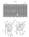
- FIG. 1shows two different pixel architectures used in semiconductor display arrays.
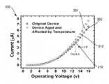
- FIG. 2is a graph of current versus operating voltage for an original device and a device aged and affected by temperature.
- FIG. 3is a reference map created by interpolation between measured values of reference pixels for localized phenomena from the content of a display.
- FIG. 4is a reference map showing the original results of panel measurements including the effect of aging and localized phenomena.
- FIG. 5is a reference map showing aging compensation results after the effect of localized phenomena are removed from the original results of the panel measurement by means of reference pixels, using simple subtraction to eliminate the effect of localized phenomena.
- FIG. 6show two modified pixel structures with reference loads used in semiconductor display arrays for correction for localized phenomena.
- FIG. 7is a reference map showing aging compensation results after the effect of localized phenomena are removed from the original results of the panel measurement by means of reference loads.
- FIG. 8Ais a block diagram of a display array including reference pixels for correction for localized phenomena.
- FIG. 8Bis a block diagram of a pixel including subpixels that may be used as a reference pixel.
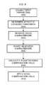
- FIG. 9is a flow diagram of the process to correct for localized phenomena in a semiconductor array display.
- FIG. 1shows two pixel architectures for a semiconductor display array, such as an array used in an OLED type displays.
- FIG. 1shows a first pixel architecture 100 that includes a driving circuit 102 , a load 104 that is coupled in series between a voltage supply (VDD) 106 and a voltage supply (VSS) 108 .
- a write switch 110allows data from an input line 112 to be programmed to the driving circuit 102 .
- a read switch 114allows a monitor line 116 to read the output from the driving circuit 102 .
- the load 104is a load that is driven by the pixel or resets the internal pixel circuit.
- the driving circuit 102is the driving or amplifying part of the circuit that powers the pixel in the display array.
- FIG. 1also shows a second pixel architecture 150 that includes a driving circuit 152 , a load 154 that is coupled in series between a voltage source (VDD) 156 and a voltage source (VSS) 158 .
- a write switch 160allows data from an input line 162 to be programmed to the driving circuit 152 .
- a read switch 164allows a monitor line 166 to read the output from the driving circuit 152 .
- the load 154is a load that is driven by the pixel or resets the internal pixel circuit.
- the driving circuit 152is the driving or amplifying part of the circuit that powers the pixel in the display array.
- the respective input lines 112 and 162 and monitor lines 116 and 166are coupled to a controller which programs the respective pixels via the input lines 112 , 162 controlled by the write switches 110 and 160 and monitors the respective pixels via the monitor lines 116 and 166 controlled by the read switches 114 and 164 .
- the pixels driven by the drivers 102 and 152are organic light emitting devices (OLEDs) which may include components such as thin film transistors that may have operating characteristics that change over age.
- One method to extend the semiconductor array lifetime and/or improve the array uniformityis external compensation for the effects of aging on OLEDs.
- the backplane and load input characteristics for the display arrayare measured and the backplane and load characteristics data is used to compensate for lifetime and uniformity of the OLEDs by the controller.
- Some localized phenomena effects that depend on either the content displayed by the array or localized environmental issuescan cause a divergence in the aging compensation function based on the influence of measured input characteristics data.
- the semiconductor arraywhen used in a display device, the displayed content on the pixels can affect the voltage distribution or localized temperatures throughout the display. Therefore, if the backplane and load characteristics are measured during the display of different content, the measured characteristics will vary due to localized phenomena. In this case, the compensation is based on accumulated changes in the characteristics, and thus the compensation will diverge over time and cause errors because of the localized display of different content.
- Another example of localized phenomenamay be increased temperature to certain pixels in an array such as exposure to sunlight on one part of the display.
- the increased temperature from the sunlightmay affect the voltage distribution or localized temperatures for pixels in the area exposed to the sunlight and therefore the measured input characteristics will vary for those pixels. Similar to content effects, the compensation is based on accumulated changes in the characteristics, and thus the compensation will diverge over time and cause errors because of the localized temperature effects.
- the unwanted effect of localized phenomenamay be removed from the extracted characteristics.
- Three example techniques to determine the effect of localized phenomena using at least one parameter of at least one of the pixels on the arraymay include: a) modeling based on pixel characteristics; b) use of reference pixels; and c) use of reference loads. Once the effect of localized phenomena is determined, it may be removed from characteristics that are input into the aging compensation equation for the pixels. These techniques to determine the effect of localized phenomena will be described below.
- One example techniqueis using modeling to determine the effect of localized phenomena.
- the pixel characteristicsare measured at a few points such as at different input current values.
- the pointsmay be taken during a time period of device operation that is sufficient to account for the effect of the localized phenomena.
- the changes in different parametersare calculated.
- Such parametersmay include mobility, threshold voltage, OLED voltage, and OLED off-current.
- the effect of the localized phenomenais calculated based on simplified models (e.g., temperature variation, voltage distribution, etc.) using the changes in the parameters.
- the compensation values for localized phenomenaare extracted for the array device from the results of the models.
- the measured parameter of the display circuitsuch as the architectures 100 or 150 in FIG. 1 is used to fine tune the calculated localized phenomena.
- a parameter that is mainly affected by localized phenomenae.g., mobility
- the effect of estimated localized phenomenais calculated on other parameters (e.g., off voltage (threshold voltage shift)) that are measured at different points.
- the measured pointsare input to a model to determine the effects of the localized phenomena.
- a first order modelmay suggest that mobility (gain) of a device changes by 5% for every 10° C. Therefore, if the resulting measurements of two points from the pixel characteristics show that the mobility changes by 10% an estimate may be made that the temperature changed by 20° C. Also, knowing the effect of temperature change on the other parameters (e.g., threshold voltage) allows an estimate to be made of how much of the measured changes in the parameters is due to the temperature change (20° C.) and how much is due to aging.
- the rate of change in the parametermay be used to extract the effect of localized phenomena.
- the changes in the parameterare fast while aging is a very slow process.
- a low pass filtermay remove all the fast changes in the measurement to eliminate the effect of localized parameters.
- the filtered characteristic measurementmay then be used as an input to the aging compensation algorithm.
- a low-pass filtermay be employed on the extracted parameters to eliminate the effect of localized phenomena in the form of changes that occur quickly indicating the effect of localized phenomena in contrast with gradually occurring changes that occur as a result of aging.
- the rate of change and dependency of the parameters to the localized phenomenamay be used to extract the effect of localized phenomena.
- the compensation valuesmay be corrected based on the fine-tuned localized phenomena. After estimating the effect of localized phenomena on each parameter from previous steps, this effect may be removed from those parameters by subtracting or dividing the parameters with the estimated effect for example. Then the modified parameter may be used to create the compensation values.
- the compensation values for threshold voltage shiftmay be a simple addition of the shift in the extracted parameter to the input signals.
- FIG. 2is a graph 200 of current versus operating voltage for an original device and a device after aging and also affected by a localized phenomena such as temperature.
- a first line 202shows the plot of current versus operating voltage for an original device.
- a second line 204shows the plot of current versus operating voltage for a device affected by aging and temperature.
- aging and temperaturedistort the operating characteristics of the device.
- the device off voltageis increased by 0.5 V due to aging effects and its gain is increased by 25% due to the localized phenomena of temperature.
- the affected devicehas a higher current.
- the output of the affected devicemay be compensated for aging based on many different techniques. However, compensation for aging alone would still result in deviation from the original device due to the localized phenomena such as temperature.
- two pointsmay be measured for the device to extract the temperature effect based on modeling.
- the measurement of a device characteristicmay then be adjusted from the results of the modeling to eliminate the effect of the temperature.
- the adjusted measured characteristicmay then be input to the aging compensation technique.
- a parametersuch as the operating voltage measured at a first current (point A) 210 and at a second current (point B) 212 .
- the change in the gainmay be extracted as 19% and the change in the off voltage as 0.22 V from the two operating voltage points.
- the determined change in gainis based on the localized phenomena and may then be used to correct the measured input characteristics when the compensation for aging of the pixel device is determined.
- model outputmay be made on more than two parameter points of the device for greater accuracy of the modeling results.
- the parameter points of each pixel on the arraymay be measured, or the parameter points of certain selected pixels at predetermined intervals in the array may be measured for purposes of inputs to the model.
- FIG. 8Ashows a panel display device 800 which includes a pixel array 802 that is controlled by a controller 804 .
- the controller 804accesses individual pixels via an address driver 806 .
- Contentis displayed on the pixel array 802 via a data driver 808 .
- Currentis supplied and read via a current supply and readout unit 810 .
- a supply voltage control 812regulates the voltage to the pixels in the pixel array 802 .
- a panel display device 800may include normal pixels 820 and some reference pixels 830 distributed across the pixel array 802 .
- the normal pixels 820receive content data inputs from the data driver 808 and display the content.
- the reference pixels 830are identical in structure to the normal pixels 820 . However, the status of the reference pixels 830 remains the same since such pixels are not coupled to data inputs from a controller 804 . Thus, the reference pixels 830 are either not aged or aged with a known state because they are not connected to content data signals. In this example, a parameter of both the normal pixels 820 and the reference pixels 830 are measured in the same way via the current readout 810 .
- the difference in parameter values measured between a reference pixel 830 and a normal pixel 820 in proximity to the reference pixel 830is associated with the effect of the localized phenomena.
- the difference between a parameter value of the reference pixel and a normal pixelis indicative of aging effects, since the normal pixel is subject to aging but reference pixel is not.
- the absolute parameter value after eliminating the difference in parameter values from the normal pixelis indicative of the effect of the localized phenomena since the localized phenomena affects both the normal pixel and a reference pixel in close proximity to the normal pixel.
- a reference mapmay be developed for the entire pixel array 802 based on the measurements from the reference pixels 830 in the pixel array 802 . The reference map may then be used to determine the effects of the localized phenomena for each pixel 820 in the pixel array 802 .
- the reference mapis an interpolation of the measured value for all other pixels based on the reference pixel measurement values.
- the measured values of the other pixelsare corrected by the reference value associated with that pixel (e.g. the two values are either subtracted or divided).
- the resulting corrected valueis used to adjust the measured characteristic used to calculate an adjusted aging compensation value for a pixel in the array.
- the reference mapis an interpolation of the extracted parameters for other pixels based on the reference pixel parameters.
- the parameters extracted for each pixel based on its own measurement datais tuned by the reference parameter maps (e.g., a model may be used to eliminate the unwanted effects from the extracted parameters).
- the reference measurements from the reference pixels 830may be taken when the display device 800 is either on line or off line. Generally, there are fewer reference pixels than normal pixels since the reference pixels are not coupled to content data inputs. The number of reference pixels therefore limits the display area of the pixels in the array. In this example, there is one reference pixel 830 for four normal pixels 820 , but other ratios may be used. The reference pixel measurements are applied for compensation of normal pixels 820 in proximity of the reference pixel 830 .
- the adjacent pixelsmay be used to create the content lost from the reference pixels.
- the pixel array 802may include a plurality of pixel units such as the reference pixel unit 830 which each contain sub-pixels.
- the reference pixel unit 830is the same as the normal pixel unit 820 except that some or all of the subpixels in the reference pixel 830 are not coupled to content data signals.
- the pixel unit 830has different sub-pixels such as a red pixel 840 a , a green pixel 840 b , a blue pixel 840 c and a white pixel 840 d .
- the sub-pixels 840 a - 840 dmay be used to generate color outputs from a normal pixel unit 820 .
- some of the pixels in the pixel array 802are reference pixels as shown in FIG. 8A .
- reference pixelssuch as the reference pixel 830 shown in FIG. 8B
- one or more of the sub-pixelsare used as reference pixels and the other sub-pixels may create the content of that would be output on the reference sub-pixel if the pixel unit operated normally.
- the reference pixelmay be one sub-pixel such as the white pixel 840 d .
- the red pixel 840 a , green pixel 840 b and blue pixel 840 cmay generate the white content for the white pixel 840 d which is used as a reference pixel and thus does not emit any light.
- FIGS. 3-5demonstrate the results of the aging algorithm on a panel with some localized phenomena and the results of using reference pixels to minimize the effect of the localized phenomena.
- a panelwas cooled intentionally at the top-left corner with a heat sink to simulate a localized phenomena, and there were a few images displayed on the panel affecting the voltage redistribution.
- FIG. 3is a reference map 300 created by interpolation between measured values of reference pixels for localized phenomena from the content of a display.
- the reference map 300includes an area 302 of the localized phenomena that is created by temperatures from the heat sink in proximity to the display.
- FIG. 4shows a reference map 400 that shows the original results of panel measurements including the effect of aging and localized phenomena temperature, voltage redistribution etc.).
- the original resultsinclude the localized phenomena of temperature in an area 402 .
- FIG. 5shows a reference map 500 that shows the aging compensation results after the effect of localized phenomena are removed from the original results of the panel measurement by means of reference pixels such as those shown in FIGS. 8A-8B , using simple subtraction to eliminate the effect of localized phenomena.
- An area 502 in FIG. 5may be contrasted to the area 402 in the reference map 400 in FIG. 4 to show that the effects related to localized phenomena have been eliminated.
- a third technique to determine the effect of localized phenomenais adding extra load elements to at least some of the pixels in an array to extract the localized phenomena based on measurements from the reference loads.
- the reference load elementsare not aged by content stress while the other components of the pixel architecture are aged based on content data written to the pixel.
- the characteristics of the reference loadare compared with the characteristics of the pixel load. Therefore, the differences in the characteristics of the reference load and the pixel load can be associated with the localized phenomena (e.g. voltage redistributions, temperature variation, etc.).
- FIG. 6shows two examples of pixel architectures using extra load elements for purposes of compensating for localized phenomena.
- FIG. 6shows an example reference load pixel architecture 600 and an alternate reference load pixel architecture 650 .
- the first reference load pixel architecture 600includes a driving circuit 602 and a pixel load 604 that is coupled in series between a voltage source (VDD) 606 and a voltage source (VSS) 608 .
- a write switch 610allows data from an input line 612 to be programmed to the driving circuit 602 .
- a read switch 614allows a monitor line 616 to read the output from the driving circuit 602 .
- the pixel load 604is a load that is driven by the pixel or resets the internal pixel circuit.
- the driver circuit 602is the driving or amplifying part of the circuit that powers the pixel in the display array.
- a reference load 620is also coupled to the voltage ground 608 and a reference switch 622 to the monitor line 616 .
- the reference switch 622may be controlled by the same signal controlling either the write switch 610 or the read switch 614 . Alternatively, a separate measurement line may be used for controlling the reference switch 622 to measure the reference load 620 .
- the alternate reference pixel architecture 650includes a driving circuit 652 and a pixel load 654 that is coupled in series between a voltage source 656 and a voltage ground 658 .
- a write switch 610allows data from an input line 662 to be programmed to the driving circuit 652 .
- a read switch 664allows a monitor line 666 to read the output from the driver 652 .
- the load 654is a load that is driven by the pixel or resets the internal pixel circuit.
- the driving circuit 652is the driving or amplifying part of the circuit that powers the pixel in the display array.
- a reference load 670is also coupled to the voltage source 656 and a reference switch 672 to the monitor line 616 .
- the reference switch 672may be controlled by the same signal controlling either the write switch 660 or the read switch 664 . Alternatively, a separate measurement line may be used for the reference load 670 .
- a reference signal applied to the switch 622 or switch 672may be either the read signal applied to the respective read switch 614 or 664 to read from the respective pixel drivers 602 and 652 .
- a parameter or characteristic of reference loads 620 or 670is measured in order to compare parameters or characteristics with elements in the pixel driver.
- the reference loadmay include similar components to the actual pixels on a display such as a driving transistor or a pixel circuit. However, the reference load does not include every component in the actual pixel architecture and therefore does not take up the space of a reference pixel as in the example explained above.
- the pixel itselfmay be programmed with the signal off state or if the pixel content has negligible effect on the measurement from the reference load, the pixel may be programmed with its content, and the read signal is off from the respective read switches 614 and 664 being open.
- the characteristics of the reference loads 620 or 670may be extracted via the respective read lines 616 and 666 in this example.
- any change to the power source linese.g., VSS or VDD
- the characteristics of the pixel loads 604 or 654may be extracted by the respective read lines 616 and 666 in this example.
- the reference switches 622 or 672are open, so the reference loads 620 and 670 are not read.
- the read characteristics of the reference load and the pixel loadare compared to determine the effect of the localized phenomena.
- any other localized phenomenamay be measured if it affects the reference load.
- different reference load elementsmay be used. Some of the reference load elements may match the load 604 or 654 and other reference loads may match the pixel driving circuit 602 or 652 . In another example, a different reference load may be used for measuring the effect of different localized phenomena.
- Some or all of the pixels in the display arraymay have reference load elements depending on the desired accuracy and processing overhead. The reference measurements from the reference load elements may be taken when the display is either on line or off line.
- FIG. 7is a reference graph 700 that shows aging results after the effect of localized phenomena are removed from the original results of the panel measurement by means of reference loads such as by the architectures 600 and 650 in FIG. 6 .
- the reference graph 700shows the results of using a reference load on the same panel represented in the architectures in FIG. 6 .
- the resultsmay have higher resolution with less interpolation error since the number of reference loads may be higher resulting in more input data than the smaller amount of data limited by the relatively smaller number of reference pixels without affecting image quality.
- FIG. 9is a flow diagram of the process of compensation for aging as well as localized phenomena in a display array.
- relevant input parametersare collected ( 900 ).
- the relevant input parametersmay be points from pixel characteristics or measurements of characteristics from reference pixels or a reference load.
- the effect of the localized phenomenais determined based on the relevant input parameter or parameters ( 902 ).
- a characteristicis then measured from at least one pixel in the array for aging compensation ( 904 ).
- the measured characteristic from a pixelis then adjusted to reduce the effect of the localized phenomena ( 906 ).
- the adjusted measured characteristicis then input into a compensation equation to calculate an adjusted aging compensation value ( 908 ).
- the compensation valueis then applied to adjust a data content signal for a pixel to compensate for the effects of aging ( 910 ).
Landscapes
- Engineering & Computer Science (AREA)
- Physics & Mathematics (AREA)
- Computer Hardware Design (AREA)
- General Physics & Mathematics (AREA)
- Theoretical Computer Science (AREA)
- Control Of Indicators Other Than Cathode Ray Tubes (AREA)
- Control Of El Displays (AREA)
Abstract
Description
This application is a continuation of U.S. patent application Ser. No. 14/561,697, filed Dec. 5, 2014, now allowed, which claims the benefit of U.S. Provisional Application No. 61/912,926, filed Dec. 4, 2013, each of which is hereby incorporated by reference in its entirety.
The present invention relates to semiconductor arrays such as those used in display panels and more specifically to a system to compensate for localized phenomena in OLED displays.
Displays can be created from an array of light emitting devices each controlled by individual circuits (i.e., pixel circuits) having transistors for selectively controlling the circuits to be programmed with display information and to emit light according to the display information. Thin film transistors (“TFTs”) fabricated on a substrate can be incorporated into such displays. TFTs tend to demonstrate non-uniform behavior across display panels and over time as the displays age. Compensation techniques can be applied to such displays to achieve image uniformity across the displays and to account for degradation in the displays as the displays age.
Some schemes for providing compensation to displays to account for variations across the display panel and over time utilize monitoring systems to measure time dependent parameters associated with the aging (i.e., degradation) of the pixel circuits. The measured information can then be used to inform subsequent programming of the pixel circuits so as to ensure that any measured degradation is accounted for by adjustments made to the programming. Such monitored pixel circuits may require the use of additional transistors and/or lines to selectively couple the pixel circuits to the monitoring systems and provide for reading out information. The incorporation of additional transistors and/or lines may undesirably decrease pixel-pitch (i.e., “pixel density”).
Another source of distortion may be localized phenomena such as the content of the data displayed by a pixel array, temperature effects, pressure on the screen or incidental light. For example, higher localized temperature may result in a distorted higher input data into the compensation equation which distorts the correction for aging effects. Thus, the input data for pixels may require additional compensation for effects based on the localized phenomena on a pixel display in obtaining accurate aging compensation for such pixels.
One disclosed example is a method of compensating for localized phenomena in a display device including an array of pixels and a controller for adjusting content data signals for the array of pixels to compensate for aging of the pixels in the array. A parameter of at least one of the pixels in the array is measured. The effect of a localized phenomena using the parameter is determined. A characteristic is measured for at least one of the pixels in the array. The measured characteristic is adjusted to reduce the effect of the localized phenomena. An adjusted aging compensation value is calculated based on the adjusted measured characteristic. The aging compensation value is applied to a data content signal to at least one of the pixels.
Another disclosed example is a display device including a display array having a plurality of pixels. The plurality of pixels each include a write input to write data content and a read input. A controller is coupled to the display array. The controller is operable to measure a parameter of at least one of the pixels in the array via the read input of the at least one of the pixels. The controller is operable to determine the effect of a localized phenomena on the pixel using the parameter. The controller is operable to measure a characteristic for at least one of the pixels in the array via the read input of the at least one of the pixels. The controller is operable to adjust the measured characteristic to reduce the effect of the localized phenomena. The controller is operable to calculate an adjusted aging compensation value based on the adjusted measured characteristic. The controller is operable to apply the aging compensation value to a data content signal to the write input of at least one of the pixels.
Additional aspects of the invention will be apparent to those of ordinary skill in the art in view of the detailed description of various embodiments, which is made with reference to the drawings, a brief description of which is provided below.
The foregoing and other advantages of the invention will become apparent upon reading the following detailed description and upon reference to the drawings.
While the invention is susceptible to various modifications and alternative forms, specific embodiments have been shown by way of example in the drawings and will be described in detail herein. It should be understood, however, that the invention is not intended to be limited to the particular forms disclosed. Rather, the invention is to cover all modifications, equivalents, and alternatives falling within the spirit and scope of the invention as defined by the appended claims.
One method to extend the semiconductor array lifetime and/or improve the array uniformity is external compensation for the effects of aging on OLEDs. In this example, the backplane and load input characteristics for the display array are measured and the backplane and load characteristics data is used to compensate for lifetime and uniformity of the OLEDs by the controller.
Some localized phenomena effects that depend on either the content displayed by the array or localized environmental issues can cause a divergence in the aging compensation function based on the influence of measured input characteristics data. For example, when the semiconductor array is used in a display device, the displayed content on the pixels can affect the voltage distribution or localized temperatures throughout the display. Therefore, if the backplane and load characteristics are measured during the display of different content, the measured characteristics will vary due to localized phenomena. In this case, the compensation is based on accumulated changes in the characteristics, and thus the compensation will diverge over time and cause errors because of the localized display of different content. Another example of localized phenomena may be increased temperature to certain pixels in an array such as exposure to sunlight on one part of the display. The increased temperature from the sunlight may affect the voltage distribution or localized temperatures for pixels in the area exposed to the sunlight and therefore the measured input characteristics will vary for those pixels. Similar to content effects, the compensation is based on accumulated changes in the characteristics, and thus the compensation will diverge over time and cause errors because of the localized temperature effects.
To improve the aging compensation performance, the unwanted effect of localized phenomena may be removed from the extracted characteristics. Three example techniques to determine the effect of localized phenomena using at least one parameter of at least one of the pixels on the array may include: a) modeling based on pixel characteristics; b) use of reference pixels; and c) use of reference loads. Once the effect of localized phenomena is determined, it may be removed from characteristics that are input into the aging compensation equation for the pixels. These techniques to determine the effect of localized phenomena will be described below.
One example technique is using modeling to determine the effect of localized phenomena. In this technique, the pixel characteristics are measured at a few points such as at different input current values. The points may be taken during a time period of device operation that is sufficient to account for the effect of the localized phenomena. Based on the measurement points, the changes in different parameters are calculated. Such parameters may include mobility, threshold voltage, OLED voltage, and OLED off-current. The effect of the localized phenomena is calculated based on simplified models (e.g., temperature variation, voltage distribution, etc.) using the changes in the parameters. The compensation values for localized phenomena are extracted for the array device from the results of the models.
The measured parameter of the display circuit such as thearchitectures FIG. 1 is used to fine tune the calculated localized phenomena. In one example, a parameter that is mainly affected by localized phenomena (e.g., mobility) is selected to estimate the localized phenomena. Then the effect of estimated localized phenomena is calculated on other parameters (e.g., off voltage (threshold voltage shift)) that are measured at different points. The measured points are input to a model to determine the effects of the localized phenomena.
For example, a first order model may suggest that mobility (gain) of a device changes by 5% for every 10° C. Therefore, if the resulting measurements of two points from the pixel characteristics show that the mobility changes by 10% an estimate may be made that the temperature changed by 20° C. Also, knowing the effect of temperature change on the other parameters (e.g., threshold voltage) allows an estimate to be made of how much of the measured changes in the parameters is due to the temperature change (20° C.) and how much is due to aging.
In another example, the rate of change in the parameter may be used to extract the effect of localized phenomena. For example, in case of temperature variation and content dependent voltage redistribution, the changes in the parameter are fast while aging is a very slow process. In one case, a low pass filter may remove all the fast changes in the measurement to eliminate the effect of localized parameters. The filtered characteristic measurement may then be used as an input to the aging compensation algorithm. In another case, a low-pass filter may be employed on the extracted parameters to eliminate the effect of localized phenomena in the form of changes that occur quickly indicating the effect of localized phenomena in contrast with gradually occurring changes that occur as a result of aging.
In another example, the rate of change and dependency of the parameters to the localized phenomena may be used to extract the effect of localized phenomena. The compensation values may be corrected based on the fine-tuned localized phenomena. After estimating the effect of localized phenomena on each parameter from previous steps, this effect may be removed from those parameters by subtracting or dividing the parameters with the estimated effect for example. Then the modified parameter may be used to create the compensation values. For example, the compensation values for threshold voltage shift may be a simple addition of the shift in the extracted parameter to the input signals.
The order of the aforementioned procedure can be changed. Alternatively, only on the measured parameters may be relied upon to calculate the localized phenomena.
To eliminate this effect, two points may be measured for the device to extract the temperature effect based on modeling. The measurement of a device characteristic may then be adjusted from the results of the modeling to eliminate the effect of the temperature. The adjusted measured characteristic may then be input to the aging compensation technique. In this example, a parameter such as the operating voltage measured at a first current (point A)210 and at a second current (point B)212. Using a linear model for current-voltage characteristics, the change in the gain may be extracted as 19% and the change in the off voltage as 0.22 V from the two operating voltage points. The determined change in gain is based on the localized phenomena and may then be used to correct the measured input characteristics when the compensation for aging of the pixel device is determined.
However, use of a more sophisticated non-linear model of the current-voltage characteristics based on the two measurements results in the determination of a change in the gain of 24.9% and that the off-voltage is changed by 0.502 V. Thus, depending on the required accuracy and the computation power available, different models may be used to determine the effects of localized phenomena and thus the accuracy of the adjustment of the measured input characteristic to the aging compensation techniques. The model output may be made on more than two parameter points of the device for greater accuracy of the modeling results. The parameter points of each pixel on the array may be measured, or the parameter points of certain selected pixels at predetermined intervals in the array may be measured for purposes of inputs to the model.
A second technique to determine the effect of localized phenomena may be the use of reference pixels.FIG. 8A shows apanel display device 800 which includes apixel array 802 that is controlled by acontroller 804. Thecontroller 804 accesses individual pixels via anaddress driver 806. Content is displayed on thepixel array 802 via adata driver 808. Current is supplied and read via a current supply andreadout unit 810. Asupply voltage control 812 regulates the voltage to the pixels in thepixel array 802.
As shown inFIG. 8A , apanel display device 800 may includenormal pixels 820 and somereference pixels 830 distributed across thepixel array 802. Thenormal pixels 820 receive content data inputs from thedata driver 808 and display the content. Thereference pixels 830 are identical in structure to thenormal pixels 820. However, the status of thereference pixels 830 remains the same since such pixels are not coupled to data inputs from acontroller 804. Thus, thereference pixels 830 are either not aged or aged with a known state because they are not connected to content data signals. In this example, a parameter of both thenormal pixels 820 and thereference pixels 830 are measured in the same way via thecurrent readout 810. The difference in parameter values measured between areference pixel 830 and anormal pixel 820 in proximity to thereference pixel 830 is associated with the effect of the localized phenomena. For example, the difference between a parameter value of the reference pixel and a normal pixel is indicative of aging effects, since the normal pixel is subject to aging but reference pixel is not. The absolute parameter value after eliminating the difference in parameter values from the normal pixel is indicative of the effect of the localized phenomena since the localized phenomena affects both the normal pixel and a reference pixel in close proximity to the normal pixel.
A reference map may be developed for theentire pixel array 802 based on the measurements from thereference pixels 830 in thepixel array 802. The reference map may then be used to determine the effects of the localized phenomena for eachpixel 820 in thepixel array 802.
In one example, the reference map is an interpolation of the measured value for all other pixels based on the reference pixel measurement values. In this case, the measured values of the other pixels are corrected by the reference value associated with that pixel (e.g. the two values are either subtracted or divided). The resulting corrected value is used to adjust the measured characteristic used to calculate an adjusted aging compensation value for a pixel in the array.
In another example, the reference map is an interpolation of the extracted parameters for other pixels based on the reference pixel parameters. The parameters extracted for each pixel based on its own measurement data is tuned by the reference parameter maps (e.g., a model may be used to eliminate the unwanted effects from the extracted parameters).
The reference measurements from thereference pixels 830 may be taken when thedisplay device 800 is either on line or off line. Generally, there are fewer reference pixels than normal pixels since the reference pixels are not coupled to content data inputs. The number of reference pixels therefore limits the display area of the pixels in the array. In this example, there is onereference pixel 830 for fournormal pixels 820, but other ratios may be used. The reference pixel measurements are applied for compensation ofnormal pixels 820 in proximity of thereference pixel 830.
To cover the content lost associated with reference pixels in an array, the adjacent pixels may be used to create the content lost from the reference pixels. In one example shown inFIG. 8B , thepixel array 802 may include a plurality of pixel units such as thereference pixel unit 830 which each contain sub-pixels. As explained above, thereference pixel unit 830 is the same as thenormal pixel unit 820 except that some or all of the subpixels in thereference pixel 830 are not coupled to content data signals. Each pixel unit in theexample pixel array 802 inFIG. 8A such as thepixel unit 830 has different sub-pixels such as ared pixel 840a, agreen pixel 840b, ablue pixel 840cand awhite pixel 840d. The sub-pixels840a-840dmay be used to generate color outputs from anormal pixel unit 820. In this example, some of the pixels in thepixel array 802 are reference pixels as shown inFIG. 8A . In such reference pixels such as thereference pixel 830 shown inFIG. 8B , one or more of the sub-pixels are used as reference pixels and the other sub-pixels may create the content of that would be output on the reference sub-pixel if the pixel unit operated normally. In this case, the reference pixel may be one sub-pixel such as thewhite pixel 840d. Thered pixel 840a,green pixel 840bandblue pixel 840cmay generate the white content for thewhite pixel 840dwhich is used as a reference pixel and thus does not emit any light.
A third technique to determine the effect of localized phenomena is adding extra load elements to at least some of the pixels in an array to extract the localized phenomena based on measurements from the reference loads. In this technique, the reference load elements are not aged by content stress while the other components of the pixel architecture are aged based on content data written to the pixel. The characteristics of the reference load are compared with the characteristics of the pixel load. Therefore, the differences in the characteristics of the reference load and the pixel load can be associated with the localized phenomena (e.g. voltage redistributions, temperature variation, etc.).
The alternatereference pixel architecture 650 includes adriving circuit 652 and apixel load 654 that is coupled in series between avoltage source 656 and avoltage ground 658. Awrite switch 610 allows data from aninput line 662 to be programmed to thedriving circuit 652. Aread switch 664 allows amonitor line 666 to read the output from thedriver 652. In this example, theload 654 is a load that is driven by the pixel or resets the internal pixel circuit. The drivingcircuit 652 is the driving or amplifying part of the circuit that powers the pixel in the display array. Areference load 670 is also coupled to thevoltage source 656 and areference switch 672 to themonitor line 616. Thereference switch 672 may be controlled by the same signal controlling either thewrite switch 660 or theread switch 664. Alternatively, a separate measurement line may be used for thereference load 670.
In one example, a reference signal applied to theswitch 622 or switch672 may be either the read signal applied to therespective read switch respective pixel drivers
Thus, the characteristics of the reference loads620 or670 may be extracted via therespective read lines respective read lines
In addition, any other localized phenomena may be measured if it affects the reference load. To improve the correction for the effect of localized phenomena on the pixel and the characteristics of theload load pixel driving circuit
While particular embodiments and applications of the present invention have been illustrated and described, it is to be understood that the invention is not limited to the precise construction and compositions disclosed herein and that various modifications, changes, and variations can be apparent from the foregoing descriptions without departing from the spirit and scope of the invention as defined in the appended claims.
Claims (20)
1. A method of compensating for localized phenomena in a display device including an array of pixels and a controller for adjusting content data signals for the array of pixels using original aging compensation values to compensate for aging of the pixels in the array, said method comprising;
determining an effect of a localized phenomena on an effected pixel in the array of pixels based on a change in a parameter of the effected pixel;
adjusting the original aging compensation value as a function of the change in the parameter associated with the localized phenomena to reduce the effect of the localized phenomena on the effected pixel;
applying the adjusted aging compensation value to a content data signal for the effected pixel; and
applying one of the original aging compensation values to a content data signal for each pixel not effected by the localized phenomena.
2. The method ofclaim 1 , wherein at least one of the pixels in the array of pixels is a reference pixel in proximity to the effected pixel, and
wherein determining the effect of the localized phenomena includes comparing the parameter of the reference pixel with the same parameter of the effected pixel.
3. The method ofclaim 2 , wherein the reference pixel includes a first subpixel that accepts a data content signal, and a second subpixel that is not coupled to a data content signal, wherein the parameter of the reference pixel is measured from the second subpixel.
4. The method ofclaim 3 , wherein the first subpixel generates data content in place of the second subpixel.
5. The method ofclaim 2 , wherein the parameter of the reference pixel is interpolated for comparison with the same measured parameter of the effected pixel.
6. The method ofclaim 1 , wherein at least one of the pixels in the array of pixels includes a reference load, and wherein determining the effect of the localized phenomena includes comparing the parameter of the reference load with the same parameter of the effected pixel.
7. The method ofclaim 6 , wherein the measured parameter of the reference load is interpolated for the comparison of the same parameter for a second pixel in proximity to the pixel including the reference load.
8. The method ofclaim 1 , wherein determining the effect of the localized phenomena includes inputting the parameter at one point and the parameter at a second point in a model of the current voltage characteristics to calculate the effect of the localized phenomena.
9. The method ofclaim 1 , wherein determining the effect of the localized phenomena includes filtering out changes that occur quickly between values of the parameter during different times.
10. A display device comprising:
a display array including a plurality of pixels, the plurality of pixels each including a write input to write data content and a read input; and
a controller coupled to the display array, the controller operable to:
adjust content data signals for the array of pixels using an aging compensation value for each pixel;
determine an effect of a localized phenomena on an effected pixel in the array of pixels based on a change in a parameter of the effected pixel;
adjust the aging compensation value as a function of the change in the parameter associated with the localized phenomena to reduce the effect of the localized phenomena on the effected pixel;
apply the adjusted aging compensation value to a content data signal to the effected pixel; and
applying one of the original aging compensation values to a content data signal for each pixel not effected by the localized phenomena.
11. The display device ofclaim 10 , wherein at least one of the pixels is a reference pixel in proximity to the effected pixel, and
wherein the controller determines the effect of the localized phenomena by comparing the parameter of the reference pixel with the same parameter of the effected pixel.
12. The display device ofclaim 11 , wherein the reference pixel includes a first subpixel that accepts a data content signal, and a second subpixel that is not coupled to a data content signal, wherein the parameter of the reference pixel is measured from the second subpixel.
13. The display device ofclaim 12 , wherein the first subpixel generates data content in place of the second subpixel.
14. The display device ofclaim 11 , wherein the parameter of the reference pixel is interpolated for comparison with the same parameter of the effected pixel in proximity to the reference pixel.
15. The display device ofclaim 10 , wherein at least one of the pixels includes a reference load, and wherein the controller determines the effect of the localized phenomena by comparing the parameter of the reference load with the same parameter of the effected pixel.
16. The display device ofclaim 15 , wherein the measured parameter of the reference load is interpolated for the comparison of the same parameter for a second pixel in proximity to the pixel including the reference load.
17. The display device ofclaim 10 , wherein the controller determines the effect of the localized phenomena by inputting the parameter at one point and the parameter at a second point in a model of current voltage characteristics to calculate the effect of the localized phenomena.
18. The display device ofclaim 10 , wherein determining the effect of the localized phenomena includes filtering out changes that occur quickly between values of the measured parameter during different times.
19. The display device ofclaim 10 , wherein the localized phenomena is selected from the group consisting of content displayed by the pixels from data content signals, and temperature.
20. The display device ofclaim 10 , wherein the parameter is selected from the group consisting of mobility, threshold voltage, organic light emitting device (OLED) voltage, and OLED off-current.
Priority Applications (2)
| Application Number | Priority Date | Filing Date | Title |
|---|---|---|---|
| US15/675,297US10186190B2 (en) | 2013-12-06 | 2017-08-11 | Correction for localized phenomena in an image array |
| US16/221,721US10755627B2 (en) | 2013-12-06 | 2018-12-17 | Correction for localized phenomena in an image array |
Applications Claiming Priority (3)
| Application Number | Priority Date | Filing Date | Title |
|---|---|---|---|
| US201361912926P | 2013-12-06 | 2013-12-06 | |
| US14/561,697US9761170B2 (en) | 2013-12-06 | 2014-12-05 | Correction for localized phenomena in an image array |
| US15/675,297US10186190B2 (en) | 2013-12-06 | 2017-08-11 | Correction for localized phenomena in an image array |
Related Parent Applications (1)
| Application Number | Title | Priority Date | Filing Date |
|---|---|---|---|
| US14/561,697ContinuationUS9761170B2 (en) | 2013-12-06 | 2014-12-05 | Correction for localized phenomena in an image array |
Related Child Applications (1)
| Application Number | Title | Priority Date | Filing Date |
|---|---|---|---|
| US16/221,721ContinuationUS10755627B2 (en) | 2013-12-06 | 2018-12-17 | Correction for localized phenomena in an image array |
Publications (2)
| Publication Number | Publication Date |
|---|---|
| US20170345364A1 US20170345364A1 (en) | 2017-11-30 |
| US10186190B2true US10186190B2 (en) | 2019-01-22 |
Family
ID=53271778
Family Applications (3)
| Application Number | Title | Priority Date | Filing Date |
|---|---|---|---|
| US14/561,697ActiveUS9761170B2 (en) | 2013-12-06 | 2014-12-05 | Correction for localized phenomena in an image array |
| US15/675,297ActiveUS10186190B2 (en) | 2013-12-06 | 2017-08-11 | Correction for localized phenomena in an image array |
| US16/221,721ActiveUS10755627B2 (en) | 2013-12-06 | 2018-12-17 | Correction for localized phenomena in an image array |
Family Applications Before (1)
| Application Number | Title | Priority Date | Filing Date |
|---|---|---|---|
| US14/561,697ActiveUS9761170B2 (en) | 2013-12-06 | 2014-12-05 | Correction for localized phenomena in an image array |
Family Applications After (1)
| Application Number | Title | Priority Date | Filing Date |
|---|---|---|---|
| US16/221,721ActiveUS10755627B2 (en) | 2013-12-06 | 2018-12-17 | Correction for localized phenomena in an image array |
Country Status (4)
| Country | Link |
|---|---|
| US (3) | US9761170B2 (en) |
| CN (2) | CN110619845B (en) |
| DE (1) | DE112014005536T5 (en) |
| WO (1) | WO2015083138A1 (en) |
Cited By (1)
| Publication number | Priority date | Publication date | Assignee | Title |
|---|---|---|---|---|
| US20190122606A1 (en)* | 2013-12-06 | 2019-04-25 | Ignis Innovation Inc. | Correction for localized phenomena in an image array |
Families Citing this family (28)
| Publication number | Priority date | Publication date | Assignee | Title |
|---|---|---|---|---|
| US9799246B2 (en) | 2011-05-20 | 2017-10-24 | Ignis Innovation Inc. | System and methods for extraction of threshold and mobility parameters in AMOLED displays |
| US8576217B2 (en) | 2011-05-20 | 2013-11-05 | Ignis Innovation Inc. | System and methods for extraction of threshold and mobility parameters in AMOLED displays |
| US10013907B2 (en) | 2004-12-15 | 2018-07-03 | Ignis Innovation Inc. | Method and system for programming, calibrating and/or compensating, and driving an LED display |
| US20140313111A1 (en) | 2010-02-04 | 2014-10-23 | Ignis Innovation Inc. | System and methods for extracting correlation curves for an organic light emitting device |
| CA2692097A1 (en) | 2010-02-04 | 2011-08-04 | Ignis Innovation Inc. | Extracting correlation curves for light emitting device |
| US9881532B2 (en) | 2010-02-04 | 2018-01-30 | Ignis Innovation Inc. | System and method for extracting correlation curves for an organic light emitting device |
| US10089921B2 (en) | 2010-02-04 | 2018-10-02 | Ignis Innovation Inc. | System and methods for extracting correlation curves for an organic light emitting device |
| US9466240B2 (en) | 2011-05-26 | 2016-10-11 | Ignis Innovation Inc. | Adaptive feedback system for compensating for aging pixel areas with enhanced estimation speed |
| US9773439B2 (en) | 2011-05-27 | 2017-09-26 | Ignis Innovation Inc. | Systems and methods for aging compensation in AMOLED displays |
| US10089924B2 (en) | 2011-11-29 | 2018-10-02 | Ignis Innovation Inc. | Structural and low-frequency non-uniformity compensation |
| US8937632B2 (en) | 2012-02-03 | 2015-01-20 | Ignis Innovation Inc. | Driving system for active-matrix displays |
| US8922544B2 (en) | 2012-05-23 | 2014-12-30 | Ignis Innovation Inc. | Display systems with compensation for line propagation delay |
| EP3043338A1 (en) | 2013-03-14 | 2016-07-13 | Ignis Innovation Inc. | Re-interpolation with edge detection for extracting an aging pattern for amoled displays |
| US9502653B2 (en) | 2013-12-25 | 2016-11-22 | Ignis Innovation Inc. | Electrode contacts |
| TWI540566B (en)* | 2014-12-09 | 2016-07-01 | 緯創資通股份有限公司 | Display and brightness and color compensation method and system thereof |
| CA2892714A1 (en) | 2015-05-27 | 2016-11-27 | Ignis Innovation Inc | Memory bandwidth reduction in compensation system |
| KR102457754B1 (en)* | 2015-08-04 | 2022-10-24 | 삼성디스플레이 주식회사 | Organic light emitting display device and method of driving the same |
| CA2900170A1 (en) | 2015-08-07 | 2017-02-07 | Gholamreza Chaji | Calibration of pixel based on improved reference values |
| CN106328059B (en)* | 2016-09-07 | 2017-10-27 | 京东方科技集团股份有限公司 | Method and apparatus for updating data in memory for electrical compensation |
| US10209551B2 (en)* | 2016-09-19 | 2019-02-19 | Apple Inc. | Dual-loop display sensing for compensation |
| KR102617215B1 (en) | 2017-09-21 | 2023-12-27 | 애플 인크. | Oled voltage driver with current-voltage compensation |
| US10714011B2 (en) | 2017-09-21 | 2020-07-14 | Apple Inc. | OLED voltage driver with current-voltage compensation |
| US10565912B2 (en)* | 2017-11-06 | 2020-02-18 | Wuhan China Star Optoelectronics Semiconductor Display Technology Co., Ltd. | Electrical characteristics inspection method |
| CN109144893A (en) | 2018-09-11 | 2019-01-04 | 郑州云海信息技术有限公司 | A kind of method and apparatus with Nonvolatile memory reservoir process interaction |
| JP7085018B2 (en)* | 2018-11-30 | 2022-06-15 | オリンパス株式会社 | Display device, display control method and endoscopic system |
| CN111354287B (en)* | 2018-12-20 | 2021-05-11 | 京东方科技集团股份有限公司 | Method, device, and device for determining pixel aging attenuation and compensating pixel |
| US11688363B2 (en)* | 2020-09-24 | 2023-06-27 | Apple Inc. | Reference pixel stressing for burn-in compensation systems and methods |
| CN114927091B (en)* | 2022-05-30 | 2023-11-28 | 卡莱特云科技股份有限公司 | Thermal screen effect processing method, device and system for LED display screen |
Citations (566)
| Publication number | Priority date | Publication date | Assignee | Title |
|---|---|---|---|---|
| US3506851A (en) | 1966-12-14 | 1970-04-14 | North American Rockwell | Field effect transistor driver using capacitor feedback |
| US3774055A (en) | 1972-01-24 | 1973-11-20 | Nat Semiconductor Corp | Clocked bootstrap inverter circuit |
| US4090096A (en) | 1976-03-31 | 1978-05-16 | Nippon Electric Co., Ltd. | Timing signal generator circuit |
| US4160934A (en) | 1977-08-11 | 1979-07-10 | Bell Telephone Laboratories, Incorporated | Current control circuit for light emitting diode |
| US4295091A (en) | 1978-10-12 | 1981-10-13 | Vaisala Oy | Circuit for measuring low capacitances |
| US4354162A (en) | 1981-02-09 | 1982-10-12 | National Semiconductor Corporation | Wide dynamic range control amplifier with offset correction |
| EP0158366A2 (en) | 1984-04-13 | 1985-10-16 | Sharp Kabushiki Kaisha | Color liquid-crystal display apparatus |
| JPH01272298A (en) | 1988-04-25 | 1989-10-31 | Yamaha Corp | Driving device |
| US4943956A (en) | 1988-04-25 | 1990-07-24 | Yamaha Corporation | Driving apparatus |
| US4996523A (en) | 1988-10-20 | 1991-02-26 | Eastman Kodak Company | Electroluminescent storage display with improved intensity driver circuits |
| CA1294034C (en) | 1985-01-09 | 1992-01-07 | Hiromu Hosokawa | Color uniformity compensation apparatus for cathode ray tubes |
| JPH0442619A (en) | 1990-06-08 | 1992-02-13 | Fujitsu Ltd | DA converter |
| JPH04158570A (en) | 1990-10-22 | 1992-06-01 | Seiko Epson Corp | Structure of semiconductor device and manufacture thereof |
| US5153420A (en) | 1990-11-28 | 1992-10-06 | Xerox Corporation | Timing independent pixel-scale light sensing apparatus |
| CA2109951A1 (en) | 1991-05-24 | 1992-11-26 | Robert Hotto | Dc integrating display driver employing pixel status memories |
| US5198803A (en) | 1990-06-06 | 1993-03-30 | Opto Tech Corporation | Large scale movie display system with multiple gray levels |
| US5204661A (en) | 1990-12-13 | 1993-04-20 | Xerox Corporation | Input/output pixel circuit and array of such circuits |
| US5266515A (en) | 1992-03-02 | 1993-11-30 | Motorola, Inc. | Fabricating dual gate thin film transistors |
| JPH06314977A (en) | 1993-04-28 | 1994-11-08 | Nec Ic Microcomput Syst Ltd | Current output type d/a converter circuit |
| US5489918A (en) | 1991-06-14 | 1996-02-06 | Rockwell International Corporation | Method and apparatus for dynamically and adjustably generating active matrix liquid crystal display gray level voltages |
| US5498880A (en) | 1995-01-12 | 1996-03-12 | E. I. Du Pont De Nemours And Company | Image capture panel using a solid state device |
| US5557342A (en) | 1993-07-06 | 1996-09-17 | Hitachi, Ltd. | Video display apparatus for displaying a plurality of video signals having different scanning frequencies and a multi-screen display system using the video display apparatus |
| US5561381A (en) | 1989-12-13 | 1996-10-01 | International Business Machines Corporation | Method for testing a partially constructed electronic circuit |
| US5572444A (en) | 1992-08-19 | 1996-11-05 | Mtl Systems, Inc. | Method and apparatus for automatic performance evaluation of electronic display devices |
| JPH08340243A (en) | 1995-06-14 | 1996-12-24 | Canon Inc | Bias circuit |
| US5589847A (en) | 1991-09-23 | 1996-12-31 | Xerox Corporation | Switched capacitor analog circuits using polysilicon thin film technology |
| JPH0990405A (en) | 1995-09-21 | 1997-04-04 | Sharp Corp | Thin film transistor |
| US5619033A (en) | 1995-06-07 | 1997-04-08 | Xerox Corporation | Layered solid state photodiode sensor array |
| US5648276A (en) | 1993-05-27 | 1997-07-15 | Sony Corporation | Method and apparatus for fabricating a thin film semiconductor device |
| US5670973A (en) | 1993-04-05 | 1997-09-23 | Cirrus Logic, Inc. | Method and apparatus for compensating crosstalk in liquid crystal displays |
| US5684365A (en) | 1994-12-14 | 1997-11-04 | Eastman Kodak Company | TFT-el display panel using organic electroluminescent media |
| US5691783A (en) | 1993-06-30 | 1997-11-25 | Sharp Kabushiki Kaisha | Liquid crystal display device and method for driving the same |
| US5714968A (en) | 1994-08-09 | 1998-02-03 | Nec Corporation | Current-dependent light-emitting element drive circuit for use in active matrix display device |
| US5723950A (en) | 1996-06-10 | 1998-03-03 | Motorola | Pre-charge driver for light emitting devices and method |
| US5744824A (en) | 1994-06-15 | 1998-04-28 | Sharp Kabushiki Kaisha | Semiconductor device method for producing the same and liquid crystal display including the same |
| US5745660A (en) | 1995-04-26 | 1998-04-28 | Polaroid Corporation | Image rendering system and method for generating stochastic threshold arrays for use therewith |
| US5748160A (en) | 1995-08-21 | 1998-05-05 | Mororola, Inc. | Active driven LED matrices |
| CA2249592A1 (en) | 1997-01-28 | 1998-07-30 | Casio Computer Co., Ltd. | Active matrix electroluminescent display device and a driving method thereof |
| JPH10254410A (en) | 1997-03-12 | 1998-09-25 | Pioneer Electron Corp | Organic electroluminescent display device, and driving method therefor |
| US5815303A (en) | 1997-06-26 | 1998-09-29 | Xerox Corporation | Fault tolerant projective display having redundant light modulators |
| TW342486B (en) | 1994-07-18 | 1998-10-11 | Toshiba Co Ltd | LED dot matrix display device and method for dimming thereof |
| WO1998048403A1 (en) | 1997-04-23 | 1998-10-29 | Sarnoff Corporation | Active matrix light emitting diode pixel structure and method |
| US5870071A (en) | 1995-09-07 | 1999-02-09 | Frontec Incorporated | LCD gate line drive circuit |
| US5874803A (en) | 1997-09-09 | 1999-02-23 | The Trustees Of Princeton University | Light emitting device with stack of OLEDS and phosphor downconverter |
| US5880582A (en) | 1996-09-04 | 1999-03-09 | Sumitomo Electric Industries, Ltd. | Current mirror circuit and reference voltage generating and light emitting element driving circuits using the same |
| US5903248A (en) | 1997-04-11 | 1999-05-11 | Spatialight, Inc. | Active matrix display having pixel driving circuits with integrated charge pumps |
| US5917280A (en) | 1997-02-03 | 1999-06-29 | The Trustees Of Princeton University | Stacked organic light emitting devices |
| US5923794A (en) | 1996-02-06 | 1999-07-13 | Polaroid Corporation | Current-mediated active-pixel image sensing device with current reset |
| JPH11202295A (en) | 1998-01-09 | 1999-07-30 | Seiko Epson Corp | Driving circuit for electro-optical device, electro-optical device, and electronic apparatus |
| JPH11219146A (en) | 1997-09-29 | 1999-08-10 | Mitsubishi Chemical Corp | Active matrix light emitting diode pixel structure and method |
| JPH11231805A (en) | 1998-02-10 | 1999-08-27 | Sanyo Electric Co Ltd | Display device |
| US5945972A (en) | 1995-11-30 | 1999-08-31 | Kabushiki Kaisha Toshiba | Display device |
| US5949398A (en) | 1996-04-12 | 1999-09-07 | Thomson Multimedia S.A. | Select line driver for a display matrix with toggling backplane |
| US5952991A (en) | 1996-11-14 | 1999-09-14 | Kabushiki Kaisha Toshiba | Liquid crystal display |
| US5952789A (en) | 1997-04-14 | 1999-09-14 | Sarnoff Corporation | Active matrix organic light emitting diode (amoled) display pixel structure and data load/illuminate circuit therefor |
| CA2368386A1 (en) | 1998-03-19 | 1999-09-23 | Charles J. Holloman | Analog driver for led or similar display element |
| JPH11282419A (en) | 1998-03-31 | 1999-10-15 | Nec Corp | Element driving device and method and image display device |
| US5982104A (en) | 1995-12-26 | 1999-11-09 | Pioneer Electronic Corporation | Driver for capacitive light-emitting device with degradation compensated brightness control |
| US6023259A (en) | 1997-07-11 | 2000-02-08 | Fed Corporation | OLED active matrix using a single transistor current mode pixel design |
| JP2000056847A (en) | 1998-08-14 | 2000-02-25 | Nec Corp | Constant current driving circuit |
| JP2000081607A (en) | 1998-09-04 | 2000-03-21 | Denso Corp | Matrix type liquid crystal display device |
| CA2242720C (en) | 1998-07-09 | 2000-05-16 | Ibm Canada Limited-Ibm Canada Limitee | Programmable led driver |
| US6069365A (en) | 1997-11-25 | 2000-05-30 | Alan Y. Chow | Optical processor based imaging system |
| CA2354018A1 (en) | 1998-12-14 | 2000-06-22 | Alan Richard | Portable microdisplay system |
| EP1028471A2 (en) | 1999-02-09 | 2000-08-16 | SANYO ELECTRIC Co., Ltd. | Electroluminescence display device |
| US6177915B1 (en) | 1990-06-11 | 2001-01-23 | International Business Machines Corporation | Display system having section brightness control and method of operating system |
| WO2001006484A1 (en) | 1999-07-14 | 2001-01-25 | Sony Corporation | Current drive circuit and display comprising the same, pixel circuit, and drive method |
| WO2001027910A1 (en) | 1999-10-12 | 2001-04-19 | Koninklijke Philips Electronics N.V. | Led display device |
| US6229506B1 (en) | 1997-04-23 | 2001-05-08 | Sarnoff Corporation | Active matrix light emitting diode pixel structure and concomitant method |
| JP2001134217A (en) | 1999-11-09 | 2001-05-18 | Tdk Corp | Driving device for organic el element |
| US20010002703A1 (en) | 1999-11-30 | 2001-06-07 | Jun Koyama | Electric device |
| US6246180B1 (en) | 1999-01-29 | 2001-06-12 | Nec Corporation | Organic el display device having an improved image quality |
| US6252248B1 (en) | 1998-06-08 | 2001-06-26 | Sanyo Electric Co., Ltd. | Thin film transistor and display |
| EP1111577A2 (en) | 1999-12-24 | 2001-06-27 | Sanyo Electric Co., Ltd. | Improvements in power consumption of display apparatus during still image display mode |
| US6259424B1 (en) | 1998-03-04 | 2001-07-10 | Victor Company Of Japan, Ltd. | Display matrix substrate, production method of the same and display matrix circuit |
| US6262589B1 (en) | 1998-05-25 | 2001-07-17 | Asia Electronics, Inc. | TFT array inspection method and device |
| JP2001195014A (en) | 2000-01-14 | 2001-07-19 | Tdk Corp | Driving device for organic el element |
| US20010009283A1 (en) | 2000-01-26 | 2001-07-26 | Tatsuya Arao | Semiconductor device and method of manufacturing the semiconductor device |
| US6271825B1 (en) | 1996-04-23 | 2001-08-07 | Rainbow Displays, Inc. | Correction methods for brightness in electronic display |
| WO2001063587A2 (en) | 2000-02-22 | 2001-08-30 | Sarnoff Corporation | A method and apparatus for calibrating display devices and automatically compensating for loss in their efficiency over time |
| US20010024181A1 (en) | 2000-01-17 | 2001-09-27 | Ibm | Liquid-crystal display, liquid-crystal control circuit, flicker inhibition method, and liquid-crystal driving method |
| US20010026257A1 (en) | 2000-03-27 | 2001-10-04 | Hajime Kimura | Electro-optical device |
| US6304039B1 (en) | 2000-08-08 | 2001-10-16 | E-Lite Technologies, Inc. | Power supply for illuminating an electro-luminescent panel |
| US20010030323A1 (en) | 2000-03-29 | 2001-10-18 | Sony Corporation | Thin film semiconductor apparatus and method for driving the same |
| US6307322B1 (en) | 1999-12-28 | 2001-10-23 | Sarnoff Corporation | Thin-film transistor circuitry with reduced sensitivity to variance in transistor threshold voltage |
| US6310962B1 (en) | 1997-08-20 | 2001-10-30 | Samsung Electronics Co., Ltd. | MPEG2 moving picture encoding/decoding system |
| US20010035863A1 (en) | 2000-04-26 | 2001-11-01 | Hajime Kimura | Electronic device and driving method thereof |
| US20010038367A1 (en) | 2000-05-08 | 2001-11-08 | Kazutaka Inukai | Light emitting device |
| US20010040541A1 (en) | 1997-09-08 | 2001-11-15 | Kiyoshi Yoneda | Semiconductor device having laser-annealed semiconductor device, display device and liquid crystal display device |
| US6320325B1 (en) | 2000-11-06 | 2001-11-20 | Eastman Kodak Company | Emissive display with luminance feedback from a representative pixel |
| US20010043173A1 (en) | 1997-09-04 | 2001-11-22 | Ronald Roy Troutman | Field sequential gray in active matrix led display using complementary transistor pixel circuits |
| US6323631B1 (en) | 2001-01-18 | 2001-11-27 | Sunplus Technology Co., Ltd. | Constant current driver with auto-clamped pre-charge function |
| US20010045929A1 (en) | 2000-01-21 | 2001-11-29 | Prache Olivier F. | Gray scale pixel driver for electronic display and method of operation therefor |
| US6329971B2 (en) | 1996-12-19 | 2001-12-11 | Zight Corporation | Display system having electrode modulation to alter a state of an electro-optic layer |
| US20010052940A1 (en) | 2000-02-01 | 2001-12-20 | Yoshio Hagihara | Solid-state image-sensing device |
| US20010052606A1 (en) | 2000-05-22 | 2001-12-20 | Koninklijke Philips Electronics N.V. | Display device |
| US20020000576A1 (en) | 2000-06-22 | 2002-01-03 | Kazutaka Inukai | Display device |
| US20020011796A1 (en) | 2000-05-08 | 2002-01-31 | Semiconductor Energy Laboratory Co., Ltd. | Light-emitting device, and electric device using the same |
| US20020012057A1 (en) | 2000-05-26 | 2002-01-31 | Hajime Kimura | MOS sensor and drive method thereof |
| US20020011799A1 (en) | 2000-04-06 | 2002-01-31 | Semiconductor Energy Laboratory Co., Ltd. | Electronic device and driving method |
| US20020014851A1 (en) | 2000-06-05 | 2002-02-07 | Ya-Hsiang Tai | Apparatus and method of testing an organic light emitting diode array |
| US20020018034A1 (en) | 2000-07-31 | 2002-02-14 | Shigeru Ohki | Display color temperature corrected lighting apparatus and flat plane display apparatus |
| JP2002055654A (en) | 2000-08-10 | 2002-02-20 | Nec Corp | Electroluminescence display |
| US6356029B1 (en) | 1999-10-02 | 2002-03-12 | U.S. Philips Corporation | Active matrix electroluminescent display device |
| US20020030190A1 (en) | 1998-12-03 | 2002-03-14 | Hisashi Ohtani | Electro-optical device and semiconductor circuit |
| JP2002091376A (en) | 2000-06-27 | 2002-03-27 | Hitachi Ltd | Image display device and driving method thereof |
| EP1194013A1 (en) | 2000-09-29 | 2002-04-03 | Eastman Kodak Company | A flat-panel display with luminance feedback |
| US6373454B1 (en) | 1998-06-12 | 2002-04-16 | U.S. Philips Corporation | Active matrix electroluminescent display devices |
| US6377237B1 (en) | 2000-01-07 | 2002-04-23 | Agilent Technologies, Inc. | Method and system for illuminating a layer of electro-optical material with pulses of light |
| US20020047565A1 (en) | 2000-07-28 | 2002-04-25 | Wintest Corporation | Apparatus and method for evaluating organic EL display |
| US20020052086A1 (en) | 2000-10-31 | 2002-05-02 | Mitsubishi Denki Kabushiki Kaisha | Semiconductor device and method of manufacturing same |
| US6392617B1 (en) | 1999-10-27 | 2002-05-21 | Agilent Technologies, Inc. | Active matrix light emitting diode display |
| US6404139B1 (en) | 1999-07-02 | 2002-06-11 | Seiko Instruments Inc. | Circuit for driving a light emitting elements display device |
| US20020084463A1 (en) | 2001-01-04 | 2002-07-04 | International Business Machines Corporation | Low-power organic light emitting diode pixel circuit |
| US6417825B1 (en) | 1998-09-29 | 2002-07-09 | Sarnoff Corporation | Analog active matrix emissive display |
| US20020101152A1 (en) | 2001-01-30 | 2002-08-01 | Semiconductor Energy Laboratory Co., Ltd. | Light emitting device |
| US20020101172A1 (en) | 2001-01-02 | 2002-08-01 | Bu Lin-Kai | Oled active driving system with current feedback |
| US20020105279A1 (en) | 2001-02-08 | 2002-08-08 | Hajime Kimura | Light emitting device and electronic equipment using the same |
| CA2436451A1 (en) | 2001-02-05 | 2002-08-15 | International Business Machines Corporation | Liquid crystal display device |
| JP2002229513A (en) | 2001-02-06 | 2002-08-16 | Tohoku Pioneer Corp | Device for driving organic el display panel |
| US6437106B1 (en) | 1999-06-24 | 2002-08-20 | Abbott Laboratories | Process for preparing 6-o-substituted erythromycin derivatives |
| CA2438577A1 (en) | 2001-02-16 | 2002-08-29 | Ignis Innovation Inc. | Pixel current driver for organic light emitting diode displays |
| WO2002067327A2 (en) | 2001-02-16 | 2002-08-29 | Ignis Innovation Inc. | Pixel current driver for organic light emitting diode displays |
| US20020117722A1 (en) | 1999-05-12 | 2002-08-29 | Kenichi Osada | Semiconductor integrated circuit device |
| US6445369B1 (en) | 1998-02-20 | 2002-09-03 | The University Of Hong Kong | Light emitting diode dot matrix display system with audio output |
| US20020122308A1 (en) | 2001-03-05 | 2002-09-05 | Fuji Xerox Co., Ltd. | Apparatus for driving light emitting element and system for driving light emitting element |
| TW502233B (en) | 1999-06-17 | 2002-09-11 | Sony Corp | Image display apparatus |
| JP2002278513A (en) | 2001-03-19 | 2002-09-27 | Sharp Corp | Electro-optical device |
| US20020158823A1 (en) | 1997-10-31 | 2002-10-31 | Matthew Zavracky | Portable microdisplay system |
| US20020158587A1 (en) | 2001-02-15 | 2002-10-31 | Naoaki Komiya | Organic EL pixel circuit |
| US20020158666A1 (en) | 2001-04-27 | 2002-10-31 | Munehiro Azami | Semiconductor device |
| US20020167471A1 (en) | 2001-05-09 | 2002-11-14 | Everitt James W. | System for providing pulse amplitude modulation for oled display drivers |
| US20020169575A1 (en) | 2001-05-09 | 2002-11-14 | James Everitt | Matrix element voltage sensing for precharge |
| JP2002333862A (en) | 2001-02-21 | 2002-11-22 | Semiconductor Energy Lab Co Ltd | Light emission device and electronic equipment |
| US20020180369A1 (en) | 2001-02-21 | 2002-12-05 | Jun Koyama | Light emitting device and electronic appliance |
| US20020181276A1 (en) | 2001-06-01 | 2002-12-05 | Semiconductor Energy Laboratory Co., Ltd. | Method of repairing a light-emitting device, and method of manufacturing a light -emitting device |
| US20020180721A1 (en) | 1997-03-12 | 2002-12-05 | Mutsumi Kimura | Pixel circuit display apparatus and electronic apparatus equipped with current driving type light-emitting device |
| US20020186214A1 (en) | 2001-06-05 | 2002-12-12 | Eastman Kodak Company | Method for saving power in an organic electroluminescent display using white light emitting elements |
| US20020190971A1 (en) | 2001-04-27 | 2002-12-19 | Kabushiki Kaisha Toshiba | Display apparatus, digital-to-analog conversion circuit and digital-to-analog conversion method |
| US20020190924A1 (en) | 2001-01-19 | 2002-12-19 | Mitsuru Asano | Active matrix display |
| US20020195968A1 (en) | 2001-06-22 | 2002-12-26 | International Business Machines Corporation | Oled current drive pixel circuit |
| US20020195967A1 (en) | 2001-06-22 | 2002-12-26 | Kim Sung Ki | Electro-luminescence panel |
| US6501098B2 (en) | 1998-11-25 | 2002-12-31 | Semiconductor Energy Laboratory Co, Ltd. | Semiconductor device |
| US6501466B1 (en) | 1999-11-18 | 2002-12-31 | Sony Corporation | Active matrix type display apparatus and drive circuit thereof |
| US20030020413A1 (en) | 2001-07-27 | 2003-01-30 | Masanobu Oomura | Active matrix display |
| US20030030603A1 (en) | 2001-08-09 | 2003-02-13 | Nec Corporation | Drive circuit for display device |
| US6522315B2 (en) | 1997-02-17 | 2003-02-18 | Seiko Epson Corporation | Display apparatus |
| US6525683B1 (en) | 2001-09-19 | 2003-02-25 | Intel Corporation | Nonlinearly converting a signal to compensate for non-uniformities and degradations in a display |
| US20030043088A1 (en) | 2001-08-31 | 2003-03-06 | Booth Lawrence A. | Compensating organic light emitting device displays for color variations |
| JP2003076331A (en) | 2001-08-31 | 2003-03-14 | Seiko Epson Corp | Display device and electronic equipment |
| US20030057895A1 (en) | 2001-09-07 | 2003-03-27 | Semiconductor Energy Laboratory Co., Ltd. | Light emitting device and method of driving the same |
| US20030058226A1 (en) | 1994-08-22 | 2003-03-27 | Bertram William K. | Reduced noise touch screen apparatus and method |
| US6541921B1 (en) | 2001-10-17 | 2003-04-01 | Sierra Design Group | Illumination intensity control in electroluminescent display |
| US6542138B1 (en) | 1999-09-11 | 2003-04-01 | Koninklijke Philips Electronics N.V. | Active matrix electroluminescent display device |
| US20030062524A1 (en) | 2001-08-29 | 2003-04-03 | Hajime Kimura | Light emitting device, method of driving a light emitting device, element substrate, and electronic equipment |
| US20030071821A1 (en) | 2001-10-11 | 2003-04-17 | Sundahl Robert C. | Luminance compensation for emissive displays |
| US20030076048A1 (en) | 2001-10-23 | 2003-04-24 | Rutherford James C. | Organic electroluminescent display device driving method and apparatus |
| WO2003034389A2 (en) | 2001-10-19 | 2003-04-24 | Clare Micronix Integrated Systems, Inc. | System and method for providing pulse amplitude modulation for oled display drivers |
| JP2003124519A (en) | 2001-10-11 | 2003-04-25 | Sharp Corp | Light emitting diode drive circuit and optical transmission device using the same |
| US6555420B1 (en) | 1998-08-31 | 2003-04-29 | Semiconductor Energy Laboratory Co., Ltd. | Semiconductor device and process for producing semiconductor device |
| US20030090447A1 (en) | 2001-09-21 | 2003-05-15 | Hajime Kimura | Display device and driving method thereof |
| US20030090481A1 (en) | 2001-11-13 | 2003-05-15 | Hajime Kimura | Display device and method for driving the same |
| US6577302B2 (en) | 2000-03-31 | 2003-06-10 | Koninklijke Philips Electronics N.V. | Display device having current-addressed pixels |
| US20030107560A1 (en) | 2001-01-15 | 2003-06-12 | Akira Yumoto | Active-matrix display, active-matrix organic electroluminescent display, and methods of driving them |
| US6580408B1 (en) | 1999-06-03 | 2003-06-17 | Lg. Philips Lcd Co., Ltd. | Electro-luminescent display including a current mirror |
| US20030111966A1 (en) | 2001-12-19 | 2003-06-19 | Yoshiro Mikami | Image display apparatus |
| TW538650B (en) | 2000-09-29 | 2003-06-21 | Seiko Epson Corp | Driving method for electro-optical device, electro-optical device, and electronic apparatus |
| US6583398B2 (en) | 1999-12-14 | 2003-06-24 | Koninklijke Philips Electronics N.V. | Image sensor |
| JP2003177709A (en) | 2001-12-13 | 2003-06-27 | Seiko Epson Corp | Pixel circuit for light emitting element |
| US20030122813A1 (en) | 2001-12-28 | 2003-07-03 | Pioneer Corporation | Panel display driving device and driving method |
| US20030122749A1 (en) | 2001-12-31 | 2003-07-03 | Booth Lawrence A. | Energy sensing light emitting diode display |
| JP2003195813A (en) | 2001-09-07 | 2003-07-09 | Semiconductor Energy Lab Co Ltd | Light emitting device |
| US20030142088A1 (en) | 2001-10-19 | 2003-07-31 | Lechevalier Robert | Method and system for precharging OLED/PLED displays with a precharge latency |
| WO2003063124A1 (en) | 2002-01-17 | 2003-07-31 | Nec Corporation | Semiconductor device incorporating matrix type current load driving circuits, and driving method thereof |
| US20030146897A1 (en) | 2002-02-07 | 2003-08-07 | Hunter Robert J. | Method and apparatus to reduce power consumption of a computer system display screen |
| EP1335430A1 (en) | 2002-02-12 | 2003-08-13 | Eastman Kodak Company | A flat-panel light emitting pixel with luminance feedback |
| US20030169241A1 (en) | 2001-10-19 | 2003-09-11 | Lechevalier Robert E. | Method and system for ramp control of precharge voltage |
| US20030174152A1 (en) | 2002-02-04 | 2003-09-18 | Yukihiro Noguchi | Display apparatus with function which makes gradiation control easier |
| WO2003077231A2 (en) | 2002-03-13 | 2003-09-18 | Koninklijke Philips Electronics N.V. | Two sided display device |
| JP2003271095A (en) | 2002-03-14 | 2003-09-25 | Nec Corp | Driving circuit for current control element and image display device |
| US20030185438A1 (en) | 1997-09-16 | 2003-10-02 | Olympus Optical Co., Ltd. | Color image processing apparatus |
| CN1448908A (en) | 2002-03-29 | 2003-10-15 | 精工爱普生株式会社 | Electronic device, method for driving electronic device, electrooptical device and electronic apparatus |
| US20030197663A1 (en) | 2001-12-27 | 2003-10-23 | Lee Han Sang | Electroluminescent display panel and method for operating the same |
| US6639244B1 (en) | 1999-01-11 | 2003-10-28 | Semiconductor Energy Laboratory Co., Ltd. | Semiconductor device and method of fabricating the same |
| JP2003308046A (en) | 2002-02-18 | 2003-10-31 | Sanyo Electric Co Ltd | Display device |
| JP2003317944A (en) | 2002-04-26 | 2003-11-07 | Seiko Epson Corp | Electro-optical devices and electronic equipment |
| US20030210256A1 (en) | 2002-03-25 | 2003-11-13 | Yukio Mori | Display method and display apparatus |
| EP1372136A1 (en) | 2002-06-12 | 2003-12-17 | Seiko Epson Corporation | Scan driver and a column driver for active matrix display device and corresponding method |
| US20030230980A1 (en) | 2002-06-18 | 2003-12-18 | Forrest Stephen R | Very low voltage, high efficiency phosphorescent oled in a p-i-n structure |
| US20030231148A1 (en) | 2002-06-14 | 2003-12-18 | Chun-Hsu Lin | Brightness correction apparatus and method for plasma display |
| US20030230141A1 (en) | 2002-06-18 | 2003-12-18 | Gilmour Daniel A. | Optical fuel level sensor |
| GB2389951A (en) | 2002-06-18 | 2003-12-24 | Cambridge Display Tech Ltd | Display driver circuits for active matrix OLED displays |
| JP2004004675A (en) | 2002-03-29 | 2004-01-08 | Seiko Epson Corp | Electronic device, method of driving electronic device, electro-optical device, and electronic apparatus |
| WO2004003877A2 (en) | 2002-06-27 | 2004-01-08 | Casio Computer Co., Ltd. | Current drive apparatus and drive method thereof, and electroluminescent display apparatus using the circuit |
| US6677713B1 (en) | 2002-08-28 | 2004-01-13 | Au Optronics Corporation | Driving circuit and method for light emitting device |
| EP1381019A1 (en) | 2002-07-10 | 2004-01-14 | Pioneer Corporation | Automatic luminance adjustment device and method |
| CA2463653A1 (en) | 2002-07-09 | 2004-01-15 | Casio Computer Co., Ltd. | Driving device, display apparatus using the same, and driving method therefor |
| US6680580B1 (en) | 2002-09-16 | 2004-01-20 | Au Optronics Corporation | Driving circuit and method for light emitting device |
| US6687266B1 (en) | 2002-11-08 | 2004-02-03 | Universal Display Corporation | Organic light emitting materials and devices |
| US6690000B1 (en) | 1998-12-02 | 2004-02-10 | Nec Corporation | Image sensor |
| US6690344B1 (en) | 1999-05-14 | 2004-02-10 | Ngk Insulators, Ltd. | Method and apparatus for driving device and display |
| JP2004045648A (en) | 2002-07-10 | 2004-02-12 | Pioneer Electronic Corp | Method and device for driving display panel |
| US6697057B2 (en) | 2000-10-27 | 2004-02-24 | Semiconductor Energy Laboratory Co., Ltd. | Display device and method of driving the same |
| US20040041750A1 (en) | 2001-08-29 | 2004-03-04 | Katsumi Abe | Current load device and method for driving the same |
| CA2498136A1 (en) | 2002-09-09 | 2004-03-18 | Matthew Stevenson | Organic electronic device having improved homogeneity |
| WO2004025615A1 (en) | 2002-09-16 | 2004-03-25 | Koninklijke Philips Electronics N.V. | Display device |
| US20040066357A1 (en) | 2002-09-02 | 2004-04-08 | Canon Kabushiki Kaisha | Drive circuit, display apparatus, and information display apparatus |
| US20040070565A1 (en) | 2001-12-05 | 2004-04-15 | Nayar Shree K | Method and apparatus for displaying images |
| US20040070557A1 (en) | 2002-10-11 | 2004-04-15 | Mitsuru Asano | Active-matrix display device and method of driving the same |
| US6724151B2 (en) | 2001-11-06 | 2004-04-20 | Lg. Philips Lcd Co., Ltd. | Apparatus and method of driving electro luminescence panel |
| WO2004034364A1 (en) | 2002-10-08 | 2004-04-22 | Koninklijke Philips Electronics N.V. | Electroluminescent display devices |
| EP1418566A2 (en) | 2002-11-08 | 2004-05-12 | Tohoku Pioneer Corporation | Drive methods and drive devices for active type light emitting display panel |
| US20040090400A1 (en) | 2002-11-05 | 2004-05-13 | Yoo Juhn Suk | Data driving apparatus and method of driving organic electro luminescence display panel |
| US6738034B2 (en) | 2000-06-27 | 2004-05-18 | Hitachi, Ltd. | Picture image display device and method of driving the same |
| US6738035B1 (en) | 1997-09-22 | 2004-05-18 | Nongqiang Fan | Active matrix LCD based on diode switches and methods of improving display uniformity of same |
| US20040095297A1 (en) | 2002-11-20 | 2004-05-20 | International Business Machines Corporation | Nonlinear voltage controlled current source with feedback circuit |
| JP2004145197A (en) | 2002-10-28 | 2004-05-20 | Mitsubishi Electric Corp | Display device and display panel |
| US20040100427A1 (en) | 2002-08-07 | 2004-05-27 | Seiko Epson Corporation | Electronic circuit, electro-optical device, method for driving electro-optical device and electronic apparatus |
| WO2004047058A2 (en) | 2002-11-21 | 2004-06-03 | Koninklijke Philips Electronics N.V. | Method of improving the output uniformity of a display device |
| EP1429312A2 (en) | 2002-12-12 | 2004-06-16 | Seiko Epson Corporation | Electro-optical device, method of driving electro optical device, and electronic apparatus |
| US6753655B2 (en) | 2002-09-19 | 2004-06-22 | Industrial Technology Research Institute | Pixel structure for an active matrix OLED |
| US6753834B2 (en) | 2001-03-30 | 2004-06-22 | Hitachi, Ltd. | Display device and driving method thereof |
| US6756741B2 (en) | 2002-07-12 | 2004-06-29 | Au Optronics Corp. | Driving circuit for unit pixel of organic light emitting displays |
| US6756958B2 (en) | 2000-11-30 | 2004-06-29 | Hitachi, Ltd. | Liquid crystal display device |
| US6756952B1 (en) | 1998-03-05 | 2004-06-29 | Jean-Claude Decaux | Light display panel control |
| US20040135749A1 (en) | 2003-01-14 | 2004-07-15 | Eastman Kodak Company | Compensating for aging in OLED devices |
| US6765549B1 (en) | 1999-11-08 | 2004-07-20 | Semiconductor Energy Laboratory Co., Ltd. | Active matrix display with pixel memory |
| US20040140982A1 (en) | 2003-01-21 | 2004-07-22 | Pate Michael A. | Image projection with display-condition compensation |
| US20040145547A1 (en) | 2003-01-21 | 2004-07-29 | Oh Choon-Yul | Luminescent display, and driving method and pixel circuit thereof, and display device |
| US6771028B1 (en) | 2003-04-30 | 2004-08-03 | Eastman Kodak Company | Drive circuitry for four-color organic light-emitting device |
| US20040150594A1 (en) | 2002-07-25 | 2004-08-05 | Semiconductor Energy Laboratory Co., Ltd. | Display device and drive method therefor |
| US20040150592A1 (en) | 2003-01-10 | 2004-08-05 | Eastman Kodak Company | Correction of pixels in an organic EL display device |
| WO2004066249A1 (en) | 2003-01-24 | 2004-08-05 | Koninklijke Philips Electronics N.V. | Active matrix display devices |
| US20040155841A1 (en) | 2002-11-27 | 2004-08-12 | Seiko Epson Corporation | Electro-optical device, method of driving electro-optical device, and electronic apparatus |
| US6777888B2 (en) | 2001-03-21 | 2004-08-17 | Canon Kabushiki Kaisha | Drive circuit to be used in active matrix type light-emitting element array |
| US6781567B2 (en) | 2000-09-29 | 2004-08-24 | Seiko Epson Corporation | Driving method for electro-optical device, electro-optical device, and electronic apparatus |
| EP1450341A1 (en) | 2001-09-25 | 2004-08-25 | Matsushita Electric Industrial Co., Ltd. | El display panel and el display apparatus comprising it |
| US20040174347A1 (en) | 2003-03-07 | 2004-09-09 | Wein-Town Sun | Data driver and related method used in a display device for saving space |
| US20040174349A1 (en) | 2003-03-04 | 2004-09-09 | Libsch Frank Robert | Driving circuits for displays |
| US20040174354A1 (en) | 2003-02-24 | 2004-09-09 | Shinya Ono | Display apparatus controlling brightness of current-controlled light emitting element |
| US20040178743A1 (en) | 2002-12-16 | 2004-09-16 | Eastman Kodak Company | Color OLED display system having improved performance |
| EP1465143A2 (en) | 2003-04-01 | 2004-10-06 | Samsung SDI Co., Ltd. | Light emitting display, display panel, and driving method thereof |
| JP2004287345A (en) | 2003-03-25 | 2004-10-14 | Casio Comput Co Ltd | Display drive device, display device, and drive control method thereof |
| US6806638B2 (en) | 2002-12-27 | 2004-10-19 | Au Optronics Corporation | Display of active matrix organic light emitting diode and fabricating method |
| EP1469448A1 (en) | 2001-12-28 | 2004-10-20 | Sanyo Electric Co., Ltd. | Organic el display luminance control method and luminance control circuit |
| US20040207615A1 (en) | 1999-07-14 | 2004-10-21 | Akira Yumoto | Current drive circuit and display device using same pixel circuit, and drive method |
| TWI223092B (en) | 2003-07-29 | 2004-11-01 | Primtest System Technologies | Testing apparatus and method for thin film transistor display array |
| US6815975B2 (en) | 2002-05-21 | 2004-11-09 | Wintest Corporation | Inspection method and inspection device for active matrix substrate, inspection program used therefor, and information storage medium |
| CA2522396A1 (en) | 2003-04-25 | 2004-11-11 | Visioneered Image Systems, Inc. | Led illumination source/display with individual led brightness monitoring capability and calibration method |
| US20040227697A1 (en) | 2003-05-14 | 2004-11-18 | Canon Kabushiki Kaisha | Signal processing apparatus, signal processing method, correction value generation apparatus, correction value generation method, and display apparatus manufacturing method |
| US20040233125A1 (en) | 2003-05-23 | 2004-11-25 | Gino Tanghe | Method for displaying images on a large-screen organic light-emitting diode display, and display used therefore |
| WO2004104975A1 (en) | 2003-05-23 | 2004-12-02 | Sony Corporation | Pixel circuit, display unit, and pixel circuit drive method |
| US20040239596A1 (en) | 2003-02-19 | 2004-12-02 | Shinya Ono | Image display apparatus using current-controlled light emitting element |
| KR20040100887A (en) | 2003-05-19 | 2004-12-02 | 세이코 엡슨 가부시키가이샤 | Electrooptical device and driving device thereof |
| US6828950B2 (en) | 2000-08-10 | 2004-12-07 | Semiconductor Energy Laboratory Co., Ltd. | Display device and method of driving the same |
| US20040246246A1 (en) | 2003-06-09 | 2004-12-09 | Mitsubishi Denki Kabushiki Kaisha | Image display device with increased margin for writing image signal |
| US20040252089A1 (en) | 2003-05-16 | 2004-12-16 | Shinya Ono | Image display apparatus controlling brightness of current-controlled light emitting element |
| US20040257355A1 (en) | 2003-06-18 | 2004-12-23 | Nuelight Corporation | Method and apparatus for controlling an active matrix display |
| US20040257313A1 (en) | 2003-04-15 | 2004-12-23 | Samsung Oled Co., Ltd. | Method and apparatus for driving electro-luminescence display panel designed to perform efficient booting |
| US20040263541A1 (en) | 2003-06-30 | 2004-12-30 | Fujitsu Hitachi Plasma Display Limited | Display apparatus and display driving method for effectively eliminating the occurrence of a moving image false contour |
| US20040263445A1 (en) | 2001-01-29 | 2004-12-30 | Semiconductor Energy Laboratory Co., Ltd, A Japan Corporation | Light emitting device |
| US20050007392A1 (en) | 2003-05-28 | 2005-01-13 | Seiko Epson Corporation | Electro-optical device, method of driving electro-optical device, and electronic apparatus |
| US20050007357A1 (en) | 2003-05-19 | 2005-01-13 | Sony Corporation | Pixel circuit, display device, and driving method of pixel circuit |
| US20050007355A1 (en) | 2003-05-26 | 2005-01-13 | Seiko Epson Corporation | Display apparatus, display method and method of manufacturing a display apparatus |
| US20050017650A1 (en) | 2003-07-24 | 2005-01-27 | Fryer Christopher James Newton | Control of electroluminescent displays |
| US20050024393A1 (en) | 2003-07-28 | 2005-02-03 | Canon Kabushiki Kaisha | Image forming apparatus and method of controlling image forming apparatus |
| US6853371B2 (en) | 2000-09-18 | 2005-02-08 | Sanyo Electric Co., Ltd. | Display device |
| US20050030267A1 (en) | 2003-08-07 | 2005-02-10 | Gino Tanghe | Method and system for measuring and controlling an OLED display element for improved lifetime and light output |
| JP2005057217A (en) | 2003-08-07 | 2005-03-03 | Renesas Technology Corp | Semiconductor integrated circuit device |
| WO2005022500A1 (en) | 2003-08-29 | 2005-03-10 | Koninklijke Philips Electronics N.V. | Data signal driver for light emitting display |
| WO2005022498A2 (en) | 2003-09-02 | 2005-03-10 | Koninklijke Philips Electronics N.V. | Active matrix display devices |
| US20050057484A1 (en) | 2003-09-15 | 2005-03-17 | Diefenbaugh Paul S. | Automatic image luminance control with backlight adjustment |
| CA2443206A1 (en) | 2003-09-23 | 2005-03-23 | Ignis Innovation Inc. | Amoled display backplanes - pixel driver circuits, array architecture, and external compensation |
| US6873117B2 (en) | 2002-09-30 | 2005-03-29 | Pioneer Corporation | Display panel and display device |
| US20050068270A1 (en) | 2003-09-17 | 2005-03-31 | Hiroki Awakura | Display apparatus and display control method |
| US20050067970A1 (en) | 2003-09-26 | 2005-03-31 | International Business Machines Corporation | Active-matrix light emitting display and method for obtaining threshold voltage compensation for same |
| WO2005029456A1 (en) | 2003-09-23 | 2005-03-31 | Ignis Innovation Inc. | Circuit and method for driving an array of light emitting pixels |
| US20050068275A1 (en) | 2003-09-29 | 2005-03-31 | Kane Michael Gillis | Driver circuit, as for an OLED display |
| US20050067971A1 (en) | 2003-09-29 | 2005-03-31 | Michael Gillis Kane | Pixel circuit for an active matrix organic light-emitting diode display |
| US6876346B2 (en) | 2000-09-29 | 2005-04-05 | Sanyo Electric Co., Ltd. | Thin film transistor for supplying power to element to be driven |
| EP1521203A2 (en) | 2003-10-02 | 2005-04-06 | Alps Electric Co., Ltd. | Capacitance detector circuit, capacitance detector method and fingerprint sensor using the same |
| US20050073264A1 (en) | 2003-09-29 | 2005-04-07 | Shoichiro Matsumoto | Organic EL panel |
| WO2005034072A1 (en) | 2003-10-02 | 2005-04-14 | Pioneer Corporation | Display apparatus having active matrix display panel, and method for driving the same |
| US20050083323A1 (en) | 2003-10-21 | 2005-04-21 | Tohoku Pioneer Corporation | Light emitting display device |
| US6885356B2 (en) | 2000-07-18 | 2005-04-26 | Nec Electronics Corporation | Active-matrix type display device |
| US20050088103A1 (en) | 2003-10-28 | 2005-04-28 | Hitachi., Ltd. | Image display device |
| US20050105031A1 (en) | 2003-11-13 | 2005-05-19 | Po-Sheng Shih | [pixel structure of display and driving method thereof] |
| US20050110420A1 (en) | 2003-11-25 | 2005-05-26 | Eastman Kodak Company | OLED display with aging compensation |
| US20050110807A1 (en) | 2003-11-21 | 2005-05-26 | Au Optronics Company, Ltd. | Method for displaying images on electroluminescence devices with stressed pixels |
| US6900485B2 (en) | 2003-04-30 | 2005-05-31 | Hynix Semiconductor Inc. | Unit pixel in CMOS image sensor with enhanced reset efficiency |
| US6903734B2 (en) | 2000-12-22 | 2005-06-07 | Lg.Philips Lcd Co., Ltd. | Discharging apparatus for liquid crystal display |
| US20050122294A1 (en) | 2002-04-11 | 2005-06-09 | Ilan Ben-David | Color display devices and methods with enhanced attributes |
| WO2005055185A1 (en) | 2003-11-25 | 2005-06-16 | Eastman Kodak Company | Aceing compensation in an oled display |
| US6909243B2 (en) | 2002-05-17 | 2005-06-21 | Semiconductor Energy Laboratory Co., Ltd. | Light-emitting device and method of driving the same |
| US6911960B1 (en) | 1998-11-30 | 2005-06-28 | Sanyo Electric Co., Ltd. | Active-type electroluminescent display |
| US6911964B2 (en) | 2002-11-07 | 2005-06-28 | Duke University | Frame buffer pixel circuit for liquid crystal display |
| US20050140598A1 (en) | 2003-12-30 | 2005-06-30 | Kim Chang Y. | Electro-luminescence display device and driving method thereof |
| US20050140610A1 (en) | 2002-03-14 | 2005-06-30 | Smith Euan C. | Display driver circuits |
| US6914448B2 (en) | 2002-03-15 | 2005-07-05 | Sanyo Electric Co., Ltd. | Transistor circuit |
| US20050156831A1 (en) | 2002-04-23 | 2005-07-21 | Semiconductor Energy Laboratory Co., Ltd. | Light emitting device and production system of the same |
| US20050162079A1 (en) | 2003-02-13 | 2005-07-28 | Fujitsu Limited | Display device and manufacturing method thereof |
| US20050168416A1 (en) | 2004-01-30 | 2005-08-04 | Nec Electronics Corporation | Display apparatus, and driving circuit for the same |
| US20050179626A1 (en) | 2004-02-12 | 2005-08-18 | Canon Kabushiki Kaisha | Drive circuit and image forming apparatus using the same |
| US20050185200A1 (en) | 2003-05-15 | 2005-08-25 | Zih Corp | Systems, methods, and computer program products for converting between color gamuts associated with different image processing devices |
| US6937220B2 (en) | 2001-09-25 | 2005-08-30 | Sharp Kabushiki Kaisha | Active matrix display panel and image display device adapting same |
| US6937215B2 (en) | 2003-11-03 | 2005-08-30 | Wintek Corporation | Pixel driving circuit of an organic light emitting diode display panel |
| US20050200575A1 (en) | 2004-03-10 | 2005-09-15 | Yang-Wan Kim | Light emission display, display panel, and driving method thereof |
| US6947022B2 (en) | 2002-02-11 | 2005-09-20 | National Semiconductor Corporation | Display line drivers and method for signal propagation delay compensation |
| US20050206590A1 (en) | 2002-03-05 | 2005-09-22 | Nec Corporation | Image display and Its control method |
| US20050212787A1 (en) | 2004-03-24 | 2005-09-29 | Sanyo Electric Co., Ltd. | Display apparatus that controls luminance irregularity and gradation irregularity, and method for controlling said display apparatus |
| US20050219184A1 (en) | 1999-04-30 | 2005-10-06 | E Ink Corporation | Methods for driving electro-optic displays, and apparatus for use therein |
| US6954194B2 (en) | 2002-04-04 | 2005-10-11 | Sanyo Electric Co., Ltd. | Semiconductor device and display apparatus |
| US20050225683A1 (en) | 2004-04-12 | 2005-10-13 | Seiko Epson Corporation | Electro-optical device and electronic apparatus |
| US6956547B2 (en) | 2001-06-30 | 2005-10-18 | Lg.Philips Lcd Co., Ltd. | Driving circuit and method of driving an organic electroluminescence device |
| US20050248515A1 (en) | 2004-04-28 | 2005-11-10 | Naugler W E Jr | Stabilized active matrix emissive display |
| US20050269959A1 (en) | 2004-06-02 | 2005-12-08 | Sony Corporation | Pixel circuit, active matrix apparatus and display apparatus |
| US20050269960A1 (en) | 2004-06-07 | 2005-12-08 | Kyocera Corporation | Display with current controlled light-emitting device |
| US6975332B2 (en) | 2004-03-08 | 2005-12-13 | Adobe Systems Incorporated | Selecting a transfer function for a display device |
| US20050280615A1 (en) | 2004-06-16 | 2005-12-22 | Eastman Kodak Company | Method and apparatus for uniformity and brightness correction in an oled display |
| US20050285825A1 (en) | 2004-06-29 | 2005-12-29 | Ki-Myeong Eom | Light emitting display and driving method thereof |
| US20050285822A1 (en) | 2004-06-29 | 2005-12-29 | Damoder Reddy | High-performance emissive display device for computers, information appliances, and entertainment systems |
| CA2472671A1 (en) | 2004-06-29 | 2005-12-29 | Ignis Innovation Inc. | Voltage-programming scheme for current-driven amoled displays |
| CA2567076A1 (en) | 2004-06-29 | 2006-01-05 | Ignis Innovation Inc. | Voltage-programming scheme for current-driven amoled displays |
| US20060001613A1 (en) | 2002-06-18 | 2006-01-05 | Routley Paul R | Display driver circuits for electroluminescent displays, using constant current generators |
| US20060007072A1 (en) | 2004-06-02 | 2006-01-12 | Samsung Electronics Co., Ltd. | Display device and driving method thereof |
| US20060012311A1 (en) | 2004-07-12 | 2006-01-19 | Sanyo Electric Co., Ltd. | Organic electroluminescent display device |
| US20060012310A1 (en) | 2004-07-16 | 2006-01-19 | Zhining Chen | Circuit for driving an electronic component and method of operating an electronic device having the circuit |
| US20060015272A1 (en) | 2002-11-06 | 2006-01-19 | Andrea Giraldo | Inspecting method and apparatus for a led matrix display |
| US20060022907A1 (en) | 2004-07-05 | 2006-02-02 | Sony Corporation | Pixel circuit, display device, driving method of pixel circuit, and driving method of display device |
| US20060022305A1 (en) | 2004-07-30 | 2006-02-02 | Atsuhiro Yamashita | Active-matrix-driven display device |
| US6995510B2 (en) | 2001-12-07 | 2006-02-07 | Hitachi Cable, Ltd. | Light-emitting unit and method for producing same as well as lead frame used for producing light-emitting unit |
| US20060030084A1 (en) | 2002-08-24 | 2006-02-09 | Koninklijke Philips Electronics, N.V. | Manufacture of electronic devices comprising thin-film circuit elements |
| US20060038762A1 (en) | 2004-08-21 | 2006-02-23 | Chen-Jean Chou | Light emitting device display circuit and drive method thereof |
| US20060038501A1 (en) | 2004-08-23 | 2006-02-23 | Jun Koyama | Display device, driving method of the same, and electronic device |
| CA2526436A1 (en) | 2004-12-07 | 2006-02-28 | Ignis Innovation Inc. | Method and system for programming and driving active matrix light emitting device pixel |
| US20060044227A1 (en) | 2004-06-18 | 2006-03-02 | Eastman Kodak Company | Selecting adjustment for OLED drive voltage |
| US20060061248A1 (en) | 2004-09-22 | 2006-03-23 | Eastman Kodak Company | Uniformity and brightness measurement in OLED displays |
| US20060066533A1 (en)* | 2004-09-27 | 2006-03-30 | Toshihiro Sato | Display device and the driving method of the same |
| US7023408B2 (en) | 2003-03-21 | 2006-04-04 | Industrial Technology Research Institute | Pixel circuit for active matrix OLED and driving method |
| US7027078B2 (en) | 2002-10-31 | 2006-04-11 | Oce Printing Systems Gmbh | Method, control circuit, computer program product and printing device for an electrophotographic process with temperature-compensated discharge depth regulation |
| CN1758309A (en) | 2004-10-08 | 2006-04-12 | 三星Sdi株式会社 | Digital/analog converter, display device using the same, and display panel and driving method thereof |
| US20060077135A1 (en) | 2004-10-08 | 2006-04-13 | Eastman Kodak Company | Method for compensating an OLED device for aging |
| CN1760945A (en) | 2004-08-02 | 2006-04-19 | 冲电气工业株式会社 | Display panel driving circuit and driving method |
| CA2526782A1 (en) | 2004-12-15 | 2006-04-20 | Ignis Innovation Inc. | Method and system for programming, calibrating and driving a light emitting device display |
| US20060082523A1 (en) | 2004-10-18 | 2006-04-20 | Hong-Ru Guo | Active organic electroluminescence display panel module and driving module thereof |
| US7034793B2 (en) | 2001-05-23 | 2006-04-25 | Au Optronics Corporation | Liquid crystal display device |
| US20060092185A1 (en) | 2004-10-19 | 2006-05-04 | Seiko Epson Corporation | Electro-optical device, method of driving the same, and electronic apparatus |
| US20060097631A1 (en) | 2004-11-10 | 2006-05-11 | Samsung Sdi Co., Ltd. | Double-sided light emitting organic electroluminescence display device and fabrication method thereof |
| US20060097628A1 (en) | 2004-11-08 | 2006-05-11 | Mi-Sook Suh | Flat panel display |
| US20060103611A1 (en) | 2004-11-17 | 2006-05-18 | Choi Sang M | Organic light emitting display and method of driving the same |
| US20060103324A1 (en) | 2004-11-15 | 2006-05-18 | Ji-Hoon Kim | Display device and driving method thereof |
| WO2006053424A1 (en) | 2004-11-16 | 2006-05-26 | Ignis Innovation Inc. | System and driving method for active matrix light emitting device display |
| US7057359B2 (en) | 2003-10-28 | 2006-06-06 | Au Optronics Corporation | Method and apparatus for controlling driving current of illumination source in a display system |
| US7061451B2 (en) | 2001-02-21 | 2006-06-13 | Semiconductor Energy Laboratory Co., Ltd, | Light emitting device and electronic device |
| US20060125740A1 (en) | 2004-12-13 | 2006-06-15 | Casio Computer Co., Ltd. | Light emission drive circuit and its drive control method and display unit and its display drive method |
| WO2006063448A1 (en) | 2004-12-15 | 2006-06-22 | Ignis Innovation Inc. | Method and system for programming, calibrating and driving a light emitting device display |
| US7071932B2 (en) | 2001-11-20 | 2006-07-04 | Toppoly Optoelectronics Corporation | Data voltage current drive amoled pixel circuit |
| US20060149493A1 (en) | 2004-12-01 | 2006-07-06 | Sanjiv Sambandan | Method and system for calibrating a light emitting device display |
| CA2541531A1 (en) | 2005-04-12 | 2006-07-19 | Ignis Innovation Inc. | Method and system for compensation of non-uniformities in light emitting device displays |
| US20060170623A1 (en) | 2004-12-15 | 2006-08-03 | Naugler W E Jr | Feedback based apparatus, systems and methods for controlling emissive pixels using pulse width modulation and voltage modulation techniques |
| US7088051B1 (en) | 2005-04-08 | 2006-08-08 | Eastman Kodak Company | OLED display with control |
| WO2006084360A1 (en) | 2005-02-10 | 2006-08-17 | Ignis Innovation Inc. | Driving circuit for current programmed organic light-emitting diode displays |
| US20060208971A1 (en) | 2003-05-02 | 2006-09-21 | Deane Steven C | Active matrix oled display device with threshold voltage drift compensation |
| US7112820B2 (en) | 2003-06-20 | 2006-09-26 | Au Optronics Corp. | Stacked capacitor having parallel interdigitized structure for use in thin film transistor liquid crystal display |
| US20060214888A1 (en) | 2004-09-20 | 2006-09-28 | Oliver Schneider | Method and circuit arrangement for the ageing compensation of an organic light-emitting diode and circuit arrangement |
| US7116058B2 (en) | 2004-11-30 | 2006-10-03 | Wintek Corporation | Method of improving the stability of active matrix OLED displays driven by amorphous silicon thin-film transistors |
| US7122835B1 (en) | 1999-04-07 | 2006-10-17 | Semiconductor Energy Laboratory Co., Ltd. | Electrooptical device and a method of manufacturing the same |
| US20060232522A1 (en) | 2005-04-14 | 2006-10-19 | Roy Philippe L | Active-matrix display, the emitters of which are supplied by voltage-controlled current generators |
| US20060231740A1 (en) | 2005-04-19 | 2006-10-19 | Seiko Epson Corporation | Electronic circuit, method of driving electronic circuit, electro-optical device, and electronic apparatus |
| US7127380B1 (en) | 2000-11-07 | 2006-10-24 | Alliant Techsystems Inc. | System for performing coupled finite analysis |
| US7129914B2 (en) | 2001-12-20 | 2006-10-31 | Koninklijke Philips Electronics N. V. | Active matrix electroluminescent display device |
| US20060244697A1 (en) | 2005-04-28 | 2006-11-02 | Lee Jae S | Light emitting display device and method of driving the same |
| US20060261841A1 (en) | 2004-08-20 | 2006-11-23 | Koninklijke Philips Electronics N.V. | Data signal driver for light emitting display |
| US20060273997A1 (en) | 2005-04-12 | 2006-12-07 | Ignis Innovation, Inc. | Method and system for compensation of non-uniformities in light emitting device displays |
| US20060279481A1 (en) | 2005-05-26 | 2006-12-14 | Fumio Haruna | Image displaying apparatus |
| US20060284801A1 (en) | 2005-06-20 | 2006-12-21 | Lg Philips Lcd Co., Ltd. | Driving circuit for organic light emitting diode, display device using the same and driving method of organic light emitting diode display device |
| US20060284802A1 (en) | 2005-06-15 | 2006-12-21 | Makoto Kohno | Assuring uniformity in the output of an oled |
| US20060284895A1 (en) | 2005-06-15 | 2006-12-21 | Marcu Gabriel G | Dynamic gamma correction |
| US20060290618A1 (en) | 2003-09-05 | 2006-12-28 | Masaharu Goto | Display panel conversion data deciding method and measuring apparatus |
| US20060290614A1 (en) | 2005-06-08 | 2006-12-28 | Arokia Nathan | Method and system for driving a light emitting device display |
| US20070001937A1 (en) | 2005-06-30 | 2007-01-04 | Lg. Philips Lcd Co., Ltd. | Organic light emitting diode display |
| US7161566B2 (en) | 2003-01-31 | 2007-01-09 | Eastman Kodak Company | OLED display with aging compensation |
| US20070008268A1 (en) | 2005-06-25 | 2007-01-11 | Lg. Philips Lcd Co., Ltd. | Organic light emitting diode display |
| US20070008297A1 (en)* | 2005-04-20 | 2007-01-11 | Bassetti Chester F | Method and apparatus for image based power control of drive circuitry of a display pixel |
| US20070008251A1 (en) | 2005-07-07 | 2007-01-11 | Makoto Kohno | Method of correcting nonuniformity of pixels in an oled |
| WO2007003877A2 (en) | 2005-06-30 | 2007-01-11 | Dry Ice Limited | Cooling receptacle |
| US7164417B2 (en) | 2001-03-26 | 2007-01-16 | Eastman Kodak Company | Dynamic controller for active-matrix displays |
| CN1897093A (en) | 2005-07-08 | 2007-01-17 | 三星电子株式会社 | Display device and control method thereof |
| US20070057874A1 (en) | 2003-07-03 | 2007-03-15 | Thomson Licensing S.A. | Display device and control circuit for a light modulator |
| JP2007065015A (en) | 2005-08-29 | 2007-03-15 | Seiko Epson Corp | LIGHT EMITTING CONTROL DEVICE, LIGHT EMITTING DEVICE AND ITS CONTROL METHOD |
| US20070076226A1 (en) | 2003-11-04 | 2007-04-05 | Koninklijke Philips Electronics N.V. | Smart clipper for mobile displays |
| US20070075727A1 (en) | 2003-05-21 | 2007-04-05 | International Business Machines Corporation | Inspection device and inspection method for active matrix panel, and manufacturing method for active matrix organic light emitting diode panel |
| US20070080905A1 (en) | 2003-05-07 | 2007-04-12 | Toshiba Matsushita Display Technology Co., Ltd. | El display and its driving method |
| US20070097041A1 (en) | 2005-10-28 | 2007-05-03 | Samsung Electronics Co., Ltd | Display device and driving method thereof |
| US20070097038A1 (en) | 2001-09-28 | 2007-05-03 | Shunpei Yamazaki | Light emitting device and electronic apparatus using the same |
| EP1784055A2 (en) | 2005-10-17 | 2007-05-09 | Semiconductor Energy Laboratory Co., Ltd. | Lighting system |
| US20070103411A1 (en) | 2005-11-07 | 2007-05-10 | Eastman Kodak Company | OLED display with aging compensation |
| US20070115221A1 (en) | 2003-11-13 | 2007-05-24 | Dirk Buchhauser | Full-color organic display with color filter technology and suitable white emissive material and applications thereof |
| US7227519B1 (en) | 1999-10-04 | 2007-06-05 | Matsushita Electric Industrial Co., Ltd. | Method of driving display panel, luminance correction device for display panel, and driving device for display panel |
| US20070126672A1 (en) | 2005-11-25 | 2007-06-07 | Sony Corporation | Self-luminous display apparatus, peak luminance adjustment apparatus, electronic apparatus, peak luminance adjustment method and program |
| JP2007155754A (en) | 2005-11-30 | 2007-06-21 | Kyocera Corp | Image display device and driving method thereof |
| TW200727247A (en) | 2005-10-07 | 2007-07-16 | Sony Corp | Pixel circuit and display apparatus |
| US20070164664A1 (en) | 2006-01-19 | 2007-07-19 | Eastman Kodak Company | OLED device with improved power consumption |
| US20070164938A1 (en) | 2006-01-16 | 2007-07-19 | Samsung Electronics Co., Ltd. | Display device and driving method thereof |
| WO2007079572A1 (en) | 2006-01-09 | 2007-07-19 | Ignis Innovation Inc. | Method and system for driving an active matrix display circuit |
| US7246912B2 (en) | 2003-10-03 | 2007-07-24 | Nokia Corporation | Electroluminescent lighting system |
| US7248236B2 (en) | 2001-02-16 | 2007-07-24 | Ignis Innovation Inc. | Organic light emitting diode display having shield electrodes |
| US20070236440A1 (en) | 2006-04-06 | 2007-10-11 | Emagin Corporation | OLED active matrix cell designed for optimal uniformity |
| US20070236517A1 (en) | 2004-04-15 | 2007-10-11 | Tom Kimpe | Method and Device for Improving Spatial and Off-Axis Display Standard Conformance |
| US20070236134A1 (en) | 2006-04-07 | 2007-10-11 | Industrial Technology Research Institute | OLED pixel structure and method for manufacturing the same |
| US20070241999A1 (en) | 2006-04-14 | 2007-10-18 | Toppoly Optoelectronics Corp. | Systems for displaying images involving reduced mura |
| WO2007120849A2 (en) | 2006-04-13 | 2007-10-25 | Leadis Technology, Inc. | Method and apparatus for managing and uniformly maintaining pixel circuitry in a flat panel display |
| US20070273294A1 (en) | 2006-05-23 | 2007-11-29 | Canon Kabushiki Kaisha | Organic elecroluminescence display apparatus, method of producing the same, and method of repairing a defect |
| US20070285359A1 (en) | 2006-05-16 | 2007-12-13 | Shinya Ono | Display apparatus |
| US7310092B2 (en) | 2002-04-24 | 2007-12-18 | Seiko Epson Corporation | Electronic apparatus, electronic system, and driving method for electronic apparatus |
| US20070290957A1 (en) | 2006-06-16 | 2007-12-20 | Eastman Kodak Company | Method and apparatus for compensating aging of oled display |
| US20070290958A1 (en) | 2006-06-16 | 2007-12-20 | Eastman Kodak Company | Method and apparatus for averaged luminance and uniformity correction in an amoled display |
| US20070296672A1 (en) | 2006-06-22 | 2007-12-27 | Lg.Philips Lcd Co., Ltd. | Organic light-emitting diode display device and driving method thereof |
| US7315295B2 (en) | 2000-09-29 | 2008-01-01 | Seiko Epson Corporation | Driving method for electro-optical device, electro-optical device, and electronic apparatus |
| US20080001544A1 (en) | 2002-12-11 | 2008-01-03 | Hitachi Displays, Ltd. | Organic Light-Emitting Display Device |
| US20080001525A1 (en) | 2006-06-30 | 2008-01-03 | Au Optronics Corporation | Arrangements of color pixels for full color OLED |
| EP1879169A1 (en) | 2006-07-14 | 2008-01-16 | Barco N.V. | Aging compensation for display boards comprising light emitting elements |
| EP1879172A1 (en) | 2006-07-14 | 2008-01-16 | Barco NV | Aging compensation for display boards comprising light emitting elements |
| US7321348B2 (en) | 2000-05-24 | 2008-01-22 | Eastman Kodak Company | OLED display with aging compensation |
| US20080030518A1 (en) | 2004-04-09 | 2008-02-07 | Clairvoyante, Inc | Systems and Methods for Selecting a White Point for Image Displays |
| US20080036706A1 (en) | 2006-08-09 | 2008-02-14 | Seiko Epson Corporation | Active-matrix-type light-emitting device, electronic apparatus, and pixel driving method for active-matrix-type light-emitting device |
| US20080036708A1 (en) | 2006-08-10 | 2008-02-14 | Casio Computer Co., Ltd. | Display apparatus and method for driving the same, and display driver and method for driving the same |
| US20080042948A1 (en) | 2006-08-17 | 2008-02-21 | Sony Corporation | Display device and electronic equipment |
| US20080042942A1 (en) | 2006-04-19 | 2008-02-21 | Seiko Epson Corporation | Electro-optical device, method for driving electro-optical device, and electronic apparatus |
| US7339560B2 (en) | 2004-02-12 | 2008-03-04 | Au Optronics Corporation | OLED pixel |
| US20080055211A1 (en) | 2006-09-04 | 2008-03-06 | Sanyo Electric Co., Ltd. | Method of inspecting defect for electroluminescence display apparatus, defect inspection apparatus, and method of manufacturing electroluminescence display apparatus using defect inspection method and apparatus |
| US20080055209A1 (en) | 2006-08-30 | 2008-03-06 | Eastman Kodak Company | Method and apparatus for uniformity and brightness correction in an amoled display |
| US20080074413A1 (en) | 2006-09-26 | 2008-03-27 | Casio Computer Co., Ltd. | Display apparatus, display driving apparatus and method for driving same |
| US7355574B1 (en) | 2007-01-24 | 2008-04-08 | Eastman Kodak Company | OLED display with aging and efficiency compensation |
| US20080088648A1 (en) | 2006-08-15 | 2008-04-17 | Ignis Innovation Inc. | Oled luminance degradation compensation |
| CA2550102C (en) | 2005-07-06 | 2008-04-29 | Ignis Innovation Inc. | Method and system for driving a pixel circuit in an active matrix display |
| JP2008102335A (en) | 2006-10-19 | 2008-05-01 | Seiko Epson Corp | Active matrix substrate, electro-optical device, inspection method, and electro-optical device manufacturing method |
| US20080111766A1 (en) | 2006-11-13 | 2008-05-15 | Sony Corporation | Display device, method for driving the same, and electronic apparatus |
| US20080116787A1 (en) | 2006-11-17 | 2008-05-22 | Au Optronics Corporation | Pixel structure of active matrix organic light emitting display and fabrication method thereof |
| US20080136770A1 (en) | 2006-12-07 | 2008-06-12 | Microsemi Corp. - Analog Mixed Signal Group Ltd. | Thermal Control for LED Backlight |
| US20080150847A1 (en) | 2006-12-21 | 2008-06-26 | Hyung-Soo Kim | Organic light emitting display |
| US20080150845A1 (en) | 2006-10-20 | 2008-06-26 | Masato Ishii | Display device |
| US20080158115A1 (en) | 2005-04-04 | 2008-07-03 | Koninklijke Philips Electronics, N.V. | Led Display System |
| US20080158648A1 (en) | 2006-12-29 | 2008-07-03 | Cummings William J | Peripheral switches for MEMS display test |
| US7397485B2 (en) | 2002-12-16 | 2008-07-08 | Eastman Kodak Company | Color OLED display system having improved performance |
| US7411571B2 (en) | 2004-08-13 | 2008-08-12 | Lg Display Co., Ltd. | Organic light emitting display |
| US20080198103A1 (en) | 2007-02-20 | 2008-08-21 | Sony Corporation | Display device and driving method thereof |
| US20080211749A1 (en) | 2004-04-27 | 2008-09-04 | Thomson Licensing Sa | Method for Grayscale Rendition in Am-Oled |
| US20080218451A1 (en) | 2007-03-07 | 2008-09-11 | Hitachi Displays, Ltd. | Organic electroluminescence display |
| US20080231558A1 (en) | 2007-03-20 | 2008-09-25 | Leadis Technology, Inc. | Emission control in aged active matrix oled display using voltage ratio or current ratio with temperature compensation |
| US20080231625A1 (en) | 2007-03-22 | 2008-09-25 | Sony Corporation | Display apparatus and drive method thereof and electronic device |
| US20080231562A1 (en) | 2007-03-22 | 2008-09-25 | Oh-Kyong Kwon | Organic light emitting display and driving method thereof |
| US20080246713A1 (en) | 2007-04-04 | 2008-10-09 | Samsung Electronics Co., Ltd. | Display apparatus and control method thereof |
| US20080252571A1 (en) | 2005-09-29 | 2008-10-16 | Koninklijke Philips Electronics, N.V. | Method of Compensating an Aging Process of an Illumination Device |
| US20080252223A1 (en) | 2007-03-16 | 2008-10-16 | Hironori Toyoda | Organic EL Display Device |
| US20080259020A1 (en) | 2004-05-14 | 2008-10-23 | Koninklijke Philips Electronics, N.V. | Scanning Backlight For a Matrix Display |
| US7453054B2 (en) | 2005-08-23 | 2008-11-18 | Aptina Imaging Corporation | Method and apparatus for calibrating parallel readout paths in imagers |
| US20080290805A1 (en) | 2002-06-07 | 2008-11-27 | Casio Computer Co., Ltd. | Display device and its driving method |
| US20080297055A1 (en) | 2007-05-30 | 2008-12-04 | Sony Corporation | Cathode potential controller, self light emission display device, electronic apparatus, and cathode potential controlling method |
| US7474285B2 (en) | 2002-05-17 | 2009-01-06 | Semiconductor Energy Laboratory Co., Ltd. | Display apparatus and driving method thereof |
| US20090033598A1 (en) | 2007-08-03 | 2009-02-05 | Misook Suh | Organic light emitting display |
| US20090058772A1 (en) | 2007-09-04 | 2009-03-05 | Samsung Electronics Co., Ltd. | Organic light emitting display and method for driving the same |
| WO2009048618A1 (en) | 2007-10-11 | 2009-04-16 | Veraconnex, Llc | Probe card test apparatus and method |
| US20090109142A1 (en) | 2007-03-29 | 2009-04-30 | Toshiba Matsushita Display Technology Co., Ltd. | El display device |
| US7528812B2 (en) | 2001-09-07 | 2009-05-05 | Panasonic Corporation | EL display apparatus, driving circuit of EL display apparatus, and image display apparatus |
| WO2009055920A1 (en) | 2007-10-29 | 2009-05-07 | Ignis Innovation Inc. | High aperture ratio pixel layout for display device |
| US20090121994A1 (en) | 2005-03-15 | 2009-05-14 | Hidekazu Miyata | Display Device, Liquid Crystal Monitor, Liquid Crystal Television Receiver, and Display Method |
| US7535449B2 (en) | 2003-02-12 | 2009-05-19 | Seiko Epson Corporation | Method of driving electro-optical device and electronic apparatus |
| CN101449311A (en) | 2006-02-10 | 2009-06-03 | 伊格尼斯创新有限公司 | Method and system for light emitting device displays |
| US20090146926A1 (en) | 2007-12-05 | 2009-06-11 | Si-Duk Sung | Driving apparatus and driving method for an organic light emitting device |
| US20090160743A1 (en) | 2007-12-21 | 2009-06-25 | Sony Corporation | Self-luminous display device and driving method of the same |
| US20090174628A1 (en) | 2008-01-04 | 2009-07-09 | Tpo Display Corp. | OLED display, information device, and method for displaying an image in OLED display |
| US20090184901A1 (en) | 2008-01-18 | 2009-07-23 | Samsung Sdi Co., Ltd. | Organic light emitting display and driving method thereof |
| US7569849B2 (en) | 2001-02-16 | 2009-08-04 | Ignis Innovation Inc. | Pixel driver circuit and pixel circuit having the pixel driver circuit |
| US20090195483A1 (en) | 2008-02-06 | 2009-08-06 | Leadis Technology, Inc. | Using standard current curves to correct non-uniformity in active matrix emissive displays |
| US20090201281A1 (en) | 2005-09-12 | 2009-08-13 | Cambridge Display Technology Limited | Active Matrix Display Drive Control Systems |
| US7576718B2 (en) | 2003-11-28 | 2009-08-18 | Seiko Epson Corporation | Display apparatus and method of driving the same |
| US20090206764A1 (en) | 2006-05-18 | 2009-08-20 | Thomson Licensing | Driver for Controlling a Light Emitting Element, in Particular an Organic Light Emitting Diode |
| US20090207160A1 (en) | 2008-02-15 | 2009-08-20 | Casio Computer Co., Ltd. | Display drive apparatus, display apparatus and drive control method thereof |
| US7580012B2 (en) | 2004-11-22 | 2009-08-25 | Samsung Mobile Display Co., Ltd. | Pixel and light emitting display using the same |
| US20090213046A1 (en) | 2008-02-22 | 2009-08-27 | Lg Display Co., Ltd. | Organic light emitting diode display and method of driving the same |
| US7589707B2 (en) | 2004-09-24 | 2009-09-15 | Chen-Jean Chou | Active matrix light emitting device display pixel circuit and drive method |
| US20090244046A1 (en) | 2008-03-26 | 2009-10-01 | Fujifilm Corporation | Pixel circuit, display apparatus, and pixel circuit drive control method |
| US7605792B2 (en) | 2005-06-28 | 2009-10-20 | Korea Advanced Institute Of Science And Technology | Driving method and circuit for automatic voltage output of active matrix organic light emitting device and data drive circuit using the same |
| US20090262047A1 (en) | 2008-03-23 | 2009-10-22 | Sony Corporation | EL display panel and electronic apparatus |
| US7609239B2 (en) | 2006-03-16 | 2009-10-27 | Princeton Technology Corporation | Display control system of a display panel and control method thereof |
| US7619594B2 (en) | 2005-05-23 | 2009-11-17 | Au Optronics Corp. | Display unit, array display and display panel utilizing the same and control method thereof |
| CN101615376A (en) | 2008-06-25 | 2009-12-30 | 索尼株式会社 | Display device |
| US20100004891A1 (en) | 2006-03-07 | 2010-01-07 | The Boeing Company | Method of analysis of effects of cargo fire on primary aircraft structure temperatures |
| US20100026725A1 (en) | 2006-08-31 | 2010-02-04 | Cambridge Display Technology Limited | Display Drive Systems |
| US20100039458A1 (en) | 2008-04-18 | 2010-02-18 | Ignis Innovation Inc. | System and driving method for light emitting device display |
| US20100039422A1 (en) | 2008-08-18 | 2010-02-18 | Fujifilm Corporation | Display apparatus and drive control method for the same |
| US20100045650A1 (en) | 2006-11-28 | 2010-02-25 | Koninklijke Philips Electronics N.V. | Active matrix display device with optical feedback and driving method thereof |
| US20100045646A1 (en) | 2007-03-08 | 2010-02-25 | Noritaka Kishi | Display device and its driving method |
| WO2010023270A1 (en) | 2008-09-01 | 2010-03-04 | Barco N.V. | Method and system for compensating ageing effects in light emitting diode display devices |
| US7675485B2 (en) | 2002-10-08 | 2010-03-09 | Koninklijke Philips Electronics N.V. | Electroluminescent display devices |
| US20100060911A1 (en) | 2008-09-11 | 2010-03-11 | Apple Inc. | Methods and apparatus for color uniformity |
| US20100073357A1 (en) | 2008-09-24 | 2010-03-25 | Samsung Electronics Co., Ltd. | Display device and method of driving the same |
| US20100073335A1 (en) | 2008-09-24 | 2010-03-25 | Samsung Electronics Co., Ltd. | Display device and method of driving the same |
| US20100079419A1 (en) | 2008-09-30 | 2010-04-01 | Makoto Shibusawa | Active matrix display |
| US20100085282A1 (en) | 2008-10-07 | 2010-04-08 | Sangho Yu | Organic light emitting diode display |
| US20100103160A1 (en) | 2008-10-28 | 2010-04-29 | Changhoon Jeon | Organic light emitting diode display |
| US20100134475A1 (en) | 2008-11-28 | 2010-06-03 | Casio Computer Co., Ltd. | Pixel driving device, light emitting device, and property parameter acquisition method in a pixel driving device |
| US20100134469A1 (en) | 2008-11-28 | 2010-06-03 | Casio Computer Co., Ltd. | Light emitting device and a drive control method for driving a light emitting device |
| US20100165002A1 (en) | 2008-12-26 | 2010-07-01 | Jiyoung Ahn | Liquid crystal display |
| US20100207960A1 (en) | 2009-02-13 | 2010-08-19 | Tom Kimpe | Devices and methods for reducing artefacts in display devices by the use of overdrive |
| US20100225630A1 (en) | 2009-03-03 | 2010-09-09 | Levey Charles I | Electroluminescent subpixel compensated drive signal |
| US20100251295A1 (en) | 2009-03-31 | 2010-09-30 | At&T Intellectual Property I, L.P. | System and Method to Create a Media Content Summary Based on Viewer Annotations |
| US20100277400A1 (en) | 2009-05-01 | 2010-11-04 | Leadis Technology, Inc. | Correction of aging in amoled display |
| US7847764B2 (en) | 2007-03-15 | 2010-12-07 | Global Oled Technology Llc | LED device compensation method |
| US20100315319A1 (en) | 2009-06-12 | 2010-12-16 | Cok Ronald S | Display with pixel arrangement |
| WO2010146707A1 (en) | 2009-06-19 | 2010-12-23 | パイオニア株式会社 | Active matrix type organic el display device and method for driving the same |
| US20110050870A1 (en) | 2009-09-03 | 2011-03-03 | Jun Hanari | Organic el display device |
| US20110063197A1 (en) | 2009-09-14 | 2011-03-17 | Bo-Yong Chung | Pixel circuit and organic light emitting display apparatus including the same |
| US20110069096A1 (en) | 2009-09-09 | 2011-03-24 | Ignis Innovation Inc. | Driving System For Active-Matrix Displays |
| US20110069089A1 (en) | 2009-09-23 | 2011-03-24 | Microsoft Corporation | Power management for organic light-emitting diode (oled) displays |
| US20110069051A1 (en) | 2009-09-18 | 2011-03-24 | Sony Corporation | Display |
| US20110074750A1 (en) | 2009-09-29 | 2011-03-31 | Leon Felipe A | Electroluminescent device aging compensation with reference subpixels |
| US20110074762A1 (en) | 2009-09-30 | 2011-03-31 | Casio Computer Co., Ltd. | Light-emitting apparatus and drive control method thereof as well as electronic device |
| US7924249B2 (en) | 2006-02-10 | 2011-04-12 | Ignis Innovation Inc. | Method and system for light emitting device displays |
| US7932883B2 (en) | 2005-04-21 | 2011-04-26 | Koninklijke Philips Electronics N.V. | Sub-pixel mapping |
| WO2011064761A1 (en) | 2009-11-30 | 2011-06-03 | Ignis Innovation Inc. | System and methods for aging compensation in amoled displays |
| WO2011067729A2 (en) | 2009-12-01 | 2011-06-09 | Ignis Innovation Inc. | High resolution pixel architecture |
| US20110149166A1 (en) | 2009-12-23 | 2011-06-23 | Anthony Botzas | Color correction to compensate for displays' luminance and chrominance transfer characteristics |
| US7969390B2 (en) | 2005-09-15 | 2011-06-28 | Semiconductor Energy Laboratory Co., Ltd. | Display device and driving method thereof |
| US20110169798A1 (en) | 2009-09-08 | 2011-07-14 | Au Optronics Corp. | Active Matrix Organic Light Emitting Diode (OLED) Display, Pixel Circuit and Data Current Writing Method Thereof |
| US20110175895A1 (en) | 2010-01-20 | 2011-07-21 | Semiconductor Energy Laboratory Co., Ltd. | Method for driving display device and liquid crystal display device |
| US20110181630A1 (en) | 2008-08-15 | 2011-07-28 | Cambridge Display Technology Limited | Active Matrix Displays |
| US7994712B2 (en) | 2008-04-22 | 2011-08-09 | Samsung Electronics Co., Ltd. | Organic light emitting display device having one or more color presenting pixels each with spaced apart color characteristics |
| US20110227964A1 (en) | 2010-03-17 | 2011-09-22 | Ignis Innovation Inc. | Lifetime uniformity parameter extraction methods |
| US8031180B2 (en) | 2001-08-22 | 2011-10-04 | Sharp Kabushiki Kaisha | Touch sensor, display with touch sensor, and method for generating position data |
| US8049420B2 (en) | 2008-12-19 | 2011-11-01 | Samsung Electronics Co., Ltd. | Organic emitting device |
| US20110273399A1 (en) | 2010-05-04 | 2011-11-10 | Samsung Electronics Co., Ltd. | Method and apparatus controlling touch sensing system and touch sensing system employing same |
| US20110292006A1 (en) | 2010-05-25 | 2011-12-01 | Samsung Mobile Display Co. Ltd. | Display device and driving method thereof |
| US20110293480A1 (en) | 2006-10-06 | 2011-12-01 | Ric Investments, Llc | Sensor that compensates for deterioration of a luminescable medium |
| EP2395499A1 (en) | 2008-07-23 | 2011-12-14 | Qualcomm Mems Technologies, Inc | Calibration of pixel elements by determination of white light luminance and compensation of shifts in the colour spectrum |
| US20120056558A1 (en) | 2010-09-02 | 2012-03-08 | Chimei Innolux Corporation | Display device and electronic device using the same |
| US20120062565A1 (en) | 2009-03-06 | 2012-03-15 | Henry Fuchs | Methods, systems, and computer readable media for generating autostereo three-dimensional views of a scene for a plurality of viewpoints using a pseudo-random hole barrier |
| US8208084B2 (en) | 2008-07-16 | 2012-06-26 | Au Optronics Corporation | Array substrate with test shorting bar and display panel thereof |
| US8223177B2 (en) | 2005-07-06 | 2012-07-17 | Ignis Innovation Inc. | Method and system for driving a pixel circuit in an active matrix display |
| CN102656621A (en) | 2009-11-12 | 2012-09-05 | 伊格尼斯创新公司 | Efficient programming and fast calibration schemes for light-emitting displays and stable current source/sinks for the same |
| US8264431B2 (en) | 2003-10-23 | 2012-09-11 | Massachusetts Institute Of Technology | LED array with photodetector |
| US20120262184A1 (en) | 2011-04-14 | 2012-10-18 | Au Optronics Corporation | Display panel and testing method thereof |
| WO2012160471A1 (en) | 2011-05-20 | 2012-11-29 | Ignis Innovation Inc. | System and methods for extraction of threshold and mobility parameters in amoled displays |
| US20120299973A1 (en) | 2011-05-26 | 2012-11-29 | Ignis Innovation Inc. | Adaptive Feedback System For Compensating For Aging Pixel Areas With Enhanced Estimation Speed |
| US20120299978A1 (en) | 2011-05-27 | 2012-11-29 | Ignis Innovation Inc. | Systems and methods for aging compensation in amoled displays |
| US20120299970A1 (en) | 2011-05-24 | 2012-11-29 | Apple Inc. | Application of voltage to data lines during vcom toggling |
| WO2012164474A2 (en) | 2011-05-28 | 2012-12-06 | Ignis Innovation Inc. | System and method for fast compensation programming of pixels in a display |
| US20130002527A1 (en) | 2011-06-28 | 2013-01-03 | Samsung Mobile Display Co., Ltd. | Display devices and methods of manufacturing display devices |
| US20130112960A1 (en) | 2009-12-01 | 2013-05-09 | Ignis Innovation Inc. | High resolution pixel architecture |
| US8441206B2 (en) | 2007-05-08 | 2013-05-14 | Cree, Inc. | Lighting devices and methods for lighting |
| US20130135272A1 (en) | 2011-11-25 | 2013-05-30 | Jaeyeol Park | System and method for calibrating display device using transfer functions |
| US20130162617A1 (en) | 2011-12-26 | 2013-06-27 | Lg Display Co., Ltd. | Organic light emitting diode display device and method for sensing characteristic parameters of pixel driving circuits |
| US20130201223A1 (en) | 2012-02-03 | 2013-08-08 | Ignis Innovation Inc. | Driving system for active-matrix displays |
| US20130241813A1 (en) | 2000-07-31 | 2013-09-19 | Semiconductor Energy Laboratory Co., Ltd. | Driving method of an electric circuit |
| CA2773699A1 (en) | 2012-04-10 | 2013-10-10 | Ignis Innovation Inc | External calibration system for amoled displays |
| US20130309821A1 (en) | 2009-06-03 | 2013-11-21 | Samsung Display Co., Ltd. | Thin film transistor array substrate for a display panel and a method for manufacturing a thin film transistor array substrate for a display panel |
| US20130321671A1 (en) | 2012-05-31 | 2013-12-05 | Apple Inc. | Systems and method for reducing fixed pattern noise in image data |
| US20140015824A1 (en) | 2010-02-04 | 2014-01-16 | Ignis Innovation Inc. | System and methods for extracting correlation curves for an organic light emitting device |
| US20140022289A1 (en) | 2012-07-19 | 2014-01-23 | Lg Display Co., Ltd. | Organic Light Emitting Diode Display Device for Sensing Pixel Current and Pixel Current Sensing Method Thereof |
| US20140043316A1 (en) | 2009-12-06 | 2014-02-13 | Ignis Innovation Inc. | System and methods for power conservation for amoled pixel drivers |
| US20140055500A1 (en) | 2012-08-23 | 2014-02-27 | Research In Motion Limited | Organic light emitting diode based display aging monitoring |
| US20140111567A1 (en) | 2005-04-12 | 2014-04-24 | Ignis Innovation Inc. | System and method for compensation of non-uniformities in light emitting device displays |
| TWM485337U (en) | 2014-05-29 | 2014-09-01 | Jin-Yu Guo | Bellows coupling device |
| US9368063B2 (en) | 2012-05-23 | 2016-06-14 | Ignis Innovation Inc. | Display systems with compensation for line propagation delay |
| US20160275860A1 (en) | 2014-08-22 | 2016-09-22 | Boe Technology Group Co., Ltd. | Pixel circuit, organic light emitting display panel and display apparatus |
Family Cites Families (13)
| Publication number | Priority date | Publication date | Assignee | Title |
|---|---|---|---|---|
| JP2001013904A (en)* | 1999-07-02 | 2001-01-19 | Seiko Instruments Inc | Light emitting display device drive circuit |
| DE10009204A1 (en)* | 2000-02-26 | 2001-08-30 | Univ Stuttgart | Process for controlling actively addressed OLED displays |
| US7446743B2 (en)* | 2001-09-11 | 2008-11-04 | Intel Corporation | Compensating organic light emitting device displays for temperature effects |
| JP2005055909A (en)* | 2003-08-07 | 2005-03-03 | Barco Nv | OLED display element, control device for controlling it, and method for optimizing its service life |
| GB0318613D0 (en)* | 2003-08-08 | 2003-09-10 | Koninkl Philips Electronics Nv | Electroluminescent display devices |
| US7088318B2 (en)* | 2004-10-22 | 2006-08-08 | Advantech Global, Ltd. | System and method for compensation of active element variations in an active-matrix organic light-emitting diode (OLED) flat-panel display |
| JP4816563B2 (en)* | 2006-07-06 | 2011-11-16 | セイコーエプソン株式会社 | Image display system |
| US8217867B2 (en)* | 2008-05-29 | 2012-07-10 | Global Oled Technology Llc | Compensation scheme for multi-color electroluminescent display |
| US9384698B2 (en)* | 2009-11-30 | 2016-07-05 | Ignis Innovation Inc. | System and methods for aging compensation in AMOLED displays |
| CA2669367A1 (en)* | 2009-06-16 | 2010-12-16 | Ignis Innovation Inc | Compensation technique for color shift in displays |
| US20120133835A1 (en)* | 2009-08-11 | 2012-05-31 | Koninklijke Philips Electronics N.V. | Selective compensation for age-related non uniformities in display |
| CN105474296B (en)* | 2013-08-12 | 2017-08-18 | 伊格尼斯创新公司 | A method and device for driving a display using image data |
| US9761170B2 (en)* | 2013-12-06 | 2017-09-12 | Ignis Innovation Inc. | Correction for localized phenomena in an image array |
- 2014
- 2014-12-05USUS14/561,697patent/US9761170B2/enactiveActive
- 2014-12-06CNCN201910852747.2Apatent/CN110619845B/enactiveActive
- 2014-12-06WOPCT/IB2014/066658patent/WO2015083138A1/enactiveApplication Filing
- 2014-12-06CNCN201480074120.4Apatent/CN105934789B/enactiveActive
- 2014-12-06DEDE112014005536.0Tpatent/DE112014005536T5/enactivePending
- 2017
- 2017-08-11USUS15/675,297patent/US10186190B2/enactiveActive
- 2018
- 2018-12-17USUS16/221,721patent/US10755627B2/enactiveActive
Patent Citations (712)
| Publication number | Priority date | Publication date | Assignee | Title |
|---|---|---|---|---|
| US3506851A (en) | 1966-12-14 | 1970-04-14 | North American Rockwell | Field effect transistor driver using capacitor feedback |
| US3774055A (en) | 1972-01-24 | 1973-11-20 | Nat Semiconductor Corp | Clocked bootstrap inverter circuit |
| US4090096A (en) | 1976-03-31 | 1978-05-16 | Nippon Electric Co., Ltd. | Timing signal generator circuit |
| US4160934A (en) | 1977-08-11 | 1979-07-10 | Bell Telephone Laboratories, Incorporated | Current control circuit for light emitting diode |
| US4295091A (en) | 1978-10-12 | 1981-10-13 | Vaisala Oy | Circuit for measuring low capacitances |
| US4295091B1 (en) | 1978-10-12 | 1995-08-15 | Vaisala Oy | Circuit for measuring low capacitances |
| US4354162A (en) | 1981-02-09 | 1982-10-12 | National Semiconductor Corporation | Wide dynamic range control amplifier with offset correction |
| EP0158366A2 (en) | 1984-04-13 | 1985-10-16 | Sharp Kabushiki Kaisha | Color liquid-crystal display apparatus |
| CA1294034C (en) | 1985-01-09 | 1992-01-07 | Hiromu Hosokawa | Color uniformity compensation apparatus for cathode ray tubes |
| US4943956A (en) | 1988-04-25 | 1990-07-24 | Yamaha Corporation | Driving apparatus |
| JPH01272298A (en) | 1988-04-25 | 1989-10-31 | Yamaha Corp | Driving device |
| US4996523A (en) | 1988-10-20 | 1991-02-26 | Eastman Kodak Company | Electroluminescent storage display with improved intensity driver circuits |
| US5561381A (en) | 1989-12-13 | 1996-10-01 | International Business Machines Corporation | Method for testing a partially constructed electronic circuit |
| US5198803A (en) | 1990-06-06 | 1993-03-30 | Opto Tech Corporation | Large scale movie display system with multiple gray levels |
| JPH0442619A (en) | 1990-06-08 | 1992-02-13 | Fujitsu Ltd | DA converter |
| US6177915B1 (en) | 1990-06-11 | 2001-01-23 | International Business Machines Corporation | Display system having section brightness control and method of operating system |
| JPH04158570A (en) | 1990-10-22 | 1992-06-01 | Seiko Epson Corp | Structure of semiconductor device and manufacture thereof |
| US5153420A (en) | 1990-11-28 | 1992-10-06 | Xerox Corporation | Timing independent pixel-scale light sensing apparatus |
| US5204661A (en) | 1990-12-13 | 1993-04-20 | Xerox Corporation | Input/output pixel circuit and array of such circuits |
| CA2109951A1 (en) | 1991-05-24 | 1992-11-26 | Robert Hotto | Dc integrating display driver employing pixel status memories |
| US5489918A (en) | 1991-06-14 | 1996-02-06 | Rockwell International Corporation | Method and apparatus for dynamically and adjustably generating active matrix liquid crystal display gray level voltages |
| US5589847A (en) | 1991-09-23 | 1996-12-31 | Xerox Corporation | Switched capacitor analog circuits using polysilicon thin film technology |
| US5266515A (en) | 1992-03-02 | 1993-11-30 | Motorola, Inc. | Fabricating dual gate thin film transistors |
| US5572444A (en) | 1992-08-19 | 1996-11-05 | Mtl Systems, Inc. | Method and apparatus for automatic performance evaluation of electronic display devices |
| US5670973A (en) | 1993-04-05 | 1997-09-23 | Cirrus Logic, Inc. | Method and apparatus for compensating crosstalk in liquid crystal displays |
| JPH06314977A (en) | 1993-04-28 | 1994-11-08 | Nec Ic Microcomput Syst Ltd | Current output type d/a converter circuit |
| US5648276A (en) | 1993-05-27 | 1997-07-15 | Sony Corporation | Method and apparatus for fabricating a thin film semiconductor device |
| US5691783A (en) | 1993-06-30 | 1997-11-25 | Sharp Kabushiki Kaisha | Liquid crystal display device and method for driving the same |
| US5557342A (en) | 1993-07-06 | 1996-09-17 | Hitachi, Ltd. | Video display apparatus for displaying a plurality of video signals having different scanning frequencies and a multi-screen display system using the video display apparatus |
| US5744824A (en) | 1994-06-15 | 1998-04-28 | Sharp Kabushiki Kaisha | Semiconductor device method for producing the same and liquid crystal display including the same |
| TW342486B (en) | 1994-07-18 | 1998-10-11 | Toshiba Co Ltd | LED dot matrix display device and method for dimming thereof |
| US5714968A (en) | 1994-08-09 | 1998-02-03 | Nec Corporation | Current-dependent light-emitting element drive circuit for use in active matrix display device |
| US20030058226A1 (en) | 1994-08-22 | 2003-03-27 | Bertram William K. | Reduced noise touch screen apparatus and method |
| US5684365A (en) | 1994-12-14 | 1997-11-04 | Eastman Kodak Company | TFT-el display panel using organic electroluminescent media |
| US5498880A (en) | 1995-01-12 | 1996-03-12 | E. I. Du Pont De Nemours And Company | Image capture panel using a solid state device |
| US5745660A (en) | 1995-04-26 | 1998-04-28 | Polaroid Corporation | Image rendering system and method for generating stochastic threshold arrays for use therewith |
| US5619033A (en) | 1995-06-07 | 1997-04-08 | Xerox Corporation | Layered solid state photodiode sensor array |
| JPH08340243A (en) | 1995-06-14 | 1996-12-24 | Canon Inc | Bias circuit |
| US5748160A (en) | 1995-08-21 | 1998-05-05 | Mororola, Inc. | Active driven LED matrices |
| US5870071A (en) | 1995-09-07 | 1999-02-09 | Frontec Incorporated | LCD gate line drive circuit |
| JPH0990405A (en) | 1995-09-21 | 1997-04-04 | Sharp Corp | Thin film transistor |
| US5945972A (en) | 1995-11-30 | 1999-08-31 | Kabushiki Kaisha Toshiba | Display device |
| US5982104A (en) | 1995-12-26 | 1999-11-09 | Pioneer Electronic Corporation | Driver for capacitive light-emitting device with degradation compensated brightness control |
| US5923794A (en) | 1996-02-06 | 1999-07-13 | Polaroid Corporation | Current-mediated active-pixel image sensing device with current reset |
| US5949398A (en) | 1996-04-12 | 1999-09-07 | Thomson Multimedia S.A. | Select line driver for a display matrix with toggling backplane |
| US6271825B1 (en) | 1996-04-23 | 2001-08-07 | Rainbow Displays, Inc. | Correction methods for brightness in electronic display |
| US5723950A (en) | 1996-06-10 | 1998-03-03 | Motorola | Pre-charge driver for light emitting devices and method |
| US5880582A (en) | 1996-09-04 | 1999-03-09 | Sumitomo Electric Industries, Ltd. | Current mirror circuit and reference voltage generating and light emitting element driving circuits using the same |
| US5952991A (en) | 1996-11-14 | 1999-09-14 | Kabushiki Kaisha Toshiba | Liquid crystal display |
| US6329971B2 (en) | 1996-12-19 | 2001-12-11 | Zight Corporation | Display system having electrode modulation to alter a state of an electro-optic layer |
| CA2249592A1 (en) | 1997-01-28 | 1998-07-30 | Casio Computer Co., Ltd. | Active matrix electroluminescent display device and a driving method thereof |
| US5990629A (en) | 1997-01-28 | 1999-11-23 | Casio Computer Co., Ltd. | Electroluminescent display device and a driving method thereof |
| US5917280A (en) | 1997-02-03 | 1999-06-29 | The Trustees Of Princeton University | Stacked organic light emitting devices |
| US6522315B2 (en) | 1997-02-17 | 2003-02-18 | Seiko Epson Corporation | Display apparatus |
| US20020180721A1 (en) | 1997-03-12 | 2002-12-05 | Mutsumi Kimura | Pixel circuit display apparatus and electronic apparatus equipped with current driving type light-emitting device |
| JPH10254410A (en) | 1997-03-12 | 1998-09-25 | Pioneer Electron Corp | Organic electroluminescent display device, and driving method therefor |
| US20030063081A1 (en) | 1997-03-12 | 2003-04-03 | Seiko Epson Corporation | Pixel circuit, display apparatus and electronic apparatus equipped with current driving type light-emitting device |
| US6518962B2 (en) | 1997-03-12 | 2003-02-11 | Seiko Epson Corporation | Pixel circuit display apparatus and electronic apparatus equipped with current driving type light-emitting device |
| US5903248A (en) | 1997-04-11 | 1999-05-11 | Spatialight, Inc. | Active matrix display having pixel driving circuits with integrated charge pumps |
| US5952789A (en) | 1997-04-14 | 1999-09-14 | Sarnoff Corporation | Active matrix organic light emitting diode (amoled) display pixel structure and data load/illuminate circuit therefor |
| WO1998048403A1 (en) | 1997-04-23 | 1998-10-29 | Sarnoff Corporation | Active matrix light emitting diode pixel structure and method |
| US6229506B1 (en) | 1997-04-23 | 2001-05-08 | Sarnoff Corporation | Active matrix light emitting diode pixel structure and concomitant method |
| JP2002514320A (en) | 1997-04-23 | 2002-05-14 | サーノフ コーポレイション | Active matrix light emitting diode pixel structure and method |
| US5815303A (en) | 1997-06-26 | 1998-09-29 | Xerox Corporation | Fault tolerant projective display having redundant light modulators |
| US6023259A (en) | 1997-07-11 | 2000-02-08 | Fed Corporation | OLED active matrix using a single transistor current mode pixel design |
| US6310962B1 (en) | 1997-08-20 | 2001-10-30 | Samsung Electronics Co., Ltd. | MPEG2 moving picture encoding/decoding system |
| US20010043173A1 (en) | 1997-09-04 | 2001-11-22 | Ronald Roy Troutman | Field sequential gray in active matrix led display using complementary transistor pixel circuits |
| US20010040541A1 (en) | 1997-09-08 | 2001-11-15 | Kiyoshi Yoneda | Semiconductor device having laser-annealed semiconductor device, display device and liquid crystal display device |
| US5874803A (en) | 1997-09-09 | 1999-02-23 | The Trustees Of Princeton University | Light emitting device with stack of OLEDS and phosphor downconverter |
| US20030185438A1 (en) | 1997-09-16 | 2003-10-02 | Olympus Optical Co., Ltd. | Color image processing apparatus |
| US6738035B1 (en) | 1997-09-22 | 2004-05-18 | Nongqiang Fan | Active matrix LCD based on diode switches and methods of improving display uniformity of same |
| US20010024186A1 (en) | 1997-09-29 | 2001-09-27 | Sarnoff Corporation | Active matrix light emitting diode pixel structure and concomitant method |
| JPH11219146A (en) | 1997-09-29 | 1999-08-10 | Mitsubishi Chemical Corp | Active matrix light emitting diode pixel structure and method |
| US6618030B2 (en) | 1997-09-29 | 2003-09-09 | Sarnoff Corporation | Active matrix light emitting diode pixel structure and concomitant method |
| US6229508B1 (en) | 1997-09-29 | 2001-05-08 | Sarnoff Corporation | Active matrix light emitting diode pixel structure and concomitant method |
| US6909419B2 (en) | 1997-10-31 | 2005-06-21 | Kopin Corporation | Portable microdisplay system |
| US20020158823A1 (en) | 1997-10-31 | 2002-10-31 | Matthew Zavracky | Portable microdisplay system |
| US6069365A (en) | 1997-11-25 | 2000-05-30 | Alan Y. Chow | Optical processor based imaging system |
| JPH11202295A (en) | 1998-01-09 | 1999-07-30 | Seiko Epson Corp | Driving circuit for electro-optical device, electro-optical device, and electronic apparatus |
| JPH11231805A (en) | 1998-02-10 | 1999-08-27 | Sanyo Electric Co Ltd | Display device |
| US6445369B1 (en) | 1998-02-20 | 2002-09-03 | The University Of Hong Kong | Light emitting diode dot matrix display system with audio output |
| US6259424B1 (en) | 1998-03-04 | 2001-07-10 | Victor Company Of Japan, Ltd. | Display matrix substrate, production method of the same and display matrix circuit |
| US6756952B1 (en) | 1998-03-05 | 2004-06-29 | Jean-Claude Decaux | Light display panel control |
| WO1999048079A1 (en) | 1998-03-19 | 1999-09-23 | Holloman Charles J | Analog driver for led or similar display element |
| CA2368386A1 (en) | 1998-03-19 | 1999-09-23 | Charles J. Holloman | Analog driver for led or similar display element |
| US6288696B1 (en) | 1998-03-19 | 2001-09-11 | Charles J Holloman | Analog driver for led or similar display element |
| US6097360A (en) | 1998-03-19 | 2000-08-01 | Holloman; Charles J | Analog driver for LED or similar display element |
| JPH11282419A (en) | 1998-03-31 | 1999-10-15 | Nec Corp | Element driving device and method and image display device |
| US6091203A (en) | 1998-03-31 | 2000-07-18 | Nec Corporation | Image display device with element driving device for matrix drive of multiple active elements |
| US6262589B1 (en) | 1998-05-25 | 2001-07-17 | Asia Electronics, Inc. | TFT array inspection method and device |
| TW473622B (en) | 1998-05-25 | 2002-01-21 | Asia Electronics Inc | TFT array inspection method and apparatus |
| US6252248B1 (en) | 1998-06-08 | 2001-06-26 | Sanyo Electric Co., Ltd. | Thin film transistor and display |
| US6373454B1 (en) | 1998-06-12 | 2002-04-16 | U.S. Philips Corporation | Active matrix electroluminescent display devices |
| US6144222A (en) | 1998-07-09 | 2000-11-07 | International Business Machines Corporation | Programmable LED driver |
| CA2242720C (en) | 1998-07-09 | 2000-05-16 | Ibm Canada Limited-Ibm Canada Limitee | Programmable led driver |
| JP2000056847A (en) | 1998-08-14 | 2000-02-25 | Nec Corp | Constant current driving circuit |
| US6555420B1 (en) | 1998-08-31 | 2003-04-29 | Semiconductor Energy Laboratory Co., Ltd. | Semiconductor device and process for producing semiconductor device |
| JP2000081607A (en) | 1998-09-04 | 2000-03-21 | Denso Corp | Matrix type liquid crystal display device |
| US6417825B1 (en) | 1998-09-29 | 2002-07-09 | Sarnoff Corporation | Analog active matrix emissive display |
| US6501098B2 (en) | 1998-11-25 | 2002-12-31 | Semiconductor Energy Laboratory Co, Ltd. | Semiconductor device |
| US6911960B1 (en) | 1998-11-30 | 2005-06-28 | Sanyo Electric Co., Ltd. | Active-type electroluminescent display |
| US6690000B1 (en) | 1998-12-02 | 2004-02-10 | Nec Corporation | Image sensor |
| US20020030190A1 (en) | 1998-12-03 | 2002-03-14 | Hisashi Ohtani | Electro-optical device and semiconductor circuit |
| CA2354018A1 (en) | 1998-12-14 | 2000-06-22 | Alan Richard | Portable microdisplay system |
| US6639244B1 (en) | 1999-01-11 | 2003-10-28 | Semiconductor Energy Laboratory Co., Ltd. | Semiconductor device and method of fabricating the same |
| US6246180B1 (en) | 1999-01-29 | 2001-06-12 | Nec Corporation | Organic el display device having an improved image quality |
| EP1028471A2 (en) | 1999-02-09 | 2000-08-16 | SANYO ELECTRIC Co., Ltd. | Electroluminescence display device |
| US6940214B1 (en) | 1999-02-09 | 2005-09-06 | Sanyo Electric Co., Ltd. | Electroluminescence display device |
| US7122835B1 (en) | 1999-04-07 | 2006-10-17 | Semiconductor Energy Laboratory Co., Ltd. | Electrooptical device and a method of manufacturing the same |
| US20050219184A1 (en) | 1999-04-30 | 2005-10-06 | E Ink Corporation | Methods for driving electro-optic displays, and apparatus for use therein |
| US20020117722A1 (en) | 1999-05-12 | 2002-08-29 | Kenichi Osada | Semiconductor integrated circuit device |
| US6690344B1 (en) | 1999-05-14 | 2004-02-10 | Ngk Insulators, Ltd. | Method and apparatus for driving device and display |
| US6580408B1 (en) | 1999-06-03 | 2003-06-17 | Lg. Philips Lcd Co., Ltd. | Electro-luminescent display including a current mirror |
| TW502233B (en) | 1999-06-17 | 2002-09-11 | Sony Corp | Image display apparatus |
| US6583775B1 (en) | 1999-06-17 | 2003-06-24 | Sony Corporation | Image display apparatus |
| US6437106B1 (en) | 1999-06-24 | 2002-08-20 | Abbott Laboratories | Process for preparing 6-o-substituted erythromycin derivatives |
| US6404139B1 (en) | 1999-07-02 | 2002-06-11 | Seiko Instruments Inc. | Circuit for driving a light emitting elements display device |
| US20040207615A1 (en) | 1999-07-14 | 2004-10-21 | Akira Yumoto | Current drive circuit and display device using same pixel circuit, and drive method |
| EP1130565A1 (en) | 1999-07-14 | 2001-09-05 | Sony Corporation | Current drive circuit and display comprising the same, pixel circuit, and drive method |
| WO2001006484A1 (en) | 1999-07-14 | 2001-01-25 | Sony Corporation | Current drive circuit and display comprising the same, pixel circuit, and drive method |
| US6859193B1 (en) | 1999-07-14 | 2005-02-22 | Sony Corporation | Current drive circuit and display device using the same, pixel circuit, and drive method |
| US6542138B1 (en) | 1999-09-11 | 2003-04-01 | Koninklijke Philips Electronics N.V. | Active matrix electroluminescent display device |
| US6693610B2 (en) | 1999-09-11 | 2004-02-17 | Koninklijke Philips Electronics N.V. | Active matrix electroluminescent display device |
| US6356029B1 (en) | 1999-10-02 | 2002-03-12 | U.S. Philips Corporation | Active matrix electroluminescent display device |
| US7227519B1 (en) | 1999-10-04 | 2007-06-05 | Matsushita Electric Industrial Co., Ltd. | Method of driving display panel, luminance correction device for display panel, and driving device for display panel |
| WO2001027910A1 (en) | 1999-10-12 | 2001-04-19 | Koninklijke Philips Electronics N.V. | Led display device |
| US6392617B1 (en) | 1999-10-27 | 2002-05-21 | Agilent Technologies, Inc. | Active matrix light emitting diode display |
| US6765549B1 (en) | 1999-11-08 | 2004-07-20 | Semiconductor Energy Laboratory Co., Ltd. | Active matrix display with pixel memory |
| JP2001134217A (en) | 1999-11-09 | 2001-05-18 | Tdk Corp | Driving device for organic el element |
| US6501466B1 (en) | 1999-11-18 | 2002-12-31 | Sony Corporation | Active matrix type display apparatus and drive circuit thereof |
| US20010002703A1 (en) | 1999-11-30 | 2001-06-07 | Jun Koyama | Electric device |
| US6583398B2 (en) | 1999-12-14 | 2003-06-24 | Koninklijke Philips Electronics N.V. | Image sensor |
| EP1111577A2 (en) | 1999-12-24 | 2001-06-27 | Sanyo Electric Co., Ltd. | Improvements in power consumption of display apparatus during still image display mode |
| US6307322B1 (en) | 1999-12-28 | 2001-10-23 | Sarnoff Corporation | Thin-film transistor circuitry with reduced sensitivity to variance in transistor threshold voltage |
| US6377237B1 (en) | 2000-01-07 | 2002-04-23 | Agilent Technologies, Inc. | Method and system for illuminating a layer of electro-optical material with pulses of light |
| JP2001195014A (en) | 2000-01-14 | 2001-07-19 | Tdk Corp | Driving device for organic el element |
| US20010024181A1 (en) | 2000-01-17 | 2001-09-27 | Ibm | Liquid-crystal display, liquid-crystal control circuit, flicker inhibition method, and liquid-crystal driving method |
| US20010045929A1 (en) | 2000-01-21 | 2001-11-29 | Prache Olivier F. | Gray scale pixel driver for electronic display and method of operation therefor |
| US20010009283A1 (en) | 2000-01-26 | 2001-07-26 | Tatsuya Arao | Semiconductor device and method of manufacturing the semiconductor device |
| US20010052940A1 (en) | 2000-02-01 | 2001-12-20 | Yoshio Hagihara | Solid-state image-sensing device |
| US6414661B1 (en) | 2000-02-22 | 2002-07-02 | Sarnoff Corporation | Method and apparatus for calibrating display devices and automatically compensating for loss in their efficiency over time |
| WO2001063587A2 (en) | 2000-02-22 | 2001-08-30 | Sarnoff Corporation | A method and apparatus for calibrating display devices and automatically compensating for loss in their efficiency over time |
| US6475845B2 (en) | 2000-03-27 | 2002-11-05 | Semiconductor Energy Laboratory Co., Ltd. | Electro-optical device |
| US20010026257A1 (en) | 2000-03-27 | 2001-10-04 | Hajime Kimura | Electro-optical device |
| US20010030323A1 (en) | 2000-03-29 | 2001-10-18 | Sony Corporation | Thin film semiconductor apparatus and method for driving the same |
| US6577302B2 (en) | 2000-03-31 | 2003-06-10 | Koninklijke Philips Electronics N.V. | Display device having current-addressed pixels |
| US20020011799A1 (en) | 2000-04-06 | 2002-01-31 | Semiconductor Energy Laboratory Co., Ltd. | Electronic device and driving method |
| US20010035863A1 (en) | 2000-04-26 | 2001-11-01 | Hajime Kimura | Electronic device and driving method thereof |
| US20010038367A1 (en) | 2000-05-08 | 2001-11-08 | Kazutaka Inukai | Light emitting device |
| US20020011796A1 (en) | 2000-05-08 | 2002-01-31 | Semiconductor Energy Laboratory Co., Ltd. | Light-emitting device, and electric device using the same |
| US20010052606A1 (en) | 2000-05-22 | 2001-12-20 | Koninklijke Philips Electronics N.V. | Display device |
| US6806857B2 (en) | 2000-05-22 | 2004-10-19 | Koninklijke Philips Electronics N.V. | Display device |
| CN1381032A (en) | 2000-05-22 | 2002-11-20 | 皇家菲利浦电子有限公司 | Active matrix electroluminescent display device |
| US7321348B2 (en) | 2000-05-24 | 2008-01-22 | Eastman Kodak Company | OLED display with aging compensation |
| US20020012057A1 (en) | 2000-05-26 | 2002-01-31 | Hajime Kimura | MOS sensor and drive method thereof |
| US20020014851A1 (en) | 2000-06-05 | 2002-02-07 | Ya-Hsiang Tai | Apparatus and method of testing an organic light emitting diode array |
| US20020000576A1 (en) | 2000-06-22 | 2002-01-03 | Kazutaka Inukai | Display device |
| JP2002091376A (en) | 2000-06-27 | 2002-03-27 | Hitachi Ltd | Image display device and driving method thereof |
| US6738034B2 (en) | 2000-06-27 | 2004-05-18 | Hitachi, Ltd. | Picture image display device and method of driving the same |
| US6885356B2 (en) | 2000-07-18 | 2005-04-26 | Nec Electronics Corporation | Active-matrix type display device |
| US20020047565A1 (en) | 2000-07-28 | 2002-04-25 | Wintest Corporation | Apparatus and method for evaluating organic EL display |
| US20020018034A1 (en) | 2000-07-31 | 2002-02-14 | Shigeru Ohki | Display color temperature corrected lighting apparatus and flat plane display apparatus |
| US20130241813A1 (en) | 2000-07-31 | 2013-09-19 | Semiconductor Energy Laboratory Co., Ltd. | Driving method of an electric circuit |
| US6304039B1 (en) | 2000-08-08 | 2001-10-16 | E-Lite Technologies, Inc. | Power supply for illuminating an electro-luminescent panel |
| US20020067134A1 (en) | 2000-08-10 | 2002-06-06 | Shingo Kawashima | Electroluminescence display which realizes high speed operation and high contrast |
| US6531827B2 (en) | 2000-08-10 | 2003-03-11 | Nec Corporation | Electroluminescence display which realizes high speed operation and high contrast |
| US6828950B2 (en) | 2000-08-10 | 2004-12-07 | Semiconductor Energy Laboratory Co., Ltd. | Display device and method of driving the same |
| JP2002055654A (en) | 2000-08-10 | 2002-02-20 | Nec Corp | Electroluminescence display |
| US6853371B2 (en) | 2000-09-18 | 2005-02-08 | Sanyo Electric Co., Ltd. | Display device |
| US6876346B2 (en) | 2000-09-29 | 2005-04-05 | Sanyo Electric Co., Ltd. | Thin film transistor for supplying power to element to be driven |
| EP1194013A1 (en) | 2000-09-29 | 2002-04-03 | Eastman Kodak Company | A flat-panel display with luminance feedback |
| US7064733B2 (en) | 2000-09-29 | 2006-06-20 | Eastman Kodak Company | Flat-panel display with luminance feedback |
| US20040032382A1 (en) | 2000-09-29 | 2004-02-19 | Cok Ronald S. | Flat-panel display with luminance feedback |
| US7315295B2 (en) | 2000-09-29 | 2008-01-01 | Seiko Epson Corporation | Driving method for electro-optical device, electro-optical device, and electronic apparatus |
| TW538650B (en) | 2000-09-29 | 2003-06-21 | Seiko Epson Corp | Driving method for electro-optical device, electro-optical device, and electronic apparatus |
| US6781567B2 (en) | 2000-09-29 | 2004-08-24 | Seiko Epson Corporation | Driving method for electro-optical device, electro-optical device, and electronic apparatus |
| US6697057B2 (en) | 2000-10-27 | 2004-02-24 | Semiconductor Energy Laboratory Co., Ltd. | Display device and method of driving the same |
| US20020052086A1 (en) | 2000-10-31 | 2002-05-02 | Mitsubishi Denki Kabushiki Kaisha | Semiconductor device and method of manufacturing same |
| US6320325B1 (en) | 2000-11-06 | 2001-11-20 | Eastman Kodak Company | Emissive display with luminance feedback from a representative pixel |
| US7127380B1 (en) | 2000-11-07 | 2006-10-24 | Alliant Techsystems Inc. | System for performing coupled finite analysis |
| US6756958B2 (en) | 2000-11-30 | 2004-06-29 | Hitachi, Ltd. | Liquid crystal display device |
| US6903734B2 (en) | 2000-12-22 | 2005-06-07 | Lg.Philips Lcd Co., Ltd. | Discharging apparatus for liquid crystal display |
| US6433488B1 (en) | 2001-01-02 | 2002-08-13 | Chi Mei Optoelectronics Corp. | OLED active driving system with current feedback |
| US20020101172A1 (en) | 2001-01-02 | 2002-08-01 | Bu Lin-Kai | Oled active driving system with current feedback |
| CA2432530A1 (en) | 2001-01-04 | 2002-07-11 | International Business Machines Corporation | Low-power organic light emitting diode pixel circuit |
| US20020084463A1 (en) | 2001-01-04 | 2002-07-04 | International Business Machines Corporation | Low-power organic light emitting diode pixel circuit |
| US20030179626A1 (en) | 2001-01-04 | 2003-09-25 | International Business Machines Corporation | Low-power organic light emitting diode pixel circuit |
| US6777712B2 (en) | 2001-01-04 | 2004-08-17 | International Business Machines Corporation | Low-power organic light emitting diode pixel circuit |
| US6580657B2 (en) | 2001-01-04 | 2003-06-17 | International Business Machines Corporation | Low-power organic light emitting diode pixel circuit |
| US20030107560A1 (en) | 2001-01-15 | 2003-06-12 | Akira Yumoto | Active-matrix display, active-matrix organic electroluminescent display, and methods of driving them |
| US6323631B1 (en) | 2001-01-18 | 2001-11-27 | Sunplus Technology Co., Ltd. | Constant current driver with auto-clamped pre-charge function |
| US20020190924A1 (en) | 2001-01-19 | 2002-12-19 | Mitsuru Asano | Active matrix display |
| US20040263445A1 (en) | 2001-01-29 | 2004-12-30 | Semiconductor Energy Laboratory Co., Ltd, A Japan Corporation | Light emitting device |
| US20020101152A1 (en) | 2001-01-30 | 2002-08-01 | Semiconductor Energy Laboratory Co., Ltd. | Light emitting device |
| CA2436451A1 (en) | 2001-02-05 | 2002-08-15 | International Business Machines Corporation | Liquid crystal display device |
| JP2002229513A (en) | 2001-02-06 | 2002-08-16 | Tohoku Pioneer Corp | Device for driving organic el display panel |
| US20040263444A1 (en) | 2001-02-08 | 2004-12-30 | Semiconductor Energy Laboratory Co., Ltd. | Light emitting device and electronic equipment using the same |
| US20020105279A1 (en) | 2001-02-08 | 2002-08-08 | Hajime Kimura | Light emitting device and electronic equipment using the same |
| US20020158587A1 (en) | 2001-02-15 | 2002-10-31 | Naoaki Komiya | Organic EL pixel circuit |
| US6924602B2 (en) | 2001-02-15 | 2005-08-02 | Sanyo Electric Co., Ltd. | Organic EL pixel circuit |
| CA2438577A1 (en) | 2001-02-16 | 2002-08-29 | Ignis Innovation Inc. | Pixel current driver for organic light emitting diode displays |
| WO2002067327A2 (en) | 2001-02-16 | 2002-08-29 | Ignis Innovation Inc. | Pixel current driver for organic light emitting diode displays |
| US7569849B2 (en) | 2001-02-16 | 2009-08-04 | Ignis Innovation Inc. | Pixel driver circuit and pixel circuit having the pixel driver circuit |
| US7248236B2 (en) | 2001-02-16 | 2007-07-24 | Ignis Innovation Inc. | Organic light emitting diode display having shield electrodes |
| US20060027807A1 (en) | 2001-02-16 | 2006-02-09 | Arokia Nathan | Pixel current driver for organic light emitting diode displays |
| US7414600B2 (en) | 2001-02-16 | 2008-08-19 | Ignis Innovation Inc. | Pixel current driver for organic light emitting diode displays |
| US20020180369A1 (en) | 2001-02-21 | 2002-12-05 | Jun Koyama | Light emitting device and electronic appliance |
| US7061451B2 (en) | 2001-02-21 | 2006-06-13 | Semiconductor Energy Laboratory Co., Ltd, | Light emitting device and electronic device |
| JP2002333862A (en) | 2001-02-21 | 2002-11-22 | Semiconductor Energy Lab Co Ltd | Light emission device and electronic equipment |
| US20020122308A1 (en) | 2001-03-05 | 2002-09-05 | Fuji Xerox Co., Ltd. | Apparatus for driving light emitting element and system for driving light emitting element |
| JP2002278513A (en) | 2001-03-19 | 2002-09-27 | Sharp Corp | Electro-optical device |
| US6777888B2 (en) | 2001-03-21 | 2004-08-17 | Canon Kabushiki Kaisha | Drive circuit to be used in active matrix type light-emitting element array |
| US7164417B2 (en) | 2001-03-26 | 2007-01-16 | Eastman Kodak Company | Dynamic controller for active-matrix displays |
| US6753834B2 (en) | 2001-03-30 | 2004-06-22 | Hitachi, Ltd. | Display device and driving method thereof |
| US20020158666A1 (en) | 2001-04-27 | 2002-10-31 | Munehiro Azami | Semiconductor device |
| US20020190971A1 (en) | 2001-04-27 | 2002-12-19 | Kabushiki Kaisha Toshiba | Display apparatus, digital-to-analog conversion circuit and digital-to-analog conversion method |
| US6975142B2 (en) | 2001-04-27 | 2005-12-13 | Semiconductor Energy Laboratory Co., Ltd. | Semiconductor device |
| US20020167471A1 (en) | 2001-05-09 | 2002-11-14 | Everitt James W. | System for providing pulse amplitude modulation for oled display drivers |
| US6594606B2 (en) | 2001-05-09 | 2003-07-15 | Clare Micronix Integrated Systems, Inc. | Matrix element voltage sensing for precharge |
| US20020183945A1 (en) | 2001-05-09 | 2002-12-05 | Everitt James W. | Method of sensing voltage for precharge |
| US20020169575A1 (en) | 2001-05-09 | 2002-11-14 | James Everitt | Matrix element voltage sensing for precharge |
| US20020167474A1 (en) | 2001-05-09 | 2002-11-14 | Everitt James W. | Method of providing pulse amplitude modulation for OLED display drivers |
| US7034793B2 (en) | 2001-05-23 | 2006-04-25 | Au Optronics Corporation | Liquid crystal display device |
| US20020181276A1 (en) | 2001-06-01 | 2002-12-05 | Semiconductor Energy Laboratory Co., Ltd. | Method of repairing a light-emitting device, and method of manufacturing a light -emitting device |
| US20020186214A1 (en) | 2001-06-05 | 2002-12-12 | Eastman Kodak Company | Method for saving power in an organic electroluminescent display using white light emitting elements |
| US20020195967A1 (en) | 2001-06-22 | 2002-12-26 | Kim Sung Ki | Electro-luminescence panel |
| WO2003001496A1 (en) | 2001-06-22 | 2003-01-03 | Ibm Corporation | Oled current drive pixel circuit |
| US6734636B2 (en) | 2001-06-22 | 2004-05-11 | International Business Machines Corporation | OLED current drive pixel circuit |
| US20020195968A1 (en) | 2001-06-22 | 2002-12-26 | International Business Machines Corporation | Oled current drive pixel circuit |
| US6956547B2 (en) | 2001-06-30 | 2005-10-18 | Lg.Philips Lcd Co., Ltd. | Driving circuit and method of driving an organic electroluminescence device |
| US20030020413A1 (en) | 2001-07-27 | 2003-01-30 | Masanobu Oomura | Active matrix display |
| US6693388B2 (en) | 2001-07-27 | 2004-02-17 | Canon Kabushiki Kaisha | Active matrix display |
| US6809706B2 (en) | 2001-08-09 | 2004-10-26 | Nec Corporation | Drive circuit for display device |
| US20030030603A1 (en) | 2001-08-09 | 2003-02-13 | Nec Corporation | Drive circuit for display device |
| US8031180B2 (en) | 2001-08-22 | 2011-10-04 | Sharp Kabushiki Kaisha | Touch sensor, display with touch sensor, and method for generating position data |
| US20030062524A1 (en) | 2001-08-29 | 2003-04-03 | Hajime Kimura | Light emitting device, method of driving a light emitting device, element substrate, and electronic equipment |
| US20040041750A1 (en) | 2001-08-29 | 2004-03-04 | Katsumi Abe | Current load device and method for driving the same |
| US7027015B2 (en) | 2001-08-31 | 2006-04-11 | Intel Corporation | Compensating organic light emitting device displays for color variations |
| US20030043088A1 (en) | 2001-08-31 | 2003-03-06 | Booth Lawrence A. | Compensating organic light emitting device displays for color variations |
| JP2003076331A (en) | 2001-08-31 | 2003-03-14 | Seiko Epson Corp | Display device and electronic equipment |
| US7528812B2 (en) | 2001-09-07 | 2009-05-05 | Panasonic Corporation | EL display apparatus, driving circuit of EL display apparatus, and image display apparatus |
| US20030057895A1 (en) | 2001-09-07 | 2003-03-27 | Semiconductor Energy Laboratory Co., Ltd. | Light emitting device and method of driving the same |
| TWI221268B (en) | 2001-09-07 | 2004-09-21 | Semiconductor Energy Lab | Light emitting device and method of driving the same |
| US7088052B2 (en) | 2001-09-07 | 2006-08-08 | Semiconductor Energy Laboratory Co., Ltd. | Light emitting device and method of driving the same |
| US20050179628A1 (en) | 2001-09-07 | 2005-08-18 | Semiconductor Energy Laboratory Co., Ltd. | Light emitting device and method of driving the same |
| JP2003195813A (en) | 2001-09-07 | 2003-07-09 | Semiconductor Energy Lab Co Ltd | Light emitting device |
| US6525683B1 (en) | 2001-09-19 | 2003-02-25 | Intel Corporation | Nonlinearly converting a signal to compensate for non-uniformities and degradations in a display |
| US20030090447A1 (en) | 2001-09-21 | 2003-05-15 | Hajime Kimura | Display device and driving method thereof |
| EP1450341A1 (en) | 2001-09-25 | 2004-08-25 | Matsushita Electric Industrial Co., Ltd. | El display panel and el display apparatus comprising it |
| US6937220B2 (en) | 2001-09-25 | 2005-08-30 | Sharp Kabushiki Kaisha | Active matrix display panel and image display device adapting same |
| US20050057580A1 (en) | 2001-09-25 | 2005-03-17 | Atsuhiro Yamano | El display panel and el display apparatus comprising it |
| US20070097038A1 (en) | 2001-09-28 | 2007-05-03 | Shunpei Yamazaki | Light emitting device and electronic apparatus using the same |
| JP2003124519A (en) | 2001-10-11 | 2003-04-25 | Sharp Corp | Light emitting diode drive circuit and optical transmission device using the same |
| US20030071821A1 (en) | 2001-10-11 | 2003-04-17 | Sundahl Robert C. | Luminance compensation for emissive displays |
| CN1623180A (en) | 2001-10-11 | 2005-06-01 | 英特尔公司 | Method and apparatus for brightness compensation of emissive displays |
| US6541921B1 (en) | 2001-10-17 | 2003-04-01 | Sierra Design Group | Illumination intensity control in electroluminescent display |
| US20030142088A1 (en) | 2001-10-19 | 2003-07-31 | Lechevalier Robert | Method and system for precharging OLED/PLED displays with a precharge latency |
| WO2003034389A2 (en) | 2001-10-19 | 2003-04-24 | Clare Micronix Integrated Systems, Inc. | System and method for providing pulse amplitude modulation for oled display drivers |
| US20030156101A1 (en) | 2001-10-19 | 2003-08-21 | Lechevalier Robert | Adaptive control boost current method and apparatus |
| US20030169241A1 (en) | 2001-10-19 | 2003-09-11 | Lechevalier Robert E. | Method and system for ramp control of precharge voltage |
| US6943500B2 (en) | 2001-10-19 | 2005-09-13 | Clare Micronix Integrated Systems, Inc. | Matrix element precharge voltage adjusting apparatus and method |
| US20030076048A1 (en) | 2001-10-23 | 2003-04-24 | Rutherford James C. | Organic electroluminescent display device driving method and apparatus |
| US6724151B2 (en) | 2001-11-06 | 2004-04-20 | Lg. Philips Lcd Co., Ltd. | Apparatus and method of driving electro luminescence panel |
| US20030090481A1 (en) | 2001-11-13 | 2003-05-15 | Hajime Kimura | Display device and method for driving the same |
| US7071932B2 (en) | 2001-11-20 | 2006-07-04 | Toppoly Optoelectronics Corporation | Data voltage current drive amoled pixel circuit |
| US20040070565A1 (en) | 2001-12-05 | 2004-04-15 | Nayar Shree K | Method and apparatus for displaying images |
| US6995510B2 (en) | 2001-12-07 | 2006-02-07 | Hitachi Cable, Ltd. | Light-emitting unit and method for producing same as well as lead frame used for producing light-emitting unit |
| US20030122745A1 (en) | 2001-12-13 | 2003-07-03 | Seiko Epson Corporation | Pixel circuit for light emitting element |
| JP2003177709A (en) | 2001-12-13 | 2003-06-27 | Seiko Epson Corp | Pixel circuit for light emitting element |
| US20030111966A1 (en) | 2001-12-19 | 2003-06-19 | Yoshiro Mikami | Image display apparatus |
| US7129914B2 (en) | 2001-12-20 | 2006-10-31 | Koninklijke Philips Electronics N. V. | Active matrix electroluminescent display device |
| US20030197663A1 (en) | 2001-12-27 | 2003-10-23 | Lee Han Sang | Electroluminescent display panel and method for operating the same |
| WO2003058594A1 (en) | 2001-12-28 | 2003-07-17 | Pioneer Corporation | Panel display driving device and driving method |
| EP1469448A1 (en) | 2001-12-28 | 2004-10-20 | Sanyo Electric Co., Ltd. | Organic el display luminance control method and luminance control circuit |
| US7274363B2 (en) | 2001-12-28 | 2007-09-25 | Pioneer Corporation | Panel display driving device and driving method |
| US20030122813A1 (en) | 2001-12-28 | 2003-07-03 | Pioneer Corporation | Panel display driving device and driving method |
| US20030122749A1 (en) | 2001-12-31 | 2003-07-03 | Booth Lawrence A. | Energy sensing light emitting diode display |
| US20050145891A1 (en) | 2002-01-17 | 2005-07-07 | Nec Corporation | Semiconductor device provided with matrix type current load driving circuits, and driving method thereof |
| WO2003063124A1 (en) | 2002-01-17 | 2003-07-31 | Nec Corporation | Semiconductor device incorporating matrix type current load driving circuits, and driving method thereof |
| US20030174152A1 (en) | 2002-02-04 | 2003-09-18 | Yukihiro Noguchi | Display apparatus with function which makes gradiation control easier |
| US20030146897A1 (en) | 2002-02-07 | 2003-08-07 | Hunter Robert J. | Method and apparatus to reduce power consumption of a computer system display screen |
| US6947022B2 (en) | 2002-02-11 | 2005-09-20 | National Semiconductor Corporation | Display line drivers and method for signal propagation delay compensation |
| EP1335430A1 (en) | 2002-02-12 | 2003-08-13 | Eastman Kodak Company | A flat-panel light emitting pixel with luminance feedback |
| US20030151569A1 (en) | 2002-02-12 | 2003-08-14 | Eastman Kodak Company | Flat-panel light emitting pixel with luminance feedback |
| US6720942B2 (en) | 2002-02-12 | 2004-04-13 | Eastman Kodak Company | Flat-panel light emitting pixel with luminance feedback |
| JP2003308046A (en) | 2002-02-18 | 2003-10-31 | Sanyo Electric Co Ltd | Display device |
| US7876294B2 (en) | 2002-03-05 | 2011-01-25 | Nec Corporation | Image display and its control method |
| US20050206590A1 (en) | 2002-03-05 | 2005-09-22 | Nec Corporation | Image display and Its control method |
| WO2003077231A2 (en) | 2002-03-13 | 2003-09-18 | Koninklijke Philips Electronics N.V. | Two sided display device |
| US20050140610A1 (en) | 2002-03-14 | 2005-06-30 | Smith Euan C. | Display driver circuits |
| JP2003271095A (en) | 2002-03-14 | 2003-09-25 | Nec Corp | Driving circuit for current control element and image display device |
| US6914448B2 (en) | 2002-03-15 | 2005-07-05 | Sanyo Electric Co., Ltd. | Transistor circuit |
| US20030210256A1 (en) | 2002-03-25 | 2003-11-13 | Yukio Mori | Display method and display apparatus |
| US20040108518A1 (en) | 2002-03-29 | 2004-06-10 | Seiko Epson Corporation | Electronic device, method for driving the electronic device, electro-optical device, and electronic equipment |
| CN1448908A (en) | 2002-03-29 | 2003-10-15 | 精工爱普生株式会社 | Electronic device, method for driving electronic device, electrooptical device and electronic apparatus |
| US6806497B2 (en) | 2002-03-29 | 2004-10-19 | Seiko Epson Corporation | Electronic device, method for driving the electronic device, electro-optical device, and electronic equipment |
| JP2004004675A (en) | 2002-03-29 | 2004-01-08 | Seiko Epson Corp | Electronic device, method of driving electronic device, electro-optical device, and electronic apparatus |
| US6954194B2 (en) | 2002-04-04 | 2005-10-11 | Sanyo Electric Co., Ltd. | Semiconductor device and display apparatus |
| US20050122294A1 (en) | 2002-04-11 | 2005-06-09 | Ilan Ben-David | Color display devices and methods with enhanced attributes |
| US20050156831A1 (en) | 2002-04-23 | 2005-07-21 | Semiconductor Energy Laboratory Co., Ltd. | Light emitting device and production system of the same |
| US7310092B2 (en) | 2002-04-24 | 2007-12-18 | Seiko Epson Corporation | Electronic apparatus, electronic system, and driving method for electronic apparatus |
| JP2003317944A (en) | 2002-04-26 | 2003-11-07 | Seiko Epson Corp | Electro-optical devices and electronic equipment |
| US7474285B2 (en) | 2002-05-17 | 2009-01-06 | Semiconductor Energy Laboratory Co., Ltd. | Display apparatus and driving method thereof |
| US6909243B2 (en) | 2002-05-17 | 2005-06-21 | Semiconductor Energy Laboratory Co., Ltd. | Light-emitting device and method of driving the same |
| US20080117144A1 (en) | 2002-05-21 | 2008-05-22 | Daiju Nakano | Inspection device and inspection method for active matrix panel, and manufacturing method for active matrix organic light emitting diode panel |
| US6815975B2 (en) | 2002-05-21 | 2004-11-09 | Wintest Corporation | Inspection method and inspection device for active matrix substrate, inspection program used therefor, and information storage medium |
| US20080290805A1 (en) | 2002-06-07 | 2008-11-27 | Casio Computer Co., Ltd. | Display device and its driving method |
| EP1372136A1 (en) | 2002-06-12 | 2003-12-17 | Seiko Epson Corporation | Scan driver and a column driver for active matrix display device and corresponding method |
| US20030231148A1 (en) | 2002-06-14 | 2003-12-18 | Chun-Hsu Lin | Brightness correction apparatus and method for plasma display |
| US20060038758A1 (en)* | 2002-06-18 | 2006-02-23 | Routley Paul R | Display driver circuits |
| US7800558B2 (en) | 2002-06-18 | 2010-09-21 | Cambridge Display Technology Limited | Display driver circuits for electroluminescent displays, using constant current generators |
| GB2389951A (en) | 2002-06-18 | 2003-12-24 | Cambridge Display Tech Ltd | Display driver circuits for active matrix OLED displays |
| US6668645B1 (en) | 2002-06-18 | 2003-12-30 | Ti Group Automotive Systems, L.L.C. | Optical fuel level sensor |
| US20030230980A1 (en) | 2002-06-18 | 2003-12-18 | Forrest Stephen R | Very low voltage, high efficiency phosphorescent oled in a p-i-n structure |
| US20060001613A1 (en) | 2002-06-18 | 2006-01-05 | Routley Paul R | Display driver circuits for electroluminescent displays, using constant current generators |
| US20030230141A1 (en) | 2002-06-18 | 2003-12-18 | Gilmour Daniel A. | Optical fuel level sensor |
| US20040263437A1 (en) | 2002-06-27 | 2004-12-30 | Casio Computer Co., Ltd. | Current drive circuit and drive method thereof, and electroluminescent display apparatus using the circuit |
| WO2004003877A2 (en) | 2002-06-27 | 2004-01-08 | Casio Computer Co., Ltd. | Current drive apparatus and drive method thereof, and electroluminescent display apparatus using the circuit |
| US20040196275A1 (en) | 2002-07-09 | 2004-10-07 | Casio Computer Co., Ltd. | Driving device, display apparatus using the same, and driving method therefor |
| CA2463653A1 (en) | 2002-07-09 | 2004-01-15 | Casio Computer Co., Ltd. | Driving device, display apparatus using the same, and driving method therefor |
| JP2004045648A (en) | 2002-07-10 | 2004-02-12 | Pioneer Electronic Corp | Method and device for driving display panel |
| US7245277B2 (en) | 2002-07-10 | 2007-07-17 | Pioneer Corporation | Display panel and display device |
| EP1381019A1 (en) | 2002-07-10 | 2004-01-14 | Pioneer Corporation | Automatic luminance adjustment device and method |
| US6756741B2 (en) | 2002-07-12 | 2004-06-29 | Au Optronics Corp. | Driving circuit for unit pixel of organic light emitting displays |
| US20040150594A1 (en) | 2002-07-25 | 2004-08-05 | Semiconductor Energy Laboratory Co., Ltd. | Display device and drive method therefor |
| US20040100427A1 (en) | 2002-08-07 | 2004-05-27 | Seiko Epson Corporation | Electronic circuit, electro-optical device, method for driving electro-optical device and electronic apparatus |
| US20060030084A1 (en) | 2002-08-24 | 2006-02-09 | Koninklijke Philips Electronics, N.V. | Manufacture of electronic devices comprising thin-film circuit elements |
| US6677713B1 (en) | 2002-08-28 | 2004-01-13 | Au Optronics Corporation | Driving circuit and method for light emitting device |
| US20040066357A1 (en) | 2002-09-02 | 2004-04-08 | Canon Kabushiki Kaisha | Drive circuit, display apparatus, and information display apparatus |
| US20040183759A1 (en) | 2002-09-09 | 2004-09-23 | Matthew Stevenson | Organic electronic device having improved homogeneity |
| CA2498136A1 (en) | 2002-09-09 | 2004-03-18 | Matthew Stevenson | Organic electronic device having improved homogeneity |
| US20050280766A1 (en) | 2002-09-16 | 2005-12-22 | Koninkiljke Phillips Electronics Nv | Display device |
| CN1682267A (en) | 2002-09-16 | 2005-10-12 | 皇家飞利浦电子股份有限公司 | Display device |
| WO2004025615A1 (en) | 2002-09-16 | 2004-03-25 | Koninklijke Philips Electronics N.V. | Display device |
| US6680580B1 (en) | 2002-09-16 | 2004-01-20 | Au Optronics Corporation | Driving circuit and method for light emitting device |
| US6753655B2 (en) | 2002-09-19 | 2004-06-22 | Industrial Technology Research Institute | Pixel structure for an active matrix OLED |
| US6873117B2 (en) | 2002-09-30 | 2005-03-29 | Pioneer Corporation | Display panel and display device |
| US7554512B2 (en) | 2002-10-08 | 2009-06-30 | Tpo Displays Corp. | Electroluminescent display devices |
| US7675485B2 (en) | 2002-10-08 | 2010-03-09 | Koninklijke Philips Electronics N.V. | Electroluminescent display devices |
| WO2004034364A1 (en) | 2002-10-08 | 2004-04-22 | Koninklijke Philips Electronics N.V. | Electroluminescent display devices |
| US20040070557A1 (en) | 2002-10-11 | 2004-04-15 | Mitsuru Asano | Active-matrix display device and method of driving the same |
| JP2004145197A (en) | 2002-10-28 | 2004-05-20 | Mitsubishi Electric Corp | Display device and display panel |
| US7027078B2 (en) | 2002-10-31 | 2006-04-11 | Oce Printing Systems Gmbh | Method, control circuit, computer program product and printing device for an electrophotographic process with temperature-compensated discharge depth regulation |
| US20040090400A1 (en) | 2002-11-05 | 2004-05-13 | Yoo Juhn Suk | Data driving apparatus and method of driving organic electro luminescence display panel |
| US7423617B2 (en) | 2002-11-06 | 2008-09-09 | Tpo Displays Corp. | Light emissive element having pixel sensing circuit |
| US20060015272A1 (en) | 2002-11-06 | 2006-01-19 | Andrea Giraldo | Inspecting method and apparatus for a led matrix display |
| US6911964B2 (en) | 2002-11-07 | 2005-06-28 | Duke University | Frame buffer pixel circuit for liquid crystal display |
| EP1418566A2 (en) | 2002-11-08 | 2004-05-12 | Tohoku Pioneer Corporation | Drive methods and drive devices for active type light emitting display panel |
| US20040090186A1 (en) | 2002-11-08 | 2004-05-13 | Tohoku Pioneer Corporation | Drive methods and drive devices for active type light emitting display panel |
| US7193589B2 (en) | 2002-11-08 | 2007-03-20 | Tohoku Pioneer Corporation | Drive methods and drive devices for active type light emitting display panel |
| US6687266B1 (en) | 2002-11-08 | 2004-02-03 | Universal Display Corporation | Organic light emitting materials and devices |
| US20040095297A1 (en) | 2002-11-20 | 2004-05-20 | International Business Machines Corporation | Nonlinear voltage controlled current source with feedback circuit |
| WO2004047058A2 (en) | 2002-11-21 | 2004-06-03 | Koninklijke Philips Electronics N.V. | Method of improving the output uniformity of a display device |
| US20040155841A1 (en) | 2002-11-27 | 2004-08-12 | Seiko Epson Corporation | Electro-optical device, method of driving electro-optical device, and electronic apparatus |
| US20080001544A1 (en) | 2002-12-11 | 2008-01-03 | Hitachi Displays, Ltd. | Organic Light-Emitting Display Device |
| US20040150595A1 (en) | 2002-12-12 | 2004-08-05 | Seiko Epson Corporation | Electro-optical device, method of driving electro-optical device, and electronic apparatus |
| EP1429312A2 (en) | 2002-12-12 | 2004-06-16 | Seiko Epson Corporation | Electro-optical device, method of driving electro optical device, and electronic apparatus |
| US7397485B2 (en) | 2002-12-16 | 2008-07-08 | Eastman Kodak Company | Color OLED display system having improved performance |
| US20040178743A1 (en) | 2002-12-16 | 2004-09-16 | Eastman Kodak Company | Color OLED display system having improved performance |
| US6806638B2 (en) | 2002-12-27 | 2004-10-19 | Au Optronics Corporation | Display of active matrix organic light emitting diode and fabricating method |
| US20040150592A1 (en) | 2003-01-10 | 2004-08-05 | Eastman Kodak Company | Correction of pixels in an organic EL display device |
| US20040135749A1 (en) | 2003-01-14 | 2004-07-15 | Eastman Kodak Company | Compensating for aging in OLED devices |
| US20040140982A1 (en) | 2003-01-21 | 2004-07-22 | Pate Michael A. | Image projection with display-condition compensation |
| US20040145547A1 (en) | 2003-01-21 | 2004-07-29 | Oh Choon-Yul | Luminescent display, and driving method and pixel circuit thereof, and display device |
| US20060077134A1 (en) | 2003-01-24 | 2006-04-13 | Koninklijke Philips Electronics N.V. | Active matrix display devices |
| WO2004066249A1 (en) | 2003-01-24 | 2004-08-05 | Koninklijke Philips Electronics N.V. | Active matrix display devices |
| US7161566B2 (en) | 2003-01-31 | 2007-01-09 | Eastman Kodak Company | OLED display with aging compensation |
| US7535449B2 (en) | 2003-02-12 | 2009-05-19 | Seiko Epson Corporation | Method of driving electro-optical device and electronic apparatus |
| EP1594347A1 (en) | 2003-02-13 | 2005-11-09 | Fujitsu Limited | Display apparatus and manufacturing method thereof |
| US20050162079A1 (en) | 2003-02-13 | 2005-07-28 | Fujitsu Limited | Display device and manufacturing method thereof |
| US7368868B2 (en) | 2003-02-13 | 2008-05-06 | Fujifilm Corporation | Active matrix organic EL display panel |
| US20040239596A1 (en) | 2003-02-19 | 2004-12-02 | Shinya Ono | Image display apparatus using current-controlled light emitting element |
| US7358941B2 (en) | 2003-02-19 | 2008-04-15 | Kyocera Corporation | Image display apparatus using current-controlled light emitting element |
| US20040174354A1 (en) | 2003-02-24 | 2004-09-09 | Shinya Ono | Display apparatus controlling brightness of current-controlled light emitting element |
| US20040174349A1 (en) | 2003-03-04 | 2004-09-09 | Libsch Frank Robert | Driving circuits for displays |
| US20040174347A1 (en) | 2003-03-07 | 2004-09-09 | Wein-Town Sun | Data driver and related method used in a display device for saving space |
| US7023408B2 (en) | 2003-03-21 | 2006-04-04 | Industrial Technology Research Institute | Pixel circuit for active matrix OLED and driving method |
| JP2004287345A (en) | 2003-03-25 | 2004-10-14 | Casio Comput Co Ltd | Display drive device, display device, and drive control method thereof |
| JP4158570B2 (en) | 2003-03-25 | 2008-10-01 | カシオ計算機株式会社 | Display drive device, display device, and drive control method thereof |
| EP1465143A2 (en) | 2003-04-01 | 2004-10-06 | Samsung SDI Co., Ltd. | Light emitting display, display panel, and driving method thereof |
| US6919871B2 (en) | 2003-04-01 | 2005-07-19 | Samsung Sdi Co., Ltd. | Light emitting display, display panel, and driving method thereof |
| US20040257313A1 (en) | 2003-04-15 | 2004-12-23 | Samsung Oled Co., Ltd. | Method and apparatus for driving electro-luminescence display panel designed to perform efficient booting |
| CA2522396A1 (en) | 2003-04-25 | 2004-11-11 | Visioneered Image Systems, Inc. | Led illumination source/display with individual led brightness monitoring capability and calibration method |
| US6771028B1 (en) | 2003-04-30 | 2004-08-03 | Eastman Kodak Company | Drive circuitry for four-color organic light-emitting device |
| US6900485B2 (en) | 2003-04-30 | 2005-05-31 | Hynix Semiconductor Inc. | Unit pixel in CMOS image sensor with enhanced reset efficiency |
| US20060208971A1 (en) | 2003-05-02 | 2006-09-21 | Deane Steven C | Active matrix oled display device with threshold voltage drift compensation |
| US20070080905A1 (en) | 2003-05-07 | 2007-04-12 | Toshiba Matsushita Display Technology Co., Ltd. | El display and its driving method |
| US20040227697A1 (en) | 2003-05-14 | 2004-11-18 | Canon Kabushiki Kaisha | Signal processing apparatus, signal processing method, correction value generation apparatus, correction value generation method, and display apparatus manufacturing method |
| US20050185200A1 (en) | 2003-05-15 | 2005-08-25 | Zih Corp | Systems, methods, and computer program products for converting between color gamuts associated with different image processing devices |
| US20040252089A1 (en) | 2003-05-16 | 2004-12-16 | Shinya Ono | Image display apparatus controlling brightness of current-controlled light emitting element |
| US20050007357A1 (en) | 2003-05-19 | 2005-01-13 | Sony Corporation | Pixel circuit, display device, and driving method of pixel circuit |
| KR20040100887A (en) | 2003-05-19 | 2004-12-02 | 세이코 엡슨 가부시키가이샤 | Electrooptical device and driving device thereof |
| US20040257353A1 (en) | 2003-05-19 | 2004-12-23 | Seiko Epson Corporation | Electro-optical device and driving device thereof |
| US20070075727A1 (en) | 2003-05-21 | 2007-04-05 | International Business Machines Corporation | Inspection device and inspection method for active matrix panel, and manufacturing method for active matrix organic light emitting diode panel |
| US20040233125A1 (en) | 2003-05-23 | 2004-11-25 | Gino Tanghe | Method for displaying images on a large-screen organic light-emitting diode display, and display used therefore |
| WO2004104975A1 (en) | 2003-05-23 | 2004-12-02 | Sony Corporation | Pixel circuit, display unit, and pixel circuit drive method |
| US20070057873A1 (en) | 2003-05-23 | 2007-03-15 | Sony Corporation | Pixel circuit, display unit, and pixel circuit drive method |
| US20050007355A1 (en) | 2003-05-26 | 2005-01-13 | Seiko Epson Corporation | Display apparatus, display method and method of manufacturing a display apparatus |
| US20050007392A1 (en) | 2003-05-28 | 2005-01-13 | Seiko Epson Corporation | Electro-optical device, method of driving electro-optical device, and electronic apparatus |
| US20040246246A1 (en) | 2003-06-09 | 2004-12-09 | Mitsubishi Denki Kabushiki Kaisha | Image display device with increased margin for writing image signal |
| US20040257355A1 (en) | 2003-06-18 | 2004-12-23 | Nuelight Corporation | Method and apparatus for controlling an active matrix display |
| US7106285B2 (en) | 2003-06-18 | 2006-09-12 | Nuelight Corporation | Method and apparatus for controlling an active matrix display |
| US20070069998A1 (en) | 2003-06-18 | 2007-03-29 | Naugler W Edward Jr | Method and apparatus for controlling pixel emission |
| US7112820B2 (en) | 2003-06-20 | 2006-09-26 | Au Optronics Corp. | Stacked capacitor having parallel interdigitized structure for use in thin film transistor liquid crystal display |
| US20040263541A1 (en) | 2003-06-30 | 2004-12-30 | Fujitsu Hitachi Plasma Display Limited | Display apparatus and display driving method for effectively eliminating the occurrence of a moving image false contour |
| US20070057874A1 (en) | 2003-07-03 | 2007-03-15 | Thomson Licensing S.A. | Display device and control circuit for a light modulator |
| US20050017650A1 (en) | 2003-07-24 | 2005-01-27 | Fryer Christopher James Newton | Control of electroluminescent displays |
| US7119493B2 (en) | 2003-07-24 | 2006-10-10 | Pelikon Limited | Control of electroluminescent displays |
| US20050024393A1 (en) | 2003-07-28 | 2005-02-03 | Canon Kabushiki Kaisha | Image forming apparatus and method of controlling image forming apparatus |
| US7102378B2 (en) | 2003-07-29 | 2006-09-05 | Primetech International Corporation | Testing apparatus and method for thin film transistor display array |
| US20050024081A1 (en) | 2003-07-29 | 2005-02-03 | Kuo Kuang I. | Testing apparatus and method for thin film transistor display array |
| TWI223092B (en) | 2003-07-29 | 2004-11-01 | Primtest System Technologies | Testing apparatus and method for thin film transistor display array |
| US7262753B2 (en) | 2003-08-07 | 2007-08-28 | Barco N.V. | Method and system for measuring and controlling an OLED display element for improved lifetime and light output |
| US20050030267A1 (en) | 2003-08-07 | 2005-02-10 | Gino Tanghe | Method and system for measuring and controlling an OLED display element for improved lifetime and light output |
| JP2005057217A (en) | 2003-08-07 | 2005-03-03 | Renesas Technology Corp | Semiconductor integrated circuit device |
| WO2005022500A1 (en) | 2003-08-29 | 2005-03-10 | Koninklijke Philips Electronics N.V. | Data signal driver for light emitting display |
| US20060256048A1 (en) | 2003-09-02 | 2006-11-16 | Koninklijke Philips Electronics N.V. | Active matrix display devices |
| WO2005022498A2 (en) | 2003-09-02 | 2005-03-10 | Koninklijke Philips Electronics N.V. | Active matrix display devices |
| US20060290618A1 (en) | 2003-09-05 | 2006-12-28 | Masaharu Goto | Display panel conversion data deciding method and measuring apparatus |
| US20050057484A1 (en) | 2003-09-15 | 2005-03-17 | Diefenbaugh Paul S. | Automatic image luminance control with backlight adjustment |
| US20050068270A1 (en) | 2003-09-17 | 2005-03-31 | Hiroki Awakura | Display apparatus and display control method |
| US20070182671A1 (en) | 2003-09-23 | 2007-08-09 | Arokia Nathan | Pixel driver circuit |
| US20070080908A1 (en) | 2003-09-23 | 2007-04-12 | Arokia Nathan | Circuit and method for driving an array of light emitting pixels |
| US7978187B2 (en) | 2003-09-23 | 2011-07-12 | Ignis Innovation Inc. | Circuit and method for driving an array of light emitting pixels |
| CA2443206A1 (en) | 2003-09-23 | 2005-03-23 | Ignis Innovation Inc. | Amoled display backplanes - pixel driver circuits, array architecture, and external compensation |
| WO2005029455A1 (en) | 2003-09-23 | 2005-03-31 | Ignis Innovation Inc. | Pixel driver circuit |
| WO2005029456A1 (en) | 2003-09-23 | 2005-03-31 | Ignis Innovation Inc. | Circuit and method for driving an array of light emitting pixels |
| US7038392B2 (en) | 2003-09-26 | 2006-05-02 | International Business Machines Corporation | Active-matrix light emitting display and method for obtaining threshold voltage compensation for same |
| US20050067970A1 (en) | 2003-09-26 | 2005-03-31 | International Business Machines Corporation | Active-matrix light emitting display and method for obtaining threshold voltage compensation for same |
| US20050068275A1 (en) | 2003-09-29 | 2005-03-31 | Kane Michael Gillis | Driver circuit, as for an OLED display |
| US20050067971A1 (en) | 2003-09-29 | 2005-03-31 | Michael Gillis Kane | Pixel circuit for an active matrix organic light-emitting diode display |
| US20050073264A1 (en) | 2003-09-29 | 2005-04-07 | Shoichiro Matsumoto | Organic EL panel |
| US7633470B2 (en) | 2003-09-29 | 2009-12-15 | Michael Gillis Kane | Driver circuit, as for an OLED display |
| EP1521203A2 (en) | 2003-10-02 | 2005-04-06 | Alps Electric Co., Ltd. | Capacitance detector circuit, capacitance detector method and fingerprint sensor using the same |
| WO2005034072A1 (en) | 2003-10-02 | 2005-04-14 | Pioneer Corporation | Display apparatus having active matrix display panel, and method for driving the same |
| US20070080906A1 (en) | 2003-10-02 | 2007-04-12 | Pioneer Corporation | Display apparatus with active matrix display panel, and method for driving same |
| US7246912B2 (en) | 2003-10-03 | 2007-07-24 | Nokia Corporation | Electroluminescent lighting system |
| US20050083323A1 (en) | 2003-10-21 | 2005-04-21 | Tohoku Pioneer Corporation | Light emitting display device |
| US8264431B2 (en) | 2003-10-23 | 2012-09-11 | Massachusetts Institute Of Technology | LED array with photodetector |
| US7057359B2 (en) | 2003-10-28 | 2006-06-06 | Au Optronics Corporation | Method and apparatus for controlling driving current of illumination source in a display system |
| US20050088103A1 (en) | 2003-10-28 | 2005-04-28 | Hitachi., Ltd. | Image display device |
| US6937215B2 (en) | 2003-11-03 | 2005-08-30 | Wintek Corporation | Pixel driving circuit of an organic light emitting diode display panel |
| US20070076226A1 (en) | 2003-11-04 | 2007-04-05 | Koninklijke Philips Electronics N.V. | Smart clipper for mobile displays |
| US20050105031A1 (en) | 2003-11-13 | 2005-05-19 | Po-Sheng Shih | [pixel structure of display and driving method thereof] |
| US20070115221A1 (en) | 2003-11-13 | 2007-05-24 | Dirk Buchhauser | Full-color organic display with color filter technology and suitable white emissive material and applications thereof |
| US20050110807A1 (en) | 2003-11-21 | 2005-05-26 | Au Optronics Company, Ltd. | Method for displaying images on electroluminescence devices with stressed pixels |
| US6995519B2 (en) | 2003-11-25 | 2006-02-07 | Eastman Kodak Company | OLED display with aging compensation |
| US20050110420A1 (en) | 2003-11-25 | 2005-05-26 | Eastman Kodak Company | OLED display with aging compensation |
| CN1886774A (en) | 2003-11-25 | 2006-12-27 | 伊斯曼柯达公司 | OLED display with aging compensation |
| WO2005055185A1 (en) | 2003-11-25 | 2005-06-16 | Eastman Kodak Company | Aceing compensation in an oled display |
| US7224332B2 (en) | 2003-11-25 | 2007-05-29 | Eastman Kodak Company | Method of aging compensation in an OLED display |
| US7576718B2 (en) | 2003-11-28 | 2009-08-18 | Seiko Epson Corporation | Display apparatus and method of driving the same |
| US20050140598A1 (en) | 2003-12-30 | 2005-06-30 | Kim Chang Y. | Electro-luminescence display device and driving method thereof |
| US20070001939A1 (en) | 2004-01-30 | 2007-01-04 | Nec Electronics Corporation | Display apparatus, and driving circuit for the same |
| US20050168416A1 (en) | 2004-01-30 | 2005-08-04 | Nec Electronics Corporation | Display apparatus, and driving circuit for the same |
| US20050179626A1 (en) | 2004-02-12 | 2005-08-18 | Canon Kabushiki Kaisha | Drive circuit and image forming apparatus using the same |
| US7339560B2 (en) | 2004-02-12 | 2008-03-04 | Au Optronics Corporation | OLED pixel |
| US7502000B2 (en) | 2004-02-12 | 2009-03-10 | Canon Kabushiki Kaisha | Drive circuit and image forming apparatus using the same |
| US6975332B2 (en) | 2004-03-08 | 2005-12-13 | Adobe Systems Incorporated | Selecting a transfer function for a display device |
| US20050200575A1 (en) | 2004-03-10 | 2005-09-15 | Yang-Wan Kim | Light emission display, display panel, and driving method thereof |
| US20050212787A1 (en) | 2004-03-24 | 2005-09-29 | Sanyo Electric Co., Ltd. | Display apparatus that controls luminance irregularity and gradation irregularity, and method for controlling said display apparatus |
| US20080030518A1 (en) | 2004-04-09 | 2008-02-07 | Clairvoyante, Inc | Systems and Methods for Selecting a White Point for Image Displays |
| US20050225683A1 (en) | 2004-04-12 | 2005-10-13 | Seiko Epson Corporation | Electro-optical device and electronic apparatus |
| US20070236517A1 (en) | 2004-04-15 | 2007-10-11 | Tom Kimpe | Method and Device for Improving Spatial and Off-Axis Display Standard Conformance |
| US20080211749A1 (en) | 2004-04-27 | 2008-09-04 | Thomson Licensing Sa | Method for Grayscale Rendition in Am-Oled |
| US20050248515A1 (en) | 2004-04-28 | 2005-11-10 | Naugler W E Jr | Stabilized active matrix emissive display |
| US20080259020A1 (en) | 2004-05-14 | 2008-10-23 | Koninklijke Philips Electronics, N.V. | Scanning Backlight For a Matrix Display |
| US20070103419A1 (en) | 2004-06-02 | 2007-05-10 | Sony Corporation | Pixel circuit, active matrix apparatus and display apparatus |
| US20050269959A1 (en) | 2004-06-02 | 2005-12-08 | Sony Corporation | Pixel circuit, active matrix apparatus and display apparatus |
| US20060007072A1 (en) | 2004-06-02 | 2006-01-12 | Samsung Electronics Co., Ltd. | Display device and driving method thereof |
| US20050269960A1 (en) | 2004-06-07 | 2005-12-08 | Kyocera Corporation | Display with current controlled light-emitting device |
| US20050280615A1 (en) | 2004-06-16 | 2005-12-22 | Eastman Kodak Company | Method and apparatus for uniformity and brightness correction in an oled display |
| US20060044227A1 (en) | 2004-06-18 | 2006-03-02 | Eastman Kodak Company | Selecting adjustment for OLED drive voltage |
| WO2006000101A1 (en) | 2004-06-29 | 2006-01-05 | Ignis Innovation Inc. | Voltage-programming scheme for current-driven amoled displays |
| US8232939B2 (en) | 2004-06-29 | 2012-07-31 | Ignis Innovation, Inc. | Voltage-programming scheme for current-driven AMOLED displays |
| US20080191976A1 (en) | 2004-06-29 | 2008-08-14 | Arokia Nathan | Voltage-Programming Scheme for Current-Driven Arnoled Displays |
| US20050285825A1 (en) | 2004-06-29 | 2005-12-29 | Ki-Myeong Eom | Light emitting display and driving method thereof |
| US20050285822A1 (en) | 2004-06-29 | 2005-12-29 | Damoder Reddy | High-performance emissive display device for computers, information appliances, and entertainment systems |
| CA2472671A1 (en) | 2004-06-29 | 2005-12-29 | Ignis Innovation Inc. | Voltage-programming scheme for current-driven amoled displays |
| CA2567076A1 (en) | 2004-06-29 | 2006-01-05 | Ignis Innovation Inc. | Voltage-programming scheme for current-driven amoled displays |
| US20060007249A1 (en) | 2004-06-29 | 2006-01-12 | Damoder Reddy | Method for operating and individually controlling the luminance of each pixel in an emissive active-matrix display device |
| US20060007206A1 (en) | 2004-06-29 | 2006-01-12 | Damoder Reddy | Device and method for operating a self-calibrating emissive pixel |
| US8115707B2 (en) | 2004-06-29 | 2012-02-14 | Ignis Innovation Inc. | Voltage-programming scheme for current-driven AMOLED displays |
| US20060022907A1 (en) | 2004-07-05 | 2006-02-02 | Sony Corporation | Pixel circuit, display device, driving method of pixel circuit, and driving method of display device |
| US20060012311A1 (en) | 2004-07-12 | 2006-01-19 | Sanyo Electric Co., Ltd. | Organic electroluminescent display device |
| US20060012310A1 (en) | 2004-07-16 | 2006-01-19 | Zhining Chen | Circuit for driving an electronic component and method of operating an electronic device having the circuit |
| US20060022305A1 (en) | 2004-07-30 | 2006-02-02 | Atsuhiro Yamashita | Active-matrix-driven display device |
| CN1760945A (en) | 2004-08-02 | 2006-04-19 | 冲电气工业株式会社 | Display panel driving circuit and driving method |
| US7411571B2 (en) | 2004-08-13 | 2008-08-12 | Lg Display Co., Ltd. | Organic light emitting display |
| US20060261841A1 (en) | 2004-08-20 | 2006-11-23 | Koninklijke Philips Electronics N.V. | Data signal driver for light emitting display |
| US20060038762A1 (en) | 2004-08-21 | 2006-02-23 | Chen-Jean Chou | Light emitting device display circuit and drive method thereof |
| US7053875B2 (en) | 2004-08-21 | 2006-05-30 | Chen-Jean Chou | Light emitting device display circuit and drive method thereof |
| US20060038501A1 (en) | 2004-08-23 | 2006-02-23 | Jun Koyama | Display device, driving method of the same, and electronic device |
| US7656370B2 (en) | 2004-09-20 | 2010-02-02 | Novaled Ag | Method and circuit arrangement for the ageing compensation of an organic light-emitting diode and circuit arrangement |
| US20060214888A1 (en) | 2004-09-20 | 2006-09-28 | Oliver Schneider | Method and circuit arrangement for the ageing compensation of an organic light-emitting diode and circuit arrangement |
| US20060061248A1 (en) | 2004-09-22 | 2006-03-23 | Eastman Kodak Company | Uniformity and brightness measurement in OLED displays |
| US7589707B2 (en) | 2004-09-24 | 2009-09-15 | Chen-Jean Chou | Active matrix light emitting device display pixel circuit and drive method |
| US20060066533A1 (en)* | 2004-09-27 | 2006-03-30 | Toshihiro Sato | Display device and the driving method of the same |
| US20060077142A1 (en) | 2004-10-08 | 2006-04-13 | Oh-Kyong Kwon | Digital/analog converter, display device using the same, and display panel and driving method thereof |
| US20060077135A1 (en) | 2004-10-08 | 2006-04-13 | Eastman Kodak Company | Method for compensating an OLED device for aging |
| CN1758309A (en) | 2004-10-08 | 2006-04-12 | 三星Sdi株式会社 | Digital/analog converter, display device using the same, and display panel and driving method thereof |
| US20060082523A1 (en) | 2004-10-18 | 2006-04-20 | Hong-Ru Guo | Active organic electroluminescence display panel module and driving module thereof |
| US20060092185A1 (en) | 2004-10-19 | 2006-05-04 | Seiko Epson Corporation | Electro-optical device, method of driving the same, and electronic apparatus |
| US20060097628A1 (en) | 2004-11-08 | 2006-05-11 | Mi-Sook Suh | Flat panel display |
| US20060097631A1 (en) | 2004-11-10 | 2006-05-11 | Samsung Sdi Co., Ltd. | Double-sided light emitting organic electroluminescence display device and fabrication method thereof |
| US20060103324A1 (en) | 2004-11-15 | 2006-05-18 | Ji-Hoon Kim | Display device and driving method thereof |
| WO2006053424A1 (en) | 2004-11-16 | 2006-05-26 | Ignis Innovation Inc. | System and driving method for active matrix light emitting device display |
| US20060103611A1 (en) | 2004-11-17 | 2006-05-18 | Choi Sang M | Organic light emitting display and method of driving the same |
| US7580012B2 (en) | 2004-11-22 | 2009-08-25 | Samsung Mobile Display Co., Ltd. | Pixel and light emitting display using the same |
| US7116058B2 (en) | 2004-11-30 | 2006-10-03 | Wintek Corporation | Method of improving the stability of active matrix OLED displays driven by amorphous silicon thin-film transistors |
| US20060149493A1 (en) | 2004-12-01 | 2006-07-06 | Sanjiv Sambandan | Method and system for calibrating a light emitting device display |
| US8314783B2 (en) | 2004-12-01 | 2012-11-20 | Ignis Innovation Inc. | Method and system for calibrating a light emitting device display |
| CA2526436A1 (en) | 2004-12-07 | 2006-02-28 | Ignis Innovation Inc. | Method and system for programming and driving active matrix light emitting device pixel |
| US20060176250A1 (en) | 2004-12-07 | 2006-08-10 | Arokia Nathan | Method and system for programming and driving active matrix light emitting devcie pixel |
| US20060125740A1 (en) | 2004-12-13 | 2006-06-15 | Casio Computer Co., Ltd. | Light emission drive circuit and its drive control method and display unit and its display drive method |
| WO2006063448A1 (en) | 2004-12-15 | 2006-06-22 | Ignis Innovation Inc. | Method and system for programming, calibrating and driving a light emitting device display |
| US8259044B2 (en) | 2004-12-15 | 2012-09-04 | Ignis Innovation Inc. | Method and system for programming, calibrating and driving a light emitting device display |
| US20060170623A1 (en) | 2004-12-15 | 2006-08-03 | Naugler W E Jr | Feedback based apparatus, systems and methods for controlling emissive pixels using pulse width modulation and voltage modulation techniques |
| US7619597B2 (en) | 2004-12-15 | 2009-11-17 | Ignis Innovation Inc. | Method and system for programming, calibrating and driving a light emitting device display |
| US20130027381A1 (en) | 2004-12-15 | 2013-01-31 | Ignis Innovation Inc. | Method and system for programming, calibrating and driving a light emitting device display |
| CA2526782A1 (en) | 2004-12-15 | 2006-04-20 | Ignis Innovation Inc. | Method and system for programming, calibrating and driving a light emitting device display |
| WO2006084360A1 (en) | 2005-02-10 | 2006-08-17 | Ignis Innovation Inc. | Driving circuit for current programmed organic light-emitting diode displays |
| US20060208961A1 (en)* | 2005-02-10 | 2006-09-21 | Arokia Nathan | Driving circuit for current programmed organic light-emitting diode displays |
| CN101164377A (en) | 2005-02-10 | 2008-04-16 | 伊格尼斯创新有限公司 | Driving circuit for current programmed organic light-emitting diode displays |
| EP1854338A1 (en) | 2005-02-10 | 2007-11-14 | Ignis Innovation Inc. | Driving circuit for current programmed organic light-emitting diode displays |
| US20090121994A1 (en) | 2005-03-15 | 2009-05-14 | Hidekazu Miyata | Display Device, Liquid Crystal Monitor, Liquid Crystal Television Receiver, and Display Method |
| US20080158115A1 (en) | 2005-04-04 | 2008-07-03 | Koninklijke Philips Electronics, N.V. | Led Display System |
| US7088051B1 (en) | 2005-04-08 | 2006-08-08 | Eastman Kodak Company | OLED display with control |
| US20140111567A1 (en) | 2005-04-12 | 2014-04-24 | Ignis Innovation Inc. | System and method for compensation of non-uniformities in light emitting device displays |
| CA2541531A1 (en) | 2005-04-12 | 2006-07-19 | Ignis Innovation Inc. | Method and system for compensation of non-uniformities in light emitting device displays |
| US20060273997A1 (en) | 2005-04-12 | 2006-12-07 | Ignis Innovation, Inc. | Method and system for compensation of non-uniformities in light emitting device displays |
| US20110199395A1 (en) | 2005-04-12 | 2011-08-18 | Ignis Innovation Inc. | System and method for compensation of non-uniformities in light emitting device displays |
| CN101194300A (en) | 2005-04-12 | 2008-06-04 | 伊格尼斯创新有限公司 | Method and system for compensation of non-uniformities in light emitting device displays |
| US20060232522A1 (en) | 2005-04-14 | 2006-10-19 | Roy Philippe L | Active-matrix display, the emitters of which are supplied by voltage-controlled current generators |
| US20060231740A1 (en) | 2005-04-19 | 2006-10-19 | Seiko Epson Corporation | Electronic circuit, method of driving electronic circuit, electro-optical device, and electronic apparatus |
| US20070008297A1 (en)* | 2005-04-20 | 2007-01-11 | Bassetti Chester F | Method and apparatus for image based power control of drive circuitry of a display pixel |
| US7932883B2 (en) | 2005-04-21 | 2011-04-26 | Koninklijke Philips Electronics N.V. | Sub-pixel mapping |
| US20060244697A1 (en) | 2005-04-28 | 2006-11-02 | Lee Jae S | Light emitting display device and method of driving the same |
| US7619594B2 (en) | 2005-05-23 | 2009-11-17 | Au Optronics Corp. | Display unit, array display and display panel utilizing the same and control method thereof |
| US20060279481A1 (en) | 2005-05-26 | 2006-12-14 | Fumio Haruna | Image displaying apparatus |
| US20060290614A1 (en) | 2005-06-08 | 2006-12-28 | Arokia Nathan | Method and system for driving a light emitting device display |
| US20060284895A1 (en) | 2005-06-15 | 2006-12-21 | Marcu Gabriel G | Dynamic gamma correction |
| US7859492B2 (en) | 2005-06-15 | 2010-12-28 | Global Oled Technology Llc | Assuring uniformity in the output of an OLED |
| US20060284802A1 (en) | 2005-06-15 | 2006-12-21 | Makoto Kohno | Assuring uniformity in the output of an oled |
| US20060284801A1 (en) | 2005-06-20 | 2006-12-21 | Lg Philips Lcd Co., Ltd. | Driving circuit for organic light emitting diode, display device using the same and driving method of organic light emitting diode display device |
| US20070008268A1 (en) | 2005-06-25 | 2007-01-11 | Lg. Philips Lcd Co., Ltd. | Organic light emitting diode display |
| US7605792B2 (en) | 2005-06-28 | 2009-10-20 | Korea Advanced Institute Of Science And Technology | Driving method and circuit for automatic voltage output of active matrix organic light emitting device and data drive circuit using the same |
| US20070001937A1 (en) | 2005-06-30 | 2007-01-04 | Lg. Philips Lcd Co., Ltd. | Organic light emitting diode display |
| WO2007003877A2 (en) | 2005-06-30 | 2007-01-11 | Dry Ice Limited | Cooling receptacle |
| US8223177B2 (en) | 2005-07-06 | 2012-07-17 | Ignis Innovation Inc. | Method and system for driving a pixel circuit in an active matrix display |
| CA2550102C (en) | 2005-07-06 | 2008-04-29 | Ignis Innovation Inc. | Method and system for driving a pixel circuit in an active matrix display |
| US20070008251A1 (en) | 2005-07-07 | 2007-01-11 | Makoto Kohno | Method of correcting nonuniformity of pixels in an oled |
| US20070164937A1 (en) | 2005-07-08 | 2007-07-19 | Jung Kwang-Chui | Display device and control method thereof |
| CN1897093A (en) | 2005-07-08 | 2007-01-17 | 三星电子株式会社 | Display device and control method thereof |
| US7453054B2 (en) | 2005-08-23 | 2008-11-18 | Aptina Imaging Corporation | Method and apparatus for calibrating parallel readout paths in imagers |
| JP2007065015A (en) | 2005-08-29 | 2007-03-15 | Seiko Epson Corp | LIGHT EMITTING CONTROL DEVICE, LIGHT EMITTING DEVICE AND ITS CONTROL METHOD |
| US20090201281A1 (en) | 2005-09-12 | 2009-08-13 | Cambridge Display Technology Limited | Active Matrix Display Drive Control Systems |
| US7969390B2 (en) | 2005-09-15 | 2011-06-28 | Semiconductor Energy Laboratory Co., Ltd. | Display device and driving method thereof |
| US20080252571A1 (en) | 2005-09-29 | 2008-10-16 | Koninklijke Philips Electronics, N.V. | Method of Compensating an Aging Process of an Illumination Device |
| TW200727247A (en) | 2005-10-07 | 2007-07-16 | Sony Corp | Pixel circuit and display apparatus |
| EP1784055A2 (en) | 2005-10-17 | 2007-05-09 | Semiconductor Energy Laboratory Co., Ltd. | Lighting system |
| US20070097041A1 (en) | 2005-10-28 | 2007-05-03 | Samsung Electronics Co., Ltd | Display device and driving method thereof |
| US20070103411A1 (en) | 2005-11-07 | 2007-05-10 | Eastman Kodak Company | OLED display with aging compensation |
| US20070126672A1 (en) | 2005-11-25 | 2007-06-07 | Sony Corporation | Self-luminous display apparatus, peak luminance adjustment apparatus, electronic apparatus, peak luminance adjustment method and program |
| JP2007155754A (en) | 2005-11-30 | 2007-06-21 | Kyocera Corp | Image display device and driving method thereof |
| WO2007079572A1 (en) | 2006-01-09 | 2007-07-19 | Ignis Innovation Inc. | Method and system for driving an active matrix display circuit |
| US20080088549A1 (en) | 2006-01-09 | 2008-04-17 | Arokia Nathan | Method and system for driving an active matrix display circuit |
| US20070164938A1 (en) | 2006-01-16 | 2007-07-19 | Samsung Electronics Co., Ltd. | Display device and driving method thereof |
| US20070164664A1 (en) | 2006-01-19 | 2007-07-19 | Eastman Kodak Company | OLED device with improved power consumption |
| CN101449311A (en) | 2006-02-10 | 2009-06-03 | 伊格尼斯创新有限公司 | Method and system for light emitting device displays |
| US7924249B2 (en) | 2006-02-10 | 2011-04-12 | Ignis Innovation Inc. | Method and system for light emitting device displays |
| US20100004891A1 (en) | 2006-03-07 | 2010-01-07 | The Boeing Company | Method of analysis of effects of cargo fire on primary aircraft structure temperatures |
| US7609239B2 (en) | 2006-03-16 | 2009-10-27 | Princeton Technology Corporation | Display control system of a display panel and control method thereof |
| US20070236440A1 (en) | 2006-04-06 | 2007-10-11 | Emagin Corporation | OLED active matrix cell designed for optimal uniformity |
| US20070236134A1 (en) | 2006-04-07 | 2007-10-11 | Industrial Technology Research Institute | OLED pixel structure and method for manufacturing the same |
| WO2007120849A2 (en) | 2006-04-13 | 2007-10-25 | Leadis Technology, Inc. | Method and apparatus for managing and uniformly maintaining pixel circuitry in a flat panel display |
| US20080048951A1 (en) | 2006-04-13 | 2008-02-28 | Naugler Walter E Jr | Method and apparatus for managing and uniformly maintaining pixel circuitry in a flat panel display |
| US20070241999A1 (en) | 2006-04-14 | 2007-10-18 | Toppoly Optoelectronics Corp. | Systems for displaying images involving reduced mura |
| US20080042942A1 (en) | 2006-04-19 | 2008-02-21 | Seiko Epson Corporation | Electro-optical device, method for driving electro-optical device, and electronic apparatus |
| US20070285359A1 (en) | 2006-05-16 | 2007-12-13 | Shinya Ono | Display apparatus |
| US20090206764A1 (en) | 2006-05-18 | 2009-08-20 | Thomson Licensing | Driver for Controlling a Light Emitting Element, in Particular an Organic Light Emitting Diode |
| US20070273294A1 (en) | 2006-05-23 | 2007-11-29 | Canon Kabushiki Kaisha | Organic elecroluminescence display apparatus, method of producing the same, and method of repairing a defect |
| US20100194670A1 (en) | 2006-06-16 | 2010-08-05 | Cok Ronald S | OLED Display System Compensating for Changes Therein |
| US20070290957A1 (en) | 2006-06-16 | 2007-12-20 | Eastman Kodak Company | Method and apparatus for compensating aging of oled display |
| US20070290958A1 (en) | 2006-06-16 | 2007-12-20 | Eastman Kodak Company | Method and apparatus for averaged luminance and uniformity correction in an amoled display |
| US20070296672A1 (en) | 2006-06-22 | 2007-12-27 | Lg.Philips Lcd Co., Ltd. | Organic light-emitting diode display device and driving method thereof |
| US20080001525A1 (en) | 2006-06-30 | 2008-01-03 | Au Optronics Corporation | Arrangements of color pixels for full color OLED |
| EP1879169A1 (en) | 2006-07-14 | 2008-01-16 | Barco N.V. | Aging compensation for display boards comprising light emitting elements |
| EP1879172A1 (en) | 2006-07-14 | 2008-01-16 | Barco NV | Aging compensation for display boards comprising light emitting elements |
| US20080036706A1 (en) | 2006-08-09 | 2008-02-14 | Seiko Epson Corporation | Active-matrix-type light-emitting device, electronic apparatus, and pixel driving method for active-matrix-type light-emitting device |
| US20080036708A1 (en) | 2006-08-10 | 2008-02-14 | Casio Computer Co., Ltd. | Display apparatus and method for driving the same, and display driver and method for driving the same |
| US8581809B2 (en) | 2006-08-15 | 2013-11-12 | Ignis Innovation Inc. | OLED luminance degradation compensation |
| US8279143B2 (en) | 2006-08-15 | 2012-10-02 | Ignis Innovation Inc. | OLED luminance degradation compensation |
| US20110279488A1 (en) | 2006-08-15 | 2011-11-17 | Ignis Innovation Inc. | Oled luminance degradation compensation |
| US20080088648A1 (en) | 2006-08-15 | 2008-04-17 | Ignis Innovation Inc. | Oled luminance degradation compensation |
| US20130057595A1 (en) | 2006-08-15 | 2013-03-07 | Ignis Innovation Inc. | Oled luminance degradation compensation |
| US9125278B2 (en) | 2006-08-15 | 2015-09-01 | Ignis Innovation Inc. | OLED luminance degradation compensation |
| US8026876B2 (en) | 2006-08-15 | 2011-09-27 | Ignis Innovation Inc. | OLED luminance degradation compensation |
| US20080042948A1 (en) | 2006-08-17 | 2008-02-21 | Sony Corporation | Display device and electronic equipment |
| US20080055209A1 (en) | 2006-08-30 | 2008-03-06 | Eastman Kodak Company | Method and apparatus for uniformity and brightness correction in an amoled display |
| US20100026725A1 (en) | 2006-08-31 | 2010-02-04 | Cambridge Display Technology Limited | Display Drive Systems |
| US8493296B2 (en) | 2006-09-04 | 2013-07-23 | Sanyo Semiconductor Co., Ltd. | Method of inspecting defect for electroluminescence display apparatus, defect inspection apparatus, and method of manufacturing electroluminescence display apparatus using defect inspection method and apparatus |
| US20080055211A1 (en) | 2006-09-04 | 2008-03-06 | Sanyo Electric Co., Ltd. | Method of inspecting defect for electroluminescence display apparatus, defect inspection apparatus, and method of manufacturing electroluminescence display apparatus using defect inspection method and apparatus |
| US20080074413A1 (en) | 2006-09-26 | 2008-03-27 | Casio Computer Co., Ltd. | Display apparatus, display driving apparatus and method for driving same |
| US20110293480A1 (en) | 2006-10-06 | 2011-12-01 | Ric Investments, Llc | Sensor that compensates for deterioration of a luminescable medium |
| JP2008102335A (en) | 2006-10-19 | 2008-05-01 | Seiko Epson Corp | Active matrix substrate, electro-optical device, inspection method, and electro-optical device manufacturing method |
| US20080150845A1 (en) | 2006-10-20 | 2008-06-26 | Masato Ishii | Display device |
| US20080111766A1 (en) | 2006-11-13 | 2008-05-15 | Sony Corporation | Display device, method for driving the same, and electronic apparatus |
| US20080116787A1 (en) | 2006-11-17 | 2008-05-22 | Au Optronics Corporation | Pixel structure of active matrix organic light emitting display and fabrication method thereof |
| US20100045650A1 (en) | 2006-11-28 | 2010-02-25 | Koninklijke Philips Electronics N.V. | Active matrix display device with optical feedback and driving method thereof |
| US20080136770A1 (en) | 2006-12-07 | 2008-06-12 | Microsemi Corp. - Analog Mixed Signal Group Ltd. | Thermal Control for LED Backlight |
| US20080150847A1 (en) | 2006-12-21 | 2008-06-26 | Hyung-Soo Kim | Organic light emitting display |
| US20080158648A1 (en) | 2006-12-29 | 2008-07-03 | Cummings William J | Peripheral switches for MEMS display test |
| US7355574B1 (en) | 2007-01-24 | 2008-04-08 | Eastman Kodak Company | OLED display with aging and efficiency compensation |
| US20080198103A1 (en) | 2007-02-20 | 2008-08-21 | Sony Corporation | Display device and driving method thereof |
| US20080218451A1 (en) | 2007-03-07 | 2008-09-11 | Hitachi Displays, Ltd. | Organic electroluminescence display |
| US20100045646A1 (en) | 2007-03-08 | 2010-02-25 | Noritaka Kishi | Display device and its driving method |
| US7847764B2 (en) | 2007-03-15 | 2010-12-07 | Global Oled Technology Llc | LED device compensation method |
| US20080252223A1 (en) | 2007-03-16 | 2008-10-16 | Hironori Toyoda | Organic EL Display Device |
| US20080231558A1 (en) | 2007-03-20 | 2008-09-25 | Leadis Technology, Inc. | Emission control in aged active matrix oled display using voltage ratio or current ratio with temperature compensation |
| US8077123B2 (en) | 2007-03-20 | 2011-12-13 | Leadis Technology, Inc. | Emission control in aged active matrix OLED display using voltage ratio or current ratio with temperature compensation |
| US20080231562A1 (en) | 2007-03-22 | 2008-09-25 | Oh-Kyong Kwon | Organic light emitting display and driving method thereof |
| US20080231625A1 (en) | 2007-03-22 | 2008-09-25 | Sony Corporation | Display apparatus and drive method thereof and electronic device |
| US20090109142A1 (en) | 2007-03-29 | 2009-04-30 | Toshiba Matsushita Display Technology Co., Ltd. | El display device |
| US20080246713A1 (en) | 2007-04-04 | 2008-10-09 | Samsung Electronics Co., Ltd. | Display apparatus and control method thereof |
| US8441206B2 (en) | 2007-05-08 | 2013-05-14 | Cree, Inc. | Lighting devices and methods for lighting |
| US20080297055A1 (en) | 2007-05-30 | 2008-12-04 | Sony Corporation | Cathode potential controller, self light emission display device, electronic apparatus, and cathode potential controlling method |
| US20090033598A1 (en) | 2007-08-03 | 2009-02-05 | Misook Suh | Organic light emitting display |
| US20090058772A1 (en) | 2007-09-04 | 2009-03-05 | Samsung Electronics Co., Ltd. | Organic light emitting display and method for driving the same |
| WO2009048618A1 (en) | 2007-10-11 | 2009-04-16 | Veraconnex, Llc | Probe card test apparatus and method |
| WO2009055920A1 (en) | 2007-10-29 | 2009-05-07 | Ignis Innovation Inc. | High aperture ratio pixel layout for display device |
| US20090146926A1 (en) | 2007-12-05 | 2009-06-11 | Si-Duk Sung | Driving apparatus and driving method for an organic light emitting device |
| US7868859B2 (en) | 2007-12-21 | 2011-01-11 | Sony Corporation | Self-luminous display device and driving method of the same |
| US20090160743A1 (en) | 2007-12-21 | 2009-06-25 | Sony Corporation | Self-luminous display device and driving method of the same |
| US20090174628A1 (en) | 2008-01-04 | 2009-07-09 | Tpo Display Corp. | OLED display, information device, and method for displaying an image in OLED display |
| US20090184901A1 (en) | 2008-01-18 | 2009-07-23 | Samsung Sdi Co., Ltd. | Organic light emitting display and driving method thereof |
| US20090195483A1 (en) | 2008-02-06 | 2009-08-06 | Leadis Technology, Inc. | Using standard current curves to correct non-uniformity in active matrix emissive displays |
| US20090207160A1 (en) | 2008-02-15 | 2009-08-20 | Casio Computer Co., Ltd. | Display drive apparatus, display apparatus and drive control method thereof |
| US20090213046A1 (en) | 2008-02-22 | 2009-08-27 | Lg Display Co., Ltd. | Organic light emitting diode display and method of driving the same |
| US20090262047A1 (en) | 2008-03-23 | 2009-10-22 | Sony Corporation | EL display panel and electronic apparatus |
| US20090244046A1 (en) | 2008-03-26 | 2009-10-01 | Fujifilm Corporation | Pixel circuit, display apparatus, and pixel circuit drive control method |
| US20100039458A1 (en) | 2008-04-18 | 2010-02-18 | Ignis Innovation Inc. | System and driving method for light emitting device display |
| US7994712B2 (en) | 2008-04-22 | 2011-08-09 | Samsung Electronics Co., Ltd. | Organic light emitting display device having one or more color presenting pixels each with spaced apart color characteristics |
| CN101615376A (en) | 2008-06-25 | 2009-12-30 | 索尼株式会社 | Display device |
| US8208084B2 (en) | 2008-07-16 | 2012-06-26 | Au Optronics Corporation | Array substrate with test shorting bar and display panel thereof |
| EP2395499A1 (en) | 2008-07-23 | 2011-12-14 | Qualcomm Mems Technologies, Inc | Calibration of pixel elements by determination of white light luminance and compensation of shifts in the colour spectrum |
| US20110181630A1 (en) | 2008-08-15 | 2011-07-28 | Cambridge Display Technology Limited | Active Matrix Displays |
| US20100039422A1 (en) | 2008-08-18 | 2010-02-18 | Fujifilm Corporation | Display apparatus and drive control method for the same |
| WO2010023270A1 (en) | 2008-09-01 | 2010-03-04 | Barco N.V. | Method and system for compensating ageing effects in light emitting diode display devices |
| US20110242074A1 (en) | 2008-09-01 | 2011-10-06 | Tom Bert | Method and system for compensating ageing effects in light emitting diode display devices |
| US20100060911A1 (en) | 2008-09-11 | 2010-03-11 | Apple Inc. | Methods and apparatus for color uniformity |
| US20100073357A1 (en) | 2008-09-24 | 2010-03-25 | Samsung Electronics Co., Ltd. | Display device and method of driving the same |
| US20100073335A1 (en) | 2008-09-24 | 2010-03-25 | Samsung Electronics Co., Ltd. | Display device and method of driving the same |
| US8294696B2 (en) | 2008-09-24 | 2012-10-23 | Samsung Display Co., Ltd. | Display device and method of driving the same |
| US20100079419A1 (en) | 2008-09-30 | 2010-04-01 | Makoto Shibusawa | Active matrix display |
| US20100085282A1 (en) | 2008-10-07 | 2010-04-08 | Sangho Yu | Organic light emitting diode display |
| US20100103160A1 (en) | 2008-10-28 | 2010-04-29 | Changhoon Jeon | Organic light emitting diode display |
| US20100134475A1 (en) | 2008-11-28 | 2010-06-03 | Casio Computer Co., Ltd. | Pixel driving device, light emitting device, and property parameter acquisition method in a pixel driving device |
| US20100134469A1 (en) | 2008-11-28 | 2010-06-03 | Casio Computer Co., Ltd. | Light emitting device and a drive control method for driving a light emitting device |
| US8049420B2 (en) | 2008-12-19 | 2011-11-01 | Samsung Electronics Co., Ltd. | Organic emitting device |
| US20100165002A1 (en) | 2008-12-26 | 2010-07-01 | Jiyoung Ahn | Liquid crystal display |
| US20100207960A1 (en) | 2009-02-13 | 2010-08-19 | Tom Kimpe | Devices and methods for reducing artefacts in display devices by the use of overdrive |
| US20100225630A1 (en) | 2009-03-03 | 2010-09-09 | Levey Charles I | Electroluminescent subpixel compensated drive signal |
| US20120062565A1 (en) | 2009-03-06 | 2012-03-15 | Henry Fuchs | Methods, systems, and computer readable media for generating autostereo three-dimensional views of a scene for a plurality of viewpoints using a pseudo-random hole barrier |
| US20100251295A1 (en) | 2009-03-31 | 2010-09-30 | At&T Intellectual Property I, L.P. | System and Method to Create a Media Content Summary Based on Viewer Annotations |
| US20100277400A1 (en) | 2009-05-01 | 2010-11-04 | Leadis Technology, Inc. | Correction of aging in amoled display |
| US20130309821A1 (en) | 2009-06-03 | 2013-11-21 | Samsung Display Co., Ltd. | Thin film transistor array substrate for a display panel and a method for manufacturing a thin film transistor array substrate for a display panel |
| US20100315319A1 (en) | 2009-06-12 | 2010-12-16 | Cok Ronald S | Display with pixel arrangement |
| WO2010146707A1 (en) | 2009-06-19 | 2010-12-23 | パイオニア株式会社 | Active matrix type organic el display device and method for driving the same |
| US20110050870A1 (en) | 2009-09-03 | 2011-03-03 | Jun Hanari | Organic el display device |
| US20110169798A1 (en) | 2009-09-08 | 2011-07-14 | Au Optronics Corp. | Active Matrix Organic Light Emitting Diode (OLED) Display, Pixel Circuit and Data Current Writing Method Thereof |
| US20110069096A1 (en) | 2009-09-09 | 2011-03-24 | Ignis Innovation Inc. | Driving System For Active-Matrix Displays |
| US20110063197A1 (en) | 2009-09-14 | 2011-03-17 | Bo-Yong Chung | Pixel circuit and organic light emitting display apparatus including the same |
| US20110069051A1 (en) | 2009-09-18 | 2011-03-24 | Sony Corporation | Display |
| US20110069089A1 (en) | 2009-09-23 | 2011-03-24 | Microsoft Corporation | Power management for organic light-emitting diode (oled) displays |
| US20110074750A1 (en) | 2009-09-29 | 2011-03-31 | Leon Felipe A | Electroluminescent device aging compensation with reference subpixels |
| WO2011041224A1 (en) | 2009-09-29 | 2011-04-07 | Global Oled Technology Llc | Electroluminescent device aging compensation with reference subpixels |
| US8339386B2 (en) | 2009-09-29 | 2012-12-25 | Global Oled Technology Llc | Electroluminescent device aging compensation with reference subpixels |
| US20110074762A1 (en) | 2009-09-30 | 2011-03-31 | Casio Computer Co., Ltd. | Light-emitting apparatus and drive control method thereof as well as electronic device |
| CN102656621A (en) | 2009-11-12 | 2012-09-05 | 伊格尼斯创新公司 | Efficient programming and fast calibration schemes for light-emitting displays and stable current source/sinks for the same |
| WO2011064761A1 (en) | 2009-11-30 | 2011-06-03 | Ignis Innovation Inc. | System and methods for aging compensation in amoled displays |
| CN102725786A (en) | 2009-11-30 | 2012-10-10 | 伊格尼斯创新公司 | System and methods for aging compensation in AMOLED displays |
| US20130112960A1 (en) | 2009-12-01 | 2013-05-09 | Ignis Innovation Inc. | High resolution pixel architecture |
| WO2011067729A2 (en) | 2009-12-01 | 2011-06-09 | Ignis Innovation Inc. | High resolution pixel architecture |
| US20140043316A1 (en) | 2009-12-06 | 2014-02-13 | Ignis Innovation Inc. | System and methods for power conservation for amoled pixel drivers |
| US20110149166A1 (en) | 2009-12-23 | 2011-06-23 | Anthony Botzas | Color correction to compensate for displays' luminance and chrominance transfer characteristics |
| US20110175895A1 (en) | 2010-01-20 | 2011-07-21 | Semiconductor Energy Laboratory Co., Ltd. | Method for driving display device and liquid crystal display device |
| US20140015824A1 (en) | 2010-02-04 | 2014-01-16 | Ignis Innovation Inc. | System and methods for extracting correlation curves for an organic light emitting device |
| US20110227964A1 (en) | 2010-03-17 | 2011-09-22 | Ignis Innovation Inc. | Lifetime uniformity parameter extraction methods |
| US20110273399A1 (en) | 2010-05-04 | 2011-11-10 | Samsung Electronics Co., Ltd. | Method and apparatus controlling touch sensing system and touch sensing system employing same |
| US20110292006A1 (en) | 2010-05-25 | 2011-12-01 | Samsung Mobile Display Co. Ltd. | Display device and driving method thereof |
| US20120056558A1 (en) | 2010-09-02 | 2012-03-08 | Chimei Innolux Corporation | Display device and electronic device using the same |
| US20120262184A1 (en) | 2011-04-14 | 2012-10-18 | Au Optronics Corporation | Display panel and testing method thereof |
| WO2012160471A1 (en) | 2011-05-20 | 2012-11-29 | Ignis Innovation Inc. | System and methods for extraction of threshold and mobility parameters in amoled displays |
| US20120299970A1 (en) | 2011-05-24 | 2012-11-29 | Apple Inc. | Application of voltage to data lines during vcom toggling |
| US20120299973A1 (en) | 2011-05-26 | 2012-11-29 | Ignis Innovation Inc. | Adaptive Feedback System For Compensating For Aging Pixel Areas With Enhanced Estimation Speed |
| WO2012160424A1 (en) | 2011-05-26 | 2012-11-29 | Ignis Innovation Inc. | Adaptive feedback system for compensating for aging pixel areas with enhanced estimation speed |
| US20120299978A1 (en) | 2011-05-27 | 2012-11-29 | Ignis Innovation Inc. | Systems and methods for aging compensation in amoled displays |
| WO2012164475A2 (en) | 2011-05-27 | 2012-12-06 | Ignis Innovation Inc. | Systems and methods for aging compensation in amoled displays |
| WO2012164474A2 (en) | 2011-05-28 | 2012-12-06 | Ignis Innovation Inc. | System and method for fast compensation programming of pixels in a display |
| US20130002527A1 (en) | 2011-06-28 | 2013-01-03 | Samsung Mobile Display Co., Ltd. | Display devices and methods of manufacturing display devices |
| US20130135272A1 (en) | 2011-11-25 | 2013-05-30 | Jaeyeol Park | System and method for calibrating display device using transfer functions |
| US20130162617A1 (en) | 2011-12-26 | 2013-06-27 | Lg Display Co., Ltd. | Organic light emitting diode display device and method for sensing characteristic parameters of pixel driving circuits |
| US20130201223A1 (en) | 2012-02-03 | 2013-08-08 | Ignis Innovation Inc. | Driving system for active-matrix displays |
| CA2773699A1 (en) | 2012-04-10 | 2013-10-10 | Ignis Innovation Inc | External calibration system for amoled displays |
| US9368063B2 (en) | 2012-05-23 | 2016-06-14 | Ignis Innovation Inc. | Display systems with compensation for line propagation delay |
| US9536460B2 (en) | 2012-05-23 | 2017-01-03 | Ignis Innovation Inc. | Display systems with compensation for line propagation delay |
| US20130321671A1 (en) | 2012-05-31 | 2013-12-05 | Apple Inc. | Systems and method for reducing fixed pattern noise in image data |
| US20140022289A1 (en) | 2012-07-19 | 2014-01-23 | Lg Display Co., Ltd. | Organic Light Emitting Diode Display Device for Sensing Pixel Current and Pixel Current Sensing Method Thereof |
| US20140055500A1 (en) | 2012-08-23 | 2014-02-27 | Research In Motion Limited | Organic light emitting diode based display aging monitoring |
| TWM485337U (en) | 2014-05-29 | 2014-09-01 | Jin-Yu Guo | Bellows coupling device |
| US20160275860A1 (en) | 2014-08-22 | 2016-09-22 | Boe Technology Group Co., Ltd. | Pixel circuit, organic light emitting display panel and display apparatus |
Non-Patent Citations (130)
| Title |
|---|
| Ahnood : "Effect of threshold voltage instability on field effect mobility in thin film transistors deduced from constant current measurements"; dated Aug. 2009. |
| Alexander : "Pixel circuits and drive schemes for glass and elastic AMOLED displays"; dated Jul. 2005 (9 pages). |
| Alexander : "Unique Electrical Measurement Technology for Compensation, Inspection, and Process Diagnostics of AMOLED HDTV"; dated May 2010 (4 pages). |
| Ashtiani : "AMOLED Pixel Circuit With Electronic Compensation of Luminance Degradation"; dated Mar. 2007 (4 pages). |
| Chaji : "A Current-Mode Comparator for Digital Calibration of Amorphous Silicon AMOLED Displays"; dated Jul. 2008 (5 pages). |
| Chaji : "A fast settling current driver based on the CCII for AMOLED displays"; dated Dec. 2009 (6 pages). |
| Chaji : "A Low-Cost Stable Amorphous Silicon AMOLED Display with Full V˜T- and V˜O˜L˜E—D Shift Compensation"; dated May 2007 (4 pages). |
| Chaji : "A low-power driving scheme for a-Si:H active-matrix organic light-emitting diode displays"; dated Jun. 2005 (4 pages). |
| Chaji : "A low-power high-performance digital circuit for deep submicron technologies"; dated Jun. 2005 (4 pages). |
| Chaji : "A novel a-Si:H AMOLED pixel circuit based on short-term stress stability of a-Si:H TFTs"; dated Oct. 2005 (3 pages). |
| Chaji : "A Novel Driving Scheme and Pixel Circuit for AMOLED Displays"; dated Jun. 2006 (4 pages). |
| Chaji : "A Novel Driving Scheme for High Resolution Large-area a-Si:H AMOLED displays"; dated Aug. 2005 (3 pages). |
| Chaji : "A Stable Voltage-Programmed Pixel Circuit for a-Si:H AMOLED Displays"; dated Dec. 2006 (12 pages). |
| Chaji : "A Sub-μA fast-settling current-programmed pixel circuit for AMOLED displays"; dated Sep. 2007. |
| Chaji : "An Enhanced and Simplified Optical Feedback Pixel Circuit for AMOLED Displays"; dated Oct. 2006. |
| Chaji : "Compensation technique for DC and transient instability of thin film transistor circuits for large-area devices"; dated Aug. 2008. |
| Chaji : "Driving scheme for stable operation of 2-TFT a-Si AMOLED pixel"; dated Apr. 2005 (2 pages). |
| Chaji : "Dynamic-effect compensating technique for stable a-Si:H AMOLED displays"; dated Aug. 2005 (4 pages). |
| Chaji : "Electrical Compensation of OLED Luminance Degradation"; dated Dec. 2007 (3 pages). |
| Chaji : "eUTDSP: a design study of a new VLIW-based DSP architecture"; dated May 2003 (4 pages). |
| Chaji : "Fast and Offset-Leakage Insensitive Current-Mode Line Driver for Active Matrix Displays and Sensors"; dated Feb. 2009 (8 pages). |
| Chaji : "High Speed Low Power Adder Design With a New Logic Style: Pseudo Dynamic Logic (SDL)"; dated Oct. 2001 (4 pages). |
| Chaji : "High-precision, fast current source for large-area current-programmed a-Si flat panels"; dated Sep. 2006 (4 pages). |
| Chaji : "Low-Cost AMOLED Television with IGNIS Compensating Technology"; dated May 2008 (4 pages). |
| Chaji : "Low-Cost Stable a-Si:H AMOLED Display for Portable Applications"; dated Jun. 2006 (4 pages). |
| Chaji : "Low-Power Low-Cost Voltage-Programmed a-Si:H AMOLED Display"; dated Jun. 2008 (5 pages). |
| Chaji : "Merged phototransistor pixel with enhanced near infrared response and flicker noise reduction for biomolecular imaging"; dated Nov. 2008 (3 pages). |
| Chaji : "Parallel Addressing Scheme for Voltage-Programmed Active-Matrix OLED Displays"; dated May 2007 (6 pages). |
| Chaji : "Pseudo dynamic logic (SDL): a high-speed and low-power dynamic logic family"; dated 2002 (4 pages). |
| Chaji : "Stable a-Si:H circuits based on short-term stress stability of amorphous silicon thin film transistors"; dated May 2006 (4 pages). |
| Chaji : "Stable Pixel Circuit for Small-Area High-Resolution a-Si:H AMOLED Displays"; dated Oct. 2008 (6 pages). |
| Chaji : "Stable RGBW AMOLED display with OLED degradation compensation using electrical feedback"; dated Feb. 2010 (2 pages). |
| Chaji : "Thin-Film Transistor Integration for Biomedical Imaging and AMOLED Displays"; dated 2008 (177 pages). |
| European Search Report for Application No. EP 04 78 6661 dated Mar. 9, 2009. |
| European Search Report for Application No. EP 05 75 9141 dated Oct. 30, 2009 (2 pages). |
| European Search Report for Application No. EP 05 81 9617 dated Jan. 30, 2009. |
| European Search Report for Application No. EP 06 70 5133 dated Jul. 18, 2008. |
| European Search Report for Application No. EP 06 72 1798 dated Nov. 12, 2009 (2 pages). |
| European Search Report for Application No. EP 07 71 0608.6 dated Mar. 19, 2010 (7 pages). |
| European Search Report for Application No. EP 07 71 9579 dated May 20, 2009. |
| European Search Report for Application No. EP 07 81 5784 dated Jul. 20, 2010 (2 pages). |
| European Search Report for Application No. EP 10 16 6143, dated Sep. 3, 2010 (2 pages). |
| European Search Report for Application No. EP 10 83 4294.0-1903, dated Apr. 8, 2013, (9 pages). |
| European Supplementary Search Report for Application No. EP 04 78 6662 dated Jan. 19, 2007 (2 pages). |
| Extended European Search Report for Application No. 11 73 9485.8 dated Aug. 6, 2013 (14 pages). |
| Extended European Search Report for Application No. EP 09 73 3076.5, dated Apr. 27, (13 pages). |
| Extended European Search Report for Application No. EP 10834297 dated Oct. 27, 2014 (6 pages). |
| Extended European Search Report for Application No. EP 11 16 8677.0, dated Nov. 29, 2012, (13 page). |
| Extended European Search Report for Application No. EP 11 19 1641.7 dated Jul. 11, 2012 (14 pages). |
| Extended European Search Report for Application No. EP 11866291.5, dated Mar. 9, 2015, (9 pages). |
| Extended European Search Report for Application No. EP 13794695.0, dated Dec. 18, 2015, (9 pages). |
| Extended European Search Report for Application No. EP 14158051.4, dated Jul. 29, 2014, (4 pages). |
| Extended European Search Report for Application No. EP 14181848.4, dated Mar. 5, 2015, (8 pages). |
| Extended European Search Report for Application No. EP 16157746.5, dated Apr. 8, 2016, (11 pages). |
| Extended European Search Report for Application No. EP 16192749.6, dated Dec. 15, 2016, (17 pages). |
| Fossum, Eric R.. "Active Pixel Sensors: Are CCD's Dinosaurs?" SPIE: Symposium on Electronic Imaging. Feb. 1, 1993 (13 pages). |
| Goh , "A New a-Si:H Thin-Film Transistor Pixel Circuit for Active-Matrix Organic Light-Emitting Diodes", IEEE Electron Device Letters, vol. 24, No. 9, Sep. 2003, pp. 583-585. |
| International Preliminary Report on Patentability for Application No. PCT/CA2005/001007 dated Oct. 16, 2006, 4 pages. |
| International Search Report for Application No. PCT/CA2004/001741 dated Feb. 21, 2005. |
| International Search Report for Application No. PCT/CA2004/001742, Canadian Patent Office, dated Feb. 21, 2005 (2 pages). |
| International Search Report for Application No. PCT/CA2005/001007 dated Oct. 18, 2005. |
| International Search Report for Application No. PCT/CA2005/001897, dated Mar. 21, 2006 (2 pages). |
| International Search Report for Application No. PCT/CA2007/000652 dated Jul. 25, 2007. |
| International Search Report for Application No. PCT/CA2009/000501, dated Jul. 30, 2009 (4 pages). |
| International Search Report for Application No. PCT/CA2009/001769, dated Apr. 8, 2010 (3 pages). |
| International Search Report for Application No. PCT/IB/2014/066932 dated Mar. 24, 2015. |
| International Search Report for Application No. PCT/IB/2016/054763 dated Nov. 25, 2016 (4 pages). |
| International Search Report for Application No. PCT/IB2010/055481, dated Apr. 7, 2011, 3 pages. |
| International Search Report for Application No. PCT/IB2010/055486, dated Apr. 19, 2011, 5 pages. |
| International Search Report for Application No. PCT/IB2010/055541 filed Dec. 1, 2010, dated May 26, 2011; 5 pages. |
| International Search Report for Application No. PCT/IB2011/050502, dated Jun. 27, 2011 (6 pages). |
| International Search Report for Application No. PCT/IB2011/051103, dated Jul. 8, 2011, 3 pages. |
| International Search Report for Application No. PCT/IB2011/055135, Canadian Patent Office, dated Apr. 16, 2012 (5 pages). |
| International Search Report for Application No. PCT/IB2012/052372, dated Sep. 12, 2012 (3 pages). |
| International Search Report for Application No. PCT/IB2013/054251, Canadian Intellectual Property Office, dated Sep. 11, 2013; (4 pages). |
| International Search Report for Application No. PCT/IB2014/058244, Canadian Intellectual Property Office, dated Apr. 11, 2014; (6 pages). |
| International Search Report for Application No. PCT/IB2014/059753, Canadian Intellectual Property Office, dated Jun. 23, 2014; (6 pages). |
| International Search Report for Application No. PCT/IB2014/060879, Canadian Intellectual Property Office, dated Jul. 17, 2014 (3 pages). |
| International Search Report for Application No. PCT/IB2014/060959, dated Aug. 28, 2014, 5 pages. |
| International Search Report for Application No. PCT/JP02/09668, dated Dec. 3, 2002, (4 pages). |
| International Written Opinion for Application No. PCT/CA2004/001742, Canadian Patent Office, dated Feb. 21, 2005 (5 pages). |
| International Written Opinion for Application No. PCT/CA2005/001897, dated Mar. 21, 2006 (4 pages). |
| International Written Opinion for Application No. PCT/CA2009/000501 dated Jul. 30, 2009 (6 pages). |
| International Written Opinion for Application No. PCT/IB2010/055481, dated Apr. 7, 2011, 6 pages. |
| International Written Opinion for Application No. PCT/IB2010/055486, dated Apr. 19, 2011, 8 pages. |
| International Written Opinion for Application No. PCT/IB2010/055541, dated May 26, 2011; 6 pages. |
| International Written Opinion for Application No. PCT/IB2011/050502, dated Jun. 27, 2011 (7 pages). |
| International Written Opinion for Application No. PCT/IB2011/051103, dated Jul. 8, 2011, 6 pages. |
| International Written Opinion for Application No. PCT/IB2011/055135, Canadian Patent Office, dated Apr. 16, 2012 (5 pages). |
| International Written Opinion for Application No. PCT/IB2012/052372, dated Sep. 12, 2012 (6 pages). |
| International Written Opinion for Application No. PCT/IB2013/054251, Canadian Intellectual Property Office, dated Sep. 11, 2013; (5 pages). |
| Jafarabadiashtiani : "A New Driving Method for a-Si AMOLED Displays Based on Voltage Feedback"; dated 2005 (4 pages). |
| Kanicki, J., "Amorphous Silicon Thin-Film Transistors Based Active-Matrix Organic Light-Emitting Displays." Asia Display: International Display Workshops, Sep. 2001 (pp. 315-318). |
| Karim, K. S., "Amorphous Silicon Active Pixel Sensor Readout Circuit for Digital Imaging." IEEE: Transactions on Electron Devices. vol. 50, No. 1, Jan. 2003 (pp. 200-208). |
| Lee : "Ambipolar Thin-Film Transistors Fabricated by PECVD Nanocrystalline Silicon"; dated 2006. |
| Lee, Wonbok: "Thermal Management in Microprocessor Chips and Dynamic Backlight Control in Liquid Crystal Displays", Ph.D. Dissertation, University of Southern California (124 pages). |
| Liu, P. , Innovative Voltage Driving Pixel Circuit Using Organic Thin-Film Transistor for AMOLEDs, Journal of Display Technology, vol. 5, Issue 6, Jun. 2009 (pp. 224-227). |
| Ma E Y: "organic light emitting diode/thin film transistor integration for foldable displays" dated Sep. 15, 1997(4 pages). |
| Matsueda y : "35.1: 2.5-in. AMOLED with Integrated 6-bit Gamma Compensated Digital Data Driver"; dated May 2004. |
| Mendes E., "A High Resolution Switch-Current Memory Base Cell." IEEE: Circuits and Systems. vol. 2, Aug. 1999 (pp. 718-721). |
| Nathan , "Amorphous Silicon Thin Film Transistor Circuit Integration for Organic LED Displays on Glass and Plastic", IEEE Journal of Solid-State Circuits, vol. 39, No. 9, Sep. 2004, pp. 1477-1486. |
| Nathan : "Backplane Requirements for active Matrix Organic Light Emitting Diode Displays,"; dated 2006 (16 pages). |
| Nathan : "Call for papers second international workshop on compact thin-film transistor (TFT) modeling for circuit simulation"; dated Sep. 2009 (1 page). |
| Nathan : "Driving schemes for a-Si and LTPS AMOLED displays"; dated Dec. 2005 (11 pages). |
| Nathan : "Invited Paper: a-Si for AMOLED—Meeting the Performance and Cost Demands of Display Applications (Cell Phone to HDTV)"; dated 2006 (4 pages). |
| Nathan A. , "Thin Film imaging technology on glass and plastic" ICM 2000, proceedings of the 12 international conference on microelectronics, dated Oct. 31, 2001 (4 pages). |
| Office Action in Chinese Patent Invention No. 201180008188.9, dated Jun. 4, 2014 (17 pages) (w/English translation). |
| Office Action in Chinese Patent Invention No. 201280022957.5, dated Jun. 26, 2015 (7 pages). |
| Office Action in Japanese patent application No. JP2012-541612 dated Jul. 15, 2014. (3 pages). |
| Partial European Search Report for Application No. EP 11 168 677.0, dated Sep. 22, 2011 (5 pages). |
| Partial European Search Report for Application No. EP 11 19 1641.7, dated Mar. 20, 2012 (8 pages). |
| Philipp: "Charge transfer sensing" Sensor Review, vol. 19, No. 2, Dec. 31, 1999 (Dec. 31, 1999), 10 pages. |
| Rafati : "Comparison of a 17 b multiplier in Dual-rail domino and in Dual-rail D L (D L) logic styles"; dated 2002 (4 pages). |
| Safavian : "3-TFT active pixel sensor with correlated double sampling readout circuit for real-time medical x-ray imaging"; dated Jun. 2006 (4 pages). |
| Safavian : "A novel current scaling active pixel sensor with correlated double sampling readout circuit for real time medical x-ray imaging"; dated May 2007 (7 pages). |
| Safavian : "A novel hybrid active-passive pixel with correlated double sampling CMOS readout circuit for medical x-ray imaging"; dated May 2008 (4 pages). |
| Safavian : "Self-compensated a-Si:H detector with current-mode readout circuit for digital X-ray fluoroscopy"; dated Aug. 2005 (4 pages). |
| Safavian : "TFT active image sensor with current-mode readout circuit for digital x-ray fluoroscopy [5969D-82]"; dated Sep. 2005 (9 pages). |
| Safavian : "Three-TFT image sensor for real-time digital X-ray imaging"; dated Feb. 2, 2006 (2 pages). |
| Singh, , "Current Conveyor: Novel Universal Active Block", Samriddhi, S-JPSET vol. I, Issue 1, 2010, pp. 41-48 (12EPPT). |
| Smith, Lindsay I., "A tutorial on Principal Components Analysis," dated Feb. 26, 2001 (27 pages). |
| Spindler , System Considerations for RGBW OLED Displays, Journal of the SID 14/1, 2006, pp. 37-48. |
| Stewart M. , "polysilicon TFT technology for active matrix oled displays" IEEE transactions on electron devices, vol. 48, No. 5, dated May 2001 (7 pages). |
| Vygranenko : "Stability of indium-oxide thin-film transistors by reactive ion beam assisted deposition"; dated 2009. |
| Wang : "Indium oxides by reactive ion beam assisted evaporation: From material study to device application"; dated Mar. 2009 (6 pages). |
| Written Opinion for Application No. PCT/IB/2014/066932 dated Mar. 24, 2015. |
| Written Opinion for Application No. PCT/IB/2016/054763 dated Nov. 25, 2016 (9 pages). |
| Written Opinion for Application No. PCT/IB2014/059753, Canadian Intellectual Property Office, dated Jun. 12, 2014 (6 pages). |
| Yi He , "Current-Source a-Si:H Thin Film Transistor Circuit for Active-Matrix Organic Light-Emitting Displays", IEEE Electron Device Letters, vol. 21, No. 12, Dec. 2000, pp. 590-592. |
| Yu, Jennifer: "Improve OLED Technology for Display", Ph.D. Dissertation, Massachusetts Institute of Technology, Sep. 2008 (151 pages). |
Cited By (2)
| Publication number | Priority date | Publication date | Assignee | Title |
|---|---|---|---|---|
| US20190122606A1 (en)* | 2013-12-06 | 2019-04-25 | Ignis Innovation Inc. | Correction for localized phenomena in an image array |
| US10755627B2 (en)* | 2013-12-06 | 2020-08-25 | Ignis Innovation Inc. | Correction for localized phenomena in an image array |
Also Published As
| Publication number | Publication date |
|---|---|
| US20150161942A1 (en) | 2015-06-11 |
| US20170345364A1 (en) | 2017-11-30 |
| CN105934789B (en) | 2019-09-24 |
| WO2015083138A1 (en) | 2015-06-11 |
| DE112014005536T5 (en) | 2016-09-15 |
| CN110619845A (en) | 2019-12-27 |
| US10755627B2 (en) | 2020-08-25 |
| US20190122606A1 (en) | 2019-04-25 |
| CN105934789A (en) | 2016-09-07 |
| CN110619845B (en) | 2023-10-31 |
| US9761170B2 (en) | 2017-09-12 |
Similar Documents
| Publication | Publication Date | Title |
|---|---|---|
| US10755627B2 (en) | Correction for localized phenomena in an image array | |
| US12033589B2 (en) | System and methods for aging compensation in AMOLED displays | |
| US10796622B2 (en) | Display system with compensation techniques and/or shared level resources | |
| US10679533B2 (en) | System and methods for aging compensation in AMOLED displays | |
| US20200020279A1 (en) | System and methods for thermal compensation in amoled displays | |
| US20190333430A1 (en) | System and methods for extracting correlation curves for an organic light emitting device | |
| CN105393296B (en) | Display panel with compensation technology | |
| US10319307B2 (en) | Display system with compensation techniques and/or shared level resources | |
| US10699613B2 (en) | Resetting cycle for aging compensation in AMOLED displays | |
| US11062675B2 (en) | Compensation for display degradation with temperature normalization | |
| DE102019210555A1 (en) | Systems and methods for compensating for degradation of an OLED display | |
| CN105225621A (en) | System and method for extracting correlation curves of organic light emitting devices | |
| JP6548412B2 (en) | Correction value generation device and correction value generation method | |
| CN105097872A (en) | System and method for extracting correlation curve of organic light emitting device | |
| CN105761671B (en) | System and method for extracting correlation curves of organic light-emitting devices |
Legal Events
| Date | Code | Title | Description |
|---|---|---|---|
| AS | Assignment | Owner name:IGNIS INNOVATION INC., CANADA Free format text:ASSIGNMENT OF ASSIGNORS INTEREST;ASSIGNORS:CHAJI, GHOLAMREZA;TORBATIAN, MEHDI;SIGNING DATES FROM 20140122 TO 20140131;REEL/FRAME:043272/0298 | |
| STCF | Information on status: patent grant | Free format text:PATENTED CASE | |
| MAFP | Maintenance fee payment | Free format text:PAYMENT OF MAINTENANCE FEE, 4TH YEAR, LARGE ENTITY (ORIGINAL EVENT CODE: M1551); ENTITY STATUS OF PATENT OWNER: LARGE ENTITY Year of fee payment:4 | |
| AS | Assignment | Owner name:IGNIS INNOVATION INC., VIRGIN ISLANDS, BRITISH Free format text:ASSIGNMENT OF ASSIGNORS INTEREST;ASSIGNOR:IGNIS INNOVATION INC.;REEL/FRAME:063706/0406 Effective date:20230331 |