US10181536B2 - System and method for manufacturing photovoltaic structures with a metal seed layer - Google Patents
System and method for manufacturing photovoltaic structures with a metal seed layerDownload PDFInfo
- Publication number
- US10181536B2 US10181536B2US15/672,010US201715672010AUS10181536B2US 10181536 B2US10181536 B2US 10181536B2US 201715672010 AUS201715672010 AUS 201715672010AUS 10181536 B2US10181536 B2US 10181536B2
- Authority
- US
- United States
- Prior art keywords
- layer
- metallic
- annealing
- transparent conductive
- oxide layer
- Prior art date
- Legal status (The legal status is an assumption and is not a legal conclusion. Google has not performed a legal analysis and makes no representation as to the accuracy of the status listed.)
- Active
Links
Images


Classifications
- H01L31/022466—
- H—ELECTRICITY
- H10—SEMICONDUCTOR DEVICES; ELECTRIC SOLID-STATE DEVICES NOT OTHERWISE PROVIDED FOR
- H10F—INORGANIC SEMICONDUCTOR DEVICES SENSITIVE TO INFRARED RADIATION, LIGHT, ELECTROMAGNETIC RADIATION OF SHORTER WAVELENGTH OR CORPUSCULAR RADIATION
- H10F77/00—Constructional details of devices covered by this subclass
- H10F77/20—Electrodes
- H10F77/244—Electrodes made of transparent conductive layers, e.g. transparent conductive oxide [TCO] layers
- C—CHEMISTRY; METALLURGY
- C23—COATING METALLIC MATERIAL; COATING MATERIAL WITH METALLIC MATERIAL; CHEMICAL SURFACE TREATMENT; DIFFUSION TREATMENT OF METALLIC MATERIAL; COATING BY VACUUM EVAPORATION, BY SPUTTERING, BY ION IMPLANTATION OR BY CHEMICAL VAPOUR DEPOSITION, IN GENERAL; INHIBITING CORROSION OF METALLIC MATERIAL OR INCRUSTATION IN GENERAL
- C23C—COATING METALLIC MATERIAL; COATING MATERIAL WITH METALLIC MATERIAL; SURFACE TREATMENT OF METALLIC MATERIAL BY DIFFUSION INTO THE SURFACE, BY CHEMICAL CONVERSION OR SUBSTITUTION; COATING BY VACUUM EVAPORATION, BY SPUTTERING, BY ION IMPLANTATION OR BY CHEMICAL VAPOUR DEPOSITION, IN GENERAL
- C23C14/00—Coating by vacuum evaporation, by sputtering or by ion implantation of the coating forming material
- C23C14/22—Coating by vacuum evaporation, by sputtering or by ion implantation of the coating forming material characterised by the process of coating
- C23C14/34—Sputtering
- C—CHEMISTRY; METALLURGY
- C23—COATING METALLIC MATERIAL; COATING MATERIAL WITH METALLIC MATERIAL; CHEMICAL SURFACE TREATMENT; DIFFUSION TREATMENT OF METALLIC MATERIAL; COATING BY VACUUM EVAPORATION, BY SPUTTERING, BY ION IMPLANTATION OR BY CHEMICAL VAPOUR DEPOSITION, IN GENERAL; INHIBITING CORROSION OF METALLIC MATERIAL OR INCRUSTATION IN GENERAL
- C23C—COATING METALLIC MATERIAL; COATING MATERIAL WITH METALLIC MATERIAL; SURFACE TREATMENT OF METALLIC MATERIAL BY DIFFUSION INTO THE SURFACE, BY CHEMICAL CONVERSION OR SUBSTITUTION; COATING BY VACUUM EVAPORATION, BY SPUTTERING, BY ION IMPLANTATION OR BY CHEMICAL VAPOUR DEPOSITION, IN GENERAL
- C23C14/00—Coating by vacuum evaporation, by sputtering or by ion implantation of the coating forming material
- C23C14/22—Coating by vacuum evaporation, by sputtering or by ion implantation of the coating forming material characterised by the process of coating
- C23C14/50—Substrate holders
- C—CHEMISTRY; METALLURGY
- C25—ELECTROLYTIC OR ELECTROPHORETIC PROCESSES; APPARATUS THEREFOR
- C25D—PROCESSES FOR THE ELECTROLYTIC OR ELECTROPHORETIC PRODUCTION OF COATINGS; ELECTROFORMING; APPARATUS THEREFOR
- C25D17/00—Constructional parts, or assemblies thereof, of cells for electrolytic coating
- C25D17/001—Apparatus specially adapted for electrolytic coating of wafers, e.g. semiconductors or solar cells
- C—CHEMISTRY; METALLURGY
- C25—ELECTROLYTIC OR ELECTROPHORETIC PROCESSES; APPARATUS THEREFOR
- C25D—PROCESSES FOR THE ELECTROLYTIC OR ELECTROPHORETIC PRODUCTION OF COATINGS; ELECTROFORMING; APPARATUS THEREFOR
- C25D7/00—Electroplating characterised by the article coated
- C25D7/12—Semiconductors
- C25D7/123—Semiconductors first coated with a seed layer or a conductive layer
- C25D7/126—Semiconductors first coated with a seed layer or a conductive layer for solar cells
- H—ELECTRICITY
- H01—ELECTRIC ELEMENTS
- H01L—SEMICONDUCTOR DEVICES NOT COVERED BY CLASS H10
- H01L21/00—Processes or apparatus adapted for the manufacture or treatment of semiconductor or solid state devices or of parts thereof
- H01L21/67—Apparatus specially adapted for handling semiconductor or electric solid state devices during manufacture or treatment thereof; Apparatus specially adapted for handling wafers during manufacture or treatment of semiconductor or electric solid state devices or components ; Apparatus not specifically provided for elsewhere
- H01L31/022425—
- H01L31/0747—
- H01L31/075—
- H01L31/18—
- H01L31/1864—
- H01L31/1884—
- H—ELECTRICITY
- H10—SEMICONDUCTOR DEVICES; ELECTRIC SOLID-STATE DEVICES NOT OTHERWISE PROVIDED FOR
- H10F—INORGANIC SEMICONDUCTOR DEVICES SENSITIVE TO INFRARED RADIATION, LIGHT, ELECTROMAGNETIC RADIATION OF SHORTER WAVELENGTH OR CORPUSCULAR RADIATION
- H10F10/00—Individual photovoltaic cells, e.g. solar cells
- H10F10/10—Individual photovoltaic cells, e.g. solar cells having potential barriers
- H10F10/16—Photovoltaic cells having only PN heterojunction potential barriers
- H10F10/164—Photovoltaic cells having only PN heterojunction potential barriers comprising heterojunctions with Group IV materials, e.g. ITO/Si or GaAs/SiGe photovoltaic cells
- H10F10/165—Photovoltaic cells having only PN heterojunction potential barriers comprising heterojunctions with Group IV materials, e.g. ITO/Si or GaAs/SiGe photovoltaic cells the heterojunctions being Group IV-IV heterojunctions, e.g. Si/Ge, SiGe/Si or Si/SiC photovoltaic cells
- H10F10/166—Photovoltaic cells having only PN heterojunction potential barriers comprising heterojunctions with Group IV materials, e.g. ITO/Si or GaAs/SiGe photovoltaic cells the heterojunctions being Group IV-IV heterojunctions, e.g. Si/Ge, SiGe/Si or Si/SiC photovoltaic cells the Group IV-IV heterojunctions being heterojunctions of crystalline and amorphous materials, e.g. silicon heterojunction [SHJ] photovoltaic cells
- H—ELECTRICITY
- H10—SEMICONDUCTOR DEVICES; ELECTRIC SOLID-STATE DEVICES NOT OTHERWISE PROVIDED FOR
- H10F—INORGANIC SEMICONDUCTOR DEVICES SENSITIVE TO INFRARED RADIATION, LIGHT, ELECTROMAGNETIC RADIATION OF SHORTER WAVELENGTH OR CORPUSCULAR RADIATION
- H10F10/00—Individual photovoltaic cells, e.g. solar cells
- H10F10/10—Individual photovoltaic cells, e.g. solar cells having potential barriers
- H10F10/17—Photovoltaic cells having only PIN junction potential barriers
- H—ELECTRICITY
- H10—SEMICONDUCTOR DEVICES; ELECTRIC SOLID-STATE DEVICES NOT OTHERWISE PROVIDED FOR
- H10F—INORGANIC SEMICONDUCTOR DEVICES SENSITIVE TO INFRARED RADIATION, LIGHT, ELECTROMAGNETIC RADIATION OF SHORTER WAVELENGTH OR CORPUSCULAR RADIATION
- H10F71/00—Manufacture or treatment of devices covered by this subclass
- H10F71/128—Annealing
- H—ELECTRICITY
- H10—SEMICONDUCTOR DEVICES; ELECTRIC SOLID-STATE DEVICES NOT OTHERWISE PROVIDED FOR
- H10F—INORGANIC SEMICONDUCTOR DEVICES SENSITIVE TO INFRARED RADIATION, LIGHT, ELECTROMAGNETIC RADIATION OF SHORTER WAVELENGTH OR CORPUSCULAR RADIATION
- H10F71/00—Manufacture or treatment of devices covered by this subclass
- H10F71/138—Manufacture of transparent electrodes, e.g. transparent conductive oxides [TCO] or indium tin oxide [ITO] electrodes
- H—ELECTRICITY
- H10—SEMICONDUCTOR DEVICES; ELECTRIC SOLID-STATE DEVICES NOT OTHERWISE PROVIDED FOR
- H10F—INORGANIC SEMICONDUCTOR DEVICES SENSITIVE TO INFRARED RADIATION, LIGHT, ELECTROMAGNETIC RADIATION OF SHORTER WAVELENGTH OR CORPUSCULAR RADIATION
- H10F77/00—Constructional details of devices covered by this subclass
- H10F77/20—Electrodes
- H10F77/206—Electrodes for devices having potential barriers
- H10F77/211—Electrodes for devices having potential barriers for photovoltaic cells
- Y—GENERAL TAGGING OF NEW TECHNOLOGICAL DEVELOPMENTS; GENERAL TAGGING OF CROSS-SECTIONAL TECHNOLOGIES SPANNING OVER SEVERAL SECTIONS OF THE IPC; TECHNICAL SUBJECTS COVERED BY FORMER USPC CROSS-REFERENCE ART COLLECTIONS [XRACs] AND DIGESTS
- Y02—TECHNOLOGIES OR APPLICATIONS FOR MITIGATION OR ADAPTATION AGAINST CLIMATE CHANGE
- Y02E—REDUCTION OF GREENHOUSE GAS [GHG] EMISSIONS, RELATED TO ENERGY GENERATION, TRANSMISSION OR DISTRIBUTION
- Y02E10/00—Energy generation through renewable energy sources
- Y02E10/50—Photovoltaic [PV] energy
- Y02E10/548—Amorphous silicon PV cells
- Y—GENERAL TAGGING OF NEW TECHNOLOGICAL DEVELOPMENTS; GENERAL TAGGING OF CROSS-SECTIONAL TECHNOLOGIES SPANNING OVER SEVERAL SECTIONS OF THE IPC; TECHNICAL SUBJECTS COVERED BY FORMER USPC CROSS-REFERENCE ART COLLECTIONS [XRACs] AND DIGESTS
- Y02—TECHNOLOGIES OR APPLICATIONS FOR MITIGATION OR ADAPTATION AGAINST CLIMATE CHANGE
- Y02P—CLIMATE CHANGE MITIGATION TECHNOLOGIES IN THE PRODUCTION OR PROCESSING OF GOODS
- Y02P70/00—Climate change mitigation technologies in the production process for final industrial or consumer products
- Y02P70/50—Manufacturing or production processes characterised by the final manufactured product
Definitions
- This generallyrelates to the fabrication of photovoltaic structures. More specifically, this is related to the fabrication of photovoltaic structures having a metal seed layer.
- Solar cellor “cell” is a photovoltaic structure capable of converting light into electricity.
- a cellmay have any size and any shape, and may be created from a variety of materials.
- a solar cellmay be a photovoltaic structure fabricated on a silicon wafer or one or more thin films on a substrate material (e.g., glass, plastic, or any other material capable of supporting the photovoltaic structure), or a combination thereof.
- a “solar cell strip,” “photovoltaic strip,” or “strip”is a portion or segment of a photovoltaic structure, such as a solar cell.
- a photovoltaic structuremay be divided into a number of strips.
- a stripmay have any shape and any size. The width and length of a strip may be the same or different from each other. Strips may be formed by further dividing a previously divided strip.
- Finger linesrefer to elongated, electrically conductive (e.g., metallic) electrodes of a photovoltaic structure for collecting carriers.
- a “busbar,” “bus line,” or “bus electrode”refers to an elongated, electrically conductive (e.g., metallic) electrode of a photovoltaic structure for aggregating current collected by two or more finger lines.
- a busbaris usually wider than a finger line, and can be deposited or otherwise positioned anywhere on or within the photovoltaic structure.
- a single photovoltaic structuremay have one or more busbars.
- a “photovoltaic structure”can refer to a solar cell, a segment, or solar cell strip.
- a photovoltaic structureis not limited to a device fabricated by a particular method.
- a photovoltaic structurecan be a crystalline silicon-based solar cell, a thin film solar cell, an amorphous silicon-based solar cell, a polycrystalline silicon-based solar cell, or a strip thereof.
- One embodiment of the present inventioncan provide a system for fabrication of a photovoltaic structure.
- the systemcan include a physical vapor deposition tool configured to sequentially deposit a transparent conductive oxide layer and a metallic layer on an emitter layer formed on a first surface of a Si substrate, without requiring the Si substrate to be removed from the physical vapor deposition tool after depositing the transparent conductive oxide layer.
- the systemcan further include an electroplating tool configured to plate a metallic grid on the metallic layer and a thermal annealing tool configured to anneal the transparent conductive oxide layer.
- the thermal annealing toolcan be configured to subject the photovoltaic structure to a temperature ranging from 150° C. to 400° C.
- the thermal annealing toolcan be configured to subject the photovoltaic structure to the temperature for a time period ranging from 5 seconds to 5 minutes.
- the thermal annealing toolcan be configured to anneal the transparent conducing oxide layer in air, vacuum, forming gas, or inert gases.
- the electroplating toolcan be configured to plate a metallic grid before the thermal annealing tool annealing the transparent conductive oxide layer, and the thermal annealing tool can be configured to simultaneously anneal the plated metallic grid and the transparent conductive oxide layer.
- the physical vapor deposition toolcan be further configured to sequentially deposit a second transparent conductive oxide layer and a second metallic layer on a surface-field layer formed on a second surface of the Si substrate, without requiring the Si substrate to be removed from the physical vapor deposition tool after depositing the second transparent conductive oxide layer.
- the electroplating toolcan be further configured to deposit a second metallic grid on the second metallic seed layer.
- the physical vapor deposition toolcan be configured to perform sputtering, evaporation, or both.
- the metallic thin layercan include: Cu, Ni, Ag, Ti, Ta, W, TiN, TaN, WN, TiW, NiCr, or any combination thereof.
- the transparent conductive oxide layercan include: indium-tin-oxide (ITO), aluminum-doped zinc-oxide (ZnO:Al), gallium-doped zinc-oxide (ZnO:Ga), tungsten-doped indium oxide (IWO), Zn-in-Sn—O (ZITO), or any combination thereof.
- ITOindium-tin-oxide
- ZnO:Alaluminum-doped zinc-oxide
- ZnO:Gagallium-doped zinc-oxide
- IWOtungsten-doped indium oxide
- ZITOZn-in-Sn—O
- the physical vapor deposition toolcan be configured to deposit the transparent conductive oxide layer at a temperature lower than 100° C.
- FIG. 1shows an exemplary photovoltaic structure, according to an embodiment of the present invention.
- FIG. 2shows an exemplary fabrication system, according to an embodiment of the present invention.
- FIG. 3shows an exemplary fabrication process, according to an embodiment of the present invention.
- FIG. 4shows an exemplary fabrication system, according to an embodiment of the present invention.
- FIG. 5shows an exemplary substrate holder, according to an embodiment of the present invention.
- FIG. 6shows an exemplary fabrication system, according to an embodiment of the present invention
- Embodiments of the present inventioncan solve the technical problem of improving the production throughput for photovoltaic structures with electroplated metallic grids.
- the photovoltaic structurescan include a metallic seed layer formed using a physical vapor deposition (PVD) process to improve adhesion between an electroplated metallic grid and a TCO layer.
- PVDphysical vapor deposition
- a conventional fabrication processinvolves post-deposition annealing of the TCO layer.
- the annealingis usually performed before depositing the metallic seed layer, and often involves removing the photovoltaic structures from the deposition chamber.
- the metallic seed layercan be deposited after the deposition of the TCO layer and before the TCO annealing.
- This arrangementallows the TCO layer and the metallic seed layer to be deposited in the same chamber.
- the consolidation of these two operationscan streamline the fabrication of photovoltaic structures, which can then increase the production throughput.
- a high-temperature, rapid annealing processcan be performed after the deposition of the metallic seed layer or after electrochemical plating (ECP) of the bulk metallic grid to improve the film quality of the TCO layer.
- Electroplated metallic electrode gridshave been shown to exhibit lower resistance than conventional aluminum or screen-printed-silver-paste electrodes. Such low electrical resistance can be essential in achieving high-efficiency photovoltaic structures.
- electroplated copper electrodescan also tolerate micro cracks better, which may occur during a subsequent cleaving process. Such micro cracks might impair silver-paste-electrode cells. Plated-copper electrode, on the other hand, can preserve the conductivity across the cell surface even if there are micro cracks. The copper electrode's higher tolerance for micro cracks allows the use of thinner silicon wafers, which can reduce the overall fabrication cost.
- FIG. 1shows an exemplary photovoltaic structure, according to an embodiment of the present invention.
- photovoltaic structure 100can include base layer 102 , front and back quantum tunneling barrier (QTB) layers 104 and 106 , emitter layer 108 , surface-field layer 110 , front and back TCO layers 112 and 114 , a front electrode grid that can include Cu seed layer 116 and electroplated bulk Cu layer 118 , and a back electrode grid that can include Cu seed layer 120 and electroplated bulk Cu layer 122 .
- QTBquantum tunneling barrier
- Base layer 102can include various materials, such as undoped or lightly doped monocrystalline silicon and undoped or lightly doped micro-crystalline silicon.
- QTB layers 104 and 106can include various dielectric materials, such as silicon oxide (SiO x ), hydrogenated SiO x , silicon nitride (SiN x ), hydrogenated SiN x , aluminum oxide (AlO x ), silicon oxynitride (SiON), aluminum oxide (AlO x ), hydrogenated SiON, and any combination thereof.
- the QTB layersmay also include intrinsic (e.g., undoped) silicon in various forms, such as single crystalline Si, polycrystalline Si, amorphous Si, and any combination thereof.
- the QTB layerscan be formed using a wet process that may involve wet or steam oxidation.
- Emitter layer 108can include heavily doped wide bandgap material, such as amorphous Si (a-Si) or hydrogenated a-Si (a-Si:H). If base layer 102 is lightly doped, emitter layer 108 can have a conductive doping type opposite to that of base layer 102 .
- Surface-field layer 110can also include heavily doped wide bandgap material, such as a-Si or a-Si:H. The conductive doping type of surface-field layer 110 can be opposite to that of emitter layer 108 .
- emitter layer 108 and/or surface-field layer 110can have a graded doping profile, with a lower doping concentration near the base/emitter or base/surface-field layer interface.
- the formation of emitter layer 108 and/or surface-field layer 110can involve a chemical-vapor-deposition (CVD) epitaxial process, such as a plasma-enhanced chemical-vapor-deposition (PECVD) process.
- CVDchemical-vapor-deposition
- PECVDplasma-enhanced chemical-vapor-deposition
- Front and back TCO layers 112 and 114can be formed using materials such as indium-tin-oxide (ITO), aluminum-doped zinc-oxide (ZnO:Al), gallium-doped zinc-oxide (ZnO:Ga), tungsten-doped indium oxide (IWO), Zn-in-Sn—O (ZITO), and their combinations.
- the TCO layerscan be formed using a PVD process.
- the TCO layerscan then be annealed to improve their electro-optical properties (e.g., high transparency over a wide wavelength range and low electrical resistivity). For example, if the TCO layers include ITO, the annealing can reduce its sheet resistance.
- the annealing processcan include subjecting the photovoltaic structure to an elevated temperature for a period of time.
- the annealing of an ITO filmcan involve subjecting the photovoltaic structure to 200° C. for 20 minutes or longer.
- a thin metallic seed layer(e.g., Cu seed layer 116 ) can be deposited to improve the adhesion between the electroplated Cu grid and the underlying TCO layer using a PVD technique (e.g., sputtering or evaporation), on top of the TCO layer, because high-energy atoms sputtered from the target can adhere well to the TCO layer.
- This metallic seed layercan then enhance the adhesion between the TCO layer and the subsequently plated Cu grid.
- electroplated Cu gridscan provide a number of advantages, such as reduced resistance and increased tolerance to micro cracks.
- the fabrication of a reliable Cu gridcan involve depositing a Cu seed layer using a PVD process, which can complicate the fabrication process of photovoltaic structures with Cu grids.
- FIG. 2shows an exemplary fabrication system of photovoltaic structures, according to an embodiment of the present invention.
- fabrication system 200can include wet station 202 , PECVD tool 204 , PVD tool 206 , annealing station 208 , PVD tool 210 , and electrochemical plating (ECP) tool 212 .
- ECPelectrochemical plating
- the substratese.g., crystalline Si wafers
- the substratescan first undergo a series of wet processes (e.g., surface cleaning and texturing, and wet oxidization) at wet station 202 , and then be loaded into PECVD tool 204 for the deposition of the emitter and/or surface-field layers.
- PECVD tool 204for the deposition of the emitter and/or surface-field layers.
- PVD tool 206for the deposition of the front and/or back side TCO layer(s).
- the TCO annealingtypically occurs right after the TCO deposition, which often requires taking the photovoltaic structures out of the PVD chamber. This is because the PVD process and the TCO annealing process may require different temperatures.
- radio-frequency (RF) sputtering of an ITO filmcan be performed at room temperature (e.g., between 20 and 25° C.), whereas typical annealing of the ITO film may require a temperature of at least 150° C.
- room temperaturee.g., between 20 and 25° C.
- typical annealing of the ITO filmmay require a temperature of at least 150° C.
- the photovoltaic structurescan be removed from PVD tool 206 and transferred to annealing station 208 .
- the photovoltaic structurescan be sent to PVD tool 210 , which can be different from PVD tool 206 , for the deposition of the metallic seed layer. It is also possible to send the photovoltaic structures back to PVD tool 206 for metal deposition. This approach, however, will increase the product's wait time or the equipment's idle time.
- the photovoltaic structurescan be transferred to ECP station 212 for Cu plating.
- ECP station 212can include a large electrolyte bath and a moving cathode. Photovoltaic structures attached to the moving cathode can be plated with metal as they move through the electrolyte bath.
- annealing of the TCO layercan be performed after the deposition of the metallic seed layer or ECP of the metallic grids.
- the two PVD processescan be performed back-to-back, making it possible to use a single PVD tool to deposit both the TCO layer(s) and the metallic seed layers.
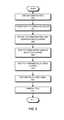
- FIG. 3shows an exemplary fabrication process, according to an embodiment of the present invention.
- a plurality of substratescan be obtained (operation 302 ).
- the substratescan include crystalline silicon (e.g., monocrystalline silicon or polycrystalline silicon) wafers and can be optionally texturized.
- the substratescan also be cleaned. In addition, saw damages can be removed via wet etching.
- the substratescan then be oxidized (e.g., steam or wet oxidation) to form the front and/or back QTB layers (operation 304 ).
- the substratescan be dried and sent to the PECVD tool for deposition of the emitter layer and surface-field layer (operation 306 ).
- the PECVD toolmay simultaneously deposit material onto a large number of substrates at a time.
- a wafer carrierthat can carry over 100 Si wafers (e.g., 5-inch or 6-inch square or pseudo-square Si wafers) can be used inside the PECVD tool to allow simultaneous material deposition.
- the wafer carriercan be a graphite or carbon fiber composite (CFC) carrier coated with a low-porosity material, such as pyrolytic carbon or silicon carbide.
- CFCcarbon fiber composite
- the wafer carriermay also include a non-flat surface or a partially carved-out structure at the bottom of the wafer-holding pockets. After deposition of the emitter layer, the wafers may be turned over for deposition of a surface-field layer. Alternatively, the deposition sequence may change so that the surface-field layer can be deposited first.
- the multilayer structurescan be sent to a PVD tool for deposition of front and/or back TCO layers (e.g., ITO films) (operation 308 ).
- the back TCO layercan facilitate the bifacial operation of the photovoltaic structures.
- only the front (e.g., the side that faces incident light) TCO layermight be needed.
- the PVD toolcan include a sputtering machine, such as a radio-frequency (RF) magnetron sputtering machine.
- a sputtering machinesuch as a radio-frequency (RF) magnetron sputtering machine.
- the RF magnetron sputtering machinecan include one or more rotary targets coupled to a periodically tuned capacitor. This arrangement can ensure a uniform etching profile of the targets, which can reduce cost and time for maintenance.
- RF magnetron sputtering machinecan include one or more rotary targets coupled to a periodically tuned capacitor. This arrangement can ensure a uniform etching profile of the targets, which can reduce cost and time for maintenance.
- a detailed description of the rotary targetscan be found in U.S. patent application Ser. No. 14/142,605, entitled “Radio-Frequency Sputtering System with Rotary Target for Fabricating Solar Cells,” filed Dec. 27, 2013, the disclosure of which is incorporated herein by reference in its entirety.
- deposition of the front and/or back TCO layerscan be performed under a relatively low temperature (e.g., at room temperature or at a temperature lower than 100° C.) in order to improve the open circuit voltage (V oc ) of the photovoltaic structures.
- a relatively low temperaturee.g., at room temperature or at a temperature lower than 100° C.
- low-temperature PVDcan increase the V oc of double-sided heterojunction photovoltaic structures from 710 mV to 720 mV.
- room temperature PVDcan also improve the system throughput, because there is no longer a need to raise the temperature of the PVD tool.
- TCO films (e.g., ITO films) formed using low-temperature PVDcan be in an amorphous structure state. Annealing can crystallize the amorphous TCO to reduce resistivity and improve transparency.
- the multilayer structurescan remain in the same PVD tool for deposition of the metallic seed layers (e.g., Cu seed layers) on the front and back side of the multilayer structures (operation 310 ).
- the sputtering toolcan include multiple targets (e.g., an ITO target and one or more metallic targets) to enable sequential deposition of multiple layers of thin films.
- the sputtering toolcan sequentially deposit an ITO layer and a Cu seed layer.
- the sputtering toolmay also deposit one or more metallic adhesive layers between the ITO layer and seed layer. These adhesive layers can improve the adhesion between any subsequently deposited metallic layer and the ITO layer.
- the metallic seed layerstypically can include the same metallic material as the subsequently plated metallic grids, whereas the metallic adhesive layers can include Cu, Ni, Ag, Ti, Ta, W, TiN, TaN, WN, TiW, NiCr, and their combinations.
- the multiple targetscan be electrically insulated from each other, and can be sequentially biased to allow one active target at a time.
- the PVD toolcan include a rotational shutter to expose only one target to the deposition surface at a time.
- Other types of sputtering toole.g., a sputtering tool with multiple chambers
- the sputtering toolcan be configured to deposit thin films of different materials without breaking the vacuum.
- the sputtering toolcan first deposit a thin layer of ITO and then deposit a thin layer of Cu under the same vacuum, thus significantly reducing the processing time.
- the multilayer structurescan be taken out of the PVD tool and sent to the ECP station for the plating of the front and back side metallic grids (operation 312 ).
- the photolithography process that defines the grid patterncan be a standard process and is not shown in the flowchart.
- ECP of the metallic gridscan include electroplating of a Cu grid on both the front and back sides of the multilayer structures.
- the multilayer structures with metallic gridscan be sent to the annealing station for annealing of the TCO layers and/or ECP metallic grids (operation 314 ).
- annealingis important to TCO because it can improve the optical and electrical properties of the TCO material.
- the multilayer structuresnow include metallic grids with thin lines (e.g., front and back Cu grids with thin Cu finger lines)
- the conventional annealing processmay not be suitable.
- a typical TCO annealing processmay involve subjecting the TCO-coated multilayer structures to a temperature of 200° C. for 20 minutes or longer.
- the annealing of the TCOcan include a high-temperature, rapid annealing process. More specifically, the annealing temperature can be between 150° C. and 400° C., and the time duration can be between a few seconds (e.g., 5 seconds) and a few minutes (e.g., 5 minutes). Because the metallic grids are only exposed to the high temperature environment for a short time period, minimal or no damage can occur.
- the annealingcan be performed in air on hot plates.
- the annealingcan be performed in a vacuum chamber, or in a chamber filled with a forming gas (N 2 /H 2 ), one or more inert gases (e.g., Ar 2 ), or a combination thereof.
- a forming gasN 2 /H 2
- one or more inert gasese.g., Ar 2
- the subsequently formed metallic layerscan also be annealed.
- Annealing the Cu grid after the ECPcan increase the reliability and reduce resistivity of the grid.
- the same high-temperature, rapid annealing process used for annealing of the TCO layercan also anneal the electroplated Cu grid. As a result, both the TCO layers and the Cu grids are annealed at the same time.
- FIG. 4shows an exemplary fabrication system, according to an embodiment of the present invention.
- fabrication system 400can include wet station 402 , PECVD tool 404 , PVD tool 406 , ECP station 408 , and annealing station 410 .
- Wet station 402 and PECVD tool 404can be similar to wet station 202 and PECVD tool 204 shown in FIG. 2 , respectively. Both wet station 402 and PECVD tool 404 can process Si substrate in batches, with each batch including tens or hundreds of Si substrates.
- wet station 402can be configured to form the front and back QTB layers simultaneously using a wet oxidation technique on the Si substrates.
- Multilayer structures emerging from PECVD tool 404can include an emitter layer on one side and a surface-field layer on the other side.
- PVD tool 406can be configured to sequentially deposit a thin layer of TCO and one or more metallic layers on one or both sides of the multilayer structures.
- PVD tool 406can include a multiple-target sputtering tool (e.g., an RF magnetron sputtering tool).
- the multiple targets inside the deposition chambercan include an ITO target and one or more metallic targets.
- the targetscan include rotary targets coupled to periodically tuned capacitors. Because the multiple layers (e.g., a TCO layer and one or more metallic layers) can be deposited sequentially without needing to break the vacuum, the PVD process consumes significantly less time than multiple separate PVD processes.
- the substrate holder inside PVD tool 406can be vertically oriented, as shown in FIG. 5 , to expose both sides of the substrate to the sputtered ions to allow simultaneous material deposition.
- the front and back TCO layerscan be simultaneously deposited onto the emitter and surface-field layers, and the front and back metallic seed layers can be simultaneously deposited onto the front and back TCO layers.
- substratescan be placed in a carrier that is oriented substantially horizontally during deposition. However, this might require that the substrates be turned over to allow deposition on the other side.
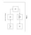
- FIG. 5shows an exemplary substrate holder, according to an embodiment of the present invention.
- substrate holder 500 for PVDcan include a number of openings (e.g., openings 502 and 504 ), which can be arranged in an array.
- Each openingcan accommodate a Si-based substrate.
- opening 502can accommodate Si-based substrate 506 .
- the openingscan be configured to accommodate Si-based substrates of various sizes and shapes, including but not limited to: 5-inch by 5-inch square, 6-inch by 6-inch square, 5-inch by 5-inch pseudo-square, and 6-inch by 6-inch pseudo-square.
- Each substratecan be held in place by multiple clips, such as clips 508 and 510 .
- one or more substrate holderscan be placed inside the PVD chamber vertically to allow simultaneous material deposition on both sides of the Si-based substrates.
- a thin layer of ITO and a thin layer of Cucan be sequentially deposited on both sides of the Si-based substrates.
- ECP station 408can be similar to ECP station 212 shown in FIG. 2 . More specifically, the wafer-holding jigs can carry the photovoltaic structures in such a way that both the front and back sides of the photovoltaic structures are exposed to the electrolyte solution. Therefore, metallic ions (e.g., Cu ions) can be deposited on both sides of the photovoltaic structures as the wafer-holding jigs moving through the electrolyte bath. In other words, the front and back metallic grids can be formed simultaneously. Photovoltaic structures emerging from ECP station 408 can be cleaned, dried, and sent to annealing station 410 for a high-temperature, rapid annealing.
- annealing station 410for a high-temperature, rapid annealing.
- Annealing station 410can take on various forms.
- annealing station 410can include hot plates, which can be placed in air or in a vacuum.
- annealing station 410can include an oven, which can be filled with various ambient gases, such as air, a forming gas, one or more inert gases (e.g., Ar 2 ), or any combinations thereof.
- the annealing temperaturecan range from 150° C. to 400° C.
- the annealing timecan range from a few seconds to a few minutes (e.g., from 5 seconds to 5 minutes). If the annealing temperature is set high, the annealing time can be set relatively short.
- fabrication system 400provides a number of advantages.
- the most obvious advantageis that system 400 can include fewer components than system 200 .
- Novel fabrication system 400can include a single PVD tool configured to deposit multiple layers of different materials. Fewer tools means lower equipment cost, smaller factory spaces, and hence reduced capital expenditures.
- the novel fabrication systemcan also provide a more streamlined fabrication process. There is no longer a need to unload the photovoltaic structures from one PVD tool and load them into another PVD tool, or to wait for the deposition chambers to be pumped down after the loading/unloading. Consequently, the production time of one batch of photovoltaic structures can be significantly reduced. The batch production time can be further reduced by the shorter time needed for annealing.
- This novel fabrication systemcan also provide additional advantages. More specifically, the low-temperature PVD of the TCO layers can improve the V oc of the fabricated photovoltaic structures, and the high-temperature rapid annealing can improve the TCO film property (e.g., transparency and resistivity) and reliability of the metallic grid. Overall, this novel fabrication system can produce, with high throughput, photovoltaic structures that have a higher V oc , higher TCO transparency, lower TCO resistivity, lower grid resistivity, and better grid reliability.
- the TCO film propertye.g., transparency and resistivity
- FIG. 6shows an exemplary fabrication system, according to an embodiment of the present invention.
- fabrication system 600can include wet station 602 , PECVD tool 604 , PVD tool 606 , annealing station 608 , and ECP station 610 . Functions and settings of the various components of fabrication system 600 can be similar to those of fabrication system 400 , with the exception of annealing station 608 .
- wet station 602can be similar to wet station 402
- PECVD tool 604can be similar to PECVD tool 404
- PVD tool 606can be similar to PVD tool 406
- ECP station 610can be similar to ECP tool 408 .
- annealing station 608can be positioned between PVD tool 606 and ECP station 610 to allow photovoltaic structures emerging from PVD tool 606 to be annealed before the ECP process.
- the photovoltaic structurescan be sent directly to anneal station 608 , which can be a separate tool.
- annealing station 608can be incorporated into PVD tool 606 to allow in-situ annealing. The annealing process can be performed at a lower temperature and for a longer duration due to the absence of the Cu grid at the moment.
- Allowing in-situ annealing of the TCO layercan simplify the fabrication system because a separate annealing tool may no longer be needed. A simplified system can lead to reduced cost.
- annealing the TCO prior to the formation of the Cu gridsalso means that the Cu grids will not be annealed by the same process. Additional annealing may be needed in order to anneal the Cu grids.
- embodiments of the present can inventionprovide a solution to a technical problem that is unique to photovoltaic structures with electroplated metallic grids. More specifically, the relative weak bonding between the electroplated metallic grid and the underlying TCO layer may require a metallic seed layer be deposited on the TCO layer using a PVD technique. This additional PVD operation can reduce the fabrication throughput. However, by allowing the TCO layer and metallic seed layer to be deposited in the same PVD chamber and by using a high temperature, rapid post-PVD annealing process, embodiments of the present invention can not only improve the optical and electrical properties of the TCO layer but also increase the fabrication throughput. The annealing of the TCO layer can be performed before or after the electroplating of the metallic grids.
Landscapes
- Chemical & Material Sciences (AREA)
- Engineering & Computer Science (AREA)
- Organic Chemistry (AREA)
- Chemical Kinetics & Catalysis (AREA)
- Materials Engineering (AREA)
- Metallurgy (AREA)
- Life Sciences & Earth Sciences (AREA)
- Sustainable Development (AREA)
- Electrochemistry (AREA)
- Mechanical Engineering (AREA)
- Manufacturing & Machinery (AREA)
- General Physics & Mathematics (AREA)
- Condensed Matter Physics & Semiconductors (AREA)
- Computer Hardware Design (AREA)
- Microelectronics & Electronic Packaging (AREA)
- Power Engineering (AREA)
- Physics & Mathematics (AREA)
- Sustainable Energy (AREA)
- Photovoltaic Devices (AREA)
Abstract
Description
This application is a continuation of U.S. application Ser. No. 14/920,776, entitled “SYSTEM AND METHOD FOR MANUFACTURING PHOTOVOLTAIC STRUCTURES WITH A METAL SEED LAYER,” by inventor Wei Wang, filed 22 Oct. 2015, which is related to U.S. patent application Ser. No. 13/220,532, entitled “SOLAR CELL WITH ELECTROPLATED METAL GRID,” filed Aug. 29, 2011, the disclosures of which are incorporated herein by reference in its entirety for all purposes.
This generally relates to the fabrication of photovoltaic structures. More specifically, this is related to the fabrication of photovoltaic structures having a metal seed layer.
“Solar cell” or “cell” is a photovoltaic structure capable of converting light into electricity. A cell may have any size and any shape, and may be created from a variety of materials. For example, a solar cell may be a photovoltaic structure fabricated on a silicon wafer or one or more thin films on a substrate material (e.g., glass, plastic, or any other material capable of supporting the photovoltaic structure), or a combination thereof.
A “solar cell strip,” “photovoltaic strip,” or “strip” is a portion or segment of a photovoltaic structure, such as a solar cell. A photovoltaic structure may be divided into a number of strips. A strip may have any shape and any size. The width and length of a strip may be the same or different from each other. Strips may be formed by further dividing a previously divided strip.
“Finger lines,” “finger electrodes,” and “fingers” refer to elongated, electrically conductive (e.g., metallic) electrodes of a photovoltaic structure for collecting carriers.
A “busbar,” “bus line,” or “bus electrode” refers to an elongated, electrically conductive (e.g., metallic) electrode of a photovoltaic structure for aggregating current collected by two or more finger lines. A busbar is usually wider than a finger line, and can be deposited or otherwise positioned anywhere on or within the photovoltaic structure. A single photovoltaic structure may have one or more busbars.
A “photovoltaic structure” can refer to a solar cell, a segment, or solar cell strip. A photovoltaic structure is not limited to a device fabricated by a particular method. For example, a photovoltaic structure can be a crystalline silicon-based solar cell, a thin film solar cell, an amorphous silicon-based solar cell, a polycrystalline silicon-based solar cell, or a strip thereof.
Most of the current solar cell manufacturing facilities, however, are insufficiently equipped and/or not optimized for large-scale production. The emerging solar market demands factories that can produce hundreds of megawatts, if not gigawatts, of solar cells per year. The design, size, and throughput of present facilities are not intended for such high-volume manufacturing. Hence, various new designs in the manufacturing process are needed.
One embodiment of the present invention can provide a system for fabrication of a photovoltaic structure. The system can include a physical vapor deposition tool configured to sequentially deposit a transparent conductive oxide layer and a metallic layer on an emitter layer formed on a first surface of a Si substrate, without requiring the Si substrate to be removed from the physical vapor deposition tool after depositing the transparent conductive oxide layer. The system can further include an electroplating tool configured to plate a metallic grid on the metallic layer and a thermal annealing tool configured to anneal the transparent conductive oxide layer.
In a variation of this embodiment, the thermal annealing tool can be configured to subject the photovoltaic structure to a temperature ranging from 150° C. to 400° C.
In a further variation, the thermal annealing tool can be configured to subject the photovoltaic structure to the temperature for a time period ranging from 5 seconds to 5 minutes.
In a further variation, the thermal annealing tool can be configured to anneal the transparent conducing oxide layer in air, vacuum, forming gas, or inert gases.
In a variation of this embodiment, the electroplating tool can be configured to plate a metallic grid before the thermal annealing tool annealing the transparent conductive oxide layer, and the thermal annealing tool can be configured to simultaneously anneal the plated metallic grid and the transparent conductive oxide layer.
In a variation of this embodiment, the physical vapor deposition tool can be further configured to sequentially deposit a second transparent conductive oxide layer and a second metallic layer on a surface-field layer formed on a second surface of the Si substrate, without requiring the Si substrate to be removed from the physical vapor deposition tool after depositing the second transparent conductive oxide layer. The electroplating tool can be further configured to deposit a second metallic grid on the second metallic seed layer.
In a variation of this embodiment, the physical vapor deposition tool can be configured to perform sputtering, evaporation, or both.
In a variation of this embodiment, the metallic thin layer can include: Cu, Ni, Ag, Ti, Ta, W, TiN, TaN, WN, TiW, NiCr, or any combination thereof.
In a variation of this embodiment, the transparent conductive oxide layer can include: indium-tin-oxide (ITO), aluminum-doped zinc-oxide (ZnO:Al), gallium-doped zinc-oxide (ZnO:Ga), tungsten-doped indium oxide (IWO), Zn-in-Sn—O (ZITO), or any combination thereof.
In a variation of this embodiment, the physical vapor deposition tool can be configured to deposit the transparent conductive oxide layer at a temperature lower than 100° C.
In the figures, like reference numerals refer to the same figure elements.
The following description is presented to enable any person skilled in the art to make and use the embodiments, and is provided in the context of a particular application and its requirements. Various modifications to the disclosed embodiments will be readily apparent to those skilled in the art, and the general principles defined herein may be applied to other embodiments and applications without departing from the spirit and scope of the present disclosure. Thus, the present invention is not limited to the embodiments shown, but is to be accorded the widest scope consistent with the principles and features disclosed herein.
Overview
Embodiments of the present invention can solve the technical problem of improving the production throughput for photovoltaic structures with electroplated metallic grids. The photovoltaic structures can include a metallic seed layer formed using a physical vapor deposition (PVD) process to improve adhesion between an electroplated metallic grid and a TCO layer. Typically, a conventional fabrication process involves post-deposition annealing of the TCO layer. For photovoltaic structures with a metallic seed layer on the TCO layer, the annealing is usually performed before depositing the metallic seed layer, and often involves removing the photovoltaic structures from the deposition chamber. In some embodiments of the present invention, the metallic seed layer can be deposited after the deposition of the TCO layer and before the TCO annealing. This arrangement allows the TCO layer and the metallic seed layer to be deposited in the same chamber. The consolidation of these two operations can streamline the fabrication of photovoltaic structures, which can then increase the production throughput. Subsequently, a high-temperature, rapid annealing process can be performed after the deposition of the metallic seed layer or after electrochemical plating (ECP) of the bulk metallic grid to improve the film quality of the TCO layer.
Photovoltaic Structures with Electroplated Metallic Grids
Electroplated metallic electrode grids (e.g., electroplated Cu grids) have been shown to exhibit lower resistance than conventional aluminum or screen-printed-silver-paste electrodes. Such low electrical resistance can be essential in achieving high-efficiency photovoltaic structures. In addition, electroplated copper electrodes can also tolerate micro cracks better, which may occur during a subsequent cleaving process. Such micro cracks might impair silver-paste-electrode cells. Plated-copper electrode, on the other hand, can preserve the conductivity across the cell surface even if there are micro cracks. The copper electrode's higher tolerance for micro cracks allows the use of thinner silicon wafers, which can reduce the overall fabrication cost. More details on using copper plating to form low-resistance electrodes on a photovoltaic structure are provided in U.S. patent application Ser. No. 13/220,532, entitled “SOLAR CELL WITH ELECTROPLATED GRID,” filed on Aug. 29, 2011, the disclosure of which is incorporated herein by reference in its entirety.
Front and back TCO layers112 and114 can be formed using materials such as indium-tin-oxide (ITO), aluminum-doped zinc-oxide (ZnO:Al), gallium-doped zinc-oxide (ZnO:Ga), tungsten-doped indium oxide (IWO), Zn-in-Sn—O (ZITO), and their combinations. The TCO layers can be formed using a PVD process. The TCO layers can then be annealed to improve their electro-optical properties (e.g., high transparency over a wide wavelength range and low electrical resistivity). For example, if the TCO layers include ITO, the annealing can reduce its sheet resistance. Typically, the annealing process can include subjecting the photovoltaic structure to an elevated temperature for a period of time. For example, the annealing of an ITO film can involve subjecting the photovoltaic structure to 200° C. for 20 minutes or longer.
As discussed in the aforementioned U.S. patent application Ser. No. 13/220,532, a thin metallic seed layer (e.g., Cu seed layer116) can be deposited to improve the adhesion between the electroplated Cu grid and the underlying TCO layer using a PVD technique (e.g., sputtering or evaporation), on top of the TCO layer, because high-energy atoms sputtered from the target can adhere well to the TCO layer. This metallic seed layer can then enhance the adhesion between the TCO layer and the subsequently plated Cu grid.
As discussed previously, electroplated Cu grids can provide a number of advantages, such as reduced resistance and increased tolerance to micro cracks. However, the fabrication of a reliable Cu grid can involve depositing a Cu seed layer using a PVD process, which can complicate the fabrication process of photovoltaic structures with Cu grids.
During fabrication, the substrates (e.g., crystalline Si wafers) can first undergo a series of wet processes (e.g., surface cleaning and texturing, and wet oxidization) atwet station 202, and then be loaded intoPECVD tool 204 for the deposition of the emitter and/or surface-field layers. Subsequently, they can be loaded intoPVD tool 206 for the deposition of the front and/or back side TCO layer(s). In this approach, the TCO annealing typically occurs right after the TCO deposition, which often requires taking the photovoltaic structures out of the PVD chamber. This is because the PVD process and the TCO annealing process may require different temperatures. For example, radio-frequency (RF) sputtering of an ITO film can be performed at room temperature (e.g., between 20 and 25° C.), whereas typical annealing of the ITO film may require a temperature of at least 150° C. In a production line, it might not be efficient to adjust the temperature setting of a processing tool between batches, because it can take a long time for the ambient temperature inside the processing tool to reach the desired setting. Hence, after the deposition of the TCO layer(s), the photovoltaic structures can be removed fromPVD tool 206 and transferred toannealing station 208. After the TCO layer(s) are annealed, the photovoltaic structures can be sent toPVD tool 210, which can be different fromPVD tool 206, for the deposition of the metallic seed layer. It is also possible to send the photovoltaic structures back toPVD tool 206 for metal deposition. This approach, however, will increase the product's wait time or the equipment's idle time. Subsequent to the deposition of the metallic seed layer, the photovoltaic structures can be transferred toECP station 212 for Cu plating.ECP station 212 can include a large electrolyte bath and a moving cathode. Photovoltaic structures attached to the moving cathode can be plated with metal as they move through the electrolyte bath.
Large-scale fabrication may need each processing tool to process tens, sometimes even hundreds, of wafers during each processing cycle. Various deposition tools, such as PECVD tool and PVD tool, can be expensive and have large footprints. The fabrication system shown inFIG. 2 can often include two separate PVD tools for the deposition of the TCO layer and the metallic seed layer. Such a system can be costly and have a large footprint. Moreover, loading and unloading the photovoltaic structures in and out of multiple processing tools can be time-consuming and can lead to wafer damage, thus reducing the overall system throughput.
To solve such a problem, in some embodiments, annealing of the TCO layer can be performed after the deposition of the metallic seed layer or ECP of the metallic grids. The two PVD processes can be performed back-to-back, making it possible to use a single PVD tool to deposit both the TCO layer(s) and the metallic seed layers.
After the wet processes, the substrates can be dried and sent to the PECVD tool for deposition of the emitter layer and surface-field layer (operation306). For large-scale, high-throughput fabrication, the PECVD tool may simultaneously deposit material onto a large number of substrates at a time. In some embodiments, a wafer carrier that can carry over 100 Si wafers (e.g., 5-inch or 6-inch square or pseudo-square Si wafers) can be used inside the PECVD tool to allow simultaneous material deposition. The wafer carrier can be a graphite or carbon fiber composite (CFC) carrier coated with a low-porosity material, such as pyrolytic carbon or silicon carbide. The wafer carrier may also include a non-flat surface or a partially carved-out structure at the bottom of the wafer-holding pockets. After deposition of the emitter layer, the wafers may be turned over for deposition of a surface-field layer. Alternatively, the deposition sequence may change so that the surface-field layer can be deposited first.
After the PECVD operation(s), the multilayer structures can be sent to a PVD tool for deposition of front and/or back TCO layers (e.g., ITO films) (operation308). The back TCO layer can facilitate the bifacial operation of the photovoltaic structures. Alternatively, only the front (e.g., the side that faces incident light) TCO layer might be needed.
In some embodiments, the PVD tool can include a sputtering machine, such as a radio-frequency (RF) magnetron sputtering machine. In further embodiments, the RF magnetron sputtering machine can include one or more rotary targets coupled to a periodically tuned capacitor. This arrangement can ensure a uniform etching profile of the targets, which can reduce cost and time for maintenance. A detailed description of the rotary targets can be found in U.S. patent application Ser. No. 14/142,605, entitled “Radio-Frequency Sputtering System with Rotary Target for Fabricating Solar Cells,” filed Dec. 27, 2013, the disclosure of which is incorporated herein by reference in its entirety.
In some embodiments, deposition of the front and/or back TCO layers can be performed under a relatively low temperature (e.g., at room temperature or at a temperature lower than 100° C.) in order to improve the open circuit voltage (Voc) of the photovoltaic structures. For example, low-temperature PVD can increase the Vocof double-sided heterojunction photovoltaic structures from 710 mV to 720 mV. In addition to improved Voc, room temperature PVD can also improve the system throughput, because there is no longer a need to raise the temperature of the PVD tool. TCO films (e.g., ITO films) formed using low-temperature PVD can be in an amorphous structure state. Annealing can crystallize the amorphous TCO to reduce resistivity and improve transparency.
After PVD of the front and/or back TCO layers, the multilayer structures can remain in the same PVD tool for deposition of the metallic seed layers (e.g., Cu seed layers) on the front and back side of the multilayer structures (operation310). To do so, in some embodiments, the sputtering tool can include multiple targets (e.g., an ITO target and one or more metallic targets) to enable sequential deposition of multiple layers of thin films. For example, the sputtering tool can sequentially deposit an ITO layer and a Cu seed layer. Moreover, the sputtering tool may also deposit one or more metallic adhesive layers between the ITO layer and seed layer. These adhesive layers can improve the adhesion between any subsequently deposited metallic layer and the ITO layer. The metallic seed layers typically can include the same metallic material as the subsequently plated metallic grids, whereas the metallic adhesive layers can include Cu, Ni, Ag, Ti, Ta, W, TiN, TaN, WN, TiW, NiCr, and their combinations. In some embodiments, the multiple targets can be electrically insulated from each other, and can be sequentially biased to allow one active target at a time. Alternatively, the PVD tool can include a rotational shutter to expose only one target to the deposition surface at a time. Other types of sputtering tool (e.g., a sputtering tool with multiple chambers) can also be possible, as long as they allow sequential deposition of multiple layers. In some embodiments, the sputtering tool can be configured to deposit thin films of different materials without breaking the vacuum. For example, the sputtering tool can first deposit a thin layer of ITO and then deposit a thin layer of Cu under the same vacuum, thus significantly reducing the processing time.
In some embodiments, subsequent to PVD deposition of the multiple layers (e.g., a TCO layer and a metallic seed layer), the multilayer structures can be taken out of the PVD tool and sent to the ECP station for the plating of the front and back side metallic grids (operation312). The photolithography process that defines the grid pattern can be a standard process and is not shown in the flowchart. ECP of the metallic grids can include electroplating of a Cu grid on both the front and back sides of the multilayer structures.
After ECP, the multilayer structures with metallic grids can be sent to the annealing station for annealing of the TCO layers and/or ECP metallic grids (operation314). As discussed previously, annealing is important to TCO because it can improve the optical and electrical properties of the TCO material. However, because the multilayer structures now include metallic grids with thin lines (e.g., front and back Cu grids with thin Cu finger lines), the conventional annealing process may not be suitable. For example, a typical TCO annealing process may involve subjecting the TCO-coated multilayer structures to a temperature of 200° C. for 20 minutes or longer. Exposing the metallic grids to a high temperature for a prolonged period may weaken the thin metal lines, especially the bonding between the thin metal lines and the underlying structure. To prevent peeling-off of the thin metal lines, in some embodiments, the annealing of the TCO can include a high-temperature, rapid annealing process. More specifically, the annealing temperature can be between 150° C. and 400° C., and the time duration can be between a few seconds (e.g., 5 seconds) and a few minutes (e.g., 5 minutes). Because the metallic grids are only exposed to the high temperature environment for a short time period, minimal or no damage can occur. Additional advantages provided by the high-temperature, rapid annealing process can also include reduced fabrication time, and thus increased production throughput. In some embodiments, the annealing can be performed in air on hot plates. In alternative embodiments, the annealing can be performed in a vacuum chamber, or in a chamber filled with a forming gas (N2/H2), one or more inert gases (e.g., Ar2), or a combination thereof.
As discussed before, high-temperature, rapid annealing can re-crystallize the amorphous TCO, which not only improves transparency but also reduces the resistivity of the TCO material. Consequently, the annealing and the low-temperature PVD of TCO layers can improve overall efficiency of photovoltaic structures by about 1-2%.
In addition to the TCO, the subsequently formed metallic layers (e.g., the metallic seed layer and the ECP Cu layer) can also be annealed. Annealing the Cu grid after the ECP can increase the reliability and reduce resistivity of the grid. In some embodiments, the same high-temperature, rapid annealing process used for annealing of the TCO layer can also anneal the electroplated Cu grid. As a result, both the TCO layers and the Cu grids are annealed at the same time.
Now returning toFIG. 4 ,ECP station 408 can be similar toECP station 212 shown inFIG. 2 . More specifically, the wafer-holding jigs can carry the photovoltaic structures in such a way that both the front and back sides of the photovoltaic structures are exposed to the electrolyte solution. Therefore, metallic ions (e.g., Cu ions) can be deposited on both sides of the photovoltaic structures as the wafer-holding jigs moving through the electrolyte bath. In other words, the front and back metallic grids can be formed simultaneously. Photovoltaic structures emerging fromECP station 408 can be cleaned, dried, and sent toannealing station 410 for a high-temperature, rapid annealing.Annealing station 410 can take on various forms. In some embodiments,annealing station 410 can include hot plates, which can be placed in air or in a vacuum. In some embodiments,annealing station 410 can include an oven, which can be filled with various ambient gases, such as air, a forming gas, one or more inert gases (e.g., Ar2), or any combinations thereof. The annealing temperature can range from 150° C. to 400° C., and the annealing time can range from a few seconds to a few minutes (e.g., from 5 seconds to 5 minutes). If the annealing temperature is set high, the annealing time can be set relatively short.
Compared with the fabrication system shown inFIG. 2 ,fabrication system 400 provides a number of advantages. The most obvious advantage is thatsystem 400 can include fewer components thansystem 200.Novel fabrication system 400 can include a single PVD tool configured to deposit multiple layers of different materials. Fewer tools means lower equipment cost, smaller factory spaces, and hence reduced capital expenditures. In addition, the novel fabrication system can also provide a more streamlined fabrication process. There is no longer a need to unload the photovoltaic structures from one PVD tool and load them into another PVD tool, or to wait for the deposition chambers to be pumped down after the loading/unloading. Consequently, the production time of one batch of photovoltaic structures can be significantly reduced. The batch production time can be further reduced by the shorter time needed for annealing.
This novel fabrication system can also provide additional advantages. More specifically, the low-temperature PVD of the TCO layers can improve the Vocof the fabricated photovoltaic structures, and the high-temperature rapid annealing can improve the TCO film property (e.g., transparency and resistivity) and reliability of the metallic grid. Overall, this novel fabrication system can produce, with high throughput, photovoltaic structures that have a higher Voc, higher TCO transparency, lower TCO resistivity, lower grid resistivity, and better grid reliability.
In the example shown inFIGS. 3 and 4 , the TCO annealing is performed after the ECP process of the metallic grid. In practice, it is also possible to have the TCO annealed before the ECP process.FIG. 6 shows an exemplary fabrication system, according to an embodiment of the present invention. InFIG. 6 ,fabrication system 600 can includewet station 602,PECVD tool 604,PVD tool 606,annealing station 608, andECP station 610. Functions and settings of the various components offabrication system 600 can be similar to those offabrication system 400, with the exception ofannealing station 608. For example,wet station 602 can be similar towet station 402,PECVD tool 604 can be similar toPECVD tool 404,PVD tool 606 can be similar toPVD tool 406, andECP station 610 can be similar toECP tool 408.
Unlike the annealing station shown inFIG. 4 , inFIG. 6 ,annealing station 608 can be positioned betweenPVD tool 606 andECP station 610 to allow photovoltaic structures emerging fromPVD tool 606 to be annealed before the ECP process. In some embodiments, after depositions of both the TCO layer and the Cu seed layer, the photovoltaic structures can be sent directly toanneal station 608, which can be a separate tool. In alternative embodiments,annealing station 608 can be incorporated intoPVD tool 606 to allow in-situ annealing. The annealing process can be performed at a lower temperature and for a longer duration due to the absence of the Cu grid at the moment.
Allowing in-situ annealing of the TCO layer can simplify the fabrication system because a separate annealing tool may no longer be needed. A simplified system can lead to reduced cost. However, annealing the TCO prior to the formation of the Cu grids also means that the Cu grids will not be annealed by the same process. Additional annealing may be needed in order to anneal the Cu grids.
In general, embodiments of the present can invention provide a solution to a technical problem that is unique to photovoltaic structures with electroplated metallic grids. More specifically, the relative weak bonding between the electroplated metallic grid and the underlying TCO layer may require a metallic seed layer be deposited on the TCO layer using a PVD technique. This additional PVD operation can reduce the fabrication throughput. However, by allowing the TCO layer and metallic seed layer to be deposited in the same PVD chamber and by using a high temperature, rapid post-PVD annealing process, embodiments of the present invention can not only improve the optical and electrical properties of the TCO layer but also increase the fabrication throughput. The annealing of the TCO layer can be performed before or after the electroplating of the metallic grids.
The foregoing descriptions of various embodiments have been presented only for purposes of illustration and description. They are not intended to be exhaustive or to limit the present invention to the forms disclosed. Accordingly, many modifications and variations will be apparent to practitioners skilled in the art. Additionally, the above disclosure is not intended to limit the present invention.
Claims (9)
1. A method for fabricating a photovoltaic structure, the method comprising:
depositing, inside a physical vapor deposition chamber, a transparent conductive oxide layer on an emitter layer of the photovoltaic structure;
depositing, within the same physical vapor deposition chamber and without requiring the photovoltaic structure to be removed from the physical vapor deposition chamber after deposition of the transparent conductive oxide layer, a metallic seed layer on the transparent conductive oxide layer;
depositing, using a plating technique, a metallic grid on the metallic seed layer; and
simultaneously annealing the transparent conductive oxide layer the metallic grid, and the metallic seed layer.
2. The method ofclaim 1 , wherein the annealing is performed in an environment comprising:
air;
vacuum;
forming gas; or
inert gases.
3. The method ofclaim 1 , further comprising:
depositing, within the same physical vapor deposition chamber, a second transparent conductive oxide layer on a surface-field layer of the photovoltaic structure; and
depositing one or more metallic layers on the second transparent conductive oxide layer.
4. The method ofclaim 1 , wherein the physical vapor deposition chamber comprises a sputtering chamber or an evaporation chamber.
5. The method ofclaim 1 , further comprising depositing one or more metallic adhesive layers on the transparent conducive oxide layer, wherein the one or more metallic adhesive layers includes: Cu, Ni, Ag, Ti, Ta, W, TiN, TaN, WN, TiW, NiCr, or any combination thereof.
6. The method ofclaim 1 , wherein the transparent conductive oxide layer includes: indium-tin-oxide (ITO), aluminum-doped zinc-oxide (ZnO:Al), gallium-doped zinc-oxide (ZnO:Ga), tungsten-doped indium oxide (IWO), Zn—In—Sn—O (ZITO), or any combination thereof.
7. The method ofclaim 1 , wherein depositing the transparent conductive oxide layer is performed at a temperature lower than 100° C.
8. The method ofclaim 1 , wherein annealing the transparent conductive oxide layer and the one or more metallic layers comprises subjecting the photovoltaic structure to a temperature between 150° C. and 400° C.
9. The method ofclaim 8 , wherein annealing the transparent conductive oxide layer and the one or more metallic layers comprises subjecting the photovoltaic structure to the temperature for a time period between 5 seconds and 5 minutes.
Priority Applications (1)
| Application Number | Priority Date | Filing Date | Title |
|---|---|---|---|
| US15/672,010US10181536B2 (en) | 2015-10-22 | 2017-08-08 | System and method for manufacturing photovoltaic structures with a metal seed layer |
Applications Claiming Priority (2)
| Application Number | Priority Date | Filing Date | Title |
|---|---|---|---|
| US14/920,776US9761744B2 (en) | 2015-10-22 | 2015-10-22 | System and method for manufacturing photovoltaic structures with a metal seed layer |
| US15/672,010US10181536B2 (en) | 2015-10-22 | 2017-08-08 | System and method for manufacturing photovoltaic structures with a metal seed layer |
Related Parent Applications (1)
| Application Number | Title | Priority Date | Filing Date |
|---|---|---|---|
| US14/920,776ContinuationUS9761744B2 (en) | 2015-10-22 | 2015-10-22 | System and method for manufacturing photovoltaic structures with a metal seed layer |
Publications (2)
| Publication Number | Publication Date |
|---|---|
| US20170338356A1 US20170338356A1 (en) | 2017-11-23 |
| US10181536B2true US10181536B2 (en) | 2019-01-15 |
Family
ID=58559040
Family Applications (2)
| Application Number | Title | Priority Date | Filing Date |
|---|---|---|---|
| US14/920,776ActiveUS9761744B2 (en) | 2015-10-22 | 2015-10-22 | System and method for manufacturing photovoltaic structures with a metal seed layer |
| US15/672,010ActiveUS10181536B2 (en) | 2015-10-22 | 2017-08-08 | System and method for manufacturing photovoltaic structures with a metal seed layer |
Family Applications Before (1)
| Application Number | Title | Priority Date | Filing Date |
|---|---|---|---|
| US14/920,776ActiveUS9761744B2 (en) | 2015-10-22 | 2015-10-22 | System and method for manufacturing photovoltaic structures with a metal seed layer |
Country Status (1)
| Country | Link |
|---|---|
| US (2) | US9761744B2 (en) |
Families Citing this family (18)
| Publication number | Priority date | Publication date | Assignee | Title |
|---|---|---|---|---|
| US9012766B2 (en) | 2009-11-12 | 2015-04-21 | Silevo, Inc. | Aluminum grid as backside conductor on epitaxial silicon thin film solar cells |
| US9412884B2 (en) | 2013-01-11 | 2016-08-09 | Solarcity Corporation | Module fabrication of solar cells with low resistivity electrodes |
| US10074755B2 (en) | 2013-01-11 | 2018-09-11 | Tesla, Inc. | High efficiency solar panel |
| US9219174B2 (en) | 2013-01-11 | 2015-12-22 | Solarcity Corporation | Module fabrication of solar cells with low resistivity electrodes |
| US10309012B2 (en) | 2014-07-03 | 2019-06-04 | Tesla, Inc. | Wafer carrier for reducing contamination from carbon particles and outgassing |
| US9761744B2 (en)* | 2015-10-22 | 2017-09-12 | Tesla, Inc. | System and method for manufacturing photovoltaic structures with a metal seed layer |
| US10115838B2 (en) | 2016-04-19 | 2018-10-30 | Tesla, Inc. | Photovoltaic structures with interlocking busbars |
| US10672919B2 (en) | 2017-09-19 | 2020-06-02 | Tesla, Inc. | Moisture-resistant solar cells for solar roof tiles |
| CN107681020A (en)* | 2017-09-26 | 2018-02-09 | 南开大学 | A method to improve the long-wavelength photoresponse of planar silicon heterojunction solar cells |
| US11190128B2 (en) | 2018-02-27 | 2021-11-30 | Tesla, Inc. | Parallel-connected solar roof tile modules |
| EP3742227A1 (en)* | 2019-05-23 | 2020-11-25 | CSEM Centre Suisse D'electronique Et De Microtechnique SA | Method of manufacturing a photovoltaic cell |
| CN110190156B (en)* | 2019-07-08 | 2024-06-11 | 无锡松煜科技有限公司 | TOPCon battery surface passivation equipment and passivation method |
| CN110344010B (en)* | 2019-07-09 | 2021-05-25 | 江苏大学 | Preparation method of driving layer patterned silver nanoparticle composite FTO film |
| FR3117675B1 (en)* | 2020-12-16 | 2023-10-27 | Commissariat Energie Atomique | Process for manufacturing at least one photovoltaic cell using a plate supported on at least one wire |
| NL2031897B1 (en)* | 2022-05-17 | 2023-11-24 | Univ Delft Tech | Localized passivated contacts for Solar Cells |
| CN115207170B (en)* | 2022-08-23 | 2025-01-24 | 中节能太阳能科技(镇江)有限公司 | A method for depositing copper grid lines for heterojunction batteries |
| CN115513340A (en)* | 2022-11-01 | 2022-12-23 | 浙江合特光电有限公司 | Photovoltaic cell with improved electrical performance and preparation method thereof |
| CN115986005B (en)* | 2022-12-22 | 2024-05-03 | 通威太阳能(成都)有限公司 | A solar cell and a method for preparing the same |
Citations (491)
| Publication number | Priority date | Publication date | Assignee | Title |
|---|---|---|---|---|
| US819360A (en) | 1905-03-22 | 1906-05-01 | Edward Newton A | Electrical switch. |
| US2626907A (en) | 1951-05-14 | 1953-01-27 | Petrolite Corp | Process for breaking petroleum emulsions |
| US2938938A (en) | 1956-07-03 | 1960-05-31 | Hoffman Electronics Corp | Photo-voltaic semiconductor apparatus or the like |
| US3094439A (en) | 1961-07-24 | 1963-06-18 | Spectrolab | Solar cell system |
| US3116171A (en) | 1961-03-14 | 1963-12-31 | Bell Telephone Labor Inc | Satellite solar cell assembly |
| US3459597A (en) | 1966-02-04 | 1969-08-05 | Trw Inc | Solar cells with flexible overlapping bifurcated connector |
| US3676179A (en) | 1968-10-03 | 1972-07-11 | Gulf Oil Corp | Coated article and method for making same |
| US3961997A (en) | 1975-05-12 | 1976-06-08 | The United States Of America As Represented By The Administrator Of The National Aeronautics And Space Administration | Fabrication of polycrystalline solar cells on low-cost substrates |
| US3969163A (en) | 1974-09-19 | 1976-07-13 | Texas Instruments Incorporated | Vapor deposition method of forming low cost semiconductor solar cells including reconstitution of the reacted gases |
| US4015280A (en) | 1974-10-19 | 1977-03-29 | Sony Corporation | Multi-layer semiconductor photovoltaic device |
| US4082568A (en) | 1977-05-10 | 1978-04-04 | Joseph Lindmayer | Solar cell with multiple-metal contacts |
| US4124410A (en) | 1977-11-21 | 1978-11-07 | Union Carbide Corporation | Silicon solar cells with low-cost substrates |
| US4193975A (en) | 1977-11-21 | 1980-03-18 | Union Carbide Corporation | Process for the production of improved refined metallurgical silicon |
| US4200621A (en) | 1978-07-18 | 1980-04-29 | Motorola, Inc. | Sequential purification and crystal growth |
| US4213798A (en) | 1979-04-27 | 1980-07-22 | Rca Corporation | Tellurium schottky barrier contact for amorphous silicon solar cells |
| US4251285A (en) | 1979-08-14 | 1981-02-17 | Westinghouse Electric Corp. | Diffusion of dopant from optical coating and single step formation of PN junction in silicon solar cell and coating thereon |
| US4284490A (en) | 1978-09-28 | 1981-08-18 | Coulter Systems Corporation | R.F. Sputtering apparatus including multi-network power supply |
| US4315096A (en) | 1980-07-25 | 1982-02-09 | Eastman Kodak Company | Integrated array of photovoltaic cells having minimized shorting losses |
| JPS5789269A (en) | 1980-09-26 | 1982-06-03 | Licentia Gmbh | Solar battery unit |
| US4336648A (en) | 1979-11-02 | 1982-06-29 | Licentia Patent-Verwaltungs-G.M.B.H. | Method of contacting a solar cell |
| US4342044A (en) | 1978-03-08 | 1982-07-27 | Energy Conversion Devices, Inc. | Method for optimizing photoresponsive amorphous alloys and devices |
| US4377723A (en) | 1980-05-02 | 1983-03-22 | The University Of Delaware | High efficiency thin-film multiple-gap photovoltaic device |
| US4431858A (en) | 1982-05-12 | 1984-02-14 | University Of Florida | Method of making quasi-grain boundary-free polycrystalline solar cell structure and solar cell structure obtained thereby |
| US4514579A (en) | 1984-01-30 | 1985-04-30 | Energy Conversion Devices, Inc. | Large area photovoltaic cell and method for producing same |
| US4540843A (en) | 1983-03-09 | 1985-09-10 | Licentia Patent-Verwaltungs-Gmbh | Solar cell |
| US4567642A (en) | 1984-09-28 | 1986-02-04 | The Standard Oil Company | Method of making photovoltaic modules |
| US4571448A (en) | 1981-11-16 | 1986-02-18 | University Of Delaware | Thin film photovoltaic solar cell and method of making the same |
| US4577051A (en) | 1984-09-28 | 1986-03-18 | The Standard Oil Company | Bypass diode assembly for photovoltaic modules |
| US4586988A (en) | 1983-08-19 | 1986-05-06 | Energy Conversion Devices, Inc. | Method of forming an electrically conductive member |
| US4589191A (en) | 1983-10-20 | 1986-05-20 | Unisearch Limited | Manufacture of high efficiency solar cells |
| US4612409A (en) | 1981-11-04 | 1986-09-16 | Kanegafuchi Kagaku Kogyo Kabushiki Kaisha | Flexible photovoltaic device |
| US4617421A (en) | 1985-04-01 | 1986-10-14 | Sovonics Solar Systems | Photovoltaic cell having increased active area and method for producing same |
| US4633033A (en) | 1985-02-08 | 1986-12-30 | Energy Conversion Devices, Inc. | Photovoltaic device and method |
| US4652693A (en) | 1985-08-30 | 1987-03-24 | The Standard Oil Company | Reformed front contact current collector grid and cell interconnect for a photovoltaic cell module |
| US4657060A (en) | 1982-03-01 | 1987-04-14 | Graber Industries, Inc. | Vertical venetian blind with inline drive |
| US4667060A (en) | 1985-05-28 | 1987-05-19 | Spire Corporation | Back junction photovoltaic solar cell |
| US4670096A (en) | 1984-05-23 | 1987-06-02 | Bayer Aktiengesellschaft | Process and apparatus for producing semi-conductor foils |
| US4694115A (en) | 1986-11-04 | 1987-09-15 | Spectrolab, Inc. | Solar cell having improved front surface metallization |
| US4729970A (en) | 1986-09-15 | 1988-03-08 | Energy Conversion Devices, Inc. | Conversion process for passivating short circuit current paths in semiconductor devices |
| US4753683A (en) | 1985-09-09 | 1988-06-28 | Hughes Aircraft Company | Gallium arsenide solar cell system |
| US4771017A (en) | 1987-06-23 | 1988-09-13 | Spire Corporation | Patterning process |
| US4784702A (en) | 1986-04-22 | 1988-11-15 | Thomson-Csf | PIN photodiode formed from an amorphous semiconductor |
| US4877460A (en) | 1987-03-17 | 1989-10-31 | Telefunken Electronic Gmbh | Solar cell module |
| US4933061A (en) | 1988-12-29 | 1990-06-12 | Trifari, Krussman & Fishel, Inc. | Electroplating tank |
| US4968384A (en) | 1988-09-29 | 1990-11-06 | Fuji Electric Corporate Research And Development Ltd. | Method of producing carbon-doped amorphous silicon thin film |
| US5053355A (en) | 1989-01-14 | 1991-10-01 | Nukem Gmbh | Method and means for producing a layered system of semiconductors |
| US5057163A (en) | 1988-05-04 | 1991-10-15 | Astropower, Inc. | Deposited-silicon film solar cell |
| WO1991017839A1 (en) | 1990-05-18 | 1991-11-28 | Bp Chemicals (Hitco) Inc. | Materials for chemical vapor deposition processes |
| US5075763A (en) | 1988-09-28 | 1991-12-24 | Kopin Corporation | High temperature metallization system for contacting semiconductor materials |
| WO1991020097A1 (en) | 1990-05-14 | 1991-12-26 | The Boeing Company | Tandem photovoltaic solar cell with iii-v diffused junction booster cell |
| US5084107A (en) | 1989-06-05 | 1992-01-28 | Mitsubishi Denki Kabushiki Kaisha | Solar cell and solar cell array with adhered electrode |
| DE4030713A1 (en) | 1990-09-28 | 1992-04-02 | Telefunken Systemtechnik | Photoelectric solar generator - has flexible intermediate connecting plate designed to prevent solar cell fracture due to temp. change stresses |
| US5118361A (en) | 1990-05-21 | 1992-06-02 | The Boeing Company | Terrestrial concentrator solar cell module |
| US5131933A (en) | 1990-03-23 | 1992-07-21 | Telefunken Systemtechnik Gmbh | Solar cell |
| JPH04245683A (en) | 1991-01-31 | 1992-09-02 | Tonen Corp | Manufacture of solar cell |
| US5155051A (en) | 1990-06-22 | 1992-10-13 | Sanyo Electric Co., Ltd. | Method of manufacturing photovoltaic device |
| US5178685A (en) | 1991-06-11 | 1993-01-12 | Mobil Solar Energy Corporation | Method for forming solar cell contacts and interconnecting solar cells |
| US5181968A (en) | 1991-06-24 | 1993-01-26 | United Solar Systems Corporation | Photovoltaic device having an improved collector grid |
| US5213628A (en) | 1990-09-20 | 1993-05-25 | Sanyo Electric Co., Ltd. | Photovoltaic device |
| US5217539A (en) | 1991-09-05 | 1993-06-08 | The Boeing Company | III-V solar cells and doping processes |
| US5279682A (en) | 1991-06-11 | 1994-01-18 | Mobil Solar Energy Corporation | Solar cell and method of making same |
| US5286306A (en) | 1992-02-07 | 1994-02-15 | Shalini Menezes | Thin film photovoltaic cells from I-III-VI-VII compounds |
| JPH06196766A (en) | 1992-12-24 | 1994-07-15 | Fujitsu Ltd | Superconducting transistor |
| US5364518A (en) | 1991-05-28 | 1994-11-15 | Leybold Aktiengesellschaft | Magnetron cathode for a rotating target |
| US5401331A (en) | 1993-09-07 | 1995-03-28 | Midwest Research Institute | Substrate for thin silicon solar cells |
| JPH07249788A (en) | 1994-03-11 | 1995-09-26 | Tonen Corp | Solar cell |
| US5455430A (en) | 1991-08-01 | 1995-10-03 | Sanyo Electric Co., Ltd. | Photovoltaic device having a semiconductor grade silicon layer formed on a metallurgical grade substrate |
| US5461002A (en) | 1990-05-30 | 1995-10-24 | Safir; Yakov | Method of making diffused doped areas for semiconductor components |
| US5563092A (en) | 1993-04-23 | 1996-10-08 | Canon Kabushiki Kaisha | Method of producing a substrate for an amorphous semiconductor |
| US5576241A (en) | 1994-05-31 | 1996-11-19 | Fuji Electric Co., Ltd. | Method of separating semiconductor wafer with dielectrics |
| US5627081A (en) | 1994-11-29 | 1997-05-06 | Midwest Research Institute | Method for processing silicon solar cells |
| US5676766A (en) | 1993-09-30 | 1997-10-14 | Siemens Aktiengesellschaft | Solar cell having a chalcopyrite absorber layer |
| US5681402A (en) | 1994-11-04 | 1997-10-28 | Canon Kabushiki Kaisha | Photovoltaic element |
| US5698451A (en) | 1988-06-10 | 1997-12-16 | Mobil Solar Energy Corporation | Method of fabricating contacts for solar cells |
| JPH104204A (en) | 1996-06-18 | 1998-01-06 | Sharp Corp | Solar cell manufacturing method |
| US5705828A (en) | 1991-08-10 | 1998-01-06 | Sanyo Electric Co., Ltd. | Photovoltaic device |
| US5726065A (en) | 1995-02-21 | 1998-03-10 | Imec Vzw | Method of preparing solar cell front contacts |
| US5808315A (en) | 1992-07-21 | 1998-09-15 | Semiconductor Energy Laboratory Co., Ltd. | Thin film transistor having transparent conductive film |
| US5814195A (en) | 1995-04-25 | 1998-09-29 | The Boc Group, Inc. | Sputtering system using cylindrical rotating magnetron electrically powered using alternating current |
| JPH1131834A (en) | 1997-07-10 | 1999-02-02 | Showa Shell Sekiyu Kk | Glass sandwich solar panel |
| US5903382A (en) | 1997-12-19 | 1999-05-11 | Rockwell International Corporation | Electrodeposition cell with high light transmission |
| US5935345A (en) | 1994-07-13 | 1999-08-10 | Centre National De La Recherche Scientifique, Etablissement Public A Caractere Scientifique Et Technologique | Process for the production of a photovoltaic material or device, material or device thus obtained, and photocell comprising such a material or device |
| US5942048A (en) | 1994-05-19 | 1999-08-24 | Canon Kabushiki Kaisha | Photovoltaic element electrode structure thereof and process for producing the same |
| US6017581A (en) | 1997-04-18 | 2000-01-25 | Semi-Alloys Company | Method for coating lenticular articles |
| US6034322A (en) | 1999-07-01 | 2000-03-07 | Space Systems/Loral, Inc. | Solar cell assembly |
| CN1253381A (en) | 1998-11-04 | 2000-05-17 | 北京市太阳能研究所 | Efficient solar battery and its making method |
| JP2000164902A (en) | 1998-11-27 | 2000-06-16 | Kyocera Corp | Solar cell |
| US6091019A (en) | 1997-09-26 | 2000-07-18 | Sanyo Electric Co., Ltd. | Photovoltaic element and manufacturing method thereof |
| US6140570A (en) | 1997-10-29 | 2000-10-31 | Canon Kabushiki Kaisha | Photovoltaic element having a back side transparent and electrically conductive layer with a light incident side surface region having a specific cross section and a module comprising said photovolatic element |
| US6232545B1 (en) | 1998-08-06 | 2001-05-15 | Jx Crystals Inc. | Linear circuit designs for solar photovoltaic concentrator and thermophotovoltaic applications using cell and substrate materials with matched coefficients of thermal expansion |
| US20010008143A1 (en) | 1998-05-20 | 2001-07-19 | Makoto Sasaoka | Photovoltaic power generating structure |
| US20010023702A1 (en) | 1998-05-15 | 2001-09-27 | Katsumi Nakagawa | Solar cell module and method of producing the same |
| US6303853B1 (en) | 1998-08-06 | 2001-10-16 | Jx Crystals Inc. | Shingle circuits for thermophotovoltaic systems |
| US6333457B1 (en) | 2000-08-29 | 2001-12-25 | Sunpower Corporation | Edge passivated silicon solar/photo cell and method of manufacture |
| US20020015881A1 (en) | 2000-06-13 | 2002-02-07 | Yoshisada Nakamura | Photoelectric conversion device and photo cell |
| JP2002057357A (en) | 2000-08-11 | 2002-02-22 | Fuji Electric Co Ltd | Thin film solar cell and method of manufacturing the same |
| US20020072207A1 (en) | 2000-12-12 | 2002-06-13 | Hideyuki Andoh | Semiconductor device and manufacturing method thereof |
| US6410843B1 (en) | 1999-11-22 | 2002-06-25 | Sanyo Electric Co., Ltd. | Solar cell module |
| US20020086456A1 (en) | 2000-12-19 | 2002-07-04 | Cunningham Shawn Jay | Bulk micromachining process for fabricating an optical MEMS device with integrated optical aperture |
| US6441297B1 (en) | 1998-03-13 | 2002-08-27 | Steffen Keller | Solar cell arrangement |
| US6468828B1 (en) | 1998-07-14 | 2002-10-22 | Sky Solar L.L.C. | Method of manufacturing lightweight, high efficiency photovoltaic module |
| US20020176404A1 (en) | 2001-04-13 | 2002-11-28 | Girard Gregory D. | Distributed edge switching system for voice-over-packet multiservice network |
| US6488824B1 (en) | 1998-11-06 | 2002-12-03 | Raycom Technologies, Inc. | Sputtering apparatus and process for high rate coatings |
| US20020189939A1 (en) | 2001-06-14 | 2002-12-19 | German John R. | Alternating current rotatable sputter cathode |
| US20030000568A1 (en) | 2001-06-15 | 2003-01-02 | Ase Americas, Inc. | Encapsulated photovoltaic modules and method of manufacturing same |
| US20030000571A1 (en) | 2001-06-13 | 2003-01-02 | Junzou Wakuda | Solar cell and method of producing the same |
| US20030034062A1 (en) | 2001-08-17 | 2003-02-20 | Stern Theodore Garry | Electrostatically clean solar array |
| US20030042516A1 (en) | 2001-08-30 | 2003-03-06 | Micron Technology, Inc. | Technique to control tunneling currents in dram capacitors, cells, and devices |
| US6538193B1 (en) | 2000-04-21 | 2003-03-25 | Jx Crystals Inc. | Thermophotovoltaic generator in high temperature industrial process |
| US20030070705A1 (en) | 2001-10-11 | 2003-04-17 | Hayden Herbert T. | Structure for supporting a photovoltaic module in a solar energy collection system |
| US6552414B1 (en) | 1996-12-24 | 2003-04-22 | Imec Vzw | Semiconductor device with selectively diffused regions |
| CN1416179A (en) | 2001-10-31 | 2003-05-07 | 四川大学 | Silicon solar cell of nesa with transparent conductive folm front electrode |
| US20030097447A1 (en) | 2001-10-25 | 2003-05-22 | Johnston Alan B. | Bridging user agent and a proxy server for supporting network services |
| US20030118865A1 (en) | 2001-08-27 | 2003-06-26 | Marks Tobin J. | High work function transparent conducting oxides as anodes for organic light-emitting diodes |
| US20030116185A1 (en) | 2001-11-05 | 2003-06-26 | Oswald Robert S. | Sealed thin film photovoltaic modules |
| US6586270B2 (en) | 2000-06-01 | 2003-07-01 | Canon Kabushiki Kaisha | Process for producing a photovoltaic element |
| US20030121228A1 (en) | 2001-12-31 | 2003-07-03 | Stoehr Robert P. | System and method for dendritic web solar cell shingling |
| US20030136440A1 (en) | 2000-03-13 | 2003-07-24 | Akio Machida | Optical energy transducer |
| US20030168578A1 (en) | 2001-11-29 | 2003-09-11 | Mikio Taguchi | Photovoltaic device and manufacturing method thereof |
| US6620645B2 (en) | 2000-11-16 | 2003-09-16 | G.T. Equipment Technologies, Inc | Making and connecting bus bars on solar cells |
| US20030183270A1 (en) | 2000-08-31 | 2003-10-02 | Fritz Falk | Multicrystalline laser-crystallized silicon thin layer solar cell deposited on a glass substrate |
| US20030201007A1 (en) | 2002-04-24 | 2003-10-30 | Fraas Lewis M. | Planar solar concentrator power module |
| KR20030083953A (en) | 2002-04-24 | 2003-11-01 | 김홍근 | Methods for Immediately Making up account Using Gift Certificate on Credit Card Terminal and Apparatus therefor |
| US6672018B2 (en) | 2001-10-12 | 2004-01-06 | Jefferson Shingleton | Solar module mounting method and clip |
| US6683360B1 (en) | 2002-01-24 | 2004-01-27 | Fillfactory | Multiple or graded epitaxial wafers for particle or radiation detection |
| US20040035458A1 (en) | 2002-08-20 | 2004-02-26 | Kevin Beernink | Series connected photovoltaic module and method for its manufacture |
| US20040065363A1 (en) | 2002-10-02 | 2004-04-08 | The Boeing Company | Isoelectronic surfactant induced sublattice disordering in optoelectronic devices |
| US6736948B2 (en) | 2002-01-18 | 2004-05-18 | Von Ardenne Anlagentechnik Gmbh | Cylindrical AC/DC magnetron with compliant drive system and improved electrical and thermal isolation |
| US20040094196A1 (en) | 2000-04-27 | 2004-05-20 | Sean Shaheen | Photovoltaic cell |
| US20040103937A1 (en) | 2002-09-09 | 2004-06-03 | Interuniversitair Microelektronica Centrum (Imec) | Photovoltaic device |
| US20040112426A1 (en) | 2002-12-11 | 2004-06-17 | Sharp Kabushiki Kaisha | Solar cell and method of manufacturing the same |
| US20040112419A1 (en) | 2001-03-21 | 2004-06-17 | Bernard Boulanger | Solar panel having electrical terminals distributed across the surface thereof |
| US20040126213A1 (en) | 2001-05-18 | 2004-07-01 | Arthur Pelzmann | Device for accommodating disk-shaped objects and apparatus for handling objects |
| US20040123897A1 (en) | 2001-03-19 | 2004-07-01 | Satoyuki Ojima | Solar cell and its manufacturing method |
| US6761771B2 (en) | 2000-10-19 | 2004-07-13 | Asm Japan K.K. | Semiconductor substrate-supporting apparatus |
| US20040135979A1 (en) | 2003-01-13 | 2004-07-15 | Nikon Corporation | Vibration-attenuation devices and methods using pressurized bellows exhibiting substantially zero lateral stiffness |
| US20040152326A1 (en) | 2003-01-28 | 2004-08-05 | Kyocera Corporation | Multicrystalline silicon substrate and process for roughening surface thereof |
| US20040185683A1 (en) | 2003-03-20 | 2004-09-23 | Hiroki Nakamura | Wiring, display device and method of manufacturing the same |
| US20040200520A1 (en) | 2003-04-10 | 2004-10-14 | Sunpower Corporation | Metal contact structure for solar cell and method of manufacture |
| US6841051B2 (en) | 2002-03-14 | 2005-01-11 | Sputtering Components, Inc. | High-power ion sputtering magnetron |
| US20050009319A1 (en) | 2003-07-08 | 2005-01-13 | Kazuhide Abe | Method of forming buried wiring in semiconductor device |
| US20050012095A1 (en) | 2003-06-26 | 2005-01-20 | Kyocera Corporation | Semiconductor/electrode contact structure and semiconductor device using the same |
| US20050022861A1 (en) | 2003-08-01 | 2005-02-03 | Rose Douglas H. | Etching of solar cell materials |
| US20050022746A1 (en) | 2003-08-01 | 2005-02-03 | Sgl Carbon, Llc | Holder for supporting wafers during semiconductor manufacture |
| KR20050015931A (en) | 2003-08-05 | 2005-02-21 | 주성엔지니어링(주) | Chamber and showerhead for uniform layer deposition |
| US20050061665A1 (en) | 2003-08-06 | 2005-03-24 | Sunpower Corporation | Substrate carrier for electroplating solar cells |
| US20050064247A1 (en) | 2003-06-25 | 2005-03-24 | Ajit Sane | Composite refractory metal carbide coating on a substrate and method for making thereof |
| US20050074954A1 (en) | 2002-10-11 | 2005-04-07 | Hideo Yamanaka | Method and apparatus for producing ultra-thin semiconductor chip and method and apparatus for producing ultra-thin back-illuminated solid-state image pickup device |
| JP2005122721A (en) | 2003-09-25 | 2005-05-12 | Fuji Photo Film Co Ltd | Image processing method, apparatus, and program |
| US20050109388A1 (en) | 2003-11-05 | 2005-05-26 | Canon Kabushiki Kaisha | Photovoltaic device and manufacturing method thereof |
| US20050133084A1 (en) | 2003-10-10 | 2005-06-23 | Toshio Joge | Silicon solar cell and production method thereof |
| US6917755B2 (en) | 2003-02-27 | 2005-07-12 | Applied Materials, Inc. | Substrate support |
| US20050178662A1 (en) | 2002-03-22 | 2005-08-18 | Dieter Wurczinger | Rotating tubular cathode |
| US20050189015A1 (en) | 2003-10-30 | 2005-09-01 | Ajeet Rohatgi | Silicon solar cells and methods of fabrication |
| US20050199279A1 (en) | 2004-01-29 | 2005-09-15 | Sanyo Electric Co., Ltd. | Solar cell module |
| US20050252544A1 (en) | 2004-05-11 | 2005-11-17 | Ajeet Rohatgi | Silicon solar cells and methods of fabrication |
| US20050257823A1 (en) | 2004-05-19 | 2005-11-24 | Dutch Space B.V. | Solar cell assembly |
| US20050263178A1 (en) | 2004-06-01 | 2005-12-01 | Alan Montello | Photovoltaic module architecture |
| US20050268963A1 (en) | 2004-02-24 | 2005-12-08 | David Jordan | Process for manufacturing photovoltaic cells |
| WO2006003277A1 (en) | 2004-06-04 | 2006-01-12 | Aventis Pharma S.A. | Aromatic biaryl products, compositions containing same and use as medicines |
| US20060012000A1 (en) | 2001-05-21 | 2006-01-19 | Estes Michael J | Thin-film transistors based on tunneling structures and applications |
| US20060060238A1 (en) | 2004-02-05 | 2006-03-23 | Advent Solar, Inc. | Process and fabrication methods for emitter wrap through back contact solar cells |
| US20060060791A1 (en) | 2004-09-08 | 2006-03-23 | Nikon Corporation | Bellows with spring anti-gravity device |
| US7030413B2 (en) | 2000-09-05 | 2006-04-18 | Sanyo Electric Co., Ltd. | Photovoltaic device with intrinsic amorphous film at junction, having varied optical band gap through thickness thereof |
| US20060130891A1 (en) | 2004-10-29 | 2006-06-22 | Carlson David E | Back-contact photovoltaic cells |
| US20060154389A1 (en) | 2005-01-11 | 2006-07-13 | Doan Trung T | Light emitting diode with conducting metal substrate |
| KR20060097189A (en) | 2005-03-04 | 2006-09-14 | 삼성전자주식회사 | Semiconductor device manufacturing equipment |
| US20060213548A1 (en) | 2005-03-22 | 2006-09-28 | Applied Materials, Inc. | Scalable photovoltaic cell and solar panel manufacturing with improved wiring |
| US20060231803A1 (en) | 2005-04-14 | 2006-10-19 | Yueli Wang | Electroconductive thick film composition(s), electrode(s), and semiconductor device(s) formed therefrom |
| US20060255340A1 (en) | 2005-05-12 | 2006-11-16 | Venkatesan Manivannan | Surface passivated photovoltaic devices |
| US20060260673A1 (en) | 2003-10-17 | 2006-11-23 | Canon Kabushiki Kaisha | Photovoltaic element and method of producing photovoltaic element |
| JP2006324504A (en) | 2005-05-19 | 2006-11-30 | Shin Etsu Handotai Co Ltd | Solar cell |
| US20060272698A1 (en) | 2005-06-06 | 2006-12-07 | Durvasula Ravi S | Photovoltaic concentrator for solar energy system |
| US20060283496A1 (en) | 2005-06-16 | 2006-12-21 | Sanyo Electric Co., Ltd. | Method for manufacturing photovoltaic module |
| US20060283499A1 (en) | 2005-02-25 | 2006-12-21 | Sanyo Electric Co., Ltd. | Photovoltaic cell |
| US7164150B2 (en) | 2002-03-05 | 2007-01-16 | Sanyo Electric Co., Ltd. | Photovoltaic device and manufacturing method thereof |
| US20070023082A1 (en) | 2005-07-28 | 2007-02-01 | Venkatesan Manivannan | Compositionally-graded back contact photovoltaic devices and methods of fabricating such devices |
| US20070023081A1 (en) | 2005-07-28 | 2007-02-01 | General Electric Company | Compositionally-graded photovoltaic device and fabrication method, and related articles |
| US20070029186A1 (en) | 2005-08-02 | 2007-02-08 | Alexey Krasnov | Method of thermally tempering coated article with transparent conductive oxide (TCO) coating using inorganic protective layer during tempering and product made using same |
| EP1770791A1 (en) | 2005-09-30 | 2007-04-04 | Sanyo Electric Co., Ltd. | Rectangular shaped solar cell module and its manufacturing method using hexagonal shaped unit solar cells |
| US20070108437A1 (en) | 1998-06-08 | 2007-05-17 | Avto Tavkhelidze | Method of fabrication of high temperature superconductors based on new mechanism of electron-electron interaction |
| US20070110975A1 (en) | 2003-12-09 | 2007-05-17 | Schunk Kohlensteofftechnik Gmbh | Carrier for receiving an object and method for the production of a carrier |
| JP2007123792A (en) | 2005-09-28 | 2007-05-17 | Kyocera Corp | Solar cell module |
| US20070132034A1 (en) | 2005-12-14 | 2007-06-14 | Giuseppe Curello | Isolation body for semiconductor devices and method to form the same |
| US20070137699A1 (en) | 2005-12-16 | 2007-06-21 | General Electric Company | Solar cell and method for fabricating solar cell |
| US20070148336A1 (en) | 2005-11-07 | 2007-06-28 | Robert Bachrach | Photovoltaic contact and wiring formation |
| EP1816684A2 (en) | 2006-02-01 | 2007-08-08 | Sanyo Electric Co. Ltd. | Solar battery module |
| US20070186970A1 (en) | 2003-05-09 | 2007-08-16 | Masatoshi Takahashi | Solar cell and method of fabricating the same |
| US20070186853A1 (en) | 2006-02-10 | 2007-08-16 | Veeco Instruments Inc. | System and method for varying wafer surface temperature via wafer-carrier temperature offset |
| US20070187652A1 (en) | 2005-12-21 | 2007-08-16 | Takuya Konno | Paste for solar cell electrodes, method for the manufacture of solar cell electrodes, and the solar cell |
| US20070186968A1 (en) | 2006-01-24 | 2007-08-16 | Atsushi Nakauchi | Photovoltaic Module |
| DE102006009194A1 (en) | 2006-02-22 | 2007-08-23 | Siegfried Gutfleisch | Arrangement of primary building structure e.g. photo-voltaic cell, consists of pre-mounted unit, with which structure of solar cell with respective segment of building structure forms assembly unit |
| US20070202029A1 (en) | 2003-12-04 | 2007-08-30 | Gary Burns | Method Of Removing Impurities From Metallurgical Grade Silicon To Produce Solar Grade Silicon |
| US20070235077A1 (en) | 2006-03-27 | 2007-10-11 | Kyocera Corporation | Solar Cell Module and Manufacturing Process Thereof |
| US20070235829A1 (en) | 2005-02-11 | 2007-10-11 | Levine Peter A | Dark Current Reduction in Back-Illuminated Imaging Sensors and Method of Fabricating Same |
| US20070256728A1 (en) | 2006-05-04 | 2007-11-08 | Sunpower Corporation | Solar cell having doped semiconductor heterojunction contacts |
| US20070274504A1 (en) | 2006-05-12 | 2007-11-29 | Oracle International Corporation | Customized sip routing to cross firewalls |
| US20070283996A1 (en) | 2006-06-13 | 2007-12-13 | Miasole | Photovoltaic module with insulating interconnect carrier |
| US20070283997A1 (en) | 2006-06-13 | 2007-12-13 | Miasole | Photovoltaic module with integrated current collection and interconnection |
| US20080000522A1 (en) | 2006-06-30 | 2008-01-03 | General Electric Company | Photovoltaic device which includes all-back-contact configuration; and related processes |
| US20080011350A1 (en) | 1999-03-30 | 2008-01-17 | Daniel Luch | Collector grid, electrode structures and interconnect structures for photovoltaic arrays and other optoelectric devices |
| US7328534B2 (en) | 2002-02-20 | 2008-02-12 | Sunpower Corporation, Systems | Shingle system |
| US20080035489A1 (en) | 2006-06-05 | 2008-02-14 | Rohm And Haas Electronic Materials Llc | Plating process |
| US20080041436A1 (en) | 2006-08-16 | 2008-02-21 | Lau Po K | Bifacial photovoltaic devices |
| US20080041437A1 (en) | 2006-06-23 | 2008-02-21 | Sharp Kabushiki Kaisha | Photoelectric conversion element and interconnector-equipped photoelectric conversion element |
| US20080047604A1 (en) | 2006-08-25 | 2008-02-28 | General Electric Company | Nanowires in thin-film silicon solar cells |
| US20080047602A1 (en) | 2006-08-22 | 2008-02-28 | Guardian Industries Corp. | Front contact with high-function TCO for use in photovoltaic device and method of making same |
| US20080053519A1 (en) | 2006-08-30 | 2008-03-06 | Miasole | Laminated photovoltaic cell |
| US20080061293A1 (en) | 2005-01-20 | 2008-03-13 | Commissariat A'energie Atomique | Semiconductor Device with Heterojunctions and an Inter-Finger Structure |
| US20080092947A1 (en) | 2006-10-24 | 2008-04-24 | Applied Materials, Inc. | Pulse plating of a low stress film on a solar cell substrate |
| US20080121932A1 (en) | 2006-09-18 | 2008-05-29 | Pushkar Ranade | Active regions with compatible dielectric layers |
| US20080121276A1 (en) | 2006-11-29 | 2008-05-29 | Applied Materials, Inc. | Selective electroless deposition for solar cells |
| US20080121272A1 (en) | 2006-11-27 | 2008-05-29 | Besser David A | System and apparatuses with multiple power extractors coupled to different power sources |
| US20080128017A1 (en) | 2004-06-24 | 2008-06-05 | Heliodynamics Limited | Solar Energy Collection Systems |
| US20080128013A1 (en)* | 2006-12-01 | 2008-06-05 | Applied Materials, Inc. | Electroplating on roll-to-roll flexible solar cell substrates |
| JP2008135655A (en) | 2006-11-29 | 2008-06-12 | Sanyo Electric Co Ltd | Solar battery module, manufacturing method therefor, and solar battery cell |
| US20080149161A1 (en) | 2006-12-25 | 2008-06-26 | Sanyo Electric Co., Ltd. | Solar cell and solar cell module |
| US20080149163A1 (en) | 2004-08-31 | 2008-06-26 | Ron Gangemi | System and method for mounting photovoltaic cells |
| US20080156370A1 (en) | 2005-04-20 | 2008-07-03 | Hahn-Meitner-Institut Berlin Gmbh | Heterocontact Solar Cell with Inverted Geometry of its Layer Structure |
| DE202007002897U1 (en) | 2007-02-28 | 2008-07-10 | SCHÜCO International KG | Photovoltaic solar module |
| US7399385B2 (en) | 2001-06-14 | 2008-07-15 | Tru Vue, Inc. | Alternating current rotatable sputter cathode |
| US20080173347A1 (en) | 2007-01-23 | 2008-07-24 | General Electric Company | Method And Apparatus For A Semiconductor Structure |
| US20080173350A1 (en) | 2007-01-18 | 2008-07-24 | Applied Materials, Inc. | Multi-junction solar cells and methods and apparatuses for forming the same |
| WO2008089657A1 (en) | 2007-01-17 | 2008-07-31 | Binxuan Yi | Solar cell and method for reducing the serial resistance of solar cells |
| US20080196757A1 (en) | 2007-02-19 | 2008-08-21 | Sanyo Electric Co., Ltd. | Solar cell and solar cell module |
| US20080202582A1 (en) | 2004-01-15 | 2008-08-28 | Japan Science And Technology Agency | Process for Producing Monocrystal Thin Film and Monocrystal Thin Film Device |
| US20080202577A1 (en) | 2007-02-16 | 2008-08-28 | Henry Hieslmair | Dynamic design of solar cell structures, photovoltaic modules and corresponding processes |
| US20080216891A1 (en) | 2007-03-05 | 2008-09-11 | Seagate Technology Llc | Quantum dot sensitized wide bandgap semiconductor photovoltaic devices & methods of fabricating same |
| US20080223439A1 (en) | 2004-02-19 | 2008-09-18 | Xunming Deng | Interconnected Photoelectrochemical Cell |
| US20080230122A1 (en) | 2007-03-19 | 2008-09-25 | Sanyo Electric Co., Ltd. | Photvoltaic device and method of manufacturing the same |
| US20080251117A1 (en) | 2005-03-14 | 2008-10-16 | Markus Schubert | Solar Cell |
| US20080251114A1 (en) | 2005-03-29 | 2008-10-16 | Kyocera Corporation | Method For Packing Solar Battery Elements and Package For Solar Battery Elements |
| US20080264477A1 (en) | 2006-10-09 | 2008-10-30 | Soltaix, Inc. | Methods for manufacturing three-dimensional thin-film solar cells |
| US20080276983A1 (en) | 2005-11-04 | 2008-11-13 | Robert Andrew Drake | Encapsulation of Photovoltaic Cells |
| US20080283115A1 (en) | 2004-01-28 | 2008-11-20 | Yuko Fukawa | Solar Battery Module and Photovoltaic Generation Device |
| US20080302030A1 (en) | 2007-05-07 | 2008-12-11 | Robert Stancel | Structures for Low Cost, Reliable Solar Roofing |
| US20080303503A1 (en) | 2004-07-13 | 2008-12-11 | Central Queensland University | Device For Distributed Maximum Power Tracking For Solar Arrays |
| US20080308145A1 (en) | 2007-06-12 | 2008-12-18 | Guardian Industries Corp | Front electrode including transparent conductive coating on etched glass substrate for use in photovoltaic device and method of making same |
| US20090014055A1 (en) | 2006-03-18 | 2009-01-15 | Solyndra, Inc. | Photovoltaic Modules Having a Filling Material |
| WO2009011519A1 (en) | 2007-07-13 | 2009-01-22 | Byung Hak Lee | Pencil lead sharpeners |
| US20090056805A1 (en) | 2007-08-28 | 2009-03-05 | Blue Square Energy Incorporated | Photovoltaic Thin-Film Solar Cell and Method Of Making The Same |
| JP2009054748A (en) | 2007-08-27 | 2009-03-12 | Sanyo Electric Co Ltd | SOLAR CELL MODULE, SOLAR CELL, AND MANUFACTURING METHOD THEREOF |
| US20090065043A1 (en) | 2006-02-22 | 2009-03-12 | Jean-Christophe Hadorn | Method of coupling photovoltaic cells and film for implementing it |
| US20090078318A1 (en) | 2007-09-25 | 2009-03-26 | First Solar, Inc. | Photovoltaic Devices Including An Interfacial Layer |
| US20090084439A1 (en) | 2007-10-02 | 2009-04-02 | Chang Gung University | TCO-based hybrid solar photovoltaic energy conversion apparatus |
| US20090101872A1 (en) | 2007-10-18 | 2009-04-23 | E.I. Du Pont De Nemours And Company | LEAD-FREE CONDUCTIVE COMPOSITIONS AND PROCESSES FOR USE IN THE MANUFACTURE OF SEMICONDUCTOR DEVICES: Mg-CONTAINING ADDITIVE |
| US7534632B2 (en) | 2007-02-20 | 2009-05-19 | Advanced Chip Engineering Technology Inc. | Method for circuits inspection and method of the same |
| US20090139512A1 (en) | 2007-11-30 | 2009-06-04 | Lima Daniel D De | Solar Line Boiler Roof |
| EP2071635A2 (en) | 2007-12-11 | 2009-06-17 | HEIc Hornbachner Energie Innovation Consulting GmbH | Cambered photovoltaic module and method for its manufacture |
| US20090151771A1 (en) | 2007-12-17 | 2009-06-18 | Qualcomm Mems Technologies, Inc. | Photovoltaics with interferometric ribbon masks |
| US20090155028A1 (en) | 2007-12-12 | 2009-06-18 | Veeco Instruments Inc. | Wafer carrier with hub |
| US20090151783A1 (en) | 2007-12-13 | 2009-06-18 | Chun-Hsiung Lu | Translucent solar cell and manufacturing method thereof |
| US20090160259A1 (en) | 2007-12-21 | 2009-06-25 | Wi-Chi, Inc. | Distributed Energy Conversion Systems |
| WO2009094578A2 (en) | 2008-01-24 | 2009-07-30 | Applied Materials, Inc. | Improved hit solar cell structure |
| US20090188561A1 (en) | 2008-01-25 | 2009-07-30 | Emcore Corporation | High concentration terrestrial solar array with III-V compound semiconductor cell |
| US20090194233A1 (en) | 2005-06-23 | 2009-08-06 | Tokyo Electron Limited | Component for semicondutor processing apparatus and manufacturing method thereof |
| JP2009177225A (en) | 2009-05-15 | 2009-08-06 | Sharp Corp | Thin film solar cell module |
| US20090211627A1 (en) | 2008-02-25 | 2009-08-27 | Suniva, Inc. | Solar cell having crystalline silicon p-n homojunction and amorphous silicon heterojunctions for surface passivation |
| US20090221111A1 (en) | 2008-02-28 | 2009-09-03 | Sunlight Photonics Inc. | Method and apparatus for fabricating composite substrates for thin film electro-optical devices |
| US20090229854A1 (en) | 2005-11-18 | 2009-09-17 | Replisaurus Technologies Ab | Electrode and method of forming the electrode |
| US20090239331A1 (en) | 2008-03-24 | 2009-09-24 | Palo Alto Research Center Incorporated | Methods for forming multiple-layer electrode structures for silicon photovoltaic cells |
| US20090250108A1 (en) | 2008-04-02 | 2009-10-08 | Applied Materials, Inc. | Silicon carbide for crystalline silicon solar cell surface passivation |
| US20090255574A1 (en) | 2008-04-14 | 2009-10-15 | Sierra Solar Power, Inc. | Solar cell fabricated by silicon liquid-phase deposition |
| EP2113946A2 (en) | 2008-04-30 | 2009-11-04 | General Electric Company | Compositionally-graded and structurally-graded photovoltaic devices and methods of fabricating such devices |
| US20090283138A1 (en) | 2008-05-19 | 2009-11-19 | Tatung Company | High performance optoelectronic device |
| US20090283145A1 (en) | 2008-05-13 | 2009-11-19 | Kim Yun-Gi | Semiconductor Solar Cells Having Front Surface Electrodes |
| US20090293948A1 (en) | 2008-05-28 | 2009-12-03 | Stichting Energieonderzoek Centrum Nederland | Method of manufacturing an amorphous/crystalline silicon heterojunction solar cell |
| US20090301549A1 (en) | 2006-10-09 | 2009-12-10 | Soltaix, Inc. | Solar module structures and assembly methods for three-dimensional thin-film solar cells |
| WO2009150654A2 (en) | 2008-06-12 | 2009-12-17 | Yissum Research Development Company | Solar volumetric structure |
| US20090308439A1 (en) | 2008-06-11 | 2009-12-17 | Solar Implant Technologies Inc. | Solar cell fabrication using implantation |
| US7635810B2 (en) | 1999-03-30 | 2009-12-22 | Daniel Luch | Substrate and collector grid structures for integrated photovoltaic arrays and process of manufacture of such arrays |
| US20090317934A1 (en) | 2006-09-05 | 2009-12-24 | Maximilian Scherff | Local heterostructure contacts |
| US20090320897A1 (en) | 2008-06-26 | 2009-12-31 | Semiconductor Energy Laboratory Co., Ltd. | Photoelectric conversion device module and manufacturing method of the photoelectric conversion device module |
| US20100006145A1 (en) | 2008-07-08 | 2010-01-14 | Synos Technology, Inc. | Solar cell and fabricating method for the same |
| US20100015756A1 (en) | 2008-07-16 | 2010-01-21 | Applied Materials, Inc. | Hybrid heterojunction solar cell fabrication using a doping layer mask |
| US20100043863A1 (en) | 2008-03-20 | 2010-02-25 | Miasole | Interconnect assembly |
| DE102008045522A1 (en) | 2008-09-03 | 2010-03-04 | Fraunhofer-Gesellschaft zur Förderung der angewandten Forschung e.V. | Hetero-solar cell and process for the preparation of hetero-solar cells |
| US20100065111A1 (en) | 2008-09-16 | 2010-03-18 | Sierra Solar Power, Inc. | Solar cells fabricated by using cvd epitaxial si films on metallurgical-grade si wafers |
| US20100068890A1 (en) | 2006-10-30 | 2010-03-18 | Merck Patent Gesellschaft | Printable medium for etching oxidic, transparent and conductive layers |
| US20100084009A1 (en) | 2007-03-16 | 2010-04-08 | Bp Corporation North America Inc. | Solar Cells |
| US20100087031A1 (en) | 2006-09-26 | 2010-04-08 | Commissariat A L'energie Atomique | Method of producing a photovoltaic cell with a heterojunction on the rear face |
| JP2010085949A (en) | 2008-10-03 | 2010-04-15 | Hitachi Displays Ltd | Liquid crystal display |
| US20100108134A1 (en) | 2008-10-31 | 2010-05-06 | Crystal Solar, Inc. | Thin two sided single crystal solar cell and manufacturing process thereof |
| US20100116325A1 (en) | 2008-11-12 | 2010-05-13 | Mehrdad Nikoonahad | High efficiency solar panel and system |
| US20100124619A1 (en) | 2008-11-14 | 2010-05-20 | Palo Alto Research Center Incorporated | Solar cell metallization using inline electroless plating |
| WO2010058095A1 (en) | 2008-11-18 | 2010-05-27 | Bpb Limited | Luminous plate |
| US20100131108A1 (en) | 2008-01-18 | 2010-05-27 | Tenksolar, Inc | Thin-film photovoltaic module |
| US20100132792A1 (en) | 2008-11-19 | 2010-06-03 | Sunho Kim | Solar cell and method of manufacturing the same |
| US20100132774A1 (en) | 2008-12-11 | 2010-06-03 | Applied Materials, Inc. | Thin Film Silicon Solar Cell Device With Amorphous Window Layer |
| US20100147364A1 (en) | 2008-12-16 | 2010-06-17 | Solopower, Inc. | Thin film photovoltaic module manufacturing methods and structures |
| WO2010070015A1 (en) | 2008-12-19 | 2010-06-24 | Q-Cells Se | Solar cell |
| US20100154869A1 (en) | 2008-12-24 | 2010-06-24 | Min-Seok Oh | Photoelectric conversion device and manufacturing method thereof |
| US20100169478A1 (en) | 2008-12-29 | 2010-07-01 | Genband Inc. | Systems, methods, and computer program products for adaptively adjusting a registration interval of an endpoint |
| US7749883B2 (en) | 2007-09-20 | 2010-07-06 | Fry's Metals, Inc. | Electroformed stencils for solar cell front side metallization |
| WO2010075606A1 (en) | 2008-12-29 | 2010-07-08 | Shaun Joseph Cunningham | Improved photo-voltaic device |
| US20100175743A1 (en) | 2009-01-09 | 2010-07-15 | Solopower, Inc. | Reliable thin film photovoltaic module structures |
| US20100186802A1 (en) | 2009-01-27 | 2010-07-29 | Peter Borden | Hit solar cell structure |
| US7769887B1 (en) | 2006-02-03 | 2010-08-03 | Sprint Communications Company L.P. | Opportunistic data transfer over heterogeneous wireless networks |
| US20100193014A1 (en) | 2007-09-05 | 2010-08-05 | Skyline Solar, Inc. | Photovoltaic receiver |
| US20100218799A1 (en) | 2007-10-12 | 2010-09-02 | System S.P.A. | Process for connecting photovoltaic cells in series, a photovoltaic cell connectable in series using the process, and a module obtained with the process |
| US20100224230A1 (en) | 2006-04-13 | 2010-09-09 | Daniel Luch | Collector grid and interconnect structures for photovoltaic arrays and modules |
| WO2010104726A2 (en) | 2009-03-10 | 2010-09-16 | Sierra Solar Power, Inc. | Heterojunction solar cell based on epitaxial crystalline-silicon thin film on metallurgical silicon substrate design |
| US20100229914A1 (en) | 2008-06-04 | 2010-09-16 | Solexant Corp. | Solar cells with shunt resistance |
| US20100240172A1 (en) | 2008-09-19 | 2010-09-23 | Applied Materials, Inc. | Methods of making an emitter having a desired dopant profile |
| US20100236612A1 (en) | 2009-02-20 | 2010-09-23 | Sayed Ali Khajehoddin | Inverter for a Distributed Power Generator |
| US20100243021A1 (en) | 2009-03-26 | 2010-09-30 | Samsung Electronics Co., Ltd. | Solar cells and methods for manufacturing the same |
| US20100243059A1 (en) | 2007-11-15 | 2010-09-30 | Hitachi Chemical Company, Ltd. | Solar battery cell |
| WO2010123974A1 (en) | 2009-04-21 | 2010-10-28 | Tetrasun, Inc. | High-efficiency solar cell structures and methods of manufacture |
| US7825329B2 (en) | 2007-01-03 | 2010-11-02 | Solopower, Inc. | Thin film solar cell manufacturing and integration |
| US20100279492A1 (en) | 2009-05-02 | 2010-11-04 | Atomic Energy Council-Institute Of Nuclear Energy Research | Method of Fabricating Upgraded Metallurgical Grade Silicon by External Gettering Procedure |
| US7829785B2 (en) | 2006-08-04 | 2010-11-09 | Solopower, Inc. | Thin film solar cell with finger pattern |
| US20100282293A1 (en) | 2009-01-21 | 2010-11-11 | Tenksolar | Illumination agnostic solar panel |
| US20100295091A1 (en) | 2009-05-19 | 2010-11-25 | Strzegowski Luke A | Encapsulant compositions, methods of manufacture and uses thereof |
| US20100300506A1 (en) | 2009-06-02 | 2010-12-02 | Sierra Solar Power, Inc. | Low-cost high-efficiency solar module using epitaxial si thin-film absorber and double-sided heterojunction solar cell with integrated module fabrication |
| US20100300525A1 (en) | 2009-05-26 | 2010-12-02 | Koeng Su Lim | Integrated thin-film solar cell and manufacturing method thereof |
| US20100300507A1 (en) | 2009-06-02 | 2010-12-02 | Sierra Solar Power, Inc. | High efficiency low cost crystalline-si thin film solar module |
| US20100307592A1 (en) | 2009-06-08 | 2010-12-09 | National Chiao Tung University | Three-dimensional indium-tin-oxide electrode, method of fabricating the same, device of fabricating the same, and method of fabricating solar cell comprising the same |
| US20100313877A1 (en) | 2008-02-20 | 2010-12-16 | Corning Incorporated | Solar heat collection element with glass-ceramic central tube |
| US20100326518A1 (en) | 2008-02-21 | 2010-12-30 | Hiroyuki Juso | Solar cell and method of manufacturing solar cell |
| US20110005920A1 (en)* | 2009-07-13 | 2011-01-13 | Seagate Technology Llc | Low Temperature Deposition of Amorphous Thin Films |
| US20110005569A1 (en) | 2007-10-16 | 2011-01-13 | Renewable Energy Corporation Asa | Parallel interconnection of solar cell units |
| WO2011005447A2 (en) | 2009-06-22 | 2011-01-13 | International Business Machines Corporation | Semiconductor optical detector structure |
| JP2011008881A (en) | 2009-06-26 | 2011-01-13 | Toshiba Storage Device Corp | Magnetic recording device and magnetic recording medium |
| WO2011008881A2 (en) | 2009-07-14 | 2011-01-20 | Spectrawatt, Inc. | Light conversion efficiency-enhanced solar cell fabricated with downshifting nanomaterial |
| US20110017258A1 (en)* | 2008-01-07 | 2011-01-27 | Lg Electronics Inc. | Solar cell and fabrication method thereof |
| US20110023958A1 (en) | 2009-07-29 | 2011-02-03 | Cyrium Technologies Incorporated | Solar cell and method of fabrication thereof |
| US20110030777A1 (en) | 2009-08-06 | 2011-02-10 | Koeng Su Lim | Photovoltaic device and method for manufacturing thereof |
| US20110048491A1 (en) | 2009-08-26 | 2011-03-03 | Sanyo Electric Co., Ltd. | Solar-cell module and solar cell |
| US20110073175A1 (en) | 2009-09-29 | 2011-03-31 | Twin Creeks Technologies, Inc. | Photovoltaic cell comprising a thin lamina having emitter formed at light-facing and back surfaces |
| US20110088762A1 (en)* | 2009-10-15 | 2011-04-21 | Applied Materials, Inc. | Barrier layer disposed between a substrate and a transparent conductive oxide layer for thin film silicon solar cells |
| WO2011053006A2 (en) | 2009-10-30 | 2011-05-05 | Lg Electronics Inc. | Thin film solar cell module |
| US20110120518A1 (en) | 2009-10-24 | 2011-05-26 | Photon Energy Systems | Manufacturing Photovoltaic Devices And Devices Formed |
| CN102088040A (en) | 2010-12-09 | 2011-06-08 | 泰通(泰州)工业有限公司 | Double-face battery assembly |
| US20110146759A1 (en) | 2008-08-19 | 2011-06-23 | Yoo Jin Lee | Solar battery module and method for manufacturing the same |
| US20110146781A1 (en) | 2009-06-26 | 2011-06-23 | E.I. Du Pont De Nemours And Company | Process of forming a grid cathode on the front-side of a silicon wafer |
| US20110156188A1 (en) | 2009-12-31 | 2011-06-30 | Kingpak Technology Inc. | Image sensor packaging structure with low transmittance encapsulant |
| US7977220B2 (en) | 2008-03-05 | 2011-07-12 | Sri International | Substrates for silicon solar cells and methods of producing the same |
| US20110168250A1 (en) | 2010-01-11 | 2011-07-14 | Tatung Company | Solar cell and manufacturing method thereof |
| US20110168261A1 (en) | 2010-01-08 | 2011-07-14 | Magnolia Solar, Inc. | High transmittance optical windows and method of constructing the same |
| US20110174374A1 (en) | 2008-07-01 | 2011-07-21 | Institut Fur Solarenergieforschung Gmbh | Heterojunction solar cell with absorber having an integrated doping profile |
| US20110177648A1 (en) | 2010-01-18 | 2011-07-21 | Applied Materials, Inc. | Method of manufacturing thin film solar cells having a high conversion efficiency |
| US20110186112A1 (en) | 2008-07-03 | 2011-08-04 | Tom Aernouts | Multi-junction photovoltaic module and the processing thereof |
| EP2362430A1 (en) | 2010-02-18 | 2011-08-31 | SAVIO S.p.A. | A photovoltaic module |
| US20110220182A1 (en) | 2010-03-12 | 2011-09-15 | Rfmarq, Inc. | Solar Panel Tracking and Performance Monitoring Through Wireless Communication |
| JP2011181966A (en) | 2011-06-20 | 2011-09-15 | Sanyo Electric Co Ltd | Solar battery cell and solar battery module |
| US20110245957A1 (en) | 2010-04-06 | 2011-10-06 | Applied Materials, Inc. | Advanced platform for processing crystalline silicon solar cells |
| WO2011123646A2 (en) | 2010-03-31 | 2011-10-06 | Mustang Solar, Llc | Cylindrical rotating magnetron sputtering cathode device and method of depositing material using radio frequency emissions |
| US20110259419A1 (en) | 2009-09-28 | 2011-10-27 | Volker Hagemann | Solar cell with an improved pigmented dielectric reflector |
| EP2385561A2 (en) | 2010-05-04 | 2011-11-09 | Sierra Solar Power, Inc. | Solar Cell |
| EP2387079A2 (en) | 2010-05-14 | 2011-11-16 | Sierra Solar Power, Inc. | Solar cell with metal grid |
| US20110277816A1 (en) | 2010-05-11 | 2011-11-17 | Sierra Solar Power, Inc. | Solar cell with shade-free front electrode |
| US20110277688A1 (en) | 2010-05-14 | 2011-11-17 | Sierra Solar Power, Inc. | Dynamic support system for quartz process chamber |
| US8070925B2 (en) | 2008-10-17 | 2011-12-06 | Applied Materials, Inc. | Physical vapor deposition reactor with circularly symmetric RF feed and DC feed to the sputter target |
| US20110300661A1 (en) | 2010-06-03 | 2011-12-08 | NuvoSun, Inc. | Solar cell interconnection method using a flat metallic mesh |
| US20110297224A1 (en) | 2009-04-30 | 2011-12-08 | Shinsuke Miyamoto | Solar battery cell |
| US20110308573A1 (en) | 2010-06-21 | 2011-12-22 | Fraunhofer USA, Inc. Center for Sustainable Energy Systems | Devices and methods to create a diffuse reflection surface |
| US20120000502A1 (en) | 2009-12-28 | 2012-01-05 | Global Solar Energy, Inc. | Integrated thin film solar cell interconnection |
| US20120012174A1 (en) | 2010-07-14 | 2012-01-19 | Solapoint Corporation | Solar cell device having an airbridge type contact |
| US20120012153A1 (en) | 2009-03-11 | 2012-01-19 | Shin-Etsu Chemical Co., Ltd. | Connection sheet for solar battery cell electrode, process for manufacturing solar cell module, and solar cell module |
| US20120028461A1 (en) | 2010-07-30 | 2012-02-02 | Applied Materials, Inc. | Methods for depositing metal in high aspect ratio features |
| US20120031480A1 (en) | 2010-01-20 | 2012-02-09 | Tisler Anthony C | Current collection system for a photovoltaic cell |
| US8115093B2 (en) | 2005-02-15 | 2012-02-14 | General Electric Company | Layer-to-layer interconnects for photoelectric devices and methods of fabricating the same |
| US20120040487A1 (en) | 2010-08-11 | 2012-02-16 | Crystal Solar, Inc. | Mwt architecture for thin si solar cells |
| US8119901B2 (en) | 2009-11-03 | 2012-02-21 | Lg Electronics Inc. | Solar cell module having a conductive pattern part |
| US20120060911A1 (en) | 2010-09-10 | 2012-03-15 | Sierra Solar Power, Inc. | Solar cell with electroplated metal grid |
| US20120073975A1 (en) | 2010-09-23 | 2012-03-29 | Ganti Kalyana Bhargava | Sealed substrate carrier for electroplating |
| US20120080083A1 (en) | 2010-09-30 | 2012-04-05 | Twin Creeks Technologies, Inc. | Semiconductor assembly with a metal oxide layer having intermediate refractive index |
| US8152536B2 (en) | 2009-03-10 | 2012-04-10 | Tyco Electronics Amp Gmbh | Connection device for connection to a solar module and solar module comprising such connection device |
| US20120085384A1 (en) | 2010-10-08 | 2012-04-12 | Silevo, Inc. | Solar panels with integrated cell-level mppt devices |
| US8168880B2 (en) | 2006-04-26 | 2012-05-01 | Certainteed Corporation | Shingle with photovoltaic element(s) and array of same laid up on a roof |
| US20120122262A1 (en) | 2008-08-29 | 2012-05-17 | Yeon-Il Kang | Thin film solar cell module and method of manufacturing the same |
| US8182662B2 (en) | 2009-03-27 | 2012-05-22 | Sputtering Components, Inc. | Rotary cathode for magnetron sputtering apparatus |
| US20120125391A1 (en) | 2010-11-19 | 2012-05-24 | Solopower, Inc. | Methods for interconnecting photovoltaic cells |
| US8196360B2 (en) | 2006-01-12 | 2012-06-12 | Msr Innovations Inc. | Photovoltaic solar roof tile assembly system |
| US20120145233A1 (en) | 2010-10-11 | 2012-06-14 | Lg Electronics Inc. | Back contact solar cell and manufacturing method thereof |
| US20120152752A1 (en) | 2010-12-17 | 2012-06-21 | Nexx Systems, Inc. | Seed layer deposition in microscale features |
| JP2012119393A (en) | 2010-11-29 | 2012-06-21 | Sanyo Electric Co Ltd | Solar cell and solar cell module |
| US20120152349A1 (en) | 2010-12-17 | 2012-06-21 | Solopower, Inc. | Junction box attachment for photovoltaic thin film devices |
| DE102010061317A1 (en) | 2010-12-17 | 2012-06-21 | Q-Cells Se | Screen printing mask for producing electrode finger structure for wafer solar cell, has bar displays spaced at distance from each other, where width of electrode displays along one of bar displays is smaller than that along other display |
| US8209920B2 (en) | 2007-11-06 | 2012-07-03 | Certain Teed Corporation | Photovoltaic roofing systems and methods for installing them |
| US20120167986A1 (en) | 2008-04-29 | 2012-07-05 | Applied Materials, Inc. | Photovoltaic modules manufactuerd using monolithic module assembly techniques |
| US8222516B2 (en) | 2008-02-20 | 2012-07-17 | Sunpower Corporation | Front contact solar cell with formed emitter |
| US8222513B2 (en) | 2006-04-13 | 2012-07-17 | Daniel Luch | Collector grid, electrode structures and interconnect structures for photovoltaic arrays and methods of manufacture |
| US20120180851A1 (en) | 2009-09-18 | 2012-07-19 | Schott Solar Ag | Crystalline solar cell, method for producing said type of solar cell and method for producing a solar cell module |
| EP2479796A1 (en) | 2009-09-18 | 2012-07-25 | Sanyo Electric Co., Ltd. | Solar battery, solar battery module, and solar battery system |
| US20120192932A1 (en) | 2011-03-25 | 2012-08-02 | Neo Solar Power Corp. | Solar cell and its electrode structure |
| US20120199184A1 (en) | 2011-02-09 | 2012-08-09 | Alta Devices, Inc. | Self-bypass diode function for gallium arsenide photovoltaic devices |
| US8258050B2 (en) | 2009-07-17 | 2012-09-04 | Hewlett-Packard Development Company, L.P. | Method of making light trapping crystalline structures |
| US20120240995A1 (en) | 2011-03-25 | 2012-09-27 | Kevin Michael Coakley | Foil-based interconnect for rear-contact solar cells |
| US20120248497A1 (en) | 2011-04-01 | 2012-10-04 | Sabic Innovative Plastics Ip B.V. | Optoelectronic devices and coatings therefore, and methods for making and using the same |
| US20120279443A1 (en) | 2009-12-11 | 2012-11-08 | Kgt Graphit Technologie Gmbh | Substrate support |
| US20120279548A1 (en) | 2009-05-18 | 2012-11-08 | Muench Markus | Arrangement and circuit, and method for interconnecting flat solar cells |
| US20120285517A1 (en) | 2011-05-09 | 2012-11-15 | International Business Machines Corporation | Schottky barrier solar cells with high and low work function metal contacts |
| US20120305060A1 (en) | 2011-06-02 | 2012-12-06 | Silevo, Inc. | Tunneling-junction solar cell with copper grid for concentrated photovoltaic application |
| US20120318319A1 (en) | 2011-06-17 | 2012-12-20 | Solopower, Inc. | Methods of interconnecting thin film solar cells |
| US20120319253A1 (en) | 2010-02-24 | 2012-12-20 | Toyota Jidosha Kabushiki Kaisha | Semiconductor module manufacturing method, semiconductor module, and manufacturing device |
| US20120318340A1 (en) | 2010-05-04 | 2012-12-20 | Silevo, Inc. | Back junction solar cell with tunnel oxide |
| US20120325282A1 (en) | 2011-06-24 | 2012-12-27 | Solopower, Inc. | Solar cells with grid wire interconnections |
| US8343795B2 (en) | 2009-09-12 | 2013-01-01 | Yuhao Luo | Method to break and assemble solar cells |
| US20130000705A1 (en) | 2009-12-16 | 2013-01-03 | Yissum Research Development Company Of The Hebrew University Of Jerusalem, Ltd. | Photovoltaic device and method of its fabrication |
| US20130014802A1 (en) | 2011-07-12 | 2013-01-17 | Astrium Gmbh | Solar cell and solar cell assembly |
| US20130019919A1 (en) | 2011-07-22 | 2013-01-24 | Space Systems/Loral, Inc. | Current collector bar and grid pattern for a photovoltaic solar cell |
| WO2013020590A1 (en) | 2011-08-09 | 2013-02-14 | Kioto Photovoltaics Gmbh | Rectangular solar cell and associated solar cell arrangement |
| US20130056051A1 (en) | 2011-09-07 | 2013-03-07 | Lg Electronics Inc. | Solar cell and manufacturing method thereof |
| WO2013046351A1 (en) | 2011-09-28 | 2013-04-04 | 三洋電機株式会社 | Solar cell and method for manufacturing solar cell |
| US20130096710A1 (en) | 2011-10-17 | 2013-04-18 | Solopower, Inc. | Tracking system and method for solar cell manufacturing |
| US20130112239A1 (en) | 2011-04-14 | 2013-05-09 | Cool Earh Solar | Solar energy receiver |
| US20130130430A1 (en) | 2011-05-20 | 2013-05-23 | Solexel, Inc. | Spatially selective laser annealing applications in high-efficiency solar cells |
| US20130139878A1 (en) | 2010-04-07 | 2013-06-06 | Applied Materials, Inc. | Use of a1 barrier layer to produce high haze zno films on glass substrates |
| US20130152996A1 (en) | 2010-09-07 | 2013-06-20 | Dow Global Technologies Llc | Photovoltaic cell assembly |
| JP2013526045A (en) | 2010-04-26 | 2013-06-20 | ローベルト ボツシユ ゲゼルシヤフト ミツト ベシユレンクテル ハフツング | Solar cell |
| US20130160826A1 (en) | 2011-11-14 | 2013-06-27 | Prism Solar Technologies, Inc. | Frameless photovoltaic module |
| US20130174897A1 (en) | 2012-01-09 | 2013-07-11 | Dongjoo YOU | Thin film solar cell |
| US20130199608A1 (en) | 2010-04-22 | 2013-08-08 | Excico Group Nv | Method for manufacturing a photovoltaic cell comprising a tco layer |
| US20130206219A1 (en) | 2010-08-06 | 2013-08-15 | Juanita N. Kurtin | Cooperative photovoltaic networks and photovoltaic cell adaptations for use therein |
| US20130206213A1 (en) | 2012-02-15 | 2013-08-15 | Alta Devices, Inc. | Photovoltaic module containing shingled photovoltaic tiles and fabrication processes thereof |
| US20130206221A1 (en) | 2012-02-13 | 2013-08-15 | John Anthony Gannon | Solar cell with metallization compensating for or preventing cracking |
| JP2013161855A (en) | 2012-02-02 | 2013-08-19 | Sharp Corp | Interconnector for solar battery, and solar battery cell with interconnector |
| US20130213469A1 (en) | 2011-08-05 | 2013-08-22 | Solexel, Inc. | High efficiency solar cell structures and manufacturing methods |
| US20130220401A1 (en) | 2012-02-29 | 2013-08-29 | Bakersun | Bifacial crystalline silicon solar panel with reflector |
| US20130228221A1 (en) | 2011-08-05 | 2013-09-05 | Solexel, Inc. | Manufacturing methods and structures for large-area thin-film solar cells and other semiconductor devices |
| JP2013536512A (en) | 2010-08-18 | 2013-09-19 | ボルテラ セミコンダクター コーポレイション | Switching circuit and associated method for extracting power from a power supply |
| US20130269771A1 (en) | 2012-04-17 | 2013-10-17 | Lg Electronics Inc. | Solar cell |
| JP2013219378A (en) | 2007-08-02 | 2013-10-24 | Sanyo Electric Co Ltd | Solar cell module |
| US8569096B1 (en) | 2013-03-13 | 2013-10-29 | Gtat Corporation | Free-standing metallic article for semiconductors |
| US20130291743A1 (en) | 2011-01-31 | 2013-11-07 | Shin-Etsu Chemical Co., Ltd. | Screen printing plate for solar cell and method for printing solar cell electrode |
| US8586857B2 (en) | 2008-11-04 | 2013-11-19 | Miasole | Combined diode, lead assembly incorporating an expansion joint |
| JP2013233553A (en) | 2012-05-07 | 2013-11-21 | Npc Inc | Wiring material connection device |
| JP2013239694A (en) | 2012-05-14 | 2013-11-28 | Sereebo Inc | Back junction solar cell with tunnel oxide |
| DE102012010151A1 (en) | 2012-05-24 | 2013-11-28 | Manz Ag | Holder, used to hold electrostatic substrate, includes identical layered structure that includes support and electrode and cover layers, where geometric ratio of support surface to thickness of layered structure has specified value |
| JP2013247231A (en) | 2012-05-25 | 2013-12-09 | Mitsubishi Electric Corp | Solar cell and solar cell module |
| US20140000682A1 (en) | 2012-06-27 | 2014-01-02 | E I Du Pont De Nemours And Company | Integrated back-sheet for back contact photovoltaic module |
| US20140053899A1 (en) | 2012-08-22 | 2014-02-27 | International Business Machines Corporation | Increasing the Efficiency of Solar Cells By Transfer of Solder |
| US20140066265A1 (en) | 2012-09-05 | 2014-03-06 | Bryan P. Oliver | Ski training device and method |
| US8671630B2 (en) | 2007-04-06 | 2014-03-18 | Certainteed Corporation | Photovoltaic roof covering |
| US20140096823A1 (en) | 2012-10-04 | 2014-04-10 | Silevo, Inc. | Photovoltaic devices with electroplated metal grids |
| US20140102524A1 (en) | 2012-10-15 | 2014-04-17 | Silevo, Inc. | Novel electron collectors for silicon photovoltaic cells |
| WO2014066265A1 (en) | 2012-10-25 | 2014-05-01 | Sunpower Corporation | Bifacial solar cell module with backside reflector |
| US20140120699A1 (en) | 2010-11-05 | 2014-05-01 | Win Semiconductors Corp. | Fabrication method for dicing of semiconductor wafers using laser cutting techniques |
| US20140124013A1 (en) | 2012-11-08 | 2014-05-08 | Cogenra Solar, Inc. | High efficiency configuration for solar cell string |
| US20140124014A1 (en) | 2012-11-08 | 2014-05-08 | Cogenra Solar, Inc. | High efficiency configuration for solar cell string |
| US20140154836A1 (en) | 2012-01-17 | 2014-06-05 | Hojin Platech Co., Ltd. | Plating equipment for solar cell wafer using electroplating and light-induced plating jointly and method of the same |
| WO2014110520A1 (en) | 2013-01-11 | 2014-07-17 | Silevo, Inc. | Module fabrication of solar cells with low resistivity electrodes |
| WO2014117138A1 (en) | 2013-01-28 | 2014-07-31 | Global Solar Energy, Inc. | Photovoltaic interconnect systems, devices, and methods |
| EP2626907B1 (en) | 2012-02-13 | 2014-08-27 | LG Electronics Inc. | Solar cell |
| US20140242746A1 (en) | 2013-02-22 | 2014-08-28 | King Abdulaziz City For Science And Technology | Electrode formation for heterojunction solar cells |
| US20140261654A1 (en) | 2013-03-13 | 2014-09-18 | Gtat Corporation | Free-standing metallic article for semiconductors |
| US20140262793A1 (en) | 2013-03-13 | 2014-09-18 | Gtat Corporation | Adaptable free-standing metallic article for semiconductors |
| US20140273338A1 (en) | 2013-03-15 | 2014-09-18 | Applied Materials, Inc. | Methods of forming solar cells and solar cell modules |
| US20140261661A1 (en) | 2013-03-13 | 2014-09-18 | Gtat Corporation | Free-standing metallic article with overplating |
| US20140261624A1 (en) | 2013-03-15 | 2014-09-18 | Sandia Corporation | Customized color patterning of photovoltaic cells |
| US20140284750A1 (en) | 2013-03-22 | 2014-09-25 | First Solar, Inc. | Photovoltaic Device Including A Back Contact And Method Of Manufacturing |
| US20140299187A1 (en) | 2013-04-03 | 2014-10-09 | Lg Electronics Inc. | Solar cell |
| US20140318611A1 (en) | 2011-08-09 | 2014-10-30 | Solexel, Inc. | Multi-level solar cell metallization |
| US20140345674A1 (en) | 2013-05-24 | 2014-11-27 | Silevo, Inc. | Moisture ingress resistant photovoltaic module |
| US20140352777A1 (en) | 2011-12-07 | 2014-12-04 | NuvoSun, Inc. | Automated flexible solar cell fabrication and interconnection utilizing rolls expanded metallic mesh |
| US20150007879A1 (en) | 2013-07-05 | 2015-01-08 | Lg Electronics Inc. | Solar cell and method for manufacturing the same |
| US20150020877A1 (en) | 2011-08-09 | 2015-01-22 | Solexel, Inc. | High-efficiency solar photovoltaic cells and modules using thin crystalline semiconductor absorbers |
| CN104409402A (en) | 2014-12-30 | 2015-03-11 | 厦门市三安光电科技有限公司 | Graphite bearing disc used for production process of LED epitaxial wafer |
| US20150075599A1 (en) | 2013-09-19 | 2015-03-19 | Zena Technologies, Inc. | Pillar structured multijunction photovoltaic devices |
| US20150090314A1 (en) | 2013-01-11 | 2015-04-02 | Silevo, Inc. | High efficiency solar panel |
| US20150096613A1 (en) | 2013-06-24 | 2015-04-09 | Sino-American Silicon Products Inc. | Photovoltaic device and method of manufacturing the same |
| US20150114444A1 (en) | 2013-10-24 | 2015-04-30 | Sandia Corporation | Photovoltaic power generation system with photovoltaic cells as bypass diodes |
| US9029181B2 (en) | 2009-02-02 | 2015-05-12 | Hanergy Hi-Tech Power (Hk) Limited | Two-part screen printing for solar collection grid |
| US20150129024A1 (en) | 2013-11-13 | 2015-05-14 | Gtat Corporation | Free-Standing Metallic Article With Expansion Segment |
| US20150144180A1 (en) | 2012-06-05 | 2015-05-28 | Ebfoil S.R.L. | Encapsulating layer adapted to be applied to back-sheets for photovoltaic modules including back-contact cells |
| US20150171230A1 (en) | 2011-08-09 | 2015-06-18 | Solexel, Inc. | Fabrication methods for back contact solar cells |
| US20150207011A1 (en) | 2013-12-20 | 2015-07-23 | Uriel Solar, Inc. | Multi-junction photovoltaic cells and methods for forming the same |
| US20150214409A1 (en) | 2012-04-03 | 2015-07-30 | Flisom Ag | Thin-film photovoltaic device with wavy monolithic interconnects |
| US20150270410A1 (en) | 2013-01-11 | 2015-09-24 | Silevo, Inc. | Module fabrication of solar cells with low resistivity electrodes |
| US20150280641A1 (en) | 2014-03-28 | 2015-10-01 | Gopal Krishan Garg | High voltage solar modules |
| JP5789269B2 (en) | 2010-01-12 | 2015-10-07 | シリコン イメージ,インコーポレイテッド | Video management and control of home multimedia network |
| US20150325731A1 (en) | 2012-08-15 | 2015-11-12 | Dow Global Technologies Llc | Bi-component electrical connector |
| US20150340531A1 (en) | 2014-05-26 | 2015-11-26 | Panasonic Intellectual Property Management Co., Ltd. | Method of manufacturing solar cell and solar cell |
| US20150349703A1 (en) | 2014-05-27 | 2015-12-03 | Cogenra Solar, Inc. | Shingled solar cell module |
| US20150349175A1 (en) | 2014-05-27 | 2015-12-03 | Cogenra Solar, Inc. | Shingled solar cell panel employing hidden taps |
| WO2015183827A2 (en) | 2014-05-27 | 2015-12-03 | Cogenra Solar, Inc. | Shingled solar cell module |
| US20150349176A1 (en) | 2014-05-27 | 2015-12-03 | Cogenra Solar, Inc. | High voltage solar panel |
| US9287431B2 (en) | 2012-12-10 | 2016-03-15 | Alliance For Sustainable Energy, Llc | Superstrate sub-cell voltage-matched multijunction solar cells |
| WO2016090332A1 (en) | 2014-12-05 | 2016-06-09 | Solarcity Corporation | Photovoltaic electrode design with contact pads for cascaded application |
| US20160163888A1 (en) | 2014-12-05 | 2016-06-09 | Solarcity Corporation | Photovoltaic cells with electrodes adapted to house conductive paste |
| US20160190354A1 (en) | 2013-12-20 | 2016-06-30 | Mukul Agrawal | Barrier-less metal seed stack and contact |
| US20160268963A1 (en) | 2013-11-14 | 2016-09-15 | NuvoSun, Inc. | Method for Delivering Flexible Solar Cells into a Roll-to-Roll Module Assembly Process |
| US20160322513A1 (en) | 2015-04-28 | 2016-11-03 | International Business Machines Corporation | Optimized Grid Design for Concentrator Solar Cell |
| US20170084766A1 (en) | 2015-09-18 | 2017-03-23 | Alta Devices, Inc. | Via structures for solar cell interconnection in solar module |
| US20170162722A1 (en) | 2015-12-08 | 2017-06-08 | Solarcity Corporation | Photovoltaic structures with electrodes having variable width and height |
| US20170222082A1 (en) | 2014-09-28 | 2017-08-03 | Jolywood (Suzhou) Sunwatt Co., Ltd. | Main-gate-free and high-efficiency back-contact solar cell module, main-gate-free and high-efficiency back-contact solar cell assembly, and preparation process thereof |
| US9761744B2 (en)* | 2015-10-22 | 2017-09-12 | Tesla, Inc. | System and method for manufacturing photovoltaic structures with a metal seed layer |
| US20170288081A1 (en) | 2013-03-13 | 2017-10-05 | Merlin Solar Technologies, Inc. | Photovoltaic module |
| US20170373204A1 (en) | 2016-06-22 | 2017-12-28 | Beijing Apollo Ding Rong Solar Technology Co., Ltd. | Photovoltaic module with flexible wire interconnection |
| US20180122964A1 (en) | 2015-06-30 | 2018-05-03 | Kaneka Corporation | Solar battery and solar battery module |
Family Cites Families (7)
| Publication number | Priority date | Publication date | Assignee | Title |
|---|---|---|---|---|
| JP2003298077A (en) | 2002-03-29 | 2003-10-17 | Ebara Corp | Solar cell |
| JP2005159312A (en) | 2003-11-05 | 2005-06-16 | Canon Inc | Base material for polycrystalline silicon substrate for solar cell and polycrystalline silicon substrate for solar cell |
| KR100624765B1 (en) | 2004-06-25 | 2006-09-20 | 한국전기연구원 | Solar cell having a composite structure of photosensitive solar cell and P-N junction silicon solar cell and method of manufacturing same |
| KR100659044B1 (en) | 2004-07-05 | 2006-12-19 | 전자부품연구원 | Solar cell having zinc oxide thin film and manufacturing method thereof |
| KR101492946B1 (en) | 2007-07-26 | 2015-02-13 | 주성엔지니어링(주) | Crystalline silicon solar cell, its manufacturing method and manufacturing system |
| CN100580957C (en) | 2007-12-28 | 2010-01-13 | 中国科学院上海技术物理研究所 | Metastable assisted quantum dot resonant tunneling diode and its working conditions |
| DE202009001817U1 (en) | 2009-01-31 | 2009-06-04 | Roth & Rau Ag | Substrate carrier for holding a plurality of solar cell wafers |
- 2015
- 2015-10-22USUS14/920,776patent/US9761744B2/enactiveActive
- 2017
- 2017-08-08USUS15/672,010patent/US10181536B2/enactiveActive
Patent Citations (537)
| Publication number | Priority date | Publication date | Assignee | Title |
|---|---|---|---|---|
| US819360A (en) | 1905-03-22 | 1906-05-01 | Edward Newton A | Electrical switch. |
| US2626907A (en) | 1951-05-14 | 1953-01-27 | Petrolite Corp | Process for breaking petroleum emulsions |
| US2938938A (en) | 1956-07-03 | 1960-05-31 | Hoffman Electronics Corp | Photo-voltaic semiconductor apparatus or the like |
| US3116171A (en) | 1961-03-14 | 1963-12-31 | Bell Telephone Labor Inc | Satellite solar cell assembly |
| US3094439A (en) | 1961-07-24 | 1963-06-18 | Spectrolab | Solar cell system |
| US3459597A (en) | 1966-02-04 | 1969-08-05 | Trw Inc | Solar cells with flexible overlapping bifurcated connector |
| US3676179A (en) | 1968-10-03 | 1972-07-11 | Gulf Oil Corp | Coated article and method for making same |
| US3969163A (en) | 1974-09-19 | 1976-07-13 | Texas Instruments Incorporated | Vapor deposition method of forming low cost semiconductor solar cells including reconstitution of the reacted gases |
| US4015280A (en) | 1974-10-19 | 1977-03-29 | Sony Corporation | Multi-layer semiconductor photovoltaic device |
| US3961997A (en) | 1975-05-12 | 1976-06-08 | The United States Of America As Represented By The Administrator Of The National Aeronautics And Space Administration | Fabrication of polycrystalline solar cells on low-cost substrates |
| US4082568A (en) | 1977-05-10 | 1978-04-04 | Joseph Lindmayer | Solar cell with multiple-metal contacts |
| US4124455A (en) | 1977-05-10 | 1978-11-07 | Joseph Lindmayer | Method of making solar cell with multiple-metal contacts |
| US4124410A (en) | 1977-11-21 | 1978-11-07 | Union Carbide Corporation | Silicon solar cells with low-cost substrates |
| US4193975A (en) | 1977-11-21 | 1980-03-18 | Union Carbide Corporation | Process for the production of improved refined metallurgical silicon |
| US4342044A (en) | 1978-03-08 | 1982-07-27 | Energy Conversion Devices, Inc. | Method for optimizing photoresponsive amorphous alloys and devices |
| US4200621A (en) | 1978-07-18 | 1980-04-29 | Motorola, Inc. | Sequential purification and crystal growth |
| US4284490A (en) | 1978-09-28 | 1981-08-18 | Coulter Systems Corporation | R.F. Sputtering apparatus including multi-network power supply |
| US4213798A (en) | 1979-04-27 | 1980-07-22 | Rca Corporation | Tellurium schottky barrier contact for amorphous silicon solar cells |
| US4251285A (en) | 1979-08-14 | 1981-02-17 | Westinghouse Electric Corp. | Diffusion of dopant from optical coating and single step formation of PN junction in silicon solar cell and coating thereon |
| US4336648A (en) | 1979-11-02 | 1982-06-29 | Licentia Patent-Verwaltungs-G.M.B.H. | Method of contacting a solar cell |
| US4377723A (en) | 1980-05-02 | 1983-03-22 | The University Of Delaware | High efficiency thin-film multiple-gap photovoltaic device |
| US4315096A (en) | 1980-07-25 | 1982-02-09 | Eastman Kodak Company | Integrated array of photovoltaic cells having minimized shorting losses |
| JPS5789269A (en) | 1980-09-26 | 1982-06-03 | Licentia Gmbh | Solar battery unit |
| US4612409A (en) | 1981-11-04 | 1986-09-16 | Kanegafuchi Kagaku Kogyo Kabushiki Kaisha | Flexible photovoltaic device |
| US4571448A (en) | 1981-11-16 | 1986-02-18 | University Of Delaware | Thin film photovoltaic solar cell and method of making the same |
| US4657060A (en) | 1982-03-01 | 1987-04-14 | Graber Industries, Inc. | Vertical venetian blind with inline drive |
| US4431858A (en) | 1982-05-12 | 1984-02-14 | University Of Florida | Method of making quasi-grain boundary-free polycrystalline solar cell structure and solar cell structure obtained thereby |
| US4540843A (en) | 1983-03-09 | 1985-09-10 | Licentia Patent-Verwaltungs-Gmbh | Solar cell |
| US4586988A (en) | 1983-08-19 | 1986-05-06 | Energy Conversion Devices, Inc. | Method of forming an electrically conductive member |
| US4589191A (en) | 1983-10-20 | 1986-05-20 | Unisearch Limited | Manufacture of high efficiency solar cells |
| US4514579A (en) | 1984-01-30 | 1985-04-30 | Energy Conversion Devices, Inc. | Large area photovoltaic cell and method for producing same |
| US4670096A (en) | 1984-05-23 | 1987-06-02 | Bayer Aktiengesellschaft | Process and apparatus for producing semi-conductor foils |
| US4577051A (en) | 1984-09-28 | 1986-03-18 | The Standard Oil Company | Bypass diode assembly for photovoltaic modules |
| US4567642A (en) | 1984-09-28 | 1986-02-04 | The Standard Oil Company | Method of making photovoltaic modules |
| US4633033A (en) | 1985-02-08 | 1986-12-30 | Energy Conversion Devices, Inc. | Photovoltaic device and method |
| US4617421A (en) | 1985-04-01 | 1986-10-14 | Sovonics Solar Systems | Photovoltaic cell having increased active area and method for producing same |
| US4667060A (en) | 1985-05-28 | 1987-05-19 | Spire Corporation | Back junction photovoltaic solar cell |
| US4652693A (en) | 1985-08-30 | 1987-03-24 | The Standard Oil Company | Reformed front contact current collector grid and cell interconnect for a photovoltaic cell module |
| US4753683A (en) | 1985-09-09 | 1988-06-28 | Hughes Aircraft Company | Gallium arsenide solar cell system |
| US4784702A (en) | 1986-04-22 | 1988-11-15 | Thomson-Csf | PIN photodiode formed from an amorphous semiconductor |
| US4729970A (en) | 1986-09-15 | 1988-03-08 | Energy Conversion Devices, Inc. | Conversion process for passivating short circuit current paths in semiconductor devices |
| US4694115A (en) | 1986-11-04 | 1987-09-15 | Spectrolab, Inc. | Solar cell having improved front surface metallization |
| US4877460A (en) | 1987-03-17 | 1989-10-31 | Telefunken Electronic Gmbh | Solar cell module |
| US4771017A (en) | 1987-06-23 | 1988-09-13 | Spire Corporation | Patterning process |
| US5057163A (en) | 1988-05-04 | 1991-10-15 | Astropower, Inc. | Deposited-silicon film solar cell |
| US5698451A (en) | 1988-06-10 | 1997-12-16 | Mobil Solar Energy Corporation | Method of fabricating contacts for solar cells |
| US5075763A (en) | 1988-09-28 | 1991-12-24 | Kopin Corporation | High temperature metallization system for contacting semiconductor materials |
| US4968384A (en) | 1988-09-29 | 1990-11-06 | Fuji Electric Corporate Research And Development Ltd. | Method of producing carbon-doped amorphous silicon thin film |
| US4933061A (en) | 1988-12-29 | 1990-06-12 | Trifari, Krussman & Fishel, Inc. | Electroplating tank |
| US5053355A (en) | 1989-01-14 | 1991-10-01 | Nukem Gmbh | Method and means for producing a layered system of semiconductors |
| US5084107A (en) | 1989-06-05 | 1992-01-28 | Mitsubishi Denki Kabushiki Kaisha | Solar cell and solar cell array with adhered electrode |
| US5131933A (en) | 1990-03-23 | 1992-07-21 | Telefunken Systemtechnik Gmbh | Solar cell |
| WO1991020097A1 (en) | 1990-05-14 | 1991-12-26 | The Boeing Company | Tandem photovoltaic solar cell with iii-v diffused junction booster cell |
| WO1991017839A1 (en) | 1990-05-18 | 1991-11-28 | Bp Chemicals (Hitco) Inc. | Materials for chemical vapor deposition processes |
| US5118361A (en) | 1990-05-21 | 1992-06-02 | The Boeing Company | Terrestrial concentrator solar cell module |
| US5461002A (en) | 1990-05-30 | 1995-10-24 | Safir; Yakov | Method of making diffused doped areas for semiconductor components |
| US5155051A (en) | 1990-06-22 | 1992-10-13 | Sanyo Electric Co., Ltd. | Method of manufacturing photovoltaic device |
| US5213628A (en) | 1990-09-20 | 1993-05-25 | Sanyo Electric Co., Ltd. | Photovoltaic device |
| DE4030713A1 (en) | 1990-09-28 | 1992-04-02 | Telefunken Systemtechnik | Photoelectric solar generator - has flexible intermediate connecting plate designed to prevent solar cell fracture due to temp. change stresses |
| JPH04245683A (en) | 1991-01-31 | 1992-09-02 | Tonen Corp | Manufacture of solar cell |
| US5364518A (en) | 1991-05-28 | 1994-11-15 | Leybold Aktiengesellschaft | Magnetron cathode for a rotating target |
| US5279682A (en) | 1991-06-11 | 1994-01-18 | Mobil Solar Energy Corporation | Solar cell and method of making same |
| US5178685A (en) | 1991-06-11 | 1993-01-12 | Mobil Solar Energy Corporation | Method for forming solar cell contacts and interconnecting solar cells |
| US5181968A (en) | 1991-06-24 | 1993-01-26 | United Solar Systems Corporation | Photovoltaic device having an improved collector grid |
| US5455430A (en) | 1991-08-01 | 1995-10-03 | Sanyo Electric Co., Ltd. | Photovoltaic device having a semiconductor grade silicon layer formed on a metallurgical grade substrate |
| US5705828A (en) | 1991-08-10 | 1998-01-06 | Sanyo Electric Co., Ltd. | Photovoltaic device |
| US5217539A (en) | 1991-09-05 | 1993-06-08 | The Boeing Company | III-V solar cells and doping processes |
| US5286306A (en) | 1992-02-07 | 1994-02-15 | Shalini Menezes | Thin film photovoltaic cells from I-III-VI-VII compounds |
| US5808315A (en) | 1992-07-21 | 1998-09-15 | Semiconductor Energy Laboratory Co., Ltd. | Thin film transistor having transparent conductive film |
| JPH06196766A (en) | 1992-12-24 | 1994-07-15 | Fujitsu Ltd | Superconducting transistor |
| US5563092A (en) | 1993-04-23 | 1996-10-08 | Canon Kabushiki Kaisha | Method of producing a substrate for an amorphous semiconductor |
| US5401331A (en) | 1993-09-07 | 1995-03-28 | Midwest Research Institute | Substrate for thin silicon solar cells |
| US5676766A (en) | 1993-09-30 | 1997-10-14 | Siemens Aktiengesellschaft | Solar cell having a chalcopyrite absorber layer |
| JPH07249788A (en) | 1994-03-11 | 1995-09-26 | Tonen Corp | Solar cell |
| US5942048A (en) | 1994-05-19 | 1999-08-24 | Canon Kabushiki Kaisha | Photovoltaic element electrode structure thereof and process for producing the same |
| US5576241A (en) | 1994-05-31 | 1996-11-19 | Fuji Electric Co., Ltd. | Method of separating semiconductor wafer with dielectrics |
| US5935345A (en) | 1994-07-13 | 1999-08-10 | Centre National De La Recherche Scientifique, Etablissement Public A Caractere Scientifique Et Technologique | Process for the production of a photovoltaic material or device, material or device thus obtained, and photocell comprising such a material or device |
| US5681402A (en) | 1994-11-04 | 1997-10-28 | Canon Kabushiki Kaisha | Photovoltaic element |
| US5627081A (en) | 1994-11-29 | 1997-05-06 | Midwest Research Institute | Method for processing silicon solar cells |
| US5726065A (en) | 1995-02-21 | 1998-03-10 | Imec Vzw | Method of preparing solar cell front contacts |
| US5814195A (en) | 1995-04-25 | 1998-09-29 | The Boc Group, Inc. | Sputtering system using cylindrical rotating magnetron electrically powered using alternating current |
| JPH104204A (en) | 1996-06-18 | 1998-01-06 | Sharp Corp | Solar cell manufacturing method |
| US6552414B1 (en) | 1996-12-24 | 2003-04-22 | Imec Vzw | Semiconductor device with selectively diffused regions |
| US6017581A (en) | 1997-04-18 | 2000-01-25 | Semi-Alloys Company | Method for coating lenticular articles |
| JPH1131834A (en) | 1997-07-10 | 1999-02-02 | Showa Shell Sekiyu Kk | Glass sandwich solar panel |
| US6091019A (en) | 1997-09-26 | 2000-07-18 | Sanyo Electric Co., Ltd. | Photovoltaic element and manufacturing method thereof |
| US6140570A (en) | 1997-10-29 | 2000-10-31 | Canon Kabushiki Kaisha | Photovoltaic element having a back side transparent and electrically conductive layer with a light incident side surface region having a specific cross section and a module comprising said photovolatic element |
| US5903382A (en) | 1997-12-19 | 1999-05-11 | Rockwell International Corporation | Electrodeposition cell with high light transmission |
| US6441297B1 (en) | 1998-03-13 | 2002-08-27 | Steffen Keller | Solar cell arrangement |
| US20010023702A1 (en) | 1998-05-15 | 2001-09-27 | Katsumi Nakagawa | Solar cell module and method of producing the same |
| US20010008143A1 (en) | 1998-05-20 | 2001-07-19 | Makoto Sasaoka | Photovoltaic power generating structure |
| US20070108437A1 (en) | 1998-06-08 | 2007-05-17 | Avto Tavkhelidze | Method of fabrication of high temperature superconductors based on new mechanism of electron-electron interaction |
| US6468828B1 (en) | 1998-07-14 | 2002-10-22 | Sky Solar L.L.C. | Method of manufacturing lightweight, high efficiency photovoltaic module |
| US6232545B1 (en) | 1998-08-06 | 2001-05-15 | Jx Crystals Inc. | Linear circuit designs for solar photovoltaic concentrator and thermophotovoltaic applications using cell and substrate materials with matched coefficients of thermal expansion |
| US6303853B1 (en) | 1998-08-06 | 2001-10-16 | Jx Crystals Inc. | Shingle circuits for thermophotovoltaic systems |
| CN1253381A (en) | 1998-11-04 | 2000-05-17 | 北京市太阳能研究所 | Efficient solar battery and its making method |
| US6488824B1 (en) | 1998-11-06 | 2002-12-03 | Raycom Technologies, Inc. | Sputtering apparatus and process for high rate coatings |
| JP2000164902A (en) | 1998-11-27 | 2000-06-16 | Kyocera Corp | Solar cell |
| US20080011350A1 (en) | 1999-03-30 | 2008-01-17 | Daniel Luch | Collector grid, electrode structures and interconnect structures for photovoltaic arrays and other optoelectric devices |
| US7635810B2 (en) | 1999-03-30 | 2009-12-22 | Daniel Luch | Substrate and collector grid structures for integrated photovoltaic arrays and process of manufacture of such arrays |
| US6034322A (en) | 1999-07-01 | 2000-03-07 | Space Systems/Loral, Inc. | Solar cell assembly |
| US6410843B1 (en) | 1999-11-22 | 2002-06-25 | Sanyo Electric Co., Ltd. | Solar cell module |
| US20030136440A1 (en) | 2000-03-13 | 2003-07-24 | Akio Machida | Optical energy transducer |
| US6538193B1 (en) | 2000-04-21 | 2003-03-25 | Jx Crystals Inc. | Thermophotovoltaic generator in high temperature industrial process |
| US20040094196A1 (en) | 2000-04-27 | 2004-05-20 | Sean Shaheen | Photovoltaic cell |
| US6586270B2 (en) | 2000-06-01 | 2003-07-01 | Canon Kabushiki Kaisha | Process for producing a photovoltaic element |
| US20020015881A1 (en) | 2000-06-13 | 2002-02-07 | Yoshisada Nakamura | Photoelectric conversion device and photo cell |
| JP2002057357A (en) | 2000-08-11 | 2002-02-22 | Fuji Electric Co Ltd | Thin film solar cell and method of manufacturing the same |
| US6333457B1 (en) | 2000-08-29 | 2001-12-25 | Sunpower Corporation | Edge passivated silicon solar/photo cell and method of manufacture |
| US20030183270A1 (en) | 2000-08-31 | 2003-10-02 | Fritz Falk | Multicrystalline laser-crystallized silicon thin layer solar cell deposited on a glass substrate |
| US7030413B2 (en) | 2000-09-05 | 2006-04-18 | Sanyo Electric Co., Ltd. | Photovoltaic device with intrinsic amorphous film at junction, having varied optical band gap through thickness thereof |
| US6761771B2 (en) | 2000-10-19 | 2004-07-13 | Asm Japan K.K. | Semiconductor substrate-supporting apparatus |
| US6620645B2 (en) | 2000-11-16 | 2003-09-16 | G.T. Equipment Technologies, Inc | Making and connecting bus bars on solar cells |
| US20020072207A1 (en) | 2000-12-12 | 2002-06-13 | Hideyuki Andoh | Semiconductor device and manufacturing method thereof |
| US20020086456A1 (en) | 2000-12-19 | 2002-07-04 | Cunningham Shawn Jay | Bulk micromachining process for fabricating an optical MEMS device with integrated optical aperture |
| US20040123897A1 (en) | 2001-03-19 | 2004-07-01 | Satoyuki Ojima | Solar cell and its manufacturing method |
| US20040112419A1 (en) | 2001-03-21 | 2004-06-17 | Bernard Boulanger | Solar panel having electrical terminals distributed across the surface thereof |
| US20020176404A1 (en) | 2001-04-13 | 2002-11-28 | Girard Gregory D. | Distributed edge switching system for voice-over-packet multiservice network |
| US20040126213A1 (en) | 2001-05-18 | 2004-07-01 | Arthur Pelzmann | Device for accommodating disk-shaped objects and apparatus for handling objects |
| US20060012000A1 (en) | 2001-05-21 | 2006-01-19 | Estes Michael J | Thin-film transistors based on tunneling structures and applications |
| US20030000571A1 (en) | 2001-06-13 | 2003-01-02 | Junzou Wakuda | Solar cell and method of producing the same |
| US20020189939A1 (en) | 2001-06-14 | 2002-12-19 | German John R. | Alternating current rotatable sputter cathode |
| US7905995B2 (en) | 2001-06-14 | 2011-03-15 | Applied Materials, Inc. | Alternating current rotatable sputter cathode |
| US7399385B2 (en) | 2001-06-14 | 2008-07-15 | Tru Vue, Inc. | Alternating current rotatable sputter cathode |
| US20030000568A1 (en) | 2001-06-15 | 2003-01-02 | Ase Americas, Inc. | Encapsulated photovoltaic modules and method of manufacturing same |
| US20030034062A1 (en) | 2001-08-17 | 2003-02-20 | Stern Theodore Garry | Electrostatically clean solar array |
| US20030118865A1 (en) | 2001-08-27 | 2003-06-26 | Marks Tobin J. | High work function transparent conducting oxides as anodes for organic light-emitting diodes |
| US20030042516A1 (en) | 2001-08-30 | 2003-03-06 | Micron Technology, Inc. | Technique to control tunneling currents in dram capacitors, cells, and devices |
| US20030070705A1 (en) | 2001-10-11 | 2003-04-17 | Hayden Herbert T. | Structure for supporting a photovoltaic module in a solar energy collection system |
| US6672018B2 (en) | 2001-10-12 | 2004-01-06 | Jefferson Shingleton | Solar module mounting method and clip |
| US20030097447A1 (en) | 2001-10-25 | 2003-05-22 | Johnston Alan B. | Bridging user agent and a proxy server for supporting network services |
| CN1416179A (en) | 2001-10-31 | 2003-05-07 | 四川大学 | Silicon solar cell of nesa with transparent conductive folm front electrode |
| US20030116185A1 (en) | 2001-11-05 | 2003-06-26 | Oswald Robert S. | Sealed thin film photovoltaic modules |
| US20030168578A1 (en) | 2001-11-29 | 2003-09-11 | Mikio Taguchi | Photovoltaic device and manufacturing method thereof |
| US20030121228A1 (en) | 2001-12-31 | 2003-07-03 | Stoehr Robert P. | System and method for dendritic web solar cell shingling |
| US6736948B2 (en) | 2002-01-18 | 2004-05-18 | Von Ardenne Anlagentechnik Gmbh | Cylindrical AC/DC magnetron with compliant drive system and improved electrical and thermal isolation |
| US6683360B1 (en) | 2002-01-24 | 2004-01-27 | Fillfactory | Multiple or graded epitaxial wafers for particle or radiation detection |
| US7328534B2 (en) | 2002-02-20 | 2008-02-12 | Sunpower Corporation, Systems | Shingle system |
| US7164150B2 (en) | 2002-03-05 | 2007-01-16 | Sanyo Electric Co., Ltd. | Photovoltaic device and manufacturing method thereof |
| US6841051B2 (en) | 2002-03-14 | 2005-01-11 | Sputtering Components, Inc. | High-power ion sputtering magnetron |
| US20050178662A1 (en) | 2002-03-22 | 2005-08-18 | Dieter Wurczinger | Rotating tubular cathode |
| US20030201007A1 (en) | 2002-04-24 | 2003-10-30 | Fraas Lewis M. | Planar solar concentrator power module |
| US7388146B2 (en) | 2002-04-24 | 2008-06-17 | Jx Crystals Inc. | Planar solar concentrator power module |
| US7872192B1 (en) | 2002-04-24 | 2011-01-18 | Jx Crystals Inc. | Planar solar concentrator power module |
| KR20030083953A (en) | 2002-04-24 | 2003-11-01 | 김홍근 | Methods for Immediately Making up account Using Gift Certificate on Credit Card Terminal and Apparatus therefor |
| US6803513B2 (en) | 2002-08-20 | 2004-10-12 | United Solar Systems Corporation | Series connected photovoltaic module and method for its manufacture |
| US20040035458A1 (en) | 2002-08-20 | 2004-02-26 | Kevin Beernink | Series connected photovoltaic module and method for its manufacture |
| US20040103937A1 (en) | 2002-09-09 | 2004-06-03 | Interuniversitair Microelektronica Centrum (Imec) | Photovoltaic device |
| US20040065363A1 (en) | 2002-10-02 | 2004-04-08 | The Boeing Company | Isoelectronic surfactant induced sublattice disordering in optoelectronic devices |
| US20050074954A1 (en) | 2002-10-11 | 2005-04-07 | Hideo Yamanaka | Method and apparatus for producing ultra-thin semiconductor chip and method and apparatus for producing ultra-thin back-illuminated solid-state image pickup device |
| US20040112426A1 (en) | 2002-12-11 | 2004-06-17 | Sharp Kabushiki Kaisha | Solar cell and method of manufacturing the same |
| US20040135979A1 (en) | 2003-01-13 | 2004-07-15 | Nikon Corporation | Vibration-attenuation devices and methods using pressurized bellows exhibiting substantially zero lateral stiffness |
| US20040152326A1 (en) | 2003-01-28 | 2004-08-05 | Kyocera Corporation | Multicrystalline silicon substrate and process for roughening surface thereof |
| US7128975B2 (en) | 2003-01-28 | 2006-10-31 | Kyocera Corporation | Multicrystalline silicon substrate and process for roughening surface thereof |
| US6917755B2 (en) | 2003-02-27 | 2005-07-12 | Applied Materials, Inc. | Substrate support |
| US20040185683A1 (en) | 2003-03-20 | 2004-09-23 | Hiroki Nakamura | Wiring, display device and method of manufacturing the same |
| US20040200520A1 (en) | 2003-04-10 | 2004-10-14 | Sunpower Corporation | Metal contact structure for solar cell and method of manufacture |
| JP2006523025A (en) | 2003-04-10 | 2006-10-05 | サンパワー コーポレイション | Metal contact structure for solar cell and manufacturing method |
| US20070186970A1 (en) | 2003-05-09 | 2007-08-16 | Masatoshi Takahashi | Solar cell and method of fabricating the same |
| US20050064247A1 (en) | 2003-06-25 | 2005-03-24 | Ajit Sane | Composite refractory metal carbide coating on a substrate and method for making thereof |
| US20050012095A1 (en) | 2003-06-26 | 2005-01-20 | Kyocera Corporation | Semiconductor/electrode contact structure and semiconductor device using the same |
| US20050009319A1 (en) | 2003-07-08 | 2005-01-13 | Kazuhide Abe | Method of forming buried wiring in semiconductor device |
| US20050022746A1 (en) | 2003-08-01 | 2005-02-03 | Sgl Carbon, Llc | Holder for supporting wafers during semiconductor manufacture |
| US20050022861A1 (en) | 2003-08-01 | 2005-02-03 | Rose Douglas H. | Etching of solar cell materials |
| KR20050015931A (en) | 2003-08-05 | 2005-02-21 | 주성엔지니어링(주) | Chamber and showerhead for uniform layer deposition |
| US20050061665A1 (en) | 2003-08-06 | 2005-03-24 | Sunpower Corporation | Substrate carrier for electroplating solar cells |
| JP2005122721A (en) | 2003-09-25 | 2005-05-12 | Fuji Photo Film Co Ltd | Image processing method, apparatus, and program |
| US20050133084A1 (en) | 2003-10-10 | 2005-06-23 | Toshio Joge | Silicon solar cell and production method thereof |
| US20060260673A1 (en) | 2003-10-17 | 2006-11-23 | Canon Kabushiki Kaisha | Photovoltaic element and method of producing photovoltaic element |
| US20050189015A1 (en) | 2003-10-30 | 2005-09-01 | Ajeet Rohatgi | Silicon solar cells and methods of fabrication |
| US20050109388A1 (en) | 2003-11-05 | 2005-05-26 | Canon Kabushiki Kaisha | Photovoltaic device and manufacturing method thereof |
| US20070202029A1 (en) | 2003-12-04 | 2007-08-30 | Gary Burns | Method Of Removing Impurities From Metallurgical Grade Silicon To Produce Solar Grade Silicon |
| US20070110975A1 (en) | 2003-12-09 | 2007-05-17 | Schunk Kohlensteofftechnik Gmbh | Carrier for receiving an object and method for the production of a carrier |
| US20080202582A1 (en) | 2004-01-15 | 2008-08-28 | Japan Science And Technology Agency | Process for Producing Monocrystal Thin Film and Monocrystal Thin Film Device |
| US20080283115A1 (en) | 2004-01-28 | 2008-11-20 | Yuko Fukawa | Solar Battery Module and Photovoltaic Generation Device |
| US20050199279A1 (en) | 2004-01-29 | 2005-09-15 | Sanyo Electric Co., Ltd. | Solar cell module |
| US20060060238A1 (en) | 2004-02-05 | 2006-03-23 | Advent Solar, Inc. | Process and fabrication methods for emitter wrap through back contact solar cells |
| US20080223439A1 (en) | 2004-02-19 | 2008-09-18 | Xunming Deng | Interconnected Photoelectrochemical Cell |
| US20050268963A1 (en) | 2004-02-24 | 2005-12-08 | David Jordan | Process for manufacturing photovoltaic cells |
| US20050252544A1 (en) | 2004-05-11 | 2005-11-17 | Ajeet Rohatgi | Silicon solar cells and methods of fabrication |
| US20090007965A1 (en) | 2004-05-11 | 2009-01-08 | Georgia Tech Research Corporation | Solar cell device having amorphous silicon layers |
| US20050257823A1 (en) | 2004-05-19 | 2005-11-24 | Dutch Space B.V. | Solar cell assembly |
| US7829781B2 (en) | 2004-06-01 | 2010-11-09 | Konarka Technologies, Inc. | Photovoltaic module architecture |
| US7772484B2 (en) | 2004-06-01 | 2010-08-10 | Konarka Technologies, Inc. | Photovoltaic module architecture |
| US7777128B2 (en) | 2004-06-01 | 2010-08-17 | Konarka Technologies, Inc. | Photovoltaic module architecture |
| US20050263178A1 (en) | 2004-06-01 | 2005-12-01 | Alan Montello | Photovoltaic module architecture |
| WO2006003277A1 (en) | 2004-06-04 | 2006-01-12 | Aventis Pharma S.A. | Aromatic biaryl products, compositions containing same and use as medicines |
| US20080128017A1 (en) | 2004-06-24 | 2008-06-05 | Heliodynamics Limited | Solar Energy Collection Systems |
| US20080303503A1 (en) | 2004-07-13 | 2008-12-11 | Central Queensland University | Device For Distributed Maximum Power Tracking For Solar Arrays |
| US20080149163A1 (en) | 2004-08-31 | 2008-06-26 | Ron Gangemi | System and method for mounting photovoltaic cells |
| US20060060791A1 (en) | 2004-09-08 | 2006-03-23 | Nikon Corporation | Bellows with spring anti-gravity device |
| US20060130891A1 (en) | 2004-10-29 | 2006-06-22 | Carlson David E | Back-contact photovoltaic cells |
| US20060154389A1 (en) | 2005-01-11 | 2006-07-13 | Doan Trung T | Light emitting diode with conducting metal substrate |
| US20080061293A1 (en) | 2005-01-20 | 2008-03-13 | Commissariat A'energie Atomique | Semiconductor Device with Heterojunctions and an Inter-Finger Structure |
| US20070235829A1 (en) | 2005-02-11 | 2007-10-11 | Levine Peter A | Dark Current Reduction in Back-Illuminated Imaging Sensors and Method of Fabricating Same |
| US8115093B2 (en) | 2005-02-15 | 2012-02-14 | General Electric Company | Layer-to-layer interconnects for photoelectric devices and methods of fabricating the same |
| US20060283499A1 (en) | 2005-02-25 | 2006-12-21 | Sanyo Electric Co., Ltd. | Photovoltaic cell |
| KR20060097189A (en) | 2005-03-04 | 2006-09-14 | 삼성전자주식회사 | Semiconductor device manufacturing equipment |
| US20080251117A1 (en) | 2005-03-14 | 2008-10-16 | Markus Schubert | Solar Cell |
| US20060213548A1 (en) | 2005-03-22 | 2006-09-28 | Applied Materials, Inc. | Scalable photovoltaic cell and solar panel manufacturing with improved wiring |
| US20080251114A1 (en) | 2005-03-29 | 2008-10-16 | Kyocera Corporation | Method For Packing Solar Battery Elements and Package For Solar Battery Elements |
| US20060231803A1 (en) | 2005-04-14 | 2006-10-19 | Yueli Wang | Electroconductive thick film composition(s), electrode(s), and semiconductor device(s) formed therefrom |
| US20080156370A1 (en) | 2005-04-20 | 2008-07-03 | Hahn-Meitner-Institut Berlin Gmbh | Heterocontact Solar Cell with Inverted Geometry of its Layer Structure |
| US20060255340A1 (en) | 2005-05-12 | 2006-11-16 | Venkatesan Manivannan | Surface passivated photovoltaic devices |
| JP2006324504A (en) | 2005-05-19 | 2006-11-30 | Shin Etsu Handotai Co Ltd | Solar cell |
| US20060272698A1 (en) | 2005-06-06 | 2006-12-07 | Durvasula Ravi S | Photovoltaic concentrator for solar energy system |
| US20060283496A1 (en) | 2005-06-16 | 2006-12-21 | Sanyo Electric Co., Ltd. | Method for manufacturing photovoltaic module |
| US20090194233A1 (en) | 2005-06-23 | 2009-08-06 | Tokyo Electron Limited | Component for semicondutor processing apparatus and manufacturing method thereof |
| US20070023082A1 (en) | 2005-07-28 | 2007-02-01 | Venkatesan Manivannan | Compositionally-graded back contact photovoltaic devices and methods of fabricating such devices |
| CN101233620A (en) | 2005-07-28 | 2008-07-30 | 通用电气公司 | Compositionally graded photovoltaic devices, methods of making same, and related article technologies |
| US20070023081A1 (en) | 2005-07-28 | 2007-02-01 | General Electric Company | Compositionally-graded photovoltaic device and fabrication method, and related articles |
| US20070029186A1 (en) | 2005-08-02 | 2007-02-08 | Alexey Krasnov | Method of thermally tempering coated article with transparent conductive oxide (TCO) coating using inorganic protective layer during tempering and product made using same |
| JP2007123792A (en) | 2005-09-28 | 2007-05-17 | Kyocera Corp | Solar cell module |
| EP1770791A1 (en) | 2005-09-30 | 2007-04-04 | Sanyo Electric Co., Ltd. | Rectangular shaped solar cell module and its manufacturing method using hexagonal shaped unit solar cells |
| US20080276983A1 (en) | 2005-11-04 | 2008-11-13 | Robert Andrew Drake | Encapsulation of Photovoltaic Cells |
| CN101305454B (en) | 2005-11-07 | 2010-05-19 | 应用材料股份有限公司 | Method for forming photovoltaic contacts and connections |
| US20070148336A1 (en) | 2005-11-07 | 2007-06-28 | Robert Bachrach | Photovoltaic contact and wiring formation |
| US20090229854A1 (en) | 2005-11-18 | 2009-09-17 | Replisaurus Technologies Ab | Electrode and method of forming the electrode |
| US20070132034A1 (en) | 2005-12-14 | 2007-06-14 | Giuseppe Curello | Isolation body for semiconductor devices and method to form the same |
| US20070137699A1 (en) | 2005-12-16 | 2007-06-21 | General Electric Company | Solar cell and method for fabricating solar cell |
| US20070187652A1 (en) | 2005-12-21 | 2007-08-16 | Takuya Konno | Paste for solar cell electrodes, method for the manufacture of solar cell electrodes, and the solar cell |
| US8196360B2 (en) | 2006-01-12 | 2012-06-12 | Msr Innovations Inc. | Photovoltaic solar roof tile assembly system |
| US20070186968A1 (en) | 2006-01-24 | 2007-08-16 | Atsushi Nakauchi | Photovoltaic Module |
| EP1816684A2 (en) | 2006-02-01 | 2007-08-08 | Sanyo Electric Co. Ltd. | Solar battery module |
| US7769887B1 (en) | 2006-02-03 | 2010-08-03 | Sprint Communications Company L.P. | Opportunistic data transfer over heterogeneous wireless networks |
| US20070186853A1 (en) | 2006-02-10 | 2007-08-16 | Veeco Instruments Inc. | System and method for varying wafer surface temperature via wafer-carrier temperature offset |
| DE102006009194A1 (en) | 2006-02-22 | 2007-08-23 | Siegfried Gutfleisch | Arrangement of primary building structure e.g. photo-voltaic cell, consists of pre-mounted unit, with which structure of solar cell with respective segment of building structure forms assembly unit |
| US20090065043A1 (en) | 2006-02-22 | 2009-03-12 | Jean-Christophe Hadorn | Method of coupling photovoltaic cells and film for implementing it |
| US20090014055A1 (en) | 2006-03-18 | 2009-01-15 | Solyndra, Inc. | Photovoltaic Modules Having a Filling Material |
| US20070235077A1 (en) | 2006-03-27 | 2007-10-11 | Kyocera Corporation | Solar Cell Module and Manufacturing Process Thereof |
| US8222513B2 (en) | 2006-04-13 | 2012-07-17 | Daniel Luch | Collector grid, electrode structures and interconnect structures for photovoltaic arrays and methods of manufacture |
| US20100224230A1 (en) | 2006-04-13 | 2010-09-09 | Daniel Luch | Collector grid and interconnect structures for photovoltaic arrays and modules |
| US8168880B2 (en) | 2006-04-26 | 2012-05-01 | Certainteed Corporation | Shingle with photovoltaic element(s) and array of same laid up on a roof |
| US8815631B2 (en) | 2006-05-04 | 2014-08-26 | Sunpower Corporation | Solar cell having doped semiconductor heterojunction contacts |
| US20100269904A1 (en) | 2006-05-04 | 2010-10-28 | Peter John Cousins | Solar Cell Having Doped Semiconductor Heterojunction Contacts |
| US20070256728A1 (en) | 2006-05-04 | 2007-11-08 | Sunpower Corporation | Solar cell having doped semiconductor heterojunction contacts |
| US7737357B2 (en) | 2006-05-04 | 2010-06-15 | Sunpower Corporation | Solar cell having doped semiconductor heterojunction contacts |
| US20070274504A1 (en) | 2006-05-12 | 2007-11-29 | Oracle International Corporation | Customized sip routing to cross firewalls |
| US20080035489A1 (en) | 2006-06-05 | 2008-02-14 | Rohm And Haas Electronic Materials Llc | Plating process |
| US20070283997A1 (en) | 2006-06-13 | 2007-12-13 | Miasole | Photovoltaic module with integrated current collection and interconnection |
| US20070283996A1 (en) | 2006-06-13 | 2007-12-13 | Miasole | Photovoltaic module with insulating interconnect carrier |
| US20080041437A1 (en) | 2006-06-23 | 2008-02-21 | Sharp Kabushiki Kaisha | Photoelectric conversion element and interconnector-equipped photoelectric conversion element |
| US20080000522A1 (en) | 2006-06-30 | 2008-01-03 | General Electric Company | Photovoltaic device which includes all-back-contact configuration; and related processes |
| US7829785B2 (en) | 2006-08-04 | 2010-11-09 | Solopower, Inc. | Thin film solar cell with finger pattern |
| US20080041436A1 (en) | 2006-08-16 | 2008-02-21 | Lau Po K | Bifacial photovoltaic devices |
| US20080047602A1 (en) | 2006-08-22 | 2008-02-28 | Guardian Industries Corp. | Front contact with high-function TCO for use in photovoltaic device and method of making same |
| US20080047604A1 (en) | 2006-08-25 | 2008-02-28 | General Electric Company | Nanowires in thin-film silicon solar cells |
| US20080053519A1 (en) | 2006-08-30 | 2008-03-06 | Miasole | Laminated photovoltaic cell |
| US20090317934A1 (en) | 2006-09-05 | 2009-12-24 | Maximilian Scherff | Local heterostructure contacts |
| US20080121932A1 (en) | 2006-09-18 | 2008-05-29 | Pushkar Ranade | Active regions with compatible dielectric layers |
| US20100087031A1 (en) | 2006-09-26 | 2010-04-08 | Commissariat A L'energie Atomique | Method of producing a photovoltaic cell with a heterojunction on the rear face |
| US20080264477A1 (en) | 2006-10-09 | 2008-10-30 | Soltaix, Inc. | Methods for manufacturing three-dimensional thin-film solar cells |
| US20090301549A1 (en) | 2006-10-09 | 2009-12-10 | Soltaix, Inc. | Solar module structures and assembly methods for three-dimensional thin-film solar cells |
| US20080092947A1 (en) | 2006-10-24 | 2008-04-24 | Applied Materials, Inc. | Pulse plating of a low stress film on a solar cell substrate |
| CN101553933A (en) | 2006-10-24 | 2009-10-07 | 应用材料股份有限公司 | Method for pulse electroplating low-stress film layer on solar cell substrate |
| US20100068890A1 (en) | 2006-10-30 | 2010-03-18 | Merck Patent Gesellschaft | Printable medium for etching oxidic, transparent and conductive layers |
| US20080121272A1 (en) | 2006-11-27 | 2008-05-29 | Besser David A | System and apparatuses with multiple power extractors coupled to different power sources |
| US20080121276A1 (en) | 2006-11-29 | 2008-05-29 | Applied Materials, Inc. | Selective electroless deposition for solar cells |
| JP2008135655A (en) | 2006-11-29 | 2008-06-12 | Sanyo Electric Co Ltd | Solar battery module, manufacturing method therefor, and solar battery cell |
| US20080128013A1 (en)* | 2006-12-01 | 2008-06-05 | Applied Materials, Inc. | Electroplating on roll-to-roll flexible solar cell substrates |
| US20080149161A1 (en) | 2006-12-25 | 2008-06-26 | Sanyo Electric Co., Ltd. | Solar cell and solar cell module |
| US7825329B2 (en) | 2007-01-03 | 2010-11-02 | Solopower, Inc. | Thin film solar cell manufacturing and integration |
| WO2008089657A1 (en) | 2007-01-17 | 2008-07-31 | Binxuan Yi | Solar cell and method for reducing the serial resistance of solar cells |
| US20080173350A1 (en) | 2007-01-18 | 2008-07-24 | Applied Materials, Inc. | Multi-junction solar cells and methods and apparatuses for forming the same |
| US20080173347A1 (en) | 2007-01-23 | 2008-07-24 | General Electric Company | Method And Apparatus For A Semiconductor Structure |
| US20080202577A1 (en) | 2007-02-16 | 2008-08-28 | Henry Hieslmair | Dynamic design of solar cell structures, photovoltaic modules and corresponding processes |
| US20080196757A1 (en) | 2007-02-19 | 2008-08-21 | Sanyo Electric Co., Ltd. | Solar cell and solar cell module |
| US7534632B2 (en) | 2007-02-20 | 2009-05-19 | Advanced Chip Engineering Technology Inc. | Method for circuits inspection and method of the same |
| DE202007002897U1 (en) | 2007-02-28 | 2008-07-10 | SCHÜCO International KG | Photovoltaic solar module |
| US20080216891A1 (en) | 2007-03-05 | 2008-09-11 | Seagate Technology Llc | Quantum dot sensitized wide bandgap semiconductor photovoltaic devices & methods of fabricating same |
| US20100084009A1 (en) | 2007-03-16 | 2010-04-08 | Bp Corporation North America Inc. | Solar Cells |
| US20080230122A1 (en) | 2007-03-19 | 2008-09-25 | Sanyo Electric Co., Ltd. | Photvoltaic device and method of manufacturing the same |
| US8671630B2 (en) | 2007-04-06 | 2014-03-18 | Certainteed Corporation | Photovoltaic roof covering |
| US20080302030A1 (en) | 2007-05-07 | 2008-12-11 | Robert Stancel | Structures for Low Cost, Reliable Solar Roofing |
| US20080308145A1 (en) | 2007-06-12 | 2008-12-18 | Guardian Industries Corp | Front electrode including transparent conductive coating on etched glass substrate for use in photovoltaic device and method of making same |
| WO2009011519A1 (en) | 2007-07-13 | 2009-01-22 | Byung Hak Lee | Pencil lead sharpeners |
| JP2013219378A (en) | 2007-08-02 | 2013-10-24 | Sanyo Electric Co Ltd | Solar cell module |
| JP2009054748A (en) | 2007-08-27 | 2009-03-12 | Sanyo Electric Co Ltd | SOLAR CELL MODULE, SOLAR CELL, AND MANUFACTURING METHOD THEREOF |
| US20090056805A1 (en) | 2007-08-28 | 2009-03-05 | Blue Square Energy Incorporated | Photovoltaic Thin-Film Solar Cell and Method Of Making The Same |
| US20100193014A1 (en) | 2007-09-05 | 2010-08-05 | Skyline Solar, Inc. | Photovoltaic receiver |
| US7749883B2 (en) | 2007-09-20 | 2010-07-06 | Fry's Metals, Inc. | Electroformed stencils for solar cell front side metallization |
| US20090078318A1 (en) | 2007-09-25 | 2009-03-26 | First Solar, Inc. | Photovoltaic Devices Including An Interfacial Layer |
| US20090084439A1 (en) | 2007-10-02 | 2009-04-02 | Chang Gung University | TCO-based hybrid solar photovoltaic energy conversion apparatus |
| US20100218799A1 (en) | 2007-10-12 | 2010-09-02 | System S.P.A. | Process for connecting photovoltaic cells in series, a photovoltaic cell connectable in series using the process, and a module obtained with the process |
| US20110005569A1 (en) | 2007-10-16 | 2011-01-13 | Renewable Energy Corporation Asa | Parallel interconnection of solar cell units |
| US20090101872A1 (en) | 2007-10-18 | 2009-04-23 | E.I. Du Pont De Nemours And Company | LEAD-FREE CONDUCTIVE COMPOSITIONS AND PROCESSES FOR USE IN THE MANUFACTURE OF SEMICONDUCTOR DEVICES: Mg-CONTAINING ADDITIVE |
| US8209920B2 (en) | 2007-11-06 | 2012-07-03 | Certain Teed Corporation | Photovoltaic roofing systems and methods for installing them |
| US20100243059A1 (en) | 2007-11-15 | 2010-09-30 | Hitachi Chemical Company, Ltd. | Solar battery cell |
| US20090139512A1 (en) | 2007-11-30 | 2009-06-04 | Lima Daniel D De | Solar Line Boiler Roof |
| EP2071635A2 (en) | 2007-12-11 | 2009-06-17 | HEIc Hornbachner Energie Innovation Consulting GmbH | Cambered photovoltaic module and method for its manufacture |
| US20090155028A1 (en) | 2007-12-12 | 2009-06-18 | Veeco Instruments Inc. | Wafer carrier with hub |
| US20090151783A1 (en) | 2007-12-13 | 2009-06-18 | Chun-Hsiung Lu | Translucent solar cell and manufacturing method thereof |
| US20090151771A1 (en) | 2007-12-17 | 2009-06-18 | Qualcomm Mems Technologies, Inc. | Photovoltaics with interferometric ribbon masks |
| US20090160259A1 (en) | 2007-12-21 | 2009-06-25 | Wi-Chi, Inc. | Distributed Energy Conversion Systems |
| US20110017258A1 (en)* | 2008-01-07 | 2011-01-27 | Lg Electronics Inc. | Solar cell and fabrication method thereof |
| US20100131108A1 (en) | 2008-01-18 | 2010-05-27 | Tenksolar, Inc | Thin-film photovoltaic module |
| WO2009094578A2 (en) | 2008-01-24 | 2009-07-30 | Applied Materials, Inc. | Improved hit solar cell structure |
| US20090188561A1 (en) | 2008-01-25 | 2009-07-30 | Emcore Corporation | High concentration terrestrial solar array with III-V compound semiconductor cell |
| US8222516B2 (en) | 2008-02-20 | 2012-07-17 | Sunpower Corporation | Front contact solar cell with formed emitter |
| US20100313877A1 (en) | 2008-02-20 | 2010-12-16 | Corning Incorporated | Solar heat collection element with glass-ceramic central tube |
| US20100326518A1 (en) | 2008-02-21 | 2010-12-30 | Hiroyuki Juso | Solar cell and method of manufacturing solar cell |
| US20090211627A1 (en) | 2008-02-25 | 2009-08-27 | Suniva, Inc. | Solar cell having crystalline silicon p-n homojunction and amorphous silicon heterojunctions for surface passivation |
| US20090221111A1 (en) | 2008-02-28 | 2009-09-03 | Sunlight Photonics Inc. | Method and apparatus for fabricating composite substrates for thin film electro-optical devices |
| US7977220B2 (en) | 2008-03-05 | 2011-07-12 | Sri International | Substrates for silicon solar cells and methods of producing the same |
| US20100043863A1 (en) | 2008-03-20 | 2010-02-25 | Miasole | Interconnect assembly |
| US20090239331A1 (en) | 2008-03-24 | 2009-09-24 | Palo Alto Research Center Incorporated | Methods for forming multiple-layer electrode structures for silicon photovoltaic cells |
| US20090250108A1 (en) | 2008-04-02 | 2009-10-08 | Applied Materials, Inc. | Silicon carbide for crystalline silicon solar cell surface passivation |
| US20090255574A1 (en) | 2008-04-14 | 2009-10-15 | Sierra Solar Power, Inc. | Solar cell fabricated by silicon liquid-phase deposition |
| US20120167986A1 (en) | 2008-04-29 | 2012-07-05 | Applied Materials, Inc. | Photovoltaic modules manufactuerd using monolithic module assembly techniques |
| EP2113946A2 (en) | 2008-04-30 | 2009-11-04 | General Electric Company | Compositionally-graded and structurally-graded photovoltaic devices and methods of fabricating such devices |
| US20090283145A1 (en) | 2008-05-13 | 2009-11-19 | Kim Yun-Gi | Semiconductor Solar Cells Having Front Surface Electrodes |
| US20090283138A1 (en) | 2008-05-19 | 2009-11-19 | Tatung Company | High performance optoelectronic device |
| US20090293948A1 (en) | 2008-05-28 | 2009-12-03 | Stichting Energieonderzoek Centrum Nederland | Method of manufacturing an amorphous/crystalline silicon heterojunction solar cell |
| US20100229914A1 (en) | 2008-06-04 | 2010-09-16 | Solexant Corp. | Solar cells with shunt resistance |
| US20090308439A1 (en) | 2008-06-11 | 2009-12-17 | Solar Implant Technologies Inc. | Solar cell fabrication using implantation |
| WO2009150654A2 (en) | 2008-06-12 | 2009-12-17 | Yissum Research Development Company | Solar volumetric structure |
| US20090320897A1 (en) | 2008-06-26 | 2009-12-31 | Semiconductor Energy Laboratory Co., Ltd. | Photoelectric conversion device module and manufacturing method of the photoelectric conversion device module |
| US20110174374A1 (en) | 2008-07-01 | 2011-07-21 | Institut Fur Solarenergieforschung Gmbh | Heterojunction solar cell with absorber having an integrated doping profile |
| US20110186112A1 (en) | 2008-07-03 | 2011-08-04 | Tom Aernouts | Multi-junction photovoltaic module and the processing thereof |
| US20100006145A1 (en) | 2008-07-08 | 2010-01-14 | Synos Technology, Inc. | Solar cell and fabricating method for the same |
| US20100015756A1 (en) | 2008-07-16 | 2010-01-21 | Applied Materials, Inc. | Hybrid heterojunction solar cell fabrication using a doping layer mask |
| US20110146759A1 (en) | 2008-08-19 | 2011-06-23 | Yoo Jin Lee | Solar battery module and method for manufacturing the same |
| US20120122262A1 (en) | 2008-08-29 | 2012-05-17 | Yeon-Il Kang | Thin film solar cell module and method of manufacturing the same |
| DE102008045522A1 (en) | 2008-09-03 | 2010-03-04 | Fraunhofer-Gesellschaft zur Förderung der angewandten Forschung e.V. | Hetero-solar cell and process for the preparation of hetero-solar cells |
| US20110297227A1 (en) | 2008-09-03 | 2011-12-08 | Fraunhofer-Gesellschaft Zur Forderung Der Angewandten Forschung E.V. | Hetero solar cell and method for producing hetero solar cells |
| US20100065111A1 (en) | 2008-09-16 | 2010-03-18 | Sierra Solar Power, Inc. | Solar cells fabricated by using cvd epitaxial si films on metallurgical-grade si wafers |
| US20100240172A1 (en) | 2008-09-19 | 2010-09-23 | Applied Materials, Inc. | Methods of making an emitter having a desired dopant profile |
| JP2010085949A (en) | 2008-10-03 | 2010-04-15 | Hitachi Displays Ltd | Liquid crystal display |
| US8070925B2 (en) | 2008-10-17 | 2011-12-06 | Applied Materials, Inc. | Physical vapor deposition reactor with circularly symmetric RF feed and DC feed to the sputter target |
| US20100108134A1 (en) | 2008-10-31 | 2010-05-06 | Crystal Solar, Inc. | Thin two sided single crystal solar cell and manufacturing process thereof |
| US8586857B2 (en) | 2008-11-04 | 2013-11-19 | Miasole | Combined diode, lead assembly incorporating an expansion joint |
| US20100116325A1 (en) | 2008-11-12 | 2010-05-13 | Mehrdad Nikoonahad | High efficiency solar panel and system |
| US20100124619A1 (en) | 2008-11-14 | 2010-05-20 | Palo Alto Research Center Incorporated | Solar cell metallization using inline electroless plating |
| WO2010058095A1 (en) | 2008-11-18 | 2010-05-27 | Bpb Limited | Luminous plate |
| US20100132792A1 (en) | 2008-11-19 | 2010-06-03 | Sunho Kim | Solar cell and method of manufacturing the same |
| US20100132774A1 (en) | 2008-12-11 | 2010-06-03 | Applied Materials, Inc. | Thin Film Silicon Solar Cell Device With Amorphous Window Layer |
| US20100147364A1 (en) | 2008-12-16 | 2010-06-17 | Solopower, Inc. | Thin film photovoltaic module manufacturing methods and structures |
| US20110284064A1 (en) | 2008-12-19 | 2011-11-24 | Q-Cells Se | Solar cell |
| WO2010070015A1 (en) | 2008-12-19 | 2010-06-24 | Q-Cells Se | Solar cell |
| US20100154869A1 (en) | 2008-12-24 | 2010-06-24 | Min-Seok Oh | Photoelectric conversion device and manufacturing method thereof |
| US20100169478A1 (en) | 2008-12-29 | 2010-07-01 | Genband Inc. | Systems, methods, and computer program products for adaptively adjusting a registration interval of an endpoint |
| WO2010075606A1 (en) | 2008-12-29 | 2010-07-08 | Shaun Joseph Cunningham | Improved photo-voltaic device |
| US20100175743A1 (en) | 2009-01-09 | 2010-07-15 | Solopower, Inc. | Reliable thin film photovoltaic module structures |
| US20100282293A1 (en) | 2009-01-21 | 2010-11-11 | Tenksolar | Illumination agnostic solar panel |
| US20100186802A1 (en) | 2009-01-27 | 2010-07-29 | Peter Borden | Hit solar cell structure |
| US9029181B2 (en) | 2009-02-02 | 2015-05-12 | Hanergy Hi-Tech Power (Hk) Limited | Two-part screen printing for solar collection grid |
| US20100236612A1 (en) | 2009-02-20 | 2010-09-23 | Sayed Ali Khajehoddin | Inverter for a Distributed Power Generator |
| US8152536B2 (en) | 2009-03-10 | 2012-04-10 | Tyco Electronics Amp Gmbh | Connection device for connection to a solar module and solar module comprising such connection device |
| WO2010104726A2 (en) | 2009-03-10 | 2010-09-16 | Sierra Solar Power, Inc. | Heterojunction solar cell based on epitaxial crystalline-silicon thin film on metallurgical silicon substrate design |
| US20120012153A1 (en) | 2009-03-11 | 2012-01-19 | Shin-Etsu Chemical Co., Ltd. | Connection sheet for solar battery cell electrode, process for manufacturing solar cell module, and solar cell module |
| US20100243021A1 (en) | 2009-03-26 | 2010-09-30 | Samsung Electronics Co., Ltd. | Solar cells and methods for manufacturing the same |
| US8182662B2 (en) | 2009-03-27 | 2012-05-22 | Sputtering Components, Inc. | Rotary cathode for magnetron sputtering apparatus |
| WO2010123974A1 (en) | 2009-04-21 | 2010-10-28 | Tetrasun, Inc. | High-efficiency solar cell structures and methods of manufacture |
| US20110297224A1 (en) | 2009-04-30 | 2011-12-08 | Shinsuke Miyamoto | Solar battery cell |
| US20100279492A1 (en) | 2009-05-02 | 2010-11-04 | Atomic Energy Council-Institute Of Nuclear Energy Research | Method of Fabricating Upgraded Metallurgical Grade Silicon by External Gettering Procedure |
| JP2009177225A (en) | 2009-05-15 | 2009-08-06 | Sharp Corp | Thin film solar cell module |
| US20120279548A1 (en) | 2009-05-18 | 2012-11-08 | Muench Markus | Arrangement and circuit, and method for interconnecting flat solar cells |
| US20100295091A1 (en) | 2009-05-19 | 2010-11-25 | Strzegowski Luke A | Encapsulant compositions, methods of manufacture and uses thereof |
| US20100300525A1 (en) | 2009-05-26 | 2010-12-02 | Koeng Su Lim | Integrated thin-film solar cell and manufacturing method thereof |
| US20100300507A1 (en) | 2009-06-02 | 2010-12-02 | Sierra Solar Power, Inc. | High efficiency low cost crystalline-si thin film solar module |
| US20100300506A1 (en) | 2009-06-02 | 2010-12-02 | Sierra Solar Power, Inc. | Low-cost high-efficiency solar module using epitaxial si thin-film absorber and double-sided heterojunction solar cell with integrated module fabrication |
| US20100307592A1 (en) | 2009-06-08 | 2010-12-09 | National Chiao Tung University | Three-dimensional indium-tin-oxide electrode, method of fabricating the same, device of fabricating the same, and method of fabricating solar cell comprising the same |
| WO2011005447A2 (en) | 2009-06-22 | 2011-01-13 | International Business Machines Corporation | Semiconductor optical detector structure |
| US20110146781A1 (en) | 2009-06-26 | 2011-06-23 | E.I. Du Pont De Nemours And Company | Process of forming a grid cathode on the front-side of a silicon wafer |
| JP2011008881A (en) | 2009-06-26 | 2011-01-13 | Toshiba Storage Device Corp | Magnetic recording device and magnetic recording medium |
| US20110005920A1 (en)* | 2009-07-13 | 2011-01-13 | Seagate Technology Llc | Low Temperature Deposition of Amorphous Thin Films |
| WO2011008881A2 (en) | 2009-07-14 | 2011-01-20 | Spectrawatt, Inc. | Light conversion efficiency-enhanced solar cell fabricated with downshifting nanomaterial |
| US8258050B2 (en) | 2009-07-17 | 2012-09-04 | Hewlett-Packard Development Company, L.P. | Method of making light trapping crystalline structures |
| US20110023958A1 (en) | 2009-07-29 | 2011-02-03 | Cyrium Technologies Incorporated | Solar cell and method of fabrication thereof |
| US20110030777A1 (en) | 2009-08-06 | 2011-02-10 | Koeng Su Lim | Photovoltaic device and method for manufacturing thereof |
| US20110048491A1 (en) | 2009-08-26 | 2011-03-03 | Sanyo Electric Co., Ltd. | Solar-cell module and solar cell |
| US8343795B2 (en) | 2009-09-12 | 2013-01-01 | Yuhao Luo | Method to break and assemble solar cells |
| US20120180851A1 (en) | 2009-09-18 | 2012-07-19 | Schott Solar Ag | Crystalline solar cell, method for producing said type of solar cell and method for producing a solar cell module |
| EP2479796A1 (en) | 2009-09-18 | 2012-07-25 | Sanyo Electric Co., Ltd. | Solar battery, solar battery module, and solar battery system |
| US20110259419A1 (en) | 2009-09-28 | 2011-10-27 | Volker Hagemann | Solar cell with an improved pigmented dielectric reflector |
| US20110073175A1 (en) | 2009-09-29 | 2011-03-31 | Twin Creeks Technologies, Inc. | Photovoltaic cell comprising a thin lamina having emitter formed at light-facing and back surfaces |
| US20110088762A1 (en)* | 2009-10-15 | 2011-04-21 | Applied Materials, Inc. | Barrier layer disposed between a substrate and a transparent conductive oxide layer for thin film silicon solar cells |
| US20110120518A1 (en) | 2009-10-24 | 2011-05-26 | Photon Energy Systems | Manufacturing Photovoltaic Devices And Devices Formed |
| WO2011053006A2 (en) | 2009-10-30 | 2011-05-05 | Lg Electronics Inc. | Thin film solar cell module |
| US8119901B2 (en) | 2009-11-03 | 2012-02-21 | Lg Electronics Inc. | Solar cell module having a conductive pattern part |
| US20120279443A1 (en) | 2009-12-11 | 2012-11-08 | Kgt Graphit Technologie Gmbh | Substrate support |
| US20130000705A1 (en) | 2009-12-16 | 2013-01-03 | Yissum Research Development Company Of The Hebrew University Of Jerusalem, Ltd. | Photovoltaic device and method of its fabrication |
| US20120000502A1 (en) | 2009-12-28 | 2012-01-05 | Global Solar Energy, Inc. | Integrated thin film solar cell interconnection |
| US20110156188A1 (en) | 2009-12-31 | 2011-06-30 | Kingpak Technology Inc. | Image sensor packaging structure with low transmittance encapsulant |
| US20110168261A1 (en) | 2010-01-08 | 2011-07-14 | Magnolia Solar, Inc. | High transmittance optical windows and method of constructing the same |
| US20110168250A1 (en) | 2010-01-11 | 2011-07-14 | Tatung Company | Solar cell and manufacturing method thereof |
| JP5789269B2 (en) | 2010-01-12 | 2015-10-07 | シリコン イメージ,インコーポレイテッド | Video management and control of home multimedia network |
| US20110177648A1 (en) | 2010-01-18 | 2011-07-21 | Applied Materials, Inc. | Method of manufacturing thin film solar cells having a high conversion efficiency |
| US20120031480A1 (en) | 2010-01-20 | 2012-02-09 | Tisler Anthony C | Current collection system for a photovoltaic cell |
| EP2362430A1 (en) | 2010-02-18 | 2011-08-31 | SAVIO S.p.A. | A photovoltaic module |
| US20120319253A1 (en) | 2010-02-24 | 2012-12-20 | Toyota Jidosha Kabushiki Kaisha | Semiconductor module manufacturing method, semiconductor module, and manufacturing device |
| US20110220182A1 (en) | 2010-03-12 | 2011-09-15 | Rfmarq, Inc. | Solar Panel Tracking and Performance Monitoring Through Wireless Communication |
| WO2011123646A2 (en) | 2010-03-31 | 2011-10-06 | Mustang Solar, Llc | Cylindrical rotating magnetron sputtering cathode device and method of depositing material using radio frequency emissions |
| US20110245957A1 (en) | 2010-04-06 | 2011-10-06 | Applied Materials, Inc. | Advanced platform for processing crystalline silicon solar cells |
| US20130139878A1 (en) | 2010-04-07 | 2013-06-06 | Applied Materials, Inc. | Use of a1 barrier layer to produce high haze zno films on glass substrates |
| US20130199608A1 (en) | 2010-04-22 | 2013-08-08 | Excico Group Nv | Method for manufacturing a photovoltaic cell comprising a tco layer |
| JP2013526045A (en) | 2010-04-26 | 2013-06-20 | ローベルト ボツシユ ゲゼルシヤフト ミツト ベシユレンクテル ハフツング | Solar cell |
| US20120318340A1 (en) | 2010-05-04 | 2012-12-20 | Silevo, Inc. | Back junction solar cell with tunnel oxide |
| US8686283B2 (en) | 2010-05-04 | 2014-04-01 | Silevo, Inc. | Solar cell with oxide tunneling junctions |
| EP2385561A2 (en) | 2010-05-04 | 2011-11-09 | Sierra Solar Power, Inc. | Solar Cell |
| US20110272012A1 (en) | 2010-05-04 | 2011-11-10 | Sierra Solar Power, Inc. | Solar cell with oxide tunneling junctions |
| CN102263157A (en) | 2010-05-04 | 2011-11-30 | 美国喜瑞能源公司 | Solar cells with oxide tunnel junctions |
| US20110277816A1 (en) | 2010-05-11 | 2011-11-17 | Sierra Solar Power, Inc. | Solar cell with shade-free front electrode |
| US20110277688A1 (en) | 2010-05-14 | 2011-11-17 | Sierra Solar Power, Inc. | Dynamic support system for quartz process chamber |
| US20140349441A1 (en) | 2010-05-14 | 2014-11-27 | Silevo, Inc. | Solar cell with metal grid fabricated by electroplating |
| US20110277825A1 (en) | 2010-05-14 | 2011-11-17 | Sierra Solar Power, Inc. | Solar cell with metal grid fabricated by electroplating |
| EP2387079A2 (en) | 2010-05-14 | 2011-11-16 | Sierra Solar Power, Inc. | Solar cell with metal grid |
| US20110300661A1 (en) | 2010-06-03 | 2011-12-08 | NuvoSun, Inc. | Solar cell interconnection method using a flat metallic mesh |
| US20110308573A1 (en) | 2010-06-21 | 2011-12-22 | Fraunhofer USA, Inc. Center for Sustainable Energy Systems | Devices and methods to create a diffuse reflection surface |
| US20120012174A1 (en) | 2010-07-14 | 2012-01-19 | Solapoint Corporation | Solar cell device having an airbridge type contact |
| US20120028461A1 (en) | 2010-07-30 | 2012-02-02 | Applied Materials, Inc. | Methods for depositing metal in high aspect ratio features |
| US20130206219A1 (en) | 2010-08-06 | 2013-08-15 | Juanita N. Kurtin | Cooperative photovoltaic networks and photovoltaic cell adaptations for use therein |
| US20120040487A1 (en) | 2010-08-11 | 2012-02-16 | Crystal Solar, Inc. | Mwt architecture for thin si solar cells |
| JP2013536512A (en) | 2010-08-18 | 2013-09-19 | ボルテラ セミコンダクター コーポレイション | Switching circuit and associated method for extracting power from a power supply |
| JP2013537000A (en) | 2010-09-07 | 2013-09-26 | ダウ グローバル テクノロジーズ エルエルシー | Improved photovoltaic cell assembly |
| US9147788B2 (en) | 2010-09-07 | 2015-09-29 | Dow Global Technologies Llc | Photovoltaic cell assembly |
| US20130152996A1 (en) | 2010-09-07 | 2013-06-20 | Dow Global Technologies Llc | Photovoltaic cell assembly |
| US20120060911A1 (en) | 2010-09-10 | 2012-03-15 | Sierra Solar Power, Inc. | Solar cell with electroplated metal grid |
| US20120073975A1 (en) | 2010-09-23 | 2012-03-29 | Ganti Kalyana Bhargava | Sealed substrate carrier for electroplating |
| US20120080083A1 (en) | 2010-09-30 | 2012-04-05 | Twin Creeks Technologies, Inc. | Semiconductor assembly with a metal oxide layer having intermediate refractive index |
| US20120085384A1 (en) | 2010-10-08 | 2012-04-12 | Silevo, Inc. | Solar panels with integrated cell-level mppt devices |
| US20120145233A1 (en) | 2010-10-11 | 2012-06-14 | Lg Electronics Inc. | Back contact solar cell and manufacturing method thereof |
| US20140120699A1 (en) | 2010-11-05 | 2014-05-01 | Win Semiconductors Corp. | Fabrication method for dicing of semiconductor wafers using laser cutting techniques |
| US20120125391A1 (en) | 2010-11-19 | 2012-05-24 | Solopower, Inc. | Methods for interconnecting photovoltaic cells |
| JP2012119393A (en) | 2010-11-29 | 2012-06-21 | Sanyo Electric Co Ltd | Solar cell and solar cell module |
| US20130247955A1 (en) | 2010-11-29 | 2013-09-26 | Sanyo Electric Co., Ltd. | Solar battery cell and solar battery module |
| CN102088040A (en) | 2010-12-09 | 2011-06-08 | 泰通(泰州)工业有限公司 | Double-face battery assembly |
| DE102010061317A1 (en) | 2010-12-17 | 2012-06-21 | Q-Cells Se | Screen printing mask for producing electrode finger structure for wafer solar cell, has bar displays spaced at distance from each other, where width of electrode displays along one of bar displays is smaller than that along other display |
| US20120152752A1 (en) | 2010-12-17 | 2012-06-21 | Nexx Systems, Inc. | Seed layer deposition in microscale features |
| US20120152349A1 (en) | 2010-12-17 | 2012-06-21 | Solopower, Inc. | Junction box attachment for photovoltaic thin film devices |
| US20130291743A1 (en) | 2011-01-31 | 2013-11-07 | Shin-Etsu Chemical Co., Ltd. | Screen printing plate for solar cell and method for printing solar cell electrode |
| US20120199184A1 (en) | 2011-02-09 | 2012-08-09 | Alta Devices, Inc. | Self-bypass diode function for gallium arsenide photovoltaic devices |
| US20120192932A1 (en) | 2011-03-25 | 2012-08-02 | Neo Solar Power Corp. | Solar cell and its electrode structure |
| US20120240995A1 (en) | 2011-03-25 | 2012-09-27 | Kevin Michael Coakley | Foil-based interconnect for rear-contact solar cells |
| US20120248497A1 (en) | 2011-04-01 | 2012-10-04 | Sabic Innovative Plastics Ip B.V. | Optoelectronic devices and coatings therefore, and methods for making and using the same |
| US20130112239A1 (en) | 2011-04-14 | 2013-05-09 | Cool Earh Solar | Solar energy receiver |
| US20120285517A1 (en) | 2011-05-09 | 2012-11-15 | International Business Machines Corporation | Schottky barrier solar cells with high and low work function metal contacts |
| US20130130430A1 (en) | 2011-05-20 | 2013-05-23 | Solexel, Inc. | Spatially selective laser annealing applications in high-efficiency solar cells |
| US20120305060A1 (en) | 2011-06-02 | 2012-12-06 | Silevo, Inc. | Tunneling-junction solar cell with copper grid for concentrated photovoltaic application |
| US20120318319A1 (en) | 2011-06-17 | 2012-12-20 | Solopower, Inc. | Methods of interconnecting thin film solar cells |
| JP2011181966A (en) | 2011-06-20 | 2011-09-15 | Sanyo Electric Co Ltd | Solar battery cell and solar battery module |
| US20120325282A1 (en) | 2011-06-24 | 2012-12-27 | Solopower, Inc. | Solar cells with grid wire interconnections |
| US20130014802A1 (en) | 2011-07-12 | 2013-01-17 | Astrium Gmbh | Solar cell and solar cell assembly |
| US20130019919A1 (en) | 2011-07-22 | 2013-01-24 | Space Systems/Loral, Inc. | Current collector bar and grid pattern for a photovoltaic solar cell |
| US20130228221A1 (en) | 2011-08-05 | 2013-09-05 | Solexel, Inc. | Manufacturing methods and structures for large-area thin-film solar cells and other semiconductor devices |
| US20130213469A1 (en) | 2011-08-05 | 2013-08-22 | Solexel, Inc. | High efficiency solar cell structures and manufacturing methods |
| US20150020877A1 (en) | 2011-08-09 | 2015-01-22 | Solexel, Inc. | High-efficiency solar photovoltaic cells and modules using thin crystalline semiconductor absorbers |
| US20150171230A1 (en) | 2011-08-09 | 2015-06-18 | Solexel, Inc. | Fabrication methods for back contact solar cells |
| US20140318611A1 (en) | 2011-08-09 | 2014-10-30 | Solexel, Inc. | Multi-level solar cell metallization |
| WO2013020590A1 (en) | 2011-08-09 | 2013-02-14 | Kioto Photovoltaics Gmbh | Rectangular solar cell and associated solar cell arrangement |
| US20130056051A1 (en) | 2011-09-07 | 2013-03-07 | Lg Electronics Inc. | Solar cell and manufacturing method thereof |
| WO2013046351A1 (en) | 2011-09-28 | 2013-04-04 | 三洋電機株式会社 | Solar cell and method for manufacturing solar cell |
| US20130096710A1 (en) | 2011-10-17 | 2013-04-18 | Solopower, Inc. | Tracking system and method for solar cell manufacturing |
| US20130160826A1 (en) | 2011-11-14 | 2013-06-27 | Prism Solar Technologies, Inc. | Frameless photovoltaic module |
| US20140352777A1 (en) | 2011-12-07 | 2014-12-04 | NuvoSun, Inc. | Automated flexible solar cell fabrication and interconnection utilizing rolls expanded metallic mesh |
| US20130174897A1 (en) | 2012-01-09 | 2013-07-11 | Dongjoo YOU | Thin film solar cell |
| US20140154836A1 (en) | 2012-01-17 | 2014-06-05 | Hojin Platech Co., Ltd. | Plating equipment for solar cell wafer using electroplating and light-induced plating jointly and method of the same |
| JP2013161855A (en) | 2012-02-02 | 2013-08-19 | Sharp Corp | Interconnector for solar battery, and solar battery cell with interconnector |
| US20130206221A1 (en) | 2012-02-13 | 2013-08-15 | John Anthony Gannon | Solar cell with metallization compensating for or preventing cracking |
| EP2626907B1 (en) | 2012-02-13 | 2014-08-27 | LG Electronics Inc. | Solar cell |
| CN104205347A (en) | 2012-02-15 | 2014-12-10 | 奥塔装置公司 | Photovoltaic module comprising shingled photovoltaic tiles and manufacturing process thereof |
| US20130206213A1 (en) | 2012-02-15 | 2013-08-15 | Alta Devices, Inc. | Photovoltaic module containing shingled photovoltaic tiles and fabrication processes thereof |
| US20130220401A1 (en) | 2012-02-29 | 2013-08-29 | Bakersun | Bifacial crystalline silicon solar panel with reflector |
| US20150214409A1 (en) | 2012-04-03 | 2015-07-30 | Flisom Ag | Thin-film photovoltaic device with wavy monolithic interconnects |
| US20130269771A1 (en) | 2012-04-17 | 2013-10-17 | Lg Electronics Inc. | Solar cell |
| JP2013233553A (en) | 2012-05-07 | 2013-11-21 | Npc Inc | Wiring material connection device |
| JP2013239694A (en) | 2012-05-14 | 2013-11-28 | Sereebo Inc | Back junction solar cell with tunnel oxide |
| DE102012010151A1 (en) | 2012-05-24 | 2013-11-28 | Manz Ag | Holder, used to hold electrostatic substrate, includes identical layered structure that includes support and electrode and cover layers, where geometric ratio of support surface to thickness of layered structure has specified value |
| JP2013247231A (en) | 2012-05-25 | 2013-12-09 | Mitsubishi Electric Corp | Solar cell and solar cell module |
| US20150144180A1 (en) | 2012-06-05 | 2015-05-28 | Ebfoil S.R.L. | Encapsulating layer adapted to be applied to back-sheets for photovoltaic modules including back-contact cells |
| US20140000682A1 (en) | 2012-06-27 | 2014-01-02 | E I Du Pont De Nemours And Company | Integrated back-sheet for back contact photovoltaic module |
| US20150325731A1 (en) | 2012-08-15 | 2015-11-12 | Dow Global Technologies Llc | Bi-component electrical connector |
| US20140053899A1 (en) | 2012-08-22 | 2014-02-27 | International Business Machines Corporation | Increasing the Efficiency of Solar Cells By Transfer of Solder |
| US20140066265A1 (en) | 2012-09-05 | 2014-03-06 | Bryan P. Oliver | Ski training device and method |
| US20140096823A1 (en) | 2012-10-04 | 2014-04-10 | Silevo, Inc. | Photovoltaic devices with electroplated metal grids |
| US20140102524A1 (en) | 2012-10-15 | 2014-04-17 | Silevo, Inc. | Novel electron collectors for silicon photovoltaic cells |
| WO2014066265A1 (en) | 2012-10-25 | 2014-05-01 | Sunpower Corporation | Bifacial solar cell module with backside reflector |
| US20140124013A1 (en) | 2012-11-08 | 2014-05-08 | Cogenra Solar, Inc. | High efficiency configuration for solar cell string |
| US20140124014A1 (en) | 2012-11-08 | 2014-05-08 | Cogenra Solar, Inc. | High efficiency configuration for solar cell string |
| WO2014074826A2 (en) | 2012-11-08 | 2014-05-15 | Cogenra Solar, Inc. | High efficiency configuration for solar cell string |
| US9287431B2 (en) | 2012-12-10 | 2016-03-15 | Alliance For Sustainable Energy, Llc | Superstrate sub-cell voltage-matched multijunction solar cells |
| US20150090314A1 (en) | 2013-01-11 | 2015-04-02 | Silevo, Inc. | High efficiency solar panel |
| US20150270410A1 (en) | 2013-01-11 | 2015-09-24 | Silevo, Inc. | Module fabrication of solar cells with low resistivity electrodes |
| WO2014110520A1 (en) | 2013-01-11 | 2014-07-17 | Silevo, Inc. | Module fabrication of solar cells with low resistivity electrodes |
| US20140196768A1 (en) | 2013-01-11 | 2014-07-17 | Silevo, Inc. | Module fabrication of solar cells with low resistivity electrodes |
| WO2014117138A1 (en) | 2013-01-28 | 2014-07-31 | Global Solar Energy, Inc. | Photovoltaic interconnect systems, devices, and methods |
| US20140242746A1 (en) | 2013-02-22 | 2014-08-28 | King Abdulaziz City For Science And Technology | Electrode formation for heterojunction solar cells |
| US20140262793A1 (en) | 2013-03-13 | 2014-09-18 | Gtat Corporation | Adaptable free-standing metallic article for semiconductors |
| US20170288081A1 (en) | 2013-03-13 | 2017-10-05 | Merlin Solar Technologies, Inc. | Photovoltaic module |
| US20140261661A1 (en) | 2013-03-13 | 2014-09-18 | Gtat Corporation | Free-standing metallic article with overplating |
| US8569096B1 (en) | 2013-03-13 | 2013-10-29 | Gtat Corporation | Free-standing metallic article for semiconductors |
| US20140261654A1 (en) | 2013-03-13 | 2014-09-18 | Gtat Corporation | Free-standing metallic article for semiconductors |
| US20140261624A1 (en) | 2013-03-15 | 2014-09-18 | Sandia Corporation | Customized color patterning of photovoltaic cells |
| US20140273338A1 (en) | 2013-03-15 | 2014-09-18 | Applied Materials, Inc. | Methods of forming solar cells and solar cell modules |
| US20140284750A1 (en) | 2013-03-22 | 2014-09-25 | First Solar, Inc. | Photovoltaic Device Including A Back Contact And Method Of Manufacturing |
| US20140299187A1 (en) | 2013-04-03 | 2014-10-09 | Lg Electronics Inc. | Solar cell |
| US20140345674A1 (en) | 2013-05-24 | 2014-11-27 | Silevo, Inc. | Moisture ingress resistant photovoltaic module |
| US20150096613A1 (en) | 2013-06-24 | 2015-04-09 | Sino-American Silicon Products Inc. | Photovoltaic device and method of manufacturing the same |
| US20150007879A1 (en) | 2013-07-05 | 2015-01-08 | Lg Electronics Inc. | Solar cell and method for manufacturing the same |
| US20150075599A1 (en) | 2013-09-19 | 2015-03-19 | Zena Technologies, Inc. | Pillar structured multijunction photovoltaic devices |
| US20150114444A1 (en) | 2013-10-24 | 2015-04-30 | Sandia Corporation | Photovoltaic power generation system with photovoltaic cells as bypass diodes |
| US20150129024A1 (en) | 2013-11-13 | 2015-05-14 | Gtat Corporation | Free-Standing Metallic Article With Expansion Segment |
| US20160268963A1 (en) | 2013-11-14 | 2016-09-15 | NuvoSun, Inc. | Method for Delivering Flexible Solar Cells into a Roll-to-Roll Module Assembly Process |
| US20150207011A1 (en) | 2013-12-20 | 2015-07-23 | Uriel Solar, Inc. | Multi-junction photovoltaic cells and methods for forming the same |
| US20160190354A1 (en) | 2013-12-20 | 2016-06-30 | Mukul Agrawal | Barrier-less metal seed stack and contact |
| US20150280641A1 (en) | 2014-03-28 | 2015-10-01 | Gopal Krishan Garg | High voltage solar modules |
| US20150340531A1 (en) | 2014-05-26 | 2015-11-26 | Panasonic Intellectual Property Management Co., Ltd. | Method of manufacturing solar cell and solar cell |
| US20150349161A1 (en) | 2014-05-27 | 2015-12-03 | Cogenra Solar, Inc. | Shingled solar cell module |
| US20150349703A1 (en) | 2014-05-27 | 2015-12-03 | Cogenra Solar, Inc. | Shingled solar cell module |
| US20150349193A1 (en) | 2014-05-27 | 2015-12-03 | Cogenra Solar, Inc. | Shingled solar cell module |
| US20150349167A1 (en) | 2014-05-27 | 2015-12-03 | Cogenra Solar, Inc. | Shingled solar cell module |
| US20150349153A1 (en) | 2014-05-27 | 2015-12-03 | Cogenra Solar, Inc. | Shingled solar cell module |
| US20150349173A1 (en) | 2014-05-27 | 2015-12-03 | Cogenra Solar, Inc. | Shingled solar cell module |
| US20150349702A1 (en) | 2014-05-27 | 2015-12-03 | Cogenra Solar, Inc. | Shingled solar cell module |
| US20150349171A1 (en) | 2014-05-27 | 2015-12-03 | Cogenra Solar, Inc. | Shingled solar cell module |
| US20150349145A1 (en) | 2014-05-27 | 2015-12-03 | Cogenra Solar, Inc. | Shingled solar cell module |
| US20150349174A1 (en) | 2014-05-27 | 2015-12-03 | Cogenra Solar, Inc. | Shingled solar cell module |
| US20150349162A1 (en) | 2014-05-27 | 2015-12-03 | Cogenra Solar, Inc. | Shingled solar cell module |
| WO2015183827A2 (en) | 2014-05-27 | 2015-12-03 | Cogenra Solar, Inc. | Shingled solar cell module |
| US20150349172A1 (en) | 2014-05-27 | 2015-12-03 | Cogenra Solar, Inc. | Shingled solar cell module |
| US20150349190A1 (en) | 2014-05-27 | 2015-12-03 | Cogenra Solar, Inc. | Shingled solar cell module |
| US20150349170A1 (en) | 2014-05-27 | 2015-12-03 | Cogenra Solar, Inc. | Shingled solar cell module |
| US20150349176A1 (en) | 2014-05-27 | 2015-12-03 | Cogenra Solar, Inc. | High voltage solar panel |
| US20150349168A1 (en) | 2014-05-27 | 2015-12-03 | Cogenra Solar, Inc. | Shingled solar cell module |
| US20150349169A1 (en) | 2014-05-27 | 2015-12-03 | Cogenra Solar, Inc. | Shingled solar cell module |
| US20150349175A1 (en) | 2014-05-27 | 2015-12-03 | Cogenra Solar, Inc. | Shingled solar cell panel employing hidden taps |
| US20150349701A1 (en) | 2014-05-27 | 2015-12-03 | Cogenra Solar, Inc. | Shingled solar cell module |
| US20170222082A1 (en) | 2014-09-28 | 2017-08-03 | Jolywood (Suzhou) Sunwatt Co., Ltd. | Main-gate-free and high-efficiency back-contact solar cell module, main-gate-free and high-efficiency back-contact solar cell assembly, and preparation process thereof |
| US20160163888A1 (en) | 2014-12-05 | 2016-06-09 | Solarcity Corporation | Photovoltaic cells with electrodes adapted to house conductive paste |
| WO2016090332A1 (en) | 2014-12-05 | 2016-06-09 | Solarcity Corporation | Photovoltaic electrode design with contact pads for cascaded application |
| CN104409402A (en) | 2014-12-30 | 2015-03-11 | 厦门市三安光电科技有限公司 | Graphite bearing disc used for production process of LED epitaxial wafer |
| US20160322513A1 (en) | 2015-04-28 | 2016-11-03 | International Business Machines Corporation | Optimized Grid Design for Concentrator Solar Cell |
| US20180122964A1 (en) | 2015-06-30 | 2018-05-03 | Kaneka Corporation | Solar battery and solar battery module |
| US20170084766A1 (en) | 2015-09-18 | 2017-03-23 | Alta Devices, Inc. | Via structures for solar cell interconnection in solar module |
| US9761744B2 (en)* | 2015-10-22 | 2017-09-12 | Tesla, Inc. | System and method for manufacturing photovoltaic structures with a metal seed layer |
| US20170162722A1 (en) | 2015-12-08 | 2017-06-08 | Solarcity Corporation | Photovoltaic structures with electrodes having variable width and height |
| US20170373204A1 (en) | 2016-06-22 | 2017-12-28 | Beijing Apollo Ding Rong Solar Technology Co., Ltd. | Photovoltaic module with flexible wire interconnection |
Non-Patent Citations (43)
| Title |
|---|
| "Doping Diffusion and Implantation" Parthavi, <http://www.leb.eei.uni-erlangen.de/winterakademie/2010/report/content/course03/pdf/0306.pdf>; accessed Jul. 27, 2017. |
| "Nonequilibrium boron doping effects in low-temperature epitaxial silicon" Meyerson et al., Appl. Phys. Lett. 50 (2), p. 113 (1987). |
| Beaucarne G et al: 'Epitaxial thin-film Si solar cells' Thin Solid Films, Elsevier-Sequoia S.A. Lausanne, CH LNKD-DOI:10.1016/J.TSF.2005.12.003, vol. 511-512, Jul. 26, 2006 (Jul. 26, 2006), pp. 533-542, XP025007243 ISSN: 0040-6090 [retrieved on Jul. 26, 2006]. |
| BEAUCARNE, G. ; DUERINCKX, F. ; KUZMA, I. ; VAN NIEUWENHUYSEN, K. ; KIM, H.J. ; POORTMANS, J.: "Epitaxial thin-film Si solar cells", THIN SOLID FILMS, ELSEVIER, AMSTERDAM, NL, vol. 511-512, 26 July 2006 (2006-07-26), AMSTERDAM, NL, pages 533 - 542, XP025007243, ISSN: 0040-6090, DOI: 10.1016/j.tsf.2005.12.003 |
| Chabal, Yves J. et al., ‘Silicon Surface and Interface Issues for Nanoelectronics,’ The Electrochemical Society Interface, Spring 2005, pp. 31-33. |
| Collins English Dictionary (Convex. (2000). In Collins English Dictionary. http://search.credoreference.com/content/entry/hcengdict/convex/0 on Oct. 18, 2014). |
| Cui, ‘Chapter 7 Dopant diffusion’, publically available as early as Nov. 4, 2010 at <https://web.archive.org/web/20101104143332/http://ece.uwaterloo.ca/˜bcui/content/NE/%20343/Chapter/%207%20Dopant%20 diffusion%20_%20l.pptx> and converted to PDF. |
| Cui, et al., Advanced Materials, 2001, col. 13, pp. 1476-1480 (Year:2001). |
| Davies, P.C.W., ‘Quantum tunneling time,’ Am. J. Phys. 73, Jan. 2005, pp. 23-27. |
| Dosaj V D et al: 'Single Crystal Silicon Ingot Pulled From Chemically-Upgraded Metallurgical-Grade Silicon' Conference Record of the IEEE Photovoltaic Specialists Conference, May 6, 1975 (May 6, 1975), pp. 275-279, XP001050345. |
| DOSAJ V D, HUNT L P, CROSSMAN L D: "SINGLE CRYSTAL SILICON INGOT PULLED FROM CHEMICALLY-UPGRADED METALLURGICAL-GRADE SILICON", CONFERENCE RECORD OF THE IEEE PHOTOVOLTAIC SPECIALISTS CONFERENCE, XX, XX, 6 May 1975 (1975-05-06), XX, pages 275 - 279, XP001050345 |
| Electrically Conductive Foil Tape for Bus Bar Components in Photovoltaic Modules, Adhesives Research, http://www.adhesivesresearch.com/electrically-conductive-foil-tape-for-bus-bar-components-in-photovoltaic-modules/, accessed Oct. 12, 2017. |
| Geissbuhler et al., Silicon Heterojunction solar Cells with Copper-Plated Grid Electrodes: Status and Comparison with Silver Thick-Film Techniques, IEEE Journal of Photovoltaics, vol. 4, No. 4, Jul. 2014. |
| Green, Martin A. et al., ‘High-Efficiency Silicon Solar Cells,’ IEEE Transactions on Electron Devices, vol. ED-31, No. 5, May 1984, pp. 679-683. |
| Hamm, Gary, Wei, Lingyum, Jacques, Dave, Development of a Plated Nickel Seed Layer for Front Side Metallization of Silicon Solar Cells, EU PVSEC Proceedings, Presented Sep. 2009. |
| Hornbachner et al., "Cambered Photovoltaic Module and Method for its Manufacture" Jun. 17, 2009. |
| JCS Pires, J Otubo, AFB Braga, PR Mei; The purification of metallurgical grade silicon by electron beam melting, J of Mats Process Tech 169 (2005) 16-20. |
| Jianhua Zhao et al. "24% Efficient perl silicon solar cell: Recent improvements in high efficiency silicon cell research"; Jun. 1996. |
| Kanani, Nasser. Electroplating: Basic Principles, Processes and Practice, Chapter 8—"Coating Thickness and its Measurement," 2004, pp. 247-291. |
| Khattak, C. P. et al., "Refining Molten Metallurgical Grade Silicon for use as Feedstock for Photovoltaic Applications", 16th E.C. Photovoltaic Solar Energy Conference, May 1-5, 2000, pp. 1282-1283. |
| L. Korte et al. "Overview on a-Se:H/c heterojunction solar cells—physics and technology", Proceedings of the 22nd European Photovoltaic Solar Energy Conference, Sep. 3, 2007-Sep. 7, 2007, pp. 859-865. |
| Li, "Surface and Bulk Passsivation of Multicrystalline Silicon Solar Cells by Silicon Nitride (H) Layer: Modeling and Experiments", Ph.D. dissertation, N.J. Inst. of Tech., Jan. 2009. |
| Machine translation of JP 10004204 A, Shindou et al. |
| Merriam-Webster online dictionary—"mesh". (accessed Oct. 8, 2012). |
| Meyerson et al. "Nonequilibrium boron doping effects in low-temperature epitaxial silicon", Appl. Phys. Lett. 50 (2), p. 113 (1987). |
| Mueller, Thomas, et al. "Application of wide-band gap hydrogenated amorphous silicon oxide layers to heterojunction solar cells for high quality passivation." Photovoltaic Specialists Conference, 2008. PVSC'08. 33rd IEEE. IEEE, 2008. |
| Mueller, Thomas, et al. "High quality passivation for heteroj unction solar cells by hydrogenated amorphous silicon suboxide films." Applied Physics Letters 92.3 (2008): 033504-033504. |
| Munzer, K.A. "High Throughput Industrial In-Line Boron BSF Diffusion" Jun. 2005. 20th European Photovoltaic Solar Energy Conference, pp. 777-780. |
| National Weather Service Weather Forecast Office ("Why Do We have Seasons?" http://www.crh.noaa.gov/lmk/?n=seasons Accessed Oct. 18, 2014). |
| O'Mara, W.C.; Herring, R.B.; Hunt L.P. (1990). Handbook of Semiconductor Silicon Technology. William Andrew Publishing/Noyes. pp. 275-293. |
| P. Borden et al. "Polysilicon Tunnel Junctions as Alternates to Diffused Junctions" Proceedings of the 23rd European Photovoltaic Solar Energy Conference, Sep. 1, 2008-Sep. 5, 2008, pp. 1149-1152. |
| Parthavi, "Doping by Diffusion and Implantation", <http://www.leb.eei.uni-erlangen.de/winterakademie/2010/report/course03/pdf/0306.pdf>. |
| Roedern, B. von, et al., ‘Why is the Open-Circuit Voltage of Crystalline Si Solar Cells so Critically Dependent on Emitter-and Base-Doping?’ Presented at the 9th Workshop on Crystalline Silicon Solar Cell Materials and Processes, Breckenridge, CO, Aug. 9-11, 1999. |
| Rwenyagila et al "Optical properties of ZnO/Al/ZnO multilayer films for large area transparent electrodes" J. Mater. Res. vol. 29, No. 24 (Dec. 28, 2014) pp. 2912-2920.* |
| Sahu et al "Characteristics of ZnO—Cu—ZnO multilayer films on copper layer properties" Applied Surface Science , vol. 253 (2006) pp. 827-832.* |
| Stangl et al., Amorphous/Crystalline Silicon heterojunction solar cells—a simulation study; 17th European Photovoltaic Conference, Munich, Oct. 2001. |
| Tomasi, "Back-contacted Silicon Heterojunction Solar Cells With Efficiency>21%" 2014 IEEE. |
| Warabisako T et al: 'Efficient Solar Cells From Metallurgical-Grade Silicon' Japanese Journal of Applied Physics, Japan Society of Applied Physics, JP, vol. 19, No. Suppl. 19-01, Jan. 1, 1980 (Jan. 1, 1980), pp. 539-544, XP008036363 ISSN: 0021-4922. |
| WARABISAKO T, ET AL.: "EFFICIENT SOLAR CELLS FROM METALLURGICAL-GRADE SILICON", JAPANESE JOURNAL OF APPLIED PHYSICS, JAPAN SOCIETY OF APPLIED PHYSICS, JP, vol. 19, no. SUPPL. 19-01, 1 January 1980 (1980-01-01), JP, pages 539 - 544, XP008036363, ISSN: 0021-4922 |
| Weiss, "Development of different copper seed layers with respect to the copper electroplating process," Microelectronic Engineering 50 (2000) 443-440, Mar. 15, 2000. |
| WP Leroy et al., "In Search for the Limits of Rotating Cylindrical Magnetron Sputtering", Magnetron, ION Processing and ARC Technologies European Conference, Jun. 18, 2010, pp. 1-32. |
| Yao Wen-Jie et al: 'Interdisciplinary Physics and Related Areas of Science and Technology;The p recombination layer in tunnel junctions for micromorph tandem solar cells', Chinese Physics B, Chinese Physics B, Bristol GB, vol. 20, No. 7, Jul. 26, 2011 (Jul. 26, 2011), p. 78402, XP020207379, ISSN: 1674-1056, DOI: 10.1088/1674-1056/20/7/078402. |
| YAO WEN-JIE; ZENG XIANG-BO; PENG WEN-BO; LIU SHI-YONG; XIE XIAO-BING; WANG CHAO; LIAO XIAN-BO: "INTERDISCIPLINARY PHYSICS AND RELATED AREAS OF SCIENCE AND TECHNOLOGY;The p recombination layer in tunnel junctions for micromorph tandem solar cells", CHINESE PHYSICS B, CHINESE PHYSICS B, BRISTOL GB, vol. 20, no. 7, 26 July 2011 (2011-07-26), Bristol GB, pages 78402, XP020207379, ISSN: 1674-1056, DOI: 10.1088/1674-1056/20/7/078402 |
Also Published As
| Publication number | Publication date |
|---|---|
| US9761744B2 (en) | 2017-09-12 |
| US20170117423A1 (en) | 2017-04-27 |
| US20170338356A1 (en) | 2017-11-23 |
Similar Documents
| Publication | Publication Date | Title |
|---|---|---|
| US10181536B2 (en) | System and method for manufacturing photovoltaic structures with a metal seed layer | |
| US20180062008A1 (en) | Method and system for manufacturing electrical contact for photovoltaic structures | |
| US9496429B1 (en) | System and method for tin plating metal electrodes | |
| US8257561B2 (en) | Methods of forming a conductive transparent oxide film layer for use in a cadmium telluride based thin film photovoltaic device | |
| US12148846B2 (en) | Solar cell and a manufacturing method therefor | |
| US8852989B2 (en) | Back-contact for thin film solar cells optimized for light trapping for ultrathin absorbers | |
| US20140166107A1 (en) | Back-Contact Electron Reflectors Enhancing Thin Film Solar Cell Efficiency | |
| US20110244622A1 (en) | Methods of forming a conductive transparent oxide film layer for use in a cadmium telluride based thin film photovoltaic device | |
| US20100313945A1 (en) | Solar Cell Substrate and Methods of Manufacture | |
| Li et al. | Influence of room temperature sputtered Al-doped zinc oxide on passivation quality in silicon heterojunction solar cells | |
| US8303779B2 (en) | Methods for forming a transparent conductive oxide layer on a substrate | |
| CN102208485B (en) | Based on the formation method of the film photovoltaic device of cadmium telluride conductive transparent oxide rete used | |
| EP2371990B1 (en) | Methods of forming a conductive transparent oxide film layer for use in a cadmium telluride based thin film photovoltaic device | |
| EP2403016B1 (en) | Methods of forming a conductive transparent oxide film layer for use in a cadmium telluride based thin film photovoltaic device | |
| AU2011202979B8 (en) | Apparatus and methods of forming a conductive transparent oxide film layer for use in a cadmium telluride based thin film photovoltaic device | |
| US9842956B2 (en) | System and method for mass-production of high-efficiency photovoltaic structures | |
| EP2402479B1 (en) | Method for sputtering a resistive transparent thin film for use in cadmium telluride based photovoltaic devices | |
| EP2403014A1 (en) | Transparent electrically conductive layer and method for forming same | |
| WO2014074982A2 (en) | Methods of annealing a conductive transparent oxide film layer for use in a thin film photovoltaic device | |
| KR20100085769A (en) | Cds/cdte thin film solar cells and manufacturing method thereof | |
| Krawczak et al. | Electrical properties of aluminum contacts deposited by DC sputtering method for photovoltaic applications | |
| JP4105811B2 (en) | Method for forming polycrystalline silicon film | |
| TW201110400A (en) | Method for the manufacturing of thin film photovoltaic converter device | |
| US20130137208A1 (en) | Method for manufacturing solar cell module | |
| JP2012109563A (en) | Method of manufacturing solar cell |
Legal Events
| Date | Code | Title | Description |
|---|---|---|---|
| STCF | Information on status: patent grant | Free format text:PATENTED CASE | |
| AS | Assignment | Owner name:TESLA, INC., CALIFORNIA Free format text:ASSIGNMENT OF ASSIGNORS INTEREST;ASSIGNOR:SOLARCITY CORPORATION;REEL/FRAME:056172/0062 Effective date:20210316 | |
| MAFP | Maintenance fee payment | Free format text:PAYMENT OF MAINTENANCE FEE, 4TH YEAR, LARGE ENTITY (ORIGINAL EVENT CODE: M1551); ENTITY STATUS OF PATENT OWNER: LARGE ENTITY Year of fee payment:4 |