US10181457B2 - Microelectronic package for wafer-level chip scale packaging with fan-out - Google Patents
Microelectronic package for wafer-level chip scale packaging with fan-outDownload PDFInfo
- Publication number
- US10181457B2 US10181457B2US15/332,991US201615332991AUS10181457B2US 10181457 B2US10181457 B2US 10181457B2US 201615332991 AUS201615332991 AUS 201615332991AUS 10181457 B2US10181457 B2US 10181457B2
- Authority
- US
- United States
- Prior art keywords
- package
- wire bond
- bond wires
- substrate
- microelectronic
- Prior art date
- Legal status (The legal status is an assumption and is not a legal conclusion. Google has not performed a legal analysis and makes no representation as to the accuracy of the status listed.)
- Active
Links
Images


Classifications
- H—ELECTRICITY
- H01—ELECTRIC ELEMENTS
- H01L—SEMICONDUCTOR DEVICES NOT COVERED BY CLASS H10
- H01L25/00—Assemblies consisting of a plurality of semiconductor or other solid state devices
- H01L25/03—Assemblies consisting of a plurality of semiconductor or other solid state devices all the devices being of a type provided for in a single subclass of subclasses H10B, H10D, H10F, H10H, H10K or H10N, e.g. assemblies of rectifier diodes
- H01L25/10—Assemblies consisting of a plurality of semiconductor or other solid state devices all the devices being of a type provided for in a single subclass of subclasses H10B, H10D, H10F, H10H, H10K or H10N, e.g. assemblies of rectifier diodes the devices having separate containers
- H01L25/105—Assemblies consisting of a plurality of semiconductor or other solid state devices all the devices being of a type provided for in a single subclass of subclasses H10B, H10D, H10F, H10H, H10K or H10N, e.g. assemblies of rectifier diodes the devices having separate containers the devices being integrated devices of class H10
- H—ELECTRICITY
- H01—ELECTRIC ELEMENTS
- H01L—SEMICONDUCTOR DEVICES NOT COVERED BY CLASS H10
- H01L21/00—Processes or apparatus adapted for the manufacture or treatment of semiconductor or solid state devices or of parts thereof
- H01L21/02—Manufacture or treatment of semiconductor devices or of parts thereof
- H01L21/04—Manufacture or treatment of semiconductor devices or of parts thereof the devices having potential barriers, e.g. a PN junction, depletion layer or carrier concentration layer
- H01L21/48—Manufacture or treatment of parts, e.g. containers, prior to assembly of the devices, using processes not provided for in a single one of the groups H01L21/18 - H01L21/326 or H10D48/04 - H10D48/07
- H01L21/4814—Conductive parts
- H01L21/4846—Leads on or in insulating or insulated substrates, e.g. metallisation
- H—ELECTRICITY
- H01—ELECTRIC ELEMENTS
- H01L—SEMICONDUCTOR DEVICES NOT COVERED BY CLASS H10
- H01L21/00—Processes or apparatus adapted for the manufacture or treatment of semiconductor or solid state devices or of parts thereof
- H01L21/02—Manufacture or treatment of semiconductor devices or of parts thereof
- H01L21/04—Manufacture or treatment of semiconductor devices or of parts thereof the devices having potential barriers, e.g. a PN junction, depletion layer or carrier concentration layer
- H01L21/48—Manufacture or treatment of parts, e.g. containers, prior to assembly of the devices, using processes not provided for in a single one of the groups H01L21/18 - H01L21/326 or H10D48/04 - H10D48/07
- H01L21/4814—Conductive parts
- H01L21/4885—Wire-like parts or pins
- H—ELECTRICITY
- H01—ELECTRIC ELEMENTS
- H01L—SEMICONDUCTOR DEVICES NOT COVERED BY CLASS H10
- H01L23/00—Details of semiconductor or other solid state devices
- H01L23/28—Encapsulations, e.g. encapsulating layers, coatings, e.g. for protection
- H01L23/31—Encapsulations, e.g. encapsulating layers, coatings, e.g. for protection characterised by the arrangement or shape
- H01L23/3107—Encapsulations, e.g. encapsulating layers, coatings, e.g. for protection characterised by the arrangement or shape the device being completely enclosed
- H01L23/3121—Encapsulations, e.g. encapsulating layers, coatings, e.g. for protection characterised by the arrangement or shape the device being completely enclosed a substrate forming part of the encapsulation
- H01L23/3128—Encapsulations, e.g. encapsulating layers, coatings, e.g. for protection characterised by the arrangement or shape the device being completely enclosed a substrate forming part of the encapsulation the substrate having spherical bumps for external connection
- H—ELECTRICITY
- H01—ELECTRIC ELEMENTS
- H01L—SEMICONDUCTOR DEVICES NOT COVERED BY CLASS H10
- H01L24/00—Arrangements for connecting or disconnecting semiconductor or solid-state bodies; Methods or apparatus related thereto
- H01L24/01—Means for bonding being attached to, or being formed on, the surface to be connected, e.g. chip-to-package, die-attach, "first-level" interconnects; Manufacturing methods related thereto
- H01L24/02—Bonding areas ; Manufacturing methods related thereto
- H—ELECTRICITY
- H01—ELECTRIC ELEMENTS
- H01L—SEMICONDUCTOR DEVICES NOT COVERED BY CLASS H10
- H01L24/00—Arrangements for connecting or disconnecting semiconductor or solid-state bodies; Methods or apparatus related thereto
- H01L24/01—Means for bonding being attached to, or being formed on, the surface to be connected, e.g. chip-to-package, die-attach, "first-level" interconnects; Manufacturing methods related thereto
- H01L24/10—Bump connectors ; Manufacturing methods related thereto
- H01L24/12—Structure, shape, material or disposition of the bump connectors prior to the connecting process
- H01L24/14—Structure, shape, material or disposition of the bump connectors prior to the connecting process of a plurality of bump connectors
- H—ELECTRICITY
- H01—ELECTRIC ELEMENTS
- H01L—SEMICONDUCTOR DEVICES NOT COVERED BY CLASS H10
- H01L24/00—Arrangements for connecting or disconnecting semiconductor or solid-state bodies; Methods or apparatus related thereto
- H01L24/01—Means for bonding being attached to, or being formed on, the surface to be connected, e.g. chip-to-package, die-attach, "first-level" interconnects; Manufacturing methods related thereto
- H01L24/18—High density interconnect [HDI] connectors; Manufacturing methods related thereto
- H01L24/19—Manufacturing methods of high density interconnect preforms
- H—ELECTRICITY
- H01—ELECTRIC ELEMENTS
- H01L—SEMICONDUCTOR DEVICES NOT COVERED BY CLASS H10
- H01L24/00—Arrangements for connecting or disconnecting semiconductor or solid-state bodies; Methods or apparatus related thereto
- H01L24/01—Means for bonding being attached to, or being formed on, the surface to be connected, e.g. chip-to-package, die-attach, "first-level" interconnects; Manufacturing methods related thereto
- H01L24/18—High density interconnect [HDI] connectors; Manufacturing methods related thereto
- H01L24/20—Structure, shape, material or disposition of high density interconnect preforms
- H01L2021/60—
- H—ELECTRICITY
- H01—ELECTRIC ELEMENTS
- H01L—SEMICONDUCTOR DEVICES NOT COVERED BY CLASS H10
- H01L21/00—Processes or apparatus adapted for the manufacture or treatment of semiconductor or solid state devices or of parts thereof
- H01L21/02—Manufacture or treatment of semiconductor devices or of parts thereof
- H01L21/04—Manufacture or treatment of semiconductor devices or of parts thereof the devices having potential barriers, e.g. a PN junction, depletion layer or carrier concentration layer
- H01L21/50—Assembly of semiconductor devices using processes or apparatus not provided for in a single one of the groups H01L21/18 - H01L21/326 or H10D48/04 - H10D48/07 e.g. sealing of a cap to a base of a container
- H01L21/56—Encapsulations, e.g. encapsulation layers, coatings
- H01L21/568—Temporary substrate used as encapsulation process aid
- H—ELECTRICITY
- H01—ELECTRIC ELEMENTS
- H01L—SEMICONDUCTOR DEVICES NOT COVERED BY CLASS H10
- H01L21/00—Processes or apparatus adapted for the manufacture or treatment of semiconductor or solid state devices or of parts thereof
- H01L21/02—Manufacture or treatment of semiconductor devices or of parts thereof
- H01L21/04—Manufacture or treatment of semiconductor devices or of parts thereof the devices having potential barriers, e.g. a PN junction, depletion layer or carrier concentration layer
- H01L21/50—Assembly of semiconductor devices using processes or apparatus not provided for in a single one of the groups H01L21/18 - H01L21/326 or H10D48/04 - H10D48/07 e.g. sealing of a cap to a base of a container
- H01L21/60—Attaching or detaching leads or other conductive members, to be used for carrying current to or from the device in operation
- H—ELECTRICITY
- H01—ELECTRIC ELEMENTS
- H01L—SEMICONDUCTOR DEVICES NOT COVERED BY CLASS H10
- H01L2224/00—Indexing scheme for arrangements for connecting or disconnecting semiconductor or solid-state bodies and methods related thereto as covered by H01L24/00
- H01L2224/01—Means for bonding being attached to, or being formed on, the surface to be connected, e.g. chip-to-package, die-attach, "first-level" interconnects; Manufacturing methods related thereto
- H01L2224/02—Bonding areas; Manufacturing methods related thereto
- H01L2224/023—Redistribution layers [RDL] for bonding areas
- H01L2224/0237—Disposition of the redistribution layers
- H01L2224/02373—Layout of the redistribution layers
- H—ELECTRICITY
- H01—ELECTRIC ELEMENTS
- H01L—SEMICONDUCTOR DEVICES NOT COVERED BY CLASS H10
- H01L2224/00—Indexing scheme for arrangements for connecting or disconnecting semiconductor or solid-state bodies and methods related thereto as covered by H01L24/00
- H01L2224/01—Means for bonding being attached to, or being formed on, the surface to be connected, e.g. chip-to-package, die-attach, "first-level" interconnects; Manufacturing methods related thereto
- H01L2224/02—Bonding areas; Manufacturing methods related thereto
- H01L2224/023—Redistribution layers [RDL] for bonding areas
- H01L2224/0237—Disposition of the redistribution layers
- H01L2224/02375—Top view
- H—ELECTRICITY
- H01—ELECTRIC ELEMENTS
- H01L—SEMICONDUCTOR DEVICES NOT COVERED BY CLASS H10
- H01L2224/00—Indexing scheme for arrangements for connecting or disconnecting semiconductor or solid-state bodies and methods related thereto as covered by H01L24/00
- H01L2224/01—Means for bonding being attached to, or being formed on, the surface to be connected, e.g. chip-to-package, die-attach, "first-level" interconnects; Manufacturing methods related thereto
- H01L2224/02—Bonding areas; Manufacturing methods related thereto
- H01L2224/023—Redistribution layers [RDL] for bonding areas
- H01L2224/0237—Disposition of the redistribution layers
- H01L2224/02379—Fan-out arrangement
- H—ELECTRICITY
- H01—ELECTRIC ELEMENTS
- H01L—SEMICONDUCTOR DEVICES NOT COVERED BY CLASS H10
- H01L2224/00—Indexing scheme for arrangements for connecting or disconnecting semiconductor or solid-state bodies and methods related thereto as covered by H01L24/00
- H01L2224/01—Means for bonding being attached to, or being formed on, the surface to be connected, e.g. chip-to-package, die-attach, "first-level" interconnects; Manufacturing methods related thereto
- H01L2224/02—Bonding areas; Manufacturing methods related thereto
- H01L2224/04—Structure, shape, material or disposition of the bonding areas prior to the connecting process
- H01L2224/04105—Bonding areas formed on an encapsulation of the semiconductor or solid-state body, e.g. bonding areas on chip-scale packages
- H—ELECTRICITY
- H01—ELECTRIC ELEMENTS
- H01L—SEMICONDUCTOR DEVICES NOT COVERED BY CLASS H10
- H01L2224/00—Indexing scheme for arrangements for connecting or disconnecting semiconductor or solid-state bodies and methods related thereto as covered by H01L24/00
- H01L2224/01—Means for bonding being attached to, or being formed on, the surface to be connected, e.g. chip-to-package, die-attach, "first-level" interconnects; Manufacturing methods related thereto
- H01L2224/10—Bump connectors; Manufacturing methods related thereto
- H01L2224/12—Structure, shape, material or disposition of the bump connectors prior to the connecting process
- H01L2224/12105—Bump connectors formed on an encapsulation of the semiconductor or solid-state body, e.g. bumps on chip-scale packages
- H—ELECTRICITY
- H01—ELECTRIC ELEMENTS
- H01L—SEMICONDUCTOR DEVICES NOT COVERED BY CLASS H10
- H01L2224/00—Indexing scheme for arrangements for connecting or disconnecting semiconductor or solid-state bodies and methods related thereto as covered by H01L24/00
- H01L2224/01—Means for bonding being attached to, or being formed on, the surface to be connected, e.g. chip-to-package, die-attach, "first-level" interconnects; Manufacturing methods related thereto
- H01L2224/10—Bump connectors; Manufacturing methods related thereto
- H01L2224/12—Structure, shape, material or disposition of the bump connectors prior to the connecting process
- H01L2224/13—Structure, shape, material or disposition of the bump connectors prior to the connecting process of an individual bump connector
- H01L2224/13001—Core members of the bump connector
- H01L2224/13075—Plural core members
- H01L2224/1308—Plural core members being stacked
- H01L2224/13082—Two-layer arrangements
- H—ELECTRICITY
- H01—ELECTRIC ELEMENTS
- H01L—SEMICONDUCTOR DEVICES NOT COVERED BY CLASS H10
- H01L2224/00—Indexing scheme for arrangements for connecting or disconnecting semiconductor or solid-state bodies and methods related thereto as covered by H01L24/00
- H01L2224/01—Means for bonding being attached to, or being formed on, the surface to be connected, e.g. chip-to-package, die-attach, "first-level" interconnects; Manufacturing methods related thereto
- H01L2224/10—Bump connectors; Manufacturing methods related thereto
- H01L2224/12—Structure, shape, material or disposition of the bump connectors prior to the connecting process
- H01L2224/13—Structure, shape, material or disposition of the bump connectors prior to the connecting process of an individual bump connector
- H01L2224/13001—Core members of the bump connector
- H01L2224/13099—Material
- H01L2224/131—Material with a principal constituent of the material being a metal or a metalloid, e.g. boron [B], silicon [Si], germanium [Ge], arsenic [As], antimony [Sb], tellurium [Te] and polonium [Po], and alloys thereof
- H01L2224/13138—Material with a principal constituent of the material being a metal or a metalloid, e.g. boron [B], silicon [Si], germanium [Ge], arsenic [As], antimony [Sb], tellurium [Te] and polonium [Po], and alloys thereof the principal constituent melting at a temperature of greater than or equal to 950°C and less than 1550°C
- H01L2224/13147—Copper [Cu] as principal constituent
- H—ELECTRICITY
- H01—ELECTRIC ELEMENTS
- H01L—SEMICONDUCTOR DEVICES NOT COVERED BY CLASS H10
- H01L2224/00—Indexing scheme for arrangements for connecting or disconnecting semiconductor or solid-state bodies and methods related thereto as covered by H01L24/00
- H01L2224/01—Means for bonding being attached to, or being formed on, the surface to be connected, e.g. chip-to-package, die-attach, "first-level" interconnects; Manufacturing methods related thereto
- H01L2224/10—Bump connectors; Manufacturing methods related thereto
- H01L2224/12—Structure, shape, material or disposition of the bump connectors prior to the connecting process
- H01L2224/14—Structure, shape, material or disposition of the bump connectors prior to the connecting process of a plurality of bump connectors
- H01L2224/141—Disposition
- H01L2224/1412—Layout
- H01L2224/1413—Square or rectangular array
- H01L2224/14131—Square or rectangular array being uniform, i.e. having a uniform pitch across the array
- H—ELECTRICITY
- H01—ELECTRIC ELEMENTS
- H01L—SEMICONDUCTOR DEVICES NOT COVERED BY CLASS H10
- H01L2224/00—Indexing scheme for arrangements for connecting or disconnecting semiconductor or solid-state bodies and methods related thereto as covered by H01L24/00
- H01L2224/01—Means for bonding being attached to, or being formed on, the surface to be connected, e.g. chip-to-package, die-attach, "first-level" interconnects; Manufacturing methods related thereto
- H01L2224/10—Bump connectors; Manufacturing methods related thereto
- H01L2224/12—Structure, shape, material or disposition of the bump connectors prior to the connecting process
- H01L2224/14—Structure, shape, material or disposition of the bump connectors prior to the connecting process of a plurality of bump connectors
- H01L2224/141—Disposition
- H01L2224/1412—Layout
- H01L2224/1413—Square or rectangular array
- H01L2224/14133—Square or rectangular array with a staggered arrangement, e.g. depopulated array
- H—ELECTRICITY
- H01—ELECTRIC ELEMENTS
- H01L—SEMICONDUCTOR DEVICES NOT COVERED BY CLASS H10
- H01L2224/00—Indexing scheme for arrangements for connecting or disconnecting semiconductor or solid-state bodies and methods related thereto as covered by H01L24/00
- H01L2224/01—Means for bonding being attached to, or being formed on, the surface to be connected, e.g. chip-to-package, die-attach, "first-level" interconnects; Manufacturing methods related thereto
- H01L2224/10—Bump connectors; Manufacturing methods related thereto
- H01L2224/12—Structure, shape, material or disposition of the bump connectors prior to the connecting process
- H01L2224/14—Structure, shape, material or disposition of the bump connectors prior to the connecting process of a plurality of bump connectors
- H01L2224/141—Disposition
- H01L2224/1412—Layout
- H01L2224/1413—Square or rectangular array
- H01L2224/14134—Square or rectangular array covering only portions of the surface to be connected
- H01L2224/14135—Covering only the peripheral area of the surface to be connected, i.e. peripheral arrangements
- H—ELECTRICITY
- H01—ELECTRIC ELEMENTS
- H01L—SEMICONDUCTOR DEVICES NOT COVERED BY CLASS H10
- H01L2224/00—Indexing scheme for arrangements for connecting or disconnecting semiconductor or solid-state bodies and methods related thereto as covered by H01L24/00
- H01L2224/01—Means for bonding being attached to, or being formed on, the surface to be connected, e.g. chip-to-package, die-attach, "first-level" interconnects; Manufacturing methods related thereto
- H01L2224/10—Bump connectors; Manufacturing methods related thereto
- H01L2224/12—Structure, shape, material or disposition of the bump connectors prior to the connecting process
- H01L2224/14—Structure, shape, material or disposition of the bump connectors prior to the connecting process of a plurality of bump connectors
- H01L2224/141—Disposition
- H01L2224/1412—Layout
- H01L2224/1416—Random layout, i.e. layout with no symmetry
- H01L2224/14163—Random layout, i.e. layout with no symmetry with a staggered arrangement
- H—ELECTRICITY
- H01—ELECTRIC ELEMENTS
- H01L—SEMICONDUCTOR DEVICES NOT COVERED BY CLASS H10
- H01L2224/00—Indexing scheme for arrangements for connecting or disconnecting semiconductor or solid-state bodies and methods related thereto as covered by H01L24/00
- H01L2224/01—Means for bonding being attached to, or being formed on, the surface to be connected, e.g. chip-to-package, die-attach, "first-level" interconnects; Manufacturing methods related thereto
- H01L2224/10—Bump connectors; Manufacturing methods related thereto
- H01L2224/12—Structure, shape, material or disposition of the bump connectors prior to the connecting process
- H01L2224/14—Structure, shape, material or disposition of the bump connectors prior to the connecting process of a plurality of bump connectors
- H01L2224/141—Disposition
- H01L2224/1412—Layout
- H01L2224/14177—Combinations of arrays with different layouts
- H—ELECTRICITY
- H01—ELECTRIC ELEMENTS
- H01L—SEMICONDUCTOR DEVICES NOT COVERED BY CLASS H10
- H01L2224/00—Indexing scheme for arrangements for connecting or disconnecting semiconductor or solid-state bodies and methods related thereto as covered by H01L24/00
- H01L2224/01—Means for bonding being attached to, or being formed on, the surface to be connected, e.g. chip-to-package, die-attach, "first-level" interconnects; Manufacturing methods related thereto
- H01L2224/10—Bump connectors; Manufacturing methods related thereto
- H01L2224/15—Structure, shape, material or disposition of the bump connectors after the connecting process
- H01L2224/16—Structure, shape, material or disposition of the bump connectors after the connecting process of an individual bump connector
- H01L2224/161—Disposition
- H01L2224/16151—Disposition the bump connector connecting between a semiconductor or solid-state body and an item not being a semiconductor or solid-state body, e.g. chip-to-substrate, chip-to-passive
- H01L2224/16221—Disposition the bump connector connecting between a semiconductor or solid-state body and an item not being a semiconductor or solid-state body, e.g. chip-to-substrate, chip-to-passive the body and the item being stacked
- H01L2224/16225—Disposition the bump connector connecting between a semiconductor or solid-state body and an item not being a semiconductor or solid-state body, e.g. chip-to-substrate, chip-to-passive the body and the item being stacked the item being non-metallic, e.g. insulating substrate with or without metallisation
- H01L2224/16227—Disposition the bump connector connecting between a semiconductor or solid-state body and an item not being a semiconductor or solid-state body, e.g. chip-to-substrate, chip-to-passive the body and the item being stacked the item being non-metallic, e.g. insulating substrate with or without metallisation the bump connector connecting to a bond pad of the item
- H—ELECTRICITY
- H01—ELECTRIC ELEMENTS
- H01L—SEMICONDUCTOR DEVICES NOT COVERED BY CLASS H10
- H01L2224/00—Indexing scheme for arrangements for connecting or disconnecting semiconductor or solid-state bodies and methods related thereto as covered by H01L24/00
- H01L2224/01—Means for bonding being attached to, or being formed on, the surface to be connected, e.g. chip-to-package, die-attach, "first-level" interconnects; Manufacturing methods related thereto
- H01L2224/10—Bump connectors; Manufacturing methods related thereto
- H01L2224/15—Structure, shape, material or disposition of the bump connectors after the connecting process
- H01L2224/16—Structure, shape, material or disposition of the bump connectors after the connecting process of an individual bump connector
- H01L2224/161—Disposition
- H01L2224/16151—Disposition the bump connector connecting between a semiconductor or solid-state body and an item not being a semiconductor or solid-state body, e.g. chip-to-substrate, chip-to-passive
- H01L2224/16221—Disposition the bump connector connecting between a semiconductor or solid-state body and an item not being a semiconductor or solid-state body, e.g. chip-to-substrate, chip-to-passive the body and the item being stacked
- H01L2224/16225—Disposition the bump connector connecting between a semiconductor or solid-state body and an item not being a semiconductor or solid-state body, e.g. chip-to-substrate, chip-to-passive the body and the item being stacked the item being non-metallic, e.g. insulating substrate with or without metallisation
- H01L2224/16235—Disposition the bump connector connecting between a semiconductor or solid-state body and an item not being a semiconductor or solid-state body, e.g. chip-to-substrate, chip-to-passive the body and the item being stacked the item being non-metallic, e.g. insulating substrate with or without metallisation the bump connector connecting to a via metallisation of the item
- H—ELECTRICITY
- H01—ELECTRIC ELEMENTS
- H01L—SEMICONDUCTOR DEVICES NOT COVERED BY CLASS H10
- H01L2224/00—Indexing scheme for arrangements for connecting or disconnecting semiconductor or solid-state bodies and methods related thereto as covered by H01L24/00
- H01L2224/01—Means for bonding being attached to, or being formed on, the surface to be connected, e.g. chip-to-package, die-attach, "first-level" interconnects; Manufacturing methods related thereto
- H01L2224/26—Layer connectors, e.g. plate connectors, solder or adhesive layers; Manufacturing methods related thereto
- H01L2224/28—Structure, shape, material or disposition of the layer connectors prior to the connecting process
- H01L2224/29—Structure, shape, material or disposition of the layer connectors prior to the connecting process of an individual layer connector
- H01L2224/29001—Core members of the layer connector
- H01L2224/29099—Material
- H01L2224/2919—Material with a principal constituent of the material being a polymer, e.g. polyester, phenolic based polymer, epoxy
- H—ELECTRICITY
- H01—ELECTRIC ELEMENTS
- H01L—SEMICONDUCTOR DEVICES NOT COVERED BY CLASS H10
- H01L2224/00—Indexing scheme for arrangements for connecting or disconnecting semiconductor or solid-state bodies and methods related thereto as covered by H01L24/00
- H01L2224/01—Means for bonding being attached to, or being formed on, the surface to be connected, e.g. chip-to-package, die-attach, "first-level" interconnects; Manufacturing methods related thereto
- H01L2224/26—Layer connectors, e.g. plate connectors, solder or adhesive layers; Manufacturing methods related thereto
- H01L2224/31—Structure, shape, material or disposition of the layer connectors after the connecting process
- H01L2224/32—Structure, shape, material or disposition of the layer connectors after the connecting process of an individual layer connector
- H01L2224/321—Disposition
- H01L2224/32151—Disposition the layer connector connecting between a semiconductor or solid-state body and an item not being a semiconductor or solid-state body, e.g. chip-to-substrate, chip-to-passive
- H01L2224/32221—Disposition the layer connector connecting between a semiconductor or solid-state body and an item not being a semiconductor or solid-state body, e.g. chip-to-substrate, chip-to-passive the body and the item being stacked
- H01L2224/32245—Disposition the layer connector connecting between a semiconductor or solid-state body and an item not being a semiconductor or solid-state body, e.g. chip-to-substrate, chip-to-passive the body and the item being stacked the item being metallic
- H—ELECTRICITY
- H01—ELECTRIC ELEMENTS
- H01L—SEMICONDUCTOR DEVICES NOT COVERED BY CLASS H10
- H01L2224/00—Indexing scheme for arrangements for connecting or disconnecting semiconductor or solid-state bodies and methods related thereto as covered by H01L24/00
- H01L2224/73—Means for bonding being of different types provided for in two or more of groups H01L2224/10, H01L2224/18, H01L2224/26, H01L2224/34, H01L2224/42, H01L2224/50, H01L2224/63, H01L2224/71
- H01L2224/732—Location after the connecting process
- H01L2224/73251—Location after the connecting process on different surfaces
- H01L2224/73267—Layer and HDI connectors
- H—ELECTRICITY
- H01—ELECTRIC ELEMENTS
- H01L—SEMICONDUCTOR DEVICES NOT COVERED BY CLASS H10
- H01L2224/00—Indexing scheme for arrangements for connecting or disconnecting semiconductor or solid-state bodies and methods related thereto as covered by H01L24/00
- H01L2224/80—Methods for connecting semiconductor or other solid state bodies using means for bonding being attached to, or being formed on, the surface to be connected
- H01L2224/81—Methods for connecting semiconductor or other solid state bodies using means for bonding being attached to, or being formed on, the surface to be connected using a bump connector
- H01L2224/81001—Methods for connecting semiconductor or other solid state bodies using means for bonding being attached to, or being formed on, the surface to be connected using a bump connector involving a temporary auxiliary member not forming part of the bonding apparatus
- H01L2224/81005—Methods for connecting semiconductor or other solid state bodies using means for bonding being attached to, or being formed on, the surface to be connected using a bump connector involving a temporary auxiliary member not forming part of the bonding apparatus being a temporary or sacrificial substrate
- H—ELECTRICITY
- H01—ELECTRIC ELEMENTS
- H01L—SEMICONDUCTOR DEVICES NOT COVERED BY CLASS H10
- H01L2224/00—Indexing scheme for arrangements for connecting or disconnecting semiconductor or solid-state bodies and methods related thereto as covered by H01L24/00
- H01L2224/80—Methods for connecting semiconductor or other solid state bodies using means for bonding being attached to, or being formed on, the surface to be connected
- H01L2224/81—Methods for connecting semiconductor or other solid state bodies using means for bonding being attached to, or being formed on, the surface to be connected using a bump connector
- H01L2224/818—Bonding techniques
- H01L2224/81801—Soldering or alloying
- H01L2224/81815—Reflow soldering
- H—ELECTRICITY
- H01—ELECTRIC ELEMENTS
- H01L—SEMICONDUCTOR DEVICES NOT COVERED BY CLASS H10
- H01L2224/00—Indexing scheme for arrangements for connecting or disconnecting semiconductor or solid-state bodies and methods related thereto as covered by H01L24/00
- H01L2224/91—Methods for connecting semiconductor or solid state bodies including different methods provided for in two or more of groups H01L2224/80 - H01L2224/90
- H01L2224/92—Specific sequence of method steps
- H01L2224/922—Connecting different surfaces of the semiconductor or solid-state body with connectors of different types
- H01L2224/9222—Sequential connecting processes
- H01L2224/92242—Sequential connecting processes the first connecting process involving a layer connector
- H01L2224/92244—Sequential connecting processes the first connecting process involving a layer connector the second connecting process involving a build-up interconnect
- H—ELECTRICITY
- H01—ELECTRIC ELEMENTS
- H01L—SEMICONDUCTOR DEVICES NOT COVERED BY CLASS H10
- H01L2224/00—Indexing scheme for arrangements for connecting or disconnecting semiconductor or solid-state bodies and methods related thereto as covered by H01L24/00
- H01L2224/93—Batch processes
- H01L2224/95—Batch processes at chip-level, i.e. with connecting carried out on a plurality of singulated devices, i.e. on diced chips
- H01L2224/97—Batch processes at chip-level, i.e. with connecting carried out on a plurality of singulated devices, i.e. on diced chips the devices being connected to a common substrate, e.g. interposer, said common substrate being separable into individual assemblies after connecting
- H—ELECTRICITY
- H01—ELECTRIC ELEMENTS
- H01L—SEMICONDUCTOR DEVICES NOT COVERED BY CLASS H10
- H01L2225/00—Details relating to assemblies covered by the group H01L25/00 but not provided for in its subgroups
- H01L2225/03—All the devices being of a type provided for in the same main group of the same subclass of class H10, e.g. assemblies of rectifier diodes
- H01L2225/10—All the devices being of a type provided for in the same main group of the same subclass of class H10, e.g. assemblies of rectifier diodes the devices having separate containers
- H01L2225/1005—All the devices being of a type provided for in the same main group of the same subclass of class H10, e.g. assemblies of rectifier diodes the devices having separate containers the devices being integrated devices of class H10
- H01L2225/1011—All the devices being of a type provided for in the same main group of the same subclass of class H10, e.g. assemblies of rectifier diodes the devices having separate containers the devices being integrated devices of class H10 the containers being in a stacked arrangement
- H01L2225/1017—All the devices being of a type provided for in the same main group of the same subclass of class H10, e.g. assemblies of rectifier diodes the devices having separate containers the devices being integrated devices of class H10 the containers being in a stacked arrangement the lowermost container comprising a device support
- H01L2225/1023—All the devices being of a type provided for in the same main group of the same subclass of class H10, e.g. assemblies of rectifier diodes the devices having separate containers the devices being integrated devices of class H10 the containers being in a stacked arrangement the lowermost container comprising a device support the support being an insulating substrate
- H—ELECTRICITY
- H01—ELECTRIC ELEMENTS
- H01L—SEMICONDUCTOR DEVICES NOT COVERED BY CLASS H10
- H01L2225/00—Details relating to assemblies covered by the group H01L25/00 but not provided for in its subgroups
- H01L2225/03—All the devices being of a type provided for in the same main group of the same subclass of class H10, e.g. assemblies of rectifier diodes
- H01L2225/10—All the devices being of a type provided for in the same main group of the same subclass of class H10, e.g. assemblies of rectifier diodes the devices having separate containers
- H01L2225/1005—All the devices being of a type provided for in the same main group of the same subclass of class H10, e.g. assemblies of rectifier diodes the devices having separate containers the devices being integrated devices of class H10
- H01L2225/1011—All the devices being of a type provided for in the same main group of the same subclass of class H10, e.g. assemblies of rectifier diodes the devices having separate containers the devices being integrated devices of class H10 the containers being in a stacked arrangement
- H01L2225/1017—All the devices being of a type provided for in the same main group of the same subclass of class H10, e.g. assemblies of rectifier diodes the devices having separate containers the devices being integrated devices of class H10 the containers being in a stacked arrangement the lowermost container comprising a device support
- H01L2225/1035—All the devices being of a type provided for in the same main group of the same subclass of class H10, e.g. assemblies of rectifier diodes the devices having separate containers the devices being integrated devices of class H10 the containers being in a stacked arrangement the lowermost container comprising a device support the device being entirely enclosed by the support, e.g. high-density interconnect [HDI]
- H—ELECTRICITY
- H01—ELECTRIC ELEMENTS
- H01L—SEMICONDUCTOR DEVICES NOT COVERED BY CLASS H10
- H01L2225/00—Details relating to assemblies covered by the group H01L25/00 but not provided for in its subgroups
- H01L2225/03—All the devices being of a type provided for in the same main group of the same subclass of class H10, e.g. assemblies of rectifier diodes
- H01L2225/10—All the devices being of a type provided for in the same main group of the same subclass of class H10, e.g. assemblies of rectifier diodes the devices having separate containers
- H01L2225/1005—All the devices being of a type provided for in the same main group of the same subclass of class H10, e.g. assemblies of rectifier diodes the devices having separate containers the devices being integrated devices of class H10
- H01L2225/1011—All the devices being of a type provided for in the same main group of the same subclass of class H10, e.g. assemblies of rectifier diodes the devices having separate containers the devices being integrated devices of class H10 the containers being in a stacked arrangement
- H01L2225/1041—Special adaptations for top connections of the lowermost container, e.g. redistribution layer, integral interposer
- H—ELECTRICITY
- H01—ELECTRIC ELEMENTS
- H01L—SEMICONDUCTOR DEVICES NOT COVERED BY CLASS H10
- H01L2225/00—Details relating to assemblies covered by the group H01L25/00 but not provided for in its subgroups
- H01L2225/03—All the devices being of a type provided for in the same main group of the same subclass of class H10, e.g. assemblies of rectifier diodes
- H01L2225/10—All the devices being of a type provided for in the same main group of the same subclass of class H10, e.g. assemblies of rectifier diodes the devices having separate containers
- H01L2225/1005—All the devices being of a type provided for in the same main group of the same subclass of class H10, e.g. assemblies of rectifier diodes the devices having separate containers the devices being integrated devices of class H10
- H01L2225/1011—All the devices being of a type provided for in the same main group of the same subclass of class H10, e.g. assemblies of rectifier diodes the devices having separate containers the devices being integrated devices of class H10 the containers being in a stacked arrangement
- H01L2225/1047—Details of electrical connections between containers
- H01L2225/1058—Bump or bump-like electrical connections, e.g. balls, pillars, posts
- H—ELECTRICITY
- H01—ELECTRIC ELEMENTS
- H01L—SEMICONDUCTOR DEVICES NOT COVERED BY CLASS H10
- H01L24/00—Arrangements for connecting or disconnecting semiconductor or solid-state bodies; Methods or apparatus related thereto
- H01L24/01—Means for bonding being attached to, or being formed on, the surface to be connected, e.g. chip-to-package, die-attach, "first-level" interconnects; Manufacturing methods related thereto
- H01L24/10—Bump connectors ; Manufacturing methods related thereto
- H01L24/12—Structure, shape, material or disposition of the bump connectors prior to the connecting process
- H01L24/13—Structure, shape, material or disposition of the bump connectors prior to the connecting process of an individual bump connector
- H—ELECTRICITY
- H01—ELECTRIC ELEMENTS
- H01L—SEMICONDUCTOR DEVICES NOT COVERED BY CLASS H10
- H01L24/00—Arrangements for connecting or disconnecting semiconductor or solid-state bodies; Methods or apparatus related thereto
- H01L24/01—Means for bonding being attached to, or being formed on, the surface to be connected, e.g. chip-to-package, die-attach, "first-level" interconnects; Manufacturing methods related thereto
- H01L24/10—Bump connectors ; Manufacturing methods related thereto
- H01L24/15—Structure, shape, material or disposition of the bump connectors after the connecting process
- H01L24/16—Structure, shape, material or disposition of the bump connectors after the connecting process of an individual bump connector
- H—ELECTRICITY
- H01—ELECTRIC ELEMENTS
- H01L—SEMICONDUCTOR DEVICES NOT COVERED BY CLASS H10
- H01L24/00—Arrangements for connecting or disconnecting semiconductor or solid-state bodies; Methods or apparatus related thereto
- H01L24/01—Means for bonding being attached to, or being formed on, the surface to be connected, e.g. chip-to-package, die-attach, "first-level" interconnects; Manufacturing methods related thereto
- H01L24/26—Layer connectors, e.g. plate connectors, solder or adhesive layers; Manufacturing methods related thereto
- H01L24/31—Structure, shape, material or disposition of the layer connectors after the connecting process
- H01L24/32—Structure, shape, material or disposition of the layer connectors after the connecting process of an individual layer connector
- H—ELECTRICITY
- H01—ELECTRIC ELEMENTS
- H01L—SEMICONDUCTOR DEVICES NOT COVERED BY CLASS H10
- H01L24/00—Arrangements for connecting or disconnecting semiconductor or solid-state bodies; Methods or apparatus related thereto
- H01L24/73—Means for bonding being of different types provided for in two or more of groups H01L24/10, H01L24/18, H01L24/26, H01L24/34, H01L24/42, H01L24/50, H01L24/63, H01L24/71
- H—ELECTRICITY
- H01—ELECTRIC ELEMENTS
- H01L—SEMICONDUCTOR DEVICES NOT COVERED BY CLASS H10
- H01L24/00—Arrangements for connecting or disconnecting semiconductor or solid-state bodies; Methods or apparatus related thereto
- H01L24/80—Methods for connecting semiconductor or other solid state bodies using means for bonding being attached to, or being formed on, the surface to be connected
- H01L24/81—Methods for connecting semiconductor or other solid state bodies using means for bonding being attached to, or being formed on, the surface to be connected using a bump connector
- H—ELECTRICITY
- H01—ELECTRIC ELEMENTS
- H01L—SEMICONDUCTOR DEVICES NOT COVERED BY CLASS H10
- H01L24/00—Arrangements for connecting or disconnecting semiconductor or solid-state bodies; Methods or apparatus related thereto
- H01L24/91—Methods for connecting semiconductor or solid state bodies including different methods provided for in two or more of groups H01L24/80 - H01L24/90
- H01L24/92—Specific sequence of method steps
- H—ELECTRICITY
- H01—ELECTRIC ELEMENTS
- H01L—SEMICONDUCTOR DEVICES NOT COVERED BY CLASS H10
- H01L2924/00—Indexing scheme for arrangements or methods for connecting or disconnecting semiconductor or solid-state bodies as covered by H01L24/00
- H01L2924/15—Details of package parts other than the semiconductor or other solid state devices to be connected
- H01L2924/151—Die mounting substrate
- H01L2924/1517—Multilayer substrate
- H01L2924/15192—Resurf arrangement of the internal vias
- H—ELECTRICITY
- H01—ELECTRIC ELEMENTS
- H01L—SEMICONDUCTOR DEVICES NOT COVERED BY CLASS H10
- H01L2924/00—Indexing scheme for arrangements or methods for connecting or disconnecting semiconductor or solid-state bodies as covered by H01L24/00
- H01L2924/15—Details of package parts other than the semiconductor or other solid state devices to be connected
- H01L2924/151—Die mounting substrate
- H01L2924/153—Connection portion
- H01L2924/1531—Connection portion the connection portion being formed only on the surface of the substrate opposite to the die mounting surface
- H01L2924/15311—Connection portion the connection portion being formed only on the surface of the substrate opposite to the die mounting surface being a ball array, e.g. BGA
- H—ELECTRICITY
- H01—ELECTRIC ELEMENTS
- H01L—SEMICONDUCTOR DEVICES NOT COVERED BY CLASS H10
- H01L2924/00—Indexing scheme for arrangements or methods for connecting or disconnecting semiconductor or solid-state bodies as covered by H01L24/00
- H01L2924/15—Details of package parts other than the semiconductor or other solid state devices to be connected
- H01L2924/151—Die mounting substrate
- H01L2924/153—Connection portion
- H01L2924/1532—Connection portion the connection portion being formed on the die mounting surface of the substrate
- H01L2924/1533—Connection portion the connection portion being formed on the die mounting surface of the substrate the connection portion being formed both on the die mounting surface of the substrate and outside the die mounting surface of the substrate
- H—ELECTRICITY
- H01—ELECTRIC ELEMENTS
- H01L—SEMICONDUCTOR DEVICES NOT COVERED BY CLASS H10
- H01L2924/00—Indexing scheme for arrangements or methods for connecting or disconnecting semiconductor or solid-state bodies as covered by H01L24/00
- H01L2924/19—Details of hybrid assemblies other than the semiconductor or other solid state devices to be connected
- H01L2924/191—Disposition
- H01L2924/19101—Disposition of discrete passive components
- H01L2924/19107—Disposition of discrete passive components off-chip wires
Definitions
- the following descriptionrelates to integrated circuit (“IC”) packaging. More particularly, the following description relates to microelectronic packages for wafer-level chip scale packaging with fan-out.
- ICintegrated circuit
- Microelectronic assembliesgenerally include one or more ICs, such as for example one or more packaged dies (“chips”) or one or more dies.
- ICssuch as for example one or more packaged dies (“chips”) or one or more dies.
- One or more of such ICsmay be mounted on a circuit platform, such as a wafer such as in wafer-level-packaging (“WLP”), printed board (“PB”), a printed wiring board (“PWB”), a printed circuit board (“PCB”), a printed wiring assembly (“PWA”), a printed circuit assembly (“PCA”), a package substrate, an interposer, or a chip carrier.
- WLPwafer-level-packaging
- PBprinted board
- PWBprinted wiring board
- PCBprinted circuit board
- PWAprinted wiring assembly
- PCAprinted circuit assembly
- package substratean interposer
- interposeror a chip carrier
- An interposermay be an IC, and an interposer may be a passive or an active IC, where the latter includes one or more active devices, such as transistors for example, and the former does not include any active device. Furthermore, an interposer may be formed like a PWB, namely without any circuit elements such as capacitors, resistors, or active devices. Additionally, an interposer includes at least one through-substrate-via.
- An ICmay include conductive elements, such as pathways, traces, tracks, vias, contacts, pads such as contact pads and bond pads, plugs, nodes, or terminals for example, that may be used for making electrical interconnections with a circuit platform. These arrangements may facilitate electrical connections used to provide functionality of ICs.
- An ICmay be coupled to a circuit platform by bonding, such as bonding traces or terminals, for example, of such circuit platform to bond pads or exposed ends of pins or posts or the like of an IC.
- a redistribution layer (“RDL”)may be part of an IC to facilitate a flip-chip configuration, die stacking, or more convenient or accessible position of bond pads for example.
- fan-out wafer-level chip scale packaging(“FO-WCSP”) has been used to reduce costs.
- Semiconductor diesare formed, such as in their smallest configurations, and these dies or a combination of different dies may then be molded together in what is known as a reconstituted wafer.
- This reconstituted waferprovides more surface area for interconnects using WCSP in combination with a fan-out technology, such as a lead frame, ball grid array, or other fan-out technology. This allows for a larger pitch for interconnection to a PCB or other circuit board.
- FO-WCSPpackage-on-package
- An apparatusrelates generally to a microelectronic package for wafer-level chip scale packaging with fan-out.
- a substratehaving an upper surface and a lower surface opposite the upper surface.
- a microelectronic deviceis coupled to the upper surface with the microelectronic device in a face-up orientation.
- Wire bond wiresare coupled to and extending away from a face of the microelectronic device facing away from the substrate.
- Posts of the microelectronic deviceextend away from a front face thereof. Conductive pads are formed in the substrate.
- a methodrelates generally to forming a microelectronic package for wafer-level chip scale packaging with fan-out.
- a substratehaving an upper surface and a lower surface opposite the upper surface.
- a microelectronic device having postsis coupled in a face-up orientation to the upper surface of the substrate.
- Wire bond wiresare bonded to the upper surface of the substrate for extending away therefrom to a height above the posts.
- the substrate, the microelectronic device and the wire bond wires in combinationis molded with a molding material layer. An uppermost portion of the wire bond wires and an uppermost portion of the molding material layer is removed to upper ends of the posts.
- Conductive padsare formed in the substrate. The conductive pads are for the wire bond wires for electrical conductivity between the wire bond wires and the conductive pads associated therewith.
- An apparatusrelates generally to another microelectronic package for wafer-level chip scale packaging with fan-out.
- a substratehas an upper surface and a lower surface opposite the upper surface.
- the substrateincludes conductive pads formed therein.
- Wire bond wiresare coupled to and extend away from a first portion of the conductive pads along the upper surface for electrical conductivity between the wire bond wires and the first portion of the conductive pads associated therewith.
- a microelectronic deviceis coupled to a second portion of the conductive pads along the upper surface with the microelectronic device in a face-down orientation.
- a methodrelates generally to another microelectronic package for wafer-level chip scale packaging with fan-out.
- a substratehaving an upper surface and a lower surface opposite the upper surface.
- Conductive padsare formed in the substrate.
- Wire bond wiresare bonded to the conductive pads along the upper surface of the substrate for extending away therefrom.
- the conductive padsare for the wire bond wires for electrical conductivity between the wire bond wires and the conductive pads associated therewith.
- a microelectronic deviceis coupled in a face-down orientation to the upper surface of the substrate with interconnects.
- the substrate, the microelectronic device and the wire bond wires in combinationis molded with a molding material layer.
- FIGS. 1-1 through 1-9are a progression of block diagrams of a cross-sectional side view depicting formation of an exemplary in-process microelectronic package for wafer-level chip scale package (“WCSP”) with fan-out (“FO”).
- WCSPwafer-level chip scale package
- FOfan-out
- FIG. 2is a block diagram of a top view depicting an exemplary in-process microelectronic package.
- FIG. 3is a block diagram of a top view depicting an exemplary in-process microelectronic package after forming balls on a redistribution layer (“RDL”).
- RDLredistribution layer
- FIG. 4is a block diagram of a cross-sectional side view depicting an exemplary package-on-package (“PoP”) microelectronic package.
- PoPpackage-on-package
- FIG. 5is a block diagram of a cross-sectional side view depicting another exemplary PoP microelectronic package.
- FIG. 6is a flow diagram depicting an exemplary process flow for forming a microelectronic package for WCSP with FO.
- FIGS. 7-1 through 7-6are a progression of block diagrams of a cross-sectional side view depicting formation of another exemplary in-process microelectronic package for WCSP with fan-out FO.
- FIG. 8is a flow diagram depicting an exemplary process flow for forming another microelectronic package for WCSP with fan-out FO.
- FIG. 9is a block diagram of a cross-sectional side view depicting an exemplary PoP microelectronic package.
- FIG. 10is a block diagram of a cross-sectional side view depicting another exemplary PoP microelectronic package.
- an integrated circuit dieincludes a substrate of a semiconductor material such as silicon (Si), gallium arsenide (GaAs), polymeric, ceramic, carbon-based substrates such as diamond, a silicon carbon (SiC), germanium (Ge), Si 1-x Ge x , or the like.
- a semiconductor substrate as provided from an in-process waferis generally described below, any sheet or layer semiconductor material or dielectric material, such as ceramic or glass for example, may be used as a substrate.
- a substrateincludes an upper surface and a lower surface that extend in lateral directions and are generally parallel to each other at a thickness thereof.
- Use of terms such as “upper” and “lower” or other directional termsis made with respect to the reference frame of the figures and is not meant to be limiting with respect to potential alternative orientations, such as in further assemblies or as used in various systems.
- An upper surfacemay generally be associated with what is referred to as a “front side” of an in-process wafer, and a lower surface may generally be associated with what is referred to as a “back side” of an in-process wafer.
- a front-side of an in-process wafermay be used for forming what is referred to as front-end-of-line (“FEOL”) structures and back-end-of-line (“BEOL”) structures.
- FEOLfront-end-of-line
- BEOLback-end-of-line
- FEOL structuresmay include shallow trench isolations (“STI”), transistor gates, transistor source/drain regions (not shown), transistor gate dielectrics (not shown), contact etch stop layer (“CESL”; not shown), a pre-metallization dielectric or pre-metal dielectric (“PMD”), and contact plugs, among other FEOL structures.
- a PMDmay be composed of one or more layers.
- BEOL structuresmay include one or more inter-level dielectrics (“ILDs”) and one or more levels of metallization (“M”). Each ILD may be composed of one or more dielectric layers, and each metal or metallization level may be composed of one or more metal layers, as well as one or more barrier and/or liner layers.
- metal from a metallization levelmay extend through one or more ILDs, as is known.
- a passivation levelmay be formed on a last metallization layer.
- Such passivation levelmay include one or more dielectric layers, and further may include an anti-reflective coating (“ARC”).
- ARCanti-reflective coating
- RDLredistribution layer
- an RDLmay include: a dielectric layer, such as a polyimide layer for example; another metal layer on such dielectric layer connected to a bond pad of a metal layer of a last metallization level; and another dielectric layer, such as another polyimide layer for example, over such RDL metal layer while leaving a portion thereof exposed to provide another bond pad.
- a terminal openingmay expose such other bond pad of such RDL metal layer.
- a solder bump or wire bondmay be conventionally coupled to such bond pad.
- Balls or other discrete interconnectsmay be respectively formed on bonding pads, where such pads may be formed on or as part of metal layer. Balls may be formed of a bonding material, such as solder or other bonding material. Balls may be microbumps, C4 bumps, ball grid array (“BGA”) balls, or some other die interconnect structure. In some applications, metal layer may be referred to as a landing pad. BGA, lead frame, and other types of interconnects may be used as fan-out technologies.
- wire bond wiresare used for interconnection with an upper package of a PoP device.
- Use of wire bond wires as described belowmay eliminate a substrate and/or corresponding through substrate vias used in a conventionally manufactured PoP device with fan-out.
- a lower cost and thinner PoP device with fan-outmay be manufactured using wire bond wires as described hereinbelow.
- a PoP device with fan-out using wire bond wiressuch as of a BVATM technology, may be used in mobile devices and other small form factor applications.
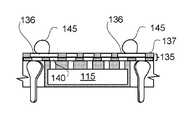
- FIGS. 1-1 through 1-9are a progression of block diagrams of a cross-sectional side view depicting formation of an exemplary in-process microelectronic package 100 for wafer-level chip scale package (“WCSP”) with fan-out (“FO”).
- FIGS. 1, 4 and 5 hereofare described with simultaneous reference to FIG. 6 , where there is shown a flow diagram depicting an exemplary process flow 600 for forming a microelectronic package 100 for WCSP with FO.
- in-process microelectronic package 100includes a carrier 101 coupled to a foil substrate layer 103 with a releasable adhesive 102 .
- carrier 101is a copper carrier
- foil substrate layer 103is copper foil layer.
- carrier 101may be silicon, glass, laminate, or other dielectric and/or metal carrier material.
- Carrier 101may or may not be opaque, such as with respect to UV rays for example.
- releasable adhesive 102may be a thermal or UV released adhesive for example.
- foil substrate layer 103may be another electrical conductor, such as gold, platinum or other thin film metal for example.
- Foil substrate layer (“substrate”) 103has an upper surface 104 and a lower surface 105 opposite such upper surface 104 .
- wire bond wiresmay be bonded to the upper surface of the substrate for extending away therefrom to a height above posts of a microelectronic device.
- wire bond wires 110are coupled to and extend away from upper surface 104 .
- copper wire bond wires 110are used.
- another form of wire bond wires 110may be used, such as aluminum, silver, gold, palladium-coated copper (“PCC”), core wires, or other forms of wire bond wire.
- Wire bond wires 110may be BVATM bonded wires. Columns and/or rows (“rows”) 112 of wire bond wires 110 may be spaced apart from one another to define a region 111 and may be coupled to upper surface 104 .
- wire bond wires 110are ball bonded with corresponding ball bonds 113 to upper surface 104 .
- stitch, wedge, compliant, or other forms of BVA bondingmay be used.
- copper wire bond wires 110may be attached with ball bonds to upper surface 104 of substrate 103 for substrate-to-upper package routing.
- a “wired-arch” or “wired-loop” wire bond wire 114may be formed on upper surface 104 such that a first bond, such as a ball bond 113 for example, is formed at a first location on upper surface 104 and a second bond, such as a wedge or stitch bond 144 , is formed at a second location on upper surface 104 spaced apart from such first location by at least approximately 10-400 microns for example.
- An upper surface 134 of such a “wired-arch” wire bond wire 114may be used for interconnection, as described elsewhere herein. However, for purposes of clarity by way of example and not limitation, generally only wire bond wires 110 , and not wired-arch wire bond wires 114 , are further described.
- Ball bonds 113may be spaced apart from one another. Even though only single rows 112 spaced apart from one another are illustratively depicted in FIG. 1-2 , in other implementations one or more rows 112 may be on one or more sides of region 111 defined by such rows 112 . However, for purposes of clarity by way of example and not limitation, it shall be assumed that a single row 112 is located on each side of region 111 for defining such region for receipt of a microelectronic device. Moreover, wire bond wires 110 may extend to a height above posts of such a microelectronic device, as described below in additional detail.
- a microelectronic device having postsmay be coupled in a face-up orientation to the upper surface of the substrate.
- operations at 602 and 603may be in reverse order.
- a microelectronic device 115may be coupled to upper surface 104 with an adhesive or an underfill 116 in region 111 .
- Microelectronic device 115may be spaced apart from ball bonds 113 after coupling to upper surface 104 .
- Adhesive 116may be a compliant material after curing, such as a polyimide (“PI”) or a polybenzoxazole (“PBO”) for example, with a modulus of elasticity of less than approximately 4 gigapascals (“GPa”).
- PIpolyimide
- PBOpolybenzoxazole
- Microelectronic device 115may be coupled to upper surface 104 in a face-up or front side up orientation. Generally, a face of microelectronic device 115 having posts extending away therefrom, such a face may be facing away from such substrate to which microelectronic device 115 is coupled in this implementation. Even though wire bond wires 110 are attached to upper surface 104 in this example prior to coupling microelectronic device 115 , this order may be reversed in this or another implementation. Microelectronic device 115 may be a packaged or bare integrated circuit die formed using a Si, GaAs, or other semiconductor wafer. Optionally, microelectronic device 115 may be a passive device.
- conductive posts or pads 117 of microelectronic device 115extend away from a front side or face thereof, namely upper surface 118 .
- upper ends 122 of electrically conductive posts or pads 117are over and above an upper surface 118 of microelectronic device 115 .
- copper posts or pads 117are used.
- another type of electrically conductive materialmay be used for posts or pads 117 .
- a structure other than posts or pads 117such as stud bumps for example, may be attached along upper surface 118 of microelectronic device 115 .
- Stud bumpsmay be a ball bonds, such as a ball bond-only portion of wire bonds.
- posts or pads 117may be formed with a metalization layer used in forming microelectronic device 115 .
- a metalization layerused in forming microelectronic device 115 .
- copper posts 117are used for interconnects.
- in-process microelectronic package 100may be a portion of a reconstituted wafer having multiple in-process microelectronic packages 100 .
- a reconstituted wafertypically consist of dies coupled to one another by a molding material in-between them to form a wafer or substrate.
- the substrate, the microelectronic device and the wire bond wires assemblage or combinationmay be molded with a molding material layer, which may include grinding or polishing of a surface of such molding material layer.
- a molding material layer 120may be formed over upper surface 104 , microelectronic device 115 and wire bond wires 110 .
- tips or upper ends 123 of wire bond wires 110are above an upper surface 124 of molding material layer 120 .
- an upper surface 134 of such a wire arch 114may be embedded or protrude above an upper surface 124 of molding material layer 120 .
- wire bond wires 110may extend above upper ends 122 of posts 117 .
- tips 123 of wire bond wires 110 , or upper surface 134 of wired-arch wire bond wires 114may be exposed after forming molding material layer 120
- upper ends 122 of post 117are covered by molding material layer 120 .
- molding layer 120may cover tips 123 , or upper surfaces 134 , as generally indicated by dashed line 121 .
- it shall be assumed that tips 123are exposed after forming molding material layer 120 .
- Molding material layer 120may be for forming a reconstituted wafer having multiple in-process microelectronic packages 100 .
- carrier 101may be removed along with adhesive 102 .
- adhesive 102may be a releasable adhesive using temperature, UV rays, and/or other releasing agent.
- molding material layer 120may be ground or polished down to expose upper ends 122 . Removal of material such as by grinding may occur before or after removal of carrier 101 . After grinding, upper ends 130 of wire bond wires 110 , as well as upper ends 122 of posts 117 , may be exposed for interconnections respectively thereto. However, after grinding, molding material layer 120 may be left in place around posts 117 and remaining portions of wire bond wires 110 .
- first and second bonds thereofmay be electrically disconnected from one another for example by grinding a protruding upper surface 134 to cause a break in such wire arch 114 leaving two at least temporarily exposed upper ends along upper surface 134 .
- grindingmay effectively form two separate wire bonds with different bond types, for example a ball bond 113 and a wedge or stitch bond 144 .
- upper surface 124may be generally co-planar with upper ends 122 and 130 after grinding.
- Posts 117may be in region 111 defined by rows and columns of wire bond wires 110 surrounding microelectronic device 115 .
- a redistribution layer (“RDL”) 135may be formed with a bottom surface thereof interconnected to upper ends 122 of posts 117 and upper ends 130 of wire bond wires 110 for interconnecting at least a portion of wire bond wires 110 with at least a portion of posts 117 .
- RDL 135may include one or more dielectric and conductive layers.
- an integrated circuit diemay be interconnected to conductive pads on a lower surface of a substrate, as described below in additional detail.
- RDL 135may be entirely formed on upper surface 124 of molding material layer 120 , as well as being interconnect to upper ends 130 of wire bond wires 110 and to upper ends 122 of posts 117 .
- an RDLis formed on top of a Si substrate and then surrounded with molding material, and so a large stress field is developed around a transition area or “triple point” where such RDL, Si substrate and molding material intersect.
- RDL 135avoids a conventional “triple point.”
- wire bond wires 110may provide “vertical interconnects” along sides of a microelectronic device for interconnecting substrate 103 and RDL 135 . Such wire bond wires 110 may additionally be interconnected to corresponding posts 117 of microelectronic device 115 .
- conductive padsmay be formed in the substrate electrically isolated from a remainder of the substrate, where the conductive pads correspond to the wire bond wires for electrical conductivity between the wire bond wires and the conductive pads corresponding thereto.
- in-process microelectronic package 100may be flipped for patterning and etching a lower surface 105 of substrate 103 , namely a back side of microelectronic package 100 .
- a direct write etchmay be used on lower surface 105 .
- Through substrate channels 142may be formed from lower surface 105 to upper surface 104 with a stop molding layer 120 for example.
- Through substrate channels 142may be at least partially, if not completely, filled with a dielectric material 143 , such as a polyimide for example.
- Conductive pads 140may be defined by such through substrate channels 142 in copper substrate 103 for this example implementation. Conductive pads or conductive islands 140 may have previously been coupled to wire bond wires 110 , as previously described with reference to bonding to upper surface 104 of substrate 103 .
- Conductive pads 140may be defined in substrate 103 as respective islands of a material of such substrate.
- conductive pads 140are illustratively depicted near an outer edge of microelectronic package 100 , conductive pads 140 may be formed in generally a middle region (“remainder”) 141 , such as directly below microelectronic device 115 for example.
- Conductive pads 140may be formed using substrate 103 material for electrical isolation from a remainder 141 of substrate 103 . Such remainder 141 may be used as a ground plane. In some instances, no conductive pad 140 may be associated with a wire bond wire 110 for coupling to a ground plane, or other voltage plane. Conductive pads 140 corresponding to wire bond wires 110 for electrical conductivity therebetween may be used for electrical communication with microelectronic package 100 and/or another microelectronic package as described below in additional detail. Although not illustratively depicted in FIG. 1 , another redistribution layer RDL may be formed on a top surface of substrate 103 . This RDL, like RDL 135 , may include one or more dielectric and conductive layers.
- first interconnectsmay be attached to a top surface of the redistribution layer for electrical conductivity with the posts and the wire bond wires.
- balls or bumps 145may be formed on exposed surfaces of traces or pads 169 of conductive layer 136 . Such balls or bumps 145 may be mechanically isolated from electrical conductivity by one or more dielectric layers 137 of an RDL 135 . However, such conductive traces or pads 169 of conductive layer 136 may be coupled for electrical conductivity with wire bond wires 110 , as well as one or more posts 117 , as previously described. Balls or bumps 145 for interconnection with posts 117 and not wire bond wires 110 are not illustratively depicted in this figure for purposes of clarity and not limitation.
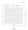
- FIG. 3where there is shown a block diagram of a top view depicting an exemplary in-process microelectronic package 100 after forming balls 145 on RDL 135 .
- balls 145may be associated with pads or traces 169 of conductive layer 136 for coupling to wire bond wires.
- Others of balls 145may be associated with pads or traces 169 of conductive layer 136 not associated with wire bond wires 110 and associated with posts 117 .
- wire bond wires 110may be interconnected to more than one post 117 . In one or more instances, there may not be a direct coupling for an electrical connection between at least one wire bond wire 110 and at least one post 117 .
- Pitch 148 of pads 169 of conductive layer 136 for balls 145 associated with wire bond wires 110may be in a range of approximately 350 to 600 microns or less for correspondence with pitch of contacts on a PCB or other circuit board.
- minimum pitch of posts 117 and wire bond wires 110may be as small as 5 microns and as small as 20 microns, respectively.
- An RDL 135may effectively cause pitch 148 to be at least approximately the same as for example a BGA pitch of a circuit board, such as approximately 350 microns.
- second interconnects of another microelectronic devicemay be coupled to the conductive pads for electrical conductivity with the wire bond wires.
- FIG. 4there is shown a block diagram of a cross-sectional side view depicting an exemplary PoP microelectronic package 300 .
- a microelectronic package 100which may still be in a reconstituted wafer or may be diced therefrom, has coupled on the back side thereof another microelectronic package 200 .
- PoP microelectronic package 300may be package-to-package assembled, package-to reconstituted wafer assembled, or wafer/reconstituted wafer to reconstituted wafer assembled, with the last three involving subsequent dicing.
- microelectronic devices 115 and 201are respective packaged integrated circuit dies; however, in another example either or both microelectronic devices 115 and 201 may be bare integrated circuit dies.
- microelectronic package 100may be an applications processor or a baseband processor or any other logic device
- microelectronic package 200may be a memory device, such as with one or more types of memory die including NAND, DRAM, memory controller, and/or the like.
- Bumps or balls 155 of microelectronic package 200may be physically coupled to conductive pads 140 of microelectronic package 100 for electrical conductivity between microelectronic packages 100 and 200 .
- PoP microelectronic package 300may be coupled to a PCB or other circuit board 160 which is not part of PoP microelectronic package 300 .
- Overall height 400 of PoP microelectronic package 300may be approximately 1.5 mm or less.
- an underfill(not shown) may be injected between microelectronic packages 100 and 200 .
- FIG. 5there is shown a block diagram of a cross-sectional side view depicting another exemplary PoP microelectronic package 300 .
- a microelectronic package 100which may still be in a reconstituted wafer or may be diced therefrom, has formed on a back side thereof another RDL 165 .
- Another microelectronic package 200may be coupled to an optional RDL 165 .
- a bottom surface of RDL 165may be interconnected to conductive pads 140 of microelectronic package 100 for electrical conductivity therewith.
- Either or both of RDLs 135 and/or 165may have one or more metal layers and/or one or more dielectric layers.
- Bumps or balls 155 of microelectronic package 200may be physically coupled to conductive pads 164 of RDL 165 of microelectronic package 100 for electrical conductivity between microelectronic packages 100 and 200 .
- PoP microelectronic package 300may be coupled to a PCB or other circuit board 160 not part of PoP microelectronic package 300 .
- Overall height 400 of PoP microelectronic package 300may be approximately 1.5 mm or less.
- Wire bond wires 110may be disposed around a perimeter of microelectronic device 115 , which may be packaged integrated circuit die or a bare integrated circuit die.
- FIGS. 7-1 through 7-6are a progression of block diagrams of a cross-sectional side view depicting formation of another exemplary in-process microelectronic package 100 for WCSP with fan-out FO.
- FIGS. 7, 9 and 10are hereafter described with simultaneous reference to FIG. 8 , where there is shown a flow diagram depicting an exemplary process flow 800 for forming such other microelectronic package 100 for WCSP with fan-out FO.
- in-process microelectronic package 100includes a carrier 101 coupled to a foil substrate layer 103 with a releasable adhesive 102 .
- carrier 101is a copper carrier
- foil substrate layer 103is copper foil layer.
- carrier 101may be silicon, glass, laminate, or other metal and/or dielectric carrier material.
- Carrier 101may or may not be opaque, such as with respect to UV rays for example.
- releasable adhesive 102may be a thermal or UV released adhesive for example.
- foil substrate layer 103may be another electrical conductor, such as gold, platinum or other thin film metal for example.
- Foil substrate layer (“substrate”) 103has an upper surface 104 and a lower surface 105 opposite such upper surface 104 .
- conductive pads or conductive islandsmay be formed in the substrate electrically isolated from a remainder of the substrate.
- the conductive padsmay correspond to the wire bond wires for electrical conductivity between the wire bond wires and the conductive pads corresponding thereto as described below in additional detail.
- in-process microelectronic package 100may have an upper surface 104 of substrate 103 directly written with a laser drill. In another implementation, patterning and etching may be used on upper surface 104 . Through substrate channels 142 may be formed from upper surface 104 down to lower surface 105 .
- Through substrate channels 142may be at least partially, if not completely, be filled with a dielectric material 143 , such as a polyimide for example.
- Conductive pads 140may be defined by such through substrate channels 142 in copper substrate 103 for this example implementation.
- Conductive pads 140may be defined in substrate 103 as respective islands of a material of such substrate.
- substrate channels 142may not be filled with any material, and conductive pads 140 may only be attached to carrier 101 via adhesive 102 .
- Conductive pads 140may be formed using substrate 103 material for electrical isolation from a remainder of substrate 103 , and such remainder of substrate 103 not used for conductive pads 140 may be used as a ground plane (not shown in this figure). However, for a face-down configuration as described with reference to FIG. 7 for example, conductive pads 140 may be formed for interconnection with posts or pads 117 of a microelectronic device 115 , as described below in additional detail.
- wire bond wiresmay be bonded to the upper surface of the substrate for extending away therefrom to a height above a microelectronic device, as described below in additional detail.
- wire bond wires 110are coupled to and extend away from upper surface 104 .
- copper wire bond wires 110are used.
- another form of wire bond wires 110may be used, such as aluminum, silver, gold, palladium-coated copper (“PCC”), core wires, or other forms of wire bond wire.
- Wire bond wires 110may be BVATM bonded wires.
- a “wired-arch” or “wired-loop” wire bond wire 114may be formed on upper surface 104 such that a first bond, such as a ball bond 113 for example, is formed at a first location on upper surface 104 and a second bond, such as a wedge or stitch bond 144 , is formed at a second location on upper surface 104 spaced apart from such first location by at least approximately 10 microns for example.
- An upper surface 134 of such a “wired-arch” wire bond wire 114may be used for interconnection, as described elsewhere herein. However, for purposes of clarity by way of example and not limitation, generally only wire bond wires 110 , and not wired-arch wire bond wires 114 , are further described.
- Rows 112 of wire bond wires 110may be spaced apart from one another to define a region 111 and may be coupled to upper surface 104 .
- Such spacing between wire bond wires 110may, though need not be uniform.
- a denser spacingmay be used in some locations as compared with other locations, as may vary from application to application depending on routing.
- routing, including via RDLmay be denser in some areas as compare with other areas corresponding to layout of an integrated circuit die. Having the flexibility to have wire bond wires 110 use different spacings may be useful to accommodate shorter path distances and/or pin layout of a package.
- wire bond wires 110are ball bonded with corresponding ball bonds 113 to conductive pads 140 along upper surface 104 .
- stitch, wedge, compliant, or other forms of BVA bondingmay be used.
- copper wire bond wires 110may be attached with ball bonds to upper surface 104 of substrate 103 for substrate-to-upper package routing.
- no conductive pad 140may be associated with a wire bond wire 110 , such as for coupling to a ground plane or other voltage plane.
- Conductive pads 140 corresponding to wire bond wires 110 for electrical conductivity therebetweenmay be used for electrical communication with microelectronic package 100 and/or another microelectronic package as described below in additional detail.
- Ball bonds 113may be spaced apart from one another. Even though only single rows 112 spaced apart from one another are illustratively depicted in FIG. 7-2 , in other implementations one or more rows 112 may be on one or more sides of region 111 defined by such rows 112 . However, for purposes of clarity by way of example and not limitation, it shall be assumed that a single row 112 is located on each side of region 111 for defining such region for receipt of a microelectronic device. Moreover, wire bond wires 110 may extend to a height above a back side surface of such a microelectronic device, as described below in additional detail.
- a microelectronic device having postsmay be coupled in a face-down orientation to the upper surface of the substrate with first interconnects.
- operations at 803 and 804may be in reverse order.
- microelectronic device 115may be coupled to an upper surface 104 by injecting an underfill 168 prior to molding.
- a microelectronic device 115may be coupled to upper surface 104 in region 111 .
- a microelectronic device 115may be a bare IC or a packaged IC. Even though a single instance of an exemplary in-process microelectronic package 100 is illustratively depicted, two or more such in-process microelectronic packages 100 may be used. In another example, such in-process microelectronic package 100 may be a portion of a reconstituted wafer having multiple in-process microelectronic packages 100 .
- Microelectronic device 115may be spaced apart from ball bonds 113 after coupling to upper surface 104 .
- Posts or pads 117may be coupled to corresponding conductive pads 140 by bonding, such as copper-to-copper as in this example. Accordingly, soldering may be avoided for this interconnection by having copper conductive pads 140 aligned with lower surfaces of posts 117 .
- a copper-to-copper bondis illustratively depicted in FIG. 7 , in another implementation a conventional reflow bond using a solder material may be used.
- conductive posts or pads 117may extend away therefrom.
- lower ends of electrically conductive posts or pads 117are over and above conductive pads 140 of microelectronic device 100 .
- copper posts or pads 117are used.
- another type of electrically conductive materialmay be used for posts or pads 117 .
- posts or pads 117may be formed with a metalization layer used in forming microelectronic device 115 .
- microelectronic device 115may be further coupled to upper surface 104 in a face-down or front side down orientation with an adhesive 716 .
- Adhesive 716may be injected between posts or pads 117 underneath microelectronic device 115 . Additionally, adhesive 716 may extend into gaps between near surfaces of wire bond wires 110 and sidewalls of microelectronic device 115 . Adhesive 716 may be deposited on a back side surface 724 of a packaged die or bare die integrated circuit of microelectronic device 115 . Tips 123 of wire bond wires 110 may be above (i.e., higher than) an upper surface 725 of adhesive 716 , or at least higher than back side surface 724 .
- adhesive 716may be an epoxy mold compound.
- adhesive 716may be an underfill material which may extend into gaps between near surfaces of wire bond wires 110 and sidewalls of microelectronic device 115 .
- the substrate, the microelectronic device and the wire bond wires assemblage or combinationmay be molded with a molding material layer, which may include grinding or polishing such molding material layer.
- a molding material layer 120is formed over upper surface 104 , microelectronic device 115 , and wire bond wires 110 .
- tips or upper ends 123 of wire bond wires 110are above an upper surface 124 of molding material layer 120 .
- tips 123 of wire bond wires 110may be exposed after forming molding material layer 120 .
- Surfaces 724 or 725may or may not be covered by molding material layer 120 .
- molding layer 120may cover tips 123 followed by a grind or etch back to reveal upper ends of wire bond wires 110 .
- tips 123are exposed after forming molding material layer 120 .
- Molding material layer 120may be for forming a reconstituted wafer having multiple in-process microelectronic packages 100 .
- an upper surface 134 of such a wire arch 114may be embedded or protrude above an upper surface 124 of molding material layer 120 .
- carrier 101may be removed along with adhesive 102 .
- adhesive 102may be a releasable adhesive with temperature, UV rays, and/or other releasing agent.
- molding material layer 120may be ground or polished down to an upper surface 724 or 725 . Removal of material such as by grinding may occur before or after removal of carrier 101 . After grinding, upper ends 130 , such as in FIG. 1-6 , of wire bond wires 110 may be exposed for interconnections respectively thereto in such an implementation. After grinding, molding material layer 120 may be left in place around posts 117 and remaining portions of wire bond wires 110 . However, for purposes of clarity by way of example and not limitation, it shall be assumed that tips 123 extend above an upper surface 124 of molding material layer 120 , and that grinding of tips 123 is not used.
- first and second bonds thereofmay be electrically disconnected from one another for example by grinding a protruding upper surface 134 to cause a break in such wire arch 114 leaving two at least temporarily exposed upper ends along upper surface 134 .
- grindingmay effectively form two separate wire bonds with different bond types, for example a ball bond 113 and a wedge or stitch bond 144 .
- the wire bond wires and the first interconnectsmay be interconnected via the conductive pads with a redistribution layer, where the redistribution layer has a first surface in contact with the conductive pads for the interconnecting.
- an RDL 135may be formed with a bottom surface thereof interconnected to upper surfaces of conductive pads 140 for interconnecting at least a portion of wire bond wires 110 with at least a portion of posts 117 .
- RDL 135may include one or more dielectric and conductive layers.
- a PCB or other circuit boardmay be interconnected to RDL 135 , as described below in additional detail.
- Traces or pads 169 of conductive layer 136may interconnect upper surfaces of conductive pads 140 for coupling upper ends of wire bond wires 110 and posts 117 to one another. Accordingly, wire bond wires 110 may provide “vertical interconnects” along sides of a microelectronic device 115 for interconnecting substrate 103 and RDL 135 .
- second interconnectsmay be attached to a second surface opposite the first surface of the redistribution layer.
- balls or bumps 145may be formed on exposed surfaces of traces or pads 169 of conductive layer 136 . Such balls or bumps 145 may be mechanically isolated from electrical conductivity by one or more dielectric layers 137 of an RDL 135 . However, such conductive traces or pads 169 of conductive layer 136 may be coupled for electrical conductivity with wire bond wires 110 , as well as one or more posts 117 , as previously described. Balls or bumps 145 for interconnection with posts 117 and not wire bond wires 110 are not illustratively depicted in this figure for purposes of clarity and not limitation.
- third interconnects of another microelectronic devicemay be coupled to the conductive pads for electrical conductivity with the wire bond wires.
- FIG. 9there is shown a block diagram of a cross-sectional side view depicting an exemplary PoP microelectronic package 300 .
- a microelectronic package 100which may still be in a reconstituted wafer or may be diced therefrom, has coupled on a back side thereof another microelectronic package 200 .
- PoP microelectronic package 300may be package-to-package assembled, package-to reconstituted wafer assembled, or wafer/reconstituted wafer to reconstituted wafer assembled, with the last three involving subsequent dicing.
- microelectronic devices 115 and 201are respective packaged integrated circuit dies; however, in another example either or both microelectronic devices 115 and 201 may be bare integrated circuit dies.
- Bumps or balls 155 of microelectronic package 200may be physically coupled to tips 123 , or upper surfaces 130 in another implementation, of wire bond wires 110 of microelectronic package 100 for electrical conductivity between microelectronic packages 100 and 200 .
- PoP microelectronic package 300may be coupled to a PCB or other circuit board 160 not part of PoP microelectronic package 300 .
- Overall height 400 of PoP microelectronic package 300may be approximately 1.5 mm or less.
- an underfill(not shown) may be injected between microelectronic packages 100 and 200 .
- wire bond wires 110may be disposed around a perimeter of microelectronic device 115 .
- FIG. 10there is shown a block diagram of a cross-sectional side view depicting another exemplary PoP microelectronic package 300 .
- a microelectronic package 100which may still be in a reconstituted wafer or may be diced therefrom, has formed on a back side thereof another RDL 165 .
- Another microelectronic package 200may be coupled to an optional RDL 165 .
- a bottom surface of RDL 165may be interconnected to upper surfaces 130 of wire bond wires 110 of microelectronic package 100 for electrical conductivity therewith.
- tips 123 of FIG. 7-5may be ground down to surface 124 for example.
- Bumps or balls 155 of microelectronic package 200may be physically coupled to conductive pads 164 of RDL 165 of microelectronic package 100 for electrical conductivity between microelectronic packages 100 and 200 .
- PoP microelectronic package 300may be coupled to a PCB or other circuit board 160 not part of PoP microelectronic package 300 .
- Overall height 400 of PoP microelectronic package 300may be approximately 1.5 mm or less.
Landscapes
- Engineering & Computer Science (AREA)
- Microelectronics & Electronic Packaging (AREA)
- Power Engineering (AREA)
- Computer Hardware Design (AREA)
- Physics & Mathematics (AREA)
- Condensed Matter Physics & Semiconductors (AREA)
- General Physics & Mathematics (AREA)
- Manufacturing & Machinery (AREA)
- Ceramic Engineering (AREA)
- Wire Bonding (AREA)
Abstract
Description
This patent application claims the benefit of priority to U.S. Provisional Patent Application No. 62/246,517 to Prabhu et al., entitled, “Microelectronic Package for Wafer-Level Chip Scale Packaging with Fan-Out,” filed Oct. 26, 2015 and incorporated herein by reference in its entirety.
The following description relates to integrated circuit (“IC”) packaging. More particularly, the following description relates to microelectronic packages for wafer-level chip scale packaging with fan-out.
Microelectronic assemblies generally include one or more ICs, such as for example one or more packaged dies (“chips”) or one or more dies. One or more of such ICs may be mounted on a circuit platform, such as a wafer such as in wafer-level-packaging (“WLP”), printed board (“PB”), a printed wiring board (“PWB”), a printed circuit board (“PCB”), a printed wiring assembly (“PWA”), a printed circuit assembly (“PCA”), a package substrate, an interposer, or a chip carrier. Additionally, one IC may be mounted on another IC. An interposer may be an IC, and an interposer may be a passive or an active IC, where the latter includes one or more active devices, such as transistors for example, and the former does not include any active device. Furthermore, an interposer may be formed like a PWB, namely without any circuit elements such as capacitors, resistors, or active devices. Additionally, an interposer includes at least one through-substrate-via.
An IC may include conductive elements, such as pathways, traces, tracks, vias, contacts, pads such as contact pads and bond pads, plugs, nodes, or terminals for example, that may be used for making electrical interconnections with a circuit platform. These arrangements may facilitate electrical connections used to provide functionality of ICs. An IC may be coupled to a circuit platform by bonding, such as bonding traces or terminals, for example, of such circuit platform to bond pads or exposed ends of pins or posts or the like of an IC. Additionally, a redistribution layer (“RDL”) may be part of an IC to facilitate a flip-chip configuration, die stacking, or more convenient or accessible position of bond pads for example.
More recently, fan-out wafer-level chip scale packaging (“FO-WCSP”) has been used to reduce costs. Semiconductor dies are formed, such as in their smallest configurations, and these dies or a combination of different dies may then be molded together in what is known as a reconstituted wafer. This reconstituted wafer provides more surface area for interconnects using WCSP in combination with a fan-out technology, such as a lead frame, ball grid array, or other fan-out technology. This allows for a larger pitch for interconnection to a PCB or other circuit board.
Accordingly, it would be desirable and useful to provide for FO-WCSP for a package-on-package (“PoP”) configuration or other die stacking configuration.
An apparatus relates generally to a microelectronic package for wafer-level chip scale packaging with fan-out. In such an apparatus, there is a substrate having an upper surface and a lower surface opposite the upper surface. A microelectronic device is coupled to the upper surface with the microelectronic device in a face-up orientation. Wire bond wires are coupled to and extending away from a face of the microelectronic device facing away from the substrate. Posts of the microelectronic device extend away from a front face thereof. Conductive pads are formed in the substrate.
A method relates generally to forming a microelectronic package for wafer-level chip scale packaging with fan-out. In such a method, obtained is a substrate having an upper surface and a lower surface opposite the upper surface. A microelectronic device having posts is coupled in a face-up orientation to the upper surface of the substrate. Wire bond wires are bonded to the upper surface of the substrate for extending away therefrom to a height above the posts. The substrate, the microelectronic device and the wire bond wires in combination is molded with a molding material layer. An uppermost portion of the wire bond wires and an uppermost portion of the molding material layer is removed to upper ends of the posts. Conductive pads are formed in the substrate. The conductive pads are for the wire bond wires for electrical conductivity between the wire bond wires and the conductive pads associated therewith.
An apparatus relates generally to another microelectronic package for wafer-level chip scale packaging with fan-out. In such an apparatus, a substrate has an upper surface and a lower surface opposite the upper surface. The substrate includes conductive pads formed therein. Wire bond wires are coupled to and extend away from a first portion of the conductive pads along the upper surface for electrical conductivity between the wire bond wires and the first portion of the conductive pads associated therewith. A microelectronic device is coupled to a second portion of the conductive pads along the upper surface with the microelectronic device in a face-down orientation.
A method relates generally to another microelectronic package for wafer-level chip scale packaging with fan-out. In such a method, obtained is a substrate having an upper surface and a lower surface opposite the upper surface. Conductive pads are formed in the substrate. Wire bond wires are bonded to the conductive pads along the upper surface of the substrate for extending away therefrom. The conductive pads are for the wire bond wires for electrical conductivity between the wire bond wires and the conductive pads associated therewith. A microelectronic device is coupled in a face-down orientation to the upper surface of the substrate with interconnects. The substrate, the microelectronic device and the wire bond wires in combination is molded with a molding material layer.
Accompanying drawing(s) show exemplary embodiment(s) in accordance with one or more aspects of exemplary apparatus(es) or method(s). However, the accompanying drawings should not be taken to limit the scope of the claims, but are for explanation and understanding only.
In the following description, numerous specific details are set forth to provide a more thorough description of the specific examples described herein. It should be apparent, however, to one skilled in the art, that one or more other examples or variations of these examples may be practiced without all the specific details given below. In other instances, well known features have not been described in detail so as not to obscure the description of the examples herein. For ease of illustration, the same number labels are used in different diagrams to refer to the same items; however, in alternative examples the items may be different.
Moreover, the features described herein as well as the numerical instances thereof are for purposes of conveying with clarity one or more aspects of exemplary apparatus(es) and/or method(s) described herein. These features are not to scale, and numerical instances thereof in an actual implementation may be the same or different from the numerical instances illustratively depicted. It should be understood that the word “exemplary” is used herein to mean “serving as an example, instance, or illustration.” Any example or feature described herein as “exemplary” is not necessarily to be construed as preferred or advantageous over other examples or features.
Generally, an integrated circuit die includes a substrate of a semiconductor material such as silicon (Si), gallium arsenide (GaAs), polymeric, ceramic, carbon-based substrates such as diamond, a silicon carbon (SiC), germanium (Ge), Si1-xGex, or the like. Even though a semiconductor substrate as provided from an in-process wafer is generally described below, any sheet or layer semiconductor material or dielectric material, such as ceramic or glass for example, may be used as a substrate.
A substrate includes an upper surface and a lower surface that extend in lateral directions and are generally parallel to each other at a thickness thereof. Use of terms such as “upper” and “lower” or other directional terms is made with respect to the reference frame of the figures and is not meant to be limiting with respect to potential alternative orientations, such as in further assemblies or as used in various systems.
An upper surface may generally be associated with what is referred to as a “front side” of an in-process wafer, and a lower surface may generally be associated with what is referred to as a “back side” of an in-process wafer. However, upper and lower may be reversed during processing. Along those lines, a front-side of an in-process wafer may be used for forming what is referred to as front-end-of-line (“FEOL”) structures and back-end-of-line (“BEOL”) structures. Generally, FEOL structures may include shallow trench isolations (“STI”), transistor gates, transistor source/drain regions (not shown), transistor gate dielectrics (not shown), contact etch stop layer (“CESL”; not shown), a pre-metallization dielectric or pre-metal dielectric (“PMD”), and contact plugs, among other FEOL structures. A PMD may be composed of one or more layers. Generally, BEOL structures may include one or more inter-level dielectrics (“ILDs”) and one or more levels of metallization (“M”). Each ILD may be composed of one or more dielectric layers, and each metal or metallization level may be composed of one or more metal layers, as well as one or more barrier and/or liner layers. Additionally, metal from a metallization level may extend through one or more ILDs, as is known. A passivation level may be formed on a last metallization layer. Such passivation level may include one or more dielectric layers, and further may include an anti-reflective coating (“ARC”). Furthermore, a redistribution layer (“RDL”) may be formed on such passivation level. Conventionally, an RDL may include: a dielectric layer, such as a polyimide layer for example; another metal layer on such dielectric layer connected to a bond pad of a metal layer of a last metallization level; and another dielectric layer, such as another polyimide layer for example, over such RDL metal layer while leaving a portion thereof exposed to provide another bond pad. A terminal opening may expose such other bond pad of such RDL metal layer. Thereafter, a solder bump or wire bond may be conventionally coupled to such bond pad.
Balls or other discrete interconnects may be respectively formed on bonding pads, where such pads may be formed on or as part of metal layer. Balls may be formed of a bonding material, such as solder or other bonding material. Balls may be microbumps, C4 bumps, ball grid array (“BGA”) balls, or some other die interconnect structure. In some applications, metal layer may be referred to as a landing pad. BGA, lead frame, and other types of interconnects may be used as fan-out technologies.
The following description is for fan-out wafer-level chip scale packaging (“FO-WCSP for a stacked or 3D device, such as for a package-on-package PoP device. Along those lines, wire bond wires are used for interconnection with an upper package of a PoP device. Use of wire bond wires as described below may eliminate a substrate and/or corresponding through substrate vias used in a conventionally manufactured PoP device with fan-out. Thus, a lower cost and thinner PoP device with fan-out may be manufactured using wire bond wires as described hereinbelow. Along those lines, a PoP device with fan-out using wire bond wires, such as of a BVA™ technology, may be used in mobile devices and other small form factor applications.
At601, a substrate having an upper surface and a lower surface opposite the upper surface is obtained. With reference toFIG. 1-1 , in-process microelectronic package 100 includes acarrier 101 coupled to afoil substrate layer 103 with areleasable adhesive 102. In this example implementation,carrier 101 is a copper carrier, and foilsubstrate layer 103 is copper foil layer. However, in other implementations,carrier 101 may be silicon, glass, laminate, or other dielectric and/or metal carrier material.Carrier 101 may or may not be opaque, such as with respect to UV rays for example. Along those lines,releasable adhesive 102 may be a thermal or UV released adhesive for example. Moreover, in other implementations,foil substrate layer 103 may be another electrical conductor, such as gold, platinum or other thin film metal for example. Foil substrate layer (“substrate”)103 has anupper surface 104 and alower surface 105 opposite suchupper surface 104.
At602, wire bond wires may be bonded to the upper surface of the substrate for extending away therefrom to a height above posts of a microelectronic device. With reference toFIG. 1-2 ,wire bond wires 110 are coupled to and extend away fromupper surface 104. In this example, copperwire bond wires 110 are used. However, in another implementation, another form ofwire bond wires 110 may be used, such as aluminum, silver, gold, palladium-coated copper (“PCC”), core wires, or other forms of wire bond wire.Wire bond wires 110 may be BVA™ bonded wires. Columns and/or rows (“rows”)112 ofwire bond wires 110 may be spaced apart from one another to define aregion 111 and may be coupled toupper surface 104.
In this example,wire bond wires 110 are ball bonded withcorresponding ball bonds 113 toupper surface 104. However, in another implementation, stitch, wedge, compliant, or other forms of BVA bonding may be used. For this implementation, which does not use soldering ofwire bond wires 110, copperwire bond wires 110 may be attached with ball bonds toupper surface 104 ofsubstrate 103 for substrate-to-upper package routing.
In another example, a “wired-arch” or “wired-loop”wire bond wire 114 may be formed onupper surface 104 such that a first bond, such as aball bond 113 for example, is formed at a first location onupper surface 104 and a second bond, such as a wedge or stitchbond 144, is formed at a second location onupper surface 104 spaced apart from such first location by at least approximately 10-400 microns for example. Anupper surface 134 of such a “wired-arch”wire bond wire 114 may be used for interconnection, as described elsewhere herein. However, for purposes of clarity by way of example and not limitation, generally onlywire bond wires 110, and not wired-archwire bond wires 114, are further described.
At603, a microelectronic device having posts may be coupled in a face-up orientation to the upper surface of the substrate. In another implementation, operations at602 and603 may be in reverse order. With reference toFIG. 1-3 , amicroelectronic device 115 may be coupled toupper surface 104 with an adhesive or anunderfill 116 inregion 111.Microelectronic device 115 may be spaced apart fromball bonds 113 after coupling toupper surface 104. Adhesive116 may be a compliant material after curing, such as a polyimide (“PI”) or a polybenzoxazole (“PBO”) for example, with a modulus of elasticity of less than approximately 4 gigapascals (“GPa”).
Along anupper surface 118 ofmicroelectronic device 115, conductive posts orpads 117 ofmicroelectronic device 115 extend away from a front side or face thereof, namelyupper surface 118. In this example, upper ends122 of electrically conductive posts orpads 117 are over and above anupper surface 118 ofmicroelectronic device 115. In this example, copper posts orpads 117 are used. However, in another example, another type of electrically conductive material may be used for posts orpads 117. Furthermore, a structure other than posts orpads 117, such as stud bumps for example, may be attached alongupper surface 118 ofmicroelectronic device 115. Stud bumps may be a ball bonds, such as a ball bond-only portion of wire bonds. Additionally, posts orpads 117 may be formed with a metalization layer used in formingmicroelectronic device 115. For purposes of clarity by way of example and not limitation, it shall be assumed that copper posts117 are used for interconnects.
Even though a single instance of an exemplary in-process microelectronic package 100 is illustratively depicted, two or more of such in-processmicroelectronic packages 100 may be used. In another example, such in-process microelectronic package 100 may be a portion of a reconstituted wafer having multiple in-process microelectronic packages100. A reconstituted wafer typically consist of dies coupled to one another by a molding material in-between them to form a wafer or substrate.
At604, the substrate, the microelectronic device and the wire bond wires assemblage or combination may be molded with a molding material layer, which may include grinding or polishing of a surface of such molding material layer. With reference toFIG. 1-4 , amolding material layer 120 may be formed overupper surface 104,microelectronic device 115 andwire bond wires 110. In this example, tips orupper ends 123 ofwire bond wires 110 are above anupper surface 124 ofmolding material layer 120. For a wired-archwire bond wire 114, anupper surface 134 of such awire arch 114 may be embedded or protrude above anupper surface 124 ofmolding material layer 120. Along those lines,wire bond wires 110 may extend above upper ends122 ofposts 117. Thus, whiletips 123 ofwire bond wires 110, orupper surface 134 of wired-archwire bond wires 114, may be exposed after formingmolding material layer 120, upper ends122 ofpost 117 are covered bymolding material layer 120. In another implementation,molding layer 120 may covertips 123, orupper surfaces 134, as generally indicated by dashedline 121. For purposes of clarity by way of example and not limitation, it shall be assumed thattips 123 are exposed after formingmolding material layer 120.Molding material layer 120 may be for forming a reconstituted wafer having multiple in-process microelectronic packages100.
With reference toFIG. 1-5 , after molding,carrier 101 may be removed along withadhesive 102. Again, adhesive102 may be a releasable adhesive using temperature, UV rays, and/or other releasing agent.
With reference toFIG. 1-6 ,molding material layer 120, as well astips 123 ofwire bond wires 110, may be ground or polished down to expose upper ends122. Removal of material such as by grinding may occur before or after removal ofcarrier 101. After grinding, upper ends130 ofwire bond wires 110, as well as upper ends122 ofposts 117, may be exposed for interconnections respectively thereto. However, after grinding,molding material layer 120 may be left in place aroundposts 117 and remaining portions ofwire bond wires 110. For a wired-archwire bond wire 114, after grinding ofupper surface 134 of such awire arch 114, first and second bonds thereof may be electrically disconnected from one another for example by grinding a protrudingupper surface 134 to cause a break insuch wire arch 114 leaving two at least temporarily exposed upper ends alongupper surface 134. Along those lines, grinding may effectively form two separate wire bonds with different bond types, for example aball bond 113 and a wedge or stitchbond 144.
With reference toFIG. 2 , where there is shown a block diagram of a top view depicting an exemplary in-process microelectronic package 100. For this implementation,upper surface 124 may be generally co-planar withupper ends Posts 117 may be inregion 111 defined by rows and columns ofwire bond wires 110 surroundingmicroelectronic device 115.
At605, the wire bond wires and the posts may be interconnected with a redistribution layer. With reference toFIG. 1-7 , a redistribution layer (“RDL”)135 may be formed with a bottom surface thereof interconnected toupper ends 122 ofposts 117 andupper ends 130 ofwire bond wires 110 for interconnecting at least a portion ofwire bond wires 110 with at least a portion ofposts 117. Even though a single layer of adielectric layer 137 and aconductive layer 136 is illustratively depicted forRDL 135, in other implementations,RDL 135 may include one or more dielectric and conductive layers. Along those lines, an integrated circuit die may be interconnected to conductive pads on a lower surface of a substrate, as described below in additional detail.
Traces orpads 169 ofconductive layer 136 may interconnect upper ends122 ofposts 117 andupper ends 130 ofwire bond wires 110. Accordingly,wire bond wires 110 may provide “vertical interconnects” along sides of a microelectronic device for interconnectingsubstrate 103 andRDL 135. Suchwire bond wires 110 may additionally be interconnected tocorresponding posts 117 ofmicroelectronic device 115.
At606, conductive pads may be formed in the substrate electrically isolated from a remainder of the substrate, where the conductive pads correspond to the wire bond wires for electrical conductivity between the wire bond wires and the conductive pads corresponding thereto. With reference toFIG. 1-8 , in-process microelectronic package 100 may be flipped for patterning and etching alower surface 105 ofsubstrate 103, namely a back side ofmicroelectronic package 100. In another implementation, a direct write etch may be used onlower surface 105.
Throughsubstrate channels 142 may be formed fromlower surface 105 toupper surface 104 with astop molding layer 120 for example. Throughsubstrate channels 142 may be at least partially, if not completely, filled with adielectric material 143, such as a polyimide for example.Conductive pads 140 may be defined by such throughsubstrate channels 142 incopper substrate 103 for this example implementation. Conductive pads orconductive islands 140 may have previously been coupled towire bond wires 110, as previously described with reference to bonding toupper surface 104 ofsubstrate 103.Conductive pads 140 may be defined insubstrate 103 as respective islands of a material of such substrate. Even thoughconductive pads 140 are illustratively depicted near an outer edge ofmicroelectronic package 100,conductive pads 140 may be formed in generally a middle region (“remainder”)141, such as directly belowmicroelectronic device 115 for example.
At607, first interconnects may be attached to a top surface of the redistribution layer for electrical conductivity with the posts and the wire bond wires. With reference toFIG. 1-9 , balls or bumps145 may be formed on exposed surfaces of traces orpads 169 ofconductive layer 136. Such balls or bumps145 may be mechanically isolated from electrical conductivity by one or moredielectric layers 137 of anRDL 135. However, such conductive traces orpads 169 ofconductive layer 136 may be coupled for electrical conductivity withwire bond wires 110, as well as one ormore posts 117, as previously described. Balls or bumps145 for interconnection withposts 117 and not wirebond wires 110 are not illustratively depicted in this figure for purposes of clarity and not limitation.
With reference toFIG. 3 , where there is shown a block diagram of a top view depicting an exemplary in-process microelectronic package 100 after formingballs 145 onRDL 135. Some ofballs 145 may be associated with pads or traces169 ofconductive layer 136 for coupling to wire bond wires. Others ofballs 145 may be associated with pads or traces169 ofconductive layer 136 not associated withwire bond wires 110 and associated withposts 117. Moreover, even though generally a one-to-one correspondence betweenwire bond wires 110 coupled toposts 117 is illustratively depicted,wire bond wires 110 may be interconnected to more than onepost 117. In one or more instances, there may not be a direct coupling for an electrical connection between at least onewire bond wire 110 and at least onepost 117.
At608, second interconnects of another microelectronic device may be coupled to the conductive pads for electrical conductivity with the wire bond wires. With reference toFIG. 4 , there is shown a block diagram of a cross-sectional side view depicting an exemplary PoPmicroelectronic package 300. In this example, amicroelectronic package 100, which may still be in a reconstituted wafer or may be diced therefrom, has coupled on the back side thereof anothermicroelectronic package 200. In other words, PoPmicroelectronic package 300 may be package-to-package assembled, package-to reconstituted wafer assembled, or wafer/reconstituted wafer to reconstituted wafer assembled, with the last three involving subsequent dicing. In this example,microelectronic devices microelectronic devices microelectronic package 100 may be an applications processor or a baseband processor or any other logic device, andmicroelectronic package 200 may be a memory device, such as with one or more types of memory die including NAND, DRAM, memory controller, and/or the like.
Bumps orballs 155 ofmicroelectronic package 200 may be physically coupled toconductive pads 140 ofmicroelectronic package 100 for electrical conductivity betweenmicroelectronic packages microelectronic package 300 may be coupled to a PCB orother circuit board 160 which is not part of PoPmicroelectronic package 300.Overall height 400 of PoPmicroelectronic package 300 may be approximately 1.5 mm or less. Optionally, an underfill (not shown) may be injected betweenmicroelectronic packages
With reference toFIG. 5 , there is shown a block diagram of a cross-sectional side view depicting another exemplary PoPmicroelectronic package 300. In this example, amicroelectronic package 100, which may still be in a reconstituted wafer or may be diced therefrom, has formed on a back side thereof anotherRDL 165. Anothermicroelectronic package 200 may be coupled to anoptional RDL 165. Along those lines, a bottom surface ofRDL 165 may be interconnected toconductive pads 140 ofmicroelectronic package 100 for electrical conductivity therewith. Either or both ofRDLs 135 and/or165 may have one or more metal layers and/or one or more dielectric layers.
Bumps orballs 155 ofmicroelectronic package 200 may be physically coupled toconductive pads 164 ofRDL 165 ofmicroelectronic package 100 for electrical conductivity betweenmicroelectronic packages microelectronic package 300 may be coupled to a PCB orother circuit board 160 not part of PoPmicroelectronic package 300.Overall height 400 of PoPmicroelectronic package 300 may be approximately 1.5 mm or less.Wire bond wires 110 may be disposed around a perimeter ofmicroelectronic device 115, which may be packaged integrated circuit die or a bare integrated circuit die.
At601, a substrate having an upper surface and a lower surface opposite the upper surface is obtained. With reference toFIG. 7-1 , in-process microelectronic package 100 includes acarrier 101 coupled to afoil substrate layer 103 with areleasable adhesive 102. In this example implementation,carrier 101 is a copper carrier, and foilsubstrate layer 103 is copper foil layer. However, in other implementations,carrier 101 may be silicon, glass, laminate, or other metal and/or dielectric carrier material.Carrier 101 may or may not be opaque, such as with respect to UV rays for example. Along those lines,releasable adhesive 102 may be a thermal or UV released adhesive for example. Moreover, in other implementations,foil substrate layer 103 may be another electrical conductor, such as gold, platinum or other thin film metal for example. Foil substrate layer (“substrate”)103 has anupper surface 104 and alower surface 105 opposite suchupper surface 104.
At802, conductive pads or conductive islands may be formed in the substrate electrically isolated from a remainder of the substrate. The conductive pads may correspond to the wire bond wires for electrical conductivity between the wire bond wires and the conductive pads corresponding thereto as described below in additional detail.
With reference toFIG. 7-1 , in-process microelectronic package 100 may have anupper surface 104 ofsubstrate 103 directly written with a laser drill. In another implementation, patterning and etching may be used onupper surface 104. Throughsubstrate channels 142 may be formed fromupper surface 104 down tolower surface 105.
Throughsubstrate channels 142 may be at least partially, if not completely, be filled with adielectric material 143, such as a polyimide for example.Conductive pads 140 may be defined by such throughsubstrate channels 142 incopper substrate 103 for this example implementation.Conductive pads 140 may be defined insubstrate 103 as respective islands of a material of such substrate. In another implementation,substrate channels 142 may not be filled with any material, andconductive pads 140 may only be attached tocarrier 101 viaadhesive 102.
At803, wire bond wires may be bonded to the upper surface of the substrate for extending away therefrom to a height above a microelectronic device, as described below in additional detail. With reference toFIG. 7-2 ,wire bond wires 110 are coupled to and extend away fromupper surface 104. In this example, copperwire bond wires 110 are used. However, in another implementation, another form ofwire bond wires 110 may be used, such as aluminum, silver, gold, palladium-coated copper (“PCC”), core wires, or other forms of wire bond wire.Wire bond wires 110 may be BVA™ bonded wires.
Again, in another example, a “wired-arch” or “wired-loop”wire bond wire 114 may be formed onupper surface 104 such that a first bond, such as aball bond 113 for example, is formed at a first location onupper surface 104 and a second bond, such as a wedge or stitchbond 144, is formed at a second location onupper surface 104 spaced apart from such first location by at least approximately 10 microns for example. Anupper surface 134 of such a “wired-arch”wire bond wire 114 may be used for interconnection, as described elsewhere herein. However, for purposes of clarity by way of example and not limitation, generally onlywire bond wires 110, and not wired-archwire bond wires 114, are further described.
Columns and/or rows (“rows”)112 ofwire bond wires 110 may be spaced apart from one another to define aregion 111 and may be coupled toupper surface 104. Such spacing betweenwire bond wires 110 may, though need not be uniform. For example, a denser spacing may be used in some locations as compared with other locations, as may vary from application to application depending on routing. Moreover, routing, including via RDL, may be denser in some areas as compare with other areas corresponding to layout of an integrated circuit die. Having the flexibility to havewire bond wires 110 use different spacings may be useful to accommodate shorter path distances and/or pin layout of a package.
In this example,wire bond wires 110 are ball bonded withcorresponding ball bonds 113 toconductive pads 140 alongupper surface 104. However, in another implementation, stitch, wedge, compliant, or other forms of BVA bonding may be used. For this implementation, which does not use soldering ofwire bond wires 110, copperwire bond wires 110 may be attached with ball bonds toupper surface 104 ofsubstrate 103 for substrate-to-upper package routing.
In some instances, noconductive pad 140 may be associated with awire bond wire 110, such as for coupling to a ground plane or other voltage plane.Conductive pads 140 corresponding to wirebond wires 110 for electrical conductivity therebetween may be used for electrical communication withmicroelectronic package 100 and/or another microelectronic package as described below in additional detail.
At804, a microelectronic device having posts may be coupled in a face-down orientation to the upper surface of the substrate with first interconnects. In another implementation, operations at803 and804 may be in reverse order. Optionally,microelectronic device 115 may be coupled to anupper surface 104 by injecting anunderfill 168 prior to molding.
With reference toFIG. 7-3 , amicroelectronic device 115 may be coupled toupper surface 104 inregion 111. Amicroelectronic device 115 may be a bare IC or a packaged IC. Even though a single instance of an exemplary in-process microelectronic package 100 is illustratively depicted, two or more such in-processmicroelectronic packages 100 may be used. In another example, such in-process microelectronic package 100 may be a portion of a reconstituted wafer having multiple in-process microelectronic packages100.
Along a lower front side surface ofmicroelectronic device 115, conductive posts orpads 117 may extend away therefrom. In this example, lower ends of electrically conductive posts orpads 117 are over and aboveconductive pads 140 ofmicroelectronic device 100. In this example, copper posts orpads 117 are used. However, in another example, another type of electrically conductive material may be used for posts orpads 117. Additionally, posts orpads 117 may be formed with a metalization layer used in formingmicroelectronic device 115. For purposes of clarity by way of example and not limitation, it shall be assumed that copper posts117 are used for interconnects.
With reference toFIG. 7-4 ,microelectronic device 115 may be further coupled toupper surface 104 in a face-down or front side down orientation with an adhesive716. Adhesive716 may be injected between posts orpads 117 underneathmicroelectronic device 115. Additionally, adhesive716 may extend into gaps between near surfaces ofwire bond wires 110 and sidewalls ofmicroelectronic device 115. Adhesive716 may be deposited on aback side surface 724 of a packaged die or bare die integrated circuit ofmicroelectronic device 115.Tips 123 ofwire bond wires 110 may be above (i.e., higher than) anupper surface 725 of adhesive716, or at least higher than backside surface 724. In another example, adhesive716 may be an epoxy mold compound. In yet another example, adhesive716 may be an underfill material which may extend into gaps between near surfaces ofwire bond wires 110 and sidewalls ofmicroelectronic device 115.
At805, the substrate, the microelectronic device and the wire bond wires assemblage or combination may be molded with a molding material layer, which may include grinding or polishing such molding material layer. With reference toFIG. 7-5 , amolding material layer 120 is formed overupper surface 104,microelectronic device 115, andwire bond wires 110. In this example, tips orupper ends 123 ofwire bond wires 110 are above anupper surface 124 ofmolding material layer 120. Thus,tips 123 ofwire bond wires 110 may be exposed after formingmolding material layer 120.Surfaces molding material layer 120. In another implementation,molding layer 120 may covertips 123 followed by a grind or etch back to reveal upper ends ofwire bond wires 110. For purposes of clarity by way of example and not limitation, it shall be assumed thattips 123 are exposed after formingmolding material layer 120.Molding material layer 120 may be for forming a reconstituted wafer having multiple in-process microelectronic packages100.
For a wired-archwire bond wire 114, anupper surface 134 of such awire arch 114 may be embedded or protrude above anupper surface 124 ofmolding material layer 120. After molding,carrier 101 may be removed along withadhesive 102. Again, adhesive102 may be a releasable adhesive with temperature, UV rays, and/or other releasing agent.
In another implementation,molding material layer 120, as well astips 123 ofwire bond wires 110, or an upperarched surface 134 of wired-archwire bond wires 114, may be ground or polished down to anupper surface carrier 101. After grinding, upper ends130, such as inFIG. 1-6 , ofwire bond wires 110 may be exposed for interconnections respectively thereto in such an implementation. After grinding,molding material layer 120 may be left in place aroundposts 117 and remaining portions ofwire bond wires 110. However, for purposes of clarity by way of example and not limitation, it shall be assumed thattips 123 extend above anupper surface 124 ofmolding material layer 120, and that grinding oftips 123 is not used. For a wired-archwire bond wire 114, after grinding ofupper surface 134 of such awire arch 114, first and second bonds thereof may be electrically disconnected from one another for example by grinding a protrudingupper surface 134 to cause a break insuch wire arch 114 leaving two at least temporarily exposed upper ends alongupper surface 134. Along those lines, grinding may effectively form two separate wire bonds with different bond types, for example aball bond 113 and a wedge or stitchbond 144.
At806, the wire bond wires and the first interconnects may be interconnected via the conductive pads with a redistribution layer, where the redistribution layer has a first surface in contact with the conductive pads for the interconnecting. With reference toFIG. 7-6 , anRDL 135 may be formed with a bottom surface thereof interconnected to upper surfaces ofconductive pads 140 for interconnecting at least a portion ofwire bond wires 110 with at least a portion ofposts 117. Even though asingle dielectric layer 137 and a singleconductive layer 136 are illustratively depicted forRDL 135, inother implementations RDL 135 may include one or more dielectric and conductive layers. Along those lines, a PCB or other circuit board may be interconnected toRDL 135, as described below in additional detail.
Traces orpads 169 ofconductive layer 136 may interconnect upper surfaces ofconductive pads 140 for coupling upper ends ofwire bond wires 110 andposts 117 to one another. Accordingly,wire bond wires 110 may provide “vertical interconnects” along sides of amicroelectronic device 115 for interconnectingsubstrate 103 andRDL 135.
At807, second interconnects may be attached to a second surface opposite the first surface of the redistribution layer. With continued reference toFIG. 7-6 , balls or bumps145 may be formed on exposed surfaces of traces orpads 169 ofconductive layer 136. Such balls or bumps145 may be mechanically isolated from electrical conductivity by one or moredielectric layers 137 of anRDL 135. However, such conductive traces orpads 169 ofconductive layer 136 may be coupled for electrical conductivity withwire bond wires 110, as well as one ormore posts 117, as previously described. Balls or bumps145 for interconnection withposts 117 and not wirebond wires 110 are not illustratively depicted in this figure for purposes of clarity and not limitation.
At808, third interconnects of another microelectronic device may be coupled to the conductive pads for electrical conductivity with the wire bond wires. With reference toFIG. 9 , there is shown a block diagram of a cross-sectional side view depicting an exemplary PoPmicroelectronic package 300. In this example, amicroelectronic package 100, which may still be in a reconstituted wafer or may be diced therefrom, has coupled on a back side thereof anothermicroelectronic package 200. In other words, PoPmicroelectronic package 300 may be package-to-package assembled, package-to reconstituted wafer assembled, or wafer/reconstituted wafer to reconstituted wafer assembled, with the last three involving subsequent dicing. In this example,microelectronic devices microelectronic devices
Bumps orballs 155 ofmicroelectronic package 200 may be physically coupled totips 123, orupper surfaces 130 in another implementation, ofwire bond wires 110 ofmicroelectronic package 100 for electrical conductivity betweenmicroelectronic packages microelectronic package 300 may be coupled to a PCB orother circuit board 160 not part of PoPmicroelectronic package 300.Overall height 400 of PoPmicroelectronic package 300 may be approximately 1.5 mm or less. Optionally, an underfill (not shown) may be injected betweenmicroelectronic packages wire tips 123 may thus avoid having to introduce another metal layer, such as another copper layer on a back side surface, such as either ofsurfaces FIG. 7-4 , for example. Again,wire bond wires 110 may be disposed around a perimeter ofmicroelectronic device 115.
With reference toFIG. 10 , there is shown a block diagram of a cross-sectional side view depicting another exemplary PoPmicroelectronic package 300. In this example, amicroelectronic package 100, which may still be in a reconstituted wafer or may be diced therefrom, has formed on a back side thereof anotherRDL 165. Anothermicroelectronic package 200 may be coupled to anoptional RDL 165. Along those lines, a bottom surface ofRDL 165 may be interconnected toupper surfaces 130 ofwire bond wires 110 ofmicroelectronic package 100 for electrical conductivity therewith. Along those lines,tips 123 ofFIG. 7-5 may be ground down tosurface 124 for example.
Bumps orballs 155 ofmicroelectronic package 200 may be physically coupled toconductive pads 164 ofRDL 165 ofmicroelectronic package 100 for electrical conductivity betweenmicroelectronic packages microelectronic package 300 may be coupled to a PCB orother circuit board 160 not part of PoPmicroelectronic package 300.Overall height 400 of PoPmicroelectronic package 300 may be approximately 1.5 mm or less.
While the foregoing describes exemplary embodiment(s) in accordance with one or more aspects of the invention, other and further embodiment(s) in accordance with the one or more aspects of the invention may be devised without departing from the scope thereof, which is determined by the claim(s) that follow and equivalents thereof. Claim(s) listing steps do not imply any order of the steps. Trademarks are the property of their respective owners.
Claims (6)
1. A package-on-package device for wafer-level chip scale packaging with fan-out, comprising:
a metal substrate having an upper surface and a lower surface opposite the upper surface;
the substrate including outer conductive pads and inner conductive pads formed therein from material of the substrate electrically isolated from one another and from a remainder of the substrate;
lower ends of wire bond wires directly coupled to the outer conductive pads along the upper surface for electrical conductivity between the wire bond wires and the outer conductive pads associated therewith;
lower ends of first interconnects directly coupled to the inner conductive pads along the upper surface for electrical conductivity between the first interconnects and the inner conductive pads;
a redistribution layer having second interconnects coupled to the outer and the inner conductive pads along the lower surface for electrical conductivity between the outer and the inner conductive pads; and
a microelectronic device directly coupled to upper ends of the first interconnects for electrical conductivity, wherein the outer conductive pads are located outside of a perimeter of the microelectronic device for the fan-out from the inner conductive pads located below the microelectronic device.
2. The package-on-package device according toclaim 1 , wherein the remainder of the substrate is a ground plane.
3. The package-on-package device according toclaim 1 , wherein the redistribution layer is a first redistribution layer, the package-on-package device further comprising a second redistribution layer with a bottom surface thereof interconnected to upper ends of the wire bond wires for electrical conductivity.
4. The package-on-package device according toclaim 3 , wherein the microelectronic device is a first microelectronic device, the package-on-package device further comprising:
a second microelectronic device interconnected to a top surface of the second redistribution layer for electrical conductivity to the upper ends of the wire bond wires through the second redistribution layer; and
wherein the first interconnects are posts.
5. The package-on-package device according toclaim 1 , further comprising a molding material layer disposed around the posts and the microelectronic device.
6. The package-on-package device according toclaim 5 , wherein the molding material layer is a first molding material layer, the package-on-package device further comprising a second molding material layer disposed around the wire bond wires.
Priority Applications (2)
| Application Number | Priority Date | Filing Date | Title |
|---|---|---|---|
| US15/332,991US10181457B2 (en) | 2015-10-26 | 2016-10-24 | Microelectronic package for wafer-level chip scale packaging with fan-out |
| US16/201,569US20190096861A1 (en) | 2015-10-26 | 2018-11-27 | Microelectronic package for wafer-level chip scale packaging with fan-out |
Applications Claiming Priority (2)
| Application Number | Priority Date | Filing Date | Title |
|---|---|---|---|
| US201562246517P | 2015-10-26 | 2015-10-26 | |
| US15/332,991US10181457B2 (en) | 2015-10-26 | 2016-10-24 | Microelectronic package for wafer-level chip scale packaging with fan-out |
Related Child Applications (1)
| Application Number | Title | Priority Date | Filing Date |
|---|---|---|---|
| US16/201,569DivisionUS20190096861A1 (en) | 2015-10-26 | 2018-11-27 | Microelectronic package for wafer-level chip scale packaging with fan-out |
Publications (2)
| Publication Number | Publication Date |
|---|---|
| US20170117260A1 US20170117260A1 (en) | 2017-04-27 |
| US10181457B2true US10181457B2 (en) | 2019-01-15 |
Family
ID=58559010
Family Applications (2)
| Application Number | Title | Priority Date | Filing Date |
|---|---|---|---|
| US15/332,991ActiveUS10181457B2 (en) | 2015-10-26 | 2016-10-24 | Microelectronic package for wafer-level chip scale packaging with fan-out |
| US16/201,569AbandonedUS20190096861A1 (en) | 2015-10-26 | 2018-11-27 | Microelectronic package for wafer-level chip scale packaging with fan-out |
Family Applications After (1)
| Application Number | Title | Priority Date | Filing Date |
|---|---|---|---|
| US16/201,569AbandonedUS20190096861A1 (en) | 2015-10-26 | 2018-11-27 | Microelectronic package for wafer-level chip scale packaging with fan-out |
Country Status (1)
| Country | Link |
|---|---|
| US (2) | US10181457B2 (en) |
Cited By (12)
| Publication number | Priority date | Publication date | Assignee | Title |
|---|---|---|---|---|
| US20180226356A1 (en)* | 2016-01-31 | 2018-08-09 | Shindengen Electric Manufacturing Co., Ltd. | Semiconductor module |
| US10460958B2 (en) | 2013-08-07 | 2019-10-29 | Invensas Corporation | Method of manufacturing embedded packaging with preformed vias |
| US10510659B2 (en) | 2012-05-22 | 2019-12-17 | Invensas Corporation | Substrate-less stackable package with wire-bond interconnect |
| US10529636B2 (en) | 2014-01-17 | 2020-01-07 | Invensas Corporation | Fine pitch BVA using reconstituted wafer with area array accessible for testing |
| US10629567B2 (en) | 2013-11-22 | 2020-04-21 | Invensas Corporation | Multiple plated via arrays of different wire heights on same substrate |
| US10756049B2 (en) | 2011-10-17 | 2020-08-25 | Invensas Corporation | Package-on-package assembly with wire bond vias |
| US11145627B2 (en) | 2019-10-04 | 2021-10-12 | Winbond Electronics Corp. | Semiconductor package and manufacturing method thereof |
| US11177307B2 (en)* | 2016-01-12 | 2021-11-16 | Taiwan Semiconductor Manufacturing Company, Ltd. | Stacked semiconductor dies with a conductive feature passing through a passivation layer |
| US11289453B2 (en)* | 2020-02-27 | 2022-03-29 | Qualcomm Incorporated | Package comprising a substrate and a high-density interconnect structure coupled to the substrate |
| US11424211B2 (en) | 2011-05-03 | 2022-08-23 | Tessera Llc | Package-on-package assembly with wire bonds to encapsulation surface |
| US11462483B2 (en) | 2015-10-12 | 2022-10-04 | Invensas Llc | Wire bond wires for interference shielding |
| US20220352047A1 (en)* | 2021-04-28 | 2022-11-03 | Stmicroelectronics S.R.L. | Method of manufacturing semiconductor devices and corresponding semiconductor device |
Families Citing this family (12)
| Publication number | Priority date | Publication date | Assignee | Title |
|---|---|---|---|---|
| US10043779B2 (en)* | 2015-11-17 | 2018-08-07 | Invensas Corporation | Packaged microelectronic device for a package-on-package device |
| SG11201809883QA (en)* | 2016-05-10 | 2018-12-28 | Agency Science Tech & Res | Fan-out wafer-level packaging method and the package produced thereof |
| US10461022B2 (en) | 2017-08-21 | 2019-10-29 | Taiwan Semiconductor Manufacturing Company Ltd. | Semiconductor package structure and manufacturing method thereof |
| US11764187B2 (en)* | 2017-09-29 | 2023-09-19 | Intel Corporation | Semiconductor packages, and methods for forming semiconductor packages |
| KR20230100752A (en)* | 2018-02-20 | 2023-07-05 | 가부시키가이샤 무라타 세이사쿠쇼 | Semiconductor device and method for manufacturing semiconductor device |
| US10818635B2 (en)* | 2018-04-23 | 2020-10-27 | Deca Technologies Inc. | Fully molded semiconductor package for power devices and method of making the same |
| US10593647B2 (en) | 2018-06-27 | 2020-03-17 | Powertech Technology Inc. | Package structure and manufacturing method thereof |
| US11107791B2 (en)* | 2019-03-14 | 2021-08-31 | Advanced Semiconductor Engineering, Inc. | Semiconductor package structure and method for manufacturing the same |
| US20210125959A1 (en)* | 2019-10-24 | 2021-04-29 | Texas Instruments Incorporated | Metal-covered chip scale packages |
| US11335646B2 (en)* | 2020-03-10 | 2022-05-17 | Advanced Semiconductor Engineering, Inc. | Substrate structure including embedded semiconductor device and method of manufacturing the same |
| WO2023070033A1 (en)* | 2021-10-22 | 2023-04-27 | Adeia Semiconductor Technologies Llc | Radio frequency device packages |
| US20240063118A1 (en)* | 2022-08-16 | 2024-02-22 | Texas Instruments Incorporated | Back end of line structure for improved current density in hr devices |
Citations (798)
| Publication number | Priority date | Publication date | Assignee | Title |
|---|---|---|---|---|
| US2230663A (en) | 1940-01-18 | 1941-02-04 | Alden Milton | Electric contact and wire assembly mechanism |
| US3017452A (en) | 1958-12-23 | 1962-01-16 | Bell Telephone Labor Inc | High pressure seals for lead-in conductors |
| US3017437A (en) | 1956-11-27 | 1962-01-16 | Rhone Poulenc Sa | Production of glycol monoethers |
| US3020290A (en) | 1959-10-14 | 1962-02-06 | Jefferson Chem Co Inc | Preparation of unsaturated compounds |
| US3289452A (en) | 1963-07-23 | 1966-12-06 | Siemens Ag | Method and device for bonding a contact wire to a semiconductor member |
| US3358897A (en) | 1964-03-31 | 1967-12-19 | Tempress Res Co | Electric lead wire bonding tools |
| US3430835A (en) | 1966-06-07 | 1969-03-04 | Westinghouse Electric Corp | Wire bonding apparatus for microelectronic components |
| US3623649A (en) | 1969-06-09 | 1971-11-30 | Gen Motors Corp | Wedge bonding tool for the attachment of semiconductor leads |
| US3795037A (en) | 1970-05-05 | 1974-03-05 | Int Computers Ltd | Electrical connector devices |
| US3900153A (en) | 1972-06-13 | 1975-08-19 | Licentia Gmbh | Formation of solder layers |
| JPS5150661A (en) | 1974-10-30 | 1976-05-04 | Hitachi Ltd | |
| US4067104A (en) | 1977-02-24 | 1978-01-10 | Rockwell International Corporation | Method of fabricating an array of flexible metallic interconnects for coupling microelectronics components |
| US4072816A (en) | 1976-12-13 | 1978-02-07 | International Business Machines Corporation | Integrated circuit package |
| US4213556A (en) | 1978-10-02 | 1980-07-22 | General Motors Corporation | Method and apparatus to detect automatic wire bonder failure |
| US4327860A (en) | 1980-01-03 | 1982-05-04 | Kulicke And Soffa Ind. Inc. | Method of making slack free wire interconnections |
| US4422568A (en) | 1981-01-12 | 1983-12-27 | Kulicke And Soffa Industries, Inc. | Method of making constant bonding wire tail lengths |
| US4437604A (en) | 1982-03-15 | 1984-03-20 | Kulicke & Soffa Industries, Inc. | Method of making fine wire interconnections |
| JPS59189069A (en) | 1983-04-12 | 1984-10-26 | Alps Electric Co Ltd | Device and method for coating solder on terminal |
| JPS61125062A (en) | 1984-11-22 | 1986-06-12 | Hitachi Ltd | Method and device for attaching pin |
| US4604644A (en) | 1985-01-28 | 1986-08-05 | International Business Machines Corporation | Solder interconnection structure for joining semiconductor devices to substrates that have improved fatigue life, and process for making |
| US4642889A (en) | 1985-04-29 | 1987-02-17 | Amp Incorporated | Compliant interconnection and method therefor |
| US4667267A (en) | 1985-01-22 | 1987-05-19 | Rogers Corporation | Decoupling capacitor for pin grid array package |
| JPS62158338A (en) | 1985-12-28 | 1987-07-14 | Tanaka Denshi Kogyo Kk | semiconductor equipment |
| US4695870A (en) | 1986-03-27 | 1987-09-22 | Hughes Aircraft Company | Inverted chip carrier |
| JPS62226307A (en) | 1986-03-28 | 1987-10-05 | Toshiba Corp | robot equipment |
| US4716049A (en) | 1985-12-20 | 1987-12-29 | Hughes Aircraft Company | Compressive pedestal for microminiature connections |
| US4725692A (en) | 1985-05-24 | 1988-02-16 | Hitachi, Ltd. | Electronic device and lead frame used thereon |
| US4771930A (en) | 1986-06-30 | 1988-09-20 | Kulicke And Soffa Industries Inc. | Apparatus for supplying uniform tail lengths |
| US4793814A (en) | 1986-07-21 | 1988-12-27 | Rogers Corporation | Electrical circuit board interconnect |
| JPS6412769A (en) | 1987-07-07 | 1989-01-17 | Sony Corp | Correction circuit for image distortion |
| US4804132A (en) | 1987-08-28 | 1989-02-14 | Difrancesco Louis | Method for cold bonding |
| JPS6471162A (en) | 1987-09-11 | 1989-03-16 | Hitachi Ltd | Semiconductor device |
| JPH01118364A (en) | 1987-10-30 | 1989-05-10 | Fujitsu Ltd | Preliminary solder dipping method |
| US4845354A (en) | 1988-03-08 | 1989-07-04 | International Business Machines Corporation | Process control for laser wire bonding |
| US4867267A (en) | 1987-10-14 | 1989-09-19 | Industrial Research Products, Inc. | Hearing aid transducer |
| US4902600A (en) | 1986-10-14 | 1990-02-20 | Fuji Photo Film Co., Ltd. | Light-sensitive material comprising light-sensitive layer provided on support wherein the light-sensitive layer and support have specified pH values |
| US4924353A (en) | 1985-12-20 | 1990-05-08 | Hughes Aircraft Company | Connector system for coupling to an integrated circuit chip |
| US4925083A (en) | 1987-02-06 | 1990-05-15 | Emhart Deutschland Gmbh | Ball bonding method and apparatus for performing the method |
| US4955523A (en) | 1986-12-17 | 1990-09-11 | Raychem Corporation | Interconnection of electronic components |
| US4975079A (en) | 1990-02-23 | 1990-12-04 | International Business Machines Corp. | Connector assembly for chip testing |
| US4982265A (en) | 1987-06-24 | 1991-01-01 | Hitachi, Ltd. | Semiconductor integrated circuit device and method of manufacturing the same |
| US4999472A (en) | 1990-03-12 | 1991-03-12 | Neinast James E | Electric arc system for ablating a surface coating |
| US4998885A (en) | 1989-10-27 | 1991-03-12 | International Business Machines Corporation | Elastomeric area array interposer |
| US5067007A (en) | 1988-06-13 | 1991-11-19 | Hitachi, Ltd. | Semiconductor device having leads for mounting to a surface of a printed circuit board |
| US5067382A (en) | 1990-11-02 | 1991-11-26 | Cray Computer Corporation | Method and apparatus for notching a lead wire attached to an IC chip to facilitate severing the wire |
| US5083697A (en) | 1990-02-14 | 1992-01-28 | Difrancesco Louis | Particle-enhanced joining of metal surfaces |
| US5095187A (en) | 1989-12-20 | 1992-03-10 | Raychem Corporation | Weakening wire supplied through a wire bonder |
| US5133495A (en) | 1991-08-12 | 1992-07-28 | International Business Machines Corporation | Method of bonding flexible circuit to circuitized substrate to provide electrical connection therebetween |
| US5138438A (en) | 1987-06-24 | 1992-08-11 | Akita Electronics Co. Ltd. | Lead connections means for stacked tab packaged IC chips |
| US5148265A (en) | 1990-09-24 | 1992-09-15 | Ist Associates, Inc. | Semiconductor chip assemblies with fan-in leads |
| US5148266A (en) | 1990-09-24 | 1992-09-15 | Ist Associates, Inc. | Semiconductor chip assemblies having interposer and flexible lead |
| JPH04346436A (en) | 1991-05-24 | 1992-12-02 | Fujitsu Ltd | Bump manufacturing method and bump manufacturing equipment |
| US5186381A (en) | 1991-04-16 | 1993-02-16 | Samsung Electronics, Co., Ltd. | Semiconductor chip bonding process |
| US5189505A (en) | 1989-11-08 | 1993-02-23 | Hewlett-Packard Company | Flexible attachment flip-chip assembly |
| US5196726A (en) | 1990-01-23 | 1993-03-23 | Sumitomo Electric Industries, Ltd. | Substrate for packaging a semiconductor device having particular terminal and bump structure |
| US5203075A (en) | 1991-08-12 | 1993-04-20 | Inernational Business Machines | Method of bonding flexible circuit to cicuitized substrate to provide electrical connection therebetween using different solders |
| US5214308A (en) | 1990-01-23 | 1993-05-25 | Sumitomo Electric Industries, Ltd. | Substrate for packaging a semiconductor device |
| US5220489A (en) | 1991-10-11 | 1993-06-15 | Motorola, Inc. | Multicomponent integrated circuit package |
| US5222014A (en) | 1992-03-02 | 1993-06-22 | Motorola, Inc. | Three-dimensional multi-chip pad array carrier |
| US5238173A (en) | 1991-12-04 | 1993-08-24 | Kaijo Corporation | Wire bonding misattachment detection apparatus and that detection method in a wire bonder |
| US5241454A (en) | 1992-01-22 | 1993-08-31 | International Business Machines Corporation | Mutlilayered flexible circuit package |
| US5241456A (en) | 1990-07-02 | 1993-08-31 | General Electric Company | Compact high density interconnect structure |
| US5316788A (en) | 1991-07-26 | 1994-05-31 | International Business Machines Corporation | Applying solder to high density substrates |
| US5340771A (en) | 1993-03-18 | 1994-08-23 | Lsi Logic Corporation | Techniques for providing high I/O count connections to semiconductor dies |
| US5346118A (en) | 1993-09-28 | 1994-09-13 | At&T Bell Laboratories | Surface mount solder assembly of leadless integrated circuit packages to substrates |
| JPH06268015A (en) | 1993-03-10 | 1994-09-22 | Nec Corp | Integrated circuit |
| JPH06268101A (en) | 1993-03-17 | 1994-09-22 | Hitachi Ltd | Semiconductor device and manufacturing method thereof, electronic device, lead frame and mounting substrate |
| JPH06333931A (en) | 1993-05-20 | 1994-12-02 | Nippondenso Co Ltd | Manufacture of fine electrode of semiconductor device |
| US5371654A (en) | 1992-10-19 | 1994-12-06 | International Business Machines Corporation | Three dimensional high performance interconnection package |
| US5397997A (en) | 1991-08-23 | 1995-03-14 | Nchip, Inc. | Burn-in technologies for unpackaged integrated circuits |
| JPH07122787A (en) | 1993-09-06 | 1995-05-12 | Sharp Corp | Structure of chip component type LED and manufacturing method thereof |
| US5438224A (en) | 1992-04-23 | 1995-08-01 | Motorola, Inc. | Integrated circuit package having a face-to-face IC chip arrangement |
| US5455390A (en) | 1994-02-01 | 1995-10-03 | Tessera, Inc. | Microelectronics unit mounting with multiple lead bonding |
| US5468995A (en) | 1994-07-05 | 1995-11-21 | Motorola, Inc. | Semiconductor device having compliant columnar electrical connections |
| US5476211A (en) | 1993-11-16 | 1995-12-19 | Form Factor, Inc. | Method of manufacturing electrical contacts, using a sacrificial member |
| US5494667A (en) | 1992-06-04 | 1996-02-27 | Kabushiki Kaisha Hayahibara | Topically applied hair restorer containing pine extract |
| US5495667A (en) | 1994-11-07 | 1996-03-05 | Micron Technology, Inc. | Method for forming contact pins for semiconductor dice and interconnects |
| US5518964A (en) | 1994-07-07 | 1996-05-21 | Tessera, Inc. | Microelectronic mounting with multiple lead deformation and bonding |
| WO1996015458A1 (en) | 1994-11-15 | 1996-05-23 | Formfactor, Inc. | Probe card assembly and kit, and methods of using same |
| US5536909A (en) | 1992-07-24 | 1996-07-16 | Tessera, Inc. | Semiconductor connection components and methods with releasable lead support |
| US5541567A (en) | 1994-10-17 | 1996-07-30 | International Business Machines Corporation | Coaxial vias in an electronic substrate |
| US5571428A (en) | 1992-01-17 | 1996-11-05 | Hitachi, Ltd. | Semiconductor leadframe and its production method and plastic encapsulated semiconductor device |
| US5578869A (en) | 1994-03-29 | 1996-11-26 | Olin Corporation | Components for housing an integrated circuit device |
| US5615824A (en) | 1994-06-07 | 1997-04-01 | Tessera, Inc. | Soldering with resilient contacts |
| JPH09505439A (en) | 1993-11-16 | 1997-05-27 | フォームファクター・インコーポレイテッド | Contact structure, interposer, semiconductor assembly and method for interconnection |
| US5656550A (en) | 1994-08-24 | 1997-08-12 | Fujitsu Limited | Method of producing a semicondutor device having a lead portion with outer connecting terminal |
| US5659952A (en) | 1994-09-20 | 1997-08-26 | Tessera, Inc. | Method of fabricating compliant interface for semiconductor chip |
| US5679977A (en) | 1990-09-24 | 1997-10-21 | Tessera, Inc. | Semiconductor chip assemblies, methods of making same and components for same |
| US5688716A (en) | 1994-07-07 | 1997-11-18 | Tessera, Inc. | Fan-out semiconductor chip assembly |
| US5718361A (en) | 1995-11-21 | 1998-02-17 | International Business Machines Corporation | Apparatus and method for forming mold for metallic material |
| JPH1065054A (en) | 1996-06-20 | 1998-03-06 | Lg Semicon Co Ltd | Chip size semiconductor package and its manufacturing method |
| US5726493A (en) | 1994-06-13 | 1998-03-10 | Fujitsu Limited | Semiconductor device and semiconductor device unit having ball-grid-array type package structure |
| US5731709A (en) | 1996-01-26 | 1998-03-24 | Motorola, Inc. | Method for testing a ball grid array semiconductor device and a device for such testing |
| US5736780A (en) | 1995-11-07 | 1998-04-07 | Shinko Electric Industries Co., Ltd. | Semiconductor device having circuit pattern along outer periphery of sealing resin and related processes |
| US5736785A (en) | 1996-12-20 | 1998-04-07 | Industrial Technology Research Institute | Semiconductor package for improving the capability of spreading heat |
| JPH10135220A (en) | 1996-10-29 | 1998-05-22 | Taiyo Yuden Co Ltd | Bump-forming method |
| JPH10135221A (en) | 1996-10-29 | 1998-05-22 | Taiyo Yuden Co Ltd | Bump-forming method |
| US5766987A (en) | 1995-09-22 | 1998-06-16 | Tessera, Inc. | Microelectronic encapsulation methods and equipment |
| US5802699A (en) | 1994-06-07 | 1998-09-08 | Tessera, Inc. | Methods of assembling microelectronic assembly with socket for engaging bump leads |
| US5811982A (en) | 1995-11-27 | 1998-09-22 | International Business Machines Corporation | High density cantilevered probe for electronic devices |
| US5831836A (en) | 1992-01-30 | 1998-11-03 | Lsi Logic | Power plane for semiconductor device |
| US5830389A (en) | 1990-02-09 | 1998-11-03 | Toranaga Technologies, Inc. | Electrically conductive compositions and methods for the preparation and use thereof |
| US5839191A (en) | 1997-01-24 | 1998-11-24 | Unisys Corporation | Vibrating template method of placing solder balls on the I/O pads of an integrated circuit package |
| US5854507A (en) | 1998-07-21 | 1998-12-29 | Hewlett-Packard Company | Multiple chip assembly |
| US5874781A (en) | 1995-08-16 | 1999-02-23 | Micron Technology, Inc. | Angularly offset stacked die multichip device and method of manufacture |
| JPH1174295A (en) | 1997-08-29 | 1999-03-16 | Citizen Electron Co Ltd | Method for packaging electronic circuit |
| US5898991A (en) | 1997-01-16 | 1999-05-04 | International Business Machines Corporation | Methods of fabrication of coaxial vias and magnetic devices |
| JPH11135663A (en) | 1997-10-28 | 1999-05-21 | Nec Kyushu Ltd | Molded bga type semiconductor device and manufacture thereof |
| JPH11145323A (en) | 1997-11-05 | 1999-05-28 | Shinko Electric Ind Co Ltd | Semiconductor device and manufacturing method therefor |
| US5908317A (en) | 1996-03-11 | 1999-06-01 | Anam Semiconductor Inc. | Method of forming chip bumps of bump chip scale semiconductor package |
| EP0920058A2 (en) | 1997-11-25 | 1999-06-02 | Matsushita Electric Industrial Co., Ltd. | Circuit component built-in module and method for producing the same |
| US5912505A (en) | 1995-11-07 | 1999-06-15 | Sumitomo Metal (Smi) Electronics Devices, Inc. | Semiconductor package and semiconductor device |
| US5948533A (en) | 1990-02-09 | 1999-09-07 | Ormet Corporation | Vertically interconnected electronic assemblies and compositions useful therefor |
| US5953624A (en) | 1997-01-13 | 1999-09-14 | Kabushiki Kaisha Shinkawa | Bump forming method |
| JPH11251350A (en) | 1998-02-27 | 1999-09-17 | Fuji Xerox Co Ltd | Method and apparatus for forming bump |
| JPH11260856A (en) | 1998-03-11 | 1999-09-24 | Matsushita Electron Corp | Semiconductor device and its manufacture and mounting structure of the device |
| US5971253A (en) | 1995-07-31 | 1999-10-26 | Tessera, Inc. | Microelectronic component mounting with deformable shell terminals |
| US5973391A (en) | 1997-12-11 | 1999-10-26 | Read-Rite Corporation | Interposer with embedded circuitry and method for using the same to package microelectronic units |
| US5977640A (en) | 1998-06-26 | 1999-11-02 | International Business Machines Corporation | Highly integrated chip-on-chip packaging |
| US5977618A (en) | 1992-07-24 | 1999-11-02 | Tessera, Inc. | Semiconductor connection components and methods with releasable lead support |
| JPH11317476A (en) | 1997-10-02 | 1999-11-16 | Internatl Business Mach Corp <Ibm> | Angled flying lead wire bonding process |
| US5989936A (en) | 1994-07-07 | 1999-11-23 | Tessera, Inc. | Microelectronic assembly fabrication with terminal formation from a conductive layer |
| US5994152A (en) | 1996-02-21 | 1999-11-30 | Formfactor, Inc. | Fabricating interconnects and tips using sacrificial substrates |
| US6000126A (en) | 1996-03-29 | 1999-12-14 | General Dynamics Information Systems, Inc. | Method and apparatus for connecting area grid arrays to printed wire board |
| US6002168A (en) | 1997-11-25 | 1999-12-14 | Tessera, Inc. | Microelectronic component with rigid interposer |
| US6032359A (en) | 1997-08-21 | 2000-03-07 | Carroll; Keith C. | Method of manufacturing a female electrical connector in a single layer flexible polymeric dielectric film substrate |
| US6038136A (en) | 1997-10-29 | 2000-03-14 | Hestia Technologies, Inc. | Chip package with molded underfill |
| US6052287A (en) | 1997-12-09 | 2000-04-18 | Sandia Corporation | Silicon ball grid array chip carrier |
| US6054337A (en) | 1996-12-13 | 2000-04-25 | Tessera, Inc. | Method of making a compliant multichip package |
| US6054756A (en) | 1992-07-24 | 2000-04-25 | Tessera, Inc. | Connection components with frangible leads and bus |
| US6077380A (en) | 1995-06-30 | 2000-06-20 | Microfab Technologies, Inc. | Method of forming an adhesive connection |
| US6117694A (en) | 1994-07-07 | 2000-09-12 | Tessera, Inc. | Flexible lead structures and methods of making same |
| US6121676A (en) | 1996-12-13 | 2000-09-19 | Tessera, Inc. | Stacked microelectronic assembly and method therefor |
| US6124546A (en) | 1997-12-03 | 2000-09-26 | Advanced Micro Devices, Inc. | Integrated circuit chip package and method of making the same |
| US6133072A (en) | 1996-12-13 | 2000-10-17 | Tessera, Inc. | Microelectronic connector with planar elastomer sockets |
| US6145733A (en) | 1996-05-07 | 2000-11-14 | Herbert Streckfuss Gmbh | Process for soldering electronic components to a printed circuit board |
| JP2000323516A (en) | 1999-05-14 | 2000-11-24 | Fujitsu Ltd | Wiring board manufacturing method, wiring board and semiconductor device |
| US6157080A (en) | 1997-11-06 | 2000-12-05 | Sharp Kabushiki Kaisha | Semiconductor device using a chip scale package |
| US6158647A (en) | 1998-09-29 | 2000-12-12 | Micron Technology, Inc. | Concave face wire bond capillary |
| US6164523A (en) | 1998-07-01 | 2000-12-26 | Semiconductor Components Industries, Llc | Electronic component and method of manufacture |
| US6168965B1 (en) | 1999-08-12 | 2001-01-02 | Tower Semiconductor Ltd. | Method for making backside illuminated image sensor |
| US6177636B1 (en) | 1994-12-29 | 2001-01-23 | Tessera, Inc. | Connection components with posts |
| US6180881B1 (en) | 1998-05-05 | 2001-01-30 | Harlan Ruben Isaak | Chip stack and method of making same |
| US6194250B1 (en) | 1998-09-14 | 2001-02-27 | Motorola, Inc. | Low-profile microelectronic package |
| US6202297B1 (en) | 1995-08-28 | 2001-03-20 | Tessera, Inc. | Socket for engaging bump leads on a microelectronic device and methods therefor |
| US6206273B1 (en) | 1999-02-17 | 2001-03-27 | International Business Machines Corporation | Structures and processes to create a desired probetip contact geometry on a wafer test probe |
| US6208024B1 (en) | 1996-12-12 | 2001-03-27 | Tessera, Inc. | Microelectronic mounting with multiple lead deformation using restraining straps |
| US6211574B1 (en) | 1999-04-16 | 2001-04-03 | Advanced Semiconductor Engineering Inc. | Semiconductor package with wire protection and method therefor |
| US6211572B1 (en) | 1995-10-31 | 2001-04-03 | Tessera, Inc. | Semiconductor chip package with fan-in leads |
| US6225688B1 (en) | 1997-12-11 | 2001-05-01 | Tessera, Inc. | Stacked microelectronic assembly and method therefor |
| US6238949B1 (en) | 1999-06-18 | 2001-05-29 | National Semiconductor Corporation | Method and apparatus for forming a plastic chip on chip package module |
| KR20010061849A (en) | 1999-12-29 | 2001-07-07 | 박종섭 | Wafer level package |
| US6258625B1 (en) | 1999-05-18 | 2001-07-10 | International Business Machines Corporation | Method of interconnecting electronic components using a plurality of conductive studs |
| US6262482B1 (en) | 1998-02-03 | 2001-07-17 | Oki Electric Industry Co., Ltd. | Semiconductor device |
| US6260264B1 (en) | 1997-12-08 | 2001-07-17 | 3M Innovative Properties Company | Methods for making z-axis electrical connections |
| JP2001196407A (en) | 2000-01-14 | 2001-07-19 | Seiko Instruments Inc | Semiconductor device and method of forming the same |
| US6268662B1 (en) | 1998-10-14 | 2001-07-31 | Texas Instruments Incorporated | Wire bonded flip-chip assembly of semiconductor devices |
| US6295729B1 (en) | 1992-10-19 | 2001-10-02 | International Business Machines Corporation | Angled flying lead wire bonding process |
| US6303997B1 (en) | 1998-04-08 | 2001-10-16 | Anam Semiconductor, Inc. | Thin, stackable semiconductor packages |
| KR20010094894A (en) | 2000-04-07 | 2001-11-03 | 마이클 디. 오브라이언 | Semiconductor package and its manufacturing method |
| US6316838B1 (en) | 1999-10-29 | 2001-11-13 | Fujitsu Limited | Semiconductor device |
| US20010042925A1 (en) | 1998-05-12 | 2001-11-22 | Noriaki Yamamoto | Wire bonding method and apparatus, and semiconductor device |
| JP2001326236A (en) | 2000-05-12 | 2001-11-22 | Nec Kyushu Ltd | Manufacturing method of semiconductor device |
| US6329224B1 (en) | 1998-04-28 | 2001-12-11 | Tessera, Inc. | Encapsulation of microelectronic assemblies |
| US6332270B2 (en) | 1998-11-23 | 2001-12-25 | International Business Machines Corporation | Method of making high density integral test probe |
| WO2002013256A1 (en) | 2000-08-08 | 2002-02-14 | Telefonaktiebolaget Lm Ericsson (Publ) | Method of securing solder balls and any components fixed to one and the same side of a substrate |
| JP2002050871A (en) | 2000-08-02 | 2002-02-15 | Casio Comput Co Ltd | Build-up circuit board and method of manufacturing the same |
| US6358627B2 (en) | 1999-04-03 | 2002-03-19 | International Business Machines Corporation | Rolling ball connector |
| US6362525B1 (en) | 1999-11-09 | 2002-03-26 | Cypress Semiconductor Corp. | Circuit structure including a passive element formed within a grid array substrate and method for making the same |
| US6376769B1 (en) | 1999-05-18 | 2002-04-23 | Amerasia International Technology, Inc. | High-density electronic package, and method for making same |
| US6388333B1 (en) | 1999-11-30 | 2002-05-14 | Fujitsu Limited | Semiconductor device having protruding electrodes higher than a sealed portion |
| US6395199B1 (en) | 2000-06-07 | 2002-05-28 | Graftech Inc. | Process for providing increased conductivity to a material |
| US6399426B1 (en) | 1998-07-21 | 2002-06-04 | Miguel Albert Capote | Semiconductor flip-chip package and method for the fabrication thereof |
| US6407456B1 (en) | 1996-02-20 | 2002-06-18 | Micron Technology, Inc. | Multi-chip device utilizing a flip chip and wire bond assembly |
| US6407448B2 (en) | 1998-05-30 | 2002-06-18 | Hyundai Electronics Industries Co., Inc. | Stackable ball grid array semiconductor package and fabrication method thereof |
| US6410431B2 (en) | 1998-04-07 | 2002-06-25 | International Business Machines Corporation | Through-chip conductors for low inductance chip-to-chip integration and off-chip connections |
| US6413850B1 (en) | 1999-11-18 | 2002-07-02 | Hitachi, Ltd. | Method of forming bumps |
| KR20020058216A (en) | 2000-12-29 | 2002-07-12 | 마이클 디. 오브라이언 | Stacked semiconductor package and its manufacturing method |
| US20020125556A1 (en) | 2001-03-09 | 2002-09-12 | Oh Kwang Seok | Stacking structure of semiconductor chips and semiconductor package using it |
| US6458411B1 (en) | 2001-01-17 | 2002-10-01 | Aralight, Inc. | Method of making a mechanically compliant bump |
| JP2002289769A (en) | 2001-03-26 | 2002-10-04 | Matsushita Electric Ind Co Ltd | Stacked semiconductor device and method of manufacturing the same |
| US6469260B2 (en) | 2000-02-28 | 2002-10-22 | Shinko Electric Industries Co., Ltd. | Wiring boards, semiconductor devices and their production processes |
| US6469373B2 (en) | 2000-05-15 | 2002-10-22 | Kabushiki Kaisha Toshiba | Semiconductor apparatus with improved thermal and mechanical characteristic under-fill layer and manufacturing method therefor |
| US6472743B2 (en) | 2001-02-22 | 2002-10-29 | Siliconware Precision Industries, Co., Ltd. | Semiconductor package with heat dissipating structure |
| US6476503B1 (en) | 1999-08-12 | 2002-11-05 | Fujitsu Limited | Semiconductor device having columnar electrode and method of manufacturing same |
| US6476583B2 (en) | 2000-07-21 | 2002-11-05 | Jomahip, Llc | Automatic battery charging system for a battery back-up DC power supply |
| US6476506B1 (en) | 2001-09-28 | 2002-11-05 | Motorola, Inc. | Packaged semiconductor with multiple rows of bond pads and method therefor |
| US20020171152A1 (en) | 2001-05-18 | 2002-11-21 | Nec Corporation | Flip-chip-type semiconductor device and manufacturing method thereof |
| US6486545B1 (en) | 2001-07-26 | 2002-11-26 | Amkor Technology, Inc. | Pre-drilled ball grid array package |
| US6489182B2 (en) | 1999-03-09 | 2002-12-03 | Hynix Semiconductur, Inc. | Method of fabricating a wire arrayed chip size package |
| US6489676B2 (en) | 2000-12-04 | 2002-12-03 | Fujitsu Limited | Semiconductor device having an interconnecting post formed on an interposer within a sealing resin |
| US6495914B1 (en) | 1997-08-19 | 2002-12-17 | Hitachi, Ltd. | Multi-chip module structure having conductive blocks to provide electrical connection between conductors on first and second sides of a conductive base substrate |
| US20030006494A1 (en) | 2001-07-03 | 2003-01-09 | Lee Sang Ho | Thin profile stackable semiconductor package and method for manufacturing |
| US6507104B2 (en) | 2000-09-07 | 2003-01-14 | Siliconware Precision Industries Co., Ltd. | Semiconductor package with embedded heat-dissipating device |
| US6509639B1 (en) | 2001-07-27 | 2003-01-21 | Charles W. C. Lin | Three-dimensional stacked semiconductor package |
| US6514847B1 (en) | 1997-11-28 | 2003-02-04 | Sony Corporation | Method for making a semiconductor device |
| US6515355B1 (en) | 1998-09-02 | 2003-02-04 | Micron Technology, Inc. | Passivation layer for packaged integrated circuits |
| JP2003037764A (en) | 2001-05-15 | 2003-02-07 | Hewlett Packard Co <Hp> | Docking camera with electrophotographic frame function |
| JP2003042639A (en) | 2001-07-31 | 2003-02-13 | Matsushita Refrig Co Ltd | Refrigerator |
| US6522018B1 (en) | 2000-05-16 | 2003-02-18 | Micron Technology, Inc. | Ball grid array chip packages having improved testing and stacking characteristics |
| US6531784B1 (en) | 2000-06-02 | 2003-03-11 | Amkor Technology, Inc. | Semiconductor package with spacer strips |
| US20030048108A1 (en) | 1993-04-30 | 2003-03-13 | Beaman Brian Samuel | Structural design and processes to control probe position accuracy in a wafer test probe assembly |
| US20030057544A1 (en) | 2001-09-13 | 2003-03-27 | Nathan Richard J. | Integrated assembly protocol |
| US6545228B2 (en) | 2000-09-05 | 2003-04-08 | Seiko Epson Corporation | Semiconductor device with a plurality of stacked boards and method of making |
| US6550666B2 (en) | 2001-08-21 | 2003-04-22 | Advanpack Solutions Pte Ltd | Method for forming a flip chip on leadframe semiconductor package |
| JP2003122611A (en) | 2001-10-11 | 2003-04-25 | Oki Electric Ind Co Ltd | Data providing method and server device |
| US6555918B2 (en) | 1997-09-29 | 2003-04-29 | Hitachi, Ltd. | Stacked semiconductor device including improved lead frame arrangement |
| US6560117B2 (en) | 2000-06-28 | 2003-05-06 | Micron Technology, Inc. | Packaged microelectronic die assemblies and methods of manufacture |
| US6563217B2 (en) | 1998-06-30 | 2003-05-13 | Micron Technology, Inc. | Module assembly for stacked BGA packages |
| US6563205B1 (en) | 1995-08-16 | 2003-05-13 | Micron Technology, Inc. | Angularly offset and recessed stacked die multichip device and method of manufacture |
| US20030094666A1 (en) | 2001-11-16 | 2003-05-22 | R-Tec Corporation | Interposer |
| US6573458B1 (en) | 1998-09-07 | 2003-06-03 | Ngk Spark Plug Co., Ltd. | Printed circuit board |
| US6578754B1 (en) | 2000-04-27 | 2003-06-17 | Advanpack Solutions Pte. Ltd. | Pillar connections for semiconductor chips and method of manufacture |
| JP2003174124A (en) | 2001-12-04 | 2003-06-20 | Sainekkusu:Kk | Method for forming external electrode of semiconductor device |
| US6581283B2 (en) | 1999-12-02 | 2003-06-24 | Kabushiki Kaisha Shinkawa | Method for forming pin-form wires and the like |
| US6581276B2 (en) | 2000-04-04 | 2003-06-24 | Amerasia International Technology, Inc. | Fine-pitch flexible connector, and method for making same |
| JP2003197668A (en) | 2001-12-10 | 2003-07-11 | Senmao Koochii Kofun Yugenkoshi | Bonding wire for semiconductor package and manufacturing method thereof |
| US20030162378A1 (en) | 2001-12-28 | 2003-08-28 | Seiko Epson Corporation | Bonding method and bonding apparatus |
| US6624653B1 (en) | 2000-08-28 | 2003-09-23 | Micron Technology, Inc. | Method and system for wafer level testing and burning-in semiconductor components |
| US6630730B2 (en) | 2000-04-28 | 2003-10-07 | Micron Technology, Inc. | Semiconductor device assemblies including interposers with dams protruding therefrom |
| US6639303B2 (en) | 1996-10-29 | 2003-10-28 | Tru-Si Technolgies, Inc. | Integrated circuits and methods for their fabrication |
| JP2003307897A (en) | 2001-10-16 | 2003-10-31 | Hokushin Ind Inc | Conductive blade |
| JP2003318327A (en) | 2002-04-22 | 2003-11-07 | Mitsui Chemicals Inc | Printed wiring board and stacked package |
| US6647310B1 (en) | 2000-05-30 | 2003-11-11 | Advanced Micro Devices, Inc. | Temperature control of an integrated circuit |
| US6650013B2 (en) | 2001-08-29 | 2003-11-18 | Micron Technology, Inc. | Method of manufacturing wire bonded microelectronic device assemblies |
| US6653170B1 (en) | 2001-02-06 | 2003-11-25 | Charles W. C. Lin | Semiconductor chip assembly with elongated wire ball bonded to chip and electrolessly plated to support circuit |
| US6684007B2 (en) | 1998-10-09 | 2004-01-27 | Fujitsu Limited | Optical coupling structures and the fabrication processes |
| JP2004031754A (en) | 2002-06-27 | 2004-01-29 | Oki Electric Ind Co Ltd | Laminated multi-chip package, method of manufacturing chip constituting the same, and wire bonding method |
| US6686268B2 (en) | 1998-04-06 | 2004-02-03 | Micron Technology, Inc. | Method of forming overmolded chip scale package and resulting product |
| US6687988B1 (en) | 1999-10-20 | 2004-02-10 | Kabushiki Kaisha Shinkawa | Method for forming pin-form wires and the like |
| JP2004047702A (en) | 2002-07-11 | 2004-02-12 | Toshiba Corp | Semiconductor device stack module |
| JP2004048048A (en) | 2003-09-16 | 2004-02-12 | Oki Electric Ind Co Ltd | Semiconductor device and method of manufacturing the same |
| US6696305B2 (en) | 2002-01-23 | 2004-02-24 | Via Technologies, Inc. | Metal post manufacturing method |
| US20040041757A1 (en) | 2002-09-04 | 2004-03-04 | Ming-Hsiang Yang | Light emitting diode display module with high heat-dispersion and the substrate thereof |
| US6720783B2 (en) | 1999-06-25 | 2004-04-13 | Enplas Corporation | IC socket and spring means of IC socket |
| US6730544B1 (en) | 1999-12-20 | 2004-05-04 | Amkor Technology, Inc. | Stackable semiconductor package and method for manufacturing same |
| US6733711B2 (en) | 2000-09-01 | 2004-05-11 | General Electric Company | Plastic packaging of LED arrays |
| US6734542B2 (en) | 2000-12-27 | 2004-05-11 | Matsushita Electric Industrial Co., Ltd. | Component built-in module and method for producing the same |
| US6734539B2 (en) | 2000-12-27 | 2004-05-11 | Lucent Technologies Inc. | Stacked module package |
| US6741085B1 (en) | 1993-11-16 | 2004-05-25 | Formfactor, Inc. | Contact carriers (tiles) for populating larger substrates with spring contacts |
| US6740981B2 (en) | 2000-03-27 | 2004-05-25 | Kabushiki Kaisha, Toshiba | Semiconductor device including memory unit and semiconductor module including memory units |
| US6740980B2 (en) | 2002-07-04 | 2004-05-25 | Renesas Technology Corp. | Semiconductor device |
| US6746894B2 (en) | 2001-03-30 | 2004-06-08 | Micron Technology, Inc. | Ball grid array interposer, packages and methods |
| JP2004172157A (en) | 2002-11-15 | 2004-06-17 | Shinko Electric Ind Co Ltd | Semiconductor package and package stack semiconductor device |
| US6754407B2 (en) | 2001-06-26 | 2004-06-22 | Intel Corporation | Flip-chip package integrating optical and electrical devices and coupling to a waveguide on a board |
| US6756252B2 (en) | 2002-07-17 | 2004-06-29 | Texas Instrument Incorporated | Multilayer laser trim interconnect method |
| US6756663B2 (en) | 1997-09-16 | 2004-06-29 | Matsushita Electric Industrial Co., Ltd. | Semiconductor device including wiring board with three dimensional wiring pattern |
| US6759738B1 (en) | 1995-08-02 | 2004-07-06 | International Business Machines Corporation | Systems interconnected by bumps of joining material |
| US6762078B2 (en) | 1999-05-20 | 2004-07-13 | Amkor Technology, Inc. | Semiconductor package having semiconductor chip within central aperture of substrate |
| JP2004200316A (en) | 2002-12-17 | 2004-07-15 | Shinko Electric Ind Co Ltd | Semiconductor device |
| US6765287B1 (en) | 2001-07-27 | 2004-07-20 | Charles W. C. Lin | Three-dimensional stacked semiconductor package |
| US6774317B2 (en) | 1994-12-29 | 2004-08-10 | Tessera, Inc. | Connection components with posts |
| US6774473B1 (en) | 1999-07-30 | 2004-08-10 | Ming-Tung Shen | Semiconductor chip module |
| US6774467B2 (en) | 2000-03-24 | 2004-08-10 | Shinko Electric Industries Co., Ltd | Semiconductor device and process of production of same |
| US6774494B2 (en) | 2001-03-22 | 2004-08-10 | Renesas Technology Corp. | Semiconductor device and manufacturing method thereof |
| US6777787B2 (en) | 2000-03-28 | 2004-08-17 | Rohm Co., Ltd. | Semiconductor device with warp preventing board joined thereto |
| US6778406B2 (en) | 1993-11-16 | 2004-08-17 | Formfactor, Inc. | Resilient contact structures for interconnecting electronic devices |
| US6780746B2 (en) | 2000-06-02 | 2004-08-24 | Micron Technology, Inc. | Method for fabricating a chip scale package using wafer level processing and devices resulting therefrom |
| US6787926B2 (en) | 2001-09-05 | 2004-09-07 | Taiwan Semiconductor Manufacturing Co., Ltd | Wire stitch bond on an integrated circuit bond pad and method of making the same |
| WO2004077525A2 (en) | 2003-02-25 | 2004-09-10 | Tessera, Inc. | Ball grid array with bumps |
| US6790757B1 (en) | 1999-12-20 | 2004-09-14 | Agere Systems Inc. | Wire bonding method for copper interconnects in semiconductor devices |
| US6800941B2 (en) | 2001-12-31 | 2004-10-05 | Megic Corporation | Integrated chip package structure using ceramic substrate and method of manufacturing the same |
| JP2004281514A (en) | 2003-03-13 | 2004-10-07 | Denso Corp | Wire bonding method |
| US6812575B2 (en) | 2000-08-29 | 2004-11-02 | Nec Corporation | Semiconductor device |
| US6815257B2 (en) | 2002-03-18 | 2004-11-09 | Samsung Electro-Mechanics Co., Ltd. | Chip scale package and method of fabricating the same |
| JP2004319892A (en) | 2003-04-18 | 2004-11-11 | Renesas Technology Corp | Manufacturing method of semiconductor device |
| JP2004327856A (en) | 2003-04-25 | 2004-11-18 | North:Kk | Method for manufacturing wiring circuit board and method for manufacturing semiconductor integrated circuit device using the wiring circuit board |
| JP2004327855A (en) | 2003-04-25 | 2004-11-18 | Nec Electronics Corp | Semiconductor device and its manufacturing method |
| US6825552B2 (en) | 2001-05-09 | 2004-11-30 | Tessera, Inc. | Connection components with anisotropic conductive material interconnection |
| JP2004343030A (en) | 2003-03-31 | 2004-12-02 | North:Kk | Wiring circuit board, manufacturing method thereof, circuit module provided with this wiring circuit board |
| US6828665B2 (en) | 2002-10-18 | 2004-12-07 | Siliconware Precision Industries Co., Ltd. | Module device of stacked semiconductor packages and method for fabricating the same |
| US6828668B2 (en) | 1994-07-07 | 2004-12-07 | Tessera, Inc. | Flexible lead structures and methods of making same |
| US20040262728A1 (en) | 2003-06-30 | 2004-12-30 | Sterrett Terry L. | Modular device assemblies |
| JP2005011874A (en) | 2003-06-17 | 2005-01-13 | Matsushita Electric Ind Co Ltd | Semiconductor built-in module and manufacturing method thereof |
| US6844619B2 (en) | 2000-12-01 | 2005-01-18 | Nec Corporation | Compact semiconductor device capable of mounting a plurality of semiconductor chips with high density and method of manufacturing the same |
| JP2005033141A (en) | 2003-07-11 | 2005-02-03 | Sony Corp | Semiconductor device, its manufacturing method, false wafer, its manufacturing method, and packaging structure of semiconductor device |
| US6856235B2 (en) | 1996-04-18 | 2005-02-15 | Tessera, Inc. | Methods for manufacturing resistors using a sacrificial layer |
| US6864166B1 (en) | 2001-08-29 | 2005-03-08 | Micron Technology, Inc. | Method of manufacturing wire bonded microelectronic device assemblies |
| US6867499B1 (en) | 1999-09-30 | 2005-03-15 | Skyworks Solutions, Inc. | Semiconductor packaging |
| US20050062492A1 (en) | 2001-08-03 | 2005-03-24 | Beaman Brian Samuel | High density integrated circuit apparatus, test probe and methods of use thereof |
| US6874910B2 (en) | 2001-04-12 | 2005-04-05 | Matsushita Electric Works, Ltd. | Light source device using LED, and method of producing same |
| JP2005093551A (en) | 2003-09-12 | 2005-04-07 | Genusion:Kk | Package structure of semiconductor device, and packaging method |
| US20050082664A1 (en) | 2003-10-16 | 2005-04-21 | Elpida Memory, Inc. | Stacked semiconductor device and semiconductor chip control method |
| US20050095835A1 (en) | 2003-09-26 | 2005-05-05 | Tessera, Inc. | Structure and method of making capped chips having vertical interconnects |
| US6897565B2 (en) | 2001-10-09 | 2005-05-24 | Tessera, Inc. | Stacked packages |
| US6900530B1 (en) | 2003-12-29 | 2005-05-31 | Ramtek Technology, Inc. | Stacked IC |
| JP2005142378A (en) | 2003-11-07 | 2005-06-02 | North:Kk | Method for manufacturing member for wiring circuit |
| US6902950B2 (en) | 2000-10-18 | 2005-06-07 | Intel Corporation | Method to protect an encapsulated die package during back grinding with a solder metallization layer and devices formed thereby |
| US6902869B2 (en) | 1997-11-12 | 2005-06-07 | International Business Machines Corporation | Manufacturing methods for printed circuit boards |
| US6906408B2 (en) | 2000-07-12 | 2005-06-14 | Micron Technology, Inc. | Assemblies and packages including die-to-die connections |
| US6908785B2 (en) | 2001-12-06 | 2005-06-21 | Samsung Electronics Co., Ltd. | Multi-chip package (MCP) with a conductive bar and method for manufacturing the same |
| US6909181B2 (en) | 2001-11-16 | 2005-06-21 | Fujitsu Limited | Light signal processing system |
| JP2005175019A (en) | 2003-12-08 | 2005-06-30 | Sharp Corp | Semiconductor device and stacked semiconductor device |
| JP2005183923A (en) | 2003-11-28 | 2005-07-07 | Matsushita Electric Ind Co Ltd | Semiconductor device and manufacturing method thereof |
| JP2005183880A (en) | 2003-12-24 | 2005-07-07 | Fujikura Ltd | SUBSTRATE FOR MULTILAYER WIRING BOARD, DOUBLE WIRE WIRING BOARD AND METHOD FOR PRODUCING THEM |
| US6917098B1 (en) | 2003-12-29 | 2005-07-12 | Texas Instruments Incorporated | Three-level leadframe for no-lead packages |
| CN1641832A (en) | 2004-01-14 | 2005-07-20 | 株式会社东芝 | Semiconductor device and manufacturing method for the same |
| US20050161814A1 (en) | 2002-12-27 | 2005-07-28 | Fujitsu Limited | Method for forming bumps, semiconductor device and method for manufacturing same, substrate processing apparatus, and semiconductor manufacturing apparatus |
| US20050173807A1 (en) | 2004-02-05 | 2005-08-11 | Jianbai Zhu | High density vertically stacked semiconductor device |
| US20050176233A1 (en) | 2002-11-15 | 2005-08-11 | Rajeev Joshi | Wafer-level chip scale package and method for fabricating and using the same |
| US6930256B1 (en) | 2002-05-01 | 2005-08-16 | Amkor Technology, Inc. | Integrated circuit substrate having laser-embedded conductive patterns and method therefor |
| US6933598B2 (en) | 2002-10-08 | 2005-08-23 | Chippac, Inc. | Semiconductor stacked multi-package module having inverted second package and electrically shielded first package |
| US6933608B2 (en) | 2002-11-21 | 2005-08-23 | Kaijo Corporation | Wire loop, semiconductor device having same, wire bonding method and wire bonding apparatus |
| US6939723B2 (en) | 1999-08-25 | 2005-09-06 | Micron Technology, Inc. | Method of forming haze-free BST films |
| US6946380B2 (en) | 2002-02-19 | 2005-09-20 | Seiko Epson Corporation | Method for forming bump, semiconductor element having bumps and method of manufacturing the same, semiconductor device and method of manufacturing the same, circuit board, and electronic equipment |
| US6951773B2 (en) | 2002-11-07 | 2005-10-04 | Via Technologies, Inc. | Chip packaging structure and manufacturing process thereof |
| JP2005302765A (en) | 2004-04-06 | 2005-10-27 | Seiko Epson Corp | SEMICONDUCTOR DEVICE, ITS MANUFACTURING METHOD, AND ELECTRONIC DEVICE |
| US6962282B2 (en) | 2002-03-09 | 2005-11-08 | Fujitsu Limited | System for providing an open-cavity low profile encapsulated semiconductor package |
| US6962864B1 (en) | 2004-05-26 | 2005-11-08 | National Chung Cheng University | Wire-bonding method for chips with copper interconnects by introducing a thin layer |
| TW200539406A (en) | 2004-05-31 | 2005-12-01 | Via Tech Inc | Circuit carrier and manufacturing process thereof |
| US6977440B2 (en) | 2001-10-09 | 2005-12-20 | Tessera, Inc. | Stacked packages |
| US6979599B2 (en) | 2001-01-10 | 2005-12-27 | Silverbrook Research Pty Ltd | Chip with molded cap array |
| US6987032B1 (en) | 2002-07-19 | 2006-01-17 | Asat Ltd. | Ball grid array package and process for manufacturing same |
| US6989122B1 (en) | 2002-10-17 | 2006-01-24 | National Semiconductor Corporation | Techniques for manufacturing flash-free contacts on a semiconductor package |
| US7009297B1 (en) | 2000-10-13 | 2006-03-07 | Bridge Semiconductor Corporation | Semiconductor chip assembly with embedded metal particle |
| US7017794B2 (en) | 2003-01-14 | 2006-03-28 | Seiko Epson Corporation | Wire bonding method and wire bonding apparatus |
| US7021521B2 (en) | 1998-10-28 | 2006-04-04 | International Business Machines Corporation | Bump connection and method and apparatus for forming said connection |
| JP2006108588A (en) | 2004-10-08 | 2006-04-20 | Oki Electric Ind Co Ltd | Manufacturing method for semiconductor device |
| US20060087013A1 (en) | 2004-10-21 | 2006-04-27 | Etron Technology, Inc. | Stacked multiple integrated circuit die package assembly |
| US7045884B2 (en) | 2002-10-04 | 2006-05-16 | International Rectifier Corporation | Semiconductor device package |
| WO2006050691A2 (en) | 2004-11-02 | 2006-05-18 | Imasys Ag | Laying device, contacting device, advancing system, laying and contacting unit, production system, method for the production and a transponder unit |
| US7051915B2 (en) | 2002-08-29 | 2006-05-30 | Rohm Co., Ltd. | Capillary for wire bonding and method of wire bonding using it |
| US7053485B2 (en) | 2002-08-16 | 2006-05-30 | Tessera, Inc. | Microelectronic packages with self-aligning features |
| US7052935B2 (en) | 2003-02-26 | 2006-05-30 | Advanced Semiconductor Engineering, Inc. | Flip-chip package and fabricating process thereof |
| KR20060064291A (en) | 2004-12-08 | 2006-06-13 | 삼성전자주식회사 | Memory card and its manufacturing method |
| US7061079B2 (en) | 2003-11-17 | 2006-06-13 | Advanced Semiconductor Engineering, Inc. | Chip package structure and manufacturing method thereof |
| US7071547B2 (en) | 2002-09-11 | 2006-07-04 | Tessera, Inc. | Assemblies having stacked semiconductor chips and methods of making same |
| US7071028B2 (en) | 2001-07-31 | 2006-07-04 | Sony Corporation | Semiconductor device and its manufacturing method |
| JP2006186086A (en) | 2004-12-27 | 2006-07-13 | Itoo:Kk | Method for soldering printed circuit board and guide plate for preventing bridge |
| US7078822B2 (en) | 2002-06-25 | 2006-07-18 | Intel Corporation | Microelectronic device interconnects |
| US7078788B2 (en) | 2000-08-16 | 2006-07-18 | Intel Corporation | Microelectronic substrates with integrated devices |
| US7095105B2 (en) | 2004-03-23 | 2006-08-22 | Texas Instruments Incorporated | Vertically stacked semiconductor device |
| US7112520B2 (en) | 2002-03-04 | 2006-09-26 | Micron Technology, Inc. | Semiconductor die packages with recessed interconnecting structures and methods for assembling the same |
| US20060216868A1 (en)* | 2005-03-25 | 2006-09-28 | Advanced Semiconductor Engineering Inc. | Package structure and fabrication thereof |
| US7115986B2 (en) | 2001-05-02 | 2006-10-03 | Micron Technology, Inc. | Flexible ball grid array chip scale packages |
| US7119427B2 (en) | 2003-11-13 | 2006-10-10 | Samsung Electronics Ltd., Co. | Stacked BGA packages |
| US7121891B2 (en) | 2002-03-20 | 2006-10-17 | Gabe Cherian | Interposer |
| US20060255449A1 (en) | 2005-05-12 | 2006-11-16 | Yonggill Lee | Lid used in package structure and the package structure having the same |
| US7138722B2 (en) | 1996-12-04 | 2006-11-21 | Renesas Technology Corp. | Semiconductor device |
| CN1877824A (en) | 2005-06-10 | 2006-12-13 | 夏普株式会社 | Semiconductor device, stacked semiconductor device, and manufacturing method for semiconductor device |
| US20070010086A1 (en) | 2005-07-06 | 2007-01-11 | Delta Electronics, Inc. | Circuit board with a through hole wire and manufacturing method thereof |
| US7176559B2 (en) | 2002-08-16 | 2007-02-13 | Via Technologies, Inc. | Integrated circuit package with a balanced-part structure |
| US7176043B2 (en) | 2003-12-30 | 2007-02-13 | Tessera, Inc. | Microelectronic packages and methods therefor |
| US7176506B2 (en) | 2001-08-28 | 2007-02-13 | Tessera, Inc. | High frequency chip packages with connecting elements |
| US7187072B2 (en) | 1994-03-18 | 2007-03-06 | Hitachi Chemical Company, Ltd. | Fabrication process of semiconductor package and semiconductor package |
| US7190061B2 (en) | 2003-01-03 | 2007-03-13 | Samsung Electronics Co., Ltd. | stack package made of chip scale packages |
| US7198980B2 (en) | 2002-06-27 | 2007-04-03 | Micron Technology, Inc. | Methods for assembling multiple semiconductor devices |
| US7198987B1 (en) | 2004-03-04 | 2007-04-03 | Skyworks Solutions, Inc. | Overmolded semiconductor package with an integrated EMI and RFI shield |
| US20070080360A1 (en) | 2005-10-06 | 2007-04-12 | Url Mirsky | Microelectronic interconnect substrate and packaging techniques |
| US7205670B2 (en) | 2002-08-30 | 2007-04-17 | Kabushiki Kaisha Toshiba | Semiconductor device and manufacturing method therefor |
| US7215033B2 (en) | 2003-11-19 | 2007-05-08 | Samsung Electronics Co., Ltd. | Wafer level stack structure for system-in-package and method thereof |
| US7216794B2 (en) | 2005-06-09 | 2007-05-15 | Texas Instruments Incorporated | Bond capillary design for ribbon wire bonding |
| JP2007123595A (en) | 2005-10-28 | 2007-05-17 | Nec Corp | Semiconductor device and its mounting structure |
| TW200721327A (en) | 2005-07-26 | 2007-06-01 | Nec Electronics Corp | Semiconductor device and method of manufacturing the same |
| US7227095B2 (en) | 2003-08-06 | 2007-06-05 | Micron Technology, Inc. | Wire bonders and methods of wire-bonding |
| KR20070058680A (en) | 2004-09-28 | 2007-06-08 | 프리스케일 세미컨덕터, 인크. | Method of forming semiconductor package and its structure |
| US7229906B2 (en) | 2002-09-19 | 2007-06-12 | Kulicke And Soffa Industries, Inc. | Method and apparatus for forming bumps for semiconductor interconnections using a wire bonding machine |
| US7233057B2 (en) | 2004-05-28 | 2007-06-19 | Nokia Corporation | Integrated circuit package with optimized mold shape |
| US7242081B1 (en) | 2006-04-24 | 2007-07-10 | Advanced Semiconductor Engineering Inc. | Stacked package structure |
| US20070164457A1 (en) | 2006-01-19 | 2007-07-19 | Elpida Memory Inc. | Semiconductor package, substrate with conductive post, stacked type semiconductor device, manufacturing method of semiconductor package and manufacturing method of stacked type semiconductor device |
| US7246431B2 (en) | 2002-09-06 | 2007-07-24 | Tessera, Inc. | Methods of making microelectronic packages including folded substrates |
| US7256069B2 (en) | 1999-06-28 | 2007-08-14 | Micron Technology, Inc. | Wafer-level package and methods of fabricating |
| US20070190747A1 (en) | 2006-01-23 | 2007-08-16 | Tessera Technologies Hungary Kft. | Wafer level packaging to lidded chips |
| JP2007208159A (en) | 2006-02-06 | 2007-08-16 | Hitachi Ltd | Semiconductor device |
| US7259445B2 (en) | 2002-09-30 | 2007-08-21 | Advanced Interconnect Technologies Limited | Thermal enhanced package for block mold assembly |
| US7262506B2 (en) | 2001-06-21 | 2007-08-28 | Micron Technology, Inc. | Stacked mass storage flash memory package |
| WO2007101251A2 (en) | 2006-02-28 | 2007-09-07 | Micron Technology, Inc. | Microelectronic devices, stacked microelectronic devices, and methods for manufacturing such devices |
| US7268421B1 (en) | 2004-11-10 | 2007-09-11 | Bridge Semiconductor Corporation | Semiconductor chip assembly with welded metal pillar that includes enlarged ball bond |
| JP2007234845A (en) | 2006-03-01 | 2007-09-13 | Nec Corp | Semiconductor device |
| US7276785B2 (en) | 2002-03-07 | 2007-10-02 | Infineon Technologies Ag | Electronic module, panel having electronic modules which are to be divided up, and process for the production thereof |
| US7276799B2 (en) | 2003-08-26 | 2007-10-02 | Samsung Electronics Co., Ltd. | Chip stack package and manufacturing method thereof |
| WO2007116544A1 (en) | 2006-04-10 | 2007-10-18 | Murata Manufacturing Co., Ltd. | Composite substrate and method of manufacturing composite substrate |
| US7287322B2 (en) | 1998-12-02 | 2007-10-30 | Formfactor, Inc. | Lithographic contact elements |
| JP2007287922A (en) | 2006-04-17 | 2007-11-01 | Elpida Memory Inc | Multilayer semiconductor device and manufacturing method thereof |
| US7290448B2 (en) | 2004-09-10 | 2007-11-06 | Yamaha Corporation | Physical quantity sensor, lead frame, and manufacturing method therefor |
| US7294928B2 (en) | 2002-09-06 | 2007-11-13 | Tessera, Inc. | Components, methods and assemblies for stacked packages |
| US7294920B2 (en) | 2004-07-23 | 2007-11-13 | Industrial Technology Research Institute | Wafer-leveled chip packaging structure and method thereof |
| US7298033B2 (en) | 2003-06-30 | 2007-11-20 | Samsung Electronics Co., Ltd. | Stack type ball grid array package and method for manufacturing the same |
| US7301770B2 (en) | 2004-12-10 | 2007-11-27 | International Business Machines Corporation | Cooling apparatus, cooled electronic module, and methods of fabrication thereof employing thermally conductive, wire-bonded pin fins |
| US7307348B2 (en) | 2005-12-07 | 2007-12-11 | Micron Technology, Inc. | Semiconductor components having through wire interconnects (TWI) |
| US20070290325A1 (en) | 2006-06-16 | 2007-12-20 | Lite-On Semiconductor Corporation | Surface mounting structure and packaging method thereof |
| JP2007335464A (en) | 2006-06-12 | 2007-12-27 | Nec Corp | Wiring board provided with metal post, semiconductor device, semiconductor device module, and manufacturing method therefor |
| US20080006942A1 (en) | 2006-07-06 | 2008-01-10 | Samsung Electro-Mechanics Co., Ltd. | Bottom substrate of package on package and manufacturing method thereof |
| US7321164B2 (en) | 2005-08-15 | 2008-01-22 | Phoenix Precision Technology Corporation | Stack structure with semiconductor chip embedded in carrier |
| US20080017968A1 (en) | 2006-07-18 | 2008-01-24 | Samsung Electronics Co., Ltd. | Stack type semiconductor package and method of fabricating the same |
| US7323767B2 (en) | 2002-04-25 | 2008-01-29 | Micron Technology, Inc. | Standoffs for centralizing internals in packaging process |
| US20080023805A1 (en) | 2006-07-26 | 2008-01-31 | Texas Instruments Incorporated | Array-Processed Stacked Semiconductor Packages |
| US7327038B2 (en) | 2004-12-27 | 2008-02-05 | Samsung Electronics Co., Ltd. | Semiconductor device package |
| JP2008034534A (en) | 2006-07-27 | 2008-02-14 | Shinko Electric Ind Co Ltd | Stack package structure and unitized package used in manufacturing it, and manufacturing method for them |
| US20080042265A1 (en) | 2006-08-15 | 2008-02-21 | Merilo Leo A | Chip scale module package in bga semiconductor package |
| KR20080020069A (en) | 2006-08-30 | 2008-03-05 | 삼성전자주식회사 | Semiconductor package and manufacturing method |
| US20080054434A1 (en) | 2006-08-31 | 2008-03-06 | Jae Myun Kim | Semiconductor stack package for optimal packaging of components having interconnections |
| US7342803B2 (en) | 1999-09-02 | 2008-03-11 | Ibiden Co., Ltd. | Printed circuit board and method of manufacturing printed circuit board |
| US7344917B2 (en) | 2005-11-30 | 2008-03-18 | Freescale Semiconductor, Inc. | Method for packaging a semiconductor device |
| US7345361B2 (en) | 2003-12-04 | 2008-03-18 | Intel Corporation | Stackable integrated circuit packaging |
| US20080073769A1 (en) | 2006-09-27 | 2008-03-27 | Yen-Yi Wu | Semiconductor package and semiconductor device |
| US7355289B2 (en) | 2005-07-29 | 2008-04-08 | Freescale Semiconductor, Inc. | Packaged integrated circuit with enhanced thermal dissipation |
| US7365416B2 (en) | 2004-12-16 | 2008-04-29 | Matsushita Electric Industrial Co., Ltd. | Multi-level semiconductor module and method for fabricating the same |
| US7368924B2 (en) | 1993-04-30 | 2008-05-06 | International Business Machines Corporation | Probe structure having a plurality of discrete insulated probe tips projecting from a support surface, apparatus for use thereof and methods of fabrication thereof |
| US20080105984A1 (en) | 2006-11-03 | 2008-05-08 | Samsung Electronics Co., Ltd. | Semiconductor chip stack package with reinforcing member for preventing package warpage connected to substrate |
| US7371676B2 (en) | 2005-04-08 | 2008-05-13 | Micron Technology, Inc. | Method for fabricating semiconductor components with through wire interconnects |
| US7372151B1 (en) | 2003-09-12 | 2008-05-13 | Asat Ltd. | Ball grid array package and process for manufacturing same |
| US20080111233A1 (en)* | 2006-11-10 | 2008-05-15 | Pendse Rajendra D | Semiconductor package with embedded die |
| US7378726B2 (en) | 2005-12-28 | 2008-05-27 | Intel Corporation | Stacked packages with interconnecting pins |
| WO2008065896A1 (en) | 2006-11-28 | 2008-06-05 | Kyushu Institute Of Technology | Method for manufacturing semiconductor device having dual-face electrode structure and semiconductor device manufactured by the method |
| US7391121B2 (en) | 2005-02-10 | 2008-06-24 | Infineon Technologies Ag | Semiconductor device with a number of bonding leads and method for producing the same |
| US7391105B2 (en) | 2003-08-28 | 2008-06-24 | Samsung Electronics Co., Ltd. | Unit semiconductor chip and multi chip package with center bonding pads and methods for manufacturing the same |
| US7390700B2 (en) | 2006-04-07 | 2008-06-24 | Texas Instruments Incorporated | Packaged system of semiconductor chips having a semiconductor interposer |
| US20080156518A1 (en) | 2007-01-03 | 2008-07-03 | Tessera, Inc. | Alignment and cutting of microelectronic substrates |
| US20080164595A1 (en) | 2007-01-09 | 2008-07-10 | Advanced Semiconductor Engineering, Inc. | Stackable semiconductor package and the method for making the same |
| JP2008166439A (en) | 2006-12-27 | 2008-07-17 | Spansion Llc | Semiconductor device and manufacturing method thereof |
| US20080169548A1 (en) | 2007-01-16 | 2008-07-17 | Samsung Electronics Co., Ltd | Semiconductor package having a semiconductor chip in a substrate and method of fabricating the same |
| JP2008171938A (en) | 2007-01-10 | 2008-07-24 | Fujitsu Ltd | Semiconductor device and its manufacturing method |
| US20080217708A1 (en) | 2007-03-09 | 2008-09-11 | Skyworks Solutions, Inc. | Integrated passive cap in a system-in-package |
| US7425758B2 (en) | 2006-08-28 | 2008-09-16 | Micron Technology, Inc. | Metal core foldover package structures |
| JP2008235378A (en) | 2007-03-16 | 2008-10-02 | Nec Corp | Wiring board with metal post, semiconductor device and their manufacturing methods |
| US20080246126A1 (en)* | 2007-04-04 | 2008-10-09 | Freescale Semiconductor, Inc. | Stacked and shielded die packages with interconnects |
| WO2008120755A1 (en) | 2007-03-30 | 2008-10-09 | Nec Corporation | Circuit board incorporating functional element, method for manufacturing the circuit board, and electronic device |
| JP2008251794A (en) | 2007-03-30 | 2008-10-16 | Aoi Electronics Co Ltd | Semiconductor device and manufacturing method of semiconductor device |
| KR20080094251A (en) | 2007-04-19 | 2008-10-23 | 삼성전자주식회사 | Wafer level package and manufacturing method thereof |
| KR100865125B1 (en) | 2007-06-12 | 2008-10-24 | 삼성전기주식회사 | Semiconductor package and manufacturing method |
| JP2008277362A (en) | 2007-04-26 | 2008-11-13 | Spansion Llc | Semiconductor device, and manufacturing method thereof |
| US20080280393A1 (en) | 2007-05-09 | 2008-11-13 | Taiwan Semiconductor Manufacturing Co., Ltd. | Methods for forming package structures |
| US7453157B2 (en) | 2004-06-25 | 2008-11-18 | Tessera, Inc. | Microelectronic packages and methods therefor |
| US20080284045A1 (en) | 2007-05-18 | 2008-11-20 | Texas Instruments Incorporated | Method for Fabricating Array-Molded Package-On-Package |
| US7456495B2 (en) | 2003-12-19 | 2008-11-25 | Infineon Technologies Ag | Semiconductor module with a semiconductor stack, and methods for its production |
| US7456091B2 (en) | 2005-05-20 | 2008-11-25 | Renesas Technology Corp. | Semiconductor device and method of manufacturing the same |
| US7462936B2 (en) | 2003-10-06 | 2008-12-09 | Tessera, Inc. | Formation of circuitry with modification of feature height |
| US20080303153A1 (en) | 2007-06-11 | 2008-12-11 | Shinko Electric Industries Co., Ltd. | Semiconductor device, manufacturing method thereof, and semiconductor device product |
| US20080308305A1 (en) | 2007-06-15 | 2008-12-18 | Ngk Spark Plug Co., Ltd. | Wiring substrate with reinforcing member |
| JP2009004650A (en) | 2007-06-22 | 2009-01-08 | Oki Electric Ind Co Ltd | Semiconductor device and manufacturing method thereof |
| US20090008796A1 (en) | 2006-12-29 | 2009-01-08 | United Test And Assembly Center Ltd. | Copper on organic solderability preservative (osp) interconnect |
| US7476962B2 (en) | 2005-03-04 | 2009-01-13 | Samsung Electronics Co., Ltd. | Stack semiconductor package formed by multiple molding and method of manufacturing the same |
| US7476608B2 (en) | 2005-07-14 | 2009-01-13 | Hewlett-Packard Development Company, L.P. | Electrically connecting substrate with electrical device |
| US20090014876A1 (en) | 2007-07-13 | 2009-01-15 | Samsung Electronics Co., Ltd. | Wafer level stacked package having via contact in encapsulation portion and manufacturing method thereof |
| US7485969B2 (en) | 2005-09-01 | 2009-02-03 | Micron Technology, Inc. | Stacked microelectronic devices and methods for manufacturing microelectronic devices |
| US7485562B2 (en) | 2002-08-27 | 2009-02-03 | Micron Technology, Inc. | Method of making multichip wafer level packages and computing systems incorporating same |
| US20090032913A1 (en) | 2003-02-27 | 2009-02-05 | Tessera, Inc. | Component and assemblies with ends offset downwardly |
| JP2009506553A (en) | 2005-08-31 | 2009-02-12 | マイクロン テクノロジー, インク. | Microelectronic device package, stacked microelectronic device package, and method of manufacturing microelectronic device |
| US7495179B2 (en) | 2003-10-06 | 2009-02-24 | Tessera, Inc. | Components with posts and pads |
| US7495644B2 (en) | 2003-12-26 | 2009-02-24 | Semiconductor Energy Laboratory Co., Ltd. | Display device and method for manufacturing display device |
| JP2009044110A (en) | 2007-08-13 | 2009-02-26 | Elpida Memory Inc | Semiconductor device and its manufacturing method |
| JP2009508324A (en) | 2005-08-19 | 2009-02-26 | マイクロン テクノロジー, インク. | Microelectronic device, stacked microelectronic device, and method of manufacturing microelectronic device |
| KR100886100B1 (en) | 2007-11-29 | 2009-02-27 | 앰코 테크놀로지 코리아 주식회사 | Semiconductor package and manufacturing method thereof |
| US7504284B2 (en) | 2005-08-26 | 2009-03-17 | Micron Technology, Inc. | Microelectronic device packages, stacked microelectronic device packages, and methods for manufacturing microelectronic devices |
| US7504716B2 (en) | 2005-10-26 | 2009-03-17 | Texas Instruments Incorporated | Structure and method of molded QFN device suitable for miniaturization, multiple rows and stacking |
| JP2009064966A (en) | 2007-09-06 | 2009-03-26 | Shinko Electric Ind Co Ltd | Multilayer wiring board and manufacturing method thereof, and semiconductor device |
| US20090085185A1 (en) | 2007-10-01 | 2009-04-02 | Samsung Electronics Co., Ltd. | Stack-type semiconductor package, method of forming the same and electronic system including the same |
| US20090091009A1 (en) | 2007-10-03 | 2009-04-09 | Corisis David J | Stackable integrated circuit package |
| US7517733B2 (en) | 2007-03-22 | 2009-04-14 | Stats Chippac, Ltd. | Leadframe design for QFN package with top terminal leads |
| CN101409241A (en) | 2007-10-09 | 2009-04-15 | 英飞凌科技股份有限公司 | Semiconductor chip package, semiconductor chip assembly and method of manufacturing device |
| JP2009088254A (en) | 2007-09-28 | 2009-04-23 | Toshiba Corp | Electronic component package and method of manufacturing electronic component package |
| US20090102063A1 (en) | 2007-10-22 | 2009-04-23 | Siliconware Precision Industries Co., Ltd. | Semiconductor package and method for fabricating the same |
| US7527505B2 (en) | 2006-08-03 | 2009-05-05 | Alps Electric Co., Ltd. | Semiconductor device contact resistant to deterioration due to heat and method for manufacturing contact |
| US7528474B2 (en) | 2005-05-31 | 2009-05-05 | Stats Chippac Ltd. | Stacked semiconductor package assembly having hollowed substrate |
| US7535090B2 (en) | 2003-12-26 | 2009-05-19 | Kabuhsiki Kaisha Toshiba | LSI package provided with interface module |
| US20090127686A1 (en) | 2007-11-21 | 2009-05-21 | Advanced Chip Engineering Technology Inc. | Stacking die package structure for semiconductor devices and method of the same |
| JP2009111384A (en) | 2007-10-26 | 2009-05-21 | 3D Plus | Method for vertical interconnection of 3d electronic modules using via |
| US7537962B2 (en) | 2006-12-22 | 2009-05-26 | Stats Chippac Ltd. | Method of fabricating a shielded stacked integrated circuit package system |
| CN101449375A (en) | 2006-06-29 | 2009-06-03 | 英特尔公司 | A device, a system and a method applied to the connection without leads in the encapsulation of an integrate circuit |
| US20090140415A1 (en) | 2007-11-29 | 2009-06-04 | Ibiden Co., Ltd | Combination substrate |
| US7550836B2 (en) | 2006-10-27 | 2009-06-23 | Advanced Semiconductor Engineering, Inc. | Structure of package on package and method for fabricating the same |
| US20090166873A1 (en) | 2007-12-27 | 2009-07-02 | Advanced Chip Engineering Technology Inc. | Inter-connecting structure for semiconductor device package and method of the same |
| US20090166664A1 (en) | 2007-12-28 | 2009-07-02 | Samsung Electro-Mechanics Co., Ltd. | High power light emitting diode package and manufacturing method thereof |
| US7560360B2 (en) | 2006-08-30 | 2009-07-14 | International Business Machines Corporation | Methods for enhancing trench capacitance and trench capacitor |
| US7564116B2 (en) | 2005-03-02 | 2009-07-21 | Samsung Electro-Mechanics Co., Ltd. | Printed circuit board with embedded capacitors therein and manufacturing process thereof |
| TW200933760A (en) | 2007-08-16 | 2009-08-01 | Micron Technology Inc | Microelectronic die packages with leadframes, including leadframe-based interposer for stacked die packages, and associated systems and methods |
| US20090194829A1 (en) | 2008-01-31 | 2009-08-06 | Shine Chung | MEMS Packaging Including Integrated Circuit Dies |
| WO2009096950A1 (en) | 2008-01-30 | 2009-08-06 | Kulicke And Soffa Industries, Inc. | Wire loop and method of forming the wire loop |
| US7576415B2 (en) | 2007-06-15 | 2009-08-18 | Advanced Semiconductor Engineering, Inc. | EMI shielded semiconductor package |
| US7582963B2 (en) | 2005-03-29 | 2009-09-01 | Texas Instruments Incorporated | Vertically integrated system-in-a-package |
| US7589394B2 (en) | 2007-04-10 | 2009-09-15 | Ibiden Co., Ltd. | Interposer |
| US7592638B2 (en) | 2005-10-19 | 2009-09-22 | Lg Innotek Co., Ltd. | Light emitting diode package |
| US7595548B2 (en) | 2004-10-08 | 2009-09-29 | Yamaha Corporation | Physical quantity sensor and manufacturing method therefor |
| US20090256229A1 (en) | 2005-11-16 | 2009-10-15 | Sharp Kabushiki Kaisha | Semiconductor Package, Method for Manufacturing the Same, Semiconductor Module, and Electronic Device |
| US7605479B2 (en) | 2001-08-22 | 2009-10-20 | Tessera, Inc. | Stacked chip assembly with encapsulant layer |
| US20090261466A1 (en)* | 2006-11-10 | 2009-10-22 | Stats Chippac, Ltd. | Semiconductor Device and Method of Forming Vertical Interconnect Structure Using Stud Bumps |
| US7612638B2 (en) | 2006-07-14 | 2009-11-03 | Taiwan Semiconductor Manufacturing Co., Ltd. | Waveguides in integrated circuits |
| JP2009260132A (en) | 2008-04-18 | 2009-11-05 | Oki Semiconductor Co Ltd | Method for manufacturing semiconductor device |
| US7621436B2 (en) | 2005-11-14 | 2009-11-24 | Kabushiki Kaisha Shinkawa | Wire bonding method |
| US7625781B2 (en) | 2005-02-15 | 2009-12-01 | Infineon Technologies Ag | Semiconductor device having a plastic housing and external connections and method for producing the same |
| KR20090123680A (en) | 2008-05-28 | 2009-12-02 | 주식회사 하이닉스반도체 | Laminated Semiconductor Packages |
| US7629695B2 (en) | 2004-05-20 | 2009-12-08 | Kabushiki Kaisha Toshiba | Stacked electronic component and manufacturing method thereof |
| US7633765B1 (en) | 2004-03-23 | 2009-12-15 | Amkor Technology, Inc. | Semiconductor package including a top-surface metal layer for implementing circuit features |
| US7633154B2 (en) | 2006-02-13 | 2009-12-15 | Industrial Technology Research Institute | Encapsulation and methods thereof |
| WO2009158098A2 (en) | 2008-06-03 | 2009-12-30 | Intel Corporation | Package on package using a bump-less build up layer (bbul) package |
| US7646102B2 (en) | 2000-02-16 | 2010-01-12 | Micron Technology, Inc. | Wafer level pre-packaged flip chip systems |
| WO2010014103A1 (en) | 2008-07-31 | 2010-02-04 | Skyworks Solutions, Inc. | Semiconductor package with integrated interference shielding and method of manufacture therof |
| US7659612B2 (en) | 2006-04-24 | 2010-02-09 | Micron Technology, Inc. | Semiconductor components having encapsulated through wire interconnects (TWI) |
| US7659617B2 (en) | 2006-11-30 | 2010-02-09 | Tessera, Inc. | Substrate for a flexible microelectronic assembly and a method of fabricating thereof |
| US20100032822A1 (en) | 2008-08-07 | 2010-02-11 | Advanced Semiconductor Engineering, Inc. | Chip package structure |
| US7663226B2 (en) | 2007-09-28 | 2010-02-16 | Samsung Electro-Mechanics Co., Ltd. | Heat-releasing printed circuit board and semiconductor chip package |
| US20100044860A1 (en) | 2008-08-21 | 2010-02-25 | Tessera Interconnect Materials, Inc. | Microelectronic substrate or element having conductive pads and metal posts joined thereto using bond layer |
| US7670940B2 (en) | 2004-10-18 | 2010-03-02 | Fujitsu Limited | Plating method, semiconductor device fabrication method and circuit board fabrication method |
| US7675152B2 (en) | 2005-09-01 | 2010-03-09 | Texas Instruments Incorporated | Package-on-package semiconductor assembly |
| KR20100026556A (en) | 2008-08-30 | 2010-03-10 | 박민호 | Safty boxing ring |
| CN101675516A (en) | 2007-03-05 | 2010-03-17 | 泰塞拉公司 | Has the chip that is connected to the rear side contact of front side contact by via hole |
| US7683482B2 (en) | 1999-01-29 | 2010-03-23 | Panasonic Corporation | Electronic component unit |
| US7683460B2 (en) | 2006-09-22 | 2010-03-23 | Infineon Technologies Ag | Module with a shielding and/or heat dissipating element |
| US7682960B2 (en) | 2007-06-04 | 2010-03-23 | Advanced Semiconductor Engineering, Inc. | Method of fabricating a wafer structure having a pad and a first protection layer and a second protection layer |
| KR20100033012A (en) | 2008-09-19 | 2010-03-29 | 주식회사 하이닉스반도체 | Semiconductor package and stacked semiconductor package having the same |
| US20100078795A1 (en) | 2005-07-01 | 2010-04-01 | Koninklijke Philips Electronics, N.V. | Electronic device |
| US7692931B2 (en) | 2006-07-17 | 2010-04-06 | Micron Technology, Inc. | Microelectronic packages with leadframes, including leadframes configured for stacked die packages, and associated systems and methods |
| US7696631B2 (en) | 2007-12-10 | 2010-04-13 | International Business Machines Corporation | Wire bonding personalization and discrete component attachment on wirebond pads |
| WO2010041630A1 (en) | 2008-10-10 | 2010-04-15 | 日本電気株式会社 | Semiconductor device and method for manufacturing same |
| US7706144B2 (en) | 2007-12-17 | 2010-04-27 | Lynch Thomas W | Heat dissipation system and related method |
| US7709968B2 (en) | 2003-12-30 | 2010-05-04 | Tessera, Inc. | Micro pin grid array with pin motion isolation |
| JP2010103129A (en) | 2008-10-21 | 2010-05-06 | Panasonic Corp | Multilayer semiconductor device and electronic apparatus |
| US7719122B2 (en) | 2007-01-11 | 2010-05-18 | Taiwan Semiconductor Manufacturing Co., Ltd. | System-in-package packaging for minimizing bond wire contamination and yield loss |
| KR20100062315A (en) | 2008-12-02 | 2010-06-10 | 앰코 테크놀로지 코리아 주식회사 | Semiconductor package and fabricating method thereof |
| US7737545B2 (en) | 2003-09-24 | 2010-06-15 | Interconnect Portfolio Llc | Multi-surface IC packaging structures and methods for their manufacture |
| TW201023277A (en) | 2008-07-18 | 2010-06-16 | United Test & Assembly Ct Lt | Packaging structural member |
| JP2010135671A (en) | 2008-12-08 | 2010-06-17 | Panasonic Corp | Semiconductor equipment and method of manufacturing the same |
| US7750483B1 (en) | 2004-11-10 | 2010-07-06 | Bridge Semiconductor Corporation | Semiconductor chip assembly with welded metal pillar and enlarged plated contact terminal |
| US7759782B2 (en) | 2006-04-07 | 2010-07-20 | Tessera, Inc. | Substrate for a microelectronic package and method of fabricating thereof |
| US20100193937A1 (en) | 2009-01-30 | 2010-08-05 | Sanyo Electric Co., Ltd. | Semiconductor module |
| US20100200981A1 (en) | 2009-02-09 | 2010-08-12 | Advanced Semiconductor Engineering, Inc. | Semiconductor package and method of manufacturing the same |
| US7777238B2 (en) | 2004-09-07 | 2010-08-17 | Hitachi Aic Inc. | Chip-type light emitting device and wiring substrate for the same |
| US7777351B1 (en) | 2007-10-01 | 2010-08-17 | Amkor Technology, Inc. | Thin stacked interposer package |
| US7777328B2 (en) | 2006-01-27 | 2010-08-17 | Ibiden Co., Ltd. | Substrate and multilayer circuit board |
| US7781877B2 (en) | 2007-08-07 | 2010-08-24 | Micron Technology, Inc. | Packaged integrated circuit devices with through-body conductive vias, and methods of making same |
| US7780064B2 (en) | 2006-06-02 | 2010-08-24 | Asm Technology Singapore Pte Ltd | Wire bonding method for forming low-loop profiles |
| JP2010192928A (en) | 1999-08-12 | 2010-09-02 | Fujitsu Semiconductor Ltd | Semiconductor device, and method of manufacturing the same |
| JP2010199528A (en) | 2009-01-27 | 2010-09-09 | Tatsuta System Electronics Kk | Bonding wire |
| WO2010101163A1 (en) | 2009-03-04 | 2010-09-10 | 日本電気株式会社 | Substrate with built-in functional element, and electronic device using the substrate |
| US7795717B2 (en) | 2003-05-07 | 2010-09-14 | Infineon Technologies Ag | Electronic component embedded within a plastic compound and including copper columns within the plastic compound extending between upper and lower rewiring layers, and system carrier and panel for producing an electronic component |
| JP2010206007A (en) | 2009-03-04 | 2010-09-16 | Nec Corp | Semiconductor device and method of manufacturing the same |
| DE102009001461A1 (en) | 2009-03-11 | 2010-09-16 | Robert Bosch Gmbh | Method for producing an electronic assembly |
| EP2234158A1 (en) | 2009-03-25 | 2010-09-29 | LSI Corporation | A three-dimensional electronics package |
| US7807512B2 (en) | 2008-03-21 | 2010-10-05 | Samsung Electronics Co., Ltd. | Semiconductor packages and methods of fabricating the same |
| US7808439B2 (en) | 2007-09-07 | 2010-10-05 | University Of Tennessee Reserch Foundation | Substrate integrated waveguide antenna array |
| US20100258955A1 (en) | 2009-04-14 | 2010-10-14 | Nec Electronics Corporation | Semiconductor device and method of manufacturing the same |
| US7815323B2 (en) | 2005-05-04 | 2010-10-19 | Lang-Mekra North America, Llc | Mirror stabilizer arm connector assembly |
| US20100289142A1 (en) | 2009-05-15 | 2010-11-18 | Il Kwon Shim | Integrated circuit packaging system with coin bonded interconnects and method of manufacture thereof |
| US7838334B2 (en) | 2008-12-01 | 2010-11-23 | Advanced Semiconductor Engineering, Inc. | Package-on-package device, semiconductor package and method for manufacturing the same |
| US7842541B1 (en) | 2008-09-24 | 2010-11-30 | Amkor Technology, Inc. | Ultra thin package and fabrication method |
| US7851259B2 (en) | 2007-08-31 | 2010-12-14 | Samsung Electronics Co., Ltd. | Stack-type semiconductor package, method of forming the same and electronic system including the same |
| US20100314748A1 (en) | 2009-06-15 | 2010-12-16 | Kun Yuan Technology Co., Ltd. | Chip packaging method and structure thereof |
| US7855462B2 (en) | 2007-07-09 | 2010-12-21 | Micron Technology, Inc. | Packaged semiconductor assemblies and methods for manufacturing such assemblies |
| US7855464B2 (en) | 2008-07-10 | 2010-12-21 | Mitsubishi Electric Corporation | Semiconductor device having a semiconductor chip and resin sealing portion |
| US7859033B2 (en) | 2008-07-09 | 2010-12-28 | Eastman Kodak Company | Wafer level processing for backside illuminated sensors |
| US7857190B2 (en) | 2005-12-28 | 2010-12-28 | Kabushiki Kaisha Shinkawa | Wire bonding apparatus, record medium storing bonding control program, and bonding method |
| US20100327419A1 (en) | 2009-06-26 | 2010-12-30 | Sriram Muthukumar | Stacked-chip packages in package-on-package apparatus, methods of assembling same, and systems containing same |
| US7872335B2 (en) | 2007-06-08 | 2011-01-18 | Broadcom Corporation | Lead frame-BGA package with enhanced thermal performance and I/O counts |
| US7876180B2 (en) | 2006-03-09 | 2011-01-25 | Kyocera Corporation | Waveguide forming apparatus, dielectric waveguide forming apparatus, pin structure, and high frequency circuit |
| US7880290B2 (en) | 2006-12-29 | 2011-02-01 | Samsung Electronics Co., Ltd. | Flip-chip packages allowing reduced size without electrical shorts and methods of manufacturing the same |
| US20110042699A1 (en) | 2009-08-24 | 2011-02-24 | Samsung Electro-Mechanics Co., Ltd, | Substrate for light emitting diode package and light emitting diode package having the same |
| US7898083B2 (en) | 2008-12-17 | 2011-03-01 | Texas Instruments Incorporated | Method for low stress flip-chip assembly of fine-pitch semiconductor devices |
| US7902652B2 (en) | 2006-09-26 | 2011-03-08 | Samsung Electronics Co., Ltd. | Semiconductor package and semiconductor system in package using the same |
| US7902644B2 (en) | 2007-12-07 | 2011-03-08 | Stats Chippac Ltd. | Integrated circuit package system for electromagnetic isolation |
| US7901989B2 (en) | 2006-10-10 | 2011-03-08 | Tessera, Inc. | Reconstituted wafer level stacking |
| US7910385B2 (en) | 2006-05-12 | 2011-03-22 | Micron Technology, Inc. | Method of fabricating microelectronic devices |
| US7911805B2 (en) | 2007-06-29 | 2011-03-22 | Tessera, Inc. | Multilayer wiring element having pin interface |
| US20110068478A1 (en) | 2009-03-26 | 2011-03-24 | Reza Argenty Pagaila | Integrated circuit packaging system with package stacking and method of manufacture thereof |
| US7919871B2 (en) | 2008-03-21 | 2011-04-05 | Stats Chippac Ltd. | Integrated circuit package system for stackable devices |
| US7923295B2 (en) | 2007-12-26 | 2011-04-12 | Stats Chippac, Ltd. | Semiconductor device and method of forming the device using sacrificial carrier |
| US7923304B2 (en) | 2009-09-10 | 2011-04-12 | Stats Chippac Ltd. | Integrated circuit packaging system with conductive pillars and method of manufacture thereof |
| US7928552B1 (en) | 2010-03-12 | 2011-04-19 | Stats Chippac Ltd. | Integrated circuit packaging system with multi-tier conductive interconnects and method of manufacture thereof |
| US7932170B1 (en) | 2008-06-23 | 2011-04-26 | Amkor Technology, Inc. | Flip chip bump structure and fabrication method |
| US7934313B1 (en) | 2009-12-28 | 2011-05-03 | Siliconware Precision Industries Co., Ltd. | Package structure fabrication method |
| US7939934B2 (en) | 2005-03-16 | 2011-05-10 | Tessera, Inc. | Microelectronic packages and methods therefor |
| US7944034B2 (en) | 2007-06-22 | 2011-05-17 | Texas Instruments Incorporated | Array molded package-on-package having redistribution lines |
| US7956456B2 (en) | 2008-02-27 | 2011-06-07 | Texas Instruments Incorporated | Thermal interface material design for enhanced thermal performance and improved package structural integrity |
| US7960843B2 (en) | 2008-06-27 | 2011-06-14 | Qimonda Ag | Chip arrangement and method of manufacturing a chip arrangement |
| US7964956B1 (en) | 2007-12-10 | 2011-06-21 | Oracle America, Inc. | Circuit packaging and connectivity |
| US7967062B2 (en) | 2006-06-16 | 2011-06-28 | International Business Machines Corporation | Thermally conductive composite interface, cooled electronic assemblies employing the same, and methods of fabrication thereof |
| US20110157834A1 (en) | 2009-12-25 | 2011-06-30 | Hsiang-Hua Wang | Heat/electricity discrete metal core-chip on board module |
| US7974099B2 (en) | 2007-11-19 | 2011-07-05 | Nexxus Lighting, Inc. | Apparatus and methods for thermal management of light emitting diodes |
| US7990711B1 (en) | 2010-02-24 | 2011-08-02 | International Business Machines Corporation | Double-face heat removal of vertically integrated chip-stacks utilizing combined symmetric silicon carrier fluid cavity and micro-channel cold plate |
| US7994622B2 (en) | 2007-04-16 | 2011-08-09 | Tessera, Inc. | Microelectronic packages having cavities for receiving microelectric elements |
| US8004093B2 (en) | 2008-08-01 | 2011-08-23 | Stats Chippac Ltd. | Integrated circuit package stacking system |
| US8004074B2 (en) | 2007-04-13 | 2011-08-23 | Nec Corporation | Semiconductor device and fabrication method |
| JP2011166051A (en) | 2010-02-15 | 2011-08-25 | Panasonic Corp | Semiconductor device and method of manufacturing the same |
| US8008121B2 (en) | 2009-11-04 | 2011-08-30 | Stats Chippac, Ltd. | Semiconductor package and method of mounting semiconductor die to opposite sides of TSV substrate |
| US20110209908A1 (en) | 2009-08-06 | 2011-09-01 | Advanced Chip Engineering Technology Inc. | Conductor package structure and method of the same |
| US8012797B2 (en) | 2009-01-07 | 2011-09-06 | Advanced Semiconductor Engineering, Inc. | Method for forming stackable semiconductor device packages including openings with conductive bumps of specified geometries |
| US20110215472A1 (en) | 2008-06-30 | 2011-09-08 | Qualcomm Incorporated | Through Silicon via Bridge Interconnect |
| US8018033B2 (en) | 2007-01-31 | 2011-09-13 | Fujitsu Semiconductor Limited | Semiconductor device and manufacturing method of the same |
| US8018065B2 (en) | 2008-02-28 | 2011-09-13 | Atmel Corporation | Wafer-level integrated circuit package with top and bottom side electrical connections |
| US8021907B2 (en) | 2008-06-09 | 2011-09-20 | Stats Chippac, Ltd. | Method and apparatus for thermally enhanced semiconductor package |
| US8035213B2 (en) | 2007-10-22 | 2011-10-11 | Advanced Semiconductor Engineering, Inc. | Chip package structure and method of manufacturing the same |
| US8039970B2 (en) | 2007-01-31 | 2011-10-18 | Kabushiki Kaisha Toshiba | Stacked semiconductor device and method of manufacturing the same |
| US8039960B2 (en) | 2007-09-21 | 2011-10-18 | Stats Chippac, Ltd. | Solder bump with inner core pillar in semiconductor package |
| US8039316B2 (en) | 2009-04-14 | 2011-10-18 | Stats Chippac Ltd. | Integrated circuit packaging system with stacked integrated circuit and heat spreader with openings and method of manufacture thereof |
| US8048479B2 (en) | 2006-08-01 | 2011-11-01 | Qimonda Ag | Method for placing material onto a target board by means of a transfer board |
| US8053814B2 (en) | 2009-04-08 | 2011-11-08 | International Business Machines Corporation | On-chip embedded thermal antenna for chip cooling |
| US8053879B2 (en) | 2008-09-01 | 2011-11-08 | Hynix Semiconductor Inc. | Stacked semiconductor package and method for fabricating the same |
| US8053906B2 (en) | 2008-07-11 | 2011-11-08 | Advanced Semiconductor Engineering, Inc. | Semiconductor package and method for processing and bonding a wire |
| US8058101B2 (en) | 2005-12-23 | 2011-11-15 | Tessera, Inc. | Microelectronic packages and methods therefor |
| US8063475B2 (en) | 2008-09-26 | 2011-11-22 | Stats Chippac Ltd. | Semiconductor package system with through silicon via interposer |
| US8071431B2 (en) | 2004-03-04 | 2011-12-06 | Skyworks Solutions, Inc. | Overmolded semiconductor package with a wirebond cage for EMI shielding |
| US8071470B2 (en) | 2008-10-23 | 2011-12-06 | Carsem (M) Sdn. Bhd. | Wafer level package using stud bump coated with solder |
| US8076765B2 (en) | 2009-01-07 | 2011-12-13 | Advanced Semiconductor Engineering, Inc. | Stackable semiconductor device packages including openings partially exposing connecting elements, conductive bumps, or conductive conductors |
| US8080445B1 (en) | 2010-09-07 | 2011-12-20 | Stats Chippac, Ltd. | Semiconductor device and method of forming WLP with semiconductor die embedded within penetrable encapsulant between TSV interposers |
| US20120001336A1 (en) | 2010-07-02 | 2012-01-05 | Texas Instruments Incorporated | Corrosion-resistant copper-to-aluminum bonds |
| US8092734B2 (en) | 2004-05-13 | 2012-01-10 | Aptina Imaging Corporation | Covers for microelectronic imagers and methods for wafer-level packaging of microelectronics imagers |
| CN102324418A (en) | 2011-08-09 | 2012-01-18 | 日月光半导体制造股份有限公司 | Semiconductor element packaging structure and manufacturing method thereof |
| US8106498B2 (en) | 2009-03-05 | 2012-01-31 | Stats Chippac Ltd. | Integrated circuit packaging system with a dual board-on-chip structure and method of manufacture thereof |
| US8115283B1 (en) | 2009-07-14 | 2012-02-14 | Amkor Technology, Inc. | Reversible top/bottom MEMS package |
| US8120186B2 (en) | 2008-02-15 | 2012-02-21 | Qimonda Ag | Integrated circuit and method |
| US8119516B2 (en) | 2007-11-14 | 2012-02-21 | Tessera Interconnect Materials, Inc. | Bump structure formed from using removable mandrel |
| US8120054B2 (en) | 2007-09-04 | 2012-02-21 | Seoul Semiconductor Co., Ltd. | Light emitting diode package having heat dissipating slugs |
| US20120063090A1 (en) | 2010-09-09 | 2012-03-15 | Taiwan Semiconductor Manufacturing Company, Ltd. | Cooling mechanism for stacked die package and method of manufacturing the same |
| US8143141B2 (en) | 2004-11-12 | 2012-03-27 | Hamamatsu Photonics K.K. | Laser beam machining method and semiconductor chip |
| US8143710B2 (en) | 2008-11-06 | 2012-03-27 | Samsung Electronics Co., Ltd. | Wafer-level chip-on-chip package, package on package, and methods of manufacturing the same |
| US20120080787A1 (en) | 2010-10-05 | 2012-04-05 | Qualcomm Incorporated | Electronic Package and Method of Making an Electronic Package |
| US20120086111A1 (en) | 2010-10-12 | 2012-04-12 | Elpida Memory, Inc. | Semiconductor device |
| US8158888B2 (en) | 2008-07-03 | 2012-04-17 | Advanced Semiconductor Engineering, Inc. | Circuit substrate and method of fabricating the same and chip package structure |
| US8169065B2 (en) | 2009-12-22 | 2012-05-01 | Epic Technologies, Inc. | Stackable circuit structures and methods of fabrication thereof |
| US8183684B2 (en) | 2007-03-23 | 2012-05-22 | Semiconductor Components Industries, Llc | Semiconductor device and method of manufacturing the same |
| US8183682B2 (en) | 2005-11-01 | 2012-05-22 | Nxp B.V. | Methods of packaging a semiconductor die and package formed by the methods |
| US20120126431A1 (en) | 2010-11-24 | 2012-05-24 | Samsung Electronics Co., Ltd. | Semiconductor package |
| WO2012067177A1 (en) | 2010-11-17 | 2012-05-24 | 株式会社フジクラ | Wiring board and method for producing same |
| US8194411B2 (en) | 2009-03-31 | 2012-06-05 | Hong Kong Applied Science and Technology Research Institute Co. Ltd | Electronic package with stacked modules with channels passing through metal layers of the modules |
| US8198716B2 (en) | 2007-03-26 | 2012-06-12 | Intel Corporation | Die backside wire bond technology for single or stacked die package |
| US20120153444A1 (en) | 2009-06-18 | 2012-06-21 | Rohm Co., Ltd | Semiconductor device |
| US8207604B2 (en) | 2003-12-30 | 2012-06-26 | Tessera, Inc. | Microelectronic package comprising offset conductive posts on compliant layer |
| US8213184B2 (en) | 2006-08-04 | 2012-07-03 | International Business Machines Corporation | Method of testing using a temporary chip attach carrier |
| KR20120075855A (en) | 2010-12-29 | 2012-07-09 | 앰코 테크놀로지 코리아 주식회사 | Semiconductor package structure and method of manufacturing the same |
| US8217502B2 (en) | 2010-06-08 | 2012-07-10 | Stats Chippac Ltd. | Integrated circuit packaging system with multipart conductive pillars and method of manufacture thereof |
| US20120184116A1 (en) | 2011-01-18 | 2012-07-19 | Tyco Electronics Corporation | Interposer |
| US8225982B2 (en) | 2007-10-04 | 2012-07-24 | Texas Instruments Incorporated | Dual capillary IC wirebonding |
| US8237257B2 (en) | 2008-09-25 | 2012-08-07 | King Dragon International Inc. | Substrate structure with die embedded inside and dual build-up layers over both side surfaces and method of the same |
| US8258010B2 (en) | 2009-03-17 | 2012-09-04 | Stats Chippac, Ltd. | Making a semiconductor device having conductive through organic vias |
| US8258015B2 (en) | 2008-02-22 | 2012-09-04 | Stats Chippac Ltd. | Integrated circuit package system with penetrable film adhesive |
| US8264091B2 (en) | 2009-09-21 | 2012-09-11 | Stats Chippac Ltd. | Integrated circuit packaging system with encapsulated via and method of manufacture thereof |
| US8263435B2 (en) | 2010-10-28 | 2012-09-11 | Stats Chippac, Ltd. | Semiconductor device and method of stacking semiconductor die in mold laser package interconnected by bumps and conductive vias |
| US8278746B2 (en) | 2010-04-02 | 2012-10-02 | Advanced Semiconductor Engineering, Inc. | Semiconductor device packages including connecting elements |
| US8288854B2 (en) | 2010-05-19 | 2012-10-16 | Advanced Semiconductor Engineering, Inc. | Semiconductor package and method for making the same |
| US8293580B2 (en) | 2010-03-24 | 2012-10-23 | Samsung Electronics Co., Ltd. | Method of forming package-on-package and device related thereto |
| US8299368B2 (en) | 2007-12-25 | 2012-10-30 | Invensas Corporation | Interconnection element for electric circuits |
| US8304900B2 (en) | 2010-08-11 | 2012-11-06 | Stats Chippac Ltd. | Integrated circuit packaging system with stacked lead and method of manufacture thereof |
| US8315060B2 (en) | 2008-03-31 | 2012-11-20 | Murata Manufacturing Co., Ltd. | Electronic component module and method of manufacturing the electronic component module |
| US8314492B2 (en) | 2009-07-30 | 2012-11-20 | Lapis Semiconductor Co., Ltd. | Semiconductor package and package-on-package semiconductor device |
| US8324633B2 (en) | 2007-11-08 | 2012-12-04 | Photonstar Led Limited | Ultra high thermal performance packaging for optoelectronics devices |
| US8330272B2 (en) | 2010-07-08 | 2012-12-11 | Tessera, Inc. | Microelectronic packages with dual or multiple-etched flip-chip connectors |
| TW201250979A (en) | 2011-05-03 | 2012-12-16 | Tessera Inc | Package-on-package assembly with wire bonds to encapsulation surface |
| US20130001797A1 (en) | 2011-06-28 | 2013-01-03 | Choi Yun-Seok | Package on package using through substrate vias |
| US8349735B2 (en) | 2010-09-22 | 2013-01-08 | Stats Chippac, Ltd. | Semiconductor device and method of forming conductive TSV with insulating annular ring |
| US8354297B2 (en) | 2010-09-03 | 2013-01-15 | Stats Chippac, Ltd. | Semiconductor device and method of forming different height conductive pillars to electrically interconnect stacked laterally offset semiconductor die |
| US8362620B2 (en) | 2009-08-28 | 2013-01-29 | Stmicroelectronics S.R.L. | Electronic devices with extended metallization layer on a passivation layer |
| US8372741B1 (en) | 2012-02-24 | 2013-02-12 | Invensas Corporation | Method for package-on-package assembly with wire bonds to encapsulation surface |
| US20130040423A1 (en) | 2011-08-10 | 2013-02-14 | Taiwan Semiconductor Manufacturing Company, Ltd. | Method of Multi-Chip Wafer Level Packaging |
| US20130049218A1 (en) | 2011-08-31 | 2013-02-28 | Zhiwei Gong | Semiconductor device packaging having pre-encapsulation through via formation |
| US8390117B2 (en) | 2007-12-11 | 2013-03-05 | Panasonic Corporation | Semiconductor device and method of manufacturing the same |
| US8390108B2 (en) | 2009-12-16 | 2013-03-05 | Stats Chippac Ltd. | Integrated circuit packaging system with stacking interconnect and method of manufacture thereof |
| US8395259B2 (en) | 2006-08-08 | 2013-03-12 | Samsung Electronics Co., Ltd. | Multi-chip package having a stacked plurality of different sized semiconductor chips, and method of manufacturing the same |
| US8404520B1 (en) | 2011-10-17 | 2013-03-26 | Invensas Corporation | Package-on-package assembly with wire bond vias |
| US8409922B2 (en) | 2010-09-14 | 2013-04-02 | Stats Chippac, Ltd. | Semiconductor device and method of forming leadframe interposer over semiconductor die and TSV substrate for vertical electrical interconnect |
| US8415704B2 (en) | 2010-09-22 | 2013-04-09 | Ut-Battelle, Llc | Close-packed array of light emitting devices |
| US20130087915A1 (en) | 2011-10-10 | 2013-04-11 | Conexant Systems, Inc. | Copper Stud Bump Wafer Level Package |
| US8419442B2 (en) | 2010-07-20 | 2013-04-16 | Shinko Electric Industries Co., Ltd. | Socket and method of fabricating the same |
| US8435899B2 (en) | 2002-12-13 | 2013-05-07 | Canon Kabushiki Kaisha | Method for producing columnar structured material |
| WO2013065895A1 (en) | 2011-11-03 | 2013-05-10 | 주식회사 네패스 | Method for manufacturing a fanout semiconductor package using a lead frame, and semiconductor package and package-on-package for same |
| US20130153646A1 (en) | 2011-12-14 | 2013-06-20 | Yuan Ze University | Method for suppressing kirkendall voids formation at the interface between solder and copper pad |
| US8476115B2 (en) | 2011-05-03 | 2013-07-02 | Stats Chippac, Ltd. | Semiconductor device and method of mounting cover to semiconductor die and interposer with adhesive material |
| US8476770B2 (en) | 2011-07-07 | 2013-07-02 | Taiwan Semiconductor Manufacturing Company, Ltd. | Apparatus and methods for forming through vias |
| US8482111B2 (en) | 2010-07-19 | 2013-07-09 | Tessera, Inc. | Stackable molded microelectronic packages |
| US8487421B2 (en) | 2011-08-01 | 2013-07-16 | Tessera, Inc. | Microelectronic package with stacked microelectronic elements and method for manufacture thereof |
| US8492201B2 (en) | 2008-05-27 | 2013-07-23 | Stats Chippac, Ltd. | Semiconductor device and method of forming through vias with reflowed conductive material |
| US8502387B2 (en) | 2010-12-09 | 2013-08-06 | Stats Chippac Ltd. | Integrated circuit packaging system with vertical interconnection and method of manufacture thereof |
| US20130200524A1 (en) | 2012-02-03 | 2013-08-08 | Samsung Electronics Co., Ltd. | Package-on-package type semiconductor packages and methods for fabricating the same |
| US8508045B2 (en) | 2011-03-03 | 2013-08-13 | Broadcom Corporation | Package 3D interconnection and method of making same |
| US8507297B2 (en) | 2008-08-06 | 2013-08-13 | Spatial Photonics, Inc. | Packaging and testing of multiple MEMS devices on a wafer |
| US8518746B2 (en) | 2010-09-02 | 2013-08-27 | Stats Chippac, Ltd. | Semiconductor device and method of forming TSV semiconductor wafer with embedded semiconductor die |
| US8525314B2 (en) | 2004-11-03 | 2013-09-03 | Tessera, Inc. | Stacked packaging improvements |
| US8525214B2 (en) | 2008-03-25 | 2013-09-03 | Bridge Semiconductor Corporation | Semiconductor chip assembly with post/base heat spreader with thermal via |
| US8525318B1 (en) | 2010-11-10 | 2013-09-03 | Amkor Technology, Inc. | Semiconductor device and fabricating method thereof |
| US20130234317A1 (en) | 2012-03-09 | 2013-09-12 | Taiwan Semiconductor Manufacturing Company, Ltd. | Packaging Methods and Packaged Semiconductor Devices |
| US20130256847A1 (en) | 2012-04-02 | 2013-10-03 | Samsung Electronics Co., Ltd. | Semiconductor devices including electromagnetic interference shield |
| US8552556B1 (en) | 2011-11-22 | 2013-10-08 | Amkor Technology, Inc. | Wafer level fan out package |
| US8558392B2 (en) | 2010-05-14 | 2013-10-15 | Stats Chippac, Ltd. | Semiconductor device and method of forming interconnect structure and mounting semiconductor die in recessed encapsulant |
| US8558379B2 (en) | 2007-09-28 | 2013-10-15 | Tessera, Inc. | Flip chip interconnection with double post |
| US8564141B2 (en) | 2010-05-06 | 2013-10-22 | SK Hynix Inc. | Chip unit and stack package having the same |
| US8580607B2 (en) | 2010-07-27 | 2013-11-12 | Tessera, Inc. | Microelectronic packages with nanoparticle joining |
| US8598717B2 (en) | 2006-12-27 | 2013-12-03 | Spansion Llc | Semiconductor device and method for manufacturing the same |
| US20130323409A1 (en) | 2012-05-31 | 2013-12-05 | Skyworks Solutions, Inc. | Systems and methods for controlling electromagnetic interference for integrated circuit modules |
| US20130328178A1 (en) | 2006-05-12 | 2013-12-12 | Infineon Technologies Ag | Shielding device |
| US8618646B2 (en) | 2010-10-12 | 2013-12-31 | Headway Technologies, Inc. | Layered chip package and method of manufacturing same |
| US8618659B2 (en) | 2011-05-03 | 2013-12-31 | Tessera, Inc. | Package-on-package assembly with wire bonds to encapsulation surface |
| US8624374B2 (en) | 2010-04-02 | 2014-01-07 | Advanced Semiconductor Engineering, Inc. | Semiconductor device packages with fan-out and with connecting elements for stacking and manufacturing methods thereof |
| US8633059B2 (en) | 2011-05-11 | 2014-01-21 | Stats Chippac Ltd. | Integrated circuit packaging system with interconnect and method of manufacture thereof |
| US8637991B2 (en) | 2010-11-15 | 2014-01-28 | Tessera, Inc. | Microelectronic package with terminals on dielectric mass |
| US8642393B1 (en) | 2012-08-08 | 2014-02-04 | Taiwan Semiconductor Manufacturing Company, Ltd. | Package on package devices and methods of forming same |
| US20140035892A1 (en) | 2012-08-03 | 2014-02-06 | Qualcomm Mems Technologies, Inc. | Incorporation of passives and fine pitch through via for package on package |
| US8646508B2 (en) | 2010-10-27 | 2014-02-11 | Towa Seiko Co., Ltd. | Label peeling machine |
| US8653676B2 (en) | 2011-10-04 | 2014-02-18 | Samsung Electronics Co., Ltd. | Semiconductor package and method of manufacturing the same |
| US8653668B2 (en) | 2010-02-03 | 2014-02-18 | Nippon Steel & Sumikin Materials Co., Ltd. | Copper bonding wire for semiconductor device and bonding structure thereof |
| US8653626B2 (en) | 2012-07-18 | 2014-02-18 | Taiwan Semiconductor Manufacturing Company, Ltd. | Package structures including a capacitor and methods of forming the same |
| US8664780B2 (en) | 2011-08-31 | 2014-03-04 | Samsung Electronics Co., Ltd. | Semiconductor package having plural semiconductor chips and method of forming the same |
| US8670261B2 (en) | 2011-10-03 | 2014-03-11 | Invensas Corporation | Stub minimization using duplicate sets of signal terminals |
| US8669646B2 (en) | 2011-05-31 | 2014-03-11 | Broadcom Corporation | Apparatus and method for grounding an IC package lid for EMI reduction |
| US8680662B2 (en) | 2008-06-16 | 2014-03-25 | Tessera, Inc. | Wafer level edge stacking |
| US8680677B2 (en) | 2004-11-04 | 2014-03-25 | Nxp B.V. | Carbon nanotube-based conductive connections for integrated circuit devices |
| US8680684B2 (en) | 2012-01-09 | 2014-03-25 | Invensas Corporation | Stackable microelectronic package structures |
| US8685792B2 (en) | 2007-03-03 | 2014-04-01 | Stats Chippac Ltd. | Integrated circuit package system with interposer |
| US8686570B2 (en) | 2012-01-20 | 2014-04-01 | Taiwan Semiconductor Manufacturing Company, Ltd. | Multi-dimensional integrated circuit structures and methods of forming the same |
| US8697492B2 (en) | 2010-11-02 | 2014-04-15 | Tessera, Inc. | No flow underfill |
| US20140103527A1 (en) | 2012-03-23 | 2014-04-17 | Stats Chippac, Ltd. | Semiconductor Device and Method of Forming a POP Device with Embedded Vertical Interconnect Units |
| US20140124949A1 (en) | 2012-11-06 | 2014-05-08 | Jong Sik Paek | Semiconductor device and method of manufacturing semiconductor device |
| KR101393102B1 (en) | 2012-12-03 | 2014-05-09 | (주)원에스티 | Supporting device for preventing earthquake and equipment to preventing earthquake using the same |
| US8729714B1 (en) | 2012-12-31 | 2014-05-20 | Intel Mobile Communications GmbH | Flip-chip wafer level package and methods thereof |
| US8742576B2 (en) | 2012-02-15 | 2014-06-03 | Oracle International Corporation | Maintaining alignment in a multi-chip module using a compressible structure |
| US8742597B2 (en) | 2012-06-29 | 2014-06-03 | Intel Corporation | Package substrates with multiple dice |
| US20140175657A1 (en) | 2012-12-21 | 2014-06-26 | Mihir A. Oka | Methods to improve laser mark contrast on die backside film in embedded die packages |
| US8766436B2 (en) | 2011-03-01 | 2014-07-01 | Lsi Corporation | Moisture barrier for a wire bond |
| US8772817B2 (en) | 2010-12-22 | 2014-07-08 | Cree, Inc. | Electronic device submounts including substrates with thermally conductive vias |
| WO2014107301A1 (en) | 2012-12-20 | 2014-07-10 | Invensas Corporation | Structure for microelectronic packaging with encapsulated bond elements |
| US8785245B2 (en) | 2010-07-15 | 2014-07-22 | Samsung Electronics Co., Ltd. | Method of manufacturing stack type semiconductor package |
| US8791580B2 (en) | 2011-12-30 | 2014-07-29 | Samsung Electronics Co., Ltd. | Integrated circuit packages having redistribution structures |
| US8791575B2 (en) | 2010-07-23 | 2014-07-29 | Tessera, Inc. | Microelectronic elements having metallic pads overlying vias |
| US8796846B2 (en) | 2008-12-12 | 2014-08-05 | Stats Chippac, Ltd. | Semiconductor device with a vertical interconnect structure for 3-D FO-WLCSP |
| US8796135B2 (en) | 2010-07-23 | 2014-08-05 | Tessera, Inc. | Microelectronic elements with rear contacts connected with via first or via middle structures |
| US8802494B2 (en) | 2009-08-04 | 2014-08-12 | Amkor Technology Korea, Inc. | Method of fabricating a semiconductor device having an interposer |
| US20140225248A1 (en) | 2013-02-13 | 2014-08-14 | Qualcomm Incorporated | Power distribution and thermal solution for direct stacked integrated circuits |
| US8810031B2 (en) | 2005-10-26 | 2014-08-19 | Industrial Technology Research Institute | Wafer-to-wafer stack with supporting pedestal |
| US8811055B2 (en) | 2011-09-19 | 2014-08-19 | Samsung Electronics Co., Ltd. | Semiconductor memory device |
| US8816505B2 (en) | 2011-07-29 | 2014-08-26 | Tessera, Inc. | Low stress vias |
| US8816404B2 (en) | 2011-09-16 | 2014-08-26 | Stats Chippac, Ltd. | Semiconductor device and method of forming stacked semiconductor die and conductive interconnect structure through an encapsulant |
| US20140239490A1 (en) | 2013-02-26 | 2014-08-28 | Unimicron Technology Corporation | Packaging substrate and fabrication method thereof |
| US20140239479A1 (en) | 2013-02-26 | 2014-08-28 | Paul R Start | Microelectronic package including an encapsulated heat spreader |
| US8836140B2 (en) | 2010-10-12 | 2014-09-16 | Peking University | Three-dimensional vertically interconnected structure |
| US8835228B2 (en) | 2012-05-22 | 2014-09-16 | Invensas Corporation | Substrate-less stackable package with wire-bond interconnect |
| US8836147B2 (en) | 2010-10-01 | 2014-09-16 | Nippon Steel & Sumikin Materials Co., Ltd. | Bonding structure of multilayer copper bonding wire |
| US8841765B2 (en) | 2011-04-22 | 2014-09-23 | Tessera, Inc. | Multi-chip module with stacked face-down connected dies |
| US8847376B2 (en) | 2010-07-23 | 2014-09-30 | Tessera, Inc. | Microelectronic elements with post-assembly planarization |
| US8853558B2 (en) | 2010-12-10 | 2014-10-07 | Tessera, Inc. | Interconnect structure |
| US20140308907A1 (en) | 2013-04-16 | 2014-10-16 | Skyworks Solutions, Inc. | Apparatus and methods related to ground paths implemented with surface mount devices |
| US20140312503A1 (en) | 2013-04-23 | 2014-10-23 | ByoungRim SEO | Semiconductor packages and methods of fabricating the same |
| US8884416B2 (en) | 2010-07-26 | 2014-11-11 | Samsung Electronics Co., Ltd. | Semiconductor apparatus having through vias configured to isolate power supplied to a memory chip from data signals supplied to the memory chip |
| US8893380B2 (en) | 2008-12-05 | 2014-11-25 | Samsung Electro-Mechanics Co., Ltd. | Method of manufacturing a chip embedded printed circuit board |
| US8907500B2 (en) | 2013-02-04 | 2014-12-09 | Invensas Corporation | Multi-die wirebond packages with elongated windows |
| US8912651B2 (en) | 2011-11-30 | 2014-12-16 | Taiwan Semiconductor Manufacturing Company, Ltd. | Package-on-package (PoP) structure including stud bulbs and method |
| US8916781B2 (en) | 2011-11-15 | 2014-12-23 | Invensas Corporation | Cavities containing multi-wiring structures and devices |
| US8923004B2 (en) | 2008-07-31 | 2014-12-30 | Micron Technology, Inc. | Microelectronic packages with small footprints and associated methods of manufacturing |
| US8922005B2 (en) | 2012-04-11 | 2014-12-30 | Taiwan Semiconductor Manufacturing Company, Ltd. | Methods and apparatus for package on package devices with reversed stud bump through via interconnections |
| US8937309B2 (en) | 2011-08-08 | 2015-01-20 | Micron Technology, Inc. | Semiconductor die assemblies, semiconductor devices including same, and methods of fabrication |
| US8940636B2 (en) | 2008-03-27 | 2015-01-27 | STATS ChipPAC, Ltc. | Through hole vias at saw streets including protrusions or recesses for interconnection |
| US8940630B2 (en) | 2013-02-01 | 2015-01-27 | Invensas Corporation | Method of making wire bond vias and microelectronic package having wire bond vias |
| US8948712B2 (en) | 2012-05-31 | 2015-02-03 | Skyworks Solutions, Inc. | Via density and placement in radio frequency shielding applications |
| US8946757B2 (en) | 2012-02-17 | 2015-02-03 | Invensas Corporation | Heat spreading substrate with embedded interconnects |
| US20150044823A1 (en) | 2013-08-08 | 2015-02-12 | Invensas Corporation | Microelectronic package with integrated bearing surfaces |
| US8963339B2 (en) | 2012-10-08 | 2015-02-24 | Qualcomm Incorporated | Stacked multi-chip integrated circuit package |
| US8970049B2 (en) | 2003-12-17 | 2015-03-03 | Chippac, Inc. | Multiple chip package module having inverted package stacked over die |
| US8975726B2 (en) | 2012-10-11 | 2015-03-10 | Taiwan Semiconductor Manufacturing Company, Ltd. | POP structures and methods of forming the same |
| US8981559B2 (en) | 2012-06-25 | 2015-03-17 | Taiwan Semiconductor Manufacturing Company, Ltd. | Package on package devices and methods of packaging semiconductor dies |
| US8978247B2 (en) | 2012-05-22 | 2015-03-17 | Invensas Corporation | TSV fabrication using a removable handling structure |
| US20150076714A1 (en) | 2013-09-16 | 2015-03-19 | Invensas Corporation | Microelectronic element with bond elements to encapsulation surface |
| US8987132B2 (en) | 2012-08-30 | 2015-03-24 | International Business Machines Corporation | Double solder bumps on substrates for low temperature flip chip bonding |
| US8988895B2 (en) | 2011-08-23 | 2015-03-24 | Tessera, Inc. | Interconnection elements with encased interconnects |
| US8993376B2 (en) | 2010-08-16 | 2015-03-31 | Stats Chippac, Ltd. | Semiconductor device and method of forming wafer-level multi-row etched leadframe with base leads and embedded semiconductor die |
| US9006031B2 (en) | 2011-06-23 | 2015-04-14 | Stats Chippac, Ltd. | Semiconductor device and method of forming EWLB package with standoff conductive layer over encapsulant bumps |
| US9012263B1 (en) | 2013-10-31 | 2015-04-21 | Freescale Semiconductor, Inc. | Method for treating a bond pad of a package substrate |
| US20150130054A1 (en) | 2013-11-13 | 2015-05-14 | Amkor Technology, Inc. | Semiconductor package structure and manufacturing method thereof |
| US9082763B2 (en) | 2012-03-15 | 2015-07-14 | Taiwan Semiconductor Manufacturing Company, Ltd. | Joint structure for substrates and methods of forming |
| US20150206865A1 (en) | 2014-01-17 | 2015-07-23 | Taiwan Semiconductor Manufacturing Company, Ltd. | Integrated Circuit Package and Methods of Forming Same |
| US9105552B2 (en) | 2011-10-31 | 2015-08-11 | Taiwan Semiconductor Manufacturing Company, Ltd. | Package on package devices and methods of packaging semiconductor dies |
| US9117811B2 (en) | 2011-06-13 | 2015-08-25 | Tessera, Inc. | Flip chip assembly and process with sintering material on metal bumps |
| US9128123B2 (en) | 2011-06-03 | 2015-09-08 | Taiwan Semiconductor Manufacturing Company, Ltd. | Interposer test structures and methods |
| US9136254B2 (en) | 2013-02-01 | 2015-09-15 | Invensas Corporation | Microelectronic package having wire bond vias and stiffening layer |
| US9142586B2 (en) | 2009-02-24 | 2015-09-22 | Taiwan Semiconductor Manufacturing Company, Ltd. | Pad design for backside illuminated image sensor |
| US9167710B2 (en)* | 2013-08-07 | 2015-10-20 | Invensas Corporation | Embedded packaging with preformed vias |
| US9171790B2 (en) | 2012-05-30 | 2015-10-27 | Taiwan Semiconductor Manufacturing Company, Ltd. | Package on package devices and methods of packaging semiconductor dies |
| US9177832B2 (en) | 2011-09-16 | 2015-11-03 | Stats Chippac, Ltd. | Semiconductor device and method of forming a reconfigured stackable wafer level package with vertical interconnect |
| US9196586B2 (en) | 2014-02-13 | 2015-11-24 | Taiwan Semiconductor Manufacturing Company, Ltd. | Semiconductor package including an embedded surface mount device and method of forming the same |
| US9196588B2 (en) | 2011-11-04 | 2015-11-24 | Invensas Corporation | EMI shield |
| US20150340305A1 (en) | 2014-05-20 | 2015-11-26 | Freescale Semiconductor, Inc. | Stacked die package with redistribution layer |
| US9209081B2 (en) | 2013-02-21 | 2015-12-08 | Freescale Semiconductor, Inc. | Semiconductor grid array package |
| US9224647B2 (en) | 2010-09-24 | 2015-12-29 | Stats Chippac, Ltd. | Semiconductor device and method of forming TSV interposer with semiconductor die and build-up interconnect structure on opposing surfaces of the interposer |
| US20150380376A1 (en) | 2014-06-25 | 2015-12-31 | Varughese Mathew | Surface finish for wirebonding |
| US9258922B2 (en) | 2012-01-18 | 2016-02-09 | Taiwan Semiconductor Manufacturing Company, Ltd. | PoP structures including through-assembly via modules |
| US9263394B2 (en) | 2013-11-22 | 2016-02-16 | Invensas Corporation | Multiple bond via arrays of different wire heights on a same substrate |
| US9299670B2 (en) | 2013-03-14 | 2016-03-29 | Freescale Semiconductor, Inc. | Stacked microelectronic packages having sidewall conductors and methods for the fabrication thereof |
| US9318452B2 (en) | 2014-03-21 | 2016-04-19 | Taiwan Semiconductor Manufacturing Company, Ltd. | Semiconductor packages and methods of forming the same |
| US9318449B2 (en) | 2012-03-02 | 2016-04-19 | Robert Bosch Gmbh | Semiconductor module having an integrated waveguide for radar signals |
| US9324696B2 (en) | 2013-08-29 | 2016-04-26 | Samsung Electronics Co., Ltd. | Package-on-package devices, methods of fabricating the same, and semiconductor packages |
| US9330945B2 (en) | 2007-09-18 | 2016-05-03 | Stats Chippac Ltd. | Integrated circuit package system with multi-chip module |
| US9349706B2 (en) | 2012-02-24 | 2016-05-24 | Invensas Corporation | Method for package-on-package assembly with wire bonds to encapsulation surface |
| US9362161B2 (en) | 2014-03-20 | 2016-06-07 | Stats Chippac, Ltd. | Semiconductor device and method of forming 3D dual side die embedded build-up semiconductor package |
| US9379074B2 (en) | 2013-11-22 | 2016-06-28 | Invensas Corporation | Die stacks with one or more bond via arrays of wire bond wires and with one or more arrays of bump interconnects |
| US9378982B2 (en) | 2013-01-31 | 2016-06-28 | Taiwan Semiconductor Manufacturing Company, Ltd. | Die package with openings surrounding end-portions of through package vias (TPVs) and package on package (PoP) using the die package |
| US9379078B2 (en) | 2013-11-07 | 2016-06-28 | Taiwan Semiconductor Manufacturing Company, Ltd. | 3D die stacking structure with fine pitches |
| US20160200566A1 (en) | 2013-06-28 | 2016-07-14 | Intel IP Corporation | Microelectromechanical system (mems) on application specific integrated circuit (asic) |
| US9401338B2 (en) | 2012-11-29 | 2016-07-26 | Freescale Semiconductor, Inc. | Electronic devices with embedded die interconnect structures, and methods of manufacture thereof |
| US9405064B2 (en) | 2012-04-04 | 2016-08-02 | Texas Instruments Incorporated | Microstrip line of different widths, ground planes of different distances |
| US20160225692A1 (en) | 2015-02-04 | 2016-08-04 | Amkor Technology, Inc. | Semiconductor package and fabricating method thereof |
| US9412661B2 (en) | 2012-11-21 | 2016-08-09 | Taiwan Semiconductor Manufacturing Company, Ltd. | Method for forming package-on-package structure |
| US9418971B2 (en) | 2012-11-08 | 2016-08-16 | Taiwan Semiconductor Manufacturing Company, Ltd. | Package-on-package structure including a thermal isolation material and method of forming the same |
| US9437459B2 (en) | 2014-05-01 | 2016-09-06 | Freescale Semiconductor, Inc. | Aluminum clad copper structure of an electronic component package and a method of making an electronic component package with an aluminum clad copper structure |
| US9443797B2 (en) | 2012-09-14 | 2016-09-13 | STATS ChipPAC Pte. Ltd. | Semiconductor device having wire studs as vertical interconnect in FO-WLP |
| US9449941B2 (en) | 2011-07-07 | 2016-09-20 | Taiwan Semiconductor Manufacturing Company, Ltd. | Connecting function chips to a package to form package-on-package |
| US9461025B2 (en) | 2013-03-12 | 2016-10-04 | Taiwan Semiconductor Manfacturing Company, Ltd. | Electric magnetic shielding structure in packages |
| US9496152B2 (en) | 2010-03-12 | 2016-11-15 | STATS ChipPAC Pte. Ltd. | Carrier system with multi-tier conductive posts and method of manufacture thereof |
| US9502390B2 (en) | 2012-08-03 | 2016-11-22 | Invensas Corporation | BVA interposer |
| US9508622B2 (en) | 2011-04-28 | 2016-11-29 | Freescale Semiconductor, Inc. | Method for protecting copper wire bonds on aluminum pads of a semiconductor device from corrosion |
| US9559088B2 (en) | 2010-12-22 | 2017-01-31 | Intel Corporation | Multi-chip package having a substrate with a plurality of vertically embedded die and a process of forming the same |
| US9583456B2 (en) | 2013-11-22 | 2017-02-28 | Invensas Corporation | Multiple bond via arrays of different wire heights on a same substrate |
| US20170117231A1 (en) | 2015-10-12 | 2017-04-27 | Invensas Corporation | Wire bond wires for interference shielding |
- 2016
- 2016-10-24USUS15/332,991patent/US10181457B2/enactiveActive
- 2018
- 2018-11-27USUS16/201,569patent/US20190096861A1/ennot_activeAbandoned
Patent Citations (952)
| Publication number | Priority date | Publication date | Assignee | Title |
|---|---|---|---|---|
| US2230663A (en) | 1940-01-18 | 1941-02-04 | Alden Milton | Electric contact and wire assembly mechanism |
| US3017437A (en) | 1956-11-27 | 1962-01-16 | Rhone Poulenc Sa | Production of glycol monoethers |
| US3017452A (en) | 1958-12-23 | 1962-01-16 | Bell Telephone Labor Inc | High pressure seals for lead-in conductors |
| US3020290A (en) | 1959-10-14 | 1962-02-06 | Jefferson Chem Co Inc | Preparation of unsaturated compounds |
| US3289452A (en) | 1963-07-23 | 1966-12-06 | Siemens Ag | Method and device for bonding a contact wire to a semiconductor member |
| US3358897A (en) | 1964-03-31 | 1967-12-19 | Tempress Res Co | Electric lead wire bonding tools |
| US3430835A (en) | 1966-06-07 | 1969-03-04 | Westinghouse Electric Corp | Wire bonding apparatus for microelectronic components |
| US3623649A (en) | 1969-06-09 | 1971-11-30 | Gen Motors Corp | Wedge bonding tool for the attachment of semiconductor leads |
| US3795037A (en) | 1970-05-05 | 1974-03-05 | Int Computers Ltd | Electrical connector devices |
| US3900153A (en) | 1972-06-13 | 1975-08-19 | Licentia Gmbh | Formation of solder layers |
| JPS5150661A (en) | 1974-10-30 | 1976-05-04 | Hitachi Ltd | |
| US4072816A (en) | 1976-12-13 | 1978-02-07 | International Business Machines Corporation | Integrated circuit package |
| US4067104A (en) | 1977-02-24 | 1978-01-10 | Rockwell International Corporation | Method of fabricating an array of flexible metallic interconnects for coupling microelectronics components |
| US4213556A (en) | 1978-10-02 | 1980-07-22 | General Motors Corporation | Method and apparatus to detect automatic wire bonder failure |
| US4327860A (en) | 1980-01-03 | 1982-05-04 | Kulicke And Soffa Ind. Inc. | Method of making slack free wire interconnections |
| US4422568A (en) | 1981-01-12 | 1983-12-27 | Kulicke And Soffa Industries, Inc. | Method of making constant bonding wire tail lengths |
| US4437604A (en) | 1982-03-15 | 1984-03-20 | Kulicke & Soffa Industries, Inc. | Method of making fine wire interconnections |
| JPS59189069A (en) | 1983-04-12 | 1984-10-26 | Alps Electric Co Ltd | Device and method for coating solder on terminal |
| JPS61125062A (en) | 1984-11-22 | 1986-06-12 | Hitachi Ltd | Method and device for attaching pin |
| US4667267A (en) | 1985-01-22 | 1987-05-19 | Rogers Corporation | Decoupling capacitor for pin grid array package |
| US4604644A (en) | 1985-01-28 | 1986-08-05 | International Business Machines Corporation | Solder interconnection structure for joining semiconductor devices to substrates that have improved fatigue life, and process for making |
| US4642889A (en) | 1985-04-29 | 1987-02-17 | Amp Incorporated | Compliant interconnection and method therefor |
| US4725692A (en) | 1985-05-24 | 1988-02-16 | Hitachi, Ltd. | Electronic device and lead frame used thereon |
| US4716049A (en) | 1985-12-20 | 1987-12-29 | Hughes Aircraft Company | Compressive pedestal for microminiature connections |
| US4924353A (en) | 1985-12-20 | 1990-05-08 | Hughes Aircraft Company | Connector system for coupling to an integrated circuit chip |
| JPS62158338A (en) | 1985-12-28 | 1987-07-14 | Tanaka Denshi Kogyo Kk | semiconductor equipment |
| US4695870A (en) | 1986-03-27 | 1987-09-22 | Hughes Aircraft Company | Inverted chip carrier |
| JPS62226307A (en) | 1986-03-28 | 1987-10-05 | Toshiba Corp | robot equipment |
| US4771930A (en) | 1986-06-30 | 1988-09-20 | Kulicke And Soffa Industries Inc. | Apparatus for supplying uniform tail lengths |
| US4793814A (en) | 1986-07-21 | 1988-12-27 | Rogers Corporation | Electrical circuit board interconnect |
| US4902600A (en) | 1986-10-14 | 1990-02-20 | Fuji Photo Film Co., Ltd. | Light-sensitive material comprising light-sensitive layer provided on support wherein the light-sensitive layer and support have specified pH values |
| US4955523A (en) | 1986-12-17 | 1990-09-11 | Raychem Corporation | Interconnection of electronic components |
| US4925083A (en) | 1987-02-06 | 1990-05-15 | Emhart Deutschland Gmbh | Ball bonding method and apparatus for performing the method |
| US4982265A (en) | 1987-06-24 | 1991-01-01 | Hitachi, Ltd. | Semiconductor integrated circuit device and method of manufacturing the same |
| US5138438A (en) | 1987-06-24 | 1992-08-11 | Akita Electronics Co. Ltd. | Lead connections means for stacked tab packaged IC chips |
| JPS6412769A (en) | 1987-07-07 | 1989-01-17 | Sony Corp | Correction circuit for image distortion |
| US4804132A (en) | 1987-08-28 | 1989-02-14 | Difrancesco Louis | Method for cold bonding |
| JPS6471162A (en) | 1987-09-11 | 1989-03-16 | Hitachi Ltd | Semiconductor device |
| US4867267A (en) | 1987-10-14 | 1989-09-19 | Industrial Research Products, Inc. | Hearing aid transducer |
| JPH01118364A (en) | 1987-10-30 | 1989-05-10 | Fujitsu Ltd | Preliminary solder dipping method |
| US4845354A (en) | 1988-03-08 | 1989-07-04 | International Business Machines Corporation | Process control for laser wire bonding |
| US5067007A (en) | 1988-06-13 | 1991-11-19 | Hitachi, Ltd. | Semiconductor device having leads for mounting to a surface of a printed circuit board |
| US4998885A (en) | 1989-10-27 | 1991-03-12 | International Business Machines Corporation | Elastomeric area array interposer |
| US5189505A (en) | 1989-11-08 | 1993-02-23 | Hewlett-Packard Company | Flexible attachment flip-chip assembly |
| US5095187A (en) | 1989-12-20 | 1992-03-10 | Raychem Corporation | Weakening wire supplied through a wire bonder |
| US5214308A (en) | 1990-01-23 | 1993-05-25 | Sumitomo Electric Industries, Ltd. | Substrate for packaging a semiconductor device |
| US5196726A (en) | 1990-01-23 | 1993-03-23 | Sumitomo Electric Industries, Ltd. | Substrate for packaging a semiconductor device having particular terminal and bump structure |
| US5830389A (en) | 1990-02-09 | 1998-11-03 | Toranaga Technologies, Inc. | Electrically conductive compositions and methods for the preparation and use thereof |
| US5948533A (en) | 1990-02-09 | 1999-09-07 | Ormet Corporation | Vertically interconnected electronic assemblies and compositions useful therefor |
| US5083697A (en) | 1990-02-14 | 1992-01-28 | Difrancesco Louis | Particle-enhanced joining of metal surfaces |
| US4975079A (en) | 1990-02-23 | 1990-12-04 | International Business Machines Corp. | Connector assembly for chip testing |
| US4999472A (en) | 1990-03-12 | 1991-03-12 | Neinast James E | Electric arc system for ablating a surface coating |
| US5241456A (en) | 1990-07-02 | 1993-08-31 | General Electric Company | Compact high density interconnect structure |
| US5148266A (en) | 1990-09-24 | 1992-09-15 | Ist Associates, Inc. | Semiconductor chip assemblies having interposer and flexible lead |
| US5148265A (en) | 1990-09-24 | 1992-09-15 | Ist Associates, Inc. | Semiconductor chip assemblies with fan-in leads |
| US5679977A (en) | 1990-09-24 | 1997-10-21 | Tessera, Inc. | Semiconductor chip assemblies, methods of making same and components for same |
| US5067382A (en) | 1990-11-02 | 1991-11-26 | Cray Computer Corporation | Method and apparatus for notching a lead wire attached to an IC chip to facilitate severing the wire |
| US5186381A (en) | 1991-04-16 | 1993-02-16 | Samsung Electronics, Co., Ltd. | Semiconductor chip bonding process |
| JPH04346436A (en) | 1991-05-24 | 1992-12-02 | Fujitsu Ltd | Bump manufacturing method and bump manufacturing equipment |
| US5316788A (en) | 1991-07-26 | 1994-05-31 | International Business Machines Corporation | Applying solder to high density substrates |
| US5203075A (en) | 1991-08-12 | 1993-04-20 | Inernational Business Machines | Method of bonding flexible circuit to cicuitized substrate to provide electrical connection therebetween using different solders |
| US5133495A (en) | 1991-08-12 | 1992-07-28 | International Business Machines Corporation | Method of bonding flexible circuit to circuitized substrate to provide electrical connection therebetween |
| US5397997A (en) | 1991-08-23 | 1995-03-14 | Nchip, Inc. | Burn-in technologies for unpackaged integrated circuits |
| US5220489A (en) | 1991-10-11 | 1993-06-15 | Motorola, Inc. | Multicomponent integrated circuit package |
| US5238173A (en) | 1991-12-04 | 1993-08-24 | Kaijo Corporation | Wire bonding misattachment detection apparatus and that detection method in a wire bonder |
| US5571428A (en) | 1992-01-17 | 1996-11-05 | Hitachi, Ltd. | Semiconductor leadframe and its production method and plastic encapsulated semiconductor device |
| US5241454A (en) | 1992-01-22 | 1993-08-31 | International Business Machines Corporation | Mutlilayered flexible circuit package |
| US5831836A (en) | 1992-01-30 | 1998-11-03 | Lsi Logic | Power plane for semiconductor device |
| US5222014A (en) | 1992-03-02 | 1993-06-22 | Motorola, Inc. | Three-dimensional multi-chip pad array carrier |
| US5438224A (en) | 1992-04-23 | 1995-08-01 | Motorola, Inc. | Integrated circuit package having a face-to-face IC chip arrangement |
| US5494667A (en) | 1992-06-04 | 1996-02-27 | Kabushiki Kaisha Hayahibara | Topically applied hair restorer containing pine extract |
| US5977618A (en) | 1992-07-24 | 1999-11-02 | Tessera, Inc. | Semiconductor connection components and methods with releasable lead support |
| US5787581A (en) | 1992-07-24 | 1998-08-04 | Tessera, Inc. | Methods of making semiconductor connection components with releasable load support |
| US6054756A (en) | 1992-07-24 | 2000-04-25 | Tessera, Inc. | Connection components with frangible leads and bus |
| US5536909A (en) | 1992-07-24 | 1996-07-16 | Tessera, Inc. | Semiconductor connection components and methods with releasable lead support |
| US20080112146A1 (en) | 1992-10-19 | 2008-05-15 | International Business Machines Corporation | High density integrated circuit apparatus, test probe and methods of use thereof |
| US20080112145A1 (en) | 1992-10-19 | 2008-05-15 | International Business Machines Corporation | High density integrated circuit apparatus, test probe and methods of use thereof |
| US6295729B1 (en) | 1992-10-19 | 2001-10-02 | International Business Machines Corporation | Angled flying lead wire bonding process |
| US6300780B1 (en) | 1992-10-19 | 2001-10-09 | International Business Machines Corporation | High density integrated circuit apparatus, test probe and methods of use thereof |
| US5531022A (en) | 1992-10-19 | 1996-07-02 | International Business Machines Corporation | Method of forming a three dimensional high performance interconnection package |
| US6334247B1 (en) | 1992-10-19 | 2002-01-01 | International Business Machines Corporation | High density integrated circuit apparatus, test probe and methods of use thereof |
| US20070271781A9 (en) | 1992-10-19 | 2007-11-29 | Beaman Brian S | High density integrated circuit apparatus, test probe and methods of use thereof |
| US20020014004A1 (en) | 1992-10-19 | 2002-02-07 | Beaman Brian Samuel | High density integrated circuit apparatus, test probe and methods of use thereof |
| US6526655B2 (en) | 1992-10-19 | 2003-03-04 | International Business Machines Corporation | Angled flying lead wire bonding process |
| US20090315579A1 (en) | 1992-10-19 | 2009-12-24 | International Business Machines Corporation | High density integrated circuit apparatus, test probe and methods of use thereof |
| US20090189288A1 (en) | 1992-10-19 | 2009-07-30 | Brian Samuel Beaman | Angled flying lead wire bonding process |
| US6708403B2 (en) | 1992-10-19 | 2004-03-23 | International Business Machines Corporation | Angled flying lead wire bonding process |
| US5635846A (en) | 1992-10-19 | 1997-06-03 | International Business Machines Corporation | Test probe having elongated conductor embedded in an elostomeric material which is mounted on a space transformer |
| US20080047741A1 (en) | 1992-10-19 | 2008-02-28 | International Business Machines Corporation | High density integrated circuit apparatus, test probe and methods of use thereof |
| US20080048697A1 (en) | 1992-10-19 | 2008-02-28 | International Business Machines Corporation | High density integrated circuit apparatus, test probe and methods of use thereof |
| US7538565B1 (en) | 1992-10-19 | 2009-05-26 | International Business Machines Corporation | High density integrated circuit apparatus, test probe and methods of use thereof |
| US20090128176A1 (en) | 1992-10-19 | 2009-05-21 | Brian Samuel Beaman | High density integrated circuit apparatus, test probe and methods of use thereof |
| US20080048690A1 (en) | 1992-10-19 | 2008-02-28 | International Business Machines Corporation | High density integrated circuit apparatus, test probe and methods of use thereof |
| US20080048691A1 (en) | 1992-10-19 | 2008-02-28 | International Business Machines Corporation | High density integrated circuit apparatus, test probe and methods of use thereof |
| US7495342B2 (en) | 1992-10-19 | 2009-02-24 | International Business Machines Corporation | Angled flying lead wire bonding process |
| US20080100324A1 (en) | 1992-10-19 | 2008-05-01 | International Business Machines Corporation | High density integrated circuit apparatus, test probe and methods of use thereof |
| US20080100317A1 (en) | 1992-10-19 | 2008-05-01 | International Business Machines Corporation | High density integrated circuit apparatus, test probe and methods of use thereof |
| US20080100318A1 (en) | 1992-10-19 | 2008-05-01 | International Business Machines Corporation | High density integrated circuit apparatus, test probe and methods of use thereof |
| US20080100316A1 (en) | 1992-10-19 | 2008-05-01 | International Business Machines Corporation | High density integrated circuit apparatus, test probe and methods of use thereof |
| US20080129319A1 (en) | 1992-10-19 | 2008-06-05 | International Business Machines Corporation | High density integrated circuit apparatus, test probe and methods of use thereof |
| US20080106282A1 (en) | 1992-10-19 | 2008-05-08 | International Business Machines Corporation | High density integrated circuit apparatus, test probe and methods of use thereof |
| US20080129320A1 (en) | 1992-10-19 | 2008-06-05 | International Business Machines Corporation | High density integrated circuit apparatus, test probe and methods of use thereof |
| US20080132094A1 (en) | 1992-10-19 | 2008-06-05 | International Business Machines Corporation | High density integrated circuit apparatus, test probe and methods of use thereof |
| US20080123310A1 (en) | 1992-10-19 | 2008-05-29 | International Business Machines Corporation | High density integrated circuit apparatus, test probe and methods of use thereof |
| US20080106285A1 (en) | 1992-10-19 | 2008-05-08 | International Business Machines Corporation | High density integrated circuit apparatus, test probe and methods of use thereof |
| US5821763A (en) | 1992-10-19 | 1998-10-13 | International Business Machines Corporation | Test probe for high density integrated circuits, methods of fabrication thereof and methods of use thereof |
| US5371654A (en) | 1992-10-19 | 1994-12-06 | International Business Machines Corporation | Three dimensional high performance interconnection package |
| US20080121879A1 (en) | 1992-10-19 | 2008-05-29 | Brian Samuel Beaman | High density integrated circuit apparatus, test probe and methods of use thereof |
| US20080106872A1 (en) | 1992-10-19 | 2008-05-08 | International Business Machines Corporation | High density integrated circuit apparatus, test probe and methods of use thereof |
| US20080106291A1 (en) | 1992-10-19 | 2008-05-08 | Beaman Brian S | High density integrated circuit apparatus, test probe and methods of use thereof |
| US20080106284A1 (en) | 1992-10-19 | 2008-05-08 | International Business Machines Corporation | High density integrated circuit apparatus, test probe and methods of use thereof |
| US20080106281A1 (en) | 1992-10-19 | 2008-05-08 | International Business Machines Corporation | High density integrated circuit apparatus, test probe and methods of use thereof |
| US20080106283A1 (en) | 1992-10-19 | 2008-05-08 | International Business Machines Corporation | High density integrated circuit apparatus, test probe and methods of use thereof |
| US20080112148A1 (en) | 1992-10-19 | 2008-05-15 | International Business Machines Corporation | High density integrated circuit apparatus, test probe and methods of use thereof |
| US20080111569A1 (en) | 1992-10-19 | 2008-05-15 | International Business Machines Corporation | High density integrated circuit apparatus, test probe and methods of use thereof |
| US20080111568A1 (en) | 1992-10-19 | 2008-05-15 | International Business Machines Corporation | High density integrated circuit apparatus, test probe and methods of use thereof |
| US20080117613A1 (en) | 1992-10-19 | 2008-05-22 | International Business Machines Corporation | High density integrated circuit apparatus, test probe and methods of use thereof |
| US20080116916A1 (en) | 1992-10-19 | 2008-05-22 | International Business Machines Corporation | High density integrated circuit apparatus, test probe and methods of use thereof |
| US20080116915A1 (en) | 1992-10-19 | 2008-05-22 | International Business Machines Corporation | High density integrated circuit apparatus, test probe and methods of use thereof |
| US20080112149A1 (en) | 1992-10-19 | 2008-05-15 | International Business Machines Corporation | High density integrated circuit apparatus, test probe and methods of use thereof |
| US20080112144A1 (en) | 1992-10-19 | 2008-05-15 | International Business Machines Corporation | High density integrated circuit apparatus, test probe and methods of use thereof |
| US20080111570A1 (en) | 1992-10-19 | 2008-05-15 | International Business Machines Corporation | High density integrated circuit apparatus, test probe and methods of use thereof |
| US20080112147A1 (en) | 1992-10-19 | 2008-05-15 | International Business Machines Corporation | High density integrated circuit apparatus, test probe and methods of use thereof |
| US20080116914A1 (en) | 1992-10-19 | 2008-05-22 | International Business Machines Corporation | High density integrated circuit apparatus, test probe and methods of use thereof |
| US20080117611A1 (en) | 1992-10-19 | 2008-05-22 | International Business Machines Corporation | High density integrated circuit apparatus, test probe and methods of use thereof |
| US20080117612A1 (en) | 1992-10-19 | 2008-05-22 | International Business Machines Corporation | High density integrated circuit apparatus, test probe and methods of use thereof |
| US20080116912A1 (en) | 1992-10-19 | 2008-05-22 | International Business Machines Corporation | High density integrated circuit apparatus, test probe and methods of use thereof |
| US20080116913A1 (en) | 1992-10-19 | 2008-05-22 | International Business Machines Corporation | High density integrated circuit apparatus, test probe and methods of use thereof |
| JPH06268015A (en) | 1993-03-10 | 1994-09-22 | Nec Corp | Integrated circuit |
| JPH06268101A (en) | 1993-03-17 | 1994-09-22 | Hitachi Ltd | Semiconductor device and manufacturing method thereof, electronic device, lead frame and mounting substrate |
| US5608265A (en) | 1993-03-17 | 1997-03-04 | Hitachi, Ltd. | Encapsulated semiconductor device package having holes for electrically conductive material |
| US5340771A (en) | 1993-03-18 | 1994-08-23 | Lsi Logic Corporation | Techniques for providing high I/O count connections to semiconductor dies |
| US7368924B2 (en) | 1993-04-30 | 2008-05-06 | International Business Machines Corporation | Probe structure having a plurality of discrete insulated probe tips projecting from a support surface, apparatus for use thereof and methods of fabrication thereof |
| US20030048108A1 (en) | 1993-04-30 | 2003-03-13 | Beaman Brian Samuel | Structural design and processes to control probe position accuracy in a wafer test probe assembly |
| JPH06333931A (en) | 1993-05-20 | 1994-12-02 | Nippondenso Co Ltd | Manufacture of fine electrode of semiconductor device |
| JPH07122787A (en) | 1993-09-06 | 1995-05-12 | Sharp Corp | Structure of chip component type LED and manufacturing method thereof |
| US5346118A (en) | 1993-09-28 | 1994-09-13 | At&T Bell Laboratories | Surface mount solder assembly of leadless integrated circuit packages to substrates |
| US6741085B1 (en) | 1993-11-16 | 2004-05-25 | Formfactor, Inc. | Contact carriers (tiles) for populating larger substrates with spring contacts |
| US6215670B1 (en) | 1993-11-16 | 2001-04-10 | Formfactor, Inc. | Method for manufacturing raised electrical contact pattern of controlled geometry |
| US7225538B2 (en) | 1993-11-16 | 2007-06-05 | Formfactor, Inc. | Resilient contact structures formed and then attached to a substrate |
| US5476211A (en) | 1993-11-16 | 1995-12-19 | Form Factor, Inc. | Method of manufacturing electrical contacts, using a sacrificial member |
| US6778406B2 (en) | 1993-11-16 | 2004-08-17 | Formfactor, Inc. | Resilient contact structures for interconnecting electronic devices |
| JPH09505439A (en) | 1993-11-16 | 1997-05-27 | フォームファクター・インコーポレイテッド | Contact structure, interposer, semiconductor assembly and method for interconnection |
| US5455390A (en) | 1994-02-01 | 1995-10-03 | Tessera, Inc. | Microelectronics unit mounting with multiple lead bonding |
| US7187072B2 (en) | 1994-03-18 | 2007-03-06 | Hitachi Chemical Company, Ltd. | Fabrication process of semiconductor package and semiconductor package |
| US5578869A (en) | 1994-03-29 | 1996-11-26 | Olin Corporation | Components for housing an integrated circuit device |
| US5802699A (en) | 1994-06-07 | 1998-09-08 | Tessera, Inc. | Methods of assembling microelectronic assembly with socket for engaging bump leads |
| US5615824A (en) | 1994-06-07 | 1997-04-01 | Tessera, Inc. | Soldering with resilient contacts |
| US5980270A (en) | 1994-06-07 | 1999-11-09 | Tessera, Inc. | Soldering with resilient contacts |
| US5726493A (en) | 1994-06-13 | 1998-03-10 | Fujitsu Limited | Semiconductor device and semiconductor device unit having ball-grid-array type package structure |
| US5468995A (en) | 1994-07-05 | 1995-11-21 | Motorola, Inc. | Semiconductor device having compliant columnar electrical connections |
| US5989936A (en) | 1994-07-07 | 1999-11-23 | Tessera, Inc. | Microelectronic assembly fabrication with terminal formation from a conductive layer |
| US6194291B1 (en) | 1994-07-07 | 2001-02-27 | Tessera, Inc. | Microelectronic assemblies with multiple leads |
| US6117694A (en) | 1994-07-07 | 2000-09-12 | Tessera, Inc. | Flexible lead structures and methods of making same |
| US6828668B2 (en) | 1994-07-07 | 2004-12-07 | Tessera, Inc. | Flexible lead structures and methods of making same |
| US5801441A (en) | 1994-07-07 | 1998-09-01 | Tessera, Inc. | Microelectronic mounting with multiple lead deformation and bonding |
| US5688716A (en) | 1994-07-07 | 1997-11-18 | Tessera, Inc. | Fan-out semiconductor chip assembly |
| US5518964A (en) | 1994-07-07 | 1996-05-21 | Tessera, Inc. | Microelectronic mounting with multiple lead deformation and bonding |
| US5656550A (en) | 1994-08-24 | 1997-08-12 | Fujitsu Limited | Method of producing a semicondutor device having a lead portion with outer connecting terminal |
| US5659952A (en) | 1994-09-20 | 1997-08-26 | Tessera, Inc. | Method of fabricating compliant interface for semiconductor chip |
| US5541567A (en) | 1994-10-17 | 1996-07-30 | International Business Machines Corporation | Coaxial vias in an electronic substrate |
| US5495667A (en) | 1994-11-07 | 1996-03-05 | Micron Technology, Inc. | Method for forming contact pins for semiconductor dice and interconnects |
| JP3157134B2 (en) | 1994-11-15 | 2001-04-16 | フォームファクター,インコーポレイテッド | Mounting electronic components on circuit boards |
| WO1996015458A1 (en) | 1994-11-15 | 1996-05-23 | Formfactor, Inc. | Probe card assembly and kit, and methods of using same |
| US6177636B1 (en) | 1994-12-29 | 2001-01-23 | Tessera, Inc. | Connection components with posts |
| US6774317B2 (en) | 1994-12-29 | 2004-08-10 | Tessera, Inc. | Connection components with posts |
| US6077380A (en) | 1995-06-30 | 2000-06-20 | Microfab Technologies, Inc. | Method of forming an adhesive connection |
| US5971253A (en) | 1995-07-31 | 1999-10-26 | Tessera, Inc. | Microelectronic component mounting with deformable shell terminals |
| US6759738B1 (en) | 1995-08-02 | 2004-07-06 | International Business Machines Corporation | Systems interconnected by bumps of joining material |
| US5874781A (en) | 1995-08-16 | 1999-02-23 | Micron Technology, Inc. | Angularly offset stacked die multichip device and method of manufacture |
| US6563205B1 (en) | 1995-08-16 | 2003-05-13 | Micron Technology, Inc. | Angularly offset and recessed stacked die multichip device and method of manufacture |
| US6202297B1 (en) | 1995-08-28 | 2001-03-20 | Tessera, Inc. | Socket for engaging bump leads on a microelectronic device and methods therefor |
| US5766987A (en) | 1995-09-22 | 1998-06-16 | Tessera, Inc. | Microelectronic encapsulation methods and equipment |
| US6211572B1 (en) | 1995-10-31 | 2001-04-03 | Tessera, Inc. | Semiconductor chip package with fan-in leads |
| US5736780A (en) | 1995-11-07 | 1998-04-07 | Shinko Electric Industries Co., Ltd. | Semiconductor device having circuit pattern along outer periphery of sealing resin and related processes |
| US5912505A (en) | 1995-11-07 | 1999-06-15 | Sumitomo Metal (Smi) Electronics Devices, Inc. | Semiconductor package and semiconductor device |
| US5718361A (en) | 1995-11-21 | 1998-02-17 | International Business Machines Corporation | Apparatus and method for forming mold for metallic material |
| US5811982A (en) | 1995-11-27 | 1998-09-22 | International Business Machines Corporation | High density cantilevered probe for electronic devices |
| US5731709A (en) | 1996-01-26 | 1998-03-24 | Motorola, Inc. | Method for testing a ball grid array semiconductor device and a device for such testing |
| US6407456B1 (en) | 1996-02-20 | 2002-06-18 | Micron Technology, Inc. | Multi-chip device utilizing a flip chip and wire bond assembly |
| US5994152A (en) | 1996-02-21 | 1999-11-30 | Formfactor, Inc. | Fabricating interconnects and tips using sacrificial substrates |
| US5908317A (en) | 1996-03-11 | 1999-06-01 | Anam Semiconductor Inc. | Method of forming chip bumps of bump chip scale semiconductor package |
| US6000126A (en) | 1996-03-29 | 1999-12-14 | General Dynamics Information Systems, Inc. | Method and apparatus for connecting area grid arrays to printed wire board |
| US6856235B2 (en) | 1996-04-18 | 2005-02-15 | Tessera, Inc. | Methods for manufacturing resistors using a sacrificial layer |
| US6145733A (en) | 1996-05-07 | 2000-11-14 | Herbert Streckfuss Gmbh | Process for soldering electronic components to a printed circuit board |
| JPH1065054A (en) | 1996-06-20 | 1998-03-06 | Lg Semicon Co Ltd | Chip size semiconductor package and its manufacturing method |
| US6639303B2 (en) | 1996-10-29 | 2003-10-28 | Tru-Si Technolgies, Inc. | Integrated circuits and methods for their fabrication |
| JPH10135220A (en) | 1996-10-29 | 1998-05-22 | Taiyo Yuden Co Ltd | Bump-forming method |
| JPH10135221A (en) | 1996-10-29 | 1998-05-22 | Taiyo Yuden Co Ltd | Bump-forming method |
| US7138722B2 (en) | 1996-12-04 | 2006-11-21 | Renesas Technology Corp. | Semiconductor device |
| US6362520B2 (en) | 1996-12-12 | 2002-03-26 | Tessera, Inc. | Microelectronic mounting with multiple lead deformation using restraining straps |
| US6208024B1 (en) | 1996-12-12 | 2001-03-27 | Tessera, Inc. | Microelectronic mounting with multiple lead deformation using restraining straps |
| US6121676A (en) | 1996-12-13 | 2000-09-19 | Tessera, Inc. | Stacked microelectronic assembly and method therefor |
| US6699730B2 (en) | 1996-12-13 | 2004-03-02 | Tessers, Inc. | Stacked microelectronic assembly and method therefor |
| US6313528B1 (en) | 1996-12-13 | 2001-11-06 | Tessera, Inc. | Compliant multichip package |
| US6133072A (en) | 1996-12-13 | 2000-10-17 | Tessera, Inc. | Microelectronic connector with planar elastomer sockets |
| US6054337A (en) | 1996-12-13 | 2000-04-25 | Tessera, Inc. | Method of making a compliant multichip package |
| US5736785A (en) | 1996-12-20 | 1998-04-07 | Industrial Technology Research Institute | Semiconductor package for improving the capability of spreading heat |
| US5953624A (en) | 1997-01-13 | 1999-09-14 | Kabushiki Kaisha Shinkawa | Bump forming method |
| US5898991A (en) | 1997-01-16 | 1999-05-04 | International Business Machines Corporation | Methods of fabrication of coaxial vias and magnetic devices |
| US5839191A (en) | 1997-01-24 | 1998-11-24 | Unisys Corporation | Vibrating template method of placing solder balls on the I/O pads of an integrated circuit package |
| US6495914B1 (en) | 1997-08-19 | 2002-12-17 | Hitachi, Ltd. | Multi-chip module structure having conductive blocks to provide electrical connection between conductors on first and second sides of a conductive base substrate |
| US6032359A (en) | 1997-08-21 | 2000-03-07 | Carroll; Keith C. | Method of manufacturing a female electrical connector in a single layer flexible polymeric dielectric film substrate |
| JPH1174295A (en) | 1997-08-29 | 1999-03-16 | Citizen Electron Co Ltd | Method for packaging electronic circuit |
| US6756663B2 (en) | 1997-09-16 | 2004-06-29 | Matsushita Electric Industrial Co., Ltd. | Semiconductor device including wiring board with three dimensional wiring pattern |
| US6555918B2 (en) | 1997-09-29 | 2003-04-29 | Hitachi, Ltd. | Stacked semiconductor device including improved lead frame arrangement |
| JPH11317476A (en) | 1997-10-02 | 1999-11-16 | Internatl Business Mach Corp <Ibm> | Angled flying lead wire bonding process |
| JPH11135663A (en) | 1997-10-28 | 1999-05-21 | Nec Kyushu Ltd | Molded bga type semiconductor device and manufacture thereof |
| US6218728B1 (en) | 1997-10-28 | 2001-04-17 | Nec Corporation | Mold-BGA-type semiconductor device and method for making the same |
| US6038136A (en) | 1997-10-29 | 2000-03-14 | Hestia Technologies, Inc. | Chip package with molded underfill |
| JPH11145323A (en) | 1997-11-05 | 1999-05-28 | Shinko Electric Ind Co Ltd | Semiconductor device and manufacturing method therefor |
| US6157080A (en) | 1997-11-06 | 2000-12-05 | Sharp Kabushiki Kaisha | Semiconductor device using a chip scale package |
| US6902869B2 (en) | 1997-11-12 | 2005-06-07 | International Business Machines Corporation | Manufacturing methods for printed circuit boards |
| EP0920058A2 (en) | 1997-11-25 | 1999-06-02 | Matsushita Electric Industrial Co., Ltd. | Circuit component built-in module and method for producing the same |
| US6002168A (en) | 1997-11-25 | 1999-12-14 | Tessera, Inc. | Microelectronic component with rigid interposer |
| US6514847B1 (en) | 1997-11-28 | 2003-02-04 | Sony Corporation | Method for making a semiconductor device |
| US6124546A (en) | 1997-12-03 | 2000-09-26 | Advanced Micro Devices, Inc. | Integrated circuit chip package and method of making the same |
| US7170185B1 (en) | 1997-12-08 | 2007-01-30 | 3M Innovative Properties Company | Solvent assisted burnishing of pre-underfilled solder bumped wafers for flipchip bonding |
| US6260264B1 (en) | 1997-12-08 | 2001-07-17 | 3M Innovative Properties Company | Methods for making z-axis electrical connections |
| US6052287A (en) | 1997-12-09 | 2000-04-18 | Sandia Corporation | Silicon ball grid array chip carrier |
| US5973391A (en) | 1997-12-11 | 1999-10-26 | Read-Rite Corporation | Interposer with embedded circuitry and method for using the same to package microelectronic units |
| US6225688B1 (en) | 1997-12-11 | 2001-05-01 | Tessera, Inc. | Stacked microelectronic assembly and method therefor |
| US6262482B1 (en) | 1998-02-03 | 2001-07-17 | Oki Electric Industry Co., Ltd. | Semiconductor device |
| JPH11251350A (en) | 1998-02-27 | 1999-09-17 | Fuji Xerox Co Ltd | Method and apparatus for forming bump |
| JPH11260856A (en) | 1998-03-11 | 1999-09-24 | Matsushita Electron Corp | Semiconductor device and its manufacture and mounting structure of the device |
| US6686268B2 (en) | 1998-04-06 | 2004-02-03 | Micron Technology, Inc. | Method of forming overmolded chip scale package and resulting product |
| US6410431B2 (en) | 1998-04-07 | 2002-06-25 | International Business Machines Corporation | Through-chip conductors for low inductance chip-to-chip integration and off-chip connections |
| US6303997B1 (en) | 1998-04-08 | 2001-10-16 | Anam Semiconductor, Inc. | Thin, stackable semiconductor packages |
| US6329224B1 (en) | 1998-04-28 | 2001-12-11 | Tessera, Inc. | Encapsulation of microelectronic assemblies |
| US6180881B1 (en) | 1998-05-05 | 2001-01-30 | Harlan Ruben Isaak | Chip stack and method of making same |
| US20010042925A1 (en) | 1998-05-12 | 2001-11-22 | Noriaki Yamamoto | Wire bonding method and apparatus, and semiconductor device |
| US6407448B2 (en) | 1998-05-30 | 2002-06-18 | Hyundai Electronics Industries Co., Inc. | Stackable ball grid array semiconductor package and fabrication method thereof |
| JP2000156461A (en) | 1998-06-26 | 2000-06-06 | Internatl Business Mach Corp <Ibm> | High-integration chip-on-chip packaging |
| US5977640A (en) | 1998-06-26 | 1999-11-02 | International Business Machines Corporation | Highly integrated chip-on-chip packaging |
| US6563217B2 (en) | 1998-06-30 | 2003-05-13 | Micron Technology, Inc. | Module assembly for stacked BGA packages |
| US6164523A (en) | 1998-07-01 | 2000-12-26 | Semiconductor Components Industries, Llc | Electronic component and method of manufacture |
| US6399426B1 (en) | 1998-07-21 | 2002-06-04 | Miguel Albert Capote | Semiconductor flip-chip package and method for the fabrication thereof |
| US5854507A (en) | 1998-07-21 | 1998-12-29 | Hewlett-Packard Company | Multiple chip assembly |
| US6515355B1 (en) | 1998-09-02 | 2003-02-04 | Micron Technology, Inc. | Passivation layer for packaged integrated circuits |
| US6573458B1 (en) | 1998-09-07 | 2003-06-03 | Ngk Spark Plug Co., Ltd. | Printed circuit board |
| US6194250B1 (en) | 1998-09-14 | 2001-02-27 | Motorola, Inc. | Low-profile microelectronic package |
| US6439450B1 (en) | 1998-09-29 | 2002-08-27 | Micron Technology, Inc. | Concave face wire bond capillary |
| US7416107B2 (en) | 1998-09-29 | 2008-08-26 | Micron Technology, Inc. | Concave face wire bond capillary and method |
| US6158647A (en) | 1998-09-29 | 2000-12-12 | Micron Technology, Inc. | Concave face wire bond capillary |
| US7677429B2 (en) | 1998-09-29 | 2010-03-16 | Micron Technology, Inc. | Concave face wire bond capillary and method |
| US6684007B2 (en) | 1998-10-09 | 2004-01-27 | Fujitsu Limited | Optical coupling structures and the fabrication processes |
| US6268662B1 (en) | 1998-10-14 | 2001-07-31 | Texas Instruments Incorporated | Wire bonded flip-chip assembly of semiconductor devices |
| US7021521B2 (en) | 1998-10-28 | 2006-04-04 | International Business Machines Corporation | Bump connection and method and apparatus for forming said connection |
| US6332270B2 (en) | 1998-11-23 | 2001-12-25 | International Business Machines Corporation | Method of making high density integral test probe |
| US7287322B2 (en) | 1998-12-02 | 2007-10-30 | Formfactor, Inc. | Lithographic contact elements |
| US7683482B2 (en) | 1999-01-29 | 2010-03-23 | Panasonic Corporation | Electronic component unit |
| US6206273B1 (en) | 1999-02-17 | 2001-03-27 | International Business Machines Corporation | Structures and processes to create a desired probetip contact geometry on a wafer test probe |
| US6489182B2 (en) | 1999-03-09 | 2002-12-03 | Hynix Semiconductur, Inc. | Method of fabricating a wire arrayed chip size package |
| US6358627B2 (en) | 1999-04-03 | 2002-03-19 | International Business Machines Corporation | Rolling ball connector |
| US6211574B1 (en) | 1999-04-16 | 2001-04-03 | Advanced Semiconductor Engineering Inc. | Semiconductor package with wire protection and method therefor |
| JP2000323516A (en) | 1999-05-14 | 2000-11-24 | Fujitsu Ltd | Wiring board manufacturing method, wiring board and semiconductor device |
| CN1352804A (en) | 1999-05-18 | 2002-06-05 | 阿梅拉西亚国际技术公司 | High-density electronic package and method for making same |
| US6258625B1 (en) | 1999-05-18 | 2001-07-10 | International Business Machines Corporation | Method of interconnecting electronic components using a plurality of conductive studs |
| US6376769B1 (en) | 1999-05-18 | 2002-04-23 | Amerasia International Technology, Inc. | High-density electronic package, and method for making same |
| US6762078B2 (en) | 1999-05-20 | 2004-07-13 | Amkor Technology, Inc. | Semiconductor package having semiconductor chip within central aperture of substrate |
| US6238949B1 (en) | 1999-06-18 | 2001-05-29 | National Semiconductor Corporation | Method and apparatus for forming a plastic chip on chip package module |
| US6720783B2 (en) | 1999-06-25 | 2004-04-13 | Enplas Corporation | IC socket and spring means of IC socket |
| US7256069B2 (en) | 1999-06-28 | 2007-08-14 | Micron Technology, Inc. | Wafer-level package and methods of fabricating |
| US6774473B1 (en) | 1999-07-30 | 2004-08-10 | Ming-Tung Shen | Semiconductor chip module |
| JP2010192928A (en) | 1999-08-12 | 2010-09-02 | Fujitsu Semiconductor Ltd | Semiconductor device, and method of manufacturing the same |
| US6476503B1 (en) | 1999-08-12 | 2002-11-05 | Fujitsu Limited | Semiconductor device having columnar electrode and method of manufacturing same |
| US6168965B1 (en) | 1999-08-12 | 2001-01-02 | Tower Semiconductor Ltd. | Method for making backside illuminated image sensor |
| US6939723B2 (en) | 1999-08-25 | 2005-09-06 | Micron Technology, Inc. | Method of forming haze-free BST films |
| US7342803B2 (en) | 1999-09-02 | 2008-03-11 | Ibiden Co., Ltd. | Printed circuit board and method of manufacturing printed circuit board |
| US6867499B1 (en) | 1999-09-30 | 2005-03-15 | Skyworks Solutions, Inc. | Semiconductor packaging |
| US6687988B1 (en) | 1999-10-20 | 2004-02-10 | Kabushiki Kaisha Shinkawa | Method for forming pin-form wires and the like |
| US6316838B1 (en) | 1999-10-29 | 2001-11-13 | Fujitsu Limited | Semiconductor device |
| US6362525B1 (en) | 1999-11-09 | 2002-03-26 | Cypress Semiconductor Corp. | Circuit structure including a passive element formed within a grid array substrate and method for making the same |
| US6413850B1 (en) | 1999-11-18 | 2002-07-02 | Hitachi, Ltd. | Method of forming bumps |
| US6388333B1 (en) | 1999-11-30 | 2002-05-14 | Fujitsu Limited | Semiconductor device having protruding electrodes higher than a sealed portion |
| US6581283B2 (en) | 1999-12-02 | 2003-06-24 | Kabushiki Kaisha Shinkawa | Method for forming pin-form wires and the like |
| US6790757B1 (en) | 1999-12-20 | 2004-09-14 | Agere Systems Inc. | Wire bonding method for copper interconnects in semiconductor devices |
| US6730544B1 (en) | 1999-12-20 | 2004-05-04 | Amkor Technology, Inc. | Stackable semiconductor package and method for manufacturing same |
| KR20010061849A (en) | 1999-12-29 | 2001-07-07 | 박종섭 | Wafer level package |
| JP2001196407A (en) | 2000-01-14 | 2001-07-19 | Seiko Instruments Inc | Semiconductor device and method of forming the same |
| US7646102B2 (en) | 2000-02-16 | 2010-01-12 | Micron Technology, Inc. | Wafer level pre-packaged flip chip systems |
| US6469260B2 (en) | 2000-02-28 | 2002-10-22 | Shinko Electric Industries Co., Ltd. | Wiring boards, semiconductor devices and their production processes |
| US6774467B2 (en) | 2000-03-24 | 2004-08-10 | Shinko Electric Industries Co., Ltd | Semiconductor device and process of production of same |
| US6740981B2 (en) | 2000-03-27 | 2004-05-25 | Kabushiki Kaisha, Toshiba | Semiconductor device including memory unit and semiconductor module including memory units |
| US6777787B2 (en) | 2000-03-28 | 2004-08-17 | Rohm Co., Ltd. | Semiconductor device with warp preventing board joined thereto |
| US6581276B2 (en) | 2000-04-04 | 2003-06-24 | Amerasia International Technology, Inc. | Fine-pitch flexible connector, and method for making same |
| KR20010094894A (en) | 2000-04-07 | 2001-11-03 | 마이클 디. 오브라이언 | Semiconductor package and its manufacturing method |
| US6578754B1 (en) | 2000-04-27 | 2003-06-17 | Advanpack Solutions Pte. Ltd. | Pillar connections for semiconductor chips and method of manufacture |
| US6630730B2 (en) | 2000-04-28 | 2003-10-07 | Micron Technology, Inc. | Semiconductor device assemblies including interposers with dams protruding therefrom |
| JP2001326236A (en) | 2000-05-12 | 2001-11-22 | Nec Kyushu Ltd | Manufacturing method of semiconductor device |
| US6469373B2 (en) | 2000-05-15 | 2002-10-22 | Kabushiki Kaisha Toshiba | Semiconductor apparatus with improved thermal and mechanical characteristic under-fill layer and manufacturing method therefor |
| US6693363B2 (en) | 2000-05-16 | 2004-02-17 | Micron Technology, Inc. | Ball grid array chip packages having improved testing and stacking characteristics |
| US6522018B1 (en) | 2000-05-16 | 2003-02-18 | Micron Technology, Inc. | Ball grid array chip packages having improved testing and stacking characteristics |
| US6647310B1 (en) | 2000-05-30 | 2003-11-11 | Advanced Micro Devices, Inc. | Temperature control of an integrated circuit |
| US6780746B2 (en) | 2000-06-02 | 2004-08-24 | Micron Technology, Inc. | Method for fabricating a chip scale package using wafer level processing and devices resulting therefrom |
| US6531784B1 (en) | 2000-06-02 | 2003-03-11 | Amkor Technology, Inc. | Semiconductor package with spacer strips |
| US6395199B1 (en) | 2000-06-07 | 2002-05-28 | Graftech Inc. | Process for providing increased conductivity to a material |
| US6560117B2 (en) | 2000-06-28 | 2003-05-06 | Micron Technology, Inc. | Packaged microelectronic die assemblies and methods of manufacture |
| US6906408B2 (en) | 2000-07-12 | 2005-06-14 | Micron Technology, Inc. | Assemblies and packages including die-to-die connections |
| US6476583B2 (en) | 2000-07-21 | 2002-11-05 | Jomahip, Llc | Automatic battery charging system for a battery back-up DC power supply |
| JP2002050871A (en) | 2000-08-02 | 2002-02-15 | Casio Comput Co Ltd | Build-up circuit board and method of manufacturing the same |
| WO2002013256A1 (en) | 2000-08-08 | 2002-02-14 | Telefonaktiebolaget Lm Ericsson (Publ) | Method of securing solder balls and any components fixed to one and the same side of a substrate |
| US7078788B2 (en) | 2000-08-16 | 2006-07-18 | Intel Corporation | Microelectronic substrates with integrated devices |
| US6624653B1 (en) | 2000-08-28 | 2003-09-23 | Micron Technology, Inc. | Method and system for wafer level testing and burning-in semiconductor components |
| US6812575B2 (en) | 2000-08-29 | 2004-11-02 | Nec Corporation | Semiconductor device |
| US6733711B2 (en) | 2000-09-01 | 2004-05-11 | General Electric Company | Plastic packaging of LED arrays |
| US6545228B2 (en) | 2000-09-05 | 2003-04-08 | Seiko Epson Corporation | Semiconductor device with a plurality of stacked boards and method of making |
| US6507104B2 (en) | 2000-09-07 | 2003-01-14 | Siliconware Precision Industries Co., Ltd. | Semiconductor package with embedded heat-dissipating device |
| US7009297B1 (en) | 2000-10-13 | 2006-03-07 | Bridge Semiconductor Corporation | Semiconductor chip assembly with embedded metal particle |
| US7071573B1 (en) | 2000-10-13 | 2006-07-04 | Bridge Semiconductor Corporation | Semiconductor chip assembly with welded metal pillar |
| US7067911B1 (en) | 2000-10-13 | 2006-06-27 | Bridge Semiconductor Corporation | Three-dimensional stacked semiconductor package with metal pillar in encapsulant aperture |
| US6902950B2 (en) | 2000-10-18 | 2005-06-07 | Intel Corporation | Method to protect an encapsulated die package during back grinding with a solder metallization layer and devices formed thereby |
| US6844619B2 (en) | 2000-12-01 | 2005-01-18 | Nec Corporation | Compact semiconductor device capable of mounting a plurality of semiconductor chips with high density and method of manufacturing the same |
| US6489676B2 (en) | 2000-12-04 | 2002-12-03 | Fujitsu Limited | Semiconductor device having an interconnecting post formed on an interposer within a sealing resin |
| US6734539B2 (en) | 2000-12-27 | 2004-05-11 | Lucent Technologies Inc. | Stacked module package |
| US6734542B2 (en) | 2000-12-27 | 2004-05-11 | Matsushita Electric Industrial Co., Ltd. | Component built-in module and method for producing the same |
| KR20020058216A (en) | 2000-12-29 | 2002-07-12 | 마이클 디. 오브라이언 | Stacked semiconductor package and its manufacturing method |
| KR100393102B1 (en) | 2000-12-29 | 2003-07-31 | 앰코 테크놀로지 코리아 주식회사 | Stacked semiconductor package |
| US6979599B2 (en) | 2001-01-10 | 2005-12-27 | Silverbrook Research Pty Ltd | Chip with molded cap array |
| US6458411B1 (en) | 2001-01-17 | 2002-10-01 | Aralight, Inc. | Method of making a mechanically compliant bump |
| US6653170B1 (en) | 2001-02-06 | 2003-11-25 | Charles W. C. Lin | Semiconductor chip assembly with elongated wire ball bonded to chip and electrolessly plated to support circuit |
| US6472743B2 (en) | 2001-02-22 | 2002-10-29 | Siliconware Precision Industries, Co., Ltd. | Semiconductor package with heat dissipating structure |
| US20020125556A1 (en) | 2001-03-09 | 2002-09-12 | Oh Kwang Seok | Stacking structure of semiconductor chips and semiconductor package using it |
| US6774494B2 (en) | 2001-03-22 | 2004-08-10 | Renesas Technology Corp. | Semiconductor device and manufacturing method thereof |
| JP2002289769A (en) | 2001-03-26 | 2002-10-04 | Matsushita Electric Ind Co Ltd | Stacked semiconductor device and method of manufacturing the same |
| US6746894B2 (en) | 2001-03-30 | 2004-06-08 | Micron Technology, Inc. | Ball grid array interposer, packages and methods |
| US6874910B2 (en) | 2001-04-12 | 2005-04-05 | Matsushita Electric Works, Ltd. | Light source device using LED, and method of producing same |
| US7115986B2 (en) | 2001-05-02 | 2006-10-03 | Micron Technology, Inc. | Flexible ball grid array chip scale packages |
| US6825552B2 (en) | 2001-05-09 | 2004-11-30 | Tessera, Inc. | Connection components with anisotropic conductive material interconnection |
| JP2003037764A (en) | 2001-05-15 | 2003-02-07 | Hewlett Packard Co <Hp> | Docking camera with electrophotographic frame function |
| US20020171152A1 (en) | 2001-05-18 | 2002-11-21 | Nec Corporation | Flip-chip-type semiconductor device and manufacturing method thereof |
| US7262506B2 (en) | 2001-06-21 | 2007-08-28 | Micron Technology, Inc. | Stacked mass storage flash memory package |
| US6754407B2 (en) | 2001-06-26 | 2004-06-22 | Intel Corporation | Flip-chip package integrating optical and electrical devices and coupling to a waveguide on a board |
| US20030006494A1 (en) | 2001-07-03 | 2003-01-09 | Lee Sang Ho | Thin profile stackable semiconductor package and method for manufacturing |
| US6486545B1 (en) | 2001-07-26 | 2002-11-26 | Amkor Technology, Inc. | Pre-drilled ball grid array package |
| US6765287B1 (en) | 2001-07-27 | 2004-07-20 | Charles W. C. Lin | Three-dimensional stacked semiconductor package |
| US6509639B1 (en) | 2001-07-27 | 2003-01-21 | Charles W. C. Lin | Three-dimensional stacked semiconductor package |
| JP2003042639A (en) | 2001-07-31 | 2003-02-13 | Matsushita Refrig Co Ltd | Refrigerator |
| US7071028B2 (en) | 2001-07-31 | 2006-07-04 | Sony Corporation | Semiconductor device and its manufacturing method |
| US20050062492A1 (en) | 2001-08-03 | 2005-03-24 | Beaman Brian Samuel | High density integrated circuit apparatus, test probe and methods of use thereof |
| US6550666B2 (en) | 2001-08-21 | 2003-04-22 | Advanpack Solutions Pte Ltd | Method for forming a flip chip on leadframe semiconductor package |
| US7605479B2 (en) | 2001-08-22 | 2009-10-20 | Tessera, Inc. | Stacked chip assembly with encapsulant layer |
| US7176506B2 (en) | 2001-08-28 | 2007-02-13 | Tessera, Inc. | High frequency chip packages with connecting elements |
| US6864166B1 (en) | 2001-08-29 | 2005-03-08 | Micron Technology, Inc. | Method of manufacturing wire bonded microelectronic device assemblies |
| US6650013B2 (en) | 2001-08-29 | 2003-11-18 | Micron Technology, Inc. | Method of manufacturing wire bonded microelectronic device assemblies |
| US6787926B2 (en) | 2001-09-05 | 2004-09-07 | Taiwan Semiconductor Manufacturing Co., Ltd | Wire stitch bond on an integrated circuit bond pad and method of making the same |
| US20030057544A1 (en) | 2001-09-13 | 2003-03-27 | Nathan Richard J. | Integrated assembly protocol |
| US6476506B1 (en) | 2001-09-28 | 2002-11-05 | Motorola, Inc. | Packaged semiconductor with multiple rows of bond pads and method therefor |
| US6977440B2 (en) | 2001-10-09 | 2005-12-20 | Tessera, Inc. | Stacked packages |
| US6897565B2 (en) | 2001-10-09 | 2005-05-24 | Tessera, Inc. | Stacked packages |
| JP2003122611A (en) | 2001-10-11 | 2003-04-25 | Oki Electric Ind Co Ltd | Data providing method and server device |
| JP2003307897A (en) | 2001-10-16 | 2003-10-31 | Hokushin Ind Inc | Conductive blade |
| US20030094666A1 (en) | 2001-11-16 | 2003-05-22 | R-Tec Corporation | Interposer |
| US20050017369A1 (en) | 2001-11-16 | 2005-01-27 | Gary Clayton | Interposer |
| US6909181B2 (en) | 2001-11-16 | 2005-06-21 | Fujitsu Limited | Light signal processing system |
| WO2003045123A1 (en) | 2001-11-16 | 2003-05-30 | R-Tec Corporation | Interposer |
| EP1449414A1 (en) | 2001-11-16 | 2004-08-25 | R-Tec Corporation | Interposer |
| JP2003174124A (en) | 2001-12-04 | 2003-06-20 | Sainekkusu:Kk | Method for forming external electrode of semiconductor device |
| US6908785B2 (en) | 2001-12-06 | 2005-06-21 | Samsung Electronics Co., Ltd. | Multi-chip package (MCP) with a conductive bar and method for manufacturing the same |
| JP2003197668A (en) | 2001-12-10 | 2003-07-11 | Senmao Koochii Kofun Yugenkoshi | Bonding wire for semiconductor package and manufacturing method thereof |
| US20030162378A1 (en) | 2001-12-28 | 2003-08-28 | Seiko Epson Corporation | Bonding method and bonding apparatus |
| US6800941B2 (en) | 2001-12-31 | 2004-10-05 | Megic Corporation | Integrated chip package structure using ceramic substrate and method of manufacturing the same |
| US6696305B2 (en) | 2002-01-23 | 2004-02-24 | Via Technologies, Inc. | Metal post manufacturing method |
| US6946380B2 (en) | 2002-02-19 | 2005-09-20 | Seiko Epson Corporation | Method for forming bump, semiconductor element having bumps and method of manufacturing the same, semiconductor device and method of manufacturing the same, circuit board, and electronic equipment |
| US7112520B2 (en) | 2002-03-04 | 2006-09-26 | Micron Technology, Inc. | Semiconductor die packages with recessed interconnecting structures and methods for assembling the same |
| US7276785B2 (en) | 2002-03-07 | 2007-10-02 | Infineon Technologies Ag | Electronic module, panel having electronic modules which are to be divided up, and process for the production thereof |
| US6962282B2 (en) | 2002-03-09 | 2005-11-08 | Fujitsu Limited | System for providing an open-cavity low profile encapsulated semiconductor package |
| US6815257B2 (en) | 2002-03-18 | 2004-11-09 | Samsung Electro-Mechanics Co., Ltd. | Chip scale package and method of fabricating the same |
| US7121891B2 (en) | 2002-03-20 | 2006-10-17 | Gabe Cherian | Interposer |
| JP2003318327A (en) | 2002-04-22 | 2003-11-07 | Mitsui Chemicals Inc | Printed wiring board and stacked package |
| US7323767B2 (en) | 2002-04-25 | 2008-01-29 | Micron Technology, Inc. | Standoffs for centralizing internals in packaging process |
| US6930256B1 (en) | 2002-05-01 | 2005-08-16 | Amkor Technology, Inc. | Integrated circuit substrate having laser-embedded conductive patterns and method therefor |
| US7671457B1 (en) | 2002-05-01 | 2010-03-02 | Amkor Technology, Inc. | Semiconductor package including top-surface terminals for mounting another semiconductor package |
| US7185426B1 (en) | 2002-05-01 | 2007-03-06 | Amkor Technology, Inc. | Method of manufacturing a semiconductor package |
| US7078822B2 (en) | 2002-06-25 | 2006-07-18 | Intel Corporation | Microelectronic device interconnects |
| JP2004031754A (en) | 2002-06-27 | 2004-01-29 | Oki Electric Ind Co Ltd | Laminated multi-chip package, method of manufacturing chip constituting the same, and wire bonding method |
| US6777797B2 (en) | 2002-06-27 | 2004-08-17 | Oki Electric Industry. Co., Ltd. | Stacked multi-chip package, process for fabrication of chip structuring package, and process for wire-bonding |
| US7198980B2 (en) | 2002-06-27 | 2007-04-03 | Micron Technology, Inc. | Methods for assembling multiple semiconductor devices |
| US6740980B2 (en) | 2002-07-04 | 2004-05-25 | Renesas Technology Corp. | Semiconductor device |
| JP2004047702A (en) | 2002-07-11 | 2004-02-12 | Toshiba Corp | Semiconductor device stack module |
| US6756252B2 (en) | 2002-07-17 | 2004-06-29 | Texas Instrument Incorporated | Multilayer laser trim interconnect method |
| US6987032B1 (en) | 2002-07-19 | 2006-01-17 | Asat Ltd. | Ball grid array package and process for manufacturing same |
| US7176559B2 (en) | 2002-08-16 | 2007-02-13 | Via Technologies, Inc. | Integrated circuit package with a balanced-part structure |
| US7053485B2 (en) | 2002-08-16 | 2006-05-30 | Tessera, Inc. | Microelectronic packages with self-aligning features |
| US7485562B2 (en) | 2002-08-27 | 2009-02-03 | Micron Technology, Inc. | Method of making multichip wafer level packages and computing systems incorporating same |
| US7051915B2 (en) | 2002-08-29 | 2006-05-30 | Rohm Co., Ltd. | Capillary for wire bonding and method of wire bonding using it |
| US7205670B2 (en) | 2002-08-30 | 2007-04-17 | Kabushiki Kaisha Toshiba | Semiconductor device and manufacturing method therefor |
| US20040041757A1 (en) | 2002-09-04 | 2004-03-04 | Ming-Hsiang Yang | Light emitting diode display module with high heat-dispersion and the substrate thereof |
| US7294928B2 (en) | 2002-09-06 | 2007-11-13 | Tessera, Inc. | Components, methods and assemblies for stacked packages |
| US7246431B2 (en) | 2002-09-06 | 2007-07-24 | Tessera, Inc. | Methods of making microelectronic packages including folded substrates |
| US7071547B2 (en) | 2002-09-11 | 2006-07-04 | Tessera, Inc. | Assemblies having stacked semiconductor chips and methods of making same |
| US7229906B2 (en) | 2002-09-19 | 2007-06-12 | Kulicke And Soffa Industries, Inc. | Method and apparatus for forming bumps for semiconductor interconnections using a wire bonding machine |
| US7259445B2 (en) | 2002-09-30 | 2007-08-21 | Advanced Interconnect Technologies Limited | Thermal enhanced package for block mold assembly |
| US7045884B2 (en) | 2002-10-04 | 2006-05-16 | International Rectifier Corporation | Semiconductor device package |
| US6933598B2 (en) | 2002-10-08 | 2005-08-23 | Chippac, Inc. | Semiconductor stacked multi-package module having inverted second package and electrically shielded first package |
| US7053477B2 (en) | 2002-10-08 | 2006-05-30 | Chippac, Inc. | Semiconductor multi-package module having inverted bump chip carrier second package |
| US6989122B1 (en) | 2002-10-17 | 2006-01-24 | National Semiconductor Corporation | Techniques for manufacturing flash-free contacts on a semiconductor package |
| US6828665B2 (en) | 2002-10-18 | 2004-12-07 | Siliconware Precision Industries Co., Ltd. | Module device of stacked semiconductor packages and method for fabricating the same |
| US6951773B2 (en) | 2002-11-07 | 2005-10-04 | Via Technologies, Inc. | Chip packaging structure and manufacturing process thereof |
| US20050176233A1 (en) | 2002-11-15 | 2005-08-11 | Rajeev Joshi | Wafer-level chip scale package and method for fabricating and using the same |
| JP2004172157A (en) | 2002-11-15 | 2004-06-17 | Shinko Electric Ind Co Ltd | Semiconductor package and package stack semiconductor device |
| US6933608B2 (en) | 2002-11-21 | 2005-08-23 | Kaijo Corporation | Wire loop, semiconductor device having same, wire bonding method and wire bonding apparatus |
| US7262124B2 (en) | 2002-11-21 | 2007-08-28 | Kaijo Corporation | Wire loop, semiconductor device having same, wire bonding method and wire bonding apparatus |
| US8435899B2 (en) | 2002-12-13 | 2013-05-07 | Canon Kabushiki Kaisha | Method for producing columnar structured material |
| JP2004200316A (en) | 2002-12-17 | 2004-07-15 | Shinko Electric Ind Co Ltd | Semiconductor device |
| US20050161814A1 (en) | 2002-12-27 | 2005-07-28 | Fujitsu Limited | Method for forming bumps, semiconductor device and method for manufacturing same, substrate processing apparatus, and semiconductor manufacturing apparatus |
| US7190061B2 (en) | 2003-01-03 | 2007-03-13 | Samsung Electronics Co., Ltd. | stack package made of chip scale packages |
| US7017794B2 (en) | 2003-01-14 | 2006-03-28 | Seiko Epson Corporation | Wire bonding method and wire bonding apparatus |
| WO2004077525A2 (en) | 2003-02-25 | 2004-09-10 | Tessera, Inc. | Ball grid array with bumps |
| US7052935B2 (en) | 2003-02-26 | 2006-05-30 | Advanced Semiconductor Engineering, Inc. | Flip-chip package and fabricating process thereof |
| US20090032913A1 (en) | 2003-02-27 | 2009-02-05 | Tessera, Inc. | Component and assemblies with ends offset downwardly |
| JP2004281514A (en) | 2003-03-13 | 2004-10-07 | Denso Corp | Wire bonding method |
| JP2004343030A (en) | 2003-03-31 | 2004-12-02 | North:Kk | Wiring circuit board, manufacturing method thereof, circuit module provided with this wiring circuit board |
| JP2004319892A (en) | 2003-04-18 | 2004-11-11 | Renesas Technology Corp | Manufacturing method of semiconductor device |
| JP2004327856A (en) | 2003-04-25 | 2004-11-18 | North:Kk | Method for manufacturing wiring circuit board and method for manufacturing semiconductor integrated circuit device using the wiring circuit board |
| JP2004327855A (en) | 2003-04-25 | 2004-11-18 | Nec Electronics Corp | Semiconductor device and its manufacturing method |
| US7795717B2 (en) | 2003-05-07 | 2010-09-14 | Infineon Technologies Ag | Electronic component embedded within a plastic compound and including copper columns within the plastic compound extending between upper and lower rewiring layers, and system carrier and panel for producing an electronic component |
| JP2005011874A (en) | 2003-06-17 | 2005-01-13 | Matsushita Electric Ind Co Ltd | Semiconductor built-in module and manufacturing method thereof |
| US7298033B2 (en) | 2003-06-30 | 2007-11-20 | Samsung Electronics Co., Ltd. | Stack type ball grid array package and method for manufacturing the same |
| US20040262728A1 (en) | 2003-06-30 | 2004-12-30 | Sterrett Terry L. | Modular device assemblies |
| JP2005033141A (en) | 2003-07-11 | 2005-02-03 | Sony Corp | Semiconductor device, its manufacturing method, false wafer, its manufacturing method, and packaging structure of semiconductor device |
| US7977597B2 (en) | 2003-08-06 | 2011-07-12 | Micron Technology, Inc. | Wire bonders and methods of wire-bonding |
| US7227095B2 (en) | 2003-08-06 | 2007-06-05 | Micron Technology, Inc. | Wire bonders and methods of wire-bonding |
| US7276799B2 (en) | 2003-08-26 | 2007-10-02 | Samsung Electronics Co., Ltd. | Chip stack package and manufacturing method thereof |
| US7391105B2 (en) | 2003-08-28 | 2008-06-24 | Samsung Electronics Co., Ltd. | Unit semiconductor chip and multi chip package with center bonding pads and methods for manufacturing the same |
| US7372151B1 (en) | 2003-09-12 | 2008-05-13 | Asat Ltd. | Ball grid array package and process for manufacturing same |
| JP2005093551A (en) | 2003-09-12 | 2005-04-07 | Genusion:Kk | Package structure of semiconductor device, and packaging method |
| JP2004048048A (en) | 2003-09-16 | 2004-02-12 | Oki Electric Ind Co Ltd | Semiconductor device and method of manufacturing the same |
| US7737545B2 (en) | 2003-09-24 | 2010-06-15 | Interconnect Portfolio Llc | Multi-surface IC packaging structures and methods for their manufacture |
| US20050095835A1 (en) | 2003-09-26 | 2005-05-05 | Tessera, Inc. | Structure and method of making capped chips having vertical interconnects |
| US7462936B2 (en) | 2003-10-06 | 2008-12-09 | Tessera, Inc. | Formation of circuitry with modification of feature height |
| US7495179B2 (en) | 2003-10-06 | 2009-02-24 | Tessera, Inc. | Components with posts and pads |
| US20050082664A1 (en) | 2003-10-16 | 2005-04-21 | Elpida Memory, Inc. | Stacked semiconductor device and semiconductor chip control method |
| JP2005142378A (en) | 2003-11-07 | 2005-06-02 | North:Kk | Method for manufacturing member for wiring circuit |
| US7119427B2 (en) | 2003-11-13 | 2006-10-10 | Samsung Electronics Ltd., Co. | Stacked BGA packages |
| US7061079B2 (en) | 2003-11-17 | 2006-06-13 | Advanced Semiconductor Engineering, Inc. | Chip package structure and manufacturing method thereof |
| US7215033B2 (en) | 2003-11-19 | 2007-05-08 | Samsung Electronics Co., Ltd. | Wafer level stack structure for system-in-package and method thereof |
| JP2005183923A (en) | 2003-11-28 | 2005-07-07 | Matsushita Electric Ind Co Ltd | Semiconductor device and manufacturing method thereof |
| US7345361B2 (en) | 2003-12-04 | 2008-03-18 | Intel Corporation | Stackable integrated circuit packaging |
| JP2005175019A (en) | 2003-12-08 | 2005-06-30 | Sharp Corp | Semiconductor device and stacked semiconductor device |
| US8970049B2 (en) | 2003-12-17 | 2015-03-03 | Chippac, Inc. | Multiple chip package module having inverted package stacked over die |
| US7456495B2 (en) | 2003-12-19 | 2008-11-25 | Infineon Technologies Ag | Semiconductor module with a semiconductor stack, and methods for its production |
| JP2005183880A (en) | 2003-12-24 | 2005-07-07 | Fujikura Ltd | SUBSTRATE FOR MULTILAYER WIRING BOARD, DOUBLE WIRE WIRING BOARD AND METHOD FOR PRODUCING THEM |
| US7495644B2 (en) | 2003-12-26 | 2009-02-24 | Semiconductor Energy Laboratory Co., Ltd. | Display device and method for manufacturing display device |
| US7535090B2 (en) | 2003-12-26 | 2009-05-19 | Kabuhsiki Kaisha Toshiba | LSI package provided with interface module |
| US6917098B1 (en) | 2003-12-29 | 2005-07-12 | Texas Instruments Incorporated | Three-level leadframe for no-lead packages |
| US6900530B1 (en) | 2003-12-29 | 2005-05-31 | Ramtek Technology, Inc. | Stacked IC |
| US8207604B2 (en) | 2003-12-30 | 2012-06-26 | Tessera, Inc. | Microelectronic package comprising offset conductive posts on compliant layer |
| US7176043B2 (en) | 2003-12-30 | 2007-02-13 | Tessera, Inc. | Microelectronic packages and methods therefor |
| US7709968B2 (en) | 2003-12-30 | 2010-05-04 | Tessera, Inc. | Micro pin grid array with pin motion isolation |
| JP2005203497A (en) | 2004-01-14 | 2005-07-28 | Toshiba Corp | Semiconductor device and manufacturing method thereof |
| US7061097B2 (en) | 2004-01-14 | 2006-06-13 | Kabushiki Kaisha Toshiba | Semiconductor device and manufacturing method for the same |
| CN1641832A (en) | 2004-01-14 | 2005-07-20 | 株式会社东芝 | Semiconductor device and manufacturing method for the same |
| US20050173807A1 (en) | 2004-02-05 | 2005-08-11 | Jianbai Zhu | High density vertically stacked semiconductor device |
| US8399972B2 (en) | 2004-03-04 | 2013-03-19 | Skyworks Solutions, Inc. | Overmolded semiconductor package with a wirebond cage for EMI shielding |
| US8071431B2 (en) | 2004-03-04 | 2011-12-06 | Skyworks Solutions, Inc. | Overmolded semiconductor package with a wirebond cage for EMI shielding |
| US7198987B1 (en) | 2004-03-04 | 2007-04-03 | Skyworks Solutions, Inc. | Overmolded semiconductor package with an integrated EMI and RFI shield |
| US7633765B1 (en) | 2004-03-23 | 2009-12-15 | Amkor Technology, Inc. | Semiconductor package including a top-surface metal layer for implementing circuit features |
| US7095105B2 (en) | 2004-03-23 | 2006-08-22 | Texas Instruments Incorporated | Vertically stacked semiconductor device |
| JP2005302765A (en) | 2004-04-06 | 2005-10-27 | Seiko Epson Corp | SEMICONDUCTOR DEVICE, ITS MANUFACTURING METHOD, AND ELECTRONIC DEVICE |
| US8092734B2 (en) | 2004-05-13 | 2012-01-10 | Aptina Imaging Corporation | Covers for microelectronic imagers and methods for wafer-level packaging of microelectronics imagers |
| US7629695B2 (en) | 2004-05-20 | 2009-12-08 | Kabushiki Kaisha Toshiba | Stacked electronic component and manufacturing method thereof |
| US6962864B1 (en) | 2004-05-26 | 2005-11-08 | National Chung Cheng University | Wire-bonding method for chips with copper interconnects by introducing a thin layer |
| US7233057B2 (en) | 2004-05-28 | 2007-06-19 | Nokia Corporation | Integrated circuit package with optimized mold shape |
| TW200539406A (en) | 2004-05-31 | 2005-12-01 | Via Tech Inc | Circuit carrier and manufacturing process thereof |
| US7453157B2 (en) | 2004-06-25 | 2008-11-18 | Tessera, Inc. | Microelectronic packages and methods therefor |
| US7294920B2 (en) | 2004-07-23 | 2007-11-13 | Industrial Technology Research Institute | Wafer-leveled chip packaging structure and method thereof |
| US7777238B2 (en) | 2004-09-07 | 2010-08-17 | Hitachi Aic Inc. | Chip-type light emitting device and wiring substrate for the same |
| US7290448B2 (en) | 2004-09-10 | 2007-11-06 | Yamaha Corporation | Physical quantity sensor, lead frame, and manufacturing method therefor |
| US8138584B2 (en) | 2004-09-28 | 2012-03-20 | Freescale Semiconductor, Inc. | Method of forming a semiconductor package and structure thereof |
| KR20070058680A (en) | 2004-09-28 | 2007-06-08 | 프리스케일 세미컨덕터, 인크. | Method of forming semiconductor package and its structure |
| JP2006108588A (en) | 2004-10-08 | 2006-04-20 | Oki Electric Ind Co Ltd | Manufacturing method for semiconductor device |
| US7595548B2 (en) | 2004-10-08 | 2009-09-29 | Yamaha Corporation | Physical quantity sensor and manufacturing method therefor |
| US7670940B2 (en) | 2004-10-18 | 2010-03-02 | Fujitsu Limited | Plating method, semiconductor device fabrication method and circuit board fabrication method |
| US20060087013A1 (en) | 2004-10-21 | 2006-04-27 | Etron Technology, Inc. | Stacked multiple integrated circuit die package assembly |
| WO2006050691A2 (en) | 2004-11-02 | 2006-05-18 | Imasys Ag | Laying device, contacting device, advancing system, laying and contacting unit, production system, method for the production and a transponder unit |
| US8525314B2 (en) | 2004-11-03 | 2013-09-03 | Tessera, Inc. | Stacked packaging improvements |
| US8927337B2 (en) | 2004-11-03 | 2015-01-06 | Tessera, Inc. | Stacked packaging improvements |
| US9153562B2 (en) | 2004-11-03 | 2015-10-06 | Tessera, Inc. | Stacked packaging improvements |
| US8680677B2 (en) | 2004-11-04 | 2014-03-25 | Nxp B.V. | Carbon nanotube-based conductive connections for integrated circuit devices |
| US7750483B1 (en) | 2004-11-10 | 2010-07-06 | Bridge Semiconductor Corporation | Semiconductor chip assembly with welded metal pillar and enlarged plated contact terminal |
| US7268421B1 (en) | 2004-11-10 | 2007-09-11 | Bridge Semiconductor Corporation | Semiconductor chip assembly with welded metal pillar that includes enlarged ball bond |
| US8143141B2 (en) | 2004-11-12 | 2012-03-27 | Hamamatsu Photonics K.K. | Laser beam machining method and semiconductor chip |
| US7850087B2 (en) | 2004-12-08 | 2010-12-14 | Samsung Electronics Co. Ltd. | Semiconductor device and method of manufacturing the same |
| KR20060064291A (en) | 2004-12-08 | 2006-06-13 | 삼성전자주식회사 | Memory card and its manufacturing method |
| US7301770B2 (en) | 2004-12-10 | 2007-11-27 | International Business Machines Corporation | Cooling apparatus, cooled electronic module, and methods of fabrication thereof employing thermally conductive, wire-bonded pin fins |
| US7365416B2 (en) | 2004-12-16 | 2008-04-29 | Matsushita Electric Industrial Co., Ltd. | Multi-level semiconductor module and method for fabricating the same |
| US7327038B2 (en) | 2004-12-27 | 2008-02-05 | Samsung Electronics Co., Ltd. | Semiconductor device package |
| JP2006186086A (en) | 2004-12-27 | 2006-07-13 | Itoo:Kk | Method for soldering printed circuit board and guide plate for preventing bridge |
| US7391121B2 (en) | 2005-02-10 | 2008-06-24 | Infineon Technologies Ag | Semiconductor device with a number of bonding leads and method for producing the same |
| US7625781B2 (en) | 2005-02-15 | 2009-12-01 | Infineon Technologies Ag | Semiconductor device having a plastic housing and external connections and method for producing the same |
| US7564116B2 (en) | 2005-03-02 | 2009-07-21 | Samsung Electro-Mechanics Co., Ltd. | Printed circuit board with embedded capacitors therein and manufacturing process thereof |
| US7476962B2 (en) | 2005-03-04 | 2009-01-13 | Samsung Electronics Co., Ltd. | Stack semiconductor package formed by multiple molding and method of manufacturing the same |
| US7939934B2 (en) | 2005-03-16 | 2011-05-10 | Tessera, Inc. | Microelectronic packages and methods therefor |
| US20060216868A1 (en)* | 2005-03-25 | 2006-09-28 | Advanced Semiconductor Engineering Inc. | Package structure and fabrication thereof |
| US7582963B2 (en) | 2005-03-29 | 2009-09-01 | Texas Instruments Incorporated | Vertically integrated system-in-a-package |
| US7682962B2 (en) | 2005-04-08 | 2010-03-23 | Micron Technology, Inc. | Method for fabricating stacked semiconductor components with through wire interconnects |
| US7919846B2 (en) | 2005-04-08 | 2011-04-05 | Micron Technology, Inc. | Stacked semiconductor component having through wire interconnect |
| US7371676B2 (en) | 2005-04-08 | 2008-05-13 | Micron Technology, Inc. | Method for fabricating semiconductor components with through wire interconnects |
| US7757385B2 (en) | 2005-04-08 | 2010-07-20 | Micron Technology, Inc. | System for fabricating semiconductor components with through wire interconnects |
| US7728443B2 (en) | 2005-04-08 | 2010-06-01 | Micron Technology, Inc. | Semiconductor components with through wire interconnects |
| US7815323B2 (en) | 2005-05-04 | 2010-10-19 | Lang-Mekra North America, Llc | Mirror stabilizer arm connector assembly |
| US20060255449A1 (en) | 2005-05-12 | 2006-11-16 | Yonggill Lee | Lid used in package structure and the package structure having the same |
| US7456091B2 (en) | 2005-05-20 | 2008-11-25 | Renesas Technology Corp. | Semiconductor device and method of manufacturing the same |
| US7528474B2 (en) | 2005-05-31 | 2009-05-05 | Stats Chippac Ltd. | Stacked semiconductor package assembly having hollowed substrate |
| US7578422B2 (en) | 2005-06-09 | 2009-08-25 | Texas Instruments Incorporated | Bond capillary design for ribbon wire bonding |
| US7216794B2 (en) | 2005-06-09 | 2007-05-15 | Texas Instruments Incorporated | Bond capillary design for ribbon wire bonding |
| US7723839B2 (en) | 2005-06-10 | 2010-05-25 | Sharp Kabushiki Kaisha | Semiconductor device, stacked semiconductor device, and manufacturing method for semiconductor device |
| CN1877824A (en) | 2005-06-10 | 2006-12-13 | 夏普株式会社 | Semiconductor device, stacked semiconductor device, and manufacturing method for semiconductor device |
| JP2006344917A (en) | 2005-06-10 | 2006-12-21 | Sharp Corp | Semiconductor device, stacked semiconductor device, and manufacturing method of semiconductor device |
| US20100078795A1 (en) | 2005-07-01 | 2010-04-01 | Koninklijke Philips Electronics, N.V. | Electronic device |
| US20070010086A1 (en) | 2005-07-06 | 2007-01-11 | Delta Electronics, Inc. | Circuit board with a through hole wire and manufacturing method thereof |
| US7576439B2 (en) | 2005-07-14 | 2009-08-18 | Hewlett-Packard Development Company, L.P. | Electrically connecting substrate with electrical device |
| US7476608B2 (en) | 2005-07-14 | 2009-01-13 | Hewlett-Packard Development Company, L.P. | Electrically connecting substrate with electrical device |
| TW200721327A (en) | 2005-07-26 | 2007-06-01 | Nec Electronics Corp | Semiconductor device and method of manufacturing the same |
| US7800233B2 (en) | 2005-07-26 | 2010-09-21 | Nec Electronics Corporation | Semiconductor device and method of manufacturing the same |
| US7355289B2 (en) | 2005-07-29 | 2008-04-08 | Freescale Semiconductor, Inc. | Packaged integrated circuit with enhanced thermal dissipation |
| US7321164B2 (en) | 2005-08-15 | 2008-01-22 | Phoenix Precision Technology Corporation | Stack structure with semiconductor chip embedded in carrier |
| JP2009508324A (en) | 2005-08-19 | 2009-02-26 | マイクロン テクノロジー, インク. | Microelectronic device, stacked microelectronic device, and method of manufacturing microelectronic device |
| US7504284B2 (en) | 2005-08-26 | 2009-03-17 | Micron Technology, Inc. | Microelectronic device packages, stacked microelectronic device packages, and methods for manufacturing microelectronic devices |
| JP2009506553A (en) | 2005-08-31 | 2009-02-12 | マイクロン テクノロジー, インク. | Microelectronic device package, stacked microelectronic device package, and method of manufacturing microelectronic device |
| US7675152B2 (en) | 2005-09-01 | 2010-03-09 | Texas Instruments Incorporated | Package-on-package semiconductor assembly |
| US7485969B2 (en) | 2005-09-01 | 2009-02-03 | Micron Technology, Inc. | Stacked microelectronic devices and methods for manufacturing microelectronic devices |
| US20070080360A1 (en) | 2005-10-06 | 2007-04-12 | Url Mirsky | Microelectronic interconnect substrate and packaging techniques |
| US7592638B2 (en) | 2005-10-19 | 2009-09-22 | Lg Innotek Co., Ltd. | Light emitting diode package |
| US7504716B2 (en) | 2005-10-26 | 2009-03-17 | Texas Instruments Incorporated | Structure and method of molded QFN device suitable for miniaturization, multiple rows and stacking |
| US8810031B2 (en) | 2005-10-26 | 2014-08-19 | Industrial Technology Research Institute | Wafer-to-wafer stack with supporting pedestal |
| JP2007123595A (en) | 2005-10-28 | 2007-05-17 | Nec Corp | Semiconductor device and its mounting structure |
| US8183682B2 (en) | 2005-11-01 | 2012-05-22 | Nxp B.V. | Methods of packaging a semiconductor die and package formed by the methods |
| US7621436B2 (en) | 2005-11-14 | 2009-11-24 | Kabushiki Kaisha Shinkawa | Wire bonding method |
| US20090256229A1 (en) | 2005-11-16 | 2009-10-15 | Sharp Kabushiki Kaisha | Semiconductor Package, Method for Manufacturing the Same, Semiconductor Module, and Electronic Device |
| US7344917B2 (en) | 2005-11-30 | 2008-03-18 | Freescale Semiconductor, Inc. | Method for packaging a semiconductor device |
| US7307348B2 (en) | 2005-12-07 | 2007-12-11 | Micron Technology, Inc. | Semiconductor components having through wire interconnects (TWI) |
| US8728865B2 (en) | 2005-12-23 | 2014-05-20 | Tessera, Inc. | Microelectronic packages and methods therefor |
| US8058101B2 (en) | 2005-12-23 | 2011-11-15 | Tessera, Inc. | Microelectronic packages and methods therefor |
| US8093697B2 (en) | 2005-12-23 | 2012-01-10 | Tessera, Inc. | Microelectronic packages and methods therefor |
| US7857190B2 (en) | 2005-12-28 | 2010-12-28 | Kabushiki Kaisha Shinkawa | Wire bonding apparatus, record medium storing bonding control program, and bonding method |
| US7378726B2 (en) | 2005-12-28 | 2008-05-27 | Intel Corporation | Stacked packages with interconnecting pins |
| US20070164457A1 (en) | 2006-01-19 | 2007-07-19 | Elpida Memory Inc. | Semiconductor package, substrate with conductive post, stacked type semiconductor device, manufacturing method of semiconductor package and manufacturing method of stacked type semiconductor device |
| JP2007194436A (en) | 2006-01-19 | 2007-08-02 | Elpida Memory Inc | Semiconductor package, substrate with conductive post, stacked semiconductor device, manufacturing method of semiconductor package, and manufacturing method of stacked semiconductor device |
| US20070190747A1 (en) | 2006-01-23 | 2007-08-16 | Tessera Technologies Hungary Kft. | Wafer level packaging to lidded chips |
| US7777328B2 (en) | 2006-01-27 | 2010-08-17 | Ibiden Co., Ltd. | Substrate and multilayer circuit board |
| JP2007208159A (en) | 2006-02-06 | 2007-08-16 | Hitachi Ltd | Semiconductor device |
| US7671459B2 (en) | 2006-02-08 | 2010-03-02 | Micron Technologies, Inc. | Microelectronic devices, stacked microelectronic devices, and methods for manufacturing such devices |
| US7633154B2 (en) | 2006-02-13 | 2009-12-15 | Industrial Technology Research Institute | Encapsulation and methods thereof |
| JP2009528706A (en) | 2006-02-28 | 2009-08-06 | マイクロン テクノロジー, インク. | Microelectronic device, stacked microelectronic device, and method of manufacturing such device |
| WO2007101251A2 (en) | 2006-02-28 | 2007-09-07 | Micron Technology, Inc. | Microelectronic devices, stacked microelectronic devices, and methods for manufacturing such devices |
| US8450839B2 (en) | 2006-02-28 | 2013-05-28 | Micron Technology, Inc. | Microelectronic devices, stacked microelectronic devices, and methods for manufacturing such devices |
| JP2007234845A (en) | 2006-03-01 | 2007-09-13 | Nec Corp | Semiconductor device |
| US7876180B2 (en) | 2006-03-09 | 2011-01-25 | Kyocera Corporation | Waveguide forming apparatus, dielectric waveguide forming apparatus, pin structure, and high frequency circuit |
| US7390700B2 (en) | 2006-04-07 | 2008-06-24 | Texas Instruments Incorporated | Packaged system of semiconductor chips having a semiconductor interposer |
| US7759782B2 (en) | 2006-04-07 | 2010-07-20 | Tessera, Inc. | Substrate for a microelectronic package and method of fabricating thereof |
| US8071424B2 (en) | 2006-04-07 | 2011-12-06 | Tessera, Inc. | Substrate for a microelectronic package and method of fabricating thereof |
| WO2007116544A1 (en) | 2006-04-10 | 2007-10-18 | Murata Manufacturing Co., Ltd. | Composite substrate and method of manufacturing composite substrate |
| US7808093B2 (en) | 2006-04-17 | 2010-10-05 | Elpida Memory, Inc. | Stacked semiconductor device |
| TW200810079A (en) | 2006-04-17 | 2008-02-16 | Elpida Memory Inc | Stacked semiconductor device and fabrication method for same |
| JP2007287922A (en) | 2006-04-17 | 2007-11-01 | Elpida Memory Inc | Multilayer semiconductor device and manufacturing method thereof |
| US20070254406A1 (en) | 2006-04-24 | 2007-11-01 | Advanced Semiconductor Engineering Inc. | Method for manufacturing stacked package structure |
| US7659612B2 (en) | 2006-04-24 | 2010-02-09 | Micron Technology, Inc. | Semiconductor components having encapsulated through wire interconnects (TWI) |
| US7242081B1 (en) | 2006-04-24 | 2007-07-10 | Advanced Semiconductor Engineering Inc. | Stacked package structure |
| US20130328178A1 (en) | 2006-05-12 | 2013-12-12 | Infineon Technologies Ag | Shielding device |
| US7910385B2 (en) | 2006-05-12 | 2011-03-22 | Micron Technology, Inc. | Method of fabricating microelectronic devices |
| US7780064B2 (en) | 2006-06-02 | 2010-08-24 | Asm Technology Singapore Pte Ltd | Wire bonding method for forming low-loop profiles |
| JP2007335464A (en) | 2006-06-12 | 2007-12-27 | Nec Corp | Wiring board provided with metal post, semiconductor device, semiconductor device module, and manufacturing method therefor |
| US7967062B2 (en) | 2006-06-16 | 2011-06-28 | International Business Machines Corporation | Thermally conductive composite interface, cooled electronic assemblies employing the same, and methods of fabrication thereof |
| US20070290325A1 (en) | 2006-06-16 | 2007-12-20 | Lite-On Semiconductor Corporation | Surface mounting structure and packaging method thereof |
| CN101449375A (en) | 2006-06-29 | 2009-06-03 | 英特尔公司 | A device, a system and a method applied to the connection without leads in the encapsulation of an integrate circuit |
| US8084867B2 (en) | 2006-06-29 | 2011-12-27 | Intel Corporation | Apparatus, system, and method for wireless connection in integrated circuit packages |
| US20080006942A1 (en) | 2006-07-06 | 2008-01-10 | Samsung Electro-Mechanics Co., Ltd. | Bottom substrate of package on package and manufacturing method thereof |
| US7612638B2 (en) | 2006-07-14 | 2009-11-03 | Taiwan Semiconductor Manufacturing Co., Ltd. | Waveguides in integrated circuits |
| US7692931B2 (en) | 2006-07-17 | 2010-04-06 | Micron Technology, Inc. | Microelectronic packages with leadframes, including leadframes configured for stacked die packages, and associated systems and methods |
| US20080017968A1 (en) | 2006-07-18 | 2008-01-24 | Samsung Electronics Co., Ltd. | Stack type semiconductor package and method of fabricating the same |
| US7892889B2 (en) | 2006-07-26 | 2011-02-22 | Texas Instruments Incorporated | Array-processed stacked semiconductor packages |
| US20080023805A1 (en) | 2006-07-26 | 2008-01-31 | Texas Instruments Incorporated | Array-Processed Stacked Semiconductor Packages |
| JP2008034534A (en) | 2006-07-27 | 2008-02-14 | Shinko Electric Ind Co Ltd | Stack package structure and unitized package used in manufacturing it, and manufacturing method for them |
| US8048479B2 (en) | 2006-08-01 | 2011-11-01 | Qimonda Ag | Method for placing material onto a target board by means of a transfer board |
| US7527505B2 (en) | 2006-08-03 | 2009-05-05 | Alps Electric Co., Ltd. | Semiconductor device contact resistant to deterioration due to heat and method for manufacturing contact |
| US8213184B2 (en) | 2006-08-04 | 2012-07-03 | International Business Machines Corporation | Method of testing using a temporary chip attach carrier |
| US8395259B2 (en) | 2006-08-08 | 2013-03-12 | Samsung Electronics Co., Ltd. | Multi-chip package having a stacked plurality of different sized semiconductor chips, and method of manufacturing the same |
| US20080042265A1 (en) | 2006-08-15 | 2008-02-21 | Merilo Leo A | Chip scale module package in bga semiconductor package |
| US7425758B2 (en) | 2006-08-28 | 2008-09-16 | Micron Technology, Inc. | Metal core foldover package structures |
| US7560360B2 (en) | 2006-08-30 | 2009-07-14 | International Business Machines Corporation | Methods for enhancing trench capacitance and trench capacitor |
| KR20080020069A (en) | 2006-08-30 | 2008-03-05 | 삼성전자주식회사 | Semiconductor package and manufacturing method |
| US20080054434A1 (en) | 2006-08-31 | 2008-03-06 | Jae Myun Kim | Semiconductor stack package for optimal packaging of components having interconnections |
| US7683460B2 (en) | 2006-09-22 | 2010-03-23 | Infineon Technologies Ag | Module with a shielding and/or heat dissipating element |
| US7902652B2 (en) | 2006-09-26 | 2011-03-08 | Samsung Electronics Co., Ltd. | Semiconductor package and semiconductor system in package using the same |
| US7642133B2 (en) | 2006-09-27 | 2010-01-05 | Advanced Semiconductor Engineering, Inc. | Method of making a semiconductor package and method of making a semiconductor device |
| US20080073769A1 (en) | 2006-09-27 | 2008-03-27 | Yen-Yi Wu | Semiconductor package and semiconductor device |
| US7901989B2 (en) | 2006-10-10 | 2011-03-08 | Tessera, Inc. | Reconstituted wafer level stacking |
| US7550836B2 (en) | 2006-10-27 | 2009-06-23 | Advanced Semiconductor Engineering, Inc. | Structure of package on package and method for fabricating the same |
| US20080105984A1 (en) | 2006-11-03 | 2008-05-08 | Samsung Electronics Co., Ltd. | Semiconductor chip stack package with reinforcing member for preventing package warpage connected to substrate |
| US20080111233A1 (en)* | 2006-11-10 | 2008-05-15 | Pendse Rajendra D | Semiconductor package with embedded die |
| US20090261466A1 (en)* | 2006-11-10 | 2009-10-22 | Stats Chippac, Ltd. | Semiconductor Device and Method of Forming Vertical Interconnect Structure Using Stud Bumps |
| US8193034B2 (en) | 2006-11-10 | 2012-06-05 | Stats Chippac, Ltd. | Semiconductor device and method of forming vertical interconnect structure using stud bumps |
| WO2008065896A1 (en) | 2006-11-28 | 2008-06-05 | Kyushu Institute Of Technology | Method for manufacturing semiconductor device having dual-face electrode structure and semiconductor device manufactured by the method |
| US7659617B2 (en) | 2006-11-30 | 2010-02-09 | Tessera, Inc. | Substrate for a flexible microelectronic assembly and a method of fabricating thereof |
| US7537962B2 (en) | 2006-12-22 | 2009-05-26 | Stats Chippac Ltd. | Method of fabricating a shielded stacked integrated circuit package system |
| US8598717B2 (en) | 2006-12-27 | 2013-12-03 | Spansion Llc | Semiconductor device and method for manufacturing the same |
| JP2008166439A (en) | 2006-12-27 | 2008-07-17 | Spansion Llc | Semiconductor device and manufacturing method thereof |
| US7880290B2 (en) | 2006-12-29 | 2011-02-01 | Samsung Electronics Co., Ltd. | Flip-chip packages allowing reduced size without electrical shorts and methods of manufacturing the same |
| US20090008796A1 (en) | 2006-12-29 | 2009-01-08 | United Test And Assembly Center Ltd. | Copper on organic solderability preservative (osp) interconnect |
| US20080156518A1 (en) | 2007-01-03 | 2008-07-03 | Tessera, Inc. | Alignment and cutting of microelectronic substrates |
| US20080164595A1 (en) | 2007-01-09 | 2008-07-10 | Advanced Semiconductor Engineering, Inc. | Stackable semiconductor package and the method for making the same |
| JP2008171938A (en) | 2007-01-10 | 2008-07-24 | Fujitsu Ltd | Semiconductor device and its manufacturing method |
| US7719122B2 (en) | 2007-01-11 | 2010-05-18 | Taiwan Semiconductor Manufacturing Co., Ltd. | System-in-package packaging for minimizing bond wire contamination and yield loss |
| US20080169548A1 (en) | 2007-01-16 | 2008-07-17 | Samsung Electronics Co., Ltd | Semiconductor package having a semiconductor chip in a substrate and method of fabricating the same |
| US8018033B2 (en) | 2007-01-31 | 2011-09-13 | Fujitsu Semiconductor Limited | Semiconductor device and manufacturing method of the same |
| US8039970B2 (en) | 2007-01-31 | 2011-10-18 | Kabushiki Kaisha Toshiba | Stacked semiconductor device and method of manufacturing the same |
| US8685792B2 (en) | 2007-03-03 | 2014-04-01 | Stats Chippac Ltd. | Integrated circuit package system with interposer |
| CN101675516A (en) | 2007-03-05 | 2010-03-17 | 泰塞拉公司 | Has the chip that is connected to the rear side contact of front side contact by via hole |
| US20080217708A1 (en) | 2007-03-09 | 2008-09-11 | Skyworks Solutions, Inc. | Integrated passive cap in a system-in-package |
| JP2008235378A (en) | 2007-03-16 | 2008-10-02 | Nec Corp | Wiring board with metal post, semiconductor device and their manufacturing methods |
| US7517733B2 (en) | 2007-03-22 | 2009-04-14 | Stats Chippac, Ltd. | Leadframe design for QFN package with top terminal leads |
| US8183684B2 (en) | 2007-03-23 | 2012-05-22 | Semiconductor Components Industries, Llc | Semiconductor device and method of manufacturing the same |
| US8198716B2 (en) | 2007-03-26 | 2012-06-12 | Intel Corporation | Die backside wire bond technology for single or stacked die package |
| WO2008120755A1 (en) | 2007-03-30 | 2008-10-09 | Nec Corporation | Circuit board incorporating functional element, method for manufacturing the circuit board, and electronic device |
| JP2008251794A (en) | 2007-03-30 | 2008-10-16 | Aoi Electronics Co Ltd | Semiconductor device and manufacturing method of semiconductor device |
| US20080246126A1 (en)* | 2007-04-04 | 2008-10-09 | Freescale Semiconductor, Inc. | Stacked and shielded die packages with interconnects |
| US7589394B2 (en) | 2007-04-10 | 2009-09-15 | Ibiden Co., Ltd. | Interposer |
| US8004074B2 (en) | 2007-04-13 | 2011-08-23 | Nec Corporation | Semiconductor device and fabrication method |
| US7994622B2 (en) | 2007-04-16 | 2011-08-09 | Tessera, Inc. | Microelectronic packages having cavities for receiving microelectric elements |
| KR20080094251A (en) | 2007-04-19 | 2008-10-23 | 삼성전자주식회사 | Wafer level package and manufacturing method thereof |
| JP2008277362A (en) | 2007-04-26 | 2008-11-13 | Spansion Llc | Semiconductor device, and manufacturing method thereof |
| US9418940B2 (en) | 2007-04-26 | 2016-08-16 | Cypress Semiconductor Corporation | Structures and methods for stack type semiconductor packaging |
| US20080280393A1 (en) | 2007-05-09 | 2008-11-13 | Taiwan Semiconductor Manufacturing Co., Ltd. | Methods for forming package structures |
| US20080284045A1 (en) | 2007-05-18 | 2008-11-20 | Texas Instruments Incorporated | Method for Fabricating Array-Molded Package-On-Package |
| US7682960B2 (en) | 2007-06-04 | 2010-03-23 | Advanced Semiconductor Engineering, Inc. | Method of fabricating a wafer structure having a pad and a first protection layer and a second protection layer |
| US7872335B2 (en) | 2007-06-08 | 2011-01-18 | Broadcom Corporation | Lead frame-BGA package with enhanced thermal performance and I/O counts |
| JP2008306128A (en) | 2007-06-11 | 2008-12-18 | Shinko Electric Ind Co Ltd | Semiconductor device and its production process |
| TW200849551A (en) | 2007-06-11 | 2008-12-16 | Shinko Electric Ind Co | Semiconductor device, manufacturing method thereof, and semiconductor device product |
| US20080303153A1 (en) | 2007-06-11 | 2008-12-11 | Shinko Electric Industries Co., Ltd. | Semiconductor device, manufacturing method thereof, and semiconductor device product |
| KR100865125B1 (en) | 2007-06-12 | 2008-10-24 | 삼성전기주식회사 | Semiconductor package and manufacturing method |
| US7576415B2 (en) | 2007-06-15 | 2009-08-18 | Advanced Semiconductor Engineering, Inc. | EMI shielded semiconductor package |
| US20080308305A1 (en) | 2007-06-15 | 2008-12-18 | Ngk Spark Plug Co., Ltd. | Wiring substrate with reinforcing member |
| JP2009004650A (en) | 2007-06-22 | 2009-01-08 | Oki Electric Ind Co Ltd | Semiconductor device and manufacturing method thereof |
| US7944034B2 (en) | 2007-06-22 | 2011-05-17 | Texas Instruments Incorporated | Array molded package-on-package having redistribution lines |
| US7911805B2 (en) | 2007-06-29 | 2011-03-22 | Tessera, Inc. | Multilayer wiring element having pin interface |
| US7855462B2 (en) | 2007-07-09 | 2010-12-21 | Micron Technology, Inc. | Packaged semiconductor assemblies and methods for manufacturing such assemblies |
| US20090014876A1 (en) | 2007-07-13 | 2009-01-15 | Samsung Electronics Co., Ltd. | Wafer level stacked package having via contact in encapsulation portion and manufacturing method thereof |
| US7781877B2 (en) | 2007-08-07 | 2010-08-24 | Micron Technology, Inc. | Packaged integrated circuit devices with through-body conductive vias, and methods of making same |
| US8723307B2 (en) | 2007-08-07 | 2014-05-13 | Micron Technology, Inc. | Packaged integrated circuit devices with through-body conductive vias, and methods of making same |
| US8076770B2 (en) | 2007-08-13 | 2011-12-13 | Elpida Memory, Inc. | Semiconductor device including a first land on the wiring substrate and a second land on the sealing portion |
| JP2009044110A (en) | 2007-08-13 | 2009-02-26 | Elpida Memory Inc | Semiconductor device and its manufacturing method |
| TW200933760A (en) | 2007-08-16 | 2009-08-01 | Micron Technology Inc | Microelectronic die packages with leadframes, including leadframe-based interposer for stacked die packages, and associated systems and methods |
| US7851259B2 (en) | 2007-08-31 | 2010-12-14 | Samsung Electronics Co., Ltd. | Stack-type semiconductor package, method of forming the same and electronic system including the same |
| US8120054B2 (en) | 2007-09-04 | 2012-02-21 | Seoul Semiconductor Co., Ltd. | Light emitting diode package having heat dissipating slugs |
| JP2009064966A (en) | 2007-09-06 | 2009-03-26 | Shinko Electric Ind Co Ltd | Multilayer wiring board and manufacturing method thereof, and semiconductor device |
| US7808439B2 (en) | 2007-09-07 | 2010-10-05 | University Of Tennessee Reserch Foundation | Substrate integrated waveguide antenna array |
| US9330945B2 (en) | 2007-09-18 | 2016-05-03 | Stats Chippac Ltd. | Integrated circuit package system with multi-chip module |
| US8039960B2 (en) | 2007-09-21 | 2011-10-18 | Stats Chippac, Ltd. | Solder bump with inner core pillar in semiconductor package |
| JP2009088254A (en) | 2007-09-28 | 2009-04-23 | Toshiba Corp | Electronic component package and method of manufacturing electronic component package |
| US8558379B2 (en) | 2007-09-28 | 2013-10-15 | Tessera, Inc. | Flip chip interconnection with double post |
| US8846521B2 (en) | 2007-09-28 | 2014-09-30 | Kabushiki Kaisha Toshiba | Method for manufacturing an electronic component package and electronic component package |
| US7663226B2 (en) | 2007-09-28 | 2010-02-16 | Samsung Electro-Mechanics Co., Ltd. | Heat-releasing printed circuit board and semiconductor chip package |
| US8319338B1 (en) | 2007-10-01 | 2012-11-27 | Amkor Technology, Inc. | Thin stacked interposer package |
| US7777351B1 (en) | 2007-10-01 | 2010-08-17 | Amkor Technology, Inc. | Thin stacked interposer package |
| KR20090033605A (en) | 2007-10-01 | 2009-04-06 | 삼성전자주식회사 | Multilayer semiconductor package, method for forming the same and electronic device having same |
| US20090085185A1 (en) | 2007-10-01 | 2009-04-02 | Samsung Electronics Co., Ltd. | Stack-type semiconductor package, method of forming the same and electronic system including the same |
| US20090091009A1 (en) | 2007-10-03 | 2009-04-09 | Corisis David J | Stackable integrated circuit package |
| US8225982B2 (en) | 2007-10-04 | 2012-07-24 | Texas Instruments Incorporated | Dual capillary IC wirebonding |
| US7834464B2 (en) | 2007-10-09 | 2010-11-16 | Infineon Technologies Ag | Semiconductor chip package, semiconductor chip assembly, and method for fabricating a device |
| CN101409241A (en) | 2007-10-09 | 2009-04-15 | 英飞凌科技股份有限公司 | Semiconductor chip package, semiconductor chip assembly and method of manufacturing device |
| US20090102063A1 (en) | 2007-10-22 | 2009-04-23 | Siliconware Precision Industries Co., Ltd. | Semiconductor package and method for fabricating the same |
| US8035213B2 (en) | 2007-10-22 | 2011-10-11 | Advanced Semiconductor Engineering, Inc. | Chip package structure and method of manufacturing the same |
| JP2009111384A (en) | 2007-10-26 | 2009-05-21 | 3D Plus | Method for vertical interconnection of 3d electronic modules using via |
| US8567051B2 (en) | 2007-10-26 | 2013-10-29 | 3D Plus | Process for the vertical interconnection of 3D electronic modules by vias |
| US8324633B2 (en) | 2007-11-08 | 2012-12-04 | Photonstar Led Limited | Ultra high thermal performance packaging for optoelectronics devices |
| US8119516B2 (en) | 2007-11-14 | 2012-02-21 | Tessera Interconnect Materials, Inc. | Bump structure formed from using removable mandrel |
| US7974099B2 (en) | 2007-11-19 | 2011-07-05 | Nexxus Lighting, Inc. | Apparatus and methods for thermal management of light emitting diodes |
| US20090127686A1 (en) | 2007-11-21 | 2009-05-21 | Advanced Chip Engineering Technology Inc. | Stacking die package structure for semiconductor devices and method of the same |
| US20090140415A1 (en) | 2007-11-29 | 2009-06-04 | Ibiden Co., Ltd | Combination substrate |
| KR100886100B1 (en) | 2007-11-29 | 2009-02-27 | 앰코 테크놀로지 코리아 주식회사 | Semiconductor package and manufacturing method thereof |
| US7902644B2 (en) | 2007-12-07 | 2011-03-08 | Stats Chippac Ltd. | Integrated circuit package system for electromagnetic isolation |
| US7964956B1 (en) | 2007-12-10 | 2011-06-21 | Oracle America, Inc. | Circuit packaging and connectivity |
| US7696631B2 (en) | 2007-12-10 | 2010-04-13 | International Business Machines Corporation | Wire bonding personalization and discrete component attachment on wirebond pads |
| US8390117B2 (en) | 2007-12-11 | 2013-03-05 | Panasonic Corporation | Semiconductor device and method of manufacturing the same |
| US7706144B2 (en) | 2007-12-17 | 2010-04-27 | Lynch Thomas W | Heat dissipation system and related method |
| US8299368B2 (en) | 2007-12-25 | 2012-10-30 | Invensas Corporation | Interconnection element for electric circuits |
| US7923295B2 (en) | 2007-12-26 | 2011-04-12 | Stats Chippac, Ltd. | Semiconductor device and method of forming the device using sacrificial carrier |
| US20090166873A1 (en) | 2007-12-27 | 2009-07-02 | Advanced Chip Engineering Technology Inc. | Inter-connecting structure for semiconductor device package and method of the same |
| US20090166664A1 (en) | 2007-12-28 | 2009-07-02 | Samsung Electro-Mechanics Co., Ltd. | High power light emitting diode package and manufacturing method thereof |
| WO2009096950A1 (en) | 2008-01-30 | 2009-08-06 | Kulicke And Soffa Industries, Inc. | Wire loop and method of forming the wire loop |
| US20090194829A1 (en) | 2008-01-31 | 2009-08-06 | Shine Chung | MEMS Packaging Including Integrated Circuit Dies |
| US8120186B2 (en) | 2008-02-15 | 2012-02-21 | Qimonda Ag | Integrated circuit and method |
| US8258015B2 (en) | 2008-02-22 | 2012-09-04 | Stats Chippac Ltd. | Integrated circuit package system with penetrable film adhesive |
| US7956456B2 (en) | 2008-02-27 | 2011-06-07 | Texas Instruments Incorporated | Thermal interface material design for enhanced thermal performance and improved package structural integrity |
| US8018065B2 (en) | 2008-02-28 | 2011-09-13 | Atmel Corporation | Wafer-level integrated circuit package with top and bottom side electrical connections |
| US7919871B2 (en) | 2008-03-21 | 2011-04-05 | Stats Chippac Ltd. | Integrated circuit package system for stackable devices |
| US7807512B2 (en) | 2008-03-21 | 2010-10-05 | Samsung Electronics Co., Ltd. | Semiconductor packages and methods of fabricating the same |
| US8525214B2 (en) | 2008-03-25 | 2013-09-03 | Bridge Semiconductor Corporation | Semiconductor chip assembly with post/base heat spreader with thermal via |
| US8940636B2 (en) | 2008-03-27 | 2015-01-27 | STATS ChipPAC, Ltc. | Through hole vias at saw streets including protrusions or recesses for interconnection |
| US8315060B2 (en) | 2008-03-31 | 2012-11-20 | Murata Manufacturing Co., Ltd. | Electronic component module and method of manufacturing the electronic component module |
| JP2009260132A (en) | 2008-04-18 | 2009-11-05 | Oki Semiconductor Co Ltd | Method for manufacturing semiconductor device |
| US8492201B2 (en) | 2008-05-27 | 2013-07-23 | Stats Chippac, Ltd. | Semiconductor device and method of forming through vias with reflowed conductive material |
| KR20090123680A (en) | 2008-05-28 | 2009-12-02 | 주식회사 하이닉스반도체 | Laminated Semiconductor Packages |
| WO2009158098A2 (en) | 2008-06-03 | 2009-12-30 | Intel Corporation | Package on package using a bump-less build up layer (bbul) package |
| JP2011514015A (en) | 2008-06-03 | 2011-04-28 | インテル コーポレイション | Package on package using bumpless build-up layer (BBUL) |
| US8021907B2 (en) | 2008-06-09 | 2011-09-20 | Stats Chippac, Ltd. | Method and apparatus for thermally enhanced semiconductor package |
| US8680662B2 (en) | 2008-06-16 | 2014-03-25 | Tessera, Inc. | Wafer level edge stacking |
| US7932170B1 (en) | 2008-06-23 | 2011-04-26 | Amkor Technology, Inc. | Flip chip bump structure and fabrication method |
| US7960843B2 (en) | 2008-06-27 | 2011-06-14 | Qimonda Ag | Chip arrangement and method of manufacturing a chip arrangement |
| US20110215472A1 (en) | 2008-06-30 | 2011-09-08 | Qualcomm Incorporated | Through Silicon via Bridge Interconnect |
| US8158888B2 (en) | 2008-07-03 | 2012-04-17 | Advanced Semiconductor Engineering, Inc. | Circuit substrate and method of fabricating the same and chip package structure |
| US7859033B2 (en) | 2008-07-09 | 2010-12-28 | Eastman Kodak Company | Wafer level processing for backside illuminated sensors |
| US7855464B2 (en) | 2008-07-10 | 2010-12-21 | Mitsubishi Electric Corporation | Semiconductor device having a semiconductor chip and resin sealing portion |
| US8053906B2 (en) | 2008-07-11 | 2011-11-08 | Advanced Semiconductor Engineering, Inc. | Semiconductor package and method for processing and bonding a wire |
| TW201023277A (en) | 2008-07-18 | 2010-06-16 | United Test & Assembly Ct Lt | Packaging structural member |
| WO2010014103A1 (en) | 2008-07-31 | 2010-02-04 | Skyworks Solutions, Inc. | Semiconductor package with integrated interference shielding and method of manufacture therof |
| US8923004B2 (en) | 2008-07-31 | 2014-12-30 | Micron Technology, Inc. | Microelectronic packages with small footprints and associated methods of manufacturing |
| US8004093B2 (en) | 2008-08-01 | 2011-08-23 | Stats Chippac Ltd. | Integrated circuit package stacking system |
| US8507297B2 (en) | 2008-08-06 | 2013-08-13 | Spatial Photonics, Inc. | Packaging and testing of multiple MEMS devices on a wafer |
| US20100032822A1 (en) | 2008-08-07 | 2010-02-11 | Advanced Semiconductor Engineering, Inc. | Chip package structure |
| US20100044860A1 (en) | 2008-08-21 | 2010-02-25 | Tessera Interconnect Materials, Inc. | Microelectronic substrate or element having conductive pads and metal posts joined thereto using bond layer |
| KR20100026556A (en) | 2008-08-30 | 2010-03-10 | 박민호 | Safty boxing ring |
| US8053879B2 (en) | 2008-09-01 | 2011-11-08 | Hynix Semiconductor Inc. | Stacked semiconductor package and method for fabricating the same |
| KR20100033012A (en) | 2008-09-19 | 2010-03-29 | 주식회사 하이닉스반도체 | Semiconductor package and stacked semiconductor package having the same |
| US7842541B1 (en) | 2008-09-24 | 2010-11-30 | Amkor Technology, Inc. | Ultra thin package and fabrication method |
| US8237257B2 (en) | 2008-09-25 | 2012-08-07 | King Dragon International Inc. | Substrate structure with die embedded inside and dual build-up layers over both side surfaces and method of the same |
| US8063475B2 (en) | 2008-09-26 | 2011-11-22 | Stats Chippac Ltd. | Semiconductor package system with through silicon via interposer |
| US8569892B2 (en) | 2008-10-10 | 2013-10-29 | Nec Corporation | Semiconductor device and manufacturing method thereof |
| WO2010041630A1 (en) | 2008-10-10 | 2010-04-15 | 日本電気株式会社 | Semiconductor device and method for manufacturing same |
| JP2010103129A (en) | 2008-10-21 | 2010-05-06 | Panasonic Corp | Multilayer semiconductor device and electronic apparatus |
| US8269335B2 (en) | 2008-10-21 | 2012-09-18 | Panasonic Corporation | Multilayer semiconductor device and electronic equipment |
| US8071470B2 (en) | 2008-10-23 | 2011-12-06 | Carsem (M) Sdn. Bhd. | Wafer level package using stud bump coated with solder |
| US20120043655A1 (en) | 2008-10-23 | 2012-02-23 | Carsem (M) Sdn. Bhd. | Wafer-level package using stud bump coated with solder |
| US8143710B2 (en) | 2008-11-06 | 2012-03-27 | Samsung Electronics Co., Ltd. | Wafer-level chip-on-chip package, package on package, and methods of manufacturing the same |
| US7838334B2 (en) | 2008-12-01 | 2010-11-23 | Advanced Semiconductor Engineering, Inc. | Package-on-package device, semiconductor package and method for manufacturing the same |
| KR101011863B1 (en) | 2008-12-02 | 2011-01-31 | 앰코 테크놀로지 코리아 주식회사 | Semiconductor package and manufacturing method thereof |
| KR20100062315A (en) | 2008-12-02 | 2010-06-10 | 앰코 테크놀로지 코리아 주식회사 | Semiconductor package and fabricating method thereof |
| US8893380B2 (en) | 2008-12-05 | 2014-11-25 | Samsung Electro-Mechanics Co., Ltd. | Method of manufacturing a chip embedded printed circuit board |
| JP2010135671A (en) | 2008-12-08 | 2010-06-17 | Panasonic Corp | Semiconductor equipment and method of manufacturing the same |
| US8796846B2 (en) | 2008-12-12 | 2014-08-05 | Stats Chippac, Ltd. | Semiconductor device with a vertical interconnect structure for 3-D FO-WLCSP |
| US7898083B2 (en) | 2008-12-17 | 2011-03-01 | Texas Instruments Incorporated | Method for low stress flip-chip assembly of fine-pitch semiconductor devices |
| US8012797B2 (en) | 2009-01-07 | 2011-09-06 | Advanced Semiconductor Engineering, Inc. | Method for forming stackable semiconductor device packages including openings with conductive bumps of specified geometries |
| US8076765B2 (en) | 2009-01-07 | 2011-12-13 | Advanced Semiconductor Engineering, Inc. | Stackable semiconductor device packages including openings partially exposing connecting elements, conductive bumps, or conductive conductors |
| JP2010199528A (en) | 2009-01-27 | 2010-09-09 | Tatsuta System Electronics Kk | Bonding wire |
| US20100193937A1 (en) | 2009-01-30 | 2010-08-05 | Sanyo Electric Co., Ltd. | Semiconductor module |
| CN101819959A (en) | 2009-01-30 | 2010-09-01 | 三洋电机株式会社 | Semiconductor module and portable set |
| US20100200981A1 (en) | 2009-02-09 | 2010-08-12 | Advanced Semiconductor Engineering, Inc. | Semiconductor package and method of manufacturing the same |
| US9142586B2 (en) | 2009-02-24 | 2015-09-22 | Taiwan Semiconductor Manufacturing Company, Ltd. | Pad design for backside illuminated image sensor |
| WO2010101163A1 (en) | 2009-03-04 | 2010-09-10 | 日本電気株式会社 | Substrate with built-in functional element, and electronic device using the substrate |
| JP2010206007A (en) | 2009-03-04 | 2010-09-16 | Nec Corp | Semiconductor device and method of manufacturing the same |
| US8106498B2 (en) | 2009-03-05 | 2012-01-31 | Stats Chippac Ltd. | Integrated circuit packaging system with a dual board-on-chip structure and method of manufacture thereof |
| US8520396B2 (en) | 2009-03-11 | 2013-08-27 | Robert Bosch Gmbh | Method for producing an electronic module |
| DE102009001461A1 (en) | 2009-03-11 | 2010-09-16 | Robert Bosch Gmbh | Method for producing an electronic assembly |
| US8258010B2 (en) | 2009-03-17 | 2012-09-04 | Stats Chippac, Ltd. | Making a semiconductor device having conductive through organic vias |
| EP2234158A1 (en) | 2009-03-25 | 2010-09-29 | LSI Corporation | A three-dimensional electronics package |
| US20110068478A1 (en) | 2009-03-26 | 2011-03-24 | Reza Argenty Pagaila | Integrated circuit packaging system with package stacking and method of manufacture thereof |
| US8194411B2 (en) | 2009-03-31 | 2012-06-05 | Hong Kong Applied Science and Technology Research Institute Co. Ltd | Electronic package with stacked modules with channels passing through metal layers of the modules |
| US8053814B2 (en) | 2009-04-08 | 2011-11-08 | International Business Machines Corporation | On-chip embedded thermal antenna for chip cooling |
| US8039316B2 (en) | 2009-04-14 | 2011-10-18 | Stats Chippac Ltd. | Integrated circuit packaging system with stacked integrated circuit and heat spreader with openings and method of manufacture thereof |
| US20100258955A1 (en) | 2009-04-14 | 2010-10-14 | Nec Electronics Corporation | Semiconductor device and method of manufacturing the same |
| US20100289142A1 (en) | 2009-05-15 | 2010-11-18 | Il Kwon Shim | Integrated circuit packaging system with coin bonded interconnects and method of manufacture thereof |
| US20100314748A1 (en) | 2009-06-15 | 2010-12-16 | Kun Yuan Technology Co., Ltd. | Chip packaging method and structure thereof |
| US20120153444A1 (en) | 2009-06-18 | 2012-06-21 | Rohm Co., Ltd | Semiconductor device |
| US20100327419A1 (en) | 2009-06-26 | 2010-12-30 | Sriram Muthukumar | Stacked-chip packages in package-on-package apparatus, methods of assembling same, and systems containing same |
| US8115283B1 (en) | 2009-07-14 | 2012-02-14 | Amkor Technology, Inc. | Reversible top/bottom MEMS package |
| US8314492B2 (en) | 2009-07-30 | 2012-11-20 | Lapis Semiconductor Co., Ltd. | Semiconductor package and package-on-package semiconductor device |
| US8802494B2 (en) | 2009-08-04 | 2014-08-12 | Amkor Technology Korea, Inc. | Method of fabricating a semiconductor device having an interposer |
| US20110209908A1 (en) | 2009-08-06 | 2011-09-01 | Advanced Chip Engineering Technology Inc. | Conductor package structure and method of the same |
| US20110042699A1 (en) | 2009-08-24 | 2011-02-24 | Samsung Electro-Mechanics Co., Ltd, | Substrate for light emitting diode package and light emitting diode package having the same |
| US8362620B2 (en) | 2009-08-28 | 2013-01-29 | Stmicroelectronics S.R.L. | Electronic devices with extended metallization layer on a passivation layer |
| US8232141B2 (en) | 2009-09-10 | 2012-07-31 | Stats Chippac Ltd. | Integrated circuit packaging system with conductive pillars and method of manufacture thereof |
| US7923304B2 (en) | 2009-09-10 | 2011-04-12 | Stats Chippac Ltd. | Integrated circuit packaging system with conductive pillars and method of manufacture thereof |
| US8264091B2 (en) | 2009-09-21 | 2012-09-11 | Stats Chippac Ltd. | Integrated circuit packaging system with encapsulated via and method of manufacture thereof |
| US8008121B2 (en) | 2009-11-04 | 2011-08-30 | Stats Chippac, Ltd. | Semiconductor package and method of mounting semiconductor die to opposite sides of TSV substrate |
| US8390108B2 (en) | 2009-12-16 | 2013-03-05 | Stats Chippac Ltd. | Integrated circuit packaging system with stacking interconnect and method of manufacture thereof |
| US8169065B2 (en) | 2009-12-22 | 2012-05-01 | Epic Technologies, Inc. | Stackable circuit structures and methods of fabrication thereof |
| US20110157834A1 (en) | 2009-12-25 | 2011-06-30 | Hsiang-Hua Wang | Heat/electricity discrete metal core-chip on board module |
| US7934313B1 (en) | 2009-12-28 | 2011-05-03 | Siliconware Precision Industries Co., Ltd. | Package structure fabrication method |
| US8653668B2 (en) | 2010-02-03 | 2014-02-18 | Nippon Steel & Sumikin Materials Co., Ltd. | Copper bonding wire for semiconductor device and bonding structure thereof |
| JP2011166051A (en) | 2010-02-15 | 2011-08-25 | Panasonic Corp | Semiconductor device and method of manufacturing the same |
| US7990711B1 (en) | 2010-02-24 | 2011-08-02 | International Business Machines Corporation | Double-face heat removal of vertically integrated chip-stacks utilizing combined symmetric silicon carrier fluid cavity and micro-channel cold plate |
| US8318539B2 (en) | 2010-03-12 | 2012-11-27 | Stats Chippac Ltd. | Method of manufacture of integrated circuit packaging system with multi-tier conductive interconnects |
| US9496152B2 (en) | 2010-03-12 | 2016-11-15 | STATS ChipPAC Pte. Ltd. | Carrier system with multi-tier conductive posts and method of manufacture thereof |
| US7928552B1 (en) | 2010-03-12 | 2011-04-19 | Stats Chippac Ltd. | Integrated circuit packaging system with multi-tier conductive interconnects and method of manufacture thereof |
| US8293580B2 (en) | 2010-03-24 | 2012-10-23 | Samsung Electronics Co., Ltd. | Method of forming package-on-package and device related thereto |
| US8278746B2 (en) | 2010-04-02 | 2012-10-02 | Advanced Semiconductor Engineering, Inc. | Semiconductor device packages including connecting elements |
| US8624374B2 (en) | 2010-04-02 | 2014-01-07 | Advanced Semiconductor Engineering, Inc. | Semiconductor device packages with fan-out and with connecting elements for stacking and manufacturing methods thereof |
| US8564141B2 (en) | 2010-05-06 | 2013-10-22 | SK Hynix Inc. | Chip unit and stack package having the same |
| US8558392B2 (en) | 2010-05-14 | 2013-10-15 | Stats Chippac, Ltd. | Semiconductor device and method of forming interconnect structure and mounting semiconductor die in recessed encapsulant |
| US8288854B2 (en) | 2010-05-19 | 2012-10-16 | Advanced Semiconductor Engineering, Inc. | Semiconductor package and method for making the same |
| US8217502B2 (en) | 2010-06-08 | 2012-07-10 | Stats Chippac Ltd. | Integrated circuit packaging system with multipart conductive pillars and method of manufacture thereof |
| US20120001336A1 (en) | 2010-07-02 | 2012-01-05 | Texas Instruments Incorporated | Corrosion-resistant copper-to-aluminum bonds |
| US8330272B2 (en) | 2010-07-08 | 2012-12-11 | Tessera, Inc. | Microelectronic packages with dual or multiple-etched flip-chip connectors |
| US8785245B2 (en) | 2010-07-15 | 2014-07-22 | Samsung Electronics Co., Ltd. | Method of manufacturing stack type semiconductor package |
| US9570382B2 (en) | 2010-07-19 | 2017-02-14 | Tessera, Inc. | Stackable molded microelectronic packages |
| US8482111B2 (en) | 2010-07-19 | 2013-07-09 | Tessera, Inc. | Stackable molded microelectronic packages |
| US8907466B2 (en) | 2010-07-19 | 2014-12-09 | Tessera, Inc. | Stackable molded microelectronic packages |
| US9123664B2 (en) | 2010-07-19 | 2015-09-01 | Tessera, Inc. | Stackable molded microelectronic packages |
| US8419442B2 (en) | 2010-07-20 | 2013-04-16 | Shinko Electric Industries Co., Ltd. | Socket and method of fabricating the same |
| US8847376B2 (en) | 2010-07-23 | 2014-09-30 | Tessera, Inc. | Microelectronic elements with post-assembly planarization |
| US8791575B2 (en) | 2010-07-23 | 2014-07-29 | Tessera, Inc. | Microelectronic elements having metallic pads overlying vias |
| US8796135B2 (en) | 2010-07-23 | 2014-08-05 | Tessera, Inc. | Microelectronic elements with rear contacts connected with via first or via middle structures |
| US8884416B2 (en) | 2010-07-26 | 2014-11-11 | Samsung Electronics Co., Ltd. | Semiconductor apparatus having through vias configured to isolate power supplied to a memory chip from data signals supplied to the memory chip |
| US8580607B2 (en) | 2010-07-27 | 2013-11-12 | Tessera, Inc. | Microelectronic packages with nanoparticle joining |
| US8304900B2 (en) | 2010-08-11 | 2012-11-06 | Stats Chippac Ltd. | Integrated circuit packaging system with stacked lead and method of manufacture thereof |
| US8993376B2 (en) | 2010-08-16 | 2015-03-31 | Stats Chippac, Ltd. | Semiconductor device and method of forming wafer-level multi-row etched leadframe with base leads and embedded semiconductor die |
| US8518746B2 (en) | 2010-09-02 | 2013-08-27 | Stats Chippac, Ltd. | Semiconductor device and method of forming TSV semiconductor wafer with embedded semiconductor die |
| US8354297B2 (en) | 2010-09-03 | 2013-01-15 | Stats Chippac, Ltd. | Semiconductor device and method of forming different height conductive pillars to electrically interconnect stacked laterally offset semiconductor die |
| US9054095B2 (en) | 2010-09-07 | 2015-06-09 | Stats Chippac, Ltd. | Semiconductor device and method of forming WLP with semiconductor die embedded within penetrable encapsulant between TSV interposers |
| US8080445B1 (en) | 2010-09-07 | 2011-12-20 | Stats Chippac, Ltd. | Semiconductor device and method of forming WLP with semiconductor die embedded within penetrable encapsulant between TSV interposers |
| US20120063090A1 (en) | 2010-09-09 | 2012-03-15 | Taiwan Semiconductor Manufacturing Company, Ltd. | Cooling mechanism for stacked die package and method of manufacturing the same |
| US8409922B2 (en) | 2010-09-14 | 2013-04-02 | Stats Chippac, Ltd. | Semiconductor device and method of forming leadframe interposer over semiconductor die and TSV substrate for vertical electrical interconnect |
| US8415704B2 (en) | 2010-09-22 | 2013-04-09 | Ut-Battelle, Llc | Close-packed array of light emitting devices |
| US8349735B2 (en) | 2010-09-22 | 2013-01-08 | Stats Chippac, Ltd. | Semiconductor device and method of forming conductive TSV with insulating annular ring |
| US9224647B2 (en) | 2010-09-24 | 2015-12-29 | Stats Chippac, Ltd. | Semiconductor device and method of forming TSV interposer with semiconductor die and build-up interconnect structure on opposing surfaces of the interposer |
| US8836147B2 (en) | 2010-10-01 | 2014-09-16 | Nippon Steel & Sumikin Materials Co., Ltd. | Bonding structure of multilayer copper bonding wire |
| US20120080787A1 (en) | 2010-10-05 | 2012-04-05 | Qualcomm Incorporated | Electronic Package and Method of Making an Electronic Package |
| US8836140B2 (en) | 2010-10-12 | 2014-09-16 | Peking University | Three-dimensional vertically interconnected structure |
| US20120086111A1 (en) | 2010-10-12 | 2012-04-12 | Elpida Memory, Inc. | Semiconductor device |
| US8618646B2 (en) | 2010-10-12 | 2013-12-31 | Headway Technologies, Inc. | Layered chip package and method of manufacturing same |
| US8646508B2 (en) | 2010-10-27 | 2014-02-11 | Towa Seiko Co., Ltd. | Label peeling machine |
| US8263435B2 (en) | 2010-10-28 | 2012-09-11 | Stats Chippac, Ltd. | Semiconductor device and method of stacking semiconductor die in mold laser package interconnected by bumps and conductive vias |
| US8697492B2 (en) | 2010-11-02 | 2014-04-15 | Tessera, Inc. | No flow underfill |
| US8525318B1 (en) | 2010-11-10 | 2013-09-03 | Amkor Technology, Inc. | Semiconductor device and fabricating method thereof |
| US8637991B2 (en) | 2010-11-15 | 2014-01-28 | Tessera, Inc. | Microelectronic package with terminals on dielectric mass |
| US8659164B2 (en) | 2010-11-15 | 2014-02-25 | Tessera, Inc. | Microelectronic package with terminals on dielectric mass |
| WO2012067177A1 (en) | 2010-11-17 | 2012-05-24 | 株式会社フジクラ | Wiring board and method for producing same |
| US20120126431A1 (en) | 2010-11-24 | 2012-05-24 | Samsung Electronics Co., Ltd. | Semiconductor package |
| US8502387B2 (en) | 2010-12-09 | 2013-08-06 | Stats Chippac Ltd. | Integrated circuit packaging system with vertical interconnection and method of manufacture thereof |
| US8853558B2 (en) | 2010-12-10 | 2014-10-07 | Tessera, Inc. | Interconnect structure |
| US8772817B2 (en) | 2010-12-22 | 2014-07-08 | Cree, Inc. | Electronic device submounts including substrates with thermally conductive vias |
| US9559088B2 (en) | 2010-12-22 | 2017-01-31 | Intel Corporation | Multi-chip package having a substrate with a plurality of vertically embedded die and a process of forming the same |
| KR20120075855A (en) | 2010-12-29 | 2012-07-09 | 앰코 테크놀로지 코리아 주식회사 | Semiconductor package structure and method of manufacturing the same |
| KR101215271B1 (en) | 2010-12-29 | 2012-12-26 | 앰코 테크놀로지 코리아 주식회사 | Semiconductor package structure and method of manufacturing the same |
| US20120184116A1 (en) | 2011-01-18 | 2012-07-19 | Tyco Electronics Corporation | Interposer |
| US8766436B2 (en) | 2011-03-01 | 2014-07-01 | Lsi Corporation | Moisture barrier for a wire bond |
| US8508045B2 (en) | 2011-03-03 | 2013-08-13 | Broadcom Corporation | Package 3D interconnection and method of making same |
| US8841765B2 (en) | 2011-04-22 | 2014-09-23 | Tessera, Inc. | Multi-chip module with stacked face-down connected dies |
| US9508622B2 (en) | 2011-04-28 | 2016-11-29 | Freescale Semiconductor, Inc. | Method for protecting copper wire bonds on aluminum pads of a semiconductor device from corrosion |
| US8618659B2 (en) | 2011-05-03 | 2013-12-31 | Tessera, Inc. | Package-on-package assembly with wire bonds to encapsulation surface |
| US8476115B2 (en) | 2011-05-03 | 2013-07-02 | Stats Chippac, Ltd. | Semiconductor device and method of mounting cover to semiconductor die and interposer with adhesive material |
| TW201250979A (en) | 2011-05-03 | 2012-12-16 | Tessera Inc | Package-on-package assembly with wire bonds to encapsulation surface |
| US9224717B2 (en) | 2011-05-03 | 2015-12-29 | Tessera, Inc. | Package-on-package assembly with wire bonds to encapsulation surface |
| US9093435B2 (en) | 2011-05-03 | 2015-07-28 | Tessera, Inc. | Package-on-package assembly with wire bonds to encapsulation surface |
| US8633059B2 (en) | 2011-05-11 | 2014-01-21 | Stats Chippac Ltd. | Integrated circuit packaging system with interconnect and method of manufacture thereof |
| US8669646B2 (en) | 2011-05-31 | 2014-03-11 | Broadcom Corporation | Apparatus and method for grounding an IC package lid for EMI reduction |
| US9128123B2 (en) | 2011-06-03 | 2015-09-08 | Taiwan Semiconductor Manufacturing Company, Ltd. | Interposer test structures and methods |
| US9117811B2 (en) | 2011-06-13 | 2015-08-25 | Tessera, Inc. | Flip chip assembly and process with sintering material on metal bumps |
| US9006031B2 (en) | 2011-06-23 | 2015-04-14 | Stats Chippac, Ltd. | Semiconductor device and method of forming EWLB package with standoff conductive layer over encapsulant bumps |
| US20130001797A1 (en) | 2011-06-28 | 2013-01-03 | Choi Yun-Seok | Package on package using through substrate vias |
| US8476770B2 (en) | 2011-07-07 | 2013-07-02 | Taiwan Semiconductor Manufacturing Company, Ltd. | Apparatus and methods for forming through vias |
| US9449941B2 (en) | 2011-07-07 | 2016-09-20 | Taiwan Semiconductor Manufacturing Company, Ltd. | Connecting function chips to a package to form package-on-package |
| US8816505B2 (en) | 2011-07-29 | 2014-08-26 | Tessera, Inc. | Low stress vias |
| US8487421B2 (en) | 2011-08-01 | 2013-07-16 | Tessera, Inc. | Microelectronic package with stacked microelectronic elements and method for manufacture thereof |
| US8937309B2 (en) | 2011-08-08 | 2015-01-20 | Micron Technology, Inc. | Semiconductor die assemblies, semiconductor devices including same, and methods of fabrication |
| CN102324418A (en) | 2011-08-09 | 2012-01-18 | 日月光半导体制造股份有限公司 | Semiconductor element packaging structure and manufacturing method thereof |
| US20130040423A1 (en) | 2011-08-10 | 2013-02-14 | Taiwan Semiconductor Manufacturing Company, Ltd. | Method of Multi-Chip Wafer Level Packaging |
| US8988895B2 (en) | 2011-08-23 | 2015-03-24 | Tessera, Inc. | Interconnection elements with encased interconnects |
| US8664780B2 (en) | 2011-08-31 | 2014-03-04 | Samsung Electronics Co., Ltd. | Semiconductor package having plural semiconductor chips and method of forming the same |
| US20130049218A1 (en) | 2011-08-31 | 2013-02-28 | Zhiwei Gong | Semiconductor device packaging having pre-encapsulation through via formation |
| US8816404B2 (en) | 2011-09-16 | 2014-08-26 | Stats Chippac, Ltd. | Semiconductor device and method of forming stacked semiconductor die and conductive interconnect structure through an encapsulant |
| US9177832B2 (en) | 2011-09-16 | 2015-11-03 | Stats Chippac, Ltd. | Semiconductor device and method of forming a reconfigured stackable wafer level package with vertical interconnect |
| US8811055B2 (en) | 2011-09-19 | 2014-08-19 | Samsung Electronics Co., Ltd. | Semiconductor memory device |
| US8670261B2 (en) | 2011-10-03 | 2014-03-11 | Invensas Corporation | Stub minimization using duplicate sets of signal terminals |
| US8653676B2 (en) | 2011-10-04 | 2014-02-18 | Samsung Electronics Co., Ltd. | Semiconductor package and method of manufacturing the same |
| US20130087915A1 (en) | 2011-10-10 | 2013-04-11 | Conexant Systems, Inc. | Copper Stud Bump Wafer Level Package |
| US8404520B1 (en) | 2011-10-17 | 2013-03-26 | Invensas Corporation | Package-on-package assembly with wire bond vias |
| US9041227B2 (en) | 2011-10-17 | 2015-05-26 | Invensas Corporation | Package-on-package assembly with wire bond vias |
| US8836136B2 (en) | 2011-10-17 | 2014-09-16 | Invensas Corporation | Package-on-package assembly with wire bond vias |
| WO2013059181A1 (en) | 2011-10-17 | 2013-04-25 | Invensas Corporation | Package-on-package assembly with wire bond vias |
| US9105483B2 (en) | 2011-10-17 | 2015-08-11 | Invensas Corporation | Package-on-package assembly with wire bond vias |
| US9105552B2 (en) | 2011-10-31 | 2015-08-11 | Taiwan Semiconductor Manufacturing Company, Ltd. | Package on package devices and methods of packaging semiconductor dies |
| KR20130048810A (en) | 2011-11-03 | 2013-05-13 | 주식회사 네패스 | Method of manufacturing fan-out semiconductor package using lead frame, semiconductor package thereof, and package on package thereof |
| WO2013065895A1 (en) | 2011-11-03 | 2013-05-10 | 주식회사 네패스 | Method for manufacturing a fanout semiconductor package using a lead frame, and semiconductor package and package-on-package for same |
| US9196588B2 (en) | 2011-11-04 | 2015-11-24 | Invensas Corporation | EMI shield |
| US8916781B2 (en) | 2011-11-15 | 2014-12-23 | Invensas Corporation | Cavities containing multi-wiring structures and devices |
| US8552556B1 (en) | 2011-11-22 | 2013-10-08 | Amkor Technology, Inc. | Wafer level fan out package |
| US9214434B1 (en) | 2011-11-22 | 2015-12-15 | Amkor Technology, Inc. | Fan-out semiconductor package |
| US8912651B2 (en) | 2011-11-30 | 2014-12-16 | Taiwan Semiconductor Manufacturing Company, Ltd. | Package-on-package (PoP) structure including stud bulbs and method |
| US20130153646A1 (en) | 2011-12-14 | 2013-06-20 | Yuan Ze University | Method for suppressing kirkendall voids formation at the interface between solder and copper pad |
| US8791580B2 (en) | 2011-12-30 | 2014-07-29 | Samsung Electronics Co., Ltd. | Integrated circuit packages having redistribution structures |
| US8680684B2 (en) | 2012-01-09 | 2014-03-25 | Invensas Corporation | Stackable microelectronic package structures |
| US9258922B2 (en) | 2012-01-18 | 2016-02-09 | Taiwan Semiconductor Manufacturing Company, Ltd. | PoP structures including through-assembly via modules |
| US8686570B2 (en) | 2012-01-20 | 2014-04-01 | Taiwan Semiconductor Manufacturing Company, Ltd. | Multi-dimensional integrated circuit structures and methods of forming the same |
| US20130200524A1 (en) | 2012-02-03 | 2013-08-08 | Samsung Electronics Co., Ltd. | Package-on-package type semiconductor packages and methods for fabricating the same |
| US8742576B2 (en) | 2012-02-15 | 2014-06-03 | Oracle International Corporation | Maintaining alignment in a multi-chip module using a compressible structure |
| US8946757B2 (en) | 2012-02-17 | 2015-02-03 | Invensas Corporation | Heat spreading substrate with embedded interconnects |
| US9349706B2 (en) | 2012-02-24 | 2016-05-24 | Invensas Corporation | Method for package-on-package assembly with wire bonds to encapsulation surface |
| US8772152B2 (en) | 2012-02-24 | 2014-07-08 | Invensas Corporation | Method for package-on-package assembly with wire bonds to encapsulation surface |
| US8372741B1 (en) | 2012-02-24 | 2013-02-12 | Invensas Corporation | Method for package-on-package assembly with wire bonds to encapsulation surface |
| US9318449B2 (en) | 2012-03-02 | 2016-04-19 | Robert Bosch Gmbh | Semiconductor module having an integrated waveguide for radar signals |
| US20130234317A1 (en) | 2012-03-09 | 2013-09-12 | Taiwan Semiconductor Manufacturing Company, Ltd. | Packaging Methods and Packaged Semiconductor Devices |
| US9082763B2 (en) | 2012-03-15 | 2015-07-14 | Taiwan Semiconductor Manufacturing Company, Ltd. | Joint structure for substrates and methods of forming |
| US20140103527A1 (en) | 2012-03-23 | 2014-04-17 | Stats Chippac, Ltd. | Semiconductor Device and Method of Forming a POP Device with Embedded Vertical Interconnect Units |
| US20130256847A1 (en) | 2012-04-02 | 2013-10-03 | Samsung Electronics Co., Ltd. | Semiconductor devices including electromagnetic interference shield |
| US9405064B2 (en) | 2012-04-04 | 2016-08-02 | Texas Instruments Incorporated | Microstrip line of different widths, ground planes of different distances |
| US8922005B2 (en) | 2012-04-11 | 2014-12-30 | Taiwan Semiconductor Manufacturing Company, Ltd. | Methods and apparatus for package on package devices with reversed stud bump through via interconnections |
| US8835228B2 (en) | 2012-05-22 | 2014-09-16 | Invensas Corporation | Substrate-less stackable package with wire-bond interconnect |
| US9263413B2 (en) | 2012-05-22 | 2016-02-16 | Invensas Corporation | Substrate-less stackable package with wire-bond interconnect |
| KR20150012285A (en) | 2012-05-22 | 2015-02-03 | 인벤사스 코포레이션 | Substrate-less stackable package with wire-bond interconnect |
| US8978247B2 (en) | 2012-05-22 | 2015-03-17 | Invensas Corporation | TSV fabrication using a removable handling structure |
| US9171790B2 (en) | 2012-05-30 | 2015-10-27 | Taiwan Semiconductor Manufacturing Company, Ltd. | Package on package devices and methods of packaging semiconductor dies |
| US8948712B2 (en) | 2012-05-31 | 2015-02-03 | Skyworks Solutions, Inc. | Via density and placement in radio frequency shielding applications |
| US20130323409A1 (en) | 2012-05-31 | 2013-12-05 | Skyworks Solutions, Inc. | Systems and methods for controlling electromagnetic interference for integrated circuit modules |
| US20160043813A1 (en) | 2012-05-31 | 2016-02-11 | Skyworks Solutions, Inc. | Via density in radio frequency shielding applications |
| US8981559B2 (en) | 2012-06-25 | 2015-03-17 | Taiwan Semiconductor Manufacturing Company, Ltd. | Package on package devices and methods of packaging semiconductor dies |
| US8742597B2 (en) | 2012-06-29 | 2014-06-03 | Intel Corporation | Package substrates with multiple dice |
| US8653626B2 (en) | 2012-07-18 | 2014-02-18 | Taiwan Semiconductor Manufacturing Company, Ltd. | Package structures including a capacitor and methods of forming the same |
| US9502390B2 (en) | 2012-08-03 | 2016-11-22 | Invensas Corporation | BVA interposer |
| US20140035892A1 (en) | 2012-08-03 | 2014-02-06 | Qualcomm Mems Technologies, Inc. | Incorporation of passives and fine pitch through via for package on package |
| US8642393B1 (en) | 2012-08-08 | 2014-02-04 | Taiwan Semiconductor Manufacturing Company, Ltd. | Package on package devices and methods of forming same |
| US8987132B2 (en) | 2012-08-30 | 2015-03-24 | International Business Machines Corporation | Double solder bumps on substrates for low temperature flip chip bonding |
| US9443797B2 (en) | 2012-09-14 | 2016-09-13 | STATS ChipPAC Pte. Ltd. | Semiconductor device having wire studs as vertical interconnect in FO-WLP |
| US8963339B2 (en) | 2012-10-08 | 2015-02-24 | Qualcomm Incorporated | Stacked multi-chip integrated circuit package |
| US8975726B2 (en) | 2012-10-11 | 2015-03-10 | Taiwan Semiconductor Manufacturing Company, Ltd. | POP structures and methods of forming the same |
| US20140124949A1 (en) | 2012-11-06 | 2014-05-08 | Jong Sik Paek | Semiconductor device and method of manufacturing semiconductor device |
| US9418971B2 (en) | 2012-11-08 | 2016-08-16 | Taiwan Semiconductor Manufacturing Company, Ltd. | Package-on-package structure including a thermal isolation material and method of forming the same |
| US9412661B2 (en) | 2012-11-21 | 2016-08-09 | Taiwan Semiconductor Manufacturing Company, Ltd. | Method for forming package-on-package structure |
| US9401338B2 (en) | 2012-11-29 | 2016-07-26 | Freescale Semiconductor, Inc. | Electronic devices with embedded die interconnect structures, and methods of manufacture thereof |
| KR101393102B1 (en) | 2012-12-03 | 2014-05-09 | (주)원에스티 | Supporting device for preventing earthquake and equipment to preventing earthquake using the same |
| US8878353B2 (en) | 2012-12-20 | 2014-11-04 | Invensas Corporation | Structure for microelectronic packaging with bond elements to encapsulation surface |
| US9095074B2 (en) | 2012-12-20 | 2015-07-28 | Invensas Corporation | Structure for microelectronic packaging with bond elements to encapsulation surface |
| WO2014107301A1 (en) | 2012-12-20 | 2014-07-10 | Invensas Corporation | Structure for microelectronic packaging with encapsulated bond elements |
| US20140175657A1 (en) | 2012-12-21 | 2014-06-26 | Mihir A. Oka | Methods to improve laser mark contrast on die backside film in embedded die packages |
| US8729714B1 (en) | 2012-12-31 | 2014-05-20 | Intel Mobile Communications GmbH | Flip-chip wafer level package and methods thereof |
| US20170229432A1 (en) | 2013-01-31 | 2017-08-10 | Taiwan Semiconductor Manufacturing Company, Ltd. | Die package with Openings Surrounding End-portions of Through Package Vias (TPVs) and Package on Package (PoP) Using the Die Package |
| US9378982B2 (en) | 2013-01-31 | 2016-06-28 | Taiwan Semiconductor Manufacturing Company, Ltd. | Die package with openings surrounding end-portions of through package vias (TPVs) and package on package (PoP) using the die package |
| US9601454B2 (en) | 2013-02-01 | 2017-03-21 | Invensas Corporation | Method of forming a component having wire bonds and a stiffening layer |
| US8940630B2 (en) | 2013-02-01 | 2015-01-27 | Invensas Corporation | Method of making wire bond vias and microelectronic package having wire bond vias |
| US9136254B2 (en) | 2013-02-01 | 2015-09-15 | Invensas Corporation | Microelectronic package having wire bond vias and stiffening layer |
| US8907500B2 (en) | 2013-02-04 | 2014-12-09 | Invensas Corporation | Multi-die wirebond packages with elongated windows |
| US20140225248A1 (en) | 2013-02-13 | 2014-08-14 | Qualcomm Incorporated | Power distribution and thermal solution for direct stacked integrated circuits |
| US9209081B2 (en) | 2013-02-21 | 2015-12-08 | Freescale Semiconductor, Inc. | Semiconductor grid array package |
| US20140239479A1 (en) | 2013-02-26 | 2014-08-28 | Paul R Start | Microelectronic package including an encapsulated heat spreader |
| US20140239490A1 (en) | 2013-02-26 | 2014-08-28 | Unimicron Technology Corporation | Packaging substrate and fabrication method thereof |
| US9461025B2 (en) | 2013-03-12 | 2016-10-04 | Taiwan Semiconductor Manfacturing Company, Ltd. | Electric magnetic shielding structure in packages |
| US9299670B2 (en) | 2013-03-14 | 2016-03-29 | Freescale Semiconductor, Inc. | Stacked microelectronic packages having sidewall conductors and methods for the fabrication thereof |
| US20140308907A1 (en) | 2013-04-16 | 2014-10-16 | Skyworks Solutions, Inc. | Apparatus and methods related to ground paths implemented with surface mount devices |
| US20140312503A1 (en) | 2013-04-23 | 2014-10-23 | ByoungRim SEO | Semiconductor packages and methods of fabricating the same |
| US20160200566A1 (en) | 2013-06-28 | 2016-07-14 | Intel IP Corporation | Microelectromechanical system (mems) on application specific integrated circuit (asic) |
| US9167710B2 (en)* | 2013-08-07 | 2015-10-20 | Invensas Corporation | Embedded packaging with preformed vias |
| TWI605558B (en) | 2013-08-07 | 2017-11-11 | 英凡薩斯公司 | Embedded packaging with preformed vias |
| US20150044823A1 (en) | 2013-08-08 | 2015-02-12 | Invensas Corporation | Microelectronic package with integrated bearing surfaces |
| US9324696B2 (en) | 2013-08-29 | 2016-04-26 | Samsung Electronics Co., Ltd. | Package-on-package devices, methods of fabricating the same, and semiconductor packages |
| US20150076714A1 (en) | 2013-09-16 | 2015-03-19 | Invensas Corporation | Microelectronic element with bond elements to encapsulation surface |
| US9012263B1 (en) | 2013-10-31 | 2015-04-21 | Freescale Semiconductor, Inc. | Method for treating a bond pad of a package substrate |
| US9379078B2 (en) | 2013-11-07 | 2016-06-28 | Taiwan Semiconductor Manufacturing Company, Ltd. | 3D die stacking structure with fine pitches |
| US20150130054A1 (en) | 2013-11-13 | 2015-05-14 | Amkor Technology, Inc. | Semiconductor package structure and manufacturing method thereof |
| US9583456B2 (en) | 2013-11-22 | 2017-02-28 | Invensas Corporation | Multiple bond via arrays of different wire heights on a same substrate |
| US9379074B2 (en) | 2013-11-22 | 2016-06-28 | Invensas Corporation | Die stacks with one or more bond via arrays of wire bond wires and with one or more arrays of bump interconnects |
| US9263394B2 (en) | 2013-11-22 | 2016-02-16 | Invensas Corporation | Multiple bond via arrays of different wire heights on a same substrate |
| US20150206865A1 (en) | 2014-01-17 | 2015-07-23 | Taiwan Semiconductor Manufacturing Company, Ltd. | Integrated Circuit Package and Methods of Forming Same |
| US9196586B2 (en) | 2014-02-13 | 2015-11-24 | Taiwan Semiconductor Manufacturing Company, Ltd. | Semiconductor package including an embedded surface mount device and method of forming the same |
| US9362161B2 (en) | 2014-03-20 | 2016-06-07 | Stats Chippac, Ltd. | Semiconductor device and method of forming 3D dual side die embedded build-up semiconductor package |
| US9318452B2 (en) | 2014-03-21 | 2016-04-19 | Taiwan Semiconductor Manufacturing Company, Ltd. | Semiconductor packages and methods of forming the same |
| US9437459B2 (en) | 2014-05-01 | 2016-09-06 | Freescale Semiconductor, Inc. | Aluminum clad copper structure of an electronic component package and a method of making an electronic component package with an aluminum clad copper structure |
| US20150340305A1 (en) | 2014-05-20 | 2015-11-26 | Freescale Semiconductor, Inc. | Stacked die package with redistribution layer |
| US20150380376A1 (en) | 2014-06-25 | 2015-12-31 | Varughese Mathew | Surface finish for wirebonding |
| US20160225692A1 (en) | 2015-02-04 | 2016-08-04 | Amkor Technology, Inc. | Semiconductor package and fabricating method thereof |
| US20170117231A1 (en) | 2015-10-12 | 2017-04-27 | Invensas Corporation | Wire bond wires for interference shielding |
Non-Patent Citations (73)
| Title |
|---|
| 3D Plus "Wafer Level Stack—WDoD", [online] [Retrieved Aug. 5, 2010] Retrieved from internet: <http://www.3d-plus.com/techno-wafer-level-stack-wdod.php>, 2 pages. |
| Bang, U.S. Appl. No. 10/656,534, filed Sep. 5, 2003. |
| Brochure, "High Performance BVA PoP Package for Mobile Systems," Invensas Corporation, May 2013, 20 pages. |
| Brochure, "Invensas BVA PoP for Mobile Computing: 100+ GB/s BVA PoP," Invensas Corporation, c. 2012, 2 pages. |
| Brochure, "Invensas BVA PoP for Mobile Computing: Ultra High 10 Without TSVs," Invensas Corporation, Jun. 26, 2012, 4 pages. |
| Campos et al., "System in Package Solutions Using Fan-Out Wafer Level Packaging Technology," SEMI Networking Day, Jun. 27, 2013, 31 pages. |
| Chinese Office Action for Application No. 201180022247.8 dated Apr. 14, 2015. |
| Chinese Office Action for Application No. 201180022247.8 dated Sep. 16, 2014. |
| Chinese Office Action for Application No. 201310264264.3 dated May 12, 2015. |
| Chinese Office Action Search Report for Application No. 2014800551784 dated Jan. 23, 2018. |
| EE Times Asia "Freescale Cuts Die Area, Thickness with New Packaging Tech" [online] [Retrieved Aug. 5, 2010] Retrieved from internet: <http://www.eetasia.com/ART_8800428222_280300_NT_DEC52276.htm>, Aug. 3, 2006, 2 pages. |
| European Search Report for Appln. No. EP12712792, dated Feb. 27, 2018, 2 pages. |
| Extended European Search Report for Appln. No. EP13162975, dated Sep. 5, 2013. |
| Ghaffarian Ph.D., Reza et al., "Evaluation Methodology Guidance for Stack Packages," Jet Propulsion Laboratory, California Institute of Technology, Pasadena, CA, NASA, Oct. 2009, 44 pages. |
| IBM et al., "Method of Producing Thin-Film Wirings with Vias," IBM Technical Disclosure Bulletin, Apr. 1, 1989, IBM Corp., (Thornwood), US-ISSN 0018-8689, vol. 31, No. 11, pp. 209-210, https://priorart.ip.com. |
| International Preliminary Report on Patentability for Appln. No. PCT/US2014/055695, dated Dec. 15, 2015. |
| International Search Report and Written Opinion for Appln. No. PCT/US2011/024143, dated Sep. 14, 2011. |
| International Search Report and Written Opinion for Appln. No. PCT/US2011/044342, dated May 7, 2012. |
| International Search Report and Written Opinion for Appln. No. PCT/US2011/044346, dated May 11, 2012. |
| International Search Report and Written Opinion for Appln. No. PCT/US2011/060551, dated Apr. 18, 2012. |
| International Search Report and Written Opinion for Appln. No. PCT/US2012/060402, dated Apr. 2, 2013. |
| International Search Report and Written Opinion for Appln. No. PCT/US2013/026126, dated Jul. 25, 2013. |
| International Search Report and Written Opinion for Appln. No. PCT/US2013/041981, dated Nov. 13, 2013. |
| International Search Report and Written Opinion for Appln. No. PCT/US2013/052883, dated Oct. 21, 2013. |
| International Search Report and Written Opinion for Appln. No. PCT/US2013/053437, dated Nov. 25, 2013. |
| International Search Report and Written Opinion for Appln. No. PCT/US2013/075672, dated Apr. 22, 2014. |
| International Search Report and Written Opinion for Appln. No. PCT/US2014/014181, dated Jun. 13, 2014. |
| International Search Report and Written Opinion for Appln. No. PCT/US2014/050125, dated Feb. 4, 2015. |
| International Search Report and Written Opinion for Appln. No. PCT/US2014/050148, dated Feb. 9, 2015. |
| International Search Report and Written Opinion for Appln. No. PCT/US2014/055695, dated Mar. 20, 2015. |
| International Search Report and Written Opinion for Appln. No. PCT/US2015/011715, dated Apr. 20, 2015. |
| International Search Report and Written Opinion for Appln. No. PCT/US2015/032679, dated Nov. 11, 2015. |
| International Search Report and Written Opinion for Appln. No. PCT/US2016/056402, dated Jan. 31, 2017. |
| International Search Report and Written Opinion for Appln. No. PCT/US2016/056526, dated Jan. 20, 2017. |
| International Search Report and Written Opinion for Appln. No. PCT/US2016/068297, dated Apr. 17, 2017. |
| International Search Report and Written Opinion for Appln. No. PCT/US2017/064437, dated Mar. 29, 2018. |
| International Search Report for Appln. No. PCT/US2005/039716, dated Apr. 5, 2006. |
| Japanese Office Action for Appln. No. 2013-509325, dated Oct. 18, 2013. |
| Japanese Office Action for Appln. No. 2013-520776, dated Apr. 21, 2015. |
| Japanese Office Action for Appln. No. 2013-520777, dated May 22, 2015. |
| Jin, Yonggang et al., "STM 3D-IC Package and 3D eWLB Development," STMicroelectronics Singapore/STMicroelectronics France, May 21, 2010, 28 pages. |
| Kim et al., "Application of Through Mold Via (TMV) as PoP Base Package," 2008, 6 pages. |
| Korean Office Action for Appn. 10-2011-0041843, dated Jun. 20, 2011. |
| Korean Office Action for Appn. 2014-7025992, dated Feb. 5, 2015. |
| Korean Search Report KR10-2010-0113271, dated Jan. 12, 2011. |
| Korean Search Report KR10-2011-0041843, dated Feb. 24, 2011. |
| MEISER S.: "KLEIN UND KOMPLEX.", ELEKTRONIK, W E K A FACHZEITSCHRIFTEN-VERLAG GMBH, DE, vol. 41., no. 01., 7 January 1992 (1992-01-07), DE, pages 72 - 77., XP000277326, ISSN: 0013-5658 |
| Meiser, S., "Klein Und Komplex," Elektronik Irl Press Ltd, DE, vol. 41, No. 1, Jan. 7, 1992 (Jan. 7, 1992) pp. 72-77, XP000277326, [ISR Appln. No. PCT/US2012/060402, dated Feb. 21, 2013 provides concise stmt. of relevance). |
| Neo-Manhattan Technology, A Novel HDI Manufacturing Process, "High-Density Interconnects for Advanced Flex Substrates and 3-D Package Stacking," IPC Flex & Chips Symposium, Tempe, AZ, Feb. 11-12, 2003, 34 pages. |
| North Corporation, Processed intra-Layer Interconnection Material for PWBs [Etched Copper Bump with Copper Foil], NMBITM, Version 2001.6. |
| NTK HTCC Package General Design Guide, Communication Media Components Group, NGK Spark Plug Co., Ltd., Komaki, Aichi, Japan, Apr. 2010, 32 pages. |
| Partial International Search Report for Appln. No. PCT/US2012/060402, dated Feb. 21, 2013. |
| Partial International Search Report for Appln. No. PCT/US2013/026126, dated Jun. 17, 2013. |
| Partial International Search Report for Appln. No. PCT/US2013/075672, dated Mar. 12, 2014. |
| Partial International Search Report for Appln. No. PCT/US2014/014181, dated May 8, 2014. |
| Partial International Search Report for Appln. No. PCT/US2015/032679, dated Sep. 4, 2015. |
| Partial International Search Report for Appln. No. PCT/US2015/033004, dated Sep. 9, 2015. |
| Partial International Search Report from Invitation to Pay Additional Fees for Appln. No. PCT/US2012/028738, dated Jun. 6, 2012. |
| Partial Search Report—Invitation to Pay Fees for Appln. No. PCT/US2011/024143, dated Jan. 17, 2012. |
| Redistributed Chip Package (RCP) Technology, Freescale Semiconductor, 2005, 6 pages. |
| Taiwan Office Action for 100125521, dated Dec. 20, 2013. |
| Taiwan Office Action for 100125522, dated Jan. 27, 2014. |
| Taiwan Office Action for 100138311, dated Jun. 27, 2014. |
| Taiwan Office Action for 100140428, dated Jan. 26, 2015. |
| Taiwan Office Action for 100141695, dated Mar. 19, 2014. |
| Taiwan Office Action for 102106326, dated Dec. 13, 2013. |
| Taiwan Office Action for 102106326, dated Sep. 8, 2015. |
| Taiwan Office Action for 103103350, dated Mar. 21, 2016. |
| Taiwan Search Report for 105128420, dated Sep. 26, 2017. |
| U.S. Appl. No. 13/477,532, dated May 22, 2012. |
| U.S. Office Action for U.S. Appl. No. 12/769,930, dated May 5, 2011. |
| Written Opinion for Appln. No. PCT/US2014/050125, dated Jul. 15, 2015. |
| Yoon, PhD, Seung Wook, "Next Generation Wafer Level Packaging Solution for 3D Integration," May 2010, STATS ChipPAC Ltd. |
Cited By (18)
| Publication number | Priority date | Publication date | Assignee | Title |
|---|---|---|---|---|
| US11424211B2 (en) | 2011-05-03 | 2022-08-23 | Tessera Llc | Package-on-package assembly with wire bonds to encapsulation surface |
| US11189595B2 (en) | 2011-10-17 | 2021-11-30 | Invensas Corporation | Package-on-package assembly with wire bond vias |
| US11735563B2 (en) | 2011-10-17 | 2023-08-22 | Invensas Llc | Package-on-package assembly with wire bond vias |
| US10756049B2 (en) | 2011-10-17 | 2020-08-25 | Invensas Corporation | Package-on-package assembly with wire bond vias |
| US10510659B2 (en) | 2012-05-22 | 2019-12-17 | Invensas Corporation | Substrate-less stackable package with wire-bond interconnect |
| US10460958B2 (en) | 2013-08-07 | 2019-10-29 | Invensas Corporation | Method of manufacturing embedded packaging with preformed vias |
| USRE49987E1 (en) | 2013-11-22 | 2024-05-28 | Invensas Llc | Multiple plated via arrays of different wire heights on a same substrate |
| US10629567B2 (en) | 2013-11-22 | 2020-04-21 | Invensas Corporation | Multiple plated via arrays of different wire heights on same substrate |
| US10529636B2 (en) | 2014-01-17 | 2020-01-07 | Invensas Corporation | Fine pitch BVA using reconstituted wafer with area array accessible for testing |
| US11404338B2 (en) | 2014-01-17 | 2022-08-02 | Invensas Corporation | Fine pitch bva using reconstituted wafer with area array accessible for testing |
| US11990382B2 (en) | 2014-01-17 | 2024-05-21 | Adeia Semiconductor Technologies Llc | Fine pitch BVA using reconstituted wafer with area array accessible for testing |
| US11462483B2 (en) | 2015-10-12 | 2022-10-04 | Invensas Llc | Wire bond wires for interference shielding |
| US11177307B2 (en)* | 2016-01-12 | 2021-11-16 | Taiwan Semiconductor Manufacturing Company, Ltd. | Stacked semiconductor dies with a conductive feature passing through a passivation layer |
| US20180226356A1 (en)* | 2016-01-31 | 2018-08-09 | Shindengen Electric Manufacturing Co., Ltd. | Semiconductor module |
| US10461042B2 (en)* | 2016-01-31 | 2019-10-29 | Shindengen Electric Manufacturing Co., Ltd. | Semiconductor module |
| US11145627B2 (en) | 2019-10-04 | 2021-10-12 | Winbond Electronics Corp. | Semiconductor package and manufacturing method thereof |
| US11289453B2 (en)* | 2020-02-27 | 2022-03-29 | Qualcomm Incorporated | Package comprising a substrate and a high-density interconnect structure coupled to the substrate |
| US20220352047A1 (en)* | 2021-04-28 | 2022-11-03 | Stmicroelectronics S.R.L. | Method of manufacturing semiconductor devices and corresponding semiconductor device |
Also Published As
| Publication number | Publication date |
|---|---|
| US20170117260A1 (en) | 2017-04-27 |
| US20190096861A1 (en) | 2019-03-28 |
Similar Documents
| Publication | Publication Date | Title |
|---|---|---|
| US10181457B2 (en) | Microelectronic package for wafer-level chip scale packaging with fan-out | |
| US12374656B2 (en) | Multi-chip modules formed using wafer-level processing of a reconstituted wafer | |
| US12142597B2 (en) | Integrated fan-out package and the methods of manufacturing | |
| US11955442B2 (en) | Semiconductor package and method | |
| US11217546B2 (en) | Embedded voltage regulator structure and method forming same | |
| US12074148B2 (en) | Heat dissipation in semiconductor packages and methods of forming same | |
| KR20170034758A (en) | Integrated fan-out package and the methods of manufacturing | |
| US20190326257A1 (en) | High density fan-out packaging | |
| US10008469B2 (en) | Wafer-level packaging using wire bond wires in place of a redistribution layer | |
| US12368077B2 (en) | Semiconductor package and method comprising formation of redistribution structure and interconnecting die | |
| US20230387039A1 (en) | Semicondcutor packages and methods of forming thereof | |
| US20250096199A1 (en) | Semiconductor package structures and methods of forming same | |
| US20250323182A1 (en) | Semiconductor packages and methods of forming thereof |
Legal Events
| Date | Code | Title | Description |
|---|---|---|---|
| AS | Assignment | Owner name:INVENSAS CORPORATION, CALIFORNIA Free format text:ASSIGNMENT OF ASSIGNORS INTEREST;ASSIGNORS:PRABHU, ASHOK S.;KATKAR, RAJESH;SIGNING DATES FROM 20161004 TO 20161005;REEL/FRAME:040106/0519 | |
| STCF | Information on status: patent grant | Free format text:PATENTED CASE | |
| AS | Assignment | Owner name:BANK OF AMERICA, N.A., NORTH CAROLINA Free format text:SECURITY INTEREST;ASSIGNORS:ROVI SOLUTIONS CORPORATION;ROVI TECHNOLOGIES CORPORATION;ROVI GUIDES, INC.;AND OTHERS;REEL/FRAME:053468/0001 Effective date:20200601 | |
| MAFP | Maintenance fee payment | Free format text:PAYMENT OF MAINTENANCE FEE, 4TH YEAR, LARGE ENTITY (ORIGINAL EVENT CODE: M1551); ENTITY STATUS OF PATENT OWNER: LARGE ENTITY Year of fee payment:4 |