US10179947B2 - Method for forming conformal nitrided, oxidized, or carbonized dielectric film by atomic layer deposition - Google Patents
Method for forming conformal nitrided, oxidized, or carbonized dielectric film by atomic layer depositionDownload PDFInfo
- Publication number
- US10179947B2 US10179947B2US14/090,750US201314090750AUS10179947B2US 10179947 B2US10179947 B2US 10179947B2US 201314090750 AUS201314090750 AUS 201314090750AUS 10179947 B2US10179947 B2US 10179947B2
- Authority
- US
- United States
- Prior art keywords
- precursor
- reactant
- gas
- film
- reaction space
- Prior art date
- Legal status (The legal status is an assumption and is not a legal conclusion. Google has not performed a legal analysis and makes no representation as to the accuracy of the status listed.)
- Active, expires
Links
Images


Classifications
- C—CHEMISTRY; METALLURGY
- C23—COATING METALLIC MATERIAL; COATING MATERIAL WITH METALLIC MATERIAL; CHEMICAL SURFACE TREATMENT; DIFFUSION TREATMENT OF METALLIC MATERIAL; COATING BY VACUUM EVAPORATION, BY SPUTTERING, BY ION IMPLANTATION OR BY CHEMICAL VAPOUR DEPOSITION, IN GENERAL; INHIBITING CORROSION OF METALLIC MATERIAL OR INCRUSTATION IN GENERAL
- C23C—COATING METALLIC MATERIAL; COATING MATERIAL WITH METALLIC MATERIAL; SURFACE TREATMENT OF METALLIC MATERIAL BY DIFFUSION INTO THE SURFACE, BY CHEMICAL CONVERSION OR SUBSTITUTION; COATING BY VACUUM EVAPORATION, BY SPUTTERING, BY ION IMPLANTATION OR BY CHEMICAL VAPOUR DEPOSITION, IN GENERAL
- C23C16/00—Chemical coating by decomposition of gaseous compounds, without leaving reaction products of surface material in the coating, i.e. chemical vapour deposition [CVD] processes
- C23C16/22—Chemical coating by decomposition of gaseous compounds, without leaving reaction products of surface material in the coating, i.e. chemical vapour deposition [CVD] processes characterised by the deposition of inorganic material, other than metallic material
- C23C16/30—Deposition of compounds, mixtures or solid solutions, e.g. borides, carbides, nitrides
- C23C16/34—Nitrides
- C23C16/345—Silicon nitride
- C—CHEMISTRY; METALLURGY
- C23—COATING METALLIC MATERIAL; COATING MATERIAL WITH METALLIC MATERIAL; CHEMICAL SURFACE TREATMENT; DIFFUSION TREATMENT OF METALLIC MATERIAL; COATING BY VACUUM EVAPORATION, BY SPUTTERING, BY ION IMPLANTATION OR BY CHEMICAL VAPOUR DEPOSITION, IN GENERAL; INHIBITING CORROSION OF METALLIC MATERIAL OR INCRUSTATION IN GENERAL
- C23C—COATING METALLIC MATERIAL; COATING MATERIAL WITH METALLIC MATERIAL; SURFACE TREATMENT OF METALLIC MATERIAL BY DIFFUSION INTO THE SURFACE, BY CHEMICAL CONVERSION OR SUBSTITUTION; COATING BY VACUUM EVAPORATION, BY SPUTTERING, BY ION IMPLANTATION OR BY CHEMICAL VAPOUR DEPOSITION, IN GENERAL
- C23C16/00—Chemical coating by decomposition of gaseous compounds, without leaving reaction products of surface material in the coating, i.e. chemical vapour deposition [CVD] processes
- C23C16/44—Chemical coating by decomposition of gaseous compounds, without leaving reaction products of surface material in the coating, i.e. chemical vapour deposition [CVD] processes characterised by the method of coating
- C23C16/455—Chemical coating by decomposition of gaseous compounds, without leaving reaction products of surface material in the coating, i.e. chemical vapour deposition [CVD] processes characterised by the method of coating characterised by the method used for introducing gases into reaction chamber or for modifying gas flows in reaction chamber
- C23C16/45523—Pulsed gas flow or change of composition over time
- C23C16/45525—Atomic layer deposition [ALD]
- C23C16/45527—Atomic layer deposition [ALD] characterized by the ALD cycle, e.g. different flows or temperatures during half-reactions, unusual pulsing sequence, use of precursor mixtures or auxiliary reactants or activations
- C23C16/45536—Use of plasma, radiation or electromagnetic fields
- C23C16/4554—Plasma being used non-continuously in between ALD reactions
Definitions
- the present inventiongenerally relates to a method for forming a conformal nitrided, oxidized, or carbonized dielectric film by atomic layer deposition (ALD).
- ALDatomic layer deposition
- substitution reaction by thermal reaction, plasma reaction, or remote plasma reactionis generally utilized.
- a problemmay occur in that film quality is degraded because reaction in grooves of a recess pattern becomes insufficient, or secondary reaction such as physical adsorption interferes with reaction, or the like.
- raising a process temperature and conducting post-process treatmentare considered to be the most effective and have been widely conducted.
- the problems of the above solutionsare that when a limitation is imposed on temperature, raising the process temperature may not be acceptable, and when the post-process treatment is conducted, the total duration is prolonged, and modification reaction occurs only in a surface of a film.
- the process temperatureoften exceeds 400° C.
- the post-process temperatureoften exceeds 400° C., and therefore, if the process requires a process temperature lower than 400° C., it is difficult to apply the process temperature control and the post-process treatment.
- evaluating new materials, studying the dependency of reactant gas type, and researching comprehensive reactant reactionshave been conducted.
- these attemptshave not resolved the problems and have not fundamentally improved film quality in grooves.
- the present inventorsconducted research on the process sequence dependency of the quality of film in grooves and discovered that by reacting a precursor multiple times in one cycle using a reactant, and by changing reactants and reacting a precursor multiple times in one cycle, the film quality in grooves can be improved.
- wet etch rate of the film in grooveswas improved from 5 times that of the film on a top surface to 1.2 times that of the film on a top surface.
- growth rate of the film per cycle of ALDbecame significantly low, which became a problem.
- a method for forming a film on a patterned surface of a substrate by atomic layer deposition (ALD) processingcomprises: (i) adsorbing onto the patterned surface a non-excited gas of a first precursor containing silicon or metal in its molecule; and then (ii) adsorbing onto the first-precursor-adsorbed surface a non-excited gas of a second precursor containing no silicon or metal in its molecule, thereby rendering the substrate surface more easily oxidized, nitrided, or carbonized.
- ALDatomic layer deposition
- the second-precursor-adsorbed surfaceis exposed to an excited gas of a reactant in the reaction space to oxidize, nitride, or carbonize the precursors adsorbed on the surface.
- the above cycleis repeated to form a film on the patterned surface of the substrate. Accordingly, the quality, uniformity, and conformality of film in grooves can be improved while maintaining appropriate growth rate.
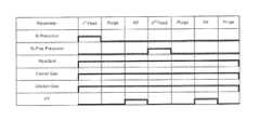
- FIG. 1shows a schematic process sequence of PEALD in one cycle according to a comparative example (the size of each column does not represent duration of each process).
- FIG. 2shows a schematic process sequence of PEALD in one cycle according to an embodiment of the present invention wherein a step illustrated in a column represents an ON state whereas no step illustrated in a column represents an OFF state, and the width of each column does not represent duration of each process.
- FIG. 3shows a schematic process sequence of PEALD in one cycle according to another embodiment of the present invention wherein a step illustrated in a column represents an ON state whereas no step illustrated in a column represents an OFF state, and the width of each column does not represent duration of each process.
- FIG. 4shows a schematic process sequence of PEALD in one cycle according to still another embodiment of the present invention wherein a step illustrated in a column represents an ON state whereas no step illustrated in a column represents an OFF state, and the width of each column does not represent duration of each process.
- FIG. 5shows a schematic process sequence of PEALD in one cycle according to yet another embodiment of the present invention wherein a step illustrated in a column represents an ON state whereas no step illustrated in a column represents an OFF state, and the width of each column does not represent duration of each process.
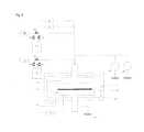
- FIG. 6is a schematic representation of a PEALD apparatus for depositing a dielectric layer usable for an embodiment of the present invention.
- gasmay include vaporized solid and/or liquid and may be constituted by a single gas or a mixture of gases.
- an article “a” or “an”refers to a species or a genus including multiple species.
- a process gas introduced to a reaction chamber through a showerheadmay be comprised of, consist essentially of, or consist of a first precursor containing silicon or metal, a second precursor containing no silicon or metal, and a reactant gas.
- the term “precursor”refers generally to a compound that participates in the chemical reaction that produces another compound, and particularly to a compound that constitutes a film matrix or a main skeleton of a film
- the term “reactant”refers to a gas that activates a precursor, modifies a precursor, or catalyzes a reaction of a precursor.
- the reactantincludes a gas for oxidizing, nitriding, or carbonizing the precursors when RF power is applied to the reactant gas.
- the first precursor, the second precursor, and the reactant gasmay be different from each other or mutually exclusive in terms of gas types, i.e., there is no overlap of gas types among these categories.
- the precursor and the reactant gascan be introduced separately or simultaneously to a reaction space.
- the precursorcan be introduced with a carrier gas such as a rare gas, and additionally, a dilution gas such as a rare gas can also be introduced to the reaction space.
- a gas other than the process gasi.e., a gas introduced without passing through the showerhead, may be used for, e.g., sealing the reaction space, which includes a seal gas such as a rare gas.
- filmrefers to a layer continuously extending in a direction perpendicular to a thickness direction substantially without pinholes to cover an entire target or concerned surface, or simply a layer covering a target or concerned surface.
- “layer”refers to a structure having a certain thickness formed on a surface or a synonym of film or a non-film structure.
- a film or layermay be constituted by a discrete single film or layer having certain characteristics or multiple films or layers, and a boundary between adjacent films or layers may or may not be clear and may be established based on physical, chemical, and/or any other characteristics, formation processes or sequence, and/or functions or purposes of the adjacent films or layers.
- any two numbers of a variablecan constitute a workable range of the variable as the workable range can be determined based on routine work, and any ranges indicated may include or exclude the endpoints.
- any values of variables indicatedmay refer to precise values or approximate values and include equivalents, and may refer to average, median, representative, majority, etc. in some embodiments.
- any element used in an embodimentcan be replaced with any elements equivalent thereto, including those explicitly, necessarily, or inherently disclosed herein, for the intended purposes. Further, the present invention can equally be applied to apparatuses and methods.
- An embodimentprovides a method for forming a film on a patterned surface of a substrate by atomic layer deposition (ALD) processing wherein the surface is patterned with a recess having side walls and a bottom.
- the methodcomprises: (i) adsorbing a non-excited gas of a first precursor onto a patterned surface of a substrate in a reaction space, said first precursor containing silicon or metal in its molecule; (ii) adsorbing a non-excited gas of a second precursor onto the first-precursor-adsorbed surface of the substrate in the reaction space, said second precursor containing no silicon or metal in its molecule; (iii) exposing the second-precursor-adsorbed surface of the substrate to an excited gas of a reactant in the reaction space to oxidize, nitride, or carbonize the precursors adsorbed on the surface of the substrate, said reactant having a smaller molecular size than the second precursor and being reactive to both the first and second precursor
- the non-metal element in the second precursorincludes a metalloid such as boron.
- the second precursorhas a higher molecular size than the reactant and is typically in liquid form at room temperature, which requires vaporization for feeding it to the reaction space using a carrier gas.
- the reactanthas a smaller molecular size than the precursor and is typically in gaseous form.
- the first precursoris also typically in liquid form at room temperature, which requires vaporization for feeding it to the reaction space using a carrier gas.
- the second precursoris at least one compound selected from the group consisting of C x H y O z , C x O y , and N x C y O z (x, y, and z are integers), and the reactant is at least one gas selected from the group consisting of O 2 , O 3 , CO 2 , H 2 O, and N 2 O, whereby the excited reactant oxidizes the precursors adsorbed on the surface of the substrate.
- the second reactantmay be an ether compound such as diethylether and dimethylether.
- the second precursoris at least one compound selected from the group consisting of C x N y H z and N x H y (x, y, and z are integers), and the reactant is at least one gas selected from the group consisting of N 2 , N 2 and H 2 , NH 3 , N x H y , and N x H y C z (x, y, and z are integers), whereby the excited reactant nitrides the precursors adsorbed on the surface of the substrate.
- the second reactantmay be an amine compound such as diethylamine and dimethylamine.
- the second precursoris at least one compound selected from the group consisting of C x H y and C x N y H z (x, y, and z are integers), and the reactant is at least one gas selected from the group consisting of H 2 , N 2 , Ar, and He, whereby the excited reactant carbonizes the precursors adsorbed on the surface of the substrate.
- the first precursoris a halide compound such as dichlorodiethylsilane, dichlorodimethylsilane, dichlorotetramethyldisilazane, dichlorotetraethyldisilazane, dichloroethylsilane, dichloromethylsilane, diiodomethylsilane, diiodoethylsilane.
- the first precursoris an aminosilane compound such as bis(diethylamino)silane and bis(dimethylamino)silane.
- the first precursorcontains a metal selected from the group consisting of Ti, Zr, Al, and Mn, such as tris(dimethylamino)titanium, tris(diethylamino)titanium, dimethylaluminium-isopropoxide, diethylaluminium-isopropoxide, and aluminium diisopropoxide, wherein after adsorbing the first precursor, by adsorbing the second precursor containing no silicon or metal immediately on top of the first-precursor adsorbed surface so as to form M-O—X, M-N—X, or M-C—X (M represents a metal, and X represents an element other than silicon and metal in the precursors), thereby promoting oxidizing, nitriding, or carbonizing the precursors adsorbed on the surface of the substrate when exposing the second-precursor-adsorbed surface of the substrate to an excited gas of a reactant.
- the first and second precursorsare
- the adsorbed weight of the second precursor in step (ii)is equivalent to or higher (e.g., about 1.5 times higher, but typically no more than 10 times, 50 times, or 100 times higher) than the adsorbed weight of the first precursor in step (i), whereby refractive index of a resultant film can be increased.
- the reactantis excited by heat and/or a plasma in step (iii). In some embodiments, the reactant is excited by a plasma generated by applying RF power to the reaction space. In some embodiments, the reactant is continuously supplied to the reaction space throughout steps (i) to (iii), and RF power is applied in step (iii). In the above, “continuously” refers to without breaking a vacuum, without interruption as a timeline, without changing treatment conditions, or immediately thereafter. In some embodiments, the method further comprises applying RF power to the reaction space between steps (i) and (ii). In some embodiments, the reactant is supplied only during step (iii), and RF power is applied in step (iii). In some embodiments, the method further comprises applying RF power to the reaction space between steps (i) and (ii).
- a rare gasis continuously supplied to the reaction space throughout steps (i) to (iii).
- the methodfurther comprises purging the reaction space between steps (i) and (ii), between steps (ii) and (iii), and between steps (iii) and (i).
- the methodfurther comprises, after step (iv), (v) exposing the film on the substrate to a plasma of an inert gas, a hydrogen-containing gas, ammonium-containing gas, and/or oxidizing gas.
- a conformality of the film formed in the recessis 95% or higher.
- FIG. 6is a schematic view of an apparatus combining a plasma-enhanced ALD reactor and flow control valves, desirably in conjunction with controls programmed to conduct the sequences described below, which can be used in an embodiment of the present invention.
- a first precursoris provided to the showerhead 44 through a gas flow controller 63 and pulse flow control valves 71 - 73 .
- the precursoris stored as a liquid in a bottle 74 equipped with a heater.
- a rare gas as a carrier gascan continuously flow into the reaction chamber 43 either (a) through the valve 71 when the valves 72 and 73 are closed, or (b) through the valve 72 , the bottle 74 , and the valve 73 when the valve 71 is closed.
- the rare gascarries the precursor and flows into the reaction chamber 43 together with the precursor.
- the rare gas aloneflows into the reaction chamber 43 without the precursor.
- a second precursor stored in a bottle 78can be provided to the showerhead 44 in the same manner as the first precursor using a gas flow controller 65 and pulse flow control valves 75 - 77 .
- a gas flow controller 65 and pulse flow control valves 75 - 77When the precursor has a low vapor pressure, by heating the gas lines of the FPS and/or the bottle with a heater (not shown), the vapor pressure of the precursor can be increased, thereby increasing the supply amount to the reaction space.
- an automatic pressure regulatorAPR can be used for feeding the precursor gas wherein a carrier gas flows only together with a precursor.
- a reactant gascan be provided to the showerhead 44 through a gas flow controller 61 , and a dilution gas can be provided to the showerhead 44 through a gas flow controller 62 .
- an exhaust pipe 46is provided, through which gas in the interior 51 of the reaction chamber 43 is exhausted.
- the reaction chamberis provided with a seal gas flow controller 64 to introduce seal gas into the interior 51 of the reaction chamber 43 (a separation plate for separating a reaction zone and a transfer zone in the interior of the reaction chamber is omitted from this figure).
- the apparatusincludes one or more controller(s) (not shown) programmed or otherwise configured to cause the deposition and reactor cleaning processes described elsewhere herein to be conducted.
- the controller(s)are communicated with the various power sources, heating systems, pumps, robotics and gas flow controllers or valves of the reactor, as will be appreciated by the skilled artisan.
- FIG. 1shows a schematic process sequence of PEALD in one cycle according to a comparative example wherein a step illustrated in a column represents an ON state whereas no step illustrated in a column represents an OFF state, and the width of each column does not represent duration of each process.
- FIGS. 2 to 5show schematic process sequences of PEALD in one cycle according to embodiments of the present invention wherein a step illustrated in a column represents an ON state whereas no step illustrated in a column represents an OFF state, and the width of each column does not represent duration of each process.
- no second precursoris used, and a reactant, carrier gas, and dilution gas continuously flow.
- These gasesfunction as a purge gas before and after a first precursor is introduced in each cycle. That is, after adsorbing the first precursor on a substrate, non-adsorbed components are removed from the surface of the substrate using the purge gas, and then RF power is applied to the reaction space so that the first-precursor adsorbed surface is exposed to a plasma of the reactant, thereby fixing a monolayer or sub-layer (or atomic layer) which will constitute a film on the substrate. Thereafter, non-reacted components are removed from the monolayer of the substrate using the purge gas. The above one cycle is repeated to form a film on the substrate.
- FIG. 2the process sequence is similar to that illustrated in FIG. 1 , except that a second precursor which contains no silicon or metal in its molecule is introduced after a first precursor which contains silicon or metal in its molecule. Purging is conducted after adsorbing the first precursor but before adsorbing the second precursor, and after adsorbing the second precursor but before applying RF power, and after applying RF power but before adsorbing the first precursor.
- Si—O—X, Si—N—X, or Si—C—X (X is an element other than silicon or metal) bondsare formed after adsorbing the Si/metal-free second precursor on top of the Si/metal-containing first precursor adsorbed on the substrate surface, prior to activation of the adsorbed precursors by an excited reactant, so that activation of the adsorbed precursors can significantly be promoted, and densification can be performed.
- a combination of a Si-containing precursor and a Si-free amine-containing precursor which are alternately adsorbedcan improve nitridization of a side film.
- Alternate adsorption of a Si-containing precursor and a Si-free amine-containing precursorcan also increase reflective index (RI) by about 0.05 to 0.1, as compared with the use of a Si-containing precursor without a Si-free amine-containing precursor.
- RIreflective index
- the process sequenceis similar to that illustrated in FIG. 2 , except that RF power is applied also before adsorbing the second precursor.
- the adsorbed first precursoris activated by an excited reactant before adsorbing the second precursor, and then, the adsorbed second precursor is activated by an excited reactant.
- nitridization/oxidization/carbonization of the precursorsis performed after alternately adsorbing the precursors
- RF poweris applied after adsorbing the first precursor to conduct nitridization/oxidization/carbonization of the first precursor so that the second precursor can more easily be adsorbed and also, improvement of film quality of a side wall film is expected.
- the same combinations of the precursors and the reactant gascan be employed in the sequences illustrated in FIGS. 2 and 3 .
- no purgeis conducted after applying RF power before supplying the second precursor, so that interaction between the first and second precursors can be maintained while densifying each monolayer.
- the reactant gasis supplied continuously to the reaction space. This is because the reactant and the precursors do not cause reaction merely by mixing them together in the reaction space.
- a precursor other than halide having two or more halogen groups, and a reactant other than O 2 or N—H gas such as NH 3can be supplied in accordance with the sequence illustrated in FIG. 2 or 3 .
- the process sequenceis similar to that illustrated in FIG. 2 , except that the reactant is not continuously introduced to the reaction space, but is introduced in a pulse beginning after introducing the Si-free precursor and purging the reaction space but before applying RF power to the reaction space, and ending when RF power application ends.
- This sequenceis effective when the precursors and the reactant are reactive to each other without excitation.
- a precursor which is a halide and a reactant which is oxygen or ammoniummay be reactive to each other.
- a pulse of the Si precursorBy separating a pulse of the Si precursor, a pulse of the Si-free precursor, and a pulse of the reactant, generation of particles can be suppressed, and safety may be increased (continuous supply of the flammable reactant may require more careful processes). However, pulsing the reactant may decrease productivity or throughput.
- the process sequenceis similar to that illustrated in FIG. 3 , except that the reactant is not continuously introduced to the reaction space, but is introduced in a pulse beginning after introducing the Si-free precursor and purging the reaction space but before applying RF power to the reaction space, and ending when RF power application ends.
- This sequenceis effective when the precursors and the reactant are reactive to each other without excitation.
- a precursor which is a halide and a reactant which is oxygen or ammoniummay be reactive to each other.
- generation of particlescan be suppressed, and safety may be increased (continuous supply of the flammable reactant may require more careful processes).
- pulsing the reactantmay decrease productivity or throughput.
- the sequences illustrated in FIGS. 4 and 5can be modified accordingly, wherein the reactant gas excited by heat or remote plasma is introduced in a pulse as illustrated in FIGS. 4 and 5 without application of RF power.
- more than one reactant gascan be used in sequence.
- a second reactantcan be introduced in a pulse after the pulse of the first reactant gas illustrated in FIG. 4 in a manner substantially similar to that for the first reactant gas.
- the first reactant gasis ammonia
- the second reactant gasis hydrogen, whereby the refractive index of a resultant film may increase, and wet etch rate thereof may decrease.
- no purge timeis set after each pulse of gas.
- a conformal dielectric filmcan be formed by PEALD under conditions shown in Table 1 below, although the conditions may vary depending on the type of film, the type of precursor, the type of reactant, etc. Since ALD is a self-limiting adsorption reaction process, the amount of deposited precursor molecules is determined by the number of reactive surface sites and is independent of the precursor exposure after saturation, and a supply of the precursor is such that the reactive surface sites are saturated thereby per cycle.
- first precursor0.0001 to 0.01 g/cycle 0.0005 g/cycle
- second precursor0.0005 to 0.01 g/cycle 0.003 g/cycle
- Carrier gas flowfor each first and 1000 sccm to 3000 2000 sccm second precursors (continuous) sccm
- Reactant gas flowcontinuously 200 sccm to 5000 2000 sccm sccm
- Dilution gas flowcontinuously 200 sccm to 5000 2000 sccm sccm
- Substrate temperature25° C. to 650° C. 300° C.
- Step First percursor supply time 0.05 sec. to 4 sec. 0.2 sec.(i) Purge time after precursor 0.2 sec. to 3 sec. 0.3 sec. pulse Step Second precursor supply time 0.05 sec.to 4 sec. 0.2 sec. (ii) Purge time after precursor 0.2 sec. to 3 sec. 0.3 sec. pulse Step RF plasma exciting time 0.05 sec. to 5 sec. 0.2 sec. (iii) Purge time after RF 0.05 sec. to 1 sec. 0.1 sec. application Number of cycles 10-200 50
- the thickness of the oxide film by PEALDis in a range of about 1 nm to about 350 nm (a desired film thickness can be selected as deemed appropriate according to the application and purpose of film, etc.).
- a rare gassuch as Ar, He, Ne, Kr, and Xe can be used, singly or in any combination of two or more.
- a plasma of a rare gas, hydrogen-containing gas, ammonia-containing gas, and/or oxidization gasis applied to the film as a post-film formation process.
- the post-film formation processcan be conducted continuously in the same reaction chamber upon the film formation process.
- the post-film formation processcan be conducted under conditions as shown in Table 2 below (as for a 300-mm substrate).
- a dielectric filmwas deposited on a bare silicon substrate ( ⁇ 300 mm) by PEALD under common conditions shown in Table 2 below using the PEALD apparatus illustrated in FIG. 6 .
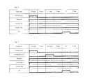
- the specific conditions including the process sequence (SQ)are shown in Table 3.
- the flow rate of the precursor(g/cycle) was calculated based on the vapor pressure of the precursor and the temperature of the precursor in use.
- the SQ numbercorresponds to the figure number.
- the substratehad a flat surface and trenches having an opening width of about 40 nm and an aspect ratio of 1:7.5.
- the thickness of filmwas 350 nm for evaluating film properties.
- the filmwas analyzed in terms of growth rate per cycle (GPC) (nm/cycle), refractive index (RI) at 635 nm, side step coverage (ratio in percentage of thickness of film on sidewall to thickness of film on top surface), bottom step coverage (ratio in percentage of thickness of film on bottom surface to thickness of film on top surface), ratio of wet etch rate (WERR) of the film on flat surface in DHF (100:1) to that of thermal oxide film on flat surface, and ratio of wet etch rate (WERR) of the film on sidewall in DHF (100:1) to that of the film on top surface. Results are shown in Table 4 below.
- the step coverage at the side and the bottomwas high (at least 95%), and the wet etch rate of the film on a flat surface was significantly lower than that of thermal oxide film, and the wet etch rate of the film on the sidewall was equal to or substantially equal to that of the film on the top surface.
- the refractive index of the film in Examples 1, 2, 7, and 8was significantly higher than that in Example C1 and C2. That is, by using the second precursor, surprisingly uniform and conformal films with good film quality can be formed.
- Example 2when RF power was applied after each pulse of the first and second precursors in Example 2, slight improvements on growth rate, refractive index, and side step coverage were observed as compared with those in Example 1. Additionally, when the second precursor was supplied in amounts 6 times higher than the first precursor in Example 8, slight improvements on growth rate, refractive index, and the step coverage at the bottom were observed as compared with those in Example 7 (wherein the second precursor was supplied in amounts 4 times higher than the first precursor).
- Example 11When using an aminosilane precursor as a first precursor without a second precursor in Example C3 to form an oxide film, although the step coverage at the side and the bottom were relatively high, the wet etch rate of the film on the sidewall was significantly higher than that of the film on the top surface. In contrast, when using an aminosilane precursor as a first precursor with an ether compound as a second precursor in Example 11 to form an oxide film, the wet etch rate of the film on the sidewall was equal to that of the film on the top surface, indicating that film densification on the sidewall was more progressed than at the bottom. Further, the wet etch rate in Example 11 was lower than that in Example C3, and the growth rate in Example 11 was also higher than that in Example C3.
- Example C4When using a metal oxide precursor as a first precursor without a second precursor in Example C4 to form an oxide film, although the step coverage at the side and the bottom was relatively high, the wet etch rate of the film on the sidewall was significantly higher than that of the film on the top surface. In contrast, when using a metal oxide precursor as a first precursor with an ether compound as a second precursor in Example 12 to form an oxide film, the wet etch rate of the film on the sidewall was equal to that of the film on the top surface. Further, the wet etch rate in Example 12 was lower than that in Example C4, and the growth rate in Example 12 was also higher than that in Example C4.
- Example 9When using dichloroethylsilane as a first precursor in Example 9 in place of dichlorodiethylsilane in Example 1, the wet etch rate of the film on a flat surface was higher than that in Example 1, and the wet etch rate of the film on the sidewall was higher than that of the film on the top surface. Additionally, when the second precursor was supplied in amounts 1.5 times higher than the first precursor in Example 10, slight improvements on growth rate, refractive index, and the wet etch rate step coverage at the sidewall were observed as compared with those in Example 9 (wherein the second precursor was supplied in amounts equal to the first precursor).
- Example 1when RF power was applied after each pulse of the first and second precursors in Examples 4 and 6, slight improvements on film densification on the sidewall were observed as compared with densification in Examples 3 and 5, respectively. Further, in comparing Examples 1, 3, and 9, the use of the “diethyl” first precursor in Example 1 exhibited better and more even film densification than the use of the “dimethyl” first precursor in Example 3, or the use of the “ethyl” first precursor in Example 9.
- Table 5 belowshows the results of composition analysis of the films by Rutherford backscattering/hydrogen forward scattering (RBS/HFS).
Landscapes
- Chemical & Material Sciences (AREA)
- Engineering & Computer Science (AREA)
- Metallurgy (AREA)
- General Chemical & Material Sciences (AREA)
- Chemical Kinetics & Catalysis (AREA)
- Materials Engineering (AREA)
- Mechanical Engineering (AREA)
- Organic Chemistry (AREA)
- Inorganic Chemistry (AREA)
- Plasma & Fusion (AREA)
- Electromagnetism (AREA)
- Physics & Mathematics (AREA)
- Chemical Vapour Deposition (AREA)
- Formation Of Insulating Films (AREA)
Abstract
Description
Field of the Invention
The present invention generally relates to a method for forming a conformal nitrided, oxidized, or carbonized dielectric film by atomic layer deposition (ALD).
Description of the Related Art
As a method for depositing an insulation film on a substrate by ALD, substitution reaction by thermal reaction, plasma reaction, or remote plasma reaction is generally utilized. However, depending on the type of deposited film and the type of starting material, a problem may occur in that film quality is degraded because reaction in grooves of a recess pattern becomes insufficient, or secondary reaction such as physical adsorption interferes with reaction, or the like. In order to resolve the above problems, raising a process temperature and conducting post-process treatment are considered to be the most effective and have been widely conducted.
The problems of the above solutions are that when a limitation is imposed on temperature, raising the process temperature may not be acceptable, and when the post-process treatment is conducted, the total duration is prolonged, and modification reaction occurs only in a surface of a film. For example, for improving film quality in grooves by controlling temperature, the process temperature often exceeds 400° C., and also the post-process temperature often exceeds 400° C., and therefore, if the process requires a process temperature lower than 400° C., it is difficult to apply the process temperature control and the post-process treatment. In view of the above, in order to improve film quality in grooves by modifying reaction between a process material and a reactant, evaluating new materials, studying the dependency of reactant gas type, and researching comprehensive reactant reactions have been conducted. However, these attempts have not resolved the problems and have not fundamentally improved film quality in grooves.
Any discussion of problems and solutions involved in the related art has been included in this disclosure solely for the purposes of providing a context for the present invention, and should not be taken as an admission that any or all of the discussion were known at the time the invention was made.
The present inventors conducted research on the process sequence dependency of the quality of film in grooves and discovered that by reacting a precursor multiple times in one cycle using a reactant, and by changing reactants and reacting a precursor multiple times in one cycle, the film quality in grooves can be improved. For example, wet etch rate of the film in grooves was improved from 5 times that of the film on a top surface to 1.2 times that of the film on a top surface. However, growth rate of the film per cycle of ALD became significantly low, which became a problem. In view of the above, in an embodiment of the present invention, a method for forming a film on a patterned surface of a substrate by atomic layer deposition (ALD) processing comprises: (i) adsorbing onto the patterned surface a non-excited gas of a first precursor containing silicon or metal in its molecule; and then (ii) adsorbing onto the first-precursor-adsorbed surface a non-excited gas of a second precursor containing no silicon or metal in its molecule, thereby rendering the substrate surface more easily oxidized, nitrided, or carbonized. In the next step, the second-precursor-adsorbed surface is exposed to an excited gas of a reactant in the reaction space to oxidize, nitride, or carbonize the precursors adsorbed on the surface. The above cycle is repeated to form a film on the patterned surface of the substrate. Accordingly, the quality, uniformity, and conformality of film in grooves can be improved while maintaining appropriate growth rate.
For purposes of summarizing aspects of the invention and the advantages achieved over the related art, certain objects and advantages of the invention are described in this disclosure. Of course, it is to be understood that not necessarily all such objects or advantages may be achieved in accordance with any particular embodiment of the invention. Thus, for example, those skilled in the art will recognize that the invention may be embodied or carried out in a manner that achieves or optimizes one advantage or group of advantages as taught herein without necessarily achieving other objects or advantages as may be taught or suggested herein.
Further aspects, features and advantages of this invention will become apparent from the detailed description which follows.
These and other features of this invention will now be described with reference to the drawings of preferred embodiments which are intended to illustrate and not to limit the invention. The drawings are greatly simplified for illustrative purposes and are not necessarily to scale.
In this disclosure, “gas” may include vaporized solid and/or liquid and may be constituted by a single gas or a mixture of gases. Likewise, an article “a” or “an” refers to a species or a genus including multiple species. In this disclosure, a process gas introduced to a reaction chamber through a showerhead may be comprised of, consist essentially of, or consist of a first precursor containing silicon or metal, a second precursor containing no silicon or metal, and a reactant gas. In some embodiments, the term “precursor” refers generally to a compound that participates in the chemical reaction that produces another compound, and particularly to a compound that constitutes a film matrix or a main skeleton of a film, whereas the term “reactant” refers to a gas that activates a precursor, modifies a precursor, or catalyzes a reaction of a precursor. The reactant includes a gas for oxidizing, nitriding, or carbonizing the precursors when RF power is applied to the reactant gas. The first precursor, the second precursor, and the reactant gas may be different from each other or mutually exclusive in terms of gas types, i.e., there is no overlap of gas types among these categories. The precursor and the reactant gas can be introduced separately or simultaneously to a reaction space. The precursor can be introduced with a carrier gas such as a rare gas, and additionally, a dilution gas such as a rare gas can also be introduced to the reaction space. A gas other than the process gas, i.e., a gas introduced without passing through the showerhead, may be used for, e.g., sealing the reaction space, which includes a seal gas such as a rare gas. In some embodiments, “film” refers to a layer continuously extending in a direction perpendicular to a thickness direction substantially without pinholes to cover an entire target or concerned surface, or simply a layer covering a target or concerned surface. In some embodiments, “layer” refers to a structure having a certain thickness formed on a surface or a synonym of film or a non-film structure. A film or layer may be constituted by a discrete single film or layer having certain characteristics or multiple films or layers, and a boundary between adjacent films or layers may or may not be clear and may be established based on physical, chemical, and/or any other characteristics, formation processes or sequence, and/or functions or purposes of the adjacent films or layers. Further, in this disclosure, any two numbers of a variable can constitute a workable range of the variable as the workable range can be determined based on routine work, and any ranges indicated may include or exclude the endpoints. Additionally, any values of variables indicated (regardless of whether they are indicated with “about” or not) may refer to precise values or approximate values and include equivalents, and may refer to average, median, representative, majority, etc. in some embodiments.
In this disclosure, any defined meanings do not necessarily exclude ordinary and customary meanings in some embodiments.
In the present disclosure where conditions and/or structures are not specified, the skilled artisan in the art can readily provide such conditions and/or structures, in view of the present disclosure, as a matter of routine experimentation.
In all of the disclosed embodiments, any element used in an embodiment can be replaced with any elements equivalent thereto, including those explicitly, necessarily, or inherently disclosed herein, for the intended purposes. Further, the present invention can equally be applied to apparatuses and methods.
An embodiment provides a method for forming a film on a patterned surface of a substrate by atomic layer deposition (ALD) processing wherein the surface is patterned with a recess having side walls and a bottom. The method comprises: (i) adsorbing a non-excited gas of a first precursor onto a patterned surface of a substrate in a reaction space, said first precursor containing silicon or metal in its molecule; (ii) adsorbing a non-excited gas of a second precursor onto the first-precursor-adsorbed surface of the substrate in the reaction space, said second precursor containing no silicon or metal in its molecule; (iii) exposing the second-precursor-adsorbed surface of the substrate to an excited gas of a reactant in the reaction space to oxidize, nitride, or carbonize the precursors adsorbed on the surface of the substrate, said reactant having a smaller molecular size than the second precursor and being reactive to both the first and second precursors in step (iii); and (iv) repeating steps (i) to (iii) to form a film on the patterned surface of the substrate. After adsorbing the first precursor containing silicon or metal on the substrate, by adsorbing the second precursor containing no silicon or metal immediately on top of the first-precursor adsorbed surface so as to form Si—O—X, Si—N—X, or Si—C—X (X represents an element other than silicon and metal in the precursors), thereby promoting oxidizing, nitriding, or carbonizing the precursors adsorbed on the surface of the substrate when exposing the second-precursor-adsorbed surface of the substrate to an excited gas of a reactant. In some embodiments, the non-metal element in the second precursor includes a metalloid such as boron. The second precursor has a higher molecular size than the reactant and is typically in liquid form at room temperature, which requires vaporization for feeding it to the reaction space using a carrier gas. In contrast, the reactant has a smaller molecular size than the precursor and is typically in gaseous form. The first precursor is also typically in liquid form at room temperature, which requires vaporization for feeding it to the reaction space using a carrier gas.
In some embodiments, the second precursor is at least one compound selected from the group consisting of CxHyOz, CxOy, and NxCyOz(x, y, and z are integers), and the reactant is at least one gas selected from the group consisting of O2, O3, CO2, H2O, and N2O, whereby the excited reactant oxidizes the precursors adsorbed on the surface of the substrate. For example, the second reactant may be an ether compound such as diethylether and dimethylether.
In some embodiments, the second precursor is at least one compound selected from the group consisting of CxNyHzand NxHy(x, y, and z are integers), and the reactant is at least one gas selected from the group consisting of N2, N2and H2, NH3, NxHy, and NxHyCz(x, y, and z are integers), whereby the excited reactant nitrides the precursors adsorbed on the surface of the substrate. For example, the second reactant may be an amine compound such as diethylamine and dimethylamine.
In some embodiments, the second precursor is at least one compound selected from the group consisting of CxHyand CxNyHz(x, y, and z are integers), and the reactant is at least one gas selected from the group consisting of H2, N2, Ar, and He, whereby the excited reactant carbonizes the precursors adsorbed on the surface of the substrate.
In some embodiments, the first precursor is a halide compound such as dichlorodiethylsilane, dichlorodimethylsilane, dichlorotetramethyldisilazane, dichlorotetraethyldisilazane, dichloroethylsilane, dichloromethylsilane, diiodomethylsilane, diiodoethylsilane. In some embodiments, the first precursor is an aminosilane compound such as bis(diethylamino)silane and bis(dimethylamino)silane. In some embodiments, the first precursor contains a metal selected from the group consisting of Ti, Zr, Al, and Mn, such as tris(dimethylamino)titanium, tris(diethylamino)titanium, dimethylaluminium-isopropoxide, diethylaluminium-isopropoxide, and aluminium diisopropoxide, wherein after adsorbing the first precursor, by adsorbing the second precursor containing no silicon or metal immediately on top of the first-precursor adsorbed surface so as to form M-O—X, M-N—X, or M-C—X (M represents a metal, and X represents an element other than silicon and metal in the precursors), thereby promoting oxidizing, nitriding, or carbonizing the precursors adsorbed on the surface of the substrate when exposing the second-precursor-adsorbed surface of the substrate to an excited gas of a reactant. In some embodiments, the first and second precursors are organic compounds.
In some embodiments, the adsorbed weight of the second precursor in step (ii) is equivalent to or higher (e.g., about 1.5 times higher, but typically no more than 10 times, 50 times, or 100 times higher) than the adsorbed weight of the first precursor in step (i), whereby refractive index of a resultant film can be increased.
In some embodiments, the reactant is excited by heat and/or a plasma in step (iii). In some embodiments, the reactant is excited by a plasma generated by applying RF power to the reaction space. In some embodiments, the reactant is continuously supplied to the reaction space throughout steps (i) to (iii), and RF power is applied in step (iii). In the above, “continuously” refers to without breaking a vacuum, without interruption as a timeline, without changing treatment conditions, or immediately thereafter. In some embodiments, the method further comprises applying RF power to the reaction space between steps (i) and (ii). In some embodiments, the reactant is supplied only during step (iii), and RF power is applied in step (iii). In some embodiments, the method further comprises applying RF power to the reaction space between steps (i) and (ii).
In some embodiments, a rare gas is continuously supplied to the reaction space throughout steps (i) to (iii). In some embodiments, the method further comprises purging the reaction space between steps (i) and (ii), between steps (ii) and (iii), and between steps (iii) and (i).
In some embodiments, the method further comprises, after step (iv), (v) exposing the film on the substrate to a plasma of an inert gas, a hydrogen-containing gas, ammonium-containing gas, and/or oxidizing gas.
In some embodiments, a conformality of the film formed in the recess is 95% or higher.
Steps (i) to (iv) and optionally (v) can be performed using any suitable apparatus. For example,FIG. 6 is a schematic view of an apparatus combining a plasma-enhanced ALD reactor and flow control valves, desirably in conjunction with controls programmed to conduct the sequences described below, which can be used in an embodiment of the present invention. In this figure, by providing a pair of electrically conductive flat-plate electrodes44,42 in parallel and facing each other in the interior51 of a reaction chamber43, applying HRF power (13.56 MHz or 27 MHz)45 (and LRF power of 5 MHz or less (400 kHz-500 kHz)90 as necessary) to one side, and electrically grounding52 the other side, a plasma is excited between the electrodes. A temperature regulator is provided in a lower stage42 (the lower electrode), and a temperature of a substrate41 placed thereon is kept constant at a given temperature. The upper electrode44 serves as a showerhead as well, and process gas and other gases are introduced into the reaction chamber43. A first precursor is provided to the showerhead44 through a gas flow controller63 and pulse flow control valves71-73. The precursor is stored as a liquid in a bottle74 equipped with a heater. A rare gas as a carrier gas can continuously flow into the reaction chamber43 either (a) through the valve71 when the valves72 and73 are closed, or (b) through the valve72, the bottle74, and the valve73 when the valve71 is closed. In (b), the rare gas carries the precursor and flows into the reaction chamber43 together with the precursor. In (a), the rare gas alone flows into the reaction chamber43 without the precursor. By the above mechanism with operation of the valves, the rare gas can be fed continuously while pulsing the feed of the precursor. This system is referred to as a flow pass system (FPS). A second precursor stored in a bottle78 can be provided to the showerhead44 in the same manner as the first precursor using a gas flow controller65 and pulse flow control valves75-77. When the precursor has a low vapor pressure, by heating the gas lines of the FPS and/or the bottle with a heater (not shown), the vapor pressure of the precursor can be increased, thereby increasing the supply amount to the reaction space. In some embodiments, in place of the FPS, an automatic pressure regulator (APR) can be used for feeding the precursor gas wherein a carrier gas flows only together with a precursor. A reactant gas can be provided to the showerhead44 through a gas flow controller61, and a dilution gas can be provided to the showerhead44 through a gas flow controller62. Additionally, in the reaction chamber43, an exhaust pipe46 is provided, through which gas in the interior51 of the reaction chamber43 is exhausted. Additionally, the reaction chamber is provided with a seal gas flow controller64 to introduce seal gas into the interior51 of the reaction chamber43 (a separation plate for separating a reaction zone and a transfer zone in the interior of the reaction chamber is omitted from this figure).
A skilled artisan will appreciate that the apparatus includes one or more controller(s) (not shown) programmed or otherwise configured to cause the deposition and reactor cleaning processes described elsewhere herein to be conducted. The controller(s) are communicated with the various power sources, heating systems, pumps, robotics and gas flow controllers or valves of the reactor, as will be appreciated by the skilled artisan.
Steps (i) to (iv) can be performed in various sequences as illustrated inFIGS. 2 to 5 , for example.FIG. 1 shows a schematic process sequence of PEALD in one cycle according to a comparative example wherein a step illustrated in a column represents an ON state whereas no step illustrated in a column represents an OFF state, and the width of each column does not represent duration of each process.FIGS. 2 to 5 show schematic process sequences of PEALD in one cycle according to embodiments of the present invention wherein a step illustrated in a column represents an ON state whereas no step illustrated in a column represents an OFF state, and the width of each column does not represent duration of each process.
InFIG. 1 , no second precursor is used, and a reactant, carrier gas, and dilution gas continuously flow. These gases function as a purge gas before and after a first precursor is introduced in each cycle. That is, after adsorbing the first precursor on a substrate, non-adsorbed components are removed from the surface of the substrate using the purge gas, and then RF power is applied to the reaction space so that the first-precursor adsorbed surface is exposed to a plasma of the reactant, thereby fixing a monolayer or sub-layer (or atomic layer) which will constitute a film on the substrate. Thereafter, non-reacted components are removed from the monolayer of the substrate using the purge gas. The above one cycle is repeated to form a film on the substrate.
InFIG. 2 , the process sequence is similar to that illustrated inFIG. 1 , except that a second precursor which contains no silicon or metal in its molecule is introduced after a first precursor which contains silicon or metal in its molecule. Purging is conducted after adsorbing the first precursor but before adsorbing the second precursor, and after adsorbing the second precursor but before applying RF power, and after applying RF power but before adsorbing the first precursor. By the above sequence, Si—O—X, Si—N—X, or Si—C—X (X is an element other than silicon or metal) bonds are formed after adsorbing the Si/metal-free second precursor on top of the Si/metal-containing first precursor adsorbed on the substrate surface, prior to activation of the adsorbed precursors by an excited reactant, so that activation of the adsorbed precursors can significantly be promoted, and densification can be performed. For example, when dichloromethylsilane is used as the first precursor and chemisorbed on a surface of a substrate, and then diethylamine is adsorbed as the second precursor, followed by applying about 100 W of RF power of 13.56 MHz for one second while supplying H2and N2each at about 1 SLM, it has been confirmed that a SiN film having a step coverage of about 90% can be formed on the substrate. It has been confirmed that if diethylamine is not used, a film obtained is a SiN film having a step coverage of about 80% and containing a small amount of carbon. Thus, it has been confirmed that a combination of a Si-containing precursor and a Si-free amine-containing precursor which are alternately adsorbed can improve nitridization of a side film. Alternate adsorption of a Si-containing precursor and a Si-free amine-containing precursor can also increase reflective index (RI) by about 0.05 to 0.1, as compared with the use of a Si-containing precursor without a Si-free amine-containing precursor. By selecting a suitable second precursor and a suitable reactant, not only nitridization, but also oxidization or carbonization of the precursors can be promoted.
InFIG. 3 , the process sequence is similar to that illustrated inFIG. 2 , except that RF power is applied also before adsorbing the second precursor. The adsorbed first precursor is activated by an excited reactant before adsorbing the second precursor, and then, the adsorbed second precursor is activated by an excited reactant. In the sequence illustrated inFIG. 2 , nitridization/oxidization/carbonization of the precursors is performed after alternately adsorbing the precursors, whereas in the sequence illustrated inFIG. 3 , RF power is applied after adsorbing the first precursor to conduct nitridization/oxidization/carbonization of the first precursor so that the second precursor can more easily be adsorbed and also, improvement of film quality of a side wall film is expected. The same combinations of the precursors and the reactant gas can be employed in the sequences illustrated inFIGS. 2 and 3 . In the process sequence illustrated inFIG. 3 , no purge is conducted after applying RF power before supplying the second precursor, so that interaction between the first and second precursors can be maintained while densifying each monolayer. In the sequences illustrated inFIGS. 2 and 3 , the reactant gas is supplied continuously to the reaction space. This is because the reactant and the precursors do not cause reaction merely by mixing them together in the reaction space. For example, a precursor other than halide having two or more halogen groups, and a reactant other than O2or N—H gas such as NH3, can be supplied in accordance with the sequence illustrated inFIG. 2 or 3 .
InFIG. 4 , the process sequence is similar to that illustrated inFIG. 2 , except that the reactant is not continuously introduced to the reaction space, but is introduced in a pulse beginning after introducing the Si-free precursor and purging the reaction space but before applying RF power to the reaction space, and ending when RF power application ends. This sequence is effective when the precursors and the reactant are reactive to each other without excitation. For example, a precursor which is a halide and a reactant which is oxygen or ammonium (e.g., for a SiN film) may be reactive to each other. By separating a pulse of the Si precursor, a pulse of the Si-free precursor, and a pulse of the reactant, generation of particles can be suppressed, and safety may be increased (continuous supply of the flammable reactant may require more careful processes). However, pulsing the reactant may decrease productivity or throughput.
InFIG. 5 , the process sequence is similar to that illustrated inFIG. 3 , except that the reactant is not continuously introduced to the reaction space, but is introduced in a pulse beginning after introducing the Si-free precursor and purging the reaction space but before applying RF power to the reaction space, and ending when RF power application ends. This sequence is effective when the precursors and the reactant are reactive to each other without excitation. For example, a precursor which is a halide and a reactant which is oxygen or ammonium may be reactive to each other. By separating a pulse of the Si precursor, a pulse of the Si-free precursor, and a pulse of the reactant, generation of particles can be suppressed, and safety may be increased (continuous supply of the flammable reactant may require more careful processes). However, pulsing the reactant may decrease productivity or throughput.
When the reactant gas is excited by energy other than in-situ plasma, such as heat or remote plasma, the sequences illustrated inFIGS. 4 and 5 can be modified accordingly, wherein the reactant gas excited by heat or remote plasma is introduced in a pulse as illustrated inFIGS. 4 and 5 without application of RF power.
In some embodiments, more than one reactant gas can be used in sequence. For example, a second reactant can be introduced in a pulse after the pulse of the first reactant gas illustrated inFIG. 4 in a manner substantially similar to that for the first reactant gas. For example, the first reactant gas is ammonia, and the second reactant gas is hydrogen, whereby the refractive index of a resultant film may increase, and wet etch rate thereof may decrease. In some embodiments, no purge time is set after each pulse of gas.
In some embodiments, a conformal dielectric film can be formed by PEALD under conditions shown in Table 1 below, although the conditions may vary depending on the type of film, the type of precursor, the type of reactant, etc. Since ALD is a self-limiting adsorption reaction process, the amount of deposited precursor molecules is determined by the number of reactive surface sites and is independent of the precursor exposure after saturation, and a supply of the precursor is such that the reactive surface sites are saturated thereby per cycle.
| TABLE 1 |
| (the numbers are approximate) |
| Typically | ||
| Preferably | (±50%) | |
| Quantity of first precursor | 0.0001 to 0.01 g/cycle | 0.0005 |
| g/cycle | ||
| Quantity of second precursor | 0.0005 to 0.01 g/cycle | 0.003 |
| g/cycle | ||
| Carrier gas flow for each first and | 1000 sccm to 3000 | 2000 sccm |
| second precursors (continuous) | sccm | |
| Reactant gas flow (continuous) | 200 sccm to 5000 | 2000 sccm |
| sccm | ||
| Dilution gas flow (continuous) | 200 sccm to 5000 | 2000 sccm |
| sccm | ||
| Substrate temperature | 25° C. to 650° C. | 300° C. |
| Pressure | 133 Pa to 800 Pa | 400 Pa |
| RF power (13.56 MHz) | 10 W to 1000 W | 200 W |
| (300-mm tool) | ||
| Step | First percursor supply time | 0.05 sec. to 4 sec. | 0.2 sec. |
| (i) | Purge time after precursor | 0.2 sec. to 3 sec. | 0.3 sec. |
| pulse | |||
| Step | Second precursor supply time | 0.05 sec.to 4 sec. | 0.2 sec. |
| (ii) | Purge time after precursor | 0.2 sec. to 3 sec. | 0.3 sec. |
| pulse | |||
| Step | RF plasma exciting time | 0.05 sec. to 5 sec. | 0.2 sec. |
| (iii) | Purge time after RF | 0.05 sec. to 1 sec. | 0.1 sec. |
| application |
| Number of cycles | 10-200 | 50 |
In the above, by continuously feeding the carrier gas and the dilution gas, no separate purge gas is required, since the continuous feed of these gases functions as a mechanism of purging. The reactant gas can be continuously fed since it is not reactive to the precursor, and thus, the continuous feed of the reactant gas also functions as a mechanism of purging.
In some embodiments, the thickness of the oxide film by PEALD is in a range of about 1 nm to about 350 nm (a desired film thickness can be selected as deemed appropriate according to the application and purpose of film, etc.).
As a carrier gas, seal gas, purge gas, or process-adjustment gas (dilution or auxiliary gas), a rare gas such as Ar, He, Ne, Kr, and Xe can be used, singly or in any combination of two or more.
In some embodiments, after the film formation process, a plasma of a rare gas, hydrogen-containing gas, ammonia-containing gas, and/or oxidization gas is applied to the film as a post-film formation process. The post-film formation process can be conducted continuously in the same reaction chamber upon the film formation process. The post-film formation process can be conducted under conditions as shown in Table 2 below (as for a 300-mm substrate).
| TABLE 2 | |
| Gas | O2, O3, NH3, H2, N2, Ar, and/or He |
| Gas flow | 100 to 8000 sccm (typically 1000 to 4000 sccm) |
| Susceptor Temperature | 50 to 420° C. (typically 200 to 400° C.) |
| RF power | 50 to 1000 W (typically 50 to 400 W) |
| (13.56 MHz) | |
| Pressure | 133 to 1333 Pa (typically 266 to 533 Pa) |
| Duration | 10 to 300 seconds (typically 30 to 60 seconds) |
The embodiments will be explained with respect to preferred embodiments. However, the present invention is not limited to the preferred embodiments
In the following examples where conditions and/or structures are not specified, the skilled artisan in the art can readily provide such conditions and/or structures, in view of the present disclosure, as a matter of routine experimentation.
A dielectric film was deposited on a bare silicon substrate (Φ300 mm) by PEALD under common conditions shown in Table 2 below using the PEALD apparatus illustrated inFIG. 6 . The specific conditions including the process sequence (SQ) are shown in Table 3. The flow rate of the precursor (g/cycle) was calculated based on the vapor pressure of the precursor and the temperature of the precursor in use. The SQ number corresponds to the figure number. The substrate had a flat surface and trenches having an opening width of about 40 nm and an aspect ratio of 1:7.5. The thickness of film was 350 nm for evaluating film properties.
| TABLE 2 | ||
| Carrier gas | Ar; 2 SLM | |
| Dilution gas | 100-2000 sccm | |
| Susceptor Temperature | 300° C. | |
| Distance between electrodes | 13 mm | |
| RF power | 13.56 MHz | |
| TABLE 3 | ||||||||
| SQ | ||||||||
| Flow | Si/metal-free | Flow | Reactant | Pressure | RF | FIG. | ||
| Ex. | Si/metal precursor | (g/Cycle) | precursor | (g/Cycle) | (SLM) | (Pa) | (W) | # |
| C1 | Dichlorodimethylsilane | 0.01 | — | — | NH3 | 400 | 200 | 1 |
| (2) | ||||||||
| C2 | Dichlorotetraethyldisilane | 0.005 | — | — | NH3 | 400 | 200 | 1 |
| (2) | ||||||||
| C3 | Dis(diethylamino)silane | 0.005 | — | — | O2 | 200 | 100 | 1 |
| (0.5) | ||||||||
| C4 | Diethylaluminium- | 0.001 | — | — | O2 | 200 | 50 | 1 |
| isopropoxide | (0.1) | |||||||
| 1 | Dichlorodiethylsilane | 0.01 | Diethylamine | 0.02 | NH3 | 400 | 200 | 2 |
| (2) | ||||||||
| 2 | Dichlorodiethylsilane | 0.01 | Diethylamine | 0.02 | NH3 | 400 | 200 | 3 |
| (2) | ||||||||
| 3 | Dichlorodimethylsilane | 0.007 | Diethylamine | 0.02 | NH3 | 400 | 200 | 2 |
| (2) | ||||||||
| 4 | Dichlorodimethylsilane | 0.007 | Diethylamine | 0.02 | NH3 | 400 | 200 | 3 |
| (2) | ||||||||
| 5 | Dichlorodiethylsilane | 0.01 | Diethylether | 0.01 | O2 | 400 | 200 | 2 |
| (0.1) | ||||||||
| 6 | Dichlorodiethylsilane | 0.01 | Diethylether | 0.01 | O2 | 400 | 200 | 3 |
| (0.1) | ||||||||
| 7 | Dichlorotetraethyldisilane | 0.005 | Diethylamine | 0.02 | NH3 | 400 | 400 | 2 |
| (2) | ||||||||
| 8 | Dichlorotetraethyldisilane | 0.005 | Diethylamine | 0.03 | NH3 | 400 | 400 | 2 |
| (2) | ||||||||
| 9 | Dichloroethylsilane | 0.02 | Diethylamine | 0.02 | NH3 | 400 | 400 | 2 |
| (2) | ||||||||
| 10 | Dichloroethylsilane | 0.02 | Diethylamine | 0.03 | NH3 | 400 | 400 | 2 |
| (2) | ||||||||
| 11 | Dis(diethylamino)silane | 0.005 | Diethylether | 0.05 | O2 | 200 | 100 | 3 |
| (0.1) | ||||||||
| 12 | Diethylaluminium- | 0.001 | Diethylether | 0.05 | O2 | 200 | 50 | 4 |
| isopropoxide | (0.1) | |||||||
The film was analyzed in terms of growth rate per cycle (GPC) (nm/cycle), refractive index (RI) at 635 nm, side step coverage (ratio in percentage of thickness of film on sidewall to thickness of film on top surface), bottom step coverage (ratio in percentage of thickness of film on bottom surface to thickness of film on top surface), ratio of wet etch rate (WERR) of the film on flat surface in DHF (100:1) to that of thermal oxide film on flat surface, and ratio of wet etch rate (WERR) of the film on sidewall in DHF (100:1) to that of the film on top surface. Results are shown in Table 4 below.
| TABLE 4 | ||||||
| 100:1 DHF | 100:1 DHF | |||||
| Step | Step | WERR | WERR | |||
| GPC | coverage | coverage | Relative to | Relative to | ||
| [nm/ | RI@ | (side) | (bottom) | thermal | film on | |
| Ex | cycle] | 633 nm | [%] | [%] | oxide film | pattern top |
| C1 | 0.03 | 1.71 | 80 | 80 | 5 | >10 |
| C2 | 0.03 | 1.71 | 80 | 80 | 5 | >10 |
| C3 | 0.1 | 1.46 | 95 | 95 | 1 | 1.4 |
| C4 | 0.1 | 1.65 | 95 | 95 | 8.5 | 1.5 |
| 1 | 0.04 | 1.84 | 95 | 96 | 0.5 | 1 |
| 2 | 0.06 | 1.85 | 97 | 96 | 0.5 | 1 |
| 3 | 0.05 | 1.82 | 97 | 99 | 0.6 | 1.1 |
| 4 | 0.05 | 1.86 | 97 | 96 | 0.8 | 0.8 |
| 5 | 0.1 | 1.45 | 97 | 98 | 1.1 | 1.2 |
| 6 | 0.1 | 1.47 | 97 | 93 | 1.2 | 0.9 |
| 7 | 0.06 | 1.89 | 98 | 98 | 0.6 | 0.8 |
| 8 | 0.07 | 1.90 | 97 | 99 | 0.6 | 0.8 |
| 9 | 0.05 | 1.84 | 96 | 97 | 0.9 | 1.4 |
| 10 | 0.06 | 1.83 | 99 | 95 | 0.9 | 1.2 |
| 11 | 0.13 | 1.45 | 95 | 95 | 0.7 | 1.0 |
| 12 | 0.13 | 1.67 | 95 | 95 | 2.6 | 0.8 |
As shown in Table 4, when using a silicon-containing halide precursor as a first precursor without a second precursor in Examples C1 and C2 to form a nitride film, the step coverage at the side and the bottom was relatively low (80%), and the wet etch rate of the film on a flat surface was significantly higher than that of thermal oxide film, and the wet etch rate of the film on the sidewall was significantly higher than that of the film on the top surface. In contrast, when using the silicon-containing halide precursor as a first precursor with an amine compound as a second precursor in Examples 1, 2, 7, and 8 to form a nitride film, the step coverage at the side and the bottom was high (at least 95%), and the wet etch rate of the film on a flat surface was significantly lower than that of thermal oxide film, and the wet etch rate of the film on the sidewall was equal to or substantially equal to that of the film on the top surface. Further, the refractive index of the film in Examples 1, 2, 7, and 8 was significantly higher than that in Example C1 and C2. That is, by using the second precursor, surprisingly uniform and conformal films with good film quality can be formed. Further, when RF power was applied after each pulse of the first and second precursors in Example 2, slight improvements on growth rate, refractive index, and side step coverage were observed as compared with those in Example 1. Additionally, when the second precursor was supplied in amounts 6 times higher than the first precursor in Example 8, slight improvements on growth rate, refractive index, and the step coverage at the bottom were observed as compared with those in Example 7 (wherein the second precursor was supplied in amounts 4 times higher than the first precursor).
When using an aminosilane precursor as a first precursor without a second precursor in Example C3 to form an oxide film, although the step coverage at the side and the bottom were relatively high, the wet etch rate of the film on the sidewall was significantly higher than that of the film on the top surface. In contrast, when using an aminosilane precursor as a first precursor with an ether compound as a second precursor in Example 11 to form an oxide film, the wet etch rate of the film on the sidewall was equal to that of the film on the top surface, indicating that film densification on the sidewall was more progressed than at the bottom. Further, the wet etch rate in Example 11 was lower than that in Example C3, and the growth rate in Example 11 was also higher than that in Example C3.
When using a metal oxide precursor as a first precursor without a second precursor in Example C4 to form an oxide film, although the step coverage at the side and the bottom was relatively high, the wet etch rate of the film on the sidewall was significantly higher than that of the film on the top surface. In contrast, when using a metal oxide precursor as a first precursor with an ether compound as a second precursor in Example 12 to form an oxide film, the wet etch rate of the film on the sidewall was equal to that of the film on the top surface. Further, the wet etch rate in Example 12 was lower than that in Example C4, and the growth rate in Example 12 was also higher than that in Example C4.
When using dichlorodimethylsilane as a first precursor in Examples 3 and 4 in place of dichlorodiethylsilane in Examples 1 and 2, the resultant film had uniformity, conformality, and quality equivalent to those in Examples 1 and 2. When using an silicon-containing halide precursor as a first precursor in Examples 5 and 6 in place of the aminosilane precursor in Example 11, the resultant film had uniformity, conformality, and quality nearly equivalent to those in Example 11, except that the wet etch rate in Examples 5 and 6 was higher than that in Example 11.
When using dichloroethylsilane as a first precursor in Example 9 in place of dichlorodiethylsilane in Example 1, the wet etch rate of the film on a flat surface was higher than that in Example 1, and the wet etch rate of the film on the sidewall was higher than that of the film on the top surface. Additionally, when the second precursor was supplied in amounts 1.5 times higher than the first precursor in Example 10, slight improvements on growth rate, refractive index, and the wet etch rate step coverage at the sidewall were observed as compared with those in Example 9 (wherein the second precursor was supplied in amounts equal to the first precursor).
Additionally, when RF power was applied after each pulse of the first and second precursors in Examples 4 and 6, slight improvements on film densification on the sidewall were observed as compared with densification in Examples 3 and 5, respectively. Further, in comparing Examples 1, 3, and 9, the use of the “diethyl” first precursor in Example 1 exhibited better and more even film densification than the use of the “dimethyl” first precursor in Example 3, or the use of the “ethyl” first precursor in Example 9.
Table 5 below shows the results of composition analysis of the films by Rutherford backscattering/hydrogen forward scattering (RBS/HFS).
| TABLE 5 | ||||
| Example | Si (atm %) | N (atm %) | C (atm %) | H (atm %) |
| C1 | 35 | 37 | 3 | 25 |
| 1 | 35 | 49 | N/D | 16 |
| C2 | 35 | 41 | 3 | 21 |
| 7 | 37 | 52 | N/D | 11 |
As shown in Table 5, by using the second precursor which does not contain silicon or metal, nitridization of the films progressed, thereby reducing the carbon content.
It will be understood by those of skill in the art that numerous and various modifications can be made without departing from the spirit of the present invention. Therefore, it should be clearly understood that the forms of the present invention are illustrative only and are not intended to limit the scope of the present invention.
Claims (11)
1. A method for forming a film on a patterned surface of a substrate by atomic layer deposition (ALD) processing, said surface being patterned with a recess having side walls and a bottom, said ALD processing being constituted by a plurality of atomic layer deposition cycles, each cycle comprising in the following sequence of steps (i) to (iii) using a first precursor containing silicon in its molecule, a second precursor containing no silicon in its molecule, and a reactant for nitriding the precursors, said reactant being neither first nor second precursor, being nitriding gas selected from the group consisting of NH3, NxHy, and NxHyCz(x, y, and z are integers) excluding N2, and having a smaller molecular size than the second precursor, each cycle being defined as a cycle forming a monolayer using the first precursor and a monolayer using the second precursor, wherein the reactant is continuously supplied to the reaction space throughout steps (i) to (iii):
(i) adsorbing a non-excited gas of the first precursor onto a patterned surface of a substrate in a reaction space by feeding the first precursor to the reaction space in a pulse;
(ia) purging the reaction space between steps (i) and (ib) to purge therefrom the first precursor present in the reaction space;
(ib) applying RF power to the reaction space between steps (ia) and (ii) to excite the reactant to conduct nitridization of the first precursor;
(ii) adsorbing a non-excited gas of the second precursor onto the first-precursor-adsorbed surface of the substrate in the reaction space by feeding the second precursor to the reaction space in a pulse so as to form Si—N—X (X represents an element other than silicon and metal in the second precursor);
(iia) purging the reaction space between steps (ii) and (iii) to purge therefrom the second precursor present in the reaction space where the first precursor is already purged;
(iii) applying RF power to the reaction space between steps (iia) and (iv) to expose the non-excited second-precursor-adsorbed surface of the substrate to an excited gas of the reactant to nitride the precursors adsorbed on the surface of the substrate;
said ALD processing further comprising (iv) repeating the cycle constituted by steps (i) to (iii) to form a film on the patterned surface of the substrate, step (iv) further comprising purging the reaction space between steps (iii) and (i) when repeating the cycle.
2. The method according toclaim 1 , wherein the second precursor is at least one compound selected from the group consisting of CxNyHzand NxHy(x, y, and z are integers), whereby the excited reactant nitrides the precursors adsorbed on the surface of the substrate.
3. The method according toclaim 1 , wherein the first precursor is at least one selected from the group consisting of dichlorodiethylsilane, dichlorodimethylsilane, dichlorotetramethyldisilazane, dichlorotetraethyldisilazane, dichloroethylsilane, dichloromethylsilane, diiodomethylsilane, diiodoethylsilane.
4. The method according toclaim 1 , wherein the first precursor is an aminosilane compound.
5. The method according toclaim 4 , wherein the first precursor is at least one selected from the group consisting of bis(diethylamino)silane and bis(dimethylamino)silane.
6. The method according toclaim 1 , wherein the first and second precursors are organic compounds which are liquid at room temperature.
7. The method according toclaim 1 , wherein the adsorbed weight of the second precursor in step (ii) is equivalent to or higher than the adsorbed weight of the first precursor in step (i).
8. The method according toclaim 1 , wherein the reactant is excited by heat and/or a plasma in step (iii).
9. The method according toclaim 8 , wherein the reactant is excited by a plasma generated by applying RF power to the reaction space.
10. The method according toclaim 1 , further comprising, after step (iv), (v) exposing the film on the substrate to a plasma of an inert gas, a hydrogen-containing gas, ammonium-containing gas, and/or oxidizing gas.
11. The method according toclaim 1 , wherein no purge is conducted between steps (ib) and (ii).
Priority Applications (3)
| Application Number | Priority Date | Filing Date | Title |
|---|---|---|---|
| US14/090,750US10179947B2 (en) | 2013-11-26 | 2013-11-26 | Method for forming conformal nitrided, oxidized, or carbonized dielectric film by atomic layer deposition |
| TW103138510ATWI631232B (en) | 2013-11-26 | 2014-11-06 | Method for forming conformal nitrided, oxidized, or carbonized dielectric film by atomic layer deposition |
| KR1020140165685AKR102373917B1 (en) | 2013-11-26 | 2014-11-25 | Method for forming conformal nitrided, oxidized, or carbonized dielectric film by atomic layer deposition |
Applications Claiming Priority (1)
| Application Number | Priority Date | Filing Date | Title |
|---|---|---|---|
| US14/090,750US10179947B2 (en) | 2013-11-26 | 2013-11-26 | Method for forming conformal nitrided, oxidized, or carbonized dielectric film by atomic layer deposition |
Publications (2)
| Publication Number | Publication Date |
|---|---|
| US20150147483A1 US20150147483A1 (en) | 2015-05-28 |
| US10179947B2true US10179947B2 (en) | 2019-01-15 |
Family
ID=53182884
Family Applications (1)
| Application Number | Title | Priority Date | Filing Date |
|---|---|---|---|
| US14/090,750Active2034-07-17US10179947B2 (en) | 2013-11-26 | 2013-11-26 | Method for forming conformal nitrided, oxidized, or carbonized dielectric film by atomic layer deposition |
Country Status (3)
| Country | Link |
|---|---|
| US (1) | US10179947B2 (en) |
| KR (1) | KR102373917B1 (en) |
| TW (1) | TWI631232B (en) |
Cited By (320)
| Publication number | Priority date | Publication date | Assignee | Title |
|---|---|---|---|---|
| US10559458B1 (en) | 2018-11-26 | 2020-02-11 | Asm Ip Holding B.V. | Method of forming oxynitride film |
| US10561975B2 (en) | 2014-10-07 | 2020-02-18 | Asm Ip Holdings B.V. | Variable conductance gas distribution apparatus and method |
| USD876504S1 (en) | 2017-04-03 | 2020-02-25 | Asm Ip Holding B.V. | Exhaust flow control ring for semiconductor deposition apparatus |
| US10590535B2 (en) | 2017-07-26 | 2020-03-17 | Asm Ip Holdings B.V. | Chemical treatment, deposition and/or infiltration apparatus and method for using the same |
| US10600673B2 (en) | 2015-07-07 | 2020-03-24 | Asm Ip Holding B.V. | Magnetic susceptor to baseplate seal |
| US10604847B2 (en) | 2014-03-18 | 2020-03-31 | Asm Ip Holding B.V. | Gas distribution system, reactor including the system, and methods of using the same |
| US10612136B2 (en) | 2018-06-29 | 2020-04-07 | ASM IP Holding, B.V. | Temperature-controlled flange and reactor system including same |
| US10622375B2 (en) | 2016-11-07 | 2020-04-14 | Asm Ip Holding B.V. | Method of processing a substrate and a device manufactured by using the method |
| US10643904B2 (en) | 2016-11-01 | 2020-05-05 | Asm Ip Holdings B.V. | Methods for forming a semiconductor device and related semiconductor device structures |
| US10643826B2 (en) | 2016-10-26 | 2020-05-05 | Asm Ip Holdings B.V. | Methods for thermally calibrating reaction chambers |
| US10655221B2 (en) | 2017-02-09 | 2020-05-19 | Asm Ip Holding B.V. | Method for depositing oxide film by thermal ALD and PEALD |
| US10658205B2 (en) | 2017-09-28 | 2020-05-19 | Asm Ip Holdings B.V. | Chemical dispensing apparatus and methods for dispensing a chemical to a reaction chamber |
| US10658181B2 (en) | 2018-02-20 | 2020-05-19 | Asm Ip Holding B.V. | Method of spacer-defined direct patterning in semiconductor fabrication |
| US10665452B2 (en) | 2016-05-02 | 2020-05-26 | Asm Ip Holdings B.V. | Source/drain performance through conformal solid state doping |
| US10672636B2 (en) | 2017-08-09 | 2020-06-02 | Asm Ip Holding B.V. | Cassette holder assembly for a substrate cassette and holding member for use in such assembly |
| US10683571B2 (en) | 2014-02-25 | 2020-06-16 | Asm Ip Holding B.V. | Gas supply manifold and method of supplying gases to chamber using same |
| US10685834B2 (en) | 2017-07-05 | 2020-06-16 | Asm Ip Holdings B.V. | Methods for forming a silicon germanium tin layer and related semiconductor device structures |
| US10692741B2 (en) | 2017-08-08 | 2020-06-23 | Asm Ip Holdings B.V. | Radiation shield |
| US10707106B2 (en) | 2011-06-06 | 2020-07-07 | Asm Ip Holding B.V. | High-throughput semiconductor-processing apparatus equipped with multiple dual-chamber modules |
| US10714315B2 (en) | 2012-10-12 | 2020-07-14 | Asm Ip Holdings B.V. | Semiconductor reaction chamber showerhead |
| US10714350B2 (en) | 2016-11-01 | 2020-07-14 | ASM IP Holdings, B.V. | Methods for forming a transition metal niobium nitride film on a substrate by atomic layer deposition and related semiconductor device structures |
| US10714385B2 (en) | 2016-07-19 | 2020-07-14 | Asm Ip Holding B.V. | Selective deposition of tungsten |
| US10714335B2 (en) | 2017-04-25 | 2020-07-14 | Asm Ip Holding B.V. | Method of depositing thin film and method of manufacturing semiconductor device |
| US10720331B2 (en) | 2016-11-01 | 2020-07-21 | ASM IP Holdings, B.V. | Methods for forming a transition metal nitride film on a substrate by atomic layer deposition and related semiconductor device structures |
| US10720322B2 (en) | 2016-02-19 | 2020-07-21 | Asm Ip Holding B.V. | Method for forming silicon nitride film selectively on top surface |
| US10731249B2 (en) | 2018-02-15 | 2020-08-04 | Asm Ip Holding B.V. | Method of forming a transition metal containing film on a substrate by a cyclical deposition process, a method for supplying a transition metal halide compound to a reaction chamber, and related vapor deposition apparatus |
| US10734244B2 (en) | 2017-11-16 | 2020-08-04 | Asm Ip Holding B.V. | Method of processing a substrate and a device manufactured by the same |
| US10734223B2 (en) | 2017-10-10 | 2020-08-04 | Asm Ip Holding B.V. | Method for depositing a metal chalcogenide on a substrate by cyclical deposition |
| US10734497B2 (en) | 2017-07-18 | 2020-08-04 | Asm Ip Holding B.V. | Methods for forming a semiconductor device structure and related semiconductor device structures |
| US10741385B2 (en) | 2016-07-28 | 2020-08-11 | Asm Ip Holding B.V. | Method and apparatus for filling a gap |
| US10755923B2 (en) | 2018-07-03 | 2020-08-25 | Asm Ip Holding B.V. | Method for depositing silicon-free carbon-containing film as gap-fill layer by pulse plasma-assisted deposition |
| US10755922B2 (en) | 2018-07-03 | 2020-08-25 | Asm Ip Holding B.V. | Method for depositing silicon-free carbon-containing film as gap-fill layer by pulse plasma-assisted deposition |
| US10767789B2 (en) | 2018-07-16 | 2020-09-08 | Asm Ip Holding B.V. | Diaphragm valves, valve components, and methods for forming valve components |
| US10770286B2 (en) | 2017-05-08 | 2020-09-08 | Asm Ip Holdings B.V. | Methods for selectively forming a silicon nitride film on a substrate and related semiconductor device structures |
| US10770336B2 (en) | 2017-08-08 | 2020-09-08 | Asm Ip Holding B.V. | Substrate lift mechanism and reactor including same |
| US10784102B2 (en) | 2016-12-22 | 2020-09-22 | Asm Ip Holding B.V. | Method of forming a structure on a substrate |
| US10787741B2 (en) | 2014-08-21 | 2020-09-29 | Asm Ip Holding B.V. | Method and system for in situ formation of gas-phase compounds |
| US10797133B2 (en) | 2018-06-21 | 2020-10-06 | Asm Ip Holding B.V. | Method for depositing a phosphorus doped silicon arsenide film and related semiconductor device structures |
| US10804098B2 (en) | 2009-08-14 | 2020-10-13 | Asm Ip Holding B.V. | Systems and methods for thin-film deposition of metal oxides using excited nitrogen-oxygen species |
| US10811256B2 (en) | 2018-10-16 | 2020-10-20 | Asm Ip Holding B.V. | Method for etching a carbon-containing feature |
| US10818758B2 (en) | 2018-11-16 | 2020-10-27 | Asm Ip Holding B.V. | Methods for forming a metal silicate film on a substrate in a reaction chamber and related semiconductor device structures |
| USD900036S1 (en) | 2017-08-24 | 2020-10-27 | Asm Ip Holding B.V. | Heater electrical connector and adapter |
| US10829852B2 (en) | 2018-08-16 | 2020-11-10 | Asm Ip Holding B.V. | Gas distribution device for a wafer processing apparatus |
| US10832903B2 (en) | 2011-10-28 | 2020-11-10 | Asm Ip Holding B.V. | Process feed management for semiconductor substrate processing |
| US10847365B2 (en) | 2018-10-11 | 2020-11-24 | Asm Ip Holding B.V. | Method of forming conformal silicon carbide film by cyclic CVD |
| US10844486B2 (en) | 2009-04-06 | 2020-11-24 | Asm Ip Holding B.V. | Semiconductor processing reactor and components thereof |
| US10847371B2 (en) | 2018-03-27 | 2020-11-24 | Asm Ip Holding B.V. | Method of forming an electrode on a substrate and a semiconductor device structure including an electrode |
| US10847366B2 (en) | 2018-11-16 | 2020-11-24 | Asm Ip Holding B.V. | Methods for depositing a transition metal chalcogenide film on a substrate by a cyclical deposition process |
| US10844484B2 (en) | 2017-09-22 | 2020-11-24 | Asm Ip Holding B.V. | Apparatus for dispensing a vapor phase reactant to a reaction chamber and related methods |
| US10851456B2 (en) | 2016-04-21 | 2020-12-01 | Asm Ip Holding B.V. | Deposition of metal borides |
| US10854498B2 (en) | 2011-07-15 | 2020-12-01 | Asm Ip Holding B.V. | Wafer-supporting device and method for producing same |
| USD903477S1 (en) | 2018-01-24 | 2020-12-01 | Asm Ip Holdings B.V. | Metal clamp |
| US10858737B2 (en) | 2014-07-28 | 2020-12-08 | Asm Ip Holding B.V. | Showerhead assembly and components thereof |
| US10867788B2 (en) | 2016-12-28 | 2020-12-15 | Asm Ip Holding B.V. | Method of forming a structure on a substrate |
| US10865475B2 (en) | 2016-04-21 | 2020-12-15 | Asm Ip Holding B.V. | Deposition of metal borides and silicides |
| US10867786B2 (en) | 2018-03-30 | 2020-12-15 | Asm Ip Holding B.V. | Substrate processing method |
| US10872771B2 (en) | 2018-01-16 | 2020-12-22 | Asm Ip Holding B. V. | Method for depositing a material film on a substrate within a reaction chamber by a cyclical deposition process and related device structures |
| US10883175B2 (en) | 2018-08-09 | 2021-01-05 | Asm Ip Holding B.V. | Vertical furnace for processing substrates and a liner for use therein |
| US10892156B2 (en) | 2017-05-08 | 2021-01-12 | Asm Ip Holding B.V. | Methods for forming a silicon nitride film on a substrate and related semiconductor device structures |
| US10896820B2 (en) | 2018-02-14 | 2021-01-19 | Asm Ip Holding B.V. | Method for depositing a ruthenium-containing film on a substrate by a cyclical deposition process |
| US10910262B2 (en) | 2017-11-16 | 2021-02-02 | Asm Ip Holding B.V. | Method of selectively depositing a capping layer structure on a semiconductor device structure |
| US10914004B2 (en) | 2018-06-29 | 2021-02-09 | Asm Ip Holding B.V. | Thin-film deposition method and manufacturing method of semiconductor device |
| US10923344B2 (en) | 2017-10-30 | 2021-02-16 | Asm Ip Holding B.V. | Methods for forming a semiconductor structure and related semiconductor structures |
| US10928731B2 (en) | 2017-09-21 | 2021-02-23 | Asm Ip Holding B.V. | Method of sequential infiltration synthesis treatment of infiltrateable material and structures and devices formed using same |
| US10934619B2 (en) | 2016-11-15 | 2021-03-02 | Asm Ip Holding B.V. | Gas supply unit and substrate processing apparatus including the gas supply unit |
| US10941490B2 (en) | 2014-10-07 | 2021-03-09 | Asm Ip Holding B.V. | Multiple temperature range susceptor, assembly, reactor and system including the susceptor, and methods of using the same |
| USD913980S1 (en) | 2018-02-01 | 2021-03-23 | Asm Ip Holding B.V. | Gas supply plate for semiconductor manufacturing apparatus |
| US10975470B2 (en) | 2018-02-23 | 2021-04-13 | Asm Ip Holding B.V. | Apparatus for detecting or monitoring for a chemical precursor in a high temperature environment |
| US11004977B2 (en) | 2017-07-19 | 2021-05-11 | Asm Ip Holding B.V. | Method for depositing a group IV semiconductor and related semiconductor device structures |
| US11001925B2 (en) | 2016-12-19 | 2021-05-11 | Asm Ip Holding B.V. | Substrate processing apparatus |
| US11015245B2 (en) | 2014-03-19 | 2021-05-25 | Asm Ip Holding B.V. | Gas-phase reactor and system having exhaust plenum and components thereof |
| US11018047B2 (en) | 2018-01-25 | 2021-05-25 | Asm Ip Holding B.V. | Hybrid lift pin |
| US11018002B2 (en) | 2017-07-19 | 2021-05-25 | Asm Ip Holding B.V. | Method for selectively depositing a Group IV semiconductor and related semiconductor device structures |
| US11022879B2 (en) | 2017-11-24 | 2021-06-01 | Asm Ip Holding B.V. | Method of forming an enhanced unexposed photoresist layer |
| US11024523B2 (en) | 2018-09-11 | 2021-06-01 | Asm Ip Holding B.V. | Substrate processing apparatus and method |
| US11031242B2 (en) | 2018-11-07 | 2021-06-08 | Asm Ip Holding B.V. | Methods for depositing a boron doped silicon germanium film |
| USD922229S1 (en) | 2019-06-05 | 2021-06-15 | Asm Ip Holding B.V. | Device for controlling a temperature of a gas supply unit |
| US11049751B2 (en) | 2018-09-14 | 2021-06-29 | Asm Ip Holding B.V. | Cassette supply system to store and handle cassettes and processing apparatus equipped therewith |
| US11056344B2 (en) | 2017-08-30 | 2021-07-06 | Asm Ip Holding B.V. | Layer forming method |
| US11056567B2 (en) | 2018-05-11 | 2021-07-06 | Asm Ip Holding B.V. | Method of forming a doped metal carbide film on a substrate and related semiconductor device structures |
| US11053591B2 (en) | 2018-08-06 | 2021-07-06 | Asm Ip Holding B.V. | Multi-port gas injection system and reactor system including same |
| US11069510B2 (en) | 2017-08-30 | 2021-07-20 | Asm Ip Holding B.V. | Substrate processing apparatus |
| US11081345B2 (en) | 2018-02-06 | 2021-08-03 | Asm Ip Holding B.V. | Method of post-deposition treatment for silicon oxide film |
| US11088002B2 (en) | 2018-03-29 | 2021-08-10 | Asm Ip Holding B.V. | Substrate rack and a substrate processing system and method |
| US11087997B2 (en) | 2018-10-31 | 2021-08-10 | Asm Ip Holding B.V. | Substrate processing apparatus for processing substrates |
| US11094582B2 (en) | 2016-07-08 | 2021-08-17 | Asm Ip Holding B.V. | Selective deposition method to form air gaps |
| US11094546B2 (en) | 2017-10-05 | 2021-08-17 | Asm Ip Holding B.V. | Method for selectively depositing a metallic film on a substrate |
| US11101370B2 (en) | 2016-05-02 | 2021-08-24 | Asm Ip Holding B.V. | Method of forming a germanium oxynitride film |
| US11114283B2 (en) | 2018-03-16 | 2021-09-07 | Asm Ip Holding B.V. | Reactor, system including the reactor, and methods of manufacturing and using same |
| US11114294B2 (en) | 2019-03-08 | 2021-09-07 | Asm Ip Holding B.V. | Structure including SiOC layer and method of forming same |
| USD930782S1 (en) | 2019-08-22 | 2021-09-14 | Asm Ip Holding B.V. | Gas distributor |
| US11127589B2 (en) | 2019-02-01 | 2021-09-21 | Asm Ip Holding B.V. | Method of topology-selective film formation of silicon oxide |
| US11127617B2 (en) | 2017-11-27 | 2021-09-21 | Asm Ip Holding B.V. | Storage device for storing wafer cassettes for use with a batch furnace |
| USD931978S1 (en) | 2019-06-27 | 2021-09-28 | Asm Ip Holding B.V. | Showerhead vacuum transport |
| US11139308B2 (en) | 2015-12-29 | 2021-10-05 | Asm Ip Holding B.V. | Atomic layer deposition of III-V compounds to form V-NAND devices |
| US11139191B2 (en) | 2017-08-09 | 2021-10-05 | Asm Ip Holding B.V. | Storage apparatus for storing cassettes for substrates and processing apparatus equipped therewith |
| US11158513B2 (en) | 2018-12-13 | 2021-10-26 | Asm Ip Holding B.V. | Methods for forming a rhenium-containing film on a substrate by a cyclical deposition process and related semiconductor device structures |
| USD935572S1 (en) | 2019-05-24 | 2021-11-09 | Asm Ip Holding B.V. | Gas channel plate |
| US11171025B2 (en) | 2019-01-22 | 2021-11-09 | Asm Ip Holding B.V. | Substrate processing device |
| US11205585B2 (en) | 2016-07-28 | 2021-12-21 | Asm Ip Holding B.V. | Substrate processing apparatus and method of operating the same |
| US11217444B2 (en) | 2018-11-30 | 2022-01-04 | Asm Ip Holding B.V. | Method for forming an ultraviolet radiation responsive metal oxide-containing film |
| US11222772B2 (en) | 2016-12-14 | 2022-01-11 | Asm Ip Holding B.V. | Substrate processing apparatus |
| USD940837S1 (en) | 2019-08-22 | 2022-01-11 | Asm Ip Holding B.V. | Electrode |
| US11227782B2 (en) | 2019-07-31 | 2022-01-18 | Asm Ip Holding B.V. | Vertical batch furnace assembly |
| US11227789B2 (en) | 2019-02-20 | 2022-01-18 | Asm Ip Holding B.V. | Method and apparatus for filling a recess formed within a substrate surface |
| US11232963B2 (en) | 2018-10-03 | 2022-01-25 | Asm Ip Holding B.V. | Substrate processing apparatus and method |
| US11230766B2 (en) | 2018-03-29 | 2022-01-25 | Asm Ip Holding B.V. | Substrate processing apparatus and method |
| US11233133B2 (en) | 2015-10-21 | 2022-01-25 | Asm Ip Holding B.V. | NbMC layers |
| US11242598B2 (en) | 2015-06-26 | 2022-02-08 | Asm Ip Holding B.V. | Structures including metal carbide material, devices including the structures, and methods of forming same |
| US11251068B2 (en) | 2018-10-19 | 2022-02-15 | Asm Ip Holding B.V. | Substrate processing apparatus and substrate processing method |
| US11251040B2 (en) | 2019-02-20 | 2022-02-15 | Asm Ip Holding B.V. | Cyclical deposition method including treatment step and apparatus for same |
| USD944946S1 (en) | 2019-06-14 | 2022-03-01 | Asm Ip Holding B.V. | Shower plate |
| US11270899B2 (en) | 2018-06-04 | 2022-03-08 | Asm Ip Holding B.V. | Wafer handling chamber with moisture reduction |
| US11274369B2 (en) | 2018-09-11 | 2022-03-15 | Asm Ip Holding B.V. | Thin film deposition method |
| US11282698B2 (en) | 2019-07-19 | 2022-03-22 | Asm Ip Holding B.V. | Method of forming topology-controlled amorphous carbon polymer film |
| US11289326B2 (en) | 2019-05-07 | 2022-03-29 | Asm Ip Holding B.V. | Method for reforming amorphous carbon polymer film |
| US11286558B2 (en) | 2019-08-23 | 2022-03-29 | Asm Ip Holding B.V. | Methods for depositing a molybdenum nitride film on a surface of a substrate by a cyclical deposition process and related semiconductor device structures including a molybdenum nitride film |
| US11286562B2 (en) | 2018-06-08 | 2022-03-29 | Asm Ip Holding B.V. | Gas-phase chemical reactor and method of using same |
| USD947913S1 (en) | 2019-05-17 | 2022-04-05 | Asm Ip Holding B.V. | Susceptor shaft |
| US11295980B2 (en) | 2017-08-30 | 2022-04-05 | Asm Ip Holding B.V. | Methods for depositing a molybdenum metal film over a dielectric surface of a substrate by a cyclical deposition process and related semiconductor device structures |
| USD948463S1 (en) | 2018-10-24 | 2022-04-12 | Asm Ip Holding B.V. | Susceptor for semiconductor substrate supporting apparatus |
| US11306395B2 (en) | 2017-06-28 | 2022-04-19 | Asm Ip Holding B.V. | Methods for depositing a transition metal nitride film on a substrate by atomic layer deposition and related deposition apparatus |
| USD949319S1 (en) | 2019-08-22 | 2022-04-19 | Asm Ip Holding B.V. | Exhaust duct |
| US11315794B2 (en) | 2019-10-21 | 2022-04-26 | Asm Ip Holding B.V. | Apparatus and methods for selectively etching films |
| US11339476B2 (en) | 2019-10-08 | 2022-05-24 | Asm Ip Holding B.V. | Substrate processing device having connection plates, substrate processing method |
| US11342216B2 (en) | 2019-02-20 | 2022-05-24 | Asm Ip Holding B.V. | Cyclical deposition method and apparatus for filling a recess formed within a substrate surface |
| US11345999B2 (en) | 2019-06-06 | 2022-05-31 | Asm Ip Holding B.V. | Method of using a gas-phase reactor system including analyzing exhausted gas |
| US11355338B2 (en) | 2019-05-10 | 2022-06-07 | Asm Ip Holding B.V. | Method of depositing material onto a surface and structure formed according to the method |
| US11361990B2 (en) | 2018-05-28 | 2022-06-14 | Asm Ip Holding B.V. | Substrate processing method and device manufactured by using the same |
| US11374112B2 (en) | 2017-07-19 | 2022-06-28 | Asm Ip Holding B.V. | Method for depositing a group IV semiconductor and related semiconductor device structures |
| US11378337B2 (en) | 2019-03-28 | 2022-07-05 | Asm Ip Holding B.V. | Door opener and substrate processing apparatus provided therewith |
| US11393690B2 (en) | 2018-01-19 | 2022-07-19 | Asm Ip Holding B.V. | Deposition method |
| US11390946B2 (en) | 2019-01-17 | 2022-07-19 | Asm Ip Holding B.V. | Methods of forming a transition metal containing film on a substrate by a cyclical deposition process |
| US11390945B2 (en) | 2019-07-03 | 2022-07-19 | Asm Ip Holding B.V. | Temperature control assembly for substrate processing apparatus and method of using same |
| US11390950B2 (en) | 2017-01-10 | 2022-07-19 | Asm Ip Holding B.V. | Reactor system and method to reduce residue buildup during a film deposition process |
| US11401605B2 (en) | 2019-11-26 | 2022-08-02 | Asm Ip Holding B.V. | Substrate processing apparatus |
| US11410851B2 (en) | 2017-02-15 | 2022-08-09 | Asm Ip Holding B.V. | Methods for forming a metallic film on a substrate by cyclical deposition and related semiconductor device structures |
| US11414760B2 (en) | 2018-10-08 | 2022-08-16 | Asm Ip Holding B.V. | Substrate support unit, thin film deposition apparatus including the same, and substrate processing apparatus including the same |
| US11424119B2 (en) | 2019-03-08 | 2022-08-23 | Asm Ip Holding B.V. | Method for selective deposition of silicon nitride layer and structure including selectively-deposited silicon nitride layer |
| US11430640B2 (en) | 2019-07-30 | 2022-08-30 | Asm Ip Holding B.V. | Substrate processing apparatus |
| US11430674B2 (en) | 2018-08-22 | 2022-08-30 | Asm Ip Holding B.V. | Sensor array, apparatus for dispensing a vapor phase reactant to a reaction chamber and related methods |
| US11437241B2 (en) | 2020-04-08 | 2022-09-06 | Asm Ip Holding B.V. | Apparatus and methods for selectively etching silicon oxide films |
| US11443926B2 (en) | 2019-07-30 | 2022-09-13 | Asm Ip Holding B.V. | Substrate processing apparatus |
| US11447864B2 (en) | 2019-04-19 | 2022-09-20 | Asm Ip Holding B.V. | Layer forming method and apparatus |
| US11447861B2 (en) | 2016-12-15 | 2022-09-20 | Asm Ip Holding B.V. | Sequential infiltration synthesis apparatus and a method of forming a patterned structure |
| US11453943B2 (en) | 2016-05-25 | 2022-09-27 | Asm Ip Holding B.V. | Method for forming carbon-containing silicon/metal oxide or nitride film by ALD using silicon precursor and hydrocarbon precursor |
| USD965044S1 (en) | 2019-08-19 | 2022-09-27 | Asm Ip Holding B.V. | Susceptor shaft |
| USD965524S1 (en) | 2019-08-19 | 2022-10-04 | Asm Ip Holding B.V. | Susceptor support |
| US11469098B2 (en) | 2018-05-08 | 2022-10-11 | Asm Ip Holding B.V. | Methods for depositing an oxide film on a substrate by a cyclical deposition process and related device structures |
| US11476109B2 (en) | 2019-06-11 | 2022-10-18 | Asm Ip Holding B.V. | Method of forming an electronic structure using reforming gas, system for performing the method, and structure formed using the method |
| US11473195B2 (en) | 2018-03-01 | 2022-10-18 | Asm Ip Holding B.V. | Semiconductor processing apparatus and a method for processing a substrate |
| US11482533B2 (en) | 2019-02-20 | 2022-10-25 | Asm Ip Holding B.V. | Apparatus and methods for plug fill deposition in 3-D NAND applications |
| US11482412B2 (en) | 2018-01-19 | 2022-10-25 | Asm Ip Holding B.V. | Method for depositing a gap-fill layer by plasma-assisted deposition |
| US11482418B2 (en) | 2018-02-20 | 2022-10-25 | Asm Ip Holding B.V. | Substrate processing method and apparatus |
| US11488854B2 (en) | 2020-03-11 | 2022-11-01 | Asm Ip Holding B.V. | Substrate handling device with adjustable joints |
| US11488819B2 (en) | 2018-12-04 | 2022-11-01 | Asm Ip Holding B.V. | Method of cleaning substrate processing apparatus |
| US11495459B2 (en) | 2019-09-04 | 2022-11-08 | Asm Ip Holding B.V. | Methods for selective deposition using a sacrificial capping layer |
| US11492703B2 (en) | 2018-06-27 | 2022-11-08 | Asm Ip Holding B.V. | Cyclic deposition methods for forming metal-containing material and films and structures including the metal-containing material |
| US11499222B2 (en) | 2018-06-27 | 2022-11-15 | Asm Ip Holding B.V. | Cyclic deposition methods for forming metal-containing material and films and structures including the metal-containing material |
| US11499226B2 (en) | 2018-11-02 | 2022-11-15 | Asm Ip Holding B.V. | Substrate supporting unit and a substrate processing device including the same |
| US11501968B2 (en) | 2019-11-15 | 2022-11-15 | Asm Ip Holding B.V. | Method for providing a semiconductor device with silicon filled gaps |
| US11515187B2 (en) | 2020-05-01 | 2022-11-29 | Asm Ip Holding B.V. | Fast FOUP swapping with a FOUP handler |
| US11515188B2 (en) | 2019-05-16 | 2022-11-29 | Asm Ip Holding B.V. | Wafer boat handling device, vertical batch furnace and method |
| US11521851B2 (en) | 2020-02-03 | 2022-12-06 | Asm Ip Holding B.V. | Method of forming structures including a vanadium or indium layer |
| US11527403B2 (en) | 2019-12-19 | 2022-12-13 | Asm Ip Holding B.V. | Methods for filling a gap feature on a substrate surface and related semiconductor structures |
| US11527400B2 (en) | 2019-08-23 | 2022-12-13 | Asm Ip Holding B.V. | Method for depositing silicon oxide film having improved quality by peald using bis(diethylamino)silane |
| US11530483B2 (en) | 2018-06-21 | 2022-12-20 | Asm Ip Holding B.V. | Substrate processing system |
| US11532757B2 (en) | 2016-10-27 | 2022-12-20 | Asm Ip Holding B.V. | Deposition of charge trapping layers |
| US11530876B2 (en) | 2020-04-24 | 2022-12-20 | Asm Ip Holding B.V. | Vertical batch furnace assembly comprising a cooling gas supply |
| US11551925B2 (en) | 2019-04-01 | 2023-01-10 | Asm Ip Holding B.V. | Method for manufacturing a semiconductor device |
| US11551912B2 (en) | 2020-01-20 | 2023-01-10 | Asm Ip Holding B.V. | Method of forming thin film and method of modifying surface of thin film |
| USD975665S1 (en) | 2019-05-17 | 2023-01-17 | Asm Ip Holding B.V. | Susceptor shaft |
| US11557474B2 (en) | 2019-07-29 | 2023-01-17 | Asm Ip Holding B.V. | Methods for selective deposition utilizing n-type dopants and/or alternative dopants to achieve high dopant incorporation |
| US11562901B2 (en) | 2019-09-25 | 2023-01-24 | Asm Ip Holding B.V. | Substrate processing method |
| US11572620B2 (en) | 2018-11-06 | 2023-02-07 | Asm Ip Holding B.V. | Methods for selectively depositing an amorphous silicon film on a substrate |
| US11581186B2 (en) | 2016-12-15 | 2023-02-14 | Asm Ip Holding B.V. | Sequential infiltration synthesis apparatus |
| US11587814B2 (en) | 2019-07-31 | 2023-02-21 | Asm Ip Holding B.V. | Vertical batch furnace assembly |
| US11587815B2 (en) | 2019-07-31 | 2023-02-21 | Asm Ip Holding B.V. | Vertical batch furnace assembly |
| US11594450B2 (en) | 2019-08-22 | 2023-02-28 | Asm Ip Holding B.V. | Method for forming a structure with a hole |
| USD979506S1 (en) | 2019-08-22 | 2023-02-28 | Asm Ip Holding B.V. | Insulator |
| US11594600B2 (en) | 2019-11-05 | 2023-02-28 | Asm Ip Holding B.V. | Structures with doped semiconductor layers and methods and systems for forming same |
| USD980813S1 (en) | 2021-05-11 | 2023-03-14 | Asm Ip Holding B.V. | Gas flow control plate for substrate processing apparatus |
| USD980814S1 (en) | 2021-05-11 | 2023-03-14 | Asm Ip Holding B.V. | Gas distributor for substrate processing apparatus |
| US11605528B2 (en) | 2019-07-09 | 2023-03-14 | Asm Ip Holding B.V. | Plasma device using coaxial waveguide, and substrate treatment method |
| US11610774B2 (en) | 2019-10-02 | 2023-03-21 | Asm Ip Holding B.V. | Methods for forming a topographically selective silicon oxide film by a cyclical plasma-enhanced deposition process |
| US11610775B2 (en) | 2016-07-28 | 2023-03-21 | Asm Ip Holding B.V. | Method and apparatus for filling a gap |
| USD981973S1 (en) | 2021-05-11 | 2023-03-28 | Asm Ip Holding B.V. | Reactor wall for substrate processing apparatus |
| US11615970B2 (en) | 2019-07-17 | 2023-03-28 | Asm Ip Holding B.V. | Radical assist ignition plasma system and method |
| US11626316B2 (en) | 2019-11-20 | 2023-04-11 | Asm Ip Holding B.V. | Method of depositing carbon-containing material on a surface of a substrate, structure formed using the method, and system for forming the structure |
| US11626308B2 (en) | 2020-05-13 | 2023-04-11 | Asm Ip Holding B.V. | Laser alignment fixture for a reactor system |
| US11629406B2 (en) | 2018-03-09 | 2023-04-18 | Asm Ip Holding B.V. | Semiconductor processing apparatus comprising one or more pyrometers for measuring a temperature of a substrate during transfer of the substrate |
| US11629407B2 (en) | 2019-02-22 | 2023-04-18 | Asm Ip Holding B.V. | Substrate processing apparatus and method for processing substrates |
| US11637011B2 (en) | 2019-10-16 | 2023-04-25 | Asm Ip Holding B.V. | Method of topology-selective film formation of silicon oxide |
| US11637014B2 (en) | 2019-10-17 | 2023-04-25 | Asm Ip Holding B.V. | Methods for selective deposition of doped semiconductor material |
| US11639811B2 (en) | 2017-11-27 | 2023-05-02 | Asm Ip Holding B.V. | Apparatus including a clean mini environment |
| US11639548B2 (en) | 2019-08-21 | 2023-05-02 | Asm Ip Holding B.V. | Film-forming material mixed-gas forming device and film forming device |
| US11646184B2 (en) | 2019-11-29 | 2023-05-09 | Asm Ip Holding B.V. | Substrate processing apparatus |
| US11644758B2 (en) | 2020-07-17 | 2023-05-09 | Asm Ip Holding B.V. | Structures and methods for use in photolithography |
| US11646204B2 (en) | 2020-06-24 | 2023-05-09 | Asm Ip Holding B.V. | Method for forming a layer provided with silicon |
| US11646205B2 (en) | 2019-10-29 | 2023-05-09 | Asm Ip Holding B.V. | Methods of selectively forming n-type doped material on a surface, systems for selectively forming n-type doped material, and structures formed using same |
| US11643724B2 (en) | 2019-07-18 | 2023-05-09 | Asm Ip Holding B.V. | Method of forming structures using a neutral beam |
| US11649546B2 (en) | 2016-07-08 | 2023-05-16 | Asm Ip Holding B.V. | Organic reactants for atomic layer deposition |
| US11658035B2 (en) | 2020-06-30 | 2023-05-23 | Asm Ip Holding B.V. | Substrate processing method |
| US11658029B2 (en) | 2018-12-14 | 2023-05-23 | Asm Ip Holding B.V. | Method of forming a device structure using selective deposition of gallium nitride and system for same |
| US11658030B2 (en) | 2017-03-29 | 2023-05-23 | Asm Ip Holding B.V. | Method for forming doped metal oxide films on a substrate by cyclical deposition and related semiconductor device structures |
| US11664267B2 (en) | 2019-07-10 | 2023-05-30 | Asm Ip Holding B.V. | Substrate support assembly and substrate processing device including the same |
| US11664199B2 (en) | 2018-10-19 | 2023-05-30 | Asm Ip Holding B.V. | Substrate processing apparatus and substrate processing method |
| US11664245B2 (en) | 2019-07-16 | 2023-05-30 | Asm Ip Holding B.V. | Substrate processing device |
| US11674220B2 (en) | 2020-07-20 | 2023-06-13 | Asm Ip Holding B.V. | Method for depositing molybdenum layers using an underlayer |
| US11680839B2 (en) | 2019-08-05 | 2023-06-20 | Asm Ip Holding B.V. | Liquid level sensor for a chemical source vessel |
| USD990441S1 (en) | 2021-09-07 | 2023-06-27 | Asm Ip Holding B.V. | Gas flow control plate |
| USD990534S1 (en) | 2020-09-11 | 2023-06-27 | Asm Ip Holding B.V. | Weighted lift pin |
| US11685991B2 (en) | 2018-02-14 | 2023-06-27 | Asm Ip Holding B.V. | Method for depositing a ruthenium-containing film on a substrate by a cyclical deposition process |
| US11688603B2 (en) | 2019-07-17 | 2023-06-27 | Asm Ip Holding B.V. | Methods of forming silicon germanium structures |
| US11705333B2 (en) | 2020-05-21 | 2023-07-18 | Asm Ip Holding B.V. | Structures including multiple carbon layers and methods of forming and using same |
| US11718913B2 (en) | 2018-06-04 | 2023-08-08 | Asm Ip Holding B.V. | Gas distribution system and reactor system including same |
| US11725280B2 (en) | 2020-08-26 | 2023-08-15 | Asm Ip Holding B.V. | Method for forming metal silicon oxide and metal silicon oxynitride layers |
| US11725277B2 (en) | 2011-07-20 | 2023-08-15 | Asm Ip Holding B.V. | Pressure transmitter for a semiconductor processing environment |
| US11735422B2 (en) | 2019-10-10 | 2023-08-22 | Asm Ip Holding B.V. | Method of forming a photoresist underlayer and structure including same |
| US11742189B2 (en) | 2015-03-12 | 2023-08-29 | Asm Ip Holding B.V. | Multi-zone reactor, system including the reactor, and method of using the same |
| US11742198B2 (en) | 2019-03-08 | 2023-08-29 | Asm Ip Holding B.V. | Structure including SiOCN layer and method of forming same |
| US11769682B2 (en) | 2017-08-09 | 2023-09-26 | Asm Ip Holding B.V. | Storage apparatus for storing cassettes for substrates and processing apparatus equipped therewith |
| US11767589B2 (en) | 2020-05-29 | 2023-09-26 | Asm Ip Holding B.V. | Substrate processing device |
| US11776846B2 (en) | 2020-02-07 | 2023-10-03 | Asm Ip Holding B.V. | Methods for depositing gap filling fluids and related systems and devices |
| US11781221B2 (en) | 2019-05-07 | 2023-10-10 | Asm Ip Holding B.V. | Chemical source vessel with dip tube |
| US11781243B2 (en) | 2020-02-17 | 2023-10-10 | Asm Ip Holding B.V. | Method for depositing low temperature phosphorous-doped silicon |
| US11804364B2 (en) | 2020-05-19 | 2023-10-31 | Asm Ip Holding B.V. | Substrate processing apparatus |
| US11814747B2 (en) | 2019-04-24 | 2023-11-14 | Asm Ip Holding B.V. | Gas-phase reactor system-with a reaction chamber, a solid precursor source vessel, a gas distribution system, and a flange assembly |
| US11823866B2 (en) | 2020-04-02 | 2023-11-21 | Asm Ip Holding B.V. | Thin film forming method |
| US11821078B2 (en) | 2020-04-15 | 2023-11-21 | Asm Ip Holding B.V. | Method for forming precoat film and method for forming silicon-containing film |
| US11823876B2 (en) | 2019-09-05 | 2023-11-21 | Asm Ip Holding B.V. | Substrate processing apparatus |
| US11828707B2 (en) | 2020-02-04 | 2023-11-28 | Asm Ip Holding B.V. | Method and apparatus for transmittance measurements of large articles |
| US11830738B2 (en) | 2020-04-03 | 2023-11-28 | Asm Ip Holding B.V. | Method for forming barrier layer and method for manufacturing semiconductor device |
| US11827981B2 (en) | 2020-10-14 | 2023-11-28 | Asm Ip Holding B.V. | Method of depositing material on stepped structure |
| US11830730B2 (en) | 2017-08-29 | 2023-11-28 | Asm Ip Holding B.V. | Layer forming method and apparatus |
| US11840761B2 (en) | 2019-12-04 | 2023-12-12 | Asm Ip Holding B.V. | Substrate processing apparatus |
| US11876356B2 (en) | 2020-03-11 | 2024-01-16 | Asm Ip Holding B.V. | Lockout tagout assembly and system and method of using same |
| US11873557B2 (en) | 2020-10-22 | 2024-01-16 | Asm Ip Holding B.V. | Method of depositing vanadium metal |
| US11887857B2 (en) | 2020-04-24 | 2024-01-30 | Asm Ip Holding B.V. | Methods and systems for depositing a layer comprising vanadium, nitrogen, and a further element |
| US11885013B2 (en) | 2019-12-17 | 2024-01-30 | Asm Ip Holding B.V. | Method of forming vanadium nitride layer and structure including the vanadium nitride layer |
| USD1012873S1 (en) | 2020-09-24 | 2024-01-30 | Asm Ip Holding B.V. | Electrode for semiconductor processing apparatus |
| US11885020B2 (en) | 2020-12-22 | 2024-01-30 | Asm Ip Holding B.V. | Transition metal deposition method |
| US11885023B2 (en) | 2018-10-01 | 2024-01-30 | Asm Ip Holding B.V. | Substrate retaining apparatus, system including the apparatus, and method of using same |
| US11891696B2 (en) | 2020-11-30 | 2024-02-06 | Asm Ip Holding B.V. | Injector configured for arrangement within a reaction chamber of a substrate processing apparatus |
| US11901179B2 (en) | 2020-10-28 | 2024-02-13 | Asm Ip Holding B.V. | Method and device for depositing silicon onto substrates |
| US11898243B2 (en) | 2020-04-24 | 2024-02-13 | Asm Ip Holding B.V. | Method of forming vanadium nitride-containing layer |
| US11915929B2 (en) | 2019-11-26 | 2024-02-27 | Asm Ip Holding B.V. | Methods for selectively forming a target film on a substrate comprising a first dielectric surface and a second metallic surface |
| US11923181B2 (en) | 2019-11-29 | 2024-03-05 | Asm Ip Holding B.V. | Substrate processing apparatus for minimizing the effect of a filling gas during substrate processing |
| US11929251B2 (en) | 2019-12-02 | 2024-03-12 | Asm Ip Holding B.V. | Substrate processing apparatus having electrostatic chuck and substrate processing method |
| US11946137B2 (en) | 2020-12-16 | 2024-04-02 | Asm Ip Holding B.V. | Runout and wobble measurement fixtures |
| US11959168B2 (en) | 2020-04-29 | 2024-04-16 | Asm Ip Holding B.V. | Solid source precursor vessel |
| US11961741B2 (en) | 2020-03-12 | 2024-04-16 | Asm Ip Holding B.V. | Method for fabricating layer structure having target topological profile |
| USD1023959S1 (en) | 2021-05-11 | 2024-04-23 | Asm Ip Holding B.V. | Electrode for substrate processing apparatus |
| US11967488B2 (en) | 2013-02-01 | 2024-04-23 | Asm Ip Holding B.V. | Method for treatment of deposition reactor |
| US11976359B2 (en) | 2020-01-06 | 2024-05-07 | Asm Ip Holding B.V. | Gas supply assembly, components thereof, and reactor system including same |
| US11986868B2 (en) | 2020-02-28 | 2024-05-21 | Asm Ip Holding B.V. | System dedicated for parts cleaning |
| US11987881B2 (en) | 2020-05-22 | 2024-05-21 | Asm Ip Holding B.V. | Apparatus for depositing thin films using hydrogen peroxide |
| US11996292B2 (en) | 2019-10-25 | 2024-05-28 | Asm Ip Holding B.V. | Methods for filling a gap feature on a substrate surface and related semiconductor structures |
| US11993847B2 (en) | 2020-01-08 | 2024-05-28 | Asm Ip Holding B.V. | Injector |
| US11993843B2 (en) | 2017-08-31 | 2024-05-28 | Asm Ip Holding B.V. | Substrate processing apparatus |
| US11996289B2 (en) | 2020-04-16 | 2024-05-28 | Asm Ip Holding B.V. | Methods of forming structures including silicon germanium and silicon layers, devices formed using the methods, and systems for performing the methods |
| US11996309B2 (en) | 2019-05-16 | 2024-05-28 | Asm Ip Holding B.V. | Wafer boat handling device, vertical batch furnace and method |
| US12006572B2 (en) | 2019-10-08 | 2024-06-11 | Asm Ip Holding B.V. | Reactor system including a gas distribution assembly for use with activated species and method of using same |
| US12009224B2 (en) | 2020-09-29 | 2024-06-11 | Asm Ip Holding B.V. | Apparatus and method for etching metal nitrides |
| US12009241B2 (en) | 2019-10-14 | 2024-06-11 | Asm Ip Holding B.V. | Vertical batch furnace assembly with detector to detect cassette |
| US12020934B2 (en) | 2020-07-08 | 2024-06-25 | Asm Ip Holding B.V. | Substrate processing method |
| US12025484B2 (en) | 2018-05-08 | 2024-07-02 | Asm Ip Holding B.V. | Thin film forming method |
| US12027365B2 (en) | 2020-11-24 | 2024-07-02 | Asm Ip Holding B.V. | Methods for filling a gap and related systems and devices |
| US12033885B2 (en) | 2020-01-06 | 2024-07-09 | Asm Ip Holding B.V. | Channeled lift pin |
| US12040199B2 (en) | 2018-11-28 | 2024-07-16 | Asm Ip Holding B.V. | Substrate processing apparatus for processing substrates |
| US12040177B2 (en) | 2020-08-18 | 2024-07-16 | Asm Ip Holding B.V. | Methods for forming a laminate film by cyclical plasma-enhanced deposition processes |
| US12040200B2 (en) | 2017-06-20 | 2024-07-16 | Asm Ip Holding B.V. | Semiconductor processing apparatus and methods for calibrating a semiconductor processing apparatus |
| US12051602B2 (en) | 2020-05-04 | 2024-07-30 | Asm Ip Holding B.V. | Substrate processing system for processing substrates with an electronics module located behind a door in a front wall of the substrate processing system |
| US12051567B2 (en) | 2020-10-07 | 2024-07-30 | Asm Ip Holding B.V. | Gas supply unit and substrate processing apparatus including gas supply unit |
| US12057314B2 (en) | 2020-05-15 | 2024-08-06 | Asm Ip Holding B.V. | Methods for silicon germanium uniformity control using multiple precursors |
| US12068154B2 (en) | 2020-04-13 | 2024-08-20 | Asm Ip Holding B.V. | Method of forming a nitrogen-containing carbon film and system for performing the method |
| US12074022B2 (en) | 2020-08-27 | 2024-08-27 | Asm Ip Holding B.V. | Method and system for forming patterned structures using multiple patterning process |
| US12087586B2 (en) | 2020-04-15 | 2024-09-10 | Asm Ip Holding B.V. | Method of forming chromium nitride layer and structure including the chromium nitride layer |
| US12106944B2 (en) | 2020-06-02 | 2024-10-01 | Asm Ip Holding B.V. | Rotating substrate support |
| US12107005B2 (en) | 2020-10-06 | 2024-10-01 | Asm Ip Holding B.V. | Deposition method and an apparatus for depositing a silicon-containing material |
| US12112940B2 (en) | 2019-07-19 | 2024-10-08 | Asm Ip Holding B.V. | Method of forming topology-controlled amorphous carbon polymer film |
| US12125700B2 (en) | 2020-01-16 | 2024-10-22 | Asm Ip Holding B.V. | Method of forming high aspect ratio features |
| US12131885B2 (en) | 2020-12-22 | 2024-10-29 | Asm Ip Holding B.V. | Plasma treatment device having matching box |
| US12129545B2 (en) | 2020-12-22 | 2024-10-29 | Asm Ip Holding B.V. | Precursor capsule, a vessel and a method |
| US12148609B2 (en) | 2020-09-16 | 2024-11-19 | Asm Ip Holding B.V. | Silicon oxide deposition method |
| US12154824B2 (en) | 2020-08-14 | 2024-11-26 | Asm Ip Holding B.V. | Substrate processing method |
| US12159788B2 (en) | 2020-12-14 | 2024-12-03 | Asm Ip Holding B.V. | Method of forming structures for threshold voltage control |
| US12169361B2 (en) | 2019-07-30 | 2024-12-17 | Asm Ip Holding B.V. | Substrate processing apparatus and method |
| US12173404B2 (en) | 2020-03-17 | 2024-12-24 | Asm Ip Holding B.V. | Method of depositing epitaxial material, structure formed using the method, and system for performing the method |
| US12195852B2 (en) | 2020-11-23 | 2025-01-14 | Asm Ip Holding B.V. | Substrate processing apparatus with an injector |
| US12209308B2 (en) | 2020-11-12 | 2025-01-28 | Asm Ip Holding B.V. | Reactor and related methods |
| US12211742B2 (en) | 2020-09-10 | 2025-01-28 | Asm Ip Holding B.V. | Methods for depositing gap filling fluid |
| US12218269B2 (en) | 2020-02-13 | 2025-02-04 | Asm Ip Holding B.V. | Substrate processing apparatus including light receiving device and calibration method of light receiving device |
| US12217954B2 (en) | 2020-08-25 | 2025-02-04 | Asm Ip Holding B.V. | Method of cleaning a surface |
| USD1060598S1 (en) | 2021-12-03 | 2025-02-04 | Asm Ip Holding B.V. | Split showerhead cover |
| US12217946B2 (en) | 2020-10-15 | 2025-02-04 | Asm Ip Holding B.V. | Method of manufacturing semiconductor device, and substrate treatment apparatus using ether-CAT |
| US12218000B2 (en) | 2020-09-25 | 2025-02-04 | Asm Ip Holding B.V. | Semiconductor processing method |
| US12221357B2 (en) | 2020-04-24 | 2025-02-11 | Asm Ip Holding B.V. | Methods and apparatus for stabilizing vanadium compounds |
| US12230531B2 (en) | 2018-04-09 | 2025-02-18 | Asm Ip Holding B.V. | Substrate supporting apparatus, substrate processing apparatus including the same, and substrate processing method |
| US12241158B2 (en) | 2020-07-20 | 2025-03-04 | Asm Ip Holding B.V. | Method for forming structures including transition metal layers |
| US12240760B2 (en) | 2016-03-18 | 2025-03-04 | Asm Ip Holding B.V. | Aligned carbon nanotubes |
| US12243757B2 (en) | 2020-05-21 | 2025-03-04 | Asm Ip Holding B.V. | Flange and apparatus for processing substrates |
| US12243742B2 (en) | 2020-04-21 | 2025-03-04 | Asm Ip Holding B.V. | Method for processing a substrate |
| US12243747B2 (en) | 2020-04-24 | 2025-03-04 | Asm Ip Holding B.V. | Methods of forming structures including vanadium boride and vanadium phosphide layers |
| US12247286B2 (en) | 2019-08-09 | 2025-03-11 | Asm Ip Holding B.V. | Heater assembly including cooling apparatus and method of using same |
| US12252785B2 (en) | 2019-06-10 | 2025-03-18 | Asm Ip Holding B.V. | Method for cleaning quartz epitaxial chambers |
| US12255053B2 (en) | 2020-12-10 | 2025-03-18 | Asm Ip Holding B.V. | Methods and systems for depositing a layer |
| US12266524B2 (en) | 2020-06-16 | 2025-04-01 | Asm Ip Holding B.V. | Method for depositing boron containing silicon germanium layers |
| US12272527B2 (en) | 2018-05-09 | 2025-04-08 | Asm Ip Holding B.V. | Apparatus for use with hydrogen radicals and method of using same |
| US12278129B2 (en) | 2020-03-04 | 2025-04-15 | Asm Ip Holding B.V. | Alignment fixture for a reactor system |
| US12276023B2 (en) | 2017-08-04 | 2025-04-15 | Asm Ip Holding B.V. | Showerhead assembly for distributing a gas within a reaction chamber |
| US12288710B2 (en) | 2020-12-18 | 2025-04-29 | Asm Ip Holding B.V. | Wafer processing apparatus with a rotatable table |
| US12322591B2 (en) | 2020-07-27 | 2025-06-03 | Asm Ip Holding B.V. | Thin film deposition process |
| US12378665B2 (en) | 2018-10-26 | 2025-08-05 | Asm Ip Holding B.V. | High temperature coatings for a preclean and etch apparatus and related methods |
| US12406846B2 (en) | 2020-05-26 | 2025-09-02 | Asm Ip Holding B.V. | Method for depositing boron and gallium containing silicon germanium layers |
| US12410515B2 (en) | 2020-01-29 | 2025-09-09 | Asm Ip Holding B.V. | Contaminant trap system for a reactor system |
| US12431334B2 (en) | 2020-02-13 | 2025-09-30 | Asm Ip Holding B.V. | Gas distribution assembly |
| US12431354B2 (en) | 2020-07-01 | 2025-09-30 | Asm Ip Holding B.V. | Silicon nitride and silicon oxide deposition methods using fluorine inhibitor |
| US12428726B2 (en) | 2019-10-08 | 2025-09-30 | Asm Ip Holding B.V. | Gas injection system and reactor system including same |
| US12442082B2 (en) | 2021-05-04 | 2025-10-14 | Asm Ip Holding B.V. | Reactor system comprising a tuning circuit |
Families Citing this family (94)
| Publication number | Priority date | Publication date | Assignee | Title |
|---|---|---|---|---|
| US10378106B2 (en) | 2008-11-14 | 2019-08-13 | Asm Ip Holding B.V. | Method of forming insulation film by modified PEALD |
| US9997357B2 (en) | 2010-04-15 | 2018-06-12 | Lam Research Corporation | Capped ALD films for doping fin-shaped channel regions of 3-D IC transistors |
| US9390909B2 (en) | 2013-11-07 | 2016-07-12 | Novellus Systems, Inc. | Soft landing nanolaminates for advanced patterning |
| US9257274B2 (en) | 2010-04-15 | 2016-02-09 | Lam Research Corporation | Gapfill of variable aspect ratio features with a composite PEALD and PECVD method |
| US9373500B2 (en) | 2014-02-21 | 2016-06-21 | Lam Research Corporation | Plasma assisted atomic layer deposition titanium oxide for conformal encapsulation and gapfill applications |
| US8637411B2 (en) | 2010-04-15 | 2014-01-28 | Novellus Systems, Inc. | Plasma activated conformal dielectric film deposition |
| US9287113B2 (en) | 2012-11-08 | 2016-03-15 | Novellus Systems, Inc. | Methods for depositing films on sensitive substrates |
| US9892917B2 (en) | 2010-04-15 | 2018-02-13 | Lam Research Corporation | Plasma assisted atomic layer deposition of multi-layer films for patterning applications |
| US9611544B2 (en) | 2010-04-15 | 2017-04-04 | Novellus Systems, Inc. | Plasma activated conformal dielectric film deposition |
| US9685320B2 (en) | 2010-09-23 | 2017-06-20 | Lam Research Corporation | Methods for depositing silicon oxide |
| US9793148B2 (en) | 2011-06-22 | 2017-10-17 | Asm Japan K.K. | Method for positioning wafers in multiple wafer transport |
| US10364496B2 (en) | 2011-06-27 | 2019-07-30 | Asm Ip Holding B.V. | Dual section module having shared and unshared mass flow controllers |
| US8946830B2 (en) | 2012-04-04 | 2015-02-03 | Asm Ip Holdings B.V. | Metal oxide protective layer for a semiconductor device |
| US9558931B2 (en) | 2012-07-27 | 2017-01-31 | Asm Ip Holding B.V. | System and method for gas-phase sulfur passivation of a semiconductor surface |
| US9659799B2 (en) | 2012-08-28 | 2017-05-23 | Asm Ip Holding B.V. | Systems and methods for dynamic semiconductor process scheduling |
| US9021985B2 (en) | 2012-09-12 | 2015-05-05 | Asm Ip Holdings B.V. | Process gas management for an inductively-coupled plasma deposition reactor |
| US9324811B2 (en) | 2012-09-26 | 2016-04-26 | Asm Ip Holding B.V. | Structures and devices including a tensile-stressed silicon arsenic layer and methods of forming same |
| TWI595112B (en) | 2012-10-23 | 2017-08-11 | 蘭姆研究公司 | Sub-saturated atomic layer deposition and conformal film deposition |
| US9640416B2 (en) | 2012-12-26 | 2017-05-02 | Asm Ip Holding B.V. | Single-and dual-chamber module-attachable wafer-handling chamber |
| US9484191B2 (en) | 2013-03-08 | 2016-11-01 | Asm Ip Holding B.V. | Pulsed remote plasma method and system |
| US9589770B2 (en) | 2013-03-08 | 2017-03-07 | Asm Ip Holding B.V. | Method and systems for in-situ formation of intermediate reactive species |
| US8993054B2 (en) | 2013-07-12 | 2015-03-31 | Asm Ip Holding B.V. | Method and system to reduce outgassing in a reaction chamber |
| US9018111B2 (en) | 2013-07-22 | 2015-04-28 | Asm Ip Holding B.V. | Semiconductor reaction chamber with plasma capabilities |
| US9793115B2 (en) | 2013-08-14 | 2017-10-17 | Asm Ip Holding B.V. | Structures and devices including germanium-tin films and methods of forming same |
| US9240412B2 (en) | 2013-09-27 | 2016-01-19 | Asm Ip Holding B.V. | Semiconductor structure and device and methods of forming same using selective epitaxial process |
| US9556516B2 (en) | 2013-10-09 | 2017-01-31 | ASM IP Holding B.V | Method for forming Ti-containing film by PEALD using TDMAT or TDEAT |
| US10179947B2 (en) | 2013-11-26 | 2019-01-15 | Asm Ip Holding B.V. | Method for forming conformal nitrided, oxidized, or carbonized dielectric film by atomic layer deposition |
| US9214334B2 (en) | 2014-02-18 | 2015-12-15 | Lam Research Corporation | High growth rate process for conformal aluminum nitride |
| US9447498B2 (en) | 2014-03-18 | 2016-09-20 | Asm Ip Holding B.V. | Method for performing uniform processing in gas system-sharing multiple reaction chambers |
| US9404587B2 (en) | 2014-04-24 | 2016-08-02 | ASM IP Holding B.V | Lockout tagout for semiconductor vacuum valve |
| US9543180B2 (en) | 2014-08-01 | 2017-01-10 | Asm Ip Holding B.V. | Apparatus and method for transporting wafers between wafer carrier and process tool under vacuum |
| US9478411B2 (en) | 2014-08-20 | 2016-10-25 | Lam Research Corporation | Method to tune TiOx stoichiometry using atomic layer deposited Ti film to minimize contact resistance for TiOx/Ti based MIS contact scheme for CMOS |
| US9478438B2 (en) | 2014-08-20 | 2016-10-25 | Lam Research Corporation | Method and apparatus to deposit pure titanium thin film at low temperature using titanium tetraiodide precursor |
| KR102300403B1 (en) | 2014-11-19 | 2021-09-09 | 에이에스엠 아이피 홀딩 비.브이. | Method of depositing thin film |
| US9564312B2 (en) | 2014-11-24 | 2017-02-07 | Lam Research Corporation | Selective inhibition in atomic layer deposition of silicon-containing films |
| KR102263121B1 (en) | 2014-12-22 | 2021-06-09 | 에이에스엠 아이피 홀딩 비.브이. | Semiconductor device and manufacuring method thereof |
| US9478415B2 (en) | 2015-02-13 | 2016-10-25 | Asm Ip Holding B.V. | Method for forming film having low resistance and shallow junction depth |
| US10529542B2 (en) | 2015-03-11 | 2020-01-07 | Asm Ip Holdings B.V. | Cross-flow reactor and method |
| US10566187B2 (en) | 2015-03-20 | 2020-02-18 | Lam Research Corporation | Ultrathin atomic layer deposition film accuracy thickness control |
| US9502238B2 (en) | 2015-04-03 | 2016-11-22 | Lam Research Corporation | Deposition of conformal films by atomic layer deposition and atomic layer etch |
| US10526701B2 (en) | 2015-07-09 | 2020-01-07 | Lam Research Corporation | Multi-cycle ALD process for film uniformity and thickness profile modulation |
| US9899291B2 (en) | 2015-07-13 | 2018-02-20 | Asm Ip Holding B.V. | Method for protecting layer by forming hydrocarbon-based extremely thin film |
| US10043661B2 (en) | 2015-07-13 | 2018-08-07 | Asm Ip Holding B.V. | Method for protecting layer by forming hydrocarbon-based extremely thin film |
| US10083836B2 (en) | 2015-07-24 | 2018-09-25 | Asm Ip Holding B.V. | Formation of boron-doped titanium metal films with high work function |
| US10087525B2 (en) | 2015-08-04 | 2018-10-02 | Asm Ip Holding B.V. | Variable gap hard stop design |
| US9647114B2 (en) | 2015-08-14 | 2017-05-09 | Asm Ip Holding B.V. | Methods of forming highly p-type doped germanium tin films and structures and devices including the films |
| US9711345B2 (en) | 2015-08-25 | 2017-07-18 | Asm Ip Holding B.V. | Method for forming aluminum nitride-based film by PEALD |
| US9960072B2 (en) | 2015-09-29 | 2018-05-01 | Asm Ip Holding B.V. | Variable adjustment for precise matching of multiple chamber cavity housings |
| US9909214B2 (en) | 2015-10-15 | 2018-03-06 | Asm Ip Holding B.V. | Method for depositing dielectric film in trenches by PEALD |
| US10322384B2 (en) | 2015-11-09 | 2019-06-18 | Asm Ip Holding B.V. | Counter flow mixer for process chamber |
| US9455138B1 (en) | 2015-11-10 | 2016-09-27 | Asm Ip Holding B.V. | Method for forming dielectric film in trenches by PEALD using H-containing gas |
| US9905420B2 (en) | 2015-12-01 | 2018-02-27 | Asm Ip Holding B.V. | Methods of forming silicon germanium tin films and structures and devices including the films |
| US9607837B1 (en) | 2015-12-21 | 2017-03-28 | Asm Ip Holding B.V. | Method for forming silicon oxide cap layer for solid state diffusion process |
| US9627221B1 (en) | 2015-12-28 | 2017-04-18 | Asm Ip Holding B.V. | Continuous process incorporating atomic layer etching |
| US9735024B2 (en) | 2015-12-28 | 2017-08-15 | Asm Ip Holding B.V. | Method of atomic layer etching using functional group-containing fluorocarbon |
| US9754779B1 (en) | 2016-02-19 | 2017-09-05 | Asm Ip Holding B.V. | Method for forming silicon nitride film selectively on sidewalls or flat surfaces of trenches |
| US10468251B2 (en) | 2016-02-19 | 2019-11-05 | Asm Ip Holding B.V. | Method for forming spacers using silicon nitride film for spacer-defined multiple patterning |
| US10501866B2 (en) | 2016-03-09 | 2019-12-10 | Asm Ip Holding B.V. | Gas distribution apparatus for improved film uniformity in an epitaxial system |
| US9892913B2 (en) | 2016-03-24 | 2018-02-13 | Asm Ip Holding B.V. | Radial and thickness control via biased multi-port injection settings |
| US10087522B2 (en) | 2016-04-21 | 2018-10-02 | Asm Ip Holding B.V. | Deposition of metal borides |
| KR102592471B1 (en) | 2016-05-17 | 2023-10-20 | 에이에스엠 아이피 홀딩 비.브이. | Method of forming metal interconnection and method of fabricating semiconductor device using the same |
| US10388509B2 (en) | 2016-06-28 | 2019-08-20 | Asm Ip Holding B.V. | Formation of epitaxial layers via dislocation filtering |
| US9773643B1 (en) | 2016-06-30 | 2017-09-26 | Lam Research Corporation | Apparatus and method for deposition and etch in gap fill |
| US10062563B2 (en) | 2016-07-01 | 2018-08-28 | Lam Research Corporation | Selective atomic layer deposition with post-dose treatment |
| US9793135B1 (en) | 2016-07-14 | 2017-10-17 | ASM IP Holding B.V | Method of cyclic dry etching using etchant film |
| US10381226B2 (en) | 2016-07-27 | 2019-08-13 | Asm Ip Holding B.V. | Method of processing substrate |
| US10177025B2 (en) | 2016-07-28 | 2019-01-08 | Asm Ip Holding B.V. | Method and apparatus for filling a gap |
| US10395919B2 (en) | 2016-07-28 | 2019-08-27 | Asm Ip Holding B.V. | Method and apparatus for filling a gap |
| US10037884B2 (en) | 2016-08-31 | 2018-07-31 | Lam Research Corporation | Selective atomic layer deposition for gapfill using sacrificial underlayer |
| US10090316B2 (en) | 2016-09-01 | 2018-10-02 | Asm Ip Holding B.V. | 3D stacked multilayer semiconductor memory using doped select transistor channel |
| US10410943B2 (en) | 2016-10-13 | 2019-09-10 | Asm Ip Holding B.V. | Method for passivating a surface of a semiconductor and related systems |
| US10435790B2 (en) | 2016-11-01 | 2019-10-08 | Asm Ip Holding B.V. | Method of subatmospheric plasma-enhanced ALD using capacitively coupled electrodes with narrow gap |
| US10340135B2 (en) | 2016-11-28 | 2019-07-02 | Asm Ip Holding B.V. | Method of topologically restricted plasma-enhanced cyclic deposition of silicon or metal nitride |
| US9916980B1 (en) | 2016-12-15 | 2018-03-13 | Asm Ip Holding B.V. | Method of forming a structure on a substrate |
| US10283353B2 (en) | 2017-03-29 | 2019-05-07 | Asm Ip Holding B.V. | Method of reforming insulating film deposited on substrate with recess pattern |
| KR102324630B1 (en) | 2017-03-29 | 2021-11-10 | 삼성전자주식회사 | Method of manufacturing integrated circuit device |
| US10103040B1 (en) | 2017-03-31 | 2018-10-16 | Asm Ip Holding B.V. | Apparatus and method for manufacturing a semiconductor device |
| USD830981S1 (en) | 2017-04-07 | 2018-10-16 | Asm Ip Holding B.V. | Susceptor for semiconductor substrate processing apparatus |
| US10446393B2 (en) | 2017-05-08 | 2019-10-15 | Asm Ip Holding B.V. | Methods for forming silicon-containing epitaxial layers and related semiconductor device structures |
| US10504742B2 (en) | 2017-05-31 | 2019-12-10 | Asm Ip Holding B.V. | Method of atomic layer etching using hydrogen plasma |
| US10886123B2 (en) | 2017-06-02 | 2021-01-05 | Asm Ip Holding B.V. | Methods for forming low temperature semiconductor layers and related semiconductor device structures |
| US10605530B2 (en) | 2017-07-26 | 2020-03-31 | Asm Ip Holding B.V. | Assembly of a liner and a flange for a vertical furnace as well as the liner and the vertical furnace |
| US10312055B2 (en) | 2017-07-26 | 2019-06-04 | Asm Ip Holding B.V. | Method of depositing film by PEALD using negative bias |
| US10236177B1 (en) | 2017-08-22 | 2019-03-19 | ASM IP Holding B.V.. | Methods for depositing a doped germanium tin semiconductor and related semiconductor device structures |
| US10269559B2 (en) | 2017-09-13 | 2019-04-23 | Lam Research Corporation | Dielectric gapfill of high aspect ratio features utilizing a sacrificial etch cap layer |
| US10607895B2 (en) | 2017-09-18 | 2020-03-31 | Asm Ip Holdings B.V. | Method for forming a semiconductor device structure comprising a gate fill metal |
| US10290508B1 (en) | 2017-12-05 | 2019-05-14 | Asm Ip Holding B.V. | Method for forming vertical spacers for spacer-defined patterning |
| US10535516B2 (en) | 2018-02-01 | 2020-01-14 | Asm Ip Holdings B.V. | Method for depositing a semiconductor structure on a surface of a substrate and related semiconductor structures |
| US10510536B2 (en) | 2018-03-29 | 2019-12-17 | Asm Ip Holding B.V. | Method of depositing a co-doped polysilicon film on a surface of a substrate within a reaction chamber |
| US10483099B1 (en) | 2018-07-26 | 2019-11-19 | Asm Ip Holding B.V. | Method for forming thermally stable organosilicon polymer film |
| US10381219B1 (en) | 2018-10-25 | 2019-08-13 | Asm Ip Holding B.V. | Methods for forming a silicon nitride film |
| KR20240160679A (en) | 2019-05-01 | 2024-11-11 | 램 리써치 코포레이션 | Modulated atomic layer deposition |
| WO2020247548A1 (en) | 2019-06-07 | 2020-12-10 | Lam Research Corporation | In-situ control of film properties during atomic layer deposition |
| KR102862222B1 (en)* | 2020-07-27 | 2025-09-19 | 삼성디스플레이 주식회사 | Display Device |
Citations (1180)
| Publication number | Priority date | Publication date | Assignee | Title |
|---|---|---|---|---|
| US2161626A (en) | 1937-09-25 | 1939-06-06 | Walworth Patents Inc | Locking device |
| US2745640A (en) | 1953-09-24 | 1956-05-15 | American Viscose Corp | Heat exchanging apparatus |
| US2990045A (en) | 1959-09-18 | 1961-06-27 | Lipe Rollway Corp | Thermally responsive transmission for automobile fan |
| US3089507A (en) | 1963-05-14 | Air eject system control valve | ||
| US3094396A (en) | 1959-07-07 | 1963-06-18 | Continental Can Co | Method of and apparatus for curing internal coatings on can bodies |
| US3232437A (en) | 1963-03-13 | 1966-02-01 | Champlon Lab Inc | Spin-on filter cartridge |
| US3833492A (en) | 1971-09-22 | 1974-09-03 | Pollution Control Ind Inc | Method of producing ozone |
| US3854443A (en) | 1973-12-19 | 1974-12-17 | Intel Corp | Gas reactor for depositing thin films |
| US3862397A (en) | 1972-03-24 | 1975-01-21 | Applied Materials Tech | Cool wall radiantly heated reactor |
| US3887790A (en) | 1974-10-07 | 1975-06-03 | Vernon H Ferguson | Wrap-around electric resistance heater |
| US4054071A (en) | 1975-06-17 | 1977-10-18 | Aetna-Standard Engineering Company | Flying saw with movable work shifter |
| US4058430A (en) | 1974-11-29 | 1977-11-15 | Tuomo Suntola | Method for producing compound thin films |
| US4134425A (en) | 1976-03-12 | 1979-01-16 | Siemens Aktiengesellschaft | Device for distributing flowing media over a flow cross section |
| US4145699A (en) | 1977-12-07 | 1979-03-20 | Bell Telephone Laboratories, Incorporated | Superconducting junctions utilizing a binary semiconductor barrier |
| US4176630A (en) | 1977-06-01 | 1979-12-04 | Dynair Limited | Automatic control valves |
| US4181330A (en) | 1977-03-22 | 1980-01-01 | Noriatsu Kojima | Horn shaped multi-inlet pipe fitting |
| US4194536A (en) | 1976-12-09 | 1980-03-25 | Eaton Corporation | Composite tubing product |
| US4322592A (en) | 1980-08-22 | 1982-03-30 | Rca Corporation | Susceptor for heating semiconductor substrates |
| US4389973A (en) | 1980-03-18 | 1983-06-28 | Oy Lohja Ab | Apparatus for performing growth of compound thin films |
| US4393013A (en) | 1970-05-20 | 1983-07-12 | J. C. Schumacher Company | Vapor mass flow control system |
| US4401507A (en) | 1982-07-14 | 1983-08-30 | Advanced Semiconductor Materials/Am. | Method and apparatus for achieving spatially uniform externally excited non-thermal chemical reactions |
| US4414492A (en) | 1982-02-02 | 1983-11-08 | Intent Patent A.G. | Electronic ballast system |
| US4436674A (en) | 1981-07-30 | 1984-03-13 | J.C. Schumacher Co. | Vapor mass flow control system |
| US4479831A (en) | 1980-09-15 | 1984-10-30 | Burroughs Corporation | Method of making low resistance polysilicon gate transistors and low resistance interconnections therefor via gas deposited in-situ doped amorphous layer and heat-treatment |
| US4499354A (en) | 1982-10-06 | 1985-02-12 | General Instrument Corp. | Susceptor for radiant absorption heater system |
| US4512113A (en) | 1982-09-23 | 1985-04-23 | Budinger William D | Workpiece holder for polishing operation |
| US4570328A (en) | 1983-03-07 | 1986-02-18 | Motorola, Inc. | Method of producing titanium nitride MOS device gate electrode |
| US4579623A (en) | 1983-08-31 | 1986-04-01 | Hitachi, Ltd. | Method and apparatus for surface treatment by plasma |
| USD288556S (en) | 1984-02-21 | 1987-03-03 | Pace, Incorporated | Ornamental design for a frame of circuit elements utilized to replace damaged elements on printed circuit boards |
| US4653541A (en) | 1985-06-26 | 1987-03-31 | Parker Hannifin Corporation | Dual wall safety tube |
| US4654226A (en) | 1986-03-03 | 1987-03-31 | The University Of Delaware | Apparatus and method for photochemical vapor deposition |
| US4681134A (en) | 1986-07-23 | 1987-07-21 | Paris Sr Raymond L | Valve lock |
| US4718637A (en) | 1986-07-02 | 1988-01-12 | Mdc Vacuum Products Corporation | High vacuum gate valve having improved metal vacuum joint |
| US4722298A (en) | 1986-05-19 | 1988-02-02 | Machine Technology, Inc. | Modular processing apparatus for processing semiconductor wafers |
| US4735259A (en) | 1984-02-21 | 1988-04-05 | Hewlett-Packard Company | Heated transfer line for capillary tubing |
| US4753192A (en) | 1987-01-08 | 1988-06-28 | Btu Engineering Corporation | Movable core fast cool-down furnace |
| US4756794A (en) | 1987-08-31 | 1988-07-12 | The United States Of America As Represented By The Secretary Of The Navy | Atomic layer etching |
| US4780169A (en) | 1987-05-11 | 1988-10-25 | Tegal Corporation | Non-uniform gas inlet for dry etching apparatus |
| US4789294A (en) | 1985-08-30 | 1988-12-06 | Canon Kabushiki Kaisha | Wafer handling apparatus and method |
| US4821674A (en) | 1987-03-31 | 1989-04-18 | Deboer Wiebe B | Rotatable substrate supporting mechanism with temperature sensing device for use in chemical vapor deposition equipment |
| US4827430A (en) | 1987-05-11 | 1989-05-02 | Baxter International Inc. | Flow measurement system |
| US4837185A (en) | 1988-10-26 | 1989-06-06 | Intel Corporation | Pulsed dual radio frequency CVD process |
| US4854263A (en) | 1987-08-14 | 1989-08-08 | Applied Materials, Inc. | Inlet manifold and methods for increasing gas dissociation and for PECVD of dielectric films |
| US4857382A (en) | 1988-04-26 | 1989-08-15 | General Electric Company | Apparatus and method for photoetching of polyimides, polycarbonates and polyetherimides |
| US4857137A (en) | 1986-01-31 | 1989-08-15 | Hitachi, Ltd. | Process for surface treatment |
| US4882199A (en) | 1986-08-15 | 1989-11-21 | Massachusetts Institute Of Technology | Method of forming a metal coating on a substrate |
| US4976996A (en) | 1987-02-17 | 1990-12-11 | Lam Research Corporation | Chemical vapor deposition reactor and method of use thereof |
| US4978567A (en) | 1988-03-31 | 1990-12-18 | Materials Technology Corporation, Subsidiary Of The Carbon/Graphite Group, Inc. | Wafer holding fixture for chemical reaction processes in rapid thermal processing equipment and method for making same |
| US4985114A (en) | 1988-10-14 | 1991-01-15 | Hitachi, Ltd. | Dry etching by alternately etching and depositing |
| US4984904A (en) | 1987-12-24 | 1991-01-15 | Kawaso Electric Industrial Co., Ltd. | Apparatus for continuously measuring temperature of molten metal and method for making same |
| US4986215A (en) | 1988-09-01 | 1991-01-22 | Kyushu Electronic Metal Co., Ltd. | Susceptor for vapor-phase growth system |
| US4987856A (en) | 1989-05-22 | 1991-01-29 | Advanced Semiconductor Materials America, Inc. | High throughput multi station processor for multiple single wafers |
| US4991614A (en) | 1987-06-25 | 1991-02-12 | Kvaerner Engineering A/S | Method and a plant for transport of hydrocarbons over a long distance from an offshore source of hydrocarbons |
| JPH0344472A (en) | 1989-07-11 | 1991-02-26 | Seiko Epson Corp | Production of plasma thin film |
| US5013691A (en) | 1989-07-31 | 1991-05-07 | At&T Bell Laboratories | Anisotropic deposition of silicon dioxide |
| US5028366A (en) | 1988-01-12 | 1991-07-02 | Air Products And Chemicals, Inc. | Water based mold release compositions for making molded polyurethane foam |
| US5027746A (en) | 1988-03-22 | 1991-07-02 | U.S. Philips Corporation | Epitaxial reactor having a wall which is protected from deposits |
| US5060322A (en) | 1989-07-27 | 1991-10-29 | Delepine Jean C | Shower room and ceiling element, especially for a shower room |
| US5062386A (en) | 1987-07-27 | 1991-11-05 | Epitaxy Systems, Inc. | Induction heated pancake epitaxial reactor |
| US5065698A (en) | 1988-04-11 | 1991-11-19 | Canon Kabushiki Kaisha | Film forming apparatus capable of preventing adhesion of film deposits |
| US5074017A (en) | 1989-01-13 | 1991-12-24 | Toshiba Ceramics Co., Ltd. | Susceptor |
| US5098638A (en) | 1989-04-25 | 1992-03-24 | Matsushita Electric Industrial Co., Ltd. | Method of manufacturing a semiconductor device |
| US5104514A (en) | 1991-05-16 | 1992-04-14 | The United States Of America As Represented By The Secretary Of The Navy | Protective coating system for aluminum |
| JPH04115531A (en) | 1990-09-05 | 1992-04-16 | Mitsubishi Electric Corp | chemical vapor deposition equipment |
| US5116018A (en) | 1991-04-12 | 1992-05-26 | Automax, Inc. | Lockout modules |
| US5119760A (en) | 1988-12-27 | 1992-06-09 | Symetrix Corporation | Methods and apparatus for material deposition |
| USD327534S (en) | 1987-07-30 | 1992-06-30 | CLM Investments, Inc. | Floor drain strainer |
| US5167716A (en) | 1990-09-28 | 1992-12-01 | Gasonics, Inc. | Method and apparatus for batch processing a semiconductor wafer |
| US5178682A (en) | 1988-06-21 | 1993-01-12 | Mitsubishi Denki Kabushiki Kaisha | Method for forming a thin layer on a semiconductor substrate and apparatus therefor |
| US5183511A (en) | 1986-07-23 | 1993-02-02 | Semiconductor Energy Laboratory Co., Ltd. | Photo CVD apparatus with a glow discharge system |
| US5192717A (en) | 1989-04-28 | 1993-03-09 | Canon Kabushiki Kaisha | Process for the formation of a polycrystalline semiconductor film by microwave plasma chemical vapor deposition method |
| US5194401A (en) | 1989-04-18 | 1993-03-16 | Applied Materials, Inc. | Thermally processing semiconductor wafers at non-ambient pressures |
| US5199603A (en) | 1991-11-26 | 1993-04-06 | Prescott Norman F | Delivery system for organometallic compounds |
| US5221556A (en) | 1987-06-24 | 1993-06-22 | Epsilon Technology, Inc. | Gas injectors for reaction chambers in CVD systems |
| US5242539A (en) | 1991-04-04 | 1993-09-07 | Hitachi, Ltd. | Plasma treatment method and apparatus |
| US5243195A (en) | 1991-04-25 | 1993-09-07 | Nikon Corporation | Projection exposure apparatus having an off-axis alignment system and method of alignment therefor |
| US5246500A (en) | 1991-09-05 | 1993-09-21 | Kabushiki Kaisha Toshiba | Vapor phase epitaxial growth apparatus |
| US5271967A (en) | 1992-08-21 | 1993-12-21 | General Motors Corporation | Method and apparatus for application of thermal spray coatings to engine blocks |
| US5288684A (en) | 1990-03-27 | 1994-02-22 | Semiconductor Energy Laboratory Co., Ltd. | Photochemical vapor phase reaction apparatus and method of causing a photochemical vapor phase reaction |
| JPH0653210A (en) | 1992-07-28 | 1994-02-25 | Nec Corp | Semiconductor device |
| US5306946A (en) | 1990-10-15 | 1994-04-26 | Seiko Epson Corporation | Semiconductor device having a passivation layer with silicon nitride layers |
| US5315092A (en) | 1990-10-11 | 1994-05-24 | Dainippon Screen Mfg. Co., Ltd. | Apparatus for heat-treating wafer by light-irradiation and device for measuring temperature of substrate used in such apparatus |
| US5326427A (en) | 1992-09-11 | 1994-07-05 | Lsi Logic Corporation | Method of selectively etching titanium-containing materials on a semiconductor wafer using remote plasma generation |
| US5336327A (en) | 1992-06-01 | 1994-08-09 | Motorola, Inc. | CVD reactor with uniform layer depositing ability |
| US5354580A (en) | 1993-06-08 | 1994-10-11 | Cvd Incorporated | Triangular deposition chamber for a vapor deposition system |
| US5356478A (en) | 1992-06-22 | 1994-10-18 | Lam Research Corporation | Plasma cleaning method for removing residues in a plasma treatment chamber |
| US5360269A (en) | 1989-05-10 | 1994-11-01 | Tokyo Kogyo Kabushiki Kaisha | Immersion-type temperature measuring apparatus using thermocouple |
| US5380367A (en) | 1992-12-04 | 1995-01-10 | Cselt - Centro Studi E Laboratori Telecomunicazioni S.P.A. | Vapour generator for chemical vapour deposition systems |
| US5382311A (en) | 1992-12-17 | 1995-01-17 | Tokyo Electron Limited | Stage having electrostatic chuck and plasma processing apparatus using same |
| JPH0734936A (en) | 1993-07-16 | 1995-02-03 | Hitachi Ltd | Engine system diagnostic device |
| US5404082A (en) | 1993-04-23 | 1995-04-04 | North American Philips Corporation | High frequency inverter with power-line-controlled frequency modulation |
| US5413813A (en) | 1993-11-23 | 1995-05-09 | Enichem S.P.A. | CVD of silicon-based ceramic materials on internal surface of a reactor |
| US5415753A (en) | 1993-07-22 | 1995-05-16 | Materials Research Corporation | Stationary aperture plate for reactive sputter deposition |
| JPH07130731A (en) | 1993-10-29 | 1995-05-19 | Nec Corp | Semiconductor device and its manufacturing method and apparatus |
| US5422139A (en) | 1990-04-12 | 1995-06-06 | Balzers Aktiengesellschaft | Method for a reactive surface treatment of a workpiece and a treatment chamber for practicing such method |
| US5421893A (en) | 1993-02-26 | 1995-06-06 | Applied Materials, Inc. | Susceptor drive and wafer displacement mechanism |
| US5430011A (en) | 1991-09-17 | 1995-07-04 | Sumitomi Electric Industries, Ltd. | Crystal compensated superconducting thin film formed of oxide superconductor material |
| JPH07272694A (en) | 1994-03-30 | 1995-10-20 | Ushio Inc | Dielectric barrier discharge fluorescent lamp |
| JPH07283149A (en) | 1994-04-04 | 1995-10-27 | Nissin Electric Co Ltd | Thin film vapor growth device |
| US5494494A (en) | 1992-06-24 | 1996-02-27 | Anelva Corporation | Integrated module multi-chamber CVD processing system and its method for processing substrates |
| US5496408A (en) | 1992-11-20 | 1996-03-05 | Mitsubishi Denki Kabushiki Kaisha | Apparatus for producing compound semiconductor devices |
| US5504042A (en) | 1994-06-23 | 1996-04-02 | Texas Instruments Incorporated | Porous dielectric material with improved pore surface properties for electronics applications |
| US5518549A (en) | 1995-04-18 | 1996-05-21 | Memc Electronic Materials, Inc. | Susceptor and baffle therefor |
| US5527417A (en) | 1992-07-06 | 1996-06-18 | Kabushiki Kaisha Toshiba | Photo-assisted CVD apparatus |
| US5531835A (en) | 1994-05-18 | 1996-07-02 | Applied Materials, Inc. | Patterned susceptor to reduce electrostatic force in a CVD chamber |
| JPH08181135A (en) | 1994-12-22 | 1996-07-12 | Sharp Corp | Method for manufacturing semiconductor device |
| US5574247A (en) | 1993-06-21 | 1996-11-12 | Hitachi, Ltd. | CVD reactor apparatus |
| US5577331A (en) | 1994-06-30 | 1996-11-26 | Nippon Precision Circuits Inc. | Downflow spin dryer |
| JPH08335558A (en) | 1995-06-08 | 1996-12-17 | Nissin Electric Co Ltd | Thin film vapor phase deposition apparatus |
| US5589002A (en) | 1994-03-24 | 1996-12-31 | Applied Materials, Inc. | Gas distribution plate for semiconductor wafer processing apparatus with means for inhibiting arcing |
| US5595606A (en) | 1995-04-20 | 1997-01-21 | Tokyo Electron Limited | Shower head and film forming apparatus using the same |
| US5601641A (en) | 1992-07-21 | 1997-02-11 | Tse Industries, Inc. | Mold release composition with polybutadiene and method of coating a mold core |
| US5604410A (en) | 1993-04-05 | 1997-02-18 | Patent-Treuhand-Gesellschaft Fur Elektrische Gluhlampen Mbh | Method to operate an incoherently emitting radiation source having at least one dielectrically impeded electrode |
| US5616947A (en) | 1994-02-01 | 1997-04-01 | Matsushita Electric Industrial Co., Ltd. | Semiconductor device having an MIS structure |
| US5621982A (en) | 1992-07-29 | 1997-04-22 | Shinko Electric Co., Ltd. | Electronic substrate processing system using portable closed containers and its equipments |
| US5632919A (en) | 1996-01-25 | 1997-05-27 | T.G.M., Inc. | Temperature controlled insulation system |
| USD380527S (en) | 1996-03-19 | 1997-07-01 | Cherle Velez | Sink drain shield |
| US5679215A (en) | 1996-01-02 | 1997-10-21 | Lam Research Corporation | Method of in situ cleaning a vacuum plasma processing chamber |
| US5681779A (en) | 1994-02-04 | 1997-10-28 | Lsi Logic Corporation | Method of doping metal layers for electromigration resistance |
| US5683517A (en) | 1995-06-07 | 1997-11-04 | Applied Materials, Inc. | Plasma reactor with programmable reactant gas distribution |
| US5695567A (en) | 1996-02-26 | 1997-12-09 | Abb Research Ltd. | Susceptor for a device for epitaxially growing objects and such a device |
| US5718574A (en) | 1995-03-01 | 1998-02-17 | Tokyo Electron Limited | Heat treatment apparatus |
| JPH1064696A (en) | 1996-08-23 | 1998-03-06 | Tokyo Electron Ltd | Plasma processing device |
| US5724748A (en) | 1996-07-24 | 1998-03-10 | Brooks; Ray G. | Apparatus for packaging contaminant-sensitive articles and resulting package |
| US5728223A (en) | 1995-06-09 | 1998-03-17 | Ebara Corporation | Reactant gas ejector head and thin-film vapor deposition apparatus |
| US5730801A (en) | 1994-08-23 | 1998-03-24 | Applied Materials, Inc. | Compartnetalized substrate processing chamber |
| US5732744A (en) | 1996-03-08 | 1998-03-31 | Control Systems, Inc. | Method and apparatus for aligning and supporting semiconductor process gas delivery and regulation components |
| US5736314A (en) | 1995-11-16 | 1998-04-07 | Microfab Technologies, Inc. | Inline thermo-cycler |
| US5777838A (en) | 1995-12-19 | 1998-07-07 | Fujitsu Limited | Electrostatic chuck and method of attracting wafer |
| US5781693A (en) | 1996-07-24 | 1998-07-14 | Applied Materials, Inc. | Gas introduction showerhead for an RTP chamber with upper and lower transparent plates and gas flow therebetween |
| WO1998032893A2 (en) | 1997-01-23 | 1998-07-30 | Asm America, Inc. | Wafer support system |
| US5796074A (en) | 1995-11-28 | 1998-08-18 | Applied Materials, Inc. | Wafer heater assembly |
| US5801104A (en) | 1995-10-24 | 1998-09-01 | Micron Technology, Inc. | Uniform dielectric film deposition on textured surfaces |
| JPH10261620A (en) | 1997-03-19 | 1998-09-29 | Hitachi Ltd | Surface treatment equipment |
| US5819434A (en) | 1996-04-25 | 1998-10-13 | Applied Materials, Inc. | Etch enhancement using an improved gas distribution plate |
| US5827757A (en) | 1996-07-16 | 1998-10-27 | Direct Radiography Corp. | Fabrication of large area x-ray image capturing element |
| US5837320A (en) | 1996-02-27 | 1998-11-17 | The University Of New Mexico | Chemical vapor deposition of metal sulfide films from metal thiocarboxylate complexes with monodenate or multidentate ligands |
| US5836483A (en) | 1997-02-05 | 1998-11-17 | Aerotech Dental Systems, Inc. | Self-regulating fluid dispensing cap with safety pressure relief valve for dental/medical unit fluid bottles |
| US5853484A (en) | 1995-10-28 | 1998-12-29 | Lg Semicon Co., Ltd. | Gas distribution system and method for chemical vapor deposition apparatus |
| US5852879A (en) | 1995-04-26 | 1998-12-29 | Schumaier; Daniel R. | Moisture sensitive item drying appliance |
| US5855681A (en) | 1996-11-18 | 1999-01-05 | Applied Materials, Inc. | Ultra high throughput wafer vacuum processing system |
| US5855680A (en) | 1994-11-28 | 1999-01-05 | Neste Oy | Apparatus for growing thin films |
| JP2845163B2 (en) | 1994-10-27 | 1999-01-13 | 日本電気株式会社 | Plasma processing method and apparatus |
| US5873942A (en) | 1996-08-08 | 1999-02-23 | Samsung Electronics Co., Ltd. | Apparatus and method for low pressure chemical vapor deposition using multiple chambers and vacuum pumps |
| US5877095A (en) | 1994-09-30 | 1999-03-02 | Nippondenso Co., Ltd. | Method of fabricating a semiconductor device having a silicon nitride film made of silane, ammonia and nitrogen |
| USD409894S (en) | 1997-12-30 | 1999-05-18 | Mcclurg Ben B | Sheet rock plug |
| US5908672A (en)* | 1997-10-15 | 1999-06-01 | Applied Materials, Inc. | Method and apparatus for depositing a planarized passivation layer |
| US5916365A (en) | 1996-08-16 | 1999-06-29 | Sherman; Arthur | Sequential chemical vapor deposition |
| US5920798A (en) | 1996-05-28 | 1999-07-06 | Matsushita Battery Industrial Co., Ltd. | Method of preparing a semiconductor layer for an optical transforming device |
| US5968275A (en) | 1997-06-25 | 1999-10-19 | Lam Research Corporation | Methods and apparatus for passivating a substrate in a plasma reactor |
| US5975492A (en) | 1997-07-14 | 1999-11-02 | Brenes; Arthur | Bellows driver slot valve |
| US5979506A (en) | 1995-08-16 | 1999-11-09 | Aker Engineering As | Arrangement in a pipe bundle |
| US5997768A (en) | 1993-06-29 | 1999-12-07 | Ciba Specialty Chemicals Corporation | Pelletization of metal soap powders |
| US5997588A (en) | 1995-10-13 | 1999-12-07 | Advanced Semiconductor Materials America, Inc. | Semiconductor processing system with gas curtain |
| US6013553A (en) | 1997-07-24 | 2000-01-11 | Texas Instruments Incorporated | Zirconium and/or hafnium oxynitride gate dielectric |
| US6015465A (en) | 1998-04-08 | 2000-01-18 | Applied Materials, Inc. | Temperature control system for semiconductor process chamber |
| US6017779A (en) | 1994-06-15 | 2000-01-25 | Seiko Epson Corporation | Fabrication method for a thin film semiconductor device, the thin film semiconductor device itself, liquid crystal display, and electronic device |
| USD419652S (en) | 1997-09-23 | 2000-01-25 | Imbibitive Technologies Corp. | Stand-pipe assembly unit for a containment basin which holds a sorbent material containing cartridge and which can hold a silt-collecting sock over its top tray |
| US6024799A (en) | 1997-07-11 | 2000-02-15 | Applied Materials, Inc. | Chemical vapor deposition manifold |
| US6035101A (en) | 1997-02-12 | 2000-03-07 | Applied Materials, Inc. | High temperature multi-layered alloy heater assembly and related methods |
| US6042652A (en) | 1999-05-01 | 2000-03-28 | P.K. Ltd | Atomic layer deposition apparatus for depositing atomic layer on multiple substrates |
| US6044860A (en) | 1999-02-01 | 2000-04-04 | Spx Corporation | Adjustable lockout device for knife gate valves |
| US6050506A (en) | 1998-02-13 | 2000-04-18 | Applied Materials, Inc. | Pattern of apertures in a showerhead for chemical vapor deposition |
| US6060691A (en) | 1997-04-21 | 2000-05-09 | Fujikin Incorporated | Device for heating fluid controller |
| US6074443A (en) | 1996-10-21 | 2000-06-13 | Applied Materials, Inc. | Method and apparatus for scheduling wafer processing within a multiple chamber semiconductor wafer processing tool having a multiple blade robot |
| US6083321A (en) | 1997-07-11 | 2000-07-04 | Applied Materials, Inc. | Fluid delivery system and method |
| US6086677A (en) | 1998-06-16 | 2000-07-11 | Applied Materials, Inc. | Dual gas faceplate for a showerhead in a semiconductor wafer processing system |
| US6099302A (en) | 1998-06-23 | 2000-08-08 | Samsung Electronics Co., Ltd. | Semiconductor wafer boat with reduced wafer contact area |
| US6122036A (en) | 1993-10-21 | 2000-09-19 | Nikon Corporation | Projection exposure apparatus and method |
| US6124600A (en) | 1997-05-27 | 2000-09-26 | Ushiodenki Kabushiki Kaisha | Ultraviolet irradiation device of the optical path division type |
| US6125789A (en) | 1998-01-30 | 2000-10-03 | Applied Materials, Inc. | Increasing the sensitivity of an in-situ particle monitor |
| US6129044A (en) | 1996-07-12 | 2000-10-10 | Applied Materials, Inc. | Apparatus for substrate processing with improved throughput and yield |
| US6134807A (en) | 1997-05-16 | 2000-10-24 | Tokyo Electron Limited | Drying processing method and apparatus using same |
| US6137240A (en) | 1998-12-31 | 2000-10-24 | Lumion Corporation | Universal ballast control circuit |
| US6148761A (en) | 1998-06-16 | 2000-11-21 | Applied Materials, Inc. | Dual channel gas distribution plate |
| US6160244A (en) | 1998-05-29 | 2000-12-12 | Ngk Insulators, Ltd. | Susceptors |
| US6161500A (en) | 1997-09-30 | 2000-12-19 | Tokyo Electron Limited | Apparatus and method for preventing the premature mixture of reactant gases in CVD and PECVD reactions |
| US6162323A (en) | 1997-08-12 | 2000-12-19 | Tokyo Electron Yamanashi Limited | Plasma processing apparatus |
| JP2001015698A (en) | 1999-07-02 | 2001-01-19 | Matsushita Electronics Industry Corp | Semiconductor device and manufacture thereof |
| US6180979B1 (en) | 1996-03-12 | 2001-01-30 | Siemens Aktiengesellschaft | Memory cell arrangement with vertical MOS transistors and the production process thereof |
| US6187691B1 (en) | 1999-05-14 | 2001-02-13 | Asm Japan K.K. | Method of forming film on semiconductor substrate in film-forming apparatus |
| US6190634B1 (en) | 1995-06-07 | 2001-02-20 | President And Fellows Of Harvard College | Carbide nanomaterials |
| US6194037B1 (en) | 1995-12-28 | 2001-02-27 | Kokusai Electric Co., Ltd. | Method of plasma processing a substrate placed on a substrate table |
| US6201999B1 (en) | 1997-06-09 | 2001-03-13 | Applied Materials, Inc. | Method and apparatus for automatically generating schedules for wafer processing within a multichamber semiconductor wafer processing tool |
| US6207932B1 (en) | 1997-12-30 | 2001-03-27 | Hyundai Electronics Industries, Co., Ltd. | Heater block for heating wafer |
| US6212789B1 (en) | 1998-06-19 | 2001-04-10 | Canon Sales Co., Inc. | Semiconductor device manufacturing system |
| US6218288B1 (en) | 1998-05-11 | 2001-04-17 | Micron Technology, Inc. | Multiple step methods for forming conformal layers |
| US6250250B1 (en) | 1999-03-18 | 2001-06-26 | Yuri Maishev | Multiple-cell source of uniform plasma |
| US6271148B1 (en) | 1997-04-23 | 2001-08-07 | Applied Materials, Inc. | Method for improved remote microwave plasma source for use with substrate processing system |
| US6274878B1 (en) | 1997-07-23 | 2001-08-14 | Applied Materials, Inc. | Wafer out-of-pocket detection method |
| US6281098B1 (en) | 1999-06-15 | 2001-08-28 | Midwest Research Institute | Process for Polycrystalline film silicon growth |
| US20010018267A1 (en) | 1998-07-03 | 2001-08-30 | Hiroshi Shinriki | Single-substrate-heat-processing apparatus and method for performing reformation and crystallization |
| US20010017103A1 (en) | 1997-12-15 | 2001-08-30 | Tokyo Electron Limited | Method of coating film, coating unit, aging unit, solvent replacement unit, and apparatus for coating film |
| US20010019900A1 (en) | 2000-02-28 | 2001-09-06 | Hiroyuki Hasegawa | Semiconductor manufacturing method and semiconductor manufacturing apparatus |
| US20010019777A1 (en) | 2000-02-04 | 2001-09-06 | Kabushiki Kaisha Kobe Seiko Sho (Kobe Steel, Ltd.) | Chamber material made of Al alloy and heater block |
| US6287965B1 (en) | 1997-07-28 | 2001-09-11 | Samsung Electronics Co, Ltd. | Method of forming metal layer using atomic layer deposition and semiconductor device having the metal layer as barrier metal layer or upper or lower electrode of capacitor |
| US6296909B1 (en) | 1998-12-22 | 2001-10-02 | General Electric Company | Method for thermally spraying crack-free mullite coatings on ceramic-based substrates |
| US6299133B2 (en) | 1999-12-21 | 2001-10-09 | Smc Kabushiki Kaisha | Gate valve |
| US20010028924A1 (en) | 1996-08-16 | 2001-10-11 | Arthur Sherman | Sequential chemical vapor deposition |
| US6302964B1 (en) | 1998-06-16 | 2001-10-16 | Applied Materials, Inc. | One-piece dual gas faceplate for a showerhead in a semiconductor wafer processing system |
| US6303523B2 (en) | 1998-02-11 | 2001-10-16 | Applied Materials, Inc. | Plasma processes for depositing low dielectric constant films |
| US6305898B1 (en) | 1998-07-22 | 2001-10-23 | Asm Japan K.K. | Wafer transfer mechanism |
| USD449873S1 (en) | 2000-09-22 | 2001-10-30 | James Bronson | Garbage disposal strainer and splash guard |
| US6312525B1 (en) | 1997-07-11 | 2001-11-06 | Applied Materials, Inc. | Modular architecture for semiconductor wafer fabrication equipment |
| US6315512B1 (en) | 1997-11-28 | 2001-11-13 | Mattson Technology, Inc. | Systems and methods for robotic transfer of workpieces between a storage area and a processing chamber |
| US20010046765A1 (en) | 2000-05-05 | 2001-11-29 | Annalisa Cappellani | Method for producing a barrier layer in an electronic component and method for producing an electronic component with a barrier layer |
| US6326597B1 (en) | 1999-04-15 | 2001-12-04 | Applied Materials, Inc. | Temperature control system for process chamber |
| US6325858B1 (en) | 1997-11-03 | 2001-12-04 | Asm America, Inc. | Long life high temperature process chamber |
| US20010049202A1 (en) | 1998-05-20 | 2001-12-06 | Kazuo Maeda | Method of film formation and method for manufacturing semiconductor device |
| USD451893S1 (en) | 1998-10-15 | 2001-12-11 | Meto International Gmbh | Arrangement of aluminum foil coils forming an inductor of a resonant frequency identification element |
| US6329297B1 (en) | 2000-04-21 | 2001-12-11 | Applied Materials, Inc. | Dilute remote plasma clean |
| JP2001342570A (en) | 2000-03-30 | 2001-12-14 | Hitachi Kokusai Electric Inc | Semiconductor device manufacturing method and semiconductor manufacturing apparatus |
| US20020001974A1 (en) | 2000-06-30 | 2002-01-03 | Lim Chan | Method for manufacturing zirconium oxide film for use in semiconductor device |
| US6342427B1 (en) | 1999-12-02 | 2002-01-29 | Electronics And Telecommunications Research Institute | Method for forming micro cavity |
| US20020011210A1 (en) | 2000-01-18 | 2002-01-31 | Kiyoshi Satoh | Semiconductor-processing device provided with a remote plasma source for self-cleaning |
| US20020014204A1 (en) | 2000-06-13 | 2002-02-07 | Pyo Sung Gyu | Heater block having catalyst spray means |
| US6347636B1 (en) | 1996-11-13 | 2002-02-19 | Applied Materials, Inc. | Methods and apparatus for gettering fluorine from chamber material surfaces |
| US6352945B1 (en) | 1998-02-05 | 2002-03-05 | Asm Japan K.K. | Silicone polymer insulation film on semiconductor substrate and method for forming the film |
| US6367410B1 (en) | 1996-12-16 | 2002-04-09 | Applied Materials, Inc. | Closed-loop dome thermal control apparatus for a semiconductor wafer processing system |
| US6370796B1 (en) | 2000-09-29 | 2002-04-16 | Sony Corporation | Heater block cooling system for wafer processing apparatus |
| US6372583B1 (en) | 2000-02-09 | 2002-04-16 | Intel Corporation | Process for making semiconductor device with epitaxially grown source and drain |
| US6375312B1 (en) | 1993-06-28 | 2002-04-23 | Canon Kabushiki Kaisha | HEAT GENERATING RESISTOR CONTAINING TaN0.8, SUBSTRATE PROVIDED WITH SAID HEAT GENERATING RESISTOR FOR LIQUID JET HEAD, LIQUID JET HEAD PROVIDED WITH SAID SUBSTRATE, AND LIQUID JET APPARATUS PROVIDED WITH SAID LIQUID JET HEAD |
| US6374831B1 (en) | 1999-02-04 | 2002-04-23 | Applied Materials, Inc. | Accelerated plasma clean |
| US6383955B1 (en) | 1998-02-05 | 2002-05-07 | Asm Japan K.K. | Silicone polymer insulation film on semiconductor substrate and method for forming the film |
| US6383566B1 (en) | 1999-06-30 | 2002-05-07 | Saint-Gobain Vitrage | Process for depositing a tungsten-based and/or molybdenum-based layer on a rigid substrate, and substrate thus coated |
| US6387207B1 (en) | 2000-04-28 | 2002-05-14 | Applied Materials, Inc. | Integration of remote plasma generator with semiconductor processing chamber |
| USD457609S1 (en) | 2000-09-29 | 2002-05-21 | American Standard International Inc. | Shower plate |
| US6391803B1 (en) | 2001-06-20 | 2002-05-21 | Samsung Electronics Co., Ltd. | Method of forming silicon containing thin films by atomic layer deposition utilizing trisdimethylaminosilane |
| US20020064592A1 (en) | 2000-11-29 | 2002-05-30 | Madhav Datta | Electroless method of seed layer depostion, repair, and fabrication of Cu interconnects |
| US6398184B1 (en) | 2000-12-29 | 2002-06-04 | General Signal Corporation | Lock device and lock method for knife gate valves |
| US20020076507A1 (en) | 2000-12-15 | 2002-06-20 | Chiang Tony P. | Process sequence for atomic layer deposition |
| US6410459B2 (en) | 1999-09-02 | 2002-06-25 | Micron Technology, Inc. | Wafer planarization using a uniform layer of material and method and apparatus for forming uniform layer of material used in semiconductor processing |
| US20020079714A1 (en) | 2000-10-02 | 2002-06-27 | Soucy Alan J. | Apparatus and methods for handling semiconductor wafers |
| US6413583B1 (en) | 1998-02-11 | 2002-07-02 | Applied Materials, Inc. | Formation of a liquid-like silica layer by reaction of an organosilicon compound and a hydroxyl forming compound |
| US6413321B1 (en) | 2000-12-07 | 2002-07-02 | Applied Materials, Inc. | Method and apparatus for reducing particle contamination on wafer backside during CVD process |
| US20020088542A1 (en) | 1999-07-07 | 2002-07-11 | Kazuyasu Nishikawa | Plasma processing apparatus |
| US6420279B1 (en) | 2001-06-28 | 2002-07-16 | Sharp Laboratories Of America, Inc. | Methods of using atomic layer deposition to deposit a high dielectric constant material on a substrate |
| US20020098627A1 (en) | 2000-11-24 | 2002-07-25 | Pomarede Christophe F. | Surface preparation prior to deposition |
| USD461233S1 (en) | 2001-11-29 | 2002-08-06 | James Michael Whalen | Marine deck drain strainer |
| US20020108670A1 (en) | 2001-02-12 | 2002-08-15 | Baker John Eric | High purity chemical container with external level sensor and removable dip tube |
| US20020110991A1 (en) | 2001-02-13 | 2002-08-15 | Micron Technology, Inc. | Sequential pulse deposition |
| US6435798B1 (en) | 1999-04-09 | 2002-08-20 | Asm Japan K.K. | Semiconductor processing apparatus with substrate-supporting mechanism |
| US6436819B1 (en) | 2000-02-01 | 2002-08-20 | Applied Materials, Inc. | Nitrogen treatment of a metal nitride/metal stack |
| US6437444B2 (en) | 1996-12-19 | 2002-08-20 | Intel Corporation | Interlayer dielectric with a composite dielectric stack |
| US20020115252A1 (en) | 2000-10-10 | 2002-08-22 | Haukka Suvi P. | Dielectric interface films and methods therefor |
| US20020114886A1 (en) | 1995-07-06 | 2002-08-22 | Applied Materials, Inc. | Method of tisin deposition using a chemical vapor deposition process |
| US6445574B1 (en) | 2000-10-30 | 2002-09-03 | Motorola, Inc. | Electronic device |
| US6446573B2 (en) | 1999-05-31 | 2002-09-10 | Tadahiro Ohmi | Plasma process device |
| US6450757B1 (en) | 1998-11-17 | 2002-09-17 | Tokyo Electron Limited | Conveyor system |
| US6454860B2 (en) | 1998-10-27 | 2002-09-24 | Applied Materials, Inc. | Deposition reactor having vaporizing, mixing and cleaning capabilities |
| US6461435B1 (en) | 2000-06-22 | 2002-10-08 | Applied Materials, Inc. | Showerhead with reduced contact area |
| US6468924B2 (en)* | 2000-12-06 | 2002-10-22 | Samsung Electronics Co., Ltd. | Methods of forming thin films by atomic layer deposition |
| US6472266B1 (en) | 2001-06-18 | 2002-10-29 | Taiwan Semiconductor Manufacturing Company | Method to reduce bit line capacitance in cub drams |
| US6475930B1 (en) | 2000-01-31 | 2002-11-05 | Motorola, Inc. | UV cure process and tool for low k film formation |
| US6475276B1 (en) | 1999-10-15 | 2002-11-05 | Asm Microchemistry Oy | Production of elemental thin films using a boron-containing reducing agent |
| US6478872B1 (en) | 1999-01-18 | 2002-11-12 | Samsung Electronics Co., Ltd. | Method of delivering gas into reaction chamber and shower head used to deliver gas |
| US6482331B2 (en) | 2001-04-18 | 2002-11-19 | Taiwan Semiconductor Manufacturing Co., Ltd. | Method for preventing contamination in a plasma process chamber |
| US6483989B1 (en) | 2000-11-21 | 2002-11-19 | Hitachi Kokusai Electric Inc. | Substrate processing apparatus and semiconductor device producing method |
| US6482663B1 (en) | 1995-04-27 | 2002-11-19 | Telefonaktiebolaget Lm Ericsson (Publ) | Silicon substrate having a recess for receiving an element, and a method of producing such a recess |
| US20020172768A1 (en) | 2001-05-21 | 2002-11-21 | Nec Corporation | Method for vapor deposition of a metal compound film |
| US6494065B2 (en) | 2000-09-26 | 2002-12-17 | Babbitt Steam Specialty Company | Valve lockout/tag out system |
| US20020197849A1 (en) | 2000-01-18 | 2002-12-26 | Applied Materials, Inc. | Very low dielectric constant plasma-enhanced CVD films |
| US6499533B2 (en) | 2000-05-25 | 2002-12-31 | Sumitomo Heavy Industries, Ltd. | Cooling disk unit for use in a wafer chucking device |
| US20030003635A1 (en) | 2001-05-23 | 2003-01-02 | Paranjpe Ajit P. | Atomic layer deposition for fabricating thin films |
| US6503826B1 (en) | 1997-11-12 | 2003-01-07 | Nec Corporation | Semiconductor device and method for manufacturing the same |
| US6503562B1 (en) | 1999-05-17 | 2003-01-07 | Applied Materials, Inc. | Semiconductor fabrication apparatus and fabrication method thereof |
| US20030010452A1 (en) | 2001-07-16 | 2003-01-16 | Jong-Chul Park | Shower head of a wafer treatment apparatus having a gap controller |
| US6511539B1 (en) | 1999-09-08 | 2003-01-28 | Asm America, Inc. | Apparatus and method for growth of a thin film |
| US20030019580A1 (en) | 2000-03-30 | 2003-01-30 | Strang Eric J. | Method of and apparatus for tunable gas injection in a plasma processing system |
| US20030019428A1 (en) | 2001-04-28 | 2003-01-30 | Applied Materials, Inc. | Chemical vapor deposition chamber |
| US20030025146A1 (en) | 2001-07-23 | 2003-02-06 | Pravin Narwankar | Processes for making a barrier between a dielectric and a conductor and products produced therefrom |
| US6521547B1 (en) | 2001-09-07 | 2003-02-18 | United Microelectronics Corp. | Method of repairing a low dielectric constant material layer |
| US6521295B1 (en) | 2001-04-17 | 2003-02-18 | Pilkington North America, Inc. | Chemical vapor deposition of antimony-doped metal oxide and the coated article made thereby |
| US20030040158A1 (en) | 2001-08-21 | 2003-02-27 | Nec Corporation | Semiconductor device and method of fabricating the same |
| US6528767B2 (en) | 2001-05-22 | 2003-03-04 | Applied Materials, Inc. | Pre-heating and load lock pedestal material for high temperature CVD liquid crystal and flat panel display applications |
| US6528430B2 (en) | 2001-05-01 | 2003-03-04 | Samsung Electronics Co., Ltd. | Method of forming silicon containing thin films by atomic layer deposition utilizing Si2C16 and NH3 |
| US20030042419A1 (en) | 1999-12-21 | 2003-03-06 | Hirohumi Katsumata | Method and apparatus for detecting a wafer's posture on a susceptor |
| US6531412B2 (en) | 2001-08-10 | 2003-03-11 | International Business Machines Corporation | Method for low temperature chemical vapor deposition of low-k films using selected cyclosiloxane and ozone gases for semiconductor applications |
| US6531193B2 (en) | 1997-07-07 | 2003-03-11 | The Penn State Research Foundation | Low temperature, high quality silicon dioxide thin films deposited using tetramethylsilane (TMS) for stress control and coverage applications |
| US20030049375A1 (en) | 2001-09-10 | 2003-03-13 | Tue Nguyen | Nanolayer thick film processing system and method |
| US6534395B2 (en) | 2000-03-07 | 2003-03-18 | Asm Microchemistry Oy | Method of forming graded thin films using alternating pulses of vapor phase reactants |
| US20030054670A1 (en) | 2001-09-17 | 2003-03-20 | Taiwan Semiconductor Manufacturing Co., Ltd. | Composite microelectronic dielectric layer with inhibited crack susceptibility |
| US20030059535A1 (en) | 2001-09-25 | 2003-03-27 | Lee Luo | Cycling deposition of low temperature films in a cold wall single wafer process chamber |
| US20030059980A1 (en) | 2001-09-25 | 2003-03-27 | Ling Chen | Copper interconnect barrier layer structure and formation method |
| US20030066826A1 (en) | 2001-10-05 | 2003-04-10 | Samsung Electronics Co., Ltd. | Apparatus for processing a substrate including a heating apparatus |
| US20030075925A1 (en) | 2001-07-03 | 2003-04-24 | Sven Lindfors | Source chemical container assembly |
| US20030082307A1 (en) | 2001-10-26 | 2003-05-01 | Applied Materials, Inc. | Integration of ALD tantalum nitride and alpha-phase tantalum for copper metallization application |
| US6558755B2 (en) | 2000-03-20 | 2003-05-06 | Dow Corning Corporation | Plasma curing process for porous silica thin film |
| US20030091938A1 (en) | 2000-02-17 | 2003-05-15 | Applied Materials, Inc. | Method of depositing an amorphous carbon layer |
| US20030094133A1 (en) | 2001-11-21 | 2003-05-22 | Applied Materials, Inc. | Piezoelectric vaporizer |
| US6569239B2 (en) | 1998-07-29 | 2003-05-27 | Shin-Etsu Handotai Co., Ltd. | Silicon epitaxial wafer and production method therefor |
| US6576300B1 (en) | 2000-03-20 | 2003-06-10 | Dow Corning Corporation | High modulus, low dielectric constant coatings |
| US6576064B2 (en) | 1997-07-10 | 2003-06-10 | Sandia Corporation | Support apparatus for semiconductor wafer processing |
| US6576062B2 (en) | 2000-01-06 | 2003-06-10 | Tokyo Electron Limited | Film forming apparatus and film forming method |
| US6579833B1 (en) | 1999-09-01 | 2003-06-17 | The Board Of Trustees Of The University Of Illinois | Process for converting a metal carbide to carbon by etching in halogens |
| US20030111963A1 (en) | 2001-12-14 | 2003-06-19 | Tolmachev Yuri Nikolaevich | Inductively coupled plasma system |
| US6583048B2 (en) | 2001-01-17 | 2003-06-24 | Air Products And Chemicals, Inc. | Organosilicon precursors for interlayer dielectric films with low dielectric constants |
| US6590251B2 (en) | 1999-12-08 | 2003-07-08 | Samsung Electronics Co., Ltd. | Semiconductor devices having metal layers as barrier layers on upper or lower electrodes of capacitors |
| US6594550B1 (en) | 2002-03-29 | 2003-07-15 | Asm America, Inc. | Method and system for using a buffer to track robotic movement |
| US20030134038A1 (en) | 1997-08-11 | 2003-07-17 | Paranjpe Ajit P. | Method and apparatus for layer by layer deposition of thin films |
| US6598559B1 (en) | 2000-03-24 | 2003-07-29 | Applied Materials, Inc. | Temperature controlled chamber |
| US20030141820A1 (en) | 2002-01-30 | 2003-07-31 | Applied Materials, Inc. | Method and apparatus for substrate processing |
| US20030157436A1 (en) | 2002-02-20 | 2003-08-21 | Dirk Manger | Method for forming a hard mask in a layer on a planar device |
| US20030168001A1 (en) | 2002-03-08 | 2003-09-11 | Sundew Technologies, Llc | ALD method and apparatus |
| US20030170583A1 (en) | 2002-03-01 | 2003-09-11 | Hitachi Kokusai Electric Inc. | Heat treatment apparatus and a method for fabricating substrates |
| US20030180458A1 (en) | 2002-01-17 | 2003-09-25 | Sundew Technologies, Llc | ALD apparatus and method |
| US6627503B2 (en) | 2000-02-11 | 2003-09-30 | Sharp Laboratories Of America, Inc. | Method of forming a multilayer dielectric stack |
| US20030183156A1 (en) | 2002-03-26 | 2003-10-02 | Dando Ross S. | Chemical vapor deposition methods, atomic layer deposition methods, and valve assemblies for use with a reactive precursor in semiconductor processing |
| US6633364B2 (en) | 2000-03-31 | 2003-10-14 | Nikon Corporation | Exposure apparatus, exposure method, and device manufacturing method |
| US6632478B2 (en) | 2001-02-22 | 2003-10-14 | Applied Materials, Inc. | Process for forming a low dielectric constant carbon-containing film |
| US20030192875A1 (en) | 2002-04-12 | 2003-10-16 | Lisa Bieker | Heating jacket assembly with field replaceable thermostat |
| US6635117B1 (en) | 2000-04-26 | 2003-10-21 | Axcelis Technologies, Inc. | Actively-cooled distribution plate for reducing reactive gas temperature in a plasma processing system |
| US20030198587A1 (en) | 1999-02-12 | 2003-10-23 | Gelest, Inc. | Method for low-temperature organic chemical vapor deposition of tungsten nitride, tungsten nitride films and tungsten nitride diffusion barriers for computer interconnect metallization |
| US6638839B2 (en) | 2001-07-26 | 2003-10-28 | The University Of Toledo | Hot-filament chemical vapor deposition chamber and process with multiple gas inlets |
| US6645304B2 (en) | 2000-10-23 | 2003-11-11 | Ngk Insulators, Ltd. | Susceptors for semiconductor-producing apparatuses |
| US20030209323A1 (en) | 2002-05-07 | 2003-11-13 | Nec Electronics Corporation | Production apparatus for manufacturing semiconductor device |
| US6649921B1 (en) | 2002-08-19 | 2003-11-18 | Fusion Uv Systems, Inc. | Apparatus and method providing substantially two-dimensionally uniform irradiation |
| US6648974B1 (en) | 1999-02-12 | 2003-11-18 | Lpe Spa | Device and method for handling substrates by means of a self-leveling vacuum system in epitaxial induction |
| US20030228772A1 (en) | 2002-06-05 | 2003-12-11 | Cowans Kenneth W. | Lateral temperature equalizing system for large area surfaces during processing |
| US20030232138A1 (en) | 2002-06-17 | 2003-12-18 | Marko Tuominen | System for controlling the sublimation of reactants |
| US6673196B1 (en) | 1999-09-02 | 2004-01-06 | Tokyo Electron Limited | Plasma processing apparatus |
| US20040009679A1 (en) | 2001-01-19 | 2004-01-15 | Yeo Jae-Hyun | Method of forming material using atomic layer deposition and method of forming capacitor of semiconductor device using the same |
| JP2004014952A (en) | 2002-06-10 | 2004-01-15 | Tokyo Electron Ltd | Processing system and processing method |
| US20040013577A1 (en) | 2002-07-17 | 2004-01-22 | Seshadri Ganguli | Method and apparatus for providing gas to a processing chamber |
| US20040013818A1 (en) | 2002-07-19 | 2004-01-22 | Moon Kwang-Jin | Method of cleaning a chemical vapor deposition chamber |
| US6682973B1 (en) | 2002-05-16 | 2004-01-27 | Advanced Micro Devices, Inc. | Formation of well-controlled thin SiO, SiN, SiON layer for multilayer high-K dielectric applications |
| WO2004008827A2 (en) | 2002-07-19 | 2004-01-29 | Aviza Technology, Inc. | Atomic layer deposition of high k dielectric films |
| WO2004010467A2 (en) | 2002-07-19 | 2004-01-29 | Aviza Technology, Inc. | Low temperature dielectric deposition using aminosilane and ozone |
| US20040016637A1 (en) | 2002-07-24 | 2004-01-29 | Applied Materials, Inc. | Multi-chemistry plating system |
| US20040018307A1 (en) | 2002-07-26 | 2004-01-29 | Park In-Sung | Methods of forming atomic layers of a material on a substrate by sequentially introducing precursors of the material |
| US20040018750A1 (en) | 2002-07-02 | 2004-01-29 | Sophie Auguste J.L. | Method for deposition of nitrogen doped silicon carbide films |
| US20040023516A1 (en) | 2001-10-02 | 2004-02-05 | Londergan Ana R. | Passivation method for improved uniformity and repeatability for atomic layer deposition and chemical vapor deposition |
| US6689220B1 (en) | 2000-11-22 | 2004-02-10 | Simplus Systems Corporation | Plasma enhanced pulsed layer deposition |
| US6688784B1 (en) | 2000-10-25 | 2004-02-10 | Advanced Micro Devices, Inc. | Parallel plate development with multiple holes in top plate for control of developer flow and pressure |
| US20040029052A1 (en) | 2002-08-09 | 2004-02-12 | Samsung Electronics Co., Ltd. | Method of forming fine patterns using silicon oxide layer |
| US6692575B1 (en) | 1998-09-03 | 2004-02-17 | Cvc Products Inc. | Apparatus for supporting a substrate in a reaction chamber |
| USD486891S1 (en) | 2003-01-21 | 2004-02-17 | Richard W. Cronce, Jr. | Vent pipe protective cover |
| US20040036129A1 (en) | 2002-08-22 | 2004-02-26 | Micron Technology, Inc. | Atomic layer deposition of CMOS gates with variable work functions |
| US6710364B2 (en) | 1999-09-24 | 2004-03-23 | Texas Instruments Incorporated | Semiconductor wafer edge marking |
| US6709989B2 (en) | 2001-06-21 | 2004-03-23 | Motorola, Inc. | Method for fabricating a semiconductor structure including a metal oxide interface with silicon |
| JP2004091848A (en) | 2002-08-30 | 2004-03-25 | Tokyo Electron Ltd | Gaseous raw material supply system for thin film forming apparatus and thin film forming apparatus |
| US6713824B1 (en) | 1998-12-15 | 2004-03-30 | Kabushiki Kaisha Toshiba | Reliable semiconductor device and method of manufacturing the same |
| US20040063289A1 (en) | 2002-09-30 | 2004-04-01 | Fujitsu Limited | Reduction in source-drain resistance of semiconductor device |
| US6716571B2 (en) | 2001-03-28 | 2004-04-06 | Advanced Micro Devices, Inc. | Selective photoresist hardening to facilitate lateral trimming |
| US20040071897A1 (en) | 2002-10-11 | 2004-04-15 | Applied Materials, Inc. | Activated species generator for rapid cycle deposition processes |
| US6723642B1 (en) | 2002-10-22 | 2004-04-20 | Electronics And Telecommunications Research Institute | Method for forming nitrogen-containing oxide thin film using plasma enhanced atomic layer deposition |
| JP2004128019A (en) | 2002-09-30 | 2004-04-22 | Applied Materials Inc | Plasma processing method and apparatus |
| US20040080697A1 (en) | 1998-05-16 | 2004-04-29 | Song Jang-Kun | Liquid crystal displays having multi-domains and a manufacturing method thereof |
| US20040079960A1 (en) | 1994-08-22 | 2004-04-29 | Rohm Co., Ltd. | Semiconductor light emitting device and method for producing the same |
| US20040082171A1 (en) | 2002-09-17 | 2004-04-29 | Shin Cheol Ho | ALD apparatus and ALD method for manufacturing semiconductor device |
| JP2004134553A (en) | 2002-10-10 | 2004-04-30 | Sony Corp | Process for forming resist pattern and process for fabricating semiconductor device |
| US6730614B1 (en) | 2002-11-29 | 2004-05-04 | Electronics And Telecommunications Research Institute | Method of forming a thin film in a semiconductor device |
| US6734090B2 (en) | 2002-02-20 | 2004-05-11 | International Business Machines Corporation | Method of making an edge seal for a semiconductor device |
| US6740853B1 (en) | 1999-09-29 | 2004-05-25 | Tokyo Electron Limited | Multi-zone resistance heater |
| US20040101622A1 (en) | 2002-11-20 | 2004-05-27 | Park Young Hoon | Method of depositing thin film using aluminum oxide |
| US6743475B2 (en) | 2000-10-23 | 2004-06-01 | Asm International N.V. | Process for producing aluminum oxide films at low temperatures |
| US6743738B2 (en) | 2001-02-12 | 2004-06-01 | Asm America, Inc. | Dopant precursors and processes |
| US20040103914A1 (en) | 2002-12-02 | 2004-06-03 | Au Optronics Corp. | Method for cleaning a plasma chamber |
| US20040106249A1 (en) | 2002-12-03 | 2004-06-03 | Hannu Huotari | Method to fabricate dual metal CMOS devices |
| US6753507B2 (en) | 2001-04-27 | 2004-06-22 | Kyocera Corporation | Wafer heating apparatus |
| US20040124549A1 (en) | 2002-09-16 | 2004-07-01 | Curran William J. | Liquid vapor delivery system and method of maintaining a constant level of fluid therein |
| US6759098B2 (en) | 2000-03-20 | 2004-07-06 | Axcelis Technologies, Inc. | Plasma curing of MSQ-based porous low-k film materials |
| US6760981B2 (en) | 2002-01-18 | 2004-07-13 | Speedline Technologies, Inc. | Compact convection drying chamber for drying printed circuit boards and other electronic assemblies by enhanced evaporation |
| US20040134429A1 (en) | 1999-01-22 | 2004-07-15 | Hideo Yamanaka | Film forming method and film forming apparatus |
| US20040146644A1 (en) | 2003-01-23 | 2004-07-29 | Manchao Xiao | Precursors for depositing silicon containing films and processes thereof |
| US20040144980A1 (en) | 2003-01-27 | 2004-07-29 | Ahn Kie Y. | Atomic layer deposition of metal oxynitride layers as gate dielectrics and semiconductor device structures utilizing metal oxynitride layers |
| US6784108B1 (en) | 2000-08-31 | 2004-08-31 | Micron Technology, Inc. | Gas pulsing for etch profile control |
| US20040169032A1 (en) | 2003-02-27 | 2004-09-02 | Dainippon Screen Mfg. Co., Ltd. | Heat treatment apparatus by means of light irradiation |
| US20040168627A1 (en) | 2003-02-27 | 2004-09-02 | Sharp Laboratories Of America, Inc. | Atomic layer deposition of oxide film |
| US20040198069A1 (en) | 2003-04-04 | 2004-10-07 | Applied Materials, Inc. | Method for hafnium nitride deposition |
| US20040200499A1 (en) | 2003-04-11 | 2004-10-14 | Applied Materials, Inc. | Backflush chamber clean |
| US20040209477A1 (en) | 2003-04-18 | 2004-10-21 | Applied Materials, Inc. | Methods for substrate orientation |
| JP2004294638A (en) | 2003-03-26 | 2004-10-21 | Tokyo Ohka Kogyo Co Ltd | Negative resist material and method for forming resist pattern |
| US20040212947A1 (en) | 2003-04-22 | 2004-10-28 | Applied Materials, Inc. | Substrate support having heat transfer system |
| US20040214445A1 (en) | 2001-07-10 | 2004-10-28 | Akitaka Shimizu | Dry etching method |
| USD497977S1 (en) | 2003-01-22 | 2004-11-02 | Tour & Andersson Ab | Sealing ring membrane |
| JP2004310019A (en) | 2003-03-24 | 2004-11-04 | Shin Etsu Chem Co Ltd | Antireflection film material, substrate having antireflection film, and pattern forming method |
| US20040219793A1 (en) | 2000-12-05 | 2004-11-04 | Shingo Hishiya | Method and apparatus for treating article to be treated |
| US6815350B2 (en) | 2002-03-05 | 2004-11-09 | Samsung Electronics Co., Ltd. | Method for forming a thin film using an atomic layer deposition (ALD) process |
| US20040221807A1 (en) | 2003-05-09 | 2004-11-11 | Mohith Verghese | Reactor surface passivation through chemical deactivation |
| US6820570B2 (en) | 2001-08-15 | 2004-11-23 | Nobel Biocare Services Ag | Atomic layer deposition reactor |
| US6821910B2 (en) | 2000-07-24 | 2004-11-23 | University Of Maryland, College Park | Spatially programmable microelectronics process equipment using segmented gas injection showerhead with exhaust gas recirculation |
| US6825134B2 (en) | 2002-03-26 | 2004-11-30 | Applied Materials, Inc. | Deposition of film layers by alternately pulsing a precursor and high frequency power in a continuous gas flow |
| US6824665B2 (en) | 2000-10-25 | 2004-11-30 | Shipley Company, L.L.C. | Seed layer deposition |
| US20040247779A1 (en) | 2003-06-05 | 2004-12-09 | Venkat Selvamanickam | Ultraviolet (UV) and plasma assisted metalorganic chemical vapor deposition (MOCVD) system |
| US20040266011A1 (en) | 2003-06-26 | 2004-12-30 | Samsung Electronics Co., Ltd. | In-situ analysis method for atomic layer deposition process |
| US20040261712A1 (en) | 2003-04-25 | 2004-12-30 | Daisuke Hayashi | Plasma processing apparatus |
| US20050003662A1 (en) | 2003-06-05 | 2005-01-06 | Jursich Gregory M. | Methods for forming aluminum containing films utilizing amino aluminum precursors |
| TWI226380B (en) | 1999-12-03 | 2005-01-11 | Asm Int | Method of growing oxide films |
| CN1563483A (en) | 2004-04-01 | 2005-01-12 | 南昌大学 | Bilayer inlet gas spray nozzle in use for metal-organic chemical vapor deposition device |
| US20050008799A1 (en) | 2003-07-08 | 2005-01-13 | Shizuo Tomiyasu | Solid organometallic compound-filled container and filling method thereof |
| US6846515B2 (en) | 2002-04-17 | 2005-01-25 | Air Products And Chemicals, Inc. | Methods for using porogens and/or porogenated precursors to provide porous organosilica glass films with low dielectric constants |
| US6847014B1 (en) | 2001-04-30 | 2005-01-25 | Lam Research Corporation | Method and apparatus for controlling the spatial temperature distribution across the surface of a workpiece support |
| US20050020071A1 (en) | 2001-07-31 | 2005-01-27 | Jun Sonobe | Method and apparatus for cleaning and method and apparatus for etching |
| US20050019026A1 (en) | 2003-07-23 | 2005-01-27 | Luping Wang | Delivery systems for efficient vaporization of precursor source material |
| US20050023624A1 (en) | 2002-06-05 | 2005-02-03 | Micron Technology, Inc. | Atomic layer-deposited HfAlO3 films for gate dielectrics |
| US20050037154A1 (en) | 2001-11-08 | 2005-02-17 | Koh Won Yong | Method for forming thin film |
| US20050034674A1 (en) | 2002-03-29 | 2005-02-17 | Tokyo Electron Limited | Processing apparatus for object to be processed and processing method using same |
| US6858524B2 (en) | 2002-12-03 | 2005-02-22 | Asm International, Nv | Method of depositing barrier layer for metal gates |
| US6858547B2 (en) | 2002-06-14 | 2005-02-22 | Applied Materials, Inc. | System and method for forming a gate dielectric |
| US6863019B2 (en) | 2000-06-13 | 2005-03-08 | Applied Materials, Inc. | Semiconductor device fabrication chamber cleaning method and apparatus with recirculation of cleaning gas |
| US6864041B2 (en) | 2001-05-02 | 2005-03-08 | International Business Machines Corporation | Gate linewidth tailoring and critical dimension control for sub-100 nm devices using plasma etching |
| US20050051093A1 (en) | 2003-09-08 | 2005-03-10 | Akitaka Makino | Vacuum processing apparatus |
| US20050054228A1 (en) | 2003-05-01 | 2005-03-10 | March David Martin | Mid-line connector and method for pipe-in-pipe electrical heating |
| JP2005507030A (en) | 2001-10-26 | 2005-03-10 | アプライド マテリアルズ インコーポレイテッド | Gas delivery device for atomic layer deposition |
| US20050059262A1 (en) | 2003-09-12 | 2005-03-17 | Zhiping Yin | Transparent amorphous carbon structure in semiconductor devices |
| US20050064207A1 (en) | 2003-04-21 | 2005-03-24 | Yoshihide Senzaki | System and method for forming multi-component dielectric films |
| US20050064719A1 (en) | 2003-09-19 | 2005-03-24 | Applied Materials, Inc. | Method of controlling critical dimension microloading of photoresist trimming process by selective sidewall polymer deposition |
| US20050070729A1 (en) | 2003-09-25 | 2005-03-31 | Ayumu Kiyomori | Processes of making gamma,delta-unsaturated carboxylic acid and silyl ester thereof, carboxyl group-containing organosilicon compound and process of making |
| US20050069651A1 (en) | 2003-09-30 | 2005-03-31 | Tokyo Electron Limited | Plasma processing system |
| US20050070123A1 (en) | 2003-08-27 | 2005-03-31 | Tomoyuki Hirano | Method for forming a thin film and method for fabricating a semiconductor device |
| US20050066893A1 (en) | 2003-09-29 | 2005-03-31 | Soininen Pekka T. | Safe liquid source containers |
| US6874480B1 (en) | 2000-07-03 | 2005-04-05 | Combustion Dynamics Corp. | Flow meter |
| US6876017B2 (en) | 2003-02-08 | 2005-04-05 | Intel Corporation | Polymer sacrificial light absorbing structure and method |
| US6874247B1 (en) | 2004-10-12 | 2005-04-05 | Tsang-Hung Hsu | Toothbrush dryer |
| US6875677B1 (en) | 2003-09-30 | 2005-04-05 | Sharp Laboratories Of America, Inc. | Method to control the interfacial layer for deposition of high dielectric constant films |
| US20050074983A1 (en) | 2002-03-26 | 2005-04-07 | Tokyo Electron Limited | Substrate processing apparatus and substrate processing method, high speed rotary valve, and cleaning method |
| US20050072357A1 (en) | 2002-07-30 | 2005-04-07 | Shero Eric J. | Sublimation bed employing carrier gas guidance structures |
| US6884319B2 (en) | 2001-11-12 | 2005-04-26 | Jusung Engineering Co., Ltd. | Susceptor of apparatus for manufacturing semiconductor device |
| US6884066B2 (en) | 2002-09-10 | 2005-04-26 | Fsi International, Inc. | Thermal process station with heated lid |
| US20050095770A1 (en) | 2002-01-15 | 2005-05-05 | Takeshi Kumagai | Cvd method and device for forming silicon-containing insulation film |
| US20050100669A1 (en) | 2003-11-12 | 2005-05-12 | Veeco Instruments, Inc. | Method and apparatus for fabricating a conformal thin film on a substrate |
| US20050101154A1 (en) | 1999-06-18 | 2005-05-12 | Judy Huang | Plasma treatment to enhance adhesion and to minimize oxidation of carbon-containing layers |
| US6895158B2 (en) | 2002-12-09 | 2005-05-17 | Eastman Kodak Company | Waveguide and method of smoothing optical surfaces |
| US20050106893A1 (en) | 2003-08-04 | 2005-05-19 | Glen Wilk | Surface preparation prior to deposition on germanium |
| US20050110069A1 (en) | 2003-11-22 | 2005-05-26 | Hynix Semiconductor Inc. | Hafnium oxide and aluminium oxide alloyed dielectric layer and method for fabricating the same |
| US6899507B2 (en) | 2002-02-08 | 2005-05-31 | Asm Japan K.K. | Semiconductor processing apparatus comprising chamber partitioned into reaction and transfer sections |
| US20050120962A1 (en) | 2001-02-08 | 2005-06-09 | Joichi Ushioda | Substrate supporting table, method for producing same, and processing system |
| US20050123690A1 (en) | 2003-12-09 | 2005-06-09 | Derderian Garo J. | Atomic layer deposition method of depositing an oxide on a substrate |
| US20050133161A1 (en) | 2002-07-08 | 2005-06-23 | Carpenter Craig M. | Apparatus and method for depositing materials onto microelectronic workpieces |
| US20050142361A1 (en) | 2003-12-04 | 2005-06-30 | Kabushiki Kaisha Toyota Chuo Kenkyusho | Amorphous carbon, amorphous-carbon coated member, and process for forming amorphous carbon film |
| US6913796B2 (en) | 2000-03-20 | 2005-07-05 | Axcelis Technologies, Inc. | Plasma curing process for porous low-k materials |
| US20050153571A1 (en) | 2003-11-17 | 2005-07-14 | Yoshihide Senzaki | Nitridation of high-k dielectric films |
| US20050173003A1 (en) | 2002-07-19 | 2005-08-11 | Mykrolis Corporation | Liquid flow controller and precision dispense apparatus and system |
| US6930059B2 (en) | 2003-02-27 | 2005-08-16 | Sharp Laboratories Of America, Inc. | Method for depositing a nanolaminate film by atomic layer deposition |
| US20050181535A1 (en) | 2004-02-17 | 2005-08-18 | Yun Sun J. | Method of fabricating passivation layer for organic devices |
| US20050187647A1 (en) | 2004-02-19 | 2005-08-25 | Kuo-Hua Wang | Intelligent full automation controlled flow for a semiconductor furnace tool |
| US6935269B2 (en) | 2000-05-02 | 2005-08-30 | Sem Technology Co., Ltd. | Apparatus for treating the surface with neutral particle beams |
| US20050191828A1 (en) | 2000-08-11 | 2005-09-01 | Applied Materials, Inc. | Method for ion implanting insulator material to reduce dielectric constant |
| US6939817B2 (en) | 2003-05-08 | 2005-09-06 | Micron Technology, Inc. | Removal of carbon from an insulative layer using ozone |
| US20050199013A1 (en) | 2004-03-12 | 2005-09-15 | Applied Materials, Inc. | Use of amorphous carbon film as a hardmask in the fabrication of optical waveguides |
| US20050208718A1 (en) | 2004-03-16 | 2005-09-22 | Lim Jae-Soon | Methods of forming a capacitor using an atomic layer deposition process |
| US20050214458A1 (en) | 2004-03-01 | 2005-09-29 | Meiere Scott H | Low zirconium hafnium halide compositions |
| US20050212119A1 (en) | 2001-10-02 | 2005-09-29 | Shero Eric J | Incorporation of nitrogen into high k dielectric film |
| US20050214457A1 (en) | 2004-03-29 | 2005-09-29 | Applied Materials, Inc. | Deposition of low dielectric constant films by N2O addition |
| US6951587B1 (en) | 1999-12-01 | 2005-10-04 | Tokyo Electron Limited | Ceramic heater system and substrate processing apparatus having the same installed therein |
| US20050221618A1 (en) | 2004-03-31 | 2005-10-06 | Amrhein Frederick J | System for controlling a plenum output flow geometry |
| US6953609B2 (en) | 2002-10-11 | 2005-10-11 | Stmicroelectronics S.R.L. | High-density plasma process for depositing a layer of silicon nitride |
| US20050223994A1 (en) | 2004-04-08 | 2005-10-13 | Blomiley Eric R | Substrate susceptors for receiving semiconductor substrates to be deposited upon and methods of depositing materials over semiconductor substrates |
| US20050227502A1 (en) | 2004-04-12 | 2005-10-13 | Applied Materials, Inc. | Method for forming an ultra low dielectric film by forming an organosilicon matrix and large porogens as a template for increased porosity |
| US6955836B2 (en) | 2001-12-25 | 2005-10-18 | Anelva Corporation | Silicon oxide film formation method |
| US20050229848A1 (en) | 2004-04-15 | 2005-10-20 | Asm Japan K.K. | Thin-film deposition apparatus |
| US20050229972A1 (en) | 2001-03-05 | 2005-10-20 | George Hoshi | Fluid controller |
| US20050241176A1 (en) | 2003-10-29 | 2005-11-03 | Shero Eric J | Reaction system for growing a thin film |
| US20050241763A1 (en) | 2004-04-30 | 2005-11-03 | Zhisong Huang | Gas distribution system having fast gas switching capabilities |
| US20050255257A1 (en) | 2004-04-20 | 2005-11-17 | Choi Soo Y | Method of controlling the film properties of PECVD-deposited thin films |
| US20050260347A1 (en) | 2004-05-21 | 2005-11-24 | Narwankar Pravin K | Formation of a silicon oxynitride layer on a high-k dielectric material |
| US20050260850A1 (en) | 2004-05-24 | 2005-11-24 | Asm Japan K.K. | Low-carbon-doped silicon oxide film and damascene structure using same |
| US20050258280A1 (en) | 2004-05-24 | 2005-11-24 | Shin-Etsu Chemical Co., Ltd. | Shower plate for plasma processing apparatus and plasma processing apparatus |
| US20050263932A1 (en) | 2002-08-02 | 2005-12-01 | Martin Heugel | Device and method for the production of three-dimensional objects by means of generative production method |
| US6972478B1 (en) | 2005-03-07 | 2005-12-06 | Advanced Micro Devices, Inc. | Integrated circuit and method for its manufacture |
| US20050271813A1 (en) | 2004-05-12 | 2005-12-08 | Shreyas Kher | Apparatuses and methods for atomic layer deposition of hafnium-containing high-k dielectric materials |
| US6974781B2 (en) | 2003-10-20 | 2005-12-13 | Asm International N.V. | Reactor precoating for reduced stress and uniform CVD |
| US20050274323A1 (en) | 2001-10-29 | 2005-12-15 | Seidel Thomas E | Massively parallel atomic layer deposition/chemical vapor deposition system |
| US6976822B2 (en) | 2002-07-16 | 2005-12-20 | Semitool, Inc. | End-effectors and transfer devices for handling microelectronic workpieces |
| US20050282101A1 (en) | 2004-06-21 | 2005-12-22 | Naoshi Adachi | Heat treatment jig for silicon semiconductor substrate |
| US20050287725A1 (en) | 2003-02-06 | 2005-12-29 | Tokyo Electron Limited | Plasma processing method, plasma processing apparatus, and computer recording medium |
| US20050287771A1 (en) | 2004-03-05 | 2005-12-29 | Applied Materials, Inc. | Liquid precursors for the CVD deposition of amorphous carbon films |
| US6984595B1 (en) | 1984-11-26 | 2006-01-10 | Semiconductor Energy Laboratory Co., Ltd. | Layer member forming method |
| US20060013946A1 (en) | 2004-07-15 | 2006-01-19 | Park Hong-Bae | Methods of forming a thin film structure, and a gate structure and a capacitor including the thin film structure |
| US20060014384A1 (en) | 2002-06-05 | 2006-01-19 | Jong-Cheol Lee | Method of forming a layer and forming a capacitor of a semiconductor device having the same layer |
| US20060014397A1 (en) | 2004-07-13 | 2006-01-19 | Seamons Martin J | Methods for the reduction and elimination of particulate contamination with CVD of amorphous carbon |
| US6990430B2 (en) | 2002-12-20 | 2006-01-24 | Brooks Automation, Inc. | System and method for on-the-fly eccentricity recognition |
| US20060019033A1 (en) | 2004-05-21 | 2006-01-26 | Applied Materials, Inc. | Plasma treatment of hafnium-containing materials |
| US20060019502A1 (en) | 2004-07-23 | 2006-01-26 | Park Beom S | Method of controlling the film properties of a CVD-deposited silicon nitride film |
| US20060016783A1 (en) | 2004-07-22 | 2006-01-26 | Dingjun Wu | Process for titanium nitride removal |
| US20060021703A1 (en) | 2004-07-29 | 2006-02-02 | Applied Materials, Inc. | Dual gas faceplate for a showerhead in a semiconductor wafer processing system |
| US20060046518A1 (en) | 2004-08-31 | 2006-03-02 | Micron Technology, Inc. | Method of increasing deposition rate of silicon dioxide on a catalyst |
| US20060051520A1 (en) | 2004-08-31 | 2006-03-09 | Schott Ag | Process and apparatus for the plasma coating of workpieces with spectral evaluation of the process parameters |
| US20060063346A1 (en) | 2004-06-10 | 2006-03-23 | Jong-Cheol Lee | Method of forming a layer and method of forming a capacitor of a semiconductor device having the same |
| US20060060930A1 (en) | 2004-09-17 | 2006-03-23 | Metz Matthew V | Atomic layer deposition of high dielectric constant gate dielectrics |
| US20060062910A1 (en) | 2004-03-01 | 2006-03-23 | Meiere Scott H | Low zirconium, hafnium-containing compositions, processes for the preparation thereof and methods of use thereof |
| US20060068121A1 (en) | 2004-08-27 | 2006-03-30 | Lg Philips Lcd Co., Ltd. | Apparatus for treating thin film and method of treating thin film |
| US20060068125A1 (en) | 2004-09-30 | 2006-03-30 | Gouri Radhakrishnan | Method for producing carbon surface films by plasma exposure of a carbide compound |
| US7045430B2 (en) | 2002-05-02 | 2006-05-16 | Micron Technology Inc. | Atomic layer-deposited LaAlO3 films for gate dielectrics |
| US20060105566A1 (en) | 2004-11-12 | 2006-05-18 | Carlo Waldfried | Ultraviolet assisted pore sealing of porous low k dielectric films |
| US7049247B2 (en) | 2004-05-03 | 2006-05-23 | International Business Machines Corporation | Method for fabricating an ultralow dielectric constant material as an intralevel or interlevel dielectric in a semiconductor device and electronic device made |
| US20060110934A1 (en) | 2004-11-08 | 2006-05-25 | Yusuke Fukuchi | Method and apparatus for forming insulating film |
| WO2006054854A1 (en) | 2004-11-18 | 2006-05-26 | Ips Ltd. | A method for depositing thin film using ald |
| US20060113675A1 (en) | 2004-12-01 | 2006-06-01 | Chung-Liang Chang | Barrier material and process for Cu interconnect |
| US20060113806A1 (en) | 2004-11-29 | 2006-06-01 | Asm Japan K.K. | Wafer transfer mechanism |
| WO2006056091A1 (en) | 2004-11-24 | 2006-06-01 | Oc Oerlikon Balzers Ag | Vacuum processing chamber for very large area substrates |
| US7055875B2 (en) | 2003-07-11 | 2006-06-06 | Asyst Technologies, Inc. | Ultra low contact area end effector |
| US20060128168A1 (en) | 2004-12-13 | 2006-06-15 | Micron Technology, Inc. | Atomic layer deposited lanthanum hafnium oxide dielectrics |
| US20060130767A1 (en) | 2004-12-22 | 2006-06-22 | Applied Materials, Inc. | Purged vacuum chuck with proximity pins |
| US20060137609A1 (en) | 2004-09-13 | 2006-06-29 | Puchacz Jerzy P | Multi-single wafer processing apparatus |
| US7071051B1 (en) | 2004-01-20 | 2006-07-04 | Advanced Micro Devices, Inc. | Method for forming a thin, high quality buffer layer in a field effect transistor and related structure |
| US20060147626A1 (en) | 2004-12-30 | 2006-07-06 | Blomberg Tom E | Method of pulsing vapor precursors in an ALD reactor |
| US20060148180A1 (en) | 2005-01-05 | 2006-07-06 | Micron Technology, Inc. | Atomic layer deposited hafnium tantalum oxide dielectrics |
| JP2006186271A (en) | 2004-12-28 | 2006-07-13 | Sharp Corp | Vapor phase growth apparatus and method of manufacturing film-formed substrate |
| US20060163612A1 (en) | 2003-06-13 | 2006-07-27 | Arizona Board Of Regents | Sixsnyge1-x-y and related alloy heterostructures based on si, ge and sn |
| WO2006078666A2 (en) | 2005-01-18 | 2006-07-27 | Asm America, Inc. | Reaction system for growing a thin film |
| WO2006080782A1 (en) | 2005-01-26 | 2006-08-03 | Ips Ltd. | Method of depositing thin layer using atomic layer deposition |
| US20060172531A1 (en) | 2005-02-01 | 2006-08-03 | Keng-Chu Lin | Sealing pores of low-k dielectrics using CxHy |
| US7088003B2 (en) | 2004-02-19 | 2006-08-08 | International Business Machines Corporation | Structures and methods for integration of ultralow-k dielectrics with improved reliability |
| US7092287B2 (en) | 2002-12-18 | 2006-08-15 | Asm International N.V. | Method of fabricating silicon nitride nanodots |
| US7098149B2 (en) | 2003-03-04 | 2006-08-29 | Air Products And Chemicals, Inc. | Mechanical enhancement of dense and porous organosilicate materials by UV exposure |
| US20060191555A1 (en) | 2005-02-28 | 2006-08-31 | Atsushi Yoshida | Method of cleaning etching apparatus |
| US20060199357A1 (en) | 2005-03-07 | 2006-09-07 | Wan Yuet M | High stress nitride film and method for formation thereof |
| US20060205223A1 (en) | 2004-12-30 | 2006-09-14 | Smayling Michael C | Line edge roughness reduction compatible with trimming |
| US7109098B1 (en) | 2005-05-17 | 2006-09-19 | Applied Materials, Inc. | Semiconductor junction formation process including low temperature plasma deposition of an optical absorption layer and high speed optical annealing |
| US20060213439A1 (en) | 2005-03-25 | 2006-09-28 | Tadahiro Ishizaka | Plasma enhanced atomic layer deposition system having reduced contamination |
| WO2006101857A2 (en) | 2005-03-21 | 2006-09-28 | Tokyo Electron Limited | A plasma enhanced atomic layer deposition system and method |
| US7115838B2 (en) | 2003-07-23 | 2006-10-03 | Espec Corp. | Unit for varying a temperature of a test piece and testing instrument incorporating same |
| US20060223301A1 (en) | 2004-12-17 | 2006-10-05 | Serge Vanhaelemeersch | Formation of deep via airgaps for three dimensional wafer to wafer interconnect |
| US20060228888A1 (en) | 2002-08-18 | 2006-10-12 | Lee Sang-In | Atomic layer deposition of high k metal silicates |
| US20060226117A1 (en) | 2005-03-29 | 2006-10-12 | Bertram Ronald T | Phase change based heating element system and method |
| US20060236934A1 (en) | 2004-05-12 | 2006-10-26 | Choi Soo Y | Plasma uniformity control by gas diffuser hole design |
| US20060240574A1 (en) | 2005-04-20 | 2006-10-26 | Toru Yoshie | Method for manufacturing semiconductor device |
| US20060240662A1 (en) | 2005-04-25 | 2006-10-26 | Sharp Laboratories Of America, Inc. | Method to perform selective atomic layer deposition of zinc oxide |
| US7129165B2 (en) | 2003-02-04 | 2006-10-31 | Asm Nutool, Inc. | Method and structure to improve reliability of copper interconnects |
| US7132360B2 (en) | 2004-06-10 | 2006-11-07 | Freescale Semiconductor, Inc. | Method for treating a semiconductor surface to form a metal-containing layer |
| US20060251827A1 (en) | 2005-05-09 | 2006-11-09 | Applied Materials, Inc. | Tandem uv chamber for curing dielectric materials |
| US20060258173A1 (en) | 2005-05-16 | 2006-11-16 | Manchao Xiao | Precursors for CVD silicon carbo-nitride films |
| US20060257563A1 (en) | 2004-10-13 | 2006-11-16 | Seok-Joo Doh | Method of fabricating silicon-doped metal oxide layer using atomic layer deposition technique |
| US20060258078A1 (en) | 2002-08-18 | 2006-11-16 | Lee Sang-In | Atomic layer deposition of high-k metal oxides |
| US20060264060A1 (en) | 2005-05-17 | 2006-11-23 | Kartik Ramaswamy | Low temperature plasma deposition process for carbon layer deposition |
| US20060260545A1 (en) | 2005-05-17 | 2006-11-23 | Kartik Ramaswamy | Low temperature absorption layer deposition and high speed optical annealing system |
| US20060264066A1 (en) | 2005-04-07 | 2006-11-23 | Aviza Technology, Inc. | Multilayer multicomponent high-k films and methods for depositing the same |
| US20060269692A1 (en) | 2005-05-26 | 2006-11-30 | Applied Materials, Inc. A Delaware Corporation | Method to increase the compressive stress of PECVD silicon nitride films |
| US7143897B1 (en) | 2003-12-09 | 2006-12-05 | H20 International, Inc. | Water filter |
| US7147766B2 (en) | 1999-09-17 | 2006-12-12 | Asm Nutool, Inc. | Chip interconnect and packaging deposition methods and structures |
| US20060278524A1 (en) | 2005-06-14 | 2006-12-14 | Stowell Michael W | System and method for modulating power signals to control sputtering |
| US7153542B2 (en) | 2002-08-06 | 2006-12-26 | Tegal Corporation | Assembly line processing method |
| US20070006806A1 (en) | 2003-03-26 | 2007-01-11 | Masayuki Imai | Wafer Support Tool for Heat Treatment and Heat Treatment Apparatus |
| US20070010072A1 (en) | 2005-07-09 | 2007-01-11 | Aviza Technology, Inc. | Uniform batch film deposition process and films so produced |
| US7163900B2 (en) | 2004-11-01 | 2007-01-16 | Infineon Technologies Ag | Using polydentate ligands for sealing pores in low-k dielectrics |
| US7163721B2 (en) | 2003-02-04 | 2007-01-16 | Tegal Corporation | Method to plasma deposit on organic polymer dielectric film |
| US20070020953A1 (en) | 2005-07-21 | 2007-01-25 | Taiwan Semiconductor Manufacturing Co., Ltd. | Method for forming a high density dielectric film by chemical vapor deposition |
| US20070022954A1 (en) | 2003-09-03 | 2007-02-01 | Tokyo Electron Limited | Gas treatment device and heat readiting method |
| US7172497B2 (en) | 2001-01-05 | 2007-02-06 | Asm Nutool, Inc. | Fabrication of semiconductor interconnect structures |
| US20070032082A1 (en) | 2005-08-08 | 2007-02-08 | Applied Materials, Inc. | Semiconductor substrate process using an optically writable carbon-containing mask |
| US20070031598A1 (en) | 2005-07-08 | 2007-02-08 | Yoshikazu Okuyama | Method for depositing silicon-containing films |
| US20070031599A1 (en) | 2004-02-03 | 2007-02-08 | Alexander Gschwandtner | Use of dissolved hafnium alkoxides or zirconium alkoxides as precursors for hafnium oxide and hafnium oxynitride layers or zirconium oxide and zirconium oxynitride layers |
| US20070028842A1 (en) | 2005-08-02 | 2007-02-08 | Makoto Inagawa | Vacuum chamber bottom |
| US20070037412A1 (en) | 2005-08-05 | 2007-02-15 | Tokyo Electron Limited | In-situ atomic layer deposition |
| US20070042117A1 (en) | 2005-08-17 | 2007-02-22 | Applied Materials, Inc. | Method and apparatus to control semiconductor film deposition characteristics |
| US20070049053A1 (en) | 2005-08-26 | 2007-03-01 | Applied Materials, Inc. | Pretreatment processes within a batch ALD reactor |
| US20070054499A1 (en) | 2005-09-06 | 2007-03-08 | Terasemicon Co., Ltd. | Apparatus and method for forming polycrystalline silicon thin film |
| US20070059948A1 (en) | 2002-06-14 | 2007-03-15 | Metzner Craig R | Ald metal oxide deposition process using direct oxidation |
| US7192824B2 (en) | 2003-06-24 | 2007-03-20 | Micron Technology, Inc. | Lanthanide oxide / hafnium oxide dielectric layers |
| US7192892B2 (en) | 2003-03-04 | 2007-03-20 | Micron Technology, Inc. | Atomic layer deposited dielectric layers |
| US20070066079A1 (en) | 2003-07-25 | 2007-03-22 | Grant Kloster | Sealing porous dielectrics with silane coupling reagents |
| US20070062453A1 (en) | 2005-06-15 | 2007-03-22 | Tokyo Electron Limited | Substrate processing method, computer readable recording medium and substrate processing apparatus |
| US20070065578A1 (en) | 2005-09-21 | 2007-03-22 | Applied Materials, Inc. | Treatment processes for a batch ALD reactor |
| US20070066010A1 (en) | 2005-09-21 | 2007-03-22 | Takashi Ando | Method of manufacturing semiconductor device |
| US20070077355A1 (en) | 2005-09-30 | 2007-04-05 | Applied Materials, Inc. | Film formation apparatus and methods including temperature and emissivity/pattern compensation |
| US20070082132A1 (en) | 2005-10-07 | 2007-04-12 | Asm Japan K.K. | Method for forming metal wiring structure |
| US7205246B2 (en) | 2001-11-16 | 2007-04-17 | Aviza Technology Limited | Forming low k dielectric layers |
| US7205247B2 (en) | 2003-09-30 | 2007-04-17 | Aviza Technology, Inc. | Atomic layer deposition of hafnium-based high-k dielectric |
| US7204887B2 (en) | 2000-10-16 | 2007-04-17 | Nippon Steel Corporation | Wafer holding, wafer support member, wafer boat and heat treatment furnace |
| US20070084405A1 (en) | 2003-09-09 | 2007-04-19 | Adaptive Plasama Technology Corporation | Adaptive plasma source for generating uniform plasma |
| US7208389B1 (en) | 2003-03-31 | 2007-04-24 | Novellus Systems, Inc. | Method of porogen removal from porous low-k films using UV radiation |
| US7207763B2 (en) | 2004-01-15 | 2007-04-24 | Terasemicon Co., Ltd | Semiconductor manufacturing system and wafer holder for semiconductor manufacturing system |
| US7211524B2 (en) | 2002-05-17 | 2007-05-01 | Hynix Semiconductor Inc. | Method of forming insulating layer in semiconductor device |
| US20070096194A1 (en) | 2005-10-31 | 2007-05-03 | Christof Streck | Technique for strain engineering in si-based transistors by using embedded semiconductor layers including atoms with high covalent radius |
| US20070098527A1 (en) | 2005-07-11 | 2007-05-03 | Hall Daniel A | Equipment storage for substrate processing apparatus |
| US20070111545A1 (en) | 2005-11-16 | 2007-05-17 | Sung-Hae Lee | Methods of forming silicon dioxide layers using atomic layer deposition |
| US20070107845A1 (en) | 2001-08-14 | 2007-05-17 | Shigeru Ishizawa | Semiconductor processing system |
| US20070116873A1 (en) | 2005-11-18 | 2007-05-24 | Tokyo Electron Limited | Apparatus for thermal and plasma enhanced vapor deposition and method of operating |
| US20070123037A1 (en) | 2005-04-19 | 2007-05-31 | Ji-Young Lee | Method of forming pattern using fine pitch hard mask |
| US20070125762A1 (en) | 2005-12-01 | 2007-06-07 | Applied Materials, Inc. | Multi-zone resistive heater |
| US20070134942A1 (en) | 2005-12-08 | 2007-06-14 | Micron Technology, Inc. | Hafnium tantalum titanium oxide films |
| US7235137B2 (en) | 2001-01-23 | 2007-06-26 | Tokyo Electron Limited | Conductor treating single-wafer type treating device and method for semi-conductor treating |
| US7235482B2 (en) | 2003-09-08 | 2007-06-26 | Taiwan Semiconductor Manufacturing Company, Ltd. | Method of manufacturing a contact interconnection layer containing a metal and nitrogen by atomic layer deposition for deep sub-micron semiconductor technology |
| US7234476B2 (en) | 2002-03-11 | 2007-06-26 | Asm Japan K.K. | Method of cleaning CVD equipment processing chamber |
| US20070148990A1 (en) | 1997-02-27 | 2007-06-28 | Micron Technology, Inc. | Methods and apparatus for forming a high dielectric film and the dielectric film formed thereby |
| US20070146621A1 (en) | 2005-12-28 | 2007-06-28 | Lg.Philips Lcd Co., Ltd. | Apparatus for fabricating flat panel display, and apparatus and method for detecting quantity of static electricity thereof |
| US7238596B2 (en) | 2003-06-13 | 2007-07-03 | Arizona Board of Regenta, a body corporate of the State of Arizona acting for and on behalf of Arizona State University | Method for preparing Ge1-x-ySnxEy (E=P, As, Sb) semiconductors and related Si-Ge-Sn-E and Si-Ge-E analogs |
| US20070155138A1 (en) | 2005-05-24 | 2007-07-05 | Pierre Tomasini | Apparatus and method for depositing silicon germanium films |
| US20070158026A1 (en) | 2004-01-16 | 2007-07-12 | Manabu Amikura | Processing apparatus |
| US20070163440A1 (en) | 2006-01-19 | 2007-07-19 | Atto Co., Ltd. | Gas separation type showerhead |
| US20070166999A1 (en) | 2002-08-28 | 2007-07-19 | Micron Technology, Inc. | Systems and methods of forming refractory metal nitride layers using disilazanes |
| US20070166457A1 (en) | 2003-03-07 | 2007-07-19 | Hisayoshi Yamoto | Vaporizer, film forming apparatus including the same, method of vaporization and method of forming film |
| US20070166966A1 (en) | 2004-09-03 | 2007-07-19 | Asm America, Inc. | Deposition from liquid sources |
| US20070173071A1 (en) | 2006-01-20 | 2007-07-26 | International Business Machines Corporation | SiCOH dielectric |
| US20070175397A1 (en) | 2006-01-27 | 2007-08-02 | Shizuo Tomiyasu | Method for packing solid organometallic compound and packed container |
| US20070175393A1 (en) | 2006-01-31 | 2007-08-02 | Tokyo Electron Limited | Substrate processing apparatus, substrate processing method, and storage medium storing program for implementing the method |
| US20070186952A1 (en) | 2006-02-13 | 2007-08-16 | Tokyo Electron Limited | Method of cleaning substrate processing chamber, storage medium, and substrate processing chamber |
| US7265061B1 (en) | 2003-05-09 | 2007-09-04 | Novellus Systems, Inc. | Method and apparatus for UV exposure of low dielectric constant materials for porogen removal and improved mechanical properties |
| US20070207275A1 (en) | 2006-02-21 | 2007-09-06 | Applied Materials, Inc. | Enhancement of remote plasma source clean for dielectric films |
| US20070210890A1 (en) | 2006-03-09 | 2007-09-13 | International Business Machines Corporation | Electronic fuse with conformal fuse element formed over a freestanding dielectric spacer |
| US20070209590A1 (en) | 2006-03-08 | 2007-09-13 | Tokyo Electron Limited | Sealing device and method for a processing system |
| US20070218705A1 (en) | 2004-08-09 | 2007-09-20 | Asm Japan K.K. | Method of forming a carbon polymer film using plasma CVD |
| US20070215048A1 (en) | 2006-03-16 | 2007-09-20 | Kenji Suzuki | Method and apparatus for reducing particle contamination in a deposition system |
| US20070218200A1 (en) | 2006-03-16 | 2007-09-20 | Kenji Suzuki | Method and apparatus for reducing particle formation in a vapor distribution system |
| US20070224777A1 (en) | 2004-01-30 | 2007-09-27 | Tokyo Electron Limited | Substrate Holder Having a Fluid Gap and Method of Fabricating the Substrate Holder |
| US20070224833A1 (en) | 2006-03-23 | 2007-09-27 | Asm Japan K.K. | Method of forming carbon polymer film using plasma CVD |
| US20070232071A1 (en) | 2006-03-31 | 2007-10-04 | Applied Materials, Inc. | Method to improve the step coverage and pattern loading for dielectric films |
| US20070232501A1 (en) | 2006-03-29 | 2007-10-04 | Osamu Tonomura | Manufacturing method of semiconductor integrated circuit |
| US20070232031A1 (en) | 2004-06-10 | 2007-10-04 | Applied Materials, Inc. | UV assisted low temperature epitaxial growth of silicon-containing films |
| US20070237697A1 (en) | 2006-03-31 | 2007-10-11 | Tokyo Electron Limited | Method of forming mixed rare earth oxide and aluminate films by atomic layer deposition |
| US20070234955A1 (en) | 2006-03-29 | 2007-10-11 | Tokyo Electron Limited | Method and apparatus for reducing carbon monoxide poisoning at the peripheral edge of a substrate in a thin film deposition system |
| USD553104S1 (en) | 2004-04-21 | 2007-10-16 | Tokyo Electron Limited | Absorption board for an electric chuck used in semiconductor manufacture |
| US20070241688A1 (en) | 2005-10-27 | 2007-10-18 | Devincentis Marc | Plasma lamp with conductive material positioned relative to rf feed |
| US20070249131A1 (en) | 2006-04-21 | 2007-10-25 | International Business Machines Corporation | Opto-thermal annealing methods for forming metal gate and fully silicided gate field effect transistors |
| US20070248767A1 (en) | 2006-04-19 | 2007-10-25 | Asm Japan K.K. | Method of self-cleaning of carbon-based film |
| US20070252532A1 (en) | 2005-10-27 | 2007-11-01 | Devincentis Marc | Plasma lamp with stable feedback amplification and method therefor |
| US20070251444A1 (en) | 2006-04-25 | 2007-11-01 | Stmicroelectronics S.A. | PEALD Deposition of a Silicon-Based Material |
| US20070252244A1 (en) | 2006-04-28 | 2007-11-01 | Micron Technology, Inc. | Methods of forming material over substrates |
| US7290813B2 (en) | 2004-12-16 | 2007-11-06 | Asyst Technologies, Inc. | Active edge grip rest pad |
| US7294581B2 (en) | 2005-10-17 | 2007-11-13 | Applied Materials, Inc. | Method for fabricating silicon nitride spacer structures |
| US20070264807A1 (en) | 2004-08-30 | 2007-11-15 | Stefano Leone | Cleaining Process and Operating Process for a Cvd Reactor |
| US7298009B2 (en) | 2005-02-01 | 2007-11-20 | Infineon Technologies Ag | Semiconductor method and device with mixed orientation substrate |
| US7297641B2 (en) | 2002-07-19 | 2007-11-20 | Asm America, Inc. | Method to form ultra high quality silicon-containing compound layers |
| US20070275166A1 (en) | 2006-05-23 | 2007-11-29 | Hareesh Thridandam | Process for producing silicon oxide films from organoaminosilane precursors |
| WO2007140376A2 (en) | 2006-05-30 | 2007-12-06 | Applied Materials, Inc. | A method for depositing and curing low-k films for gapfill and conformal film applications |
| US20070277735A1 (en) | 2006-06-02 | 2007-12-06 | Nima Mokhlesi | Systems for Atomic Layer Deposition of Oxides Using Krypton as an Ion Generating Feeding Gas |
| US20070281496A1 (en) | 2006-05-30 | 2007-12-06 | Applied Materials, Inc. | Chemical vapor deposition of high quality flow-like silicon dioxide using a silicon containing precursor and atomic oxygen |
| USD557226S1 (en) | 2005-08-25 | 2007-12-11 | Hitachi High-Technologies Corporation | Electrode cover for a plasma processing apparatus |
| US7312148B2 (en) | 2005-08-08 | 2007-12-25 | Applied Materials, Inc. | Copper barrier reflow process employing high speed optical annealing |
| US20070298362A1 (en) | 2006-06-26 | 2007-12-27 | Applied Materials, Inc. | Increased tool utilization/reduction in mwbc for uv curing chamber |
| US20080003824A1 (en) | 2006-06-28 | 2008-01-03 | Deenesh Padhi | Method For Depositing an Amorphous Carbon Film with Improved Density and Step Coverage |
| US20080003838A1 (en) | 2006-06-22 | 2008-01-03 | Asm International N.V. | Deposition of complex nitride films |
| US20080006208A1 (en) | 2006-07-05 | 2008-01-10 | Sumitomo Electric Industries, Ltd. | Metal organic chemical vapor deposition equipment |
| US7323401B2 (en) | 2005-08-08 | 2008-01-29 | Applied Materials, Inc. | Semiconductor substrate process using a low temperature deposited carbon-containing hard mask |
| US20080023436A1 (en) | 2006-07-27 | 2008-01-31 | Stmicroelectronics S.A. | Deposition by adsorption under an electrical field |
| US20080026574A1 (en) | 2004-05-26 | 2008-01-31 | Tokyo Electron Limited | Method and apparatus of distributed plasma processing system for conformal ion stimulated nanoscale deposition process |
| US7327948B1 (en) | 2005-04-26 | 2008-02-05 | Novellus Systems, Inc. | Cast pedestal with heating element and coaxial heat exchanger |
| US7326657B2 (en) | 1999-08-17 | 2008-02-05 | Applied Materials, Inc. | Post-deposition treatment to enhance properties of Si-O-C low k films |
| US20080029790A1 (en) | 2006-08-03 | 2008-02-07 | Micron Technology, Inc. | ALD of silicon films on germanium |
| US7329947B2 (en) | 2003-11-07 | 2008-02-12 | Sumitomo Mitsubishi Silicon Corporation | Heat treatment jig for semiconductor substrate |
| US20080038485A1 (en) | 2006-08-08 | 2008-02-14 | Asm Japan K.K. | Method for forming silicon carbide film containing oxygen |
| US20080036354A1 (en) | 2006-08-11 | 2008-02-14 | Martin Letz | External electrode fluorescent lamp with optimized operating efficiency |
| US7335611B2 (en) | 2005-08-08 | 2008-02-26 | Applied Materials, Inc. | Copper conductor annealing process employing high speed optical annealing with a low temperature-deposited optical absorber layer |
| US20080057659A1 (en) | 2006-08-31 | 2008-03-06 | Micron Technology, Inc. | Hafnium aluminium oxynitride high-K dielectric and metal gates |
| US20080054332A1 (en) | 2006-08-30 | 2008-03-06 | Korea Research Institute Of Chemical Technology | Method of depositing nanolaminate film for non-volatile floating gate memory devices by atomic layer deposition |
| JP2008060304A (en) | 2006-08-31 | 2008-03-13 | Hitachi High-Technologies Corp | Plasma processing apparatus and plasma processing method |
| US20080061667A1 (en) | 2004-07-09 | 2008-03-13 | Koninklijke Philips Electronics, N.V. | Uvc/Vuv Dielectric Barrier Discharge Lamp with Reflector |
| JP3140111U (en) | 2007-12-21 | 2008-03-13 | 日本エー・エス・エム株式会社 | Gas supply equipment for semiconductor manufacturing equipment |
| US20080066778A1 (en) | 2006-09-19 | 2008-03-20 | Asm Japan K.K. | Method of cleaning uv irradiation chamber |
| US20080069955A1 (en) | 2006-09-20 | 2008-03-20 | Asm Genitech Korea Ltd. | Atomic layer deposition apparatus |
| US20080075881A1 (en) | 2006-07-26 | 2008-03-27 | Won Seok-Jun | Method of Forming A Metallic Oxide Film Using Atomic Layer Deposition |
| US20080076266A1 (en) | 2006-09-21 | 2008-03-27 | Asm Japan K.K. | Method for forming insulation film having high density |
| US20080081121A1 (en) | 2006-09-21 | 2008-04-03 | Fujifilm Corporation | Composition, film and formation process thereof |
| US20080081104A1 (en) | 2006-09-28 | 2008-04-03 | Kazuhide Hasebe | Film formation method and apparatus for forming silicon oxide film |
| US20080081113A1 (en) | 2006-09-29 | 2008-04-03 | Tokyo Electron Limited | Nitrogen profile engineering in nitrided high dielectric constant films |
| US7354847B2 (en) | 2004-01-26 | 2008-04-08 | Taiwan Semiconductor Manufacturing Company | Method of trimming technology |
| US20080085226A1 (en) | 2006-10-10 | 2008-04-10 | Asm America, Inc. | Precursor delivery system |
| US7357138B2 (en) | 2002-07-18 | 2008-04-15 | Air Products And Chemicals, Inc. | Method for etching high dielectric constant materials and for cleaning deposition chambers for high dielectric constant materials |
| US20080092815A1 (en) | 2006-10-18 | 2008-04-24 | Advanced Micro-Fabrication Equipment, Inc. Asia | Gas distribution assembly for use in a semiconductor work piece processing reactor |
| US20080113097A1 (en) | 2006-11-14 | 2008-05-15 | Maitreyee Mahajani | LOW TEMPERATURE ALD SiO2 |
| US20080113094A1 (en) | 2006-11-15 | 2008-05-15 | Casper Daniel J | Compositions with Improved Adhesion to Low Surface Energy Substrates |
| US20080113096A1 (en) | 2006-11-14 | 2008-05-15 | Maitreyee Mahajani | Method of depositing catalyst assisted silicates of high-k materials |
| US20080124197A1 (en) | 2003-11-10 | 2008-05-29 | Van Der Meulen Peter | Semiconductor manufacturing process modules |
| US20080124908A1 (en) | 2006-08-31 | 2008-05-29 | Micron Technology, Inc. | Hafnium tantalum oxynitride high-k dielectric and metal gates |
| US20080124946A1 (en) | 2006-11-28 | 2008-05-29 | Air Products And Chemicals, Inc. | Organosilane compounds for modifying dielectrical properties of silicon oxide and silicon nitride films |
| US7381644B1 (en) | 2005-12-23 | 2008-06-03 | Novellus Systems, Inc. | Pulsed PECVD method for modulating hydrogen content in hard mask |
| US20080133154A1 (en) | 2002-04-12 | 2008-06-05 | Schneider Electric | System and Method for Detecting Non-Cathode Arcing in a Plasma Generation Apparatus |
| US20080152463A1 (en) | 2006-09-27 | 2008-06-26 | Mahendran Chidambaram | Wafer processing system with dual wafer robots capable of asynchronous motion |
| US20080153311A1 (en) | 2006-06-28 | 2008-06-26 | Deenesh Padhi | Method for depositing an amorphous carbon film with improved density and step coverage |
| US20080149031A1 (en) | 2006-03-30 | 2008-06-26 | Applied Materials, Inc. | Ampoule with a thermally conductive coating |
| US7393418B2 (en) | 2004-09-29 | 2008-07-01 | Covalent Materials Corporation | Susceptor |
| US7393736B2 (en) | 2005-08-29 | 2008-07-01 | Micron Technology, Inc. | Atomic layer deposition of Zrx Hfy Sn1-x-y O2 films as high k gate dielectrics |
| US7393765B2 (en) | 2002-06-05 | 2008-07-01 | Applied Materials, Inc. | Low temperature CVD process with selected stress of the CVD layer on CMOS devices |
| US7396491B2 (en) | 2006-04-06 | 2008-07-08 | Osram Sylvania Inc. | UV-emitting phosphor and lamp containing same |
| US7399388B2 (en) | 2003-07-25 | 2008-07-15 | Applied Materials, Inc. | Sequential gas flow oxide deposition technique |
| US20080173326A1 (en) | 2007-01-23 | 2008-07-24 | Quancheng Gu | Oxygen plasma clean to remove carbon species deposited on a glass dome surface |
| US20080173240A1 (en) | 2007-01-24 | 2008-07-24 | Asm Japan K.K. | Liquid material vaporization apparatus for semiconductor processing apparatus |
| US20080176375A1 (en) | 2007-01-19 | 2008-07-24 | Qimonda Ag | Method for forming a dielectric layer |
| US7405166B2 (en) | 2006-01-10 | 2008-07-29 | Industrial Technology Research Institute | Method of manufacturing charge storage device |
| US20080182075A1 (en) | 2006-12-12 | 2008-07-31 | Saurabh Chopra | Phosphorus Containing Si Epitaxial Layers in N-Type Source/Drain Junctions |
| US20080179715A1 (en) | 2007-01-30 | 2008-07-31 | Micron Technology, Inc. | Shallow trench isolation using atomic layer deposition during fabrication of a semiconductor device |
| US20080182390A1 (en) | 2006-12-07 | 2008-07-31 | Francesco Lemmi | Methods of filling a set of interstitial spaces of a nanoparticle thin film with a dielectric material |
| US20080178805A1 (en) | 2006-12-05 | 2008-07-31 | Applied Materials, Inc. | Mid-chamber gas distribution plate, tuned plasma flow control grid and electrode |
| US7411352B2 (en) | 2002-09-19 | 2008-08-12 | Applied Process Technologies, Inc. | Dual plasma beam sources and method |
| US20080191193A1 (en) | 2007-01-22 | 2008-08-14 | Xuegeng Li | In situ modification of group iv nanoparticles using gas phase nanoparticle reactors |
| US7414281B1 (en) | 2003-09-09 | 2008-08-19 | Spansion Llc | Flash memory with high-K dielectric material between substrate and gate |
| US20080199977A1 (en) | 2007-02-15 | 2008-08-21 | Air Products And Chemicals, Inc. | Activated Chemical Process for Enhancing Material Properties of Dielectric Films |
| USD575713S1 (en) | 2007-06-21 | 2008-08-26 | Ratcliffe Peter W | Vehicle accessory |
| US7416989B1 (en) | 2006-06-30 | 2008-08-26 | Novellus Systems, Inc. | Adsorption based material removal process |
| US20080203487A1 (en) | 2007-02-28 | 2008-08-28 | Joerg Hohage | Field effect transistor having an interlayer dielectric material having increased intrinsic stress |
| US20080216077A1 (en) | 2007-03-02 | 2008-09-04 | Applied Materials, Inc. | Software sequencer for integrated substrate processing system |
| US20080211526A1 (en) | 2005-07-25 | 2008-09-04 | Kenji Shinma | Wafer holder, heater unit used for wafer prober and having wafer holder, and wafer prober |
| US20080211423A1 (en) | 2004-12-24 | 2008-09-04 | Minebea Co., Ltd. | Multiple-Light Discharge Lamp Lighting Device |
| JP2008202107A (en) | 2007-02-21 | 2008-09-04 | Hitachi Kokusai Electric Inc | Substrate processing equipment |
| US7422653B2 (en) | 2004-07-13 | 2008-09-09 | Applied Materials, Inc. | Single-sided inflatable vertical slit valve |
| US7422775B2 (en) | 2005-05-17 | 2008-09-09 | Applied Materials, Inc. | Process for low temperature plasma deposition of an optical absorption layer and high speed optical annealing |
| US20080220619A1 (en) | 2007-03-09 | 2008-09-11 | Asm Japan K.K. | Method for increasing mechanical strength of dielectric film by using sequential combination of two types of uv irradiation |
| US20080233288A1 (en) | 2007-03-20 | 2008-09-25 | Tokyo Electron Limited | Method of forming crystallographically stabilized doped hafnium zirconium based films |
| US20080237572A1 (en) | 2007-03-27 | 2008-10-02 | Chi On Chui | Forming a type i heterostructure in a group iv semiconductor |
| US20080241384A1 (en) | 2007-04-02 | 2008-10-02 | Asm Genitech Korea Ltd. | Lateral flow deposition apparatus and method of depositing film by using the apparatus |
| US20080242116A1 (en) | 2007-03-30 | 2008-10-02 | Tokyo Electron Limited | Method for forming strained silicon nitride films and a device containing such films |
| US20080248310A1 (en) | 2007-04-04 | 2008-10-09 | Samsung Sdi Co., Ltd. | Carbon nanotube hybrid system using carbide-derived carbon, a method of making the same, an electron emitter comprising the same, and an electron emission device comprising the electron emitter |
| US20080257494A1 (en) | 2007-01-31 | 2008-10-23 | Tokyo Electron Limited | Substrate processing apparatus |
| US20080264337A1 (en) | 2007-04-02 | 2008-10-30 | Hitachi Kokusai Electric Inc. | Substrate processing apparatus and method for manufacturing semiconductor device |
| US20080267598A1 (en) | 2004-04-21 | 2008-10-30 | Hitachi Kokusai Electric Inc. | Heat Treating Apparatus |
| US20080277715A1 (en) | 2000-12-28 | 2008-11-13 | Tadahiro Ohmi | Dielectric film and formation method thereof, semiconductor device, non-volatile semiconductor memory device, and fabrication method for a semiconductor device |
| US20080282970A1 (en) | 2005-11-16 | 2008-11-20 | Peter Nicholas Heys | Cyclopentadienyl Type Hafnium and Zirconium Precursors and Use Thereof in Atomic Layer Deposition |
| US20080299326A1 (en) | 2007-05-30 | 2008-12-04 | Asm Japan K.K. | Plasma cvd apparatus having non-metal susceptor |
| US20080295872A1 (en) | 2007-05-30 | 2008-12-04 | Applied Materials, Inc. | Substrate cleaning chamber and components |
| US20080302303A1 (en) | 2007-06-07 | 2008-12-11 | Applied Materials, Inc. | Methods and apparatus for depositing a uniform silicon film with flow gradient designs |
| US20080305443A1 (en) | 2007-06-11 | 2008-12-11 | Hiroko Nakamura | Pattern forming method using relacs process |
| US20080305246A1 (en) | 2007-06-07 | 2008-12-11 | Applied Materials, Inc. | Apparatus for depositing a uniform silicon film and methods for manufacturing the same |
| CN101330015A (en) | 2007-06-22 | 2008-12-24 | 中芯国际集成电路制造(上海)有限公司 | Atomic layer deposition method and formed semiconductor device |
| US20080317972A1 (en) | 2007-06-21 | 2008-12-25 | Asm International N.V. | Method for depositing thin films by mixed pulsed cvd and ald |
| US20090000550A1 (en) | 2007-06-29 | 2009-01-01 | Applied Materials, Inc. | Manifold assembly |
| US20090011608A1 (en) | 2007-05-15 | 2009-01-08 | Renesas Technology Corp. | Manufacturing method of semiconductor device |
| US7476291B2 (en) | 2006-09-28 | 2009-01-13 | Lam Research Corporation | High chamber temperature process and chamber design for photo-resist stripping and post-metal etch passivation |
| US7479198B2 (en) | 2005-04-07 | 2009-01-20 | Timothy D'Annunzio | Methods for forming nanofiber adhesive structures |
| US20090020072A1 (en) | 2007-07-20 | 2009-01-22 | Tokyo Electron Limited | Chemical solution vaporizing tank and chemical solution treating system |
| US20090023229A1 (en) | 2007-07-19 | 2009-01-22 | Asm Japan K.K. | Method for managing uv irradiation for curing semiconductor substrate |
| JP2009016815A (en) | 2007-06-08 | 2009-01-22 | Tokyo Electron Ltd | Method for forming fine pattern |
| US20090029564A1 (en) | 2005-05-31 | 2009-01-29 | Tokyo Electron Limited | Plasma treatment apparatus and plasma treatment method |
| US20090029528A1 (en) | 2007-07-26 | 2009-01-29 | Applied Materials, Inc. | Method and apparatus for cleaning a substrate surface |
| USD585968S1 (en) | 2008-03-06 | 2009-02-03 | West Coast Washers, Inc. | Pipe flashing |
| US20090035947A1 (en) | 2005-06-13 | 2009-02-05 | Hitachi Kokusai Electric Inc. | Manufacturing Method of Semiconductor Device, and Substrate Processing Apparatus |
| US20090033907A1 (en) | 2007-07-05 | 2009-02-05 | Nikon Corporation | Devices and methods for decreasing residual chucking forces |
| US7489389B2 (en) | 2003-02-17 | 2009-02-10 | Nikon Corporation | Stage device with frame-shaped member movable in at least three degrees of freedom within a two-dimensional plane |
| US20090041952A1 (en) | 2007-08-10 | 2009-02-12 | Asm Genitech Korea Ltd. | Method of depositing silicon oxide films |
| US20090041984A1 (en) | 2007-08-10 | 2009-02-12 | Nano Terra Inc. | Structured Smudge-Resistant Coatings and Methods of Making and Using the Same |
| US20090045829A1 (en) | 2005-08-04 | 2009-02-19 | Sumitomo Electric Industries, Ltd. | Wafer holder for wafer prober and wafer prober equipped with same |
| US7494882B2 (en) | 2006-03-10 | 2009-02-24 | Texas Instruments Incorporated | Manufacturing a semiconductive device using a controlled atomic layer removal process |
| US20090050621A1 (en) | 2005-07-27 | 2009-02-26 | Tomoyuki Awazu | Wafer holder, heater unit used for wafer prober having the wafer holder, and wafer prober having the heater unit |
| US7498242B2 (en) | 2005-02-22 | 2009-03-03 | Asm America, Inc. | Plasma pre-treating surfaces for atomic layer deposition |
| US20090061647A1 (en) | 2007-08-27 | 2009-03-05 | Applied Materials, Inc. | Curing methods for silicon dioxide thin films deposited from alkoxysilane precursor with harp ii process |
| US20090061644A1 (en) | 2007-09-05 | 2009-03-05 | Chiang Tony P | Vapor based combinatorial processing |
| US7503980B2 (en) | 2005-12-27 | 2009-03-17 | Nhk Spring Co., Ltd. | Substrate supporting apparatus |
| EP2036600A1 (en) | 2006-07-04 | 2009-03-18 | Toshiba Mitsubishi-Electric Industrial Systems Corporation | Apparatus and method for the concentration and dilution of specific gas |
| US20090085156A1 (en) | 2007-09-28 | 2009-04-02 | Gilbert Dewey | Metal surface treatments for uniformly growing dielectric layers |
| US7514375B1 (en) | 2006-08-08 | 2009-04-07 | Novellus Systems, Inc. | Pulsed bias having high pulse frequency for filling gaps with dielectric material |
| US20090090382A1 (en) | 2007-10-05 | 2009-04-09 | Asm Japan K.K. | Method of self-cleaning of carbon-based film |
| US20090093094A1 (en) | 2007-10-05 | 2009-04-09 | Zhiyuan Ye | Selective Formation of Silicon Carbon Epitaxial Layer |
| US20090095221A1 (en) | 2007-10-16 | 2009-04-16 | Alexander Tam | Multi-gas concentric injection showerhead |
| USD590933S1 (en) | 2008-03-31 | 2009-04-21 | Mcp Industries, Inc. | Vent cap device |
| US20090104789A1 (en) | 2007-10-22 | 2009-04-23 | Applied Materials, Inc. | Method and system for improving dielectric film quality for void free gap fill |
| US20090107404A1 (en) | 2004-07-30 | 2009-04-30 | Katten Muchin Rosenman Llp | Epitaxial reactor with susceptor controlled positioning |
| JP2009099938A (en) | 2007-09-28 | 2009-05-07 | Tokyo Electron Ltd | Method and apparatus for manufacturing semiconductor device, control program, and program recording medium |
| US20090120580A1 (en) | 2001-06-29 | 2009-05-14 | Akira Kagoshima | Disturbance-Free, Recipe-Controlled Plasma Processing System And Method |
| US20090136668A1 (en) | 2002-07-23 | 2009-05-28 | Advanced Technology Materials, Inc. | Method and apparatus to help promote contact of gas with vaporized material |
| US20090136683A1 (en) | 2007-11-27 | 2009-05-28 | Asm Japan K.K. | Method of plasma treatment using amplitude-modulated rf power |
| US20090142935A1 (en) | 2007-12-03 | 2009-06-04 | Asm Japan K.K. | Method for forming silazane-based dielectric film |
| US20090139657A1 (en) | 2007-12-04 | 2009-06-04 | Applied Materials, Inc. | Etch system |
| USD593969S1 (en) | 2006-10-10 | 2009-06-09 | Tokyo Electron Limited | Processing chamber for manufacturing semiconductors |
| US20090146322A1 (en) | 2007-12-07 | 2009-06-11 | Milind Weling | Method of eliminating a lithography operation |
| DE102008052750A1 (en) | 2007-12-13 | 2009-06-18 | Samsung Electro - Mechanics Co., Ltd., Suwon-shi | Device for metal organic chemical vapor deposition, comprises reactor with upper- and lower cover, wafer-applying unit with susceptors, heating unit, rotary drive unit, gas supply unit with gas supply connections, and gas output unit |
| US20090156015A1 (en) | 2007-12-18 | 2009-06-18 | Asm Genitech Korea Ltd. | Deposition apparatus |
| US7550396B2 (en) | 2006-09-29 | 2009-06-23 | Advanced Micro Devices, Inc. | Method for reducing resist poisoning during patterning of silicon nitride layers in a semiconductor device |
| US7566891B2 (en) | 2006-03-17 | 2009-07-28 | Applied Materials, Inc. | Apparatus and method for treating a substrate with UV radiation using primary and secondary reflectors |
| US7575968B2 (en) | 2007-04-30 | 2009-08-18 | Freescale Semiconductor, Inc. | Inverse slope isolation and dual surface orientation integration |
| US20090209081A1 (en) | 2007-12-21 | 2009-08-20 | Asm International N.V. | Silicon Dioxide Thin Films by ALD |
| US20090211525A1 (en) | 2008-02-22 | 2009-08-27 | Demetrius Sarigiannis | Multiple ampoule delivery systems |
| US7582555B1 (en) | 2005-12-29 | 2009-09-01 | Novellus Systems, Inc. | CVD flowable gap fill |
| US7589029B2 (en) | 2002-05-02 | 2009-09-15 | Micron Technology, Inc. | Atomic layer deposition and conversion |
| US7589003B2 (en) | 2003-06-13 | 2009-09-15 | Arizona Board Of Regents, Acting For And On Behalf Of Arizona State University, A Corporate Body Organized Under Arizona Law | GeSn alloys and ordered phases with direct tunable bandgaps grown directly on silicon |
| US20090239386A1 (en) | 2003-09-19 | 2009-09-24 | Kenichi Suzaki | Producing method of semiconductor device and substrate processing apparatus |
| US20090246971A1 (en) | 2008-03-28 | 2009-10-01 | Tokyo Electron Limited | In-situ hybrid deposition of high dielectric constant films using atomic layer deposition and chemical vapor deposition |
| US20090246399A1 (en) | 2008-03-28 | 2009-10-01 | Asm Japan K.K. | Method for activating reactive oxygen species for cleaning carbon-based film deposition |
| US20090246374A1 (en) | 2008-03-28 | 2009-10-01 | Tokyo Electron Limited | Gas distribution system and method for distributing process gas in a processing system |
| US20090242957A1 (en) | 2008-03-31 | 2009-10-01 | Yi Ma | Atomic layer deposition processes for non-volatile memory devices |
| US20090250955A1 (en) | 2008-04-07 | 2009-10-08 | Applied Materials, Inc. | Wafer transfer blade |
| US7601223B2 (en) | 2003-04-29 | 2009-10-13 | Asm International N.V. | Showerhead assembly and ALD methods |
| USD602575S1 (en) | 2007-11-19 | 2009-10-20 | Silvano Breda | Shower strainer |
| US20090261331A1 (en) | 2008-04-17 | 2009-10-22 | Applied Materials, Inc. | Low temperature thin film transistor process, device property, and device stability improvement |
| US20090269506A1 (en) | 2008-04-24 | 2009-10-29 | Seiji Okura | Method and apparatus for cleaning of a CVD reactor |
| US7611751B2 (en) | 2006-11-01 | 2009-11-03 | Asm America, Inc. | Vapor deposition of metal carbide films |
| US7611980B2 (en) | 2006-08-30 | 2009-11-03 | Micron Technology, Inc. | Single spacer process for multiplying pitch by a factor greater than two and related intermediate IC structures |
| US20090275205A1 (en) | 2008-05-02 | 2009-11-05 | Micron Technology, Inc. | Methods of removing silicon oxide and gaseous mixtures for achieving same |
| US20090277510A1 (en) | 2005-06-17 | 2009-11-12 | Fujikin Incorporated | Fluid control device |
| US7618226B2 (en) | 2005-06-24 | 2009-11-17 | Asm Japan K.K. | Semiconductor substrate transfer apparatus and semiconductor substrate processing apparatus equipped with the same |
| US20090286402A1 (en) | 2008-05-13 | 2009-11-19 | Applied Materials, Inc | Method for critical dimension shrink using conformal pecvd films |
| US20090283217A1 (en) | 2008-05-15 | 2009-11-19 | Applied Materials, Inc. | Apparatus for etching semiconductor wafers |
| US20090286400A1 (en) | 2008-05-13 | 2009-11-19 | Lam Research Corporation | Plasma process with photoresist mask pretreatment |
| US20090289300A1 (en) | 2007-07-27 | 2009-11-26 | Yuichiro Sasaki | Semiconductor device and method for producing the same |
| US7629277B2 (en) | 2005-11-23 | 2009-12-08 | Honeywell International Inc. | Frag shield |
| US20090304558A1 (en) | 2007-04-26 | 2009-12-10 | John Madison Patton | Apparatus, system, and method for generating a gas from solid reactant pouches |
| US7632549B2 (en) | 2008-05-05 | 2009-12-15 | Asm Japan K.K. | Method of forming a high transparent carbon film |
| US7640142B2 (en) | 2005-07-28 | 2009-12-29 | Nuflare Technology, Inc. | Position measurement apparatus and method and pattern forming apparatus and writing method |
| USD606952S1 (en) | 2009-01-16 | 2009-12-29 | Asm Genitech Korea Ltd. | Plasma inducing plate for semiconductor deposition apparatus |
| US20100001409A1 (en) | 2006-11-09 | 2010-01-07 | Nxp, B.V. | Semiconductor device and method of manufacturing thereof |
| US20100006031A1 (en) | 2008-07-08 | 2010-01-14 | Jusung Engineering Co., Ltd. | Gas distribution plate and substrate treating apparatus including the same |
| US20100015813A1 (en) | 2008-07-17 | 2010-01-21 | Micron Technology, Inc. | Gap processing |
| US20100014479A1 (en) | 2004-06-01 | 2010-01-21 | Myeong Cheol Kim | Method and apparatus for providing enhanced messages on common control channel in wireless communication system |
| US7651583B2 (en) | 2004-06-04 | 2010-01-26 | Tokyo Electron Limited | Processing system and method for treating a substrate |
| US20100025796A1 (en) | 2008-08-04 | 2010-02-04 | Amir Massoud Dabiran | Microchannel plate photocathode |
| US20100024727A1 (en) | 2008-08-04 | 2010-02-04 | Samsung Electro-Mechanics Co., Ltd | Showerhead and chemical vapor deposition apparatus including the same |
| USD609652S1 (en) | 2008-07-22 | 2010-02-09 | Tokyo Electron Limited | Wafer attracting plate |
| USD609655S1 (en) | 2008-10-03 | 2010-02-09 | Ngk Insulators, Ltd. | Electrostatic chuck |
| US20100041179A1 (en) | 2008-08-13 | 2010-02-18 | Synos Technology, Inc. | Forming Substrate Structure by Filling Recesses with Deposition Material |
| US20100041243A1 (en) | 2008-08-12 | 2010-02-18 | Air Products And Chemicals, Inc. | Precursors for Depositing Silicon-containing Films and Methods for Making and Using Same |
| US20100040441A1 (en) | 2008-08-13 | 2010-02-18 | Tokyo Electron Limited | Foup opening/closing device and probe apparatus |
| KR20100020834A (en) | 2008-08-13 | 2010-02-23 | 주식회사 동부하이텍 | Back metal process chamber |
| US20100055442A1 (en) | 2008-09-03 | 2010-03-04 | International Business Machines Corporation | METHOD OF PE-ALD OF SiNxCy AND INTEGRATION OF LINER MATERIALS ON POROUS LOW K SUBSTRATES |
| US20100055312A1 (en) | 2008-09-04 | 2010-03-04 | Tokyo Electron Limited | Film deposition apparatus, substrate processing apparatus, film deposition method, and computer-readable storage medium |
| US7678715B2 (en) | 2007-12-21 | 2010-03-16 | Applied Materials, Inc. | Low wet etch rate silicon nitride film |
| US7678197B2 (en) | 2002-08-09 | 2010-03-16 | Sumitomo Osaka Cement Co., Ltd. | Susceptor device |
| US20100075507A1 (en) | 2008-09-22 | 2010-03-25 | Taiwan Semiconductor Manufacturing Company, Ltd. | Method of Fabricating a Gate Dielectric for High-K Metal Gate Devices |
| US7690881B2 (en) | 2006-08-30 | 2010-04-06 | Asm Japan K.K. | Substrate-processing apparatus with buffer mechanism and substrate-transferring apparatus |
| US7691205B2 (en) | 2005-10-18 | 2010-04-06 | Asm Japan K.K. | Substrate-supporting device |
| WO2010039363A2 (en) | 2008-10-01 | 2010-04-08 | Applied Materials, Inc. | Methods for forming silicon nitride based film or silicon carbon based film |
| USD613829S1 (en) | 2006-09-13 | 2010-04-13 | Hayward Industries, Inc. | Circular suction outlet assembly cover |
| US20100089320A1 (en) | 2008-10-13 | 2010-04-15 | Asm Genitech Korea Ltd. | Plasma processing member, deposition apparatus including the same, and depositing method using the same |
| US20100093187A1 (en) | 2008-10-14 | 2010-04-15 | Applied Materials, Inc. | Method for Depositing Conformal Amorphous Carbon Film by Plasma-Enhanced Chemical Vapor Deposition (PECVD) |
| USD614268S1 (en) | 2007-11-19 | 2010-04-20 | Silvano Breda | Shower strainer |
| USD614267S1 (en) | 2007-09-10 | 2010-04-20 | Silvano Breda | Circular shower strainer |
| USD614593S1 (en) | 2008-07-21 | 2010-04-27 | Asm Genitech Korea Ltd | Substrate support for a semiconductor deposition apparatus |
| US20100102417A1 (en) | 2008-10-27 | 2010-04-29 | Applied Materials, Inc. | Vapor deposition method for ternary compounds |
| JP2010097834A (en) | 2008-10-17 | 2010-04-30 | Ushio Inc | Backlight unit |
| US7713874B2 (en) | 2007-05-02 | 2010-05-11 | Asm America, Inc. | Periodic plasma annealing in an ALD-type process |
| US20100116209A1 (en) | 2008-11-10 | 2010-05-13 | Tokyo Electron Limited | Film deposition apparatus |
| US7720560B2 (en) | 2007-07-26 | 2010-05-18 | International Business Machines Corporation | Semiconductor manufacturing process monitoring |
| US20100124618A1 (en) | 2008-11-14 | 2010-05-20 | Asm Japan K.K. | Method of Forming Insulation Film Using Plasma Treatment Cycles |
| US20100124621A1 (en) | 2008-11-14 | 2010-05-20 | Asm Japan K.K. | Method of Forming Insulation Film by Modified PEALD |
| US20100124610A1 (en) | 2008-11-19 | 2010-05-20 | Tokyo Electron Limited | Substrate position detection apparatus, substrate position detection method, film deposition apparatus, film deposition method, and a computer readable storage medium |
| US7723648B2 (en) | 2006-09-25 | 2010-05-25 | Tokyo Electron Limited | Temperature controlled substrate holder with non-uniform insulation layer for a substrate processing system |
| US20100126605A1 (en) | 2006-08-08 | 2010-05-27 | Edwards Limited | Apparatus for conveying a waste stream |
| US20100130017A1 (en) | 2008-11-21 | 2010-05-27 | Axcelis Technologies, Inc. | Front end of line plasma mediated ashing processes and apparatus |
| US7727864B2 (en) | 2006-11-01 | 2010-06-01 | Asm America, Inc. | Controlled composition using plasma-enhanced atomic layer deposition |
| US20100134023A1 (en) | 2008-12-01 | 2010-06-03 | Mills Robert L | Methods and systems for dimmable fluorescent lighting |
| US20100136216A1 (en) | 2008-12-01 | 2010-06-03 | Applied Materials, Inc. | Gas distribution blocker apparatus |
| US7732343B2 (en) | 2006-04-07 | 2010-06-08 | Micron Technology, Inc. | Simplified pitch doubling process flow |
| US20100140221A1 (en) | 2008-12-09 | 2010-06-10 | Tokyo Electron Limited | Plasma etching apparatus and plasma cleaning method |
| US20100144162A1 (en) | 2009-01-21 | 2010-06-10 | Asm Japan K.K. | METHOD OF FORMING CONFORMAL DIELECTRIC FILM HAVING Si-N BONDS BY PECVD |
| US20100151206A1 (en) | 2008-12-11 | 2010-06-17 | Air Products And Chemicals, Inc. | Method for Removal of Carbon From An Organosilicate Material |
| US7740705B2 (en) | 2006-03-08 | 2010-06-22 | Tokyo Electron Limited | Exhaust apparatus configured to reduce particle contamination in a deposition system |
| US20100159638A1 (en) | 2008-12-24 | 2010-06-24 | Samsung Electronics Co., Ltd. | Method of fabricating nonvolatile memory device |
| US7745346B2 (en) | 2008-10-17 | 2010-06-29 | Novellus Systems, Inc. | Method for improving process control and film conformality of PECVD film |
| US7748760B2 (en) | 2006-10-27 | 2010-07-06 | Daihen Corporation | Work holding mechanism |
| US20100170441A1 (en) | 2006-07-10 | 2010-07-08 | Won Seok-Jun | Method of Forming Metal Oxide and Apparatus for Performing the Same |
| US7754621B2 (en) | 2000-04-14 | 2010-07-13 | Asm International N.V. | Process for producing zirconium oxide thin films |
| US20100178137A1 (en) | 2009-01-11 | 2010-07-15 | Applied Materials, Inc. | Systems, apparatus and methods for moving substrates |
| US20100178423A1 (en) | 2009-01-13 | 2010-07-15 | Asm Japan K.K. | Method for controlling flow and concentration of liquid precursor |
| US20100184302A1 (en) | 2009-01-21 | 2010-07-22 | Asm Japan K.K. | Method of Forming Conformal Dielectric Film Having Si-N Bonds by PECVD |
| US7763869B2 (en) | 2007-03-23 | 2010-07-27 | Asm Japan K.K. | UV light irradiating apparatus with liquid filter |
| US20100193501A1 (en) | 2009-02-04 | 2010-08-05 | Mattson Technology, Inc. | Electrostatic chuck system and process for radially tuning the temperature profile across the surface of a substrate |
| US20100195392A1 (en) | 2009-02-03 | 2010-08-05 | Micron Technology, Inc. | Capacitor structure having improved area efficiency, a memory device including the same, and a method of forming the same |
| US7771796B2 (en) | 2004-11-09 | 2010-08-10 | Tokyo Electron Limited | Plasma processing method and film forming method |
| US7780440B2 (en) | 2004-10-19 | 2010-08-24 | Canon Anelva Corporation | Substrate supporting/transferring tray |
| US20100221452A1 (en) | 2005-07-09 | 2010-09-02 | Bang-Kwon Kang | Surface coating method for hydrophobic and superhydrophobic treatment in atmospheric pressure plasma |
| US7790633B1 (en) | 2004-10-26 | 2010-09-07 | Novellus Systems, Inc. | Sequential deposition/anneal film densification method |
| US20100230051A1 (en) | 2009-03-10 | 2010-09-16 | Tokyo Electron Limited | Shower head and plasma processing apparatus having same |
| JP2010205967A (en) | 2009-03-04 | 2010-09-16 | Tokyo Electron Ltd | Plasma etching method, plasma etching device, and computer storage medium |
| US20100233886A1 (en) | 2009-03-13 | 2010-09-16 | Air Products And Chemicals, Inc. | Dielectric Films Comprising Silicon And Methods For Making Same |
| US7803722B2 (en) | 2007-10-22 | 2010-09-28 | Applied Materials, Inc | Methods for forming a dielectric layer within trenches |
| US20100243166A1 (en) | 2009-03-31 | 2010-09-30 | Tokyo Electron Limited | Gas flow path structure and substrate processing apparatus |
| US20100244688A1 (en) | 2007-11-28 | 2010-09-30 | Koninklijke Philips Electronics N.V. | Dielectric barrier discharge lamp |
| US7807578B2 (en) | 2007-06-01 | 2010-10-05 | Applied Materials, Inc. | Frequency doubling using spacer mask |
| US20100255625A1 (en) | 2007-09-07 | 2010-10-07 | Fujifilm Manufacturing Europe B.V. | Method and apparatus for atomic layer deposition using an atmospheric pressure glow discharge plasma |
| US20100255198A1 (en) | 2006-08-31 | 2010-10-07 | Advanced Technology Materials, Inc. | Solid precursor-based delivery of fluid utilizing controlled solids morphology |
| US20100259152A1 (en) | 2007-12-17 | 2010-10-14 | Orc Manufacturing Co., Ltd. | Discharge lamp |
| WO2010118051A2 (en) | 2009-04-06 | 2010-10-14 | Asm America, Inc. | Semiconductor processing reactor and components thereof |
| US20100270675A1 (en) | 1998-06-11 | 2010-10-28 | Oki Semiconductor Co., Ltd. | Semiconductor device having damascene interconnection structure that prevents void formation between interconnections having transparent dielectric substrate |
| US7825040B1 (en) | 2009-06-22 | 2010-11-02 | Asm Japan K.K. | Method for depositing flowable material using alkoxysilane or aminosilane precursor |
| JP2010251444A (en) | 2009-04-14 | 2010-11-04 | Shin Etsu Handotai Co Ltd | Manufacturing method of SOI wafer |
| US20100285319A1 (en) | 2008-01-07 | 2010-11-11 | Soonjong Kwak | Method for fabrication of transparent gas barrier film using plasma surface treatment and transparent gas barrier film fabricated thereby |
| US20100294199A1 (en) | 2009-04-21 | 2010-11-25 | Applied Materials, Inc. | Cvd apparatus for improved film thickness non-uniformity and particle performance |
| US7842622B1 (en) | 2009-05-15 | 2010-11-30 | Asm Japan K.K. | Method of forming highly conformal amorphous carbon layer |
| US7842518B2 (en) | 2006-11-02 | 2010-11-30 | Kabushiki Kaisha Toshiba | Method for fabricating semiconductor device |
| US20100301752A1 (en) | 2009-05-28 | 2010-12-02 | Osram Sylvania Inc. | Resetting an electronic ballast in the event of fault |
| US20100304047A1 (en) | 2008-06-02 | 2010-12-02 | Air Products And Chemicals, Inc. | Low Temperature Deposition of Silicon-Containing Films |
| US7851232B2 (en) | 2006-10-30 | 2010-12-14 | Novellus Systems, Inc. | UV treatment for carbon-containing low-k dielectric repair in semiconductor processing |
| US20100317198A1 (en) | 2009-06-12 | 2010-12-16 | Novellus Systems, Inc. | Remote plasma processing of interface surfaces |
| US20100322604A1 (en) | 2006-10-10 | 2010-12-23 | Kyle Fondurulia | Precursor delivery system |
| USD629874S1 (en) | 2009-11-23 | 2010-12-28 | Ty Gerard Hermans | Garbage disposal cover with scraper |
| US20110000619A1 (en) | 2008-02-29 | 2011-01-06 | Allied Techfinders Co., Ltd | Rotational antenna and semiconductor device including the same |
| US20110006402A1 (en) | 2006-11-29 | 2011-01-13 | Micron Technology, Inc. | Methods to reduce the critical dimension of semiconductor devices and related semiconductor devices |
| US20110006406A1 (en) | 2009-07-08 | 2011-01-13 | Imec | Fabrication of porogen residues free and mechanically robust low-k materials |
| US20110014795A1 (en) | 2009-07-15 | 2011-01-20 | Asm Japan K.K. | Method of Forming Stress-Tuned Dielectric Film Having Si-N Bonds by Modified PEALD |
| US20110027999A1 (en) | 2006-08-16 | 2011-02-03 | Freescale Semiconductor, Inc. | Etch method in the manufacture of an integrated circuit |
| US7884918B2 (en) | 2008-06-09 | 2011-02-08 | Canon Kabushiki Kaisha | Exposure apparatus and method of manufacturing device |
| US20110034039A1 (en) | 2009-08-06 | 2011-02-10 | Applied Materials, Inc. | Formation of silicon oxide using non-carbon flowable cvd processes |
| US7888233B1 (en) | 2004-03-25 | 2011-02-15 | Novellus Systems, Inc. | Flowable film dielectric gap fill process |
| WO2011019950A1 (en) | 2009-08-14 | 2011-02-17 | Asm America, Inc. | Systems and methods for thin-film deposition of metal oxides using excited nitrogen-oxygen species |
| US7897215B1 (en) | 2001-05-03 | 2011-03-01 | Novellus Systems, Inc. | Sequential UV induced chemical vapor deposition |
| US20110052833A1 (en) | 2009-08-27 | 2011-03-03 | Applied Materials, Inc. | Gas distribution showerhead and method of cleaning |
| US20110048642A1 (en) | 2009-09-02 | 2011-03-03 | Tokyo Electron Limited | Plasma processing apparatus |
| US7902582B2 (en) | 2006-08-31 | 2011-03-08 | Micron Technology, Inc. | Tantalum lanthanide oxynitride films |
| US20110056513A1 (en) | 2008-06-05 | 2011-03-10 | Axel Hombach | Method for treating surfaces, lamp for said method, and irradiation system having said lamp |
| US20110056626A1 (en) | 2009-09-10 | 2011-03-10 | Lam Research Corporation | Replaceable upper chamber parts of plasma processing apparatus |
| US20110061810A1 (en) | 2009-09-11 | 2011-03-17 | Applied Materials, Inc. | Apparatus and Methods for Cyclical Oxidation and Etching |
| USD634719S1 (en) | 2009-08-27 | 2011-03-22 | Ebara Corporation | Elastic membrane for semiconductor wafer polishing apparatus |
| US7910288B2 (en) | 2004-09-01 | 2011-03-22 | Micron Technology, Inc. | Mask material conversion |
| US20110081519A1 (en) | 2008-03-07 | 2011-04-07 | Nederlandse Organisatie Voor Toegepast-Natuurweten | Process for adjusting the coefficient of friction and/or adhesion between surfaces of two solid objects |
| US7925378B2 (en) | 2005-07-11 | 2011-04-12 | Brooks Automation, Inc. | Process apparatus with on-the-fly workpiece centering |
| US20110086516A1 (en) | 2009-10-14 | 2011-04-14 | Asm Japan K.K. | METHOD OF DEPOSITING DIELECTRIC FILM HAVING Si-N BONDS BY MODIFIED PEALD METHOD |
| US20110089469A1 (en) | 2009-10-02 | 2011-04-21 | Imec | Method for Manufacturing a Low Defect Interface Between a Dielectric and a III-V Compound |
| US20110097901A1 (en) | 2009-10-26 | 2011-04-28 | Applied Materials, Inc. | Dual mode inductively coupled plasma reactor with adjustable phase coil assembly |
| US7935940B1 (en) | 2008-01-08 | 2011-05-03 | Novellus Systems, Inc. | Measuring in-situ UV intensity in UV cure tool |
| US7939447B2 (en) | 2007-10-26 | 2011-05-10 | Asm America, Inc. | Inhibitors for selective deposition of silicon containing films |
| US20110108741A1 (en) | 2009-11-12 | 2011-05-12 | Vela Technologies, Inc. | Integrating Optical System and Methods |
| US20110108194A1 (en) | 2009-11-10 | 2011-05-12 | Hitachi High-Technologies Corporation | Plasma processing apparatus |
| US20110107512A1 (en) | 2008-02-12 | 2011-05-12 | Patrick Gilbert | Heat exchange devices |
| US20110108929A1 (en) | 2002-08-26 | 2011-05-12 | Round Rock Research, Llc | Enhanced atomic layer deposition |
| US20110117737A1 (en) | 2009-01-09 | 2011-05-19 | Birendra Agarwala | Method of Forming Metal Interconnect Structures in Ultra Low-K Dielectrics |
| US20110117490A1 (en) | 2009-11-19 | 2011-05-19 | Rohm And Haas Electronic Materials Llc | Methods of forming electronic devices |
| US20110124196A1 (en) | 2009-11-20 | 2011-05-26 | Hynix Semiconductor Inc. | Method for forming fine pattern in semiconductor device |
| US7955516B2 (en) | 2006-11-02 | 2011-06-07 | Applied Materials, Inc. | Etching of nano-imprint templates using an etch reactor |
| US20110143032A1 (en) | 2002-04-17 | 2011-06-16 | Air Products And Chemicals, Inc. | Porogens, Porogenated Precursors and Methods for Using the Same to Provide Porous Organosilica Glass Films With Low Dielectric Constants |
| US20110143461A1 (en) | 2009-12-15 | 2011-06-16 | Varian Semiconductor Equipment Associates, Inc. | In vacuum optical wafer heater for cryogenic processing |
| US20110139748A1 (en) | 2009-12-15 | 2011-06-16 | University Of Houston | Atomic layer etching with pulsed plasmas |
| US7963736B2 (en) | 2008-04-03 | 2011-06-21 | Asm Japan K.K. | Wafer processing apparatus with wafer alignment device |
| US20110159202A1 (en) | 2009-12-29 | 2011-06-30 | Asm Japan K.K. | Method for Sealing Pores at Surface of Dielectric Layer by UV Light-Assisted CVD |
| US20110159673A1 (en) | 2008-02-08 | 2011-06-30 | Hiroji Hanawa | Novel method for conformal plasma immersed ion implantation assisted by atomic layer deposition |
| US7972980B2 (en) | 2009-01-21 | 2011-07-05 | Asm Japan K.K. | Method of forming conformal dielectric film having Si-N bonds by PECVD |
| US7981751B2 (en) | 2007-10-26 | 2011-07-19 | International Business Machines Corporation | Structure and method for fabricating self-aligned metal contacts |
| US20110175011A1 (en) | 2008-09-29 | 2011-07-21 | Vat Holding Ag | Vacuum valve |
| US20110183079A1 (en) | 2009-08-31 | 2011-07-28 | Penn State Research Foundation | Plasma enhanced atomic layer deposition process |
| US20110183269A1 (en) | 2010-01-25 | 2011-07-28 | Hongbin Zhu | Methods Of Forming Patterns, And Methods For Trimming Photoresist Features |
| USD643055S1 (en) | 2008-09-11 | 2011-08-09 | Asm Japan K.K. | Heater block for use in a semiconductor processing tool |
| US7992318B2 (en) | 2007-01-22 | 2011-08-09 | Tokyo Electron Limited | Heating apparatus, heating method, and computer readable storage medium |
| US7994721B2 (en) | 2005-10-27 | 2011-08-09 | Luxim Corporation | Plasma lamp and methods using a waveguide body and protruding bulb |
| US20110192820A1 (en) | 2010-02-09 | 2011-08-11 | Sungkyunkwan University Foundation For Corporate Collaboration | Atomic layer etching apparatus and etching method using the same |
| US7998875B2 (en) | 2007-12-19 | 2011-08-16 | Lam Research Corporation | Vapor phase repair and pore sealing of low-K dielectric materials |
| US20110198736A1 (en) | 2010-02-17 | 2011-08-18 | Asm America, Inc. | Reactive site deactivation against vapor deposition |
| US8003174B2 (en) | 2007-12-13 | 2011-08-23 | Asm Japan K.K. | Method for forming dielectric film using siloxane-silazane mixture |
| US20110210468A1 (en) | 2010-01-27 | 2011-09-01 | Shannon Mark A | Method of forming a patterned layer of a material on a substrate |
| US20110220874A1 (en) | 2008-08-08 | 2011-09-15 | Tobias Hanrath | Inorganic Bulk Multijunction Materials and Processes for Preparing the Same |
| US8020315B2 (en) | 2006-09-07 | 2011-09-20 | Tokyo Electron Limited | Substrate processing method, substrate processing apparatus, and program storage medium |
| US20110236600A1 (en) | 2010-03-25 | 2011-09-29 | Keith Fox | Smooth Silicon-Containing Films |
| US8038835B2 (en) | 2002-03-27 | 2011-10-18 | Tokyo Electron Limited | Processing device, electrode, electrode plate, and processing method |
| US8041197B2 (en) | 2005-11-14 | 2011-10-18 | Tokyo Electron Limited | Heating apparatus, heat treatment apparatus, computer program and storage medium |
| US8041450B2 (en) | 2007-10-04 | 2011-10-18 | Asm Japan K.K. | Position sensor system for substrate transfer robot |
| US20110256726A1 (en)* | 2010-04-15 | 2011-10-20 | Adrien Lavoie | Plasma activated conformal film deposition |
| US20110256727A1 (en) | 2010-04-14 | 2011-10-20 | Asm Genitech Korea Ltd. | Method of forming semiconductor patterns |
| US20110256675A1 (en) | 2005-01-07 | 2011-10-20 | International Business Machines Corporation | SELF-ALIGNED PROCESS FOR NANOTUBE/NANOWIRE FETs |
| US20110254052A1 (en) | 2008-10-15 | 2011-10-20 | Arizona Board of Regents, a body corporate acting for and on behalf of Arizona State University | Hybrid Group IV/III-V Semiconductor Structures |
| US20110265951A1 (en) | 2010-04-30 | 2011-11-03 | Applied Materials, Inc. | Twin chamber processing system |
| US20110265549A1 (en) | 2010-04-30 | 2011-11-03 | Applied Materials, Inc. | Methods and apparatus for calibrating flow controllers in substrate processing systems |
| US8055378B2 (en) | 2007-09-18 | 2011-11-08 | Tokyo Electron Limited | Device for controlling processing system, method for controlling processing system and computer-readable storage medium stored processing program |
| US20110275166A1 (en) | 2010-05-07 | 2011-11-10 | Asm America, Inc. | Systems and methods for thin-film deposition of metal oxides using excited nitrogen-oxygen species |
| US8060252B2 (en) | 2007-11-30 | 2011-11-15 | Novellus Systems, Inc. | High throughput method of in transit wafer position correction in system using multiple robots |
| US20110281417A1 (en) | 2002-03-28 | 2011-11-17 | Gordon Roy G | Vapor deposition of silicon dioxide nanolaminates |
| US20110283933A1 (en) | 2007-01-24 | 2011-11-24 | Yuri Makarov | METHOD, SYSTEM, AND APPARATUS FOR THE GROWTH OF SiC AND RELATED OR SIMILAR MATERIAL, BY CHEMICAL VAPOR DEPOSITION, USING PRECURSORS IN MODIFIED COLD-WALL REACTOR |
| US20110294075A1 (en) | 2010-05-25 | 2011-12-01 | United Microelectronics Corp. | Patterning method |
| US8071452B2 (en) | 2009-04-27 | 2011-12-06 | Asm America, Inc. | Atomic layer deposition of hafnium lanthanum oxides |
| US8072578B2 (en) | 2004-11-18 | 2011-12-06 | Nikon Corporation | Position measurement method, position control method, measurement method, loading method, exposure method and exposure apparatus, and device manufacturing method |
| US8071451B2 (en) | 2009-07-29 | 2011-12-06 | Axcelis Technologies, Inc. | Method of doping semiconductors |
| US8076230B2 (en) | 2005-07-01 | 2011-12-13 | Macronix International Co. Ltd. | Method of forming self-aligned contacts and local interconnects |
| US8076237B2 (en) | 2008-05-09 | 2011-12-13 | Asm America, Inc. | Method and apparatus for 3D interconnect |
| US20120003500A1 (en) | 2009-02-16 | 2012-01-05 | Mitsubishi Plastics, Inc. | Process for producing multilayered gas-barrier film |
| US20120006489A1 (en) | 2009-03-26 | 2012-01-12 | Shogo Okita | Plasma processing apparatus and plasma processing method |
| USD652896S1 (en) | 2009-06-17 | 2012-01-24 | Neoperl Gmbh | Faucet stream former |
| US20120024479A1 (en) | 2010-07-30 | 2012-02-02 | Applied Materials, Inc. | Apparatus for controlling the flow of a gas in a process chamber |
| USD653734S1 (en) | 2010-01-08 | 2012-02-07 | Bulk Tank, Inc. | Screened gasket |
| US20120032311A1 (en) | 2010-08-09 | 2012-02-09 | International Business Machines Corporation | Multi component dielectric layer |
| US20120043556A1 (en) | 2010-08-20 | 2012-02-23 | International Business Machines Corporation | Epitaxial growth of silicon doped with carbon and phosphorus using hydrogen carrier gas |
| USD655055S1 (en) | 2011-04-28 | 2012-02-28 | Carolyn Grace Toll | Pet outfit |
| USD654884S1 (en) | 2010-10-21 | 2012-02-28 | Tokyo Electron Limited | Top plate for reactor for manufacturing semiconductor |
| US20120052681A1 (en) | 2010-08-31 | 2012-03-01 | Micron Technology, Inc. | Methods of selectively forming a material |
| EP2426233A1 (en) | 2010-09-03 | 2012-03-07 | L'air Liquide, Societe Anonyme Pour L'etude Et L'exploitation Des Procedes Georges Claude | Growth of Al2O3 thin films for photovoltaic applications |
| US20120070997A1 (en) | 2006-01-11 | 2012-03-22 | Lam Research Corporation | Gas switching section including valves having different flow coefficient's for gas distribution system |
| US20120070136A1 (en) | 2010-08-09 | 2012-03-22 | Applied Materials, Inc. | Transparent Reflector Plate For Rapid Thermal Processing Chamber |
| US20120098107A1 (en) | 2009-08-14 | 2012-04-26 | Petri Raisanen | Systems and methods for thin-film deposition of metal oxides using excited nitrogen-oxygen species |
| US20120100464A1 (en) | 2010-10-21 | 2012-04-26 | Asahi Glass Company, Limited | Glass substrate-holding tool |
| US20120103939A1 (en) | 2010-10-27 | 2012-05-03 | Applied Materials, Inc. | Methods and apparatus for controlling photoresist line width roughness |
| US20120107607A1 (en) | 2009-07-17 | 2012-05-03 | Mitsui Chemicals, Inc. | Multilayered material and method of producing the same |
| US20120114877A1 (en) | 2010-11-05 | 2012-05-10 | Synos Technology, Inc. | Radical Reactor with Multiple Plasma Chambers |
| US20120121823A1 (en) | 2010-11-12 | 2012-05-17 | Applied Materials, Inc. | Process for lowering adhesion layer thickness and improving damage resistance for thin ultra low-k dielectric film |
| US20120122302A1 (en) | 2010-11-03 | 2012-05-17 | Applied Materials, Inc. | Apparatus And Methods For Deposition Of Silicon Carbide And Silicon Carbonitride Films |
| US20120128897A1 (en) | 2010-06-02 | 2012-05-24 | Air Products And Chemicals, Inc. | Organoaminosilane Precursors and Methods for Depositing Films Comprising Same |
| US8187951B1 (en) | 2006-11-01 | 2012-05-29 | Novellus Systems, Inc. | CVD flowable gap fill |
| US20120135145A1 (en) | 2009-07-08 | 2012-05-31 | Sung Tae Je | Substrate-processing apparatus and substrate-processing method for selectively inserting diffusion plates |
| US8196234B2 (en) | 2007-01-16 | 2012-06-12 | Hansgrohe Ag | Shower installation |
| US8197915B2 (en) | 2009-04-01 | 2012-06-12 | Asm Japan K.K. | Method of depositing silicon oxide film by plasma enhanced atomic layer deposition at low temperature |
| US20120164327A1 (en) | 2010-12-27 | 2012-06-28 | Tokyo Electron Limited | Film-forming method and film-forming apparatus for forming silicon oxide film on tungsten film or tungsten oxide film |
| US20120164842A1 (en) | 2010-12-27 | 2012-06-28 | Tokyo Electron Limited | Trench embedding method and film-forming apparatus |
| US20120160172A1 (en) | 2010-12-28 | 2012-06-28 | Tokyo Electron Limited | Raw material supplying device and film forming apparatus |
| US20120164837A1 (en) | 2010-12-23 | 2012-06-28 | Tan Elliot N | Feature size reduction |
| US20120171874A1 (en) | 2007-02-27 | 2012-07-05 | Air Products And Chemicals, Inc. | Plasma Enhanced Cyclic Chemical Vapor Deposition of Silicon- Containing Films |
| US20120171391A1 (en) | 2010-12-30 | 2012-07-05 | Applied Materials, Inc. | Thin film deposition using microwave plasma |
| US8216380B2 (en) | 2009-01-08 | 2012-07-10 | Asm America, Inc. | Gap maintenance for opening to process chamber |
| US8231799B2 (en) | 2006-04-28 | 2012-07-31 | Applied Materials, Inc. | Plasma reactor apparatus with multiple gas injection zones having time-changing separate configurable gas compositions for each zone |
| JP2012146939A (en) | 2010-12-21 | 2012-08-02 | Hitachi Kokusai Electric Inc | Substrate processing apparatus, method of manufacturing substrate, and method of manufacturing semiconductor device |
| USD665055S1 (en) | 2012-01-24 | 2012-08-07 | Asm Ip Holding B.V. | Shower plate |
| US8242031B2 (en) | 2007-10-22 | 2012-08-14 | Applied Materials, Inc. | High quality silicon oxide films by remote plasma CVD from disilane precursors |
| US8241991B2 (en) | 2010-03-05 | 2012-08-14 | Asm Japan K.K. | Method for forming interconnect structure having airgap |
| US20120207456A1 (en) | 2009-08-21 | 2012-08-16 | Ap Systems Inc. | Heater block for a rapid thermal processing apparatus |
| US20120212121A1 (en) | 2011-02-21 | 2012-08-23 | Lin Wen-Fei | Ceramic-glass composite electrode and fluorescent lamp having the same |
| US20120214318A1 (en) | 2011-02-18 | 2012-08-23 | Asm Japan K.K. | Method of Depositing Dielectric Film by ALD Using Precursor Containing Silicon, Hydrocarbon, and Halogen |
| US8252659B2 (en) | 2008-12-02 | 2012-08-28 | Imec | Method for producing interconnect structures for integrated circuits |
| US20120220139A1 (en) | 2009-10-14 | 2012-08-30 | Asm Japan K.K. | Method of depositing dielectric film by modified peald method |
| US20120225561A1 (en) | 2011-03-03 | 2012-09-06 | Tokyo Electron Limited | Semiconductor device manufacturing method and computer-readable storage medium |
| US8272516B2 (en) | 2007-11-19 | 2012-09-25 | Caterpillar Inc. | Fluid filter system |
| US20120240858A1 (en) | 2011-03-22 | 2012-09-27 | Kitz Sct Corporation | Substrate processing apparatus and solid raw material replenishing method |
| US8278176B2 (en) | 2006-06-07 | 2012-10-02 | Asm America, Inc. | Selective epitaxial formation of semiconductor films |
| US8287648B2 (en) | 2009-02-09 | 2012-10-16 | Asm America, Inc. | Method and apparatus for minimizing contamination in semiconductor processing chamber |
| US20120263876A1 (en) | 2011-02-14 | 2012-10-18 | Asm Ip Holding B.V. | Deposition of silicon dioxide on hydrophobic surfaces |
| US8293016B2 (en) | 2008-10-07 | 2012-10-23 | Applied Materials, Inc. | Apparatus for efficient removal of halogen residues from etched substrates |
| US20120270339A1 (en) | 2011-04-25 | 2012-10-25 | Applied Materials, Inc. | Uv assisted silylation for recovery and pore sealing of damaged low k films |
| US20120270393A1 (en) | 2008-12-19 | 2012-10-25 | Asm International N.V. | Metal silicide, metal germanide, methods for making the same |
| US8298951B1 (en) | 2011-04-13 | 2012-10-30 | Asm Japan K.K. | Footing reduction using etch-selective layer |
| US8307472B1 (en) | 2009-02-04 | 2012-11-13 | Thomas Jason Saxon | Light emitting diode system |
| US20120289053A1 (en) | 2011-05-10 | 2012-11-15 | Lam Research Corporation | Semiconductor Processing System Having Multiple Decoupled Plasma Sources |
| US20120295427A1 (en) | 2011-05-19 | 2012-11-22 | Asm America, Inc. | High throughput cyclical epitaxial deposition and etch process |
| US8323413B2 (en) | 2006-03-14 | 2012-12-04 | Lg Innotek Co., Ltd | Susceptor and semiconductor manufacturing apparatus including the same |
| US20120305196A1 (en) | 2011-06-06 | 2012-12-06 | Asm Japan K.K. | High-Throughput Semiconductor-Processing Apparatus Equipped with Multiple Dual-Chamber Modules |
| US20120304935A1 (en) | 2011-05-31 | 2012-12-06 | Oosterlaken Theodorus G M | Bubbler assembly and method for vapor flow control |
| US20120315113A1 (en) | 2010-02-05 | 2012-12-13 | Tokyo Electron Limited | Substrate holder, substrate transfer apparatus, and substrate processing apparatus |
| US20120322252A1 (en) | 2009-04-01 | 2012-12-20 | Byoungkeun Son | Semiconductor memory device comprising three-dimensional memory cell array |
| US20120321786A1 (en) | 2011-06-17 | 2012-12-20 | Intermolecular, Inc. | System for multi-region processing |
| US20120318334A1 (en) | 2011-06-14 | 2012-12-20 | International Business Machines Corporation | Spalling methods to form multi-junction photovoltaic structure |
| US20120328780A1 (en) | 2011-06-27 | 2012-12-27 | Asm Japan K.K. | Dual Section Module Having Shared and Unshared Mass Flow Controllers |
| US20120325148A1 (en) | 2011-06-22 | 2012-12-27 | Asm Japan K.K. | Method for Positioning Wafers in Multiple Wafer Transport |
| US20130005122A1 (en) | 2010-03-18 | 2013-01-03 | Soitec | Method for finishing a substrate of the semiconductor-on-insulator type |
| US20130011983A1 (en) | 2011-07-07 | 2013-01-10 | Taiwan Semiconductor Manufacturing Company, Ltd. | In-Situ Doping of Arsenic for Source and Drain Epitaxy |
| US20130014697A1 (en) | 2011-07-12 | 2013-01-17 | Asm Japan K.K. | Container Having Multiple Compartments Containing Liquid Material for Multiple Wafer-Processing Chambers |
| US20130014896A1 (en) | 2011-07-15 | 2013-01-17 | Asm Japan K.K. | Wafer-Supporting Device and Method for Producing Same |
| US20130019944A1 (en) | 2011-07-21 | 2013-01-24 | International Business Machines Corporation | Method of stabilizing hydrogenated amorphous silicon and amorphous hydrogenated silicon alloys |
| US20130023129A1 (en) | 2011-07-20 | 2013-01-24 | Asm America, Inc. | Pressure transmitter for a semiconductor processing environment |
| US8367528B2 (en) | 2009-11-17 | 2013-02-05 | Asm America, Inc. | Cyclical epitaxial deposition and etch |
| US8372204B2 (en) | 2002-05-13 | 2013-02-12 | Cree, Inc. | Susceptor for MOCVD reactor |
| USD676943S1 (en) | 2012-01-11 | 2013-02-26 | Bill Kluss | Pipe end cap |
| US20130048606A1 (en) | 2011-08-31 | 2013-02-28 | Zhigang Mao | Methods for in-situ chamber dry clean in photomask plasma etching processing chamber |
| US8393091B2 (en) | 2007-02-21 | 2013-03-12 | Fujitsu Semiconductor Limited | Substrate processing method, and method of manufacturing semiconductor device |
| US8394466B2 (en) | 2010-09-03 | 2013-03-12 | Asm Japan K.K. | Method of forming conformal film having si-N bonds on high-aspect ratio pattern |
| US20130064973A1 (en) | 2011-09-09 | 2013-03-14 | Taiwan Semiconductor Manufacturing Company, Ltd. | Chamber Conditioning Method |
| US20130068970A1 (en) | 2011-09-21 | 2013-03-21 | Asm Japan K.K. | UV Irradiation Apparatus Having UV Lamp-Shared Multiple Process Stations |
| US20130078392A1 (en) | 2011-09-27 | 2013-03-28 | Air Products And Chemicals, Inc. | Halogenated organoaminosilane precursors and methods for depositing films comprising same |
| US20130081702A1 (en) | 2011-09-29 | 2013-04-04 | Applied Materials, Inc. | Methods for in-situ calibration of a flow controller |
| US20130084714A1 (en) | 2011-09-30 | 2013-04-04 | Asm Japan K.K. | Method for Forming Single-Phase Multi-Element Film by PEALD |
| US20130084156A1 (en) | 2010-06-10 | 2013-04-04 | Nabtesco Corporation | Robot arm |
| US20130104988A1 (en) | 2011-10-27 | 2013-05-02 | Asm America, Inc. | Heater jacket for a fluid line |
| US20130104992A1 (en) | 2011-10-27 | 2013-05-02 | Asm America, Inc. | Deposition valve assembly and method of heating the same |
| US20130115383A1 (en) | 2011-11-08 | 2013-05-09 | Xinliang Lu | Deposition of metal films using alane-based precursors |
| US20130115763A1 (en) | 2011-11-04 | 2013-05-09 | ASM International. N.V. | Methods for forming doped silicon oxide thin films |
| US20130122712A1 (en) | 2011-11-14 | 2013-05-16 | Jong Mun Kim | Method of etching high aspect ratio features in a dielectric layer |
| US8445075B2 (en) | 2006-03-31 | 2013-05-21 | Applied Materials, Inc. | Method to minimize wet etch undercuts and provide pore sealing of extreme low k (k<2.5) dielectrics |
| US20130129577A1 (en) | 2011-11-23 | 2013-05-23 | ASM Holding B.V. | Chamber sealing member |
| US20130126515A1 (en) | 2011-11-23 | 2013-05-23 | Asm Ip Holding B.V. | Radiation shielding for a substrate holder |
| US20130134148A1 (en) | 2011-11-25 | 2013-05-30 | Nhk Spring Co., Ltd. | Substrate support device |
| US8466411B2 (en) | 2011-03-03 | 2013-06-18 | Asm Japan K.K. | Calibration method of UV sensor for UV curing |
| US8465811B2 (en) | 2011-01-28 | 2013-06-18 | Asm Japan K.K. | Method of depositing film by atomic layer deposition with pulse-time-modulated plasma |
| US8470187B2 (en) | 2010-11-05 | 2013-06-25 | Asm Japan K.K. | Method of depositing film with tailored comformality |
| US20130168354A1 (en) | 2011-12-28 | 2013-07-04 | Keren Jacobs Kanarik | Mixed mode pulsing etching in plasma processing systems |
| US8484846B2 (en) | 2008-08-15 | 2013-07-16 | Lam Research Corporation | Method of joining components for a composite showerhead electrode assembly for a plasma processing apparatus |
| US20130183814A1 (en) | 2012-01-13 | 2013-07-18 | Applied Materials, Inc. | Method of depositing a silicon germanium tin layer on a substrate |
| US20130180448A1 (en) | 2011-07-15 | 2013-07-18 | Tokyo Electron Limited | Substrate transfer device and substrate processing system |
| US8496756B2 (en) | 2010-04-30 | 2013-07-30 | Applied Materials, Inc. | Methods for processing substrates in process systems having shared resources |
| US8506713B2 (en) | 2007-09-12 | 2013-08-13 | Tokyo Electron Limited | Film deposition apparatus and film deposition method |
| US20130210241A1 (en) | 2012-02-14 | 2013-08-15 | Novellus Systems Inc. | Precursors for Plasma Activated Conformal Film Deposition |
| US20130217243A1 (en) | 2011-09-09 | 2013-08-22 | Applied Materials, Inc. | Doping of dielectric layers |
| US20130217240A1 (en) | 2011-09-09 | 2013-08-22 | Applied Materials, Inc. | Flowable silicon-carbon-nitrogen layers for semiconductor processing |
| US20130217241A1 (en) | 2011-09-09 | 2013-08-22 | Applied Materials, Inc. | Treatments for decreasing etch rates after flowable deposition of silicon-carbon-and-nitrogen-containing layers |
| US20130217239A1 (en) | 2011-09-09 | 2013-08-22 | Applied Materials, Inc. | Flowable silicon-and-carbon-containing layers for semiconductor processing |
| US20130224964A1 (en) | 2012-02-28 | 2013-08-29 | Asm Ip Holding B.V. | Method for Forming Dielectric Film Containing Si-C bonds by Atomic Layer Deposition Using Precursor Containing Si-C-Si bond |
| US20130230814A1 (en) | 2012-03-02 | 2013-09-05 | Asm Ip Holding B.V. | Susceptor heater shim |
| US8535767B1 (en) | 2012-04-18 | 2013-09-17 | Asm Ip Holding B.V. | Method for repairing damage of dielectric film by hydrocarbon restoration and hydrocarbon depletion using UV irradiation |
| US20130256838A1 (en) | 2012-04-02 | 2013-10-03 | Errol Antonio C. Sanchez | Method of epitaxial doped germanium tin alloy formation |
| US8551892B2 (en) | 2011-07-27 | 2013-10-08 | Asm Japan K.K. | Method for reducing dielectric constant of film using direct plasma of hydrogen |
| US20130264659A1 (en) | 2012-04-04 | 2013-10-10 | Asm Ip Holdings B.V. | Metal Oxide Protective Layer for a Semiconductor Device |
| USD691974S1 (en) | 2011-12-22 | 2013-10-22 | Tokyo Electron Limited | Holding pad for transferring a wafer |
| US8563443B2 (en) | 2011-02-18 | 2013-10-22 | Asm Japan K.K. | Method of depositing dielectric film by ALD using precursor containing silicon, hydrocarbon, and halogen |
| US20130288480A1 (en) | 2012-04-26 | 2013-10-31 | Applied Materials, Inc. | Method of epitaxial germanium tin alloy surface preparation |
| US20130292676A1 (en) | 2012-05-02 | 2013-11-07 | Asm Ip Holding B.V. | Phase-stabilized thin films, structures and devices including the thin films, and methods of forming same |
| US20130292807A1 (en) | 2012-05-07 | 2013-11-07 | Asm Ip Holdings B.V. | Semiconductor Device Dielectric Interface Layer |
| US20130295779A1 (en) | 2012-04-12 | 2013-11-07 | Air Products And Chemicals, Inc. | High temperature atomic layer deposition of silicon oxide thin films |
| US20130292047A1 (en) | 2006-01-20 | 2013-11-07 | Tokyo Electron Limited | Manufacturing method of top plate of plasma processing apparatus |
| US8591659B1 (en) | 2009-01-16 | 2013-11-26 | Novellus Systems, Inc. | Plasma clean method for deposition chamber |
| US8592005B2 (en) | 2011-04-26 | 2013-11-26 | Asm Japan K.K. | Atomic layer deposition for controlling vertical film growth |
| US20130319290A1 (en) | 2012-06-01 | 2013-12-05 | Air Products And Chemicals, Inc. | Organoaminodisilane precursors and methods for depositing films comprising same |
| US20130323435A1 (en) | 2012-06-01 | 2013-12-05 | Air Products And Chemicals, Inc. | Organoaminodisilane precursors and methods for depositing films comprising same |
| US20130330911A1 (en) | 2012-06-08 | 2013-12-12 | Yi-Chiau Huang | Method of semiconductor film stabilization |
| US20130330165A1 (en) | 2010-12-20 | 2013-12-12 | Ev Group E. Thallner Gmbh | Accommodating device for retaining wafers |
| US20130330933A1 (en) | 2012-06-11 | 2013-12-12 | Asm Ip Holding B.V. | Method for Forming Silicon-Containing Dielectric Film by Cyclic Deposition with Side Wall Coverage Control |
| US8608885B2 (en) | 2005-12-07 | 2013-12-17 | Dainippon Screen Mfg. Co., Ltd. | Substrate heat treatment apparatus |
| US20130337583A1 (en) | 2012-05-31 | 2013-12-19 | Asm Ip Holding B.V. | Method for repairing damage of dielectric film by cyclic processes |
| US8617411B2 (en) | 2011-07-20 | 2013-12-31 | Lam Research Corporation | Methods and apparatus for atomic layer etching |
| US20140000843A1 (en) | 2012-06-27 | 2014-01-02 | Asm Ip Holding B.V. | Susceptor heater and method of heating a substrate |
| US20140014644A1 (en) | 2011-03-28 | 2014-01-16 | Tokyo Electron Limited | Heating Device |
| US20140014642A1 (en) | 2012-06-12 | 2014-01-16 | Component Re-Engineering Company, Inc. | Multiple Zone Heater |
| US8633115B2 (en) | 2011-11-30 | 2014-01-21 | Applied Materials, Inc. | Methods for atomic layer etching |
| US20140020619A1 (en) | 2011-03-31 | 2014-01-23 | Benjamin Vincent | Method for Growing a Monocrystalline Tin-Containing Semiconductor Material |
| US20140027884A1 (en) | 2012-07-27 | 2014-01-30 | Asm Ip Holding B.V. | System and method for gas-phase sulfur passivation of a semiconductor surface |
| US20140033978A1 (en) | 2012-08-02 | 2014-02-06 | Asm Ip Holding B.V. | Method of Parallel Shift Operation of Multiple Reactors |
| US20140036274A1 (en) | 2012-07-31 | 2014-02-06 | Asm Ip Holding B.V. | Apparatus and method for calculating a wafer position in a processing chamber under process conditions |
| US20140048765A1 (en) | 2012-08-16 | 2014-02-20 | Xiaolong Ma | Semiconductor device and method for manufacturing the same |
| US20140056679A1 (en) | 2011-04-15 | 2014-02-27 | Tazmo Co., Ltd. | Wafer exchange apparatus and wafer supporting hand |
| US8664627B1 (en) | 2012-08-08 | 2014-03-04 | Asm Ip Holding B.V. | Method for supplying gas with flow rate gradient over substrate |
| US20140060147A1 (en) | 2012-08-28 | 2014-03-06 | Asm Ip Holding B.V. | Systems and methods for mass flow controller verification |
| US20140067110A1 (en) | 2012-08-28 | 2014-03-06 | Asm Ip Holding B.V. | Systems and methods for dynamic semiconductor process scheduling |
| US20140062304A1 (en) | 2012-09-05 | 2014-03-06 | Asm Ip Holding B.V. | Method for Stabilizing Plasma Ignition |
| US8668957B2 (en) | 2006-06-02 | 2014-03-11 | L'Air Liquide, Société Anonyme pour l'Etude et l'Exploitation des Procédés Georges Claude | Method of forming dielectric films, new precursors and their use in semiconductor manufacturing |
| US8667654B2 (en) | 2010-12-29 | 2014-03-11 | Stmicroelectronics (Crolles 2) Sas | Method for manufacturing a polycrystalline dielectric layer |
| US8669185B2 (en) | 2010-07-30 | 2014-03-11 | Asm Japan K.K. | Method of tailoring conformality of Si-containing film |
| US20140073143A1 (en) | 2012-09-12 | 2014-03-13 | Asm Ip Holdings B.V. | Process Gas Management for an Inductively-Coupled Plasma Deposition Reactor |
| US20140077240A1 (en) | 2012-09-17 | 2014-03-20 | Radek Roucka | Iv material photonic device on dbr |
| US20140084341A1 (en) | 2012-09-26 | 2014-03-27 | Asm Ip Holding B.V. | Structures and devices including a tensile-stressed silicon arsenic layer and methods of forming same |
| US20140087544A1 (en) | 2012-09-24 | 2014-03-27 | Asm America, Inc. | Tin precursors for vapor deposition and deposition processes |
| US8683943B2 (en) | 2009-05-01 | 2014-04-01 | Tokyo Electron Limited | Plasma process apparatus and plasma process method |
| US20140094027A1 (en) | 2012-10-03 | 2014-04-03 | Osaka University | Film forming method and film forming apparatus |
| US20140099798A1 (en) | 2012-10-05 | 2014-04-10 | Asm Ip Holding B.V. | UV-Curing Apparatus Provided With Wavelength-Tuned Excimer Lamp and Method of Processing Semiconductor Substrate Using Same |
| US20140096716A1 (en) | 2012-10-05 | 2014-04-10 | Asm Ip Holding B.V. | Heating/Cooling Pedestal for Semiconductor-Processing Apparatus |
| US20140103145A1 (en) | 2012-10-12 | 2014-04-17 | Asm Ip Holding B.V. | Semiconductor reaction chamber showerhead |
| US8711338B2 (en) | 2009-10-16 | 2014-04-29 | Msp Corporation | Apparatus for counting particles in a gas |
| US20140120487A1 (en) | 2012-10-31 | 2014-05-01 | Tokyo Electron Limited | Heat treatment apparatus |
| US20140116335A1 (en) | 2012-10-31 | 2014-05-01 | Asm Ip Holding B.V. | UV Irradiation Apparatus with Cleaning Mechanism and Method for Cleaning UV Irradiation Apparatus |
| US20140127907A1 (en) | 2012-11-08 | 2014-05-08 | Micron Technology, Inc. | Methods of forming semiconductor structures and related sulfur dioxide etch chemistries |
| US8720965B2 (en) | 2011-09-26 | 2014-05-13 | Kabushiki Kaisha Yaskawa Denki | Robot hand and robot |
| US8726837B2 (en) | 2008-06-23 | 2014-05-20 | Applied Materials, Inc. | Semiconductor process chamber vision and monitoring system |
| US20140141625A1 (en) | 2012-11-16 | 2014-05-22 | Asm Ip Holding B.V. | Method for Forming Insulation Film Using Non-Halide Precursor Having Four or More Silicons |
| USD705745S1 (en) | 2013-07-08 | 2014-05-27 | Witricity Corporation | Printed resonator coil |
| US20140175054A1 (en) | 2006-11-21 | 2014-06-26 | Applied Materials, Inc. | Independent radiant gas preheating for precursor disassociation control and gas reaction kinetics in low temperature cvd systems |
| US20140174354A1 (en) | 2012-12-26 | 2014-06-26 | Asm Ip Holding B.V. | Single-and dual-chamber module-attachable wafer-handling chamber |
| US8764085B2 (en) | 2012-10-19 | 2014-07-01 | Sinfonia Technology Co., Ltd. | Clamping device and workpiece conveying robot |
| US20140182053A1 (en) | 2012-12-29 | 2014-07-03 | Alexander Yeh Industry Co., Ltd. | Pullable drain plug |
| US8784950B2 (en) | 2012-07-16 | 2014-07-22 | Asm Ip Holding B.V. | Method for forming aluminum oxide film using Al compound containing alkyl group and alkoxy or alkylamine group |
| US8790749B2 (en) | 2010-04-16 | 2014-07-29 | Zuzana {hacek over (S)}kutchanová | Method for providing a grinding surface on glass implements used in personal care |
| US20140217065A1 (en) | 2013-02-01 | 2014-08-07 | Asm Ip Holding B.V. | Multi-step method and apparatus for etching compounds containing a metal |
| US20140225065A1 (en) | 2011-12-23 | 2014-08-14 | Willy Rachmady | Non-planar gate all-around device and method of fabrication thereof |
| US20140227072A1 (en) | 2013-02-14 | 2014-08-14 | Samsung Electronics Co., Ltd. | Wafer transfer blade and wafer transfer apparatus having the same |
| US8820809B2 (en) | 2012-01-26 | 2014-09-02 | Kabushiki Kaisha Yaskawa Denki | Robot hand and robot |
| US20140251953A1 (en) | 2013-03-08 | 2014-09-11 | Asm Ip Holding B.V. | Method and systems for in-situ formation of intermediate reactive species |
| US20140251954A1 (en) | 2013-03-08 | 2014-09-11 | Asm Ip Holding B.V. | Pulsed remote plasma method and system |
| US8841182B1 (en) | 2013-03-14 | 2014-09-23 | Asm Ip Holding B.V. | Silane and borane treatments for titanium carbide films |
| US20140283747A1 (en) | 2013-03-21 | 2014-09-25 | Tokyo Electron Limited | Plasma processing apparatus and shower plate |
| US8845806B2 (en) | 2010-10-22 | 2014-09-30 | Asm Japan K.K. | Shower plate having different aperture dimensions and/or distributions |
| USD715410S1 (en) | 2012-03-21 | 2014-10-14 | Blucher Metal A/S | Roof drain |
| US8864202B1 (en) | 2013-04-12 | 2014-10-21 | Varian Semiconductor Equipment Associates, Inc. | Spring retained end effector contact pad |
| USD716742S1 (en) | 2013-09-13 | 2014-11-04 | Asm Ip Holding B.V. | Substrate supporter for semiconductor deposition apparatus |
| US20140349033A1 (en) | 2013-05-23 | 2014-11-27 | Asm Ip Holding B.V. | Method For Forming Film By Plasma-Assisted Deposition Using Two-Frequency Combined Pulsed RF Power |
| US8901016B2 (en) | 2010-12-28 | 2014-12-02 | Asm Japan K.K. | Method of forming metal oxide hardmask |
| US20140363980A1 (en) | 2012-02-17 | 2014-12-11 | Tokyo Electron Limited | Semiconductor device manufacturing method |
| US20140363985A1 (en) | 2013-06-07 | 2014-12-11 | Dnf Co., Ltd. | Novel Amino-Silyl Amine Compound, Method for Preparing the Same and Silicon-Containing Thin-Film Using the Same |
| US8912101B2 (en) | 2012-03-15 | 2014-12-16 | Asm Ip Holding B.V. | Method for forming Si-containing film using two precursors by ALD |
| US20140367043A1 (en) | 2013-06-17 | 2014-12-18 | Applied Materials, Inc. | Method for fast and repeatable plasma ignition and tuning in plasma chambers |
| US20150004316A1 (en) | 2013-06-26 | 2015-01-01 | Applied Materials, Inc. | Methods Of Depositing A Metal Alloy Film |
| US20150004317A1 (en) | 2012-07-20 | 2015-01-01 | American Air Liquide, Inc. | Organosilane precursors for ald/cvd silicon-containing film applications |
| USD720838S1 (en) | 2014-02-04 | 2015-01-06 | Asm Ip Holding B.V. | Shower plate |
| US20150007770A1 (en) | 2013-07-03 | 2015-01-08 | Novellus Systems, Inc. | Multi-plenum, dual-temperature showerhead |
| US20150014632A1 (en) | 2013-03-15 | 2015-01-15 | Matthew H. Kim | Advanced Heterojunction Devices and Methods of Manufacturing Advanced Heterojunction Devices |
| US20150024609A1 (en) | 2013-07-22 | 2015-01-22 | Asm Ip Holding B.V. | Semiconductor reaction chamber with plasma capabilities |
| US20150021599A1 (en) | 2012-03-09 | 2015-01-22 | Air Products And Chemicals, Inc. | Barrier materials for display devices |
| US8940646B1 (en) | 2013-07-12 | 2015-01-27 | Lam Research Corporation | Sequential precursor dosing in an ALD multi-station/batch reactor |
| US8956983B2 (en) | 2010-04-15 | 2015-02-17 | Novellus Systems, Inc. | Conformal doping via plasma activated atomic layer deposition and conformal film deposition |
| US20150048485A1 (en) | 2013-08-14 | 2015-02-19 | Asm Ip Holding B.V. | Methods of forming films including germanium tin and structures and devices including the films |
| USD723153S1 (en) | 2013-03-08 | 2015-02-24 | Olen Borkholder | Recess ceiling fan bezel |
| US8967608B2 (en) | 2011-01-18 | 2015-03-03 | Asahi Glass Company, Limited | Glass substrate-holding tool and method for producing an EUV mask blank by employing the same |
| USD724701S1 (en) | 2014-02-04 | 2015-03-17 | ASM IP Holding, B.V. | Shower plate |
| USD724553S1 (en) | 2013-09-13 | 2015-03-17 | Asm Ip Holding B.V. | Substrate supporter for semiconductor deposition apparatus |
| US20150078874A1 (en) | 2013-09-16 | 2015-03-19 | Applied Materials, Inc. | Compliant robot blade for defect reduction |
| USD725168S1 (en) | 2014-02-04 | 2015-03-24 | Asm Ip Holding B.V. | Heater block |
| US20150086316A1 (en) | 2013-09-26 | 2015-03-26 | Applied Materials, Inc. | Pneumatic end effector apparatus, substrate transportation systems, and methods for transporting substrates |
| US8991887B2 (en) | 2013-07-08 | 2015-03-31 | Kabushiki Kaisha Yaskawa Denki | Suction structure, robot hand and robot |
| US8993054B2 (en) | 2013-07-12 | 2015-03-31 | Asm Ip Holding B.V. | Method and system to reduce outgassing in a reaction chamber |
| US20150091057A1 (en) | 2013-09-27 | 2015-04-02 | Asm Ip Holding B.V. | Semiconductor structure and device and methods of forming same using selective epitaxial process |
| USD726365S1 (en) | 2013-05-29 | 2015-04-07 | Sis Resources Ltd. | Mouthpiece plug for electronic cigarette |
| US20150099072A1 (en) | 2013-10-09 | 2015-04-09 | Asm Ip Holding B.V. | Method for Forming Ti-Containing Film by PEALD using TDMAT or TDEAT |
| USD726884S1 (en) | 2014-02-04 | 2015-04-14 | Asm Ip Holding B.V. | Heater block |
| US9017481B1 (en) | 2011-10-28 | 2015-04-28 | Asm America, Inc. | Process feed management for semiconductor substrate processing |
| US9018093B2 (en) | 2013-01-25 | 2015-04-28 | Asm Ip Holding B.V. | Method for forming layer constituted by repeated stacked layers |
| US9023737B2 (en) | 2012-07-11 | 2015-05-05 | Asm Ip Holding B.V. | Method for forming conformal, homogeneous dielectric film by cyclic deposition and heat treatment |
| US9029272B1 (en) | 2013-10-31 | 2015-05-12 | Asm Ip Holding B.V. | Method for treating SiOCH film with hydrogen plasma |
| US20150132212A1 (en) | 2013-11-13 | 2015-05-14 | Asm Ip Holding B.V. | Method for forming conformal carbon films, structures and devices including a conformal carbon film, and system of forming same |
| US20150147483A1 (en) | 2013-11-26 | 2015-05-28 | Asm Ip Holding B.V. | Method for Forming Conformal Nitrided, Oxidized, or Carbonized Dielectric Film by Atomic Layer Deposition |
| USD732145S1 (en) | 2014-02-04 | 2015-06-16 | Asm Ip Holding B.V. | Shower plate |
| US20150170954A1 (en) | 2013-12-17 | 2015-06-18 | Applied Materials, Inc. | Substrate support apparatus having reduced substrate particle generation |
| USD732644S1 (en) | 2014-02-04 | 2015-06-23 | Asm Ip Holding B.V. | Top plate |
| US20150174768A1 (en) | 2013-12-23 | 2015-06-25 | Lam Research Corporation | Microstructures for improved wafer handling |
| USD734377S1 (en) | 2013-03-28 | 2015-07-14 | Hirata Corporation | Top cover of a load lock chamber |
| US20150217456A1 (en) | 2014-02-04 | 2015-08-06 | Asm Ip Holding B.V. | Anti-slip end-effector for transporting workpiece |
| US9117657B2 (en) | 2013-06-07 | 2015-08-25 | Asm Ip Holding B.V. | Method for filling recesses using pre-treatment with hydrocarbon-containing gas |
| US20150240359A1 (en) | 2014-02-25 | 2015-08-27 | Asm Ip Holding B.V. | Gas Supply Manifold And Method Of Supplying Gases To Chamber Using Same |
| US9123510B2 (en) | 2013-06-12 | 2015-09-01 | ASM IP Holding, B.V. | Method for controlling in-plane uniformity of substrate processed by plasma-assisted process |
| US9136108B2 (en) | 2013-09-04 | 2015-09-15 | Asm Ip Holding B.V. | Method for restoring porous surface of dielectric layer by UV light-assisted ALD |
| USD739222S1 (en) | 2013-11-13 | 2015-09-22 | Jeff Chadbourne | Two-piece magnetic clamp |
| US9142393B2 (en) | 2013-05-23 | 2015-09-22 | Asm Ip Holding B.V. | Method for cleaning reaction chamber using pre-cleaning process |
| US20150267301A1 (en) | 2014-03-19 | 2015-09-24 | Asm Ip Holding B.V. | Gas-phase reactor and system having exhaust plenum and components thereof |
| US20150267297A1 (en) | 2014-03-18 | 2015-09-24 | Asm Ip Holding B.V. | Method for Performing Uniform Processing in Gas System-Sharing Multiple Reaction Chambers |
| US20150267295A1 (en) | 2014-03-19 | 2015-09-24 | Asm Ip Holding B.V. | Removable substrate tray and assembly and reactor including same |
| US20150267299A1 (en) | 2014-03-18 | 2015-09-24 | Asm Ip Holding B.V. | Gas distribution system, reactor including the system, and methods of using the same |
| US20150284848A1 (en) | 2014-04-07 | 2015-10-08 | Asm Ip Holding B.V. | Method for Stabilizing Reaction Chamber Pressure |
| US20150287626A1 (en) | 2014-04-03 | 2015-10-08 | Asm Ip Holding B.V. | Anti-Slip End Effector For Transporting Workpiece Using Van Der Waals Force |
| US9171714B2 (en) | 2012-09-07 | 2015-10-27 | Applied Materials, Inc. | Integrated processing of porous dielectric, polymer-coated substrates and epoxy within a multi-chamber vacuum system confirmation |
| US20150308586A1 (en) | 2014-04-24 | 2015-10-29 | Asm Ip Holding B.V. | Lockout tagout for semiconductor vacuum valve |
| US20150315704A1 (en) | 2014-05-02 | 2015-11-05 | Asm Ip Holding B.V. | Low-Oxidation Plasma-Assisted Process |
| US9190263B2 (en) | 2013-08-22 | 2015-11-17 | Asm Ip Holding B.V. | Method for forming SiOCH film using organoaminosilane annealing |
| USD743513S1 (en) | 2014-06-13 | 2015-11-17 | Asm Ip Holding B.V. | Seal ring |
| US9196483B1 (en) | 2014-05-14 | 2015-11-24 | National Tsing Hua University | Carrier channel with element concentration gradient distribution and fabrication method thereof |
| US20160024656A1 (en) | 2014-07-28 | 2016-01-28 | Asm Ip Holding B.V. | Showerhead assembly and components thereof |
| US20160051964A1 (en) | 2014-08-21 | 2016-02-25 | Asm Ip Holding B.V. | Method and system for in situ formation of gas-phase compounds |
- 2013
- 2013-11-26USUS14/090,750patent/US10179947B2/enactiveActive
- 2014
- 2014-11-06TWTW103138510Apatent/TWI631232B/ennot_activeIP Right Cessation
- 2014-11-25KRKR1020140165685Apatent/KR102373917B1/enactiveActive
Patent Citations (1342)
| Publication number | Priority date | Publication date | Assignee | Title |
|---|---|---|---|---|
| US3089507A (en) | 1963-05-14 | Air eject system control valve | ||
| US2161626A (en) | 1937-09-25 | 1939-06-06 | Walworth Patents Inc | Locking device |
| US2745640A (en) | 1953-09-24 | 1956-05-15 | American Viscose Corp | Heat exchanging apparatus |
| US3094396A (en) | 1959-07-07 | 1963-06-18 | Continental Can Co | Method of and apparatus for curing internal coatings on can bodies |
| US2990045A (en) | 1959-09-18 | 1961-06-27 | Lipe Rollway Corp | Thermally responsive transmission for automobile fan |
| US3232437A (en) | 1963-03-13 | 1966-02-01 | Champlon Lab Inc | Spin-on filter cartridge |
| US4393013A (en) | 1970-05-20 | 1983-07-12 | J. C. Schumacher Company | Vapor mass flow control system |
| US3833492A (en) | 1971-09-22 | 1974-09-03 | Pollution Control Ind Inc | Method of producing ozone |
| US3862397A (en) | 1972-03-24 | 1975-01-21 | Applied Materials Tech | Cool wall radiantly heated reactor |
| US3854443A (en) | 1973-12-19 | 1974-12-17 | Intel Corp | Gas reactor for depositing thin films |
| US3887790A (en) | 1974-10-07 | 1975-06-03 | Vernon H Ferguson | Wrap-around electric resistance heater |
| US4058430A (en) | 1974-11-29 | 1977-11-15 | Tuomo Suntola | Method for producing compound thin films |
| US4054071A (en) | 1975-06-17 | 1977-10-18 | Aetna-Standard Engineering Company | Flying saw with movable work shifter |
| US4134425A (en) | 1976-03-12 | 1979-01-16 | Siemens Aktiengesellschaft | Device for distributing flowing media over a flow cross section |
| US4194536A (en) | 1976-12-09 | 1980-03-25 | Eaton Corporation | Composite tubing product |
| US4181330A (en) | 1977-03-22 | 1980-01-01 | Noriatsu Kojima | Horn shaped multi-inlet pipe fitting |
| US4176630A (en) | 1977-06-01 | 1979-12-04 | Dynair Limited | Automatic control valves |
| US4145699A (en) | 1977-12-07 | 1979-03-20 | Bell Telephone Laboratories, Incorporated | Superconducting junctions utilizing a binary semiconductor barrier |
| US4389973A (en) | 1980-03-18 | 1983-06-28 | Oy Lohja Ab | Apparatus for performing growth of compound thin films |
| US4322592A (en) | 1980-08-22 | 1982-03-30 | Rca Corporation | Susceptor for heating semiconductor substrates |
| US4479831A (en) | 1980-09-15 | 1984-10-30 | Burroughs Corporation | Method of making low resistance polysilicon gate transistors and low resistance interconnections therefor via gas deposited in-situ doped amorphous layer and heat-treatment |
| US4436674A (en) | 1981-07-30 | 1984-03-13 | J.C. Schumacher Co. | Vapor mass flow control system |
| US4414492A (en) | 1982-02-02 | 1983-11-08 | Intent Patent A.G. | Electronic ballast system |
| US4401507A (en) | 1982-07-14 | 1983-08-30 | Advanced Semiconductor Materials/Am. | Method and apparatus for achieving spatially uniform externally excited non-thermal chemical reactions |
| US4512113A (en) | 1982-09-23 | 1985-04-23 | Budinger William D | Workpiece holder for polishing operation |
| US4499354A (en) | 1982-10-06 | 1985-02-12 | General Instrument Corp. | Susceptor for radiant absorption heater system |
| US4570328A (en) | 1983-03-07 | 1986-02-18 | Motorola, Inc. | Method of producing titanium nitride MOS device gate electrode |
| US4579623A (en) | 1983-08-31 | 1986-04-01 | Hitachi, Ltd. | Method and apparatus for surface treatment by plasma |
| USD288556S (en) | 1984-02-21 | 1987-03-03 | Pace, Incorporated | Ornamental design for a frame of circuit elements utilized to replace damaged elements on printed circuit boards |
| US4735259A (en) | 1984-02-21 | 1988-04-05 | Hewlett-Packard Company | Heated transfer line for capillary tubing |
| US6984595B1 (en) | 1984-11-26 | 2006-01-10 | Semiconductor Energy Laboratory Co., Ltd. | Layer member forming method |
| US4653541A (en) | 1985-06-26 | 1987-03-31 | Parker Hannifin Corporation | Dual wall safety tube |
| US4789294A (en) | 1985-08-30 | 1988-12-06 | Canon Kabushiki Kaisha | Wafer handling apparatus and method |
| US4857137A (en) | 1986-01-31 | 1989-08-15 | Hitachi, Ltd. | Process for surface treatment |
| US4654226A (en) | 1986-03-03 | 1987-03-31 | The University Of Delaware | Apparatus and method for photochemical vapor deposition |
| US4722298A (en) | 1986-05-19 | 1988-02-02 | Machine Technology, Inc. | Modular processing apparatus for processing semiconductor wafers |
| US4718637A (en) | 1986-07-02 | 1988-01-12 | Mdc Vacuum Products Corporation | High vacuum gate valve having improved metal vacuum joint |
| US5183511A (en) | 1986-07-23 | 1993-02-02 | Semiconductor Energy Laboratory Co., Ltd. | Photo CVD apparatus with a glow discharge system |
| US4681134A (en) | 1986-07-23 | 1987-07-21 | Paris Sr Raymond L | Valve lock |
| US4882199A (en) | 1986-08-15 | 1989-11-21 | Massachusetts Institute Of Technology | Method of forming a metal coating on a substrate |
| US4753192A (en) | 1987-01-08 | 1988-06-28 | Btu Engineering Corporation | Movable core fast cool-down furnace |
| US4976996A (en) | 1987-02-17 | 1990-12-11 | Lam Research Corporation | Chemical vapor deposition reactor and method of use thereof |
| US4821674A (en) | 1987-03-31 | 1989-04-18 | Deboer Wiebe B | Rotatable substrate supporting mechanism with temperature sensing device for use in chemical vapor deposition equipment |
| US4780169A (en) | 1987-05-11 | 1988-10-25 | Tegal Corporation | Non-uniform gas inlet for dry etching apparatus |
| US4827430A (en) | 1987-05-11 | 1989-05-02 | Baxter International Inc. | Flow measurement system |
| US5221556A (en) | 1987-06-24 | 1993-06-22 | Epsilon Technology, Inc. | Gas injectors for reaction chambers in CVD systems |
| US4991614A (en) | 1987-06-25 | 1991-02-12 | Kvaerner Engineering A/S | Method and a plant for transport of hydrocarbons over a long distance from an offshore source of hydrocarbons |
| US5062386A (en) | 1987-07-27 | 1991-11-05 | Epitaxy Systems, Inc. | Induction heated pancake epitaxial reactor |
| USD327534S (en) | 1987-07-30 | 1992-06-30 | CLM Investments, Inc. | Floor drain strainer |
| US4854263A (en) | 1987-08-14 | 1989-08-08 | Applied Materials, Inc. | Inlet manifold and methods for increasing gas dissociation and for PECVD of dielectric films |
| US4854263B1 (en) | 1987-08-14 | 1997-06-17 | Applied Materials Inc | Inlet manifold and methods for increasing gas dissociation and for PECVD of dielectric films |
| US4756794A (en) | 1987-08-31 | 1988-07-12 | The United States Of America As Represented By The Secretary Of The Navy | Atomic layer etching |
| US4984904A (en) | 1987-12-24 | 1991-01-15 | Kawaso Electric Industrial Co., Ltd. | Apparatus for continuously measuring temperature of molten metal and method for making same |
| US5028366A (en) | 1988-01-12 | 1991-07-02 | Air Products And Chemicals, Inc. | Water based mold release compositions for making molded polyurethane foam |
| US5027746A (en) | 1988-03-22 | 1991-07-02 | U.S. Philips Corporation | Epitaxial reactor having a wall which is protected from deposits |
| US4978567A (en) | 1988-03-31 | 1990-12-18 | Materials Technology Corporation, Subsidiary Of The Carbon/Graphite Group, Inc. | Wafer holding fixture for chemical reaction processes in rapid thermal processing equipment and method for making same |
| US5065698A (en) | 1988-04-11 | 1991-11-19 | Canon Kabushiki Kaisha | Film forming apparatus capable of preventing adhesion of film deposits |
| US4857382A (en) | 1988-04-26 | 1989-08-15 | General Electric Company | Apparatus and method for photoetching of polyimides, polycarbonates and polyetherimides |
| US5178682A (en) | 1988-06-21 | 1993-01-12 | Mitsubishi Denki Kabushiki Kaisha | Method for forming a thin layer on a semiconductor substrate and apparatus therefor |
| US4986215A (en) | 1988-09-01 | 1991-01-22 | Kyushu Electronic Metal Co., Ltd. | Susceptor for vapor-phase growth system |
| US4985114A (en) | 1988-10-14 | 1991-01-15 | Hitachi, Ltd. | Dry etching by alternately etching and depositing |
| US4837185A (en) | 1988-10-26 | 1989-06-06 | Intel Corporation | Pulsed dual radio frequency CVD process |
| US5119760A (en) | 1988-12-27 | 1992-06-09 | Symetrix Corporation | Methods and apparatus for material deposition |
| US5074017A (en) | 1989-01-13 | 1991-12-24 | Toshiba Ceramics Co., Ltd. | Susceptor |
| US5194401A (en) | 1989-04-18 | 1993-03-16 | Applied Materials, Inc. | Thermally processing semiconductor wafers at non-ambient pressures |
| US5098638A (en) | 1989-04-25 | 1992-03-24 | Matsushita Electric Industrial Co., Ltd. | Method of manufacturing a semiconductor device |
| US5192717A (en) | 1989-04-28 | 1993-03-09 | Canon Kabushiki Kaisha | Process for the formation of a polycrystalline semiconductor film by microwave plasma chemical vapor deposition method |
| US5360269A (en) | 1989-05-10 | 1994-11-01 | Tokyo Kogyo Kabushiki Kaisha | Immersion-type temperature measuring apparatus using thermocouple |
| US4987856A (en) | 1989-05-22 | 1991-01-29 | Advanced Semiconductor Materials America, Inc. | High throughput multi station processor for multiple single wafers |
| JPH0344472A (en) | 1989-07-11 | 1991-02-26 | Seiko Epson Corp | Production of plasma thin film |
| US5060322A (en) | 1989-07-27 | 1991-10-29 | Delepine Jean C | Shower room and ceiling element, especially for a shower room |
| US5013691A (en) | 1989-07-31 | 1991-05-07 | At&T Bell Laboratories | Anisotropic deposition of silicon dioxide |
| US5288684A (en) | 1990-03-27 | 1994-02-22 | Semiconductor Energy Laboratory Co., Ltd. | Photochemical vapor phase reaction apparatus and method of causing a photochemical vapor phase reaction |
| US5422139A (en) | 1990-04-12 | 1995-06-06 | Balzers Aktiengesellschaft | Method for a reactive surface treatment of a workpiece and a treatment chamber for practicing such method |
| JPH04115531A (en) | 1990-09-05 | 1992-04-16 | Mitsubishi Electric Corp | chemical vapor deposition equipment |
| US5167716A (en) | 1990-09-28 | 1992-12-01 | Gasonics, Inc. | Method and apparatus for batch processing a semiconductor wafer |
| US5315092A (en) | 1990-10-11 | 1994-05-24 | Dainippon Screen Mfg. Co., Ltd. | Apparatus for heat-treating wafer by light-irradiation and device for measuring temperature of substrate used in such apparatus |
| US5306946A (en) | 1990-10-15 | 1994-04-26 | Seiko Epson Corporation | Semiconductor device having a passivation layer with silicon nitride layers |
| US5242539A (en) | 1991-04-04 | 1993-09-07 | Hitachi, Ltd. | Plasma treatment method and apparatus |
| US5116018A (en) | 1991-04-12 | 1992-05-26 | Automax, Inc. | Lockout modules |
| US5243195A (en) | 1991-04-25 | 1993-09-07 | Nikon Corporation | Projection exposure apparatus having an off-axis alignment system and method of alignment therefor |
| US5104514A (en) | 1991-05-16 | 1992-04-14 | The United States Of America As Represented By The Secretary Of The Navy | Protective coating system for aluminum |
| US5246500A (en) | 1991-09-05 | 1993-09-21 | Kabushiki Kaisha Toshiba | Vapor phase epitaxial growth apparatus |
| US5430011A (en) | 1991-09-17 | 1995-07-04 | Sumitomi Electric Industries, Ltd. | Crystal compensated superconducting thin film formed of oxide superconductor material |
| US5199603A (en) | 1991-11-26 | 1993-04-06 | Prescott Norman F | Delivery system for organometallic compounds |
| US5336327A (en) | 1992-06-01 | 1994-08-09 | Motorola, Inc. | CVD reactor with uniform layer depositing ability |
| US5356478A (en) | 1992-06-22 | 1994-10-18 | Lam Research Corporation | Plasma cleaning method for removing residues in a plasma treatment chamber |
| US5494494A (en) | 1992-06-24 | 1996-02-27 | Anelva Corporation | Integrated module multi-chamber CVD processing system and its method for processing substrates |
| US5527417A (en) | 1992-07-06 | 1996-06-18 | Kabushiki Kaisha Toshiba | Photo-assisted CVD apparatus |
| US5601641A (en) | 1992-07-21 | 1997-02-11 | Tse Industries, Inc. | Mold release composition with polybutadiene and method of coating a mold core |
| JPH0653210A (en) | 1992-07-28 | 1994-02-25 | Nec Corp | Semiconductor device |
| US5621982A (en) | 1992-07-29 | 1997-04-22 | Shinko Electric Co., Ltd. | Electronic substrate processing system using portable closed containers and its equipments |
| US5271967A (en) | 1992-08-21 | 1993-12-21 | General Motors Corporation | Method and apparatus for application of thermal spray coatings to engine blocks |
| US5326427A (en) | 1992-09-11 | 1994-07-05 | Lsi Logic Corporation | Method of selectively etching titanium-containing materials on a semiconductor wafer using remote plasma generation |
| US5496408A (en) | 1992-11-20 | 1996-03-05 | Mitsubishi Denki Kabushiki Kaisha | Apparatus for producing compound semiconductor devices |
| US5589110A (en) | 1992-11-20 | 1996-12-31 | Mitsubishi Electric Corp | Container for liquid metal organic compound |
| US5380367A (en) | 1992-12-04 | 1995-01-10 | Cselt - Centro Studi E Laboratori Telecomunicazioni S.P.A. | Vapour generator for chemical vapour deposition systems |
| US5382311A (en) | 1992-12-17 | 1995-01-17 | Tokyo Electron Limited | Stage having electrostatic chuck and plasma processing apparatus using same |
| US5421893A (en) | 1993-02-26 | 1995-06-06 | Applied Materials, Inc. | Susceptor drive and wafer displacement mechanism |
| US5604410A (en) | 1993-04-05 | 1997-02-18 | Patent-Treuhand-Gesellschaft Fur Elektrische Gluhlampen Mbh | Method to operate an incoherently emitting radiation source having at least one dielectrically impeded electrode |
| US5404082A (en) | 1993-04-23 | 1995-04-04 | North American Philips Corporation | High frequency inverter with power-line-controlled frequency modulation |
| US5354580A (en) | 1993-06-08 | 1994-10-11 | Cvd Incorporated | Triangular deposition chamber for a vapor deposition system |
| US5574247A (en) | 1993-06-21 | 1996-11-12 | Hitachi, Ltd. | CVD reactor apparatus |
| US6375312B1 (en) | 1993-06-28 | 2002-04-23 | Canon Kabushiki Kaisha | HEAT GENERATING RESISTOR CONTAINING TaN0.8, SUBSTRATE PROVIDED WITH SAID HEAT GENERATING RESISTOR FOR LIQUID JET HEAD, LIQUID JET HEAD PROVIDED WITH SAID SUBSTRATE, AND LIQUID JET APPARATUS PROVIDED WITH SAID LIQUID JET HEAD |
| US5997768A (en) | 1993-06-29 | 1999-12-07 | Ciba Specialty Chemicals Corporation | Pelletization of metal soap powders |
| JPH0734936A (en) | 1993-07-16 | 1995-02-03 | Hitachi Ltd | Engine system diagnostic device |
| US5415753A (en) | 1993-07-22 | 1995-05-16 | Materials Research Corporation | Stationary aperture plate for reactive sputter deposition |
| US6122036A (en) | 1993-10-21 | 2000-09-19 | Nikon Corporation | Projection exposure apparatus and method |
| JPH07130731A (en) | 1993-10-29 | 1995-05-19 | Nec Corp | Semiconductor device and its manufacturing method and apparatus |
| US5413813A (en) | 1993-11-23 | 1995-05-09 | Enichem S.P.A. | CVD of silicon-based ceramic materials on internal surface of a reactor |
| US5616947A (en) | 1994-02-01 | 1997-04-01 | Matsushita Electric Industrial Co., Ltd. | Semiconductor device having an MIS structure |
| US5681779A (en) | 1994-02-04 | 1997-10-28 | Lsi Logic Corporation | Method of doping metal layers for electromigration resistance |
| US5589002A (en) | 1994-03-24 | 1996-12-31 | Applied Materials, Inc. | Gas distribution plate for semiconductor wafer processing apparatus with means for inhibiting arcing |
| JPH07272694A (en) | 1994-03-30 | 1995-10-20 | Ushio Inc | Dielectric barrier discharge fluorescent lamp |
| JPH07283149A (en) | 1994-04-04 | 1995-10-27 | Nissin Electric Co Ltd | Thin film vapor growth device |
| US5531835A (en) | 1994-05-18 | 1996-07-02 | Applied Materials, Inc. | Patterned susceptor to reduce electrostatic force in a CVD chamber |
| US6017779A (en) | 1994-06-15 | 2000-01-25 | Seiko Epson Corporation | Fabrication method for a thin film semiconductor device, the thin film semiconductor device itself, liquid crystal display, and electronic device |
| US5504042A (en) | 1994-06-23 | 1996-04-02 | Texas Instruments Incorporated | Porous dielectric material with improved pore surface properties for electronics applications |
| US6140252A (en) | 1994-06-23 | 2000-10-31 | Texas Instruments Incorporated | Porous dielectric material with improved pore surface properties for electronics applications |
| US5577331A (en) | 1994-06-30 | 1996-11-26 | Nippon Precision Circuits Inc. | Downflow spin dryer |
| US20040079960A1 (en) | 1994-08-22 | 2004-04-29 | Rohm Co., Ltd. | Semiconductor light emitting device and method for producing the same |
| US5730801A (en) | 1994-08-23 | 1998-03-24 | Applied Materials, Inc. | Compartnetalized substrate processing chamber |
| US5877095A (en) | 1994-09-30 | 1999-03-02 | Nippondenso Co., Ltd. | Method of fabricating a semiconductor device having a silicon nitride film made of silane, ammonia and nitrogen |
| JP2845163B2 (en) | 1994-10-27 | 1999-01-13 | 日本電気株式会社 | Plasma processing method and apparatus |
| US5855680A (en) | 1994-11-28 | 1999-01-05 | Neste Oy | Apparatus for growing thin films |
| JPH08181135A (en) | 1994-12-22 | 1996-07-12 | Sharp Corp | Method for manufacturing semiconductor device |
| US5718574A (en) | 1995-03-01 | 1998-02-17 | Tokyo Electron Limited | Heat treatment apparatus |
| US5518549A (en) | 1995-04-18 | 1996-05-21 | Memc Electronic Materials, Inc. | Susceptor and baffle therefor |
| US5595606A (en) | 1995-04-20 | 1997-01-21 | Tokyo Electron Limited | Shower head and film forming apparatus using the same |
| US5852879A (en) | 1995-04-26 | 1998-12-29 | Schumaier; Daniel R. | Moisture sensitive item drying appliance |
| US6482663B1 (en) | 1995-04-27 | 2002-11-19 | Telefonaktiebolaget Lm Ericsson (Publ) | Silicon substrate having a recess for receiving an element, and a method of producing such a recess |
| US5683517A (en) | 1995-06-07 | 1997-11-04 | Applied Materials, Inc. | Plasma reactor with programmable reactant gas distribution |
| US6190634B1 (en) | 1995-06-07 | 2001-02-20 | President And Fellows Of Harvard College | Carbide nanomaterials |
| JPH08335558A (en) | 1995-06-08 | 1996-12-17 | Nissin Electric Co Ltd | Thin film vapor phase deposition apparatus |
| US5728223A (en) | 1995-06-09 | 1998-03-17 | Ebara Corporation | Reactant gas ejector head and thin-film vapor deposition apparatus |
| US20020114886A1 (en) | 1995-07-06 | 2002-08-22 | Applied Materials, Inc. | Method of tisin deposition using a chemical vapor deposition process |
| US5979506A (en) | 1995-08-16 | 1999-11-09 | Aker Engineering As | Arrangement in a pipe bundle |
| US6692576B2 (en) | 1995-09-01 | 2004-02-17 | Asm America, Inc. | Wafer support system |
| US5997588A (en) | 1995-10-13 | 1999-12-07 | Advanced Semiconductor Materials America, Inc. | Semiconductor processing system with gas curtain |
| US5801104A (en) | 1995-10-24 | 1998-09-01 | Micron Technology, Inc. | Uniform dielectric film deposition on textured surfaces |
| US5853484A (en) | 1995-10-28 | 1998-12-29 | Lg Semicon Co., Ltd. | Gas distribution system and method for chemical vapor deposition apparatus |
| US5736314A (en) | 1995-11-16 | 1998-04-07 | Microfab Technologies, Inc. | Inline thermo-cycler |
| US5796074A (en) | 1995-11-28 | 1998-08-18 | Applied Materials, Inc. | Wafer heater assembly |
| US5777838A (en) | 1995-12-19 | 1998-07-07 | Fujitsu Limited | Electrostatic chuck and method of attracting wafer |
| US6194037B1 (en) | 1995-12-28 | 2001-02-27 | Kokusai Electric Co., Ltd. | Method of plasma processing a substrate placed on a substrate table |
| US5679215A (en) | 1996-01-02 | 1997-10-21 | Lam Research Corporation | Method of in situ cleaning a vacuum plasma processing chamber |
| US5632919A (en) | 1996-01-25 | 1997-05-27 | T.G.M., Inc. | Temperature controlled insulation system |
| US5695567A (en) | 1996-02-26 | 1997-12-09 | Abb Research Ltd. | Susceptor for a device for epitaxially growing objects and such a device |
| US5837320A (en) | 1996-02-27 | 1998-11-17 | The University Of New Mexico | Chemical vapor deposition of metal sulfide films from metal thiocarboxylate complexes with monodenate or multidentate ligands |
| US5732744A (en) | 1996-03-08 | 1998-03-31 | Control Systems, Inc. | Method and apparatus for aligning and supporting semiconductor process gas delivery and regulation components |
| US6180979B1 (en) | 1996-03-12 | 2001-01-30 | Siemens Aktiengesellschaft | Memory cell arrangement with vertical MOS transistors and the production process thereof |
| USD380527S (en) | 1996-03-19 | 1997-07-01 | Cherle Velez | Sink drain shield |
| US5819434A (en) | 1996-04-25 | 1998-10-13 | Applied Materials, Inc. | Etch enhancement using an improved gas distribution plate |
| US5920798A (en) | 1996-05-28 | 1999-07-06 | Matsushita Battery Industrial Co., Ltd. | Method of preparing a semiconductor layer for an optical transforming device |
| US6129044A (en) | 1996-07-12 | 2000-10-10 | Applied Materials, Inc. | Apparatus for substrate processing with improved throughput and yield |
| US5827757A (en) | 1996-07-16 | 1998-10-27 | Direct Radiography Corp. | Fabrication of large area x-ray image capturing element |
| US5781693A (en) | 1996-07-24 | 1998-07-14 | Applied Materials, Inc. | Gas introduction showerhead for an RTP chamber with upper and lower transparent plates and gas flow therebetween |
| US5724748A (en) | 1996-07-24 | 1998-03-10 | Brooks; Ray G. | Apparatus for packaging contaminant-sensitive articles and resulting package |
| US5873942A (en) | 1996-08-08 | 1999-02-23 | Samsung Electronics Co., Ltd. | Apparatus and method for low pressure chemical vapor deposition using multiple chambers and vacuum pumps |
| US7682657B2 (en) | 1996-08-16 | 2010-03-23 | Asm International N.V. | Sequential chemical vapor deposition |
| US20010028924A1 (en) | 1996-08-16 | 2001-10-11 | Arthur Sherman | Sequential chemical vapor deposition |
| US5916365A (en) | 1996-08-16 | 1999-06-29 | Sherman; Arthur | Sequential chemical vapor deposition |
| US6652924B2 (en) | 1996-08-16 | 2003-11-25 | Licensee For Microelectronics: Asm America, Inc. | Sequential chemical vapor deposition |
| JPH1064696A (en) | 1996-08-23 | 1998-03-06 | Tokyo Electron Ltd | Plasma processing device |
| US6074443A (en) | 1996-10-21 | 2000-06-13 | Applied Materials, Inc. | Method and apparatus for scheduling wafer processing within a multiple chamber semiconductor wafer processing tool having a multiple blade robot |
| US6347636B1 (en) | 1996-11-13 | 2002-02-19 | Applied Materials, Inc. | Methods and apparatus for gettering fluorine from chamber material surfaces |
| US5855681A (en) | 1996-11-18 | 1999-01-05 | Applied Materials, Inc. | Ultra high throughput wafer vacuum processing system |
| US6367410B1 (en) | 1996-12-16 | 2002-04-09 | Applied Materials, Inc. | Closed-loop dome thermal control apparatus for a semiconductor wafer processing system |
| US6437444B2 (en) | 1996-12-19 | 2002-08-20 | Intel Corporation | Interlayer dielectric with a composite dielectric stack |
| WO1998032893A2 (en) | 1997-01-23 | 1998-07-30 | Asm America, Inc. | Wafer support system |
| US5836483A (en) | 1997-02-05 | 1998-11-17 | Aerotech Dental Systems, Inc. | Self-regulating fluid dispensing cap with safety pressure relief valve for dental/medical unit fluid bottles |
| US6035101A (en) | 1997-02-12 | 2000-03-07 | Applied Materials, Inc. | High temperature multi-layered alloy heater assembly and related methods |
| US20070148990A1 (en) | 1997-02-27 | 2007-06-28 | Micron Technology, Inc. | Methods and apparatus for forming a high dielectric film and the dielectric film formed thereby |
| JPH10261620A (en) | 1997-03-19 | 1998-09-29 | Hitachi Ltd | Surface treatment equipment |
| US6060691A (en) | 1997-04-21 | 2000-05-09 | Fujikin Incorporated | Device for heating fluid controller |
| US6271148B1 (en) | 1997-04-23 | 2001-08-07 | Applied Materials, Inc. | Method for improved remote microwave plasma source for use with substrate processing system |
| US6134807A (en) | 1997-05-16 | 2000-10-24 | Tokyo Electron Limited | Drying processing method and apparatus using same |
| US6124600A (en) | 1997-05-27 | 2000-09-26 | Ushiodenki Kabushiki Kaisha | Ultraviolet irradiation device of the optical path division type |
| US6201999B1 (en) | 1997-06-09 | 2001-03-13 | Applied Materials, Inc. | Method and apparatus for automatically generating schedules for wafer processing within a multichamber semiconductor wafer processing tool |
| US5968275A (en) | 1997-06-25 | 1999-10-19 | Lam Research Corporation | Methods and apparatus for passivating a substrate in a plasma reactor |
| US6531193B2 (en) | 1997-07-07 | 2003-03-11 | The Penn State Research Foundation | Low temperature, high quality silicon dioxide thin films deposited using tetramethylsilane (TMS) for stress control and coverage applications |
| US6576064B2 (en) | 1997-07-10 | 2003-06-10 | Sandia Corporation | Support apparatus for semiconductor wafer processing |
| US6024799A (en) | 1997-07-11 | 2000-02-15 | Applied Materials, Inc. | Chemical vapor deposition manifold |
| US6083321A (en) | 1997-07-11 | 2000-07-04 | Applied Materials, Inc. | Fluid delivery system and method |
| US6312525B1 (en) | 1997-07-11 | 2001-11-06 | Applied Materials, Inc. | Modular architecture for semiconductor wafer fabrication equipment |
| US5975492A (en) | 1997-07-14 | 1999-11-02 | Brenes; Arthur | Bellows driver slot valve |
| US6274878B1 (en) | 1997-07-23 | 2001-08-14 | Applied Materials, Inc. | Wafer out-of-pocket detection method |
| US6013553A (en) | 1997-07-24 | 2000-01-11 | Texas Instruments Incorporated | Zirconium and/or hafnium oxynitride gate dielectric |
| US6287965B1 (en) | 1997-07-28 | 2001-09-11 | Samsung Electronics Co, Ltd. | Method of forming metal layer using atomic layer deposition and semiconductor device having the metal layer as barrier metal layer or upper or lower electrode of capacitor |
| US20030134038A1 (en) | 1997-08-11 | 2003-07-17 | Paranjpe Ajit P. | Method and apparatus for layer by layer deposition of thin films |
| US6162323A (en) | 1997-08-12 | 2000-12-19 | Tokyo Electron Yamanashi Limited | Plasma processing apparatus |
| USD419652S (en) | 1997-09-23 | 2000-01-25 | Imbibitive Technologies Corp. | Stand-pipe assembly unit for a containment basin which holds a sorbent material containing cartridge and which can hold a silt-collecting sock over its top tray |
| US6161500A (en) | 1997-09-30 | 2000-12-19 | Tokyo Electron Limited | Apparatus and method for preventing the premature mixture of reactant gases in CVD and PECVD reactions |
| US6368987B1 (en) | 1997-09-30 | 2002-04-09 | Tokyo Electron Limited | Apparatus and method for preventing the premature mixture of reactant gases in CVD and PECVD reactions |
| US5908672A (en)* | 1997-10-15 | 1999-06-01 | Applied Materials, Inc. | Method and apparatus for depositing a planarized passivation layer |
| US6325858B1 (en) | 1997-11-03 | 2001-12-04 | Asm America, Inc. | Long life high temperature process chamber |
| US6503826B1 (en) | 1997-11-12 | 2003-01-07 | Nec Corporation | Semiconductor device and method for manufacturing the same |
| US6315512B1 (en) | 1997-11-28 | 2001-11-13 | Mattson Technology, Inc. | Systems and methods for robotic transfer of workpieces between a storage area and a processing chamber |
| US20010017103A1 (en) | 1997-12-15 | 2001-08-30 | Tokyo Electron Limited | Method of coating film, coating unit, aging unit, solvent replacement unit, and apparatus for coating film |
| US6207932B1 (en) | 1997-12-30 | 2001-03-27 | Hyundai Electronics Industries, Co., Ltd. | Heater block for heating wafer |
| USD409894S (en) | 1997-12-30 | 1999-05-18 | Mcclurg Ben B | Sheet rock plug |
| US6125789A (en) | 1998-01-30 | 2000-10-03 | Applied Materials, Inc. | Increasing the sensitivity of an in-situ particle monitor |
| US6352945B1 (en) | 1998-02-05 | 2002-03-05 | Asm Japan K.K. | Silicone polymer insulation film on semiconductor substrate and method for forming the film |
| US6455445B2 (en) | 1998-02-05 | 2002-09-24 | Asm Japan K.K. | Silicone polymer insulation film on semiconductor substrate and method for forming the film |
| US6383955B1 (en) | 1998-02-05 | 2002-05-07 | Asm Japan K.K. | Silicone polymer insulation film on semiconductor substrate and method for forming the film |
| US6413583B1 (en) | 1998-02-11 | 2002-07-02 | Applied Materials, Inc. | Formation of a liquid-like silica layer by reaction of an organosilicon compound and a hydroxyl forming compound |
| US6303523B2 (en) | 1998-02-11 | 2001-10-16 | Applied Materials, Inc. | Plasma processes for depositing low dielectric constant films |
| US6050506A (en) | 1998-02-13 | 2000-04-18 | Applied Materials, Inc. | Pattern of apertures in a showerhead for chemical vapor deposition |
| US6015465A (en) | 1998-04-08 | 2000-01-18 | Applied Materials, Inc. | Temperature control system for semiconductor process chamber |
| US6218288B1 (en) | 1998-05-11 | 2001-04-17 | Micron Technology, Inc. | Multiple step methods for forming conformal layers |
| US20040080697A1 (en) | 1998-05-16 | 2004-04-29 | Song Jang-Kun | Liquid crystal displays having multi-domains and a manufacturing method thereof |
| US20010049202A1 (en) | 1998-05-20 | 2001-12-06 | Kazuo Maeda | Method of film formation and method for manufacturing semiconductor device |
| US6160244A (en) | 1998-05-29 | 2000-12-12 | Ngk Insulators, Ltd. | Susceptors |
| US20100270675A1 (en) | 1998-06-11 | 2010-10-28 | Oki Semiconductor Co., Ltd. | Semiconductor device having damascene interconnection structure that prevents void formation between interconnections having transparent dielectric substrate |
| US6302964B1 (en) | 1998-06-16 | 2001-10-16 | Applied Materials, Inc. | One-piece dual gas faceplate for a showerhead in a semiconductor wafer processing system |
| US6086677A (en) | 1998-06-16 | 2000-07-11 | Applied Materials, Inc. | Dual gas faceplate for a showerhead in a semiconductor wafer processing system |
| US6148761A (en) | 1998-06-16 | 2000-11-21 | Applied Materials, Inc. | Dual channel gas distribution plate |
| US6212789B1 (en) | 1998-06-19 | 2001-04-10 | Canon Sales Co., Inc. | Semiconductor device manufacturing system |
| US6099302A (en) | 1998-06-23 | 2000-08-08 | Samsung Electronics Co., Ltd. | Semiconductor wafer boat with reduced wafer contact area |
| US20010018267A1 (en) | 1998-07-03 | 2001-08-30 | Hiroshi Shinriki | Single-substrate-heat-processing apparatus and method for performing reformation and crystallization |
| US6305898B1 (en) | 1998-07-22 | 2001-10-23 | Asm Japan K.K. | Wafer transfer mechanism |
| US6569239B2 (en) | 1998-07-29 | 2003-05-27 | Shin-Etsu Handotai Co., Ltd. | Silicon epitaxial wafer and production method therefor |
| US6692575B1 (en) | 1998-09-03 | 2004-02-17 | Cvc Products Inc. | Apparatus for supporting a substrate in a reaction chamber |
| USD451893S1 (en) | 1998-10-15 | 2001-12-11 | Meto International Gmbh | Arrangement of aluminum foil coils forming an inductor of a resonant frequency identification element |
| USD452220S1 (en) | 1998-10-15 | 2001-12-18 | Meto International Gmbh | Arrangement of aluminum foil coils forming an inductor of a resonant frequency identification element |
| US6454860B2 (en) | 1998-10-27 | 2002-09-24 | Applied Materials, Inc. | Deposition reactor having vaporizing, mixing and cleaning capabilities |
| US20030012632A1 (en) | 1998-11-17 | 2003-01-16 | Hiroaki Saeki | Carrying device |
| US6699003B2 (en) | 1998-11-17 | 2004-03-02 | Tokyo Electron Limited | Carrying device |
| US6450757B1 (en) | 1998-11-17 | 2002-09-17 | Tokyo Electron Limited | Conveyor system |
| US6713824B1 (en) | 1998-12-15 | 2004-03-30 | Kabushiki Kaisha Toshiba | Reliable semiconductor device and method of manufacturing the same |
| US6296909B1 (en) | 1998-12-22 | 2001-10-02 | General Electric Company | Method for thermally spraying crack-free mullite coatings on ceramic-based substrates |
| US6137240A (en) | 1998-12-31 | 2000-10-24 | Lumion Corporation | Universal ballast control circuit |
| US6478872B1 (en) | 1999-01-18 | 2002-11-12 | Samsung Electronics Co., Ltd. | Method of delivering gas into reaction chamber and shower head used to deliver gas |
| US20040134429A1 (en) | 1999-01-22 | 2004-07-15 | Hideo Yamanaka | Film forming method and film forming apparatus |
| US6044860A (en) | 1999-02-01 | 2000-04-04 | Spx Corporation | Adjustable lockout device for knife gate valves |
| US6374831B1 (en) | 1999-02-04 | 2002-04-23 | Applied Materials, Inc. | Accelerated plasma clean |
| US20030198587A1 (en) | 1999-02-12 | 2003-10-23 | Gelest, Inc. | Method for low-temperature organic chemical vapor deposition of tungsten nitride, tungsten nitride films and tungsten nitride diffusion barriers for computer interconnect metallization |
| US6648974B1 (en) | 1999-02-12 | 2003-11-18 | Lpe Spa | Device and method for handling substrates by means of a self-leveling vacuum system in epitaxial induction |
| US6250250B1 (en) | 1999-03-18 | 2001-06-26 | Yuri Maishev | Multiple-cell source of uniform plasma |
| US6435798B1 (en) | 1999-04-09 | 2002-08-20 | Asm Japan K.K. | Semiconductor processing apparatus with substrate-supporting mechanism |
| US6326597B1 (en) | 1999-04-15 | 2001-12-04 | Applied Materials, Inc. | Temperature control system for process chamber |
| US6042652A (en) | 1999-05-01 | 2000-03-28 | P.K. Ltd | Atomic layer deposition apparatus for depositing atomic layer on multiple substrates |
| US6187691B1 (en) | 1999-05-14 | 2001-02-13 | Asm Japan K.K. | Method of forming film on semiconductor substrate in film-forming apparatus |
| US6503562B1 (en) | 1999-05-17 | 2003-01-07 | Applied Materials, Inc. | Semiconductor fabrication apparatus and fabrication method thereof |
| US6446573B2 (en) | 1999-05-31 | 2002-09-10 | Tadahiro Ohmi | Plasma process device |
| US6281098B1 (en) | 1999-06-15 | 2001-08-28 | Midwest Research Institute | Process for Polycrystalline film silicon growth |
| US20050101154A1 (en) | 1999-06-18 | 2005-05-12 | Judy Huang | Plasma treatment to enhance adhesion and to minimize oxidation of carbon-containing layers |
| US6383566B1 (en) | 1999-06-30 | 2002-05-07 | Saint-Gobain Vitrage | Process for depositing a tungsten-based and/or molybdenum-based layer on a rigid substrate, and substrate thus coated |
| JP2001015698A (en) | 1999-07-02 | 2001-01-19 | Matsushita Electronics Industry Corp | Semiconductor device and manufacture thereof |
| US20020088542A1 (en) | 1999-07-07 | 2002-07-11 | Kazuyasu Nishikawa | Plasma processing apparatus |
| US8143174B2 (en) | 1999-08-17 | 2012-03-27 | Applied Materials, Inc. | Post-deposition treatment to enhance properties of Si-O-C low K films |
| US7326657B2 (en) | 1999-08-17 | 2008-02-05 | Applied Materials, Inc. | Post-deposition treatment to enhance properties of Si-O-C low k films |
| US6579833B1 (en) | 1999-09-01 | 2003-06-17 | The Board Of Trustees Of The University Of Illinois | Process for converting a metal carbide to carbon by etching in halogens |
| US6410459B2 (en) | 1999-09-02 | 2002-06-25 | Micron Technology, Inc. | Wafer planarization using a uniform layer of material and method and apparatus for forming uniform layer of material used in semiconductor processing |
| US6673196B1 (en) | 1999-09-02 | 2004-01-06 | Tokyo Electron Limited | Plasma processing apparatus |
| US20020187650A1 (en) | 1999-09-02 | 2002-12-12 | Micron Technology, Inc. | Wafer planarization using a uniform layer of material and method and apparatus for forming uniform layer of material used in semiconductor processing |
| US6511539B1 (en) | 1999-09-08 | 2003-01-28 | Asm America, Inc. | Apparatus and method for growth of a thin film |
| US7147766B2 (en) | 1999-09-17 | 2006-12-12 | Asm Nutool, Inc. | Chip interconnect and packaging deposition methods and structures |
| US6710364B2 (en) | 1999-09-24 | 2004-03-23 | Texas Instruments Incorporated | Semiconductor wafer edge marking |
| US6740853B1 (en) | 1999-09-29 | 2004-05-25 | Tokyo Electron Limited | Multi-zone resistance heater |
| US6475276B1 (en) | 1999-10-15 | 2002-11-05 | Asm Microchemistry Oy | Production of elemental thin films using a boron-containing reducing agent |
| US6951587B1 (en) | 1999-12-01 | 2005-10-04 | Tokyo Electron Limited | Ceramic heater system and substrate processing apparatus having the same installed therein |
| US6342427B1 (en) | 1999-12-02 | 2002-01-29 | Electronics And Telecommunications Research Institute | Method for forming micro cavity |
| TWI226380B (en) | 1999-12-03 | 2005-01-11 | Asm Int | Method of growing oxide films |
| US7824492B2 (en) | 1999-12-03 | 2010-11-02 | Asm International N.V. | Method of growing oxide thin films |
| US6590251B2 (en) | 1999-12-08 | 2003-07-08 | Samsung Electronics Co., Ltd. | Semiconductor devices having metal layers as barrier layers on upper or lower electrodes of capacitors |
| US20030042419A1 (en) | 1999-12-21 | 2003-03-06 | Hirohumi Katsumata | Method and apparatus for detecting a wafer's posture on a susceptor |
| US6299133B2 (en) | 1999-12-21 | 2001-10-09 | Smc Kabushiki Kaisha | Gate valve |
| US6576062B2 (en) | 2000-01-06 | 2003-06-10 | Tokyo Electron Limited | Film forming apparatus and film forming method |
| US20020011210A1 (en) | 2000-01-18 | 2002-01-31 | Kiyoshi Satoh | Semiconductor-processing device provided with a remote plasma source for self-cleaning |
| US20020197849A1 (en) | 2000-01-18 | 2002-12-26 | Applied Materials, Inc. | Very low dielectric constant plasma-enhanced CVD films |
| US6475930B1 (en) | 2000-01-31 | 2002-11-05 | Motorola, Inc. | UV cure process and tool for low k film formation |
| US6436819B1 (en) | 2000-02-01 | 2002-08-20 | Applied Materials, Inc. | Nitrogen treatment of a metal nitride/metal stack |
| US20010019777A1 (en) | 2000-02-04 | 2001-09-06 | Kabushiki Kaisha Kobe Seiko Sho (Kobe Steel, Ltd.) | Chamber material made of Al alloy and heater block |
| US6372583B1 (en) | 2000-02-09 | 2002-04-16 | Intel Corporation | Process for making semiconductor device with epitaxially grown source and drain |
| US6627503B2 (en) | 2000-02-11 | 2003-09-30 | Sharp Laboratories Of America, Inc. | Method of forming a multilayer dielectric stack |
| US20070128538A1 (en) | 2000-02-17 | 2007-06-07 | Applied Materials, Inc. | Method of depositing an amorphous carbon layer |
| US20030091938A1 (en) | 2000-02-17 | 2003-05-15 | Applied Materials, Inc. | Method of depositing an amorphous carbon layer |
| US6573030B1 (en) | 2000-02-17 | 2003-06-03 | Applied Materials, Inc. | Method for depositing an amorphous carbon layer |
| US20010019900A1 (en) | 2000-02-28 | 2001-09-06 | Hiroyuki Hasegawa | Semiconductor manufacturing method and semiconductor manufacturing apparatus |
| US6534395B2 (en) | 2000-03-07 | 2003-03-18 | Asm Microchemistry Oy | Method of forming graded thin films using alternating pulses of vapor phase reactants |
| US6759098B2 (en) | 2000-03-20 | 2004-07-06 | Axcelis Technologies, Inc. | Plasma curing of MSQ-based porous low-k film materials |
| US6576300B1 (en) | 2000-03-20 | 2003-06-10 | Dow Corning Corporation | High modulus, low dielectric constant coatings |
| US6913796B2 (en) | 2000-03-20 | 2005-07-05 | Axcelis Technologies, Inc. | Plasma curing process for porous low-k materials |
| US6558755B2 (en) | 2000-03-20 | 2003-05-06 | Dow Corning Corporation | Plasma curing process for porous silica thin film |
| US6598559B1 (en) | 2000-03-24 | 2003-07-29 | Applied Materials, Inc. | Temperature controlled chamber |
| US6872259B2 (en) | 2000-03-30 | 2005-03-29 | Tokyo Electron Limited | Method of and apparatus for tunable gas injection in a plasma processing system |
| US20030019580A1 (en) | 2000-03-30 | 2003-01-30 | Strang Eric J. | Method of and apparatus for tunable gas injection in a plasma processing system |
| JP2001342570A (en) | 2000-03-30 | 2001-12-14 | Hitachi Kokusai Electric Inc | Semiconductor device manufacturing method and semiconductor manufacturing apparatus |
| US6633364B2 (en) | 2000-03-31 | 2003-10-14 | Nikon Corporation | Exposure apparatus, exposure method, and device manufacturing method |
| US7754621B2 (en) | 2000-04-14 | 2010-07-13 | Asm International N.V. | Process for producing zirconium oxide thin films |
| US6329297B1 (en) | 2000-04-21 | 2001-12-11 | Applied Materials, Inc. | Dilute remote plasma clean |
| US6635117B1 (en) | 2000-04-26 | 2003-10-21 | Axcelis Technologies, Inc. | Actively-cooled distribution plate for reducing reactive gas temperature in a plasma processing system |
| US6387207B1 (en) | 2000-04-28 | 2002-05-14 | Applied Materials, Inc. | Integration of remote plasma generator with semiconductor processing chamber |
| US6935269B2 (en) | 2000-05-02 | 2005-08-30 | Sem Technology Co., Ltd. | Apparatus for treating the surface with neutral particle beams |
| US20010046765A1 (en) | 2000-05-05 | 2001-11-29 | Annalisa Cappellani | Method for producing a barrier layer in an electronic component and method for producing an electronic component with a barrier layer |
| US6499533B2 (en) | 2000-05-25 | 2002-12-31 | Sumitomo Heavy Industries, Ltd. | Cooling disk unit for use in a wafer chucking device |
| US6863019B2 (en) | 2000-06-13 | 2005-03-08 | Applied Materials, Inc. | Semiconductor device fabrication chamber cleaning method and apparatus with recirculation of cleaning gas |
| US20020014204A1 (en) | 2000-06-13 | 2002-02-07 | Pyo Sung Gyu | Heater block having catalyst spray means |
| US6461435B1 (en) | 2000-06-22 | 2002-10-08 | Applied Materials, Inc. | Showerhead with reduced contact area |
| US20020001974A1 (en) | 2000-06-30 | 2002-01-03 | Lim Chan | Method for manufacturing zirconium oxide film for use in semiconductor device |
| US6874480B1 (en) | 2000-07-03 | 2005-04-05 | Combustion Dynamics Corp. | Flow meter |
| US6821910B2 (en) | 2000-07-24 | 2004-11-23 | University Of Maryland, College Park | Spatially programmable microelectronics process equipment using segmented gas injection showerhead with exhaust gas recirculation |
| US20050191828A1 (en) | 2000-08-11 | 2005-09-01 | Applied Materials, Inc. | Method for ion implanting insulator material to reduce dielectric constant |
| US6784108B1 (en) | 2000-08-31 | 2004-08-31 | Micron Technology, Inc. | Gas pulsing for etch profile control |
| USD449873S1 (en) | 2000-09-22 | 2001-10-30 | James Bronson | Garbage disposal strainer and splash guard |
| US6494065B2 (en) | 2000-09-26 | 2002-12-17 | Babbitt Steam Specialty Company | Valve lockout/tag out system |
| USD457609S1 (en) | 2000-09-29 | 2002-05-21 | American Standard International Inc. | Shower plate |
| US6370796B1 (en) | 2000-09-29 | 2002-04-16 | Sony Corporation | Heater block cooling system for wafer processing apparatus |
| USD461882S1 (en) | 2000-09-29 | 2002-08-20 | American Standard International Inc. | Shower plate |
| US20020079714A1 (en) | 2000-10-02 | 2002-06-27 | Soucy Alan J. | Apparatus and methods for handling semiconductor wafers |
| US20020115252A1 (en) | 2000-10-10 | 2002-08-22 | Haukka Suvi P. | Dielectric interface films and methods therefor |
| US7204887B2 (en) | 2000-10-16 | 2007-04-17 | Nippon Steel Corporation | Wafer holding, wafer support member, wafer boat and heat treatment furnace |
| US6743475B2 (en) | 2000-10-23 | 2004-06-01 | Asm International N.V. | Process for producing aluminum oxide films at low temperatures |
| US6645304B2 (en) | 2000-10-23 | 2003-11-11 | Ngk Insulators, Ltd. | Susceptors for semiconductor-producing apparatuses |
| US6688784B1 (en) | 2000-10-25 | 2004-02-10 | Advanced Micro Devices, Inc. | Parallel plate development with multiple holes in top plate for control of developer flow and pressure |
| US6824665B2 (en) | 2000-10-25 | 2004-11-30 | Shipley Company, L.L.C. | Seed layer deposition |
| US6445574B1 (en) | 2000-10-30 | 2002-09-03 | Motorola, Inc. | Electronic device |
| US6483989B1 (en) | 2000-11-21 | 2002-11-19 | Hitachi Kokusai Electric Inc. | Substrate processing apparatus and semiconductor device producing method |
| US6689220B1 (en) | 2000-11-22 | 2004-02-10 | Simplus Systems Corporation | Plasma enhanced pulsed layer deposition |
| US20020098627A1 (en) | 2000-11-24 | 2002-07-25 | Pomarede Christophe F. | Surface preparation prior to deposition |
| US20020064592A1 (en) | 2000-11-29 | 2002-05-30 | Madhav Datta | Electroless method of seed layer depostion, repair, and fabrication of Cu interconnects |
| US20040219793A1 (en) | 2000-12-05 | 2004-11-04 | Shingo Hishiya | Method and apparatus for treating article to be treated |
| US6468924B2 (en)* | 2000-12-06 | 2002-10-22 | Samsung Electronics Co., Ltd. | Methods of forming thin films by atomic layer deposition |
| US6413321B1 (en) | 2000-12-07 | 2002-07-02 | Applied Materials, Inc. | Method and apparatus for reducing particle contamination on wafer backside during CVD process |
| US20020076507A1 (en) | 2000-12-15 | 2002-06-20 | Chiang Tony P. | Process sequence for atomic layer deposition |
| US20080277715A1 (en) | 2000-12-28 | 2008-11-13 | Tadahiro Ohmi | Dielectric film and formation method thereof, semiconductor device, non-volatile semiconductor memory device, and fabrication method for a semiconductor device |
| US6398184B1 (en) | 2000-12-29 | 2002-06-04 | General Signal Corporation | Lock device and lock method for knife gate valves |
| US7172497B2 (en) | 2001-01-05 | 2007-02-06 | Asm Nutool, Inc. | Fabrication of semiconductor interconnect structures |
| US6583048B2 (en) | 2001-01-17 | 2003-06-24 | Air Products And Chemicals, Inc. | Organosilicon precursors for interlayer dielectric films with low dielectric constants |
| US20040009679A1 (en) | 2001-01-19 | 2004-01-15 | Yeo Jae-Hyun | Method of forming material using atomic layer deposition and method of forming capacitor of semiconductor device using the same |
| US7235137B2 (en) | 2001-01-23 | 2007-06-26 | Tokyo Electron Limited | Conductor treating single-wafer type treating device and method for semi-conductor treating |
| US20050120962A1 (en) | 2001-02-08 | 2005-06-09 | Joichi Ushioda | Substrate supporting table, method for producing same, and processing system |
| US20020108670A1 (en) | 2001-02-12 | 2002-08-15 | Baker John Eric | High purity chemical container with external level sensor and removable dip tube |
| US6743738B2 (en) | 2001-02-12 | 2004-06-01 | Asm America, Inc. | Dopant precursors and processes |
| US20020110991A1 (en) | 2001-02-13 | 2002-08-15 | Micron Technology, Inc. | Sequential pulse deposition |
| US6632478B2 (en) | 2001-02-22 | 2003-10-14 | Applied Materials, Inc. | Process for forming a low dielectric constant carbon-containing film |
| US20050229972A1 (en) | 2001-03-05 | 2005-10-20 | George Hoshi | Fluid controller |
| US6716571B2 (en) | 2001-03-28 | 2004-04-06 | Advanced Micro Devices, Inc. | Selective photoresist hardening to facilitate lateral trimming |
| US6521295B1 (en) | 2001-04-17 | 2003-02-18 | Pilkington North America, Inc. | Chemical vapor deposition of antimony-doped metal oxide and the coated article made thereby |
| US6482331B2 (en) | 2001-04-18 | 2002-11-19 | Taiwan Semiconductor Manufacturing Co., Ltd. | Method for preventing contamination in a plasma process chamber |
| US6753507B2 (en) | 2001-04-27 | 2004-06-22 | Kyocera Corporation | Wafer heating apparatus |
| US20030019428A1 (en) | 2001-04-28 | 2003-01-30 | Applied Materials, Inc. | Chemical vapor deposition chamber |
| US6847014B1 (en) | 2001-04-30 | 2005-01-25 | Lam Research Corporation | Method and apparatus for controlling the spatial temperature distribution across the surface of a workpiece support |
| US6528430B2 (en) | 2001-05-01 | 2003-03-04 | Samsung Electronics Co., Ltd. | Method of forming silicon containing thin films by atomic layer deposition utilizing Si2C16 and NH3 |
| US6864041B2 (en) | 2001-05-02 | 2005-03-08 | International Business Machines Corporation | Gate linewidth tailoring and critical dimension control for sub-100 nm devices using plasma etching |
| US7897215B1 (en) | 2001-05-03 | 2011-03-01 | Novellus Systems, Inc. | Sequential UV induced chemical vapor deposition |
| US20020172768A1 (en) | 2001-05-21 | 2002-11-21 | Nec Corporation | Method for vapor deposition of a metal compound film |
| US6528767B2 (en) | 2001-05-22 | 2003-03-04 | Applied Materials, Inc. | Pre-heating and load lock pedestal material for high temperature CVD liquid crystal and flat panel display applications |
| US20030003635A1 (en) | 2001-05-23 | 2003-01-02 | Paranjpe Ajit P. | Atomic layer deposition for fabricating thin films |
| US6472266B1 (en) | 2001-06-18 | 2002-10-29 | Taiwan Semiconductor Manufacturing Company | Method to reduce bit line capacitance in cub drams |
| US6391803B1 (en) | 2001-06-20 | 2002-05-21 | Samsung Electronics Co., Ltd. | Method of forming silicon containing thin films by atomic layer deposition utilizing trisdimethylaminosilane |
| US6709989B2 (en) | 2001-06-21 | 2004-03-23 | Motorola, Inc. | Method for fabricating a semiconductor structure including a metal oxide interface with silicon |
| US6420279B1 (en) | 2001-06-28 | 2002-07-16 | Sharp Laboratories Of America, Inc. | Methods of using atomic layer deposition to deposit a high dielectric constant material on a substrate |
| US20090120580A1 (en) | 2001-06-29 | 2009-05-14 | Akira Kagoshima | Disturbance-Free, Recipe-Controlled Plasma Processing System And Method |
| US20030075925A1 (en) | 2001-07-03 | 2003-04-24 | Sven Lindfors | Source chemical container assembly |
| US6889864B2 (en) | 2001-07-03 | 2005-05-10 | Asm International, Nv | Source chemical container assembly |
| US20040214445A1 (en) | 2001-07-10 | 2004-10-28 | Akitaka Shimizu | Dry etching method |
| US20030010452A1 (en) | 2001-07-16 | 2003-01-16 | Jong-Chul Park | Shower head of a wafer treatment apparatus having a gap controller |
| US20050145338A1 (en) | 2001-07-16 | 2005-07-07 | Samsung Electronics Co., Ltd. | Shower head of a wafer treatment apparatus having a gap controller |
| US6872258B2 (en) | 2001-07-16 | 2005-03-29 | Samsung Electronics Co., Ltd. | Shower head of a wafer treatment apparatus having a gap controller |
| US20030025146A1 (en) | 2001-07-23 | 2003-02-06 | Pravin Narwankar | Processes for making a barrier between a dielectric and a conductor and products produced therefrom |
| US6638839B2 (en) | 2001-07-26 | 2003-10-28 | The University Of Toledo | Hot-filament chemical vapor deposition chamber and process with multiple gas inlets |
| US20050020071A1 (en) | 2001-07-31 | 2005-01-27 | Jun Sonobe | Method and apparatus for cleaning and method and apparatus for etching |
| US7084079B2 (en) | 2001-08-10 | 2006-08-01 | International Business Machines Corporation | Method for low temperature chemical vapor deposition of low-k films using selected cyclosiloxane and ozone gases for semiconductor applications |
| US6531412B2 (en) | 2001-08-10 | 2003-03-11 | International Business Machines Corporation | Method for low temperature chemical vapor deposition of low-k films using selected cyclosiloxane and ozone gases for semiconductor applications |
| US20070107845A1 (en) | 2001-08-14 | 2007-05-17 | Shigeru Ishizawa | Semiconductor processing system |
| US6820570B2 (en) | 2001-08-15 | 2004-11-23 | Nobel Biocare Services Ag | Atomic layer deposition reactor |
| US20050092249A1 (en) | 2001-08-15 | 2005-05-05 | Olli Kilpela | Atomic layer deposition reactor |
| JP2004538374A (en) | 2001-08-15 | 2004-12-24 | エーエスエム インターナショナル エヌ.ヴェー. | Atomic layer deposition reactor |
| US20030040158A1 (en) | 2001-08-21 | 2003-02-27 | Nec Corporation | Semiconductor device and method of fabricating the same |
| US6521547B1 (en) | 2001-09-07 | 2003-02-18 | United Microelectronics Corp. | Method of repairing a low dielectric constant material layer |
| US20030049375A1 (en) | 2001-09-10 | 2003-03-13 | Tue Nguyen | Nanolayer thick film processing system and method |
| US6756318B2 (en) | 2001-09-10 | 2004-06-29 | Tegal Corporation | Nanolayer thick film processing system and method |
| US20030054670A1 (en) | 2001-09-17 | 2003-03-20 | Taiwan Semiconductor Manufacturing Co., Ltd. | Composite microelectronic dielectric layer with inhibited crack susceptibility |
| US20030059980A1 (en) | 2001-09-25 | 2003-03-27 | Ling Chen | Copper interconnect barrier layer structure and formation method |
| US20030059535A1 (en) | 2001-09-25 | 2003-03-27 | Lee Luo | Cycling deposition of low temperature films in a cold wall single wafer process chamber |
| US20050212119A1 (en) | 2001-10-02 | 2005-09-29 | Shero Eric J | Incorporation of nitrogen into high k dielectric film |
| US20040023516A1 (en) | 2001-10-02 | 2004-02-05 | Londergan Ana R. | Passivation method for improved uniformity and repeatability for atomic layer deposition and chemical vapor deposition |
| US20030066826A1 (en) | 2001-10-05 | 2003-04-10 | Samsung Electronics Co., Ltd. | Apparatus for processing a substrate including a heating apparatus |
| JP2005507030A (en) | 2001-10-26 | 2005-03-10 | アプライド マテリアルズ インコーポレイテッド | Gas delivery device for atomic layer deposition |
| US20030082307A1 (en) | 2001-10-26 | 2003-05-01 | Applied Materials, Inc. | Integration of ALD tantalum nitride and alpha-phase tantalum for copper metallization application |
| US20050274323A1 (en) | 2001-10-29 | 2005-12-15 | Seidel Thomas E | Massively parallel atomic layer deposition/chemical vapor deposition system |
| US20050037154A1 (en) | 2001-11-08 | 2005-02-17 | Koh Won Yong | Method for forming thin film |
| US6884319B2 (en) | 2001-11-12 | 2005-04-26 | Jusung Engineering Co., Ltd. | Susceptor of apparatus for manufacturing semiconductor device |
| US7205246B2 (en) | 2001-11-16 | 2007-04-17 | Aviza Technology Limited | Forming low k dielectric layers |
| US20030094133A1 (en) | 2001-11-21 | 2003-05-22 | Applied Materials, Inc. | Piezoelectric vaporizer |
| USD461233S1 (en) | 2001-11-29 | 2002-08-06 | James Michael Whalen | Marine deck drain strainer |
| US20030111963A1 (en) | 2001-12-14 | 2003-06-19 | Tolmachev Yuri Nikolaevich | Inductively coupled plasma system |
| US6955836B2 (en) | 2001-12-25 | 2005-10-18 | Anelva Corporation | Silicon oxide film formation method |
| US20050095770A1 (en) | 2002-01-15 | 2005-05-05 | Takeshi Kumagai | Cvd method and device for forming silicon-containing insulation film |
| US20030180458A1 (en) | 2002-01-17 | 2003-09-25 | Sundew Technologies, Llc | ALD apparatus and method |
| US6911092B2 (en) | 2002-01-17 | 2005-06-28 | Sundew Technologies, Llc | ALD apparatus and method |
| US6760981B2 (en) | 2002-01-18 | 2004-07-13 | Speedline Technologies, Inc. | Compact convection drying chamber for drying printed circuit boards and other electronic assemblies by enhanced evaporation |
| US20030141820A1 (en) | 2002-01-30 | 2003-07-31 | Applied Materials, Inc. | Method and apparatus for substrate processing |
| US7021881B2 (en) | 2002-02-08 | 2006-04-04 | Asm Japan K.K. | Semiconductor processing apparatus comprising chamber partitioned into reaction and transfer sections |
| US6899507B2 (en) | 2002-02-08 | 2005-05-31 | Asm Japan K.K. | Semiconductor processing apparatus comprising chamber partitioned into reaction and transfer sections |
| US20030157436A1 (en) | 2002-02-20 | 2003-08-21 | Dirk Manger | Method for forming a hard mask in a layer on a planar device |
| US6734090B2 (en) | 2002-02-20 | 2004-05-11 | International Business Machines Corporation | Method of making an edge seal for a semiconductor device |
| US20030170583A1 (en) | 2002-03-01 | 2003-09-11 | Hitachi Kokusai Electric Inc. | Heat treatment apparatus and a method for fabricating substrates |
| US6815350B2 (en) | 2002-03-05 | 2004-11-09 | Samsung Electronics Co., Ltd. | Method for forming a thin film using an atomic layer deposition (ALD) process |
| US20030168001A1 (en) | 2002-03-08 | 2003-09-11 | Sundew Technologies, Llc | ALD method and apparatus |
| US7234476B2 (en) | 2002-03-11 | 2007-06-26 | Asm Japan K.K. | Method of cleaning CVD equipment processing chamber |
| US6825134B2 (en) | 2002-03-26 | 2004-11-30 | Applied Materials, Inc. | Deposition of film layers by alternately pulsing a precursor and high frequency power in a continuous gas flow |
| US20030183156A1 (en) | 2002-03-26 | 2003-10-02 | Dando Ross S. | Chemical vapor deposition methods, atomic layer deposition methods, and valve assemblies for use with a reactive precursor in semiconductor processing |
| US20050074983A1 (en) | 2002-03-26 | 2005-04-07 | Tokyo Electron Limited | Substrate processing apparatus and substrate processing method, high speed rotary valve, and cleaning method |
| US8038835B2 (en) | 2002-03-27 | 2011-10-18 | Tokyo Electron Limited | Processing device, electrode, electrode plate, and processing method |
| US20110281417A1 (en) | 2002-03-28 | 2011-11-17 | Gordon Roy G | Vapor deposition of silicon dioxide nanolaminates |
| US6594550B1 (en) | 2002-03-29 | 2003-07-15 | Asm America, Inc. | Method and system for using a buffer to track robotic movement |
| US20050034674A1 (en) | 2002-03-29 | 2005-02-17 | Tokyo Electron Limited | Processing apparatus for object to be processed and processing method using same |
| US20080133154A1 (en) | 2002-04-12 | 2008-06-05 | Schneider Electric | System and Method for Detecting Non-Cathode Arcing in a Plasma Generation Apparatus |
| US20030192875A1 (en) | 2002-04-12 | 2003-10-16 | Lisa Bieker | Heating jacket assembly with field replaceable thermostat |
| US20110143032A1 (en) | 2002-04-17 | 2011-06-16 | Air Products And Chemicals, Inc. | Porogens, Porogenated Precursors and Methods for Using the Same to Provide Porous Organosilica Glass Films With Low Dielectric Constants |
| US6846515B2 (en) | 2002-04-17 | 2005-01-25 | Air Products And Chemicals, Inc. | Methods for using porogens and/or porogenated precursors to provide porous organosilica glass films with low dielectric constants |
| US7589029B2 (en) | 2002-05-02 | 2009-09-15 | Micron Technology, Inc. | Atomic layer deposition and conversion |
| US7045430B2 (en) | 2002-05-02 | 2006-05-16 | Micron Technology Inc. | Atomic layer-deposited LaAlO3 films for gate dielectrics |
| US20030209323A1 (en) | 2002-05-07 | 2003-11-13 | Nec Electronics Corporation | Production apparatus for manufacturing semiconductor device |
| US8372204B2 (en) | 2002-05-13 | 2013-02-12 | Cree, Inc. | Susceptor for MOCVD reactor |
| US6682973B1 (en) | 2002-05-16 | 2004-01-27 | Advanced Micro Devices, Inc. | Formation of well-controlled thin SiO, SiN, SiON layer for multilayer high-K dielectric applications |
| US7211524B2 (en) | 2002-05-17 | 2007-05-01 | Hynix Semiconductor Inc. | Method of forming insulating layer in semiconductor device |
| US20060014384A1 (en) | 2002-06-05 | 2006-01-19 | Jong-Cheol Lee | Method of forming a layer and forming a capacitor of a semiconductor device having the same layer |
| US7442275B2 (en) | 2002-06-05 | 2008-10-28 | Advanced Thermal Sciences | Lateral temperature equalizing system for large area surfaces during processing |
| US20030228772A1 (en) | 2002-06-05 | 2003-12-11 | Cowans Kenneth W. | Lateral temperature equalizing system for large area surfaces during processing |
| US7135421B2 (en) | 2002-06-05 | 2006-11-14 | Micron Technology, Inc. | Atomic layer-deposited hafnium aluminum oxide |
| US7393765B2 (en) | 2002-06-05 | 2008-07-01 | Applied Materials, Inc. | Low temperature CVD process with selected stress of the CVD layer on CMOS devices |
| US7195693B2 (en) | 2002-06-05 | 2007-03-27 | Advanced Thermal Sciences | Lateral temperature equalizing system for large area surfaces during processing |
| US20050023624A1 (en) | 2002-06-05 | 2005-02-03 | Micron Technology, Inc. | Atomic layer-deposited HfAlO3 films for gate dielectrics |
| JP2004014952A (en) | 2002-06-10 | 2004-01-15 | Tokyo Electron Ltd | Processing system and processing method |
| US6858547B2 (en) | 2002-06-14 | 2005-02-22 | Applied Materials, Inc. | System and method for forming a gate dielectric |
| US20070059948A1 (en) | 2002-06-14 | 2007-03-15 | Metzner Craig R | Ald metal oxide deposition process using direct oxidation |
| US7601225B2 (en) | 2002-06-17 | 2009-10-13 | Asm International N.V. | System for controlling the sublimation of reactants |
| US8309173B2 (en) | 2002-06-17 | 2012-11-13 | Asm International N.V. | System for controlling the sublimation of reactants |
| US20030232138A1 (en) | 2002-06-17 | 2003-12-18 | Marko Tuominen | System for controlling the sublimation of reactants |
| US7851019B2 (en) | 2002-06-17 | 2010-12-14 | Asm International N.V. | Method for controlling the sublimation of reactants |
| US20060024439A2 (en) | 2002-06-17 | 2006-02-02 | Asm International N.V. | System for controlling the sublimation of reactants |
| US20040018750A1 (en) | 2002-07-02 | 2004-01-29 | Sophie Auguste J.L. | Method for deposition of nitrogen doped silicon carbide films |
| US20050133161A1 (en) | 2002-07-08 | 2005-06-23 | Carpenter Craig M. | Apparatus and method for depositing materials onto microelectronic workpieces |
| US6976822B2 (en) | 2002-07-16 | 2005-12-20 | Semitool, Inc. | End-effectors and transfer devices for handling microelectronic workpieces |
| US20040013577A1 (en) | 2002-07-17 | 2004-01-22 | Seshadri Ganguli | Method and apparatus for providing gas to a processing chamber |
| US7357138B2 (en) | 2002-07-18 | 2008-04-15 | Air Products And Chemicals, Inc. | Method for etching high dielectric constant materials and for cleaning deposition chambers for high dielectric constant materials |
| US7297641B2 (en) | 2002-07-19 | 2007-11-20 | Asm America, Inc. | Method to form ultra high quality silicon-containing compound layers |
| US20090311857A1 (en) | 2002-07-19 | 2009-12-17 | Asm America, Inc. | Method to form ultra high quality silicon-containing compound layers |
| WO2004008827A2 (en) | 2002-07-19 | 2004-01-29 | Aviza Technology, Inc. | Atomic layer deposition of high k dielectric films |
| US20050173003A1 (en) | 2002-07-19 | 2005-08-11 | Mykrolis Corporation | Liquid flow controller and precision dispense apparatus and system |
| US8082946B2 (en) | 2002-07-19 | 2011-12-27 | Entegris, Inc. | Liquid flow controller and precision dispense apparatus and system |
| US20120090704A1 (en) | 2002-07-19 | 2012-04-19 | Entegris, Inc. | Liquid Flow Controller And Precision Dispense Apparatus And System |
| WO2004010467A2 (en) | 2002-07-19 | 2004-01-29 | Aviza Technology, Inc. | Low temperature dielectric deposition using aminosilane and ozone |
| US20040013818A1 (en) | 2002-07-19 | 2004-01-22 | Moon Kwang-Jin | Method of cleaning a chemical vapor deposition chamber |
| US8444120B2 (en) | 2002-07-23 | 2013-05-21 | Advanced Technology Materials, Inc. | Method and apparatus to help promote contact of gas with vaporized material |
| US20090136668A1 (en) | 2002-07-23 | 2009-05-28 | Advanced Technology Materials, Inc. | Method and apparatus to help promote contact of gas with vaporized material |
| US20040016637A1 (en) | 2002-07-24 | 2004-01-29 | Applied Materials, Inc. | Multi-chemistry plating system |
| US7201943B2 (en) | 2002-07-26 | 2007-04-10 | Samsung Electronics Co., Ltd. | Methods of forming atomic layers of a material on a substrate by sequentially introducing precursors of the material |
| US20040018307A1 (en) | 2002-07-26 | 2004-01-29 | Park In-Sung | Methods of forming atomic layers of a material on a substrate by sequentially introducing precursors of the material |
| US20050072357A1 (en) | 2002-07-30 | 2005-04-07 | Shero Eric J. | Sublimation bed employing carrier gas guidance structures |
| US7122085B2 (en) | 2002-07-30 | 2006-10-17 | Asm America, Inc. | Sublimation bed employing carrier gas guidance structures |
| US20050263932A1 (en) | 2002-08-02 | 2005-12-01 | Martin Heugel | Device and method for the production of three-dimensional objects by means of generative production method |
| US7153542B2 (en) | 2002-08-06 | 2006-12-26 | Tegal Corporation | Assembly line processing method |
| US20040029052A1 (en) | 2002-08-09 | 2004-02-12 | Samsung Electronics Co., Ltd. | Method of forming fine patterns using silicon oxide layer |
| US7678197B2 (en) | 2002-08-09 | 2010-03-16 | Sumitomo Osaka Cement Co., Ltd. | Susceptor device |
| US20060258078A1 (en) | 2002-08-18 | 2006-11-16 | Lee Sang-In | Atomic layer deposition of high-k metal oxides |
| US20060228888A1 (en) | 2002-08-18 | 2006-10-12 | Lee Sang-In | Atomic layer deposition of high k metal silicates |
| US6649921B1 (en) | 2002-08-19 | 2003-11-18 | Fusion Uv Systems, Inc. | Apparatus and method providing substantially two-dimensionally uniform irradiation |
| US20040036129A1 (en) | 2002-08-22 | 2004-02-26 | Micron Technology, Inc. | Atomic layer deposition of CMOS gates with variable work functions |
| US20110108929A1 (en) | 2002-08-26 | 2011-05-12 | Round Rock Research, Llc | Enhanced atomic layer deposition |
| US20070166999A1 (en) | 2002-08-28 | 2007-07-19 | Micron Technology, Inc. | Systems and methods of forming refractory metal nitride layers using disilazanes |
| JP2004091848A (en) | 2002-08-30 | 2004-03-25 | Tokyo Electron Ltd | Gaseous raw material supply system for thin film forming apparatus and thin film forming apparatus |
| US6884066B2 (en) | 2002-09-10 | 2005-04-26 | Fsi International, Inc. | Thermal process station with heated lid |
| US20040124549A1 (en) | 2002-09-16 | 2004-07-01 | Curran William J. | Liquid vapor delivery system and method of maintaining a constant level of fluid therein |
| US20040082171A1 (en) | 2002-09-17 | 2004-04-29 | Shin Cheol Ho | ALD apparatus and ALD method for manufacturing semiconductor device |
| US7411352B2 (en) | 2002-09-19 | 2008-08-12 | Applied Process Technologies, Inc. | Dual plasma beam sources and method |
| JP2004128019A (en) | 2002-09-30 | 2004-04-22 | Applied Materials Inc | Plasma processing method and apparatus |
| US20040063289A1 (en) | 2002-09-30 | 2004-04-01 | Fujitsu Limited | Reduction in source-drain resistance of semiconductor device |
| JP2004134553A (en) | 2002-10-10 | 2004-04-30 | Sony Corp | Process for forming resist pattern and process for fabricating semiconductor device |
| US6953609B2 (en) | 2002-10-11 | 2005-10-11 | Stmicroelectronics S.R.L. | High-density plasma process for depositing a layer of silicon nitride |
| US20040071897A1 (en) | 2002-10-11 | 2004-04-15 | Applied Materials, Inc. | Activated species generator for rapid cycle deposition processes |
| US6723642B1 (en) | 2002-10-22 | 2004-04-20 | Electronics And Telecommunications Research Institute | Method for forming nitrogen-containing oxide thin film using plasma enhanced atomic layer deposition |
| US20040077182A1 (en) | 2002-10-22 | 2004-04-22 | Lim Jung-Wook | Method for forming introgen-containing oxide thin film using plasma enhanced atomic layer deposition |
| US20040101622A1 (en) | 2002-11-20 | 2004-05-27 | Park Young Hoon | Method of depositing thin film using aluminum oxide |
| US6730614B1 (en) | 2002-11-29 | 2004-05-04 | Electronics And Telecommunications Research Institute | Method of forming a thin film in a semiconductor device |
| US20040103914A1 (en) | 2002-12-02 | 2004-06-03 | Au Optronics Corp. | Method for cleaning a plasma chamber |
| US6858524B2 (en) | 2002-12-03 | 2005-02-22 | Asm International, Nv | Method of depositing barrier layer for metal gates |
| US20040106249A1 (en) | 2002-12-03 | 2004-06-03 | Hannu Huotari | Method to fabricate dual metal CMOS devices |
| US6895158B2 (en) | 2002-12-09 | 2005-05-17 | Eastman Kodak Company | Waveguide and method of smoothing optical surfaces |
| US7092287B2 (en) | 2002-12-18 | 2006-08-15 | Asm International N.V. | Method of fabricating silicon nitride nanodots |
| US6990430B2 (en) | 2002-12-20 | 2006-01-24 | Brooks Automation, Inc. | System and method for on-the-fly eccentricity recognition |
| USD486891S1 (en) | 2003-01-21 | 2004-02-17 | Richard W. Cronce, Jr. | Vent pipe protective cover |
| USD497977S1 (en) | 2003-01-22 | 2004-11-02 | Tour & Andersson Ab | Sealing ring membrane |
| US20040146644A1 (en) | 2003-01-23 | 2004-07-29 | Manchao Xiao | Precursors for depositing silicon containing films and processes thereof |
| US7122222B2 (en) | 2003-01-23 | 2006-10-17 | Air Products And Chemicals, Inc. | Precursors for depositing silicon containing films and processes thereof |
| US20060051925A1 (en) | 2003-01-27 | 2006-03-09 | Ahn Kie Y | Atomic layer deposition of metal oxynitride layers as gate dielectrics |
| US20040144980A1 (en) | 2003-01-27 | 2004-07-29 | Ahn Kie Y. | Atomic layer deposition of metal oxynitride layers as gate dielectrics and semiconductor device structures utilizing metal oxynitride layers |
| US20050218462A1 (en) | 2003-01-27 | 2005-10-06 | Ahn Kie Y | Atomic layer deposition of metal oxynitride layers as gate dielectrics |
| US7129165B2 (en) | 2003-02-04 | 2006-10-31 | Asm Nutool, Inc. | Method and structure to improve reliability of copper interconnects |
| US7163721B2 (en) | 2003-02-04 | 2007-01-16 | Tegal Corporation | Method to plasma deposit on organic polymer dielectric film |
| US20100275846A1 (en) | 2003-02-06 | 2010-11-04 | Tokyo Electron Limited | Plasma processing method, plasma processing apparatus, and computer recording medium |
| US20050287725A1 (en) | 2003-02-06 | 2005-12-29 | Tokyo Electron Limited | Plasma processing method, plasma processing apparatus, and computer recording medium |
| US6876017B2 (en) | 2003-02-08 | 2005-04-05 | Intel Corporation | Polymer sacrificial light absorbing structure and method |
| US7489389B2 (en) | 2003-02-17 | 2009-02-10 | Nikon Corporation | Stage device with frame-shaped member movable in at least three degrees of freedom within a two-dimensional plane |
| US20090122293A1 (en) | 2003-02-17 | 2009-05-14 | Nikon Corporation | Stage device, exposure apparatus, and method of manufacturing devices |
| US20040169032A1 (en) | 2003-02-27 | 2004-09-02 | Dainippon Screen Mfg. Co., Ltd. | Heat treatment apparatus by means of light irradiation |
| US6930059B2 (en) | 2003-02-27 | 2005-08-16 | Sharp Laboratories Of America, Inc. | Method for depositing a nanolaminate film by atomic layer deposition |
| US7053009B2 (en) | 2003-02-27 | 2006-05-30 | Sharp Laboratories Of America, Inc. | Nanolaminate film atomic layer deposition method |
| US20040168627A1 (en) | 2003-02-27 | 2004-09-02 | Sharp Laboratories Of America, Inc. | Atomic layer deposition of oxide film |
| US7405454B2 (en) | 2003-03-04 | 2008-07-29 | Micron Technology, Inc. | Electronic apparatus with deposited dielectric layers |
| US7192892B2 (en) | 2003-03-04 | 2007-03-20 | Micron Technology, Inc. | Atomic layer deposited dielectric layers |
| US7098149B2 (en) | 2003-03-04 | 2006-08-29 | Air Products And Chemicals, Inc. | Mechanical enhancement of dense and porous organosilicate materials by UV exposure |
| US20070166457A1 (en) | 2003-03-07 | 2007-07-19 | Hisayoshi Yamoto | Vaporizer, film forming apparatus including the same, method of vaporization and method of forming film |
| JP2004310019A (en) | 2003-03-24 | 2004-11-04 | Shin Etsu Chem Co Ltd | Antireflection film material, substrate having antireflection film, and pattern forming method |
| US20070006806A1 (en) | 2003-03-26 | 2007-01-11 | Masayuki Imai | Wafer Support Tool for Heat Treatment and Heat Treatment Apparatus |
| JP2004294638A (en) | 2003-03-26 | 2004-10-21 | Tokyo Ohka Kogyo Co Ltd | Negative resist material and method for forming resist pattern |
| US7208389B1 (en) | 2003-03-31 | 2007-04-24 | Novellus Systems, Inc. | Method of porogen removal from porous low-k films using UV radiation |
| US20040198069A1 (en) | 2003-04-04 | 2004-10-07 | Applied Materials, Inc. | Method for hafnium nitride deposition |
| US20060208215A1 (en) | 2003-04-04 | 2006-09-21 | Craig Metzner | Method for hafnium nitride deposition |
| US20040200499A1 (en) | 2003-04-11 | 2004-10-14 | Applied Materials, Inc. | Backflush chamber clean |
| US20040209477A1 (en) | 2003-04-18 | 2004-10-21 | Applied Materials, Inc. | Methods for substrate orientation |
| US20050064207A1 (en) | 2003-04-21 | 2005-03-24 | Yoshihide Senzaki | System and method for forming multi-component dielectric films |
| US20040212947A1 (en) | 2003-04-22 | 2004-10-28 | Applied Materials, Inc. | Substrate support having heat transfer system |
| US20040261712A1 (en) | 2003-04-25 | 2004-12-30 | Daisuke Hayashi | Plasma processing apparatus |
| US7601223B2 (en) | 2003-04-29 | 2009-10-13 | Asm International N.V. | Showerhead assembly and ALD methods |
| US20050054228A1 (en) | 2003-05-01 | 2005-03-10 | March David Martin | Mid-line connector and method for pipe-in-pipe electrical heating |
| US6939817B2 (en) | 2003-05-08 | 2005-09-06 | Micron Technology, Inc. | Removal of carbon from an insulative layer using ozone |
| US20040221807A1 (en) | 2003-05-09 | 2004-11-11 | Mohith Verghese | Reactor surface passivation through chemical deactivation |
| US7265061B1 (en) | 2003-05-09 | 2007-09-04 | Novellus Systems, Inc. | Method and apparatus for UV exposure of low dielectric constant materials for porogen removal and improved mechanical properties |
| US20040247779A1 (en) | 2003-06-05 | 2004-12-09 | Venkat Selvamanickam | Ultraviolet (UV) and plasma assisted metalorganic chemical vapor deposition (MOCVD) system |
| US20050003662A1 (en) | 2003-06-05 | 2005-01-06 | Jursich Gregory M. | Methods for forming aluminum containing films utilizing amino aluminum precursors |
| US7238596B2 (en) | 2003-06-13 | 2007-07-03 | Arizona Board of Regenta, a body corporate of the State of Arizona acting for and on behalf of Arizona State University | Method for preparing Ge1-x-ySnxEy (E=P, As, Sb) semiconductors and related Si-Ge-Sn-E and Si-Ge-E analogs |
| US7598513B2 (en) | 2003-06-13 | 2009-10-06 | Arizona Board Of Regents, Acting For And On Behalf Of Arizona State University, A Corporate Body Organized Under Arizona Law | SixSnyGe1-x-y and related alloy heterostructures based on Si, Ge and Sn |
| US20060163612A1 (en) | 2003-06-13 | 2006-07-27 | Arizona Board Of Regents | Sixsnyge1-x-y and related alloy heterostructures based on si, ge and sn |
| US7589003B2 (en) | 2003-06-13 | 2009-09-15 | Arizona Board Of Regents, Acting For And On Behalf Of Arizona State University, A Corporate Body Organized Under Arizona Law | GeSn alloys and ordered phases with direct tunable bandgaps grown directly on silicon |
| US7192824B2 (en) | 2003-06-24 | 2007-03-20 | Micron Technology, Inc. | Lanthanide oxide / hafnium oxide dielectric layers |
| US7312494B2 (en) | 2003-06-24 | 2007-12-25 | Micron Technology, Inc. | Lanthanide oxide / hafnium oxide dielectric layers |
| US20040266011A1 (en) | 2003-06-26 | 2004-12-30 | Samsung Electronics Co., Ltd. | In-situ analysis method for atomic layer deposition process |
| US8092604B2 (en) | 2003-07-08 | 2012-01-10 | Tosoh Finechem Corporation | Solid organometallic compound-filled container and filling method thereof |
| US20050008799A1 (en) | 2003-07-08 | 2005-01-13 | Shizuo Tomiyasu | Solid organometallic compound-filled container and filling method thereof |
| US7547363B2 (en) | 2003-07-08 | 2009-06-16 | Tosoh Finechem Corporation | Solid organometallic compound-filled container and filling method thereof |
| US20090283041A1 (en) | 2003-07-08 | 2009-11-19 | Shizuo Tomiyasu | Solid organometallic compound-filled container and filling method thereof |
| US7055875B2 (en) | 2003-07-11 | 2006-06-06 | Asyst Technologies, Inc. | Ultra low contact area end effector |
| US20050263075A1 (en) | 2003-07-23 | 2005-12-01 | Luping Wang | Delivery systems for efficient vaporization of precursor source material |
| US20050019026A1 (en) | 2003-07-23 | 2005-01-27 | Luping Wang | Delivery systems for efficient vaporization of precursor source material |
| US6909839B2 (en) | 2003-07-23 | 2005-06-21 | Advanced Technology Materials, Inc. | Delivery systems for efficient vaporization of precursor source material |
| US7437060B2 (en) | 2003-07-23 | 2008-10-14 | Advanced Technology Materials, Inc. | Delivery systems for efficient vaporization of precursor source material |
| US7115838B2 (en) | 2003-07-23 | 2006-10-03 | Espec Corp. | Unit for varying a temperature of a test piece and testing instrument incorporating same |
| US7399388B2 (en) | 2003-07-25 | 2008-07-15 | Applied Materials, Inc. | Sequential gas flow oxide deposition technique |
| US20070066079A1 (en) | 2003-07-25 | 2007-03-22 | Grant Kloster | Sealing porous dielectrics with silane coupling reagents |
| US20050106893A1 (en) | 2003-08-04 | 2005-05-19 | Glen Wilk | Surface preparation prior to deposition on germanium |
| US20050070123A1 (en) | 2003-08-27 | 2005-03-31 | Tomoyuki Hirano | Method for forming a thin film and method for fabricating a semiconductor device |
| US20070022954A1 (en) | 2003-09-03 | 2007-02-01 | Tokyo Electron Limited | Gas treatment device and heat readiting method |
| US7235482B2 (en) | 2003-09-08 | 2007-06-26 | Taiwan Semiconductor Manufacturing Company, Ltd. | Method of manufacturing a contact interconnection layer containing a metal and nitrogen by atomic layer deposition for deep sub-micron semiconductor technology |
| US20050051093A1 (en) | 2003-09-08 | 2005-03-10 | Akitaka Makino | Vacuum processing apparatus |
| US20070084405A1 (en) | 2003-09-09 | 2007-04-19 | Adaptive Plasama Technology Corporation | Adaptive plasma source for generating uniform plasma |
| US7414281B1 (en) | 2003-09-09 | 2008-08-19 | Spansion Llc | Flash memory with high-K dielectric material between substrate and gate |
| US20050059262A1 (en) | 2003-09-12 | 2005-03-17 | Zhiping Yin | Transparent amorphous carbon structure in semiconductor devices |
| US20050064719A1 (en) | 2003-09-19 | 2005-03-24 | Applied Materials, Inc. | Method of controlling critical dimension microloading of photoresist trimming process by selective sidewall polymer deposition |
| US20110239936A1 (en) | 2003-09-19 | 2011-10-06 | Kenichi Suzaki | Producing method of semiconductor device and substrate processing apparatus |
| US20090239386A1 (en) | 2003-09-19 | 2009-09-24 | Kenichi Suzaki | Producing method of semiconductor device and substrate processing apparatus |
| US7307178B2 (en) | 2003-09-25 | 2007-12-11 | Shin-Etsu Chemical Co., Ltd. | Processes of making γ,δ-unsaturated carboxylic acid and silyl ester thereof, carboxyl group-containing organosilicon compound and process of making |
| US20050070729A1 (en) | 2003-09-25 | 2005-03-31 | Ayumu Kiyomori | Processes of making gamma,delta-unsaturated carboxylic acid and silyl ester thereof, carboxyl group-containing organosilicon compound and process of making |
| US20050066893A1 (en) | 2003-09-29 | 2005-03-31 | Soininen Pekka T. | Safe liquid source containers |
| US20050069651A1 (en) | 2003-09-30 | 2005-03-31 | Tokyo Electron Limited | Plasma processing system |
| US6875677B1 (en) | 2003-09-30 | 2005-04-05 | Sharp Laboratories Of America, Inc. | Method to control the interfacial layer for deposition of high dielectric constant films |
| US7205247B2 (en) | 2003-09-30 | 2007-04-17 | Aviza Technology, Inc. | Atomic layer deposition of hafnium-based high-k dielectric |
| US6974781B2 (en) | 2003-10-20 | 2005-12-13 | Asm International N.V. | Reactor precoating for reduced stress and uniform CVD |
| US20050241176A1 (en) | 2003-10-29 | 2005-11-03 | Shero Eric J | Reaction system for growing a thin film |
| US7329947B2 (en) | 2003-11-07 | 2008-02-12 | Sumitomo Mitsubishi Silicon Corporation | Heat treatment jig for semiconductor substrate |
| US20080124197A1 (en) | 2003-11-10 | 2008-05-29 | Van Der Meulen Peter | Semiconductor manufacturing process modules |
| US20050100669A1 (en) | 2003-11-12 | 2005-05-12 | Veeco Instruments, Inc. | Method and apparatus for fabricating a conformal thin film on a substrate |
| US20050153571A1 (en) | 2003-11-17 | 2005-07-14 | Yoshihide Senzaki | Nitridation of high-k dielectric films |
| US20050110069A1 (en) | 2003-11-22 | 2005-05-26 | Hynix Semiconductor Inc. | Hafnium oxide and aluminium oxide alloyed dielectric layer and method for fabricating the same |
| US20050142361A1 (en) | 2003-12-04 | 2005-06-30 | Kabushiki Kaisha Toyota Chuo Kenkyusho | Amorphous carbon, amorphous-carbon coated member, and process for forming amorphous carbon film |
| US7431966B2 (en) | 2003-12-09 | 2008-10-07 | Micron Technology, Inc. | Atomic layer deposition method of depositing an oxide on a substrate |
| US20050123690A1 (en) | 2003-12-09 | 2005-06-09 | Derderian Garo J. | Atomic layer deposition method of depositing an oxide on a substrate |
| US7143897B1 (en) | 2003-12-09 | 2006-12-05 | H20 International, Inc. | Water filter |
| US20060257584A1 (en) | 2003-12-09 | 2006-11-16 | Derderian Garo J | Atomic layer deposition method of depositing an oxide on a substrate |
| US7838084B2 (en) | 2003-12-09 | 2010-11-23 | Micron Technology, Inc. | Atomic layer deposition method of depositing an oxide on a substrate |
| US7207763B2 (en) | 2004-01-15 | 2007-04-24 | Terasemicon Co., Ltd | Semiconductor manufacturing system and wafer holder for semiconductor manufacturing system |
| US20070158026A1 (en) | 2004-01-16 | 2007-07-12 | Manabu Amikura | Processing apparatus |
| US7071051B1 (en) | 2004-01-20 | 2006-07-04 | Advanced Micro Devices, Inc. | Method for forming a thin, high quality buffer layer in a field effect transistor and related structure |
| US7354847B2 (en) | 2004-01-26 | 2008-04-08 | Taiwan Semiconductor Manufacturing Company | Method of trimming technology |
| US20070224777A1 (en) | 2004-01-30 | 2007-09-27 | Tokyo Electron Limited | Substrate Holder Having a Fluid Gap and Method of Fabricating the Substrate Holder |
| US20070031599A1 (en) | 2004-02-03 | 2007-02-08 | Alexander Gschwandtner | Use of dissolved hafnium alkoxides or zirconium alkoxides as precursors for hafnium oxide and hafnium oxynitride layers or zirconium oxide and zirconium oxynitride layers |
| US20050181535A1 (en) | 2004-02-17 | 2005-08-18 | Yun Sun J. | Method of fabricating passivation layer for organic devices |
| US20050187647A1 (en) | 2004-02-19 | 2005-08-25 | Kuo-Hua Wang | Intelligent full automation controlled flow for a semiconductor furnace tool |
| US7088003B2 (en) | 2004-02-19 | 2006-08-08 | International Business Machines Corporation | Structures and methods for integration of ultralow-k dielectrics with improved reliability |
| US20060062910A1 (en) | 2004-03-01 | 2006-03-23 | Meiere Scott H | Low zirconium, hafnium-containing compositions, processes for the preparation thereof and methods of use thereof |
| US20060193979A1 (en) | 2004-03-01 | 2006-08-31 | Meiere Scott H | Low zirconium, hafnium-containing compositions, processes for the preparation thereof and methods of use thereof |
| US20050214458A1 (en) | 2004-03-01 | 2005-09-29 | Meiere Scott H | Low zirconium hafnium halide compositions |
| US20050287771A1 (en) | 2004-03-05 | 2005-12-29 | Applied Materials, Inc. | Liquid precursors for the CVD deposition of amorphous carbon films |
| US20050199013A1 (en) | 2004-03-12 | 2005-09-15 | Applied Materials, Inc. | Use of amorphous carbon film as a hardmask in the fabrication of optical waveguides |
| US20050208718A1 (en) | 2004-03-16 | 2005-09-22 | Lim Jae-Soon | Methods of forming a capacitor using an atomic layer deposition process |
| US7888233B1 (en) | 2004-03-25 | 2011-02-15 | Novellus Systems, Inc. | Flowable film dielectric gap fill process |
| US20050214457A1 (en) | 2004-03-29 | 2005-09-29 | Applied Materials, Inc. | Deposition of low dielectric constant films by N2O addition |
| US20050221618A1 (en) | 2004-03-31 | 2005-10-06 | Amrhein Frederick J | System for controlling a plenum output flow geometry |
| CN1563483A (en) | 2004-04-01 | 2005-01-12 | 南昌大学 | Bilayer inlet gas spray nozzle in use for metal-organic chemical vapor deposition device |
| US20050223994A1 (en) | 2004-04-08 | 2005-10-13 | Blomiley Eric R | Substrate susceptors for receiving semiconductor substrates to be deposited upon and methods of depositing materials over semiconductor substrates |
| US20050227502A1 (en) | 2004-04-12 | 2005-10-13 | Applied Materials, Inc. | Method for forming an ultra low dielectric film by forming an organosilicon matrix and large porogens as a template for increased porosity |
| US20050229848A1 (en) | 2004-04-15 | 2005-10-20 | Asm Japan K.K. | Thin-film deposition apparatus |
| US20050255257A1 (en) | 2004-04-20 | 2005-11-17 | Choi Soo Y | Method of controlling the film properties of PECVD-deposited thin films |
| USD553104S1 (en) | 2004-04-21 | 2007-10-16 | Tokyo Electron Limited | Absorption board for an electric chuck used in semiconductor manufacture |
| US20080267598A1 (en) | 2004-04-21 | 2008-10-30 | Hitachi Kokusai Electric Inc. | Heat Treating Apparatus |
| US7865070B2 (en) | 2004-04-21 | 2011-01-04 | Hitachi Kokusai Electric Inc. | Heat treating apparatus |
| US20050241763A1 (en) | 2004-04-30 | 2005-11-03 | Zhisong Huang | Gas distribution system having fast gas switching capabilities |
| US7049247B2 (en) | 2004-05-03 | 2006-05-23 | International Business Machines Corporation | Method for fabricating an ultralow dielectric constant material as an intralevel or interlevel dielectric in a semiconductor device and electronic device made |
| US20050271813A1 (en) | 2004-05-12 | 2005-12-08 | Shreyas Kher | Apparatuses and methods for atomic layer deposition of hafnium-containing high-k dielectric materials |
| US20060236934A1 (en) | 2004-05-12 | 2006-10-26 | Choi Soo Y | Plasma uniformity control by gas diffuser hole design |
| US20060019033A1 (en) | 2004-05-21 | 2006-01-26 | Applied Materials, Inc. | Plasma treatment of hafnium-containing materials |
| US20050260347A1 (en) | 2004-05-21 | 2005-11-24 | Narwankar Pravin K | Formation of a silicon oxynitride layer on a high-k dielectric material |
| US20050260850A1 (en) | 2004-05-24 | 2005-11-24 | Asm Japan K.K. | Low-carbon-doped silicon oxide film and damascene structure using same |
| US20050258280A1 (en) | 2004-05-24 | 2005-11-24 | Shin-Etsu Chemical Co., Ltd. | Shower plate for plasma processing apparatus and plasma processing apparatus |
| US20080026574A1 (en) | 2004-05-26 | 2008-01-31 | Tokyo Electron Limited | Method and apparatus of distributed plasma processing system for conformal ion stimulated nanoscale deposition process |
| US20100014479A1 (en) | 2004-06-01 | 2010-01-21 | Myeong Cheol Kim | Method and apparatus for providing enhanced messages on common control channel in wireless communication system |
| US7651583B2 (en) | 2004-06-04 | 2010-01-26 | Tokyo Electron Limited | Processing system and method for treating a substrate |
| US7132360B2 (en) | 2004-06-10 | 2006-11-07 | Freescale Semiconductor, Inc. | Method for treating a semiconductor surface to form a metal-containing layer |
| US20060063346A1 (en) | 2004-06-10 | 2006-03-23 | Jong-Cheol Lee | Method of forming a layer and method of forming a capacitor of a semiconductor device having the same |
| US20070232031A1 (en) | 2004-06-10 | 2007-10-04 | Applied Materials, Inc. | UV assisted low temperature epitaxial growth of silicon-containing films |
| US20050282101A1 (en) | 2004-06-21 | 2005-12-22 | Naoshi Adachi | Heat treatment jig for silicon semiconductor substrate |
| US20080061667A1 (en) | 2004-07-09 | 2008-03-13 | Koninklijke Philips Electronics, N.V. | Uvc/Vuv Dielectric Barrier Discharge Lamp with Reflector |
| US20060014397A1 (en) | 2004-07-13 | 2006-01-19 | Seamons Martin J | Methods for the reduction and elimination of particulate contamination with CVD of amorphous carbon |
| US7422653B2 (en) | 2004-07-13 | 2008-09-09 | Applied Materials, Inc. | Single-sided inflatable vertical slit valve |
| US20060013946A1 (en) | 2004-07-15 | 2006-01-19 | Park Hong-Bae | Methods of forming a thin film structure, and a gate structure and a capacitor including the thin film structure |
| US20060016783A1 (en) | 2004-07-22 | 2006-01-26 | Dingjun Wu | Process for titanium nitride removal |
| US20060019502A1 (en) | 2004-07-23 | 2006-01-26 | Park Beom S | Method of controlling the film properties of a CVD-deposited silicon nitride film |
| US20060021703A1 (en) | 2004-07-29 | 2006-02-02 | Applied Materials, Inc. | Dual gas faceplate for a showerhead in a semiconductor wafer processing system |
| US20090107404A1 (en) | 2004-07-30 | 2009-04-30 | Katten Muchin Rosenman Llp | Epitaxial reactor with susceptor controlled positioning |
| US20070218705A1 (en) | 2004-08-09 | 2007-09-20 | Asm Japan K.K. | Method of forming a carbon polymer film using plasma CVD |
| US20060068121A1 (en) | 2004-08-27 | 2006-03-30 | Lg Philips Lcd Co., Ltd. | Apparatus for treating thin film and method of treating thin film |
| US20070264807A1 (en) | 2004-08-30 | 2007-11-15 | Stefano Leone | Cleaining Process and Operating Process for a Cvd Reactor |
| US20060046518A1 (en) | 2004-08-31 | 2006-03-02 | Micron Technology, Inc. | Method of increasing deposition rate of silicon dioxide on a catalyst |
| US20060051520A1 (en) | 2004-08-31 | 2006-03-09 | Schott Ag | Process and apparatus for the plasma coating of workpieces with spectral evaluation of the process parameters |
| US7910288B2 (en) | 2004-09-01 | 2011-03-22 | Micron Technology, Inc. | Mask material conversion |
| US20070166966A1 (en) | 2004-09-03 | 2007-07-19 | Asm America, Inc. | Deposition from liquid sources |
| US20060137609A1 (en) | 2004-09-13 | 2006-06-29 | Puchacz Jerzy P | Multi-single wafer processing apparatus |
| US20060060930A1 (en) | 2004-09-17 | 2006-03-23 | Metz Matthew V | Atomic layer deposition of high dielectric constant gate dielectrics |
| US7393418B2 (en) | 2004-09-29 | 2008-07-01 | Covalent Materials Corporation | Susceptor |
| US20060068125A1 (en) | 2004-09-30 | 2006-03-30 | Gouri Radhakrishnan | Method for producing carbon surface films by plasma exposure of a carbide compound |
| US6874247B1 (en) | 2004-10-12 | 2005-04-05 | Tsang-Hung Hsu | Toothbrush dryer |
| US20060257563A1 (en) | 2004-10-13 | 2006-11-16 | Seok-Joo Doh | Method of fabricating silicon-doped metal oxide layer using atomic layer deposition technique |
| US8147242B2 (en) | 2004-10-19 | 2012-04-03 | Canon Anelva Corporation | Substrate supporting/transferring tray |
| US7780440B2 (en) | 2004-10-19 | 2010-08-24 | Canon Anelva Corporation | Substrate supporting/transferring tray |
| US7790633B1 (en) | 2004-10-26 | 2010-09-07 | Novellus Systems, Inc. | Sequential deposition/anneal film densification method |
| US7163900B2 (en) | 2004-11-01 | 2007-01-16 | Infineon Technologies Ag | Using polydentate ligands for sealing pores in low-k dielectrics |
| US20060110934A1 (en) | 2004-11-08 | 2006-05-25 | Yusuke Fukuchi | Method and apparatus for forming insulating film |
| US7771796B2 (en) | 2004-11-09 | 2010-08-10 | Tokyo Electron Limited | Plasma processing method and film forming method |
| US20060105566A1 (en) | 2004-11-12 | 2006-05-18 | Carlo Waldfried | Ultraviolet assisted pore sealing of porous low k dielectric films |
| US8072578B2 (en) | 2004-11-18 | 2011-12-06 | Nikon Corporation | Position measurement method, position control method, measurement method, loading method, exposure method and exposure apparatus, and device manufacturing method |
| WO2006054854A1 (en) | 2004-11-18 | 2006-05-26 | Ips Ltd. | A method for depositing thin film using ald |
| WO2006056091A1 (en) | 2004-11-24 | 2006-06-01 | Oc Oerlikon Balzers Ag | Vacuum processing chamber for very large area substrates |
| US20060113806A1 (en) | 2004-11-29 | 2006-06-01 | Asm Japan K.K. | Wafer transfer mechanism |
| US20060113675A1 (en) | 2004-12-01 | 2006-06-01 | Chung-Liang Chang | Barrier material and process for Cu interconnect |
| US20060128168A1 (en) | 2004-12-13 | 2006-06-15 | Micron Technology, Inc. | Atomic layer deposited lanthanum hafnium oxide dielectrics |
| US7235501B2 (en) | 2004-12-13 | 2007-06-26 | Micron Technology, Inc. | Lanthanum hafnium oxide dielectrics |
| US7290813B2 (en) | 2004-12-16 | 2007-11-06 | Asyst Technologies, Inc. | Active edge grip rest pad |
| US20060223301A1 (en) | 2004-12-17 | 2006-10-05 | Serge Vanhaelemeersch | Formation of deep via airgaps for three dimensional wafer to wafer interconnect |
| US20060130767A1 (en) | 2004-12-22 | 2006-06-22 | Applied Materials, Inc. | Purged vacuum chuck with proximity pins |
| US7579785B2 (en) | 2004-12-24 | 2009-08-25 | Minebea Co., Ltd. | Multiple-light discharge lamp lighting device |
| US20080211423A1 (en) | 2004-12-24 | 2008-09-04 | Minebea Co., Ltd. | Multiple-Light Discharge Lamp Lighting Device |
| JP2006186271A (en) | 2004-12-28 | 2006-07-13 | Sharp Corp | Vapor phase growth apparatus and method of manufacturing film-formed substrate |
| US20060147626A1 (en) | 2004-12-30 | 2006-07-06 | Blomberg Tom E | Method of pulsing vapor precursors in an ALD reactor |
| US20060205223A1 (en) | 2004-12-30 | 2006-09-14 | Smayling Michael C | Line edge roughness reduction compatible with trimming |
| US20060148180A1 (en) | 2005-01-05 | 2006-07-06 | Micron Technology, Inc. | Atomic layer deposited hafnium tantalum oxide dielectrics |
| US8119466B2 (en) | 2005-01-07 | 2012-02-21 | International Business Machines Corporation | Self-aligned process for nanotube/nanowire FETs |
| US20110256675A1 (en) | 2005-01-07 | 2011-10-20 | International Business Machines Corporation | SELF-ALIGNED PROCESS FOR NANOTUBE/NANOWIRE FETs |
| TW200701301A (en) | 2005-01-18 | 2007-01-01 | Asm Inc | Reaction system for growing a thin film |
| WO2006078666A2 (en) | 2005-01-18 | 2006-07-27 | Asm America, Inc. | Reaction system for growing a thin film |
| JP2008527748A (en) | 2005-01-18 | 2008-07-24 | エーエスエム アメリカ インコーポレイテッド | Reactor for thin film growth |
| US20060266289A1 (en) | 2005-01-18 | 2006-11-30 | Mohith Verghese | Reaction system for growing a thin film |
| WO2006080782A1 (en) | 2005-01-26 | 2006-08-03 | Ips Ltd. | Method of depositing thin layer using atomic layer deposition |
| US20060172531A1 (en) | 2005-02-01 | 2006-08-03 | Keng-Chu Lin | Sealing pores of low-k dielectrics using CxHy |
| US7298009B2 (en) | 2005-02-01 | 2007-11-20 | Infineon Technologies Ag | Semiconductor method and device with mixed orientation substrate |
| US7498242B2 (en) | 2005-02-22 | 2009-03-03 | Asm America, Inc. | Plasma pre-treating surfaces for atomic layer deposition |
| US20060191555A1 (en) | 2005-02-28 | 2006-08-31 | Atsushi Yoshida | Method of cleaning etching apparatus |
| US6972478B1 (en) | 2005-03-07 | 2005-12-06 | Advanced Micro Devices, Inc. | Integrated circuit and method for its manufacture |
| US20060199357A1 (en) | 2005-03-07 | 2006-09-07 | Wan Yuet M | High stress nitride film and method for formation thereof |
| WO2006101857A2 (en) | 2005-03-21 | 2006-09-28 | Tokyo Electron Limited | A plasma enhanced atomic layer deposition system and method |
| US20060213439A1 (en) | 2005-03-25 | 2006-09-28 | Tadahiro Ishizaka | Plasma enhanced atomic layer deposition system having reduced contamination |
| US20060226117A1 (en) | 2005-03-29 | 2006-10-12 | Bertram Ronald T | Phase change based heating element system and method |
| US20060264066A1 (en) | 2005-04-07 | 2006-11-23 | Aviza Technology, Inc. | Multilayer multicomponent high-k films and methods for depositing the same |
| US7479198B2 (en) | 2005-04-07 | 2009-01-20 | Timothy D'Annunzio | Methods for forming nanofiber adhesive structures |
| US20070123037A1 (en) | 2005-04-19 | 2007-05-31 | Ji-Young Lee | Method of forming pattern using fine pitch hard mask |
| US20060240574A1 (en) | 2005-04-20 | 2006-10-26 | Toru Yoshie | Method for manufacturing semiconductor device |
| US20060240662A1 (en) | 2005-04-25 | 2006-10-26 | Sharp Laboratories Of America, Inc. | Method to perform selective atomic layer deposition of zinc oxide |
| US7327948B1 (en) | 2005-04-26 | 2008-02-05 | Novellus Systems, Inc. | Cast pedestal with heating element and coaxial heat exchanger |
| US8137465B1 (en) | 2005-04-26 | 2012-03-20 | Novellus Systems, Inc. | Single-chamber sequential curing of semiconductor wafers |
| US20060251827A1 (en) | 2005-05-09 | 2006-11-09 | Applied Materials, Inc. | Tandem uv chamber for curing dielectric materials |
| US20060258173A1 (en) | 2005-05-16 | 2006-11-16 | Manchao Xiao | Precursors for CVD silicon carbo-nitride films |
| US7109098B1 (en) | 2005-05-17 | 2006-09-19 | Applied Materials, Inc. | Semiconductor junction formation process including low temperature plasma deposition of an optical absorption layer and high speed optical annealing |
| US20060264060A1 (en) | 2005-05-17 | 2006-11-23 | Kartik Ramaswamy | Low temperature plasma deposition process for carbon layer deposition |
| US7312162B2 (en) | 2005-05-17 | 2007-12-25 | Applied Materials, Inc. | Low temperature plasma deposition process for carbon layer deposition |
| US20060260545A1 (en) | 2005-05-17 | 2006-11-23 | Kartik Ramaswamy | Low temperature absorption layer deposition and high speed optical annealing system |
| US7422775B2 (en) | 2005-05-17 | 2008-09-09 | Applied Materials, Inc. | Process for low temperature plasma deposition of an optical absorption layer and high speed optical annealing |
| US20070155138A1 (en) | 2005-05-24 | 2007-07-05 | Pierre Tomasini | Apparatus and method for depositing silicon germanium films |
| US20060269692A1 (en) | 2005-05-26 | 2006-11-30 | Applied Materials, Inc. A Delaware Corporation | Method to increase the compressive stress of PECVD silicon nitride films |
| US20090029564A1 (en) | 2005-05-31 | 2009-01-29 | Tokyo Electron Limited | Plasma treatment apparatus and plasma treatment method |
| US20090035947A1 (en) | 2005-06-13 | 2009-02-05 | Hitachi Kokusai Electric Inc. | Manufacturing Method of Semiconductor Device, and Substrate Processing Apparatus |
| US20060278524A1 (en) | 2005-06-14 | 2006-12-14 | Stowell Michael W | System and method for modulating power signals to control sputtering |
| US20070062453A1 (en) | 2005-06-15 | 2007-03-22 | Tokyo Electron Limited | Substrate processing method, computer readable recording medium and substrate processing apparatus |
| US20090277510A1 (en) | 2005-06-17 | 2009-11-12 | Fujikin Incorporated | Fluid control device |
| US7618226B2 (en) | 2005-06-24 | 2009-11-17 | Asm Japan K.K. | Semiconductor substrate transfer apparatus and semiconductor substrate processing apparatus equipped with the same |
| US8076230B2 (en) | 2005-07-01 | 2011-12-13 | Macronix International Co. Ltd. | Method of forming self-aligned contacts and local interconnects |
| US20070031598A1 (en) | 2005-07-08 | 2007-02-08 | Yoshikazu Okuyama | Method for depositing silicon-containing films |
| US20070010072A1 (en) | 2005-07-09 | 2007-01-11 | Aviza Technology, Inc. | Uniform batch film deposition process and films so produced |
| US20100221452A1 (en) | 2005-07-09 | 2010-09-02 | Bang-Kwon Kang | Surface coating method for hydrophobic and superhydrophobic treatment in atmospheric pressure plasma |
| US7925378B2 (en) | 2005-07-11 | 2011-04-12 | Brooks Automation, Inc. | Process apparatus with on-the-fly workpiece centering |
| US20070098527A1 (en) | 2005-07-11 | 2007-05-03 | Hall Daniel A | Equipment storage for substrate processing apparatus |
| US20070020953A1 (en) | 2005-07-21 | 2007-01-25 | Taiwan Semiconductor Manufacturing Co., Ltd. | Method for forming a high density dielectric film by chemical vapor deposition |
| US20080211526A1 (en) | 2005-07-25 | 2008-09-04 | Kenji Shinma | Wafer holder, heater unit used for wafer prober and having wafer holder, and wafer prober |
| US20090050621A1 (en) | 2005-07-27 | 2009-02-26 | Tomoyuki Awazu | Wafer holder, heater unit used for wafer prober having the wafer holder, and wafer prober having the heater unit |
| US7640142B2 (en) | 2005-07-28 | 2009-12-29 | Nuflare Technology, Inc. | Position measurement apparatus and method and pattern forming apparatus and writing method |
| US20070028842A1 (en) | 2005-08-02 | 2007-02-08 | Makoto Inagawa | Vacuum chamber bottom |
| US20090045829A1 (en) | 2005-08-04 | 2009-02-19 | Sumitomo Electric Industries, Ltd. | Wafer holder for wafer prober and wafer prober equipped with same |
| US20070037412A1 (en) | 2005-08-05 | 2007-02-15 | Tokyo Electron Limited | In-situ atomic layer deposition |
| US7323401B2 (en) | 2005-08-08 | 2008-01-29 | Applied Materials, Inc. | Semiconductor substrate process using a low temperature deposited carbon-containing hard mask |
| US7429532B2 (en) | 2005-08-08 | 2008-09-30 | Applied Materials, Inc. | Semiconductor substrate process using an optically writable carbon-containing mask |
| US7335611B2 (en) | 2005-08-08 | 2008-02-26 | Applied Materials, Inc. | Copper conductor annealing process employing high speed optical annealing with a low temperature-deposited optical absorber layer |
| US7312148B2 (en) | 2005-08-08 | 2007-12-25 | Applied Materials, Inc. | Copper barrier reflow process employing high speed optical annealing |
| US20070032082A1 (en) | 2005-08-08 | 2007-02-08 | Applied Materials, Inc. | Semiconductor substrate process using an optically writable carbon-containing mask |
| US20090211523A1 (en) | 2005-08-17 | 2009-08-27 | Applied Materials, Inc. | Apparatus to Control Semiconductor Film Deposition Characteristics |
| US20070042117A1 (en) | 2005-08-17 | 2007-02-22 | Applied Materials, Inc. | Method and apparatus to control semiconductor film deposition characteristics |
| USD557226S1 (en) | 2005-08-25 | 2007-12-11 | Hitachi High-Technologies Corporation | Electrode cover for a plasma processing apparatus |
| US20080261413A1 (en) | 2005-08-26 | 2008-10-23 | Maitreyee Mahajani | Pretreatment processes within a batch ald reactor |
| US20070049053A1 (en) | 2005-08-26 | 2007-03-01 | Applied Materials, Inc. | Pretreatment processes within a batch ALD reactor |
| US7402534B2 (en) | 2005-08-26 | 2008-07-22 | Applied Materials, Inc. | Pretreatment processes within a batch ALD reactor |
| US7393736B2 (en) | 2005-08-29 | 2008-07-01 | Micron Technology, Inc. | Atomic layer deposition of Zrx Hfy Sn1-x-y O2 films as high k gate dielectrics |
| US20080224240A1 (en) | 2005-08-29 | 2008-09-18 | Micron Technology, Inc. | ATOMIC LAYER DEPOSITION OF Zrx Hfy Sn1-x-y O2 FILMS AS HIGH k GATE DIELECTRICS |
| US20070054499A1 (en) | 2005-09-06 | 2007-03-08 | Terasemicon Co., Ltd. | Apparatus and method for forming polycrystalline silicon thin film |
| US20070065578A1 (en) | 2005-09-21 | 2007-03-22 | Applied Materials, Inc. | Treatment processes for a batch ALD reactor |
| US20070066010A1 (en) | 2005-09-21 | 2007-03-22 | Takashi Ando | Method of manufacturing semiconductor device |
| US20070077355A1 (en) | 2005-09-30 | 2007-04-05 | Applied Materials, Inc. | Film formation apparatus and methods including temperature and emissivity/pattern compensation |
| US20070082132A1 (en) | 2005-10-07 | 2007-04-12 | Asm Japan K.K. | Method for forming metal wiring structure |
| US7294581B2 (en) | 2005-10-17 | 2007-11-13 | Applied Materials, Inc. | Method for fabricating silicon nitride spacer structures |
| US7691205B2 (en) | 2005-10-18 | 2010-04-06 | Asm Japan K.K. | Substrate-supporting device |
| US20080054813A1 (en) | 2005-10-27 | 2008-03-06 | Luxim Corporation | Plasma lamp with conductive material positioned relative to rf feed |
| US7994721B2 (en) | 2005-10-27 | 2011-08-09 | Luxim Corporation | Plasma lamp and methods using a waveguide body and protruding bulb |
| US20070241688A1 (en) | 2005-10-27 | 2007-10-18 | Devincentis Marc | Plasma lamp with conductive material positioned relative to rf feed |
| US20070252532A1 (en) | 2005-10-27 | 2007-11-01 | Devincentis Marc | Plasma lamp with stable feedback amplification and method therefor |
| US20070096194A1 (en) | 2005-10-31 | 2007-05-03 | Christof Streck | Technique for strain engineering in si-based transistors by using embedded semiconductor layers including atoms with high covalent radius |
| US8041197B2 (en) | 2005-11-14 | 2011-10-18 | Tokyo Electron Limited | Heating apparatus, heat treatment apparatus, computer program and storage medium |
| US20070111545A1 (en) | 2005-11-16 | 2007-05-17 | Sung-Hae Lee | Methods of forming silicon dioxide layers using atomic layer deposition |
| US20080282970A1 (en) | 2005-11-16 | 2008-11-20 | Peter Nicholas Heys | Cyclopentadienyl Type Hafnium and Zirconium Precursors and Use Thereof in Atomic Layer Deposition |
| US20070116873A1 (en) | 2005-11-18 | 2007-05-24 | Tokyo Electron Limited | Apparatus for thermal and plasma enhanced vapor deposition and method of operating |
| US7629277B2 (en) | 2005-11-23 | 2009-12-08 | Honeywell International Inc. | Frag shield |
| US20070125762A1 (en) | 2005-12-01 | 2007-06-07 | Applied Materials, Inc. | Multi-zone resistive heater |
| US8608885B2 (en) | 2005-12-07 | 2013-12-17 | Dainippon Screen Mfg. Co., Ltd. | Substrate heat treatment apparatus |
| US20070134942A1 (en) | 2005-12-08 | 2007-06-14 | Micron Technology, Inc. | Hafnium tantalum titanium oxide films |
| US7381644B1 (en) | 2005-12-23 | 2008-06-03 | Novellus Systems, Inc. | Pulsed PECVD method for modulating hydrogen content in hard mask |
| US7503980B2 (en) | 2005-12-27 | 2009-03-17 | Nhk Spring Co., Ltd. | Substrate supporting apparatus |
| US20070146621A1 (en) | 2005-12-28 | 2007-06-28 | Lg.Philips Lcd Co., Ltd. | Apparatus for fabricating flat panel display, and apparatus and method for detecting quantity of static electricity thereof |
| US7915139B1 (en) | 2005-12-29 | 2011-03-29 | Novellus Systems, Inc. | CVD flowable gap fill |
| US7582555B1 (en) | 2005-12-29 | 2009-09-01 | Novellus Systems, Inc. | CVD flowable gap fill |
| US7405166B2 (en) | 2006-01-10 | 2008-07-29 | Industrial Technology Research Institute | Method of manufacturing charge storage device |
| US20120070997A1 (en) | 2006-01-11 | 2012-03-22 | Lam Research Corporation | Gas switching section including valves having different flow coefficient's for gas distribution system |
| US20070163440A1 (en) | 2006-01-19 | 2007-07-19 | Atto Co., Ltd. | Gas separation type showerhead |
| US20070173071A1 (en) | 2006-01-20 | 2007-07-26 | International Business Machines Corporation | SiCOH dielectric |
| US20130292047A1 (en) | 2006-01-20 | 2013-11-07 | Tokyo Electron Limited | Manufacturing method of top plate of plasma processing apparatus |
| US20070175397A1 (en) | 2006-01-27 | 2007-08-02 | Shizuo Tomiyasu | Method for packing solid organometallic compound and packed container |
| US20070175393A1 (en) | 2006-01-31 | 2007-08-02 | Tokyo Electron Limited | Substrate processing apparatus, substrate processing method, and storage medium storing program for implementing the method |
| US20070186952A1 (en) | 2006-02-13 | 2007-08-16 | Tokyo Electron Limited | Method of cleaning substrate processing chamber, storage medium, and substrate processing chamber |
| US20070207275A1 (en) | 2006-02-21 | 2007-09-06 | Applied Materials, Inc. | Enhancement of remote plasma source clean for dielectric films |
| US7740705B2 (en) | 2006-03-08 | 2010-06-22 | Tokyo Electron Limited | Exhaust apparatus configured to reduce particle contamination in a deposition system |
| US20070209590A1 (en) | 2006-03-08 | 2007-09-13 | Tokyo Electron Limited | Sealing device and method for a processing system |
| US20070210890A1 (en) | 2006-03-09 | 2007-09-13 | International Business Machines Corporation | Electronic fuse with conformal fuse element formed over a freestanding dielectric spacer |
| US7494882B2 (en) | 2006-03-10 | 2009-02-24 | Texas Instruments Incorporated | Manufacturing a semiconductive device using a controlled atomic layer removal process |
| US8323413B2 (en) | 2006-03-14 | 2012-12-04 | Lg Innotek Co., Ltd | Susceptor and semiconductor manufacturing apparatus including the same |
| US20070218200A1 (en) | 2006-03-16 | 2007-09-20 | Kenji Suzuki | Method and apparatus for reducing particle formation in a vapor distribution system |
| US20070215048A1 (en) | 2006-03-16 | 2007-09-20 | Kenji Suzuki | Method and apparatus for reducing particle contamination in a deposition system |
| US7566891B2 (en) | 2006-03-17 | 2009-07-28 | Applied Materials, Inc. | Apparatus and method for treating a substrate with UV radiation using primary and secondary reflectors |
| US20070224833A1 (en) | 2006-03-23 | 2007-09-27 | Asm Japan K.K. | Method of forming carbon polymer film using plasma CVD |
| US20070234955A1 (en) | 2006-03-29 | 2007-10-11 | Tokyo Electron Limited | Method and apparatus for reducing carbon monoxide poisoning at the peripheral edge of a substrate in a thin film deposition system |
| US20070232501A1 (en) | 2006-03-29 | 2007-10-04 | Osamu Tonomura | Manufacturing method of semiconductor integrated circuit |
| US20080149031A1 (en) | 2006-03-30 | 2008-06-26 | Applied Materials, Inc. | Ampoule with a thermally conductive coating |
| US8445075B2 (en) | 2006-03-31 | 2013-05-21 | Applied Materials, Inc. | Method to minimize wet etch undercuts and provide pore sealing of extreme low k (k<2.5) dielectrics |
| US20070232071A1 (en) | 2006-03-31 | 2007-10-04 | Applied Materials, Inc. | Method to improve the step coverage and pattern loading for dielectric films |
| US20070237697A1 (en) | 2006-03-31 | 2007-10-11 | Tokyo Electron Limited | Method of forming mixed rare earth oxide and aluminate films by atomic layer deposition |
| US7396491B2 (en) | 2006-04-06 | 2008-07-08 | Osram Sylvania Inc. | UV-emitting phosphor and lamp containing same |
| US7732343B2 (en) | 2006-04-07 | 2010-06-08 | Micron Technology, Inc. | Simplified pitch doubling process flow |
| US20070248767A1 (en) | 2006-04-19 | 2007-10-25 | Asm Japan K.K. | Method of self-cleaning of carbon-based film |
| US20070249131A1 (en) | 2006-04-21 | 2007-10-25 | International Business Machines Corporation | Opto-thermal annealing methods for forming metal gate and fully silicided gate field effect transistors |
| US20070251444A1 (en) | 2006-04-25 | 2007-11-01 | Stmicroelectronics S.A. | PEALD Deposition of a Silicon-Based Material |
| US8231799B2 (en) | 2006-04-28 | 2012-07-31 | Applied Materials, Inc. | Plasma reactor apparatus with multiple gas injection zones having time-changing separate configurable gas compositions for each zone |
| US20070252244A1 (en) | 2006-04-28 | 2007-11-01 | Micron Technology, Inc. | Methods of forming material over substrates |
| US20070275166A1 (en) | 2006-05-23 | 2007-11-29 | Hareesh Thridandam | Process for producing silicon oxide films from organoaminosilane precursors |
| WO2007140376A2 (en) | 2006-05-30 | 2007-12-06 | Applied Materials, Inc. | A method for depositing and curing low-k films for gapfill and conformal film applications |
| US20070281496A1 (en) | 2006-05-30 | 2007-12-06 | Applied Materials, Inc. | Chemical vapor deposition of high quality flow-like silicon dioxide using a silicon containing precursor and atomic oxygen |
| US20080026597A1 (en) | 2006-05-30 | 2008-01-31 | Applied Materials, Inc. | Method for depositing and curing low-k films for gapfill and conformal film applications |
| US20070277735A1 (en) | 2006-06-02 | 2007-12-06 | Nima Mokhlesi | Systems for Atomic Layer Deposition of Oxides Using Krypton as an Ion Generating Feeding Gas |
| US8668957B2 (en) | 2006-06-02 | 2014-03-11 | L'Air Liquide, Société Anonyme pour l'Etude et l'Exploitation des Procédés Georges Claude | Method of forming dielectric films, new precursors and their use in semiconductor manufacturing |
| US8278176B2 (en) | 2006-06-07 | 2012-10-02 | Asm America, Inc. | Selective epitaxial formation of semiconductor films |
| US20080003838A1 (en) | 2006-06-22 | 2008-01-03 | Asm International N.V. | Deposition of complex nitride films |
| US20070298362A1 (en) | 2006-06-26 | 2007-12-27 | Applied Materials, Inc. | Increased tool utilization/reduction in mwbc for uv curing chamber |
| US20080003824A1 (en) | 2006-06-28 | 2008-01-03 | Deenesh Padhi | Method For Depositing an Amorphous Carbon Film with Improved Density and Step Coverage |
| US20080153311A1 (en) | 2006-06-28 | 2008-06-26 | Deenesh Padhi | Method for depositing an amorphous carbon film with improved density and step coverage |
| US7416989B1 (en) | 2006-06-30 | 2008-08-26 | Novellus Systems, Inc. | Adsorption based material removal process |
| US8043972B1 (en) | 2006-06-30 | 2011-10-25 | Novellus Systems, Inc. | Adsorption based material removal process |
| EP2036600A1 (en) | 2006-07-04 | 2009-03-18 | Toshiba Mitsubishi-Electric Industrial Systems Corporation | Apparatus and method for the concentration and dilution of specific gas |
| US20100162752A1 (en) | 2006-07-04 | 2010-07-01 | Toshiba Mitsubishi Electric Industrial Systems | Apparatus for concentrating and diluting specific gas and method for concentrating and diluting specific gas |
| US20080006208A1 (en) | 2006-07-05 | 2008-01-10 | Sumitomo Electric Industries, Ltd. | Metal organic chemical vapor deposition equipment |
| US20100170441A1 (en) | 2006-07-10 | 2010-07-08 | Won Seok-Jun | Method of Forming Metal Oxide and Apparatus for Performing the Same |
| US20080075881A1 (en) | 2006-07-26 | 2008-03-27 | Won Seok-Jun | Method of Forming A Metallic Oxide Film Using Atomic Layer Deposition |
| US20080023436A1 (en) | 2006-07-27 | 2008-01-31 | Stmicroelectronics S.A. | Deposition by adsorption under an electrical field |
| US20080029790A1 (en) | 2006-08-03 | 2008-02-07 | Micron Technology, Inc. | ALD of silicon films on germanium |
| US7514375B1 (en) | 2006-08-08 | 2009-04-07 | Novellus Systems, Inc. | Pulsed bias having high pulse frequency for filling gaps with dielectric material |
| US20080038485A1 (en) | 2006-08-08 | 2008-02-14 | Asm Japan K.K. | Method for forming silicon carbide film containing oxygen |
| US20100126605A1 (en) | 2006-08-08 | 2010-05-27 | Edwards Limited | Apparatus for conveying a waste stream |
| US20080036354A1 (en) | 2006-08-11 | 2008-02-14 | Martin Letz | External electrode fluorescent lamp with optimized operating efficiency |
| US20110027999A1 (en) | 2006-08-16 | 2011-02-03 | Freescale Semiconductor, Inc. | Etch method in the manufacture of an integrated circuit |
| US20080054332A1 (en) | 2006-08-30 | 2008-03-06 | Korea Research Institute Of Chemical Technology | Method of depositing nanolaminate film for non-volatile floating gate memory devices by atomic layer deposition |
| US7690881B2 (en) | 2006-08-30 | 2010-04-06 | Asm Japan K.K. | Substrate-processing apparatus with buffer mechanism and substrate-transferring apparatus |
| US7611980B2 (en) | 2006-08-30 | 2009-11-03 | Micron Technology, Inc. | Single spacer process for multiplying pitch by a factor greater than two and related intermediate IC structures |
| US20080057659A1 (en) | 2006-08-31 | 2008-03-06 | Micron Technology, Inc. | Hafnium aluminium oxynitride high-K dielectric and metal gates |
| US20100255198A1 (en) | 2006-08-31 | 2010-10-07 | Advanced Technology Materials, Inc. | Solid precursor-based delivery of fluid utilizing controlled solids morphology |
| US8821640B2 (en) | 2006-08-31 | 2014-09-02 | Advanced Technology Materials, Inc. | Solid precursor-based delivery of fluid utilizing controlled solids morphology |
| US7902582B2 (en) | 2006-08-31 | 2011-03-08 | Micron Technology, Inc. | Tantalum lanthanide oxynitride films |
| JP2008060304A (en) | 2006-08-31 | 2008-03-13 | Hitachi High-Technologies Corp | Plasma processing apparatus and plasma processing method |
| US20080124908A1 (en) | 2006-08-31 | 2008-05-29 | Micron Technology, Inc. | Hafnium tantalum oxynitride high-k dielectric and metal gates |
| US8020315B2 (en) | 2006-09-07 | 2011-09-20 | Tokyo Electron Limited | Substrate processing method, substrate processing apparatus, and program storage medium |
| USD613829S1 (en) | 2006-09-13 | 2010-04-13 | Hayward Industries, Inc. | Circular suction outlet assembly cover |
| US20080066778A1 (en) | 2006-09-19 | 2008-03-20 | Asm Japan K.K. | Method of cleaning uv irradiation chamber |
| US7789965B2 (en) | 2006-09-19 | 2010-09-07 | Asm Japan K.K. | Method of cleaning UV irradiation chamber |
| US20080069955A1 (en) | 2006-09-20 | 2008-03-20 | Asm Genitech Korea Ltd. | Atomic layer deposition apparatus |
| US20110308460A1 (en) | 2006-09-20 | 2011-12-22 | Asm Genitech Korea Ltd. | Atomic layer deposition apparatus |
| US20080081121A1 (en) | 2006-09-21 | 2008-04-03 | Fujifilm Corporation | Composition, film and formation process thereof |
| US20080076266A1 (en) | 2006-09-21 | 2008-03-27 | Asm Japan K.K. | Method for forming insulation film having high density |
| US7723648B2 (en) | 2006-09-25 | 2010-05-25 | Tokyo Electron Limited | Temperature controlled substrate holder with non-uniform insulation layer for a substrate processing system |
| US20080152463A1 (en) | 2006-09-27 | 2008-06-26 | Mahendran Chidambaram | Wafer processing system with dual wafer robots capable of asynchronous motion |
| US20080081104A1 (en) | 2006-09-28 | 2008-04-03 | Kazuhide Hasebe | Film formation method and apparatus for forming silicon oxide film |
| US7476291B2 (en) | 2006-09-28 | 2009-01-13 | Lam Research Corporation | High chamber temperature process and chamber design for photo-resist stripping and post-metal etch passivation |
| US20080081113A1 (en) | 2006-09-29 | 2008-04-03 | Tokyo Electron Limited | Nitrogen profile engineering in nitrided high dielectric constant films |
| US7550396B2 (en) | 2006-09-29 | 2009-06-23 | Advanced Micro Devices, Inc. | Method for reducing resist poisoning during patterning of silicon nitride layers in a semiconductor device |
| US7767262B2 (en) | 2006-09-29 | 2010-08-03 | Tokyo Electron Limited | Nitrogen profile engineering in nitrided high dielectric constant films |
| USD614153S1 (en) | 2006-10-10 | 2010-04-20 | Asm America, Inc. | Reactant source vessel |
| US8986456B2 (en) | 2006-10-10 | 2015-03-24 | Asm America, Inc. | Precursor delivery system |
| US20100322604A1 (en) | 2006-10-10 | 2010-12-23 | Kyle Fondurulia | Precursor delivery system |
| US20120156108A1 (en) | 2006-10-10 | 2012-06-21 | Asm America, Inc. | Precursor delivery system |
| US8137462B2 (en) | 2006-10-10 | 2012-03-20 | Asm America, Inc. | Precursor delivery system |
| USD593969S1 (en) | 2006-10-10 | 2009-06-09 | Tokyo Electron Limited | Processing chamber for manufacturing semiconductors |
| US20080085226A1 (en) | 2006-10-10 | 2008-04-10 | Asm America, Inc. | Precursor delivery system |
| CN101522943A (en) | 2006-10-10 | 2009-09-02 | Asm美国公司 | Precursor delivery system |
| US20080092815A1 (en) | 2006-10-18 | 2008-04-24 | Advanced Micro-Fabrication Equipment, Inc. Asia | Gas distribution assembly for use in a semiconductor work piece processing reactor |
| US7748760B2 (en) | 2006-10-27 | 2010-07-06 | Daihen Corporation | Work holding mechanism |
| US7851232B2 (en) | 2006-10-30 | 2010-12-14 | Novellus Systems, Inc. | UV treatment for carbon-containing low-k dielectric repair in semiconductor processing |
| US7611751B2 (en) | 2006-11-01 | 2009-11-03 | Asm America, Inc. | Vapor deposition of metal carbide films |
| US7727864B2 (en) | 2006-11-01 | 2010-06-01 | Asm America, Inc. | Controlled composition using plasma-enhanced atomic layer deposition |
| US8187951B1 (en) | 2006-11-01 | 2012-05-29 | Novellus Systems, Inc. | CVD flowable gap fill |
| US7955516B2 (en) | 2006-11-02 | 2011-06-07 | Applied Materials, Inc. | Etching of nano-imprint templates using an etch reactor |
| US7842518B2 (en) | 2006-11-02 | 2010-11-30 | Kabushiki Kaisha Toshiba | Method for fabricating semiconductor device |
| US20100001409A1 (en) | 2006-11-09 | 2010-01-07 | Nxp, B.V. | Semiconductor device and method of manufacturing thereof |
| US20080113096A1 (en) | 2006-11-14 | 2008-05-15 | Maitreyee Mahajani | Method of depositing catalyst assisted silicates of high-k materials |
| US20080113097A1 (en) | 2006-11-14 | 2008-05-15 | Maitreyee Mahajani | LOW TEMPERATURE ALD SiO2 |
| US20080113094A1 (en) | 2006-11-15 | 2008-05-15 | Casper Daniel J | Compositions with Improved Adhesion to Low Surface Energy Substrates |
| US20140175054A1 (en) | 2006-11-21 | 2014-06-26 | Applied Materials, Inc. | Independent radiant gas preheating for precursor disassociation control and gas reaction kinetics in low temperature cvd systems |
| US20080124946A1 (en) | 2006-11-28 | 2008-05-29 | Air Products And Chemicals, Inc. | Organosilane compounds for modifying dielectrical properties of silicon oxide and silicon nitride films |
| US20110006402A1 (en) | 2006-11-29 | 2011-01-13 | Micron Technology, Inc. | Methods to reduce the critical dimension of semiconductor devices and related semiconductor devices |
| US20080178805A1 (en) | 2006-12-05 | 2008-07-31 | Applied Materials, Inc. | Mid-chamber gas distribution plate, tuned plasma flow control grid and electrode |
| US20080182390A1 (en) | 2006-12-07 | 2008-07-31 | Francesco Lemmi | Methods of filling a set of interstitial spaces of a nanoparticle thin film with a dielectric material |
| US20080182075A1 (en) | 2006-12-12 | 2008-07-31 | Saurabh Chopra | Phosphorus Containing Si Epitaxial Layers in N-Type Source/Drain Junctions |
| US8196234B2 (en) | 2007-01-16 | 2012-06-12 | Hansgrohe Ag | Shower installation |
| US20080176375A1 (en) | 2007-01-19 | 2008-07-24 | Qimonda Ag | Method for forming a dielectric layer |
| US7992318B2 (en) | 2007-01-22 | 2011-08-09 | Tokyo Electron Limited | Heating apparatus, heating method, and computer readable storage medium |
| US20080191193A1 (en) | 2007-01-22 | 2008-08-14 | Xuegeng Li | In situ modification of group iv nanoparticles using gas phase nanoparticle reactors |
| US20080173326A1 (en) | 2007-01-23 | 2008-07-24 | Quancheng Gu | Oxygen plasma clean to remove carbon species deposited on a glass dome surface |
| US20080173240A1 (en) | 2007-01-24 | 2008-07-24 | Asm Japan K.K. | Liquid material vaporization apparatus for semiconductor processing apparatus |
| US20110283933A1 (en) | 2007-01-24 | 2011-11-24 | Yuri Makarov | METHOD, SYSTEM, AND APPARATUS FOR THE GROWTH OF SiC AND RELATED OR SIMILAR MATERIAL, BY CHEMICAL VAPOR DEPOSITION, USING PRECURSORS IN MODIFIED COLD-WALL REACTOR |
| US7833353B2 (en) | 2007-01-24 | 2010-11-16 | Asm Japan K.K. | Liquid material vaporization apparatus for semiconductor processing apparatus |
| US20080179715A1 (en) | 2007-01-30 | 2008-07-31 | Micron Technology, Inc. | Shallow trench isolation using atomic layer deposition during fabrication of a semiconductor device |
| US20080257494A1 (en) | 2007-01-31 | 2008-10-23 | Tokyo Electron Limited | Substrate processing apparatus |
| US20080199977A1 (en) | 2007-02-15 | 2008-08-21 | Air Products And Chemicals, Inc. | Activated Chemical Process for Enhancing Material Properties of Dielectric Films |
| US8393091B2 (en) | 2007-02-21 | 2013-03-12 | Fujitsu Semiconductor Limited | Substrate processing method, and method of manufacturing semiconductor device |
| JP2008202107A (en) | 2007-02-21 | 2008-09-04 | Hitachi Kokusai Electric Inc | Substrate processing equipment |
| US20120171874A1 (en) | 2007-02-27 | 2012-07-05 | Air Products And Chemicals, Inc. | Plasma Enhanced Cyclic Chemical Vapor Deposition of Silicon- Containing Films |
| US20080203487A1 (en) | 2007-02-28 | 2008-08-28 | Joerg Hohage | Field effect transistor having an interlayer dielectric material having increased intrinsic stress |
| US20080216077A1 (en) | 2007-03-02 | 2008-09-04 | Applied Materials, Inc. | Software sequencer for integrated substrate processing system |
| US20080220619A1 (en) | 2007-03-09 | 2008-09-11 | Asm Japan K.K. | Method for increasing mechanical strength of dielectric film by using sequential combination of two types of uv irradiation |
| US20080233288A1 (en) | 2007-03-20 | 2008-09-25 | Tokyo Electron Limited | Method of forming crystallographically stabilized doped hafnium zirconium based films |
| US7763869B2 (en) | 2007-03-23 | 2010-07-27 | Asm Japan K.K. | UV light irradiating apparatus with liquid filter |
| US20080237572A1 (en) | 2007-03-27 | 2008-10-02 | Chi On Chui | Forming a type i heterostructure in a group iv semiconductor |
| US7651961B2 (en)* | 2007-03-30 | 2010-01-26 | Tokyo Electron Limited | Method for forming strained silicon nitride films and a device containing such films |
| US20080242116A1 (en) | 2007-03-30 | 2008-10-02 | Tokyo Electron Limited | Method for forming strained silicon nitride films and a device containing such films |
| US20080264337A1 (en) | 2007-04-02 | 2008-10-30 | Hitachi Kokusai Electric Inc. | Substrate processing apparatus and method for manufacturing semiconductor device |
| US20080241384A1 (en) | 2007-04-02 | 2008-10-02 | Asm Genitech Korea Ltd. | Lateral flow deposition apparatus and method of depositing film by using the apparatus |
| US20080248310A1 (en) | 2007-04-04 | 2008-10-09 | Samsung Sdi Co., Ltd. | Carbon nanotube hybrid system using carbide-derived carbon, a method of making the same, an electron emitter comprising the same, and an electron emission device comprising the electron emitter |
| US20090304558A1 (en) | 2007-04-26 | 2009-12-10 | John Madison Patton | Apparatus, system, and method for generating a gas from solid reactant pouches |
| US7575968B2 (en) | 2007-04-30 | 2009-08-18 | Freescale Semiconductor, Inc. | Inverse slope isolation and dual surface orientation integration |
| US7713874B2 (en) | 2007-05-02 | 2010-05-11 | Asm America, Inc. | Periodic plasma annealing in an ALD-type process |
| US20090011608A1 (en) | 2007-05-15 | 2009-01-08 | Renesas Technology Corp. | Manufacturing method of semiconductor device |
| US20080295872A1 (en) | 2007-05-30 | 2008-12-04 | Applied Materials, Inc. | Substrate cleaning chamber and components |
| US20080299326A1 (en) | 2007-05-30 | 2008-12-04 | Asm Japan K.K. | Plasma cvd apparatus having non-metal susceptor |
| US7807578B2 (en) | 2007-06-01 | 2010-10-05 | Applied Materials, Inc. | Frequency doubling using spacer mask |
| US20120103264A1 (en) | 2007-06-07 | 2012-05-03 | Soo Young Choi | Methods and apparatus for depositing a uniform silicon film with flow gradient designs |
| US20090000551A1 (en) | 2007-06-07 | 2009-01-01 | Soo Young Choi | Methods and apparatus for depositing a uniform silicon film with flow gradient designs |
| US20080305246A1 (en) | 2007-06-07 | 2008-12-11 | Applied Materials, Inc. | Apparatus for depositing a uniform silicon film and methods for manufacturing the same |
| US20080302303A1 (en) | 2007-06-07 | 2008-12-11 | Applied Materials, Inc. | Methods and apparatus for depositing a uniform silicon film with flow gradient designs |
| JP2009016815A (en) | 2007-06-08 | 2009-01-22 | Tokyo Electron Ltd | Method for forming fine pattern |
| US20080305443A1 (en) | 2007-06-11 | 2008-12-11 | Hiroko Nakamura | Pattern forming method using relacs process |
| USD575713S1 (en) | 2007-06-21 | 2008-08-26 | Ratcliffe Peter W | Vehicle accessory |
| US20080317972A1 (en) | 2007-06-21 | 2008-12-25 | Asm International N.V. | Method for depositing thin films by mixed pulsed cvd and ald |
| CN101330015A (en) | 2007-06-22 | 2008-12-24 | 中芯国际集成电路制造(上海)有限公司 | Atomic layer deposition method and formed semiconductor device |
| US20080315292A1 (en) | 2007-06-22 | 2008-12-25 | Semiconductor Manufacturing International (Shanghai) Corporation | Atomic Layer Deposition Method and Semiconductor Device Formed by the Same |
| US20090000550A1 (en) | 2007-06-29 | 2009-01-01 | Applied Materials, Inc. | Manifold assembly |
| US20090033907A1 (en) | 2007-07-05 | 2009-02-05 | Nikon Corporation | Devices and methods for decreasing residual chucking forces |
| US20090023229A1 (en) | 2007-07-19 | 2009-01-22 | Asm Japan K.K. | Method for managing uv irradiation for curing semiconductor substrate |
| US7501292B2 (en) | 2007-07-19 | 2009-03-10 | Asm Japan K.K. | Method for managing UV irradiation for curing semiconductor substrate |
| US20090020072A1 (en) | 2007-07-20 | 2009-01-22 | Tokyo Electron Limited | Chemical solution vaporizing tank and chemical solution treating system |
| US20090029528A1 (en) | 2007-07-26 | 2009-01-29 | Applied Materials, Inc. | Method and apparatus for cleaning a substrate surface |
| US7720560B2 (en) | 2007-07-26 | 2010-05-18 | International Business Machines Corporation | Semiconductor manufacturing process monitoring |
| US20090289300A1 (en) | 2007-07-27 | 2009-11-26 | Yuichiro Sasaki | Semiconductor device and method for producing the same |
| US20090041984A1 (en) | 2007-08-10 | 2009-02-12 | Nano Terra Inc. | Structured Smudge-Resistant Coatings and Methods of Making and Using the Same |
| US20090041952A1 (en) | 2007-08-10 | 2009-02-12 | Asm Genitech Korea Ltd. | Method of depositing silicon oxide films |
| US20090061647A1 (en) | 2007-08-27 | 2009-03-05 | Applied Materials, Inc. | Curing methods for silicon dioxide thin films deposited from alkoxysilane precursor with harp ii process |
| US8440259B2 (en) | 2007-09-05 | 2013-05-14 | Intermolecular, Inc. | Vapor based combinatorial processing |
| US20090061644A1 (en) | 2007-09-05 | 2009-03-05 | Chiang Tony P | Vapor based combinatorial processing |
| US20100255625A1 (en) | 2007-09-07 | 2010-10-07 | Fujifilm Manufacturing Europe B.V. | Method and apparatus for atomic layer deposition using an atmospheric pressure glow discharge plasma |
| USD614267S1 (en) | 2007-09-10 | 2010-04-20 | Silvano Breda | Circular shower strainer |
| US8506713B2 (en) | 2007-09-12 | 2013-08-13 | Tokyo Electron Limited | Film deposition apparatus and film deposition method |
| US8055378B2 (en) | 2007-09-18 | 2011-11-08 | Tokyo Electron Limited | Device for controlling processing system, method for controlling processing system and computer-readable storage medium stored processing program |
| US20090085156A1 (en) | 2007-09-28 | 2009-04-02 | Gilbert Dewey | Metal surface treatments for uniformly growing dielectric layers |
| JP2009099938A (en) | 2007-09-28 | 2009-05-07 | Tokyo Electron Ltd | Method and apparatus for manufacturing semiconductor device, control program, and program recording medium |
| US8041450B2 (en) | 2007-10-04 | 2011-10-18 | Asm Japan K.K. | Position sensor system for substrate transfer robot |
| US20090090382A1 (en) | 2007-10-05 | 2009-04-09 | Asm Japan K.K. | Method of self-cleaning of carbon-based film |
| US20090093094A1 (en) | 2007-10-05 | 2009-04-09 | Zhiyuan Ye | Selective Formation of Silicon Carbon Epitaxial Layer |
| US20090095221A1 (en) | 2007-10-16 | 2009-04-16 | Alexander Tam | Multi-gas concentric injection showerhead |
| CN101423937B (en) | 2007-10-16 | 2011-09-28 | 应用材料股份有限公司 | Multi-gas concentric injection showerhead |
| US20090104789A1 (en) | 2007-10-22 | 2009-04-23 | Applied Materials, Inc. | Method and system for improving dielectric film quality for void free gap fill |
| US8242031B2 (en) | 2007-10-22 | 2012-08-14 | Applied Materials, Inc. | High quality silicon oxide films by remote plasma CVD from disilane precursors |
| US7803722B2 (en) | 2007-10-22 | 2010-09-28 | Applied Materials, Inc | Methods for forming a dielectric layer within trenches |
| US7541297B2 (en) | 2007-10-22 | 2009-06-02 | Applied Materials, Inc. | Method and system for improving dielectric film quality for void free gap fill |
| US7939447B2 (en) | 2007-10-26 | 2011-05-10 | Asm America, Inc. | Inhibitors for selective deposition of silicon containing films |
| US7981751B2 (en) | 2007-10-26 | 2011-07-19 | International Business Machines Corporation | Structure and method for fabricating self-aligned metal contacts |
| USD614268S1 (en) | 2007-11-19 | 2010-04-20 | Silvano Breda | Shower strainer |
| USD602575S1 (en) | 2007-11-19 | 2009-10-20 | Silvano Breda | Shower strainer |
| US8272516B2 (en) | 2007-11-19 | 2012-09-25 | Caterpillar Inc. | Fluid filter system |
| US20090136683A1 (en) | 2007-11-27 | 2009-05-28 | Asm Japan K.K. | Method of plasma treatment using amplitude-modulated rf power |
| US20100244688A1 (en) | 2007-11-28 | 2010-09-30 | Koninklijke Philips Electronics N.V. | Dielectric barrier discharge lamp |
| US8060252B2 (en) | 2007-11-30 | 2011-11-15 | Novellus Systems, Inc. | High throughput method of in transit wafer position correction in system using multiple robots |
| US20090142935A1 (en) | 2007-12-03 | 2009-06-04 | Asm Japan K.K. | Method for forming silazane-based dielectric film |
| US20090139657A1 (en) | 2007-12-04 | 2009-06-04 | Applied Materials, Inc. | Etch system |
| US20090146322A1 (en) | 2007-12-07 | 2009-06-11 | Milind Weling | Method of eliminating a lithography operation |
| DE102008052750A1 (en) | 2007-12-13 | 2009-06-18 | Samsung Electro - Mechanics Co., Ltd., Suwon-shi | Device for metal organic chemical vapor deposition, comprises reactor with upper- and lower cover, wafer-applying unit with susceptors, heating unit, rotary drive unit, gas supply unit with gas supply connections, and gas output unit |
| US8003174B2 (en) | 2007-12-13 | 2011-08-23 | Asm Japan K.K. | Method for forming dielectric film using siloxane-silazane mixture |
| US20100259152A1 (en) | 2007-12-17 | 2010-10-14 | Orc Manufacturing Co., Ltd. | Discharge lamp |
| US20090156015A1 (en) | 2007-12-18 | 2009-06-18 | Asm Genitech Korea Ltd. | Deposition apparatus |
| US7998875B2 (en) | 2007-12-19 | 2011-08-16 | Lam Research Corporation | Vapor phase repair and pore sealing of low-K dielectric materials |
| JP3140111U (en) | 2007-12-21 | 2008-03-13 | 日本エー・エス・エム株式会社 | Gas supply equipment for semiconductor manufacturing equipment |
| US20090209081A1 (en) | 2007-12-21 | 2009-08-20 | Asm International N.V. | Silicon Dioxide Thin Films by ALD |
| US7678715B2 (en) | 2007-12-21 | 2010-03-16 | Applied Materials, Inc. | Low wet etch rate silicon nitride film |
| US20100285319A1 (en) | 2008-01-07 | 2010-11-11 | Soonjong Kwak | Method for fabrication of transparent gas barrier film using plasma surface treatment and transparent gas barrier film fabricated thereby |
| US7935940B1 (en) | 2008-01-08 | 2011-05-03 | Novellus Systems, Inc. | Measuring in-situ UV intensity in UV cure tool |
| US20110159673A1 (en) | 2008-02-08 | 2011-06-30 | Hiroji Hanawa | Novel method for conformal plasma immersed ion implantation assisted by atomic layer deposition |
| US20110107512A1 (en) | 2008-02-12 | 2011-05-12 | Patrick Gilbert | Heat exchange devices |
| US20090211525A1 (en) | 2008-02-22 | 2009-08-27 | Demetrius Sarigiannis | Multiple ampoule delivery systems |
| US20110000619A1 (en) | 2008-02-29 | 2011-01-06 | Allied Techfinders Co., Ltd | Rotational antenna and semiconductor device including the same |
| USD585968S1 (en) | 2008-03-06 | 2009-02-03 | West Coast Washers, Inc. | Pipe flashing |
| US20110081519A1 (en) | 2008-03-07 | 2011-04-07 | Nederlandse Organisatie Voor Toegepast-Natuurweten | Process for adjusting the coefficient of friction and/or adhesion between surfaces of two solid objects |
| US20090246374A1 (en) | 2008-03-28 | 2009-10-01 | Tokyo Electron Limited | Gas distribution system and method for distributing process gas in a processing system |
| US7816278B2 (en) | 2008-03-28 | 2010-10-19 | Tokyo Electron Limited | In-situ hybrid deposition of high dielectric constant films using atomic layer deposition and chemical vapor deposition |
| US20090246971A1 (en) | 2008-03-28 | 2009-10-01 | Tokyo Electron Limited | In-situ hybrid deposition of high dielectric constant films using atomic layer deposition and chemical vapor deposition |
| US8252114B2 (en) | 2008-03-28 | 2012-08-28 | Tokyo Electron Limited | Gas distribution system and method for distributing process gas in a processing system |
| US20090246399A1 (en) | 2008-03-28 | 2009-10-01 | Asm Japan K.K. | Method for activating reactive oxygen species for cleaning carbon-based film deposition |
| USD590933S1 (en) | 2008-03-31 | 2009-04-21 | Mcp Industries, Inc. | Vent cap device |
| US20090242957A1 (en) | 2008-03-31 | 2009-10-01 | Yi Ma | Atomic layer deposition processes for non-volatile memory devices |
| US7963736B2 (en) | 2008-04-03 | 2011-06-21 | Asm Japan K.K. | Wafer processing apparatus with wafer alignment device |
| US20090250955A1 (en) | 2008-04-07 | 2009-10-08 | Applied Materials, Inc. | Wafer transfer blade |
| US20090261331A1 (en) | 2008-04-17 | 2009-10-22 | Applied Materials, Inc. | Low temperature thin film transistor process, device property, and device stability improvement |
| US20090269506A1 (en) | 2008-04-24 | 2009-10-29 | Seiji Okura | Method and apparatus for cleaning of a CVD reactor |
| US20090275205A1 (en) | 2008-05-02 | 2009-11-05 | Micron Technology, Inc. | Methods of removing silicon oxide and gaseous mixtures for achieving same |
| US7632549B2 (en) | 2008-05-05 | 2009-12-15 | Asm Japan K.K. | Method of forming a high transparent carbon film |
| US8076237B2 (en) | 2008-05-09 | 2011-12-13 | Asm America, Inc. | Method and apparatus for 3D interconnect |
| US20090286400A1 (en) | 2008-05-13 | 2009-11-19 | Lam Research Corporation | Plasma process with photoresist mask pretreatment |
| US20090286402A1 (en) | 2008-05-13 | 2009-11-19 | Applied Materials, Inc | Method for critical dimension shrink using conformal pecvd films |
| US20090283217A1 (en) | 2008-05-15 | 2009-11-19 | Applied Materials, Inc. | Apparatus for etching semiconductor wafers |
| US20100304047A1 (en) | 2008-06-02 | 2010-12-02 | Air Products And Chemicals, Inc. | Low Temperature Deposition of Silicon-Containing Films |
| US20110056513A1 (en) | 2008-06-05 | 2011-03-10 | Axel Hombach | Method for treating surfaces, lamp for said method, and irradiation system having said lamp |
| US7884918B2 (en) | 2008-06-09 | 2011-02-08 | Canon Kabushiki Kaisha | Exposure apparatus and method of manufacturing device |
| US8726837B2 (en) | 2008-06-23 | 2014-05-20 | Applied Materials, Inc. | Semiconductor process chamber vision and monitoring system |
| US20100006031A1 (en) | 2008-07-08 | 2010-01-14 | Jusung Engineering Co., Ltd. | Gas distribution plate and substrate treating apparatus including the same |
| US20100015813A1 (en) | 2008-07-17 | 2010-01-21 | Micron Technology, Inc. | Gap processing |
| USD614593S1 (en) | 2008-07-21 | 2010-04-27 | Asm Genitech Korea Ltd | Substrate support for a semiconductor deposition apparatus |
| USD609652S1 (en) | 2008-07-22 | 2010-02-09 | Tokyo Electron Limited | Wafer attracting plate |
| US20100025796A1 (en) | 2008-08-04 | 2010-02-04 | Amir Massoud Dabiran | Microchannel plate photocathode |
| US20100024727A1 (en) | 2008-08-04 | 2010-02-04 | Samsung Electro-Mechanics Co., Ltd | Showerhead and chemical vapor deposition apparatus including the same |
| US20110220874A1 (en) | 2008-08-08 | 2011-09-15 | Tobias Hanrath | Inorganic Bulk Multijunction Materials and Processes for Preparing the Same |
| US20100041243A1 (en) | 2008-08-12 | 2010-02-18 | Air Products And Chemicals, Inc. | Precursors for Depositing Silicon-containing Films and Methods for Making and Using Same |
| JP2010067940A (en) | 2008-08-13 | 2010-03-25 | Tokyo Electron Ltd | Foup opening/closing device and probe apparatus |
| US20100041179A1 (en) | 2008-08-13 | 2010-02-18 | Synos Technology, Inc. | Forming Substrate Structure by Filling Recesses with Deposition Material |
| US20100040441A1 (en) | 2008-08-13 | 2010-02-18 | Tokyo Electron Limited | Foup opening/closing device and probe apparatus |
| KR20100020834A (en) | 2008-08-13 | 2010-02-23 | 주식회사 동부하이텍 | Back metal process chamber |
| US8484846B2 (en) | 2008-08-15 | 2013-07-16 | Lam Research Corporation | Method of joining components for a composite showerhead electrode assembly for a plasma processing apparatus |
| US20100055442A1 (en) | 2008-09-03 | 2010-03-04 | International Business Machines Corporation | METHOD OF PE-ALD OF SiNxCy AND INTEGRATION OF LINER MATERIALS ON POROUS LOW K SUBSTRATES |
| US20100055312A1 (en) | 2008-09-04 | 2010-03-04 | Tokyo Electron Limited | Film deposition apparatus, substrate processing apparatus, film deposition method, and computer-readable storage medium |
| USD643055S1 (en) | 2008-09-11 | 2011-08-09 | Asm Japan K.K. | Heater block for use in a semiconductor processing tool |
| US20100075507A1 (en) | 2008-09-22 | 2010-03-25 | Taiwan Semiconductor Manufacturing Company, Ltd. | Method of Fabricating a Gate Dielectric for High-K Metal Gate Devices |
| US20110175011A1 (en) | 2008-09-29 | 2011-07-21 | Vat Holding Ag | Vacuum valve |
| WO2010039363A2 (en) | 2008-10-01 | 2010-04-08 | Applied Materials, Inc. | Methods for forming silicon nitride based film or silicon carbon based film |
| USD609655S1 (en) | 2008-10-03 | 2010-02-09 | Ngk Insulators, Ltd. | Electrostatic chuck |
| US8293016B2 (en) | 2008-10-07 | 2012-10-23 | Applied Materials, Inc. | Apparatus for efficient removal of halogen residues from etched substrates |
| US20100089320A1 (en) | 2008-10-13 | 2010-04-15 | Asm Genitech Korea Ltd. | Plasma processing member, deposition apparatus including the same, and depositing method using the same |
| US20100093187A1 (en) | 2008-10-14 | 2010-04-15 | Applied Materials, Inc. | Method for Depositing Conformal Amorphous Carbon Film by Plasma-Enhanced Chemical Vapor Deposition (PECVD) |
| US20110254052A1 (en) | 2008-10-15 | 2011-10-20 | Arizona Board of Regents, a body corporate acting for and on behalf of Arizona State University | Hybrid Group IV/III-V Semiconductor Structures |
| US7745346B2 (en) | 2008-10-17 | 2010-06-29 | Novellus Systems, Inc. | Method for improving process control and film conformality of PECVD film |
| JP2010097834A (en) | 2008-10-17 | 2010-04-30 | Ushio Inc | Backlight unit |
| US20100102417A1 (en) | 2008-10-27 | 2010-04-29 | Applied Materials, Inc. | Vapor deposition method for ternary compounds |
| US20100116209A1 (en) | 2008-11-10 | 2010-05-13 | Tokyo Electron Limited | Film deposition apparatus |
| US8647722B2 (en) | 2008-11-14 | 2014-02-11 | Asm Japan K.K. | Method of forming insulation film using plasma treatment cycles |
| US20100124618A1 (en) | 2008-11-14 | 2010-05-20 | Asm Japan K.K. | Method of Forming Insulation Film Using Plasma Treatment Cycles |
| US20100124621A1 (en) | 2008-11-14 | 2010-05-20 | Asm Japan K.K. | Method of Forming Insulation Film by Modified PEALD |
| US20100124610A1 (en) | 2008-11-19 | 2010-05-20 | Tokyo Electron Limited | Substrate position detection apparatus, substrate position detection method, film deposition apparatus, film deposition method, and a computer readable storage medium |
| US20100130017A1 (en) | 2008-11-21 | 2010-05-27 | Axcelis Technologies, Inc. | Front end of line plasma mediated ashing processes and apparatus |
| US20100136216A1 (en) | 2008-12-01 | 2010-06-03 | Applied Materials, Inc. | Gas distribution blocker apparatus |
| US20100134023A1 (en) | 2008-12-01 | 2010-06-03 | Mills Robert L | Methods and systems for dimmable fluorescent lighting |
| US8138676B2 (en) | 2008-12-01 | 2012-03-20 | Mills Robert L | Methods and systems for dimmable fluorescent lighting using multiple frequencies |
| US8252659B2 (en) | 2008-12-02 | 2012-08-28 | Imec | Method for producing interconnect structures for integrated circuits |
| US20100140221A1 (en) | 2008-12-09 | 2010-06-10 | Tokyo Electron Limited | Plasma etching apparatus and plasma cleaning method |
| US20100151206A1 (en) | 2008-12-11 | 2010-06-17 | Air Products And Chemicals, Inc. | Method for Removal of Carbon From An Organosilicate Material |
| US20120270393A1 (en) | 2008-12-19 | 2012-10-25 | Asm International N.V. | Metal silicide, metal germanide, methods for making the same |
| US8030129B2 (en) | 2008-12-24 | 2011-10-04 | Samsung Electronics Co., Ltd. | Method of fabricating nonvolatile memory device |
| US20100159638A1 (en) | 2008-12-24 | 2010-06-24 | Samsung Electronics Co., Ltd. | Method of fabricating nonvolatile memory device |
| US8216380B2 (en) | 2009-01-08 | 2012-07-10 | Asm America, Inc. | Gap maintenance for opening to process chamber |
| US20110117737A1 (en) | 2009-01-09 | 2011-05-19 | Birendra Agarwala | Method of Forming Metal Interconnect Structures in Ultra Low-K Dielectrics |
| US20100178137A1 (en) | 2009-01-11 | 2010-07-15 | Applied Materials, Inc. | Systems, apparatus and methods for moving substrates |
| US20100178423A1 (en) | 2009-01-13 | 2010-07-15 | Asm Japan K.K. | Method for controlling flow and concentration of liquid precursor |
| US8591659B1 (en) | 2009-01-16 | 2013-11-26 | Novellus Systems, Inc. | Plasma clean method for deposition chamber |
| USD606952S1 (en) | 2009-01-16 | 2009-12-29 | Asm Genitech Korea Ltd. | Plasma inducing plate for semiconductor deposition apparatus |
| US20100144162A1 (en) | 2009-01-21 | 2010-06-10 | Asm Japan K.K. | METHOD OF FORMING CONFORMAL DIELECTRIC FILM HAVING Si-N BONDS BY PECVD |
| US20100184302A1 (en) | 2009-01-21 | 2010-07-22 | Asm Japan K.K. | Method of Forming Conformal Dielectric Film Having Si-N Bonds by PECVD |
| US7919416B2 (en) | 2009-01-21 | 2011-04-05 | Asm Japan K.K. | Method of forming conformal dielectric film having Si-N bonds by PECVD |
| US8142862B2 (en) | 2009-01-21 | 2012-03-27 | Asm Japan K.K. | Method of forming conformal dielectric film having Si-N bonds by PECVD |
| US7972980B2 (en) | 2009-01-21 | 2011-07-05 | Asm Japan K.K. | Method of forming conformal dielectric film having Si-N bonds by PECVD |
| US20100195392A1 (en) | 2009-02-03 | 2010-08-05 | Micron Technology, Inc. | Capacitor structure having improved area efficiency, a memory device including the same, and a method of forming the same |
| US8307472B1 (en) | 2009-02-04 | 2012-11-13 | Thomas Jason Saxon | Light emitting diode system |
| US20100193501A1 (en) | 2009-02-04 | 2010-08-05 | Mattson Technology, Inc. | Electrostatic chuck system and process for radially tuning the temperature profile across the surface of a substrate |
| US8287648B2 (en) | 2009-02-09 | 2012-10-16 | Asm America, Inc. | Method and apparatus for minimizing contamination in semiconductor processing chamber |
| US20120003500A1 (en) | 2009-02-16 | 2012-01-05 | Mitsubishi Plastics, Inc. | Process for producing multilayered gas-barrier film |
| JP2010205967A (en) | 2009-03-04 | 2010-09-16 | Tokyo Electron Ltd | Plasma etching method, plasma etching device, and computer storage medium |
| US8282769B2 (en) | 2009-03-10 | 2012-10-09 | Tokyo Electron Limited | Shower head and plasma processing apparatus having same |
| US20100230051A1 (en) | 2009-03-10 | 2010-09-16 | Tokyo Electron Limited | Shower head and plasma processing apparatus having same |
| US20100233886A1 (en) | 2009-03-13 | 2010-09-16 | Air Products And Chemicals, Inc. | Dielectric Films Comprising Silicon And Methods For Making Same |
| US20120006489A1 (en) | 2009-03-26 | 2012-01-12 | Shogo Okita | Plasma processing apparatus and plasma processing method |
| US20100243166A1 (en) | 2009-03-31 | 2010-09-30 | Tokyo Electron Limited | Gas flow path structure and substrate processing apparatus |
| US8197915B2 (en) | 2009-04-01 | 2012-06-12 | Asm Japan K.K. | Method of depositing silicon oxide film by plasma enhanced atomic layer deposition at low temperature |
| US20120322252A1 (en) | 2009-04-01 | 2012-12-20 | Byoungkeun Son | Semiconductor memory device comprising three-dimensional memory cell array |
| WO2010118051A2 (en) | 2009-04-06 | 2010-10-14 | Asm America, Inc. | Semiconductor processing reactor and components thereof |
| US20100307415A1 (en) | 2009-04-06 | 2010-12-09 | Eric Shero | Semiconductor processing reactor and components thereof |
| JP2010251444A (en) | 2009-04-14 | 2010-11-04 | Shin Etsu Handotai Co Ltd | Manufacturing method of SOI wafer |
| US20100294199A1 (en) | 2009-04-21 | 2010-11-25 | Applied Materials, Inc. | Cvd apparatus for improved film thickness non-uniformity and particle performance |
| US8071452B2 (en) | 2009-04-27 | 2011-12-06 | Asm America, Inc. | Atomic layer deposition of hafnium lanthanum oxides |
| US8683943B2 (en) | 2009-05-01 | 2014-04-01 | Tokyo Electron Limited | Plasma process apparatus and plasma process method |
| US7842622B1 (en) | 2009-05-15 | 2010-11-30 | Asm Japan K.K. | Method of forming highly conformal amorphous carbon layer |
| US20100301752A1 (en) | 2009-05-28 | 2010-12-02 | Osram Sylvania Inc. | Resetting an electronic ballast in the event of fault |
| US8004198B2 (en) | 2009-05-28 | 2011-08-23 | Osram Sylvania Inc. | Resetting an electronic ballast in the event of fault |
| US20100317198A1 (en) | 2009-06-12 | 2010-12-16 | Novellus Systems, Inc. | Remote plasma processing of interface surfaces |
| USD652896S1 (en) | 2009-06-17 | 2012-01-24 | Neoperl Gmbh | Faucet stream former |
| US7825040B1 (en) | 2009-06-22 | 2010-11-02 | Asm Japan K.K. | Method for depositing flowable material using alkoxysilane or aminosilane precursor |
| US20120135145A1 (en) | 2009-07-08 | 2012-05-31 | Sung Tae Je | Substrate-processing apparatus and substrate-processing method for selectively inserting diffusion plates |
| US20110006406A1 (en) | 2009-07-08 | 2011-01-13 | Imec | Fabrication of porogen residues free and mechanically robust low-k materials |
| US20110014795A1 (en) | 2009-07-15 | 2011-01-20 | Asm Japan K.K. | Method of Forming Stress-Tuned Dielectric Film Having Si-N Bonds by Modified PEALD |
| US8334219B2 (en) | 2009-07-15 | 2012-12-18 | Asm Japan K.K. | Method of forming stress-tuned dielectric film having Si-N bonds by modified PEALD |
| US20120107607A1 (en) | 2009-07-17 | 2012-05-03 | Mitsui Chemicals, Inc. | Multilayered material and method of producing the same |
| US8071451B2 (en) | 2009-07-29 | 2011-12-06 | Axcelis Technologies, Inc. | Method of doping semiconductors |
| US20110034039A1 (en) | 2009-08-06 | 2011-02-10 | Applied Materials, Inc. | Formation of silicon oxide using non-carbon flowable cvd processes |
| US20140346650A1 (en) | 2009-08-14 | 2014-11-27 | Asm Ip Holding B.V. | Systems and methods for thin-film deposition of metal oxides using excited nitrogen-oxygen species |
| US20120098107A1 (en) | 2009-08-14 | 2012-04-26 | Petri Raisanen | Systems and methods for thin-film deposition of metal oxides using excited nitrogen-oxygen species |
| US8883270B2 (en) | 2009-08-14 | 2014-11-11 | Asm America, Inc. | Systems and methods for thin-film deposition of metal oxides using excited nitrogen—oxygen species |
| US20110070380A1 (en) | 2009-08-14 | 2011-03-24 | Eric Shero | Systems and methods for thin-film deposition of metal oxides using excited nitrogen-oxygen species |
| US8802201B2 (en) | 2009-08-14 | 2014-08-12 | Asm America, Inc. | Systems and methods for thin-film deposition of metal oxides using excited nitrogen-oxygen species |
| WO2011019950A1 (en) | 2009-08-14 | 2011-02-17 | Asm America, Inc. | Systems and methods for thin-film deposition of metal oxides using excited nitrogen-oxygen species |
| US20120207456A1 (en) | 2009-08-21 | 2012-08-16 | Ap Systems Inc. | Heater block for a rapid thermal processing apparatus |
| USD634719S1 (en) | 2009-08-27 | 2011-03-22 | Ebara Corporation | Elastic membrane for semiconductor wafer polishing apparatus |
| US20110052833A1 (en) | 2009-08-27 | 2011-03-03 | Applied Materials, Inc. | Gas distribution showerhead and method of cleaning |
| US20110183079A1 (en) | 2009-08-31 | 2011-07-28 | Penn State Research Foundation | Plasma enhanced atomic layer deposition process |
| US20110048642A1 (en) | 2009-09-02 | 2011-03-03 | Tokyo Electron Limited | Plasma processing apparatus |
| US20110056626A1 (en) | 2009-09-10 | 2011-03-10 | Lam Research Corporation | Replaceable upper chamber parts of plasma processing apparatus |
| US20110061810A1 (en) | 2009-09-11 | 2011-03-17 | Applied Materials, Inc. | Apparatus and Methods for Cyclical Oxidation and Etching |
| US20110089469A1 (en) | 2009-10-02 | 2011-04-21 | Imec | Method for Manufacturing a Low Defect Interface Between a Dielectric and a III-V Compound |
| US20120220139A1 (en) | 2009-10-14 | 2012-08-30 | Asm Japan K.K. | Method of depositing dielectric film by modified peald method |
| US20110086516A1 (en) | 2009-10-14 | 2011-04-14 | Asm Japan K.K. | METHOD OF DEPOSITING DIELECTRIC FILM HAVING Si-N BONDS BY MODIFIED PEALD METHOD |
| US8415259B2 (en) | 2009-10-14 | 2013-04-09 | Asm Japan K.K. | Method of depositing dielectric film by modified PEALD method |
| US8173554B2 (en) | 2009-10-14 | 2012-05-08 | Asm Japan K.K. | Method of depositing dielectric film having Si-N bonds by modified peald method |
| US8711338B2 (en) | 2009-10-16 | 2014-04-29 | Msp Corporation | Apparatus for counting particles in a gas |
| US20110097901A1 (en) | 2009-10-26 | 2011-04-28 | Applied Materials, Inc. | Dual mode inductively coupled plasma reactor with adjustable phase coil assembly |
| US20110108194A1 (en) | 2009-11-10 | 2011-05-12 | Hitachi High-Technologies Corporation | Plasma processing apparatus |
| US20110108741A1 (en) | 2009-11-12 | 2011-05-12 | Vela Technologies, Inc. | Integrating Optical System and Methods |
| US8367528B2 (en) | 2009-11-17 | 2013-02-05 | Asm America, Inc. | Cyclical epitaxial deposition and etch |
| US20110117490A1 (en) | 2009-11-19 | 2011-05-19 | Rohm And Haas Electronic Materials Llc | Methods of forming electronic devices |
| US20110124196A1 (en) | 2009-11-20 | 2011-05-26 | Hynix Semiconductor Inc. | Method for forming fine pattern in semiconductor device |
| USD629874S1 (en) | 2009-11-23 | 2010-12-28 | Ty Gerard Hermans | Garbage disposal cover with scraper |
| US20110143461A1 (en) | 2009-12-15 | 2011-06-16 | Varian Semiconductor Equipment Associates, Inc. | In vacuum optical wafer heater for cryogenic processing |
| US20110139748A1 (en) | 2009-12-15 | 2011-06-16 | University Of Houston | Atomic layer etching with pulsed plasmas |
| US20110159202A1 (en) | 2009-12-29 | 2011-06-30 | Asm Japan K.K. | Method for Sealing Pores at Surface of Dielectric Layer by UV Light-Assisted CVD |
| USD653734S1 (en) | 2010-01-08 | 2012-02-07 | Bulk Tank, Inc. | Screened gasket |
| US20110183269A1 (en) | 2010-01-25 | 2011-07-28 | Hongbin Zhu | Methods Of Forming Patterns, And Methods For Trimming Photoresist Features |
| US20110210468A1 (en) | 2010-01-27 | 2011-09-01 | Shannon Mark A | Method of forming a patterned layer of a material on a substrate |
| US20120315113A1 (en) | 2010-02-05 | 2012-12-13 | Tokyo Electron Limited | Substrate holder, substrate transfer apparatus, and substrate processing apparatus |
| US20110192820A1 (en) | 2010-02-09 | 2011-08-11 | Sungkyunkwan University Foundation For Corporate Collaboration | Atomic layer etching apparatus and etching method using the same |
| US20110198736A1 (en) | 2010-02-17 | 2011-08-18 | Asm America, Inc. | Reactive site deactivation against vapor deposition |
| US8241991B2 (en) | 2010-03-05 | 2012-08-14 | Asm Japan K.K. | Method for forming interconnect structure having airgap |
| US20130005122A1 (en) | 2010-03-18 | 2013-01-03 | Soitec | Method for finishing a substrate of the semiconductor-on-insulator type |
| US20110236600A1 (en) | 2010-03-25 | 2011-09-29 | Keith Fox | Smooth Silicon-Containing Films |
| US8252691B2 (en) | 2010-04-14 | 2012-08-28 | Asm Genitech Korea Ltd. | Method of forming semiconductor patterns |
| US20110256727A1 (en) | 2010-04-14 | 2011-10-20 | Asm Genitech Korea Ltd. | Method of forming semiconductor patterns |
| US20110256734A1 (en)* | 2010-04-15 | 2011-10-20 | Hausmann Dennis M | Silicon nitride films and methods |
| US20110256726A1 (en)* | 2010-04-15 | 2011-10-20 | Adrien Lavoie | Plasma activated conformal film deposition |
| US8956983B2 (en) | 2010-04-15 | 2015-02-17 | Novellus Systems, Inc. | Conformal doping via plasma activated atomic layer deposition and conformal film deposition |
| US8790749B2 (en) | 2010-04-16 | 2014-07-29 | Zuzana {hacek over (S)}kutchanová | Method for providing a grinding surface on glass implements used in personal care |
| US20110265951A1 (en) | 2010-04-30 | 2011-11-03 | Applied Materials, Inc. | Twin chamber processing system |
| US20110265549A1 (en) | 2010-04-30 | 2011-11-03 | Applied Materials, Inc. | Methods and apparatus for calibrating flow controllers in substrate processing systems |
| US8496756B2 (en) | 2010-04-30 | 2013-07-30 | Applied Materials, Inc. | Methods for processing substrates in process systems having shared resources |
| US8877655B2 (en) | 2010-05-07 | 2014-11-04 | Asm America, Inc. | Systems and methods for thin-film deposition of metal oxides using excited nitrogen-oxygen species |
| US20110275166A1 (en) | 2010-05-07 | 2011-11-10 | Asm America, Inc. | Systems and methods for thin-film deposition of metal oxides using excited nitrogen-oxygen species |
| US20110294075A1 (en) | 2010-05-25 | 2011-12-01 | United Microelectronics Corp. | Patterning method |
| US20120128897A1 (en) | 2010-06-02 | 2012-05-24 | Air Products And Chemicals, Inc. | Organoaminosilane Precursors and Methods for Depositing Films Comprising Same |
| US20130084156A1 (en) | 2010-06-10 | 2013-04-04 | Nabtesco Corporation | Robot arm |
| US8669185B2 (en) | 2010-07-30 | 2014-03-11 | Asm Japan K.K. | Method of tailoring conformality of Si-containing film |
| US20120024479A1 (en) | 2010-07-30 | 2012-02-02 | Applied Materials, Inc. | Apparatus for controlling the flow of a gas in a process chamber |
| US20120070136A1 (en) | 2010-08-09 | 2012-03-22 | Applied Materials, Inc. | Transparent Reflector Plate For Rapid Thermal Processing Chamber |
| US20120032311A1 (en) | 2010-08-09 | 2012-02-09 | International Business Machines Corporation | Multi component dielectric layer |
| US20120043556A1 (en) | 2010-08-20 | 2012-02-23 | International Business Machines Corporation | Epitaxial growth of silicon doped with carbon and phosphorus using hydrogen carrier gas |
| US20120052681A1 (en) | 2010-08-31 | 2012-03-01 | Micron Technology, Inc. | Methods of selectively forming a material |
| EP2426233A1 (en) | 2010-09-03 | 2012-03-07 | L'air Liquide, Societe Anonyme Pour L'etude Et L'exploitation Des Procedes Georges Claude | Growth of Al2O3 thin films for photovoltaic applications |
| US8394466B2 (en) | 2010-09-03 | 2013-03-12 | Asm Japan K.K. | Method of forming conformal film having si-N bonds on high-aspect ratio pattern |
| JP2012089837A (en) | 2010-10-21 | 2012-05-10 | Asahi Glass Co Ltd | Glass substrate holding means |
| US8192901B2 (en) | 2010-10-21 | 2012-06-05 | Asahi Glass Company, Limited | Glass substrate-holding tool |
| US20120100464A1 (en) | 2010-10-21 | 2012-04-26 | Asahi Glass Company, Limited | Glass substrate-holding tool |
| USD654884S1 (en) | 2010-10-21 | 2012-02-28 | Tokyo Electron Limited | Top plate for reactor for manufacturing semiconductor |
| US8845806B2 (en) | 2010-10-22 | 2014-09-30 | Asm Japan K.K. | Shower plate having different aperture dimensions and/or distributions |
| US20120103939A1 (en) | 2010-10-27 | 2012-05-03 | Applied Materials, Inc. | Methods and apparatus for controlling photoresist line width roughness |
| US20120122302A1 (en) | 2010-11-03 | 2012-05-17 | Applied Materials, Inc. | Apparatus And Methods For Deposition Of Silicon Carbide And Silicon Carbonitride Films |
| US20120114877A1 (en) | 2010-11-05 | 2012-05-10 | Synos Technology, Inc. | Radical Reactor with Multiple Plasma Chambers |
| US8470187B2 (en) | 2010-11-05 | 2013-06-25 | Asm Japan K.K. | Method of depositing film with tailored comformality |
| US20120121823A1 (en) | 2010-11-12 | 2012-05-17 | Applied Materials, Inc. | Process for lowering adhesion layer thickness and improving damage resistance for thin ultra low-k dielectric film |
| US20130330165A1 (en) | 2010-12-20 | 2013-12-12 | Ev Group E. Thallner Gmbh | Accommodating device for retaining wafers |
| JP2012146939A (en) | 2010-12-21 | 2012-08-02 | Hitachi Kokusai Electric Inc | Substrate processing apparatus, method of manufacturing substrate, and method of manufacturing semiconductor device |
| US20120164837A1 (en) | 2010-12-23 | 2012-06-28 | Tan Elliot N | Feature size reduction |
| US20120164327A1 (en) | 2010-12-27 | 2012-06-28 | Tokyo Electron Limited | Film-forming method and film-forming apparatus for forming silicon oxide film on tungsten film or tungsten oxide film |
| US20120164842A1 (en) | 2010-12-27 | 2012-06-28 | Tokyo Electron Limited | Trench embedding method and film-forming apparatus |
| US9171716B2 (en) | 2010-12-28 | 2015-10-27 | Asm Japan K.K. | Method of forming metal oxide hardmask |
| US8901016B2 (en) | 2010-12-28 | 2014-12-02 | Asm Japan K.K. | Method of forming metal oxide hardmask |
| US20120160172A1 (en) | 2010-12-28 | 2012-06-28 | Tokyo Electron Limited | Raw material supplying device and film forming apparatus |
| US8667654B2 (en) | 2010-12-29 | 2014-03-11 | Stmicroelectronics (Crolles 2) Sas | Method for manufacturing a polycrystalline dielectric layer |
| US20120171391A1 (en) | 2010-12-30 | 2012-07-05 | Applied Materials, Inc. | Thin film deposition using microwave plasma |
| US8967608B2 (en) | 2011-01-18 | 2015-03-03 | Asahi Glass Company, Limited | Glass substrate-holding tool and method for producing an EUV mask blank by employing the same |
| US8465811B2 (en) | 2011-01-28 | 2013-06-18 | Asm Japan K.K. | Method of depositing film by atomic layer deposition with pulse-time-modulated plasma |
| US20120263876A1 (en) | 2011-02-14 | 2012-10-18 | Asm Ip Holding B.V. | Deposition of silicon dioxide on hydrophobic surfaces |
| US20120214318A1 (en) | 2011-02-18 | 2012-08-23 | Asm Japan K.K. | Method of Depositing Dielectric Film by ALD Using Precursor Containing Silicon, Hydrocarbon, and Halogen |
| US8329599B2 (en) | 2011-02-18 | 2012-12-11 | Asm Japan K.K. | Method of depositing dielectric film by ALD using precursor containing silicon, hydrocarbon, and halogen |
| US8563443B2 (en) | 2011-02-18 | 2013-10-22 | Asm Japan K.K. | Method of depositing dielectric film by ALD using precursor containing silicon, hydrocarbon, and halogen |
| US20120212121A1 (en) | 2011-02-21 | 2012-08-23 | Lin Wen-Fei | Ceramic-glass composite electrode and fluorescent lamp having the same |
| US20120225561A1 (en) | 2011-03-03 | 2012-09-06 | Tokyo Electron Limited | Semiconductor device manufacturing method and computer-readable storage medium |
| US8466411B2 (en) | 2011-03-03 | 2013-06-18 | Asm Japan K.K. | Calibration method of UV sensor for UV curing |
| US20120240858A1 (en) | 2011-03-22 | 2012-09-27 | Kitz Sct Corporation | Substrate processing apparatus and solid raw material replenishing method |
| US20140014644A1 (en) | 2011-03-28 | 2014-01-16 | Tokyo Electron Limited | Heating Device |
| US20140020619A1 (en) | 2011-03-31 | 2014-01-23 | Benjamin Vincent | Method for Growing a Monocrystalline Tin-Containing Semiconductor Material |
| US8298951B1 (en) | 2011-04-13 | 2012-10-30 | Asm Japan K.K. | Footing reduction using etch-selective layer |
| US20140056679A1 (en) | 2011-04-15 | 2014-02-27 | Tazmo Co., Ltd. | Wafer exchange apparatus and wafer supporting hand |
| US8492170B2 (en) | 2011-04-25 | 2013-07-23 | Applied Materials, Inc. | UV assisted silylation for recovery and pore sealing of damaged low K films |
| US20120270339A1 (en) | 2011-04-25 | 2012-10-25 | Applied Materials, Inc. | Uv assisted silylation for recovery and pore sealing of damaged low k films |
| US8592005B2 (en) | 2011-04-26 | 2013-11-26 | Asm Japan K.K. | Atomic layer deposition for controlling vertical film growth |
| USD655055S1 (en) | 2011-04-28 | 2012-02-28 | Carolyn Grace Toll | Pet outfit |
| US20120289053A1 (en) | 2011-05-10 | 2012-11-15 | Lam Research Corporation | Semiconductor Processing System Having Multiple Decoupled Plasma Sources |
| US20120295427A1 (en) | 2011-05-19 | 2012-11-22 | Asm America, Inc. | High throughput cyclical epitaxial deposition and etch process |
| US20120304935A1 (en) | 2011-05-31 | 2012-12-06 | Oosterlaken Theodorus G M | Bubbler assembly and method for vapor flow control |
| US20120305196A1 (en) | 2011-06-06 | 2012-12-06 | Asm Japan K.K. | High-Throughput Semiconductor-Processing Apparatus Equipped with Multiple Dual-Chamber Modules |
| US20120318334A1 (en) | 2011-06-14 | 2012-12-20 | International Business Machines Corporation | Spalling methods to form multi-junction photovoltaic structure |
| US20120321786A1 (en) | 2011-06-17 | 2012-12-20 | Intermolecular, Inc. | System for multi-region processing |
| US20120325148A1 (en) | 2011-06-22 | 2012-12-27 | Asm Japan K.K. | Method for Positioning Wafers in Multiple Wafer Transport |
| US20120328780A1 (en) | 2011-06-27 | 2012-12-27 | Asm Japan K.K. | Dual Section Module Having Shared and Unshared Mass Flow Controllers |
| US20130011983A1 (en) | 2011-07-07 | 2013-01-10 | Taiwan Semiconductor Manufacturing Company, Ltd. | In-Situ Doping of Arsenic for Source and Drain Epitaxy |
| US20130014697A1 (en) | 2011-07-12 | 2013-01-17 | Asm Japan K.K. | Container Having Multiple Compartments Containing Liquid Material for Multiple Wafer-Processing Chambers |
| US20130014896A1 (en) | 2011-07-15 | 2013-01-17 | Asm Japan K.K. | Wafer-Supporting Device and Method for Producing Same |
| US20130180448A1 (en) | 2011-07-15 | 2013-07-18 | Tokyo Electron Limited | Substrate transfer device and substrate processing system |
| US8617411B2 (en) | 2011-07-20 | 2013-12-31 | Lam Research Corporation | Methods and apparatus for atomic layer etching |
| US20130023129A1 (en) | 2011-07-20 | 2013-01-24 | Asm America, Inc. | Pressure transmitter for a semiconductor processing environment |
| US20130019944A1 (en) | 2011-07-21 | 2013-01-24 | International Business Machines Corporation | Method of stabilizing hydrogenated amorphous silicon and amorphous hydrogenated silicon alloys |
| US20130019945A1 (en) | 2011-07-21 | 2013-01-24 | International Business Machines Corporation | Method of stabilizing hydrogenated amorphous silicon and amorphous hydrogenated silicon alloys |
| US8551892B2 (en) | 2011-07-27 | 2013-10-08 | Asm Japan K.K. | Method for reducing dielectric constant of film using direct plasma of hydrogen |
| US20130048606A1 (en) | 2011-08-31 | 2013-02-28 | Zhigang Mao | Methods for in-situ chamber dry clean in photomask plasma etching processing chamber |
| US20130217239A1 (en) | 2011-09-09 | 2013-08-22 | Applied Materials, Inc. | Flowable silicon-and-carbon-containing layers for semiconductor processing |
| US20130217243A1 (en) | 2011-09-09 | 2013-08-22 | Applied Materials, Inc. | Doping of dielectric layers |
| US20130217240A1 (en) | 2011-09-09 | 2013-08-22 | Applied Materials, Inc. | Flowable silicon-carbon-nitrogen layers for semiconductor processing |
| US20130217241A1 (en) | 2011-09-09 | 2013-08-22 | Applied Materials, Inc. | Treatments for decreasing etch rates after flowable deposition of silicon-carbon-and-nitrogen-containing layers |
| US20130064973A1 (en) | 2011-09-09 | 2013-03-14 | Taiwan Semiconductor Manufacturing Company, Ltd. | Chamber Conditioning Method |
| US20130068970A1 (en) | 2011-09-21 | 2013-03-21 | Asm Japan K.K. | UV Irradiation Apparatus Having UV Lamp-Shared Multiple Process Stations |
| US8720965B2 (en) | 2011-09-26 | 2014-05-13 | Kabushiki Kaisha Yaskawa Denki | Robot hand and robot |
| US20130078392A1 (en) | 2011-09-27 | 2013-03-28 | Air Products And Chemicals, Inc. | Halogenated organoaminosilane precursors and methods for depositing films comprising same |
| US20130081702A1 (en) | 2011-09-29 | 2013-04-04 | Applied Materials, Inc. | Methods for in-situ calibration of a flow controller |
| US8569184B2 (en) | 2011-09-30 | 2013-10-29 | Asm Japan K.K. | Method for forming single-phase multi-element film by PEALD |
| US20130084714A1 (en) | 2011-09-30 | 2013-04-04 | Asm Japan K.K. | Method for Forming Single-Phase Multi-Element Film by PEALD |
| US9096931B2 (en) | 2011-10-27 | 2015-08-04 | Asm America, Inc | Deposition valve assembly and method of heating the same |
| US20130104992A1 (en) | 2011-10-27 | 2013-05-02 | Asm America, Inc. | Deposition valve assembly and method of heating the same |
| US20130104988A1 (en) | 2011-10-27 | 2013-05-02 | Asm America, Inc. | Heater jacket for a fluid line |
| US9017481B1 (en) | 2011-10-28 | 2015-04-28 | Asm America, Inc. | Process feed management for semiconductor substrate processing |
| US20150187568A1 (en) | 2011-10-28 | 2015-07-02 | Asm America, Inc. | Process feed management for semiconductor substrate processing |
| US20130115763A1 (en) | 2011-11-04 | 2013-05-09 | ASM International. N.V. | Methods for forming doped silicon oxide thin films |
| US20130115383A1 (en) | 2011-11-08 | 2013-05-09 | Xinliang Lu | Deposition of metal films using alane-based precursors |
| US20130122712A1 (en) | 2011-11-14 | 2013-05-16 | Jong Mun Kim | Method of etching high aspect ratio features in a dielectric layer |
| WO2013078066A1 (en) | 2011-11-23 | 2013-05-30 | Asm Ip Holding B.V. | Radiation shielding for a substrate holder |
| US9005539B2 (en) | 2011-11-23 | 2015-04-14 | Asm Ip Holding B.V. | Chamber sealing member |
| US20130126515A1 (en) | 2011-11-23 | 2013-05-23 | Asm Ip Holding B.V. | Radiation shielding for a substrate holder |
| WO2013078065A1 (en) | 2011-11-23 | 2013-05-30 | Asm Ip Holding B.V. | Chamber sealing member |
| US20130129577A1 (en) | 2011-11-23 | 2013-05-23 | ASM Holding B.V. | Chamber sealing member |
| US20150167159A1 (en) | 2011-11-23 | 2015-06-18 | Asm Ip Holding B.V. | Chamber sealing member |
| US20130134148A1 (en) | 2011-11-25 | 2013-05-30 | Nhk Spring Co., Ltd. | Substrate support device |
| US8633115B2 (en) | 2011-11-30 | 2014-01-21 | Applied Materials, Inc. | Methods for atomic layer etching |
| USD691974S1 (en) | 2011-12-22 | 2013-10-22 | Tokyo Electron Limited | Holding pad for transferring a wafer |
| US20140225065A1 (en) | 2011-12-23 | 2014-08-14 | Willy Rachmady | Non-planar gate all-around device and method of fabrication thereof |
| US20130168354A1 (en) | 2011-12-28 | 2013-07-04 | Keren Jacobs Kanarik | Mixed mode pulsing etching in plasma processing systems |
| USD676943S1 (en) | 2012-01-11 | 2013-02-26 | Bill Kluss | Pipe end cap |
| US20130183814A1 (en) | 2012-01-13 | 2013-07-18 | Applied Materials, Inc. | Method of depositing a silicon germanium tin layer on a substrate |
| USD665055S1 (en) | 2012-01-24 | 2012-08-07 | Asm Ip Holding B.V. | Shower plate |
| US8820809B2 (en) | 2012-01-26 | 2014-09-02 | Kabushiki Kaisha Yaskawa Denki | Robot hand and robot |
| US20130210241A1 (en) | 2012-02-14 | 2013-08-15 | Novellus Systems Inc. | Precursors for Plasma Activated Conformal Film Deposition |
| US20140363980A1 (en) | 2012-02-17 | 2014-12-11 | Tokyo Electron Limited | Semiconductor device manufacturing method |
| US20130224964A1 (en) | 2012-02-28 | 2013-08-29 | Asm Ip Holding B.V. | Method for Forming Dielectric Film Containing Si-C bonds by Atomic Layer Deposition Using Precursor Containing Si-C-Si bond |
| US9202727B2 (en) | 2012-03-02 | 2015-12-01 | ASM IP Holding | Susceptor heater shim |
| US20130230814A1 (en) | 2012-03-02 | 2013-09-05 | Asm Ip Holding B.V. | Susceptor heater shim |
| US20150021599A1 (en) | 2012-03-09 | 2015-01-22 | Air Products And Chemicals, Inc. | Barrier materials for display devices |
| US8912101B2 (en) | 2012-03-15 | 2014-12-16 | Asm Ip Holding B.V. | Method for forming Si-containing film using two precursors by ALD |
| USD715410S1 (en) | 2012-03-21 | 2014-10-14 | Blucher Metal A/S | Roof drain |
| US20130256838A1 (en) | 2012-04-02 | 2013-10-03 | Errol Antonio C. Sanchez | Method of epitaxial doped germanium tin alloy formation |
| US20130264659A1 (en) | 2012-04-04 | 2013-10-10 | Asm Ip Holdings B.V. | Metal Oxide Protective Layer for a Semiconductor Device |
| US20150147877A1 (en) | 2012-04-04 | 2015-05-28 | Asm Ip Holding B.V. | Metal oxide protective layer for a semiconductor device |
| US8946830B2 (en) | 2012-04-04 | 2015-02-03 | Asm Ip Holdings B.V. | Metal oxide protective layer for a semiconductor device |
| US20130295779A1 (en) | 2012-04-12 | 2013-11-07 | Air Products And Chemicals, Inc. | High temperature atomic layer deposition of silicon oxide thin films |
| US8535767B1 (en) | 2012-04-18 | 2013-09-17 | Asm Ip Holding B.V. | Method for repairing damage of dielectric film by hydrocarbon restoration and hydrocarbon depletion using UV irradiation |
| US20130288480A1 (en) | 2012-04-26 | 2013-10-31 | Applied Materials, Inc. | Method of epitaxial germanium tin alloy surface preparation |
| US9029253B2 (en) | 2012-05-02 | 2015-05-12 | Asm Ip Holding B.V. | Phase-stabilized thin films, structures and devices including the thin films, and methods of forming same |
| US20130292676A1 (en) | 2012-05-02 | 2013-11-07 | Asm Ip Holding B.V. | Phase-stabilized thin films, structures and devices including the thin films, and methods of forming same |
| US8728832B2 (en) | 2012-05-07 | 2014-05-20 | Asm Ip Holdings B.V. | Semiconductor device dielectric interface layer |
| US20130292807A1 (en) | 2012-05-07 | 2013-11-07 | Asm Ip Holdings B.V. | Semiconductor Device Dielectric Interface Layer |
| US20140159170A1 (en) | 2012-05-07 | 2014-06-12 | Asm Ip Holding B.V. | Semiconductor device dielectric interface layer |
| US9177784B2 (en) | 2012-05-07 | 2015-11-03 | Asm Ip Holdings B.V. | Semiconductor device dielectric interface layer |
| US20130337583A1 (en) | 2012-05-31 | 2013-12-19 | Asm Ip Holding B.V. | Method for repairing damage of dielectric film by cyclic processes |
| US8785215B2 (en) | 2012-05-31 | 2014-07-22 | Asm Ip Holding B.V. | Method for repairing damage of dielectric film by cyclic processes |
| US20130319290A1 (en) | 2012-06-01 | 2013-12-05 | Air Products And Chemicals, Inc. | Organoaminodisilane precursors and methods for depositing films comprising same |
| US20130323435A1 (en) | 2012-06-01 | 2013-12-05 | Air Products And Chemicals, Inc. | Organoaminodisilane precursors and methods for depositing films comprising same |
| US20130330911A1 (en) | 2012-06-08 | 2013-12-12 | Yi-Chiau Huang | Method of semiconductor film stabilization |
| US8722546B2 (en) | 2012-06-11 | 2014-05-13 | Asm Ip Holding B.V. | Method for forming silicon-containing dielectric film by cyclic deposition with side wall coverage control |
| US20130330933A1 (en) | 2012-06-11 | 2013-12-12 | Asm Ip Holding B.V. | Method for Forming Silicon-Containing Dielectric Film by Cyclic Deposition with Side Wall Coverage Control |
| US20140014642A1 (en) | 2012-06-12 | 2014-01-16 | Component Re-Engineering Company, Inc. | Multiple Zone Heater |
| US20150096973A1 (en) | 2012-06-27 | 2015-04-09 | Asm Ip Holding B.V. | Susceptor heater and method of heating a substrate |
| US20140000843A1 (en) | 2012-06-27 | 2014-01-02 | Asm Ip Holding B.V. | Susceptor heater and method of heating a substrate |
| US8933375B2 (en) | 2012-06-27 | 2015-01-13 | Asm Ip Holding B.V. | Susceptor heater and method of heating a substrate |
| US9023737B2 (en) | 2012-07-11 | 2015-05-05 | Asm Ip Holding B.V. | Method for forming conformal, homogeneous dielectric film by cyclic deposition and heat treatment |
| US8784950B2 (en) | 2012-07-16 | 2014-07-22 | Asm Ip Holding B.V. | Method for forming aluminum oxide film using Al compound containing alkyl group and alkoxy or alkylamine group |
| US20150004317A1 (en) | 2012-07-20 | 2015-01-01 | American Air Liquide, Inc. | Organosilane precursors for ald/cvd silicon-containing film applications |
| US20140027884A1 (en) | 2012-07-27 | 2014-01-30 | Asm Ip Holding B.V. | System and method for gas-phase sulfur passivation of a semiconductor surface |
| US9117866B2 (en) | 2012-07-31 | 2015-08-25 | Asm Ip Holding B.V. | Apparatus and method for calculating a wafer position in a processing chamber under process conditions |
| US20140036274A1 (en) | 2012-07-31 | 2014-02-06 | Asm Ip Holding B.V. | Apparatus and method for calculating a wafer position in a processing chamber under process conditions |
| US8911826B2 (en) | 2012-08-02 | 2014-12-16 | Asm Ip Holding B.V. | Method of parallel shift operation of multiple reactors |
| US20140033978A1 (en) | 2012-08-02 | 2014-02-06 | Asm Ip Holding B.V. | Method of Parallel Shift Operation of Multiple Reactors |
| US8664627B1 (en) | 2012-08-08 | 2014-03-04 | Asm Ip Holding B.V. | Method for supplying gas with flow rate gradient over substrate |
| US20140048765A1 (en) | 2012-08-16 | 2014-02-20 | Xiaolong Ma | Semiconductor device and method for manufacturing the same |
| US20140060147A1 (en) | 2012-08-28 | 2014-03-06 | Asm Ip Holding B.V. | Systems and methods for mass flow controller verification |
| US20140067110A1 (en) | 2012-08-28 | 2014-03-06 | Asm Ip Holding B.V. | Systems and methods for dynamic semiconductor process scheduling |
| US9169975B2 (en) | 2012-08-28 | 2015-10-27 | Asm Ip Holding B.V. | Systems and methods for mass flow controller verification |
| US20140062304A1 (en) | 2012-09-05 | 2014-03-06 | Asm Ip Holding B.V. | Method for Stabilizing Plasma Ignition |
| US8742668B2 (en) | 2012-09-05 | 2014-06-03 | Asm Ip Holdings B.V. | Method for stabilizing plasma ignition |
| US9171714B2 (en) | 2012-09-07 | 2015-10-27 | Applied Materials, Inc. | Integrated processing of porous dielectric, polymer-coated substrates and epoxy within a multi-chamber vacuum system confirmation |
| US9021985B2 (en) | 2012-09-12 | 2015-05-05 | Asm Ip Holdings B.V. | Process gas management for an inductively-coupled plasma deposition reactor |
| US20140073143A1 (en) | 2012-09-12 | 2014-03-13 | Asm Ip Holdings B.V. | Process Gas Management for an Inductively-Coupled Plasma Deposition Reactor |
| US20150184291A1 (en) | 2012-09-12 | 2015-07-02 | Asm Ip Holding B.V. | Process gas management for an inductively-coupled plasma deposition reactor |
| US20140077240A1 (en) | 2012-09-17 | 2014-03-20 | Radek Roucka | Iv material photonic device on dbr |
| US20140087544A1 (en) | 2012-09-24 | 2014-03-27 | Asm America, Inc. | Tin precursors for vapor deposition and deposition processes |
| US20140084341A1 (en) | 2012-09-26 | 2014-03-27 | Asm Ip Holding B.V. | Structures and devices including a tensile-stressed silicon arsenic layer and methods of forming same |
| US20140094027A1 (en) | 2012-10-03 | 2014-04-03 | Osaka University | Film forming method and film forming apparatus |
| US20140096716A1 (en) | 2012-10-05 | 2014-04-10 | Asm Ip Holding B.V. | Heating/Cooling Pedestal for Semiconductor-Processing Apparatus |
| US20140099798A1 (en) | 2012-10-05 | 2014-04-10 | Asm Ip Holding B.V. | UV-Curing Apparatus Provided With Wavelength-Tuned Excimer Lamp and Method of Processing Semiconductor Substrate Using Same |
| US20140103145A1 (en) | 2012-10-12 | 2014-04-17 | Asm Ip Holding B.V. | Semiconductor reaction chamber showerhead |
| US8764085B2 (en) | 2012-10-19 | 2014-07-01 | Sinfonia Technology Co., Ltd. | Clamping device and workpiece conveying robot |
| US20140120487A1 (en) | 2012-10-31 | 2014-05-01 | Tokyo Electron Limited | Heat treatment apparatus |
| US20140116335A1 (en) | 2012-10-31 | 2014-05-01 | Asm Ip Holding B.V. | UV Irradiation Apparatus with Cleaning Mechanism and Method for Cleaning UV Irradiation Apparatus |
| US20140127907A1 (en) | 2012-11-08 | 2014-05-08 | Micron Technology, Inc. | Methods of forming semiconductor structures and related sulfur dioxide etch chemistries |
| US20140141625A1 (en) | 2012-11-16 | 2014-05-22 | Asm Ip Holding B.V. | Method for Forming Insulation Film Using Non-Halide Precursor Having Four or More Silicons |
| US8784951B2 (en) | 2012-11-16 | 2014-07-22 | Asm Ip Holding B.V. | Method for forming insulation film using non-halide precursor having four or more silicons |
| US20140174354A1 (en) | 2012-12-26 | 2014-06-26 | Asm Ip Holding B.V. | Single-and dual-chamber module-attachable wafer-handling chamber |
| US20140182053A1 (en) | 2012-12-29 | 2014-07-03 | Alexander Yeh Industry Co., Ltd. | Pullable drain plug |
| US9018093B2 (en) | 2013-01-25 | 2015-04-28 | Asm Ip Holding B.V. | Method for forming layer constituted by repeated stacked layers |
| US20140217065A1 (en) | 2013-02-01 | 2014-08-07 | Asm Ip Holding B.V. | Multi-step method and apparatus for etching compounds containing a metal |
| US20140220247A1 (en) | 2013-02-01 | 2014-08-07 | Asm Ip Holding B.V. | Method and system for treatment of deposition reactor |
| US9228259B2 (en) | 2013-02-01 | 2016-01-05 | Asm Ip Holding B.V. | Method for treatment of deposition reactor |
| US20140227072A1 (en) | 2013-02-14 | 2014-08-14 | Samsung Electronics Co., Ltd. | Wafer transfer blade and wafer transfer apparatus having the same |
| USD723153S1 (en) | 2013-03-08 | 2015-02-24 | Olen Borkholder | Recess ceiling fan bezel |
| US20140251953A1 (en) | 2013-03-08 | 2014-09-11 | Asm Ip Holding B.V. | Method and systems for in-situ formation of intermediate reactive species |
| US20140251954A1 (en) | 2013-03-08 | 2014-09-11 | Asm Ip Holding B.V. | Pulsed remote plasma method and system |
| US8841182B1 (en) | 2013-03-14 | 2014-09-23 | Asm Ip Holding B.V. | Silane and borane treatments for titanium carbide films |
| US20150014632A1 (en) | 2013-03-15 | 2015-01-15 | Matthew H. Kim | Advanced Heterojunction Devices and Methods of Manufacturing Advanced Heterojunction Devices |
| US20140283747A1 (en) | 2013-03-21 | 2014-09-25 | Tokyo Electron Limited | Plasma processing apparatus and shower plate |
| USD734377S1 (en) | 2013-03-28 | 2015-07-14 | Hirata Corporation | Top cover of a load lock chamber |
| US8864202B1 (en) | 2013-04-12 | 2014-10-21 | Varian Semiconductor Equipment Associates, Inc. | Spring retained end effector contact pad |
| US9142393B2 (en) | 2013-05-23 | 2015-09-22 | Asm Ip Holding B.V. | Method for cleaning reaction chamber using pre-cleaning process |
| US20140349033A1 (en) | 2013-05-23 | 2014-11-27 | Asm Ip Holding B.V. | Method For Forming Film By Plasma-Assisted Deposition Using Two-Frequency Combined Pulsed RF Power |
| USD726365S1 (en) | 2013-05-29 | 2015-04-07 | Sis Resources Ltd. | Mouthpiece plug for electronic cigarette |
| US20140363985A1 (en) | 2013-06-07 | 2014-12-11 | Dnf Co., Ltd. | Novel Amino-Silyl Amine Compound, Method for Preparing the Same and Silicon-Containing Thin-Film Using the Same |
| US9117657B2 (en) | 2013-06-07 | 2015-08-25 | Asm Ip Holding B.V. | Method for filling recesses using pre-treatment with hydrocarbon-containing gas |
| US9123510B2 (en) | 2013-06-12 | 2015-09-01 | ASM IP Holding, B.V. | Method for controlling in-plane uniformity of substrate processed by plasma-assisted process |
| US20140367043A1 (en) | 2013-06-17 | 2014-12-18 | Applied Materials, Inc. | Method for fast and repeatable plasma ignition and tuning in plasma chambers |
| US20150004316A1 (en) | 2013-06-26 | 2015-01-01 | Applied Materials, Inc. | Methods Of Depositing A Metal Alloy Film |
| US20150007770A1 (en) | 2013-07-03 | 2015-01-08 | Novellus Systems, Inc. | Multi-plenum, dual-temperature showerhead |
| US8991887B2 (en) | 2013-07-08 | 2015-03-31 | Kabushiki Kaisha Yaskawa Denki | Suction structure, robot hand and robot |
| USD705745S1 (en) | 2013-07-08 | 2014-05-27 | Witricity Corporation | Printed resonator coil |
| US8940646B1 (en) | 2013-07-12 | 2015-01-27 | Lam Research Corporation | Sequential precursor dosing in an ALD multi-station/batch reactor |
| US20150140210A1 (en) | 2013-07-12 | 2015-05-21 | Asm Ip Holding B.V. | Method and system to reduce outgassing in a reaction chamber |
| US8993054B2 (en) | 2013-07-12 | 2015-03-31 | Asm Ip Holding B.V. | Method and system to reduce outgassing in a reaction chamber |
| US20160013024A1 (en) | 2013-07-22 | 2016-01-14 | Asm Ip Holding B.V. | Semiconductor reaction chamber with plasma capabilities |
| US20150024609A1 (en) | 2013-07-22 | 2015-01-22 | Asm Ip Holding B.V. | Semiconductor reaction chamber with plasma capabilities |
| US9018111B2 (en) | 2013-07-22 | 2015-04-28 | Asm Ip Holding B.V. | Semiconductor reaction chamber with plasma capabilities |
| US20150048485A1 (en) | 2013-08-14 | 2015-02-19 | Asm Ip Holding B.V. | Methods of forming films including germanium tin and structures and devices including the films |
| US9190263B2 (en) | 2013-08-22 | 2015-11-17 | Asm Ip Holding B.V. | Method for forming SiOCH film using organoaminosilane annealing |
| US9136108B2 (en) | 2013-09-04 | 2015-09-15 | Asm Ip Holding B.V. | Method for restoring porous surface of dielectric layer by UV light-assisted ALD |
| USD716742S1 (en) | 2013-09-13 | 2014-11-04 | Asm Ip Holding B.V. | Substrate supporter for semiconductor deposition apparatus |
| USD724553S1 (en) | 2013-09-13 | 2015-03-17 | Asm Ip Holding B.V. | Substrate supporter for semiconductor deposition apparatus |
| US20150078874A1 (en) | 2013-09-16 | 2015-03-19 | Applied Materials, Inc. | Compliant robot blade for defect reduction |
| US20150086316A1 (en) | 2013-09-26 | 2015-03-26 | Applied Materials, Inc. | Pneumatic end effector apparatus, substrate transportation systems, and methods for transporting substrates |
| US20150091057A1 (en) | 2013-09-27 | 2015-04-02 | Asm Ip Holding B.V. | Semiconductor structure and device and methods of forming same using selective epitaxial process |
| US9240412B2 (en) | 2013-09-27 | 2016-01-19 | Asm Ip Holding B.V. | Semiconductor structure and device and methods of forming same using selective epitaxial process |
| US20150099072A1 (en) | 2013-10-09 | 2015-04-09 | Asm Ip Holding B.V. | Method for Forming Ti-Containing Film by PEALD using TDMAT or TDEAT |
| US9029272B1 (en) | 2013-10-31 | 2015-05-12 | Asm Ip Holding B.V. | Method for treating SiOCH film with hydrogen plasma |
| USD739222S1 (en) | 2013-11-13 | 2015-09-22 | Jeff Chadbourne | Two-piece magnetic clamp |
| US20150132212A1 (en) | 2013-11-13 | 2015-05-14 | Asm Ip Holding B.V. | Method for forming conformal carbon films, structures and devices including a conformal carbon film, and system of forming same |
| US20150147483A1 (en) | 2013-11-26 | 2015-05-28 | Asm Ip Holding B.V. | Method for Forming Conformal Nitrided, Oxidized, or Carbonized Dielectric Film by Atomic Layer Deposition |
| US20150170954A1 (en) | 2013-12-17 | 2015-06-18 | Applied Materials, Inc. | Substrate support apparatus having reduced substrate particle generation |
| US20150174768A1 (en) | 2013-12-23 | 2015-06-25 | Lam Research Corporation | Microstructures for improved wafer handling |
| USD724701S1 (en) | 2014-02-04 | 2015-03-17 | ASM IP Holding, B.V. | Shower plate |
| USD733261S1 (en) | 2014-02-04 | 2015-06-30 | Asm Ip Holding B.V. | Top plate |
| US20150217456A1 (en) | 2014-02-04 | 2015-08-06 | Asm Ip Holding B.V. | Anti-slip end-effector for transporting workpiece |
| USD726884S1 (en) | 2014-02-04 | 2015-04-14 | Asm Ip Holding B.V. | Heater block |
| USD725168S1 (en) | 2014-02-04 | 2015-03-24 | Asm Ip Holding B.V. | Heater block |
| USD720838S1 (en) | 2014-02-04 | 2015-01-06 | Asm Ip Holding B.V. | Shower plate |
| USD733843S1 (en) | 2014-02-04 | 2015-07-07 | ASM IP Holding, B.V. | Shower plate |
| USD732644S1 (en) | 2014-02-04 | 2015-06-23 | Asm Ip Holding B.V. | Top plate |
| USD735836S1 (en) | 2014-02-04 | 2015-08-04 | Asm Ip Holding B.V. | Shower plate |
| USD732145S1 (en) | 2014-02-04 | 2015-06-16 | Asm Ip Holding B.V. | Shower plate |
| US20150240359A1 (en) | 2014-02-25 | 2015-08-27 | Asm Ip Holding B.V. | Gas Supply Manifold And Method Of Supplying Gases To Chamber Using Same |
| US20150267297A1 (en) | 2014-03-18 | 2015-09-24 | Asm Ip Holding B.V. | Method for Performing Uniform Processing in Gas System-Sharing Multiple Reaction Chambers |
| US20150267299A1 (en) | 2014-03-18 | 2015-09-24 | Asm Ip Holding B.V. | Gas distribution system, reactor including the system, and methods of using the same |
| US20150267301A1 (en) | 2014-03-19 | 2015-09-24 | Asm Ip Holding B.V. | Gas-phase reactor and system having exhaust plenum and components thereof |
| US20150267295A1 (en) | 2014-03-19 | 2015-09-24 | Asm Ip Holding B.V. | Removable substrate tray and assembly and reactor including same |
| US20150287626A1 (en) | 2014-04-03 | 2015-10-08 | Asm Ip Holding B.V. | Anti-Slip End Effector For Transporting Workpiece Using Van Der Waals Force |
| US20150284848A1 (en) | 2014-04-07 | 2015-10-08 | Asm Ip Holding B.V. | Method for Stabilizing Reaction Chamber Pressure |
| US20150308586A1 (en) | 2014-04-24 | 2015-10-29 | Asm Ip Holding B.V. | Lockout tagout for semiconductor vacuum valve |
| US20150315704A1 (en) | 2014-05-02 | 2015-11-05 | Asm Ip Holding B.V. | Low-Oxidation Plasma-Assisted Process |
| US9196483B1 (en) | 2014-05-14 | 2015-11-24 | National Tsing Hua University | Carrier channel with element concentration gradient distribution and fabrication method thereof |
| USD743513S1 (en) | 2014-06-13 | 2015-11-17 | Asm Ip Holding B.V. | Seal ring |
| US20160024656A1 (en) | 2014-07-28 | 2016-01-28 | Asm Ip Holding B.V. | Showerhead assembly and components thereof |
| US20160051964A1 (en) | 2014-08-21 | 2016-02-25 | Asm Ip Holding B.V. | Method and system for in situ formation of gas-phase compounds |
Non-Patent Citations (383)
| Title |
|---|
| Bearzotti, et al., "Fast Humidity Response of a Metal Halide-Doped Novel Polymer," Sensors and Actuators B, 7, pp. 451-454, (1992). |
| Bhatnagar et al., "Copper Interconnect Advances to Meet Moore's Law Milestones," Solid State Technology, 52, 10 (2009). |
| Buriak, "Organometallic Chemistry on Silicon and Germanium Surfaces," Chemical Reviews, 102, 5 (2002). |
| Cant et al., "Chemisorption Sites on Porous Silica Glass and on Mixed-Oxide Catalysis," Can. J. Chem. 46, 1373 (1968). |
| Chang et al. "Small-Subthreshold-Swing and Low-Voltage Flexible Organic Thin-Film Transistors Which Use HfLaO as the Gate Dielectric," IEEE Electron Device Letters, 30, 2, IEEE Electron Device Society 133-135 (2009). |
| Chen et al., "A Self-Aligned Airgap Interconnect Scheme," IEEE International Interconnect Technology Conference, 1-3, 146-148 (2009). |
| Chinese Patent Office; Office Action dated Feb. 8, 2014 in Application No. 201110155056. |
| Chinese Patent Office; Office Action dated Feb. 9, 2015 in Application No. 201110155056. |
| Chinese Patent Office; Office Action dated Jan. 10, 2013 in Application No. 201080015699.9. |
| Chinese Patent Office; Office Action dated Jan. 12, 2015 in Application No. 201080015699.9. |
| Chinese Patent Office; Office Action dated Jan. 2, 2014 in Application No. 201080036764.6. |
| Chinese Patent Office; Office Action dated Jul. 1, 2014 in Application No. 201080036764.6. |
| Chinese Patent Office; Office Action dated May 24, 2013 in Application No. 201080036764.6. |
| Chinese Patent Office; Office Action dated Sep. 16, 2014 in Application No. 201110155056. |
| Choi et al., "Improvement of Silicon Direct Bonding using Surfaces Activated by Hydrogen Plasma Treatment," Journal of the Korean Physical Society, 37, 6, 878-881 (2000). |
| Choi et al., "Low Temperature Formation of Silicon Oxide Thin Films by Atomic Layer Deposition Using NH3/O2 Plasma," ECS Solid State Letters, 2(12) 114-116 (2013). |
| Crowell, "Chemical methods of thin film deposition: Chemical vapor deposition, atomic layer deposition, and related technologies," Journal of Vacuum Science & Technology A 21.5, S88-S95 (2003). |
| Cui et al., "Impact of Reductive N2/H2 Plasma on Porous Low-Dielectric Constant SiCOH Thin Films," Journal of Applied Physics 97, 113302, 1-8 (2005). |
| Dingemans et al., "Comparison Between Aluminum Oxide Surface Passivation Films Deposited with Thermal Aid," Plasma Aid and Pecvd, 35th IEEE PVCS, Jun. (2010). |
| Drummond et al., "Hydrophobic Radiofrequency Plasma-Deposited Polymer Films: Dielectric Properties and Surface Forces," Colloids and Surfaces A, 129-130, 117-129 (2006). |
| Easley et al., "Thermal Isolation of Microchip Reaction Chambers for Rapid Non-Contact DNA Amplification," J. Micromech. Microeng. 17, 1758-1766 (2007). |
| Ge et al., "Carbon Nanotube-Based Synthetic Gecko Tapes," Department of Polymer Science, PNAS, 10792-10795 (2007). |
| George et al., "Atomic Layer Deposition: An Overview," Chem. Rev. 110, 111-131 (2010). |
| Grill et al., "The Effect of Plasma Chemistry on the Damage Induced Porous SiCOH Dielectrics," IBM Research Division, RC23683 (W0508-008), Materials Science, 1-19 (2005). |
| Gupta et al., "Conversion of Metal Carbides to Carbide Derived Carbon by Reactive Ion Etching in Halogen Gas," Proceedings of SPIE—The International Society for Optical Engineering and Nanotechnologies for Space Applications, ISSN: 0277-786X (2006). |
| H.J. Yun et al., "Comparison of Atomic Scale Etching of Poly-Si in Inductively Coupled Ar and He Plasmas," Korean Journal of Chemical Engineering, 24, 670-673 (2007). |
| Heo et al., "Structural Characterization of Nanoporous Low-Dielectric Constant SiCOH Films Using Organosilane Precursors," NSTI-Nanotech, vol. 4, 122-123 (2007). |
| Japanese Patent Office; Office Action dated Dec. 1, 2014 in Application No. 2012-504786. |
| Japanese Patent Office; Office Action dated Jan. 25, 2014 in Application No. 2012-504786. |
| Jung et al., "Double Patterning of Contact Array with Carbon Polymer," Proc. of SPIE, 6924, 69240C, 1-10 (2008). |
| Katamreddy et al., "ALD and Characterization of Aluminum Oxide Deposited on Si(100) using Tris(diethylamino) Aluminum and Water Vapor," Journal of the Electrochemical Society, 153 (10) C701-C706 (2006). |
| Kim et al., "Characteristics of Low Tempemure High Quality Silicon Oxide by Plasma Enhanced Atomic Layer Deposition with In-Situ Plasma Densification Process," The Electrochemical Society, ECS Transactions, College of Information and Communication Engineerign, Sungkyunkwan University, 53(1), 321-329 (2013). |
| Kim et al., "Passivation Effect on Low-k S/OC Dielectrics by H2 Plasma Treatment," Journal of the Korean Physical Society, 40, 1, 94-98 (2002). |
| King, Plasma. Enhanced Atomic Layer Deposition of SiNx: H and SiO2, J. Vac. Sci. Technol., A29(4) (2011). |
| Kobayshi et al. "Temperature Dependence of SiO2 Film Growth with Plasma-Enhanced Atomic Layer Deposition," International Journal on the Science and Technology of Condensed Matter, 520, 3994-3998, (2012). |
| Koo et al., "Characteristics of Al2O3 Thin Films Deposited Using Dimethylaluminum Isopropoxide and Trimethylaluminum Precursors by the Plasma-Enhanced Atomic-Layer Deposition Method," Journal of Physical Society, 48, 1, 131-136 (2006). |
| Korean Patent Office; Office Action dated Dec. 10, 2015 in Application No. 10-2010-0028336. |
| Koutsokeras et al. Texture and Microstructure Evolution in Single-Phase TixTal-xN Alloys of Rocksalt Structure. Journal of Applied Physics, 110, 043535-1-043535-6, (2011). |
| Krenek et al. "IR Laser CVD of Nanodisperse Ge—Si—Sn Alloys Obtained by Dielectric Breakdown of GeH4/SiH4/SnH4 Mixtures", NanoCon, Brno, Czech Republic, EU (2014). |
| Kurosawa et al., "Synthesis and Characterization of Plasma-Polymerized Hexamethyldisiloxane Films," Thin Solid Films, 506-507, 176-179 (2006). |
| Lieberman, et al., "Principles of Plasma Discharges and Materials Processing," Second Edition, 368-381. |
| Lim et al., "Low-Temperature Growth of SiO2 Films by Plasma-Enhanced Atomic Layer Deposition," ETRI Journal, 27 (1), 118-121 (2005). |
| Liu et al., "Research, Design, and Experimen of End Effector for Wafer Transfer Robot," Industrial Robot: An International Journal, 79-91 (2012). |
| Mackus et al., "Optical Emission Spectroscopy as a Tool for Studying Optimizing, and Monitoring Plasma-Assisted Atomic Layer Deposition Processes," Journal of Vacuum Science and Technology, 77-87 (2010). |
| Maeng et al., "Electrical properties of atomic layer disposition Hf02 and Hf0xNy on Si Substrates with Various Crystal Orientations," Journal of the Electrochemical Society, 155, Department of Materials Science and Engineering, Pohang University of Science and Technology, H267-H271 (2008). |
| Maeno, "Gecko Tape Using Carbon Nanotubes," Nitto Denko Gihou, 47, 48-51. |
| Marsik et al., "Effect of Ultraviolet Curing Wavelength on Low-k Dielectric Material Properties and Plasma Damage Resistance," Sciencedirect.com, 519, 11, 3619-3626 (2011). |
| Moeen, "Design, Modelling and Characterization of Si/SiGe Structures for IR Bolometer Applications," KTH Royal Institute of Technology. Information and Communication Technology, Department of Integrated Devices and Circuits, Stockholm Sweden (2015). |
| Morishige et al., "Thermal Desorption and Infrared Studies of Ammonia Amines and Pyridines Chemisorbed on Chromic Oxide," J.Chem. Soc., Faraday Trans. 1, 78, 2947-2957 (1982). |
| Mukai et al., "A Study of CD Budget in Spacer Patterning Technology," Proc. of SPIE, 6924, 1-8 (2008). |
| Nogueira et al., "Production of Highly Hydrophobic Films Using Low Frequency and High Density Plasma," Revista Brasileira de Aplicacoes de Vacuo, 25(1), 45-53 (2006). |
| Novaro et al., "Theoretical Study on a Reaction Pathway of Ziegler-Natta-Type Catalysis," J. Chem. Phys. 68(5), 2337-2351 (1978). |
| PCT; International Preliminary Report on Patentability dated Oct. 11, 2011 Application No. PCT/US2010/030126. |
| PCT; International Search report and Written Opinion dated Feb. 13, 2013 in Application No. PCT/US2012/065347. |
| PCT; International Search report and Written Opinion dated Feb. 6, 2013 in Application No. PCT/US2012/065343. |
| PCT; International Search report and Written Opinion dated Jan. 20, 2011 in Application No. PCT/US2010/045368. |
| PCT; International Search report and Written Opinion dated Nov. 12, 2010 in Application No. PCT/US2010/030126. |
| Radamson et al.,"Growth of Sn-alloyed Group IV Materials for Photonic and Electronic Applications", Manufacturing Nano Structures, 5, 129-144,. |
| S.D. Athavale et al., "Realization of Atomic Layer Etching of Silicon", Journal of Vacuum Science and Technology B, 14, 3702-3705 (1996). |
| Schmatz et al., "Unusual Isomerization Reactions in 1.3-Diaza-2-Silcyclopentanes," Organometallics, 23, 1180-1182 (2004). |
| Scientific and Technical Information Center EIC 2800 Search Report dated Feb. 16, 2012. |
| Shamma et al., "PDL Oxide Enabled Doubling," Proc. of SPIE, 6924, 69240D, 1-10 (2008). |
| Taiwan Patent Office; Office Action dated Dec. 19, 2014 in Taiwan Application No. 099127063. |
| Taiwan Patent Office; Office Action dated Jul. 4, 2014 in Application No. 099110511. |
| UPPTO; Notice of Allowance dated Oct. 21, 2014 in U.S. Appl. No. 13/439,528. |
| USPTO; Final Office Action dated Apr. 10, 2013 in U.S. Appl. No. 13/191,762. |
| USPTO; Final Office Action dated Apr. 10, 2015 in U.S. Appl. No. 13/915,732. |
| USPTO; Final Office Action dated Apr. 12, 2016 in U.S. Appl. No. 13/791,339. |
| USPTO; Final Office Action dated Apr. 15, 2015 in U.S. Appl. No. 13/187,300. |
| USPTO; Final Office Action dated Apr. 16, 2015 in U.S. Appl. No. 13/901,372. |
| USPTO; Final Office Action dated Apr. 20, 2016 in U.S. Appl. No. 13/791,246. |
| USPTO; Final Office Action dated Apr. 21, 2014 in U.S. Appl. No. 13/406,791. |
| USPTO; Final Office Action dated Apr. 21, 2015 in U.S. Appl. No. 13/646,471. |
| USPTO; Final Office Action dated Apr. 22, 2013 in U.S. Appl. No. 12/847,848. |
| USPTO; Final Office Action dated Apr. 22, 2013 in U.S. Appl. No. 12/953,870. |
| USPTO; Final Office Action dated Apr. 28, 2014 in U.S. Appl. No. 12/910,607. |
| USPTO; Final Office Action dated Apr. 5, 2016 in U.S. Appl. No. 14/498,036. |
| USPTO; Final Office Action dated Apr. 8, 2015 in U.S. Appl. No. 13/181,407. |
| USPTO; Final Office Action dated Aug. 12, 2015 in U.S. Appl. No. 12/754,223. |
| USPTO; Final Office Action dated Aug. 18, 2014 in U.S. Appl. No. 13/646,471. |
| USPTO; Final Office Action dated Aug. 22, 2012 in U.S. Appl. No. 13/030,438. |
| USPTO; Final Office Action dated Aug. 23, 2013 in U.S. Appl. No. 13/406,791. |
| USPTO; Final Office Action dated Aug. 28, 2015 in U.S. Appl. No. 14/031,982. |
| USPTO; Final Office Action dated Dec. 10, 2014 in U.S. Appl. No. 13/749,878. |
| USPTO; Final Office Action dated Dec. 18, 2013 in U.S. Appl. No. 13/339,609. |
| USPTO; Final Office Action dated Dec. 18, 2015 in U.S. Appl. No. 13/283,408. |
| USPTO; Final Office Action dated Dec. 6, 2011 in U.S. Appl. No. 12/416,809. |
| USPTO; Final Office Action dated Feb. 11, 2013 in U.S. Appl. No. 13/016,735. |
| USPTO; Final Office Action dated Feb. 11, 2016 U.S. Appl. No. 14/090,750. |
| USPTO; Final Office Action dated Feb. 12, 2015 in U.S. Appl. No. 13/563,066. |
| USPTO; Final Office Action dated Feb. 13, 2013 in U.S. Appl. No. 12/940,906. |
| USPTO; Final Office Action dated Feb. 17, 2015 in U.S. Appl. No. 13/184,351. |
| USPTO; Final Office Action dated Feb. 22, 2016 in U.S. Appl. No. 14/571,126. |
| USPTO; Final Office Action dated Feb. 23, 2016 in U.S. Appl. No. 14/218,374. |
| USPTO; Final Office Action dated Feb. 25, 2014 in U.S. Appl. No. 13/679,502. |
| USPTO; Final Office Action dated Feb. 28, 2014 in U.S. Appl. No. 13/565,564. |
| USPTO; Final Office Action dated Jan. 14, 2016 in U.S. Appl. No. 13/901,400. |
| USPTO; Final Office Action dated Jan. 16, 2015 in U.S. Appl. No. 13/411,271. |
| USPTO; Final Office Action dated Jan. 2, 2015 in U.S. Appl. No. 13/154,271. |
| USPTO; Final Office Action dated Jan. 22, 2016 in U.S. Appl. No. 13/646,471. |
| USPTO; Final Office Action dated Jan. 22, 2016 in U.S. Appl. No. 13/727,324. |
| USPTO; Final Office Action dated Jan. 27, 2014 in U.S. Appl. No. 13/550,419. |
| USPTO; Final Office Action dated Jan. 29, 2015 in U.S. Appl. No. 13/283,408. |
| USPTO; Final Office Action dated Jan. 31, 2013 in U.S. Appl. No. 13/406,791. |
| USPTO; Final Office Action dated Jan. 4, 2016 in U.S. Appl. No. 13/966,782. |
| USPTO; Final Office Action dated Jul. 10, 2015 in U.S. Appl. No. 14/183,187. |
| USPTO; Final Office Action dated Jul. 14, 2014 in U.S. Appl. No. 12/754,223. |
| USPTO; Final Office Action dated Jul. 14, 2015 in U.S. Appl. No. 14/457,058. |
| USPTO; Final Office Action dated Jul. 16, 2015 in U.S. Appl. No. 14/563,044. |
| USPTO; Final Office Action dated Jul. 17, 2013 in U.S. Appl. No. 13/094,402. |
| USPTO; Final Office Action dated Jul. 29, 2013 in U.S. Appl. No. 13/184,351. |
| USPTO; Final Office Action dated Jul. 8, 2014 in U.S. Appl. No. 13/439,528. |
| USPTO; Final Office Action dated Jun. 1, 2015 in U.S. Appl. No. 13/597,108. |
| USPTO; Final Office Action dated Jun. 18, 2014 in U.S. Appl. No. 13/535,214. |
| USPTO; Final Office Action dated Jun. 19, 2015 in U.S. Appl. No. 14/065,114. |
| USPTO; Final Office Action dated Jun. 22, 2012 in U.S. Appl. No. 12/618,419. |
| USPTO; Final Office Action dated Jun. 28, 2013 in U.S. Appl. No. 12/754,223. |
| USPTO; Final Office Action dated Mar. 13, 2013 in U.S. Appl. No. 12/854,818. |
| USPTO; Final Office Action dated Mar. 13, 2015 in U.S. Appl. No. 13/597,043. |
| USPTO; Final Office Action dated Mar. 17, 2016 in U.S. Appl. No. 14/659,437. |
| USPTO; Final Office Action dated Mar. 20, 2015 in U.S. Appl. No. 13/312,591. |
| USPTO; Final Office Action dated Mar. 25, 2014 in U.S. Appl. No. 13/102,980. |
| USPTO; Final Office Action dated Mar. 25, 2015 in U.S. Appl. No. 13/791,246. |
| USPTO; Final Office Action dated Mar. 25, 2016 in U.S. Appl. No. 14/219,839. |
| USPTO; Final Office Action dated Mar. 26, 2014 in U.S. Appl. No. 12/854,818. |
| USPTO; Final Office Action dated May 14, 2014 in U.S. Appl. No. 13/312,591. |
| USPTO; Final Office Action dated May 17, 2013 in U.S. Appl. No. 13/339,609. |
| USPTO; Final Office Action dated May 26, 2015 in U.S. Appl. No. 13/169,591. |
| USPTO; Final Office Action dated May 3, 2013 in U.S. Appl. No. 13/238,960. |
| USPTO; Final Office Action dated May 4, 2011 in U.S. Appl. No. 12/553,759. |
| USPTO; Final Office Action dated May 8, 2013 in U.S. Appl. No. 12/618,355. |
| USPTO; Final Office Action dated Nov. 14, 2014 in U.S. Appl. No. 13/677,151. |
| USPTO; Final Office Action dated Nov. 19, 2015 in U.S. Appl. No. 13/651,144. |
| USPTO; Final Office Action dated Nov. 23, 2015 in U.S. Appl. No. 13/154,271. |
| USPTO; Final Office Action dated Nov. 7, 2014 in U.S. Appl. No. 14/183,187. |
| USPTO; Final Office Action dated Oct. 15, 2015 in U.S. Appl. No. 13/646,403. |
| USPTO; Final Office Action dated Oct. 21, 2013 in U.S. Appl. No. 12/763,037. |
| USPTO; Final Office Action dated Oct. 22, 2015 in U.S. Appl. No. 12/618,355. |
| USPTO; Final Office Action dated Oct. 30, 2013 in U.S. Appl. No. 13/465,340. |
| USPTO; Final Office Action dated Sep. 1, 2010 in U.S. Appl. No. 12/357,174. |
| USPTO; Final Office Action dated Sep. 1, 2015 in U.S. Appl. No. 14/079,302. |
| USPTO; Final Office Action dated Sep. 14, 2015 in U.S. Appl. No. 14/018,345. |
| USPTO; Final Office Action dated Sep. 24, 2014 in U.S. Appl. No. 13/181,407. |
| USPTO; Final Office Action dated Sep. 25, 2014 in U.S. Appl. No. 13/912,666. |
| USPTO; Non-Final Action dated Dec. 3, 2015 in U.S. Appl. No. 14/050,150. |
| USPTO; Non-Final Office Action dated Apr. 1, 2010 in U.S. Appl. No. 12/357,174. |
| USPTO; Non-Final Office Action dated Apr. 10, 2015 in U.S. Appl. No. 14/505,290. |
| USPTO; Non-Final Office Action dated Apr. 11, 2013 in U.S. Appl. No. 13/450,368. |
| USPTO; Non-Final Office Action dated Apr. 15, 2015 in U.S. Appl. No. 13/646,403. |
| USPTO; Non-Final Office Action dated Apr. 24, 2014 in U.S. Appl. No. 13/912,666. |
| USPTO; Non-Final Office Action dated Apr. 25, 2013 in U.S. Appl. No. 13/406,791. |
| USPTO; Non-Final Office Action dated Apr. 26, 2013 in U.S. Appl. No. 13/250,721. |
| USPTO; Non-Final Office Action dated Apr. 28, 2015 in U.S. Appl. No. 14/040,196. |
| USPTO; Non-Final Office Action dated Apr. 3, 2015 in U.S. Appl. No. 13/677,133. |
| USPTO; Non-Final Office Action dated Apr. 4, 2012 in U.S. Appl. No. 13/030,438. |
| USPTO; Non-Final Office Action dated Apr. 7, 2015 in U.S. Appl. No. 14/018,345. |
| USPTO; Non-Final Office Action dated Apr. 7, 2016 in U.S. Appl. No. 13/187,300. |
| USPTO; Non-Final Office Action dated Apr. 8, 2015 in U.S. Appl. No. 12/618,355. |
| USPTO; Non-Final Office Action dated Apr. 9, 2014 in U.S. Appl. No. 13/333,420. |
| USPTO; Non-Final Office Action dated Aug. 10, 2015 in U.S. Appl. No. 13/184,351. |
| USPTO; Non-Final Office Action dated Aug. 19, 2015 in U.S. Appl. No. 13/646,471. |
| USPTO; Non-Final Office Action dated Aug. 19, 2015 in U.S. Appl. No. 14/268,348. |
| USPTO; Non-Final Office Action dated Aug. 20, 2013 in U.S. Appl. No. 13/679,502. |
| USPTO; Non-Final Office Action dated Aug. 30, 2013 in U.S. Appl. No. 13/570,067. |
| USPTO; Non-Final Office Action dated Aug. 8, 2014 in U.S. Appl. No. 13/563,066. |
| USPTO; Non-Final Office Action dated Dec. 15, 2010 in U.S. Appl. No. 12/553,759. |
| USPTO; Non-Final Office Action dated Dec. 15, 2014 in U.S. Appl. No. 14/065,114. |
| USPTO; Non-Final Office Action dated Dec. 16, 2014 in U.S. Appl. No. 13/646/,471. |
| USPTO; Non-Final Office Action dated Dec. 16, 2014 in U.S. Appl. No. 13/915,732. |
| USPTO; Non-Final Office Action dated Dec. 19, 2013 in U.S. Appl. No. 13/784,388. |
| USPTO; Non-Final Office Action dated Dec. 29, 2010 in U.S. Appl. No. 12/362,023. |
| USPTO; Non-Final Office Action dated Dec. 3, 2012 in U.S. Appl. No. 13/040,013. |
| USPTO; Non-Final Office Action dated Dec. 4, 2013 in U.S. Appl. No. 13/406,791. |
| USPTO; Non-Final Office Action dated Dec. 6, 2011 in U.S. Appl. No. 12/718,731. |
| USPTO; Non-Final Office Action dated Dec. 7, 2012 in U.S. Appl. No. 12/953,870. |
| USPTO; Non-Final Office Action dated Dec. 8, 2015 in U.S. Appl. No. 13/597,108. |
| USPTO; Non-Final Office Action dated Feb. 12, 2015 in U.S. Appl. No. 13/597,108. |
| USPTO; Non-Final Office Action dated Feb. 12, 2015 in U.S. Appl. No. 14/457,058. |
| USPTO; Non-Final Office Action dated Feb. 13, 2014 in U.S. Appl. No. 13/411,271. |
| USPTO; Non-Final Office Action dated Feb. 16, 2012 in U.S. Appl. No. 12/618,419. |
| USPTO; Non-Final Office Action dated Feb. 20, 2015 in U.S. Appl. No. 14/018,231. |
| USPTO; Non-Final Office Action dated Jan. 11, 2016 in U.S. Appl. No. 14/188,760. |
| USPTO; Non-Final Office Action dated Jan. 14, 2013 in U.S. Appl. No. 13/410,970. |
| USPTO; Non-Final Office Action dated Jan. 15, 2016 in U.S. Appl. No. 14/606,364. |
| USPTO; Non-Final Office Action dated Jan. 16, 2015 in U.S. Appl. No. 14/563,044. |
| USPTO; Non-Final Office Action dated Jan. 2, 2015 in U.S. Appl. No. 13/181,407. |
| USPTO; Non-Final Office Action dated Jan. 2, 2015 in U.S. Appl. No. 13/901,372. |
| USPTO; Non-Final Office Action dated Jan. 23, 2013 in U.S. Appl. No. 13/184,351. |
| USPTO; Non-Final Office Action dated Jan. 24, 2011 in U.S. Appl. No. 12/778,808. |
| USPTO; Non-Final Office Action dated Jan. 26, 2015 in U.S. Appl. No. 13/912,666. |
| USPTO; Non-Final Office Action dated Jan. 6, 2016 in U.S. Appl. No. 14/268,348. |
| USPTO; Non-Final Office Action dated Jul. 11, 2012 in U.S. Appl. No. 12/875,889. |
| USPTO; Non-Final Office Action dated Jul. 16, 2014 in U.S. Appl. No. 13/184,351. |
| USPTO; Non-Final Office Action dated Jul. 17, 2014 in U.S. Appl. No. 13/154,271. |
| USPTO; Non-Final Office Action dated Jul. 2, 2014 in U.S. Appl. No. 13/283,408. |
| USPTO; Non-Final Office Action dated Jul. 2, 2014 in U.S. Appl. No. 13/565,564. |
| USPTO; Non-Final Office Action dated Jul. 21, 2015 in U.S. Appl. No. 13/727,324. |
| USPTO; Non-Final Office Action dated Jul. 26, 2011 in U.S. Appl. No. 12/416,809. |
| USPTO; Non-Final Office Action dated Jul. 30, 2015 in U.S. Appl. No. 13/941,216. |
| USPTO; Non-Final Office Action dated Jul. 31, 2014 in U.S. Appl. No. 13/411,271. |
| USPTO; Non-Final Office Action dated Jul. 8, 2015 in U.S. Appl. No. 13/901,400. |
| USPTO; Non-Final Office Action dated Jun. 17, 2015 in U.S. Appl. No. 13/283,408. |
| USPTO; Non-Final Office Action dated Jun. 18, 2014 in U.S. Appl. No. 13/749,878. |
| USPTO; Non-Final Office Action dated Jun. 18, 2015 in U.S. Appl. No. 13/665,366. |
| USPTO; Non-Final Office Action dated Jun. 24, 2014 in U.S. Appl. No. 13/181,407. |
| USPTO; Non-Final Office Action dated Jun. 29, 2015 in U.S. Appl. No. 13/966,782. |
| USPTO; Non-Final Office Action dated Mar. 16, 2015 in U.S. Appl. No. 14/183,187. |
| USPTO; Non-Final Office Action dated Mar. 16, 2015 in U.S. Appl. No. 29/447,298. |
| USPTO; Non-Final Office Action dated Mar. 18, 2010 in U.S. Appl. No. 12/489,252. |
| USPTO; Non-Final Office Action dated Mar. 19, 2015 in U.S. Appl. No. 14/079,302. |
| USPTO; Non-Final Office Action dated Mar. 19, 2015 in U.S. Appl. No. 14/166,462. |
| USPTO; Non-Final Office Action dated Mar. 21, 2014 in U.S. Appl. No. 13/799,708. |
| USPTO; Non-Final Office Action dated Mar. 21, 2016 in U.S. Appl. No. 14/659,152. |
| USPTO; Non-Final Office Action dated Mar. 22, 2016 in U.S. Appl. No. 14/987,420. |
| USPTO; Non-Final Office Action dated Mar. 25, 2015 in U.S. Appl. No. 12/754,223. |
| USPTO; Non-Final Office Action dated Mar. 26, 2015 in U.S. Appl. No. 14/031,982. |
| USPTO; Non-Final Office Action dated Mar. 29, 2013 in U.S. Appl. No. 13/094,402. |
| USPTO; Non-Final Office Action dated Mar. 3, 2016 in U.S. Appl. No. 14/622,603. |
| USPTO; Non-Final Office Action dated Mar. 30, 2016 in U.S. Appl. No. 14/808,979. |
| USPTO; Non-Final Office Action dated May 15, 2014 in U.S. Appl. No. 13/646,471. |
| USPTO; Non-Final Office Action dated May 27, 2015 in U.S. Appl. No. 13/154,271. |
| USPTO; Non-Final Office Action dated May 28, 2015 in U.S. Appl. No. 13/651,144. |
| USPTO; Non-Final Office Action dated Nov. 14, 2014 in U.S. Appl. No. 14/069,244. |
| USPTO; Non-Final Office Action dated Nov. 17, 2015 in U.S. Appl. No. 14/172,220. |
| USPTO; Non-Final Office Action dated Nov. 19, 2015 in U.S. Appl. No. 14/659,437. |
| USPTO; Non-Final Office Action dated Nov. 20, 2013 in U.S. Appl. No. 12/910,607. |
| USPTO; Non-Final Office Action dated Nov. 20, 2015 in U.S. Appl. No. 14/260,701. |
| USPTO; Non-Final Office Action dated Nov. 24, 2015 in U.S. Appl. No. 14/498,036. |
| USPTO; Non-Final Office Action dated Nov. 25, 2015 in U.S. Appl. No. 14/219,879. |
| USPTO; Non-Final Office Action dated Nov. 25, 2015 in U.S. Appl. No. 14/598,532. |
| USPTO; Non-Final Office Action dated Nov. 26, 2014 in U.S. Appl. No. 13/312,591. |
| USPTO; Non-Final Office Action dated Nov. 27, 2012 in U.S. Appl. No. 12/618,419. |
| USPTO; Non-Final Office Action dated Nov. 6, 2015 in U.S. Appl. No. 13/791,339. |
| USPTO; Non-Final Office Action dated Nov. 6, 2015 in U.S. Appl. No. 14/457,058. |
| USPTO; Non-Final Office Action dated Nov. 7, 2013 in U.S. Appl. No. 13/565,564. |
| USPTO; Non-Final Office Action dated Oct. 1, 2012 in U.S. Appl. No. 13/191,762. |
| USPTO; Non-Final Office Action dated Oct. 1, 2015 in U.S. Appl. No. 14/571,126. |
| USPTO; Non-Final Office Action dated Oct. 10, 2012 in U.S. Appl. No. 13/406,791. |
| USPTO; Non-Final Office Action dated Oct. 15, 2014 in U.S. Appl. No. 13/597,043. |
| USPTO; Non-Final Office Action dated Oct. 16, 2012 in U.S. Appl. No. 12/847,848. |
| USPTO; Non-Final Office Action dated Oct. 17, 2013 in U.S. Appl. No. 13/493,897. |
| USPTO; Non-Final Office Action dated Oct. 19, 2012 in U.S. Appl. No. 12/618,355. |
| USPTO; Non-Final Office Action dated Oct. 20, 2015 in U.S. Appl. No. 14/281,477. |
| USPTO; Non-Final Office Action dated Oct. 22, 2012 in U.S. Appl. No. 13/238,960. |
| USPTO; Non-Final Office Action dated Oct. 24, 2012 in U.S. Appl. No. 12/940,906. |
| USPTO; Non-Final Office Action dated Oct. 24, 2013 in U.S. Appl. No. 13/749,878. |
| USPTO; Non-Final Office Action dated Oct. 26, 2015 in U.S. Appl. No. 13/791,246. |
| USPTO; Non-Final Office Action dated Oct. 27, 2014 in U.S. Appl. No. 13/169,951. |
| USPTO; Non-Final Office Action dated Oct. 30, 2014 in U.S. Appl. No. 13/948,055. |
| USPTO; Non-Final Office Action dated Oct. 7, 2015 in U.S. Appl. No. 14/065,114. |
| USPTO; Non-Final Office Action dated Oct. 7, 2015 in U.S. Appl. No. 14/246,969. |
| USPTO; Non-Final Office Action dated Oct. 8, 2015 in U.S. Appl. No. 14/218,374. |
| USPTO; Non-Final Office Action dated Oct. 9, 2014 in U.S. Appl. No. 13/874,708. |
| USPTO; Non-Final Office Action dated Sep. 1, 2015 in U.S. Appl. No. 13/169,951. |
| USPTO; Non-Final Office Action dated Sep. 11, 2013 in U.S. Appl. No. 13/550,419. |
| USPTO; Non-Final Office Action dated Sep. 12, 2014 in U.S. Appl. No. 13/941,134. |
| USPTO; Non-Final Office Action dated Sep. 17, 2014 in U.S. Appl. No. 13/187,300. |
| USPTO; Non-Final Office Action dated Sep. 18, 2015 in U.S. Appl. No. 14/244,689. |
| USPTO; Non-Final Office Action dated Sep. 19, 2012 in U.S. Appl. No. 13/016,735. |
| USPTO; Non-Final Office Action dated Sep. 19, 2014 in U.S. Appl. No. 13/791,246. |
| USPTO; Non-Final Office Action dated Sep. 22, 2015 in U.S. Appl. No. 14/219,839. |
| USPTO; Non-Final Office Action dated Sep. 6, 2011 in U.S. Appl. No. 12/553,759. |
| USPTO; Non-Final Office Action dated Sep. 9, 2015 in U.S. Appl. No. 14/090,750. |
| USPTO; Notice of Allowance dated Apr. 10, 2014 in U.S. Appl. No. 13/901,341. |
| USPTO; Notice of Allowance dated Apr. 12, 2013 in U.S. Appl. No. 12/618,419. |
| USPTO; Notice of Allowance dated Apr. 23, 2013 in U.S. Appl. No. 12/940,906. |
| USPTO; Notice of Allowance dated Apr. 24, 2013 in U.S. Appl. No. 13/016,735. |
| USPTO; Notice of Allowance dated Apr. 30, 2015 in U.S. Appl. No. 29/481,315. |
| USPTO; Notice of Allowance dated Apr. 7, 2014 in U.S. Appl. No. 13/339,609. |
| USPTO; Notice of Allowance dated Aug. 13, 2014 in U.S. Appl. No. 13/784,362. |
| USPTO; Notice of Allowance dated Aug. 15, 2013 in U.S. Appl. No. 13/191,762. |
| USPTO; Notice of Allowance dated Aug. 15, 2014 in U.S. Appl. No. 12/910,607. |
| USPTO; Notice of Allowance dated Aug. 21, 2015 in U.S. Appl. No. 14/505,290. |
| USPTO; Notice of Allowance dated Aug. 4, 2011 in U.S. Appl. No. 12/118,596. |
| USPTO; Notice of Allowance dated Aug. 4, 2015 in U.S. Appl. No. 13/677,133. |
| USPTO; Notice of Allowance dated Aug. 5, 2015 in U.S. Appl. No. 13/901,372. |
| USPTO; Notice of Allowance dated Dec. 13, 2010 in U.S. Appl. No. 12/357,174. |
| USPTO; Notice of Allowance dated Dec. 14, 2015 in U.S. Appl. No. 29/514,264. |
| USPTO; Notice of Allowance dated Dec. 2, 2015 in U.S. Appl. No. 14/563,044. |
| USPTO; Notice of Allowance dated Feb. 10, 2016 in U.S. Appl. No. 13/154,271. |
| USPTO; Notice of Allowance dated Feb. 11, 2015 in U.S. Appl. No. 13/284,642. |
| USPTO; Notice of Allowance dated Feb. 11, 2016 in U.S. Appl. No. 14/244,689. |
| USPTO; Notice of Allowance dated Feb. 12, 2014 in U.S. Appl. No. 13/465,340. |
| USPTO; Notice of Allowance dated Feb. 14, 2013 in U.S. Appl. No. 13/410,970. |
| USPTO; Notice of Allowance dated Feb. 17, 2015 in U.S. Appl. No. 29/481,308. |
| USPTO; Notice of Allowance dated Feb. 2, 2016 in U.S. Appl. No. 13/646,403. |
| USPTO; Notice of Allowance dated Feb. 22, 2016 in U.S. Appl. No. 14/065,114. |
| USPTO; Notice of Allowance dated Feb. 26, 2015 in U.S. Appl. No. 13/677,151. |
| USPTO; Notice of Allowance dated Jan. 12, 2015 in U.S. Appl. No. 29/481,312. |
| USPTO; Notice of Allowance dated Jan. 14, 2016 in U.S. Appl. No. 14/018,345. |
| USPTO; Notice of Allowance dated Jan. 16, 2014 in U.S. Appl. No. 12/847,848. |
| USPTO; Notice of Allowance dated Jan. 20, 2015 in U.S. Appl. No. 13/941,134. |
| USPTO; Notice of Allowance dated Jan. 24, 2012 in U.S. Appl. No. 12/553,759. |
| USPTO; Notice of Allowance dated Jan. 27, 2015 in U.S. Appl. No. 12/763,037. |
| USPTO; Notice of Allowance dated Jan. 4, 2013 in U.S. Appl. No. 12/875,889. |
| USPTO; Notice of Allowance dated Jan. 6, 2014 in U.S. Appl. No. 13/570,067. |
| USPTO; Notice of Allowance dated Jan. 9, 2012 in U.S. Appl. No. 12/901,323. |
| USPTO; Notice of Allowance dated Jul. 16, 2015 in U.S. Appl. No. 13/563,066. |
| USPTO; Notice of Allowance dated Jul. 17, 2013 in U.S. Appl. No. 13/450,368. |
| USPTO; Notice of Allowance dated Jul. 20, 2015 in U.S. Appl. No. 14/018,231. |
| USPTO; Notice of Allowance dated Jul. 27, 2011 in U.S. Appl. No. 12/430,751. |
| USPTO; Notice of Allowance dated Jul. 3, 2014 in U.S. Appl. No. 13/102,980. |
| USPTO; Notice of Allowance dated Jul. 6, 2015 in U.S. Appl. No. 29/447,298. |
| USPTO; Notice of Allowance dated Jun. 12, 2015 in U.S. Appl. No. 13/563,066. |
| USPTO; Notice of Allowance dated Jun. 16, 2011 in U.S. Appl. No. 12/430,751. |
| USPTO; Notice of Allowance dated Jun. 19, 2015 in U.S. Appl. No. 13/915,732. |
| USPTO; Notice of Allowance dated Jun. 25, 2015 in U.S. Appl. No. 13/912,666. |
| USPTO; Notice of Allowance dated Jun. 4, 2014 in U.S. Appl. No. 13/784,388. |
| USPTO; Notice of Allowance dated Jun. 6, 2014 in U.S. Appl. No. 13/901,341. |
| USPTO; Notice of Allowance dated Mar. 10, 2015 in U.S. Appl. No. 13/874,708. |
| USPTO; Notice of Allowance dated Mar. 16, 2012 in U.S. Appl. No. 12/718,731. |
| USPTO; Notice of Allowance dated Mar. 17, 2015 in U.S. Appl. No. 13/923,197. |
| USPTO; Notice of Allowance dated Mar. 17, 2016 in U.S. Appl. No. 14/018,345. |
| USPTO; Notice of Allowance dated Mar. 20, 2014 in U.S. Appl. No. 13/493,897. |
| USPTO; Notice of Allowance dated Mar. 25, 2015 in U.S. Appl. No. 14/069,244. |
| USPTO; Notice of Allowance dated Mar. 27, 2014 in U.S. Appl. No. 13/604,498. |
| USPTO; Notice of Allowance dated Mar. 28, 2016 in U.S. Appl. No. 13/283,408. |
| USPTO; Notice of Allowance dated May 11, 2015 in U.S. Appl. No. 29/511,011. |
| USPTO; Notice of Allowance dated May 11, 2015 in U.S. Appl. No. 29/514,153. |
| USPTO; Notice of Allowance dated May 14, 2015 in U.S. Appl. No. 13/312,591. |
| USPTO; Notice of Allowance dated May 2, 2014 in U.S. Appl. No. 13/679,502. |
| USPTO; Notice of Allowance dated May 29, 2014 in U.S. Appl. No. 13/550,419. |
| USPTO; Notice of Allowance dated May 3, 2013 in U.S. Appl. No. 13/040,013. |
| USPTO; Notice of Allowance dated May 9, 2011 in U.S. Appl. No. 12/778,808. |
| USPTO; Notice of Allowance dated Nov. 17, 2015 in U.S. Appl. No. 14/031,982. |
| USPTO; Notice of Allowance dated Nov. 26, 2014 in U.S. Appl. No. 29/481,301. |
| USPTO; Notice of Allowance dated Nov. 3, 2014 in U.S. Appl. No. 13/565,564. |
| USPTO; Notice of Allowance dated Oct. 1, 2010 in U.S. Appl. No. 12/467,017. |
| USPTO; Notice of Allowance dated Oct. 12, 2012 in U.S. Appl. No. 12/832,739. |
| USPTO; Notice of Allowance dated Oct. 15, 2015 in U.S. Appl. No. 14/563,044. |
| USPTO; Notice of Allowance dated Oct. 23, 2014 in U.S. Appl. No. 13/535,214. |
| USPTO; Notice of Allowance dated Oct. 24, 2012 in U.S. Appl. No. 13/030,438. |
| USPTO; Notice of Allowance dated Oct. 31, 2014 in U.S. Appl. No. 13/799,708. |
| USPTO; Notice of Allowance dated Oct. 6, 2015 in U.S. Appl. No. 13/411,271. |
| USPTO; Notice of Allowance dated Oct. 7, 2015 in U.S. Appl. No. 13/973,777. |
| USPTO; Notice of Allowance dated Sep. 11, 2013 in U.S. Appl. No. 13/250,721. |
| USPTO; Notice of Allowance dated Sep. 11, 2015 in U.S. Appl. No. 14/040,196. |
| USPTO; Notice of Allowance dated Sep. 13, 2012 in U.S. Appl. No. 13/085,698. |
| USPTO; Notice of Allowance dated Sep. 15, 2014 in U.S. Appl. No. 13/333,420. |
| USPTO; Notice of Allowance dated Sep. 2, 2010 in U.S. Appl. No. 12/489,252. |
| USPTO; Notice of Allowance dated Sep. 3, 2015 in U.S. Appl. No. 14/166,462. |
| USPTO; Notice of Allowance dated Sep. 30, 2013 in U.S. Appl. No. 13/094,402. |
| USPTO; Notice of Allowance Mar. 13, 2015 dated in U.S. Appl. No. 13/749,878. |
| USPTO; Office Action dated Apr. 23, 2013 in U.S. Appl. No. 12/763,037. |
| USPTO; Office Action dated Apr. 23, 2014 in U.S. Appl. No. 13/784,362. |
| USPTO; Office Action dated Aug. 27, 2010 in U.S. Appl. No. 12/118,596. |
| USPTO; Office Action dated Aug. 29, 2013 in U.S. Appl. No. 13/339,609. |
| USPTO; Office Action dated Aug. 30, 2013 in U.S. Appl. No. 12/854,818. |
| USPTO; Office Action dated Dec. 20, 2013 in U.S. Appl. No. 13/535,214. |
| USPTO; Office Action dated Dec. 6, 2012 in U.S. Appl. No. 12/854,818. |
| USPTO; Office Action dated Feb. 11, 2013 in U.S. Appl. No. 13/339,609. |
| USPTO; Office Action dated Feb. 15, 2011 in U.S. Appl. No. 12/118,596. |
| USPTO; Office Action dated Feb. 25, 2014 in U.S. Appl. No. 12/754,223. |
| USPTO; Office Action dated Feb. 26, 2013 in U.S. Appl. No. 12/754,223. |
| USPTO; Office Action dated Feb. 4, 2014 in U.S. Appl. No. 13/439,528. |
| USPTO; Office Action dated Jan. 10, 2013 in U.S. Appl. No. 13/339,609. |
| USPTO; Office Action dated Jan. 28, 2014 in U.S. Appl. No. 13/312,591. |
| USPTO; Office Action dated Jul. 10, 2014 in U.S. Appl. No. 13/612,538. |
| USPTO; Office Action dated Jul. 30, 2014 in U.S. Appl. No. 13/284,642. |
| USPTO; Office Action dated Jun. 2, 2014 in U.S. Appl. No. 13/677,151. |
| USPTO; Office Action dated Jun. 3, 2014 in U.S. Appl. No. 12/854,818. |
| USPTO; Office Action dated May 23, 2013 in U.S. Appl. No. 13/465,340. |
| USPTO; Office Action dated May 29, 2014 in U.S. Appl. No. 14/183,187. |
| USPTO; Office Action dated Nov. 15, 2013 in U.S. Appl. No. 13/612,538. |
| USPTO; Office Action dated Oct. 7, 2013 in U.S. Appl. No. 13/102,980. |
| USPTO; Office Action dated Oct. 8, 2014 in U.S. Appl. No. 12/763,037. |
| USPTO; Restriction Requirement Action dated Jan. 28, 2015 in U.S. Appl. No. 14/018,345. |
| USPTO; Restriction Requirement dated Apr. 21, 2014 in U.S. Appl. No. 13/284,642. |
| USPTO; Restriction Requirement dated Apr. 30, 2015 in U.S. Appl. No. 13/941,216. |
| USPTO; Restriction Requirement dated Dec. 16, 2013 in U.S. Appl. No. 13/284,642. |
| USPTO; Restriction Requirement dated Jan. 15, 2013 in U.S. Appl. No. 12/754,223. |
| USPTO; Restriction Requirement dated Jun. 26, 2014 in U.S. Appl. No. 13/874,708. |
| USPTO; Restriction Requirement dated May 8, 2013 in U.S. Appl. No. 13/102,980. |
| USPTO; Restriction Requirement dated May 8, 2014 in U.S. Appl. No. 13/791,246. |
| USPTO; Restriction Requirement dated Oct. 29, 2013 in U.S. Appl. No. 13/439,528. |
| USPTO; Restriction Requirement dated Sep. 16, 2014 in U.S. Appl. No. 13/948,055. |
| USPTO; Restriction Requirement dated Sep. 25, 2012 in U.S. Appl. No. 12/854,818. |
| USPTO; USPTO; Notice of Allowance dated Aug. 28, 2015 in U.S. Appl. No. 13/597,043. |
| USPTO;Notice of Allowance dated Mar. 25, 2016 in U.S. Appl. No. 14/693,138. |
| USPTO1; Notice of Allowance dated Feb. 23, 2016 in U.S. Appl. No. 14/327,134. |
| Varma, et al., "Effect of Metal Halides on Thermal, Mechanical, and Electrical Properties of Polypyromelitimide Films," Journal of Applied Polymer Science, 32, 3987-4000, (1986). |
| Wirths, et al, "SiGeSn Growth tudies Using Reduced Pressure Chemical Vapor Deposition Towards Optoeleconic Applications," This Soid Films, 557, 183-187 (2014). |
| Yun et al., "Behavior of Various Organosilicon Molecules in PECVD Processes for Hydrocarbon-Doped Silicon Oxide Films," Solid State Phenomena, 124-126, 347-350 (2007). |
Cited By (401)
| Publication number | Priority date | Publication date | Assignee | Title |
|---|---|---|---|---|
| US10844486B2 (en) | 2009-04-06 | 2020-11-24 | Asm Ip Holding B.V. | Semiconductor processing reactor and components thereof |
| US10804098B2 (en) | 2009-08-14 | 2020-10-13 | Asm Ip Holding B.V. | Systems and methods for thin-film deposition of metal oxides using excited nitrogen-oxygen species |
| US10707106B2 (en) | 2011-06-06 | 2020-07-07 | Asm Ip Holding B.V. | High-throughput semiconductor-processing apparatus equipped with multiple dual-chamber modules |
| US10854498B2 (en) | 2011-07-15 | 2020-12-01 | Asm Ip Holding B.V. | Wafer-supporting device and method for producing same |
| US11725277B2 (en) | 2011-07-20 | 2023-08-15 | Asm Ip Holding B.V. | Pressure transmitter for a semiconductor processing environment |
| US10832903B2 (en) | 2011-10-28 | 2020-11-10 | Asm Ip Holding B.V. | Process feed management for semiconductor substrate processing |
| US10714315B2 (en) | 2012-10-12 | 2020-07-14 | Asm Ip Holdings B.V. | Semiconductor reaction chamber showerhead |
| US11501956B2 (en) | 2012-10-12 | 2022-11-15 | Asm Ip Holding B.V. | Semiconductor reaction chamber showerhead |
| US11967488B2 (en) | 2013-02-01 | 2024-04-23 | Asm Ip Holding B.V. | Method for treatment of deposition reactor |
| US10683571B2 (en) | 2014-02-25 | 2020-06-16 | Asm Ip Holding B.V. | Gas supply manifold and method of supplying gases to chamber using same |
| US10604847B2 (en) | 2014-03-18 | 2020-03-31 | Asm Ip Holding B.V. | Gas distribution system, reactor including the system, and methods of using the same |
| US11015245B2 (en) | 2014-03-19 | 2021-05-25 | Asm Ip Holding B.V. | Gas-phase reactor and system having exhaust plenum and components thereof |
| US10858737B2 (en) | 2014-07-28 | 2020-12-08 | Asm Ip Holding B.V. | Showerhead assembly and components thereof |
| US10787741B2 (en) | 2014-08-21 | 2020-09-29 | Asm Ip Holding B.V. | Method and system for in situ formation of gas-phase compounds |
| US10941490B2 (en) | 2014-10-07 | 2021-03-09 | Asm Ip Holding B.V. | Multiple temperature range susceptor, assembly, reactor and system including the susceptor, and methods of using the same |
| US10561975B2 (en) | 2014-10-07 | 2020-02-18 | Asm Ip Holdings B.V. | Variable conductance gas distribution apparatus and method |
| US11795545B2 (en) | 2014-10-07 | 2023-10-24 | Asm Ip Holding B.V. | Multiple temperature range susceptor, assembly, reactor and system including the susceptor, and methods of using the same |
| US11742189B2 (en) | 2015-03-12 | 2023-08-29 | Asm Ip Holding B.V. | Multi-zone reactor, system including the reactor, and method of using the same |
| US11242598B2 (en) | 2015-06-26 | 2022-02-08 | Asm Ip Holding B.V. | Structures including metal carbide material, devices including the structures, and methods of forming same |
| US10600673B2 (en) | 2015-07-07 | 2020-03-24 | Asm Ip Holding B.V. | Magnetic susceptor to baseplate seal |
| US11233133B2 (en) | 2015-10-21 | 2022-01-25 | Asm Ip Holding B.V. | NbMC layers |
| US11139308B2 (en) | 2015-12-29 | 2021-10-05 | Asm Ip Holding B.V. | Atomic layer deposition of III-V compounds to form V-NAND devices |
| US11956977B2 (en) | 2015-12-29 | 2024-04-09 | Asm Ip Holding B.V. | Atomic layer deposition of III-V compounds to form V-NAND devices |
| US10720322B2 (en) | 2016-02-19 | 2020-07-21 | Asm Ip Holding B.V. | Method for forming silicon nitride film selectively on top surface |
| US11676812B2 (en) | 2016-02-19 | 2023-06-13 | Asm Ip Holding B.V. | Method for forming silicon nitride film selectively on top/bottom portions |
| US12240760B2 (en) | 2016-03-18 | 2025-03-04 | Asm Ip Holding B.V. | Aligned carbon nanotubes |
| US10865475B2 (en) | 2016-04-21 | 2020-12-15 | Asm Ip Holding B.V. | Deposition of metal borides and silicides |
| US10851456B2 (en) | 2016-04-21 | 2020-12-01 | Asm Ip Holding B.V. | Deposition of metal borides |
| US10665452B2 (en) | 2016-05-02 | 2020-05-26 | Asm Ip Holdings B.V. | Source/drain performance through conformal solid state doping |
| US11101370B2 (en) | 2016-05-02 | 2021-08-24 | Asm Ip Holding B.V. | Method of forming a germanium oxynitride film |
| US11453943B2 (en) | 2016-05-25 | 2022-09-27 | Asm Ip Holding B.V. | Method for forming carbon-containing silicon/metal oxide or nitride film by ALD using silicon precursor and hydrocarbon precursor |
| US11649546B2 (en) | 2016-07-08 | 2023-05-16 | Asm Ip Holding B.V. | Organic reactants for atomic layer deposition |
| US11094582B2 (en) | 2016-07-08 | 2021-08-17 | Asm Ip Holding B.V. | Selective deposition method to form air gaps |
| US11749562B2 (en) | 2016-07-08 | 2023-09-05 | Asm Ip Holding B.V. | Selective deposition method to form air gaps |
| US10714385B2 (en) | 2016-07-19 | 2020-07-14 | Asm Ip Holding B.V. | Selective deposition of tungsten |
| US11205585B2 (en) | 2016-07-28 | 2021-12-21 | Asm Ip Holding B.V. | Substrate processing apparatus and method of operating the same |
| US11107676B2 (en) | 2016-07-28 | 2021-08-31 | Asm Ip Holding B.V. | Method and apparatus for filling a gap |
| US11610775B2 (en) | 2016-07-28 | 2023-03-21 | Asm Ip Holding B.V. | Method and apparatus for filling a gap |
| US10741385B2 (en) | 2016-07-28 | 2020-08-11 | Asm Ip Holding B.V. | Method and apparatus for filling a gap |
| US11694892B2 (en) | 2016-07-28 | 2023-07-04 | Asm Ip Holding B.V. | Method and apparatus for filling a gap |
| US10943771B2 (en) | 2016-10-26 | 2021-03-09 | Asm Ip Holding B.V. | Methods for thermally calibrating reaction chambers |
| US10643826B2 (en) | 2016-10-26 | 2020-05-05 | Asm Ip Holdings B.V. | Methods for thermally calibrating reaction chambers |
| US11532757B2 (en) | 2016-10-27 | 2022-12-20 | Asm Ip Holding B.V. | Deposition of charge trapping layers |
| US10643904B2 (en) | 2016-11-01 | 2020-05-05 | Asm Ip Holdings B.V. | Methods for forming a semiconductor device and related semiconductor device structures |
| US10714350B2 (en) | 2016-11-01 | 2020-07-14 | ASM IP Holdings, B.V. | Methods for forming a transition metal niobium nitride film on a substrate by atomic layer deposition and related semiconductor device structures |
| US10720331B2 (en) | 2016-11-01 | 2020-07-21 | ASM IP Holdings, B.V. | Methods for forming a transition metal nitride film on a substrate by atomic layer deposition and related semiconductor device structures |
| US11810788B2 (en) | 2016-11-01 | 2023-11-07 | Asm Ip Holding B.V. | Methods for forming a transition metal niobium nitride film on a substrate by atomic layer deposition and related semiconductor device structures |
| US10622375B2 (en) | 2016-11-07 | 2020-04-14 | Asm Ip Holding B.V. | Method of processing a substrate and a device manufactured by using the method |
| US10644025B2 (en) | 2016-11-07 | 2020-05-05 | Asm Ip Holding B.V. | Method of processing a substrate and a device manufactured by using the method |
| US11396702B2 (en) | 2016-11-15 | 2022-07-26 | Asm Ip Holding B.V. | Gas supply unit and substrate processing apparatus including the gas supply unit |
| US10934619B2 (en) | 2016-11-15 | 2021-03-02 | Asm Ip Holding B.V. | Gas supply unit and substrate processing apparatus including the gas supply unit |
| US11222772B2 (en) | 2016-12-14 | 2022-01-11 | Asm Ip Holding B.V. | Substrate processing apparatus |
| US11970766B2 (en) | 2016-12-15 | 2024-04-30 | Asm Ip Holding B.V. | Sequential infiltration synthesis apparatus |
| US11447861B2 (en) | 2016-12-15 | 2022-09-20 | Asm Ip Holding B.V. | Sequential infiltration synthesis apparatus and a method of forming a patterned structure |
| US11851755B2 (en) | 2016-12-15 | 2023-12-26 | Asm Ip Holding B.V. | Sequential infiltration synthesis apparatus and a method of forming a patterned structure |
| US12000042B2 (en) | 2016-12-15 | 2024-06-04 | Asm Ip Holding B.V. | Sequential infiltration synthesis apparatus and a method of forming a patterned structure |
| US11581186B2 (en) | 2016-12-15 | 2023-02-14 | Asm Ip Holding B.V. | Sequential infiltration synthesis apparatus |
| US11001925B2 (en) | 2016-12-19 | 2021-05-11 | Asm Ip Holding B.V. | Substrate processing apparatus |
| US10784102B2 (en) | 2016-12-22 | 2020-09-22 | Asm Ip Holding B.V. | Method of forming a structure on a substrate |
| US11251035B2 (en) | 2016-12-22 | 2022-02-15 | Asm Ip Holding B.V. | Method of forming a structure on a substrate |
| US10867788B2 (en) | 2016-12-28 | 2020-12-15 | Asm Ip Holding B.V. | Method of forming a structure on a substrate |
| US11390950B2 (en) | 2017-01-10 | 2022-07-19 | Asm Ip Holding B.V. | Reactor system and method to reduce residue buildup during a film deposition process |
| US12043899B2 (en) | 2017-01-10 | 2024-07-23 | Asm Ip Holding B.V. | Reactor system and method to reduce residue buildup during a film deposition process |
| US10655221B2 (en) | 2017-02-09 | 2020-05-19 | Asm Ip Holding B.V. | Method for depositing oxide film by thermal ALD and PEALD |
| US11410851B2 (en) | 2017-02-15 | 2022-08-09 | Asm Ip Holding B.V. | Methods for forming a metallic film on a substrate by cyclical deposition and related semiconductor device structures |
| US12106965B2 (en) | 2017-02-15 | 2024-10-01 | Asm Ip Holding B.V. | Methods for forming a metallic film on a substrate by cyclical deposition and related semiconductor device structures |
| US11658030B2 (en) | 2017-03-29 | 2023-05-23 | Asm Ip Holding B.V. | Method for forming doped metal oxide films on a substrate by cyclical deposition and related semiconductor device structures |
| USD876504S1 (en) | 2017-04-03 | 2020-02-25 | Asm Ip Holding B.V. | Exhaust flow control ring for semiconductor deposition apparatus |
| US10714335B2 (en) | 2017-04-25 | 2020-07-14 | Asm Ip Holding B.V. | Method of depositing thin film and method of manufacturing semiconductor device |
| US10950432B2 (en) | 2017-04-25 | 2021-03-16 | Asm Ip Holding B.V. | Method of depositing thin film and method of manufacturing semiconductor device |
| US10770286B2 (en) | 2017-05-08 | 2020-09-08 | Asm Ip Holdings B.V. | Methods for selectively forming a silicon nitride film on a substrate and related semiconductor device structures |
| US10892156B2 (en) | 2017-05-08 | 2021-01-12 | Asm Ip Holding B.V. | Methods for forming a silicon nitride film on a substrate and related semiconductor device structures |
| US11848200B2 (en) | 2017-05-08 | 2023-12-19 | Asm Ip Holding B.V. | Methods for selectively forming a silicon nitride film on a substrate and related semiconductor device structures |
| US12040200B2 (en) | 2017-06-20 | 2024-07-16 | Asm Ip Holding B.V. | Semiconductor processing apparatus and methods for calibrating a semiconductor processing apparatus |
| US11976361B2 (en) | 2017-06-28 | 2024-05-07 | Asm Ip Holding B.V. | Methods for depositing a transition metal nitride film on a substrate by atomic layer deposition and related deposition apparatus |
| US11306395B2 (en) | 2017-06-28 | 2022-04-19 | Asm Ip Holding B.V. | Methods for depositing a transition metal nitride film on a substrate by atomic layer deposition and related deposition apparatus |
| US10685834B2 (en) | 2017-07-05 | 2020-06-16 | Asm Ip Holdings B.V. | Methods for forming a silicon germanium tin layer and related semiconductor device structures |
| US11164955B2 (en) | 2017-07-18 | 2021-11-02 | Asm Ip Holding B.V. | Methods for forming a semiconductor device structure and related semiconductor device structures |
| US11695054B2 (en) | 2017-07-18 | 2023-07-04 | Asm Ip Holding B.V. | Methods for forming a semiconductor device structure and related semiconductor device structures |
| US10734497B2 (en) | 2017-07-18 | 2020-08-04 | Asm Ip Holding B.V. | Methods for forming a semiconductor device structure and related semiconductor device structures |
| US11018002B2 (en) | 2017-07-19 | 2021-05-25 | Asm Ip Holding B.V. | Method for selectively depositing a Group IV semiconductor and related semiconductor device structures |
| US12363960B2 (en) | 2017-07-19 | 2025-07-15 | Asm Ip Holding B.V. | Method for depositing a Group IV semiconductor and related semiconductor device structures |
| US11004977B2 (en) | 2017-07-19 | 2021-05-11 | Asm Ip Holding B.V. | Method for depositing a group IV semiconductor and related semiconductor device structures |
| US11374112B2 (en) | 2017-07-19 | 2022-06-28 | Asm Ip Holding B.V. | Method for depositing a group IV semiconductor and related semiconductor device structures |
| US10590535B2 (en) | 2017-07-26 | 2020-03-17 | Asm Ip Holdings B.V. | Chemical treatment, deposition and/or infiltration apparatus and method for using the same |
| US11802338B2 (en) | 2017-07-26 | 2023-10-31 | Asm Ip Holding B.V. | Chemical treatment, deposition and/or infiltration apparatus and method for using the same |
| US12276023B2 (en) | 2017-08-04 | 2025-04-15 | Asm Ip Holding B.V. | Showerhead assembly for distributing a gas within a reaction chamber |
| US10692741B2 (en) | 2017-08-08 | 2020-06-23 | Asm Ip Holdings B.V. | Radiation shield |
| US11417545B2 (en) | 2017-08-08 | 2022-08-16 | Asm Ip Holding B.V. | Radiation shield |
| US10770336B2 (en) | 2017-08-08 | 2020-09-08 | Asm Ip Holding B.V. | Substrate lift mechanism and reactor including same |
| US11587821B2 (en) | 2017-08-08 | 2023-02-21 | Asm Ip Holding B.V. | Substrate lift mechanism and reactor including same |
| US11769682B2 (en) | 2017-08-09 | 2023-09-26 | Asm Ip Holding B.V. | Storage apparatus for storing cassettes for substrates and processing apparatus equipped therewith |
| US11139191B2 (en) | 2017-08-09 | 2021-10-05 | Asm Ip Holding B.V. | Storage apparatus for storing cassettes for substrates and processing apparatus equipped therewith |
| US10672636B2 (en) | 2017-08-09 | 2020-06-02 | Asm Ip Holding B.V. | Cassette holder assembly for a substrate cassette and holding member for use in such assembly |
| USD900036S1 (en) | 2017-08-24 | 2020-10-27 | Asm Ip Holding B.V. | Heater electrical connector and adapter |
| US11830730B2 (en) | 2017-08-29 | 2023-11-28 | Asm Ip Holding B.V. | Layer forming method and apparatus |
| US11295980B2 (en) | 2017-08-30 | 2022-04-05 | Asm Ip Holding B.V. | Methods for depositing a molybdenum metal film over a dielectric surface of a substrate by a cyclical deposition process and related semiconductor device structures |
| US11581220B2 (en) | 2017-08-30 | 2023-02-14 | Asm Ip Holding B.V. | Methods for depositing a molybdenum metal film over a dielectric surface of a substrate by a cyclical deposition process and related semiconductor device structures |
| US11069510B2 (en) | 2017-08-30 | 2021-07-20 | Asm Ip Holding B.V. | Substrate processing apparatus |
| US11056344B2 (en) | 2017-08-30 | 2021-07-06 | Asm Ip Holding B.V. | Layer forming method |
| US11993843B2 (en) | 2017-08-31 | 2024-05-28 | Asm Ip Holding B.V. | Substrate processing apparatus |
| US10928731B2 (en) | 2017-09-21 | 2021-02-23 | Asm Ip Holding B.V. | Method of sequential infiltration synthesis treatment of infiltrateable material and structures and devices formed using same |
| US10844484B2 (en) | 2017-09-22 | 2020-11-24 | Asm Ip Holding B.V. | Apparatus for dispensing a vapor phase reactant to a reaction chamber and related methods |
| US11387120B2 (en) | 2017-09-28 | 2022-07-12 | Asm Ip Holding B.V. | Chemical dispensing apparatus and methods for dispensing a chemical to a reaction chamber |
| US10658205B2 (en) | 2017-09-28 | 2020-05-19 | Asm Ip Holdings B.V. | Chemical dispensing apparatus and methods for dispensing a chemical to a reaction chamber |
| US11094546B2 (en) | 2017-10-05 | 2021-08-17 | Asm Ip Holding B.V. | Method for selectively depositing a metallic film on a substrate |
| US12033861B2 (en) | 2017-10-05 | 2024-07-09 | Asm Ip Holding B.V. | Method for selectively depositing a metallic film on a substrate |
| US10734223B2 (en) | 2017-10-10 | 2020-08-04 | Asm Ip Holding B.V. | Method for depositing a metal chalcogenide on a substrate by cyclical deposition |
| US10923344B2 (en) | 2017-10-30 | 2021-02-16 | Asm Ip Holding B.V. | Methods for forming a semiconductor structure and related semiconductor structures |
| US12040184B2 (en) | 2017-10-30 | 2024-07-16 | Asm Ip Holding B.V. | Methods for forming a semiconductor structure and related semiconductor structures |
| US10734244B2 (en) | 2017-11-16 | 2020-08-04 | Asm Ip Holding B.V. | Method of processing a substrate and a device manufactured by the same |
| US10910262B2 (en) | 2017-11-16 | 2021-02-02 | Asm Ip Holding B.V. | Method of selectively depositing a capping layer structure on a semiconductor device structure |
| US11022879B2 (en) | 2017-11-24 | 2021-06-01 | Asm Ip Holding B.V. | Method of forming an enhanced unexposed photoresist layer |
| US11639811B2 (en) | 2017-11-27 | 2023-05-02 | Asm Ip Holding B.V. | Apparatus including a clean mini environment |
| US11127617B2 (en) | 2017-11-27 | 2021-09-21 | Asm Ip Holding B.V. | Storage device for storing wafer cassettes for use with a batch furnace |
| US11682572B2 (en) | 2017-11-27 | 2023-06-20 | Asm Ip Holdings B.V. | Storage device for storing wafer cassettes for use with a batch furnace |
| US11501973B2 (en) | 2018-01-16 | 2022-11-15 | Asm Ip Holding B.V. | Method for depositing a material film on a substrate within a reaction chamber by a cyclical deposition process and related device structures |
| US10872771B2 (en) | 2018-01-16 | 2020-12-22 | Asm Ip Holding B. V. | Method for depositing a material film on a substrate within a reaction chamber by a cyclical deposition process and related device structures |
| US11482412B2 (en) | 2018-01-19 | 2022-10-25 | Asm Ip Holding B.V. | Method for depositing a gap-fill layer by plasma-assisted deposition |
| US12119228B2 (en) | 2018-01-19 | 2024-10-15 | Asm Ip Holding B.V. | Deposition method |
| US11393690B2 (en) | 2018-01-19 | 2022-07-19 | Asm Ip Holding B.V. | Deposition method |
| US11972944B2 (en) | 2018-01-19 | 2024-04-30 | Asm Ip Holding B.V. | Method for depositing a gap-fill layer by plasma-assisted deposition |
| USD903477S1 (en) | 2018-01-24 | 2020-12-01 | Asm Ip Holdings B.V. | Metal clamp |
| US11018047B2 (en) | 2018-01-25 | 2021-05-25 | Asm Ip Holding B.V. | Hybrid lift pin |
| USD913980S1 (en) | 2018-02-01 | 2021-03-23 | Asm Ip Holding B.V. | Gas supply plate for semiconductor manufacturing apparatus |
| US11081345B2 (en) | 2018-02-06 | 2021-08-03 | Asm Ip Holding B.V. | Method of post-deposition treatment for silicon oxide film |
| US11735414B2 (en) | 2018-02-06 | 2023-08-22 | Asm Ip Holding B.V. | Method of post-deposition treatment for silicon oxide film |
| US10896820B2 (en) | 2018-02-14 | 2021-01-19 | Asm Ip Holding B.V. | Method for depositing a ruthenium-containing film on a substrate by a cyclical deposition process |
| US11387106B2 (en) | 2018-02-14 | 2022-07-12 | Asm Ip Holding B.V. | Method for depositing a ruthenium-containing film on a substrate by a cyclical deposition process |
| US11685991B2 (en) | 2018-02-14 | 2023-06-27 | Asm Ip Holding B.V. | Method for depositing a ruthenium-containing film on a substrate by a cyclical deposition process |
| US12173402B2 (en) | 2018-02-15 | 2024-12-24 | Asm Ip Holding B.V. | Method of forming a transition metal containing film on a substrate by a cyclical deposition process, a method for supplying a transition metal halide compound to a reaction chamber, and related vapor deposition apparatus |
| US10731249B2 (en) | 2018-02-15 | 2020-08-04 | Asm Ip Holding B.V. | Method of forming a transition metal containing film on a substrate by a cyclical deposition process, a method for supplying a transition metal halide compound to a reaction chamber, and related vapor deposition apparatus |
| US11482418B2 (en) | 2018-02-20 | 2022-10-25 | Asm Ip Holding B.V. | Substrate processing method and apparatus |
| US10658181B2 (en) | 2018-02-20 | 2020-05-19 | Asm Ip Holding B.V. | Method of spacer-defined direct patterning in semiconductor fabrication |
| US10975470B2 (en) | 2018-02-23 | 2021-04-13 | Asm Ip Holding B.V. | Apparatus for detecting or monitoring for a chemical precursor in a high temperature environment |
| US11939673B2 (en) | 2018-02-23 | 2024-03-26 | Asm Ip Holding B.V. | Apparatus for detecting or monitoring for a chemical precursor in a high temperature environment |
| US11473195B2 (en) | 2018-03-01 | 2022-10-18 | Asm Ip Holding B.V. | Semiconductor processing apparatus and a method for processing a substrate |
| US11629406B2 (en) | 2018-03-09 | 2023-04-18 | Asm Ip Holding B.V. | Semiconductor processing apparatus comprising one or more pyrometers for measuring a temperature of a substrate during transfer of the substrate |
| US11114283B2 (en) | 2018-03-16 | 2021-09-07 | Asm Ip Holding B.V. | Reactor, system including the reactor, and methods of manufacturing and using same |
| US10847371B2 (en) | 2018-03-27 | 2020-11-24 | Asm Ip Holding B.V. | Method of forming an electrode on a substrate and a semiconductor device structure including an electrode |
| US12020938B2 (en) | 2018-03-27 | 2024-06-25 | Asm Ip Holding B.V. | Method of forming an electrode on a substrate and a semiconductor device structure including an electrode |
| US11398382B2 (en) | 2018-03-27 | 2022-07-26 | Asm Ip Holding B.V. | Method of forming an electrode on a substrate and a semiconductor device structure including an electrode |
| US11230766B2 (en) | 2018-03-29 | 2022-01-25 | Asm Ip Holding B.V. | Substrate processing apparatus and method |
| US11088002B2 (en) | 2018-03-29 | 2021-08-10 | Asm Ip Holding B.V. | Substrate rack and a substrate processing system and method |
| US10867786B2 (en) | 2018-03-30 | 2020-12-15 | Asm Ip Holding B.V. | Substrate processing method |
| US12230531B2 (en) | 2018-04-09 | 2025-02-18 | Asm Ip Holding B.V. | Substrate supporting apparatus, substrate processing apparatus including the same, and substrate processing method |
| US11469098B2 (en) | 2018-05-08 | 2022-10-11 | Asm Ip Holding B.V. | Methods for depositing an oxide film on a substrate by a cyclical deposition process and related device structures |
| US12025484B2 (en) | 2018-05-08 | 2024-07-02 | Asm Ip Holding B.V. | Thin film forming method |
| US12272527B2 (en) | 2018-05-09 | 2025-04-08 | Asm Ip Holding B.V. | Apparatus for use with hydrogen radicals and method of using same |
| US11056567B2 (en) | 2018-05-11 | 2021-07-06 | Asm Ip Holding B.V. | Method of forming a doped metal carbide film on a substrate and related semiconductor device structures |
| US11908733B2 (en) | 2018-05-28 | 2024-02-20 | Asm Ip Holding B.V. | Substrate processing method and device manufactured by using the same |
| US11361990B2 (en) | 2018-05-28 | 2022-06-14 | Asm Ip Holding B.V. | Substrate processing method and device manufactured by using the same |
| US11837483B2 (en) | 2018-06-04 | 2023-12-05 | Asm Ip Holding B.V. | Wafer handling chamber with moisture reduction |
| US11270899B2 (en) | 2018-06-04 | 2022-03-08 | Asm Ip Holding B.V. | Wafer handling chamber with moisture reduction |
| US11718913B2 (en) | 2018-06-04 | 2023-08-08 | Asm Ip Holding B.V. | Gas distribution system and reactor system including same |
| US11286562B2 (en) | 2018-06-08 | 2022-03-29 | Asm Ip Holding B.V. | Gas-phase chemical reactor and method of using same |
| US10797133B2 (en) | 2018-06-21 | 2020-10-06 | Asm Ip Holding B.V. | Method for depositing a phosphorus doped silicon arsenide film and related semiconductor device structures |
| US11296189B2 (en) | 2018-06-21 | 2022-04-05 | Asm Ip Holding B.V. | Method for depositing a phosphorus doped silicon arsenide film and related semiconductor device structures |
| US11530483B2 (en) | 2018-06-21 | 2022-12-20 | Asm Ip Holding B.V. | Substrate processing system |
| US11499222B2 (en) | 2018-06-27 | 2022-11-15 | Asm Ip Holding B.V. | Cyclic deposition methods for forming metal-containing material and films and structures including the metal-containing material |
| US11952658B2 (en) | 2018-06-27 | 2024-04-09 | Asm Ip Holding B.V. | Cyclic deposition methods for forming metal-containing material and films and structures including the metal-containing material |
| US11492703B2 (en) | 2018-06-27 | 2022-11-08 | Asm Ip Holding B.V. | Cyclic deposition methods for forming metal-containing material and films and structures including the metal-containing material |
| US11814715B2 (en) | 2018-06-27 | 2023-11-14 | Asm Ip Holding B.V. | Cyclic deposition methods for forming metal-containing material and films and structures including the metal-containing material |
| US10612136B2 (en) | 2018-06-29 | 2020-04-07 | ASM IP Holding, B.V. | Temperature-controlled flange and reactor system including same |
| US10914004B2 (en) | 2018-06-29 | 2021-02-09 | Asm Ip Holding B.V. | Thin-film deposition method and manufacturing method of semiconductor device |
| US11168395B2 (en) | 2018-06-29 | 2021-11-09 | Asm Ip Holding B.V. | Temperature-controlled flange and reactor system including same |
| US10755922B2 (en) | 2018-07-03 | 2020-08-25 | Asm Ip Holding B.V. | Method for depositing silicon-free carbon-containing film as gap-fill layer by pulse plasma-assisted deposition |
| US11646197B2 (en) | 2018-07-03 | 2023-05-09 | Asm Ip Holding B.V. | Method for depositing silicon-free carbon-containing film as gap-fill layer by pulse plasma-assisted deposition |
| US10755923B2 (en) | 2018-07-03 | 2020-08-25 | Asm Ip Holding B.V. | Method for depositing silicon-free carbon-containing film as gap-fill layer by pulse plasma-assisted deposition |
| US11923190B2 (en) | 2018-07-03 | 2024-03-05 | Asm Ip Holding B.V. | Method for depositing silicon-free carbon-containing film as gap-fill layer by pulse plasma-assisted deposition |
| US10767789B2 (en) | 2018-07-16 | 2020-09-08 | Asm Ip Holding B.V. | Diaphragm valves, valve components, and methods for forming valve components |
| US11053591B2 (en) | 2018-08-06 | 2021-07-06 | Asm Ip Holding B.V. | Multi-port gas injection system and reactor system including same |
| US10883175B2 (en) | 2018-08-09 | 2021-01-05 | Asm Ip Holding B.V. | Vertical furnace for processing substrates and a liner for use therein |
| US10829852B2 (en) | 2018-08-16 | 2020-11-10 | Asm Ip Holding B.V. | Gas distribution device for a wafer processing apparatus |
| US11430674B2 (en) | 2018-08-22 | 2022-08-30 | Asm Ip Holding B.V. | Sensor array, apparatus for dispensing a vapor phase reactant to a reaction chamber and related methods |
| US11024523B2 (en) | 2018-09-11 | 2021-06-01 | Asm Ip Holding B.V. | Substrate processing apparatus and method |
| US11804388B2 (en) | 2018-09-11 | 2023-10-31 | Asm Ip Holding B.V. | Substrate processing apparatus and method |
| US11274369B2 (en) | 2018-09-11 | 2022-03-15 | Asm Ip Holding B.V. | Thin film deposition method |
| US11049751B2 (en) | 2018-09-14 | 2021-06-29 | Asm Ip Holding B.V. | Cassette supply system to store and handle cassettes and processing apparatus equipped therewith |
| US11885023B2 (en) | 2018-10-01 | 2024-01-30 | Asm Ip Holding B.V. | Substrate retaining apparatus, system including the apparatus, and method of using same |
| US11232963B2 (en) | 2018-10-03 | 2022-01-25 | Asm Ip Holding B.V. | Substrate processing apparatus and method |
| US11414760B2 (en) | 2018-10-08 | 2022-08-16 | Asm Ip Holding B.V. | Substrate support unit, thin film deposition apparatus including the same, and substrate processing apparatus including the same |
| US10847365B2 (en) | 2018-10-11 | 2020-11-24 | Asm Ip Holding B.V. | Method of forming conformal silicon carbide film by cyclic CVD |
| US10811256B2 (en) | 2018-10-16 | 2020-10-20 | Asm Ip Holding B.V. | Method for etching a carbon-containing feature |
| US11251068B2 (en) | 2018-10-19 | 2022-02-15 | Asm Ip Holding B.V. | Substrate processing apparatus and substrate processing method |
| US11664199B2 (en) | 2018-10-19 | 2023-05-30 | Asm Ip Holding B.V. | Substrate processing apparatus and substrate processing method |
| USD948463S1 (en) | 2018-10-24 | 2022-04-12 | Asm Ip Holding B.V. | Susceptor for semiconductor substrate supporting apparatus |
| US12378665B2 (en) | 2018-10-26 | 2025-08-05 | Asm Ip Holding B.V. | High temperature coatings for a preclean and etch apparatus and related methods |
| US11735445B2 (en) | 2018-10-31 | 2023-08-22 | Asm Ip Holding B.V. | Substrate processing apparatus for processing substrates |
| US11087997B2 (en) | 2018-10-31 | 2021-08-10 | Asm Ip Holding B.V. | Substrate processing apparatus for processing substrates |
| US11499226B2 (en) | 2018-11-02 | 2022-11-15 | Asm Ip Holding B.V. | Substrate supporting unit and a substrate processing device including the same |
| US11866823B2 (en) | 2018-11-02 | 2024-01-09 | Asm Ip Holding B.V. | Substrate supporting unit and a substrate processing device including the same |
| US11572620B2 (en) | 2018-11-06 | 2023-02-07 | Asm Ip Holding B.V. | Methods for selectively depositing an amorphous silicon film on a substrate |
| US11031242B2 (en) | 2018-11-07 | 2021-06-08 | Asm Ip Holding B.V. | Methods for depositing a boron doped silicon germanium film |
| US11411088B2 (en) | 2018-11-16 | 2022-08-09 | Asm Ip Holding B.V. | Methods for forming a metal silicate film on a substrate in a reaction chamber and related semiconductor device structures |
| US11244825B2 (en) | 2018-11-16 | 2022-02-08 | Asm Ip Holding B.V. | Methods for depositing a transition metal chalcogenide film on a substrate by a cyclical deposition process |
| US10818758B2 (en) | 2018-11-16 | 2020-10-27 | Asm Ip Holding B.V. | Methods for forming a metal silicate film on a substrate in a reaction chamber and related semiconductor device structures |
| US11798999B2 (en) | 2018-11-16 | 2023-10-24 | Asm Ip Holding B.V. | Methods for forming a metal silicate film on a substrate in a reaction chamber and related semiconductor device structures |
| US10847366B2 (en) | 2018-11-16 | 2020-11-24 | Asm Ip Holding B.V. | Methods for depositing a transition metal chalcogenide film on a substrate by a cyclical deposition process |
| US10559458B1 (en) | 2018-11-26 | 2020-02-11 | Asm Ip Holding B.V. | Method of forming oxynitride film |
| US12040199B2 (en) | 2018-11-28 | 2024-07-16 | Asm Ip Holding B.V. | Substrate processing apparatus for processing substrates |
| US11217444B2 (en) | 2018-11-30 | 2022-01-04 | Asm Ip Holding B.V. | Method for forming an ultraviolet radiation responsive metal oxide-containing film |
| US11488819B2 (en) | 2018-12-04 | 2022-11-01 | Asm Ip Holding B.V. | Method of cleaning substrate processing apparatus |
| US11769670B2 (en) | 2018-12-13 | 2023-09-26 | Asm Ip Holding B.V. | Methods for forming a rhenium-containing film on a substrate by a cyclical deposition process and related semiconductor device structures |
| US11158513B2 (en) | 2018-12-13 | 2021-10-26 | Asm Ip Holding B.V. | Methods for forming a rhenium-containing film on a substrate by a cyclical deposition process and related semiconductor device structures |
| US11658029B2 (en) | 2018-12-14 | 2023-05-23 | Asm Ip Holding B.V. | Method of forming a device structure using selective deposition of gallium nitride and system for same |
| US11959171B2 (en) | 2019-01-17 | 2024-04-16 | Asm Ip Holding B.V. | Methods of forming a transition metal containing film on a substrate by a cyclical deposition process |
| US11390946B2 (en) | 2019-01-17 | 2022-07-19 | Asm Ip Holding B.V. | Methods of forming a transition metal containing film on a substrate by a cyclical deposition process |
| US11171025B2 (en) | 2019-01-22 | 2021-11-09 | Asm Ip Holding B.V. | Substrate processing device |
| US11127589B2 (en) | 2019-02-01 | 2021-09-21 | Asm Ip Holding B.V. | Method of topology-selective film formation of silicon oxide |
| US12176243B2 (en) | 2019-02-20 | 2024-12-24 | Asm Ip Holding B.V. | Method and apparatus for filling a recess formed within a substrate surface |
| US11482533B2 (en) | 2019-02-20 | 2022-10-25 | Asm Ip Holding B.V. | Apparatus and methods for plug fill deposition in 3-D NAND applications |
| US11342216B2 (en) | 2019-02-20 | 2022-05-24 | Asm Ip Holding B.V. | Cyclical deposition method and apparatus for filling a recess formed within a substrate surface |
| US11798834B2 (en) | 2019-02-20 | 2023-10-24 | Asm Ip Holding B.V. | Cyclical deposition method and apparatus for filling a recess formed within a substrate surface |
| US11615980B2 (en) | 2019-02-20 | 2023-03-28 | Asm Ip Holding B.V. | Method and apparatus for filling a recess formed within a substrate surface |
| US11227789B2 (en) | 2019-02-20 | 2022-01-18 | Asm Ip Holding B.V. | Method and apparatus for filling a recess formed within a substrate surface |
| US11251040B2 (en) | 2019-02-20 | 2022-02-15 | Asm Ip Holding B.V. | Cyclical deposition method including treatment step and apparatus for same |
| US11629407B2 (en) | 2019-02-22 | 2023-04-18 | Asm Ip Holding B.V. | Substrate processing apparatus and method for processing substrates |
| US12410522B2 (en) | 2019-02-22 | 2025-09-09 | Asm Ip Holding B.V. | Substrate processing apparatus and method for processing substrates |
| US11742198B2 (en) | 2019-03-08 | 2023-08-29 | Asm Ip Holding B.V. | Structure including SiOCN layer and method of forming same |
| US11114294B2 (en) | 2019-03-08 | 2021-09-07 | Asm Ip Holding B.V. | Structure including SiOC layer and method of forming same |
| US11901175B2 (en) | 2019-03-08 | 2024-02-13 | Asm Ip Holding B.V. | Method for selective deposition of silicon nitride layer and structure including selectively-deposited silicon nitride layer |
| US11424119B2 (en) | 2019-03-08 | 2022-08-23 | Asm Ip Holding B.V. | Method for selective deposition of silicon nitride layer and structure including selectively-deposited silicon nitride layer |
| US11378337B2 (en) | 2019-03-28 | 2022-07-05 | Asm Ip Holding B.V. | Door opener and substrate processing apparatus provided therewith |
| US11551925B2 (en) | 2019-04-01 | 2023-01-10 | Asm Ip Holding B.V. | Method for manufacturing a semiconductor device |
| US11447864B2 (en) | 2019-04-19 | 2022-09-20 | Asm Ip Holding B.V. | Layer forming method and apparatus |
| US11814747B2 (en) | 2019-04-24 | 2023-11-14 | Asm Ip Holding B.V. | Gas-phase reactor system-with a reaction chamber, a solid precursor source vessel, a gas distribution system, and a flange assembly |
| US11781221B2 (en) | 2019-05-07 | 2023-10-10 | Asm Ip Holding B.V. | Chemical source vessel with dip tube |
| US11289326B2 (en) | 2019-05-07 | 2022-03-29 | Asm Ip Holding B.V. | Method for reforming amorphous carbon polymer film |
| US11355338B2 (en) | 2019-05-10 | 2022-06-07 | Asm Ip Holding B.V. | Method of depositing material onto a surface and structure formed according to the method |
| US11515188B2 (en) | 2019-05-16 | 2022-11-29 | Asm Ip Holding B.V. | Wafer boat handling device, vertical batch furnace and method |
| US11996309B2 (en) | 2019-05-16 | 2024-05-28 | Asm Ip Holding B.V. | Wafer boat handling device, vertical batch furnace and method |
| USD975665S1 (en) | 2019-05-17 | 2023-01-17 | Asm Ip Holding B.V. | Susceptor shaft |
| USD947913S1 (en) | 2019-05-17 | 2022-04-05 | Asm Ip Holding B.V. | Susceptor shaft |
| USD935572S1 (en) | 2019-05-24 | 2021-11-09 | Asm Ip Holding B.V. | Gas channel plate |
| USD922229S1 (en) | 2019-06-05 | 2021-06-15 | Asm Ip Holding B.V. | Device for controlling a temperature of a gas supply unit |
| US12195855B2 (en) | 2019-06-06 | 2025-01-14 | Asm Ip Holding B.V. | Gas-phase reactor system including a gas detector |
| US11453946B2 (en) | 2019-06-06 | 2022-09-27 | Asm Ip Holding B.V. | Gas-phase reactor system including a gas detector |
| US11345999B2 (en) | 2019-06-06 | 2022-05-31 | Asm Ip Holding B.V. | Method of using a gas-phase reactor system including analyzing exhausted gas |
| US12252785B2 (en) | 2019-06-10 | 2025-03-18 | Asm Ip Holding B.V. | Method for cleaning quartz epitaxial chambers |
| US11908684B2 (en) | 2019-06-11 | 2024-02-20 | Asm Ip Holding B.V. | Method of forming an electronic structure using reforming gas, system for performing the method, and structure formed using the method |
| US11476109B2 (en) | 2019-06-11 | 2022-10-18 | Asm Ip Holding B.V. | Method of forming an electronic structure using reforming gas, system for performing the method, and structure formed using the method |
| USD944946S1 (en) | 2019-06-14 | 2022-03-01 | Asm Ip Holding B.V. | Shower plate |
| USD931978S1 (en) | 2019-06-27 | 2021-09-28 | Asm Ip Holding B.V. | Showerhead vacuum transport |
| US11390945B2 (en) | 2019-07-03 | 2022-07-19 | Asm Ip Holding B.V. | Temperature control assembly for substrate processing apparatus and method of using same |
| US11746414B2 (en) | 2019-07-03 | 2023-09-05 | Asm Ip Holding B.V. | Temperature control assembly for substrate processing apparatus and method of using same |
| US11605528B2 (en) | 2019-07-09 | 2023-03-14 | Asm Ip Holding B.V. | Plasma device using coaxial waveguide, and substrate treatment method |
| US11664267B2 (en) | 2019-07-10 | 2023-05-30 | Asm Ip Holding B.V. | Substrate support assembly and substrate processing device including the same |
| US12107000B2 (en) | 2019-07-10 | 2024-10-01 | Asm Ip Holding B.V. | Substrate support assembly and substrate processing device including the same |
| US11664245B2 (en) | 2019-07-16 | 2023-05-30 | Asm Ip Holding B.V. | Substrate processing device |
| US11996304B2 (en) | 2019-07-16 | 2024-05-28 | Asm Ip Holding B.V. | Substrate processing device |
| US11615970B2 (en) | 2019-07-17 | 2023-03-28 | Asm Ip Holding B.V. | Radical assist ignition plasma system and method |
| US11688603B2 (en) | 2019-07-17 | 2023-06-27 | Asm Ip Holding B.V. | Methods of forming silicon germanium structures |
| US12129548B2 (en) | 2019-07-18 | 2024-10-29 | Asm Ip Holding B.V. | Method of forming structures using a neutral beam |
| US11643724B2 (en) | 2019-07-18 | 2023-05-09 | Asm Ip Holding B.V. | Method of forming structures using a neutral beam |
| US12112940B2 (en) | 2019-07-19 | 2024-10-08 | Asm Ip Holding B.V. | Method of forming topology-controlled amorphous carbon polymer film |
| US11282698B2 (en) | 2019-07-19 | 2022-03-22 | Asm Ip Holding B.V. | Method of forming topology-controlled amorphous carbon polymer film |
| US11557474B2 (en) | 2019-07-29 | 2023-01-17 | Asm Ip Holding B.V. | Methods for selective deposition utilizing n-type dopants and/or alternative dopants to achieve high dopant incorporation |
| US11443926B2 (en) | 2019-07-30 | 2022-09-13 | Asm Ip Holding B.V. | Substrate processing apparatus |
| US12169361B2 (en) | 2019-07-30 | 2024-12-17 | Asm Ip Holding B.V. | Substrate processing apparatus and method |
| US11430640B2 (en) | 2019-07-30 | 2022-08-30 | Asm Ip Holding B.V. | Substrate processing apparatus |
| US11876008B2 (en) | 2019-07-31 | 2024-01-16 | Asm Ip Holding B.V. | Vertical batch furnace assembly |
| US11587814B2 (en) | 2019-07-31 | 2023-02-21 | Asm Ip Holding B.V. | Vertical batch furnace assembly |
| US11587815B2 (en) | 2019-07-31 | 2023-02-21 | Asm Ip Holding B.V. | Vertical batch furnace assembly |
| US11227782B2 (en) | 2019-07-31 | 2022-01-18 | Asm Ip Holding B.V. | Vertical batch furnace assembly |
| US11680839B2 (en) | 2019-08-05 | 2023-06-20 | Asm Ip Holding B.V. | Liquid level sensor for a chemical source vessel |
| US12247286B2 (en) | 2019-08-09 | 2025-03-11 | Asm Ip Holding B.V. | Heater assembly including cooling apparatus and method of using same |
| USD965044S1 (en) | 2019-08-19 | 2022-09-27 | Asm Ip Holding B.V. | Susceptor shaft |
| USD965524S1 (en) | 2019-08-19 | 2022-10-04 | Asm Ip Holding B.V. | Susceptor support |
| US11639548B2 (en) | 2019-08-21 | 2023-05-02 | Asm Ip Holding B.V. | Film-forming material mixed-gas forming device and film forming device |
| USD979506S1 (en) | 2019-08-22 | 2023-02-28 | Asm Ip Holding B.V. | Insulator |
| US11594450B2 (en) | 2019-08-22 | 2023-02-28 | Asm Ip Holding B.V. | Method for forming a structure with a hole |
| USD949319S1 (en) | 2019-08-22 | 2022-04-19 | Asm Ip Holding B.V. | Exhaust duct |
| USD930782S1 (en) | 2019-08-22 | 2021-09-14 | Asm Ip Holding B.V. | Gas distributor |
| US12040229B2 (en) | 2019-08-22 | 2024-07-16 | Asm Ip Holding B.V. | Method for forming a structure with a hole |
| USD940837S1 (en) | 2019-08-22 | 2022-01-11 | Asm Ip Holding B.V. | Electrode |
| US11827978B2 (en) | 2019-08-23 | 2023-11-28 | Asm Ip Holding B.V. | Methods for depositing a molybdenum nitride film on a surface of a substrate by a cyclical deposition process and related semiconductor device structures including a molybdenum nitride film |
| US11286558B2 (en) | 2019-08-23 | 2022-03-29 | Asm Ip Holding B.V. | Methods for depositing a molybdenum nitride film on a surface of a substrate by a cyclical deposition process and related semiconductor device structures including a molybdenum nitride film |
| US12033849B2 (en) | 2019-08-23 | 2024-07-09 | Asm Ip Holding B.V. | Method for depositing silicon oxide film having improved quality by PEALD using bis(diethylamino)silane |
| US11527400B2 (en) | 2019-08-23 | 2022-12-13 | Asm Ip Holding B.V. | Method for depositing silicon oxide film having improved quality by peald using bis(diethylamino)silane |
| US11898242B2 (en) | 2019-08-23 | 2024-02-13 | Asm Ip Holding B.V. | Methods for forming a polycrystalline molybdenum film over a surface of a substrate and related structures including a polycrystalline molybdenum film |
| US11495459B2 (en) | 2019-09-04 | 2022-11-08 | Asm Ip Holding B.V. | Methods for selective deposition using a sacrificial capping layer |
| US11823876B2 (en) | 2019-09-05 | 2023-11-21 | Asm Ip Holding B.V. | Substrate processing apparatus |
| US11562901B2 (en) | 2019-09-25 | 2023-01-24 | Asm Ip Holding B.V. | Substrate processing method |
| US11610774B2 (en) | 2019-10-02 | 2023-03-21 | Asm Ip Holding B.V. | Methods for forming a topographically selective silicon oxide film by a cyclical plasma-enhanced deposition process |
| US12230497B2 (en) | 2019-10-02 | 2025-02-18 | Asm Ip Holding B.V. | Methods for forming a topographically selective silicon oxide film by a cyclical plasma-enhanced deposition process |
| US12006572B2 (en) | 2019-10-08 | 2024-06-11 | Asm Ip Holding B.V. | Reactor system including a gas distribution assembly for use with activated species and method of using same |
| US11339476B2 (en) | 2019-10-08 | 2022-05-24 | Asm Ip Holding B.V. | Substrate processing device having connection plates, substrate processing method |
| US12428726B2 (en) | 2019-10-08 | 2025-09-30 | Asm Ip Holding B.V. | Gas injection system and reactor system including same |
| US11735422B2 (en) | 2019-10-10 | 2023-08-22 | Asm Ip Holding B.V. | Method of forming a photoresist underlayer and structure including same |
| US12009241B2 (en) | 2019-10-14 | 2024-06-11 | Asm Ip Holding B.V. | Vertical batch furnace assembly with detector to detect cassette |
| US11637011B2 (en) | 2019-10-16 | 2023-04-25 | Asm Ip Holding B.V. | Method of topology-selective film formation of silicon oxide |
| US11637014B2 (en) | 2019-10-17 | 2023-04-25 | Asm Ip Holding B.V. | Methods for selective deposition of doped semiconductor material |
| US11315794B2 (en) | 2019-10-21 | 2022-04-26 | Asm Ip Holding B.V. | Apparatus and methods for selectively etching films |
| US11996292B2 (en) | 2019-10-25 | 2024-05-28 | Asm Ip Holding B.V. | Methods for filling a gap feature on a substrate surface and related semiconductor structures |
| US11646205B2 (en) | 2019-10-29 | 2023-05-09 | Asm Ip Holding B.V. | Methods of selectively forming n-type doped material on a surface, systems for selectively forming n-type doped material, and structures formed using same |
| US11594600B2 (en) | 2019-11-05 | 2023-02-28 | Asm Ip Holding B.V. | Structures with doped semiconductor layers and methods and systems for forming same |
| US12266695B2 (en) | 2019-11-05 | 2025-04-01 | Asm Ip Holding B.V. | Structures with doped semiconductor layers and methods and systems for forming same |
| US11501968B2 (en) | 2019-11-15 | 2022-11-15 | Asm Ip Holding B.V. | Method for providing a semiconductor device with silicon filled gaps |
| US11626316B2 (en) | 2019-11-20 | 2023-04-11 | Asm Ip Holding B.V. | Method of depositing carbon-containing material on a surface of a substrate, structure formed using the method, and system for forming the structure |
| US11915929B2 (en) | 2019-11-26 | 2024-02-27 | Asm Ip Holding B.V. | Methods for selectively forming a target film on a substrate comprising a first dielectric surface and a second metallic surface |
| US11401605B2 (en) | 2019-11-26 | 2022-08-02 | Asm Ip Holding B.V. | Substrate processing apparatus |
| US11646184B2 (en) | 2019-11-29 | 2023-05-09 | Asm Ip Holding B.V. | Substrate processing apparatus |
| US11923181B2 (en) | 2019-11-29 | 2024-03-05 | Asm Ip Holding B.V. | Substrate processing apparatus for minimizing the effect of a filling gas during substrate processing |
| US11929251B2 (en) | 2019-12-02 | 2024-03-12 | Asm Ip Holding B.V. | Substrate processing apparatus having electrostatic chuck and substrate processing method |
| US11840761B2 (en) | 2019-12-04 | 2023-12-12 | Asm Ip Holding B.V. | Substrate processing apparatus |
| US11885013B2 (en) | 2019-12-17 | 2024-01-30 | Asm Ip Holding B.V. | Method of forming vanadium nitride layer and structure including the vanadium nitride layer |
| US11527403B2 (en) | 2019-12-19 | 2022-12-13 | Asm Ip Holding B.V. | Methods for filling a gap feature on a substrate surface and related semiconductor structures |
| US12119220B2 (en) | 2019-12-19 | 2024-10-15 | Asm Ip Holding B.V. | Methods for filling a gap feature on a substrate surface and related semiconductor structures |
| US12033885B2 (en) | 2020-01-06 | 2024-07-09 | Asm Ip Holding B.V. | Channeled lift pin |
| US11976359B2 (en) | 2020-01-06 | 2024-05-07 | Asm Ip Holding B.V. | Gas supply assembly, components thereof, and reactor system including same |
| US11993847B2 (en) | 2020-01-08 | 2024-05-28 | Asm Ip Holding B.V. | Injector |
| US12125700B2 (en) | 2020-01-16 | 2024-10-22 | Asm Ip Holding B.V. | Method of forming high aspect ratio features |
| US11551912B2 (en) | 2020-01-20 | 2023-01-10 | Asm Ip Holding B.V. | Method of forming thin film and method of modifying surface of thin film |
| US12410515B2 (en) | 2020-01-29 | 2025-09-09 | Asm Ip Holding B.V. | Contaminant trap system for a reactor system |
| US11521851B2 (en) | 2020-02-03 | 2022-12-06 | Asm Ip Holding B.V. | Method of forming structures including a vanadium or indium layer |
| US11828707B2 (en) | 2020-02-04 | 2023-11-28 | Asm Ip Holding B.V. | Method and apparatus for transmittance measurements of large articles |
| US11776846B2 (en) | 2020-02-07 | 2023-10-03 | Asm Ip Holding B.V. | Methods for depositing gap filling fluids and related systems and devices |
| US12431334B2 (en) | 2020-02-13 | 2025-09-30 | Asm Ip Holding B.V. | Gas distribution assembly |
| US12218269B2 (en) | 2020-02-13 | 2025-02-04 | Asm Ip Holding B.V. | Substrate processing apparatus including light receiving device and calibration method of light receiving device |
| US11781243B2 (en) | 2020-02-17 | 2023-10-10 | Asm Ip Holding B.V. | Method for depositing low temperature phosphorous-doped silicon |
| US11986868B2 (en) | 2020-02-28 | 2024-05-21 | Asm Ip Holding B.V. | System dedicated for parts cleaning |
| US12278129B2 (en) | 2020-03-04 | 2025-04-15 | Asm Ip Holding B.V. | Alignment fixture for a reactor system |
| US11488854B2 (en) | 2020-03-11 | 2022-11-01 | Asm Ip Holding B.V. | Substrate handling device with adjustable joints |
| US11837494B2 (en) | 2020-03-11 | 2023-12-05 | Asm Ip Holding B.V. | Substrate handling device with adjustable joints |
| US11876356B2 (en) | 2020-03-11 | 2024-01-16 | Asm Ip Holding B.V. | Lockout tagout assembly and system and method of using same |
| US11961741B2 (en) | 2020-03-12 | 2024-04-16 | Asm Ip Holding B.V. | Method for fabricating layer structure having target topological profile |
| US12173404B2 (en) | 2020-03-17 | 2024-12-24 | Asm Ip Holding B.V. | Method of depositing epitaxial material, structure formed using the method, and system for performing the method |
| US11823866B2 (en) | 2020-04-02 | 2023-11-21 | Asm Ip Holding B.V. | Thin film forming method |
| US11830738B2 (en) | 2020-04-03 | 2023-11-28 | Asm Ip Holding B.V. | Method for forming barrier layer and method for manufacturing semiconductor device |
| US11437241B2 (en) | 2020-04-08 | 2022-09-06 | Asm Ip Holding B.V. | Apparatus and methods for selectively etching silicon oxide films |
| US12068154B2 (en) | 2020-04-13 | 2024-08-20 | Asm Ip Holding B.V. | Method of forming a nitrogen-containing carbon film and system for performing the method |
| US12087586B2 (en) | 2020-04-15 | 2024-09-10 | Asm Ip Holding B.V. | Method of forming chromium nitride layer and structure including the chromium nitride layer |
| US11821078B2 (en) | 2020-04-15 | 2023-11-21 | Asm Ip Holding B.V. | Method for forming precoat film and method for forming silicon-containing film |
| US11996289B2 (en) | 2020-04-16 | 2024-05-28 | Asm Ip Holding B.V. | Methods of forming structures including silicon germanium and silicon layers, devices formed using the methods, and systems for performing the methods |
| US12243742B2 (en) | 2020-04-21 | 2025-03-04 | Asm Ip Holding B.V. | Method for processing a substrate |
| US11898243B2 (en) | 2020-04-24 | 2024-02-13 | Asm Ip Holding B.V. | Method of forming vanadium nitride-containing layer |
| US11530876B2 (en) | 2020-04-24 | 2022-12-20 | Asm Ip Holding B.V. | Vertical batch furnace assembly comprising a cooling gas supply |
| US12243747B2 (en) | 2020-04-24 | 2025-03-04 | Asm Ip Holding B.V. | Methods of forming structures including vanadium boride and vanadium phosphide layers |
| US11887857B2 (en) | 2020-04-24 | 2024-01-30 | Asm Ip Holding B.V. | Methods and systems for depositing a layer comprising vanadium, nitrogen, and a further element |
| US12130084B2 (en) | 2020-04-24 | 2024-10-29 | Asm Ip Holding B.V. | Vertical batch furnace assembly comprising a cooling gas supply |
| US12221357B2 (en) | 2020-04-24 | 2025-02-11 | Asm Ip Holding B.V. | Methods and apparatus for stabilizing vanadium compounds |
| US11959168B2 (en) | 2020-04-29 | 2024-04-16 | Asm Ip Holding B.V. | Solid source precursor vessel |
| US11798830B2 (en) | 2020-05-01 | 2023-10-24 | Asm Ip Holding B.V. | Fast FOUP swapping with a FOUP handler |
| US11515187B2 (en) | 2020-05-01 | 2022-11-29 | Asm Ip Holding B.V. | Fast FOUP swapping with a FOUP handler |
| US12051602B2 (en) | 2020-05-04 | 2024-07-30 | Asm Ip Holding B.V. | Substrate processing system for processing substrates with an electronics module located behind a door in a front wall of the substrate processing system |
| US11626308B2 (en) | 2020-05-13 | 2023-04-11 | Asm Ip Holding B.V. | Laser alignment fixture for a reactor system |
| US12057314B2 (en) | 2020-05-15 | 2024-08-06 | Asm Ip Holding B.V. | Methods for silicon germanium uniformity control using multiple precursors |
| US11804364B2 (en) | 2020-05-19 | 2023-10-31 | Asm Ip Holding B.V. | Substrate processing apparatus |
| US12243757B2 (en) | 2020-05-21 | 2025-03-04 | Asm Ip Holding B.V. | Flange and apparatus for processing substrates |
| US11705333B2 (en) | 2020-05-21 | 2023-07-18 | Asm Ip Holding B.V. | Structures including multiple carbon layers and methods of forming and using same |
| US11987881B2 (en) | 2020-05-22 | 2024-05-21 | Asm Ip Holding B.V. | Apparatus for depositing thin films using hydrogen peroxide |
| US12406846B2 (en) | 2020-05-26 | 2025-09-02 | Asm Ip Holding B.V. | Method for depositing boron and gallium containing silicon germanium layers |
| US11767589B2 (en) | 2020-05-29 | 2023-09-26 | Asm Ip Holding B.V. | Substrate processing device |
| US12106944B2 (en) | 2020-06-02 | 2024-10-01 | Asm Ip Holding B.V. | Rotating substrate support |
| US12266524B2 (en) | 2020-06-16 | 2025-04-01 | Asm Ip Holding B.V. | Method for depositing boron containing silicon germanium layers |
| US11646204B2 (en) | 2020-06-24 | 2023-05-09 | Asm Ip Holding B.V. | Method for forming a layer provided with silicon |
| US11658035B2 (en) | 2020-06-30 | 2023-05-23 | Asm Ip Holding B.V. | Substrate processing method |
| US12431354B2 (en) | 2020-07-01 | 2025-09-30 | Asm Ip Holding B.V. | Silicon nitride and silicon oxide deposition methods using fluorine inhibitor |
| US12020934B2 (en) | 2020-07-08 | 2024-06-25 | Asm Ip Holding B.V. | Substrate processing method |
| US11644758B2 (en) | 2020-07-17 | 2023-05-09 | Asm Ip Holding B.V. | Structures and methods for use in photolithography |
| US12055863B2 (en) | 2020-07-17 | 2024-08-06 | Asm Ip Holding B.V. | Structures and methods for use in photolithography |
| US12241158B2 (en) | 2020-07-20 | 2025-03-04 | Asm Ip Holding B.V. | Method for forming structures including transition metal layers |
| US11674220B2 (en) | 2020-07-20 | 2023-06-13 | Asm Ip Holding B.V. | Method for depositing molybdenum layers using an underlayer |
| US12322591B2 (en) | 2020-07-27 | 2025-06-03 | Asm Ip Holding B.V. | Thin film deposition process |
| US12154824B2 (en) | 2020-08-14 | 2024-11-26 | Asm Ip Holding B.V. | Substrate processing method |
| US12040177B2 (en) | 2020-08-18 | 2024-07-16 | Asm Ip Holding B.V. | Methods for forming a laminate film by cyclical plasma-enhanced deposition processes |
| US12217954B2 (en) | 2020-08-25 | 2025-02-04 | Asm Ip Holding B.V. | Method of cleaning a surface |
| US11725280B2 (en) | 2020-08-26 | 2023-08-15 | Asm Ip Holding B.V. | Method for forming metal silicon oxide and metal silicon oxynitride layers |
| US12074022B2 (en) | 2020-08-27 | 2024-08-27 | Asm Ip Holding B.V. | Method and system for forming patterned structures using multiple patterning process |
| US12211742B2 (en) | 2020-09-10 | 2025-01-28 | Asm Ip Holding B.V. | Methods for depositing gap filling fluid |
| USD990534S1 (en) | 2020-09-11 | 2023-06-27 | Asm Ip Holding B.V. | Weighted lift pin |
| US12148609B2 (en) | 2020-09-16 | 2024-11-19 | Asm Ip Holding B.V. | Silicon oxide deposition method |
| USD1012873S1 (en) | 2020-09-24 | 2024-01-30 | Asm Ip Holding B.V. | Electrode for semiconductor processing apparatus |
| US12218000B2 (en) | 2020-09-25 | 2025-02-04 | Asm Ip Holding B.V. | Semiconductor processing method |
| US12009224B2 (en) | 2020-09-29 | 2024-06-11 | Asm Ip Holding B.V. | Apparatus and method for etching metal nitrides |
| US12107005B2 (en) | 2020-10-06 | 2024-10-01 | Asm Ip Holding B.V. | Deposition method and an apparatus for depositing a silicon-containing material |
| US12051567B2 (en) | 2020-10-07 | 2024-07-30 | Asm Ip Holding B.V. | Gas supply unit and substrate processing apparatus including gas supply unit |
| US11827981B2 (en) | 2020-10-14 | 2023-11-28 | Asm Ip Holding B.V. | Method of depositing material on stepped structure |
| US12217946B2 (en) | 2020-10-15 | 2025-02-04 | Asm Ip Holding B.V. | Method of manufacturing semiconductor device, and substrate treatment apparatus using ether-CAT |
| US11873557B2 (en) | 2020-10-22 | 2024-01-16 | Asm Ip Holding B.V. | Method of depositing vanadium metal |
| US11901179B2 (en) | 2020-10-28 | 2024-02-13 | Asm Ip Holding B.V. | Method and device for depositing silicon onto substrates |
| US12209308B2 (en) | 2020-11-12 | 2025-01-28 | Asm Ip Holding B.V. | Reactor and related methods |
| US12195852B2 (en) | 2020-11-23 | 2025-01-14 | Asm Ip Holding B.V. | Substrate processing apparatus with an injector |
| US12027365B2 (en) | 2020-11-24 | 2024-07-02 | Asm Ip Holding B.V. | Methods for filling a gap and related systems and devices |
| US11891696B2 (en) | 2020-11-30 | 2024-02-06 | Asm Ip Holding B.V. | Injector configured for arrangement within a reaction chamber of a substrate processing apparatus |
| US12255053B2 (en) | 2020-12-10 | 2025-03-18 | Asm Ip Holding B.V. | Methods and systems for depositing a layer |
| US12159788B2 (en) | 2020-12-14 | 2024-12-03 | Asm Ip Holding B.V. | Method of forming structures for threshold voltage control |
| US11946137B2 (en) | 2020-12-16 | 2024-04-02 | Asm Ip Holding B.V. | Runout and wobble measurement fixtures |
| US12288710B2 (en) | 2020-12-18 | 2025-04-29 | Asm Ip Holding B.V. | Wafer processing apparatus with a rotatable table |
| US12131885B2 (en) | 2020-12-22 | 2024-10-29 | Asm Ip Holding B.V. | Plasma treatment device having matching box |
| US12129545B2 (en) | 2020-12-22 | 2024-10-29 | Asm Ip Holding B.V. | Precursor capsule, a vessel and a method |
| US11885020B2 (en) | 2020-12-22 | 2024-01-30 | Asm Ip Holding B.V. | Transition metal deposition method |
| US12442082B2 (en) | 2021-05-04 | 2025-10-14 | Asm Ip Holding B.V. | Reactor system comprising a tuning circuit |
| USD1023959S1 (en) | 2021-05-11 | 2024-04-23 | Asm Ip Holding B.V. | Electrode for substrate processing apparatus |
| USD981973S1 (en) | 2021-05-11 | 2023-03-28 | Asm Ip Holding B.V. | Reactor wall for substrate processing apparatus |
| USD980813S1 (en) | 2021-05-11 | 2023-03-14 | Asm Ip Holding B.V. | Gas flow control plate for substrate processing apparatus |
| USD980814S1 (en) | 2021-05-11 | 2023-03-14 | Asm Ip Holding B.V. | Gas distributor for substrate processing apparatus |
| USD990441S1 (en) | 2021-09-07 | 2023-06-27 | Asm Ip Holding B.V. | Gas flow control plate |
| USD1060598S1 (en) | 2021-12-03 | 2025-02-04 | Asm Ip Holding B.V. | Split showerhead cover |
| US12444599B2 (en) | 2021-12-08 | 2025-10-14 | Asm Ip Holding B.V. | Method for forming an ultraviolet radiation responsive metal oxide-containing film |
Also Published As
| Publication number | Publication date |
|---|---|
| TWI631232B (en) | 2018-08-01 |
| KR102373917B1 (en) | 2022-03-11 |
| US20150147483A1 (en) | 2015-05-28 |
| TW201531583A (en) | 2015-08-16 |
| KR20150060592A (en) | 2015-06-03 |
Similar Documents
| Publication | Publication Date | Title |
|---|---|---|
| US10179947B2 (en) | Method for forming conformal nitrided, oxidized, or carbonized dielectric film by atomic layer deposition | |
| CN113136561B (en) | Method for depositing silicon nitride layer, structure formed by the method, and execution system | |
| US11127589B2 (en) | Method of topology-selective film formation of silicon oxide | |
| US10847365B2 (en) | Method of forming conformal silicon carbide film by cyclic CVD | |
| US11453943B2 (en) | Method for forming carbon-containing silicon/metal oxide or nitride film by ALD using silicon precursor and hydrocarbon precursor | |
| US9984869B1 (en) | Method of plasma-assisted cyclic deposition using ramp-down flow of reactant gas | |
| US9284642B2 (en) | Method for forming oxide film by plasma-assisted processing | |
| US9343297B1 (en) | Method for forming multi-element thin film constituted by at least five elements by PEALD | |
| US10435790B2 (en) | Method of subatmospheric plasma-enhanced ALD using capacitively coupled electrodes with narrow gap | |
| US8329599B2 (en) | Method of depositing dielectric film by ALD using precursor containing silicon, hydrocarbon, and halogen | |
| US8722546B2 (en) | Method for forming silicon-containing dielectric film by cyclic deposition with side wall coverage control | |
| US8563443B2 (en) | Method of depositing dielectric film by ALD using precursor containing silicon, hydrocarbon, and halogen | |
| US8784951B2 (en) | Method for forming insulation film using non-halide precursor having four or more silicons | |
| US8647722B2 (en) | Method of forming insulation film using plasma treatment cycles | |
| KR20210028093A (en) | Structures including dielectric layers and methods of forming same | |
| US20170051405A1 (en) | Method for forming sin or sicn film in trenches by peald | |
| US20150364318A1 (en) | Method for manufacturing semiconductor device, method for processing substrate, substrate processing apparatus and recording medium | |
| TWI523104B (en) | Method of manufacturing semiconductor device, method of processing substrate and substrate processing apparatus | |
| WO2018055700A1 (en) | Substrate processing device, method for manufacturing semiconductor device, and electrode fixing unit | |
| JP7405572B2 (en) | Method of forming oxynitride film | |
| CN107240563B (en) | Substrate processing apparatus and manufacturing method of semiconductor device | |
| US12400840B2 (en) | Substrate processing apparatus, substrate holder, and method of manufacturing semiconductor device |
Legal Events
| Date | Code | Title | Description |
|---|---|---|---|
| AS | Assignment | Owner name:ASM IP HOLDING B.V., NETHERLANDS Free format text:ASSIGNMENT OF ASSIGNORS INTEREST;ASSIGNOR:FUKAZAWA, ATSUKI;REEL/FRAME:031680/0817 Effective date:20131126 | |
| STCF | Information on status: patent grant | Free format text:PATENTED CASE | |
| MAFP | Maintenance fee payment | Free format text:PAYMENT OF MAINTENANCE FEE, 4TH YEAR, LARGE ENTITY (ORIGINAL EVENT CODE: M1551); ENTITY STATUS OF PATENT OWNER: LARGE ENTITY Year of fee payment:4 |