US10176736B2 - System and methods for extracting correlation curves for an organic light emitting device - Google Patents
System and methods for extracting correlation curves for an organic light emitting deviceDownload PDFInfo
- Publication number
- US10176736B2 US10176736B2US14/314,514US201414314514AUS10176736B2US 10176736 B2US10176736 B2US 10176736B2US 201414314514 AUS201414314514 AUS 201414314514AUS 10176736 B2US10176736 B2US 10176736B2
- Authority
- US
- United States
- Prior art keywords
- oled
- array
- interdependency
- pixels
- based semiconductor
- Prior art date
- Legal status (The legal status is an assumption and is not a legal conclusion. Google has not performed a legal analysis and makes no representation as to the accuracy of the status listed.)
- Active, expires
Links
Images


Classifications
- G—PHYSICS
- G09—EDUCATION; CRYPTOGRAPHY; DISPLAY; ADVERTISING; SEALS
- G09G—ARRANGEMENTS OR CIRCUITS FOR CONTROL OF INDICATING DEVICES USING STATIC MEANS TO PRESENT VARIABLE INFORMATION
- G09G3/00—Control arrangements or circuits, of interest only in connection with visual indicators other than cathode-ray tubes
- G09G3/006—Electronic inspection or testing of displays and display drivers, e.g. of LED or LCD displays
- G—PHYSICS
- G09—EDUCATION; CRYPTOGRAPHY; DISPLAY; ADVERTISING; SEALS
- G09G—ARRANGEMENTS OR CIRCUITS FOR CONTROL OF INDICATING DEVICES USING STATIC MEANS TO PRESENT VARIABLE INFORMATION
- G09G3/00—Control arrangements or circuits, of interest only in connection with visual indicators other than cathode-ray tubes
- G09G3/20—Control arrangements or circuits, of interest only in connection with visual indicators other than cathode-ray tubes for presentation of an assembly of a number of characters, e.g. a page, by composing the assembly by combination of individual elements arranged in a matrix no fixed position being assigned to or needed to be assigned to the individual characters or partial characters
- G09G3/22—Control arrangements or circuits, of interest only in connection with visual indicators other than cathode-ray tubes for presentation of an assembly of a number of characters, e.g. a page, by composing the assembly by combination of individual elements arranged in a matrix no fixed position being assigned to or needed to be assigned to the individual characters or partial characters using controlled light sources
- G09G3/30—Control arrangements or circuits, of interest only in connection with visual indicators other than cathode-ray tubes for presentation of an assembly of a number of characters, e.g. a page, by composing the assembly by combination of individual elements arranged in a matrix no fixed position being assigned to or needed to be assigned to the individual characters or partial characters using controlled light sources using electroluminescent panels
- G09G3/32—Control arrangements or circuits, of interest only in connection with visual indicators other than cathode-ray tubes for presentation of an assembly of a number of characters, e.g. a page, by composing the assembly by combination of individual elements arranged in a matrix no fixed position being assigned to or needed to be assigned to the individual characters or partial characters using controlled light sources using electroluminescent panels semiconductive, e.g. using light-emitting diodes [LED]
- G09G3/3208—Control arrangements or circuits, of interest only in connection with visual indicators other than cathode-ray tubes for presentation of an assembly of a number of characters, e.g. a page, by composing the assembly by combination of individual elements arranged in a matrix no fixed position being assigned to or needed to be assigned to the individual characters or partial characters using controlled light sources using electroluminescent panels semiconductive, e.g. using light-emitting diodes [LED] organic, e.g. using organic light-emitting diodes [OLED]
- G09G3/3225—Control arrangements or circuits, of interest only in connection with visual indicators other than cathode-ray tubes for presentation of an assembly of a number of characters, e.g. a page, by composing the assembly by combination of individual elements arranged in a matrix no fixed position being assigned to or needed to be assigned to the individual characters or partial characters using controlled light sources using electroluminescent panels semiconductive, e.g. using light-emitting diodes [LED] organic, e.g. using organic light-emitting diodes [OLED] using an active matrix
- G09G3/3258—Control arrangements or circuits, of interest only in connection with visual indicators other than cathode-ray tubes for presentation of an assembly of a number of characters, e.g. a page, by composing the assembly by combination of individual elements arranged in a matrix no fixed position being assigned to or needed to be assigned to the individual characters or partial characters using controlled light sources using electroluminescent panels semiconductive, e.g. using light-emitting diodes [LED] organic, e.g. using organic light-emitting diodes [OLED] using an active matrix with pixel circuitry controlling the voltage across the light-emitting element
- G—PHYSICS
- G09—EDUCATION; CRYPTOGRAPHY; DISPLAY; ADVERTISING; SEALS
- G09G—ARRANGEMENTS OR CIRCUITS FOR CONTROL OF INDICATING DEVICES USING STATIC MEANS TO PRESENT VARIABLE INFORMATION
- G09G3/00—Control arrangements or circuits, of interest only in connection with visual indicators other than cathode-ray tubes
- G09G3/20—Control arrangements or circuits, of interest only in connection with visual indicators other than cathode-ray tubes for presentation of an assembly of a number of characters, e.g. a page, by composing the assembly by combination of individual elements arranged in a matrix no fixed position being assigned to or needed to be assigned to the individual characters or partial characters
- G09G3/22—Control arrangements or circuits, of interest only in connection with visual indicators other than cathode-ray tubes for presentation of an assembly of a number of characters, e.g. a page, by composing the assembly by combination of individual elements arranged in a matrix no fixed position being assigned to or needed to be assigned to the individual characters or partial characters using controlled light sources
- G09G3/30—Control arrangements or circuits, of interest only in connection with visual indicators other than cathode-ray tubes for presentation of an assembly of a number of characters, e.g. a page, by composing the assembly by combination of individual elements arranged in a matrix no fixed position being assigned to or needed to be assigned to the individual characters or partial characters using controlled light sources using electroluminescent panels
- G09G3/32—Control arrangements or circuits, of interest only in connection with visual indicators other than cathode-ray tubes for presentation of an assembly of a number of characters, e.g. a page, by composing the assembly by combination of individual elements arranged in a matrix no fixed position being assigned to or needed to be assigned to the individual characters or partial characters using controlled light sources using electroluminescent panels semiconductive, e.g. using light-emitting diodes [LED]
- G09G3/3208—Control arrangements or circuits, of interest only in connection with visual indicators other than cathode-ray tubes for presentation of an assembly of a number of characters, e.g. a page, by composing the assembly by combination of individual elements arranged in a matrix no fixed position being assigned to or needed to be assigned to the individual characters or partial characters using controlled light sources using electroluminescent panels semiconductive, e.g. using light-emitting diodes [LED] organic, e.g. using organic light-emitting diodes [OLED]
- G09G3/3275—Details of drivers for data electrodes
- G09G3/3291—Details of drivers for data electrodes in which the data driver supplies a variable data voltage for setting the current through, or the voltage across, the light-emitting elements
- G—PHYSICS
- G09—EDUCATION; CRYPTOGRAPHY; DISPLAY; ADVERTISING; SEALS
- G09G—ARRANGEMENTS OR CIRCUITS FOR CONTROL OF INDICATING DEVICES USING STATIC MEANS TO PRESENT VARIABLE INFORMATION
- G09G2300/00—Aspects of the constitution of display devices
- G09G2300/04—Structural and physical details of display devices
- G09G2300/0404—Matrix technologies
- G09G2300/0413—Details of dummy pixels or dummy lines in flat panels
- G—PHYSICS
- G09—EDUCATION; CRYPTOGRAPHY; DISPLAY; ADVERTISING; SEALS
- G09G—ARRANGEMENTS OR CIRCUITS FOR CONTROL OF INDICATING DEVICES USING STATIC MEANS TO PRESENT VARIABLE INFORMATION
- G09G2320/00—Control of display operating conditions
- G09G2320/02—Improving the quality of display appearance
- G09G2320/0285—Improving the quality of display appearance using tables for spatial correction of display data
- G—PHYSICS
- G09—EDUCATION; CRYPTOGRAPHY; DISPLAY; ADVERTISING; SEALS
- G09G—ARRANGEMENTS OR CIRCUITS FOR CONTROL OF INDICATING DEVICES USING STATIC MEANS TO PRESENT VARIABLE INFORMATION
- G09G2320/00—Control of display operating conditions
- G09G2320/02—Improving the quality of display appearance
- G09G2320/029—Improving the quality of display appearance by monitoring one or more pixels in the display panel, e.g. by monitoring a fixed reference pixel
- G—PHYSICS
- G09—EDUCATION; CRYPTOGRAPHY; DISPLAY; ADVERTISING; SEALS
- G09G—ARRANGEMENTS OR CIRCUITS FOR CONTROL OF INDICATING DEVICES USING STATIC MEANS TO PRESENT VARIABLE INFORMATION
- G09G2320/00—Control of display operating conditions
- G09G2320/04—Maintaining the quality of display appearance
- G09G2320/043—Preventing or counteracting the effects of ageing
- G—PHYSICS
- G09—EDUCATION; CRYPTOGRAPHY; DISPLAY; ADVERTISING; SEALS
- G09G—ARRANGEMENTS OR CIRCUITS FOR CONTROL OF INDICATING DEVICES USING STATIC MEANS TO PRESENT VARIABLE INFORMATION
- G09G2360/00—Aspects of the architecture of display systems
- G09G2360/14—Detecting light within display terminals, e.g. using a single or a plurality of photosensors
- G09G2360/145—Detecting light within display terminals, e.g. using a single or a plurality of photosensors the light originating from the display screen
Definitions
- This inventionis directed generally to displays that use light emissive devices such as OLEDs and, more particularly, to extracting characterization correlation curves under different stress conditions in such displays to compensate for aging of the light emissive devices.
- AMOLEDActive matrix organic light emitting device
- LCDActive matrix organic light emitting device
- each pixelconsists of different colored OLEDs emitting light independently.
- the OLEDsemit light based on current supplied through a drive transistor.
- the drive transistoris typically a thin film transistor (TFT).
- TFTthin film transistor
- an organic light emitting diode deviceundergoes degradation, which causes light output at a constant current to decrease over time.
- the OLED devicealso undergoes an electrical degradation, which causes the current to drop at a constant bias voltage over time.
- These degradationsare caused primarily by stress related to the magnitude and duration of the applied voltage on the OLED and the resulting current passing through the device.
- Such degradationsare compounded by contributions from the environmental factors such as temperature, humidity, or presence of oxidants over time.
- the aging rate of the thin film transistor devicesis also environmental and stress (bias) dependent.
- the aging of the drive transistor and the OLEDmay be properly determined via calibrating the pixel against stored historical data from the pixel at previous times to determine the aging effects on the pixel. Accurate aging data is therefore necessary throughout the lifetime of the display device.
- the aging (and/or uniformity) of a panel of pixelsis extracted and stored in lookup tables as raw or processed data. Then a compensation module uses the stored data to compensate for any shift in electrical and optical parameters of the OLED (e.g., the shift in the OLED operating voltage and the optical efficiency) and the backplane (e.g., the threshold voltage shift of the TFT), hence the programming voltage of each pixel is modified according to the stored data and the video content.
- the compensation modulemodifies the bias of the driving TFT in a way that the OLED passes enough current to maintain the same luminance level for each gray-scale level. In other words, a correct programming voltage properly offsets the electrical and optical aging of the OLED as well as the electrical degradation of the TFT.
- the electrical parameters of the backplane TFTs and OLED devicesare continuously monitored and extracted throughout the lifetime of the display by electrical feedback-based measurement circuits. Further, the optical aging parameters of the OLED devices are estimated from the OLED's electrical degradation data. However, the optical aging effect of the OLED is dependent on the stress conditions placed on individual pixels as well, and since the stresses vary from pixel to pixel, accurate compensation is not assured unless the compensation tailored for a specific stress level is determined.
- a systemfor determining the efficiency degradation of organic light emitting devices (OLEDs) in multiple array-based semiconductor devices having arrays of pixels that include OLEDs.
- the systemdetermines the relationship between changes in an electrical operating parameter of the OLEDs and the efficiency degradation of the OLEDs in each of the array-based semiconductor devices, uses the determined relationship for a selected one of the array-based semiconductor devices to determine the efficiency degradation of the OLEDs, and compensates for the efficiency degradation.
- the relationship between changes in an electrical operating parameter of the OLEDs and the efficiency degradation of the OLEDs in the array-based semiconductor devicesis determined by the use of a test OLED associated with each of the devices.
- the test OLEDmay be located on the substrate of the associated array-based semiconductor device, or in the semiconductor device itself.
- the determined relationshipmay be an OLED interdependency curve that relates an OLED electrical signal from the test OLED in a selected array-based semiconductor device with the efficiency degradation of that test OLED.
- the relationshipmay be determined at the time of fabrication of each of the array-based semiconductor devices, or during operation of the devices.
- One embodimentuses a library of OLED interdependency curves that relate OLED electrical signals from test OLEDs in array-based semiconductor devices with the efficiency degradation of test OLEDs in the devices.
- the systemmeasures a test OLED in a selected array-based semiconductor device, identifies an interdependency curve in the library that corresponds to the measurements of the test OLED in the selected array-based semiconductor device, and uses the identified interdependency curve to determine the aging behavior of the test OLED.
- the identified interdependency curvemay be the curve in the library that has the closest aging behavior to the measured test OLED, and then the system compares the difference between the aging behaviors of the identified interdependency curve and the measured test OLED with a predetermined threshold, and if the difference exceeds the threshold, calculates a new interdependency curve and adding the new curve to the library. If the difference is less than the threshold, using the identified interdependency curve to compensate for the efficiency degradation of the display containing the measured test OLED
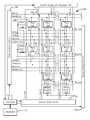
- FIG. 1is a block diagram of an AMOLED display system with compensation control
- FIG. 2is a circuit diagram of one of the reference pixels in FIG. 1 for modifying characterization correlation curves based on the measured data;
- FIG. 3is a graph of luminance emitted from an active pixel reflecting the different levels of stress conditions over time that may require different compensation;
- FIG. 4is a graph of the plots of different characterization correlation curves and the results of techniques of using predetermined stress conditions to determine compensation
- FIG. 5is a flow diagram of the process of determining and updating characterization correlation curves based on groups of reference pixels under predetermined stress conditions.
- FIG. 6is a flow diagram of the process of compensating the programming voltages of active pixels on a display using predetermined characterization correlation curves.
- FIG. 7is an interdependency curve of OLED efficiency degradation versus changes in OLED voltage.
- FIG. 8is a graph of OLED stress history versus stress intensity.
- FIG. 9Ais a graph of change in OLED voltage versus time for different stress conditions.
- FIG. 9Bis a graph of rate of change of OLED voltage versus time for different stress conditions.
- FIG. 10is a graph of rate of change of OLED voltage versus change in OLED voltage, for different stress conditions.
- FIG. 11is a flow chart of a procedure for extracting OLED efficiency degradation from changes in an OLED parameter such as OLED voltage.
- FIG. 12is an OLED interdependency curve relating an OLED electrical signal and efficiency degradation.
- FIG. 13is a flow chart of a procedure for extracting interdependency curves from test devices.
- FIG. 14is a flow chart of a procedure for calculating interdependency curves from a library.
- FIG. 1is an electronic display system 100 having an active matrix area or pixel array 102 in which an array of active pixels 104 are arranged in a row and column configuration. For ease of illustration, only two rows and columns are shown.
- a peripheral area 106External to the active matrix area, which is the pixel array 102 , is a peripheral area 106 where peripheral circuitry for driving and controlling the area of the pixel array 102 are disposed.
- the peripheral circuitryincludes a gate or address driver circuit 108 , a source or data driver circuit 110 , a controller 112 , and an optional supply voltage (e.g., EL_Vdd) driver 114 .
- the controller 112controls the gate, source, and supply voltage drivers 108 , 110 , 114 .
- the gate driver 108under control of the controller 112 , operates on address or select lines SEL[i], SEL[i+1], and so forth, one for each row of pixels 104 in the pixel array 102 .
- the gate or address driver circuit 108can also optionally operate on global select lines GSEL[j] and optionally/GSEL[j], which operate on multiple rows of pixels 104 in the pixel array 102 , such as every two rows of pixels 104 .
- the source driver circuit 110under control of the controller 112 , operates on voltage data lines Vdata[k], Vdata[k+1], and so forth, one for each column of pixels 104 in the pixel array 102 .
- the voltage data linescarry voltage programming information to each pixel 104 indicative of brightness of each light emitting device in the pixel 104 .
- a storage element, such as a capacitor, in each pixel 104stores the voltage programming information until an emission or driving cycle turns on the light emitting device.
- the optional supply voltage driver 114under control of the controller 112 , controls a supply voltage (EL_Vdd) line, one for each row of pixels 104 in the pixel array 102 .
- the controller 112is also coupled to a memory 118 that stores various characterization correlation curves and aging parameters of the pixels 104 as will be explained below.
- the memory 118may be one or more of a flash memory, an SRAM, a DRAM, combinations thereof, and/or the like.
- the display system 100may also include a current source circuit, which supplies a fixed current on current bias lines.
- a reference currentcan be supplied to the current source circuit.
- a current source controlcontrols the timing of the application of a bias current on the current bias lines.
- a current source address drivercontrols the timing of the application of a bias current on the current bias lines.
- each pixel 104 in the display system 100needs to be programmed with information indicating the brightness of the light emitting device in the pixel 104 .
- a framedefines the time period that includes a programming cycle or phase during which each and every pixel in the display system 100 is programmed with a programming voltage indicative of a brightness and a driving or emission cycle or phase during which each light emitting device in each pixel is turned on to emit light at a brightness commensurate with the programming voltage stored in a storage element.
- a frameis thus one of many still images that compose a complete moving picture displayed on the display system 100 .
- row-by-row programminga row of pixels is programmed and then driven before the next row of pixels is programmed and driven.
- frame-by-frame programmingall rows of pixels in the display system 100 are programmed first, and all of the frames are driven row-by-row. Either scheme can employ a brief vertical blanking time at the beginning or end of each period during which the pixels are neither programmed nor driven.
- the components located outside of the pixel array 102may be disposed in a peripheral area 106 around the pixel array 102 on the same physical substrate on which the pixel array 102 is disposed. These components include the gate driver 108 , the source driver 110 , and the optional supply voltage control 114 . Alternately, some of the components in the peripheral area can be disposed on the same substrate as the pixel array 102 while other components are disposed on a different substrate, or all of the components in the peripheral area can be disposed on a substrate different from the substrate on which the pixel array 102 is disposed. Together, the gate driver 108 , the source driver 110 , and the supply voltage control 114 make up a display driver circuit. The display driver circuit in some configurations may include the gate driver 108 and the source driver 110 but not the supply voltage control 114 .
- the display system 100further includes a current supply and readout circuit 120 , which reads output data from data output lines, VD[k], VD[k+1], and so forth, one for each column of active pixels 104 in the pixel array 102 .
- a set of optional reference devicessuch as reference pixels 130 is fabricated on the edge of the pixel array 102 outside the active pixels 104 in the peripheral area 106 .
- the reference pixels 130also may receive input signals from the controller 112 and may output data signals to the current supply and readout circuit 120 .
- the reference pixels 130include the drive transistor and an OLED but are not part of the pixel array 102 that displays images. As will be explained below, different groups of reference pixels 130 are placed under different stress conditions via different current levels from the current supply circuit 120 .
- the reference pixels 130may provide data indicating the effects of aging at different stress conditions. Although only one row and column of reference pixels 130 is shown in FIG. 1 , it is to be understood that there may be any number of reference pixels. Each of the reference pixels 130 in the example shown in FIG. 1 are fabricated next to a corresponding photo sensor 132 . The photo sensor 132 is used to determine the luminance level emitted by the corresponding reference pixel 130 . It is to be understood that reference devices such as the reference pixels 130 may be a stand alone device rather than being fabricated on the display with the active pixels 104 .
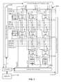
- FIG. 2shows one example of a driver circuit 200 for one of the example reference pixels 130 in FIG. 1 .
- the driver circuit 200 of the reference pixel 130includes a drive transistor 202 , an organic light emitting device (“OLED”) 204 , a storage capacitor 206 , a select transistor 208 and a monitoring transistor 210 .
- a voltage source 212is coupled to the drive transistor 202 .
- the drive transistor 202is a thin film transistor in this example that is fabricated from amorphous silicon.
- a select line 214is coupled to the select transistor 208 to activate the driver circuit 200 .
- a voltage programming input line 216allows a programming voltage to be applied to the drive transistor 202 .
- a monitoring line 218allows outputs of the OLED 204 and/or the drive transistor 202 to be monitored.
- the select line 214is coupled to the select transistor 208 and the monitoring transistor 210 . During the readout time, the select line 214 is pulled high.
- a programming voltagemay be applied via the programming voltage input line 216 .
- a monitoring voltagemay be read from the monitoring line 218 that is coupled to the monitoring transistor 210 .
- the signal to the select line 214may be sent in parallel with the pixel programming cycle.
- the reference pixel 130may be stressed at a certain current level by applying a constant voltage to the programming voltage input line 216 .
- the voltage output measured from the monitoring line 218 based on a reference voltage applied to the programming voltage input line 216allows the determination of electrical characterization data for the applied stress conditions over the time of operation of the reference pixel 130 .
- the monitor line 218 and the programming voltage input line 216may be merged into one line (i.e., Data/Mon) to carry out both the programming and monitoring functions through that single line.
- the output of the photo-sensor 132allows the determination of optical characterization data for stress conditions over the time of operation for the reference pixel 130 .
- the display system 100 in FIG. 1in which the brightness of each pixel (or subpixel) is adjusted based on the aging of at least one of the pixels, to maintain a substantially uniform display over the operating life of the system (e.g., 75,000 hours).
- display devices incorporating the display system 100include a mobile phone, a digital camera, a personal digital assistant (PDA), a computer, a television, a portable video player, a global positioning system (GPS), etc.
- the memory 118stores the required compensation voltage of each active pixel to maintain a constant current. It also stores data in the form of characterization correlation curves for different stress conditions that is utilized by the controller 112 to determine compensation voltages to modify the programming voltages to drive each OLED of the active pixels 104 to correctly display a desired output level of luminance by increasing the OLED's current to compensate for the optical aging of the OLED.
- the memory 118stores a plurality of predefined characterization correlation curves or functions, which represent the degradation in luminance efficiency for OLEDs operating under different predetermined stress conditions.
- the different predetermined stress conditionsgenerally represent different types of stress or operating conditions that an active pixel 104 may undergo during the lifetime of the pixel.
- Different stress conditionsmay include constant current requirements at different levels from low to high, constant luminance requirements from low to high, or a mix of two or more stress levels.
- the stress levelsmay be at a certain current for some percentage of the time and another current level for another percentage of the time.
- Other stress levelsmay be specialized such as a level representing an average streaming video displayed on the display system 100 .
- the base line electrical and optical characteristics of the reference devicessuch as the reference pixels 130 at different stress conditions are stored in the memory 118 .
- the baseline optical characteristic and the baseline electrical characteristic of the reference deviceare measured from the reference device immediately after fabrication of the reference device.
- Each such stress conditionmay be applied to a group of reference pixels such as the reference pixels 130 by maintaining a constant current through the reference pixel 130 over a period of time, maintaining a constant luminance of the reference pixel 130 over a period of time, and/or varying the current through or luminance of the reference pixel at different predetermined levels and predetermined intervals over a period of time.
- the current or luminance level(s) generated in the reference pixel 130can be, for example, high values, low values, and/or average values expected for the particular application for which the display system 100 is intended. For example, applications such as a computer monitor require high values.
- the period(s) of time for which the current or luminance level(s) are generated in the reference pixelmay depend on the particular application for which the display system 100 is intended.
- the different predetermined stress conditionsare applied to different reference pixels 130 during the operation of the display system 100 in order to replicate aging effects under each of the predetermined stress conditions.
- a first predetermined stress conditionis applied to a first set of reference pixels
- a second predetermined stress conditionis applied to a second set of reference pixels, and so on.
- the display system 100has groups of reference pixels 130 that are stressed under 16 different stress conditions that range from a low current value to a high current value for the pixels.
- greater or lesser numbers of stress conditionsmay be applied depending on factors such as the desired accuracy of the compensation, the physical space in the peripheral area 106 , the amount of processing power available, and the amount of memory for storing the characterization correlation curve data.
- the components of the reference pixelare aged according to the operating conditions of the stress condition.
- the stress conditionis applied to the reference pixel during the operation of the system 100
- the electrical and optical characteristics of the reference pixelare measured and evaluated to determine data for determining correction curves for the compensation of aging in the active pixels 104 in the array 102 .
- the optical characteristics and electrical characteristicsare measured once an hour for each group of reference pixels 130 .
- the corresponding characteristic correlation curvesare therefore updated for the measured characteristics of the reference pixels 130 .
- these measurementsmay be made in shorter periods of time or for longer periods of time depending on the accuracy desired for aging compensation.
- the luminance of the OLED 204has a direct linear relationship with the current applied to the OLED 204 .
- luminance, Lis a result of a coefficient, O, based on the properties of the OLED multiplied by the current I.
- Oa coefficient
- the measured luminance at a given currentmay therefore be used to determine the characteristic change in the coefficient, O, due to aging for a particular OLED 204 at a particular time for a predetermined stress condition.
- the measured electrical characteristicrepresents the relationship between the voltage provided to the drive transistor 202 and the resulting current through the OLED 204 .
- the change in voltage required to achieve a constant current level through the OLED of the reference pixelmay be measured with a voltage sensor or thin film transistor such as the monitoring transistor 210 in FIG. 2 .
- the required voltagegenerally increases as the OLED 204 and drive transistor 202 ages.
- the currentis determined by a constant, k, multiplied by the input voltage, V, minus a coefficient, e, which represents the electrical characteristics of the drive transistor 202 .
- the voltagetherefore has a power law relation by the variable, a, to the current, I.
- the coefficient, eincreases thereby requiring greater voltage to produce the same current.
- the measured current from the reference pixelmay therefore be used to determine the value of the coefficient, e, for a particular reference pixel at a certain time for the stress condition applied to the reference pixel.
- the optical characteristic, Orepresents the relationship between the luminance generated by the OLED 204 of the reference pixel 130 as measured by the photo sensor 132 and the current through the OLED 204 in FIG. 2 .
- the measured electrical characteristic, erepresents the relationship between the voltage applied and the resulting current.
- the change in luminance of the reference pixel 130 at a constant current level from a baseline optical characteristicmay be measured by a photo sensor such as the photo sensor 132 in FIG. 1 as the stress condition is applied to the reference pixel.
- the change in electric characteristics, e, from a baseline electrical characteristicmay be measured from the monitoring line to determine the current output.
- the stress condition current levelis continuously applied to the reference pixel 130 .
- the stress condition currentis removed and the select line 214 is activated.
- a reference voltageis applied and the resulting luminance level is taken from the output of the photo sensor 132 and the output voltage is measured from the monitoring line 218 .
- the resulting datais compared with previous optical and electrical data to determine changes in current and luminance outputs for a particular stress condition from aging to update the characteristics of the reference pixel at the stress condition.
- the updated characteristics datais used to update the characteristic correlation curve.
- a characterization correlation curve(or function) is determined for the predetermined stress condition over time.
- the characterization correlation curveprovides a quantifiable relationship between the optical degradation and the electrical aging expected for a given pixel operating under the stress condition. More particularly, each point on the characterization correlation curve determines the correlation between the electrical and optical characteristics of an OLED of a given pixel under the stress condition at a given time where measurements are taken from the reference pixel 130 . The characteristics may then be used by the controller 112 to determine appropriate compensation voltages for active pixels 104 that have been aged under the same stress conditions as applied to the reference pixels 130 .
- the baseline optical characteristicmay be periodically measured from a base OLED device at the same time as the optical characteristic of the OLED of the reference pixel is being measured.
- the base OLED deviceeither is not being stressed or being stressed on a known and controlled rate. This will eliminate any environmental effect on the reference OLED characterization.
- each reference pixel 130 of the display system 100may not have uniform characteristics, resulting in different emitting performances.
- One techniqueis to average the values for the electrical characteristics and the values of the luminance characteristics obtained by a set of reference pixels under a predetermined stress condition.
- a better representation of the effect of the stress condition on an average pixelis obtained by applying the stress condition to a set of the reference pixels 130 and applying a polling-averaging technique to avoid defects, measurement noise, and other issues that can arise during application of the stress condition to the reference pixels. For example, faulty values such as those determined due to noise or a dead reference pixel may be removed from the averaging.
- Such a techniquemay have predetermined levels of luminance and electrical characteristics that must be met before inclusion of those values in the averaging. Additional statistical regression techniques may also be utilized to provide less weight to electrical and optical characteristic values that are significantly different from the other measured values for the reference pixels under a given stress condition.
- each of the stress conditionsis applied to a different set of reference pixels.
- the optical and electrical characteristics of the reference pixelsare measured, and a polling-averaging technique and/or a statistical regression technique are applied to determine different characterization correlation curves corresponding to each of the stress conditions.
- the different characterization correlation curvesare stored in the memory 118 .
- this exampleuses reference devices to determine the correlation curves, the correlation curves may be determined in other ways such as from historical data or predetermined by a manufacturer.
- each group of the reference pixels 130may be subjected to the respective stress conditions and the characterization correlation curves initially stored in the memory 118 may be updated by the controller 112 to reflect data taken from the reference pixels 130 that are subject to the same external conditions as the active pixels 104 .
- the characterization correlation curvesmay thus be tuned for each of the active pixels 104 based on measurements made for the electrical and luminance characteristics of the reference pixels 130 during operation of the display system 100 .
- the electrical and luminance characteristics for each stress conditionare therefore stored in the memory 118 and updated during the operation of the display system 100 .
- the storage of the datamay be in a piecewise linear model.
- such a piecewise linear modelhas 16 coefficients that are updated as the reference pixels 130 are measured for voltage and luminance characteristics.
- a curvemay be determined and updated using linear regression or by storing data in a look up table in the memory 118 .
- the disclosed display system 100overcomes such limitations by determining and storing a discrete number of characterization correlation curves at predetermined stress conditions and subsequently combining those predefined characterization correlation curves using linear or nonlinear algorithm(s) to synthesize a compensation factor for each pixel 104 of the display system 100 depending on the particular operating condition of each pixel. As explained above, in this example there are a range of 16 different predetermined stress conditions and therefore 16 different characterization correlation curves stored in the memory 118 .
- the display system 100For each pixel 104 , the display system 100 analyzes the stress condition being applied to the pixel 104 , and determines a compensation factor using an algorithm based on the predefined characterization correlation curves and the measured electrical aging of the panel pixels. The display system 100 then provides a voltage to the pixel based on the compensation factor. The controller 112 therefore determines the stress of a particular pixel 104 and determines the closest two predetermined stress conditions and attendant characteristic data obtained from the reference pixels 130 at those predetermined stress conditions for the stress condition of the particular pixel 104 . The stress condition of the active pixel 104 therefore falls between a low predetermined stress condition and a high predetermined stress condition.
- the following examples of linear and nonlinear equations for combining characterization correlation curvesare described in terms of two such predefined characterization correlation curves for ease of disclosure; however, it is to be understood that any other number of predefined characterization correlation curves can be utilized in the exemplary techniques for combining the characterization correlation curves.
- the two exemplary characterization correlation curvesinclude a first characterization correlation curve determined for a high stress condition and a second characterization correlation curve determined for a low stress condition.
- FIG. 3is a graph showing different stress conditions over time for an active pixel 104 that shows luminance levels emitted over time.
- the luminance of the active pixelis represented by trace 302 , which shows that the luminance is between 300 and 500 nits (cd/cm 2 ).
- the stress condition applied to the active pixel during the trace 302is therefore relatively high.
- the luminance of the active pixelis represented by a trace 304 , which shows that the luminance is between 300 and 100 nits.
- the stress condition during the trace 304is therefore lower than that of the first time period and the age effects of the pixel during this time differ from the higher stress condition.
- the luminance of the active pixelis represented by a trace 306 , which shows that the luminance is between 100 and 0 nits. The stress condition during this period is lower than that of the second period.
- the luminance of the active pixelis represented by a trace 308 showing a return to a higher stress condition based on a higher luminance between 400 and 500 nits.
- the limited number of reference pixels 130 and corresponding limited numbers of stress conditionsmay require the use of averaging or continuous (moving) averaging for the specific stress condition of each active pixel 104 .
- the specific stress conditionsmay be mapped for each pixel as a linear combination of characteristic correlation curves from several reference pixels 130 .
- the combinations of two characteristic curves at predetermined stress conditionsallow accurate compensation for all stress conditions occurring between such stress conditions.
- the two reference characterization correlation curves for high and low stress conditionsallow a close characterization correlation curve for an active pixel having a stress condition between the two reference curves to be determined.
- the first and second reference characterization correlation curves stored in the memory 118are combined by the controller 112 using a weighted moving average algorithm.
- St(t i-1 )is the stress condition at a previous time
- k avgis a moving average constant
- L(t i )is the measured luminance of the active pixel at the certain time, which may be determined by:
- L ⁇ ( t i )L peak ⁇ ( g ⁇ ( t i ) g peak ) ⁇
- L peakis the highest luminance permitted by the design of the display system 100 .
- the variable, g(t i )is the grayscale at the time of measurement, g peak is the highest grayscale value of use (e.g. 255) and ⁇ is a gamma constant.
- f highis the first function corresponding to the characterization correlation curve for a high predetermined stress condition
- f lowis the second function corresponding to the characterization correlation curve for a low predetermined stress condition.
- ⁇ Iis the change in the current in the OLED for a fixed voltage input, which shows the change (electrical degradation) due to aging effects measured at a particular time. It is to be understood that the change in current may be replaced by a change in voltage, ⁇ V, for a fixed current.
- K highis the weighted variable assigned to the characterization correlation curve for the high stress condition and K low is the weight assigned to the characterization correlation curve for the low stress condition.
- the change in voltage or current in the active pixel at any time during operationrepresents the electrical characteristic while the change in current as part of the function for the high or low stress condition represents the optical characteristic.
- the luminance at the high stress condition, the peak luminance, and the average compensation factor (function of difference between the two characterization correlation curves), K avgare stored in the memory 118 for determining the compensation factors for each of the active pixels. Additional variables are stored in the memory 118 including, but not limited to, the grayscale value for the maximum luminance permitted for the display system 100 (e.g., grayscale value of 255). Additionally, the average compensation factor, K avg , may be empirically determined from the data obtained during the application of stress conditions to the reference pixels.
- the relationship between the optical degradation and the electrical aging of any pixel 104 in the display system 100may be tuned to avoid errors associated with divergence in the characterization correlation curves due to different stress conditions.
- the number of characterization correlation curves storedmay also be minimized to a number providing confidence that the averaging technique will be sufficiently accurate for required compensation levels.
- the compensation factor, K compcan be used for compensation of the OLED optical efficiency aging for adjusting programming voltages for the active pixel.
- Another technique for determining the appropriate compensation factor for a stress condition on an active pixelmay be termed dynamic moving averaging.
- the dynamic moving averaging techniqueinvolves changing the moving average coefficient, K avg , during the lifetime of the display system 100 to compensate between the divergence in two characterization correlation curves at different predetermined stress conditions in order to prevent distortions in the display output. As the OLEDs of the active pixels age, the divergence between two characterization correlation curves at different stress conditions increases.
- K avgmay be increased during the lifetime of the display system 100 to avoid a sharp transition between the two curves for an active pixel having a stress condition falling between the two predetermined stress conditions.
- the measured change in current, ⁇ Imay be used to adjust the K avg value to improve the performance of the algorithm to determine the compensation factor.
- Another technique to improve performance of the compensation process termed event-based moving averagingis to reset the system after each aging step. This technique further improves the extraction of the characterization correlation curves for the OLEDs of each of the active pixels 104 .
- the display system 100is reset after every aging step (or after a user turns on or off the display system 100 ).
- K compK comp _ evt +K high ( f high ( ⁇ I ) ⁇ f high ( ⁇ I evt ))+ K low ( f low ( ⁇ I ) ⁇ f low ( ⁇ I evt ))
- K comp _ evtK high ( f high ( ⁇ I ) ⁇ f high ( ⁇ I evt ))+ K low ( f low ( ⁇ I ) ⁇ f low ( ⁇ I evt ))
- K comp _ evtis the compensation factor calculated at a previous time
- ⁇ I evtis the change in the OLED current during the previous time at a fixed voltage.
- the change in currentmay be replaced with the change in an OLED voltage change under a fixed current.
- FIG. 4is a graph 400 showing the different characterization correlation curves based on the different techniques.
- the graph 400compares the change in the optical compensation percent and the change in the voltage of the OLED of the active pixel required to produce a given current.
- a high stress predetermined characterization correlation curve 402diverges from a low stress predetermined characterization correlation curve 404 at greater changes in voltage reflecting aging of an active pixel.
- a set of points 406represents the correction curve determined by the moving average technique from the predetermined characterization correlation curves 402 and 404 for the current compensation of an active pixel at different changes in voltage.
- a set of points 408represents the characterization correlation curve determined by the dynamic moving averaging technique.
- a set of points 410represents the compensation factors determined by the event-based moving averaging technique. Based on OLED behavior, one of the above techniques can be used to improve the compensation for OLED efficiency degradation.
- an electrical characteristic of a first set of sample pixelsis measured.
- the electrical characteristic of each of the first set of sample pixelscan be measured by a thin film transistor (TFT) connected to each pixel.
- an optical characteristice.g., luminance
- the amount of change required in the brightness of each pixelcan be extracted from the shift in voltage of one or more of the pixels. This may be implemented by a series of calculations to determine the correlation between shifts in the voltage or current supplied to a pixel and/or the brightness of the light-emitting material in that pixel.
- the above described methods of extracting characteristic correlation curves for compensating aging of the pixels in the arraymay be performed by a processing device such as the controller 112 in FIG. 1 or another such device, which may be conveniently implemented using one or more general purpose computer systems, microprocessors, digital signal processors, micro-controllers, application specific integrated circuits (ASIC), programmable logic devices (PLD), field programmable logic devices (FPLD), field programmable gate arrays (FPGA) and the like, programmed according to the teachings as described and illustrated herein, as will be appreciated by those skilled in the computer, software, and networking arts.
- a processing devicesuch as the controller 112 in FIG. 1 or another such device, which may be conveniently implemented using one or more general purpose computer systems, microprocessors, digital signal processors, micro-controllers, application specific integrated circuits (ASIC), programmable logic devices (PLD), field programmable logic devices (FPLD), field programmable gate arrays (FPGA) and the like, programmed according to the teachings as described and illustrated
- the operation of the example characteristic correlation curves for compensating aging methodsmay be performed by machine readable instructions.
- the machine readable instructionscomprise an algorithm for execution by: (a) a processor, (b) a controller, and/or (c) one or more other suitable processing device(s).
- the algorithmmay be embodied in software stored on tangible media such as, for example, a flash memory, a CD-ROM, a floppy disk, a hard drive, a digital video (versatile) disk (DVD), or other memory devices, but persons of ordinary skill in the art will readily appreciate that the entire algorithm and/or parts thereof could alternatively be executed by a device other than a processor and/or embodied in firmware or dedicated hardware in a well-known manner (e.g., it may be implemented by an application specific integrated circuit (ASIC), a programmable logic device (PLD), a field programmable logic device (FPLD), a field programmable gate array (FPGA), discrete logic, etc.).
- ASICapplication specific integrated circuit
- PLDprogrammable logic device
- FPLDfield programmable logic device
- FPGAfield programmable gate array
- any or all of the components of the characteristic correlation curves for compensating aging methodscould be implemented by software, hardware, and/or firmware.
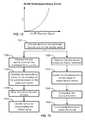
- FIG. 5is a flow diagram of a process to determine and update the characterization correlation curves for a display system such as the display system 100 in FIG. 1 .
- a selection of stress conditionsis made to provide sufficient baselines for correlating the range of stress conditions for the active pixels ( 500 ).
- a group of reference pixelsis then selected for each of the stress conditions ( 502 ).
- the reference pixels for each of the groups corresponding to each of the stress conditionsare then stressed at the corresponding stress condition and base line optical and electrical characteristics are stored ( 504 ).
- the luminance levelsare measured and recorded for each pixel in each of the groups ( 506 ).
- the luminance characteristicis then determined by averaging the measured luminance for each pixel in the group of the pixels for each of the stress conditions ( 508 ).
- the electrical characteristics for each of the pixels in each of the groupsare determined ( 510 ).
- the average of each pixel in the groupis determined to determine the average electrical characteristic ( 512 ).
- the average luminance characteristic and the average electrical characteristic for each groupare then used to update the characterization correlation curve for the corresponding predetermined stress condition ( 514 ).
- the controllermay use the updated characterization correlation curves to compensate for aging effects for active pixels subjected to different stress conditions.
- a flowchartis illustrated for a process of using appropriate predetermined characterization correlation curves for a display system 100 as obtained in the process in FIG. 5 to determine the compensation factor for an active pixel at a given time.
- the luminance emitted by the active pixelis determined based on the highest luminance and the programming voltage ( 600 ).
- a stress conditionis measured for a particular active pixel based on the previous stress condition, determined luminance, and the average compensation factor ( 602 ).
- the appropriate predetermined stress characterization correlation curvesare read from memory ( 604 ).
- the two characterization correlation curvescorrespond to predetermined stress conditions that the measured stress condition of the active pixel falls between.
- the controller 112determines the coefficients from each of the predetermined stress conditions by using the measured current or voltage change from the active pixel ( 606 ). The controller then determines a modified coefficient to calculate a compensation voltage to add to the programming voltage to the active pixels ( 608 ). The determined stress condition is stored in the memory ( 610 ). The controller 112 then stores the new compensation factor, which may then be applied to modify the programming voltages to the active pixel during each frame period after the measurements of the reference pixels 130 ( 612 ).
- OLED efficiency degradationcan be calculated based on an interdependency curve based on OLED electrical changes versus efficiency degradation, such as the interdependency curve in FIG. 7 .
- the change in the OLED electrical parameteris detected, and that value is used to extract the efficiency degradation from the curve.
- the pixel currentcan then be adjusted accordingly to compensate for the degradation.
- the main challengeis that the interdependency curve is a function of stress conditions. Therefore, to achieve more accurate compensation, one needs to consider the effect of different stress conditions.
- One methodis to use the stress condition of each pixel (or a group of pixels) to select from among different interdependency curves, to extract the proper efficiency lost for each specific case.
- the stress historycan be simply a moving average of the stress conditions.
- a weighted stress historycan be used.
- the effect of each stresscan have a different weight based on stress intensity or period, as in the example depicted in FIG. 8 .
- the effect of low intensity stressis less on selecting the OLED interdependency curve. Therefore, a curve that has lower weight for small intensity can be used, such as the curve in FIG. 8 .
- Sub-samplingcan also be used to calculate the stress history, to reduce the memory transfer activities.
- the stress historyis low frequency in time. In this case, there is no need to sample the pixel conditions for every frame.
- the sampling ratecan be modified for different applications based on content frame rate. Here, during every frame only a few pixels can be selected to obtain an updated stress history.
- the stress historyis low frequency in space. In this case, there is no need to sample all the pixels.
- a sub-set of pixelsare used to calculate the stress history, and then an interpolation technique can be used to calculate the stress history for all the pixels.
- the rate of change in the OLED electrical parametercan be used to extract the stress conditions, as depicted in FIGS. 9A and 9B .
- FIG. 9Aillustrates the change of ⁇ V OLED with time, for low, medium and high stress conditions
- FIG. 9Billustrates the rate of change versus time for the same three stress conditions.
- the rate of change in the electrical parametercan be used as an indicator of stress conditions.
- the rate of change in the electrical parameter based on the change in the electrical parametermay be modeled or experimentally extracted for different stress conditions, as depicted in FIG. 10 .
- the rate of changemay also be used to extract the stress condition based on comparing the measured change and rate of change in the electrical parameter.
- the function developed for change and rate of change of the electrical parameteris used.
- the stress condition, interdependency curves, and measured changed parametermay be used.
- FIG. 11is a flow chart of a procedure for compensating the OLED efficiency degradation based on measuring the change and rate of change in the electrical parameter of the OLED.
- the change in the OLED parametere.g., OLED voltage
- the rate of change in the OLED parameterbased on previously extracted values
- Step 1102uses the rate of change and the change in the parameter to identify the stress condition.
- step 1104calculates the efficiency degradation from the stress condition, the measured parameter, and interdependency curves.
- interdependency curvesrelating OLED electrical change (current or voltage) and efficiency degradation, as depicted in FIG. 12 . Due to process variations, the interdependency curve may vary.
- a test OLEDcan be used in each display and the curve extracted for each display after fabrication or during the display operation. In the case of smaller displays, the test OLED devices can be put on the substrates and used to extract the curves after fabrication.
- FIG. 13is a flow chart of a process for extracting the interdependency curves from the test devices, either off line or during the display operation, or a combination of both.
- the curves extracted in the factoryare stored for aging compensation.
- the curvecan be updated with additional data based on measurement results of the test device in the display.
- a set of curvesmay measured in advance and put in the library.
- the test devicesare aged at predetermined aging levels (generally higher than normal) to extract some aging behavior in a short time period (and/or their current-voltage-luminance, IVL, is measured). After that, the extracted aging behavior is used to find a proper curve, having a similar or close aging behavior, from the library of curves.
- the first step 1301adds the test device on the substrate, in or out of the display area.
- step 1302measures the test device to extract the interdependency curves.
- Step 1303calculates the interdependency curves for the displays on the substrate, based on the measured curves.
- the curvesare stored for each display in step 1304 , and then used for compensating the display aging in step 1305 .
- the test devicescan be measured during the display operation at step 1306 .
- Step 1307updates the interdependence curves based on the measured results.
- Step 1308extrapolates the curves if needed, and step 1309 compensates the display based on the curves.
- FIG. 14is a flow chart of a procedure for addressing the process variation between substrates or within a substrate.
- the first step 1401adds a test device on the substrate, either in or out of the display area, or the test device can be the display itself.
- Step 1402measures the test device for predetermined aging levels to extract the aging behavior and/or measures the IVL characteristics of the test devices.
- Step 1403finds a set of samples in an interdependency curve library that have the closest aging or IVL behavior to the test device.
- step 1404determines whether the error between the IVL and/or aging behavior is less than a threshold. If the answer is affirmative, step 1405 uses the curves from the library to calculate the interdependency curves for the display in the substrate.
- step 1406uses the test device to extract the new interdependency curves. Then the curves are used to calculate the interdependency curves for the display in the substrate in step 1407 , and step 1408 adds the new curves to the library.
Landscapes
- Engineering & Computer Science (AREA)
- Physics & Mathematics (AREA)
- Computer Hardware Design (AREA)
- General Physics & Mathematics (AREA)
- Theoretical Computer Science (AREA)
- Electroluminescent Light Sources (AREA)
- Control Of Indicators Other Than Cathode Ray Tubes (AREA)
Abstract
Description
This application is a continuation-in-part of and claims priority to pending U.S. patent application Ser. No. 14/286,711, filed May 23, 2014, which is a continuation-in-part of U.S. patent application Ser. No. 14/027,811, filed Sep. 16, 2013, which is a continuation of U.S. patent application Ser. No. 13/020,252, filed Feb. 3, 2011, now U.S. Pat. No. 8,589,100, which claims priority to Canadian Application No. 2,692,097, filed Feb. 4, 2010, now abandoned, each of which is hereby incorporated by reference herein in its entirety.
This invention is directed generally to displays that use light emissive devices such as OLEDs and, more particularly, to extracting characterization correlation curves under different stress conditions in such displays to compensate for aging of the light emissive devices.
Active matrix organic light emitting device (“AMOLED”) displays offer the advantages of lower power consumption, manufacturing flexibility, and faster refresh rate over conventional liquid crystal displays. In contrast to conventional liquid crystal displays, there is no backlighting in an AMOLED display as each pixel consists of different colored OLEDs emitting light independently. The OLEDs emit light based on current supplied through a drive transistor. The drive transistor is typically a thin film transistor (TFT). The power consumed in each pixel has a direct relation with the magnitude of the generated light in that pixel.
During operation of an organic light emitting diode device, it undergoes degradation, which causes light output at a constant current to decrease over time. The OLED device also undergoes an electrical degradation, which causes the current to drop at a constant bias voltage over time. These degradations are caused primarily by stress related to the magnitude and duration of the applied voltage on the OLED and the resulting current passing through the device. Such degradations are compounded by contributions from the environmental factors such as temperature, humidity, or presence of oxidants over time. The aging rate of the thin film transistor devices is also environmental and stress (bias) dependent. The aging of the drive transistor and the OLED may be properly determined via calibrating the pixel against stored historical data from the pixel at previous times to determine the aging effects on the pixel. Accurate aging data is therefore necessary throughout the lifetime of the display device.
In one compensation technique for OLED displays, the aging (and/or uniformity) of a panel of pixels is extracted and stored in lookup tables as raw or processed data. Then a compensation module uses the stored data to compensate for any shift in electrical and optical parameters of the OLED (e.g., the shift in the OLED operating voltage and the optical efficiency) and the backplane (e.g., the threshold voltage shift of the TFT), hence the programming voltage of each pixel is modified according to the stored data and the video content. The compensation module modifies the bias of the driving TFT in a way that the OLED passes enough current to maintain the same luminance level for each gray-scale level. In other words, a correct programming voltage properly offsets the electrical and optical aging of the OLED as well as the electrical degradation of the TFT.
The electrical parameters of the backplane TFTs and OLED devices are continuously monitored and extracted throughout the lifetime of the display by electrical feedback-based measurement circuits. Further, the optical aging parameters of the OLED devices are estimated from the OLED's electrical degradation data. However, the optical aging effect of the OLED is dependent on the stress conditions placed on individual pixels as well, and since the stresses vary from pixel to pixel, accurate compensation is not assured unless the compensation tailored for a specific stress level is determined.
There is therefore a need for efficient extraction of characterization correlation curves of the optical and electrical parameters that are accurate for stress conditions on active pixels for compensation for aging and other effects. There is also a need for having a variety of characterization correlation curves for a variety of stress conditions that the active pixels may be subjected to during operation of the display. There is a further need for accurate compensation systems for pixels in an organic light emitting device based display.
In accordance with one embodiment, a system is provided for determining the efficiency degradation of organic light emitting devices (OLEDs) in multiple array-based semiconductor devices having arrays of pixels that include OLEDs. The system determines the relationship between changes in an electrical operating parameter of the OLEDs and the efficiency degradation of the OLEDs in each of the array-based semiconductor devices, uses the determined relationship for a selected one of the array-based semiconductor devices to determine the efficiency degradation of the OLEDs, and compensates for the efficiency degradation.
In one implementation, the relationship between changes in an electrical operating parameter of the OLEDs and the efficiency degradation of the OLEDs in the array-based semiconductor devices is determined by the use of a test OLED associated with each of the devices. The test OLED may be located on the substrate of the associated array-based semiconductor device, or in the semiconductor device itself. The determined relationship may be an OLED interdependency curve that relates an OLED electrical signal from the test OLED in a selected array-based semiconductor device with the efficiency degradation of that test OLED. The relationship may be determined at the time of fabrication of each of the array-based semiconductor devices, or during operation of the devices.
One embodiment uses a library of OLED interdependency curves that relate OLED electrical signals from test OLEDs in array-based semiconductor devices with the efficiency degradation of test OLEDs in the devices. The system measures a test OLED in a selected array-based semiconductor device, identifies an interdependency curve in the library that corresponds to the measurements of the test OLED in the selected array-based semiconductor device, and uses the identified interdependency curve to determine the aging behavior of the test OLED. The identified interdependency curve may be the curve in the library that has the closest aging behavior to the measured test OLED, and then the system compares the difference between the aging behaviors of the identified interdependency curve and the measured test OLED with a predetermined threshold, and if the difference exceeds the threshold, calculates a new interdependency curve and adding the new curve to the library. If the difference is less than the threshold, using the identified interdependency curve to compensate for the efficiency degradation of the display containing the measured test OLED
Additional aspects of the invention will be apparent to those of ordinary skill in the art in view of the detailed description of various embodiments, which is made with reference to the drawings, a brief description of which is provided below.
The invention may best be understood by reference to the following description taken in conjunction with the accompanying drawings.
While the invention is susceptible to various modifications and alternative forms, specific embodiments have been shown by way of example in the drawings and will be described in detail herein. It should be understood, however, that the invention is not intended to be limited to the particular forms disclosed. Rather, the invention is to cover all modifications, equivalents, and alternatives falling within the spirit and scope of the invention as defined by the appended claims.
Thedisplay system 100 may also include a current source circuit, which supplies a fixed current on current bias lines. In some configurations, a reference current can be supplied to the current source circuit. In such configurations, a current source control controls the timing of the application of a bias current on the current bias lines. In configurations in which the reference current is not supplied to the current source circuit, a current source address driver controls the timing of the application of a bias current on the current bias lines.
As is known, eachpixel 104 in thedisplay system 100 needs to be programmed with information indicating the brightness of the light emitting device in thepixel 104. A frame defines the time period that includes a programming cycle or phase during which each and every pixel in thedisplay system 100 is programmed with a programming voltage indicative of a brightness and a driving or emission cycle or phase during which each light emitting device in each pixel is turned on to emit light at a brightness commensurate with the programming voltage stored in a storage element. A frame is thus one of many still images that compose a complete moving picture displayed on thedisplay system 100. There are at least two schemes for programming and driving the pixels: row-by-row, or frame-by-frame. In row-by-row programming, a row of pixels is programmed and then driven before the next row of pixels is programmed and driven. In frame-by-frame programming, all rows of pixels in thedisplay system 100 are programmed first, and all of the frames are driven row-by-row. Either scheme can employ a brief vertical blanking time at the beginning or end of each period during which the pixels are neither programmed nor driven.
The components located outside of thepixel array 102 may be disposed in aperipheral area 106 around thepixel array 102 on the same physical substrate on which thepixel array 102 is disposed. These components include thegate driver 108, thesource driver 110, and the optionalsupply voltage control 114. Alternately, some of the components in the peripheral area can be disposed on the same substrate as thepixel array 102 while other components are disposed on a different substrate, or all of the components in the peripheral area can be disposed on a substrate different from the substrate on which thepixel array 102 is disposed. Together, thegate driver 108, thesource driver 110, and thesupply voltage control 114 make up a display driver circuit. The display driver circuit in some configurations may include thegate driver 108 and thesource driver 110 but not thesupply voltage control 114.
Thedisplay system 100 further includes a current supply andreadout circuit 120, which reads output data from data output lines, VD[k], VD[k+1], and so forth, one for each column ofactive pixels 104 in thepixel array 102. A set of optional reference devices such asreference pixels 130 is fabricated on the edge of thepixel array 102 outside theactive pixels 104 in theperipheral area 106. Thereference pixels 130 also may receive input signals from thecontroller 112 and may output data signals to the current supply andreadout circuit 120. Thereference pixels 130 include the drive transistor and an OLED but are not part of thepixel array 102 that displays images. As will be explained below, different groups ofreference pixels 130 are placed under different stress conditions via different current levels from thecurrent supply circuit 120. Because thereference pixels 130 are not part of thepixel array 102 and thus do not display images, thereference pixels 130 may provide data indicating the effects of aging at different stress conditions. Although only one row and column ofreference pixels 130 is shown inFIG. 1 , it is to be understood that there may be any number of reference pixels. Each of thereference pixels 130 in the example shown inFIG. 1 are fabricated next to acorresponding photo sensor 132. Thephoto sensor 132 is used to determine the luminance level emitted by the correspondingreference pixel 130. It is to be understood that reference devices such as thereference pixels 130 may be a stand alone device rather than being fabricated on the display with theactive pixels 104.
Thereference pixel 130 may be stressed at a certain current level by applying a constant voltage to the programmingvoltage input line 216. As will be explained below, the voltage output measured from themonitoring line 218 based on a reference voltage applied to the programmingvoltage input line 216 allows the determination of electrical characterization data for the applied stress conditions over the time of operation of thereference pixel 130. Alternatively, themonitor line 218 and the programmingvoltage input line 216 may be merged into one line (i.e., Data/Mon) to carry out both the programming and monitoring functions through that single line. The output of the photo-sensor 132 allows the determination of optical characterization data for stress conditions over the time of operation for thereference pixel 130.
Thedisplay system 100 inFIG. 1 , according to one exemplary embodiment, in which the brightness of each pixel (or subpixel) is adjusted based on the aging of at least one of the pixels, to maintain a substantially uniform display over the operating life of the system (e.g., 75,000 hours). Non-limiting examples of display devices incorporating thedisplay system 100 include a mobile phone, a digital camera, a personal digital assistant (PDA), a computer, a television, a portable video player, a global positioning system (GPS), etc.
As the OLED material of anactive pixel 104 ages, the voltage required to maintain a constant current for a given level through the OLED increases. To compensate for electrical aging of the OLEDs, thememory 118 stores the required compensation voltage of each active pixel to maintain a constant current. It also stores data in the form of characterization correlation curves for different stress conditions that is utilized by thecontroller 112 to determine compensation voltages to modify the programming voltages to drive each OLED of theactive pixels 104 to correctly display a desired output level of luminance by increasing the OLED's current to compensate for the optical aging of the OLED. In particular, thememory 118 stores a plurality of predefined characterization correlation curves or functions, which represent the degradation in luminance efficiency for OLEDs operating under different predetermined stress conditions. The different predetermined stress conditions generally represent different types of stress or operating conditions that anactive pixel 104 may undergo during the lifetime of the pixel. Different stress conditions may include constant current requirements at different levels from low to high, constant luminance requirements from low to high, or a mix of two or more stress levels. For example, the stress levels may be at a certain current for some percentage of the time and another current level for another percentage of the time. Other stress levels may be specialized such as a level representing an average streaming video displayed on thedisplay system 100. Initially, the base line electrical and optical characteristics of the reference devices such as thereference pixels 130 at different stress conditions are stored in thememory 118. In this example, the baseline optical characteristic and the baseline electrical characteristic of the reference device are measured from the reference device immediately after fabrication of the reference device.
Each such stress condition may be applied to a group of reference pixels such as thereference pixels 130 by maintaining a constant current through thereference pixel 130 over a period of time, maintaining a constant luminance of thereference pixel 130 over a period of time, and/or varying the current through or luminance of the reference pixel at different predetermined levels and predetermined intervals over a period of time. The current or luminance level(s) generated in thereference pixel 130 can be, for example, high values, low values, and/or average values expected for the particular application for which thedisplay system 100 is intended. For example, applications such as a computer monitor require high values. Similarly, the period(s) of time for which the current or luminance level(s) are generated in the reference pixel may depend on the particular application for which thedisplay system 100 is intended.
It is contemplated that the different predetermined stress conditions are applied todifferent reference pixels 130 during the operation of thedisplay system 100 in order to replicate aging effects under each of the predetermined stress conditions. In other words, a first predetermined stress condition is applied to a first set of reference pixels, a second predetermined stress condition is applied to a second set of reference pixels, and so on. In this example, thedisplay system 100 has groups ofreference pixels 130 that are stressed under 16 different stress conditions that range from a low current value to a high current value for the pixels. Thus, there are 16 different groups ofreference pixels 130 in this example. Of course, greater or lesser numbers of stress conditions may be applied depending on factors such as the desired accuracy of the compensation, the physical space in theperipheral area 106, the amount of processing power available, and the amount of memory for storing the characterization correlation curve data.
By continually subjecting a reference pixel or group of reference pixels to a stress condition, the components of the reference pixel are aged according to the operating conditions of the stress condition. As the stress condition is applied to the reference pixel during the operation of thesystem 100, the electrical and optical characteristics of the reference pixel are measured and evaluated to determine data for determining correction curves for the compensation of aging in theactive pixels 104 in thearray 102. In this example, the optical characteristics and electrical characteristics are measured once an hour for each group ofreference pixels 130. The corresponding characteristic correlation curves are therefore updated for the measured characteristics of thereference pixels 130. Of course, these measurements may be made in shorter periods of time or for longer periods of time depending on the accuracy desired for aging compensation.
Generally, the luminance of theOLED 204 has a direct linear relationship with the current applied to theOLED 204. The optical characteristic of an OLED may be expressed as:
L=O*I
In this equation, luminance, L, is a result of a coefficient, O, based on the properties of the OLED multiplied by the current I. As theOLED 204 ages, the coefficient O decreases and therefore the luminance decreases for a constant current value. The measured luminance at a given current may therefore be used to determine the characteristic change in the coefficient, O, due to aging for aparticular OLED 204 at a particular time for a predetermined stress condition.
L=O*I
In this equation, luminance, L, is a result of a coefficient, O, based on the properties of the OLED multiplied by the current I. As the
The measured electrical characteristic represents the relationship between the voltage provided to thedrive transistor 202 and the resulting current through theOLED 204. For example, the change in voltage required to achieve a constant current level through the OLED of the reference pixel may be measured with a voltage sensor or thin film transistor such as themonitoring transistor 210 inFIG. 2 . The required voltage generally increases as theOLED 204 and drivetransistor 202 ages. The required voltage has a power law relation with the output current as shown in the following equation
I=k*(V−e)a
In this equation, the current is determined by a constant, k, multiplied by the input voltage, V, minus a coefficient, e, which represents the electrical characteristics of thedrive transistor 202. The voltage therefore has a power law relation by the variable, a, to the current, I. As thetransistor 202 ages, the coefficient, e, increases thereby requiring greater voltage to produce the same current. The measured current from the reference pixel may therefore be used to determine the value of the coefficient, e, for a particular reference pixel at a certain time for the stress condition applied to the reference pixel.
I=k*(V−e)a
In this equation, the current is determined by a constant, k, multiplied by the input voltage, V, minus a coefficient, e, which represents the electrical characteristics of the
As explained above, the optical characteristic, O, represents the relationship between the luminance generated by theOLED 204 of thereference pixel 130 as measured by thephoto sensor 132 and the current through theOLED 204 inFIG. 2 . The measured electrical characteristic, e, represents the relationship between the voltage applied and the resulting current. The change in luminance of thereference pixel 130 at a constant current level from a baseline optical characteristic may be measured by a photo sensor such as thephoto sensor 132 inFIG. 1 as the stress condition is applied to the reference pixel. The change in electric characteristics, e, from a baseline electrical characteristic may be measured from the monitoring line to determine the current output. During the operation of thedisplay system 100, the stress condition current level is continuously applied to thereference pixel 130. When a measurement is desired, the stress condition current is removed and theselect line 214 is activated. A reference voltage is applied and the resulting luminance level is taken from the output of thephoto sensor 132 and the output voltage is measured from themonitoring line 218. The resulting data is compared with previous optical and electrical data to determine changes in current and luminance outputs for a particular stress condition from aging to update the characteristics of the reference pixel at the stress condition. The updated characteristics data is used to update the characteristic correlation curve.
Then by using the electrical and optical characteristics measured from the reference pixel, a characterization correlation curve (or function) is determined for the predetermined stress condition over time. The characterization correlation curve provides a quantifiable relationship between the optical degradation and the electrical aging expected for a given pixel operating under the stress condition. More particularly, each point on the characterization correlation curve determines the correlation between the electrical and optical characteristics of an OLED of a given pixel under the stress condition at a given time where measurements are taken from thereference pixel 130. The characteristics may then be used by thecontroller 112 to determine appropriate compensation voltages foractive pixels 104 that have been aged under the same stress conditions as applied to thereference pixels 130. In another example, the baseline optical characteristic may be periodically measured from a base OLED device at the same time as the optical characteristic of the OLED of the reference pixel is being measured. The base OLED device either is not being stressed or being stressed on a known and controlled rate. This will eliminate any environmental effect on the reference OLED characterization.
Due to manufacturing processes and other factors known to those skilled in the art, eachreference pixel 130 of thedisplay system 100 may not have uniform characteristics, resulting in different emitting performances. One technique is to average the values for the electrical characteristics and the values of the luminance characteristics obtained by a set of reference pixels under a predetermined stress condition. A better representation of the effect of the stress condition on an average pixel is obtained by applying the stress condition to a set of thereference pixels 130 and applying a polling-averaging technique to avoid defects, measurement noise, and other issues that can arise during application of the stress condition to the reference pixels. For example, faulty values such as those determined due to noise or a dead reference pixel may be removed from the averaging. Such a technique may have predetermined levels of luminance and electrical characteristics that must be met before inclusion of those values in the averaging. Additional statistical regression techniques may also be utilized to provide less weight to electrical and optical characteristic values that are significantly different from the other measured values for the reference pixels under a given stress condition.
In this example, each of the stress conditions is applied to a different set of reference pixels. The optical and electrical characteristics of the reference pixels are measured, and a polling-averaging technique and/or a statistical regression technique are applied to determine different characterization correlation curves corresponding to each of the stress conditions. The different characterization correlation curves are stored in thememory 118. Although this example uses reference devices to determine the correlation curves, the correlation curves may be determined in other ways such as from historical data or predetermined by a manufacturer.
During the operation of thedisplay system 100, each group of thereference pixels 130 may be subjected to the respective stress conditions and the characterization correlation curves initially stored in thememory 118 may be updated by thecontroller 112 to reflect data taken from thereference pixels 130 that are subject to the same external conditions as theactive pixels 104. The characterization correlation curves may thus be tuned for each of theactive pixels 104 based on measurements made for the electrical and luminance characteristics of thereference pixels 130 during operation of thedisplay system 100. The electrical and luminance characteristics for each stress condition are therefore stored in thememory 118 and updated during the operation of thedisplay system 100. The storage of the data may be in a piecewise linear model. In this example, such a piecewise linear model has 16 coefficients that are updated as thereference pixels 130 are measured for voltage and luminance characteristics. Alternatively, a curve may be determined and updated using linear regression or by storing data in a look up table in thememory 118.
To generate and store a characterization correlation curve for every possible stress condition would be impractical due to the large amount of resources (e.g., memory storage, processing power, etc.) that would be required. The discloseddisplay system 100 overcomes such limitations by determining and storing a discrete number of characterization correlation curves at predetermined stress conditions and subsequently combining those predefined characterization correlation curves using linear or nonlinear algorithm(s) to synthesize a compensation factor for eachpixel 104 of thedisplay system 100 depending on the particular operating condition of each pixel. As explained above, in this example there are a range of 16 different predetermined stress conditions and therefore 16 different characterization correlation curves stored in thememory 118.
For eachpixel 104, thedisplay system 100 analyzes the stress condition being applied to thepixel 104, and determines a compensation factor using an algorithm based on the predefined characterization correlation curves and the measured electrical aging of the panel pixels. Thedisplay system 100 then provides a voltage to the pixel based on the compensation factor. Thecontroller 112 therefore determines the stress of aparticular pixel 104 and determines the closest two predetermined stress conditions and attendant characteristic data obtained from thereference pixels 130 at those predetermined stress conditions for the stress condition of theparticular pixel 104. The stress condition of theactive pixel 104 therefore falls between a low predetermined stress condition and a high predetermined stress condition.
The following examples of linear and nonlinear equations for combining characterization correlation curves are described in terms of two such predefined characterization correlation curves for ease of disclosure; however, it is to be understood that any other number of predefined characterization correlation curves can be utilized in the exemplary techniques for combining the characterization correlation curves. The two exemplary characterization correlation curves include a first characterization correlation curve determined for a high stress condition and a second characterization correlation curve determined for a low stress condition.
The ability to use different characterization correlation curves over different levels provides accurate compensation foractive pixels 104 that are subjected to different stress conditions than the predetermined stress conditions applied to thereference pixels 130.FIG. 3 is a graph showing different stress conditions over time for anactive pixel 104 that shows luminance levels emitted over time. During a first time period, the luminance of the active pixel is represented bytrace 302, which shows that the luminance is between 300 and 500 nits (cd/cm2). The stress condition applied to the active pixel during thetrace 302 is therefore relatively high. In a second time period, the luminance of the active pixel is represented by atrace 304, which shows that the luminance is between 300 and 100 nits. The stress condition during thetrace 304 is therefore lower than that of the first time period and the age effects of the pixel during this time differ from the higher stress condition. In a third time period, the luminance of the active pixel is represented by atrace 306, which shows that the luminance is between 100 and 0 nits. The stress condition during this period is lower than that of the second period. In a fourth time period, the luminance of the active pixel is represented by atrace 308 showing a return to a higher stress condition based on a higher luminance between 400 and 500 nits.
The limited number ofreference pixels 130 and corresponding limited numbers of stress conditions may require the use of averaging or continuous (moving) averaging for the specific stress condition of eachactive pixel 104. The specific stress conditions may be mapped for each pixel as a linear combination of characteristic correlation curves fromseveral reference pixels 130. The combinations of two characteristic curves at predetermined stress conditions allow accurate compensation for all stress conditions occurring between such stress conditions. For example, the two reference characterization correlation curves for high and low stress conditions allow a close characterization correlation curve for an active pixel having a stress condition between the two reference curves to be determined. The first and second reference characterization correlation curves stored in thememory 118 are combined by thecontroller 112 using a weighted moving average algorithm. A stress condition at a certain time St (ti) for an active pixel may be represented by:
St(ti)=(St(ti-1)*kavg+L(ti))/(kavg+1)
In this equation, St(ti-1) is the stress condition at a previous time, kavgis a moving average constant. L(ti) is the measured luminance of the active pixel at the certain time, which may be determined by:
St(ti)=(St(ti-1)*kavg+L(ti))/(kavg+1)
In this equation, St(ti-1) is the stress condition at a previous time, kavgis a moving average constant. L(ti) is the measured luminance of the active pixel at the certain time, which may be determined by:
In this equation, Lpeakis the highest luminance permitted by the design of the
Kcomp=Khighfhigh(ΔI)+Klowflow(ΔI)
In this equation, fhighis the first function corresponding to the characterization correlation curve for a high predetermined stress condition and flowis the second function corresponding to the characterization correlation curve for a low predetermined stress condition. ΔI is the change in the current in the OLED for a fixed voltage input, which shows the change (electrical degradation) due to aging effects measured at a particular time. It is to be understood that the change in current may be replaced by a change in voltage, ΔV, for a fixed current. Khighis the weighted variable assigned to the characterization correlation curve for the high stress condition and Klowis the weight assigned to the characterization correlation curve for the low stress condition. The weighted variables Khighand Klowmay be determined from the following equations:
Khigh=St(ti)/Lhigh
Klow=1−Khigh
Where Lhighis the luminance that was associated with the high stress condition.
The change in voltage or current in the active pixel at any time during operation represents the electrical characteristic while the change in current as part of the function for the high or low stress condition represents the optical characteristic. In this example, the luminance at the high stress condition, the peak luminance, and the average compensation factor (function of difference between the two characterization correlation curves), Kavg, are stored in thememory 118 for determining the compensation factors for each of the active pixels. Additional variables are stored in thememory 118 including, but not limited to, the grayscale value for the maximum luminance permitted for the display system100 (e.g., grayscale value of 255). Additionally, the average compensation factor, Kavg, may be empirically determined from the data obtained during the application of stress conditions to the reference pixels.
As such, the relationship between the optical degradation and the electrical aging of anypixel 104 in thedisplay system 100 may be tuned to avoid errors associated with divergence in the characterization correlation curves due to different stress conditions. The number of characterization correlation curves stored may also be minimized to a number providing confidence that the averaging technique will be sufficiently accurate for required compensation levels.
The compensation factor, Kcompcan be used for compensation of the OLED optical efficiency aging for adjusting programming voltages for the active pixel. Another technique for determining the appropriate compensation factor for a stress condition on an active pixel may be termed dynamic moving averaging. The dynamic moving averaging technique involves changing the moving average coefficient, Kavg, during the lifetime of thedisplay system 100 to compensate between the divergence in two characterization correlation curves at different predetermined stress conditions in order to prevent distortions in the display output. As the OLEDs of the active pixels age, the divergence between two characterization correlation curves at different stress conditions increases. Thus, Kavgmay be increased during the lifetime of thedisplay system 100 to avoid a sharp transition between the two curves for an active pixel having a stress condition falling between the two predetermined stress conditions. The measured change in current, ΔI, may be used to adjust the Kavgvalue to improve the performance of the algorithm to determine the compensation factor.
Another technique to improve performance of the compensation process termed event-based moving averaging is to reset the system after each aging step. This technique further improves the extraction of the characterization correlation curves for the OLEDs of each of theactive pixels 104. Thedisplay system 100 is reset after every aging step (or after a user turns on or off the display system100). In this example, the compensation factor, Kcompis determined by
Kcomp=Kcomp_evt+Khigh(fhigh(ΔI)−fhigh(ΔIevt))+Klow(flow(ΔI)−flow(ΔIevt))
In this equation, Kcomp_evtis the compensation factor calculated at a previous time, and ΔIevtis the change in the OLED current during the previous time at a fixed voltage. As with the other compensation determination technique, the change in current may be replaced with the change in an OLED voltage change under a fixed current.
As explained above, an electrical characteristic of a first set of sample pixels is measured. For example, the electrical characteristic of each of the first set of sample pixels can be measured by a thin film transistor (TFT) connected to each pixel. Alternatively, for example, an optical characteristic (e.g., luminance) can be measured by a photo sensor provided to each of the first set of sample pixels. The amount of change required in the brightness of each pixel can be extracted from the shift in voltage of one or more of the pixels. This may be implemented by a series of calculations to determine the correlation between shifts in the voltage or current supplied to a pixel and/or the brightness of the light-emitting material in that pixel.
The above described methods of extracting characteristic correlation curves for compensating aging of the pixels in the array may be performed by a processing device such as thecontroller 112 inFIG. 1 or another such device, which may be conveniently implemented using one or more general purpose computer systems, microprocessors, digital signal processors, micro-controllers, application specific integrated circuits (ASIC), programmable logic devices (PLD), field programmable logic devices (FPLD), field programmable gate arrays (FPGA) and the like, programmed according to the teachings as described and illustrated herein, as will be appreciated by those skilled in the computer, software, and networking arts.
In addition, two or more computing systems or devices may be substituted for any one of the controllers described herein. Accordingly, principles and advantages of distributed processing, such as redundancy, replication, and the like, also can be implemented, as desired, to increase the robustness and performance of controllers described herein.
The operation of the example characteristic correlation curves for compensating aging methods may be performed by machine readable instructions. In these examples, the machine readable instructions comprise an algorithm for execution by: (a) a processor, (b) a controller, and/or (c) one or more other suitable processing device(s). The algorithm may be embodied in software stored on tangible media such as, for example, a flash memory, a CD-ROM, a floppy disk, a hard drive, a digital video (versatile) disk (DVD), or other memory devices, but persons of ordinary skill in the art will readily appreciate that the entire algorithm and/or parts thereof could alternatively be executed by a device other than a processor and/or embodied in firmware or dedicated hardware in a well-known manner (e.g., it may be implemented by an application specific integrated circuit (ASIC), a programmable logic device (PLD), a field programmable logic device (FPLD), a field programmable gate array (FPGA), discrete logic, etc.). For example, any or all of the components of the characteristic correlation curves for compensating aging methods could be implemented by software, hardware, and/or firmware. Also, some or all of the machine readable instructions represented may be implemented manually.
Referring toFIG. 6 , a flowchart is illustrated for a process of using appropriate predetermined characterization correlation curves for adisplay system 100 as obtained in the process inFIG. 5 to determine the compensation factor for an active pixel at a given time. The luminance emitted by the active pixel is determined based on the highest luminance and the programming voltage (600). A stress condition is measured for a particular active pixel based on the previous stress condition, determined luminance, and the average compensation factor (602). The appropriate predetermined stress characterization correlation curves are read from memory (604). In this example, the two characterization correlation curves correspond to predetermined stress conditions that the measured stress condition of the active pixel falls between. Thecontroller 112 then determines the coefficients from each of the predetermined stress conditions by using the measured current or voltage change from the active pixel (606). The controller then determines a modified coefficient to calculate a compensation voltage to add to the programming voltage to the active pixels (608). The determined stress condition is stored in the memory (610). Thecontroller 112 then stores the new compensation factor, which may then be applied to modify the programming voltages to the active pixel during each frame period after the measurements of the reference pixels130 (612).
OLED efficiency degradation can be calculated based on an interdependency curve based on OLED electrical changes versus efficiency degradation, such as the interdependency curve inFIG. 7 . Here, the change in the OLED electrical parameter is detected, and that value is used to extract the efficiency degradation from the curve. The pixel current can then be adjusted accordingly to compensate for the degradation. The main challenge is that the interdependency curve is a function of stress conditions. Therefore, to achieve more accurate compensation, one needs to consider the effect of different stress conditions. One method is to use the stress condition of each pixel (or a group of pixels) to select from among different interdependency curves, to extract the proper efficiency lost for each specific case. Several methods of determining the stress condition will now be described.
First, one can create a stress history for each pixel (or group of pixels). The stress history can be simply a moving average of the stress conditions. To improve the calculation accuracy, a weighted stress history can be used. Here, the effect of each stress can have a different weight based on stress intensity or period, as in the example depicted inFIG. 8 . For example, the effect of low intensity stress is less on selecting the OLED interdependency curve. Therefore, a curve that has lower weight for small intensity can be used, such as the curve inFIG. 8 . Sub-sampling can also be used to calculate the stress history, to reduce the memory transfer activities. In one case, one can assume the stress history is low frequency in time. In this case, there is no need to sample the pixel conditions for every frame. The sampling rate can be modified for different applications based on content frame rate. Here, during every frame only a few pixels can be selected to obtain an updated stress history.
In another case, one can assume the stress history is low frequency in space. In this case, there is no need to sample all the pixels. Here, a sub-set of pixels are used to calculate the stress history, and then an interpolation technique can be used to calculate the stress history for all the pixels.
In another case, one can combine both low sampling rates in time and space.
In some cases, including the memory and calculation block required for stress history may not be possible. Here, the rate of change in the OLED electrical parameter can be used to extract the stress conditions, as depicted inFIGS. 9A and 9B .FIG. 9A illustrates the change of ΔVOLEDwith time, for low, medium and high stress conditions, andFIG. 9B illustrates the rate of change versus time for the same three stress conditions.
As illustrated inFIG. 10 , the rate of change in the electrical parameter can be used as an indicator of stress conditions. For example, the rate of change in the electrical parameter based on the change in the electrical parameter may be modeled or experimentally extracted for different stress conditions, as depicted inFIG. 10 . The rate of change may also be used to extract the stress condition based on comparing the measured change and rate of change in the electrical parameter. Here, the function developed for change and rate of change of the electrical parameter is used. Alternatively, the stress condition, interdependency curves, and measured changed parameter may be used.
One can compensate for OLED efficiency degradation using interdependency curves relating OLED electrical change (current or voltage) and efficiency degradation, as depicted inFIG. 12 . Due to process variations, the interdependency curve may vary. In one example, a test OLED can be used in each display and the curve extracted for each display after fabrication or during the display operation. In the case of smaller displays, the test OLED devices can be put on the substrates and used to extract the curves after fabrication.
InFIG. 13 , thefirst step 1301 adds the test device on the substrate, in or out of the display area. Then step1302 measures the test device to extract the interdependency curves.Step 1303 calculates the interdependency curves for the displays on the substrate, based on the measured curves. The curves are stored for each display instep 1304, and then used for compensating the display aging instep 1305. Alternatively, the test devices can be measured during the display operation atstep 1306.Step 1307 then updates the interdependence curves based on the measured results.Step 1308 extrapolates the curves if needed, andstep 1309 compensates the display based on the curves.
The following are some examples of procedures for finding a proper curve from a library:
- (1) Choose the one with closest aging behavior (and/or IVL characteristic).
- (2) Use the samples in the library with the closer behavior to the test sample and create a curve for the display. Here, weighted averaging can be used in which the weight of each curve is determined based on the error between their aging behaviors.
- (3) If the error between the closet set of curves in the library and the test device is higher than a predetermined threshold, the test device can be used to create new curves and add them to the library.
While particular embodiments, aspects, and applications of the present invention have been illustrated and described, it is to be understood that the invention is not limited to the precise construction and compositions disclosed herein and that various modifications, changes, and variations may be apparent from the foregoing descriptions without departing from the spirit and scope of the invention as defined in the appended claims.
Claims (8)
1. A method of determining the efficiency degradation of organic light emitting devices (OLEDs) and compensating for said deficiency in multiple array-based semiconductor display devices having arrays of pixels that include OLEDs each of the array-based semiconductor display devices further comprising a controller and a readout circuit, said method comprising:
storing a library of interdependency curves in memory of each of the array-based semiconductor display devices, said interdependency curves directly relating changes in an electrical operating parameter for one or more reference OLED pixels to the efficiency degradation of said one or more reference OLED pixels for a plurality of stress conditions;
for each of the array-based semiconductor display devices in operation, using the controller thereof to:
a) control the readout circuit thereof to periodically measure the electrical operating parameter for at least one OLED in at least one of the pixels of the array-based semiconductor display devices, determine a change in said electrical operating parameter from a baseline value, and store the change in the memory;
b) calculate the rate of change of the electrical operating parameter based on a current value of the change and one or more previously recorded values of the change;
c) determine a stress condition of the at least one OLED using the calculated rate of change of the electrical operating parameter for the at least one OLED;
d) select at least one interdependency curve from the stored library based on the determined stress condition,
e) determine the efficiency degradation of the at least one OLED based on the at least one interdependency curve, and
f) modify a programming voltage or current for the at least one of the pixels to compensate for said efficiency degradation.
2. The method ofclaim 1 wherein the libraries of the interdependency curves stored with the display devices comprise interdependency curves that are obtained by the controllers measuring one or more test OLEDs in each of the respective array-based semiconductor display devices using a readout circuit of the display and one or more optical sensors coupled to said one or more test OLEDs.
3. The method ofclaim 1 wherein the arrays of pixels of the multiple array-based semiconductor display devices are fabricated from a same substrate, the substrate further including one or more test OLED devices, the method comprising:
using one or more photo sensors optically coupled to the one or more test OLED devices and a readout circuit electrically coupled to the one or more test OLED devices to obtain a set of interdependency curves for a set of different stress conditions, each of said interdependency curves directly relating changes in the electrical operating parameter of the one or more test OLED devices to the efficiency degradation thereof at one of the stress conditions, and
storing the set of interdependency curves in the library of interdependency curves of each array based semiconductor display.
4. The method ofclaim 3 wherein the one or more photo sensors are comprised within said one or more test OLED devices.
5. The method ofclaim 3 comprising, for at least one of the array-based semiconductor display devices in operation:
i) measuring a test OLED comprised in said at least one array-based semiconductor display,
ii) identifying an interdependency curve from the library that has the closest aging behavior to said measured test OLED,
iii) comparing the difference between the aging behaviors of said identified interdependency curve and said measured test OLED with a predetermined threshold, and
iv) if said difference exceeds said threshold, using the test OLED to obtain a new interdependency curve and updating the library of interdependency curves stored with the display.
6. The method ofclaim 5 comprising using said identified interdependency curve to compensate for the efficiency degradation of the display containing said measured test OLED if said difference is less than said threshold.
7. The method ofclaim 1 in which the controller in at least one of the display devices compares the rate of change and the change determined in steps (a) and (b) to stored values thereof to determine the stress condition.
8. The method ofclaim 1 further comprising, for at least one of the array-based semiconductor display devices in operation, measuring a test OLED comprised in said at least one array-based semiconductor display device, generating an interdependency curve that corresponds to the measurements of said test OLED in said array-based semiconductor display device, and updating the library of interdependency curves in said at least one of the array-based semiconductor display devices with the interdependency curve generated from the measurements of said test OLED.
Priority Applications (12)
| Application Number | Priority Date | Filing Date | Title |
|---|---|---|---|
| US14/314,514US10176736B2 (en) | 2010-02-04 | 2014-06-25 | System and methods for extracting correlation curves for an organic light emitting device |
| US14/322,443US20140313111A1 (en) | 2010-02-04 | 2014-07-02 | System and methods for extracting correlation curves for an organic light emitting device |
| US14/590,105US10089921B2 (en) | 2010-02-04 | 2015-01-06 | System and methods for extracting correlation curves for an organic light emitting device |
| CN201510348819.1ACN105225621B (en) | 2014-06-25 | 2015-06-23 | System and method for extracting correlation curve of organic light emitting device |
| CN202010811518.9ACN112002285B (en) | 2014-06-25 | 2015-06-23 | Method for determining and compensating efficiency degradation of organic light emitting device |
| DE102015211677.8ADE102015211677A1 (en) | 2014-06-25 | 2015-06-24 | SYSTEM AND METHOD FOR EXTRACTING CORRELATION CURVES FOR AN ORGANIC LIGHTING DEVICE |
| US15/198,981US10163401B2 (en) | 2010-02-04 | 2016-06-30 | System and methods for extracting correlation curves for an organic light emitting device |
| US15/866,717US10573231B2 (en) | 2010-02-04 | 2018-01-10 | System and methods for extracting correlation curves for an organic light emitting device |
| US16/113,111US11200839B2 (en) | 2010-02-04 | 2018-08-27 | System and methods for extracting correlation curves for an organic light emitting device |
| US16/193,605US10699648B2 (en) | 2010-02-04 | 2018-11-16 | System and methods for extracting correlation curves for an organic light emitting device |
| US16/203,728US10783814B2 (en) | 2010-02-04 | 2018-11-29 | System and methods for extracting correlation curves for an organic light emitting device |
| US17/520,842US20220130329A1 (en) | 2010-02-04 | 2021-11-08 | System and methods for extracting correlation curves for an organic light emitting device |
Applications Claiming Priority (6)
| Application Number | Priority Date | Filing Date | Title |
|---|---|---|---|
| CA2692097 | 2010-02-04 | ||
| CA2692097ACA2692097A1 (en) | 2010-02-04 | 2010-02-04 | Extracting correlation curves for light emitting device |
| US13/020,252US8589100B2 (en) | 2010-02-04 | 2011-02-03 | System and methods for extracting correlation curves for an organic light emitting device |
| US14/027,811US9430958B2 (en) | 2010-02-04 | 2013-09-16 | System and methods for extracting correlation curves for an organic light emitting device |
| US14/286,711US9881532B2 (en) | 2010-02-04 | 2014-05-23 | System and method for extracting correlation curves for an organic light emitting device |
| US14/314,514US10176736B2 (en) | 2010-02-04 | 2014-06-25 | System and methods for extracting correlation curves for an organic light emitting device |
Related Parent Applications (1)
| Application Number | Title | Priority Date | Filing Date |
|---|---|---|---|
| US14/286,711Continuation-In-PartUS9881532B2 (en) | 2010-02-04 | 2014-05-23 | System and method for extracting correlation curves for an organic light emitting device |
Related Child Applications (2)
| Application Number | Title | Priority Date | Filing Date |
|---|---|---|---|
| US14/322,443Continuation-In-PartUS20140313111A1 (en) | 2010-02-04 | 2014-07-02 | System and methods for extracting correlation curves for an organic light emitting device |
| US16/203,728ContinuationUS10783814B2 (en) | 2010-02-04 | 2018-11-29 | System and methods for extracting correlation curves for an organic light emitting device |
Publications (2)
| Publication Number | Publication Date |
|---|---|
| US20140306868A1 US20140306868A1 (en) | 2014-10-16 |
| US10176736B2true US10176736B2 (en) | 2019-01-08 |
Family
ID=51686434
Family Applications (2)
| Application Number | Title | Priority Date | Filing Date |
|---|---|---|---|
| US14/314,514Active2032-05-16US10176736B2 (en) | 2010-02-04 | 2014-06-25 | System and methods for extracting correlation curves for an organic light emitting device |
| US16/203,728ActiveUS10783814B2 (en) | 2010-02-04 | 2018-11-29 | System and methods for extracting correlation curves for an organic light emitting device |
Family Applications After (1)
| Application Number | Title | Priority Date | Filing Date |
|---|---|---|---|
| US16/203,728ActiveUS10783814B2 (en) | 2010-02-04 | 2018-11-29 | System and methods for extracting correlation curves for an organic light emitting device |
Country Status (1)
| Country | Link |
|---|---|
| US (2) | US10176736B2 (en) |
Cited By (5)
| Publication number | Priority date | Publication date | Assignee | Title |
|---|---|---|---|---|
| US20180172854A1 (en)* | 2016-12-16 | 2018-06-21 | Morpho Detection, Llc | System and method for monitoring a computed tomography imaging system |
| US20190096301A1 (en)* | 2010-02-04 | 2019-03-28 | Ignis Innovation Inc. | System and methods for extracting correlation curves for an organic light emitting device |
| US10573231B2 (en)* | 2010-02-04 | 2020-02-25 | Ignis Innovation Inc. | System and methods for extracting correlation curves for an organic light emitting device |
| US10909928B2 (en)* | 2017-06-23 | 2021-02-02 | Huawei Technologies Co., Ltd. | Image display apparatus and control method thereof |
| US11984068B2 (en)* | 2020-12-28 | 2024-05-14 | Lg Display Co., Ltd. | Display device for compensating deterioration and method of compensating thereof |
Families Citing this family (19)
| Publication number | Priority date | Publication date | Assignee | Title |
|---|---|---|---|---|
| EP2860720A1 (en)* | 2013-10-10 | 2015-04-15 | Nederlandse Organisatie voor toegepast- natuurwetenschappelijk onderzoek TNO | Electro-optical unit for a picture element that can be programmed by electromagnetic radiation |
| US9870731B2 (en)* | 2015-06-25 | 2018-01-16 | Intel Corporation | Wear compensation for a display |
| US9830851B2 (en)* | 2015-06-25 | 2017-11-28 | Intel Corporation | Wear compensation for a display |
| US10453388B2 (en)* | 2015-09-14 | 2019-10-22 | Apple Inc. | Light-emitting diode displays with predictive luminance compensation |
| US10163388B2 (en)* | 2015-09-14 | 2018-12-25 | Apple Inc. | Light-emitting diode displays with predictive luminance compensation |
| US9997104B2 (en)* | 2015-09-14 | 2018-06-12 | Apple Inc. | Light-emitting diode displays with predictive luminance compensation |
| US10002562B2 (en) | 2016-03-30 | 2018-06-19 | Intel Corporation | Wear compensation for a display |
| EP3544142A1 (en)* | 2018-03-19 | 2019-09-25 | ABB Schweiz AG | Power system optimisation |
| US11417274B2 (en) | 2018-03-30 | 2022-08-16 | Sharp Kabushiki Kaisha | Display device |
| US10923025B2 (en) | 2018-04-11 | 2021-02-16 | Boe Technology Group Co., Ltd. | Pixel compensation circuit, method for compensating pixel driving circuit, and display device |
| CN108538253B (en)* | 2018-04-23 | 2019-11-26 | 深圳市华星光电半导体显示技术有限公司 | The pixel driver system and driving method of displayer |
| WO2020068067A1 (en)* | 2018-09-26 | 2020-04-02 | Hewlett-Packard Development Company, L.P. | Temperature based oled sub-pixel luminosity correction |
| KR102085516B1 (en)* | 2019-05-01 | 2020-03-05 | 주식회사 티엘아이 | Organic light emmiting display having effective degradation compensating structure |
| US10885832B1 (en)* | 2019-07-08 | 2021-01-05 | Innolux Corporation | Display device |
| KR102721161B1 (en) | 2019-12-13 | 2024-10-25 | 삼성디스플레이 주식회사 | Display device and method of driving the same |
| US11984053B2 (en) | 2020-04-08 | 2024-05-14 | Sharp Kabushiki Kaisha | Display device and method of driving display device |
| US11632830B2 (en)* | 2020-08-07 | 2023-04-18 | Samsung Display Co., Ltd. | System and method for transistor parameter estimation |
| CN116072074B (en)* | 2022-10-25 | 2024-08-13 | 厦门天马显示科技有限公司 | Display panel and display device |
| CN118335012B (en)* | 2024-06-12 | 2024-08-20 | 深圳市起立科技有限公司 | OLED signal transmission method, device, equipment and storage medium |
Citations (485)
| Publication number | Priority date | Publication date | Assignee | Title |
|---|---|---|---|---|
| US3506851A (en) | 1966-12-14 | 1970-04-14 | North American Rockwell | Field effect transistor driver using capacitor feedback |
| US3774055A (en) | 1972-01-24 | 1973-11-20 | Nat Semiconductor Corp | Clocked bootstrap inverter circuit |
| US4090096A (en) | 1976-03-31 | 1978-05-16 | Nippon Electric Co., Ltd. | Timing signal generator circuit |
| US4160934A (en) | 1977-08-11 | 1979-07-10 | Bell Telephone Laboratories, Incorporated | Current control circuit for light emitting diode |
| US4354162A (en) | 1981-02-09 | 1982-10-12 | National Semiconductor Corporation | Wide dynamic range control amplifier with offset correction |
| EP0158366A2 (en) | 1984-04-13 | 1985-10-16 | Sharp Kabushiki Kaisha | Color liquid-crystal display apparatus |
| JPH01272298A (en) | 1988-04-25 | 1989-10-31 | Yamaha Corp | Driving device |
| US4943956A (en) | 1988-04-25 | 1990-07-24 | Yamaha Corporation | Driving apparatus |
| US4996523A (en) | 1988-10-20 | 1991-02-26 | Eastman Kodak Company | Electroluminescent storage display with improved intensity driver circuits |
| CA1294034C (en) | 1985-01-09 | 1992-01-07 | Hiromu Hosokawa | Color uniformity compensation apparatus for cathode ray tubes |
| JPH0442619A (en) | 1990-06-08 | 1992-02-13 | Fujitsu Ltd | DA converter |
| JPH04158570A (en) | 1990-10-22 | 1992-06-01 | Seiko Epson Corp | Structure of semiconductor device and manufacture thereof |
| US5153420A (en) | 1990-11-28 | 1992-10-06 | Xerox Corporation | Timing independent pixel-scale light sensing apparatus |
| CA2109951A1 (en) | 1991-05-24 | 1992-11-26 | Robert Hotto | Dc integrating display driver employing pixel status memories |
| US5198803A (en) | 1990-06-06 | 1993-03-30 | Opto Tech Corporation | Large scale movie display system with multiple gray levels |
| US5204661A (en) | 1990-12-13 | 1993-04-20 | Xerox Corporation | Input/output pixel circuit and array of such circuits |
| US5266515A (en) | 1992-03-02 | 1993-11-30 | Motorola, Inc. | Fabricating dual gate thin film transistors |
| JPH06314977A (en) | 1993-04-28 | 1994-11-08 | Nec Ic Microcomput Syst Ltd | Current output type d/a converter circuit |
| US5489918A (en) | 1991-06-14 | 1996-02-06 | Rockwell International Corporation | Method and apparatus for dynamically and adjustably generating active matrix liquid crystal display gray level voltages |
| US5498880A (en) | 1995-01-12 | 1996-03-12 | E. I. Du Pont De Nemours And Company | Image capture panel using a solid state device |
| US5557342A (en) | 1993-07-06 | 1996-09-17 | Hitachi, Ltd. | Video display apparatus for displaying a plurality of video signals having different scanning frequencies and a multi-screen display system using the video display apparatus |
| US5572444A (en) | 1992-08-19 | 1996-11-05 | Mtl Systems, Inc. | Method and apparatus for automatic performance evaluation of electronic display devices |
| JPH08340243A (en) | 1995-06-14 | 1996-12-24 | Canon Inc | Bias circuit |
| US5589847A (en) | 1991-09-23 | 1996-12-31 | Xerox Corporation | Switched capacitor analog circuits using polysilicon thin film technology |
| JPH0990405A (en) | 1995-09-21 | 1997-04-04 | Sharp Corp | Thin film transistor |
| US5619033A (en) | 1995-06-07 | 1997-04-08 | Xerox Corporation | Layered solid state photodiode sensor array |
| US5648276A (en) | 1993-05-27 | 1997-07-15 | Sony Corporation | Method and apparatus for fabricating a thin film semiconductor device |
| US5670973A (en) | 1993-04-05 | 1997-09-23 | Cirrus Logic, Inc. | Method and apparatus for compensating crosstalk in liquid crystal displays |
| US5691783A (en) | 1993-06-30 | 1997-11-25 | Sharp Kabushiki Kaisha | Liquid crystal display device and method for driving the same |
| US5714968A (en) | 1994-08-09 | 1998-02-03 | Nec Corporation | Current-dependent light-emitting element drive circuit for use in active matrix display device |
| US5723950A (en) | 1996-06-10 | 1998-03-03 | Motorola | Pre-charge driver for light emitting devices and method |
| US5745660A (en) | 1995-04-26 | 1998-04-28 | Polaroid Corporation | Image rendering system and method for generating stochastic threshold arrays for use therewith |
| US5744824A (en) | 1994-06-15 | 1998-04-28 | Sharp Kabushiki Kaisha | Semiconductor device method for producing the same and liquid crystal display including the same |
| US5748160A (en) | 1995-08-21 | 1998-05-05 | Mororola, Inc. | Active driven LED matrices |
| CA2249592A1 (en) | 1997-01-28 | 1998-07-30 | Casio Computer Co., Ltd. | Active matrix electroluminescent display device and a driving method thereof |
| JPH10254410A (en) | 1997-03-12 | 1998-09-25 | Pioneer Electron Corp | Organic electroluminescent display device, and driving method therefor |
| US5815303A (en) | 1997-06-26 | 1998-09-29 | Xerox Corporation | Fault tolerant projective display having redundant light modulators |
| TW342486B (en) | 1994-07-18 | 1998-10-11 | Toshiba Co Ltd | LED dot matrix display device and method for dimming thereof |
| WO1998048403A1 (en) | 1997-04-23 | 1998-10-29 | Sarnoff Corporation | Active matrix light emitting diode pixel structure and method |
| US5870071A (en) | 1995-09-07 | 1999-02-09 | Frontec Incorporated | LCD gate line drive circuit |
| US5874803A (en) | 1997-09-09 | 1999-02-23 | The Trustees Of Princeton University | Light emitting device with stack of OLEDS and phosphor downconverter |
| US5880582A (en) | 1996-09-04 | 1999-03-09 | Sumitomo Electric Industries, Ltd. | Current mirror circuit and reference voltage generating and light emitting element driving circuits using the same |
| US5903248A (en) | 1997-04-11 | 1999-05-11 | Spatialight, Inc. | Active matrix display having pixel driving circuits with integrated charge pumps |
| US5917280A (en) | 1997-02-03 | 1999-06-29 | The Trustees Of Princeton University | Stacked organic light emitting devices |
| US5923794A (en) | 1996-02-06 | 1999-07-13 | Polaroid Corporation | Current-mediated active-pixel image sensing device with current reset |
| JPH11202295A (en) | 1998-01-09 | 1999-07-30 | Seiko Epson Corp | Driving circuit for electro-optical device, electro-optical device, and electronic apparatus |
| JPH11219146A (en) | 1997-09-29 | 1999-08-10 | Mitsubishi Chemical Corp | Active matrix light emitting diode pixel structure and method |
| JPH11231805A (en) | 1998-02-10 | 1999-08-27 | Sanyo Electric Co Ltd | Display device |
| US5945972A (en) | 1995-11-30 | 1999-08-31 | Kabushiki Kaisha Toshiba | Display device |
| US5949398A (en) | 1996-04-12 | 1999-09-07 | Thomson Multimedia S.A. | Select line driver for a display matrix with toggling backplane |
| US5952991A (en) | 1996-11-14 | 1999-09-14 | Kabushiki Kaisha Toshiba | Liquid crystal display |
| US5952789A (en) | 1997-04-14 | 1999-09-14 | Sarnoff Corporation | Active matrix organic light emitting diode (amoled) display pixel structure and data load/illuminate circuit therefor |
| WO1999048079A1 (en) | 1998-03-19 | 1999-09-23 | Holloman Charles J | Analog driver for led or similar display element |
| JPH11282419A (en) | 1998-03-31 | 1999-10-15 | Nec Corp | Element driving device and method and image display device |
| US5982104A (en) | 1995-12-26 | 1999-11-09 | Pioneer Electronic Corporation | Driver for capacitive light-emitting device with degradation compensated brightness control |
| US6023259A (en) | 1997-07-11 | 2000-02-08 | Fed Corporation | OLED active matrix using a single transistor current mode pixel design |
| JP2000056847A (en) | 1998-08-14 | 2000-02-25 | Nec Corp | Constant current driving circuit |
| JP2000081607A (en) | 1998-09-04 | 2000-03-21 | Denso Corp | Matrix type liquid crystal display device |
| CA2242720C (en) | 1998-07-09 | 2000-05-16 | Ibm Canada Limited-Ibm Canada Limitee | Programmable led driver |
| US6069365A (en) | 1997-11-25 | 2000-05-30 | Alan Y. Chow | Optical processor based imaging system |
| CA2354018A1 (en) | 1998-12-14 | 2000-06-22 | Alan Richard | Portable microdisplay system |
| EP1028471A2 (en) | 1999-02-09 | 2000-08-16 | SANYO ELECTRIC Co., Ltd. | Electroluminescence display device |
| US6177915B1 (en) | 1990-06-11 | 2001-01-23 | International Business Machines Corporation | Display system having section brightness control and method of operating system |
| WO2001006484A1 (en) | 1999-07-14 | 2001-01-25 | Sony Corporation | Current drive circuit and display comprising the same, pixel circuit, and drive method |
| WO2001027910A1 (en) | 1999-10-12 | 2001-04-19 | Koninklijke Philips Electronics N.V. | Led display device |
| US6229506B1 (en) | 1997-04-23 | 2001-05-08 | Sarnoff Corporation | Active matrix light emitting diode pixel structure and concomitant method |
| JP2001134217A (en) | 1999-11-09 | 2001-05-18 | Tdk Corp | Driving device for organic el element |
| US20010002703A1 (en) | 1999-11-30 | 2001-06-07 | Jun Koyama | Electric device |
| US6246180B1 (en) | 1999-01-29 | 2001-06-12 | Nec Corporation | Organic el display device having an improved image quality |
| US6252248B1 (en) | 1998-06-08 | 2001-06-26 | Sanyo Electric Co., Ltd. | Thin film transistor and display |
| EP1111577A2 (en) | 1999-12-24 | 2001-06-27 | Sanyo Electric Co., Ltd. | Improvements in power consumption of display apparatus during still image display mode |
| US6259424B1 (en) | 1998-03-04 | 2001-07-10 | Victor Company Of Japan, Ltd. | Display matrix substrate, production method of the same and display matrix circuit |
| US6262589B1 (en) | 1998-05-25 | 2001-07-17 | Asia Electronics, Inc. | TFT array inspection method and device |
| JP2001195014A (en) | 2000-01-14 | 2001-07-19 | Tdk Corp | Driving device for organic el element |
| US20010009283A1 (en) | 2000-01-26 | 2001-07-26 | Tatsuya Arao | Semiconductor device and method of manufacturing the semiconductor device |
| US6271825B1 (en) | 1996-04-23 | 2001-08-07 | Rainbow Displays, Inc. | Correction methods for brightness in electronic display |
| WO2001063587A2 (en) | 2000-02-22 | 2001-08-30 | Sarnoff Corporation | A method and apparatus for calibrating display devices and automatically compensating for loss in their efficiency over time |
| US20010024181A1 (en) | 2000-01-17 | 2001-09-27 | Ibm | Liquid-crystal display, liquid-crystal control circuit, flicker inhibition method, and liquid-crystal driving method |
| US20010026725A1 (en) | 1996-11-27 | 2001-10-04 | Steven Petteruti | Thermal printer |
| US20010026257A1 (en) | 2000-03-27 | 2001-10-04 | Hajime Kimura | Electro-optical device |
| US6304039B1 (en) | 2000-08-08 | 2001-10-16 | E-Lite Technologies, Inc. | Power supply for illuminating an electro-luminescent panel |
| US20010030323A1 (en) | 2000-03-29 | 2001-10-18 | Sony Corporation | Thin film semiconductor apparatus and method for driving the same |
| US6307322B1 (en) | 1999-12-28 | 2001-10-23 | Sarnoff Corporation | Thin-film transistor circuitry with reduced sensitivity to variance in transistor threshold voltage |
| US6310962B1 (en) | 1997-08-20 | 2001-10-30 | Samsung Electronics Co., Ltd. | MPEG2 moving picture encoding/decoding system |
| US20010035863A1 (en) | 2000-04-26 | 2001-11-01 | Hajime Kimura | Electronic device and driving method thereof |
| US20010040541A1 (en) | 1997-09-08 | 2001-11-15 | Kiyoshi Yoneda | Semiconductor device having laser-annealed semiconductor device, display device and liquid crystal display device |
| US6320325B1 (en) | 2000-11-06 | 2001-11-20 | Eastman Kodak Company | Emissive display with luminance feedback from a representative pixel |
| US20010043173A1 (en) | 1997-09-04 | 2001-11-22 | Ronald Roy Troutman | Field sequential gray in active matrix led display using complementary transistor pixel circuits |
| US6323631B1 (en) | 2001-01-18 | 2001-11-27 | Sunplus Technology Co., Ltd. | Constant current driver with auto-clamped pre-charge function |
| US20010045929A1 (en) | 2000-01-21 | 2001-11-29 | Prache Olivier F. | Gray scale pixel driver for electronic display and method of operation therefor |
| US20010052940A1 (en) | 2000-02-01 | 2001-12-20 | Yoshio Hagihara | Solid-state image-sensing device |
| US20010052606A1 (en) | 2000-05-22 | 2001-12-20 | Koninklijke Philips Electronics N.V. | Display device |
| US20020000576A1 (en) | 2000-06-22 | 2002-01-03 | Kazutaka Inukai | Display device |
| US20020012057A1 (en) | 2000-05-26 | 2002-01-31 | Hajime Kimura | MOS sensor and drive method thereof |
| US20020011799A1 (en) | 2000-04-06 | 2002-01-31 | Semiconductor Energy Laboratory Co., Ltd. | Electronic device and driving method |
| US20020011796A1 (en) | 2000-05-08 | 2002-01-31 | Semiconductor Energy Laboratory Co., Ltd. | Light-emitting device, and electric device using the same |
| US20020014851A1 (en) | 2000-06-05 | 2002-02-07 | Ya-Hsiang Tai | Apparatus and method of testing an organic light emitting diode array |
| US20020018034A1 (en) | 2000-07-31 | 2002-02-14 | Shigeru Ohki | Display color temperature corrected lighting apparatus and flat plane display apparatus |
| JP2002055654A (en) | 2000-08-10 | 2002-02-20 | Nec Corp | Electroluminescence display |
| US6356029B1 (en) | 1999-10-02 | 2002-03-12 | U.S. Philips Corporation | Active matrix electroluminescent display device |
| US20020030190A1 (en) | 1998-12-03 | 2002-03-14 | Hisashi Ohtani | Electro-optical device and semiconductor circuit |
| JP2002091376A (en) | 2000-06-27 | 2002-03-27 | Hitachi Ltd | Image display device and driving method thereof |
| EP1194013A1 (en) | 2000-09-29 | 2002-04-03 | Eastman Kodak Company | A flat-panel display with luminance feedback |
| US6373454B1 (en) | 1998-06-12 | 2002-04-16 | U.S. Philips Corporation | Active matrix electroluminescent display devices |
| US20020047565A1 (en) | 2000-07-28 | 2002-04-25 | Wintest Corporation | Apparatus and method for evaluating organic EL display |
| US20020052086A1 (en) | 2000-10-31 | 2002-05-02 | Mitsubishi Denki Kabushiki Kaisha | Semiconductor device and method of manufacturing same |
| US6392617B1 (en) | 1999-10-27 | 2002-05-21 | Agilent Technologies, Inc. | Active matrix light emitting diode display |
| US20020084463A1 (en) | 2001-01-04 | 2002-07-04 | International Business Machines Corporation | Low-power organic light emitting diode pixel circuit |
| US6417825B1 (en) | 1998-09-29 | 2002-07-09 | Sarnoff Corporation | Analog active matrix emissive display |
| US20020101172A1 (en) | 2001-01-02 | 2002-08-01 | Bu Lin-Kai | Oled active driving system with current feedback |
| US20020105279A1 (en) | 2001-02-08 | 2002-08-08 | Hajime Kimura | Light emitting device and electronic equipment using the same |
| CA2436451A1 (en) | 2001-02-05 | 2002-08-15 | International Business Machines Corporation | Liquid crystal display device |
| US6437106B1 (en) | 1999-06-24 | 2002-08-20 | Abbott Laboratories | Process for preparing 6-o-substituted erythromycin derivatives |
| WO2002067327A2 (en) | 2001-02-16 | 2002-08-29 | Ignis Innovation Inc. | Pixel current driver for organic light emitting diode displays |
| US20020117722A1 (en) | 1999-05-12 | 2002-08-29 | Kenichi Osada | Semiconductor integrated circuit device |
| CA2438577A1 (en) | 2001-02-16 | 2002-08-29 | Ignis Innovation Inc. | Pixel current driver for organic light emitting diode displays |
| US6445369B1 (en) | 1998-02-20 | 2002-09-03 | The University Of Hong Kong | Light emitting diode dot matrix display system with audio output |
| US20020122308A1 (en) | 2001-03-05 | 2002-09-05 | Fuji Xerox Co., Ltd. | Apparatus for driving light emitting element and system for driving light emitting element |
| TW502233B (en) | 1999-06-17 | 2002-09-11 | Sony Corp | Image display apparatus |
| JP2002278513A (en) | 2001-03-19 | 2002-09-27 | Sharp Corp | Electro-optical device |
| US20020158823A1 (en) | 1997-10-31 | 2002-10-31 | Matthew Zavracky | Portable microdisplay system |
| US20020158666A1 (en) | 2001-04-27 | 2002-10-31 | Munehiro Azami | Semiconductor device |
| US20020158587A1 (en) | 2001-02-15 | 2002-10-31 | Naoaki Komiya | Organic EL pixel circuit |
| US20020167474A1 (en) | 2001-05-09 | 2002-11-14 | Everitt James W. | Method of providing pulse amplitude modulation for OLED display drivers |
| JP2002333862A (en) | 2001-02-21 | 2002-11-22 | Semiconductor Energy Lab Co Ltd | Light emission device and electronic equipment |
| US20020181276A1 (en) | 2001-06-01 | 2002-12-05 | Semiconductor Energy Laboratory Co., Ltd. | Method of repairing a light-emitting device, and method of manufacturing a light -emitting device |
| US20020180721A1 (en) | 1997-03-12 | 2002-12-05 | Mutsumi Kimura | Pixel circuit display apparatus and electronic apparatus equipped with current driving type light-emitting device |
| US20020180369A1 (en) | 2001-02-21 | 2002-12-05 | Jun Koyama | Light emitting device and electronic appliance |
| US20020186214A1 (en) | 2001-06-05 | 2002-12-12 | Eastman Kodak Company | Method for saving power in an organic electroluminescent display using white light emitting elements |
| US20020190971A1 (en) | 2001-04-27 | 2002-12-19 | Kabushiki Kaisha Toshiba | Display apparatus, digital-to-analog conversion circuit and digital-to-analog conversion method |
| US20020190924A1 (en) | 2001-01-19 | 2002-12-19 | Mitsuru Asano | Active matrix display |
| US20020195968A1 (en) | 2001-06-22 | 2002-12-26 | International Business Machines Corporation | Oled current drive pixel circuit |
| US20020195967A1 (en) | 2001-06-22 | 2002-12-26 | Kim Sung Ki | Electro-luminescence panel |
| US6501466B1 (en) | 1999-11-18 | 2002-12-31 | Sony Corporation | Active matrix type display apparatus and drive circuit thereof |
| US6501098B2 (en) | 1998-11-25 | 2002-12-31 | Semiconductor Energy Laboratory Co, Ltd. | Semiconductor device |
| US20030020413A1 (en) | 2001-07-27 | 2003-01-30 | Masanobu Oomura | Active matrix display |
| US20030030603A1 (en) | 2001-08-09 | 2003-02-13 | Nec Corporation | Drive circuit for display device |
| US6522315B2 (en) | 1997-02-17 | 2003-02-18 | Seiko Epson Corporation | Display apparatus |
| US6525683B1 (en) | 2001-09-19 | 2003-02-25 | Intel Corporation | Nonlinearly converting a signal to compensate for non-uniformities and degradations in a display |
| US20030043088A1 (en) | 2001-08-31 | 2003-03-06 | Booth Lawrence A. | Compensating organic light emitting device displays for color variations |
| JP2003076331A (en) | 2001-08-31 | 2003-03-14 | Seiko Epson Corp | Display device and electronic equipment |
| US20030058226A1 (en) | 1994-08-22 | 2003-03-27 | Bertram William K. | Reduced noise touch screen apparatus and method |
| US20030057895A1 (en) | 2001-09-07 | 2003-03-27 | Semiconductor Energy Laboratory Co., Ltd. | Light emitting device and method of driving the same |
| US6542138B1 (en) | 1999-09-11 | 2003-04-01 | Koninklijke Philips Electronics N.V. | Active matrix electroluminescent display device |
| US20030062524A1 (en) | 2001-08-29 | 2003-04-03 | Hajime Kimura | Light emitting device, method of driving a light emitting device, element substrate, and electronic equipment |
| US20030071821A1 (en) | 2001-10-11 | 2003-04-17 | Sundahl Robert C. | Luminance compensation for emissive displays |
| US20030076048A1 (en) | 2001-10-23 | 2003-04-24 | Rutherford James C. | Organic electroluminescent display device driving method and apparatus |
| WO2003034389A2 (en) | 2001-10-19 | 2003-04-24 | Clare Micronix Integrated Systems, Inc. | System and method for providing pulse amplitude modulation for oled display drivers |
| JP2003124519A (en) | 2001-10-11 | 2003-04-25 | Sharp Corp | Light emitting diode drive circuit and optical transmission device using the same |
| US6555420B1 (en) | 1998-08-31 | 2003-04-29 | Semiconductor Energy Laboratory Co., Ltd. | Semiconductor device and process for producing semiconductor device |
| US20030090447A1 (en) | 2001-09-21 | 2003-05-15 | Hajime Kimura | Display device and driving method thereof |
| US20030090481A1 (en) | 2001-11-13 | 2003-05-15 | Hajime Kimura | Display device and method for driving the same |
| US20030107560A1 (en) | 2001-01-15 | 2003-06-12 | Akira Yumoto | Active-matrix display, active-matrix organic electroluminescent display, and methods of driving them |
| US6580408B1 (en) | 1999-06-03 | 2003-06-17 | Lg. Philips Lcd Co., Ltd. | Electro-luminescent display including a current mirror |
| US20030111966A1 (en) | 2001-12-19 | 2003-06-19 | Yoshiro Mikami | Image display apparatus |
| TW538650B (en) | 2000-09-29 | 2003-06-21 | Seiko Epson Corp | Driving method for electro-optical device, electro-optical device, and electronic apparatus |
| US6583398B2 (en) | 1999-12-14 | 2003-06-24 | Koninklijke Philips Electronics N.V. | Image sensor |
| JP2003177709A (en) | 2001-12-13 | 2003-06-27 | Seiko Epson Corp | Pixel circuit for light emitting element |
| US20030122813A1 (en) | 2001-12-28 | 2003-07-03 | Pioneer Corporation | Panel display driving device and driving method |
| US6594606B2 (en) | 2001-05-09 | 2003-07-15 | Clare Micronix Integrated Systems, Inc. | Matrix element voltage sensing for precharge |
| WO2003063124A1 (en) | 2002-01-17 | 2003-07-31 | Nec Corporation | Semiconductor device incorporating matrix type current load driving circuits, and driving method thereof |
| US20030142088A1 (en) | 2001-10-19 | 2003-07-31 | Lechevalier Robert | Method and system for precharging OLED/PLED displays with a precharge latency |
| EP1335430A1 (en) | 2002-02-12 | 2003-08-13 | Eastman Kodak Company | A flat-panel light emitting pixel with luminance feedback |
| US20030174152A1 (en) | 2002-02-04 | 2003-09-18 | Yukihiro Noguchi | Display apparatus with function which makes gradiation control easier |
| WO2003077231A2 (en) | 2002-03-13 | 2003-09-18 | Koninklijke Philips Electronics N.V. | Two sided display device |
| JP2003271095A (en) | 2002-03-14 | 2003-09-25 | Nec Corp | Driving circuit for current control element and image display device |
| US20030185438A1 (en) | 1997-09-16 | 2003-10-02 | Olympus Optical Co., Ltd. | Color image processing apparatus |
| CN1448908A (en) | 2002-03-29 | 2003-10-15 | 精工爱普生株式会社 | Electronic device, method for driving electronic device, electrooptical device and electronic apparatus |
| US20030197663A1 (en) | 2001-12-27 | 2003-10-23 | Lee Han Sang | Electroluminescent display panel and method for operating the same |
| US6639244B1 (en) | 1999-01-11 | 2003-10-28 | Semiconductor Energy Laboratory Co., Ltd. | Semiconductor device and method of fabricating the same |
| JP2003308046A (en) | 2002-02-18 | 2003-10-31 | Sanyo Electric Co Ltd | Display device |
| JP2003317944A (en) | 2002-04-26 | 2003-11-07 | Seiko Epson Corp | Electro-optical devices and electronic equipment |
| US20030210256A1 (en)* | 2002-03-25 | 2003-11-13 | Yukio Mori | Display method and display apparatus |
| EP1372136A1 (en) | 2002-06-12 | 2003-12-17 | Seiko Epson Corporation | Scan driver and a column driver for active matrix display device and corresponding method |
| US20030231148A1 (en) | 2002-06-14 | 2003-12-18 | Chun-Hsu Lin | Brightness correction apparatus and method for plasma display |
| US20030230980A1 (en) | 2002-06-18 | 2003-12-18 | Forrest Stephen R | Very low voltage, high efficiency phosphorescent oled in a p-i-n structure |
| US20030230141A1 (en) | 2002-06-18 | 2003-12-18 | Gilmour Daniel A. | Optical fuel level sensor |
| GB2389951A (en) | 2002-06-18 | 2003-12-24 | Cambridge Display Tech Ltd | Display driver circuits for active matrix OLED displays |
| JP2004004675A (en) | 2002-03-29 | 2004-01-08 | Seiko Epson Corp | Electronic device, method of driving electronic device, electro-optical device, and electronic apparatus |
| WO2004003877A2 (en) | 2002-06-27 | 2004-01-08 | Casio Computer Co., Ltd. | Current drive apparatus and drive method thereof, and electroluminescent display apparatus using the circuit |
| US6677713B1 (en) | 2002-08-28 | 2004-01-13 | Au Optronics Corporation | Driving circuit and method for light emitting device |
| EP1381019A1 (en) | 2002-07-10 | 2004-01-14 | Pioneer Corporation | Automatic luminance adjustment device and method |
| CA2463653A1 (en) | 2002-07-09 | 2004-01-15 | Casio Computer Co., Ltd. | Driving device, display apparatus using the same, and driving method therefor |
| US6680580B1 (en) | 2002-09-16 | 2004-01-20 | Au Optronics Corporation | Driving circuit and method for light emitting device |
| US6687266B1 (en) | 2002-11-08 | 2004-02-03 | Universal Display Corporation | Organic light emitting materials and devices |
| US6690000B1 (en) | 1998-12-02 | 2004-02-10 | Nec Corporation | Image sensor |
| US6690344B1 (en) | 1999-05-14 | 2004-02-10 | Ngk Insulators, Ltd. | Method and apparatus for driving device and display |
| US6697057B2 (en) | 2000-10-27 | 2004-02-24 | Semiconductor Energy Laboratory Co., Ltd. | Display device and method of driving the same |
| CA2498136A1 (en) | 2002-09-09 | 2004-03-18 | Matthew Stevenson | Organic electronic device having improved homogeneity |
| WO2004025615A1 (en) | 2002-09-16 | 2004-03-25 | Koninklijke Philips Electronics N.V. | Display device |
| US20040066357A1 (en) | 2002-09-02 | 2004-04-08 | Canon Kabushiki Kaisha | Drive circuit, display apparatus, and information display apparatus |
| US20040070557A1 (en) | 2002-10-11 | 2004-04-15 | Mitsuru Asano | Active-matrix display device and method of driving the same |
| US20040070565A1 (en) | 2001-12-05 | 2004-04-15 | Nayar Shree K | Method and apparatus for displaying images |
| US6724151B2 (en) | 2001-11-06 | 2004-04-20 | Lg. Philips Lcd Co., Ltd. | Apparatus and method of driving electro luminescence panel |
| WO2004034364A1 (en) | 2002-10-08 | 2004-04-22 | Koninklijke Philips Electronics N.V. | Electroluminescent display devices |
| EP1418566A2 (en) | 2002-11-08 | 2004-05-12 | Tohoku Pioneer Corporation | Drive methods and drive devices for active type light emitting display panel |
| US20040090400A1 (en) | 2002-11-05 | 2004-05-13 | Yoo Juhn Suk | Data driving apparatus and method of driving organic electro luminescence display panel |
| US6738035B1 (en) | 1997-09-22 | 2004-05-18 | Nongqiang Fan | Active matrix LCD based on diode switches and methods of improving display uniformity of same |
| US6738034B2 (en) | 2000-06-27 | 2004-05-18 | Hitachi, Ltd. | Picture image display device and method of driving the same |
| US20040095297A1 (en) | 2002-11-20 | 2004-05-20 | International Business Machines Corporation | Nonlinear voltage controlled current source with feedback circuit |
| JP2004145197A (en) | 2002-10-28 | 2004-05-20 | Mitsubishi Electric Corp | Display device and display panel |
| US20040100427A1 (en) | 2002-08-07 | 2004-05-27 | Seiko Epson Corporation | Electronic circuit, electro-optical device, method for driving electro-optical device and electronic apparatus |
| WO2004047058A2 (en) | 2002-11-21 | 2004-06-03 | Koninklijke Philips Electronics N.V. | Method of improving the output uniformity of a display device |
| EP1429312A2 (en) | 2002-12-12 | 2004-06-16 | Seiko Epson Corporation | Electro-optical device, method of driving electro optical device, and electronic apparatus |
| US6753655B2 (en) | 2002-09-19 | 2004-06-22 | Industrial Technology Research Institute | Pixel structure for an active matrix OLED |
| US6753834B2 (en) | 2001-03-30 | 2004-06-22 | Hitachi, Ltd. | Display device and driving method thereof |
| US6756985B1 (en) | 1998-06-18 | 2004-06-29 | Matsushita Electric Industrial Co., Ltd. | Image processor and image display |
| US6756952B1 (en) | 1998-03-05 | 2004-06-29 | Jean-Claude Decaux | Light display panel control |
| US6756741B2 (en) | 2002-07-12 | 2004-06-29 | Au Optronics Corp. | Driving circuit for unit pixel of organic light emitting displays |
| US20040135749A1 (en) | 2003-01-14 | 2004-07-15 | Eastman Kodak Company | Compensating for aging in OLED devices |
| US20040140982A1 (en) | 2003-01-21 | 2004-07-22 | Pate Michael A. | Image projection with display-condition compensation |
| US20040145547A1 (en) | 2003-01-21 | 2004-07-29 | Oh Choon-Yul | Luminescent display, and driving method and pixel circuit thereof, and display device |
| US6771028B1 (en) | 2003-04-30 | 2004-08-03 | Eastman Kodak Company | Drive circuitry for four-color organic light-emitting device |
| US20040150592A1 (en) | 2003-01-10 | 2004-08-05 | Eastman Kodak Company | Correction of pixels in an organic EL display device |
| US20040150594A1 (en) | 2002-07-25 | 2004-08-05 | Semiconductor Energy Laboratory Co., Ltd. | Display device and drive method therefor |
| US20040155841A1 (en) | 2002-11-27 | 2004-08-12 | Seiko Epson Corporation | Electro-optical device, method of driving electro-optical device, and electronic apparatus |
| US6777888B2 (en) | 2001-03-21 | 2004-08-17 | Canon Kabushiki Kaisha | Drive circuit to be used in active matrix type light-emitting element array |
| US6781567B2 (en) | 2000-09-29 | 2004-08-24 | Seiko Epson Corporation | Driving method for electro-optical device, electro-optical device, and electronic apparatus |
| EP1450341A1 (en) | 2001-09-25 | 2004-08-25 | Matsushita Electric Industrial Co., Ltd. | El display panel and el display apparatus comprising it |
| US20040174354A1 (en) | 2003-02-24 | 2004-09-09 | Shinya Ono | Display apparatus controlling brightness of current-controlled light emitting element |
| US20040174347A1 (en) | 2003-03-07 | 2004-09-09 | Wein-Town Sun | Data driver and related method used in a display device for saving space |
| US20040178743A1 (en)* | 2002-12-16 | 2004-09-16 | Eastman Kodak Company | Color OLED display system having improved performance |
| EP1465143A2 (en) | 2003-04-01 | 2004-10-06 | Samsung SDI Co., Ltd. | Light emitting display, display panel, and driving method thereof |
| JP2004287345A (en) | 2003-03-25 | 2004-10-14 | Casio Comput Co Ltd | Display drive device, display device, and drive control method thereof |
| US6806638B2 (en) | 2002-12-27 | 2004-10-19 | Au Optronics Corporation | Display of active matrix organic light emitting diode and fabricating method |
| EP1469448A1 (en) | 2001-12-28 | 2004-10-20 | Sanyo Electric Co., Ltd. | Organic el display luminance control method and luminance control circuit |
| US20040207615A1 (en) | 1999-07-14 | 2004-10-21 | Akira Yumoto | Current drive circuit and display device using same pixel circuit, and drive method |
| TWI223092B (en) | 2003-07-29 | 2004-11-01 | Primtest System Technologies | Testing apparatus and method for thin film transistor display array |
| US6815975B2 (en) | 2002-05-21 | 2004-11-09 | Wintest Corporation | Inspection method and inspection device for active matrix substrate, inspection program used therefor, and information storage medium |
| CA2522396A1 (en) | 2003-04-25 | 2004-11-11 | Visioneered Image Systems, Inc. | Led illumination source/display with individual led brightness monitoring capability and calibration method |
| US20040227697A1 (en)* | 2003-05-14 | 2004-11-18 | Canon Kabushiki Kaisha | Signal processing apparatus, signal processing method, correction value generation apparatus, correction value generation method, and display apparatus manufacturing method |
| US20040239596A1 (en) | 2003-02-19 | 2004-12-02 | Shinya Ono | Image display apparatus using current-controlled light emitting element |
| KR20040100887A (en) | 2003-05-19 | 2004-12-02 | 세이코 엡슨 가부시키가이샤 | Electrooptical device and driving device thereof |
| WO2004104975A1 (en) | 2003-05-23 | 2004-12-02 | Sony Corporation | Pixel circuit, display unit, and pixel circuit drive method |
| US6828950B2 (en) | 2000-08-10 | 2004-12-07 | Semiconductor Energy Laboratory Co., Ltd. | Display device and method of driving the same |
| US20040252089A1 (en) | 2003-05-16 | 2004-12-16 | Shinya Ono | Image display apparatus controlling brightness of current-controlled light emitting element |
| US20040257355A1 (en) | 2003-06-18 | 2004-12-23 | Nuelight Corporation | Method and apparatus for controlling an active matrix display |
| US20040257313A1 (en) | 2003-04-15 | 2004-12-23 | Samsung Oled Co., Ltd. | Method and apparatus for driving electro-luminescence display panel designed to perform efficient booting |
| US20040263445A1 (en) | 2001-01-29 | 2004-12-30 | Semiconductor Energy Laboratory Co., Ltd, A Japan Corporation | Light emitting device |
| US20040263541A1 (en) | 2003-06-30 | 2004-12-30 | Fujitsu Hitachi Plasma Display Limited | Display apparatus and display driving method for effectively eliminating the occurrence of a moving image false contour |
| US20050007357A1 (en) | 2003-05-19 | 2005-01-13 | Sony Corporation | Pixel circuit, display device, and driving method of pixel circuit |
| US20050007355A1 (en) | 2003-05-26 | 2005-01-13 | Seiko Epson Corporation | Display apparatus, display method and method of manufacturing a display apparatus |
| US20050007392A1 (en) | 2003-05-28 | 2005-01-13 | Seiko Epson Corporation | Electro-optical device, method of driving electro-optical device, and electronic apparatus |
| US20050017650A1 (en) | 2003-07-24 | 2005-01-27 | Fryer Christopher James Newton | Control of electroluminescent displays |
| US20050024393A1 (en) | 2003-07-28 | 2005-02-03 | Canon Kabushiki Kaisha | Image forming apparatus and method of controlling image forming apparatus |
| US6853371B2 (en) | 2000-09-18 | 2005-02-08 | Sanyo Electric Co., Ltd. | Display device |
| US20050030267A1 (en) | 2003-08-07 | 2005-02-10 | Gino Tanghe | Method and system for measuring and controlling an OLED display element for improved lifetime and light output |
| JP2005057217A (en) | 2003-08-07 | 2005-03-03 | Renesas Technology Corp | Semiconductor integrated circuit device |
| WO2005022500A1 (en) | 2003-08-29 | 2005-03-10 | Koninklijke Philips Electronics N.V. | Data signal driver for light emitting display |
| WO2005022498A2 (en) | 2003-09-02 | 2005-03-10 | Koninklijke Philips Electronics N.V. | Active matrix display devices |
| US20050057484A1 (en) | 2003-09-15 | 2005-03-17 | Diefenbaugh Paul S. | Automatic image luminance control with backlight adjustment |
| CA2443206A1 (en) | 2003-09-23 | 2005-03-23 | Ignis Innovation Inc. | Amoled display backplanes - pixel driver circuits, array architecture, and external compensation |
| US6873117B2 (en) | 2002-09-30 | 2005-03-29 | Pioneer Corporation | Display panel and display device |
| US20050067970A1 (en) | 2003-09-26 | 2005-03-31 | International Business Machines Corporation | Active-matrix light emitting display and method for obtaining threshold voltage compensation for same |
| WO2005029456A1 (en) | 2003-09-23 | 2005-03-31 | Ignis Innovation Inc. | Circuit and method for driving an array of light emitting pixels |
| US20050068270A1 (en) | 2003-09-17 | 2005-03-31 | Hiroki Awakura | Display apparatus and display control method |
| US20050068275A1 (en) | 2003-09-29 | 2005-03-31 | Kane Michael Gillis | Driver circuit, as for an OLED display |
| US20050067971A1 (en) | 2003-09-29 | 2005-03-31 | Michael Gillis Kane | Pixel circuit for an active matrix organic light-emitting diode display |
| US6876346B2 (en) | 2000-09-29 | 2005-04-05 | Sanyo Electric Co., Ltd. | Thin film transistor for supplying power to element to be driven |
| EP1521203A2 (en) | 2003-10-02 | 2005-04-06 | Alps Electric Co., Ltd. | Capacitance detector circuit, capacitance detector method and fingerprint sensor using the same |
| US20050073264A1 (en) | 2003-09-29 | 2005-04-07 | Shoichiro Matsumoto | Organic EL panel |
| US20050083323A1 (en) | 2003-10-21 | 2005-04-21 | Tohoku Pioneer Corporation | Light emitting display device |
| US6885356B2 (en) | 2000-07-18 | 2005-04-26 | Nec Electronics Corporation | Active-matrix type display device |
| US20050088103A1 (en) | 2003-10-28 | 2005-04-28 | Hitachi., Ltd. | Image display device |
| US20050110807A1 (en) | 2003-11-21 | 2005-05-26 | Au Optronics Company, Ltd. | Method for displaying images on electroluminescence devices with stressed pixels |
| US20050110420A1 (en) | 2003-11-25 | 2005-05-26 | Eastman Kodak Company | OLED display with aging compensation |
| US6900485B2 (en) | 2003-04-30 | 2005-05-31 | Hynix Semiconductor Inc. | Unit pixel in CMOS image sensor with enhanced reset efficiency |
| US6903734B2 (en) | 2000-12-22 | 2005-06-07 | Lg.Philips Lcd Co., Ltd. | Discharging apparatus for liquid crystal display |
| WO2005055185A1 (en) | 2003-11-25 | 2005-06-16 | Eastman Kodak Company | Aceing compensation in an oled display |
| US6909243B2 (en) | 2002-05-17 | 2005-06-21 | Semiconductor Energy Laboratory Co., Ltd. | Light-emitting device and method of driving the same |
| US6911964B2 (en) | 2002-11-07 | 2005-06-28 | Duke University | Frame buffer pixel circuit for liquid crystal display |
| US6911960B1 (en) | 1998-11-30 | 2005-06-28 | Sanyo Electric Co., Ltd. | Active-type electroluminescent display |
| US20050140598A1 (en) | 2003-12-30 | 2005-06-30 | Kim Chang Y. | Electro-luminescence display device and driving method thereof |
| US20050140610A1 (en) | 2002-03-14 | 2005-06-30 | Smith Euan C. | Display driver circuits |
| US6914448B2 (en) | 2002-03-15 | 2005-07-05 | Sanyo Electric Co., Ltd. | Transistor circuit |
| US20050156831A1 (en) | 2002-04-23 | 2005-07-21 | Semiconductor Energy Laboratory Co., Ltd. | Light emitting device and production system of the same |
| US20050162079A1 (en) | 2003-02-13 | 2005-07-28 | Fujitsu Limited | Display device and manufacturing method thereof |
| US20050168416A1 (en) | 2004-01-30 | 2005-08-04 | Nec Electronics Corporation | Display apparatus, and driving circuit for the same |
| US20050179626A1 (en) | 2004-02-12 | 2005-08-18 | Canon Kabushiki Kaisha | Drive circuit and image forming apparatus using the same |
| US20050185200A1 (en) | 2003-05-15 | 2005-08-25 | Zih Corp | Systems, methods, and computer program products for converting between color gamuts associated with different image processing devices |
| US6937220B2 (en) | 2001-09-25 | 2005-08-30 | Sharp Kabushiki Kaisha | Active matrix display panel and image display device adapting same |
| US6937215B2 (en) | 2003-11-03 | 2005-08-30 | Wintek Corporation | Pixel driving circuit of an organic light emitting diode display panel |
| US20050200575A1 (en) | 2004-03-10 | 2005-09-15 | Yang-Wan Kim | Light emission display, display panel, and driving method thereof |
| US6947022B2 (en) | 2002-02-11 | 2005-09-20 | National Semiconductor Corporation | Display line drivers and method for signal propagation delay compensation |
| US20050206590A1 (en) | 2002-03-05 | 2005-09-22 | Nec Corporation | Image display and Its control method |
| US20050212787A1 (en) | 2004-03-24 | 2005-09-29 | Sanyo Electric Co., Ltd. | Display apparatus that controls luminance irregularity and gradation irregularity, and method for controlling said display apparatus |
| US20050219184A1 (en) | 1999-04-30 | 2005-10-06 | E Ink Corporation | Methods for driving electro-optic displays, and apparatus for use therein |
| US6954194B2 (en) | 2002-04-04 | 2005-10-11 | Sanyo Electric Co., Ltd. | Semiconductor device and display apparatus |
| US6956547B2 (en) | 2001-06-30 | 2005-10-18 | Lg.Philips Lcd Co., Ltd. | Driving circuit and method of driving an organic electroluminescence device |
| US20050248515A1 (en) | 2004-04-28 | 2005-11-10 | Naugler W E Jr | Stabilized active matrix emissive display |
| US20050269959A1 (en) | 2004-06-02 | 2005-12-08 | Sony Corporation | Pixel circuit, active matrix apparatus and display apparatus |
| US20050269960A1 (en) | 2004-06-07 | 2005-12-08 | Kyocera Corporation | Display with current controlled light-emitting device |
| US6975332B2 (en) | 2004-03-08 | 2005-12-13 | Adobe Systems Incorporated | Selecting a transfer function for a display device |
| US20050280615A1 (en) | 2004-06-16 | 2005-12-22 | Eastman Kodak Company | Method and apparatus for uniformity and brightness correction in an oled display |
| CA2472671A1 (en) | 2004-06-29 | 2005-12-29 | Ignis Innovation Inc. | Voltage-programming scheme for current-driven amoled displays |
| US20050285822A1 (en) | 2004-06-29 | 2005-12-29 | Damoder Reddy | High-performance emissive display device for computers, information appliances, and entertainment systems |
| US20050285825A1 (en) | 2004-06-29 | 2005-12-29 | Ki-Myeong Eom | Light emitting display and driving method thereof |
| CA2567076A1 (en) | 2004-06-29 | 2006-01-05 | Ignis Innovation Inc. | Voltage-programming scheme for current-driven amoled displays |
| US20060001613A1 (en) | 2002-06-18 | 2006-01-05 | Routley Paul R | Display driver circuits for electroluminescent displays, using constant current generators |
| US20060007072A1 (en) | 2004-06-02 | 2006-01-12 | Samsung Electronics Co., Ltd. | Display device and driving method thereof |
| US20060012311A1 (en) | 2004-07-12 | 2006-01-19 | Sanyo Electric Co., Ltd. | Organic electroluminescent display device |
| US20060012310A1 (en) | 2004-07-16 | 2006-01-19 | Zhining Chen | Circuit for driving an electronic component and method of operating an electronic device having the circuit |
| US20060022305A1 (en) | 2004-07-30 | 2006-02-02 | Atsuhiro Yamashita | Active-matrix-driven display device |
| US6995510B2 (en) | 2001-12-07 | 2006-02-07 | Hitachi Cable, Ltd. | Light-emitting unit and method for producing same as well as lead frame used for producing light-emitting unit |
| US20060030084A1 (en) | 2002-08-24 | 2006-02-09 | Koninklijke Philips Electronics, N.V. | Manufacture of electronic devices comprising thin-film circuit elements |
| US20060038762A1 (en) | 2004-08-21 | 2006-02-23 | Chen-Jean Chou | Light emitting device display circuit and drive method thereof |
| US20060066533A1 (en) | 2004-09-27 | 2006-03-30 | Toshihiro Sato | Display device and the driving method of the same |
| US7023408B2 (en) | 2003-03-21 | 2006-04-04 | Industrial Technology Research Institute | Pixel circuit for active matrix OLED and driving method |
| US7027078B2 (en) | 2002-10-31 | 2006-04-11 | Oce Printing Systems Gmbh | Method, control circuit, computer program product and printing device for an electrophotographic process with temperature-compensated discharge depth regulation |
| US20060077142A1 (en) | 2004-10-08 | 2006-04-13 | Oh-Kyong Kwon | Digital/analog converter, display device using the same, and display panel and driving method thereof |
| US20060077135A1 (en) | 2004-10-08 | 2006-04-13 | Eastman Kodak Company | Method for compensating an OLED device for aging |
| CN1760945A (en) | 2004-08-02 | 2006-04-19 | 冲电气工业株式会社 | Display panel driving circuit and driving method |
| CA2526782A1 (en) | 2004-12-15 | 2006-04-20 | Ignis Innovation Inc. | Method and system for programming, calibrating and driving a light emitting device display |
| US20060082523A1 (en) | 2004-10-18 | 2006-04-20 | Hong-Ru Guo | Active organic electroluminescence display panel module and driving module thereof |
| US7034793B2 (en) | 2001-05-23 | 2006-04-25 | Au Optronics Corporation | Liquid crystal display device |
| US20060092185A1 (en)* | 2004-10-19 | 2006-05-04 | Seiko Epson Corporation | Electro-optical device, method of driving the same, and electronic apparatus |
| US20060097628A1 (en) | 2004-11-08 | 2006-05-11 | Mi-Sook Suh | Flat panel display |
| US20060097631A1 (en) | 2004-11-10 | 2006-05-11 | Samsung Sdi Co., Ltd. | Double-sided light emitting organic electroluminescence display device and fabrication method thereof |
| US20060103611A1 (en) | 2004-11-17 | 2006-05-18 | Choi Sang M | Organic light emitting display and method of driving the same |
| WO2006053424A1 (en) | 2004-11-16 | 2006-05-26 | Ignis Innovation Inc. | System and driving method for active matrix light emitting device display |
| US7057359B2 (en) | 2003-10-28 | 2006-06-06 | Au Optronics Corporation | Method and apparatus for controlling driving current of illumination source in a display system |
| US7061451B2 (en) | 2001-02-21 | 2006-06-13 | Semiconductor Energy Laboratory Co., Ltd, | Light emitting device and electronic device |
| WO2006063448A1 (en) | 2004-12-15 | 2006-06-22 | Ignis Innovation Inc. | Method and system for programming, calibrating and driving a light emitting device display |
| US7071932B2 (en) | 2001-11-20 | 2006-07-04 | Toppoly Optoelectronics Corporation | Data voltage current drive amoled pixel circuit |
| US20060149493A1 (en) | 2004-12-01 | 2006-07-06 | Sanjiv Sambandan | Method and system for calibrating a light emitting device display |
| CA2541531A1 (en) | 2005-04-12 | 2006-07-19 | Ignis Innovation Inc. | Method and system for compensation of non-uniformities in light emitting device displays |
| US20060170623A1 (en) | 2004-12-15 | 2006-08-03 | Naugler W E Jr | Feedback based apparatus, systems and methods for controlling emissive pixels using pulse width modulation and voltage modulation techniques |
| US7088051B1 (en) | 2005-04-08 | 2006-08-08 | Eastman Kodak Company | OLED display with control |
| US20060176250A1 (en) | 2004-12-07 | 2006-08-10 | Arokia Nathan | Method and system for programming and driving active matrix light emitting devcie pixel |
| WO2006084360A1 (en) | 2005-02-10 | 2006-08-17 | Ignis Innovation Inc. | Driving circuit for current programmed organic light-emitting diode displays |
| US20060208971A1 (en) | 2003-05-02 | 2006-09-21 | Deane Steven C | Active matrix oled display device with threshold voltage drift compensation |
| US7112820B2 (en) | 2003-06-20 | 2006-09-26 | Au Optronics Corp. | Stacked capacitor having parallel interdigitized structure for use in thin film transistor liquid crystal display |
| US20060214888A1 (en) | 2004-09-20 | 2006-09-28 | Oliver Schneider | Method and circuit arrangement for the ageing compensation of an organic light-emitting diode and circuit arrangement |
| US7116058B2 (en) | 2004-11-30 | 2006-10-03 | Wintek Corporation | Method of improving the stability of active matrix OLED displays driven by amorphous silicon thin-film transistors |
| US7122835B1 (en) | 1999-04-07 | 2006-10-17 | Semiconductor Energy Laboratory Co., Ltd. | Electrooptical device and a method of manufacturing the same |
| US20060232522A1 (en) | 2005-04-14 | 2006-10-19 | Roy Philippe L | Active-matrix display, the emitters of which are supplied by voltage-controlled current generators |
| US7127380B1 (en) | 2000-11-07 | 2006-10-24 | Alliant Techsystems Inc. | System for performing coupled finite analysis |
| US7129914B2 (en) | 2001-12-20 | 2006-10-31 | Koninklijke Philips Electronics N. V. | Active matrix electroluminescent display device |
| US20060244697A1 (en) | 2005-04-28 | 2006-11-02 | Lee Jae S | Light emitting display device and method of driving the same |
| US20060261841A1 (en) | 2004-08-20 | 2006-11-23 | Koninklijke Philips Electronics N.V. | Data signal driver for light emitting display |
| US20060273997A1 (en) | 2005-04-12 | 2006-12-07 | Ignis Innovation, Inc. | Method and system for compensation of non-uniformities in light emitting device displays |
| US20060279481A1 (en) | 2005-05-26 | 2006-12-14 | Fumio Haruna | Image displaying apparatus |
| US20060284801A1 (en) | 2005-06-20 | 2006-12-21 | Lg Philips Lcd Co., Ltd. | Driving circuit for organic light emitting diode, display device using the same and driving method of organic light emitting diode display device |
| US20060284895A1 (en) | 2005-06-15 | 2006-12-21 | Marcu Gabriel G | Dynamic gamma correction |
| US20060290618A1 (en) | 2003-09-05 | 2006-12-28 | Masaharu Goto | Display panel conversion data deciding method and measuring apparatus |
| US20070001937A1 (en) | 2005-06-30 | 2007-01-04 | Lg. Philips Lcd Co., Ltd. | Organic light emitting diode display |
| WO2007003877A2 (en) | 2005-06-30 | 2007-01-11 | Dry Ice Limited | Cooling receptacle |
| US20070008268A1 (en) | 2005-06-25 | 2007-01-11 | Lg. Philips Lcd Co., Ltd. | Organic light emitting diode display |
| US20070008297A1 (en) | 2005-04-20 | 2007-01-11 | Bassetti Chester F | Method and apparatus for image based power control of drive circuitry of a display pixel |
| US20070008251A1 (en) | 2005-07-07 | 2007-01-11 | Makoto Kohno | Method of correcting nonuniformity of pixels in an oled |
| US7164417B2 (en) | 2001-03-26 | 2007-01-16 | Eastman Kodak Company | Dynamic controller for active-matrix displays |
| JP2007065015A (en) | 2005-08-29 | 2007-03-15 | Seiko Epson Corp | LIGHT EMITTING CONTROL DEVICE, LIGHT EMITTING DEVICE AND ITS CONTROL METHOD |
| US20070057874A1 (en) | 2003-07-03 | 2007-03-15 | Thomson Licensing S.A. | Display device and control circuit for a light modulator |
| US20070075727A1 (en) | 2003-05-21 | 2007-04-05 | International Business Machines Corporation | Inspection device and inspection method for active matrix panel, and manufacturing method for active matrix organic light emitting diode panel |
| US20070076226A1 (en) | 2003-11-04 | 2007-04-05 | Koninklijke Philips Electronics N.V. | Smart clipper for mobile displays |
| US20070080905A1 (en) | 2003-05-07 | 2007-04-12 | Toshiba Matsushita Display Technology Co., Ltd. | El display and its driving method |
| US20070080906A1 (en) | 2003-10-02 | 2007-04-12 | Pioneer Corporation | Display apparatus with active matrix display panel, and method for driving same |
| US20070097041A1 (en) | 2005-10-28 | 2007-05-03 | Samsung Electronics Co., Ltd | Display device and driving method thereof |
| US20070097038A1 (en) | 2001-09-28 | 2007-05-03 | Shunpei Yamazaki | Light emitting device and electronic apparatus using the same |
| EP1784055A2 (en) | 2005-10-17 | 2007-05-09 | Semiconductor Energy Laboratory Co., Ltd. | Lighting system |
| US20070115221A1 (en) | 2003-11-13 | 2007-05-24 | Dirk Buchhauser | Full-color organic display with color filter technology and suitable white emissive material and applications thereof |
| US7227519B1 (en) | 1999-10-04 | 2007-06-05 | Matsushita Electric Industrial Co., Ltd. | Method of driving display panel, luminance correction device for display panel, and driving device for display panel |
| JP2007163712A (en) | 2005-12-12 | 2007-06-28 | Sony Corp | Display panel, self-luminous display device, gradation value/degradation rate conversion table updating device, input display data correction device, and program |
| TW200727247A (en) | 2005-10-07 | 2007-07-16 | Sony Corp | Pixel circuit and display apparatus |
| WO2007079572A1 (en) | 2006-01-09 | 2007-07-19 | Ignis Innovation Inc. | Method and system for driving an active matrix display circuit |
| US20070164664A1 (en) | 2006-01-19 | 2007-07-19 | Eastman Kodak Company | OLED device with improved power consumption |
| US7248236B2 (en) | 2001-02-16 | 2007-07-24 | Ignis Innovation Inc. | Organic light emitting diode display having shield electrodes |
| US20070236517A1 (en) | 2004-04-15 | 2007-10-11 | Tom Kimpe | Method and Device for Improving Spatial and Off-Axis Display Standard Conformance |
| US20070236440A1 (en) | 2006-04-06 | 2007-10-11 | Emagin Corporation | OLED active matrix cell designed for optimal uniformity |
| US20070241999A1 (en) | 2006-04-14 | 2007-10-18 | Toppoly Optoelectronics Corp. | Systems for displaying images involving reduced mura |
| WO2007120849A2 (en) | 2006-04-13 | 2007-10-25 | Leadis Technology, Inc. | Method and apparatus for managing and uniformly maintaining pixel circuitry in a flat panel display |
| US20070273294A1 (en) | 2006-05-23 | 2007-11-29 | Canon Kabushiki Kaisha | Organic elecroluminescence display apparatus, method of producing the same, and method of repairing a defect |
| US20070285359A1 (en) | 2006-05-16 | 2007-12-13 | Shinya Ono | Display apparatus |
| US7310092B2 (en) | 2002-04-24 | 2007-12-18 | Seiko Epson Corporation | Electronic apparatus, electronic system, and driving method for electronic apparatus |
| US20070290958A1 (en) | 2006-06-16 | 2007-12-20 | Eastman Kodak Company | Method and apparatus for averaged luminance and uniformity correction in an amoled display |
| US20070296672A1 (en) | 2006-06-22 | 2007-12-27 | Lg.Philips Lcd Co., Ltd. | Organic light-emitting diode display device and driving method thereof |
| US7315295B2 (en) | 2000-09-29 | 2008-01-01 | Seiko Epson Corporation | Driving method for electro-optical device, electro-optical device, and electronic apparatus |
| US20080001525A1 (en) | 2006-06-30 | 2008-01-03 | Au Optronics Corporation | Arrangements of color pixels for full color OLED |
| US20080001544A1 (en) | 2002-12-11 | 2008-01-03 | Hitachi Displays, Ltd. | Organic Light-Emitting Display Device |
| EP1879169A1 (en) | 2006-07-14 | 2008-01-16 | Barco N.V. | Aging compensation for display boards comprising light emitting elements |
| EP1879172A1 (en) | 2006-07-14 | 2008-01-16 | Barco NV | Aging compensation for display boards comprising light emitting elements |
| US7321348B2 (en) | 2000-05-24 | 2008-01-22 | Eastman Kodak Company | OLED display with aging compensation |
| US20080030518A1 (en) | 2004-04-09 | 2008-02-07 | Clairvoyante, Inc | Systems and Methods for Selecting a White Point for Image Displays |
| US20080036708A1 (en) | 2006-08-10 | 2008-02-14 | Casio Computer Co., Ltd. | Display apparatus and method for driving the same, and display driver and method for driving the same |
| US20080042942A1 (en) | 2006-04-19 | 2008-02-21 | Seiko Epson Corporation | Electro-optical device, method for driving electro-optical device, and electronic apparatus |
| US20080042948A1 (en) | 2006-08-17 | 2008-02-21 | Sony Corporation | Display device and electronic equipment |
| US7339560B2 (en) | 2004-02-12 | 2008-03-04 | Au Optronics Corporation | OLED pixel |
| US20080055209A1 (en) | 2006-08-30 | 2008-03-06 | Eastman Kodak Company | Method and apparatus for uniformity and brightness correction in an amoled display |
| US20080055211A1 (en) | 2006-09-04 | 2008-03-06 | Sanyo Electric Co., Ltd. | Method of inspecting defect for electroluminescence display apparatus, defect inspection apparatus, and method of manufacturing electroluminescence display apparatus using defect inspection method and apparatus |
| US20080074413A1 (en) | 2006-09-26 | 2008-03-27 | Casio Computer Co., Ltd. | Display apparatus, display driving apparatus and method for driving same |
| US7355574B1 (en) | 2007-01-24 | 2008-04-08 | Eastman Kodak Company | OLED display with aging and efficiency compensation |
| US20080088648A1 (en) | 2006-08-15 | 2008-04-17 | Ignis Innovation Inc. | Oled luminance degradation compensation |
| CA2550102C (en) | 2005-07-06 | 2008-04-29 | Ignis Innovation Inc. | Method and system for driving a pixel circuit in an active matrix display |
| JP2008102335A (en) | 2006-10-19 | 2008-05-01 | Seiko Epson Corp | Active matrix substrate, electro-optical device, inspection method, and electro-optical device manufacturing method |
| US20080111766A1 (en) | 2006-11-13 | 2008-05-15 | Sony Corporation | Display device, method for driving the same, and electronic apparatus |
| US20080116787A1 (en) | 2006-11-17 | 2008-05-22 | Au Optronics Corporation | Pixel structure of active matrix organic light emitting display and fabrication method thereof |
| US20080150845A1 (en) | 2006-10-20 | 2008-06-26 | Masato Ishii | Display device |
| US20080150847A1 (en) | 2006-12-21 | 2008-06-26 | Hyung-Soo Kim | Organic light emitting display |
| US20080158648A1 (en) | 2006-12-29 | 2008-07-03 | Cummings William J | Peripheral switches for MEMS display test |
| US20080158115A1 (en) | 2005-04-04 | 2008-07-03 | Koninklijke Philips Electronics, N.V. | Led Display System |
| US7411571B2 (en) | 2004-08-13 | 2008-08-12 | Lg Display Co., Ltd. | Organic light emitting display |
| US20080198103A1 (en) | 2007-02-20 | 2008-08-21 | Sony Corporation | Display device and driving method thereof |
| US20080211749A1 (en) | 2004-04-27 | 2008-09-04 | Thomson Licensing Sa | Method for Grayscale Rendition in Am-Oled |
| US7423617B2 (en) | 2002-11-06 | 2008-09-09 | Tpo Displays Corp. | Light emissive element having pixel sensing circuit |
| US20080231558A1 (en) | 2007-03-20 | 2008-09-25 | Leadis Technology, Inc. | Emission control in aged active matrix oled display using voltage ratio or current ratio with temperature compensation |
| US20080231562A1 (en) | 2007-03-22 | 2008-09-25 | Oh-Kyong Kwon | Organic light emitting display and driving method thereof |
| US20080231625A1 (en) | 2007-03-22 | 2008-09-25 | Sony Corporation | Display apparatus and drive method thereof and electronic device |
| US20080252223A1 (en) | 2007-03-16 | 2008-10-16 | Hironori Toyoda | Organic EL Display Device |
| US20080252571A1 (en) | 2005-09-29 | 2008-10-16 | Koninklijke Philips Electronics, N.V. | Method of Compensating an Aging Process of an Illumination Device |
| US20080259020A1 (en) | 2004-05-14 | 2008-10-23 | Koninklijke Philips Electronics, N.V. | Scanning Backlight For a Matrix Display |
| US20080290805A1 (en) | 2002-06-07 | 2008-11-27 | Casio Computer Co., Ltd. | Display device and its driving method |
| US20080297055A1 (en) | 2007-05-30 | 2008-12-04 | Sony Corporation | Cathode potential controller, self light emission display device, electronic apparatus, and cathode potential controlling method |
| US7474285B2 (en) | 2002-05-17 | 2009-01-06 | Semiconductor Energy Laboratory Co., Ltd. | Display apparatus and driving method thereof |
| US20090033598A1 (en)* | 2007-08-03 | 2009-02-05 | Misook Suh | Organic light emitting display |
| US20090058772A1 (en) | 2007-09-04 | 2009-03-05 | Samsung Electronics Co., Ltd. | Organic light emitting display and method for driving the same |
| WO2009048618A1 (en) | 2007-10-11 | 2009-04-16 | Veraconnex, Llc | Probe card test apparatus and method |
| US20090109142A1 (en) | 2007-03-29 | 2009-04-30 | Toshiba Matsushita Display Technology Co., Ltd. | El display device |
| US7528812B2 (en) | 2001-09-07 | 2009-05-05 | Panasonic Corporation | EL display apparatus, driving circuit of EL display apparatus, and image display apparatus |
| WO2009055920A1 (en) | 2007-10-29 | 2009-05-07 | Ignis Innovation Inc. | High aperture ratio pixel layout for display device |
| US20090121994A1 (en) | 2005-03-15 | 2009-05-14 | Hidekazu Miyata | Display Device, Liquid Crystal Monitor, Liquid Crystal Television Receiver, and Display Method |
| US7535449B2 (en) | 2003-02-12 | 2009-05-19 | Seiko Epson Corporation | Method of driving electro-optical device and electronic apparatus |
| US20090146926A1 (en) | 2007-12-05 | 2009-06-11 | Si-Duk Sung | Driving apparatus and driving method for an organic light emitting device |
| US20090160743A1 (en) | 2007-12-21 | 2009-06-25 | Sony Corporation | Self-luminous display device and driving method of the same |
| US20090174628A1 (en) | 2008-01-04 | 2009-07-09 | Tpo Display Corp. | OLED display, information device, and method for displaying an image in OLED display |
| US20090184901A1 (en) | 2008-01-18 | 2009-07-23 | Samsung Sdi Co., Ltd. | Organic light emitting display and driving method thereof |
| US7569849B2 (en) | 2001-02-16 | 2009-08-04 | Ignis Innovation Inc. | Pixel driver circuit and pixel circuit having the pixel driver circuit |
| US20090195483A1 (en) | 2008-02-06 | 2009-08-06 | Leadis Technology, Inc. | Using standard current curves to correct non-uniformity in active matrix emissive displays |
| US20090201281A1 (en) | 2005-09-12 | 2009-08-13 | Cambridge Display Technology Limited | Active Matrix Display Drive Control Systems |
| US7576718B2 (en) | 2003-11-28 | 2009-08-18 | Seiko Epson Corporation | Display apparatus and method of driving the same |
| US20090206764A1 (en) | 2006-05-18 | 2009-08-20 | Thomson Licensing | Driver for Controlling a Light Emitting Element, in Particular an Organic Light Emitting Diode |
| US7580012B2 (en) | 2004-11-22 | 2009-08-25 | Samsung Mobile Display Co., Ltd. | Pixel and light emitting display using the same |
| US20090213046A1 (en) | 2008-02-22 | 2009-08-27 | Lg Display Co., Ltd. | Organic light emitting diode display and method of driving the same |
| US7589707B2 (en) | 2004-09-24 | 2009-09-15 | Chen-Jean Chou | Active matrix light emitting device display pixel circuit and drive method |
| US20090244046A1 (en) | 2008-03-26 | 2009-10-01 | Fujifilm Corporation | Pixel circuit, display apparatus, and pixel circuit drive control method |
| US7609239B2 (en) | 2006-03-16 | 2009-10-27 | Princeton Technology Corporation | Display control system of a display panel and control method thereof |
| JP2009265621A (en) | 2008-03-31 | 2009-11-12 | Casio Comput Co Ltd | Light-emitting device, display, and method for controlling driving of the light-emitting device |
| US7619594B2 (en) | 2005-05-23 | 2009-11-17 | Au Optronics Corp. | Display unit, array display and display panel utilizing the same and control method thereof |
| US20100004891A1 (en) | 2006-03-07 | 2010-01-07 | The Boeing Company | Method of analysis of effects of cargo fire on primary aircraft structure temperatures |
| US20100039422A1 (en) | 2008-08-18 | 2010-02-18 | Fujifilm Corporation | Display apparatus and drive control method for the same |
| US20100039458A1 (en) | 2008-04-18 | 2010-02-18 | Ignis Innovation Inc. | System and driving method for light emitting device display |
| WO2010023270A1 (en) | 2008-09-01 | 2010-03-04 | Barco N.V. | Method and system for compensating ageing effects in light emitting diode display devices |
| US20100060911A1 (en) | 2008-09-11 | 2010-03-11 | Apple Inc. | Methods and apparatus for color uniformity |
| US20100079419A1 (en) | 2008-09-30 | 2010-04-01 | Makoto Shibusawa | Active matrix display |
| US20100165002A1 (en) | 2008-12-26 | 2010-07-01 | Jiyoung Ahn | Liquid crystal display |
| US20100194670A1 (en) | 2006-06-16 | 2010-08-05 | Cok Ronald S | OLED Display System Compensating for Changes Therein |
| US20100207960A1 (en) | 2009-02-13 | 2010-08-19 | Tom Kimpe | Devices and methods for reducing artefacts in display devices by the use of overdrive |
| US20100225630A1 (en) | 2009-03-03 | 2010-09-09 | Levey Charles I | Electroluminescent subpixel compensated drive signal |
| US20100251295A1 (en) | 2009-03-31 | 2010-09-30 | At&T Intellectual Property I, L.P. | System and Method to Create a Media Content Summary Based on Viewer Annotations |
| US20100277400A1 (en) | 2009-05-01 | 2010-11-04 | Leadis Technology, Inc. | Correction of aging in amoled display |
| US7847764B2 (en) | 2007-03-15 | 2010-12-07 | Global Oled Technology Llc | LED device compensation method |
| US20100315319A1 (en) | 2009-06-12 | 2010-12-16 | Cok Ronald S | Display with pixel arrangement |
| US7859492B2 (en) | 2005-06-15 | 2010-12-28 | Global Oled Technology Llc | Assuring uniformity in the output of an OLED |
| US20110063197A1 (en) | 2009-09-14 | 2011-03-17 | Bo-Yong Chung | Pixel circuit and organic light emitting display apparatus including the same |
| US20110069089A1 (en) | 2009-09-23 | 2011-03-24 | Microsoft Corporation | Power management for organic light-emitting diode (oled) displays |
| US20110069051A1 (en) | 2009-09-18 | 2011-03-24 | Sony Corporation | Display |
| US20110074750A1 (en) | 2009-09-29 | 2011-03-31 | Leon Felipe A | Electroluminescent device aging compensation with reference subpixels |
| US7924249B2 (en) | 2006-02-10 | 2011-04-12 | Ignis Innovation Inc. | Method and system for light emitting device displays |
| US7932883B2 (en) | 2005-04-21 | 2011-04-26 | Koninklijke Philips Electronics N.V. | Sub-pixel mapping |
| WO2011064761A1 (en) | 2009-11-30 | 2011-06-03 | Ignis Innovation Inc. | System and methods for aging compensation in amoled displays |
| WO2011067729A2 (en) | 2009-12-01 | 2011-06-09 | Ignis Innovation Inc. | High resolution pixel architecture |
| US20110149166A1 (en) | 2009-12-23 | 2011-06-23 | Anthony Botzas | Color correction to compensate for displays' luminance and chrominance transfer characteristics |
| US7969390B2 (en) | 2005-09-15 | 2011-06-28 | Semiconductor Energy Laboratory Co., Ltd. | Display device and driving method thereof |
| US20110181630A1 (en) | 2008-08-15 | 2011-07-28 | Cambridge Display Technology Limited | Active Matrix Displays |
| US7994712B2 (en) | 2008-04-22 | 2011-08-09 | Samsung Electronics Co., Ltd. | Organic light emitting display device having one or more color presenting pixels each with spaced apart color characteristics |
| US20110227964A1 (en) | 2010-03-17 | 2011-09-22 | Ignis Innovation Inc. | Lifetime uniformity parameter extraction methods |
| US8049420B2 (en) | 2008-12-19 | 2011-11-01 | Samsung Electronics Co., Ltd. | Organic emitting device |
| US20110273399A1 (en) | 2010-05-04 | 2011-11-10 | Samsung Electronics Co., Ltd. | Method and apparatus controlling touch sensing system and touch sensing system employing same |
| US20110293480A1 (en) | 2006-10-06 | 2011-12-01 | Ric Investments, Llc | Sensor that compensates for deterioration of a luminescable medium |
| US20120056558A1 (en) | 2010-09-02 | 2012-03-08 | Chimei Innolux Corporation | Display device and electronic device using the same |
| US20120062565A1 (en) | 2009-03-06 | 2012-03-15 | Henry Fuchs | Methods, systems, and computer readable media for generating autostereo three-dimensional views of a scene for a plurality of viewpoints using a pseudo-random hole barrier |
| US8208084B2 (en) | 2008-07-16 | 2012-06-26 | Au Optronics Corporation | Array substrate with test shorting bar and display panel thereof |
| US8223177B2 (en) | 2005-07-06 | 2012-07-17 | Ignis Innovation Inc. | Method and system for driving a pixel circuit in an active matrix display |
| CN102656621A (en) | 2009-11-12 | 2012-09-05 | 伊格尼斯创新公司 | Efficient programming and fast calibration schemes for light-emitting displays and stable current source/sinks for the same |
| US8264431B2 (en) | 2003-10-23 | 2012-09-11 | Massachusetts Institute Of Technology | LED array with photodetector |
| US20120262184A1 (en) | 2011-04-14 | 2012-10-18 | Au Optronics Corporation | Display panel and testing method thereof |
| WO2012160471A1 (en) | 2011-05-20 | 2012-11-29 | Ignis Innovation Inc. | System and methods for extraction of threshold and mobility parameters in amoled displays |
| US20120299978A1 (en) | 2011-05-27 | 2012-11-29 | Ignis Innovation Inc. | Systems and methods for aging compensation in amoled displays |
| WO2012160424A1 (en) | 2011-05-26 | 2012-11-29 | Ignis Innovation Inc. | Adaptive feedback system for compensating for aging pixel areas with enhanced estimation speed |
| WO2012164474A2 (en) | 2011-05-28 | 2012-12-06 | Ignis Innovation Inc. | System and method for fast compensation programming of pixels in a display |
| US20130112960A1 (en) | 2009-12-01 | 2013-05-09 | Ignis Innovation Inc. | High resolution pixel architecture |
| US20130135272A1 (en) | 2011-11-25 | 2013-05-30 | Jaeyeol Park | System and method for calibrating display device using transfer functions |
| CA2773699A1 (en) | 2012-04-10 | 2013-10-10 | Ignis Innovation Inc | External calibration system for amoled displays |
| US20130309821A1 (en) | 2009-06-03 | 2013-11-21 | Samsung Display Co., Ltd. | Thin film transistor array substrate for a display panel and a method for manufacturing a thin film transistor array substrate for a display panel |
| US20130321671A1 (en) | 2012-05-31 | 2013-12-05 | Apple Inc. | Systems and method for reducing fixed pattern noise in image data |
| TWM485337U (en) | 2014-05-29 | 2014-09-01 | Jin-Yu Guo | Bellows coupling device |
Family Cites Families (2)
| Publication number | Priority date | Publication date | Assignee | Title |
|---|---|---|---|---|
| JP2008076197A (en)* | 2006-09-20 | 2008-04-03 | Eastman Kodak Co | Testing apparatus |
| US10176736B2 (en)* | 2010-02-04 | 2019-01-08 | Ignis Innovation Inc. | System and methods for extracting correlation curves for an organic light emitting device |
- 2014
- 2014-06-25USUS14/314,514patent/US10176736B2/enactiveActive
- 2018
- 2018-11-29USUS16/203,728patent/US10783814B2/enactiveActive
Patent Citations (602)
| Publication number | Priority date | Publication date | Assignee | Title |
|---|---|---|---|---|
| US3506851A (en) | 1966-12-14 | 1970-04-14 | North American Rockwell | Field effect transistor driver using capacitor feedback |
| US3774055A (en) | 1972-01-24 | 1973-11-20 | Nat Semiconductor Corp | Clocked bootstrap inverter circuit |
| US4090096A (en) | 1976-03-31 | 1978-05-16 | Nippon Electric Co., Ltd. | Timing signal generator circuit |
| US4160934A (en) | 1977-08-11 | 1979-07-10 | Bell Telephone Laboratories, Incorporated | Current control circuit for light emitting diode |
| US4354162A (en) | 1981-02-09 | 1982-10-12 | National Semiconductor Corporation | Wide dynamic range control amplifier with offset correction |
| EP0158366A2 (en) | 1984-04-13 | 1985-10-16 | Sharp Kabushiki Kaisha | Color liquid-crystal display apparatus |
| CA1294034C (en) | 1985-01-09 | 1992-01-07 | Hiromu Hosokawa | Color uniformity compensation apparatus for cathode ray tubes |
| JPH01272298A (en) | 1988-04-25 | 1989-10-31 | Yamaha Corp | Driving device |
| US4943956A (en) | 1988-04-25 | 1990-07-24 | Yamaha Corporation | Driving apparatus |
| US4996523A (en) | 1988-10-20 | 1991-02-26 | Eastman Kodak Company | Electroluminescent storage display with improved intensity driver circuits |
| US5198803A (en) | 1990-06-06 | 1993-03-30 | Opto Tech Corporation | Large scale movie display system with multiple gray levels |
| JPH0442619A (en) | 1990-06-08 | 1992-02-13 | Fujitsu Ltd | DA converter |
| US6177915B1 (en) | 1990-06-11 | 2001-01-23 | International Business Machines Corporation | Display system having section brightness control and method of operating system |
| JPH04158570A (en) | 1990-10-22 | 1992-06-01 | Seiko Epson Corp | Structure of semiconductor device and manufacture thereof |
| US5153420A (en) | 1990-11-28 | 1992-10-06 | Xerox Corporation | Timing independent pixel-scale light sensing apparatus |
| US5204661A (en) | 1990-12-13 | 1993-04-20 | Xerox Corporation | Input/output pixel circuit and array of such circuits |
| CA2109951A1 (en) | 1991-05-24 | 1992-11-26 | Robert Hotto | Dc integrating display driver employing pixel status memories |
| US5489918A (en) | 1991-06-14 | 1996-02-06 | Rockwell International Corporation | Method and apparatus for dynamically and adjustably generating active matrix liquid crystal display gray level voltages |
| US5589847A (en) | 1991-09-23 | 1996-12-31 | Xerox Corporation | Switched capacitor analog circuits using polysilicon thin film technology |
| US5266515A (en) | 1992-03-02 | 1993-11-30 | Motorola, Inc. | Fabricating dual gate thin film transistors |
| US5572444A (en) | 1992-08-19 | 1996-11-05 | Mtl Systems, Inc. | Method and apparatus for automatic performance evaluation of electronic display devices |
| US5670973A (en) | 1993-04-05 | 1997-09-23 | Cirrus Logic, Inc. | Method and apparatus for compensating crosstalk in liquid crystal displays |
| JPH06314977A (en) | 1993-04-28 | 1994-11-08 | Nec Ic Microcomput Syst Ltd | Current output type d/a converter circuit |
| US5648276A (en) | 1993-05-27 | 1997-07-15 | Sony Corporation | Method and apparatus for fabricating a thin film semiconductor device |
| US5691783A (en) | 1993-06-30 | 1997-11-25 | Sharp Kabushiki Kaisha | Liquid crystal display device and method for driving the same |
| US5557342A (en) | 1993-07-06 | 1996-09-17 | Hitachi, Ltd. | Video display apparatus for displaying a plurality of video signals having different scanning frequencies and a multi-screen display system using the video display apparatus |
| US5744824A (en) | 1994-06-15 | 1998-04-28 | Sharp Kabushiki Kaisha | Semiconductor device method for producing the same and liquid crystal display including the same |
| TW342486B (en) | 1994-07-18 | 1998-10-11 | Toshiba Co Ltd | LED dot matrix display device and method for dimming thereof |
| US5714968A (en) | 1994-08-09 | 1998-02-03 | Nec Corporation | Current-dependent light-emitting element drive circuit for use in active matrix display device |
| US20030058226A1 (en) | 1994-08-22 | 2003-03-27 | Bertram William K. | Reduced noise touch screen apparatus and method |
| US5498880A (en) | 1995-01-12 | 1996-03-12 | E. I. Du Pont De Nemours And Company | Image capture panel using a solid state device |
| US5745660A (en) | 1995-04-26 | 1998-04-28 | Polaroid Corporation | Image rendering system and method for generating stochastic threshold arrays for use therewith |
| US5619033A (en) | 1995-06-07 | 1997-04-08 | Xerox Corporation | Layered solid state photodiode sensor array |
| JPH08340243A (en) | 1995-06-14 | 1996-12-24 | Canon Inc | Bias circuit |
| US5748160A (en) | 1995-08-21 | 1998-05-05 | Mororola, Inc. | Active driven LED matrices |
| US5870071A (en) | 1995-09-07 | 1999-02-09 | Frontec Incorporated | LCD gate line drive circuit |
| JPH0990405A (en) | 1995-09-21 | 1997-04-04 | Sharp Corp | Thin film transistor |
| US5945972A (en) | 1995-11-30 | 1999-08-31 | Kabushiki Kaisha Toshiba | Display device |
| US5982104A (en) | 1995-12-26 | 1999-11-09 | Pioneer Electronic Corporation | Driver for capacitive light-emitting device with degradation compensated brightness control |
| US5923794A (en) | 1996-02-06 | 1999-07-13 | Polaroid Corporation | Current-mediated active-pixel image sensing device with current reset |
| US5949398A (en) | 1996-04-12 | 1999-09-07 | Thomson Multimedia S.A. | Select line driver for a display matrix with toggling backplane |
| US6271825B1 (en) | 1996-04-23 | 2001-08-07 | Rainbow Displays, Inc. | Correction methods for brightness in electronic display |
| US5723950A (en) | 1996-06-10 | 1998-03-03 | Motorola | Pre-charge driver for light emitting devices and method |
| US5880582A (en) | 1996-09-04 | 1999-03-09 | Sumitomo Electric Industries, Ltd. | Current mirror circuit and reference voltage generating and light emitting element driving circuits using the same |
| US5952991A (en) | 1996-11-14 | 1999-09-14 | Kabushiki Kaisha Toshiba | Liquid crystal display |
| US20010026725A1 (en) | 1996-11-27 | 2001-10-04 | Steven Petteruti | Thermal printer |
| CA2249592A1 (en) | 1997-01-28 | 1998-07-30 | Casio Computer Co., Ltd. | Active matrix electroluminescent display device and a driving method thereof |
| US5990629A (en) | 1997-01-28 | 1999-11-23 | Casio Computer Co., Ltd. | Electroluminescent display device and a driving method thereof |
| US5917280A (en) | 1997-02-03 | 1999-06-29 | The Trustees Of Princeton University | Stacked organic light emitting devices |
| US6522315B2 (en) | 1997-02-17 | 2003-02-18 | Seiko Epson Corporation | Display apparatus |
| US6518962B2 (en) | 1997-03-12 | 2003-02-11 | Seiko Epson Corporation | Pixel circuit display apparatus and electronic apparatus equipped with current driving type light-emitting device |
| US20030063081A1 (en) | 1997-03-12 | 2003-04-03 | Seiko Epson Corporation | Pixel circuit, display apparatus and electronic apparatus equipped with current driving type light-emitting device |
| JPH10254410A (en) | 1997-03-12 | 1998-09-25 | Pioneer Electron Corp | Organic electroluminescent display device, and driving method therefor |
| US20020180721A1 (en) | 1997-03-12 | 2002-12-05 | Mutsumi Kimura | Pixel circuit display apparatus and electronic apparatus equipped with current driving type light-emitting device |
| US5903248A (en) | 1997-04-11 | 1999-05-11 | Spatialight, Inc. | Active matrix display having pixel driving circuits with integrated charge pumps |
| US5952789A (en) | 1997-04-14 | 1999-09-14 | Sarnoff Corporation | Active matrix organic light emitting diode (amoled) display pixel structure and data load/illuminate circuit therefor |
| US6229506B1 (en) | 1997-04-23 | 2001-05-08 | Sarnoff Corporation | Active matrix light emitting diode pixel structure and concomitant method |
| JP2002514320A (en) | 1997-04-23 | 2002-05-14 | サーノフ コーポレイション | Active matrix light emitting diode pixel structure and method |
| WO1998048403A1 (en) | 1997-04-23 | 1998-10-29 | Sarnoff Corporation | Active matrix light emitting diode pixel structure and method |
| US5815303A (en) | 1997-06-26 | 1998-09-29 | Xerox Corporation | Fault tolerant projective display having redundant light modulators |
| US6023259A (en) | 1997-07-11 | 2000-02-08 | Fed Corporation | OLED active matrix using a single transistor current mode pixel design |
| US6310962B1 (en) | 1997-08-20 | 2001-10-30 | Samsung Electronics Co., Ltd. | MPEG2 moving picture encoding/decoding system |
| US20010043173A1 (en) | 1997-09-04 | 2001-11-22 | Ronald Roy Troutman | Field sequential gray in active matrix led display using complementary transistor pixel circuits |
| US20010040541A1 (en) | 1997-09-08 | 2001-11-15 | Kiyoshi Yoneda | Semiconductor device having laser-annealed semiconductor device, display device and liquid crystal display device |
| US5874803A (en) | 1997-09-09 | 1999-02-23 | The Trustees Of Princeton University | Light emitting device with stack of OLEDS and phosphor downconverter |
| US20030185438A1 (en) | 1997-09-16 | 2003-10-02 | Olympus Optical Co., Ltd. | Color image processing apparatus |
| US6738035B1 (en) | 1997-09-22 | 2004-05-18 | Nongqiang Fan | Active matrix LCD based on diode switches and methods of improving display uniformity of same |
| US6618030B2 (en) | 1997-09-29 | 2003-09-09 | Sarnoff Corporation | Active matrix light emitting diode pixel structure and concomitant method |
| JPH11219146A (en) | 1997-09-29 | 1999-08-10 | Mitsubishi Chemical Corp | Active matrix light emitting diode pixel structure and method |
| US20010024186A1 (en) | 1997-09-29 | 2001-09-27 | Sarnoff Corporation | Active matrix light emitting diode pixel structure and concomitant method |
| US6229508B1 (en) | 1997-09-29 | 2001-05-08 | Sarnoff Corporation | Active matrix light emitting diode pixel structure and concomitant method |
| US6909419B2 (en) | 1997-10-31 | 2005-06-21 | Kopin Corporation | Portable microdisplay system |
| US20020158823A1 (en) | 1997-10-31 | 2002-10-31 | Matthew Zavracky | Portable microdisplay system |
| US6069365A (en) | 1997-11-25 | 2000-05-30 | Alan Y. Chow | Optical processor based imaging system |
| JPH11202295A (en) | 1998-01-09 | 1999-07-30 | Seiko Epson Corp | Driving circuit for electro-optical device, electro-optical device, and electronic apparatus |
| JPH11231805A (en) | 1998-02-10 | 1999-08-27 | Sanyo Electric Co Ltd | Display device |
| US6445369B1 (en) | 1998-02-20 | 2002-09-03 | The University Of Hong Kong | Light emitting diode dot matrix display system with audio output |
| US6259424B1 (en) | 1998-03-04 | 2001-07-10 | Victor Company Of Japan, Ltd. | Display matrix substrate, production method of the same and display matrix circuit |
| US6756952B1 (en) | 1998-03-05 | 2004-06-29 | Jean-Claude Decaux | Light display panel control |
| US6288696B1 (en) | 1998-03-19 | 2001-09-11 | Charles J Holloman | Analog driver for led or similar display element |
| CA2368386A1 (en) | 1998-03-19 | 1999-09-23 | Charles J. Holloman | Analog driver for led or similar display element |
| WO1999048079A1 (en) | 1998-03-19 | 1999-09-23 | Holloman Charles J | Analog driver for led or similar display element |
| US6097360A (en) | 1998-03-19 | 2000-08-01 | Holloman; Charles J | Analog driver for LED or similar display element |
| JPH11282419A (en) | 1998-03-31 | 1999-10-15 | Nec Corp | Element driving device and method and image display device |
| US6091203A (en) | 1998-03-31 | 2000-07-18 | Nec Corporation | Image display device with element driving device for matrix drive of multiple active elements |
| TW473622B (en) | 1998-05-25 | 2002-01-21 | Asia Electronics Inc | TFT array inspection method and apparatus |
| US6262589B1 (en) | 1998-05-25 | 2001-07-17 | Asia Electronics, Inc. | TFT array inspection method and device |
| US6252248B1 (en) | 1998-06-08 | 2001-06-26 | Sanyo Electric Co., Ltd. | Thin film transistor and display |
| US6373454B1 (en) | 1998-06-12 | 2002-04-16 | U.S. Philips Corporation | Active matrix electroluminescent display devices |
| US6756985B1 (en) | 1998-06-18 | 2004-06-29 | Matsushita Electric Industrial Co., Ltd. | Image processor and image display |
| US6144222A (en) | 1998-07-09 | 2000-11-07 | International Business Machines Corporation | Programmable LED driver |
| CA2242720C (en) | 1998-07-09 | 2000-05-16 | Ibm Canada Limited-Ibm Canada Limitee | Programmable led driver |
| JP2000056847A (en) | 1998-08-14 | 2000-02-25 | Nec Corp | Constant current driving circuit |
| US6555420B1 (en) | 1998-08-31 | 2003-04-29 | Semiconductor Energy Laboratory Co., Ltd. | Semiconductor device and process for producing semiconductor device |
| JP2000081607A (en) | 1998-09-04 | 2000-03-21 | Denso Corp | Matrix type liquid crystal display device |
| US6417825B1 (en) | 1998-09-29 | 2002-07-09 | Sarnoff Corporation | Analog active matrix emissive display |
| US6501098B2 (en) | 1998-11-25 | 2002-12-31 | Semiconductor Energy Laboratory Co, Ltd. | Semiconductor device |
| US6911960B1 (en) | 1998-11-30 | 2005-06-28 | Sanyo Electric Co., Ltd. | Active-type electroluminescent display |
| US6690000B1 (en) | 1998-12-02 | 2004-02-10 | Nec Corporation | Image sensor |
| US20020030190A1 (en) | 1998-12-03 | 2002-03-14 | Hisashi Ohtani | Electro-optical device and semiconductor circuit |
| CA2354018A1 (en) | 1998-12-14 | 2000-06-22 | Alan Richard | Portable microdisplay system |
| US6639244B1 (en) | 1999-01-11 | 2003-10-28 | Semiconductor Energy Laboratory Co., Ltd. | Semiconductor device and method of fabricating the same |
| US6246180B1 (en) | 1999-01-29 | 2001-06-12 | Nec Corporation | Organic el display device having an improved image quality |
| US6940214B1 (en) | 1999-02-09 | 2005-09-06 | Sanyo Electric Co., Ltd. | Electroluminescence display device |
| EP1028471A2 (en) | 1999-02-09 | 2000-08-16 | SANYO ELECTRIC Co., Ltd. | Electroluminescence display device |
| US7122835B1 (en) | 1999-04-07 | 2006-10-17 | Semiconductor Energy Laboratory Co., Ltd. | Electrooptical device and a method of manufacturing the same |
| US20050219184A1 (en) | 1999-04-30 | 2005-10-06 | E Ink Corporation | Methods for driving electro-optic displays, and apparatus for use therein |
| US20020117722A1 (en) | 1999-05-12 | 2002-08-29 | Kenichi Osada | Semiconductor integrated circuit device |
| US6690344B1 (en) | 1999-05-14 | 2004-02-10 | Ngk Insulators, Ltd. | Method and apparatus for driving device and display |
| US6580408B1 (en) | 1999-06-03 | 2003-06-17 | Lg. Philips Lcd Co., Ltd. | Electro-luminescent display including a current mirror |
| US6583775B1 (en) | 1999-06-17 | 2003-06-24 | Sony Corporation | Image display apparatus |
| TW502233B (en) | 1999-06-17 | 2002-09-11 | Sony Corp | Image display apparatus |
| US6437106B1 (en) | 1999-06-24 | 2002-08-20 | Abbott Laboratories | Process for preparing 6-o-substituted erythromycin derivatives |
| US20040207615A1 (en) | 1999-07-14 | 2004-10-21 | Akira Yumoto | Current drive circuit and display device using same pixel circuit, and drive method |
| EP1130565A1 (en) | 1999-07-14 | 2001-09-05 | Sony Corporation | Current drive circuit and display comprising the same, pixel circuit, and drive method |
| WO2001006484A1 (en) | 1999-07-14 | 2001-01-25 | Sony Corporation | Current drive circuit and display comprising the same, pixel circuit, and drive method |
| US6859193B1 (en) | 1999-07-14 | 2005-02-22 | Sony Corporation | Current drive circuit and display device using the same, pixel circuit, and drive method |
| US6542138B1 (en) | 1999-09-11 | 2003-04-01 | Koninklijke Philips Electronics N.V. | Active matrix electroluminescent display device |
| US6693610B2 (en) | 1999-09-11 | 2004-02-17 | Koninklijke Philips Electronics N.V. | Active matrix electroluminescent display device |
| US6356029B1 (en) | 1999-10-02 | 2002-03-12 | U.S. Philips Corporation | Active matrix electroluminescent display device |
| US7227519B1 (en) | 1999-10-04 | 2007-06-05 | Matsushita Electric Industrial Co., Ltd. | Method of driving display panel, luminance correction device for display panel, and driving device for display panel |
| WO2001027910A1 (en) | 1999-10-12 | 2001-04-19 | Koninklijke Philips Electronics N.V. | Led display device |
| US6392617B1 (en) | 1999-10-27 | 2002-05-21 | Agilent Technologies, Inc. | Active matrix light emitting diode display |
| JP2001134217A (en) | 1999-11-09 | 2001-05-18 | Tdk Corp | Driving device for organic el element |
| US6501466B1 (en) | 1999-11-18 | 2002-12-31 | Sony Corporation | Active matrix type display apparatus and drive circuit thereof |
| US20010002703A1 (en) | 1999-11-30 | 2001-06-07 | Jun Koyama | Electric device |
| US6583398B2 (en) | 1999-12-14 | 2003-06-24 | Koninklijke Philips Electronics N.V. | Image sensor |
| EP1111577A2 (en) | 1999-12-24 | 2001-06-27 | Sanyo Electric Co., Ltd. | Improvements in power consumption of display apparatus during still image display mode |
| US6307322B1 (en) | 1999-12-28 | 2001-10-23 | Sarnoff Corporation | Thin-film transistor circuitry with reduced sensitivity to variance in transistor threshold voltage |
| JP2001195014A (en) | 2000-01-14 | 2001-07-19 | Tdk Corp | Driving device for organic el element |
| US20010024181A1 (en) | 2000-01-17 | 2001-09-27 | Ibm | Liquid-crystal display, liquid-crystal control circuit, flicker inhibition method, and liquid-crystal driving method |
| US20010045929A1 (en) | 2000-01-21 | 2001-11-29 | Prache Olivier F. | Gray scale pixel driver for electronic display and method of operation therefor |
| US20010009283A1 (en) | 2000-01-26 | 2001-07-26 | Tatsuya Arao | Semiconductor device and method of manufacturing the semiconductor device |
| US20010052940A1 (en) | 2000-02-01 | 2001-12-20 | Yoshio Hagihara | Solid-state image-sensing device |
| US6414661B1 (en) | 2000-02-22 | 2002-07-02 | Sarnoff Corporation | Method and apparatus for calibrating display devices and automatically compensating for loss in their efficiency over time |
| WO2001063587A2 (en) | 2000-02-22 | 2001-08-30 | Sarnoff Corporation | A method and apparatus for calibrating display devices and automatically compensating for loss in their efficiency over time |
| US6475845B2 (en) | 2000-03-27 | 2002-11-05 | Semiconductor Energy Laboratory Co., Ltd. | Electro-optical device |
| US20010026257A1 (en) | 2000-03-27 | 2001-10-04 | Hajime Kimura | Electro-optical device |
| US20010030323A1 (en) | 2000-03-29 | 2001-10-18 | Sony Corporation | Thin film semiconductor apparatus and method for driving the same |
| US20020011799A1 (en) | 2000-04-06 | 2002-01-31 | Semiconductor Energy Laboratory Co., Ltd. | Electronic device and driving method |
| US20010035863A1 (en) | 2000-04-26 | 2001-11-01 | Hajime Kimura | Electronic device and driving method thereof |
| US20020011796A1 (en) | 2000-05-08 | 2002-01-31 | Semiconductor Energy Laboratory Co., Ltd. | Light-emitting device, and electric device using the same |
| US6806857B2 (en) | 2000-05-22 | 2004-10-19 | Koninklijke Philips Electronics N.V. | Display device |
| US20010052606A1 (en) | 2000-05-22 | 2001-12-20 | Koninklijke Philips Electronics N.V. | Display device |
| CN1381032A (en) | 2000-05-22 | 2002-11-20 | 皇家菲利浦电子有限公司 | Active matrix electroluminescent display device |
| US7321348B2 (en) | 2000-05-24 | 2008-01-22 | Eastman Kodak Company | OLED display with aging compensation |
| US20020012057A1 (en) | 2000-05-26 | 2002-01-31 | Hajime Kimura | MOS sensor and drive method thereof |
| US20020014851A1 (en) | 2000-06-05 | 2002-02-07 | Ya-Hsiang Tai | Apparatus and method of testing an organic light emitting diode array |
| US20020000576A1 (en) | 2000-06-22 | 2002-01-03 | Kazutaka Inukai | Display device |
| US6738034B2 (en) | 2000-06-27 | 2004-05-18 | Hitachi, Ltd. | Picture image display device and method of driving the same |
| JP2002091376A (en) | 2000-06-27 | 2002-03-27 | Hitachi Ltd | Image display device and driving method thereof |
| US6885356B2 (en) | 2000-07-18 | 2005-04-26 | Nec Electronics Corporation | Active-matrix type display device |
| US20020047565A1 (en) | 2000-07-28 | 2002-04-25 | Wintest Corporation | Apparatus and method for evaluating organic EL display |
| US20020018034A1 (en) | 2000-07-31 | 2002-02-14 | Shigeru Ohki | Display color temperature corrected lighting apparatus and flat plane display apparatus |
| US6304039B1 (en) | 2000-08-08 | 2001-10-16 | E-Lite Technologies, Inc. | Power supply for illuminating an electro-luminescent panel |
| US20020067134A1 (en) | 2000-08-10 | 2002-06-06 | Shingo Kawashima | Electroluminescence display which realizes high speed operation and high contrast |
| US6828950B2 (en) | 2000-08-10 | 2004-12-07 | Semiconductor Energy Laboratory Co., Ltd. | Display device and method of driving the same |
| JP2002055654A (en) | 2000-08-10 | 2002-02-20 | Nec Corp | Electroluminescence display |
| US6531827B2 (en) | 2000-08-10 | 2003-03-11 | Nec Corporation | Electroluminescence display which realizes high speed operation and high contrast |
| US6853371B2 (en) | 2000-09-18 | 2005-02-08 | Sanyo Electric Co., Ltd. | Display device |
| US7064733B2 (en) | 2000-09-29 | 2006-06-20 | Eastman Kodak Company | Flat-panel display with luminance feedback |
| US20040032382A1 (en) | 2000-09-29 | 2004-02-19 | Cok Ronald S. | Flat-panel display with luminance feedback |
| EP1194013A1 (en) | 2000-09-29 | 2002-04-03 | Eastman Kodak Company | A flat-panel display with luminance feedback |
| TW538650B (en) | 2000-09-29 | 2003-06-21 | Seiko Epson Corp | Driving method for electro-optical device, electro-optical device, and electronic apparatus |
| US6876346B2 (en) | 2000-09-29 | 2005-04-05 | Sanyo Electric Co., Ltd. | Thin film transistor for supplying power to element to be driven |
| US7315295B2 (en) | 2000-09-29 | 2008-01-01 | Seiko Epson Corporation | Driving method for electro-optical device, electro-optical device, and electronic apparatus |
| US6781567B2 (en) | 2000-09-29 | 2004-08-24 | Seiko Epson Corporation | Driving method for electro-optical device, electro-optical device, and electronic apparatus |
| US6697057B2 (en) | 2000-10-27 | 2004-02-24 | Semiconductor Energy Laboratory Co., Ltd. | Display device and method of driving the same |
| US20020052086A1 (en) | 2000-10-31 | 2002-05-02 | Mitsubishi Denki Kabushiki Kaisha | Semiconductor device and method of manufacturing same |
| US6320325B1 (en) | 2000-11-06 | 2001-11-20 | Eastman Kodak Company | Emissive display with luminance feedback from a representative pixel |
| US7127380B1 (en) | 2000-11-07 | 2006-10-24 | Alliant Techsystems Inc. | System for performing coupled finite analysis |
| US6903734B2 (en) | 2000-12-22 | 2005-06-07 | Lg.Philips Lcd Co., Ltd. | Discharging apparatus for liquid crystal display |
| US20020101172A1 (en) | 2001-01-02 | 2002-08-01 | Bu Lin-Kai | Oled active driving system with current feedback |
| US6433488B1 (en) | 2001-01-02 | 2002-08-13 | Chi Mei Optoelectronics Corp. | OLED active driving system with current feedback |
| US20020084463A1 (en) | 2001-01-04 | 2002-07-04 | International Business Machines Corporation | Low-power organic light emitting diode pixel circuit |
| US20030179626A1 (en) | 2001-01-04 | 2003-09-25 | International Business Machines Corporation | Low-power organic light emitting diode pixel circuit |
| US6777712B2 (en) | 2001-01-04 | 2004-08-17 | International Business Machines Corporation | Low-power organic light emitting diode pixel circuit |
| US6580657B2 (en) | 2001-01-04 | 2003-06-17 | International Business Machines Corporation | Low-power organic light emitting diode pixel circuit |
| CA2432530A1 (en) | 2001-01-04 | 2002-07-11 | International Business Machines Corporation | Low-power organic light emitting diode pixel circuit |
| US20030107560A1 (en) | 2001-01-15 | 2003-06-12 | Akira Yumoto | Active-matrix display, active-matrix organic electroluminescent display, and methods of driving them |
| US6323631B1 (en) | 2001-01-18 | 2001-11-27 | Sunplus Technology Co., Ltd. | Constant current driver with auto-clamped pre-charge function |
| US20020190924A1 (en) | 2001-01-19 | 2002-12-19 | Mitsuru Asano | Active matrix display |
| US20040263445A1 (en) | 2001-01-29 | 2004-12-30 | Semiconductor Energy Laboratory Co., Ltd, A Japan Corporation | Light emitting device |
| CA2436451A1 (en) | 2001-02-05 | 2002-08-15 | International Business Machines Corporation | Liquid crystal display device |
| US20020105279A1 (en) | 2001-02-08 | 2002-08-08 | Hajime Kimura | Light emitting device and electronic equipment using the same |
| US20040263444A1 (en) | 2001-02-08 | 2004-12-30 | Semiconductor Energy Laboratory Co., Ltd. | Light emitting device and electronic equipment using the same |
| US6924602B2 (en) | 2001-02-15 | 2005-08-02 | Sanyo Electric Co., Ltd. | Organic EL pixel circuit |
| US20020158587A1 (en) | 2001-02-15 | 2002-10-31 | Naoaki Komiya | Organic EL pixel circuit |
| US7569849B2 (en) | 2001-02-16 | 2009-08-04 | Ignis Innovation Inc. | Pixel driver circuit and pixel circuit having the pixel driver circuit |
| WO2002067327A2 (en) | 2001-02-16 | 2002-08-29 | Ignis Innovation Inc. | Pixel current driver for organic light emitting diode displays |
| CA2438577A1 (en) | 2001-02-16 | 2002-08-29 | Ignis Innovation Inc. | Pixel current driver for organic light emitting diode displays |
| US7248236B2 (en) | 2001-02-16 | 2007-07-24 | Ignis Innovation Inc. | Organic light emitting diode display having shield electrodes |
| US7414600B2 (en) | 2001-02-16 | 2008-08-19 | Ignis Innovation Inc. | Pixel current driver for organic light emitting diode displays |
| US20060027807A1 (en) | 2001-02-16 | 2006-02-09 | Arokia Nathan | Pixel current driver for organic light emitting diode displays |
| US7061451B2 (en) | 2001-02-21 | 2006-06-13 | Semiconductor Energy Laboratory Co., Ltd, | Light emitting device and electronic device |
| US20020180369A1 (en) | 2001-02-21 | 2002-12-05 | Jun Koyama | Light emitting device and electronic appliance |
| JP2002333862A (en) | 2001-02-21 | 2002-11-22 | Semiconductor Energy Lab Co Ltd | Light emission device and electronic equipment |
| US20020122308A1 (en) | 2001-03-05 | 2002-09-05 | Fuji Xerox Co., Ltd. | Apparatus for driving light emitting element and system for driving light emitting element |
| JP2002278513A (en) | 2001-03-19 | 2002-09-27 | Sharp Corp | Electro-optical device |
| US6777888B2 (en) | 2001-03-21 | 2004-08-17 | Canon Kabushiki Kaisha | Drive circuit to be used in active matrix type light-emitting element array |
| US7164417B2 (en) | 2001-03-26 | 2007-01-16 | Eastman Kodak Company | Dynamic controller for active-matrix displays |
| US6753834B2 (en) | 2001-03-30 | 2004-06-22 | Hitachi, Ltd. | Display device and driving method thereof |
| US20020190971A1 (en) | 2001-04-27 | 2002-12-19 | Kabushiki Kaisha Toshiba | Display apparatus, digital-to-analog conversion circuit and digital-to-analog conversion method |
| US6975142B2 (en) | 2001-04-27 | 2005-12-13 | Semiconductor Energy Laboratory Co., Ltd. | Semiconductor device |
| US20020158666A1 (en) | 2001-04-27 | 2002-10-31 | Munehiro Azami | Semiconductor device |
| US6594606B2 (en) | 2001-05-09 | 2003-07-15 | Clare Micronix Integrated Systems, Inc. | Matrix element voltage sensing for precharge |
| US20020167474A1 (en) | 2001-05-09 | 2002-11-14 | Everitt James W. | Method of providing pulse amplitude modulation for OLED display drivers |
| US7034793B2 (en) | 2001-05-23 | 2006-04-25 | Au Optronics Corporation | Liquid crystal display device |
| US20020181276A1 (en) | 2001-06-01 | 2002-12-05 | Semiconductor Energy Laboratory Co., Ltd. | Method of repairing a light-emitting device, and method of manufacturing a light -emitting device |
| US20020186214A1 (en) | 2001-06-05 | 2002-12-12 | Eastman Kodak Company | Method for saving power in an organic electroluminescent display using white light emitting elements |
| US20020195968A1 (en) | 2001-06-22 | 2002-12-26 | International Business Machines Corporation | Oled current drive pixel circuit |
| US6734636B2 (en) | 2001-06-22 | 2004-05-11 | International Business Machines Corporation | OLED current drive pixel circuit |
| US20020195967A1 (en) | 2001-06-22 | 2002-12-26 | Kim Sung Ki | Electro-luminescence panel |
| WO2003001496A1 (en) | 2001-06-22 | 2003-01-03 | Ibm Corporation | Oled current drive pixel circuit |
| US6956547B2 (en) | 2001-06-30 | 2005-10-18 | Lg.Philips Lcd Co., Ltd. | Driving circuit and method of driving an organic electroluminescence device |
| US20030020413A1 (en) | 2001-07-27 | 2003-01-30 | Masanobu Oomura | Active matrix display |
| US6693388B2 (en) | 2001-07-27 | 2004-02-17 | Canon Kabushiki Kaisha | Active matrix display |
| US6809706B2 (en) | 2001-08-09 | 2004-10-26 | Nec Corporation | Drive circuit for display device |
| US20030030603A1 (en) | 2001-08-09 | 2003-02-13 | Nec Corporation | Drive circuit for display device |
| US20030062524A1 (en) | 2001-08-29 | 2003-04-03 | Hajime Kimura | Light emitting device, method of driving a light emitting device, element substrate, and electronic equipment |
| JP2003076331A (en) | 2001-08-31 | 2003-03-14 | Seiko Epson Corp | Display device and electronic equipment |
| US20030043088A1 (en) | 2001-08-31 | 2003-03-06 | Booth Lawrence A. | Compensating organic light emitting device displays for color variations |
| US7027015B2 (en) | 2001-08-31 | 2006-04-11 | Intel Corporation | Compensating organic light emitting device displays for color variations |
| US7528812B2 (en) | 2001-09-07 | 2009-05-05 | Panasonic Corporation | EL display apparatus, driving circuit of EL display apparatus, and image display apparatus |
| US7088052B2 (en) | 2001-09-07 | 2006-08-08 | Semiconductor Energy Laboratory Co., Ltd. | Light emitting device and method of driving the same |
| US20050179628A1 (en) | 2001-09-07 | 2005-08-18 | Semiconductor Energy Laboratory Co., Ltd. | Light emitting device and method of driving the same |
| TWI221268B (en) | 2001-09-07 | 2004-09-21 | Semiconductor Energy Lab | Light emitting device and method of driving the same |
| US20030057895A1 (en) | 2001-09-07 | 2003-03-27 | Semiconductor Energy Laboratory Co., Ltd. | Light emitting device and method of driving the same |
| US6525683B1 (en) | 2001-09-19 | 2003-02-25 | Intel Corporation | Nonlinearly converting a signal to compensate for non-uniformities and degradations in a display |
| US20030090447A1 (en) | 2001-09-21 | 2003-05-15 | Hajime Kimura | Display device and driving method thereof |
| US20050057580A1 (en) | 2001-09-25 | 2005-03-17 | Atsuhiro Yamano | El display panel and el display apparatus comprising it |
| EP1450341A1 (en) | 2001-09-25 | 2004-08-25 | Matsushita Electric Industrial Co., Ltd. | El display panel and el display apparatus comprising it |
| US6937220B2 (en) | 2001-09-25 | 2005-08-30 | Sharp Kabushiki Kaisha | Active matrix display panel and image display device adapting same |
| US20070097038A1 (en) | 2001-09-28 | 2007-05-03 | Shunpei Yamazaki | Light emitting device and electronic apparatus using the same |
| JP2003124519A (en) | 2001-10-11 | 2003-04-25 | Sharp Corp | Light emitting diode drive circuit and optical transmission device using the same |
| US20030071821A1 (en) | 2001-10-11 | 2003-04-17 | Sundahl Robert C. | Luminance compensation for emissive displays |
| US20030156101A1 (en) | 2001-10-19 | 2003-08-21 | Lechevalier Robert | Adaptive control boost current method and apparatus |
| US6943500B2 (en) | 2001-10-19 | 2005-09-13 | Clare Micronix Integrated Systems, Inc. | Matrix element precharge voltage adjusting apparatus and method |
| WO2003034389A2 (en) | 2001-10-19 | 2003-04-24 | Clare Micronix Integrated Systems, Inc. | System and method for providing pulse amplitude modulation for oled display drivers |
| US20030142088A1 (en) | 2001-10-19 | 2003-07-31 | Lechevalier Robert | Method and system for precharging OLED/PLED displays with a precharge latency |
| US20030076048A1 (en) | 2001-10-23 | 2003-04-24 | Rutherford James C. | Organic electroluminescent display device driving method and apparatus |
| US6724151B2 (en) | 2001-11-06 | 2004-04-20 | Lg. Philips Lcd Co., Ltd. | Apparatus and method of driving electro luminescence panel |
| US20030090481A1 (en) | 2001-11-13 | 2003-05-15 | Hajime Kimura | Display device and method for driving the same |
| US7071932B2 (en) | 2001-11-20 | 2006-07-04 | Toppoly Optoelectronics Corporation | Data voltage current drive amoled pixel circuit |
| US20040070565A1 (en) | 2001-12-05 | 2004-04-15 | Nayar Shree K | Method and apparatus for displaying images |
| US6995510B2 (en) | 2001-12-07 | 2006-02-07 | Hitachi Cable, Ltd. | Light-emitting unit and method for producing same as well as lead frame used for producing light-emitting unit |
| US20030122745A1 (en) | 2001-12-13 | 2003-07-03 | Seiko Epson Corporation | Pixel circuit for light emitting element |
| JP2003177709A (en) | 2001-12-13 | 2003-06-27 | Seiko Epson Corp | Pixel circuit for light emitting element |
| US20030111966A1 (en) | 2001-12-19 | 2003-06-19 | Yoshiro Mikami | Image display apparatus |
| US7129914B2 (en) | 2001-12-20 | 2006-10-31 | Koninklijke Philips Electronics N. V. | Active matrix electroluminescent display device |
| US20030197663A1 (en) | 2001-12-27 | 2003-10-23 | Lee Han Sang | Electroluminescent display panel and method for operating the same |
| US20030122813A1 (en) | 2001-12-28 | 2003-07-03 | Pioneer Corporation | Panel display driving device and driving method |
| WO2003058594A1 (en) | 2001-12-28 | 2003-07-17 | Pioneer Corporation | Panel display driving device and driving method |
| EP1469448A1 (en) | 2001-12-28 | 2004-10-20 | Sanyo Electric Co., Ltd. | Organic el display luminance control method and luminance control circuit |
| US7274363B2 (en) | 2001-12-28 | 2007-09-25 | Pioneer Corporation | Panel display driving device and driving method |
| WO2003063124A1 (en) | 2002-01-17 | 2003-07-31 | Nec Corporation | Semiconductor device incorporating matrix type current load driving circuits, and driving method thereof |
| US20050145891A1 (en)* | 2002-01-17 | 2005-07-07 | Nec Corporation | Semiconductor device provided with matrix type current load driving circuits, and driving method thereof |
| US20030174152A1 (en) | 2002-02-04 | 2003-09-18 | Yukihiro Noguchi | Display apparatus with function which makes gradiation control easier |
| US6947022B2 (en) | 2002-02-11 | 2005-09-20 | National Semiconductor Corporation | Display line drivers and method for signal propagation delay compensation |
| US6720942B2 (en) | 2002-02-12 | 2004-04-13 | Eastman Kodak Company | Flat-panel light emitting pixel with luminance feedback |
| US20030151569A1 (en) | 2002-02-12 | 2003-08-14 | Eastman Kodak Company | Flat-panel light emitting pixel with luminance feedback |
| EP1335430A1 (en) | 2002-02-12 | 2003-08-13 | Eastman Kodak Company | A flat-panel light emitting pixel with luminance feedback |
| JP2003308046A (en) | 2002-02-18 | 2003-10-31 | Sanyo Electric Co Ltd | Display device |
| US20050206590A1 (en) | 2002-03-05 | 2005-09-22 | Nec Corporation | Image display and Its control method |
| US7876294B2 (en) | 2002-03-05 | 2011-01-25 | Nec Corporation | Image display and its control method |
| WO2003077231A2 (en) | 2002-03-13 | 2003-09-18 | Koninklijke Philips Electronics N.V. | Two sided display device |
| JP2003271095A (en) | 2002-03-14 | 2003-09-25 | Nec Corp | Driving circuit for current control element and image display device |
| US20050140610A1 (en) | 2002-03-14 | 2005-06-30 | Smith Euan C. | Display driver circuits |
| US6914448B2 (en) | 2002-03-15 | 2005-07-05 | Sanyo Electric Co., Ltd. | Transistor circuit |
| US20030210256A1 (en)* | 2002-03-25 | 2003-11-13 | Yukio Mori | Display method and display apparatus |
| CN1448908A (en) | 2002-03-29 | 2003-10-15 | 精工爱普生株式会社 | Electronic device, method for driving electronic device, electrooptical device and electronic apparatus |
| US20040108518A1 (en) | 2002-03-29 | 2004-06-10 | Seiko Epson Corporation | Electronic device, method for driving the electronic device, electro-optical device, and electronic equipment |
| US6806497B2 (en) | 2002-03-29 | 2004-10-19 | Seiko Epson Corporation | Electronic device, method for driving the electronic device, electro-optical device, and electronic equipment |
| JP2004004675A (en) | 2002-03-29 | 2004-01-08 | Seiko Epson Corp | Electronic device, method of driving electronic device, electro-optical device, and electronic apparatus |
| US6954194B2 (en) | 2002-04-04 | 2005-10-11 | Sanyo Electric Co., Ltd. | Semiconductor device and display apparatus |
| US20050156831A1 (en) | 2002-04-23 | 2005-07-21 | Semiconductor Energy Laboratory Co., Ltd. | Light emitting device and production system of the same |
| US7310092B2 (en) | 2002-04-24 | 2007-12-18 | Seiko Epson Corporation | Electronic apparatus, electronic system, and driving method for electronic apparatus |
| JP2003317944A (en) | 2002-04-26 | 2003-11-07 | Seiko Epson Corp | Electro-optical devices and electronic equipment |
| US6909243B2 (en) | 2002-05-17 | 2005-06-21 | Semiconductor Energy Laboratory Co., Ltd. | Light-emitting device and method of driving the same |
| US7474285B2 (en) | 2002-05-17 | 2009-01-06 | Semiconductor Energy Laboratory Co., Ltd. | Display apparatus and driving method thereof |
| US6815975B2 (en) | 2002-05-21 | 2004-11-09 | Wintest Corporation | Inspection method and inspection device for active matrix substrate, inspection program used therefor, and information storage medium |
| US20080117144A1 (en) | 2002-05-21 | 2008-05-22 | Daiju Nakano | Inspection device and inspection method for active matrix panel, and manufacturing method for active matrix organic light emitting diode panel |
| US20080290805A1 (en) | 2002-06-07 | 2008-11-27 | Casio Computer Co., Ltd. | Display device and its driving method |
| EP1372136A1 (en) | 2002-06-12 | 2003-12-17 | Seiko Epson Corporation | Scan driver and a column driver for active matrix display device and corresponding method |
| US20030231148A1 (en) | 2002-06-14 | 2003-12-18 | Chun-Hsu Lin | Brightness correction apparatus and method for plasma display |
| US20060001613A1 (en) | 2002-06-18 | 2006-01-05 | Routley Paul R | Display driver circuits for electroluminescent displays, using constant current generators |
| US20030230980A1 (en) | 2002-06-18 | 2003-12-18 | Forrest Stephen R | Very low voltage, high efficiency phosphorescent oled in a p-i-n structure |
| US20030230141A1 (en) | 2002-06-18 | 2003-12-18 | Gilmour Daniel A. | Optical fuel level sensor |
| GB2389951A (en) | 2002-06-18 | 2003-12-24 | Cambridge Display Tech Ltd | Display driver circuits for active matrix OLED displays |
| US6668645B1 (en) | 2002-06-18 | 2003-12-30 | Ti Group Automotive Systems, L.L.C. | Optical fuel level sensor |
| US20060038758A1 (en) | 2002-06-18 | 2006-02-23 | Routley Paul R | Display driver circuits |
| US7800558B2 (en) | 2002-06-18 | 2010-09-21 | Cambridge Display Technology Limited | Display driver circuits for electroluminescent displays, using constant current generators |
| US20040263437A1 (en) | 2002-06-27 | 2004-12-30 | Casio Computer Co., Ltd. | Current drive circuit and drive method thereof, and electroluminescent display apparatus using the circuit |
| WO2004003877A2 (en) | 2002-06-27 | 2004-01-08 | Casio Computer Co., Ltd. | Current drive apparatus and drive method thereof, and electroluminescent display apparatus using the circuit |
| US20040196275A1 (en) | 2002-07-09 | 2004-10-07 | Casio Computer Co., Ltd. | Driving device, display apparatus using the same, and driving method therefor |
| CA2463653A1 (en) | 2002-07-09 | 2004-01-15 | Casio Computer Co., Ltd. | Driving device, display apparatus using the same, and driving method therefor |
| EP1381019A1 (en) | 2002-07-10 | 2004-01-14 | Pioneer Corporation | Automatic luminance adjustment device and method |
| US7245277B2 (en) | 2002-07-10 | 2007-07-17 | Pioneer Corporation | Display panel and display device |
| US6756741B2 (en) | 2002-07-12 | 2004-06-29 | Au Optronics Corp. | Driving circuit for unit pixel of organic light emitting displays |
| US20040150594A1 (en) | 2002-07-25 | 2004-08-05 | Semiconductor Energy Laboratory Co., Ltd. | Display device and drive method therefor |
| US20040100427A1 (en) | 2002-08-07 | 2004-05-27 | Seiko Epson Corporation | Electronic circuit, electro-optical device, method for driving electro-optical device and electronic apparatus |
| US20060030084A1 (en) | 2002-08-24 | 2006-02-09 | Koninklijke Philips Electronics, N.V. | Manufacture of electronic devices comprising thin-film circuit elements |
| US6677713B1 (en) | 2002-08-28 | 2004-01-13 | Au Optronics Corporation | Driving circuit and method for light emitting device |
| US20040066357A1 (en) | 2002-09-02 | 2004-04-08 | Canon Kabushiki Kaisha | Drive circuit, display apparatus, and information display apparatus |
| US20040183759A1 (en) | 2002-09-09 | 2004-09-23 | Matthew Stevenson | Organic electronic device having improved homogeneity |
| CA2498136A1 (en) | 2002-09-09 | 2004-03-18 | Matthew Stevenson | Organic electronic device having improved homogeneity |
| US6680580B1 (en) | 2002-09-16 | 2004-01-20 | Au Optronics Corporation | Driving circuit and method for light emitting device |
| WO2004025615A1 (en) | 2002-09-16 | 2004-03-25 | Koninklijke Philips Electronics N.V. | Display device |
| US20050280766A1 (en) | 2002-09-16 | 2005-12-22 | Koninkiljke Phillips Electronics Nv | Display device |
| US6753655B2 (en) | 2002-09-19 | 2004-06-22 | Industrial Technology Research Institute | Pixel structure for an active matrix OLED |
| US6873117B2 (en) | 2002-09-30 | 2005-03-29 | Pioneer Corporation | Display panel and display device |
| US7554512B2 (en) | 2002-10-08 | 2009-06-30 | Tpo Displays Corp. | Electroluminescent display devices |
| WO2004034364A1 (en) | 2002-10-08 | 2004-04-22 | Koninklijke Philips Electronics N.V. | Electroluminescent display devices |
| US20040070557A1 (en) | 2002-10-11 | 2004-04-15 | Mitsuru Asano | Active-matrix display device and method of driving the same |
| JP2004145197A (en) | 2002-10-28 | 2004-05-20 | Mitsubishi Electric Corp | Display device and display panel |
| US7027078B2 (en) | 2002-10-31 | 2006-04-11 | Oce Printing Systems Gmbh | Method, control circuit, computer program product and printing device for an electrophotographic process with temperature-compensated discharge depth regulation |
| US20040090400A1 (en) | 2002-11-05 | 2004-05-13 | Yoo Juhn Suk | Data driving apparatus and method of driving organic electro luminescence display panel |
| US7423617B2 (en) | 2002-11-06 | 2008-09-09 | Tpo Displays Corp. | Light emissive element having pixel sensing circuit |
| US6911964B2 (en) | 2002-11-07 | 2005-06-28 | Duke University | Frame buffer pixel circuit for liquid crystal display |
| US7193589B2 (en) | 2002-11-08 | 2007-03-20 | Tohoku Pioneer Corporation | Drive methods and drive devices for active type light emitting display panel |
| EP1418566A2 (en) | 2002-11-08 | 2004-05-12 | Tohoku Pioneer Corporation | Drive methods and drive devices for active type light emitting display panel |
| US6687266B1 (en) | 2002-11-08 | 2004-02-03 | Universal Display Corporation | Organic light emitting materials and devices |
| US20040090186A1 (en) | 2002-11-08 | 2004-05-13 | Tohoku Pioneer Corporation | Drive methods and drive devices for active type light emitting display panel |
| US20040095297A1 (en) | 2002-11-20 | 2004-05-20 | International Business Machines Corporation | Nonlinear voltage controlled current source with feedback circuit |
| WO2004047058A2 (en) | 2002-11-21 | 2004-06-03 | Koninklijke Philips Electronics N.V. | Method of improving the output uniformity of a display device |
| US20040155841A1 (en) | 2002-11-27 | 2004-08-12 | Seiko Epson Corporation | Electro-optical device, method of driving electro-optical device, and electronic apparatus |
| US20080001544A1 (en) | 2002-12-11 | 2008-01-03 | Hitachi Displays, Ltd. | Organic Light-Emitting Display Device |
| EP1429312A2 (en) | 2002-12-12 | 2004-06-16 | Seiko Epson Corporation | Electro-optical device, method of driving electro optical device, and electronic apparatus |
| US20040150595A1 (en) | 2002-12-12 | 2004-08-05 | Seiko Epson Corporation | Electro-optical device, method of driving electro-optical device, and electronic apparatus |
| US20040178743A1 (en)* | 2002-12-16 | 2004-09-16 | Eastman Kodak Company | Color OLED display system having improved performance |
| US6806638B2 (en) | 2002-12-27 | 2004-10-19 | Au Optronics Corporation | Display of active matrix organic light emitting diode and fabricating method |
| US20040150592A1 (en) | 2003-01-10 | 2004-08-05 | Eastman Kodak Company | Correction of pixels in an organic EL display device |
| US20040135749A1 (en) | 2003-01-14 | 2004-07-15 | Eastman Kodak Company | Compensating for aging in OLED devices |
| US20040145547A1 (en) | 2003-01-21 | 2004-07-29 | Oh Choon-Yul | Luminescent display, and driving method and pixel circuit thereof, and display device |
| US20040140982A1 (en) | 2003-01-21 | 2004-07-22 | Pate Michael A. | Image projection with display-condition compensation |
| US7535449B2 (en) | 2003-02-12 | 2009-05-19 | Seiko Epson Corporation | Method of driving electro-optical device and electronic apparatus |
| US20050162079A1 (en) | 2003-02-13 | 2005-07-28 | Fujitsu Limited | Display device and manufacturing method thereof |
| EP1594347A1 (en) | 2003-02-13 | 2005-11-09 | Fujitsu Limited | Display apparatus and manufacturing method thereof |
| US7368868B2 (en) | 2003-02-13 | 2008-05-06 | Fujifilm Corporation | Active matrix organic EL display panel |
| US7358941B2 (en) | 2003-02-19 | 2008-04-15 | Kyocera Corporation | Image display apparatus using current-controlled light emitting element |
| US20040239596A1 (en) | 2003-02-19 | 2004-12-02 | Shinya Ono | Image display apparatus using current-controlled light emitting element |
| US20040174354A1 (en) | 2003-02-24 | 2004-09-09 | Shinya Ono | Display apparatus controlling brightness of current-controlled light emitting element |
| US20040174347A1 (en) | 2003-03-07 | 2004-09-09 | Wein-Town Sun | Data driver and related method used in a display device for saving space |
| US7023408B2 (en) | 2003-03-21 | 2006-04-04 | Industrial Technology Research Institute | Pixel circuit for active matrix OLED and driving method |
| JP4158570B2 (en) | 2003-03-25 | 2008-10-01 | カシオ計算機株式会社 | Display drive device, display device, and drive control method thereof |
| JP2004287345A (en) | 2003-03-25 | 2004-10-14 | Casio Comput Co Ltd | Display drive device, display device, and drive control method thereof |
| EP1465143A2 (en) | 2003-04-01 | 2004-10-06 | Samsung SDI Co., Ltd. | Light emitting display, display panel, and driving method thereof |
| US6919871B2 (en) | 2003-04-01 | 2005-07-19 | Samsung Sdi Co., Ltd. | Light emitting display, display panel, and driving method thereof |
| US20040257313A1 (en) | 2003-04-15 | 2004-12-23 | Samsung Oled Co., Ltd. | Method and apparatus for driving electro-luminescence display panel designed to perform efficient booting |
| CA2522396A1 (en) | 2003-04-25 | 2004-11-11 | Visioneered Image Systems, Inc. | Led illumination source/display with individual led brightness monitoring capability and calibration method |
| US6900485B2 (en) | 2003-04-30 | 2005-05-31 | Hynix Semiconductor Inc. | Unit pixel in CMOS image sensor with enhanced reset efficiency |
| US6771028B1 (en) | 2003-04-30 | 2004-08-03 | Eastman Kodak Company | Drive circuitry for four-color organic light-emitting device |
| US20060208971A1 (en) | 2003-05-02 | 2006-09-21 | Deane Steven C | Active matrix oled display device with threshold voltage drift compensation |
| US20070080905A1 (en) | 2003-05-07 | 2007-04-12 | Toshiba Matsushita Display Technology Co., Ltd. | El display and its driving method |
| US20040227697A1 (en)* | 2003-05-14 | 2004-11-18 | Canon Kabushiki Kaisha | Signal processing apparatus, signal processing method, correction value generation apparatus, correction value generation method, and display apparatus manufacturing method |
| US20050185200A1 (en) | 2003-05-15 | 2005-08-25 | Zih Corp | Systems, methods, and computer program products for converting between color gamuts associated with different image processing devices |
| US20040252089A1 (en) | 2003-05-16 | 2004-12-16 | Shinya Ono | Image display apparatus controlling brightness of current-controlled light emitting element |
| US20050007357A1 (en) | 2003-05-19 | 2005-01-13 | Sony Corporation | Pixel circuit, display device, and driving method of pixel circuit |
| KR20040100887A (en) | 2003-05-19 | 2004-12-02 | 세이코 엡슨 가부시키가이샤 | Electrooptical device and driving device thereof |
| US20040257353A1 (en) | 2003-05-19 | 2004-12-23 | Seiko Epson Corporation | Electro-optical device and driving device thereof |
| US20070075727A1 (en) | 2003-05-21 | 2007-04-05 | International Business Machines Corporation | Inspection device and inspection method for active matrix panel, and manufacturing method for active matrix organic light emitting diode panel |
| US20070057873A1 (en) | 2003-05-23 | 2007-03-15 | Sony Corporation | Pixel circuit, display unit, and pixel circuit drive method |
| WO2004104975A1 (en) | 2003-05-23 | 2004-12-02 | Sony Corporation | Pixel circuit, display unit, and pixel circuit drive method |
| US20050007355A1 (en) | 2003-05-26 | 2005-01-13 | Seiko Epson Corporation | Display apparatus, display method and method of manufacturing a display apparatus |
| US20050007392A1 (en) | 2003-05-28 | 2005-01-13 | Seiko Epson Corporation | Electro-optical device, method of driving electro-optical device, and electronic apparatus |
| US7106285B2 (en) | 2003-06-18 | 2006-09-12 | Nuelight Corporation | Method and apparatus for controlling an active matrix display |
| US20070069998A1 (en) | 2003-06-18 | 2007-03-29 | Naugler W Edward Jr | Method and apparatus for controlling pixel emission |
| US20040257355A1 (en) | 2003-06-18 | 2004-12-23 | Nuelight Corporation | Method and apparatus for controlling an active matrix display |
| US7112820B2 (en) | 2003-06-20 | 2006-09-26 | Au Optronics Corp. | Stacked capacitor having parallel interdigitized structure for use in thin film transistor liquid crystal display |
| US20040263541A1 (en) | 2003-06-30 | 2004-12-30 | Fujitsu Hitachi Plasma Display Limited | Display apparatus and display driving method for effectively eliminating the occurrence of a moving image false contour |
| US20070057874A1 (en) | 2003-07-03 | 2007-03-15 | Thomson Licensing S.A. | Display device and control circuit for a light modulator |
| US7119493B2 (en) | 2003-07-24 | 2006-10-10 | Pelikon Limited | Control of electroluminescent displays |
| US20050017650A1 (en) | 2003-07-24 | 2005-01-27 | Fryer Christopher James Newton | Control of electroluminescent displays |
| US20050024393A1 (en) | 2003-07-28 | 2005-02-03 | Canon Kabushiki Kaisha | Image forming apparatus and method of controlling image forming apparatus |
| US20050024081A1 (en) | 2003-07-29 | 2005-02-03 | Kuo Kuang I. | Testing apparatus and method for thin film transistor display array |
| US7102378B2 (en) | 2003-07-29 | 2006-09-05 | Primetech International Corporation | Testing apparatus and method for thin film transistor display array |
| TWI223092B (en) | 2003-07-29 | 2004-11-01 | Primtest System Technologies | Testing apparatus and method for thin film transistor display array |
| US20050030267A1 (en) | 2003-08-07 | 2005-02-10 | Gino Tanghe | Method and system for measuring and controlling an OLED display element for improved lifetime and light output |
| JP2005057217A (en) | 2003-08-07 | 2005-03-03 | Renesas Technology Corp | Semiconductor integrated circuit device |
| US7262753B2 (en) | 2003-08-07 | 2007-08-28 | Barco N.V. | Method and system for measuring and controlling an OLED display element for improved lifetime and light output |
| WO2005022500A1 (en) | 2003-08-29 | 2005-03-10 | Koninklijke Philips Electronics N.V. | Data signal driver for light emitting display |
| WO2005022498A2 (en) | 2003-09-02 | 2005-03-10 | Koninklijke Philips Electronics N.V. | Active matrix display devices |
| US20060290618A1 (en) | 2003-09-05 | 2006-12-28 | Masaharu Goto | Display panel conversion data deciding method and measuring apparatus |
| US20050057484A1 (en) | 2003-09-15 | 2005-03-17 | Diefenbaugh Paul S. | Automatic image luminance control with backlight adjustment |
| US20050068270A1 (en) | 2003-09-17 | 2005-03-31 | Hiroki Awakura | Display apparatus and display control method |
| US20070080908A1 (en) | 2003-09-23 | 2007-04-12 | Arokia Nathan | Circuit and method for driving an array of light emitting pixels |
| WO2005029456A1 (en) | 2003-09-23 | 2005-03-31 | Ignis Innovation Inc. | Circuit and method for driving an array of light emitting pixels |
| CA2443206A1 (en) | 2003-09-23 | 2005-03-23 | Ignis Innovation Inc. | Amoled display backplanes - pixel driver circuits, array architecture, and external compensation |
| US20070182671A1 (en) | 2003-09-23 | 2007-08-09 | Arokia Nathan | Pixel driver circuit |
| US7978187B2 (en) | 2003-09-23 | 2011-07-12 | Ignis Innovation Inc. | Circuit and method for driving an array of light emitting pixels |
| WO2005029455A1 (en) | 2003-09-23 | 2005-03-31 | Ignis Innovation Inc. | Pixel driver circuit |
| US7038392B2 (en) | 2003-09-26 | 2006-05-02 | International Business Machines Corporation | Active-matrix light emitting display and method for obtaining threshold voltage compensation for same |
| US20050067970A1 (en) | 2003-09-26 | 2005-03-31 | International Business Machines Corporation | Active-matrix light emitting display and method for obtaining threshold voltage compensation for same |
| US7633470B2 (en) | 2003-09-29 | 2009-12-15 | Michael Gillis Kane | Driver circuit, as for an OLED display |
| US20050067971A1 (en) | 2003-09-29 | 2005-03-31 | Michael Gillis Kane | Pixel circuit for an active matrix organic light-emitting diode display |
| US20050068275A1 (en) | 2003-09-29 | 2005-03-31 | Kane Michael Gillis | Driver circuit, as for an OLED display |
| US20050073264A1 (en) | 2003-09-29 | 2005-04-07 | Shoichiro Matsumoto | Organic EL panel |
| EP1521203A2 (en) | 2003-10-02 | 2005-04-06 | Alps Electric Co., Ltd. | Capacitance detector circuit, capacitance detector method and fingerprint sensor using the same |
| US20070080906A1 (en) | 2003-10-02 | 2007-04-12 | Pioneer Corporation | Display apparatus with active matrix display panel, and method for driving same |
| US20050083323A1 (en) | 2003-10-21 | 2005-04-21 | Tohoku Pioneer Corporation | Light emitting display device |
| US8264431B2 (en) | 2003-10-23 | 2012-09-11 | Massachusetts Institute Of Technology | LED array with photodetector |
| US20050088103A1 (en) | 2003-10-28 | 2005-04-28 | Hitachi., Ltd. | Image display device |
| US7057359B2 (en) | 2003-10-28 | 2006-06-06 | Au Optronics Corporation | Method and apparatus for controlling driving current of illumination source in a display system |
| US6937215B2 (en) | 2003-11-03 | 2005-08-30 | Wintek Corporation | Pixel driving circuit of an organic light emitting diode display panel |
| US20070076226A1 (en) | 2003-11-04 | 2007-04-05 | Koninklijke Philips Electronics N.V. | Smart clipper for mobile displays |
| US20070115221A1 (en) | 2003-11-13 | 2007-05-24 | Dirk Buchhauser | Full-color organic display with color filter technology and suitable white emissive material and applications thereof |
| US20050110807A1 (en) | 2003-11-21 | 2005-05-26 | Au Optronics Company, Ltd. | Method for displaying images on electroluminescence devices with stressed pixels |
| US7224332B2 (en) | 2003-11-25 | 2007-05-29 | Eastman Kodak Company | Method of aging compensation in an OLED display |
| CN1886774A (en) | 2003-11-25 | 2006-12-27 | 伊斯曼柯达公司 | OLED display with aging compensation |
| WO2005055185A1 (en) | 2003-11-25 | 2005-06-16 | Eastman Kodak Company | Aceing compensation in an oled display |
| US6995519B2 (en) | 2003-11-25 | 2006-02-07 | Eastman Kodak Company | OLED display with aging compensation |
| US20050110420A1 (en) | 2003-11-25 | 2005-05-26 | Eastman Kodak Company | OLED display with aging compensation |
| US7576718B2 (en) | 2003-11-28 | 2009-08-18 | Seiko Epson Corporation | Display apparatus and method of driving the same |
| US20050140598A1 (en) | 2003-12-30 | 2005-06-30 | Kim Chang Y. | Electro-luminescence display device and driving method thereof |
| US20070001939A1 (en) | 2004-01-30 | 2007-01-04 | Nec Electronics Corporation | Display apparatus, and driving circuit for the same |
| US20050168416A1 (en) | 2004-01-30 | 2005-08-04 | Nec Electronics Corporation | Display apparatus, and driving circuit for the same |
| US7502000B2 (en) | 2004-02-12 | 2009-03-10 | Canon Kabushiki Kaisha | Drive circuit and image forming apparatus using the same |
| US20050179626A1 (en) | 2004-02-12 | 2005-08-18 | Canon Kabushiki Kaisha | Drive circuit and image forming apparatus using the same |
| US7339560B2 (en) | 2004-02-12 | 2008-03-04 | Au Optronics Corporation | OLED pixel |
| US6975332B2 (en) | 2004-03-08 | 2005-12-13 | Adobe Systems Incorporated | Selecting a transfer function for a display device |
| US20050200575A1 (en) | 2004-03-10 | 2005-09-15 | Yang-Wan Kim | Light emission display, display panel, and driving method thereof |
| US20050212787A1 (en) | 2004-03-24 | 2005-09-29 | Sanyo Electric Co., Ltd. | Display apparatus that controls luminance irregularity and gradation irregularity, and method for controlling said display apparatus |
| US20080030518A1 (en) | 2004-04-09 | 2008-02-07 | Clairvoyante, Inc | Systems and Methods for Selecting a White Point for Image Displays |
| US20070236517A1 (en) | 2004-04-15 | 2007-10-11 | Tom Kimpe | Method and Device for Improving Spatial and Off-Axis Display Standard Conformance |
| US20080211749A1 (en) | 2004-04-27 | 2008-09-04 | Thomson Licensing Sa | Method for Grayscale Rendition in Am-Oled |
| US20050248515A1 (en) | 2004-04-28 | 2005-11-10 | Naugler W E Jr | Stabilized active matrix emissive display |
| US20080259020A1 (en) | 2004-05-14 | 2008-10-23 | Koninklijke Philips Electronics, N.V. | Scanning Backlight For a Matrix Display |
| US20070103419A1 (en) | 2004-06-02 | 2007-05-10 | Sony Corporation | Pixel circuit, active matrix apparatus and display apparatus |
| US20050269959A1 (en) | 2004-06-02 | 2005-12-08 | Sony Corporation | Pixel circuit, active matrix apparatus and display apparatus |
| US20060007072A1 (en) | 2004-06-02 | 2006-01-12 | Samsung Electronics Co., Ltd. | Display device and driving method thereof |
| US20050269960A1 (en) | 2004-06-07 | 2005-12-08 | Kyocera Corporation | Display with current controlled light-emitting device |
| US20050280615A1 (en) | 2004-06-16 | 2005-12-22 | Eastman Kodak Company | Method and apparatus for uniformity and brightness correction in an oled display |
| CA2472671A1 (en) | 2004-06-29 | 2005-12-29 | Ignis Innovation Inc. | Voltage-programming scheme for current-driven amoled displays |
| US20050285822A1 (en) | 2004-06-29 | 2005-12-29 | Damoder Reddy | High-performance emissive display device for computers, information appliances, and entertainment systems |
| US20050285825A1 (en) | 2004-06-29 | 2005-12-29 | Ki-Myeong Eom | Light emitting display and driving method thereof |
| CA2567076A1 (en) | 2004-06-29 | 2006-01-05 | Ignis Innovation Inc. | Voltage-programming scheme for current-driven amoled displays |
| US8115707B2 (en) | 2004-06-29 | 2012-02-14 | Ignis Innovation Inc. | Voltage-programming scheme for current-driven AMOLED displays |
| US20060007249A1 (en) | 2004-06-29 | 2006-01-12 | Damoder Reddy | Method for operating and individually controlling the luminance of each pixel in an emissive active-matrix display device |
| WO2006000101A1 (en) | 2004-06-29 | 2006-01-05 | Ignis Innovation Inc. | Voltage-programming scheme for current-driven amoled displays |
| US8232939B2 (en) | 2004-06-29 | 2012-07-31 | Ignis Innovation, Inc. | Voltage-programming scheme for current-driven AMOLED displays |
| US20060012311A1 (en) | 2004-07-12 | 2006-01-19 | Sanyo Electric Co., Ltd. | Organic electroluminescent display device |
| US20060012310A1 (en) | 2004-07-16 | 2006-01-19 | Zhining Chen | Circuit for driving an electronic component and method of operating an electronic device having the circuit |
| US20060022305A1 (en) | 2004-07-30 | 2006-02-02 | Atsuhiro Yamashita | Active-matrix-driven display device |
| CN1760945A (en) | 2004-08-02 | 2006-04-19 | 冲电气工业株式会社 | Display panel driving circuit and driving method |
| US7411571B2 (en) | 2004-08-13 | 2008-08-12 | Lg Display Co., Ltd. | Organic light emitting display |
| US20060261841A1 (en) | 2004-08-20 | 2006-11-23 | Koninklijke Philips Electronics N.V. | Data signal driver for light emitting display |
| US20060038762A1 (en) | 2004-08-21 | 2006-02-23 | Chen-Jean Chou | Light emitting device display circuit and drive method thereof |
| US20060214888A1 (en) | 2004-09-20 | 2006-09-28 | Oliver Schneider | Method and circuit arrangement for the ageing compensation of an organic light-emitting diode and circuit arrangement |
| US7656370B2 (en) | 2004-09-20 | 2010-02-02 | Novaled Ag | Method and circuit arrangement for the ageing compensation of an organic light-emitting diode and circuit arrangement |
| US7589707B2 (en) | 2004-09-24 | 2009-09-15 | Chen-Jean Chou | Active matrix light emitting device display pixel circuit and drive method |
| US20060066533A1 (en) | 2004-09-27 | 2006-03-30 | Toshihiro Sato | Display device and the driving method of the same |
| US20060077142A1 (en) | 2004-10-08 | 2006-04-13 | Oh-Kyong Kwon | Digital/analog converter, display device using the same, and display panel and driving method thereof |
| US20060077135A1 (en) | 2004-10-08 | 2006-04-13 | Eastman Kodak Company | Method for compensating an OLED device for aging |
| US20060082523A1 (en) | 2004-10-18 | 2006-04-20 | Hong-Ru Guo | Active organic electroluminescence display panel module and driving module thereof |
| US20060092185A1 (en)* | 2004-10-19 | 2006-05-04 | Seiko Epson Corporation | Electro-optical device, method of driving the same, and electronic apparatus |
| US20060097628A1 (en) | 2004-11-08 | 2006-05-11 | Mi-Sook Suh | Flat panel display |
| US20060097631A1 (en) | 2004-11-10 | 2006-05-11 | Samsung Sdi Co., Ltd. | Double-sided light emitting organic electroluminescence display device and fabrication method thereof |
| WO2006053424A1 (en) | 2004-11-16 | 2006-05-26 | Ignis Innovation Inc. | System and driving method for active matrix light emitting device display |
| US20060103611A1 (en) | 2004-11-17 | 2006-05-18 | Choi Sang M | Organic light emitting display and method of driving the same |
| US7580012B2 (en) | 2004-11-22 | 2009-08-25 | Samsung Mobile Display Co., Ltd. | Pixel and light emitting display using the same |
| US7116058B2 (en) | 2004-11-30 | 2006-10-03 | Wintek Corporation | Method of improving the stability of active matrix OLED displays driven by amorphous silicon thin-film transistors |
| US20060149493A1 (en) | 2004-12-01 | 2006-07-06 | Sanjiv Sambandan | Method and system for calibrating a light emitting device display |
| US20060176250A1 (en) | 2004-12-07 | 2006-08-10 | Arokia Nathan | Method and system for programming and driving active matrix light emitting devcie pixel |
| CA2526782A1 (en) | 2004-12-15 | 2006-04-20 | Ignis Innovation Inc. | Method and system for programming, calibrating and driving a light emitting device display |
| WO2006063448A1 (en) | 2004-12-15 | 2006-06-22 | Ignis Innovation Inc. | Method and system for programming, calibrating and driving a light emitting device display |
| US7619597B2 (en) | 2004-12-15 | 2009-11-17 | Ignis Innovation Inc. | Method and system for programming, calibrating and driving a light emitting device display |
| US8259044B2 (en) | 2004-12-15 | 2012-09-04 | Ignis Innovation Inc. | Method and system for programming, calibrating and driving a light emitting device display |
| US20130027381A1 (en) | 2004-12-15 | 2013-01-31 | Ignis Innovation Inc. | Method and system for programming, calibrating and driving a light emitting device display |
| US20060170623A1 (en) | 2004-12-15 | 2006-08-03 | Naugler W E Jr | Feedback based apparatus, systems and methods for controlling emissive pixels using pulse width modulation and voltage modulation techniques |
| US20060208961A1 (en)* | 2005-02-10 | 2006-09-21 | Arokia Nathan | Driving circuit for current programmed organic light-emitting diode displays |
| EP1854338A1 (en) | 2005-02-10 | 2007-11-14 | Ignis Innovation Inc. | Driving circuit for current programmed organic light-emitting diode displays |
| WO2006084360A1 (en) | 2005-02-10 | 2006-08-17 | Ignis Innovation Inc. | Driving circuit for current programmed organic light-emitting diode displays |
| US20090121994A1 (en) | 2005-03-15 | 2009-05-14 | Hidekazu Miyata | Display Device, Liquid Crystal Monitor, Liquid Crystal Television Receiver, and Display Method |
| US20080158115A1 (en) | 2005-04-04 | 2008-07-03 | Koninklijke Philips Electronics, N.V. | Led Display System |
| US7088051B1 (en) | 2005-04-08 | 2006-08-08 | Eastman Kodak Company | OLED display with control |
| US20110199395A1 (en) | 2005-04-12 | 2011-08-18 | Ignis Innovation Inc. | System and method for compensation of non-uniformities in light emitting device displays |
| CA2541531A1 (en) | 2005-04-12 | 2006-07-19 | Ignis Innovation Inc. | Method and system for compensation of non-uniformities in light emitting device displays |
| US20060273997A1 (en) | 2005-04-12 | 2006-12-07 | Ignis Innovation, Inc. | Method and system for compensation of non-uniformities in light emitting device displays |
| US20060232522A1 (en) | 2005-04-14 | 2006-10-19 | Roy Philippe L | Active-matrix display, the emitters of which are supplied by voltage-controlled current generators |
| US20070008297A1 (en) | 2005-04-20 | 2007-01-11 | Bassetti Chester F | Method and apparatus for image based power control of drive circuitry of a display pixel |
| US7932883B2 (en) | 2005-04-21 | 2011-04-26 | Koninklijke Philips Electronics N.V. | Sub-pixel mapping |
| US20060244697A1 (en) | 2005-04-28 | 2006-11-02 | Lee Jae S | Light emitting display device and method of driving the same |
| US7619594B2 (en) | 2005-05-23 | 2009-11-17 | Au Optronics Corp. | Display unit, array display and display panel utilizing the same and control method thereof |
| US20060279481A1 (en) | 2005-05-26 | 2006-12-14 | Fumio Haruna | Image displaying apparatus |
| US7859492B2 (en) | 2005-06-15 | 2010-12-28 | Global Oled Technology Llc | Assuring uniformity in the output of an OLED |
| US20060284895A1 (en) | 2005-06-15 | 2006-12-21 | Marcu Gabriel G | Dynamic gamma correction |
| US20060284801A1 (en) | 2005-06-20 | 2006-12-21 | Lg Philips Lcd Co., Ltd. | Driving circuit for organic light emitting diode, display device using the same and driving method of organic light emitting diode display device |
| US20070008268A1 (en) | 2005-06-25 | 2007-01-11 | Lg. Philips Lcd Co., Ltd. | Organic light emitting diode display |
| US20070001937A1 (en) | 2005-06-30 | 2007-01-04 | Lg. Philips Lcd Co., Ltd. | Organic light emitting diode display |
| WO2007003877A2 (en) | 2005-06-30 | 2007-01-11 | Dry Ice Limited | Cooling receptacle |
| CA2550102C (en) | 2005-07-06 | 2008-04-29 | Ignis Innovation Inc. | Method and system for driving a pixel circuit in an active matrix display |
| US8223177B2 (en) | 2005-07-06 | 2012-07-17 | Ignis Innovation Inc. | Method and system for driving a pixel circuit in an active matrix display |
| US20070008251A1 (en) | 2005-07-07 | 2007-01-11 | Makoto Kohno | Method of correcting nonuniformity of pixels in an oled |
| JP2007065015A (en) | 2005-08-29 | 2007-03-15 | Seiko Epson Corp | LIGHT EMITTING CONTROL DEVICE, LIGHT EMITTING DEVICE AND ITS CONTROL METHOD |
| US20090201281A1 (en) | 2005-09-12 | 2009-08-13 | Cambridge Display Technology Limited | Active Matrix Display Drive Control Systems |
| US7969390B2 (en) | 2005-09-15 | 2011-06-28 | Semiconductor Energy Laboratory Co., Ltd. | Display device and driving method thereof |
| US20080252571A1 (en) | 2005-09-29 | 2008-10-16 | Koninklijke Philips Electronics, N.V. | Method of Compensating an Aging Process of an Illumination Device |
| TW200727247A (en) | 2005-10-07 | 2007-07-16 | Sony Corp | Pixel circuit and display apparatus |
| EP1784055A2 (en) | 2005-10-17 | 2007-05-09 | Semiconductor Energy Laboratory Co., Ltd. | Lighting system |
| US20070097041A1 (en) | 2005-10-28 | 2007-05-03 | Samsung Electronics Co., Ltd | Display device and driving method thereof |
| JP2007163712A (en) | 2005-12-12 | 2007-06-28 | Sony Corp | Display panel, self-luminous display device, gradation value/degradation rate conversion table updating device, input display data correction device, and program |
| US20080088549A1 (en) | 2006-01-09 | 2008-04-17 | Arokia Nathan | Method and system for driving an active matrix display circuit |
| WO2007079572A1 (en) | 2006-01-09 | 2007-07-19 | Ignis Innovation Inc. | Method and system for driving an active matrix display circuit |
| US20070164664A1 (en) | 2006-01-19 | 2007-07-19 | Eastman Kodak Company | OLED device with improved power consumption |
| US7924249B2 (en) | 2006-02-10 | 2011-04-12 | Ignis Innovation Inc. | Method and system for light emitting device displays |
| US20100004891A1 (en) | 2006-03-07 | 2010-01-07 | The Boeing Company | Method of analysis of effects of cargo fire on primary aircraft structure temperatures |
| US7609239B2 (en) | 2006-03-16 | 2009-10-27 | Princeton Technology Corporation | Display control system of a display panel and control method thereof |
| US20070236440A1 (en) | 2006-04-06 | 2007-10-11 | Emagin Corporation | OLED active matrix cell designed for optimal uniformity |
| WO2007120849A2 (en) | 2006-04-13 | 2007-10-25 | Leadis Technology, Inc. | Method and apparatus for managing and uniformly maintaining pixel circuitry in a flat panel display |
| US20080048951A1 (en) | 2006-04-13 | 2008-02-28 | Naugler Walter E Jr | Method and apparatus for managing and uniformly maintaining pixel circuitry in a flat panel display |
| US20070241999A1 (en) | 2006-04-14 | 2007-10-18 | Toppoly Optoelectronics Corp. | Systems for displaying images involving reduced mura |
| US20080042942A1 (en) | 2006-04-19 | 2008-02-21 | Seiko Epson Corporation | Electro-optical device, method for driving electro-optical device, and electronic apparatus |
| US20070285359A1 (en) | 2006-05-16 | 2007-12-13 | Shinya Ono | Display apparatus |
| US20090206764A1 (en) | 2006-05-18 | 2009-08-20 | Thomson Licensing | Driver for Controlling a Light Emitting Element, in Particular an Organic Light Emitting Diode |
| US20070273294A1 (en) | 2006-05-23 | 2007-11-29 | Canon Kabushiki Kaisha | Organic elecroluminescence display apparatus, method of producing the same, and method of repairing a defect |
| US20100194670A1 (en) | 2006-06-16 | 2010-08-05 | Cok Ronald S | OLED Display System Compensating for Changes Therein |
| US20070290958A1 (en) | 2006-06-16 | 2007-12-20 | Eastman Kodak Company | Method and apparatus for averaged luminance and uniformity correction in an amoled display |
| US20070296672A1 (en) | 2006-06-22 | 2007-12-27 | Lg.Philips Lcd Co., Ltd. | Organic light-emitting diode display device and driving method thereof |
| US20080001525A1 (en) | 2006-06-30 | 2008-01-03 | Au Optronics Corporation | Arrangements of color pixels for full color OLED |
| EP1879169A1 (en) | 2006-07-14 | 2008-01-16 | Barco N.V. | Aging compensation for display boards comprising light emitting elements |
| EP1879172A1 (en) | 2006-07-14 | 2008-01-16 | Barco NV | Aging compensation for display boards comprising light emitting elements |
| US20080036708A1 (en) | 2006-08-10 | 2008-02-14 | Casio Computer Co., Ltd. | Display apparatus and method for driving the same, and display driver and method for driving the same |
| US8026876B2 (en) | 2006-08-15 | 2011-09-27 | Ignis Innovation Inc. | OLED luminance degradation compensation |
| US20080088648A1 (en) | 2006-08-15 | 2008-04-17 | Ignis Innovation Inc. | Oled luminance degradation compensation |
| US20130057595A1 (en) | 2006-08-15 | 2013-03-07 | Ignis Innovation Inc. | Oled luminance degradation compensation |
| US8279143B2 (en) | 2006-08-15 | 2012-10-02 | Ignis Innovation Inc. | OLED luminance degradation compensation |
| US20080042948A1 (en) | 2006-08-17 | 2008-02-21 | Sony Corporation | Display device and electronic equipment |
| US20080055209A1 (en) | 2006-08-30 | 2008-03-06 | Eastman Kodak Company | Method and apparatus for uniformity and brightness correction in an amoled display |
| US20080055211A1 (en) | 2006-09-04 | 2008-03-06 | Sanyo Electric Co., Ltd. | Method of inspecting defect for electroluminescence display apparatus, defect inspection apparatus, and method of manufacturing electroluminescence display apparatus using defect inspection method and apparatus |
| US20080074413A1 (en) | 2006-09-26 | 2008-03-27 | Casio Computer Co., Ltd. | Display apparatus, display driving apparatus and method for driving same |
| US20110293480A1 (en) | 2006-10-06 | 2011-12-01 | Ric Investments, Llc | Sensor that compensates for deterioration of a luminescable medium |
| JP2008102335A (en) | 2006-10-19 | 2008-05-01 | Seiko Epson Corp | Active matrix substrate, electro-optical device, inspection method, and electro-optical device manufacturing method |
| US20080150845A1 (en) | 2006-10-20 | 2008-06-26 | Masato Ishii | Display device |
| US20080111766A1 (en) | 2006-11-13 | 2008-05-15 | Sony Corporation | Display device, method for driving the same, and electronic apparatus |
| US20080116787A1 (en) | 2006-11-17 | 2008-05-22 | Au Optronics Corporation | Pixel structure of active matrix organic light emitting display and fabrication method thereof |
| US20080150847A1 (en) | 2006-12-21 | 2008-06-26 | Hyung-Soo Kim | Organic light emitting display |
| US20080158648A1 (en) | 2006-12-29 | 2008-07-03 | Cummings William J | Peripheral switches for MEMS display test |
| US7355574B1 (en) | 2007-01-24 | 2008-04-08 | Eastman Kodak Company | OLED display with aging and efficiency compensation |
| US20080198103A1 (en) | 2007-02-20 | 2008-08-21 | Sony Corporation | Display device and driving method thereof |
| US7847764B2 (en) | 2007-03-15 | 2010-12-07 | Global Oled Technology Llc | LED device compensation method |
| US20080252223A1 (en) | 2007-03-16 | 2008-10-16 | Hironori Toyoda | Organic EL Display Device |
| US8077123B2 (en) | 2007-03-20 | 2011-12-13 | Leadis Technology, Inc. | Emission control in aged active matrix OLED display using voltage ratio or current ratio with temperature compensation |
| US20080231558A1 (en) | 2007-03-20 | 2008-09-25 | Leadis Technology, Inc. | Emission control in aged active matrix oled display using voltage ratio or current ratio with temperature compensation |
| US20080231625A1 (en) | 2007-03-22 | 2008-09-25 | Sony Corporation | Display apparatus and drive method thereof and electronic device |
| US20080231562A1 (en) | 2007-03-22 | 2008-09-25 | Oh-Kyong Kwon | Organic light emitting display and driving method thereof |
| US20090109142A1 (en) | 2007-03-29 | 2009-04-30 | Toshiba Matsushita Display Technology Co., Ltd. | El display device |
| US20080297055A1 (en) | 2007-05-30 | 2008-12-04 | Sony Corporation | Cathode potential controller, self light emission display device, electronic apparatus, and cathode potential controlling method |
| US20090033598A1 (en)* | 2007-08-03 | 2009-02-05 | Misook Suh | Organic light emitting display |
| US20090058772A1 (en) | 2007-09-04 | 2009-03-05 | Samsung Electronics Co., Ltd. | Organic light emitting display and method for driving the same |
| WO2009048618A1 (en) | 2007-10-11 | 2009-04-16 | Veraconnex, Llc | Probe card test apparatus and method |
| WO2009055920A1 (en) | 2007-10-29 | 2009-05-07 | Ignis Innovation Inc. | High aperture ratio pixel layout for display device |
| US20090146926A1 (en) | 2007-12-05 | 2009-06-11 | Si-Duk Sung | Driving apparatus and driving method for an organic light emitting device |
| US7868859B2 (en) | 2007-12-21 | 2011-01-11 | Sony Corporation | Self-luminous display device and driving method of the same |
| US20090160743A1 (en) | 2007-12-21 | 2009-06-25 | Sony Corporation | Self-luminous display device and driving method of the same |
| US20090174628A1 (en) | 2008-01-04 | 2009-07-09 | Tpo Display Corp. | OLED display, information device, and method for displaying an image in OLED display |
| US20090184901A1 (en) | 2008-01-18 | 2009-07-23 | Samsung Sdi Co., Ltd. | Organic light emitting display and driving method thereof |
| US20090195483A1 (en) | 2008-02-06 | 2009-08-06 | Leadis Technology, Inc. | Using standard current curves to correct non-uniformity in active matrix emissive displays |
| US20090213046A1 (en) | 2008-02-22 | 2009-08-27 | Lg Display Co., Ltd. | Organic light emitting diode display and method of driving the same |
| US20090244046A1 (en) | 2008-03-26 | 2009-10-01 | Fujifilm Corporation | Pixel circuit, display apparatus, and pixel circuit drive control method |
| JP2009265621A (en) | 2008-03-31 | 2009-11-12 | Casio Comput Co Ltd | Light-emitting device, display, and method for controlling driving of the light-emitting device |
| US20100039458A1 (en) | 2008-04-18 | 2010-02-18 | Ignis Innovation Inc. | System and driving method for light emitting device display |
| US7994712B2 (en) | 2008-04-22 | 2011-08-09 | Samsung Electronics Co., Ltd. | Organic light emitting display device having one or more color presenting pixels each with spaced apart color characteristics |
| US8208084B2 (en) | 2008-07-16 | 2012-06-26 | Au Optronics Corporation | Array substrate with test shorting bar and display panel thereof |
| US20110181630A1 (en) | 2008-08-15 | 2011-07-28 | Cambridge Display Technology Limited | Active Matrix Displays |
| US20100039422A1 (en) | 2008-08-18 | 2010-02-18 | Fujifilm Corporation | Display apparatus and drive control method for the same |
| WO2010023270A1 (en) | 2008-09-01 | 2010-03-04 | Barco N.V. | Method and system for compensating ageing effects in light emitting diode display devices |
| US20100060911A1 (en) | 2008-09-11 | 2010-03-11 | Apple Inc. | Methods and apparatus for color uniformity |
| US20100079419A1 (en) | 2008-09-30 | 2010-04-01 | Makoto Shibusawa | Active matrix display |
| US8049420B2 (en) | 2008-12-19 | 2011-11-01 | Samsung Electronics Co., Ltd. | Organic emitting device |
| US20100165002A1 (en) | 2008-12-26 | 2010-07-01 | Jiyoung Ahn | Liquid crystal display |
| US20100207960A1 (en) | 2009-02-13 | 2010-08-19 | Tom Kimpe | Devices and methods for reducing artefacts in display devices by the use of overdrive |
| US20100225630A1 (en) | 2009-03-03 | 2010-09-09 | Levey Charles I | Electroluminescent subpixel compensated drive signal |
| US20120062565A1 (en) | 2009-03-06 | 2012-03-15 | Henry Fuchs | Methods, systems, and computer readable media for generating autostereo three-dimensional views of a scene for a plurality of viewpoints using a pseudo-random hole barrier |
| US20100251295A1 (en) | 2009-03-31 | 2010-09-30 | At&T Intellectual Property I, L.P. | System and Method to Create a Media Content Summary Based on Viewer Annotations |
| US20100277400A1 (en) | 2009-05-01 | 2010-11-04 | Leadis Technology, Inc. | Correction of aging in amoled display |
| US20130309821A1 (en) | 2009-06-03 | 2013-11-21 | Samsung Display Co., Ltd. | Thin film transistor array substrate for a display panel and a method for manufacturing a thin film transistor array substrate for a display panel |
| US20100315319A1 (en) | 2009-06-12 | 2010-12-16 | Cok Ronald S | Display with pixel arrangement |
| US20110063197A1 (en) | 2009-09-14 | 2011-03-17 | Bo-Yong Chung | Pixel circuit and organic light emitting display apparatus including the same |
| US20110069051A1 (en) | 2009-09-18 | 2011-03-24 | Sony Corporation | Display |
| US20110069089A1 (en) | 2009-09-23 | 2011-03-24 | Microsoft Corporation | Power management for organic light-emitting diode (oled) displays |
| WO2011041224A1 (en) | 2009-09-29 | 2011-04-07 | Global Oled Technology Llc | Electroluminescent device aging compensation with reference subpixels |
| US8339386B2 (en) | 2009-09-29 | 2012-12-25 | Global Oled Technology Llc | Electroluminescent device aging compensation with reference subpixels |
| JP2013506168A (en) | 2009-09-29 | 2013-02-21 | グローバル・オーエルイーディー・テクノロジー・リミテッド・ライアビリティ・カンパニー | Electroluminescent device aging compensation using reference subpixels |
| US20110074750A1 (en) | 2009-09-29 | 2011-03-31 | Leon Felipe A | Electroluminescent device aging compensation with reference subpixels |
| CN102656621A (en) | 2009-11-12 | 2012-09-05 | 伊格尼斯创新公司 | Efficient programming and fast calibration schemes for light-emitting displays and stable current source/sinks for the same |
| WO2011064761A1 (en) | 2009-11-30 | 2011-06-03 | Ignis Innovation Inc. | System and methods for aging compensation in amoled displays |
| US20130112960A1 (en) | 2009-12-01 | 2013-05-09 | Ignis Innovation Inc. | High resolution pixel architecture |
| WO2011067729A2 (en) | 2009-12-01 | 2011-06-09 | Ignis Innovation Inc. | High resolution pixel architecture |
| US20110149166A1 (en) | 2009-12-23 | 2011-06-23 | Anthony Botzas | Color correction to compensate for displays' luminance and chrominance transfer characteristics |
| US20110227964A1 (en) | 2010-03-17 | 2011-09-22 | Ignis Innovation Inc. | Lifetime uniformity parameter extraction methods |
| US20110273399A1 (en) | 2010-05-04 | 2011-11-10 | Samsung Electronics Co., Ltd. | Method and apparatus controlling touch sensing system and touch sensing system employing same |
| US20120056558A1 (en) | 2010-09-02 | 2012-03-08 | Chimei Innolux Corporation | Display device and electronic device using the same |
| US20120262184A1 (en) | 2011-04-14 | 2012-10-18 | Au Optronics Corporation | Display panel and testing method thereof |
| WO2012160471A1 (en) | 2011-05-20 | 2012-11-29 | Ignis Innovation Inc. | System and methods for extraction of threshold and mobility parameters in amoled displays |
| WO2012160424A1 (en) | 2011-05-26 | 2012-11-29 | Ignis Innovation Inc. | Adaptive feedback system for compensating for aging pixel areas with enhanced estimation speed |
| WO2012164475A2 (en) | 2011-05-27 | 2012-12-06 | Ignis Innovation Inc. | Systems and methods for aging compensation in amoled displays |
| US20120299978A1 (en) | 2011-05-27 | 2012-11-29 | Ignis Innovation Inc. | Systems and methods for aging compensation in amoled displays |
| WO2012164474A2 (en) | 2011-05-28 | 2012-12-06 | Ignis Innovation Inc. | System and method for fast compensation programming of pixels in a display |
| US20130135272A1 (en) | 2011-11-25 | 2013-05-30 | Jaeyeol Park | System and method for calibrating display device using transfer functions |
| CA2773699A1 (en) | 2012-04-10 | 2013-10-10 | Ignis Innovation Inc | External calibration system for amoled displays |
| US20130321671A1 (en) | 2012-05-31 | 2013-12-05 | Apple Inc. | Systems and method for reducing fixed pattern noise in image data |
| TWM485337U (en) | 2014-05-29 | 2014-09-01 | Jin-Yu Guo | Bellows coupling device |
Non-Patent Citations (124)
| Title |
|---|
| Ahnood et al.: "Effect of threshold voltage instability on field effect mobility in thin film transistors deduced from constant current measurements"; dated Aug. 2009. |
| Alexander et al.: "Pixel circuits and drive schemes for glass and elastic AMOLED displays"; dated Jul. 2005 (9 pages). |
| Alexander et al.: "Unique Electrical Measurement Technology for Compensation, Inspection, and Process Diagnostics of AMOLED HDTV"; dated May 2010 (4 pages). |
| Ashtiani et al.: "AMOLED Pixel Circuit With Electronic Compensation of Luminance Degradation"; dated Mar. 2007 (4 pages). |
| Chaji et al.: "A Current-Mode Comparator for Digital Calibration of Amorphous Silicon AMOLED Displays"; dated Jul. 2008 (5 pages). |
| Chaji et al.: "A fast settling current driver based on the CCII for AMOLED displays"; dated Dec. 2009 (6 pages). |
| Chaji et al.: "A Low-Cost Stable Amorphous Silicon AMOLED Display with Full V˜T- and V˜O˜L˜E˜D Shift Compensation"; dated May 2007 (4 pages). |
| Chaji et al.: "A low-power driving scheme for a-Si:H active-matrix organic light-emitting diode displays"; dated Jun. 2005 (4 pages). |
| Chaji et al.: "A low-power high-performance digital circuit for deep submicron technologies"; dated Jun. 2005 (4 pages). |
| Chaji et al.: "A novel a-Si:H AMOLED pixel circuit based on short-term stress stability of a-Si:H TFTs"; dated Oct. 2005 (3 pages). |
| Chaji et al.: "A Novel Driving Scheme and Pixel Circuit for AMOLED Displays"; dated Jun. 2006 (4 pages). |
| Chaji et al.: "A Novel Driving Scheme for High Resolution Large-area a-Si:H AMOLED displays"; dated Aug. 2005 (3 pages). |
| Chaji et al.: "A Stable Voltage-Programmed Pixel Circuit for a-Si:H AMOLED Displays"; dated Dec. 2006 (12 pages). |
| Chaji et al.: "A Sub-μA fast-settling current-programmed pixel circuit for AMOLED displays"; dated Sep. 2007. |
| Chaji et al.: "An Enhanced and Simplified Optical Feedback Pixel Circuit for AMOLED Displays"; dated Oct. 2006. |
| Chaji et al.: "Compensation technique for DC and transient instability of thin film transistor circuits for large-area devices"; dated Aug. 2008. |
| Chaji et al.: "Driving scheme for stable operation of 2-TFT a-Si AMOLED pixel"; dated Apr. 2005 (2 pages). |
| Chaji et al.: "Dynamic-effect compensating technique for stable a-Si:H AMOLED displays"; dated Aug. 2005 (4 pages). |
| Chaji et al.: "Electrical Compensation of OLED Luminance Degradation"; dated Dec. 2007 (3 pages). |
| Chaji et al.: "eUTDSP: a design study of a new VLIW-based DSP architecture"; dated May 2003 (4 pages). |
| Chaji et al.: "Fast and Offset-Leakage Insensitive Current-Mode Line Driver for Active Matrix Displays and Sensors"; dated Feb. 2009 (8 pages). |
| Chaji et al.: "High Speed Low Power Adder Design With a New Logic Style: Pseudo Dynamic Logic (SDL)"; dated Oct. 2001 (4 pages). |
| Chaji et al.: "High-precision, fast current source for large-area current-programmed a-Si flat panels"; dated Sep. 2006 (4 pages). |
| Chaji et al.: "Low-Cost AMOLED Television with IGNIS Compensating Technology"; dated May 2008 (4 pages). |
| Chaji et al.: "Low-Cost Stable a-Si:H AMOLED Display for Portable Applications"; dated Jun. 2006 (4 pages). |
| Chaji et al.: "Low-Power Low-Cost Voltage-Programmed a-Si:H AMOLED Display"; dated Jun. 2008 (5 pages). |
| Chaji et al.: "Merged phototransistor pixel with enhanced near infrared response and flicker noise reduction for biomolecular imaging"; dated Nov. 2008 (3 pages). |
| Chaji et al.: "Parallel Addressing Scheme for Voltage-Programmed Active-Matrix OLED Displays"; dated May 2007 (6 pages). |
| Chaji et al.: "Pseudo dynamic logic (SDL): a high-speed and low-power dynamic logic family"; dated 2002 (4 pages). |
| Chaji et al.: "Stable a-Si:H circuits based on short-term stress stability of amorphous silicon thin film transistors"; dated May 2006 (4 pages). |
| Chaji et al.: "Stable Pixel Circuit for Small-Area High-Resolution a-Si:H AMOLED Displays"; dated Oct. 2008 (6 pages). |
| Chaji et al.: "Stable RGBW AMOLED display with OLED degradation compensation using electrical feedback"; dated Feb. 2010 (2 pages). |
| Chaji et al.: "Thin-Film Transistor Integration for Biomedical Imaging and AMOLED Displays"; dated 2008 (177 pages). |
| European Search Report for Application No. EP 01 11 22313 dated Sep. 14, 2005 (4 pages). |
| European Search Report for Application No. EP 04 78 6661 dated Mar. 9, 2009. |
| European Search Report for Application No. EP 05 75 9141 dated Oct. 30, 2009. |
| European Search Report for Application No. EP 05 81 9617 dated Jan. 30, 2009. |
| European Search Report for Application No. EP 06 70 5133 dated Jul. 18, 2008. |
| European Search Report for Application No. EP 06 72 1798 dated Nov. 12, 2009. |
| European Search Report for Application No. EP 07 71 0608.6 dated Mar. 19, 2010 (7 pages). |
| European Search Report for Application No. EP 07 71 9579 dated May 20, 2009. |
| European Search Report for Application No. EP 07 81 5784 dated Jul. 20, 2010 (2 pages). |
| European Search Report for Application No. EP 10 16 6143, dated Sep. 3, 2010 (2 pages). |
| European Search Report for Application No. EP 10 83 4294.0-1903, dated Apr. 8, 2013, (9 pages). |
| European Search Report for Application No. PCT/CA2006/000177 dated Jun. 2, 2006. |
| European Supplementary Search Report for Application No. EP 04 78 6662 dated Jan. 19, 2007 (2 pages). |
| Extended European Search Report for Application No. 11 73 9485.8 dated Aug. 6, 2013(14 pages). |
| Extended European Search Report for Application No. EP 09 73 3076.5, dated Apr. 27, (13 pages). |
| Extended European Search Report for Application No. EP 11 16 8677.0, dated Nov. 29, 2012, (13 page). |
| Extended European Search Report for Application No. EP 11 19 1641.7 dated Jul. 11, 2012 (14 pages). |
| Extended European Search Report for Application No. EP 14158051.4, dated Jul. 29, 2014, (4 pages). |
| Fossum, Eric R.. "Active Pixel Sensors: Are CCD's Dinosaurs?" SPIE: Symposium on Electronic Imaging. Feb. 1, 1993 (13 pages). |
| Goh et al., "A New a-Si:H Thin-Film Transistor Pixel Circuit for Active-Matrix Organic Light-Emitting Diodes", IEEE Electron Device Letters, vol. 24, No. 9, Sep. 2003, pp. 583-585. |
| International Preliminary Report on Patentability for Application No. PCT/CA2005/001007 dated Oct. 16, 2006, 4 pages. |
| International Search Report for Application No. PCT/CA2004/001741 dated Feb. 21, 2005. |
| International Search Report for Application No. PCT/CA2004/001742, Canadian Patent Office, dated Feb. 21, 2005 (2 pages). |
| International Search Report for Application No. PCT/CA2005/001007 dated Oct. 18, 2005. |
| International Search Report for Application No. PCT/CA2005/001897, dated Mar. 21, 2006 (2 pages). |
| International Search Report for Application No. PCT/CA2007/000652 dated Jul. 25, 2007. |
| International Search Report for Application No. PCT/CA2009/000501, dated Jul. 30, 2009 (4 pages). |
| International Search Report for Application No. PCT/CA2009/001769, dated Apr. 8, 2010 (3 pages). |
| International Search Report for Application No. PCT/IB2010/055481, dated Apr. 7, 2011, 3 pages. |
| International Search Report for Application No. PCT/IB2010/055486, dated Apr. 19, 2011, 5 pages. |
| International Search Report for Application No. PCT/IB2010/055541 filed Dec. 1, 2010, dated May 26, 2011; 5 pages. |
| International Search Report for Application No. PCT/IB2011/050502, dated Jun. 27, 2011 (6 pages). |
| International Search Report for Application No. PCT/IB2011/051103, dated Jul. 8, 2011, 3 pages. |
| International Search Report for Application No. PCT/IB2011/055135, Canadian Patent Office, dated Apr. 16, 2012 (5 pages). |
| International Search Report for Application No. PCT/IB2012/052372, dated Sep. 12, 2012 (3 pages). |
| International Search Report for Application No. PCT/IB2013/054251, Canadian Intellectual Property Office, dated Sep. 11, 2013; (4 pages). |
| International Search Report for Application No. PCT/IB2014/058244, Canadian Intellectual Property Office, dated Apr. 11, 2014; (6 pages). |
| International Search Report for Application No. PCT/IB2014/059753, Canadian Intellectual Property Office, dated Jun. 23, 2014; (6 pages). |
| International Search Report for Application No. PCT/IB2014/060879, Canadian Intellectual Property Office, dated Jul. 17, 2014; (4 pages). |
| International Search Report for Application No. PCT/JP02/09668, dated Dec. 3, 2002, (4 pages). |
| International Written Opinion for Application No. PCT/CA2004/001742, Canadian Patent Office, dated Feb. 21, 2005 (5 pages). |
| International Written Opinion for Application No. PCT/CA2005/001897, dated Mar. 21, 2006 (4 pages). |
| International Written Opinion for Application No. PCT/CA2009/000501 dated Jul. 30, 2009 (6 pages). |
| International Written Opinion for Application No. PCT/IB2010/055481, dated Apr. 7, 2011, 6 pages. |
| International Written Opinion for Application No. PCT/IB2010/055486, dated Apr. 19, 2011, 8 pages. |
| International Written Opinion for Application No. PCT/IB2010/055541, dated May 26, 2011; 6 pages. |
| International Written Opinion for Application No. PCT/IB2011/050502, dated Jun. 27, 2011 (7 pages). |
| International Written Opinion for Application No. PCT/IB2011/051103, dated Jul. 8, 2011, 6 pages. |
| International Written Opinion for Application No. PCT/IB2011/055135, Canadian Patent Office, dated Apr. 16, 2012 (5 pages). |
| International Written Opinion for Application No. PCT/IB2012/052372, dated Sep. 12, 2012 (6 pages). |
| International Written Opinion for Application No. PCT/IB2013/054251, Canadian Intellectual Property Office, dated Sep. 11, 2013; (5 pages). |
| Jafarabadiashtiani et al.: "A New Driving Method for a-Si AMOLED Displays Based on Voltage Feedback"; dated 2005 (4 pages). |
| Japanese Office Action for Japanese Application No. 2012-551728, dated Jan. 6, 2015, with English language translation, 11 pages. |
| Kanicki, J., et al. "Amorphous Silicon Thin-Film Transistors Based Active-Matrix Organic Light-Emitting Displays." Asia Display: International Display Workshops, Sep. 2001 (pp. 315-318). |
| Karim, K. S., et al. "Amorphous Silicon Active Pixel Sensor Readout Circuit for Digital Imaging." IEEE: Transactions on Electron Devices. vol. 50, No. 1, Jan. 2003 (pp. 200-208). |
| Lee et al.: "Ambipolar Thin-Film Transistors Fabricated by PECVD Nanocrystalline Silicon"; dated 2006. |
| Lee, Wonbok: "Thermal Management in Microprocessor Chips and Dynamic Backlight Control in Liquid Crystal Displays", Ph.D. Dissertation, University of Southern California (124 pages), Aug. 2008. |
| Ma E Y et al.: "organic light emitting diode/thin film transistor integration for foldable displays" dated Sep. 15, 1997(4 pages). |
| Matsueda y et al.: "35.1: 2.5-in. AMOLED with Integrated 6-bit Gamma Compensated Digital Data Driver"; dated May 2004. |
| Mendes E., et al. "A High Resolution Switch-Current Memory Base Cell." IEEE: Circuits and Systems. vol. 2, Aug. 1999 (pp. 718-721). |
| Nathan A. et al., "Thin Film imaging technology on glass and plastic" ICM 2000, proceedings of the 12 international conference on microelectronics, dated Oct. 31, 2001 (4 pages). |
| Nathan et al., "Amorphous Silicon Thin Film Transistor Circuit Integration for Organic LED Displays on Glass and Plastic", IEEE Journal of Solid-State Circuits, vol. 39, No. 9, Sep. 2004, pp. 1477-1486. |
| Nathan et al.: "Backplane Requirements for active Matrix Organic Light Emitting Diode Displays,"; dated 2006 (16 pages). |
| Nathan et al.: "Call for papers second international workshop on compact thin-film transistor (TFT) modeling for circuit simulation"; dated Sep. 2009 (1 page). |
| Nathan et al.: "Driving schemes for a-Si and LTPS AMOLED displays"; dated Dec. 2005 (11 pages). |
| Nathan et al.: "Invited Paper: a-Si for AMOLED—Meeting the Performance and Cost Demands of Display Applications (Cell Phone to HDTV)"; dated 2006 (4 pages). |
| Office Action in Japanese patent application No. JP2006-527247 dated Mar. 15, 2010. (8 pages). |
| Office Action in Japanese patent application No. JP2007-545796 dated Sep. 5, 2011. (8 pages). |
| Office Action in Japanese patent application No. JP2012-541612 dated Jul. 15, 2014. (3 pages). |
| Partial European Search Report for Application No. EP 11 168 677.0, dated Sep. 22, 2011 (5 pages). |
| Partial European Search Report for Application No. EP 11 19 1641.7, dated Mar. 20, 2012 (8 pages). |
| Philipp: "Charge transfer sensing" Sensor Review, vol. 19, No. 2, Dec. 31, 1999 (Dec. 31, 1999), 10 pages. |
| Rafati et al.: "Comparison of a 17 b multiplier in Dual-rail domino and in Dual-rail D L (D L) logic styles"; dated 2002 (4 pages). |
| Safavian et al.: "3-TFT active pixel sensor with correlated double sampling readout circuit for real-time medical x-ray imaging"; dated Jun. 2006 (4 pages). |
| Safavian et al.: "A novel current scaling active pixel sensor with correlated double sampling readout circuit for real time medical x-ray imaging"; dated May 2007 (7 pages). |
| Safavian et al.: "A novel hybrid active-passive pixel with correlated double sampling CMOS readout circuit for medical x-ray imaging"; dated May 2008 (4 pages). |
| Safavian et al.: "Self-compensated a-Si:H detector with current-mode readout circuit for digital X-ray fluoroscopy"; dated Aug. 2005 (4 pages). |
| Safavian et al.: "TFT active image sensor with current-mode readout circuit for digital x-ray fluoroscopy [5969D-82]"; dated Sep. 2005 (9 pages). |
| Safavian et al.: "Three-TFT image sensor for real-time digital X-ray imaging"; dated Feb. 2, 2006 (2 pages). |
| Search Report for Taiwan Invention Patent Application No. 093128894 dated May 1, 2012. (1 page). |
| Search Report for Taiwan Invention Patent Application No. 94144535 dated Nov. 1, 2012. (1 page). |
| Singh, et al., "Current Conveyor: Novel Universal Active Block", Samriddhi, S-JPSET vol. I, Issue 1, 2010, pp. 41-48. |
| Smith, Lindsay I., "A tutorial on Principal Components Analysis," dated Feb. 26, 2001 (27 pages). |
| Spindler et al., System Considerations for RGBW OLED Displays, Journal of the SID 14/1, 2006, pp. 37-48. |
| Stewart M. et al., "polysilicon TFT technology for active matrix oled displays" IEEE transactions on electron devices, vol. 48, No. 5, dated May 2001 (7 pages). |
| Vygranenko et al.: "Stability of indium-oxide thin-film transistors by reactive ion beam assisted deposition"; dated 2009. |
| Wang et al.: "Indium oxides by reactive ion beam assisted evaporation: From material study to device application"; dated Mar. 2009 (6 pages). |
| Written Opinion for Application No. PCT/IB2014/059753, Canadian Intellectual Property Office, dated Jun. 12, 2014 (6 pages). |
| Written Opinion for Application No. PCT/IB2014/060879, Canadian Intellectual Property Office, dated Jul. 17, 2014 (3 pages). |
| Yi He et al., "Current-Source a-Si:H Thin Film Transistor Circuit for Active-Matrix Organic Light-Emitting Displays", IEEE Electron Device Letters, vol. 21, No. 12, Dec. 2000, pp. 590-592. |
| Yu, Jennifer: "Improve OLED Technology for Display", Ph.D. Dissertation, Massachusetts Institute of Technology, Sep. 2008 (151 pages). |
Cited By (7)
| Publication number | Priority date | Publication date | Assignee | Title |
|---|---|---|---|---|
| US20190096301A1 (en)* | 2010-02-04 | 2019-03-28 | Ignis Innovation Inc. | System and methods for extracting correlation curves for an organic light emitting device |
| US10573231B2 (en)* | 2010-02-04 | 2020-02-25 | Ignis Innovation Inc. | System and methods for extracting correlation curves for an organic light emitting device |
| US10783814B2 (en)* | 2010-02-04 | 2020-09-22 | Ignis Innovation Inc. | System and methods for extracting correlation curves for an organic light emitting device |
| US20180172854A1 (en)* | 2016-12-16 | 2018-06-21 | Morpho Detection, Llc | System and method for monitoring a computed tomography imaging system |
| US10677943B2 (en)* | 2016-12-16 | 2020-06-09 | Smiths Detection, Llc | System and method for monitoring a computed tomography imaging system |
| US10909928B2 (en)* | 2017-06-23 | 2021-02-02 | Huawei Technologies Co., Ltd. | Image display apparatus and control method thereof |
| US11984068B2 (en)* | 2020-12-28 | 2024-05-14 | Lg Display Co., Ltd. | Display device for compensating deterioration and method of compensating thereof |
Also Published As
| Publication number | Publication date |
|---|---|
| US10783814B2 (en) | 2020-09-22 |
| US20140306868A1 (en) | 2014-10-16 |
| US20190096301A1 (en) | 2019-03-28 |
Similar Documents
| Publication | Publication Date | Title |
|---|---|---|
| US10783814B2 (en) | System and methods for extracting correlation curves for an organic light emitting device | |
| US20220130329A1 (en) | System and methods for extracting correlation curves for an organic light emitting device | |
| US10854121B2 (en) | System and methods for extracting correlation curves for an organic light emitting device | |
| US10699648B2 (en) | System and methods for extracting correlation curves for an organic light emitting device | |
| US10971043B2 (en) | System and method for extracting correlation curves for an organic light emitting device | |
| US10573231B2 (en) | System and methods for extracting correlation curves for an organic light emitting device | |
| CN112002285B (en) | Method for determining and compensating efficiency degradation of organic light emitting device | |
| CN110729214B (en) | Method for determining efficiency degradation of organic light emitting device and display system | |
| CN112201205B (en) | Method and system for equalizing pixel circuits | |
| CN105243992B (en) | System and method for extracting correlation curve of organic light emitting device |
Legal Events
| Date | Code | Title | Description |
|---|---|---|---|
| AS | Assignment | Owner name:IGNIS INNOVATION INC., CANADA Free format text:ASSIGNMENT OF ASSIGNORS INTEREST;ASSIGNOR:CHAJI, GHOLAMREZA;REEL/FRAME:033176/0453 Effective date:20140625 | |
| FEPP | Fee payment procedure | Free format text:ENTITY STATUS SET TO UNDISCOUNTED (ORIGINAL EVENT CODE: BIG.); ENTITY STATUS OF PATENT OWNER: LARGE ENTITY | |
| STCF | Information on status: patent grant | Free format text:PATENTED CASE | |
| MAFP | Maintenance fee payment | Free format text:PAYMENT OF MAINTENANCE FEE, 4TH YEAR, LARGE ENTITY (ORIGINAL EVENT CODE: M1551); ENTITY STATUS OF PATENT OWNER: LARGE ENTITY Year of fee payment:4 | |
| AS | Assignment | Owner name:IGNIS INNOVATION INC., VIRGIN ISLANDS, BRITISH Free format text:ASSIGNMENT OF ASSIGNORS INTEREST;ASSIGNOR:IGNIS INNOVATION INC.;REEL/FRAME:063706/0406 Effective date:20230331 |