US10163996B2 - Pixel having an organic light emitting diode and method of fabricating the pixel - Google Patents
Pixel having an organic light emitting diode and method of fabricating the pixelDownload PDFInfo
- Publication number
- US10163996B2 US10163996B2US15/403,313US201715403313AUS10163996B2US 10163996 B2US10163996 B2US 10163996B2US 201715403313 AUS201715403313 AUS 201715403313AUS 10163996 B2US10163996 B2US 10163996B2
- Authority
- US
- United States
- Prior art keywords
- pixel
- oled
- dielectric layer
- tft
- bottom electrode
- Prior art date
- Legal status (The legal status is an assumption and is not a legal conclusion. Google has not performed a legal analysis and makes no representation as to the accuracy of the status listed.)
- Expired - Lifetime
Links
- 238000004519manufacturing processMethods0.000titleclaimsdescription18
- 238000000034methodMethods0.000claimsabstractdescription26
- 239000010409thin filmSubstances0.000claimsabstractdescription7
- 239000010410layerSubstances0.000claimsdescription131
- 239000000758substrateSubstances0.000claimsdescription29
- 239000000463materialSubstances0.000claimsdescription23
- 238000000151depositionMethods0.000claimsdescription14
- 239000011229interlayerSubstances0.000claimsdescription12
- 238000000059patterningMethods0.000claimsdescription12
- 229920000642polymerPolymers0.000claimsdescription12
- 239000012212insulatorSubstances0.000claimsdescription9
- 239000007772electrode materialSubstances0.000claimsdescription6
- 239000004642PolyimideSubstances0.000claimsdescription4
- 229920001721polyimidePolymers0.000claimsdescription4
- 229910052581Si3N4Inorganic materials0.000claimsdescription3
- HQVNEWCFYHHQES-UHFFFAOYSA-Nsilicon nitrideChemical compoundN12[Si]34N5[Si]62N3[Si]51N64HQVNEWCFYHHQES-UHFFFAOYSA-N0.000claimsdescription3
- 229910052751metalInorganic materials0.000description28
- 239000002184metalSubstances0.000description28
- UMIVXZPTRXBADB-UHFFFAOYSA-NbenzocyclobuteneChemical compoundC1=CC=C2CCC2=C1UMIVXZPTRXBADB-UHFFFAOYSA-N0.000description14
- 230000008569processEffects0.000description11
- 230000008021depositionEffects0.000description10
- 238000001465metallisationMethods0.000description9
- 239000000203mixtureSubstances0.000description8
- 230000015572biosynthetic processEffects0.000description6
- 239000004020conductorSubstances0.000description6
- 238000001020plasma etchingMethods0.000description6
- 239000002904solventSubstances0.000description6
- 229910000838Al alloyInorganic materials0.000description5
- 229910052804chromiumInorganic materials0.000description5
- 239000010408filmSubstances0.000description5
- 238000009472formulationMethods0.000description5
- 239000011159matrix materialSubstances0.000description5
- 229910052750molybdenumInorganic materials0.000description5
- 238000004528spin coatingMethods0.000description5
- 230000003746surface roughnessEffects0.000description5
- 229910052782aluminiumInorganic materials0.000description4
- 238000013461designMethods0.000description4
- 238000010586diagramMethods0.000description4
- 239000012044organic layerSubstances0.000description4
- 238000012545processingMethods0.000description4
- 230000009467reductionEffects0.000description4
- 229910052814silicon oxideInorganic materials0.000description4
- VYPSYNLAJGMNEJ-UHFFFAOYSA-NSilicium dioxideChemical compoundO=[Si]=OVYPSYNLAJGMNEJ-UHFFFAOYSA-N0.000description3
- 229910021417amorphous siliconInorganic materials0.000description3
- 238000000576coating methodMethods0.000description3
- 238000005530etchingMethods0.000description3
- 230000010354integrationEffects0.000description3
- 239000000178monomerSubstances0.000description3
- 229910021420polycrystalline siliconInorganic materials0.000description3
- CFAKWWQIUFSQFU-UHFFFAOYSA-N2-hydroxy-3-methylcyclopent-2-en-1-oneChemical compoundCC1=C(O)C(=O)CC1CFAKWWQIUFSQFU-UHFFFAOYSA-N0.000description2
- 239000011248coating agentSubstances0.000description2
- 239000003989dielectric materialSubstances0.000description2
- 150000002739metalsChemical class0.000description2
- 238000004544sputter depositionMethods0.000description2
- 239000000126substanceSubstances0.000description2
- 2390000018372-hydroxy-3-methylcyclopent-2-en-1-oneSubstances0.000description1
- 101100172879Caenorhabditis elegans sec-5 geneProteins0.000description1
- 239000004952PolyamideSubstances0.000description1
- XUIMIQQOPSSXEZ-UHFFFAOYSA-NSiliconChemical compound[Si]XUIMIQQOPSSXEZ-UHFFFAOYSA-N0.000description1
- 230000009286beneficial effectEffects0.000description1
- UHYPYGJEEGLRJD-UHFFFAOYSA-Ncadmium(2+);selenium(2-)Chemical compound[Se-2].[Cd+2]UHYPYGJEEGLRJD-UHFFFAOYSA-N0.000description1
- 239000003054catalystSubstances0.000description1
- 230000008859changeEffects0.000description1
- 230000006866deteriorationEffects0.000description1
- 230000000694effectsEffects0.000description1
- 238000005516engineering processMethods0.000description1
- 230000008020evaporationEffects0.000description1
- 238000001704evaporationMethods0.000description1
- 229910052737goldInorganic materials0.000description1
- 230000017525heat dissipationEffects0.000description1
- 230000005525hole transportEffects0.000description1
- AMGQUBHHOARCQH-UHFFFAOYSA-Nindium;oxotinChemical compound[In].[Sn]=OAMGQUBHHOARCQH-UHFFFAOYSA-N0.000description1
- 238000009616inductively coupled plasmaMethods0.000description1
- 238000002347injectionMethods0.000description1
- 239000007924injectionSubstances0.000description1
- 230000000873masking effectEffects0.000description1
- 229910021424microcrystalline siliconInorganic materials0.000description1
- 238000012986modificationMethods0.000description1
- 230000004048modificationEffects0.000description1
- 229910021423nanocrystalline siliconInorganic materials0.000description1
- 229910052759nickelInorganic materials0.000description1
- 150000002894organic compoundsChemical class0.000description1
- 229920000620organic polymerPolymers0.000description1
- 229910052763palladiumInorganic materials0.000description1
- 238000000623plasma-assisted chemical vapour depositionMethods0.000description1
- 229920002647polyamidePolymers0.000description1
- 229920006254polymer filmPolymers0.000description1
- 229920005591polysiliconPolymers0.000description1
- 229920005989resinPolymers0.000description1
- 239000011347resinSubstances0.000description1
- 230000004044responseEffects0.000description1
- 238000012552reviewMethods0.000description1
- 238000007788rougheningMethods0.000description1
- 239000004065semiconductorSubstances0.000description1
- 229910052710siliconInorganic materials0.000description1
- 239000010703siliconSubstances0.000description1
- -1silicon oxide nitrideChemical class0.000description1
- 150000003384small moleculesChemical class0.000description1
- 238000000427thin-film depositionMethods0.000description1
- 229910052719titaniumInorganic materials0.000description1
- 238000001039wet etchingMethods0.000description1
Images


Classifications
- H—ELECTRICITY
- H10—SEMICONDUCTOR DEVICES; ELECTRIC SOLID-STATE DEVICES NOT OTHERWISE PROVIDED FOR
- H10K—ORGANIC ELECTRIC SOLID-STATE DEVICES
- H10K59/00—Integrated devices, or assemblies of multiple devices, comprising at least one organic light-emitting element covered by group H10K50/00
- H10K59/10—OLED displays
- H10K59/12—Active-matrix OLED [AMOLED] displays
- H10K59/122—Pixel-defining structures or layers, e.g. banks
- H01L27/3248—
- H01L27/3246—
- H01L27/3258—
- H01L27/3262—
- H01L27/3272—
- H01L27/3276—
- H01L51/5234—
- H01L51/56—
- H—ELECTRICITY
- H10—SEMICONDUCTOR DEVICES; ELECTRIC SOLID-STATE DEVICES NOT OTHERWISE PROVIDED FOR
- H10K—ORGANIC ELECTRIC SOLID-STATE DEVICES
- H10K50/00—Organic light-emitting devices
- H10K50/80—Constructional details
- H10K50/805—Electrodes
- H10K50/82—Cathodes
- H10K50/828—Transparent cathodes, e.g. comprising thin metal layers
- H—ELECTRICITY
- H10—SEMICONDUCTOR DEVICES; ELECTRIC SOLID-STATE DEVICES NOT OTHERWISE PROVIDED FOR
- H10K—ORGANIC ELECTRIC SOLID-STATE DEVICES
- H10K59/00—Integrated devices, or assemblies of multiple devices, comprising at least one organic light-emitting element covered by group H10K50/00
- H10K59/10—OLED displays
- H10K59/12—Active-matrix OLED [AMOLED] displays
- H10K59/121—Active-matrix OLED [AMOLED] displays characterised by the geometry or disposition of pixel elements
- H10K59/1213—Active-matrix OLED [AMOLED] displays characterised by the geometry or disposition of pixel elements the pixel elements being TFTs
- H—ELECTRICITY
- H10—SEMICONDUCTOR DEVICES; ELECTRIC SOLID-STATE DEVICES NOT OTHERWISE PROVIDED FOR
- H10K—ORGANIC ELECTRIC SOLID-STATE DEVICES
- H10K59/00—Integrated devices, or assemblies of multiple devices, comprising at least one organic light-emitting element covered by group H10K50/00
- H10K59/10—OLED displays
- H10K59/12—Active-matrix OLED [AMOLED] displays
- H10K59/123—Connection of the pixel electrodes to the thin film transistors [TFT]
- H—ELECTRICITY
- H10—SEMICONDUCTOR DEVICES; ELECTRIC SOLID-STATE DEVICES NOT OTHERWISE PROVIDED FOR
- H10K—ORGANIC ELECTRIC SOLID-STATE DEVICES
- H10K59/00—Integrated devices, or assemblies of multiple devices, comprising at least one organic light-emitting element covered by group H10K50/00
- H10K59/10—OLED displays
- H10K59/12—Active-matrix OLED [AMOLED] displays
- H10K59/124—Insulating layers formed between TFT elements and OLED elements
- H—ELECTRICITY
- H10—SEMICONDUCTOR DEVICES; ELECTRIC SOLID-STATE DEVICES NOT OTHERWISE PROVIDED FOR
- H10K—ORGANIC ELECTRIC SOLID-STATE DEVICES
- H10K59/00—Integrated devices, or assemblies of multiple devices, comprising at least one organic light-emitting element covered by group H10K50/00
- H10K59/10—OLED displays
- H10K59/12—Active-matrix OLED [AMOLED] displays
- H10K59/126—Shielding, e.g. light-blocking means over the TFTs
- H—ELECTRICITY
- H10—SEMICONDUCTOR DEVICES; ELECTRIC SOLID-STATE DEVICES NOT OTHERWISE PROVIDED FOR
- H10K—ORGANIC ELECTRIC SOLID-STATE DEVICES
- H10K59/00—Integrated devices, or assemblies of multiple devices, comprising at least one organic light-emitting element covered by group H10K50/00
- H10K59/10—OLED displays
- H10K59/12—Active-matrix OLED [AMOLED] displays
- H10K59/131—Interconnections, e.g. wiring lines or terminals
- H—ELECTRICITY
- H10—SEMICONDUCTOR DEVICES; ELECTRIC SOLID-STATE DEVICES NOT OTHERWISE PROVIDED FOR
- H10K—ORGANIC ELECTRIC SOLID-STATE DEVICES
- H10K71/00—Manufacture or treatment specially adapted for the organic devices covered by this subclass
- H01L2227/323—
- H01L2251/5315—
- H01L27/124—
- H01L27/1248—
- H—ELECTRICITY
- H10—SEMICONDUCTOR DEVICES; ELECTRIC SOLID-STATE DEVICES NOT OTHERWISE PROVIDED FOR
- H10D—INORGANIC ELECTRIC SEMICONDUCTOR DEVICES
- H10D86/00—Integrated devices formed in or on insulating or conducting substrates, e.g. formed in silicon-on-insulator [SOI] substrates or on stainless steel or glass substrates
- H10D86/40—Integrated devices formed in or on insulating or conducting substrates, e.g. formed in silicon-on-insulator [SOI] substrates or on stainless steel or glass substrates characterised by multiple TFTs
- H10D86/441—Interconnections, e.g. scanning lines
- H—ELECTRICITY
- H10—SEMICONDUCTOR DEVICES; ELECTRIC SOLID-STATE DEVICES NOT OTHERWISE PROVIDED FOR
- H10D—INORGANIC ELECTRIC SEMICONDUCTOR DEVICES
- H10D86/00—Integrated devices formed in or on insulating or conducting substrates, e.g. formed in silicon-on-insulator [SOI] substrates or on stainless steel or glass substrates
- H10D86/40—Integrated devices formed in or on insulating or conducting substrates, e.g. formed in silicon-on-insulator [SOI] substrates or on stainless steel or glass substrates characterised by multiple TFTs
- H10D86/451—Integrated devices formed in or on insulating or conducting substrates, e.g. formed in silicon-on-insulator [SOI] substrates or on stainless steel or glass substrates characterised by multiple TFTs characterised by the compositions or shapes of the interlayer dielectrics
- H—ELECTRICITY
- H10—SEMICONDUCTOR DEVICES; ELECTRIC SOLID-STATE DEVICES NOT OTHERWISE PROVIDED FOR
- H10D—INORGANIC ELECTRIC SEMICONDUCTOR DEVICES
- H10D86/00—Integrated devices formed in or on insulating or conducting substrates, e.g. formed in silicon-on-insulator [SOI] substrates or on stainless steel or glass substrates
- H10D86/40—Integrated devices formed in or on insulating or conducting substrates, e.g. formed in silicon-on-insulator [SOI] substrates or on stainless steel or glass substrates characterised by multiple TFTs
- H10D86/60—Integrated devices formed in or on insulating or conducting substrates, e.g. formed in silicon-on-insulator [SOI] substrates or on stainless steel or glass substrates characterised by multiple TFTs wherein the TFTs are in active matrices
- H—ELECTRICITY
- H10—SEMICONDUCTOR DEVICES; ELECTRIC SOLID-STATE DEVICES NOT OTHERWISE PROVIDED FOR
- H10K—ORGANIC ELECTRIC SOLID-STATE DEVICES
- H10K2102/00—Constructional details relating to the organic devices covered by this subclass
- H10K2102/301—Details of OLEDs
- H10K2102/302—Details of OLEDs of OLED structures
- H10K2102/3023—Direction of light emission
- H10K2102/3026—Top emission
- H—ELECTRICITY
- H10—SEMICONDUCTOR DEVICES; ELECTRIC SOLID-STATE DEVICES NOT OTHERWISE PROVIDED FOR
- H10K—ORGANIC ELECTRIC SOLID-STATE DEVICES
- H10K59/00—Integrated devices, or assemblies of multiple devices, comprising at least one organic light-emitting element covered by group H10K50/00
- H10K59/10—OLED displays
- H10K59/12—Active-matrix OLED [AMOLED] displays
- H10K59/1201—Manufacture or treatment
Definitions
- This inventionrelates to a pixel, more particularly, to a pixel having an organic emitting diode.
- OLEDSare electro-luminescent (EL) devices for emitting light.
- the OLEDgenerates light by a current flowing through an organic compound.
- Pixels including the OLEDshave various advantages, i.e. simple structure, fast response and wide viewing angle.
- matrix displayswith the OLEDs, passive type and active type.
- TFTthin-film transistors
- the active matrixeliminates high peak driving currents and thereby enables high-resolutions and high information density, improves power consumption and life-time compared to the passive matrix.
- the difficult part in building the vertical stacked pixelsis to make a TFT backplane suitable for subsequent OLED fabrication and provide high yield and good performance of OLED pixels.
- the OLED deviceis typically made of very thin layers. Overall thickness of organic layers in the OLED is of the order of 100 nm. For this reason, it requires a smooth substrate to achieve good performance and yield. Step-wise features on the substrate surface and roughness can cause deterioration of light-emitting properties or OLED device failure due to shorts between its electrodes.
- a planarization dielectric layeris disposed between a TFT based backplane and OLED layers.
- the planarization dielectric layeris thick enough to smoothen a TFT substrate profile to such an extent that will make it suitable for subsequent fabrication of the OLEDs.
- the planarization dielectric and subsequent electrode layerhave a roughness of the order of 1 nm to permit successful OLED fabrication.
- TFT circuitElectrical connection between TFT circuit and OLED is provided by means through-via made in planarization dielectric.
- a vertical pixel architecturein which continuous sidewall coverage is provided by pixel electrode material in a through-via profile provided in the planarization dielectric. This is achieved by the formation of sloped sidewalls of the through-via.
- the angle between the via and a TFT substrateis less than 45 degrees.
- the interconnection between TFT final metal and OLED bottom electrode in vertical pixel architectureis provided via a smooth contact plate made of conductive material.
- a vertical pixel architecturein which a dielectric layer is deposited and patterned on the top of the pixel electrode in such a way that it covers pixel via and the edges of the pixel electrode.
- FIG. 1is a schematic cross-section view showing a vertically integrated pixel in accordance with an embodiment of the present invention.
- FIG. 2is a schematic cross-section view showing an example of the pixel of FIG. 1 .
- FIG. 3is a schematic cross-section view showing an example of the pixel of FIG. 1 , which incorporates a shield electrode.
- FIG. 4is a schematic diagram showing an example of surface planarization with BCB.
- FIG. 5is a schematic cross-section view showing a sidewall slope .beta. of the pixel of FIGS. 2 to 3 .
- FIGS. 6 to 8are schematic diagrams showing fabricating process of the pixel of FIG. 2 .
- FIG. 9is a schematic cross-section view showing an example of the pixel of FIG. 1 , which incorporates a contact plate.
- FIG. 10is a schematic cross-section view showing an example of the pixel of FIG. 1 , which incorporates a shield electrode and a contact plate.
- FIG. 11is a schematic cross-section view showing a vertically integrated pixel in accordance with another embodiment of the present invention.
- FIG. 12is a schematic diagram showing fabricating process of the pixel of FIG. 11 .
- FIG. 13is a schematic diagram of a vertically integrated pixel in accordance with another embodiment of the present invention.
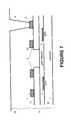
- FIG. 1shows a vertically integrated pixel 10 in accordance with an embodiment of the present invention.
- the pixel 10includes OLED device layer 12 and a TFT based backplane 14 (hereinafter referred to as TFT backplane).
- TFT backplaneTFT based backplane
- the OLED device 12includes one or more organic layers, a cathode and an anode.
- layers between the cathode and the anodeare referred to as OLED layers 18 .
- the OLED layers 18may be incorporating an electron transport layer, an organic light emitting layer, a hole transport layer, and a hole injection layer.
- FIG. 1an OLED top electrode 16 and an OLED bottom electrode 20 are shown as the cathode and the anode, respectively.
- the top electrode 16is transparent to enable the light to be emitted by the OLED in the direction opposite to the substrate (i.e., top-emitting OLED).
- top-emitting OLEDreverse top-emitting OLED structure, where the bottom electrode 20 is a cathode, and the top electrode 16 is an (transparent) anode, is also possible.
- Each pixel of the TFT backplane 14includes TFT pixel circuits formed on a substrate 30 .
- two TFTs T 1 and T 2form a pixel circuit.
- Each of the transistors T 1 -T 2has metallization for a source, a drain and a gate 6 .
- “ 2 ”represents either a source node or a drain node.
- the pixel 10may include more than two transistors.
- the OLED bottom electrode 20is formed on the top of the TFT backplane 14 , and is separated from the backplane 14 by a dielectric layer 22 .
- the dielectric layer 22is continuously provided everywhere on the top of the TFT pixel circuit except at a through-via 8 , which provides electrical connection between a specific node of the TFT pixel circuit and the OLED bottom electrode 20 .
- This specific nodemay be source node or drain node of a TFT, which depends on pixel circuit design and order of deposition for the OLED electrodes and layers. The details of circuit design and OLED fabrication are not to restrict the applicability of the present invention.
- the planarization dielectric and subsequent electrode layerhave a roughness of the order of 1 nm to permit successful OLED fabrication.
- a shield electrode 24is provided on the top of TFTs.
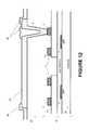
- FIG. 2shows an example of the pixel 10 of FIG. 1 .
- the sidewalls of the through-via 8are sloped.
- the OLED bottom electrode materialis disposed on the top surface of the dielectric layer 22 and along the sidewall of the sloped through-via 8 .
- FIG. 3is another example of the pixel of FIG. 1 .
- the shield electrode 24is provided above the TFT layers to keep the potential right on the top of the TFT pixel circuit at certain designed level regardless of the potential of the pixel electrode.
- the shield electrode 24may be a thin-film conductor, Al, Al-alloy, Mo, Cr or the like.
- An interlayer dielectric 21is provided between source/drain and shield layers.
- the connection between the desired pixel circuit node and the OLED bottom electrode 20is made by means-of a via in the interlayer insulator 21 , an interconnection plate 26 formed in the shield metal layer and the through-via 8 formed in the dielectric layer 22 .
- FIGS. 1-3The transistor structure of FIGS. 1-3 is typical for bottom-gate amorphous silicon TFT, and it is shown here as one possible example only. However, the method of pixel integration described here may be applicable in general to any appropriate known TFT backplane, including recrystallized or deposited poly-silicon, micro- and nano-crystalline silicon, CdSe and others.
- Active matrix TFT backplanemay be fabricated by successive deposition and patterning of metal, insulator and semiconductor layers leading to an overall profile height of the structure that is in the range of a few 100 nm to 1 micron, with nearly vertical or sharp-angled sidewalls of the structures.
- active organic layershave an overall thickness in the range of 10-100 nm. This implies that it is desirable to provide the OLED substrate with the roughness in 1 nm range to prevent electrical shorts between OLED layers or top and bottom electrodes.
- the substrateis either planer or has sufficiently smooth features whose vertical profile does not prevent reliable step coverage with thin OLED layers and their continuity, where necessary.
- the planarization dielectric and subsequent electrode layerare formed so as to have a roughness of the order of 1 nm.
- the dielectric layer 22smoothens or planarizes the vertical profiles of the structures on the substrate with fabricated TFT 14 . Further, the through-via profile in the dielectric layer 22 enables continuous sidewall coverage by the OLED bottom electrode material, and reduction of thickness of the pixel electrode.
- the dielectric layer 22 of the pixel 10is described in detail.
- the dielectric layer 22which is used for separating the TFT backplane 14 and the OLED bottom electrode 20 , smoothens or planarizes the vertical profiles of the structures on the substrate 30 with the fabricated TFT backplane 14 . This ensures continuity of the electrodes 16 , 20 and organic layers 18 in the OLED device 12 .
- This smooting/planarizingis achieved by using a planarizing dielectric, rather than one coating the substrate conformally.
- the planarizing dielectricmay be an organic polymer such as benzocyclobutene (BCB), polyimide, polyamide, acrilic and others.
- planarization layerMinimum thickness of planarization layer required depends on planarization properties of the dielectric and the profile height of TFT backplane.
- the thickness of planarizing dielectriccan be between 0.5 and 5 ⁇ mu ⁇ m.
- BCB layerabout 3 micron-thick, produced from photosensitive BCB-material is used as the planarizing layer.
- Planarizing dielectric layersare most often produced by application of corresponding initial material or monomer, which can be polymerized on the substrate by means of thermal cure, UV-cure with our without catalyst or by other method.
- the initial or monomer materialcan or cannot be patterned by photo-exposure. This property depends on chemical formulation of initial material or monomer by the manufacturer, whether the photosensitive components were added or not.
- the processing of the formermay include steps such as application of initial material, pattern definition by photoexposure trough a photomask, pattern developing and final cure. As a result a patterned polymer layer is obtained.
- the processing of the lattermay include application of initial material, cure, application and patterning of the mask, patterning cured polymer by means of plasma or wet etching with the mask, strip the mask.
- there are available both photosensitive and non-photosensitive versions of initial materialthat can lead to about the same chemical composition and structure of polymer dielectric material after final cure.
- BCB-layer made of photosensitive initial materialis used as a planarization dielectric.
- the present inventionmay be applicable to different types of material, such as but not limited to other planarization materials made of both of photosensitive and non-photosensitive initial formulations.
- FIG. 4shows the planarization effect of BCB-layer.
- a TFT substrateis schematically shown as-having stepwise profile of the patterns 50 with nearly vertical sidewalls and profile height of 0.5-0.9 .mu ⁇ m before application of BCB.
- the patterns 50are translated into 0.3-0.5 micron profiles 52 with the sidewall angle a about 10 degrees on the surface of BCB dielectric.
- the BCB-polymer filmwas produced by spin-coating photosensitive material (photosensitive BCB) with subsequent soft bake, exposure, post-exposure bake, pattern developing, solvent removal and cure. The process conditions are shown in Table 1.
- the through-via profile in the dielectric 22 of the pixel 10is now described in detail.
- the OLED bottom electrode 20is a conductive material such as indium-tin oxide (ITO) or the like, a metal film, Au, Pd, Ni or the like, sputtered, evaporated or fabricated by other method of thin film deposition. Other metals or thin multi-layer metal coatings may be also applicable.
- ITOindium-tin oxide
- a metal filmAu, Pd, Ni or the like
- sputteredevaporated or fabricated by other method of thin film deposition.
- Other metals or thin multi-layer metal coatingsmay be also applicable.
- conductive layers in a flat-panel display substrateare fabricated by sputtering which has limitations in terms of step coverage.
- the roughness of the conductive layerssuch as metal films and ITO, increases with layer thickness. A thinner electrode layer produces a smoother surface suitable for OLED fabrication. This also reduces the cost of production. Therefore, a reduction of the thickness of the
- the thickness of the metal to cover sidewall continuouslycould be of the same order as the depth of the via, which is equal to the thickness of the planarization dielectric layer (in a range of few micron).
- the sidewallis made sloped rather than vertical. That permits the thickness of the pixel electrode to be reduced substantially in a vertically stacked pixel structure.
- FIG. 5shows one example of a sidewall slop inside the via 8 of FIGS. 2 and 3 .
- an angle .beta. between the OLED bottom electrode 20 on the sidewall and a TFT final material 54is less than 90 degrees. If planarizing polymer dielectric is formed from photosensitive initial formulation, the sloped sidewall can be achieved by means of appropriate exposure conditions.
- the formation of the layer and patterning of the viaswere achieved by means of spin-coating photosensitive BCB material with subsequent soft-bake, light-exposure, developing, developer solvent removal and cure.
- Table 1the sidewall angle .beta. between the planarization layer 22 and the TFT final material 54 is shown as a function of photosensitive BCB-exposure time.
- the filmAfter the exposure, the film underwent 30 seconds post-exposure bake at 55 . degree C. and was developed for around 3 minutes in the developer solvent followed by 60 second bake at 75. degree C. for developer solvent removal and then final cure.
- the conditions for spin-coating, soft-bake, exposure, post-exposure bake and final cureare variable, and may depend on pixel design requirements. Recommendations about process conditions of Photo-BCB are given, for example, by “CycloteneTM 4000 Series Advanced Electronic Resins (Photo-BCB)” of Dow ChemicalTM, at hftp://www.dow.com/cyclotene/prods/402235 htm.
- the sidewall angle .beta.relates to the exposure time.
- the sidewall angle .beta.becomes smaller when exposure time is longer.
- the continuous coverage of the via sidewallswas achieved with a pixel electrode thickness of order 100 nm. This is much less than the through-via depth and enables the electrode surface of the OLED bottom electrode 20 to be sufficiently smooth.
- the sloped sidewallcan be also achieved. For example, this can be done, by optimizing masking and plasma etching steps.
- the parameters, materials and/or process of fabricating the sloped through-vias 8are adjusted so as to: ensure the continuous sidewall coverage by a material of the pixel electrode; make the roughness of the OLED electrode small enough (1 nm order) to prevent electrical shorts between the OLED top electrode 16 and the OLED bottom electrode 20 .
- FIGS. 6 to 8One example of fabricating the pixel 10 of FIG. 2 is shown in FIGS. 6 to 8 .
- the TFT backplane 14is fabricated ( FIG. 6 ) on the substrate 30 .
- the TFT backplane 14is coated with a planarization layer 22 , where the vias 8 with sloped sidewalls are opened to the selected nodes of the TFT backplane 14 ( FIG. 7 ).
- BCB planarization layer made of photosensitive formulationBCB material is applied by spin coating, and processed including soft-bake, UV-exposure through a photomask, post-exposure cure, developing, solvent removal and final cure.
- This sequencegives patterned material (with the through-vias 8 ) whose layer thickness and via sidewall slope depend on processing conditions, such as the exposure time as described above.
- processing conditionssuch as the exposure time as described above.
- surface roughness of cured BCB-layeris about 1 nm.
- a thin residual layer on the bottom of the through-vias 8is removed by plasma etching. Etching conditions are optimized for short etching time and minimum roughening of the BCB surface.
- the fabrication of the pixel 10may include plasma etching in CF4+O2 gas mixture or SF6+O2 gas mixture, a combination of high power high density plasma (for example, inductively coupled plasma) and low power reactive ion etching to achieve short etching time (few-20 seconds); and virtually no change in roughness after plasma etching.
- plasma etching in CF4+O2 gas mixture or SF6+O2 gas mixturea combination of high power high density plasma (for example, inductively coupled plasma) and low power reactive ion etching to achieve short etching time (few-20 seconds); and virtually no change in roughness after plasma etching.
- a conductive materialis deposited and patterned to form the OLED bottom electrode 20 ( FIG. 8 ). Finally, the OLED layers 18 and transparent electrode top electrode 16 of the OLED are continuously applied over the pixels ( FIG. 2 ).
- shield electrode 24 of FIG. 3is now described in detail.
- optional shield electrodecan be incorporated in a pixel structure.
- interlayer dielectric 21is deposited. This can be done by means of CVD, plasma-enhanced CVD process or other method. Silicon nitride, silicon oxide or silicon oxide nitride with the thickness between 0.1 and 1 .mu ⁇ m can be used as the interlayer dielectric 21 .
- shield metal layeris deposited and patterned to form the shield electrodes 24 and interconnection plates 26 .
- the interconnection plates 26serve to carry the potential from the certain node of TFT pixel, which can be either source or drain of a TFT, to the bottom electrode of OLED device 20 . Then, the planarization layer 22 is applied and patterned, as described above, which is followed by deposition and patterning of OLED bottom electrode 20 , deposition of the OLED layers 18 and top transparent electrode 16 .
- FIG. 9shows another example of the pixel of FIG. 1 .
- TFT source/drain metaloverlaps a contact plate 23 made of thin and smooth conductive material, such as Cr, Mo or other.
- the contact plate 23is formed by deposition and patterning of conductive films on the flat portion of pixel area.
- the thickness of the contact plate 23is between 50 and 150 nm.
- the contact between the certain node of the TFT circuit, which is in the source/drain metallization layer of the TFT backplane 14 , and the OLED bottom electrode 20is made via the contact plate 23 rather than directly.
- the source-drain metalmay have surface roughness well in excess of 1 nm. This may be the case if relatively thick metal layer, especially Al or Al-alloy, is used for source/drain metallization.
- a source-drain metallizationcan be required for the reasons associated with particular TFT fabrication process or display design. For example, highly conductive routing metallization is beneficial for reduction of power dissipation or better OLED brightness uniformity over the substrate area, especially if the display size is large. If such a source/drain metal would be in a direct contact with the bottom electrode of the OLED 20 , its surface roughness is translated into the roughness of electrode 20 inside via area.
- the contact to the bottom OLED electrode 20is made via the smooth contact plate 23 formed in separate layer.
- the TFT final metal (source/drain-metal) 2is Al or Al-alloy or the like
- the bottom OLED electrode 20is conductive oxide such as ITO
- having a contact to the electrode 20 made of Cr, Mo or the like instead of Al/Al-alloywill reduce contact resistance, heat dissipation in the contact and improve overall contact reliability.
- the contact plate 23is formed before source/drain metallization of the TFT backplane 14 .
- the TFT source drain-metalwhich is formed next, has to overlap some portion of the contact plate 23 but leave a sufficient portion open for formation of via 8 .
- source/drain metalcan be selectively etched over contact plate metal.
- source/drain metalis Al or Al-alloy
- using Cr for contact platewould provide excellent wet-etch selectivity. Roughness of the order 1 nm is easy to achieve with thin layers of metals such as Cr, Mo, Ti produced by sputtering, evaporation or other methods. Appropriate thin multi-layer metal coating can off cause be also used for contact plate 23 .
- FIG. 10shows another example of the pixel of FIG. 1 .
- the pixelhas the shield electrode 24 and the contact plate 23 .
- the shield 24is formed to keep electric potential on the top of the TFTs at certain desired level.
- the interlayer dielectric 21is deposited.
- the contact plate 23is formed of a thin and smooth metal layer such as Cr, Mo or the like on a flat portion of the pixel area.
- the thickness of the contact plate 23is between 50 and 150 nm.
- the vias in the dielectric 21are patterned to provide interconnections between the source/drain and shield metallization levels where necessary.
- shield metalis deposited and patterned to form the shield electrodes 24 and the interconnection plates 26 .
- the interconnection plate 26is to overlap the contact plate 23 but to leave its sufficient portion open, as shown schematically in FIG. 10 .
- the shield metalis selectively etched over the contact plate metal.
- the planarization dielectric 22is applied and though-via 8 is formed on the top of the portion of contact plate 23 , which is free from shield metal ( FIG. 10 ). Further steps (deposition and patterning of the bottom OLED electrode 20 , deposition of the OLED layers 18 and OLED top electrode) may be performed in a similar manner as described above.
- FIG. 11shows a vertically integrated TFT-OLED pixel in accordance with another embodiment of the present invention.
- the dielectric layer 22 and the through-via profile of FIG. 11are similar to those of FIG. 2 .
- the pixel 10 of FIG. 11further includes an additional dielectric layer, i.e., dielectric cap 40 , which is deposited on the top of the OLED bottom electrode 20 .
- the dielectric cap 40is patterned so as to cover the via area and the edges of the OLED bottom electrode pattern leaving the rest of the OLED bottom electrode 20 uncovered.
- the OLED layers 18 and the top electrode 16are deposited in a similar manner as described above.
- the dielectric cap 40is provided to avoid breakage of continuously deposited OLED top electrode layers at the pixel edges, and therefore to prevent shortage of OLED devices. Further, the dielectric cap 40 insulates the via area, which, depending on the structure and fabrication method of the TFT backplane 14 , may have higher surface roughness than the rest of the OLED bottom electrode 20 and may be therefore a source of the shortage of the OLED device.
- the dielectric cap 40is made of material, which may be either polymer dielectric (such as, BCB, polyimide, other polymer dielectric) or inorganic insulator (such as, silicon oxide, silicon nitride, silicon oxide-nitride).
- polymer dielectricsuch as, BCB, polyimide, other polymer dielectric
- inorganic insulatorsuch as, silicon oxide, silicon nitride, silicon oxide-nitride.
- the thickness of the polymer insulatormay be from a few 100 nm to a few micron. With the polymer insulator, as shown above, the sidewall profile of the cap pattern can be made smooth enough to enable continuous coverage with the OLED layers 18 and OLED top electrode 16 .
- the thickness of the dielectric cap 40is adjusted in such a way to enable continuous coverage of the profile steps associated with the cap layer by the OLED top electrode 16 .
- the thickness of an inorganic insulatorcan be between 50 and 500 nm (most preferably 50 to 200 nm).
- the conditions of dry or wet patterning of an inorganic insulator, such as silicon oxide or the like,can be adjusted to form the sloped sidewalls.
- FIGS. 6 to 8, 11 and 12One example of the fabricating process for the pixel 10 of FIG. 11 is seen from FIGS. 6 to 8, 11 and 12 .
- the planarization dielectric 22is applied where the vias 8 with sloped sidewalls are opened to the source-drain metal 2 ( FIG. 7 ).
- a conductive materialis deposited and patterned to form the OLED bottom electrode 20 ( FIG. 8 ).
- the dielectric cap 40is disposed as described above ( FIG. 12 ).
- the OLED layers 18 and the electrodeare disposed and which completes the formation of the pixel structure shown in FIG. 11 .
- FIG. 13shows a vertically integrated pixel in accordance with another embodiment of the present invention.
- the pixel 10 in FIG. 13includes the shield electrode 26 and the dielectric cap 40 .
- the TFT backplane 14is fabricated followed by deposition and patterning of the interlayer dielectric 21 and the shield electrode 24 .
- the vias in the interlayer dielectricare formed to provide interconnection between the source/drain and interconnection plates 26 made in the shield metallization layer, where necessary.
- shield metalis deposited and patterned to form the shield electrodes 24 and the interconnection plates 26 .
- the planarization dielectric 22 and the OLED bottom electrode 20are deposited and patterned in a similar manner as described above.
- the cap dielectric layer 40is disposed and pattern as described in the previous embodiment.
- the OLED layers 18 and the OLED top electrode 16are formed.
- the vertical pixel integrationprovides higher aperture ratio, which leads to: the possibility of using more advanced multi-transistor pixel driver circuit for improved display performance without taking up extra light-emitting area from the pixel; the possibility of using a TFT backplane, such as amorphous silicon, having lower mobility in contrast to poly-silicon, thereby simplifying the manufacturing process and reducing cost; and the reduction of current density through OLED providing higher operational stability and improved lifetime of the display device.
- the fabrication process sequences and critical processing details described abovesolve a variety of issues pertinent to vertical integration such as: smoothening out/planarizing vertical profiles in the dielectric layer 22 of the structures on the TFT substrate 14 to enable continuity of the OLED device layers 12 ; continuous sidewall coverage by pixel electrode material in the through-via profile in the dielectric 22 ; roughness of the order of 1 nm on the dielectric 22 and subsequent electrode layer, which enables successful OLED fabrication and to higher yield rate; and capping structure feature which do not comply to OLED fabrication process in terms of step height, sidewall angle and surface roughness by a dielectric layer.
- the via and edges of the electrodeare covered with the dielectric cap 40 .
Landscapes
- Engineering & Computer Science (AREA)
- Microelectronics & Electronic Packaging (AREA)
- Physics & Mathematics (AREA)
- Manufacturing & Machinery (AREA)
- Optics & Photonics (AREA)
- Geometry (AREA)
- Electroluminescent Light Sources (AREA)
- Devices For Indicating Variable Information By Combining Individual Elements (AREA)
Abstract
Description
This application is a continuation of U.S. application Ser. No. 13/112,654, filed May 20, 2011, which is a continuation of U.S. application Ser. No. 10/546,695, filed May 18, 2006, which is a U.S. National Stage of International Application No. PCT/CA2004/00256, filed Feb. 24, 2003, which claims priority to Canadian Patent No. 2,419,704, filed Feb. 24, 2003, each of which is hereby incorporated by reference herein in its entirety.
This invention relates to a pixel, more particularly, to a pixel having an organic emitting diode.
Organic light emitting diodes (OLEDS) are electro-luminescent (EL) devices for emitting light. The OLED generates light by a current flowing through an organic compound. Pixels including the OLEDs have various advantages, i.e. simple structure, fast response and wide viewing angle. There are two types of matrix displays with the OLEDs, passive type and active type. In the active matrix display, thin-film transistors (TFT) are provided in each pixel to drive the OLEDs of display. The active matrix eliminates high peak driving currents and thereby enables high-resolutions and high information density, improves power consumption and life-time compared to the passive matrix.
Vertical pixel architecture, in which the TFT and the OLED device are stacked vertically, has been developed. Such architecture can achieve higher aperture ratios. This favors using lower mobility amorphous silicon TFT backplanes compared polysilicon TFT technology, which is of higher mobility but also of higher cost.
The difficult part in building the vertical stacked pixels is to make a TFT backplane suitable for subsequent OLED fabrication and provide high yield and good performance of OLED pixels. The OLED device is typically made of very thin layers. Overall thickness of organic layers in the OLED is of the order of 100 nm. For this reason, it requires a smooth substrate to achieve good performance and yield. Step-wise features on the substrate surface and roughness can cause deterioration of light-emitting properties or OLED device failure due to shorts between its electrodes.
It is, therefore, desirable to provide new pixel architecture, which can achieve a high aperture rate, and at the same time, higher yield rate.
It is an object of the invention to provide novel pixel architecture that obviates or mitigates at least one of the disadvantages of existing pixels.
In accordance with an aspect of the present invention, there is provided vertical pixel architecture in which a planarization dielectric layer is disposed between a TFT based backplane and OLED layers. The planarization dielectric layer is thick enough to smoothen a TFT substrate profile to such an extent that will make it suitable for subsequent fabrication of the OLEDs. Preferably, the planarization dielectric and subsequent electrode layer have a roughness of the order of 1 nm to permit successful OLED fabrication.
Electrical connection between TFT circuit and OLED is provided by means through-via made in planarization dielectric.
In accordance with a further aspect of the present invention, there is provided a vertical pixel architecture in which continuous sidewall coverage is provided by pixel electrode material in a through-via profile provided in the planarization dielectric. This is achieved by the formation of sloped sidewalls of the through-via. Preferably, the angle between the via and a TFT substrate is less than 45 degrees.
In accordance with a further aspect of the present invention, the interconnection between TFT final metal and OLED bottom electrode in vertical pixel architecture is provided via a smooth contact plate made of conductive material.
In accordance with a further aspect of the present invention, there is provided a vertical pixel architecture in which a dielectric layer is deposited and patterned on the top of the pixel electrode in such a way that it covers pixel via and the edges of the pixel electrode.
Other aspects and features of the present invention will be readily apparent to those skilled in the art from a review of the following detailed description of preferred embodiments in conjunction with the accompanying drawings.
The invention will be further understood from the following description with reference to the drawings in which:
A vertically integrated pixel of the present invention is described.FIG. 1 shows a vertically integratedpixel 10 in accordance with an embodiment of the present invention. Thepixel 10 includesOLED device layer 12 and a TFT based backplane14 (hereinafter referred to as TFT backplane).
TheOLED device 12 includes one or more organic layers, a cathode and an anode. In the description, layers between the cathode and the anode are referred to asOLED layers 18. TheOLED layers 18 may be incorporating an electron transport layer, an organic light emitting layer, a hole transport layer, and a hole injection layer. InFIG. 1 , an OLEDtop electrode 16 and anOLED bottom electrode 20 are shown as the cathode and the anode, respectively.
Thetop electrode 16 is transparent to enable the light to be emitted by the OLED in the direction opposite to the substrate (i.e., top-emitting OLED). However, reverse top-emitting OLED structure, where thebottom electrode 20 is a cathode, and thetop electrode 16 is an (transparent) anode, is also possible.
Each pixel of theTFT backplane 14 includes TFT pixel circuits formed on asubstrate 30. InFIG. 1 , two TFTs T1 and T2 form a pixel circuit. Each of the transistors T1-T2 has metallization for a source, a drain and agate 6. InFIG. 1 , “2” represents either a source node or a drain node. However, thepixel 10 may include more than two transistors.
TheOLED bottom electrode 20 is formed on the top of theTFT backplane 14, and is separated from thebackplane 14 by adielectric layer 22. Thedielectric layer 22 is continuously provided everywhere on the top of the TFT pixel circuit except at a through-via 8, which provides electrical connection between a specific node of the TFT pixel circuit and theOLED bottom electrode 20. This specific node may be source node or drain node of a TFT, which depends on pixel circuit design and order of deposition for the OLED electrodes and layers. The details of circuit design and OLED fabrication are not to restrict the applicability of the present invention.
Preferably, the planarization dielectric and subsequent electrode layer have a roughness of the order of 1 nm to permit successful OLED fabrication. Optionally, ashield electrode 24 is provided on the top of TFTs.
The transistor structure ofFIGS. 1-3 is typical for bottom-gate amorphous silicon TFT, and it is shown here as one possible example only. However, the method of pixel integration described here may be applicable in general to any appropriate known TFT backplane, including recrystallized or deposited poly-silicon, micro- and nano-crystalline silicon, CdSe and others.
Active matrix TFT backplane may be fabricated by successive deposition and patterning of metal, insulator and semiconductor layers leading to an overall profile height of the structure that is in the range of a few 100 nm to 1 micron, with nearly vertical or sharp-angled sidewalls of the structures. On the other hand, in high performance small molecule and polymer organic light emitting devices, active organic layers have an overall thickness in the range of 10-100 nm. This implies that it is desirable to provide the OLED substrate with the roughness in 1 nm range to prevent electrical shorts between OLED layers or top and bottom electrodes. In addition, it is desirable that the substrate is either planer or has sufficiently smooth features whose vertical profile does not prevent reliable step coverage with thin OLED layers and their continuity, where necessary.
In the embodiment of the preset invention, the planarization dielectric and subsequent electrode layer are formed so as to have a roughness of the order of 1 nm. Thedielectric layer 22 smoothens or planarizes the vertical profiles of the structures on the substrate with fabricatedTFT 14. Further, the through-via profile in thedielectric layer 22 enables continuous sidewall coverage by the OLED bottom electrode material, and reduction of thickness of the pixel electrode.
Thedielectric layer 22 of thepixel 10 is described in detail. Thedielectric layer 22, which is used for separating theTFT backplane 14 and theOLED bottom electrode 20, smoothens or planarizes the vertical profiles of the structures on thesubstrate 30 with the fabricatedTFT backplane 14. This ensures continuity of theelectrodes organic layers 18 in theOLED device 12. This smooting/planarizing is achieved by using a planarizing dielectric, rather than one coating the substrate conformally. The planarizing dielectric may be an organic polymer such as benzocyclobutene (BCB), polyimide, polyamide, acrilic and others. Minimum thickness of planarization layer required depends on planarization properties of the dielectric and the profile height of TFT backplane. The thickness of planarizing dielectric can be between 0.5 and 5 ·mu·m. In the embodiment of the present invention, BCB layer, about 3 micron-thick, produced from photosensitive BCB-material is used as the planarizing layer.
Planarizing dielectric layers are most often produced by application of corresponding initial material or monomer, which can be polymerized on the substrate by means of thermal cure, UV-cure with our without catalyst or by other method. The initial or monomer material can or cannot be patterned by photo-exposure. This property depends on chemical formulation of initial material or monomer by the manufacturer, whether the photosensitive components were added or not. The processing of the former may include steps such as application of initial material, pattern definition by photoexposure trough a photomask, pattern developing and final cure. As a result a patterned polymer layer is obtained. The processing of the latter may include application of initial material, cure, application and patterning of the mask, patterning cured polymer by means of plasma or wet etching with the mask, strip the mask. In some cases, like polyimides and BCB, there are available both photosensitive and non-photosensitive versions of initial material that can lead to about the same chemical composition and structure of polymer dielectric material after final cure.
In the embodiment of the present invention, BCB-layer made of photosensitive initial material is used as a planarization dielectric. However, the present invention may be applicable to different types of material, such as but not limited to other planarization materials made of both of photosensitive and non-photosensitive initial formulations.
| TABLE 1 |
| Process conditions for planarization layer |
| Nr | Step | Conditions |
| 1 | Spin-coating | 2500-4000 rpm, 25-40 |
| 2 | Soft-bake | 60-70 degree C., 90 sec |
| 3 | Exposure | 12-60 sec |
| 4 | Post-exposure bake | 50-60.degree C., 30 sec |
| 5 | Developing | 2-4 |
| 6 | Solvent removal | 75 degree C., 60 sec |
| 7 | Cure | 190-250.degree C., 2-4 hrs |
The through-via profile in the dielectric22 of thepixel 10 is now described in detail. TheOLED bottom electrode 20 is a conductive material such as indium-tin oxide (ITO) or the like, a metal film, Au, Pd, Ni or the like, sputtered, evaporated or fabricated by other method of thin film deposition. Other metals or thin multi-layer metal coatings may be also applicable. Typically, conductive layers in a flat-panel display substrate are fabricated by sputtering which has limitations in terms of step coverage. On the other hand, the roughness of the conductive layers such as metal films and ITO, increases with layer thickness. A thinner electrode layer produces a smoother surface suitable for OLED fabrication. This also reduces the cost of production. Therefore, a reduction of the thickness of the pixel electrode while maintaining its continuity over substrate profile is desirable.
If the through-via had a nearly vertical sidewall, the thickness of the metal to cover sidewall continuously, could be of the same order as the depth of the via, which is equal to the thickness of the planarization dielectric layer (in a range of few micron). In thepixel 10 ofFIGS. 2 to 3 , the sidewall is made sloped rather than vertical. That permits the thickness of the pixel electrode to be reduced substantially in a vertically stacked pixel structure.
An example of sidewall slope control in the through-via for BCB-layer (i.e., dielectric22), which is produced from photosensitive initial material, is presented in Table 2.
| TABLE 2 |
| Sidewall angle in cured BCB layer which was produced from |
| photosensitive BCB-material as a function of exposure time |
| Exposure time, sec | Sidewall angle, deg | ||
| 20 | 45 | ||
| 30 | 33 | ||
| 13 | 27 | ||
The formation of the layer and patterning of the vias were achieved by means of spin-coating photosensitive BCB material with subsequent soft-bake, light-exposure, developing, developer solvent removal and cure. In Table 1, the sidewall angle .beta. between theplanarization layer 22 and the TFTfinal material 54 is shown as a function of photosensitive BCB-exposure time.
After the exposure, the film underwent30 seconds post-exposure bake at55. degree C. and was developed for around 3 minutes in the developer solvent followed by 60 second bake at 75. degree C. for developer solvent removal and then final cure.
The conditions for spin-coating, soft-bake, exposure, post-exposure bake and final cure are variable, and may depend on pixel design requirements. Recommendations about process conditions of Photo-BCB are given, for example, by “Cyclotene™ 4000 Series Advanced Electronic Resins (Photo-BCB)” of Dow Chemical™, at hftp://www.dow.com/cyclotene/prods/402235 htm.
As shown in Table 2, the sidewall angle .beta. relates to the exposure time. The sidewall angle .beta. becomes smaller when exposure time is longer. For example, for the sidewall angle .beta. of less than 45 degrees and the planarization dielectric thickness of around 3 .mu.m, the continuous coverage of the via sidewalls was achieved with a pixel electrode thickness of order 100 nm. This is much less than the through-via depth and enables the electrode surface of theOLED bottom electrode 20 to be sufficiently smooth.
For polymer dielectric material made of non-photosensitive initial formulation, the sloped sidewall can be also achieved. For example, this can be done, by optimizing masking and plasma etching steps.
The parameters, materials and/or process of fabricating the sloped through-vias 8 are adjusted so as to: ensure the continuous sidewall coverage by a material of the pixel electrode; make the roughness of the OLED electrode small enough (1 nm order) to prevent electrical shorts between theOLED top electrode 16 and theOLED bottom electrode 20.
One example of fabricating thepixel 10 ofFIG. 2 is shown inFIGS. 6 to 8 . First, theTFT backplane 14 is fabricated (FIG. 6 ) on thesubstrate 30. Next, theTFT backplane 14 is coated with aplanarization layer 22, where thevias 8 with sloped sidewalls are opened to the selected nodes of the TFT backplane14 (FIG. 7 ). For BCB planarization layer made of photosensitive formulation, BCB material is applied by spin coating, and processed including soft-bake, UV-exposure through a photomask, post-exposure cure, developing, solvent removal and final cure. This sequence gives patterned material (with the through-vias8) whose layer thickness and via sidewall slope depend on processing conditions, such as the exposure time as described above. Typically, surface roughness of cured BCB-layer is about 1 nm. Then, a thin residual layer on the bottom of the through-vias 8 is removed by plasma etching. Etching conditions are optimized for short etching time and minimum roughening of the BCB surface. For example, the fabrication of thepixel 10 may include plasma etching in CF4+O2 gas mixture or SF6+O2 gas mixture, a combination of high power high density plasma (for example, inductively coupled plasma) and low power reactive ion etching to achieve short etching time (few-20 seconds); and virtually no change in roughness after plasma etching.
Subsequently, a conductive material is deposited and patterned to form the OLED bottom electrode20 (FIG. 8 ). Finally; the OLED layers18 and transparentelectrode top electrode 16 of the OLED are continuously applied over the pixels (FIG. 2 ).
Theshield electrode 24 ofFIG. 3 is now described in detail. As shown inFIG. 3 , optional shield electrode can be incorporated in a pixel structure. After formation of theTFT backplane 14,interlayer dielectric 21 is deposited. This can be done by means of CVD, plasma-enhanced CVD process or other method. Silicon nitride, silicon oxide or silicon oxide nitride with the thickness between 0.1 and 1 .mu·m can be used as theinterlayer dielectric 21. After formation of the vias in the interlayer dielectric that provide interconnection between source-drain and shield metallization layers, shield metal layer is deposited and patterned to form theshield electrodes 24 andinterconnection plates 26. Theinterconnection plates 26 serve to carry the potential from the certain node of TFT pixel, which can be either source or drain of a TFT, to the bottom electrode ofOLED device 20. Then, theplanarization layer 22 is applied and patterned, as described above, which is followed by deposition and patterning ofOLED bottom electrode 20, deposition of the OLED layers18 and toptransparent electrode 16.
The contact between the certain node of the TFT circuit, which is in the source/drain metallization layer of theTFT backplane 14, and theOLED bottom electrode 20 is made via thecontact plate 23 rather than directly.
Depending on structure and fabrication method of theTFT backplane 14, the source-drain metal may have surface roughness well in excess of 1 nm. This may be the case if relatively thick metal layer, especially Al or Al-alloy, is used for source/drain metallization. Such a source-drain metallization can be required for the reasons associated with particular TFT fabrication process or display design. For example, highly conductive routing metallization is beneficial for reduction of power dissipation or better OLED brightness uniformity over the substrate area, especially if the display size is large. If such a source/drain metal would be in a direct contact with the bottom electrode of theOLED 20, its surface roughness is translated into the roughness ofelectrode 20 inside via area. This can make this area a source of shortages betweenOLED electrodes FIG. 9 , the contact to thebottom OLED electrode 20 is made via thesmooth contact plate 23 formed in separate layer. In addition, if the TFT final metal (source/drain-metal)2 is Al or Al-alloy or the like, and thebottom OLED electrode 20 is conductive oxide such as ITO, having a contact to theelectrode 20 made of Cr, Mo or the like instead of Al/Al-alloy will reduce contact resistance, heat dissipation in the contact and improve overall contact reliability.
Thecontact plate 23 is formed before source/drain metallization of theTFT backplane 14. The TFT source drain-metal, which is formed next, has to overlap some portion of thecontact plate 23 but leave a sufficient portion open for formation of via8. In addition, it is desirable that source/drain metal can be selectively etched over contact plate metal. For example, if source/drain metal is Al or Al-alloy, using Cr for contact plate would provide excellent wet-etch selectivity. Roughness of the order 1 nm is easy to achieve with thin layers of metals such as Cr, Mo, Ti produced by sputtering, evaporation or other methods. Appropriate thin multi-layer metal coating can off cause be also used forcontact plate 23.
After theTFT backplane 14 with thecontact plate 23 is formed, further steps, application and patterning of theplanarization dielectric layer 22, deposition and patterning of thebottom OLED electrode 20, deposition of the OLED layers18 and OLED top electrode are performed in a manner described above.
Thepixel 10 ofFIG. 11 further includes an additional dielectric layer, i.e.,dielectric cap 40, which is deposited on the top of theOLED bottom electrode 20. Thedielectric cap 40 is patterned so as to cover the via area and the edges of the OLED bottom electrode pattern leaving the rest of theOLED bottom electrode 20 uncovered. The OLED layers18 and thetop electrode 16 are deposited in a similar manner as described above.
Thedielectric cap 40 is provided to avoid breakage of continuously deposited OLED top electrode layers at the pixel edges, and therefore to prevent shortage of OLED devices. Further, thedielectric cap 40 insulates the via area, which, depending on the structure and fabrication method of theTFT backplane 14, may have higher surface roughness than the rest of theOLED bottom electrode 20 and may be therefore a source of the shortage of the OLED device.
Thedielectric cap 40 is made of material, which may be either polymer dielectric (such as, BCB, polyimide, other polymer dielectric) or inorganic insulator (such as, silicon oxide, silicon nitride, silicon oxide-nitride).
The thickness of the polymer insulator may be from a few 100 nm to a few micron. With the polymer insulator, as shown above, the sidewall profile of the cap pattern can be made smooth enough to enable continuous coverage with the OLED layers18 andOLED top electrode 16.
With inorganic insulator, the thickness of thedielectric cap 40 is adjusted in such a way to enable continuous coverage of the profile steps associated with the cap layer by theOLED top electrode 16. The thickness of an inorganic insulator can be between 50 and 500 nm (most preferably 50 to 200 nm). In addition, the conditions of dry or wet patterning of an inorganic insulator, such as silicon oxide or the like, can be adjusted to form the sloped sidewalls.
One example of the fabricating process for thepixel 10 ofFIG. 11 is seen fromFIGS. 6 to 8, 11 and 12 . As theTFT backplane 14 is formed on the substrate30 (FIG. 6 ), theplanarization dielectric 22 is applied where thevias 8 with sloped sidewalls are opened to the source-drain metal2 (FIG. 7 ). A conductive material is deposited and patterned to form the OLED bottom electrode20 (FIG. 8 ). Then, thedielectric cap 40 is disposed as described above (FIG. 12 ). Then, the OLED layers18 and the electrode are disposed and which completes the formation of the pixel structure shown inFIG. 11 .
According to the embodiments of the present invention, the vertical pixel integration provides higher aperture ratio, which leads to: the possibility of using more advanced multi-transistor pixel driver circuit for improved display performance without taking up extra light-emitting area from the pixel; the possibility of using a TFT backplane, such as amorphous silicon, having lower mobility in contrast to poly-silicon, thereby simplifying the manufacturing process and reducing cost; and the reduction of current density through OLED providing higher operational stability and improved lifetime of the display device.
Further, the fabrication process sequences and critical processing details described above solve a variety of issues pertinent to vertical integration such as: smoothening out/planarizing vertical profiles in thedielectric layer 22 of the structures on theTFT substrate 14 to enable continuity of the OLED device layers12; continuous sidewall coverage by pixel electrode material in the through-via profile in the dielectric22; roughness of the order of1 nm on the dielectric22 and subsequent electrode layer, which enables successful OLED fabrication and to higher yield rate; and capping structure feature which do not comply to OLED fabrication process in terms of step height, sidewall angle and surface roughness by a dielectric layer. The via and edges of the electrode are covered with thedielectric cap 40.
While particular embodiments of the present invention have been shown and described, changes and modifications may be made to such embodiments without departing from the true scope of the invention which is defined in the claims.
Claims (21)
1. A pixel having a vertical architecture, comprising:
an organic light emitting diode (OLED) device having a bottom electrode, one or more OLED layers and a transparent top electrode for emitting light;
a thin-film transistor (TFT) based backplane for electrically driving the OLED device, the TFT based backplane being vertically integrated with the OLED layers and located below said bottom electrode to form a top-emitting OLED, the TFT based backplane comprising:
source and drain nodes; and
a thin conductive contact plate formed entirely on a flat portion of the pixel area and electrically coupled to a source or drain node, the thin conductive contact plate defined by a top surface, a bottom surface, and side surfaces, its vertical dimension defined by the top and bottom surfaces substantially smaller than its horizontal dimensions defined by the side surfaces;
a planarization dielectric layer provided between the TFT based backplane and the OLED bottom electrode so as to planarize the vertical profile on the TFT based backplane, said planarization dielectric layer being in direct contact with both said TFT based backplane and said OLED bottom electrode;
a via in said planarization dielectric layer to provide a communication path between said TFT based backplane and said OLED device and through said thin conductive contact plate; and
a dielectric layer deposited on top of said bottom electrode and covering said via and all the edges of said bottom electrode while leaving the rest of said bottom electrode uncovered.
2. The pixel as claimed inclaim 1 , wherein the sidewall of said via in the planarization layer is sloped against the TFT based backplane.
3. The pixel as claimed inclaim 2 , wherein the TFT based backplane includes:
a substrate;
an interlayer dielectric layer on the source and drain nodes; and
an interconnection plate patterned on a via of the interlayer dielectric layer and being connected to the source or drain node and the thin conductive contact plate;
wherein the planarization dielectric layer planarizes the vertical profile on the substrate with the fabricated TFT based backplane, and the sloped via providing the communication path through the interconnection plate.
4. The pixel as claimed inclaim 3 , wherein the thin conductive contact plate is formed on a flat portion of the interlayer dielectric layer such that the interconnection plate overlaps a part of the contact plate.
5. The pixel as claimed inclaim 3 , further comprising a shield electrode disposed between the planarization dielectric layer and the interlayer dielectric layer, which is located separately from the interconnection plate.
6. The pixel as claimed inclaim 2 , wherein the TFT based backplane includes:
a substrate;
wherein the thin conductive contact plate is formed such that the source or drain material overlaps the thin conductive contact plate and the planarization dielectric layer planarizes the vertical profile on the substrate with the fabricated TFT based backplane.
7. The pixel as claimed inclaim 6 , further comprising a shield electrode formed separately from said thin conductive contact plate.
8. The pixel as claimed inclaim 1 , in which said dielectric layer is patterned in such a way that it insulates the OLED layers from the OLED bottom electrode at pixel edges and in and around the via while leaving the rest of the OLED bottom electrode in the direct contact with the OLED layers.
9. The pixel as claimed inclaim 8 , wherein said dielectric layer includes polymer dielectric or inorganic insulator.
10. The pixel as claimed inclaim 8 , wherein said dielectric layer includes material selected from the group from BCB, polyimide, polymer dielectric, silicon nitride and a thin film inorganic.
11. The pixel as claimed inclaim 1 , wherein the pixel has a roughness of the order of 1 nm on the planarization dielectric layer and subsequent electrode layer.
12. The pixel as claimed inclaim 1 , further comprising continuous sidewall coverage by pixel electrode material in the via profile in the planarization dielectric layer.
13. The pixel as claimed inclaim 1 , further comprising a shield electrode formed over the TFT.
14. The pixel as claimed inclaim 1 , wherein the planarization dielectric layer includes photosensitive benzocylobutene (BCB), the slope of the via being adjusted by the exposure time of the photosensitive BCB.
15. A method of fabricating a pixel, the pixel having an organic light emitting diode (OLED) bottom electrode, one or more OLED layers on the OLED bottom electrode, a transparent top electrode, and a thin-film transistor (TFT) based backplane for electrically driving the OLED and including a substrate, the method comprising the steps of:
providing the TFT based backplane on said substrate, including forming within the TFT based backplane a thin conductive contact plate entirely on a flat portion of the pixel area and electrically coupled to a source or drain node of the TFT based backplane, the thin conductive contact plate defined by a top surface, a bottom surface, and side surfaces, its vertical dimension defined by the top and bottom surfaces substantially smaller than its horizontal dimensions defined by the side surfaces;
providing a dielectric layer on the TFT based backplane, including the step of planarizing a vertical profile in the dielectric layer so as to planarize the vertical profile on the substrate with the TFT based backplane, said planarized dielectric layer being in direct contact with said TFT based backplane;
forming a via in said planarization dielectric layer to provide a communication path between said TFT based backplane and said OLED device and through said thin conductive contact plate;
depositing said OLED bottom electrode directly on top of said planarized dielectric layer and extending through said via into direct contact with said thin conductive contact plate of said TFT based backplane; and
depositing a dielectric layer on top of said bottom electrode and covering said via and all the edges of said bottom electrode while leaving the rest of said bottom electrode uncovered.
16. A method as claimed inclaim 15 , wherein forming said via which provides the communication path between the TFT backplane and the OLED device through the planarization dielectric layer, comprises forming the via such that the sidewall of the via in the planarization layer is sloped against the TFT based backplane.
17. A method as claimed inclaim 15 , wherein providing said dielectric layer between the OLED bottom electrode and the OLED layers, comprises patterning the dielectric layer in such a way that it insulates the OLED layers from the OLED bottom electrode at pixel edges and in and around the via while leaving the rest of the OLED bottom electrode in the direct contact with the OLED layers.
18. A method as claimed inclaim 15 , wherein the planarization dielectric layer including photosensitive benzocylobutene (BCB), further comprising the step of adjusting the exposure time of the photosensitive BCB such that the sidewall of the via in the planarization layer is sloped against the TFT based backplane.
19. A method as claimed inclaim 15 , wherein the pixel is formed such that the pixel has a roughness of the order of 1 nm on the planarization dielectric layer and subsequent electrode layer.
20. A method as claimed inclaim 15 , further comprising the step of providing continuous sidewall coverage by pixel electrode material in the via profile in the planarization dielectric layer.
21. A method of fabricating a pixel, the pixel having an organic light emitting diode (OLED) bottom electrode, one or more OLED layers on the OLED bottom electrode, and a thin-film transistor (TFT) based backplane for electrically driving the OLED and including a substrate, the method comprising the steps of:
providing the TFT based backplane on said substrate, including forming within the TFT based backplane a thin conductive contact plate entirely on a flat portion of the pixel area and electrically coupled to a source or drain node of the TFT based backplane, the thin conductive contact plate defined by a top surface, a bottom surface, and side surfaces, its vertical dimension defined by the top and bottom surfaces substantially smaller than its horizontal dimensions defined by the side surfaces;
providing a dielectric layer on the TFT based backplane, including the step of planarizing a vertical profile in the dielectric layer so as to planarize the vertical profile on the substrate with the TFT based backplane, said planarized dielectric layer being in direct contact with said TFT based backplane;
forming a via in said planarization dielectric layer to provide a communication path between said TFT based backplane and said OLED device and through said thin conductive contact plate;
depositing said OLED bottom electrode directly on top of said planarized dielectric layer and extending through said via into direct contact with said thin conductive contact plate of said TFT based backplane, and
depositing a dielectric layer on top of said bottom electrode and covering said via and all the edges of said bottom electrode while leaving the rest of said bottom electrode uncovered.
Priority Applications (6)
| Application Number | Priority Date | Filing Date | Title |
|---|---|---|---|
| US15/403,313US10163996B2 (en) | 2003-02-24 | 2017-01-11 | Pixel having an organic light emitting diode and method of fabricating the pixel |
| US16/193,702US10439013B2 (en) | 2003-02-24 | 2018-11-16 | Pixel having an organic light emitting diode and method of fabricating the pixel |
| US16/553,423US10991777B2 (en) | 2003-02-24 | 2019-08-28 | Pixel having an organic light emitting diode and method of fabricating the pixel |
| US17/215,259US11348984B2 (en) | 2003-02-24 | 2021-03-29 | Pixel having an organic light emitting diode and method of fabricating the pixel |
| US17/741,957US11665934B2 (en) | 2003-02-24 | 2022-05-11 | Pixel having an organic light emitting diode and method of fabricating the pixel |
| US18/137,470US20230292557A1 (en) | 2003-02-24 | 2023-04-21 | Pixel having an organic light emitting diode and method of fabricating the pixel |
Applications Claiming Priority (6)
| Application Number | Priority Date | Filing Date | Title |
|---|---|---|---|
| CA002419704ACA2419704A1 (en) | 2003-02-24 | 2003-02-24 | Method of manufacturing a pixel with organic light-emitting diode |
| CA2419704 | 2003-02-24 | ||
| US10/546,695US7948170B2 (en) | 2003-02-24 | 2004-02-24 | Pixel having an organic light emitting diode and method of fabricating the pixel |
| PCT/CA2004/000256WO2004075245A2 (en) | 2003-02-24 | 2004-02-24 | A pixel having an organic light emitting diode and method of fabricating the pixel |
| US13/112,654US20110272695A1 (en) | 2003-02-24 | 2011-05-20 | Pixel having an organic light emitting diode and method of fabricating the pixel |
| US15/403,313US10163996B2 (en) | 2003-02-24 | 2017-01-11 | Pixel having an organic light emitting diode and method of fabricating the pixel |
Related Parent Applications (1)
| Application Number | Title | Priority Date | Filing Date |
|---|---|---|---|
| US13/112,654ContinuationUS20110272695A1 (en) | 2003-02-24 | 2011-05-20 | Pixel having an organic light emitting diode and method of fabricating the pixel |
Related Child Applications (1)
| Application Number | Title | Priority Date | Filing Date |
|---|---|---|---|
| US16/193,702ContinuationUS10439013B2 (en) | 2003-02-24 | 2018-11-16 | Pixel having an organic light emitting diode and method of fabricating the pixel |
Publications (2)
| Publication Number | Publication Date |
|---|---|
| US20170125498A1 US20170125498A1 (en) | 2017-05-04 |
| US10163996B2true US10163996B2 (en) | 2018-12-25 |
Family
ID=32873349
Family Applications (8)
| Application Number | Title | Priority Date | Filing Date |
|---|---|---|---|
| US10/546,695Active2026-10-25US7948170B2 (en) | 2003-02-24 | 2004-02-24 | Pixel having an organic light emitting diode and method of fabricating the pixel |
| US13/112,654AbandonedUS20110272695A1 (en) | 2003-02-24 | 2011-05-20 | Pixel having an organic light emitting diode and method of fabricating the pixel |
| US15/403,313Expired - LifetimeUS10163996B2 (en) | 2003-02-24 | 2017-01-11 | Pixel having an organic light emitting diode and method of fabricating the pixel |
| US16/193,702Expired - LifetimeUS10439013B2 (en) | 2003-02-24 | 2018-11-16 | Pixel having an organic light emitting diode and method of fabricating the pixel |
| US16/553,423Expired - LifetimeUS10991777B2 (en) | 2003-02-24 | 2019-08-28 | Pixel having an organic light emitting diode and method of fabricating the pixel |
| US17/215,259Expired - LifetimeUS11348984B2 (en) | 2003-02-24 | 2021-03-29 | Pixel having an organic light emitting diode and method of fabricating the pixel |
| US17/741,957Expired - LifetimeUS11665934B2 (en) | 2003-02-24 | 2022-05-11 | Pixel having an organic light emitting diode and method of fabricating the pixel |
| US18/137,470AbandonedUS20230292557A1 (en) | 2003-02-24 | 2023-04-21 | Pixel having an organic light emitting diode and method of fabricating the pixel |
Family Applications Before (2)
| Application Number | Title | Priority Date | Filing Date |
|---|---|---|---|
| US10/546,695Active2026-10-25US7948170B2 (en) | 2003-02-24 | 2004-02-24 | Pixel having an organic light emitting diode and method of fabricating the pixel |
| US13/112,654AbandonedUS20110272695A1 (en) | 2003-02-24 | 2011-05-20 | Pixel having an organic light emitting diode and method of fabricating the pixel |
Family Applications After (5)
| Application Number | Title | Priority Date | Filing Date |
|---|---|---|---|
| US16/193,702Expired - LifetimeUS10439013B2 (en) | 2003-02-24 | 2018-11-16 | Pixel having an organic light emitting diode and method of fabricating the pixel |
| US16/553,423Expired - LifetimeUS10991777B2 (en) | 2003-02-24 | 2019-08-28 | Pixel having an organic light emitting diode and method of fabricating the pixel |
| US17/215,259Expired - LifetimeUS11348984B2 (en) | 2003-02-24 | 2021-03-29 | Pixel having an organic light emitting diode and method of fabricating the pixel |
| US17/741,957Expired - LifetimeUS11665934B2 (en) | 2003-02-24 | 2022-05-11 | Pixel having an organic light emitting diode and method of fabricating the pixel |
| US18/137,470AbandonedUS20230292557A1 (en) | 2003-02-24 | 2023-04-21 | Pixel having an organic light emitting diode and method of fabricating the pixel |
Country Status (6)
| Country | Link |
|---|---|
| US (8) | US7948170B2 (en) |
| EP (1) | EP1599910A2 (en) |
| JP (1) | JP5178006B2 (en) |
| CA (1) | CA2419704A1 (en) |
| TW (1) | TW200423805A (en) |
| WO (1) | WO2004075245A2 (en) |
Cited By (2)
| Publication number | Priority date | Publication date | Assignee | Title |
|---|---|---|---|---|
| US10439013B2 (en)* | 2003-02-24 | 2019-10-08 | Ignis Innovation Inc. | Pixel having an organic light emitting diode and method of fabricating the pixel |
| US10930787B2 (en) | 2009-02-27 | 2021-02-23 | Semiconductor Energy Laboratory Co., Ltd. | Method for driving semiconductor device |
Families Citing this family (82)
| Publication number | Priority date | Publication date | Assignee | Title |
|---|---|---|---|---|
| US7569849B2 (en) | 2001-02-16 | 2009-08-04 | Ignis Innovation Inc. | Pixel driver circuit and pixel circuit having the pixel driver circuit |
| CA2443206A1 (en) | 2003-09-23 | 2005-03-23 | Ignis Innovation Inc. | Amoled display backplanes - pixel driver circuits, array architecture, and external compensation |
| CA2472671A1 (en) | 2004-06-29 | 2005-12-29 | Ignis Innovation Inc. | Voltage-programming scheme for current-driven amoled displays |
| US8029186B2 (en)* | 2004-11-05 | 2011-10-04 | International Business Machines Corporation | Method for thermal characterization under non-uniform heat load |
| KR100741967B1 (en)* | 2004-11-08 | 2007-07-23 | 삼성에스디아이 주식회사 | Flat Panel Display |
| US7189991B2 (en)* | 2004-12-29 | 2007-03-13 | E. I. Du Pont De Nemours And Company | Electronic devices comprising conductive members that connect electrodes to other conductive members within a substrate and processes for forming the electronic devices |
| CA2495726A1 (en) | 2005-01-28 | 2006-07-28 | Ignis Innovation Inc. | Locally referenced voltage programmed pixel for amoled displays |
| JP4837295B2 (en) | 2005-03-02 | 2011-12-14 | 株式会社沖データ | Semiconductor device, LED device, LED head, and image forming apparatus |
| KR100683766B1 (en)* | 2005-03-30 | 2007-02-15 | 삼성에스디아이 주식회사 | Flat panel display and manufacturing method |
| KR102381391B1 (en) | 2015-04-16 | 2022-03-31 | 삼성디스플레이 주식회사 | Display device |
| US7459351B2 (en)* | 2005-08-16 | 2008-12-02 | Chunghwa Picture Tubes, Ltd. | Method of manufacturing an AMOLED |
| CN100534242C (en)* | 2005-08-24 | 2009-08-26 | 中华映管股份有限公司 | Organic electroluminescent display device |
| US7381596B2 (en)* | 2005-09-26 | 2008-06-03 | Chunghwa Picture Tubes, Ltd. | Method of manufacturing an AMOLED |
| TW200746022A (en) | 2006-04-19 | 2007-12-16 | Ignis Innovation Inc | Stable driving scheme for active matrix displays |
| WO2008102867A1 (en)* | 2007-02-22 | 2008-08-28 | Konica Minolta Holdings, Inc. | Organic electroluminescence element and method for manufacturing organic electroluminescence element |
| JP2009175198A (en)* | 2008-01-21 | 2009-08-06 | Sony Corp | El display panel and electronic apparatus |
| US9515218B2 (en)* | 2008-09-04 | 2016-12-06 | Zena Technologies, Inc. | Vertical pillar structured photovoltaic devices with mirrors and optical claddings |
| US8519379B2 (en) | 2009-12-08 | 2013-08-27 | Zena Technologies, Inc. | Nanowire structured photodiode with a surrounding epitaxially grown P or N layer |
| US8384007B2 (en)* | 2009-10-07 | 2013-02-26 | Zena Technologies, Inc. | Nano wire based passive pixel image sensor |
| US8269985B2 (en) | 2009-05-26 | 2012-09-18 | Zena Technologies, Inc. | Determination of optimal diameters for nanowires |
| US8835831B2 (en) | 2010-06-22 | 2014-09-16 | Zena Technologies, Inc. | Polarized light detecting device and fabrication methods of the same |
| US8546742B2 (en)* | 2009-06-04 | 2013-10-01 | Zena Technologies, Inc. | Array of nanowires in a single cavity with anti-reflective coating on substrate |
| US8735797B2 (en) | 2009-12-08 | 2014-05-27 | Zena Technologies, Inc. | Nanowire photo-detector grown on a back-side illuminated image sensor |
| US20100148221A1 (en)* | 2008-11-13 | 2010-06-17 | Zena Technologies, Inc. | Vertical photogate (vpg) pixel structure with nanowires |
| US9343490B2 (en) | 2013-08-09 | 2016-05-17 | Zena Technologies, Inc. | Nanowire structured color filter arrays and fabrication method of the same |
| US9478685B2 (en) | 2014-06-23 | 2016-10-25 | Zena Technologies, Inc. | Vertical pillar structured infrared detector and fabrication method for the same |
| US8791470B2 (en)* | 2009-10-05 | 2014-07-29 | Zena Technologies, Inc. | Nano structured LEDs |
| US9000353B2 (en) | 2010-06-22 | 2015-04-07 | President And Fellows Of Harvard College | Light absorption and filtering properties of vertically oriented semiconductor nano wires |
| US8507840B2 (en) | 2010-12-21 | 2013-08-13 | Zena Technologies, Inc. | Vertically structured passive pixel arrays and methods for fabricating the same |
| US8299472B2 (en)* | 2009-12-08 | 2012-10-30 | Young-June Yu | Active pixel sensor with nanowire structured photodetectors |
| US20110115041A1 (en)* | 2009-11-19 | 2011-05-19 | Zena Technologies, Inc. | Nanowire core-shell light pipes |
| US8890271B2 (en) | 2010-06-30 | 2014-11-18 | Zena Technologies, Inc. | Silicon nitride light pipes for image sensors |
| US9299866B2 (en) | 2010-12-30 | 2016-03-29 | Zena Technologies, Inc. | Nanowire array based solar energy harvesting device |
| US8748799B2 (en) | 2010-12-14 | 2014-06-10 | Zena Technologies, Inc. | Full color single pixel including doublet or quadruplet si nanowires for image sensors |
| US9082673B2 (en) | 2009-10-05 | 2015-07-14 | Zena Technologies, Inc. | Passivated upstanding nanostructures and methods of making the same |
| US9406709B2 (en) | 2010-06-22 | 2016-08-02 | President And Fellows Of Harvard College | Methods for fabricating and using nanowires |
| US8229255B2 (en)* | 2008-09-04 | 2012-07-24 | Zena Technologies, Inc. | Optical waveguides in image sensors |
| US8889455B2 (en)* | 2009-12-08 | 2014-11-18 | Zena Technologies, Inc. | Manufacturing nanowire photo-detector grown on a back-side illuminated image sensor |
| US20100304061A1 (en)* | 2009-05-26 | 2010-12-02 | Zena Technologies, Inc. | Fabrication of high aspect ratio features in a glass layer by etching |
| US8866065B2 (en) | 2010-12-13 | 2014-10-21 | Zena Technologies, Inc. | Nanowire arrays comprising fluorescent nanowires |
| US8274039B2 (en) | 2008-11-13 | 2012-09-25 | Zena Technologies, Inc. | Vertical waveguides with various functionality on integrated circuits |
| US8497828B2 (en) | 2009-11-12 | 2013-07-30 | Ignis Innovation Inc. | Sharing switch TFTS in pixel circuits |
| US9606607B2 (en) | 2011-05-17 | 2017-03-28 | Ignis Innovation Inc. | Systems and methods for display systems with dynamic power control |
| CN109272933A (en) | 2011-05-17 | 2019-01-25 | 伊格尼斯创新公司 | The method for operating display |
| US8629063B2 (en)* | 2011-06-08 | 2014-01-14 | International Business Machines Corporation | Forming features on a substrate having varying feature densities |
| US9070775B2 (en) | 2011-08-03 | 2015-06-30 | Ignis Innovations Inc. | Thin film transistor |
| US8901579B2 (en) | 2011-08-03 | 2014-12-02 | Ignis Innovation Inc. | Organic light emitting diode and method of manufacturing |
| US10089924B2 (en) | 2011-11-29 | 2018-10-02 | Ignis Innovation Inc. | Structural and low-frequency non-uniformity compensation |
| US9385169B2 (en) | 2011-11-29 | 2016-07-05 | Ignis Innovation Inc. | Multi-functional active matrix organic light-emitting diode display |
| US8658444B2 (en)* | 2012-05-16 | 2014-02-25 | International Business Machines Corporation | Semiconductor active matrix on buried insulator |
| US20130335312A1 (en)* | 2012-06-15 | 2013-12-19 | Qualcomm Mems Technologies, Inc. | Integration of thin film switching device with electromechanical systems device |
| KR20140070142A (en)* | 2012-11-30 | 2014-06-10 | 삼성디스플레이 주식회사 | Organic light emitting display and manufacturing method thereof |
| US9721505B2 (en) | 2013-03-08 | 2017-08-01 | Ignis Innovation Inc. | Pixel circuits for AMOLED displays |
| US9952698B2 (en) | 2013-03-15 | 2018-04-24 | Ignis Innovation Inc. | Dynamic adjustment of touch resolutions on an AMOLED display |
| US9059123B2 (en) | 2013-07-24 | 2015-06-16 | International Business Machines Corporation | Active matrix using hybrid integrated circuit and bipolar transistor |
| CN104425544B (en)* | 2013-09-09 | 2017-07-07 | 瀚宇彩晶股份有限公司 | Pixel Structure of Organic Light Emitting Diode Display |
| US9502653B2 (en) | 2013-12-25 | 2016-11-22 | Ignis Innovation Inc. | Electrode contacts |
| US10997901B2 (en) | 2014-02-28 | 2021-05-04 | Ignis Innovation Inc. | Display system |
| US10176752B2 (en) | 2014-03-24 | 2019-01-08 | Ignis Innovation Inc. | Integrated gate driver |
| JP6887806B2 (en)* | 2014-10-29 | 2021-06-16 | 凸版印刷株式会社 | Thin film transistor and its manufacturing method |
| CA2872563A1 (en) | 2014-11-28 | 2016-05-28 | Ignis Innovation Inc. | High pixel density array architecture |
| CN104659038A (en)* | 2015-03-13 | 2015-05-27 | 京东方科技集团股份有限公司 | Display backboard, method for manufacturing the display backboard, and display device |
| US10657895B2 (en) | 2015-07-24 | 2020-05-19 | Ignis Innovation Inc. | Pixels and reference circuits and timing techniques |
| CA2898282A1 (en) | 2015-07-24 | 2017-01-24 | Ignis Innovation Inc. | Hybrid calibration of current sources for current biased voltage progra mmed (cbvp) displays |
| US10373554B2 (en) | 2015-07-24 | 2019-08-06 | Ignis Innovation Inc. | Pixels and reference circuits and timing techniques |
| CA2909813A1 (en) | 2015-10-26 | 2017-04-26 | Ignis Innovation Inc | High ppi pattern orientation |
| US9721812B2 (en)* | 2015-11-20 | 2017-08-01 | International Business Machines Corporation | Optical device with precoated underfill |
| US10586491B2 (en) | 2016-12-06 | 2020-03-10 | Ignis Innovation Inc. | Pixel circuits for mitigation of hysteresis |
| US10714018B2 (en) | 2017-05-17 | 2020-07-14 | Ignis Innovation Inc. | System and method for loading image correction data for displays |
| CN107331689A (en)* | 2017-07-21 | 2017-11-07 | 京东方科技集团股份有限公司 | Ray structure, display device and preparation method thereof |
| US11025899B2 (en) | 2017-08-11 | 2021-06-01 | Ignis Innovation Inc. | Optical correction systems and methods for correcting non-uniformity of emissive display devices |
| CN107623087A (en)* | 2017-10-30 | 2018-01-23 | 武汉华星光电半导体显示技术有限公司 | Flexible OLED display panel and preparation method thereof |
| TWI642176B (en)* | 2018-01-15 | 2018-11-21 | 友達光電股份有限公司 | Array substrate and display panel |
| US10971078B2 (en) | 2018-02-12 | 2021-04-06 | Ignis Innovation Inc. | Pixel measurement through data line |
| JP6926169B2 (en)* | 2018-03-28 | 2021-08-25 | 堺ディスプレイプロダクト株式会社 | Organic EL display device and its manufacturing method |
| US11349052B2 (en)* | 2019-02-05 | 2022-05-31 | Facebook Technologies, Llc | Bonding interface for hybrid TFT-based micro display projector |
| US20220209166A1 (en)* | 2019-04-11 | 2022-06-30 | Sharp Kabushiki Kaisha | Light-emitting element and display device |
| CN111584567B (en)* | 2020-05-11 | 2022-08-23 | 武汉华星光电半导体显示技术有限公司 | Display device and method for manufacturing the same |
| KR20210142028A (en) | 2020-05-14 | 2021-11-24 | 삼성디스플레이 주식회사 | Display device and manufacturing method thereof |
| CN112582381B (en)* | 2020-12-10 | 2023-09-26 | 武汉华星光电半导体显示技术有限公司 | Touch display panel and preparation method thereof |
| CN115172556A (en)* | 2021-06-17 | 2022-10-11 | 厦门三安光电有限公司 | Light emitting diode chip, light emitting device and display device |
| US12205880B2 (en) | 2022-03-21 | 2025-01-21 | Eagle Technology, Llc | Electronic device and multi-level interposer with RF sloped via and related method |
Citations (369)
| Publication number | Priority date | Publication date | Assignee | Title |
|---|---|---|---|---|
| US4354162A (en) | 1981-02-09 | 1982-10-12 | National Semiconductor Corporation | Wide dynamic range control amplifier with offset correction |
| US4758831A (en) | 1984-11-05 | 1988-07-19 | Kabushiki Kaisha Toshiba | Matrix-addressed display device |
| GB2205431A (en) | 1986-09-27 | 1988-12-07 | Junichi Nishizawa | Color display device |
| US4963860A (en) | 1988-02-01 | 1990-10-16 | General Electric Company | Integrated matrix display circuitry |
| US4975691A (en) | 1987-06-16 | 1990-12-04 | Interstate Electronics Corporation | Scan inversion symmetric drive |
| US4996523A (en) | 1988-10-20 | 1991-02-26 | Eastman Kodak Company | Electroluminescent storage display with improved intensity driver circuits |
| US5051739A (en) | 1986-05-13 | 1991-09-24 | Sanyo Electric Co., Ltd. | Driving circuit for an image display apparatus with improved yield and performance |
| CA1294034C (en) | 1985-01-09 | 1992-01-07 | Hiromu Hosokawa | Color uniformity compensation apparatus for cathode ray tubes |
| CA2109951A1 (en) | 1991-05-24 | 1992-11-26 | Robert Hotto | Dc integrating display driver employing pixel status memories |
| US5222082A (en) | 1991-02-28 | 1993-06-22 | Thomson Consumer Electronics, S.A. | Shift register useful as a select line scanner for liquid crystal display |
| US5266515A (en) | 1992-03-02 | 1993-11-30 | Motorola, Inc. | Fabricating dual gate thin film transistors |
| WO1994025954A1 (en) | 1993-04-30 | 1994-11-10 | Prime View Hk Limited | Apparatus for recovery of threshold voltage shift in amorphous silicon thin-film transistor device |
| US5498880A (en) | 1995-01-12 | 1996-03-12 | E. I. Du Pont De Nemours And Company | Image capture panel using a solid state device |
| US5589847A (en) | 1991-09-23 | 1996-12-31 | Xerox Corporation | Switched capacitor analog circuits using polysilicon thin film technology |
| JPH0990405A (en) | 1995-09-21 | 1997-04-04 | Sharp Corp | Thin film transistor |
| US5619033A (en) | 1995-06-07 | 1997-04-08 | Xerox Corporation | Layered solid state photodiode sensor array |
| US5648276A (en) | 1993-05-27 | 1997-07-15 | Sony Corporation | Method and apparatus for fabricating a thin film semiconductor device |
| US5670973A (en) | 1993-04-05 | 1997-09-23 | Cirrus Logic, Inc. | Method and apparatus for compensating crosstalk in liquid crystal displays |
| US5684365A (en) | 1994-12-14 | 1997-11-04 | Eastman Kodak Company | TFT-el display panel using organic electroluminescent media |
| US5686935A (en) | 1995-03-06 | 1997-11-11 | Thomson Consumer Electronics, S.A. | Data line drivers with column initialization transistor |
| US5712653A (en) | 1993-12-27 | 1998-01-27 | Sharp Kabushiki Kaisha | Image display scanning circuit with outputs from sequentially switched pulse signals |
| US5714968A (en) | 1994-08-09 | 1998-02-03 | Nec Corporation | Current-dependent light-emitting element drive circuit for use in active matrix display device |
| US5747928A (en) | 1994-10-07 | 1998-05-05 | Iowa State University Research Foundation, Inc. | Flexible panel display having thin film transistors driving polymer light-emitting diodes |
| US5748160A (en) | 1995-08-21 | 1998-05-05 | Mororola, Inc. | Active driven LED matrices |
| JPH10153759A (en) | 1996-11-26 | 1998-06-09 | Matsushita Electric Ind Co Ltd | Liquid crystal display |
| US5784042A (en) | 1991-03-19 | 1998-07-21 | Hitachi, Ltd. | Liquid crystal display device and method for driving the same |
| CA2249592A1 (en) | 1997-01-28 | 1998-07-30 | Casio Computer Co., Ltd. | Active matrix electroluminescent display device and a driving method thereof |
| US5790234A (en) | 1995-12-27 | 1998-08-04 | Canon Kabushiki Kaisha | Eyeball detection apparatus |
| JPH10254410A (en) | 1997-03-12 | 1998-09-25 | Pioneer Electron Corp | Organic electroluminescent display device, and driving method therefor |
| US5815303A (en) | 1997-06-26 | 1998-09-29 | Xerox Corporation | Fault tolerant projective display having redundant light modulators |
| US5870071A (en) | 1995-09-07 | 1999-02-09 | Frontec Incorporated | LCD gate line drive circuit |
| US5874803A (en) | 1997-09-09 | 1999-02-23 | The Trustees Of Princeton University | Light emitting device with stack of OLEDS and phosphor downconverter |
| US5880582A (en) | 1996-09-04 | 1999-03-09 | Sumitomo Electric Industries, Ltd. | Current mirror circuit and reference voltage generating and light emitting element driving circuits using the same |
| US5903248A (en) | 1997-04-11 | 1999-05-11 | Spatialight, Inc. | Active matrix display having pixel driving circuits with integrated charge pumps |
| US5917280A (en) | 1997-02-03 | 1999-06-29 | The Trustees Of Princeton University | Stacked organic light emitting devices |
| US5923794A (en) | 1996-02-06 | 1999-07-13 | Polaroid Corporation | Current-mediated active-pixel image sensing device with current reset |
| JPH11231805A (en) | 1998-02-10 | 1999-08-27 | Sanyo Electric Co Ltd | Display device |
| EP0940796A1 (en) | 1997-08-21 | 1999-09-08 | Seiko Epson Corporation | Active matrix display |
| US5952789A (en) | 1997-04-14 | 1999-09-14 | Sarnoff Corporation | Active matrix organic light emitting diode (amoled) display pixel structure and data load/illuminate circuit therefor |
| WO1999048079A1 (en) | 1998-03-19 | 1999-09-23 | Holloman Charles J | Analog driver for led or similar display element |
| JPH11282419A (en) | 1998-03-31 | 1999-10-15 | Nec Corp | Element driving device and method and image display device |
| US6023259A (en) | 1997-07-11 | 2000-02-08 | Fed Corporation | OLED active matrix using a single transistor current mode pixel design |
| JP2000056847A (en) | 1998-08-14 | 2000-02-25 | Nec Corp | Constant current driving circuit |
| JP2000077192A (en) | 1998-09-01 | 2000-03-14 | Pioneer Electronic Corp | Organic electroluminescent panel and manufacture thereof |
| JP2000089198A (en) | 1998-09-11 | 2000-03-31 | Seiko Epson Corp | Compensation method for liquid crystal applied voltage of liquid crystal display device, liquid crystal display device, electronic device, and voltage detection method for liquid crystal layer |
| CA2242720C (en) | 1998-07-09 | 2000-05-16 | Ibm Canada Limited-Ibm Canada Limitee | Programmable led driver |
| US6069365A (en) | 1997-11-25 | 2000-05-30 | Alan Y. Chow | Optical processor based imaging system |
| CA2354018A1 (en) | 1998-12-14 | 2000-06-22 | Alan Richard | Portable microdisplay system |
| US6081131A (en) | 1997-11-12 | 2000-06-27 | Seiko Epson Corporation | Logical amplitude level conversion circuit, liquid crystal device and electronic apparatus |
| EP1028471A2 (en) | 1999-02-09 | 2000-08-16 | SANYO ELECTRIC Co., Ltd. | Electroluminescence display device |
| US6157583A (en) | 1999-03-02 | 2000-12-05 | Motorola, Inc. | Integrated circuit memory having a fuse detect circuit and method therefor |
| JP2000352941A (en) | 1999-06-14 | 2000-12-19 | Sony Corp | Display device |
| US6166489A (en) | 1998-09-15 | 2000-12-26 | The Trustees Of Princeton University | Light emitting device using dual light emitting stacks to achieve full-color emission |
| US6177915B1 (en) | 1990-06-11 | 2001-01-23 | International Business Machines Corporation | Display system having section brightness control and method of operating system |
| WO2001027910A1 (en) | 1999-10-12 | 2001-04-19 | Koninklijke Philips Electronics N.V. | Led display device |
| US6225846B1 (en) | 1997-01-23 | 2001-05-01 | Mitsubishi Denki Kabushiki Kaisha | Body voltage controlled semiconductor integrated circuit |
| US6229508B1 (en) | 1997-09-29 | 2001-05-08 | Sarnoff Corporation | Active matrix light emitting diode pixel structure and concomitant method |
| US6232939B1 (en) | 1997-11-10 | 2001-05-15 | Hitachi, Ltd. | Liquid crystal display apparatus including scanning circuit having bidirectional shift register stages |
| EP1103947A2 (en) | 1999-11-29 | 2001-05-30 | Sel Semiconductor Energy Laboratory Co., Ltd. | EL display device and electronic apparatus |
| US20010002703A1 (en) | 1999-11-30 | 2001-06-07 | Jun Koyama | Electric device |
| US6246180B1 (en) | 1999-01-29 | 2001-06-12 | Nec Corporation | Organic el display device having an improved image quality |
| US20010004190A1 (en) | 1999-12-15 | 2001-06-21 | Semiconductor Energy Laboratory Co., Ltd. | EL disply device |
| US6252248B1 (en) | 1998-06-08 | 2001-06-26 | Sanyo Electric Co., Ltd. | Thin film transistor and display |
| US6259424B1 (en) | 1998-03-04 | 2001-07-10 | Victor Company Of Japan, Ltd. | Display matrix substrate, production method of the same and display matrix circuit |
| US6274887B1 (en) | 1998-11-02 | 2001-08-14 | Semiconductor Energy Laboratory Co., Ltd. | Semiconductor device and manufacturing method therefor |
| US20010013806A1 (en) | 2000-02-15 | 2001-08-16 | Hiromi Notani | Semiconductor integrated circuit |
| US20010015653A1 (en) | 2000-02-23 | 2001-08-23 | U.S. Philips Corporation. | Integrated circuit with test interface |
| EP1130565A1 (en) | 1999-07-14 | 2001-09-05 | Sony Corporation | Current drive circuit and display comprising the same, pixel circuit, and drive method |
| US20010020926A1 (en) | 2000-02-15 | 2001-09-13 | Kuijk Karel Elbert | Display device |
| US20010026127A1 (en) | 1998-02-27 | 2001-10-04 | Kiyoshi Yoneda | Color display apparatus having electroluminescence elements |
| US20010026179A1 (en) | 2000-03-24 | 2001-10-04 | Takanori Saeki | Clock control circuit and clock control method |
| US20010026257A1 (en) | 2000-03-27 | 2001-10-04 | Hajime Kimura | Electro-optical device |
| US6300928B1 (en) | 1997-08-09 | 2001-10-09 | Lg Electronics Inc. | Scanning circuit for driving liquid crystal display |
| US6303963B1 (en) | 1998-12-03 | 2001-10-16 | Semiconductor Energy Laboratory Co., Ltd. | Electro-optical device and semiconductor circuit |
| US20010030323A1 (en) | 2000-03-29 | 2001-10-18 | Sony Corporation | Thin film semiconductor apparatus and method for driving the same |
| US6306694B1 (en) | 1999-03-12 | 2001-10-23 | Semiconductor Energy Laboratory Co., Ltd. | Process of fabricating a semiconductor device |
| US6307322B1 (en) | 1999-12-28 | 2001-10-23 | Sarnoff Corporation | Thin-film transistor circuitry with reduced sensitivity to variance in transistor threshold voltage |
| US20010033199A1 (en) | 2000-02-07 | 2001-10-25 | Yuuichi Aoki | Variable-gain circuit |
| US20010038098A1 (en) | 2000-02-29 | 2001-11-08 | Shunpei Yamazaki | Light-emitting device |
| US6316786B1 (en) | 1998-08-29 | 2001-11-13 | International Business Machines Corporation | Organic opto-electronic devices |
| US6320325B1 (en) | 2000-11-06 | 2001-11-20 | Eastman Kodak Company | Emissive display with luminance feedback from a representative pixel |
| US20010043173A1 (en) | 1997-09-04 | 2001-11-22 | Ronald Roy Troutman | Field sequential gray in active matrix led display using complementary transistor pixel circuits |
| US6323832B1 (en) | 1986-09-27 | 2001-11-27 | Junichi Nishizawa | Color display device |
| US6323631B1 (en) | 2001-01-18 | 2001-11-27 | Sunplus Technology Co., Ltd. | Constant current driver with auto-clamped pre-charge function |
| US20010045929A1 (en) | 2000-01-21 | 2001-11-29 | Prache Olivier F. | Gray scale pixel driver for electronic display and method of operation therefor |
| US20010052606A1 (en) | 2000-05-22 | 2001-12-20 | Koninklijke Philips Electronics N.V. | Display device |
| US20010052898A1 (en) | 2000-02-01 | 2001-12-20 | Semiconductor Energy Laboratory Co., Ltd. | Semiconductor display device and method of driving the same |
| US20020000576A1 (en) | 2000-06-22 | 2002-01-03 | Kazutaka Inukai | Display device |
| US20020011799A1 (en) | 2000-04-06 | 2002-01-31 | Semiconductor Energy Laboratory Co., Ltd. | Electronic device and driving method |
| US20020011981A1 (en) | 2000-07-20 | 2002-01-31 | Koninklijke Philips Electronics N.V. | Display device |
| US20020011796A1 (en) | 2000-05-08 | 2002-01-31 | Semiconductor Energy Laboratory Co., Ltd. | Light-emitting device, and electric device using the same |
| US6345085B1 (en) | 1999-11-05 | 2002-02-05 | Lg. Philips Lcd Co., Ltd. | Shift register |
| US20020015031A1 (en) | 2000-07-24 | 2002-02-07 | Seiko Epson Corporation | Electro-optical panel, method for driving the same, electrooptical device, and electronic equipment |
| US20020015032A1 (en) | 2000-07-25 | 2002-02-07 | Jun Koyama | Driver circuit of a display device |
| US6348835B1 (en) | 1999-05-27 | 2002-02-19 | Nec Corporation | Semiconductor device with constant current source circuit not influenced by noise |
| EP1184833A2 (en) | 2000-09-04 | 2002-03-06 | Sel Semiconductor Energy Laboratory Co., Ltd. | Method of driving EL display device |
| US20020030528A1 (en) | 2000-06-14 | 2002-03-14 | Shoichiro Matsumoto | Level shifter for use in active matrix display apparatus |
| US20020030647A1 (en) | 2000-06-06 | 2002-03-14 | Michael Hack | Uniform active matrix oled displays |
| JP2002091376A (en) | 2000-06-27 | 2002-03-27 | Hitachi Ltd | Image display device and driving method thereof |
| US6365917B1 (en) | 1998-11-25 | 2002-04-02 | Semiconductor Energy Laboratory Co., Ltd. | Semiconductor device |
| EP1194013A1 (en) | 2000-09-29 | 2002-04-03 | Eastman Kodak Company | A flat-panel display with luminance feedback |
| US20020048829A1 (en) | 2000-04-19 | 2002-04-25 | Shunpei Yamazaki | Light emitting device and fabricating method thereof |
| US20020050795A1 (en) | 2000-10-27 | 2002-05-02 | Nec Corporation | Active matrix organic el display device and method of forming the same |
| US6384427B1 (en) | 1999-10-29 | 2002-05-07 | Semiconductor Energy Laboratory Co., Ltd. | Electronic device |
| US20020053401A1 (en) | 2000-10-31 | 2002-05-09 | Nobuyuki Ishikawa | Organic luminescence display device and process for production thereof |
| US6392617B1 (en) | 1999-10-27 | 2002-05-21 | Agilent Technologies, Inc. | Active matrix light emitting diode display |
| US6399988B1 (en) | 1999-03-26 | 2002-06-04 | Semiconductor Energy Laboratory Co., Ltd. | Thin film transistor having lightly doped regions |
| US20020070909A1 (en) | 2000-11-22 | 2002-06-13 | Mitsuru Asano | Active matrix type display apparatus |
| US20020080108A1 (en) | 2000-12-26 | 2002-06-27 | Hannstar Display Corp. | Gate lines driving circuit and driving method |
| US6414661B1 (en) | 2000-02-22 | 2002-07-02 | Sarnoff Corporation | Method and apparatus for calibrating display devices and automatically compensating for loss in their efficiency over time |
| US20020084463A1 (en) | 2001-01-04 | 2002-07-04 | International Business Machines Corporation | Low-power organic light emitting diode pixel circuit |
| US6420988B1 (en) | 1998-12-03 | 2002-07-16 | Semiconductor Energy Laboratory Co., Ltd. | Digital analog converter and electronic device using the same |
| US6420758B1 (en) | 1998-11-17 | 2002-07-16 | Semiconductor Energy Laboratory Co., Ltd. | Semiconductor device having an impurity region overlapping a gate electrode |
| US6420834B2 (en) | 2000-03-27 | 2002-07-16 | Semiconductor Energy Laboratory Co., Ltd. | Light emitting device and a method of manufacturing the same |
| US20020101433A1 (en) | 1996-12-19 | 2002-08-01 | Mcknight Douglas | Display system having electrode modulation to alter a state of an electro-optic layer |
| US20020101172A1 (en) | 2001-01-02 | 2002-08-01 | Bu Lin-Kai | Oled active driving system with current feedback |
| CA2436451A1 (en) | 2001-02-05 | 2002-08-15 | International Business Machines Corporation | Liquid crystal display device |
| US20020113248A1 (en) | 2001-02-19 | 2002-08-22 | Semiconductor Energy Laboratory Co., Ltd. | Light emitting device and method of manufacturing the same |
| CA2438577A1 (en) | 2001-02-16 | 2002-08-29 | Ignis Innovation Inc. | Pixel current driver for organic light emitting diode displays |
| WO2002067327A2 (en) | 2001-02-16 | 2002-08-29 | Ignis Innovation Inc. | Pixel current driver for organic light emitting diode displays |
| US6445376B2 (en) | 1997-09-12 | 2002-09-03 | Sean T. Parrish | Alternative power for a portable computer via solar cells |
| US20020122308A1 (en) | 2001-03-05 | 2002-09-05 | Fuji Xerox Co., Ltd. | Apparatus for driving light emitting element and system for driving light emitting element |
| TW502233B (en) | 1999-06-17 | 2002-09-11 | Sony Corp | Image display apparatus |
| US20020130686A1 (en) | 2001-03-14 | 2002-09-19 | Micron Technology, Inc. | CMOS gate array with vertical transistors |
| JP2002268576A (en) | 2000-12-05 | 2002-09-20 | Matsushita Electric Ind Co Ltd | Image display device, method of manufacturing image display device, and image display driver IC |
| JP2002278513A (en) | 2001-03-19 | 2002-09-27 | Sharp Corp | Electro-optical device |
| US6468638B2 (en) | 1999-03-16 | 2002-10-22 | Alien Technology Corporation | Web process interconnect in electronic assemblies |
| US20020154084A1 (en) | 2000-06-16 | 2002-10-24 | Yukio Tanaka | Active matrix display device, its driving method, and display element |
| US20020158823A1 (en) | 1997-10-31 | 2002-10-31 | Matthew Zavracky | Portable microdisplay system |
| US20020167471A1 (en) | 2001-05-09 | 2002-11-14 | Everitt James W. | System for providing pulse amplitude modulation for oled display drivers |
| JP2002333862A (en) | 2001-02-21 | 2002-11-22 | Semiconductor Energy Lab Co Ltd | Light emission device and electronic equipment |
| US6489952B1 (en) | 1998-11-17 | 2002-12-03 | Semiconductor Energy Laboratory Co., Ltd. | Active matrix type semiconductor display device |
| US20020180369A1 (en) | 2001-02-21 | 2002-12-05 | Jun Koyama | Light emitting device and electronic appliance |
| US20020180721A1 (en) | 1997-03-12 | 2002-12-05 | Mutsumi Kimura | Pixel circuit display apparatus and electronic apparatus equipped with current driving type light-emitting device |
| US20020186214A1 (en) | 2001-06-05 | 2002-12-12 | Eastman Kodak Company | Method for saving power in an organic electroluminescent display using white light emitting elements |
| US20020190332A1 (en) | 2001-06-15 | 2002-12-19 | Lg Electronics Inc. | Thin film transistor, and organic EL display thereof and method for fabricating the same |
| US20020190971A1 (en) | 2001-04-27 | 2002-12-19 | Kabushiki Kaisha Toshiba | Display apparatus, digital-to-analog conversion circuit and digital-to-analog conversion method |
| US20020190924A1 (en) | 2001-01-19 | 2002-12-19 | Mitsuru Asano | Active matrix display |
| US20020195968A1 (en) | 2001-06-22 | 2002-12-26 | International Business Machines Corporation | Oled current drive pixel circuit |
| US20020195967A1 (en) | 2001-06-22 | 2002-12-26 | Kim Sung Ki | Electro-luminescence panel |
| US6501098B2 (en) | 1998-11-25 | 2002-12-31 | Semiconductor Energy Laboratory Co, Ltd. | Semiconductor device |
| US6501466B1 (en) | 1999-11-18 | 2002-12-31 | Sony Corporation | Active matrix type display apparatus and drive circuit thereof |
| JP2003022035A (en) | 2001-07-10 | 2003-01-24 | Sharp Corp | Organic EL panel and manufacturing method thereof |
| US6512271B1 (en) | 1998-11-16 | 2003-01-28 | Semiconductor Energy Laboratory Co., Ltd. | Semiconductor device |
| US20030020413A1 (en) | 2001-07-27 | 2003-01-30 | Masanobu Oomura | Active matrix display |
| US6518594B1 (en) | 1998-11-16 | 2003-02-11 | Semiconductor Energy Laboratory Co., Ltd. | Semiconductor devices |
| US20030030603A1 (en) | 2001-08-09 | 2003-02-13 | Nec Corporation | Drive circuit for display device |
| US6524895B2 (en) | 1998-12-25 | 2003-02-25 | Semiconductor Energy Laboratory Co., Ltd. | Semiconductor device and method of fabricating the same |
| US6531713B1 (en) | 1999-03-19 | 2003-03-11 | Semiconductor Energy Laboratory Co., Ltd. | Electro-optical device and manufacturing method thereof |
| JP2003076331A (en) | 2001-08-31 | 2003-03-14 | Seiko Epson Corp | Display device and electronic equipment |
| US20030062524A1 (en) | 2001-08-29 | 2003-04-03 | Hajime Kimura | Light emitting device, method of driving a light emitting device, element substrate, and electronic equipment |
| US20030071821A1 (en) | 2001-10-11 | 2003-04-17 | Sundahl Robert C. | Luminance compensation for emissive displays |
| US20030071804A1 (en) | 2001-09-28 | 2003-04-17 | Semiconductor Energy Laboratory Co., Ltd. | Light emitting device and electronic apparatus using the same |
| WO2003034389A2 (en) | 2001-10-19 | 2003-04-24 | Clare Micronix Integrated Systems, Inc. | System and method for providing pulse amplitude modulation for oled display drivers |
| US20030076048A1 (en) | 2001-10-23 | 2003-04-24 | Rutherford James C. | Organic electroluminescent display device driving method and apparatus |
| US6559594B2 (en) | 2000-02-03 | 2003-05-06 | Semiconductor Energy Laboratory Co., Ltd. | Light-emitting device |
| EP1310939A2 (en) | 2001-09-28 | 2003-05-14 | Sel Semiconductor Energy Laboratory Co., Ltd. | A light emitting device and electronic apparatus using the same |
| US20030090447A1 (en) | 2001-09-21 | 2003-05-15 | Hajime Kimura | Display device and driving method thereof |
| US20030090481A1 (en) | 2001-11-13 | 2003-05-15 | Hajime Kimura | Display device and method for driving the same |
| US20030090445A1 (en) | 2001-11-14 | 2003-05-15 | Industrial Technology Research Institute | Current driver for active matrix organic light emitting diode |
| JP2003150082A (en) | 2001-11-15 | 2003-05-21 | Matsushita Electric Ind Co Ltd | EL display device driving method, EL display device, manufacturing method thereof, and information display device |
| US20030095087A1 (en) | 2001-11-20 | 2003-05-22 | International Business Machines Corporation | Data voltage current drive amoled pixel circuit |
| US6573195B1 (en) | 1999-01-26 | 2003-06-03 | Semiconductor Energy Laboratory Co., Ltd. | Method for manufacturing a semiconductor device by performing a heat-treatment in a hydrogen atmosphere |
| US6573584B1 (en) | 1999-10-29 | 2003-06-03 | Kyocera Corporation | Thin film electronic device and circuit board mounting the same |
| US6577302B2 (en) | 2000-03-31 | 2003-06-10 | Koninklijke Philips Electronics N.V. | Display device having current-addressed pixels |
| US6576926B1 (en) | 1999-02-23 | 2003-06-10 | Semiconductor Energy Laboratory Co., Ltd. | Semiconductor device and fabrication method thereof |
| US20030107560A1 (en) | 2001-01-15 | 2003-06-12 | Akira Yumoto | Active-matrix display, active-matrix organic electroluminescent display, and methods of driving them |
| US6580408B1 (en) | 1999-06-03 | 2003-06-17 | Lg. Philips Lcd Co., Ltd. | Electro-luminescent display including a current mirror |
| US20030111966A1 (en) | 2001-12-19 | 2003-06-19 | Yoshiro Mikami | Image display apparatus |
| TW538650B (en) | 2000-09-29 | 2003-06-21 | Seiko Epson Corp | Driving method for electro-optical device, electro-optical device, and electronic apparatus |
| JP2003177709A (en) | 2001-12-13 | 2003-06-27 | Seiko Epson Corp | Pixel circuit for light emitting element |
| US6587086B1 (en) | 1999-10-26 | 2003-07-01 | Semiconductor Energy Laboratory Co., Ltd. | Electro-optical device |
| US6594606B2 (en) | 2001-05-09 | 2003-07-15 | Clare Micronix Integrated Systems, Inc. | Matrix element voltage sensing for precharge |
| US20030140958A1 (en) | 2002-01-28 | 2003-07-31 | Cheng-Chieh Yang | Solar photoelectric module |
| WO2003063124A1 (en) | 2002-01-17 | 2003-07-31 | Nec Corporation | Semiconductor device incorporating matrix type current load driving circuits, and driving method thereof |
| US20030146693A1 (en)* | 2002-02-06 | 2003-08-07 | Shingo Ishihara | Organic light-emitting display device |
| EP1335430A1 (en) | 2002-02-12 | 2003-08-13 | Eastman Kodak Company | A flat-panel light emitting pixel with luminance feedback |
| US6611108B2 (en) | 2000-04-26 | 2003-08-26 | Semiconductor Energy Laboratory Co., Ltd. | Electronic device and driving method thereof |
| US6617644B1 (en) | 1998-11-09 | 2003-09-09 | Semiconductor Energy Laboratory Co., Ltd. | Semiconductor device and method of manufacturing the same |
| US20030169219A1 (en) | 2001-10-19 | 2003-09-11 | Lechevalier Robert | System and method for exposure timing compensation for row resistance |
| WO2003077231A2 (en) | 2002-03-13 | 2003-09-18 | Koninklijke Philips Electronics N.V. | Two sided display device |
| US20030174152A1 (en) | 2002-02-04 | 2003-09-18 | Yukihiro Noguchi | Display apparatus with function which makes gradiation control easier |
| US20030178617A1 (en) | 2002-03-20 | 2003-09-25 | International Business Machines Corporation | Self-aligned nanotube field effect transistor and method of fabricating same |
| JP2003271095A (en) | 2002-03-14 | 2003-09-25 | Nec Corp | Driving circuit for current control element and image display device |
| CN1448908A (en) | 2002-03-29 | 2003-10-15 | 精工爱普生株式会社 | Electronic device, method for driving electronic device, electrooptical device and electronic apparatus |
| US20030197663A1 (en) | 2001-12-27 | 2003-10-23 | Lee Han Sang | Electroluminescent display panel and method for operating the same |
| JP2003308046A (en) | 2002-02-18 | 2003-10-31 | Sanyo Electric Co Ltd | Display device |
| US6641933B1 (en) | 1999-09-24 | 2003-11-04 | Semiconductor Energy Laboratory Co., Ltd. | Light-emitting EL display device |
| US20030206060A1 (en) | 2000-05-16 | 2003-11-06 | Fujitsu Limited | Operational amplifier circuit |
| US6661397B2 (en) | 2001-03-30 | 2003-12-09 | Hitachi, Ltd. | Emissive display using organic electroluminescent devices |
| US6661180B2 (en) | 2001-03-22 | 2003-12-09 | Semiconductor Energy Laboratory Co., Ltd. | Light emitting device, driving method for the same and electronic apparatus |
| EP1372136A1 (en) | 2002-06-12 | 2003-12-17 | Seiko Epson Corporation | Scan driver and a column driver for active matrix display device and corresponding method |
| WO2003105117A2 (en) | 2002-06-07 | 2003-12-18 | Casio Computer Co., Ltd. | Display device and its driving method |
| US20030230980A1 (en) | 2002-06-18 | 2003-12-18 | Forrest Stephen R | Very low voltage, high efficiency phosphorescent oled in a p-i-n structure |
| CA2483645A1 (en) | 2002-06-21 | 2003-12-31 | Josuke Nakata | Light-receiving or light-emitting device and its production method |
| TW569173B (en) | 2002-08-05 | 2004-01-01 | Etoms Electronics Corp | Driver for controlling display cycle of OLED and its method |
| WO2004003877A2 (en) | 2002-06-27 | 2004-01-08 | Casio Computer Co., Ltd. | Current drive apparatus and drive method thereof, and electroluminescent display apparatus using the circuit |
| US6677713B1 (en) | 2002-08-28 | 2004-01-13 | Au Optronics Corporation | Driving circuit and method for light emitting device |
| EP1381019A1 (en) | 2002-07-10 | 2004-01-14 | Pioneer Corporation | Automatic luminance adjustment device and method |
| CA2463653A1 (en) | 2002-07-09 | 2004-01-15 | Casio Computer Co., Ltd. | Driving device, display apparatus using the same, and driving method therefor |
| US6687266B1 (en) | 2002-11-08 | 2004-02-03 | Universal Display Corporation | Organic light emitting materials and devices |
| US6690344B1 (en) | 1999-05-14 | 2004-02-10 | Ngk Insulators, Ltd. | Method and apparatus for driving device and display |
| US20040027063A1 (en) | 2002-03-13 | 2004-02-12 | Ryuji Nishikawa | Organic EL panel and manufacturing method thereof |
| US6693610B2 (en) | 1999-09-11 | 2004-02-17 | Koninklijke Philips Electronics N.V. | Active matrix electroluminescent display device |
| US6697057B2 (en) | 2000-10-27 | 2004-02-24 | Semiconductor Energy Laboratory Co., Ltd. | Display device and method of driving the same |
| CA2498136A1 (en) | 2002-09-09 | 2004-03-18 | Matthew Stevenson | Organic electronic device having improved homogeneity |
| US20040056604A1 (en) | 2002-09-19 | 2004-03-25 | Jun-Ren Shih | Pixel structure for an active matrix OLED |
| US20040066357A1 (en) | 2002-09-02 | 2004-04-08 | Canon Kabushiki Kaisha | Drive circuit, display apparatus, and information display apparatus |
| US20040070557A1 (en) | 2002-10-11 | 2004-04-15 | Mitsuru Asano | Active-matrix display device and method of driving the same |
| WO2004034364A1 (en) | 2002-10-08 | 2004-04-22 | Koninklijke Philips Electronics N.V. | Electroluminescent display devices |
| US20040080262A1 (en) | 2002-10-29 | 2004-04-29 | Lg.Philips Lcd Co., Ltd. | Dual panel type organic electro luminescent display device and manufacturing method for the same |
| EP1418566A2 (en) | 2002-11-08 | 2004-05-12 | Tohoku Pioneer Corporation | Drive methods and drive devices for active type light emitting display panel |
| US20040090400A1 (en) | 2002-11-05 | 2004-05-13 | Yoo Juhn Suk | Data driving apparatus and method of driving organic electro luminescence display panel |
| US6738035B1 (en) | 1997-09-22 | 2004-05-18 | Nongqiang Fan | Active matrix LCD based on diode switches and methods of improving display uniformity of same |
| US6738034B2 (en) | 2000-06-27 | 2004-05-18 | Hitachi, Ltd. | Picture image display device and method of driving the same |
| US20040108518A1 (en) | 2002-03-29 | 2004-06-10 | Seiko Epson Corporation | Electronic device, method for driving the electronic device, electro-optical device, and electronic equipment |
| EP1429312A2 (en) | 2002-12-12 | 2004-06-16 | Seiko Epson Corporation | Electro-optical device, method of driving electro optical device, and electronic apparatus |
| US20040113903A1 (en) | 2002-12-11 | 2004-06-17 | Yoshiro Mikami | Low-power driven display device |
| US20040130516A1 (en) | 2001-02-16 | 2004-07-08 | Arokia Nathan | Organic light emitting diode display having shield electrodes |
| US20040135749A1 (en) | 2003-01-14 | 2004-07-15 | Eastman Kodak Company | Compensating for aging in OLED devices |
| EP1439520A2 (en) | 2003-01-20 | 2004-07-21 | SANYO ELECTRIC Co., Ltd. | Display device of active matrix drive type |
| US20040145547A1 (en) | 2003-01-21 | 2004-07-29 | Oh Choon-Yul | Luminescent display, and driving method and pixel circuit thereof, and display device |
| US6771028B1 (en) | 2003-04-30 | 2004-08-03 | Eastman Kodak Company | Drive circuitry for four-color organic light-emitting device |
| US20040150594A1 (en) | 2002-07-25 | 2004-08-05 | Semiconductor Energy Laboratory Co., Ltd. | Display device and drive method therefor |
| US20040150592A1 (en) | 2003-01-10 | 2004-08-05 | Eastman Kodak Company | Correction of pixels in an organic EL display device |
| US20040155841A1 (en) | 2002-11-27 | 2004-08-12 | Seiko Epson Corporation | Electro-optical device, method of driving electro-optical device, and electronic apparatus |
| US6780687B2 (en) | 2000-01-28 | 2004-08-24 | Semiconductor Energy Laboratory Co., Ltd. | Method of manufacturing a semiconductor device having a heat absorbing layer |
| US20040174349A1 (en) | 2003-03-04 | 2004-09-09 | Libsch Frank Robert | Driving circuits for displays |
| US20040174347A1 (en) | 2003-03-07 | 2004-09-09 | Wein-Town Sun | Data driver and related method used in a display device for saving space |
| US20040189627A1 (en) | 2003-03-05 | 2004-09-30 | Casio Computer Co., Ltd. | Display device and method for driving display device |
| EP1465143A2 (en) | 2003-04-01 | 2004-10-06 | Samsung SDI Co., Ltd. | Light emitting display, display panel, and driving method thereof |
| EP1467408A2 (en) | 2003-04-09 | 2004-10-13 | Eastman Kodak Company | An oled display with integrated photosensor |
| US20040201554A1 (en) | 2003-04-10 | 2004-10-14 | Shinichi Satoh | Method of driving display panel and drive for carrying out same |
| US6806638B2 (en) | 2002-12-27 | 2004-10-19 | Au Optronics Corporation | Display of active matrix organic light emitting diode and fabricating method |
| US20040207615A1 (en) | 1999-07-14 | 2004-10-21 | Akira Yumoto | Current drive circuit and display device using same pixel circuit, and drive method |
| CA2522396A1 (en) | 2003-04-25 | 2004-11-11 | Visioneered Image Systems, Inc. | Led illumination source/display with individual led brightness monitoring capability and calibration method |
| US20040233125A1 (en) | 2003-05-23 | 2004-11-25 | Gino Tanghe | Method for displaying images on a large-screen organic light-emitting diode display, and display used therefore |
| US20040239596A1 (en) | 2003-02-19 | 2004-12-02 | Shinya Ono | Image display apparatus using current-controlled light emitting element |
| US20040252089A1 (en) | 2003-05-16 | 2004-12-16 | Shinya Ono | Image display apparatus controlling brightness of current-controlled light emitting element |
| US20040257355A1 (en) | 2003-06-18 | 2004-12-23 | Nuelight Corporation | Method and apparatus for controlling an active matrix display |
| US20050007357A1 (en) | 2003-05-19 | 2005-01-13 | Sony Corporation | Pixel circuit, display device, and driving method of pixel circuit |
| US20050030267A1 (en) | 2003-08-07 | 2005-02-10 | Gino Tanghe | Method and system for measuring and controlling an OLED display element for improved lifetime and light output |
| US20050035709A1 (en) | 2003-08-11 | 2005-02-17 | Hitachi Displays, Ltd. | Organic electroluminescent display device |
| US6861670B1 (en) | 1999-04-01 | 2005-03-01 | Semiconductor Energy Laboratory Co., Ltd. | Semiconductor device having multi-layer wiring |
| JP2005057217A (en) | 2003-08-07 | 2005-03-03 | Renesas Technology Corp | Semiconductor integrated circuit device |
| WO2005022498A2 (en) | 2003-09-02 | 2005-03-10 | Koninklijke Philips Electronics N.V. | Active matrix display devices |
| CA2443206A1 (en) | 2003-09-23 | 2005-03-23 | Ignis Innovation Inc. | Amoled display backplanes - pixel driver circuits, array architecture, and external compensation |
| EP1517290A2 (en) | 2003-08-29 | 2005-03-23 | Seiko Epson Corporation | Driving circuit for electroluminescent display device and its related method of operation |
| US6873117B2 (en) | 2002-09-30 | 2005-03-29 | Pioneer Corporation | Display panel and display device |
| US6873320B2 (en) | 2000-09-05 | 2005-03-29 | Kabushiki Kaisha Toshiba | Display device and driving method thereof |
| US20050067970A1 (en) | 2003-09-26 | 2005-03-31 | International Business Machines Corporation | Active-matrix light emitting display and method for obtaining threshold voltage compensation for same |
| US20050067971A1 (en) | 2003-09-29 | 2005-03-31 | Michael Gillis Kane | Pixel circuit for an active matrix organic light-emitting diode display |
| US20050068270A1 (en) | 2003-09-17 | 2005-03-31 | Hiroki Awakura | Display apparatus and display control method |
| EP1521203A2 (en) | 2003-10-02 | 2005-04-06 | Alps Electric Co., Ltd. | Capacitance detector circuit, capacitance detector method and fingerprint sensor using the same |
| US6878968B1 (en) | 1999-05-10 | 2005-04-12 | Semiconductor Energy Laboratory Co., Ltd. | Semiconductor device |
| US20050088085A1 (en) | 2003-09-30 | 2005-04-28 | Ryuji Nishikawa | Organic EL panel |
| US20050088103A1 (en) | 2003-10-28 | 2005-04-28 | Hitachi., Ltd. | Image display device |
| US20050110420A1 (en) | 2003-11-25 | 2005-05-26 | Eastman Kodak Company | OLED display with aging compensation |
| US20050117096A1 (en) | 2003-12-02 | 2005-06-02 | Motorola, Inc. | Color Display and Solar Cell Device |
| WO2005055185A1 (en) | 2003-11-25 | 2005-06-16 | Eastman Kodak Company | Aceing compensation in an oled display |
| US6909114B1 (en) | 1998-11-17 | 2005-06-21 | Semiconductor Energy Laboratory Co., Ltd. | Semiconductor device having LDD regions |
| US20050140598A1 (en) | 2003-12-30 | 2005-06-30 | Kim Chang Y. | Electro-luminescence display device and driving method thereof |
| US20050140610A1 (en) | 2002-03-14 | 2005-06-30 | Smith Euan C. | Display driver circuits |
| US20050156831A1 (en) | 2002-04-23 | 2005-07-21 | Semiconductor Energy Laboratory Co., Ltd. | Light emitting device and production system of the same |
| US20050168416A1 (en) | 2004-01-30 | 2005-08-04 | Nec Electronics Corporation | Display apparatus, and driving circuit for the same |
| US6937215B2 (en) | 2003-11-03 | 2005-08-30 | Wintek Corporation | Pixel driving circuit of an organic light emitting diode display panel |
| US6943500B2 (en) | 2001-10-19 | 2005-09-13 | Clare Micronix Integrated Systems, Inc. | Matrix element precharge voltage adjusting apparatus and method |
| US20050206590A1 (en) | 2002-03-05 | 2005-09-22 | Nec Corporation | Image display and Its control method |
| US6954194B2 (en) | 2002-04-04 | 2005-10-11 | Sanyo Electric Co., Ltd. | Semiconductor device and display apparatus |
| US20050225686A1 (en) | 2002-05-14 | 2005-10-13 | Hanna Brummack | Device comprising a solar cell arrangement and a liquid crystal display |
| US6956547B2 (en) | 2001-06-30 | 2005-10-18 | Lg.Philips Lcd Co., Ltd. | Driving circuit and method of driving an organic electroluminescence device |
| US20050260777A1 (en) | 2001-08-21 | 2005-11-24 | Brabec Christoph J | Organic luminous diode, method for the production thefeof and uses thereof |
| US20050269959A1 (en) | 2004-06-02 | 2005-12-08 | Sony Corporation | Pixel circuit, active matrix apparatus and display apparatus |
| US20050269960A1 (en) | 2004-06-07 | 2005-12-08 | Kyocera Corporation | Display with current controlled light-emitting device |
| US20050285825A1 (en) | 2004-06-29 | 2005-12-29 | Ki-Myeong Eom | Light emitting display and driving method thereof |
| CA2472671A1 (en) | 2004-06-29 | 2005-12-29 | Ignis Innovation Inc. | Voltage-programming scheme for current-driven amoled displays |
| US20050285822A1 (en) | 2004-06-29 | 2005-12-29 | Damoder Reddy | High-performance emissive display device for computers, information appliances, and entertainment systems |
| CA2567076A1 (en) | 2004-06-29 | 2006-01-05 | Ignis Innovation Inc. | Voltage-programming scheme for current-driven amoled displays |
| US20060007072A1 (en) | 2004-06-02 | 2006-01-12 | Samsung Electronics Co., Ltd. | Display device and driving method thereof |
| US20060012310A1 (en) | 2004-07-16 | 2006-01-19 | Zhining Chen | Circuit for driving an electronic component and method of operating an electronic device having the circuit |
| US6995510B2 (en) | 2001-12-07 | 2006-02-07 | Hitachi Cable, Ltd. | Light-emitting unit and method for producing same as well as lead frame used for producing light-emitting unit |
| US20060030084A1 (en) | 2002-08-24 | 2006-02-09 | Koninklijke Philips Electronics, N.V. | Manufacture of electronic devices comprising thin-film circuit elements |
| US20060038758A1 (en) | 2002-06-18 | 2006-02-23 | Routley Paul R | Display driver circuits |
| US20060044227A1 (en) | 2004-06-18 | 2006-03-02 | Eastman Kodak Company | Selecting adjustment for OLED drive voltage |
| JP2006065148A (en) | 2004-08-30 | 2006-03-09 | Sony Corp | Display device, and its driving method |
| US20060066527A1 (en) | 2004-09-24 | 2006-03-30 | Chen-Jean Chou | Active matrix light emitting device display pixel circuit and drive method |
| US7023408B2 (en) | 2003-03-21 | 2006-04-04 | Industrial Technology Research Institute | Pixel circuit for active matrix OLED and driving method |
| US7022556B1 (en) | 1998-11-11 | 2006-04-04 | Semiconductor Energy Laboratory Co., Ltd. | Exposure device, exposure method and method of manufacturing semiconductor device |
| US7027015B2 (en) | 2001-08-31 | 2006-04-11 | Intel Corporation | Compensating organic light emitting device displays for color variations |
| CA2526782A1 (en) | 2004-12-15 | 2006-04-20 | Ignis Innovation Inc. | Method and system for programming, calibrating and driving a light emitting device display |
| US7034793B2 (en) | 2001-05-23 | 2006-04-25 | Au Optronics Corporation | Liquid crystal display device |
| US20060092185A1 (en) | 2004-10-19 | 2006-05-04 | Seiko Epson Corporation | Electro-optical device, method of driving the same, and electronic apparatus |
| CN1776922A (en) | 2004-11-19 | 2006-05-24 | 株式会社日立制作所 | Manufacturing method of field effect transistor and field effect transistor manufactured by the method |
| WO2006053424A1 (en) | 2004-11-16 | 2006-05-26 | Ignis Innovation Inc. | System and driving method for active matrix light emitting device display |
| DE202006005427U1 (en) | 2006-04-04 | 2006-06-08 | Emde, Thomas | lighting device |
| WO2006063448A1 (en) | 2004-12-15 | 2006-06-22 | Ignis Innovation Inc. | Method and system for programming, calibrating and driving a light emitting device display |
| US7088051B1 (en) | 2005-04-08 | 2006-08-08 | Eastman Kodak Company | OLED display with control |
| US7116058B2 (en) | 2004-11-30 | 2006-10-03 | Wintek Corporation | Method of improving the stability of active matrix OLED displays driven by amorphous silicon thin-film transistors |
| US20060232522A1 (en) | 2005-04-14 | 2006-10-19 | Roy Philippe L | Active-matrix display, the emitters of which are supplied by voltage-controlled current generators |
| US7129914B2 (en) | 2001-12-20 | 2006-10-31 | Koninklijke Philips Electronics N. V. | Active matrix electroluminescent display device |
| US20060264143A1 (en) | 2003-12-08 | 2006-11-23 | Ritdisplay Corporation | Fabricating method of an organic electroluminescent device having solar cells |
| US20060261841A1 (en) | 2004-08-20 | 2006-11-23 | Koninklijke Philips Electronics N.V. | Data signal driver for light emitting display |
| US7141821B1 (en) | 1998-11-10 | 2006-11-28 | Semiconductor Energy Laboratory Co., Ltd. | Semiconductor device having an impurity gradient in the impurity regions and method of manufacture |
| US20060273997A1 (en) | 2005-04-12 | 2006-12-07 | Ignis Innovation, Inc. | Method and system for compensation of non-uniformities in light emitting device displays |
| US20060284801A1 (en) | 2005-06-20 | 2006-12-21 | Lg Philips Lcd Co., Ltd. | Driving circuit for organic light emitting diode, display device using the same and driving method of organic light emitting diode display device |
| WO2006137337A1 (en) | 2005-06-23 | 2006-12-28 | Tpo Hong Kong Holding Limited | Liquid crystal display having photoelectric converting function |
| US20070001937A1 (en) | 2005-06-30 | 2007-01-04 | Lg. Philips Lcd Co., Ltd. | Organic light emitting diode display |
| US7161566B2 (en) | 2003-01-31 | 2007-01-09 | Eastman Kodak Company | OLED display with aging compensation |
| WO2007003877A2 (en) | 2005-06-30 | 2007-01-11 | Dry Ice Limited | Cooling receptacle |
| US20070008268A1 (en) | 2005-06-25 | 2007-01-11 | Lg. Philips Lcd Co., Ltd. | Organic light emitting diode display |
| US20070008297A1 (en) | 2005-04-20 | 2007-01-11 | Bassetti Chester F | Method and apparatus for image based power control of drive circuitry of a display pixel |
| US20070046195A1 (en) | 2005-08-31 | 2007-03-01 | Univision Technology Inc. | Organic light-emitting display and fabricating method thereof |
| US7199516B2 (en) | 2002-01-25 | 2007-04-03 | Semiconductor Energy Laboratory Co., Ltd. | Display device and method for manufacturing thereof |
| US20070080918A1 (en) | 2001-11-29 | 2007-04-12 | Genshiro Kawachi | Display device |
| US20070080906A1 (en) | 2003-10-02 | 2007-04-12 | Pioneer Corporation | Display apparatus with active matrix display panel, and method for driving same |
| US20070080905A1 (en) | 2003-05-07 | 2007-04-12 | Toshiba Matsushita Display Technology Co., Ltd. | El display and its driving method |
| US7235810B1 (en) | 1998-12-03 | 2007-06-26 | Semiconductor Energy Laboratory Co., Ltd. | Semiconductor device and method of fabricating the same |
| WO2007079572A1 (en) | 2006-01-09 | 2007-07-19 | Ignis Innovation Inc. | Method and system for driving an active matrix display circuit |
| US7274345B2 (en) | 2003-05-19 | 2007-09-25 | Seiko Epson Corporation | Electro-optical device and driving device thereof |
| US7274363B2 (en) | 2001-12-28 | 2007-09-25 | Pioneer Corporation | Panel display driving device and driving method |
| US20070273294A1 (en) | 2006-05-23 | 2007-11-29 | Canon Kabushiki Kaisha | Organic elecroluminescence display apparatus, method of producing the same, and method of repairing a defect |
| US7304621B2 (en) | 2003-04-09 | 2007-12-04 | Matsushita Electric Industrial Co., Ltd. | Display apparatus, source driver and display panel |
| US20070285359A1 (en) | 2006-05-16 | 2007-12-13 | Shinya Ono | Display apparatus |
| US7310092B2 (en) | 2002-04-24 | 2007-12-18 | Seiko Epson Corporation | Electronic apparatus, electronic system, and driving method for electronic apparatus |
| US20070296672A1 (en) | 2006-06-22 | 2007-12-27 | Lg.Philips Lcd Co., Ltd. | Organic light-emitting diode display device and driving method thereof |
| US7315295B2 (en) | 2000-09-29 | 2008-01-01 | Seiko Epson Corporation | Driving method for electro-optical device, electro-optical device, and electronic apparatus |
| US7317429B2 (en) | 2001-12-28 | 2008-01-08 | Casio Computer Co., Ltd. | Display panel and display panel driving method |
| US7321348B2 (en) | 2000-05-24 | 2008-01-22 | Eastman Kodak Company | OLED display with aging compensation |
| US20080042948A1 (en) | 2006-08-17 | 2008-02-21 | Sony Corporation | Display device and electronic equipment |
| US20080055209A1 (en) | 2006-08-30 | 2008-03-06 | Eastman Kodak Company | Method and apparatus for uniformity and brightness correction in an amoled display |
| US20080074413A1 (en) | 2006-09-26 | 2008-03-27 | Casio Computer Co., Ltd. | Display apparatus, display driving apparatus and method for driving same |
| US7355574B1 (en) | 2007-01-24 | 2008-04-08 | Eastman Kodak Company | OLED display with aging and efficiency compensation |
| US20080122803A1 (en) | 2006-11-27 | 2008-05-29 | Microsoft Corporation | Touch Sensing Using Shadow and Reflective Modes |
| US7402467B1 (en) | 1999-03-26 | 2008-07-22 | Semiconductor Energy Laboratory Co., Ltd. | Method of manufacturing a semiconductor device |
| US20080230118A1 (en) | 2005-11-28 | 2008-09-25 | Mitsubishi Electric Coporation | Printing Mask and Solar Cell |
| US7474285B2 (en) | 2002-05-17 | 2009-01-06 | Semiconductor Energy Laboratory Co., Ltd. | Display apparatus and driving method thereof |
| US20090032807A1 (en) | 2005-04-18 | 2009-02-05 | Seiko Epson Corporation | Method of Manufacturing Semiconductor Element, Semiconductor Element, Electronic Device, and Electronic Equipment |
| US20090051283A1 (en) | 2007-08-21 | 2009-02-26 | Cok Ronald S | Led device having improved contrast |
| US7502000B2 (en) | 2004-02-12 | 2009-03-10 | Canon Kabushiki Kaisha | Drive circuit and image forming apparatus using the same |
| US7535449B2 (en) | 2003-02-12 | 2009-05-19 | Seiko Epson Corporation | Method of driving electro-optical device and electronic apparatus |
| US20090160743A1 (en) | 2007-12-21 | 2009-06-25 | Sony Corporation | Self-luminous display device and driving method of the same |
| US20090162961A1 (en) | 2003-12-15 | 2009-06-25 | Koninklijke Philips Electronics, N.V. | Active matrix device with photo sensor |
| US20090174628A1 (en) | 2008-01-04 | 2009-07-09 | Tpo Display Corp. | OLED display, information device, and method for displaying an image in OLED display |
| US7569849B2 (en) | 2001-02-16 | 2009-08-04 | Ignis Innovation Inc. | Pixel driver circuit and pixel circuit having the pixel driver circuit |
| US20090213046A1 (en) | 2008-02-22 | 2009-08-27 | Lg Display Co., Ltd. | Organic light emitting diode display and method of driving the same |
| US7619594B2 (en) | 2005-05-23 | 2009-11-17 | Au Optronics Corp. | Display unit, array display and display panel utilizing the same and control method thereof |
| JP2009282158A (en) | 2008-05-20 | 2009-12-03 | Samsung Electronics Co Ltd | Display device |
| WO2010023270A1 (en) | 2008-09-01 | 2010-03-04 | Barco N.V. | Method and system for compensating ageing effects in light emitting diode display devices |
| US20100052524A1 (en) | 2008-08-29 | 2010-03-04 | Fujifilm Corporation | Color display device and method for manufacturing the same |
| US20100078230A1 (en) | 2008-09-30 | 2010-04-01 | Michael Nathaniel Rosenblatt | Integrated touch sensor and solar assembly |
| US7697052B1 (en) | 1999-02-17 | 2010-04-13 | Semiconductor Energy Laboratory Co., Ltd. | Electronic view finder utilizing an organic electroluminescence display |
| US20100097335A1 (en) | 2008-10-20 | 2010-04-22 | Samsung Electronics Co. Ltd. | Apparatus and method for determining input in computing equipment with touch screen |
| US20100133994A1 (en) | 2008-12-02 | 2010-06-03 | Song Jung-Bae | Organic light emitting diode display and method for manufacturing the same |
| US20100134456A1 (en) | 2007-03-22 | 2010-06-03 | Pioneer Corporation | Organic electroluminescent element, display incorporating electroluminescent element,and electrical generator |
| US20100140600A1 (en) | 2007-06-28 | 2010-06-10 | 3M Innovative Properties Company | Thin film transistors incorporating interfacial conductive clusters |
| US20100156279A1 (en) | 2008-12-19 | 2010-06-24 | Shinichiro Tamura | Organic emitting device |
| US20100237374A1 (en) | 2009-03-20 | 2010-09-23 | Electronics And Telecommunications Research Institute | Transparent Organic Light Emitting Diode Lighting Device |
| US7859492B2 (en) | 2005-06-15 | 2010-12-28 | Global Oled Technology Llc | Assuring uniformity in the output of an OLED |
| EP2317499A2 (en) | 2009-10-09 | 2011-05-04 | Samsung Mobile Display Co., Ltd. | Organic light emitting display and method of driving the same |
| US7948170B2 (en) | 2003-02-24 | 2011-05-24 | Ignis Innovation Inc. | Pixel having an organic light emitting diode and method of fabricating the pixel |
| US20110133636A1 (en) | 2008-08-08 | 2011-06-09 | Sony Corporation | Display device and method of manufacturing same |
| US7969390B2 (en) | 2005-09-15 | 2011-06-28 | Semiconductor Energy Laboratory Co., Ltd. | Display device and driving method thereof |
| US20110180825A1 (en) | 2010-01-27 | 2011-07-28 | Sang-Pil Lee | Organic light emitting device display and method of manufacturing the same |
| US8044893B2 (en) | 2005-01-28 | 2011-10-25 | Ignis Innovation Inc. | Voltage programmed pixel circuit, display system and driving method thereof |
| US20120212468A1 (en) | 2008-02-11 | 2012-08-23 | Qualcomm Mems Technologies, Inc. | Method and apparatus for sensing, measurement or characterization of display elements integrated with the display drive scheme, and system and applications using the same |
| US20130009930A1 (en) | 2011-07-08 | 2013-01-10 | Se Hyoung Cho | Display device and driving method thereof |
| US20130032831A1 (en) | 2011-08-03 | 2013-02-07 | Ignis Innovation Inc. | Organic light emitting diode and method of manufacturing |
| US8378362B2 (en) | 2009-08-05 | 2013-02-19 | Lg Display Co., Ltd. | Organic light emitting diode display and method of manufacturing the same |
| US20130113785A1 (en) | 2011-11-08 | 2013-05-09 | Chimei Innolux Corporation | Stereophonic display devices |
Family Cites Families (5)
| Publication number | Priority date | Publication date | Assignee | Title |
|---|---|---|---|---|
| JP2001284168A (en)* | 2000-03-31 | 2001-10-12 | Kyocera Corp | Thin film electronic components and substrates |
| EP1292307A2 (en) | 2000-06-09 | 2003-03-19 | The Regents of The University of California | Method of treating pain using nalbuphine and opioid antagonists |
| JP4830189B2 (en)* | 2000-09-12 | 2011-12-07 | ソニー株式会社 | Thin film transistor manufacturing method, liquid crystal display device manufacturing method, and electroluminescence display device manufacturing method |
| JP4223218B2 (en)* | 2001-02-19 | 2009-02-12 | 株式会社半導体エネルギー研究所 | Light emitting device |
| JP4090786B2 (en)* | 2001-05-22 | 2008-05-28 | 株式会社半導体エネルギー研究所 | Light emitting device |
- 2003
- 2003-02-24CACA002419704Apatent/CA2419704A1/ennot_activeAbandoned
- 2004
- 2004-02-24USUS10/546,695patent/US7948170B2/enactiveActive
- 2004-02-24JPJP2006501428Apatent/JP5178006B2/ennot_activeExpired - Lifetime
- 2004-02-24EPEP04713826Apatent/EP1599910A2/ennot_activeWithdrawn
- 2004-02-24WOPCT/CA2004/000256patent/WO2004075245A2/enactiveApplication Filing
- 2004-02-24TWTW093104676Apatent/TW200423805A/enunknown
- 2011
- 2011-05-20USUS13/112,654patent/US20110272695A1/ennot_activeAbandoned
- 2017
- 2017-01-11USUS15/403,313patent/US10163996B2/ennot_activeExpired - Lifetime
- 2018
- 2018-11-16USUS16/193,702patent/US10439013B2/ennot_activeExpired - Lifetime
- 2019
- 2019-08-28USUS16/553,423patent/US10991777B2/ennot_activeExpired - Lifetime
- 2021
- 2021-03-29USUS17/215,259patent/US11348984B2/ennot_activeExpired - Lifetime
- 2022
- 2022-05-11USUS17/741,957patent/US11665934B2/ennot_activeExpired - Lifetime
- 2023
- 2023-04-21USUS18/137,470patent/US20230292557A1/ennot_activeAbandoned
Patent Citations (447)
| Publication number | Priority date | Publication date | Assignee | Title |
|---|---|---|---|---|
| US4354162A (en) | 1981-02-09 | 1982-10-12 | National Semiconductor Corporation | Wide dynamic range control amplifier with offset correction |
| US4758831A (en) | 1984-11-05 | 1988-07-19 | Kabushiki Kaisha Toshiba | Matrix-addressed display device |
| CA1294034C (en) | 1985-01-09 | 1992-01-07 | Hiromu Hosokawa | Color uniformity compensation apparatus for cathode ray tubes |
| US5051739A (en) | 1986-05-13 | 1991-09-24 | Sanyo Electric Co., Ltd. | Driving circuit for an image display apparatus with improved yield and performance |
| GB2205431A (en) | 1986-09-27 | 1988-12-07 | Junichi Nishizawa | Color display device |
| US6323832B1 (en) | 1986-09-27 | 2001-11-27 | Junichi Nishizawa | Color display device |
| US4975691A (en) | 1987-06-16 | 1990-12-04 | Interstate Electronics Corporation | Scan inversion symmetric drive |
| US4963860A (en) | 1988-02-01 | 1990-10-16 | General Electric Company | Integrated matrix display circuitry |
| US4996523A (en) | 1988-10-20 | 1991-02-26 | Eastman Kodak Company | Electroluminescent storage display with improved intensity driver circuits |
| US6177915B1 (en) | 1990-06-11 | 2001-01-23 | International Business Machines Corporation | Display system having section brightness control and method of operating system |
| US5222082A (en) | 1991-02-28 | 1993-06-22 | Thomson Consumer Electronics, S.A. | Shift register useful as a select line scanner for liquid crystal display |
| US5784042A (en) | 1991-03-19 | 1998-07-21 | Hitachi, Ltd. | Liquid crystal display device and method for driving the same |
| CA2109951A1 (en) | 1991-05-24 | 1992-11-26 | Robert Hotto | Dc integrating display driver employing pixel status memories |
| US5589847A (en) | 1991-09-23 | 1996-12-31 | Xerox Corporation | Switched capacitor analog circuits using polysilicon thin film technology |
| US5266515A (en) | 1992-03-02 | 1993-11-30 | Motorola, Inc. | Fabricating dual gate thin film transistors |
| US5670973A (en) | 1993-04-05 | 1997-09-23 | Cirrus Logic, Inc. | Method and apparatus for compensating crosstalk in liquid crystal displays |
| WO1994025954A1 (en) | 1993-04-30 | 1994-11-10 | Prime View Hk Limited | Apparatus for recovery of threshold voltage shift in amorphous silicon thin-film transistor device |
| US5648276A (en) | 1993-05-27 | 1997-07-15 | Sony Corporation | Method and apparatus for fabricating a thin film semiconductor device |
| US5712653A (en) | 1993-12-27 | 1998-01-27 | Sharp Kabushiki Kaisha | Image display scanning circuit with outputs from sequentially switched pulse signals |
| US5714968A (en) | 1994-08-09 | 1998-02-03 | Nec Corporation | Current-dependent light-emitting element drive circuit for use in active matrix display device |
| US5747928A (en) | 1994-10-07 | 1998-05-05 | Iowa State University Research Foundation, Inc. | Flexible panel display having thin film transistors driving polymer light-emitting diodes |
| US5684365A (en) | 1994-12-14 | 1997-11-04 | Eastman Kodak Company | TFT-el display panel using organic electroluminescent media |
| US5498880A (en) | 1995-01-12 | 1996-03-12 | E. I. Du Pont De Nemours And Company | Image capture panel using a solid state device |
| US5686935A (en) | 1995-03-06 | 1997-11-11 | Thomson Consumer Electronics, S.A. | Data line drivers with column initialization transistor |
| US5619033A (en) | 1995-06-07 | 1997-04-08 | Xerox Corporation | Layered solid state photodiode sensor array |
| US5748160A (en) | 1995-08-21 | 1998-05-05 | Mororola, Inc. | Active driven LED matrices |
| US5870071A (en) | 1995-09-07 | 1999-02-09 | Frontec Incorporated | LCD gate line drive circuit |
| JPH0990405A (en) | 1995-09-21 | 1997-04-04 | Sharp Corp | Thin film transistor |
| US5790234A (en) | 1995-12-27 | 1998-08-04 | Canon Kabushiki Kaisha | Eyeball detection apparatus |
| US5923794A (en) | 1996-02-06 | 1999-07-13 | Polaroid Corporation | Current-mediated active-pixel image sensing device with current reset |
| US5880582A (en) | 1996-09-04 | 1999-03-09 | Sumitomo Electric Industries, Ltd. | Current mirror circuit and reference voltage generating and light emitting element driving circuits using the same |
| JPH10153759A (en) | 1996-11-26 | 1998-06-09 | Matsushita Electric Ind Co Ltd | Liquid crystal display |
| US20020101433A1 (en) | 1996-12-19 | 2002-08-01 | Mcknight Douglas | Display system having electrode modulation to alter a state of an electro-optic layer |
| US6225846B1 (en) | 1997-01-23 | 2001-05-01 | Mitsubishi Denki Kabushiki Kaisha | Body voltage controlled semiconductor integrated circuit |
| CA2249592A1 (en) | 1997-01-28 | 1998-07-30 | Casio Computer Co., Ltd. | Active matrix electroluminescent display device and a driving method thereof |
| US5990629A (en) | 1997-01-28 | 1999-11-23 | Casio Computer Co., Ltd. | Electroluminescent display device and a driving method thereof |
| US5917280A (en) | 1997-02-03 | 1999-06-29 | The Trustees Of Princeton University | Stacked organic light emitting devices |
| US20020180721A1 (en) | 1997-03-12 | 2002-12-05 | Mutsumi Kimura | Pixel circuit display apparatus and electronic apparatus equipped with current driving type light-emitting device |
| US20030063081A1 (en) | 1997-03-12 | 2003-04-03 | Seiko Epson Corporation | Pixel circuit, display apparatus and electronic apparatus equipped with current driving type light-emitting device |
| JPH10254410A (en) | 1997-03-12 | 1998-09-25 | Pioneer Electron Corp | Organic electroluminescent display device, and driving method therefor |
| US5903248A (en) | 1997-04-11 | 1999-05-11 | Spatialight, Inc. | Active matrix display having pixel driving circuits with integrated charge pumps |
| US5952789A (en) | 1997-04-14 | 1999-09-14 | Sarnoff Corporation | Active matrix organic light emitting diode (amoled) display pixel structure and data load/illuminate circuit therefor |
| US5815303A (en) | 1997-06-26 | 1998-09-29 | Xerox Corporation | Fault tolerant projective display having redundant light modulators |
| US6023259A (en) | 1997-07-11 | 2000-02-08 | Fed Corporation | OLED active matrix using a single transistor current mode pixel design |
| US6300928B1 (en) | 1997-08-09 | 2001-10-09 | Lg Electronics Inc. | Scanning circuit for driving liquid crystal display |
| US6373453B1 (en) | 1997-08-21 | 2002-04-16 | Seiko Epson Corporation | Active matrix display |
| EP0940796A1 (en) | 1997-08-21 | 1999-09-08 | Seiko Epson Corporation | Active matrix display |
| US20010043173A1 (en) | 1997-09-04 | 2001-11-22 | Ronald Roy Troutman | Field sequential gray in active matrix led display using complementary transistor pixel circuits |
| US5874803A (en) | 1997-09-09 | 1999-02-23 | The Trustees Of Princeton University | Light emitting device with stack of OLEDS and phosphor downconverter |
| US6445376B2 (en) | 1997-09-12 | 2002-09-03 | Sean T. Parrish | Alternative power for a portable computer via solar cells |
| US6738035B1 (en) | 1997-09-22 | 2004-05-18 | Nongqiang Fan | Active matrix LCD based on diode switches and methods of improving display uniformity of same |
| US6618030B2 (en) | 1997-09-29 | 2003-09-09 | Sarnoff Corporation | Active matrix light emitting diode pixel structure and concomitant method |
| US20010024186A1 (en) | 1997-09-29 | 2001-09-27 | Sarnoff Corporation | Active matrix light emitting diode pixel structure and concomitant method |
| US6229508B1 (en) | 1997-09-29 | 2001-05-08 | Sarnoff Corporation | Active matrix light emitting diode pixel structure and concomitant method |
| US6909419B2 (en) | 1997-10-31 | 2005-06-21 | Kopin Corporation | Portable microdisplay system |
| US20020158823A1 (en) | 1997-10-31 | 2002-10-31 | Matthew Zavracky | Portable microdisplay system |
| US6232939B1 (en) | 1997-11-10 | 2001-05-15 | Hitachi, Ltd. | Liquid crystal display apparatus including scanning circuit having bidirectional shift register stages |
| US6081131A (en) | 1997-11-12 | 2000-06-27 | Seiko Epson Corporation | Logical amplitude level conversion circuit, liquid crystal device and electronic apparatus |
| US6069365A (en) | 1997-11-25 | 2000-05-30 | Alan Y. Chow | Optical processor based imaging system |
| JPH11231805A (en) | 1998-02-10 | 1999-08-27 | Sanyo Electric Co Ltd | Display device |
| US20020036463A1 (en) | 1998-02-27 | 2002-03-28 | Kiyoshi Yoneda | Color display apparatus having electroluminescence elements |
| US20010026127A1 (en) | 1998-02-27 | 2001-10-04 | Kiyoshi Yoneda | Color display apparatus having electroluminescence elements |
| US6259424B1 (en) | 1998-03-04 | 2001-07-10 | Victor Company Of Japan, Ltd. | Display matrix substrate, production method of the same and display matrix circuit |
| US6288696B1 (en) | 1998-03-19 | 2001-09-11 | Charles J Holloman | Analog driver for led or similar display element |
| CA2368386A1 (en) | 1998-03-19 | 1999-09-23 | Charles J. Holloman | Analog driver for led or similar display element |
| US6097360A (en) | 1998-03-19 | 2000-08-01 | Holloman; Charles J | Analog driver for LED or similar display element |
| WO1999048079A1 (en) | 1998-03-19 | 1999-09-23 | Holloman Charles J | Analog driver for led or similar display element |
| JPH11282419A (en) | 1998-03-31 | 1999-10-15 | Nec Corp | Element driving device and method and image display device |
| US6091203A (en) | 1998-03-31 | 2000-07-18 | Nec Corporation | Image display device with element driving device for matrix drive of multiple active elements |
| US6252248B1 (en) | 1998-06-08 | 2001-06-26 | Sanyo Electric Co., Ltd. | Thin film transistor and display |
| US6144222A (en) | 1998-07-09 | 2000-11-07 | International Business Machines Corporation | Programmable LED driver |
| CA2242720C (en) | 1998-07-09 | 2000-05-16 | Ibm Canada Limited-Ibm Canada Limitee | Programmable led driver |
| JP2000056847A (en) | 1998-08-14 | 2000-02-25 | Nec Corp | Constant current driving circuit |
| US6316786B1 (en) | 1998-08-29 | 2001-11-13 | International Business Machines Corporation | Organic opto-electronic devices |
| JP2000077192A (en) | 1998-09-01 | 2000-03-14 | Pioneer Electronic Corp | Organic electroluminescent panel and manufacture thereof |
| JP2000089198A (en) | 1998-09-11 | 2000-03-31 | Seiko Epson Corp | Compensation method for liquid crystal applied voltage of liquid crystal display device, liquid crystal display device, electronic device, and voltage detection method for liquid crystal layer |
| US6166489A (en) | 1998-09-15 | 2000-12-26 | The Trustees Of Princeton University | Light emitting device using dual light emitting stacks to achieve full-color emission |
| US6274887B1 (en) | 1998-11-02 | 2001-08-14 | Semiconductor Energy Laboratory Co., Ltd. | Semiconductor device and manufacturing method therefor |
| US6617644B1 (en) | 1998-11-09 | 2003-09-09 | Semiconductor Energy Laboratory Co., Ltd. | Semiconductor device and method of manufacturing the same |
| US7279711B1 (en) | 1998-11-09 | 2007-10-09 | Semiconductor Energy Laboratory Co., Ltd. | Ferroelectric liquid crystal and goggle type display devices |
| US7141821B1 (en) | 1998-11-10 | 2006-11-28 | Semiconductor Energy Laboratory Co., Ltd. | Semiconductor device having an impurity gradient in the impurity regions and method of manufacture |
| US7022556B1 (en) | 1998-11-11 | 2006-04-04 | Semiconductor Energy Laboratory Co., Ltd. | Exposure device, exposure method and method of manufacturing semiconductor device |
| US6518594B1 (en) | 1998-11-16 | 2003-02-11 | Semiconductor Energy Laboratory Co., Ltd. | Semiconductor devices |
| US6512271B1 (en) | 1998-11-16 | 2003-01-28 | Semiconductor Energy Laboratory Co., Ltd. | Semiconductor device |
| US6909114B1 (en) | 1998-11-17 | 2005-06-21 | Semiconductor Energy Laboratory Co., Ltd. | Semiconductor device having LDD regions |
| US6489952B1 (en) | 1998-11-17 | 2002-12-03 | Semiconductor Energy Laboratory Co., Ltd. | Active matrix type semiconductor display device |
| US6420758B1 (en) | 1998-11-17 | 2002-07-16 | Semiconductor Energy Laboratory Co., Ltd. | Semiconductor device having an impurity region overlapping a gate electrode |
| US6501098B2 (en) | 1998-11-25 | 2002-12-31 | Semiconductor Energy Laboratory Co, Ltd. | Semiconductor device |
| US6365917B1 (en) | 1998-11-25 | 2002-04-02 | Semiconductor Energy Laboratory Co., Ltd. | Semiconductor device |
| US6303963B1 (en) | 1998-12-03 | 2001-10-16 | Semiconductor Energy Laboratory Co., Ltd. | Electro-optical device and semiconductor circuit |
| US6420988B1 (en) | 1998-12-03 | 2002-07-16 | Semiconductor Energy Laboratory Co., Ltd. | Digital analog converter and electronic device using the same |
| US7235810B1 (en) | 1998-12-03 | 2007-06-26 | Semiconductor Energy Laboratory Co., Ltd. | Semiconductor device and method of fabricating the same |
| CA2354018A1 (en) | 1998-12-14 | 2000-06-22 | Alan Richard | Portable microdisplay system |
| US6524895B2 (en) | 1998-12-25 | 2003-02-25 | Semiconductor Energy Laboratory Co., Ltd. | Semiconductor device and method of fabricating the same |
| US6573195B1 (en) | 1999-01-26 | 2003-06-03 | Semiconductor Energy Laboratory Co., Ltd. | Method for manufacturing a semiconductor device by performing a heat-treatment in a hydrogen atmosphere |
| US6246180B1 (en) | 1999-01-29 | 2001-06-12 | Nec Corporation | Organic el display device having an improved image quality |
| EP1028471A2 (en) | 1999-02-09 | 2000-08-16 | SANYO ELECTRIC Co., Ltd. | Electroluminescence display device |
| US6940214B1 (en) | 1999-02-09 | 2005-09-06 | Sanyo Electric Co., Ltd. | Electroluminescence display device |
| US7697052B1 (en) | 1999-02-17 | 2010-04-13 | Semiconductor Energy Laboratory Co., Ltd. | Electronic view finder utilizing an organic electroluminescence display |
| US6576926B1 (en) | 1999-02-23 | 2003-06-10 | Semiconductor Energy Laboratory Co., Ltd. | Semiconductor device and fabrication method thereof |
| US6157583A (en) | 1999-03-02 | 2000-12-05 | Motorola, Inc. | Integrated circuit memory having a fuse detect circuit and method therefor |
| US6306694B1 (en) | 1999-03-12 | 2001-10-23 | Semiconductor Energy Laboratory Co., Ltd. | Process of fabricating a semiconductor device |
| US6468638B2 (en) | 1999-03-16 | 2002-10-22 | Alien Technology Corporation | Web process interconnect in electronic assemblies |
| US6531713B1 (en) | 1999-03-19 | 2003-03-11 | Semiconductor Energy Laboratory Co., Ltd. | Electro-optical device and manufacturing method thereof |
| US6399988B1 (en) | 1999-03-26 | 2002-06-04 | Semiconductor Energy Laboratory Co., Ltd. | Thin film transistor having lightly doped regions |
| US7402467B1 (en) | 1999-03-26 | 2008-07-22 | Semiconductor Energy Laboratory Co., Ltd. | Method of manufacturing a semiconductor device |
| US6861670B1 (en) | 1999-04-01 | 2005-03-01 | Semiconductor Energy Laboratory Co., Ltd. | Semiconductor device having multi-layer wiring |
| US6878968B1 (en) | 1999-05-10 | 2005-04-12 | Semiconductor Energy Laboratory Co., Ltd. | Semiconductor device |
| US6690344B1 (en) | 1999-05-14 | 2004-02-10 | Ngk Insulators, Ltd. | Method and apparatus for driving device and display |
| US6348835B1 (en) | 1999-05-27 | 2002-02-19 | Nec Corporation | Semiconductor device with constant current source circuit not influenced by noise |
| US6580408B1 (en) | 1999-06-03 | 2003-06-17 | Lg. Philips Lcd Co., Ltd. | Electro-luminescent display including a current mirror |
| JP2000352941A (en) | 1999-06-14 | 2000-12-19 | Sony Corp | Display device |
| TW502233B (en) | 1999-06-17 | 2002-09-11 | Sony Corp | Image display apparatus |
| US6583775B1 (en) | 1999-06-17 | 2003-06-24 | Sony Corporation | Image display apparatus |
| US6859193B1 (en) | 1999-07-14 | 2005-02-22 | Sony Corporation | Current drive circuit and display device using the same, pixel circuit, and drive method |
| US20040207615A1 (en) | 1999-07-14 | 2004-10-21 | Akira Yumoto | Current drive circuit and display device using same pixel circuit, and drive method |
| EP1130565A1 (en) | 1999-07-14 | 2001-09-05 | Sony Corporation | Current drive circuit and display comprising the same, pixel circuit, and drive method |
| US6693610B2 (en) | 1999-09-11 | 2004-02-17 | Koninklijke Philips Electronics N.V. | Active matrix electroluminescent display device |
| US6641933B1 (en) | 1999-09-24 | 2003-11-04 | Semiconductor Energy Laboratory Co., Ltd. | Light-emitting EL display device |
| WO2001027910A1 (en) | 1999-10-12 | 2001-04-19 | Koninklijke Philips Electronics N.V. | Led display device |
| US6587086B1 (en) | 1999-10-26 | 2003-07-01 | Semiconductor Energy Laboratory Co., Ltd. | Electro-optical device |
| US6392617B1 (en) | 1999-10-27 | 2002-05-21 | Agilent Technologies, Inc. | Active matrix light emitting diode display |
| US6670637B2 (en) | 1999-10-29 | 2003-12-30 | Semiconductor Energy Laboratory Co., Ltd. | Electronic device |
| US6573584B1 (en) | 1999-10-29 | 2003-06-03 | Kyocera Corporation | Thin film electronic device and circuit board mounting the same |
| US6384427B1 (en) | 1999-10-29 | 2002-05-07 | Semiconductor Energy Laboratory Co., Ltd. | Electronic device |
| US6345085B1 (en) | 1999-11-05 | 2002-02-05 | Lg. Philips Lcd Co., Ltd. | Shift register |
| US6501466B1 (en) | 1999-11-18 | 2002-12-31 | Sony Corporation | Active matrix type display apparatus and drive circuit thereof |
| US6680577B1 (en) | 1999-11-29 | 2004-01-20 | Semiconductor Energy Laboratory Co., Ltd. | EL display device and electronic apparatus |
| EP1103947A2 (en) | 1999-11-29 | 2001-05-30 | Sel Semiconductor Energy Laboratory Co., Ltd. | EL display device and electronic apparatus |
| US20010002703A1 (en) | 1999-11-30 | 2001-06-07 | Jun Koyama | Electric device |
| US6593691B2 (en) | 1999-12-15 | 2003-07-15 | Semiconductor Energy Laboratory Co., Ltd. | EL display device |
| US20010004190A1 (en) | 1999-12-15 | 2001-06-21 | Semiconductor Energy Laboratory Co., Ltd. | EL disply device |
| US6307322B1 (en) | 1999-12-28 | 2001-10-23 | Sarnoff Corporation | Thin-film transistor circuitry with reduced sensitivity to variance in transistor threshold voltage |
| US20010045929A1 (en) | 2000-01-21 | 2001-11-29 | Prache Olivier F. | Gray scale pixel driver for electronic display and method of operation therefor |
| US6780687B2 (en) | 2000-01-28 | 2004-08-24 | Semiconductor Energy Laboratory Co., Ltd. | Method of manufacturing a semiconductor device having a heat absorbing layer |
| US20010052898A1 (en) | 2000-02-01 | 2001-12-20 | Semiconductor Energy Laboratory Co., Ltd. | Semiconductor display device and method of driving the same |
| US6559594B2 (en) | 2000-02-03 | 2003-05-06 | Semiconductor Energy Laboratory Co., Ltd. | Light-emitting device |
| US20010033199A1 (en) | 2000-02-07 | 2001-10-25 | Yuuichi Aoki | Variable-gain circuit |
| US20010013806A1 (en) | 2000-02-15 | 2001-08-16 | Hiromi Notani | Semiconductor integrated circuit |
| US20010020926A1 (en) | 2000-02-15 | 2001-09-13 | Kuijk Karel Elbert | Display device |
| US6414661B1 (en) | 2000-02-22 | 2002-07-02 | Sarnoff Corporation | Method and apparatus for calibrating display devices and automatically compensating for loss in their efficiency over time |
| US20010015653A1 (en) | 2000-02-23 | 2001-08-23 | U.S. Philips Corporation. | Integrated circuit with test interface |
| US20010038098A1 (en) | 2000-02-29 | 2001-11-08 | Shunpei Yamazaki | Light-emitting device |
| JP2001318627A (en) | 2000-02-29 | 2001-11-16 | Semiconductor Energy Lab Co Ltd | Light emitting device |
| US6583776B2 (en) | 2000-02-29 | 2003-06-24 | Semiconductor Energy Laboratory Co., Ltd. | Light-emitting device |
| US7995010B2 (en) | 2000-02-29 | 2011-08-09 | Semiconductor Energy Laboratory Co., Ltd. | Light-emitting device |
| US7129917B2 (en) | 2000-02-29 | 2006-10-31 | Semiconductor Energy Laboratory Co., Ltd. | Light-emitting device |
| US8493295B2 (en) | 2000-02-29 | 2013-07-23 | Semiconductor Energy Laboratory Co., Ltd. | Light-emitting device |
| US20040080470A1 (en) | 2000-02-29 | 2004-04-29 | Semiconductor Energy Laboratory Co., Ltd., A Japan Corporation | Light-emitting device |
| US20010026179A1 (en) | 2000-03-24 | 2001-10-04 | Takanori Saeki | Clock control circuit and clock control method |
| US6420834B2 (en) | 2000-03-27 | 2002-07-16 | Semiconductor Energy Laboratory Co., Ltd. | Light emitting device and a method of manufacturing the same |
| US20020163314A1 (en) | 2000-03-27 | 2002-11-07 | Semiconductor Energy Laboratory Co., Ltd., A Japan Corporation | Light emitting device and a method of manufacturing the same |
| US20010026257A1 (en) | 2000-03-27 | 2001-10-04 | Hajime Kimura | Electro-optical device |
| US20010030323A1 (en) | 2000-03-29 | 2001-10-18 | Sony Corporation | Thin film semiconductor apparatus and method for driving the same |
| US6577302B2 (en) | 2000-03-31 | 2003-06-10 | Koninklijke Philips Electronics N.V. | Display device having current-addressed pixels |
| US20020011799A1 (en) | 2000-04-06 | 2002-01-31 | Semiconductor Energy Laboratory Co., Ltd. | Electronic device and driving method |
| US20020048829A1 (en) | 2000-04-19 | 2002-04-25 | Shunpei Yamazaki | Light emitting device and fabricating method thereof |
| US6611108B2 (en) | 2000-04-26 | 2003-08-26 | Semiconductor Energy Laboratory Co., Ltd. | Electronic device and driving method thereof |
| US20020011796A1 (en) | 2000-05-08 | 2002-01-31 | Semiconductor Energy Laboratory Co., Ltd. | Light-emitting device, and electric device using the same |
| US20030206060A1 (en) | 2000-05-16 | 2003-11-06 | Fujitsu Limited | Operational amplifier circuit |
| US6806857B2 (en) | 2000-05-22 | 2004-10-19 | Koninklijke Philips Electronics N.V. | Display device |
| CN1381032A (en) | 2000-05-22 | 2002-11-20 | 皇家菲利浦电子有限公司 | Active matrix electroluminescent display device |
| US20010052606A1 (en) | 2000-05-22 | 2001-12-20 | Koninklijke Philips Electronics N.V. | Display device |
| US7321348B2 (en) | 2000-05-24 | 2008-01-22 | Eastman Kodak Company | OLED display with aging compensation |
| US20020030647A1 (en) | 2000-06-06 | 2002-03-14 | Michael Hack | Uniform active matrix oled displays |
| US20020030528A1 (en) | 2000-06-14 | 2002-03-14 | Shoichiro Matsumoto | Level shifter for use in active matrix display apparatus |
| US20020154084A1 (en) | 2000-06-16 | 2002-10-24 | Yukio Tanaka | Active matrix display device, its driving method, and display element |
| US20020000576A1 (en) | 2000-06-22 | 2002-01-03 | Kazutaka Inukai | Display device |
| JP2002091376A (en) | 2000-06-27 | 2002-03-27 | Hitachi Ltd | Image display device and driving method thereof |
| US6738034B2 (en) | 2000-06-27 | 2004-05-18 | Hitachi, Ltd. | Picture image display device and method of driving the same |
| US20020011981A1 (en) | 2000-07-20 | 2002-01-31 | Koninklijke Philips Electronics N.V. | Display device |
| US20020015031A1 (en) | 2000-07-24 | 2002-02-07 | Seiko Epson Corporation | Electro-optical panel, method for driving the same, electrooptical device, and electronic equipment |
| US20020015032A1 (en) | 2000-07-25 | 2002-02-07 | Jun Koyama | Driver circuit of a display device |
| US20020047852A1 (en) | 2000-09-04 | 2002-04-25 | Kazutaka Inukai | Method of driving EL display device |
| EP1184833A2 (en) | 2000-09-04 | 2002-03-06 | Sel Semiconductor Energy Laboratory Co., Ltd. | Method of driving EL display device |
| US6873320B2 (en) | 2000-09-05 | 2005-03-29 | Kabushiki Kaisha Toshiba | Display device and driving method thereof |
| EP1194013A1 (en) | 2000-09-29 | 2002-04-03 | Eastman Kodak Company | A flat-panel display with luminance feedback |
| US7315295B2 (en) | 2000-09-29 | 2008-01-01 | Seiko Epson Corporation | Driving method for electro-optical device, electro-optical device, and electronic apparatus |
| TW538650B (en) | 2000-09-29 | 2003-06-21 | Seiko Epson Corp | Driving method for electro-optical device, electro-optical device, and electronic apparatus |
| US20020050795A1 (en) | 2000-10-27 | 2002-05-02 | Nec Corporation | Active matrix organic el display device and method of forming the same |
| US6697057B2 (en) | 2000-10-27 | 2004-02-24 | Semiconductor Energy Laboratory Co., Ltd. | Display device and method of driving the same |
| US20020053401A1 (en) | 2000-10-31 | 2002-05-09 | Nobuyuki Ishikawa | Organic luminescence display device and process for production thereof |
| US6320325B1 (en) | 2000-11-06 | 2001-11-20 | Eastman Kodak Company | Emissive display with luminance feedback from a representative pixel |
| US20020070909A1 (en) | 2000-11-22 | 2002-06-13 | Mitsuru Asano | Active matrix type display apparatus |
| JP2002268576A (en) | 2000-12-05 | 2002-09-20 | Matsushita Electric Ind Co Ltd | Image display device, method of manufacturing image display device, and image display driver IC |
| US20020080108A1 (en) | 2000-12-26 | 2002-06-27 | Hannstar Display Corp. | Gate lines driving circuit and driving method |
| US6433488B1 (en) | 2001-01-02 | 2002-08-13 | Chi Mei Optoelectronics Corp. | OLED active driving system with current feedback |
| US20020101172A1 (en) | 2001-01-02 | 2002-08-01 | Bu Lin-Kai | Oled active driving system with current feedback |
| US6777712B2 (en) | 2001-01-04 | 2004-08-17 | International Business Machines Corporation | Low-power organic light emitting diode pixel circuit |
| US20030179626A1 (en) | 2001-01-04 | 2003-09-25 | International Business Machines Corporation | Low-power organic light emitting diode pixel circuit |
| US6580657B2 (en) | 2001-01-04 | 2003-06-17 | International Business Machines Corporation | Low-power organic light emitting diode pixel circuit |
| US20020084463A1 (en) | 2001-01-04 | 2002-07-04 | International Business Machines Corporation | Low-power organic light emitting diode pixel circuit |
| US20030107560A1 (en) | 2001-01-15 | 2003-06-12 | Akira Yumoto | Active-matrix display, active-matrix organic electroluminescent display, and methods of driving them |
| US6323631B1 (en) | 2001-01-18 | 2001-11-27 | Sunplus Technology Co., Ltd. | Constant current driver with auto-clamped pre-charge function |
| US20020190924A1 (en) | 2001-01-19 | 2002-12-19 | Mitsuru Asano | Active matrix display |
| US7432885B2 (en) | 2001-01-19 | 2008-10-07 | Sony Corporation | Active matrix display |
| CA2436451A1 (en) | 2001-02-05 | 2002-08-15 | International Business Machines Corporation | Liquid crystal display device |
| US7569849B2 (en) | 2001-02-16 | 2009-08-04 | Ignis Innovation Inc. | Pixel driver circuit and pixel circuit having the pixel driver circuit |
| US7414600B2 (en) | 2001-02-16 | 2008-08-19 | Ignis Innovation Inc. | Pixel current driver for organic light emitting diode displays |
| US20040130516A1 (en) | 2001-02-16 | 2004-07-08 | Arokia Nathan | Organic light emitting diode display having shield electrodes |
| CA2438577A1 (en) | 2001-02-16 | 2002-08-29 | Ignis Innovation Inc. | Pixel current driver for organic light emitting diode displays |
| US7248236B2 (en) | 2001-02-16 | 2007-07-24 | Ignis Innovation Inc. | Organic light emitting diode display having shield electrodes |
| US20060027807A1 (en) | 2001-02-16 | 2006-02-09 | Arokia Nathan | Pixel current driver for organic light emitting diode displays |
| US20040129933A1 (en) | 2001-02-16 | 2004-07-08 | Arokia Nathan | Pixel current driver for organic light emitting diode displays |
| WO2002067327A2 (en) | 2001-02-16 | 2002-08-29 | Ignis Innovation Inc. | Pixel current driver for organic light emitting diode displays |
| US7825419B2 (en) | 2001-02-19 | 2010-11-02 | Semiconductor Energy Laboratory Co., Ltd. | Light emitting device and method of manufacturing the same |
| US7485478B2 (en) | 2001-02-19 | 2009-02-03 | Semiconductor Energy Laboratory Co., Ltd. | Light emitting device and method of manufacturing the same |
| US8497525B2 (en) | 2001-02-19 | 2013-07-30 | Semiconductor Energy Laboratory Co., Ltd. | Light emitting device and method of manufacturing the same |
| US20020113248A1 (en) | 2001-02-19 | 2002-08-22 | Semiconductor Energy Laboratory Co., Ltd. | Light emitting device and method of manufacturing the same |
| US7264979B2 (en) | 2001-02-19 | 2007-09-04 | Semiconductor Energy Laboratory Co., Ltd. | Method of manufacturing light emitting device |
| JP2002333862A (en) | 2001-02-21 | 2002-11-22 | Semiconductor Energy Lab Co Ltd | Light emission device and electronic equipment |
| US20020180369A1 (en) | 2001-02-21 | 2002-12-05 | Jun Koyama | Light emitting device and electronic appliance |
| US20020122308A1 (en) | 2001-03-05 | 2002-09-05 | Fuji Xerox Co., Ltd. | Apparatus for driving light emitting element and system for driving light emitting element |
| US20020130686A1 (en) | 2001-03-14 | 2002-09-19 | Micron Technology, Inc. | CMOS gate array with vertical transistors |
| US6597203B2 (en) | 2001-03-14 | 2003-07-22 | Micron Technology, Inc. | CMOS gate array with vertical transistors |
| JP2002278513A (en) | 2001-03-19 | 2002-09-27 | Sharp Corp | Electro-optical device |
| US6661180B2 (en) | 2001-03-22 | 2003-12-09 | Semiconductor Energy Laboratory Co., Ltd. | Light emitting device, driving method for the same and electronic apparatus |
| US6661397B2 (en) | 2001-03-30 | 2003-12-09 | Hitachi, Ltd. | Emissive display using organic electroluminescent devices |
| US20020190971A1 (en) | 2001-04-27 | 2002-12-19 | Kabushiki Kaisha Toshiba | Display apparatus, digital-to-analog conversion circuit and digital-to-analog conversion method |
| US6594606B2 (en) | 2001-05-09 | 2003-07-15 | Clare Micronix Integrated Systems, Inc. | Matrix element voltage sensing for precharge |
| US20020167471A1 (en) | 2001-05-09 | 2002-11-14 | Everitt James W. | System for providing pulse amplitude modulation for oled display drivers |
| US7034793B2 (en) | 2001-05-23 | 2006-04-25 | Au Optronics Corporation | Liquid crystal display device |
| US20020186214A1 (en) | 2001-06-05 | 2002-12-12 | Eastman Kodak Company | Method for saving power in an organic electroluminescent display using white light emitting elements |
| US20020190332A1 (en) | 2001-06-15 | 2002-12-19 | Lg Electronics Inc. | Thin film transistor, and organic EL display thereof and method for fabricating the same |
| US20020195967A1 (en) | 2001-06-22 | 2002-12-26 | Kim Sung Ki | Electro-luminescence panel |
| US20020195968A1 (en) | 2001-06-22 | 2002-12-26 | International Business Machines Corporation | Oled current drive pixel circuit |
| US6734636B2 (en) | 2001-06-22 | 2004-05-11 | International Business Machines Corporation | OLED current drive pixel circuit |
| US6956547B2 (en) | 2001-06-30 | 2005-10-18 | Lg.Philips Lcd Co., Ltd. | Driving circuit and method of driving an organic electroluminescence device |
| JP2003022035A (en) | 2001-07-10 | 2003-01-24 | Sharp Corp | Organic EL panel and manufacturing method thereof |
| US20030020413A1 (en) | 2001-07-27 | 2003-01-30 | Masanobu Oomura | Active matrix display |
| US6693388B2 (en) | 2001-07-27 | 2004-02-17 | Canon Kabushiki Kaisha | Active matrix display |
| US20030030603A1 (en) | 2001-08-09 | 2003-02-13 | Nec Corporation | Drive circuit for display device |
| US6809706B2 (en) | 2001-08-09 | 2004-10-26 | Nec Corporation | Drive circuit for display device |
| US20050260777A1 (en) | 2001-08-21 | 2005-11-24 | Brabec Christoph J | Organic luminous diode, method for the production thefeof and uses thereof |
| US20030062524A1 (en) | 2001-08-29 | 2003-04-03 | Hajime Kimura | Light emitting device, method of driving a light emitting device, element substrate, and electronic equipment |
| US7027015B2 (en) | 2001-08-31 | 2006-04-11 | Intel Corporation | Compensating organic light emitting device displays for color variations |
| JP2003076331A (en) | 2001-08-31 | 2003-03-14 | Seiko Epson Corp | Display device and electronic equipment |
| US20030090447A1 (en) | 2001-09-21 | 2003-05-15 | Hajime Kimura | Display device and driving method thereof |
| US20030071804A1 (en) | 2001-09-28 | 2003-04-17 | Semiconductor Energy Laboratory Co., Ltd. | Light emitting device and electronic apparatus using the same |
| EP1310939A2 (en) | 2001-09-28 | 2003-05-14 | Sel Semiconductor Energy Laboratory Co., Ltd. | A light emitting device and electronic apparatus using the same |
| US20030071821A1 (en) | 2001-10-11 | 2003-04-17 | Sundahl Robert C. | Luminance compensation for emissive displays |
| WO2003034389A2 (en) | 2001-10-19 | 2003-04-24 | Clare Micronix Integrated Systems, Inc. | System and method for providing pulse amplitude modulation for oled display drivers |
| US6943500B2 (en) | 2001-10-19 | 2005-09-13 | Clare Micronix Integrated Systems, Inc. | Matrix element precharge voltage adjusting apparatus and method |
| US20030169219A1 (en) | 2001-10-19 | 2003-09-11 | Lechevalier Robert | System and method for exposure timing compensation for row resistance |
| US20030076048A1 (en) | 2001-10-23 | 2003-04-24 | Rutherford James C. | Organic electroluminescent display device driving method and apparatus |
| US20030090481A1 (en) | 2001-11-13 | 2003-05-15 | Hajime Kimura | Display device and method for driving the same |
| US20030090445A1 (en) | 2001-11-14 | 2003-05-15 | Industrial Technology Research Institute | Current driver for active matrix organic light emitting diode |
| JP2003150082A (en) | 2001-11-15 | 2003-05-21 | Matsushita Electric Ind Co Ltd | EL display device driving method, EL display device, manufacturing method thereof, and information display device |
| US20030095087A1 (en) | 2001-11-20 | 2003-05-22 | International Business Machines Corporation | Data voltage current drive amoled pixel circuit |
| US20070080918A1 (en) | 2001-11-29 | 2007-04-12 | Genshiro Kawachi | Display device |
| US6995510B2 (en) | 2001-12-07 | 2006-02-07 | Hitachi Cable, Ltd. | Light-emitting unit and method for producing same as well as lead frame used for producing light-emitting unit |
| US20030122745A1 (en) | 2001-12-13 | 2003-07-03 | Seiko Epson Corporation | Pixel circuit for light emitting element |
| JP2003177709A (en) | 2001-12-13 | 2003-06-27 | Seiko Epson Corp | Pixel circuit for light emitting element |
| US20030111966A1 (en) | 2001-12-19 | 2003-06-19 | Yoshiro Mikami | Image display apparatus |
| US7129914B2 (en) | 2001-12-20 | 2006-10-31 | Koninklijke Philips Electronics N. V. | Active matrix electroluminescent display device |
| US20030197663A1 (en) | 2001-12-27 | 2003-10-23 | Lee Han Sang | Electroluminescent display panel and method for operating the same |
| US7274363B2 (en) | 2001-12-28 | 2007-09-25 | Pioneer Corporation | Panel display driving device and driving method |
| US7317429B2 (en) | 2001-12-28 | 2008-01-08 | Casio Computer Co., Ltd. | Display panel and display panel driving method |
| US20050145891A1 (en) | 2002-01-17 | 2005-07-07 | Nec Corporation | Semiconductor device provided with matrix type current load driving circuits, and driving method thereof |
| WO2003063124A1 (en) | 2002-01-17 | 2003-07-31 | Nec Corporation | Semiconductor device incorporating matrix type current load driving circuits, and driving method thereof |
| US7199516B2 (en) | 2002-01-25 | 2007-04-03 | Semiconductor Energy Laboratory Co., Ltd. | Display device and method for manufacturing thereof |
| US20030140958A1 (en) | 2002-01-28 | 2003-07-31 | Cheng-Chieh Yang | Solar photoelectric module |
| US20030174152A1 (en) | 2002-02-04 | 2003-09-18 | Yukihiro Noguchi | Display apparatus with function which makes gradiation control easier |
| US20030146693A1 (en)* | 2002-02-06 | 2003-08-07 | Shingo Ishihara | Organic light-emitting display device |
| EP1335430A1 (en) | 2002-02-12 | 2003-08-13 | Eastman Kodak Company | A flat-panel light emitting pixel with luminance feedback |
| US20030151569A1 (en) | 2002-02-12 | 2003-08-14 | Eastman Kodak Company | Flat-panel light emitting pixel with luminance feedback |
| US6720942B2 (en) | 2002-02-12 | 2004-04-13 | Eastman Kodak Company | Flat-panel light emitting pixel with luminance feedback |
| JP2003308046A (en) | 2002-02-18 | 2003-10-31 | Sanyo Electric Co Ltd | Display device |
| US7876294B2 (en) | 2002-03-05 | 2011-01-25 | Nec Corporation | Image display and its control method |
| US20050206590A1 (en) | 2002-03-05 | 2005-09-22 | Nec Corporation | Image display and Its control method |
| US20100328294A1 (en) | 2002-03-05 | 2010-12-30 | Isao Sasaki | Image display apparatus and control method therefor |
| US20110090210A1 (en) | 2002-03-05 | 2011-04-21 | Isao Sasaki | Image display apparatus and control method therefor |
| US20040027063A1 (en) | 2002-03-13 | 2004-02-12 | Ryuji Nishikawa | Organic EL panel and manufacturing method thereof |
| WO2003077231A2 (en) | 2002-03-13 | 2003-09-18 | Koninklijke Philips Electronics N.V. | Two sided display device |
| JP2003271095A (en) | 2002-03-14 | 2003-09-25 | Nec Corp | Driving circuit for current control element and image display device |
| US20050140610A1 (en) | 2002-03-14 | 2005-06-30 | Smith Euan C. | Display driver circuits |
| US20030178617A1 (en) | 2002-03-20 | 2003-09-25 | International Business Machines Corporation | Self-aligned nanotube field effect transistor and method of fabricating same |
| US20040108518A1 (en) | 2002-03-29 | 2004-06-10 | Seiko Epson Corporation | Electronic device, method for driving the electronic device, electro-optical device, and electronic equipment |
| CN1448908A (en) | 2002-03-29 | 2003-10-15 | 精工爱普生株式会社 | Electronic device, method for driving electronic device, electrooptical device and electronic apparatus |
| US6954194B2 (en) | 2002-04-04 | 2005-10-11 | Sanyo Electric Co., Ltd. | Semiconductor device and display apparatus |
| US20050156831A1 (en) | 2002-04-23 | 2005-07-21 | Semiconductor Energy Laboratory Co., Ltd. | Light emitting device and production system of the same |
| US7310092B2 (en) | 2002-04-24 | 2007-12-18 | Seiko Epson Corporation | Electronic apparatus, electronic system, and driving method for electronic apparatus |
| US20050225686A1 (en) | 2002-05-14 | 2005-10-13 | Hanna Brummack | Device comprising a solar cell arrangement and a liquid crystal display |
| US7474285B2 (en) | 2002-05-17 | 2009-01-06 | Semiconductor Energy Laboratory Co., Ltd. | Display apparatus and driving method thereof |
| WO2003105117A2 (en) | 2002-06-07 | 2003-12-18 | Casio Computer Co., Ltd. | Display device and its driving method |
| EP1372136A1 (en) | 2002-06-12 | 2003-12-17 | Seiko Epson Corporation | Scan driver and a column driver for active matrix display device and corresponding method |
| US20030230980A1 (en) | 2002-06-18 | 2003-12-18 | Forrest Stephen R | Very low voltage, high efficiency phosphorescent oled in a p-i-n structure |
| US20060038758A1 (en) | 2002-06-18 | 2006-02-23 | Routley Paul R | Display driver circuits |
| CA2483645A1 (en) | 2002-06-21 | 2003-12-31 | Josuke Nakata | Light-receiving or light-emitting device and its production method |
| US7220997B2 (en) | 2002-06-21 | 2007-05-22 | Josuke Nakata | Light receiving or light emitting device and itsd production method |
| WO2004003877A2 (en) | 2002-06-27 | 2004-01-08 | Casio Computer Co., Ltd. | Current drive apparatus and drive method thereof, and electroluminescent display apparatus using the circuit |
| US20040263437A1 (en) | 2002-06-27 | 2004-12-30 | Casio Computer Co., Ltd. | Current drive circuit and drive method thereof, and electroluminescent display apparatus using the circuit |
| CA2463653A1 (en) | 2002-07-09 | 2004-01-15 | Casio Computer Co., Ltd. | Driving device, display apparatus using the same, and driving method therefor |
| US20040196275A1 (en) | 2002-07-09 | 2004-10-07 | Casio Computer Co., Ltd. | Driving device, display apparatus using the same, and driving method therefor |
| EP1381019A1 (en) | 2002-07-10 | 2004-01-14 | Pioneer Corporation | Automatic luminance adjustment device and method |
| US7245277B2 (en) | 2002-07-10 | 2007-07-17 | Pioneer Corporation | Display panel and display device |
| US20040150594A1 (en) | 2002-07-25 | 2004-08-05 | Semiconductor Energy Laboratory Co., Ltd. | Display device and drive method therefor |
| TW569173B (en) | 2002-08-05 | 2004-01-01 | Etoms Electronics Corp | Driver for controlling display cycle of OLED and its method |
| US20060030084A1 (en) | 2002-08-24 | 2006-02-09 | Koninklijke Philips Electronics, N.V. | Manufacture of electronic devices comprising thin-film circuit elements |
| US6677713B1 (en) | 2002-08-28 | 2004-01-13 | Au Optronics Corporation | Driving circuit and method for light emitting device |
| US20040066357A1 (en) | 2002-09-02 | 2004-04-08 | Canon Kabushiki Kaisha | Drive circuit, display apparatus, and information display apparatus |
| CA2498136A1 (en) | 2002-09-09 | 2004-03-18 | Matthew Stevenson | Organic electronic device having improved homogeneity |
| US20040183759A1 (en) | 2002-09-09 | 2004-09-23 | Matthew Stevenson | Organic electronic device having improved homogeneity |
| US20040056604A1 (en) | 2002-09-19 | 2004-03-25 | Jun-Ren Shih | Pixel structure for an active matrix OLED |
| US6873117B2 (en) | 2002-09-30 | 2005-03-29 | Pioneer Corporation | Display panel and display device |
| WO2004034364A1 (en) | 2002-10-08 | 2004-04-22 | Koninklijke Philips Electronics N.V. | Electroluminescent display devices |
| US7554512B2 (en) | 2002-10-08 | 2009-06-30 | Tpo Displays Corp. | Electroluminescent display devices |
| US20040070557A1 (en) | 2002-10-11 | 2004-04-15 | Mitsuru Asano | Active-matrix display device and method of driving the same |
| US20040080262A1 (en) | 2002-10-29 | 2004-04-29 | Lg.Philips Lcd Co., Ltd. | Dual panel type organic electro luminescent display device and manufacturing method for the same |
| US20040090400A1 (en) | 2002-11-05 | 2004-05-13 | Yoo Juhn Suk | Data driving apparatus and method of driving organic electro luminescence display panel |
| US7193589B2 (en) | 2002-11-08 | 2007-03-20 | Tohoku Pioneer Corporation | Drive methods and drive devices for active type light emitting display panel |
| US6687266B1 (en) | 2002-11-08 | 2004-02-03 | Universal Display Corporation | Organic light emitting materials and devices |
| EP1418566A2 (en) | 2002-11-08 | 2004-05-12 | Tohoku Pioneer Corporation | Drive methods and drive devices for active type light emitting display panel |
| US20040155841A1 (en) | 2002-11-27 | 2004-08-12 | Seiko Epson Corporation | Electro-optical device, method of driving electro-optical device, and electronic apparatus |
| US20040113903A1 (en) | 2002-12-11 | 2004-06-17 | Yoshiro Mikami | Low-power driven display device |
| US7319465B2 (en) | 2002-12-11 | 2008-01-15 | Hitachi, Ltd. | Low-power driven display device |
| US20040150595A1 (en) | 2002-12-12 | 2004-08-05 | Seiko Epson Corporation | Electro-optical device, method of driving electro-optical device, and electronic apparatus |
| EP1429312A2 (en) | 2002-12-12 | 2004-06-16 | Seiko Epson Corporation | Electro-optical device, method of driving electro optical device, and electronic apparatus |
| US6806638B2 (en) | 2002-12-27 | 2004-10-19 | Au Optronics Corporation | Display of active matrix organic light emitting diode and fabricating method |
| US20040150592A1 (en) | 2003-01-10 | 2004-08-05 | Eastman Kodak Company | Correction of pixels in an organic EL display device |
| US20040135749A1 (en) | 2003-01-14 | 2004-07-15 | Eastman Kodak Company | Compensating for aging in OLED devices |
| EP1439520A2 (en) | 2003-01-20 | 2004-07-21 | SANYO ELECTRIC Co., Ltd. | Display device of active matrix drive type |
| US20040145547A1 (en) | 2003-01-21 | 2004-07-29 | Oh Choon-Yul | Luminescent display, and driving method and pixel circuit thereof, and display device |
| US7161566B2 (en) | 2003-01-31 | 2007-01-09 | Eastman Kodak Company | OLED display with aging compensation |
| US7535449B2 (en) | 2003-02-12 | 2009-05-19 | Seiko Epson Corporation | Method of driving electro-optical device and electronic apparatus |
| US7358941B2 (en) | 2003-02-19 | 2008-04-15 | Kyocera Corporation | Image display apparatus using current-controlled light emitting element |
| US20040239596A1 (en) | 2003-02-19 | 2004-12-02 | Shinya Ono | Image display apparatus using current-controlled light emitting element |
| US7948170B2 (en) | 2003-02-24 | 2011-05-24 | Ignis Innovation Inc. | Pixel having an organic light emitting diode and method of fabricating the pixel |
| US20040174349A1 (en) | 2003-03-04 | 2004-09-09 | Libsch Frank Robert | Driving circuits for displays |
| US20040189627A1 (en) | 2003-03-05 | 2004-09-30 | Casio Computer Co., Ltd. | Display device and method for driving display device |
| US20040174347A1 (en) | 2003-03-07 | 2004-09-09 | Wein-Town Sun | Data driver and related method used in a display device for saving space |
| US7023408B2 (en) | 2003-03-21 | 2006-04-04 | Industrial Technology Research Institute | Pixel circuit for active matrix OLED and driving method |
| US6919871B2 (en) | 2003-04-01 | 2005-07-19 | Samsung Sdi Co., Ltd. | Light emitting display, display panel, and driving method thereof |
| EP1465143A2 (en) | 2003-04-01 | 2004-10-06 | Samsung SDI Co., Ltd. | Light emitting display, display panel, and driving method thereof |
| EP1467408A2 (en) | 2003-04-09 | 2004-10-13 | Eastman Kodak Company | An oled display with integrated photosensor |
| US7304621B2 (en) | 2003-04-09 | 2007-12-04 | Matsushita Electric Industrial Co., Ltd. | Display apparatus, source driver and display panel |
| US20040201554A1 (en) | 2003-04-10 | 2004-10-14 | Shinichi Satoh | Method of driving display panel and drive for carrying out same |
| CA2522396A1 (en) | 2003-04-25 | 2004-11-11 | Visioneered Image Systems, Inc. | Led illumination source/display with individual led brightness monitoring capability and calibration method |
| US6771028B1 (en) | 2003-04-30 | 2004-08-03 | Eastman Kodak Company | Drive circuitry for four-color organic light-emitting device |
| US20070080905A1 (en) | 2003-05-07 | 2007-04-12 | Toshiba Matsushita Display Technology Co., Ltd. | El display and its driving method |
| US20040252089A1 (en) | 2003-05-16 | 2004-12-16 | Shinya Ono | Image display apparatus controlling brightness of current-controlled light emitting element |
| US20050007357A1 (en) | 2003-05-19 | 2005-01-13 | Sony Corporation | Pixel circuit, display device, and driving method of pixel circuit |
| US7274345B2 (en) | 2003-05-19 | 2007-09-25 | Seiko Epson Corporation | Electro-optical device and driving device thereof |
| US20040233125A1 (en) | 2003-05-23 | 2004-11-25 | Gino Tanghe | Method for displaying images on a large-screen organic light-emitting diode display, and display used therefore |
| US7106285B2 (en) | 2003-06-18 | 2006-09-12 | Nuelight Corporation | Method and apparatus for controlling an active matrix display |
| US20070069998A1 (en) | 2003-06-18 | 2007-03-29 | Naugler W Edward Jr | Method and apparatus for controlling pixel emission |
| US20040257355A1 (en) | 2003-06-18 | 2004-12-23 | Nuelight Corporation | Method and apparatus for controlling an active matrix display |
| JP2005057217A (en) | 2003-08-07 | 2005-03-03 | Renesas Technology Corp | Semiconductor integrated circuit device |
| US20050030267A1 (en) | 2003-08-07 | 2005-02-10 | Gino Tanghe | Method and system for measuring and controlling an OLED display element for improved lifetime and light output |
| US20050035709A1 (en) | 2003-08-11 | 2005-02-17 | Hitachi Displays, Ltd. | Organic electroluminescent display device |
| EP1517290A2 (en) | 2003-08-29 | 2005-03-23 | Seiko Epson Corporation | Driving circuit for electroluminescent display device and its related method of operation |
| WO2005022498A2 (en) | 2003-09-02 | 2005-03-10 | Koninklijke Philips Electronics N.V. | Active matrix display devices |
| US20050068270A1 (en) | 2003-09-17 | 2005-03-31 | Hiroki Awakura | Display apparatus and display control method |
| US20070182671A1 (en) | 2003-09-23 | 2007-08-09 | Arokia Nathan | Pixel driver circuit |
| WO2005029455A1 (en) | 2003-09-23 | 2005-03-31 | Ignis Innovation Inc. | Pixel driver circuit |
| US20070080908A1 (en) | 2003-09-23 | 2007-04-12 | Arokia Nathan | Circuit and method for driving an array of light emitting pixels |
| CA2443206A1 (en) | 2003-09-23 | 2005-03-23 | Ignis Innovation Inc. | Amoled display backplanes - pixel driver circuits, array architecture, and external compensation |
| US20050067970A1 (en) | 2003-09-26 | 2005-03-31 | International Business Machines Corporation | Active-matrix light emitting display and method for obtaining threshold voltage compensation for same |
| US20050067971A1 (en) | 2003-09-29 | 2005-03-31 | Michael Gillis Kane | Pixel circuit for an active matrix organic light-emitting diode display |
| US20050088085A1 (en) | 2003-09-30 | 2005-04-28 | Ryuji Nishikawa | Organic EL panel |
| US20070080906A1 (en) | 2003-10-02 | 2007-04-12 | Pioneer Corporation | Display apparatus with active matrix display panel, and method for driving same |
| EP1521203A2 (en) | 2003-10-02 | 2005-04-06 | Alps Electric Co., Ltd. | Capacitance detector circuit, capacitance detector method and fingerprint sensor using the same |
| US20050088103A1 (en) | 2003-10-28 | 2005-04-28 | Hitachi., Ltd. | Image display device |
| US6937215B2 (en) | 2003-11-03 | 2005-08-30 | Wintek Corporation | Pixel driving circuit of an organic light emitting diode display panel |
| WO2005055185A1 (en) | 2003-11-25 | 2005-06-16 | Eastman Kodak Company | Aceing compensation in an oled display |
| US20050110420A1 (en) | 2003-11-25 | 2005-05-26 | Eastman Kodak Company | OLED display with aging compensation |
| US6995519B2 (en) | 2003-11-25 | 2006-02-07 | Eastman Kodak Company | OLED display with aging compensation |
| US20050117096A1 (en) | 2003-12-02 | 2005-06-02 | Motorola, Inc. | Color Display and Solar Cell Device |
| US7339636B2 (en) | 2003-12-02 | 2008-03-04 | Motorola, Inc. | Color display and solar cell device |
| US20060264143A1 (en) | 2003-12-08 | 2006-11-23 | Ritdisplay Corporation | Fabricating method of an organic electroluminescent device having solar cells |
| US20090162961A1 (en) | 2003-12-15 | 2009-06-25 | Koninklijke Philips Electronics, N.V. | Active matrix device with photo sensor |
| US20050140598A1 (en) | 2003-12-30 | 2005-06-30 | Kim Chang Y. | Electro-luminescence display device and driving method thereof |
| US20070001939A1 (en) | 2004-01-30 | 2007-01-04 | Nec Electronics Corporation | Display apparatus, and driving circuit for the same |
| US20050168416A1 (en) | 2004-01-30 | 2005-08-04 | Nec Electronics Corporation | Display apparatus, and driving circuit for the same |
| US7502000B2 (en) | 2004-02-12 | 2009-03-10 | Canon Kabushiki Kaisha | Drive circuit and image forming apparatus using the same |
| US20070103419A1 (en) | 2004-06-02 | 2007-05-10 | Sony Corporation | Pixel circuit, active matrix apparatus and display apparatus |
| US20060007072A1 (en) | 2004-06-02 | 2006-01-12 | Samsung Electronics Co., Ltd. | Display device and driving method thereof |
| US20050269959A1 (en) | 2004-06-02 | 2005-12-08 | Sony Corporation | Pixel circuit, active matrix apparatus and display apparatus |
| US20050269960A1 (en) | 2004-06-07 | 2005-12-08 | Kyocera Corporation | Display with current controlled light-emitting device |
| US20060044227A1 (en) | 2004-06-18 | 2006-03-02 | Eastman Kodak Company | Selecting adjustment for OLED drive voltage |
| CA2567076A1 (en) | 2004-06-29 | 2006-01-05 | Ignis Innovation Inc. | Voltage-programming scheme for current-driven amoled displays |
| US20050285822A1 (en) | 2004-06-29 | 2005-12-29 | Damoder Reddy | High-performance emissive display device for computers, information appliances, and entertainment systems |
| US8115707B2 (en) | 2004-06-29 | 2012-02-14 | Ignis Innovation Inc. | Voltage-programming scheme for current-driven AMOLED displays |
| CA2472671A1 (en) | 2004-06-29 | 2005-12-29 | Ignis Innovation Inc. | Voltage-programming scheme for current-driven amoled displays |
| US20050285825A1 (en) | 2004-06-29 | 2005-12-29 | Ki-Myeong Eom | Light emitting display and driving method thereof |
| US20060012310A1 (en) | 2004-07-16 | 2006-01-19 | Zhining Chen | Circuit for driving an electronic component and method of operating an electronic device having the circuit |
| US20060261841A1 (en) | 2004-08-20 | 2006-11-23 | Koninklijke Philips Electronics N.V. | Data signal driver for light emitting display |
| JP2006065148A (en) | 2004-08-30 | 2006-03-09 | Sony Corp | Display device, and its driving method |
| US20060066527A1 (en) | 2004-09-24 | 2006-03-30 | Chen-Jean Chou | Active matrix light emitting device display pixel circuit and drive method |
| US20060092185A1 (en) | 2004-10-19 | 2006-05-04 | Seiko Epson Corporation | Electro-optical device, method of driving the same, and electronic apparatus |
| WO2006053424A1 (en) | 2004-11-16 | 2006-05-26 | Ignis Innovation Inc. | System and driving method for active matrix light emitting device display |
| CN1776922A (en) | 2004-11-19 | 2006-05-24 | 株式会社日立制作所 | Manufacturing method of field effect transistor and field effect transistor manufactured by the method |
| US7116058B2 (en) | 2004-11-30 | 2006-10-03 | Wintek Corporation | Method of improving the stability of active matrix OLED displays driven by amorphous silicon thin-film transistors |
| WO2006063448A1 (en) | 2004-12-15 | 2006-06-22 | Ignis Innovation Inc. | Method and system for programming, calibrating and driving a light emitting device display |
| CA2526782A1 (en) | 2004-12-15 | 2006-04-20 | Ignis Innovation Inc. | Method and system for programming, calibrating and driving a light emitting device display |
| US7619597B2 (en) | 2004-12-15 | 2009-11-17 | Ignis Innovation Inc. | Method and system for programming, calibrating and driving a light emitting device display |
| US8044893B2 (en) | 2005-01-28 | 2011-10-25 | Ignis Innovation Inc. | Voltage programmed pixel circuit, display system and driving method thereof |
| US7088051B1 (en) | 2005-04-08 | 2006-08-08 | Eastman Kodak Company | OLED display with control |
| US20060273997A1 (en) | 2005-04-12 | 2006-12-07 | Ignis Innovation, Inc. | Method and system for compensation of non-uniformities in light emitting device displays |
| US20060232522A1 (en) | 2005-04-14 | 2006-10-19 | Roy Philippe L | Active-matrix display, the emitters of which are supplied by voltage-controlled current generators |
| US20090032807A1 (en) | 2005-04-18 | 2009-02-05 | Seiko Epson Corporation | Method of Manufacturing Semiconductor Element, Semiconductor Element, Electronic Device, and Electronic Equipment |
| US20070008297A1 (en) | 2005-04-20 | 2007-01-11 | Bassetti Chester F | Method and apparatus for image based power control of drive circuitry of a display pixel |
| US7619594B2 (en) | 2005-05-23 | 2009-11-17 | Au Optronics Corp. | Display unit, array display and display panel utilizing the same and control method thereof |
| US7859492B2 (en) | 2005-06-15 | 2010-12-28 | Global Oled Technology Llc | Assuring uniformity in the output of an OLED |
| US20060284801A1 (en) | 2005-06-20 | 2006-12-21 | Lg Philips Lcd Co., Ltd. | Driving circuit for organic light emitting diode, display device using the same and driving method of organic light emitting diode display device |
| WO2006137337A1 (en) | 2005-06-23 | 2006-12-28 | Tpo Hong Kong Holding Limited | Liquid crystal display having photoelectric converting function |
| US20100079711A1 (en) | 2005-06-23 | 2010-04-01 | TPO Hong Holding Limited | Liquid crystal display device equipped with a photovoltaic conversion function |
| US20070008268A1 (en) | 2005-06-25 | 2007-01-11 | Lg. Philips Lcd Co., Ltd. | Organic light emitting diode display |
| WO2007003877A2 (en) | 2005-06-30 | 2007-01-11 | Dry Ice Limited | Cooling receptacle |
| US20070001937A1 (en) | 2005-06-30 | 2007-01-04 | Lg. Philips Lcd Co., Ltd. | Organic light emitting diode display |
| US20070046195A1 (en) | 2005-08-31 | 2007-03-01 | Univision Technology Inc. | Organic light-emitting display and fabricating method thereof |
| US7969390B2 (en) | 2005-09-15 | 2011-06-28 | Semiconductor Energy Laboratory Co., Ltd. | Display device and driving method thereof |
| US20080230118A1 (en) | 2005-11-28 | 2008-09-25 | Mitsubishi Electric Coporation | Printing Mask and Solar Cell |
| WO2007079572A1 (en) | 2006-01-09 | 2007-07-19 | Ignis Innovation Inc. | Method and system for driving an active matrix display circuit |
| US20080088549A1 (en) | 2006-01-09 | 2008-04-17 | Arokia Nathan | Method and system for driving an active matrix display circuit |
| DE202006005427U1 (en) | 2006-04-04 | 2006-06-08 | Emde, Thomas | lighting device |
| US20070285359A1 (en) | 2006-05-16 | 2007-12-13 | Shinya Ono | Display apparatus |
| US20070273294A1 (en) | 2006-05-23 | 2007-11-29 | Canon Kabushiki Kaisha | Organic elecroluminescence display apparatus, method of producing the same, and method of repairing a defect |
| US20070296672A1 (en) | 2006-06-22 | 2007-12-27 | Lg.Philips Lcd Co., Ltd. | Organic light-emitting diode display device and driving method thereof |
| US20080042948A1 (en) | 2006-08-17 | 2008-02-21 | Sony Corporation | Display device and electronic equipment |
| US20080055209A1 (en) | 2006-08-30 | 2008-03-06 | Eastman Kodak Company | Method and apparatus for uniformity and brightness correction in an amoled display |
| US20080074413A1 (en) | 2006-09-26 | 2008-03-27 | Casio Computer Co., Ltd. | Display apparatus, display driving apparatus and method for driving same |
| US20080122803A1 (en) | 2006-11-27 | 2008-05-29 | Microsoft Corporation | Touch Sensing Using Shadow and Reflective Modes |
| US7355574B1 (en) | 2007-01-24 | 2008-04-08 | Eastman Kodak Company | OLED display with aging and efficiency compensation |
| US20100134456A1 (en) | 2007-03-22 | 2010-06-03 | Pioneer Corporation | Organic electroluminescent element, display incorporating electroluminescent element,and electrical generator |
| US20100140600A1 (en) | 2007-06-28 | 2010-06-10 | 3M Innovative Properties Company | Thin film transistors incorporating interfacial conductive clusters |
| US20090051283A1 (en) | 2007-08-21 | 2009-02-26 | Cok Ronald S | Led device having improved contrast |
| US20090160743A1 (en) | 2007-12-21 | 2009-06-25 | Sony Corporation | Self-luminous display device and driving method of the same |
| US7868859B2 (en) | 2007-12-21 | 2011-01-11 | Sony Corporation | Self-luminous display device and driving method of the same |
| US20090174628A1 (en) | 2008-01-04 | 2009-07-09 | Tpo Display Corp. | OLED display, information device, and method for displaying an image in OLED display |
| US20120212468A1 (en) | 2008-02-11 | 2012-08-23 | Qualcomm Mems Technologies, Inc. | Method and apparatus for sensing, measurement or characterization of display elements integrated with the display drive scheme, and system and applications using the same |
| US20090213046A1 (en) | 2008-02-22 | 2009-08-27 | Lg Display Co., Ltd. | Organic light emitting diode display and method of driving the same |
| JP2009282158A (en) | 2008-05-20 | 2009-12-03 | Samsung Electronics Co Ltd | Display device |
| US20110133636A1 (en) | 2008-08-08 | 2011-06-09 | Sony Corporation | Display device and method of manufacturing same |
| US20100052524A1 (en) | 2008-08-29 | 2010-03-04 | Fujifilm Corporation | Color display device and method for manufacturing the same |
| WO2010023270A1 (en) | 2008-09-01 | 2010-03-04 | Barco N.V. | Method and system for compensating ageing effects in light emitting diode display devices |
| US20100078230A1 (en) | 2008-09-30 | 2010-04-01 | Michael Nathaniel Rosenblatt | Integrated touch sensor and solar assembly |
| US20100097335A1 (en) | 2008-10-20 | 2010-04-22 | Samsung Electronics Co. Ltd. | Apparatus and method for determining input in computing equipment with touch screen |
| US20100133994A1 (en) | 2008-12-02 | 2010-06-03 | Song Jung-Bae | Organic light emitting diode display and method for manufacturing the same |
| US20100156279A1 (en) | 2008-12-19 | 2010-06-24 | Shinichiro Tamura | Organic emitting device |
| US20100237374A1 (en) | 2009-03-20 | 2010-09-23 | Electronics And Telecommunications Research Institute | Transparent Organic Light Emitting Diode Lighting Device |
| US8378362B2 (en) | 2009-08-05 | 2013-02-19 | Lg Display Co., Ltd. | Organic light emitting diode display and method of manufacturing the same |
| EP2317499A2 (en) | 2009-10-09 | 2011-05-04 | Samsung Mobile Display Co., Ltd. | Organic light emitting display and method of driving the same |
| US20110180825A1 (en) | 2010-01-27 | 2011-07-28 | Sang-Pil Lee | Organic light emitting device display and method of manufacturing the same |
| US20130009930A1 (en) | 2011-07-08 | 2013-01-10 | Se Hyoung Cho | Display device and driving method thereof |
| US20130032831A1 (en) | 2011-08-03 | 2013-02-07 | Ignis Innovation Inc. | Organic light emitting diode and method of manufacturing |
| US20130113785A1 (en) | 2011-11-08 | 2013-05-09 | Chimei Innolux Corporation | Stereophonic display devices |
Non-Patent Citations (81)
| Title |
|---|
| Ahnood et al.: "Effect of threshold voltage instability on field effect mobility in thin film transistors deduced from constant current measurements"; dated Aug. 2009 (3 pages). |
| Alexander et al.: "Pixel circuits and drive schemes for glass and elastic AMOLED displays"; dated Jul. 2005 (9 pages). |
| Alexander et al.: "Unique Electrical Measurement Technology for Compensation, Inspection, and Process Diagnostics of AMOLED HDTV"; dated May 2010 (4 pages). |
| Ashtiani et al.: "AMOLED Pixel Circuit With Electronic Compensation of Luminance Degradation"; dated Mar. 2007 (4 pages). |
| Chaji et al.: "A Current-Mode Comparator for Digital Calibration of Amorphous Silicon AMOLED Displays"; dated Jul. 2008 (5 pages). |
| Chaji et al.: "A fast settling current driver based on the CCII for AMOLED displays"; dated Dec. 2009 (6 pages). |
| Chaji et al.: "A Low-Cost Stable Amorphous Silicon AMOLED Display with Full V˜T- and V˜O˜L˜E˜D Shift Compensation"; dated May 2007 (4 pages). |
| Chaji et al.: "A low-power driving scheme for a-Si:H active-matrix organic light-emitting diode displays"; dated Jun. 2005 (4 pages). |
| Chaji et al.: "A low-power high-performance digital circuit for deep submicron technologies"; dated Jun. 2005 (4 pages). |
| Chaji et al.: "A novel a-Si:H AMOLED pixel circuit based on short-term stress stability of a-Si:H TFTs"; dated Oct. 2005 (3 pages). |
| Chaji et al.: "A Novel Driving Scheme and Pixel Circuit for AMOLED Displays"; dated Jun. 2006 (4 pages). |
| Chaji et al.: "A novel driving scheme for high-resolution large-area a-Si:H AMOLED displays"; dated Aug. 2005 (4 pages). |
| Chaji et al.: "A Stable Voltage-Programmed Pixel Circuit for a-Si:H AMOLED Displays"; dated Dec. 2006 (12 pages). |
| Chaji et al.: "A Sub-μA fast-settling current-programmed pixel circuit for AMOLED displays"; dated Sep. 2007. |
| Chaji et al.: "An Enhanced and Simplified Optical Feedback Pixel Circuit for AMOLED Displays"; dated Oct. 2006. |
| Chaji et al.: "Compensation technique for DC and transient instability of thin film transistor circuits for large-area devices"; dated Aug. 2008. |
| Chaji et al.: "Driving scheme for stable operation of 2-TFT a-Si AMOLED pixel"; dated Apr. 2005 (2 pages). |
| Chaji et al.: "Dynamic-effect compensating technique for stable a-Si:H AMOLED displays"; dated Aug. 2005 (4 pages). |
| Chaji et al.: "Electrical Compensation of OLED Luminance Degradation"; dated Dec. 2007 (3 pages). |
| Chaji et al.: "eUTDSP: a design study of a new VLIW-based DSP architecture"; dated May 2003 (4 pages). |
| Chaji et al.: "Fast and Offset-Leakage Insensitive Current-Mode Line Driver for Active Matrix Displays and Sensors"; dated Feb. 2009 (8 pages). |
| Chaji et al.: "High Speed Low Power Adder Design With a New Logic Style: Pseudo Dynamic Logic (SDL)"; dated Oct. 2001 (4 pages). |
| Chaji et al.: "High-precision, fast current source for large-area current-programmed a-Si flat panels"; dated Sep. 2006 (4 pages). |
| Chaji et al.: "Low-Cost AMOLED Television with IGNIS Compensating Technology"; dated May 2008 (4 pages). |
| Chaji et al.: "Low-Cost Stable a-Si:H AMOLED Display for Portable Applications"; dated Jun. 2006 (4 pages). |
| Chaji et al.: "Low-Power Low-Cost Voltage-Programmed a-Si:H AMOLED Display"; dated Jun. 2008 (5 pages). |
| Chaji et al.: "Merged phototransistor pixel with enhanced near infrared response and flicker noise reduction for biomolecular imaging"; dated Nov. 2008 (3 pages). |
| Chaji et al.: "Parallel Addressing Scheme for Voltage-Programmed Active-Matrix OLED Displays"; dated May 2007 (6 pages). |
| Chaji et al.: "Pseudo dynamic logic (SDL): a high-speed and low-power dynamic logic family"; dated 2002 (4 pages). |
| Chaji et al.: "Stable a-Si:H circuits based on short-term stress stability of amorphous silicon thin film transistors"; dated May 2006 (4 pages). |
| Chaji et al.: "Stable Pixel Circuit for Small-Area High-Resolution a-Si:H AMOLED Displays"; dated Oct. 2008 (6 pages). |
| Chaji et al.: "Stable RGBW AMOLED display with OLED degradation compensation using electrical feedback"; dated Feb. 2010 (2 pages). |
| Chaji et al.: "Thin-Film Transistor Integration for Biomedical Imaging and AMOLED Displays"; dated 2008 (177 pages). |
| European Search Report and Written Opinion for Application No. 08 86 5338 dated Nov. 2, 2011 (7 pages). |
| European Search Report dated Mar. 26, 2012 in corresponding European Patent Application No. 10000421.7 (6 pages). |
| European Search Report for European Application No. EP 04 78 6661 dated Mar. 9, 2009. |
| European Search Report for European Application No. EP 05 75 9141 dated Oct. 30, 2009. |
| European Search Report for European Application No. EP 05 82 1114 dated Mar. 27, 2009 (2 pages). |
| European Search Report for European Application No. EP 07 71 9579 dated May 20, 2009. |
| Extended European Search Report dated Apr. 27, 2011 issued during prosecution of European patent application No. 09733076.5 (13 pages). |
| Extended European Search Report for Application No. EP 14181848.4, dated Mar. 5, 2015, (9 pages). |
| Goh et al., "A New a-Si:H Thin Film Transistor Pixel Circul for Active-Matrix Organic Light-Emitting Diodes", IEEE Electron Device Letters, vol. 24, No. 9, Sep. 2003, 4 pages. |
| International Search Report dated Jul. 30, 2009 for International Application No. PCT/CA2009/000501 (4 pages). |
| International Search Report for Application No. PCT/IB2014/059409, Canadian Intellectual Property Office, dated Jun. 12, 2014 (4 pages). |
| International Search Report for International Application No. PCT/CA02/00180 dated Jul. 31, 2002 (3 pages). |
| International Search Report for International Application No. PCT/CA2004/001741 dated Feb. 21, 2005. |
| International Search Report for International Application No. PCT/CA2005/001007 dated Oct. 18, 2005. |
| International Search Report for International Application No. PCT/CA2005/001844 dated Mar. 28, 2006 (2 pages). |
| International Search Report for International Application No. PCT/CA2007/000652 dated Jul. 25, 2007. |
| International Search Report for International Application No. PCT/CA2008/002307, dated Apr. 28. 2009 (3 pages). |
| International Search Report for International Application No. PCT/IB2011/055135, Canadian Patent Office, dated Apr. 16, 2012 (5 pages). |
| Jafarabadiashtiani et al.: "A New Driving Method for a-Si AMOLED Displays Based on Voltage Feedback"; dated 2005 (4 pages). |
| Lee et al.: "Ambipolar Thin-Film Transistors Fabricated by PECVD Nanocrystalline Silicon"; dated 2006 (6 pages). |
| Ma e y et al: "Organic Light-Emitting Diode/Thin Film Transistor Integration for foldable Displays" Conference record of the 1997 International display research conference and international workshops on LCD technology and emissive technology. Toronto, Sep. 15-19, 1997 (6 pages). |
| Matsueda y et al.: "35.1: 2.5-in. AMOLED with Integrated 6-bit Gamma Compensated Digital Data Driver"; dated May 2004. |
| Nathan et al., "Amorphous Silicon Thin Film Transistor Circuit Integration for Organic LED Displays on Glass and Plastic", IEEE Journal of Solid-State Circuits, vol. 39, No. 9, Sep. 2004, pp. 1477-1486. |
| Nathan et al.: "Backplane Requirements for Active Matrix Organic Light Emitting Diode Displays"; dated 2006 (16 pages). |
| Nathan et al.: "Call for papers second international workshop on compact thin-film transistor (TFT) modeling for circuit simulation"; dated Sep. 2009 (1 page). |
| Nathan et al.: "Driving schemes for a-Si and LTPS AMOLED displays"; dated Dec. 2005 (11 pages). |
| Nathan et al.: "Invited Paper: a -Si for AMOLED—Meeting the Performance and Cost Demands of Display Applications (Cell Phone to HDTV)"; dated 2006 (4 pages). |
| Nathan et al.: "Thin film imaging technology on glass and plastic" ICM 2000, Proceedings of the 12th International Conference on Microelectronics, (IEEE Cat. No. 00EX453), Tehran Iran; dated Oct. 31-Nov. 2, 2000, pp. 11-14, ISBN: 964-360-057-2, p. 13, col. 1, line 11-48; (4 pages). |
| Office Action issued in Chinese Patent Application 200910246264.4 dated Jul. 5, 2013; 8 pages. |
| Patent Abstracts of Japan, vol. 2000, No. 09, Oct. 13, 2000—JP 2000 172199 A, Jun. 3, 2000, abstract. |
| Patent Abstracts of Japan, vol. 2002, No. 03, Apr. 3, 2002 (Apr. 4, 2004 & JP 2001 318627 A (Semiconductor EnergyLab DO LTD), Nov. 16, 2001, abstract, paragraphs '01331-01801, paragraph '01691, paragraph '01701, paragraph'01721 and figure 10. |
| Philipp: "Charge transfer sensing" Sensor Review, vol. 19, No. 2, Dec. 31, 1999 (Dec. 31, 1999), 10 pages. |
| Rafati et al.: "Comparison of a 17 b multiplier in Dual-rail domino and in Dual-rail D L (D L) logic styles"; dated 2002 (4 pages). |
| Safavaian et al.: "Three-TFT image sensor for real-time digital X-ray imaging"; dated Feb. 2, 2006 (2 pages). |
| Safavian et al.: "3-TFT active pixel sensor with correlated double sampling readout circuit for real-time medical x-ray imaging"; dated Jun. 2006 (4 pages). |
| Safavian et al.: "A novel current scaling active pixel sensor with correlated double sampling readout circuit for real time medical x-ray imaging"; dated May 2007 (7 pages). |
| Safavian et al.: "A novel hybrid active-passive pixel with correlated double sampling CMOS readout circuit for medical x-ray imaging"; dated May 2008 (4 pages). |
| Safavian et al.: "Self-compensated a-Si:H detector with current-mode readout circuit for digital X-ray fluoroscopy"; dated Aug. 2005 (4 pages). |
| Safavian et al.: "TFT active image sensor with current-mode readout circuit for digital x-ray fluoroscopy [5969D-82]"; dated Sep. 2005 (9 pages). |
| Sanford, James L., et al., "4.2 TFT AMOLED Pixel Circuits and Driving Methods", SID 03 Digest, ISSN/0003, 2003, pp. 10-13. |
| Stewart M. et al., "Polysilicon TFT technology for active matrix OLED displays" IEEE transactions on electron devices, vol. 48, No. 5; Dated May 2001 (7 pages). |
| Tatsuya Sasaoka et al., 24.4L; Late-News Paper: A 13.0-inch AM-Oled Display with Top Emitting Structure and Adaptive Current Mode Programmed Pixel Circuit (TAC), SID 01 Digest, (2001), pp. 384-387. |
| Vygranenko et al.: "Stability of indium-oxide thin-film transistors by reactive ion beam assisted deposition"; dated 2009. |
| Wang et al.: "Indium oxides by reactive ion beam assisted evaporation: From material study to device application"; dated Mar. 2009 (6 pages). |
| Written Opinion dated Jul. 30, 2009 for International Application No. PCT/CA2009/000501 (6 pages). |
| Written Opinion for Application No. PCT/IB2014/059409, Canadian Intellectual Property Office, dated Jun. 12, 2014 (5 pages). |
| Yi He et al., "Current-Source a-Si:H Thin Film Transistor Circuit for Active-Matrix Organic Light-Emitting Displays", IEEE Electron Device Letters, vol. 21, No. 12, Dec. 2000, pp. 590-592. |
| Zhiguo Meng et al; "24.3: Active-Matrix Organic Light-Emitting Diode Display implemented Using Metal-Induced Unilaterally Crystallized Polycrystalline Silicon Thin-Film Transistors", SID 01Digest, (2001), pp. 380-383. |
Cited By (8)
| Publication number | Priority date | Publication date | Assignee | Title |
|---|---|---|---|---|
| US10439013B2 (en)* | 2003-02-24 | 2019-10-08 | Ignis Innovation Inc. | Pixel having an organic light emitting diode and method of fabricating the pixel |
| US20190386080A1 (en)* | 2003-02-24 | 2019-12-19 | Ignis Innovation Inc. | Pixel having an organic light emitting diode and method of fabricating the pixel |
| US10991777B2 (en)* | 2003-02-24 | 2021-04-27 | Ignis Innovation Inc. | Pixel having an organic light emitting diode and method of fabricating the pixel |
| US20220271111A1 (en)* | 2003-02-24 | 2022-08-25 | Ignis Innovation Inc. | Pixel having an organic light emitting diode and method of fabricating the pixel |
| US11665934B2 (en)* | 2003-02-24 | 2023-05-30 | Ignis Innovation Inc. | Pixel having an organic light emitting diode and method of fabricating the pixel |
| US20230292557A1 (en)* | 2003-02-24 | 2023-09-14 | Ignis Innovation Inc. | Pixel having an organic light emitting diode and method of fabricating the pixel |
| US10930787B2 (en) | 2009-02-27 | 2021-02-23 | Semiconductor Energy Laboratory Co., Ltd. | Method for driving semiconductor device |
| US11387368B2 (en) | 2009-02-27 | 2022-07-12 | Semiconductor Energy Laboratory Co., Ltd. | Method for driving semiconductor device |
Also Published As
| Publication number | Publication date |
|---|---|
| CA2419704A1 (en) | 2004-08-24 |
| JP2006518864A (en) | 2006-08-17 |
| US20190088729A1 (en) | 2019-03-21 |
| US10991777B2 (en) | 2021-04-27 |
| US20230292557A1 (en) | 2023-09-14 |
| US7948170B2 (en) | 2011-05-24 |
| US10439013B2 (en) | 2019-10-08 |
| EP1599910A2 (en) | 2005-11-30 |
| US20110272695A1 (en) | 2011-11-10 |
| US11348984B2 (en) | 2022-05-31 |
| WO2004075245A2 (en) | 2004-09-02 |
| JP5178006B2 (en) | 2013-04-10 |
| US20220271111A1 (en) | 2022-08-25 |
| WO2004075245A3 (en) | 2004-10-14 |
| US20210217832A1 (en) | 2021-07-15 |
| TW200423805A (en) | 2004-11-01 |
| US20070029545A1 (en) | 2007-02-08 |
| US20170125498A1 (en) | 2017-05-04 |
| US20190386080A1 (en) | 2019-12-19 |
| US11665934B2 (en) | 2023-05-30 |
Similar Documents
| Publication | Publication Date | Title |
|---|---|---|
| US11665934B2 (en) | Pixel having an organic light emitting diode and method of fabricating the pixel | |
| US12356822B2 (en) | Oled display panel having multiple light-emitting layers and a pixel definition layer provided with openings, and preparation method therefor, and display apparatus | |
| US7701132B2 (en) | Organic electroluminescence display device having auxiliary electrode line and method of manufacturing the same | |
| US11957004B2 (en) | OLED display panel and fabrication method thereof | |
| US8227803B2 (en) | Organic electroluminescent display device and method for fabricating the same | |
| EP1973162A2 (en) | Organic light-emitting display panel and method of manufacturing the same | |
| US7888856B2 (en) | Organic electroluminescence device and display apparatus containing the same, method for making organic electroluminescence device and method for making display apparatus | |
| US8946730B2 (en) | Thin-film transistor device and method for manufacturing same, organic electroluminescent display element, and organic electroluminescent display device | |
| US20160218165A1 (en) | Organic light-emitting diode display and method of manufacturing the same | |
| US7109650B2 (en) | Active matrix organic electroluminescent display device and method of fabricating the same | |
| CN113972236A (en) | Display substrate, preparation method thereof and display device | |
| US12004380B2 (en) | Organic light-emitting diode display device and manufacturing method thereof | |
| US8564194B2 (en) | Organic light emitting diode device and method for fabricating the same | |
| US8969884B2 (en) | Thin-film transistor device and method for manufacturing same, organic electroluminescent display elements and organic electroluminescent display device | |
| KR100623720B1 (en) | Organic electroluminescent device and manufacturing method thereof | |
| KR102452176B1 (en) | Organic light emitting diode and method of fabricating the same | |
| CA2516960C (en) | A pixel having an organic emitting diode and method of fabricating the pixel | |
| KR100611217B1 (en) | Organic electroluminescent display using organic protective film | |
| KR20080034704A (en) | Organic thin film transistor display substrate and manufacturing method thereof |
Legal Events
| Date | Code | Title | Description |
|---|---|---|---|
| AS | Assignment | Owner name:IGNIS INNOVATION INC., CANADA Free format text:ASSIGNMENT OF ASSIGNORS INTEREST;ASSIGNORS:STRIAKHILEV, DENIS;NATHAN, AROKIA;VYGRANENKO, YURI;AND OTHERS;SIGNING DATES FROM 20050918 TO 20051020;REEL/FRAME:040944/0072 | |
| STCF | Information on status: patent grant | Free format text:PATENTED CASE | |
| MAFP | Maintenance fee payment | Free format text:PAYMENT OF MAINTENANCE FEE, 4TH YEAR, LARGE ENTITY (ORIGINAL EVENT CODE: M1551); ENTITY STATUS OF PATENT OWNER: LARGE ENTITY Year of fee payment:4 | |
| AS | Assignment | Owner name:IGNIS INNOVATION INC., VIRGIN ISLANDS, BRITISH Free format text:ASSIGNMENT OF ASSIGNORS INTEREST;ASSIGNOR:IGNIS INNOVATION INC.;REEL/FRAME:063706/0406 Effective date:20230331 |