US10163467B2 - Multiple endianness compatibility - Google Patents
Multiple endianness compatibilityDownload PDFInfo
- Publication number
- US10163467B2 US10163467B2US14/885,546US201514885546AUS10163467B2US 10163467 B2US10163467 B2US 10163467B2US 201514885546 AUS201514885546 AUS 201514885546AUS 10163467 B2US10163467 B2US 10163467B2
- Authority
- US
- United States
- Prior art keywords
- byte
- bits
- significant bit
- bytes
- format
- Prior art date
- Legal status (The legal status is an assumption and is not a legal conclusion. Google has not performed a legal analysis and makes no representation as to the accuracy of the status listed.)
- Active, expires
Links
- 238000000034methodMethods0.000claimsabstractdescription29
- 238000012545processingMethods0.000claimsdescription11
- 230000002441reversible effectEffects0.000claimsdescription3
- 230000000295complement effectEffects0.000description58
- 238000002955isolationMethods0.000description20
- 239000003990capacitorSubstances0.000description12
- 238000010586diagramMethods0.000description12
- 238000011067equilibrationMethods0.000description11
- 238000004364calculation methodMethods0.000description9
- 238000012546transferMethods0.000description8
- 230000006870functionEffects0.000description7
- 230000003213activating effectEffects0.000description6
- 239000013642negative controlSubstances0.000description6
- 239000013641positive controlSubstances0.000description6
- 238000013459approachMethods0.000description4
- 230000008878couplingEffects0.000description4
- 238000010168coupling processMethods0.000description4
- 238000005859coupling reactionMethods0.000description4
- 238000010304firingMethods0.000description4
- 230000003068static effectEffects0.000description4
- 230000004913activationEffects0.000description3
- 238000003491arrayMethods0.000description3
- 238000013500data storageMethods0.000description3
- 230000008569processEffects0.000description3
- 230000001419dependent effectEffects0.000description2
- 230000001066destructive effectEffects0.000description2
- 230000004044responseEffects0.000description2
- 239000004065semiconductorSubstances0.000description2
- 230000006978adaptationEffects0.000description1
- 230000008901benefitEffects0.000description1
- 230000008859changeEffects0.000description1
- 238000004891communicationMethods0.000description1
- 230000003028elevating effectEffects0.000description1
- 238000007667floatingMethods0.000description1
- 238000007620mathematical functionMethods0.000description1
- 238000010899nucleationMethods0.000description1
- 230000000737periodic effectEffects0.000description1
- 230000002085persistent effectEffects0.000description1
- 230000001360synchronised effectEffects0.000description1
Images


Classifications
- G—PHYSICS
- G11—INFORMATION STORAGE
- G11C—STATIC STORES
- G11C7/00—Arrangements for writing information into, or reading information out from, a digital store
- G11C7/10—Input/output [I/O] data interface arrangements, e.g. I/O data control circuits, I/O data buffers
- G11C7/1006—Data managing, e.g. manipulating data before writing or reading out, data bus switches or control circuits therefor
- G11C7/1012—Data reordering during input/output, e.g. crossbars, layers of multiplexers, shifting or rotating
- G—PHYSICS
- G11—INFORMATION STORAGE
- G11C—STATIC STORES
- G11C7/00—Arrangements for writing information into, or reading information out from, a digital store
- G11C7/10—Input/output [I/O] data interface arrangements, e.g. I/O data control circuits, I/O data buffers
- G11C7/1006—Data managing, e.g. manipulating data before writing or reading out, data bus switches or control circuits therefor
Definitions
- the present disclosurerelates generally to semiconductor memory apparatuses and methods, and more particularly, to apparatuses and methods related to supporting multiple endianness compatibility.
- Memory devicesare typically provided as internal, semiconductor, integrated circuits in computers or other electronic systems. There are many different types of memory including volatile and non-volatile memory. Volatile memory can require power to maintain its data (e.g., host data, error data, etc.) and includes random access memory (RAM), dynamic random access memory (DRAM), static random access memory (SRAM), synchronous dynamic random access memory (SDRAM), and thyristor random access memory (TRAM), among others.
- RAMrandom access memory
- DRAMdynamic random access memory
- SRAMstatic random access memory
- SDRAMsynchronous dynamic random access memory
- TAMthyristor random access memory
- Non-volatile memorycan provide persistent data by retaining stored data when not powered and can include NAND flash memory, NOR flash memory, and resistance variable memory such as phase change random access memory (PCRAM), resistive random access memory (RRAM), and magnetoresistive random access memory (MRAM), such as spin torque transfer random access memory (STT RAM), among others.
- PCRAMphase change random access memory
- RRAMresistive random access memory
- MRAMmagnetoresistive random access memory
- STT RAMspin torque transfer random access memory
- a processorcan comprise a number of functional units (e.g., herein referred to as functional unit circuitry such as arithmetic logic unit (ALU) circuitry, floating point unit (FPU) circuitry, and/or a combinatorial logic block, for example, which can execute instructions to perform logical operations such as AND, OR, NOT, NAND, NOR, and XOR logical operations on data (e.g., one or more operands).
- ALUarithmetic logic unit
- FPUfloating point unit
- combinatorial logic blockfor example, which can execute instructions to perform logical operations such as AND, OR, NOT, NAND, NOR, and XOR logical operations on data (e.g., one or more operands).
- a number of components in an electronic systemmay be involved in providing instructions to the functional unit circuitry for execution.
- the instructionsmay be generated, for instance, by a processing resource such as a controller and/or host processor.
- Datae.g., the operands on which the instructions will be executed to perform the logical operations
- the instructions and/or datamay be retrieved from the memory array and sequenced and/or buffered before the functional unit circuitry begins to execute instructions on the data.
- intermediate results of the operations and/or datamay also be sequenced and/or buffered.
- the processing resourcesmay be external to the memory array, and data can be accessed (e.g., via a bus between the processing resources and the memory array to execute instructions).
- Datacan be moved from the memory array to registers external to the memory array via a bus or to a host or processor.
- Datae.g., bits
- Datacan be ordered based on bit significance in a bytewise big endian or bytewise little endian format.
- a bytewise big endian formatorders bytes from most to least significant while a little endian format orders bytes from least to most significant.
- Bitscan be ordered within each byte in bitwise big endian or bitwise little endian, among other orders.
- FIG. 1is a block diagram of an apparatus in the form of a computing system including a memory device in accordance with a number of embodiments of the present disclosure.
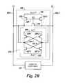
- FIG. 2Aillustrates a schematic diagram of a portion of a memory array in accordance with a number of embodiments of the present disclosure.
- FIG. 2Billustrates a schematic diagram of a portion of sensing circuitry in accordance with a number of embodiments of the present disclosure.
- FIGS. 3A-3Cillustrate a schematic diagram of a portion of a memory array in accordance with a number of embodiments of the present disclosure.
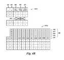
- FIG. 4Ais a schematic diagram illustrating sensing circuitry in accordance with a number of embodiments of the present disclosure.
- FIG. 4Bis a logic table illustrating selectable logic operation results implemented by sensing circuitry in accordance with a number of embodiments of the present disclosure.
- the present disclosureincludes apparatuses and methods related to multiple endianness compatibility.
- an order of a plurality of bytes received in a bytewise little endian formatcan be reordered (e.g., by reversing an ordering of the bits in each byte of the plurality of bytes such that the plurality of bytes are arranged in a bit-sequential little endian format) to be in a bit-sequential format.
- the plurality of bytes arranged in a bit-sequential little endian format or big endian formatcan be stored in an array of memory cells.
- the bit-sequential little endian formatis an arrangement of the bits from a least significant bit of each byte of the plurality of bytes being stored in a most significant bit position and a most significant bit of each byte of the plurality of bytes being stored in a least significant bit position.
- the bit-sequential big endian formatis an arrangement of bits from a most significant bit of each byte of a plurality of bytes being stored in a most significant bit position and a least significant bit of each byte of the plurality of bytes being stored in a least significant bit position.
- Reordering the bits of a byte to be bit-sequentialcan provide transparent support from a host's perspective of little endian compatibility or big endian compatibility for performing operations (e.g., shift operations in memory). For example, bits of an element in a bytewise little endian format (but still big endian bitwise) can be sent from a host to be processed. The bits of the element can be reordered to be bit-sequential and a number of operations can be performed on the bit-sequential bits.
- bit-sequential bitscan be reordered back to the bytewise little endian (bitwise big endian) format and returned to the host transparently, independent of additional shifting calculations (e.g., shifting in memory) to account for non-sequential bits.
- bits that are non-sequential in big endian formatcan be reordered to be bit-sequential.
- the reordering of the bitscan be performed independent of knowledge of how many bytes the element contains. In previous approaches, knowledge of how many bytes comprise an element was used to determine how to switch bytes from little endian format to big endian format and vice versa.
- FIG. 1is a block diagram of an apparatus in the form of a computing system 100 including a memory device 120 in accordance with a number of embodiments of the present disclosure.
- a memory device 120a memory array 130 , and/or sensing circuitry 150 might also be separately considered an “apparatus.”
- System 100includes a host 110 coupled to memory device 120 , which includes a memory array 130 .
- Host 110can be a host system such as a personal laptop computer, a desktop computer, a digital camera, a mobile telephone, or a memory card reader, among various other types of hosts.
- Host 110can include a system motherboard and/or backplane and can include a number of processing resources (e.g., one or more processors, microprocessors, or some other type of controlling circuitry).
- the system 100can include separate integrated circuits or both the host 110 and the memory device 120 can be on the same integrated circuit.
- the system 100can be, for instance, a server system and/or a high performance computing (HPC) system and/or a portion thereof.
- HPChigh performance computing
- FIG. 1illustrates a system having a Von Neumann architecture
- embodiments of the present disclosurecan be implemented in non-Von Neumann architectures (e.g., a Turing machine), which may not include one or more components (e.g., CPU, ALU, etc.) often associated with a Von Neumann architecture.
- non-Von Neumann architecturese.g., a Turing machine
- componentse.g., CPU, ALU, etc.
- the memory array 130can be a DRAM array, SRAM array, STT RAM array, PCRAM array, TRAM array, RRAM array, NAND flash array, and/or NOR flash array, for instance.
- the array 130can comprise memory cells arranged in rows coupled by access lines (which may be referred to herein as word lines or select lines) and columns coupled by sense lines (which may be referred to herein as digit lines or data lines).
- access lineswhich may be referred to herein as word lines or select lines
- sense lineswhich may be referred to herein as digit lines or data lines.
- memory device 160may include a number of arrays 130 (e.g., a number of banks of DRAM cells).
- An example DRAM arrayis described in association with FIGS. 2A and 4A .
- the memory device 120includes address circuitry 142 to latch address signals provided over an I/O bus 156 (e.g., a data bus and/or an address bus) through I/O circuitry 144 .
- I/O bus 156e.g., a data bus and/or an address bus
- the bus 156is illustrated as single I/O bus 156 ; however, the system 100 can include separate data and address busses.
- Address signalsare received and decoded by a row decoder 146 and a column decoder 152 to access the memory array 130 .
- Datacan be read from memory array 130 by sensing voltage and/or current changes on the sense lines using sensing circuitry 150 .
- the sensing circuitry 150can read and latch a page (e.g., row) of data from the memory array 130 .
- the I/O circuitry 144can be used for bi-directional data communication with host 110 over the I/O bus 156 .
- the write circuitry 148is used to write data to the memory array
- the I/O circuitry 144can include reordering circuitry 170 that performs a number of operations to reorder data (e.g., bits and/or bytes) received thereto.
- the reordering circuitry 170can reorder data received thereto (e.g., from host 110 and/or array 130 ) and send (e.g., transmit) the reordered data to a desired location (e.g., host 110 , array 130 , and/or elsewhere).
- the reordering circuitry 170can be a number of multiplexers that reorder bits of a byte. In a number of embodiments, whether reordering of the data occurs can be determined based on the status of an indicator (e.g., a flag).
- the reordering circuitry 170can be an engine including software, hardware, and/or firmware. While the reordering circuitry 170 is illustrated as within the I/O circuitry 144 (e.g., within the I/O data path), examples are not so limited. For example, the reordering circuitry 170 can be located on controller 140 , on a channel controller (not shown and which may be located on device 120 or host 110 , for instance), on address circuitry 142 , and/or in additional locations. In a number of embodiments, reordering of the data can include modifying addresses associated with the data.
- Controller 140decodes signals provided by control bus 154 from the host 110 . These signals can include chip enable signals, write enable signals, and address latch signals that are used to control operations performed on the memory array 130 , including data read, data write, and data erase operations.
- the controller 140is responsible for executing instructions from the host 110 .
- the controller 140can comprise hardware, software, and/or firmware, and can be, for example, a state machine, a sequencer, or some other type of controller.
- the controller 140can perform a number of shift operations (e.g., via shifting circuitry 223 in memory array 230 in FIG. 2A ).
- the controller 140can be coupled to a host 110 in a similar manner (e.g., in relation to its wiring) for a number of endiannesses (e.g., little endianness and big endianness) such that the host 110 does not have an endianness fixed in hardware. Reordering of bits can be performed based on an indication (e.g., a flag register) whose value is not fixed in the hardware.
- an indicatione.g., a flag register
- Reordering the bits and bytescan be performed on an element including a number of 8-bit bytes.
- the bitscan be ordered based on a significance of each bit within a byte.
- the bytescan be ordered based on a significance of the byte within an element.
- a number of operationscan be performed on the bits that include shifting a bit from one location to another in order to perform the operations.
- the direction of the shiftcan be determined based on the format that the bits are ordered in. For example, a bit can be shifted toward a more significant bit or a less significant bit based on what operation is being performed. If the bits are ordered from most significant to least significant and a shift is in the direction of toward more significant bits, the bits would shift towards the left. If the bits are ordered from least significant to most significant and a shift is in the direction of toward more significant bits, the bits would shift towards the right, and so forth.
- Sequential bitscan be shifted based on the number of shifts corresponding to a particular operation.
- Non-sequential bitscan be shifted based on the distance to the next sequential bit. For example, if a first and second bit in sequence is next to one another and the operation is to perform one shift, the bit can move one position. However, if the first and second bit are out of sequence by eight positions (e.g., the size of a byte if they are sequentially off by a byte), one shift to be performed by the operation would turn into eight shifts since they are eight positions out of sequence. Ordering the bits sequentially can improve efficiency of shifting and decrease the number of calculations performed when performing an operation.
- the sensing circuitry 150can comprise a number of sense amplifiers and a number of compute components, which may comprise a latch serving as an accumulator and can be used to perform logical operations (e.g., on data associated with complementary sense lines).
- the sensing circuitrye.g., 150
- the sensing circuitrycan be used to perform a number of operations (e.g., shift operations) using data stored in array 130 as inputs and store the results of the operations back to the array 130 without transferring via a sense line address access (e.g., without firing a column decode signal).
- sensing circuitry 150can be performed using sensing circuitry 150 rather than and/or in addition to being performed by processing resources external to the sensing circuitry 150 (e.g., by a processor associated with host 110 and/or other processing circuitry, such as ALU circuitry, located on device 160 (e.g., on controller 140 or elsewhere)).
- processing resources external to the sensing circuitry 150e.g., by a processor associated with host 110 and/or other processing circuitry, such as ALU circuitry, located on device 160 (e.g., on controller 140 or elsewhere)).
- sensing circuitrye.g., 150
- sensing circuitryis configured to perform an operation on data stored in memory cells in memory array 130 and store the result back to the array 130 without enabling a local I/O line coupled to the sensing circuitry.
- the operations performed in memory array 130includes a number of shift operations that are affected by the format of the data (e.g., whether in big endian or little endian formats).
- Data in big endian formatmay include shifting in a first direction while data in little endian format may include shifting a different direction.
- the shifting operationscan be simplified and replicated by simply reversing the directions of the shift.
- FIG. 2Aillustrates a schematic diagram of a portion of a memory array 230 in accordance with a number of embodiments of the present disclosure.
- a memory cellcomprises a storage element (e.g., capacitor) and an access device (e.g., transistor).
- transistor 202 - 1 and capacitor 203 - 1comprises memory cell 201 - 1
- transistor 202 - 2 and capacitor 203 - 2comprises memory cell 201 - 2
- transistor 202 - 3 and capacitor 203 - 3comprises memory cell 201 - 3
- transistor 202 - 4 and capacitor 203 - 4comprises memory cell 201 - 4 , etc.
- the memory array 230is a DRAM array of 1T1C (one transistor one capacitor) memory cells.
- the memory cellsmay be destructive read memory cells (e.g., reading the data stored in the cell destroys the data such that the data originally stored in the cell is refreshed after being read).
- the cells of the memory array 230are arranged in rows coupled by word lines 204 -X (Row X), 204 -Y (Row Y), etc., and columns coupled by pairs of complementary data lines DIGIT(n ⁇ 1)/DIGIT(n ⁇ 1)_, DIGIT(n)/DIGIT(n)_, DIGIT(n+1)/DIGIT(n+1)_.
- the individual data lines corresponding to each pair of complementary data linescan also be referred to as data lines 205 - 1 (D) and 205 - 2 (D_) respectively.
- an array of memory cellscan include additional columns of memory cells and/or data lines (e.g., 4,096, 8,192, 16,384, etc.).
- Memory cellscan be coupled to different data lines and/or word lines.
- a first source/drain region of a transistor 202 - 3can be coupled to data line 205 - 1 (D)
- a second source/drain region of transistor 202 - 3can be coupled to capacitor 203 - 3
- a gate of a transistor 202 - 3can be coupled to word line 204 -X.
- a first source/drain region of a transistor 202 - 4can be coupled to data line 205 - 2 (D_)
- a second source/drain region of transistor 202 - 4can be coupled to capacitor 203 - 4
- a gate of a transistor 202 - 4can be coupled to word line 204 -Y.
- the cell plateas shown in FIG. 2A , can be coupled to each of capacitors 203 - 3 and 203 - 4 .
- the cell platecan be a common node to which a reference voltage (e.g., ground) can be applied in various memory array configurations.
- a reference voltagee.g., ground
- the memory array 230is coupled to sensing circuitry 250 - 1 , 250 - 2 , 250 - 3 , etc., in accordance with a number of embodiments of the present disclosure.
- Sensing circuitrycomprises a sense amplifier and a compute component corresponding to respective columns of memory cells (e.g., coupled to respective pairs of complementary data lines).
- the sensing circuitry 250 - 1comprises a sense amplifier 206 - 1 and a compute component 231 - 1 corresponding to respective columns of memory cells (e.g., memory cells 201 - 1 and 201 - 2 coupled to respective pairs of complementary data lines).
- Sensing circuitry 250 - 2comprises a sense amplifier 206 - 2 and a compute component 231 - 2 corresponding to respective columns of memory cells (e.g., memory cells 201 - 3 and 201 - 4 coupled to respective pairs of complementary data lines).
- Sensing circuitry 250 - 3comprises a sense amplifier 206 - 3 and a compute component 231 - 3 corresponding to respective columns of memory cells (e.g., memory cells 201 - 5 and 201 - 6 coupled to respective pairs of complementary data lines).
- a sense amplifiere.g., sense amplifier 206 - 1
- the sense amplifiere.g., sense amplifier 206 - 1
- the sense amplifiercan be configured, for example, as described with respect to FIG. 2B .
- the circuitry corresponding to compute component 231 - 2comprises a static latch 264 and an additional ten transistors that implement, among other things, a dynamic latch.
- compute component 231 - 2has been illustrated in an expanded format to describe the functioning of the compute component.
- Additional compute componentse.g., compute components 231 - 1 and 231 - 3
- the dynamic latch and/or static latch of the compute component 231 - 2can be collectively referred to herein as a secondary latch, which can serve as an accumulator.
- the compute component 231 - 2can operate as and/or be referred to herein as an accumulator.
- the compute component 231 - 2can be coupled to each of the data lines D 205 - 1 and D_ 205 - 2 as shown in FIG. 2A .
- the transistors of compute component 231 - 2can all be n-channel transistors (e.g., NMOS transistors), for example.
- data line D 205 - 1can be coupled to a first source/drain region of transistors 216 - 1 and 239 - 1 , as well as to a first source/drain region of load/pass transistor 218 - 1 .
- Data line D_ 205 - 2can be coupled to a first source/drain region of transistors 216 - 2 and 239 - 2 , as well as to a first source/drain region of load/pass transistor 218 - 2 .
- load/pass transistor 218 - 1 and 218 - 2can be commonly coupled to a LOAD control signal, or respectively coupled to a PASSD/PASSDB control signal, as discussed further below.
- a second source/drain region of load/pass transistor 218 - 1can be directly coupled to the gates of transistors 216 - 1 and 239 - 2 .
- a second source/drain region of load/pass transistor 218 - 2can be directly coupled to the gates of transistors 216 - 2 and 239 - 1 .
- a second source/drain region of transistor 216 - 1can be directly coupled to a first source/drain region of pull-down transistor 214 - 1 .
- a second source/drain region of transistor 239 - 1can be directly coupled to a first source/drain region of pull-down transistor 207 - 1 .
- a second source/drain region of transistor 216 - 2can be directly coupled to a first source/drain region of pull-down transistor 214 - 2 .
- a second source/drain region of transistor 239 - 2can be directly coupled to a first source/drain region of pull-down transistor 207 - 2 .
- a second source/drain region of each of pull-down transistors 207 - 1 , 207 - 2 , 214 - 1 , and 214 - 2can be commonly coupled together to a reference voltage (e.g., ground (GND)).
- a gate of pull-down transistor 207 - 1can be coupled to an AND control signal line
- a gate of pull-down transistor 214 - 1can be coupled to an ANDinv control signal line 213 - 1
- a gate of pull-down transistor 214 - 2can be coupled to an ORinv control signal line 213 - 2
- a gate of pull-down transistor 207 - 2can be coupled to an OR control signal line.
- the gate of transistor 239 - 1can be referred to as node S 1
- the gate of transistor 239 - 2can be referred to as node S 2
- the circuit shown in FIG. 2Astores accumulator data dynamically on nodes S 1 and S 2 .
- Activating the LOAD control signalcauses load/pass transistors 218 - 1 and 218 - 2 to conduct, and thereby load complementary data onto nodes S 1 and S 2 .
- the LOAD control signalcan be elevated to a voltage greater than V DD to pass a full V DD level to S 1 /S 2 .
- elevating the LOAD control signal to a voltage greater than V DDis optional, and functionality of the circuit shown in FIG. 2A is not contingent on the LOAD control signal being elevated to a voltage greater than V DD .
- the configuration of compute component 231 - 2 shown in FIG. 2Ahas the benefit of balancing the sense amplifier for functionality when the pull-down transistors 207 - 1 , 207 - 2 , 214 - 1 , and 214 - 2 are conducting before the sense amplifier 206 - 2 is fired (e.g., during pre-seeding of the sense amplifier 206 - 2 ).
- firing the sense amplifier 206 - 2refers to enabling the sense amplifier 206 - 2 to set the primary latch and subsequently disabling the sense amplifier 206 - 2 to retain the set primary latch.
- full rail voltagese.g., V DD , GND
- Inverting transistorscan pull-down a respective data line in performing certain logical operations.
- transistor 216 - 1having a gate coupled to S 2 of the dynamic latch
- transistor 214 - 1having a gate coupled to an ANDinv control signal line 213 - 1
- transistor 216 - 2having a gate coupled to S 1 of the dynamic latch
- transistor 214 - 2having a gate coupled to an ANDinv control signal line 213 - 2
- D_pull-down data line 205 - 2
- the latch 264can be controllably enabled by coupling to an active negative control signal line 212 - 1 (ACCUMB) and an active positive control signal line 212 - 2 (ACCUM) rather than be configured to be continuously enabled by coupling to ground and V DD .
- load/pass transistors 208 - 1 and 208 - 2can each having a gate coupled to one of a LOAD control signal or a PASSD/PASSDB control signal.
- the gates of load/pass transistors 218 - 1 and 218 - 2can be commonly coupled to a LOAD control signal.
- transistors 218 - 1 and 218 - 2can be load transistors.
- Activating the LOAD control signalcauses the load transistors to conduct, and thereby load complementary data onto nodes S 1 and S 2 .
- the LOAD control signalcan be elevated to a voltage greater than V DD to pass a full V DD level to S 1 /S 2 .
- the LOAD control signalneed not be elevated to a voltage greater than V DD is optional, and functionality of the circuit shown in FIG. 2A is not contingent on the LOAD control signal being elevated to a voltage greater than V DD .
- the gate of load/pass transistor 218 - 1can be coupled to a PASSD control signal
- the gate of load/pass transistor 218 - 2can be coupled to a PASSDB control signal.
- transistors 218 - 1 and 218 - 2can be pass transistors. Pass transistors can be operated differently (e.g., at different times and/or under different voltage/current conditions) than load transistors. As such, the configuration of pass transistors can be different than the configuration of load transistors.
- Load transistorsare constructed to handle loading associated with coupling data lines to the local dynamic nodes S 1 and S 2 , for example.
- Pass transistorsare constructed to handle heavier loading associated with coupling data lines to an adjacent accumulator (e.g., through the shift circuitry 223 - 2 in memory array 230 , as shown in FIG. 2A ).
- load/pass transistors 218 - 1 and 218 - 2can be configured to accommodate the heavier loading corresponding to a pass transistor but be coupled and operated as a load transistor.
- Load/pass transistors 218 - 1 and 218 - 2 configured as pass transistorscan also be utilized as load transistors. However, load/pass transistors 218 - 1 and 218 - 2 configured as load transistors may not be capable of being utilized as pass transistors.
- the compute component 231 - 2can comprise a number of transistors formed on pitch with the transistors of the corresponding memory cells of an array (e.g., array 230 shown in FIG. 2A ) to which they are coupled, which may conform to a particular feature size (e.g., 4F 2 , 6F 2 , etc.).
- latch 1364includes four transistors 208 - 1 , 208 - 2 , 1309 - 1 , and 209 - 2 coupled to a pair of complementary data lines D 205 - 1 and D_ 205 - 2 through load/pass transistors 218 - 1 and 218 - 2 .
- the latch 264can be a cross coupled latch (e.g., gates of a pair of transistors, such as n-channel transistors (e.g., NMOS transistors) 209 - 1 and 209 - 2 are cross coupled with the gates of another pair of transistors, such as p-channel transistors (e.g., PMOS transistors) 208 - 1 and 208 - 2 ).
- the cross coupled latch 264can be referred to as a static latch.
- the voltages or currents on the respective data lines D and D —can be provided to the respective latch inputs 217 - 1 and 217 - 2 of the cross coupled latch 264 (e.g., the input of the secondary latch).
- the latch input 217 - 1is coupled to a first source/drain region of transistors 208 - 1 and 209 - 1 as well as to the gates of transistors 208 - 2 and 209 - 2 .
- the latch input 217 - 2can be coupled to a first source/drain region of transistors 208 - 2 and 209 - 2 as well as to the gates of transistors 208 - 1 and 209 - 1 .
- a second source/drain region of transistor 209 - 1 and 209 - 2is commonly coupled to a negative control signal line 1312 - 1 (e.g., ground (GND) or ACCUMB control signal similar to control signal RnIF shown in FIG. 2B with respect to the primary latch).
- a second source/drain region of transistors 208 - 1 and 208 - 2is commonly coupled to a positive control signal line 212 - 2 (e.g., V DD or ACCUM control signal similar to control signal ACT shown in FIG. 2B with respect to the primary latch).
- the positive control signal 212 - 2can provide a supply voltage (e.g., V DD ) and the negative control signal 212 - 1 can be a reference voltage (e.g., ground) to enable the cross coupled latch 264 .
- the second source/drain region of transistors 208 - 1 and 208 - 2are commonly coupled directly to the supply voltage (e.g., V DD ), and the second source/drain region of transistor 209 - 1 and 209 - 2 are commonly coupled directly to the reference voltage (e.g., ground) so as to continuously enable latch 264 .
- the enabled cross coupled latch 264operates to amplify a differential voltage between latch input 217 - 1 (e.g., first common node) and latch input 217 - 2 (e.g., second common node) such that latch input 217 - 1 is driven to either the activated positive control signal voltage (e.g., V DD ) or the activated negative control signal voltage (e.g., ground), and latch input 217 - 2 is driven to the other of the activated positive control signal voltage (e.g., V DD ) or the activated negative control signal voltage (e.g., ground).
- the activated positive control signal voltagee.g., V DD
- the activated negative control signal voltagee.g., ground
- the sense amplifier 206 - 2 and the compute component 231 - 2can be coupled to the array 230 via shift circuitry 223 - 2 .
- the shift circuitry 223 - 2comprises a pair of isolation devices (e.g., isolation transistors 221 - 1 and 221 - 2 ) coupled to data lines 205 - 1 (D) and 205 - 2 (D_), respectively).
- the isolation transistors 221 - 1 and 221 - 2are coupled to a control signal 222 (NORM) that, when activated, enables (e.g., turns on) the isolation transistors 221 - 1 and 221 - 2 to couple the corresponding sense amplifier 206 - 2 and compute component 231 - 2 to a corresponding column of memory cells (e.g., to a corresponding pair of complementary data lines 205 - 1 (D) and 205 - 2 (D_)).
- conduction of isolation transistors 221 - 1 and 221 - 2can be referred to as a “normal” configuration of the shift circuitry 223 - 2 .
- the shift circuitry 223 - 2includes another (e.g., a second) pair of isolation devices (e.g., isolation transistors 221 - 3 and 221 - 4 ) coupled to a complementary control signal 219 (SHIFT), which can be activated, for example, when NORM is deactivated.
- SHIFTcomplementary control signal 219
- the isolation transistors 221 - 3 and 221 - 4can be operated (e.g., via control signal 219 ) such that a particular sense amplifier 206 - 2 and compute component 231 - 2 are coupled to a different pair of complementary data lines (e.g., a pair of complementary data lines different than the pair of complementary data lines to which isolation transistors 221 - 1 and 221 - 2 couple the particular sense amplifier 206 - 2 and compute component 231 - 2 ), or can couple a particular sense amplifier 206 - 2 and compute component 231 - 2 to another memory array (and isolate the particular sense amplifier 206 - 2 and compute component 231 - 2 from a first memory array).
- the shift circuitry 223 - 2can be arranged as a portion of (e.g., within) the sense amplifier 206 - 2 , for instance.
- the shift circuitry 223 - 2 shown in FIG. 2Aincludes isolation transistors 221 - 1 and 221 - 2 used to couple particular sensing circuitry 250 - 2 (e.g., a particular sense amplifier 206 - 2 and corresponding compute component 231 - 2 ) to a particular pair of complementary data lines 205 - 1 (D) and 205 - 2 (D_) (e.g., DIGIT(n) and DIGIT(n)_) and isolation transistors 221 - 3 and 221 - 4 are arranged to couple the particular sensing circuitry 250 - 2 to an adjacent pair of complementary data lines in one particular direction (e.g., adjacent data lines DIGIT(n+1) and DIGIT(n+1)_ shown to the right in FIG.
- particular sensing circuitry 250 - 2e.g., a particular sense amplifier 206 - 2 and corresponding compute component 231 - 2
- D_complementary data lines
- isolation transistors 221 - 3 and 221 - 4are
- shift circuitrycan include isolation transistors 221 - 1 and 221 - 2 used to couple particular sensing circuitry to a particular pair of complementary data lines (e.g., DIGIT(n) and DIGIT(n)_ and isolation transistors 221 - 3 and 221 - 4 arranged so as to be used to couple the particular sensing circuitry to an adjacent pair of complementary data lines in another particular direction (e.g., adjacent data lines DIGIT(n ⁇ 1) and DIGIT(n ⁇ 1)_ shown to the left in FIG. 2A ).
- DIGIT(n) and DIGIT(n)_isolation transistors 221 - 3 and 221 - 4 arranged so as to be used to couple the particular sensing circuitry to an adjacent pair of complementary data lines in another particular direction (e.g., adjacent data lines DIGIT(n ⁇ 1) and DIGIT(n ⁇ 1)_ shown to the left in FIG. 2A ).
- Shift circuitry 223 - 1can include isolation transistors used to couple particular sensing circuitry 250 - 1 to a particular pair of complementary data lines (e.g., DIGIT(n ⁇ 1) and DIGIT(n ⁇ 1)_) and isolation transistors arranged to couple the particular sensing circuitry 250 - 1 to an adjacent pair of complementary data lines in one particular direction (e.g., adjacent data lines DIGIT(n) and DIGIT(n)_ shown in FIG. 2A ).
- a particular pair of complementary data linese.g., DIGIT(n ⁇ 1) and DIGIT(n ⁇ 1)_
- isolation transistorsarranged to couple the particular sensing circuitry 250 - 1 to an adjacent pair of complementary data lines in one particular direction (e.g., adjacent data lines DIGIT(n) and DIGIT(n)_ shown in FIG. 2A ).
- Shift circuitry 223 - 3can include isolation transistors used to couple particular 250 - 3 to a particular pair of complementary data lines (e.g., DIGIT(n+1) and DIGIT(n+1)_) and isolation transistors arranged to couple the particular sensing circuitry 250 - 3 to an adjacent pair of complementary data lines in one particular direction (e.g., adjacent data lines DIGIT (n) and DIGIT(n)_ to the left and DIGIT(n+2) and DIGIT(n+2)_ to the right (not shown)).
- a particular pair of complementary data linese.g., DIGIT(n+1) and DIGIT(n+1)_
- isolation transistorsarranged to couple the particular sensing circuitry 250 - 3 to an adjacent pair of complementary data lines in one particular direction (e.g., adjacent data lines DIGIT (n) and DIGIT(n)_ to the left and DIGIT(n+2) and DIGIT(n+2)_ to the right (not shown)).
- Embodiments of the present disclosureare not limited to the configuration of shift circuitry 223 - 2 shown in FIG. 2A .
- shift circuitry 223 - 2such as that shown in FIG. 2A can be operated (e.g., in conjunction with sense amplifiers 206 - 2 and compute components 231 - 2 ) in association with performing compute functions such as adding and subtracting functions without transferring data out of the sensing circuitry 250 via an I/O line (e.g., local I/O line (IO/IO_)), for instance.
- I/O linee.g., local I/O line (IO/IO_)
- each column of memory cellscan be coupled to a column decode line that can be activated to transfer, via local I/O line, a data value from a corresponding sense amplifier 206 - 2 and/or compute component 231 - 2 to a control component external to the array such as an external processing resource (e.g., host processor and/or other functional unit circuitry).
- the column decode linecan be coupled to a column decoder (e.g., column decoder).
- dataneed not be transferred via such I/O lines to perform logical operations in accordance with embodiments of the present disclosure.
- shift circuitry 223 - 2can be operated in conjunction with sense amplifiers 206 - 2 and compute components 231 - 2 to perform reordering of the bits without transferring data to a control component external to the array, for instance.
- FIG. 2Bis a schematic diagram illustrating a portion of sensing circuitry in accordance with a number of embodiments of the present disclosure.
- sense amplifier 206 - 2can comprise a cross coupled latch.
- embodiments of the sense amplifier 206 - 2are not limited to a cross coupled latch.
- the sense amplifier 206 - 2 in FIG. 2Bcan be current-mode sense amplifier and/or single-ended sense amplifier (e.g., sense amplifier coupled to one data line).
- embodiments of the present disclosureare not limited to a folded data line architecture.
- a sense amplifier(e.g., 206 - 2 ) can comprise a number of transistors formed on pitch with the transistors of the corresponding compute component 231 - 2 and/or the memory cells of an array (e.g., 230 shown in FIG. 2A ) to which they are coupled, which may conform to a particular feature size (e.g., 4F 2 , 6F 2 , etc.).
- the sense amplifier 206 - 2comprises a latch 215 including four transistors coupled to a pair of complementary data lines D 205 - 1 and D_ 205 - 2 .
- the latch 215can be a cross coupled latch (e.g., gates of a pair of transistors, such as n-channel transistors (e.g., NMOS transistors) 227 - 1 and 227 - 2 are cross coupled with the gates of another pair of transistors, such as p-channel transistors (e.g., PMOS transistors) 229 - 1 and 229 - 2 ).
- the latch 215comprising transistors 227 - 1 , 227 - 2 , 229 - 1 , and 229 - 2 can be referred to as a primary latch.
- embodimentsare not limited to this example.
- the voltages or currents on the respective data lines D and D_can be provided to the respective latch inputs 233 - 1 and 233 - 2 of the cross coupled latch 215 (e.g., the input of the secondary latch).
- the latch input 233 - 1is coupled to a first source/drain region of transistors 227 - 1 and 229 - 1 as well as to the gates of transistors 227 - 2 and 229 - 2 .
- the latch input 233 - 2can be coupled to a first source/drain region of transistors 227 - 2 and 229 - 2 as well as to the gates of transistors 227 - 1 and 229 - 1 .
- the compute component 231 - 2which may be referred to herein as an accumulator, can be coupled to latch inputs 233 - 1 and 233 - 2 of the cross coupled latch 215 as shown; however, embodiments are not limited to the example shown in FIG. 2B .
- a second source/drain region of transistor 227 - 1 and 227 - 2is commonly coupled to an active negative control signal 228 (RnIF)
- a second source/drain region of transistors 229 - 1 and 229 - 2is commonly coupled to an active positive control signal 290 (ACT).
- the ACT signal 290can be a supply voltage (e.g., V DD ) and the RnIF signal can be a reference voltage (e.g., ground).
- Activating signals 228 and 290enables the cross coupled latch 215 .
- the enabled cross coupled latch 215operates to amplify a differential voltage between latch input 233 - 1 (e.g., first common node) and latch input 233 - 2 (e.g., second common node) such that latch input 233 - 1 is driven to one of the ACT signal voltage and the RnIF signal voltage (e.g., to one of V DD and ground), and latch input 233 - 2 is driven to the other of the ACT signal voltage and the RnIF signal voltage.
- latch input 233 - 1e.g., first common node
- latch input 233 - 2e.g., second common node
- the sense amplifier 206 - 2can also include circuitry configured to equilibrate the data lines D and D — (e.g., in association with preparing the sense amplifier for a sensing operation).
- the equilibration circuitrycomprises a transistor 224 having a first source/drain region coupled to a first source/drain region of transistor 225 - 1 and data line D 205 - 1 .
- a second source/drain region of transistor 224can be coupled to a first source/drain region of transistor 225 - 2 and data line D_ 205 - 2 .
- a gate of transistor 224can be coupled to gates of transistors 225 - 1 and 225 - 2 .
- the second source drain regions of transistors 225 - 1 and 225 - 2are coupled to an equilibration voltage 238 (e.g., V DD /2), which can be equal to V DD /2, where V DD is a supply voltage associated with the array.
- the gates of transistors 224 , 225 - 1 , and 225 - 2can be coupled to control signal 225 (EQ).
- EQcontrol signal 225
- activating EQenables the transistors 224 , 225 - 1 , and 225 - 2 , which effectively shorts data line D to data line D — such that the data lines D and D — are equilibrated to equilibration voltage V DD /2.
- a number of logical operationscan be performed using the sense amplifier 206 - 2 and compute component 231 - 2 , and the result can be stored in the sense amplifier and/or compute component.
- the sensing circuitry 250can be operated in several modes to perform logical operations, including a first mode in which a result of the logical operation is initially stored in the sense amplifier 206 - 2 , and a second mode in which a result of the logical operation is initially stored in the compute component 231 - 2 . Additionally with respect to the first operating mode, sensing circuitry 250 can be operated in both pre-sensing (e.g., sense amps fired before logical operation control signal active) and post-sensing (e.g., sense amps fired after logical operation control signal active) modes with a result of a logical operation being initially stored in the sense amplifier 206 - 2 .
- pre-sensinge.g., sense amps fired before logical operation control signal active
- post-sensinge.g., sense amps fired after logical operation control signal active
- the sense amplifier 206 - 2can, in conjunction with the compute component 231 - 2 , be operated to perform various logical operations using data from an array as input.
- the result of a logical operationcan be stored back to the array without transferring the data via a data line address access (e.g., without firing a column decode signal such that data is transferred to circuitry external from the array and sensing circuitry via local I/O lines).
- a number of embodiments of the present disclosurecan enable performing logical operations and compute functions associated therewith using less power than various previous approaches.
- a number of embodimentscan enable an increased parallel processing capability as compared to previous approaches.
- FIGS. 3A-3Cillustrate schematic diagrams of a portion of a memory array storing data in accordance with a number of embodiments of the present disclosure.
- FIG. 3Aillustrates a row 311 - 1 of a plurality of memory cells 301 - 1 to 301 - 32 storing an element (e.g., a plurality of data values, bits, etc.).
- Each of the plurality of memory cells 301 - 1 to 301 - 32can be coupled to a corresponding sense line and a corresponding access line.
- Each of the corresponding sense linescan be coupled to sensing circuitry.
- memory cell 301 - 1e.g., corresponding to memory cell 201 - 3 in FIG.
- a sense linee.g., sense line 205 - 1
- an access linee.g., access line 204 -Y
- the sense linee.g., 205 - 1
- sensing circuitrye.g., sensing circuitry 250 - 2
- Memory cell 301 - 1can correspond to memory cell 201 - 1 in FIG.
- cell 301 - 2can correspond to cell 201 - 2
- cell 301 - 3can correspond to cell 201 - 3
- cell 301 - 4can correspond to cell 201 - 4
- cell 301 - 5can correspond to cell 201 - 5
- cell 301 - 6can correspond to cell 201 - 6
- Cells 301 - 7 to 301 - 32can correspond to cells 201 - 7 to 201 - 32 (not shown). While the example given describes a correspondence using both cells (e.g., cells 203 - 3 and 203 - 4 ) coupled to a pair of complementary sense lines (e.g., sense lines 205 - 1 and 205 - 2 ), embodiments are not so limited.
- cell 301 - 1can correspond to cell 201 - 1
- cell 301 - 2can correspond to cell 201 - 3 , thereby using a cell coupled to each of a first sense line of the pair of complementary sense lines.
- a 32-bit elementcan be stored in a row 331 - 1 of the plurality of memory cells 301 - 1 to 301 - 32 .
- the 32-bit elementincludes a number of bits and can represent a data value (e.g., a base ten (10) numerical value).
- the example 32-bit elementincludes four (4) bytes with eight bits per byte. Embodiments are not so limited as a byte with any number of bits may be used.
- the bits of the 32-bit element exampleeach have a corresponding significance within the 32-bit element.
- a first bit(e.g., the “0” th bit illustrated as stored in cell 301 - 8 ) can be a least significant bit, meaning the first bit has the least significance within the 32-bit element.
- a 32 nd bit(e.g., the “31” st bit illustrated as stored in cell 301 - 25 in FIG. 3A ) can be a most significant bit, meaning the 32 nd bit has the most significance within the 32-bit element.
- a significance of a bitcan also correspond to a significance within a byte.
- a first byte 351 - 1can have a least significant bit of the first byte 351 - 1 (e.g., an “0” th bit in cell 301 - 8 in FIG.
- a second byte 351 - 2can have a least significant bit of the second byte 351 - 2 (e.g., an “8” th bit stored in cell 301 - 16 in FIG. 3A ) and a most significant bit for the second byte 351 - 2 (e.g., a “15” th bit stored in cell 301 - 9 in FIG. 3A ).
- a third byte 351 - 3can have a least significant bit of the third byte 351 - 3 (e.g., a “16” th bit stored in cell 301 - 24 in FIG. 3A ) and a most significant bit of the third byte 351 - 3 (e.g., a “23” rd bit stored in cell 301 - 17 in FIG. 3A ).
- a fourth byte 351 - 4can have a least significant bit of the fourth byte 351 - 4 (e.g., a “24” th bit stored in cell 301 - 32 in FIG. 3A ) and a most significant bit of the fourth byte 351 - 4 (e.g., a “31” st bit stored in cell 301 - 25 in FIG. 3A ).
- a number of bytes within an elementcan also have a significance.
- a 32-bit elementas illustrated in FIG. 3A , can include a first byte 351 - 1 , a second byte 351 - 2 , a third byte 351 - 3 , and a fourth byte 351 - 4 .
- a most significant byte of a 32-bit elementincludes the most significant bits (e.g., the “31” st through “24” th bits are the most significant for the 32-bit element example).
- the fourth byte 351 - 4would be the most significant byte as the fourth byte 351 - 4 includes the most significant bits of the 32-bit element in FIG. 3A .
- Bits within a byte and bytes within an elementcan correspond to a particular significance position. Bits within a byte can have a most significant bit position (e.g., corresponding to a smallest address or left-most address) and a least significant bit position (e.g., corresponding to a largest address or right-most address). For example, a first byte 351 - 1 can have a most significant bit position 353 - 1 that corresponds to a bit stored in cell 301 - 1 (e.g., the left-most bit position for the first byte 351 - 1 ).
- the most significant bit (e.g., “7” th bit) of the first byte 351 - 1is stored in the most significant bit position 341 - 1 of the first byte 351 - 1 .
- the second most-significant bit (e.g., “6”) of the first byte 351 - 1is stored in the second most-significant bit position 341 - 2 .
- the most significant bit (e.g., “15” th ) of the second byte 351 - 2is in the most significant bit position 341 - 9 of the second byte 351 - 2
- the most significant bit (e.g., “23” rd ) of the third byte 351 - 3is in the most significant bit position 341 - 17 of the third byte 351 - 3
- the most significant bit (e.g., “31” st ) of the fourth byte 351 - 4is in the most significant bit position 341 - 25 of the fourth byte 351 - 4 .
- Bytes within an elementcan have a most significant byte position (e.g., corresponding to a smallest byte address or left-most byte address) and a least significant byte position (e.g., corresponding to a largest byte address or left-most byte address).
- a least significant bytee.g., byte 351 - 1 including least significant bits “0” through “7”
- the byteis located furthest to the left in the element sequence.
- the second byte 351 - 2is in a second most significant byte position 353 - 2
- the third byte 351 - 3is in a third most significant byte position 353 - 3
- the fourth byte 351 - 4is in a least significant byte position 353 - 4 .
- the least significant byte positionis not limited to a fourth byte position.
- an element with 64 bits, including 8 bits per bytewould have an eighth byte in the least significant byte position.
- a number of bytes and byte positionscan depend on the size of the element.
- the plurality of bits(e.g., “0” th through “31” st bits of the 32-bit element 311 - 1 ) are stored in the plurality of corresponding memory cells 301 - 1 to 301 - 32 in a bytewise little endian format.
- Little endiancan refer to an order of least significant to most significant (e.g., least significant byte stored in a smallest or left-most address and most significant byte stored in a largest or right-most address).
- Big endiancan refer to an order of most significant to least significant (e.g., most significant byte stored in a smallest or left-most address and least significant byte stored in a largest or right-most address).
- Bitwise little endianrefers to storing bits (e.g., “0” to “31”) in memory cells (e.g., cells 301 - 1 to 301 - 32 ) from a least significant bit to a most significant bit (from left to right).
- Bytewise little endianrefers to storing bytes (e.g., 351 - 1 , 351 - 2 , 351 - 3 , and 351 - 4 ) in order from a least significant byte (e.g., 351 - 1 ) to a most significant byte (e.g., 351 - 4 ).
- the plurality of bitse.g., bits “0” to “31” illustrated in FIG.
- 3Aare stored in a bytewise little endian format but are bit-wise big-endian.
- the bits within a byteare stored from most significant bit to least significant bit (e.g., first byte 351 - 1 is ordered from “7” th bit to “0” th bit) while the bytes are stored from least significant byte (e.g., byte 351 - 1 in most significant byte position 353 - 1 ) to most significant byte (e.g., byte 351 - 4 in least significant byte position 353 - 4 ).
- Hostse.g., processors
- bitsmay be ordered in a number of different ways depending on how the host (e.g., a processor) and/or a number of devices may have altered the order to perform a number of functions (e.g., perform a mathematical calculation with the bits, etc.).
- the ordering of the bitse.g., as stored in the memory
- a bytewise big endian formatis bit-sequential while a bytewise little endian (when still bitwise big endian) is non-sequential. Shifting becomes more problematic when bits are not sequential because a determination of the next contiguous bit (in terms of significance) would be determined before performing a shift and the shift would include additional movement based on the location of the next contiguous bit.
- each 8-bit byte of each of the elementsrepresent a portion of the numerical values and calculations including shifting across the whole element may be performed for the calculation.
- a bytewise big endian formatas illustrated in row 311 - 2 in FIG. 3B )
- the bitsare sequential (in relation to significance) and therefore the shifts can be performed without further calculation.
- the bitsare non-sequential and determinations of contiguous bits and how many spaces each contiguous bit is from the current bit being calculated would need to be determined.
- FIG. 3Billustrates a schematic diagram of a portion of a memory array in accordance with a number of embodiments of the present disclosure.
- FIG. 3Billustrates an element 311 - 2 stored in memory in a big endian format both bytewise and bitwise.
- the most significant bytee.g., byte 351 - 4 including most significant bites “31” through “24”
- the most significant byteis stored in memory cells 301 - 1 to 301 - 8 corresponding to a most significant byte position 353 - 1 .
- the second (or next) most significant byte(e.g., byte 351 - 3 ) is stored in memory cells 301 - 9 to 301 - 16 corresponding to a second most significant byte position 353 - 2
- the third most significant byte(e.g., byte 351 - 2 ) is stored in memory cells 301 - 17 to 301 - 24 corresponding to a third most significant byte position 353 - 3
- the least (or fourth most) significant byte(e.g., byte 351 - 1 ) is stored in memory cells 301 - 25 to 301 - 32 corresponding to a least (or fourth most) significant byte position 353 - 4 .
- bits (e.g., bits “0” through “31”) of element 311 - 2are stored in a bit-sequential little endian format. For example, the bits are ordered from bit “31” to bit “0” in sequential order. Further, bit “24” of byte 351 - 4 stored in memory cell 301 - 8 corresponding to the least significant bit position 341 - 8 of byte 351 - 4 is ordered right before bit “23” of byte 351 - 3 stored in memory cell 301 - 9 corresponding to the most significant bit position 341 - 9 of byte 351 - 3 .
- Bit “16”is stored in memory cell 301 - 16 and ordered right before bit “15” (stored in memory cell 301 - 17 ) and bit “8” is stored in memory cell 301 - 24 , right before bit “8” stored in memory cell 301 - 25 .
- each bit in the least significant bit position of a byteis sequential with the following bit in the next most significant byte's most significant bit position.
- hostse.g., processors
- a processorcan read in either bytewise little endian format or bytewise big endian format (with the ordered bits being ordered in a bitwise big endian format).
- FIG. 3Cillustrates a schematic diagram of a portion of a memory array in accordance with a number of embodiments of the present disclosure.
- the row 311 - 3 of a 32-bit elementis ordered in a bytewise little endian format and a bitwise little endian format.
- the bitsare ordered such that a least significant bit (e.g., bit “0”) of the 32-bit element is in a most significant bit position (e.g., bit position 341 - 1 ) of a least significant byte (e.g., byte 355 - 1 including bits “0” through “7”) in a most significant byte position (e.g., byte position 353 - 1 ).
- a most significant bit (e.g., bit “31”) of element 311 - 3is in a least significant bit position (e.g., bit position 341 - 32 ) of a most significant byte (e.g., byte 355 - 4 including bits “24” through “31”) in a least significant byte position (e.g., byte position 353 - 4 ).
- An elementcan be reordered from a bytewise little endian, bitwise big endian format (e.g., 32-bit element stored in row 311 - 1 ) to a bytewise little endian, bitwise little endian format (e.g., 32-bit element stored in row 311 - 3 ).
- the bytewise little endian, bitwise little endian formatis also referred to as bit-sequential little endian as the bits of the 32-bit element stored in row 311 - 3 have bits ordered sequentially (e.g., ordered from bit “0” to “31” in sequential order).
- the 32-bit elementcan be arranged in a bit-sequential little endian format from a bytewise little endian, bitwise big endian format by reordering the bits of a byte on a bytewise basis.
- byte 351 - 1 in row 311 - 1 of FIG. 3Aincludes bits “7,” “6,” “5,” “4,” “3,” “2,” “1,” and “0,” in that order (from most significant bit to least significant bit of byte 351 - 1 ).
- the bits of byte 351 - 1 in row 311 - 1can be reversed by reordering circuitry (e.g., reordering circuitry 170 in FIG.
- the reordering circuitry(e.g., reordering circuitry 170 in FIG. 1 ) can reorder the bits on a bytewise basis such that the total number of bytes in an element does not need to be determined before reordering the bits of the element. For example, when receiving bits of the 32-bit element of row 311 - 1 , the reordering circuitry may not know there are four (4) bytes in the element and can process the bits to a bit-sequential little endian format without knowing the number of bytes of the element.
- the reordering circuitryreceives the first eight (8) bits (e.g., bits “7” through “0”), the reordering circuitry reorders the bits to be in a reversed order (e.g., to bits “0” through “7”, as illustrated by byte 355 - 1 in FIG. 3C ).
- the reordering circuitryreceives the second byte (e.g., byte 351 - 2 including bits “15” through “8”), the reordering circuitry reverses the bits to by “8” through “15” (as illustrated by byte 355 - 2 in FIG. 3C ).
- the reordering circuitrycan reorder on a bytewise basis, the reordering will continue until the element has been received (without knowing how many total bytes when it starts reordering).
- embodimentsare not so limited. A number of elements can be received (beyond the 32-bit element example) and the reordering circuitry can continue to reorder bits for a number of elements as the number of elements are received.
- Performing a number of shift operationscan include shifting bits stored in a big endian format both bitwise and bytewise (e.g., illustrated in row 311 - 2 ).
- bitscan be shifted from a less significant bit towards a more significant bit.
- the bitscan be shifted from being stored in a first location (e.g., compute component 231 - 2 ) corresponding to a lesser significant bit position to a second location (e.g., compute component 231 - 1 ) corresponding to a more significant bit position.
- a bitcan be shifted from a compute component (e.g., compute component 231 - 2 ) corresponding to bit position 341 - 2 to a compute component (e.g., compute component 231 - 1 ) corresponding to bit position 341 - 1 of row 311 - 2 .
- a compute componente.g., compute component 231 - 2
- a compute componente.g., compute component 231 - 1
- the direction of shiftingis reversed. For example, a less significant bit is still shifted toward a more significant bit but a bit in a more significant bit position is shifted toward a less significant bit position (e.g., to the right in the illustrated example of FIG. 3C ).
- bits in a big endian formatboth bitwise and bytewise
- the bits that are shifted leftare shifted right when reordered in a bit-sequential little endian format.
- bits shifted right in big endian formatboth bitwise and bytewise
- bits shifted left in a bit-sequential little endian formatare shifted left when in a bit-sequential little endian format when performing the same shifting operations.
- the shifting operation directioncan be adjusted depending on the data format.
- the elementWhen an element is received by the reordering circuitry, the element can be reordered from a bytewise little endian, bitwise big endian format to a bit-sequential little endian format and stored in a number of memory cells (e.g., cells 301 - 1 to 301 - 32 in FIGS. 3A-3C ).
- a number of shift operationscan be performed on the bits stored in a bit-sequential little endian format in the memory cells using sensing circuitry, for example.
- the bits stored in the memory cellscan be sent to the reordering circuitry and can be reordered from the bit-sequential little endian format to a bytewise little endian, bitwise big endian format.
- the reordering circuitrycan reorder the bits in bit-sequential little endian format by reversing the bits on a bytewise basis. For example, the reordering circuitry can receive byte 355 - 1 in the order of bits “0,” “1,” “2,” “3,” “4,” “5,” “6,” and “7” (as illustrated in cells 301 - 1 to 301 - 8 in FIG. 3C ).
- the reordering circuitrycan reverse the bits to “7,” “6,” “5,” “4,” “3,” “2,” “1,” and “0.”
- the reordering circuitrycan receive a second byte 355 - 2 and reorder the bits from bits “8” to “15” to bits “15 to “8,” and so on with bytes 355 - 3 , and 355 - 4 to output a 32-bit element in bytewise little endian, bitwise big endian format (e.g., illustrated in row 311 - 1 of FIG. 3A ).
- the bits in the bytewise little endian, bitwise big endian formatcan be sent to a host and/or a processor.
- bits in a non-bit-sequential big endian formatcan be reordered to be bit-sequential (e.g., contiguous) in order to perform a number of operations (e.g., shift operations) on the bits.
- bit-sequentiale.g., contiguous
- operationse.g., shift operations
- a host's native endiannesscan be little endian or big endian
- either formatlittle endian or big endian
- a hostcan have little endian as the host's native endianness and use reordering of the bits to support big endian operation.
- FIG. 4Ais a schematic diagram illustrating sensing circuitry capable of implementing a number of logical operations in accordance with a number of embodiments of the present disclosure.
- FIG. 4Ashows a number of sense amplifiers 406 coupled to respective pairs of complementary sense lines 405 - 1 and 405 - 2 , and a corresponding number of compute components 431 coupled to the sense amplifiers 406 via pass gates 407 - 1 and 407 - 2 .
- the sense amplifiers 406 and compute components 431 shown in FIG. 4Acan correspond to sensing circuitry 150 shown in FIG. 1 , for example.
- the sensing circuitry shown in FIG. 4Aincludes logical operation selection logic 413 , which can be operated as described further below.
- memory cellsare coupled to the pairs of complementary sense lines 405 - 1 and 405 - 2 (e.g., columns).
- the memory cellscan be, for example, 1T1C DRAM cells each comprising a storage element (e.g., capacitor) and an access device (e.g., transistor).
- a memory cellcan comprise a transistor and a capacitor.
- the memory cellsmay be destructive read memory cells (e.g., reading the data stored in the cell destroys the data such that the data originally stored in the cell is refreshed after being read).
- the cells of the memory arraycan be arranged in rows coupled by word lines and columns coupled by pairs of complementary data lines DIGIT(n ⁇ 1)/DIGIT(n ⁇ 1)_, DIGIT(n)/DIGIT(n)_, DIGIT(n+1)/DIGIT(n+1)_.
- the individual data lines corresponding to each pair of complementary data linescan also be referred to as data lines 405 - 1 (D) and 405 - 2 (D_) respectively.
- FIG. 4AAlthough only three pairs of complementary data lines (e.g., three columns) are shown in FIG. 4A , embodiments of the present disclosure are not so limited, and an array of memory cells can include additional columns of memory cells and/or data lines (e.g., 4,096, 8,192, 16,384, etc.).
- Memory cellscan be coupled to different data lines and/or word lines.
- a first source/drain region of an access transistor of a memory cellcan be coupled to a data line 405 - 1 (D)
- a second source/drain region of the access transistor of the memory cellcan be coupled to a capacitor of the memory cell
- a gate of the access transistor of the memory cellcan be coupled to a word line of the memory array.
- the sensing circuitrycan comprise a sense amplifier 406 , a compute component 431 , and logical operation selection logic 413 corresponding to respective columns of memory cells (e.g., coupled to respective pairs of complementary data lines).
- the sense amplifier 406can comprise, for example, a cross coupled latch, which can be referred to herein as a primary latch.
- the sense amplifiers 406can be configured, for example, as described with respect to FIG. 4B .
- each compute component 431comprises a latch, which may be referred to herein as a secondary latch, and an additional number of transistors operable to transfer (e.g., shift) data values right and/or left (e.g., to a latch of an adjacent compute component 431 ).
- the latch of the compute component 431can serve as an accumulator.
- the compute component 431can operate as and/or may be referred to herein as an accumulator.
- the gates of the pass gates 407 - 1 and 407 - 2can be controlled by a logical operation selection logic signal, Pass.
- a logical operation selection logic signalPass.
- an output of the logical operation selection logic 413can be coupled to the gates of the pass gates 407 - 1 and 407 - 2 , as shown in FIG. 4A .
- the sensing circuitry shown in FIG. 4Aalso shows logical operation selection logic 413 coupled to a number of logic selection control input control lines, including ISO, TF, TT, FT, and FF. Selection of a logical operation from a plurality of logical operations is determined from the condition of logic selection control signals on the logic selection control input control lines, as well as the data values present on the pairs of complementary sense lines 405 - 1 and 405 - 2 when the isolation transistors (e.g., 450 - 1 and 450 - 2 ) are enabled via the ISO control signal being asserted.
- the isolation transistorse.g., 450 - 1 and 450 - 2
- the logical operation selection logic 413can include four logic selection transistors: logic selection transistor 462 coupled between the gates of the swap transistors 442 and a TF signal control line, logic selection transistor 452 coupled between the gates of the pass gates 407 - 1 and 407 - 2 and a TT signal control line, logic selection transistor 454 coupled between the gates of the pass gates 407 - 1 and 407 - 2 and a FT signal control line, and logic selection transistor 464 coupled between the gates of the swap transistors 442 and a FF signal control line.
- Gates of logic selection transistors 462 and 452are coupled to the true sense line through isolation transistor 450 - 1 (having a gate coupled to an ISO signal control line).
- Gates of logic selection transistors 464 and 454are coupled to the complementary sense line through isolation transistor 450 - 2 (also having a gate coupled to an ISO signal control line).
- Data values present on the pair of complementary sense lines 405 - 1 and 405 - 2can be loaded into the compute component 431 via the pass gates 407 - 1 and 407 - 2 .
- the pass gates 407 - 1 and 407 - 2are OPEN, data values on the pair of complementary sense lines 405 - 1 and 405 - 2 are passed to the compute component 431 and thereby loaded into the loadable shift register.
- the data values on the pair of complementary sense lines 405 - 1 and 405 - 2can be the data value stored in the sense amplifier 406 when the sense amplifier is enabled (e.g., fired).
- the logical operation selection logic signal, Passis activated to OPEN (e.g., turn on) the pass gates 407 - 1 and 407 - 2 .
- the ISO, TF, TT, FT, and FF control signalscan operate to select a logical operation to implement based on the data value (“B”) in the sense amplifier 406 and the data value (“A”) in the compute component 431 (e.g., as used herein, the data value stored in a latch of a sense amplifier is referred to as a “B” data value, and the data value stored in a latch of a compute component is referred to as an “A” data value).
- the ISO, TF, TT, FT, and FF control signalsare configured to select the logical operation (e.g., function) to implement independent from the data value present on the pair of complementary sense lines 405 - 1 and 405 - 2 (although the result of the implemented logical operation can be dependent on the data value present on the pair of complementary sense lines 405 - 1 and 405 - 2 ).
- the ISO, TF, TT, FT, and FF control signalsselect the logical operation to implement directly since the data value present on the pair of complementary sense lines 405 - 1 and 405 - 2 is not passed through logic to operate the gates of the pass gates 407 - 1 and 407 - 2 .
- FIG. 4Ashows swap transistors 442 configured to swap the orientation of the pair of complementary sense lines 405 - 1 and 405 - 2 between the sense amplifier 406 and the compute component 431 .
- the swap transistors 442are OPEN (e.g., turned on)
- data values on the pair of complementary sense lines 405 - 1 and 405 - 2 on the sense amplifier 406 side of the swap transistors 442are oppositely-coupled to the pair of complementary sense lines 405 - 1 and 405 - 2 on the compute component 431 side of the swap transistors 442 , and thereby loaded into the loadable shift register of the compute component 431 in a complementary manner.
- the logical operation selection logic signal Passcan be activated (e.g., high) to OPEN (e.g., turn on) the pass gates 407 - 1 and 407 - 2 when the ISO control signal line is activated and either the TT control signal is activated (e.g., high) with the data value on the true sense line being “1” or the FT control signal is activated (e.g., high) with the data value on the complement sense line being “1.”
- the data value on the true sense linebeing a “1” OPENs logic selection transistors 452 and 462 .
- the data value on the complementary sense linebeing a “1” OPENs logic selection transistors 454 and 464 . If the ISO control signal or either the respective TT/FT control signal or the data value on the corresponding sense line (e.g., sense line to which the gate of the particular logic selection transistor is coupled) is not high, then the pass gates 407 - 1 and 407 - 2 will not be OPENed by a particular logic selection transistor.
- the logical operation selection logic signal Pass*can be activated (e.g., high) to OPEN (e.g., turn on) the swap transistors 442 when the ISO control signal line is activated and either the TF control signal is activated (e.g., high) with data value on the true sense line being “1,” or the FF control signal is activated (e.g., high) with the data value on the complement sense line being “1.” If either the respective control signal or the data value on the corresponding sense line (e.g., sense line to which the gate of the particular logic selection transistor is coupled) is not high, then the swap transistors 442 will not be OPENed by a particular logic selection transistor.
- OPENe.g., turn on
- the sensing circuitry illustrated in FIG. 4Ais configured to select one of a plurality of logical operations to implement directly from the four logic selection control signals (e.g., logical operation selection is not dependent on the data value present on the pair of complementary sense lines). Some combinations of the logic selection control signals can cause both the pass gates 407 - 1 and 407 - 2 and swap transistors 442 to be OPEN (e.g., conducting) at the same time, which shorts the pair of complementary sense lines 405 - 1 and 405 - 2 together.
- the logical operations which can be implemented by the sensing circuitry illustrated in FIG. 4Acan be the logical operations summarized in the logic tables shown in FIG. 4B .
- each column of memory cellscan be coupled to a column decode line that can be activated to transfer, via a local I/O line, a data value from a corresponding sense amplifier 406 and/or compute component 431 to a control component external to the array such as an external processing resource (e.g., host processor and/or other functional unit circuitry).
- the column decode linecan be coupled to a column decoder.
- dataneed not be transferred via such I/O lines to perform logical operations in accordance with embodiments of the present disclosure.
- shift circuitrycan be operated in conjunction with sense amplifiers 406 and compute components 431 to perform logical operations without transferring data to a control component external to the array, for instance.
- transferring datawhich may also be referred to as moving data is an inclusive term that can include, for example, copying data from a source location to a destination location and/or moving data from a source location to a destination location without necessarily maintaining a copy of the data at the source location.
- each compute component 231can comprise a loadable shift register.
- each compute component 231is coupled to a corresponding pair of complementary data lines 405 - 1 / 405 - 2 , with a node ST 2 being coupled to the particular data line (e.g., DIGIT(n)) communicating a “true” data value and with node SF 2 being coupled to the corresponding complementary data line (e.g., DIGIT(n)_) communicating the complementary data value (e.g., “false” data value).
- the loadable shift registercomprises a first right-shift transistor 481 of a particular compute component 431 having a gate coupled to a first right-shift control line 482 (e.g., PHASE 1 R), and a second right-shift transistor 486 of the particular compute component 231 having a gate coupled to a second right-shift control line 483 (e.g., PHASE 2 R).
- Node ST 2 of the particular control componentis coupled to an input of a first inverter 487 , whose output (e.g., node SF 1 ) is coupled to a first source/drain region of transistor 286 .
- the second source/drain region of transistor 486is coupled to the input (e.g., node SF 2 ) of a second inverter 488 .
- the output (e.g., node ST 1 ) of inverter 488is coupled to a first source/drain region of transistor 481
- a second source/drain region of transistor 481 the particular compute component 431is coupled to an input (e.g., node ST 2 ) of a first inverter 487 of an adjacent compute component 431 .
- the loadable shift register shown in FIG. 4Aincludes a first left-shift transistor 489 coupled between node SF 2 of a particular compute component and node SF 1 of an adjacent compute component 431 .
- FIG. 4Aalso includes a second left-shift transistor 490 of a particular compute component 431 having a first source/drain region coupled to node ST 2 and a second source/drain region coupled to node ST 1 .
- the gate of the first left-shift transistor 489is coupled to a first left-shift control line 491 (e.g., PHASE 1 L), and the gate of the second left-shift transistor 490 is coupled to a second left-shift control line 492 (e.g., PHASE 2 L).
- a data value on a pair of complementary data linescan be loaded into a corresponding compute component 431 (e.g., by operating logical operation selection logic as described above).
- a data valuecan be loaded into a compute component 431 via overwriting of the data value currently stored in the compute component 431 with the data value stored in the corresponding sense amplifier 406 .
- a data valuemay be loaded into a compute component by deactivating the control lines 482 , 483 , 491 , and 492 .
- Shifting data to the rightcan include alternating operation of the first right-shift transistor 481 and the second right-shift transistor 486 , for example, via the PHASE 1 R and PHASE 2 R control signals being periodic signals that go high out of phase from one another (e.g., non-overlapping alternating square waves 180 out of phase).
- the transistor 490can be turned on to latch the shifted data value.
- An example of shifting data left via the shift register shown in FIG. 4Acan include operating control signals 491 and 492 to move a data value one control component to the left through transistors 489 and 490 .
- Data from node ST 2is inverted through inverter 487 to node SF 1 .
- Activation of control signal 491causes the data from node SF 1 to move left through transistor 489 to node SF 2 of a left-adjacent compute component 431 .
- Data from node SF 2is inverted through inverter 488 to node ST 1 .
- Subsequent activation of control signal 492causes the data from node ST 1 to move through transistor 490 left to node ST 2 , which completes a left shift by one compute component 431 .
- Datacan be “bubbled” to the left by repeating the left shift sequence multiple times. Data values can be latched (and prevented from being further shifted) by maintaining the control signal 492 activated.
- Embodiments of the present disclosureare not limited to the shifting capability described in association with the compute components 431 .
- the sensing circuitry in FIG. 4Acan be operated in several modes to perform logical operations, including a first mode in which a result of the logical operation is initially stored in the sense amplifier 406 , and a second mode in which a result of the logical operation is initially stored in the compute component 431 . Additionally with respect to the first operating mode, sensing circuitry can be operated in both pre-sensing (e.g., sense amplifiers fired before logical operation control signal active) and post-sensing (e.g., sense amplifiers fired after logical operation control signal active) modes with a result of a logical operation being initially stored in the sense amplifier 406 .
- pre-sensinge.g., sense amplifiers fired before logical operation control signal active
- post-sensinge.g., sense amplifiers fired after logical operation control signal active
- the sense amplifier 406 and the compute component 431can be in at least one of two states associated with the first mode and the second mode.
- a state of a sense amplifier 406 and/or the compute component 431describes a transfer of data between the sense amplifier 406 and/or the compute component 431 .
- the state of the sense amplifier 406 and the compute component 431can also be described as the state of a sensing component.
- the state of a sensing componentcan be based on whether the sense amplifier 406 is in an equilibration state or is storing a data value (e.g., logic “0” or logic “1”).
- a sense amplifiercan be configured to be in an initial state, wherein the initial state is one of an equilibration state and a data storage state.
- An equilibration stateincludes the sense amplifier 406 being in an equilibration state.
- a data storage stateincludes the sense amplifiers 406 storing a data value.
- a data valuecan be referred to as a bit and/or a digit value.
- Datacan be transferred from a compute component 431 to a sense amplifier 406 in response to enabling a pass gate (e.g., activating the PASS and/or PASS* control signals via the TF 462 , TT 452 , FT 454 , and/or FF 464 control signals that are referred to herein as a logical operation selection logic) and the sense amplifier 406 being in a equilibration state.
- a pass gatee.g., activating the PASS and/or PASS* control signals via the TF 462 , TT 452 , FT 454 , and/or FF 464 control signals that are referred to herein as a logical operation selection logic
- Datacan be transferred from a sense amplifier 406 to a compute component 431 in response to enabling the pass gate (e.g., activating the PASS and/or PASS* control signals via the TF 462 , TT 452 , FT 454 , and/or FF 464 control signals that are referred to herein as a logical operation selection logic) and the sense amplifier 406 being in a data storage state.
- the pass gatee.g., activating the PASS and/or PASS* control signals via the TF 462 , TT 452 , FT 454 , and/or FF 464 control signals that are referred to herein as a logical operation selection logic
- the direction of the transfer of data between the sense amplifier 406 and the compute component 431is determined by whether the sense amplifier 406 is in an equilibration state or stores a data value before the PASS and/or PASS* control signals are activated and by a particular operation selected via the logical operation selection logic (e.g., TF 462 , TT 452 , FT 454 , and FF 464 control signals).
- the logical operation selection logice.g., TF 462 , TT 452 , FT 454 , and FF 464 control signals.
- a data value stored in the compute component 431can be transferred from the compute component 431 to the sense amplifier 406 .
- the sense amplifier 406is configured to store a first bit (e.g., first data value) and the PASS and/or PASS* control signals are activated to provide a conduction path between the sense amplifier 406 and the compute component 431 , then a second bit (e.g., second data value) that is stored in the compute component 431 before the activation of the PASS and/or PASS* control signals can be replaced by the first bit and the sense amplifier 406 retains the first bit. Furthermore, a number of operations can be performed using the first bit and the second bit using the logical operation selection logic and the result of the operation can be stored in the compute component 431 .
- Using an equilibration signal to direct the transfer of data between the sense amplifier 406 and the compute component 431can provide the ability to selectively perform an operation in sense amplifiers that are not equilibrated without performing the operation in sense amplifiers that are equilibrated.
- a PASS and/or a PASS* control signalcan be activated in a plurality of sensing components to move data between a first group of a plurality of sense amplifiers that are equilibrated and a first group of a plurality of compute components.
- the PASS and/or PASS* control signalscan also be activated to move data between a second group of the plurality of sense amplifiers and a second group of the plurality of component components that are not equilibrated to selectively perform an operation in a second group of sense components while not performing the operation on a first group of sense components.
- FIG. 4Bis a logic table illustrating selectable logic operation results implemented by a sensing circuitry in accordance with a number of embodiments of the present disclosure.
- the four logic selection control signalse.g., TF, TT, FT, and FF
- the four control signalsin conjunction with a particular data value present on the complementary sense lines, can be used to select one of plural logical operations to implement involving the starting data values stored in the sense amplifier 406 and compute component 431 .
- the four control signalsin conjunction with a particular data value present on the complementary sense lines, controls the state (conducting or not conducting) of the pass gates 407 - 1 and 407 - 2 and swap transistors 442 , which in turn affects the data value in the compute component 231 and/or sense amplifier 406 before/after firing.
- the capability to selectably control the state of the swap transistors 442facilitates implementing logical operations involving inverse data values (e.g., inverse operands and/or inverse result), among others.
- Logic Table 413 - 1 illustrated in FIG. 4Bshows the starting data value stored in the compute component 431 in FIG. 4A shown in column A at 444 , and the starting data value stored in the sense amplifier 406 shown in column B at 445 .
- the other 3 column headings in Logic Table 413 - 1refer to the state of the pass gates 407 - 1 and 407 - 2 , and the swap transistors 442 , which can respectively be controlled to be OPEN (e.g., conducting/on) or CLOSED (e.g., not conducting/off) depending on the state of the four logic selection control signals (e.g., TF, TT, FT, and FF), in conjunction with a particular data value present on the pair of complementary sense lines 405 - 1 and 405 - 2 when the ISO control signal is asserted.
- OPENe.g., conducting/on
- CLOSEDe.g., not conducting/off
- the “Not Open” columncorresponds to the pass gates 407 - 1 and 407 - 2 and the swap transistors 442 both being in a non-conducting condition
- the “Open True”corresponds to the pass gates 407 - 1 and 407 - 2 being in a conducting condition
- the “Open Invert”corresponds to the swap transistors 442 being in a conducting condition.
- the configuration corresponding to the pass gates 407 - 1 and 407 - 2 and the swap transistors 442 both being in a conducting conditionis not reflected in Logic Table 413 - 1 since this results in the sense lines being shorted together.
- the logic tables illustrated in FIG. 4Breflect a result initially stored in the compute component 431 in FIG. 4A . Therefore, when the pass gates 407 - 1 and 407 - 2 are controlled to be CLOSED (e.g., not conducting), the result initially stored in the compute component 431 is the same as the starting data value in the compute component 431 .
- the sense sensing circuitry 450is configured such that the sense amplifier 406 can overpower the compute component 431 as shown in the “Not Open” column 456 of the Logic Table 413 - 1
- the result initially stored in the compute component 431is the same as the starting data value in the sense amplifier 406 when the pass gates 407 - 1 and 407 - 2 are controlled to be OPEN (e.g., conducting) as shown in the “Open True” column 470 of the Logic Table 413 - 1 .
- the compute component 431can be inverted as shown in the “Open Invert” column 471 when the swap transistors 442 are in a conducting condition.
- the nine different selectable logical operations that can be implemented by the sensing circuitry 450are summarized in Logic Table 413 - 2 illustrated in FIG. 4B .
- the columns of Logic Table 413 - 2 illustrated in FIG. 4Bshow a heading 480 that includes the state of logic selection control signals.
- the state of a first logic selection control signalis provided in row 476
- the state of a second logic selection control signalis provided in row 477
- the state of a third logic selection control signalis provided in row 478
- the state of a fourth logic selection control signalis provided in row 479 .
- the particular logical operation corresponding to the resultsis summarized in row 447 .
- results for the values of FF, FT, TF, and TT of “0000”are summarized as “A” since the result (initially stored in the compute component after the sense amplifier fires) is the same as the starting value in the compute component.
- Other columns of resultsare similarly annotated in row 447 , where “A*B” intends A AND B, “A+B” intends A OR B, and “AXB” intends A XOR B.
- a bar over a data value or a logical operationindicates an inverted value of the quantity shown under the bar. For example, AXB bar intends not A XOR B, which is also A XNOR B.
Landscapes
- Engineering & Computer Science (AREA)
- Theoretical Computer Science (AREA)
- Static Random-Access Memory (AREA)
- Human Computer Interaction (AREA)
- Physics & Mathematics (AREA)
- General Engineering & Computer Science (AREA)
- General Physics & Mathematics (AREA)
- Read Only Memory (AREA)
Abstract
Description
Claims (27)
Priority Applications (3)
| Application Number | Priority Date | Filing Date | Title |
|---|---|---|---|
| US14/885,546US10163467B2 (en) | 2014-10-16 | 2015-10-16 | Multiple endianness compatibility |
| US16/219,569US10593377B2 (en) | 2014-10-16 | 2018-12-13 | Multiple endianness compatibility |
| US16/819,565US10984842B2 (en) | 2014-10-16 | 2020-03-16 | Multiple endianness compatibility |
Applications Claiming Priority (2)
| Application Number | Priority Date | Filing Date | Title |
|---|---|---|---|
| US201462064561P | 2014-10-16 | 2014-10-16 | |
| US14/885,546US10163467B2 (en) | 2014-10-16 | 2015-10-16 | Multiple endianness compatibility |
Related Child Applications (1)
| Application Number | Title | Priority Date | Filing Date |
|---|---|---|---|
| US16/219,569ContinuationUS10593377B2 (en) | 2014-10-16 | 2018-12-13 | Multiple endianness compatibility |
Publications (2)
| Publication Number | Publication Date |
|---|---|
| US20160110135A1 US20160110135A1 (en) | 2016-04-21 |
| US10163467B2true US10163467B2 (en) | 2018-12-25 |
Family
ID=55749121
Family Applications (3)
| Application Number | Title | Priority Date | Filing Date |
|---|---|---|---|
| US14/885,546Active2036-10-16US10163467B2 (en) | 2014-10-16 | 2015-10-16 | Multiple endianness compatibility |
| US16/219,569ActiveUS10593377B2 (en) | 2014-10-16 | 2018-12-13 | Multiple endianness compatibility |
| US16/819,565ActiveUS10984842B2 (en) | 2014-10-16 | 2020-03-16 | Multiple endianness compatibility |
Family Applications After (2)
| Application Number | Title | Priority Date | Filing Date |
|---|---|---|---|
| US16/219,569ActiveUS10593377B2 (en) | 2014-10-16 | 2018-12-13 | Multiple endianness compatibility |
| US16/819,565ActiveUS10984842B2 (en) | 2014-10-16 | 2020-03-16 | Multiple endianness compatibility |
Country Status (1)
| Country | Link |
|---|---|
| US (3) | US10163467B2 (en) |
Families Citing this family (66)
| Publication number | Priority date | Publication date | Assignee | Title |
|---|---|---|---|---|
| US10365851B2 (en) | 2015-03-12 | 2019-07-30 | Micron Technology, Inc. | Apparatuses and methods for data movement |
| US9704541B2 (en) | 2015-06-12 | 2017-07-11 | Micron Technology, Inc. | Simulating access lines |
| US10042608B2 (en) | 2016-05-11 | 2018-08-07 | Micron Technology, Inc. | Signed division in memory |
| US9659610B1 (en) | 2016-05-18 | 2017-05-23 | Micron Technology, Inc. | Apparatuses and methods for shifting data |
| US10049707B2 (en) | 2016-06-03 | 2018-08-14 | Micron Technology, Inc. | Shifting data |
| US10387046B2 (en) | 2016-06-22 | 2019-08-20 | Micron Technology, Inc. | Bank to bank data transfer |
| US10037785B2 (en) | 2016-07-08 | 2018-07-31 | Micron Technology, Inc. | Scan chain operation in sensing circuitry |
| US10388360B2 (en) | 2016-07-19 | 2019-08-20 | Micron Technology, Inc. | Utilization of data stored in an edge section of an array |
| US10733089B2 (en) | 2016-07-20 | 2020-08-04 | Micron Technology, Inc. | Apparatuses and methods for write address tracking |
| US10387299B2 (en) | 2016-07-20 | 2019-08-20 | Micron Technology, Inc. | Apparatuses and methods for transferring data |
| US9767864B1 (en) | 2016-07-21 | 2017-09-19 | Micron Technology, Inc. | Apparatuses and methods for storing a data value in a sensing circuitry element |
| US9972367B2 (en) | 2016-07-21 | 2018-05-15 | Micron Technology, Inc. | Shifting data in sensing circuitry |
| US10303632B2 (en) | 2016-07-26 | 2019-05-28 | Micron Technology, Inc. | Accessing status information |
| US10468087B2 (en) | 2016-07-28 | 2019-11-05 | Micron Technology, Inc. | Apparatuses and methods for operations in a self-refresh state |
| US9990181B2 (en) | 2016-08-03 | 2018-06-05 | Micron Technology, Inc. | Apparatuses and methods for random number generation |
| US11029951B2 (en) | 2016-08-15 | 2021-06-08 | Micron Technology, Inc. | Smallest or largest value element determination |
| US10606587B2 (en) | 2016-08-24 | 2020-03-31 | Micron Technology, Inc. | Apparatus and methods related to microcode instructions indicating instruction types |
| US10466928B2 (en) | 2016-09-15 | 2019-11-05 | Micron Technology, Inc. | Updating a register in memory |
| US10387058B2 (en) | 2016-09-29 | 2019-08-20 | Micron Technology, Inc. | Apparatuses and methods to change data category values |
| US10014034B2 (en) | 2016-10-06 | 2018-07-03 | Micron Technology, Inc. | Shifting data in sensing circuitry |
| US10529409B2 (en) | 2016-10-13 | 2020-01-07 | Micron Technology, Inc. | Apparatuses and methods to perform logical operations using sensing circuitry |
| US9805772B1 (en) | 2016-10-20 | 2017-10-31 | Micron Technology, Inc. | Apparatuses and methods to selectively perform logical operations |
| CN207637499U (en) | 2016-11-08 | 2018-07-20 | 美光科技公司 | The equipment for being used to form the computation module above memory cell array |
| US10423353B2 (en) | 2016-11-11 | 2019-09-24 | Micron Technology, Inc. | Apparatuses and methods for memory alignment |
| US9761300B1 (en) | 2016-11-22 | 2017-09-12 | Micron Technology, Inc. | Data shift apparatuses and methods |
| US10402340B2 (en) | 2017-02-21 | 2019-09-03 | Micron Technology, Inc. | Memory array page table walk |
| US10403352B2 (en) | 2017-02-22 | 2019-09-03 | Micron Technology, Inc. | Apparatuses and methods for compute in data path |
| US10268389B2 (en) | 2017-02-22 | 2019-04-23 | Micron Technology, Inc. | Apparatuses and methods for in-memory operations |
| US10838899B2 (en) | 2017-03-21 | 2020-11-17 | Micron Technology, Inc. | Apparatuses and methods for in-memory data switching networks |
| US10185674B2 (en) | 2017-03-22 | 2019-01-22 | Micron Technology, Inc. | Apparatus and methods for in data path compute operations |
| US11222260B2 (en) | 2017-03-22 | 2022-01-11 | Micron Technology, Inc. | Apparatuses and methods for operating neural networks |
| US10049721B1 (en) | 2017-03-27 | 2018-08-14 | Micron Technology, Inc. | Apparatuses and methods for in-memory operations |
| US10147467B2 (en) | 2017-04-17 | 2018-12-04 | Micron Technology, Inc. | Element value comparison in memory |
| US10043570B1 (en) | 2017-04-17 | 2018-08-07 | Micron Technology, Inc. | Signed element compare in memory |
| US10445259B2 (en)* | 2017-04-18 | 2019-10-15 | Western Digital Technologies, Inc. | Bit reordering for memory devices |
| US9997212B1 (en) | 2017-04-24 | 2018-06-12 | Micron Technology, Inc. | Accessing data in memory |
| US10942843B2 (en) | 2017-04-25 | 2021-03-09 | Micron Technology, Inc. | Storing data elements of different lengths in respective adjacent rows or columns according to memory shapes |
| US10236038B2 (en) | 2017-05-15 | 2019-03-19 | Micron Technology, Inc. | Bank to bank data transfer |
| US10068664B1 (en) | 2017-05-19 | 2018-09-04 | Micron Technology, Inc. | Column repair in memory |
| US10013197B1 (en) | 2017-06-01 | 2018-07-03 | Micron Technology, Inc. | Shift skip |
| US10152271B1 (en) | 2017-06-07 | 2018-12-11 | Micron Technology, Inc. | Data replication |
| US10262701B2 (en) | 2017-06-07 | 2019-04-16 | Micron Technology, Inc. | Data transfer between subarrays in memory |
| US10318168B2 (en) | 2017-06-19 | 2019-06-11 | Micron Technology, Inc. | Apparatuses and methods for simultaneous in data path compute operations |
| US10162005B1 (en) | 2017-08-09 | 2018-12-25 | Micron Technology, Inc. | Scan chain operations |
| US10534553B2 (en) | 2017-08-30 | 2020-01-14 | Micron Technology, Inc. | Memory array accessibility |
| US10416927B2 (en) | 2017-08-31 | 2019-09-17 | Micron Technology, Inc. | Processing in memory |
| US10741239B2 (en) | 2017-08-31 | 2020-08-11 | Micron Technology, Inc. | Processing in memory device including a row address strobe manager |
| US10346092B2 (en) | 2017-08-31 | 2019-07-09 | Micron Technology, Inc. | Apparatuses and methods for in-memory operations using timing circuitry |
| US10409739B2 (en) | 2017-10-24 | 2019-09-10 | Micron Technology, Inc. | Command selection policy |
| US10522210B2 (en) | 2017-12-14 | 2019-12-31 | Micron Technology, Inc. | Apparatuses and methods for subarray addressing |
| US10332586B1 (en) | 2017-12-19 | 2019-06-25 | Micron Technology, Inc. | Apparatuses and methods for subrow addressing |
| US10614875B2 (en) | 2018-01-30 | 2020-04-07 | Micron Technology, Inc. | Logical operations using memory cells |
| US11194477B2 (en) | 2018-01-31 | 2021-12-07 | Micron Technology, Inc. | Determination of a match between data values stored by three or more arrays |
| US10437557B2 (en) | 2018-01-31 | 2019-10-08 | Micron Technology, Inc. | Determination of a match between data values stored by several arrays |
| US10725696B2 (en) | 2018-04-12 | 2020-07-28 | Micron Technology, Inc. | Command selection policy with read priority |
| US10440341B1 (en) | 2018-06-07 | 2019-10-08 | Micron Technology, Inc. | Image processor formed in an array of memory cells |
| US11175915B2 (en) | 2018-10-10 | 2021-11-16 | Micron Technology, Inc. | Vector registers implemented in memory |
| US10769071B2 (en) | 2018-10-10 | 2020-09-08 | Micron Technology, Inc. | Coherent memory access |
| US10483978B1 (en) | 2018-10-16 | 2019-11-19 | Micron Technology, Inc. | Memory device processing |
| US11184446B2 (en) | 2018-12-05 | 2021-11-23 | Micron Technology, Inc. | Methods and apparatus for incentivizing participation in fog networks |
| US12118056B2 (en) | 2019-05-03 | 2024-10-15 | Micron Technology, Inc. | Methods and apparatus for performing matrix transformations within a memory array |
| US10867655B1 (en) | 2019-07-08 | 2020-12-15 | Micron Technology, Inc. | Methods and apparatus for dynamically adjusting performance of partitioned memory |
| US11360768B2 (en) | 2019-08-14 | 2022-06-14 | Micron Technolgy, Inc. | Bit string operations in memory |
| US11449577B2 (en) | 2019-11-20 | 2022-09-20 | Micron Technology, Inc. | Methods and apparatus for performing video processing matrix operations within a memory array |
| US11853385B2 (en) | 2019-12-05 | 2023-12-26 | Micron Technology, Inc. | Methods and apparatus for performing diversity matrix operations within a memory array |
| US11227641B1 (en) | 2020-07-21 | 2022-01-18 | Micron Technology, Inc. | Arithmetic operations in memory |
Citations (266)
| Publication number | Priority date | Publication date | Assignee | Title |
|---|---|---|---|---|
| US3988601A (en)* | 1974-12-23 | 1976-10-26 | Rca Corporation | Data processor reorder shift register memory |
| US4380046A (en) | 1979-05-21 | 1983-04-12 | Nasa | Massively parallel processor computer |
| US4435792A (en) | 1982-06-30 | 1984-03-06 | Sun Microsystems, Inc. | Raster memory manipulation apparatus |
| US4435793A (en) | 1979-07-26 | 1984-03-06 | Tokyo Shibaura Denki Kabushiki Kaisha | Semiconductor memory device with dummy word line/sense amplifier activation |
| EP0214718A2 (en) | 1985-07-22 | 1987-03-18 | Alliant Computer Systems Corporation | Digital computer |
| US4727474A (en) | 1983-02-18 | 1988-02-23 | Loral Corporation | Staging memory for massively parallel processor |
| US4843264A (en) | 1987-11-25 | 1989-06-27 | Visic, Inc. | Dynamic sense amplifier for CMOS static RAM |
| US4958378A (en) | 1989-04-26 | 1990-09-18 | Sun Microsystems, Inc. | Method and apparatus for detecting changes in raster data |
| US4977542A (en) | 1988-08-30 | 1990-12-11 | Mitsubishi Denki Kabushiki Kaisha | Dynamic semiconductor memory device of a twisted bit line system having improved reliability of readout |
| US5023838A (en) | 1988-12-02 | 1991-06-11 | Ncr Corporation | Random access memory device with integral logic capability |
| US5034636A (en) | 1990-06-04 | 1991-07-23 | Motorola, Inc. | Sense amplifier with an integral logic function |
| US5201039A (en) | 1987-09-30 | 1993-04-06 | Mitsubishi Denki Kabushiki Kaisha | Multiple address-space data processor with addressable register and context switching |
| US5210850A (en) | 1990-06-15 | 1993-05-11 | Compaq Computer Corporation | Memory address space determination using programmable limit registers with single-ended comparators |
| US5253308A (en) | 1989-06-21 | 1993-10-12 | Amber Engineering, Inc. | Massively parallel digital image data processor using pixel-mapped input/output and relative indexed addressing |
| US5276643A (en) | 1988-08-11 | 1994-01-04 | Siemens Aktiengesellschaft | Integrated semiconductor circuit |
| US5325519A (en) | 1991-10-18 | 1994-06-28 | Texas Microsystems, Inc. | Fault tolerant computer with archival rollback capabilities |
| US5367488A (en) | 1992-03-18 | 1994-11-22 | Goldstar Electron Co., Ltd. | DRAM having bidirectional global bit lines |
| US5379257A (en) | 1990-11-16 | 1995-01-03 | Mitsubishi Denki Kabushiki Kaisha | Semiconductor integrated circuit device having a memory and an operational unit integrated therein |
| US5386379A (en) | 1992-01-03 | 1995-01-31 | France Telecom, Establissement Autonome De Droit Public | Memory cell for associative memory |
| US5398213A (en) | 1992-10-08 | 1995-03-14 | Samsung Electronics Co., Ltd. | Access time speed-up circuit for a semiconductor memory device |
| US5440482A (en) | 1993-03-25 | 1995-08-08 | Taligent, Inc. | Forward and reverse Boyer-Moore string searching of multilingual text having a defined collation order |
| US5446690A (en) | 1993-08-10 | 1995-08-29 | Hitachi, Ltd. | Semiconductor nonvolatile memory device |
| US5473576A (en) | 1993-07-27 | 1995-12-05 | Nec Corporation | Dynamic random access memory device with low-power consumption column selector |
| US5481500A (en) | 1994-07-22 | 1996-01-02 | International Business Machines Corporation | Precharged bit decoder and sense amplifier with integrated latch usable in pipelined memories |
| US5485373A (en) | 1993-03-25 | 1996-01-16 | Taligent, Inc. | Language-sensitive text searching system with modified Boyer-Moore process |
| JPH0831168A (en) | 1994-07-13 | 1996-02-02 | Hitachi Ltd | Semiconductor memory device |
| US5506811A (en) | 1993-04-20 | 1996-04-09 | Micron Technology Inc. | Dynamic memory with isolated digit lines |
| US5519842A (en) | 1993-02-26 | 1996-05-21 | Intel Corporation | Method and apparatus for performing unaligned little endian and big endian data accesses in a processing system |
| US5615404A (en) | 1994-10-31 | 1997-03-25 | Intel Corporation | System having independently addressable bus interfaces coupled to serially connected multi-ported signal distributors generating and maintaining frame based polling schedule favoring isochronous peripherals |
| US5638317A (en) | 1990-08-22 | 1997-06-10 | Texas Instruments Incorporated | Hierarchical DRAM array with grouped I/O lines and high speed sensing circuit |
| US5638128A (en) | 1994-11-08 | 1997-06-10 | General Instrument Corporation Of Delaware | Pixel interpolation filters for video decompression processor |
| US5654936A (en) | 1995-05-25 | 1997-08-05 | Samsung Electronics Co., Ltd. | Control circuit and method for controlling a data line switching circuit in a semiconductor memory device |
| US5678021A (en) | 1992-08-25 | 1997-10-14 | Texas Instruments Incorporated | Apparatus and method for a memory unit with a processor integrated therein |
| US5724366A (en) | 1995-05-16 | 1998-03-03 | Mitsubishi Denki Kabushiki Kaisha | Semiconductor memory device |
| US5724291A (en) | 1995-11-30 | 1998-03-03 | Nec Corporation | Semiconductor memory device with reduced chip area |
| US5751987A (en) | 1990-03-16 | 1998-05-12 | Texas Instruments Incorporated | Distributed processing memory chip with embedded logic having both data memory and broadcast memory |
| US5781923A (en) | 1996-05-28 | 1998-07-14 | Hewlett-Packard Company | Adding a field to the cache tag in a computer system to indicate byte ordering |
| US5787458A (en) | 1995-08-31 | 1998-07-28 | Nec Corporation | Content addressable memory of a simple construction capable of retrieving a variable word length data |
| US5854636A (en) | 1994-04-11 | 1998-12-29 | Hitachi, Ltd. | Semiconductor IC with a plurality of processing circuits which receive parallel data via a parallel data transfer circuit |
| US5867429A (en) | 1997-11-19 | 1999-02-02 | Sandisk Corporation | High density non-volatile flash memory without adverse effects of electric field coupling between adjacent floating gates |
| US5870504A (en) | 1996-02-29 | 1999-02-09 | International Business Machines Corporation | High speed outline smoothing method and apparatus including the operation of shifting bits of the current, preceding, and succeeding lines left and right |
| US5915084A (en) | 1996-09-30 | 1999-06-22 | Advanced Micro Devices, Inc. | Scannable sense amplifier circuit |
| US5935263A (en) | 1997-07-01 | 1999-08-10 | Micron Technology, Inc. | Method and apparatus for memory array compressed data testing |
| US5986942A (en) | 1998-01-20 | 1999-11-16 | Nec Corporation | Semiconductor memory device |
| US5991209A (en) | 1997-04-11 | 1999-11-23 | Raytheon Company | Split sense amplifier and staging buffer for wide memory architecture |
| US5991785A (en) | 1997-11-13 | 1999-11-23 | Lucent Technologies Inc. | Determining an extremum value and its index in an array using a dual-accumulation processor |
| US6005799A (en) | 1998-08-06 | 1999-12-21 | Silicon Aquarius | Methods and circuits for single-memory dynamic cell multivalue data storage |
| US6009020A (en) | 1998-03-13 | 1999-12-28 | Nec Corporation | Semiconductor memory device having dynamic data amplifier circuit capable of reducing power dissipation |
| US6092186A (en) | 1996-05-07 | 2000-07-18 | Lucent Technologies Inc. | Apparatus and method for aborting un-needed instruction fetches in a digital microprocessor device |
| US6122211A (en) | 1993-04-20 | 2000-09-19 | Micron Technology, Inc. | Fast, low power, write scheme for memory circuits using pulsed off isolation device |
| US6125071A (en) | 1998-04-22 | 2000-09-26 | Kabushiki Kaisha Toshiba | Semiconductor memory device with high data read rate |
| US6134164A (en) | 1999-04-22 | 2000-10-17 | International Business Machines Corp. | Sensing circuit for a memory cell array |
| US6147514A (en) | 1997-12-11 | 2000-11-14 | Kabushiki Kaisha Toshiba | Sense amplifier circuit |
| US6151244A (en) | 1998-03-17 | 2000-11-21 | Mitsubishi Denki Kabushiki Kaisha | Dynamic semiconductor memory device |
| US6157578A (en) | 1999-07-15 | 2000-12-05 | Stmicroelectronics, Inc. | Method and apparatus for accessing a memory device |
| US6163862A (en) | 1997-12-01 | 2000-12-19 | International Business Machines Corporation | On-chip test circuit for evaluating an on-chip signal using an external test signal |
| US6166942A (en) | 1998-08-21 | 2000-12-26 | Micron Technology, Inc. | Embedded DRAM architecture with local data drivers and programmable number of data read and data write lines |
| US6172918B1 (en) | 1998-12-08 | 2001-01-09 | Mitsubishi Denki Kabushiki Kaisha | Semiconductor memory device allowing high-speed operation of internal data buses |
| US6175514B1 (en) | 1999-01-15 | 2001-01-16 | Fast-Chip, Inc. | Content addressable memory device |
| US6181698B1 (en) | 1997-07-09 | 2001-01-30 | Yoichi Hariguchi | Network routing table using content addressable memory |
| US6208544B1 (en) | 1999-09-09 | 2001-03-27 | Harris Corporation | Content addressable memory cell providing simultaneous read and compare capability |
| US6226215B1 (en) | 1998-12-30 | 2001-05-01 | Hyundai Electronics Industries Co., Ltd. | Semiconductor memory device having reduced data access time and improve speed |
| US20010007112A1 (en) | 1997-07-02 | 2001-07-05 | Porterfield A. Kent | System for implementing a graphic address remapping table as a virtual register file in system memory |
| US20010008492A1 (en) | 2000-01-18 | 2001-07-19 | Fujitsu Limited | Semiconductor memory and method for controlling the same |
| US20010010057A1 (en) | 1997-06-24 | 2001-07-26 | Matsushita Electronics Corporation | Semiconductor integrated circuit, computer system, data processor and data processing method |
| WO2001065359A2 (en) | 2000-02-29 | 2001-09-07 | Peter Petrov | Method and apparatus for building a memory image |
| US6301164B1 (en) | 2000-08-25 | 2001-10-09 | Micron Technology, Inc. | Antifuse method to repair columns in a prefetched output memory architecture |
| US6301153B1 (en) | 1997-04-30 | 2001-10-09 | Kabushiki Kaisha Toshiba | Nonvolatile semiconductor memory device |
| US20010028584A1 (en) | 2000-03-28 | 2001-10-11 | Kabushiki Kaisha Toshiba | Semiconductor memory device having replacing defective columns with redundant columns |
| US6304477B1 (en) | 2001-01-31 | 2001-10-16 | Motorola, Inc. | Content addressable magnetic random access memory |
| US20010043089A1 (en) | 1999-05-26 | 2001-11-22 | Leonard Forbes | Dram sense amplifier for low voltages |
| US6389507B1 (en) | 1999-01-15 | 2002-05-14 | Gigabus, Inc. | Memory device search system and method |
| US20020059355A1 (en) | 1995-08-31 | 2002-05-16 | Intel Corporation | Method and apparatus for performing multiply-add operations on packed data |
| US20020069339A1 (en) | 2000-08-21 | 2002-06-06 | Serge Lasserre | MMU descriptor having big/little endian bit to control the transfer data between devices |
| US6418498B1 (en) | 1999-12-30 | 2002-07-09 | Intel Corporation | Integrated system management memory for system management interrupt handler independent of BIOS and operating system |
| US6466499B1 (en) | 2000-07-11 | 2002-10-15 | Micron Technology, Inc. | DRAM sense amplifier having pre-charged transistor body nodes |
| US6510098B1 (en) | 1997-05-28 | 2003-01-21 | Cirrus Logic, Inc. | Method and apparatus for transferring data in a dual port memory |
| US6563754B1 (en) | 2001-02-08 | 2003-05-13 | Integrated Device Technology, Inc. | DRAM circuit with separate refresh memory |
| US6578058B1 (en) | 1999-10-06 | 2003-06-10 | Agilent Technologies, Inc. | System and method for comparing values from target systems |
| US20030167426A1 (en) | 2001-12-20 | 2003-09-04 | Richard Slobodnik | Method and apparatus for memory self testing |
| US20030222879A1 (en) | 2002-04-09 | 2003-12-04 | University Of Rochester | Multiplier-based processor-in-memory architectures for image and graphics processing |
| US20040073592A1 (en) | 2002-06-10 | 2004-04-15 | International Business Machines Corporation | Sense-amp based adder with source follower evaluation tree |
| US20040073773A1 (en) | 2002-02-06 | 2004-04-15 | Victor Demjanenko | Vector processor architecture and methods performed therein |
| US6731542B1 (en) | 2002-12-05 | 2004-05-04 | Advanced Micro Devices, Inc. | Circuit for accurate memory read operations |
| US20040085840A1 (en) | 2001-08-29 | 2004-05-06 | Micron Technology, Inc. | High voltage low power sensing device for flash memory |
| US20040095826A1 (en) | 2002-11-19 | 2004-05-20 | Frederick Perner | System and method for sensing memory cells of an array of memory cells |
| US6754746B1 (en) | 1994-07-05 | 2004-06-22 | Monolithic System Technology, Inc. | Memory array with read/write methods |
| US6768679B1 (en) | 2003-02-10 | 2004-07-27 | Advanced Micro Devices, Inc. | Selection circuit for accurate memory read operations |
| US20040154002A1 (en) | 2003-02-04 | 2004-08-05 | Ball Michael S. | System & method of linking separately compiled simulations |
| US20040205289A1 (en) | 2003-04-11 | 2004-10-14 | Sujaya Srinivasan | Reclaiming blocks in a block-alterable memory |
| US6807614B2 (en) | 2001-07-19 | 2004-10-19 | Shine C. Chung | Method and apparatus for using smart memories in computing |
| US6816422B2 (en) | 2002-05-13 | 2004-11-09 | Renesas Technology Corp. | Semiconductor memory device having multi-bit testing function |
| US6819612B1 (en) | 2003-03-13 | 2004-11-16 | Advanced Micro Devices, Inc. | Apparatus and method for a sense amplifier circuit that samples and holds a reference voltage |
| US20040240251A1 (en) | 2003-05-27 | 2004-12-02 | Rohm Co., Ltd. | Memory device with function to perform operation, and method of performing operation and storage |
| US20050015557A1 (en) | 2002-12-27 | 2005-01-20 | Chih-Hung Wang | Nonvolatile memory unit with specific cache |
| US20050078514A1 (en) | 2003-09-30 | 2005-04-14 | Scheuerlein Roy E. | Multiple twin cell non-volatile memory array and logic block structure and method therefor |
| US20050097417A1 (en) | 2003-11-04 | 2005-05-05 | Agrawal Ghasi R. | Novel bisr mode to test the redundant elements and regular functional memory to avoid test escapes |
| US6894549B2 (en) | 2001-02-21 | 2005-05-17 | Ramtron International Corporation | Ferroelectric non-volatile logic elements |
| US6943579B1 (en) | 2002-12-20 | 2005-09-13 | Altera Corporation | Variable fixed multipliers using memory blocks |
| US6948056B1 (en) | 2000-09-28 | 2005-09-20 | Intel Corporation | Maintaining even and odd array pointers to extreme values by searching and comparing multiple elements concurrently where a pointer is adjusted after processing to account for a number of pipeline stages |
| US6950898B2 (en) | 2000-08-31 | 2005-09-27 | Micron Technology, Inc. | Data amplifier having reduced data lines and/or higher data rates |
| US6950771B1 (en) | 2003-12-09 | 2005-09-27 | Xilinx, Inc. | Correlation of electrical test data with physical defect data |
| US6956770B2 (en) | 2003-09-17 | 2005-10-18 | Sandisk Corporation | Non-volatile memory and method with bit line compensation dependent on neighboring operating modes |
| US6961272B2 (en) | 2002-02-15 | 2005-11-01 | Micron Technology, Inc. | Physically alternating sense amplifier activation |
| US6965648B1 (en) | 2000-05-04 | 2005-11-15 | Sun Microsystems, Inc. | Source synchronous link integrity validation |
| US6985394B2 (en) | 2002-12-05 | 2006-01-10 | Samsung Electronics Co., Ltd | Integrated circuit devices including input/output line pairs and precharge circuits and related memory devices |
| US6987693B2 (en) | 2002-09-24 | 2006-01-17 | Sandisk Corporation | Non-volatile memory and method with reduced neighboring field errors |
| US20060047937A1 (en) | 2004-08-30 | 2006-03-02 | Ati Technologies Inc. | SIMD processor and addressing method |
| US7020017B2 (en) | 2004-04-06 | 2006-03-28 | Sandisk Corporation | Variable programming of non-volatile memory |
| US20060069849A1 (en) | 2004-09-30 | 2006-03-30 | Rudelic John C | Methods and apparatus to update information in a memory |
| US7028170B2 (en) | 2000-03-08 | 2006-04-11 | Sun Microsystems, Inc. | Processing architecture having a compare capability |
| US7045834B2 (en) | 1997-08-22 | 2006-05-16 | Micron Technology, Inc. | Memory cell arrays |
| US7054178B1 (en) | 2002-09-06 | 2006-05-30 | Etron Technology, Inc. | Datapath architecture for high area efficiency |
| US7061817B2 (en) | 2004-06-30 | 2006-06-13 | Micron Technology, Inc. | Data path having grounded precharge operation and test compression capability |
| US20060146623A1 (en) | 2000-02-04 | 2006-07-06 | Renesas Technology Corp. | Semiconductor device |
| US20060149804A1 (en) | 2004-11-30 | 2006-07-06 | International Business Machines Corporation | Multiply-sum dot product instruction with mask and splat |
| US7079407B1 (en) | 2002-10-18 | 2006-07-18 | Netlogic Microsystems, Inc. | Content addressable memory (CAM) device including match line sensing |
| US20060181917A1 (en) | 2005-01-28 | 2006-08-17 | Kang Hee-Bok | Semiconductor memory device for low voltage |
| US20060215432A1 (en) | 2005-03-28 | 2006-09-28 | Wickeraad John A | TCAM BIST with redundancy |
| US20060225072A1 (en) | 2004-05-18 | 2006-10-05 | Oracle International Corporation | Packaging multiple groups of read-only files of an application's components into multiple shared libraries |
| US20060291282A1 (en) | 2004-05-07 | 2006-12-28 | Zhizheng Liu | Flash memory cell and methods for programming and erasing |
| US7173857B2 (en) | 2002-05-23 | 2007-02-06 | Renesas Technology Corp. | Nonvolatile semiconductor memory device capable of uniformly inputting/outputting data |
| US7187585B2 (en) | 2005-04-05 | 2007-03-06 | Sandisk Corporation | Read operation for non-volatile storage that includes compensation for coupling |
| US7196928B2 (en) | 2005-04-05 | 2007-03-27 | Sandisk Corporation | Compensating for coupling during read operations of non-volatile memory |
| US20070171747A1 (en) | 2006-01-23 | 2007-07-26 | Freescale Semiconductor, Inc. | Memory and method for sensing data in a memory using complementary sensing scheme |
| US20070180184A1 (en) | 2005-12-13 | 2007-08-02 | Mototada Sakashita | Semiconductor device and control method therefor |
| US20070180006A1 (en) | 2006-01-31 | 2007-08-02 | Renesas Technology Corp. | Parallel operational processing device |
| US7260672B2 (en) | 2001-09-07 | 2007-08-21 | Intel Corporation | Using data stored in a destructive-read memory |
| US7260565B2 (en) | 2000-03-09 | 2007-08-21 | Broadcom Corporation | Method and apparatus for high speed table search |
| US20070195602A1 (en) | 2004-12-23 | 2007-08-23 | Yupin Fong | Reducing floating gate to floating gate coupling effect |
| US20070285131A1 (en) | 2006-04-28 | 2007-12-13 | Young-Soo Sohn | Sense amplifier circuit and sense amplifier-based flip-flop having the same |
| US20070285979A1 (en) | 2004-03-10 | 2007-12-13 | Altera Corporation | Dynamic ram storage techniques |
| US20070291532A1 (en) | 2004-02-23 | 2007-12-20 | Renesas Technology Corp. | Semiconductor integrated circuit device and magnetic memory device capable of maintaining data integrity |
| US20080025073A1 (en) | 2006-07-14 | 2008-01-31 | Igor Arsovski | Self-Referenced Match-Line Sense Amplifier For Content Addressable Memories |
| US20080037333A1 (en) | 2006-04-17 | 2008-02-14 | Kyoung Ho Kim | Memory device with separate read and write gate voltage controls |
| US20080052711A1 (en) | 1998-09-09 | 2008-02-28 | Microsoft Corporation | Highly componentized system architecture with loadable virtual memory manager |
| US7372715B2 (en) | 2006-06-14 | 2008-05-13 | Micron Technology, Inc. | Architecture and method for NAND flash memory |
| US20080137388A1 (en) | 2006-12-08 | 2008-06-12 | Krishnan Rengarajan S | Novel match mismatch emulation scheme for an addressed location in a cam |
| US20080165601A1 (en) | 2007-01-05 | 2008-07-10 | International Business Machines Corporation | eDRAM HIERARCHICAL DIFFERENTIAL SENSE AMP |
| US7400532B2 (en) | 2006-02-16 | 2008-07-15 | Micron Technology, Inc. | Programming method to reduce gate coupling interference for non-volatile memory |
| US20080178053A1 (en) | 2004-01-29 | 2008-07-24 | Gorman Kevin W | Hybrid built-in self test (bist) architecture for embedded memory arrays and an associated method |
| US7406494B2 (en) | 2002-05-14 | 2008-07-29 | Texas Instruments Incorporated | Method of generating a cycle-efficient bit-reverse index array for a wireless communication system |
| US20080215937A1 (en) | 2004-01-29 | 2008-09-04 | International Business Machines Corporation | Remote bist for high speed test and redundancy calculation |
| US7447720B2 (en) | 2003-04-23 | 2008-11-04 | Micron Technology, Inc. | Method for finding global extrema of a set of bytes distributed across an array of parallel processing elements |
| US7454451B2 (en) | 2003-04-23 | 2008-11-18 | Micron Technology, Inc. | Method for finding local extrema of a set of values for a parallel processing element |
| US7457181B2 (en) | 2005-11-17 | 2008-11-25 | Samsung Electronics Co., Ltd. | Memory device and method of operating the same |
| EP2026209A2 (en) | 2007-08-14 | 2009-02-18 | Dell Products, L.P. | System and method for using a memory mapping function to map memory defects |
| US20090067218A1 (en) | 2007-09-06 | 2009-03-12 | Philippe Graber | Sense amplifier circuitry for integrated circuit having memory cell array, and method of operating same |
| US7535769B2 (en) | 2005-06-20 | 2009-05-19 | Sandisk Corporation | Time-dependent compensation currents in non-volatile memory read operations |
| US7546438B2 (en) | 2001-07-19 | 2009-06-09 | Chung Shine C | Algorithm mapping, specialized instructions and architecture features for smart memory computing |
| US20090154273A1 (en) | 2007-12-17 | 2009-06-18 | Stmicroelectronics Sa | Memory including a performance test circuit |
| US20090154238A1 (en) | 2007-07-25 | 2009-06-18 | Micron Technology, Inc. | Programming multilevel cell memory arrays |
| US7562198B2 (en) | 2004-06-09 | 2009-07-14 | Renesas Technology Corp. | Semiconductor device and semiconductor signal processing apparatus |
| US7574466B2 (en) | 2003-04-23 | 2009-08-11 | Micron Technology, Inc. | Method for finding global extrema of a set of shorts distributed across an array of parallel processing elements |
| US20090254697A1 (en) | 2008-04-02 | 2009-10-08 | Zikbit Ltd. | Memory with embedded associative section for computations |
| US7602647B2 (en) | 2006-07-20 | 2009-10-13 | Sandisk Corporation | System that compensates for coupling based on sensing a neighbor using coupling |
| JP2009259193A (en) | 2008-02-20 | 2009-11-05 | Renesas Technology Corp | Semiconductor signal processor |
| US7663928B2 (en) | 2007-10-09 | 2010-02-16 | Ememory Technology Inc. | Sense amplifier circuit having current mirror architecture |
| US20100067296A1 (en) | 2006-07-20 | 2010-03-18 | Yan Li | Compensating for coupling during programming |
| US7685365B2 (en) | 2004-09-30 | 2010-03-23 | Intel Corporation | Transactional memory execution utilizing virtual memory |
| US7692466B2 (en) | 2006-08-18 | 2010-04-06 | Ati Technologies Ulc | Sense amplifier based flip-flop |
| US20100091582A1 (en) | 2008-10-09 | 2010-04-15 | Micron Technology, Inc. | Architecture and method for memory programming |
| US7752417B2 (en) | 2006-06-05 | 2010-07-06 | Oracle America, Inc. | Dynamic selection of memory virtualization techniques |
| US20100172190A1 (en) | 2007-09-18 | 2010-07-08 | Zikbit, Inc. | Processor Arrays Made of Standard Memory Cells |
| WO2010079451A1 (en) | 2009-01-08 | 2010-07-15 | Zikbit Ltd. | Memory with smaller, faster, and/or less complex storage cells |
| US20100210076A1 (en) | 2003-04-29 | 2010-08-19 | Infineon Technologies Ag | Memory circuit arrangement and method for the production thereof |
| US20100226183A1 (en) | 2007-03-07 | 2010-09-09 | Mosaid Technologies Incorporated | Partial block erase architecture for flash memory |
| US7796453B2 (en) | 2007-06-29 | 2010-09-14 | Elpida Memory, Inc. | Semiconductor device |
| US7805587B1 (en) | 2006-11-01 | 2010-09-28 | Nvidia Corporation | Memory addressing controlled by PTE fields |
| US7808854B2 (en) | 2008-02-19 | 2010-10-05 | Kabushiki Kaisha Toshiba | Systems and methods for data transfers between memory cells |
| US7827372B2 (en) | 2003-09-04 | 2010-11-02 | Nxp B.V. | Intergrated circuit and a method of cache remapping |
| US20100313104A1 (en) | 2009-06-09 | 2010-12-09 | Microchip Technology Incorporated | Programmable CRC Unit |
| KR20100134235A (en) | 2009-06-15 | 2010-12-23 | 삼성전자주식회사 | Semiconductor memory device |
| US20100332895A1 (en) | 2009-06-30 | 2010-12-30 | Gurkirat Billing | Non-volatile memory to store memory remap information |
| US7869273B2 (en) | 2007-09-04 | 2011-01-11 | Sandisk Corporation | Reducing the impact of interference during programming |
| US7898864B2 (en) | 2009-06-24 | 2011-03-01 | Sandisk Corporation | Read operation for memory with compensation for coupling based on write-erase cycles |
| US20110051523A1 (en) | 2009-09-02 | 2011-03-03 | Micron Technology, Inc. | Small unit internal verify read in a memory device |
| US20110063919A1 (en) | 2009-09-14 | 2011-03-17 | Micron Technology, Inc. | Memory kink checking |
| US7924628B2 (en) | 2007-11-14 | 2011-04-12 | Spansion Israel Ltd | Operation of a non-volatile memory array |
| US20110093662A1 (en) | 2009-10-21 | 2011-04-21 | Micron Technology, Inc. | Memory having internal processors and data communication methods in memory |
| US7937535B2 (en) | 2007-02-22 | 2011-05-03 | Arm Limited | Managing cache coherency in a data processing apparatus |
| US20110103151A1 (en) | 2009-11-03 | 2011-05-05 | Samsung Electronics Co., Ltd. | Methods of Programming Semiconductor Memory Devices |
| US20110119467A1 (en) | 2009-11-13 | 2011-05-19 | Nec Laboratories America, Inc. | Massively parallel, smart memory based accelerator |
| US20110122695A1 (en) | 2009-11-24 | 2011-05-26 | Yan Li | Programming memory with bit line floating to reduce channel-to-floating gate coupling |
| US7957206B2 (en) | 2008-04-04 | 2011-06-07 | Micron Technology, Inc. | Read circuitry for an integrated circuit having memory cells and/or a memory cell array, and method of operating same |
| US20110140741A1 (en) | 1999-10-19 | 2011-06-16 | Zerbe Jared L | Integrating receiver with precharge circuitry |
| US7979667B2 (en) | 2007-12-10 | 2011-07-12 | Spansion Llc | Memory array search engine |
| CN102141905A (en) | 2010-01-29 | 2011-08-03 | 上海芯豪微电子有限公司 | Processor system structure |
| US7996749B2 (en) | 2007-07-03 | 2011-08-09 | Altera Corporation | Signal loss detector for high-speed serial interface of a programmable logic device |
| US20110219260A1 (en) | 2007-01-22 | 2011-09-08 | Micron Technology, Inc. | Defective memory block remapping method and system, and memory device and processor-based system using same |
| US8042082B2 (en) | 2007-09-12 | 2011-10-18 | Neal Solomon | Three dimensional memory in a system on a chip |
| US8045391B2 (en) | 2007-06-07 | 2011-10-25 | Sandisk Technologies Inc. | Non-volatile memory and method with improved sensing having bit-line lockout control |
| US20110267883A1 (en) | 2010-05-03 | 2011-11-03 | Peter Wung Lee | Dram-like nvm memory array and sense amplifier design for high temperature and high endurance operation |
| US8059438B2 (en) | 2009-08-28 | 2011-11-15 | International Business Machines Corporation | Content addressable memory array programmed to perform logic operations |
| US20110317496A1 (en) | 2010-06-23 | 2011-12-29 | International Business Machines Corporation | Jam latch for latching memory array output data |
| US20120005397A1 (en) | 2010-07-02 | 2012-01-05 | Hynix Semiconductor Inc. | Sense amplifier and semiconductor apparatus including the same |
| US8095825B2 (en) | 2006-01-16 | 2012-01-10 | Renesas Electronics Corporation | Error correction method with instruction level rollback |
| US20120017039A1 (en) | 2010-07-16 | 2012-01-19 | Plx Technology, Inc. | Caching using virtual memory |
| US20120023281A1 (en) | 1993-09-17 | 2012-01-26 | Shumpei Kawasaki | Single-chip microcomputer |
| US8117462B2 (en) | 2000-08-21 | 2012-02-14 | United States Postal Service | Delivery point validation system |
| US8164942B2 (en) | 2010-02-01 | 2012-04-24 | International Business Machines Corporation | High performance eDRAM sense amplifier |
| US20120120705A1 (en) | 2010-11-11 | 2012-05-17 | Elpida Memory, Inc. | Semiconductor device having bit lines and local i/o lines |
| US20120134226A1 (en) | 2010-11-29 | 2012-05-31 | Chow Daniel C | Sense amplifier and sense amplifier latch having common control |
| US20120135225A1 (en) | 2009-08-18 | 2012-05-31 | Andre Colas | Multi-layer Transdermal Patch |
| US20120134216A1 (en) | 2006-06-26 | 2012-05-31 | Micron Technology, Inc. | Integrated circuit having memory array including ecc and column redundancy, and method of operating same |
| US20120140540A1 (en) | 2009-07-16 | 2012-06-07 | Agam Oren | Charge sharing in a tcam array |
| US8213248B2 (en) | 2009-03-06 | 2012-07-03 | Samsung Electronics Co., Ltd. | Semiconductor memory device having improved local input/output line precharge scheme |
| US8223568B2 (en) | 2008-12-19 | 2012-07-17 | Samsung Electronics Co., Ltd. | Semiconductor memory device adopting improved local input/output line precharging scheme |
| US20120182798A1 (en) | 2000-03-08 | 2012-07-19 | Kabushiki Kaisha Toshiba | Non-Volatile Semiconductor Memory |
| US20120195146A1 (en) | 2011-02-01 | 2012-08-02 | Jun In-Woo | Local sense amplifier circuit and semiconductor memory device including the same |
| US20120198310A1 (en) | 2010-09-28 | 2012-08-02 | Texas Instruments Incorporated | Configurable source based/requestor based error detection and correction for soft errors in multi-level cache memory to minimize cpu interrupt service routines |
| US8238173B2 (en) | 2009-07-16 | 2012-08-07 | Zikbit Ltd | Using storage cells to perform computation |
| US20120246380A1 (en) | 2009-10-21 | 2012-09-27 | Avidan Akerib | Neighborhood operations for parallel processing |
| US8279683B2 (en) | 2004-07-15 | 2012-10-02 | Micron Technology, Inc. | Digit line comparison circuits |
| US20120265964A1 (en) | 2011-02-22 | 2012-10-18 | Renesas Electronics Corporation | Data processing device and data processing method thereof |
| US20120281486A1 (en) | 2008-08-18 | 2012-11-08 | Elpida Memory, Inc | Semiconductor memory device and method with auxiliary i/o line assist circuit and functionality |
| US8310884B2 (en) | 2009-08-06 | 2012-11-13 | Kabushiki Kaisha Toshiba | Semiconductor memory device |
| US20120303627A1 (en) | 2011-05-23 | 2012-11-29 | Kimberly Keeton | Responding to a query in a data processing system |
| US8332367B2 (en) | 2010-10-20 | 2012-12-11 | International Business Machines Corporation | Parallel data redundancy removal |
| US8339824B2 (en) | 2008-07-02 | 2012-12-25 | Cooke Laurence H | Nearest neighbor serial content addressable memory |
| US8339883B2 (en) | 2009-11-18 | 2012-12-25 | Samsung Electronics Co., Ltd. | Semiconductor memory device |
| US8347154B2 (en) | 2010-09-21 | 2013-01-01 | International Business Machines Corporation | Use of hashing function to distinguish random and repeat errors in a memory system |
| US8351292B2 (en) | 2010-01-15 | 2013-01-08 | Elpida Memory, Inc. | Semiconductor device and data processing system |
| US8356144B2 (en) | 2005-02-10 | 2013-01-15 | Richard Hessel | Vector processor system |
| US20130061006A1 (en) | 2011-09-01 | 2013-03-07 | Elpida Memory, Inc. | Data mask encoding in data bit inversion scheme |
| US8417921B2 (en) | 2008-08-15 | 2013-04-09 | Apple Inc. | Running-min and running-max instructions for processing vectors using a base value from a key element of an input vector |
| WO2013062596A1 (en) | 2011-10-28 | 2013-05-02 | Hewlett-Packard Development Company, L.P. | Row shifting shiftable memory |
| US20130107623A1 (en) | 2011-11-01 | 2013-05-02 | Micron Technology, Inc. | Memory cell sensing |
| US20130117541A1 (en) | 2011-11-04 | 2013-05-09 | Jack Hilaire Choquette | Speculative execution and rollback |
| KR20130049421A (en) | 2011-11-04 | 2013-05-14 | 에스케이하이닉스 주식회사 | Semiconductor memory apparatus and test circuit therefor |
| US20130124783A1 (en) | 2011-11-14 | 2013-05-16 | Samsung Electronics Co., Ltd. | Method of operating nonvolatile memory devices storing randomized data generated by copyback operation |
| US20130132702A1 (en) | 2011-11-22 | 2013-05-23 | Mips Technologies, Inc. | Processor with Kernel Mode Access to User Space Virtual Addresses |
| US20130138646A1 (en) | 2010-04-27 | 2013-05-30 | Emin Gun Sirer | System and methods for mapping and searching objects in multidimensional space |
| WO2013081588A1 (en) | 2011-11-30 | 2013-06-06 | Intel Corporation | Instruction and logic to provide vector horizontal compare functionality |
| US8462532B1 (en) | 2010-08-31 | 2013-06-11 | Netlogic Microsystems, Inc. | Fast quaternary content addressable memory cell |
| US20130163362A1 (en) | 2011-12-22 | 2013-06-27 | SK Hynix Inc. | Precharge circuit and non-volatile memory device |
| WO2013095592A1 (en) | 2011-12-22 | 2013-06-27 | Intel Corporation | Apparatus and method for vector compute and accumulate |
| US20130173888A1 (en) | 1998-08-24 | 2013-07-04 | Microunity Systems Engineering, Inc. | Processor for Executing Wide Operand Operations Using a Control Register and a Results Register |
| US8484276B2 (en) | 2009-03-18 | 2013-07-09 | International Business Machines Corporation | Processing array data on SIMD multi-core processor architectures |
| US8495438B2 (en) | 2007-12-28 | 2013-07-23 | Texas Instruments Incorporated | Technique for memory imprint reliability improvement |
| US8503250B2 (en) | 2000-07-07 | 2013-08-06 | Mosaid Technologies Incorporated | High speed DRAM architecture with uniform access latency |
| US20130205114A1 (en) | 2006-12-06 | 2013-08-08 | Fusion-Io | Object-based memory storage |
| US20130219112A1 (en) | 2007-10-19 | 2013-08-22 | Virident Systems Inc. | Managing memory systems containing components with asymmetric characteristics |
| US20130227361A1 (en) | 2009-06-30 | 2013-08-29 | Micro Technology, Inc. | Hardwired remapped memory |
| US8526239B2 (en) | 2010-04-29 | 2013-09-03 | Hynix Semiconductor Inc. | Semiconductor memory device and method of operating the same |
| US8533245B1 (en) | 2010-03-03 | 2013-09-10 | Altera Corporation | Multipliers with a reduced number of memory blocks |
| US8555037B2 (en) | 2008-08-15 | 2013-10-08 | Apple Inc. | Processing vectors using wrapping minima and maxima instructions in the macroscalar architecture |
| US20130283122A1 (en) | 2009-10-15 | 2013-10-24 | Apple Inc. | Error Correction Coding Over Multiple Memory Pages |
| US20130286705A1 (en) | 2012-04-26 | 2013-10-31 | David B. Grover | Low power content addressable memory hitline precharge and sensing circuit |
| US8599613B2 (en) | 2011-03-29 | 2013-12-03 | Kabushiki Kaisha Toshiba | Nonvolatile semiconductor memory |
| US20130326154A1 (en) | 2012-05-31 | 2013-12-05 | Samsung Electronics Co., Ltd. | Cache system optimized for cache miss detection |
| US8605015B2 (en) | 2009-12-23 | 2013-12-10 | Syndiant, Inc. | Spatial light modulator with masking-comparators |
| US20130332707A1 (en) | 2012-06-07 | 2013-12-12 | Intel Corporation | Speed up big-number multiplication using single instruction multiple data (simd) architectures |
| US8625376B2 (en) | 2010-11-02 | 2014-01-07 | Hynix Semiconductor Inc. | Semiconductor memory device and method of operation the same |
| US8650232B2 (en) | 2009-10-26 | 2014-02-11 | Via Technologies, Inc. | System and method for determination of a horizontal minimum of digital values |
| US20140185395A1 (en) | 2013-01-03 | 2014-07-03 | Seong-young Seo | Methods of copying a page in a memory device and methods of managing pages in a memory system |
| US20140215185A1 (en) | 2013-01-29 | 2014-07-31 | Atmel Norway | Fetching instructions of a loop routine |
| US20140250279A1 (en) | 2013-03-04 | 2014-09-04 | Micron Technology, Inc. | Apparatuses and methods for performing logical operations using sensing circuitry |
| US20140344934A1 (en) | 2013-05-17 | 2014-11-20 | Hewlett-Packard Development Company, L.P. | Bloom filter with memory element |
| US8964496B2 (en) | 2013-07-26 | 2015-02-24 | Micron Technology, Inc. | Apparatuses and methods for performing compare operations using sensing circuitry |
| US8971124B1 (en) | 2013-08-08 | 2015-03-03 | Micron Technology, Inc. | Apparatuses and methods for performing logical operations using sensing circuitry |
| US9015390B2 (en) | 2003-04-25 | 2015-04-21 | Micron Technology, Inc. | Active memory data compression system and method |
| US20150134713A1 (en) | 2013-11-08 | 2015-05-14 | Micron Technology, Inc. | Divsion operations for memory |
| US9165023B2 (en) | 2011-01-31 | 2015-10-20 | Freescale Semiconductor, Inc. | Integrated circuit device and method for determining an index of an extreme value within an array of values |
| US20150325272A1 (en) | 2014-05-08 | 2015-11-12 | Richard C. Murphy | In-memory lightweight coherency |
| US20150324290A1 (en) | 2014-05-08 | 2015-11-12 | John Leidel | Hybrid memory cube system interconnect directory-based cache coherence methodology |
Family Cites Families (1)
| Publication number | Priority date | Publication date | Assignee | Title |
|---|---|---|---|---|
| JPH0831168B2 (en) | 1987-11-06 | 1996-03-27 | 沖電気工業株式会社 | Automatic transaction device for counters |
- 2015
- 2015-10-16USUS14/885,546patent/US10163467B2/enactiveActive
- 2018
- 2018-12-13USUS16/219,569patent/US10593377B2/enactiveActive
- 2020
- 2020-03-16USUS16/819,565patent/US10984842B2/enactiveActive
Patent Citations (276)
| Publication number | Priority date | Publication date | Assignee | Title |
|---|---|---|---|---|
| US3988601A (en)* | 1974-12-23 | 1976-10-26 | Rca Corporation | Data processor reorder shift register memory |
| US4380046A (en) | 1979-05-21 | 1983-04-12 | Nasa | Massively parallel processor computer |
| US4435793A (en) | 1979-07-26 | 1984-03-06 | Tokyo Shibaura Denki Kabushiki Kaisha | Semiconductor memory device with dummy word line/sense amplifier activation |
| US4435792A (en) | 1982-06-30 | 1984-03-06 | Sun Microsystems, Inc. | Raster memory manipulation apparatus |
| US4727474A (en) | 1983-02-18 | 1988-02-23 | Loral Corporation | Staging memory for massively parallel processor |
| EP0214718A2 (en) | 1985-07-22 | 1987-03-18 | Alliant Computer Systems Corporation | Digital computer |
| US5201039A (en) | 1987-09-30 | 1993-04-06 | Mitsubishi Denki Kabushiki Kaisha | Multiple address-space data processor with addressable register and context switching |
| US4843264A (en) | 1987-11-25 | 1989-06-27 | Visic, Inc. | Dynamic sense amplifier for CMOS static RAM |
| US5276643A (en) | 1988-08-11 | 1994-01-04 | Siemens Aktiengesellschaft | Integrated semiconductor circuit |
| US4977542A (en) | 1988-08-30 | 1990-12-11 | Mitsubishi Denki Kabushiki Kaisha | Dynamic semiconductor memory device of a twisted bit line system having improved reliability of readout |
| US5023838A (en) | 1988-12-02 | 1991-06-11 | Ncr Corporation | Random access memory device with integral logic capability |
| US4958378A (en) | 1989-04-26 | 1990-09-18 | Sun Microsystems, Inc. | Method and apparatus for detecting changes in raster data |
| US5253308A (en) | 1989-06-21 | 1993-10-12 | Amber Engineering, Inc. | Massively parallel digital image data processor using pixel-mapped input/output and relative indexed addressing |
| US5751987A (en) | 1990-03-16 | 1998-05-12 | Texas Instruments Incorporated | Distributed processing memory chip with embedded logic having both data memory and broadcast memory |
| US5034636A (en) | 1990-06-04 | 1991-07-23 | Motorola, Inc. | Sense amplifier with an integral logic function |
| US5210850A (en) | 1990-06-15 | 1993-05-11 | Compaq Computer Corporation | Memory address space determination using programmable limit registers with single-ended comparators |
| US5638317A (en) | 1990-08-22 | 1997-06-10 | Texas Instruments Incorporated | Hierarchical DRAM array with grouped I/O lines and high speed sensing circuit |
| US5379257A (en) | 1990-11-16 | 1995-01-03 | Mitsubishi Denki Kabushiki Kaisha | Semiconductor integrated circuit device having a memory and an operational unit integrated therein |
| US5325519A (en) | 1991-10-18 | 1994-06-28 | Texas Microsystems, Inc. | Fault tolerant computer with archival rollback capabilities |
| US5386379A (en) | 1992-01-03 | 1995-01-31 | France Telecom, Establissement Autonome De Droit Public | Memory cell for associative memory |
| US5367488A (en) | 1992-03-18 | 1994-11-22 | Goldstar Electron Co., Ltd. | DRAM having bidirectional global bit lines |
| US5678021A (en) | 1992-08-25 | 1997-10-14 | Texas Instruments Incorporated | Apparatus and method for a memory unit with a processor integrated therein |
| US5398213A (en) | 1992-10-08 | 1995-03-14 | Samsung Electronics Co., Ltd. | Access time speed-up circuit for a semiconductor memory device |
| US5519842A (en) | 1993-02-26 | 1996-05-21 | Intel Corporation | Method and apparatus for performing unaligned little endian and big endian data accesses in a processing system |
| US5485373A (en) | 1993-03-25 | 1996-01-16 | Taligent, Inc. | Language-sensitive text searching system with modified Boyer-Moore process |
| US5440482A (en) | 1993-03-25 | 1995-08-08 | Taligent, Inc. | Forward and reverse Boyer-Moore string searching of multilingual text having a defined collation order |
| US6122211A (en) | 1993-04-20 | 2000-09-19 | Micron Technology, Inc. | Fast, low power, write scheme for memory circuits using pulsed off isolation device |
| US5506811A (en) | 1993-04-20 | 1996-04-09 | Micron Technology Inc. | Dynamic memory with isolated digit lines |
| US5473576A (en) | 1993-07-27 | 1995-12-05 | Nec Corporation | Dynamic random access memory device with low-power consumption column selector |
| US5446690A (en) | 1993-08-10 | 1995-08-29 | Hitachi, Ltd. | Semiconductor nonvolatile memory device |
| US20120023281A1 (en) | 1993-09-17 | 2012-01-26 | Shumpei Kawasaki | Single-chip microcomputer |
| US5854636A (en) | 1994-04-11 | 1998-12-29 | Hitachi, Ltd. | Semiconductor IC with a plurality of processing circuits which receive parallel data via a parallel data transfer circuit |
| US6754746B1 (en) | 1994-07-05 | 2004-06-22 | Monolithic System Technology, Inc. | Memory array with read/write methods |
| JPH0831168A (en) | 1994-07-13 | 1996-02-02 | Hitachi Ltd | Semiconductor memory device |
| US5481500A (en) | 1994-07-22 | 1996-01-02 | International Business Machines Corporation | Precharged bit decoder and sense amplifier with integrated latch usable in pipelined memories |
| US5615404A (en) | 1994-10-31 | 1997-03-25 | Intel Corporation | System having independently addressable bus interfaces coupled to serially connected multi-ported signal distributors generating and maintaining frame based polling schedule favoring isochronous peripherals |
| US5638128A (en) | 1994-11-08 | 1997-06-10 | General Instrument Corporation Of Delaware | Pixel interpolation filters for video decompression processor |
| US5724366A (en) | 1995-05-16 | 1998-03-03 | Mitsubishi Denki Kabushiki Kaisha | Semiconductor memory device |
| US5654936A (en) | 1995-05-25 | 1997-08-05 | Samsung Electronics Co., Ltd. | Control circuit and method for controlling a data line switching circuit in a semiconductor memory device |
| US5787458A (en) | 1995-08-31 | 1998-07-28 | Nec Corporation | Content addressable memory of a simple construction capable of retrieving a variable word length data |
| US20020059355A1 (en) | 1995-08-31 | 2002-05-16 | Intel Corporation | Method and apparatus for performing multiply-add operations on packed data |
| US5724291A (en) | 1995-11-30 | 1998-03-03 | Nec Corporation | Semiconductor memory device with reduced chip area |
| KR100211482B1 (en) | 1995-11-30 | 1999-08-02 | 가네꼬 히사시 | Semiconductor memory device with reduced chip area |
| US5870504A (en) | 1996-02-29 | 1999-02-09 | International Business Machines Corporation | High speed outline smoothing method and apparatus including the operation of shifting bits of the current, preceding, and succeeding lines left and right |
| US6092186A (en) | 1996-05-07 | 2000-07-18 | Lucent Technologies Inc. | Apparatus and method for aborting un-needed instruction fetches in a digital microprocessor device |
| US5781923A (en) | 1996-05-28 | 1998-07-14 | Hewlett-Packard Company | Adding a field to the cache tag in a computer system to indicate byte ordering |
| US5915084A (en) | 1996-09-30 | 1999-06-22 | Advanced Micro Devices, Inc. | Scannable sense amplifier circuit |
| US5991209A (en) | 1997-04-11 | 1999-11-23 | Raytheon Company | Split sense amplifier and staging buffer for wide memory architecture |
| US6301153B1 (en) | 1997-04-30 | 2001-10-09 | Kabushiki Kaisha Toshiba | Nonvolatile semiconductor memory device |
| US6510098B1 (en) | 1997-05-28 | 2003-01-21 | Cirrus Logic, Inc. | Method and apparatus for transferring data in a dual port memory |
| US20010010057A1 (en) | 1997-06-24 | 2001-07-26 | Matsushita Electronics Corporation | Semiconductor integrated circuit, computer system, data processor and data processing method |
| US5935263A (en) | 1997-07-01 | 1999-08-10 | Micron Technology, Inc. | Method and apparatus for memory array compressed data testing |
| US20010007112A1 (en) | 1997-07-02 | 2001-07-05 | Porterfield A. Kent | System for implementing a graphic address remapping table as a virtual register file in system memory |
| US6181698B1 (en) | 1997-07-09 | 2001-01-30 | Yoichi Hariguchi | Network routing table using content addressable memory |
| US7045834B2 (en) | 1997-08-22 | 2006-05-16 | Micron Technology, Inc. | Memory cell arrays |
| US5991785A (en) | 1997-11-13 | 1999-11-23 | Lucent Technologies Inc. | Determining an extremum value and its index in an array using a dual-accumulation processor |
| US5867429A (en) | 1997-11-19 | 1999-02-02 | Sandisk Corporation | High density non-volatile flash memory without adverse effects of electric field coupling between adjacent floating gates |
| US6163862A (en) | 1997-12-01 | 2000-12-19 | International Business Machines Corporation | On-chip test circuit for evaluating an on-chip signal using an external test signal |
| US6147514A (en) | 1997-12-11 | 2000-11-14 | Kabushiki Kaisha Toshiba | Sense amplifier circuit |
| US5986942A (en) | 1998-01-20 | 1999-11-16 | Nec Corporation | Semiconductor memory device |
| US6009020A (en) | 1998-03-13 | 1999-12-28 | Nec Corporation | Semiconductor memory device having dynamic data amplifier circuit capable of reducing power dissipation |
| US6151244A (en) | 1998-03-17 | 2000-11-21 | Mitsubishi Denki Kabushiki Kaisha | Dynamic semiconductor memory device |
| US6125071A (en) | 1998-04-22 | 2000-09-26 | Kabushiki Kaisha Toshiba | Semiconductor memory device with high data read rate |
| US6005799A (en) | 1998-08-06 | 1999-12-21 | Silicon Aquarius | Methods and circuits for single-memory dynamic cell multivalue data storage |
| US6166942A (en) | 1998-08-21 | 2000-12-26 | Micron Technology, Inc. | Embedded DRAM architecture with local data drivers and programmable number of data read and data write lines |
| US20130173888A1 (en) | 1998-08-24 | 2013-07-04 | Microunity Systems Engineering, Inc. | Processor for Executing Wide Operand Operations Using a Control Register and a Results Register |
| US20080052711A1 (en) | 1998-09-09 | 2008-02-28 | Microsoft Corporation | Highly componentized system architecture with loadable virtual memory manager |
| US6172918B1 (en) | 1998-12-08 | 2001-01-09 | Mitsubishi Denki Kabushiki Kaisha | Semiconductor memory device allowing high-speed operation of internal data buses |
| US6226215B1 (en) | 1998-12-30 | 2001-05-01 | Hyundai Electronics Industries Co., Ltd. | Semiconductor memory device having reduced data access time and improve speed |
| US6389507B1 (en) | 1999-01-15 | 2002-05-14 | Gigabus, Inc. | Memory device search system and method |
| US6175514B1 (en) | 1999-01-15 | 2001-01-16 | Fast-Chip, Inc. | Content addressable memory device |
| US6134164A (en) | 1999-04-22 | 2000-10-17 | International Business Machines Corp. | Sensing circuit for a memory cell array |
| US20010043089A1 (en) | 1999-05-26 | 2001-11-22 | Leonard Forbes | Dram sense amplifier for low voltages |
| US6157578A (en) | 1999-07-15 | 2000-12-05 | Stmicroelectronics, Inc. | Method and apparatus for accessing a memory device |
| US6208544B1 (en) | 1999-09-09 | 2001-03-27 | Harris Corporation | Content addressable memory cell providing simultaneous read and compare capability |
| US6578058B1 (en) | 1999-10-06 | 2003-06-10 | Agilent Technologies, Inc. | System and method for comparing values from target systems |
| US20110140741A1 (en) | 1999-10-19 | 2011-06-16 | Zerbe Jared L | Integrating receiver with precharge circuitry |
| US6418498B1 (en) | 1999-12-30 | 2002-07-09 | Intel Corporation | Integrated system management memory for system management interrupt handler independent of BIOS and operating system |
| US20010008492A1 (en) | 2000-01-18 | 2001-07-19 | Fujitsu Limited | Semiconductor memory and method for controlling the same |
| US20060146623A1 (en) | 2000-02-04 | 2006-07-06 | Renesas Technology Corp. | Semiconductor device |
| WO2001065359A2 (en) | 2000-02-29 | 2001-09-07 | Peter Petrov | Method and apparatus for building a memory image |
| US20120182798A1 (en) | 2000-03-08 | 2012-07-19 | Kabushiki Kaisha Toshiba | Non-Volatile Semiconductor Memory |
| US7028170B2 (en) | 2000-03-08 | 2006-04-11 | Sun Microsystems, Inc. | Processing architecture having a compare capability |
| US7260565B2 (en) | 2000-03-09 | 2007-08-21 | Broadcom Corporation | Method and apparatus for high speed table search |
| US20010028584A1 (en) | 2000-03-28 | 2001-10-11 | Kabushiki Kaisha Toshiba | Semiconductor memory device having replacing defective columns with redundant columns |
| US6965648B1 (en) | 2000-05-04 | 2005-11-15 | Sun Microsystems, Inc. | Source synchronous link integrity validation |
| US8503250B2 (en) | 2000-07-07 | 2013-08-06 | Mosaid Technologies Incorporated | High speed DRAM architecture with uniform access latency |
| US6466499B1 (en) | 2000-07-11 | 2002-10-15 | Micron Technology, Inc. | DRAM sense amplifier having pre-charged transistor body nodes |
| US8117462B2 (en) | 2000-08-21 | 2012-02-14 | United States Postal Service | Delivery point validation system |
| US20020069339A1 (en) | 2000-08-21 | 2002-06-06 | Serge Lasserre | MMU descriptor having big/little endian bit to control the transfer data between devices |
| US6301164B1 (en) | 2000-08-25 | 2001-10-09 | Micron Technology, Inc. | Antifuse method to repair columns in a prefetched output memory architecture |
| US6950898B2 (en) | 2000-08-31 | 2005-09-27 | Micron Technology, Inc. | Data amplifier having reduced data lines and/or higher data rates |
| US6948056B1 (en) | 2000-09-28 | 2005-09-20 | Intel Corporation | Maintaining even and odd array pointers to extreme values by searching and comparing multiple elements concurrently where a pointer is adjusted after processing to account for a number of pipeline stages |
| US6304477B1 (en) | 2001-01-31 | 2001-10-16 | Motorola, Inc. | Content addressable magnetic random access memory |
| US6563754B1 (en) | 2001-02-08 | 2003-05-13 | Integrated Device Technology, Inc. | DRAM circuit with separate refresh memory |
| US6894549B2 (en) | 2001-02-21 | 2005-05-17 | Ramtron International Corporation | Ferroelectric non-volatile logic elements |
| US6807614B2 (en) | 2001-07-19 | 2004-10-19 | Shine C. Chung | Method and apparatus for using smart memories in computing |
| US7546438B2 (en) | 2001-07-19 | 2009-06-09 | Chung Shine C | Algorithm mapping, specialized instructions and architecture features for smart memory computing |
| US20040085840A1 (en) | 2001-08-29 | 2004-05-06 | Micron Technology, Inc. | High voltage low power sensing device for flash memory |
| US7260672B2 (en) | 2001-09-07 | 2007-08-21 | Intel Corporation | Using data stored in a destructive-read memory |
| US20030167426A1 (en) | 2001-12-20 | 2003-09-04 | Richard Slobodnik | Method and apparatus for memory self testing |
| US20040073773A1 (en) | 2002-02-06 | 2004-04-15 | Victor Demjanenko | Vector processor architecture and methods performed therein |
| US6961272B2 (en) | 2002-02-15 | 2005-11-01 | Micron Technology, Inc. | Physically alternating sense amplifier activation |
| US20030222879A1 (en) | 2002-04-09 | 2003-12-04 | University Of Rochester | Multiplier-based processor-in-memory architectures for image and graphics processing |
| US6816422B2 (en) | 2002-05-13 | 2004-11-09 | Renesas Technology Corp. | Semiconductor memory device having multi-bit testing function |
| US7406494B2 (en) | 2002-05-14 | 2008-07-29 | Texas Instruments Incorporated | Method of generating a cycle-efficient bit-reverse index array for a wireless communication system |
| US7173857B2 (en) | 2002-05-23 | 2007-02-06 | Renesas Technology Corp. | Nonvolatile semiconductor memory device capable of uniformly inputting/outputting data |
| US20040073592A1 (en) | 2002-06-10 | 2004-04-15 | International Business Machines Corporation | Sense-amp based adder with source follower evaluation tree |
| US7054178B1 (en) | 2002-09-06 | 2006-05-30 | Etron Technology, Inc. | Datapath architecture for high area efficiency |
| US6987693B2 (en) | 2002-09-24 | 2006-01-17 | Sandisk Corporation | Non-volatile memory and method with reduced neighboring field errors |
| US7079407B1 (en) | 2002-10-18 | 2006-07-18 | Netlogic Microsystems, Inc. | Content addressable memory (CAM) device including match line sensing |
| US20040095826A1 (en) | 2002-11-19 | 2004-05-20 | Frederick Perner | System and method for sensing memory cells of an array of memory cells |
| US6731542B1 (en) | 2002-12-05 | 2004-05-04 | Advanced Micro Devices, Inc. | Circuit for accurate memory read operations |
| US6985394B2 (en) | 2002-12-05 | 2006-01-10 | Samsung Electronics Co., Ltd | Integrated circuit devices including input/output line pairs and precharge circuits and related memory devices |
| US6943579B1 (en) | 2002-12-20 | 2005-09-13 | Altera Corporation | Variable fixed multipliers using memory blocks |
| US20050015557A1 (en) | 2002-12-27 | 2005-01-20 | Chih-Hung Wang | Nonvolatile memory unit with specific cache |
| US20040154002A1 (en) | 2003-02-04 | 2004-08-05 | Ball Michael S. | System & method of linking separately compiled simulations |
| US6768679B1 (en) | 2003-02-10 | 2004-07-27 | Advanced Micro Devices, Inc. | Selection circuit for accurate memory read operations |
| US6819612B1 (en) | 2003-03-13 | 2004-11-16 | Advanced Micro Devices, Inc. | Apparatus and method for a sense amplifier circuit that samples and holds a reference voltage |
| US20040205289A1 (en) | 2003-04-11 | 2004-10-14 | Sujaya Srinivasan | Reclaiming blocks in a block-alterable memory |
| US7447720B2 (en) | 2003-04-23 | 2008-11-04 | Micron Technology, Inc. | Method for finding global extrema of a set of bytes distributed across an array of parallel processing elements |
| US7574466B2 (en) | 2003-04-23 | 2009-08-11 | Micron Technology, Inc. | Method for finding global extrema of a set of shorts distributed across an array of parallel processing elements |
| US7454451B2 (en) | 2003-04-23 | 2008-11-18 | Micron Technology, Inc. | Method for finding local extrema of a set of values for a parallel processing element |
| US9015390B2 (en) | 2003-04-25 | 2015-04-21 | Micron Technology, Inc. | Active memory data compression system and method |
| US20100210076A1 (en) | 2003-04-29 | 2010-08-19 | Infineon Technologies Ag | Memory circuit arrangement and method for the production thereof |
| US20040240251A1 (en) | 2003-05-27 | 2004-12-02 | Rohm Co., Ltd. | Memory device with function to perform operation, and method of performing operation and storage |
| US7827372B2 (en) | 2003-09-04 | 2010-11-02 | Nxp B.V. | Intergrated circuit and a method of cache remapping |
| US6956770B2 (en) | 2003-09-17 | 2005-10-18 | Sandisk Corporation | Non-volatile memory and method with bit line compensation dependent on neighboring operating modes |
| US20050078514A1 (en) | 2003-09-30 | 2005-04-14 | Scheuerlein Roy E. | Multiple twin cell non-volatile memory array and logic block structure and method therefor |
| US20050097417A1 (en) | 2003-11-04 | 2005-05-05 | Agrawal Ghasi R. | Novel bisr mode to test the redundant elements and regular functional memory to avoid test escapes |
| US6950771B1 (en) | 2003-12-09 | 2005-09-27 | Xilinx, Inc. | Correlation of electrical test data with physical defect data |
| US20080178053A1 (en) | 2004-01-29 | 2008-07-24 | Gorman Kevin W | Hybrid built-in self test (bist) architecture for embedded memory arrays and an associated method |
| US20080215937A1 (en) | 2004-01-29 | 2008-09-04 | International Business Machines Corporation | Remote bist for high speed test and redundancy calculation |
| US20070291532A1 (en) | 2004-02-23 | 2007-12-20 | Renesas Technology Corp. | Semiconductor integrated circuit device and magnetic memory device capable of maintaining data integrity |
| US20070285979A1 (en) | 2004-03-10 | 2007-12-13 | Altera Corporation | Dynamic ram storage techniques |
| US7020017B2 (en) | 2004-04-06 | 2006-03-28 | Sandisk Corporation | Variable programming of non-volatile memory |
| US20060291282A1 (en) | 2004-05-07 | 2006-12-28 | Zhizheng Liu | Flash memory cell and methods for programming and erasing |
| US20060225072A1 (en) | 2004-05-18 | 2006-10-05 | Oracle International Corporation | Packaging multiple groups of read-only files of an application's components into multiple shared libraries |
| US7791962B2 (en) | 2004-06-09 | 2010-09-07 | Renesas Technology Corp. | Semiconductor device and semiconductor signal processing apparatus |
| US7562198B2 (en) | 2004-06-09 | 2009-07-14 | Renesas Technology Corp. | Semiconductor device and semiconductor signal processing apparatus |
| US20100308858A1 (en) | 2004-06-09 | 2010-12-09 | Renesas Technology Corp. | Semiconductor device and semiconductor signal processing apparatus |
| US7061817B2 (en) | 2004-06-30 | 2006-06-13 | Micron Technology, Inc. | Data path having grounded precharge operation and test compression capability |
| US8279683B2 (en) | 2004-07-15 | 2012-10-02 | Micron Technology, Inc. | Digit line comparison circuits |
| US20130003467A1 (en) | 2004-07-15 | 2013-01-03 | Micron Technology, Inc. | Digit line comparison circuits |
| US20060047937A1 (en) | 2004-08-30 | 2006-03-02 | Ati Technologies Inc. | SIMD processor and addressing method |
| US20060069849A1 (en) | 2004-09-30 | 2006-03-30 | Rudelic John C | Methods and apparatus to update information in a memory |
| US7685365B2 (en) | 2004-09-30 | 2010-03-23 | Intel Corporation | Transactional memory execution utilizing virtual memory |
| US20060149804A1 (en) | 2004-11-30 | 2006-07-06 | International Business Machines Corporation | Multiply-sum dot product instruction with mask and splat |
| US20070195602A1 (en) | 2004-12-23 | 2007-08-23 | Yupin Fong | Reducing floating gate to floating gate coupling effect |
| US20060181917A1 (en) | 2005-01-28 | 2006-08-17 | Kang Hee-Bok | Semiconductor memory device for low voltage |
| US8356144B2 (en) | 2005-02-10 | 2013-01-15 | Richard Hessel | Vector processor system |
| US20060215432A1 (en) | 2005-03-28 | 2006-09-28 | Wickeraad John A | TCAM BIST with redundancy |
| US20070103986A1 (en) | 2005-04-05 | 2007-05-10 | Jian Chen | Compensating for coupling during read operations of non-volatile memory |
| US7187585B2 (en) | 2005-04-05 | 2007-03-06 | Sandisk Corporation | Read operation for non-volatile storage that includes compensation for coupling |
| US7196928B2 (en) | 2005-04-05 | 2007-03-27 | Sandisk Corporation | Compensating for coupling during read operations of non-volatile memory |
| US7535769B2 (en) | 2005-06-20 | 2009-05-19 | Sandisk Corporation | Time-dependent compensation currents in non-volatile memory read operations |
| US7457181B2 (en) | 2005-11-17 | 2008-11-25 | Samsung Electronics Co., Ltd. | Memory device and method of operating the same |
| US20070180184A1 (en) | 2005-12-13 | 2007-08-02 | Mototada Sakashita | Semiconductor device and control method therefor |
| US8095825B2 (en) | 2006-01-16 | 2012-01-10 | Renesas Electronics Corporation | Error correction method with instruction level rollback |
| US20070171747A1 (en) | 2006-01-23 | 2007-07-26 | Freescale Semiconductor, Inc. | Memory and method for sensing data in a memory using complementary sensing scheme |
| US20070180006A1 (en) | 2006-01-31 | 2007-08-02 | Renesas Technology Corp. | Parallel operational processing device |
| US7400532B2 (en) | 2006-02-16 | 2008-07-15 | Micron Technology, Inc. | Programming method to reduce gate coupling interference for non-volatile memory |
| US20080037333A1 (en) | 2006-04-17 | 2008-02-14 | Kyoung Ho Kim | Memory device with separate read and write gate voltage controls |
| US20070285131A1 (en) | 2006-04-28 | 2007-12-13 | Young-Soo Sohn | Sense amplifier circuit and sense amplifier-based flip-flop having the same |
| US7752417B2 (en) | 2006-06-05 | 2010-07-06 | Oracle America, Inc. | Dynamic selection of memory virtualization techniques |
| US7372715B2 (en) | 2006-06-14 | 2008-05-13 | Micron Technology, Inc. | Architecture and method for NAND flash memory |
| US20120134216A1 (en) | 2006-06-26 | 2012-05-31 | Micron Technology, Inc. | Integrated circuit having memory array including ecc and column redundancy, and method of operating same |
| US20080025073A1 (en) | 2006-07-14 | 2008-01-31 | Igor Arsovski | Self-Referenced Match-Line Sense Amplifier For Content Addressable Memories |
| US7602647B2 (en) | 2006-07-20 | 2009-10-13 | Sandisk Corporation | System that compensates for coupling based on sensing a neighbor using coupling |
| US20100067296A1 (en) | 2006-07-20 | 2010-03-18 | Yan Li | Compensating for coupling during programming |
| US7692466B2 (en) | 2006-08-18 | 2010-04-06 | Ati Technologies Ulc | Sense amplifier based flip-flop |
| US7805587B1 (en) | 2006-11-01 | 2010-09-28 | Nvidia Corporation | Memory addressing controlled by PTE fields |
| US20130205114A1 (en) | 2006-12-06 | 2013-08-08 | Fusion-Io | Object-based memory storage |
| US20080137388A1 (en) | 2006-12-08 | 2008-06-12 | Krishnan Rengarajan S | Novel match mismatch emulation scheme for an addressed location in a cam |
| US20080165601A1 (en) | 2007-01-05 | 2008-07-10 | International Business Machines Corporation | eDRAM HIERARCHICAL DIFFERENTIAL SENSE AMP |
| US20110219260A1 (en) | 2007-01-22 | 2011-09-08 | Micron Technology, Inc. | Defective memory block remapping method and system, and memory device and processor-based system using same |
| US7937535B2 (en) | 2007-02-22 | 2011-05-03 | Arm Limited | Managing cache coherency in a data processing apparatus |
| US20100226183A1 (en) | 2007-03-07 | 2010-09-09 | Mosaid Technologies Incorporated | Partial block erase architecture for flash memory |
| US8045391B2 (en) | 2007-06-07 | 2011-10-25 | Sandisk Technologies Inc. | Non-volatile memory and method with improved sensing having bit-line lockout control |
| US7796453B2 (en) | 2007-06-29 | 2010-09-14 | Elpida Memory, Inc. | Semiconductor device |
| US7996749B2 (en) | 2007-07-03 | 2011-08-09 | Altera Corporation | Signal loss detector for high-speed serial interface of a programmable logic device |
| US20090154238A1 (en) | 2007-07-25 | 2009-06-18 | Micron Technology, Inc. | Programming multilevel cell memory arrays |
| EP2026209A2 (en) | 2007-08-14 | 2009-02-18 | Dell Products, L.P. | System and method for using a memory mapping function to map memory defects |
| US7869273B2 (en) | 2007-09-04 | 2011-01-11 | Sandisk Corporation | Reducing the impact of interference during programming |
| US20090067218A1 (en) | 2007-09-06 | 2009-03-12 | Philippe Graber | Sense amplifier circuitry for integrated circuit having memory cell array, and method of operating same |
| US8042082B2 (en) | 2007-09-12 | 2011-10-18 | Neal Solomon | Three dimensional memory in a system on a chip |
| US20100172190A1 (en) | 2007-09-18 | 2010-07-08 | Zikbit, Inc. | Processor Arrays Made of Standard Memory Cells |
| US7663928B2 (en) | 2007-10-09 | 2010-02-16 | Ememory Technology Inc. | Sense amplifier circuit having current mirror architecture |
| US20130219112A1 (en) | 2007-10-19 | 2013-08-22 | Virident Systems Inc. | Managing memory systems containing components with asymmetric characteristics |
| US7924628B2 (en) | 2007-11-14 | 2011-04-12 | Spansion Israel Ltd | Operation of a non-volatile memory array |
| US7979667B2 (en) | 2007-12-10 | 2011-07-12 | Spansion Llc | Memory array search engine |
| US20090154273A1 (en) | 2007-12-17 | 2009-06-18 | Stmicroelectronics Sa | Memory including a performance test circuit |
| US8495438B2 (en) | 2007-12-28 | 2013-07-23 | Texas Instruments Incorporated | Technique for memory imprint reliability improvement |
| US7808854B2 (en) | 2008-02-19 | 2010-10-05 | Kabushiki Kaisha Toshiba | Systems and methods for data transfers between memory cells |
| US8274841B2 (en) | 2008-02-20 | 2012-09-25 | Renesas Electronics Corporation | Semiconductor signal processing device |
| JP2009259193A (en) | 2008-02-20 | 2009-11-05 | Renesas Technology Corp | Semiconductor signal processor |
| US20090254697A1 (en) | 2008-04-02 | 2009-10-08 | Zikbit Ltd. | Memory with embedded associative section for computations |
| US7957206B2 (en) | 2008-04-04 | 2011-06-07 | Micron Technology, Inc. | Read circuitry for an integrated circuit having memory cells and/or a memory cell array, and method of operating same |
| US8339824B2 (en) | 2008-07-02 | 2012-12-25 | Cooke Laurence H | Nearest neighbor serial content addressable memory |
| US8417921B2 (en) | 2008-08-15 | 2013-04-09 | Apple Inc. | Running-min and running-max instructions for processing vectors using a base value from a key element of an input vector |
| US8555037B2 (en) | 2008-08-15 | 2013-10-08 | Apple Inc. | Processing vectors using wrapping minima and maxima instructions in the macroscalar architecture |
| US20120281486A1 (en) | 2008-08-18 | 2012-11-08 | Elpida Memory, Inc | Semiconductor memory device and method with auxiliary i/o line assist circuit and functionality |
| US20100091582A1 (en) | 2008-10-09 | 2010-04-15 | Micron Technology, Inc. | Architecture and method for memory programming |
| US8223568B2 (en) | 2008-12-19 | 2012-07-17 | Samsung Electronics Co., Ltd. | Semiconductor memory device adopting improved local input/output line precharging scheme |
| WO2010079451A1 (en) | 2009-01-08 | 2010-07-15 | Zikbit Ltd. | Memory with smaller, faster, and/or less complex storage cells |
| US8213248B2 (en) | 2009-03-06 | 2012-07-03 | Samsung Electronics Co., Ltd. | Semiconductor memory device having improved local input/output line precharge scheme |
| US8484276B2 (en) | 2009-03-18 | 2013-07-09 | International Business Machines Corporation | Processing array data on SIMD multi-core processor architectures |
| US20100313104A1 (en) | 2009-06-09 | 2010-12-09 | Microchip Technology Incorporated | Programmable CRC Unit |
| US8208328B2 (en) | 2009-06-15 | 2012-06-26 | Samsung Electronics Co., Ltd. | Semiconductor memory device |
| KR20100134235A (en) | 2009-06-15 | 2010-12-23 | 삼성전자주식회사 | Semiconductor memory device |
| US7898864B2 (en) | 2009-06-24 | 2011-03-01 | Sandisk Corporation | Read operation for memory with compensation for coupling based on write-erase cycles |
| US20100332895A1 (en) | 2009-06-30 | 2010-12-30 | Gurkirat Billing | Non-volatile memory to store memory remap information |
| US20130227361A1 (en) | 2009-06-30 | 2013-08-29 | Micro Technology, Inc. | Hardwired remapped memory |
| US20120140540A1 (en) | 2009-07-16 | 2012-06-07 | Agam Oren | Charge sharing in a tcam array |
| US8238173B2 (en) | 2009-07-16 | 2012-08-07 | Zikbit Ltd | Using storage cells to perform computation |
| US8310884B2 (en) | 2009-08-06 | 2012-11-13 | Kabushiki Kaisha Toshiba | Semiconductor memory device |
| US20120135225A1 (en) | 2009-08-18 | 2012-05-31 | Andre Colas | Multi-layer Transdermal Patch |
| US8059438B2 (en) | 2009-08-28 | 2011-11-15 | International Business Machines Corporation | Content addressable memory array programmed to perform logic operations |
| US20110051523A1 (en) | 2009-09-02 | 2011-03-03 | Micron Technology, Inc. | Small unit internal verify read in a memory device |
| US20110063919A1 (en) | 2009-09-14 | 2011-03-17 | Micron Technology, Inc. | Memory kink checking |
| US20130283122A1 (en) | 2009-10-15 | 2013-10-24 | Apple Inc. | Error Correction Coding Over Multiple Memory Pages |
| US20120246380A1 (en) | 2009-10-21 | 2012-09-27 | Avidan Akerib | Neighborhood operations for parallel processing |
| US20110093662A1 (en) | 2009-10-21 | 2011-04-21 | Micron Technology, Inc. | Memory having internal processors and data communication methods in memory |
| US8650232B2 (en) | 2009-10-26 | 2014-02-11 | Via Technologies, Inc. | System and method for determination of a horizontal minimum of digital values |
| US20110103151A1 (en) | 2009-11-03 | 2011-05-05 | Samsung Electronics Co., Ltd. | Methods of Programming Semiconductor Memory Devices |
| US20110119467A1 (en) | 2009-11-13 | 2011-05-19 | Nec Laboratories America, Inc. | Massively parallel, smart memory based accelerator |
| US8339883B2 (en) | 2009-11-18 | 2012-12-25 | Samsung Electronics Co., Ltd. | Semiconductor memory device |
| US20110122695A1 (en) | 2009-11-24 | 2011-05-26 | Yan Li | Programming memory with bit line floating to reduce channel-to-floating gate coupling |
| US8605015B2 (en) | 2009-12-23 | 2013-12-10 | Syndiant, Inc. | Spatial light modulator with masking-comparators |
| US8351292B2 (en) | 2010-01-15 | 2013-01-08 | Elpida Memory, Inc. | Semiconductor device and data processing system |
| US9047193B2 (en) | 2010-01-29 | 2015-06-02 | Shanghai Xin Hao Micro Electronics Co. Ltd. | Processor-cache system and method |
| CN102141905A (en) | 2010-01-29 | 2011-08-03 | 上海芯豪微电子有限公司 | Processor system structure |
| US8164942B2 (en) | 2010-02-01 | 2012-04-24 | International Business Machines Corporation | High performance eDRAM sense amplifier |
| US8533245B1 (en) | 2010-03-03 | 2013-09-10 | Altera Corporation | Multipliers with a reduced number of memory blocks |
| US20130138646A1 (en) | 2010-04-27 | 2013-05-30 | Emin Gun Sirer | System and methods for mapping and searching objects in multidimensional space |
| US8526239B2 (en) | 2010-04-29 | 2013-09-03 | Hynix Semiconductor Inc. | Semiconductor memory device and method of operating the same |
| US20110267883A1 (en) | 2010-05-03 | 2011-11-03 | Peter Wung Lee | Dram-like nvm memory array and sense amplifier design for high temperature and high endurance operation |
| US20110317496A1 (en) | 2010-06-23 | 2011-12-29 | International Business Machines Corporation | Jam latch for latching memory array output data |
| US20120005397A1 (en) | 2010-07-02 | 2012-01-05 | Hynix Semiconductor Inc. | Sense amplifier and semiconductor apparatus including the same |
| US20120017039A1 (en) | 2010-07-16 | 2012-01-19 | Plx Technology, Inc. | Caching using virtual memory |
| US8462532B1 (en) | 2010-08-31 | 2013-06-11 | Netlogic Microsystems, Inc. | Fast quaternary content addressable memory cell |
| US8347154B2 (en) | 2010-09-21 | 2013-01-01 | International Business Machines Corporation | Use of hashing function to distinguish random and repeat errors in a memory system |
| US20120198310A1 (en) | 2010-09-28 | 2012-08-02 | Texas Instruments Incorporated | Configurable source based/requestor based error detection and correction for soft errors in multi-level cache memory to minimize cpu interrupt service routines |
| US8332367B2 (en) | 2010-10-20 | 2012-12-11 | International Business Machines Corporation | Parallel data redundancy removal |
| US8625376B2 (en) | 2010-11-02 | 2014-01-07 | Hynix Semiconductor Inc. | Semiconductor memory device and method of operation the same |
| US20120120705A1 (en) | 2010-11-11 | 2012-05-17 | Elpida Memory, Inc. | Semiconductor device having bit lines and local i/o lines |
| US20120134226A1 (en) | 2010-11-29 | 2012-05-31 | Chow Daniel C | Sense amplifier and sense amplifier latch having common control |
| US9165023B2 (en) | 2011-01-31 | 2015-10-20 | Freescale Semiconductor, Inc. | Integrated circuit device and method for determining an index of an extreme value within an array of values |
| US20120195146A1 (en) | 2011-02-01 | 2012-08-02 | Jun In-Woo | Local sense amplifier circuit and semiconductor memory device including the same |
| US8644101B2 (en) | 2011-02-01 | 2014-02-04 | Samsung Electronics Co., Ltd. | Local sense amplifier circuit and semiconductor memory device including the same |
| US20120265964A1 (en) | 2011-02-22 | 2012-10-18 | Renesas Electronics Corporation | Data processing device and data processing method thereof |
| US8599613B2 (en) | 2011-03-29 | 2013-12-03 | Kabushiki Kaisha Toshiba | Nonvolatile semiconductor memory |
| US20120303627A1 (en) | 2011-05-23 | 2012-11-29 | Kimberly Keeton | Responding to a query in a data processing system |
| US20130061006A1 (en) | 2011-09-01 | 2013-03-07 | Elpida Memory, Inc. | Data mask encoding in data bit inversion scheme |
| WO2013062596A1 (en) | 2011-10-28 | 2013-05-02 | Hewlett-Packard Development Company, L.P. | Row shifting shiftable memory |
| US20130107623A1 (en) | 2011-11-01 | 2013-05-02 | Micron Technology, Inc. | Memory cell sensing |
| KR20130049421A (en) | 2011-11-04 | 2013-05-14 | 에스케이하이닉스 주식회사 | Semiconductor memory apparatus and test circuit therefor |
| US8873272B2 (en) | 2011-11-04 | 2014-10-28 | SK Hynix Inc. | Semiconductor memory apparatus and test circuit therefor |
| US20130117541A1 (en) | 2011-11-04 | 2013-05-09 | Jack Hilaire Choquette | Speculative execution and rollback |
| US20130124783A1 (en) | 2011-11-14 | 2013-05-16 | Samsung Electronics Co., Ltd. | Method of operating nonvolatile memory devices storing randomized data generated by copyback operation |
| US20130132702A1 (en) | 2011-11-22 | 2013-05-23 | Mips Technologies, Inc. | Processor with Kernel Mode Access to User Space Virtual Addresses |
| WO2013081588A1 (en) | 2011-11-30 | 2013-06-06 | Intel Corporation | Instruction and logic to provide vector horizontal compare functionality |
| US20130163362A1 (en) | 2011-12-22 | 2013-06-27 | SK Hynix Inc. | Precharge circuit and non-volatile memory device |
| WO2013095592A1 (en) | 2011-12-22 | 2013-06-27 | Intel Corporation | Apparatus and method for vector compute and accumulate |
| US20130286705A1 (en) | 2012-04-26 | 2013-10-31 | David B. Grover | Low power content addressable memory hitline precharge and sensing circuit |
| US20130326154A1 (en) | 2012-05-31 | 2013-12-05 | Samsung Electronics Co., Ltd. | Cache system optimized for cache miss detection |
| US20130332707A1 (en) | 2012-06-07 | 2013-12-12 | Intel Corporation | Speed up big-number multiplication using single instruction multiple data (simd) architectures |
| US20140185395A1 (en) | 2013-01-03 | 2014-07-03 | Seong-young Seo | Methods of copying a page in a memory device and methods of managing pages in a memory system |
| US20140215185A1 (en) | 2013-01-29 | 2014-07-31 | Atmel Norway | Fetching instructions of a loop routine |
| US20140250279A1 (en) | 2013-03-04 | 2014-09-04 | Micron Technology, Inc. | Apparatuses and methods for performing logical operations using sensing circuitry |
| US20140344934A1 (en) | 2013-05-17 | 2014-11-20 | Hewlett-Packard Development Company, L.P. | Bloom filter with memory element |
| US8964496B2 (en) | 2013-07-26 | 2015-02-24 | Micron Technology, Inc. | Apparatuses and methods for performing compare operations using sensing circuitry |
| US8971124B1 (en) | 2013-08-08 | 2015-03-03 | Micron Technology, Inc. | Apparatuses and methods for performing logical operations using sensing circuitry |
| US20150134713A1 (en) | 2013-11-08 | 2015-05-14 | Micron Technology, Inc. | Divsion operations for memory |
| US20150325272A1 (en) | 2014-05-08 | 2015-11-12 | Richard C. Murphy | In-memory lightweight coherency |
| US20150324290A1 (en) | 2014-05-08 | 2015-11-12 | John Leidel | Hybrid memory cube system interconnect directory-based cache coherence methodology |
Non-Patent Citations (19)
| Title |
|---|
| "4.9.3 MINLOC and MAXLOC", Jun. 12, 1995, (5pgs.), Message Passing Interface Forum 1.1, retrieved from http://www.mpi-forum.org/docs/mpi-1.1/mpi-11-html/node79.html. |
| Adibi, et al., "Processing-In-Memory Technology for Knowledge Discovery Algorithms," Jun. 25, 2006, (10 pgs.), Proceeding of the Second International Workshop on Data Management on New Hardware, retrieved from: http://www.cs.cmu.edu/˜damon2006/pdf/adibi06inmemory.pdf. |
| Boyd et al., "On the General Applicability of Instruction-Set Randomization", Jul.-Sep. 2010, (14 pgs.), vol. 7, Issue 3, IEEE Transactions on Dependable and Secure Computing. |
| Debnath, Biplob, Bloomflash: Bloom Filter on Flash-Based Storage, 2011 31st Annual Conference on Distributed Computing Systems, Jun. 20-24, 2011, 10 pgs. |
| Derby, et al., "A High-Performance Embedded DSP Core with Novel SIMD Features", Apr. 6-10, 2003, (4 pgs), vol. 2, pp. 301-304, 2003 IEEE International Conference on Accoustics, Speech, and Signal Processing. |
| Draper, et al., "The Architecture of the DIVA Processing-In-Memory Chip," Jun. 22-26, 2002, (12 pgs.), ICS '02, retrieved from: http://www.isi.edu/˜draper/papers/ics02.pdf. |
| Dybdahl, et al., "Destructive-Read in Embedded DRAM, Impact on Power Consumption," Apr. 2006, (10 pgs.), vol. 2, Issue 2, Journal of Embedded Computing-Issues in embedded single-chip multicore architectures. |
| Dybdahl, et al., "Destructive-Read in Embedded DRAM, Impact on Power Consumption," Apr. 2006, (10 pgs.), vol. 2, Issue 2, Journal of Embedded Computing—Issues in embedded single-chip multicore architectures. |
| Elliot, et al., "Computational RAM: Implementing Processors in Memory", Jan.-Mar. 1999, (10 pgs.), vol. 16, Issue 1, IEEE Design and Test of Computers Magazine. |
| International Search Report and Written Opinion for PCT Application No. PCT/US2013/043702, dated Sep. 26, 2013, (11 pgs.). |
| Kogge, et al., "Processing in Memory: Chips to Petaflops," May 23, 1997, (8 pgs.), retrieved from: http://www.cs.ucf.edu/courses/cda5106/summer02/papers/kogge97PIM.pdf. |
| Pagiamtzis, et al., "Content-Addressable Memory (CAM) Circuits and Architectures: A Tutorial and Survey", Mar. 2006, (16 pgs.), vol. 41, No. 3, IEEE Journal of Solid-State Circuits. |
| Pagiamtzis, Kostas, "Content-Addressable Memory Introduction", Jun. 25, 2007, (6 pgs.), retrieved from: http://www.pagiamtzis.com/cam/camintro. |
| Stojmenovic, "Multiplicative Circulant Networks Topological Properties and Communication Algorithms", (25 pgs.), Discrete Applied Mathematics 77 (1997) 281-305. |
| U.S. Appl. No. 13/449,082, entitled, "Methods and Apparatus for Pattern Matching," filed Apr. 17, 2012, (37 pgs.). |
| U.S. Appl. No. 13/743,686, entitled "Weighted Search and Compare in a Memory Device," filed Jan. 17, 2013, (25 pgs.). |
| U.S. Appl. No. 13/774,553, entitled, "Neural Network in a Memory Device," filed Feb. 22, 2013, (63 pgs.). |
| U.S. Appl. No. 13/774,636, entitled, "Memory as a Programmable Logic Device," filed Feb. 22, 2013, (30 pgs.). |
| U.S. Appl. No. 13/796,189, entitled, "Performing Complex Arithmetic Functions in a Memory Device," filed Mar. 12, 2013, (23 pgs.). |
Also Published As
| Publication number | Publication date |
|---|---|
| US20200219545A1 (en) | 2020-07-09 |
| US20160110135A1 (en) | 2016-04-21 |
| US10984842B2 (en) | 2021-04-20 |
| US20190122706A1 (en) | 2019-04-25 |
| US10593377B2 (en) | 2020-03-17 |
Similar Documents
| Publication | Publication Date | Title |
|---|---|---|
| US10984842B2 (en) | Multiple endianness compatibility | |
| US12259903B2 (en) | Data transfer with a bit vector operation device | |
| US10983706B2 (en) | Multiple endianness compatibility | |
| US11842191B2 (en) | Apparatus and methods related to microcode instructions indicating instruction types | |
| US10529387B2 (en) | Apparatuses and methods for performing logical operations using sensing circuitry | |
| US10388334B2 (en) | Scan chain operation in sensing circuitry | |
| US9990967B2 (en) | Apparatuses and methods for performing corner turn operations using sensing circuitry | |
| US9905276B2 (en) | Control of sensing components in association with performing operations | |
| US20180067656A1 (en) | Computing reduction and prefix sum operations in memory | |
| US20190378557A1 (en) | Apparatuses and methods to perform logical operations using sensing circuitry | |
| US10839870B2 (en) | Apparatuses and methods for storing a data value in a sensing circuitry element | |
| US20180349052A1 (en) | Shift skip |
Legal Events
| Date | Code | Title | Description |
|---|---|---|---|
| AS | Assignment | Owner name:MICRON TECHNOLOGY, INC., IDAHO Free format text:ASSIGNMENT OF ASSIGNORS INTEREST;ASSIGNORS:WHEELER, KYLE B.;FINKBEINER, TIMOTHY P.;WILLCOCK, JEREMIAH J.;SIGNING DATES FROM 20151015 TO 20151016;REEL/FRAME:036813/0282 | |
| AS | Assignment | Owner name:U.S. BANK NATIONAL ASSOCIATION, AS COLLATERAL AGENT, CALIFORNIA Free format text:SECURITY INTEREST;ASSIGNOR:MICRON TECHNOLOGY, INC.;REEL/FRAME:038669/0001 Effective date:20160426 Owner name:U.S. BANK NATIONAL ASSOCIATION, AS COLLATERAL AGEN Free format text:SECURITY INTEREST;ASSIGNOR:MICRON TECHNOLOGY, INC.;REEL/FRAME:038669/0001 Effective date:20160426 | |
| AS | Assignment | Owner name:MORGAN STANLEY SENIOR FUNDING, INC., AS COLLATERAL AGENT, MARYLAND Free format text:PATENT SECURITY AGREEMENT;ASSIGNOR:MICRON TECHNOLOGY, INC.;REEL/FRAME:038954/0001 Effective date:20160426 Owner name:MORGAN STANLEY SENIOR FUNDING, INC., AS COLLATERAL Free format text:PATENT SECURITY AGREEMENT;ASSIGNOR:MICRON TECHNOLOGY, INC.;REEL/FRAME:038954/0001 Effective date:20160426 | |
| AS | Assignment | Owner name:U.S. BANK NATIONAL ASSOCIATION, AS COLLATERAL AGENT, CALIFORNIA Free format text:CORRECTIVE ASSIGNMENT TO CORRECT THE REPLACE ERRONEOUSLY FILED PATENT #7358718 WITH THE CORRECT PATENT #7358178 PREVIOUSLY RECORDED ON REEL 038669 FRAME 0001. ASSIGNOR(S) HEREBY CONFIRMS THE SECURITY INTEREST;ASSIGNOR:MICRON TECHNOLOGY, INC.;REEL/FRAME:043079/0001 Effective date:20160426 Owner name:U.S. BANK NATIONAL ASSOCIATION, AS COLLATERAL AGEN Free format text:CORRECTIVE ASSIGNMENT TO CORRECT THE REPLACE ERRONEOUSLY FILED PATENT #7358718 WITH THE CORRECT PATENT #7358178 PREVIOUSLY RECORDED ON REEL 038669 FRAME 0001. ASSIGNOR(S) HEREBY CONFIRMS THE SECURITY INTEREST;ASSIGNOR:MICRON TECHNOLOGY, INC.;REEL/FRAME:043079/0001 Effective date:20160426 | |
| AS | Assignment | Owner name:JPMORGAN CHASE BANK, N.A., AS COLLATERAL AGENT, ILLINOIS Free format text:SECURITY INTEREST;ASSIGNORS:MICRON TECHNOLOGY, INC.;MICRON SEMICONDUCTOR PRODUCTS, INC.;REEL/FRAME:047540/0001 Effective date:20180703 Owner name:JPMORGAN CHASE BANK, N.A., AS COLLATERAL AGENT, IL Free format text:SECURITY INTEREST;ASSIGNORS:MICRON TECHNOLOGY, INC.;MICRON SEMICONDUCTOR PRODUCTS, INC.;REEL/FRAME:047540/0001 Effective date:20180703 | |
| AS | Assignment | Owner name:MICRON TECHNOLOGY, INC., IDAHO Free format text:RELEASE BY SECURED PARTY;ASSIGNOR:U.S. BANK NATIONAL ASSOCIATION, AS COLLATERAL AGENT;REEL/FRAME:047243/0001 Effective date:20180629 | |
| STCF | Information on status: patent grant | Free format text:PATENTED CASE | |
| AS | Assignment | Owner name:MICRON TECHNOLOGY, INC., IDAHO Free format text:RELEASE BY SECURED PARTY;ASSIGNOR:MORGAN STANLEY SENIOR FUNDING, INC., AS COLLATERAL AGENT;REEL/FRAME:050937/0001 Effective date:20190731 | |
| AS | Assignment | Owner name:MICRON SEMICONDUCTOR PRODUCTS, INC., IDAHO Free format text:RELEASE BY SECURED PARTY;ASSIGNOR:JPMORGAN CHASE BANK, N.A., AS COLLATERAL AGENT;REEL/FRAME:051028/0001 Effective date:20190731 Owner name:MICRON TECHNOLOGY, INC., IDAHO Free format text:RELEASE BY SECURED PARTY;ASSIGNOR:JPMORGAN CHASE BANK, N.A., AS COLLATERAL AGENT;REEL/FRAME:051028/0001 Effective date:20190731 | |
| MAFP | Maintenance fee payment | Free format text:PAYMENT OF MAINTENANCE FEE, 4TH YEAR, LARGE ENTITY (ORIGINAL EVENT CODE: M1551); ENTITY STATUS OF PATENT OWNER: LARGE ENTITY Year of fee payment:4 |