US10162005B1 - Scan chain operations - Google Patents
Scan chain operationsDownload PDFInfo
- Publication number
- US10162005B1 US10162005B1US15/672,512US201715672512AUS10162005B1US 10162005 B1US10162005 B1US 10162005B1US 201715672512 AUS201715672512 AUS 201715672512AUS 10162005 B1US10162005 B1US 10162005B1
- Authority
- US
- United States
- Prior art keywords
- scan
- serializer
- vector
- under test
- device under
- Prior art date
- Legal status (The legal status is an assumption and is not a legal conclusion. Google has not performed a legal analysis and makes no representation as to the accuracy of the status listed.)
- Active
Links
Images


Classifications
- G—PHYSICS
- G01—MEASURING; TESTING
- G01R—MEASURING ELECTRIC VARIABLES; MEASURING MAGNETIC VARIABLES
- G01R31/00—Arrangements for testing electric properties; Arrangements for locating electric faults; Arrangements for electrical testing characterised by what is being tested not provided for elsewhere
- G01R31/28—Testing of electronic circuits, e.g. by signal tracer
- G01R31/317—Testing of digital circuits
- G01R31/3181—Functional testing
- G01R31/3185—Reconfiguring for testing, e.g. LSSD, partitioning
- G01R31/318533—Reconfiguring for testing, e.g. LSSD, partitioning using scanning techniques, e.g. LSSD, Boundary Scan, JTAG
- G01R31/318544—Scanning methods, algorithms and patterns
- G01R31/318547—Data generators or compressors
- G—PHYSICS
- G01—MEASURING; TESTING
- G01R—MEASURING ELECTRIC VARIABLES; MEASURING MAGNETIC VARIABLES
- G01R31/00—Arrangements for testing electric properties; Arrangements for locating electric faults; Arrangements for electrical testing characterised by what is being tested not provided for elsewhere
- G01R31/28—Testing of electronic circuits, e.g. by signal tracer
- G01R31/317—Testing of digital circuits
- G01R31/31727—Clock circuits aspects, e.g. test clock circuit details, timing aspects for signal generation, circuits for testing clocks
- G—PHYSICS
- G01—MEASURING; TESTING
- G01R—MEASURING ELECTRIC VARIABLES; MEASURING MAGNETIC VARIABLES
- G01R31/00—Arrangements for testing electric properties; Arrangements for locating electric faults; Arrangements for electrical testing characterised by what is being tested not provided for elsewhere
- G01R31/28—Testing of electronic circuits, e.g. by signal tracer
- G01R31/317—Testing of digital circuits
- G01R31/3177—Testing of logic operation, e.g. by logic analysers
- G—PHYSICS
- G01—MEASURING; TESTING
- G01R—MEASURING ELECTRIC VARIABLES; MEASURING MAGNETIC VARIABLES
- G01R31/00—Arrangements for testing electric properties; Arrangements for locating electric faults; Arrangements for electrical testing characterised by what is being tested not provided for elsewhere
- G01R31/28—Testing of electronic circuits, e.g. by signal tracer
- G01R31/317—Testing of digital circuits
- G01R31/3181—Functional testing
- G01R31/3185—Reconfiguring for testing, e.g. LSSD, partitioning
- G01R31/318533—Reconfiguring for testing, e.g. LSSD, partitioning using scanning techniques, e.g. LSSD, Boundary Scan, JTAG
- G01R31/318558—Addressing or selecting of subparts of the device under test
- G01R31/318563—Multiple simultaneous testing of subparts
- G—PHYSICS
- G06—COMPUTING OR CALCULATING; COUNTING
- G06F—ELECTRIC DIGITAL DATA PROCESSING
- G06F13/00—Interconnection of, or transfer of information or other signals between, memories, input/output devices or central processing units
- G06F13/38—Information transfer, e.g. on bus
- G06F13/40—Bus structure
- G—PHYSICS
- G11—INFORMATION STORAGE
- G11C—STATIC STORES
- G11C29/00—Checking stores for correct operation ; Subsequent repair; Testing stores during standby or offline operation
- G11C29/04—Detection or location of defective memory elements, e.g. cell constructio details, timing of test signals
- G11C29/08—Functional testing, e.g. testing during refresh, power-on self testing [POST] or distributed testing
- G11C29/12—Built-in arrangements for testing, e.g. built-in self testing [BIST] or interconnection details
- G11C29/1201—Built-in arrangements for testing, e.g. built-in self testing [BIST] or interconnection details comprising I/O circuitry
- G—PHYSICS
- G11—INFORMATION STORAGE
- G11C—STATIC STORES
- G11C29/00—Checking stores for correct operation ; Subsequent repair; Testing stores during standby or offline operation
- G11C29/04—Detection or location of defective memory elements, e.g. cell constructio details, timing of test signals
- G11C29/08—Functional testing, e.g. testing during refresh, power-on self testing [POST] or distributed testing
- G11C29/12—Built-in arrangements for testing, e.g. built-in self testing [BIST] or interconnection details
- G11C29/12015—Built-in arrangements for testing, e.g. built-in self testing [BIST] or interconnection details comprising clock generation or timing circuitry
- G—PHYSICS
- G11—INFORMATION STORAGE
- G11C—STATIC STORES
- G11C29/00—Checking stores for correct operation ; Subsequent repair; Testing stores during standby or offline operation
- G11C29/04—Detection or location of defective memory elements, e.g. cell constructio details, timing of test signals
- G11C29/08—Functional testing, e.g. testing during refresh, power-on self testing [POST] or distributed testing
- G11C29/12—Built-in arrangements for testing, e.g. built-in self testing [BIST] or interconnection details
- G11C29/18—Address generation devices; Devices for accessing memories, e.g. details of addressing circuits
- G11C29/30—Accessing single arrays
- G11C29/32—Serial access; Scan testing
- G—PHYSICS
- G11—INFORMATION STORAGE
- G11C—STATIC STORES
- G11C29/00—Checking stores for correct operation ; Subsequent repair; Testing stores during standby or offline operation
- G11C29/04—Detection or location of defective memory elements, e.g. cell constructio details, timing of test signals
- G11C29/08—Functional testing, e.g. testing during refresh, power-on self testing [POST] or distributed testing
- G11C29/12—Built-in arrangements for testing, e.g. built-in self testing [BIST] or interconnection details
- G11C29/14—Implementation of control logic, e.g. test mode decoders
- G11C29/16—Implementation of control logic, e.g. test mode decoders using microprogrammed units, e.g. state machines
- G—PHYSICS
- G11—INFORMATION STORAGE
- G11C—STATIC STORES
- G11C29/00—Checking stores for correct operation ; Subsequent repair; Testing stores during standby or offline operation
- G11C29/04—Detection or location of defective memory elements, e.g. cell constructio details, timing of test signals
- G11C29/08—Functional testing, e.g. testing during refresh, power-on self testing [POST] or distributed testing
- G11C29/48—Arrangements in static stores specially adapted for testing by means external to the store, e.g. using direct memory access [DMA] or using auxiliary access paths
Definitions
- the present disclosurerelates generally to semiconductor memory and methods, and more particularly, to apparatuses and methods related to a scan chain operations.
- Memory devicesare typically provided as internal, semiconductor, integrated circuits in computers or other electronic systems. There are many different types of memory including volatile and non-volatile memory. Volatile memory can require power to maintain its data (e.g., host data, error data, etc.) and includes random access memory (RAM), dynamic random access memory (DRAM), static random access memory (SRAM), synchronous dynamic random access memory (SDRAM), and thyristor random access memory (TRAM), among others.
- RAMrandom access memory
- DRAMdynamic random access memory
- SRAMstatic random access memory
- SDRAMsynchronous dynamic random access memory
- TAMthyristor random access memory
- Non-volatile memorycan provide persistent data by retaining stored data when not powered and can include NAND flash memory, NOR flash memory, and resistance variable memory such as phase change random access memory (PCRAM), resistive random access memory (RRAM), and magnetoresistive random access memory (MRAM), such as spin torque transfer random access memory (STT RAM), among others.
- PCRAMphase change random access memory
- RRAMresistive random access memory
- MRAMmagnetoresistive random access memory
- STT RAMspin torque transfer random access memory
- a processorcan comprise a number of functional units such as arithmetic logic unit (ALU) circuitry, floating point unit (FPU) circuitry, and a combinatorial logic block, for example, which can be used to execute instructions by performing logical operations such as AND, OR, NOT, NAND, NOR, and XOR logical operations on data (e.g., one or more operands).
- ALUarithmetic logic unit
- FPUfloating point unit
- combinatorial logic blockfor example, which can be used to execute instructions by performing logical operations such as AND, OR, NOT, NAND, NOR, and XOR logical operations on data (e.g., one or more operands).
- functional unit circuitrymay be used to perform arithmetic operations such as addition, subtraction, multiplication, and division on operands via a number of logical operations in addition to scan chain operations.
- a number of components in an electronic systemmay be involved in providing instructions to the functional unit circuitry for execution.
- the instructionsmay be executed, for instance, by a processing resource such as a controller and/or host processor.
- Datae.g., the operands on which the instructions will be executed
- the instructions and datamay be retrieved from the memory array and sequenced and/or buffered before the functional unit circuitry begins to execute instructions on the data.
- intermediate results of the instructions and datamay also be sequenced and/or buffered.
- FIG. 1is a block diagram of an apparatus in the form of a computing system including a memory device in accordance with a number of embodiments of the present disclosure.
- FIG. 2is a prior art block diagram of an apparatus for performing scan chain operations in a computing system in accordance with a number of previous approaches to scan chain testing.
- FIG. 3is a block diagram of an apparatus for performing scan chain operations in a computing system in accordance with a number of embodiments of the present disclosure.
- FIG. 4is a timing diagram for performing scan chain operations in accordance with a number of embodiments of the present disclosure.
- the present disclosureincludes apparatuses and methods related to scan chain operations.
- a number of embodimentsinclude an apparatus comprising a memory array including a first memory bank and a second memory bank and a serializer/de-serializer coupled to the first memory bank and the second memory bank.
- the serializer/de-serializermay be configured to receive a scan vector from the first memory bank, send the scan vector to a device under test, receive scan test responses from the device under test, and send the scan test responses to the second memory bank.
- Scan control logicmay be coupled to the serializer/de-serializer and the device under test.
- the scan control logicmay be configured to control operation of the serializer/de-serializer and send a scan chain control signal to the device under test, wherein the scan chain control signal is to initiate performance of a scan chain operation using the scan vector.
- a “scan vector” or “scan chain vector”is a physically contiguous number of bits that can be stored, shifted, read, and/or written to and/or from a memory device and/or device under test.
- Scan chain testingmay be used to detect various manufacturing faults in an electronic system. Such faults may include shorts and opens exhibited in components associated with the electronic system. Scan chain testing may be desirable to minimize the chance of selling or shipping a defective part to a customer, which could not only result in a loss of good will toward the manufacturer or reseller of the defective part, but may also have more dire consequences, for example in the case of electronic systems for automotive or medical applications.
- a flip-flopis coupled via its input to a multiplexer.
- One input of the multiplexermay act as a functional input, while the other input of the multiplexer may be a scan-in input.
- a scan enable signalmay be provided to the multiplexer to select between the functional input and the scan-in input.
- the output of the flip-flopis coupled to another multiplexer that is coupled to another flip-flop in the same manner as described above. Accordingly, a plurality of flip-flops may be connected together via a plurality of multiplexers to form a chain, which may effectively act as a shift register.
- the first flip-flop of the chainis coupled to a scan-in port, and the last flip-flop of the chain is coupled to a scan-out port.
- a clock signalis provided to each flip-flop in the chain.
- the clock signalmay be provided to each flip-flop to coordinate transfer of data from one flip-flop to the next flip-flop in the chain.
- a number of embodiments of the present disclosurecan utilize a native datapath and a serializer/de-serializer to transfer data to and from a memory array to a device under test in a more efficient manner as compared to previous approaches. For example, scan vectors may be stored in the memory array and subsequently transferred through a native datapath to a device under test. A resultant scan vector may then be transferred from the device under test back to the memory array. Further, various embodiments can utilize a native datapath and a serializer/de-serializer to transfer data into and/or out of periphery logic as part of performing a scan chain operation.
- a “native datapath”is a data path which allows data to be written to and read from specific memory locations.
- the native datapathmay allow for bidirectional transfer of data to and from the specific memory locations.
- the native datapathmay include sense amplifier, input/output (I/O) devices, multiplexers, write drivers, and/or data amplifiers.
- Some of the circuits of the native datapathmay be truly bidirectional (e.g., they may pass data in for write operations and out for read operations), while some of the circuits of the native datapath may be unidirectional but occurring in complementary pairs such that data can be transferred bidirectionally.
- a number of a particular thingcan refer to one or more of such things (e.g., a number of memory arrays can refer to one or more memory arrays).
- a “plurality of”is intended to refer to more than one of such things.
- FIG. 1is a block diagram of an apparatus in the form of a computing system 100 including a memory device 120 in accordance with a number of embodiments of the present disclosure.
- a memory device 120 , controller 140 , and memory array 130might also be separately considered an “apparatus.”
- System 100includes a host 110 coupled (e.g., connected) to memory device 120 , which includes a memory array 130 .
- Host 110can be a host system such as a personal laptop computer, a desktop computer, a digital camera, a smart phone, or a memory card reader, among various other types of hosts.
- Host 110can include a system motherboard and/or backplane and can include a number of processing resources (e.g., one or more processors, microprocessors, or some other type of controlling circuitry).
- the system 100can include separate integrated circuits or both the host 110 and the memory device 120 can be on the same integrated circuit.
- the system 100can be, for instance, a server system and/or a high performance computing (HPC) system and/or a portion thereof.
- HPChigh performance computing
- FIG. 1illustrates a system having a Von Neumann architecture
- embodiments of the present disclosurecan be implemented in non-Von Neumann architectures, which may not include one or more components (e.g., CPU, ALU, etc.) often associated with a Von Neumann architecture.
- componentse.g., CPU, ALU, etc.
- the memory array 130can be a DRAM array, SRAM array, STT RAM array, PCRAM array, TRAM array, RRAM array, NAND flash array, and/or NOR flash array, for instance.
- the array 130can comprise memory cells arranged in rows coupled by access lines, which may be referred to herein as word lines or select lines, and columns coupled by sense lines, which may be referred to herein as data lines or digit lines. Although a single array 130 is shown in FIG. 1 , embodiments are not so limited.
- memory device 120may include a number of arrays 130 (e.g., a number of banks of DRAM cells, NAND flash cells, etc.).
- the memory device 120includes address circuitry 142 to latch address signals provided over a bus 156 through I/O circuitry 144 and/or to latch address signals provided over control bus 154 . Address signals are received through address circuitry 142 and decoded by a row decoder 146 and a column decoder 152 to access the memory array 130 .
- the I/O circuitry 144can be used for bidirectional data communication with host 110 over the bus 156 .
- the write circuitry 148is used to write data to the memory array 130 .
- bus 156serves as a combined address/data bus; however, embodiments are not so limited. For example, a control bus, address bus, and/or data bus may be separate buses.
- Controller 140decodes signals provided by control bus 154 from the host 110 . These signals can include chip enable signals, write enable signals, and address latch signals that are used to control operations performed on the memory array 130 , including data read, data write, and data erase operations.
- the controller 140is responsible for executing instructions from the host 110 and sequencing access to the array 130 .
- the controller 140can be a state machine (e.g., hardware and/or firmware in the form of an application specific integrated circuit (ASIC)), a sequencer, or some other type of controller.
- ASICapplication specific integrated circuit
- the controller 140can control, for example, reading and writing scan vectors into and out of the memory array 130 , and/or can control timing of scan chain operations performed on a scan vector.
- a “scan chain operation”includes one or more of: receiving (e.g., scanning in, shifting in) an input scan vector, storing (e.g., capturing) the scan vector, and writing (e.g., scanning out, shifting out) the resultant scan vector out of a serializer/de-serializer and/or device under test.
- a scan vectorcan be loaded into a serializer/de-serializer and/or device under test.
- the scan vectorcan be stored, for example, by asserting a capture clock pulse, and the resultant scan vector can be shifted out of the serializer/de-serializer and/or device under test, for example, to a portion of the memory array 130 .
- FIG. 2is a prior art block diagram of an apparatus for performing scan chain operations in a computing system in accordance with some previous approaches to scan chain testing.
- Scan chain testingcan be used to set and observe storage elements in a piece of hardware, for example. By setting and observing storage elements in a scan, internal nodes of a piece of hardware can be tested.
- a scan chainis formed by a plurality of flip-flops 294 - 1 , 294 - 2 , . . . 294 -N. Each of the flip-flops 294 - 1 , 294 - 2 , . . .
- the 294 -Ncan include a data input D, a data output Q, and/or clock signal input 295 - 1 , 295 - 2 , . . . 295 -N.
- the flip-flops 294 - 1 , 294 - 2 , . . . 294 -Ncan be serially coupled to form the scan chain. That is, the plurality of flip-flops 294 - 1 , 294 - 2 , . . . 294 -N can be configured for use in scan chain testing.
- a data input D of a respective storage elemente.g., 294 - 2
- data output Q of a preceding storage elemente.g., 294 - 1 ).
- Scan testingmay be done using the apparatus shown in FIG. 2 in order to detect manufacturing faults in the combinational logic 296 .
- nodes within the combinational logic 296may be excited by applying input vectors at the flip-flops of the scan chain.
- a scan enable signalmay be asserted on scan enable signal line 253 .
- datamay be shifted in to each of the flip-flops 294 - 1 , . . . 294 -N such that the flip-flops 294 - 1 , . . . 294 -N are loaded with an input vector.
- a clock pulsemay be asserted on CLK signal line 251 to excite the combinational logic 296 .
- the outputis then captured and compared to an expected signature to determine if there are manufacturing faults in the combinational logic 296 .
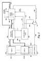
- FIG. 3is a block diagram of an apparatus for performing scan chain operations in a computing system in accordance with a number of embodiments of the present disclosure.
- a memory array 330may include a plurality of memory banks 331 - 1 (Bank A), . . . 331 -N (Bank N), which may be coupled to a serializer/de-serializer 334 via native data paths 373 and 375 .
- the native datapaths 373 and 375may include functional units (e.g., arithmetic logic units, multipliers, etc. to perform data processing operations), registers, and/or buses.
- the native datapathsmay be DRAM or DDR data paths configured to allow data transfer between specific locations of the memory.
- the native datapaths 373 and 375may be used to transfer data from the memory array 330 to the serializer/de-serializer 334 and from the serializer/de-serializer 334 to the memory array 330 .
- native datapath 373may be used to transfer a scan vector from memory bank 331 - 1 of the memory array 330 to the serializer/de-serializer 334
- native datapath 375may be used to transfer a scan vector (e.g., a resultant scan vector as described in more detail, herein) from the serializer/de-serializer 334 to another memory bank 331 -N of the memory array 330 .
- the serializer/de-serializer 334may include logic and/or a plurality of data (DQ) pins. Bidirectional data signals may be sent and/or received via the DQ.
- the serializer/de-serializer 334may include parallel-to-serial converters and/or serial-to-parallel converters to serialize or de-serialize data received or sent by the serializer/de-serializer 334 .
- the serializer/de-serializer 334may be configured to read data (e.g., receive data) in parallel (e.g., using the DQ pins) from the memory array 330 and convert the data to a serial data stream.
- the serializer/de-serializermay be configured to convert the serial data into parallel data and write the data (e.g., send the data) in parallel (e.g., using the DQ pins) to a device under test 338 .
- the device under test 338may be any electronic assembly that is testable using scan insertion techniques.
- the serializer/de-serializer 334may receive serial data from the device under test 338 (e.g., a resultant serial scan vector), convert the data to parallel, and send the parallel data (e.g., the resultant parallelized scan vector) to the memory array 330 .
- Parallel datamay be transferred via native datapaths 373 and 375
- serial datamay be transferred via SCAN IN path 355 and SCAN OUT path 357 .
- native datapath 373 and/or native datapath 375may be n-bit datapaths.
- native datapath 373 and/or native datapath 375may be capable of transferring n-bits of data in a given period of time.
- the serializer/de-serializer 334may, in some embodiments, include m DQ pins and therefore may be capable of outputting an m-bit parallel word. In such examples,
- n 2 bitsmay be scanned into the device under test 338 .
- n 2 bitsmay be scanned out of the device under test 338 in
- serializer/de-serializer 334may be configured to send an
- n 2 bit scan vectorto the device under test 338 via SCAN IN path 355 , and receive an
- the datapath(e.g., native datapaths 373 / 375 and/or SCAN IN path 355 /SCAN OUT path 357 ) may be modified such that half of the datapath (e.g., native data path 373 and/or SCAN IN path 355 ) may be used for writes and half of the datapath (e.g., native datapath 375 and/or SCAN OUT path 357 ) may be used for reads at any given time. For example, half of the datapath (e.g., native datapaths 373 / 375 and/or SCAN IN path 355 ) may be used for writes and half of the datapath (e.g., native datapath 375 and/or SCAN OUT path 357 ) may be used for reads at any given time. For example, half of the datapath (e.g.,
- n 2 bitsmay be used for writes concurrently with the other half of the datapath (e.g.,
- the serializer/de-serializer 334may include a 32-bit
- ( n 2 ) read bus(e.g., may include 4 input DQ pins by 8 burst bits) and a 32-bit
- ( n 2 ) write bus(e.g., may include 4 output DQ pins by 8 burst bits) with 4
- the memory array 330may include a DDR2, DDR3, or other suitable DRAM memory device.
- scan control logic 336is configured to control which half of a word (e.g., which
- n 2 bit portion or an n-bit wordis used for writes and which half of the word is used for reads.
- scan control logic 336may be configured to control which 32-bit portion of a 64-bit word is used for writes and which 32-bit portion of the 64-bit word is used for reads. In some embodiments, a first
- n 2 bit portion of the wordmay be a scan vector, and a second
- n 2 bit portion of the wordmay be a resultant scan vector.
- the serializer/de-serializer 334may include circuitry to control operation of the serializer/de-serializer 334 .
- the serializer/de-serializer 334may include driver and/or input buffers, parallel-to-serial and/or serial-to-parallel converters, circuitry for receiving data (e.g., scan vectors from memory array 330 ) and/or clock signals (e.g., external clock signal XCLK 359 ), and circuitry for receiving control signals (e.g., via scan control signal line 368 ) from the scan control logic 336 .
- datae.g., scan vectors from memory array 330
- clock signalse.g., external clock signal XCLK 359
- control signalse.g., via scan control signal line 368
- the serializer/de-serializer 334is configured to transfer a scan vector via SCAN IN path 355 , such as a scan vector received from the memory array 330 via native datapath 373 , to the device under test 338 .
- the serializer/de-serializer 334may be configured to transfer the scan vector to the device under test 338 in response to receipt of a scan control signal from the scan control logic 336 .
- the scan control signalmay be sent from the scan control logic 336 to the serializer/de-serializer 334 via scan control signal line 368 .
- the scan control logic 336may be provided on-chip and may be configured to control operation of the serializer/de-serializer 334 via scan control signals sent via scan control signal line 368 .
- Scan control logic 336may include an interface for interacting with the memory array 330 (e.g., via bank control 332 ), serializer/de-serializer 334 , and/or device under test 338 .
- scan control logic 336may include an interface that may be configured to control data movement (e.g., may control “steering” data into the scan chain) to facilitate performance of a scan chain operation.
- the scan control logic 336may keep track of which bit in the scan vector is currently be used in order to control timing (e.g., clocking) of the scan vector.
- Scan control logic 336may be configured to generate and assert various signals via scan control signal line 368 , CLK signal line 351 , read/write activation signal line 364 , and scan enable signal line 353 / 365 , etc.
- scan control logic 336may assert first-in-first-out (FIFO)/serializer/de-serializer/clocking signals via scan control signal line 368 to control the serializer/de-serializer 334 to perform various tasks and/or operations, as described above.
- clock signalsmay be asserted on CLK signal line 351 .
- clock signals to control timing of performance of a scan chain operationmay be asserted by the scan control logic 336 to the device under test 338 via CLK signal line 351 .
- a control signal to activate read and write operations for the memory array 330may be asserted on read/write activation signal line 364 .
- the control signal to activate read and write operations for the memory array 330may activate bank control 332 , which is coupled to each bank in the memory array 330 via bank control signal lines 366 - 1 , . . . 366 -N.
- bank control 332may send additional control signals to banks 331 - 1 , . . . 331 -N of the memory array 330 to cause data to be read from the memory array 330 or written to the memory array 330 .
- the scan control logic 336may be configured to assert a scan enable signal on scan enable signal line 353 / 365 to enable a scan chain operation to be performed.
- the scan control logic 336may take over control of access of the memory array 330 .
- the scan control logic 336can coordinate operation of the serializer/de-serializer 334 as part of performing a scan chain operation on a scan vector.
- Scan control logic 336may include one or more state machines to access the memory array 330 .
- the state machine(s)may be used to keep track of row and column addresses for data in the memory array 330 as scan vectors are transferred into or out of the memory array 330 , for example to the serializer/de-serializer 334 and/or the device under test 338 .
- the state machine(s)may receive input from a register (e.g., a current bit register), which is not explicitly shown in FIG. 3 , to select a next row of data to be used for a scan chain operation once the current row of data is exhausted.
- the current bit registermay be used to count (or keep track of) a bit in the scan vector that is currently being read from the memory array 330 , scanned in (e.g., at 355 ) to the device under test 338 , scanned out (e.g., at 357 ) of the device under test 338 , and/or written to the memory array 330 .
- the current bit registermay be included in the scan control logic 336 , or the current bit register may be located external to the scan control logic 336 so long as the current bit register is communicatively coupled to the scan control logic 336 .
- the current bit registermay be used as a counter when performing a scan chain operation on a scan vector.
- the device under test 338may be clocked and a next scan vector may be scanned in (e.g., loaded) into the device under test 338 . This may occur during a “cycle machine” mode (e.g., cycle machine 463 illustrated and discussed in more detail in connection with FIG. 4 , herein) of the scan chain operation.
- cycle machinee.g., cycle machine 463 illustrated and discussed in more detail in connection with FIG. 4 , herein
- the scan control logic 336may include other registers in addition to the current bit register.
- the scan control logic 336may include vector length register(s), number of tests register(s), test number register(s), etc. that may be used to control performance of the scan chain operation and/or may be used as part of preparing for performing a scan chain operation.
- the vector length register(s)may be used to control the length of the scan vector.
- the vector length registermay comprise more than 16 bits or fewer than 16 bits, which may alter the number of pre-fetches that may be performed.
- the memory array 330is a DDR4 memory device, there may be 32 bits per pre-fetch, which may allow for a scan vector length of 2 Mb.
- the number of tests register(s)may be used to determine how many scan vectors are to be scanned in (e.g., at 355 ) to the device under test 338 and have a scan chain operation performed thereon.
- the number of tests register(s)may be 16 bits in length, however, the number of tests register(s) may comprise more than 16 bits or fewer than 16 bits, which may alter the number of scan vectors that may have a scan chain operation performed thereon.
- the test number register(s)may be used to count (or keep track of) how many scan vectors are to be scanned in to the device under test 338 for scan chain operations and/or may count (or keep track of) how many scan vectors have already been scanned in to the device under test 338 for scan chain operations.
- the test number register(s)may cause performance of scan chain operations to stop. For example, when test number number of tests, scan chain operations may be stopped.
- the test number register(s)may be 16 bits in length, however, the test number register(s) may comprise more than 16 bits or fewer than 16 bits.
- the scan control logic 336may include an interface to facilitate access to the registers.
- the scan control logic 336may be programmed using a load mode register (LMR) command.
- LMRload mode register
- the scan control logic 336may include address buses (e.g., a row address bus and a column address bus), which may be activated responsive to the LMR command, to facilitate access to the scan control logic 336 registers.
- a test-mode LMR commandmay be received by the scan control logic 336 prior to loading data into the registers.
- the scan control logic 336may issue commands (e.g., via its state machine(s)) to read data from the memory array 330 or write data to the memory array 330 until a current bit is the length of the scan vector (e.g., until a particular row of data is exhausted).
- commandsmay include commands to read data from a source memory bank (e.g., Bank A) of the memory array 330 and commands to write data to a destination memory bank (e.g., Bank B) of the memory array 330 .
- the scan control logic 336may close the particular row, open a new row of data, and continue issuing commands to the memory array to read the new row of data from the memory array 330 or write a new row of data to the memory array 330 .
- commandsmay be issued via assertion of a signal on the read/write activation signal line 364 and/or in response to assertion of signals by the bank control 332 to the memory array 330 via bank control signal lines 366 - 1 , . . . , 366 -N.
- the bank control 332may assert such signals in response to receipt of a signal asserted by the scan control logic 336 via the read/write activation signal line 364 .
- the source addresses and destination addresses of scan vectors stored in the memory array 330may be the same, but located in different banks of the memory array 330 .
- a source address for a scan vector in a first banke.g., 331 - 1
- a destination address for a resultant scan vector in a second banke.g., 331 -N
- the different bankse.g., Bank A, Bank N, etc.
- the source and destination addresses of scan vectors stored in the memory array 330may be different and may be located in different banks of the memory array 330 .
- the device under test 338is configured to receive scan vectors during SCAN IN 355 , perform a scan chain operation on the scan vector, and output a resultant scan vector during SCAN OUT 357 .
- the scan vectormay be received from the serializer/de-serializer 334 , and the resultant scan vector may be sent back to the serializer/de-serializer 334 .
- the device under test 338may include logic (e.g., flip-flops, shift registers, etc.) to be tested during the scan chain operation.
- the device under testmay be any device that is capable of scan insertion.
- the device under test 338may be a synchronously clocked device.
- the device under testmay be coupled to an external interface via external interface signal line 372 .
- the external interfacemay be an external DRAM interface and may include, for example, a command bus, address bus, on-die termination, and pins to asserts row address strobe signals, column address strobe signals, activate signals (e.g., ACT signals to activate a row or page of DRAM), column select signals, and/or clock enable signals.
- the device under test 338may also be coupled to an external clock signal which may be asserted via XCLK signal line 359 . As shown in FIG.
- XCLK signal line 359may also be coupled to the serializer/de-serializer 334 and/or scan chain logic 336 , and may be configured to pass the asserted external clock signal to serializer/de-serializer 334 and/or the scan chain logic 336 .
- the device under test 338may receive a clock signal from the scan control logic 336 via CLK signal line 351 .
- the clock signalmay be used to facilitate timing of performance of the scan chain operation by the device under test 338 . Further details regarding assertion of the clock signal to control timing of the scan chain operation are described in connection with FIG. 4 , herein.
- the device under test 338may receive a scan enable signal from the scan control logic 336 via scan enable signal line 353 to enable a scan chain operation to be performed. As described above, when the scan enable signal is asserted on scan enable signal line 353 , the scan control logic 336 may take over control of access of the memory array 330 .
- the device under testmay send array control signals via array control interface 362 .
- the array control signals asserted via the array control interface 362may include read/write signals, row address select and/or column address select signals, as well as various activate signals such as activate bank signals and/or activate column signals.
- the array control signalsmay be muxed (e.g., by multiplexer 377 ) scan control signals sent from the scan control logic 336 via scan control signal line 371 .
- the select line of the multiplexer 377may be driven with the scan enable signal sent from the scan control logic 336 via scan enable signal line 365 to select between asserting the array control signals or the scan control signals.
- FIG. 4is a timing diagram for performing scan chain operations in accordance with a number of embodiments of the present disclosure. Timing as described in connection with FIG. 4 may be controlled by a controller such as controller 140 illustrated in FIG. 1 or scan control logic 336 illustrated in FIG. 3 .
- the controllercan include a clock signal 451 , for example, a timing component or timing circuitry in the form of hardware and/or transistor circuitry.
- Clock signal 451can be provided to control timing of performing a scan chain operation.
- scan enable signal 453can be driven to a high state by the controller to scan in signal 455 a scan vector 461 . As shown in FIG.
- the scan in vector 461(e.g., a first scan in vector) can include a plurality of data values AI 5 , AI 4 , AI 3 , AI 2 , AI 1 , and AI 0 .
- a second scan in vectoris represented by BI 5 , BI 4 , BI 3 , BI 2 , BI 1 , BI 0 , and a third scan in vector is shown starting with CI 5 .
- 6 data valuesare shown for the first and second scan in vectors, the number of data values may be greater than or less than 6 data values.
- the scan enable signal 453can be driven low to store (e.g., “capture”) the scan vector 461 , for example, by providing a clock cycle signal 463 .
- the clock cycle pulse 463can toggle logic of the scan chain.
- capturing the scan vector 461can include exciting the device under test (e.g., device under test 338 illustrated in FIG. 3 ).
- the clock cycle pulse 463may be a capture pulse.
- scan enable 453can be driven high again and a second scan vector 467 can be scanned in (e.g., by asserting scan in signal 455 ).
- the resultant scan vector 469 from scan vector 461can be scanned out (e.g., by asserting scan out signal 457 ).
- a first scan out vectoris shown in FIG. 4 as AO 5 , AO 4 , AO 3 , AO 2 , AO 1 , AO 0 .
- resultant scan vector 469can be scanned out in parallel with second scan vector 467 being scanned in (e.g., by asserting scan in signal 453 ), as shown at the bottom portion of FIG. 4 where a scan in vector containing data values BI 5 -BI 0 is scanned in in parallel with scan out vector containing data values AO 5 -AO 0 being scanned out.
- scan vectors 461 of various lengthscan be subjected to scan chain operations. For example, if a scan vector (e.g., second scan vector 467 ) is longer than a remaining length of a page of DRAM, the scan vector (e.g., second scan vector 467 ) can be split into one or more portions that are each shorter than a maximum length available to be scanned in. In this example, a next portion of the scan vector can be scanned in (e.g., by asserting scan enable signal 453 ) in response to completion of a scan chain operation on a previous portion of the scan vector.
- a scan vectore.g., second scan vector 467
- the scan vectore.g., second scan vector 467
- a next portion of the scan vectorcan be scanned in (e.g., by asserting scan enable signal 453 ) in response to completion of a scan chain operation on a previous portion of the scan vector.
- the scan vectormay not need to be divided into one or more portions, and the scan chain operation can be completed without fetching additional portions of the scan vector.
- determining if a scan vector 461 is to be split into one or more portions, and/or coordination of performing scan chain operations on one or more portions of a truncated scan vector 461is controlled by a controller (e.g., controller 140 , scan control logic 336 ).
- a memory testercan be provided to perform scan vector 461 truncation and coordination.
- Some embodimentsallow for on-die comparison between a resultant scan vector 469 and an expected result vector.
- compressioncan be implemented in the memory array (e.g., memory array 130 illustrated in FIG. 1 , memory array 330 illustrated in FIG. 3 ), which can allow for a final pattern read out to be presented as a pass/fail flag.
- the sensing circuitrycan provide ample elements to perform a comparison of the resultant scan vector 469 to a base set of expected data and/or to perform compression computations to reduce a size of the resultant scan vector 469 .
- an example procedure for performing scan chain operationscan include writing one or more input scan vectors and/or expected output vectors to DRAM.
- applying an XNOR operation to the output scan vector 469 and the expected output vectorcan compress the result such that the final result can be stored as a single bit (e.g., a pass/fail flag).
Landscapes
- Engineering & Computer Science (AREA)
- General Engineering & Computer Science (AREA)
- Physics & Mathematics (AREA)
- General Physics & Mathematics (AREA)
- Theoretical Computer Science (AREA)
- Computer Hardware Design (AREA)
- Tests Of Electronic Circuits (AREA)
Abstract
Description
The present disclosure relates generally to semiconductor memory and methods, and more particularly, to apparatuses and methods related to a scan chain operations.
Memory devices are typically provided as internal, semiconductor, integrated circuits in computers or other electronic systems. There are many different types of memory including volatile and non-volatile memory. Volatile memory can require power to maintain its data (e.g., host data, error data, etc.) and includes random access memory (RAM), dynamic random access memory (DRAM), static random access memory (SRAM), synchronous dynamic random access memory (SDRAM), and thyristor random access memory (TRAM), among others. Non-volatile memory can provide persistent data by retaining stored data when not powered and can include NAND flash memory, NOR flash memory, and resistance variable memory such as phase change random access memory (PCRAM), resistive random access memory (RRAM), and magnetoresistive random access memory (MRAM), such as spin torque transfer random access memory (STT RAM), among others.
Electronic systems often include a number of processing resources (e.g., one or more processors), which may retrieve and execute instructions and store the results of the executed instructions to a suitable location. A processor can comprise a number of functional units such as arithmetic logic unit (ALU) circuitry, floating point unit (FPU) circuitry, and a combinatorial logic block, for example, which can be used to execute instructions by performing logical operations such as AND, OR, NOT, NAND, NOR, and XOR logical operations on data (e.g., one or more operands). For example, functional unit circuitry may be used to perform arithmetic operations such as addition, subtraction, multiplication, and division on operands via a number of logical operations in addition to scan chain operations.
A number of components in an electronic system may be involved in providing instructions to the functional unit circuitry for execution. The instructions may be executed, for instance, by a processing resource such as a controller and/or host processor. Data (e.g., the operands on which the instructions will be executed) may be stored in a memory array that is accessible by the functional unit circuitry. The instructions and data may be retrieved from the memory array and sequenced and/or buffered before the functional unit circuitry begins to execute instructions on the data. Furthermore, as different types of operations may be executed in one or multiple clock cycles through the functional unit circuitry, intermediate results of the instructions and data may also be sequenced and/or buffered.
The present disclosure includes apparatuses and methods related to scan chain operations. A number of embodiments include an apparatus comprising a memory array including a first memory bank and a second memory bank and a serializer/de-serializer coupled to the first memory bank and the second memory bank. The serializer/de-serializer may be configured to receive a scan vector from the first memory bank, send the scan vector to a device under test, receive scan test responses from the device under test, and send the scan test responses to the second memory bank. Scan control logic may be coupled to the serializer/de-serializer and the device under test. The scan control logic may be configured to control operation of the serializer/de-serializer and send a scan chain control signal to the device under test, wherein the scan chain control signal is to initiate performance of a scan chain operation using the scan vector. As used herein, a “scan vector” or “scan chain vector” is a physically contiguous number of bits that can be stored, shifted, read, and/or written to and/or from a memory device and/or device under test.
Scan chain testing may be used to detect various manufacturing faults in an electronic system. Such faults may include shorts and opens exhibited in components associated with the electronic system. Scan chain testing may be desirable to minimize the chance of selling or shipping a defective part to a customer, which could not only result in a loss of good will toward the manufacturer or reseller of the defective part, but may also have more dire consequences, for example in the case of electronic systems for automotive or medical applications.
In some approaches, a flip-flop is coupled via its input to a multiplexer. One input of the multiplexer may act as a functional input, while the other input of the multiplexer may be a scan-in input. A scan enable signal may be provided to the multiplexer to select between the functional input and the scan-in input. The output of the flip-flop is coupled to another multiplexer that is coupled to another flip-flop in the same manner as described above. Accordingly, a plurality of flip-flops may be connected together via a plurality of multiplexers to form a chain, which may effectively act as a shift register.
In such approaches, the first flip-flop of the chain is coupled to a scan-in port, and the last flip-flop of the chain is coupled to a scan-out port. In general, a clock signal is provided to each flip-flop in the chain. The clock signal may be provided to each flip-flop to coordinate transfer of data from one flip-flop to the next flip-flop in the chain.
In contrast, a number of embodiments of the present disclosure can utilize a native datapath and a serializer/de-serializer to transfer data to and from a memory array to a device under test in a more efficient manner as compared to previous approaches. For example, scan vectors may be stored in the memory array and subsequently transferred through a native datapath to a device under test. A resultant scan vector may then be transferred from the device under test back to the memory array. Further, various embodiments can utilize a native datapath and a serializer/de-serializer to transfer data into and/or out of periphery logic as part of performing a scan chain operation.
As used herein, a “native datapath” is a data path which allows data to be written to and read from specific memory locations. The native datapath may allow for bidirectional transfer of data to and from the specific memory locations. In some embodiments, the native datapath may include sense amplifier, input/output (I/O) devices, multiplexers, write drivers, and/or data amplifiers. Some of the circuits of the native datapath may be truly bidirectional (e.g., they may pass data in for write operations and out for read operations), while some of the circuits of the native datapath may be unidirectional but occurring in complementary pairs such that data can be transferred bidirectionally.
In the following detailed description of the present disclosure, reference is made to the accompanying drawings that form a part hereof, and in which is shown by way of illustration how one or more embodiments of the disclosure may be practiced. These embodiments are described in sufficient detail to enable those of ordinary skill in the art to practice the embodiments of this disclosure, and it is to be understood that other embodiments may be utilized and that process, electrical, and/or structural changes may be made without departing from the scope of the present disclosure. As used herein, designators such as “N,” particularly with respect to reference numerals in the drawings, indicate that a number of the particular feature so designated can be included. As used herein, “a number of” a particular thing can refer to one or more of such things (e.g., a number of memory arrays can refer to one or more memory arrays). A “plurality of” is intended to refer to more than one of such things.
The figures herein follow a numbering convention in which the first digit or digits correspond to the drawing figure number and the remaining digits identify an element or component in the drawing. Similar elements or components between different figures may be identified by the use of similar digits. For example, 130 may reference element “30” inFIG. 1 , and a similar element may be referenced as 330 inFIG. 3 . As will be appreciated, elements shown in the various embodiments herein can be added, exchanged, and/or eliminated so as to provide a number of additional embodiments of the present disclosure. In addition, as will be appreciated, the proportion and the relative scale of the elements provided in the figures are intended to illustrate certain embodiments of the present invention, and should not be taken in a limiting sense.
For clarity, thesystem 100 has been simplified to focus on features with particular relevance to the present disclosure. Thememory array 130 can be a DRAM array, SRAM array, STT RAM array, PCRAM array, TRAM array, RRAM array, NAND flash array, and/or NOR flash array, for instance. Thearray 130 can comprise memory cells arranged in rows coupled by access lines, which may be referred to herein as word lines or select lines, and columns coupled by sense lines, which may be referred to herein as data lines or digit lines. Although asingle array 130 is shown inFIG. 1 , embodiments are not so limited. For instance,memory device 120 may include a number of arrays130 (e.g., a number of banks of DRAM cells, NAND flash cells, etc.).
Thememory device 120 includesaddress circuitry 142 to latch address signals provided over abus 156 through I/O circuitry 144 and/or to latch address signals provided overcontrol bus 154. Address signals are received throughaddress circuitry 142 and decoded by arow decoder 146 and acolumn decoder 152 to access thememory array 130. The I/O circuitry 144 can be used for bidirectional data communication withhost 110 over thebus 156. Thewrite circuitry 148 is used to write data to thememory array 130. InFIG. 1 ,bus 156 serves as a combined address/data bus; however, embodiments are not so limited. For example, a control bus, address bus, and/or data bus may be separate buses.
Thecontroller 140 can control, for example, reading and writing scan vectors into and out of thememory array 130, and/or can control timing of scan chain operations performed on a scan vector. As used herein, a “scan chain operation” includes one or more of: receiving (e.g., scanning in, shifting in) an input scan vector, storing (e.g., capturing) the scan vector, and writing (e.g., scanning out, shifting out) the resultant scan vector out of a serializer/de-serializer and/or device under test. For example, according to embodiments, a scan vector can be loaded into a serializer/de-serializer and/or device under test. The scan vector can be stored, for example, by asserting a capture clock pulse, and the resultant scan vector can be shifted out of the serializer/de-serializer and/or device under test, for example, to a portion of thememory array 130.
Scan testing may be done using the apparatus shown inFIG. 2 in order to detect manufacturing faults in thecombinational logic 296. In order to do so, nodes within thecombinational logic 296 may be excited by applying input vectors at the flip-flops of the scan chain. At the beginning of a scan testing operation, a scan enable signal may be asserted on scan enablesignal line 253. Responsive to assertion of the scan enable signal, data may be shifted in to each of the flip-flops294-1, . . .294-N such that the flip-flops294-1, . . .294-N are loaded with an input vector. Subsequently, a clock pulse may be asserted onCLK signal line 251 to excite thecombinational logic 296. The output is then captured and compared to an expected signature to determine if there are manufacturing faults in thecombinational logic 296.
Thenative datapaths memory array 330 to the serializer/de-serializer 334 and from the serializer/de-serializer 334 to thememory array 330. In some embodiments,native datapath 373 may be used to transfer a scan vector from memory bank331-1 of thememory array 330 to the serializer/de-serializer 334, whilenative datapath 375 may be used to transfer a scan vector (e.g., a resultant scan vector as described in more detail, herein) from the serializer/de-serializer 334 to another memory bank331-N of thememory array 330.
The serializer/de-serializer 334 may include logic and/or a plurality of data (DQ) pins. Bidirectional data signals may be sent and/or received via the DQ. In some embodiments, the serializer/de-serializer 334 may include parallel-to-serial converters and/or serial-to-parallel converters to serialize or de-serialize data received or sent by the serializer/de-serializer 334. For example, the serializer/de-serializer 334 may be configured to read data (e.g., receive data) in parallel (e.g., using the DQ pins) from thememory array 330 and convert the data to a serial data stream. Similarly, the serializer/de-serializer may be configured to convert the serial data into parallel data and write the data (e.g., send the data) in parallel (e.g., using the DQ pins) to a device undertest 338. The device undertest 338 may be any electronic assembly that is testable using scan insertion techniques. In some embodiments, the serializer/de-serializer 334 may receive serial data from the device under test338 (e.g., a resultant serial scan vector), convert the data to parallel, and send the parallel data (e.g., the resultant parallelized scan vector) to thememory array 330. Parallel data may be transferred vianative datapaths path 355 andSCAN OUT path 357.
In some embodiments,native datapath 373 and/ornative datapath 375 may be n-bit datapaths. For example,native datapath 373 and/ornative datapath 375 may be capable of transferring n-bits of data in a given period of time. The serializer/de-serializer 334 may, in some embodiments, include m DQ pins and therefore may be capable of outputting an m-bit parallel word. In such examples,
bits may be scanned into the device under
bits may be scanned out of the device under
parallel scan chains. That is, in some embodiments, the serializer/
bit scan vector to the device under
bit resultant scan vector output from the device under
In some embodiments, the datapath (e.g.,native datapaths 373/375 and/or SCAN INpath 355/SCAN OUT path357) may be modified such that half of the datapath (e.g.,native data path 373 and/or SCAN IN path355) may be used for writes and half of the datapath (e.g.,native datapath 375 and/or SCAN OUT path357) may be used for reads at any given time. For example, half of the datapath (e.g.,
bits) may be used for writes concurrently with the other half of the datapath (e.g.,
bits) being used for reads.
As an example, thememory array 330 may comprise a 4 Gb×8 DDR4 SDRAM memory device, which may have n=64 and m=8. In this example, the serializer/de-serializer 334 may include a 32-bit
read bus (e.g., may include 4 input DQ pins by 8 burst bits) and a 32-bit
write bus (e.g., may include 4 output DQ pins by 8 burst bits) with 4
parallel scan chains. Embodiments are not so limited; however. Although described above in connection with a DDR4 SDRAM device, the
In some embodiments, scancontrol logic 336 is configured to control which half of a word (e.g., which
bit portion or an n-bit word) is used for writes and which half of the word is used for reads. For example, scan
bit portion of the word may be a scan vector, and a second
bit portion of the word may be a resultant scan vector.
The serializer/de-serializer 334 may include circuitry to control operation of the serializer/de-serializer 334. For example, the serializer/de-serializer 334 may include driver and/or input buffers, parallel-to-serial and/or serial-to-parallel converters, circuitry for receiving data (e.g., scan vectors from memory array330) and/or clock signals (e.g., external clock signal XCLK359), and circuitry for receiving control signals (e.g., via scan control signal line368) from thescan control logic 336.
In some embodiments, the serializer/de-serializer 334 is configured to transfer a scan vector via SCAN INpath 355, such as a scan vector received from thememory array 330 vianative datapath 373, to the device undertest 338. The serializer/de-serializer 334 may be configured to transfer the scan vector to the device undertest 338 in response to receipt of a scan control signal from thescan control logic 336. The scan control signal may be sent from thescan control logic 336 to the serializer/de-serializer 334 via scancontrol signal line 368.
Thescan control logic 336 may be provided on-chip and may be configured to control operation of the serializer/de-serializer 334 via scan control signals sent via scancontrol signal line 368.Scan control logic 336 may include an interface for interacting with the memory array330 (e.g., via bank control332), serializer/de-serializer 334, and/or device undertest 338. For example, scancontrol logic 336 may include an interface that may be configured to control data movement (e.g., may control “steering” data into the scan chain) to facilitate performance of a scan chain operation. In some embodiments, thescan control logic 336 may keep track of which bit in the scan vector is currently be used in order to control timing (e.g., clocking) of the scan vector.
A control signal to activate read and write operations for thememory array 330 may be asserted on read/writeactivation signal line 364. In some embodiments, the control signal to activate read and write operations for thememory array 330 may activatebank control 332, which is coupled to each bank in thememory array 330 via bank control signal lines366-1, . . .366-N. For example, responsive to receipt of the control signal to activate read and write operations for thememory array 330,bank control 332 may send additional control signals to banks331-1, . . .331-N of thememory array 330 to cause data to be read from thememory array 330 or written to thememory array 330.
In some embodiments, thescan control logic 336 may be configured to assert a scan enable signal on scan enablesignal line 353/365 to enable a scan chain operation to be performed. When the scan enable signal is asserted on scan enablesignal line 353/365, thescan control logic 336 may take over control of access of thememory array 330. By providing control of access to thememory array 330 to thescan control logic 336 responsive to assertion of the scan enable signal, thescan control logic 336 can coordinate operation of the serializer/de-serializer 334 as part of performing a scan chain operation on a scan vector.
The current bit register may be used to count (or keep track of) a bit in the scan vector that is currently being read from thememory array 330, scanned in (e.g., at355) to the device undertest 338, scanned out (e.g., at357) of the device undertest 338, and/or written to thememory array 330. The current bit register may be included in thescan control logic 336, or the current bit register may be located external to thescan control logic 336 so long as the current bit register is communicatively coupled to thescan control logic 336. The current bit register may be used as a counter when performing a scan chain operation on a scan vector. In some embodiments, when the current bit (as determined by the current bit register, for example) is the last bit in a scan vector (e.g., when current bit==vector length), the device undertest 338 may be clocked and a next scan vector may be scanned in (e.g., loaded) into the device undertest 338. This may occur during a “cycle machine” mode (e.g.,cycle machine 463 illustrated and discussed in more detail in connection withFIG. 4 , herein) of the scan chain operation.
In some embodiments, thescan control logic 336 may include other registers in addition to the current bit register. For example, thescan control logic 336 may include vector length register(s), number of tests register(s), test number register(s), etc. that may be used to control performance of the scan chain operation and/or may be used as part of preparing for performing a scan chain operation.
The vector length register(s) may be used to control the length of the scan vector. In the case of a 16 bit vector length register, there may be 64 pre-fetches, however, the vector length register may comprise more than 16 bits or fewer than 16 bits, which may alter the number of pre-fetches that may be performed. In the example where thememory array 330 is a DDR4 memory device, there may be 32 bits per pre-fetch, which may allow for a scan vector length of 2 Mb.
The number of tests register(s) may be used to determine how many scan vectors are to be scanned in (e.g., at355) to the device undertest 338 and have a scan chain operation performed thereon. In some embodiments, the number of tests register(s) may be 16 bits in length, however, the number of tests register(s) may comprise more than 16 bits or fewer than 16 bits, which may alter the number of scan vectors that may have a scan chain operation performed thereon.
The test number register(s) may be used to count (or keep track of) how many scan vectors are to be scanned in to the device undertest 338 for scan chain operations and/or may count (or keep track of) how many scan vectors have already been scanned in to the device undertest 338 for scan chain operations. When a threshold number of scan vectors have been scanned in to the device undertest 338 for scan chain operations, the test number register(s) may cause performance of scan chain operations to stop. For example, when test number number of tests, scan chain operations may be stopped. In some embodiments, the test number register(s) may be 16 bits in length, however, the test number register(s) may comprise more than 16 bits or fewer than 16 bits.
In some embodiments, thescan control logic 336 may include an interface to facilitate access to the registers. Thescan control logic 336 may be programmed using a load mode register (LMR) command. For example, thescan control logic 336 may include address buses (e.g., a row address bus and a column address bus), which may be activated responsive to the LMR command, to facilitate access to thescan control logic 336 registers. In some embodiments, a test-mode LMR command may be received by thescan control logic 336 prior to loading data into the registers.
In some embodiments, thescan control logic 336 may issue commands (e.g., via its state machine(s)) to read data from thememory array 330 or write data to thememory array 330 until a current bit is the length of the scan vector (e.g., until a particular row of data is exhausted). Such commands may include commands to read data from a source memory bank (e.g., Bank A) of thememory array 330 and commands to write data to a destination memory bank (e.g., Bank B) of thememory array 330. Once the particular row of data is exhausted, thescan control logic 336 may close the particular row, open a new row of data, and continue issuing commands to the memory array to read the new row of data from thememory array 330 or write a new row of data to thememory array 330. As described above, such commands may be issued via assertion of a signal on the read/writeactivation signal line 364 and/or in response to assertion of signals by thebank control 332 to thememory array 330 via bank control signal lines366-1, . . . ,366-N. In some embodiments, thebank control 332 may assert such signals in response to receipt of a signal asserted by thescan control logic 336 via the read/writeactivation signal line 364.
In some embodiments, the source addresses and destination addresses of scan vectors stored in thememory array 330 may be the same, but located in different banks of thememory array 330. For example, a source address for a scan vector in a first bank (e.g.,331-1) may be the same address as a destination address for a resultant scan vector in a second bank (e.g.,331-N). In some embodiments, the different banks (e.g., Bank A, Bank N, etc.) may share portions of a global data bus to facilitate communication between the banks of thememory array 330. Embodiments are not so limited, however, and the source and destination addresses of scan vectors stored in thememory array 330 may be different and may be located in different banks of thememory array 330.
As described above, the device undertest 338 is configured to receive scan vectors during SCAN IN355, perform a scan chain operation on the scan vector, and output a resultant scan vector duringSCAN OUT 357. The scan vector may be received from the serializer/de-serializer 334, and the resultant scan vector may be sent back to the serializer/de-serializer 334. In some embodiments, the device undertest 338 may include logic (e.g., flip-flops, shift registers, etc.) to be tested during the scan chain operation. The device under test may be any device that is capable of scan insertion. For example, the device undertest 338 may be a synchronously clocked device.
In some embodiments, the device under test may be coupled to an external interface via externalinterface signal line 372. The external interface may be an external DRAM interface and may include, for example, a command bus, address bus, on-die termination, and pins to asserts row address strobe signals, column address strobe signals, activate signals (e.g., ACT signals to activate a row or page of DRAM), column select signals, and/or clock enable signals. The device undertest 338 may also be coupled to an external clock signal which may be asserted viaXCLK signal line 359. As shown inFIG. 3 ,XCLK signal line 359 may also be coupled to the serializer/de-serializer 334 and/or scanchain logic 336, and may be configured to pass the asserted external clock signal to serializer/de-serializer 334 and/or thescan chain logic 336.
The device undertest 338 may receive a clock signal from thescan control logic 336 viaCLK signal line 351. The clock signal may be used to facilitate timing of performance of the scan chain operation by the device undertest 338. Further details regarding assertion of the clock signal to control timing of the scan chain operation are described in connection withFIG. 4 , herein.
The device undertest 338 may receive a scan enable signal from thescan control logic 336 via scan enablesignal line 353 to enable a scan chain operation to be performed. As described above, when the scan enable signal is asserted on scan enablesignal line 353, thescan control logic 336 may take over control of access of thememory array 330.
In some embodiments, the device under test may send array control signals viaarray control interface 362. The array control signals asserted via thearray control interface 362 may include read/write signals, row address select and/or column address select signals, as well as various activate signals such as activate bank signals and/or activate column signals. The array control signals may be muxed (e.g., by multiplexer377) scan control signals sent from thescan control logic 336 via scancontrol signal line 371. In some embodiments, the select line of themultiplexer 377 may be driven with the scan enable signal sent from thescan control logic 336 via scan enablesignal line 365 to select between asserting the array control signals or the scan control signals.
Once thescan vector 461 has been scanned in (e.g., by asserting scan in signal455) the scan enablesignal 453 can be driven low to store (e.g., “capture”) thescan vector 461, for example, by providing aclock cycle signal 463. Theclock cycle pulse 463 can toggle logic of the scan chain. In at least one embodiment, capturing thescan vector 461 can include exciting the device under test (e.g., device undertest 338 illustrated inFIG. 3 ). In some embodiments, theclock cycle pulse 463 may be a capture pulse.
Following theclock cycle pulse 463, scan enable453 can be driven high again and asecond scan vector 467 can be scanned in (e.g., by asserting scan in signal455). Theresultant scan vector 469 fromscan vector 461 can be scanned out (e.g., by asserting scan out signal457). A first scan out vector is shown inFIG. 4 as AO5, AO4, AO3, AO2, AO1, AO0. In at least one embodiment,resultant scan vector 469 can be scanned out in parallel withsecond scan vector 467 being scanned in (e.g., by asserting scan in signal453), as shown at the bottom portion ofFIG. 4 where a scan in vector containing data values BI5-BI0 is scanned in in parallel with scan out vector containing data values AO5-AO0 being scanned out.
In some embodiments, scanvectors 461 of various lengths can be subjected to scan chain operations. For example, if a scan vector (e.g., second scan vector467) is longer than a remaining length of a page of DRAM, the scan vector (e.g., second scan vector467) can be split into one or more portions that are each shorter than a maximum length available to be scanned in. In this example, a next portion of the scan vector can be scanned in (e.g., by asserting scan enable signal453) in response to completion of a scan chain operation on a previous portion of the scan vector. However, if the length of the scan vector (e.g., scan vector461) is less than a page size of DRAM, the scan vector may not need to be divided into one or more portions, and the scan chain operation can be completed without fetching additional portions of the scan vector. In at least one embodiment, determining if ascan vector 461 is to be split into one or more portions, and/or coordination of performing scan chain operations on one or more portions of atruncated scan vector 461 is controlled by a controller (e.g.,controller 140, scan control logic336). In some embodiments, a memory tester can be provided to performscan vector 461 truncation and coordination.
Some embodiments allow for on-die comparison between aresultant scan vector 469 and an expected result vector. In at least one embodiment, compression can be implemented in the memory array (e.g.,memory array 130 illustrated inFIG. 1 ,memory array 330 illustrated inFIG. 3 ), which can allow for a final pattern read out to be presented as a pass/fail flag. For example, the sensing circuitry can provide ample elements to perform a comparison of theresultant scan vector 469 to a base set of expected data and/or to perform compression computations to reduce a size of theresultant scan vector 469.
In some embodiments, an example procedure for performing scan chain operations can include writing one or more input scan vectors and/or expected output vectors to DRAM. In some embodiments, applying an XNOR operation to theoutput scan vector 469 and the expected output vector can compress the result such that the final result can be stored as a single bit (e.g., a pass/fail flag).
Although specific embodiments have been illustrated and described herein, those of ordinary skill in the art will appreciate that an arrangement calculated to achieve the same results can be substituted for the specific embodiments shown. This disclosure is intended to cover adaptations or variations of one or more embodiments of the present disclosure. It is to be understood that the above description has been made in an illustrative fashion, and not a restrictive one. Combination of the above embodiments, and other embodiments not specifically described herein will be apparent to those of skill in the art upon reviewing the above description. The scope of the one or more embodiments of the present disclosure includes other applications in which the above structures and methods are used. Therefore, the scope of one or more embodiments of the present disclosure should be determined with reference to the appended claims, along with the full range of equivalents to which such claims are entitled.
In the foregoing Detailed Description, some features are grouped together in a single embodiment for the purpose of streamlining the disclosure. This method of disclosure is not to be interpreted as reflecting an intention that the disclosed embodiments of the present disclosure have to use more features than are expressly recited in each claim. Rather, as the following claims reflect, inventive subject matter lies in less than all features of a single disclosed embodiment. Thus, the following claims are hereby incorporated into the Detailed Description, with each claim standing on its own as a separate embodiment.
Claims (14)
1. An apparatus, comprising:
a memory array including a first memory bank and a second memory bank;
a serializer/de-serializer coupled to the first memory bank and the second memory bank, the serializer/de-serializer configured to:
receive a scan vector from the first memory bank;
send the scan vector to a device under test;
receive scan test responses from the device under test; and
send the scan test responses to the second memory bank; and
scan control logic coupled to the serializer/de-serializer and the device under test, the scan control logic configured to:
control operation of the serializer/de-serializer; and
send a scan chain control signal to the device under test, wherein the scan chain control signal is to initiate performance of a scan chain operation using the scan vector.
2. The apparatus ofclaim 1 , wherein the scan control logic is further configured to provide a scan chain clock signal to the device under test to coordinate performance of the scan chain operation.
3. The apparatus ofclaim 1 , wherein the scan control logic is further configured to:
receive an external clock signal to control timing of operations of the scan control logic;
control operation of the serializer/de-serializer based at least in part on receipt the external clock signal; and
provide a scan chain clock signal to the device under test based at least in part on receipt of the external clock signal.
4. The apparatus ofclaim 1 , wherein the scan control logic includes a state machine configured to:
provide the scan control logic with access to the memory array responsive to a determination that the scan chain control signal has been initiated by the scan control logic;
store information corresponding to a row address and a column address of the memory array; and
control selection of a row of data stored in the memory array to be used as the scan vector based on the stored information corresponding to the row address and the column address.
5. The apparatus ofclaim 1 , wherein the scan chain control signal is a synchronous signal.
6. The apparatus ofclaim 1 , wherein the scan control logic is further configured to issue commands to:
read the scan vector from the first memory bank; and
write a resultant scan vector to the second memory bank, wherein the resultant scan vector is a resultant output scan vector received from the device under test.
7. The apparatus ofclaim 1 , further comprising bank control logic coupled to the scan control logic and configured to receive a bank control activation signal from the scan chain logic, wherein the bank control activation signal is to cause a resultant output scan vector to be written to the second memory bank.
8. The apparatus ofclaim 1 , wherein the scan control logic is configured to control writing the scan vector to the device under test and reading a resultant output scan vector from the device under test concurrently.
9. A system, comprising:
bank control logic coupled to a memory array comprising a first memory bank and a second memory bank;
a serializer/de-serializer coupled to the first memory bank, the second memory bank, and a device under test; and
scan control logic coupled to the serializer/de-serializer, the device under test, and the bank control logic, the scan chain logic configured to:
control operation of the serializer/de-serializer to send a scan vector from the serializer/de-serializer to the device under test;
send a scan chain control signal to initiate performance of a scan chain operation using the scan vector to the device under test; and
send a synchronous clock signal to the device under test to coordinate timing of the scan chain operation.
10. The system ofclaim 9 , further comprising a datapath between the memory array and the serializer/de-serializer, the datapath configured to carry an n-bit word, wherein the serializer/de-serializer is configured to output m-bit parallel words, and wherein the serializer/de-serializer is configured to, for
parallel scan chain vectors:
send an
bit scan vector to the device under test; and
receive an
bit resultant output scan vector from the device under test.
11. The system ofclaim 10 , wherein the scan control logic is configured to determine which
bit portion of the n-bit word is to be used as the scan vector.
12. The system ofclaim 9 , wherein the scan control logic is configured to control data transfer through the serializer/de-serializer such that the data is transferred according to first in first out scheme.
13. The system ofclaim 9 , wherein the scan control logic is configured to issue column commands to the memory array to cause scan vector to be read from the first memory bank and resultant output scan vectors to be written to the second memory bank.
14. The system ofclaim 9 , wherein the scan control logic is configured to control operation of the memory array to cause:
the scan vector to be sent from the first memory bank to the serializer/de-serializer; and
a resultant output scan vector to be sent from the device under test to the second memory bank.
Priority Applications (2)
| Application Number | Priority Date | Filing Date | Title |
|---|---|---|---|
| US15/672,512US10162005B1 (en) | 2017-08-09 | 2017-08-09 | Scan chain operations |
| US16/221,233US10712389B2 (en) | 2017-08-09 | 2018-12-14 | Scan chain operations |
Applications Claiming Priority (1)
| Application Number | Priority Date | Filing Date | Title |
|---|---|---|---|
| US15/672,512US10162005B1 (en) | 2017-08-09 | 2017-08-09 | Scan chain operations |
Related Child Applications (1)
| Application Number | Title | Priority Date | Filing Date |
|---|---|---|---|
| US16/221,233DivisionUS10712389B2 (en) | 2017-08-09 | 2018-12-14 | Scan chain operations |
Publications (1)
| Publication Number | Publication Date |
|---|---|
| US10162005B1true US10162005B1 (en) | 2018-12-25 |
Family
ID=64717068
Family Applications (2)
| Application Number | Title | Priority Date | Filing Date |
|---|---|---|---|
| US15/672,512ActiveUS10162005B1 (en) | 2017-08-09 | 2017-08-09 | Scan chain operations |
| US16/221,233ActiveUS10712389B2 (en) | 2017-08-09 | 2018-12-14 | Scan chain operations |
Family Applications After (1)
| Application Number | Title | Priority Date | Filing Date |
|---|---|---|---|
| US16/221,233ActiveUS10712389B2 (en) | 2017-08-09 | 2018-12-14 | Scan chain operations |
Country Status (1)
| Country | Link |
|---|---|
| US (2) | US10162005B1 (en) |
Cited By (4)
| Publication number | Priority date | Publication date | Assignee | Title |
|---|---|---|---|---|
| US10482933B2 (en)* | 2018-04-12 | 2019-11-19 | Globalfoundries U.S. Inc. | Column multiplexor decoding |
| US10622088B2 (en)* | 2018-07-23 | 2020-04-14 | Samsung Electronics Co., Ltd. | Stacked memory devices, memory systems and methods of operating stacked memory devices |
| US10922203B1 (en)* | 2018-09-21 | 2021-02-16 | Nvidia Corporation | Fault injection architecture for resilient GPU computing |
| US20240412798A1 (en)* | 2023-06-08 | 2024-12-12 | SambaNova Systems, Inc. | Method for Scanning a Memory Array |
Families Citing this family (1)
| Publication number | Priority date | Publication date | Assignee | Title |
|---|---|---|---|---|
| TWI800925B (en)* | 2021-09-17 | 2023-05-01 | 瑞昱半導體股份有限公司 | Test syatem and test method |
Citations (323)
| Publication number | Priority date | Publication date | Assignee | Title |
|---|---|---|---|---|
| US4380046A (en) | 1979-05-21 | 1983-04-12 | Nasa | Massively parallel processor computer |
| US4435792A (en) | 1982-06-30 | 1984-03-06 | Sun Microsystems, Inc. | Raster memory manipulation apparatus |
| US4435793A (en) | 1979-07-26 | 1984-03-06 | Tokyo Shibaura Denki Kabushiki Kaisha | Semiconductor memory device with dummy word line/sense amplifier activation |
| EP0214718A2 (en) | 1985-07-22 | 1987-03-18 | Alliant Computer Systems Corporation | Digital computer |
| US4727474A (en) | 1983-02-18 | 1988-02-23 | Loral Corporation | Staging memory for massively parallel processor |
| US4843264A (en) | 1987-11-25 | 1989-06-27 | Visic, Inc. | Dynamic sense amplifier for CMOS static RAM |
| US4891809A (en)* | 1987-02-16 | 1990-01-02 | Nec Corporation | Cache memory having self-error checking and sequential verification circuits |
| US4958378A (en) | 1989-04-26 | 1990-09-18 | Sun Microsystems, Inc. | Method and apparatus for detecting changes in raster data |
| US4977542A (en) | 1988-08-30 | 1990-12-11 | Mitsubishi Denki Kabushiki Kaisha | Dynamic semiconductor memory device of a twisted bit line system having improved reliability of readout |
| US5023838A (en) | 1988-12-02 | 1991-06-11 | Ncr Corporation | Random access memory device with integral logic capability |
| US5034636A (en) | 1990-06-04 | 1991-07-23 | Motorola, Inc. | Sense amplifier with an integral logic function |
| US5201039A (en) | 1987-09-30 | 1993-04-06 | Mitsubishi Denki Kabushiki Kaisha | Multiple address-space data processor with addressable register and context switching |
| US5210850A (en) | 1990-06-15 | 1993-05-11 | Compaq Computer Corporation | Memory address space determination using programmable limit registers with single-ended comparators |
| US5253308A (en) | 1989-06-21 | 1993-10-12 | Amber Engineering, Inc. | Massively parallel digital image data processor using pixel-mapped input/output and relative indexed addressing |
| US5276643A (en) | 1988-08-11 | 1994-01-04 | Siemens Aktiengesellschaft | Integrated semiconductor circuit |
| US5325519A (en) | 1991-10-18 | 1994-06-28 | Texas Microsystems, Inc. | Fault tolerant computer with archival rollback capabilities |
| US5341382A (en) | 1991-06-19 | 1994-08-23 | Sun Microsystems, Inc. | Method and apparatus for improving fault coverage of system logic of an integrated circuit with embedded memory arrays |
| US5349587A (en)* | 1992-03-26 | 1994-09-20 | Northern Telecom Limited | Multiple clock rate test apparatus for testing digital systems |
| US5367488A (en) | 1992-03-18 | 1994-11-22 | Goldstar Electron Co., Ltd. | DRAM having bidirectional global bit lines |
| US5379257A (en) | 1990-11-16 | 1995-01-03 | Mitsubishi Denki Kabushiki Kaisha | Semiconductor integrated circuit device having a memory and an operational unit integrated therein |
| US5383143A (en) | 1994-03-30 | 1995-01-17 | Motorola, Inc. | Self re-seeding linear feedback shift register (LFSR) data processing system for generating a pseudo-random test bit stream and method of operation |
| US5386379A (en) | 1992-01-03 | 1995-01-31 | France Telecom, Establissement Autonome De Droit Public | Memory cell for associative memory |
| US5398213A (en) | 1992-10-08 | 1995-03-14 | Samsung Electronics Co., Ltd. | Access time speed-up circuit for a semiconductor memory device |
| US5414714A (en) | 1992-03-26 | 1995-05-09 | Motorola, Inc. | Method and apparatus for scan testing an array in a data processing system |
| US5440482A (en) | 1993-03-25 | 1995-08-08 | Taligent, Inc. | Forward and reverse Boyer-Moore string searching of multilingual text having a defined collation order |
| US5446690A (en) | 1993-08-10 | 1995-08-29 | Hitachi, Ltd. | Semiconductor nonvolatile memory device |
| US5473576A (en) | 1993-07-27 | 1995-12-05 | Nec Corporation | Dynamic random access memory device with low-power consumption column selector |
| US5481500A (en) | 1994-07-22 | 1996-01-02 | International Business Machines Corporation | Precharged bit decoder and sense amplifier with integrated latch usable in pipelined memories |
| US5485373A (en) | 1993-03-25 | 1996-01-16 | Taligent, Inc. | Language-sensitive text searching system with modified Boyer-Moore process |
| JPH0831168A (en) | 1994-07-13 | 1996-02-02 | Hitachi Ltd | Semiconductor memory device |
| US5506811A (en) | 1993-04-20 | 1996-04-09 | Micron Technology Inc. | Dynamic memory with isolated digit lines |
| US5550843A (en) | 1994-04-01 | 1996-08-27 | Xilinx, Inc. | Programmable scan chain testing structure and method |
| US5615404A (en) | 1994-10-31 | 1997-03-25 | Intel Corporation | System having independently addressable bus interfaces coupled to serially connected multi-ported signal distributors generating and maintaining frame based polling schedule favoring isochronous peripherals |
| US5638128A (en) | 1994-11-08 | 1997-06-10 | General Instrument Corporation Of Delaware | Pixel interpolation filters for video decompression processor |
| US5638317A (en) | 1990-08-22 | 1997-06-10 | Texas Instruments Incorporated | Hierarchical DRAM array with grouped I/O lines and high speed sensing circuit |
| US5654936A (en) | 1995-05-25 | 1997-08-05 | Samsung Electronics Co., Ltd. | Control circuit and method for controlling a data line switching circuit in a semiconductor memory device |
| US5678021A (en) | 1992-08-25 | 1997-10-14 | Texas Instruments Incorporated | Apparatus and method for a memory unit with a processor integrated therein |
| US5724366A (en) | 1995-05-16 | 1998-03-03 | Mitsubishi Denki Kabushiki Kaisha | Semiconductor memory device |
| US5724291A (en) | 1995-11-30 | 1998-03-03 | Nec Corporation | Semiconductor memory device with reduced chip area |
| US5751987A (en) | 1990-03-16 | 1998-05-12 | Texas Instruments Incorporated | Distributed processing memory chip with embedded logic having both data memory and broadcast memory |
| US5787458A (en) | 1995-08-31 | 1998-07-28 | Nec Corporation | Content addressable memory of a simple construction capable of retrieving a variable word length data |
| US5854636A (en) | 1994-04-11 | 1998-12-29 | Hitachi, Ltd. | Semiconductor IC with a plurality of processing circuits which receive parallel data via a parallel data transfer circuit |
| US5867429A (en) | 1997-11-19 | 1999-02-02 | Sandisk Corporation | High density non-volatile flash memory without adverse effects of electric field coupling between adjacent floating gates |
| US5870504A (en) | 1996-02-29 | 1999-02-09 | International Business Machines Corporation | High speed outline smoothing method and apparatus including the operation of shifting bits of the current, preceding, and succeeding lines left and right |
| US5915084A (en) | 1996-09-30 | 1999-06-22 | Advanced Micro Devices, Inc. | Scannable sense amplifier circuit |
| US5935263A (en) | 1997-07-01 | 1999-08-10 | Micron Technology, Inc. | Method and apparatus for memory array compressed data testing |
| US5961272A (en) | 1998-03-04 | 1999-10-05 | Short; Russell J. | Waste receptacle transport device |
| US5986942A (en) | 1998-01-20 | 1999-11-16 | Nec Corporation | Semiconductor memory device |
| US5991209A (en) | 1997-04-11 | 1999-11-23 | Raytheon Company | Split sense amplifier and staging buffer for wide memory architecture |
| US5991785A (en) | 1997-11-13 | 1999-11-23 | Lucent Technologies Inc. | Determining an extremum value and its index in an array using a dual-accumulation processor |
| US6005799A (en) | 1998-08-06 | 1999-12-21 | Silicon Aquarius | Methods and circuits for single-memory dynamic cell multivalue data storage |
| US6009020A (en) | 1998-03-13 | 1999-12-28 | Nec Corporation | Semiconductor memory device having dynamic data amplifier circuit capable of reducing power dissipation |
| US6070255A (en)* | 1998-05-28 | 2000-05-30 | International Business Machines Corporation | Error protection power-on-self-test for memory cards having ECC on board |
| US6092186A (en) | 1996-05-07 | 2000-07-18 | Lucent Technologies Inc. | Apparatus and method for aborting un-needed instruction fetches in a digital microprocessor device |
| US6122211A (en) | 1993-04-20 | 2000-09-19 | Micron Technology, Inc. | Fast, low power, write scheme for memory circuits using pulsed off isolation device |
| US6125071A (en) | 1998-04-22 | 2000-09-26 | Kabushiki Kaisha Toshiba | Semiconductor memory device with high data read rate |
| US6134164A (en) | 1999-04-22 | 2000-10-17 | International Business Machines Corp. | Sensing circuit for a memory cell array |
| US6147514A (en) | 1997-12-11 | 2000-11-14 | Kabushiki Kaisha Toshiba | Sense amplifier circuit |
| US6151244A (en) | 1998-03-17 | 2000-11-21 | Mitsubishi Denki Kabushiki Kaisha | Dynamic semiconductor memory device |
| US6157578A (en) | 1999-07-15 | 2000-12-05 | Stmicroelectronics, Inc. | Method and apparatus for accessing a memory device |
| US6163862A (en) | 1997-12-01 | 2000-12-19 | International Business Machines Corporation | On-chip test circuit for evaluating an on-chip signal using an external test signal |
| US6166942A (en) | 1998-08-21 | 2000-12-26 | Micron Technology, Inc. | Embedded DRAM architecture with local data drivers and programmable number of data read and data write lines |
| US6172918B1 (en) | 1998-12-08 | 2001-01-09 | Mitsubishi Denki Kabushiki Kaisha | Semiconductor memory device allowing high-speed operation of internal data buses |
| US6175514B1 (en) | 1999-01-15 | 2001-01-16 | Fast-Chip, Inc. | Content addressable memory device |
| US6181698B1 (en) | 1997-07-09 | 2001-01-30 | Yoichi Hariguchi | Network routing table using content addressable memory |
| US6208544B1 (en) | 1999-09-09 | 2001-03-27 | Harris Corporation | Content addressable memory cell providing simultaneous read and compare capability |
| US6226215B1 (en) | 1998-12-30 | 2001-05-01 | Hyundai Electronics Industries Co., Ltd. | Semiconductor memory device having reduced data access time and improve speed |
| US20010007112A1 (en) | 1997-07-02 | 2001-07-05 | Porterfield A. Kent | System for implementing a graphic address remapping table as a virtual register file in system memory |
| US20010008492A1 (en) | 2000-01-18 | 2001-07-19 | Fujitsu Limited | Semiconductor memory and method for controlling the same |
| US20010010057A1 (en) | 1997-06-24 | 2001-07-26 | Matsushita Electronics Corporation | Semiconductor integrated circuit, computer system, data processor and data processing method |
| WO2001065359A2 (en) | 2000-02-29 | 2001-09-07 | Peter Petrov | Method and apparatus for building a memory image |
| US6301164B1 (en) | 2000-08-25 | 2001-10-09 | Micron Technology, Inc. | Antifuse method to repair columns in a prefetched output memory architecture |
| US6301153B1 (en) | 1997-04-30 | 2001-10-09 | Kabushiki Kaisha Toshiba | Nonvolatile semiconductor memory device |
| US20010028584A1 (en) | 2000-03-28 | 2001-10-11 | Kabushiki Kaisha Toshiba | Semiconductor memory device having replacing defective columns with redundant columns |
| US6304477B1 (en) | 2001-01-31 | 2001-10-16 | Motorola, Inc. | Content addressable magnetic random access memory |
| US20010043089A1 (en) | 1999-05-26 | 2001-11-22 | Leonard Forbes | Dram sense amplifier for low voltages |
| US6389507B1 (en) | 1999-01-15 | 2002-05-14 | Gigabus, Inc. | Memory device search system and method |
| US20020059355A1 (en) | 1995-08-31 | 2002-05-16 | Intel Corporation | Method and apparatus for performing multiply-add operations on packed data |
| US6418498B1 (en) | 1999-12-30 | 2002-07-09 | Intel Corporation | Integrated system management memory for system management interrupt handler independent of BIOS and operating system |
| US6466499B1 (en) | 2000-07-11 | 2002-10-15 | Micron Technology, Inc. | DRAM sense amplifier having pre-charged transistor body nodes |
| US20020154536A1 (en) | 2001-04-21 | 2002-10-24 | Perner Frederick A. | Multi-function serial I/O circuit |
| US20020162069A1 (en)* | 2001-04-30 | 2002-10-31 | Laurent Duane Giles | System and method for correcting soft errors in random access memory devices |
| US6510098B1 (en) | 1997-05-28 | 2003-01-21 | Cirrus Logic, Inc. | Method and apparatus for transferring data in a dual port memory |
| US20030056164A1 (en) | 2001-09-14 | 2003-03-20 | Stmicroelectronics Limited | Circuit scan output arrangement |
| US20030065996A1 (en)* | 2001-07-25 | 2003-04-03 | Mitsubishi Denki Kabushiki Kaisha | Test circuit for semiconductor memory and semiconductor memory device |
| US20030067043A1 (en) | 2001-10-07 | 2003-04-10 | Guobiao Zhang | Three-dimensional memory |
| US6563754B1 (en) | 2001-02-08 | 2003-05-13 | Integrated Device Technology, Inc. | DRAM circuit with separate refresh memory |
| US6578058B1 (en) | 1999-10-06 | 2003-06-10 | Agilent Technologies, Inc. | System and method for comparing values from target systems |
| US20030167426A1 (en) | 2001-12-20 | 2003-09-04 | Richard Slobodnik | Method and apparatus for memory self testing |
| US20030204795A1 (en)* | 2002-04-30 | 2003-10-30 | International Business Machines Corporation | Testing of ECC memories |
| US20030222879A1 (en) | 2002-04-09 | 2003-12-04 | University Of Rochester | Multiplier-based processor-in-memory architectures for image and graphics processing |
| US20040073592A1 (en) | 2002-06-10 | 2004-04-15 | International Business Machines Corporation | Sense-amp based adder with source follower evaluation tree |
| US20040073773A1 (en) | 2002-02-06 | 2004-04-15 | Victor Demjanenko | Vector processor architecture and methods performed therein |
| US6731542B1 (en) | 2002-12-05 | 2004-05-04 | Advanced Micro Devices, Inc. | Circuit for accurate memory read operations |
| US20040085840A1 (en) | 2001-08-29 | 2004-05-06 | Micron Technology, Inc. | High voltage low power sensing device for flash memory |
| US20040095826A1 (en) | 2002-11-19 | 2004-05-20 | Frederick Perner | System and method for sensing memory cells of an array of memory cells |
| US6754746B1 (en) | 1994-07-05 | 2004-06-22 | Monolithic System Technology, Inc. | Memory array with read/write methods |
| US6768679B1 (en) | 2003-02-10 | 2004-07-27 | Advanced Micro Devices, Inc. | Selection circuit for accurate memory read operations |
| US20040154002A1 (en) | 2003-02-04 | 2004-08-05 | Ball Michael S. | System & method of linking separately compiled simulations |
| US20040205289A1 (en) | 2003-04-11 | 2004-10-14 | Sujaya Srinivasan | Reclaiming blocks in a block-alterable memory |
| US6807614B2 (en) | 2001-07-19 | 2004-10-19 | Shine C. Chung | Method and apparatus for using smart memories in computing |
| US6816422B2 (en) | 2002-05-13 | 2004-11-09 | Renesas Technology Corp. | Semiconductor memory device having multi-bit testing function |
| US6819612B1 (en) | 2003-03-13 | 2004-11-16 | Advanced Micro Devices, Inc. | Apparatus and method for a sense amplifier circuit that samples and holds a reference voltage |
| US20040240251A1 (en) | 2003-05-27 | 2004-12-02 | Rohm Co., Ltd. | Memory device with function to perform operation, and method of performing operation and storage |
| US20050015557A1 (en) | 2002-12-27 | 2005-01-20 | Chih-Hung Wang | Nonvolatile memory unit with specific cache |
| US20050078514A1 (en) | 2003-09-30 | 2005-04-14 | Scheuerlein Roy E. | Multiple twin cell non-volatile memory array and logic block structure and method therefor |
| US20050097417A1 (en) | 2003-11-04 | 2005-05-05 | Agrawal Ghasi R. | Novel bisr mode to test the redundant elements and regular functional memory to avoid test escapes |
| US6894549B2 (en) | 2001-02-21 | 2005-05-17 | Ramtron International Corporation | Ferroelectric non-volatile logic elements |
| US6943579B1 (en) | 2002-12-20 | 2005-09-13 | Altera Corporation | Variable fixed multipliers using memory blocks |
| US6948056B1 (en) | 2000-09-28 | 2005-09-20 | Intel Corporation | Maintaining even and odd array pointers to extreme values by searching and comparing multiple elements concurrently where a pointer is adjusted after processing to account for a number of pipeline stages |
| US6950898B2 (en) | 2000-08-31 | 2005-09-27 | Micron Technology, Inc. | Data amplifier having reduced data lines and/or higher data rates |
| US6950771B1 (en) | 2003-12-09 | 2005-09-27 | Xilinx, Inc. | Correlation of electrical test data with physical defect data |
| US6956770B2 (en) | 2003-09-17 | 2005-10-18 | Sandisk Corporation | Non-volatile memory and method with bit line compensation dependent on neighboring operating modes |
| US6965648B1 (en) | 2000-05-04 | 2005-11-15 | Sun Microsystems, Inc. | Source synchronous link integrity validation |
| US6985394B2 (en) | 2002-12-05 | 2006-01-10 | Samsung Electronics Co., Ltd | Integrated circuit devices including input/output line pairs and precharge circuits and related memory devices |
| US6987693B2 (en) | 2002-09-24 | 2006-01-17 | Sandisk Corporation | Non-volatile memory and method with reduced neighboring field errors |
| US20060047937A1 (en) | 2004-08-30 | 2006-03-02 | Ati Technologies Inc. | SIMD processor and addressing method |
| US7020017B2 (en) | 2004-04-06 | 2006-03-28 | Sandisk Corporation | Variable programming of non-volatile memory |
| US20060069849A1 (en) | 2004-09-30 | 2006-03-30 | Rudelic John C | Methods and apparatus to update information in a memory |
| US7028170B2 (en) | 2000-03-08 | 2006-04-11 | Sun Microsystems, Inc. | Processing architecture having a compare capability |
| US7045834B2 (en) | 1997-08-22 | 2006-05-16 | Micron Technology, Inc. | Memory cell arrays |
| US7054178B1 (en) | 2002-09-06 | 2006-05-30 | Etron Technology, Inc. | Datapath architecture for high area efficiency |
| US7061817B2 (en) | 2004-06-30 | 2006-06-13 | Micron Technology, Inc. | Data path having grounded precharge operation and test compression capability |
| US20060149804A1 (en) | 2004-11-30 | 2006-07-06 | International Business Machines Corporation | Multiply-sum dot product instruction with mask and splat |
| US20060146623A1 (en) | 2000-02-04 | 2006-07-06 | Renesas Technology Corp. | Semiconductor device |
| US7079407B1 (en) | 2002-10-18 | 2006-07-18 | Netlogic Microsystems, Inc. | Content addressable memory (CAM) device including match line sensing |
| US20060181917A1 (en) | 2005-01-28 | 2006-08-17 | Kang Hee-Bok | Semiconductor memory device for low voltage |
| US20060215432A1 (en) | 2005-03-28 | 2006-09-28 | Wickeraad John A | TCAM BIST with redundancy |
| US20060225072A1 (en) | 2004-05-18 | 2006-10-05 | Oracle International Corporation | Packaging multiple groups of read-only files of an application's components into multiple shared libraries |
| US20060291282A1 (en) | 2004-05-07 | 2006-12-28 | Zhizheng Liu | Flash memory cell and methods for programming and erasing |
| US7173857B2 (en) | 2002-05-23 | 2007-02-06 | Renesas Technology Corp. | Nonvolatile semiconductor memory device capable of uniformly inputting/outputting data |
| US7187585B2 (en) | 2005-04-05 | 2007-03-06 | Sandisk Corporation | Read operation for non-volatile storage that includes compensation for coupling |
| US7196928B2 (en) | 2005-04-05 | 2007-03-27 | Sandisk Corporation | Compensating for coupling during read operations of non-volatile memory |
| US20070171747A1 (en) | 2006-01-23 | 2007-07-26 | Freescale Semiconductor, Inc. | Memory and method for sensing data in a memory using complementary sensing scheme |
| US20070180184A1 (en) | 2005-12-13 | 2007-08-02 | Mototada Sakashita | Semiconductor device and control method therefor |
| US20070180006A1 (en) | 2006-01-31 | 2007-08-02 | Renesas Technology Corp. | Parallel operational processing device |
| US7260672B2 (en) | 2001-09-07 | 2007-08-21 | Intel Corporation | Using data stored in a destructive-read memory |
| US7260565B2 (en) | 2000-03-09 | 2007-08-21 | Broadcom Corporation | Method and apparatus for high speed table search |
| US20070195602A1 (en) | 2004-12-23 | 2007-08-23 | Yupin Fong | Reducing floating gate to floating gate coupling effect |
| US20070285131A1 (en) | 2006-04-28 | 2007-12-13 | Young-Soo Sohn | Sense amplifier circuit and sense amplifier-based flip-flop having the same |
| US20070285979A1 (en) | 2004-03-10 | 2007-12-13 | Altera Corporation | Dynamic ram storage techniques |
| US20070291532A1 (en) | 2004-02-23 | 2007-12-20 | Renesas Technology Corp. | Semiconductor integrated circuit device and magnetic memory device capable of maintaining data integrity |
| US20080025073A1 (en) | 2006-07-14 | 2008-01-31 | Igor Arsovski | Self-Referenced Match-Line Sense Amplifier For Content Addressable Memories |
| US20080037333A1 (en) | 2006-04-17 | 2008-02-14 | Kyoung Ho Kim | Memory device with separate read and write gate voltage controls |
| US20080052711A1 (en) | 1998-09-09 | 2008-02-28 | Microsoft Corporation | Highly componentized system architecture with loadable virtual memory manager |
| US7372715B2 (en) | 2006-06-14 | 2008-05-13 | Micron Technology, Inc. | Architecture and method for NAND flash memory |
| US20080137388A1 (en) | 2006-12-08 | 2008-06-12 | Krishnan Rengarajan S | Novel match mismatch emulation scheme for an addressed location in a cam |
| US20080165601A1 (en) | 2007-01-05 | 2008-07-10 | International Business Machines Corporation | eDRAM HIERARCHICAL DIFFERENTIAL SENSE AMP |
| US7400532B2 (en) | 2006-02-16 | 2008-07-15 | Micron Technology, Inc. | Programming method to reduce gate coupling interference for non-volatile memory |
| US20080178053A1 (en) | 2004-01-29 | 2008-07-24 | Gorman Kevin W | Hybrid built-in self test (bist) architecture for embedded memory arrays and an associated method |
| US7406494B2 (en) | 2002-05-14 | 2008-07-29 | Texas Instruments Incorporated | Method of generating a cycle-efficient bit-reverse index array for a wireless communication system |
| US20080215937A1 (en) | 2004-01-29 | 2008-09-04 | International Business Machines Corporation | Remote bist for high speed test and redundancy calculation |
| US7447720B2 (en) | 2003-04-23 | 2008-11-04 | Micron Technology, Inc. | Method for finding global extrema of a set of bytes distributed across an array of parallel processing elements |
| US7454451B2 (en) | 2003-04-23 | 2008-11-18 | Micron Technology, Inc. | Method for finding local extrema of a set of values for a parallel processing element |
| US7457181B2 (en) | 2005-11-17 | 2008-11-25 | Samsung Electronics Co., Ltd. | Memory device and method of operating the same |
| EP2026209A2 (en) | 2007-08-14 | 2009-02-18 | Dell Products, L.P. | System and method for using a memory mapping function to map memory defects |
| US20090067218A1 (en) | 2007-09-06 | 2009-03-12 | Philippe Graber | Sense amplifier circuitry for integrated circuit having memory cell array, and method of operating same |
| US7535769B2 (en) | 2005-06-20 | 2009-05-19 | Sandisk Corporation | Time-dependent compensation currents in non-volatile memory read operations |
| US7546438B2 (en) | 2001-07-19 | 2009-06-09 | Chung Shine C | Algorithm mapping, specialized instructions and architecture features for smart memory computing |
| US20090154238A1 (en) | 2007-07-25 | 2009-06-18 | Micron Technology, Inc. | Programming multilevel cell memory arrays |
| US20090154273A1 (en) | 2007-12-17 | 2009-06-18 | Stmicroelectronics Sa | Memory including a performance test circuit |
| US7562198B2 (en) | 2004-06-09 | 2009-07-14 | Renesas Technology Corp. | Semiconductor device and semiconductor signal processing apparatus |
| US7574466B2 (en) | 2003-04-23 | 2009-08-11 | Micron Technology, Inc. | Method for finding global extrema of a set of shorts distributed across an array of parallel processing elements |
| US20090254697A1 (en) | 2008-04-02 | 2009-10-08 | Zikbit Ltd. | Memory with embedded associative section for computations |
| US7602647B2 (en) | 2006-07-20 | 2009-10-13 | Sandisk Corporation | System that compensates for coupling based on sensing a neighbor using coupling |
| US20090265596A1 (en)* | 2008-04-22 | 2009-10-22 | Mediatek Inc. | Semiconductor devices, integrated circuit packages and testing methods thereof |
| JP2009259193A (en) | 2008-02-20 | 2009-11-05 | Renesas Technology Corp | Semiconductor signal processor |
| US7663928B2 (en) | 2007-10-09 | 2010-02-16 | Ememory Technology Inc. | Sense amplifier circuit having current mirror architecture |
| US20100067296A1 (en) | 2006-07-20 | 2010-03-18 | Yan Li | Compensating for coupling during programming |
| US7685365B2 (en) | 2004-09-30 | 2010-03-23 | Intel Corporation | Transactional memory execution utilizing virtual memory |
| US7692466B2 (en) | 2006-08-18 | 2010-04-06 | Ati Technologies Ulc | Sense amplifier based flip-flop |
| US20100091582A1 (en) | 2008-10-09 | 2010-04-15 | Micron Technology, Inc. | Architecture and method for memory programming |
| US7752417B2 (en) | 2006-06-05 | 2010-07-06 | Oracle America, Inc. | Dynamic selection of memory virtualization techniques |
| US20100172190A1 (en) | 2007-09-18 | 2010-07-08 | Zikbit, Inc. | Processor Arrays Made of Standard Memory Cells |
| WO2010079451A1 (en) | 2009-01-08 | 2010-07-15 | Zikbit Ltd. | Memory with smaller, faster, and/or less complex storage cells |
| US20100210076A1 (en) | 2003-04-29 | 2010-08-19 | Infineon Technologies Ag | Memory circuit arrangement and method for the production thereof |
| US20100226183A1 (en) | 2007-03-07 | 2010-09-09 | Mosaid Technologies Incorporated | Partial block erase architecture for flash memory |
| US7796453B2 (en) | 2007-06-29 | 2010-09-14 | Elpida Memory, Inc. | Semiconductor device |
| US7805587B1 (en) | 2006-11-01 | 2010-09-28 | Nvidia Corporation | Memory addressing controlled by PTE fields |
| US7808854B2 (en) | 2008-02-19 | 2010-10-05 | Kabushiki Kaisha Toshiba | Systems and methods for data transfers between memory cells |
| US7827372B2 (en) | 2003-09-04 | 2010-11-02 | Nxp B.V. | Intergrated circuit and a method of cache remapping |
| US20100313089A1 (en)* | 2008-07-18 | 2010-12-09 | Janusz Rajski | Scan Test Application Through High-Speed Serial Input/Outputs |
| KR20100134235A (en) | 2009-06-15 | 2010-12-23 | 삼성전자주식회사 | Semiconductor memory device |
| US20100332895A1 (en) | 2009-06-30 | 2010-12-30 | Gurkirat Billing | Non-volatile memory to store memory remap information |
| US7869273B2 (en) | 2007-09-04 | 2011-01-11 | Sandisk Corporation | Reducing the impact of interference during programming |
| US7898864B2 (en) | 2009-06-24 | 2011-03-01 | Sandisk Corporation | Read operation for memory with compensation for coupling based on write-erase cycles |
| US20110051523A1 (en) | 2009-09-02 | 2011-03-03 | Micron Technology, Inc. | Small unit internal verify read in a memory device |
| US20110063919A1 (en) | 2009-09-14 | 2011-03-17 | Micron Technology, Inc. | Memory kink checking |
| US7924628B2 (en) | 2007-11-14 | 2011-04-12 | Spansion Israel Ltd | Operation of a non-volatile memory array |
| US20110093662A1 (en) | 2009-10-21 | 2011-04-21 | Micron Technology, Inc. | Memory having internal processors and data communication methods in memory |
| US7937535B2 (en) | 2007-02-22 | 2011-05-03 | Arm Limited | Managing cache coherency in a data processing apparatus |
| US20110103151A1 (en) | 2009-11-03 | 2011-05-05 | Samsung Electronics Co., Ltd. | Methods of Programming Semiconductor Memory Devices |
| US20110119467A1 (en) | 2009-11-13 | 2011-05-19 | Nec Laboratories America, Inc. | Massively parallel, smart memory based accelerator |
| US20110122695A1 (en) | 2009-11-24 | 2011-05-26 | Yan Li | Programming memory with bit line floating to reduce channel-to-floating gate coupling |
| US7957206B2 (en) | 2008-04-04 | 2011-06-07 | Micron Technology, Inc. | Read circuitry for an integrated circuit having memory cells and/or a memory cell array, and method of operating same |
| US20110140741A1 (en) | 1999-10-19 | 2011-06-16 | Zerbe Jared L | Integrating receiver with precharge circuitry |
| US7979667B2 (en) | 2007-12-10 | 2011-07-12 | Spansion Llc | Memory array search engine |
| CN102141905A (en) | 2010-01-29 | 2011-08-03 | 上海芯豪微电子有限公司 | Processor system structure |
| US7996749B2 (en) | 2007-07-03 | 2011-08-09 | Altera Corporation | Signal loss detector for high-speed serial interface of a programmable logic device |
| US20110219260A1 (en) | 2007-01-22 | 2011-09-08 | Micron Technology, Inc. | Defective memory block remapping method and system, and memory device and processor-based system using same |
| US8042082B2 (en) | 2007-09-12 | 2011-10-18 | Neal Solomon | Three dimensional memory in a system on a chip |
| US8045391B2 (en) | 2007-06-07 | 2011-10-25 | Sandisk Technologies Inc. | Non-volatile memory and method with improved sensing having bit-line lockout control |
| US20110267883A1 (en) | 2010-05-03 | 2011-11-03 | Peter Wung Lee | Dram-like nvm memory array and sense amplifier design for high temperature and high endurance operation |
| US8059438B2 (en) | 2009-08-28 | 2011-11-15 | International Business Machines Corporation | Content addressable memory array programmed to perform logic operations |
| US20110317496A1 (en) | 2010-06-23 | 2011-12-29 | International Business Machines Corporation | Jam latch for latching memory array output data |
| US20120005397A1 (en) | 2010-07-02 | 2012-01-05 | Hynix Semiconductor Inc. | Sense amplifier and semiconductor apparatus including the same |
| US8095825B2 (en) | 2006-01-16 | 2012-01-10 | Renesas Electronics Corporation | Error correction method with instruction level rollback |
| US20120017039A1 (en) | 2010-07-16 | 2012-01-19 | Plx Technology, Inc. | Caching using virtual memory |
| US20120023281A1 (en) | 1993-09-17 | 2012-01-26 | Shumpei Kawasaki | Single-chip microcomputer |
| US8117462B2 (en) | 2000-08-21 | 2012-02-14 | United States Postal Service | Delivery point validation system |
| US8164942B2 (en) | 2010-02-01 | 2012-04-24 | International Business Machines Corporation | High performance eDRAM sense amplifier |
| US20120120705A1 (en) | 2010-11-11 | 2012-05-17 | Elpida Memory, Inc. | Semiconductor device having bit lines and local i/o lines |
| US20120134216A1 (en) | 2006-06-26 | 2012-05-31 | Micron Technology, Inc. | Integrated circuit having memory array including ecc and column redundancy, and method of operating same |
| US20120134226A1 (en) | 2010-11-29 | 2012-05-31 | Chow Daniel C | Sense amplifier and sense amplifier latch having common control |
| US20120140540A1 (en) | 2009-07-16 | 2012-06-07 | Agam Oren | Charge sharing in a tcam array |
| US8213248B2 (en) | 2009-03-06 | 2012-07-03 | Samsung Electronics Co., Ltd. | Semiconductor memory device having improved local input/output line precharge scheme |
| US8223568B2 (en) | 2008-12-19 | 2012-07-17 | Samsung Electronics Co., Ltd. | Semiconductor memory device adopting improved local input/output line precharging scheme |
| US20120182798A1 (en) | 2000-03-08 | 2012-07-19 | Kabushiki Kaisha Toshiba | Non-Volatile Semiconductor Memory |
| US20120198310A1 (en) | 2010-09-28 | 2012-08-02 | Texas Instruments Incorporated | Configurable source based/requestor based error detection and correction for soft errors in multi-level cache memory to minimize cpu interrupt service routines |
| US20120195146A1 (en) | 2011-02-01 | 2012-08-02 | Jun In-Woo | Local sense amplifier circuit and semiconductor memory device including the same |
| US8238173B2 (en) | 2009-07-16 | 2012-08-07 | Zikbit Ltd | Using storage cells to perform computation |
| US20120246380A1 (en) | 2009-10-21 | 2012-09-27 | Avidan Akerib | Neighborhood operations for parallel processing |
| US8279683B2 (en) | 2004-07-15 | 2012-10-02 | Micron Technology, Inc. | Digit line comparison circuits |
| US20120265964A1 (en) | 2011-02-22 | 2012-10-18 | Renesas Electronics Corporation | Data processing device and data processing method thereof |
| US20120281486A1 (en) | 2008-08-18 | 2012-11-08 | Elpida Memory, Inc | Semiconductor memory device and method with auxiliary i/o line assist circuit and functionality |
| US8310884B2 (en) | 2009-08-06 | 2012-11-13 | Kabushiki Kaisha Toshiba | Semiconductor memory device |
| US20120303627A1 (en) | 2011-05-23 | 2012-11-29 | Kimberly Keeton | Responding to a query in a data processing system |
| US8332367B2 (en) | 2010-10-20 | 2012-12-11 | International Business Machines Corporation | Parallel data redundancy removal |
| US8339883B2 (en) | 2009-11-18 | 2012-12-25 | Samsung Electronics Co., Ltd. | Semiconductor memory device |
| US8339824B2 (en) | 2008-07-02 | 2012-12-25 | Cooke Laurence H | Nearest neighbor serial content addressable memory |
| US8347154B2 (en) | 2010-09-21 | 2013-01-01 | International Business Machines Corporation | Use of hashing function to distinguish random and repeat errors in a memory system |
| US8351292B2 (en) | 2010-01-15 | 2013-01-08 | Elpida Memory, Inc. | Semiconductor device and data processing system |
| US8356144B2 (en) | 2005-02-10 | 2013-01-15 | Richard Hessel | Vector processor system |
| US20130061006A1 (en) | 2011-09-01 | 2013-03-07 | Elpida Memory, Inc. | Data mask encoding in data bit inversion scheme |
| US8417921B2 (en) | 2008-08-15 | 2013-04-09 | Apple Inc. | Running-min and running-max instructions for processing vectors using a base value from a key element of an input vector |
| WO2013062596A1 (en) | 2011-10-28 | 2013-05-02 | Hewlett-Packard Development Company, L.P. | Row shifting shiftable memory |
| US20130107623A1 (en) | 2011-11-01 | 2013-05-02 | Micron Technology, Inc. | Memory cell sensing |
| US20130117541A1 (en) | 2011-11-04 | 2013-05-09 | Jack Hilaire Choquette | Speculative execution and rollback |
| KR20130049421A (en) | 2011-11-04 | 2013-05-14 | 에스케이하이닉스 주식회사 | Semiconductor memory apparatus and test circuit therefor |
| US20130124783A1 (en) | 2011-11-14 | 2013-05-16 | Samsung Electronics Co., Ltd. | Method of operating nonvolatile memory devices storing randomized data generated by copyback operation |
| US20130132702A1 (en) | 2011-11-22 | 2013-05-23 | Mips Technologies, Inc. | Processor with Kernel Mode Access to User Space Virtual Addresses |
| US20130138646A1 (en) | 2010-04-27 | 2013-05-30 | Emin Gun Sirer | System and methods for mapping and searching objects in multidimensional space |
| WO2013081588A1 (en) | 2011-11-30 | 2013-06-06 | Intel Corporation | Instruction and logic to provide vector horizontal compare functionality |
| US8462532B1 (en) | 2010-08-31 | 2013-06-11 | Netlogic Microsystems, Inc. | Fast quaternary content addressable memory cell |
| US20130163362A1 (en) | 2011-12-22 | 2013-06-27 | SK Hynix Inc. | Precharge circuit and non-volatile memory device |
| WO2013095592A1 (en) | 2011-12-22 | 2013-06-27 | Intel Corporation | Apparatus and method for vector compute and accumulate |
| US20130173888A1 (en) | 1998-08-24 | 2013-07-04 | Microunity Systems Engineering, Inc. | Processor for Executing Wide Operand Operations Using a Control Register and a Results Register |
| US8484276B2 (en) | 2009-03-18 | 2013-07-09 | International Business Machines Corporation | Processing array data on SIMD multi-core processor architectures |
| US8495438B2 (en) | 2007-12-28 | 2013-07-23 | Texas Instruments Incorporated | Technique for memory imprint reliability improvement |
| US8503250B2 (en) | 2000-07-07 | 2013-08-06 | Mosaid Technologies Incorporated | High speed DRAM architecture with uniform access latency |
| US20130205114A1 (en) | 2006-12-06 | 2013-08-08 | Fusion-Io | Object-based memory storage |
| US20130219112A1 (en) | 2007-10-19 | 2013-08-22 | Virident Systems Inc. | Managing memory systems containing components with asymmetric characteristics |
| US20130227361A1 (en) | 2009-06-30 | 2013-08-29 | Micro Technology, Inc. | Hardwired remapped memory |
| US8526239B2 (en) | 2010-04-29 | 2013-09-03 | Hynix Semiconductor Inc. | Semiconductor memory device and method of operating the same |
| US8533245B1 (en) | 2010-03-03 | 2013-09-10 | Altera Corporation | Multipliers with a reduced number of memory blocks |
| US8555037B2 (en) | 2008-08-15 | 2013-10-08 | Apple Inc. | Processing vectors using wrapping minima and maxima instructions in the macroscalar architecture |
| US20130283122A1 (en) | 2009-10-15 | 2013-10-24 | Apple Inc. | Error Correction Coding Over Multiple Memory Pages |
| US20130286705A1 (en) | 2012-04-26 | 2013-10-31 | David B. Grover | Low power content addressable memory hitline precharge and sensing circuit |
| US20130318410A1 (en)* | 2012-05-22 | 2013-11-28 | Cisco Technology, Inc. | Removing Scan Channel Limitation on Semiconductor Devices |
| US8599613B2 (en) | 2011-03-29 | 2013-12-03 | Kabushiki Kaisha Toshiba | Nonvolatile semiconductor memory |
| US20130326154A1 (en) | 2012-05-31 | 2013-12-05 | Samsung Electronics Co., Ltd. | Cache system optimized for cache miss detection |
| US8605015B2 (en) | 2009-12-23 | 2013-12-10 | Syndiant, Inc. | Spatial light modulator with masking-comparators |
| US20130332707A1 (en) | 2012-06-07 | 2013-12-12 | Intel Corporation | Speed up big-number multiplication using single instruction multiple data (simd) architectures |
| US8625376B2 (en) | 2010-11-02 | 2014-01-07 | Hynix Semiconductor Inc. | Semiconductor memory device and method of operation the same |
| US8650232B2 (en) | 2009-10-26 | 2014-02-11 | Via Technologies, Inc. | System and method for determination of a horizontal minimum of digital values |
| US20140185395A1 (en) | 2013-01-03 | 2014-07-03 | Seong-young Seo | Methods of copying a page in a memory device and methods of managing pages in a memory system |
| US20140215185A1 (en) | 2013-01-29 | 2014-07-31 | Atmel Norway | Fetching instructions of a loop routine |
| US20140250279A1 (en) | 2013-03-04 | 2014-09-04 | Micron Technology, Inc. | Apparatuses and methods for performing logical operations using sensing circuitry |
| US20140344934A1 (en) | 2013-05-17 | 2014-11-20 | Hewlett-Packard Development Company, L.P. | Bloom filter with memory element |
| US20150029798A1 (en) | 2013-07-26 | 2015-01-29 | Micron Technology, Inc. | Apparatuses and methods for performing compare operations using sensing circuitry |
| US20150042380A1 (en) | 2013-08-08 | 2015-02-12 | Micron Technology, Inc. | Apparatuses and methods for performing logical operations using sensing circuitry |
| US20150063052A1 (en) | 2013-08-30 | 2015-03-05 | Micron Technology, Inc. | Independently addressable memory array address spaces |
| US20150078108A1 (en) | 2013-09-19 | 2015-03-19 | Micron Technology, Inc. | Data shifting via a number of isolation devices |
| US9015390B2 (en) | 2003-04-25 | 2015-04-21 | Micron Technology, Inc. | Active memory data compression system and method |
| US20150120987A1 (en) | 2013-10-31 | 2015-04-30 | Micron Technology, Inc. | Apparatuses and methods for identifying an extremum value stored in an array of memory cells |
| US20150134713A1 (en) | 2013-11-08 | 2015-05-14 | Micron Technology, Inc. | Divsion operations for memory |
| US20150212151A1 (en)* | 2014-01-28 | 2015-07-30 | Omnivision Technologies, Inc. | System And Method For Scan-Testing Of Idle Functional Units In Operating Systems |
| US20150270015A1 (en) | 2014-03-19 | 2015-09-24 | Micron Technology, Inc. | Memory mapping |
| US20150279466A1 (en) | 2014-03-31 | 2015-10-01 | Micron Technology, Inc. | Apparatuses and methods for comparing data patterns in memory |
| US9165023B2 (en) | 2011-01-31 | 2015-10-20 | Freescale Semiconductor, Inc. | Integrated circuit device and method for determining an index of an extreme value within an array of values |
| US20150324290A1 (en) | 2014-05-08 | 2015-11-12 | John Leidel | Hybrid memory cube system interconnect directory-based cache coherence methodology |
| US20150325272A1 (en) | 2014-05-08 | 2015-11-12 | Richard C. Murphy | In-memory lightweight coherency |
| US20150357019A1 (en) | 2014-06-05 | 2015-12-10 | Micron Technology, Inc. | Comparison operations in memory |
| US20150357020A1 (en) | 2014-06-05 | 2015-12-10 | Micron Technology, Inc. | Apparatuses and methods for performing an exclusive or operation using sensing circuitry |
| US20150357008A1 (en) | 2014-06-05 | 2015-12-10 | Micron Technology, Inc. | Apparatuses and methods for performing logical operations using sensing circuitry |
| US20150357023A1 (en) | 2014-06-05 | 2015-12-10 | Micron Technology, Inc. | Performing logical operations using sensing circuitry |
| US20150357007A1 (en) | 2014-06-05 | 2015-12-10 | Micron Technology, Inc. | Apparatuses and methods for parity determination using sensing circuitry |
| US20150357021A1 (en) | 2014-06-05 | 2015-12-10 | Micron Technology, Inc. | Performing logical operations using sensing circuitry |
| US20150357022A1 (en) | 2014-06-05 | 2015-12-10 | Micron Technology, Inc. | Performing logical operations using sensing circuitry |
| US20150356022A1 (en) | 2014-06-05 | 2015-12-10 | Micron Technology, Inc. | Virtual address table |
| US20150357047A1 (en) | 2014-06-05 | 2015-12-10 | Micron Technology, Inc. | Comparison operations in memory |
| US20150357024A1 (en) | 2014-06-05 | 2015-12-10 | Micron Technology, Inc. | Apparatuses and methods for performing logical operations using sensing circuitry |
| US20150356009A1 (en) | 2014-06-05 | 2015-12-10 | Micron Technology, Inc. | Data storage layout |
| US20160062692A1 (en) | 2014-09-03 | 2016-03-03 | Micron Technology, Inc. | Apparatuses and methods for determining population count |
| US20160064047A1 (en) | 2014-09-03 | 2016-03-03 | Micron Technology, Inc. | Comparison operations in memory |
| US20160064045A1 (en) | 2014-09-03 | 2016-03-03 | Micron Technology, Inc. | Apparatuses and methods for storing a data value in multiple columns |
| US20160062673A1 (en) | 2014-09-03 | 2016-03-03 | Micron Technology, Inc. | Division operations in memory |
| US20160063284A1 (en) | 2014-09-03 | 2016-03-03 | Micron Technology, Inc. | Multiplication operations in memory |
| US20160062733A1 (en) | 2014-09-03 | 2016-03-03 | Micron Technology, Inc. | Multiplication operations in memory |
| US20160062672A1 (en) | 2014-09-03 | 2016-03-03 | Micron Technology, Inc. | Swap operations in memory |
| US20160098209A1 (en) | 2014-10-03 | 2016-04-07 | Micron Technology, Inc. | Multidimensional contiguous memory allocation |
| US20160098208A1 (en) | 2014-10-03 | 2016-04-07 | Micron Technology, Inc. | Computing reduction and prefix sum operations in memory |
| US20160110135A1 (en) | 2014-10-16 | 2016-04-21 | Micron Technology, Inc. | Multiple endianness compatibility |
| US20160125919A1 (en) | 2014-10-29 | 2016-05-05 | Micron Technology, Inc. | Apparatuses and methods for performing logical operations using sensing circuitry |
| US20160154596A1 (en) | 2014-12-01 | 2016-06-02 | Micron Technology, Inc. | Multiple endianness compatibility |
| US20160155482A1 (en) | 2014-12-01 | 2016-06-02 | Micron Technology, Inc. | Apparatuses and methods for converting a mask to an index |
| US20160188250A1 (en) | 2014-10-24 | 2016-06-30 | Micron Technology, Inc. | Sort operation in memory |
| US9383409B2 (en) | 2012-04-27 | 2016-07-05 | International Business Machines Corporation | Method of diagnosable scan chain |
| US20160196142A1 (en) | 2015-01-07 | 2016-07-07 | Micron Technology, Inc. | Generating and executing a control flow |
| US20160196856A1 (en) | 2015-01-07 | 2016-07-07 | Micron Technology, Inc. | Longest element length determination in memory |
| US20160225422A1 (en) | 2015-02-03 | 2016-08-04 | Micron Technology, Inc. | Loop structure for operations in memory |
| US20160266899A1 (en) | 2015-03-13 | 2016-09-15 | Micron Technology, Inc. | Vector population count determination in memory |
| US20160266873A1 (en) | 2015-03-11 | 2016-09-15 | Micron Technology, Inc. | Division operations on variable length elements in memory |
| US20160267951A1 (en) | 2015-03-11 | 2016-09-15 | Micron Technology, Inc. | Data shift by elements of a vector in memory |
| US20160292080A1 (en) | 2015-04-01 | 2016-10-06 | Micron Technology, Inc. | Virtual register file |
| US20160306584A1 (en) | 2015-04-16 | 2016-10-20 | Micron Technology, Inc. | Apparatuses and methods to reverse data stored in memory |
| US20160306614A1 (en) | 2015-04-14 | 2016-10-20 | Micron Technology, Inc. | Target architecture determination |
| US20160365129A1 (en) | 2015-06-12 | 2016-12-15 | Micron Technology, Inc. | Simulating access lines |
| US20160371033A1 (en) | 2015-06-22 | 2016-12-22 | Micron Technology, Inc. | Apparatuses and methods for data transfer from sensing circuitry to a controller |
| US20170052906A1 (en) | 2015-08-17 | 2017-02-23 | Micron Technology, Inc. | Encryption of executables in computational memory |
| US20170178701A1 (en) | 2015-12-21 | 2017-06-22 | Micron Technology, Inc. | Control lines to sensing components |
| US20170192844A1 (en) | 2016-01-06 | 2017-07-06 | Micron Technology, Inc. | Error code calculation on sensing circuitry |
| US20180038910A1 (en)* | 2016-08-02 | 2018-02-08 | Texas Instruments Incorporated | Generating Multiple Pseudo Static Control Signals Using On-chip JTAG State Machine |
Family Cites Families (7)
| Publication number | Priority date | Publication date | Assignee | Title |
|---|---|---|---|---|
| US7003697B2 (en)* | 2001-07-02 | 2006-02-21 | Nextest Systems, Corporation | Apparatus having pattern scrambler for testing a semiconductor device and method for operating same |
| US6707729B2 (en) | 2002-02-15 | 2004-03-16 | Micron Technology, Inc. | Physically alternating sense amplifier activation |
| US8719649B2 (en)* | 2009-03-04 | 2014-05-06 | Alcatel Lucent | Method and apparatus for deferred scheduling for JTAG systems |
| WO2010124148A1 (en)* | 2009-04-22 | 2010-10-28 | Mentor Graphics Corporation | At-speed scan testing with controlled switching activity |
| US8127187B2 (en)* | 2009-09-30 | 2012-02-28 | Integrated Device Technology, Inc. | Method and apparatus of ATE IC scan test using FPGA-based system |
| US20140149812A1 (en)* | 2012-11-27 | 2014-05-29 | Lsi Corporation | Scan test circuitry with control circuitry configured to support a debug mode of operation |
| US9599672B2 (en)* | 2014-12-11 | 2017-03-21 | Nxp Usa, Inc. | Integrated circuit with scan chain having dual-edge triggered scannable flip flops and method of operating thereof |
- 2017
- 2017-08-09USUS15/672,512patent/US10162005B1/enactiveActive
- 2018
- 2018-12-14USUS16/221,233patent/US10712389B2/enactiveActive
Patent Citations (336)
| Publication number | Priority date | Publication date | Assignee | Title |
|---|---|---|---|---|
| US4380046A (en) | 1979-05-21 | 1983-04-12 | Nasa | Massively parallel processor computer |
| US4435793A (en) | 1979-07-26 | 1984-03-06 | Tokyo Shibaura Denki Kabushiki Kaisha | Semiconductor memory device with dummy word line/sense amplifier activation |
| US4435792A (en) | 1982-06-30 | 1984-03-06 | Sun Microsystems, Inc. | Raster memory manipulation apparatus |
| US4727474A (en) | 1983-02-18 | 1988-02-23 | Loral Corporation | Staging memory for massively parallel processor |
| EP0214718A2 (en) | 1985-07-22 | 1987-03-18 | Alliant Computer Systems Corporation | Digital computer |
| US4891809A (en)* | 1987-02-16 | 1990-01-02 | Nec Corporation | Cache memory having self-error checking and sequential verification circuits |
| US5201039A (en) | 1987-09-30 | 1993-04-06 | Mitsubishi Denki Kabushiki Kaisha | Multiple address-space data processor with addressable register and context switching |
| US4843264A (en) | 1987-11-25 | 1989-06-27 | Visic, Inc. | Dynamic sense amplifier for CMOS static RAM |
| US5276643A (en) | 1988-08-11 | 1994-01-04 | Siemens Aktiengesellschaft | Integrated semiconductor circuit |
| US4977542A (en) | 1988-08-30 | 1990-12-11 | Mitsubishi Denki Kabushiki Kaisha | Dynamic semiconductor memory device of a twisted bit line system having improved reliability of readout |
| US5023838A (en) | 1988-12-02 | 1991-06-11 | Ncr Corporation | Random access memory device with integral logic capability |
| US4958378A (en) | 1989-04-26 | 1990-09-18 | Sun Microsystems, Inc. | Method and apparatus for detecting changes in raster data |
| US5253308A (en) | 1989-06-21 | 1993-10-12 | Amber Engineering, Inc. | Massively parallel digital image data processor using pixel-mapped input/output and relative indexed addressing |
| US5751987A (en) | 1990-03-16 | 1998-05-12 | Texas Instruments Incorporated | Distributed processing memory chip with embedded logic having both data memory and broadcast memory |
| US5034636A (en) | 1990-06-04 | 1991-07-23 | Motorola, Inc. | Sense amplifier with an integral logic function |
| US5210850A (en) | 1990-06-15 | 1993-05-11 | Compaq Computer Corporation | Memory address space determination using programmable limit registers with single-ended comparators |
| US5638317A (en) | 1990-08-22 | 1997-06-10 | Texas Instruments Incorporated | Hierarchical DRAM array with grouped I/O lines and high speed sensing circuit |
| US5379257A (en) | 1990-11-16 | 1995-01-03 | Mitsubishi Denki Kabushiki Kaisha | Semiconductor integrated circuit device having a memory and an operational unit integrated therein |
| US5341382A (en) | 1991-06-19 | 1994-08-23 | Sun Microsystems, Inc. | Method and apparatus for improving fault coverage of system logic of an integrated circuit with embedded memory arrays |
| US5325519A (en) | 1991-10-18 | 1994-06-28 | Texas Microsystems, Inc. | Fault tolerant computer with archival rollback capabilities |
| US5386379A (en) | 1992-01-03 | 1995-01-31 | France Telecom, Establissement Autonome De Droit Public | Memory cell for associative memory |
| US5367488A (en) | 1992-03-18 | 1994-11-22 | Goldstar Electron Co., Ltd. | DRAM having bidirectional global bit lines |
| US5349587A (en)* | 1992-03-26 | 1994-09-20 | Northern Telecom Limited | Multiple clock rate test apparatus for testing digital systems |
| US5414714A (en) | 1992-03-26 | 1995-05-09 | Motorola, Inc. | Method and apparatus for scan testing an array in a data processing system |
| US5678021A (en) | 1992-08-25 | 1997-10-14 | Texas Instruments Incorporated | Apparatus and method for a memory unit with a processor integrated therein |
| US5398213A (en) | 1992-10-08 | 1995-03-14 | Samsung Electronics Co., Ltd. | Access time speed-up circuit for a semiconductor memory device |
| US5440482A (en) | 1993-03-25 | 1995-08-08 | Taligent, Inc. | Forward and reverse Boyer-Moore string searching of multilingual text having a defined collation order |
| US5485373A (en) | 1993-03-25 | 1996-01-16 | Taligent, Inc. | Language-sensitive text searching system with modified Boyer-Moore process |
| US5506811A (en) | 1993-04-20 | 1996-04-09 | Micron Technology Inc. | Dynamic memory with isolated digit lines |
| US6122211A (en) | 1993-04-20 | 2000-09-19 | Micron Technology, Inc. | Fast, low power, write scheme for memory circuits using pulsed off isolation device |
| US5473576A (en) | 1993-07-27 | 1995-12-05 | Nec Corporation | Dynamic random access memory device with low-power consumption column selector |
| US5446690A (en) | 1993-08-10 | 1995-08-29 | Hitachi, Ltd. | Semiconductor nonvolatile memory device |
| US20120023281A1 (en) | 1993-09-17 | 2012-01-26 | Shumpei Kawasaki | Single-chip microcomputer |
| US5383143A (en) | 1994-03-30 | 1995-01-17 | Motorola, Inc. | Self re-seeding linear feedback shift register (LFSR) data processing system for generating a pseudo-random test bit stream and method of operation |
| US5550843A (en) | 1994-04-01 | 1996-08-27 | Xilinx, Inc. | Programmable scan chain testing structure and method |
| US5854636A (en) | 1994-04-11 | 1998-12-29 | Hitachi, Ltd. | Semiconductor IC with a plurality of processing circuits which receive parallel data via a parallel data transfer circuit |
| US6754746B1 (en) | 1994-07-05 | 2004-06-22 | Monolithic System Technology, Inc. | Memory array with read/write methods |
| JPH0831168A (en) | 1994-07-13 | 1996-02-02 | Hitachi Ltd | Semiconductor memory device |
| US5481500A (en) | 1994-07-22 | 1996-01-02 | International Business Machines Corporation | Precharged bit decoder and sense amplifier with integrated latch usable in pipelined memories |
| US5615404A (en) | 1994-10-31 | 1997-03-25 | Intel Corporation | System having independently addressable bus interfaces coupled to serially connected multi-ported signal distributors generating and maintaining frame based polling schedule favoring isochronous peripherals |
| US5638128A (en) | 1994-11-08 | 1997-06-10 | General Instrument Corporation Of Delaware | Pixel interpolation filters for video decompression processor |
| US5724366A (en) | 1995-05-16 | 1998-03-03 | Mitsubishi Denki Kabushiki Kaisha | Semiconductor memory device |
| US5654936A (en) | 1995-05-25 | 1997-08-05 | Samsung Electronics Co., Ltd. | Control circuit and method for controlling a data line switching circuit in a semiconductor memory device |
| US5787458A (en) | 1995-08-31 | 1998-07-28 | Nec Corporation | Content addressable memory of a simple construction capable of retrieving a variable word length data |
| US20020059355A1 (en) | 1995-08-31 | 2002-05-16 | Intel Corporation | Method and apparatus for performing multiply-add operations on packed data |
| US5724291A (en) | 1995-11-30 | 1998-03-03 | Nec Corporation | Semiconductor memory device with reduced chip area |
| KR100211482B1 (en) | 1995-11-30 | 1999-08-02 | 가네꼬 히사시 | Semiconductor memory device with reduced chip area |
| US5870504A (en) | 1996-02-29 | 1999-02-09 | International Business Machines Corporation | High speed outline smoothing method and apparatus including the operation of shifting bits of the current, preceding, and succeeding lines left and right |
| US6092186A (en) | 1996-05-07 | 2000-07-18 | Lucent Technologies Inc. | Apparatus and method for aborting un-needed instruction fetches in a digital microprocessor device |
| US5915084A (en) | 1996-09-30 | 1999-06-22 | Advanced Micro Devices, Inc. | Scannable sense amplifier circuit |
| US5991209A (en) | 1997-04-11 | 1999-11-23 | Raytheon Company | Split sense amplifier and staging buffer for wide memory architecture |
| US6301153B1 (en) | 1997-04-30 | 2001-10-09 | Kabushiki Kaisha Toshiba | Nonvolatile semiconductor memory device |
| US6510098B1 (en) | 1997-05-28 | 2003-01-21 | Cirrus Logic, Inc. | Method and apparatus for transferring data in a dual port memory |
| US20010010057A1 (en) | 1997-06-24 | 2001-07-26 | Matsushita Electronics Corporation | Semiconductor integrated circuit, computer system, data processor and data processing method |
| US5935263A (en) | 1997-07-01 | 1999-08-10 | Micron Technology, Inc. | Method and apparatus for memory array compressed data testing |
| US20010007112A1 (en) | 1997-07-02 | 2001-07-05 | Porterfield A. Kent | System for implementing a graphic address remapping table as a virtual register file in system memory |
| US6181698B1 (en) | 1997-07-09 | 2001-01-30 | Yoichi Hariguchi | Network routing table using content addressable memory |
| US7045834B2 (en) | 1997-08-22 | 2006-05-16 | Micron Technology, Inc. | Memory cell arrays |
| US5991785A (en) | 1997-11-13 | 1999-11-23 | Lucent Technologies Inc. | Determining an extremum value and its index in an array using a dual-accumulation processor |
| US5867429A (en) | 1997-11-19 | 1999-02-02 | Sandisk Corporation | High density non-volatile flash memory without adverse effects of electric field coupling between adjacent floating gates |
| US6163862A (en) | 1997-12-01 | 2000-12-19 | International Business Machines Corporation | On-chip test circuit for evaluating an on-chip signal using an external test signal |
| US6147514A (en) | 1997-12-11 | 2000-11-14 | Kabushiki Kaisha Toshiba | Sense amplifier circuit |
| US5986942A (en) | 1998-01-20 | 1999-11-16 | Nec Corporation | Semiconductor memory device |
| US5961272A (en) | 1998-03-04 | 1999-10-05 | Short; Russell J. | Waste receptacle transport device |
| US6009020A (en) | 1998-03-13 | 1999-12-28 | Nec Corporation | Semiconductor memory device having dynamic data amplifier circuit capable of reducing power dissipation |
| US6151244A (en) | 1998-03-17 | 2000-11-21 | Mitsubishi Denki Kabushiki Kaisha | Dynamic semiconductor memory device |
| US6125071A (en) | 1998-04-22 | 2000-09-26 | Kabushiki Kaisha Toshiba | Semiconductor memory device with high data read rate |
| US6070255A (en)* | 1998-05-28 | 2000-05-30 | International Business Machines Corporation | Error protection power-on-self-test for memory cards having ECC on board |
| US6005799A (en) | 1998-08-06 | 1999-12-21 | Silicon Aquarius | Methods and circuits for single-memory dynamic cell multivalue data storage |
| US6166942A (en) | 1998-08-21 | 2000-12-26 | Micron Technology, Inc. | Embedded DRAM architecture with local data drivers and programmable number of data read and data write lines |
| US20130173888A1 (en) | 1998-08-24 | 2013-07-04 | Microunity Systems Engineering, Inc. | Processor for Executing Wide Operand Operations Using a Control Register and a Results Register |
| US20080052711A1 (en) | 1998-09-09 | 2008-02-28 | Microsoft Corporation | Highly componentized system architecture with loadable virtual memory manager |
| US6172918B1 (en) | 1998-12-08 | 2001-01-09 | Mitsubishi Denki Kabushiki Kaisha | Semiconductor memory device allowing high-speed operation of internal data buses |
| US6226215B1 (en) | 1998-12-30 | 2001-05-01 | Hyundai Electronics Industries Co., Ltd. | Semiconductor memory device having reduced data access time and improve speed |
| US6389507B1 (en) | 1999-01-15 | 2002-05-14 | Gigabus, Inc. | Memory device search system and method |
| US6175514B1 (en) | 1999-01-15 | 2001-01-16 | Fast-Chip, Inc. | Content addressable memory device |
| US6134164A (en) | 1999-04-22 | 2000-10-17 | International Business Machines Corp. | Sensing circuit for a memory cell array |
| US20010043089A1 (en) | 1999-05-26 | 2001-11-22 | Leonard Forbes | Dram sense amplifier for low voltages |
| US6157578A (en) | 1999-07-15 | 2000-12-05 | Stmicroelectronics, Inc. | Method and apparatus for accessing a memory device |
| US6208544B1 (en) | 1999-09-09 | 2001-03-27 | Harris Corporation | Content addressable memory cell providing simultaneous read and compare capability |
| US6578058B1 (en) | 1999-10-06 | 2003-06-10 | Agilent Technologies, Inc. | System and method for comparing values from target systems |
| US20110140741A1 (en) | 1999-10-19 | 2011-06-16 | Zerbe Jared L | Integrating receiver with precharge circuitry |
| US6418498B1 (en) | 1999-12-30 | 2002-07-09 | Intel Corporation | Integrated system management memory for system management interrupt handler independent of BIOS and operating system |
| US20010008492A1 (en) | 2000-01-18 | 2001-07-19 | Fujitsu Limited | Semiconductor memory and method for controlling the same |
| US20060146623A1 (en) | 2000-02-04 | 2006-07-06 | Renesas Technology Corp. | Semiconductor device |
| WO2001065359A2 (en) | 2000-02-29 | 2001-09-07 | Peter Petrov | Method and apparatus for building a memory image |
| US7028170B2 (en) | 2000-03-08 | 2006-04-11 | Sun Microsystems, Inc. | Processing architecture having a compare capability |
| US20120182798A1 (en) | 2000-03-08 | 2012-07-19 | Kabushiki Kaisha Toshiba | Non-Volatile Semiconductor Memory |
| US7260565B2 (en) | 2000-03-09 | 2007-08-21 | Broadcom Corporation | Method and apparatus for high speed table search |
| US20010028584A1 (en) | 2000-03-28 | 2001-10-11 | Kabushiki Kaisha Toshiba | Semiconductor memory device having replacing defective columns with redundant columns |
| US6965648B1 (en) | 2000-05-04 | 2005-11-15 | Sun Microsystems, Inc. | Source synchronous link integrity validation |
| US8503250B2 (en) | 2000-07-07 | 2013-08-06 | Mosaid Technologies Incorporated | High speed DRAM architecture with uniform access latency |
| US6466499B1 (en) | 2000-07-11 | 2002-10-15 | Micron Technology, Inc. | DRAM sense amplifier having pre-charged transistor body nodes |
| US8117462B2 (en) | 2000-08-21 | 2012-02-14 | United States Postal Service | Delivery point validation system |
| US6301164B1 (en) | 2000-08-25 | 2001-10-09 | Micron Technology, Inc. | Antifuse method to repair columns in a prefetched output memory architecture |
| US6950898B2 (en) | 2000-08-31 | 2005-09-27 | Micron Technology, Inc. | Data amplifier having reduced data lines and/or higher data rates |
| US6948056B1 (en) | 2000-09-28 | 2005-09-20 | Intel Corporation | Maintaining even and odd array pointers to extreme values by searching and comparing multiple elements concurrently where a pointer is adjusted after processing to account for a number of pipeline stages |
| US6304477B1 (en) | 2001-01-31 | 2001-10-16 | Motorola, Inc. | Content addressable magnetic random access memory |
| US6563754B1 (en) | 2001-02-08 | 2003-05-13 | Integrated Device Technology, Inc. | DRAM circuit with separate refresh memory |
| US6894549B2 (en) | 2001-02-21 | 2005-05-17 | Ramtron International Corporation | Ferroelectric non-volatile logic elements |
| US20020154536A1 (en) | 2001-04-21 | 2002-10-24 | Perner Frederick A. | Multi-function serial I/O circuit |
| US20020162069A1 (en)* | 2001-04-30 | 2002-10-31 | Laurent Duane Giles | System and method for correcting soft errors in random access memory devices |
| US7546438B2 (en) | 2001-07-19 | 2009-06-09 | Chung Shine C | Algorithm mapping, specialized instructions and architecture features for smart memory computing |
| US6807614B2 (en) | 2001-07-19 | 2004-10-19 | Shine C. Chung | Method and apparatus for using smart memories in computing |
| US20030065996A1 (en)* | 2001-07-25 | 2003-04-03 | Mitsubishi Denki Kabushiki Kaisha | Test circuit for semiconductor memory and semiconductor memory device |
| US20040085840A1 (en) | 2001-08-29 | 2004-05-06 | Micron Technology, Inc. | High voltage low power sensing device for flash memory |
| US7260672B2 (en) | 2001-09-07 | 2007-08-21 | Intel Corporation | Using data stored in a destructive-read memory |
| US20030056164A1 (en) | 2001-09-14 | 2003-03-20 | Stmicroelectronics Limited | Circuit scan output arrangement |
| US20030067043A1 (en) | 2001-10-07 | 2003-04-10 | Guobiao Zhang | Three-dimensional memory |
| US20030167426A1 (en) | 2001-12-20 | 2003-09-04 | Richard Slobodnik | Method and apparatus for memory self testing |
| US20040073773A1 (en) | 2002-02-06 | 2004-04-15 | Victor Demjanenko | Vector processor architecture and methods performed therein |
| US20030222879A1 (en) | 2002-04-09 | 2003-12-04 | University Of Rochester | Multiplier-based processor-in-memory architectures for image and graphics processing |
| US20030204795A1 (en)* | 2002-04-30 | 2003-10-30 | International Business Machines Corporation | Testing of ECC memories |
| US6816422B2 (en) | 2002-05-13 | 2004-11-09 | Renesas Technology Corp. | Semiconductor memory device having multi-bit testing function |
| US7406494B2 (en) | 2002-05-14 | 2008-07-29 | Texas Instruments Incorporated | Method of generating a cycle-efficient bit-reverse index array for a wireless communication system |
| US7173857B2 (en) | 2002-05-23 | 2007-02-06 | Renesas Technology Corp. | Nonvolatile semiconductor memory device capable of uniformly inputting/outputting data |
| US20040073592A1 (en) | 2002-06-10 | 2004-04-15 | International Business Machines Corporation | Sense-amp based adder with source follower evaluation tree |
| US7054178B1 (en) | 2002-09-06 | 2006-05-30 | Etron Technology, Inc. | Datapath architecture for high area efficiency |
| US6987693B2 (en) | 2002-09-24 | 2006-01-17 | Sandisk Corporation | Non-volatile memory and method with reduced neighboring field errors |
| US7079407B1 (en) | 2002-10-18 | 2006-07-18 | Netlogic Microsystems, Inc. | Content addressable memory (CAM) device including match line sensing |
| US20040095826A1 (en) | 2002-11-19 | 2004-05-20 | Frederick Perner | System and method for sensing memory cells of an array of memory cells |
| US6731542B1 (en) | 2002-12-05 | 2004-05-04 | Advanced Micro Devices, Inc. | Circuit for accurate memory read operations |
| US6985394B2 (en) | 2002-12-05 | 2006-01-10 | Samsung Electronics Co., Ltd | Integrated circuit devices including input/output line pairs and precharge circuits and related memory devices |
| US6943579B1 (en) | 2002-12-20 | 2005-09-13 | Altera Corporation | Variable fixed multipliers using memory blocks |
| US20050015557A1 (en) | 2002-12-27 | 2005-01-20 | Chih-Hung Wang | Nonvolatile memory unit with specific cache |
| US20040154002A1 (en) | 2003-02-04 | 2004-08-05 | Ball Michael S. | System & method of linking separately compiled simulations |
| US6768679B1 (en) | 2003-02-10 | 2004-07-27 | Advanced Micro Devices, Inc. | Selection circuit for accurate memory read operations |
| US6819612B1 (en) | 2003-03-13 | 2004-11-16 | Advanced Micro Devices, Inc. | Apparatus and method for a sense amplifier circuit that samples and holds a reference voltage |
| US20040205289A1 (en) | 2003-04-11 | 2004-10-14 | Sujaya Srinivasan | Reclaiming blocks in a block-alterable memory |
| US7574466B2 (en) | 2003-04-23 | 2009-08-11 | Micron Technology, Inc. | Method for finding global extrema of a set of shorts distributed across an array of parallel processing elements |
| US7454451B2 (en) | 2003-04-23 | 2008-11-18 | Micron Technology, Inc. | Method for finding local extrema of a set of values for a parallel processing element |
| US7447720B2 (en) | 2003-04-23 | 2008-11-04 | Micron Technology, Inc. | Method for finding global extrema of a set of bytes distributed across an array of parallel processing elements |
| US9015390B2 (en) | 2003-04-25 | 2015-04-21 | Micron Technology, Inc. | Active memory data compression system and method |
| US20100210076A1 (en) | 2003-04-29 | 2010-08-19 | Infineon Technologies Ag | Memory circuit arrangement and method for the production thereof |
| US20040240251A1 (en) | 2003-05-27 | 2004-12-02 | Rohm Co., Ltd. | Memory device with function to perform operation, and method of performing operation and storage |
| US7827372B2 (en) | 2003-09-04 | 2010-11-02 | Nxp B.V. | Intergrated circuit and a method of cache remapping |
| US6956770B2 (en) | 2003-09-17 | 2005-10-18 | Sandisk Corporation | Non-volatile memory and method with bit line compensation dependent on neighboring operating modes |
| US20050078514A1 (en) | 2003-09-30 | 2005-04-14 | Scheuerlein Roy E. | Multiple twin cell non-volatile memory array and logic block structure and method therefor |
| US20050097417A1 (en) | 2003-11-04 | 2005-05-05 | Agrawal Ghasi R. | Novel bisr mode to test the redundant elements and regular functional memory to avoid test escapes |
| US6950771B1 (en) | 2003-12-09 | 2005-09-27 | Xilinx, Inc. | Correlation of electrical test data with physical defect data |
| US20080215937A1 (en) | 2004-01-29 | 2008-09-04 | International Business Machines Corporation | Remote bist for high speed test and redundancy calculation |
| US20080178053A1 (en) | 2004-01-29 | 2008-07-24 | Gorman Kevin W | Hybrid built-in self test (bist) architecture for embedded memory arrays and an associated method |
| US20070291532A1 (en) | 2004-02-23 | 2007-12-20 | Renesas Technology Corp. | Semiconductor integrated circuit device and magnetic memory device capable of maintaining data integrity |
| US20070285979A1 (en) | 2004-03-10 | 2007-12-13 | Altera Corporation | Dynamic ram storage techniques |
| US7020017B2 (en) | 2004-04-06 | 2006-03-28 | Sandisk Corporation | Variable programming of non-volatile memory |
| US20060291282A1 (en) | 2004-05-07 | 2006-12-28 | Zhizheng Liu | Flash memory cell and methods for programming and erasing |
| US20060225072A1 (en) | 2004-05-18 | 2006-10-05 | Oracle International Corporation | Packaging multiple groups of read-only files of an application's components into multiple shared libraries |
| US7562198B2 (en) | 2004-06-09 | 2009-07-14 | Renesas Technology Corp. | Semiconductor device and semiconductor signal processing apparatus |
| US20100308858A1 (en) | 2004-06-09 | 2010-12-09 | Renesas Technology Corp. | Semiconductor device and semiconductor signal processing apparatus |
| US7791962B2 (en) | 2004-06-09 | 2010-09-07 | Renesas Technology Corp. | Semiconductor device and semiconductor signal processing apparatus |
| US7061817B2 (en) | 2004-06-30 | 2006-06-13 | Micron Technology, Inc. | Data path having grounded precharge operation and test compression capability |
| US8279683B2 (en) | 2004-07-15 | 2012-10-02 | Micron Technology, Inc. | Digit line comparison circuits |
| US20130003467A1 (en) | 2004-07-15 | 2013-01-03 | Micron Technology, Inc. | Digit line comparison circuits |
| US20060047937A1 (en) | 2004-08-30 | 2006-03-02 | Ati Technologies Inc. | SIMD processor and addressing method |
| US7685365B2 (en) | 2004-09-30 | 2010-03-23 | Intel Corporation | Transactional memory execution utilizing virtual memory |
| US20060069849A1 (en) | 2004-09-30 | 2006-03-30 | Rudelic John C | Methods and apparatus to update information in a memory |
| US20060149804A1 (en) | 2004-11-30 | 2006-07-06 | International Business Machines Corporation | Multiply-sum dot product instruction with mask and splat |
| US20070195602A1 (en) | 2004-12-23 | 2007-08-23 | Yupin Fong | Reducing floating gate to floating gate coupling effect |
| US20060181917A1 (en) | 2005-01-28 | 2006-08-17 | Kang Hee-Bok | Semiconductor memory device for low voltage |
| US8356144B2 (en) | 2005-02-10 | 2013-01-15 | Richard Hessel | Vector processor system |
| US20060215432A1 (en) | 2005-03-28 | 2006-09-28 | Wickeraad John A | TCAM BIST with redundancy |
| US7187585B2 (en) | 2005-04-05 | 2007-03-06 | Sandisk Corporation | Read operation for non-volatile storage that includes compensation for coupling |
| US7196928B2 (en) | 2005-04-05 | 2007-03-27 | Sandisk Corporation | Compensating for coupling during read operations of non-volatile memory |
| US20070103986A1 (en) | 2005-04-05 | 2007-05-10 | Jian Chen | Compensating for coupling during read operations of non-volatile memory |
| US7535769B2 (en) | 2005-06-20 | 2009-05-19 | Sandisk Corporation | Time-dependent compensation currents in non-volatile memory read operations |
| US7457181B2 (en) | 2005-11-17 | 2008-11-25 | Samsung Electronics Co., Ltd. | Memory device and method of operating the same |
| US20070180184A1 (en) | 2005-12-13 | 2007-08-02 | Mototada Sakashita | Semiconductor device and control method therefor |
| US8095825B2 (en) | 2006-01-16 | 2012-01-10 | Renesas Electronics Corporation | Error correction method with instruction level rollback |
| US20070171747A1 (en) | 2006-01-23 | 2007-07-26 | Freescale Semiconductor, Inc. | Memory and method for sensing data in a memory using complementary sensing scheme |
| US20070180006A1 (en) | 2006-01-31 | 2007-08-02 | Renesas Technology Corp. | Parallel operational processing device |
| US7400532B2 (en) | 2006-02-16 | 2008-07-15 | Micron Technology, Inc. | Programming method to reduce gate coupling interference for non-volatile memory |
| US20080037333A1 (en) | 2006-04-17 | 2008-02-14 | Kyoung Ho Kim | Memory device with separate read and write gate voltage controls |
| US20070285131A1 (en) | 2006-04-28 | 2007-12-13 | Young-Soo Sohn | Sense amplifier circuit and sense amplifier-based flip-flop having the same |
| US7752417B2 (en) | 2006-06-05 | 2010-07-06 | Oracle America, Inc. | Dynamic selection of memory virtualization techniques |
| US7372715B2 (en) | 2006-06-14 | 2008-05-13 | Micron Technology, Inc. | Architecture and method for NAND flash memory |
| US20120134216A1 (en) | 2006-06-26 | 2012-05-31 | Micron Technology, Inc. | Integrated circuit having memory array including ecc and column redundancy, and method of operating same |
| US20080025073A1 (en) | 2006-07-14 | 2008-01-31 | Igor Arsovski | Self-Referenced Match-Line Sense Amplifier For Content Addressable Memories |
| US20100067296A1 (en) | 2006-07-20 | 2010-03-18 | Yan Li | Compensating for coupling during programming |
| US7602647B2 (en) | 2006-07-20 | 2009-10-13 | Sandisk Corporation | System that compensates for coupling based on sensing a neighbor using coupling |
| US7692466B2 (en) | 2006-08-18 | 2010-04-06 | Ati Technologies Ulc | Sense amplifier based flip-flop |
| US7805587B1 (en) | 2006-11-01 | 2010-09-28 | Nvidia Corporation | Memory addressing controlled by PTE fields |
| US20130205114A1 (en) | 2006-12-06 | 2013-08-08 | Fusion-Io | Object-based memory storage |
| US20080137388A1 (en) | 2006-12-08 | 2008-06-12 | Krishnan Rengarajan S | Novel match mismatch emulation scheme for an addressed location in a cam |
| US20080165601A1 (en) | 2007-01-05 | 2008-07-10 | International Business Machines Corporation | eDRAM HIERARCHICAL DIFFERENTIAL SENSE AMP |
| US20110219260A1 (en) | 2007-01-22 | 2011-09-08 | Micron Technology, Inc. | Defective memory block remapping method and system, and memory device and processor-based system using same |
| US7937535B2 (en) | 2007-02-22 | 2011-05-03 | Arm Limited | Managing cache coherency in a data processing apparatus |
| US20100226183A1 (en) | 2007-03-07 | 2010-09-09 | Mosaid Technologies Incorporated | Partial block erase architecture for flash memory |
| US8045391B2 (en) | 2007-06-07 | 2011-10-25 | Sandisk Technologies Inc. | Non-volatile memory and method with improved sensing having bit-line lockout control |
| US7796453B2 (en) | 2007-06-29 | 2010-09-14 | Elpida Memory, Inc. | Semiconductor device |
| US7996749B2 (en) | 2007-07-03 | 2011-08-09 | Altera Corporation | Signal loss detector for high-speed serial interface of a programmable logic device |
| US20090154238A1 (en) | 2007-07-25 | 2009-06-18 | Micron Technology, Inc. | Programming multilevel cell memory arrays |
| EP2026209A2 (en) | 2007-08-14 | 2009-02-18 | Dell Products, L.P. | System and method for using a memory mapping function to map memory defects |
| US7869273B2 (en) | 2007-09-04 | 2011-01-11 | Sandisk Corporation | Reducing the impact of interference during programming |
| US20090067218A1 (en) | 2007-09-06 | 2009-03-12 | Philippe Graber | Sense amplifier circuitry for integrated circuit having memory cell array, and method of operating same |
| US8042082B2 (en) | 2007-09-12 | 2011-10-18 | Neal Solomon | Three dimensional memory in a system on a chip |
| US20100172190A1 (en) | 2007-09-18 | 2010-07-08 | Zikbit, Inc. | Processor Arrays Made of Standard Memory Cells |
| US7663928B2 (en) | 2007-10-09 | 2010-02-16 | Ememory Technology Inc. | Sense amplifier circuit having current mirror architecture |
| US20130219112A1 (en) | 2007-10-19 | 2013-08-22 | Virident Systems Inc. | Managing memory systems containing components with asymmetric characteristics |
| US7924628B2 (en) | 2007-11-14 | 2011-04-12 | Spansion Israel Ltd | Operation of a non-volatile memory array |
| US7979667B2 (en) | 2007-12-10 | 2011-07-12 | Spansion Llc | Memory array search engine |
| US20090154273A1 (en) | 2007-12-17 | 2009-06-18 | Stmicroelectronics Sa | Memory including a performance test circuit |
| US8495438B2 (en) | 2007-12-28 | 2013-07-23 | Texas Instruments Incorporated | Technique for memory imprint reliability improvement |
| US7808854B2 (en) | 2008-02-19 | 2010-10-05 | Kabushiki Kaisha Toshiba | Systems and methods for data transfers between memory cells |
| JP2009259193A (en) | 2008-02-20 | 2009-11-05 | Renesas Technology Corp | Semiconductor signal processor |
| US8274841B2 (en) | 2008-02-20 | 2012-09-25 | Renesas Electronics Corporation | Semiconductor signal processing device |
| US20090254697A1 (en) | 2008-04-02 | 2009-10-08 | Zikbit Ltd. | Memory with embedded associative section for computations |
| US7957206B2 (en) | 2008-04-04 | 2011-06-07 | Micron Technology, Inc. | Read circuitry for an integrated circuit having memory cells and/or a memory cell array, and method of operating same |
| US20090265596A1 (en)* | 2008-04-22 | 2009-10-22 | Mediatek Inc. | Semiconductor devices, integrated circuit packages and testing methods thereof |
| US8339824B2 (en) | 2008-07-02 | 2012-12-25 | Cooke Laurence H | Nearest neighbor serial content addressable memory |
| US20100313089A1 (en)* | 2008-07-18 | 2010-12-09 | Janusz Rajski | Scan Test Application Through High-Speed Serial Input/Outputs |
| US8555037B2 (en) | 2008-08-15 | 2013-10-08 | Apple Inc. | Processing vectors using wrapping minima and maxima instructions in the macroscalar architecture |
| US8417921B2 (en) | 2008-08-15 | 2013-04-09 | Apple Inc. | Running-min and running-max instructions for processing vectors using a base value from a key element of an input vector |
| US20120281486A1 (en) | 2008-08-18 | 2012-11-08 | Elpida Memory, Inc | Semiconductor memory device and method with auxiliary i/o line assist circuit and functionality |
| US20100091582A1 (en) | 2008-10-09 | 2010-04-15 | Micron Technology, Inc. | Architecture and method for memory programming |
| US8223568B2 (en) | 2008-12-19 | 2012-07-17 | Samsung Electronics Co., Ltd. | Semiconductor memory device adopting improved local input/output line precharging scheme |
| WO2010079451A1 (en) | 2009-01-08 | 2010-07-15 | Zikbit Ltd. | Memory with smaller, faster, and/or less complex storage cells |
| US8213248B2 (en) | 2009-03-06 | 2012-07-03 | Samsung Electronics Co., Ltd. | Semiconductor memory device having improved local input/output line precharge scheme |
| US8484276B2 (en) | 2009-03-18 | 2013-07-09 | International Business Machines Corporation | Processing array data on SIMD multi-core processor architectures |
| US8208328B2 (en) | 2009-06-15 | 2012-06-26 | Samsung Electronics Co., Ltd. | Semiconductor memory device |
| KR20100134235A (en) | 2009-06-15 | 2010-12-23 | 삼성전자주식회사 | Semiconductor memory device |
| US7898864B2 (en) | 2009-06-24 | 2011-03-01 | Sandisk Corporation | Read operation for memory with compensation for coupling based on write-erase cycles |
| US20100332895A1 (en) | 2009-06-30 | 2010-12-30 | Gurkirat Billing | Non-volatile memory to store memory remap information |
| US20130227361A1 (en) | 2009-06-30 | 2013-08-29 | Micro Technology, Inc. | Hardwired remapped memory |
| US20120140540A1 (en) | 2009-07-16 | 2012-06-07 | Agam Oren | Charge sharing in a tcam array |
| US8238173B2 (en) | 2009-07-16 | 2012-08-07 | Zikbit Ltd | Using storage cells to perform computation |
| US8310884B2 (en) | 2009-08-06 | 2012-11-13 | Kabushiki Kaisha Toshiba | Semiconductor memory device |
| US8059438B2 (en) | 2009-08-28 | 2011-11-15 | International Business Machines Corporation | Content addressable memory array programmed to perform logic operations |
| US20110051523A1 (en) | 2009-09-02 | 2011-03-03 | Micron Technology, Inc. | Small unit internal verify read in a memory device |
| US20110063919A1 (en) | 2009-09-14 | 2011-03-17 | Micron Technology, Inc. | Memory kink checking |
| US20130283122A1 (en) | 2009-10-15 | 2013-10-24 | Apple Inc. | Error Correction Coding Over Multiple Memory Pages |
| US20110093662A1 (en) | 2009-10-21 | 2011-04-21 | Micron Technology, Inc. | Memory having internal processors and data communication methods in memory |
| US20120246380A1 (en) | 2009-10-21 | 2012-09-27 | Avidan Akerib | Neighborhood operations for parallel processing |
| US8650232B2 (en) | 2009-10-26 | 2014-02-11 | Via Technologies, Inc. | System and method for determination of a horizontal minimum of digital values |
| US20110103151A1 (en) | 2009-11-03 | 2011-05-05 | Samsung Electronics Co., Ltd. | Methods of Programming Semiconductor Memory Devices |
| US20110119467A1 (en) | 2009-11-13 | 2011-05-19 | Nec Laboratories America, Inc. | Massively parallel, smart memory based accelerator |
| US8339883B2 (en) | 2009-11-18 | 2012-12-25 | Samsung Electronics Co., Ltd. | Semiconductor memory device |
| US20110122695A1 (en) | 2009-11-24 | 2011-05-26 | Yan Li | Programming memory with bit line floating to reduce channel-to-floating gate coupling |
| US8605015B2 (en) | 2009-12-23 | 2013-12-10 | Syndiant, Inc. | Spatial light modulator with masking-comparators |
| US8351292B2 (en) | 2010-01-15 | 2013-01-08 | Elpida Memory, Inc. | Semiconductor device and data processing system |
| US9047193B2 (en) | 2010-01-29 | 2015-06-02 | Shanghai Xin Hao Micro Electronics Co. Ltd. | Processor-cache system and method |
| CN102141905A (en) | 2010-01-29 | 2011-08-03 | 上海芯豪微电子有限公司 | Processor system structure |
| US8164942B2 (en) | 2010-02-01 | 2012-04-24 | International Business Machines Corporation | High performance eDRAM sense amplifier |
| US8533245B1 (en) | 2010-03-03 | 2013-09-10 | Altera Corporation | Multipliers with a reduced number of memory blocks |
| US20130138646A1 (en) | 2010-04-27 | 2013-05-30 | Emin Gun Sirer | System and methods for mapping and searching objects in multidimensional space |
| US8526239B2 (en) | 2010-04-29 | 2013-09-03 | Hynix Semiconductor Inc. | Semiconductor memory device and method of operating the same |
| US20110267883A1 (en) | 2010-05-03 | 2011-11-03 | Peter Wung Lee | Dram-like nvm memory array and sense amplifier design for high temperature and high endurance operation |
| US20110317496A1 (en) | 2010-06-23 | 2011-12-29 | International Business Machines Corporation | Jam latch for latching memory array output data |
| US20120005397A1 (en) | 2010-07-02 | 2012-01-05 | Hynix Semiconductor Inc. | Sense amplifier and semiconductor apparatus including the same |
| US20120017039A1 (en) | 2010-07-16 | 2012-01-19 | Plx Technology, Inc. | Caching using virtual memory |
| US8462532B1 (en) | 2010-08-31 | 2013-06-11 | Netlogic Microsystems, Inc. | Fast quaternary content addressable memory cell |
| US8347154B2 (en) | 2010-09-21 | 2013-01-01 | International Business Machines Corporation | Use of hashing function to distinguish random and repeat errors in a memory system |
| US20120198310A1 (en) | 2010-09-28 | 2012-08-02 | Texas Instruments Incorporated | Configurable source based/requestor based error detection and correction for soft errors in multi-level cache memory to minimize cpu interrupt service routines |
| US8332367B2 (en) | 2010-10-20 | 2012-12-11 | International Business Machines Corporation | Parallel data redundancy removal |
| US8625376B2 (en) | 2010-11-02 | 2014-01-07 | Hynix Semiconductor Inc. | Semiconductor memory device and method of operation the same |
| US20120120705A1 (en) | 2010-11-11 | 2012-05-17 | Elpida Memory, Inc. | Semiconductor device having bit lines and local i/o lines |
| US20120134225A1 (en) | 2010-11-29 | 2012-05-31 | Chow Daniel C | Sense amplifier latch with integrated test data multiplexer |
| US20120134226A1 (en) | 2010-11-29 | 2012-05-31 | Chow Daniel C | Sense amplifier and sense amplifier latch having common control |
| US9165023B2 (en) | 2011-01-31 | 2015-10-20 | Freescale Semiconductor, Inc. | Integrated circuit device and method for determining an index of an extreme value within an array of values |
| US8644101B2 (en) | 2011-02-01 | 2014-02-04 | Samsung Electronics Co., Ltd. | Local sense amplifier circuit and semiconductor memory device including the same |
| US20120195146A1 (en) | 2011-02-01 | 2012-08-02 | Jun In-Woo | Local sense amplifier circuit and semiconductor memory device including the same |
| US20120265964A1 (en) | 2011-02-22 | 2012-10-18 | Renesas Electronics Corporation | Data processing device and data processing method thereof |
| US8599613B2 (en) | 2011-03-29 | 2013-12-03 | Kabushiki Kaisha Toshiba | Nonvolatile semiconductor memory |
| US20120303627A1 (en) | 2011-05-23 | 2012-11-29 | Kimberly Keeton | Responding to a query in a data processing system |
| US20130061006A1 (en) | 2011-09-01 | 2013-03-07 | Elpida Memory, Inc. | Data mask encoding in data bit inversion scheme |
| WO2013062596A1 (en) | 2011-10-28 | 2013-05-02 | Hewlett-Packard Development Company, L.P. | Row shifting shiftable memory |
| US20130107623A1 (en) | 2011-11-01 | 2013-05-02 | Micron Technology, Inc. | Memory cell sensing |
| US20130117541A1 (en) | 2011-11-04 | 2013-05-09 | Jack Hilaire Choquette | Speculative execution and rollback |
| KR20130049421A (en) | 2011-11-04 | 2013-05-14 | 에스케이하이닉스 주식회사 | Semiconductor memory apparatus and test circuit therefor |
| US8873272B2 (en) | 2011-11-04 | 2014-10-28 | SK Hynix Inc. | Semiconductor memory apparatus and test circuit therefor |
| US20130124783A1 (en) | 2011-11-14 | 2013-05-16 | Samsung Electronics Co., Ltd. | Method of operating nonvolatile memory devices storing randomized data generated by copyback operation |
| US20130132702A1 (en) | 2011-11-22 | 2013-05-23 | Mips Technologies, Inc. | Processor with Kernel Mode Access to User Space Virtual Addresses |
| WO2013081588A1 (en) | 2011-11-30 | 2013-06-06 | Intel Corporation | Instruction and logic to provide vector horizontal compare functionality |
| WO2013095592A1 (en) | 2011-12-22 | 2013-06-27 | Intel Corporation | Apparatus and method for vector compute and accumulate |
| US20130163362A1 (en) | 2011-12-22 | 2013-06-27 | SK Hynix Inc. | Precharge circuit and non-volatile memory device |
| US20130286705A1 (en) | 2012-04-26 | 2013-10-31 | David B. Grover | Low power content addressable memory hitline precharge and sensing circuit |
| US9383409B2 (en) | 2012-04-27 | 2016-07-05 | International Business Machines Corporation | Method of diagnosable scan chain |
| US20130318410A1 (en)* | 2012-05-22 | 2013-11-28 | Cisco Technology, Inc. | Removing Scan Channel Limitation on Semiconductor Devices |
| US20130326154A1 (en) | 2012-05-31 | 2013-12-05 | Samsung Electronics Co., Ltd. | Cache system optimized for cache miss detection |
| US20130332707A1 (en) | 2012-06-07 | 2013-12-12 | Intel Corporation | Speed up big-number multiplication using single instruction multiple data (simd) architectures |
| US20140185395A1 (en) | 2013-01-03 | 2014-07-03 | Seong-young Seo | Methods of copying a page in a memory device and methods of managing pages in a memory system |
| US20140215185A1 (en) | 2013-01-29 | 2014-07-31 | Atmel Norway | Fetching instructions of a loop routine |
| US20140250279A1 (en) | 2013-03-04 | 2014-09-04 | Micron Technology, Inc. | Apparatuses and methods for performing logical operations using sensing circuitry |
| US20140344934A1 (en) | 2013-05-17 | 2014-11-20 | Hewlett-Packard Development Company, L.P. | Bloom filter with memory element |
| US8964496B2 (en) | 2013-07-26 | 2015-02-24 | Micron Technology, Inc. | Apparatuses and methods for performing compare operations using sensing circuitry |
| US20150029798A1 (en) | 2013-07-26 | 2015-01-29 | Micron Technology, Inc. | Apparatuses and methods for performing compare operations using sensing circuitry |
| US8971124B1 (en) | 2013-08-08 | 2015-03-03 | Micron Technology, Inc. | Apparatuses and methods for performing logical operations using sensing circuitry |
| US20150042380A1 (en) | 2013-08-08 | 2015-02-12 | Micron Technology, Inc. | Apparatuses and methods for performing logical operations using sensing circuitry |
| US20150063052A1 (en) | 2013-08-30 | 2015-03-05 | Micron Technology, Inc. | Independently addressable memory array address spaces |
| US20150078108A1 (en) | 2013-09-19 | 2015-03-19 | Micron Technology, Inc. | Data shifting via a number of isolation devices |
| US20150120987A1 (en) | 2013-10-31 | 2015-04-30 | Micron Technology, Inc. | Apparatuses and methods for identifying an extremum value stored in an array of memory cells |
| US20150134713A1 (en) | 2013-11-08 | 2015-05-14 | Micron Technology, Inc. | Divsion operations for memory |
| US20150212151A1 (en)* | 2014-01-28 | 2015-07-30 | Omnivision Technologies, Inc. | System And Method For Scan-Testing Of Idle Functional Units In Operating Systems |
| US20150270015A1 (en) | 2014-03-19 | 2015-09-24 | Micron Technology, Inc. | Memory mapping |
| US20150279466A1 (en) | 2014-03-31 | 2015-10-01 | Micron Technology, Inc. | Apparatuses and methods for comparing data patterns in memory |
| US20150325272A1 (en) | 2014-05-08 | 2015-11-12 | Richard C. Murphy | In-memory lightweight coherency |
| US20150324290A1 (en) | 2014-05-08 | 2015-11-12 | John Leidel | Hybrid memory cube system interconnect directory-based cache coherence methodology |
| US20150356009A1 (en) | 2014-06-05 | 2015-12-10 | Micron Technology, Inc. | Data storage layout |
| US20150357008A1 (en) | 2014-06-05 | 2015-12-10 | Micron Technology, Inc. | Apparatuses and methods for performing logical operations using sensing circuitry |
| US20150357023A1 (en) | 2014-06-05 | 2015-12-10 | Micron Technology, Inc. | Performing logical operations using sensing circuitry |
| US20150357007A1 (en) | 2014-06-05 | 2015-12-10 | Micron Technology, Inc. | Apparatuses and methods for parity determination using sensing circuitry |
| US20150357021A1 (en) | 2014-06-05 | 2015-12-10 | Micron Technology, Inc. | Performing logical operations using sensing circuitry |
| US20150357022A1 (en) | 2014-06-05 | 2015-12-10 | Micron Technology, Inc. | Performing logical operations using sensing circuitry |
| US20150356022A1 (en) | 2014-06-05 | 2015-12-10 | Micron Technology, Inc. | Virtual address table |
| US20150357047A1 (en) | 2014-06-05 | 2015-12-10 | Micron Technology, Inc. | Comparison operations in memory |
| US20150357020A1 (en) | 2014-06-05 | 2015-12-10 | Micron Technology, Inc. | Apparatuses and methods for performing an exclusive or operation using sensing circuitry |
| US20150357024A1 (en) | 2014-06-05 | 2015-12-10 | Micron Technology, Inc. | Apparatuses and methods for performing logical operations using sensing circuitry |
| US20150357019A1 (en) | 2014-06-05 | 2015-12-10 | Micron Technology, Inc. | Comparison operations in memory |
| US20160064047A1 (en) | 2014-09-03 | 2016-03-03 | Micron Technology, Inc. | Comparison operations in memory |
| US20160062692A1 (en) | 2014-09-03 | 2016-03-03 | Micron Technology, Inc. | Apparatuses and methods for determining population count |
| US20160062673A1 (en) | 2014-09-03 | 2016-03-03 | Micron Technology, Inc. | Division operations in memory |
| US20160063284A1 (en) | 2014-09-03 | 2016-03-03 | Micron Technology, Inc. | Multiplication operations in memory |
| US20160062733A1 (en) | 2014-09-03 | 2016-03-03 | Micron Technology, Inc. | Multiplication operations in memory |
| US20160062672A1 (en) | 2014-09-03 | 2016-03-03 | Micron Technology, Inc. | Swap operations in memory |
| US20160064045A1 (en) | 2014-09-03 | 2016-03-03 | Micron Technology, Inc. | Apparatuses and methods for storing a data value in multiple columns |
| US20160098209A1 (en) | 2014-10-03 | 2016-04-07 | Micron Technology, Inc. | Multidimensional contiguous memory allocation |
| US20160098208A1 (en) | 2014-10-03 | 2016-04-07 | Micron Technology, Inc. | Computing reduction and prefix sum operations in memory |
| US20160110135A1 (en) | 2014-10-16 | 2016-04-21 | Micron Technology, Inc. | Multiple endianness compatibility |
| US20160188250A1 (en) | 2014-10-24 | 2016-06-30 | Micron Technology, Inc. | Sort operation in memory |
| US20160125919A1 (en) | 2014-10-29 | 2016-05-05 | Micron Technology, Inc. | Apparatuses and methods for performing logical operations using sensing circuitry |
| US20160154596A1 (en) | 2014-12-01 | 2016-06-02 | Micron Technology, Inc. | Multiple endianness compatibility |
| US20160155482A1 (en) | 2014-12-01 | 2016-06-02 | Micron Technology, Inc. | Apparatuses and methods for converting a mask to an index |
| US20160196142A1 (en) | 2015-01-07 | 2016-07-07 | Micron Technology, Inc. | Generating and executing a control flow |
| US20160196856A1 (en) | 2015-01-07 | 2016-07-07 | Micron Technology, Inc. | Longest element length determination in memory |
| US20160225422A1 (en) | 2015-02-03 | 2016-08-04 | Micron Technology, Inc. | Loop structure for operations in memory |
| US20160266873A1 (en) | 2015-03-11 | 2016-09-15 | Micron Technology, Inc. | Division operations on variable length elements in memory |
| US20160267951A1 (en) | 2015-03-11 | 2016-09-15 | Micron Technology, Inc. | Data shift by elements of a vector in memory |
| US20160266899A1 (en) | 2015-03-13 | 2016-09-15 | Micron Technology, Inc. | Vector population count determination in memory |
| US20160292080A1 (en) | 2015-04-01 | 2016-10-06 | Micron Technology, Inc. | Virtual register file |
| US20160306614A1 (en) | 2015-04-14 | 2016-10-20 | Micron Technology, Inc. | Target architecture determination |
| US20160306584A1 (en) | 2015-04-16 | 2016-10-20 | Micron Technology, Inc. | Apparatuses and methods to reverse data stored in memory |
| US20160365129A1 (en) | 2015-06-12 | 2016-12-15 | Micron Technology, Inc. | Simulating access lines |
| US20160371033A1 (en) | 2015-06-22 | 2016-12-22 | Micron Technology, Inc. | Apparatuses and methods for data transfer from sensing circuitry to a controller |
| US20170052906A1 (en) | 2015-08-17 | 2017-02-23 | Micron Technology, Inc. | Encryption of executables in computational memory |
| US20170178701A1 (en) | 2015-12-21 | 2017-06-22 | Micron Technology, Inc. | Control lines to sensing components |
| US20170192844A1 (en) | 2016-01-06 | 2017-07-06 | Micron Technology, Inc. | Error code calculation on sensing circuitry |
| US20180038910A1 (en)* | 2016-08-02 | 2018-02-08 | Texas Instruments Incorporated | Generating Multiple Pseudo Static Control Signals Using On-chip JTAG State Machine |
Non-Patent Citations (18)
| Title |
|---|
| "4.9.3 MINLOC and MAXLOC", Jun. 12, 1995, (5pgs.), Message Passing Interface Forum 1.1, retrieved from http://www.mpi-forum.org/docs/mpi-1.1/mpi-11-html/node79.html. |
| Adibi, et al., "Processing-In-Memory Technology for Knowledge Discovery Algorithms," Jun. 25, 2006, (10 pgs.), Proceeding of the Second International Workshop on Data Management on New Hardware, retrieved from: http://www.cs.cmu.edu/˜damon2006/pdf/adibi06inmemory.pdf. |
| Boyd et al., "On the General Applicability of Instruction-Set Randomization", Jul.-Sep. 2010, (14 pgs.), vol. 7, Issue 3, IEEE Transactions on Dependable and Secure Computing. |
| Debnath, Biplob, Bloomflash: Bloom Filter on Flash-Based Storage, 2011 31st Annual Conference on Distributed Computing Systems, Jun. 20-24, 2011, 10 pgs. |
| Derby, et al., "A High-Performance Embedded DSP Core with Novel SIMD Features", Apr. 6-10, 2003, (4 pgs), vol. 2, pp. 301-304, 2003 IEEE International Conference on Accoustics, Speech, and Signal Processing. |
| Draper, et al., "The Architecture of the DIVA Processing-In-Memory Chip," Jun. 22-26, 2002, (12 pgs.), ICS '02, retrieved from: http://www.isi.edu/˜draper/papers/ics02.pdf. |
| Dybdahl, et al., "Destructive-Read in Embedded DRAM, Impact on Power Consumption," Apr. 2006, (10 pgs.), vol. 2, Issue 2, Journal of Embedded Computing-Issues in embedded single-chip multicore architectures. |
| Elliot, et al., "Computational RAM: Implementing Processors in Memory", Jan.-Mar. 1999, (10 pgs.), vol. 16, Issue 1, IEEE Design and Test of Computers Magazine. |
| International Search Report and Written Opinion for PCT Application No. PCT/US2013/043702, dated Sep. 26, 2013, (11 pgs.). |
| Kogge, et al., "Processing in Memory: Chips to Petaflops," May 23, 1997, (8 pgs.), retrieved from: http://www.cs.ucf.edu/courses/cda5106/summer02/papers/kogge97PIM.pdf. |
| Pagiamtzis, et al., "Content-Addressable Memory (CAM) Circuits and Architectures: A Tutorial and Survey", Mar. 2006, (16 pgs.), vol. 41, No. 3, IEEE Journal of Solid-State Circuits. |
| Pagiamtzis, Kostas, "Content-Addressable Memory Introduction", Jun. 25, 2007, (6 pgs.), retrieved from: http://www.pagiamtzis.com/cam/camintro. |
| Stojmenovic, "Multiplicative Circulant Networks Topological Properties and Communication Algorithms", (25 pgs.), Discrete Applied Mathematics 77 (1997) 281-305. |
| U.S. Appl. No. 13/449,082, entitled, "Methods and Apparatus for Pattern Matching," filed Apr. 17, 2012, (37 pgs.). |
| U.S. Appl. No. 13/743,686, entitled, "Weighted Search and Compare in a Memory Device," filed Jan. 17, 2013, (25 pgs.). |
| U.S. Appl. No. 13/774,553, entitled, "Neural Network in a Memory Device," filed Feb. 22, 2013, (63 pgs.). |
| U.S. Appl. No. 13/774,636, entitled, "Memory as a Programmable Logic Device," filed Feb. 22, 2013, (30 pgs.). |
| U.S. Appl. No. 13/796,189, entitled, "Performing Complex Arithmetic Functions in a Memory Device," filed Mar. 12, 2013, (23 pgs.). |
Cited By (7)
| Publication number | Priority date | Publication date | Assignee | Title |
|---|---|---|---|---|
| US10482933B2 (en)* | 2018-04-12 | 2019-11-19 | Globalfoundries U.S. Inc. | Column multiplexor decoding |
| US10622088B2 (en)* | 2018-07-23 | 2020-04-14 | Samsung Electronics Co., Ltd. | Stacked memory devices, memory systems and methods of operating stacked memory devices |
| US10922203B1 (en)* | 2018-09-21 | 2021-02-16 | Nvidia Corporation | Fault injection architecture for resilient GPU computing |
| US20220156169A1 (en)* | 2018-09-21 | 2022-05-19 | Nvidia Corporation | Fault injection architecture for resilient gpu computing |
| US11669421B2 (en)* | 2018-09-21 | 2023-06-06 | Nvidia Corporation | Fault injection architecture for resilient GPU computing |
| US20240412798A1 (en)* | 2023-06-08 | 2024-12-12 | SambaNova Systems, Inc. | Method for Scanning a Memory Array |
| US20240412797A1 (en)* | 2023-06-08 | 2024-12-12 | SambaNova Systems, Inc. | Fully Scannable Memory Arrays |
Also Published As
| Publication number | Publication date |
|---|---|
| US10712389B2 (en) | 2020-07-14 |
| US20190120902A1 (en) | 2019-04-25 |
Similar Documents
| Publication | Publication Date | Title |
|---|---|---|
| US10712389B2 (en) | Scan chain operations | |
| US10388334B2 (en) | Scan chain operation in sensing circuitry | |
| US11842191B2 (en) | Apparatus and methods related to microcode instructions indicating instruction types | |
| US10971214B2 (en) | Apparatuses and methods to perform logical operations using sensing circuitry | |
| US11442107B2 (en) | System-on-chip for AT-SPEED test of logic circuit and operating method thereof | |
| US10867662B2 (en) | Apparatuses and methods for subarray addressing | |
| US10418123B2 (en) | Column repair in memory | |
| JP2021517692A (en) | Interface for cache and memory with multiple independent arrays | |
| US11782721B2 (en) | Apparatuses and methods for ordering bits in a memory device | |
| US8250418B2 (en) | Test mode for parallel load of address dependent data to enable loading of desired data backgrounds | |
| US20170053712A1 (en) | Test devices and test systems | |
| US9892802B1 (en) | Hardware assisted scheme for testing memories using scan |
Legal Events
| Date | Code | Title | Description |
|---|---|---|---|
| STCF | Information on status: patent grant | Free format text:PATENTED CASE | |
| MAFP | Maintenance fee payment | Free format text:PAYMENT OF MAINTENANCE FEE, 4TH YEAR, LARGE ENTITY (ORIGINAL EVENT CODE: M1551); ENTITY STATUS OF PATENT OWNER: LARGE ENTITY Year of fee payment:4 |