US10158049B2 - Method of bonding a substrate to a semiconductor light emitting device - Google Patents
Method of bonding a substrate to a semiconductor light emitting deviceDownload PDFInfo
- Publication number
- US10158049B2 US10158049B2US14/131,686US201214131686AUS10158049B2US 10158049 B2US10158049 B2US 10158049B2US 201214131686 AUS201214131686 AUS 201214131686AUS 10158049 B2US10158049 B2US 10158049B2
- Authority
- US
- United States
- Prior art keywords
- bonding
- substrate
- film
- bonding film
- light
- Prior art date
- Legal status (The legal status is an assumption and is not a legal conclusion. Google has not performed a legal analysis and makes no representation as to the accuracy of the status listed.)
- Active
Links
Images


Classifications
- H—ELECTRICITY
- H10—SEMICONDUCTOR DEVICES; ELECTRIC SOLID-STATE DEVICES NOT OTHERWISE PROVIDED FOR
- H10H—INORGANIC LIGHT-EMITTING SEMICONDUCTOR DEVICES HAVING POTENTIAL BARRIERS
- H10H20/00—Individual inorganic light-emitting semiconductor devices having potential barriers, e.g. light-emitting diodes [LED]
- H10H20/80—Constructional details
- H10H20/85—Packages
- H01L33/48—
- H—ELECTRICITY
- H01—ELECTRIC ELEMENTS
- H01L—SEMICONDUCTOR DEVICES NOT COVERED BY CLASS H10
- H01L21/00—Processes or apparatus adapted for the manufacture or treatment of semiconductor or solid state devices or of parts thereof
- H01L21/67—Apparatus specially adapted for handling semiconductor or electric solid state devices during manufacture or treatment thereof; Apparatus specially adapted for handling wafers during manufacture or treatment of semiconductor or electric solid state devices or components ; Apparatus not specifically provided for elsewhere
- H01L21/683—Apparatus specially adapted for handling semiconductor or electric solid state devices during manufacture or treatment thereof; Apparatus specially adapted for handling wafers during manufacture or treatment of semiconductor or electric solid state devices or components ; Apparatus not specifically provided for elsewhere for supporting or gripping
- H01L21/6835—Apparatus specially adapted for handling semiconductor or electric solid state devices during manufacture or treatment thereof; Apparatus specially adapted for handling wafers during manufacture or treatment of semiconductor or electric solid state devices or components ; Apparatus not specifically provided for elsewhere for supporting or gripping using temporarily an auxiliary support
- H01L21/6836—Wafer tapes, e.g. grinding or dicing support tapes
- H—ELECTRICITY
- H01—ELECTRIC ELEMENTS
- H01L—SEMICONDUCTOR DEVICES NOT COVERED BY CLASS H10
- H01L24/00—Arrangements for connecting or disconnecting semiconductor or solid-state bodies; Methods or apparatus related thereto
- H01L24/80—Methods for connecting semiconductor or other solid state bodies using means for bonding being attached to, or being formed on, the surface to be connected
- H01L24/83—Methods for connecting semiconductor or other solid state bodies using means for bonding being attached to, or being formed on, the surface to be connected using a layer connector
- H—ELECTRICITY
- H01—ELECTRIC ELEMENTS
- H01L—SEMICONDUCTOR DEVICES NOT COVERED BY CLASS H10
- H01L24/00—Arrangements for connecting or disconnecting semiconductor or solid-state bodies; Methods or apparatus related thereto
- H01L24/93—Batch processes
- H01L24/94—Batch processes at wafer-level, i.e. with connecting carried out on a wafer comprising a plurality of undiced individual devices
- H01L33/005—
- H01L33/0079—
- H01L33/50—
- H—ELECTRICITY
- H10—SEMICONDUCTOR DEVICES; ELECTRIC SOLID-STATE DEVICES NOT OTHERWISE PROVIDED FOR
- H10H—INORGANIC LIGHT-EMITTING SEMICONDUCTOR DEVICES HAVING POTENTIAL BARRIERS
- H10H20/00—Individual inorganic light-emitting semiconductor devices having potential barriers, e.g. light-emitting diodes [LED]
- H10H20/01—Manufacture or treatment
- H10H20/011—Manufacture or treatment of bodies, e.g. forming semiconductor layers
- H10H20/018—Bonding of wafers
- H—ELECTRICITY
- H10—SEMICONDUCTOR DEVICES; ELECTRIC SOLID-STATE DEVICES NOT OTHERWISE PROVIDED FOR
- H10H—INORGANIC LIGHT-EMITTING SEMICONDUCTOR DEVICES HAVING POTENTIAL BARRIERS
- H10H20/00—Individual inorganic light-emitting semiconductor devices having potential barriers, e.g. light-emitting diodes [LED]
- H10H20/80—Constructional details
- H10H20/85—Packages
- H10H20/851—Wavelength conversion means
- H—ELECTRICITY
- H01—ELECTRIC ELEMENTS
- H01L—SEMICONDUCTOR DEVICES NOT COVERED BY CLASS H10
- H01L2224/00—Indexing scheme for arrangements for connecting or disconnecting semiconductor or solid-state bodies and methods related thereto as covered by H01L24/00
- H01L2224/01—Means for bonding being attached to, or being formed on, the surface to be connected, e.g. chip-to-package, die-attach, "first-level" interconnects; Manufacturing methods related thereto
- H01L2224/02—Bonding areas; Manufacturing methods related thereto
- H01L2224/03—Manufacturing methods
- H01L2224/034—Manufacturing methods by blanket deposition of the material of the bonding area
- H01L2224/03444—Manufacturing methods by blanket deposition of the material of the bonding area in gaseous form
- H01L2224/0345—Physical vapour deposition [PVD], e.g. evaporation, or sputtering
- H—ELECTRICITY
- H01—ELECTRIC ELEMENTS
- H01L—SEMICONDUCTOR DEVICES NOT COVERED BY CLASS H10
- H01L2224/00—Indexing scheme for arrangements for connecting or disconnecting semiconductor or solid-state bodies and methods related thereto as covered by H01L24/00
- H01L2224/01—Means for bonding being attached to, or being formed on, the surface to be connected, e.g. chip-to-package, die-attach, "first-level" interconnects; Manufacturing methods related thereto
- H01L2224/02—Bonding areas; Manufacturing methods related thereto
- H01L2224/03—Manufacturing methods
- H01L2224/034—Manufacturing methods by blanket deposition of the material of the bonding area
- H01L2224/0346—Plating
- H—ELECTRICITY
- H01—ELECTRIC ELEMENTS
- H01L—SEMICONDUCTOR DEVICES NOT COVERED BY CLASS H10
- H01L2224/00—Indexing scheme for arrangements for connecting or disconnecting semiconductor or solid-state bodies and methods related thereto as covered by H01L24/00
- H01L2224/01—Means for bonding being attached to, or being formed on, the surface to be connected, e.g. chip-to-package, die-attach, "first-level" interconnects; Manufacturing methods related thereto
- H01L2224/02—Bonding areas; Manufacturing methods related thereto
- H01L2224/04—Structure, shape, material or disposition of the bonding areas prior to the connecting process
- H01L2224/05—Structure, shape, material or disposition of the bonding areas prior to the connecting process of an individual bonding area
- H01L2224/05001—Internal layers
- H01L2224/05099—Material
- H01L2224/051—Material with a principal constituent of the material being a metal or a metalloid, e.g. boron [B], silicon [Si], germanium [Ge], arsenic [As], antimony [Sb], tellurium [Te] and polonium [Po], and alloys thereof
- H01L2224/05138—Material with a principal constituent of the material being a metal or a metalloid, e.g. boron [B], silicon [Si], germanium [Ge], arsenic [As], antimony [Sb], tellurium [Te] and polonium [Po], and alloys thereof the principal constituent melting at a temperature of greater than or equal to 950°C and less than 1550°C
- H01L2224/05147—Copper [Cu] as principal constituent
- H—ELECTRICITY
- H01—ELECTRIC ELEMENTS
- H01L—SEMICONDUCTOR DEVICES NOT COVERED BY CLASS H10
- H01L2224/00—Indexing scheme for arrangements for connecting or disconnecting semiconductor or solid-state bodies and methods related thereto as covered by H01L24/00
- H01L2224/01—Means for bonding being attached to, or being formed on, the surface to be connected, e.g. chip-to-package, die-attach, "first-level" interconnects; Manufacturing methods related thereto
- H01L2224/02—Bonding areas; Manufacturing methods related thereto
- H01L2224/04—Structure, shape, material or disposition of the bonding areas prior to the connecting process
- H01L2224/05—Structure, shape, material or disposition of the bonding areas prior to the connecting process of an individual bonding area
- H01L2224/05001—Internal layers
- H01L2224/05099—Material
- H01L2224/051—Material with a principal constituent of the material being a metal or a metalloid, e.g. boron [B], silicon [Si], germanium [Ge], arsenic [As], antimony [Sb], tellurium [Te] and polonium [Po], and alloys thereof
- H01L2224/05138—Material with a principal constituent of the material being a metal or a metalloid, e.g. boron [B], silicon [Si], germanium [Ge], arsenic [As], antimony [Sb], tellurium [Te] and polonium [Po], and alloys thereof the principal constituent melting at a temperature of greater than or equal to 950°C and less than 1550°C
- H01L2224/05155—Nickel [Ni] as principal constituent
- H—ELECTRICITY
- H01—ELECTRIC ELEMENTS
- H01L—SEMICONDUCTOR DEVICES NOT COVERED BY CLASS H10
- H01L2224/00—Indexing scheme for arrangements for connecting or disconnecting semiconductor or solid-state bodies and methods related thereto as covered by H01L24/00
- H01L2224/01—Means for bonding being attached to, or being formed on, the surface to be connected, e.g. chip-to-package, die-attach, "first-level" interconnects; Manufacturing methods related thereto
- H01L2224/02—Bonding areas; Manufacturing methods related thereto
- H01L2224/04—Structure, shape, material or disposition of the bonding areas prior to the connecting process
- H01L2224/05—Structure, shape, material or disposition of the bonding areas prior to the connecting process of an individual bonding area
- H01L2224/05001—Internal layers
- H01L2224/05099—Material
- H01L2224/051—Material with a principal constituent of the material being a metal or a metalloid, e.g. boron [B], silicon [Si], germanium [Ge], arsenic [As], antimony [Sb], tellurium [Te] and polonium [Po], and alloys thereof
- H01L2224/05163—Material with a principal constituent of the material being a metal or a metalloid, e.g. boron [B], silicon [Si], germanium [Ge], arsenic [As], antimony [Sb], tellurium [Te] and polonium [Po], and alloys thereof the principal constituent melting at a temperature of greater than 1550°C
- H01L2224/05166—Titanium [Ti] as principal constituent
- H—ELECTRICITY
- H01—ELECTRIC ELEMENTS
- H01L—SEMICONDUCTOR DEVICES NOT COVERED BY CLASS H10
- H01L2224/00—Indexing scheme for arrangements for connecting or disconnecting semiconductor or solid-state bodies and methods related thereto as covered by H01L24/00
- H01L2224/01—Means for bonding being attached to, or being formed on, the surface to be connected, e.g. chip-to-package, die-attach, "first-level" interconnects; Manufacturing methods related thereto
- H01L2224/02—Bonding areas; Manufacturing methods related thereto
- H01L2224/04—Structure, shape, material or disposition of the bonding areas prior to the connecting process
- H01L2224/05—Structure, shape, material or disposition of the bonding areas prior to the connecting process of an individual bonding area
- H01L2224/0554—External layer
- H01L2224/05599—Material
- H01L2224/056—Material with a principal constituent of the material being a metal or a metalloid, e.g. boron [B], silicon [Si], germanium [Ge], arsenic [As], antimony [Sb], tellurium [Te] and polonium [Po], and alloys thereof
- H01L2224/05638—Material with a principal constituent of the material being a metal or a metalloid, e.g. boron [B], silicon [Si], germanium [Ge], arsenic [As], antimony [Sb], tellurium [Te] and polonium [Po], and alloys thereof the principal constituent melting at a temperature of greater than or equal to 950°C and less than 1550°C
- H01L2224/05644—Gold [Au] as principal constituent
- H—ELECTRICITY
- H01—ELECTRIC ELEMENTS
- H01L—SEMICONDUCTOR DEVICES NOT COVERED BY CLASS H10
- H01L2224/00—Indexing scheme for arrangements for connecting or disconnecting semiconductor or solid-state bodies and methods related thereto as covered by H01L24/00
- H01L2224/01—Means for bonding being attached to, or being formed on, the surface to be connected, e.g. chip-to-package, die-attach, "first-level" interconnects; Manufacturing methods related thereto
- H01L2224/02—Bonding areas; Manufacturing methods related thereto
- H01L2224/04—Structure, shape, material or disposition of the bonding areas prior to the connecting process
- H01L2224/05—Structure, shape, material or disposition of the bonding areas prior to the connecting process of an individual bonding area
- H01L2224/0554—External layer
- H01L2224/05599—Material
- H01L2224/056—Material with a principal constituent of the material being a metal or a metalloid, e.g. boron [B], silicon [Si], germanium [Ge], arsenic [As], antimony [Sb], tellurium [Te] and polonium [Po], and alloys thereof
- H01L2224/05638—Material with a principal constituent of the material being a metal or a metalloid, e.g. boron [B], silicon [Si], germanium [Ge], arsenic [As], antimony [Sb], tellurium [Te] and polonium [Po], and alloys thereof the principal constituent melting at a temperature of greater than or equal to 950°C and less than 1550°C
- H01L2224/05647—Copper [Cu] as principal constituent
- H—ELECTRICITY
- H01—ELECTRIC ELEMENTS
- H01L—SEMICONDUCTOR DEVICES NOT COVERED BY CLASS H10
- H01L2224/00—Indexing scheme for arrangements for connecting or disconnecting semiconductor or solid-state bodies and methods related thereto as covered by H01L24/00
- H01L2224/01—Means for bonding being attached to, or being formed on, the surface to be connected, e.g. chip-to-package, die-attach, "first-level" interconnects; Manufacturing methods related thereto
- H01L2224/26—Layer connectors, e.g. plate connectors, solder or adhesive layers; Manufacturing methods related thereto
- H01L2224/27—Manufacturing methods
- H01L2224/274—Manufacturing methods by blanket deposition of the material of the layer connector
- H01L2224/2743—Manufacturing methods by blanket deposition of the material of the layer connector in solid form
- H01L2224/27436—Lamination of a preform, e.g. foil, sheet or layer
- H—ELECTRICITY
- H01—ELECTRIC ELEMENTS
- H01L—SEMICONDUCTOR DEVICES NOT COVERED BY CLASS H10
- H01L2224/00—Indexing scheme for arrangements for connecting or disconnecting semiconductor or solid-state bodies and methods related thereto as covered by H01L24/00
- H01L2224/01—Means for bonding being attached to, or being formed on, the surface to be connected, e.g. chip-to-package, die-attach, "first-level" interconnects; Manufacturing methods related thereto
- H01L2224/26—Layer connectors, e.g. plate connectors, solder or adhesive layers; Manufacturing methods related thereto
- H01L2224/28—Structure, shape, material or disposition of the layer connectors prior to the connecting process
- H01L2224/29—Structure, shape, material or disposition of the layer connectors prior to the connecting process of an individual layer connector
- H01L2224/29001—Core members of the layer connector
- H01L2224/29099—Material
- H01L2224/2919—Material with a principal constituent of the material being a polymer, e.g. polyester, phenolic based polymer, epoxy
- H01L2224/29191—The principal constituent being an elastomer, e.g. silicones, isoprene, neoprene
- H—ELECTRICITY
- H01—ELECTRIC ELEMENTS
- H01L—SEMICONDUCTOR DEVICES NOT COVERED BY CLASS H10
- H01L2224/00—Indexing scheme for arrangements for connecting or disconnecting semiconductor or solid-state bodies and methods related thereto as covered by H01L24/00
- H01L2224/01—Means for bonding being attached to, or being formed on, the surface to be connected, e.g. chip-to-package, die-attach, "first-level" interconnects; Manufacturing methods related thereto
- H01L2224/26—Layer connectors, e.g. plate connectors, solder or adhesive layers; Manufacturing methods related thereto
- H01L2224/31—Structure, shape, material or disposition of the layer connectors after the connecting process
- H01L2224/32—Structure, shape, material or disposition of the layer connectors after the connecting process of an individual layer connector
- H01L2224/321—Disposition
- H01L2224/32151—Disposition the layer connector connecting between a semiconductor or solid-state body and an item not being a semiconductor or solid-state body, e.g. chip-to-substrate, chip-to-passive
- H01L2224/32221—Disposition the layer connector connecting between a semiconductor or solid-state body and an item not being a semiconductor or solid-state body, e.g. chip-to-substrate, chip-to-passive the body and the item being stacked
- H01L2224/32225—Disposition the layer connector connecting between a semiconductor or solid-state body and an item not being a semiconductor or solid-state body, e.g. chip-to-substrate, chip-to-passive the body and the item being stacked the item being non-metallic, e.g. insulating substrate with or without metallisation
- H—ELECTRICITY
- H01—ELECTRIC ELEMENTS
- H01L—SEMICONDUCTOR DEVICES NOT COVERED BY CLASS H10
- H01L2224/00—Indexing scheme for arrangements for connecting or disconnecting semiconductor or solid-state bodies and methods related thereto as covered by H01L24/00
- H01L2224/80—Methods for connecting semiconductor or other solid state bodies using means for bonding being attached to, or being formed on, the surface to be connected
- H01L2224/83—Methods for connecting semiconductor or other solid state bodies using means for bonding being attached to, or being formed on, the surface to be connected using a layer connector
- H01L2224/83001—Methods for connecting semiconductor or other solid state bodies using means for bonding being attached to, or being formed on, the surface to be connected using a layer connector involving a temporary auxiliary member not forming part of the bonding apparatus
- H01L2224/83005—Methods for connecting semiconductor or other solid state bodies using means for bonding being attached to, or being formed on, the surface to be connected using a layer connector involving a temporary auxiliary member not forming part of the bonding apparatus being a temporary or sacrificial substrate
- H—ELECTRICITY
- H01—ELECTRIC ELEMENTS
- H01L—SEMICONDUCTOR DEVICES NOT COVERED BY CLASS H10
- H01L2224/00—Indexing scheme for arrangements for connecting or disconnecting semiconductor or solid-state bodies and methods related thereto as covered by H01L24/00
- H01L2224/80—Methods for connecting semiconductor or other solid state bodies using means for bonding being attached to, or being formed on, the surface to be connected
- H01L2224/83—Methods for connecting semiconductor or other solid state bodies using means for bonding being attached to, or being formed on, the surface to be connected using a layer connector
- H01L2224/83053—Bonding environment
- H01L2224/8309—Vacuum
- H—ELECTRICITY
- H01—ELECTRIC ELEMENTS
- H01L—SEMICONDUCTOR DEVICES NOT COVERED BY CLASS H10
- H01L2224/00—Indexing scheme for arrangements for connecting or disconnecting semiconductor or solid-state bodies and methods related thereto as covered by H01L24/00
- H01L2224/80—Methods for connecting semiconductor or other solid state bodies using means for bonding being attached to, or being formed on, the surface to be connected
- H01L2224/83—Methods for connecting semiconductor or other solid state bodies using means for bonding being attached to, or being formed on, the surface to be connected using a layer connector
- H01L2224/83053—Bonding environment
- H01L2224/83095—Temperature settings
- H01L2224/83096—Transient conditions
- H01L2224/83097—Heating
- H—ELECTRICITY
- H01—ELECTRIC ELEMENTS
- H01L—SEMICONDUCTOR DEVICES NOT COVERED BY CLASS H10
- H01L2224/00—Indexing scheme for arrangements for connecting or disconnecting semiconductor or solid-state bodies and methods related thereto as covered by H01L24/00
- H01L2224/80—Methods for connecting semiconductor or other solid state bodies using means for bonding being attached to, or being formed on, the surface to be connected
- H01L2224/83—Methods for connecting semiconductor or other solid state bodies using means for bonding being attached to, or being formed on, the surface to be connected using a layer connector
- H01L2224/8319—Arrangement of the layer connectors prior to mounting
- H01L2224/83191—Arrangement of the layer connectors prior to mounting wherein the layer connectors are disposed only on the semiconductor or solid-state body
- H—ELECTRICITY
- H01—ELECTRIC ELEMENTS
- H01L—SEMICONDUCTOR DEVICES NOT COVERED BY CLASS H10
- H01L2224/00—Indexing scheme for arrangements for connecting or disconnecting semiconductor or solid-state bodies and methods related thereto as covered by H01L24/00
- H01L2224/80—Methods for connecting semiconductor or other solid state bodies using means for bonding being attached to, or being formed on, the surface to be connected
- H01L2224/83—Methods for connecting semiconductor or other solid state bodies using means for bonding being attached to, or being formed on, the surface to be connected using a layer connector
- H01L2224/832—Applying energy for connecting
- H01L2224/83201—Compression bonding
- H01L2224/83209—Compression bonding applying isostatic pressure, e.g. degassing using vacuum or a pressurised liquid
- H—ELECTRICITY
- H01—ELECTRIC ELEMENTS
- H01L—SEMICONDUCTOR DEVICES NOT COVERED BY CLASS H10
- H01L2224/00—Indexing scheme for arrangements for connecting or disconnecting semiconductor or solid-state bodies and methods related thereto as covered by H01L24/00
- H01L2224/93—Batch processes
- H01L2224/94—Batch processes at wafer-level, i.e. with connecting carried out on a wafer comprising a plurality of undiced individual devices
- H—ELECTRICITY
- H01—ELECTRIC ELEMENTS
- H01L—SEMICONDUCTOR DEVICES NOT COVERED BY CLASS H10
- H01L24/00—Arrangements for connecting or disconnecting semiconductor or solid-state bodies; Methods or apparatus related thereto
- H01L24/01—Means for bonding being attached to, or being formed on, the surface to be connected, e.g. chip-to-package, die-attach, "first-level" interconnects; Manufacturing methods related thereto
- H01L24/26—Layer connectors, e.g. plate connectors, solder or adhesive layers; Manufacturing methods related thereto
- H01L24/28—Structure, shape, material or disposition of the layer connectors prior to the connecting process
- H01L24/29—Structure, shape, material or disposition of the layer connectors prior to the connecting process of an individual layer connector
- H—ELECTRICITY
- H01—ELECTRIC ELEMENTS
- H01L—SEMICONDUCTOR DEVICES NOT COVERED BY CLASS H10
- H01L24/00—Arrangements for connecting or disconnecting semiconductor or solid-state bodies; Methods or apparatus related thereto
- H01L24/01—Means for bonding being attached to, or being formed on, the surface to be connected, e.g. chip-to-package, die-attach, "first-level" interconnects; Manufacturing methods related thereto
- H01L24/26—Layer connectors, e.g. plate connectors, solder or adhesive layers; Manufacturing methods related thereto
- H01L24/31—Structure, shape, material or disposition of the layer connectors after the connecting process
- H01L24/32—Structure, shape, material or disposition of the layer connectors after the connecting process of an individual layer connector
- H—ELECTRICITY
- H01—ELECTRIC ELEMENTS
- H01L—SEMICONDUCTOR DEVICES NOT COVERED BY CLASS H10
- H01L2924/00—Indexing scheme for arrangements or methods for connecting or disconnecting semiconductor or solid-state bodies as covered by H01L24/00
- H—ELECTRICITY
- H01—ELECTRIC ELEMENTS
- H01L—SEMICONDUCTOR DEVICES NOT COVERED BY CLASS H10
- H01L2924/00—Indexing scheme for arrangements or methods for connecting or disconnecting semiconductor or solid-state bodies as covered by H01L24/00
- H01L2924/0001—Technical content checked by a classifier
- H01L2924/00014—Technical content checked by a classifier the subject-matter covered by the group, the symbol of which is combined with the symbol of this group, being disclosed without further technical details
- H—ELECTRICITY
- H01—ELECTRIC ELEMENTS
- H01L—SEMICONDUCTOR DEVICES NOT COVERED BY CLASS H10
- H01L2924/00—Indexing scheme for arrangements or methods for connecting or disconnecting semiconductor or solid-state bodies as covered by H01L24/00
- H01L2924/01—Chemical elements
- H01L2924/01074—Tungsten [W]
- H—ELECTRICITY
- H01—ELECTRIC ELEMENTS
- H01L—SEMICONDUCTOR DEVICES NOT COVERED BY CLASS H10
- H01L2924/00—Indexing scheme for arrangements or methods for connecting or disconnecting semiconductor or solid-state bodies as covered by H01L24/00
- H01L2924/10—Details of semiconductor or other solid state devices to be connected
- H01L2924/11—Device type
- H01L2924/12—Passive devices, e.g. 2 terminal devices
- H01L2924/1204—Optical Diode
- H01L2924/12041—LED
- H—ELECTRICITY
- H01—ELECTRIC ELEMENTS
- H01L—SEMICONDUCTOR DEVICES NOT COVERED BY CLASS H10
- H01L2924/00—Indexing scheme for arrangements or methods for connecting or disconnecting semiconductor or solid-state bodies as covered by H01L24/00
- H01L2924/10—Details of semiconductor or other solid state devices to be connected
- H01L2924/11—Device type
- H01L2924/12—Passive devices, e.g. 2 terminal devices
- H01L2924/1204—Optical Diode
- H01L2924/12042—LASER
- H—ELECTRICITY
- H01—ELECTRIC ELEMENTS
- H01L—SEMICONDUCTOR DEVICES NOT COVERED BY CLASS H10
- H01L2924/00—Indexing scheme for arrangements or methods for connecting or disconnecting semiconductor or solid-state bodies as covered by H01L24/00
- H01L2924/15—Details of package parts other than the semiconductor or other solid state devices to be connected
- H01L2924/151—Die mounting substrate
- H01L2924/156—Material
- H01L2924/15786—Material with a principal constituent of the material being a non metallic, non metalloid inorganic material
- H01L2924/15788—Glasses, e.g. amorphous oxides, nitrides or fluorides
- H01L2933/0091—
- H01L33/0095—
- H01L33/22—
- H01L33/501—
- H01L33/505—
- H01L33/507—
- H—ELECTRICITY
- H10—SEMICONDUCTOR DEVICES; ELECTRIC SOLID-STATE DEVICES NOT OTHERWISE PROVIDED FOR
- H10H—INORGANIC LIGHT-EMITTING SEMICONDUCTOR DEVICES HAVING POTENTIAL BARRIERS
- H10H20/00—Individual inorganic light-emitting semiconductor devices having potential barriers, e.g. light-emitting diodes [LED]
- H10H20/80—Constructional details
- H10H20/81—Bodies
- H10H20/819—Bodies characterised by their shape, e.g. curved or truncated substrates
- H10H20/82—Roughened surfaces, e.g. at the interface between epitaxial layers
- H—ELECTRICITY
- H10—SEMICONDUCTOR DEVICES; ELECTRIC SOLID-STATE DEVICES NOT OTHERWISE PROVIDED FOR
- H10H—INORGANIC LIGHT-EMITTING SEMICONDUCTOR DEVICES HAVING POTENTIAL BARRIERS
- H10H20/00—Individual inorganic light-emitting semiconductor devices having potential barriers, e.g. light-emitting diodes [LED]
- H10H20/80—Constructional details
- H10H20/85—Packages
- H10H20/851—Wavelength conversion means
- H10H20/8511—Wavelength conversion means characterised by their material, e.g. binder
- H—ELECTRICITY
- H10—SEMICONDUCTOR DEVICES; ELECTRIC SOLID-STATE DEVICES NOT OTHERWISE PROVIDED FOR
- H10H—INORGANIC LIGHT-EMITTING SEMICONDUCTOR DEVICES HAVING POTENTIAL BARRIERS
- H10H20/00—Individual inorganic light-emitting semiconductor devices having potential barriers, e.g. light-emitting diodes [LED]
- H10H20/80—Constructional details
- H10H20/85—Packages
- H10H20/851—Wavelength conversion means
- H10H20/8514—Wavelength conversion means characterised by their shape, e.g. plate or foil
- H—ELECTRICITY
- H10—SEMICONDUCTOR DEVICES; ELECTRIC SOLID-STATE DEVICES NOT OTHERWISE PROVIDED FOR
- H10H—INORGANIC LIGHT-EMITTING SEMICONDUCTOR DEVICES HAVING POTENTIAL BARRIERS
- H10H20/00—Individual inorganic light-emitting semiconductor devices having potential barriers, e.g. light-emitting diodes [LED]
- H10H20/80—Constructional details
- H10H20/85—Packages
- H10H20/851—Wavelength conversion means
- H10H20/8515—Wavelength conversion means not being in contact with the bodies
- H—ELECTRICITY
- H10—SEMICONDUCTOR DEVICES; ELECTRIC SOLID-STATE DEVICES NOT OTHERWISE PROVIDED FOR
- H10H—INORGANIC LIGHT-EMITTING SEMICONDUCTOR DEVICES HAVING POTENTIAL BARRIERS
- H10H20/00—Individual inorganic light-emitting semiconductor devices having potential barriers, e.g. light-emitting diodes [LED]
- H10H20/80—Constructional details
- H10H20/882—Scattering means
Definitions
- the present inventionrelates to bonding a wafer of semiconductor light emitting devices to a substrate.
- LEDslight emitting diodes
- RCLEDsresonant cavity light emitting diodes
- VCSELssurface-emitting lasers
- edge emitting lasersare among the most efficient light sources currently available.
- Materials systems currently of interest in the manufacture of high-brightness light emitting devices capable of operation across the visible spectruminclude Group III-V semiconductors, particularly binary, ternary, and quaternary alloys of gallium, aluminum, indium, and nitrogen, also referred to as III-nitride materials.
- III-nitride light emitting devicesare fabricated by epitaxially growing a stack of semiconductor layers of different compositions and dopant concentrations on a sapphire, silicon carbide, III-nitride, or other suitable substrate by metal-organic chemical vapor deposition (MOCVD), molecular beam epitaxy (MBE), or other epitaxial techniques.
- MOCVDmetal-organic chemical vapor deposition
- MBEmolecular beam epitaxy
- the stackoften includes one or more n-type layers doped with, for example, Si, formed over the substrate, one or more light emitting layers in an active region formed over the n-type layer or layers, and one or more p-type layers doped with, for example, Mg, formed over the active region. Electrical contacts are formed on the n- and p-type regions.
- FIG. 6illustrates an LED die 4 bonded to a transparent lens 2 , described in more detail in U.S. Pat. No. 7,053,419.
- LED die 4includes a first semiconductor layer 80 of n-type conductivity and a second semiconductor layer 100 of p-type conductivity. Semiconductor layers 80 and 100 are electrically coupled to active region 120 .
- N-contact 140 and p-contact 160are disposed on the same side of LED die 4 in a flip chip configuration.
- Transparent superstrate 340is formed from a material such as, for example, sapphire, SiC, GaN, or GaP.
- Lens 2is bonded with bonding layer 6 to transparent superstrate 340 .
- Bonding layer 6may be silicone. Bonding layer 6 may include luminescent material that converts light of wavelengths emitted by active region 120 to other wavelengths. The luminescent material may be conventional phosphor particles.
- a methodincludes positioning a flexible film over a wafer of semiconductor light emitting devices, each semiconductor light emitting device including a semiconductor structure including a light emitting layer sandwiched between an n-type region and a p-type region.
- the wafer of semiconductor light emitting devicesis bonded to a substrate via the flexible film. After bonding, the flexible film is in direct contact with the semiconductor structures.
- the methodfurther includes dividing the wafer after bonding the wafer to the substrate.
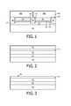
- FIG. 1illustrates a semiconductor light emitting device including a semiconductor structure grown on a growth substrate, metal n- and p-contacts, and bonding pads.
- FIG. 2illustrates a wafer of semiconductor light emitting devices bonded to a handle.
- FIG. 3illustrates the structure of FIG. 2 after removing the growth substrate and texturing the top surface of the semiconductor structure.
- FIG. 4illustrates the structure of FIG. 3 after bonding to a second substrate.
- FIG. 5illustrates the structure of FIG. 4 after removing the handle and dividing the wafer.
- FIG. 6illustrates a prior art LED die bonded to a transparent lens.
- lens 2is attached to LED chip 4 after LED chip 4 is singulated from a wafer of LED chips.
- a wafer of semiconductor light emitting devicesincluding a light emitting region disposed between an n-type region and a p-type region is bonded to a substrate by a pre-formed silicone lamination film.
- waferrefers to a structure before it is divided into smaller structures, such as a growth substrate on which has been grown semiconductor material for many light emitting devices.
- semiconductor light emitting devicesare III-nitride LEDs that emit blue or UV light
- semiconductor light emitting devices besides LEDssuch as laser diodes and semiconductor light emitting devices made from other materials systems such as other III-V materials, III-phosphide, III-arsenide, II-VI materials, ZnO, or Si-based materials may be used.
- FIG. 1illustrates a semiconductor light emitting device.
- a semiconductor structure 13is grown on a growth substrate 11 .
- Substrate 11may be any suitable substrate such as, for example, sapphire, SiC, Si, GaN, or composite substrates.
- the semiconductor structure 13includes a light emitting or active region 14 sandwiched between n- and p-type regions 12 and 16 .
- An n-type region 12may be grown first and may include multiple layers of different compositions and dopant concentration including, for example, preparation layers such as buffer layers or nucleation layers, and/or layers designed to facilitate removal of the growth substrate, which may be n-type or not intentionally doped, and n- or even p-type device layers designed for particular optical, material, or electrical properties desirable for the light emitting region to efficiently emit light.
- a light emitting or active region 14is grown over the n-type region 12 . Examples of suitable light emitting regions include a single thick or thin light emitting layer, or a multiple quantum well light emitting region including multiple thin or thick light emitting layers separated by barrier layers.
- a p-type region 16may then be grown over the light emitting region 14 .
- the p-type region 16may include multiple layers of different composition, thickness, and dopant concentration, including layers that are not intentionally doped, or n-type layers.
- the total thickness of all the semiconductor material in the deviceis less than 10 ⁇ m in some embodiments and less than 6 ⁇ m in some embodiments.
- the semiconductor materialmay optionally be annealed at between 200° C. and 800° C. after growth.
- a p-contact 33is formed on p-type region 16 .
- P-contact 33may be a multi-layer metal contact.
- a first metal layer in direct contact with p-type region 16may be deposited by, for example, evaporation or sputtering, then patterned by standard photolithographic operations including, for example, etching or lift-off.
- the first metal layermay be a reflective metal that makes an ohmic contact with p-type III-nitride material such as, for example, silver.
- the first metal layermay also be a multi-layer stack of a transition metal and silver.
- the transition metalmay be, for example, nickel.
- the first metal layeris between 100 ⁇ and 2000 ⁇ thick in some embodiments, between 500 ⁇ and 1700 ⁇ thick in some embodiments, and between 1000 ⁇ and 1600 ⁇ in some embodiments.
- the structuremay optionally be annealed after deposition of the first metal layer.
- An optional second metal layermay be deposited over the first metal layer by, for example, evaporation or sputtering, then patterned by standard photolithographic operations such as, for example, etching or lift-off.
- the second metal layermay be any electrically-conductive material which reacts minimally with silver, such as, for example, an alloy of titanium and tungsten. This alloy may be nitrided either partially, wholly, or not at all.
- the second metal layermay alternatively be chromium, platinum or silicon, or may be a multi-layer stack of any of the above materials optimized for adhesion to surrounding layers and for blocking diffusion of the first metal layer.
- the second metal layermay be between 1000 ⁇ and 10000 ⁇ thick in some embodiments, between 2000 ⁇ and 8000 ⁇ in some embodiments, and between 2000 ⁇ and 7000 ⁇ thick in some embodiments.
- the structureis then patterned by standard photolithographic operations and etched by, for example, reactive ion etching (RIE), where chemically reactive plasma is used to remove the semiconductor material, or inductively coupled plasma (ICP) etching, an RIE process where the plasma is generated by an RF-powered magnetic field.
- RIEreactive ion etching
- ICPinductively coupled plasma
- the patternis determined by the photolithographic mask used to pattern one or more of the p-contact metal layers.
- etchingmay be performed subsequent to etching of the p-contact metal in a single operation.
- the entire thickness of p-type region 16 and the entire thickness of light emitting region 14are removed, revealing a surface of n-type region 12 (three such regions are illustrated in FIG. 1 ).
- a metal n-contact 36is formed on the portion or portions of n-type region 12 exposed by etching away the p-type region and the light emitting region.
- N-contact 36may be any suitable metal including aluminum or a multi-layer stack of metals including aluminum, titanium-tungsten alloy, copper and gold.
- the first metali.e. the metal adjacent to n-type region 12
- the first layermay be, for example, aluminum.
- N-contact 36may be deposited by any suitable process including, for example, sputtering, evaporation, plating, or a combination of these processes.
- a dielectric 38may be deposited over the structure, for example by plasma-enhanced chemical vapor deposition (PECVD), chemical vapor deposition (CVD), or evaporation.
- PECVDplasma-enhanced chemical vapor deposition
- CVDchemical vapor deposition
- Dielectric 38electrical isolates n-contact 36 and p-contact 33 .
- Dielectric 38is patterned by standard photolithographic operations and etched by ICP etching or RIE to expose n-contact 36 and p-contact 33 .
- Dielectric 38may be any suitable dielectric including silicon nitride, silicon oxide and silicon oxy-nitride. In some embodiments, dielectric 38 is a reflective stack. Dielectric 38 may be formed before or after n-contact 36 .
- Bonding pads 40 a and 40 bare formed over the n- and p-contacts and dielectric 38 , to redistribute the n- and p-contacts into large conductive pads suitable for bonding to another structure such as, for example, a PC board. Bonding pads are typically metal but may be any suitable conductive material. Bonding pad 40 a is electrically connected to p-type region 16 through p-contact 33 . Bonding pad 40 b is electrically connected to n-type region 12 , through re-contact 36 .
- Bonding pads 40may be, for example, Cu, or a multi-layer metal stack comprising, for example Ti, TiW, Cu, Ni, and Au, deposited by sputtering, or by a combination of sputtering and plating. Bonding pads 40 a and 40 b may be electrically isolated by a gap, as illustrated in FIG. 1 , or by a solid dielectric such as the materials described above in reference to dielectric 38 .
- FIG. 1Many of the devices illustrated in FIG. 1 are formed at the same time on a single wafer.
- the particular structure of light emitting device illustrated in FIG. 1is not relevant to embodiments of the invention—any suitable light emitting device structure may be used.
- a wafer of devicessuch as, for example, the device illustrated in FIG. 1 is attached to a handle 44 .
- the semiconductor structure 13is attached to handle 44 through metal layers 31 and bonding layer 42 .
- Metal layers 31 in FIGS. 2, 3, 4, and 5include n- and p-contacts 36 and 33 , dielectric 38 , and bonding pads 40 described above and illustrated in detail in FIG. 1 .
- Handle 44mechanically supports semiconductor structure 13 during removal of growth substrate 11 .
- Handle 44may be, for example, glass, sapphire, silicon, or any other suitable material.
- a bonding layermay be formed on handle 44 only, on semiconductor structure 13 only, or on both handle 44 and semiconductor structure 13 .
- the bonding layer or layersmay be any suitable material, such as, for example, organic material such as silicone formed by any suitable technique such as, for example, spinning-on.
- handle 44 and semiconductor structure 13are pressed together under elevated temperature. The bond between handle 44 and semiconductor structure 13 does not require any alignment, since handle 44 is later removed and therefore contains no features that must be aligned with the individual light emitting devices on the wafer.
- growth substrate 11is removed from the wafer of semiconductor devices by any technique suitable to the growth substrate material including, for example, laser lift off, etching, or mechanical techniques.
- the surface 46 of semiconductor structure 13 exposed by removing growth substrate 11may be optionally thinned, then optionally textured, for example by roughening or by forming a pattern, to improve light extraction from the semiconductor structure 13 .
- Surface 46may be patterned by standard photolithography and etching and may be roughened by any suitable technique including, for example, etching such as photo-electrochemical etching in a KOH solution, mechanical grinding, or ablation.
- a bonding layer 48is formed over the textured surface 46 of semiconductor structure 13 .
- bonding layer 48is flexible film which may be fully or partially cured transparent material, such as silicone.
- the bonding film 48may be formed separate from semiconductor structure 13 and substrate 50 , which permits tight control of the thickness of the film as well as testing and verification of the characteristics of the film prior to attaching to semiconductor structure 13 .
- a heat dissipating materialsuch as diamond may be added to the bonding film 48 .
- a materialsuch as diamond, silica, TiO 2 , and/or other inorganic additives may be added to the bonding film 48 to adjust the refractive index of the film, to improve optical transmission, to cause scattering of light, and/or to improve conversion by a wavelength converting material disposed in the film, as described below.
- bonding film 48is formed on a support film such as an ethylene tetrafluoroethylene film, for example by spreading a mixture of silicone over the support film then fully or partially curing the silicone. The finished film is solid.
- a protective filmis formed over the bonding film 48 after forming the bonding film 48 , such that bonding film 48 is sandwiched between a support film and a protective film.
- One of the support film and the protective filmis removed before making the first bond with bonding film 48 (for example, to semiconductor structure 13 ), then the other of the support film and the protective film is removed before making the second bond with bonding film 48 (for example, to substrate 50 ).
- Bonding film 48is attached to semiconductor structure 13 or substrate 50 as follows. One of the support film and the protective film are removed followed pre-cure of bonding film 48 . Bonding film 48 is pre-cured at between 100 and 150 ° C. for 1-10 minutes in order to achieve film hardness which prevents the silicone from melting during bonding, and which may maintain the targeted bonding film thickness over the semiconductor structure 13 or substrate 50 . After bonding film 48 is pre-cured, it is attached in a first bonding step to the semiconductor structure 13 . The structure including bonding film 48 and semiconductor structure 13 is loaded into a vacuum laminator to attach bonding film 48 to the surface 46 of semiconductor structure 13 using one or more of vacuum, elevated temperature, and elevated pressure.
- bonding film 48may be bonded to semiconductor structure 13 at temperatures between 60 and 100° C. in some embodiments, at pressures between 0.1 and 0.3 MPa in some embodiments, and under a vacuum of about 10 ⁇ 3 Torr in some embodiments.
- Substrate 50may be a transparent, high refractive index material such as glass pre-formed into a substrate wafer before bonding to semiconductor structure 13 .
- the index of refraction of the glasses abovemay be in the range of 1.5 to 2.2 or higher in some embodiments, closely matched to the refractive index of GaN (2.4).
- Suitable materials for substrate 50include suitable high refractive-index glasses, such as lead chloride, lead bromide, potassium fluoride, zinc fluoride, an oxide of aluminum, antimony, bismuth, boron, lead, lithium, phosphorus, potassium, silicon, sodium, tellurium, thallium, tungsten, or zinc, or any mixtures thereof.
- High refractive-index glassesalso include materials such as Schott glass LaSFN35, LaF10, NZK7, NLAF21, LaSFN18, SF59, or LaSF3, or Ohara glass SLAH51 or SLAM60, or mixtures thereof, glasses such as (Ge, As, Sb, Ga)(S, Se, Te, F, Cl, I, Br) chalcogenide and chalcogen-halogenide glasses, for example.
- substrate 50may include or be formed from lower index materials, such as glass, magnesium fluoride and polymers.
- bonding film 48After bonding the bonding film 48 to semiconductor structure 13 , the other of the support film and the protective film is removed from bonding film 48 and substrate 50 is positioned on top of bonding film 48 .
- the structureis then placed in a second vacuum laminator which bonds substrate 50 to bonding film 48 under higher temperature and pressure than used in the first bonding step, in some embodiments.
- substrate 50may be bonded to bonding film 48 at temperatures between 110 and 120° C. in some embodiments.
- bonding film 48is attached to semiconductor structure 13 in a first bonding step and attached to substrate 50 in a second bonding step, in some embodiments, bonding film 48 is attached to substrate 50 in the first bonding step, then to semiconductor structure 13 in the second bonding step.
- one or more luminescent materials that convert light of wavelengths emitted by the light emitting region to other wavelengthsare included in bonding film 48 , substrate 50 , or both. All or only a portion of the light emitted by the light emitting region and incident on the wavelength converting material may be converted by the wavelength converting material. Unconverted light emitted by the light emitting region may be part of the final spectrum of light, though it need not be.
- Examples of common combinationsinclude a blue-emitting LED combined with a yellow-emitting wavelength converting material, a blue-emitting LED combined with green- and red-emitting wavelength converting materials, a UV-emitting LED combined with blue- and yellow-emitting wavelength converting material, and a UV-emitting LED combined with blue-, green-, and red-emitting wavelength converting materials.
- Wavelength converting materials emitting other colors of lightmay be added to tailor the spectrum of light emitted from the device.
- the wavelength converting materialmay be conventional phosphor particles, organic semiconductors, II-VI or III-V semiconductors, II-VI or III-V semiconductor quantum dots or nanocrystals, dyes, polymers, or materials such as GaN that luminesce.
- substrate 50 and bonding layer 48include conventional phosphor particles
- the structure including the phosphoris thick enough to accommodate particles typically having a size of about 5 microns to about 50 microns.
- Any suitable phosphormay be used, including garnet-based phosphors such as Y 3 Al 5 O 12 :Ce (YAG), Lu 3 Al 5 O 12 :Ce (LuAG), Y 3 Al 5-x Ga x O 12 :Ce (YAlGaG), (Ba 1-x Sr x )SiO 3 :Eu (BOSE), and nitride-based phosphors such as (Ca,Sr)AlSiN 3 :Eu and (Ca,Sr,Ba) 2 Si 5 N 8 :Eu.
- Wavelength converting materialsmay be mixed together or formed as discrete layers. Wavelength converting materials may be incorporated into bonding film 48 and/or substrate 50 during fabrication of these structures. For example, wavelength converting material may be mixed with silicone before the silicone mixture is spread over the support film to form bonding film 48 .
- handle 44is removed, for example by etching, mechanical separation, laser lift off, or any other suitable technique. Any bonding material 42 remaining after removing handle 44 is removed, for example by etching or other suitable technique.
- the wafermay then be divided into individual devices or groups of devices. The boundaries 52 between three structures separated from the wafer are illustrated in FIG. 5 . Since the semiconductor structure 13 and substrate 50 are diced together, the substrate is no wider than the light emitting device, as illustrated in FIG. 5 . Separation of the wafer into individual or groups of devices may be performed, for example, by conventionally sawing, by laser ablation using 193 nm, 248 nm, or 355 nm light, or by water jet cutting.
- Separationmay also be performed via a combination of scribing and mechanical breaking, scribing being performed, for example, by conventionally sawing, by laser ablation using 193 nm, 248 nm, or 355 nm light, or by water jet cutting.
Landscapes
- Engineering & Computer Science (AREA)
- Microelectronics & Electronic Packaging (AREA)
- Computer Hardware Design (AREA)
- Power Engineering (AREA)
- Physics & Mathematics (AREA)
- Condensed Matter Physics & Semiconductors (AREA)
- General Physics & Mathematics (AREA)
- Manufacturing & Machinery (AREA)
- Led Devices (AREA)
- Led Device Packages (AREA)
Abstract
Description
Claims (13)
Priority Applications (1)
| Application Number | Priority Date | Filing Date | Title |
|---|---|---|---|
| US14/131,686US10158049B2 (en) | 2011-08-30 | 2012-07-30 | Method of bonding a substrate to a semiconductor light emitting device |
Applications Claiming Priority (3)
| Application Number | Priority Date | Filing Date | Title |
|---|---|---|---|
| US201161528886P | 2011-08-30 | 2011-08-30 | |
| PCT/IB2012/053880WO2013030690A1 (en) | 2011-08-30 | 2012-07-30 | Method of bonding a substrate to a semiconductor light emitting device |
| US14/131,686US10158049B2 (en) | 2011-08-30 | 2012-07-30 | Method of bonding a substrate to a semiconductor light emitting device |
Publications (2)
| Publication Number | Publication Date |
|---|---|
| US20140193931A1 US20140193931A1 (en) | 2014-07-10 |
| US10158049B2true US10158049B2 (en) | 2018-12-18 |
Family
ID=46934626
Family Applications (1)
| Application Number | Title | Priority Date | Filing Date |
|---|---|---|---|
| US14/131,686ActiveUS10158049B2 (en) | 2011-08-30 | 2012-07-30 | Method of bonding a substrate to a semiconductor light emitting device |
Country Status (7)
| Country | Link |
|---|---|
| US (1) | US10158049B2 (en) |
| EP (1) | EP2751852A1 (en) |
| JP (2) | JP2014525683A (en) |
| KR (1) | KR101934138B1 (en) |
| CN (3) | CN107086198B (en) |
| TW (1) | TWI553745B (en) |
| WO (1) | WO2013030690A1 (en) |
Families Citing this family (9)
| Publication number | Priority date | Publication date | Assignee | Title |
|---|---|---|---|---|
| TWI552382B (en)* | 2014-01-24 | 2016-10-01 | 隆達電子股份有限公司 | Light-emitting diode device and method of manufacturing same |
| TWI730096B (en)* | 2016-05-20 | 2021-06-11 | 荷蘭商露明控股公司 | Light emitting devices and methods for growing the same |
| US10168475B2 (en) | 2017-01-18 | 2019-01-01 | Juniper Networks, Inc. | Atomic layer deposition bonding for heterogeneous integration of photonics and electronics |
| US20190198564A1 (en)* | 2017-12-20 | 2019-06-27 | Lumileds Llc | Monolithic segmented led array architecture with islanded epitaxial growth |
| KR102510356B1 (en)* | 2018-05-03 | 2023-03-17 | 오픈라이트 포토닉스, 인크. | Atomic layer deposition bonding for heterogeneous integration of photonics and electronics |
| US11177250B2 (en)* | 2019-09-17 | 2021-11-16 | Tokyo Electron Limited | Method for fabrication of high density logic and memory for advanced circuit architecture |
| US11942576B2 (en)* | 2020-08-28 | 2024-03-26 | Applied Materials, Inc. | Blue color converter for micro LEDs |
| US11935987B2 (en)* | 2021-11-03 | 2024-03-19 | Lumileds Llc | Light emitting diode arrays with a light-emitting pixel area |
| DE102023131829A1 (en)* | 2023-11-15 | 2025-05-15 | Ams-Osram International Gmbh | Method for fixing an optical element on a substrate in an optical path of an optoelectronic component and optoelectronic component |
Citations (42)
| Publication number | Priority date | Publication date | Assignee | Title |
|---|---|---|---|---|
| US5261157A (en)* | 1991-01-22 | 1993-11-16 | Olin Corporation | Assembly of electronic packages by vacuum lamination |
| US6087202A (en)* | 1997-06-03 | 2000-07-11 | Stmicroelectronics S.A. | Process for manufacturing semiconductor packages comprising an integrated circuit |
| US20020012762A1 (en)* | 1997-07-28 | 2002-01-31 | Michael H. Bunyan | Double-side thermally conductive adhesive tape for plastic-packaged electronic components |
| US20030045021A1 (en)* | 2001-08-30 | 2003-03-06 | Tomonori Akai | Production method for organic electroluminescent device |
| JP2005191476A (en) | 2003-12-26 | 2005-07-14 | Shin Etsu Handotai Co Ltd | Manufacturing method of light emitting element |
| US20050158500A1 (en)* | 2002-03-13 | 2005-07-21 | Hideki Kitano | Photo-curable adhesive sheet, photo-curable transfer sheet, optical information recording medium, and method for preparing optical information recording medium |
| JP2006041479A (en) | 2004-06-24 | 2006-02-09 | Toyoda Gosei Co Ltd | Light emitting element and its manufacturing method |
| US7053419B1 (en) | 2000-09-12 | 2006-05-30 | Lumileds Lighting U.S., Llc | Light emitting diodes with improved light extraction efficiency |
| JP2006210916A (en) | 2005-01-25 | 2006-08-10 | Shogen Koden Kofun Yugenkoshi | Light emitting device |
| CN1845968A (en) | 2003-09-01 | 2006-10-11 | 陶氏康宁东丽株式会社 | Adhesive silicone elastomer sheet |
| US20070004065A1 (en)* | 2005-06-30 | 2007-01-04 | 3M Innovative Properties Company | Phosphor tape article |
| JP2007042664A (en) | 2005-07-29 | 2007-02-15 | Shin Etsu Handotai Co Ltd | Light emitting device and manufacturing method thereof |
| US20070096131A1 (en)* | 2005-10-28 | 2007-05-03 | Lumileds Lighting U.S. Llc | Laminating encapsulant film containing phosphor over LEDS |
| US20070110941A1 (en)* | 2005-11-15 | 2007-05-17 | Tesa Aktiengesellschaft | Use of a double-sided PSA tape for bonding in the production of electronics articles |
| US20070190280A1 (en)* | 2006-02-16 | 2007-08-16 | Nitto Denko Corporation | Double-sided pressure-sensitive adhesive tape or sheet |
| US20070221866A1 (en)* | 2006-03-10 | 2007-09-27 | Choong-Yong Sohn | Photoluminescent sheet |
| JP2008042143A (en) | 2006-08-10 | 2008-02-21 | Toyoda Gosei Co Ltd | Group iii nitride compound semiconductor light emitting element, and its manufacturing method |
| WO2008062783A1 (en) | 2006-11-20 | 2008-05-29 | Nikon Corporation | Led device and method for manufacturing the same |
| US20080197378A1 (en) | 2007-02-20 | 2008-08-21 | Hua-Shuang Kong | Group III Nitride Diodes on Low Index Carrier Substrates |
| US20080230177A1 (en)* | 2007-03-19 | 2008-09-25 | White Electronic Designs Corp. | Enhanced liquid crystal display system and methods |
| JP2008262993A (en) | 2007-04-10 | 2008-10-30 | Nikon Corp | Display device |
| US20090078952A1 (en) | 2007-09-21 | 2009-03-26 | Ray-Hua Horng | Light-emitting chip device with high thermal conductivity |
| US20090127575A1 (en) | 2007-09-21 | 2009-05-21 | Ray-Hua Horng | Light-Emitting Diode Chip With High Light Extraction And Method For Manufacturing The Same |
| US7560294B2 (en) | 2004-06-07 | 2009-07-14 | Toyoda Gosei Co., Ltd. | Light emitting element and method of making same |
| US7622363B2 (en) | 2003-05-06 | 2009-11-24 | Canon Kabushiki Kaisha | Semiconductor substrate, semiconductor device, light emitting diode and producing method therefor |
| DE102008039790A1 (en) | 2008-08-26 | 2010-03-04 | Osram Opto Semiconductors Gmbh | Optoelectronic component i.e. LED, for use as headlight in motor vehicle, has connecting terminals provided for supplying charge carriers to partial layers of layer sequence, where terminals are arranged at main side of layer sequence |
| EP2194586A1 (en) | 2008-12-08 | 2010-06-09 | Kabushiki Kaisha Toshiba | Semiconductor device and method for manufacturing the same |
| US20100295077A1 (en) | 2009-05-19 | 2010-11-25 | Intematix Corporation | Manufacture of light emitting devices with phosphor wavelength conversion |
| US7858198B2 (en) | 2007-04-10 | 2010-12-28 | Shin-Etsu Chemical Co., Ltd. | Phosphor-containing adhesive silicone composition, composition sheet formed of the composition, and method of producing light emitting device using the sheet |
| US20100327733A1 (en)* | 2009-06-25 | 2010-12-30 | Bridgelux, Inc. | Multiple layer phosphor bearing film |
| US20100328923A1 (en)* | 2009-06-25 | 2010-12-30 | Bridgelux, Inc. | Multiple layer phosphor bearing film |
| US20110046320A1 (en) | 2009-08-24 | 2011-02-24 | Ntto Denko Corporation | Composition for thermosetting silicone resin |
| DE102009048401A1 (en) | 2009-10-06 | 2011-04-07 | Osram Opto Semiconductors Gmbh | Method for producing an optoelectronic semiconductor component and optoelectronic semiconductor component |
| US20110266560A1 (en)* | 2010-04-30 | 2011-11-03 | Cree, Inc. | White-emitting led chips and method for making same |
| US20110297980A1 (en)* | 2010-06-03 | 2011-12-08 | Kabushiki Kaisha Toshiba | Semiconductor light emitting device and method for manufacturing same |
| US20110316032A1 (en)* | 2010-06-29 | 2011-12-29 | Nitto Denko Corporation | Phosphor layer and light-emitting device |
| US20110316031A1 (en)* | 2010-06-29 | 2011-12-29 | Nitto Denko Corporation | Transfer sheet for phosphor layer and light-emitting device |
| US20120014640A1 (en)* | 2009-03-31 | 2012-01-19 | Panasonic Electric Works Co., Ltd. | Method of manufacturing optical waveguide core, method of manufacturing optical waveguide, optical waveguide, and optoelectric composite wiring board |
| US20120052608A1 (en)* | 2010-08-25 | 2012-03-01 | Yoo Cheol-Jun | Phosphor film, method of forming the same, and method of coating phosphor layer on led chips |
| US20120319575A1 (en)* | 2011-06-16 | 2012-12-20 | Nitto Denko Corporation | Phosphor adhesive sheet, light emitting diode element including phosphor layer, light emitting diode device, and producing methods thereof |
| US20130334956A1 (en)* | 2010-05-05 | 2013-12-19 | Next Lighting Coro. | Remote phosphor tape lighting units |
| US9287469B2 (en) | 2008-05-02 | 2016-03-15 | Cree, Inc. | Encapsulation for phosphor-converted white light emitting diode |
Family Cites Families (1)
| Publication number | Priority date | Publication date | Assignee | Title |
|---|---|---|---|---|
| US7514721B2 (en)* | 2005-11-29 | 2009-04-07 | Koninklijke Philips Electronics N.V. | Luminescent ceramic element for a light emitting device |
- 2012
- 2012-07-30CNCN201710012849.4Apatent/CN107086198B/enactiveActive
- 2012-07-30WOPCT/IB2012/053880patent/WO2013030690A1/enactiveApplication Filing
- 2012-07-30EPEP12766151.0Apatent/EP2751852A1/ennot_activeWithdrawn
- 2012-07-30KRKR1020147008165Apatent/KR101934138B1/enactiveActive
- 2012-07-30CNCN201810161389.6Apatent/CN108269756A/enactivePending
- 2012-07-30CNCN201280042515.7Apatent/CN103858243A/enactivePending
- 2012-07-30USUS14/131,686patent/US10158049B2/enactiveActive
- 2012-07-30JPJP2014527757Apatent/JP2014525683A/enactivePending
- 2012-08-27TWTW101131072Apatent/TWI553745B/enactive
- 2017
- 2017-03-29JPJP2017064523Apatent/JP6462029B2/enactiveActive
Patent Citations (49)
| Publication number | Priority date | Publication date | Assignee | Title |
|---|---|---|---|---|
| US5261157A (en)* | 1991-01-22 | 1993-11-16 | Olin Corporation | Assembly of electronic packages by vacuum lamination |
| US6087202A (en)* | 1997-06-03 | 2000-07-11 | Stmicroelectronics S.A. | Process for manufacturing semiconductor packages comprising an integrated circuit |
| US20020012762A1 (en)* | 1997-07-28 | 2002-01-31 | Michael H. Bunyan | Double-side thermally conductive adhesive tape for plastic-packaged electronic components |
| US7053419B1 (en) | 2000-09-12 | 2006-05-30 | Lumileds Lighting U.S., Llc | Light emitting diodes with improved light extraction efficiency |
| US20030045021A1 (en)* | 2001-08-30 | 2003-03-06 | Tomonori Akai | Production method for organic electroluminescent device |
| US20050158500A1 (en)* | 2002-03-13 | 2005-07-21 | Hideki Kitano | Photo-curable adhesive sheet, photo-curable transfer sheet, optical information recording medium, and method for preparing optical information recording medium |
| US7622363B2 (en) | 2003-05-06 | 2009-11-24 | Canon Kabushiki Kaisha | Semiconductor substrate, semiconductor device, light emitting diode and producing method therefor |
| CN1845968A (en) | 2003-09-01 | 2006-10-11 | 陶氏康宁东丽株式会社 | Adhesive silicone elastomer sheet |
| US20070009748A1 (en)* | 2003-09-01 | 2007-01-11 | Akiko Takanami | Adhesive silicone elastomer sheet |
| JP2005191476A (en) | 2003-12-26 | 2005-07-14 | Shin Etsu Handotai Co Ltd | Manufacturing method of light emitting element |
| US7560294B2 (en) | 2004-06-07 | 2009-07-14 | Toyoda Gosei Co., Ltd. | Light emitting element and method of making same |
| JP2006041479A (en) | 2004-06-24 | 2006-02-09 | Toyoda Gosei Co Ltd | Light emitting element and its manufacturing method |
| JP2006210916A (en) | 2005-01-25 | 2006-08-10 | Shogen Koden Kofun Yugenkoshi | Light emitting device |
| US7489068B2 (en) | 2005-01-25 | 2009-02-10 | Epistar Corporation | Light emitting device |
| US20070004065A1 (en)* | 2005-06-30 | 2007-01-04 | 3M Innovative Properties Company | Phosphor tape article |
| JP2007042664A (en) | 2005-07-29 | 2007-02-15 | Shin Etsu Handotai Co Ltd | Light emitting device and manufacturing method thereof |
| US20070096131A1 (en)* | 2005-10-28 | 2007-05-03 | Lumileds Lighting U.S. Llc | Laminating encapsulant film containing phosphor over LEDS |
| US20070110941A1 (en)* | 2005-11-15 | 2007-05-17 | Tesa Aktiengesellschaft | Use of a double-sided PSA tape for bonding in the production of electronics articles |
| US20070190280A1 (en)* | 2006-02-16 | 2007-08-16 | Nitto Denko Corporation | Double-sided pressure-sensitive adhesive tape or sheet |
| US20070221866A1 (en)* | 2006-03-10 | 2007-09-27 | Choong-Yong Sohn | Photoluminescent sheet |
| JP2008042143A (en) | 2006-08-10 | 2008-02-21 | Toyoda Gosei Co Ltd | Group iii nitride compound semiconductor light emitting element, and its manufacturing method |
| WO2008062783A1 (en) | 2006-11-20 | 2008-05-29 | Nikon Corporation | Led device and method for manufacturing the same |
| US20080197378A1 (en) | 2007-02-20 | 2008-08-21 | Hua-Shuang Kong | Group III Nitride Diodes on Low Index Carrier Substrates |
| JP2008205468A (en) | 2007-02-20 | 2008-09-04 | Cree Inc | III-nitride diodes on low refractive index carrier substrate |
| US20080230177A1 (en)* | 2007-03-19 | 2008-09-25 | White Electronic Designs Corp. | Enhanced liquid crystal display system and methods |
| JP2008262993A (en) | 2007-04-10 | 2008-10-30 | Nikon Corp | Display device |
| US7858198B2 (en) | 2007-04-10 | 2010-12-28 | Shin-Etsu Chemical Co., Ltd. | Phosphor-containing adhesive silicone composition, composition sheet formed of the composition, and method of producing light emitting device using the sheet |
| US20090078952A1 (en) | 2007-09-21 | 2009-03-26 | Ray-Hua Horng | Light-emitting chip device with high thermal conductivity |
| US20090127575A1 (en) | 2007-09-21 | 2009-05-21 | Ray-Hua Horng | Light-Emitting Diode Chip With High Light Extraction And Method For Manufacturing The Same |
| US9287469B2 (en) | 2008-05-02 | 2016-03-15 | Cree, Inc. | Encapsulation for phosphor-converted white light emitting diode |
| DE102008039790A1 (en) | 2008-08-26 | 2010-03-04 | Osram Opto Semiconductors Gmbh | Optoelectronic component i.e. LED, for use as headlight in motor vehicle, has connecting terminals provided for supplying charge carriers to partial layers of layer sequence, where terminals are arranged at main side of layer sequence |
| EP2194586A1 (en) | 2008-12-08 | 2010-06-09 | Kabushiki Kaisha Toshiba | Semiconductor device and method for manufacturing the same |
| US20100140640A1 (en) | 2008-12-08 | 2010-06-10 | Kabushiki Kaisha Toshiba | Semiconductor device and method for manufacturing the same |
| JP2010135693A (en) | 2008-12-08 | 2010-06-17 | Toshiba Corp | Optical semiconductor device and method of manufacturing optical semiconductor device |
| US20120014640A1 (en)* | 2009-03-31 | 2012-01-19 | Panasonic Electric Works Co., Ltd. | Method of manufacturing optical waveguide core, method of manufacturing optical waveguide, optical waveguide, and optoelectric composite wiring board |
| US20100295077A1 (en) | 2009-05-19 | 2010-11-25 | Intematix Corporation | Manufacture of light emitting devices with phosphor wavelength conversion |
| US20100328923A1 (en)* | 2009-06-25 | 2010-12-30 | Bridgelux, Inc. | Multiple layer phosphor bearing film |
| US20100327733A1 (en)* | 2009-06-25 | 2010-12-30 | Bridgelux, Inc. | Multiple layer phosphor bearing film |
| US20110046320A1 (en) | 2009-08-24 | 2011-02-24 | Ntto Denko Corporation | Composition for thermosetting silicone resin |
| JP2011042760A (en) | 2009-08-24 | 2011-03-03 | Nitto Denko Corp | Composition for thermosetting silicone resin |
| US20120193669A1 (en) | 2009-10-06 | 2012-08-02 | Hans-Christoph Gallmeier | Contacting an Optoelectronic Semiconductor Component Through a Conversion Element and Corresponding Optoelectronic Semiconductor Component |
| DE102009048401A1 (en) | 2009-10-06 | 2011-04-07 | Osram Opto Semiconductors Gmbh | Method for producing an optoelectronic semiconductor component and optoelectronic semiconductor component |
| US20110266560A1 (en)* | 2010-04-30 | 2011-11-03 | Cree, Inc. | White-emitting led chips and method for making same |
| US20130334956A1 (en)* | 2010-05-05 | 2013-12-19 | Next Lighting Coro. | Remote phosphor tape lighting units |
| US20110297980A1 (en)* | 2010-06-03 | 2011-12-08 | Kabushiki Kaisha Toshiba | Semiconductor light emitting device and method for manufacturing same |
| US20110316032A1 (en)* | 2010-06-29 | 2011-12-29 | Nitto Denko Corporation | Phosphor layer and light-emitting device |
| US20110316031A1 (en)* | 2010-06-29 | 2011-12-29 | Nitto Denko Corporation | Transfer sheet for phosphor layer and light-emitting device |
| US20120052608A1 (en)* | 2010-08-25 | 2012-03-01 | Yoo Cheol-Jun | Phosphor film, method of forming the same, and method of coating phosphor layer on led chips |
| US20120319575A1 (en)* | 2011-06-16 | 2012-12-20 | Nitto Denko Corporation | Phosphor adhesive sheet, light emitting diode element including phosphor layer, light emitting diode device, and producing methods thereof |
Non-Patent Citations (6)
| Title |
|---|
| CN OA, 201280042515.7, dated Feb. 29, 2016, 17 pps. |
| CN Office Action, Application 201280042515.7, dated Sep. 26, 2016, 12 pps. |
| EPO as ISA, PCT/IB2012/053880 filed Jul. 30, 2012, "International Search Report and Written Opinion", dated Nov. 9, 2012, 11 pages. |
| First Office Action, Taiwan Application No. 101131072, dated Nov. 18, 2015, 10 pages. |
| JP OA, Application 2014-527757, dated Apr. 19, 2016, 9 pps. |
| JP Office Action, Application 2014-527757, dated Nov. 29, 2016, 5 pps. |
Also Published As
| Publication number | Publication date |
|---|---|
| TWI553745B (en) | 2016-10-11 |
| WO2013030690A1 (en) | 2013-03-07 |
| JP2014525683A (en) | 2014-09-29 |
| KR101934138B1 (en) | 2018-12-31 |
| US20140193931A1 (en) | 2014-07-10 |
| JP2017139481A (en) | 2017-08-10 |
| CN107086198B (en) | 2020-09-11 |
| CN108269756A (en) | 2018-07-10 |
| TW201318079A (en) | 2013-05-01 |
| EP2751852A1 (en) | 2014-07-09 |
| JP6462029B2 (en) | 2019-01-30 |
| CN107086198A (en) | 2017-08-22 |
| CN103858243A (en) | 2014-06-11 |
| KR20140058658A (en) | 2014-05-14 |
Similar Documents
| Publication | Publication Date | Title |
|---|---|---|
| US10158049B2 (en) | Method of bonding a substrate to a semiconductor light emitting device | |
| US10056531B2 (en) | Method of processing a semiconductor structure | |
| US9431581B2 (en) | Method of attaching a light emitting device to a support substrate | |
| JP6419077B2 (en) | Wavelength conversion light emitting device | |
| US9484513B2 (en) | Semiconductor light emitting device with thick metal layers | |
| US9362471B2 (en) | Semiconductor light emitting device with thick metal layers | |
| WO2013084155A1 (en) | Forming thick metal layers on a semiconductor light emitting device | |
| WO2013084103A1 (en) | Semiconductor light emitting device with thick metal layers |
Legal Events
| Date | Code | Title | Description |
|---|---|---|---|
| AS | Assignment | Owner name:KONINKLIJKE PHILIPS ELECTRONICS N.V., NETHERLANDS Free format text:ASSIGNMENT OF ASSIGNORS INTEREST;ASSIGNORS:BASIN, GRIGORIY;EPLER, JOHN EDWARD;MARTIN, PAUL SCOTT;SIGNING DATES FROM 20120802 TO 20120803;REEL/FRAME:031924/0173 | |
| AS | Assignment | Owner name:KONINKLIJKE PHILIPS N.V., NETHERLANDS Free format text:CHANGE OF NAME;ASSIGNOR:KONINKLIJKE PHILIPS ELECTRONICS N.V.;REEL/FRAME:036129/0653 Effective date:20130515 | |
| AS | Assignment | Owner name:LUMILEDS LLC, CALIFORNIA Free format text:ASSIGNMENT OF ASSIGNORS INTEREST;ASSIGNOR:KONINKLIJKE PHILIPS N.V.;REEL/FRAME:042821/0001 Effective date:20170428 | |
| AS | Assignment | Owner name:DEUTSCHE BANK AG NEW YORK BRANCH, AS COLLATERAL AGENT, NEW YORK Free format text:SECURITY INTEREST;ASSIGNOR:LUMILEDS LLC;REEL/FRAME:043108/0001 Effective date:20170630 Owner name:DEUTSCHE BANK AG NEW YORK BRANCH, AS COLLATERAL AG Free format text:SECURITY INTEREST;ASSIGNOR:LUMILEDS LLC;REEL/FRAME:043108/0001 Effective date:20170630 | |
| STCF | Information on status: patent grant | Free format text:PATENTED CASE | |
| MAFP | Maintenance fee payment | Free format text:PAYMENT OF MAINTENANCE FEE, 4TH YEAR, LARGE ENTITY (ORIGINAL EVENT CODE: M1551); ENTITY STATUS OF PATENT OWNER: LARGE ENTITY Year of fee payment:4 | |
| AS | Assignment | Owner name:SOUND POINT AGENCY LLC, NEW YORK Free format text:SECURITY INTEREST;ASSIGNORS:LUMILEDS LLC;LUMILEDS HOLDING B.V.;REEL/FRAME:062299/0338 Effective date:20221230 | |
| AS | Assignment | Owner name:LUMILEDS HOLDING B.V., NETHERLANDS Free format text:RELEASE BY SECURED PARTY;ASSIGNOR:SOUND POINT AGENCY LLC;REEL/FRAME:070046/0001 Effective date:20240731 Owner name:LUMILEDS LLC, CALIFORNIA Free format text:RELEASE BY SECURED PARTY;ASSIGNOR:SOUND POINT AGENCY LLC;REEL/FRAME:070046/0001 Effective date:20240731 | |
| AS | Assignment | Owner name:LUMILEDS SINGAPORE PTE. LTD., SINGAPORE Free format text:ASSIGNMENT OF ASSIGNORS INTEREST;ASSIGNOR:LUMILEDS LLC;REEL/FRAME:071888/0086 Effective date:20250708 |