US10157880B2 - Micro-transfer printing with volatile adhesive layer - Google Patents
Micro-transfer printing with volatile adhesive layerDownload PDFInfo
- Publication number
- US10157880B2 US10157880B2US15/718,636US201715718636AUS10157880B2US 10157880 B2US10157880 B2US 10157880B2US 201715718636 AUS201715718636 AUS 201715718636AUS 10157880 B2US10157880 B2US 10157880B2
- Authority
- US
- United States
- Prior art keywords
- micro
- component
- metal
- transfer
- contact
- Prior art date
- Legal status (The legal status is an assumption and is not a legal conclusion. Google has not performed a legal analysis and makes no representation as to the accuracy of the status listed.)
- Active
Links
- 239000012790adhesive layerSubstances0.000titleclaimsabstractdescription63
- 238000010023transfer printingMethods0.000titleclaimsabstractdescription40
- 229910052751metalInorganic materials0.000claimsabstractdescription196
- 239000002184metalSubstances0.000claimsabstractdescription196
- 239000000758substrateSubstances0.000claimsabstractdescription140
- 238000012546transferMethods0.000claimsabstractdescription85
- 239000010410layerSubstances0.000claimsabstractdescription82
- 239000000853adhesiveSubstances0.000claimsabstractdescription57
- 230000001070adhesive effectEffects0.000claimsabstractdescription57
- 238000001704evaporationMethods0.000claimsabstractdescription21
- 230000008020evaporationEffects0.000claimsabstractdescription18
- 238000004519manufacturing processMethods0.000claimsabstractdescription8
- 238000000034methodMethods0.000claimsdescription60
- 239000000463materialSubstances0.000claimsdescription41
- 238000010438heat treatmentMethods0.000claimsdescription31
- 239000004065semiconductorSubstances0.000claimsdescription17
- 238000001816coolingMethods0.000claimsdescription12
- 229910052710siliconInorganic materials0.000claimsdescription11
- 239000010703siliconSubstances0.000claimsdescription11
- 238000007639printingMethods0.000claimsdescription9
- PXHVJJICTQNCMI-UHFFFAOYSA-NNickelChemical compound[Ni]PXHVJJICTQNCMI-UHFFFAOYSA-N0.000claimsdescription8
- 150000001875compoundsChemical class0.000claimsdescription8
- 229910001092metal group alloyInorganic materials0.000claimsdescription8
- BASFCYQUMIYNBI-UHFFFAOYSA-NplatinumChemical compound[Pt]BASFCYQUMIYNBI-UHFFFAOYSA-N0.000claimsdescription8
- 229910001218Gallium arsenideInorganic materials0.000claimsdescription6
- 239000010931goldSubstances0.000claimsdescription6
- RYGMFSIKBFXOCR-UHFFFAOYSA-NCopperChemical compound[Cu]RYGMFSIKBFXOCR-UHFFFAOYSA-N0.000claimsdescription4
- 229910000530Gallium indium arsenideInorganic materials0.000claimsdescription4
- BQCADISMDOOEFD-UHFFFAOYSA-NSilverChemical compound[Ag]BQCADISMDOOEFD-UHFFFAOYSA-N0.000claimsdescription4
- ATJFFYVFTNAWJD-UHFFFAOYSA-NTinChemical compound[Sn]ATJFFYVFTNAWJD-UHFFFAOYSA-N0.000claimsdescription4
- 229910052797bismuthInorganic materials0.000claimsdescription4
- JCXGWMGPZLAOME-UHFFFAOYSA-Nbismuth atomChemical compound[Bi]JCXGWMGPZLAOME-UHFFFAOYSA-N0.000claimsdescription4
- 229910052802copperInorganic materials0.000claimsdescription4
- 239000010949copperSubstances0.000claimsdescription4
- PCHJSUWPFVWCPO-UHFFFAOYSA-NgoldChemical compound[Au]PCHJSUWPFVWCPO-UHFFFAOYSA-N0.000claimsdescription4
- 229910052737goldInorganic materials0.000claimsdescription4
- 229910052738indiumInorganic materials0.000claimsdescription4
- APFVFJFRJDLVQX-UHFFFAOYSA-Nindium atomChemical compound[In]APFVFJFRJDLVQX-UHFFFAOYSA-N0.000claimsdescription4
- 229910052759nickelInorganic materials0.000claimsdescription4
- 229910052697platinumInorganic materials0.000claimsdescription4
- 238000003825pressingMethods0.000claimsdescription4
- 229910052709silverInorganic materials0.000claimsdescription4
- 239000004332silverSubstances0.000claimsdescription4
- 238000009736wettingMethods0.000claimsdescription3
- 235000012431wafersNutrition0.000description32
- 230000008569processEffects0.000description13
- XUIMIQQOPSSXEZ-UHFFFAOYSA-NSiliconChemical compound[Si]XUIMIQQOPSSXEZ-UHFFFAOYSA-N0.000description10
- 229920000642polymerPolymers0.000description10
- OKKJLVBELUTLKV-UHFFFAOYSA-NMethanolChemical compoundOCOKKJLVBELUTLKV-UHFFFAOYSA-N0.000description9
- 239000007788liquidSubstances0.000description8
- 238000005516engineering processMethods0.000description6
- 238000012545processingMethods0.000description6
- 230000008901benefitEffects0.000description5
- 239000002344surface layerSubstances0.000description5
- LFQSCWFLJHTTHZ-UHFFFAOYSA-NEthanolChemical compoundCCOLFQSCWFLJHTTHZ-UHFFFAOYSA-N0.000description4
- 239000011521glassSubstances0.000description4
- 239000002904solventSubstances0.000description4
- KFZMGEQAYNKOFK-UHFFFAOYSA-NIsopropanolChemical compoundCC(C)OKFZMGEQAYNKOFK-UHFFFAOYSA-N0.000description3
- 238000005530etchingMethods0.000description3
- 238000002161passivationMethods0.000description3
- 239000004033plasticSubstances0.000description3
- 229920003023plasticPolymers0.000description3
- 239000002202Polyethylene glycolSubstances0.000description2
- 230000009471actionEffects0.000description2
- 150000002739metalsChemical class0.000description2
- 238000000059patterningMethods0.000description2
- 229920001223polyethylene glycolPolymers0.000description2
- 238000004544sputter depositionMethods0.000description2
- 239000010409thin filmSubstances0.000description2
- 229910000952Be alloyInorganic materials0.000description1
- 239000004593EpoxySubstances0.000description1
- 229920002565Polyethylene Glycol 400Polymers0.000description1
- 229910052581Si3N4Inorganic materials0.000description1
- VYPSYNLAJGMNEJ-UHFFFAOYSA-NSilicium dioxideChemical compoundO=[Si]=OVYPSYNLAJGMNEJ-UHFFFAOYSA-N0.000description1
- 150000001298alcoholsChemical class0.000description1
- 230000015572biosynthetic processEffects0.000description1
- 239000000919ceramicSubstances0.000description1
- 239000011248coating agentSubstances0.000description1
- 238000000576coating methodMethods0.000description1
- 238000010276constructionMethods0.000description1
- 238000007796conventional methodMethods0.000description1
- 238000007766curtain coatingMethods0.000description1
- 230000003247decreasing effectEffects0.000description1
- 238000010586diagramMethods0.000description1
- 229910003460diamondInorganic materials0.000description1
- 239000010432diamondSubstances0.000description1
- 238000009792diffusion processMethods0.000description1
- 238000001035dryingMethods0.000description1
- 230000005684electric fieldEffects0.000description1
- -1elementsSubstances0.000description1
- 238000010030laminatingMethods0.000description1
- 239000000155meltSubstances0.000description1
- 238000002844meltingMethods0.000description1
- 230000008018meltingEffects0.000description1
- 238000001000micrographMethods0.000description1
- 239000000203mixtureSubstances0.000description1
- 238000012986modificationMethods0.000description1
- 230000004048modificationEffects0.000description1
- 150000004767nitridesChemical class0.000description1
- 229920005989resinPolymers0.000description1
- 239000011347resinSubstances0.000description1
- 230000031070response to heatEffects0.000description1
- 229910052594sapphireInorganic materials0.000description1
- 239000010980sapphireSubstances0.000description1
- HQVNEWCFYHHQES-UHFFFAOYSA-Nsilicon nitrideChemical compoundN12[Si]34N5[Si]62N3[Si]51N64HQVNEWCFYHHQES-UHFFFAOYSA-N0.000description1
- 229910052814silicon oxideInorganic materials0.000description1
- 229920002379silicone rubberPolymers0.000description1
- 239000007787solidSubstances0.000description1
- 238000004528spin coatingMethods0.000description1
- 238000005507sprayingMethods0.000description1
Images


Classifications
- H—ELECTRICITY
- H01—ELECTRIC ELEMENTS
- H01L—SEMICONDUCTOR DEVICES NOT COVERED BY CLASS H10
- H01L24/00—Arrangements for connecting or disconnecting semiconductor or solid-state bodies; Methods or apparatus related thereto
- H01L24/80—Methods for connecting semiconductor or other solid state bodies using means for bonding being attached to, or being formed on, the surface to be connected
- H01L24/83—Methods for connecting semiconductor or other solid state bodies using means for bonding being attached to, or being formed on, the surface to be connected using a layer connector
- H—ELECTRICITY
- H01—ELECTRIC ELEMENTS
- H01L—SEMICONDUCTOR DEVICES NOT COVERED BY CLASS H10
- H01L21/00—Processes or apparatus adapted for the manufacture or treatment of semiconductor or solid state devices or of parts thereof
- H01L21/67—Apparatus specially adapted for handling semiconductor or electric solid state devices during manufacture or treatment thereof; Apparatus specially adapted for handling wafers during manufacture or treatment of semiconductor or electric solid state devices or components ; Apparatus not specifically provided for elsewhere
- H01L21/67005—Apparatus not specifically provided for elsewhere
- H01L21/67011—Apparatus for manufacture or treatment
- H01L21/67144—Apparatus for mounting on conductive members, e.g. leadframes or conductors on insulating substrates
- H—ELECTRICITY
- H01—ELECTRIC ELEMENTS
- H01L—SEMICONDUCTOR DEVICES NOT COVERED BY CLASS H10
- H01L21/00—Processes or apparatus adapted for the manufacture or treatment of semiconductor or solid state devices or of parts thereof
- H01L21/67—Apparatus specially adapted for handling semiconductor or electric solid state devices during manufacture or treatment thereof; Apparatus specially adapted for handling wafers during manufacture or treatment of semiconductor or electric solid state devices or components ; Apparatus not specifically provided for elsewhere
- H01L21/683—Apparatus specially adapted for handling semiconductor or electric solid state devices during manufacture or treatment thereof; Apparatus specially adapted for handling wafers during manufacture or treatment of semiconductor or electric solid state devices or components ; Apparatus not specifically provided for elsewhere for supporting or gripping
- H01L21/6835—Apparatus specially adapted for handling semiconductor or electric solid state devices during manufacture or treatment thereof; Apparatus specially adapted for handling wafers during manufacture or treatment of semiconductor or electric solid state devices or components ; Apparatus not specifically provided for elsewhere for supporting or gripping using temporarily an auxiliary support
- H—ELECTRICITY
- H01—ELECTRIC ELEMENTS
- H01L—SEMICONDUCTOR DEVICES NOT COVERED BY CLASS H10
- H01L24/00—Arrangements for connecting or disconnecting semiconductor or solid-state bodies; Methods or apparatus related thereto
- H01L24/01—Means for bonding being attached to, or being formed on, the surface to be connected, e.g. chip-to-package, die-attach, "first-level" interconnects; Manufacturing methods related thereto
- H01L24/26—Layer connectors, e.g. plate connectors, solder or adhesive layers; Manufacturing methods related thereto
- H01L24/31—Structure, shape, material or disposition of the layer connectors after the connecting process
- H01L24/32—Structure, shape, material or disposition of the layer connectors after the connecting process of an individual layer connector
- H—ELECTRICITY
- H01—ELECTRIC ELEMENTS
- H01L—SEMICONDUCTOR DEVICES NOT COVERED BY CLASS H10
- H01L24/00—Arrangements for connecting or disconnecting semiconductor or solid-state bodies; Methods or apparatus related thereto
- H01L24/80—Methods for connecting semiconductor or other solid state bodies using means for bonding being attached to, or being formed on, the surface to be connected
- H01L24/81—Methods for connecting semiconductor or other solid state bodies using means for bonding being attached to, or being formed on, the surface to be connected using a bump connector
- H01L33/0079—
- H01L33/62—
- H—ELECTRICITY
- H10—SEMICONDUCTOR DEVICES; ELECTRIC SOLID-STATE DEVICES NOT OTHERWISE PROVIDED FOR
- H10H—INORGANIC LIGHT-EMITTING SEMICONDUCTOR DEVICES HAVING POTENTIAL BARRIERS
- H10H20/00—Individual inorganic light-emitting semiconductor devices having potential barriers, e.g. light-emitting diodes [LED]
- H10H20/01—Manufacture or treatment
- H10H20/011—Manufacture or treatment of bodies, e.g. forming semiconductor layers
- H10H20/018—Bonding of wafers
- H—ELECTRICITY
- H10—SEMICONDUCTOR DEVICES; ELECTRIC SOLID-STATE DEVICES NOT OTHERWISE PROVIDED FOR
- H10H—INORGANIC LIGHT-EMITTING SEMICONDUCTOR DEVICES HAVING POTENTIAL BARRIERS
- H10H20/00—Individual inorganic light-emitting semiconductor devices having potential barriers, e.g. light-emitting diodes [LED]
- H10H20/80—Constructional details
- H10H20/85—Packages
- H10H20/857—Interconnections, e.g. lead-frames, bond wires or solder balls
- H—ELECTRICITY
- H01—ELECTRIC ELEMENTS
- H01L—SEMICONDUCTOR DEVICES NOT COVERED BY CLASS H10
- H01L2221/00—Processes or apparatus adapted for the manufacture or treatment of semiconductor or solid state devices or of parts thereof covered by H01L21/00
- H01L2221/67—Apparatus for handling semiconductor or electric solid state devices during manufacture or treatment thereof; Apparatus for handling wafers during manufacture or treatment of semiconductor or electric solid state devices or components; Apparatus not specifically provided for elsewhere
- H01L2221/683—Apparatus for handling semiconductor or electric solid state devices during manufacture or treatment thereof; Apparatus for handling wafers during manufacture or treatment of semiconductor or electric solid state devices or components; Apparatus not specifically provided for elsewhere for supporting or gripping
- H01L2221/68304—Apparatus for handling semiconductor or electric solid state devices during manufacture or treatment thereof; Apparatus for handling wafers during manufacture or treatment of semiconductor or electric solid state devices or components; Apparatus not specifically provided for elsewhere for supporting or gripping using temporarily an auxiliary support
- H01L2221/68359—Apparatus for handling semiconductor or electric solid state devices during manufacture or treatment thereof; Apparatus for handling wafers during manufacture or treatment of semiconductor or electric solid state devices or components; Apparatus not specifically provided for elsewhere for supporting or gripping using temporarily an auxiliary support used as a support during manufacture of interconnect decals or build up layers
- H—ELECTRICITY
- H01—ELECTRIC ELEMENTS
- H01L—SEMICONDUCTOR DEVICES NOT COVERED BY CLASS H10
- H01L2221/00—Processes or apparatus adapted for the manufacture or treatment of semiconductor or solid state devices or of parts thereof covered by H01L21/00
- H01L2221/67—Apparatus for handling semiconductor or electric solid state devices during manufacture or treatment thereof; Apparatus for handling wafers during manufacture or treatment of semiconductor or electric solid state devices or components; Apparatus not specifically provided for elsewhere
- H01L2221/683—Apparatus for handling semiconductor or electric solid state devices during manufacture or treatment thereof; Apparatus for handling wafers during manufacture or treatment of semiconductor or electric solid state devices or components; Apparatus not specifically provided for elsewhere for supporting or gripping
- H01L2221/68304—Apparatus for handling semiconductor or electric solid state devices during manufacture or treatment thereof; Apparatus for handling wafers during manufacture or treatment of semiconductor or electric solid state devices or components; Apparatus not specifically provided for elsewhere for supporting or gripping using temporarily an auxiliary support
- H01L2221/68363—Apparatus for handling semiconductor or electric solid state devices during manufacture or treatment thereof; Apparatus for handling wafers during manufacture or treatment of semiconductor or electric solid state devices or components; Apparatus not specifically provided for elsewhere for supporting or gripping using temporarily an auxiliary support used in a transfer process involving transfer directly from an origin substrate to a target substrate without use of an intermediate handle substrate
- H—ELECTRICITY
- H01—ELECTRIC ELEMENTS
- H01L—SEMICONDUCTOR DEVICES NOT COVERED BY CLASS H10
- H01L2221/00—Processes or apparatus adapted for the manufacture or treatment of semiconductor or solid state devices or of parts thereof covered by H01L21/00
- H01L2221/67—Apparatus for handling semiconductor or electric solid state devices during manufacture or treatment thereof; Apparatus for handling wafers during manufacture or treatment of semiconductor or electric solid state devices or components; Apparatus not specifically provided for elsewhere
- H01L2221/683—Apparatus for handling semiconductor or electric solid state devices during manufacture or treatment thereof; Apparatus for handling wafers during manufacture or treatment of semiconductor or electric solid state devices or components; Apparatus not specifically provided for elsewhere for supporting or gripping
- H01L2221/68304—Apparatus for handling semiconductor or electric solid state devices during manufacture or treatment thereof; Apparatus for handling wafers during manufacture or treatment of semiconductor or electric solid state devices or components; Apparatus not specifically provided for elsewhere for supporting or gripping using temporarily an auxiliary support
- H01L2221/68368—Apparatus for handling semiconductor or electric solid state devices during manufacture or treatment thereof; Apparatus for handling wafers during manufacture or treatment of semiconductor or electric solid state devices or components; Apparatus not specifically provided for elsewhere for supporting or gripping using temporarily an auxiliary support used in a transfer process involving at least two transfer steps, i.e. including an intermediate handle substrate
- H—ELECTRICITY
- H01—ELECTRIC ELEMENTS
- H01L—SEMICONDUCTOR DEVICES NOT COVERED BY CLASS H10
- H01L2224/00—Indexing scheme for arrangements for connecting or disconnecting semiconductor or solid-state bodies and methods related thereto as covered by H01L24/00
- H01L2224/01—Means for bonding being attached to, or being formed on, the surface to be connected, e.g. chip-to-package, die-attach, "first-level" interconnects; Manufacturing methods related thereto
- H01L2224/10—Bump connectors; Manufacturing methods related thereto
- H01L2224/15—Structure, shape, material or disposition of the bump connectors after the connecting process
- H01L2224/16—Structure, shape, material or disposition of the bump connectors after the connecting process of an individual bump connector
- H01L2224/161—Disposition
- H01L2224/16151—Disposition the bump connector connecting between a semiconductor or solid-state body and an item not being a semiconductor or solid-state body, e.g. chip-to-substrate, chip-to-passive
- H01L2224/16221—Disposition the bump connector connecting between a semiconductor or solid-state body and an item not being a semiconductor or solid-state body, e.g. chip-to-substrate, chip-to-passive the body and the item being stacked
- H01L2224/16225—Disposition the bump connector connecting between a semiconductor or solid-state body and an item not being a semiconductor or solid-state body, e.g. chip-to-substrate, chip-to-passive the body and the item being stacked the item being non-metallic, e.g. insulating substrate with or without metallisation
- H—ELECTRICITY
- H01—ELECTRIC ELEMENTS
- H01L—SEMICONDUCTOR DEVICES NOT COVERED BY CLASS H10
- H01L2224/00—Indexing scheme for arrangements for connecting or disconnecting semiconductor or solid-state bodies and methods related thereto as covered by H01L24/00
- H01L2224/01—Means for bonding being attached to, or being formed on, the surface to be connected, e.g. chip-to-package, die-attach, "first-level" interconnects; Manufacturing methods related thereto
- H01L2224/10—Bump connectors; Manufacturing methods related thereto
- H01L2224/15—Structure, shape, material or disposition of the bump connectors after the connecting process
- H01L2224/16—Structure, shape, material or disposition of the bump connectors after the connecting process of an individual bump connector
- H01L2224/165—Material
- H01L2224/16505—Material outside the bonding interface, e.g. in the bulk of the bump connector
- H01L2224/16507—Material outside the bonding interface, e.g. in the bulk of the bump connector comprising an intermetallic compound
- H—ELECTRICITY
- H01—ELECTRIC ELEMENTS
- H01L—SEMICONDUCTOR DEVICES NOT COVERED BY CLASS H10
- H01L2224/00—Indexing scheme for arrangements for connecting or disconnecting semiconductor or solid-state bodies and methods related thereto as covered by H01L24/00
- H01L2224/01—Means for bonding being attached to, or being formed on, the surface to be connected, e.g. chip-to-package, die-attach, "first-level" interconnects; Manufacturing methods related thereto
- H01L2224/26—Layer connectors, e.g. plate connectors, solder or adhesive layers; Manufacturing methods related thereto
- H01L2224/31—Structure, shape, material or disposition of the layer connectors after the connecting process
- H01L2224/32—Structure, shape, material or disposition of the layer connectors after the connecting process of an individual layer connector
- H01L2224/321—Disposition
- H01L2224/32151—Disposition the layer connector connecting between a semiconductor or solid-state body and an item not being a semiconductor or solid-state body, e.g. chip-to-substrate, chip-to-passive
- H01L2224/32221—Disposition the layer connector connecting between a semiconductor or solid-state body and an item not being a semiconductor or solid-state body, e.g. chip-to-substrate, chip-to-passive the body and the item being stacked
- H01L2224/32225—Disposition the layer connector connecting between a semiconductor or solid-state body and an item not being a semiconductor or solid-state body, e.g. chip-to-substrate, chip-to-passive the body and the item being stacked the item being non-metallic, e.g. insulating substrate with or without metallisation
- H01L2224/32227—Disposition the layer connector connecting between a semiconductor or solid-state body and an item not being a semiconductor or solid-state body, e.g. chip-to-substrate, chip-to-passive the body and the item being stacked the item being non-metallic, e.g. insulating substrate with or without metallisation the layer connector connecting to a bond pad of the item
- H—ELECTRICITY
- H01—ELECTRIC ELEMENTS
- H01L—SEMICONDUCTOR DEVICES NOT COVERED BY CLASS H10
- H01L2224/00—Indexing scheme for arrangements for connecting or disconnecting semiconductor or solid-state bodies and methods related thereto as covered by H01L24/00
- H01L2224/01—Means for bonding being attached to, or being formed on, the surface to be connected, e.g. chip-to-package, die-attach, "first-level" interconnects; Manufacturing methods related thereto
- H01L2224/26—Layer connectors, e.g. plate connectors, solder or adhesive layers; Manufacturing methods related thereto
- H01L2224/31—Structure, shape, material or disposition of the layer connectors after the connecting process
- H01L2224/32—Structure, shape, material or disposition of the layer connectors after the connecting process of an individual layer connector
- H01L2224/325—Material
- H01L2224/32501—Material at the bonding interface
- H01L2224/32503—Material at the bonding interface comprising an intermetallic compound
- H—ELECTRICITY
- H01—ELECTRIC ELEMENTS
- H01L—SEMICONDUCTOR DEVICES NOT COVERED BY CLASS H10
- H01L2224/00—Indexing scheme for arrangements for connecting or disconnecting semiconductor or solid-state bodies and methods related thereto as covered by H01L24/00
- H01L2224/80—Methods for connecting semiconductor or other solid state bodies using means for bonding being attached to, or being formed on, the surface to be connected
- H01L2224/81—Methods for connecting semiconductor or other solid state bodies using means for bonding being attached to, or being formed on, the surface to be connected using a bump connector
- H01L2224/81001—Methods for connecting semiconductor or other solid state bodies using means for bonding being attached to, or being formed on, the surface to be connected using a bump connector involving a temporary auxiliary member not forming part of the bonding apparatus
- H01L2224/81002—Methods for connecting semiconductor or other solid state bodies using means for bonding being attached to, or being formed on, the surface to be connected using a bump connector involving a temporary auxiliary member not forming part of the bonding apparatus being a removable or sacrificial coating
- H—ELECTRICITY
- H01—ELECTRIC ELEMENTS
- H01L—SEMICONDUCTOR DEVICES NOT COVERED BY CLASS H10
- H01L2224/00—Indexing scheme for arrangements for connecting or disconnecting semiconductor or solid-state bodies and methods related thereto as covered by H01L24/00
- H01L2224/80—Methods for connecting semiconductor or other solid state bodies using means for bonding being attached to, or being formed on, the surface to be connected
- H01L2224/81—Methods for connecting semiconductor or other solid state bodies using means for bonding being attached to, or being formed on, the surface to be connected using a bump connector
- H01L2224/81053—Bonding environment
- H01L2224/81095—Temperature settings
- H01L2224/81096—Transient conditions
- H01L2224/81097—Heating
- H—ELECTRICITY
- H01—ELECTRIC ELEMENTS
- H01L—SEMICONDUCTOR DEVICES NOT COVERED BY CLASS H10
- H01L2224/00—Indexing scheme for arrangements for connecting or disconnecting semiconductor or solid-state bodies and methods related thereto as covered by H01L24/00
- H01L2224/80—Methods for connecting semiconductor or other solid state bodies using means for bonding being attached to, or being formed on, the surface to be connected
- H01L2224/81—Methods for connecting semiconductor or other solid state bodies using means for bonding being attached to, or being formed on, the surface to be connected using a bump connector
- H01L2224/8119—Arrangement of the bump connectors prior to mounting
- H01L2224/81192—Arrangement of the bump connectors prior to mounting wherein the bump connectors are disposed only on another item or body to be connected to the semiconductor or solid-state body
- H—ELECTRICITY
- H01—ELECTRIC ELEMENTS
- H01L—SEMICONDUCTOR DEVICES NOT COVERED BY CLASS H10
- H01L2224/00—Indexing scheme for arrangements for connecting or disconnecting semiconductor or solid-state bodies and methods related thereto as covered by H01L24/00
- H01L2224/80—Methods for connecting semiconductor or other solid state bodies using means for bonding being attached to, or being formed on, the surface to be connected
- H01L2224/81—Methods for connecting semiconductor or other solid state bodies using means for bonding being attached to, or being formed on, the surface to be connected using a bump connector
- H01L2224/812—Applying energy for connecting
- H01L2224/8121—Applying energy for connecting using a reflow oven
- H—ELECTRICITY
- H01—ELECTRIC ELEMENTS
- H01L—SEMICONDUCTOR DEVICES NOT COVERED BY CLASS H10
- H01L2224/00—Indexing scheme for arrangements for connecting or disconnecting semiconductor or solid-state bodies and methods related thereto as covered by H01L24/00
- H01L2224/80—Methods for connecting semiconductor or other solid state bodies using means for bonding being attached to, or being formed on, the surface to be connected
- H01L2224/81—Methods for connecting semiconductor or other solid state bodies using means for bonding being attached to, or being formed on, the surface to be connected using a bump connector
- H01L2224/8138—Bonding interfaces outside the semiconductor or solid-state body
- H01L2224/81399—Material
- H01L2224/814—Material with a principal constituent of the material being a metal or a metalloid, e.g. boron [B], silicon [Si], germanium [Ge], arsenic [As], antimony [Sb], tellurium [Te] and polonium [Po], and alloys thereof
- H01L2224/81401—Material with a principal constituent of the material being a metal or a metalloid, e.g. boron [B], silicon [Si], germanium [Ge], arsenic [As], antimony [Sb], tellurium [Te] and polonium [Po], and alloys thereof the principal constituent melting at a temperature of less than 400°C
- H01L2224/81409—Indium [In] as principal constituent
- H—ELECTRICITY
- H01—ELECTRIC ELEMENTS
- H01L—SEMICONDUCTOR DEVICES NOT COVERED BY CLASS H10
- H01L2224/00—Indexing scheme for arrangements for connecting or disconnecting semiconductor or solid-state bodies and methods related thereto as covered by H01L24/00
- H01L2224/80—Methods for connecting semiconductor or other solid state bodies using means for bonding being attached to, or being formed on, the surface to be connected
- H01L2224/81—Methods for connecting semiconductor or other solid state bodies using means for bonding being attached to, or being formed on, the surface to be connected using a bump connector
- H01L2224/8138—Bonding interfaces outside the semiconductor or solid-state body
- H01L2224/81399—Material
- H01L2224/814—Material with a principal constituent of the material being a metal or a metalloid, e.g. boron [B], silicon [Si], germanium [Ge], arsenic [As], antimony [Sb], tellurium [Te] and polonium [Po], and alloys thereof
- H01L2224/81401—Material with a principal constituent of the material being a metal or a metalloid, e.g. boron [B], silicon [Si], germanium [Ge], arsenic [As], antimony [Sb], tellurium [Te] and polonium [Po], and alloys thereof the principal constituent melting at a temperature of less than 400°C
- H01L2224/81411—Tin [Sn] as principal constituent
- H—ELECTRICITY
- H01—ELECTRIC ELEMENTS
- H01L—SEMICONDUCTOR DEVICES NOT COVERED BY CLASS H10
- H01L2224/00—Indexing scheme for arrangements for connecting or disconnecting semiconductor or solid-state bodies and methods related thereto as covered by H01L24/00
- H01L2224/80—Methods for connecting semiconductor or other solid state bodies using means for bonding being attached to, or being formed on, the surface to be connected
- H01L2224/81—Methods for connecting semiconductor or other solid state bodies using means for bonding being attached to, or being formed on, the surface to be connected using a bump connector
- H01L2224/8138—Bonding interfaces outside the semiconductor or solid-state body
- H01L2224/81399—Material
- H01L2224/814—Material with a principal constituent of the material being a metal or a metalloid, e.g. boron [B], silicon [Si], germanium [Ge], arsenic [As], antimony [Sb], tellurium [Te] and polonium [Po], and alloys thereof
- H01L2224/81401—Material with a principal constituent of the material being a metal or a metalloid, e.g. boron [B], silicon [Si], germanium [Ge], arsenic [As], antimony [Sb], tellurium [Te] and polonium [Po], and alloys thereof the principal constituent melting at a temperature of less than 400°C
- H01L2224/81413—Bismuth [Bi] as principal constituent
- H—ELECTRICITY
- H01—ELECTRIC ELEMENTS
- H01L—SEMICONDUCTOR DEVICES NOT COVERED BY CLASS H10
- H01L2224/00—Indexing scheme for arrangements for connecting or disconnecting semiconductor or solid-state bodies and methods related thereto as covered by H01L24/00
- H01L2224/80—Methods for connecting semiconductor or other solid state bodies using means for bonding being attached to, or being formed on, the surface to be connected
- H01L2224/81—Methods for connecting semiconductor or other solid state bodies using means for bonding being attached to, or being formed on, the surface to be connected using a bump connector
- H01L2224/8138—Bonding interfaces outside the semiconductor or solid-state body
- H01L2224/81399—Material
- H01L2224/814—Material with a principal constituent of the material being a metal or a metalloid, e.g. boron [B], silicon [Si], germanium [Ge], arsenic [As], antimony [Sb], tellurium [Te] and polonium [Po], and alloys thereof
- H01L2224/81438—Material with a principal constituent of the material being a metal or a metalloid, e.g. boron [B], silicon [Si], germanium [Ge], arsenic [As], antimony [Sb], tellurium [Te] and polonium [Po], and alloys thereof the principal constituent melting at a temperature of greater than or equal to 950°C and less than 1550°C
- H01L2224/81439—Silver [Ag] as principal constituent
- H—ELECTRICITY
- H01—ELECTRIC ELEMENTS
- H01L—SEMICONDUCTOR DEVICES NOT COVERED BY CLASS H10
- H01L2224/00—Indexing scheme for arrangements for connecting or disconnecting semiconductor or solid-state bodies and methods related thereto as covered by H01L24/00
- H01L2224/80—Methods for connecting semiconductor or other solid state bodies using means for bonding being attached to, or being formed on, the surface to be connected
- H01L2224/81—Methods for connecting semiconductor or other solid state bodies using means for bonding being attached to, or being formed on, the surface to be connected using a bump connector
- H01L2224/8138—Bonding interfaces outside the semiconductor or solid-state body
- H01L2224/81399—Material
- H01L2224/814—Material with a principal constituent of the material being a metal or a metalloid, e.g. boron [B], silicon [Si], germanium [Ge], arsenic [As], antimony [Sb], tellurium [Te] and polonium [Po], and alloys thereof
- H01L2224/81438—Material with a principal constituent of the material being a metal or a metalloid, e.g. boron [B], silicon [Si], germanium [Ge], arsenic [As], antimony [Sb], tellurium [Te] and polonium [Po], and alloys thereof the principal constituent melting at a temperature of greater than or equal to 950°C and less than 1550°C
- H01L2224/81444—Gold [Au] as principal constituent
- H—ELECTRICITY
- H01—ELECTRIC ELEMENTS
- H01L—SEMICONDUCTOR DEVICES NOT COVERED BY CLASS H10
- H01L2224/00—Indexing scheme for arrangements for connecting or disconnecting semiconductor or solid-state bodies and methods related thereto as covered by H01L24/00
- H01L2224/80—Methods for connecting semiconductor or other solid state bodies using means for bonding being attached to, or being formed on, the surface to be connected
- H01L2224/81—Methods for connecting semiconductor or other solid state bodies using means for bonding being attached to, or being formed on, the surface to be connected using a bump connector
- H01L2224/8138—Bonding interfaces outside the semiconductor or solid-state body
- H01L2224/81399—Material
- H01L2224/814—Material with a principal constituent of the material being a metal or a metalloid, e.g. boron [B], silicon [Si], germanium [Ge], arsenic [As], antimony [Sb], tellurium [Te] and polonium [Po], and alloys thereof
- H01L2224/81438—Material with a principal constituent of the material being a metal or a metalloid, e.g. boron [B], silicon [Si], germanium [Ge], arsenic [As], antimony [Sb], tellurium [Te] and polonium [Po], and alloys thereof the principal constituent melting at a temperature of greater than or equal to 950°C and less than 1550°C
- H01L2224/81447—Copper [Cu] as principal constituent
- H—ELECTRICITY
- H01—ELECTRIC ELEMENTS
- H01L—SEMICONDUCTOR DEVICES NOT COVERED BY CLASS H10
- H01L2224/00—Indexing scheme for arrangements for connecting or disconnecting semiconductor or solid-state bodies and methods related thereto as covered by H01L24/00
- H01L2224/80—Methods for connecting semiconductor or other solid state bodies using means for bonding being attached to, or being formed on, the surface to be connected
- H01L2224/81—Methods for connecting semiconductor or other solid state bodies using means for bonding being attached to, or being formed on, the surface to be connected using a bump connector
- H01L2224/8138—Bonding interfaces outside the semiconductor or solid-state body
- H01L2224/81399—Material
- H01L2224/814—Material with a principal constituent of the material being a metal or a metalloid, e.g. boron [B], silicon [Si], germanium [Ge], arsenic [As], antimony [Sb], tellurium [Te] and polonium [Po], and alloys thereof
- H01L2224/81438—Material with a principal constituent of the material being a metal or a metalloid, e.g. boron [B], silicon [Si], germanium [Ge], arsenic [As], antimony [Sb], tellurium [Te] and polonium [Po], and alloys thereof the principal constituent melting at a temperature of greater than or equal to 950°C and less than 1550°C
- H01L2224/81455—Nickel [Ni] as principal constituent
- H—ELECTRICITY
- H01—ELECTRIC ELEMENTS
- H01L—SEMICONDUCTOR DEVICES NOT COVERED BY CLASS H10
- H01L2224/00—Indexing scheme for arrangements for connecting or disconnecting semiconductor or solid-state bodies and methods related thereto as covered by H01L24/00
- H01L2224/80—Methods for connecting semiconductor or other solid state bodies using means for bonding being attached to, or being formed on, the surface to be connected
- H01L2224/81—Methods for connecting semiconductor or other solid state bodies using means for bonding being attached to, or being formed on, the surface to be connected using a bump connector
- H01L2224/818—Bonding techniques
- H01L2224/81801—Soldering or alloying
- H01L2224/8181—Soldering or alloying involving forming an intermetallic compound at the bonding interface
- H—ELECTRICITY
- H01—ELECTRIC ELEMENTS
- H01L—SEMICONDUCTOR DEVICES NOT COVERED BY CLASS H10
- H01L2224/00—Indexing scheme for arrangements for connecting or disconnecting semiconductor or solid-state bodies and methods related thereto as covered by H01L24/00
- H01L2224/80—Methods for connecting semiconductor or other solid state bodies using means for bonding being attached to, or being formed on, the surface to be connected
- H01L2224/81—Methods for connecting semiconductor or other solid state bodies using means for bonding being attached to, or being formed on, the surface to be connected using a bump connector
- H01L2224/818—Bonding techniques
- H01L2224/81801—Soldering or alloying
- H01L2224/81815—Reflow soldering
- H—ELECTRICITY
- H01—ELECTRIC ELEMENTS
- H01L—SEMICONDUCTOR DEVICES NOT COVERED BY CLASS H10
- H01L2224/00—Indexing scheme for arrangements for connecting or disconnecting semiconductor or solid-state bodies and methods related thereto as covered by H01L24/00
- H01L2224/80—Methods for connecting semiconductor or other solid state bodies using means for bonding being attached to, or being formed on, the surface to be connected
- H01L2224/81—Methods for connecting semiconductor or other solid state bodies using means for bonding being attached to, or being formed on, the surface to be connected using a bump connector
- H01L2224/818—Bonding techniques
- H01L2224/81801—Soldering or alloying
- H01L2224/8182—Diffusion bonding
- H—ELECTRICITY
- H01—ELECTRIC ELEMENTS
- H01L—SEMICONDUCTOR DEVICES NOT COVERED BY CLASS H10
- H01L2224/00—Indexing scheme for arrangements for connecting or disconnecting semiconductor or solid-state bodies and methods related thereto as covered by H01L24/00
- H01L2224/80—Methods for connecting semiconductor or other solid state bodies using means for bonding being attached to, or being formed on, the surface to be connected
- H01L2224/81—Methods for connecting semiconductor or other solid state bodies using means for bonding being attached to, or being formed on, the surface to be connected using a bump connector
- H01L2224/81905—Combinations of bonding methods provided for in at least two different groups from H01L2224/818 - H01L2224/81904
- H01L2224/81907—Intermediate bonding, i.e. intermediate bonding step for temporarily bonding the semiconductor or solid-state body, followed by at least a further bonding step
- H—ELECTRICITY
- H01—ELECTRIC ELEMENTS
- H01L—SEMICONDUCTOR DEVICES NOT COVERED BY CLASS H10
- H01L2224/00—Indexing scheme for arrangements for connecting or disconnecting semiconductor or solid-state bodies and methods related thereto as covered by H01L24/00
- H01L2224/80—Methods for connecting semiconductor or other solid state bodies using means for bonding being attached to, or being formed on, the surface to be connected
- H01L2224/83—Methods for connecting semiconductor or other solid state bodies using means for bonding being attached to, or being formed on, the surface to be connected using a layer connector
- H01L2224/83001—Methods for connecting semiconductor or other solid state bodies using means for bonding being attached to, or being formed on, the surface to be connected using a layer connector involving a temporary auxiliary member not forming part of the bonding apparatus
- H01L2224/83002—Methods for connecting semiconductor or other solid state bodies using means for bonding being attached to, or being formed on, the surface to be connected using a layer connector involving a temporary auxiliary member not forming part of the bonding apparatus being a removable or sacrificial coating
- H—ELECTRICITY
- H01—ELECTRIC ELEMENTS
- H01L—SEMICONDUCTOR DEVICES NOT COVERED BY CLASS H10
- H01L2224/00—Indexing scheme for arrangements for connecting or disconnecting semiconductor or solid-state bodies and methods related thereto as covered by H01L24/00
- H01L2224/80—Methods for connecting semiconductor or other solid state bodies using means for bonding being attached to, or being formed on, the surface to be connected
- H01L2224/83—Methods for connecting semiconductor or other solid state bodies using means for bonding being attached to, or being formed on, the surface to be connected using a layer connector
- H01L2224/83053—Bonding environment
- H01L2224/83095—Temperature settings
- H01L2224/83096—Transient conditions
- H01L2224/83097—Heating
- H—ELECTRICITY
- H01—ELECTRIC ELEMENTS
- H01L—SEMICONDUCTOR DEVICES NOT COVERED BY CLASS H10
- H01L2224/00—Indexing scheme for arrangements for connecting or disconnecting semiconductor or solid-state bodies and methods related thereto as covered by H01L24/00
- H01L2224/80—Methods for connecting semiconductor or other solid state bodies using means for bonding being attached to, or being formed on, the surface to be connected
- H01L2224/83—Methods for connecting semiconductor or other solid state bodies using means for bonding being attached to, or being formed on, the surface to be connected using a layer connector
- H01L2224/8319—Arrangement of the layer connectors prior to mounting
- H01L2224/83192—Arrangement of the layer connectors prior to mounting wherein the layer connectors are disposed only on another item or body to be connected to the semiconductor or solid-state body
- H—ELECTRICITY
- H01—ELECTRIC ELEMENTS
- H01L—SEMICONDUCTOR DEVICES NOT COVERED BY CLASS H10
- H01L2224/00—Indexing scheme for arrangements for connecting or disconnecting semiconductor or solid-state bodies and methods related thereto as covered by H01L24/00
- H01L2224/80—Methods for connecting semiconductor or other solid state bodies using means for bonding being attached to, or being formed on, the surface to be connected
- H01L2224/83—Methods for connecting semiconductor or other solid state bodies using means for bonding being attached to, or being formed on, the surface to be connected using a layer connector
- H01L2224/832—Applying energy for connecting
- H01L2224/8321—Applying energy for connecting using a reflow oven
- H—ELECTRICITY
- H01—ELECTRIC ELEMENTS
- H01L—SEMICONDUCTOR DEVICES NOT COVERED BY CLASS H10
- H01L2224/00—Indexing scheme for arrangements for connecting or disconnecting semiconductor or solid-state bodies and methods related thereto as covered by H01L24/00
- H01L2224/80—Methods for connecting semiconductor or other solid state bodies using means for bonding being attached to, or being formed on, the surface to be connected
- H01L2224/83—Methods for connecting semiconductor or other solid state bodies using means for bonding being attached to, or being formed on, the surface to be connected using a layer connector
- H01L2224/8338—Bonding interfaces outside the semiconductor or solid-state body
- H01L2224/83399—Material
- H01L2224/834—Material with a principal constituent of the material being a metal or a metalloid, e.g. boron [B], silicon [Si], germanium [Ge], arsenic [As], antimony [Sb], tellurium [Te] and polonium [Po], and alloys thereof
- H01L2224/83401—Material with a principal constituent of the material being a metal or a metalloid, e.g. boron [B], silicon [Si], germanium [Ge], arsenic [As], antimony [Sb], tellurium [Te] and polonium [Po], and alloys thereof the principal constituent melting at a temperature of less than 400°C
- H01L2224/83409—Indium [In] as principal constituent
- H—ELECTRICITY
- H01—ELECTRIC ELEMENTS
- H01L—SEMICONDUCTOR DEVICES NOT COVERED BY CLASS H10
- H01L2224/00—Indexing scheme for arrangements for connecting or disconnecting semiconductor or solid-state bodies and methods related thereto as covered by H01L24/00
- H01L2224/80—Methods for connecting semiconductor or other solid state bodies using means for bonding being attached to, or being formed on, the surface to be connected
- H01L2224/83—Methods for connecting semiconductor or other solid state bodies using means for bonding being attached to, or being formed on, the surface to be connected using a layer connector
- H01L2224/8338—Bonding interfaces outside the semiconductor or solid-state body
- H01L2224/83399—Material
- H01L2224/834—Material with a principal constituent of the material being a metal or a metalloid, e.g. boron [B], silicon [Si], germanium [Ge], arsenic [As], antimony [Sb], tellurium [Te] and polonium [Po], and alloys thereof
- H01L2224/83401—Material with a principal constituent of the material being a metal or a metalloid, e.g. boron [B], silicon [Si], germanium [Ge], arsenic [As], antimony [Sb], tellurium [Te] and polonium [Po], and alloys thereof the principal constituent melting at a temperature of less than 400°C
- H01L2224/83411—Tin [Sn] as principal constituent
- H—ELECTRICITY
- H01—ELECTRIC ELEMENTS
- H01L—SEMICONDUCTOR DEVICES NOT COVERED BY CLASS H10
- H01L2224/00—Indexing scheme for arrangements for connecting or disconnecting semiconductor or solid-state bodies and methods related thereto as covered by H01L24/00
- H01L2224/80—Methods for connecting semiconductor or other solid state bodies using means for bonding being attached to, or being formed on, the surface to be connected
- H01L2224/83—Methods for connecting semiconductor or other solid state bodies using means for bonding being attached to, or being formed on, the surface to be connected using a layer connector
- H01L2224/8338—Bonding interfaces outside the semiconductor or solid-state body
- H01L2224/83399—Material
- H01L2224/834—Material with a principal constituent of the material being a metal or a metalloid, e.g. boron [B], silicon [Si], germanium [Ge], arsenic [As], antimony [Sb], tellurium [Te] and polonium [Po], and alloys thereof
- H01L2224/83401—Material with a principal constituent of the material being a metal or a metalloid, e.g. boron [B], silicon [Si], germanium [Ge], arsenic [As], antimony [Sb], tellurium [Te] and polonium [Po], and alloys thereof the principal constituent melting at a temperature of less than 400°C
- H01L2224/83413—Bismuth [Bi] as principal constituent
- H—ELECTRICITY
- H01—ELECTRIC ELEMENTS
- H01L—SEMICONDUCTOR DEVICES NOT COVERED BY CLASS H10
- H01L2224/00—Indexing scheme for arrangements for connecting or disconnecting semiconductor or solid-state bodies and methods related thereto as covered by H01L24/00
- H01L2224/80—Methods for connecting semiconductor or other solid state bodies using means for bonding being attached to, or being formed on, the surface to be connected
- H01L2224/83—Methods for connecting semiconductor or other solid state bodies using means for bonding being attached to, or being formed on, the surface to be connected using a layer connector
- H01L2224/8338—Bonding interfaces outside the semiconductor or solid-state body
- H01L2224/83399—Material
- H01L2224/834—Material with a principal constituent of the material being a metal or a metalloid, e.g. boron [B], silicon [Si], germanium [Ge], arsenic [As], antimony [Sb], tellurium [Te] and polonium [Po], and alloys thereof
- H01L2224/83401—Material with a principal constituent of the material being a metal or a metalloid, e.g. boron [B], silicon [Si], germanium [Ge], arsenic [As], antimony [Sb], tellurium [Te] and polonium [Po], and alloys thereof the principal constituent melting at a temperature of less than 400°C
- H01L2224/83416—Lead [Pb] as principal constituent
- H—ELECTRICITY
- H01—ELECTRIC ELEMENTS
- H01L—SEMICONDUCTOR DEVICES NOT COVERED BY CLASS H10
- H01L2224/00—Indexing scheme for arrangements for connecting or disconnecting semiconductor or solid-state bodies and methods related thereto as covered by H01L24/00
- H01L2224/80—Methods for connecting semiconductor or other solid state bodies using means for bonding being attached to, or being formed on, the surface to be connected
- H01L2224/83—Methods for connecting semiconductor or other solid state bodies using means for bonding being attached to, or being formed on, the surface to be connected using a layer connector
- H01L2224/8338—Bonding interfaces outside the semiconductor or solid-state body
- H01L2224/83399—Material
- H01L2224/834—Material with a principal constituent of the material being a metal or a metalloid, e.g. boron [B], silicon [Si], germanium [Ge], arsenic [As], antimony [Sb], tellurium [Te] and polonium [Po], and alloys thereof
- H01L2224/83438—Material with a principal constituent of the material being a metal or a metalloid, e.g. boron [B], silicon [Si], germanium [Ge], arsenic [As], antimony [Sb], tellurium [Te] and polonium [Po], and alloys thereof the principal constituent melting at a temperature of greater than or equal to 950°C and less than 1550°C
- H01L2224/83439—Silver [Ag] as principal constituent
- H—ELECTRICITY
- H01—ELECTRIC ELEMENTS
- H01L—SEMICONDUCTOR DEVICES NOT COVERED BY CLASS H10
- H01L2224/00—Indexing scheme for arrangements for connecting or disconnecting semiconductor or solid-state bodies and methods related thereto as covered by H01L24/00
- H01L2224/80—Methods for connecting semiconductor or other solid state bodies using means for bonding being attached to, or being formed on, the surface to be connected
- H01L2224/83—Methods for connecting semiconductor or other solid state bodies using means for bonding being attached to, or being formed on, the surface to be connected using a layer connector
- H01L2224/8338—Bonding interfaces outside the semiconductor or solid-state body
- H01L2224/83399—Material
- H01L2224/834—Material with a principal constituent of the material being a metal or a metalloid, e.g. boron [B], silicon [Si], germanium [Ge], arsenic [As], antimony [Sb], tellurium [Te] and polonium [Po], and alloys thereof
- H01L2224/83438—Material with a principal constituent of the material being a metal or a metalloid, e.g. boron [B], silicon [Si], germanium [Ge], arsenic [As], antimony [Sb], tellurium [Te] and polonium [Po], and alloys thereof the principal constituent melting at a temperature of greater than or equal to 950°C and less than 1550°C
- H01L2224/83444—Gold [Au] as principal constituent
- H—ELECTRICITY
- H01—ELECTRIC ELEMENTS
- H01L—SEMICONDUCTOR DEVICES NOT COVERED BY CLASS H10
- H01L2224/00—Indexing scheme for arrangements for connecting or disconnecting semiconductor or solid-state bodies and methods related thereto as covered by H01L24/00
- H01L2224/80—Methods for connecting semiconductor or other solid state bodies using means for bonding being attached to, or being formed on, the surface to be connected
- H01L2224/83—Methods for connecting semiconductor or other solid state bodies using means for bonding being attached to, or being formed on, the surface to be connected using a layer connector
- H01L2224/8338—Bonding interfaces outside the semiconductor or solid-state body
- H01L2224/83399—Material
- H01L2224/834—Material with a principal constituent of the material being a metal or a metalloid, e.g. boron [B], silicon [Si], germanium [Ge], arsenic [As], antimony [Sb], tellurium [Te] and polonium [Po], and alloys thereof
- H01L2224/83438—Material with a principal constituent of the material being a metal or a metalloid, e.g. boron [B], silicon [Si], germanium [Ge], arsenic [As], antimony [Sb], tellurium [Te] and polonium [Po], and alloys thereof the principal constituent melting at a temperature of greater than or equal to 950°C and less than 1550°C
- H01L2224/83447—Copper [Cu] as principal constituent
- H—ELECTRICITY
- H01—ELECTRIC ELEMENTS
- H01L—SEMICONDUCTOR DEVICES NOT COVERED BY CLASS H10
- H01L2224/00—Indexing scheme for arrangements for connecting or disconnecting semiconductor or solid-state bodies and methods related thereto as covered by H01L24/00
- H01L2224/80—Methods for connecting semiconductor or other solid state bodies using means for bonding being attached to, or being formed on, the surface to be connected
- H01L2224/83—Methods for connecting semiconductor or other solid state bodies using means for bonding being attached to, or being formed on, the surface to be connected using a layer connector
- H01L2224/8338—Bonding interfaces outside the semiconductor or solid-state body
- H01L2224/83399—Material
- H01L2224/834—Material with a principal constituent of the material being a metal or a metalloid, e.g. boron [B], silicon [Si], germanium [Ge], arsenic [As], antimony [Sb], tellurium [Te] and polonium [Po], and alloys thereof
- H01L2224/83438—Material with a principal constituent of the material being a metal or a metalloid, e.g. boron [B], silicon [Si], germanium [Ge], arsenic [As], antimony [Sb], tellurium [Te] and polonium [Po], and alloys thereof the principal constituent melting at a temperature of greater than or equal to 950°C and less than 1550°C
- H01L2224/83455—Nickel [Ni] as principal constituent
- H—ELECTRICITY
- H01—ELECTRIC ELEMENTS
- H01L—SEMICONDUCTOR DEVICES NOT COVERED BY CLASS H10
- H01L2224/00—Indexing scheme for arrangements for connecting or disconnecting semiconductor or solid-state bodies and methods related thereto as covered by H01L24/00
- H01L2224/80—Methods for connecting semiconductor or other solid state bodies using means for bonding being attached to, or being formed on, the surface to be connected
- H01L2224/83—Methods for connecting semiconductor or other solid state bodies using means for bonding being attached to, or being formed on, the surface to be connected using a layer connector
- H01L2224/8338—Bonding interfaces outside the semiconductor or solid-state body
- H01L2224/83399—Material
- H01L2224/834—Material with a principal constituent of the material being a metal or a metalloid, e.g. boron [B], silicon [Si], germanium [Ge], arsenic [As], antimony [Sb], tellurium [Te] and polonium [Po], and alloys thereof
- H01L2224/83463—Material with a principal constituent of the material being a metal or a metalloid, e.g. boron [B], silicon [Si], germanium [Ge], arsenic [As], antimony [Sb], tellurium [Te] and polonium [Po], and alloys thereof the principal constituent melting at a temperature of greater than 1550°C
- H01L2224/83469—Platinum [Pt] as principal constituent
- H—ELECTRICITY
- H01—ELECTRIC ELEMENTS
- H01L—SEMICONDUCTOR DEVICES NOT COVERED BY CLASS H10
- H01L2224/00—Indexing scheme for arrangements for connecting or disconnecting semiconductor or solid-state bodies and methods related thereto as covered by H01L24/00
- H01L2224/80—Methods for connecting semiconductor or other solid state bodies using means for bonding being attached to, or being formed on, the surface to be connected
- H01L2224/83—Methods for connecting semiconductor or other solid state bodies using means for bonding being attached to, or being formed on, the surface to be connected using a layer connector
- H01L2224/838—Bonding techniques
- H01L2224/83801—Soldering or alloying
- H01L2224/8381—Soldering or alloying involving forming an intermetallic compound at the bonding interface
- H—ELECTRICITY
- H01—ELECTRIC ELEMENTS
- H01L—SEMICONDUCTOR DEVICES NOT COVERED BY CLASS H10
- H01L2224/00—Indexing scheme for arrangements for connecting or disconnecting semiconductor or solid-state bodies and methods related thereto as covered by H01L24/00
- H01L2224/80—Methods for connecting semiconductor or other solid state bodies using means for bonding being attached to, or being formed on, the surface to be connected
- H01L2224/83—Methods for connecting semiconductor or other solid state bodies using means for bonding being attached to, or being formed on, the surface to be connected using a layer connector
- H01L2224/838—Bonding techniques
- H01L2224/83801—Soldering or alloying
- H01L2224/83815—Reflow soldering
- H—ELECTRICITY
- H01—ELECTRIC ELEMENTS
- H01L—SEMICONDUCTOR DEVICES NOT COVERED BY CLASS H10
- H01L2224/00—Indexing scheme for arrangements for connecting or disconnecting semiconductor or solid-state bodies and methods related thereto as covered by H01L24/00
- H01L2224/80—Methods for connecting semiconductor or other solid state bodies using means for bonding being attached to, or being formed on, the surface to be connected
- H01L2224/83—Methods for connecting semiconductor or other solid state bodies using means for bonding being attached to, or being formed on, the surface to be connected using a layer connector
- H01L2224/838—Bonding techniques
- H01L2224/83801—Soldering or alloying
- H01L2224/8382—Diffusion bonding
- H—ELECTRICITY
- H01—ELECTRIC ELEMENTS
- H01L—SEMICONDUCTOR DEVICES NOT COVERED BY CLASS H10
- H01L2224/00—Indexing scheme for arrangements for connecting or disconnecting semiconductor or solid-state bodies and methods related thereto as covered by H01L24/00
- H01L2224/80—Methods for connecting semiconductor or other solid state bodies using means for bonding being attached to, or being formed on, the surface to be connected
- H01L2224/83—Methods for connecting semiconductor or other solid state bodies using means for bonding being attached to, or being formed on, the surface to be connected using a layer connector
- H01L2224/83905—Combinations of bonding methods provided for in at least two different groups from H01L2224/838 - H01L2224/83904
- H01L2224/83907—Intermediate bonding, i.e. intermediate bonding step for temporarily bonding the semiconductor or solid-state body, followed by at least a further bonding step
- H—ELECTRICITY
- H01—ELECTRIC ELEMENTS
- H01L—SEMICONDUCTOR DEVICES NOT COVERED BY CLASS H10
- H01L2224/00—Indexing scheme for arrangements for connecting or disconnecting semiconductor or solid-state bodies and methods related thereto as covered by H01L24/00
- H01L2224/80—Methods for connecting semiconductor or other solid state bodies using means for bonding being attached to, or being formed on, the surface to be connected
- H01L2224/83—Methods for connecting semiconductor or other solid state bodies using means for bonding being attached to, or being formed on, the surface to be connected using a layer connector
- H01L2224/83909—Post-treatment of the layer connector or bonding area
- H01L2224/83948—Thermal treatments, e.g. annealing, controlled cooling
- H—ELECTRICITY
- H01—ELECTRIC ELEMENTS
- H01L—SEMICONDUCTOR DEVICES NOT COVERED BY CLASS H10
- H01L2224/00—Indexing scheme for arrangements for connecting or disconnecting semiconductor or solid-state bodies and methods related thereto as covered by H01L24/00
- H01L2224/93—Batch processes
- H01L2224/95—Batch processes at chip-level, i.e. with connecting carried out on a plurality of singulated devices, i.e. on diced chips
- H01L2224/9512—Aligning the plurality of semiconductor or solid-state bodies
- H01L2224/95136—Aligning the plurality of semiconductor or solid-state bodies involving guiding structures, e.g. shape matching, spacers or supporting members
- H—ELECTRICITY
- H01—ELECTRIC ELEMENTS
- H01L—SEMICONDUCTOR DEVICES NOT COVERED BY CLASS H10
- H01L24/00—Arrangements for connecting or disconnecting semiconductor or solid-state bodies; Methods or apparatus related thereto
- H01L24/93—Batch processes
- H01L24/95—Batch processes at chip-level, i.e. with connecting carried out on a plurality of singulated devices, i.e. on diced chips
- H01L24/97—Batch processes at chip-level, i.e. with connecting carried out on a plurality of singulated devices, i.e. on diced chips the devices being connected to a common substrate, e.g. interposer, said common substrate being separable into individual assemblies after connecting
- H—ELECTRICITY
- H01—ELECTRIC ELEMENTS
- H01L—SEMICONDUCTOR DEVICES NOT COVERED BY CLASS H10
- H01L2924/00—Indexing scheme for arrangements or methods for connecting or disconnecting semiconductor or solid-state bodies as covered by H01L24/00
- H01L2924/0001—Technical content checked by a classifier
- H01L2924/00012—Relevant to the scope of the group, the symbol of which is combined with the symbol of this group
- H—ELECTRICITY
- H01—ELECTRIC ELEMENTS
- H01L—SEMICONDUCTOR DEVICES NOT COVERED BY CLASS H10
- H01L2924/00—Indexing scheme for arrangements or methods for connecting or disconnecting semiconductor or solid-state bodies as covered by H01L24/00
- H01L2924/0001—Technical content checked by a classifier
- H01L2924/00014—Technical content checked by a classifier the subject-matter covered by the group, the symbol of which is combined with the symbol of this group, being disclosed without further technical details
- H—ELECTRICITY
- H01—ELECTRIC ELEMENTS
- H01L—SEMICONDUCTOR DEVICES NOT COVERED BY CLASS H10
- H01L2924/00—Indexing scheme for arrangements or methods for connecting or disconnecting semiconductor or solid-state bodies as covered by H01L24/00
- H01L2924/10—Details of semiconductor or other solid state devices to be connected
- H01L2924/11—Device type
- H01L2924/12—Passive devices, e.g. 2 terminal devices
- H01L2924/1204—Optical Diode
- H01L2924/12041—LED
- H—ELECTRICITY
- H01—ELECTRIC ELEMENTS
- H01L—SEMICONDUCTOR DEVICES NOT COVERED BY CLASS H10
- H01L2924/00—Indexing scheme for arrangements or methods for connecting or disconnecting semiconductor or solid-state bodies as covered by H01L24/00
- H01L2924/10—Details of semiconductor or other solid state devices to be connected
- H01L2924/11—Device type
- H01L2924/14—Integrated circuits
- H01L2933/0066—
- H—ELECTRICITY
- H10—SEMICONDUCTOR DEVICES; ELECTRIC SOLID-STATE DEVICES NOT OTHERWISE PROVIDED FOR
- H10H—INORGANIC LIGHT-EMITTING SEMICONDUCTOR DEVICES HAVING POTENTIAL BARRIERS
- H10H20/00—Individual inorganic light-emitting semiconductor devices having potential barriers, e.g. light-emitting diodes [LED]
- H10H20/01—Manufacture or treatment
- H10H20/036—Manufacture or treatment of packages
- H10H20/0364—Manufacture or treatment of packages of interconnections
Definitions
- the present inventionrelates to micro-transfer printing processes, materials and structures for use during micro-transfer printing processes, and, in certain embodiments, to use of a layer of volatile adhesive located between a micro-transfer printed component and a target destination substrate.
- Integrated circuitsare formed in wafers of semiconductor materials, such as silicon or compound semiconductors such as GaAs, GaN and the like.
- the wafersare processed in fabrication clean rooms with processing and handling equipment of a limited size.
- wafersare diced into small integrated circuits, for example with a diamond saw, there is a lower limit on the size of integrated circuits that can be readily physically handled, for example surface mountable devices having a size of 0.4 mm by 0.2 mm.
- Large flat-panel displaystypically rely on thin-film semiconductor structures coated on display substrates to provide control signals that control pixels in large-substrate flat-panel displays, for example a 65-inch diagonal rectangular display.
- thin-film structureshave relatively low performance when compared to crystalline semiconductor structures typically used in integrated circuits.
- Micro-transfer printingis an alternative method for assembling small high-performance integrated circuits onto large substrates including, but not limited to, for display applications.
- Micro-transfer printingrelies on forming small integrated circuits (chiplets) on a source wafer substrate and then, in one exemplary technique, using silicone elastomer stamps to transfer the chiplets to a target destination substrate, for example as described in U.S. Pat. No. 9,434,150 entitled “Apparatus and Methods for Micro-Transfer-Printing” and issued Sep. 6, 2016.
- the target destination substratecan range in size from tens of microns to several meters in a dimension.
- the efficiency and yields of the transfer processare important.
- the above-referenced U.S. patentdescribes exposing the transferred integrated circuits to a plasma to improve transfer.
- further improvements in micro-transfer printing yields and efficiencyare useful.
- Certain embodiments of the present inventionprovide methods of making a micro-transfer printed structure.
- the methodscomprise providing a destination substrate and a source substrate having one or more micro-transfer printable components, forming a layer of volatile adhesive over the destination substrate, micro-transfer printing one or more components from the source substrate onto the volatile adhesive layer at a non-evaporable temperature of the volatile adhesive layer, and heating the volatile adhesive layer to an evaporation temperature to evaporate the volatile adhesive after micro-transfer printing.
- a componentcan be connected to a source substrate by one or more tethers that are broken during micro-transfer printing such that the component comprises one or more broken tethers after micro-transfer printing.
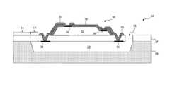
- a destination substratecan include one or more electrically conductive metal contacts (e.g., a plurality of spatially separated metal contacts) on which a volatile adhesive layer is formed.
- heating an adhesive layer to an evaporation temperaturecauses at least a portion of each of one or more metal contacts (e.g., a surface layer of a metal contact, a metal component of a metal contact, or a metal contact itself) to melt and enter a liquid or partially liquid state (e.g., a two phase state comprising a liquid).
- a metal contactcan be a designated portion of an unpatterned metal layer or a portion of a patterned metal layer.
- a componenthas a printing surface and a flat opposing surface including one or more electrically conductive component contacts electrically connected to electrical elements in the component.
- Micro-transfer printing the component from a source substratecan include contacting the printing surface with a stamp, releasing the component from the source substrate, and pressing the component contacts to the adhesive layer. The steps of heating and cooling can form an electrical connection between one or more metal contacts and one or more component contacts.
- the evaporation process caused by a heating stepcan render a volatile adhesive gaseous.
- An evaporation process caused by a heating stepcan drive an adhesive through the surface of and into a destination substrate or drive the adhesive through the surface of and into a component, or both.
- Adhesivecan diffuse into a metal contact, diffuse into a component contact, or diffuse into both the metal contact and the component contact.
- adhesivecan diffuse spontaneously during heating.
- a material of a metal contacte.g., a metal
- a material of a component contactdiffuses into a component contact or a material (e.g., a metal) of a component contact diffuses into the metal contact, or both.
- diffusioncan occur spontaneously during heating.
- a material of a metal contactcan wet a component contact when a portion of a metal contact melts (e.g., at least partially enters a liquid state). For example, wetting can occur spontaneously during heating.
- a volatile adhesive layercan be patterned or unpatterned.
- a componentcan include a plurality of component contacts.
- a component contact and a metal contactcan each be one or more of a solderable material, a metal alloy, and a metal alloy including one or more of gold, tin, lead, bismuth, indium, nickel, silver, platinum, and copper.
- a component contactcan be, for example, one or more of a semiconductor, a compound semiconductor, silicon, GaAs, InGaAs, InP, GaN, and InGaN.
- a componentcan have at least one of a length, a width and a height dimension less than or equal to one micron, two microns, five microns, ten microns, twenty microns, fifty microns, or one hundred microns.
- a micro-transfer printed structureincludes a destination substrate having one or more metal contacts and one or more micro-transfer printable components having one or more component contacts disposed on the destination substrate with the metal contact aligned with the component contact. At least one metal contact can form an intermetallic bond with a component contact (e.g., due to heating). One or more metal contacts can form an electrical connection to a component contact. For example, each metal contact can form at least one of (i) an intermetallic bond and (ii) an electrical connection with a component contact (e.g., with a one to one correspondence).
- a micro-transfer printed structurecomprises an adhesive that is at least partially diffused into one or more metal contacts, one or more component contacts, or both.
- a metal contactcan include a material (e.g., metal) that is diffused into a component contact or a component contact can include a material (e.g., metal) that is diffused into a metal contact, or both.
- a metal contactcan include metal that contacts the surface of a component contact to form an electrical connection or electrical contact.
- the disclosed technologyincludes a method of making a micro transfer printed structure, comprising: providing a destination substrate; providing a source substrate comprising one or more micro-transfer printable components; forming a layer of volatile adhesive over the destination substrate; micro-transfer printing one or more of the one or more micro-transfer printable components from the source substrate onto the volatile adhesive layer at a non-evaporable temperature of the volatile adhesive layer; and heating the volatile adhesive layer to an evaporation temperature to evaporate at least a portion of the volatile adhesive after micro-transfer printing.
- the volatile adhesive layeris patterned. In some embodiments, the volatile adhesive layer is unpatterned.
- heating the volatile adhesive layerrenders at least a portion of the volatile adhesive gaseous.
- heating the volatile adhesive layerdrives at least a portion of the adhesive through the surface of and into at least one of (i) the destination substrate and (ii) the component. In some embodiments, diffusing a portion of the adhesive into the one or more metal contacts.
- the one or more micro-transfer printed componentseach comprise one or more electrically conductive component contacts.
- the methodcomprises providing one or more electrically conductive metal contacts disposed on, in, or over the destination substrate.
- each metal contactis one or more of a solderable material, a metal alloy, and a metal alloy comprising at least one of gold, tin, lead, bismuth, indium, nickel, silver, platinum, and copper.
- the forming stepcomprises forming the volatile adhesive layer on the one or more metal contacts; the heating step causes at least a portion of at least one of the one or more metal contacts to melt; and the method comprises cooling the at least one metal contact to a temperature at which the at least a portion of the at least one metal contact solidifies in order to adhere at least one of the one or more components to the at least one metal contact.
- the one or more metal contactsare one or more designated portions of an unpatterned metal layer or one or more portions of a patterned metal layer.
- each of the one or more micro-transfer printed componentshas a printing surface and a flat opposing surface and comprises one or more electrically conductive component contacts electrically connected to electrical elements in the component
- the micro-transfer printing stepcomprises contacting each printing surface with a stamp, releasing each component from the source substrate, and pressing each component contact of the one or more micro-transfer printed components to the adhesive layer, and wherein the steps of heating and cooling form an electrical connection between the at least one metal contact and one or more of the component contacts of the one or more micro-transfer printed components.
- each of the component contactsare one or more of a semiconductor, a compound semiconductor, silicon, GaAs, InGaAs, InP, GaN, and InGaN.
- the methodcomprises diffusing at least one of (i) a material of one or more of the one or more metal contacts into one or more of the component contact(s) of the one or more micro-transfer printed components and (ii) a material of one or more of the component contact(s) diffuses into the metal contact.
- the methodcomprises wetting a component contact of the one or more micro-transfer printed components with material of the one or more metal contacts. In some embodiments, the method comprises diffusing adhesive into the one or more component contacts.
- the methodcomprises providing one or more electrically conductive metal contacts disposed on, in, or over the destination substrate, wherein the forming step comprises forming the volatile adhesive layer on the one or more metal contacts; the heating step causes at least a portion of at least one component contact to melt; and the method comprises cooling the at least one component contact to a temperature at which the at least a portion of the at least one component solidifies in order to adhere at least one of the one or more components to the at least one metal contact.
- micro-transfer printingcomprises, for each micro-transfer printable component being micro-transfer printed, breaking one or more tethers that connect the micro-transfer printable component to the source substrate.
- the componenthas at least one of a length, width and height dimension that is less than or equal to one micron, less than or equal to two microns, less than or equal to five microns, less than or equal to ten microns, less than or equal to twenty microns, less than or equal to fifty microns, or less than or equal to one hundred microns.
- the disclosed technologyincludes a micro-transfer printed structure, comprising: a destination substrate comprising one or more metal contacts; and one or more micro-transfer printed components each comprising one or more component contacts, the one or more micro-transfer printed components disposed on the destination substrate with the one or more metal contacts aligned with the one or more component contacts, wherein the one or more metal contacts form an intermetallic bond with the one or more component contacts of the one or more micro-transfer printed components.
- the structurecomprises an adhesive that is diffused into at least one of the one or more metal contacts and the one or more component contacts of the one or more micro-transfer printed components.
- At least one of (i) the one or more metal contactscomprise metal that is diffused into the component contact and (ii) the one or more component contacts of the one or more micro-transfer printed components comprise a material that is diffused into the metal contact. In some embodiments, the one or more metal contacts comprise metal that contacts the surface of the one or more component contacts of the one or more micro-transfer printed components.
- each of the one or more micro-transfer printed componentscomprises a broken tether.
- the disclosed technologyincludes a method of making a micro transfer printed structure, comprising: providing a destination substrate comprising one or more electrically conductive metal contacts; providing a source substrate comprising one or more micro-transfer printable components, each component comprising one or more electrically conductive component contacts; forming a layer of volatile adhesive over the destination substrate; micro-transfer printing one or more micro-transfer printable components from the source substrate onto the volatile adhesive layer at a non-evaporable temperature of the volatile adhesive layer such that the component contact(s) of the one or more micro-transfer printable components micro-transfer printed from the source substrate are in alignment with and adhered to the one or more metal contacts; heating the volatile adhesive layer to an evaporation temperature to evaporate the volatile adhesive after micro-transfer printing; and cooling the component(s) and metal contact(s) to adhere the one or more components micro-transfer printed from the source substrate to the one or more metal contacts and form an electrical connection between the one or more metal contacts and the component contact(s) of the one or more micro-transfer printed components micro
- the one or more metal contactsform corresponding intermetallic bond(s) with the component contact.
- FIG. 1is a flow diagram illustrating an exemplary method in accordance with some illustrative embodiments of the present invention
- FIG. 2is a cross section of a component source wafer according to some illustrative embodiments of the present invention.
- FIGS. 3A-3Hare sequential cross sections of structures made in an exemplary method in accordance with some illustrative embodiments of the present invention.
- FIG. 4is a cross section of alternative destination substrate layers according to some illustrative embodiments of the present invention.
- FIGS. 5-8are micrographs illustrating construction steps according to an exemplary method in accordance with some illustrative embodiments of the present invention.
- an exemplary method of making a micro-transfer printed structure 70 in accordance with some embodiments of the present inventionincludes providing a destination substrate 20 (illustrated in FIG. 3A ) in step 100 and a source wafer 10 having a substrate 16 with one or more micro-transfer printable components 30 (as illustrated, for example, in FIG. 2 , where one micro-transfer printable component is shown) in step 110 .
- a patterned metal layer 22 with one or more electrically conductive metal contacts 24can be formed on, in, or over a surface of the destination substrate 20 (illustrated in FIG. 3B ). As shown in FIG.
- metal contacts 24can be spatially separated over the surface of a destination substrate 20 .
- a metal layer 22can be formed as an unpatterned metal layer 22 or the metal contacts 24 can be a designated portion of an unpatterned metal layer 22 (not shown).
- the metal layer 22(patterned or unpatterned) can be provided with the destination substrate 20 in step 100 .
- a destination substrate 20can be any substrate with two substantially flat and parallel sides, for example, a glass, plastic, resin, or ceramic sheet as is found in the display, semiconductor, or printed circuit board arts.
- a metal layer 22can be formed using photolithographic or printed circuit board methods and materials, for example, by laminating, sputtering, or evaporating a metal layer 22 onto a destination substrate 20 .
- a metal layer 22can be patterned to form metal contacts 24 using conventional photolithographic methods including coating a photosensitive polymer (e.g., a photo-resist) over an unpatterned metal layer 22 , exposing the photosensitive polymer using a mask, developing the exposed photosensitive polymer to expose a pattern on the metal layer 22 , etching the exposed portions of the metal layer 22 to form a patterned metal layer 22 , and removing residual photosensitive polymer.
- a photosensitive polymeris applied over a destination substrate 20 , patterned using a mask, and developed to remove a portion of the polymer.
- a metal layer 22is provided over the destination substrate 20 and the remaining photosensitive polymer.
- the remaining photosensitive polymeris removed together with the portions of the metal layer 22 disposed on the remaining photosensitive polymer, for example, by using a solvent to which the photosensitive polymer is susceptible, leaving a corresponding patterned metal layer 22 on the destination substrate 20 .
- the metal layer 22 or any patterned metal contacts 24can be one or more of a solderable material, a metal alloy, and a metal alloy including one or more of gold, tin, lead, bismuth, indium, nickel, silver, platinum, and copper.
- metal contacts 24can be alloys, can include different metals, or can have multiple layers of different materials such as metals.
- a layer 40 of volatile adhesiveis formed over the destination substrate 20 in step 130 .
- the volatile adhesive layer 40can be patterned (as shown in FIG. 4 ), or unpatterned (as shown in FIG. 3C ) and can be formed over the metal layer 22 or patterned metal contacts 24 .
- a volatile adhesive layer 40can be patterned over metal contacts 24 only (as shown in FIG. 4 ) or additionally over areas on a destination substrate 20 between the metal contacts 24 (as shown in FIG. 3C ).
- a volatile adhesive layer 40is a layer of material that is adhesive and remains in place at a relatively lower non-evaporable temperature but evaporates or otherwise leaves the layer at a relatively higher evaporation temperature. Accordingly, a non-evaporable temperature is a temperature below an evaporation temperature.
- a non-evaporable temperaturecan be room temperature for a particular adhesive layer.
- a volatile adhesive 40can be, for example, polyethylene glycol (PEG) (e.g., having a molecular weight ranging from 100 to 600 g/mol) diluted with one or more solvents.
- useful solventscan be alcohols such as methanol, ethanol, or isopropyl alcohol.
- a volatile adhesive 40can originate in a solution state and can be disposed on or over a metal layer 22 or destination substrate 20 , for example by curtain, spin, or spray coating a solution of volatile adhesive 40 , and subsequently drying the volatile adhesive 40 on the destination substrate 20 by allowing the solvent(s) (e.g., alcohol) to evaporate, for example at room temperature.
- the remaining volatile adhesive 40provides an adhesive layer having, for example, a thickness of 1 to 10 nm, 10 to 100 nm, 100 to 500 nm, or larger.
- a micro-transfer printing stamp 50is provided in step 120 and can be an elastomeric stamp 50 formed using photolithographic processes. Certain useful photolithographic processes are described, for example, in U.S. patent application Ser. Nos. 14/804,031, 14/975,041 and 14/918,174, the disclosures of which are incorporated by reference herein.
- a micro-transfer printing stamp 50includes one or more stamp posts 52 that, during micro-transfer printing, are each located in contact with a component 30 on a component source wafer 10 (as illustrated in FIG. 2 ) and pressed against the component 30 to break (e.g., fracture) one or more tethers 12 connecting the component 30 to an anchor 14 of the source wafer substrate 16 .
- the component 30 with one or more broken tethers 13adheres to the stamp post 52 and is transported to, and in alignment with, the destination substrate 20 and any metal contacts 24 (as shown in FIG. 3D ) on the destination substrate 20 .
- the stamp 50then presses the component(s) 30 with the broken tether 13 onto the volatile adhesive layer 40 on the destination substrate 20 in alignment with the metal contacts 24 while the volatile adhesive layer 40 is at a relatively lower non-evaporable temperature to micro-transfer print the component(s) 30 onto the volatile adhesive layer 40 .
- This micro-transfer printing processoccurs in step 140 (as shown in FIG. 3E ).
- the stamp 50is then removed (as shown in FIG. 3F ).
- step 150heat 60 is applied to the printed structure and to the volatile adhesive layer 40 so that the volatile adhesive layer 40 is heated to a relatively higher, adhesive evaporation temperature, for example by baking in an oven or placing the destination substrate 20 and micro-transfer printed structure on a hotplate or by providing electromagnetic energy that is absorbed by the volatile adhesive layer 40 , for example, from a laser, microwave, or other electromagnetic energy source.
- a printed systemcan be heated to a temperature at or above the adhesive evaporation temperature, for example to also melt at least a portion of at least one of a metal contact and a component contact (e.g., a surface layer of a metal contact 24 or component contact 34 , a metal component in a metal contact 24 or component contact 34 , or a metal contact 24 or component contact 34 itself).
- a metal or a metal layer in or on a metal contact 24 or component contact 34can become at least partially liquid and at least partially wet the metal contact 24 or component contact 34 .
- a volatile adhesive in the layer 40at least partially evaporates, leaving component(s) 30 adhered to a destination substrate 20 (as shown in FIG. 3H ).
- a volatile adhesive 40can sublime directly from a solid state to a gaseous state. In some embodiments, a volatile adhesive 40 can melt into a liquid state and subsequently into a gaseous state. Using a volatile adhesive 40 is useful for temporarily adhering the component 30 to a destination substrate 20 (e.g., to metal contacts 24 disposed thereon) and for formation of permanent electrical bonds and/or permanent physical bonds between the metal or component contacts 24 , 34 , as a result of heating. Heating can occur at elevated temperatures above room temperature (e.g., exceeding an evaporation temperature), for example, at or exceeding 100° C., 110° C., 120° C., 150° C. or 160° C. or above.
- room temperaturee.g., exceeding an evaporation temperature
- a component 30 with component contacts 34can be aligned with, disposed upon, and electrically connected to electrical contacts (e.g., metal contacts 24 ) coated with a volatile adhesive 40 on a destination substrate 20 by micro-transfer printing the components 30 in alignment with the electrical contacts 24 onto the destination substrate 20 and heating the printed structure without the need for subsequent processing, for example subsequent photolithographic processing in a vacuum chamber, thereby reducing manufacturing equipment needs, costs, and steps.
- electrical contactse.g., metal contacts 24
- the evaporation process of step 150renders the volatile adhesive gaseous, evaporates the volatile adhesive 40 into the local environment, drives the adhesive through the surface of and into the destination substrate 20 , drives the volatile adhesive 40 through the surface of and into the component 30 , drives the volatile adhesive 40 through the surface of and into the component 30 and through the surface of and into the destination substrate 20 , or any combination thereof.
- volatile adhesive 40diffuses into a metal contact 24 .
- Heating a volatile adhesive layer 40 to a temperature greater than or equal to the evaporation temperaturecan cause at least a portion of a metal contact 24 to melt, such as the metal contact 24 itself, a metal component (e.g., material) of the metal contact 24 , or a surface layer of the metal contact 24 .
- a metal contact 24solidifies to adhere and bond a component 30 to the metal contact 24 .
- a component contact 34can be similarly melted (e.g., by melting the component contact itself, a metal component (e.g., material) of the component contact, or a surface layer of component contact) and solidified to adhere and bond a component 30 to a destination substrate 20 (e.g., to at least one metal contact of the destination substrate).
- both at least a portion of a metal contact 24 and at least a portion of a component contact 34are melted and solidified by heating and cooling, respectively, in order to adhere and bond a component 30 to a destination substrate 20 .
- both at least a portion of a metal contact 24 and at least a portion of a component contact 34melt and are subsequently solidified in order to adhere and bond a component 30 to a destination substrate 20 .
- a component 30has a printing surface 80 and a flat opposing surface 82 including one or more electrically conductive component contacts 34 electrically connected to electrical elements 32 in the component 30 through element contacts 36 .
- Component contacts 34can be or include, for example, one or more of a semiconductor, a compound semiconductor, silicon, GaAs, InGaAs, InP, GaN, and InGaN.
- micro-transfer printing a component 30 from a substrate 16 of a source wafer 10includes contacting the printing surface 80 with a stamp 50 , releasing the component 30 from the source wafer substrate 16 , and pressing component contacts 34 on the opposing surface 82 of the component 30 to a volatile adhesive layer 40 (as shown in FIG. 3E ). Heating and subsequent cooling (e.g., as in steps 150 , 160 ) forms an electrical connection between one or more of the metal contacts 24 and one or more of the component contacts 34 .
- a heating processcauses a material of a metal contact 24 to diffuse into a component contact 34 .
- a material of the component contact 34diffuses into the metal contact 24 .
- both a material of the metal contact 24diffuses into the component contact 34 and a material of the component contact 34 diffuses into the metal contact 24 .
- a material of a metal contact 24can wet a component contact 34 , particularly when a surface layer of the metal contact 24 , a metal component of the metal contact 24 , or the metal contact 24 is in a melted state (i.e., at least partially liquid state), as described above.
- a volatile adhesive 40can diffuse into a component contact 34 , a metal contact 24 , or into both the metal contact 24 and the component contact 34 .
- An electrical connectionelectrically connects an element 32 of a component 30 , through an element contact 36 , to a metal contact 24 of a destination substrate 20 and, in some embodiments, to an external electrical power or signal source (not shown) electrically connected to the metal layer 22 or metal contacts 24 .
- Components 30can be micro-transfer printed from a source wafer 10 to a target destination substrate 20 .
- Components 30 suitable for micro-transfer printingcan be very small, for example having at least one of a length, a width and a height dimension less than or equal to one micron, two microns, five microns, ten microns, twenty microns, fifty microns, or one hundred microns.
- Such small components 30are not readily transferred from a native, source wafer 10 to a destination substrate 20 having a different material composition than the components 30 using conventional surface-mount or pick-and-place tools.
- a micro-transfer printed structure 70includes a destination substrate 20 having one or more metal contacts 24 and one or more micro-transfer printed components 30 having one or more component contacts 34 .
- the one or more micro-transfer printed components 30are disposed on the destination substrate 20 so that metal contacts 24 of the destination substrate 20 are aligned with component contacts 34 of the components 30 .
- each metal contact 24forms an intermetallic bond and electrical connection with a corresponding component contact 34 .
- a micro-transfer printed structure 70includes a volatile adhesive 40 that is diffused into a metal contact 24 , diffused into a component contact 34 , or both.
- a metal contact 24includes material (e.g., metal) that is diffused into a component contact 34 or the component contact 34 includes a material that is diffused into the metal contact 24 , or both.
- the metal contact 24can include metal that contacts the surface of the component contact 34 .
- components 30 of a source wafer 10can be made by first providing a source wafer substrate 16 (for example a substrate comprising glass, sapphire, a semiconductor such as silicon, or a compound semiconductor, for example GaN) and patterning a sacrificial layer on or over the source wafer 10 to form an array of sacrificial portions spatially separated by anchors 14 .
- Component contacts 34e.g., contact pads
- a dielectric layer 17can be deposited, for example by sputtering, over a sacrificial layer and component contacts 34 .
- An element 32can then be formed, for example a patterned semiconductor structure, on or over the dielectric layer 17 .
- Such an element 32can be an integrated circuit (for example CMOS) or light-emitting diode (LED) and can include electrical element contacts 36 .
- a dielectric layer 38can be formed to insulate the element 32 and patterned to form vias providing access to element contacts 36 through dielectric layer 38 and component contacts 34 through dielectric layer 17 and to expose a portion of a sacrificial layer.
- a metal layer 22is deposited and patterned to form electrodes 35 electrically connecting the element 32 and element contacts 36 to component contacts 34 .
- Sacrificial portionsare etched through the exposed portion of the sacrificial layer to form gaps 18 and tethers 12 physically connecting the components 30 to anchors 14 of the source wafer substrate 16 .
- the components 30can then be micro-transfer printed using a micro-transfer printing stamp 50 .
- Multiple micro-transfer printable components 30can be formed on a source wafer 10 in common processing steps. All of these steps (except transfer printing) can be performed using standard microfabrication methods and materials, including photolithographic methods and materials.
- the present inventionprovides an advantage in that a volatile adhesive layer 40 assists in micro-transfer printing a micro-transfer printable component 30 to a destination substrate 20 by adhering the micro-transfer printed component 30 to the destination substrate 20 (e.g., to the metal contacts 24 thereof) (as in step 140 ). If not evaporated, a volatile adhesive 40 can increase the resistance of one or more electrical connection between metal contact(s) 24 and component contact(s) 34 . In some embodiments, by evaporating a volatile adhesive (as in step 150 ), the electrical contact between metal contacts 24 and component contacts 34 is improved and contact resistance is decreased. Furthermore, components 30 can be affixed and electrically connected to metal contacts 24 on a destination substrate 20 in a simple atmospheric process. Moreover, bonds formed between metal contacts 24 of a destination substrate 20 and component contacts 34 of components 30 can form an excellent thermal connection for conducting heat from the components 30 to the destination substrate 20 , improving operating characteristics of the printed system.
- the element 32 of the component 30was a GaAs red-light-emitting inorganic light-emitting diode (LED) having a size of 8 ⁇ m by 8 ⁇ m by 1 ⁇ m and two electrical contacts 36 .
- the component 30had a single component contact 34 of n-InGaP electrically connected to a first one of the element contacts 36 of the LED element 32 .
- components 30 of other figuresillustrate two component contacts 34 .
- a component wafer substrate 16 having components 30was processed and the components 30 released from the component wafer substrate 16 by etching the sacrificial portions of the source wafer 10 (in accordance with step 110 , as shown in FIG. 5 ).
- a destination substrate 20comprised a 4-inch-diagonal silicon wafer.
- a Ti (250 ⁇ )/Au (2000 ⁇ )/Sn (500 ⁇ )/Au (200 ⁇ ) blanket metal layer 22was evaporated onto the silicon wafer (in accordance with step 100 ).
- a 10 mL methanol/1 mL PEG (400 g/mol molecular weight) volatile adhesive layer 40was spin coated onto the unpatterned metal layer 22 and dried at room temperature by evaporating the methanol to form a dried volatile adhesive layer 40 (in accordance with step 130 ).
- the released components 30(in accordance with step 110 , as shown in FIG. 5 ) were micro-transfer printed from the wafer substrate 10 onto the volatile adhesive layer 40 and adhered to the metal layer 22 of the destination substrate 20 (in accordance with step 140 , as shown in FIG. 6 ).
- the micro-transfer printed structure(including destination substrate 20 ) was thermally treated on a hotplate at 235° C. for one minute (in accordance with step 150 ) and the exposed volatile adhesive layer 40 was visually observed to evaporate into the atmosphere.
- the metal contact 24 between the destination substrate 20 and the component 30melted and incorporated at least a portion of the volatile adhesive 40 and material of the component contact 34 .
- the structurewas cooled to room temperature (in accordance with step 160 , as shown in FIG. 7 ), forming an intermetallic bond and electrical connection between the metal layer 22 and the component contact 34 .
- a 1.4 ⁇ m epoxy layerwas spin coated over the structure and cured to form a passivation layer. A portion of the top surface of the passivation layer was removed to expose a portion of the micro-transfer printed LEDs, forming a second element contact 36 and providing a second electrical contact to each LED.
- a shadow maskwas applied to the structure and a metal layer (20 ⁇ Ti, 2500 ⁇ AlZnO) was deposited through the shadow mask to form a patterned electrode providing a second electrical connection to each LED that is electrically separate from the metal layer 22 . Electrical power was applied to the metal layer 22 and the patterned (Ti, AlZnO) electrode and the LEDs operated to emit red light (as shown in FIG. 8 ).
- the micro-transfer-printed components 30were micro-transfer printed to the volatile adhesive layer 40 , the components 30 adhered to the metal layer 22 , and the volatile adhesive 40 heated and evaporated so that a bond and electrical connection were formed between the LED component contact 34 and the metal layer 22 after the thermal processing.
- the components 30did not adhere to the substrate.
- components 30 printed and adhered to a destination substrate 20 with a non-volatile adhesive layerdid not form an electrical contact between the component contacts 34 and the metal layer 22 . Rather, the non-volatile adhesive layer formed a non-conductive passivation layer that inhibited electrical conduction between the metal layer 22 and the component contact 34 .
- the tested embodiment of the present inventiondemonstrated improved adhesion in combination with improved electrical connections to a destination substrate 20 compared to conventional methods and materials used as a control.
- elements 32 or components 30can be relatively small, for example in some embodiments, each element 32 or component 30 has at least one of a width from 2 to 5 ⁇ m, 5 to 10 ⁇ m, 10 to 20 ⁇ m, or 20 to 50 ⁇ m, a length from 2 to 5 ⁇ m, 5 to 10 ⁇ m, 10 to 20 ⁇ m, or 20 to 50 ⁇ m, and a height from 2 to 5 ⁇ m, 4 to 10 ⁇ m, 10 to 20 ⁇ m, or 20 to 50 ⁇ m.
- Elements 32can be integrated circuits, light emitters such as light-emitting diodes, or sensors, such as photo-sensors, magnetic sensors, or electrical-field sensors.
- a source wafer 10can comprise a semiconductor source wafer substrate 16 , for example comprising silicon, such as silicon (1 0 0) or silicon (1 1 1), glass, plastic, or other materials suitable for wafers.
- Sacrificial layers or sacrificial portionscan include layers or patterned layers of etchable materials, for example such as oxides or nitrides such as silicon oxide or silicon nitride, or portions of the source wafer substrate 16 that are differentially etchable in different directions (i.e., exhibit anisotropic etching) (for example by taking advantage of the crystalline structure of the source wafer substrate 16 to etch in one direction more rapidly than in another direction).
- a destination substrate 20can have a thickness from 5 to 10 microns, 10 to 50 microns, 50 to 100 microns, 100 to 200 microns, 200 to 500 microns, 500 microns to 0.5 mm, 0.5 to 1 mm, 1 mm to 5 mm, 5 mm to 10 mm, or 10 mm to 20 mm.
- a destination substrate 20can include layers formed on an underlying structure or substrate, for example a rigid or flexible glass or plastic substrate.
- a destination substrate 20can be transparent (e.g., at least partially transparent) or opaque.
- a first layer on a second layerin some embodiments means a first layer directly on and in contact with a second layer. In other embodiments, a first layer on a second layer can include another layer there between.
- a sacrificial layer or sacrificial portionis considered “on” a substrate when a layer of sacrificial material or sacrificial portion is on top of the substrate, when a portion of the substrate itself is the sacrificial layer, or when the sacrificial layer or sacrificial portion comprises material on top of the substrate and a portion of the substrate itself.
Landscapes
- Engineering & Computer Science (AREA)
- Computer Hardware Design (AREA)
- Microelectronics & Electronic Packaging (AREA)
- Power Engineering (AREA)
- Physics & Mathematics (AREA)
- Condensed Matter Physics & Semiconductors (AREA)
- General Physics & Mathematics (AREA)
- Manufacturing & Machinery (AREA)
- Wire Bonding (AREA)
- Manufacturing Of Printed Wiring (AREA)
Abstract
Description
- 10 source wafer
- 12 tether
- 13 broken tether
- 14 anchor
- 16 source wafer substrate
- 17 dielectric layer
- 18 gap
- 20 destination (target) substrate
- 22 metal layer
- 24 metal contact
- 30 component
- 32 element
- 34 component contact
- 35 electrode
- 36 element contact
- 38 dielectric
- 40 volatile adhesive layer/volatile adhesive
- 50 stamp
- 52 stamp post
- 60 heat
- 70 micro-transfer printed structure
- 80 printing surface
- 82 opposing surface
- 100 provide destination substrate step
- 110 provide source wafer with components step
- 120 provide transfer stamp step
- 130 form volatile adhesive layer on destination substrate step
- 140 micro-transfer print components from source wafer to adhesive layer on destination substrate at non-evaporable temperature step
- 150 heat printed system to adhesive evaporation temperature step
- 160 cool component and destination substrate step
Claims (21)
Priority Applications (1)
| Application Number | Priority Date | Filing Date | Title |
|---|---|---|---|
| US15/718,636US10157880B2 (en) | 2016-10-03 | 2017-09-28 | Micro-transfer printing with volatile adhesive layer |
Applications Claiming Priority (2)
| Application Number | Priority Date | Filing Date | Title |
|---|---|---|---|
| US201662403427P | 2016-10-03 | 2016-10-03 | |
| US15/718,636US10157880B2 (en) | 2016-10-03 | 2017-09-28 | Micro-transfer printing with volatile adhesive layer |
Publications (2)
| Publication Number | Publication Date |
|---|---|
| US20180096964A1 US20180096964A1 (en) | 2018-04-05 |
| US10157880B2true US10157880B2 (en) | 2018-12-18 |
Family
ID=61758389
Family Applications (1)
| Application Number | Title | Priority Date | Filing Date |
|---|---|---|---|
| US15/718,636ActiveUS10157880B2 (en) | 2016-10-03 | 2017-09-28 | Micro-transfer printing with volatile adhesive layer |
Country Status (1)
| Country | Link |
|---|---|
| US (1) | US10157880B2 (en) |
Cited By (4)
| Publication number | Priority date | Publication date | Assignee | Title |
|---|---|---|---|---|
| US10347535B2 (en) | 2014-06-18 | 2019-07-09 | X-Celeprint Limited | Systems and methods for controlling release of transferable semiconductor structures |
| US10361124B2 (en) | 2014-06-18 | 2019-07-23 | X-Celeprint Limited | Systems and methods for controlling release of transferable semiconductor structures |
| US10796971B2 (en) | 2018-08-13 | 2020-10-06 | X Display Company Technology Limited | Pressure-activated electrical interconnection with additive repair |
| US11398399B2 (en) | 2019-03-08 | 2022-07-26 | X Display Company Technology Limited | Components with backside adhesive layers |
Families Citing this family (5)
| Publication number | Priority date | Publication date | Assignee | Title |
|---|---|---|---|---|
| US10297502B2 (en) | 2016-12-19 | 2019-05-21 | X-Celeprint Limited | Isolation structure for micro-transfer-printable devices |
| US10832935B2 (en) | 2017-08-14 | 2020-11-10 | X Display Company Technology Limited | Multi-level micro-device tethers |
| US10593827B2 (en) | 2018-01-24 | 2020-03-17 | X-Celeprint Limited | Device source wafers with patterned dissociation interfaces |
| US10832934B2 (en) | 2018-06-14 | 2020-11-10 | X Display Company Technology Limited | Multi-layer tethers for micro-transfer printing |
| WO2022019200A1 (en)* | 2020-07-20 | 2022-01-27 | Agc株式会社 | Transparent display device and manufacturing method therefor |
Citations (75)
| Publication number | Priority date | Publication date | Assignee | Title |
|---|---|---|---|---|
| US5475224A (en) | 1994-08-26 | 1995-12-12 | Grumman Aerospace Corporation | Infrared detector substrate with breakaway test tabs |
| US5621555A (en) | 1993-12-31 | 1997-04-15 | Goldstar Co., Ltd. | Liquid crystal display having redundant pixel electrodes and thin film transistors and a manufacturing method thereof |
| US5815303A (en) | 1997-06-26 | 1998-09-29 | Xerox Corporation | Fault tolerant projective display having redundant light modulators |
| US5882532A (en) | 1996-05-31 | 1999-03-16 | Hewlett-Packard Company | Fabrication of single-crystal silicon structures using sacrificial-layer wafer bonding |
| US6142358A (en) | 1997-05-31 | 2000-11-07 | The Regents Of The University Of California | Wafer-to-wafer transfer of microstructures using break-away tethers |
| US6278242B1 (en) | 2000-03-20 | 2001-08-21 | Eastman Kodak Company | Solid state emissive display with on-demand refresh |
| US6577367B2 (en) | 2000-01-12 | 2003-06-10 | Lg. Philips Lcd Co., Ltd | Array substrate for a liquid crystal display device and method for fabricating the same |
| US20030141570A1 (en) | 2002-01-28 | 2003-07-31 | Chen Shiuh-Hui Steven | Semiconductor wafer having a thin die and tethers and methods of making the same |
| US6717560B2 (en) | 2000-05-15 | 2004-04-06 | Eastman Kodak Company | Self-illuminating imaging device |
| US6756576B1 (en) | 2000-08-30 | 2004-06-29 | Micron Technology, Inc. | Imaging system having redundant pixel groupings |
| US6933532B2 (en) | 2003-03-28 | 2005-08-23 | Eastman Kodak Company | OLED display with photosensor |
| US20060079010A1 (en) | 2004-09-30 | 2006-04-13 | Seiko Epson Corporation | Transfer base substrate and method of semiconductor device |
| US20070032089A1 (en) | 2004-06-04 | 2007-02-08 | The Board Of Trustees Of The University Of Illinois | Printable Semiconductor Structures and Related Methods of Making and Assembling |
| US7195733B2 (en) | 2004-04-27 | 2007-03-27 | The Board Of Trustees Of The University Of Illinois | Composite patterning devices for soft lithography |
| US20070173034A1 (en) | 2004-03-22 | 2007-07-26 | Semiconductor Energy Laboratory Co., Ltd. | Method for manufacturing integrated circuit |
| US7288753B2 (en) | 2004-05-05 | 2007-10-30 | Eastman Kodak Company | OLED display with composite photosensor |
| US20070281556A1 (en) | 2006-06-05 | 2007-12-06 | Homac Mfg. Company | Electrical connector with plug tether assembly and related methods |
| WO2008036837A2 (en) | 2006-09-20 | 2008-03-27 | The Board Of Trustees Of The University Of Illinois | Release strategies for making transferable semiconductor structures, devices and device components |
| US20080079246A1 (en) | 2006-09-29 | 2008-04-03 | Nissan Technical Center North America, Inc. | Tether guided inflatable sail panel |
| US7354801B2 (en) | 2004-09-21 | 2008-04-08 | Semiconductor Energy Laboratory Co., Ltd. | Method for manufacturing semiconductor device |
| WO2008103931A2 (en) | 2007-02-23 | 2008-08-28 | Strategic Patent Acquisitions Llc | Techniques for three dimensional displays |
| US7521292B2 (en) | 2004-06-04 | 2009-04-21 | The Board Of Trustees Of The University Of Illinois | Stretchable form of single crystal silicon for high performance electronics on rubber substrates |
| US7557367B2 (en) | 2004-06-04 | 2009-07-07 | The Board Of Trustees Of The University Of Illinois | Stretchable semiconductor elements and stretchable electrical circuits |
| US20090202089A1 (en) | 2007-06-06 | 2009-08-13 | Analog Devices, Inc. | Microphone with Reduced Parasitic Capacitance |
| US7586497B2 (en) | 2005-12-20 | 2009-09-08 | Eastman Kodak Company | OLED display with improved power performance |
| US7662545B2 (en) | 2004-10-14 | 2010-02-16 | The Board Of Trustees Of The University Of Illinois | Decal transfer lithography |
| US7704684B2 (en) | 2003-12-01 | 2010-04-27 | The Board Of Trustees Of The University Of Illinois | Methods and devices for fabricating three-dimensional nanoscale structures |
| US20100248484A1 (en) | 2009-03-26 | 2010-09-30 | Christopher Bower | Methods of Forming Printable Integrated Circuit Devices and Devices Formed Thereby |
| US7816856B2 (en) | 2009-02-25 | 2010-10-19 | Global Oled Technology Llc | Flexible oled display with chiplets |
| US20100306993A1 (en) | 2007-11-20 | 2010-12-09 | Board Of Regents, The University Of Texas System | Method and Apparatus for Detethering Mesoscale, Microscale, and Nanoscale Components and Devices |
| US20100317132A1 (en) | 2009-05-12 | 2010-12-16 | Rogers John A | Printed Assemblies of Ultrathin, Microscale Inorganic Light Emitting Diodes for Deformable and Semitransparent Displays |
| US7893612B2 (en) | 2008-02-27 | 2011-02-22 | Global Oled Technology Llc | LED device having improved light output |
| JP2011066130A (en) | 2009-09-16 | 2011-03-31 | Seiko Epson Corp | Method of manufacturing semiconductor circuit device, semiconductor circuit device, and electronic apparatus |
| US7927976B2 (en) | 2008-07-23 | 2011-04-19 | Semprius, Inc. | Reinforced composite stamp for dry transfer printing of semiconductor elements |
| US7943491B2 (en) | 2004-06-04 | 2011-05-17 | The Board Of Trustees Of The University Of Illinois | Pattern transfer printing by kinetic control of adhesion to an elastomeric stamp |
| US7972875B2 (en) | 2007-01-17 | 2011-07-05 | The Board Of Trustees Of The University Of Illinois | Optical systems fabricated by printing-based assembly |
| US7999454B2 (en) | 2008-08-14 | 2011-08-16 | Global Oled Technology Llc | OLED device with embedded chip driving |
| US8029139B2 (en) | 2008-01-29 | 2011-10-04 | Eastman Kodak Company | 2D/3D switchable color display apparatus with narrow band emitters |
| WO2011123285A1 (en) | 2010-03-29 | 2011-10-06 | Semprius, Inc. | Selective transfer of active components |
| US8207547B2 (en) | 2009-06-10 | 2012-06-26 | Brudgelux, Inc. | Thin-film LED with P and N contacts electrically isolated from the substrate |
| US8261660B2 (en) | 2009-07-22 | 2012-09-11 | Semprius, Inc. | Vacuum coupled tool apparatus for dry transfer printing semiconductor elements |
| US20120228669A1 (en) | 2009-09-16 | 2012-09-13 | Christopher Bower | High-yield fabrication of large-format substrates with distributed, independent control elements |
| US20120314388A1 (en) | 2011-06-08 | 2012-12-13 | Semprius, Inc. | Substrates with transferable chiplets |
| US8334545B2 (en) | 2010-03-24 | 2012-12-18 | Universal Display Corporation | OLED display architecture |
| US20130069275A1 (en) | 2011-09-20 | 2013-03-21 | Etienne Menard | Printing transferable components using microstructured elastomeric surfaces with pressure modulated reversible adhesion |
| US20130088416A1 (en) | 2011-10-11 | 2013-04-11 | Cambridge Display Technology Limited | OLED Display Driver Circuits and Techniques |
| US8470701B2 (en) | 2008-04-03 | 2013-06-25 | Advanced Diamond Technologies, Inc. | Printable, flexible and stretchable diamond for thermal management |
| US20130196474A1 (en) | 2010-08-06 | 2013-08-01 | Matthew Meitl | Materials and processes for releasing printable compound semiconductor devices |
| US8502192B2 (en) | 2010-01-12 | 2013-08-06 | Varian Semiconductor Equipment Associates, Inc. | LED with uniform current spreading and method of fabrication |
| US8506867B2 (en) | 2008-11-19 | 2013-08-13 | Semprius, Inc. | Printing semiconductor elements by shear-assisted elastomeric stamp transfer |
| US20130207964A1 (en) | 2012-02-15 | 2013-08-15 | Rod G. Fleck | Imaging structure with embedded light sources |
| US20130221355A1 (en) | 2010-08-26 | 2013-08-29 | Christopher Bower | Structures and methods for testing printable integrated circuits |
| US8686447B2 (en) | 2011-03-01 | 2014-04-01 | Sony Corporation | Light emitting unit and display device |
| US20140104243A1 (en) | 2012-10-15 | 2014-04-17 | Kapil V. Sakariya | Content-Based Adaptive Refresh Schemes For Low-Power Displays |
| US8766970B2 (en) | 2008-05-05 | 2014-07-01 | Au Optronics Corporation | Pixel circuit, display panel, and driving method thereof |
| US8791474B1 (en) | 2013-03-15 | 2014-07-29 | LuxVue Technology Corporation | Light emitting diode display with redundancy scheme |
| US8794501B2 (en) | 2011-11-18 | 2014-08-05 | LuxVue Technology Corporation | Method of transferring a light emitting diode |
| US8803857B2 (en) | 2011-02-10 | 2014-08-12 | Ronald S. Cok | Chiplet display device with serial control |
| US8817369B2 (en) | 2009-08-31 | 2014-08-26 | Samsung Display Co., Ltd. | Three dimensional display device and method of controlling parallax barrier |
| US8835940B2 (en) | 2012-09-24 | 2014-09-16 | LuxVue Technology Corporation | Micro device stabilization post |
| US20140267683A1 (en) | 2013-03-15 | 2014-09-18 | LuxVue Technology Corporation | Method of fabricating a light emitting diode display with integrated defect detection test |
| US20140264763A1 (en) | 2013-03-15 | 2014-09-18 | Semprius, Inc. | Engineered substrates for semiconductor epitaxy and methods of fabricating the same |
| US8854294B2 (en) | 2009-03-06 | 2014-10-07 | Apple Inc. | Circuitry for independent gamma adjustment points |
| US20140340900A1 (en) | 2013-05-14 | 2014-11-20 | LuxVue Technology Corporation | Stabilization structure including shear release posts |
| US20140367633A1 (en) | 2013-06-18 | 2014-12-18 | LuxVue Technology Corporation | Led display with wavelength conversion layer |
| US20150028362A1 (en) | 2013-07-26 | 2015-01-29 | LuxVue Technology Corporation | Adhesive wafer bonding with controlled thickness variation |
| US8987765B2 (en) | 2013-06-17 | 2015-03-24 | LuxVue Technology Corporation | Reflective bank structure and method for integrating a light emitting device |
| US9161448B2 (en) | 2010-03-29 | 2015-10-13 | Semprius, Inc. | Laser assisted transfer welding process |
| WO2015193435A1 (en) | 2014-06-18 | 2015-12-23 | X-Celeprint Limited | Systems and methods for controlling release of transferable semiconductor structures |
| US20160020131A1 (en) | 2014-07-20 | 2016-01-21 | X-Celeprint Limited | Apparatus and methods for micro-transfer-printing |
| US20160086855A1 (en) | 2014-06-18 | 2016-03-24 | X-Celeprint Limited | Systems and methods for controlling release of transferable semiconductor structures |
| US20160093600A1 (en) | 2014-09-25 | 2016-03-31 | X-Celeprint Limited | Compound micro-assembly strategies and devices |
| US9520537B2 (en) | 2014-06-18 | 2016-12-13 | X-Celeprint Limited | Micro assembled LED displays and lighting elements |
| US20170047306A1 (en) | 2015-08-11 | 2017-02-16 | X-Celeprint Limited | Stamp with structured posts |
| US20170256521A1 (en)* | 2016-03-03 | 2017-09-07 | X-Celeprint Limited | Micro-transfer printable electronic component |
- 2017
- 2017-09-28USUS15/718,636patent/US10157880B2/enactiveActive
Patent Citations (101)
| Publication number | Priority date | Publication date | Assignee | Title |
|---|---|---|---|---|
| US5621555A (en) | 1993-12-31 | 1997-04-15 | Goldstar Co., Ltd. | Liquid crystal display having redundant pixel electrodes and thin film transistors and a manufacturing method thereof |
| US5475224A (en) | 1994-08-26 | 1995-12-12 | Grumman Aerospace Corporation | Infrared detector substrate with breakaway test tabs |
| US5882532A (en) | 1996-05-31 | 1999-03-16 | Hewlett-Packard Company | Fabrication of single-crystal silicon structures using sacrificial-layer wafer bonding |
| US6142358A (en) | 1997-05-31 | 2000-11-07 | The Regents Of The University Of California | Wafer-to-wafer transfer of microstructures using break-away tethers |
| US5815303A (en) | 1997-06-26 | 1998-09-29 | Xerox Corporation | Fault tolerant projective display having redundant light modulators |
| US6577367B2 (en) | 2000-01-12 | 2003-06-10 | Lg. Philips Lcd Co., Ltd | Array substrate for a liquid crystal display device and method for fabricating the same |
| US6278242B1 (en) | 2000-03-20 | 2001-08-21 | Eastman Kodak Company | Solid state emissive display with on-demand refresh |
| US6717560B2 (en) | 2000-05-15 | 2004-04-06 | Eastman Kodak Company | Self-illuminating imaging device |
| US6756576B1 (en) | 2000-08-30 | 2004-06-29 | Micron Technology, Inc. | Imaging system having redundant pixel groupings |
| US7129457B2 (en) | 2000-08-30 | 2006-10-31 | Micron Technology, Inc. | Redundant imaging systems |
| US20030141570A1 (en) | 2002-01-28 | 2003-07-31 | Chen Shiuh-Hui Steven | Semiconductor wafer having a thin die and tethers and methods of making the same |
| US6933532B2 (en) | 2003-03-28 | 2005-08-23 | Eastman Kodak Company | OLED display with photosensor |
| US7704684B2 (en) | 2003-12-01 | 2010-04-27 | The Board Of Trustees Of The University Of Illinois | Methods and devices for fabricating three-dimensional nanoscale structures |
| US20070173034A1 (en) | 2004-03-22 | 2007-07-26 | Semiconductor Energy Laboratory Co., Ltd. | Method for manufacturing integrated circuit |
| US7195733B2 (en) | 2004-04-27 | 2007-03-27 | The Board Of Trustees Of The University Of Illinois | Composite patterning devices for soft lithography |
| US7288753B2 (en) | 2004-05-05 | 2007-10-30 | Eastman Kodak Company | OLED display with composite photosensor |
| US7799699B2 (en) | 2004-06-04 | 2010-09-21 | The Board Of Trustees Of The University Of Illinois | Printable semiconductor structures and related methods of making and assembling |
| US8039847B2 (en) | 2004-06-04 | 2011-10-18 | The Board Of Trustees Of The University Of Illinois | Printable semiconductor structures and related methods of making and assembling |
| US8754396B2 (en) | 2004-06-04 | 2014-06-17 | The Board Of Trustees Of The University Of Illinois | Stretchable form of single crystal silicon for high performance electronics on rubber substrates |
| US8440546B2 (en) | 2004-06-04 | 2013-05-14 | The Board Of Trustees Of The University Of Illinois | Methods and devices for fabricating and assembling printable semiconductor elements |
| US8664699B2 (en) | 2004-06-04 | 2014-03-04 | The Board Of Trustees Of The University Of Illinois | Methods and devices for fabricating and assembling printable semiconductor elements |
| US8394706B2 (en) | 2004-06-04 | 2013-03-12 | The Board Of Trustees Of The University Of Illinois | Printable semiconductor structures and related methods of making and assembling |
| US20070032089A1 (en) | 2004-06-04 | 2007-02-08 | The Board Of Trustees Of The University Of Illinois | Printable Semiconductor Structures and Related Methods of Making and Assembling |
| US7521292B2 (en) | 2004-06-04 | 2009-04-21 | The Board Of Trustees Of The University Of Illinois | Stretchable form of single crystal silicon for high performance electronics on rubber substrates |
| US7557367B2 (en) | 2004-06-04 | 2009-07-07 | The Board Of Trustees Of The University Of Illinois | Stretchable semiconductor elements and stretchable electrical circuits |
| US8198621B2 (en) | 2004-06-04 | 2012-06-12 | The Board Of Trustees Of The University Of Illinois | Stretchable form of single crystal silicon for high performance electronics on rubber substrates |
| US7943491B2 (en) | 2004-06-04 | 2011-05-17 | The Board Of Trustees Of The University Of Illinois | Pattern transfer printing by kinetic control of adhesion to an elastomeric stamp |
| US7622367B1 (en) | 2004-06-04 | 2009-11-24 | The Board Of Trustees Of The University Of Illinois | Methods and devices for fabricating and assembling printable semiconductor elements |
| US7982296B2 (en) | 2004-06-04 | 2011-07-19 | The Board Of Trustees Of The University Of Illinois | Methods and devices for fabricating and assembling printable semiconductor elements |
| US7354801B2 (en) | 2004-09-21 | 2008-04-08 | Semiconductor Energy Laboratory Co., Ltd. | Method for manufacturing semiconductor device |
| US20060079010A1 (en) | 2004-09-30 | 2006-04-13 | Seiko Epson Corporation | Transfer base substrate and method of semiconductor device |
| US7662545B2 (en) | 2004-10-14 | 2010-02-16 | The Board Of Trustees Of The University Of Illinois | Decal transfer lithography |
| US7586497B2 (en) | 2005-12-20 | 2009-09-08 | Eastman Kodak Company | OLED display with improved power performance |
| US20070281556A1 (en) | 2006-06-05 | 2007-12-06 | Homac Mfg. Company | Electrical connector with plug tether assembly and related methods |
| US8895406B2 (en) | 2006-09-20 | 2014-11-25 | The Board Of Trustees Of The University Of Illinois | Release strategies for making transferable semiconductor structures, devices and device components |
| WO2008036837A2 (en) | 2006-09-20 | 2008-03-27 | The Board Of Trustees Of The University Of Illinois | Release strategies for making transferable semiconductor structures, devices and device components |
| US20080108171A1 (en) | 2006-09-20 | 2008-05-08 | Rogers John A | Release strategies for making transferable semiconductor structures, devices and device components |
| US7932123B2 (en) | 2006-09-20 | 2011-04-26 | The Board Of Trustees Of The University Of Illinois | Release strategies for making transferable semiconductor structures, devices and device components |
| US20080079246A1 (en) | 2006-09-29 | 2008-04-03 | Nissan Technical Center North America, Inc. | Tether guided inflatable sail panel |
| US8722458B2 (en) | 2007-01-17 | 2014-05-13 | The Board Of Trustees Of The University Of Illinois | Optical systems fabricated by printing-based assembly |
| US7972875B2 (en) | 2007-01-17 | 2011-07-05 | The Board Of Trustees Of The University Of Illinois | Optical systems fabricated by printing-based assembly |
| WO2008103931A2 (en) | 2007-02-23 | 2008-08-28 | Strategic Patent Acquisitions Llc | Techniques for three dimensional displays |
| US20090202089A1 (en) | 2007-06-06 | 2009-08-13 | Analog Devices, Inc. | Microphone with Reduced Parasitic Capacitance |
| US20100306993A1 (en) | 2007-11-20 | 2010-12-09 | Board Of Regents, The University Of Texas System | Method and Apparatus for Detethering Mesoscale, Microscale, and Nanoscale Components and Devices |
| US8029139B2 (en) | 2008-01-29 | 2011-10-04 | Eastman Kodak Company | 2D/3D switchable color display apparatus with narrow band emitters |
| US7893612B2 (en) | 2008-02-27 | 2011-02-22 | Global Oled Technology Llc | LED device having improved light output |
| US8470701B2 (en) | 2008-04-03 | 2013-06-25 | Advanced Diamond Technologies, Inc. | Printable, flexible and stretchable diamond for thermal management |
| US8766970B2 (en) | 2008-05-05 | 2014-07-01 | Au Optronics Corporation | Pixel circuit, display panel, and driving method thereof |
| US7927976B2 (en) | 2008-07-23 | 2011-04-19 | Semprius, Inc. | Reinforced composite stamp for dry transfer printing of semiconductor elements |
| US7999454B2 (en) | 2008-08-14 | 2011-08-16 | Global Oled Technology Llc | OLED device with embedded chip driving |
| US8506867B2 (en) | 2008-11-19 | 2013-08-13 | Semprius, Inc. | Printing semiconductor elements by shear-assisted elastomeric stamp transfer |
| US7816856B2 (en) | 2009-02-25 | 2010-10-19 | Global Oled Technology Llc | Flexible oled display with chiplets |
| US8854294B2 (en) | 2009-03-06 | 2014-10-07 | Apple Inc. | Circuitry for independent gamma adjustment points |
| US8877648B2 (en) | 2009-03-26 | 2014-11-04 | Semprius, Inc. | Methods of forming printable integrated circuit devices by selective etching to suspend the devices from a handling substrate and devices formed thereby |
| US20100248484A1 (en) | 2009-03-26 | 2010-09-30 | Christopher Bower | Methods of Forming Printable Integrated Circuit Devices and Devices Formed Thereby |
| US20100317132A1 (en) | 2009-05-12 | 2010-12-16 | Rogers John A | Printed Assemblies of Ultrathin, Microscale Inorganic Light Emitting Diodes for Deformable and Semitransparent Displays |
| US8207547B2 (en) | 2009-06-10 | 2012-06-26 | Brudgelux, Inc. | Thin-film LED with P and N contacts electrically isolated from the substrate |
| US8261660B2 (en) | 2009-07-22 | 2012-09-11 | Semprius, Inc. | Vacuum coupled tool apparatus for dry transfer printing semiconductor elements |
| US8817369B2 (en) | 2009-08-31 | 2014-08-26 | Samsung Display Co., Ltd. | Three dimensional display device and method of controlling parallax barrier |
| US20120228669A1 (en) | 2009-09-16 | 2012-09-13 | Christopher Bower | High-yield fabrication of large-format substrates with distributed, independent control elements |
| JP2011066130A (en) | 2009-09-16 | 2011-03-31 | Seiko Epson Corp | Method of manufacturing semiconductor circuit device, semiconductor circuit device, and electronic apparatus |
| US8502192B2 (en) | 2010-01-12 | 2013-08-06 | Varian Semiconductor Equipment Associates, Inc. | LED with uniform current spreading and method of fabrication |
| US8334545B2 (en) | 2010-03-24 | 2012-12-18 | Universal Display Corporation | OLED display architecture |
| WO2011123285A1 (en) | 2010-03-29 | 2011-10-06 | Semprius, Inc. | Selective transfer of active components |
| US9161448B2 (en) | 2010-03-29 | 2015-10-13 | Semprius, Inc. | Laser assisted transfer welding process |
| US20130273695A1 (en) | 2010-03-29 | 2013-10-17 | Semprius, Inc. | Selective transfer of active components |
| US20130196474A1 (en) | 2010-08-06 | 2013-08-01 | Matthew Meitl | Materials and processes for releasing printable compound semiconductor devices |
| US9142468B2 (en) | 2010-08-26 | 2015-09-22 | Semprius, Inc. | Structures and methods for testing printable integrated circuits |
| US20130221355A1 (en) | 2010-08-26 | 2013-08-29 | Christopher Bower | Structures and methods for testing printable integrated circuits |
| US8803857B2 (en) | 2011-02-10 | 2014-08-12 | Ronald S. Cok | Chiplet display device with serial control |
| US8686447B2 (en) | 2011-03-01 | 2014-04-01 | Sony Corporation | Light emitting unit and display device |
| US20150135525A1 (en) | 2011-06-08 | 2015-05-21 | Semprius, Inc. | Methods for surface attachment of flipped active components |
| US20120314388A1 (en) | 2011-06-08 | 2012-12-13 | Semprius, Inc. | Substrates with transferable chiplets |
| US8889485B2 (en)* | 2011-06-08 | 2014-11-18 | Semprius, Inc. | Methods for surface attachment of flipped active componenets |
| US8934259B2 (en)* | 2011-06-08 | 2015-01-13 | Semprius, Inc. | Substrates with transferable chiplets |
| US20130069275A1 (en) | 2011-09-20 | 2013-03-21 | Etienne Menard | Printing transferable components using microstructured elastomeric surfaces with pressure modulated reversible adhesion |
| US20130088416A1 (en) | 2011-10-11 | 2013-04-11 | Cambridge Display Technology Limited | OLED Display Driver Circuits and Techniques |
| US8794501B2 (en) | 2011-11-18 | 2014-08-05 | LuxVue Technology Corporation | Method of transferring a light emitting diode |
| US20130207964A1 (en) | 2012-02-15 | 2013-08-15 | Rod G. Fleck | Imaging structure with embedded light sources |
| US8835940B2 (en) | 2012-09-24 | 2014-09-16 | LuxVue Technology Corporation | Micro device stabilization post |
| US20140104243A1 (en) | 2012-10-15 | 2014-04-17 | Kapil V. Sakariya | Content-Based Adaptive Refresh Schemes For Low-Power Displays |
| US8791474B1 (en) | 2013-03-15 | 2014-07-29 | LuxVue Technology Corporation | Light emitting diode display with redundancy scheme |
| US20140264763A1 (en) | 2013-03-15 | 2014-09-18 | Semprius, Inc. | Engineered substrates for semiconductor epitaxy and methods of fabricating the same |
| US20140267683A1 (en) | 2013-03-15 | 2014-09-18 | LuxVue Technology Corporation | Method of fabricating a light emitting diode display with integrated defect detection test |
| US20140340900A1 (en) | 2013-05-14 | 2014-11-20 | LuxVue Technology Corporation | Stabilization structure including shear release posts |
| US8987765B2 (en) | 2013-06-17 | 2015-03-24 | LuxVue Technology Corporation | Reflective bank structure and method for integrating a light emitting device |
| US20150137153A1 (en) | 2013-06-17 | 2015-05-21 | LuxVue Technology Corporation | Method for integrating a light emitting device |
| US20140367633A1 (en) | 2013-06-18 | 2014-12-18 | LuxVue Technology Corporation | Led display with wavelength conversion layer |
| US20150028362A1 (en) | 2013-07-26 | 2015-01-29 | LuxVue Technology Corporation | Adhesive wafer bonding with controlled thickness variation |
| US9520537B2 (en) | 2014-06-18 | 2016-12-13 | X-Celeprint Limited | Micro assembled LED displays and lighting elements |
| WO2015193435A1 (en) | 2014-06-18 | 2015-12-23 | X-Celeprint Limited | Systems and methods for controlling release of transferable semiconductor structures |
| US20150371874A1 (en) | 2014-06-18 | 2015-12-24 | X-Celeprint Limited | Systems and methods for controlling release of transferable semiconductor structures |
| US20160086855A1 (en) | 2014-06-18 | 2016-03-24 | X-Celeprint Limited | Systems and methods for controlling release of transferable semiconductor structures |
| US20170154819A1 (en) | 2014-06-18 | 2017-06-01 | X-Celeprint Limited | Systems and methods for controlling release of transferable semiconductor structures |
| US9601356B2 (en) | 2014-06-18 | 2017-03-21 | X-Celeprint Limited | Systems and methods for controlling release of transferable semiconductor structures |
| US20160020131A1 (en) | 2014-07-20 | 2016-01-21 | X-Celeprint Limited | Apparatus and methods for micro-transfer-printing |
| US9434150B2 (en) | 2014-07-20 | 2016-09-06 | X-Celeprint Limited | Apparatus and methods for micro-transfer-printing |
| US20160093600A1 (en) | 2014-09-25 | 2016-03-31 | X-Celeprint Limited | Compound micro-assembly strategies and devices |
| US20170173852A1 (en) | 2015-07-20 | 2017-06-22 | X-Celeprint Limited | Multi-layer stamp |
| US20170047306A1 (en) | 2015-08-11 | 2017-02-16 | X-Celeprint Limited | Stamp with structured posts |
| US20170256521A1 (en)* | 2016-03-03 | 2017-09-07 | X-Celeprint Limited | Micro-transfer printable electronic component |
Non-Patent Citations (3)
| Title |
|---|
| Cok, R. S. et al., AMOLED displays with transfer-printed integrated circuits, Journal of the SID, 19(4):335-341 (2011). |
| Roscher, H., VCSEL Arrays with Redundant Pixel Designs for 10Gbits/s 2-D Space-Parallel MMF Transmission, Annual Report, optoelectronics Department, (2005). |
| Yaniv et al., A 640×480 Pixel Computer Display Using Pin Diodes with Device Redundancy, 1988 International Display Research Conference, IEEE, CH-2678-1/88:152-154 (1988). |
Cited By (6)
| Publication number | Priority date | Publication date | Assignee | Title |
|---|---|---|---|---|
| US10347535B2 (en) | 2014-06-18 | 2019-07-09 | X-Celeprint Limited | Systems and methods for controlling release of transferable semiconductor structures |
| US10361124B2 (en) | 2014-06-18 | 2019-07-23 | X-Celeprint Limited | Systems and methods for controlling release of transferable semiconductor structures |
| US10796971B2 (en) | 2018-08-13 | 2020-10-06 | X Display Company Technology Limited | Pressure-activated electrical interconnection with additive repair |
| US11387153B2 (en) | 2018-08-13 | 2022-07-12 | X Display Company Technology Limited | Pressure-activated electrical interconnection with additive repair |
| US11393730B2 (en) | 2018-08-13 | 2022-07-19 | X Display Company Technology Limited | Pressure-activated electrical interconnection with additive repair |
| US11398399B2 (en) | 2019-03-08 | 2022-07-26 | X Display Company Technology Limited | Components with backside adhesive layers |
Also Published As
| Publication number | Publication date |
|---|---|
| US20180096964A1 (en) | 2018-04-05 |
Similar Documents
| Publication | Publication Date | Title |
|---|---|---|
| US10157880B2 (en) | Micro-transfer printing with volatile adhesive layer | |
| TWI653694B (en) | Micro light-emitting element array manufacturing method, transfer carrier plate and micro light-emitting element array | |
| US10522710B2 (en) | Printable inorganic semiconductor structures | |
| US11508694B2 (en) | Chip assembly | |
| KR101382354B1 (en) | Electronic device, method of producing the same, light-emitting diode display unit, and method of producing the same | |
| US11799061B2 (en) | Displays with unpatterned layers of light-absorbing material | |
| US6770971B2 (en) | Semiconductor device and method of fabricating the same | |
| US20090014748A1 (en) | Method of electrically connecting element to wiring, method of producing light-emitting element assembly, and light-emitting element assembly | |
| TW201929212A (en) | Pixel array substrate and manufacturing method thereof | |
| US6998533B2 (en) | Electronic device and method of manufacturing same | |
| US20050142835A1 (en) | Method of disposing conductive bumps onto a semiconductor device and semiconductor devices so formed | |
| US11540398B2 (en) | Methods of making printed structures | |
| JP4400327B2 (en) | Wiring formation method for tile-shaped element | |
| JP4396754B2 (en) | Method for electrically connecting element to wiring and method for manufacturing light emitting element assembly | |
| CN115172246B (en) | Device transfer substrate, preparation method thereof and device transfer method | |
| CN114121914B (en) | Display panel and manufacturing method thereof, and display device | |
| US20210375731A1 (en) | Integrated capacitor with extended head bump bond pillar | |
| CN113257963A (en) | Micro LED chip structure, manufacturing method and display panel | |
| JP2002134541A (en) | Semiconductor device and its fabrication method and packaging structure of the device | |
| US20240071801A1 (en) | Print-ready wafers with bottom-anchored components | |
| US7144791B2 (en) | Lamination through a mask | |
| CN115274940A (en) | Method and device for transferring chip mass |
Legal Events
| Date | Code | Title | Description |
|---|---|---|---|
| FEPP | Fee payment procedure | Free format text:ENTITY STATUS SET TO UNDISCOUNTED (ORIGINAL EVENT CODE: BIG.); ENTITY STATUS OF PATENT OWNER: LARGE ENTITY | |
| FEPP | Fee payment procedure | Free format text:ENTITY STATUS SET TO SMALL (ORIGINAL EVENT CODE: SMAL); ENTITY STATUS OF PATENT OWNER: LARGE ENTITY | |
| AS | Assignment | Owner name:X-CELEPRINT LIMITED, IRELAND Free format text:ASSIGNMENT OF ASSIGNORS INTEREST;ASSIGNORS:BONAFEDE, SALVATORE;MEITL, MATTHEW;COK, RONALD S.;REEL/FRAME:044104/0223 Effective date:20171031 | |
| FEPP | Fee payment procedure | Free format text:ENTITY STATUS SET TO UNDISCOUNTED (ORIGINAL EVENT CODE: BIG.); ENTITY STATUS OF PATENT OWNER: LARGE ENTITY | |
| STCF | Information on status: patent grant | Free format text:PATENTED CASE | |
| AS | Assignment | Owner name:X DISPLAY COMPANY TECHNOLOGY LIMITED, IRELAND Free format text:CHANGE OF NAME;ASSIGNOR:X-CELEPRINT LIMITED;REEL/FRAME:052631/0800 Effective date:20191223 | |
| AS | Assignment | Owner name:X DISPLAY COMPANY TECHNOLOGY LIMITED, IRELAND Free format text:CHANGE OF NAME;ASSIGNOR:X-CELEPRINT LIMITED;REEL/FRAME:057498/0800 Effective date:20191223 | |
| MAFP | Maintenance fee payment | Free format text:PAYMENT OF MAINTENANCE FEE, 4TH YEAR, LARGE ENTITY (ORIGINAL EVENT CODE: M1551); ENTITY STATUS OF PATENT OWNER: LARGE ENTITY Year of fee payment:4 |