US10153364B2 - Power module having a switch module for supporting high current densities - Google Patents
Power module having a switch module for supporting high current densitiesDownload PDFInfo
- Publication number
- US10153364B2 US10153364B2US15/482,936US201715482936AUS10153364B2US 10153364 B2US10153364 B2US 10153364B2US 201715482936 AUS201715482936 AUS 201715482936AUS 10153364 B2US10153364 B2US 10153364B2
- Authority
- US
- United States
- Prior art keywords
- region
- source
- power module
- contact
- conductivity type
- Prior art date
- Legal status (The legal status is an assumption and is not a legal conclusion. Google has not performed a legal analysis and makes no representation as to the accuracy of the status listed.)
- Active
Links
- 229910010271silicon carbideInorganic materials0.000claimsdescription29
- 230000000903blocking effectEffects0.000claimsdescription25
- HBMJWWWQQXIZIP-UHFFFAOYSA-Nsilicon carbideChemical compound[Si+]#[C-]HBMJWWWQQXIZIP-UHFFFAOYSA-N0.000claimsdescription20
- 230000002441reversible effectEffects0.000claimsdescription19
- 239000004065semiconductorSubstances0.000claimsdescription19
- 230000005669field effectEffects0.000claimsdescription10
- 229910044991metal oxideInorganic materials0.000claimsdescription6
- 150000004706metal oxidesChemical class0.000claimsdescription6
- 230000001965increasing effectEffects0.000description13
- 239000000463materialSubstances0.000description11
- 239000000758substrateSubstances0.000description11
- IJGRMHOSHXDMSA-UHFFFAOYSA-NAtomic nitrogenChemical compoundN#NIJGRMHOSHXDMSA-UHFFFAOYSA-N0.000description10
- MINPZZUPSSVGJN-UHFFFAOYSA-N1,1,1,4,4,4-hexachlorobutaneChemical compoundClC(Cl)(Cl)CCC(Cl)(Cl)ClMINPZZUPSSVGJN-UHFFFAOYSA-N0.000description9
- AGCPZMJBXSCWQY-UHFFFAOYSA-N1,1,2,3,4-pentachlorobutaneChemical compoundClCC(Cl)C(Cl)C(Cl)ClAGCPZMJBXSCWQY-UHFFFAOYSA-N0.000description9
- 101150049492DVR geneProteins0.000description9
- 238000000576coating methodMethods0.000description8
- OKTJSMMVPCPJKN-UHFFFAOYSA-NCarbonChemical compound[C]OKTJSMMVPCPJKN-UHFFFAOYSA-N0.000description7
- VYPSYNLAJGMNEJ-UHFFFAOYSA-NSilicium dioxideChemical compoundO=[Si]=OVYPSYNLAJGMNEJ-UHFFFAOYSA-N0.000description7
- XUIMIQQOPSSXEZ-UHFFFAOYSA-NSiliconChemical compound[Si]XUIMIQQOPSSXEZ-UHFFFAOYSA-N0.000description7
- 239000011248coating agentSubstances0.000description7
- 230000007423decreaseEffects0.000description7
- 239000002019doping agentSubstances0.000description7
- 229910002804graphiteInorganic materials0.000description7
- 239000010439graphiteSubstances0.000description7
- 238000002513implantationMethods0.000description7
- 229910052710siliconInorganic materials0.000description7
- 239000010703siliconSubstances0.000description7
- 239000012212insulatorSubstances0.000description6
- 238000005259measurementMethods0.000description5
- 238000000034methodMethods0.000description5
- 229910052757nitrogenInorganic materials0.000description5
- 229910052782aluminiumInorganic materials0.000description4
- XAGFODPZIPBFFR-UHFFFAOYSA-NaluminiumChemical compound[Al]XAGFODPZIPBFFR-UHFFFAOYSA-N0.000description4
- 238000010586diagramMethods0.000description4
- 230000000694effectsEffects0.000description4
- 230000001939inductive effectEffects0.000description4
- 238000004519manufacturing processMethods0.000description4
- 229910052751metalInorganic materials0.000description4
- 239000002184metalSubstances0.000description4
- 230000008569processEffects0.000description4
- 238000000137annealingMethods0.000description3
- 239000000969carrierSubstances0.000description3
- 230000036961partial effectEffects0.000description3
- 235000012239silicon dioxideNutrition0.000description3
- 239000000377silicon dioxideSubstances0.000description3
- XKRFYHLGVUSROY-UHFFFAOYSA-NArgonChemical compound[Ar]XKRFYHLGVUSROY-UHFFFAOYSA-N0.000description2
- XLOMVQKBTHCTTD-UHFFFAOYSA-NZinc monoxideChemical compound[Zn]=OXLOMVQKBTHCTTD-UHFFFAOYSA-N0.000description2
- 230000008901benefitEffects0.000description2
- 229910052796boronInorganic materials0.000description2
- 239000013078crystalSubstances0.000description2
- 238000011161developmentMethods0.000description2
- 230000018109developmental processEffects0.000description2
- 239000007943implantSubstances0.000description2
- 150000002500ionsChemical class0.000description2
- 230000003647oxidationEffects0.000description2
- 238000007254oxidation reactionMethods0.000description2
- ZOXJGFHDIHLPTG-UHFFFAOYSA-NBoronChemical compound[B]ZOXJGFHDIHLPTG-UHFFFAOYSA-N0.000description1
- 229910002601GaNInorganic materials0.000description1
- JMASRVWKEDWRBT-UHFFFAOYSA-NGallium nitrideChemical compound[Ga]#NJMASRVWKEDWRBT-UHFFFAOYSA-N0.000description1
- BLRPTPMANUNPDV-UHFFFAOYSA-NSilaneChemical compound[SiH4]BLRPTPMANUNPDV-UHFFFAOYSA-N0.000description1
- 230000002411adverseEffects0.000description1
- 238000013459approachMethods0.000description1
- 229910052786argonInorganic materials0.000description1
- 238000004380ashingMethods0.000description1
- 230000004888barrier functionEffects0.000description1
- 230000015572biosynthetic processEffects0.000description1
- 230000015556catabolic processEffects0.000description1
- 230000008859changeEffects0.000description1
- 229910052681coesiteInorganic materials0.000description1
- 150000001875compoundsChemical class0.000description1
- 230000001276controlling effectEffects0.000description1
- 229910052906cristobaliteInorganic materials0.000description1
- 230000003247decreasing effectEffects0.000description1
- 238000006731degradation reactionMethods0.000description1
- 230000001419dependent effectEffects0.000description1
- 229910003460diamondInorganic materials0.000description1
- 239000010432diamondSubstances0.000description1
- 238000009792diffusion processMethods0.000description1
- 230000005672electromagnetic fieldEffects0.000description1
- 238000005538encapsulationMethods0.000description1
- 238000000407epitaxyMethods0.000description1
- 239000011261inert gasSubstances0.000description1
- 238000005468ion implantationMethods0.000description1
- 230000000670limiting effectEffects0.000description1
- 238000001465metallisationMethods0.000description1
- 150000002739metalsChemical class0.000description1
- 230000003071parasitic effectEffects0.000description1
- 229910021420polycrystalline siliconInorganic materials0.000description1
- 229920005591polysiliconPolymers0.000description1
- 230000004224protectionEffects0.000description1
- 239000010453quartzSubstances0.000description1
- 239000000700radioactive tracerSubstances0.000description1
- 230000009467reductionEffects0.000description1
- 230000002829reductive effectEffects0.000description1
- 230000001105regulatory effectEffects0.000description1
- 229910000077silaneInorganic materials0.000description1
- 229910052682stishoviteInorganic materials0.000description1
- 238000012360testing methodMethods0.000description1
- 230000007704transitionEffects0.000description1
- 229910052905tridymiteInorganic materials0.000description1
- 238000009279wet oxidation reactionMethods0.000description1
- 238000004804windingMethods0.000description1
Images


Classifications
- H01L29/7805—
- H—ELECTRICITY
- H10—SEMICONDUCTOR DEVICES; ELECTRIC SOLID-STATE DEVICES NOT OTHERWISE PROVIDED FOR
- H10D—INORGANIC ELECTRIC SEMICONDUCTOR DEVICES
- H10D84/00—Integrated devices formed in or on semiconductor substrates that comprise only semiconducting layers, e.g. on Si wafers or on GaAs-on-Si wafers
- H10D84/101—Integrated devices comprising main components and built-in components, e.g. IGBT having built-in freewheel diode
- H10D84/141—VDMOS having built-in components
- H10D84/143—VDMOS having built-in components the built-in components being PN junction diodes
- H10D84/144—VDMOS having built-in components the built-in components being PN junction diodes in antiparallel diode configurations
- H—ELECTRICITY
- H01—ELECTRIC ELEMENTS
- H01L—SEMICONDUCTOR DEVICES NOT COVERED BY CLASS H10
- H01L21/00—Processes or apparatus adapted for the manufacture or treatment of semiconductor or solid state devices or of parts thereof
- H01L21/02—Manufacture or treatment of semiconductor devices or of parts thereof
- H01L21/04—Manufacture or treatment of semiconductor devices or of parts thereof the devices having potential barriers, e.g. a PN junction, depletion layer or carrier concentration layer
- H01L21/0445—Manufacture or treatment of semiconductor devices or of parts thereof the devices having potential barriers, e.g. a PN junction, depletion layer or carrier concentration layer the devices having semiconductor bodies comprising crystalline silicon carbide
- H01L21/0455—Making n or p doped regions or layers, e.g. using diffusion
- H01L21/046—Making n or p doped regions or layers, e.g. using diffusion using ion implantation
- H—ELECTRICITY
- H01—ELECTRIC ELEMENTS
- H01L—SEMICONDUCTOR DEVICES NOT COVERED BY CLASS H10
- H01L21/00—Processes or apparatus adapted for the manufacture or treatment of semiconductor or solid state devices or of parts thereof
- H01L21/02—Manufacture or treatment of semiconductor devices or of parts thereof
- H01L21/04—Manufacture or treatment of semiconductor devices or of parts thereof the devices having potential barriers, e.g. a PN junction, depletion layer or carrier concentration layer
- H01L21/0445—Manufacture or treatment of semiconductor devices or of parts thereof the devices having potential barriers, e.g. a PN junction, depletion layer or carrier concentration layer the devices having semiconductor bodies comprising crystalline silicon carbide
- H01L21/048—Making electrodes
- H01L21/049—Conductor-insulator-semiconductor electrodes, e.g. MIS contacts
- H—ELECTRICITY
- H01—ELECTRIC ELEMENTS
- H01L—SEMICONDUCTOR DEVICES NOT COVERED BY CLASS H10
- H01L25/00—Assemblies consisting of a plurality of semiconductor or other solid state devices
- H01L25/18—Assemblies consisting of a plurality of semiconductor or other solid state devices the devices being of the types provided for in two or more different main groups of the same subclass of H10B, H10D, H10F, H10H, H10K or H10N
- H01L27/0629—
- H01L29/0696—
- H01L29/1608—
- H01L29/7395—
- H01L29/7802—
- H01L29/7806—
- H—ELECTRICITY
- H10—SEMICONDUCTOR DEVICES; ELECTRIC SOLID-STATE DEVICES NOT OTHERWISE PROVIDED FOR
- H10D—INORGANIC ELECTRIC SEMICONDUCTOR DEVICES
- H10D12/00—Bipolar devices controlled by the field effect, e.g. insulated-gate bipolar transistors [IGBT]
- H10D12/411—Insulated-gate bipolar transistors [IGBT]
- H10D12/441—Vertical IGBTs
- H—ELECTRICITY
- H10—SEMICONDUCTOR DEVICES; ELECTRIC SOLID-STATE DEVICES NOT OTHERWISE PROVIDED FOR
- H10D—INORGANIC ELECTRIC SEMICONDUCTOR DEVICES
- H10D30/00—Field-effect transistors [FET]
- H10D30/60—Insulated-gate field-effect transistors [IGFET]
- H10D30/64—Double-diffused metal-oxide semiconductor [DMOS] FETs
- H10D30/66—Vertical DMOS [VDMOS] FETs
- H—ELECTRICITY
- H10—SEMICONDUCTOR DEVICES; ELECTRIC SOLID-STATE DEVICES NOT OTHERWISE PROVIDED FOR
- H10D—INORGANIC ELECTRIC SEMICONDUCTOR DEVICES
- H10D62/00—Semiconductor bodies, or regions thereof, of devices having potential barriers
- H10D62/10—Shapes, relative sizes or dispositions of the regions of the semiconductor bodies; Shapes of the semiconductor bodies
- H10D62/124—Shapes, relative sizes or dispositions of the regions of semiconductor bodies or of junctions between the regions
- H10D62/126—Top-view geometrical layouts of the regions or the junctions
- H10D62/127—Top-view geometrical layouts of the regions or the junctions of cellular field-effect devices, e.g. multicellular DMOS transistors or IGBTs
- H—ELECTRICITY
- H10—SEMICONDUCTOR DEVICES; ELECTRIC SOLID-STATE DEVICES NOT OTHERWISE PROVIDED FOR
- H10D—INORGANIC ELECTRIC SEMICONDUCTOR DEVICES
- H10D62/00—Semiconductor bodies, or regions thereof, of devices having potential barriers
- H10D62/80—Semiconductor bodies, or regions thereof, of devices having potential barriers characterised by the materials
- H10D62/83—Semiconductor bodies, or regions thereof, of devices having potential barriers characterised by the materials being Group IV materials, e.g. B-doped Si or undoped Ge
- H10D62/832—Semiconductor bodies, or regions thereof, of devices having potential barriers characterised by the materials being Group IV materials, e.g. B-doped Si or undoped Ge being Group IV materials comprising two or more elements, e.g. SiGe
- H10D62/8325—Silicon carbide
- H—ELECTRICITY
- H10—SEMICONDUCTOR DEVICES; ELECTRIC SOLID-STATE DEVICES NOT OTHERWISE PROVIDED FOR
- H10D—INORGANIC ELECTRIC SEMICONDUCTOR DEVICES
- H10D84/00—Integrated devices formed in or on semiconductor substrates that comprise only semiconducting layers, e.g. on Si wafers or on GaAs-on-Si wafers
- H10D84/101—Integrated devices comprising main components and built-in components, e.g. IGBT having built-in freewheel diode
- H10D84/141—VDMOS having built-in components
- H10D84/146—VDMOS having built-in components the built-in components being Schottky barrier diodes
- H—ELECTRICITY
- H10—SEMICONDUCTOR DEVICES; ELECTRIC SOLID-STATE DEVICES NOT OTHERWISE PROVIDED FOR
- H10D—INORGANIC ELECTRIC SEMICONDUCTOR DEVICES
- H10D84/00—Integrated devices formed in or on semiconductor substrates that comprise only semiconducting layers, e.g. on Si wafers or on GaAs-on-Si wafers
- H10D84/80—Integrated devices formed in or on semiconductor substrates that comprise only semiconducting layers, e.g. on Si wafers or on GaAs-on-Si wafers characterised by the integration of at least one component covered by groups H10D12/00 or H10D30/00, e.g. integration of IGFETs
- H10D84/811—Combinations of field-effect devices and one or more diodes, capacitors or resistors
- H01L29/045—
- H01L29/66068—
- H—ELECTRICITY
- H01—ELECTRIC ELEMENTS
- H01L—SEMICONDUCTOR DEVICES NOT COVERED BY CLASS H10
- H01L2924/00—Indexing scheme for arrangements or methods for connecting or disconnecting semiconductor or solid-state bodies as covered by H01L24/00
- H—ELECTRICITY
- H01—ELECTRIC ELEMENTS
- H01L—SEMICONDUCTOR DEVICES NOT COVERED BY CLASS H10
- H01L2924/00—Indexing scheme for arrangements or methods for connecting or disconnecting semiconductor or solid-state bodies as covered by H01L24/00
- H01L2924/0001—Technical content checked by a classifier
- H01L2924/0002—Not covered by any one of groups H01L24/00, H01L24/00 and H01L2224/00
- H—ELECTRICITY
- H01—ELECTRIC ELEMENTS
- H01L—SEMICONDUCTOR DEVICES NOT COVERED BY CLASS H10
- H01L2924/00—Indexing scheme for arrangements or methods for connecting or disconnecting semiconductor or solid-state bodies as covered by H01L24/00
- H01L2924/10—Details of semiconductor or other solid state devices to be connected
- H01L2924/11—Device type
- H01L2924/13—Discrete devices, e.g. 3 terminal devices
- H01L2924/1304—Transistor
- H01L2924/1306—Field-effect transistor [FET]
- H01L2924/13091—Metal-Oxide-Semiconductor Field-Effect Transistor [MOSFET]
- H—ELECTRICITY
- H02—GENERATION; CONVERSION OR DISTRIBUTION OF ELECTRIC POWER
- H02M—APPARATUS FOR CONVERSION BETWEEN AC AND AC, BETWEEN AC AND DC, OR BETWEEN DC AND DC, AND FOR USE WITH MAINS OR SIMILAR POWER SUPPLY SYSTEMS; CONVERSION OF DC OR AC INPUT POWER INTO SURGE OUTPUT POWER; CONTROL OR REGULATION THEREOF
- H02M7/00—Conversion of AC power input into DC power output; Conversion of DC power input into AC power output
- H02M7/003—Constructional details, e.g. physical layout, assembly, wiring or busbar connections
- H—ELECTRICITY
- H02—GENERATION; CONVERSION OR DISTRIBUTION OF ELECTRIC POWER
- H02P—CONTROL OR REGULATION OF ELECTRIC MOTORS, ELECTRIC GENERATORS OR DYNAMO-ELECTRIC CONVERTERS; CONTROLLING TRANSFORMERS, REACTORS OR CHOKE COILS
- H02P7/00—Arrangements for regulating or controlling the speed or torque of electric DC motors
- H02P7/03—Arrangements for regulating or controlling the speed or torque of electric DC motors for controlling the direction of rotation of DC motors
- H02P7/04—Arrangements for regulating or controlling the speed or torque of electric DC motors for controlling the direction of rotation of DC motors by means of a H-bridge circuit
- H—ELECTRICITY
- H10—SEMICONDUCTOR DEVICES; ELECTRIC SOLID-STATE DEVICES NOT OTHERWISE PROVIDED FOR
- H10D—INORGANIC ELECTRIC SEMICONDUCTOR DEVICES
- H10D12/00—Bipolar devices controlled by the field effect, e.g. insulated-gate bipolar transistors [IGBT]
- H10D12/01—Manufacture or treatment
- H10D12/031—Manufacture or treatment of IGBTs
- H—ELECTRICITY
- H10—SEMICONDUCTOR DEVICES; ELECTRIC SOLID-STATE DEVICES NOT OTHERWISE PROVIDED FOR
- H10D—INORGANIC ELECTRIC SEMICONDUCTOR DEVICES
- H10D62/00—Semiconductor bodies, or regions thereof, of devices having potential barriers
- H10D62/40—Crystalline structures
- H10D62/405—Orientations of crystalline planes
Definitions
- the present disclosurerelates to electronic devices and in particular to power modules.
- SiCsilicon carbide
- Bipolar operationto reduce the drift layer resistance via conductivity modulation resulting from injected minority carriers.
- BPDBasal Plane Dislocations
- unipolar devicessuch as SiC Schottky diodes and MOSFETs are typically used for high power applications, e.g., up to 10kV or more.
- SiC DMOSFET devices with a 10 kV blocking capabilityhave been fabricated with a specific on-resistance of about 100 m ⁇ cm 2 .
- DMOSFET devicesmay exhibit very fast switching speeds of, for example, less than 100 ns, due to their majority carrier nature.
- the desired blocking voltage of devicesincreases, for example up to 15 kV or more, the on-resistance of a MOSFET device may increase substantially, due to the corresponding increase in the drift layer thickness. This problem may be exacerbated at high temperatures due to bulk mobility reduction, which may result in excessive power dissipation.
- SiC bipolar devicemay have gate turn-off capability. Due to their superior on-state characteristics, reasonable switching speed, and/or excellent safe-operation-area (SOA), 4H-SiC insulated gate bipolar transistors (IGBTs) are becoming more suitable for power switching applications.
- SOAsafe-operation-area
- IGBTs4H-SiC insulated gate bipolar transistors
- a power modulethat supports high current densities.
- the power moduleincludes a housing with an interior chamber wherein multiple switch modules are mounted within the interior chamber.
- the switch modulescomprise multiple transistors and diodes that are interconnected to facilitate switching power to a load.
- at least one of the switch modulessupports a current density of at least 10 amperes per cm 2 .
- At least one transistor in a switch moduleincludes a drift layer having a first conductivity type, a well region in the drift layer having a second conductivity type opposite the first conductivity type, and a source region in the well region.
- the source regionhas the first conductivity type and defines a channel region in the well region.
- the source regionincludes a lateral source region adjacent the channel region and a plurality of source contact regions extending away from the lateral source region opposite the channel region.
- a body contact region having the second conductivity typeis between at least two of the plurality of source contact regions and is in contact with the well region, and a source ohmic contact is in contact with the source contact regions and the body contact region.
- the body contact regionmay include a plurality of body contact regions that are interspersed between the source contact regions.
- the plurality of body contact regionsmay be spaced apart from the channel region by the lateral source region.
- the source ohmic contactmay be in contact with the source region in a source contact area and the source ohmic contact may be in contact with the body contact region in a body contact region area.
- a ratio of a minimum dimension p 1 of the contact region area to a minimum dimension w 1 of the well regionmay be greater than 0.2. In further embodiments, the ratio of the minimum dimension p 1 of the contact region area to the minimum dimension w 1 of the well region may be greater than about 0.3.
- the drift regionmay include a wide bandgap semiconductor material, such as silicon carbide.
- the source regionhas a sheet resistance and the source ohmic contact has a sheet resistance that is greater than 75% of the contact resistance of the source region, and in some embodiments is greater than the contact resistance of the source region.
- the transistormay have a reverse blocking voltage in excess of 1000 volts and a current density greater than 200 amps per square centimeter.
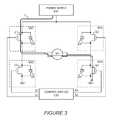
- FIG. 1is a circuit diagram of an H-bridge for an exemplary power module that is configured to drive a motor.
- FIG. 2illustrates a first current path in the H-bridge of FIG. 1 when driving the motor in a first direction.
- FIG. 3illustrates a second current path in the H-bridge of FIG. 1 when driving the motor in a second direction.
- FIG. 4is a circuit diagram of a switch module of the H-bridge of FIG. 1 .
- FIG. 5is a top plan view of a power module according to one embodiment.
- FIG. 6is an isometric view of the power module of FIG. 5 .
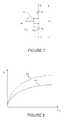
- FIG. 7is a circuit diagram of a metal-oxide-semiconductor field effect (MOSFET) device.
- MOSFETmetal-oxide-semiconductor field effect
- FIG. 8is a graph illustrating hypothetical on-state current-voltage characteristics for a MOSFET device.
- FIG. 9is a graph illustrating the effect of source resistance on gate voltage.
- FIG. 10is a partial cross sectional illustration of cell of a conventional power MOSFET device.
- FIGS. 11 and 12are plan views illustrating layouts of conventional power MOSFET devices.
- FIGS. 13 and 14are plan views illustrating layouts of power MOSFET devices according to some embodiments.
- FIGS. 15 and 16are partial cross sectional illustrations of a cell of a power MOSFET device according to some embodiments.
- FIG. 17is a graph on-state current-voltage characteristics for a MOSFET device according to some embodiments.
- FIG. 18is a cross sectional illustration of cell of a power MOSFET device according to some embodiments.
- FIG. 19is a cross sectional illustration of cell of an insulated gate bipolar transistor device according to some embodiments.
- FIG. 20is a cross sectional illustration of cell of a p-type insulated gate bipolar transistor device according to some embodiments.
- FIG. 21is a graph showing current-voltage characteristics of the P-IGBT device of FIG. 20 .
- FIG. 22Ais a graph showing voltage blocking characteristics of the p-IGBT of FIG. 20 .
- FIG. 22Bis a graph showing pulsed on-state current-voltage characteristics of the P-IGBT of FIG. 20 .
- FIG. 22Cis a graph showing further on-state current-voltage characteristics of the P-IGBTs of FIG. 20 for temperatures ranging from room temperature to 300° C.
- FIG. 22Dis a graph showing on-state current-voltage characteristics of the P-IGBTs of FIG. 22 as a function of temperature.
- Relative terms such as “below” or “above” or “upper” or “lower” or “horizontal” or “lateral” or “vertical”may be used herein to describe a relationship of one element, layer or region to another element, layer or region as illustrated in the figures. It will be understood that these terms are intended to encompass different orientations of the device in addition to the orientation depicted in the figures.
- Embodiments of the disclosureare described herein with reference to cross-section illustrations that are schematic illustrations of idealized embodiments (and intermediate structures) of the disclosure.
- the thickness of layers and regions in the drawingsmay be exaggerated for clarity. Additionally, variations from the shapes of the illustrations as a result, for example, of manufacturing techniques and/or tolerances, are to be expected.
- embodiments of the disclosureshould not be construed as limited to the particular shapes of regions illustrated herein but are to include deviations in shapes that result, for example, from manufacturing.
- an implanted region illustrated as a rectanglewill, typically, have rounded or curved features and/or a gradient of implant concentration at its edges rather than a discrete change from implanted to non-implanted region.
- a buried region formed by implantationmay result in some implantation in the region between the buried region and the surface through which the implantation takes place.
- the regions illustrated in the figuresare schematic in nature and their shapes are not intended to illustrate the actual shape of a region of a device and are not intended to limit the scope of the disclosure.
- n-type materialhas a majority equilibrium concentration of negatively charged electrons
- p-type materialhas a majority equilibrium concentration of positively charged holes.
- Some materialmay be designated with a “+” or “ ⁇ ” (as in n+, n ⁇ , p+, p ⁇ , n++, n ⁇ , p++, p ⁇ , or the like), to indicate a relatively larger (“+”) or smaller (“ ⁇ ”) concentration of majority carriers compared to another layer or region.
- ⁇concentration of majority carriers
- the power modulecan include four switch modules SM 1 -SM 4 , which are controlled by a control CS 1 to deliver power from a power supply PS 1 to a load in a controlled manner.
- the switch modules SM 1 and SM 2form a first half of an H-bridge, while switch modules SM 3 and SM 4 form a second half of the H-bridge.
- power modulesare often used to drive an inductive load, such as that provided by a direct current (DC) motor M 1 .
- DCdirect current
- the switch modules SM 1 -SM 4can include at least one transistor in parallel with an internal or external diode that is connected in anti-parallel with the transistor.
- the transistorsare illustrated as metal oxide field effect transistors (MOSFETs), and the diodes are illustrated as Schottky diodes for purposes of description.
- MOSFETsmay be replaced with other types of transistors, such as bipolar transistors, including insulated gate bipolar transistors (IGBTs), and various kinds of field effect transistors (FETs), such as junction field effect transistors (JFETs), and high electron mobility transistors (HEMTs).
- the Schottky diodesmay be replaced with traditional p-n diodes.
- switch module SM 1may include either an n-channel or p-channel MOSFET Q 1 that has a Schottky diode D 1 connected in anti-parallel across the drain and source terminals of the MOSFET Q 1 .
- Switch modules SM 2 -SM 4are similarly configured.
- Switch module SM 2includes an n-channel MOSFET Q 2 that has a Schottky diode D 2 connected in anti-parallel across the drain and source terminals of the MOSFET Q 2 .
- Switch module SM 3may include either an n-channel or p-channel MOSFET Q 3 that has a Schottky diode D 3 connected in anti-parallel across the drain and source terminals of the MOSFET Q 3 .
- Switch module SM 4includes an n-channel MOSFET Q 4 that has a Schottky diode D 4 connected in anti-parallel across the drain and source terminals of the MOSFET Q 4 .
- the switch modules SM 1 and SM 3are considered on the “high” side, and the switch modules SM 2 and SM 4 are considered on the “low” side of the power module.
- the drains of MOSFETs Q 1 and Q 3 and the cathodes of diodes D 1 and D 3are coupled together and to the power supply PS 1 .
- the source of MOSFET Q 1 , the anode of diode D 1 , the drain of MOSFET Q 2 , and the cathode of diode D 2are coupled together and to a first terminal of the motor M 1 .
- MOSFET Q 3The source of MOSFET Q 3 , the anode of diode D 3 , the drain of MOSFET Q 4 , and the cathode of diode D 4 are coupled together and to a second terminal of the motor M 1 . Finally, the sources of MOSFETs Q 2 and Q 4 and the anodes of diodes D 2 and D 4 are coupled to ground.
- the gates of MOSFETs Q 1 -Q 4are respectively driven by control signals S 1 -S 4 , which are provided by the control system CS 1 . Assume the motor M 1 may be driven in both forward and reverse directions.
- control signals S 1 -S 4are configured to turn on MOSFETs Q 2 and Q 3 and turn off MOSFETs Q 1 and Q 4 , which corresponds to driving the motor M 1 in a forward direction.
- a forward current i fflows from the power supply PS 1 through MOSFET Q 3 , the motor M 1 , and the MOSFET Q 2 to ground. If MOSFETs Q 2 and Q 3 stay on, the maximum forward current i f is provided and the motor M 1 will turn in the forward direction at a maximum speed, with maximum torque, or a combination thereof.
- one or both of the MOSFETs Q 2 and Q 3may be switched off and on at a duty cycle that corresponds to the speed or torque desired from the motor M 1 .
- the voltage supplied to the motor M 1is pulse width modulated, wherein the on-to-off switching ratio of the MOSFETs Q 2 and Q 3 dictates the average voltage presented to the Motor M 1 .
- the inductive nature of the motor M 1tries to keep the forward current i f constant, and as a result, averages the voltage presented to the motor M 1 to a level corresponding to the on-to-off switching ratio of the MOSFETs Q 2 AND Q 3 .
- the average voltage presented to the motor M 1dictates the forward current i f that is passed through the motor M 1 , and thus, controls the actual speed or torque of the motor M 1 .
- control signals S 1 -S 4are configured to turn on MOSFETs Q 1 and Q 4 and turn off MOSFETs Q 2 and Q 3 .
- a reverse current i rflows from the power supply PS 1 through MOSFET Q 1 , the motor M 1 , and the MOSFET Q 4 to ground. If MOSFETs Q 1 and Q 4 stay on, the maximum reverse current i r is provided and the motor M 1 will turn in the reverse direction at a maximum speed, with maximum torque, or a combination thereof.
- the term “reverse” when used as an adjective in the term “reverse current i r ,”merely refers to the direction of operation for the motor M 1 .
- the arrows provided in FIGS. 2 and 3respectively, indicate the direction of current flow for both the forward current i f and the reverse current i r .
- the various MOSFETs Q 1 -Q 4may be turned on and off at a relatively high frequency to provide pulse width modulated voltage to the motor M 1 for either forward or reverse operation as well as to switch from forward operation to reverse operation.
- a pair of MOSFETssuch as MOSFETs Q 2 and Q 3 transition from an on-state to an off-state during forward operation
- the forward current i fcontinues to flow through the motor M 1 after the MOSFETs Q 2 and Q 3 are turned off, due to the electromagnetic field that is present in the inductive windings of the motor M 1 .
- all of the MOSFETs Q 1 -Q 4are off, yet the forward current i f remains flowing through the motor M 1 .
- one or more of the Schottky diodes D 1 through D 4may become forward biased and provide a path for the forward current i f to flow to either ground or the power supply PS 1 .
- each of the MOSFETs Q 1 -Q 4may represent an array of effectively parallel transistors.
- each of the Schottky diodes D 1 -D 4may represent an array of effectively parallel diodes. This concept is represented in FIG. 4 where an exemplary embodiment of switch module SM 1 is illustrated. The other switch modules SM 2 -SM 3 may be similarly configured.
- switch module SM 1includes an array of MOSFETs Q 1 1 -Q 1 N , which are effectively coupled in parallel, such that the drains are all coupled together and to the power supply PS 1 ; the sources are all coupled together and to the motor M 1 and switch module SM 2 ; and the gates are coupled together and to the control system C 1 (control signal S 1 ).
- the Schottky diodes D 1 1 -D 1 Nare coupled in anti-parallel across the drain and sources of the MOSFETs Q 1 1 -Q 1 N .
- the number (N) of MOSFETs Q 1 1 -Q 1 N and Schottky diodes D 1 1 -D 1 Nmay range from two to more than 100, depending on the capability of each individual device and the application. Notably, there may be two or more Schottky diodes D 1 for each MOSFET Q 1 , even though there is only a one-to-one relationship in the illustration.
- FIGS. 5 and 6show top and perspective views of an exemplary power module.
- rectangular housing H 1is provided with an interior chamber that holds one or more printed circuit boards PCB 1 and PCB 2 .
- the printed circuit boards PCB 1 and PCB 2are not shown in FIG. 6 .
- Each printed circuit board PCB 1 and PCB 2is shown as having multiple transistors Q and diodes D that represent the primary components of the switch modules SW 1 -SW 4 .
- the high and low side of the first half-H bridge formed by switch modules SW 1 and SW 2are provided on printed circuit board PCB 1
- the high and low side of the second half-H bridge formed by switch modules SW 3 and SW 4are provided on printed circuit board PCB 2 .
- the first and second half-H bridgesform the above-described full-H bridge.
- the necessary interconnects between the components on the printed circuit boards PCB 1 and PCB 2are provided by metal traces (not shown) on the printed circuit boards PCB 1 and PCB 2 .
- Bond wiresmay be used to make connections between the printed circuit boards PCB 1 and PCB 2 and one more connectors or buses B 1 and B 2 .
- bus B 1may be used to connect switch modules SM 2 and SM 4 to ground
- bus B 2may be used to connect switch modules SM 1 and SM 3 to the power supply PS 1 .
- These or other connectorsmay be used for the control signals S 1 -S 4 .
- the printed circuit boards PCB 1 and PCB 2may be mounted to a mounting structure that is affixed to the housing H 1 . As illustrated, the mounting structure is a planar heat sink HS 1 that also functions to dissipate heat generated by the switch modules SM 1 -SM 4 .
- the H-bridge configuration of the power moduleis just one of many available designs for power modules, especially those used to drive inductive loads.
- Alternatives to the H-bridge configuration for the power moduleinclude a half-H bridge and like known power switching or control circuits.
- one metric for measuring the power handling capabilities of the deviceis current density of one of the switch modules SM 1 -SM 4 .
- This switch module current densityis defined as the ratio of the maximum average current that a single switch module SM 1 -SM 4 can handle to the interior area of the housing H 1 that is allocated to the single switch module SM 1 -SM 4 .
- the interior area of the housing H 1 that is allocated to a single switch module SM 1 -SM 4is one-fourth (1 ⁇ 4) the total interior area of the housing H 1 .
- the interior area of the housing H 1is 100 cm 2
- the maximum average current handling of one of the switch modules SM 1 -SM 4is 250 amperes.
- the interior area of the housing H 1 that is allocated to a single switch module SM 1 -SM 4is one-fourth of 100 cm 2 , or 25 cm 2 .
- the switch module current densityis calculated by dividing the maximum average current handling of 250 amperes by the interior area of the housing H 1 that is allocated to the single switch module SM 1 -SM 4 , which yields 10 amperes/cm 2 .
- the interior area of the housing H 1is defined as the maximum (two-dimensional) cross-sectional area of the interior of the housing H 1 wherein the plane of measurement is along the plane in which one or more printed circuit boards PCB 1 and PCB 2 or one or more semiconductor die that provide the switch modules SM 1 -SM 4 reside.
- the interior areais defined by the perimeter P of the inside wall of the housing H 1 .
- the perimeter Pis highlighted in bold.
- the housing H 1may have various shapes and configurations in addition to the rectangular configuration shown in FIGS. 5 and 6 , the interior areas need not be rectangular and the perimeter of the interior areas will follow the interior sidewalls of the housing H 1 .
- the switch module current densityis about 10 amperes/cm 2 or greater. In another embodiment, the switch module current density is about 12 amperes/cm 2 or greater. In another embodiment, the switch module current density is about 15 amperes/cm 2 or greater.
- MOSFETs Q 1 N -Q 4 NMOSFETs Q 1 N -Q 4 N or alternatives thereto.
- Other transistor configurationsmay be employed.
- Some embodiments of the disclosureprovide silicon carbide (SiC) insulated gate devices that are suitable for high power and/or high temperature applications.
- FIG. 7is a circuit diagram of a metal oxide semiconductor field effect transistor (MOSFET) device 10 .
- a MOSFET devicegenerally includes three terminals, namely, a drain terminal (D), a source terminal (S) and a gate terminal (G).
- the gate-to-source voltage of the deviceis denoted V GS
- the drain-to-source voltage of the deviceis denoted V DS .
- the devicehas a built in source resistance R S and a built-in drain resistance R D based on the physical characteristics of the device.
- the voltage over the built-in source resistance R Sis denoted V Rs .
- a MOSFET devicecurrent passing through a channel of the device from the drain to the source is regulated by applying a voltage to the gate.
- the gateis insulated from the channel by a gate insulator, such as silicon dioxide. As the voltage on the gate terminal is increased, current passing through the device may increase.
- FIG. 8is a graph illustrating hypothetical (curve 102 ) and actual ( 104 ) on-state current-voltage characteristics for a MOSFET device for a given gate-to-source voltage (V GS ).
- V GSgate-to-source voltage
- FIG. 9is a graph illustrating the effect of source resistance on gate voltage.
- V GSthe voltage from the gate terminal to the source terminal
- a portion of the gate voltage V GS applied to the device across the gate and source terminalsis dropped over the internal source resistance R S of the device. That portion of the gate voltage is denoted V Rs in FIG. 9 .
- the remainder of the gate-to-source voltageappears as a voltage across the gate insulator, denoted V GS,int in FIG. 9 .
- V GSis equal to the sum of V Rs and V GS,int .
- the gate-to-source voltagemay remain constant as the drain current increases.
- the portion of the gate voltage V GS that is dropped over the internal source resistance of the device, V Rsincreases as the drain current I D increases, while the portion of the gate-to-source voltage that appears as a voltage across the gate insulator, V GS, int , decreases as the drain current I D increases.
- the portion of the gate voltage that is being used to maintain the channeldecreases, which may cause the device to go into saturation at a lower level of drain-to-source voltage. Accordingly, a high source resistance can adversely affect the operation of a MOSFET or other insulated gate controlled device.
- FIG. 10A unit cell 10 of a MOSFET structure according to some embodiments is shown in FIG. 10 .
- the device 10 of FIG. 10includes an n ⁇ drift epitaxial layer 14 on an n-type, 8° off-axis 4H-SiC substrate 12 .
- the n ⁇ drift layer 14may have a thickness of about 100 ⁇ m to about 120 ⁇ m, and may be doped with n-type dopants at a doping concentration of about 2 ⁇ 10 14 cm ⁇ 3 to about 6 ⁇ 10 14 cm ⁇ 3 for a blocking capability of about 10 kV. Other doping concentrations/voltage blocking ranges are also possible.
- the substratemay be 4° off-axis 4H-SiC and the drift layer may have a thickness of about 10 ⁇ m and may be doped with n-type dopants at a doping concentration of about 6 ⁇ 10 15 cm ⁇ 3 .
- the structurefurther includes a p+ well region 18 and an n+ source region 20 that may be formed by selective implantation of, for example, aluminum and nitrogen, respectively.
- the junction depth of the p+ well region 18may be about 0.5 ⁇ m, although other depths are possible.
- the structure 10further includes a p+ contact region 22 that extends from a surface of the drift layer 14 into the p+ well region 18 .
- a junction termination(not shown) may be provided around the device periphery.
- All of the implanted dopantsmay be activated by annealing the structure at a temperature of about 1600° C. with a silicon over pressure and/or covered by an encapsulation layer such as a graphite film.
- a high temperature annealmay damage the surface of the silicon carbide epitaxy without these conditions.
- the silicon overpressuremay be provided by the presence of silane, or the close proximity of silicon carbide coated objects that provide a certain amount of silicon overpressure.
- a graphite coatingmay be formed on the surface of the device. Prior to annealing the device to activate the implanted ions, a graphite coating may be applied to the top/front side of the structure in order to protect the surface of the structure during the anneal.
- the graphite coatingmay be applied by a conventional resist coating method and may have a thickness of about 1 ⁇ m.
- the graphite coatingmay be heated to form a crystalline coating on the drift layer 14 .
- the implanted ionsmay be activated by a thermal anneal that may be performed, for example, in an inert gas at a temperature of about 1600° C. or greater. In particular the thermal anneal may be performed at a temperature of about 1600° C. in argon for 5 minutes.
- the graphite coatingmay help to protect the surface of the drift layer 14 during the high temperature anneal.
- the graphite coatingmay then be removed, for example, by ashing and thermal oxidation.
- a field oxide of silicon dioxide(not shown) having a thickness of about 1 ⁇ m may be deposited and patterned to expose the active region of the device.
- a gate oxide layer 36may be formed by a gate oxidation process, with a final gate oxide thickness of 400-600 ⁇ .
- the gate oxidemay be grown by a dry-wet oxidation process that includes a growth of bulk oxide in dry O 2 followed by an anneal of the bulk oxide in wet O 2 as described, for example, in U.S. Pat. No. 5,972,801, the disclosure of which is incorporated herein by reference in its entirety.
- anneal of oxide in wet O 2refers to anneal of an oxide in an ambient containing both O 2 and vaporized H 2 O.
- An annealmay be performed in between the dry oxide growth and the wet oxide growth.
- the dry O 2 oxide growthmay be performed, for example, in a quartz tube at a temperature of up to about 1200° C. in dry O 2 for a time of at least about 2.5 hours. Dry oxide growth is performed to grow the bulk oxide layer to a desired thickness.
- the temperature of the dry oxide growthmay affect the oxide growth rate. For example, higher process temperatures may produce higher oxide growth rates. The maximum growth temperature may be dependent on the system used.
- the dry O 2 oxide growthmay be performed at a temperature of about 1175° C. in dry O 2 for about 3.5 hours.
- the resulting oxide layermay be annealed at a temperature of up to about 1200° C. in an inert atmosphere.
- the resulting oxide layermay be annealed at a temperature of about 1175° C. in Ar for about 1 hour.
- the wet O 2 oxide annealmay be performed at a temperature of about 950° C. or less for a time of at least about 1 hour.
- the temperature of the wet O 2 annealmay be limited to discourage further thermal oxide growth at the SiC/SiO 2 interface, which may introduce additional interface states.
- the wet O 2 annealmay be performed in wet O 2 at a temperature of about 950° C. for about 3 hours.
- the resulting gate oxide layermay have a thickness of about 500 ⁇ .
- the dry O 2 oxide growthmay be performed at a temperature of about 1175° C. in dry O 2 for about 4 hours.
- the resulting oxide layermay be annealed at a temperature of up to about 1175° C. in an inert atmosphere.
- the resulting oxide layermay be annealed at a temperature of about 1175° C. in Ar for about a time duration ranging from 30 min to 2 hours.
- the oxide layerreceives an anneal in NO ambient at a temperature ranging from 1175° C. to 1300C, for a duration ranging from 30 minutes to 3 hours.
- the resulting gate oxide layermay have a thickness of about 500 ⁇ .
- a polysilicon gate 32may be deposited and doped, for example, with boron followed by a metallization process to reduce the gate resistance.
- Al/Ni contactsmay be deposited as the p-type ohmic source contact metal 28 , and Ni as the n-type drain contact metal 26 . All contacts may be sintered in a Rapid Thermal Annealer (RTA), and thick Ti/Au layers may be used for pad metals.
- RTARapid Thermal Annealer
- the source resistance of a MOSFET devicehas two primary components, namely, the contact resistance R C between the source ohmic contact 34 and the source region 20 , and the sheet resistance R sheet in the source region 20 between the source ohmic contact 34 and the channel.
- R SR C +R sheet .
- the sheet resistance R sheetis the dominant factor in determining the source resistance, because it is possible to form very low resistivity ohmic contacts to silicon and other narrow-bandgap semiconductors.
- the contact resistance R Cmay be the dominant contributor to the source resistance.
- FIGS. 11 and 12are plan views illustrating layouts of conventional power MOSFET devices.
- the layoutis designed to reduce or minimize sheet resistance under the assumption that contact resistance is less important than sheet resistance.
- a conventional power MOSFET devicetypically includes a p-well 18 formed in a drift layer 14 , an n+ source region 20 in the p-well 18 , and a p+ contact region 22 in the n+ source region 20 .
- a source contact 34is formed on the n+ source region 20 and the p+ contact region 22 .
- a gate 32is formed over the p-well 18 and overlaps the periphery of the n+ source region 20 and adjacent portions of the drift layer 14 . Current flow from the drain to the source is indicated by the arrows 42 in FIG. 11 .
- the source resistancemay be more affected by the contact resistance of the source ohmic contact than by the sheet resistance of the source layer. Accordingly, to decrease the source resistance of a wide bandgap power semiconductor device, it may be desirable to decrease the contact resistance of the source ohmic contact.
- contact resistancecan be decreased by increasing the minimum dimension of the contact, which is the smallest dimension of the contact in any direction.
- simply increasing the minimum dimension of the source ohmic contact of an electronic devicecan undesirably increase the cell to cell spacing, or pitch, of the device.
- the pitch of a MOSFET devicemay be proportional to the width of the p-well region of the device. Increasing the pitch of the device reduces the density of the devices that can be formed on a single substrate, reducing the devices yielded and increasing manufacturing costs.
- an insulated gate device layoutis provided that increases the minimum dimension of the source ohmic contact without increasing the pitch of the device and/or the width of the p-well region of the device.
- a device layout according to some embodimentsmay increase the sheet resistance of the device. Such an effect may be highly undesirable in a device based on a narrow bandgap semiconductor material. However, since sheet resistance is not the dominant factor in determining source resistance of a wide bandgap device, such a tradeoff may be acceptable for wide bandgap devices.
- a ratio of the source sheet resistance to the source contact resistancemay be greater than 0.75 (i.e. R sheet /R C >0.75).
- the devicemay have a source contact resistance that is less than the source sheet resistance. That is, in some embodiments, the ratio of the source sheet resistance to the source contact resistance may be greater than 1 (i.e. R sheet /R C >1), and in further embodiments, the ratio of the source sheet resistance to the source contact resistance may be greater than 5.
- FIGS. 13 and 14are plan views illustrating layouts of MOSFET device cells 100 according to some embodiments
- FIGS. 15 and 16are partial cross sectional illustrations of a cell of a MOSFET device according to some embodiments.
- FIG. 15is a cross section taken along line A-A′ of FIG. 13
- FIG. 16is a cross section taken along line B-B′ of FIG. 14 .
- the device 100 shown in FIGS. 13-16includes an n ⁇ drift epitaxial layer 114 on an n-type, 8° off-axis 4H-SiC substrate 112 .
- the n ⁇ drift layer 114may have a thickness of about 100 ⁇ m to about 120 ⁇ m, and may be doped with n-type dopants at a doping concentration of about 2 ⁇ 10 14 cm ⁇ 3 to about 6 ⁇ 10 14 cm ⁇ 3 for a blocking capability of about 10 kV.
- the substratemay be 4° off-axis 4H-SiC and the drift layer may have a thickness of about 10 ⁇ m and may be doped with n-type dopants at a doping concentration of about 6 ⁇ 10 15 cm ⁇ 3 .
- the structurefurther includes a p+ well region 118 and an n+ source region 120 that may be formed by selective implantation of, for example, aluminum and nitrogen, respectively.
- the junction depth of the p+ well region 118may be about 0.5 ⁇ m.
- the structure 100further includes a plurality of p+ contact regions 122 that extend from a surface of the drift layer 114 into the p+ well region 118 .
- a junction termination(not shown) may be provided around the device periphery.
- the n+ source region 120includes a pair of lateral source regions 120 A that are parallel to opposing channel regions 125 in the p-well 118 .
- a plurality of source contact regions 120 Bextend between the lateral source regions 120 A, and the plurality of p+ contact regions 122 are provided between the source contact regions 120 B.
- gate contacts 132are formed over the channel regions 125 and overlap the lateral source regions 120 A.
- a source ohmic contact 134is formed across the source contact regions 120 B and the p+ contact regions 122 .
- the source ohmic contact 134overlaps the source contact regions 120 B in a source contact region 136 .
- the source ohmic contact 134overlaps the p+ contact regions 122 in a body contact region 138 .
- the portion of the source contact regions 120 B contacted by the source ohmic contact 134may have a minimum dimension that is larger than the minimum dimension that can be obtained for a conventional layout such as the layout shown in FIGS. 11 and 12 for a similar pitch/p-well size. Accordingly, the source contact resistance may be reduced without substantially increasing the device pitch/p-well size.
- the “minimum dimension” of a featurerefers to the smallest width of the feature in any cross section of the feature. For example, the minimum dimension p 1 of the body contact region 138 , the minimum dimension n 1 of the n-type contact region 136 and the minimum dimension w 1 of the p-well region 118 are shown in FIG. 14 .
- the source contact regions 120 Bmay have an increased sheet resistance compared to the source region of a device having a conventional layout as shown in FIGS. 11 and 12 .
- the increase in sheet resistancemay be more than compensated by the decrease in contact resistance, thus providing an overall decrease in the source resistance of the device.
- FIG. 17is a graph of on-state current-voltage characteristics for a 7 mm ⁇ 8 mm 1200 V silicon carbide MOSFET device according to some embodiments.
- a drain current (I D ) of 377 Awas measured at a forward voltage drain-to-source voltage (V DS ) of 3.8 V.
- the current density, normalized to the active area,was over 750 A/cm 2 .
- the on-resistance of a MOSFET deviceis affected by the drain resistance, the channel resistance and the source resistance of the device. Accordingly, reducing the source resistance of the device also reduces the on-resistance of the device.
- a wide bandgap MOSFET device having a layout according to some embodimentsmay be capable of substantially increased saturation current due to the lower on-resistance of the device and the fact that increased current levels have less of a de-biasing effect on the gate. That is, because of the lower source resistance, less voltage will be developed over the source resistance as the drain current increases. Thus, more of the gate-to-source voltage is applied to the channel of the device.
- FIG. 18is an idealized cross section of a device having a layout in accordance with some embodiments.
- FIG. 18illustrates some dimensions of a device having a layout in accordance with some embodiments.
- the minimum dimension of the implanted cell areai.e. the p-well 118
- width w 1the minimum dimension of the implanted cell area
- the minimum dimension of the p-well 118may occur in a dimension that is different from the plane of the device illustrated in FIG. 18 .
- the minimum dimension of the p-well 118may occur in a dimension that is perpendicular to the plane of the device illustrated in FIG. 18 .
- the minimum dimension of the n-type contact areais denoted as width n 1 in FIG. 18
- the minimum dimension of the p-type contact areais denoted as width p 1 in FIG. 18
- the n-type contact areamay be defined as the area of overlap between the source ohmic contact 132 and the n+ source region 120
- the p-type contact areamay be defined as the area of overlap between the source ohmic contact 132 and the p+ contact regions 122 .
- the IGBT deviceincludes an n ⁇ drift epitaxial layer 214 on a p-type epitaxial layer 212 .
- the p-type epitaxial layer 212is formed on a heavily doped p-type, 8° off-axis 4H-SiC substrate or layer 210 .
- the n ⁇ drift layer 214may have a thickness of about 100 ⁇ m to about 120 ⁇ m, and may be doped with p-type dopants at a doping concentration of about 2 ⁇ 10 14 cm ⁇ 3 to about 6 ⁇ 10 14 cm ⁇ 3 for a blocking capability of about 10 kV.
- the IGBT structure 200further includes a p+ well region 218 and an n+ source/emitter region 220 that may be formed by selective implantation of, for example, aluminum and nitrogen, respectively.
- the junction depth of the p+ well region 218may be about 0.5 ⁇ m.
- the structure 200further includes a plurality of p+ body contact regions 222 that extend from a surface of the drift layer 214 into the p+ well region 218 .
- the conductivity typesmay be reversed in some embodiments.
- a gate contact 232is on a gate insulator 236
- a source/emitter contact 234is on the source contact regions 220 and the body contact regions 222 .
- a collector contact 226contacts the substrate 210 .
- a transistor devicemay have a ratio of n 1 to w 1 that is greater than 0.2. In further embodiments, a transistor device may have a ratio of n 1 to w 1 that is greater than about 0.3. In further embodiments, a transistor device may have a ratio of n 1 to w 1 that is in the range of about 0.2 to 1. In further embodiments, a transistor device may have a ratio of n 1 to w 1 that is in the range of about 0.3 to 1. In further embodiments, transistor device may have a ratio of n 1 to w 1 that is greater than 0.5. For example, the minimum dimension n 1 of the n-type contact area of a device having a layout according to some embodiments may be about 2 ⁇ m for a device having a minimum dimension of the implanted cell area of 6 ⁇ m.
- a transistor devicemay have a ratio of p 1 to w 1 that is greater than 0.2. In further embodiments, a transistor device may have a ratio of p 1 to w 1 that is greater than about 0.3. In further embodiments, a transistor device may have a ratio of p 1 to w 1 that is greater than about 0.5. In further embodiments, a transistor device may have a ratio of p 1 to w 1 that is in the range of about 0.2 to 0.5. In further embodiments, a transistor device may have a ratio of p 1 to w 1 that is in the range of about 0.2 to 1.
- Some embodimentsprovide transistor devices having increased current densities.
- Current densityis defined as the total current divided by the area of the chip.
- a wide bandgap transistor devicemay be capable of current densities in excess of 200 A/cm 2 and a blocking voltage of 1000 V or more.
- a wide bandgap transistor devicemay be capable of a current of 100 A or greater at current densities in excess of 200 A/cm 2 , a forward voltage drop of less than 5 V and a blocking voltage of 1000 V or more.
- a wide bandgap transistor device according to still further embodimentsmay be capable of a current of 100 A or greater at current densities in excess of 300 A/cm 2 , a forward voltage drop of less than 5 V and a blocking voltage of 1000 V or more.
- a semiconductor devicehas a reverse blocking voltage in excess of 1000 volts and a current density greater than 200 amps per square centimeter at a current greater than 100 A.
- a semiconductor devicehas a reverse blocking voltage of 1000 volts or more and a forward current capability greater than 100 A at a forward voltage of 5 volts or less.
- a metal-oxide semiconductor field effect transistor devicehas a reverse blocking voltage of 1200 volts or more and a forward current capability greater than 100 A.
- a metal-oxide semiconductor field effect transistor devicehas a reverse blocking voltage of 1000 volts or more and a differential on-resistance less than 8 mOhms-cm 2 .
- a semiconductor devicehaving a blocking voltage less than 1000 V and configured to pass forward current at a current density greater than 200 amps per square centimeter at a forward voltage drop of 5 V or less.
- Some embodimentsmay enable wide bandgap transistor devices to achieve drain currents of 100 Amps or higher at a drain to source voltage that is less than 4 Volts in a device having a cell pitch of less than 20 ⁇ m. Some embodiments may enable wide bandgap transistor devices to achieve drain currents of 100 Amps or higher at a drain to source voltage that is less than 4 Volts in a device having a cell pitch of less than 10 ⁇ m. Some embodiments may enable wide bandgap transistor devices to achieve drain currents of 80 Amps or higher at a drain to source voltage that is less than 5 Volts in a device having a cell pitch of less than 10 ⁇ m.
- An IGBT devicewith a voltage blocking capability of 10 kV or greater may have a differential specific on-resistance of less than 14 mOhm-cm 2 with a forward voltage drop of 5.2 V or less at a current density of 100 A/cm 2 .
- a p-type insulated gate bipolar transistor (p-IGBT) device 300is illustrated in FIG. 20 .
- the IGBT deviceincludes a p ⁇ drift epitaxial layer 314 on a p-type field stop buffer layer 311 formed on an n-type, 8° off-axis 4H-SiC substrate 310 .
- the p ⁇ drift layer 314may have a thickness of about 100 ⁇ m to about 200 ⁇ m, and may be doped with p-type dopants at a doping concentration of about 2 ⁇ 10 14 cm ⁇ 3 to about 6 ⁇ 10 14 cm ⁇ 3 .
- the p-IGBT structure 300further includes an n+ well region 318 and a p+ source/emitter region 320 that may be formed by selective implantation of, for example, nitrogen and aluminum, respectively.
- the junction depth of the n+ well region 318may be about 0.5 ⁇ m.
- the structure 300further includes a plurality of n+ body contact regions 322 that extend from a surface of the drift layer 314 into the n+ well region 318 .
- a gate contact 332is on a gate insulator 336
- a source/emitter contact 334is on the source contact regions 320 and the body contact regions 322 .
- a collector contact 326contacts the substrate 310 .
- a 4H-SiC p-IGBT as shown in FIG. 20was fabricated using a 2 ⁇ 10 14 cm ⁇ 3 doped, 140 ⁇ m thick p-type epilayer as the drift layer 314 , and a 2 ⁇ m thick p-type Field-Stop buffer layer 311 , with a doping concentration ranging from 1 ⁇ 10 17 cm ⁇ 3 to 5 ⁇ 10 17 cm ⁇ 3 .
- a multi-zone JTE (15 zone) edge termination structure(not shown) was formed by nitrogen ion implantation. JTE terminations are described, for example, in U.S. Pat. No. 6,002,159, which is incorporated herein by reference.
- MOS channelswere formed on implanted n-wells 318 .
- a 50 nm thick thermally grown oxide layerwas used as the gate insulator 336 .
- FIG. 21shows the I D -V GS characteristics of the p-IGBT device shown in FIG. 20 , with V DS fixed at ⁇ 50 mV.
- the I D -V GS characteristicswere measured from a test MOSFET with a W/L of 200 ⁇ m/200 ⁇ m, fabricated on the same wafer.
- a threshold voltage of ⁇ 10 V, and a peak MOS channel mobility of 10 cm 2 /Vswere extracted from the I D -V GS characteristics.
- the measurement voltagewas limited to ⁇ 15 kV, due to the limitation of probing equipment.
- the deviceshowed a leakage current of 0.6 ⁇ A, which corresponds to a leakage current density of 1.2 ⁇ A/cm 2 at a V CE of ⁇ 15 kV. This is the highest blocking voltage ever reported in SiC power switches.
- FIG. 22Bshows the pulsed on-state I-V characteristics of the p-IGBT, measured using a Tektronix 371 curve tracer.
- FIG. 22Cshows I C -V GE characteristics of the 4H-SiC P-IGBTs for temperatures ranging from room temperature to 300° C.
- V CEwas fixed at ⁇ 10V for this measurement.
- the I-V characteristicsshifted towards zero at elevated temperature.
- the devicemaintained normally-off properties throughout the temperature range.
- FIG. 22Dshows the on-state I-V characteristics as a function of temperature. V GE was fixed at ⁇ 20 V for this measurement. A monotonic decrease in forward voltage drop with increasing temperature was observed. This is believed due to the increase in minority carrier (electron) diffusion length, caused by increased carrier lifetime at elevated temperatures.
- a p-IGBTmay have a reverse blocking voltage that is greater than about 10 kV, and in some cases greater than about 13 kV, and that has a forward current capability greater than 5 Amps.
- IGBT and MOSFET devices having n-type drift layersthe present disclosure is not limited thereto, and may be embodied in devices having p-type substrates and/or drift layers. Furthermore, the disclosure may be used in many different types of devices, including but not limited to insulated gate bipolar transistors (IGBTs), MOS controlled thyristors (MCTs), insulated gate commutated thyristors (IGCTs), junction field effect transistors (JFETs), high electron mobility transistors (HEMTs), etc.
- IGBTsinsulated gate bipolar transistors
- MCTsMOS controlled thyristors
- IGCTsinsulated gate commutated thyristors
- JFETsjunction field effect transistors
- HEMTshigh electron mobility transistors
Landscapes
- Engineering & Computer Science (AREA)
- Microelectronics & Electronic Packaging (AREA)
- Power Engineering (AREA)
- Physics & Mathematics (AREA)
- Condensed Matter Physics & Semiconductors (AREA)
- General Physics & Mathematics (AREA)
- Computer Hardware Design (AREA)
- Manufacturing & Machinery (AREA)
- Crystallography & Structural Chemistry (AREA)
- Chemical & Material Sciences (AREA)
- Inverter Devices (AREA)
- Electrodes Of Semiconductors (AREA)
- Metal-Oxide And Bipolar Metal-Oxide Semiconductor Integrated Circuits (AREA)
Abstract
Description
This application is a continuation of U.S. patent application Ser. No. 13/588,329 filed on Aug. 17, 2012, now U.S. Pat. No. 9,673,283, which claims the benefit of U.S. provisional patent application No. 61/533,254 filed Sep. 11, 2011, the disclosures of which are incorporated herein by reference in their entireties. The present application is a continuation of U.S. patent application Ser. No. 13/588,329 filed on Aug. 17, 2012, which is related to U.S. Pat. No. 9,142,662 issued on Sep. 22, 2015, which is a continuation in part of U.S. Pat. No. 9,029,945 issued on May 12, 2015. The present application is related to U.S. Pat. No. 9,142,662 issued on Sep. 22, 2015, which is a continuation in part of U.S. Pat. No. 9,029,945 issued on May 12, 2015, the disclosures of which are incorporated herein by reference in their entireties.
The present disclosure relates to electronic devices and in particular to power modules.
Power devices made with silicon carbide (SiC) are expected to show great advantages as compared to those on silicon for high speed, high power and/or high temperature applications due to the high critical field and wide band gap of SiC. For devices capable of blocking high voltages, such as voltages in excess of about 5 kV, it may be desirable to have bipolar operation to reduce the drift layer resistance via conductivity modulation resulting from injected minority carriers. However, one technical challenge for bipolar devices in silicon carbide is forward voltage degradation over time, possibly due to the presence of Basal Plane Dislocations (BPD) in single crystals of silicon carbide. Thus, unipolar devices such as SiC Schottky diodes and MOSFETs are typically used for high power applications, e.g., up to 10kV or more.
SiC DMOSFET devices with a 10 kV blocking capability have been fabricated with a specific on-resistance of about 100 mΩ×cm2. DMOSFET devices may exhibit very fast switching speeds of, for example, less than 100 ns, due to their majority carrier nature. However, as the desired blocking voltage of devices increases, for example up to 15 kV or more, the on-resistance of a MOSFET device may increase substantially, due to the corresponding increase in the drift layer thickness. This problem may be exacerbated at high temperatures due to bulk mobility reduction, which may result in excessive power dissipation.
With the progress of SiC crystal material growth, several approaches have been developed to mitigate BPD related problems. See, e.g., B. Hull, M. Das, J. Sumakeris, J. Richmond, and S. Krishinaswami, “Drift-Free 10-kV, 20-A 4H-SiC PiN Diodes”, Journal of Electrical Materials, Vol. 34, No. 4, 2005, which is incorporated herein by reference in its entirety. These developments may enhance the development and/or potential applications of SiC bipolar devices such as thyristors, GTOs, etc. Even though thyristors and/or GTOs may offer low forward voltage drops, they may require bulky commutating circuits for the gate drive and protections. Accordingly, it may be desirable for a SiC bipolar device to have gate turn-off capability. Due to their superior on-state characteristics, reasonable switching speed, and/or excellent safe-operation-area (SOA), 4H-SiC insulated gate bipolar transistors (IGBTs) are becoming more suitable for power switching applications.
These devices are used in power modules, which operate to dynamically control large amounts of power through switching for motors, inverters, generators, and the like. There is a continuing need for power modules that are smaller and less expensive to manufacture while at the same time being capable of controlling larger loads.
A power module is disclosed that supports high current densities. The power module includes a housing with an interior chamber wherein multiple switch modules are mounted within the interior chamber. The switch modules comprise multiple transistors and diodes that are interconnected to facilitate switching power to a load. In one embodiment, at least one of the switch modules supports a current density of at least 10 amperes per cm2.
In other embodiments, at least one transistor in a switch module includes a drift layer having a first conductivity type, a well region in the drift layer having a second conductivity type opposite the first conductivity type, and a source region in the well region. The source region has the first conductivity type and defines a channel region in the well region. The source region includes a lateral source region adjacent the channel region and a plurality of source contact regions extending away from the lateral source region opposite the channel region. A body contact region having the second conductivity type is between at least two of the plurality of source contact regions and is in contact with the well region, and a source ohmic contact is in contact with the source contact regions and the body contact region.
The body contact region may include a plurality of body contact regions that are interspersed between the source contact regions. The plurality of body contact regions may be spaced apart from the channel region by the lateral source region.
The source ohmic contact may be in contact with the source region in a source contact area and the source ohmic contact may be in contact with the body contact region in a body contact region area.
In some embodiments, a ratio of a minimum dimension p1 of the contact region area to a minimum dimension w1 of the well region may be greater than 0.2. In further embodiments, the ratio of the minimum dimension p1 of the contact region area to the minimum dimension w1 of the well region may be greater than about 0.3.
The drift region may include a wide bandgap semiconductor material, such as silicon carbide.
The source region has a sheet resistance and the source ohmic contact has a sheet resistance that is greater than 75% of the contact resistance of the source region, and in some embodiments is greater than the contact resistance of the source region.
The transistor may have a reverse blocking voltage in excess of 1000 volts and a current density greater than 200 amps per square centimeter.
The accompanying drawings, which are included to provide a further understanding of the disclosure and are incorporated in and constitute a part of this application, illustrate certain embodiment(s) of the disclosure. In the drawings:
Embodiments of the present disclosure now will be described more fully hereinafter with reference to the accompanying drawings, in which embodiments of the disclosure are shown. This disclosure may, however, be embodied in many different forms and should not be construed as limited to the embodiments set forth herein. Rather, these embodiments are provided so that this disclosure will be thorough and complete, and will fully convey the scope of the disclosure to those skilled in the art. Like numbers refer to like elements throughout.
It will be understood that, although the terms first, second, etc. may be used herein to describe various elements, these elements should not be limited by these terms. These terms are only used to distinguish one element from another. For example, a first element could be termed a second element, and, similarly, a second element could be termed a first element, without departing from the scope of the present disclosure. As used herein, the term “and/or” includes any and all combinations of one or more of the associated listed items.
The terminology used herein is for the purpose of describing particular embodiments only and is not intended to be limiting of the disclosure. As used herein, the singular forms “a”, “an” and “the” are intended to include the plural forms as well, unless the context clearly indicates otherwise. It will be further understood that the terms “comprises” “comprising,” “includes” and/or “including” when used herein, specify the presence of stated features, integers, steps, operations, elements, and/or components, but do not preclude the presence or addition of one or more other features, integers, steps, operations, elements, components, and/or groups thereof.
Unless otherwise defined, all terms (including technical and scientific terms) used herein have the same meaning as commonly understood by one of ordinary skill in the art to which this disclosure belongs. It will be further understood that terms used herein should be interpreted as having a meaning that is consistent with their meaning in the context of this specification and the relevant art and will not be interpreted in an idealized or overly formal sense unless expressly so defined herein.
It will be understood that when an element such as a layer, region or substrate is referred to as being “on” or extending “onto” another element, it can be directly on or extend directly onto the other element or intervening elements may also be present. In contrast, when an element is referred to as being “directly on” or extending “directly onto” another element, there are no intervening elements present. It will also be understood that when an element is referred to as being “connected” or “coupled” to another element, it can be directly connected or coupled to the other element or intervening elements may be present. In contrast, when an element is referred to as being “directly connected” or “directly coupled” to another element, there are no intervening elements present.
Relative terms such as “below” or “above” or “upper” or “lower” or “horizontal” or “lateral” or “vertical” may be used herein to describe a relationship of one element, layer or region to another element, layer or region as illustrated in the figures. It will be understood that these terms are intended to encompass different orientations of the device in addition to the orientation depicted in the figures.
Embodiments of the disclosure are described herein with reference to cross-section illustrations that are schematic illustrations of idealized embodiments (and intermediate structures) of the disclosure. The thickness of layers and regions in the drawings may be exaggerated for clarity. Additionally, variations from the shapes of the illustrations as a result, for example, of manufacturing techniques and/or tolerances, are to be expected. Thus, embodiments of the disclosure should not be construed as limited to the particular shapes of regions illustrated herein but are to include deviations in shapes that result, for example, from manufacturing. For example, an implanted region illustrated as a rectangle will, typically, have rounded or curved features and/or a gradient of implant concentration at its edges rather than a discrete change from implanted to non-implanted region. Likewise, a buried region formed by implantation may result in some implantation in the region between the buried region and the surface through which the implantation takes place. Thus, the regions illustrated in the figures are schematic in nature and their shapes are not intended to illustrate the actual shape of a region of a device and are not intended to limit the scope of the disclosure.
Some embodiments of the disclosure are described with reference to semiconductor layers and/or regions which are characterized as having a conductivity type such as n-type or p-type, which refers to the majority carrier concentration in the layer and/or region. Thus, n-type material has a majority equilibrium concentration of negatively charged electrons, while p-type material has a majority equilibrium concentration of positively charged holes. Some material may be designated with a “+” or “−” (as in n+, n−, p+, p−, n++, n−−, p++, p−−, or the like), to indicate a relatively larger (“+”) or smaller (“−”) concentration of majority carriers compared to another layer or region. However, such notation does not imply the existence of a particular concentration of majority or minority carriers in a layer or region.
An exemplary system that employs a power module is illustrated inFIG. 1 . As depicted, the power module can include four switch modules SM1-SM4, which are controlled by a control CS1 to deliver power from a power supply PS1 to a load in a controlled manner. The switch modules SM1 and SM2 form a first half of an H-bridge, while switch modules SM3 and SM4 form a second half of the H-bridge. As noted, power modules are often used to drive an inductive load, such as that provided by a direct current (DC) motor M1. The details of the switch modules SM1-SM4 are described in further detail below.
For now, assume the switch modules SM1-SM4 can include at least one transistor in parallel with an internal or external diode that is connected in anti-parallel with the transistor. The transistors are illustrated as metal oxide field effect transistors (MOSFETs), and the diodes are illustrated as Schottky diodes for purposes of description. The MOSFETs may be replaced with other types of transistors, such as bipolar transistors, including insulated gate bipolar transistors (IGBTs), and various kinds of field effect transistors (FETs), such as junction field effect transistors (JFETs), and high electron mobility transistors (HEMTs). Similarly, the Schottky diodes may be replaced with traditional p-n diodes.
As illustrated, switch module SM1 may include either an n-channel or p-channel MOSFET Q1 that has a Schottky diode D1 connected in anti-parallel across the drain and source terminals of the MOSFET Q1. Switch modules SM2-SM4 are similarly configured. Switch module SM2 includes an n-channel MOSFET Q2 that has a Schottky diode D2 connected in anti-parallel across the drain and source terminals of the MOSFET Q2. Switch module SM3 may include either an n-channel or p-channel MOSFET Q3 that has a Schottky diode D3 connected in anti-parallel across the drain and source terminals of the MOSFET Q3. Switch module SM4 includes an n-channel MOSFET Q4 that has a Schottky diode D4 connected in anti-parallel across the drain and source terminals of the MOSFET Q4.
The switch modules SM1 and SM3 are considered on the “high” side, and the switch modules SM2 and SM4 are considered on the “low” side of the power module. The drains of MOSFETs Q1 and Q3 and the cathodes of diodes D1 and D3 are coupled together and to the power supply PS1. The source of MOSFET Q1, the anode of diode D1, the drain of MOSFET Q2, and the cathode of diode D2 are coupled together and to a first terminal of the motor M1. The source of MOSFET Q3, the anode of diode D3, the drain of MOSFET Q4, and the cathode of diode D4 are coupled together and to a second terminal of the motor M1. Finally, the sources of MOSFETs Q2 and Q4 and the anodes of diodes D2 and D4 are coupled to ground. The gates of MOSFETs Q1-Q4 are respectively driven by control signals S1-S4, which are provided by the control system CS1. Assume the motor M1 may be driven in both forward and reverse directions.
For forward operation, assume control signals S1-S4 are configured to turn on MOSFETs Q2 and Q3 and turn off MOSFETs Q1 and Q4, which corresponds to driving the motor M1 in a forward direction. As illustrated inFIG. 2 , a forward current ifflows from the power supply PS1 through MOSFET Q3, the motor M1, and the MOSFET Q2 to ground. If MOSFETs Q2 and Q3 stay on, the maximum forward current ifis provided and the motor M1 will turn in the forward direction at a maximum speed, with maximum torque, or a combination thereof.
To control the speed or torque, one or both of the MOSFETs Q2 and Q3 may be switched off and on at a duty cycle that corresponds to the speed or torque desired from the motor M1. As a result, the voltage supplied to the motor M1 is pulse width modulated, wherein the on-to-off switching ratio of the MOSFETs Q2 and Q3 dictates the average voltage presented to the Motor M1. The inductive nature of the motor M1 tries to keep the forward current ifconstant, and as a result, averages the voltage presented to the motor M1 to a level corresponding to the on-to-off switching ratio of the MOSFETs Q2 AND Q3. The average voltage presented to the motor M1 dictates the forward current ifthat is passed through the motor M1, and thus, controls the actual speed or torque of the motor M1.
For reverse operation, assume control signals S1-S4 are configured to turn on MOSFETs Q1 and Q4 and turn off MOSFETs Q2 and Q3. As illustrated inFIG. 3 , a reverse current irflows from the power supply PS1 through MOSFET Q1, the motor M1, and the MOSFET Q4 to ground. If MOSFETs Q1 and Q4 stay on, the maximum reverse current iris provided and the motor M1 will turn in the reverse direction at a maximum speed, with maximum torque, or a combination thereof. Notably, the term “reverse” when used as an adjective in the term “reverse current ir,” merely refers to the direction of operation for the motor M1. The arrows provided inFIGS. 2 and 3 , respectively, indicate the direction of current flow for both the forward current ifand the reverse current ir.
As described above, the various MOSFETs Q1-Q4 may be turned on and off at a relatively high frequency to provide pulse width modulated voltage to the motor M1 for either forward or reverse operation as well as to switch from forward operation to reverse operation. When a pair of MOSFETs, such as MOSFETs Q2 and Q3 transition from an on-state to an off-state during forward operation, the forward current ifcontinues to flow through the motor M1 after the MOSFETs Q2 and Q3 are turned off, due to the electromagnetic field that is present in the inductive windings of the motor M1. At this point, all of the MOSFETs Q1-Q4 are off, yet the forward current ifremains flowing through the motor M1. Since the forward current ifcannot flow through any of the MOSFETS Q1-Q4 to a lower potential node, one or more of the Schottky diodes D1 through D4 may become forward biased and provide a path for the forward current ifto flow to either ground or the power supply PS1.
To increase the power handling of a switch module SM1-SM4, each of the MOSFETs Q1-Q4 may represent an array of effectively parallel transistors. Similarly, each of the Schottky diodes D1-D4 may represent an array of effectively parallel diodes. This concept is represented inFIG. 4 where an exemplary embodiment of switch module SM1 is illustrated. The other switch modules SM2-SM3 may be similarly configured.
As illustrated, switch module SM1 includes an array of MOSFETs Q11-Q1N, which are effectively coupled in parallel, such that the drains are all coupled together and to the power supply PS1; the sources are all coupled together and to the motor M1 and switch module SM2; and the gates are coupled together and to the control system C1 (control signal S1). The Schottky diodes D11-D1Nare coupled in anti-parallel across the drain and sources of the MOSFETs Q11-Q1N. The number (N) of MOSFETs Q11-Q1Nand Schottky diodes D11-D1Nmay range from two to more than 100, depending on the capability of each individual device and the application. Notably, there may be two or more Schottky diodes D1 for each MOSFET Q1, even though there is only a one-to-one relationship in the illustration.
The necessary interconnects between the components on the printed circuit boards PCB1 and PCB2 are provided by metal traces (not shown) on the printed circuit boards PCB1 and PCB2. Bond wires may be used to make connections between the printed circuit boards PCB1 and PCB2 and one more connectors or buses B1 and B2. For example, bus B1 may be used to connect switch modules SM2 and SM4 to ground, and bus B2 may be used to connect switch modules SM1 and SM3 to the power supply PS1. These or other connectors may be used for the control signals S1-S4. The printed circuit boards PCB1 and PCB2 may be mounted to a mounting structure that is affixed to the housing H1. As illustrated, the mounting structure is a planar heat sink HS1 that also functions to dissipate heat generated by the switch modules SM1-SM4.
Again, the H-bridge configuration of the power module is just one of many available designs for power modules, especially those used to drive inductive loads. Alternatives to the H-bridge configuration for the power module include a half-H bridge and like known power switching or control circuits.
Regardless of the type of configuration of the power module, one metric for measuring the power handling capabilities of the device is current density of one of the switch modules SM1-SM4. This switch module current density is defined as the ratio of the maximum average current that a single switch module SM1-SM4 can handle to the interior area of the housing H1 that is allocated to the single switch module SM1-SM4. For the illustrated example, there are four switch modules SM1-SM4 of equal size. As such, the interior area of the housing H1 that is allocated to a single switch module SM1-SM4 is one-fourth (¼) the total interior area of the housing H1.
For example, assume the interior area of the housing H1 is 100 cm2, and the maximum average current handling of one of the switch modules SM1-SM4 is 250 amperes. As such, the interior area of the housing H1 that is allocated to a single switch module SM1-SM4 is one-fourth of 100 cm2, or 25 cm2. The switch module current density is calculated by dividing the maximum average current handling of 250 amperes by the interior area of the housing H1 that is allocated to the single switch module SM1-SM4, which yields 10 amperes/cm2.
The interior area of the housing H1 is defined as the maximum (two-dimensional) cross-sectional area of the interior of the housing H1 wherein the plane of measurement is along the plane in which one or more printed circuit boards PCB1 and PCB2 or one or more semiconductor die that provide the switch modules SM1-SM4 reside. For the illustrated example inFIG. 5 , the interior area is defined by the perimeter P of the inside wall of the housing H1. The perimeter P is highlighted in bold. Notably, since the housing H1 may have various shapes and configurations in addition to the rectangular configuration shown inFIGS. 5 and 6 , the interior areas need not be rectangular and the perimeter of the interior areas will follow the interior sidewalls of the housing H1. In one embodiment, the switch module current density is about 10 amperes/cm2or greater. In another embodiment, the switch module current density is about 12 amperes/cm2or greater. In another embodiment, the switch module current density is about 15 amperes/cm2or greater.
The following description outlines several transistor configurations that can be used in the power module as MOSFETs Q1N-Q4Nor alternatives thereto. Other transistor configurations may be employed. Some embodiments of the disclosure provide silicon carbide (SiC) insulated gate devices that are suitable for high power and/or high temperature applications.
In a MOSFET device, current passing through a channel of the device from the drain to the source is regulated by applying a voltage to the gate. The gate is insulated from the channel by a gate insulator, such as silicon dioxide. As the voltage on the gate terminal is increased, current passing through the device may increase.
In particular, as the drain current IDpassing through the device increases, the amount of voltage dropped over the source resistance RSincreases in direct proportion.FIG. 9 is a graph illustrating the effect of source resistance on gate voltage. InFIG. 9 , the voltage from the gate terminal to the source terminal is denoted VGS. A portion of the gate voltage VGSapplied to the device across the gate and source terminals is dropped over the internal source resistance RSof the device. That portion of the gate voltage is denoted VRsinFIG. 9 . The remainder of the gate-to-source voltage appears as a voltage across the gate insulator, denoted VGS,intinFIG. 9 . Thus, VGSis equal to the sum of VRsand VGS,int.
As shown inFIG. 9 , the gate-to-source voltage may remain constant as the drain current increases. However, the portion of the gate voltage VGSthat is dropped over the internal source resistance of the device, VRs, increases as the drain current IDincreases, while the portion of the gate-to-source voltage that appears as a voltage across the gate insulator, VGS, int, decreases as the drain current IDincreases.
Thus, as the drain current increases the portion of the gate voltage that is being used to maintain the channel decreases, which may cause the device to go into saturation at a lower level of drain-to-source voltage. Accordingly, a high source resistance can adversely affect the operation of a MOSFET or other insulated gate controlled device.
Aunit cell 10 of a MOSFET structure according to some embodiments is shown inFIG. 10 . Thedevice 10 ofFIG. 10 includes an n− driftepitaxial layer 14 on an n-type, 8° off-axis 4H-SiC substrate 12. The n− driftlayer 14 may have a thickness of about 100 μm to about 120 μm, and may be doped with n-type dopants at a doping concentration of about 2×1014cm−3to about 6×1014cm−3for a blocking capability of about 10 kV. Other doping concentrations/voltage blocking ranges are also possible. For a 1200V MOSFET device, the substrate may be 4° off-axis 4H-SiC and the drift layer may have a thickness of about 10 μm and may be doped with n-type dopants at a doping concentration of about 6×1015cm−3.
The structure further includes ap+ well region 18 and ann+ source region 20 that may be formed by selective implantation of, for example, aluminum and nitrogen, respectively. The junction depth of thep+ well region 18 may be about 0.5 μm, although other depths are possible. Thestructure 10 further includes ap+ contact region 22 that extends from a surface of thedrift layer 14 into thep+ well region 18. A junction termination (not shown) may be provided around the device periphery.
All of the implanted dopants may be activated by annealing the structure at a temperature of about 1600° C. with a silicon over pressure and/or covered by an encapsulation layer such as a graphite film. A high temperature anneal may damage the surface of the silicon carbide epitaxy without these conditions. The silicon overpressure may be provided by the presence of silane, or the close proximity of silicon carbide coated objects that provide a certain amount of silicon overpressure. Alternatively or in combination with silicon overpressure, a graphite coating may be formed on the surface of the device. Prior to annealing the device to activate the implanted ions, a graphite coating may be applied to the top/front side of the structure in order to protect the surface of the structure during the anneal. The graphite coating may be applied by a conventional resist coating method and may have a thickness of about 1 μm. The graphite coating may be heated to form a crystalline coating on thedrift layer 14. The implanted ions may be activated by a thermal anneal that may be performed, for example, in an inert gas at a temperature of about 1600° C. or greater. In particular the thermal anneal may be performed at a temperature of about 1600° C. in argon for 5 minutes. The graphite coating may help to protect the surface of thedrift layer 14 during the high temperature anneal.
The graphite coating may then be removed, for example, by ashing and thermal oxidation.
After implant annealing, a field oxide of silicon dioxide (not shown) having a thickness of about 1 μm may be deposited and patterned to expose the active region of the device.
Agate oxide layer 36 may be formed by a gate oxidation process, with a final gate oxide thickness of 400-600 Å.
In particular, the gate oxide may be grown by a dry-wet oxidation process that includes a growth of bulk oxide in dry O2followed by an anneal of the bulk oxide in wet O2as described, for example, in U.S. Pat. No. 5,972,801, the disclosure of which is incorporated herein by reference in its entirety. As used herein, anneal of oxide in wet O2refers to anneal of an oxide in an ambient containing both O2and vaporized H2O. An anneal may be performed in between the dry oxide growth and the wet oxide growth. The dry O2oxide growth may be performed, for example, in a quartz tube at a temperature of up to about 1200° C. in dry O2for a time of at least about 2.5 hours. Dry oxide growth is performed to grow the bulk oxide layer to a desired thickness. The temperature of the dry oxide growth may affect the oxide growth rate. For example, higher process temperatures may produce higher oxide growth rates. The maximum growth temperature may be dependent on the system used.
In some embodiments, the dry O2oxide growth may be performed at a temperature of about 1175° C. in dry O2for about 3.5 hours. The resulting oxide layer may be annealed at a temperature of up to about 1200° C. in an inert atmosphere. In particular, the resulting oxide layer may be annealed at a temperature of about 1175° C. in Ar for about 1 hour. The wet O2oxide anneal may be performed at a temperature of about 950° C. or less for a time of at least about 1 hour. The temperature of the wet O2anneal may be limited to discourage further thermal oxide growth at the SiC/SiO2interface, which may introduce additional interface states. In particular, the wet O2anneal may be performed in wet O2at a temperature of about 950° C. for about 3 hours. The resulting gate oxide layer may have a thickness of about 500 Å.
In some embodiments, the dry O2oxide growth may be performed at a temperature of about 1175° C. in dry O2for about 4 hours. The resulting oxide layer may be annealed at a temperature of up to about 1175° C. in an inert atmosphere. In particular, the resulting oxide layer may be annealed at a temperature of about 1175° C. in Ar for about a time duration ranging from 30 min to 2 hours. Then the oxide layer receives an anneal in NO ambient at a temperature ranging from 1175° C. to 1300C, for a duration ranging from 30 minutes to 3 hours. The resulting gate oxide layer may have a thickness of about 500 Å.
After formation of thegate oxide 34, apolysilicon gate 32 may be deposited and doped, for example, with boron followed by a metallization process to reduce the gate resistance. Al/Ni contacts may be deposited as the p-type ohmic source contact metal28, and Ni as the n-typedrain contact metal 26. All contacts may be sintered in a Rapid Thermal Annealer (RTA), and thick Ti/Au layers may be used for pad metals.
Referring toFIG. 10 , the source resistance of a MOSFET device has two primary components, namely, the contact resistance RCbetween the sourceohmic contact 34 and thesource region 20, and the sheet resistance Rsheetin thesource region 20 between the sourceohmic contact 34 and the channel. Thus, RS=RC+Rsheet. In a conventional silicon-based MOSFET device, the sheet resistance Rsheetis the dominant factor in determining the source resistance, because it is possible to form very low resistivity ohmic contacts to silicon and other narrow-bandgap semiconductors. However, in wide bandgap semiconductors (i.e., semiconductors having a bandgap greater than about 2.0 V), including compound semiconductor materials, such as silicon carbide and gallium nitride, diamond, and ZnO, the contact resistance RCmay be the dominant contributor to the source resistance. In particular, it is difficult to form very low resistivity ohmic contacts to silicon carbide and other wide bandgap materials because of the high energy barrier associated with such materials.
As noted above, in a wide bandgap semiconductor material system, the source resistance may be more affected by the contact resistance of the source ohmic contact than by the sheet resistance of the source layer. Accordingly, to decrease the source resistance of a wide bandgap power semiconductor device, it may be desirable to decrease the contact resistance of the source ohmic contact. In general, contact resistance can be decreased by increasing the minimum dimension of the contact, which is the smallest dimension of the contact in any direction. However, simply increasing the minimum dimension of the source ohmic contact of an electronic device can undesirably increase the cell to cell spacing, or pitch, of the device. The pitch of a MOSFET device may be proportional to the width of the p-well region of the device. Increasing the pitch of the device reduces the density of the devices that can be formed on a single substrate, reducing the devices yielded and increasing manufacturing costs.
According to some embodiments, an insulated gate device layout is provided that increases the minimum dimension of the source ohmic contact without increasing the pitch of the device and/or the width of the p-well region of the device. A device layout according to some embodiments may increase the sheet resistance of the device. Such an effect may be highly undesirable in a device based on a narrow bandgap semiconductor material. However, since sheet resistance is not the dominant factor in determining source resistance of a wide bandgap device, such a tradeoff may be acceptable for wide bandgap devices. In devices according to some embodiments, a ratio of the source sheet resistance to the source contact resistance may be greater than 0.75 (i.e. Rsheet/RC>0.75). In some embodiments, the device may have a source contact resistance that is less than the source sheet resistance. That is, in some embodiments, the ratio of the source sheet resistance to the source contact resistance may be greater than 1 (i.e. Rsheet/RC>1), and in further embodiments, the ratio of the source sheet resistance to the source contact resistance may be greater than 5.
Thedevice 100 shown inFIGS. 13-16 includes an n− driftepitaxial layer 114 on an n-type, 8° off-axis 4H-SiC substrate 112. The n−drift layer 114 may have a thickness of about 100 μm to about 120 μm, and may be doped with n-type dopants at a doping concentration of about 2×1014cm−3to about 6×1014cm−3for a blocking capability of about 10 kV. For a 1200V MOSFET device, the substrate may be 4° off-axis 4H-SiC and the drift layer may have a thickness of about 10 μm and may be doped with n-type dopants at a doping concentration of about 6×1015cm−3.
The structure further includes ap+ well region 118 and ann+ source region 120 that may be formed by selective implantation of, for example, aluminum and nitrogen, respectively. The junction depth of thep+ well region 118 may be about 0.5 μm. Thestructure 100 further includes a plurality ofp+ contact regions 122 that extend from a surface of thedrift layer 114 into thep+ well region 118. A junction termination (not shown) may be provided around the device periphery.
Referring toFIG. 13 , then+ source region 120 includes a pair oflateral source regions 120A that are parallel to opposingchannel regions 125 in the p-well118. A plurality ofsource contact regions 120B extend between thelateral source regions 120A, and the plurality ofp+ contact regions 122 are provided between thesource contact regions 120B.
Referring toFIG. 14 ,gate contacts 132 are formed over thechannel regions 125 and overlap thelateral source regions 120A. A sourceohmic contact 134 is formed across thesource contact regions 120B and thep+ contact regions 122. The sourceohmic contact 134 overlaps thesource contact regions 120B in asource contact region 136. The sourceohmic contact 134 overlaps thep+ contact regions 122 in abody contact region 138.
The portion of thesource contact regions 120B contacted by the sourceohmic contact 134 may have a minimum dimension that is larger than the minimum dimension that can be obtained for a conventional layout such as the layout shown inFIGS. 11 and 12 for a similar pitch/p-well size. Accordingly, the source contact resistance may be reduced without substantially increasing the device pitch/p-well size. The “minimum dimension” of a feature refers to the smallest width of the feature in any cross section of the feature. For example, the minimum dimension p1 of thebody contact region 138, the minimum dimension n1 of the n-type contact region 136 and the minimum dimension w1 of the p-well region 118 are shown inFIG. 14 .
In a device having a layout as shown inFIGS. 13 and 14 , current flow to the source contact flows through thesource contact regions 120B, as indicated by thearrows 142 inFIG. 13 . Thesource contact regions 120B may have an increased sheet resistance compared to the source region of a device having a conventional layout as shown inFIGS. 11 and 12 . However, the increase in sheet resistance may be more than compensated by the decrease in contact resistance, thus providing an overall decrease in the source resistance of the device.
The on-resistance of a MOSFET device is affected by the drain resistance, the channel resistance and the source resistance of the device. Accordingly, reducing the source resistance of the device also reduces the on-resistance of the device.
A wide bandgap MOSFET device having a layout according to some embodiments may be capable of substantially increased saturation current due to the lower on-resistance of the device and the fact that increased current levels have less of a de-biasing effect on the gate. That is, because of the lower source resistance, less voltage will be developed over the source resistance as the drain current increases. Thus, more of the gate-to-source voltage is applied to the channel of the device.
The minimum dimension of the n-type contact area is denoted as width n1 inFIG. 18 , while the minimum dimension of the p-type contact area is denoted as width p1 inFIG. 18 . The n-type contact area may be defined as the area of overlap between the sourceohmic contact 132 and then+ source region 120, while the p-type contact area may be defined as the area of overlap between the sourceohmic contact 132 and thep+ contact regions 122.
An insulated gate bipolar transistor (IGBT)device 200 according to some embodiments is illustrated inFIG. 19 . As shown therein, the IGBT device includes an n− driftepitaxial layer 214 on a p-type epitaxial layer 212. The p-type epitaxial layer 212 is formed on a heavily doped p-type, 8° off-axis 4H-SiC substrate orlayer 210. The n−drift layer 214 may have a thickness of about 100 μm to about 120 μm, and may be doped with p-type dopants at a doping concentration of about 2×1014cm−3to about 6×1014cm−3for a blocking capability of about 10 kV.
TheIGBT structure 200 further includes ap+ well region 218 and an n+ source/emitter region 220 that may be formed by selective implantation of, for example, aluminum and nitrogen, respectively. The junction depth of thep+ well region 218 may be about 0.5 μm. Thestructure 200 further includes a plurality of p+body contact regions 222 that extend from a surface of thedrift layer 214 into thep+ well region 218. The conductivity types may be reversed in some embodiments.
Agate contact 232 is on agate insulator 236, a source/emitter contact 234 is on thesource contact regions 220 and thebody contact regions 222. Acollector contact 226 contacts thesubstrate 210.
According to some embodiments, a transistor device may have a ratio of n1 to w1 that is greater than 0.2. In further embodiments, a transistor device may have a ratio of n1 to w1 that is greater than about 0.3. In further embodiments, a transistor device may have a ratio of n1 to w1 that is in the range of about 0.2 to 1. In further embodiments, a transistor device may have a ratio of n1 to w1 that is in the range of about 0.3 to 1. In further embodiments, transistor device may have a ratio of n1 to w1 that is greater than 0.5. For example, the minimum dimension n1 of the n-type contact area of a device having a layout according to some embodiments may be about 2 μm for a device having a minimum dimension of the implanted cell area of 6 μm.
According to some embodiments, a transistor device may have a ratio of p1 to w1 that is greater than 0.2. In further embodiments, a transistor device may have a ratio of p1 to w1 that is greater than about 0.3. In further embodiments, a transistor device may have a ratio of p1 to w1 that is greater than about 0.5. In further embodiments, a transistor device may have a ratio of p1 to w1 that is in the range of about 0.2 to 0.5. In further embodiments, a transistor device may have a ratio of p1 to w1 that is in the range of about 0.2 to 1.
Some embodiments provide transistor devices having increased current densities. Current density is defined as the total current divided by the area of the chip. For example, a wide bandgap transistor device according to some embodiments may be capable of current densities in excess of 200 A/cm2and a blocking voltage of 1000 V or more. A wide bandgap transistor device according to further embodiments may be capable of a current of 100 A or greater at current densities in excess of 200 A/cm2, a forward voltage drop of less than 5 V and a blocking voltage of 1000 V or more. A wide bandgap transistor device according to still further embodiments may be capable of a current of 100 A or greater at current densities in excess of 300 A/cm2, a forward voltage drop of less than 5 V and a blocking voltage of 1000 V or more.
A semiconductor device according to some embodiments has a reverse blocking voltage in excess of 1000 volts and a current density greater than 200 amps per square centimeter at a current greater than 100 A.
A semiconductor device according to further embodiments has a reverse blocking voltage of 1000 volts or more and a forward current capability greater than 100 A at a forward voltage of 5 volts or less.
A metal-oxide semiconductor field effect transistor device according to some embodiments has a reverse blocking voltage of 1200 volts or more and a forward current capability greater than 100 A.
A metal-oxide semiconductor field effect transistor device according to some embodiments has a reverse blocking voltage of 1000 volts or more and a differential on-resistance less than 8 mOhms-cm2.
A semiconductor device having a blocking voltage less than 1000 V and configured to pass forward current at a current density greater than 200 amps per square centimeter at a forward voltage drop of 5 V or less.
Some embodiments may enable wide bandgap transistor devices to achieve drain currents of 100 Amps or higher at a drain to source voltage that is less than 4 Volts in a device having a cell pitch of less than 20 μm. Some embodiments may enable wide bandgap transistor devices to achieve drain currents of 100 Amps or higher at a drain to source voltage that is less than 4 Volts in a device having a cell pitch of less than 10 μm. Some embodiments may enable wide bandgap transistor devices to achieve drain currents of 80 Amps or higher at a drain to source voltage that is less than 5 Volts in a device having a cell pitch of less than 10 μm.
An IGBT device according to some embodiments with a voltage blocking capability of 10 kV or greater may have a differential specific on-resistance of less than 14 mOhm-cm2with a forward voltage drop of 5.2 V or less at a current density of 100 A/cm2.
A p-type insulated gate bipolar transistor (p-IGBT)device 300 according to some embodiments is illustrated inFIG. 20 . As shown therein, the IGBT device includes a p− driftepitaxial layer 314 on a p-type fieldstop buffer layer 311 formed on an n-type, 8° off-axis 4H-SiC substrate 310. The p−drift layer 314 may have a thickness of about 100 μm to about 200 μm, and may be doped with p-type dopants at a doping concentration of about 2×1014cm−3to about 6×1014cm−3.
The p-IGBT structure 300 further includes ann+ well region 318 and a p+ source/emitter region 320 that may be formed by selective implantation of, for example, nitrogen and aluminum, respectively. The junction depth of then+ well region 318 may be about 0.5 μm. Thestructure 300 further includes a plurality of n+body contact regions 322 that extend from a surface of thedrift layer 314 into then+ well region 318.
Agate contact 332 is on agate insulator 336, a source/emitter contact 334 is on thesource contact regions 320 and thebody contact regions 322. Acollector contact 326 contacts thesubstrate 310.
A 4H-SiC p-IGBT as shown inFIG. 20 was fabricated using a 2×1014cm−3doped, 140 μm thick p-type epilayer as thedrift layer 314, and a 2 μm thick p-type Field-Stop buffer layer 311, with a doping concentration ranging from 1×1017cm−3to 5×1017cm−3. A multi-zone JTE (15 zone) edge termination structure (not shown) was formed by nitrogen ion implantation. JTE terminations are described, for example, in U.S. Pat. No. 6,002,159, which is incorporated herein by reference. MOS channels were formed on implanted n-wells 318. A 50 nm thick thermally grown oxide layer was used as thegate insulator 336.
Accordingly, a p-IGBT according to some embodiments may have a reverse blocking voltage that is greater than about 10 kV, and in some cases greater than about 13 kV, and that has a forward current capability greater than 5 Amps.
It will be appreciated that although some embodiments of the disclosure have been described in connection with silicon carbide IGBT and MOSFET devices having n-type drift layers, the present disclosure is not limited thereto, and may be embodied in devices having p-type substrates and/or drift layers. Furthermore, the disclosure may be used in many different types of devices, including but not limited to insulated gate bipolar transistors (IGBTs), MOS controlled thyristors (MCTs), insulated gate commutated thyristors (IGCTs), junction field effect transistors (JFETs), high electron mobility transistors (HEMTs), etc.
In the drawings and specification, there have been disclosed typical embodiments of the disclosure and, although specific terms are employed, they are used in a generic and descriptive sense only and not for purposes of limitation, the scope of the disclosure being set forth in the following claims.
Claims (22)
1. A power module comprising:
a housing with an interior chamber; and
at least two switch modules mounted within the interior chamber and comprising at least two transistors, the at least two switch modules delivering switching power to a load, wherein at least one of the at least two switch modules supports a current density of at least 10 amperes per cm2and handles a voltage greater than 10 kV.
2. The power module ofclaim 1 further comprising at least two diodes.
3. The power module ofclaim 2 wherein each diode of the at least two diodes is a body diode.
4. The power module ofclaim 3 wherein the at least two transistors are connected in parallel with each other and in anti-parallel with the at least two diodes.
5. The power module ofclaim 3 wherein the at least two transistors and the at least two diodes are formed from silicon carbide.
6. The power module ofclaim 2 wherein each diode of the at least two diodes is an external diode.
7. The power module ofclaim 1 wherein the interior chamber is associated with an interior area and the current density is defined as a ratio of maximum average current that the at least one of the at least two switch modules supports to the interior area that is allocated to the at least one of the switch modules.
8. The power module ofclaim 1 wherein the at least one of the at least two switch modules supports a current density of at least 15 amperes per cm2.
9. The power module ofclaim 1 wherein each of the at least two switch modules forms a portion of a full H-bridge or a half H-bridge.
10. The power module ofclaim 1 wherein the at least two transistors each comprises:
a drift layer having a first conductivity type;
a well region in the drift layer having a second conductivity type opposite the first conductivity type;
a source region in the well region, the source region having the first conductivity type and defining a channel region in the well region, wherein the source region comprises a lateral source region adjacent the channel region and a plurality of source contact regions extending away from the lateral source region opposite the channel region;
a body contact region having the second conductivity type between at least two of the plurality of source contact regions and in contact with the well region; and
a source ohmic contact that overlaps at least one of the source contact regions and the body contact region, and that does not overlap the lateral source region.
11. The power module ofclaim 1 wherein the at least two transistors each comprises:
a drift layer having a first conductivity type;
a well region having a second conductivity type that is opposite the first conductivity type;
a source region in the well region, the source region having the first conductivity type;
a body contact region having the second conductivity type in contact with the well region; and
a source ohmic contact that overlaps the source region in a source contact area and that overlaps the body contact region in a body contact region area, wherein a ratio of a minimum dimension n1 of the source contact area to a minimum dimension w1 of the well region is greater than 0.2.
12. The power module ofclaim 1 wherein the at least two transistors each comprises:
a drift layer having a first conductivity type;
a well region having a second conductivity type that is opposite the first conductivity type;
a source region in the well region, the source region having the first conductivity type;
a body contact region having the second conductivity type in contact with the well region; and
a source ohmic contact that overlaps the source region in a source contact area and that overlaps the body contact region in a body contact region area; and
wherein a ratio of a minimum dimension p1 of the body contact region area to a minimum dimension w1 of the well region is greater than 0.2.
13. The power module ofclaim 1 wherein the at least two transistors each has a reverse blocking voltage in excess of 1000 volts and a current density greater than 200 amperes per cm2at a current greater than 100 amperes.
14. The power module ofclaim 1 wherein the at least two transistors each has a reverse blocking voltage of 1000 volts or more and a forward current capability greater than 100 amperes at a forward voltage of 5 volts or less.
15. The power module ofclaim 1 wherein the at least two transistors are metal-oxide semiconductor field effect transistor devices having a reverse blocking voltage of 1000 volts or more and having a differential on-resistance less than 8 mOhms-cm2.
16. The power module ofclaim 1 wherein the at least two transistors are metal-oxide semiconductor field effect transistor devices having a drain to source voltage that is less than 5 volts and a cell pitch of less than 10 μm and having a forward current capability greater than 80 amperes.
17. The power module ofclaim 1 wherein the at least two transistors are insulated gate bipolar transistor devices having a blocking voltage of 13 kV or more and a forward current capability of 5 amperes or greater.
18. The power module ofclaim 1 wherein the at least one of the at least two switch modules supports a current density of 15 amperes per cm2.
19. The power module ofclaim 1 wherein the at least one of the at least two switch modules handles a voltage of 15 kV.
20. A power module comprising:
a housing with an interior chamber;
at least two switch modules mounted within the interior chamber and comprising at least two transistors and at least two diodes, the at least two switch modules delivering switching power to a load, wherein at least one of the switch modules supports a current density of at least 10 amperes per cm2and handles a voltage greater than 10 kV.
21. The power module ofclaim 20 wherein each diode of the at least two diodes is a body diode.
22. The power module ofclaim 21 wherein each diode of the at least two diodes is an external diode.
Priority Applications (2)
| Application Number | Priority Date | Filing Date | Title |
|---|---|---|---|
| US15/482,936US10153364B2 (en) | 2011-09-11 | 2017-04-10 | Power module having a switch module for supporting high current densities |
| US16/171,521US11024731B2 (en) | 2011-09-11 | 2018-10-26 | Power module for supporting high current densities |
Applications Claiming Priority (3)
| Application Number | Priority Date | Filing Date | Title |
|---|---|---|---|
| US201161533254P | 2011-09-11 | 2011-09-11 | |
| US13/588,329US9673283B2 (en) | 2011-05-06 | 2012-08-17 | Power module for supporting high current densities |
| US15/482,936US10153364B2 (en) | 2011-09-11 | 2017-04-10 | Power module having a switch module for supporting high current densities |
Related Parent Applications (1)
| Application Number | Title | Priority Date | Filing Date |
|---|---|---|---|
| US13/588,329ContinuationUS9673283B2 (en) | 2011-05-06 | 2012-08-17 | Power module for supporting high current densities |
Related Child Applications (1)
| Application Number | Title | Priority Date | Filing Date |
|---|---|---|---|
| US16/171,521ContinuationUS11024731B2 (en) | 2011-09-11 | 2018-10-26 | Power module for supporting high current densities |
Publications (2)
| Publication Number | Publication Date |
|---|---|
| US20170263713A1 US20170263713A1 (en) | 2017-09-14 |
| US10153364B2true US10153364B2 (en) | 2018-12-11 |
Family
ID=46888649
Family Applications (3)
| Application Number | Title | Priority Date | Filing Date |
|---|---|---|---|
| US13/588,329ActiveUS9673283B2 (en) | 2011-05-06 | 2012-08-17 | Power module for supporting high current densities |
| US15/482,936ActiveUS10153364B2 (en) | 2011-09-11 | 2017-04-10 | Power module having a switch module for supporting high current densities |
| US16/171,521ActiveUS11024731B2 (en) | 2011-09-11 | 2018-10-26 | Power module for supporting high current densities |
Family Applications Before (1)
| Application Number | Title | Priority Date | Filing Date |
|---|---|---|---|
| US13/588,329ActiveUS9673283B2 (en) | 2011-05-06 | 2012-08-17 | Power module for supporting high current densities |
Family Applications After (1)
| Application Number | Title | Priority Date | Filing Date |
|---|---|---|---|
| US16/171,521ActiveUS11024731B2 (en) | 2011-09-11 | 2018-10-26 | Power module for supporting high current densities |
Country Status (5)
| Country | Link |
|---|---|
| US (3) | US9673283B2 (en) |
| EP (1) | EP2754177A1 (en) |
| JP (1) | JP2014531752A (en) |
| CN (1) | CN103918079B (en) |
| WO (1) | WO2013036370A1 (en) |
Families Citing this family (19)
| Publication number | Priority date | Publication date | Assignee | Title |
|---|---|---|---|---|
| US9673283B2 (en) | 2011-05-06 | 2017-06-06 | Cree, Inc. | Power module for supporting high current densities |
| US9373617B2 (en) | 2011-09-11 | 2016-06-21 | Cree, Inc. | High current, low switching loss SiC power module |
| US9640617B2 (en) | 2011-09-11 | 2017-05-02 | Cree, Inc. | High performance power module |
| US8809902B2 (en) | 2011-10-17 | 2014-08-19 | Infineon Technologies Austria Ag | Power semiconductor diode, IGBT, and method for manufacturing thereof |
| JP2014056920A (en)* | 2012-09-12 | 2014-03-27 | Calsonic Kansei Corp | Semiconductor device |
| EP2997596B1 (en)* | 2013-05-14 | 2021-03-17 | Cree, Inc. | High performance power module |
| EP3825326A1 (en) | 2014-04-01 | 2021-05-26 | Adimab, LLC | Multispecific antibody analogs comprising a common light chain, and methods of their preparation and use |
| US10224810B2 (en)* | 2015-03-16 | 2019-03-05 | Cree, Inc. | High speed, efficient SiC power module |
| US10680518B2 (en) | 2015-03-16 | 2020-06-09 | Cree, Inc. | High speed, efficient SiC power module |
| US9839146B2 (en) | 2015-10-20 | 2017-12-05 | Cree, Inc. | High voltage power module |
| WO2017100661A1 (en)* | 2015-12-11 | 2017-06-15 | Freebird Semiconductor Corporation | A multi-function power control circuit using enhancement mode gallium nitride (gan) high electron mobility transistors (hemts) |
| JP6490017B2 (en)* | 2016-01-19 | 2019-03-27 | 三菱電機株式会社 | Power module, three-phase inverter system, and power module inspection method |
| JP6852445B2 (en)* | 2017-02-16 | 2021-03-31 | 富士電機株式会社 | Semiconductor device |
| US9998109B1 (en)* | 2017-05-15 | 2018-06-12 | Cree, Inc. | Power module with improved reliability |
| DE102017110536B4 (en)* | 2017-05-15 | 2022-06-30 | Infineon Technologies Ag | Wide band gap semiconductor device including gate fingers between bond pads and semiconductor module |
| WO2019163343A1 (en)* | 2018-02-23 | 2019-08-29 | ローム株式会社 | Semiconductor device and power module |
| DE102018216998B4 (en)* | 2018-10-04 | 2023-01-12 | Fraunhofer-Gesellschaft zur Förderung der angewandten Forschung e.V. | Power module with unipolar semiconductor component for a long service life |
| WO2020246300A1 (en)* | 2019-06-04 | 2020-12-10 | 株式会社クオルテック | Semiconductor element testing device and testing method for semiconductor element |
| CN110572095B (en)* | 2019-09-16 | 2021-03-16 | 南京丁博控制器有限公司 | Direct current brush motor control system with reversing function for electric automobile |
Citations (322)
| Publication number | Priority date | Publication date | Assignee | Title |
|---|---|---|---|---|
| US3439189A (en) | 1965-12-28 | 1969-04-15 | Teletype Corp | Gated switching circuit comprising parallel combination of latching and shunt switches series-connected with input-output control means |
| US3629011A (en) | 1967-09-11 | 1971-12-21 | Matsushita Electric Industrial Co Ltd | Method for diffusing an impurity substance into silicon carbide |
| US3924024A (en) | 1973-04-02 | 1975-12-02 | Ncr Co | Process for fabricating MNOS non-volatile memories |
| US4160920A (en) | 1976-07-21 | 1979-07-10 | Bicosa Societe De Recherches | Bistable element and a switch circuit comprising such a bistable element |
| US4242690A (en) | 1978-06-06 | 1980-12-30 | General Electric Company | High breakdown voltage semiconductor device |
| US4466172A (en) | 1979-01-08 | 1984-08-21 | American Microsystems, Inc. | Method for fabricating MOS device with self-aligned contacts |
| JPS60240158A (en) | 1984-05-14 | 1985-11-29 | Mitsubishi Electric Corp | semiconductor circuit |
| US4581542A (en) | 1983-11-14 | 1986-04-08 | General Electric Company | Driver circuits for emitter switch gate turn-off SCR devices |
| EP0176778A2 (en) | 1984-09-28 | 1986-04-09 | Siemens Aktiengesellschaft | Method of producing a pu junction with a high disruptive breakdown voltage |
| US4644637A (en) | 1983-12-30 | 1987-02-24 | General Electric Company | Method of making an insulated-gate semiconductor device with improved shorting region |
| US4811065A (en) | 1987-06-11 | 1989-03-07 | Siliconix Incorporated | Power DMOS transistor with high speed body diode |
| JPH01117363A (en) | 1987-10-30 | 1989-05-10 | Nec Corp | Vertical insulated gate field effect transistor |
| US4875083A (en) | 1987-10-26 | 1989-10-17 | North Carolina State University | Metal-insulator-semiconductor capacitor formed on silicon carbide |
| US4927772A (en) | 1989-05-30 | 1990-05-22 | General Electric Company | Method of making high breakdown voltage semiconductor device |
| EP0372412A1 (en) | 1988-12-06 | 1990-06-13 | Fujitsu Limited | A method for fabricating a semiconductor film which is electrically isolated from substrate |
| US4945394A (en) | 1987-10-26 | 1990-07-31 | North Carolina State University | Bipolar junction transistor on silicon carbide |
| DE3942640A1 (en) | 1988-12-29 | 1990-08-02 | Fuji Electric Co Ltd | Matrix-form MOS device structure - has ring channel layers in each cell and fourth zone symmetric to four cells |
| US4946547A (en) | 1989-10-13 | 1990-08-07 | Cree Research, Inc. | Method of preparing silicon carbide surfaces for crystal growth |
| EP0389863A1 (en) | 1989-03-29 | 1990-10-03 | Siemens Aktiengesellschaft | Process for manufacturing a high-voltage withstanding planar p-n junction |
| JPH0334466A (en) | 1989-06-30 | 1991-02-14 | Nippon Telegr & Teleph Corp <Ntt> | Vertical double diffusion MOSFET |
| US5005462A (en) | 1990-01-16 | 1991-04-09 | The United States Of America As Represented By The Secretary Of The Army | Laser controlled semiconductor armature for electromagnetic launchers |
| US5011549A (en) | 1987-10-26 | 1991-04-30 | North Carolina State University | Homoepitaxial growth of Alpha-SiC thin films and semiconductor devices fabricated thereon |
| US5028977A (en) | 1989-06-16 | 1991-07-02 | Massachusetts Institute Of Technology | Merged bipolar and insulated gate transistors |
| JPH03157974A (en) | 1989-11-15 | 1991-07-05 | Nec Corp | vertical field effect transistor |
| US5032888A (en) | 1989-08-25 | 1991-07-16 | Fuji Electric Co., Ltd. | Conductivity modulation buried gate trench type MOSFET |
| JPH03225870A (en) | 1990-01-31 | 1991-10-04 | Toshiba Corp | Manufacturing method of heterojunction bipolar transistor |
| US5111253A (en) | 1989-05-09 | 1992-05-05 | General Electric Company | Multicellular FET having a Schottky diode merged therewith |
| US5155289A (en) | 1991-07-01 | 1992-10-13 | General Atomics | High-voltage solid-state switching devices |
| US5168139A (en) | 1988-09-22 | 1992-12-01 | Siemens Aktiengesellschaft | Load-break switch having a vacuum interrupter and method of operation |
| US5170455A (en) | 1991-10-30 | 1992-12-08 | At&T Bell Laboratories | Optical connective device |
| US5170231A (en) | 1990-05-24 | 1992-12-08 | Sharp Kabushiki Kaisha | Silicon carbide field-effect transistor with improved breakdown voltage and low leakage current |
| US5184199A (en) | 1989-06-07 | 1993-02-02 | Sharp Kabushiki Kaisha | Silicon carbide semiconductor device |
| US5192987A (en) | 1991-05-17 | 1993-03-09 | Apa Optics, Inc. | High electron mobility transistor with GaN/Alx Ga1-x N heterojunctions |
| US5200022A (en) | 1990-10-03 | 1993-04-06 | Cree Research, Inc. | Method of improving mechanically prepared substrate surfaces of alpha silicon carbide for deposition of beta silicon carbide thereon and resulting product |
| US5210051A (en) | 1990-03-27 | 1993-05-11 | Cree Research, Inc. | High efficiency light emitting diodes from bipolar gallium nitride |
| US5270554A (en) | 1991-06-14 | 1993-12-14 | Cree Research, Inc. | High power high frequency metal-semiconductor field-effect transistor formed in silicon carbide |
| US5292501A (en) | 1990-06-25 | 1994-03-08 | Degenhardt Charles R | Use of a carboxy-substituted polymer to inhibit plaque formation without tooth staining |
| US5348895A (en) | 1992-03-25 | 1994-09-20 | Texas Instruments Incorporated | LDMOS transistor with self-aligned source/backgate and photo-aligned gate |
| US5371383A (en) | 1993-05-14 | 1994-12-06 | Kobe Steel Usa Inc. | Highly oriented diamond film field-effect transistor |
| US5384270A (en) | 1992-11-12 | 1995-01-24 | Fuji Electric Co., Ltd. | Method of producing silicon carbide MOSFET |
| US5385855A (en) | 1994-02-24 | 1995-01-31 | General Electric Company | Fabrication of silicon carbide integrated circuits |
| EP0637069A1 (en) | 1992-06-05 | 1995-02-01 | Cree Research, Inc. | Method of obtaining high quality silicon dioxide passivation on silicon carbide and resulting passivated structures |
| USRE34861E (en) | 1987-10-26 | 1995-02-14 | North Carolina State University | Sublimation of silicon carbide to produce large, device quality single crystals of silicon carbide |
| US5393999A (en) | 1993-02-22 | 1995-02-28 | Texas Instruments Incorporated | SiC power MOSFET device structure |
| US5393993A (en) | 1993-12-13 | 1995-02-28 | Cree Research, Inc. | Buffer structure between silicon carbide and gallium nitride and resulting semiconductor devices |
| US5396085A (en) | 1993-12-28 | 1995-03-07 | North Carolina State University | Silicon carbide switching device with rectifying-gate |
| US5468654A (en) | 1987-08-19 | 1995-11-21 | Mitsubishi Denki Kabushiki Kaisha | Method of manufacturing an insulated gate bipolar transistor |
| US5479316A (en) | 1993-08-24 | 1995-12-26 | Analog Devices, Inc. | Integrated circuit metal-oxide-metal capacitor and method of making same |
| US5488236A (en) | 1994-05-26 | 1996-01-30 | North Carolina State University | Latch-up resistant bipolar transistor with trench IGFET and buried collector |
| WO1996003774A1 (en) | 1994-07-27 | 1996-02-08 | Siemens Aktiengesellschaft | Semiconductor component with a high blocking capability edge termination |
| US5506421A (en) | 1992-11-24 | 1996-04-09 | Cree Research, Inc. | Power MOSFET in silicon carbide |
| US5510281A (en) | 1995-03-20 | 1996-04-23 | General Electric Company | Method of fabricating a self-aligned DMOS transistor device using SiC and spacers |
| US5510630A (en) | 1993-10-18 | 1996-04-23 | Westinghouse Electric Corporation | Non-volatile random access memory cell constructed of silicon carbide |
| US5523589A (en) | 1994-09-20 | 1996-06-04 | Cree Research, Inc. | Vertical geometry light emitting diode with group III nitride active layer and extended lifetime |
| US5539217A (en) | 1993-08-09 | 1996-07-23 | Cree Research, Inc. | Silicon carbide thyristor |
| US5545905A (en) | 1993-04-19 | 1996-08-13 | Toyo Denki Seizo Kabushiki Kaisha | Static induction semiconductor device with a static induction schottky shorted structure |
| EP0735591A1 (en) | 1995-03-31 | 1996-10-02 | Consorzio per la Ricerca sulla Microelettronica nel Mezzogiorno - CoRiMMe | Improved DMOS device structure, and related manufacturing process |
| JPH08264766A (en) | 1995-03-27 | 1996-10-11 | Oki Electric Ind Co Ltd | Field effect transistor and method of manufacturing the same |
| US5587870A (en) | 1992-09-17 | 1996-12-24 | Research Foundation Of State University Of New York | Nanocrystalline layer thin film capacitors |
| JPH08340103A (en) | 1995-04-11 | 1996-12-24 | Toshiba Corp | Power semiconductor device |
| WO1997008754A2 (en) | 1995-08-30 | 1997-03-06 | Asea Brown Boveri Ab | SiC SEMICONDUCTOR DEVICE COMPRISING A PN JUNCTION WITH A VOLTAGE ABSORBING EDGE |
| US5629531A (en) | 1992-06-05 | 1997-05-13 | Cree Research, Inc. | Method of obtaining high quality silicon dioxide passivation on silicon carbide and resulting passivated structures |
| WO1997017730A1 (en) | 1995-11-08 | 1997-05-15 | Cree Research, Inc. | Process for reducing defects in oxide layers on silicon carbide |
| JPH09205202A (en) | 1996-01-26 | 1997-08-05 | Matsushita Electric Works Ltd | Semiconductor device |
| WO1997039485A1 (en) | 1996-04-15 | 1997-10-23 | Cree Research, Inc. | Silicon carbide cmos and method of fabrication |
| US5703383A (en) | 1995-04-11 | 1997-12-30 | Kabushiki Kaisha Toshiba | Power semiconductor device |
| US5710059A (en) | 1996-03-27 | 1998-01-20 | Abb Research Ltd. | Method for producing a semiconductor device having a semiconductor layer of SiC by implanting |
| WO1998002924A2 (en) | 1996-07-16 | 1998-01-22 | Abb Research Ltd. | SiC SEMICONDUCTOR DEVICE COMPRISING A pn JUNCTION WITH A VOLTAGE ABSORBING EDGE |
| WO1998002916A1 (en) | 1996-07-11 | 1998-01-22 | Abb Research Limited | A METHOD FOR PRODUCING A CHANNEL REGION LAYER IN A SiC-LAYER FOR A VOLTAGE CONTROLLED SEMICONDUCTOR DEVICE |
| WO1998008259A1 (en) | 1996-08-16 | 1998-02-26 | Abb Research Ltd. | A BIPOLAR SEMICONDUCTOR DEVICE HAVING SEMICONDUCTOR LAYERS OF SiC AND A METHOD FOR PRODUCING A SEMICONDUCTOR DEVICE OF SiC |
| US5726463A (en) | 1992-08-07 | 1998-03-10 | General Electric Company | Silicon carbide MOSFET having self-aligned gate structure |
| US5726469A (en) | 1994-07-20 | 1998-03-10 | University Of Elec. Sci. & Tech. Of China | Surface voltage sustaining structure for semiconductor devices |
| US5734180A (en) | 1995-06-02 | 1998-03-31 | Texas Instruments Incorporated | High-performance high-voltage device structures |
| US5739564A (en) | 1992-12-11 | 1998-04-14 | Motorola, Inc. | Semiconductor device having a static-random-access memory cell |
| EP0837508A2 (en) | 1996-10-18 | 1998-04-22 | Hitachi, Ltd. | Semiconductor device and electric power conversion apparatus therewith |
| US5763905A (en) | 1996-07-09 | 1998-06-09 | Abb Research Ltd. | Semiconductor device having a passivation layer |
| WO1998032178A1 (en) | 1997-01-21 | 1998-07-23 | Abb Research Ltd. | JUNCTION TERMINATION FOR SiC SCHOTTKY DIODE |
| DE19809554A1 (en) | 1997-03-05 | 1998-09-10 | Denso Corp | Silicon carbide semiconductor device |
| US5808451A (en) | 1995-12-29 | 1998-09-15 | Kokusan Denki Co., Ltd. | Power device for internal combustion engine |
| EP0865085A1 (en) | 1997-03-11 | 1998-09-16 | STMicroelectronics S.r.l. | Insulated gate bipolar transistor with high dynamic ruggedness |
| JPH10290562A (en) | 1997-04-14 | 1998-10-27 | Toshiba Corp | Gate resistor and insulation displacement IGBT connected to the gate resistor |
| US5831288A (en) | 1996-06-06 | 1998-11-03 | Cree Research, Inc. | Silicon carbide metal-insulator semiconductor field effect transistor |
| US5837572A (en) | 1997-01-10 | 1998-11-17 | Advanced Micro Devices, Inc. | CMOS integrated circuit formed by using removable spacers to produce asymmetrical NMOS junctions before asymmetrical PMOS junctions for optimizing thermal diffusivity of dopants implanted therein |
| US5851908A (en) | 1995-04-10 | 1998-12-22 | Abb Research Ltd. | Method for introduction of an impurity dopant in SiC, a semiconductor device formed by the method and a use of highly doped amorphous layer as a source for dopant diffusion into SiC |
| DE19832329A1 (en) | 1997-07-31 | 1999-02-04 | Siemens Ag | Silicon carbide semiconductor structure manufacturing method |
| US5877045A (en) | 1996-04-10 | 1999-03-02 | Lsi Logic Corporation | Method of forming a planar surface during multi-layer interconnect formation by a laser-assisted dielectric deposition |
| US5877041A (en) | 1997-06-30 | 1999-03-02 | Harris Corporation | Self-aligned power field effect transistor in silicon carbide |
| US5885870A (en) | 1995-11-03 | 1999-03-23 | Motorola, Inc. | Method for forming a semiconductor device having a nitrided oxide dielectric layer |
| US5917203A (en) | 1996-07-29 | 1999-06-29 | Motorola, Inc. | Lateral gate vertical drift region transistor |
| DE19900171A1 (en) | 1998-01-05 | 1999-07-08 | Denso Corp | Silicon carbide semiconductor structure especially a vertical power MOSFET has stable FET characteristics and high gate insulation reliability |
| JPH11191559A (en) | 1997-12-26 | 1999-07-13 | Matsushita Electric Works Ltd | Method of manufacturing MOSFET |
| US5939763A (en) | 1996-09-05 | 1999-08-17 | Advanced Micro Devices, Inc. | Ultrathin oxynitride structure and process for VLSI applications |
| JPH11238742A (en) | 1998-02-23 | 1999-08-31 | Denso Corp | Method for manufacturing silicon carbide semiconductor device |
| DE19817444C1 (en) | 1998-04-20 | 1999-09-16 | Driescher Spezialfab Fritz | MV load breaker switch for MV switchgear |
| JPH11261061A (en) | 1998-03-11 | 1999-09-24 | Denso Corp | Silicon carbide semiconductor device and method of manufacturing the same |
| JPH11266017A (en) | 1998-01-14 | 1999-09-28 | Denso Corp | Silicon carbide semiconductor device and method of manufacturing the same |
| US5960289A (en) | 1998-06-22 | 1999-09-28 | Motorola, Inc. | Method for making a dual-thickness gate oxide layer using a nitride/oxide composite region |
| JPH11274487A (en) | 1998-03-25 | 1999-10-08 | Denso Corp | Method for manufacturing silicon carbide semiconductor device |
| US5969378A (en) | 1997-06-12 | 1999-10-19 | Cree Research, Inc. | Latch-up free power UMOS-bipolar transistor |
| US5976936A (en) | 1995-09-06 | 1999-11-02 | Denso Corporation | Silicon carbide semiconductor device |
| WO1999063591A1 (en) | 1998-05-29 | 1999-12-09 | Conexant Systems, Inc. | Dual-damascene interconnect structures employing low-k dielectric materials |
| US6025608A (en) | 1997-11-13 | 2000-02-15 | Abb Research Ltd. | Semiconductor device of SiC with insulating layer and a refractory metal nitride layer |
| US6025233A (en) | 1995-02-08 | 2000-02-15 | Ngk Insulators, Ltd. | Method of manufacturing a semiconductor device |
| JP2000049167A (en) | 1998-07-31 | 2000-02-18 | Denso Corp | Silicon carbide semiconductor device and method of manufacturing the same |
| US6028012A (en) | 1996-12-04 | 2000-02-22 | Yale University | Process for forming a gate-quality insulating layer on a silicon carbide substrate |
| WO2000013236A2 (en) | 1998-08-28 | 2000-03-09 | Cree, Inc. | Layered dielectric on silicon carbide semiconductor structures |
| JP2000082812A (en) | 1998-06-22 | 2000-03-21 | Denso Corp | Silicon carbide semiconductor device and method of manufacturing the same |
| JP2000106371A (en) | 1998-07-31 | 2000-04-11 | Denso Corp | Method for manufacturing silicon carbide semiconductor device |
| US6048766A (en) | 1998-10-14 | 2000-04-11 | Advanced Micro Devices | Flash memory device having high permittivity stacked dielectric and fabrication thereof |
| US6054728A (en) | 1997-04-08 | 2000-04-25 | Fuji Electric Co., Ltd. | Insulated gate thyristor |
| US6054352A (en) | 1997-02-20 | 2000-04-25 | Fuji Electric Co., Ltd. | Method of manufacturing a silicon carbide vertical MOSFET |
| US6063698A (en) | 1997-06-30 | 2000-05-16 | Motorola, Inc. | Method for manufacturing a high dielectric constant gate oxide for use in semiconductor integrated circuits |
| US6083814A (en) | 1998-08-31 | 2000-07-04 | Abb Research Ltd. | Method for producing a pn-junction for a semiconductor device of SiC |
| US6091108A (en) | 1997-11-13 | 2000-07-18 | Abb Research Ltd. | Semiconductor device of SiC having an insulated gate and buried grid region for high breakdown voltage |
| US6096607A (en) | 1997-08-18 | 2000-08-01 | Fuji Electric Co., Ltd. | Method for manufacturing silicon carbide semiconductor device |
| US6100169A (en) | 1998-06-08 | 2000-08-08 | Cree, Inc. | Methods of fabricating silicon carbide power devices by controlled annealing |
| US6104043A (en) | 1997-01-20 | 2000-08-15 | Abb Research Ltd. | Schottky diode of SiC and a method for production thereof |
| US6107142A (en) | 1998-06-08 | 2000-08-22 | Cree Research, Inc. | Self-aligned methods of fabricating silicon carbide power devices by implantation and lateral diffusion |
| US6117735A (en) | 1998-01-06 | 2000-09-12 | Fuji Electric Co., Ltd. | Silicon carbide vertical FET and method for manufacturing the same |
| JP2000252461A (en) | 1999-03-01 | 2000-09-14 | Agency Of Ind Science & Technol | Method for manufacturing semiconductor device |
| JP2000252478A (en) | 1999-02-26 | 2000-09-14 | Hitachi Ltd | Schottky barrier diode |
| US6121633A (en) | 1997-06-12 | 2000-09-19 | Cree Research, Inc. | Latch-up free power MOS-bipolar transistor |
| US6133587A (en) | 1996-01-23 | 2000-10-17 | Denso Corporation | Silicon carbide semiconductor device and process for manufacturing same |
| US6136728A (en) | 1996-01-05 | 2000-10-24 | Yale University | Water vapor annealing process |
| US6136727A (en) | 1997-12-19 | 2000-10-24 | Fuji Eletric Co., Ltd. | Method for forming thermal oxide film of silicon carbide semiconductor device |
| EP1058317A2 (en) | 1999-06-03 | 2000-12-06 | Intersil Corporation | Low voltage dual-well MOS device |
| US6180958B1 (en) | 1997-02-07 | 2001-01-30 | James Albert Cooper, Jr. | Structure for increasing the maximum voltage of silicon carbide power transistors |
| US6190973B1 (en) | 1998-12-18 | 2001-02-20 | Zilog Inc. | Method of fabricating a high quality thin oxide |
| US6204203B1 (en) | 1998-10-14 | 2001-03-20 | Applied Materials, Inc. | Post deposition treatment of dielectric films for interface control |
| US6211035B1 (en) | 1998-09-09 | 2001-04-03 | Texas Instruments Incorporated | Integrated circuit and method |
| US6218254B1 (en) | 1999-09-22 | 2001-04-17 | Cree Research, Inc. | Method of fabricating a self-aligned bipolar junction transistor in silicon carbide and resulting devices |
| US6218680B1 (en) | 1999-05-18 | 2001-04-17 | Cree, Inc. | Semi-insulating silicon carbide without vanadium domination |
| US6221700B1 (en) | 1998-07-31 | 2001-04-24 | Denso Corporation | Method of manufacturing silicon carbide semiconductor device with high activation rate of impurities |
| US6228720B1 (en) | 1999-02-23 | 2001-05-08 | Matsushita Electric Industrial Co., Ltd. | Method for making insulated-gate semiconductor element |
| US6239463B1 (en) | 1997-08-28 | 2001-05-29 | Siliconix Incorporated | Low resistance power MOSFET or other device containing silicon-germanium layer |
| US6238967B1 (en) | 1999-04-12 | 2001-05-29 | Motorola, Inc. | Method of forming embedded DRAM structure |
| US6239466B1 (en) | 1998-12-04 | 2001-05-29 | General Electric Company | Insulated gate bipolar transistor for zero-voltage switching |
| US6252258B1 (en) | 1999-08-10 | 2001-06-26 | Rockwell Science Center Llc | High power rectifier |
| US6252288B1 (en) | 1999-01-19 | 2001-06-26 | Rockwell Science Center, Llc | High power trench-based rectifier with improved reverse breakdown characteristic |
| US20010011729A1 (en) | 1999-08-06 | 2001-08-09 | Ranbir Singh | Self-aligned bipolar junction silicon carbide transistors |
| US6297172B1 (en) | 1999-06-07 | 2001-10-02 | Sony Corporation | Method of forming oxide film |
| US6297100B1 (en) | 1998-09-30 | 2001-10-02 | Denso Corporation | Method of manufacturing silicon carbide semiconductor device using active and inactive ion species |
| US6303508B1 (en) | 1999-12-16 | 2001-10-16 | Philips Electronics North America Corporation | Superior silicon carbide integrated circuits and method of fabricating |
| WO2001078134A1 (en) | 2000-04-06 | 2001-10-18 | Apd Semiconductor Corporation | Method of fabricating power rectifier device to vary operating parameters and resulting device |
| US20010033502A1 (en) | 2000-02-18 | 2001-10-25 | Blair Charles F. | Modular uninterruptible power supply |
| US6310775B1 (en) | 1999-03-24 | 2001-10-30 | Mitsubishi Materials Corporation | Power module substrate |
| US6316791B1 (en) | 1997-08-20 | 2001-11-13 | Siced Electronics Development Gmbh & Co. Kg | Semiconductor structure having a predetermined alpha-silicon carbide region, and use of this semiconductor structure |
| US6316793B1 (en) | 1998-06-12 | 2001-11-13 | Cree, Inc. | Nitride based transistors on semi-insulating silicon carbide substrates |
| US20010050383A1 (en) | 2000-06-07 | 2001-12-13 | Mitsubishi Denki Kabushiki Kaisha | Semiconductor device |
| US6344676B1 (en) | 1999-03-29 | 2002-02-05 | Samsung Electronics Co., Ltd. | Power semiconductor device having low on-resistance and high breakdown voltage |
| DE10036208A1 (en) | 2000-07-25 | 2002-02-14 | Siced Elect Dev Gmbh & Co Kg | Semiconductor structure with buried island area and contact area |
| US20020030191A1 (en) | 1998-08-28 | 2002-03-14 | Das Mrinal Kanti | High voltage, high temperature capacitor structures and methods of fabricating same |
| US6365462B2 (en) | 1999-05-28 | 2002-04-02 | Micro-Ohm Corporation | Methods of forming power semiconductor devices having tapered trench-based insulating regions therein |
| US6365932B1 (en) | 1999-08-20 | 2002-04-02 | Denso Corporation | Power MOS transistor |
| US20020038891A1 (en) | 2000-10-03 | 2002-04-04 | Sei-Hyung Ryu | Silicon carbide power metal-oxide semiconductor field effect transistors having a shorting channel and methods of fabricating silicon carbide metal-oxide semiconductor field effect transistors having a shorting channel |
| US20020047125A1 (en) | 2000-11-14 | 2002-04-25 | Nat ' L Inst. Of Advanced Industrial And Technology | SiC semicoductor device |
| US6388271B1 (en) | 1997-09-10 | 2002-05-14 | Siemens Aktiengesellschaft | Semiconductor component |
| US6399996B1 (en) | 1999-04-01 | 2002-06-04 | Apd Semiconductor, Inc. | Schottky diode having increased active surface area and method of fabrication |
| US20020072247A1 (en) | 2000-10-03 | 2002-06-13 | Lipkin Lori A. | Method of N2O growth of an oxide layer on a silicon carbide layer |
| US20020071293A1 (en) | 2000-07-13 | 2002-06-13 | Eden Richard C. | Power semiconductor switching devices, power converters, integrated circuit assemblies, integrated circuitry, power current switching methods, methods of forming a power semiconductor switching device, power conversion methods, power semiconductor switching device packaging methods, and methods a of forming power transistor |
| US6420225B1 (en) | 1999-04-01 | 2002-07-16 | Apd Semiconductor, Inc. | Method of fabricating power rectifier device |
| US20020102358A1 (en) | 2000-10-03 | 2002-08-01 | Das Mrinal Kanti | Method of fabricating an oxide layer on a silicon carbide layer utilizing an anneal in a hydrogen environment |
| US6429041B1 (en) | 2000-07-13 | 2002-08-06 | Cree, Inc. | Methods of fabricating silicon carbide inversion channel devices without the need to utilize P-type implantation |
| US20020121641A1 (en) | 1999-12-07 | 2002-09-05 | Philips Electronics North America Corporation | Passivated silicon carbide devices with low leakage current and method of fabricating |
| US20020125482A1 (en) | 1999-09-22 | 2002-09-12 | Peter Friedrichs | Semiconductor device made from silicon carbide with a schottky contact and an ohmic contact made from a nickel-aluminum material and process for producing the semiconductor device |
| US20020125541A1 (en) | 1999-12-30 | 2002-09-12 | Jacek Korec | Method of fabricating trench junction barrier rectifier |
| US6455892B1 (en) | 1999-09-21 | 2002-09-24 | Denso Corporation | Silicon carbide semiconductor device and method for manufacturing the same |
| JP2002314099A (en) | 2001-04-09 | 2002-10-25 | Denso Corp | Schottky diode and method of manufacturing the same |
| US6475889B1 (en) | 2000-04-11 | 2002-11-05 | Cree, Inc. | Method of forming vias in silicon carbide and resulting devices and circuits |
| US20020185679A1 (en) | 2000-06-23 | 2002-12-12 | Baliga Bantval Jayant | Power semiconductor devices having linear transfer characteristics and methods of forming and operating same |
| US20030025175A1 (en) | 2001-07-27 | 2003-02-06 | Sanyo Electric Company, Ltd. | Schottky barrier diode |
| US6524900B2 (en) | 2001-07-25 | 2003-02-25 | Abb Research, Ltd | Method concerning a junction barrier Schottky diode, such a diode and use thereof |
| US6534367B2 (en) | 2001-04-28 | 2003-03-18 | Koninklijke Philips Electronics N.V. | Trench-gate semiconductor devices and their manufacture |
| US6548333B2 (en) | 2000-12-01 | 2003-04-15 | Cree, Inc. | Aluminum gallium nitride/gallium nitride high electron mobility transistors having a gate contact on a gallium nitride based cap segment |
| US6551865B2 (en) | 2001-03-30 | 2003-04-22 | Denso Corporation | Silicon carbide semiconductor device and method of fabricating the same |
| US6573534B1 (en) | 1995-09-06 | 2003-06-03 | Denso Corporation | Silicon carbide semiconductor device |
| US20030107041A1 (en) | 2001-12-11 | 2003-06-12 | Nissan Motor Co., Ltd. | Silicon carbide semiconductor device and its manufacturing method |
| US6593620B1 (en) | 2000-10-06 | 2003-07-15 | General Semiconductor, Inc. | Trench DMOS transistor with embedded trench schottky rectifier |
| US20030142513A1 (en) | 2002-01-31 | 2003-07-31 | Patrizio Vinciarelli | Factorized power architecture with point of load sine amplitude converters |
| US6610366B2 (en) | 2000-10-03 | 2003-08-26 | Cree, Inc. | Method of N2O annealing an oxide layer on a silicon carbide layer |
| US20030178672A1 (en) | 2002-03-25 | 2003-09-25 | Tetsuo Hatakeyama | High-breakdown-voltage semiconductor device |
| US20030201455A1 (en) | 1995-07-19 | 2003-10-30 | Mitsubishi Denki Kabushiki Kaisha | Semiconductor device and manufacturing method thereof |
| EP1361614A1 (en) | 2001-01-25 | 2003-11-12 | National Institute of Advanced Industrial Science and Technology | Semiconductor device manufacturing method |
| US20040016929A1 (en) | 2001-09-06 | 2004-01-29 | Osamu Nakatsuka | Electrode for p-type sic |
| US6696705B1 (en) | 1999-01-12 | 2004-02-24 | Eupec Europaeische Gesellschaft Fuer Leistungshalbleiter Mbh & Co. Kg | Power semiconductor component having a mesa edge termination |
| US20040041229A1 (en) | 2002-06-18 | 2004-03-04 | Chol Young-Chul | Power semiconductor device having high breakdown voltage, low on-resistance, and small switching loss and method of forming the same |
| US6703642B1 (en) | 2000-02-08 | 2004-03-09 | The United States Of America As Represented By The Secretary Of The Army | Silicon carbide (SiC) gate turn-off (GTO) thyristor structure for higher turn-off gain and larger voltage blocking when in the off-state |
| WO2004020706A1 (en) | 2002-08-30 | 2004-03-11 | Okmetic Oyj | Lightly doped silicon carbide wafer and use thereof in high power devices |
| US20040082116A1 (en) | 2002-10-24 | 2004-04-29 | Kub Francis J. | Vertical conducting power semiconductor devices implemented by deep etch |
| WO2004079789A2 (en) | 2003-03-05 | 2004-09-16 | Rensselaer Polytechnic Institute | Interstage isolation in darlington transistors |
| EP1460681A2 (en) | 2003-03-18 | 2004-09-22 | Matsushita Electric Industrial Co., Ltd. | Silicon carbide semiconductor device and method for fabricating the same |
| US20040183079A1 (en) | 2003-02-14 | 2004-09-23 | Nissan Motor Co., Ltd. | Semiconductor device and manufacturing method thereof |
| US20040207968A1 (en) | 2003-04-09 | 2004-10-21 | Alstom | Power switching module and inverter equipped therewith |
| US20040212011A1 (en) | 2003-04-24 | 2004-10-28 | Sei-Hyung Ryu | Silicon carbide mosfets with integrated antiparallel junction barrier schottky free wheeling diodes and methods of fabricating the same |
| US20040211980A1 (en) | 2003-04-24 | 2004-10-28 | Sei-Hyung Ryu | Silicon carbide power devices with self-aligned source and well regions and methods of fabricating same |
| US20040227231A1 (en)* | 2003-05-16 | 2004-11-18 | Ballard Power Systems Corporation | Power module with voltage overshoot limiting |
| US20040259339A1 (en) | 1998-05-20 | 2004-12-23 | Yoshikazu Tanabe | Process for producing semiconductor integrated circuit device and semiconductor integrated circuit device |
| US20040256659A1 (en) | 2003-03-24 | 2004-12-23 | Kim Soo-Seong | MOS-gated transistor with improved UIS capability |
| JP2004363328A (en) | 2003-06-04 | 2004-12-24 | Fuji Electric Device Technology Co Ltd | Semiconductor device and manufacturing method thereof |
| US20050012143A1 (en) | 2003-06-24 | 2005-01-20 | Hideaki Tanaka | Semiconductor device and method of manufacturing the same |
| EP1503425A2 (en) | 2003-07-30 | 2005-02-02 | Nissan Motor Co., Ltd. | Heterojunction semiconductor device and method of manufacturing the same |
| US20050035364A1 (en) | 2002-01-28 | 2005-02-17 | Masahiko Sano | Opposed terminal structure having a nitride semiconductor element |
| US6861723B2 (en) | 2002-12-18 | 2005-03-01 | Infineon Technologies Ag | Schottky diode having overcurrent protection and low reverse current |
| WO2005020308A1 (en) | 2003-08-14 | 2005-03-03 | Cree, Inc. | Localized annealing of metal-silicon carbide ohmic contacts and devices so formed |
| US20050139936A1 (en) | 2003-12-30 | 2005-06-30 | Hong-Jyh Li | Transistor with silicon and carbon layer in the channel region |
| US20050151138A1 (en) | 2003-11-12 | 2005-07-14 | Slater David B.Jr. | Methods of processing semiconductor wafer backsides having light emitting devices (LEDS) thereon and leds so formed |
| US20050152100A1 (en) | 2003-12-17 | 2005-07-14 | Pablo Rodriguez | Architecture for power modules such as power inverters |
| US20050181536A1 (en) | 2004-01-27 | 2005-08-18 | Fuji Electric Holdings Co., Ltd. | Method of manufacturing silicon carbide semiconductor device |
| US20050230686A1 (en) | 2004-04-19 | 2005-10-20 | Denso Corporation | Silicon carbide semiconductor device and method for manufacturing the same |
| US6974720B2 (en) | 2003-10-16 | 2005-12-13 | Cree, Inc. | Methods of forming power semiconductor devices using boule-grown silicon carbide drift layers and power semiconductor devices formed thereby |
| US20050275055A1 (en) | 2004-05-28 | 2005-12-15 | Vijay Parthasarathy | Schottky device |
| US20060011128A1 (en) | 2004-07-19 | 2006-01-19 | Norstel Ab | Homoepitaxial growth of SiC on low off-axis SiC wafers |
| US20060055027A1 (en) | 2003-09-04 | 2006-03-16 | Makoto Kitabatake | Semiconductor device |
| US20060060884A1 (en) | 2004-09-21 | 2006-03-23 | Takasumi Ohyanagi | Semiconductor devices |
| US20060071295A1 (en) | 2004-09-27 | 2006-04-06 | Rockwell Scientific Licensing, Llc. | High voltage FET switch with conductivity modulation |
| US7026650B2 (en) | 2003-01-15 | 2006-04-11 | Cree, Inc. | Multiple floating guard ring edge termination for silicon carbide devices |
| US20060086997A1 (en) | 2004-10-22 | 2006-04-27 | Mitsubishi Denki Kabushiki Kaisha | Schottky barrier diode |
| US20060108589A1 (en) | 2002-08-05 | 2006-05-25 | National Institute Of Advanced Undust Sci & Tech | Semiconductor device |
| EP1693896A1 (en) | 2003-12-03 | 2006-08-23 | The Kansai Electric Power Co., Inc. | Silicon carbide semiconductor device and its manufacturing method |
| US20060211210A1 (en) | 2004-08-27 | 2006-09-21 | Rensselaer Polytechnic Institute | Material for selective deposition and etching |
| US20060216896A1 (en) | 2005-03-24 | 2006-09-28 | Kabushiki Kaisha Toshiba | Semiconductor device and method for manufacturing same |
| US7118970B2 (en) | 2004-06-22 | 2006-10-10 | Cree, Inc. | Methods of fabricating silicon carbide devices with hybrid well regions |
| US7125786B2 (en) | 2000-04-11 | 2006-10-24 | Cree, Inc. | Method of forming vias in silicon carbide and resulting devices and circuits |
| US20060244010A1 (en) | 2005-04-29 | 2006-11-02 | Saxler Adam W | Aluminum free group III-nitride based high electron mobility transistors and methods of fabricating same |
| US20060255423A1 (en) | 2005-05-11 | 2006-11-16 | Sei-Hyung Ryu | Silicon carbide junction barrier schottky diodes with supressed minority carrier injection |
| US20060261347A1 (en) | 2005-05-18 | 2006-11-23 | Sei-Hyung Ryu | High voltage silicon carbide MOS-bipolar devices having bi-directional blocking capabilities and methods of fabricating the same |
| US20060261876A1 (en) | 2005-05-13 | 2006-11-23 | Cree, Inc. | Optically triggered wide bandgap bipolar power switching devices and circuits |
| US20060267021A1 (en) | 2005-05-27 | 2006-11-30 | General Electric Company | Power devices and methods of manufacture |
| US20060270103A1 (en) | 2005-05-24 | 2006-11-30 | Das Mrinal K | Methods of fabricating silicon carbide devices having smooth channels |
| WO2006135031A2 (en) | 2005-06-13 | 2006-12-21 | Honda Motor Co., Ltd. | Bipolar semiconductor device and manufacturing method thereof |
| US20070066039A1 (en) | 2005-09-16 | 2007-03-22 | Cree, Inc. | Methods of processing semiconductor wafers having silicon carbide power devices thereon |
| WO2007040710A1 (en) | 2005-09-16 | 2007-04-12 | Cree, Inc. | Silicon carbide bipolar junction transistors having epitaxial base regions and multilayer emitters and methods of fabricating the same |
| US20070090415A1 (en)* | 2003-05-19 | 2007-04-26 | Stmicroelectronics S.R.L. | Power device with high switching speed and manufacturing method thereof |
| US20070096081A1 (en) | 2003-07-30 | 2007-05-03 | The Kansai Electric Power Co.,Inc | High-heat-resistant semiconductor device |
| US7221010B2 (en) | 2002-12-20 | 2007-05-22 | Cree, Inc. | Vertical JFET limited silicon carbide power metal-oxide semiconductor field effect transistors |
| US20070114606A1 (en) | 1999-09-21 | 2007-05-24 | Renesas Technology Corp. | Semiconductor device and a method of manufacturing the same |
| US20070120148A1 (en) | 2005-10-06 | 2007-05-31 | Masanobu Nogome | Hetero-junction bipolar transistor |
| US7230275B2 (en) | 2003-11-14 | 2007-06-12 | Denso Corporation | Silicon carbide semiconductor device having junction field effect transistor and method for manufacturing the same |
| EP1806787A1 (en) | 2005-12-22 | 2007-07-11 | Cree, Inc. | Silicon carbide bipolar transistor and method of fabricating thereof |
| US20070164321A1 (en) | 2006-01-17 | 2007-07-19 | Cree, Inc. | Methods of fabricating transistors including supported gate electrodes and related devices |
| US7276747B2 (en) | 2005-04-25 | 2007-10-02 | Semiconductor Components Industries, L.L.C. | Semiconductor device having screening electrode and method |
| JP2007258742A (en) | 2007-05-23 | 2007-10-04 | Kansai Electric Power Co Inc:The | High breakdown-voltage semiconductor device |
| US7279115B1 (en) | 2003-09-22 | 2007-10-09 | Cree, Inc. | Method to reduce stacking fault nucleation sites and reduce Vf drift in bipolar devices |
| EP1845561A2 (en) | 2006-04-11 | 2007-10-17 | Nissan Motor Co., Ltd. | Semiconductor device including a heterojunction diode and manufacturing method thereof |
| US20070241427A1 (en) | 2006-04-13 | 2007-10-18 | Kazuhiro Mochizuki | Mesa-type bipolar transistor |
| US20070262324A1 (en) | 2002-04-26 | 2007-11-15 | Nissan Motor Co., Ltd. | Silicon carbide semiconductor device |
| US7304363B1 (en) | 2004-11-26 | 2007-12-04 | United States Of America As Represented By The Secretary Of The Army | Interacting current spreader and junction extender to increase the voltage blocked in the off state of a high power semiconductor device |
| US20080001158A1 (en) | 2006-06-29 | 2008-01-03 | Cree, Inc. | Silicon carbide switching devices including p-type channels and methods of forming the same |
| US20080006848A1 (en) | 2006-06-01 | 2008-01-10 | Li-Shu Chen | Semiconductor structure for use in a static induction transistor having improved gate-to-drain breakdown voltage |
| US20080029838A1 (en) | 2006-08-01 | 2008-02-07 | Cree, Inc. | Semiconductor devices including Schottky diodes with controlled breakdown and methods of fabricating same |
| US20080048258A1 (en) | 2006-08-25 | 2008-02-28 | De Fresart Edouard D | Trench power device and method |
| US20080105949A1 (en) | 2006-08-17 | 2008-05-08 | Cree, Inc. | High power insulated gate bipolar transistors |
| US20080191304A1 (en) | 2007-02-09 | 2008-08-14 | Cree, Inc. | Schottky Diode Structure with Silicon Mesa and Junction Barrier Schottky Wells |
| US7425757B2 (en) | 2003-12-22 | 2008-09-16 | Fuji Electric Device Technology Co., Ltd. | Semiconductor power module |
| US20080224316A1 (en) | 2006-10-02 | 2008-09-18 | Infineon Technologies Ag | Electronic device and method for producing electronic devices |
| US20080230787A1 (en) | 2007-03-20 | 2008-09-25 | Denso Corporation | Silicon carbide semiconductor device, and method of manufacturing the same |
| US20080251793A1 (en) | 2006-04-04 | 2008-10-16 | Semisouth Laboratories, Inc. | Junction barrier schottky rectifiers having epitaxially grown p+-n junctions and methods of making |
| US20080258252A1 (en) | 2007-04-20 | 2008-10-23 | Haruka Shimizu | Circuit arrangement having a free-wheel diode |
| JP2008277400A (en) | 2007-04-26 | 2008-11-13 | Sumitomo Electric Ind Ltd | Method for manufacturing silicon carbide semiconductor device |
| US20080277669A1 (en) | 2007-05-10 | 2008-11-13 | Denso Corporation | SiC semiconductor having junction barrier Schottky device |
| US20080296771A1 (en) | 2007-05-31 | 2008-12-04 | Cree, Inc. | Methods of fabricating silicon carbide power devices by at least partially removing an n-type silicon carbide substrate, and silicon carbide power devices so fabricated |
| US20090008709A1 (en) | 2003-05-20 | 2009-01-08 | Yedinak Joseph A | Power Semiconductor Devices with Trenched Shielded Split Gate Transistor and Methods of Manufacture |
| EP2015364A2 (en) | 2007-06-21 | 2009-01-14 | Denso Corporation | SiC semiconductor device with BPSG insulation film and method for manufacturing the same |
| US20090039498A1 (en) | 2007-08-06 | 2009-02-12 | Infineon Technologies Ag | Power semiconductor module |
| US7498633B2 (en) | 2005-01-21 | 2009-03-03 | Purdue Research Foundation | High-voltage power semiconductor device |
| US20090095979A1 (en) | 2007-10-02 | 2009-04-16 | Rohm Co., Ltd. | Power Module |
| US20090101918A1 (en) | 2006-05-18 | 2009-04-23 | Masao Uchida | Semiconductor element and method for manufacturing same |
| US20090121319A1 (en) | 2007-11-09 | 2009-05-14 | Qingchun Zhang | Power semiconductor devices with mesa structures and buffer layers including mesa steps |
| US7544963B2 (en) | 2005-04-29 | 2009-06-09 | Cree, Inc. | Binary group III-nitride based high electron mobility transistors |
| US20090146154A1 (en) | 2007-12-07 | 2009-06-11 | Cree, Inc. | Transistor with A-Face Conductive Channel and Trench Protecting Well Region |
| US7548112B2 (en) | 2005-07-21 | 2009-06-16 | Cree, Inc. | Switch mode power amplifier using MIS-HEMT with field plate extension |
| US20090168471A1 (en) | 2007-12-26 | 2009-07-02 | Dai Tsugawa | Circuit device having a free wheeling diode, circuit device and power converter using diodes |
| US20090212301A1 (en) | 2008-02-26 | 2009-08-27 | Cree, Inc. | Double Guard Ring Edge Termination for Silicon Carbide Devices and Methods of Fabricating Silicon Carbide Devices Incorporating Same |
| US20090225578A1 (en)* | 2005-07-08 | 2009-09-10 | Makoto Kitabatake | Semiconductor device and electric apparatus |
| WO2009128382A1 (en) | 2008-04-15 | 2009-10-22 | 住友電気工業株式会社 | Semiconductor device and method for manufacturing the same |
| US20090272982A1 (en) | 2008-03-03 | 2009-11-05 | Fuji Electric Device Technology Co., Ltd. | Trench gate type semiconductor device and method of producing the same |
| EP2124257A1 (en) | 2008-05-20 | 2009-11-25 | Mitsubishi Electric Corporation | Power semiconductor device |
| US20090289262A1 (en) | 2008-05-21 | 2009-11-26 | Cree, Inc. | Junction barrier schottky diodes with current surge capability |
| US20090321746A1 (en) | 2006-08-09 | 2009-12-31 | Shinsuke Harada | Silicon carbide semiconductor device and method for producing the same |
| WO2010004715A1 (en) | 2008-07-09 | 2010-01-14 | パナソニック株式会社 | Semiconductor element and manufacturing method therefor |
| JP2010010505A (en) | 2008-06-30 | 2010-01-14 | Hitachi Ltd | Power module and power conversion device |
| US7649213B2 (en) | 2004-09-29 | 2010-01-19 | Kabushiki Kaisha Toshiba | Semiconductor device |
| US20100032685A1 (en) | 2008-08-11 | 2010-02-11 | Qingchun Zhang | Mesa termination structures for power semiconductor devices and methods of forming power semiconductor devices with mesa termination structures |
| US7687825B2 (en) | 2007-09-18 | 2010-03-30 | Cree, Inc. | Insulated gate bipolar conduction transistors (IBCTS) and related methods of fabrication |
| US20100127652A1 (en) | 2007-12-07 | 2010-05-27 | Tatsuo Morita | Motor driving circuit |
| US20100127371A1 (en) | 2008-11-26 | 2010-05-27 | Infineon Technologies Ag | Power semiconductor module with segmented base plate |
| US20100133549A1 (en) | 2008-12-01 | 2010-06-03 | Qingchun Zhang | Semiconductor Devices with Current Shifting Regions and Related Methods |
| US20100133550A1 (en) | 2008-12-01 | 2010-06-03 | Qingchun Zhang | Stable power devices on low-angle off-cut silicon carbide crystals |
| US20100140628A1 (en) | 2007-02-27 | 2010-06-10 | Qingchun Zhang | Insulated gate bipolar transistors including current suppressing layers |
| WO2010074275A1 (en) | 2008-12-26 | 2010-07-01 | 日本電気株式会社 | High electron mobility transistor, method for producing high electron mobility transistor, and electronic device |
| US20100163888A1 (en) | 2008-12-30 | 2010-07-01 | Stmicroelectronics S.R.L | Manufacturing process of a power electronic device integrated in a semiconductor substrate with wide band gap and electronic device thus obtained |
| JP2010183840A (en) | 2010-05-28 | 2010-08-19 | Mitsubishi Electric Corp | Power semiconductor module |
| US20100244047A1 (en) | 2009-03-27 | 2010-09-30 | Cree, Inc. | Methods of Forming Semiconductor Devices Including Epitaxial Layers and Related Structures |
| US7829402B2 (en) | 2009-02-10 | 2010-11-09 | General Electric Company | MOSFET devices and methods of making |
| US7855384B2 (en) | 2006-04-11 | 2010-12-21 | Denso Corporation | SIC semiconductor device and method for manufacturing the same |
| US7855464B2 (en) | 2008-07-10 | 2010-12-21 | Mitsubishi Electric Corporation | Semiconductor device having a semiconductor chip and resin sealing portion |
| US20110012132A1 (en) | 2008-02-06 | 2011-01-20 | Rohm Co., Ltd. | Semiconductor Device |
| US20110018040A1 (en) | 2009-07-27 | 2011-01-27 | Smith R Peter | Methods of fabricating transistors including self-aligned gate electrodes and source/drain regions |
| US20110018004A1 (en) | 2009-07-21 | 2011-01-27 | Hitachi, Ltd. | Semiconductor device with large blocking voltage and manufacturing method thereof |
| JP2011030424A (en) | 2010-11-11 | 2011-02-10 | Mitsubishi Electric Corp | Power semiconductor module |
| US20110058293A1 (en) | 2008-06-04 | 2011-03-10 | Matthijs Pardoen | electrostatic discharge protection circuit, equipment and method |
| US20110101375A1 (en) | 2009-11-03 | 2011-05-05 | Qingchun Zhang | Power Semiconductor Devices Having Selectively Doped JFET Regions and Related Methods of Forming Such Devices |
| US20110193412A1 (en) | 2010-02-05 | 2011-08-11 | Mge Ups | Converter device and uninterruptible power supply equipped with such a device |
| US20110199792A1 (en) | 2008-09-24 | 2011-08-18 | Sma Solar Technology Ag | Converter Comprising at least one Normally on Semiconductor Switch |
| US20110246794A1 (en) | 2010-04-01 | 2011-10-06 | Hon Hai Precision Industry Co., Ltd. | Computer motherboard and power supply circuit thereof |
| US8035112B1 (en) | 2008-04-23 | 2011-10-11 | Purdue Research Foundation | SIC power DMOSFET with self-aligned source contact |
| US20110292617A1 (en) | 2010-05-25 | 2011-12-01 | Lear Corporation | Power module with current sensing |
| US20110317729A1 (en)* | 2010-06-25 | 2011-12-29 | Takeshi Matsumoto | Current driving device |
| US20120044720A1 (en) | 2010-08-20 | 2012-02-23 | Great Wall Semiconductor Corporation | Semiconductor device and method of forming low voltage mosfet for portable electronic devices and data processing centers |
| EP2432014A1 (en) | 2009-05-14 | 2012-03-21 | Rohm Co., Ltd. | Semiconductor device |
| JP2012156548A (en) | 2012-04-18 | 2012-08-16 | Hitachi Ltd | Circuit device having free-wheel diode |
| US20130001703A1 (en)* | 2010-04-15 | 2013-01-03 | Fuji Electric Co., Ltd. | Semiconductor device |
| US20130000170A1 (en) | 2009-06-11 | 2013-01-03 | Surefire, Llc | Blank safety device and firearm adapter |
| US20130016542A1 (en) | 2010-03-31 | 2013-01-17 | Mitsubishi Electric Corporation | Electric power conversion device and surge voltage suppressing method |
| US20130056755A1 (en) | 2010-05-21 | 2013-03-07 | Mitsubishi Electric Corporation | Power semiconductor module |
| WO2013036370A1 (en) | 2011-09-11 | 2013-03-14 | Cree, Inc. | High current density power module comprising transistors with improved layout |
| US8541787B2 (en) | 2009-07-15 | 2013-09-24 | Cree, Inc. | High breakdown voltage wide band-gap MOS-gated bipolar junction transistors with avalanche capability |
| US20130248883A1 (en) | 2011-09-11 | 2013-09-26 | Cree, Inc. | High performance power module |
| US20130307500A1 (en) | 2011-01-31 | 2013-11-21 | Mitsubishi Electric Corporation | Power conversion apparatus |
| US20140246681A1 (en) | 2011-09-11 | 2014-09-04 | Cree, Inc. | HIGH CURRENT, LOW SWITCHING LOSS SiC POWER MODULE |
| US9029945B2 (en) | 2011-05-06 | 2015-05-12 | Cree, Inc. | Field effect transistor devices with low source resistance |
| US9142662B2 (en) | 2011-05-06 | 2015-09-22 | Cree, Inc. | Field effect transistor devices with low source resistance |
Family Cites Families (14)
| Publication number | Priority date | Publication date | Assignee | Title |
|---|---|---|---|---|
| US5917204A (en) | 1997-03-31 | 1999-06-29 | Motorola, Inc. | Insulated gate bipolar transistor with reduced electric fields |
| JPH1117363A (en) | 1997-06-23 | 1999-01-22 | Tokyo Gas Co Ltd | Member seal structure |
| JP4585772B2 (en) | 2004-02-06 | 2010-11-24 | 関西電力株式会社 | High breakdown voltage wide gap semiconductor device and power device |
| US7573537B2 (en) | 2005-01-17 | 2009-08-11 | Samsung Electronics Co., Ltd. | Array substrate, liquid crystal display panel having the same and liquid crystal display device having the same |
| JP4513770B2 (en) | 2006-02-28 | 2010-07-28 | 株式会社豊田自動織機 | Semiconductor device |
| JP2009003111A (en)* | 2007-06-20 | 2009-01-08 | Kobelco Kaken:Kk | Pellicle frame |
| US7878871B2 (en) | 2009-03-09 | 2011-02-01 | Inteva Products, Llc. | Weld terminal, switch assembly and methods of attachment |
| US8546814B2 (en)* | 2009-03-25 | 2013-10-01 | Rohm Co., Ltd. | Semiconductor device |
| US8629509B2 (en)* | 2009-06-02 | 2014-01-14 | Cree, Inc. | High voltage insulated gate bipolar transistors with minority carrier diverter |
| US8520389B2 (en) | 2009-12-02 | 2013-08-27 | Hamilton Sundstrand Corporation | Power semiconductor module for wide temperature applications |
| US8941035B2 (en) | 2011-03-31 | 2015-01-27 | Infineon Technologies Ag | Soldering method |
| US9337268B2 (en)* | 2011-05-16 | 2016-05-10 | Cree, Inc. | SiC devices with high blocking voltage terminated by a negative bevel |
| CN103036394A (en) | 2011-09-29 | 2013-04-10 | 台达电子企业管理(上海)有限公司 | Heat dissipation device applied to middle and high voltage inverter |
| JP5879233B2 (en) | 2012-08-31 | 2016-03-08 | 日立オートモティブシステムズ株式会社 | Power semiconductor module |
- 2012
- 2012-08-17USUS13/588,329patent/US9673283B2/enactiveActive
- 2012-08-17JPJP2014529750Apatent/JP2014531752A/enactivePending
- 2012-08-17WOPCT/US2012/051429patent/WO2013036370A1/enunknown
- 2012-08-17CNCN201280055081.4Apatent/CN103918079B/enactiveActive
- 2012-08-17EPEP12762112.6Apatent/EP2754177A1/ennot_activeCeased
- 2017
- 2017-04-10USUS15/482,936patent/US10153364B2/enactiveActive
- 2018
- 2018-10-26USUS16/171,521patent/US11024731B2/enactiveActive
Patent Citations (366)
| Publication number | Priority date | Publication date | Assignee | Title |
|---|---|---|---|---|
| US3439189A (en) | 1965-12-28 | 1969-04-15 | Teletype Corp | Gated switching circuit comprising parallel combination of latching and shunt switches series-connected with input-output control means |
| US3629011A (en) | 1967-09-11 | 1971-12-21 | Matsushita Electric Industrial Co Ltd | Method for diffusing an impurity substance into silicon carbide |
| US3924024A (en) | 1973-04-02 | 1975-12-02 | Ncr Co | Process for fabricating MNOS non-volatile memories |
| US4160920A (en) | 1976-07-21 | 1979-07-10 | Bicosa Societe De Recherches | Bistable element and a switch circuit comprising such a bistable element |
| US4242690A (en) | 1978-06-06 | 1980-12-30 | General Electric Company | High breakdown voltage semiconductor device |
| US4466172A (en) | 1979-01-08 | 1984-08-21 | American Microsystems, Inc. | Method for fabricating MOS device with self-aligned contacts |
| US4581542A (en) | 1983-11-14 | 1986-04-08 | General Electric Company | Driver circuits for emitter switch gate turn-off SCR devices |
| US4644637A (en) | 1983-12-30 | 1987-02-24 | General Electric Company | Method of making an insulated-gate semiconductor device with improved shorting region |
| JPS60240158A (en) | 1984-05-14 | 1985-11-29 | Mitsubishi Electric Corp | semiconductor circuit |
| EP0176778A2 (en) | 1984-09-28 | 1986-04-09 | Siemens Aktiengesellschaft | Method of producing a pu junction with a high disruptive breakdown voltage |
| US4811065A (en) | 1987-06-11 | 1989-03-07 | Siliconix Incorporated | Power DMOS transistor with high speed body diode |
| US5468654A (en) | 1987-08-19 | 1995-11-21 | Mitsubishi Denki Kabushiki Kaisha | Method of manufacturing an insulated gate bipolar transistor |
| US4875083A (en) | 1987-10-26 | 1989-10-17 | North Carolina State University | Metal-insulator-semiconductor capacitor formed on silicon carbide |
| USRE34861E (en) | 1987-10-26 | 1995-02-14 | North Carolina State University | Sublimation of silicon carbide to produce large, device quality single crystals of silicon carbide |
| US4945394A (en) | 1987-10-26 | 1990-07-31 | North Carolina State University | Bipolar junction transistor on silicon carbide |
| US5011549A (en) | 1987-10-26 | 1991-04-30 | North Carolina State University | Homoepitaxial growth of Alpha-SiC thin films and semiconductor devices fabricated thereon |
| JPH01117363A (en) | 1987-10-30 | 1989-05-10 | Nec Corp | Vertical insulated gate field effect transistor |
| US5168139A (en) | 1988-09-22 | 1992-12-01 | Siemens Aktiengesellschaft | Load-break switch having a vacuum interrupter and method of operation |
| EP0372412A1 (en) | 1988-12-06 | 1990-06-13 | Fujitsu Limited | A method for fabricating a semiconductor film which is electrically isolated from substrate |
| DE3942640A1 (en) | 1988-12-29 | 1990-08-02 | Fuji Electric Co Ltd | Matrix-form MOS device structure - has ring channel layers in each cell and fourth zone symmetric to four cells |
| EP0389863A1 (en) | 1989-03-29 | 1990-10-03 | Siemens Aktiengesellschaft | Process for manufacturing a high-voltage withstanding planar p-n junction |
| US5111253A (en) | 1989-05-09 | 1992-05-05 | General Electric Company | Multicellular FET having a Schottky diode merged therewith |
| US4927772A (en) | 1989-05-30 | 1990-05-22 | General Electric Company | Method of making high breakdown voltage semiconductor device |
| US5184199A (en) | 1989-06-07 | 1993-02-02 | Sharp Kabushiki Kaisha | Silicon carbide semiconductor device |
| US5028977A (en) | 1989-06-16 | 1991-07-02 | Massachusetts Institute Of Technology | Merged bipolar and insulated gate transistors |
| JPH0334466A (en) | 1989-06-30 | 1991-02-14 | Nippon Telegr & Teleph Corp <Ntt> | Vertical double diffusion MOSFET |
| US5032888A (en) | 1989-08-25 | 1991-07-16 | Fuji Electric Co., Ltd. | Conductivity modulation buried gate trench type MOSFET |
| US4946547A (en) | 1989-10-13 | 1990-08-07 | Cree Research, Inc. | Method of preparing silicon carbide surfaces for crystal growth |
| JPH03157974A (en) | 1989-11-15 | 1991-07-05 | Nec Corp | vertical field effect transistor |
| US5005462A (en) | 1990-01-16 | 1991-04-09 | The United States Of America As Represented By The Secretary Of The Army | Laser controlled semiconductor armature for electromagnetic launchers |
| JPH03225870A (en) | 1990-01-31 | 1991-10-04 | Toshiba Corp | Manufacturing method of heterojunction bipolar transistor |
| US5210051A (en) | 1990-03-27 | 1993-05-11 | Cree Research, Inc. | High efficiency light emitting diodes from bipolar gallium nitride |
| US5170231A (en) | 1990-05-24 | 1992-12-08 | Sharp Kabushiki Kaisha | Silicon carbide field-effect transistor with improved breakdown voltage and low leakage current |
| US5292501A (en) | 1990-06-25 | 1994-03-08 | Degenhardt Charles R | Use of a carboxy-substituted polymer to inhibit plaque formation without tooth staining |
| US5200022A (en) | 1990-10-03 | 1993-04-06 | Cree Research, Inc. | Method of improving mechanically prepared substrate surfaces of alpha silicon carbide for deposition of beta silicon carbide thereon and resulting product |
| US5192987A (en) | 1991-05-17 | 1993-03-09 | Apa Optics, Inc. | High electron mobility transistor with GaN/Alx Ga1-x N heterojunctions |
| US5296395A (en) | 1991-05-17 | 1994-03-22 | Apa Optics, Inc. | Method of making a high electron mobility transistor |
| US5270554A (en) | 1991-06-14 | 1993-12-14 | Cree Research, Inc. | High power high frequency metal-semiconductor field-effect transistor formed in silicon carbide |
| US5155289A (en) | 1991-07-01 | 1992-10-13 | General Atomics | High-voltage solid-state switching devices |
| US5170455A (en) | 1991-10-30 | 1992-12-08 | At&T Bell Laboratories | Optical connective device |
| US5348895A (en) | 1992-03-25 | 1994-09-20 | Texas Instruments Incorporated | LDMOS transistor with self-aligned source/backgate and photo-aligned gate |
| US5629531A (en) | 1992-06-05 | 1997-05-13 | Cree Research, Inc. | Method of obtaining high quality silicon dioxide passivation on silicon carbide and resulting passivated structures |
| EP0637069A1 (en) | 1992-06-05 | 1995-02-01 | Cree Research, Inc. | Method of obtaining high quality silicon dioxide passivation on silicon carbide and resulting passivated structures |
| US5459107A (en) | 1992-06-05 | 1995-10-17 | Cree Research, Inc. | Method of obtaining high quality silicon dioxide passivation on silicon carbide and resulting passivated structures |
| US6344663B1 (en) | 1992-06-05 | 2002-02-05 | Cree, Inc. | Silicon carbide CMOS devices |
| US5776837A (en) | 1992-06-05 | 1998-07-07 | Cree Research, Inc. | Method of obtaining high quality silicon dioxide passivation on silicon carbide and resulting passivated structures |
| US5726463A (en) | 1992-08-07 | 1998-03-10 | General Electric Company | Silicon carbide MOSFET having self-aligned gate structure |
| US5587870A (en) | 1992-09-17 | 1996-12-24 | Research Foundation Of State University Of New York | Nanocrystalline layer thin film capacitors |
| US5384270A (en) | 1992-11-12 | 1995-01-24 | Fuji Electric Co., Ltd. | Method of producing silicon carbide MOSFET |
| US5506421A (en) | 1992-11-24 | 1996-04-09 | Cree Research, Inc. | Power MOSFET in silicon carbide |
| US5739564A (en) | 1992-12-11 | 1998-04-14 | Motorola, Inc. | Semiconductor device having a static-random-access memory cell |
| US5393999A (en) | 1993-02-22 | 1995-02-28 | Texas Instruments Incorporated | SiC power MOSFET device structure |
| US5545905A (en) | 1993-04-19 | 1996-08-13 | Toyo Denki Seizo Kabushiki Kaisha | Static induction semiconductor device with a static induction schottky shorted structure |
| US5371383A (en) | 1993-05-14 | 1994-12-06 | Kobe Steel Usa Inc. | Highly oriented diamond film field-effect transistor |
| US5539217A (en) | 1993-08-09 | 1996-07-23 | Cree Research, Inc. | Silicon carbide thyristor |
| US5479316A (en) | 1993-08-24 | 1995-12-26 | Analog Devices, Inc. | Integrated circuit metal-oxide-metal capacitor and method of making same |
| US5510630A (en) | 1993-10-18 | 1996-04-23 | Westinghouse Electric Corporation | Non-volatile random access memory cell constructed of silicon carbide |
| US5393993A (en) | 1993-12-13 | 1995-02-28 | Cree Research, Inc. | Buffer structure between silicon carbide and gallium nitride and resulting semiconductor devices |
| US5396085A (en) | 1993-12-28 | 1995-03-07 | North Carolina State University | Silicon carbide switching device with rectifying-gate |
| US5385855A (en) | 1994-02-24 | 1995-01-31 | General Electric Company | Fabrication of silicon carbide integrated circuits |
| US5488236A (en) | 1994-05-26 | 1996-01-30 | North Carolina State University | Latch-up resistant bipolar transistor with trench IGFET and buried collector |
| US5726469A (en) | 1994-07-20 | 1998-03-10 | University Of Elec. Sci. & Tech. Of China | Surface voltage sustaining structure for semiconductor devices |
| WO1996003774A1 (en) | 1994-07-27 | 1996-02-08 | Siemens Aktiengesellschaft | Semiconductor component with a high blocking capability edge termination |
| US5523589A (en) | 1994-09-20 | 1996-06-04 | Cree Research, Inc. | Vertical geometry light emitting diode with group III nitride active layer and extended lifetime |
| US6025233A (en) | 1995-02-08 | 2000-02-15 | Ngk Insulators, Ltd. | Method of manufacturing a semiconductor device |
| US5814859A (en) | 1995-03-20 | 1998-09-29 | General Electric Company | Self-aligned transistor device including a patterned refracting dielectric layer |
| US5510281A (en) | 1995-03-20 | 1996-04-23 | General Electric Company | Method of fabricating a self-aligned DMOS transistor device using SiC and spacers |
| JPH08264766A (en) | 1995-03-27 | 1996-10-11 | Oki Electric Ind Co Ltd | Field effect transistor and method of manufacturing the same |
| EP0735591A1 (en) | 1995-03-31 | 1996-10-02 | Consorzio per la Ricerca sulla Microelettronica nel Mezzogiorno - CoRiMMe | Improved DMOS device structure, and related manufacturing process |
| US5851908A (en) | 1995-04-10 | 1998-12-22 | Abb Research Ltd. | Method for introduction of an impurity dopant in SiC, a semiconductor device formed by the method and a use of highly doped amorphous layer as a source for dopant diffusion into SiC |
| US5703383A (en) | 1995-04-11 | 1997-12-30 | Kabushiki Kaisha Toshiba | Power semiconductor device |
| JPH08340103A (en) | 1995-04-11 | 1996-12-24 | Toshiba Corp | Power semiconductor device |
| US5734180A (en) | 1995-06-02 | 1998-03-31 | Texas Instruments Incorporated | High-performance high-voltage device structures |
| US20030201455A1 (en) | 1995-07-19 | 2003-10-30 | Mitsubishi Denki Kabushiki Kaisha | Semiconductor device and manufacturing method thereof |
| US7253031B2 (en) | 1995-07-19 | 2007-08-07 | Mitsubishi Denki Kabushiki Kaisha | Semiconductor device and manufacturing method thereof |
| WO1997008754A2 (en) | 1995-08-30 | 1997-03-06 | Asea Brown Boveri Ab | SiC SEMICONDUCTOR DEVICE COMPRISING A PN JUNCTION WITH A VOLTAGE ABSORBING EDGE |
| US5977605A (en) | 1995-08-30 | 1999-11-02 | Asea Brown Boveri Ab | SiC Semiconductor device comprising a pn Junction with a voltage absorbing edge |
| US6020600A (en) | 1995-09-06 | 2000-02-01 | Nippondenso Co., Ltd. | Silicon carbide semiconductor device with trench |
| US5976936A (en) | 1995-09-06 | 1999-11-02 | Denso Corporation | Silicon carbide semiconductor device |
| US6573534B1 (en) | 1995-09-06 | 2003-06-03 | Denso Corporation | Silicon carbide semiconductor device |
| US5885870A (en) | 1995-11-03 | 1999-03-23 | Motorola, Inc. | Method for forming a semiconductor device having a nitrided oxide dielectric layer |
| US5972801A (en) | 1995-11-08 | 1999-10-26 | Cree Research, Inc. | Process for reducing defects in oxide layers on silicon carbide |
| WO1997017730A1 (en) | 1995-11-08 | 1997-05-15 | Cree Research, Inc. | Process for reducing defects in oxide layers on silicon carbide |
| US5808451A (en) | 1995-12-29 | 1998-09-15 | Kokusan Denki Co., Ltd. | Power device for internal combustion engine |
| US6136728A (en) | 1996-01-05 | 2000-10-24 | Yale University | Water vapor annealing process |
| US6133587A (en) | 1996-01-23 | 2000-10-17 | Denso Corporation | Silicon carbide semiconductor device and process for manufacturing same |
| JPH09205202A (en) | 1996-01-26 | 1997-08-05 | Matsushita Electric Works Ltd | Semiconductor device |
| US5710059A (en) | 1996-03-27 | 1998-01-20 | Abb Research Ltd. | Method for producing a semiconductor device having a semiconductor layer of SiC by implanting |
| US5877045A (en) | 1996-04-10 | 1999-03-02 | Lsi Logic Corporation | Method of forming a planar surface during multi-layer interconnect formation by a laser-assisted dielectric deposition |
| WO1997039485A1 (en) | 1996-04-15 | 1997-10-23 | Cree Research, Inc. | Silicon carbide cmos and method of fabrication |
| US5831288A (en) | 1996-06-06 | 1998-11-03 | Cree Research, Inc. | Silicon carbide metal-insulator semiconductor field effect transistor |
| US5763905A (en) | 1996-07-09 | 1998-06-09 | Abb Research Ltd. | Semiconductor device having a passivation layer |
| WO1998002916A1 (en) | 1996-07-11 | 1998-01-22 | Abb Research Limited | A METHOD FOR PRODUCING A CHANNEL REGION LAYER IN A SiC-LAYER FOR A VOLTAGE CONTROLLED SEMICONDUCTOR DEVICE |
| US5804483A (en) | 1996-07-11 | 1998-09-08 | Abb Research Ltd. | Method for producing a channel region layer in a sic-layer for a voltage controlled semiconductor device |
| US6040237A (en) | 1996-07-16 | 2000-03-21 | Abb Research Ltd. | Fabrication of a SiC semiconductor device comprising a pn junction with a voltage absorbing edge |
| WO1998002924A2 (en) | 1996-07-16 | 1998-01-22 | Abb Research Ltd. | SiC SEMICONDUCTOR DEVICE COMPRISING A pn JUNCTION WITH A VOLTAGE ABSORBING EDGE |
| US6002159A (en) | 1996-07-16 | 1999-12-14 | Abb Research Ltd. | SiC semiconductor device comprising a pn junction with a voltage absorbing edge |
| US5917203A (en) | 1996-07-29 | 1999-06-29 | Motorola, Inc. | Lateral gate vertical drift region transistor |
| WO1998008259A1 (en) | 1996-08-16 | 1998-02-26 | Abb Research Ltd. | A BIPOLAR SEMICONDUCTOR DEVICE HAVING SEMICONDUCTOR LAYERS OF SiC AND A METHOD FOR PRODUCING A SEMICONDUCTOR DEVICE OF SiC |
| US5939763A (en) | 1996-09-05 | 1999-08-17 | Advanced Micro Devices, Inc. | Ultrathin oxynitride structure and process for VLSI applications |
| EP0837508A2 (en) | 1996-10-18 | 1998-04-22 | Hitachi, Ltd. | Semiconductor device and electric power conversion apparatus therewith |
| US6028012A (en) | 1996-12-04 | 2000-02-22 | Yale University | Process for forming a gate-quality insulating layer on a silicon carbide substrate |
| US5837572A (en) | 1997-01-10 | 1998-11-17 | Advanced Micro Devices, Inc. | CMOS integrated circuit formed by using removable spacers to produce asymmetrical NMOS junctions before asymmetrical PMOS junctions for optimizing thermal diffusivity of dopants implanted therein |
| US6104043A (en) | 1997-01-20 | 2000-08-15 | Abb Research Ltd. | Schottky diode of SiC and a method for production thereof |
| WO1998032178A1 (en) | 1997-01-21 | 1998-07-23 | Abb Research Ltd. | JUNCTION TERMINATION FOR SiC SCHOTTKY DIODE |
| US5914500A (en) | 1997-01-21 | 1999-06-22 | Abb Research Ltd. | Junction termination for SiC Schottky diode |
| US6180958B1 (en) | 1997-02-07 | 2001-01-30 | James Albert Cooper, Jr. | Structure for increasing the maximum voltage of silicon carbide power transistors |
| US6054352A (en) | 1997-02-20 | 2000-04-25 | Fuji Electric Co., Ltd. | Method of manufacturing a silicon carbide vertical MOSFET |
| DE19809554A1 (en) | 1997-03-05 | 1998-09-10 | Denso Corp | Silicon carbide semiconductor device |
| EP0865085A1 (en) | 1997-03-11 | 1998-09-16 | STMicroelectronics S.r.l. | Insulated gate bipolar transistor with high dynamic ruggedness |
| US6054728A (en) | 1997-04-08 | 2000-04-25 | Fuji Electric Co., Ltd. | Insulated gate thyristor |
| JPH10290562A (en) | 1997-04-14 | 1998-10-27 | Toshiba Corp | Gate resistor and insulation displacement IGBT connected to the gate resistor |
| US6121633A (en) | 1997-06-12 | 2000-09-19 | Cree Research, Inc. | Latch-up free power MOS-bipolar transistor |
| US5969378A (en) | 1997-06-12 | 1999-10-19 | Cree Research, Inc. | Latch-up free power UMOS-bipolar transistor |
| US6063698A (en) | 1997-06-30 | 2000-05-16 | Motorola, Inc. | Method for manufacturing a high dielectric constant gate oxide for use in semiconductor integrated circuits |
| US5877041A (en) | 1997-06-30 | 1999-03-02 | Harris Corporation | Self-aligned power field effect transistor in silicon carbide |
| US6204135B1 (en) | 1997-07-31 | 2001-03-20 | Siced Electronics Development Gmbh & Co Kg | Method for patterning semiconductors with high precision, good homogeneity and reproducibility |
| DE19832329A1 (en) | 1997-07-31 | 1999-02-04 | Siemens Ag | Silicon carbide semiconductor structure manufacturing method |
| US6096607A (en) | 1997-08-18 | 2000-08-01 | Fuji Electric Co., Ltd. | Method for manufacturing silicon carbide semiconductor device |
| US6316791B1 (en) | 1997-08-20 | 2001-11-13 | Siced Electronics Development Gmbh & Co. Kg | Semiconductor structure having a predetermined alpha-silicon carbide region, and use of this semiconductor structure |
| US6239463B1 (en) | 1997-08-28 | 2001-05-29 | Siliconix Incorporated | Low resistance power MOSFET or other device containing silicon-germanium layer |
| US6388271B1 (en) | 1997-09-10 | 2002-05-14 | Siemens Aktiengesellschaft | Semiconductor component |
| US6025608A (en) | 1997-11-13 | 2000-02-15 | Abb Research Ltd. | Semiconductor device of SiC with insulating layer and a refractory metal nitride layer |
| US6091108A (en) | 1997-11-13 | 2000-07-18 | Abb Research Ltd. | Semiconductor device of SiC having an insulated gate and buried grid region for high breakdown voltage |
| US6136727A (en) | 1997-12-19 | 2000-10-24 | Fuji Eletric Co., Ltd. | Method for forming thermal oxide film of silicon carbide semiconductor device |
| JPH11191559A (en) | 1997-12-26 | 1999-07-13 | Matsushita Electric Works Ltd | Method of manufacturing MOSFET |
| DE19900171A1 (en) | 1998-01-05 | 1999-07-08 | Denso Corp | Silicon carbide semiconductor structure especially a vertical power MOSFET has stable FET characteristics and high gate insulation reliability |
| US6165822A (en) | 1998-01-05 | 2000-12-26 | Denso Corporation | Silicon carbide semiconductor device and method of manufacturing the same |
| US6117735A (en) | 1998-01-06 | 2000-09-12 | Fuji Electric Co., Ltd. | Silicon carbide vertical FET and method for manufacturing the same |
| JPH11266017A (en) | 1998-01-14 | 1999-09-28 | Denso Corp | Silicon carbide semiconductor device and method of manufacturing the same |
| JPH11238742A (en) | 1998-02-23 | 1999-08-31 | Denso Corp | Method for manufacturing silicon carbide semiconductor device |
| JPH11261061A (en) | 1998-03-11 | 1999-09-24 | Denso Corp | Silicon carbide semiconductor device and method of manufacturing the same |
| JPH11274487A (en) | 1998-03-25 | 1999-10-08 | Denso Corp | Method for manufacturing silicon carbide semiconductor device |
| DE19817444C1 (en) | 1998-04-20 | 1999-09-16 | Driescher Spezialfab Fritz | MV load breaker switch for MV switchgear |
| US20040259339A1 (en) | 1998-05-20 | 2004-12-23 | Yoshikazu Tanabe | Process for producing semiconductor integrated circuit device and semiconductor integrated circuit device |
| US6627539B1 (en) | 1998-05-29 | 2003-09-30 | Newport Fab, Llc | Method of forming dual-damascene interconnect structures employing low-k dielectric materials |
| WO1999063591A1 (en) | 1998-05-29 | 1999-12-09 | Conexant Systems, Inc. | Dual-damascene interconnect structures employing low-k dielectric materials |
| US6107142A (en) | 1998-06-08 | 2000-08-22 | Cree Research, Inc. | Self-aligned methods of fabricating silicon carbide power devices by implantation and lateral diffusion |
| US6100169A (en) | 1998-06-08 | 2000-08-08 | Cree, Inc. | Methods of fabricating silicon carbide power devices by controlled annealing |
| US6316793B1 (en) | 1998-06-12 | 2001-11-13 | Cree, Inc. | Nitride based transistors on semi-insulating silicon carbide substrates |
| US5960289A (en) | 1998-06-22 | 1999-09-28 | Motorola, Inc. | Method for making a dual-thickness gate oxide layer using a nitride/oxide composite region |
| JP2000082812A (en) | 1998-06-22 | 2000-03-21 | Denso Corp | Silicon carbide semiconductor device and method of manufacturing the same |
| JP2000106371A (en) | 1998-07-31 | 2000-04-11 | Denso Corp | Method for manufacturing silicon carbide semiconductor device |
| US6221700B1 (en) | 1998-07-31 | 2001-04-24 | Denso Corporation | Method of manufacturing silicon carbide semiconductor device with high activation rate of impurities |
| JP2000049167A (en) | 1998-07-31 | 2000-02-18 | Denso Corp | Silicon carbide semiconductor device and method of manufacturing the same |
| US20020030191A1 (en) | 1998-08-28 | 2002-03-14 | Das Mrinal Kanti | High voltage, high temperature capacitor structures and methods of fabricating same |
| US6246076B1 (en) | 1998-08-28 | 2001-06-12 | Cree, Inc. | Layered dielectric on silicon carbide semiconductor structures |
| WO2000013236A2 (en) | 1998-08-28 | 2000-03-09 | Cree, Inc. | Layered dielectric on silicon carbide semiconductor structures |
| US6083814A (en) | 1998-08-31 | 2000-07-04 | Abb Research Ltd. | Method for producing a pn-junction for a semiconductor device of SiC |
| US20010055852A1 (en) | 1998-09-09 | 2001-12-27 | Moise Theodore S. | Integrated circuit and method |
| US6211035B1 (en) | 1998-09-09 | 2001-04-03 | Texas Instruments Incorporated | Integrated circuit and method |
| US6297100B1 (en) | 1998-09-30 | 2001-10-02 | Denso Corporation | Method of manufacturing silicon carbide semiconductor device using active and inactive ion species |
| US6204203B1 (en) | 1998-10-14 | 2001-03-20 | Applied Materials, Inc. | Post deposition treatment of dielectric films for interface control |
| US6048766A (en) | 1998-10-14 | 2000-04-11 | Advanced Micro Devices | Flash memory device having high permittivity stacked dielectric and fabrication thereof |
| US6239466B1 (en) | 1998-12-04 | 2001-05-29 | General Electric Company | Insulated gate bipolar transistor for zero-voltage switching |
| US6190973B1 (en) | 1998-12-18 | 2001-02-20 | Zilog Inc. | Method of fabricating a high quality thin oxide |
| US6696705B1 (en) | 1999-01-12 | 2004-02-24 | Eupec Europaeische Gesellschaft Fuer Leistungshalbleiter Mbh & Co. Kg | Power semiconductor component having a mesa edge termination |
| US6252288B1 (en) | 1999-01-19 | 2001-06-26 | Rockwell Science Center, Llc | High power trench-based rectifier with improved reverse breakdown characteristic |
| US6228720B1 (en) | 1999-02-23 | 2001-05-08 | Matsushita Electric Industrial Co., Ltd. | Method for making insulated-gate semiconductor element |
| JP2000252478A (en) | 1999-02-26 | 2000-09-14 | Hitachi Ltd | Schottky barrier diode |
| JP2000252461A (en) | 1999-03-01 | 2000-09-14 | Agency Of Ind Science & Technol | Method for manufacturing semiconductor device |
| US6310775B1 (en) | 1999-03-24 | 2001-10-30 | Mitsubishi Materials Corporation | Power module substrate |
| US6344676B1 (en) | 1999-03-29 | 2002-02-05 | Samsung Electronics Co., Ltd. | Power semiconductor device having low on-resistance and high breakdown voltage |
| US6420225B1 (en) | 1999-04-01 | 2002-07-16 | Apd Semiconductor, Inc. | Method of fabricating power rectifier device |
| US6448160B1 (en) | 1999-04-01 | 2002-09-10 | Apd Semiconductor, Inc. | Method of fabricating power rectifier device to vary operating parameters and resulting device |
| US6399996B1 (en) | 1999-04-01 | 2002-06-04 | Apd Semiconductor, Inc. | Schottky diode having increased active surface area and method of fabrication |
| US6238967B1 (en) | 1999-04-12 | 2001-05-29 | Motorola, Inc. | Method of forming embedded DRAM structure |
| US6218680B1 (en) | 1999-05-18 | 2001-04-17 | Cree, Inc. | Semi-insulating silicon carbide without vanadium domination |
| US6365462B2 (en) | 1999-05-28 | 2002-04-02 | Micro-Ohm Corporation | Methods of forming power semiconductor devices having tapered trench-based insulating regions therein |
| EP1058317A2 (en) | 1999-06-03 | 2000-12-06 | Intersil Corporation | Low voltage dual-well MOS device |
| US6297172B1 (en) | 1999-06-07 | 2001-10-02 | Sony Corporation | Method of forming oxide film |
| US6329675B2 (en) | 1999-08-06 | 2001-12-11 | Cree, Inc. | Self-aligned bipolar junction silicon carbide transistors |
| US20010011729A1 (en) | 1999-08-06 | 2001-08-09 | Ranbir Singh | Self-aligned bipolar junction silicon carbide transistors |
| US6252258B1 (en) | 1999-08-10 | 2001-06-26 | Rockwell Science Center Llc | High power rectifier |
| US6365932B1 (en) | 1999-08-20 | 2002-04-02 | Denso Corporation | Power MOS transistor |
| US6455892B1 (en) | 1999-09-21 | 2002-09-24 | Denso Corporation | Silicon carbide semiconductor device and method for manufacturing the same |
| US20070114606A1 (en) | 1999-09-21 | 2007-05-24 | Renesas Technology Corp. | Semiconductor device and a method of manufacturing the same |
| US20020125482A1 (en) | 1999-09-22 | 2002-09-12 | Peter Friedrichs | Semiconductor device made from silicon carbide with a schottky contact and an ohmic contact made from a nickel-aluminum material and process for producing the semiconductor device |
| US6218254B1 (en) | 1999-09-22 | 2001-04-17 | Cree Research, Inc. | Method of fabricating a self-aligned bipolar junction transistor in silicon carbide and resulting devices |
| US6936850B2 (en) | 1999-09-22 | 2005-08-30 | Siced Electronics Development Gmbh & Co. Kg | Semiconductor device made from silicon carbide with a Schottky contact and an ohmic contact made from a nickel-aluminum material |
| US20020121641A1 (en) | 1999-12-07 | 2002-09-05 | Philips Electronics North America Corporation | Passivated silicon carbide devices with low leakage current and method of fabricating |
| US6303508B1 (en) | 1999-12-16 | 2001-10-16 | Philips Electronics North America Corporation | Superior silicon carbide integrated circuits and method of fabricating |
| US20020125541A1 (en) | 1999-12-30 | 2002-09-12 | Jacek Korec | Method of fabricating trench junction barrier rectifier |
| US6703642B1 (en) | 2000-02-08 | 2004-03-09 | The United States Of America As Represented By The Secretary Of The Army | Silicon carbide (SiC) gate turn-off (GTO) thyristor structure for higher turn-off gain and larger voltage blocking when in the off-state |
| US20010033502A1 (en) | 2000-02-18 | 2001-10-25 | Blair Charles F. | Modular uninterruptible power supply |
| WO2001078134A1 (en) | 2000-04-06 | 2001-10-18 | Apd Semiconductor Corporation | Method of fabricating power rectifier device to vary operating parameters and resulting device |
| US6743703B2 (en) | 2000-04-06 | 2004-06-01 | Apd Semiconductor, Inc. | Power diode having improved on resistance and breakdown voltage |
| US6475889B1 (en) | 2000-04-11 | 2002-11-05 | Cree, Inc. | Method of forming vias in silicon carbide and resulting devices and circuits |
| US6515303B2 (en) | 2000-04-11 | 2003-02-04 | Cree, Inc. | Method of forming vias in silicon carbide and resulting devices and circuits |
| US6946739B2 (en) | 2000-04-11 | 2005-09-20 | Cree, Inc. | Layered semiconductor devices with conductive vias |
| US7125786B2 (en) | 2000-04-11 | 2006-10-24 | Cree, Inc. | Method of forming vias in silicon carbide and resulting devices and circuits |
| US6649497B2 (en) | 2000-04-11 | 2003-11-18 | Cree, Inc. | Method of forming vias in silicon carbide and resulting devices and circuits |
| US20010050383A1 (en) | 2000-06-07 | 2001-12-13 | Mitsubishi Denki Kabushiki Kaisha | Semiconductor device |
| US20020185679A1 (en) | 2000-06-23 | 2002-12-12 | Baliga Bantval Jayant | Power semiconductor devices having linear transfer characteristics and methods of forming and operating same |
| US6429041B1 (en) | 2000-07-13 | 2002-08-06 | Cree, Inc. | Methods of fabricating silicon carbide inversion channel devices without the need to utilize P-type implantation |
| US20020071293A1 (en) | 2000-07-13 | 2002-06-13 | Eden Richard C. | Power semiconductor switching devices, power converters, integrated circuit assemblies, integrated circuitry, power current switching methods, methods of forming a power semiconductor switching device, power conversion methods, power semiconductor switching device packaging methods, and methods a of forming power transistor |
| US6653659B2 (en) | 2000-07-13 | 2003-11-25 | Cree, Inc. | Silicon carbide inversion channel mosfets |
| US20030137010A1 (en) | 2000-07-25 | 2003-07-24 | Peter Friedrichs | Semiconductor construction with buried island region and contact region |
| DE10036208A1 (en) | 2000-07-25 | 2002-02-14 | Siced Elect Dev Gmbh & Co Kg | Semiconductor structure with buried island area and contact area |
| US20020072247A1 (en) | 2000-10-03 | 2002-06-13 | Lipkin Lori A. | Method of N2O growth of an oxide layer on a silicon carbide layer |
| US6610366B2 (en) | 2000-10-03 | 2003-08-26 | Cree, Inc. | Method of N2O annealing an oxide layer on a silicon carbide layer |
| US6767843B2 (en) | 2000-10-03 | 2004-07-27 | Cree, Inc. | Method of N2O growth of an oxide layer on a silicon carbide layer |
| US20020038891A1 (en) | 2000-10-03 | 2002-04-04 | Sei-Hyung Ryu | Silicon carbide power metal-oxide semiconductor field effect transistors having a shorting channel and methods of fabricating silicon carbide metal-oxide semiconductor field effect transistors having a shorting channel |
| US20020102358A1 (en) | 2000-10-03 | 2002-08-01 | Das Mrinal Kanti | Method of fabricating an oxide layer on a silicon carbide layer utilizing an anneal in a hydrogen environment |
| US6956238B2 (en) | 2000-10-03 | 2005-10-18 | Cree, Inc. | Silicon carbide power metal-oxide semiconductor field effect transistors having a shorting channel and methods of fabricating silicon carbide metal-oxide semiconductor field effect transistors having a shorting channel |
| US6593620B1 (en) | 2000-10-06 | 2003-07-15 | General Semiconductor, Inc. | Trench DMOS transistor with embedded trench schottky rectifier |
| US20020047125A1 (en) | 2000-11-14 | 2002-04-25 | Nat ' L Inst. Of Advanced Industrial And Technology | SiC semicoductor device |
| US6548333B2 (en) | 2000-12-01 | 2003-04-15 | Cree, Inc. | Aluminum gallium nitride/gallium nitride high electron mobility transistors having a gate contact on a gallium nitride based cap segment |
| EP1361614A1 (en) | 2001-01-25 | 2003-11-12 | National Institute of Advanced Industrial Science and Technology | Semiconductor device manufacturing method |
| US6551865B2 (en) | 2001-03-30 | 2003-04-22 | Denso Corporation | Silicon carbide semiconductor device and method of fabricating the same |
| JP2002314099A (en) | 2001-04-09 | 2002-10-25 | Denso Corp | Schottky diode and method of manufacturing the same |
| US6534367B2 (en) | 2001-04-28 | 2003-03-18 | Koninklijke Philips Electronics N.V. | Trench-gate semiconductor devices and their manufacture |
| US6524900B2 (en) | 2001-07-25 | 2003-02-25 | Abb Research, Ltd | Method concerning a junction barrier Schottky diode, such a diode and use thereof |
| US20030025175A1 (en) | 2001-07-27 | 2003-02-06 | Sanyo Electric Company, Ltd. | Schottky barrier diode |
| US20040016929A1 (en) | 2001-09-06 | 2004-01-29 | Osamu Nakatsuka | Electrode for p-type sic |
| US20030107041A1 (en) | 2001-12-11 | 2003-06-12 | Nissan Motor Co., Ltd. | Silicon carbide semiconductor device and its manufacturing method |
| US20050035364A1 (en) | 2002-01-28 | 2005-02-17 | Masahiko Sano | Opposed terminal structure having a nitride semiconductor element |
| US20030142513A1 (en) | 2002-01-31 | 2003-07-31 | Patrizio Vinciarelli | Factorized power architecture with point of load sine amplitude converters |
| US20030178672A1 (en) | 2002-03-25 | 2003-09-25 | Tetsuo Hatakeyama | High-breakdown-voltage semiconductor device |
| US20070262324A1 (en) | 2002-04-26 | 2007-11-15 | Nissan Motor Co., Ltd. | Silicon carbide semiconductor device |
| US20040041229A1 (en) | 2002-06-18 | 2004-03-04 | Chol Young-Chul | Power semiconductor device having high breakdown voltage, low on-resistance, and small switching loss and method of forming the same |
| US20060108589A1 (en) | 2002-08-05 | 2006-05-25 | National Institute Of Advanced Undust Sci & Tech | Semiconductor device |
| WO2004020706A1 (en) | 2002-08-30 | 2004-03-11 | Okmetic Oyj | Lightly doped silicon carbide wafer and use thereof in high power devices |
| US20040082116A1 (en) | 2002-10-24 | 2004-04-29 | Kub Francis J. | Vertical conducting power semiconductor devices implemented by deep etch |
| US6861723B2 (en) | 2002-12-18 | 2005-03-01 | Infineon Technologies Ag | Schottky diode having overcurrent protection and low reverse current |
| US7221010B2 (en) | 2002-12-20 | 2007-05-22 | Cree, Inc. | Vertical JFET limited silicon carbide power metal-oxide semiconductor field effect transistors |
| US7026650B2 (en) | 2003-01-15 | 2006-04-11 | Cree, Inc. | Multiple floating guard ring edge termination for silicon carbide devices |
| US20040183079A1 (en) | 2003-02-14 | 2004-09-23 | Nissan Motor Co., Ltd. | Semiconductor device and manufacturing method thereof |
| WO2004079789A2 (en) | 2003-03-05 | 2004-09-16 | Rensselaer Polytechnic Institute | Interstage isolation in darlington transistors |
| EP1460681A2 (en) | 2003-03-18 | 2004-09-22 | Matsushita Electric Industrial Co., Ltd. | Silicon carbide semiconductor device and method for fabricating the same |
| US20040256659A1 (en) | 2003-03-24 | 2004-12-23 | Kim Soo-Seong | MOS-gated transistor with improved UIS capability |
| US20040207968A1 (en) | 2003-04-09 | 2004-10-21 | Alstom | Power switching module and inverter equipped therewith |
| US7074643B2 (en) | 2003-04-24 | 2006-07-11 | Cree, Inc. | Silicon carbide power devices with self-aligned source and well regions and methods of fabricating same |
| US7381992B2 (en) | 2003-04-24 | 2008-06-03 | Cree, Inc. | Silicon carbide power devices with self-aligned source and well regions |
| US20040212011A1 (en) | 2003-04-24 | 2004-10-28 | Sei-Hyung Ryu | Silicon carbide mosfets with integrated antiparallel junction barrier schottky free wheeling diodes and methods of fabricating the same |
| US6979863B2 (en) | 2003-04-24 | 2005-12-27 | Cree, Inc. | Silicon carbide MOSFETs with integrated antiparallel junction barrier Schottky free wheeling diodes and methods of fabricating the same |
| US20040211980A1 (en) | 2003-04-24 | 2004-10-28 | Sei-Hyung Ryu | Silicon carbide power devices with self-aligned source and well regions and methods of fabricating same |
| US20040227231A1 (en)* | 2003-05-16 | 2004-11-18 | Ballard Power Systems Corporation | Power module with voltage overshoot limiting |
| US20070090415A1 (en)* | 2003-05-19 | 2007-04-26 | Stmicroelectronics S.R.L. | Power device with high switching speed and manufacturing method thereof |
| US20090008709A1 (en) | 2003-05-20 | 2009-01-08 | Yedinak Joseph A | Power Semiconductor Devices with Trenched Shielded Split Gate Transistor and Methods of Manufacture |
| JP2004363328A (en) | 2003-06-04 | 2004-12-24 | Fuji Electric Device Technology Co Ltd | Semiconductor device and manufacturing method thereof |
| US20050012143A1 (en) | 2003-06-24 | 2005-01-20 | Hideaki Tanaka | Semiconductor device and method of manufacturing the same |
| EP1503425A2 (en) | 2003-07-30 | 2005-02-02 | Nissan Motor Co., Ltd. | Heterojunction semiconductor device and method of manufacturing the same |
| US20070096081A1 (en) | 2003-07-30 | 2007-05-03 | The Kansai Electric Power Co.,Inc | High-heat-resistant semiconductor device |
| US20050104072A1 (en) | 2003-08-14 | 2005-05-19 | Slater David B.Jr. | Localized annealing of metal-silicon carbide ohmic contacts and devices so formed |
| WO2005020308A1 (en) | 2003-08-14 | 2005-03-03 | Cree, Inc. | Localized annealing of metal-silicon carbide ohmic contacts and devices so formed |
| US20060055027A1 (en) | 2003-09-04 | 2006-03-16 | Makoto Kitabatake | Semiconductor device |
| US7279115B1 (en) | 2003-09-22 | 2007-10-09 | Cree, Inc. | Method to reduce stacking fault nucleation sites and reduce Vf drift in bipolar devices |
| US6974720B2 (en) | 2003-10-16 | 2005-12-13 | Cree, Inc. | Methods of forming power semiconductor devices using boule-grown silicon carbide drift layers and power semiconductor devices formed thereby |
| US20050151138A1 (en) | 2003-11-12 | 2005-07-14 | Slater David B.Jr. | Methods of processing semiconductor wafer backsides having light emitting devices (LEDS) thereon and leds so formed |
| US7230275B2 (en) | 2003-11-14 | 2007-06-12 | Denso Corporation | Silicon carbide semiconductor device having junction field effect transistor and method for manufacturing the same |
| EP1693896A1 (en) | 2003-12-03 | 2006-08-23 | The Kansai Electric Power Co., Inc. | Silicon carbide semiconductor device and its manufacturing method |
| US20050152100A1 (en) | 2003-12-17 | 2005-07-14 | Pablo Rodriguez | Architecture for power modules such as power inverters |
| US7425757B2 (en) | 2003-12-22 | 2008-09-16 | Fuji Electric Device Technology Co., Ltd. | Semiconductor power module |
| US20050139936A1 (en) | 2003-12-30 | 2005-06-30 | Hong-Jyh Li | Transistor with silicon and carbon layer in the channel region |
| US20050181536A1 (en) | 2004-01-27 | 2005-08-18 | Fuji Electric Holdings Co., Ltd. | Method of manufacturing silicon carbide semiconductor device |
| US7407837B2 (en) | 2004-01-27 | 2008-08-05 | Fuji Electric Holdings Co., Ltd. | Method of manufacturing silicon carbide semiconductor device |
| US7365363B2 (en) | 2004-04-19 | 2008-04-29 | Denso Corporation | Silicon carbide semiconductor device and method for manufacturing the same |
| US20050230686A1 (en) | 2004-04-19 | 2005-10-20 | Denso Corporation | Silicon carbide semiconductor device and method for manufacturing the same |
| US20050275055A1 (en) | 2004-05-28 | 2005-12-15 | Vijay Parthasarathy | Schottky device |
| US7118970B2 (en) | 2004-06-22 | 2006-10-10 | Cree, Inc. | Methods of fabricating silicon carbide devices with hybrid well regions |
| US20060011128A1 (en) | 2004-07-19 | 2006-01-19 | Norstel Ab | Homoepitaxial growth of SiC on low off-axis SiC wafers |
| US20060211210A1 (en) | 2004-08-27 | 2006-09-21 | Rensselaer Polytechnic Institute | Material for selective deposition and etching |
| US20060060884A1 (en) | 2004-09-21 | 2006-03-23 | Takasumi Ohyanagi | Semiconductor devices |
| US20060071295A1 (en) | 2004-09-27 | 2006-04-06 | Rockwell Scientific Licensing, Llc. | High voltage FET switch with conductivity modulation |
| US7649213B2 (en) | 2004-09-29 | 2010-01-19 | Kabushiki Kaisha Toshiba | Semiconductor device |
| US20060086997A1 (en) | 2004-10-22 | 2006-04-27 | Mitsubishi Denki Kabushiki Kaisha | Schottky barrier diode |
| US7304363B1 (en) | 2004-11-26 | 2007-12-04 | United States Of America As Represented By The Secretary Of The Army | Interacting current spreader and junction extender to increase the voltage blocked in the off state of a high power semiconductor device |
| US7498633B2 (en) | 2005-01-21 | 2009-03-03 | Purdue Research Foundation | High-voltage power semiconductor device |
| US20060216896A1 (en) | 2005-03-24 | 2006-09-28 | Kabushiki Kaisha Toshiba | Semiconductor device and method for manufacturing same |
| US7276747B2 (en) | 2005-04-25 | 2007-10-02 | Semiconductor Components Industries, L.L.C. | Semiconductor device having screening electrode and method |
| US7544963B2 (en) | 2005-04-29 | 2009-06-09 | Cree, Inc. | Binary group III-nitride based high electron mobility transistors |
| US20060244010A1 (en) | 2005-04-29 | 2006-11-02 | Saxler Adam W | Aluminum free group III-nitride based high electron mobility transistors and methods of fabricating same |
| US20060255423A1 (en) | 2005-05-11 | 2006-11-16 | Sei-Hyung Ryu | Silicon carbide junction barrier schottky diodes with supressed minority carrier injection |
| US20060261876A1 (en) | 2005-05-13 | 2006-11-23 | Cree, Inc. | Optically triggered wide bandgap bipolar power switching devices and circuits |
| US20060261347A1 (en) | 2005-05-18 | 2006-11-23 | Sei-Hyung Ryu | High voltage silicon carbide MOS-bipolar devices having bi-directional blocking capabilities and methods of fabricating the same |
| US20060270103A1 (en) | 2005-05-24 | 2006-11-30 | Das Mrinal K | Methods of fabricating silicon carbide devices having smooth channels |
| US7528040B2 (en) | 2005-05-24 | 2009-05-05 | Cree, Inc. | Methods of fabricating silicon carbide devices having smooth channels |
| US20060267021A1 (en) | 2005-05-27 | 2006-11-30 | General Electric Company | Power devices and methods of manufacture |
| WO2006135031A2 (en) | 2005-06-13 | 2006-12-21 | Honda Motor Co., Ltd. | Bipolar semiconductor device and manufacturing method thereof |
| US20090225578A1 (en)* | 2005-07-08 | 2009-09-10 | Makoto Kitabatake | Semiconductor device and electric apparatus |
| US7548112B2 (en) | 2005-07-21 | 2009-06-16 | Cree, Inc. | Switch mode power amplifier using MIS-HEMT with field plate extension |
| WO2007040710A1 (en) | 2005-09-16 | 2007-04-12 | Cree, Inc. | Silicon carbide bipolar junction transistors having epitaxial base regions and multilayer emitters and methods of fabricating the same |
| US20070066039A1 (en) | 2005-09-16 | 2007-03-22 | Cree, Inc. | Methods of processing semiconductor wafers having silicon carbide power devices thereon |
| US20070120148A1 (en) | 2005-10-06 | 2007-05-31 | Masanobu Nogome | Hetero-junction bipolar transistor |
| EP1806787A1 (en) | 2005-12-22 | 2007-07-11 | Cree, Inc. | Silicon carbide bipolar transistor and method of fabricating thereof |
| US20070164321A1 (en) | 2006-01-17 | 2007-07-19 | Cree, Inc. | Methods of fabricating transistors including supported gate electrodes and related devices |
| US20080251793A1 (en) | 2006-04-04 | 2008-10-16 | Semisouth Laboratories, Inc. | Junction barrier schottky rectifiers having epitaxially grown p+-n junctions and methods of making |
| EP1845561A2 (en) | 2006-04-11 | 2007-10-17 | Nissan Motor Co., Ltd. | Semiconductor device including a heterojunction diode and manufacturing method thereof |
| US7855384B2 (en) | 2006-04-11 | 2010-12-21 | Denso Corporation | SIC semiconductor device and method for manufacturing the same |
| US20070241427A1 (en) | 2006-04-13 | 2007-10-18 | Kazuhiro Mochizuki | Mesa-type bipolar transistor |
| US20090101918A1 (en) | 2006-05-18 | 2009-04-23 | Masao Uchida | Semiconductor element and method for manufacturing same |
| US20080006848A1 (en) | 2006-06-01 | 2008-01-10 | Li-Shu Chen | Semiconductor structure for use in a static induction transistor having improved gate-to-drain breakdown voltage |
| US20080001158A1 (en) | 2006-06-29 | 2008-01-03 | Cree, Inc. | Silicon carbide switching devices including p-type channels and methods of forming the same |
| US7728402B2 (en) | 2006-08-01 | 2010-06-01 | Cree, Inc. | Semiconductor devices including schottky diodes with controlled breakdown |
| US20080029838A1 (en) | 2006-08-01 | 2008-02-07 | Cree, Inc. | Semiconductor devices including Schottky diodes with controlled breakdown and methods of fabricating same |
| US20090321746A1 (en) | 2006-08-09 | 2009-12-31 | Shinsuke Harada | Silicon carbide semiconductor device and method for producing the same |
| US20080105949A1 (en) | 2006-08-17 | 2008-05-08 | Cree, Inc. | High power insulated gate bipolar transistors |
| US20080048258A1 (en) | 2006-08-25 | 2008-02-28 | De Fresart Edouard D | Trench power device and method |
| US20080224316A1 (en) | 2006-10-02 | 2008-09-18 | Infineon Technologies Ag | Electronic device and method for producing electronic devices |
| US20080191304A1 (en) | 2007-02-09 | 2008-08-14 | Cree, Inc. | Schottky Diode Structure with Silicon Mesa and Junction Barrier Schottky Wells |
| US20100140628A1 (en) | 2007-02-27 | 2010-06-10 | Qingchun Zhang | Insulated gate bipolar transistors including current suppressing layers |
| US20080230787A1 (en) | 2007-03-20 | 2008-09-25 | Denso Corporation | Silicon carbide semiconductor device, and method of manufacturing the same |
| US20080258252A1 (en) | 2007-04-20 | 2008-10-23 | Haruka Shimizu | Circuit arrangement having a free-wheel diode |
| JP2008277400A (en) | 2007-04-26 | 2008-11-13 | Sumitomo Electric Ind Ltd | Method for manufacturing silicon carbide semiconductor device |
| US20080277669A1 (en) | 2007-05-10 | 2008-11-13 | Denso Corporation | SiC semiconductor having junction barrier Schottky device |
| JP2007258742A (en) | 2007-05-23 | 2007-10-04 | Kansai Electric Power Co Inc:The | High breakdown-voltage semiconductor device |
| US20080296771A1 (en) | 2007-05-31 | 2008-12-04 | Cree, Inc. | Methods of fabricating silicon carbide power devices by at least partially removing an n-type silicon carbide substrate, and silicon carbide power devices so fabricated |
| EP2015364A2 (en) | 2007-06-21 | 2009-01-14 | Denso Corporation | SiC semiconductor device with BPSG insulation film and method for manufacturing the same |
| US20090039498A1 (en) | 2007-08-06 | 2009-02-12 | Infineon Technologies Ag | Power semiconductor module |
| US7687825B2 (en) | 2007-09-18 | 2010-03-30 | Cree, Inc. | Insulated gate bipolar conduction transistors (IBCTS) and related methods of fabrication |
| US20090095979A1 (en) | 2007-10-02 | 2009-04-16 | Rohm Co., Ltd. | Power Module |
| US20090121319A1 (en) | 2007-11-09 | 2009-05-14 | Qingchun Zhang | Power semiconductor devices with mesa structures and buffer layers including mesa steps |
| US20090146154A1 (en) | 2007-12-07 | 2009-06-11 | Cree, Inc. | Transistor with A-Face Conductive Channel and Trench Protecting Well Region |
| US20100127652A1 (en) | 2007-12-07 | 2010-05-27 | Tatsuo Morita | Motor driving circuit |
| US20090168471A1 (en) | 2007-12-26 | 2009-07-02 | Dai Tsugawa | Circuit device having a free wheeling diode, circuit device and power converter using diodes |
| US20110012132A1 (en) | 2008-02-06 | 2011-01-20 | Rohm Co., Ltd. | Semiconductor Device |
| US20090212301A1 (en) | 2008-02-26 | 2009-08-27 | Cree, Inc. | Double Guard Ring Edge Termination for Silicon Carbide Devices and Methods of Fabricating Silicon Carbide Devices Incorporating Same |
| US20090272982A1 (en) | 2008-03-03 | 2009-11-05 | Fuji Electric Device Technology Co., Ltd. | Trench gate type semiconductor device and method of producing the same |
| WO2009128382A1 (en) | 2008-04-15 | 2009-10-22 | 住友電気工業株式会社 | Semiconductor device and method for manufacturing the same |
| US8035112B1 (en) | 2008-04-23 | 2011-10-11 | Purdue Research Foundation | SIC power DMOSFET with self-aligned source contact |
| EP2124257A1 (en) | 2008-05-20 | 2009-11-25 | Mitsubishi Electric Corporation | Power semiconductor device |
| US20120025263A1 (en) | 2008-05-20 | 2012-02-02 | Mitsubishi Electric Corporation | Power semiconductor device |
| US20090289262A1 (en) | 2008-05-21 | 2009-11-26 | Cree, Inc. | Junction barrier schottky diodes with current surge capability |
| US20110058293A1 (en) | 2008-06-04 | 2011-03-10 | Matthijs Pardoen | electrostatic discharge protection circuit, equipment and method |
| JP2010010505A (en) | 2008-06-30 | 2010-01-14 | Hitachi Ltd | Power module and power conversion device |
| WO2010004715A1 (en) | 2008-07-09 | 2010-01-14 | パナソニック株式会社 | Semiconductor element and manufacturing method therefor |
| US20100295062A1 (en) | 2008-07-09 | 2010-11-25 | Masao Uchida | Semiconductor element and manufacturing method therefor |
| US7855464B2 (en) | 2008-07-10 | 2010-12-21 | Mitsubishi Electric Corporation | Semiconductor device having a semiconductor chip and resin sealing portion |
| US20100032685A1 (en) | 2008-08-11 | 2010-02-11 | Qingchun Zhang | Mesa termination structures for power semiconductor devices and methods of forming power semiconductor devices with mesa termination structures |
| US20110199792A1 (en) | 2008-09-24 | 2011-08-18 | Sma Solar Technology Ag | Converter Comprising at least one Normally on Semiconductor Switch |
| US20100127371A1 (en) | 2008-11-26 | 2010-05-27 | Infineon Technologies Ag | Power semiconductor module with segmented base plate |
| US20100133550A1 (en) | 2008-12-01 | 2010-06-03 | Qingchun Zhang | Stable power devices on low-angle off-cut silicon carbide crystals |
| US20100133549A1 (en) | 2008-12-01 | 2010-06-03 | Qingchun Zhang | Semiconductor Devices with Current Shifting Regions and Related Methods |
| WO2010074275A1 (en) | 2008-12-26 | 2010-07-01 | 日本電気株式会社 | High electron mobility transistor, method for producing high electron mobility transistor, and electronic device |
| US20100163888A1 (en) | 2008-12-30 | 2010-07-01 | Stmicroelectronics S.R.L | Manufacturing process of a power electronic device integrated in a semiconductor substrate with wide band gap and electronic device thus obtained |
| US7829402B2 (en) | 2009-02-10 | 2010-11-09 | General Electric Company | MOSFET devices and methods of making |
| US20100244047A1 (en) | 2009-03-27 | 2010-09-30 | Cree, Inc. | Methods of Forming Semiconductor Devices Including Epitaxial Layers and Related Structures |
| EP2432014A1 (en) | 2009-05-14 | 2012-03-21 | Rohm Co., Ltd. | Semiconductor device |
| US20130000170A1 (en) | 2009-06-11 | 2013-01-03 | Surefire, Llc | Blank safety device and firearm adapter |
| US8541787B2 (en) | 2009-07-15 | 2013-09-24 | Cree, Inc. | High breakdown voltage wide band-gap MOS-gated bipolar junction transistors with avalanche capability |
| US20110018004A1 (en) | 2009-07-21 | 2011-01-27 | Hitachi, Ltd. | Semiconductor device with large blocking voltage and manufacturing method thereof |
| US20110018040A1 (en) | 2009-07-27 | 2011-01-27 | Smith R Peter | Methods of fabricating transistors including self-aligned gate electrodes and source/drain regions |
| US20110101375A1 (en) | 2009-11-03 | 2011-05-05 | Qingchun Zhang | Power Semiconductor Devices Having Selectively Doped JFET Regions and Related Methods of Forming Such Devices |
| US20110193412A1 (en) | 2010-02-05 | 2011-08-11 | Mge Ups | Converter device and uninterruptible power supply equipped with such a device |
| US20130016542A1 (en) | 2010-03-31 | 2013-01-17 | Mitsubishi Electric Corporation | Electric power conversion device and surge voltage suppressing method |
| US20110246794A1 (en) | 2010-04-01 | 2011-10-06 | Hon Hai Precision Industry Co., Ltd. | Computer motherboard and power supply circuit thereof |
| US20130001703A1 (en)* | 2010-04-15 | 2013-01-03 | Fuji Electric Co., Ltd. | Semiconductor device |
| US20130056755A1 (en) | 2010-05-21 | 2013-03-07 | Mitsubishi Electric Corporation | Power semiconductor module |
| US20110292617A1 (en) | 2010-05-25 | 2011-12-01 | Lear Corporation | Power module with current sensing |
| JP2010183840A (en) | 2010-05-28 | 2010-08-19 | Mitsubishi Electric Corp | Power semiconductor module |
| US20110317729A1 (en)* | 2010-06-25 | 2011-12-29 | Takeshi Matsumoto | Current driving device |
| US20120044720A1 (en) | 2010-08-20 | 2012-02-23 | Great Wall Semiconductor Corporation | Semiconductor device and method of forming low voltage mosfet for portable electronic devices and data processing centers |
| JP2011030424A (en) | 2010-11-11 | 2011-02-10 | Mitsubishi Electric Corp | Power semiconductor module |
| US20130307500A1 (en) | 2011-01-31 | 2013-11-21 | Mitsubishi Electric Corporation | Power conversion apparatus |
| US9029945B2 (en) | 2011-05-06 | 2015-05-12 | Cree, Inc. | Field effect transistor devices with low source resistance |
| US9673283B2 (en)* | 2011-05-06 | 2017-06-06 | Cree, Inc. | Power module for supporting high current densities |
| US20130207123A1 (en) | 2011-05-06 | 2013-08-15 | Cree, Inc. | High current density power module |
| US9142662B2 (en) | 2011-05-06 | 2015-09-22 | Cree, Inc. | Field effect transistor devices with low source resistance |
| US20140246681A1 (en) | 2011-09-11 | 2014-09-04 | Cree, Inc. | HIGH CURRENT, LOW SWITCHING LOSS SiC POWER MODULE |
| US20130248883A1 (en) | 2011-09-11 | 2013-09-26 | Cree, Inc. | High performance power module |
| US9373617B2 (en) | 2011-09-11 | 2016-06-21 | Cree, Inc. | High current, low switching loss SiC power module |
| US20160204101A1 (en) | 2011-09-11 | 2016-07-14 | Cree, Inc. | HIGH CURRENT, LOW SWITCHING LOSS SiC POWER MODULE |
| US9640617B2 (en) | 2011-09-11 | 2017-05-02 | Cree, Inc. | High performance power module |
| WO2013036370A1 (en) | 2011-09-11 | 2013-03-14 | Cree, Inc. | High current density power module comprising transistors with improved layout |
| JP2012156548A (en) | 2012-04-18 | 2012-08-16 | Hitachi Ltd | Circuit device having free-wheel diode |
Non-Patent Citations (221)
| Title |
|---|
| Advisory Action for U.S. Appl. No. 13/102,510, dated Apr. 19, 2013, 3 pages. |
| Advisory Action for U.S. Appl. No. 13/102,510, dated Feb. 6, 2014, 3 pages. |
| Advisory Action for U.S. Appl. No. 13/108,440, dated Mar. 25, 2013, 4 pages. |
| Advisory Action for U.S. Appl. No. 13/893,998, dated Aug. 31, 2016, 3 pages. |
| Advisory Action for U.S. Appl. No. 13/893,998, dated Jul. 29, 2015, 3 pages. |
| Afanasev, V. et al., "Intrinsic SiC/SiO2 Interface States", Phys. Stat. Sol., Jan. 31, 1997, vol. 162, pp. 321-337. |
| Agarwal et al., "9kV, 1xcm SiC Super GTO Technology Development for Pulse Power," Pulsed Power Conference, 2009, presented Jun. 28-Jul. 2, 2009, pp. 264-269. |
| Agarwal, A.K. et al., "1.1 kV 4H-SiC Power UMOSFETs", IEEE Electron Devices Letters, Dec. 1997, vol. 18, No. 12, pp. 586-588. |
| Agarwal, A.K. et al., "1400 V 4H-SiC Power MOSFETs", Materials Science Forum, Jan. 1998, vols. 264-268, pp. 989-992. |
| Agarwal, A.K. et al., "700-V Assymetrical 4H-SiC Gate Turn-Off Thyristors (GTO's)," IEEE Electron Device Letters, vol. 18, No. 11, Nov. 1997, pp. 518-520. |
| Agarwal, A.K. et al., "A Critical Look at the Performance Advantages and Limitations of 4H-SiC Power UMOSFET Structures", Proceedings of the International Symposium on Power Semiconductor Devices and IC's, May 20-23, 1996, pp. 119-122. |
| Agarwal, A.K. et al., "Investigation of Lateral RESURF, 6H-SiC MOSFETs", Materials Science Forum, Copyright: 2000, vols. 338-342, pp. 1307-1310. |
| Agarwal, A.K. et al., "Temperature Dependence of Fowler-Nordheim Current in 6H- and 4H-SiC MOS Capacitors", IEEE Electron Device Letters, Dec. 1997, vol. 18, No. 12, pp. 592-594. |
| Alok, Dev. et al., "Process Dependence of Inversion Layer Mobility in 4H-SiC Devices", Silicon Carbide and Related Materials, Oct. 10-15, 1999, pp. 1077-1080. |
| Asano, K. et al., "Dynamic Characteristics of 6.2 kV High Voltage 4H-SiC pn Diode with Low Loss", Transactions of the Institute of Electrical Engineers of Japan, May 2003, vol. 123-D, No. 5, pp. 623-627. |
| Author Unknown, "Definition of Overlap," The American Heritage Dictionary of the English Language, Fourth Edition, Sep. 2003, 3 pages, http://www.thefreedictionary.com/overlap. |
| Author Unknown, "Insulated-Gate Bipolar Transistor," Wikipedia—The Free Encyclopedia, Jun. 21, 2010, 6 pages, http://en.wikipedia.org/wiki/Insulated-gate_bipolar_transistor. |
| Author Unknown, "Motorola Power MOSFET Transistor Databook", 4th Edition, Motorola, Inc., Copyright: 1989, pp. 254-257. |
| Author Unknown, "The Insulated Gate Biopolar Transistor (IGBT)", University of Glasgow, Updated: Feb. 14, 2007, Retrieved Jul. 7, 2006, http://www.elec.gla.ac.uk/groups/dev_mod/papers/igbt/igbt.html. |
| Ayalew, T., "4.4.3.1 MPS Diode Structure", Tu Wien. Jul. 6, 2006, http://www.iue.tuwien.ac.at/phd/ayalew/node88.html. |
| Baliga, B., "Chapter 7: Power Mosfet", Power Semiconductor Devices, May 2, 1995, pp. 335-425, Boston, MA, PWS Publishing Company. |
| Baliga, B., "Chapter 8: Insulated Gate Bipolar Transistor", Power Semiconductor Devices, May 2, 1995, pp. 426-502, Boston, MA, PWS Publishing Company. |
| Berning, David W. et al., "High-Voltage Isolated Gate Drive Circuit for 10 kV, 100 A SiC MOSFET/JBS Power Modules," IEEE Industry Applications Society Annual Meeting, Oct. 5-9, 2008, IEEE, pp. 1-7. |
| Bhatnagar et al., "Comparison of 6H-SiC, 3C-SiC, and Si for power devices," Transactions on Electron Devices, vol. 40, No. 3, Mar. 1993, pp. 645-655. |
| Buchner, R. et al., "Laser Recrystallization of Polysilicon for Improved Device Quality", Springer Proceedings in Physics, Copyright: 1989, vol. 55, pp. 289-294. |
| Capano, M.A. et al., "Ionization Energies and Electron Mobilities in Phosphorus- and Nitrogen-Implanted 4H Silicon Carbide", IEEE ICSCRM Conference 1999, Oct. 10-13, 1999, 4 pages. |
| Capano, M.A. et al., "Surface Roughening in Ion Implanted 4-H Silicon Carbide", Journal of Electronic Materials, Jul. 20, 1998, vol. 28, No. 3, pp. 214-218. |
| Casady, J.B. et al., "900 V DMOS and 1100 V UMOS 4H-SiC Power FETs", Northrop Grumman Science and Technology Center, Published: 1997, 2 Pages. |
| Chakraborty, Supratic et al., "Interface Properties of N2O-Annealed SiO2/SiC System", 2008 IEEE Proceedings of the Electron Devices Meeting, Dec. 15-17, 2000, pp. 108-111, Hong Kong. |
| Chang, H.R. et al., "500-V n-Channel Insulated-Gate Bipolar Transistor with a Trench Gate Structure," IEEE Transactions on Electron Devices, vol. 36, No. 9, Sep. 1989, pp. 1824-1829. |
| Chang, K.C. et al., "Observation of a Non-Stoichiometric Layer at the Silicon Dioxide-Silicon Carbide Interface: Effect of Oxidation Temperature and Post-Oxidation Processing Conditions", Materials Research Social Symposium Procedures, vol. 640, Nov. 29-Dec. 2, 2011, 6 pages. |
| Chen, Jia-Rong et al., "Theoretical Analysis of Current Crowding Effect in Metal/AlGaN/GaN Schottky Diodes and its Reduction by Using Polysilicon in Anode", Chinese Physics Letters, Jul. 2007, vol. 24, No. 7, pp. 2112-2114. |
| Cho, Won-Ju et al., "Improvement of Charge Trapping by Hydrogen Post-Oxidation Annealing in Gate Oxide of 4H-SiC metal-oxide-semiconductor capacitors", Applied Physical Letters, Aug. 21, 2000, vol. 77, No. 8, 1215-1217. |
| Chung, G.Y. et al., "Effect of Nitric Oxide Annealing on the Interface Trap Densities Near the Band Edges in the 4H Polytype Silicon Carbide", Applied Physics Letters, Mar. 27, 2000, vol. 76, No. 13, pp. 1713-1715. |
| Chung, G.Y. et al., "Improved Inversion Channel Mobility for 4h-SiC MOSFETs Following High Temperature Anneals in Nitric Oxide", IEEE Electron Device Letters, Apr. 2001, vol. 22, No. 4, pp. 176-178. |
| Chung, G.Y. et al., "The Effect of Si:C Source Ratio on S102 /SiC Interface State Density for Nitrogen Doped 4H and 6H SiC", Materials Science Forum, Copyright: 2000, vol. 338-342, pp. 1097-1100. |
| Chung, Gilyong et al., "Effects of Anneals in Ammonia on the Interface Trap Density Near the Band Edges in 4H-Silicon Carbide Metal-Oxide-Semiconductor Capacitors", Applied Physical Letters, Nov. 27, 2000, vol. 77, No. 22, pp. 3601-3603. |
| Corrected Advisory Action for U.S. Appl. No. 13/588,329, dated Aug. 19, 2015, 3 pages. |
| Corrected Notice of Allowability and Response to Rule 312 Communication for U.S. Appl. No. 13/893,998, dated Mar. 30, 2017, 7 pages. |
| Corrected Notice of Allowability for U.S. Appl. No. 13/102,510, dated Mar. 26, 2015, 4 pages. |
| Corrected Notice of Allowability for U.S. Appl. No. 13/588,329, dated Jan. 25, 2017, 7 pages. |
| Corrected Notice of Allowability for U.S. Appl. No. 13/588,329, dated Mar. 13, 2017, 7 pages. |
| Corrected Notice of Allowability for U.S. Appl. No. 13/588,329, dated May 8, 2017, 6 pages. |
| Corrected Notice of Allowability for U.S. Appl. No. 13/893,998, dated Feb. 16, 2017, 6 pages. |
| Corrected Notice of Allowability for U.S. Appl. No. 13/893,998, dated Jan. 25, 2017, 6 pages. |
| Corrected Notice of Allowability for U.S. Appl. No. 13/893,998, dated Mar. 14, 2017, 6 pages. |
| Corrected Notice of Allowance for U.S. Appl. No. 15/077,329, dated Jun. 13, 2018, 5 pages. |
| Dahlquist, F. et al., "A 2.8kV, Forward Drop JBS Diode with Low Leakage", Materials Science Forum, Jan. 2000, vols. 338-342, pp. 1179-1182. |
| Das, M.K. et al., "High Mobility 4H-SiC Inversion Mode MOSFETs Using Thermally Grown", No Annealed SiO2,, IEEE 58th Device Research Conference, Jun. 19-21, 2000, 3 Pages. |
| Das, M.K. et al., "Inversion Channel Mobility in 4H- and 6H-SiC MOSFETs", School of Electrical and Computer Engineering at Purdue University, Published: 1998, 2 pages. |
| Das, Mrinal K. et al., "A 13 kV 4H-SiC n-Channel IGBT with Low Rdiff on and Fast Switching", DARPA Contract, Sep. 2008, 4 Pages. |
| Das, Mrinal K., "Fundamental Studies of the Silicon Carbide MOS Structure", Thesis submitted to Purdue University for Doctorate of Philosophy Program, Dec. 1999, 160 Pages. |
| Das, Mrinal K., et al., "State of the Art 10 kV NMOS Transistors," Proceedings of the 20th International Symposium on Power Semiconductor Devices & IC's, May 18-22, 2008, Orlando, Florida, USA, pp. 253-255. |
| Dastidar, Sujoyita, "A Study of P-Type Activation in Silicon Carbide", Thesis submitted to Faculty of Purdue University, May 1998, 102 Pages. |
| De Meo, R.C. et al., "Thermal Oxidation of SiC in N2O", The Electrochemical Society, Inc., Nov. 1994, vol. 141, No. 11, pp. L150-L152. |
| Decision of Rejection for Japanese Patent Application No. 2014-529750, dated Feb. 26, 2016, 6 pages. |
| Decision on Appeal for Japanese Patent Application No. 2014-529750, dated May 10, 2017, 41 pages. |
| Del Prado, A. et al., "Full Composition Range Silicon Oxynitride Films Deposited by ECR-PECVD at Room Temperature", Thin Solid Films, Apr. 1999, vols. 343-344, pp. 437-440. |
| Dimitrijev, Sima et al., "Nitridation of Silicon-Dioxide Films Grown on 6H Silicon Carbide", IEEE Electron Device Letters, May 1997, vol. 18, No. 5, pp. 175-177. |
| European Search Report for European Patent Application No. 07120038.0, dated Jun. 16, 2008, 7 pages. |
| European Search Report for European Patent Application No. 09163424.6, dated Apr. 9, 2010, 10 pages. |
| European Search Report for European Patent Application No. 09177558.5, dated Feb. 22, 2010, 6 pages. |
| Examination Report for European Patent Application No. 12762112.6, dated Feb. 1, 2017, 4 pages. |
| Examination Report for European Patent Application No. 14730035A, dated Jun. 28, 2018, 9 pages. |
| Extended European Search Report for European Patent Application No. 07112298.0, dated Feb. 18, 2009, 12 pages. |
| Extended European Search Report for European Patent Application No. 12782360.7, dated Oct. 7, 2014, 7 pages. |
| Final Office Action for U.S. Appl. No. 13/102,510, dated Aug. 29, 2014, 9 pages. |
| Final Office Action for U.S. Appl. No. 13/102,510, dated Feb. 12, 2013, 27 pages. |
| Final Office Action for U.S. Appl. No. 13/102,510, dated Nov. 29, 2013, 22 pages. |
| Final Office Action for U.S. Appl. No. 13/108,440, dated Jan. 17, 2013, 36 pages. |
| Final Office Action for U.S. Appl. No. 13/108,440, dated Jun. 24, 2014, 69 pages. |
| Final Office Action for U.S. Appl. No. 13/588,329, dated Feb. 20, 2015, 18 pages. |
| Final Office Action for U.S. Appl. No. 13/893,998, dated May 17, 2016, 12 pages. |
| Final Office Action for U.S. Appl. No. 13/893,998, dated May 19, 2015, 11 pages. |
| Final Office Action for U.S. Appl. No. 15/483,039, dated Oct. 11, 2018, 23 pages. |
| First Office Action and Search Report for Chinese Patent Application No. 201280055081.4, dated Feb. 1, 2016, 31 pages. |
| First Office Action for Chinese Patent Application No. 2015800376807, dated Jun. 5, 2018, 7 pages. |
| Fisher, C.A. et al., "The Performance of High-Voltage Field Relieved Schottky Barrier Diodes", IEE Proceedings, Dec. 1985, vol. 132, Pt. 1, No. 6, pp. 257-260. |
| Fukuda, Kenji et al., "Improvement of SiO2/4H-SiC Interface by Using High Temperature Hydrogen Annealing at 1000° C.", External Abstracts of the 1998 International Conference on Solid State Devices and Materials, Published: 1998, pp. 100-101. |
| Fukuda, Kenji et al., "Improvement of SiO2/4H-SiC Interface Using High-Temperature Hydrogen Annealing at Low Pressure and Vacuum Annealing", Japanese Journal of Applied Physics, Apr. 1999, vol. 38, pp. 2306-2309. |
| Grider, David et al., "10kV/120 a SiC DMOSFET Half H-Bridge Power Modules for 1 MVA Solid State Power Substation," IEEE Electric Ship Technologies Symposium (ESTS), Apr. 10-13, 2011, IEEE, pp. 131-134. |
| Hubel, Kerstin, "Hybrid Design Improves Diode Robustness and Boosts Efficiency", Compound Semiconductor. Net, Updated: May 2006, Retrieved: Jul. 7, 2006, http://www.compoundsemiconductor.net. |
| Hull, Brett A. et al., "Drift-Free 10-kV, 20-A 4H-SiC PiN Diodes", Journal of Electronic Materials, Apr. 2005, vol. 34, No. 4, pp. 341-344. |
| Hull, Brett A. et al., "Performance of 60 A, 1200 V 4H-Sic DMOSFETs," Materials Science Forum, vol. 615-617, 2009, Trans Tech Publications, pp. 749-752. |
| International Preliminary Report on Patentability for International Application No. PCT/US2012/051429, dated Mar. 20, 2014, 9 pages. |
| International Preliminary Report on Patentability for International Patent Application No. PCT/US2015/030853, dated Nov. 24, 2016, 10 pages. |
| International Preliminary Report on Patentability for PCT/US2012/027255, dated Nov. 21, 2013, 7 pages. |
| International Preliminary Report on Patentability for PCT/US2014/037977, dated Nov. 26, 2015, 8 pages. |
| International Search Report and Written Opinion for International Patent Application No. PCT/US2007/0014139, dated Feb. 4, 2008, 15 pages. |
| International Search Report and Written Opinion for International Patent Application No. PCT/US2008/0008574, dated Sep. 26, 2008, 15 pages. |
| International Search Report and Written Opinion for International Patent Application No. PCT/US2008/0010538, dated Dec. 22, 2008, 13 pages. |
| International Search Report and Written Opinion for International Patent Application No. PCT/US2008/004239, dated Mar. 2, 2009, 11 pages. |
| International Search Report and Written Opinion for International Patent Application No. PCT/US2009/0003089, dated Aug. 20, 2009, 16 pages. |
| International Search Report and Written Opinion for International Patent Application No. PCT/US2009/0065251, dated Jun. 1, 2010, 14 pages. |
| International Search Report and Written Opinion for International Patent Application No. PCT/US2010/0020071, dated Mar. 26, 2010, 14 pages. |
| International Search Report and Written Opinion for International Patent Application No. PCT/US2010/0026632, dated Oct. 8, 2010, 13 pages. |
| International Search Report and Written Opinion for International Patent Application No. PCT/US2010/0028612, dated Jun. 17, 2010, 9 pages. |
| International Search Report and Written Opinion for International Patent Application No. PCT/US2010/0035713, dated Jul. 27, 2010, 11 pages. |
| International Search Report and Written Opinion for International Patent Application No. PCT/US2010/0042075, dated Sep. 24, 2010, 12 pages. |
| International Search Report and Written Opinion for International Patent Application No. PCT/US2012/051429 dated Nov. 22, 2012, 15 pages. |
| International Search Report and Written Opinion for International Patent Application No. PCT/US2012/27255 dated Jun. 13, 2012, 10 pages. |
| International Search Report and Written Opinion for No. PCT/US2015/030853, dated Nov. 5, 2015, 15 pages. |
| International Search Report and Written Opinion for PCT/US2014/037977, dated Sep. 15, 2014, 11 pages. |
| International Search Report for International Patent Application No. PCT/US01/30715 dated Jun. 5, 2002, 9 pages. |
| International Search Report for International Patent Application No. PCT/US01/42414, dated Apr. 23, 2002, 10 pages. |
| International Search Report for International Patent Application No. PCT/US02/11691, dated Dec. 17, 2002, 9 pages. |
| International Search Report for International Patent Application No. PCT/US2004/004982 dated Jul. 22, 2004, 9 pages. |
| International Search Report for International Patent Application No. PCT/US2009/0000734, dated Apr. 23, 2009, 13 pages. |
| International Search Report for International Patent Application No. PCT/US2010/025053, dated Jul. 2, 2010, 18 pages. |
| Invitation to Pay Additional Fee for International Patent Application No. PCT/US2007/0010192, dated Oct. 29, 2007, 10 pages. |
| Jamet, P. et al., "Physical Properties of N/sub 2/0 and No-Nitrided Fate Oxides Grown on 4H SiC", Applied Physics Letters, Jul. 2001, vol. 79, No. 3, pp. 323-325. |
| Kazuhiro, I. et al., "Simultaneous Formation of Ni/Al Ohmic Contacts to Both n- and p-Type 4H-SiC," Journal of Electronic Materials, vol. 37, No. 11, 2008, TMS, pp. 1674-1680. |
| Kinoshita, Kozo et al., "Guard Ring Assisted RESURF: A New Termination Structure Providing Stable and High Breakdown Voltage for SiC Power Devices", Proceedings of the 14th International Symposium on Power Semiconductor Devces and ICs, Jun. 7, 2002, pp. 253-256. |
| Kobayashi, K. et al., "Dielectric Breakdown and Current Conduction of Oxide/Nitride/Oxide Multi-Layer Structures", 1990 Symposium of VLSI Technology, Jun. 4-7, 1990, pp. 119-120. |
| Krishnaswami, Sumi et al., "High Temperature Characterization of 4H-SiC Bipolar Junction Transistors", Materials Science Forum, Jan. 1, 2009, vols. 527-529, pp. 1437-1440. |
| Lai, P.T. et al., "Effects of Nitridation and Annealing on Interface Properties of Thermally Oxidized SIO2 /SiC Metal-Oxide-Semiconductor System", Applied Physics Letters, Jun. 19, 2000, vol. 75, No. 25, pp. 3744-3748. |
| Lai, P.T. et al., "Interface properties of N2O-Annealed NH3-Treated 6H-SiC MOS Capacitor", Proceedings of the IEEE Hong Kong Electron Devices Meeting, Jun. 26, 1999, pp. 46-49. |
| Leonhard et al. "Long Term Stability of Gate-Oxides on n- and P-Type Silicon Carbide Studied by Charge Injection Techniques," Materials Science Engineering, vol. 46, No. 1-3, Apr. 1997, pp. 263-266. |
| Levinshtein, Michael E. et al., "On the Homogeneity of the Turn-On Process in High-Voltage 4H-SiC Thyristors", Solid-State Electronics, Feb. 2005, vol. 49, pp. 233-237. |
| Li, H.F. et al., "Improving SiO2 Grown on P-Type 4H-SiC by NO Annealing", Materials Science Forum, Feb. 1998, vol. 264-268, pp. 869-872. |
| Li, Y. et al., "High-Voltage (3 kV) UMOSFETs in 4H-SiC", IEEE Transactions on Electron Devices, Jun. 2002, vol. 49, No. 6, pp. 972-975. |
| Lipkin, L.A. et al., "Low Interfaces State Density Oxides on P-Type SiC", Materials Science Forum, Jan. 1998, vols. 264-268, pp. 853-856. |
| Lipkin, Lori et al., "Challenges and State-of-the-Art of Oxides on SiC", Material Research Social Symposium Proceedings, Nov. 2000, vol. 640, pp. 89-98. |
| Lipkin, Lori et al., "Insulator Investigation on SiC for Improved Reliability", IEEE Transactions on Electron Devices, Mar. 1999, vol. 46, No. 3, pp. 525-532. |
| Losee, P.A. et al., "High-Voltage 4H-SiC PiN Rectifiers with Single-Implant, Multi-Zone JTE Termination", Proceedings for 2004 International Symposium on Power Semiconductor Devices & ICs, May 2004, pp. 301-304. |
| Losse P.A. et al. "Degraded Blocking Performance of 4H-SiC Rectifiers Under High dV/dt Conditions", Proceedings for 17th International Symposium on Power Semiconductor Devices & ICs, May 23-26, 2005, pp. 1-4. |
| Ma, Y. et al., "Fixed and Trapped Charges at Oxide-Nitride-Oxide Heterostructure Interfaces Formed by Remote Plasma Enhanced Chemical Vapor Deposition", American Vacuum Society, Jul. 1993, vol. 11, No. 4, pp. 1533-1540. |
| Mauch, Daniel et al., "High Power Lateral Silicon Carbide Photoconductive Semiconductor Switches and Investigation of Degradation Mechanisms," IEEE Transactions on Plasma Science, vol. 43, Issue 6, Jun. 2015, IEEE, pp. 2021-2031. |
| Miura, Naruhisa et al., "Successful Development of 1.2 kV 4H-SiC MOSFETs with the Very Low On-Resistance of 5 mΩm2," Proceedings of the 18th International Symposium on Power Semiconductor Devices & IC's, Jun. 4-8, 2006, 4 pages, Naples Italy. |
| Mondal, K. et al., "An Integrated 500-V Power DMOSFET/Antiparallel Rectifier Device with Improved Diode Reverse Recovery Characteristics", IEEE Electron Device Letters, Sep. 2002, vol. 23, No. 9, pp. 562-564. |
| Moran, S.L. et al., "Hydrogen spark switches for rep-rated accelerators," 9th International Conference on High-Power Particle Beams, May 25-29, 1992, IEEE, 1 page, Abstract. |
| Mutin, P. Hubert, "Control of the Composition and Structure of Silicon Oxycarbide and Oxynitride Glasses Derived from Polysiloxane Precursors", Journal of Sol-Gel Science and Technology, Mar. 1999, pp. 27-38. |
| Myer-Ward, R.L. et al., "Turning of Basal Plane Dislocations During Epitaxial Growth on 4 Off-Axis 4h-SiC", 7th European Conference on Silicon Carbide and Related Materials, Sep. 7-11, 2008, retrieved Jul. 1, 2009, http://escrm08.com/invitedpresentations.html, Barcelona, Spain. |
| Non-Final Office Action for U.S. Appl. No. 13/102,510, dated Aug. 2, 2012, 32 pages. |
| Non-Final Office Action for U.S. Appl. No. 13/102,510, dated Jun. 20, 2013, 28 pages. |
| Non-Final Office Action for U.S. Appl. No. 13/102,510, dated Mar. 13, 2014, 10 pages. |
| Non-Final Office Action for U.S. Appl. No. 13/108,440, dated Aug. 2, 2012, 23 pages. |
| Non-Final Office Action for U.S. Appl. No. 13/108,440, dated Dec. 30, 2013, 104 pages. |
| Non-Final Office Action for U.S. Appl. No. 13/108,440, dated Jan. 14, 2015, 10 pages. |
| Non-Final Office Action for U.S. Appl. No. 13/588,329, dated Apr. 22, 2014, 21 pages. |
| Non-Final Office Action for U.S. Appl. No. 13/588,329, dated Feb. 3, 2016, 18 pages. |
| Non-Final Office Action for U.S. Appl. No. 13/588,329, dated Jun. 27, 2016, 19 pages |
| Non-Final Office Action for U.S. Appl. No. 13/588,329, dated Sep. 24, 2014, 16 pages. |
| Non-Final Office Action for U.S. Appl. No. 13/893,998, dated Jan. 2, 2015, 7 pages. |
| Non-Final Office Action for U.S. Appl. No. 13/893,998, dated Jan. 4, 2016, 12 pages. |
| Non-Final Office Action for U.S. Appl. No. 14/277,820, dated Jun. 16, 2015, 13 pages. |
| Non-Final Office Action for U.S. Appl. No. 15/077,329, dated Oct. 2, 2017, 13 pages. |
| Non-Final Office Action for U.S. Appl. No. 15/483,039, dated Feb. 22, 2018, 22 pages. |
| Notice of Allowability for U.S. Appl. No. 13/893,998, dated Jan. 10, 2017, 6 pages. |
| Notice of Allowance for U.S. Appl. No. 13/102,510, dated Jan. 12, 2015, 9 pages. |
| Notice of Allowance for U.S. Appl. No. 13/108,440, dated Jun. 2, 2015, 16 pages. |
| Notice of Allowance for U.S. Appl. No. 13/588,329, dated Dec. 23, 2016, 10 pages. |
| Notice of Allowance for U.S. Appl. No. 13/893,998, dated Dec. 15, 2016, 9 pages. |
| Notice of Allowance for U.S. Appl. No. 14/277,820, dated May 25, 2016, 6 pages. |
| Notice of Allowance for U.S. Appl. No. 14/277,820, dated Nov. 27, 2015, 9 pages. |
| Notice of Allowance for U.S. Appl. No. 15/077,329, dated Mar. 26, 2018, 8 pages. |
| Notice of Reasons for Rejection for Japanese Patent Application No. 2016-567562, dated Mar. 13, 2018, 8 pages. |
| Office Action for Chinese Patent Application No. 2007800294605, dated Jan. 22, 2010, 7 pages. |
| Office Action for German Patent Application No. 112015002272.4, dated Sep. 12, 2018, 13 pages. |
| Office Action for Japanese Patent Application No. 2014-509288, dated Nov. 25, 2014, 10 pages. |
| Palmour, J.W. et al., "SiC Device Technology: Remaining Issues", Diamond and Related Materials, Aug. 1997, vol. 5, pp. 1400-1404. |
| Palmour, John, "Silicon Carbide npnp Thyristors", NASA Tech Briefs. Updated: Dec. 1, 2000, Retrieved Sep. 2, 2010, http://www.techbriefs.com/component/content/article/7031. |
| Pankin, D. et al., "Electrical and Microstructural Properties of Highly Boron-Implantation Doped 6H-SiC", Journal of Applied Physics, Mar. 15, 2001, vol. 89, No. 6, pp. 3162-3167. |
| Pantelides, S.T. et al., "Atomic-Scale Engineering of the SiC-SiO2 Interface", Materials Science Forum, Oct. 1999, vols. 338-342, pp. 1133-1136. |
| Patel, R. et al., "Phosphorus-Implanted High-Voltage N+P 4H-SiC Junction Rectifiers", Proceedings of 1998 International Symposium on Power Semiconductor Devices & Ics, Jun. 1998, pp. 387-390. |
| Rao et al., "Al and N Ion Implantations in 6H-SiC," Inst. Phys. Conf. Ser. No. 142, Chapter 3, Jan. 1996, pp. 521-524. |
| Rao, Mulpuri V. et al., "P—N Junction Formation in 6H-SiC Acceptor Implantation into a N-Type Substrate", Nuclear Instructions and Mechanics in Physics Res., Dec. 1995, vol. 106, pp. 333-338. |
| Rao, Mulpuri V., "Maturing Ion-Implantation Technology and its Device Applications in SiC", Solid State Electronics, Feb. 2003, vol. 47, pp. 213-222. |
| Rao, S. et al., "Silane Overpressure Post-Implant Annealing of A1 Dopants in SiC: Cold Wall CVD Apparatus", Applied Surface Science, Mar. 2006, vol. 252, pp. 3837-3842. |
| Reason for Rejection for Japanese Patent Application No. 2014-529750, dated Apr. 15, 2015, 8 pages. |
| Report of Reexamination before Appeal for Japanese Patent Application No. 2014-529750, dated Aug. 18, 2016, 6 pages. |
| Restriction Requirement for U.S. Appl. No. 13/588,329, dated Aug. 26, 2013, 7 pages. |
| Richmond, J.T. et al., "Hybrid 4H-SiC MOS Gated Transistor (MGT)", DARPA Contract #N00014-99-C-0377, Sep. 2002, 6 pages. |
| Rognlien, S., "Electric power supply with rectifier installation for the Alnor aluminum works at Karmoy," Elektroteknisk Tidsskrift, vol. 81, Issue 20, Oct. 17, 1968, Oslo, Ingeniørforlaget, 1 page, Abstract. |
| Ryu, Sei-Hyung et al., "27 mΩ-cm2, 1.6 kV Power DiMOSFETs in 4H-SiC", Proceedings of the 14th International Symposium on Power Semiconductor Devices & ICs 2002, ISPSD '02 Proceedings, Jun. 4-7, 2002, pp. 65-68, Santa Fe, NM. |
| Salem, T.E. et al., "High-Temperature High-Power Operation of a 100 a SiC DMOSFET Module," Twenty-Fourth Annual IEEE Applied Power Electronics Conference and Exposition, Feb. 2009, pp. 653-657. |
| Schörner, Reinhold et al., "Rugged Power MOSFETs in 6H-SiC with Blocking Capability up to 1800V", Silicon Carbide and Related Materials, Jan. 2000, vols. 338-342, pp. 1295-1298. |
| Schörner, Reinhold et al., "Significantly Improved Performance of MOSFET's on Silicon Carbide Using the 15R-SiC Polytype", IEEE Electron Device Letters, May 1999, vol. 20, No. 3, pp. 241-244. |
| Second Office Action for Chinese Patent Application No. 201280055081.4, dated Nov. 8, 2016, 20 pages. |
| Senzaki, Junji et al., "Effects of Pyrogenic Reoxidation Annealing on Inversion Channel Mobility of 4H-SiC Metal-Oxide-Semiconductor Field-effect Transistor Fabricated on (1120) Face", The Japanese Society of Applied Physics, Nov. 15, 2001, vol. 40, pp. 1201-1203. |
| Shenoy, Jayarama N. et al., "High-Voltage Double-Implanted Power MOSFET's in 6H-SiC", IEEE Electron Device Letters, Mar. 1997, vol. 18, No. 3, pp. 93-95. |
| Shenoy, Praveen M. et al., "The Planar 6H-SiC Accufet: A New High-Voltage Power MOSFET Structure", IEEE Electron Device Letters, Sep. 1999, vol. 18, No. 12, pp. 589-591. |
| Singh, R. et al., "High Temperature, High Current, 4H-SiC Accu-DMOSFET", Silicon Carbide and Related Materials, Copyright: 2000, vols. 338-342, pp. 1271-1274. |
| Singh, R. et al., "Planar Terminations in 4H-SIC Schottky Diodes with Low Leakage and High Yields", ISPSD '97, May 1997, pp. 157-160. |
| Sridevan, S. et al., "Lateral N-Channel Inversion Mode 4H-SiC MOSFET'S", IEEE Electron Devices Letters, Jul. 1998, vol. 19, No. 7, pp. 228-230. |
| Sridevan, S. et al., "On the Presence of Aluminum in Thermally Grown Oxides on 6H-Silicon Carbide", IEEE Electron Devices Letters, Mar. 1996, vol. 17, No. 3, pp. 136-138. |
| Stengl, R. et al., "Variation of Lateral Doping as a Field Terminator for High-Voltage Power Devices", IEEE Transactions on Electron Devices, Mar. 1986, vol. ED-33, No. 3, pp. 426-428. |
| Stengl, R. et al., "Variation of Lateral Doping—A New Concept to Avoid High Voltage Breakdown of Planar Junctions", Science Research Laboratories, Jan. 12, 1985, 4 pages. |
| Streetman, Ben G., "Chapter 7: Bipolar Junction Transistors", Solid State Electronic Devices, Mar. 1980, pp. 228-284, Englewood Cliffs, NJ, Prentice-Hall, Inc. |
| Sugawara, Yoshitaka et al., "3.6 kV 4H-SiC JBS Diodes with Low RonS", Materials Science Forum: Silicon Carbide and Related Materials, Sep. 2000, vol. 338-342, pp. 1183-1186. |
| Summons to Attend Oral Proceedings for European Patent Application No. 12762112.6, dated Oct. 12, 2018, 6 pages. |
| Sundaresan, Siddarth G. et al., "Ultra-Low Resistivity A1+ Implanted 4H-SiC Obtained by Microwave Annealing and a Protective Graphite Cap", Solid-State Electronics 52, Jan. 2008, pp. 140-145. |
| Suvorov, A.V. et al., "4H-Sic Self-Aligned Implant-Diffused Structure for Power DMOSFETs", Materials Science Forum, Jan. 2000, vols. 338-342, pp. 1275-1278. |
| Suzuki, Seiji et al., "Effect of Post-Oxidation-Annealing in Hydrogen on SiO2 /4H-SiC Interface", Materials Science Forums, Jan. 2000, vols. 338-342, pp. 1073-1076. |
| Sze, S.M., "Chapter 5: Bipolar Transistor and Related Devices", Semiconductor Devices Physics and Technology, Jan. 2002, p. 130, United States of America, John Wiley & Sons, Inc. |
| Sze, S.M., "Si-SiO2 MOS Diode", Physics of Semiconductor Devices, 2nd Edition, Jan. 1998, pp. 383-390, Korea, John Wiley & Sons, Inc. |
| Tamaki, Tomohiro et al., "Optimization of On-State and Switching Performances for 15-20-kV 4H-SiC IGBTs," IEEE Transactions on Electron Devices, vol. 55, No. 8, Aug. 2008, pp. 1920-1927. |
| Tan, J. et al., "High-Voltage Accumulation-Layer UMOSFET's in 4H-SiC", IEEE Electron Device Letters, Sep. 1998, vol. 49, No. 12, pp. 487-489. |
| Third Office Action for Chinese Patent Application No. 201280055081.4, dated Apr. 1, 2017, 19 pages. |
| Thomas, Chris et al., "Annealing of Ion Implantation Damage in SiC Using a Graphite Mask", Materials Research Society Symposium Proc., Apr. 1999, vol. 572, pp. 45-50. |
| Tobin, Philip et al., "Furnace Formation of Silicon Oxynitride Thin Dielectrics in Nitrous Oxide N2O: The Role of Nitric Oxide (NO)", Junior Applied Physics, Feb. 1, 1994, vol. 75, No. 3, pp. 1811-1817. |
| Tone, Kiyoshi et al., "4H-SiC Normally-Off Vertical Junction Field-Effect Transistor With High Current Density," IEEE Electron Device Letters, vol. 24, No. 7, Jul. 2003, pp. 463-465. |
| Treu, M. et al., "A Surge Current Stable and Avalanche Rugged SiC Merged pn Schottky Diode Blocking 600V Especially Suited for PFC Applications", Materials Science Forum: Silicon Carbide and Related Materials, Oct. 2006, vol. 527-539, pp. 1155-1158. |
| Ueno, Katsunori et al., "4H-SiC MOSFET's Utilizing the H2 Surface Cleaning Technique", IEEE Electron Device Letters, Jul. 1998, vol. 19, No. 7, pp. 244-246. |
| Ueno, Katsunori et al., "Counter-Doped MOSFET's of 4H-SiC", IEEE Electron Device Letters, Dec. 1999, vol. 20, No. 12, pp. 624-626. |
| Ueno, Katsunori et al., "The Guard-Ring Termination for High-Voltage Sic Schottky Barrier Diodes", IEEE Electron Device Letters, Jul. 1995, vol. 16, No. 7, pp. 331-332. |
| Vassilveski, K. et al., "High Voltage Silicon Carbide Schottky Diodes with Single Zone Junction Termination Extension", Materials Science Forum, Sep. 2007, pp. 873-876, Switzerland, Trans Tech Publications. |
| Vassilveski, K.V. et al., "Protection of Selectively Implanted and Patterned Silicon Carbide Surfaces with Graphite capping Layer During Post-Implantation Annealing", Semiconductor Science and Technology, Feb. 3, 2005, pp. 271-278, Switzerland, Trans Tech Publications. |
| Vathulya, Vickram et al., "A Novel 6H-SiC Power DMOSFET with Implanted P-Well Spacer", IEEE Electron Device Letters, Jul. 1999, vol. 20, No. 7, pp. 354-356. |
| Vathulya, Vickram et al., "Characterization of Channel Mobility of Implanted SiC to Determine Polytype Suitability for the Power DIMOS Structure", Powerpoint Presentation at Lehigh University, Presented 1999, 26 total slides, 13 pages. |
| Wang, Jun et al., "Characterization, Modeling, and Application of 10-kV SiC MOSFET," IEEE Transactions on Electron Devices, vol. 55, Issue 8, Aug. 2008, IEEE, pp. 1798-1806. |
| Wang, Xiewen W. et al., "High Temperature Characteristics of High-Quality Sic MIS Capacitors with O/N/O Gate Dielectric", IEEE Transactions on Electron Devices, Feb. 2000, vol. 47, No. 2, pp. 450-462. |
| Wang, Y. et al., "Accumulation-Mode SiC Power MOSFET Design Issues", Material Science Forum, Feb. 2000, vols. 338-342, pp. 1287-1290. |
| Williams, J.R. et al., "Passivation of the 4H-SiC/SiO2 Interface with Nitric Oxide", Materials Science Forum, Jan. 2002, vols. 389-393, pp. 967-972. |
| Xu, J.P. et al., "Improved Performance and Reliability of N20-Grown Oxynitride on 6H-SiC", IEEE Electron Device Letters, Jun. 2000, vol. 21, No. 6, pp. 298-300. |
| Yilmaz, Hamza, "Optimization and Surface Charge Sensitivity of High Voltage Blocking Structures with Shallow Junctions", IEEE Transactions on Electron Devices, Jul. 1991, vol. 38, No. 7, pp. 1666-1675. |
| Yu, Lei et al., "Design of 150 kV all-solid-state high voltage pulsed power generator," High Power Laser and Particle Beams, vol. 24, Issue 3, Mar. 2012, Nuclear Society of China, 1 page, Abstract. |
| Zhang, Qingchun at al., "A 10-K Monolithic Darlington Transistor with ßforced of 336 in 4H-SiC", Feb. 2009, IEEE Electron Device Letters, Feb. 2009, vol. 30, No. 2, pp. 142-144. |
| Zhang, Qingchun et al., "12 Kv 4H-SiC p-IGBTs with Record Low Specific On-Resistance", Materials Science Forum, Sep. 2008, vols. 600-603, 4 pages. |
| Zhang, Qingchun et al., "Design and Fabrications of High Voltage IGBTs on 4H-SiC", Power semiconductor Devices and IC's, 2006 IEEE International Symposium, Jun. 4-8, 2006, pp. 1-4. |
| Zorngiebel, Volker et al., "Modular 50-kV IGBT Switch for Pulsed-Power Applications," IEEE Transactions on Plasma Science, vol. 39, Issue 1, Jan. 2011, IEEE, pp. 364-367. |
Also Published As
| Publication number | Publication date |
|---|---|
| JP2014531752A (en) | 2014-11-27 |
| CN103918079A (en) | 2014-07-09 |
| WO2013036370A1 (en) | 2013-03-14 |
| US11024731B2 (en) | 2021-06-01 |
| EP2754177A1 (en) | 2014-07-16 |
| US20190067468A1 (en) | 2019-02-28 |
| CN103918079B (en) | 2017-10-31 |
| US20130207123A1 (en) | 2013-08-15 |
| US20170263713A1 (en) | 2017-09-14 |
| US9673283B2 (en) | 2017-06-06 |
Similar Documents
| Publication | Publication Date | Title |
|---|---|---|
| US11024731B2 (en) | Power module for supporting high current densities | |
| US11171229B2 (en) | Low switching loss high performance power module | |
| US9142662B2 (en) | Field effect transistor devices with low source resistance | |
| US8835987B2 (en) | Insulated gate bipolar transistors including current suppressing layers | |
| US8049223B2 (en) | Semiconductor device with large blocking voltage | |
| US7687825B2 (en) | Insulated gate bipolar conduction transistors (IBCTS) and related methods of fabrication | |
| US8629509B2 (en) | High voltage insulated gate bipolar transistors with minority carrier diverter | |
| EP2438618B1 (en) | Power switching devices having controllable surge current capabilities | |
| EP3832711B1 (en) | High performance power module | |
| US9029945B2 (en) | Field effect transistor devices with low source resistance |
Legal Events
| Date | Code | Title | Description |
|---|---|---|---|
| STCF | Information on status: patent grant | Free format text:PATENTED CASE | |
| AS | Assignment | Owner name:WOLFSPEED, INC., NORTH CAROLINA Free format text:CHANGE OF NAME;ASSIGNOR:CREE, INC.;REEL/FRAME:057891/0880 Effective date:20211001 | |
| MAFP | Maintenance fee payment | Free format text:PAYMENT OF MAINTENANCE FEE, 4TH YEAR, LARGE ENTITY (ORIGINAL EVENT CODE: M1551); ENTITY STATUS OF PATENT OWNER: LARGE ENTITY Year of fee payment:4 | |
| AS | Assignment | Owner name:U.S. BANK TRUST COMPANY, NATIONAL ASSOCIATION, NORTH CAROLINA Free format text:SECURITY INTEREST;ASSIGNOR:WOLFSPEED, INC.;REEL/FRAME:064185/0755 Effective date:20230623 |