US10153008B2 - Apparatuses and methods for performing corner turn operations using sensing circuitry - Google Patents
Apparatuses and methods for performing corner turn operations using sensing circuitryDownload PDFInfo
- Publication number
- US10153008B2 US10153008B2US15/133,986US201615133986AUS10153008B2US 10153008 B2US10153008 B2US 10153008B2US 201615133986 AUS201615133986 AUS 201615133986AUS 10153008 B2US10153008 B2US 10153008B2
- Authority
- US
- United States
- Prior art keywords
- memory cells
- lines
- elements
- access
- operations
- Prior art date
- Legal status (The legal status is an assumption and is not a legal conclusion. Google has not performed a legal analysis and makes no representation as to the accuracy of the status listed.)
- Active
Links
Images


Classifications
- G—PHYSICS
- G11—INFORMATION STORAGE
- G11C—STATIC STORES
- G11C7/00—Arrangements for writing information into, or reading information out from, a digital store
- G11C7/06—Sense amplifiers; Associated circuits, e.g. timing or triggering circuits
- G11C7/065—Differential amplifiers of latching type
- G—PHYSICS
- G11—INFORMATION STORAGE
- G11C—STATIC STORES
- G11C15/00—Digital stores in which information comprising one or more characteristic parts is written into the store and in which information is read-out by searching for one or more of these characteristic parts, i.e. associative or content-addressed stores
- G11C15/04—Digital stores in which information comprising one or more characteristic parts is written into the store and in which information is read-out by searching for one or more of these characteristic parts, i.e. associative or content-addressed stores using semiconductor elements
- G11C15/043—Digital stores in which information comprising one or more characteristic parts is written into the store and in which information is read-out by searching for one or more of these characteristic parts, i.e. associative or content-addressed stores using semiconductor elements using capacitive charge storage elements
- G—PHYSICS
- G11—INFORMATION STORAGE
- G11C—STATIC STORES
- G11C8/00—Arrangements for selecting an address in a digital store
- G11C8/10—Decoders
- G—PHYSICS
- G11—INFORMATION STORAGE
- G11C—STATIC STORES
- G11C8/00—Arrangements for selecting an address in a digital store
- G11C8/16—Multiple access memory array, e.g. addressing one storage element via at least two independent addressing line groups
Definitions
- the present disclosurerelates generally to semiconductor memory and methods, and more particularly, to apparatuses and methods related to performing logical operations using sensing circuitry.
- Memory devicesare typically provided as internal, semiconductor, integrated circuits in computers or other electronic systems. There are many different types of memory including volatile and non-volatile memory. Volatile memory can require power to maintain its data (e.g., host data, error data, etc.) and includes random access memory (RAM), dynamic random access memory (DRAM), static random access memory (SRAM), synchronous dynamic random access memory (SDRAM), and thyristor random access memory (TRAM), among others.
- RAMrandom access memory
- DRAMdynamic random access memory
- SRAMstatic random access memory
- SDRAMsynchronous dynamic random access memory
- TAMthyristor random access memory
- Non-volatile memorycan provide persistent data by retaining stored data when not powered and can include NAND flash memory, NOR flash memory, and resistance variable memory such as phase change random access memory (PCRAM), resistive random access memory (RRAM), and magnetoresistive random access memory (MRAM), such as spin torque transfer random access memory (STT RAM), among others.
- PCRAMphase change random access memory
- RRAMresistive random access memory
- MRAMmagnetoresistive random access memory
- STT RAMspin torque transfer random access memory
- a processorcan comprise a number of functional units such as arithmetic logic unit (ALU) circuitry, floating point unit (FPU) circuitry, and/or a combinatorial logic block, for example, which can be used to execute instructions by performing logical operations such as AND, OR, NOT, NAND, NOR, and XOR, and invert (e.g., inversion) logical operations on data (e.g., one or more operands).
- ALUarithmetic logic unit
- FPUfloating point unit
- a combinatorial logic blockfor example, which can be used to execute instructions by performing logical operations such as AND, OR, NOT, NAND, NOR, and XOR, and invert (e.g., inversion) logical operations on data (e.g., one or more operands).
- functional unit circuitrymay be used to perform arithmetic operations such as addition, subtraction, multiplication, and/or division on operands via a number of logical operations.
- a number of components in an electronic systemmay be involved in providing instructions to the functional unit circuitry for execution.
- the instructionsmay be generated, for instance, by a processing resource such as a controller and/or host processor.
- Datae.g., the operands on which the instructions will be executed
- the instructions and/or datamay be retrieved from the memory array and sequenced and/or buffered before the functional unit circuitry begins to execute instructions on the data.
- intermediate results of the instructions and/or datamay also be sequenced and/or buffered.
- the processing resourcesmay be external to the memory array, and data is accessed via a bus between the processing resources and the memory array to execute a set of instructions.
- Processing performancemay be improved in a processor-in-memory (PIM) device, in which a processor may be implemented internal and/or near to a memory (e.g., directly on a same chip as the memory array), which may conserve time and power in processing.
- PIMprocessor-in-memory
- FIG. 1is a block diagram of an apparatus in the form of a computing system including a memory device in accordance with a number of embodiments of the present disclosure.
- FIG. 2is a schematic diagram illustrating sensing circuitry in accordance with a number of embodiments of the present disclosure.
- FIG. 3is a schematic diagram illustrating sensing circuitry having selectable logical operation selection logic in accordance with a number of embodiments of the present disclosure.
- FIG. 4is a schematic diagram of a portion of a memory array in accordance with a number of embodiments of the present disclosure.
- FIG. 5illustrates a table showing the state of memory cells of an array at a particular phase associated with performing corner turn operations in accordance with a number of embodiments of the present disclosure.
- FIGS. 6A-6Beach illustrate a table showing the state of memory cells of an array at a particular phase associated with performing corner turn operations in accordance with a number of embodiments of the present disclosure.
- FIG. 7is a logic table illustrating selectable logic operation results implemented by a sensing circuitry in accordance with a number of embodiments of the present disclosure.
- FIG. 8illustrates a timing diagram associated with performing a logical operation and a shifting operation using the sensing circuitry in accordance with a number of embodiments of the present disclosure.
- FIG. 9illustrates a timing diagram associated with performing a logical operation and a shifting operation using the sensing circuitry in accordance with a number of embodiments of the present disclosure.
- An example apparatuscomprises a first group of memory cells coupled to an access line and a plurality of sense lines and a second group of memory cells coupled to a plurality of access lines and one of the plurality of sense lines.
- the example apparatuscomprises a controller configured to cause sensing circuitry to perform a corner turn operation on an element stored in the first group of memory cells resulting in the element being stored in the second group of memory cells.
- sensing circuitryis configured to perform a number of logical operations (e.g., AND operations, SHIFT operations, etc.) to perform the corner turn operation.
- the corner turn operationcan include performing an in-place corner turn operation on a number of elements stored in memory cells of the array coupled to a plurality of access lines and a plurality of sense lines.
- the number of elementscan be stored in a horizontal fashion, as illustrated in the provided figures below, in the plurality of access lines and the plurality of sense lines prior to performing the corner turn operations.
- the corner turn operationcan result in the number of elements being corner turned and stored back to the original memory cells in a different format.
- a result of the corner turn operationscan include the number of elements being stored in a vertical fashion, as illustrated below in the provided figures, in the same memory cells that originally stored the elements in the horizontal fashion.
- An element being stored in cells coupled to a single sense linee.g., in a vertical fashion and/or format
- a number of embodiments of the present disclosurecan provide improved parallelism and/or reduced power consumption in association with performing logical operations as compared to previous systems having an external processor (e.g., a processing resource located external from a memory array, such as on a separate integrated circuit chip).
- a number of embodimentscan provide for performing fully complete logical operations such as integer add, subtract, multiply, divide, and CAM (content addressable memory) functions without transferring data out of the memory array and sensing circuitry via a bus (e.g., data bus, address bus, control bus), for instance.
- Such logical operationscan involve performing a number of logical functions (e.g., logical functions such as AND, OR, NOT, NOR, NAND, XOR, etc.).
- performing logical operationscan include performing a number of non-Boolean logic operations such as sense amplifier set, sense amplifier clear, copy, compare, destroy, etc.
- datamay be transferred from the array and sensing circuitry (e.g., via a bus comprising input/output (I/O) lines) to a processing resource such as a processor, microprocessor, and/or compute engine, which may comprise ALU circuitry and/or other functional unit circuitry configured to perform the appropriate logical operations.
- a processing resourcesuch as a processor, microprocessor, and/or compute engine, which may comprise ALU circuitry and/or other functional unit circuitry configured to perform the appropriate logical operations.
- transferring data from a memory array and sensing circuitry to such processing resource(s)can involve significant power consumption.
- a sense linewhich may be referred to herein as a digit line or data line
- I/O linese.g., local I/O lines
- Some advantages of embodiments of the present disclosure over previous approachescan include capability for implementing a greater quantity of logical operations using a same circuit configuration, and increased flexibility in implementing a plurality of logical operations.
- Logical operationscan be selected dynamically from among a number of possible logical operations. Capability to select a number of different logical operations to implement directly can result in faster operations with fewer manipulations and movements (e.g., storing intermediate results) of data. And direct implementation of a plurality of different logical operations can use less power to obtain a result due in part to less movement of intermediate results. Also, embodiments of the present disclosure can be used to directly implement XOR and XNOR logical operations (e.g., in a single operation), rather than by obtaining the result via one or more logical operations involving intermediate results.
- the circuitry of the processing resource(s)may not conform to pitch rules associated with a memory array.
- the cells of a memory arraymay have a 4F 2 or 6F 2 cell size, where “F” is a feature size corresponding to the cells.
- the devicese.g., logic gates
- ALU circuitry of previous PIM systemsmay not be capable of being formed on pitch with the memory cells, which can affect chip size and/or memory density, for example.
- the sensing circuitry 150 described hereincan be formed on a same pitch as a pair of complementary sense lines.
- a pair of complementary memory cellsmay have a cell size with a 6F 2 pitch (e.g., 3F ⁇ 2F). If the pitch of a pair of complementary sense lines for the complementary memory cells is 3F, then the sensing circuitry being on pitch indicates the sensing circuitry (e.g., a sense amplifier and corresponding compute component per respective pair of complementary sense lines) is formed to fit within the 3F pitch of the complementary sense lines.
- the circuitry of the processing resource(s) of various prior systemsmay not conform to pitch rules associated with a memory array.
- the memory cells of a memory arraymay have a 4F 2 or 6F 2 cell size.
- the devices (e.g., logic gates) associated with ALU circuitry of previous systemsmay not be capable of being formed on pitch with the memory cells (e.g., on a same pitch as the sense lines), which can affect chip size and/or memory density, for example.
- datamay be processed in a location that is not on pitch and/or on chip with memory (e.g., memory cells in the array), as described herein.
- the datamay be processed by a processing resource associated with a host, for instance, rather than on pitch with the memory.
- a number of embodiments of the present disclosurecan include the sensing circuitry 150 (e.g., including sense amplifiers and/or compute components) being formed on pitch with the memory cells of the array.
- the sensing circuitry 150can be configured for (e.g., capable of) performing logical operations.
- a number of embodiments of the present disclosureinclude sensing circuitry formed on pitch with memory cells of the array and capable of performing logical functions such as those described herein below.
- FIG. 1is a block diagram of an apparatus in the form of a computing system 100 including a memory device 120 in accordance with a number of embodiments of the present disclosure.
- a memory device 120a memory array 130 , a controller 140 , and/or sensing circuitry 150 might also be separately considered an “apparatus.”
- System 100includes a host 110 coupled (e.g., connected) to memory device 120 , which includes a memory array 130 .
- Host 110can be a host system such as a personal laptop computer, a desktop computer, a digital camera, a smart phone, or a memory card reader, among various other types of hosts.
- Host 110can include a system motherboard and/or backplane and can include a number of processing resources (e.g., one or more processors, microprocessors, or some other type of controlling circuitry).
- the system 100can include separate integrated circuits or both the host 110 and the memory device 120 can be on the same integrated circuit.
- the system 100can be, for instance, a server system and/or a high performance computing (HPC) system and/or a portion thereof.
- HPChigh performance computing
- FIG. 1illustrates a system having a Von Neumann architecture
- embodiments of the present disclosurecan be implemented in non-Von Neumann architectures (e.g., a Turing machine), which may not include one or more components (e.g., CPU, ALU, etc.) often associated with a Von Neumann architecture.
- non-Von Neumann architecturese.g., a Turing machine
- componentse.g., CPU, ALU, etc.
- the memory array 130can be a DRAM array, SRAM array, STT RAM array, PCRAM array, TRAM array, RRAM array, NAND flash array, and/or NOR flash array, for instance.
- the array 130can comprise memory cells arranged in rows coupled by access lines (which may be referred to herein as word lines or select lines) and columns coupled by sense lines. Although a single array 130 is shown in FIG. 1 , embodiments are not so limited. For instance, memory device 120 may include a number of arrays 130 (e.g., a number of banks of DRAM cells). An example DRAM array is described in association with FIG. 2 .
- the memory device 120includes address circuitry 142 to latch address signals provided over an I/O bus 156 (e.g., a data bus) through I/O circuitry 144 . Address signals may also be received to controller 140 (e.g., via address circuitry 142 and/or via bus 154 ). Address signals are received and decoded by a row decoder 146 and a column decoder 152 to access the memory array 130 . Data can be read from memory array 130 by sensing voltage and/or current changes on the data lines using sensing circuitry 150 . The sensing circuitry 150 can read and latch a page (e.g., row) of data from the memory array 130 .
- the I/O circuitry 144can be used for bi-directional data communication with host 110 over the I/O bus 156 .
- the write circuitry 148is used to write data to the memory array 130 .
- Controller 140decodes signals provided by control bus 154 from the host 110 . These signals can include chip enable signals, write enable signals, and address latch signals that are used to control operations performed on the memory array 130 , including data read, data write, and data erase operations. In various embodiments, the controller 140 is responsible for executing instructions from the host 110 .
- the controller 140can be a state machine, a sequencer, or some other type of control circuitry. Controller 140 can be implemented in hardware, firmware, and/or software. Controller 140 can also control shifting circuitry, which can be implemented, for example, in the sensing circuitry 150 according to various embodiments.
- the sensing circuitry 150can comprise a number of sense amplifiers (e.g., sense amplifier shown as 206 in FIG. 2, 306 in FIG. 3 , and/or 406 in FIG. 4 ) and a number of compute components (e.g., compute component shown as 231 in FIG. 2, 331 in FIG. 3 , and/or 431 in FIG. 4 ), which can be used to perform logical operations (e.g., such as corner turn operations on data associated with complementary data lines).
- the sense amplifiercan comprise a static latch, for example, which can be referred to herein as the primary latch.
- the compute component 231can comprise a dynamic and/or static latch, for example, which can be referred to herein as the secondary latch, and which can serve as, and be referred to as, an accumulator.
- the sensing circuitry(e.g., 150 ) can be used to perform logical operations (e.g., corner turn operations) using data stored in array 130 as inputs and store the results of the logical operations back to the array 130 without transferring data via a sense line address access (e.g., without firing a column decode signal).
- logical operationse.g., corner turn operations
- various logical functionscan be performed using, and within, sensing circuitry 150 rather than (or in association with) being performed by processing resources external to the sensing circuitry (e.g., by a processor associated with host 110 and/or other processing circuitry, such as ALU circuitry, located on device 120 (e.g., on controller 140 or elsewhere)).
- data associated with an operandwould be read from memory via sensing circuitry and provided to external ALU circuitry via I/O lines (e.g., via local I/O lines and/or global I/O lines).
- the external ALU circuitrycould include a number of registers and would perform logical functions using the operands, and the result would be transferred back to the array (e.g., 130 ) via the I/O lines.
- sensing circuitrye.g., 150
- sensing circuitryis configured to perform logical operations on data stored in memory (e.g., array 130 ) and store the result back to the memory without enabling an I/O line (e.g., a local I/O line) coupled to the sensing circuitry, which can be formed on pitch with the memory cells of the array.
- Enabling an I/O linecan include enabling (e.g., turning on) a transistor having a gate coupled to a decode signal (e.g., a column decode signal) and a source/drain coupled to the I/O line.
- decode signale.g., a column decode signal
- the sensing circuitrye.g., 150
- the sensing circuitrycan be used to perform logical operations without enabling column decode lines of the array; however, the local I/O line(s) may be enabled in order to transfer a result to a suitable location other than back to the array (e.g., to an external register).
- various circuitry external to array 130 and sensing circuitry 150is not needed to perform logical functions as the sensing circuitry 150 can perform the appropriate logical operations to perform such logical functions without the use of an external processing resource. Therefore, the sensing circuitry 150 may be used to compliment and/or to replace, at least to some extent, such an external processing resource (or at least the bandwidth of such an external processing resource).
- the sensing circuitry 150may be used to perform logical operations (e.g., to execute instructions) in addition to logical operations performed by an external processing resource (e.g., host 110 ). For instance, host 110 and/or sensing circuitry 150 may be limited to performing only certain logical operations and/or a certain number of logical operations.
- FIG. 2is a schematic diagram illustrating sensing circuitry in accordance with a number of embodiments of the present disclosure.
- a memory cellcomprises a storage element (e.g., capacitor) and an access device (e.g., transistor).
- transistor 202 - 1 and capacitor 203 - 1comprise a memory cell
- transistor 202 - 2 and capacitor 203 - 2comprise a memory cell
- the memory array 230is a DRAM array of 1T1C (one transistor one capacitor) memory cells.
- the memory cellsmay be destructive read memory cells (e.g., reading the data stored in the cell destroys the data such that the data originally stored in the cell is refreshed after being read).
- the cells of the memory array 230can be arranged in rows coupled by word lines 204 -X (ROW X), 204 -Y (ROW Y), etc., and columns coupled by pairs of complementary sense lines (e.g., data lines DIGIT(n)/DIGIT(n)_).
- the individual sense lines corresponding to each pair of complementary sense linescan also be referred to as data lines 205 - 1 (D) and 205 - 2 (D_) respectively.
- Ddata lines 205 - 1
- D_data lines 205 - 2
- FIG. 2Although only one pair of complementary data lines (e.g., one column) are shown in FIG. 2 , embodiments of the present disclosure are not so limited, and an array of memory cells can include additional columns of memory cells and/or data lines (e.g., 4,096, 8,192, 16,384, etc.).
- Memory cellscan be coupled to different data lines and/or word lines.
- a first source/drain region of a transistor 202 - 1can be coupled to data line 205 - 1 (D)
- a second source/drain region of transistor 202 - 1can be coupled to capacitor 203 - 1
- a gate of a transistor 202 - 1can be coupled to word line 204 -Y.
- a first source/drain region of a transistor 202 - 2can be coupled to data line 205 - 2 (D_)
- a second source/drain region of transistor 202 - 2can be coupled to capacitor 203 - 2
- a gate of a transistor 202 - 2can be coupled to word line 204 -X.
- the cell plateas shown in FIG. 2 , can be coupled to each of capacitors 203 - 1 and 203 - 2 .
- the cell platecan be a common node to which a reference voltage (e.g., ground) can be applied in various memory array configurations.
- a reference voltagee.g., ground
- the memory array 230is coupled to sensing circuitry 250 in accordance with a number of embodiments of the present disclosure.
- the sensing circuitry 250comprises a sense amplifier 206 and a compute component 231 corresponding to respective columns of memory cells (e.g., coupled to respective pairs of complementary data lines).
- the sensing circuitry 250can correspond to sensing circuitry 150 shown in FIG. 1 , for example.
- the sense amplifier 206can be coupled to the pair of complementary sense lines 205 - 1 and 205 - 2 .
- the compute component 231can be coupled to the sense amplifier 206 via pass gates 207 - 1 and 207 - 2 .
- the gates of the pass gates 207 - 1 and 207 - 2can be coupled to logical operation selection logic 213 .
- the logical operation selection logic 213can be configured to include pass gate logic for controlling pass gates that couple the pair of complementary sense lines 205 - 1 and 205 - 2 un-transposed between the sense amplifier 206 and the compute component 231 (as shown in FIG. 2 ) and/or swap gate logic for controlling swap gates that couple the pair of complementary sense lines transposed between the sense amplifier 206 and the compute component 231 (as is discussed later with respect to FIGS. 11, 12, 14, and 15 , for example).
- the logical operation selection logic 213can also be coupled to the pair of complementary sense lines 205 - 1 and 205 - 2 .
- the logical operation selection logic 213can be configured to control pass gates 207 - 1 and 207 - 2 (e.g., to control whether the pass gates 207 - 1 and 207 - 2 are in a conducting state or a non-conducting state) based on a selected logical operation, as described in detail below for various configurations of the logical operation selection logic 213 .
- the sense amplifier 206can be operated to determine a data value (e.g., logic state) stored in a selected memory cell.
- the sense amplifier 206can comprise a cross coupled latch, which can be referred to herein as a primary latch.
- the circuitry corresponding to sense amplifier 206comprises a latch 215 including four transistors coupled to the pair of complementary data lines 205 - 1 and 205 - 2 .
- embodimentsare not limited to this example.
- the latch 215can be a cross coupled latch (e.g., gates of a pair of transistors, such as n-channel transistors (e.g., NMOS transistors) 227 - 1 and 227 - 2 are cross coupled with the gates of another pair of transistors, such as p-channel transistors (e.g., PMOS transistors) 229 - 1 and 229 - 2 ).
- a cross coupled latche.g., gates of a pair of transistors, such as n-channel transistors (e.g., NMOS transistors) 227 - 1 and 227 - 2 are cross coupled with the gates of another pair of transistors, such as p-channel transistors (e.g., PMOS transistors) 229 - 1 and 229 - 2 ).
- the voltage on one of the data lines 205 - 1 (D) or 205 - 2 (DJwill be slightly greater than the voltage on the other one of data lines 205 - 1 (D) or 205 - 2 (DJ.
- An ACT signalcan be driven high and the RNL* signal can be driven low to enable (e.g., fire) the sense amplifier 206 .
- the data line 205 - 1 (D) or 205 - 2 (D_) having the lower voltagewill turn on one of the PMOS transistor 229 - 1 or 229 - 2 to a greater extent than the other of PMOS transistor 229 - 1 or 229 - 2 , thereby driving high the data line 205 - 1 (D) or 205 - 2 (D_) having the higher voltage to a greater extent than the other data line 205 - 1 (D) or 205 - 2 (D_) is driven high.
- the data line 205 - 1 (D) or 205 - 2 (D_) having the higher voltagewill turn on one of the NMOS transistor 227 - 1 or 227 - 2 to a greater extent than the other of the NMOS transistor 227 - 1 or 227 - 2 , thereby driving low the data line 205 - 1 (D) or 205 - 2 (D_) having the lower voltage to a greater extent than the other data line 205 - 1 (D) or 205 - 2 (D_) is driven low.
- the data line 205 - 1 (D) or 205 - 2 (D_) having the slightly greater voltageis driven to the voltage of the supply voltage V DD (e.g., through a source transistor (not shown)), and the other data line 205 - 1 (D) or 205 - 2 (DJ is driven to the voltage of the reference voltage (e.g., to ground (GND) through a sink transistor (not shown)).
- V DDsupply voltage
- the other data line 205 - 1 (D) or 205 - 2 (DJis driven to the voltage of the reference voltage (e.g., to ground (GND) through a sink transistor (not shown)).
- the cross coupled NMOS transistors 227 - 1 and 227 - 2 and PMOS transistors 229 - 1 and 229 - 2serve as a sense amplifier pair, which amplify the differential voltage on the data lines 205 - 1 (D) and 205 - 2 (D_) and operate to latch a data value sensed from the selected memory cell.
- Embodimentsare not limited to the sense amplifier 206 configuration illustrated in FIG. 2 .
- the sense amplifier 206can be current-mode sense amplifier and/or single-ended sense amplifier (e.g., sense amplifier coupled to one data line).
- embodiments of the present disclosureare not limited to a folded data line architecture such as that shown in FIG. 2 .
- the sense amplifier 206can, in conjunction with the compute component 231 , be operated to perform various logical operations using data from an array as input.
- the result of a logical operationcan be stored back to the array without transferring the data via a data line address access (e.g., without firing a column decode signal such that data is transferred to circuitry external from the array and sensing circuitry via local I/O lines).
- a number of embodiments of the present disclosurecan enable performing logical operations associated therewith using less power than various previous approaches.
- a number of embodimentscan eliminate the need to transfer data across I/O lines in order to perform logical functions (e.g., between memory and discrete processor), a number of embodiments can enable an increased parallel processing capability as compared to previous approaches.
- the sense amplifier 206can further include equilibration circuitry 214 , which can be configured to equilibrate the data lines 205 - 1 (D) and 205 - 2 (D_).
- the equilibration circuitry 214comprises a transistor 224 coupled between data lines 205 - 1 (D) and 205 - 2 (D_).
- the equilibration circuitry 214also comprises transistors 225 - 1 and 225 - 2 each having a first source/drain region coupled to an equilibration voltage (e.g., V DD /2), where V DD is a supply voltage associated with the array.
- a second source/drain region of transistor 225 - 1can be coupled data line 205 - 1 (D), and a second source/drain region of transistor 225 - 2 can be coupled data line 205 - 2 (D_).
- Gates of transistors 224 , 225 - 1 , and 225 - 2can be coupled together, and to an equilibration (EQ) control signal line 226 .
- activating EQenables the transistors 224 , 225 - 1 , and 225 - 2 , which effectively shorts data lines 205 - 1 (D) and 205 - 2 (D_) together and to the an equilibration voltage (e.g., V DD /2).
- FIG. 2shows sense amplifier 206 comprising the equilibration circuitry 214
- the equilibration circuitry 214may be implemented discretely from the sense amplifier 206 , implemented in a different configuration than that shown in FIG. 2 , or not implemented at all.
- the sensing circuitrye.g., sense amplifier 206 and compute component 231
- the sensing circuitrycan be operated to perform a selected logical operation and initially store the result in one of the sense amplifier 206 or the compute component 231 without transferring data from the sensing circuitry via an I/O line (e.g., without performing a data line address access via activation of a column decode signal, for instance).
- logical operationse.g., Boolean logical functions involving data values
- Boolean logical functionsare used in many higher level functions. Consequently, speed and/or power efficiencies that can be realized with improved logical operations, which can translate into speed and/or power efficiencies of higher order functionalities.
- Described hereinare apparatuses and methods for performing logical operations without transferring data via an input/output (I/O) line and/or without transferring data to a control component external to the array.
- I/Oinput/output
- the apparatuses and methods for performing the logical operationsmay not require amplification of a sense line (e.g., data line, digit line, bit line) pair.
- the compute component 231can also comprise a latch 264 , which can be referred to herein as a secondary latch.
- the secondary latch 264can be configured and operated in a manner similar to that described above with respect to the primary latch 215 , with the exception that the pair of cross coupled p-channel transistors (e.g., PMOS transistors) comprising the secondary latch can have their respective sources coupled to a supply voltage (e.g., V DD ), and the pair of cross coupled n-channel transistors (e.g., NMOS transistors) of the secondary latch can have their respective sources selectively coupled to a reference voltage (e.g., ground), such that the secondary latch is continuously enabled.
- a reference voltagee.g., ground
- FIG. 3is a schematic diagram illustrating sensing circuitry having selectable logical operation selection logic in accordance with a number of embodiments of the present disclosure.
- FIG. 3shows a number of sense amplifiers 306 coupled to respective pairs of complementary sense lines 305 - 1 and 305 - 2 , and a corresponding number of compute component 331 coupled to the sense amplifiers 306 via pass gates 307 - 1 and 307 - 2 .
- the gates of the pass gates 307 - 1 and 307 - 2can be controlled by a logical operation selection logic signal, PASS.
- an output of the logical operation selection logic 313 - 6can be coupled to the gates of the pass gates 307 - 1 and 307 - 2 .
- the compute components 331can comprise respective stages (e.g., shift cells) of a loadable shift register configured to shift data values left and right.
- the compute component 331can have bidirectional shift capabilities.
- the compute components 331can comprise a loadable shift register (e.g., with each compute component 331 serving as a respective shift stage) configured to shift in multiple directions (e.g., right and left).
- the compute components 331can comprise respective stages (e.g., shift cells) of a loadable shift register configured to shift in one direction.
- the loadable shift registercan be coupled to the pairs of complementary sense lines 305 - 1 and 305 - 2 , with node ST 2 of each stage being coupled to the sense line (e.g., DIGIT(n)) communicating a true data value and with node SF 2 of each stage being coupled to the sense line (e.g., DIGIT(n)_) communicating a complementary (e.g., false) data value.
- DIGIT(n)complementary sense line
- the signals PHASE 1 R, PHASE 2 R, PHASE 1 L, and PHASE 2 Lcan be applied to respective control lines 382 , 383 , 391 and 392 to enable/disable feedback on the latches of the corresponding compute components 331 in association with performing logical operations and/or shifting data in accordance with embodiments described herein. Examples of shifting data (e.g., from a particular compute component 331 to an adjacent compute component 331 ) is described further below with respect to FIGS. 8 and 9 .
- the compute components 331e.g., stages of the loadable shift register can comprise a first right-shift transistor 381 having a gate coupled to a first right-shift control line 380 (e.g., “PHASE 1 R”), and a second right-shift transistor 386 having a gate coupled to a second right-shift control line 382 (e.g., “PHASE 2 R”).
- Node ST 2 of each stage of the loadable shift registeris coupled to an input of a first inverter 387 .
- the output of the first inverter 387(e.g., node SF 1 ) is coupled to one source/drain of the second right-shift transistor 386 , and another source/drain of the second right-shift transistor 386 is coupled to an input of a second inverter 388 (e.g., node SF 2 ).
- the output of the second inverter 388(e.g., node ST 1 ) is coupled to one source/drain of the first right-shift transistor 381 , and another source/drain of the first right-shift transistor 381 is coupled to an input of a second inverter (e.g., node SF 2 ) for an adjacent compute component 331 .
- Latch transistor 385has a gate coupled to a LATCH control signal 384 .
- One source/drain of the latch transistor 385is coupled to node ST 2
- another source/drain of the latch transistor 385is coupled to node ST 1 .
- Sense amplifiers 306can be coupled to respective pairs of complementary sense lines 305 - 1 and 305 - 2 , and corresponding compute components 331 coupled to the sense amplifiers 306 via respective pass gates 307 - 1 and 307 - 2 .
- the gates of the pass gates 307 - 1 and 307 - 2can be controlled by respective logical operation selection logic signals, “Passd” and “Passdb,” which can be output from logical operation selection logic (not shown for clarity).
- a first left-shift transistor 389is coupled between node SF 2 of one loadable shift register to node SF 1 of a loadable shift register corresponding to an adjacent compute component 331 .
- the channel of second left-shift transistor 390is coupled from node ST 2 to node ST 1 .
- the gate of the first left-shift transistor 389is coupled to a first left-shift control line 391 (e.g., “PHASE 1 L”), and the gate of the second left-shift transistor 390 is coupled to a second left-shift control line 392 (e.g., “PHASE 2 L”).
- the logical operation selection logic 313 - 6includes the swap gates 342 , as well as logic to control the pass gates 307 - 1 and 307 - 2 and the swap gates 342 .
- the logical operation selection logic 313 - 6includes four logic selection transistors: logic selection transistor 362 coupled between the gates of the swap transistors 342 and a TF signal control line, logic selection transistor 352 coupled between the gates of the pass gates 307 - 1 and 307 - 2 and a TT signal control line, logic selection transistor 354 coupled between the gates of the pass gates 307 - 1 and 307 - 2 and a FT signal control line, and logic selection transistor 364 coupled between the gates of the swap transistors 342 and a FF signal control line.
- Gates of logic selection transistors 362 and 352are coupled to the true sense line through isolation transistor 350 - 1 (having a gate coupled to an ISO signal control line). Gates of logic selection transistors 364 and 354 are coupled to the complementary sense line through isolation transistor 350 - 2 (also having a gate coupled to an ISO signal control line).
- FIGS. 8 and 9illustrate timing diagrams associated with performing logical operations and shifting operations using the sensing circuitry shown in FIG. 3 .
- Data values on the respective pairs of complementary sense lines 305 - 1 and 305 - 2can be loaded into the corresponding compute components 331 (e.g., loadable shift register) by causing the pass gates 307 - 1 and 307 - 2 to conduct, such as by causing the Passd control signal to go high.
- Gates that are controlled to have continuityare conducting, and can be referred to herein as being OPEN.
- Gates that are controlled to not have continuityare said to be non-conducting, and can be referred to herein as being CLOSED.
- continuityrefers to a low resistance condition in which a gate is conducting.
- the data valuescan be loaded into the respective compute components 331 by either the sense amplifier 306 overpowering the corresponding compute component 331 (e.g., to overwrite an existing data value in the compute component 331 ) and/or by turning off the PHASE 1 R and PHASE 2 R control signals 380 and 382 and the LATCH control signal 384 .
- a first latche.g., sense amplifier
- the sense amplifier 306can be configured to overpower the compute component 331 by driving the voltage on the pair of complementary sense lines 305 - 1 and 305 - 2 to the maximum power supply voltage corresponding to a data value (e.g., driving the pair of complementary sense lines 305 - 1 and 305 - 2 to the rails), which can change the data value stored in the compute component 331 .
- the compute component 331can be configured to communicate a data value to the pair of complementary sense lines 305 - 1 and 305 - 2 without driving the voltages of the pair of complementary sense lines 305 - 1 and 305 - 2 to the rails (e.g., to V DD or GND).
- the compute component 331can be configured to not overpower the sense amplifier 306 (e.g., the data values on the pair of complementary sense lines 305 - 1 and 305 - 2 from the compute component 331 will not change the data values stored in the sense amplifier 306 until the sense amplifier is enabled.
- the sense amplifier 306e.g., the data values on the pair of complementary sense lines 305 - 1 and 305 - 2 from the compute component 331 will not change the data values stored in the sense amplifier 306 until the sense amplifier is enabled.
- first inverter 387Once a data value is loaded into a compute component 331 of the loadable shift register, the true data value is separated from the complement data value by the first inverter 387 .
- the data valuecan be shifted to the right (e.g., to an adjacent compute component 331 ) by alternate operation of first right-shift transistor 381 and second right-shift transistor 386 , which can be accomplished when the first right-shift control line 380 and the second right-shift control line 382 have periodic signals that go high out-of-phase from one another (e.g., non-overlapping alternating square waves 180 degrees out of phase with one another).
- LATCH control signal 384can be activated to cause latch transistor 385 to conduct, thereby latching the data value into a corresponding compute component 331 of the loadable shift register (e.g., while signal PHASE 1 R remains low and PHASE 2 R remains high to maintain the data value latched in the compute component 331 ).
- FIG. 4illustrates a schematic diagram of a portion of a memory array 430 in accordance with a number of embodiments of the present disclosure.
- the array 430includes memory cells (referred to generally as memory cells 403 , and more specifically as 403 - 0 to 403 -J) coupled to rows of access lines 404 - 0 , 404 - 1 , 404 - 2 , 404 - 3 , 404 - 4 , 404 - 5 , 404 - 6 , . . .
- Memory array 430is not limited to a particular number of access lines and/or sense lines, and use of the terms “rows” and “columns” does not intend a particular physical structure and/or orientation of the access lines and/or sense lines.
- each column of memory cellscan be associated with a corresponding pair of complementary sense lines (e.g., complementary sense lines 305 - 1 and 305 - 2 in FIG. 3 ).
- Each column of memory cellscan be coupled to sensing circuitry (e.g., sensing circuitry 150 shown in FIG. 1 ).
- the sensing circuitrycomprises a number of sense amplifiers 406 - 0 , 406 - 1 , 406 - 2 , 406 - 3 , 406 - 4 , 406 - 5 , 406 - 6 , 406 - 7 , . . . , 406 -U coupled to the respective sense lines 405 - 0 , 405 - 1 , 405 - 2 , 405 - 3 , 405 - 4 , 405 - 5 , 405 - 6 , 405 - 7 , . . .
- the sense amplifiers 406are coupled to input/output (I/O) line 434 (e.g., a local I/O line) via access devices (e.g., transistors) 408 - 0 , 408 - 1 , 408 - 2 , 408 - 3 , 408 - 4 , 408 - 5 , 408 - 6 , 408 - 7 , . . . , 408 -V.
- I/O line 434e.g., a local I/O line
- access devicese.g., transistors
- the sensing circuitryalso comprises a number of compute components 431 - 0 , 431 - 1 , 431 - 2 , 431 - 3 , 431 - 4 , 431 - 5 , 431 - 6 , 431 - 7 , . . . , 431 -X coupled to the respective sense lines.
- Column decode lines 410 - 1 to 410 -Ware coupled to the gates of transistors 408 - 1 to 408 -V, respectively, and can be selectively activated to transfer data sensed by respective sense amps 406 - 0 to 406 -U and/or stored in respective compute components 431 - 0 to 431 -X to a secondary sense amplifier 412 .
- the compute components 431can be formed on pitch with the memory cells of their corresponding columns and/or with the corresponding sense amplifiers 406 .
- the sensing circuitrye.g., compute components 431 and sense amplifiers 406
- the sensing circuitryis configured to perform corner turn operations on an element stored in array 401 .
- a first elemente.g., a 4-bit element
- a first group of memory cellse.g., cells 403 - 0 to 403 - 3
- a particular access linee.g., 404 - 0
- sense linese.g., 405 - 0 to 405 - 3
- a number of corner turn operationscan be performed on the first element, resulting in the first element being stored in a second group of memory cells coupled to a plurality of access lines (e.g., 304 - 1 to 304 - 4 ) and to a sense line (e.g., 405 - 0 ), referred to herein as stored in a vertical fashion, as illustrated.
- a plurality of access linese.g., 304 - 1 to 304 - 4
- a sense linee.g., 405 - 0
- the sensing circuitrye.g., compute components 431 and sense amplifiers 406
- the sensing circuitryis configured to perform corner turn operations on a plurality of elements stored in array 401 .
- a first plurality of elementstwo elements each 4-bits wide, in this example
- can be stored in a first group of memory cellse.g., cells 403 - 0 to 403 - 7
- a particular access linee.g., 404 - 0
- sense linese.g., 405 - 0 to 405 - 7
- a second plurality of elementscan be stored in a second group of memory cells coupled to a different access line (e.g., 404 - 1 ) and the respective number of sense lines ( 405 - 0 to 405 - 7 ).
- a number of corner turn operationscan be performed on the first plurality of elements resulting in each of the elements being stored in a third group of memory cells coupled to a plurality of access lines and a sense line (e.g., in a vertical fashion, as illustrated).
- a first element of the first plurality of elementscan be stored in cells coupled to access lines 404 - 2 to 404 - 5 and sense line 405 - 0 after performing the number of corner turn operations.
- a second element of the first plurality of elementscan be stored in cells coupled to access lines 404 - 2 to 404 - 5 and sense line 405 - 1 after performing the number of corner turns.
- a first element of the second plurality of elementscan be stored in cells coupled to access lines 404 - 2 to 404 - 5 and sense line 405 - 4 and a second element of the second plurality of elements can be stored in cells coupled to access lines 404 - 2 to 404 - 5 and sense line 405 - 5 . While the example described above refers to two elements per row, examples are not so limited.
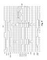
- FIG. 5illustrates a table showing the state of memory cells of an array at a particular phase associated with performing corner turn operations in accordance with a number of embodiments of the present disclosure.
- the reference numbers of the rows of the tables shown in FIG. 5correspond to respective reference numbers of the pseudo code described below (e.g., row 551 - i corresponds to reference number i of the pseudo code, rows 551 - i to 551 - iii correspond to reference number i to iii, respectively, of the pseudocode.
- Each row of the tablesindicates the values of a number of bit vectors 531 (COMP_COMP), 533 (ELEM_SPAN), 535 (TMP_SHIFTED), 537 (E), 539 (VECTOR_BLOCK), and 541 (DEST) at a particular phase of the corner turn operation as can be stored in rows and/or columns of memory cells in the array (e.g., 430 in FIG. 4 ).
- the example shown in FIG. 5is associated with performing a corner turn on eight elements stored in memory cells coupled to a number of access lines (e.g., access lines 404 - 0 to 404 - 7 in FIG. 4 ) and to sense lines (e.g., sense lines 405 - 0 to 405 - 7 in FIG. 4 ).
- access linese.g., access lines 404 - 0 to 404 - 7 in FIG. 4
- sense linese.g., sense lines 405 - 0 to 405 - 7
- the eight elementsare 8-bit wide elements.
- the eight elements to be corner turnedare illustrated as bit-vectors in rows labeled as ROW 0 (corresponding to ROW 0 of FIG. 4 ), ROW 1 , ROW 2 , ROW 3 , ROW 4 , ROW 5 , ROW 6 , and ROW 7 of bit-vector DEST 541 in FIG. 5 .
- the corner turning to be performed in association with the example below illustrated by FIGS. 5-6Bincludes corner turning data stored in a group of memory cells within the same group of memory cells that the data was originally stored in (referred to herein as an in-place corner turn).
- data stored in eight (8) rows of memory cells and eight (8) columns of memory cellscan be corner turned to be stored in a different fashion in the same 8 rows and 8 columns of memory cells.
- a first element stored in a first row of the 8 rows of cellscan be corner turned to be stored in a first column of the 8 columns of cells where a first cell of the first column is also in the first row of cells.
- a vectorcan include a number (e.g., one or more) of elements.
- bit vectoris intended to mean a physically contiguous number of bits on a bit vector memory device, e.g., Processing In Memory (PIM) device, whether physically contiguous in rows (e.g., horizontally oriented) or columns (e.g., vertically oriented) in an array of memory cells.
- PIMProcessing In Memory
- an operation on a bit vectorcan be intended to mean an operation that is performed on a bit-vector that is a contiguous portion of virtual address space, e.g., used by a PIM device.
- a virtual address spacemay have a bit length of 256 bits.
- a portion of the virtual address spacemay or may not be contiguous physically to other portions in the virtual address space.
- Bit-vector DEST 541is illustrated as including 8 rows but could include additional elements that can be stored in additional rows (e.g., in cells coupled to additional access lines 404 - 8 , not illustrated, to 404 -R). In this example, elements corresponding to cells coupled to eight access lines (e.g., 404 - 0 to 404 - 7 ) will be corner turned.
- bit-vector DEST 541e.g., ROW 0 [1111 1111]; ROW 1 [1111 0000]; ROW 2 [1100 1100]; ROW 3 [1010 1010]; ROW 4 [0000 0000]; ROW 5 [0000 1111]; ROW 6 [0011 0011]; and ROW 7 [0101 0101]
- bit-vector DEST 541e.g., ROW 0 [1111 1111]; ROW 1 [1111 0000]; ROW 2 [1100 1100]; ROW 3 [1010 1010]; ROW 4 [0000 0000]; ROW 5 [0000 1111]; ROW 6 [0011 0011]; and ROW 7 [0101 0101]
- a first element of DEST 541(e.g., [0XFF] in ROW 0 ) can represent a base ten (10) numerical value of 255.
- a second element of DEST 541(e.g., [0XF0] in ROW 1 ) can represent a base ten (10) numerical value of 240.
- a third element of DEST 541(e.g., [0XCC] in ROW 2 ) can represent a numerical value of 204
- a fourth element(e.g., [0XAA] in ROW 3 ) can represent a numerical value of 170
- a fifth elemente.g., [0X00] in ROW 4
- a sixth element(e.g., [0X0F] in ROW 5 ) can represent a numerical value of 15
- a seventh elemente.g., [0X33] in ROW 6 ) can represent a numerical value of 51
- an eighth element(e.g., [0X55) in ROW 7 ) can represent a numerical value of 85.
- bit-vector stored as COMP_COMP 531corresponds to a row of compute components such as compute components 431 in FIG. 4 .
- Bit-vectors ELEM_SPAN 533 , TMP_SHIFTED 535 , E 537 , and VECTOR_BLOCK 539each correspond to data stored in a row of cells.
- bit-vector DEST 541is illustrated as 8 rows of data, indicating eight bit-vectors stored in 8 separate rows of cells. While each of the bit-vectors includes 4 elements that are 8-bits wide each, the example below will focus on a first 8-bit element of each bit-vector for ease of reference in the example.
- bit-vectors of DEST 541will be referenced such that a first element of a bit-vector of a first row of cells is separated by a semicolon from first elements of subsequent bit-vectors.
- DEST 541 at row 551 - iwill be referenced as [0XFF; 0XF0; 0XCC; 0XAA; 0X00; 0X0F; 0X33; 0X55].
- bit-vectors ELEM_SPAN 533 , TMP_SHIFTED 535 , E 537 , VECTOR_BLOCK 539 , and DEST 541have a length of 32 bits and four elements that are each 8 bits wide. It is noted that although hexadecimal notation is used in FIGS. 5-6B , the bit-vectors are stored as binary data patterns in the array during the corner turn operations. Also, in the examples described herein, commas and/or spaces may be used to separate elements within a bit-vector for ease of reference. For instance, in the example above, the bit-vectors 533 and 535 each comprise four elements which are separated out by commas.
- Embodimentsare not limited to a particular element size (e.g., to a particular number of elements and/or bits per element).
- the result of the corner turn operationscan be stored in array (e.g., 430 ) and/or can be transferred external to the array (e.g., to functional unit circuitry of a host).
- corner turning DEST 541e.g., [0XFF; 0XF0; 0XCC; 0XAA; 0X00; 0X0F; 0X33; 0X55]
- bit-vector[0XF0; 0XE1; 0XD2; 0XC3; 0XB4; 0XA5; 0X96; 0X87].
- a first element of the ROW 0 bit-vector(e.g., [0XFF]) is corner turned to go from being stored in memory cells coupled to an access line (e.g., access line 404 - 0 ) and a number of sense lines (e.g., sense lines 405 - 0 to 405 - 7 ) to being stored in memory cells coupled to a number of access lines (e.g., access lines 404 - 0 to 404 - 7 ) and a sense line (e.g., sense line 405 - 0 ).
- an access linee.g., access line 404 - 0
- sense linese.g., sense lines 405 - 0 to 405 - 7
- the first element of the bit-vector of ROW 0goes from being the first eight bits of the bit-vector of ROW 0 (e.g., stored in a horizontal fashion, as illustrated) to being stored as a first bit of each of bit-vectors of ROW 0 to ROW 7 (e.g., stored in a vertical fashion, as illustrated).
- the result of performing a corner turncan be stored as bit-vectors in a particular group of memory cells that are the same as the group of memory cells the bit-vectors were originally stored in. For instance, in the example of FIG. 5 , the memory cells corresponding to DEST 541 are used to store the result of the corner turn. As such, at the conclusion of the example described in FIGS.
- DEST 541[0XF0,00,00,00; 0XE1,00,00,00; 0XD2,00,00,00; 0XC3,00,00,00; 0XB4,00,00,00; 0XA5,00,00,00; 0X96,00,00,00; 0X87,00,00,00], which represents the eight elements being stored in a vertical fashion in the same cells as when the bit-vectors of DEST 541 were stored in the horizontal fashion.
- bit vectors 533(ELEM_SPAN), 535 (TMP_SHIFTED), 537 (E), 539 (VECTOR_BLOCK), and 541 (DEST) can be used in association with performing a plurality of corner turn operations on eight elements of the DEST bit-vector 541 .
- the bit-vectors 533 , 535 , 537 , 539 , and 541can be stored in respective groups of memory cells coupled to particular access lines, which may be referred to as temporary storage rows.
- temporary storage rows of memory cellsare storing data that may be updated during various phases of a plurality of corner turn operations.
- the bit-vectors 533 and 535can have a same length as the DEST bit-vectors 541 (e.g., 32 bits in length), respectively, and can be stored in cells coupled to the same sense lines as the DEST bit-vector 541 (e.g., sense lines 405 - 0 to 405 - 31 ).
- the bit-vectors of 541can each have a length of 32 bits and can be stored in a group of cells coupled to access lines 404 - 0 to 404 - 7 (each corresponding to ROW 0 to ROW 7 ) and to sense lines 405 - 0 to 405 - 31 .
- the bit-vectors 533(ELEM_SPAN) and 535 (TMP_SHIFTED) can have lengths of 32 bits and can each be stored in a group of cells coupled to access lines 404 - 8 and 404 - 9 , respectively, and to sense lines 405 - 0 to 405 - 31 .
- Bit-vector 537(E) can have a length of 4 bits and can be a different length in order to be used for internal calculations.
- Bit-vector 539(VECTOR_BLOCK) can have a length of 8 bits and can be a different length in order to be used for internal calculations.
- the bit-vector 531represents the data stored in the sensing circuitry (e.g., compute components 431 and/or sense amplifiers 406 ) corresponding to the sense lines having cells coupled thereto which store elements being divided (e.g., sense lines 405 - 0 to 405 - 31 in this example).
- the first element in ROW 0 of the DEST bit-vector 541(e.g., hexadecimal value “FF” in the most significant element position) can be stored (e.g., as an eight bit bit-vector [1111 1111]) in memory cells 403 - 0 to 403 - 7 coupled to access line 304 - 0 (e.g., ROW 0 ).
- the first element in ROW 1 of the DEST bit-vector 541(e.g., hexadecimal value “F 0 ” in the most significant element position) can be stored (e.g., as an eight bit bit-vector [1111 0000]) in memory cells coupled to access line 404 - 1 (e.g., ROW 0 ) and to sense lines 405 - 0 to 405 - 7 , and each of the first elements of subsequent ROWs 2 to 7 of bit-vector DEST 541 are stored in subsequent cells coupled to access lines 404 - 2 to 404 - 7 , respectively, and to sense lines 405 - 0 to 405 - 7 .
- access line 404 - 1e.g., ROW 0
- sense lines 405 - 0 to 405 - 7each of the first elements of subsequent ROWs 2 to 7 of bit-vector DEST 541 are stored in subsequent cells coupled to access lines 404 - 2 to 404 - 7 , respectively
- the below pseudocoderepresents instructions executable to perform a number of corner turn operations in a memory in accordance with a number of embodiments of the present disclosure.
- the example pseudocodeis referenced using reference numbers i to d, which correspond to the reference numbers of the rows shown in the tables of FIG. 5 and in reference to the column numbers of FIG. 5 .
- reference number ie.g., “Obtain Temp Rows”
- reference number iie.g., “Compute Span Mask and Store Invert as ELEM_SPAN”
- ELEM_SPANi. Obtain Temp Rows ELEM_SPAN, TMP_LOOKUP, E, VECTOR_BLOCK, and DEST; ii. Compute Span Mask and Store Invert as ELEM_SPAN; iii. Compute Max Element; 1. Run Outer Loop for Element Width; a. Calculate VECTOR_BLOCK Using Inverse of E; b. For Half of ELEM_SPAN, Move Elements E Distance on Left and Right; c. Right SHIFT E by 1; d. Shift ELEM_SPAN Equal to E, XOR with ELEM_SPAN and Store as ELEM_SPAN
- the above pseudo codewill be divided into a setup phase and a corner turn phase associated with performing a corner turn operation (e.g., corner turning the eight elements of the DEST bit-vector 541 ).
- the pseudo code referenced by reference numbers i-iiican correspond to the setup phase.
- the setup phasecan be performed simultaneously for a number of the corner turn operations.
- a bit-vector value illustrated in boldindicates a change in the value of the bit-vector (e.g., the value of the bit-vector stored in the memory cells corresponding to COMP_COMP 531 is shown in bold in FIG.
- FIG. 5illustrates the values of a number of bit-vectors associated with performing the setup phase of a corner turn operation at rows 551 - i to 551 - iii .
- the pseudo code referenced by reference number 1can correspond to the corner turn phase.
- the setup phasecan be performed simultaneously for all of the elements that will be corner turned.
- the resultse.g., the resulting stored bit-vectors
- FIG. 5The results (e.g., the resulting stored bit-vectors) corresponding to a number of operations performed in the setup phase are shown in FIG. 5 .
- Rows 551 - i to 551 - iii of the table in FIG. 5corresponds to the above pseudocode instructions referenced by reference numbers i to iii, respectively.
- rows 551 - i to 551 - iiiindicate values of the bit vectors 533 , 535 , 537 , 539 , and 541 during execution of the setup phase as described by the above pseudocode.
- Reference number i(e.g., “Obtain Temp Rows ELEM_SPAN, TMP_SHIFTED, E, VECTOR_BLOCK, and DEST”) of the above pseudocode is associated with initializing a number of groups of memory cells for use as temporary storage rows to be used to store bit-vectors (e.g., 533 , 535 , 537 , 539 , and 541 ).
- Initializingrefers to designating and/or assigning particular access lines used to store particular bit-vectors for performing the corner turn operation.
- the number of groups of memory cellscan be initialized and/or designated groups of cells that can be coupled to respective access lines (e.g., rows) that store data (e.g., on a temporary basis) in association with performing the division operation.
- a first group of memory cellscan be coupled to a particular access line (e.g., 404 - 8 , ROW 8 , not shown) and can store a bit-vector referred to as a “ELEM_SPAN” bit-vector 533 .
- a second group of memory cellscan be coupled to another particular access line (e.g., 404 - 9 , ROW 9 , not shown) and can store bit-vector TMP_SHIFTED 535 .
- a third group of memory cellscan be coupled to another particular access line (e.g., 404 - 10 , ROW 10 , not shown) and can store bit-vector E 537 .
- a fourth group of memory cellscan be coupled to another particular access line (e.g., 404 - 11 , ROW 11 , not shown) and can store bit-vector VECTOR_BLOCK 539 .
- a fifth group of memory cellscan be coupled to a group of particular access lines (e.g., 404 - 0 to 404 - 7 , ROWs 0 to 7 ) and can store bit-vectors of DEST 541 .
- Embodimentsare not limited to a particular number of temporary storage rows and/or to storage of the corresponding bit-vectors on particular access lines.
- the groups of memory cells used to store bit-vectors 533 , 535 , 537 , 539 , and 541may be referred to as “rows,” the respective groups of memory cells may comprise fewer than all of the cells coupled to a particular access line (e.g. ROW).
- temporary storage rowscan refer to access lines which may not be addressable by a user (e.g., access lines that are outside of a user-addressable address space).
- a bit-vector to be corner turnedcan be loaded as DEST 541 (e.g., [0XFF,00,00,00; 0XF0,00,00,00; 0XCC,00,00,00; 0XAA,00,00,00; 0X00,00,00,00; 0X0F,00,00,00; 0X0F,00,00,00,00; 0X33,00,00,00; 0X55,00,00,00], as illustrated at row 551 - i ).
- the result of the corner turn operationswill be stored as DEST 541 , as illustrated at row 553 - 4 b in FIG. 5 .
- Reference number ii(e.g., “Compute Span Mask and Store Invert as ELEM_MASK”) of the above pseudocode can be associated with determining a span mask, inverting the span mask, and storing the inverted span mask as bit-vector ELEM_MASK 533 .
- the span maskcan be determined by setting data units (e.g., bits) of a first element of the bit-vector stored as COMP_COMP 531 to a particular data value (e.g., a “1”). The set data units can be shifted one position to the right, resulting in [0X7F,00,00,00].
- the resultant bit-vector(e.g., [0X7F,00,00,00]) can be inverted (e.g., resulting in [0X80,00,00,00]).
- the inverted resultant bit-vector(e.g., [0X80,00,00,00]) can be stored as ELEM_SPAN 533 .
- the bit-vector ELEM_SPAN 533can be loaded as COMP_COMP 531 and shifted right one position (e.g., resulting in [0X40,00,00,00]) and an OR operation can be performed with the right-shifted bit-vector (e.g., [0X40,00,00,00]) and COMP_COMP 531 (e.g., [0X80,00,00,00]), resulting in [0XC0,00,00,00]. This can be repeated by performing storing the ORed result as ELEM_SPAN 533 , shifting right once, and performing an OR operation again to result in [0XFF,00,00,00].
- the resulting bit-vector of the number of OR operations(e.g., [0XFF,00,00,00]) can be inverted (e.g., resulting in [0X00,FF,FF,FF) and stored as ELEM_SPAN 533 , as is illustrated at 551 - ii.
- Reference number iii(e.g., “Compute Maximum Element”) of the above pseudocode can be associated with determining a maximum element value that indicates when to terminate a number of INNER LOOPS (described further below in relation to FIGS. 6A-6B ).
- the maximum elementcan be determined by multiplying an element width (e.g., 8 bits) by a number of elements in a bit-vector (e.g., 4 elements per bit-vector), resulting in a maximum element value of 32 (used further in association with FIGS. 6A-6B below).
- ELEM_SPAN 533stores [0X00,FF,FF,FF] (e.g., binary [0000 0000, 1111 1111, 1111 1111, 1111 1111]), TMP_SHIFTED 535 stores [0X00,00,00,00], E 537 stores [0X0, VECTOR_BLOCK 539 stores [0X00], and DEST 541 stores [0XFF,00,00,00; 0XF0,00,00,00; 0XCC,00,00,00; 0XAA,00,00,00; 0X00,00,00,00; 0X 0F,00,00,00; 0X33,00,00,00; 0X55,00,00,00].
- Reference number 1(e.g., reference numbers 1 a to 1 d ) of the above pseudocode corresponds to the corner turn phase of a corner turn operation in accordance with a number of embodiments of the present disclosure.
- Reference number 1(e.g., “Run Outer Loop for element width”) of the above pseudocode is associated with performing a LOOP including a number of iterations corresponding to an element width.
- each of the elements of DEST 541are 8 bits wide therefore eight iterations of the loop can be performed (and four will be illustrated for ease of reference as a result is achieved after four iterations).
- a first iteration of the loopis associated with the description of FIG.
- FIG. 5at rows 553 - 1 a to 553 - 1 d which corresponds to reference numbers 1 a to 1 f for a first iteration (where the “1” of 553 - 1 a first iteration).
- a second iteration of the loopis associated with the description of FIG. 5 at rows 553 - 2 a to 553 - 2 d , which corresponds to reference numbers 1 a to 1 f for a second iteration.
- a third iterationis associated with FIG. 5 at rows 553 - 3 a to 553 - 3 d
- a fourth iterationis associated with FIG. 5 at rows 553 - 4 a to 553 - 4 d.
- reference number 1 a(e.g., “Calculate VECTOR_BLOCK Using Inverse of E”) of the above pseudocode is associated with determining VECTOR_BLOCK 437 for a particular iteration.
- the VECTOR_BLOCK 539can be determined by inverting E 537 (e.g., [0X8]).
- Bit-vector E 537can be a local temporary integer used to increment data during the number of corner turn operations.
- the invert of [0X8], for this first iteration,is equal to [0X7], and is stored as VECTOR_BLOCK 539 [0XF7], as is illustrated at row 553 - 1 a.
- Reference number 1 b(e.g., “For Half of ELEM_SPAN, Move Elements E Distance on Left and Right”) of the above pseudocode is associated with performing a number of inner LOOPS on DEST 541 to move a particular portion of the elements of DEST 541 a particular distance. Moving the particular portion of the elements in relation to reference number 1 b is further described below in association with FIGS. 6A-6B .
- DEST 541[0XFF,00,00,00; 0XF0,00,00,00; 0XCC,00,00,00; 0XAA,00,00,00; 0X00,00,00,00; 0X 0F,00,00,00; 0X33,00,00,00; 0X55,00,00,00] (e.g., unchanged from the previous DEST 541 ).
- Reference number 1 c(e.g., “Right SHIFT E by 1”) of the above pseudocode is associated with shifting E 537 (e.g, [0X8], binary [1000]) one position to the right.
- a result of shifting E 537(e.g., [0X8]) is [0X4], binary [0100].
- the result(e.g., [0X4]) is stored as E 537 at row 553 - 1 c.
- Reference number 1 d(e.g., “Shift ELEM_SPAN Equal to E, XOR with ELEM_SPAN and Store as ELEM_SPAN”) of the above pseudocode is associated with shifting ELEM_SPAN 533 (e.g., [0X00,FF,FF,FF]) a number of positions to the Left equal to E (e.g., [0X4]) using the compute components, resulting in [0X0F,FF,FF,F0] being stored as COMP_COMP 531 .
- shifting ELEM_SPAN 533e.g., [0X00,FF,FF,FF]
- Ee.g., [0X4]
- the result of the shift(e.g., COMP_COMP 531 being [0X0F,FF,FF,F0]) is XORed with ELEM_SPAN 533 (e.g., [0X00,FF,FF,FF]), resulting in [0X0F,00,00,0F] being stored as ELEM_SPAN 533 , as illustrated at row 553 - 1 d.
- COMP_COMP 531being [0X0F,FF,FF,F0]
- ELEM_SPAN 533e.g., [0X00,FF,FF,FF]
- reference number 1 a(e.g., “Calculate VECTOR_BLOCK Using Inverse of E”) of the above pseudocode is associated with determining VECTOR_BLOCK 437 for a particular iteration.
- the VECTOR_BLOCK 539can be determined by inverting E 537 (e.g., [0X4]).
- the invert of [0X4], for this second iteration,is equal to [0XB], and is stored as VECTOR_BLOCK 539 [0XFB] as is illustrated at row 553 - 2 a.
- Reference number 1 b(e.g., “For Half of ELEM_SPAN, Move Elements E Distance on Left and Right”) of the above pseudocode is associated with performing a number of inner LOOPS on DEST 541 to move a particular portion of the elements of DEST 541 a particular distance. Moving the particular portion of the elements in relation to reference number 1 b is further described below in association with FIGS. 6A-6B .
- DEST 541A result of moving the elements in association with reference number 1 b results in DEST 541 being [0XF0,00,00,00; 0XF0,00,00,00; 0XC3,00,00,00; 0XA5,00,00,00; 0XF0,00,00,00; 0X 0F,00,00,00; 0XC3,00,00,00; 0XA5,00,00,00].
- a first loop of the inner loops of this second iterationis described further in association with FIG. 6A .
- Reference number 1 c(e.g., “Right SHIFT E by 1”) of the above pseudocode is associated with shifting E 537 (e.g, [0X4], binary [ 1000 ]) one position to the right.
- a result of shifting E 537(e.g., [0X4) is [0X2], binary [0010].
- the result(e.g., [0X2]) is stored as E 537 at row 553 - 2 c.
- Reference number 1 d(e.g., “Shift ELEM_SPAN Equal to E, XOR with ELEM_SPAN and Store as ELEM_SPAN”) of the above pseudocode is associated with shifting ELEM_SPAN 533 (e.g., [0X0F,00,00,0F]) a number of positions to the Left equal to E (e.g., [0X2]) using the compute components, resulting in [0X3C,00,00,3C] being stored as COMP_COMP 531 .
- the result of the shift(e.g., COMP_COMP 531 being [0X3C,00,00,3C]) is XORed with ELEM_SPAN 533 (e.g., [0X00,FF,FF,FF]), resulting in [0X33,00,00,33] being stored as ELEM_SPAN 533 , as illustrated at row 553 - 2 d.
- COMP_COMP 531being [0X3C,00,00,3C]
- ELEM_SPAN 533e.g., [0X00,FF,FF,FF]
- reference number 1 a(e.g., “Calculate VECTOR_BLOCK Using Inverse of E”) of the above pseudocode is associated with determining VECTOR_BLOCK 437 for a particular iteration.
- the VECTOR_BLOCK 539can be determined by inverting E 537 (e.g., [0X2]).
- the invert of [0X2], for this first iteration,is equal to [0XD], and is stored as VECTOR_BLOCK 539 [0XFD] as is illustrated at row 553 - 3 a.
- Reference number 1 b(e.g., “For Half of ELEM_SPAN, Move Elements E Distance on Left and Right”) of the above pseudocode is associated with performing a number of inner LOOPS on DEST 541 to move a particular portion of the elements of DEST 541 a particular distance. Moving the particular portion of the elements in relation to reference number 1 b is further described below in association with FIGS. 6A-6B .
- DEST 541[0XF0,00,00,00; 0XE1,00,00,00; 0XC3,00,00,00; 0XE1,00,00,00; 0XF0,00,00,00; 0X2D,00,00,00; 0XC3,00,00,00; 0X2D,00,00,00].
- Reference number 1 c(e.g., “Right SHIFT E by 1”) of the above pseudocode is associated with shifting E 537 (e.g, [0X2], binary [0010]) one position to the right.
- a result of shifting E 537(e.g., [0X2]) is [0X1], binary [0001].
- the result(e.g., [0X1]) is stored as E 537 at row 553 - 3 c.
- Reference number 1 d(e.g., “Shift ELEM_SPAN Equal to E, XOR with ELEM_SPAN and Store as ELEM_SPAN”) of the above pseudocode is associated with shifting ELEM_SPAN 533 (e.g., [0X33,00,00,33]) a number of positions to the Left equal to E (e.g., [0X1]) using the compute components, resulting in [0X66,00,00,66] being stored as COMP_COMP 531 .
- the result of the shift(e.g., COMP_COMP 531 being [0X66,00,00,66]) is XORed with ELEM_SPAN 533 (e.g., [0X33,00,00,33]), resulting in [0X55,00,00,55] being stored as ELEM_SPAN 533 , as illustrated at row 553 - 3 d.
- COMP_COMP 531being [0X66,00,00,66]
- ELEM_SPAN 533e.g., [0X33,00,00,33]
- reference number 1 a(e.g., “Calculate VECTOR_BLOCK Using Inverse of E”) of the above pseudocode is associated with determining VECTOR_BLOCK 437 for a particular iteration.
- the VECTOR_BLOCK 539can be determined by inverting E 537 (e.g., [0X1]).
- the invert of [0X8], for this first iteration,is equal to [0XE], and is stored as VECTOR_BLOCK 539 [0XFE] as is illustrated at 402 553 - 1 a.
- Reference number 1 b(e.g., “For Half of ELEM_SPAN, Move Elements E Distance on Left and Right”) of the above pseudocode is associated with performing a number of inner LOOPS on DEST 541 to move a particular portion of the elements of DEST 541 a particular distance. Moving the particular portion of the elements in relation to reference number 1 b is further described below in association with FIGS. 6A-6B .
- DEST 541[0XF0,00,00,00; 0XE1,00,00,00; 0XD2,00,00,00; 0XC3,00,00,00; 0XB4,00,00,00; 0XA5,00,00,00; 0X96,00,00,00; 0X87,00,00,00].
- Reference number 1 c(e.g., “Right SHIFT E by 1”) of the above pseudocode is associated with shifting E 537 (e.g, [0X1], binary [0001]) one position to the right.
- a result of shifting E 537(e.g., [0X1]) is [0X0], binary [0000].
- the result(e.g., [0X0]) is stored as E 537 at row 553 - 4 c.
- Reference number 1 d(e.g., “Shift ELEM_SPAN Equal to E, XOR with ELEM_SPAN and Store as ELEM_SPAN”) of the above pseudocode is associated with shifting ELEM_SPAN 533 (e.g., [0X55,00,00,55]) a number of positions to the Left equal to E (e.g., [0X0]) using the compute components, resulting in [0X55,00,00,55] being stored as COMP_COMP 531 .
- the result of the shift(e.g., COMP_COMP 531 being [0X55,00,00,5]) is XORed with ELEM_SPAN 533 (e.g., [0X55,00,00,55]), resulting in [0X00,00,00,00] being stored as ELEM_SPAN 533 , as illustrated at row 553 - 4 d.
- COMP_COMP 531being [0X55,00,00,5]
- ELEM_SPAN 533e.g., [0X55,00,00,55]
- the DEST 541is [0XF0,00,00,00; 0XE1,00,00,00; 0XD2,00,00,00; 0XC3,00,00,00; 0XB4,00,00,00; 0XA5,00,00,00; 0X96,00,00,00; 0X87,00,00,00].
- the resulting DEST 541illustrates a corner turn performed on elements stored in ROWs 0 to 7 that were stored in a horizontal fashion (e.g., in cells coupled to an access line and a plurality of sense lines for each element) that results in those elements being stored in ROWs 0 to 7 that are stored in a vertical fashion (e.g., in cells coupled to a plurality of access lines and a sense line for each element).
- a first element of ROW 0e.g., [0XFF]
- a first access linee.g., 404 - 0 in FIG. 4
- a plurality of sense linese.g., 405 - 0 to 405 - 7 in FIG.
- the first bit of this first elementcan be stored in a same cell as the corner turn is performed in order to store the cells in the same array of cells. Put another way, if 8 elements are stored in an 8 ⁇ 8 array of cells, the corner turned elements will be stored in that same 8 ⁇ 8 array of cells subsequent to the corner turn (referred to as an in-place corner turn).
- FIGS. 6A-6Beach illustrate a table showing the state of memory cells of an array at a particular phase associated with performing corner turn operations in accordance with a number of embodiments of the present disclosure.
- FIG. 6Ais an illustration of a first inner LOOP of a second iteration of the Outer LOOP described above in relation to FIG. 5 .
- the reference numbers of the rows of the table shown in FIG. 6Acorrespond to respective reference numbers of the pseudo code described below (e.g., 653 - 2 b corresponds to a second iteration of an Outer LOOP associated with reference number 1 b of the pseudo code).
- Each row of the tablesindicates the values of a number of bit vectors 631 (COMP_COMP), 633 (ELEM_SPAN), 635 (TMP_SHIFTED), 637 (E), 638 (R), 639 (VECTOR_BLOCK), and DEST 641 at a particular phase of the corner turn operation as can be stored in rows and/or columns of memory cells in the array (e.g., 430 in FIG. 4 ).
- FIG. 6Ais associated with performing a first inner loop (e.g. Inner LOOP “0”) associated with reference number 1 b (e.g., “For Half of ELEM_SPAN, Move Elements E Distance on Left and Right”).
- a number of inner LOOPScan be performed in association with reference number 1 b referenced in FIG. 5 above.
- each of the elements of DEST 541are 8 bits wide and there are 8 elements referenced, on in each of ROWs 0 to 7 .
- a first iteration of the inner LOOPis associated with the description of FIG. 6A at rows 653 - 2 b . 0 . i to 653 - 2 b . 0 .
- FIG. 6Bis associated with a result of DEST 641 at the conclusion of each of the inner LOOPs of the second Outer LOOP.
- a value of DEST 641 prior to performance of the Inner LOOPS of the second Outer LOOPcan be DEST 641 [0XFF,00,00,00; 0XF0,00,00,00; 0XCC,00,00,00; 0XAA,00,00,00; 0X00,00,00,00; 0X0F,00,00,00; 0X33,00,00,00; 0X55,00,00,00] as illustrated at column 653 - 2 .
- a result of a first Inner LOOP (e.g., Inner LOOP “0”) of the second Outer LOOPresults in DEST 641 [0XF0,00,00,00; 0XF0,00,00,00; 0XCC,00,00,00; 0XAA,00,00,00; 0XF0,00,00,00; 0X0F,00,00,00; 0X33,00,00,00; 0X55,00,00,00], as illustrated at column 653 - 2 b . 0 in FIG. 6B .
- a second Inner LOOP (e.g., Inner LOOP “1”) of the second Outer LOOPcan be associated with a result of DEST 641 at column 653 - 2 b .
- a third Inner LOOP (e.g., Inner LOOP “2”) of the second Outer LOOPcan be associated with a result of DEST 641 at column 653 - 2 b . 2
- a fourth Inner LOOP (e.g., Inner LOOP “3”) of the second Outer LOOPcan be associated with a result of DEST 641 at column 653 - 2 . b . 3
- the result after the fourth Inner LOOPis also illustrated at 553 - 2 b in FIG. 5 .
- the below pseudocoderepresents instructions executable to perform a number of corner turn operations in a memory in accordance with a number of embodiments of the present disclosure.
- the example pseudocodeis referenced using reference numbers 2 b.i to 2 b.xii , which correspond to the reference numbers of the rows shown in the tables of FIG. 6A (and correspond to the “ 2 b ” of 553 - 2 b in FIG. 5 ).
- reference number 2 b.ie.g., “Load (R+E) as COMP_COMP” corresponds to row 653 - 2 b . 0 .
- reference number 2 b.iicorresponds to row 653 - 2 b . 0 . ii , column 631 , and so forth.
- Reference number 2 b.i(e.g., “Load (R+E) as COMP_COMP”) of the above pseudocode can be associated with loading a bit-vector as COMP_COMP 631 .
- Bit-vector R 638can be a local temporary integer used to increment data to perform the number of corner turn operations.
- Reference number 2 b.iie.g., “SHIFT COMP_COMP Right Equal to E”
- ESign COMP_COMP Right Equal to E
- COMP_COMP 631(e.g., [0X00,00,00,00]) is [0X00,00,00,00].
- Reference number 2 b.iii(e.g., “XOR COMP_COMP and R”) of the above pseudocode is associated with performing an XOR operation on COMP_COMP 631 (e.g., [0X00,00,00,00]) and R (which is the bit-vector of ROW 0 [0XFF,00,00,00] as R 638 is [0X00]), resulting in bit-vector [0XFF,00,00,00] as COMP_COMP 631 .
- Reference number 2 b.iv(e.g., “AND COMP_COMP and ELEM_SPAN”) of the above pseudocode is associated with performing an AND operation on COMP_COMP 631 (e.g., [0XFF,00,00,00]) and ELEM_SPAN 633 (e.g., [0X0F,00,00,0F]), resulting in [0X0F,00,00,00].
- Reference number 2 b.ve.g., “Store COMP_COMP as TMP_SHIFTED” of the above pseudocode is associated with storing COMP_COMP 631 (e.g., [0X0F,00,00,00]) as TMP_SHIFTED 635 , as illustrated at 653 - 2 b .
- Reference number 2 b.vi(e.g., “XOR COMP_COMP and R”) of the above pseudocode is associated with performing an XOR operation on COMP_COMP 631 (e.g., [0X0F,00,00,00]) and R (e.g., ROW 0 , which is [0XFF,00,00,00]), resulting in [0XF0,00,00,00].
- COMP_COMP 631e.g., [0XF0,00,00,00]
- Reference number 2 b.viii(e.g., “Load TMP_SHIFTED as COMP_COMP”) of the above pseudocode is associated with loading TMP_SHIFTED 635 (e.g. [0X0F,00,00,00]) as COMP_COMP 631 , as illustrated at 653 - 2 b . 0 . viii .
- Reference number 2 b.ix(e.g., “SHIFT COMP_COMP Left Equal to E”) of the above pseudocode is associated with performing a SHIFT operation on COMP_COMP 631 (e.g., [0X0F,00,00,00]) equal to E (e.g., [0X4], or 4 positions) to the left.
- COMP_COMP 631(e.g., [0X0F,00,00,00]) shifted 4 positions to the left results in [0XF0,00,00,00].
- VECTOR_BLOCK 639e.g., [0X0FB) and (R+1+E
- DEST 641is [0XF0,00,00,00; 0XF0,00,00,00; 0XCC,00,00,00; 0XAA,00,00,00; 0XF0,00,00,00; 0X0F,00,00,00; 0X33,00,00,00; 0X55,00,00,00].
- FIG. 6Billustrates a table showing the state of memory cells of an array at a particular phase associated with performing corner turn operations in accordance with a number of embodiments of the present disclosure.
- FIG. 6Billustrates a value of DEST 641 at the conclusion of a number of Inner LOOPs associated with a second Outer LOOP (e.g., associated with rows 553 - 2 a to 553 - 2 d ).
- DEST 641is [0XFF,00,00,00; 0XF0,00,00,00; 0XCC,00,00,00; 0XAA,00,00,00; 0X00,00,00,00; 0X0F,00,00,00; 0X33,00,00,00; 0X55,00,00,00].
- Inner LOOPe.g., Inner LOOP “0” associated with rows 653 - 2 b . 0 . i to 653 - 2 b . 0 . xii of FIG.
- DEST 641at column 653 - 2 b .
- 0is equal to [0XF0,00,00,00; 0XF0,00,00,00; 0XCC,00,00,00; 0XAA,00,00,00; 0XF0,00,00,00; 0X0F,00,00,00; 0X33,00,00,00; 0X55,00,00,00] (where bolded bits indicate a changed row).
- the first Inner LOOPcan be associated with modifying data values of ROW 0 and ROW 4 (bolded), where data values of ROW 0 are relocated to ROW 4 . Subsequent Inner LOOPS are associated with similar modifications.
- a second Inner LOOP(e.g., Inner LOOP “1”), is associated with modifying ROW 1 and ROW 5
- a third Inner LOOP(e.g., “2”) is associated with modifying ROW 2 and ROW 6
- a fourth Inner LOOP(e.g., “3”) is associated with modifying ROW 3 and ROW 7 .
- DEST 641After performance of the second Inner LOOP (e.g., Inner LOOP “1”), DEST 641 , at column 653 - 2 b . 1 , is [0XF0,00,00,00; 0XF0,00,00,00; 0XCC,00,00,00; 0XAA,00,00,00,00; 0XF0,00,00,00; 0X0F,00,00,00; 0X33,00,00,00; 0X55,00,00,00].
- the third Inner LOOPe.g., Inner LOOP “2”
- Inner LOOP 2is [0XF0,00,00,00; 0XF0,00,00,00; 0XC3,00,00,00; 0XAA,00,00,00; 0XF0,00,00,00; 0X0F,00,00,00; 0XC3,00,00,00; 0X55,00,00,00].
- DEST 641 at row 553 - 4 b of FIG. 5is an illustration of fully corner turned data.
- DEST 641 at row 551 - iis [0XFF,00,00,00; 0XF0,00,00,00; 0XCC,00,00,00; 0XAA,00,00,00; 0X00,00,00,00; 0X0F,00,00,00; 0X33,00,00,00; 0X55,00,00,00].
- DEST 641 at row 551 - iis corner turned and results in the value of DEST 641 at row 553 - 4 b , which is [0XF0,00,00,00; 0XE1,00,00,00; 0XD2,00,00,00; 0XC3,00,00,00; 0XB4,00,00,00; 0XA5,00,00,00; 0X96,00,00,00; 0X87,00,00,00].
- the first element (e.g., [0XFF]) of ROW 0is corner turned from being stored horizontally in ROW 0 to being stored vertically as the first bit of each of the bit-vectors stored in ROWs 0 to 7 .
- the element (e.g., [0XF0]) of ROW 1goes from being stored horizontally in ROW 1 to being stored vertically as the second bit of each of the bit-vectors stored in ROWs 0 to 7 .
- the element (e.g., [0XC3] of ROW 2goes from horizontal in ROW 2 to vertically as the third bit of each bit-vector
- the element (e.g., [0XA5]) of ROW 3goes from horizontal in ROW 3 to vertically as the fourth bit of each bit-vector
- the element (e.g., [0XF0]) of ROW 4goes from horizontal in ROW 4 to vertically as the fifth bit of each bit-vector
- the element (e.g., [0X0F]) of ROW 5goes from horizontal in ROW 5 to vertically as the sixth bit of each bit-vector
- the element (e.g., [0XC3]) of ROW 6goes from horizontal in ROW 6 to vertically as the
- FIG. 7is a logic table illustrating selectable logic operation results implemented by a sensing circuitry (e.g., sensing circuitry 250 shown in FIG. 2 ) in accordance with a number of embodiments of the present disclosure.
- the four logic selection control signalse.g., TF, TT, FT, and FF
- TF, TT, FT, and FFin conjunction with a particular data value present on the complementary sense lines, can be used to select one of a plurality of logical operations to implement involving the starting data values stored in the sense amplifier 206 and compute component 231 .
- the four control signals(e.g., TF, TT, FT, and FF), in conjunction with a particular data value present on the complementary sense lines (e.g., on nodes S and S*), controls the pass gates 307 - 1 and 307 - 2 and swap transistors 342 , which in turn affects the data value in the compute component 331 and/or sense amplifier 306 before/after firing.
- the capability to selectably control the swap transistors 342facilitates implementing logical operations involving inverse data values (e.g., inverse operands and/or inverse result), among others.
- Logic Table 7-1 illustrated in FIG. 7shows the starting data value stored in the compute component 231 shown in column A at 744 , and the starting data value stored in the sense amplifier 206 shown in column B at 745 .
- the other 3 column headings in Logic Table 7-1refer to the state of the pass gates 207 - 1 and 207 - 2 and the swap transistors 242 , which can respectively be controlled to be OPEN or CLOSED depending on the state of the four logic selection control signals (e.g., TF, TT, FT, and FF), in conjunction with a particular data value present on the pair of complementary sense lines 205 - 1 and 205 - 2 when the ISO control signal is asserted.
- logic selection control signalse.g., TF, TT, FT, and FF
- the “NOT OPEN” columncorresponds to the pass gates 207 - 1 and 207 - 2 and the swap transistors 242 both being in a non-conducting condition
- the “OPEN TRUE” columncorresponds to the pass gates 207 - 1 and 207 - 2 being in a conducting condition
- the “OPEN INVERT” columncorresponds to the swap transistors 242 being in a conducting condition.
- the configuration corresponding to the pass gates 207 - 1 and 207 - 2 and the swap transistors 242 both being in a conducting conditionis not reflected in Logic Table 7-1 since this results in the sense lines being shorted together.
- each of the three columns of the upper portion of Logic Table 7-1can be combined with each of the three columns of the lower portion of Logic Table 7-1 to provide nine (e.g., 3 ⁇ 3) different result combinations, corresponding to nine different logical operations, as indicated by the various connecting paths shown at 775 .
- the nine different selectable logical operations that can be implemented by the sensing circuitry 250are summarized in Logic Table 7-2.
- the columns of Logic Table 7-2show a heading 780 that includes the states of logic selection control signals (e.g., FF, FT, TF, TT).
- logic selection control signalse.g., FF, FT, TF, TT
- the state of a first logic selection control signale.g., FF
- the state of a second logic selection control signale.g., FT
- the state of a third logic selection control signale.g., TF
- the state of a fourth logic selection control signale.g., TT
- the particular logical operation corresponding to the resultsis summarized in row 747 .
- FIG. 8illustrates a timing diagram associated with performing a logical AND operation and a shifting operation using the sensing circuitry in accordance with a number of embodiments of the present disclosure.
- FIG. 8includes waveforms corresponding to signals EQ, ROW X, ROW Y, SENSE AMP, TF, TT, FT, FF, PHASE 1 R, PHASE 2 R, PHASE 1 L, PHASE 2 L, ISO, Pass, Pass*, DIGIT, and DIGIT_.
- the EQ signalcorresponds to an equilibrate signal associated with a sense amplifier (e.g., EQ 226 shown in FIG. 2 ).
- the ROW X and ROW Y signalscorrespond to signals applied to respective access line (e.g., access lines 204 -X and 204 -Y shown in FIG. 2 ) to access a selected cell (or row of cells).
- the SENSE AMP signalcorresponds to a signal used to enable/disable a sense amplifier (e.g., sense amplifier 306 ).
- the TF, TT, FT, and FF signalscorrespond to logic selection control signals such as those shown in FIG. 3 (e.g., signals coupled to logic selection transistors 362 , 3452 , 354 , and 364 ).
- the PHASE 1 R, PHASE 2 R, PHASE 1 L, and PHASE 2 L signalscorrespond to the control signals (e.g., clock signals) provided to respective control lines 382 , 383 , 391 and 392 shown in FIG. 3 .
- the ISO signalcorresponds to the signal coupled to the gates of the isolation transistors 350 - 1 and 350 - 2 shown in FIG. 3 .
- the PASS signalcorresponds to the signal coupled to the gates of pass transistors 307 - 1 and 307 - 2 shown in FIG. 3
- the PASS* signalcorresponds to the signal coupled to the gates of the swap transistors 342 .
- the DIGIT and DIGIT_signalscorrespond to the signals present on the respective sense lines 305 - 1 (e.g., DIGIT (n)) and 305 - 2 (e.g., DIGIT (n)_).
- the timing diagram shown in FIG. 8is associated with performing a logical AND operation on a data value stored in a first memory cell and a data value stored in a second memory cell of an array.
- the memory cellscan correspond to a particular column of an array (e.g., a column comprising a complementary pair of sense lines) and can be coupled to respective access lines (e.g., ROW X and ROW Y).
- access linese.g., ROW X and ROW Y.
- the 8can include storing the data value of the ROW X memory cell (e.g., the “ROW X data value) in the latch of the corresponding compute component 331 (e.g., the “A” data value), which can be referred to as the accumulator 331 , storing the data value of the ROW Y memory cell (e.g., the “ROW Y data value”) in the latch of the corresponding sense amplifier 306 (e.g., the “B” data value), and performing a selected logical operation (e.g., a logical AND operation in this example) on the ROW X data value and the ROW Y data value, with the result of the selected logical operation being stored in the latch of the compute component 331 .
- a selected logical operatione.g., a logical AND operation in this example
- equilibration of the sense amplifier 306is disabled (e.g., EQ goes low).
- ROW Xgoes high to access (e.g., select) the ROW X memory cell.
- the sense amplifier 306is enabled (e.g., SENSE AMP goes high), which drives the complementary sense lines 305 - 1 and 305 - 2 to the appropriate rail voltages (e.g., V DD and GND) responsive to the ROW X data value (e.g., as shown by the DIGIT and DIGIT_signals), and the ROW X data value is latched in the sense amplifier 306 .
- the PHASE 2 R and PHASE 2 L signalsgo low, which disables feedback on the latch of the compute component 331 (e.g., by turning off transistors 386 and 390 , respectively) such that the value stored in the compute component may be overwritten during the logical operation.
- ISOgoes low, which disables isolation transistors 350 - 1 and 350 - 2 .
- TT and FTare enabled (e.g., go high), which results in PASS going high (e.g., since either transistor 352 or 354 will conduct depending on which of node ST 2 (corresponding to node “S” in FIG. 2 ) or node SF 2 (corresponding to node “S*” in FIG.
- ROW Xis disabled, and PHASE 2 R, PHASE 2 L, and ISO are enabled. Enabling PHASE 2 R and PHASE 2 L at time T 7 enables feedback on the latch of the compute component 331 such that the ROW X data value is latched therein. Enabling ISO at time T 7 again couples nodes ST 2 and SF 2 to the gates of the enable transistors 352 , 354 , 362 , and 364 .
- equilibrationis enabled (e.g., EQ goes high such that DIGIT and DIGIT_ are driven to an equilibrate voltage such as V DD /2) and the sense amplifier 306 is disabled (e.g., SENSE AMP goes low).
- equilibrationis disabled (e.g., EQ goes low at time T 9 ).
- ROW Ygoes high to access (e.g., select) the ROW Y memory cell.
- the sense amplifier 306is enabled (e.g., SENSE AMP goes high), which drives the complementary sense lines 305 - 1 and 305 - 2 to the appropriate rail voltages (e.g., V DD and GND) responsive to the ROW Y data value (e.g., as shown by the DIGIT and DIGIT_signals), and the ROW Y data value is latched in the sense amplifier 306 .
- the PHASE 2 R and PHASE 2 L signalsgo low, which disables feedback on the latch of the compute component 331 (e.g., by turning off transistors 386 and 390 , respectively) such that the value stored in the compute component may be overwritten during the logical operation.
- Whether enabling TT results in PASS going highdepends on the value stored in the compute component 331 when ISO is disabled at time T 12 . For example, enable transistor 352 will conduct if node ST 2 was high when ISO is disabled, and enable transistor will not conduct if node ST 2 was low when ISO was disabled at time T 12 .
- the pass transistors 307 - 1 and 307 - 2are enabled such that the DIGIT and DIGIT_signals, which correspond to the ROW Y data value, are provided to the respective compute component nodes ST 2 and SF 2 .
- the value stored in the compute component 331e.g., the ROW X data value
- the value stored in the compute component 331may be flipped, depending on the value of DIGIT and DIGIT (e.g., the ROW Y data value).
- the pass transistors 307 - 1 and 307 - 2are not enabled such that the DIGIT and DIGIT_signals, which correspond to the ROW Y data value, remain isolated from the nodes ST 2 and SF 2 of the compute component 331 .
- the data value in the compute componente.g., the ROW X data value
- TTis disabled, which results in PASS going (or remaining) low, such that the pass transistors 307 - 1 and 307 - 2 are disabled. It is noted that PASS* remains low between time T 13 and T 14 since the TF and FF signals remain low.
- ROW Yis disabled, and PHASE 2 R, PHASE 2 L, and ISO are enabled. Enabling PHASE 2 R and PHASE 2 L at time T 15 enables feedback on the latch of the compute component 331 such that the result of the AND operation (e.g., “A” AND “B”) is latched therein.
- Enabling ISO at time T 15again couples nodes ST 2 and SF 2 to the gates of the enable transistors 352 , 354 , 362 , and 364 .
- equilibrationis enabled (e.g., EQ goes high such that DIGIT and DIGIT_ are driven to an equilibrate voltage) and the sense amplifier 306 is disabled (e.g., SENSE AMP goes low).
- the result of the AND operationwhich is initially stored in the compute component 331 in this example, can be transferred back to the memory array (e.g., to a memory cell coupled to ROW X, ROW Y, and/or a different row via the complementary sense lines) and/or to an external location (e.g., an external processing component) via I/O lines.
- the memory arraye.g., to a memory cell coupled to ROW X, ROW Y, and/or a different row via the complementary sense lines
- an external locatione.g., an external processing component
- FIG. 8also includes (e.g., at 801 ) signaling associated with shifting data (e.g., from a compute component 331 to an adjacent compute component 331 ).
- shifting datae.g., from a compute component 331 to an adjacent compute component 331 .
- the example shown in FIG. 8illustrates two left shifts such that a data value stored in a compute component corresponding to column “N” is shifted left to a compute component corresponding to column “N- 2 ”.
- PHASE 2 R and PHASE 2 Lare disabled, which disables feedback on the compute component latches, as described above.
- PHASE 1 Lis enabled at time T 17 and disabled at time T 18 .
- Enabling PHASE 1 Lcauses transistor 389 to conduct, which causes the data value at node SF 1 to move left to node SF 2 of a left-adjacent compute component 331 .
- PHASE 2 Lis subsequently enabled at time T 19 and disabled at time T 20 .
- Enabling PHASE 2 Lcauses transistor 390 to conduct, which causes the data value from node ST 1 to move left to node ST 2 completing a left shift.
- the above sequence(e.g., enabling/disabling PHASE 1 L and subsequently enabling/disabling PHASE 2 L) can be repeated to achieve a desired number of left shifts. For instance, in this example, a second left shift is performed by enabling PHASE 1 L at time T 21 and disabling PHASE 1 L at time T 22 . PHASE 2 L is subsequently enabled at time T 23 to complete the second left shift. Subsequent to the second left shift, PHASE 2 L remains enabled and PHASE 2 R is enabled (e.g., at time T 24 ) such that feedback is enabled to latch the data values in the compute component latches.
- a second left shiftis performed by enabling PHASE 1 L at time T 21 and disabling PHASE 1 L at time T 22 .
- PHASE 2 Lis subsequently enabled at time T 23 to complete the second left shift.
- PHASE 2 Lremains enabled and PHASE 2 R is enabled (e.g., at time T 24 )
- FIG. 9illustrates a timing diagram associated with performing a logical XOR operation and a shifting operation using the sensing circuitry in accordance with a number of embodiments of the present disclosure.
- FIG. 9includes the same waveforms described in FIG. 8 above. However, the timing diagram shown in FIG. 9 is associated with performing a logical XOR operation on a ROW X data value and a ROW Y data value (e.g., as opposed to a logical AND operation). Reference will again be made to the sensing circuitry described in FIG. 3 .
- EQis disabled with the ROW X data value being latched in the compute component 331 .
- ROW Ygoes high to access (e.g., select) the ROW Y memory cell.
- the sense amplifier 306is enabled (e.g., SENSE AMP goes high), which drives the complementary sense lines 305 - 1 and 305 - 2 to the appropriate rail voltages (e.g., V DD and GND) responsive to the ROW Y data value (e.g., as shown by the DIGIT and DIGIT_ signals), and the ROW Y data value is latched in the sense amplifier 306 .
- the PHASE 2 R and PHASE 2 L signalsgo low, which disables feedback on the latch of the compute component 1431 (e.g., by turning off transistors 386 and 390 , respectively) such that the value stored in the compute component 331 may be overwritten during the logical operation.
- enable transistor 362will conduct if node ST 2 was high when ISO is disabled, and enable transistor 362 will not conduct if node ST 2 was low when ISO was disabled at time T 12 .
- enable transistor 354will conduct if node SF 2 was high when ISO is disabled, and enable transistor 354 will not conduct if node SF 2 was low when ISO is disabled.
- the pass transistors 307 - 1 and 307 - 2are enabled such that the DIGIT and DIGIT_signals, which correspond to the ROW Y data value, are provided to the respective compute component nodes ST 2 and SF 2 .
- the value stored in the compute component 331e.g., the ROW X data value
- the value stored in the compute component 331may be flipped, depending on the value of DIGIT and DIGIT_ (e.g., the ROW Y data value).
- the pass transistors 307 - 1 and 307 - 2are not enabled such that the DIGIT and DIGIT_ signals, which correspond to the ROW Y data value, remain isolated from the nodes ST 2 and SF 2 of the compute component 331 .
- the data value in the compute componente.g., the ROW X data value
- the swap transistors 342are enabled such that the DIGIT and DIGIT_ signals, which correspond to the ROW Y data value, are provided to the respective compute component nodes ST 2 and SF 2 in a transposed manner (e.g., the “true” data value on DIGIT(n) would be provided to node SF 2 and the “complement” data value on DIGIT(n) would be provided to node ST 2 ).
- the value stored in the compute component 331e.g., the ROW X data value
- DIGIT_e.g., the ROW Y data value
- the swap transistors 342are not enabled such that the DIGIT and DIGIT_ signals, which correspond to the ROW Y data value, remain isolated from the nodes ST 2 and SF 2 of the compute component 331 .
- the data value in the compute componente.g., the ROW X data value
- TF and FTare disabled, which results in PASS and PASS* going (or remaining) low, such that the pass transistors 307 - 1 and 307 - 2 and swap transistors 342 are disabled.
- ROW Yis disabled, and PHASE 2 R, PHASE 2 L, and ISO are enabled.
- Enabling PHASE 2 R and PHASE 2 L at time T 15enables feedback on the latch of the compute component 331 such that the result of the XOR operation (e.g., “A” XOR “B”) is latched therein.
- Enabling ISO at time T 15again couples nodes ST 2 and SF 2 to the gates of the enable transistors 352 , 354 , 362 , and 364 .
- equilibrationis enabled (e.g., EQ goes high such that DIGIT and DIGIT are driven to an equilibrate voltage) and the sense amplifier 306 is disabled (e.g., SENSE AMP goes low).
- the result of the XOR operationwhich is initially stored in the compute component 331 in this example, can be transferred back to the memory array (e.g., to a memory cell coupled to ROW X, ROW Y, and/or a different row via the complementary sense lines) and/or to an external location (e.g., an external processing component) via I/O lines.
- the memory arraye.g., to a memory cell coupled to ROW X, ROW Y, and/or a different row via the complementary sense lines
- an external locatione.g., an external processing component
- FIG. 9also includes (e.g., at 901 ) signaling associated with shifting data (e.g., from a compute component 331 to an adjacent compute component 331 ).
- shifting datae.g., from a compute component 331 to an adjacent compute component 331 .
- the example shown in FIG. 9illustrates two right shifts such that a data value stored in a compute component corresponding to column “N” is shifted right to a compute component corresponding to column “N+2”.
- PHASE 2 R and PHASE 2 Lare disabled, which disables feedback on the compute component latches, as described above.
- PHASE 1 Ris enabled at time T 17 and disabled at time T 18 .
- Enabling PHASE 1 Rcauses transistor 381 to conduct, which causes the data value at node ST 1 to move right to node ST 2 of a right-adjacent compute component 331 .
- PHASE 2 Ris subsequently enabled at time T 19 and disabled at time T 20 .
- Enabling PHASE 2 Rcauses transistor 386 to conduct, which causes the data value from node SF 1 to move right to node SF 2 completing a right shift.
- the above sequence(e.g., enabling/disabling PHASE 1 R and subsequently enabling/disabling PHASE 2 R) can be repeated to achieve a desired number of right shifts. For instance, in this example, a second right shift is performed by enabling PHASE 1 R at time T 21 and disabling PHASE 1 R at time T 22 . PHASE 2 R is subsequently enabled at time T 23 to complete the second right shift. Subsequent to the second right shift, PHASE 1 R remains disabled, PHASE 2 R remains enabled, and PHASE 2 L is enabled (e.g., at time T 24 ) such that feedback is enabled to latch the data values in the compute component latches.
- a second right shiftis performed by enabling PHASE 1 R at time T 21 and disabling PHASE 1 R at time T 22 .
- PHASE 2 Ris subsequently enabled at time T 23 to complete the second right shift.
- PHASE 1 Rremains disabled
- PHASE 2 Rremains enabled
- sensing circuitry in accordance with embodiments described hereincan be operated to perform logical operations with the result being initially stored in the sense amplifier (e.g., as illustrated in FIG. 8 ). Also, embodiments are not limited to the “AND” and “XOR” logical operation examples described in FIGS. 8 and 9 , respectively.
- sensing circuitry in accordance with embodiments of the present disclosuree.g., 350 shown in FIG. 3
- sensing circuitrysense amps, compute components, dynamic latches, isolation devices, and/or shift circuitry
- embodiments of the present disclosureare not limited to those combinations explicitly recited herein.
- Other combinations and configurations of the sensing circuitry, sense amps, compute component, dynamic latches, isolation devices, and/or shift circuitry disclosed hereinare expressly included within the scope of this disclosure.
Landscapes
- Engineering & Computer Science (AREA)
- Microelectronics & Electronic Packaging (AREA)
- Dram (AREA)
Abstract
Description
| i. | Obtain Temp Rows ELEM_SPAN, TMP_LOOKUP, E, |
| VECTOR_BLOCK, and DEST; | |
| ii. | Compute Span Mask and Store Invert as ELEM_SPAN; |
| iii. | Compute Max Element; |
| 1. | Run Outer Loop for Element Width; |
| a. | Calculate VECTOR_BLOCK Using Inverse of E; | |
| b. | For Half of ELEM_SPAN, Move Elements E Distance on Left | |
| and Right; | ||
| c. | Right SHIFT E by 1; | |
| d. | Shift ELEM_SPAN Equal to E, XOR with ELEM_SPAN and | |
| Store as ELEM_SPAN | ||
Claims (25)
Priority Applications (2)
| Application Number | Priority Date | Filing Date | Title |
|---|---|---|---|
| US15/133,986US10153008B2 (en) | 2016-04-20 | 2016-04-20 | Apparatuses and methods for performing corner turn operations using sensing circuitry |
| US16/215,122US10699756B2 (en) | 2016-04-20 | 2018-12-10 | Apparatuses and methods for performing corner turn operations using sensing circuitry |
Applications Claiming Priority (1)
| Application Number | Priority Date | Filing Date | Title |
|---|---|---|---|
| US15/133,986US10153008B2 (en) | 2016-04-20 | 2016-04-20 | Apparatuses and methods for performing corner turn operations using sensing circuitry |
Related Child Applications (1)
| Application Number | Title | Priority Date | Filing Date |
|---|---|---|---|
| US16/215,122ContinuationUS10699756B2 (en) | 2016-04-20 | 2018-12-10 | Apparatuses and methods for performing corner turn operations using sensing circuitry |
Publications (2)
| Publication Number | Publication Date |
|---|---|
| US20170309314A1 US20170309314A1 (en) | 2017-10-26 |
| US10153008B2true US10153008B2 (en) | 2018-12-11 |
Family
ID=60089703
Family Applications (2)
| Application Number | Title | Priority Date | Filing Date |
|---|---|---|---|
| US15/133,986ActiveUS10153008B2 (en) | 2016-04-20 | 2016-04-20 | Apparatuses and methods for performing corner turn operations using sensing circuitry |
| US16/215,122ActiveUS10699756B2 (en) | 2016-04-20 | 2018-12-10 | Apparatuses and methods for performing corner turn operations using sensing circuitry |
Family Applications After (1)
| Application Number | Title | Priority Date | Filing Date |
|---|---|---|---|
| US16/215,122ActiveUS10699756B2 (en) | 2016-04-20 | 2018-12-10 | Apparatuses and methods for performing corner turn operations using sensing circuitry |
Country Status (1)
| Country | Link |
|---|---|
| US (2) | US10153008B2 (en) |
Cited By (1)
| Publication number | Priority date | Publication date | Assignee | Title |
|---|---|---|---|---|
| US20190108863A1 (en)* | 2016-04-20 | 2019-04-11 | Micron Technology, Inc. | Apparatuses and methods for performing corner turn operations using sensing circuitry |
Families Citing this family (21)
| Publication number | Priority date | Publication date | Assignee | Title |
|---|---|---|---|---|
| CN207637499U (en) | 2016-11-08 | 2018-07-20 | 美光科技公司 | The equipment for being used to form the computation module above memory cell array |
| US10522210B2 (en) | 2017-12-14 | 2019-12-31 | Micron Technology, Inc. | Apparatuses and methods for subarray addressing |
| US10332586B1 (en) | 2017-12-19 | 2019-06-25 | Micron Technology, Inc. | Apparatuses and methods for subrow addressing |
| US10614875B2 (en) | 2018-01-30 | 2020-04-07 | Micron Technology, Inc. | Logical operations using memory cells |
| US11194477B2 (en) | 2018-01-31 | 2021-12-07 | Micron Technology, Inc. | Determination of a match between data values stored by three or more arrays |
| US10437557B2 (en) | 2018-01-31 | 2019-10-08 | Micron Technology, Inc. | Determination of a match between data values stored by several arrays |
| US10725696B2 (en) | 2018-04-12 | 2020-07-28 | Micron Technology, Inc. | Command selection policy with read priority |
| US10573372B2 (en)* | 2018-05-31 | 2020-02-25 | Micron Technology, Inc. | Sensing operations in memory by comparing inputs in a sense amplifier |
| US10440341B1 (en) | 2018-06-07 | 2019-10-08 | Micron Technology, Inc. | Image processor formed in an array of memory cells |
| US11175915B2 (en) | 2018-10-10 | 2021-11-16 | Micron Technology, Inc. | Vector registers implemented in memory |
| US10769071B2 (en) | 2018-10-10 | 2020-09-08 | Micron Technology, Inc. | Coherent memory access |
| US10483978B1 (en) | 2018-10-16 | 2019-11-19 | Micron Technology, Inc. | Memory device processing |
| US11184446B2 (en) | 2018-12-05 | 2021-11-23 | Micron Technology, Inc. | Methods and apparatus for incentivizing participation in fog networks |
| US12118056B2 (en) | 2019-05-03 | 2024-10-15 | Micron Technology, Inc. | Methods and apparatus for performing matrix transformations within a memory array |
| US10867655B1 (en) | 2019-07-08 | 2020-12-15 | Micron Technology, Inc. | Methods and apparatus for dynamically adjusting performance of partitioned memory |
| US11360768B2 (en) | 2019-08-14 | 2022-06-14 | Micron Technolgy, Inc. | Bit string operations in memory |
| US11449577B2 (en) | 2019-11-20 | 2022-09-20 | Micron Technology, Inc. | Methods and apparatus for performing video processing matrix operations within a memory array |
| US11853385B2 (en) | 2019-12-05 | 2023-12-26 | Micron Technology, Inc. | Methods and apparatus for performing diversity matrix operations within a memory array |
| US11188329B1 (en)* | 2020-06-24 | 2021-11-30 | Micron Technology, Inc. | Dynamic precision bit string accumulation |
| US11227641B1 (en) | 2020-07-21 | 2022-01-18 | Micron Technology, Inc. | Arithmetic operations in memory |
| US12169639B2 (en)* | 2021-03-12 | 2024-12-17 | Kioxia Corporation | Data exchange between host and storage device using compute functions |
Citations (317)
| Publication number | Priority date | Publication date | Assignee | Title |
|---|---|---|---|---|
| US4380046A (en) | 1979-05-21 | 1983-04-12 | Nasa | Massively parallel processor computer |
| US4435792A (en) | 1982-06-30 | 1984-03-06 | Sun Microsystems, Inc. | Raster memory manipulation apparatus |
| US4435793A (en) | 1979-07-26 | 1984-03-06 | Tokyo Shibaura Denki Kabushiki Kaisha | Semiconductor memory device with dummy word line/sense amplifier activation |
| EP0214718A2 (en) | 1985-07-22 | 1987-03-18 | Alliant Computer Systems Corporation | Digital computer |
| US4727474A (en) | 1983-02-18 | 1988-02-23 | Loral Corporation | Staging memory for massively parallel processor |
| US4843264A (en) | 1987-11-25 | 1989-06-27 | Visic, Inc. | Dynamic sense amplifier for CMOS static RAM |
| US4852065A (en) | 1984-06-02 | 1989-07-25 | Eric Baddiley | Data reorganization apparatus |
| US4958378A (en) | 1989-04-26 | 1990-09-18 | Sun Microsystems, Inc. | Method and apparatus for detecting changes in raster data |
| US4977542A (en) | 1988-08-30 | 1990-12-11 | Mitsubishi Denki Kabushiki Kaisha | Dynamic semiconductor memory device of a twisted bit line system having improved reliability of readout |
| US5023838A (en) | 1988-12-02 | 1991-06-11 | Ncr Corporation | Random access memory device with integral logic capability |
| US5034636A (en) | 1990-06-04 | 1991-07-23 | Motorola, Inc. | Sense amplifier with an integral logic function |
| US5079739A (en) | 1988-09-23 | 1992-01-07 | Datacard Corporation | Apparatus and method for converting bit-mapped data from row orientation to column or orientation |
| US5201039A (en) | 1987-09-30 | 1993-04-06 | Mitsubishi Denki Kabushiki Kaisha | Multiple address-space data processor with addressable register and context switching |
| US5210850A (en) | 1990-06-15 | 1993-05-11 | Compaq Computer Corporation | Memory address space determination using programmable limit registers with single-ended comparators |
| US5253308A (en) | 1989-06-21 | 1993-10-12 | Amber Engineering, Inc. | Massively parallel digital image data processor using pixel-mapped input/output and relative indexed addressing |
| US5276643A (en) | 1988-08-11 | 1994-01-04 | Siemens Aktiengesellschaft | Integrated semiconductor circuit |
| US5325519A (en) | 1991-10-18 | 1994-06-28 | Texas Microsystems, Inc. | Fault tolerant computer with archival rollback capabilities |
| US5367488A (en) | 1992-03-18 | 1994-11-22 | Goldstar Electron Co., Ltd. | DRAM having bidirectional global bit lines |
| US5379257A (en) | 1990-11-16 | 1995-01-03 | Mitsubishi Denki Kabushiki Kaisha | Semiconductor integrated circuit device having a memory and an operational unit integrated therein |
| US5386379A (en) | 1992-01-03 | 1995-01-31 | France Telecom, Establissement Autonome De Droit Public | Memory cell for associative memory |
| US5398213A (en) | 1992-10-08 | 1995-03-14 | Samsung Electronics Co., Ltd. | Access time speed-up circuit for a semiconductor memory device |
| US5406525A (en) | 1994-06-06 | 1995-04-11 | Motorola, Inc. | Configurable SRAM and method for providing the same |
| US5430687A (en) | 1994-04-01 | 1995-07-04 | Xilinx, Inc. | Programmable logic device including a parallel input device for loading memory cells |
| US5440482A (en) | 1993-03-25 | 1995-08-08 | Taligent, Inc. | Forward and reverse Boyer-Moore string searching of multilingual text having a defined collation order |
| US5446690A (en) | 1993-08-10 | 1995-08-29 | Hitachi, Ltd. | Semiconductor nonvolatile memory device |
| US5449907A (en) | 1993-10-29 | 1995-09-12 | International Business Machines Corporation | Programmable on-focal plane signal processor |
| US5473576A (en) | 1993-07-27 | 1995-12-05 | Nec Corporation | Dynamic random access memory device with low-power consumption column selector |
| US5481500A (en) | 1994-07-22 | 1996-01-02 | International Business Machines Corporation | Precharged bit decoder and sense amplifier with integrated latch usable in pipelined memories |
| US5485373A (en) | 1993-03-25 | 1996-01-16 | Taligent, Inc. | Language-sensitive text searching system with modified Boyer-Moore process |
| JPH0831168A (en) | 1994-07-13 | 1996-02-02 | Hitachi Ltd | Semiconductor memory device |
| US5506811A (en) | 1993-04-20 | 1996-04-09 | Micron Technology Inc. | Dynamic memory with isolated digit lines |
| US5606707A (en) | 1994-09-30 | 1997-02-25 | Martin Marietta Corporation | Real-time image processor |
| US5615404A (en) | 1994-10-31 | 1997-03-25 | Intel Corporation | System having independently addressable bus interfaces coupled to serially connected multi-ported signal distributors generating and maintaining frame based polling schedule favoring isochronous peripherals |
| US5638128A (en) | 1994-11-08 | 1997-06-10 | General Instrument Corporation Of Delaware | Pixel interpolation filters for video decompression processor |
| US5638317A (en) | 1990-08-22 | 1997-06-10 | Texas Instruments Incorporated | Hierarchical DRAM array with grouped I/O lines and high speed sensing circuit |
| US5654936A (en) | 1995-05-25 | 1997-08-05 | Samsung Electronics Co., Ltd. | Control circuit and method for controlling a data line switching circuit in a semiconductor memory device |
| US5678021A (en) | 1992-08-25 | 1997-10-14 | Texas Instruments Incorporated | Apparatus and method for a memory unit with a processor integrated therein |
| US5724366A (en) | 1995-05-16 | 1998-03-03 | Mitsubishi Denki Kabushiki Kaisha | Semiconductor memory device |
| US5724291A (en) | 1995-11-30 | 1998-03-03 | Nec Corporation | Semiconductor memory device with reduced chip area |
| US5740340A (en) | 1993-08-09 | 1998-04-14 | C-Cube Microsystems, Inc. | 2-dimensional memory allowing access both as rows of data words and columns of data words |
| US5751987A (en) | 1990-03-16 | 1998-05-12 | Texas Instruments Incorporated | Distributed processing memory chip with embedded logic having both data memory and broadcast memory |
| US5787458A (en) | 1995-08-31 | 1998-07-28 | Nec Corporation | Content addressable memory of a simple construction capable of retrieving a variable word length data |
| US5854636A (en) | 1994-04-11 | 1998-12-29 | Hitachi, Ltd. | Semiconductor IC with a plurality of processing circuits which receive parallel data via a parallel data transfer circuit |
| US5867429A (en) | 1997-11-19 | 1999-02-02 | Sandisk Corporation | High density non-volatile flash memory without adverse effects of electric field coupling between adjacent floating gates |
| US5870504A (en) | 1996-02-29 | 1999-02-09 | International Business Machines Corporation | High speed outline smoothing method and apparatus including the operation of shifting bits of the current, preceding, and succeeding lines left and right |
| US5915084A (en) | 1996-09-30 | 1999-06-22 | Advanced Micro Devices, Inc. | Scannable sense amplifier circuit |
| US5935263A (en) | 1997-07-01 | 1999-08-10 | Micron Technology, Inc. | Method and apparatus for memory array compressed data testing |
| US5953738A (en) | 1997-07-02 | 1999-09-14 | Silicon Aquarius, Inc | DRAM with integral SRAM and arithmetic-logic units |
| US5954831A (en) | 1997-10-08 | 1999-09-21 | Ects Inc. | Method for testing a memory device |
| US5986942A (en) | 1998-01-20 | 1999-11-16 | Nec Corporation | Semiconductor memory device |
| US5991209A (en) | 1997-04-11 | 1999-11-23 | Raytheon Company | Split sense amplifier and staging buffer for wide memory architecture |
| US5991785A (en) | 1997-11-13 | 1999-11-23 | Lucent Technologies Inc. | Determining an extremum value and its index in an array using a dual-accumulation processor |
| US6005799A (en) | 1998-08-06 | 1999-12-21 | Silicon Aquarius | Methods and circuits for single-memory dynamic cell multivalue data storage |
| US6009020A (en) | 1998-03-13 | 1999-12-28 | Nec Corporation | Semiconductor memory device having dynamic data amplifier circuit capable of reducing power dissipation |
| US6092186A (en) | 1996-05-07 | 2000-07-18 | Lucent Technologies Inc. | Apparatus and method for aborting un-needed instruction fetches in a digital microprocessor device |
| US6122211A (en) | 1993-04-20 | 2000-09-19 | Micron Technology, Inc. | Fast, low power, write scheme for memory circuits using pulsed off isolation device |
| US6125071A (en) | 1998-04-22 | 2000-09-26 | Kabushiki Kaisha Toshiba | Semiconductor memory device with high data read rate |
| US6134164A (en) | 1999-04-22 | 2000-10-17 | International Business Machines Corp. | Sensing circuit for a memory cell array |
| US6147514A (en) | 1997-12-11 | 2000-11-14 | Kabushiki Kaisha Toshiba | Sense amplifier circuit |
| US6151244A (en) | 1998-03-17 | 2000-11-21 | Mitsubishi Denki Kabushiki Kaisha | Dynamic semiconductor memory device |
| US6157578A (en) | 1999-07-15 | 2000-12-05 | Stmicroelectronics, Inc. | Method and apparatus for accessing a memory device |
| US6163862A (en) | 1997-12-01 | 2000-12-19 | International Business Machines Corporation | On-chip test circuit for evaluating an on-chip signal using an external test signal |
| US6166942A (en) | 1998-08-21 | 2000-12-26 | Micron Technology, Inc. | Embedded DRAM architecture with local data drivers and programmable number of data read and data write lines |
| US6172918B1 (en) | 1998-12-08 | 2001-01-09 | Mitsubishi Denki Kabushiki Kaisha | Semiconductor memory device allowing high-speed operation of internal data buses |
| US6175514B1 (en) | 1999-01-15 | 2001-01-16 | Fast-Chip, Inc. | Content addressable memory device |
| US6181698B1 (en) | 1997-07-09 | 2001-01-30 | Yoichi Hariguchi | Network routing table using content addressable memory |
| US6208544B1 (en) | 1999-09-09 | 2001-03-27 | Harris Corporation | Content addressable memory cell providing simultaneous read and compare capability |
| US6226215B1 (en) | 1998-12-30 | 2001-05-01 | Hyundai Electronics Industries Co., Ltd. | Semiconductor memory device having reduced data access time and improve speed |
| US20010007112A1 (en) | 1997-07-02 | 2001-07-05 | Porterfield A. Kent | System for implementing a graphic address remapping table as a virtual register file in system memory |
| US20010008492A1 (en) | 2000-01-18 | 2001-07-19 | Fujitsu Limited | Semiconductor memory and method for controlling the same |
| US20010010057A1 (en) | 1997-06-24 | 2001-07-26 | Matsushita Electronics Corporation | Semiconductor integrated circuit, computer system, data processor and data processing method |
| WO2001065359A2 (en) | 2000-02-29 | 2001-09-07 | Peter Petrov | Method and apparatus for building a memory image |
| US6301164B1 (en) | 2000-08-25 | 2001-10-09 | Micron Technology, Inc. | Antifuse method to repair columns in a prefetched output memory architecture |
| US6301153B1 (en) | 1997-04-30 | 2001-10-09 | Kabushiki Kaisha Toshiba | Nonvolatile semiconductor memory device |
| US20010028584A1 (en) | 2000-03-28 | 2001-10-11 | Kabushiki Kaisha Toshiba | Semiconductor memory device having replacing defective columns with redundant columns |
| US6304477B1 (en) | 2001-01-31 | 2001-10-16 | Motorola, Inc. | Content addressable magnetic random access memory |
| US20010043089A1 (en) | 1999-05-26 | 2001-11-22 | Leonard Forbes | Dram sense amplifier for low voltages |
| US6389507B1 (en) | 1999-01-15 | 2002-05-14 | Gigabus, Inc. | Memory device search system and method |
| US20020059355A1 (en) | 1995-08-31 | 2002-05-16 | Intel Corporation | Method and apparatus for performing multiply-add operations on packed data |
| US6411333B1 (en) | 1999-04-02 | 2002-06-25 | Teralogic, Inc. | Format conversion using patch-based filtering |
| US6418498B1 (en) | 1999-12-30 | 2002-07-09 | Intel Corporation | Integrated system management memory for system management interrupt handler independent of BIOS and operating system |
| US6466499B1 (en) | 2000-07-11 | 2002-10-15 | Micron Technology, Inc. | DRAM sense amplifier having pre-charged transistor body nodes |
| US6510098B1 (en) | 1997-05-28 | 2003-01-21 | Cirrus Logic, Inc. | Method and apparatus for transferring data in a dual port memory |
| US6563754B1 (en) | 2001-02-08 | 2003-05-13 | Integrated Device Technology, Inc. | DRAM circuit with separate refresh memory |
| US6578058B1 (en) | 1999-10-06 | 2003-06-10 | Agilent Technologies, Inc. | System and method for comparing values from target systems |
| US20030167426A1 (en) | 2001-12-20 | 2003-09-04 | Richard Slobodnik | Method and apparatus for memory self testing |
| US20030196030A1 (en) | 1990-10-18 | 2003-10-16 | Elliott Duncan G. | Method and apparatus for an energy efficient operation of multiple processors in a memory |
| US20030222879A1 (en) | 2002-04-09 | 2003-12-04 | University Of Rochester | Multiplier-based processor-in-memory architectures for image and graphics processing |
| US20040073773A1 (en) | 2002-02-06 | 2004-04-15 | Victor Demjanenko | Vector processor architecture and methods performed therein |
| US20040073592A1 (en) | 2002-06-10 | 2004-04-15 | International Business Machines Corporation | Sense-amp based adder with source follower evaluation tree |
| US6731542B1 (en) | 2002-12-05 | 2004-05-04 | Advanced Micro Devices, Inc. | Circuit for accurate memory read operations |
| US20040085840A1 (en) | 2001-08-29 | 2004-05-06 | Micron Technology, Inc. | High voltage low power sensing device for flash memory |
| US20040095826A1 (en) | 2002-11-19 | 2004-05-20 | Frederick Perner | System and method for sensing memory cells of an array of memory cells |
| US6754746B1 (en) | 1994-07-05 | 2004-06-22 | Monolithic System Technology, Inc. | Memory array with read/write methods |
| US6768679B1 (en) | 2003-02-10 | 2004-07-27 | Advanced Micro Devices, Inc. | Selection circuit for accurate memory read operations |
| US20040154002A1 (en) | 2003-02-04 | 2004-08-05 | Ball Michael S. | System & method of linking separately compiled simulations |
| US20040205289A1 (en) | 2003-04-11 | 2004-10-14 | Sujaya Srinivasan | Reclaiming blocks in a block-alterable memory |
| US6807614B2 (en) | 2001-07-19 | 2004-10-19 | Shine C. Chung | Method and apparatus for using smart memories in computing |
| US6816422B2 (en) | 2002-05-13 | 2004-11-09 | Renesas Technology Corp. | Semiconductor memory device having multi-bit testing function |
| US6819612B1 (en) | 2003-03-13 | 2004-11-16 | Advanced Micro Devices, Inc. | Apparatus and method for a sense amplifier circuit that samples and holds a reference voltage |
| US20040240251A1 (en) | 2003-05-27 | 2004-12-02 | Rohm Co., Ltd. | Memory device with function to perform operation, and method of performing operation and storage |
| US20050015557A1 (en) | 2002-12-27 | 2005-01-20 | Chih-Hung Wang | Nonvolatile memory unit with specific cache |
| US20050078514A1 (en) | 2003-09-30 | 2005-04-14 | Scheuerlein Roy E. | Multiple twin cell non-volatile memory array and logic block structure and method therefor |
| US20050097417A1 (en) | 2003-11-04 | 2005-05-05 | Agrawal Ghasi R. | Novel bisr mode to test the redundant elements and regular functional memory to avoid test escapes |
| US6894549B2 (en) | 2001-02-21 | 2005-05-17 | Ramtron International Corporation | Ferroelectric non-volatile logic elements |
| US6943579B1 (en) | 2002-12-20 | 2005-09-13 | Altera Corporation | Variable fixed multipliers using memory blocks |
| US6948056B1 (en) | 2000-09-28 | 2005-09-20 | Intel Corporation | Maintaining even and odd array pointers to extreme values by searching and comparing multiple elements concurrently where a pointer is adjusted after processing to account for a number of pipeline stages |
| US6950771B1 (en) | 2003-12-09 | 2005-09-27 | Xilinx, Inc. | Correlation of electrical test data with physical defect data |
| US6950898B2 (en) | 2000-08-31 | 2005-09-27 | Micron Technology, Inc. | Data amplifier having reduced data lines and/or higher data rates |
| TW200532708A (en) | 2004-03-29 | 2005-10-01 | Saifun Semiconductors Ltd | Apparatus and methods for multi-level sensing in a memory array |
| US6956770B2 (en) | 2003-09-17 | 2005-10-18 | Sandisk Corporation | Non-volatile memory and method with bit line compensation dependent on neighboring operating modes |
| US6961272B2 (en) | 2002-02-15 | 2005-11-01 | Micron Technology, Inc. | Physically alternating sense amplifier activation |
| US6965648B1 (en) | 2000-05-04 | 2005-11-15 | Sun Microsystems, Inc. | Source synchronous link integrity validation |
| US6985394B2 (en) | 2002-12-05 | 2006-01-10 | Samsung Electronics Co., Ltd | Integrated circuit devices including input/output line pairs and precharge circuits and related memory devices |
| US6987693B2 (en) | 2002-09-24 | 2006-01-17 | Sandisk Corporation | Non-volatile memory and method with reduced neighboring field errors |
| US20060036801A1 (en) | 2004-08-11 | 2006-02-16 | Jones Christpher S | Scalable matrix register file |
| US20060047937A1 (en) | 2004-08-30 | 2006-03-02 | Ati Technologies Inc. | SIMD processor and addressing method |
| US7020017B2 (en) | 2004-04-06 | 2006-03-28 | Sandisk Corporation | Variable programming of non-volatile memory |
| US20060069849A1 (en) | 2004-09-30 | 2006-03-30 | Rudelic John C | Methods and apparatus to update information in a memory |
| US7028170B2 (en) | 2000-03-08 | 2006-04-11 | Sun Microsystems, Inc. | Processing architecture having a compare capability |
| US7045834B2 (en) | 1997-08-22 | 2006-05-16 | Micron Technology, Inc. | Memory cell arrays |
| US7054178B1 (en) | 2002-09-06 | 2006-05-30 | Etron Technology, Inc. | Datapath architecture for high area efficiency |
| US7058880B1 (en) | 2001-12-26 | 2006-06-06 | Altera Corporation | Techniques for programming and verifying data in a programmable circuit |
| US7061817B2 (en) | 2004-06-30 | 2006-06-13 | Micron Technology, Inc. | Data path having grounded precharge operation and test compression capability |
| US20060146623A1 (en) | 2000-02-04 | 2006-07-06 | Renesas Technology Corp. | Semiconductor device |
| US20060149804A1 (en) | 2004-11-30 | 2006-07-06 | International Business Machines Corporation | Multiply-sum dot product instruction with mask and splat |
| US7079407B1 (en) | 2002-10-18 | 2006-07-18 | Netlogic Microsystems, Inc. | Content addressable memory (CAM) device including match line sensing |
| US20060181917A1 (en) | 2005-01-28 | 2006-08-17 | Kang Hee-Bok | Semiconductor memory device for low voltage |
| US20060215432A1 (en) | 2005-03-28 | 2006-09-28 | Wickeraad John A | TCAM BIST with redundancy |
| US20060225072A1 (en) | 2004-05-18 | 2006-10-05 | Oracle International Corporation | Packaging multiple groups of read-only files of an application's components into multiple shared libraries |
| US20060291282A1 (en) | 2004-05-07 | 2006-12-28 | Zhizheng Liu | Flash memory cell and methods for programming and erasing |
| US7173857B2 (en) | 2002-05-23 | 2007-02-06 | Renesas Technology Corp. | Nonvolatile semiconductor memory device capable of uniformly inputting/outputting data |
| US7187585B2 (en) | 2005-04-05 | 2007-03-06 | Sandisk Corporation | Read operation for non-volatile storage that includes compensation for coupling |
| US7196928B2 (en) | 2005-04-05 | 2007-03-27 | Sandisk Corporation | Compensating for coupling during read operations of non-volatile memory |
| US20070171747A1 (en) | 2006-01-23 | 2007-07-26 | Freescale Semiconductor, Inc. | Memory and method for sensing data in a memory using complementary sensing scheme |
| US20070180184A1 (en) | 2005-12-13 | 2007-08-02 | Mototada Sakashita | Semiconductor device and control method therefor |
| US20070180006A1 (en) | 2006-01-31 | 2007-08-02 | Renesas Technology Corp. | Parallel operational processing device |
| US7260672B2 (en) | 2001-09-07 | 2007-08-21 | Intel Corporation | Using data stored in a destructive-read memory |
| US7260565B2 (en) | 2000-03-09 | 2007-08-21 | Broadcom Corporation | Method and apparatus for high speed table search |
| US20070195602A1 (en) | 2004-12-23 | 2007-08-23 | Yupin Fong | Reducing floating gate to floating gate coupling effect |
| US20070241405A1 (en)* | 2006-04-18 | 2007-10-18 | Gregory Allan Popoff | Semiconductor memory array architecture, and method of controlling same |
| US20070285979A1 (en) | 2004-03-10 | 2007-12-13 | Altera Corporation | Dynamic ram storage techniques |
| US20070285131A1 (en) | 2006-04-28 | 2007-12-13 | Young-Soo Sohn | Sense amplifier circuit and sense amplifier-based flip-flop having the same |
| US20070291532A1 (en) | 2004-02-23 | 2007-12-20 | Renesas Technology Corp. | Semiconductor integrated circuit device and magnetic memory device capable of maintaining data integrity |
| US20080025073A1 (en) | 2006-07-14 | 2008-01-31 | Igor Arsovski | Self-Referenced Match-Line Sense Amplifier For Content Addressable Memories |
| US20080037333A1 (en) | 2006-04-17 | 2008-02-14 | Kyoung Ho Kim | Memory device with separate read and write gate voltage controls |
| US20080052711A1 (en) | 1998-09-09 | 2008-02-28 | Microsoft Corporation | Highly componentized system architecture with loadable virtual memory manager |
| KR100821616B1 (en) | 2006-12-14 | 2008-04-16 | 한국과학기술원 | Two Numeric Comparators in Semiconductor Integrated Circuits |
| US7372715B2 (en) | 2006-06-14 | 2008-05-13 | Micron Technology, Inc. | Architecture and method for NAND flash memory |
| US20080137388A1 (en) | 2006-12-08 | 2008-06-12 | Krishnan Rengarajan S | Novel match mismatch emulation scheme for an addressed location in a cam |
| US20080165601A1 (en) | 2007-01-05 | 2008-07-10 | International Business Machines Corporation | eDRAM HIERARCHICAL DIFFERENTIAL SENSE AMP |
| US7400532B2 (en) | 2006-02-16 | 2008-07-15 | Micron Technology, Inc. | Programming method to reduce gate coupling interference for non-volatile memory |
| US20080178053A1 (en) | 2004-01-29 | 2008-07-24 | Gorman Kevin W | Hybrid built-in self test (bist) architecture for embedded memory arrays and an associated method |
| US7406494B2 (en) | 2002-05-14 | 2008-07-29 | Texas Instruments Incorporated | Method of generating a cycle-efficient bit-reverse index array for a wireless communication system |
| US20080215937A1 (en) | 2004-01-29 | 2008-09-04 | International Business Machines Corporation | Remote bist for high speed test and redundancy calculation |
| US7447720B2 (en) | 2003-04-23 | 2008-11-04 | Micron Technology, Inc. | Method for finding global extrema of a set of bytes distributed across an array of parallel processing elements |
| US7454451B2 (en) | 2003-04-23 | 2008-11-18 | Micron Technology, Inc. | Method for finding local extrema of a set of values for a parallel processing element |
| US7457181B2 (en) | 2005-11-17 | 2008-11-25 | Samsung Electronics Co., Ltd. | Memory device and method of operating the same |
| EP2026209A2 (en) | 2007-08-14 | 2009-02-18 | Dell Products, L.P. | System and method for using a memory mapping function to map memory defects |
| US20090067218A1 (en) | 2007-09-06 | 2009-03-12 | Philippe Graber | Sense amplifier circuitry for integrated circuit having memory cell array, and method of operating same |
| US7535769B2 (en) | 2005-06-20 | 2009-05-19 | Sandisk Corporation | Time-dependent compensation currents in non-volatile memory read operations |
| US7546438B2 (en) | 2001-07-19 | 2009-06-09 | Chung Shine C | Algorithm mapping, specialized instructions and architecture features for smart memory computing |
| US7546516B2 (en) | 2002-03-14 | 2009-06-09 | The Helbig Company, Llc | System and method for forward error correction |
| US20090154238A1 (en) | 2007-07-25 | 2009-06-18 | Micron Technology, Inc. | Programming multilevel cell memory arrays |
| US20090154273A1 (en) | 2007-12-17 | 2009-06-18 | Stmicroelectronics Sa | Memory including a performance test circuit |
| US7562198B2 (en) | 2004-06-09 | 2009-07-14 | Renesas Technology Corp. | Semiconductor device and semiconductor signal processing apparatus |
| US7574466B2 (en) | 2003-04-23 | 2009-08-11 | Micron Technology, Inc. | Method for finding global extrema of a set of shorts distributed across an array of parallel processing elements |
| US20090254697A1 (en) | 2008-04-02 | 2009-10-08 | Zikbit Ltd. | Memory with embedded associative section for computations |
| US7602647B2 (en) | 2006-07-20 | 2009-10-13 | Sandisk Corporation | System that compensates for coupling based on sensing a neighbor using coupling |
| JP2009259193A (en) | 2008-02-20 | 2009-11-05 | Renesas Technology Corp | Semiconductor signal processor |
| US7663928B2 (en) | 2007-10-09 | 2010-02-16 | Ememory Technology Inc. | Sense amplifier circuit having current mirror architecture |
| US20100067296A1 (en) | 2006-07-20 | 2010-03-18 | Yan Li | Compensating for coupling during programming |
| US7685365B2 (en) | 2004-09-30 | 2010-03-23 | Intel Corporation | Transactional memory execution utilizing virtual memory |
| US7692466B2 (en) | 2006-08-18 | 2010-04-06 | Ati Technologies Ulc | Sense amplifier based flip-flop |
| US20100091582A1 (en) | 2008-10-09 | 2010-04-15 | Micron Technology, Inc. | Architecture and method for memory programming |
| US7752417B2 (en) | 2006-06-05 | 2010-07-06 | Oracle America, Inc. | Dynamic selection of memory virtualization techniques |
| US20100172190A1 (en) | 2007-09-18 | 2010-07-08 | Zikbit, Inc. | Processor Arrays Made of Standard Memory Cells |
| WO2010079451A1 (en) | 2009-01-08 | 2010-07-15 | Zikbit Ltd. | Memory with smaller, faster, and/or less complex storage cells |
| US20100210076A1 (en) | 2003-04-29 | 2010-08-19 | Infineon Technologies Ag | Memory circuit arrangement and method for the production thereof |
| US20100226183A1 (en) | 2007-03-07 | 2010-09-09 | Mosaid Technologies Incorporated | Partial block erase architecture for flash memory |
| US7796453B2 (en) | 2007-06-29 | 2010-09-14 | Elpida Memory, Inc. | Semiconductor device |
| US7805587B1 (en) | 2006-11-01 | 2010-09-28 | Nvidia Corporation | Memory addressing controlled by PTE fields |
| US7808854B2 (en) | 2008-02-19 | 2010-10-05 | Kabushiki Kaisha Toshiba | Systems and methods for data transfers between memory cells |
| US7827372B2 (en) | 2003-09-04 | 2010-11-02 | Nxp B.V. | Intergrated circuit and a method of cache remapping |
| KR20100134235A (en) | 2009-06-15 | 2010-12-23 | 삼성전자주식회사 | Semiconductor memory device |
| US20100332895A1 (en) | 2009-06-30 | 2010-12-30 | Gurkirat Billing | Non-volatile memory to store memory remap information |
| US7869273B2 (en) | 2007-09-04 | 2011-01-11 | Sandisk Corporation | Reducing the impact of interference during programming |
| US7898864B2 (en) | 2009-06-24 | 2011-03-01 | Sandisk Corporation | Read operation for memory with compensation for coupling based on write-erase cycles |
| US20110051523A1 (en) | 2009-09-02 | 2011-03-03 | Micron Technology, Inc. | Small unit internal verify read in a memory device |
| US7907473B2 (en) | 2007-07-23 | 2011-03-15 | Renesas Electronics Corporation | Semiconductor memory device and data storage method including address conversion circuit to convert coordinate information of data into one-dimensional information to amplifier |
| US20110063919A1 (en) | 2009-09-14 | 2011-03-17 | Micron Technology, Inc. | Memory kink checking |
| US7924628B2 (en) | 2007-11-14 | 2011-04-12 | Spansion Israel Ltd | Operation of a non-volatile memory array |
| US20110093662A1 (en) | 2009-10-21 | 2011-04-21 | Micron Technology, Inc. | Memory having internal processors and data communication methods in memory |
| US7937535B2 (en) | 2007-02-22 | 2011-05-03 | Arm Limited | Managing cache coherency in a data processing apparatus |
| US20110103151A1 (en) | 2009-11-03 | 2011-05-05 | Samsung Electronics Co., Ltd. | Methods of Programming Semiconductor Memory Devices |
| US20110119467A1 (en) | 2009-11-13 | 2011-05-19 | Nec Laboratories America, Inc. | Massively parallel, smart memory based accelerator |
| US20110122695A1 (en) | 2009-11-24 | 2011-05-26 | Yan Li | Programming memory with bit line floating to reduce channel-to-floating gate coupling |
| US7957206B2 (en) | 2008-04-04 | 2011-06-07 | Micron Technology, Inc. | Read circuitry for an integrated circuit having memory cells and/or a memory cell array, and method of operating same |
| US20110140741A1 (en) | 1999-10-19 | 2011-06-16 | Zerbe Jared L | Integrating receiver with precharge circuitry |
| US20110142419A1 (en) | 2008-08-19 | 2011-06-16 | Thomson Licensing | Changeable block list |
| US7979667B2 (en) | 2007-12-10 | 2011-07-12 | Spansion Llc | Memory array search engine |
| CN102141905A (en) | 2010-01-29 | 2011-08-03 | 上海芯豪微电子有限公司 | Processor system structure |
| US7996749B2 (en) | 2007-07-03 | 2011-08-09 | Altera Corporation | Signal loss detector for high-speed serial interface of a programmable logic device |
| US20110219260A1 (en) | 2007-01-22 | 2011-09-08 | Micron Technology, Inc. | Defective memory block remapping method and system, and memory device and processor-based system using same |
| US8042082B2 (en) | 2007-09-12 | 2011-10-18 | Neal Solomon | Three dimensional memory in a system on a chip |
| US8045391B2 (en) | 2007-06-07 | 2011-10-25 | Sandisk Technologies Inc. | Non-volatile memory and method with improved sensing having bit-line lockout control |
| US20110267883A1 (en) | 2010-05-03 | 2011-11-03 | Peter Wung Lee | Dram-like nvm memory array and sense amplifier design for high temperature and high endurance operation |
| US8059438B2 (en) | 2009-08-28 | 2011-11-15 | International Business Machines Corporation | Content addressable memory array programmed to perform logic operations |
| US20110317496A1 (en) | 2010-06-23 | 2011-12-29 | International Business Machines Corporation | Jam latch for latching memory array output data |
| US20120005397A1 (en) | 2010-07-02 | 2012-01-05 | Hynix Semiconductor Inc. | Sense amplifier and semiconductor apparatus including the same |
| US8095825B2 (en) | 2006-01-16 | 2012-01-10 | Renesas Electronics Corporation | Error correction method with instruction level rollback |
| US20120017039A1 (en) | 2010-07-16 | 2012-01-19 | Plx Technology, Inc. | Caching using virtual memory |
| US20120023281A1 (en) | 1993-09-17 | 2012-01-26 | Shumpei Kawasaki | Single-chip microcomputer |
| US8117462B2 (en) | 2000-08-21 | 2012-02-14 | United States Postal Service | Delivery point validation system |
| US8164942B2 (en) | 2010-02-01 | 2012-04-24 | International Business Machines Corporation | High performance eDRAM sense amplifier |
| TW201218070A (en) | 2010-09-24 | 2012-05-01 | Intel Corp | Performing a multiply-multiply-accumulate instruction |
| US20120120705A1 (en) | 2010-11-11 | 2012-05-17 | Elpida Memory, Inc. | Semiconductor device having bit lines and local i/o lines |
| US20120135225A1 (en) | 2009-08-18 | 2012-05-31 | Andre Colas | Multi-layer Transdermal Patch |
| US20120134216A1 (en) | 2006-06-26 | 2012-05-31 | Micron Technology, Inc. | Integrated circuit having memory array including ecc and column redundancy, and method of operating same |
| US20120134226A1 (en) | 2010-11-29 | 2012-05-31 | Chow Daniel C | Sense amplifier and sense amplifier latch having common control |
| US20120140540A1 (en) | 2009-07-16 | 2012-06-07 | Agam Oren | Charge sharing in a tcam array |
| US8213248B2 (en) | 2009-03-06 | 2012-07-03 | Samsung Electronics Co., Ltd. | Semiconductor memory device having improved local input/output line precharge scheme |
| US8223568B2 (en) | 2008-12-19 | 2012-07-17 | Samsung Electronics Co., Ltd. | Semiconductor memory device adopting improved local input/output line precharging scheme |
| US20120182798A1 (en) | 2000-03-08 | 2012-07-19 | Kabushiki Kaisha Toshiba | Non-Volatile Semiconductor Memory |
| US20120195146A1 (en) | 2011-02-01 | 2012-08-02 | Jun In-Woo | Local sense amplifier circuit and semiconductor memory device including the same |
| US20120198310A1 (en) | 2010-09-28 | 2012-08-02 | Texas Instruments Incorporated | Configurable source based/requestor based error detection and correction for soft errors in multi-level cache memory to minimize cpu interrupt service routines |
| US8238173B2 (en) | 2009-07-16 | 2012-08-07 | Zikbit Ltd | Using storage cells to perform computation |
| US20120246380A1 (en) | 2009-10-21 | 2012-09-27 | Avidan Akerib | Neighborhood operations for parallel processing |
| US8279683B2 (en) | 2004-07-15 | 2012-10-02 | Micron Technology, Inc. | Digit line comparison circuits |
| US20120265964A1 (en) | 2011-02-22 | 2012-10-18 | Renesas Electronics Corporation | Data processing device and data processing method thereof |
| US20120281486A1 (en) | 2008-08-18 | 2012-11-08 | Elpida Memory, Inc | Semiconductor memory device and method with auxiliary i/o line assist circuit and functionality |
| US8310884B2 (en) | 2009-08-06 | 2012-11-13 | Kabushiki Kaisha Toshiba | Semiconductor memory device |
| US20120303627A1 (en) | 2011-05-23 | 2012-11-29 | Kimberly Keeton | Responding to a query in a data processing system |
| US8332367B2 (en) | 2010-10-20 | 2012-12-11 | International Business Machines Corporation | Parallel data redundancy removal |
| US8339883B2 (en) | 2009-11-18 | 2012-12-25 | Samsung Electronics Co., Ltd. | Semiconductor memory device |
| US8339824B2 (en) | 2008-07-02 | 2012-12-25 | Cooke Laurence H | Nearest neighbor serial content addressable memory |
| US8347154B2 (en) | 2010-09-21 | 2013-01-01 | International Business Machines Corporation | Use of hashing function to distinguish random and repeat errors in a memory system |
| US8351292B2 (en) | 2010-01-15 | 2013-01-08 | Elpida Memory, Inc. | Semiconductor device and data processing system |
| US8356144B2 (en) | 2005-02-10 | 2013-01-15 | Richard Hessel | Vector processor system |
| US20130061006A1 (en) | 2011-09-01 | 2013-03-07 | Elpida Memory, Inc. | Data mask encoding in data bit inversion scheme |
| US8417921B2 (en) | 2008-08-15 | 2013-04-09 | Apple Inc. | Running-min and running-max instructions for processing vectors using a base value from a key element of an input vector |
| US20130107623A1 (en) | 2011-11-01 | 2013-05-02 | Micron Technology, Inc. | Memory cell sensing |
| WO2013062596A1 (en) | 2011-10-28 | 2013-05-02 | Hewlett-Packard Development Company, L.P. | Row shifting shiftable memory |
| US8437217B2 (en) | 2007-09-11 | 2013-05-07 | Micron Technology, Inc. | Storing operational information in an array of memory cells |
| US20130117541A1 (en) | 2011-11-04 | 2013-05-09 | Jack Hilaire Choquette | Speculative execution and rollback |
| KR20130049421A (en) | 2011-11-04 | 2013-05-14 | 에스케이하이닉스 주식회사 | Semiconductor memory apparatus and test circuit therefor |
| US20130124783A1 (en) | 2011-11-14 | 2013-05-16 | Samsung Electronics Co., Ltd. | Method of operating nonvolatile memory devices storing randomized data generated by copyback operation |
| US8447962B2 (en) | 2009-12-22 | 2013-05-21 | Intel Corporation | Gathering and scattering multiple data elements |
| US20130132702A1 (en) | 2011-11-22 | 2013-05-23 | Mips Technologies, Inc. | Processor with Kernel Mode Access to User Space Virtual Addresses |
| US20130138646A1 (en) | 2010-04-27 | 2013-05-30 | Emin Gun Sirer | System and methods for mapping and searching objects in multidimensional space |
| WO2013081588A1 (en) | 2011-11-30 | 2013-06-06 | Intel Corporation | Instruction and logic to provide vector horizontal compare functionality |
| US8462532B1 (en) | 2010-08-31 | 2013-06-11 | Netlogic Microsystems, Inc. | Fast quaternary content addressable memory cell |
| WO2013095592A1 (en) | 2011-12-22 | 2013-06-27 | Intel Corporation | Apparatus and method for vector compute and accumulate |
| US20130163362A1 (en) | 2011-12-22 | 2013-06-27 | SK Hynix Inc. | Precharge circuit and non-volatile memory device |
| US20130173888A1 (en) | 1998-08-24 | 2013-07-04 | Microunity Systems Engineering, Inc. | Processor for Executing Wide Operand Operations Using a Control Register and a Results Register |
| US8484276B2 (en) | 2009-03-18 | 2013-07-09 | International Business Machines Corporation | Processing array data on SIMD multi-core processor architectures |
| US8495438B2 (en) | 2007-12-28 | 2013-07-23 | Texas Instruments Incorporated | Technique for memory imprint reliability improvement |
| US8503250B2 (en) | 2000-07-07 | 2013-08-06 | Mosaid Technologies Incorporated | High speed DRAM architecture with uniform access latency |
| US20130205114A1 (en) | 2006-12-06 | 2013-08-08 | Fusion-Io | Object-based memory storage |
| US20130219112A1 (en) | 2007-10-19 | 2013-08-22 | Virident Systems Inc. | Managing memory systems containing components with asymmetric characteristics |
| US20130227361A1 (en) | 2009-06-30 | 2013-08-29 | Micro Technology, Inc. | Hardwired remapped memory |
| US8526239B2 (en) | 2010-04-29 | 2013-09-03 | Hynix Semiconductor Inc. | Semiconductor memory device and method of operating the same |
| US8533245B1 (en) | 2010-03-03 | 2013-09-10 | Altera Corporation | Multipliers with a reduced number of memory blocks |
| US8555037B2 (en) | 2008-08-15 | 2013-10-08 | Apple Inc. | Processing vectors using wrapping minima and maxima instructions in the macroscalar architecture |
| US20130283122A1 (en) | 2009-10-15 | 2013-10-24 | Apple Inc. | Error Correction Coding Over Multiple Memory Pages |
| US20130286705A1 (en) | 2012-04-26 | 2013-10-31 | David B. Grover | Low power content addressable memory hitline precharge and sensing circuit |
| TW201346724A (en) | 2011-12-19 | 2013-11-16 | Intel Corp | SIMD integer multiply-accumulate instruction for multi-precision arithmetic |
| US8599613B2 (en) | 2011-03-29 | 2013-12-03 | Kabushiki Kaisha Toshiba | Nonvolatile semiconductor memory |
| US20130326154A1 (en) | 2012-05-31 | 2013-12-05 | Samsung Electronics Co., Ltd. | Cache system optimized for cache miss detection |
| US8605015B2 (en) | 2009-12-23 | 2013-12-10 | Syndiant, Inc. | Spatial light modulator with masking-comparators |
| US20130332707A1 (en) | 2012-06-07 | 2013-12-12 | Intel Corporation | Speed up big-number multiplication using single instruction multiple data (simd) architectures |
| US8625376B2 (en) | 2010-11-02 | 2014-01-07 | Hynix Semiconductor Inc. | Semiconductor memory device and method of operation the same |
| US20140040596A1 (en) | 2012-08-03 | 2014-02-06 | International Business Machines Corporation | Packed load/store with gather/scatter |
| US8650232B2 (en) | 2009-10-26 | 2014-02-11 | Via Technologies, Inc. | System and method for determination of a horizontal minimum of digital values |
| US8688962B2 (en) | 2011-04-01 | 2014-04-01 | Intel Corporation | Gather cache architecture |
| US20140185395A1 (en) | 2013-01-03 | 2014-07-03 | Seong-young Seo | Methods of copying a page in a memory device and methods of managing pages in a memory system |
| US20140215185A1 (en) | 2013-01-29 | 2014-07-31 | Atmel Norway | Fetching instructions of a loop routine |
| TWM485601U (en) | 2014-04-10 | 2014-09-01 | Joinsoon Electronics Mfg Co | Control signal disturbed circuit structure |
| US20140250279A1 (en) | 2013-03-04 | 2014-09-04 | Micron Technology, Inc. | Apparatuses and methods for performing logical operations using sensing circuitry |
| US20140281371A1 (en) | 2013-03-13 | 2014-09-18 | Hariharan Thantry | Techniques for enabling bit-parallel wide string matching with a simd register |
| US20140344934A1 (en) | 2013-05-17 | 2014-11-20 | Hewlett-Packard Development Company, L.P. | Bloom filter with memory element |
| US20150029798A1 (en) | 2013-07-26 | 2015-01-29 | Micron Technology, Inc. | Apparatuses and methods for performing compare operations using sensing circuitry |
| US20150042380A1 (en) | 2013-08-08 | 2015-02-12 | Micron Technology, Inc. | Apparatuses and methods for performing logical operations using sensing circuitry |
| US20150063052A1 (en) | 2013-08-30 | 2015-03-05 | Micron Technology, Inc. | Independently addressable memory array address spaces |
| US20150078108A1 (en) | 2013-09-19 | 2015-03-19 | Micron Technology, Inc. | Data shifting via a number of isolation devices |
| US20150085589A1 (en) | 2013-09-26 | 2015-03-26 | Shih-Lien Lu | Data movement in memory devices |
| US20150089166A1 (en) | 2013-09-26 | 2015-03-26 | Emu Solutions, Inc. | Reducing memory accesses for enhanced in-memory parallel operations |
| US9015390B2 (en) | 2003-04-25 | 2015-04-21 | Micron Technology, Inc. | Active memory data compression system and method |
| US20150120987A1 (en) | 2013-10-31 | 2015-04-30 | Micron Technology, Inc. | Apparatuses and methods for identifying an extremum value stored in an array of memory cells |
| US20150134713A1 (en) | 2013-11-08 | 2015-05-14 | Micron Technology, Inc. | Divsion operations for memory |
| US20150270015A1 (en) | 2014-03-19 | 2015-09-24 | Micron Technology, Inc. | Memory mapping |
| US20150279466A1 (en) | 2014-03-31 | 2015-10-01 | Micron Technology, Inc. | Apparatuses and methods for comparing data patterns in memory |
| US9165023B2 (en) | 2011-01-31 | 2015-10-20 | Freescale Semiconductor, Inc. | Integrated circuit device and method for determining an index of an extreme value within an array of values |
| US20150325272A1 (en) | 2014-05-08 | 2015-11-12 | Richard C. Murphy | In-memory lightweight coherency |
| US20150324290A1 (en) | 2014-05-08 | 2015-11-12 | John Leidel | Hybrid memory cube system interconnect directory-based cache coherence methodology |
| US20150356009A1 (en) | 2014-06-05 | 2015-12-10 | Micron Technology, Inc. | Data storage layout |
| US20150357047A1 (en) | 2014-06-05 | 2015-12-10 | Micron Technology, Inc. | Comparison operations in memory |
| US20150357024A1 (en) | 2014-06-05 | 2015-12-10 | Micron Technology, Inc. | Apparatuses and methods for performing logical operations using sensing circuitry |
| US20150357021A1 (en) | 2014-06-05 | 2015-12-10 | Micron Technology, Inc. | Performing logical operations using sensing circuitry |
| US20150357023A1 (en) | 2014-06-05 | 2015-12-10 | Micron Technology, Inc. | Performing logical operations using sensing circuitry |
| US20150357022A1 (en) | 2014-06-05 | 2015-12-10 | Micron Technology, Inc. | Performing logical operations using sensing circuitry |
| US20150357008A1 (en) | 2014-06-05 | 2015-12-10 | Micron Technology, Inc. | Apparatuses and methods for performing logical operations using sensing circuitry |
| US20150357019A1 (en) | 2014-06-05 | 2015-12-10 | Micron Technology, Inc. | Comparison operations in memory |
| US20150356022A1 (en) | 2014-06-05 | 2015-12-10 | Micron Technology, Inc. | Virtual address table |
| US20150357007A1 (en) | 2014-06-05 | 2015-12-10 | Micron Technology, Inc. | Apparatuses and methods for parity determination using sensing circuitry |
| US20150357020A1 (en) | 2014-06-05 | 2015-12-10 | Micron Technology, Inc. | Apparatuses and methods for performing an exclusive or operation using sensing circuitry |
| US20160064047A1 (en) | 2014-09-03 | 2016-03-03 | Micron Technology, Inc. | Comparison operations in memory |
| US20160063284A1 (en) | 2014-09-03 | 2016-03-03 | Micron Technology, Inc. | Multiplication operations in memory |
| US20160062673A1 (en) | 2014-09-03 | 2016-03-03 | Micron Technology, Inc. | Division operations in memory |
| US20160062692A1 (en) | 2014-09-03 | 2016-03-03 | Micron Technology, Inc. | Apparatuses and methods for determining population count |
| US20160062733A1 (en) | 2014-09-03 | 2016-03-03 | Micron Technology, Inc. | Multiplication operations in memory |
| US20160064045A1 (en) | 2014-09-03 | 2016-03-03 | Micron Technology, Inc. | Apparatuses and methods for storing a data value in multiple columns |
| US20160062672A1 (en)* | 2014-09-03 | 2016-03-03 | Micron Technology, Inc. | Swap operations in memory |
| US20160098208A1 (en) | 2014-10-03 | 2016-04-07 | Micron Technology, Inc. | Computing reduction and prefix sum operations in memory |
| US20160098209A1 (en) | 2014-10-03 | 2016-04-07 | Micron Technology, Inc. | Multidimensional contiguous memory allocation |
| US9659605B1 (en)* | 2016-04-20 | 2017-05-23 | Micron Technology, Inc. | Apparatuses and methods for performing corner turn operations using sensing circuitry |
| US20170243623A1 (en)* | 2016-02-19 | 2017-08-24 | Micron Technology, Inc. | Modified decode for corner turn |
Family Cites Families (1)
| Publication number | Priority date | Publication date | Assignee | Title |
|---|---|---|---|---|
| US10153008B2 (en)* | 2016-04-20 | 2018-12-11 | Micron Technology, Inc. | Apparatuses and methods for performing corner turn operations using sensing circuitry |
- 2016
- 2016-04-20USUS15/133,986patent/US10153008B2/enactiveActive
- 2018
- 2018-12-10USUS16/215,122patent/US10699756B2/enactiveActive
Patent Citations (333)
| Publication number | Priority date | Publication date | Assignee | Title |
|---|---|---|---|---|
| US4380046A (en) | 1979-05-21 | 1983-04-12 | Nasa | Massively parallel processor computer |
| US4435793A (en) | 1979-07-26 | 1984-03-06 | Tokyo Shibaura Denki Kabushiki Kaisha | Semiconductor memory device with dummy word line/sense amplifier activation |
| US4435792A (en) | 1982-06-30 | 1984-03-06 | Sun Microsystems, Inc. | Raster memory manipulation apparatus |
| US4727474A (en) | 1983-02-18 | 1988-02-23 | Loral Corporation | Staging memory for massively parallel processor |
| US4852065A (en) | 1984-06-02 | 1989-07-25 | Eric Baddiley | Data reorganization apparatus |
| EP0214718A2 (en) | 1985-07-22 | 1987-03-18 | Alliant Computer Systems Corporation | Digital computer |
| US5201039A (en) | 1987-09-30 | 1993-04-06 | Mitsubishi Denki Kabushiki Kaisha | Multiple address-space data processor with addressable register and context switching |
| US4843264A (en) | 1987-11-25 | 1989-06-27 | Visic, Inc. | Dynamic sense amplifier for CMOS static RAM |
| US5276643A (en) | 1988-08-11 | 1994-01-04 | Siemens Aktiengesellschaft | Integrated semiconductor circuit |
| US4977542A (en) | 1988-08-30 | 1990-12-11 | Mitsubishi Denki Kabushiki Kaisha | Dynamic semiconductor memory device of a twisted bit line system having improved reliability of readout |
| US5079739A (en) | 1988-09-23 | 1992-01-07 | Datacard Corporation | Apparatus and method for converting bit-mapped data from row orientation to column or orientation |
| US5023838A (en) | 1988-12-02 | 1991-06-11 | Ncr Corporation | Random access memory device with integral logic capability |
| US4958378A (en) | 1989-04-26 | 1990-09-18 | Sun Microsystems, Inc. | Method and apparatus for detecting changes in raster data |
| US5253308A (en) | 1989-06-21 | 1993-10-12 | Amber Engineering, Inc. | Massively parallel digital image data processor using pixel-mapped input/output and relative indexed addressing |
| US5751987A (en) | 1990-03-16 | 1998-05-12 | Texas Instruments Incorporated | Distributed processing memory chip with embedded logic having both data memory and broadcast memory |
| US5034636A (en) | 1990-06-04 | 1991-07-23 | Motorola, Inc. | Sense amplifier with an integral logic function |
| US5210850A (en) | 1990-06-15 | 1993-05-11 | Compaq Computer Corporation | Memory address space determination using programmable limit registers with single-ended comparators |
| US5638317A (en) | 1990-08-22 | 1997-06-10 | Texas Instruments Incorporated | Hierarchical DRAM array with grouped I/O lines and high speed sensing circuit |
| US20030196030A1 (en) | 1990-10-18 | 2003-10-16 | Elliott Duncan G. | Method and apparatus for an energy efficient operation of multiple processors in a memory |
| US5379257A (en) | 1990-11-16 | 1995-01-03 | Mitsubishi Denki Kabushiki Kaisha | Semiconductor integrated circuit device having a memory and an operational unit integrated therein |
| US5325519A (en) | 1991-10-18 | 1994-06-28 | Texas Microsystems, Inc. | Fault tolerant computer with archival rollback capabilities |
| US5386379A (en) | 1992-01-03 | 1995-01-31 | France Telecom, Establissement Autonome De Droit Public | Memory cell for associative memory |
| US5367488A (en) | 1992-03-18 | 1994-11-22 | Goldstar Electron Co., Ltd. | DRAM having bidirectional global bit lines |
| US5678021A (en) | 1992-08-25 | 1997-10-14 | Texas Instruments Incorporated | Apparatus and method for a memory unit with a processor integrated therein |
| US5398213A (en) | 1992-10-08 | 1995-03-14 | Samsung Electronics Co., Ltd. | Access time speed-up circuit for a semiconductor memory device |
| US5440482A (en) | 1993-03-25 | 1995-08-08 | Taligent, Inc. | Forward and reverse Boyer-Moore string searching of multilingual text having a defined collation order |
| US5485373A (en) | 1993-03-25 | 1996-01-16 | Taligent, Inc. | Language-sensitive text searching system with modified Boyer-Moore process |
| US6122211A (en) | 1993-04-20 | 2000-09-19 | Micron Technology, Inc. | Fast, low power, write scheme for memory circuits using pulsed off isolation device |
| US5506811A (en) | 1993-04-20 | 1996-04-09 | Micron Technology Inc. | Dynamic memory with isolated digit lines |
| US5473576A (en) | 1993-07-27 | 1995-12-05 | Nec Corporation | Dynamic random access memory device with low-power consumption column selector |
| US5740340A (en) | 1993-08-09 | 1998-04-14 | C-Cube Microsystems, Inc. | 2-dimensional memory allowing access both as rows of data words and columns of data words |
| US5446690A (en) | 1993-08-10 | 1995-08-29 | Hitachi, Ltd. | Semiconductor nonvolatile memory device |
| US20120023281A1 (en) | 1993-09-17 | 2012-01-26 | Shumpei Kawasaki | Single-chip microcomputer |
| US5449907A (en) | 1993-10-29 | 1995-09-12 | International Business Machines Corporation | Programmable on-focal plane signal processor |
| US5430687A (en) | 1994-04-01 | 1995-07-04 | Xilinx, Inc. | Programmable logic device including a parallel input device for loading memory cells |
| US5854636A (en) | 1994-04-11 | 1998-12-29 | Hitachi, Ltd. | Semiconductor IC with a plurality of processing circuits which receive parallel data via a parallel data transfer circuit |
| US5406525A (en) | 1994-06-06 | 1995-04-11 | Motorola, Inc. | Configurable SRAM and method for providing the same |
| US6754746B1 (en) | 1994-07-05 | 2004-06-22 | Monolithic System Technology, Inc. | Memory array with read/write methods |
| JPH0831168A (en) | 1994-07-13 | 1996-02-02 | Hitachi Ltd | Semiconductor memory device |
| US5481500A (en) | 1994-07-22 | 1996-01-02 | International Business Machines Corporation | Precharged bit decoder and sense amplifier with integrated latch usable in pipelined memories |
| US5606707A (en) | 1994-09-30 | 1997-02-25 | Martin Marietta Corporation | Real-time image processor |
| US5615404A (en) | 1994-10-31 | 1997-03-25 | Intel Corporation | System having independently addressable bus interfaces coupled to serially connected multi-ported signal distributors generating and maintaining frame based polling schedule favoring isochronous peripherals |
| US5638128A (en) | 1994-11-08 | 1997-06-10 | General Instrument Corporation Of Delaware | Pixel interpolation filters for video decompression processor |
| US5724366A (en) | 1995-05-16 | 1998-03-03 | Mitsubishi Denki Kabushiki Kaisha | Semiconductor memory device |
| US5654936A (en) | 1995-05-25 | 1997-08-05 | Samsung Electronics Co., Ltd. | Control circuit and method for controlling a data line switching circuit in a semiconductor memory device |
| US5787458A (en) | 1995-08-31 | 1998-07-28 | Nec Corporation | Content addressable memory of a simple construction capable of retrieving a variable word length data |
| US20020059355A1 (en) | 1995-08-31 | 2002-05-16 | Intel Corporation | Method and apparatus for performing multiply-add operations on packed data |
| US5724291A (en) | 1995-11-30 | 1998-03-03 | Nec Corporation | Semiconductor memory device with reduced chip area |
| KR100211482B1 (en) | 1995-11-30 | 1999-08-02 | 가네꼬 히사시 | Semiconductor memory device with reduced chip area |
| US5870504A (en) | 1996-02-29 | 1999-02-09 | International Business Machines Corporation | High speed outline smoothing method and apparatus including the operation of shifting bits of the current, preceding, and succeeding lines left and right |
| US6092186A (en) | 1996-05-07 | 2000-07-18 | Lucent Technologies Inc. | Apparatus and method for aborting un-needed instruction fetches in a digital microprocessor device |
| US5915084A (en) | 1996-09-30 | 1999-06-22 | Advanced Micro Devices, Inc. | Scannable sense amplifier circuit |
| US5991209A (en) | 1997-04-11 | 1999-11-23 | Raytheon Company | Split sense amplifier and staging buffer for wide memory architecture |
| US6301153B1 (en) | 1997-04-30 | 2001-10-09 | Kabushiki Kaisha Toshiba | Nonvolatile semiconductor memory device |
| US6510098B1 (en) | 1997-05-28 | 2003-01-21 | Cirrus Logic, Inc. | Method and apparatus for transferring data in a dual port memory |
| US20010010057A1 (en) | 1997-06-24 | 2001-07-26 | Matsushita Electronics Corporation | Semiconductor integrated circuit, computer system, data processor and data processing method |
| US5935263A (en) | 1997-07-01 | 1999-08-10 | Micron Technology, Inc. | Method and apparatus for memory array compressed data testing |
| US5953738A (en) | 1997-07-02 | 1999-09-14 | Silicon Aquarius, Inc | DRAM with integral SRAM and arithmetic-logic units |
| US20010007112A1 (en) | 1997-07-02 | 2001-07-05 | Porterfield A. Kent | System for implementing a graphic address remapping table as a virtual register file in system memory |
| US6181698B1 (en) | 1997-07-09 | 2001-01-30 | Yoichi Hariguchi | Network routing table using content addressable memory |
| US7045834B2 (en) | 1997-08-22 | 2006-05-16 | Micron Technology, Inc. | Memory cell arrays |
| US5954831A (en) | 1997-10-08 | 1999-09-21 | Ects Inc. | Method for testing a memory device |
| US5991785A (en) | 1997-11-13 | 1999-11-23 | Lucent Technologies Inc. | Determining an extremum value and its index in an array using a dual-accumulation processor |
| US5867429A (en) | 1997-11-19 | 1999-02-02 | Sandisk Corporation | High density non-volatile flash memory without adverse effects of electric field coupling between adjacent floating gates |
| US6163862A (en) | 1997-12-01 | 2000-12-19 | International Business Machines Corporation | On-chip test circuit for evaluating an on-chip signal using an external test signal |
| US6147514A (en) | 1997-12-11 | 2000-11-14 | Kabushiki Kaisha Toshiba | Sense amplifier circuit |
| US5986942A (en) | 1998-01-20 | 1999-11-16 | Nec Corporation | Semiconductor memory device |
| US6009020A (en) | 1998-03-13 | 1999-12-28 | Nec Corporation | Semiconductor memory device having dynamic data amplifier circuit capable of reducing power dissipation |
| US6151244A (en) | 1998-03-17 | 2000-11-21 | Mitsubishi Denki Kabushiki Kaisha | Dynamic semiconductor memory device |
| US6125071A (en) | 1998-04-22 | 2000-09-26 | Kabushiki Kaisha Toshiba | Semiconductor memory device with high data read rate |
| US6005799A (en) | 1998-08-06 | 1999-12-21 | Silicon Aquarius | Methods and circuits for single-memory dynamic cell multivalue data storage |
| US6166942A (en) | 1998-08-21 | 2000-12-26 | Micron Technology, Inc. | Embedded DRAM architecture with local data drivers and programmable number of data read and data write lines |
| US20130173888A1 (en) | 1998-08-24 | 2013-07-04 | Microunity Systems Engineering, Inc. | Processor for Executing Wide Operand Operations Using a Control Register and a Results Register |
| US20080052711A1 (en) | 1998-09-09 | 2008-02-28 | Microsoft Corporation | Highly componentized system architecture with loadable virtual memory manager |
| US6172918B1 (en) | 1998-12-08 | 2001-01-09 | Mitsubishi Denki Kabushiki Kaisha | Semiconductor memory device allowing high-speed operation of internal data buses |
| US6226215B1 (en) | 1998-12-30 | 2001-05-01 | Hyundai Electronics Industries Co., Ltd. | Semiconductor memory device having reduced data access time and improve speed |
| US6389507B1 (en) | 1999-01-15 | 2002-05-14 | Gigabus, Inc. | Memory device search system and method |
| US6175514B1 (en) | 1999-01-15 | 2001-01-16 | Fast-Chip, Inc. | Content addressable memory device |
| US6411333B1 (en) | 1999-04-02 | 2002-06-25 | Teralogic, Inc. | Format conversion using patch-based filtering |
| US6134164A (en) | 1999-04-22 | 2000-10-17 | International Business Machines Corp. | Sensing circuit for a memory cell array |
| US20010043089A1 (en) | 1999-05-26 | 2001-11-22 | Leonard Forbes | Dram sense amplifier for low voltages |
| US6157578A (en) | 1999-07-15 | 2000-12-05 | Stmicroelectronics, Inc. | Method and apparatus for accessing a memory device |
| US6208544B1 (en) | 1999-09-09 | 2001-03-27 | Harris Corporation | Content addressable memory cell providing simultaneous read and compare capability |
| US6578058B1 (en) | 1999-10-06 | 2003-06-10 | Agilent Technologies, Inc. | System and method for comparing values from target systems |
| US20110140741A1 (en) | 1999-10-19 | 2011-06-16 | Zerbe Jared L | Integrating receiver with precharge circuitry |
| US6418498B1 (en) | 1999-12-30 | 2002-07-09 | Intel Corporation | Integrated system management memory for system management interrupt handler independent of BIOS and operating system |
| US20010008492A1 (en) | 2000-01-18 | 2001-07-19 | Fujitsu Limited | Semiconductor memory and method for controlling the same |
| US20060146623A1 (en) | 2000-02-04 | 2006-07-06 | Renesas Technology Corp. | Semiconductor device |
| WO2001065359A2 (en) | 2000-02-29 | 2001-09-07 | Peter Petrov | Method and apparatus for building a memory image |
| US20120182798A1 (en) | 2000-03-08 | 2012-07-19 | Kabushiki Kaisha Toshiba | Non-Volatile Semiconductor Memory |
| US7028170B2 (en) | 2000-03-08 | 2006-04-11 | Sun Microsystems, Inc. | Processing architecture having a compare capability |
| US7260565B2 (en) | 2000-03-09 | 2007-08-21 | Broadcom Corporation | Method and apparatus for high speed table search |
| US20010028584A1 (en) | 2000-03-28 | 2001-10-11 | Kabushiki Kaisha Toshiba | Semiconductor memory device having replacing defective columns with redundant columns |
| US6965648B1 (en) | 2000-05-04 | 2005-11-15 | Sun Microsystems, Inc. | Source synchronous link integrity validation |
| US8503250B2 (en) | 2000-07-07 | 2013-08-06 | Mosaid Technologies Incorporated | High speed DRAM architecture with uniform access latency |
| US6466499B1 (en) | 2000-07-11 | 2002-10-15 | Micron Technology, Inc. | DRAM sense amplifier having pre-charged transistor body nodes |
| US8117462B2 (en) | 2000-08-21 | 2012-02-14 | United States Postal Service | Delivery point validation system |
| US6301164B1 (en) | 2000-08-25 | 2001-10-09 | Micron Technology, Inc. | Antifuse method to repair columns in a prefetched output memory architecture |
| US6950898B2 (en) | 2000-08-31 | 2005-09-27 | Micron Technology, Inc. | Data amplifier having reduced data lines and/or higher data rates |
| US6948056B1 (en) | 2000-09-28 | 2005-09-20 | Intel Corporation | Maintaining even and odd array pointers to extreme values by searching and comparing multiple elements concurrently where a pointer is adjusted after processing to account for a number of pipeline stages |
| US6304477B1 (en) | 2001-01-31 | 2001-10-16 | Motorola, Inc. | Content addressable magnetic random access memory |
| US6563754B1 (en) | 2001-02-08 | 2003-05-13 | Integrated Device Technology, Inc. | DRAM circuit with separate refresh memory |
| US6894549B2 (en) | 2001-02-21 | 2005-05-17 | Ramtron International Corporation | Ferroelectric non-volatile logic elements |
| US6807614B2 (en) | 2001-07-19 | 2004-10-19 | Shine C. Chung | Method and apparatus for using smart memories in computing |
| US7546438B2 (en) | 2001-07-19 | 2009-06-09 | Chung Shine C | Algorithm mapping, specialized instructions and architecture features for smart memory computing |
| US20040085840A1 (en) | 2001-08-29 | 2004-05-06 | Micron Technology, Inc. | High voltage low power sensing device for flash memory |
| US7260672B2 (en) | 2001-09-07 | 2007-08-21 | Intel Corporation | Using data stored in a destructive-read memory |
| US20030167426A1 (en) | 2001-12-20 | 2003-09-04 | Richard Slobodnik | Method and apparatus for memory self testing |
| US7058880B1 (en) | 2001-12-26 | 2006-06-06 | Altera Corporation | Techniques for programming and verifying data in a programmable circuit |
| US20040073773A1 (en) | 2002-02-06 | 2004-04-15 | Victor Demjanenko | Vector processor architecture and methods performed therein |
| US6961272B2 (en) | 2002-02-15 | 2005-11-01 | Micron Technology, Inc. | Physically alternating sense amplifier activation |
| US7546516B2 (en) | 2002-03-14 | 2009-06-09 | The Helbig Company, Llc | System and method for forward error correction |
| US20030222879A1 (en) | 2002-04-09 | 2003-12-04 | University Of Rochester | Multiplier-based processor-in-memory architectures for image and graphics processing |
| US6816422B2 (en) | 2002-05-13 | 2004-11-09 | Renesas Technology Corp. | Semiconductor memory device having multi-bit testing function |
| US7406494B2 (en) | 2002-05-14 | 2008-07-29 | Texas Instruments Incorporated | Method of generating a cycle-efficient bit-reverse index array for a wireless communication system |
| US7173857B2 (en) | 2002-05-23 | 2007-02-06 | Renesas Technology Corp. | Nonvolatile semiconductor memory device capable of uniformly inputting/outputting data |
| US20040073592A1 (en) | 2002-06-10 | 2004-04-15 | International Business Machines Corporation | Sense-amp based adder with source follower evaluation tree |
| US7054178B1 (en) | 2002-09-06 | 2006-05-30 | Etron Technology, Inc. | Datapath architecture for high area efficiency |
| US6987693B2 (en) | 2002-09-24 | 2006-01-17 | Sandisk Corporation | Non-volatile memory and method with reduced neighboring field errors |
| US7079407B1 (en) | 2002-10-18 | 2006-07-18 | Netlogic Microsystems, Inc. | Content addressable memory (CAM) device including match line sensing |
| US20040095826A1 (en) | 2002-11-19 | 2004-05-20 | Frederick Perner | System and method for sensing memory cells of an array of memory cells |
| US6985394B2 (en) | 2002-12-05 | 2006-01-10 | Samsung Electronics Co., Ltd | Integrated circuit devices including input/output line pairs and precharge circuits and related memory devices |
| US6731542B1 (en) | 2002-12-05 | 2004-05-04 | Advanced Micro Devices, Inc. | Circuit for accurate memory read operations |
| US6943579B1 (en) | 2002-12-20 | 2005-09-13 | Altera Corporation | Variable fixed multipliers using memory blocks |
| US20050015557A1 (en) | 2002-12-27 | 2005-01-20 | Chih-Hung Wang | Nonvolatile memory unit with specific cache |
| US20040154002A1 (en) | 2003-02-04 | 2004-08-05 | Ball Michael S. | System & method of linking separately compiled simulations |
| US6768679B1 (en) | 2003-02-10 | 2004-07-27 | Advanced Micro Devices, Inc. | Selection circuit for accurate memory read operations |
| US6819612B1 (en) | 2003-03-13 | 2004-11-16 | Advanced Micro Devices, Inc. | Apparatus and method for a sense amplifier circuit that samples and holds a reference voltage |
| US20040205289A1 (en) | 2003-04-11 | 2004-10-14 | Sujaya Srinivasan | Reclaiming blocks in a block-alterable memory |
| US7447720B2 (en) | 2003-04-23 | 2008-11-04 | Micron Technology, Inc. | Method for finding global extrema of a set of bytes distributed across an array of parallel processing elements |
| US7574466B2 (en) | 2003-04-23 | 2009-08-11 | Micron Technology, Inc. | Method for finding global extrema of a set of shorts distributed across an array of parallel processing elements |
| US7454451B2 (en) | 2003-04-23 | 2008-11-18 | Micron Technology, Inc. | Method for finding local extrema of a set of values for a parallel processing element |
| US9015390B2 (en) | 2003-04-25 | 2015-04-21 | Micron Technology, Inc. | Active memory data compression system and method |
| US20100210076A1 (en) | 2003-04-29 | 2010-08-19 | Infineon Technologies Ag | Memory circuit arrangement and method for the production thereof |
| US20040240251A1 (en) | 2003-05-27 | 2004-12-02 | Rohm Co., Ltd. | Memory device with function to perform operation, and method of performing operation and storage |
| US7827372B2 (en) | 2003-09-04 | 2010-11-02 | Nxp B.V. | Intergrated circuit and a method of cache remapping |
| US6956770B2 (en) | 2003-09-17 | 2005-10-18 | Sandisk Corporation | Non-volatile memory and method with bit line compensation dependent on neighboring operating modes |
| US20050078514A1 (en) | 2003-09-30 | 2005-04-14 | Scheuerlein Roy E. | Multiple twin cell non-volatile memory array and logic block structure and method therefor |
| US20050097417A1 (en) | 2003-11-04 | 2005-05-05 | Agrawal Ghasi R. | Novel bisr mode to test the redundant elements and regular functional memory to avoid test escapes |
| US6950771B1 (en) | 2003-12-09 | 2005-09-27 | Xilinx, Inc. | Correlation of electrical test data with physical defect data |
| US20080215937A1 (en) | 2004-01-29 | 2008-09-04 | International Business Machines Corporation | Remote bist for high speed test and redundancy calculation |
| US20080178053A1 (en) | 2004-01-29 | 2008-07-24 | Gorman Kevin W | Hybrid built-in self test (bist) architecture for embedded memory arrays and an associated method |
| US20070291532A1 (en) | 2004-02-23 | 2007-12-20 | Renesas Technology Corp. | Semiconductor integrated circuit device and magnetic memory device capable of maintaining data integrity |
| US20070285979A1 (en) | 2004-03-10 | 2007-12-13 | Altera Corporation | Dynamic ram storage techniques |
| TW200532708A (en) | 2004-03-29 | 2005-10-01 | Saifun Semiconductors Ltd | Apparatus and methods for multi-level sensing in a memory array |
| US7532529B2 (en) | 2004-03-29 | 2009-05-12 | Saifun Semiconductors Ltd. | Apparatus and methods for multi-level sensing in a memory array |
| US7020017B2 (en) | 2004-04-06 | 2006-03-28 | Sandisk Corporation | Variable programming of non-volatile memory |
| US20060291282A1 (en) | 2004-05-07 | 2006-12-28 | Zhizheng Liu | Flash memory cell and methods for programming and erasing |
| US20060225072A1 (en) | 2004-05-18 | 2006-10-05 | Oracle International Corporation | Packaging multiple groups of read-only files of an application's components into multiple shared libraries |
| US7791962B2 (en) | 2004-06-09 | 2010-09-07 | Renesas Technology Corp. | Semiconductor device and semiconductor signal processing apparatus |
| US7562198B2 (en) | 2004-06-09 | 2009-07-14 | Renesas Technology Corp. | Semiconductor device and semiconductor signal processing apparatus |
| US20100308858A1 (en) | 2004-06-09 | 2010-12-09 | Renesas Technology Corp. | Semiconductor device and semiconductor signal processing apparatus |
| US7061817B2 (en) | 2004-06-30 | 2006-06-13 | Micron Technology, Inc. | Data path having grounded precharge operation and test compression capability |
| US20130003467A1 (en) | 2004-07-15 | 2013-01-03 | Micron Technology, Inc. | Digit line comparison circuits |
| US8279683B2 (en) | 2004-07-15 | 2012-10-02 | Micron Technology, Inc. | Digit line comparison circuits |
| US20060036801A1 (en) | 2004-08-11 | 2006-02-16 | Jones Christpher S | Scalable matrix register file |
| US20060047937A1 (en) | 2004-08-30 | 2006-03-02 | Ati Technologies Inc. | SIMD processor and addressing method |
| US7685365B2 (en) | 2004-09-30 | 2010-03-23 | Intel Corporation | Transactional memory execution utilizing virtual memory |
| US20060069849A1 (en) | 2004-09-30 | 2006-03-30 | Rudelic John C | Methods and apparatus to update information in a memory |
| US20060149804A1 (en) | 2004-11-30 | 2006-07-06 | International Business Machines Corporation | Multiply-sum dot product instruction with mask and splat |
| US20070195602A1 (en) | 2004-12-23 | 2007-08-23 | Yupin Fong | Reducing floating gate to floating gate coupling effect |
| US20060181917A1 (en) | 2005-01-28 | 2006-08-17 | Kang Hee-Bok | Semiconductor memory device for low voltage |
| US8356144B2 (en) | 2005-02-10 | 2013-01-15 | Richard Hessel | Vector processor system |
| US20060215432A1 (en) | 2005-03-28 | 2006-09-28 | Wickeraad John A | TCAM BIST with redundancy |
| US7196928B2 (en) | 2005-04-05 | 2007-03-27 | Sandisk Corporation | Compensating for coupling during read operations of non-volatile memory |
| US20070103986A1 (en) | 2005-04-05 | 2007-05-10 | Jian Chen | Compensating for coupling during read operations of non-volatile memory |
| US7187585B2 (en) | 2005-04-05 | 2007-03-06 | Sandisk Corporation | Read operation for non-volatile storage that includes compensation for coupling |
| US7535769B2 (en) | 2005-06-20 | 2009-05-19 | Sandisk Corporation | Time-dependent compensation currents in non-volatile memory read operations |
| US7457181B2 (en) | 2005-11-17 | 2008-11-25 | Samsung Electronics Co., Ltd. | Memory device and method of operating the same |
| US20070180184A1 (en) | 2005-12-13 | 2007-08-02 | Mototada Sakashita | Semiconductor device and control method therefor |
| US8095825B2 (en) | 2006-01-16 | 2012-01-10 | Renesas Electronics Corporation | Error correction method with instruction level rollback |
| US20070171747A1 (en) | 2006-01-23 | 2007-07-26 | Freescale Semiconductor, Inc. | Memory and method for sensing data in a memory using complementary sensing scheme |
| US20070180006A1 (en) | 2006-01-31 | 2007-08-02 | Renesas Technology Corp. | Parallel operational processing device |
| US7400532B2 (en) | 2006-02-16 | 2008-07-15 | Micron Technology, Inc. | Programming method to reduce gate coupling interference for non-volatile memory |
| US20080037333A1 (en) | 2006-04-17 | 2008-02-14 | Kyoung Ho Kim | Memory device with separate read and write gate voltage controls |
| US20070241405A1 (en)* | 2006-04-18 | 2007-10-18 | Gregory Allan Popoff | Semiconductor memory array architecture, and method of controlling same |
| US20070285131A1 (en) | 2006-04-28 | 2007-12-13 | Young-Soo Sohn | Sense amplifier circuit and sense amplifier-based flip-flop having the same |
| US7752417B2 (en) | 2006-06-05 | 2010-07-06 | Oracle America, Inc. | Dynamic selection of memory virtualization techniques |
| US7372715B2 (en) | 2006-06-14 | 2008-05-13 | Micron Technology, Inc. | Architecture and method for NAND flash memory |
| US20120134216A1 (en) | 2006-06-26 | 2012-05-31 | Micron Technology, Inc. | Integrated circuit having memory array including ecc and column redundancy, and method of operating same |
| US20080025073A1 (en) | 2006-07-14 | 2008-01-31 | Igor Arsovski | Self-Referenced Match-Line Sense Amplifier For Content Addressable Memories |
| US20100067296A1 (en) | 2006-07-20 | 2010-03-18 | Yan Li | Compensating for coupling during programming |
| US7602647B2 (en) | 2006-07-20 | 2009-10-13 | Sandisk Corporation | System that compensates for coupling based on sensing a neighbor using coupling |
| US7692466B2 (en) | 2006-08-18 | 2010-04-06 | Ati Technologies Ulc | Sense amplifier based flip-flop |
| US7805587B1 (en) | 2006-11-01 | 2010-09-28 | Nvidia Corporation | Memory addressing controlled by PTE fields |
| US20130205114A1 (en) | 2006-12-06 | 2013-08-08 | Fusion-Io | Object-based memory storage |
| US20080137388A1 (en) | 2006-12-08 | 2008-06-12 | Krishnan Rengarajan S | Novel match mismatch emulation scheme for an addressed location in a cam |
| KR100821616B1 (en) | 2006-12-14 | 2008-04-16 | 한국과학기술원 | Two Numeric Comparators in Semiconductor Integrated Circuits |
| US20080165601A1 (en) | 2007-01-05 | 2008-07-10 | International Business Machines Corporation | eDRAM HIERARCHICAL DIFFERENTIAL SENSE AMP |
| US20110219260A1 (en) | 2007-01-22 | 2011-09-08 | Micron Technology, Inc. | Defective memory block remapping method and system, and memory device and processor-based system using same |
| US7937535B2 (en) | 2007-02-22 | 2011-05-03 | Arm Limited | Managing cache coherency in a data processing apparatus |
| US20100226183A1 (en) | 2007-03-07 | 2010-09-09 | Mosaid Technologies Incorporated | Partial block erase architecture for flash memory |
| US8045391B2 (en) | 2007-06-07 | 2011-10-25 | Sandisk Technologies Inc. | Non-volatile memory and method with improved sensing having bit-line lockout control |
| US7796453B2 (en) | 2007-06-29 | 2010-09-14 | Elpida Memory, Inc. | Semiconductor device |
| US7996749B2 (en) | 2007-07-03 | 2011-08-09 | Altera Corporation | Signal loss detector for high-speed serial interface of a programmable logic device |
| US7907473B2 (en) | 2007-07-23 | 2011-03-15 | Renesas Electronics Corporation | Semiconductor memory device and data storage method including address conversion circuit to convert coordinate information of data into one-dimensional information to amplifier |
| US20090154238A1 (en) | 2007-07-25 | 2009-06-18 | Micron Technology, Inc. | Programming multilevel cell memory arrays |
| EP2026209A2 (en) | 2007-08-14 | 2009-02-18 | Dell Products, L.P. | System and method for using a memory mapping function to map memory defects |
| US7869273B2 (en) | 2007-09-04 | 2011-01-11 | Sandisk Corporation | Reducing the impact of interference during programming |
| US20090067218A1 (en) | 2007-09-06 | 2009-03-12 | Philippe Graber | Sense amplifier circuitry for integrated circuit having memory cell array, and method of operating same |
| US8437217B2 (en) | 2007-09-11 | 2013-05-07 | Micron Technology, Inc. | Storing operational information in an array of memory cells |
| US8042082B2 (en) | 2007-09-12 | 2011-10-18 | Neal Solomon | Three dimensional memory in a system on a chip |
| US20100172190A1 (en) | 2007-09-18 | 2010-07-08 | Zikbit, Inc. | Processor Arrays Made of Standard Memory Cells |
| US7663928B2 (en) | 2007-10-09 | 2010-02-16 | Ememory Technology Inc. | Sense amplifier circuit having current mirror architecture |
| US20130219112A1 (en) | 2007-10-19 | 2013-08-22 | Virident Systems Inc. | Managing memory systems containing components with asymmetric characteristics |
| US7924628B2 (en) | 2007-11-14 | 2011-04-12 | Spansion Israel Ltd | Operation of a non-volatile memory array |
| US7979667B2 (en) | 2007-12-10 | 2011-07-12 | Spansion Llc | Memory array search engine |
| US20090154273A1 (en) | 2007-12-17 | 2009-06-18 | Stmicroelectronics Sa | Memory including a performance test circuit |
| US8495438B2 (en) | 2007-12-28 | 2013-07-23 | Texas Instruments Incorporated | Technique for memory imprint reliability improvement |
| US7808854B2 (en) | 2008-02-19 | 2010-10-05 | Kabushiki Kaisha Toshiba | Systems and methods for data transfers between memory cells |
| US8274841B2 (en) | 2008-02-20 | 2012-09-25 | Renesas Electronics Corporation | Semiconductor signal processing device |
| JP2009259193A (en) | 2008-02-20 | 2009-11-05 | Renesas Technology Corp | Semiconductor signal processor |
| US20090254697A1 (en) | 2008-04-02 | 2009-10-08 | Zikbit Ltd. | Memory with embedded associative section for computations |
| US7957206B2 (en) | 2008-04-04 | 2011-06-07 | Micron Technology, Inc. | Read circuitry for an integrated circuit having memory cells and/or a memory cell array, and method of operating same |
| US8339824B2 (en) | 2008-07-02 | 2012-12-25 | Cooke Laurence H | Nearest neighbor serial content addressable memory |
| US8555037B2 (en) | 2008-08-15 | 2013-10-08 | Apple Inc. | Processing vectors using wrapping minima and maxima instructions in the macroscalar architecture |
| US8417921B2 (en) | 2008-08-15 | 2013-04-09 | Apple Inc. | Running-min and running-max instructions for processing vectors using a base value from a key element of an input vector |
| US20120281486A1 (en) | 2008-08-18 | 2012-11-08 | Elpida Memory, Inc | Semiconductor memory device and method with auxiliary i/o line assist circuit and functionality |
| US20110142419A1 (en) | 2008-08-19 | 2011-06-16 | Thomson Licensing | Changeable block list |
| US20100091582A1 (en) | 2008-10-09 | 2010-04-15 | Micron Technology, Inc. | Architecture and method for memory programming |
| US8223568B2 (en) | 2008-12-19 | 2012-07-17 | Samsung Electronics Co., Ltd. | Semiconductor memory device adopting improved local input/output line precharging scheme |
| WO2010079451A1 (en) | 2009-01-08 | 2010-07-15 | Zikbit Ltd. | Memory with smaller, faster, and/or less complex storage cells |
| US8213248B2 (en) | 2009-03-06 | 2012-07-03 | Samsung Electronics Co., Ltd. | Semiconductor memory device having improved local input/output line precharge scheme |
| US8484276B2 (en) | 2009-03-18 | 2013-07-09 | International Business Machines Corporation | Processing array data on SIMD multi-core processor architectures |
| KR20100134235A (en) | 2009-06-15 | 2010-12-23 | 삼성전자주식회사 | Semiconductor memory device |
| US8208328B2 (en) | 2009-06-15 | 2012-06-26 | Samsung Electronics Co., Ltd. | Semiconductor memory device |
| US7898864B2 (en) | 2009-06-24 | 2011-03-01 | Sandisk Corporation | Read operation for memory with compensation for coupling based on write-erase cycles |
| US20100332895A1 (en) | 2009-06-30 | 2010-12-30 | Gurkirat Billing | Non-volatile memory to store memory remap information |
| US20130227361A1 (en) | 2009-06-30 | 2013-08-29 | Micro Technology, Inc. | Hardwired remapped memory |
| US20120140540A1 (en) | 2009-07-16 | 2012-06-07 | Agam Oren | Charge sharing in a tcam array |
| US8238173B2 (en) | 2009-07-16 | 2012-08-07 | Zikbit Ltd | Using storage cells to perform computation |
| US8310884B2 (en) | 2009-08-06 | 2012-11-13 | Kabushiki Kaisha Toshiba | Semiconductor memory device |
| US20120135225A1 (en) | 2009-08-18 | 2012-05-31 | Andre Colas | Multi-layer Transdermal Patch |
| US8059438B2 (en) | 2009-08-28 | 2011-11-15 | International Business Machines Corporation | Content addressable memory array programmed to perform logic operations |
| US20110051523A1 (en) | 2009-09-02 | 2011-03-03 | Micron Technology, Inc. | Small unit internal verify read in a memory device |
| US20110063919A1 (en) | 2009-09-14 | 2011-03-17 | Micron Technology, Inc. | Memory kink checking |
| US20130283122A1 (en) | 2009-10-15 | 2013-10-24 | Apple Inc. | Error Correction Coding Over Multiple Memory Pages |
| US20110093662A1 (en) | 2009-10-21 | 2011-04-21 | Micron Technology, Inc. | Memory having internal processors and data communication methods in memory |
| US20120246380A1 (en) | 2009-10-21 | 2012-09-27 | Avidan Akerib | Neighborhood operations for parallel processing |
| US8650232B2 (en) | 2009-10-26 | 2014-02-11 | Via Technologies, Inc. | System and method for determination of a horizontal minimum of digital values |
| US20110103151A1 (en) | 2009-11-03 | 2011-05-05 | Samsung Electronics Co., Ltd. | Methods of Programming Semiconductor Memory Devices |
| US20110119467A1 (en) | 2009-11-13 | 2011-05-19 | Nec Laboratories America, Inc. | Massively parallel, smart memory based accelerator |
| US8339883B2 (en) | 2009-11-18 | 2012-12-25 | Samsung Electronics Co., Ltd. | Semiconductor memory device |
| US20110122695A1 (en) | 2009-11-24 | 2011-05-26 | Yan Li | Programming memory with bit line floating to reduce channel-to-floating gate coupling |
| US8447962B2 (en) | 2009-12-22 | 2013-05-21 | Intel Corporation | Gathering and scattering multiple data elements |
| US8605015B2 (en) | 2009-12-23 | 2013-12-10 | Syndiant, Inc. | Spatial light modulator with masking-comparators |
| US8351292B2 (en) | 2010-01-15 | 2013-01-08 | Elpida Memory, Inc. | Semiconductor device and data processing system |
| US9047193B2 (en) | 2010-01-29 | 2015-06-02 | Shanghai Xin Hao Micro Electronics Co. Ltd. | Processor-cache system and method |
| CN102141905A (en) | 2010-01-29 | 2011-08-03 | 上海芯豪微电子有限公司 | Processor system structure |
| US8164942B2 (en) | 2010-02-01 | 2012-04-24 | International Business Machines Corporation | High performance eDRAM sense amplifier |
| US8533245B1 (en) | 2010-03-03 | 2013-09-10 | Altera Corporation | Multipliers with a reduced number of memory blocks |
| US20130138646A1 (en) | 2010-04-27 | 2013-05-30 | Emin Gun Sirer | System and methods for mapping and searching objects in multidimensional space |
| US8526239B2 (en) | 2010-04-29 | 2013-09-03 | Hynix Semiconductor Inc. | Semiconductor memory device and method of operating the same |
| US20110267883A1 (en) | 2010-05-03 | 2011-11-03 | Peter Wung Lee | Dram-like nvm memory array and sense amplifier design for high temperature and high endurance operation |
| US20110317496A1 (en) | 2010-06-23 | 2011-12-29 | International Business Machines Corporation | Jam latch for latching memory array output data |
| US20120005397A1 (en) | 2010-07-02 | 2012-01-05 | Hynix Semiconductor Inc. | Sense amplifier and semiconductor apparatus including the same |
| US20120017039A1 (en) | 2010-07-16 | 2012-01-19 | Plx Technology, Inc. | Caching using virtual memory |
| US8462532B1 (en) | 2010-08-31 | 2013-06-11 | Netlogic Microsystems, Inc. | Fast quaternary content addressable memory cell |
| US8347154B2 (en) | 2010-09-21 | 2013-01-01 | International Business Machines Corporation | Use of hashing function to distinguish random and repeat errors in a memory system |
| US8683183B2 (en) | 2010-09-24 | 2014-03-25 | Intel Corporation | Performing a multiply-multiply-accumulate instruction |
| TW201218070A (en) | 2010-09-24 | 2012-05-01 | Intel Corp | Performing a multiply-multiply-accumulate instruction |
| US20120198310A1 (en) | 2010-09-28 | 2012-08-02 | Texas Instruments Incorporated | Configurable source based/requestor based error detection and correction for soft errors in multi-level cache memory to minimize cpu interrupt service routines |
| US8332367B2 (en) | 2010-10-20 | 2012-12-11 | International Business Machines Corporation | Parallel data redundancy removal |
| US8625376B2 (en) | 2010-11-02 | 2014-01-07 | Hynix Semiconductor Inc. | Semiconductor memory device and method of operation the same |
| US20120120705A1 (en) | 2010-11-11 | 2012-05-17 | Elpida Memory, Inc. | Semiconductor device having bit lines and local i/o lines |
| US20120134226A1 (en) | 2010-11-29 | 2012-05-31 | Chow Daniel C | Sense amplifier and sense amplifier latch having common control |
| US9165023B2 (en) | 2011-01-31 | 2015-10-20 | Freescale Semiconductor, Inc. | Integrated circuit device and method for determining an index of an extreme value within an array of values |
| US20120195146A1 (en) | 2011-02-01 | 2012-08-02 | Jun In-Woo | Local sense amplifier circuit and semiconductor memory device including the same |
| US8644101B2 (en) | 2011-02-01 | 2014-02-04 | Samsung Electronics Co., Ltd. | Local sense amplifier circuit and semiconductor memory device including the same |
| US20120265964A1 (en) | 2011-02-22 | 2012-10-18 | Renesas Electronics Corporation | Data processing device and data processing method thereof |
| US8599613B2 (en) | 2011-03-29 | 2013-12-03 | Kabushiki Kaisha Toshiba | Nonvolatile semiconductor memory |
| US8688962B2 (en) | 2011-04-01 | 2014-04-01 | Intel Corporation | Gather cache architecture |
| US20120303627A1 (en) | 2011-05-23 | 2012-11-29 | Kimberly Keeton | Responding to a query in a data processing system |
| US20130061006A1 (en) | 2011-09-01 | 2013-03-07 | Elpida Memory, Inc. | Data mask encoding in data bit inversion scheme |
| US20140247673A1 (en) | 2011-10-28 | 2014-09-04 | Naveen Muralimanohar | Row shifting shiftable memory |
| WO2013062596A1 (en) | 2011-10-28 | 2013-05-02 | Hewlett-Packard Development Company, L.P. | Row shifting shiftable memory |
| US20130107623A1 (en) | 2011-11-01 | 2013-05-02 | Micron Technology, Inc. | Memory cell sensing |
| US8873272B2 (en) | 2011-11-04 | 2014-10-28 | SK Hynix Inc. | Semiconductor memory apparatus and test circuit therefor |
| US20130117541A1 (en) | 2011-11-04 | 2013-05-09 | Jack Hilaire Choquette | Speculative execution and rollback |
| KR20130049421A (en) | 2011-11-04 | 2013-05-14 | 에스케이하이닉스 주식회사 | Semiconductor memory apparatus and test circuit therefor |
| US20130124783A1 (en) | 2011-11-14 | 2013-05-16 | Samsung Electronics Co., Ltd. | Method of operating nonvolatile memory devices storing randomized data generated by copyback operation |
| US20130132702A1 (en) | 2011-11-22 | 2013-05-23 | Mips Technologies, Inc. | Processor with Kernel Mode Access to User Space Virtual Addresses |
| WO2013081588A1 (en) | 2011-11-30 | 2013-06-06 | Intel Corporation | Instruction and logic to provide vector horizontal compare functionality |
| TW201346724A (en) | 2011-12-19 | 2013-11-16 | Intel Corp | SIMD integer multiply-accumulate instruction for multi-precision arithmetic |
| US9235414B2 (en) | 2011-12-19 | 2016-01-12 | Intel Corporation | SIMD integer multiply-accumulate instruction for multi-precision arithmetic |
| WO2013095592A1 (en) | 2011-12-22 | 2013-06-27 | Intel Corporation | Apparatus and method for vector compute and accumulate |
| US20130163362A1 (en) | 2011-12-22 | 2013-06-27 | SK Hynix Inc. | Precharge circuit and non-volatile memory device |
| US20130286705A1 (en) | 2012-04-26 | 2013-10-31 | David B. Grover | Low power content addressable memory hitline precharge and sensing circuit |
| US20130326154A1 (en) | 2012-05-31 | 2013-12-05 | Samsung Electronics Co., Ltd. | Cache system optimized for cache miss detection |
| US20130332707A1 (en) | 2012-06-07 | 2013-12-12 | Intel Corporation | Speed up big-number multiplication using single instruction multiple data (simd) architectures |
| US20140040596A1 (en) | 2012-08-03 | 2014-02-06 | International Business Machines Corporation | Packed load/store with gather/scatter |
| US20140185395A1 (en) | 2013-01-03 | 2014-07-03 | Seong-young Seo | Methods of copying a page in a memory device and methods of managing pages in a memory system |
| US20140215185A1 (en) | 2013-01-29 | 2014-07-31 | Atmel Norway | Fetching instructions of a loop routine |
| US20140250279A1 (en) | 2013-03-04 | 2014-09-04 | Micron Technology, Inc. | Apparatuses and methods for performing logical operations using sensing circuitry |
| US20140281371A1 (en) | 2013-03-13 | 2014-09-18 | Hariharan Thantry | Techniques for enabling bit-parallel wide string matching with a simd register |
| US20140344934A1 (en) | 2013-05-17 | 2014-11-20 | Hewlett-Packard Development Company, L.P. | Bloom filter with memory element |
| US20150029798A1 (en) | 2013-07-26 | 2015-01-29 | Micron Technology, Inc. | Apparatuses and methods for performing compare operations using sensing circuitry |
| US8964496B2 (en) | 2013-07-26 | 2015-02-24 | Micron Technology, Inc. | Apparatuses and methods for performing compare operations using sensing circuitry |
| US8971124B1 (en) | 2013-08-08 | 2015-03-03 | Micron Technology, Inc. | Apparatuses and methods for performing logical operations using sensing circuitry |
| US20150042380A1 (en) | 2013-08-08 | 2015-02-12 | Micron Technology, Inc. | Apparatuses and methods for performing logical operations using sensing circuitry |
| US20150063052A1 (en) | 2013-08-30 | 2015-03-05 | Micron Technology, Inc. | Independently addressable memory array address spaces |
| US20150078108A1 (en) | 2013-09-19 | 2015-03-19 | Micron Technology, Inc. | Data shifting via a number of isolation devices |
| US20150085589A1 (en) | 2013-09-26 | 2015-03-26 | Shih-Lien Lu | Data movement in memory devices |
| US20150089166A1 (en) | 2013-09-26 | 2015-03-26 | Emu Solutions, Inc. | Reducing memory accesses for enhanced in-memory parallel operations |
| US20150120987A1 (en) | 2013-10-31 | 2015-04-30 | Micron Technology, Inc. | Apparatuses and methods for identifying an extremum value stored in an array of memory cells |
| US20150134713A1 (en) | 2013-11-08 | 2015-05-14 | Micron Technology, Inc. | Divsion operations for memory |
| US20150270015A1 (en) | 2014-03-19 | 2015-09-24 | Micron Technology, Inc. | Memory mapping |
| US20150279466A1 (en) | 2014-03-31 | 2015-10-01 | Micron Technology, Inc. | Apparatuses and methods for comparing data patterns in memory |
| TWM485601U (en) | 2014-04-10 | 2014-09-01 | Joinsoon Electronics Mfg Co | Control signal disturbed circuit structure |
| US20150325272A1 (en) | 2014-05-08 | 2015-11-12 | Richard C. Murphy | In-memory lightweight coherency |
| US20150324290A1 (en) | 2014-05-08 | 2015-11-12 | John Leidel | Hybrid memory cube system interconnect directory-based cache coherence methodology |
| US20150357022A1 (en) | 2014-06-05 | 2015-12-10 | Micron Technology, Inc. | Performing logical operations using sensing circuitry |
| US20150357024A1 (en) | 2014-06-05 | 2015-12-10 | Micron Technology, Inc. | Apparatuses and methods for performing logical operations using sensing circuitry |
| US20150357021A1 (en) | 2014-06-05 | 2015-12-10 | Micron Technology, Inc. | Performing logical operations using sensing circuitry |
| US20150357023A1 (en) | 2014-06-05 | 2015-12-10 | Micron Technology, Inc. | Performing logical operations using sensing circuitry |
| US20150357047A1 (en) | 2014-06-05 | 2015-12-10 | Micron Technology, Inc. | Comparison operations in memory |
| US20150357008A1 (en) | 2014-06-05 | 2015-12-10 | Micron Technology, Inc. | Apparatuses and methods for performing logical operations using sensing circuitry |
| US20150357019A1 (en) | 2014-06-05 | 2015-12-10 | Micron Technology, Inc. | Comparison operations in memory |
| US20150356022A1 (en) | 2014-06-05 | 2015-12-10 | Micron Technology, Inc. | Virtual address table |
| US20150357007A1 (en) | 2014-06-05 | 2015-12-10 | Micron Technology, Inc. | Apparatuses and methods for parity determination using sensing circuitry |
| US20150357020A1 (en) | 2014-06-05 | 2015-12-10 | Micron Technology, Inc. | Apparatuses and methods for performing an exclusive or operation using sensing circuitry |
| US20150356009A1 (en) | 2014-06-05 | 2015-12-10 | Micron Technology, Inc. | Data storage layout |
| US20160064047A1 (en) | 2014-09-03 | 2016-03-03 | Micron Technology, Inc. | Comparison operations in memory |
| US20160063284A1 (en) | 2014-09-03 | 2016-03-03 | Micron Technology, Inc. | Multiplication operations in memory |
| US20160062673A1 (en) | 2014-09-03 | 2016-03-03 | Micron Technology, Inc. | Division operations in memory |
| US20160062692A1 (en) | 2014-09-03 | 2016-03-03 | Micron Technology, Inc. | Apparatuses and methods for determining population count |
| US20160062733A1 (en) | 2014-09-03 | 2016-03-03 | Micron Technology, Inc. | Multiplication operations in memory |
| US20160064045A1 (en) | 2014-09-03 | 2016-03-03 | Micron Technology, Inc. | Apparatuses and methods for storing a data value in multiple columns |
| US20160062672A1 (en)* | 2014-09-03 | 2016-03-03 | Micron Technology, Inc. | Swap operations in memory |
| US20160098208A1 (en) | 2014-10-03 | 2016-04-07 | Micron Technology, Inc. | Computing reduction and prefix sum operations in memory |
| US20160098209A1 (en) | 2014-10-03 | 2016-04-07 | Micron Technology, Inc. | Multidimensional contiguous memory allocation |
| US20170243623A1 (en)* | 2016-02-19 | 2017-08-24 | Micron Technology, Inc. | Modified decode for corner turn |
| US9659605B1 (en)* | 2016-04-20 | 2017-05-23 | Micron Technology, Inc. | Apparatuses and methods for performing corner turn operations using sensing circuitry |
Non-Patent Citations (20)
| Title |
|---|
| "4.9.3 MINLOC and MAXLOC", Jun. 12, 1995, (5pgs.), Message Passing Interface Forum 1.1, retrieved from http://www.mpi-forum.org/docs/mpi-1.11mpi-11-html/node79.html. |
| Adibi, et al., "Processing-In-Memory Technology for Knowledge Discovery Algorithms," Jun. 25, 2006, (10 pgs.), Proceeding of the Second International Workshop on Data Management on New Hardware, retrieved from: http://www.cs.cmu.edu/˜damon2006/pdf/adibi06inmemory.pdf. |
| Boyd et al., "On the General Applicability of Instruction-Set Randomization", Jul.-Sep. 2010, (14 pgs.), vol. 7, Issue 3, IEEE Transactions on Dependable and Secure Computing. |
| Debnath, Biplob, Bloomflash: Bloom Filter on Flash-Based Storage, 2011 31st Annual Conference on Distributed Computing Systems, Jun. 20-24, 2011, 10 pgs. |
| Derby, et al., "A High-Performance Embedded DSP Core with Novel SIMD Features", Apr. 6-10, 2003, (4 pgs), vol. 2, pp. 301-304, 2003 IEEE International Conference on Accoustics, Speech, and Signal Processing. |
| Draper, et al., "The Architecture of the DIVA Processing-In-Memory Chip," Jun. 22-26, 2002, (12 pgs.), ICS '02, retrieved from: http://www.isi.edu/˜draper/papers/ics02.pdf. |
| Dybdahl, et al., "Destructive-Read in Embedded DRAM, Impact on Power Consumption," Apr. 2006, (10 pgs.), vol. 2, Issue 2, Journal of Embedded Computing-Issues in embedded single-chip multicore architectures. |
| Dybdahl, et al., "Destructive-Read in Embedded DRAM, Impact on Power Consumption," Apr. 2006, (10 pgs.), vol. 2, Issue 2, Journal of Embedded Computing—Issues in embedded single-chip multicore architectures. |
| Elliot, et al., "Computational RAM: Implementing Processors in Memory", Jan.-Mar. 1999, (10 pgs.), vol. 16, Issue 1, IEEE Design and Test of Computers Magazine. |
| International Search Report and Written Opinion for PCT Application No. PCT/US2013/043702, dated Sep. 26, 2013, (11 pgs.). |
| Kogge, et al., "Processing in Memory: Chips to Petaflops," May 23, 1997, (8 pgs.), retrieved from: http://www.cs.ucf.edu/courses/cda5106/summer02/papers/kogge97PIM.pdf. |
| Pagiamtzis, et al., "Content-Addressable Memory (CAM) Circuits and Architectures: A Tutorial and Survey", Mar. 2006, (16 pgs.), vol. 41, No. 3, IEEE Journal of Solid-State Circuits. |
| Pagiamtzis, Kostas, "Content-Addressable Memory Introduction", Jun. 25, 2007, (6 pgs.), retrieved from: http://www.pagiamtzis.com/cam/camintro. |
| Stojmenovic, "Multiplicative Circulant Networks Topological Properties and Communication Algorithms", (25 pgs.), Discrete Applied Mathematics 77 (1997) 281-305. |
| U.S. Appl. No. 13/449,082, entitled, "Methods and Apparatus for Pattern Matching," filed Apr. 17, 2012, (37 pgs.). |
| U.S. Appl. No. 13/743,686, entitled, "Weighted Search and Compare in a Memory Device," filed Jan. 17, 2013, (25 pgs.). |
| U.S. Appl. No. 13/774,553, entitled, "Neural Network in a Memory Device," filed Feb. 22, 2013, (63 pgs.). |
| U.S. Appl. No. 13/774,636, entitled, "Memory as a Programmable Logic Device," filed Feb. 22, 2013, (30 pgs.). |
| U.S. Appl. No. 13/796,189, entitled, "Performing Complex Arithmetic Functions in a Memory Device," filed Mar. 12, 2013, (23 pgs.). |
| Warren Jr., Henry S., "Hacker's Delight", Second Edition, Oct. 2013, pp. 181-184 and 194. |
Cited By (2)
| Publication number | Priority date | Publication date | Assignee | Title |
|---|---|---|---|---|
| US20190108863A1 (en)* | 2016-04-20 | 2019-04-11 | Micron Technology, Inc. | Apparatuses and methods for performing corner turn operations using sensing circuitry |
| US10699756B2 (en)* | 2016-04-20 | 2020-06-30 | Micron Technology, Inc. | Apparatuses and methods for performing corner turn operations using sensing circuitry |
Also Published As
| Publication number | Publication date |
|---|---|
| US20190108863A1 (en) | 2019-04-11 |
| US10699756B2 (en) | 2020-06-30 |
| US20170309314A1 (en) | 2017-10-26 |
Similar Documents
| Publication | Publication Date | Title |
|---|---|---|
| US10699756B2 (en) | Apparatuses and methods for performing corner turn operations using sensing circuitry | |
| US9990967B2 (en) | Apparatuses and methods for performing corner turn operations using sensing circuitry | |
| US20230418606A1 (en) | Vector population count determination in memory | |
| US10529387B2 (en) | Apparatuses and methods for performing logical operations using sensing circuitry | |
| US10685699B2 (en) | Sort operation in memory | |
| US9940981B2 (en) | Division operations in memory | |
| US10593376B2 (en) | Longest element length determination in memory | |
| US10157126B2 (en) | Swap operations in memory | |
| US10176851B2 (en) | Loop structure for operations in memory | |
| US9779789B2 (en) | Comparison operations in memory | |
| US10026459B2 (en) | Data gathering in memory | |
| US9898253B2 (en) | Division operations on variable length elements in memory | |
| US11526355B2 (en) | Smallest or largest value element determination | |
| US10622034B2 (en) | Element value comparison in memory | |
| US10043570B1 (en) | Signed element compare in memory |
Legal Events
| Date | Code | Title | Description |
|---|---|---|---|
| AS | Assignment | Owner name:MICRON TECHNOLOGY, INC., IDAHO Free format text:ASSIGNMENT OF ASSIGNORS INTEREST;ASSIGNORS:ZAWODNY, JASON T.;TIWARI, SANJAY;REEL/FRAME:038335/0180 Effective date:20160420 | |
| AS | Assignment | Owner name:MORGAN STANLEY SENIOR FUNDING, INC., AS COLLATERAL AGENT, MARYLAND Free format text:SUPPLEMENT NO. 1 TO PATENT SECURITY AGREEMENT;ASSIGNOR:MICRON TECHNOLOGY, INC.;REEL/FRAME:039824/0681 Effective date:20160725 Owner name:MORGAN STANLEY SENIOR FUNDING, INC., AS COLLATERAL Free format text:SUPPLEMENT NO. 1 TO PATENT SECURITY AGREEMENT;ASSIGNOR:MICRON TECHNOLOGY, INC.;REEL/FRAME:039824/0681 Effective date:20160725 | |
| AS | Assignment | Owner name:U.S. BANK NATIONAL ASSOCIATION, AS COLLATERAL AGENT, MINNESOTA Free format text:SUPPLEMENT NO. 1 TO PATENT SECURITY AGREEMENT;ASSIGNOR:MICRON TECHNOLOGY, INC.;REEL/FRAME:039841/0207 Effective date:20160725 Owner name:U.S. BANK NATIONAL ASSOCIATION, AS COLLATERAL AGEN Free format text:SUPPLEMENT NO. 1 TO PATENT SECURITY AGREEMENT;ASSIGNOR:MICRON TECHNOLOGY, INC.;REEL/FRAME:039841/0207 Effective date:20160725 | |
| AS | Assignment | Owner name:JPMORGAN CHASE BANK, N.A., AS COLLATERAL AGENT, ILLINOIS Free format text:SECURITY INTEREST;ASSIGNORS:MICRON TECHNOLOGY, INC.;MICRON SEMICONDUCTOR PRODUCTS, INC.;REEL/FRAME:047540/0001 Effective date:20180703 Owner name:JPMORGAN CHASE BANK, N.A., AS COLLATERAL AGENT, IL Free format text:SECURITY INTEREST;ASSIGNORS:MICRON TECHNOLOGY, INC.;MICRON SEMICONDUCTOR PRODUCTS, INC.;REEL/FRAME:047540/0001 Effective date:20180703 | |
| AS | Assignment | Owner name:MICRON TECHNOLOGY, INC., IDAHO Free format text:RELEASE BY SECURED PARTY;ASSIGNOR:U.S. BANK NATIONAL ASSOCIATION, AS AGENT;REEL/FRAME:046635/0634 Effective date:20180629 | |
| STCF | Information on status: patent grant | Free format text:PATENTED CASE | |
| AS | Assignment | Owner name:MICRON TECHNOLOGY, INC., IDAHO Free format text:RELEASE BY SECURED PARTY;ASSIGNOR:MORGAN STANLEY SENIOR FUNDING, INC., AS COLLATERAL AGENT;REEL/FRAME:050676/0782 Effective date:20190731 | |
| AS | Assignment | Owner name:MICRON TECHNOLOGY, INC., IDAHO Free format text:RELEASE BY SECURED PARTY;ASSIGNOR:JPMORGAN CHASE BANK, N.A., AS COLLATERAL AGENT;REEL/FRAME:051028/0001 Effective date:20190731 Owner name:MICRON SEMICONDUCTOR PRODUCTS, INC., IDAHO Free format text:RELEASE BY SECURED PARTY;ASSIGNOR:JPMORGAN CHASE BANK, N.A., AS COLLATERAL AGENT;REEL/FRAME:051028/0001 Effective date:20190731 | |
| MAFP | Maintenance fee payment | Free format text:PAYMENT OF MAINTENANCE FEE, 4TH YEAR, LARGE ENTITY (ORIGINAL EVENT CODE: M1551); ENTITY STATUS OF PATENT OWNER: LARGE ENTITY Year of fee payment:4 |