US10152304B2 - Apparatuses and methods for random number generation - Google Patents
Apparatuses and methods for random number generationDownload PDFInfo
- Publication number
- US10152304B2 US10152304B2US15/995,748US201815995748AUS10152304B2US 10152304 B2US10152304 B2US 10152304B2US 201815995748 AUS201815995748 AUS 201815995748AUS 10152304 B2US10152304 B2US 10152304B2
- Authority
- US
- United States
- Prior art keywords
- sense
- complementary
- sense line
- coupled
- random number
- Prior art date
- Legal status (The legal status is an assumption and is not a legal conclusion. Google has not performed a legal analysis and makes no representation as to the accuracy of the status listed.)
- Active
Links
Images


Classifications
- G—PHYSICS
- G06—COMPUTING OR CALCULATING; COUNTING
- G06F—ELECTRIC DIGITAL DATA PROCESSING
- G06F7/00—Methods or arrangements for processing data by operating upon the order or content of the data handled
- G06F7/58—Random or pseudo-random number generators
- G06F7/588—Random number generators, i.e. based on natural stochastic processes
- G—PHYSICS
- G11—INFORMATION STORAGE
- G11C—STATIC STORES
- G11C11/00—Digital stores characterised by the use of particular electric or magnetic storage elements; Storage elements therefor
- G11C11/21—Digital stores characterised by the use of particular electric or magnetic storage elements; Storage elements therefor using electric elements
- G11C11/34—Digital stores characterised by the use of particular electric or magnetic storage elements; Storage elements therefor using electric elements using semiconductor devices
- G11C11/40—Digital stores characterised by the use of particular electric or magnetic storage elements; Storage elements therefor using electric elements using semiconductor devices using transistors
- G11C11/401—Digital stores characterised by the use of particular electric or magnetic storage elements; Storage elements therefor using electric elements using semiconductor devices using transistors forming cells needing refreshing or charge regeneration, i.e. dynamic cells
- G11C11/4063—Auxiliary circuits, e.g. for addressing, decoding, driving, writing, sensing or timing
- G11C11/407—Auxiliary circuits, e.g. for addressing, decoding, driving, writing, sensing or timing for memory cells of the field-effect type
- G11C11/408—Address circuits
- G11C11/4087—Address decoders, e.g. bit - or word line decoders; Multiple line decoders
- G—PHYSICS
- G11—INFORMATION STORAGE
- G11C—STATIC STORES
- G11C11/00—Digital stores characterised by the use of particular electric or magnetic storage elements; Storage elements therefor
- G11C11/21—Digital stores characterised by the use of particular electric or magnetic storage elements; Storage elements therefor using electric elements
- G11C11/34—Digital stores characterised by the use of particular electric or magnetic storage elements; Storage elements therefor using electric elements using semiconductor devices
- G11C11/40—Digital stores characterised by the use of particular electric or magnetic storage elements; Storage elements therefor using electric elements using semiconductor devices using transistors
- G11C11/401—Digital stores characterised by the use of particular electric or magnetic storage elements; Storage elements therefor using electric elements using semiconductor devices using transistors forming cells needing refreshing or charge regeneration, i.e. dynamic cells
- G11C11/4063—Auxiliary circuits, e.g. for addressing, decoding, driving, writing, sensing or timing
- G11C11/407—Auxiliary circuits, e.g. for addressing, decoding, driving, writing, sensing or timing for memory cells of the field-effect type
- G11C11/409—Read-write [R-W] circuits
- G11C11/4091—Sense or sense/refresh amplifiers, or associated sense circuitry, e.g. for coupled bit-line precharging, equalising or isolating
- G—PHYSICS
- G11—INFORMATION STORAGE
- G11C—STATIC STORES
- G11C11/00—Digital stores characterised by the use of particular electric or magnetic storage elements; Storage elements therefor
- G11C11/21—Digital stores characterised by the use of particular electric or magnetic storage elements; Storage elements therefor using electric elements
- G11C11/34—Digital stores characterised by the use of particular electric or magnetic storage elements; Storage elements therefor using electric elements using semiconductor devices
- G11C11/40—Digital stores characterised by the use of particular electric or magnetic storage elements; Storage elements therefor using electric elements using semiconductor devices using transistors
- G11C11/401—Digital stores characterised by the use of particular electric or magnetic storage elements; Storage elements therefor using electric elements using semiconductor devices using transistors forming cells needing refreshing or charge regeneration, i.e. dynamic cells
- G11C11/4063—Auxiliary circuits, e.g. for addressing, decoding, driving, writing, sensing or timing
- G11C11/407—Auxiliary circuits, e.g. for addressing, decoding, driving, writing, sensing or timing for memory cells of the field-effect type
- G11C11/409—Read-write [R-W] circuits
- G11C11/4096—Input/output [I/O] data management or control circuits, e.g. reading or writing circuits, I/O drivers or bit-line switches
- G—PHYSICS
- G11—INFORMATION STORAGE
- G11C—STATIC STORES
- G11C7/00—Arrangements for writing information into, or reading information out from, a digital store
- G11C7/06—Sense amplifiers; Associated circuits, e.g. timing or triggering circuits
- G11C7/065—Differential amplifiers of latching type
- G—PHYSICS
- G11—INFORMATION STORAGE
- G11C—STATIC STORES
- G11C7/00—Arrangements for writing information into, or reading information out from, a digital store
- G11C7/10—Input/output [I/O] data interface arrangements, e.g. I/O data control circuits, I/O data buffers
- G11C7/1006—Data managing, e.g. manipulating data before writing or reading out, data bus switches or control circuits therefor
Definitions
- the present disclosurerelates generally to semiconductor memory and methods, and more particularly, to apparatuses and methods for random number generation.
- Memory devicesare typically provided as internal, semiconductor, integrated circuits in computers or other electronic systems. There are many different types of memory including volatile and non-volatile memory. Volatile memory can require power to maintain its data (e.g., host data, error data, etc.) and includes random access memory (RAM), dynamic random access memory (DRAM), static random access memory (SRAM), synchronous dynamic random access memory (SDRAM), and thyristor random access memory (TRAM), among others.
- RAMrandom access memory
- DRAMdynamic random access memory
- SRAMstatic random access memory
- SDRAMsynchronous dynamic random access memory
- TAMthyristor random access memory
- Non-volatile memorycan provide persistent data by retaining stored data when not powered and can include NAND flash memory, NOR flash memory, and resistance variable memory such as phase change random access memory (PCRAM), resistive random access memory (RRAM), and magnetoresistive random access memory (MRAM), such as spin torque transfer random access memory (STT RAM), among others.
- PCRAMphase change random access memory
- RRAMresistive random access memory
- MRAMmagnetoresistive random access memory
- STT RAMspin torque transfer random access memory
- a processorcan comprise a number of functional units such as arithmetic logic unit (ALU) circuitry, floating point unit (FPU) circuitry, and a combinatorial logic block, for example, which can be used to execute instructions by performing an operation on data (e.g., one or more operands).
- ALUarithmetic logic unit
- FPUfloating point unit
- combinatorial logic blockfor example, which can be used to execute instructions by performing an operation on data (e.g., one or more operands).
- an operationcan be, for example, a Boolean operation, such as AND, OR, NOT, NOT, NAND, NOR, and XOR, and/or other operations (e.g., invert, shift, arithmetic, statistics, among many other possible operations).
- functional unit circuitrymay be used to perform the arithmetic operations, such as addition, subtraction, multiplication, and division on operands, via a number of logical operations.
- the processing resourcesmay be external to the memory array, and data is accessed via a bus between the processing resources and the memory array to execute a set of instructions.
- Processing performancemay be improved in a processing in memory device, in which a processor may be implemented internally and near to a memory (e.g., directly on a same chip as the memory array).
- a processing in memory devicemay save time by reducing and eliminating external communications and may also conserve power.
- the potential for other functions, such as read and write operations, being performed in addition to processing operationsmay influence the data processing time of the processing in memory device.
- FIG. 1Bis a block diagram of a bank section of a memory device in accordance with a number of embodiments of the present disclosure.
- FIGS. 2A-2Bare schematic diagrams illustrating sensing circuitry in accordance with a number of embodiments of the present disclosure.
- FIG. 3is a schematic diagram of a memory device in accordance with a number of embodiments of the present disclosure.
- FIGS. 4A-4Billustrate waveform diagrams showing signals on sense lines corresponding to a number of logical operations and random number generation operations in accordance with a number of embodiments of the present disclosure.
- FIG. 5illustrates a timing diagram associated with performing a number of logical operations using sensing circuitry in accordance with a number of embodiments of the present disclosure.
- FIG. 6illustrates a timing diagram associated with performing a number of random number generation operations using sensing circuitry in accordance with a number of embodiments of the present disclosure.
- a methodincludes operating the memory device for random number generation by operating a sense amplifier of a memory device to perform sensing a first voltage on a first sense line coupled to the sense amplifier and sensing a second voltage on a complementary second sense line coupled to the sense amplifier.
- the example methodfurther includes generating a random number by detecting a voltage differential between the first sense line and the complementary second sense line.
- Random numbershave a variety of uses. Examples of applications that may use random number samples can include reducing aggregated error in applications where rounding is necessary, application of probabilistic models to make predictions based thereon, sampling values from probability densities, simulating stochastic processes, such as behavior of materials or financial markets, performing Monte Carlo simulations to approximate difficult to compute values, or adding additional security to passwords and encryption keys, among other applications.
- Random numbersA repeated use of one or more “random numbers” could introduce unwanted correlations and/or predictability that undermine the true randomness of such numbers.
- a source of a large number of statistically independent numbersmay be utilized, as described herein.
- the statistical independence of the random numbersmay be based upon a voltage differential sensed as a residual voltage at each of a pair of memory cells (e.g., complementary memory cells, as described herein). Residual voltage is intended to mean a voltage in a sense line for a memory cell that is in an unprogrammed logic state.
- Being in the unprogrammed logic statemay mean that neither of the pair of memory cells has been programmed to store a voltage associated with a data value (e.g., both memory cells remaining near 0.0 volts (V)) and/or that the pair of memory cells has been equilibrated to erase a stored data value (e.g., by bringing both of the memory cells and the respective sense lines to V DD /2, where V DD is a supply voltage associated with the array).
- the randomness of the differentialmay be based upon the physics of thermal noise conferring randomness to a value of the residual voltage at each of the paired memory cells.
- an apparatusmay enable a large number of random numbers of various lengths to be generated.
- random numbers of various lengthsmay be generated by splitting a vector of random data units, which may correspond to a length of a row of memory cells, to generate a plurality of vector elements.
- Different random numbersmay be generated with passage of time by, for example, sequentially sampling the residual voltage differential at the paired memory cells such that the thermal noise causes random variance of the residual voltage differential over time.
- random number generationmay be performed by a sense operation on an equilibrated first sense line and on an equilibrated second complementary sense line, for example, for a respective pair of memory cell in the unprogrammed logic state and/or the equilibrated state.
- the random number generationcan be performed by determination of a differential between the first residual voltage sensed on the equilibrated first sense line and the second residual voltage sensed on the equilibrated second sense line.
- random numbersmay be generated by sensing the first residual voltage on the first sense line and sensing the second residual voltage on the second sense line, where the sense lines may be equilibrated.
- the same memory arraymay be used for both random number generation and other logical operations (e.g., DRAM read, write, copy, and/or erase operations, among others). Performance of these two types of operations may utilize shared resources, for example, sense amplifiers and/or equilibrate circuitry in the sensing circuitry described herein.
- processing in memory (PIM) logical operationse.g., computation operations such as Boolean operations, among others
- PIMphysical operations
- the sensing circuitrymay be equilibrated by the equilibrate circuitry following completion of a DRAM and/or PIM operation and/or prior to performance of a random number generation operation.
- the equilibrationmay be performed so that the sensing circuitry is prepared to receive different data values for a next DRAM and/or PIM operation and/or to place the complementary sense lines in the memory array in the equilibrated state in preparation for sensing residual voltage on the sense lines by a sense amplifier to generate the random number.
- the embodimentscan allow a host system to allocate a number of locations (e.g., sub-arrays (or “subarrays”)) and portions of subarrays, in one or more DRAM banks to hold (e.g., store) and/or process data.
- a host system and a controllermay perform the address resolution on an entire block of program instructions (e.g., command instructions) and data and direct (e.g., control) allocation, storage, and/or movement (e.g., flow) of data and commands into allocated locations (e.g., subarrays and portions of subarrays) within a destination (e.g., target) bank.
- Executing some commandsfor example, for performing DRAM write and/or read operations and/or for performing random number generation, as described herein, may utilize some of the normal DRAM signaling paths to the DRAM device.
- executing other commandsmay utilize signaling paths particular to performing the random number generation, such as the random number component 172 and the compensate circuitry 171 illustrated in FIG. 1A and the corresponding compensate circuitry 271 illustrated in more detail in FIG. 2A .
- a DRAM bit vector operatione.g., PIM
- embodimentsare not limited to a PIM DRAM implementation.
- designatorssuch as “X”, “Y”, “N”, “M”, etc., particularly with respect to reference numerals in the drawings, indicate that a number of the particular feature so designated can be included. It is also to be understood that the terminology used herein is for the purpose of describing particular embodiments only, and is not intended to be limiting. As used herein, the singular forms “a”, “an”, and “the” can include both singular and plural referents, unless the context clearly dictates otherwise. In addition, “a number of”, “at least one”, and “one or more” (e.g., a number of memory arrays) can refer to one or more memory arrays, whereas a “plurality of” is intended to refer to more than one of such things.
- the words “can” and “may”are used throughout this application in a permissive sense (i.e., having the potential to, being able to), not in a mandatory sense (i.e., must).
- the term “include,” and derivations thereof,means “including, but not limited to”.
- the terms “coupled” and “coupling”mean to be directly or indirectly connected physically or for access to and movement (transmission) of commands and/or data, as appropriate to the context.
- the terms “data”, “data units”, and “data values”are used interchangeably herein and can have the same meaning, as appropriate to the context.
- FIG. 1Ais a block diagram of an apparatus in the form of a computing system 100 including a memory device 120 in accordance with a number of embodiments of the present disclosure.
- a memory device 120controller/sequencer 140 , random number component 172 , memory array 130 , sensing circuitry 150 , logic 170 , and/or compensate component 171 might also be separately considered an “apparatus.”
- datamay be transferred from a memory array and sensing circuitry (e.g., via a bus comprising input/output (I/O) lines) to a processing resource such as a processor, microprocessor, and/or compute engine, which may comprise ALU circuitry and/or other functional unit circuitry configured to perform the appropriate operations.
- a processing resourcesuch as a processor, microprocessor, and/or compute engine, which may comprise ALU circuitry and/or other functional unit circuitry configured to perform the appropriate operations.
- transferring data from the memory array and sensing circuitry to such processing resource(s)can involve significant time and/or power consumption.
- a sense linewhich may be referred to herein as a digit line or data line
- I/O linese.g., local I/O lines
- the circuitry of the processing resource(s)may not conform to pitch rules associated with a memory array.
- the memory cells of a memory arraymay have a 4F 2 or 6F 2 cell size, where “F” is a feature size corresponding to the cells.
- the devicese.g., logic gates
- ALU circuitry of previous PIM systemsmay not be capable of being formed on pitch with the memory cells, which can affect chip size and/or memory density, for example.
- a number of embodiments of the present disclosurecan include the control circuitry and/or the sensing circuitry (e.g., including sense amplifiers and/or compute components), as described herein, being formed on pitch with the memory cells of the array and being configured to (e.g., being capable of performing) compute functions (e.g., operations), such as those described herein, on pitch with the memory cells.
- the sensing circuitrycan, in some embodiments, be capable of performing data sensing and compute functions and at least temporary storage (e.g., caching) of data local to the array of memory cells.
- such an apparatusmay be a memory device having PIM capabilities and an associated host, although embodiments are not limited to memory devices having PIM capabilities.
- program instructionse.g., PIM commands
- a memory device having PIM capabilitiescan distribute implementation of the PIM commands and data over multiple sensing circuitries that can implement operations and can move and store the PIM commands and data within the memory array (e.g., without having to transfer such back and forth over an A/C and data bus between a host and the memory device).
- data for a memory device having PIM capabilitiescan be accessed and used in less time and/or using less power.
- a time and power advantagecan be realized by increasing the speed, rate, and/or efficiency of data being moved around and stored in a computing system in order to process requested memory array operations.
- Such operationsmay include logical operations, such as reads and/or writes, etc., as DRAM operations and/or PIM operations, such as logical Boolean operations, data movement operations, etc., in addition to random number generation operations, among others described herein.
- the system 100 illustrated in FIG. 1Acan include a host 110 coupled (e.g., connected) to memory device 120 , which includes the memory array 130 .
- Host 110can be a host system such as a personal laptop computer, a desktop computer, a tablet computer, a digital camera, a smart phone, or a memory card reader, among various other types of hosts.
- Host 110can include a system motherboard and backplane and can include a number of processing resources (e.g., one or more processors, microprocessors, or some other type of controlling circuitry).
- the system 100can include separate integrated circuits or both the host 110 and the memory device 120 can be on the same integrated circuit.
- the system 100can be, for instance, a server system and/or a high performance computing (HPC) system or a portion of either.
- HPChigh performance computing
- FIG. 1Aillustrates a system having a Von Neumann architecture
- embodiments of the present disclosurecan be implemented in non-Von Neumann architectures, which may not include one or more components (e.g., CPU, ALU, etc.) often associated with a Von Neumann architecture.
- the memory array 130can be a DRAM array, SRAM array, STT RAM array, PCRAM array, TRAM array, RRAM array, NAND flash array, and NOR flash array, for instance.
- the memory array 130can include memory cells arranged in rows coupled by access lines (which may be referred to herein as word lines or select lines) and columns coupled by sense lines (which may be referred to herein as data lines or digit lines).
- access lineswhich may be referred to herein as word lines or select lines
- sense lineswhich may be referred to herein as data lines or digit lines.
- memory device 120may include a number of memory arrays 130 (e.g., a number of banks of DRAM cells, NAND flash cells, etc.) in addition to a number of subarrays, as described herein.
- the memory device 120can include address circuitry 142 to latch address signals provided over a data bus 156 (e.g., an I/O bus from the host 110 ) by I/O circuitry 144 (e.g., provided to external ALU circuitry and to DRAM DQs via local I/O lines and global I/O lines).
- DRAM DQscan enable input of data to and output of data from a bank (e.g., from and/or to the controller 140 and/or host 110 ) via a bus (e.g., data bus 156 ).
- a DQe.g., a pin
- This voltagecan be translated into an appropriate signal and stored in a selected memory cell.
- a data value read from a selected memory cellcan appear at the DQ once access is complete and the output is enabled (e.g., by the output enable signal being low).
- DQscan be in a high impedance state, such that the DQs do not source or sink current and do not present a signal to the system. This also may reduce DQ contention when two or more devices (e.g., banks) share the data bus.
- Status and exception informationcan be provided from the controller 140 on the memory device 120 to the host 110 through, for example, a high speed interface (HSI) out-of-band (OOB) bus 157 .
- the bus 157can be used by the host 110 to dispatch commands (e.g., PIM commands) to a plurality of memory devices 120 - 1 , . . . , 120 -N (not shown) to store those program instructions within a given bank of a memory device.
- Address signalsare received through address circuitry 142 and decoded by a row decoder 146 and a column decoder 152 to access the memory array 130 .
- Datacan be sensed (read) from memory array 130 by sensing voltage and/or current changes on sense lines (digit lines in FIGS. 2A-2B and 3 ), for example, using a number of sense amplifiers of the sensing circuitry 150 .
- a sense amplifiercan read and latch data values from a page (e.g., a row) of data from the memory array 130 .
- Additional compute componentscan be coupled to the sense amplifiers and can be used in combination with the sense amplifiers to sense, store (e.g., cache and buffer), perform compute functions (e.g., operations) on, and/or move data.
- the I/O circuitry 144can be used for bi-directional data communication with host 110 over the data bus 156 (e.g., a 64 bit wide data bus).
- the write circuitry 148can be used to write data to the memory array 130 .
- Controller 140can decode signals (e.g., commands) provided by control bus 154 from the host 110 . These signals can include chip enable signals, write enable signals, and/or address latch signals that can be used to control operations performed on the memory array 130 , including data sense, data store, data movement, data compute (PIM), data read, data write, data erase, and/or random number generation operations, among other operations.
- Control circuitry having instructionse.g., stored in hardware, such as an application-specific integrated circuit (ASIC), firmware, and/or software embodiments
- ASICapplication-specific integrated circuit
- random number generationcan be controlled by a random number component 172 that, in some embodiments, may be associated with the controller 140 (e.g., of a bank).
- the controller 140can be responsible for issuing instructions from the host 110 and accessing the memory array 130 .
- the controller 140can be a state machine, a sequencer, or some other type of controller.
- the controller 140can control shifting data (e.g., right or left) in a row of an array (e.g., memory array 130 ).
- the sensing circuitry 150can include a number of sense amplifiers and/or a number of compute components.
- a compute componentmay serve as an accumulator and can be used to perform operations as directed by a controller 140 and/or a respective subarray controller (not shown) of each subarray (e.g., on data associated with complementary sense lines).
- a compute componentcan be coupled to each sense amplifier (e.g., as shown at 231 and 206 , respectively, in FIG.
- each respective sensing component stripe coupled to a subarraye.g., in sensing component stripes 124 - 0 and 124 - 1 coupled respectively to subarrays 125 - 0 and 125 - 1 shown in and described in connection with FIG. 1B ).
- a subarraye.g., in sensing component stripes 124 - 0 and 124 - 1 coupled respectively to subarrays 125 - 0 and 125 - 1 shown in and described in connection with FIG. 1B .
- there may be more than one sense amplifier per compute component or more than one compute component per sense amplifierwhich may vary between subarrays, banks, etc.
- the sensing circuitry 150can be used to perform operations using data stored in memory array 130 as input and participate in movement of the data for reading, writing, logical, copy and/or transfer, and storage operations to a different location in the memory array 130 without transferring the data via a sense line address access (e.g., without firing a column decode signal).
- various compute functionsPIM operations
- PIM operationscan be performed using, and within, the sensing circuitry 150 rather than (or in association with) being performed by processing resources external to the sensing circuitry 150 (e.g., by a processor associated with host 110 and other processing circuitry, such as ALU circuitry, located on device 120 , such as on controller 140 or elsewhere).
- random number generationmay be performed using the sense amplifier of the sensing circuitry to sense a residual voltage at a pair of complementary memory cells each coupled at corresponding positions on a respective pair of sense lines.
- data associated with an operandwould be read from memory via sensing circuitry and provided to external ALU circuitry via I/O lines (e.g., via local I/O lines and global I/O lines).
- the external ALU circuitrycould include a number of registers and would perform compute functions using the operands, and the result would be transferred back to the array via the I/O lines.
- sensing circuitry 150is configured to perform operations on data stored in memory array 130 and to store the result back to the memory array 130 without enabling a local I/O line and global I/O line coupled to the sensing circuitry 150 .
- the sensing circuitry 150can be formed on pitch with the memory cells of the array.
- Additional peripheral sense amplifiers and/or logic 170e.g., subarray controllers that each execute instructions for performing a respective operation
- the sensing circuitry 150 and the peripheral sense amplifier and logic 170can cooperate in performing operations, according to some embodiments herein.
- Logicis intended to mean hardware (e.g., in the form of an application specific integrated circuit (ASIC)) and/or firmware to implement one or more particular functions.
- ASICapplication specific integrated circuit
- One example of logicmay include a state machine, as described herein.
- Another examplemay include an embedded processing resource.
- Logiccan include instructions (e.g., PIM commands and/or microcode instructions) that can be sent to a memory device having processing capabilities to implement logical operations.
- the logicmay be associated with (e.g., located at and/or connected to) the host 110 , the controller 140 , and/or the memory array 130 (e.g., at logic 170 ).
- circuitry external to memory array 130 and sensing circuitry 150is not needed to perform compute functions, as the sensing circuitry 150 can perform the appropriate operations in order to perform such compute functions (e.g., in a sequence of instructions) without the use of an external processing resource. Therefore, the sensing circuitry 150 may be used to complement or to replace, at least to some extent, such an external processing resource (or at least reduce the bandwidth consumption of transfer of data to and/or from such an external processing resource).
- the sensing circuitry 150may be used to perform operations (e.g., to execute a sequence of instructions) in addition to operations performed by an external processing resource (e.g., host 110 ).
- an external processing resourcee.g., host 110
- either of the host 110 and the sensing circuitry 150may be limited to performing only certain operations and/or a certain number of operations.
- Enabling a local I/O line and/or global I/O linecan include enabling (e.g., turning on, activating) a transistor having a gate coupled to a decode signal (e.g., a column decode signal) and a source/drain coupled to the I/O line.
- a decode signale.g., a column decode signal
- embodimentsare not limited to not enabling a local I/O line and/or global I/O line.
- the sensing circuitry 150can be used to perform operations without enabling column decode lines of the array.
- the local I/O line(s) and/or global I/O line(s)may be enabled in order to transfer a result to a suitable location other than back to the memory array 130 (e.g., to an external register).
- FIG. 1Bis a block diagram of a bank section 123 of a memory device in accordance with a number of embodiments of the present disclosure.
- bank section 123can represent an example section of a number of bank sections of a bank of a memory device (e.g., bank section 0, bank section 1, . . . , bank section M ⁇ 1).
- a bank section 123can include a plurality of memory columns 122 shown horizontally as X (e.g., 4096, 8192, or 16,384 columns, among various possibilities) in an example DRAM bank and bank section. Additionally, the bank section 123 may be divided into subarray 0, subarray 1, . . .
- subarray N ⁇ 1(e.g., 32, 64, or 128 subarrays, among various possibilities) shown at 125 - 0 , 125 - 1 , . . . , 125 -N ⁇ 1, respectively, that are separated by amplification regions configured to be coupled to a data path.
- the subarrays 125 - 0 , 125 - 1 , . . . , 125 -N ⁇ 1can each have amplification regions 124 - 0 , 124 - 1 , . . . , 124 -N ⁇ 1 that correspond to sensing component stripe 0, sensing component stripe 1, . . . , and sensing component stripe N ⁇ 1, respectively.
- Each column 122(e.g., each pair of sense or digit lines) is configured to be coupled to sensing circuitry 150 , as described in connection with FIG. 1A and in more detail in connection with FIGS. 2A-2B and FIG. 3 .
- each column in a subarraycan be coupled individually to a sense amplifier that contributes to a sensing component stripe for that subarray.
- the bank section 123can include sensing component stripe 0, sensing component stripe 1, . . .
- sensing component stripe N ⁇ 1that each have sensing circuitry 150 with sense amplifiers that can, in various embodiments, be used as registers, cache and/or data buffering and that are coupled to each column 122 in the subarrays 125 - 0 , 125 - 1 , . . . , 125 -N ⁇ 1.
- Each of the of the subarrays 125 - 0 , 125 - 1 , . . . , 125 -N ⁇ 1can include a plurality of rows 119 shown vertically as Y (e.g., each subarray may include 256, 512, 1024 rows, among various possibilities) in an example DRAM bank. Embodiments are not limited to the example horizontal and vertical orientation of columns and rows described herein or the example numbers thereof.
- Each of the plurality of rows 119can include pairs of complementary memory cells, for example as shown in and described in connection with FIG. 3 . Each of the complementary memory cells of the pair can be coupled to one of a respective pair of sense lines at a position of the row on the sense lines.
- the number of memory cells in a rowcan correspond to the number of sense lines that intersect that row, which may be double the number of columns, as described herein.
- the portions of the sensing circuitry 150can be separated between a number of sensing component stripes 124 that are each physically associated with a subarray 125 of memory cells in a bank section 123 , as shown in FIG. 1B .
- the sense amplifiersmay sense data values stored in memory cells of the subarrays and/or the sense amplifiers may sense residual voltages on the sense lines.
- the residual voltages on the sense linesmay be sensed following selectably coupled memory cells being equilibrated (e.g., with V DD /2) via the corresponding sense lines.
- the sense amplifiersmay amplify the sensed data value voltages and/or the sensed residual voltages to full rail voltages for conversion of the sensed voltages from a pair of complementary memory cells to a data unit (e.g., a binary 0 or 1 data value) by determination of a voltage differential for either a read or a random number generation operation, among other possible operations.
- the sense amplifiersmay at least temporarily store (e.g., cache) sensed data units.
- the compute componentsmay, in some embodiments, perform compute operations on the cached data units in the plurality of sensing component stripes 124 .
- the plurality of sensing component stripes 124may each be physically associated with a subarray 125 of memory cells in the bank section 123 , as shown in FIG. 1B .
- the bank section 123can be associated with controller 140 .
- the controller 140 shown in FIG. 1Bcan, in various examples, represent at least a portion of the functionality embodied by and contained in the controller 140 shown in FIG. 1A .
- the controller 140can direct (e.g., control) input of commands and data 141 to the bank section 123 and/or output (e.g., movement) of data from the bank section 123 (e.g., to the host 110 ), along with control of random number generation in the bank section 123 by the random number component 172 , as described herein.
- each bankcan individually use the entirety of the 512 bit wide combined data bus, although one bank at a time.
- Various combinations of using the data bus portionsalso may be utilized. For example, one bank may use four data bus portions at the same time as four other banks each use one of the remaining four data bus portions, among other possibilities.
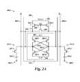
- FIG. 2Ais a schematic diagram illustrating sensing circuitry 250 - 1 in accordance with a number of embodiments of the present disclosure.
- FIG. 2Ashows a sense amplifier 206 coupled to a respective pair of complementary sense lines 205 - 1 and 205 - 2 .
- the sense amplifier 206 shown in FIG. 2Acan correspond to a plurality of sense amplifiers in the sensing circuitry 150 shown in FIG. 1A and/or the sensing circuitry 150 associated with the plurality of sensing component stripes 124 shown in FIG. 1B , for example.
- complementary memory cellsare coupled to pairs of complementary sense lines 205 - 1 and 205 - 2 (e.g., as columns) shown in FIG. 2A .
- a memory cellcan comprise a transistor and a capacitor.
- the memory cellscan be, for example, 1T1C DRAM cells each comprising a storage element (e.g., a capacitor) and an access device (e.g., a transistor), although other configurations can be used (e.g., 2T2C with two transistors and two capacitors per memory cell).
- the memory cellsmay be destructive read memory cells (e.g., reading the data stored in the cell destroys the data such that the data originally stored in the cell may be refreshed after being read).
- the cells of the memory arraycan be arranged in rows coupled by access lines and columns coupled by pairs of complementary sense lines, for example, DIGIT(n ⁇ 1)/DIGIT(n ⁇ 1)_, DIGIT(n)/DIGIT(n)_, DIGIT(n+1)/DIGIT(n+1)_.
- the individual sense lines corresponding to each pair of complementary data linescan also be referred to as sense lines 205 - 1 (D) and 205 - 2 (D_) respectively.
- sense lines 205 - 1 (D) and 205 - 2 (D_)respectively.
- an array of memory cellscan include additional columns of memory cells and/or sense lines (e.g., 4,096, 8,192, 16,384, etc.).
- Memory cellscan be coupled to different sense lines and/or access lines.
- a first source/drain region of an access transistor of a memory cellcan be coupled to a sense line 205 - 1 (D)
- a second source/drain region of the access transistor of the memory cellcan be coupled to a capacitor of the memory cell
- a gate of the access transistor of the memory cellcan be coupled to an access line of the memory array.
- the sensing circuitry 250 - 1can comprise a sense amplifier 206 corresponding to a respective column of memory cells (e.g., coupled to respective pairs of complementary sense lines).
- the sense amplifier 206can comprise, for example, a cross coupled latch, which can be referred to herein as a primary latch.
- a data storage statecan include the sense amplifiers 206 storing a data unit.
- a data unitcan be referred to as a bit and/or a digit value.
- the sense amplifier 206(or a compute component 231 as shown in and described in connection with FIG. 2B ) can be in at least one of two states associated with the first mode and the second mode.
- a state of a sense amplifier 206can describe a transfer of data to or from the sense amplifier 206 .
- the state of the sense amplifier 206can also be described as whether the sense amplifier 206 is in an equilibration state or is storing a data unit (e.g., a binary 0 or 1 data value).
- a sense amplifiercan be configured to be in an initial state, wherein the initial state is one of an equilibration state and a data storage state.
- a sense amplifier 206can comprise a cross coupled latch.
- embodiments of the sense amplifier 206are not limited to a cross coupled latch.
- the sense amplifier 206 in FIG. 2Acan be current-mode sense amplifier and/or single-ended sense amplifier (e.g., sense amplifier coupled to one data line).
- Embodiments of the present disclosurealso are not limited to a folded data line architecture.
- a sense amplifier 206can comprise a number of transistors formed on pitch with the transistors of a corresponding compute component (e.g., compute component 231 shown and described in connection with FIG. 2B ) and/or the memory cells of an array (e.g., memory array 130 shown in FIG. 1A and/or memory cells 302 / 303 shown in FIG. 3 ) to which they are coupled, which may conform to a particular feature size (e.g., 4F 2 , 6F 2 , etc.).
- Sense amplifier 206comprises a latch 215 including four transistors coupled to a pair of complementary sense lines D 205 - 1 and D_ 205 - 2 .
- the latch 215can be a cross coupled latch.
- the gates of a pair of transistorssuch as n-channel transistors (e.g., NMOS transistors) 227 - 1 and 227 - 2 can be cross coupled with the gates of another pair of transistors, such as p-channel transistors (e.g., PMOS transistors) 229 - 1 and 229 - 2 .
- the latch 215comprising transistors 227 - 1 , 227 - 2 , 229 - 1 , and 229 - 2 can be referred to as a primary latch.
- embodimentsare not limited to this example.
- the voltages and/or currents on the respective sense lines 205 - 1 and 205 - 2can be provided to the respective latch inputs 233 - 1 (S 1 ) and 233 - 2 (S 2 ) of the cross coupled latch 215 (e.g., the input of the primary latch).
- the latch input 233 - 1is coupled to a first source/drain region of transistors 227 - 1 and 229 - 1 as well as to the gates of transistors 227 - 2 and 229 - 2 .
- the latch input 233 - 2can be coupled to a first source/drain region of transistors 227 - 2 and 229 - 2 as well as to the gates of transistors 227 - 1 and 229 - 1 .
- a second source/drain region of transistors 227 - 1 and 227 - 2can be commonly coupled to a negative control signal (RnlF) 228 .
- a second source/drain region of transistors 229 - 1 and 229 - 2can be commonly coupled to an active positive control signal (ACT) 265 .
- the ACT signal 265can be a supply voltage (e.g., V DD ) and the RnlF signal can be a reference voltage (e.g., ground).
- RnlF signal 228 and ACT signal 265can function as activating signals that enable the cross coupled latch 215 .
- the enabled cross coupled latch 215can operate to amplify a differential voltage between latch input 233 - 1 (e.g., first common node) and latch input 233 - 2 (e.g., second common node) such that latch input 233 - 1 is driven to one of the ACT signal voltage and the RnlF signal voltage (e.g., to one of V DD and ground), and latch input 233 - 2 is driven to the other of the ACT signal voltage and the RnlF signal voltage.
- latch input 233 - 1e.g., first common node
- latch input 233 - 2e.g., second common node
- the ACT signal voltage and the RnlF signal voltagemay correspond to the full rail voltages for conversion of the sensed voltages from the pair of complementary memory cells to a data unit (e.g., a binary 0 or 1 data value) by determination of the voltage differential for either a read or a random number generation operation, among other possible operations.
- a data unite.g., a binary 0 or 1 data value
- the sense amplifier 206may also include equilibrate circuitry 214 configured to equilibrate sense line 205 - 1 and sense line 205 - 2 in association with, for example, preparing the sense amplifier for a logical operation and/or a random number generation operation.
- the equilibrate circuitry 214comprises a transistor 224 having a first source/drain region coupled to a first source/drain region of transistor 225 - 1 and sense line 205 - 1 .
- a second source/drain region of transistor 224can be coupled to a first source/drain region of transistor 225 - 2 and sense line 205 - 2 .
- a gate of transistor 224can be coupled to gates of transistors 225 - 1 and 225 - 2 .
- the second source drain regions of transistors 225 - 1 and 225 - 2can be coupled to an equilibration voltage 238 , which can be equal to V DD /2, where V DD is a supply voltage associated with the array.
- the gates of transistors 224 , 225 - 1 , and 225 - 2can be coupled to control signal 226 (EQ).
- activating EQcan enable the transistors 224 , 225 - 1 , and 225 - 2 , which can effectively short sense line 205 - 1 to sense line 205 - 2 . Shorting the sense lines as such may substantially equilibrate the sense lines 205 - 1 and 205 - 2 to the equilibration voltage V DD /2.
- a small residual voltage differentialmay remain between the complementary sense lines 205 - 1 and 205 - 2 , which may be sensed at the complementary memory cells coupled to the complementary sense lines in a row of the array by the corresponding sense amplifier 206 .
- the residual voltage differential itself and/or variance in direction of the differential with timemay result from, or be contributed to by, thermal noise causing random agitation of charge carriers in sense line 205 - 1 and sense line 205 - 2 .
- the sense amplifier 206may also include compensate circuitry 271 .
- the compensate circuitry 271 shown in FIG. 2Acan, in various examples, represent at least a portion of the functionality embodied by and contained in the compensate circuitry 171 shown in FIG. 1A .
- the compensate circuitry 271is configured to compensate for an inherent offset in the sense amplifier 206 and/or the respective sense lines 205 - 1 and 205 - 2 that may affect the sensed differential of the residual voltage (e.g., a magnitude of the differential).
- the sense amplifier 206may be enabled (e.g., fired) to sense and/or store voltage potentials from two complementary memory cells coupled to adjacent sense lines 205 - 1 and 205 - 2 , which may be on both sides of the sense amplifier 206 .
- An inherent offsetmay be a resistance and/or a capacitance that is not equal on both sides of the sense amplifier 206 .
- Variance in the resistance and/or capacitancemay be caused by variation in construction and/or connection (e.g., within or exceeding manufacturing tolerances) of the sense lines and/or other circuitry of the memory array.
- An intended unbalanced layout and/or unintended process variationsmay result in resistance and/or capacitance that varies between both sides of the sense amplifier 206 .
- Such variationmay cause, for example, threshold voltages to vary several millivolts from transistor to transistor.
- threshold voltages for NMOS transistors 227 - 1 and 227 - 2 and/or PMOS transistors 229 - 1 and 229 - 2may be affected such that the performance of the sense amplifier 206 may be impaired (e.g., defective).
- the compensate circuitry 271may be utilized to at least partially compensate (correct) such effects on the sense amplifier 206 .
- the compensate circuitry 271is split into a first portion 271 - 1 on the left side of the sense amplifier 206 and a second portion 271 - 2 on the right side.
- the compensate circuitry 271may be configured as a single portion on the left side or the right side of the sense amplifier 206 , among other possible locations, to compensate the variation in resistance and/or capacitance.
- each portion 271 - 1 , 271 - 2 of the compensate circuitrycan include a respective transistor 217 - 1 , 217 - 2 (e.g., an NMOS transistor) and a respective capacitor 218 - 1 , 218 - 2 .
- portion 271 - 1can be coupled to sense line 205 - 1 and latch input 233 - 1 and portion 271 - 2 can be coupled to sense line 205 - 2 and latch input 233 - 2 of the cross coupled latch 215 of the sense amplifier 206 .
- the compensate circuitry 271may be otherwise coupled to the sensing circuitry 250 - 1 .
- a compensate signal 290 - 1 , 290 - 2may be input to one or both portions of the compensate circuitry 271 - 1 , 271 - 2 .
- the compensate signals 290 - 1 , 290 - 2may be used to tune the sense amplifier 206 by effectively adding more resistance and/or capacitance to one side (e.g., via the respective sense line and/or the respective latch input) or the other side of the sense amplifier 206 . Biasing the resistance and/or capacitance of one side may be implemented by applying a particular analog voltage level to either transistor 217 - 1 , 217 - 2 and/or the respective capacitor 218 - 1 , 218 - 2 .
- a sense amplifier gaincan be changed by adjusting a DC supply voltage higher or lower to which the sense lines are equilibrated (e.g., V DD /2).
- compensate signalsmay be connected in common to all the sense amplifiers in a memory array 130 .
- the compensate signals 290 - 1 , 290 - 2may be sent from a source external to the memory array 130 (e.g., by the controller 140 and/or the random number component 172 thereof).
- the compensate signalsmay be similar to the RnlF signal 228 , the ACT signal 265 , and/or the EQ signal 226 .
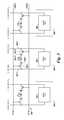
- FIG. 2Bis another schematic diagram illustrating sensing circuitry 250 - 2 in accordance with a number of embodiments of the present disclosure.
- FIG. 2Bindicates that a number of sense amplifiers 206 can be coupled to respective pairs of complementary sense lines 205 - 1 and 205 - 2 , and a corresponding number of compute components 231 can be coupled to the sense amplifiers 206 via pass gates 207 - 1 and 207 - 2 .
- the sense amplifier 206 and compute component 231 shown in FIG. 2Bcan correspond to sensing circuitry 150 shown in FIG. 1A and/or the sensing circuitry 150 associated with the plurality of sensing component stripes 124 shown in FIG. 1B , for example.
- FIG. 2Bincludes logical operation selection logic 213 , which can be operated as described further below.
- the configuration shown in FIG. 2Bdoes not include the compensate circuitry 271 illustrated in FIG. 1A .
- compensate circuitrymay be incorporated into the configuration shown in FIG. 2B .
- the sensing circuitry 250 - 2can comprise a sense amplifier 206 , a compute component 231 , and logical operation selection logic 213 corresponding to a respective column of memory cells (e.g., coupled to respective pairs of complementary sense lines).
- the sense amplifiers 206can be configured, for example, as described with respect to FIG. 2A .
- the sensing circuitry 250 - 2can be operated in both a pre-sensing mode (e.g., sense amplifiers 206 fired before logical operation control signal active) and post-sensing mode (e.g., sense amplifiers 206 fired after logical operation control signal active) with a result of a logical operation performed by the compute component 231 being initially stored in the sense amplifier 206 .
- the compute component 231can comprise a latch, which can be referred to herein as a secondary latch 264 .
- the secondary latch 264can be configured and operated in a manner similar to that described above with respect to the primary latch 215 .
- a pair of cross coupled p-channel transistors (e.g., PMOS transistors) included in the secondary latchcan have their respective sources coupled to a supply voltage 212 - 2 (e.g., V DD ), and the pair of cross coupled n-channel transistors (e.g., NMOS transistors) of the secondary latch can have their respective sources selectively coupled to a reference voltage 212 - 1 (e.g., ground), such that the secondary latch 264 may be continuously enabled.
- a supply voltage 212 - 2e.g., V DD
- NMOS transistorse.g., NMOS transistors
- the secondary latch 264 of the compute component 231can serve as an accumulator.
- the compute component 231can operate as and/or may be referred to herein as an accumulator.
- the configuration of the compute component 231is not limited to that shown in FIG. 2B , and various other embodiments are feasible within the scope of the present disclosure.
- the gates of the pass gates 207 - 1 and 207 - 2can be controlled by a logical operation selection logic signal, Pass.
- a logical operation selection logic signal, PassFor example, an output of the logical operation selection logic 213 can be coupled to the gates of the pass gates 207 - 1 and 207 - 2 .
- Data units present on the pair of complementary sense lines 205 - 1 and 205 - 2can be loaded into the compute component 231 via the pass gates 207 - 1 and 207 - 2 .
- the pass gates 207 - 1 and 207 - 2are OPEN
- data units on the pair of complementary sense lines 205 - 1 and 205 - 2may be passed to the compute component 231 .
- the data unit on the pair of complementary sense lines 205 - 1 and 205 - 2can be the data unit stored at least temporarily in the sense amplifier 206 when the sense amplifier is enabled (e.g., fired).
- the logical operation selection logic signal, Passis activated to OPEN (e.g., turn on) the pass gates 207 - 1 and 207 - 2 .
- the control signalscan operate to select a logical operation to implement based on the data unit (“B”) in the sense amplifier 206 and the data unit (“A”) in the compute component 231 (e.g., as used herein, the data unit stored in a primary latch of a sense amplifier is referred to as a “B” data unit, and the data unit stored in a secondary latch of a compute component is referred to as an “A” data unit).
- control signalsmay be configured to select the logical operation (e.g., function) to implement independent from the data unit present on the pair of complementary sense lines 205 - 1 and 205 - 2 , although the result of the implemented logical operation can be dependent on the data unit present on the pair of complementary sense lines 205 - 1 and 205 - 2 .
- logical operatione.g., function
- each column of memory cellscan be coupled to a column decode line that can be activated to transfer, via a local I/O line, a data unit from a corresponding sense amplifier 206 and/or compute component 231 to a control component external to the array such as an external processing resource (e.g., host processor and/or other functional unit circuitry).
- the column decode linecan be coupled to a column decoder (e.g., column decoder 152 in FIG. 1A ).
- dataneed not be transferred via such I/O lines to perform logical operations.
- circuitrycan be operated in conjunction with sense amplifiers 206 and compute components 231 to perform logical and/or random number generation operations without transferring data to a control component external to the array.
- transferring datacan include, for example, moving data from a source location to a destination location without necessarily maintaining a copy of the data at the source location.
- a data unit on a pair of complementary sense linescan be loaded into a corresponding compute component 231 (e.g., by operating logical operation selection logic as described above).
- a data unitcan be loaded into a compute component 231 via overwriting of the data unit currently stored in the compute component 231 with the data unit stored in the corresponding sense amplifier 206 .
- the sensing circuitry 250 - 2 in FIG. 2Bcan be operated in several modes to perform logical (e.g., PIM) operations, including a first mode in which a result of the logical operation is initially stored in the sense amplifier 206 , and a second mode in which a result of the logical operation is initially stored in the compute component 231 .
- logicale.g., PIM
- the sense amplifier 206is equilibrated and the control signals are activated to provide a conduction path (e.g., electrical continuity) between the sense amplifier 206 and the compute component 231 , then a data unit stored in the compute component 231 can be transferred from the compute component 231 to the sense amplifier 206 .
- the sense amplifier 206is configured to store a first bit (e.g., first data unit) and the control signals are activated to provide a conduction path between the sense amplifier 206 and the compute component 231 , then a second bit (e.g., second data unit) that is stored in the compute component 231 before the activation of the control signals can be replaced by the first bit and the sense amplifier 206 retains the first bit. Furthermore, a number of PIM operations can be performed using the first bit and the second bit using the logical operation selection logic and the result of the operation can be stored in the compute component 231 .
- the sense amplifier 206can, in some embodiments in conjunction with the compute component 231 , be operated to perform various logical operations and/or operations involving random number generation (e.g., using data and/or residual voltages from an array as input).
- the result of a logical operation and/or operation involving random number generationcan be stored back to the array without transferring the data via a data line address access (e.g., without firing a column decode signal such that data is transferred to circuitry external to the array and sensing circuitry via local I/O lines).
- a number of embodiments of the present disclosurecan enable performing various PIM operations (e.g., logical operations, shift operations, mathematical operations, data movement operations using shared I/O lines) and/or operations involving random number generation, etc., using less power than various previous approaches. Additionally, because a number of embodiments can reduce or eliminate moving (e.g., copying, transferring) data across I/O lines in order to perform operations (e.g., between memory and a discrete processor, which may be off pitch), a number of embodiments may enable an increased parallel processing capability as compared to previous approaches.
- PIM operationse.g., logical operations, shift operations, mathematical operations, data movement operations using shared I/O lines
- FIG. 3is a schematic diagram of a memory device in accordance with a number of embodiments of the present disclosure.
- the memory array 330is an array, for example a DRAM array, of 1T1C (one transistor one capacitor) memory cells that can each include an access device 302 (e.g., a transistor) and a storage element 303 (e.g., a capacitor).
- 1T1Cone transistor one capacitor
- the memory cells of the memory array 330can be arranged in rows (as shown at 119 and described in connection with FIG.
- a gate of a particular memory cell transistor 302can be coupled to its corresponding access line 304 -X, 304 -Y, etc.
- a first source/drain regioncan be coupled to its corresponding data line (e.g., 305 - 1 (DIGIT(n), 305 - 2 (DIGIT(n)_))
- a second source/drain region of a particular memory cell transistorcan be coupled to its corresponding capacitor 303 .
- Memory cellscan be coupled to different sense lines and/or access lines.
- a first source/drain region of a transistor 302 - 1can be coupled to sense line 305 - 1
- a second source/drain region of transistor 302 - 1can be coupled to capacitor 303 - 1
- a gate of a transistor 302 - 1can be coupled to access line 304 -Y.
- a first source/drain region of transistor 302 - 2can be coupled to sense line 305 - 2
- a second source/drain region of transistor 302 - 2can be coupled to capacitor 303 - 2
- a gate of a transistor 302 - 2can be coupled to access line 304 -X.
- the cell plateas shown in FIG. 3 , can be coupled to each of capacitors 303 - 1 and 303 - 2 .
- the cell platecan be a common node to which a reference voltage (e.g., ground) can be applied in various memory array configurations.
- the transistors 302 and capacitors 303can contribute to formation of the pairs of complementary memory cells in a single row of the memory array that are coupled to the complementary sense lines (e.g., sense lines 305 - 1 and 305 - 2 ).
- the number of data values (e.g., voltages) sensed from the memory cells in logical operations and/or random number generation operationsmay correspond to the number of columns of memory cells and/or pairs of sense lines (e.g., 4,096, 8,192, 16,384, etc.) that intersect a row, for example, of a subarray 125 shown in and described in connection with FIG. 1B .
- each subarraymay include 256, 512, 1024 rows, among other possible numbers of rows, and each bank section may be divided into 32, 64, or 128 subarrays, among various possibilities.
- the memory array 330 illustrated in FIG. 3is coupled to sensing circuitry 350 in accordance with a number of embodiments of the present disclosure.
- the sensing circuitry 350 - 1may include a sense amplifier 306 corresponding to respective columns of memory cells (e.g., coupled to respective pairs of complementary data lines 305 - 1 , 305 - 2 ) but does not additionally include a compute component (e.g., 231 shown in FIG. 2B ).
- a compute componente.g., 231 shown in FIG. 2B
- embodimentsare not so limited.
- some embodiments of the sensing circuitry 350 - 2may include a compute component that can perform compute and/or accumulator functionalities.
- the sensing circuitry 350can correspond to sensing circuitry 150 shown in FIG. 1A and/or described in connection with the sensing component stripes 124 in FIG. 1B , for example.
- the sense amplifier 306can correspond to sense amplifier 206 described previously with respect to FIGS. 2A-2B .
- the sense amplifier 306can be operated to determine a data value stored in (e.g., a logic state) and/or a residual voltage at a selected memory cell, which may be represented by the voltages present on the complementary sense lines 305 - 1 , 305 - 2 .
- FIGS. 4A-4Billustrate waveform diagrams showing signals on sense lines corresponding to a number of logical operations and random number generation operations in accordance with a number of embodiments of the present disclosure.
- logical operationse.g., read, write, and/or Boolean compute operations, among others
- a memory arraye.g., having DRAM memory cells
- a sequence of events for accessing the memory cells of a rowcan occur as illustrated in the waveform 460 shown in FIG. 4A .
- the voltage of sense lines 405 - 1 and 405 - 2may be at essentially the same voltage 461 (e.g., V DD /2).
- That rowcan be selected and/or opened 462 (e.g., fired by execution of a fire row command).
- the firing 462 of the rowmay introduce a small voltage differential between the sense lines 405 - 1 and 405 - 2 that may be sensed (e.g., at complementary memory cells coupled to the sense lines) by a coupled sense amplifier.
- a memory cell coupled to sense line 405 - 1can be programmed to hold a positive voltage that can be sensed by operating (firing) 465 the sense amplifier and amplified 466 to a full rail voltage (e.g., V DD ) that indicates a logical value (e.g., data unit) of 1 in binary, for example.
- V DDfull rail voltage
- a complementary memory cell coupled to sense line 405 - 2can remain in a low voltage state so as to hold the original voltage 461 (e.g., V DD /2), which can be sensed by operating (firing) 463 the coupled sense amplifier and amplified 464 to a full rail voltage (e.g., ground) indicative of voltage not being elevated at the complementary memory cell.
- the original small voltage differentialwill determine the data value (e.g., data unit) sensed at the sense amplifier after the sense amplifier is fired.
- the sense lines 405 - 1 and 405 - 2can have their voltages equilibrated 467 - 1 , 467 - 2 .
- the sense lines 405 - 1 and 405 - 2can have their voltages equilibrated by both sense lines having their voltages equilibrated to essentially the same voltage 469 (e.g., V DD /2), as described in connection with the equilibrate circuitry 214 shown in and described in connection with FIG. 2A .
- FIG. 4Billustrates a magnified waveform 468 corresponding to the equilibrated portion of the waveform shown at the right side of FIG. 4A .
- an equilibration operationmay equalize the voltages of both sense lines to essentially the same voltage 469 when viewed and/or analyzed on a large scale, such as shown in FIG. 4A , variations between the sense lines (e.g., differences in composition, thickness, length, conductance, and/or resistance, among other factors) may contribute to the sense lines not being brought to exactly the same voltage.
- the voltages of the sense linesmay vary randomly due to electronic noise (e.g., thermal noise) causing the residual voltage at each of the pair of complementary memory cells after equilibration to randomly vary with passage of time.
- the random variations of the residual voltage in the complementary sense linesmay cause the small scale residual voltage differentials 469 that vary with the passage of time 473 shown in FIG. 4B .
- the voltage differential between the sense linesis not exactly at 0.0 V.
- Various sources of entropymay contribute to electronic noise in electrical conductors of the sensing circuitry 150 and/or the memory array 130 .
- a major contributionmay be due to thermal noise present on the sense lines 405 - 1 and 405 - 2 and/or output of the transistors 227 - 1 , 227 - 2 , 229 - 1 , and 229 - 2 of the sense amplifiers 206 .
- thermal noisemay be modeled with the following equation:
- v ds 2 _4 ⁇ ⁇ ⁇ ⁇ ⁇ kT ⁇ ⁇ ⁇ ⁇ ⁇ f g ds
- g dsis the reciprocal of the resistance between d and s and is measured in siemens
- kis Boltzmann's constant in joules per kelvin
- Tis the absolute temperature in degrees kelvin
- ⁇ fis the bandwidth in hertz over which the noise is measured
- ⁇is a value chosen to fit a noise measurement to improve accuracy of the noise model.
- residual voltage differentialswill be non-deterministic and, hence, can be used to produce random data units (e.g., of either 0 or 1 in binary) at the sense amplifier. Because the small scale residual voltage differentials 469 between the complementary sense lines may randomly vary in a positive direction or negative direction at any point in time, sensing and amplifying the residual voltage differentials with a sense amplifier can yield a data unit (e.g., 0 or 1 in binary) that randomly varies (e.g., between 0 or 1) at any point in time.
- a data unite.g., 0 or 1 in binary
- combining a plurality of data units determined from residual voltage differentials of a plurality of complementary memory cells in a rowmay yield a vector of random data units with a length that corresponds to a number of pairs of complementary memory cells sensed by the respective sense amplifiers.
- a sense operationmay be performed to determine a residual voltage differential on the first sense line and a complimentary second sense line in a range of 15-45 millivolts
- a read operation of a memory cell of a rowmay be performed to determine a voltage differential of a programmed data unit in a range of 50-100 millivolts.
- the residual voltage differentialmay be sensed by the sense amplifier in a lower voltage (potential) range than the potential range used by the sense amplifier for sensing a voltage differential of a programmed data unit.
- a lowest millivolt value in the residual voltage differential rangemay be greater than a highest millivolt value in a range of inherent offsets for memory cells, sense lines, and/or sense amplifiers of the DRAM array or may be adjusted accordingly by compensate circuitry (e.g., as shown at 271 and described in connection with FIG. 2A ).
- FIG. 5illustrates a timing diagram associated with performing a number of logical operations using sensing circuitry in accordance with a number of embodiments of the present disclosure.
- a sequence of eventsincluding the row cycle and random number generation operations described in connection with FIGS. 4A-4B , can be directed by a series of fine-tuned operations.
- the series of operationsmay be sent to the DRAM array at specific times determined by instructions issued by, for example, a state machine and/or a timing component thereof, as described herein.
- FIG. 5illustrates a timing diagram 575 associated with performance of the various logical operations (e.g., read, write, and/or Boolean compute operations, among others) in the row cycle using circuitry in accordance with that described in connection with the left side of FIG. 4A and elsewhere herein.
- the timing diagram 575 schematically illustrated in FIG. 5is shown as an example of a sequence of signals in circuitry for the various logical operations.
- a time scale horizontally demarcated in signaling unit time points (t 0 , t 1 , t 2 , . . . , t 13 ) of arbitrary lengthis shown by way of example.
- a pair of complementary sense linesmay be in an equilibration state 567 .
- the row of memory cellsmay be selected and/or opened 562 (e.g., fired) to introduce a small voltage differential between the sense lines, as shown at 462 in FIG. 4A .
- a sense amplifiermay be fired 563 , 565 to determine a voltage differential between the sense lines at a position of complementary memory cells in the row.
- firing of the row at 562would overwhelm the residual voltage of the sense lines 405 - 1 and 405 - 2 so as to prevent the residual voltage differential at complementary memory cells from being sensed by a coupled sense amplifier.
- the residual voltage differential at the complementary memory cellsmay remain overwhelmed until bringing the row of memory cells back to the equilibration state 567 starting at to.
- FIG. 6illustrates a timing diagram 680 associated with performing a number of random number generation operations using sensing circuitry in accordance with a number of embodiments of the present disclosure.
- performance of the various logical operations in the row cyclemay render voltages and differentials thereof resulting from electronic (e.g., thermal) noise negligible when the row is fired.
- the present disclosuredescribes issuing by the state machine and/or the timing component thereof a sequence of instructions to the row that does not include instructions for performance of the row fire operation. This can be accomplished by modifying the sequence of instructions sent to the DRAM array.
- a pair of complementary sense linesmay be in an equilibration state 667 .
- the row of memory cellsmay remain unselected and/or unopened 662 (e.g., unfired).
- a sense amplifiermay be fired 663 , 665 to determine a voltage differential between the sense lines at a position of complementary memory cells in the row.
- the electronic (thermal) noisemay enable the residual voltages of the sense lines and the differential thereof to be sensed by the fired sense amplifier between a first sense line and a complimentary second sense line in the array, for example, following a previous equilibration operation.
- Executing this modified sequence of instructionsmay enable generation of a random data value (e.g., 0 or 1 in binary) at t 2 , as shown in FIG. 6 .
- a random data valuemay be generated at any of the time points t 0 , t 1 , t 2 , . . . , t 10 in the modified row cycle at which the sense amplifier is fired 663 , 665 following placing the pair of complementary sense lines in an equilibration state 667 at t 11 , t 12 , t 13 , for example.
- the modified sequence of instructionsmay be written such that the modified series of operations for the row cycle may apply to sense amplifiers corresponding to an entire row of memory cells, the same series of operations may be used to produce a number of random data units corresponding to a length of the entire row. Since the length of an element within a vector of random data units may depend only on how that vector is addressed, a hardware, firmware, and/or software application may use this set of random data units as a vector containing up to W/L elements of random data units, where W is the width of the row in the array in data units and L is a desired length of the element in data units.
- physical propertiese.g., inherent offsets for sense lines, memory cells, and/or sense amplifiers of a DRAM array
- the compensate circuitry 271 shown in and described in connection with FIG. 2Ais designed to at least partially overcome such difficulties.
- Embodiments described hereinprovide a method of operating an apparatus that may be in the form of a computing system 100 including a memory device 120 (e.g., as shown in and described in connection with FIGS. 1A-3 ) for random number generation.
- the methodcan include operating the memory device for random number generation by operating a sense amplifier (e.g., sense amplifier 206 in FIGS. 2A-2B and/or 306 in FIG. 3 ) of the memory device to perform sensing a first voltage on a first sense line (e.g., sense line 205 - 1 shown in FIGS. 2A-2B and at corresponding reference numbers on FIGS.
- a sense amplifiere.g., sense amplifier 206 in FIGS. 2A-2B and/or 306 in FIG. 3
- a first sense linee.g., sense line 205 - 1 shown in FIGS. 2A-2B and at corresponding reference numbers on FIGS.
- the methodcan include generating a random number by detecting a voltage differential between the first sense line and the complementary second sense line.
- an equilibration operationcan be performed such that the first voltage on the first sense line and the second voltage on the complementary second sense line are both in an equilibration state.
- a sense line 305 - 1 coupled to a memory celle.g., the memory cell shown at 302 - 1 , 303 - 1 in FIG. 3
- a sense line 305 - 2 coupled to a paired memory celle.g., the memory cell shown at 302 - 2 , 303 - 2 in FIG. 3
- a paired memory celle.g., the memory cell shown at 302 - 2 , 303 - 2 in FIG. 3
- the equilibration operationcan be performed, for example, using the equilibrate circuitry 214 to equilibrate sense line 205 - 1 and sense line 205 - 2 shown in and described in connection with FIGS. 2A-2B .
- Performance of the equilibration operationcan bring the voltages of the sense lines and/or memory cells to essentially the same residual voltage (e.g., close to V DD /2 as shown at 469 and described in connection with FIG. 4A ).
- the methodcan include sensing a first residual voltage on the first sense line and a second residual voltage on the complementary second sense line to detect the voltage differential to generate the random number.
- the first residual voltage and the second residual voltagemay, as described herein, result from electronic noise (e.g., thermal noise) in an electrical conductor (e.g., sense lines 205 - 1 , 205 - 2 , a sense amplifier 206 , and/or a compute component 231 shown in and described in connection with FIGS. 2A-2B ).
- a differentialmay be generated in the first residual voltage and the second residual voltage by residual voltages being unequal in the first sense line (e.g., sense line 305 - 1 ) and the second sense line (e.g., sense line 305 - 2 ).
- Performance of the equilibration operationcan result in the residual voltages being unequal in the first sense and the second sense line (e.g., as shown at 469 and described in connection with FIG. 4B ).
- the unequal residual voltagescan be due to, or at least contributed to, thermal noise that enables random agitation of charge carriers in the first sense line and the second sense line.
- a random data unitcan be generated from the detection of the voltage differential between the first sense line and the complementary second sense line and a random number can be generated utilizing the random data unit.
- a residual voltage differentialcan be determined on a first sense line and a complementary second sense line using a sense amplifier selectably coupled to the respective pair of complementary sense lines.
- the random data unitcan, in some embodiments, be generated by performing an equilibration operation on a pair of complementary sense lines of a DRAM array.
- the random data unitmay be determined based on the determined residual voltage differential.
- the random data unitmay be stored in the sense amplifier that determined residual voltage differential.
- the random data unitmay be moved for storage in a pair of complementary memory cells of a row of the DRAM array.
- the random numbermay be generated, in some embodiments, by a processor (e.g., random number component 172 shown in and described in connection with FIGS. 1A-1B ) by accessing the random data unit from the sense amplifier and/or the memory cell in which the random data unit is stored.
- a random number generation operationmay leave a row unselected and/or unopened (e.g., unfired) for a programming operation (e.g., a logical operation as described in connection with FIG. 5 ) prior to using sense amplifier to perform the sense operation to determine the residual voltage differential for random number generation.
- Leaving the row unfired for the random number generation operationmay include a state machine and/or a timing component thereof issuing a sequence of instructions (e.g., microcode) that differs from instructions issued to direct performance of the logical operation.
- Performing the random number generation operationmay include determining a residual voltage differential on each of respective pairs of complementary sense lines (e.g., as shown at 305 - 1 and 305 - 2 in FIG. 3 ).
- a single sense amplifier 306can be selectably coupled to each respective pair of complementary memory cells (e.g., via the sense lines 305 - 1 , 305 - 2 ).
- a vector of data unitsmay be generated with a length that corresponds to a number of pairs of complementary sense lines of the DRAM array (e.g., the number of pairs of complementary sense lines intersecting a row of the DRAM array).
- the vector of data units that corresponds to a number of pairs of complementary sense linesmay be divided, for example, by a processor (e.g., random number component 172 ) into a plurality of vector elements (e.g., W/L elements of random data units).
- a plurality of random numbersmay be generated from the plurality of vector elements, which may be generated from a single vector of data units.
- Each of the random numbersmay include a selected plurality of data units in the vector elements.
- all of the random numbersmay have the same number of data units (digits) by selecting four (e.g., 2761 , 9842 , 1068 , etc.) as the plurality of data units in the vector elements.
- the number of data units (digits)can vary between the vector elements and, thus, the random numbers.
- a first residual voltage differentialmay be determined at a first time by a first sense operation performed on the first sense line and the complementary second sense line to yield a first random data unit.
- a second residual voltage differentialmay be determined at a second time by a second sense operation performed on the first sense line and the complementary second sense line to yield a second random data unit.
- the first random data unitmay be different from the second random data unit due to electronic noise causing the residual voltage on the first sense line and the complementary second sense line to randomly vary with passage of time.
- At least one embodiment of such an apparatusmay include a DRAM memory cell array 130 with sensing circuitry 150 coupled to the array (e.g., as shown and described in connection with FIGS. 1A-1B ).
- the sensing circuitry 150can include a sense amplifier (e.g., as shown at 206 and described in connection with FIGS. 2A-2B and at corresponding reference numbers in FIG. 3 ) coupled to a respective sense line (e.g., as shown at 205 - 1 and 205 - 2 and described in connection with FIGS. 2A-2B and at corresponding reference numbers in FIG. 3 ).
- the sensing circuitry 150can be configured to perform random number generation operations and DRAM logical operations (e.g., read and write operations, and Boolean operations, among others).
- the sensing circuitry 150may further include equilibrate circuitry (e.g., as shown at 214 and described in connection with FIGS. 2A-2B ) configured to equilibrate complementary programmed memory cells selectably coupled to the complementary sense lines in the array, which also become equilibrated.
- a random number component 172(e.g., a processing resource associated with and/or connected to the controller 140 described in connection with FIGS. 1A-1B ) can be coupled to the array and sensing circuitry.
- the random number component 172may be configured to generate a random number from a residual voltage differential sensed by the sense amplifier on complementary sense lines, as described herein.
- the random number component 172may generate the random number from the residual voltage differential of the equilibrated complementary sense lines.
- the residual voltage differentialmay at least partially be enabled by random electronic noise in the respective sense lines, with the random number generation being based on the residual voltage differential.
- the random number component 172can include logic, for example, hardware (e.g., in the form of ASIC) and/or firmware to implement one or more particular functions.
- the random number component and/or the logicmay be configured to receive a request for a random number generation operation and to execute coded instructions (e.g., microcode to initiate the performance of the random number generation operation).
- the coded instructionsmay be included and/or associated with a state machine to control the performance of the random number generation operations and/or the DRAM operation by the sensing circuitry.
- the controller 140 of a memory device 120may include control circuitry that, in some embodiments, can include control logic and a state machine (e.g., an atomic state machine).
- the state machinemay include and/or be associated with a timing component.
- the logicmay be configured to, for example, receive requests for performance of random number generation operations and DRAM logical operations and execute coded machine instructions to initiate performance of different sequences and/or timing of operations dependent upon whether the request is for performance of a random number generation operation or a DRAM logical operation, as described with regard to FIGS. 5 and 6 .
- the coded machine instructionscan be, for example, microcode instructions.
- the sensing circuitrymay further include a compute component (e.g., as shown at 231 and described in connection with FIG. 2B ) coupled to a respective sense amplifier 206 .
- the compute componentmay be configured to utilize the random number generated from the residual voltage differential sensed by the sense amplifier in performance of a logical operation.
- a logical operationmay include the DRAM logical operations described herein.
- such a logical operationmay include the previously described examples of applications that use random number samples, among other possibilities.
- the sensing circuitry 250 , the compensate component 271 , and/or the random number component 172may be formed on pitch with the memory cells in the array 130 .
- a plurality of complementary memory cellscan be included in a row of a memory cell array (e.g., as shown and described in connection with FIG. 3 ).
- the sensing circuitry(e.g., 250 , 350 ) may be selectably coupled to the plurality of complementary memory cells via a plurality of columns (e.g., as shown at 122 and described in connection with FIG. 1B ).
- a columncan correspond to a pair of complementary of sense lines coupled to corresponding complementary memory cells (e.g., as shown in FIG. 3 ).
- the sensing circuitrycan include a respective plurality of sense amplifiers (e.g., 215 ) and equilibrate circuitry (e.g., 214 ) coupled to a respective plurality of pairs of complementary of sense lines.
- a controller 140can be selectably coupled to the row of the plurality of memory cells and the sensing circuitry and can be configured to issue a command for generation of random numbers based on the residual voltage differentials sensed by the plurality of sense amplifiers on the plurality of complementary sense lines.
- a random number component 172may be associated with and/or connected to the controller 140 .
- the random number component 172may be operatively coupled to the sensing circuitry and configured to generate a random number from the residual voltage differential sensed by the sense amplifier at the complementary memory cells.
- the random number component 172may be further configured to generate a vector of data units with a length that corresponds to a number of the plurality of complementary memory cells in the row.
- the random number component 172may be configured to generate a vector of data units with a length that corresponds to a number of the random the random data units generated from the residual voltage differentials sensed by a respective plurality of sense amplifiers (e.g., where the residual voltage differential sensed by each sense amplifier may be used to generate a single data unit for the vector).
- the controller 140may be further configured to issue a command to generate a plurality of vector elements by division of the vector of data units.
- the number of the data units in the vectormay correspond to a number of the plurality of complementary sense lines that intersect the row and a number of the plurality of vector elements may correspond to the number of the data units in the vector divided by a selected length in data units of each vector element.
- the controller 140e.g., or a state machine and/or a timing component associated with and/or connected to the controller
- sensing circuitrysense amplifiers
- compute componentsequilibrate circuitry
- random number componentscontrol circuitry (e.g., including control logic, a sequencer, a timing component, etc.), and/or compensate circuitry, etc.)
- control circuitrye.g., including control logic, a sequencer, a timing component, etc.
- compensate circuitryetc.
Landscapes
- Engineering & Computer Science (AREA)
- Microelectronics & Electronic Packaging (AREA)
- Computer Hardware Design (AREA)
- General Physics & Mathematics (AREA)
- Theoretical Computer Science (AREA)
- Physics & Mathematics (AREA)
- Mathematical Analysis (AREA)
- Mathematical Optimization (AREA)
- Pure & Applied Mathematics (AREA)
- Computational Mathematics (AREA)
- General Engineering & Computer Science (AREA)
- Databases & Information Systems (AREA)
- Dram (AREA)
Abstract
Description
where

Claims (20)
Priority Applications (2)
| Application Number | Priority Date | Filing Date | Title |
|---|---|---|---|
| US15/995,748US10152304B2 (en) | 2016-08-03 | 2018-06-01 | Apparatuses and methods for random number generation |
| US16/213,835US10387121B2 (en) | 2016-08-03 | 2018-12-07 | Apparatuses and methods for random number generation |
Applications Claiming Priority (2)
| Application Number | Priority Date | Filing Date | Title |
|---|---|---|---|
| US15/227,459US9990181B2 (en) | 2016-08-03 | 2016-08-03 | Apparatuses and methods for random number generation |
| US15/995,748US10152304B2 (en) | 2016-08-03 | 2018-06-01 | Apparatuses and methods for random number generation |
Related Parent Applications (1)
| Application Number | Title | Priority Date | Filing Date |
|---|---|---|---|
| US15/227,459ContinuationUS9990181B2 (en) | 2016-08-03 | 2016-08-03 | Apparatuses and methods for random number generation |
Related Child Applications (1)
| Application Number | Title | Priority Date | Filing Date |
|---|---|---|---|
| US16/213,835ContinuationUS10387121B2 (en) | 2016-08-03 | 2018-12-07 | Apparatuses and methods for random number generation |
Publications (2)
| Publication Number | Publication Date |
|---|---|
| US20180275964A1 US20180275964A1 (en) | 2018-09-27 |
| US10152304B2true US10152304B2 (en) | 2018-12-11 |
Family
ID=61071409
Family Applications (3)
| Application Number | Title | Priority Date | Filing Date |
|---|---|---|---|
| US15/227,459Active2036-09-13US9990181B2 (en) | 2016-08-03 | 2016-08-03 | Apparatuses and methods for random number generation |
| US15/995,748ActiveUS10152304B2 (en) | 2016-08-03 | 2018-06-01 | Apparatuses and methods for random number generation |
| US16/213,835ActiveUS10387121B2 (en) | 2016-08-03 | 2018-12-07 | Apparatuses and methods for random number generation |
Family Applications Before (1)
| Application Number | Title | Priority Date | Filing Date |
|---|---|---|---|
| US15/227,459Active2036-09-13US9990181B2 (en) | 2016-08-03 | 2016-08-03 | Apparatuses and methods for random number generation |
Family Applications After (1)
| Application Number | Title | Priority Date | Filing Date |
|---|---|---|---|
| US16/213,835ActiveUS10387121B2 (en) | 2016-08-03 | 2018-12-07 | Apparatuses and methods for random number generation |
Country Status (1)
| Country | Link |
|---|---|
| US (3) | US9990181B2 (en) |
Families Citing this family (25)
| Publication number | Priority date | Publication date | Assignee | Title |
|---|---|---|---|---|
| US10014034B2 (en)* | 2016-10-06 | 2018-07-03 | Micron Technology, Inc. | Shifting data in sensing circuitry |
| KR101920190B1 (en)* | 2016-11-22 | 2019-02-08 | 한국인터넷진흥원 | A method and apparatus for generating a random ip |
| US11728000B1 (en)* | 2017-12-13 | 2023-08-15 | Board Of Trustees Of The University Of Alabama, For And On Behalf Of The University Of Alabama In Huntsville | Systems and methods for detecting counterfeit or defective memory |
| US10725696B2 (en) | 2018-04-12 | 2020-07-28 | Micron Technology, Inc. | Command selection policy with read priority |
| TWI669714B (en)* | 2018-05-29 | 2019-08-21 | 力旺電子股份有限公司 | Voltage control device and memory system |
| US10440341B1 (en) | 2018-06-07 | 2019-10-08 | Micron Technology, Inc. | Image processor formed in an array of memory cells |
| US11175915B2 (en) | 2018-10-10 | 2021-11-16 | Micron Technology, Inc. | Vector registers implemented in memory |
| US10769071B2 (en) | 2018-10-10 | 2020-09-08 | Micron Technology, Inc. | Coherent memory access |
| US10483978B1 (en) | 2018-10-16 | 2019-11-19 | Micron Technology, Inc. | Memory device processing |
| US11184446B2 (en) | 2018-12-05 | 2021-11-23 | Micron Technology, Inc. | Methods and apparatus for incentivizing participation in fog networks |
| US12118056B2 (en) | 2019-05-03 | 2024-10-15 | Micron Technology, Inc. | Methods and apparatus for performing matrix transformations within a memory array |
| US10867655B1 (en) | 2019-07-08 | 2020-12-15 | Micron Technology, Inc. | Methods and apparatus for dynamically adjusting performance of partitioned memory |
| US11360768B2 (en) | 2019-08-14 | 2022-06-14 | Micron Technolgy, Inc. | Bit string operations in memory |
| US11449577B2 (en) | 2019-11-20 | 2022-09-20 | Micron Technology, Inc. | Methods and apparatus for performing video processing matrix operations within a memory array |
| US11853385B2 (en) | 2019-12-05 | 2023-12-26 | Micron Technology, Inc. | Methods and apparatus for performing diversity matrix operations within a memory array |
| KR102840199B1 (en) | 2019-12-17 | 2025-08-01 | 삼성전자주식회사 | Memory device and memory system having the same |
| CN111338602A (en)* | 2020-04-02 | 2020-06-26 | 北京大学 | Bit stream generator and generation method for random calculation |
| US11227641B1 (en) | 2020-07-21 | 2022-01-18 | Micron Technology, Inc. | Arithmetic operations in memory |
| WO2022027371A1 (en)* | 2020-08-05 | 2022-02-10 | Alibaba Group Holding Limited | Noise control in processor-in-memory architectures |
| US11562784B2 (en)* | 2020-08-14 | 2023-01-24 | Micron Technology, Inc. | Apparatuses, systems, and methods for voltage based random number generation |
| US20220300255A1 (en)* | 2021-03-21 | 2022-09-22 | Gsi Technology Inc. | Ram true random number generator |
| US12159053B1 (en) | 2021-05-24 | 2024-12-03 | Board of Trustees for the University of Alabama, for and on behalf of the University of Alabama in Huntsville | Systems and methods for identifying counterfeit memory |
| US12354643B2 (en) | 2021-11-12 | 2025-07-08 | Samsung Electronics Co., Ltd. | Storage device and storage system including PUF |
| US20230205531A1 (en)* | 2021-12-23 | 2023-06-29 | Intel Corporation | Random data usage |
| US12340841B2 (en) | 2023-02-17 | 2025-06-24 | Globalfoundries U.S. Inc. | Multi-rail sense circuit with pre-charge transistors and memory circuit incorporating the sense circuit |
Citations (299)
| Publication number | Priority date | Publication date | Assignee | Title |
|---|---|---|---|---|
| US4380046A (en) | 1979-05-21 | 1983-04-12 | Nasa | Massively parallel processor computer |
| US4435793A (en) | 1979-07-26 | 1984-03-06 | Tokyo Shibaura Denki Kabushiki Kaisha | Semiconductor memory device with dummy word line/sense amplifier activation |
| US4435792A (en) | 1982-06-30 | 1984-03-06 | Sun Microsystems, Inc. | Raster memory manipulation apparatus |
| EP0214718A2 (en) | 1985-07-22 | 1987-03-18 | Alliant Computer Systems Corporation | Digital computer |
| US4727474A (en) | 1983-02-18 | 1988-02-23 | Loral Corporation | Staging memory for massively parallel processor |
| US4843264A (en) | 1987-11-25 | 1989-06-27 | Visic, Inc. | Dynamic sense amplifier for CMOS static RAM |
| US4958378A (en) | 1989-04-26 | 1990-09-18 | Sun Microsystems, Inc. | Method and apparatus for detecting changes in raster data |
| US4977542A (en) | 1988-08-30 | 1990-12-11 | Mitsubishi Denki Kabushiki Kaisha | Dynamic semiconductor memory device of a twisted bit line system having improved reliability of readout |
| US5023838A (en) | 1988-12-02 | 1991-06-11 | Ncr Corporation | Random access memory device with integral logic capability |
| US5034636A (en) | 1990-06-04 | 1991-07-23 | Motorola, Inc. | Sense amplifier with an integral logic function |
| US5201039A (en) | 1987-09-30 | 1993-04-06 | Mitsubishi Denki Kabushiki Kaisha | Multiple address-space data processor with addressable register and context switching |
| US5210850A (en) | 1990-06-15 | 1993-05-11 | Compaq Computer Corporation | Memory address space determination using programmable limit registers with single-ended comparators |
| US5253308A (en) | 1989-06-21 | 1993-10-12 | Amber Engineering, Inc. | Massively parallel digital image data processor using pixel-mapped input/output and relative indexed addressing |
| US5276643A (en) | 1988-08-11 | 1994-01-04 | Siemens Aktiengesellschaft | Integrated semiconductor circuit |
| US5325519A (en) | 1991-10-18 | 1994-06-28 | Texas Microsystems, Inc. | Fault tolerant computer with archival rollback capabilities |
| US5367488A (en) | 1992-03-18 | 1994-11-22 | Goldstar Electron Co., Ltd. | DRAM having bidirectional global bit lines |
| US5379257A (en) | 1990-11-16 | 1995-01-03 | Mitsubishi Denki Kabushiki Kaisha | Semiconductor integrated circuit device having a memory and an operational unit integrated therein |
| US5386379A (en) | 1992-01-03 | 1995-01-31 | France Telecom, Establissement Autonome De Droit Public | Memory cell for associative memory |
| US5398213A (en) | 1992-10-08 | 1995-03-14 | Samsung Electronics Co., Ltd. | Access time speed-up circuit for a semiconductor memory device |
| US5440482A (en) | 1993-03-25 | 1995-08-08 | Taligent, Inc. | Forward and reverse Boyer-Moore string searching of multilingual text having a defined collation order |
| US5446690A (en) | 1993-08-10 | 1995-08-29 | Hitachi, Ltd. | Semiconductor nonvolatile memory device |
| US5473576A (en) | 1993-07-27 | 1995-12-05 | Nec Corporation | Dynamic random access memory device with low-power consumption column selector |
| US5481500A (en) | 1994-07-22 | 1996-01-02 | International Business Machines Corporation | Precharged bit decoder and sense amplifier with integrated latch usable in pipelined memories |
| US5485373A (en) | 1993-03-25 | 1996-01-16 | Taligent, Inc. | Language-sensitive text searching system with modified Boyer-Moore process |
| JPH0831168A (en) | 1994-07-13 | 1996-02-02 | Hitachi Ltd | Semiconductor memory device |
| US5506811A (en) | 1993-04-20 | 1996-04-09 | Micron Technology Inc. | Dynamic memory with isolated digit lines |
| US5615404A (en) | 1994-10-31 | 1997-03-25 | Intel Corporation | System having independently addressable bus interfaces coupled to serially connected multi-ported signal distributors generating and maintaining frame based polling schedule favoring isochronous peripherals |
| US5638128A (en) | 1994-11-08 | 1997-06-10 | General Instrument Corporation Of Delaware | Pixel interpolation filters for video decompression processor |
| US5638317A (en) | 1990-08-22 | 1997-06-10 | Texas Instruments Incorporated | Hierarchical DRAM array with grouped I/O lines and high speed sensing circuit |
| US5654936A (en) | 1995-05-25 | 1997-08-05 | Samsung Electronics Co., Ltd. | Control circuit and method for controlling a data line switching circuit in a semiconductor memory device |
| US5678021A (en) | 1992-08-25 | 1997-10-14 | Texas Instruments Incorporated | Apparatus and method for a memory unit with a processor integrated therein |
| US5724366A (en) | 1995-05-16 | 1998-03-03 | Mitsubishi Denki Kabushiki Kaisha | Semiconductor memory device |
| US5724291A (en) | 1995-11-30 | 1998-03-03 | Nec Corporation | Semiconductor memory device with reduced chip area |
| US5751987A (en) | 1990-03-16 | 1998-05-12 | Texas Instruments Incorporated | Distributed processing memory chip with embedded logic having both data memory and broadcast memory |
| US5787458A (en) | 1995-08-31 | 1998-07-28 | Nec Corporation | Content addressable memory of a simple construction capable of retrieving a variable word length data |
| US5854636A (en) | 1994-04-11 | 1998-12-29 | Hitachi, Ltd. | Semiconductor IC with a plurality of processing circuits which receive parallel data via a parallel data transfer circuit |
| US5867429A (en) | 1997-11-19 | 1999-02-02 | Sandisk Corporation | High density non-volatile flash memory without adverse effects of electric field coupling between adjacent floating gates |
| US5870504A (en) | 1996-02-29 | 1999-02-09 | International Business Machines Corporation | High speed outline smoothing method and apparatus including the operation of shifting bits of the current, preceding, and succeeding lines left and right |
| US5915084A (en) | 1996-09-30 | 1999-06-22 | Advanced Micro Devices, Inc. | Scannable sense amplifier circuit |
| US5935263A (en) | 1997-07-01 | 1999-08-10 | Micron Technology, Inc. | Method and apparatus for memory array compressed data testing |
| US5986942A (en) | 1998-01-20 | 1999-11-16 | Nec Corporation | Semiconductor memory device |
| US5991785A (en) | 1997-11-13 | 1999-11-23 | Lucent Technologies Inc. | Determining an extremum value and its index in an array using a dual-accumulation processor |
| US5991209A (en) | 1997-04-11 | 1999-11-23 | Raytheon Company | Split sense amplifier and staging buffer for wide memory architecture |
| US6005799A (en) | 1998-08-06 | 1999-12-21 | Silicon Aquarius | Methods and circuits for single-memory dynamic cell multivalue data storage |
| US6009020A (en) | 1998-03-13 | 1999-12-28 | Nec Corporation | Semiconductor memory device having dynamic data amplifier circuit capable of reducing power dissipation |
| US6092186A (en) | 1996-05-07 | 2000-07-18 | Lucent Technologies Inc. | Apparatus and method for aborting un-needed instruction fetches in a digital microprocessor device |
| US6122211A (en) | 1993-04-20 | 2000-09-19 | Micron Technology, Inc. | Fast, low power, write scheme for memory circuits using pulsed off isolation device |
| US6125071A (en) | 1998-04-22 | 2000-09-26 | Kabushiki Kaisha Toshiba | Semiconductor memory device with high data read rate |
| US6134164A (en) | 1999-04-22 | 2000-10-17 | International Business Machines Corp. | Sensing circuit for a memory cell array |
| US6147514A (en) | 1997-12-11 | 2000-11-14 | Kabushiki Kaisha Toshiba | Sense amplifier circuit |
| US6151244A (en) | 1998-03-17 | 2000-11-21 | Mitsubishi Denki Kabushiki Kaisha | Dynamic semiconductor memory device |
| US6157578A (en) | 1999-07-15 | 2000-12-05 | Stmicroelectronics, Inc. | Method and apparatus for accessing a memory device |
| US6163862A (en) | 1997-12-01 | 2000-12-19 | International Business Machines Corporation | On-chip test circuit for evaluating an on-chip signal using an external test signal |
| US6166942A (en) | 1998-08-21 | 2000-12-26 | Micron Technology, Inc. | Embedded DRAM architecture with local data drivers and programmable number of data read and data write lines |
| US6172918B1 (en) | 1998-12-08 | 2001-01-09 | Mitsubishi Denki Kabushiki Kaisha | Semiconductor memory device allowing high-speed operation of internal data buses |
| US6175514B1 (en) | 1999-01-15 | 2001-01-16 | Fast-Chip, Inc. | Content addressable memory device |
| US6181698B1 (en) | 1997-07-09 | 2001-01-30 | Yoichi Hariguchi | Network routing table using content addressable memory |
| US6208544B1 (en) | 1999-09-09 | 2001-03-27 | Harris Corporation | Content addressable memory cell providing simultaneous read and compare capability |
| US6226215B1 (en) | 1998-12-30 | 2001-05-01 | Hyundai Electronics Industries Co., Ltd. | Semiconductor memory device having reduced data access time and improve speed |
| US20010007112A1 (en) | 1997-07-02 | 2001-07-05 | Porterfield A. Kent | System for implementing a graphic address remapping table as a virtual register file in system memory |
| US20010008492A1 (en) | 2000-01-18 | 2001-07-19 | Fujitsu Limited | Semiconductor memory and method for controlling the same |
| US20010010057A1 (en) | 1997-06-24 | 2001-07-26 | Matsushita Electronics Corporation | Semiconductor integrated circuit, computer system, data processor and data processing method |
| WO2001065359A2 (en) | 2000-02-29 | 2001-09-07 | Peter Petrov | Method and apparatus for building a memory image |
| US6301164B1 (en) | 2000-08-25 | 2001-10-09 | Micron Technology, Inc. | Antifuse method to repair columns in a prefetched output memory architecture |
| US6301153B1 (en) | 1997-04-30 | 2001-10-09 | Kabushiki Kaisha Toshiba | Nonvolatile semiconductor memory device |
| US20010028584A1 (en) | 2000-03-28 | 2001-10-11 | Kabushiki Kaisha Toshiba | Semiconductor memory device having replacing defective columns with redundant columns |
| US6304477B1 (en) | 2001-01-31 | 2001-10-16 | Motorola, Inc. | Content addressable magnetic random access memory |
| US20010043089A1 (en) | 1999-05-26 | 2001-11-22 | Leonard Forbes | Dram sense amplifier for low voltages |
| US6389507B1 (en) | 1999-01-15 | 2002-05-14 | Gigabus, Inc. | Memory device search system and method |
| US20020059355A1 (en) | 1995-08-31 | 2002-05-16 | Intel Corporation | Method and apparatus for performing multiply-add operations on packed data |
| US6418498B1 (en) | 1999-12-30 | 2002-07-09 | Intel Corporation | Integrated system management memory for system management interrupt handler independent of BIOS and operating system |
| US6466499B1 (en) | 2000-07-11 | 2002-10-15 | Micron Technology, Inc. | DRAM sense amplifier having pre-charged transistor body nodes |
| US6510098B1 (en) | 1997-05-28 | 2003-01-21 | Cirrus Logic, Inc. | Method and apparatus for transferring data in a dual port memory |
| US6563754B1 (en) | 2001-02-08 | 2003-05-13 | Integrated Device Technology, Inc. | DRAM circuit with separate refresh memory |
| US6578058B1 (en) | 1999-10-06 | 2003-06-10 | Agilent Technologies, Inc. | System and method for comparing values from target systems |
| US20030167426A1 (en) | 2001-12-20 | 2003-09-04 | Richard Slobodnik | Method and apparatus for memory self testing |
| US20030222879A1 (en) | 2002-04-09 | 2003-12-04 | University Of Rochester | Multiplier-based processor-in-memory architectures for image and graphics processing |
| US20040073773A1 (en) | 2002-02-06 | 2004-04-15 | Victor Demjanenko | Vector processor architecture and methods performed therein |
| US20040073592A1 (en) | 2002-06-10 | 2004-04-15 | International Business Machines Corporation | Sense-amp based adder with source follower evaluation tree |
| US6731542B1 (en) | 2002-12-05 | 2004-05-04 | Advanced Micro Devices, Inc. | Circuit for accurate memory read operations |
| US20040085840A1 (en) | 2001-08-29 | 2004-05-06 | Micron Technology, Inc. | High voltage low power sensing device for flash memory |
| US20040095826A1 (en) | 2002-11-19 | 2004-05-20 | Frederick Perner | System and method for sensing memory cells of an array of memory cells |
| US6754746B1 (en) | 1994-07-05 | 2004-06-22 | Monolithic System Technology, Inc. | Memory array with read/write methods |
| US6768679B1 (en) | 2003-02-10 | 2004-07-27 | Advanced Micro Devices, Inc. | Selection circuit for accurate memory read operations |
| US20040154002A1 (en) | 2003-02-04 | 2004-08-05 | Ball Michael S. | System & method of linking separately compiled simulations |
| US20040205289A1 (en) | 2003-04-11 | 2004-10-14 | Sujaya Srinivasan | Reclaiming blocks in a block-alterable memory |
| US6807614B2 (en) | 2001-07-19 | 2004-10-19 | Shine C. Chung | Method and apparatus for using smart memories in computing |
| US6816422B2 (en) | 2002-05-13 | 2004-11-09 | Renesas Technology Corp. | Semiconductor memory device having multi-bit testing function |
| US6819612B1 (en) | 2003-03-13 | 2004-11-16 | Advanced Micro Devices, Inc. | Apparatus and method for a sense amplifier circuit that samples and holds a reference voltage |
| US20040240251A1 (en) | 2003-05-27 | 2004-12-02 | Rohm Co., Ltd. | Memory device with function to perform operation, and method of performing operation and storage |
| US20050015557A1 (en) | 2002-12-27 | 2005-01-20 | Chih-Hung Wang | Nonvolatile memory unit with specific cache |
| US20050078514A1 (en) | 2003-09-30 | 2005-04-14 | Scheuerlein Roy E. | Multiple twin cell non-volatile memory array and logic block structure and method therefor |
| US20050097417A1 (en) | 2003-11-04 | 2005-05-05 | Agrawal Ghasi R. | Novel bisr mode to test the redundant elements and regular functional memory to avoid test escapes |
| US6894549B2 (en) | 2001-02-21 | 2005-05-17 | Ramtron International Corporation | Ferroelectric non-volatile logic elements |
| US6943579B1 (en) | 2002-12-20 | 2005-09-13 | Altera Corporation | Variable fixed multipliers using memory blocks |
| US6948056B1 (en) | 2000-09-28 | 2005-09-20 | Intel Corporation | Maintaining even and odd array pointers to extreme values by searching and comparing multiple elements concurrently where a pointer is adjusted after processing to account for a number of pipeline stages |
| US6950898B2 (en) | 2000-08-31 | 2005-09-27 | Micron Technology, Inc. | Data amplifier having reduced data lines and/or higher data rates |
| US6950771B1 (en) | 2003-12-09 | 2005-09-27 | Xilinx, Inc. | Correlation of electrical test data with physical defect data |
| US6956770B2 (en) | 2003-09-17 | 2005-10-18 | Sandisk Corporation | Non-volatile memory and method with bit line compensation dependent on neighboring operating modes |
| US6961272B2 (en) | 2002-02-15 | 2005-11-01 | Micron Technology, Inc. | Physically alternating sense amplifier activation |
| US6965648B1 (en) | 2000-05-04 | 2005-11-15 | Sun Microsystems, Inc. | Source synchronous link integrity validation |
| US6985394B2 (en) | 2002-12-05 | 2006-01-10 | Samsung Electronics Co., Ltd | Integrated circuit devices including input/output line pairs and precharge circuits and related memory devices |
| US6987693B2 (en) | 2002-09-24 | 2006-01-17 | Sandisk Corporation | Non-volatile memory and method with reduced neighboring field errors |
| US20060047937A1 (en) | 2004-08-30 | 2006-03-02 | Ati Technologies Inc. | SIMD processor and addressing method |
| US7020017B2 (en) | 2004-04-06 | 2006-03-28 | Sandisk Corporation | Variable programming of non-volatile memory |
| US20060069849A1 (en) | 2004-09-30 | 2006-03-30 | Rudelic John C | Methods and apparatus to update information in a memory |
| US7028170B2 (en) | 2000-03-08 | 2006-04-11 | Sun Microsystems, Inc. | Processing architecture having a compare capability |
| US7045834B2 (en) | 1997-08-22 | 2006-05-16 | Micron Technology, Inc. | Memory cell arrays |
| US7054178B1 (en) | 2002-09-06 | 2006-05-30 | Etron Technology, Inc. | Datapath architecture for high area efficiency |
| US7061817B2 (en) | 2004-06-30 | 2006-06-13 | Micron Technology, Inc. | Data path having grounded precharge operation and test compression capability |
| US20060149804A1 (en) | 2004-11-30 | 2006-07-06 | International Business Machines Corporation | Multiply-sum dot product instruction with mask and splat |
| US20060146623A1 (en) | 2000-02-04 | 2006-07-06 | Renesas Technology Corp. | Semiconductor device |
| US7079407B1 (en) | 2002-10-18 | 2006-07-18 | Netlogic Microsystems, Inc. | Content addressable memory (CAM) device including match line sensing |
| US20060181917A1 (en) | 2005-01-28 | 2006-08-17 | Kang Hee-Bok | Semiconductor memory device for low voltage |
| US20060215432A1 (en) | 2005-03-28 | 2006-09-28 | Wickeraad John A | TCAM BIST with redundancy |
| US20060225072A1 (en) | 2004-05-18 | 2006-10-05 | Oracle International Corporation | Packaging multiple groups of read-only files of an application's components into multiple shared libraries |
| US20060291282A1 (en) | 2004-05-07 | 2006-12-28 | Zhizheng Liu | Flash memory cell and methods for programming and erasing |
| US7173857B2 (en) | 2002-05-23 | 2007-02-06 | Renesas Technology Corp. | Nonvolatile semiconductor memory device capable of uniformly inputting/outputting data |
| US7187585B2 (en) | 2005-04-05 | 2007-03-06 | Sandisk Corporation | Read operation for non-volatile storage that includes compensation for coupling |
| US7196928B2 (en) | 2005-04-05 | 2007-03-27 | Sandisk Corporation | Compensating for coupling during read operations of non-volatile memory |
| US20070171747A1 (en) | 2006-01-23 | 2007-07-26 | Freescale Semiconductor, Inc. | Memory and method for sensing data in a memory using complementary sensing scheme |
| US20070180006A1 (en) | 2006-01-31 | 2007-08-02 | Renesas Technology Corp. | Parallel operational processing device |
| US20070180184A1 (en) | 2005-12-13 | 2007-08-02 | Mototada Sakashita | Semiconductor device and control method therefor |
| US7260672B2 (en) | 2001-09-07 | 2007-08-21 | Intel Corporation | Using data stored in a destructive-read memory |
| US7260565B2 (en) | 2000-03-09 | 2007-08-21 | Broadcom Corporation | Method and apparatus for high speed table search |
| US20070195602A1 (en) | 2004-12-23 | 2007-08-23 | Yupin Fong | Reducing floating gate to floating gate coupling effect |
| US20070285131A1 (en) | 2006-04-28 | 2007-12-13 | Young-Soo Sohn | Sense amplifier circuit and sense amplifier-based flip-flop having the same |
| US20070285979A1 (en) | 2004-03-10 | 2007-12-13 | Altera Corporation | Dynamic ram storage techniques |
| US20070291532A1 (en) | 2004-02-23 | 2007-12-20 | Renesas Technology Corp. | Semiconductor integrated circuit device and magnetic memory device capable of maintaining data integrity |
| US20080025073A1 (en) | 2006-07-14 | 2008-01-31 | Igor Arsovski | Self-Referenced Match-Line Sense Amplifier For Content Addressable Memories |
| US20080037333A1 (en) | 2006-04-17 | 2008-02-14 | Kyoung Ho Kim | Memory device with separate read and write gate voltage controls |
| US20080052711A1 (en) | 1998-09-09 | 2008-02-28 | Microsoft Corporation | Highly componentized system architecture with loadable virtual memory manager |
| US7372715B2 (en) | 2006-06-14 | 2008-05-13 | Micron Technology, Inc. | Architecture and method for NAND flash memory |
| US20080137388A1 (en) | 2006-12-08 | 2008-06-12 | Krishnan Rengarajan S | Novel match mismatch emulation scheme for an addressed location in a cam |
| US20080165601A1 (en) | 2007-01-05 | 2008-07-10 | International Business Machines Corporation | eDRAM HIERARCHICAL DIFFERENTIAL SENSE AMP |
| US7400532B2 (en) | 2006-02-16 | 2008-07-15 | Micron Technology, Inc. | Programming method to reduce gate coupling interference for non-volatile memory |
| US20080178053A1 (en) | 2004-01-29 | 2008-07-24 | Gorman Kevin W | Hybrid built-in self test (bist) architecture for embedded memory arrays and an associated method |
| US7406494B2 (en) | 2002-05-14 | 2008-07-29 | Texas Instruments Incorporated | Method of generating a cycle-efficient bit-reverse index array for a wireless communication system |
| US20080215937A1 (en) | 2004-01-29 | 2008-09-04 | International Business Machines Corporation | Remote bist for high speed test and redundancy calculation |
| US7447720B2 (en) | 2003-04-23 | 2008-11-04 | Micron Technology, Inc. | Method for finding global extrema of a set of bytes distributed across an array of parallel processing elements |
| US7454451B2 (en) | 2003-04-23 | 2008-11-18 | Micron Technology, Inc. | Method for finding local extrema of a set of values for a parallel processing element |
| US7457181B2 (en) | 2005-11-17 | 2008-11-25 | Samsung Electronics Co., Ltd. | Memory device and method of operating the same |
| EP2026209A2 (en) | 2007-08-14 | 2009-02-18 | Dell Products, L.P. | System and method for using a memory mapping function to map memory defects |
| US20090067218A1 (en) | 2007-09-06 | 2009-03-12 | Philippe Graber | Sense amplifier circuitry for integrated circuit having memory cell array, and method of operating same |
| US7535769B2 (en) | 2005-06-20 | 2009-05-19 | Sandisk Corporation | Time-dependent compensation currents in non-volatile memory read operations |
| US7546438B2 (en) | 2001-07-19 | 2009-06-09 | Chung Shine C | Algorithm mapping, specialized instructions and architecture features for smart memory computing |
| US20090154273A1 (en) | 2007-12-17 | 2009-06-18 | Stmicroelectronics Sa | Memory including a performance test circuit |
| US20090154238A1 (en) | 2007-07-25 | 2009-06-18 | Micron Technology, Inc. | Programming multilevel cell memory arrays |
| US20090165086A1 (en)* | 2007-12-21 | 2009-06-25 | Spansion Llc | Random number generation through use of memory cell activity |
| US7562198B2 (en) | 2004-06-09 | 2009-07-14 | Renesas Technology Corp. | Semiconductor device and semiconductor signal processing apparatus |
| US7574466B2 (en) | 2003-04-23 | 2009-08-11 | Micron Technology, Inc. | Method for finding global extrema of a set of shorts distributed across an array of parallel processing elements |
| US20090254697A1 (en) | 2008-04-02 | 2009-10-08 | Zikbit Ltd. | Memory with embedded associative section for computations |
| US7602647B2 (en) | 2006-07-20 | 2009-10-13 | Sandisk Corporation | System that compensates for coupling based on sensing a neighbor using coupling |
| JP2009259193A (en) | 2008-02-20 | 2009-11-05 | Renesas Technology Corp | Semiconductor signal processor |
| US7663928B2 (en) | 2007-10-09 | 2010-02-16 | Ememory Technology Inc. | Sense amplifier circuit having current mirror architecture |
| US20100067296A1 (en) | 2006-07-20 | 2010-03-18 | Yan Li | Compensating for coupling during programming |
| US7685365B2 (en) | 2004-09-30 | 2010-03-23 | Intel Corporation | Transactional memory execution utilizing virtual memory |
| US7692466B2 (en) | 2006-08-18 | 2010-04-06 | Ati Technologies Ulc | Sense amplifier based flip-flop |
| US20100091582A1 (en) | 2008-10-09 | 2010-04-15 | Micron Technology, Inc. | Architecture and method for memory programming |
| US7752417B2 (en) | 2006-06-05 | 2010-07-06 | Oracle America, Inc. | Dynamic selection of memory virtualization techniques |
| US20100172190A1 (en) | 2007-09-18 | 2010-07-08 | Zikbit, Inc. | Processor Arrays Made of Standard Memory Cells |
| WO2010079451A1 (en) | 2009-01-08 | 2010-07-15 | Zikbit Ltd. | Memory with smaller, faster, and/or less complex storage cells |
| US20100210076A1 (en) | 2003-04-29 | 2010-08-19 | Infineon Technologies Ag | Memory circuit arrangement and method for the production thereof |
| US20100226183A1 (en) | 2007-03-07 | 2010-09-09 | Mosaid Technologies Incorporated | Partial block erase architecture for flash memory |
| US7796453B2 (en) | 2007-06-29 | 2010-09-14 | Elpida Memory, Inc. | Semiconductor device |
| US7805587B1 (en) | 2006-11-01 | 2010-09-28 | Nvidia Corporation | Memory addressing controlled by PTE fields |
| US7808854B2 (en) | 2008-02-19 | 2010-10-05 | Kabushiki Kaisha Toshiba | Systems and methods for data transfers between memory cells |
| US7827372B2 (en) | 2003-09-04 | 2010-11-02 | Nxp B.V. | Intergrated circuit and a method of cache remapping |
| KR20100134235A (en) | 2009-06-15 | 2010-12-23 | 삼성전자주식회사 | Semiconductor memory device |
| US20100332895A1 (en) | 2009-06-30 | 2010-12-30 | Gurkirat Billing | Non-volatile memory to store memory remap information |
| US7869273B2 (en) | 2007-09-04 | 2011-01-11 | Sandisk Corporation | Reducing the impact of interference during programming |
| US7898864B2 (en) | 2009-06-24 | 2011-03-01 | Sandisk Corporation | Read operation for memory with compensation for coupling based on write-erase cycles |
| US20110051523A1 (en) | 2009-09-02 | 2011-03-03 | Micron Technology, Inc. | Small unit internal verify read in a memory device |
| US20110063919A1 (en) | 2009-09-14 | 2011-03-17 | Micron Technology, Inc. | Memory kink checking |
| US7924628B2 (en) | 2007-11-14 | 2011-04-12 | Spansion Israel Ltd | Operation of a non-volatile memory array |
| US20110093662A1 (en) | 2009-10-21 | 2011-04-21 | Micron Technology, Inc. | Memory having internal processors and data communication methods in memory |
| US7937535B2 (en) | 2007-02-22 | 2011-05-03 | Arm Limited | Managing cache coherency in a data processing apparatus |
| US20110103151A1 (en) | 2009-11-03 | 2011-05-05 | Samsung Electronics Co., Ltd. | Methods of Programming Semiconductor Memory Devices |
| US20110119467A1 (en) | 2009-11-13 | 2011-05-19 | Nec Laboratories America, Inc. | Massively parallel, smart memory based accelerator |
| US20110122695A1 (en) | 2009-11-24 | 2011-05-26 | Yan Li | Programming memory with bit line floating to reduce channel-to-floating gate coupling |
| US7957206B2 (en) | 2008-04-04 | 2011-06-07 | Micron Technology, Inc. | Read circuitry for an integrated circuit having memory cells and/or a memory cell array, and method of operating same |
| US20110140741A1 (en) | 1999-10-19 | 2011-06-16 | Zerbe Jared L | Integrating receiver with precharge circuitry |
| US7979667B2 (en) | 2007-12-10 | 2011-07-12 | Spansion Llc | Memory array search engine |
| CN102141905A (en) | 2010-01-29 | 2011-08-03 | 上海芯豪微电子有限公司 | Processor system structure |
| US7996749B2 (en) | 2007-07-03 | 2011-08-09 | Altera Corporation | Signal loss detector for high-speed serial interface of a programmable logic device |
| US20110219260A1 (en) | 2007-01-22 | 2011-09-08 | Micron Technology, Inc. | Defective memory block remapping method and system, and memory device and processor-based system using same |
| US8042082B2 (en) | 2007-09-12 | 2011-10-18 | Neal Solomon | Three dimensional memory in a system on a chip |
| US8045391B2 (en) | 2007-06-07 | 2011-10-25 | Sandisk Technologies Inc. | Non-volatile memory and method with improved sensing having bit-line lockout control |
| US20110267883A1 (en) | 2010-05-03 | 2011-11-03 | Peter Wung Lee | Dram-like nvm memory array and sense amplifier design for high temperature and high endurance operation |
| US8059438B2 (en) | 2009-08-28 | 2011-11-15 | International Business Machines Corporation | Content addressable memory array programmed to perform logic operations |
| US20110317496A1 (en) | 2010-06-23 | 2011-12-29 | International Business Machines Corporation | Jam latch for latching memory array output data |
| US20120005397A1 (en) | 2010-07-02 | 2012-01-05 | Hynix Semiconductor Inc. | Sense amplifier and semiconductor apparatus including the same |
| US8095825B2 (en) | 2006-01-16 | 2012-01-10 | Renesas Electronics Corporation | Error correction method with instruction level rollback |
| US20120017039A1 (en) | 2010-07-16 | 2012-01-19 | Plx Technology, Inc. | Caching using virtual memory |
| US20120023281A1 (en) | 1993-09-17 | 2012-01-26 | Shumpei Kawasaki | Single-chip microcomputer |
| US8117462B2 (en) | 2000-08-21 | 2012-02-14 | United States Postal Service | Delivery point validation system |
| US8164942B2 (en) | 2010-02-01 | 2012-04-24 | International Business Machines Corporation | High performance eDRAM sense amplifier |
| US20120120705A1 (en) | 2010-11-11 | 2012-05-17 | Elpida Memory, Inc. | Semiconductor device having bit lines and local i/o lines |
| US20120134216A1 (en) | 2006-06-26 | 2012-05-31 | Micron Technology, Inc. | Integrated circuit having memory array including ecc and column redundancy, and method of operating same |
| US20120134225A1 (en) | 2010-11-29 | 2012-05-31 | Chow Daniel C | Sense amplifier latch with integrated test data multiplexer |
| US20120140540A1 (en) | 2009-07-16 | 2012-06-07 | Agam Oren | Charge sharing in a tcam array |
| US8213248B2 (en) | 2009-03-06 | 2012-07-03 | Samsung Electronics Co., Ltd. | Semiconductor memory device having improved local input/output line precharge scheme |
| US8223568B2 (en) | 2008-12-19 | 2012-07-17 | Samsung Electronics Co., Ltd. | Semiconductor memory device adopting improved local input/output line precharging scheme |
| US20120182798A1 (en) | 2000-03-08 | 2012-07-19 | Kabushiki Kaisha Toshiba | Non-Volatile Semiconductor Memory |
| US20120198310A1 (en) | 2010-09-28 | 2012-08-02 | Texas Instruments Incorporated | Configurable source based/requestor based error detection and correction for soft errors in multi-level cache memory to minimize cpu interrupt service routines |
| US20120195146A1 (en) | 2011-02-01 | 2012-08-02 | Jun In-Woo | Local sense amplifier circuit and semiconductor memory device including the same |
| US8238173B2 (en) | 2009-07-16 | 2012-08-07 | Zikbit Ltd | Using storage cells to perform computation |
| US20120246380A1 (en) | 2009-10-21 | 2012-09-27 | Avidan Akerib | Neighborhood operations for parallel processing |
| US8279683B2 (en) | 2004-07-15 | 2012-10-02 | Micron Technology, Inc. | Digit line comparison circuits |
| US20120265964A1 (en) | 2011-02-22 | 2012-10-18 | Renesas Electronics Corporation | Data processing device and data processing method thereof |
| US20120281486A1 (en) | 2008-08-18 | 2012-11-08 | Elpida Memory, Inc | Semiconductor memory device and method with auxiliary i/o line assist circuit and functionality |
| US8310884B2 (en) | 2009-08-06 | 2012-11-13 | Kabushiki Kaisha Toshiba | Semiconductor memory device |
| US20120303627A1 (en) | 2011-05-23 | 2012-11-29 | Kimberly Keeton | Responding to a query in a data processing system |
| US8332367B2 (en) | 2010-10-20 | 2012-12-11 | International Business Machines Corporation | Parallel data redundancy removal |
| US8339824B2 (en) | 2008-07-02 | 2012-12-25 | Cooke Laurence H | Nearest neighbor serial content addressable memory |
| US8339883B2 (en) | 2009-11-18 | 2012-12-25 | Samsung Electronics Co., Ltd. | Semiconductor memory device |
| US8347154B2 (en) | 2010-09-21 | 2013-01-01 | International Business Machines Corporation | Use of hashing function to distinguish random and repeat errors in a memory system |
| US8351292B2 (en) | 2010-01-15 | 2013-01-08 | Elpida Memory, Inc. | Semiconductor device and data processing system |
| US8356144B2 (en) | 2005-02-10 | 2013-01-15 | Richard Hessel | Vector processor system |
| US20130061006A1 (en) | 2011-09-01 | 2013-03-07 | Elpida Memory, Inc. | Data mask encoding in data bit inversion scheme |
| US8417921B2 (en) | 2008-08-15 | 2013-04-09 | Apple Inc. | Running-min and running-max instructions for processing vectors using a base value from a key element of an input vector |
| WO2013062596A1 (en) | 2011-10-28 | 2013-05-02 | Hewlett-Packard Development Company, L.P. | Row shifting shiftable memory |
| US20130107623A1 (en) | 2011-11-01 | 2013-05-02 | Micron Technology, Inc. | Memory cell sensing |
| US20130117541A1 (en) | 2011-11-04 | 2013-05-09 | Jack Hilaire Choquette | Speculative execution and rollback |
| KR20130049421A (en) | 2011-11-04 | 2013-05-14 | 에스케이하이닉스 주식회사 | Semiconductor memory apparatus and test circuit therefor |
| US20130124783A1 (en) | 2011-11-14 | 2013-05-16 | Samsung Electronics Co., Ltd. | Method of operating nonvolatile memory devices storing randomized data generated by copyback operation |
| US20130132702A1 (en) | 2011-11-22 | 2013-05-23 | Mips Technologies, Inc. | Processor with Kernel Mode Access to User Space Virtual Addresses |
| US20130138646A1 (en) | 2010-04-27 | 2013-05-30 | Emin Gun Sirer | System and methods for mapping and searching objects in multidimensional space |
| WO2013081588A1 (en) | 2011-11-30 | 2013-06-06 | Intel Corporation | Instruction and logic to provide vector horizontal compare functionality |
| US8462532B1 (en) | 2010-08-31 | 2013-06-11 | Netlogic Microsystems, Inc. | Fast quaternary content addressable memory cell |
| US20130163362A1 (en) | 2011-12-22 | 2013-06-27 | SK Hynix Inc. | Precharge circuit and non-volatile memory device |
| WO2013095592A1 (en) | 2011-12-22 | 2013-06-27 | Intel Corporation | Apparatus and method for vector compute and accumulate |
| US20130173888A1 (en) | 1998-08-24 | 2013-07-04 | Microunity Systems Engineering, Inc. | Processor for Executing Wide Operand Operations Using a Control Register and a Results Register |
| US8484276B2 (en) | 2009-03-18 | 2013-07-09 | International Business Machines Corporation | Processing array data on SIMD multi-core processor architectures |
| US8495438B2 (en) | 2007-12-28 | 2013-07-23 | Texas Instruments Incorporated | Technique for memory imprint reliability improvement |
| US8503250B2 (en) | 2000-07-07 | 2013-08-06 | Mosaid Technologies Incorporated | High speed DRAM architecture with uniform access latency |
| US20130205114A1 (en) | 2006-12-06 | 2013-08-08 | Fusion-Io | Object-based memory storage |
| US20130219112A1 (en) | 2007-10-19 | 2013-08-22 | Virident Systems Inc. | Managing memory systems containing components with asymmetric characteristics |
| US20130227361A1 (en) | 2009-06-30 | 2013-08-29 | Micro Technology, Inc. | Hardwired remapped memory |
| US8526239B2 (en) | 2010-04-29 | 2013-09-03 | Hynix Semiconductor Inc. | Semiconductor memory device and method of operating the same |
| US8533245B1 (en) | 2010-03-03 | 2013-09-10 | Altera Corporation | Multipliers with a reduced number of memory blocks |
| US8555037B2 (en) | 2008-08-15 | 2013-10-08 | Apple Inc. | Processing vectors using wrapping minima and maxima instructions in the macroscalar architecture |
| US20130283122A1 (en) | 2009-10-15 | 2013-10-24 | Apple Inc. | Error Correction Coding Over Multiple Memory Pages |
| US20130286705A1 (en) | 2012-04-26 | 2013-10-31 | David B. Grover | Low power content addressable memory hitline precharge and sensing circuit |
| US8599613B2 (en) | 2011-03-29 | 2013-12-03 | Kabushiki Kaisha Toshiba | Nonvolatile semiconductor memory |
| US20130326154A1 (en) | 2012-05-31 | 2013-12-05 | Samsung Electronics Co., Ltd. | Cache system optimized for cache miss detection |
| US8605015B2 (en) | 2009-12-23 | 2013-12-10 | Syndiant, Inc. | Spatial light modulator with masking-comparators |
| US20130332707A1 (en) | 2012-06-07 | 2013-12-12 | Intel Corporation | Speed up big-number multiplication using single instruction multiple data (simd) architectures |
| US8625376B2 (en) | 2010-11-02 | 2014-01-07 | Hynix Semiconductor Inc. | Semiconductor memory device and method of operation the same |
| US8650232B2 (en) | 2009-10-26 | 2014-02-11 | Via Technologies, Inc. | System and method for determination of a horizontal minimum of digital values |
| US20140185395A1 (en) | 2013-01-03 | 2014-07-03 | Seong-young Seo | Methods of copying a page in a memory device and methods of managing pages in a memory system |
| US20140215185A1 (en) | 2013-01-29 | 2014-07-31 | Atmel Norway | Fetching instructions of a loop routine |
| US20140250279A1 (en) | 2013-03-04 | 2014-09-04 | Micron Technology, Inc. | Apparatuses and methods for performing logical operations using sensing circuitry |
| US20140344934A1 (en) | 2013-05-17 | 2014-11-20 | Hewlett-Packard Development Company, L.P. | Bloom filter with memory element |
| US20150029798A1 (en) | 2013-07-26 | 2015-01-29 | Micron Technology, Inc. | Apparatuses and methods for performing compare operations using sensing circuitry |
| US20150042380A1 (en) | 2013-08-08 | 2015-02-12 | Micron Technology, Inc. | Apparatuses and methods for performing logical operations using sensing circuitry |
| US20150063052A1 (en) | 2013-08-30 | 2015-03-05 | Micron Technology, Inc. | Independently addressable memory array address spaces |
| US8976586B2 (en)* | 2011-06-03 | 2015-03-10 | Kabushiki Kaisha Toshiba | Semiconductor memory device for pseudo-random number generation |
| US20150078108A1 (en) | 2013-09-19 | 2015-03-19 | Micron Technology, Inc. | Data shifting via a number of isolation devices |
| US9015390B2 (en) | 2003-04-25 | 2015-04-21 | Micron Technology, Inc. | Active memory data compression system and method |
| US20150120987A1 (en) | 2013-10-31 | 2015-04-30 | Micron Technology, Inc. | Apparatuses and methods for identifying an extremum value stored in an array of memory cells |
| US20150134713A1 (en) | 2013-11-08 | 2015-05-14 | Micron Technology, Inc. | Divsion operations for memory |
| US20150270015A1 (en) | 2014-03-19 | 2015-09-24 | Micron Technology, Inc. | Memory mapping |
| US20150279466A1 (en) | 2014-03-31 | 2015-10-01 | Micron Technology, Inc. | Apparatuses and methods for comparing data patterns in memory |
| US9165023B2 (en) | 2011-01-31 | 2015-10-20 | Freescale Semiconductor, Inc. | Integrated circuit device and method for determining an index of an extreme value within an array of values |
| US20150325272A1 (en) | 2014-05-08 | 2015-11-12 | Richard C. Murphy | In-memory lightweight coherency |
| US20150324290A1 (en) | 2014-05-08 | 2015-11-12 | John Leidel | Hybrid memory cube system interconnect directory-based cache coherence methodology |
| US20150357022A1 (en) | 2014-06-05 | 2015-12-10 | Micron Technology, Inc. | Performing logical operations using sensing circuitry |
| US20150356022A1 (en) | 2014-06-05 | 2015-12-10 | Micron Technology, Inc. | Virtual address table |
| US20150355886A1 (en) | 2014-06-10 | 2015-12-10 | Texas Instruments Incorporated | Random Number Generation with Ferroelectric Random Access Memory |
| US20150357020A1 (en) | 2014-06-05 | 2015-12-10 | Micron Technology, Inc. | Apparatuses and methods for performing an exclusive or operation using sensing circuitry |
| US20150357023A1 (en) | 2014-06-05 | 2015-12-10 | Micron Technology, Inc. | Performing logical operations using sensing circuitry |
| US20150356009A1 (en) | 2014-06-05 | 2015-12-10 | Micron Technology, Inc. | Data storage layout |
| US20150357047A1 (en) | 2014-06-05 | 2015-12-10 | Micron Technology, Inc. | Comparison operations in memory |
| US20150357008A1 (en) | 2014-06-05 | 2015-12-10 | Micron Technology, Inc. | Apparatuses and methods for performing logical operations using sensing circuitry |
| US20150357021A1 (en) | 2014-06-05 | 2015-12-10 | Micron Technology, Inc. | Performing logical operations using sensing circuitry |
| US20150357024A1 (en) | 2014-06-05 | 2015-12-10 | Micron Technology, Inc. | Apparatuses and methods for performing logical operations using sensing circuitry |
| US20150357007A1 (en) | 2014-06-05 | 2015-12-10 | Micron Technology, Inc. | Apparatuses and methods for parity determination using sensing circuitry |
| US20150357019A1 (en) | 2014-06-05 | 2015-12-10 | Micron Technology, Inc. | Comparison operations in memory |
| US9218159B2 (en)* | 2012-07-31 | 2015-12-22 | Samsung Electronics Co., Ltd. | Memory system generating random number and method generating random number |
| US20160064047A1 (en) | 2014-09-03 | 2016-03-03 | Micron Technology, Inc. | Comparison operations in memory |
| US20160062733A1 (en) | 2014-09-03 | 2016-03-03 | Micron Technology, Inc. | Multiplication operations in memory |
| US20160062672A1 (en) | 2014-09-03 | 2016-03-03 | Micron Technology, Inc. | Swap operations in memory |
| US20160062692A1 (en) | 2014-09-03 | 2016-03-03 | Micron Technology, Inc. | Apparatuses and methods for determining population count |
| US20160062673A1 (en) | 2014-09-03 | 2016-03-03 | Micron Technology, Inc. | Division operations in memory |
| US20160064045A1 (en) | 2014-09-03 | 2016-03-03 | Micron Technology, Inc. | Apparatuses and methods for storing a data value in multiple columns |
| US20160063284A1 (en) | 2014-09-03 | 2016-03-03 | Micron Technology, Inc. | Multiplication operations in memory |
| US20160098208A1 (en) | 2014-10-03 | 2016-04-07 | Micron Technology, Inc. | Computing reduction and prefix sum operations in memory |
| US20160098209A1 (en) | 2014-10-03 | 2016-04-07 | Micron Technology, Inc. | Multidimensional contiguous memory allocation |
| US20160110135A1 (en) | 2014-10-16 | 2016-04-21 | Micron Technology, Inc. | Multiple endianness compatibility |
| US20160125919A1 (en) | 2014-10-29 | 2016-05-05 | Micron Technology, Inc. | Apparatuses and methods for performing logical operations using sensing circuitry |
| US20160155482A1 (en) | 2014-12-01 | 2016-06-02 | Micron Technology, Inc. | Apparatuses and methods for converting a mask to an index |
| US20160154596A1 (en) | 2014-12-01 | 2016-06-02 | Micron Technology, Inc. | Multiple endianness compatibility |
| US20160188250A1 (en) | 2014-10-24 | 2016-06-30 | Micron Technology, Inc. | Sort operation in memory |
| US20160196142A1 (en) | 2015-01-07 | 2016-07-07 | Micron Technology, Inc. | Generating and executing a control flow |
| US20160196856A1 (en) | 2015-01-07 | 2016-07-07 | Micron Technology, Inc. | Longest element length determination in memory |
| US20160202953A1 (en) | 2015-01-14 | 2016-07-14 | Qualcomm Incorporated | Methods and apparatuses for generating random numbers based on bit cell settling time |
| US20160225422A1 (en) | 2015-02-03 | 2016-08-04 | Micron Technology, Inc. | Loop structure for operations in memory |
| US20170277459A1 (en) | 2016-03-24 | 2017-09-28 | Texas Instruments Incorporated | Random number generation in ferroelectric random access memory (fram) |
Family Cites Families (2)
| Publication number | Priority date | Publication date | Assignee | Title |
|---|---|---|---|---|
| JPH10211482A (en) | 1997-01-29 | 1998-08-11 | Mitsubishi Materials Corp | Garbage disposal compound using porous calcium silicate |
| US20120135225A1 (en) | 2009-08-18 | 2012-05-31 | Andre Colas | Multi-layer Transdermal Patch |
- 2016
- 2016-08-03USUS15/227,459patent/US9990181B2/enactiveActive
- 2018
- 2018-06-01USUS15/995,748patent/US10152304B2/enactiveActive
- 2018-12-07USUS16/213,835patent/US10387121B2/enactiveActive
Patent Citations (312)
| Publication number | Priority date | Publication date | Assignee | Title |
|---|---|---|---|---|
| US4380046A (en) | 1979-05-21 | 1983-04-12 | Nasa | Massively parallel processor computer |
| US4435793A (en) | 1979-07-26 | 1984-03-06 | Tokyo Shibaura Denki Kabushiki Kaisha | Semiconductor memory device with dummy word line/sense amplifier activation |
| US4435792A (en) | 1982-06-30 | 1984-03-06 | Sun Microsystems, Inc. | Raster memory manipulation apparatus |
| US4727474A (en) | 1983-02-18 | 1988-02-23 | Loral Corporation | Staging memory for massively parallel processor |
| EP0214718A2 (en) | 1985-07-22 | 1987-03-18 | Alliant Computer Systems Corporation | Digital computer |
| US5201039A (en) | 1987-09-30 | 1993-04-06 | Mitsubishi Denki Kabushiki Kaisha | Multiple address-space data processor with addressable register and context switching |
| US4843264A (en) | 1987-11-25 | 1989-06-27 | Visic, Inc. | Dynamic sense amplifier for CMOS static RAM |
| US5276643A (en) | 1988-08-11 | 1994-01-04 | Siemens Aktiengesellschaft | Integrated semiconductor circuit |
| US4977542A (en) | 1988-08-30 | 1990-12-11 | Mitsubishi Denki Kabushiki Kaisha | Dynamic semiconductor memory device of a twisted bit line system having improved reliability of readout |
| US5023838A (en) | 1988-12-02 | 1991-06-11 | Ncr Corporation | Random access memory device with integral logic capability |
| US4958378A (en) | 1989-04-26 | 1990-09-18 | Sun Microsystems, Inc. | Method and apparatus for detecting changes in raster data |
| US5253308A (en) | 1989-06-21 | 1993-10-12 | Amber Engineering, Inc. | Massively parallel digital image data processor using pixel-mapped input/output and relative indexed addressing |
| US5751987A (en) | 1990-03-16 | 1998-05-12 | Texas Instruments Incorporated | Distributed processing memory chip with embedded logic having both data memory and broadcast memory |
| US5034636A (en) | 1990-06-04 | 1991-07-23 | Motorola, Inc. | Sense amplifier with an integral logic function |
| US5210850A (en) | 1990-06-15 | 1993-05-11 | Compaq Computer Corporation | Memory address space determination using programmable limit registers with single-ended comparators |
| US5638317A (en) | 1990-08-22 | 1997-06-10 | Texas Instruments Incorporated | Hierarchical DRAM array with grouped I/O lines and high speed sensing circuit |
| US5379257A (en) | 1990-11-16 | 1995-01-03 | Mitsubishi Denki Kabushiki Kaisha | Semiconductor integrated circuit device having a memory and an operational unit integrated therein |
| US5325519A (en) | 1991-10-18 | 1994-06-28 | Texas Microsystems, Inc. | Fault tolerant computer with archival rollback capabilities |
| US5386379A (en) | 1992-01-03 | 1995-01-31 | France Telecom, Establissement Autonome De Droit Public | Memory cell for associative memory |
| US5367488A (en) | 1992-03-18 | 1994-11-22 | Goldstar Electron Co., Ltd. | DRAM having bidirectional global bit lines |
| US5678021A (en) | 1992-08-25 | 1997-10-14 | Texas Instruments Incorporated | Apparatus and method for a memory unit with a processor integrated therein |
| US5398213A (en) | 1992-10-08 | 1995-03-14 | Samsung Electronics Co., Ltd. | Access time speed-up circuit for a semiconductor memory device |
| US5440482A (en) | 1993-03-25 | 1995-08-08 | Taligent, Inc. | Forward and reverse Boyer-Moore string searching of multilingual text having a defined collation order |
| US5485373A (en) | 1993-03-25 | 1996-01-16 | Taligent, Inc. | Language-sensitive text searching system with modified Boyer-Moore process |
| US6122211A (en) | 1993-04-20 | 2000-09-19 | Micron Technology, Inc. | Fast, low power, write scheme for memory circuits using pulsed off isolation device |
| US5506811A (en) | 1993-04-20 | 1996-04-09 | Micron Technology Inc. | Dynamic memory with isolated digit lines |
| US5473576A (en) | 1993-07-27 | 1995-12-05 | Nec Corporation | Dynamic random access memory device with low-power consumption column selector |
| US5446690A (en) | 1993-08-10 | 1995-08-29 | Hitachi, Ltd. | Semiconductor nonvolatile memory device |
| US20120023281A1 (en) | 1993-09-17 | 2012-01-26 | Shumpei Kawasaki | Single-chip microcomputer |
| US5854636A (en) | 1994-04-11 | 1998-12-29 | Hitachi, Ltd. | Semiconductor IC with a plurality of processing circuits which receive parallel data via a parallel data transfer circuit |
| US6754746B1 (en) | 1994-07-05 | 2004-06-22 | Monolithic System Technology, Inc. | Memory array with read/write methods |
| JPH0831168A (en) | 1994-07-13 | 1996-02-02 | Hitachi Ltd | Semiconductor memory device |
| US5481500A (en) | 1994-07-22 | 1996-01-02 | International Business Machines Corporation | Precharged bit decoder and sense amplifier with integrated latch usable in pipelined memories |
| US5615404A (en) | 1994-10-31 | 1997-03-25 | Intel Corporation | System having independently addressable bus interfaces coupled to serially connected multi-ported signal distributors generating and maintaining frame based polling schedule favoring isochronous peripherals |
| US5638128A (en) | 1994-11-08 | 1997-06-10 | General Instrument Corporation Of Delaware | Pixel interpolation filters for video decompression processor |
| US5724366A (en) | 1995-05-16 | 1998-03-03 | Mitsubishi Denki Kabushiki Kaisha | Semiconductor memory device |
| US5654936A (en) | 1995-05-25 | 1997-08-05 | Samsung Electronics Co., Ltd. | Control circuit and method for controlling a data line switching circuit in a semiconductor memory device |
| US5787458A (en) | 1995-08-31 | 1998-07-28 | Nec Corporation | Content addressable memory of a simple construction capable of retrieving a variable word length data |
| US20020059355A1 (en) | 1995-08-31 | 2002-05-16 | Intel Corporation | Method and apparatus for performing multiply-add operations on packed data |
| KR100211482B1 (en) | 1995-11-30 | 1999-08-02 | 가네꼬 히사시 | Semiconductor memory device with reduced chip area |
| US5724291A (en) | 1995-11-30 | 1998-03-03 | Nec Corporation | Semiconductor memory device with reduced chip area |
| US5870504A (en) | 1996-02-29 | 1999-02-09 | International Business Machines Corporation | High speed outline smoothing method and apparatus including the operation of shifting bits of the current, preceding, and succeeding lines left and right |
| US6092186A (en) | 1996-05-07 | 2000-07-18 | Lucent Technologies Inc. | Apparatus and method for aborting un-needed instruction fetches in a digital microprocessor device |
| US5915084A (en) | 1996-09-30 | 1999-06-22 | Advanced Micro Devices, Inc. | Scannable sense amplifier circuit |
| US5991209A (en) | 1997-04-11 | 1999-11-23 | Raytheon Company | Split sense amplifier and staging buffer for wide memory architecture |
| US6301153B1 (en) | 1997-04-30 | 2001-10-09 | Kabushiki Kaisha Toshiba | Nonvolatile semiconductor memory device |
| US6510098B1 (en) | 1997-05-28 | 2003-01-21 | Cirrus Logic, Inc. | Method and apparatus for transferring data in a dual port memory |
| US20010010057A1 (en) | 1997-06-24 | 2001-07-26 | Matsushita Electronics Corporation | Semiconductor integrated circuit, computer system, data processor and data processing method |
| US5935263A (en) | 1997-07-01 | 1999-08-10 | Micron Technology, Inc. | Method and apparatus for memory array compressed data testing |
| US20010007112A1 (en) | 1997-07-02 | 2001-07-05 | Porterfield A. Kent | System for implementing a graphic address remapping table as a virtual register file in system memory |
| US6181698B1 (en) | 1997-07-09 | 2001-01-30 | Yoichi Hariguchi | Network routing table using content addressable memory |
| US7045834B2 (en) | 1997-08-22 | 2006-05-16 | Micron Technology, Inc. | Memory cell arrays |
| US5991785A (en) | 1997-11-13 | 1999-11-23 | Lucent Technologies Inc. | Determining an extremum value and its index in an array using a dual-accumulation processor |
| US5867429A (en) | 1997-11-19 | 1999-02-02 | Sandisk Corporation | High density non-volatile flash memory without adverse effects of electric field coupling between adjacent floating gates |
| US6163862A (en) | 1997-12-01 | 2000-12-19 | International Business Machines Corporation | On-chip test circuit for evaluating an on-chip signal using an external test signal |
| US6147514A (en) | 1997-12-11 | 2000-11-14 | Kabushiki Kaisha Toshiba | Sense amplifier circuit |
| US5986942A (en) | 1998-01-20 | 1999-11-16 | Nec Corporation | Semiconductor memory device |
| US6009020A (en) | 1998-03-13 | 1999-12-28 | Nec Corporation | Semiconductor memory device having dynamic data amplifier circuit capable of reducing power dissipation |
| US6151244A (en) | 1998-03-17 | 2000-11-21 | Mitsubishi Denki Kabushiki Kaisha | Dynamic semiconductor memory device |
| US6125071A (en) | 1998-04-22 | 2000-09-26 | Kabushiki Kaisha Toshiba | Semiconductor memory device with high data read rate |
| US6005799A (en) | 1998-08-06 | 1999-12-21 | Silicon Aquarius | Methods and circuits for single-memory dynamic cell multivalue data storage |
| US6166942A (en) | 1998-08-21 | 2000-12-26 | Micron Technology, Inc. | Embedded DRAM architecture with local data drivers and programmable number of data read and data write lines |
| US20130173888A1 (en) | 1998-08-24 | 2013-07-04 | Microunity Systems Engineering, Inc. | Processor for Executing Wide Operand Operations Using a Control Register and a Results Register |
| US20080052711A1 (en) | 1998-09-09 | 2008-02-28 | Microsoft Corporation | Highly componentized system architecture with loadable virtual memory manager |
| US6172918B1 (en) | 1998-12-08 | 2001-01-09 | Mitsubishi Denki Kabushiki Kaisha | Semiconductor memory device allowing high-speed operation of internal data buses |
| US6226215B1 (en) | 1998-12-30 | 2001-05-01 | Hyundai Electronics Industries Co., Ltd. | Semiconductor memory device having reduced data access time and improve speed |
| US6175514B1 (en) | 1999-01-15 | 2001-01-16 | Fast-Chip, Inc. | Content addressable memory device |
| US6389507B1 (en) | 1999-01-15 | 2002-05-14 | Gigabus, Inc. | Memory device search system and method |
| US6134164A (en) | 1999-04-22 | 2000-10-17 | International Business Machines Corp. | Sensing circuit for a memory cell array |
| US20010043089A1 (en) | 1999-05-26 | 2001-11-22 | Leonard Forbes | Dram sense amplifier for low voltages |
| US6157578A (en) | 1999-07-15 | 2000-12-05 | Stmicroelectronics, Inc. | Method and apparatus for accessing a memory device |
| US6208544B1 (en) | 1999-09-09 | 2001-03-27 | Harris Corporation | Content addressable memory cell providing simultaneous read and compare capability |
| US6578058B1 (en) | 1999-10-06 | 2003-06-10 | Agilent Technologies, Inc. | System and method for comparing values from target systems |
| US20110140741A1 (en) | 1999-10-19 | 2011-06-16 | Zerbe Jared L | Integrating receiver with precharge circuitry |
| US6418498B1 (en) | 1999-12-30 | 2002-07-09 | Intel Corporation | Integrated system management memory for system management interrupt handler independent of BIOS and operating system |
| US20010008492A1 (en) | 2000-01-18 | 2001-07-19 | Fujitsu Limited | Semiconductor memory and method for controlling the same |
| US20060146623A1 (en) | 2000-02-04 | 2006-07-06 | Renesas Technology Corp. | Semiconductor device |
| WO2001065359A2 (en) | 2000-02-29 | 2001-09-07 | Peter Petrov | Method and apparatus for building a memory image |
| US7028170B2 (en) | 2000-03-08 | 2006-04-11 | Sun Microsystems, Inc. | Processing architecture having a compare capability |
| US20120182798A1 (en) | 2000-03-08 | 2012-07-19 | Kabushiki Kaisha Toshiba | Non-Volatile Semiconductor Memory |
| US7260565B2 (en) | 2000-03-09 | 2007-08-21 | Broadcom Corporation | Method and apparatus for high speed table search |
| US20010028584A1 (en) | 2000-03-28 | 2001-10-11 | Kabushiki Kaisha Toshiba | Semiconductor memory device having replacing defective columns with redundant columns |
| US6965648B1 (en) | 2000-05-04 | 2005-11-15 | Sun Microsystems, Inc. | Source synchronous link integrity validation |
| US8503250B2 (en) | 2000-07-07 | 2013-08-06 | Mosaid Technologies Incorporated | High speed DRAM architecture with uniform access latency |
| US6466499B1 (en) | 2000-07-11 | 2002-10-15 | Micron Technology, Inc. | DRAM sense amplifier having pre-charged transistor body nodes |
| US8117462B2 (en) | 2000-08-21 | 2012-02-14 | United States Postal Service | Delivery point validation system |
| US6301164B1 (en) | 2000-08-25 | 2001-10-09 | Micron Technology, Inc. | Antifuse method to repair columns in a prefetched output memory architecture |
| US6950898B2 (en) | 2000-08-31 | 2005-09-27 | Micron Technology, Inc. | Data amplifier having reduced data lines and/or higher data rates |
| US6948056B1 (en) | 2000-09-28 | 2005-09-20 | Intel Corporation | Maintaining even and odd array pointers to extreme values by searching and comparing multiple elements concurrently where a pointer is adjusted after processing to account for a number of pipeline stages |
| US6304477B1 (en) | 2001-01-31 | 2001-10-16 | Motorola, Inc. | Content addressable magnetic random access memory |
| US6563754B1 (en) | 2001-02-08 | 2003-05-13 | Integrated Device Technology, Inc. | DRAM circuit with separate refresh memory |
| US6894549B2 (en) | 2001-02-21 | 2005-05-17 | Ramtron International Corporation | Ferroelectric non-volatile logic elements |
| US6807614B2 (en) | 2001-07-19 | 2004-10-19 | Shine C. Chung | Method and apparatus for using smart memories in computing |
| US7546438B2 (en) | 2001-07-19 | 2009-06-09 | Chung Shine C | Algorithm mapping, specialized instructions and architecture features for smart memory computing |
| US20040085840A1 (en) | 2001-08-29 | 2004-05-06 | Micron Technology, Inc. | High voltage low power sensing device for flash memory |
| US7260672B2 (en) | 2001-09-07 | 2007-08-21 | Intel Corporation | Using data stored in a destructive-read memory |
| US20030167426A1 (en) | 2001-12-20 | 2003-09-04 | Richard Slobodnik | Method and apparatus for memory self testing |
| US20040073773A1 (en) | 2002-02-06 | 2004-04-15 | Victor Demjanenko | Vector processor architecture and methods performed therein |
| US6961272B2 (en) | 2002-02-15 | 2005-11-01 | Micron Technology, Inc. | Physically alternating sense amplifier activation |
| US20030222879A1 (en) | 2002-04-09 | 2003-12-04 | University Of Rochester | Multiplier-based processor-in-memory architectures for image and graphics processing |
| US6816422B2 (en) | 2002-05-13 | 2004-11-09 | Renesas Technology Corp. | Semiconductor memory device having multi-bit testing function |
| US7406494B2 (en) | 2002-05-14 | 2008-07-29 | Texas Instruments Incorporated | Method of generating a cycle-efficient bit-reverse index array for a wireless communication system |
| US7173857B2 (en) | 2002-05-23 | 2007-02-06 | Renesas Technology Corp. | Nonvolatile semiconductor memory device capable of uniformly inputting/outputting data |
| US20040073592A1 (en) | 2002-06-10 | 2004-04-15 | International Business Machines Corporation | Sense-amp based adder with source follower evaluation tree |
| US7054178B1 (en) | 2002-09-06 | 2006-05-30 | Etron Technology, Inc. | Datapath architecture for high area efficiency |
| US6987693B2 (en) | 2002-09-24 | 2006-01-17 | Sandisk Corporation | Non-volatile memory and method with reduced neighboring field errors |
| US7079407B1 (en) | 2002-10-18 | 2006-07-18 | Netlogic Microsystems, Inc. | Content addressable memory (CAM) device including match line sensing |
| US20040095826A1 (en) | 2002-11-19 | 2004-05-20 | Frederick Perner | System and method for sensing memory cells of an array of memory cells |
| US6985394B2 (en) | 2002-12-05 | 2006-01-10 | Samsung Electronics Co., Ltd | Integrated circuit devices including input/output line pairs and precharge circuits and related memory devices |
| US6731542B1 (en) | 2002-12-05 | 2004-05-04 | Advanced Micro Devices, Inc. | Circuit for accurate memory read operations |
| US6943579B1 (en) | 2002-12-20 | 2005-09-13 | Altera Corporation | Variable fixed multipliers using memory blocks |
| US20050015557A1 (en) | 2002-12-27 | 2005-01-20 | Chih-Hung Wang | Nonvolatile memory unit with specific cache |
| US20040154002A1 (en) | 2003-02-04 | 2004-08-05 | Ball Michael S. | System & method of linking separately compiled simulations |
| US6768679B1 (en) | 2003-02-10 | 2004-07-27 | Advanced Micro Devices, Inc. | Selection circuit for accurate memory read operations |
| US6819612B1 (en) | 2003-03-13 | 2004-11-16 | Advanced Micro Devices, Inc. | Apparatus and method for a sense amplifier circuit that samples and holds a reference voltage |
| US20040205289A1 (en) | 2003-04-11 | 2004-10-14 | Sujaya Srinivasan | Reclaiming blocks in a block-alterable memory |
| US7574466B2 (en) | 2003-04-23 | 2009-08-11 | Micron Technology, Inc. | Method for finding global extrema of a set of shorts distributed across an array of parallel processing elements |
| US7454451B2 (en) | 2003-04-23 | 2008-11-18 | Micron Technology, Inc. | Method for finding local extrema of a set of values for a parallel processing element |
| US7447720B2 (en) | 2003-04-23 | 2008-11-04 | Micron Technology, Inc. | Method for finding global extrema of a set of bytes distributed across an array of parallel processing elements |
| US9015390B2 (en) | 2003-04-25 | 2015-04-21 | Micron Technology, Inc. | Active memory data compression system and method |
| US20100210076A1 (en) | 2003-04-29 | 2010-08-19 | Infineon Technologies Ag | Memory circuit arrangement and method for the production thereof |
| US20040240251A1 (en) | 2003-05-27 | 2004-12-02 | Rohm Co., Ltd. | Memory device with function to perform operation, and method of performing operation and storage |
| US7827372B2 (en) | 2003-09-04 | 2010-11-02 | Nxp B.V. | Intergrated circuit and a method of cache remapping |
| US6956770B2 (en) | 2003-09-17 | 2005-10-18 | Sandisk Corporation | Non-volatile memory and method with bit line compensation dependent on neighboring operating modes |
| US20050078514A1 (en) | 2003-09-30 | 2005-04-14 | Scheuerlein Roy E. | Multiple twin cell non-volatile memory array and logic block structure and method therefor |
| US20050097417A1 (en) | 2003-11-04 | 2005-05-05 | Agrawal Ghasi R. | Novel bisr mode to test the redundant elements and regular functional memory to avoid test escapes |
| US6950771B1 (en) | 2003-12-09 | 2005-09-27 | Xilinx, Inc. | Correlation of electrical test data with physical defect data |
| US20080215937A1 (en) | 2004-01-29 | 2008-09-04 | International Business Machines Corporation | Remote bist for high speed test and redundancy calculation |
| US20080178053A1 (en) | 2004-01-29 | 2008-07-24 | Gorman Kevin W | Hybrid built-in self test (bist) architecture for embedded memory arrays and an associated method |
| US20070291532A1 (en) | 2004-02-23 | 2007-12-20 | Renesas Technology Corp. | Semiconductor integrated circuit device and magnetic memory device capable of maintaining data integrity |
| US20070285979A1 (en) | 2004-03-10 | 2007-12-13 | Altera Corporation | Dynamic ram storage techniques |
| US7020017B2 (en) | 2004-04-06 | 2006-03-28 | Sandisk Corporation | Variable programming of non-volatile memory |
| US20060291282A1 (en) | 2004-05-07 | 2006-12-28 | Zhizheng Liu | Flash memory cell and methods for programming and erasing |
| US20060225072A1 (en) | 2004-05-18 | 2006-10-05 | Oracle International Corporation | Packaging multiple groups of read-only files of an application's components into multiple shared libraries |
| US20100308858A1 (en) | 2004-06-09 | 2010-12-09 | Renesas Technology Corp. | Semiconductor device and semiconductor signal processing apparatus |
| US7562198B2 (en) | 2004-06-09 | 2009-07-14 | Renesas Technology Corp. | Semiconductor device and semiconductor signal processing apparatus |
| US7791962B2 (en) | 2004-06-09 | 2010-09-07 | Renesas Technology Corp. | Semiconductor device and semiconductor signal processing apparatus |
| US7061817B2 (en) | 2004-06-30 | 2006-06-13 | Micron Technology, Inc. | Data path having grounded precharge operation and test compression capability |
| US20130003467A1 (en) | 2004-07-15 | 2013-01-03 | Micron Technology, Inc. | Digit line comparison circuits |
| US8279683B2 (en) | 2004-07-15 | 2012-10-02 | Micron Technology, Inc. | Digit line comparison circuits |
| US20060047937A1 (en) | 2004-08-30 | 2006-03-02 | Ati Technologies Inc. | SIMD processor and addressing method |
| US20060069849A1 (en) | 2004-09-30 | 2006-03-30 | Rudelic John C | Methods and apparatus to update information in a memory |
| US7685365B2 (en) | 2004-09-30 | 2010-03-23 | Intel Corporation | Transactional memory execution utilizing virtual memory |
| US20060149804A1 (en) | 2004-11-30 | 2006-07-06 | International Business Machines Corporation | Multiply-sum dot product instruction with mask and splat |
| US20070195602A1 (en) | 2004-12-23 | 2007-08-23 | Yupin Fong | Reducing floating gate to floating gate coupling effect |
| US20060181917A1 (en) | 2005-01-28 | 2006-08-17 | Kang Hee-Bok | Semiconductor memory device for low voltage |
| US8356144B2 (en) | 2005-02-10 | 2013-01-15 | Richard Hessel | Vector processor system |
| US20060215432A1 (en) | 2005-03-28 | 2006-09-28 | Wickeraad John A | TCAM BIST with redundancy |
| US7187585B2 (en) | 2005-04-05 | 2007-03-06 | Sandisk Corporation | Read operation for non-volatile storage that includes compensation for coupling |
| US20070103986A1 (en) | 2005-04-05 | 2007-05-10 | Jian Chen | Compensating for coupling during read operations of non-volatile memory |
| US7196928B2 (en) | 2005-04-05 | 2007-03-27 | Sandisk Corporation | Compensating for coupling during read operations of non-volatile memory |
| US7535769B2 (en) | 2005-06-20 | 2009-05-19 | Sandisk Corporation | Time-dependent compensation currents in non-volatile memory read operations |
| US7457181B2 (en) | 2005-11-17 | 2008-11-25 | Samsung Electronics Co., Ltd. | Memory device and method of operating the same |
| US20070180184A1 (en) | 2005-12-13 | 2007-08-02 | Mototada Sakashita | Semiconductor device and control method therefor |
| US8095825B2 (en) | 2006-01-16 | 2012-01-10 | Renesas Electronics Corporation | Error correction method with instruction level rollback |
| US20070171747A1 (en) | 2006-01-23 | 2007-07-26 | Freescale Semiconductor, Inc. | Memory and method for sensing data in a memory using complementary sensing scheme |
| US20070180006A1 (en) | 2006-01-31 | 2007-08-02 | Renesas Technology Corp. | Parallel operational processing device |
| US7400532B2 (en) | 2006-02-16 | 2008-07-15 | Micron Technology, Inc. | Programming method to reduce gate coupling interference for non-volatile memory |
| US20080037333A1 (en) | 2006-04-17 | 2008-02-14 | Kyoung Ho Kim | Memory device with separate read and write gate voltage controls |
| US20070285131A1 (en) | 2006-04-28 | 2007-12-13 | Young-Soo Sohn | Sense amplifier circuit and sense amplifier-based flip-flop having the same |
| US7752417B2 (en) | 2006-06-05 | 2010-07-06 | Oracle America, Inc. | Dynamic selection of memory virtualization techniques |
| US7372715B2 (en) | 2006-06-14 | 2008-05-13 | Micron Technology, Inc. | Architecture and method for NAND flash memory |
| US20120134216A1 (en) | 2006-06-26 | 2012-05-31 | Micron Technology, Inc. | Integrated circuit having memory array including ecc and column redundancy, and method of operating same |
| US20080025073A1 (en) | 2006-07-14 | 2008-01-31 | Igor Arsovski | Self-Referenced Match-Line Sense Amplifier For Content Addressable Memories |
| US20100067296A1 (en) | 2006-07-20 | 2010-03-18 | Yan Li | Compensating for coupling during programming |
| US7602647B2 (en) | 2006-07-20 | 2009-10-13 | Sandisk Corporation | System that compensates for coupling based on sensing a neighbor using coupling |
| US7692466B2 (en) | 2006-08-18 | 2010-04-06 | Ati Technologies Ulc | Sense amplifier based flip-flop |
| US7805587B1 (en) | 2006-11-01 | 2010-09-28 | Nvidia Corporation | Memory addressing controlled by PTE fields |
| US20130205114A1 (en) | 2006-12-06 | 2013-08-08 | Fusion-Io | Object-based memory storage |
| US20080137388A1 (en) | 2006-12-08 | 2008-06-12 | Krishnan Rengarajan S | Novel match mismatch emulation scheme for an addressed location in a cam |
| US20080165601A1 (en) | 2007-01-05 | 2008-07-10 | International Business Machines Corporation | eDRAM HIERARCHICAL DIFFERENTIAL SENSE AMP |
| US20110219260A1 (en) | 2007-01-22 | 2011-09-08 | Micron Technology, Inc. | Defective memory block remapping method and system, and memory device and processor-based system using same |
| US7937535B2 (en) | 2007-02-22 | 2011-05-03 | Arm Limited | Managing cache coherency in a data processing apparatus |
| US20100226183A1 (en) | 2007-03-07 | 2010-09-09 | Mosaid Technologies Incorporated | Partial block erase architecture for flash memory |
| US8045391B2 (en) | 2007-06-07 | 2011-10-25 | Sandisk Technologies Inc. | Non-volatile memory and method with improved sensing having bit-line lockout control |
| US7796453B2 (en) | 2007-06-29 | 2010-09-14 | Elpida Memory, Inc. | Semiconductor device |
| US7996749B2 (en) | 2007-07-03 | 2011-08-09 | Altera Corporation | Signal loss detector for high-speed serial interface of a programmable logic device |
| US20090154238A1 (en) | 2007-07-25 | 2009-06-18 | Micron Technology, Inc. | Programming multilevel cell memory arrays |
| EP2026209A2 (en) | 2007-08-14 | 2009-02-18 | Dell Products, L.P. | System and method for using a memory mapping function to map memory defects |
| US7869273B2 (en) | 2007-09-04 | 2011-01-11 | Sandisk Corporation | Reducing the impact of interference during programming |
| US20090067218A1 (en) | 2007-09-06 | 2009-03-12 | Philippe Graber | Sense amplifier circuitry for integrated circuit having memory cell array, and method of operating same |
| US8042082B2 (en) | 2007-09-12 | 2011-10-18 | Neal Solomon | Three dimensional memory in a system on a chip |
| US20100172190A1 (en) | 2007-09-18 | 2010-07-08 | Zikbit, Inc. | Processor Arrays Made of Standard Memory Cells |
| US7663928B2 (en) | 2007-10-09 | 2010-02-16 | Ememory Technology Inc. | Sense amplifier circuit having current mirror architecture |
| US20130219112A1 (en) | 2007-10-19 | 2013-08-22 | Virident Systems Inc. | Managing memory systems containing components with asymmetric characteristics |
| US7924628B2 (en) | 2007-11-14 | 2011-04-12 | Spansion Israel Ltd | Operation of a non-volatile memory array |
| US7979667B2 (en) | 2007-12-10 | 2011-07-12 | Spansion Llc | Memory array search engine |
| US20090154273A1 (en) | 2007-12-17 | 2009-06-18 | Stmicroelectronics Sa | Memory including a performance test circuit |
| US20090165086A1 (en)* | 2007-12-21 | 2009-06-25 | Spansion Llc | Random number generation through use of memory cell activity |
| US8495438B2 (en) | 2007-12-28 | 2013-07-23 | Texas Instruments Incorporated | Technique for memory imprint reliability improvement |
| US7808854B2 (en) | 2008-02-19 | 2010-10-05 | Kabushiki Kaisha Toshiba | Systems and methods for data transfers between memory cells |
| US8274841B2 (en) | 2008-02-20 | 2012-09-25 | Renesas Electronics Corporation | Semiconductor signal processing device |
| JP2009259193A (en) | 2008-02-20 | 2009-11-05 | Renesas Technology Corp | Semiconductor signal processor |
| US20090254697A1 (en) | 2008-04-02 | 2009-10-08 | Zikbit Ltd. | Memory with embedded associative section for computations |
| US7957206B2 (en) | 2008-04-04 | 2011-06-07 | Micron Technology, Inc. | Read circuitry for an integrated circuit having memory cells and/or a memory cell array, and method of operating same |
| US8339824B2 (en) | 2008-07-02 | 2012-12-25 | Cooke Laurence H | Nearest neighbor serial content addressable memory |
| US8417921B2 (en) | 2008-08-15 | 2013-04-09 | Apple Inc. | Running-min and running-max instructions for processing vectors using a base value from a key element of an input vector |
| US8555037B2 (en) | 2008-08-15 | 2013-10-08 | Apple Inc. | Processing vectors using wrapping minima and maxima instructions in the macroscalar architecture |
| US20120281486A1 (en) | 2008-08-18 | 2012-11-08 | Elpida Memory, Inc | Semiconductor memory device and method with auxiliary i/o line assist circuit and functionality |
| US20100091582A1 (en) | 2008-10-09 | 2010-04-15 | Micron Technology, Inc. | Architecture and method for memory programming |
| US8223568B2 (en) | 2008-12-19 | 2012-07-17 | Samsung Electronics Co., Ltd. | Semiconductor memory device adopting improved local input/output line precharging scheme |
| WO2010079451A1 (en) | 2009-01-08 | 2010-07-15 | Zikbit Ltd. | Memory with smaller, faster, and/or less complex storage cells |
| US8213248B2 (en) | 2009-03-06 | 2012-07-03 | Samsung Electronics Co., Ltd. | Semiconductor memory device having improved local input/output line precharge scheme |
| US8484276B2 (en) | 2009-03-18 | 2013-07-09 | International Business Machines Corporation | Processing array data on SIMD multi-core processor architectures |
| US8208328B2 (en) | 2009-06-15 | 2012-06-26 | Samsung Electronics Co., Ltd. | Semiconductor memory device |
| KR20100134235A (en) | 2009-06-15 | 2010-12-23 | 삼성전자주식회사 | Semiconductor memory device |
| US7898864B2 (en) | 2009-06-24 | 2011-03-01 | Sandisk Corporation | Read operation for memory with compensation for coupling based on write-erase cycles |
| US20100332895A1 (en) | 2009-06-30 | 2010-12-30 | Gurkirat Billing | Non-volatile memory to store memory remap information |
| US20130227361A1 (en) | 2009-06-30 | 2013-08-29 | Micro Technology, Inc. | Hardwired remapped memory |
| US20120140540A1 (en) | 2009-07-16 | 2012-06-07 | Agam Oren | Charge sharing in a tcam array |
| US8238173B2 (en) | 2009-07-16 | 2012-08-07 | Zikbit Ltd | Using storage cells to perform computation |
| US8310884B2 (en) | 2009-08-06 | 2012-11-13 | Kabushiki Kaisha Toshiba | Semiconductor memory device |
| US8059438B2 (en) | 2009-08-28 | 2011-11-15 | International Business Machines Corporation | Content addressable memory array programmed to perform logic operations |
| US20110051523A1 (en) | 2009-09-02 | 2011-03-03 | Micron Technology, Inc. | Small unit internal verify read in a memory device |
| US20110063919A1 (en) | 2009-09-14 | 2011-03-17 | Micron Technology, Inc. | Memory kink checking |
| US20130283122A1 (en) | 2009-10-15 | 2013-10-24 | Apple Inc. | Error Correction Coding Over Multiple Memory Pages |
| US20120246380A1 (en) | 2009-10-21 | 2012-09-27 | Avidan Akerib | Neighborhood operations for parallel processing |
| US20110093662A1 (en) | 2009-10-21 | 2011-04-21 | Micron Technology, Inc. | Memory having internal processors and data communication methods in memory |
| US8650232B2 (en) | 2009-10-26 | 2014-02-11 | Via Technologies, Inc. | System and method for determination of a horizontal minimum of digital values |
| US20110103151A1 (en) | 2009-11-03 | 2011-05-05 | Samsung Electronics Co., Ltd. | Methods of Programming Semiconductor Memory Devices |
| US20110119467A1 (en) | 2009-11-13 | 2011-05-19 | Nec Laboratories America, Inc. | Massively parallel, smart memory based accelerator |
| US8339883B2 (en) | 2009-11-18 | 2012-12-25 | Samsung Electronics Co., Ltd. | Semiconductor memory device |
| US20110122695A1 (en) | 2009-11-24 | 2011-05-26 | Yan Li | Programming memory with bit line floating to reduce channel-to-floating gate coupling |
| US8605015B2 (en) | 2009-12-23 | 2013-12-10 | Syndiant, Inc. | Spatial light modulator with masking-comparators |
| US8351292B2 (en) | 2010-01-15 | 2013-01-08 | Elpida Memory, Inc. | Semiconductor device and data processing system |
| US9047193B2 (en) | 2010-01-29 | 2015-06-02 | Shanghai Xin Hao Micro Electronics Co. Ltd. | Processor-cache system and method |
| CN102141905A (en) | 2010-01-29 | 2011-08-03 | 上海芯豪微电子有限公司 | Processor system structure |
| US8164942B2 (en) | 2010-02-01 | 2012-04-24 | International Business Machines Corporation | High performance eDRAM sense amplifier |
| US8533245B1 (en) | 2010-03-03 | 2013-09-10 | Altera Corporation | Multipliers with a reduced number of memory blocks |
| US20130138646A1 (en) | 2010-04-27 | 2013-05-30 | Emin Gun Sirer | System and methods for mapping and searching objects in multidimensional space |
| US8526239B2 (en) | 2010-04-29 | 2013-09-03 | Hynix Semiconductor Inc. | Semiconductor memory device and method of operating the same |
| US20110267883A1 (en) | 2010-05-03 | 2011-11-03 | Peter Wung Lee | Dram-like nvm memory array and sense amplifier design for high temperature and high endurance operation |
| US20110317496A1 (en) | 2010-06-23 | 2011-12-29 | International Business Machines Corporation | Jam latch for latching memory array output data |
| US20120005397A1 (en) | 2010-07-02 | 2012-01-05 | Hynix Semiconductor Inc. | Sense amplifier and semiconductor apparatus including the same |
| US20120017039A1 (en) | 2010-07-16 | 2012-01-19 | Plx Technology, Inc. | Caching using virtual memory |
| US8462532B1 (en) | 2010-08-31 | 2013-06-11 | Netlogic Microsystems, Inc. | Fast quaternary content addressable memory cell |
| US8347154B2 (en) | 2010-09-21 | 2013-01-01 | International Business Machines Corporation | Use of hashing function to distinguish random and repeat errors in a memory system |
| US20120198310A1 (en) | 2010-09-28 | 2012-08-02 | Texas Instruments Incorporated | Configurable source based/requestor based error detection and correction for soft errors in multi-level cache memory to minimize cpu interrupt service routines |
| US8332367B2 (en) | 2010-10-20 | 2012-12-11 | International Business Machines Corporation | Parallel data redundancy removal |
| US8625376B2 (en) | 2010-11-02 | 2014-01-07 | Hynix Semiconductor Inc. | Semiconductor memory device and method of operation the same |
| US20120120705A1 (en) | 2010-11-11 | 2012-05-17 | Elpida Memory, Inc. | Semiconductor device having bit lines and local i/o lines |
| US20120134225A1 (en) | 2010-11-29 | 2012-05-31 | Chow Daniel C | Sense amplifier latch with integrated test data multiplexer |
| US20120134226A1 (en) | 2010-11-29 | 2012-05-31 | Chow Daniel C | Sense amplifier and sense amplifier latch having common control |
| US9165023B2 (en) | 2011-01-31 | 2015-10-20 | Freescale Semiconductor, Inc. | Integrated circuit device and method for determining an index of an extreme value within an array of values |
| US20120195146A1 (en) | 2011-02-01 | 2012-08-02 | Jun In-Woo | Local sense amplifier circuit and semiconductor memory device including the same |
| US8644101B2 (en) | 2011-02-01 | 2014-02-04 | Samsung Electronics Co., Ltd. | Local sense amplifier circuit and semiconductor memory device including the same |
| US20120265964A1 (en) | 2011-02-22 | 2012-10-18 | Renesas Electronics Corporation | Data processing device and data processing method thereof |
| US8599613B2 (en) | 2011-03-29 | 2013-12-03 | Kabushiki Kaisha Toshiba | Nonvolatile semiconductor memory |
| US20120303627A1 (en) | 2011-05-23 | 2012-11-29 | Kimberly Keeton | Responding to a query in a data processing system |
| US8976586B2 (en)* | 2011-06-03 | 2015-03-10 | Kabushiki Kaisha Toshiba | Semiconductor memory device for pseudo-random number generation |
| US20130061006A1 (en) | 2011-09-01 | 2013-03-07 | Elpida Memory, Inc. | Data mask encoding in data bit inversion scheme |
| WO2013062596A1 (en) | 2011-10-28 | 2013-05-02 | Hewlett-Packard Development Company, L.P. | Row shifting shiftable memory |
| US20130107623A1 (en) | 2011-11-01 | 2013-05-02 | Micron Technology, Inc. | Memory cell sensing |
| US8873272B2 (en) | 2011-11-04 | 2014-10-28 | SK Hynix Inc. | Semiconductor memory apparatus and test circuit therefor |
| US20130117541A1 (en) | 2011-11-04 | 2013-05-09 | Jack Hilaire Choquette | Speculative execution and rollback |
| KR20130049421A (en) | 2011-11-04 | 2013-05-14 | 에스케이하이닉스 주식회사 | Semiconductor memory apparatus and test circuit therefor |
| US20130124783A1 (en) | 2011-11-14 | 2013-05-16 | Samsung Electronics Co., Ltd. | Method of operating nonvolatile memory devices storing randomized data generated by copyback operation |
| US20130132702A1 (en) | 2011-11-22 | 2013-05-23 | Mips Technologies, Inc. | Processor with Kernel Mode Access to User Space Virtual Addresses |
| WO2013081588A1 (en) | 2011-11-30 | 2013-06-06 | Intel Corporation | Instruction and logic to provide vector horizontal compare functionality |
| US20130163362A1 (en) | 2011-12-22 | 2013-06-27 | SK Hynix Inc. | Precharge circuit and non-volatile memory device |
| WO2013095592A1 (en) | 2011-12-22 | 2013-06-27 | Intel Corporation | Apparatus and method for vector compute and accumulate |
| US20130286705A1 (en) | 2012-04-26 | 2013-10-31 | David B. Grover | Low power content addressable memory hitline precharge and sensing circuit |
| US20130326154A1 (en) | 2012-05-31 | 2013-12-05 | Samsung Electronics Co., Ltd. | Cache system optimized for cache miss detection |
| US20130332707A1 (en) | 2012-06-07 | 2013-12-12 | Intel Corporation | Speed up big-number multiplication using single instruction multiple data (simd) architectures |
| US9218159B2 (en)* | 2012-07-31 | 2015-12-22 | Samsung Electronics Co., Ltd. | Memory system generating random number and method generating random number |
| US20140185395A1 (en) | 2013-01-03 | 2014-07-03 | Seong-young Seo | Methods of copying a page in a memory device and methods of managing pages in a memory system |
| US20140215185A1 (en) | 2013-01-29 | 2014-07-31 | Atmel Norway | Fetching instructions of a loop routine |
| US20140250279A1 (en) | 2013-03-04 | 2014-09-04 | Micron Technology, Inc. | Apparatuses and methods for performing logical operations using sensing circuitry |
| US20140344934A1 (en) | 2013-05-17 | 2014-11-20 | Hewlett-Packard Development Company, L.P. | Bloom filter with memory element |
| US8964496B2 (en) | 2013-07-26 | 2015-02-24 | Micron Technology, Inc. | Apparatuses and methods for performing compare operations using sensing circuitry |
| US20150029798A1 (en) | 2013-07-26 | 2015-01-29 | Micron Technology, Inc. | Apparatuses and methods for performing compare operations using sensing circuitry |
| US8971124B1 (en) | 2013-08-08 | 2015-03-03 | Micron Technology, Inc. | Apparatuses and methods for performing logical operations using sensing circuitry |
| US20150042380A1 (en) | 2013-08-08 | 2015-02-12 | Micron Technology, Inc. | Apparatuses and methods for performing logical operations using sensing circuitry |
| US20150063052A1 (en) | 2013-08-30 | 2015-03-05 | Micron Technology, Inc. | Independently addressable memory array address spaces |
| US20150078108A1 (en) | 2013-09-19 | 2015-03-19 | Micron Technology, Inc. | Data shifting via a number of isolation devices |
| US20150120987A1 (en) | 2013-10-31 | 2015-04-30 | Micron Technology, Inc. | Apparatuses and methods for identifying an extremum value stored in an array of memory cells |
| US20150134713A1 (en) | 2013-11-08 | 2015-05-14 | Micron Technology, Inc. | Divsion operations for memory |
| US20150270015A1 (en) | 2014-03-19 | 2015-09-24 | Micron Technology, Inc. | Memory mapping |
| US20150279466A1 (en) | 2014-03-31 | 2015-10-01 | Micron Technology, Inc. | Apparatuses and methods for comparing data patterns in memory |
| US20150325272A1 (en) | 2014-05-08 | 2015-11-12 | Richard C. Murphy | In-memory lightweight coherency |
| US20150324290A1 (en) | 2014-05-08 | 2015-11-12 | John Leidel | Hybrid memory cube system interconnect directory-based cache coherence methodology |
| US20150357020A1 (en) | 2014-06-05 | 2015-12-10 | Micron Technology, Inc. | Apparatuses and methods for performing an exclusive or operation using sensing circuitry |
| US20150356022A1 (en) | 2014-06-05 | 2015-12-10 | Micron Technology, Inc. | Virtual address table |
| US20150357023A1 (en) | 2014-06-05 | 2015-12-10 | Micron Technology, Inc. | Performing logical operations using sensing circuitry |
| US20150356009A1 (en) | 2014-06-05 | 2015-12-10 | Micron Technology, Inc. | Data storage layout |
| US20150357047A1 (en) | 2014-06-05 | 2015-12-10 | Micron Technology, Inc. | Comparison operations in memory |
| US20150357008A1 (en) | 2014-06-05 | 2015-12-10 | Micron Technology, Inc. | Apparatuses and methods for performing logical operations using sensing circuitry |
| US20150357021A1 (en) | 2014-06-05 | 2015-12-10 | Micron Technology, Inc. | Performing logical operations using sensing circuitry |
| US20150357024A1 (en) | 2014-06-05 | 2015-12-10 | Micron Technology, Inc. | Apparatuses and methods for performing logical operations using sensing circuitry |
| US20150357007A1 (en) | 2014-06-05 | 2015-12-10 | Micron Technology, Inc. | Apparatuses and methods for parity determination using sensing circuitry |
| US20150357019A1 (en) | 2014-06-05 | 2015-12-10 | Micron Technology, Inc. | Comparison operations in memory |
| US20150357022A1 (en) | 2014-06-05 | 2015-12-10 | Micron Technology, Inc. | Performing logical operations using sensing circuitry |
| US20150355886A1 (en) | 2014-06-10 | 2015-12-10 | Texas Instruments Incorporated | Random Number Generation with Ferroelectric Random Access Memory |
| US20160062692A1 (en) | 2014-09-03 | 2016-03-03 | Micron Technology, Inc. | Apparatuses and methods for determining population count |
| US20160062733A1 (en) | 2014-09-03 | 2016-03-03 | Micron Technology, Inc. | Multiplication operations in memory |
| US20160062672A1 (en) | 2014-09-03 | 2016-03-03 | Micron Technology, Inc. | Swap operations in memory |
| US20160064047A1 (en) | 2014-09-03 | 2016-03-03 | Micron Technology, Inc. | Comparison operations in memory |
| US20160062673A1 (en) | 2014-09-03 | 2016-03-03 | Micron Technology, Inc. | Division operations in memory |
| US20160064045A1 (en) | 2014-09-03 | 2016-03-03 | Micron Technology, Inc. | Apparatuses and methods for storing a data value in multiple columns |
| US20160063284A1 (en) | 2014-09-03 | 2016-03-03 | Micron Technology, Inc. | Multiplication operations in memory |
| US20160098208A1 (en) | 2014-10-03 | 2016-04-07 | Micron Technology, Inc. | Computing reduction and prefix sum operations in memory |
| US20160098209A1 (en) | 2014-10-03 | 2016-04-07 | Micron Technology, Inc. | Multidimensional contiguous memory allocation |
| US20160110135A1 (en) | 2014-10-16 | 2016-04-21 | Micron Technology, Inc. | Multiple endianness compatibility |
| US20160188250A1 (en) | 2014-10-24 | 2016-06-30 | Micron Technology, Inc. | Sort operation in memory |
| US20160125919A1 (en) | 2014-10-29 | 2016-05-05 | Micron Technology, Inc. | Apparatuses and methods for performing logical operations using sensing circuitry |
| US20160155482A1 (en) | 2014-12-01 | 2016-06-02 | Micron Technology, Inc. | Apparatuses and methods for converting a mask to an index |
| US20160154596A1 (en) | 2014-12-01 | 2016-06-02 | Micron Technology, Inc. | Multiple endianness compatibility |
| US20160196142A1 (en) | 2015-01-07 | 2016-07-07 | Micron Technology, Inc. | Generating and executing a control flow |
| US20160196856A1 (en) | 2015-01-07 | 2016-07-07 | Micron Technology, Inc. | Longest element length determination in memory |
| US20160202953A1 (en) | 2015-01-14 | 2016-07-14 | Qualcomm Incorporated | Methods and apparatuses for generating random numbers based on bit cell settling time |
| US20160225422A1 (en) | 2015-02-03 | 2016-08-04 | Micron Technology, Inc. | Loop structure for operations in memory |
| US20170277459A1 (en) | 2016-03-24 | 2017-09-28 | Texas Instruments Incorporated | Random number generation in ferroelectric random access memory (fram) |
Non-Patent Citations (18)
| Title |
|---|
| "4.9.3 MINLOC and MAXLOC", Jun. 12, 1995, (5pgs.), Message Passing Interface Forum 1.1, retrieved from http://www.mpi-forum.org/docs/mpi-1.1/mpi-11-html/node79.html. |
| Adibi, et al., "Processing-In-Memory Technology for Knowledge Discovery Algorithms," Jun. 25, 2006, (10 pgs.), Proceeding of the Second International Workshop on Data Management on New Hardware, retrieved from: http://www.cs.cmu.edu/˜damon2006/pdf/adibi06inmemory.pdf. |
| Boyd et al., "On the General Applicability of Instruction-Set Randomization", Jul.-Sep. 2010, (14 pgs.), vol. 7, Issue 3, IEEE Transactions on Dependable and Secure Computing. |
| Debnath, Biplob, Bloomflash: Bloom Filter on Flash-Based Storage, 2011 31st Annual Conference on Distributed Computing Systems, Jun. 20-24, 2011, 10 pgs. |
| Derby, et al., "A High-Performance Embedded DSP Core with Novel SIMD Features", Apr. 6-10, 2003, (4 pgs), vol. 2, pp. 301-304, 2003 IEEE International Conference on Accoustics, Speech, and Signal Processing. |
| Draper, et al., "The Architecture of the DIVA Processing-In-Memory Chip," Jun. 22-26, 2002, (12 pgs.), ICS '02, retrieved from: http://www.isi.edu/˜draper/papers/ics02.pdf. |
| Dybdahl, et al., "Destructive-Read in Embedded DRAM, Impact on Power Consumption," Apr. 2006, (10 pgs.), vol. 2, Issue 2, Journal of Embedded Computing-Issues in embedded single-chip multicore architectures. |
| Elliot, et al., "Computational RAM: Implementing Processors in Memory", Jan.-Mar. 1999, (10 pgs.), vol. 16, Issue 1, IEEE Design and Test of Computers Magazine. |
| International Search Report and Written Opinion for PCT Application No. PCT/US2013/043702, dated Sep. 26, 2013, (11 pgs.). |
| Kogge, et al., "Processing In Memory: Chips to Petaflops," May 23, 1997, (8 pgs.), retrieved from: http://www.cs.ucf.edu/courses/cda5106/summer02/papers/kogge97PIM.pdf. |
| Pagiamtzis, et al., "Content-Addressable Memory (CAM) Circuits and Architectures: A Tutorial and Survey", Mar. 2006, (16 pgs.), vol. 41, No. 3, IEEE Journal of Solid-State Circuits. |
| Pagiamtzis, Kostas, "Content-Addressable Memory Introduction", Jun. 25, 2007, (6 pgs.), retrieved from: http://www.pagiamtzis.com/cam/camintro. |
| Stojmenovic, "Multiplicative Circulant Networks Topological Properties and Communication Algorithms", (25 pgs.), Discrete Applied Mathematics 77 (1997) 281-305. |
| U.S. Appl. No. 13/449,082, entitled, "Methods and Apparatus for Pattern Matching," filed Apr. 17, 2012, (37 pgs.). |
| U.S. Appl. No. 13/743,686, entitled, "Weighted Search and Compare in a Memory Device," filed Jan. 17, 2013, (25 pgs.). |
| U.S. Appl. No. 13/774,553, entitled, "Neural Network in a Memory Device," filed Feb. 22, 2013, (63 pgs.). |
| U.S. Appl. No. 13/774,636, entitled, "Memory as a Programmable Logic Device," filed Feb. 22, 2013, (30 pgs.). |
| U.S. Appl. No. 13/796,189, entitled, "Performing Complex Arithmetic Functions in a Memory Device," filed Mar. 12, 2013, (23 pgs.). |
Also Published As
| Publication number | Publication date |
|---|---|
| US10387121B2 (en) | 2019-08-20 |
| US9990181B2 (en) | 2018-06-05 |
| US20190108000A1 (en) | 2019-04-11 |
| US20180275964A1 (en) | 2018-09-27 |
| US20180039484A1 (en) | 2018-02-08 |
Similar Documents
| Publication | Publication Date | Title |
|---|---|---|
| US10387121B2 (en) | Apparatuses and methods for random number generation | |
| US11557326B2 (en) | Memory power coordination | |
| US12393341B2 (en) | Bank to bank data transfer | |
| US12019895B2 (en) | Apparatuses and methods for data movement | |
| US20210181969A1 (en) | Apparatuses and methods for data movement | |
| US11513945B2 (en) | Apparatuses and methods for transferring data using a cache | |
| US11468944B2 (en) | Utilization of data stored in an edge section of an array | |
| US10878856B2 (en) | Data transfer between subarrays in memory | |
| US11404109B2 (en) | Logical operations using memory cells | |
| US10885970B2 (en) | Non-linear activation for sensing circuitry |
Legal Events
| Date | Code | Title | Description |
|---|---|---|---|
| AS | Assignment | Owner name:MICRON TECHNOLOGY, INC., IDAHO Free format text:ASSIGNMENT OF ASSIGNORS INTEREST;ASSIGNORS:LA FRATTA, PATRICK A.;LOVITT, JESSE F.;HUSH, GLEN E.;AND OTHERS;SIGNING DATES FROM 20160718 TO 20160802;REEL/FRAME:045963/0637 | |
| FEPP | Fee payment procedure | Free format text:ENTITY STATUS SET TO UNDISCOUNTED (ORIGINAL EVENT CODE: BIG.); ENTITY STATUS OF PATENT OWNER: LARGE ENTITY | |
| AS | Assignment | Owner name:JPMORGAN CHASE BANK, N.A., AS COLLATERAL AGENT, ILLINOIS Free format text:SECURITY INTEREST;ASSIGNORS:MICRON TECHNOLOGY, INC.;MICRON SEMICONDUCTOR PRODUCTS, INC.;REEL/FRAME:047540/0001 Effective date:20180703 Owner name:JPMORGAN CHASE BANK, N.A., AS COLLATERAL AGENT, IL Free format text:SECURITY INTEREST;ASSIGNORS:MICRON TECHNOLOGY, INC.;MICRON SEMICONDUCTOR PRODUCTS, INC.;REEL/FRAME:047540/0001 Effective date:20180703 | |
| AS | Assignment | Owner name:MORGAN STANLEY SENIOR FUNDING, INC., AS COLLATERAL AGENT, MARYLAND Free format text:SUPPLEMENT NO. 9 TO PATENT SECURITY AGREEMENT;ASSIGNOR:MICRON TECHNOLOGY, INC.;REEL/FRAME:047282/0463 Effective date:20180731 Owner name:MORGAN STANLEY SENIOR FUNDING, INC., AS COLLATERAL Free format text:SUPPLEMENT NO. 9 TO PATENT SECURITY AGREEMENT;ASSIGNOR:MICRON TECHNOLOGY, INC.;REEL/FRAME:047282/0463 Effective date:20180731 | |
| STCF | Information on status: patent grant | Free format text:PATENTED CASE | |
| AS | Assignment | Owner name:MICRON TECHNOLOGY, INC., IDAHO Free format text:RELEASE BY SECURED PARTY;ASSIGNOR:MORGAN STANLEY SENIOR FUNDING, INC., AS COLLATERAL AGENT;REEL/FRAME:050713/0001 Effective date:20190731 | |
| AS | Assignment | Owner name:MICRON SEMICONDUCTOR PRODUCTS, INC., IDAHO Free format text:RELEASE BY SECURED PARTY;ASSIGNOR:JPMORGAN CHASE BANK, N.A., AS COLLATERAL AGENT;REEL/FRAME:051028/0001 Effective date:20190731 Owner name:MICRON TECHNOLOGY, INC., IDAHO Free format text:RELEASE BY SECURED PARTY;ASSIGNOR:JPMORGAN CHASE BANK, N.A., AS COLLATERAL AGENT;REEL/FRAME:051028/0001 Effective date:20190731 | |
| MAFP | Maintenance fee payment | Free format text:PAYMENT OF MAINTENANCE FEE, 4TH YEAR, LARGE ENTITY (ORIGINAL EVENT CODE: M1551); ENTITY STATUS OF PATENT OWNER: LARGE ENTITY Year of fee payment:4 |